linear gan mmic combined power amplifiers for 7-ghz microwave backhaul
TRANSCRIPT

1
Linear GaN MMIC combined power amplifiers for7 GHz microwave backhaul
Roberto Quaglia, Member, IEEE, Vittorio Camarchia, Senior Member, IEEE, Marco Pirola, Member, IEEE,Jorge Julian Moreno Rubio, and Giovanni Ghione, Fellow, IEEE
Abstract—This paper presents the design of two combinedlinear power amplifiers for 7 GHz microwave backhaul, realizedin 0.25µm GaN on SiC monolithic technology. Both modulesare based on a combined class AB structure conceived formaximum back-off efficiency and reduced phase distortion,that are important requirements in backhaul systems. Differentsecond harmonic loads are exploited in the two power amplifiers,leading to different performance in terms of output power,bandwidth and efficiency. The two stages exhibit a saturatedoutput power in excess of 35 dBm and 36 dBm on 16% and 26%of fractional bandwidth, respectively; moreover, the measuredaverage efficiency in the presence of modulated signals with7.4 dB peak-to-average power ratio is 18% and 25%. Simulationsand experimental results demonstrate that the second harmonicload has little influence on the linearity of the proposed amplifiers.Compliance with the spectrum emission mask defined for thetargeted application has been achieved through low-order polyno-mial digital predistortion, thus demonstrating the high linearityof the stages. A comparison with a Doherty amplifier realizedin same technology and for the same application shows that thetwo proposed stages need a simpler predistorter to achieve thelinearity required by standard specifications.
Index Terms—Gallium nitride, MMICs, power amplifiers,predistortion, radio link.
I. INTRODUCTION
PRESENT microwave transmission systems adopt spec-trally efficient digital modulation schemes to satisfy the
growing data rate needs of end-users [1]. The severe linearityconstraints of these applications require highly linear PowerAmplifiers (PAs) in the transmitter chain [2]. Power back-offof the PA usually leads to linearity improvement, but does notalways represent a satisfactory solution, since it degrades theefficiency, another key aspect of transmitters.
In the mobile basestation downlink, operating below 6 GHzwith power levels of hundreds of watts and limited bandwidth(below 10 MHz), enhancements in the average efficiency canbe achieved adopting advanced architectures (e.g. Doherty,Chireix [3], [4]). The needed linearity requirements can bemet through suitable linearization schemes (e.g. predistortion[5] and feedforward [6]) having relatively low impact on thesystem global efficiency and cost.
The situation is quite different for microwave backhaul: thepower levels are limited to a few watts, the working frequencyis higher (7 to 40 GHz), and the modulation bandwidth is
R.Quaglia, V. Camarchia, M. Pirola, and G. Ghione are with the Departmentof Electronics and Telecommunications, Politecnico di Torino, Torino, CorsoDuca degli Abruzzi 24, 10129 Italy e-mail: [email protected].
J.J. Moreno Rubio is with the Electronics Department, UniversidadPedagogica y Tecnologica de Colombia, Sogamoso, Colombia.
wider (up to 128-256 MHz). In such systems, the adoptionof complex linearizers is problematic, and therefore the PAlinearity constraint may limit the benefits that the advancedPA schemes could potentially provide. In this context, classAB PAs can represent a good compromise between linearity,efficiency and bandwidth.
In this work we discuss the design, characterization, andlinearization of two class AB combined stages conceived for7 GHz microwave backhaul applications, realized on TriQuintGaN HEMT on SiC Monolithic Microwave Integrated Circuit(MMIC) technology. The GaN MMIC process was preferredto GaAs considering the higher power density and the designsimplifications due to the more favourable input and outputimpedance levels, leading to reduced losses and improvedbandwidth [7], [8].
The two amplifiers have been designed so as to maximizethe back-off efficiency while limiting amplitude and phasedistortion. The most important difference between the twodesigns concerns the 2nd harmonic termination, that affectsthe efficiency, output power and bandwidth. A standard tunedload approach has been followed in the first PA, in which the2nd harmonic of the intrinsic output voltage has been shorted.In this case, the resulting resonant behaviour of the outputcombiner makes the bandwidth and efficiency optimizationdifficult. To improve efficiency and bandwidth, a 2nd harmonictuning strategy has been adopted in the second PA, to relax theconstraints on the resonant behavior of the output combiner. Itmay be asked, however, whether such strategy may negativelyaffect the amplifier linearity. Indeed, as discussed in Sec. II,the variation the 2nd harmonic termination with respect tothe resonant case was found to have limited impact on theamplifier linearity.
The fabricated MMICs have been extensively character-ized. Single-tone measurements of the two MMICs showedenhanced efficiency in back-off conditions when comparedto other class AB MMIC PAs working at similar frequency,see Table I. For linearity characterization, an ad-hoc system-level setup has been implemented at 7 GHz to test, withrealistic backhaul modulations (256-QAM), the two class ABprototypes with and without digital predistortion. A system-level performance comparison with a Doherty stage recentlyrealized with the same technology and targeted to the sameapplication [9] is also carried out in terms of efficiency andlinearity.
The paper is organized as follows: in Sec. II the designstrategies of the two class-AB MMICs are presented, includinga discussion on the effect of the 2nd harmonic load on
2
linearity. In Sec. III Continuous Wave (CW) measurements arediscussed, while Sec. IV presents the system-level characteri-zation set-up, the adopted digital predistortion technique, andthe related experimental results. Conclusions are finally drawnin Sec. V.
II. DESIGN
The two MMICs have been designed and fabricated ex-ploiting the 0.25µm GaN HEMT on SiC process of TriquintSemiconductor with a device power density of 4.5 W/mmfor 30 V drain bias. Given the 5 W output power target andaccounting for the output network losses, a total gate peripheryof 1.2 mm, obtained combining two 8×75µm GaN HEMTs,has been adopted in both cases.
The two PAs have been designed to maximize the back-off efficiency, however preserving linearity, i.e. maintainingthe maximum Amplitude Modulation to Phase Modulation(AM/PM) conversion below 10 degrees. To reduce designand architecture complexity, the effect of the load at thefundamental and 2nd harmonic only has been considered.Two different approaches have been followed in the design.In the first PA, the 2nd harmonic of the voltage has beenshorted at the intrinsic drain. This choice affects the outputcombiner, that needs to be resonant, with limited bandwidthand significant losses. In the second PA, the efficiency has beenenhanced through 2nd harmonic optimization. The resultingnon-resonant intrinsic load results in a wider bandwidth, withpossible linearity degradation effects that have been assessedthrough extensive simulations.
The optimum fundamental load, same for both PAs, hasbeen identified through simulated load-pull across the wholebandwidth. This step has been carried out to derive a simplifiedoutput equivalent circuit of the device, according to a designapproach often exploited in PA design [10]–[12] for the syn-thesis of the output matching network. From this analysis, theoptimum intrinsic drain termination resistance was found to be125Ω, while the output device reactance (to be compensated)was shown to be well approximated on the whole designbandwidth by a 0.18 pF capacitance. Thanks to the adoption ofa GaN process, that exploits higher impedance level and lowerreactive parasitics vs. other technologies, e.g. GaAs [7], thisoptimum termination is particularly favorable for widebandmatching.
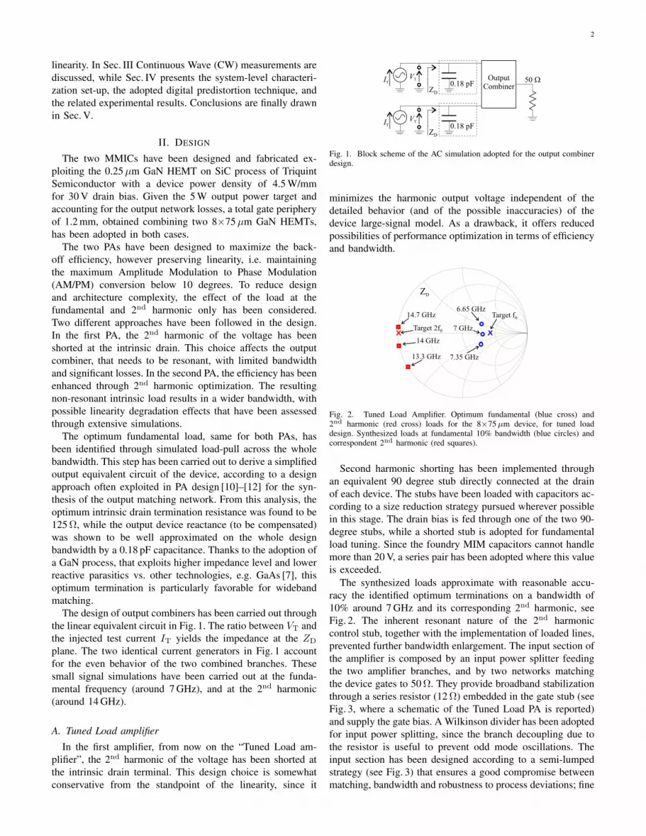
The design of output combiners has been carried out throughthe linear equivalent circuit in Fig. 1. The ratio between VT andthe injected test current IT yields the impedance at the ZD
plane. The two identical current generators in Fig. 1 accountfor the even behavior of the two combined branches. Thesesmall signal simulations have been carried out at the funda-mental frequency (around 7 GHz), and at the 2nd harmonic(around 14 GHz).
A. Tuned Load amplifier
In the first amplifier, from now on the “Tuned Load am-plifier”, the 2nd harmonic of the voltage has been shorted atthe intrinsic drain terminal. This design choice is somewhatconservative from the standpoint of the linearity, since it
Fig. 1. Block scheme of the AC simulation adopted for the output combinerdesign.
minimizes the harmonic output voltage independent of thedetailed behavior (and of the possible inaccuracies) of thedevice large-signal model. As a drawback, it offers reducedpossibilities of performance optimization in terms of efficiencyand bandwidth.
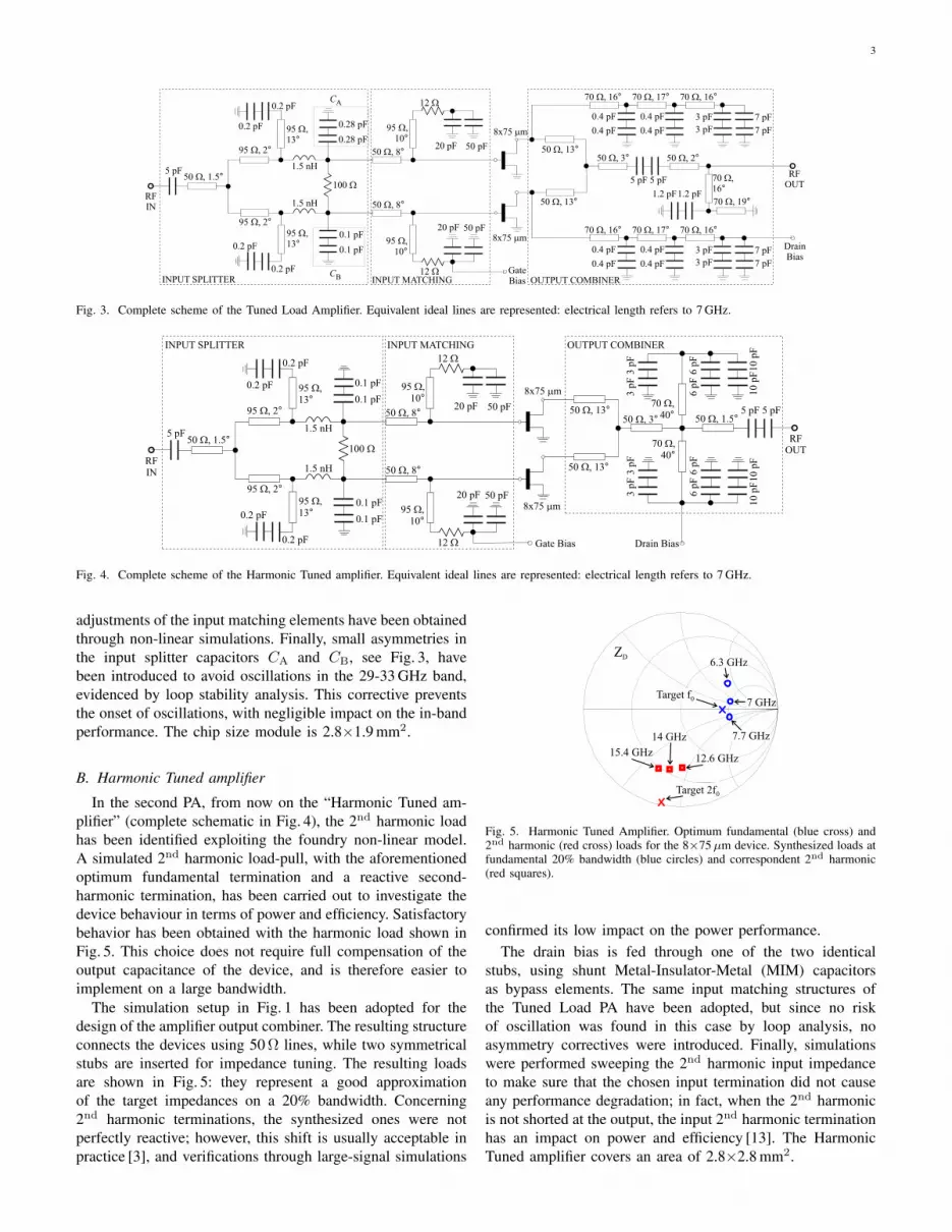
Fig. 2. Tuned Load Amplifier. Optimum fundamental (blue cross) and2nd harmonic (red cross) loads for the 8×75µm device, for tuned loaddesign. Synthesized loads at fundamental 10% bandwidth (blue circles) andcorrespondent 2nd harmonic (red squares).
Second harmonic shorting has been implemented throughan equivalent 90 degree stub directly connected at the drainof each device. The stubs have been loaded with capacitors ac-cording to a size reduction strategy pursued wherever possiblein this stage. The drain bias is fed through one of the two 90-degree stubs, while a shorted stub is adopted for fundamentalload tuning. Since the foundry MIM capacitors cannot handlemore than 20 V, a series pair has been adopted where this valueis exceeded.
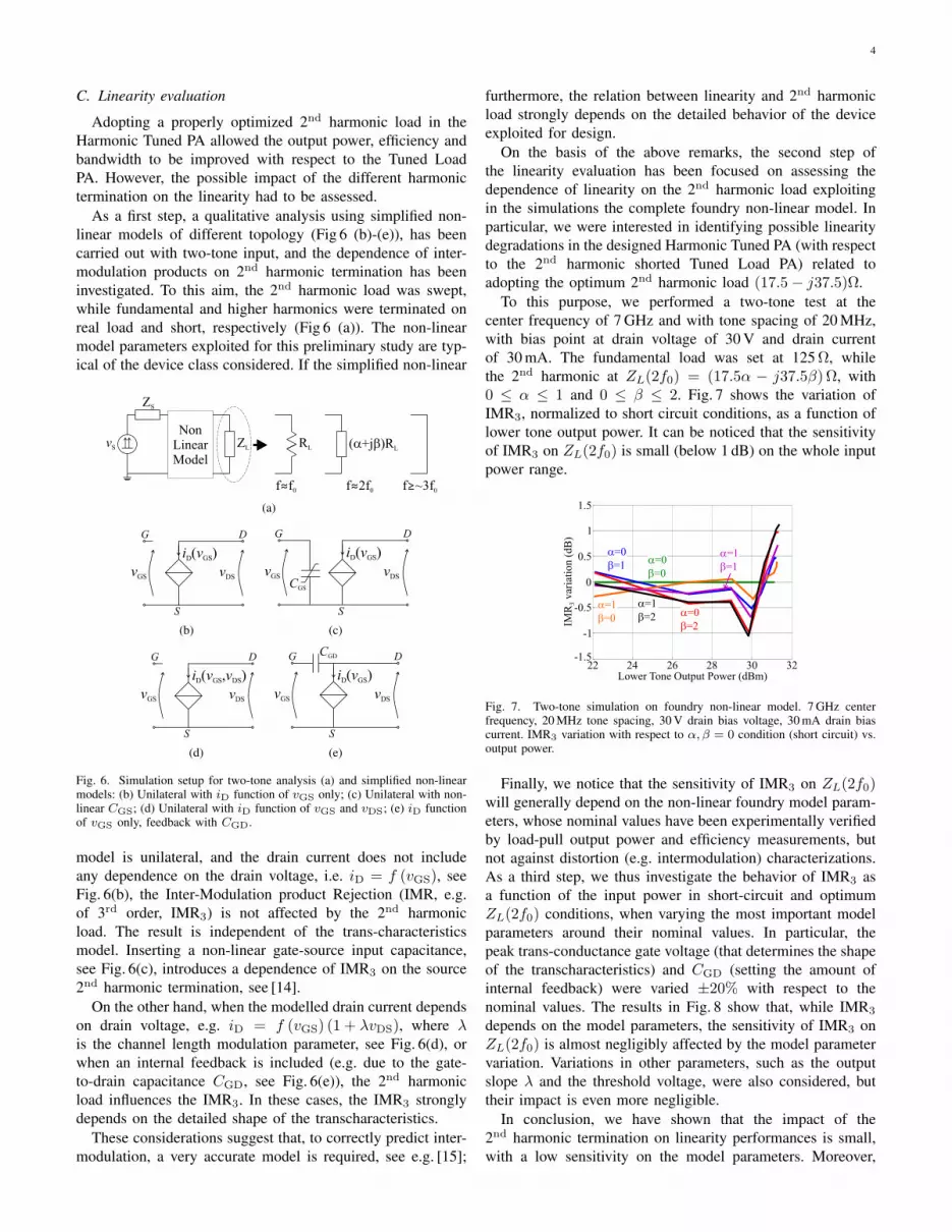
The synthesized loads approximate with reasonable accu-racy the identified optimum terminations on a bandwidth of10% around 7 GHz and its corresponding 2nd harmonic, seeFig. 2. The inherent resonant nature of the 2nd harmoniccontrol stub, together with the implementation of loaded lines,prevented further bandwidth enlargement. The input section ofthe amplifier is composed by an input power splitter feedingthe two amplifier branches, and by two networks matchingthe device gates to 50Ω. They provide broadband stabilizationthrough a series resistor (12Ω) embedded in the gate stub (seeFig. 3, where a schematic of the Tuned Load PA is reported)and supply the gate bias. A Wilkinson divider has been adoptedfor input power splitting, since the branch decoupling due tothe resistor is useful to prevent odd mode oscillations. Theinput section has been designed according to a semi-lumpedstrategy (see Fig. 3) that ensures a good compromise betweenmatching, bandwidth and robustness to process deviations; fine
3
Fig. 3. Complete scheme of the Tuned Load Amplifier. Equivalent ideal lines are represented: electrical length refers to 7 GHz.
Fig. 4. Complete scheme of the Harmonic Tuned amplifier. Equivalent ideal lines are represented: electrical length refers to 7 GHz.
adjustments of the input matching elements have been obtainedthrough non-linear simulations. Finally, small asymmetries inthe input splitter capacitors CA and CB, see Fig. 3, havebeen introduced to avoid oscillations in the 29-33 GHz band,evidenced by loop stability analysis. This corrective preventsthe onset of oscillations, with negligible impact on the in-bandperformance. The chip size module is 2.8×1.9 mm2.
B. Harmonic Tuned amplifier
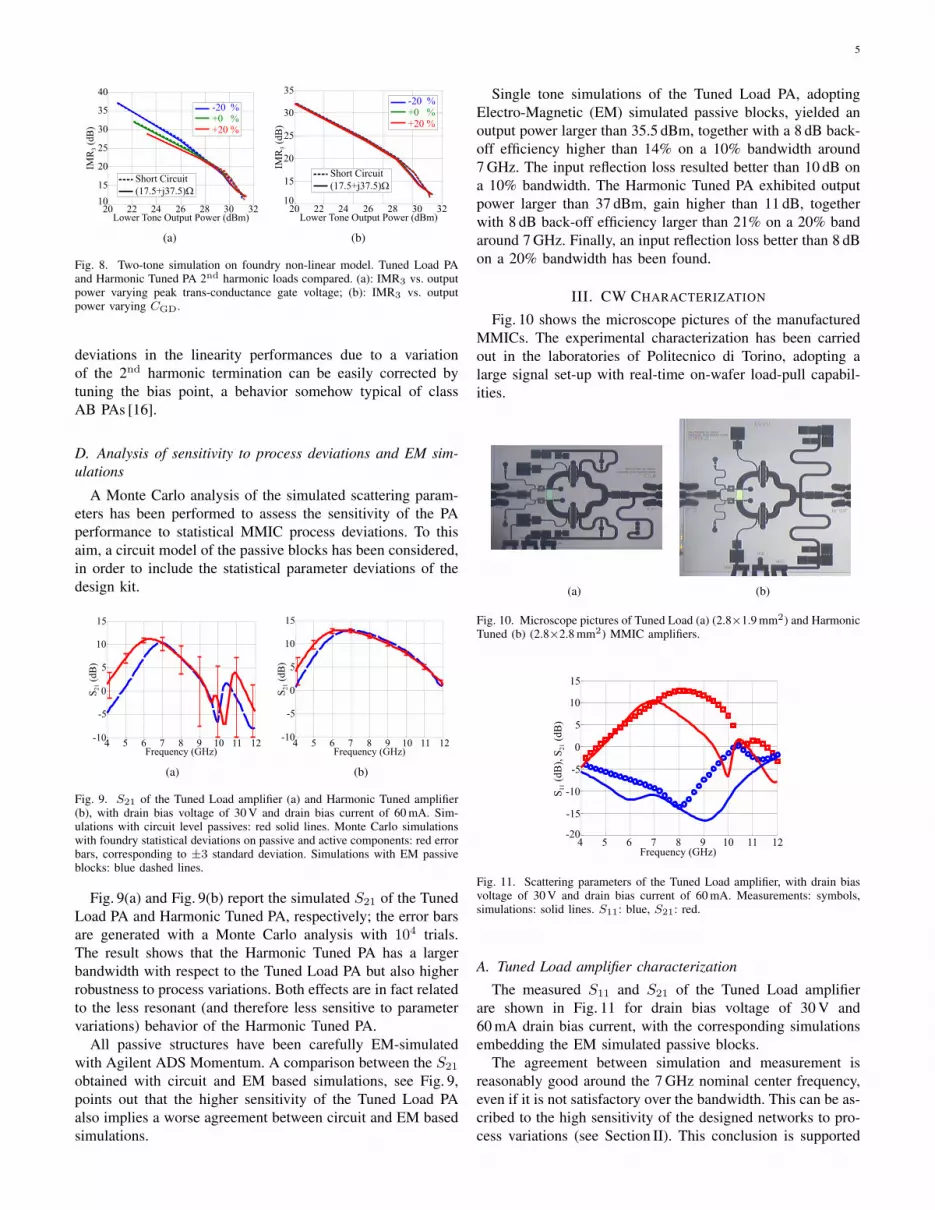
In the second PA, from now on the “Harmonic Tuned am-plifier” (complete schematic in Fig. 4), the 2nd harmonic loadhas been identified exploiting the foundry non-linear model.A simulated 2nd harmonic load-pull, with the aforementionedoptimum fundamental termination and a reactive second-harmonic termination, has been carried out to investigate thedevice behaviour in terms of power and efficiency. Satisfactorybehavior has been obtained with the harmonic load shown inFig. 5. This choice does not require full compensation of theoutput capacitance of the device, and is therefore easier toimplement on a large bandwidth.
The simulation setup in Fig. 1 has been adopted for thedesign of the amplifier output combiner. The resulting structureconnects the devices using 50Ω lines, while two symmetricalstubs are inserted for impedance tuning. The resulting loadsare shown in Fig. 5: they represent a good approximationof the target impedances on a 20% bandwidth. Concerning2nd harmonic terminations, the synthesized ones were notperfectly reactive; however, this shift is usually acceptable inpractice [3], and verifications through large-signal simulations
Fig. 5. Harmonic Tuned Amplifier. Optimum fundamental (blue cross) and2nd harmonic (red cross) loads for the 8×75µm device. Synthesized loads atfundamental 20% bandwidth (blue circles) and correspondent 2nd harmonic(red squares).
confirmed its low impact on the power performance.The drain bias is fed through one of the two identical
stubs, using shunt Metal-Insulator-Metal (MIM) capacitorsas bypass elements. The same input matching structures ofthe Tuned Load PA have been adopted, but since no riskof oscillation was found in this case by loop analysis, noasymmetry correctives were introduced. Finally, simulationswere performed sweeping the 2nd harmonic input impedanceto make sure that the chosen input termination did not causeany performance degradation; in fact, when the 2nd harmonicis not shorted at the output, the input 2nd harmonic terminationhas an impact on power and efficiency [13]. The HarmonicTuned amplifier covers an area of 2.8×2.8 mm2.
4
C. Linearity evaluation
Adopting a properly optimized 2nd harmonic load in theHarmonic Tuned PA allowed the output power, efficiency andbandwidth to be improved with respect to the Tuned LoadPA. However, the possible impact of the different harmonictermination on the linearity had to be assessed.
As a first step, a qualitative analysis using simplified non-linear models of different topology (Fig 6 (b)-(e)), has beencarried out with two-tone input, and the dependence of inter-modulation products on 2nd harmonic termination has beeninvestigated. To this aim, the 2nd harmonic load was swept,while fundamental and higher harmonics were terminated onreal load and short, respectively (Fig 6 (a)). The non-linearmodel parameters exploited for this preliminary study are typ-ical of the device class considered. If the simplified non-linear
(a)
(b) (c)
(d) (e)
Fig. 6. Simulation setup for two-tone analysis (a) and simplified non-linearmodels: (b) Unilateral with iD function of vGS only; (c) Unilateral with non-linear CGS; (d) Unilateral with iD function of vGS and vDS; (e) iD functionof vGS only, feedback with CGD.
model is unilateral, and the drain current does not includeany dependence on the drain voltage, i.e. iD = f (vGS), seeFig. 6(b), the Inter-Modulation product Rejection (IMR, e.g.of 3rd order, IMR3) is not affected by the 2nd harmonicload. The result is independent of the trans-characteristicsmodel. Inserting a non-linear gate-source input capacitance,see Fig. 6(c), introduces a dependence of IMR3 on the source2nd harmonic termination, see [14].
On the other hand, when the modelled drain current dependson drain voltage, e.g. iD = f (vGS) (1 + λvDS), where λis the channel length modulation parameter, see Fig. 6(d), orwhen an internal feedback is included (e.g. due to the gate-to-drain capacitance CGD, see Fig. 6(e)), the 2nd harmonicload influences the IMR3. In these cases, the IMR3 stronglydepends on the detailed shape of the transcharacteristics.
These considerations suggest that, to correctly predict inter-modulation, a very accurate model is required, see e.g. [15];
furthermore, the relation between linearity and 2nd harmonicload strongly depends on the detailed behavior of the deviceexploited for design.
On the basis of the above remarks, the second step ofthe linearity evaluation has been focused on assessing thedependence of linearity on the 2nd harmonic load exploitingin the simulations the complete foundry non-linear model. Inparticular, we were interested in identifying possible linearitydegradations in the designed Harmonic Tuned PA (with respectto the 2nd harmonic shorted Tuned Load PA) related toadopting the optimum 2nd harmonic load (17.5− j37.5)Ω.
To this purpose, we performed a two-tone test at thecenter frequency of 7 GHz and with tone spacing of 20 MHz,with bias point at drain voltage of 30 V and drain currentof 30 mA. The fundamental load was set at 125Ω, whilethe 2nd harmonic at ZL(2f0) = (17.5α − j37.5β)Ω, with0 ≤ α ≤ 1 and 0 ≤ β ≤ 2. Fig. 7 shows the variation ofIMR3, normalized to short circuit conditions, as a function oflower tone output power. It can be noticed that the sensitivityof IMR3 on ZL(2f0) is small (below 1 dB) on the whole inputpower range.
Fig. 7. Two-tone simulation on foundry non-linear model. 7 GHz centerfrequency, 20 MHz tone spacing, 30 V drain bias voltage, 30 mA drain biascurrent. IMR3 variation with respect to α, β = 0 condition (short circuit) vs.output power.
Finally, we notice that the sensitivity of IMR3 on ZL(2f0)will generally depend on the non-linear foundry model param-eters, whose nominal values have been experimentally verifiedby load-pull output power and efficiency measurements, butnot against distortion (e.g. intermodulation) characterizations.As a third step, we thus investigate the behavior of IMR3 asa function of the input power in short-circuit and optimumZL(2f0) conditions, when varying the most important modelparameters around their nominal values. In particular, thepeak trans-conductance gate voltage (that determines the shapeof the transcharacteristics) and CGD (setting the amount ofinternal feedback) were varied ±20% with respect to thenominal values. The results in Fig. 8 show that, while IMR3
depends on the model parameters, the sensitivity of IMR3 onZL(2f0) is almost negligibly affected by the model parametervariation. Variations in other parameters, such as the outputslope λ and the threshold voltage, were also considered, buttheir impact is even more negligible.
In conclusion, we have shown that the impact of the2nd harmonic termination on linearity performances is small,with a low sensitivity on the model parameters. Moreover,
5
(a) (b)
Fig. 8. Two-tone simulation on foundry non-linear model. Tuned Load PAand Harmonic Tuned PA 2nd harmonic loads compared. (a): IMR3 vs. outputpower varying peak trans-conductance gate voltage; (b): IMR3 vs. outputpower varying CGD.
deviations in the linearity performances due to a variationof the 2nd harmonic termination can be easily corrected bytuning the bias point, a behavior somehow typical of classAB PAs [16].
D. Analysis of sensitivity to process deviations and EM sim-ulations
A Monte Carlo analysis of the simulated scattering param-eters has been performed to assess the sensitivity of the PAperformance to statistical MMIC process deviations. To thisaim, a circuit model of the passive blocks has been considered,in order to include the statistical parameter deviations of thedesign kit.
(a) (b)
Fig. 9. S21 of the Tuned Load amplifier (a) and Harmonic Tuned amplifier(b), with drain bias voltage of 30 V and drain bias current of 60 mA. Sim-ulations with circuit level passives: red solid lines. Monte Carlo simulationswith foundry statistical deviations on passive and active components: red errorbars, corresponding to ±3 standard deviation. Simulations with EM passiveblocks: blue dashed lines.
Fig. 9(a) and Fig. 9(b) report the simulated S21 of the TunedLoad PA and Harmonic Tuned PA, respectively; the error barsare generated with a Monte Carlo analysis with 104 trials.The result shows that the Harmonic Tuned PA has a largerbandwidth with respect to the Tuned Load PA but also higherrobustness to process variations. Both effects are in fact relatedto the less resonant (and therefore less sensitive to parametervariations) behavior of the Harmonic Tuned PA.
All passive structures have been carefully EM-simulatedwith Agilent ADS Momentum. A comparison between the S21
obtained with circuit and EM based simulations, see Fig. 9,points out that the higher sensitivity of the Tuned Load PAalso implies a worse agreement between circuit and EM basedsimulations.
Single tone simulations of the Tuned Load PA, adoptingElectro-Magnetic (EM) simulated passive blocks, yielded anoutput power larger than 35.5 dBm, together with a 8 dB back-off efficiency higher than 14% on a 10% bandwidth around7 GHz. The input reflection loss resulted better than 10 dB ona 10% bandwidth. The Harmonic Tuned PA exhibited outputpower larger than 37 dBm, gain higher than 11 dB, togetherwith 8 dB back-off efficiency larger than 21% on a 20% bandaround 7 GHz. Finally, an input reflection loss better than 8 dBon a 20% bandwidth has been found.
III. CW CHARACTERIZATION
Fig. 10 shows the microscope pictures of the manufacturedMMICs. The experimental characterization has been carriedout in the laboratories of Politecnico di Torino, adopting alarge signal set-up with real-time on-wafer load-pull capabil-ities.
(a) (b)
Fig. 10. Microscope pictures of Tuned Load (a) (2.8×1.9 mm2) and HarmonicTuned (b) (2.8×2.8 mm2) MMIC amplifiers.
Fig. 11. Scattering parameters of the Tuned Load amplifier, with drain biasvoltage of 30 V and drain bias current of 60 mA. Measurements: symbols,simulations: solid lines. S11: blue, S21: red.
A. Tuned Load amplifier characterization
The measured S11 and S21 of the Tuned Load amplifierare shown in Fig. 11 for drain bias voltage of 30 V and60 mA drain bias current, with the corresponding simulationsembedding the EM simulated passive blocks.
The agreement between simulation and measurement isreasonably good around the 7 GHz nominal center frequency,even if it is not satisfactory over the bandwidth. This can be as-cribed to the high sensitivity of the designed networks to pro-cess variations (see Section II). This conclusion is supported

6
Fig. 12. Single tone power sweep at 7 GHz of the Tuned Load amplifier, withdrain bias voltage of 30 V and drain bias current of 60 mA. Measurements:symbols, simulations: solid lines. Gain: red, efficiency: green.
Fig. 13. Single tone power sweep at 7 GHz of the Tuned Load amplifier, withdrain bias voltage of 30 V and drain bias current of 60 mA. Measurements:symbols, simulations: solid lines. AM/AM: red, AM/PM: blue.
by the good agreement between the measured bare devicesand the simulated foundry model scattering parameters.
Fig. 12 shows the single tone performance at 7 GHz: gainand efficiency vs. output power are reported, for a drain biasvoltage of 30 V, and a drain bias current of 60 mA. The satu-rated output power is as high as 35.6 dBm, with correspondingefficiency of 33% (slightly lower than the simulated one). Thesmall signal gain is 10.7 dB.
Regarding linearity, Fig. 13 shows the CW Amplitude Mod-ulation to Amplitude Modulation (AM/AM) and AM/PM at7 GHz. The gain compression, i.e. AM/AM, agreement be-tween simulations and measurements is good. On the contrary,phase distortion is affected by higher discrepancies, confirmingthat the device large signal model is not able to reproduce thisbehavior with the needed accuracy. However, the maximummeasured phase distortion is below 7 degrees, and bias tuningcan be adopted for its reduction.
Fig. 14 shows the Tuned Load amplifier single tone per-formance vs. frequency: the measured output power is higherthan 35 dBm in a 6.7–7.9 GHz band. The best power/efficiencyperformance can be found at 7.4 GHz, where the outputpower reaches 36.1 dBm with 36% efficiency. If compared tothe simulated results, measurements exhibit a frequency shifttoward higher frequency, that can be ascribed to sensitivity toprocess variations.
Fig. 14. Single tone performance vs. CW frequency of the Tuned Loadamplifier, with drain bias voltage of 30 V and drain bias current of 60 mA.Measurements: symbols, simulations: solid lines.
B. Harmonic Tuned amplifier characterization
Fig. 15 shows the simulated and measured S11 and S21
parameters of the Harmonic Tuned amplifier for a drainbias voltage of 30 V, and a drain bias current of 60 mA.Measurements are in good agreement with simulations on thewhole bandwidth.
Fig. 15. Scattering parameters of the Harmonic Tuned amplifier, with drainbias voltage of 30 V and drain bias current of 60 mA. Measurements: symbols,simulations: solid lines. S11: blue, S21: red.
Fig. 16. Single tone power sweep at 7 GHz of the Harmonic Tunedamplifier, with drain bias voltage of 30 V and drain bias current of 30 mA.Measurements: symbols, simulations: solid lines. Gain: red, efficiency: green.
A single tone characterization has been performed in a 30 %band around 7 GHz. The results at center frequency, in goodagreement with the simulations, are shown in Fig. 16, wherethe gain and efficiency vs. output power are reported, for adrain bias voltage of 30 V and drain bias current of 30 mA(bias point selected for its better efficiency). A measured
7
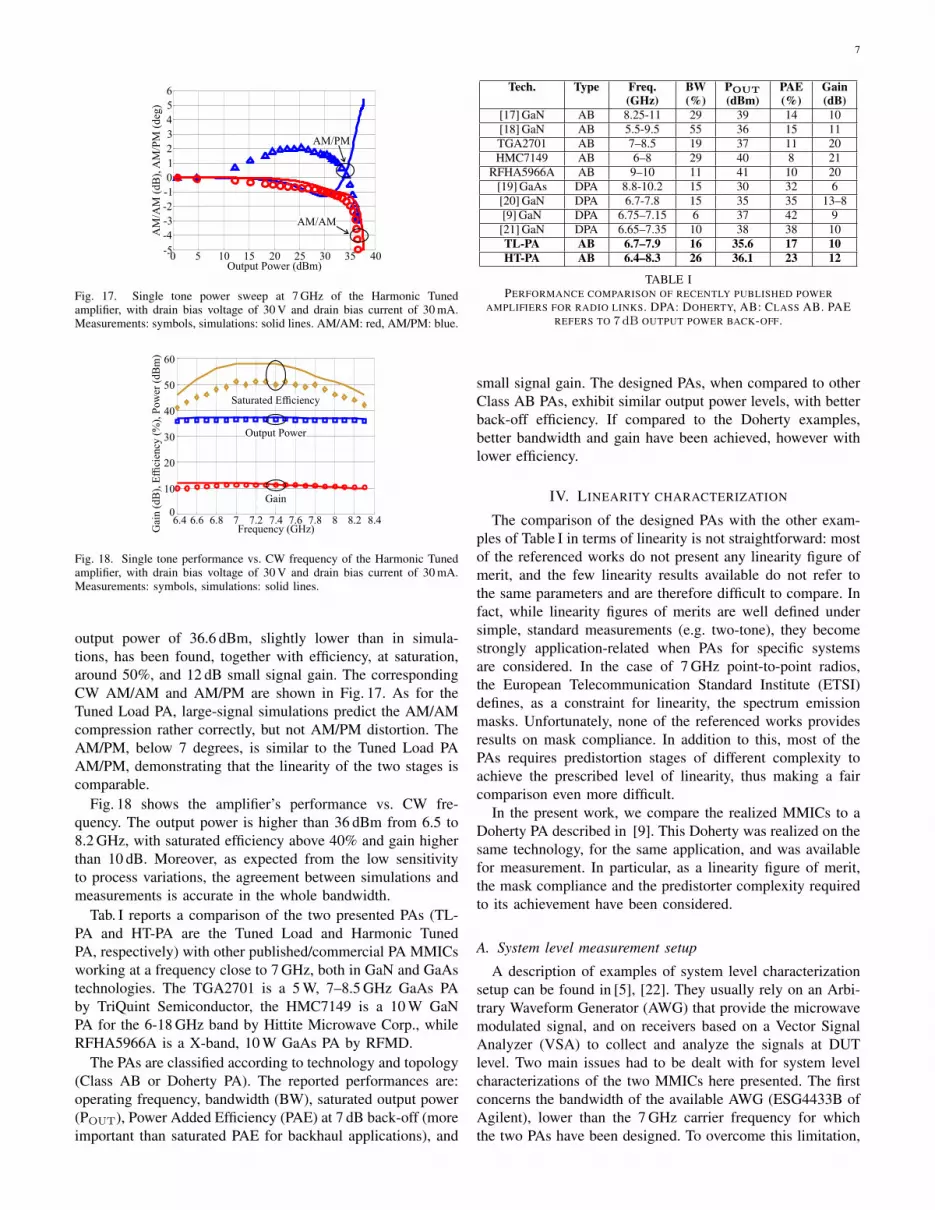
Fig. 17. Single tone power sweep at 7 GHz of the Harmonic Tunedamplifier, with drain bias voltage of 30 V and drain bias current of 30 mA.Measurements: symbols, simulations: solid lines. AM/AM: red, AM/PM: blue.
Fig. 18. Single tone performance vs. CW frequency of the Harmonic Tunedamplifier, with drain bias voltage of 30 V and drain bias current of 30 mA.Measurements: symbols, simulations: solid lines.
output power of 36.6 dBm, slightly lower than in simula-tions, has been found, together with efficiency, at saturation,around 50%, and 12 dB small signal gain. The correspondingCW AM/AM and AM/PM are shown in Fig. 17. As for theTuned Load PA, large-signal simulations predict the AM/AMcompression rather correctly, but not AM/PM distortion. TheAM/PM, below 7 degrees, is similar to the Tuned Load PAAM/PM, demonstrating that the linearity of the two stages iscomparable.
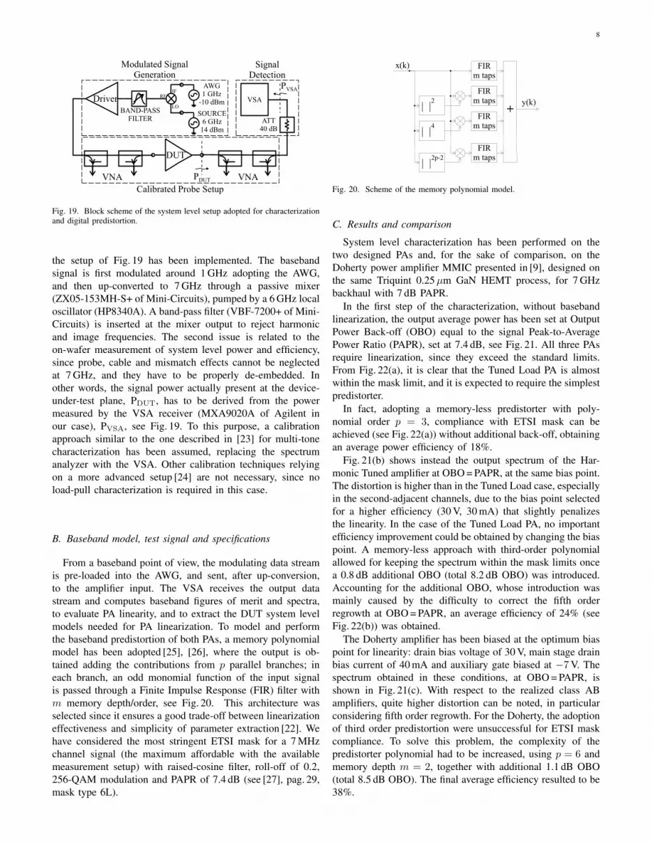
Fig. 18 shows the amplifier’s performance vs. CW fre-quency. The output power is higher than 36 dBm from 6.5 to8.2 GHz, with saturated efficiency above 40% and gain higherthan 10 dB. Moreover, as expected from the low sensitivityto process variations, the agreement between simulations andmeasurements is accurate in the whole bandwidth.
Tab. I reports a comparison of the two presented PAs (TL-PA and HT-PA are the Tuned Load and Harmonic TunedPA, respectively) with other published/commercial PA MMICsworking at a frequency close to 7 GHz, both in GaN and GaAstechnologies. The TGA2701 is a 5 W, 7–8.5 GHz GaAs PAby TriQuint Semiconductor, the HMC7149 is a 10 W GaNPA for the 6-18 GHz band by Hittite Microwave Corp., whileRFHA5966A is a X-band, 10 W GaAs PA by RFMD.
The PAs are classified according to technology and topology(Class AB or Doherty PA). The reported performances are:operating frequency, bandwidth (BW), saturated output power(POUT), Power Added Efficiency (PAE) at 7 dB back-off (moreimportant than saturated PAE for backhaul applications), and
Tech. Type Freq. BW POUT PAE Gain(GHz) (%) (dBm) (%) (dB)
[17] GaN AB 8.25-11 29 39 14 10[18] GaN AB 5.5-9.5 55 36 15 11TGA2701 AB 7–8.5 19 37 11 20HMC7149 AB 6–8 29 40 8 21
RFHA5966A AB 9–10 11 41 10 20[19] GaAs DPA 8.8-10.2 15 30 32 6[20] GaN DPA 6.7-7.8 15 35 35 13–8[9] GaN DPA 6.75–7.15 6 37 42 9[21] GaN DPA 6.65–7.35 10 38 38 10TL-PA AB 6.7–7.9 16 35.6 17 10HT-PA AB 6.4–8.3 26 36.1 23 12
TABLE IPERFORMANCE COMPARISON OF RECENTLY PUBLISHED POWER
AMPLIFIERS FOR RADIO LINKS. DPA: DOHERTY, AB: CLASS AB. PAEREFERS TO 7 dB OUTPUT POWER BACK-OFF.
small signal gain. The designed PAs, when compared to otherClass AB PAs, exhibit similar output power levels, with betterback-off efficiency. If compared to the Doherty examples,better bandwidth and gain have been achieved, however withlower efficiency.
IV. LINEARITY CHARACTERIZATION
The comparison of the designed PAs with the other exam-ples of Table I in terms of linearity is not straightforward: mostof the referenced works do not present any linearity figure ofmerit, and the few linearity results available do not refer tothe same parameters and are therefore difficult to compare. Infact, while linearity figures of merits are well defined undersimple, standard measurements (e.g. two-tone), they becomestrongly application-related when PAs for specific systemsare considered. In the case of 7 GHz point-to-point radios,the European Telecommunication Standard Institute (ETSI)defines, as a constraint for linearity, the spectrum emissionmasks. Unfortunately, none of the referenced works providesresults on mask compliance. In addition to this, most of thePAs requires predistortion stages of different complexity toachieve the prescribed level of linearity, thus making a faircomparison even more difficult.
In the present work, we compare the realized MMICs to aDoherty PA described in [9]. This Doherty was realized on thesame technology, for the same application, and was availablefor measurement. In particular, as a linearity figure of merit,the mask compliance and the predistorter complexity requiredto its achievement have been considered.
A. System level measurement setup
A description of examples of system level characterizationsetup can be found in [5], [22]. They usually rely on an Arbi-trary Waveform Generator (AWG) that provide the microwavemodulated signal, and on receivers based on a Vector SignalAnalyzer (VSA) to collect and analyze the signals at DUTlevel. Two main issues had to be dealt with for system levelcharacterizations of the two MMICs here presented. The firstconcerns the bandwidth of the available AWG (ESG4433B ofAgilent), lower than the 7 GHz carrier frequency for whichthe two PAs have been designed. To overcome this limitation,
8
Fig. 19. Block scheme of the system level setup adopted for characterizationand digital predistortion.
the setup of Fig. 19 has been implemented. The basebandsignal is first modulated around 1 GHz adopting the AWG,and then up-converted to 7 GHz through a passive mixer(ZX05-153MH-S+ of Mini-Circuits), pumped by a 6 GHz localoscillator (HP8340A). A band-pass filter (VBF-7200+ of Mini-Circuits) is inserted at the mixer output to reject harmonicand image frequencies. The second issue is related to theon-wafer measurement of system level power and efficiency,since probe, cable and mismatch effects cannot be neglectedat 7 GHz, and they have to be properly de-embedded. Inother words, the signal power actually present at the device-under-test plane, PDUT, has to be derived from the powermeasured by the VSA receiver (MXA9020A of Agilent inour case), PVSA, see Fig. 19. To this purpose, a calibrationapproach similar to the one described in [23] for multi-tonecharacterization has been assumed, replacing the spectrumanalyzer with the VSA. Other calibration techniques relyingon a more advanced setup [24] are not necessary, since noload-pull characterization is required in this case.
B. Baseband model, test signal and specifications
From a baseband point of view, the modulating data streamis pre-loaded into the AWG, and sent, after up-conversion,to the amplifier input. The VSA receives the output datastream and computes baseband figures of merit and spectra,to evaluate PA linearity, and to extract the DUT system levelmodels needed for PA linearization. To model and performthe baseband predistortion of both PAs, a memory polynomialmodel has been adopted [25], [26], where the output is ob-tained adding the contributions from p parallel branches; ineach branch, an odd monomial function of the input signalis passed through a Finite Impulse Response (FIR) filter withm memory depth/order, see Fig. 20. This architecture wasselected since it ensures a good trade-off between linearizationeffectiveness and simplicity of parameter extraction [22]. Wehave considered the most stringent ETSI mask for a 7 MHzchannel signal (the maximum affordable with the availablemeasurement setup) with raised-cosine filter, roll-off of 0.2,256-QAM modulation and PAPR of 7.4 dB (see [27], pag. 29,mask type 6L).
Fig. 20. Scheme of the memory polynomial model.
C. Results and comparison
System level characterization has been performed on thetwo designed PAs and, for the sake of comparison, on theDoherty power amplifier MMIC presented in [9], designed onthe same Triquint 0.25µm GaN HEMT process, for 7 GHzbackhaul with 7 dB PAPR.
In the first step of the characterization, without basebandlinearization, the output average power has been set at OutputPower Back-off (OBO) equal to the signal Peak-to-AveragePower Ratio (PAPR), set at 7.4 dB, see Fig. 21. All three PAsrequire linearization, since they exceed the standard limits.From Fig. 22(a), it is clear that the Tuned Load PA is almostwithin the mask limit, and it is expected to require the simplestpredistorter.
In fact, adopting a memory-less predistorter with poly-nomial order p = 3, compliance with ETSI mask can beachieved (see Fig. 22(a)) without additional back-off, obtainingan average power efficiency of 18%.
Fig. 21(b) shows instead the output spectrum of the Har-monic Tuned amplifier at OBO = PAPR, at the same bias point.The distortion is higher than in the Tuned Load case, especiallyin the second-adjacent channels, due to the bias point selectedfor a higher efficiency (30 V, 30 mA) that slightly penalizesthe linearity. In the case of the Tuned Load PA, no importantefficiency improvement could be obtained by changing the biaspoint. A memory-less approach with third-order polynomialallowed for keeping the spectrum within the mask limits oncea 0.8 dB additional OBO (total 8.2 dB OBO) was introduced.Accounting for the additional OBO, whose introduction wasmainly caused by the difficulty to correct the fifth orderregrowth at OBO = PAPR, an average efficiency of 24% (seeFig. 22(b)) was obtained.
The Doherty amplifier has been biased at the optimum biaspoint for linearity: drain bias voltage of 30 V, main stage drainbias current of 40 mA and auxiliary gate biased at −7V. Thespectrum obtained in these conditions, at OBO = PAPR, isshown in Fig. 21(c). With respect to the realized class ABamplifiers, quite higher distortion can be noted, in particularconsidering fifth order regrowth. For the Doherty, the adoptionof third order predistortion were unsuccessful for ETSI maskcompliance. To solve this problem, the complexity of thepredistorter polynomial had to be increased, using p = 6 andmemory depth m = 2, together with additional 1.1 dB OBO(total 8.5 dB OBO). The final average efficiency resulted to be38%.

9
(a) (b) (c)
Fig. 21. Normalized power spectra from system level measurements. Resolution bandwidth: 4.7 kHz. Tuned Load amplifier (a), Harmonic Tuned amplifier(b), Doherty amplifier (c). Average output power fixed at OBO equal to the signal PAPR of 7.4 dB. Applied baseband signal: 256-QAM, 7 MHz channel,PAPR of 7.4 dB.
(a) (b) (c)
Fig. 22. Normalized power spectra from system level measurements. Resolution bandwidth: 4.7 kHz. Tuned Load amplifier (a), Harmonic Tuned amplifier(b), Doherty amplifier (c). Applied baseband signal: 256-QAM, 7 MHz channel, PAPR of 7.4 dB.
¿From a linearity standpoint, the Tuned Load amplifierturned out to be the most linear, and could be predistortedat OBO = PAPR (average output power of 28.4 dBm), witha simple scheme. The Harmonic Tuned amplifier exhibitedsimilar linearity, requiring the same linearizer order, thusdemonstrating that 2nd harmonic load optimization did notdegrade significantly the linearity, but allowed for higheraverage efficiency (24% vs. 18%). Concerning the comparisonwith the Doherty, both class AB PAs showed an intrinsic betterlinearity, with important benefits in terms of predistortioncomplexity. This point can be crucial when very widebandmodulation schemes are adopted, or whenever system back-compatibility with pre-existing predistorter schemes is manda-tory.
V. CONCLUSION
The design and characterization of two combined class ABpower amplifiers for microwave backhaul on GaN MMICtechnology have been presented in this paper. The two designs,thanks to different 2nd harmonic loads, achieved different per-formance in terms of output power, efficiency and bandwidth.At the same time, the effect of 2nd harmonic termination onlinearity has been addressed, both in a more general qualitativeanalysis, and in the specific design case. At the workingfrequency of 7 GHz the two power amplifiers show CW perfor-mance in line with similar literature examples, however with
higher back-off efficiency. System level characterization andpredistortion, carried out with an ad-hoc set-up, has evidencedgood linearity of the two class AB MMICs, also in comparisonwith a Doherty power amplifier recently realized for the sameapplication.
ACKNOWLEDGMENT
The authors would like to thank Ericsson AB for partiallysupporting the research.
REFERENCES
[1] I. F. Akyildiz, W.-Y. Lee, M. C. Vuran, and S. Mohanty, “Nextgeneration/dynamic spectrum access/cognitive radio wireless networks:A survey,” Computer Networks, vol. 50, no. 13, pp. 2127 – 2159, Sep.2006.
[2] P. Kenington, High linearity RF amplifier design. Artech House, 2000.[3] S. Cripps, RF power amplifiers for wireless communications, ser. Artech
House Microwave Library. Artech House, 2006.[4] P. Colantonio, F. Giannini, and E. Limiti, High Efficiency RF and
Microwave Solid State Power Amplifiers, ser. Microwave and OpticalEngineering. John Wiley & Sons, 2009.
[5] F. Ghannouchi and O. Hammi, “Behavioral modeling and predistortion,”IEEE Microw. Mag., vol. 10, no. 7, pp. 52–64, Dec. 2010.
[6] N. Pothecary, Feedforward linear power amplifiers. Artech House,1999.
[7] R. S. Pengelly, S. M. Wood, J. W. Milligan, S. T. Sheppard, andW. L. Pribble, “A review of GaN on SiC high electron-mobility powertransistors and MMICs,” IEEE Trans. Microw. Theory Techn., vol. 60,no. 6, pp. 1764 –1783, Jun. 2012.

10
[8] V. Camarchia, J. Moreno Rubio, M. Pirola, R. Quaglia, P. Colantonio,F. Giannini, R. Giofre, L. Piazzon, T. Emanuelsson, and T. Wegeland,“High-Efficiency 7 GHz Doherty GaN MMIC Power Amplifiers forMicrowave Backhaul Radio Links,” IEEE Trans. Electron Devices,vol. 60, no. 10, pp. 3592–3595, Oct. 2013.
[9] V. Camarchia, J. Fang, J. Moreno Rubio, M. Pirola, and R. Quaglia, “7GHz MMIC GaN Doherty Power Amplifier with 47% efficiency at 7 dBoutput back-off,” IEEE Microw. Wireless Compon. Lett., vol. 23, no. 1,pp. 34–36, Jan. 2013.
[10] D. E. Dawson, “Closed-form solutions for the design of optimummatching networks,” IEEE Trans. Microw. Theory Techn., vol. 57, no. 1,pp. 121–129, Jan. 2009.
[11] P. Saad, C. Fager, H. Cao, H. Zirath, and K. Andersson, “Designof a Highly Efficient 2–4-GHz Octave Bandwidth GaN-HEMT PowerAmplifier,” IEEE Trans. Microw. Theory Techn., vol. 58, no. 7, pp. 1677–1685, Jul. 2010.
[12] J. Moreno Rubio, J. Fang, V. Camarchia, R. Quaglia, M. Pirola,and G. Ghione, “3–3.6 GHz wideband GaN Doherty power amplifierexploiting output compensation stages,” IEEE Trans. Microw. TheoryTechn., vol. 60, no. 8, pp. 2543–2548, Aug. 2012.
[13] P. Colantonio, F. Giannini, E. Limiti, and V. Teppati, “An approach toharmonic load- and source-pull measurements for high-efficiency PAdesign,” IEEE Trans. Microw. Theory Techn., vol. 52, no. 1, pp. 191–198, Jan. 2004.
[14] P. Colantonio, F. Giannini, G. Leuzzi, and E. Limiti, “High efficiencylow-voltage power amplifier design by second-harmonic manipulation,”International Journal of RF and Microwave Computer-Aided Engineer-ing, vol. 10, no. 1, pp. 19–32, Jan. 2000.
[15] N. de Carvalho and J. Pedro, “Large- and small-signal imd behaviorof microwave power amplifiers,” IEEE Trans. Microw. Theory Techn.,vol. 47, no. 12, pp. 2364–2374, Dec. 1999.
[16] R. Quaglia, L. Piazzon, V. Camarchia, R. Giofre, M. Pirola, P. Colan-tonio, G. Ghione, and F. Giannini, “Experimental investigation of biascurrent and load modulation effects in phase distortion of gan hemts,”Electronics Letters, vol. 50, no. 10, pp. 773–775, May 2014.
[17] R. Behtash, H. Tobler, F.-J. Berlec, V. Ziegler, H. Leier, B. Adelseck,T. Martin, R. Balmer, D. Pavlidis, R. Jansen, M. Neuburger, andH. Schumacher, “Coplanar AlGaN/GaN HEMT power amplifier MMICat X-band,” in Microwave Symposium Digest, 2004 IEEE MTT-S Inter-national, vol. 3, Jun. 2004, pp. 1657–1659 Vol.3.
[18] H. Klockenhoff, R. Behtash, J. Wurfl, W. Heinrich, and G. Trankle, “ACompact 16 Watt X-Band GaN-MMIC Power Amplifier,” in MicrowaveSymposium Digest, 2006. IEEE MTT-S International, Jun. 2006, pp.1846–1849.
[19] P. Colantonio, F. Giannini, R. Giofre and, E. Limiti, and L. Piazzon,“An X-Band GaAs MMIC Doherty Power Amplifier,” in IntegratedNonlinear Microwave and Millimeter-Wave Circuits (INMMIC), 2010Workshop on, Apr. 2010, pp. 41 –44.
[20] D. Gustafsson, J. C. Cahuana, D. Kuylenstierna, I. Angelov, N. Rorsman,and C. Fager, “A Wideband and Compact GaN MMIC Doherty Ampli-fier for Microwave Link Applications,” IEEE Trans. Microw. TheoryTechn., vol. 61, no. 2, pp. 922 –930, Feb. 2013.
[21] L. Piazzon, P. Colantonio, F. Giannini, and R. Giofre, “15% Bandwidth7 GHz GaN-MMIC Doherty Amplifier With Enhanced Auxiliary Chain,”Microwave and Optical Technology Letters, vol. 56, no. 2, pp. 502–504,Feb. 2014.
[22] R. Quaglia, V. Camarchia, S. Guerrieri, E. Lima, G. Ghione, Q. Luo,M. Pirola, and R. Tinivella, “Real-time FPGA-based baseband predis-tortion of W-CDMA 3GPP high-efficiency power amplifiers: ComparingGaN HEMT and Si LDMOS predistorted PA performances,” in Mi-crowave Conference, 2009. EuMC 2009. European, Oct. 2009, pp. 342–345.
[23] V. Teppati, A. Ferrero, V. Camarchia, A. Neri, and M. Pirola, “Mi-crowave measurements -Part III: Advanced non-linear measurements,”IEEE Instrum. Meas. Mag., vol. 11, no. 6, pp. 17 –22, Dec. 2008.
[24] M. Marchetti, M. Pelk, K. Buisman, W. Neo, M. Spirito, and L. C. N.De Vreede, “Active harmonic load-pull with realistic wideband commu-nications signals,” IEEE Trans. Microw. Theory Techn., vol. 56, no. 12,pp. 2979–2988, Dec. 2008.
[25] H. Ku and J. Kenney, “Behavioral modeling of nonlinear RF poweramplifiers considering memory effects,” IEEE Trans. Microw. TheoryTechn., vol. 51, no. 12, pp. 2495–2504, Dec. 2003.
[26] L. Ding, G. Zhou, D. Morgan, Z. Ma, J. Kenney, J. Kim, and C. Giar-dina, “A robust digital baseband predistorter constructed using memorypolynomials,” IEEE Trans. Commun., vol. 52, no. 1, pp. 159–165, Jan.2004.
[27] “ETSI EN 302 217-2-2. Fixed Radio Systems; Characteristics and re-quirements for point-to-point equipment and antennas; Part 2-2: Digitalsystems operating in frequency bands where frequency co-ordination isapplied,” 2012.
Roberto Quaglia (S’01-M’04-SM’14) was born inCasale Monferrato, Italy, in 1984. He graduated cumlaude in electronic engineering from Politecnico diTorino in 2008. In 2012, he received the Ph.D.degree in electronic devices from the Politecnico diTorino, Turin, Italy. His present research interestsconcern the design, modeling and predistortion ofhigh efficiency power amplifiers both hybrid andMMIC. Dr. Quaglia was the recipient of the 2009Young Graduated Research Fellowship presented bythe GAAS Association.
Vittorio Camarchia (S’01-M’04-SM’14) receivedthe Laurea degree in electronic engineering andthe Ph.D. degree in electronic and communicationsengineering from the Politecnico di Torino, Turin,Italy, in 2000 and 2003, respectively. In 2001, 2002and 2003 he was a Visiting researcher with theECE Department, Boston University, Boston, MA,USA. He is currently an Assistant Professor at theElectronics and Telecommunication Department ofPolitecnico di Torino. His research is focused on RFdevice modeling, simulation, and characterization,
both linear and nonlinear and power amplifier design. Dr. Camarchia wasthe recipient of the 2002 Young Graduated Research Fellowship presented bythe Gallium Arsenide application Symposium (GAAS) Association.
Marco Pirola (M’97) was born in Velezzo Lomel-lina, Italy, in 1963. He received the Laurea degreein electronic engineering and the Ph.D. degree fromPolitecnico di Torino, Italy, in 1987 and 1992 re-spectively. In 1992 and 1994, he was a VisitingResearcher at the Hewlett Packard Microwave Tech-nology Division, Santa Rosa, CA. Since 1992, he hasbeen with the Electronic Department of Politecnicodi Torino, first as researcher and, since 2000, asassociate professor, where his research concernsthe simulation, modeling and measurements of mi-
crowave devices and systems.
Jorge Julian Moreno Rubio was born in Villavi-cencio, Colombia, in 1978. He received the degree inelectronic engineering from Universidad Pedagogicay Tecnologica de Colombia, Sogamoso, Colombia,in 2001, the M.Sc. degree in electronic engineeringfrom the Pontificia Universidad Javeriana, Bogota,Colombia, in 2006, and the Ph.D. degree in elec-tronic devices from the Po-litecnico di Torino, Turin,Italy, in 2012. He is currently a Researcher withthe Electronics Department, Universidad Pedagogicay Tecnologica de Colombia, Sogamoso, Colombia.
His present research interests concern the design of high-efficiency poweramplifiers, both hybrid and monolithic microwave integrated circuits. Dr.Moreno was the recepient of the International Doctoral Studies Grant in2008 given by the Departamento Administrativo de Ciencia, Tecnologıa eInnovacion de Colombia - COLCIENCIAS.
11
Giovanni Ghione (M’87-SM’94-F’07) is Full Pro-fessor in Electronics since 1990, first with Universityof Catania, then again with Politecnico di Torino. Hisresearch activity concerns the field of high-frequencyelectronics, with particular attention to the physics-based modeling of compound semiconductor mate-rials and devices and to the design of microwavepower amplifiers. Prof. Ghione has authored or co-authored more than 300 research papers on the abovesubjects and five books. He is a member of theEditorial Board of the T-MTT and a T-ED Associate
Editor for Compound Semiconductors. He has been member of the QPCsubcommitee of IEDM in 1997-1998 and in 2006-2007 and Chair in 2008;he was in 2009-2010 the EU Arrangement Chair of IEDM. He also chairssince 2010 the ED Society Committee on Compound Semiconductor Devicesand Circuits.