lc75847t 1/3, 1/4-duty general-purpose lcd driver
TRANSCRIPT

© Semiconductor Components Industries, LLC, 2017 1 Publication Order Number : July 2017 - Rev. 1 LC75847T/D
www.onsemi.com
ORDERING INFORMATION See detailed ordering and shipping information on page 28 of this data sheet.
* Computer Control Bus (CCB) is an ON Semiconductor’s original bus format and the bus addresses are controlled by ON Semiconductor.
LC75847T
1/3, 1/4-Duty General-Purpose LCD Driver Overview
The LC75847T is 1/3 duty and 1/4 duty general-purpose LCD driver that can be used for frequency display in electronic tuners under the control of a microcontroller. The LC75847T can drive an LCD with up to 420 segments directly. The LC75847T can also control up to 8 general-purpose output ports.
Features Switching between 1/3 duty and 1/4 duty drive techniques under serial data
control. Switching between 1/2 bias and 1/3 bias drive techniques under serial data
control. Up to 318 segments for 1/3 duty drive and 420 segments for 1/4 duty drive
can be displayed. Serial data input supports CCB* format communication with the system
controller. Serial data control of the power-saving mode based backup function and all
the segments forced off function. Serial data control of switching between the segment output port and the
general-purpose output port functions. Serial data control of frame frequency for common and segment output
waveforms. High generality, since display data is displayed directly without decoder
intervention. Built-in display contrast adjustment circuit Independent VLCD for the LCD driver block The INH pin can force the display to the off state.
RC oscillator circuit Specifications Absolute Maximum Ratings at Ta = 25C, VSS = 0 V
Parameter Symbol Conditions Ratings unit
Maximum supply voltage VDD max VDD –0.3 to +7.0
V VLCD max VLCD –0.3 to +7.0
Input voltage
VIN1 CE, CL, DI, INH –0.3 to +7.0
V VIN2 OSC –0.3 to VDD +0.3
VIN3 VLCD1, VLCD2 –0.3 to VLCD +0.3
Output voltage VOUT1 OSC –0.3 to VDD +0.3
V VOUT2 VLCD0, S1 to S106, COM1 to COM4, P1 to P8 –0.3 to VLCD +0.3
Output current
IOUT1 S1 to S106 300 A
IOUT2 COM1 to COM4 3 mA
IOUT3 P1 to P8 5 mA
Allowable power dissipation Pd max Ta = 85°C 200 mW Operating temperature Topr –40 to +85 C Storage temperature Tstg –55 to +125 C
Stresses exceeding those listed in the Maximum Ratings table may damage the device. If any of these limits are exceeded, device functionality should not be assumed,damage may occur and reliability may be affected.
TQFP120 14x14 / TQFP120
LC75847T
www.onsemi.com 2
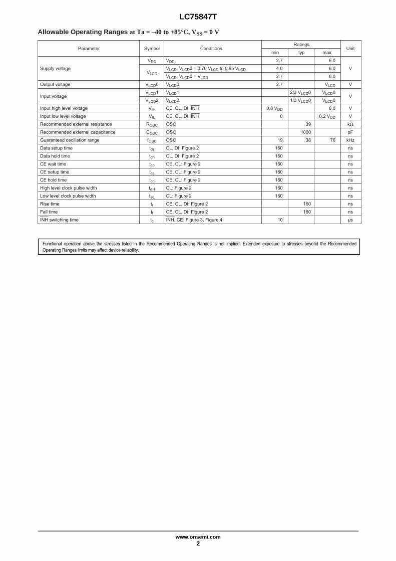
Parameter Symbol ConditionsRatings
Unitmin typ max
VDD VDD 2.7 6.0
Supply voltageVLCD
VLCD, VLCD0 = 0.70 VLCD to 0.95 VLCD 4.0 6.0 V
VLCD, VLCD0 = VLCD 2.7 6.0
Output voltage VLCD0 VLCD0 2.7 VLCD V
Input voltageVLCD1 VLCD1 2/3 VLCD0 VLCD0
VVLCD2 VLCD2 1/3 VLCD0 VLCD0
Input high level voltage VIH CE, CL, DI, INH 0.8 VDD 6.0 V
Input low level voltage VIL CE, CL, DI, INH 0 0.2 VDD V
Recommended external resistance ROSC OSC 39 k
Recommended external capacitance COSC OSC 1000 pF
Guaranteed oscillation range fOSC OSC 19 38 76 kHz
Data setup time tds CL, DI: Figure 2 160 ns
Data hold time tdh CL, DI: Figure 2 160 ns
CE wait time tcp CE, CL: Figure 2 160 ns
CE setup time tcs CE, CL: Figure 2 160 ns
CE hold time tch CE, CL: Figure 2 160 ns
High level clock pulse width tøH CL: Figure 2 160 ns
Low level clock pulse width tøL CL: Figure 2 160 ns
Rise time tr CE, CL, DI: Figure 2 160 ns
Fall time tf CE, CL, DI: Figure 2 160 ns
INH switching time tc INH, CE: Figure 3, Figure 4 10 μs
Allowable Operating Ranges at Ta = –40 to +85°C, VSS = 0 V
Functional operation above the stresses listed in the Recommended Operating Ranges is not implied. Extended exposure to stresses beyond the RecommendedOperating Ranges limits may affect device reliability.

LC75847T
www.onsemi.com 3
Note: *1 Excluding the bias voltage generation divider resistors built in the VLCD0, VLCD1, VLCD2, and VSS. (See Figure 1.)
Parameter Symbol ConditionsRatings
Unitmin typ max
Hysteresis VH CE, CL, DI, INH 0.1 VDD V
Input high level current IIH CE, CL, DI, INH: VI = 6.0 V 5.0 μA
Input low level current IIL CE, CL, DI, INH: VI = 0 V –5.0 μA
VOH1 S1 to S106: IO = –20 μA VLCD0 – 0.9
Output high level voltage VOH2 COM1 to COM4: IO = –100 μA VLCD0 – 0.9 V
VOH3 P1 to P8: IO = –1 mA VLCD – 0.9
VOL1 S1 to S106: IO = 20 μA 0.9
Output low level voltage VOL2 COM1 to COM4: IO = 100 μA 0.9 V
VOL3 P1 to P8: IO = 1 mA 0.9
VMID1 COM1 to COM4: 1/2 bias, IO = ±100 μA1/2 VLCD0 1/2 VLCD0
– 0.9 + 0.9
VMID2 S1 to S106: 1/3 bias, IO = ±20 μA2/3 VLCD0 2/3 VLCD0
– 0.9 + 0.9
Output middle level voltage*1 VMID3 S1 to S106: 1/3 bias, IO = ±20 μA1/3 VLCD0 1/3 VLCD0
V– 0.9 + 0.9
VMID4 COM1 to COM4: 1/3 bias, IO = ±100 μA2/3 VLCD0 2/3 VLCD0
– 0.9 + 0.9
VMID5 COM1 to COM4: 1/3 bias, IO = ±100 μA1/3 VLCD0 1/3 VLCD0
– 0.9 + 0.9
Oscillator frequency fOSC OSC: ROSC = 39 k, COSC = 1000 pF 30.4 38 45.6 kHz
IDD1 VDD: Power-saving mode 5
IDD2 VDD: VDD = 6.0 V, output open, fOSC = 38 kHz 250 500
ILCD1 VLCD: Power-saving mode 5
ILCD2VLCD: VLCD = 6.0 V, output open, 1/2 bias, fOSC = 38 kHz,
400 800VLCD0 = 0.70 VLCD to 0.95 VLCD
Current drainILCD3
VLCD: VLCD = 6.0 V, output open, 1/2 bias, fOSC = 38 kHz,350 700
μAVLCD0 = VLCD
ILCD4VLCD: VLCD = 6.0 V, output open, 1/3 bias, fOSC = 38 kHz,
300 600VLCD0 = 0.70 VLCD to 0.95 VLCD
ILCD5VLCD: VLCD = 6.0 V, output open, 1/3 bias, fOSC = 38 kHz,
250 500VLCD0 = VLCD
Electrical Characteristics for the allowable operating ranges
Figure 1
To the common segment driversVLCD2
VLCD1
Except these resistors
VLCD0
VLCD
VSS
CONTRASTADJUSTER
Product parametric performance is indicated in the Electrical Characteristics for the listed test conditions, unless otherwise noted. Product performance may not beindicated by the Electrical Characteristics if operated under different conditions.

1. When CL is stopped at the low level
2. When CL is stopped at the high level
Figure 2
Block Diagram
Page 4
LC75847T
VSS
VLCD2
VLCD1
VLCD
VDD
OSC SHIFT REGISTER
SEGMENT DRIVER & LATCH
ADDRESSDETECTOR
CLOCKGENERATOR
COMMONDRIVER
CONTRASTADJUSTER
VLCD0
CO
M1
INH DI
CL
CE
CO
M2
CO
M3
CO
M4/
S10
6
S10
5
S10
4
S9
S8/
P8
S2/
P2
S1/
P1
tds
VIL
VIL
VIH
VIL
VIH
VIL
VIH
50%
VIH
tchtcstcp
tdh
tr tf
tøLtøH
CE
CL
DI
tds
VIL
VIL
VIH
VIH50%
tchtcstcp
tdh
trtf
tøHtøL
CE
CL
DI

Pin Functions
Page 5
LC75847T
Symbol Pin No. Function Active I/OHandling
when unused
1 to 8
9 to 105
109 to 107
106
116
118
120
119
117
112
S1/P1 to S8/P8
S9 to S105
COM1 to COM3
COM4/S106
OSC
CE
CL
DI
INH
VLCD0
Segment outputs for displaying the display data transferred by serial data input. Thepins S1/P1 to S8/P8 can be used as general-purpose output ports when so set up bythe control data.
Common driver outputs.
The frame frequency is fO Hz.
The COM4/S106 pin can be used as a segment output in 1/3 duty.
Oscillator connection.
An oscillator circuit is formed by connecting an external resistor and capacitor to thispin.
Serial data transfer inputs. These pins are connected to the control microprocessor.
CE: Chip enableCL: Synchronization clockDI: Transfer data
Display off control input
• INH = low (VSS) ....OffS1/P1 to S8/P8 = low (VSS)(These pins are forcibly set to the segment output port functionand fixed at the VSS level.)S9 to S105 = low (VSS)COM1 to COM3 = low (VSS)COM4/S106 = low (VSS)
• INH = high (VDD) ..On
Note that serial data transfers can be performed when the display is forced off by thispin.
LCD drive 3/3 bias voltage (high level) supply. This level can be modified using thedisplay contrast adjustment circuit. However, note that VLCD0 must be greater than orequal to 2.7 V. Also, since this IC provides the built-in display contrast adjustmentcircuit, applications must not attempt to provide this level from external circuits.
—
—
—
H
—
L
—
O
O
I/O
I
I
I
I
O
Open
Open
VDD
GND
GND
Open
113
114
110
111
VLCD1
VLCD2
VDD
VLCD
LCD drive 2/3 bias voltage (middle level) supply. It is possible to supply the 2/3 VLCD0voltage to this pin externally. This pin must be shorted to VLCD2 if 1/2 bias is used.
LCD drive 1/3 bias voltage (middle level) supply. It is possible to supply the 1/3 VLCD0voltage to this pin externally. This pin must be shorted to VLCD1 if 1/2 bias is used.
Logic block power supply. Provide a voltage in the range 2.7 to 6.0 V.
LCD driver block power supply. When VLCD0 is between 0.70 VLCD and 0.95 VLCD,supply a voltage in the range 4.0 to 6.0 V. When VLCD0 and VLCD will be equal, supplya voltage in the range 2.7 to 6.0 V.
—
—
—
—
I
I
—
—
Open
Open
—
—
115VSS Ground pin. Connect to ground. — — —

Page 6
LC75847T
S96
COM2
VLCDVDD
S75
S81
S82
S83
S74
S76
S77
S78
S79
S80
S61
S62
S63
S64
S65
S66
S67
S68
S69
S70
S71
S72
S73
P5/
S5
S11
P4/
S4
P3/
S3
P2/
S2
P1/
S1
S97
S99S98
S100
LC75847T
(TQFP120)
S101S102S103
S105S104
COM3S106/COM4
COM1
VLCD0VLCD1
VSSVLCD2
OSC
CEINH
CL
S40S39S38S37S36
S34S35
S32S33
S31DI
6190
6091
31120301
S10S9
P8/
S8
P7/
S7
P6/
S6
S16
S22
S15
S14
S13
S12
S21
S20
S19
S18
S17
S25
S24
S23
S45S44S43S42S41
S50S49S48S47S46
S55S54S53S52S51
S26
S27
S29
S30
S28
S60S59S58S57S56
S85
S84
S86
S87
S88
S89
S90
S91S92S93S94S95
Pin Assignment

Serial Data Transfer Format
1. 1/3 duty① When CL is stopped at the low level
Note: DD···Direction data.
Page 7
LC75847T
B1B0
D101 P000000
DD2 bits
Control data18 bits
Display data108 bits
CCB address8 bits
DI
CL
CE
10 0001
B3B2 A1A0 A3A2
0 SCFCDTDR 00BUP1D104 D105 D106 D107 D108 P2 P3 CT0 CT1 CT2
B1B0
01
DD2 bits
Fixed data21 bits
Display data105 bits
CCB address8 bits
100 001
B3B2 A1A0 A3A2
1D212 D213D109 0 0 0 0 0 0 0 0 0 0 0 0 0 0 0 0 0 0 0 0 0 0
B1B0
01
DD2 bits
Fixed data21 bits
Display data105 bits
CCB address8 bits
10 0001
B3B2 A1A0 A3A2
1 0000000000000000000000D317 D318D214

Note: DD···Direction data.
• CCB address......85H• D1 to D318........Display data• P0 to P3 .............Segment output port/general-purpose output port switching control data• CT0 to CT2 .......Control data that sets the display contrast• DR.....................1/2 bias drive or 1/3 bias drive switching control data• DT .....................1/3 duty drive or 1/4 duty drive switching control data• FC......................Common and segment output waveforms frame frequency setting control data• SC......................Segments on/off control data• BU.....................Normal mode/power-saving mode control data
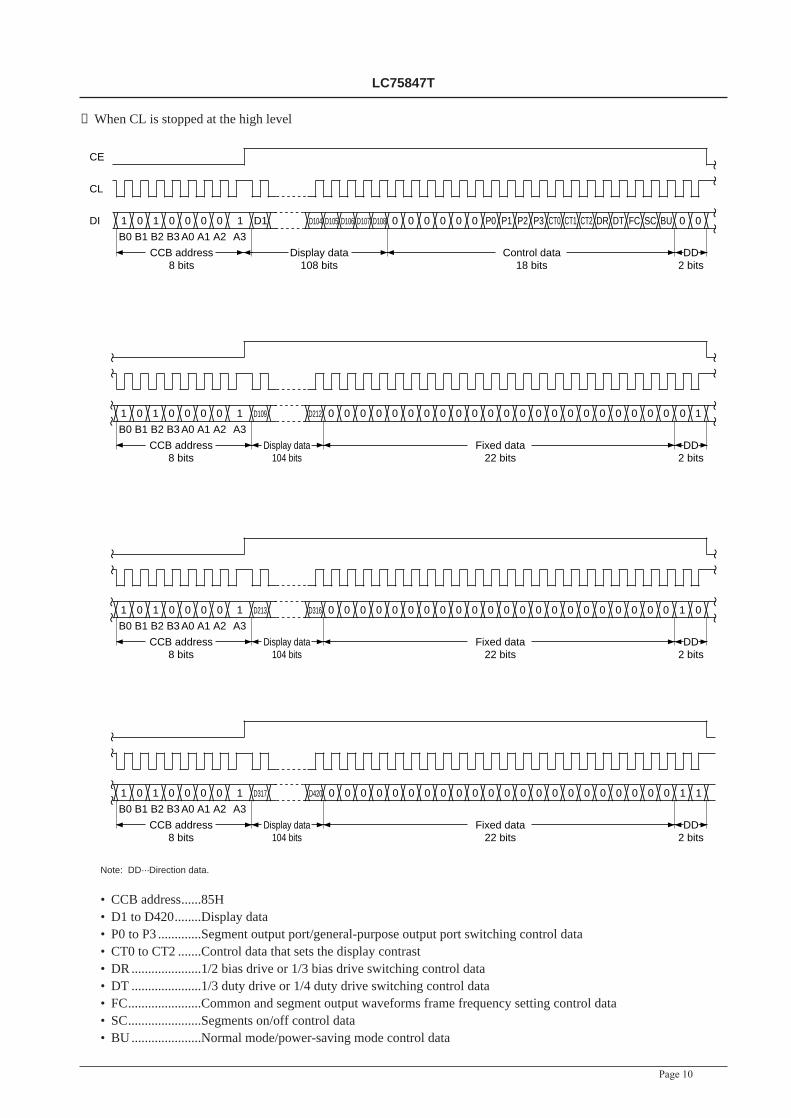
② When CL is stopped at the high level
Page 8
LC75847T
B1B0
D101 P0DI
CL
CE
10 0001
B3B2 A1A0 A3A2
SCFCDTDR 00 0 0 0 0 0 0BUP1D104 D105 D106 D107 D108 P2 P3 CT0 CT1 CT2
B1B0
01 100 001
B3B2 A1A0 A3A2
10000000000000 000000000D212 D213D109
B1B0
01 100 001
B3B2 A1A0 A3A2
1D317 D318D214 0000000000000000000000
DD2 bits
Control data18 bits
Display data108 bits
CCB address8 bits
DD2 bits
Fixed data21 bits
Display data105 bits
CCB address8 bits
DD2 bits
Fixed data21 bits
Display data105 bits
CCB address8 bits
Page 9
LC75847T
2. 1/4 duty① When CL is stopped at the low level
Note: DD···Direction data.
B1B0
D101 P00DI
CL
CE
10 0001
B3B2 A1A0 A3A2
00000 SCFCDTDR 00BUP1D104 D105 D106 D107 D108 P2 P3 CT0 CT1 CT2
B1B0
01 10 0001
B3B2 A1A0 A3A2
00000000000000000000000 1D212D109
B1B0
01 10 0001
B3B2 A1A0 A3A2
1D316D213 0 0 0 0 0 0 0 0 0 0 0 0 0 0 0 0 0 0 0 0 0 0 0
B1B0
01 10 0001
B3B2 A1A0 A3A2
10000000000000000000000 1D420D317
DD2 bits
Control data18 bits
Display data108 bits
CCB address8 bits
DD2 bits
Fixed data22 bits
Display data104 bits
CCB address8 bits
DD2 bits
Fixed data22 bits
Display data104 bits
CCB address8 bits
DD2 bits
Fixed data22 bits
Display data104 bits
CCB address8 bits
Page 10
LC75847T
Note: DD···Direction data.
• CCB address......85H• D1 to D420........Display data• P0 to P3 .............Segment output port/general-purpose output port switching control data• CT0 to CT2 .......Control data that sets the display contrast• DR.....................1/2 bias drive or 1/3 bias drive switching control data• DT .....................1/3 duty drive or 1/4 duty drive switching control data• FC......................Common and segment output waveforms frame frequency setting control data• SC......................Segments on/off control data• BU.....................Normal mode/power-saving mode control data
② When CL is stopped at the high level
B1B0
D101 P0DI
CL
CE
100 001
B3B2 A1A0 A3A2
SCFCDTDR 00 0 0 0 0 0 0BUP1D104 D105 D106 D107 D108 P2 P3 CT0 CT1 CT2
B1B0
01 10 0001
B3B2 A1A0 A3A2
1D316D213 00000000000000000000000
B1B0
01 10 0001
B3B2 A1A0 A3A2
100000000000000000000000D212D109
B1B0
01 10 0001
B3B2 A1A0 A3A2
1 10000000000000000000000D420D317
DD2 bits
Control data18 bits
Display data108 bits
CCB address8 bits
DD2 bits
Fixed data22 bits
Display data104 bits
CCB address8 bits
DD2 bits
Fixed data22 bits
Display data104 bits
CCB address8 bits
DD2 bits
Fixed data22 bits
Display data104 bits
CCB address8 bits

Serial Data Transfer Example
1. 1/3 duty① When 214 or more segments are used
All 384 bits of serial data must be sent.
② When fewer than 214 segments are usedEither 128 or 256 bits of serial data may be sent, depending on the number of segments used. However, the serial datashown below (the D1 to D108 display data and the control data) must be sent.
Page 11
LC75847T
1
128 bits8 bits
D1 00BUFC SCDTDRP1P001
B1B0 B3B2
0 00 0
A1A0 A3A2
01
B1B0 B3B2
01 0 00
A1A0 A3A2
01
B1B0 B3B2
01 0 00
11
1
1
A1A0 A3A2
D104 D105
D212
D317
D213
D318
D106 D107 D108
D109 0
10000000000000D214
P2 P3 CT0 CT1 CT2
000000
000 000
0 0 0
0000000000000 000000 0 0
128 bits8 bits
D1 00BUFC SCDTDRP1P001
B1B0 B3B2
0 00 0
A1A0 A3A2
11 D104 D105 D106 D107 D108 P2 P3 CT0 CT1 CT2000 000
2. 1/4 duty① When 317 or more segments are used
All 512 bits of serial data must be sent.
② When fewer than 317 segments are usedEither 128, 256 or 384 bits of serial data may be sent, depending on the number of segments used. However, the serialdata shown below (the D1 to D108 display data and the control data) must be sent.
1
128 bits8 bits
D1 00BUFC SCDTDRP1P001
B1B0 B3B2
0 00 0
A1A0 A3A2
01
B1B0 B3B2
01 0 00
A1A0 A3A2
01
B1B0 B3B2
01 0 00
11
1
1
A1A0 A3A2
D104 D105
D212
D316
0
0
D106 D107 D108
D109 0
10000000000000D213
P2 P3 CT0 CT1 CT2
000000
000 000
0 0 0
0000000000000 000000 0 0
101
B1B0 B3B2
01 0 00
A1A0 A3A2
1 D420 0D317 0 1000000000000 000000 0 0
128 bits8 bits
D1 00BUFC SCDTDRP1P001
B1B0 B3B2
0 00 0
A1A0 A3A2
11 D104 D105 D106 D107 D108 P2 P3 CT0 CT1 CT2000 000
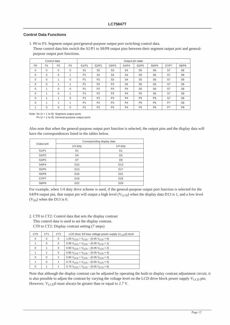
Control Data Functions
1. P0 to P3: Segment output port/general-purpose output port switching control data.These control data bits switch the S1/P1 to S8/P8 output pins between their segment output port and general-purpose output port functions.
Note: Sn (n = 1 to 8): Segment output portsPn (n = 1 to 8): General-purpose output ports
Also note that when the general-purpose output port function is selected, the output pins and the display data willhave the correspondences listed in the tables below.
For example, when 1/4 duty drive scheme is used, if the general-purpose output port function is selected for theS4/P4 output pin, that output pin will output a high level (VLCD) when the display data D13 is 1, and a low level(VSS) when the D13 is 0.
Page 12
LC75847T
Control data Output pin state
P0 P1 P2 P3 S1/P1 S2/P2 S3/P3 S4/P4 S5/P5 S6/P6 S7/P7 S8/P8
0 0 0 0 S1 S2 S3 S4 S5 S6 S7 S8
0 0 0 1 P1 S2 S3 S4 S5 S6 S7 S8
0 0 1 0 P1 P2 S3 S4 S5 S6 S7 S8
0 0 1 1 P1 P2 P3 S4 S5 S6 S7 S8
0 1 0 0 P1 P2 P3 P4 S5 S6 S7 S8
0 1 0 1 P1 P2 P3 P4 P5 S6 S7 S8
0 1 1 0 P1 P2 P3 P4 P5 P6 S7 S8
0 1 1 1 P1 P2 P3 P4 P5 P6 P7 S8
1 0 0 0 P1 P2 P3 P4 P5 P6 P7 P8
Output pinCorresponding display data
1/3 duty 1/4 duty
S1/P1 D1 D1
S2/P2 D4 D5
S3/P3 D7 D9
S4/P4 D10 D13
S5/P5 D13 D17
S6/P6 D16 D21
S7/P7 D19 D25
S8/P8 D22 D29
2. CT0 to CT2: Control data that sets the display contrastThis control data is used to set the display contrast.CT0 to CT2: Display contrast setting (7 steps)
Note that although the display contrast can be adjusted by operating the built-in display contrast adjustment circuit, itis also possible to adjust the contrast by varying the voltage level on the LCD drive block power supply VLCD pin.However, VLCD0 must always be greater than or equal to 2.7 V.
CT0 CT1 CT2 LCD drive 3/3 bias voltage power supply (VLCD0) level
0 0 0 1.00 VLCD = VLCD – (0.05 VLCD × 0)
1 0 0 0.95 VLCD = VLCD – (0.05 VLCD × 1)
0 1 0 0.90 VLCD = VLCD – (0.05 VLCD × 2)
1 1 0 0.85 VLCD = VLCD – (0.05 VLCD × 3)
0 0 1 0.80 VLCD = VLCD – (0.05 VLCD × 4)
1 0 1 0.75 VLCD = VLCD – (0.05 VLCD × 5)
0 1 1 0.70 VLCD = VLCD – (0.05 VLCD × 6)
7. BU: Normal mode/power-saving mode control dataThis control data bit selects either normal mode or power-saving mode.
6. SC: Segments on/off control dataThis control data bit controls the on/off state of the segments.
However, note that when the segments are turned off by setting SC to 1, the segments are turned off by outputtingsegment off waveforms from the segment output pins.
Page 13
LC75847T
SC Display state
0 On
1 Off
BU Mode
0 Normal mode
Power saving mode (The OSC pin oscillator is stopped, and the common and segment output pins go to the VSS level. However, 1 the S1/P1 to S8/P8 output pins that are set to be general-purpose output ports by the control data P0 to P3 can be used as
general-purpose output ports.)
5. FC: Common and segment output waveforms frame frequency setting control dataThis control data bit sets the frame frequency for common and segment output waveforms.
FC Frame frequency f0 [Hz]
0
1
fosc———384
fosc———192
3. DR: 1/2 bias drive or 1/3 bias drive switching control dataThis control data bit selects either 1/2 bias drive or 1/3 bias drive.
DR Bias drive scheme
0 1/3 bias drive
1 1/2 bias drive
4. DT: 1/3 duty drive or 1/4 duty drive switching control dataThis control data bit selects either 1/3 duty drive or 1/4 duty drive.
Note: COM4: Common outputS106: Segment output
DT Duty drive scheme Output pin state (COM4/S106)
0 1/4 duty drive COM4
1 1/3 duty drive S106

Display Data to Segment Output Pin Correspondence1. 1/3 duty
Note: This applies to the case where the S1/P1 to S8/P8, and COM4/S106 output pins are set to be segment output ports.
For example, the table below lists the segment output states for the S11 output pin.
Page 14
LC75847T
SegmentOutput pin COM1 COM2 COM3
S1/P1 D1 D2 D3
S2/P2 D4 D5 D6
S3/P3 D7 D8 D9
S4/P4 D10 D11 D12
S5/P5 D13 D14 D15
S6/P6 D16 D17 D18
S7/P7 D19 D20 D21
S8/P8 D22 D23 D24
S9 D25 D26 D27
S10 D28 D29 D30
S11 D31 D32 D33
S12 D34 D35 D36
S13 D37 D38 D39
S14 D40 D41 D42
S15 D43 D44 D45
S16 D46 D47 D48
S17 D49 D50 D51
S18 D52 D53 D54
S19 D55 D56 D57
S20 D58 D59 D60
S21 D61 D62 D63
S22 D64 D65 D66
S23 D67 D68 D69
S24 D70 D71 D72
S25 D73 D74 D75
S26 D76 D77 D78
S27 D79 D80 D81
S28 D82 D83 D84
S29 D85 D86 D87
S30 D88 D89 D90
S31 D91 D92 D93
S32 D94 D95 D96
S33 D97 D98 D99
S34 D100 D101 D102
S35 D103 D104 D105
S36 D106 D107 D108
SegmentOutput pin COM1 COM2 COM3
S37 D109 D110 D111
S38 D112 D113 D114
S39 D115 D116 D117
S40 D118 D119 D120
S41 D121 D122 D123
S42 D124 D125 D126
S43 D127 D128 D129
S44 D130 D131 D132
S45 D133 D134 D135
S46 D136 D137 D138
S47 D139 D140 D141
S48 D142 D143 D144
S49 D145 D146 D147
S50 D148 D149 D150
S51 D151 D152 D153
S52 D154 D155 D156
S53 D157 D158 D159
S54 D160 D161 D162
S55 D163 D164 D165
S56 D166 D167 D168
S57 D169 D170 D171
S58 D172 D173 D174
S59 D175 D176 D177
S60 D178 D179 D180
S61 D181 D182 D183
S62 D184 D185 D186
S63 D187 D188 D189
S64 D190 D191 D192
S65 D193 D194 D195
S66 D196 D197 D198
S67 D199 D200 D201
S68 D202 D203 D204
S69 D205 D206 D207
S70 D208 D209 D210
S71 D211 D212 D213
S72 D214 D215 D216
SegmentOutput pin COM1 COM2 COM3
S73 D217 D218 D219
S74 D220 D221 D222
S75 D223 D224 D225
S76 D226 D227 D228
S77 D229 D230 D231
S78 D232 D233 D234
S79 D235 D236 D237
S80 D238 D239 D240
S81 D241 D242 D243
S82 D244 D245 D246
S83 D247 D248 D249
S84 D250 D251 D252
S85 D253 D254 D255
S86 D256 D257 D258
S87 D259 D260 D261
S88 D262 D263 D264
S89 D265 D266 D267
S90 D268 D269 D270
S91 D271 D272 D273
S92 D274 D275 D276
S93 D277 D278 D279
S94 D280 D281 D282
S95 D283 D284 D285
S96 D286 D287 D288
S97 D289 D290 D291
S98 D292 D293 D294
S99 D295 D296 D297
S100 D298 D299 D300
S101 D301 D302 D303
S102 D304 D305 D306
S103 D307 D308 D309
S104 D310 D311 D312
S105 D313 D314 D315
COM4/S106 D316 D317 D318
Display dataSegment output pin (S11) state
D31 D32 D33
0 0 0 The LCD segments corresponding to COM1, COM2, and COM3 are off.
0 0 1 The LCD segment corresponding to COM3 is on.
0 1 0 The LCD segment corresponding to COM2 is on.
0 1 1 The LCD segments corresponding to COM2 and COM3 are on.
1 0 0 The LCD segment corresponding to COM1 is on.
1 0 1 The LCD segments corresponding to COM1 and COM3 are on.
1 1 0 The LCD segments corresponding to COM1 and COM2 are on.
1 1 1 The LCD segments corresponding to COM1, COM2, and COM3 are on.

Page 15
LC75847T
SegmentOutput pin COM1 COM2 COM3 COM4
S1/P1 D1 D2 D3 D4
S2/P2 D5 D6 D7 D8
S3/P3 D9 D10 D11 D12
S4/P4 D13 D14 D15 D16
S5/P5 D17 D18 D19 D20
S6/P6 D21 D22 D23 D24
S7/P7 D25 D26 D27 D28
S8/P8 D29 D30 D31 D32
S9 D33 D34 D35 D36
S10 D37 D38 D39 D40
S11 D41 D42 D43 D44
S12 D45 D46 D47 D48
S13 D49 D50 D51 D52
S14 D53 D54 D55 D56
S15 D57 D58 D59 D60
S16 D61 D62 D63 D64
S17 D65 D66 D67 D68
S18 D69 D70 D71 D72
S19 D73 D74 D75 D76
S20 D77 D78 D79 D80
S21 D81 D82 D83 D84
S22 D85 D86 D87 D88
S23 D89 D90 D91 D92
S24 D93 D94 D95 D96
S25 D97 D98 D99 D100
S26 D101 D102 D103 D104
S27 D105 D106 D107 D108
S28 D109 D110 D111 D112
S29 D113 D114 D115 D116
S30 D117 D118 D119 D120
S31 D121 D122 D123 D124
S32 D125 D126 D127 D128
S33 D129 D130 D131 D132
S34 D133 D134 D135 D136
S35 D137 D138 D139 D140
S36 D141 D142 D143 D144
S37 D145 D146 D147 D148
S38 D149 D150 D151 D152
S39 D153 D154 D155 D156
S40 D157 D158 D159 D160
S41 D161 D162 D163 D164
S42 D165 D166 D167 D168
S43 D169 D170 D171 D172
S44 D173 D174 D175 D176
S45 D177 D178 D179 D180
S46 D181 D182 D183 D184
S47 D185 D186 D187 D188
S48 D189 D190 D191 D192
S49 D193 D194 D195 D196
S50 D197 D198 D199 D200
S51 D201 D202 D203 D204
S52 D205 D206 D207 D208
S53 D209 D210 D211 D212
SegmentOutput pin COM1 COM2 COM3 COM4
S54 D213 D214 D215 D216
S55 D217 D218 D219 D220
S56 D221 D222 D223 D224
S57 D225 D226 D227 D228
S58 D229 D230 D231 D232
S59 D233 D234 D235 D236
S60 D237 D238 D239 D240
S61 D241 D242 D243 D244
S62 D245 D246 D247 D248
S63 D249 D250 D251 D252
S64 D253 D254 D255 D256
S65 D257 D258 D259 D260
S66 D261 D262 D263 D264
S67 D265 D266 S267 D268
S68 D269 D270 D271 D272
S69 D273 D274 D275 D276
S70 D277 D278 D279 D280
S71 D281 D282 D283 D284
S72 D285 D286 D287 D288
S73 D289 D290 D291 D292
S74 D293 D294 D295 D296
S75 D297 D298 D299 D300
S76 D301 D302 D303 D304
S77 D305 D306 D307 D308
S78 D309 D310 D311 D312
S79 D313 D314 D315 D316
S80 D317 D318 D319 D320
S81 D321 D322 D323 D324
S82 D325 D326 D327 D328
S83 D329 D330 D331 D332
S84 D333 D334 D335 D336
S85 D337 D338 D339 D340
S86 D341 D342 D343 D344
S87 D345 D346 D347 D348
S88 D349 D350 D351 D352
S89 D353 D354 D355 D356
S90 D357 D358 D359 D360
S91 D361 D362 D363 D364
S92 D365 D366 D367 D368
S93 D369 D370 D371 D372
S94 D373 D374 D375 D376
S95 D377 D378 D379 D380
S96 D381 D382 D383 D384
S97 D385 D386 D387 D388
S98 D389 D390 D391 D392
S99 D393 D394 D395 D396
S100 D397 D398 D399 D400
S101 D401 D402 D403 D404
S102 D405 D406 D407 D408
S103 D409 D410 D411 D412
S104 D413 D414 D415 D416
S105 D417 D418 D419 D420
2. 1/4 duty
Note: This applies to the case where the S1/P1 to S8/P8 output pins are set to be segment output ports.

Page 16
LC75847T
Display dataSegment output pin (S11) state
D41 D42 D43 D44
0 0 0 0 The LCD segments corresponding to COM1, COM2, COM3, and COM4 are off.
0 0 0 1 The LCD segment corresponding to COM4 is on.
0 0 1 0 The LCD segment corresponding to COM3 is on.
0 0 1 1 The LCD segments corresponding to COM3 and COM4 are on.
0 1 0 0 The LCD segment corresponding to COM2 is on.
0 1 0 1 The LCD segments corresponding to COM2 and COM4 are on.
0 1 1 0 The LCD segments corresponding to COM2 and COM3 are on.
0 1 1 1 The LCD segments corresponding to COM2, COM3, and COM4 are on.
1 0 0 0 The LCD segment corresponding to COM1 is on.
1 0 0 1 The LCD segments corresponding to COM1 and COM4 are on.
1 0 1 0 The LCD segments corresponding to COM1 and COM3 are on.
1 0 1 1 The LCD segments corresponding to COM1, COM3, and COM4 are on.
1 1 0 0 The LCD segments corresponding to COM1 and COM2 are on.
1 1 0 1 The LCD segments corresponding to COM1, COM2, and COM4 are on.
1 1 1 0 The LCD segments corresponding to COM1, COM2, and COM3 are on.
1 1 1 1 The LCD segments corresponding to COM1, COM2, COM3, and COM4 are on.
For example, the table below lists the segment output states for the S11 output pin.

1/3 Duty, 1/2 Bias Drive Technique
Page 17
LC75847T
COM3
COM2
COM1
LCD driver output when all LCD segments corresponding to COM1, COM2, and COM3 are on.
LCD driver output when LCD segments corresponding to COM2 and COM3 are on.
LCD driver output when LCD segments corresponding to COM1 and COM3 are on.
LCD driver output when all LCD segments corresponding to COM1, COM2, and COM3 are turned off.
LCD driver output when only LCD segments corresponding to COM1 are on.
LCD driver output when only LCD segments corresponding to COM2 are on.
LCD driver output when only LCD segments corresponding to COM3 are on.
LCD driver output when LCD segments corresponding to COM1 and COM2 are on.
VLCD1, VLCD2
VLCD0
0 V
fo[Hz]
VLCD1, VLCD2
VLCD0
0 V
VLCD1, VLCD2
VLCD0
0 V
VLCD1, VLCD2
VLCD0
0 V
VLCD1, VLCD2
VLCD0
0 V
VLCD1, VLCD2
VLCD0
0 V
VLCD1, VLCD2
VLCD0
0 V
VLCD1, VLCD2
VLCD0
0 V
VLCD1, VLCD2
VLCD0
0 V
VLCD1, VLCD2
VLCD0
0 V
VLCD1, VLCD2
VLCD0
0 V
When the control data FC = 0 : f0 =384fosc
When the control data FC = 1 : f0 =192fosc

1/3 Duty, 1/3 Bias Drive Technique
Page 18
LC75847T
COM3
COM2
COM1
LCD driver output when all LCD segments corresponding to COM1, COM2, and COM3 are on.
LCD driver output when LCD segments corresponding to COM2 and COM3 are on.
LCD driver output when LCD segments corresponding to COM1 and COM3 are on.
LCD driver output when all LCD segments corresponding to COM1, COM2, and COM3 are turned off.
LCD driver output when only LCD segments corresponding to COM1 are on.
LCD driver output when only LCD segments corresponding to COM2 are on.
LCD driver output when only LCD segments corresponding to COM3 are on.
LCD driver output when LCD segments corresponding to COM1 and COM2 are on.
fo[Hz]
VLCD2
VLCD1
VLCD0
0 V
VLCD2
VLCD1
VLCD0
0 V
VLCD2
VLCD1
VLCD0
0 V
VLCD2
VLCD1
VLCD0
0 V
VLCD2
VLCD1
VLCD0
0 V
VLCD2
VLCD1
VLCD0
0 V
VLCD2
VLCD1
VLCD0
0 V
VLCD2
VLCD1
VLCD0
0 V
VLCD2
VLCD1
VLCD0
0 V
VLCD2
VLCD1
VLCD0
0 V
VLCD2
VLCD1
VLCD0
0 V
When the control data FC = 0 : f0 =384fosc
When the control data FC = 1 : f0 =192fosc

Page 19
LC75847T
1/4 Duty, 1/2 Bias Drive Technique
VLCD1, VLCD2VLCD0
COM3
COM2
COM1
COM4
LCD driver output when all LCD segments corresponding to COM1, COM2, COM3, and COM4 are on.
LCD driver output when LCD segments corresponding to COM2 and COM4 are on.
LCD driver output when only LCD segments corresponding to COM4 are on.
LCD driver output when LCD segments corresponding to COM1, COM2, and COM3 are on.
LCD driver output when LCD segments corresponding to COM2 and COM3 are on.
LCD driver output when LCD segments corresponding to COM1 and COM3 are on.
LCD driver output when only LCD segments corresponding to COM3 are on.
LCD driver output when LCD segments corresponding to COM1 and COM2 are on.
LCD driver output when only LCD segments corresponding to COM2 are on.
LCD driver output when only LCD segments corresponding to COM1 are on.
LCD driver output when all LCD segments corresponding to COM1, COM2, COM3, and COM4 are turned off.
0 V
VLCD1, VLCD2VLCD0
0 V
VLCD1, VLCD2VLCD0
0 V
VLCD1, VLCD2VLCD0
0 V
VLCD1, VLCD2VLCD0
0 V
VLCD1, VLCD2VLCD0
0 V
VLCD1, VLCD2VLCD0
0 V
VLCD1, VLCD2VLCD0
0 V
VLCD1, VLCD2VLCD0
0 V
VLCD1, VLCD2VLCD0
0 V
VLCD1, VLCD2VLCD0
0 V
VLCD1, VLCD2VLCD0
0 V
VLCD1, VLCD2VLCD0
0 V
VLCD1, VLCD2VLCD0
0 V
VLCD1, VLCD2VLCD0
0 V
fo[Hz]
When the control data FC = 0 : f0 =384fosc
When the control data FC = 1 : f0 =192fosc

Page 20
LC75847T
1/4 Duty, 1/3 Bias Drive Technique
VLCD1VLCD2
fo[Hz]
VLCD0
COM3
COM2
COM1
COM4
LCD driver output when all LCD segments corresponding to COM1, COM2, COM3, and COM4 are on.
LCD driver output when LCD segments corresponding to COM2 and COM4 are on.
LCD driver output when only LCD segments corresponding to COM4 are on.
LCD driver output when LCD segments corresponding to COM1, COM2, and COM3 are on.
LCD driver output when LCD segments corresponding to COM2 and COM3 are on.
LCD driver output when LCD segments corresponding to COM1 and COM3 are on.
LCD driver output when only LCD segments corresponding to COM3 are on.
LCD driver output when LCD segments corresponding to COM1 and COM2 are on.
LCD driver output when only LCD segments corresponding to COM2 are on.
LCD driver output when only LCD segments corresponding to COM1 are on.
LCD driver output when all LCD segments corresponding to COM1, COM2, COM3, and COM4 are turned off.
0 V
VLCD1VLCD2
VLCD0
0 V
VLCD1VLCD2
VLCD0
0 V
VLCD1VLCD2
VLCD0
0 V
VLCD1VLCD2
VLCD0
0 V
VLCD1VLCD2
VLCD0
0 V
VLCD1VLCD2
VLCD0
0 V
VLCD1VLCD2
VLCD0
0 V
VLCD1VLCD2
VLCD0
0 V
VLCD1VLCD2
VLCD0
0 V
VLCD1VLCD2
VLCD0
0 V
VLCD1VLCD2
VLCD0
0 V
VLCD1VLCD2
VLCD0
0 V
VLCD1VLCD2
VLCD0
0 V
VLCD1VLCD2
VLCD0
0 V
When the control data FC = 0 : f0 =384fosc
When the control data FC = 1 : f0 =192fosc

Figure 3
Page 21
LC75847T
t1
Display and control data transfer
VDD
t2
D1 to D108,P0 to P3, CT0 to CT2,Internal dataDR, DT, FC, SC, BU
Internal data (D109 to D213)
Internal data (D214 to D318)
Notes: t1 ≥ 0 t2 > 0 t3 ≥ 0 (t2 > t3) tc .......10µs min.
VLCD
CE
Undefined UndefinedDefined
Undefined UndefinedDefined
Undefined UndefinedDefined
INH
VIL
tc
VIL
t3
The INH pin and Display Control
Since the IC internal data (1/3 duty: the display data D1 to D318 and the control data, 1/4 duty: the display data D1 toD420 and the control data) is undefined when power is first applied, applications should set the INH pin low at the sametime as power is applied to turn off the display (This sets the S1/P1 to S8/P8, S9 to S105, COM1 to COM3, andCOM4/S106 to the VSSlevel.) and during this period send serial data from the controller. The controller should then setthe INH pin high after the data transfer has completed. This procedure prevents meaningless displays at power on. (SeeFigures 3 and 4.)
Notes on the Power On/Off Sequences
Applications should observe the following sequences when turning the LC75847T power on and off.
• At power on: Logic block power supply (VDD) on →LCD driver block power supply (VLCD) on• At power off: LCD driver block power supply (VLCD) off → Logic block power supply (VDD) off
However, if the logic and LCD driver block use a shared power supply, then the power supplies can be turned on and offat the same time.
• 1/3 duty

Page 22
LC75847T
Notes on Controller Transfer of Display Data
Since the LC75847T accepts the display data (D1 to D318) divided into three separate transfer operations when using1/3 duty drive scheme and the data (D1 to D420) divided into four separate transfer operations when 1/4 duty drive, werecommend that applications transfer all of the display data within a period of less than 30 ms to prevent observabledegradation of display quality.
Figure 4
t1
Display and control data transfer
VDD
t2
D1 to D108P0 to P3, CT0 to CT2,Internal dataDR, DT, FC, SC, BU
Internal data (D109 to D212)
Internal data (D213 to D316)
VLCD
CE
INH
Undefined UndefinedDefined
Undefined UndefinedDefined
Undefined UndefinedDefined
Undefined UndefinedDefined
VIL
tc
VIL
t3
Internal data (D317 to D420)
Notes: t1 ≥ 0 t2 > 0 t3 ≥ 0 (t2 > t3) tc .......10µs min.
• 1/4 duty

Sample Application Circuit 1
1/3 Duty, 1/2 Bias (for use with normal panels)
Sample Application Circuit 2
1/3 Duty, 1/2 Bias (for use with large panels)
Page 23
LC75847T
From the controller
C
DI
CL
CE
INH
VLCD2
VLCD1
VLCD
LCD
pan
el (
up to
318
seg
men
ts)
VSS
COM4/S106
S105
S104
S9
P8/S8
P2/S2
P1/S1
COM3
COM2
Used for functions such as backlight control
General-purposeoutput ports
(P8)
(P2)
(P1)
COM1OSC
C ≥ 0.047µF
+5.8 V
*2
+3.0 V VDD
VLCD0Open
From the controller
Used for functions such as backlight control
General-purposeoutput ports
(P8)
(P2)
(P1)
DI
CL
CE
INH
VLCD2
VLCD1
VLCD0
VLCD
VSS
COM4/S106
S105
S104
S9
P8/S8
P2/S2
P1/S1
COM3
COM2
COM1OSC
VDD
C10 kΩ ≥ R ≥ 2.2 kΩC ≥ 0.047 µF
+5.8 V
+3.0 V
*2
R
R
LCD
pan
el (
up to
318
seg
men
ts)
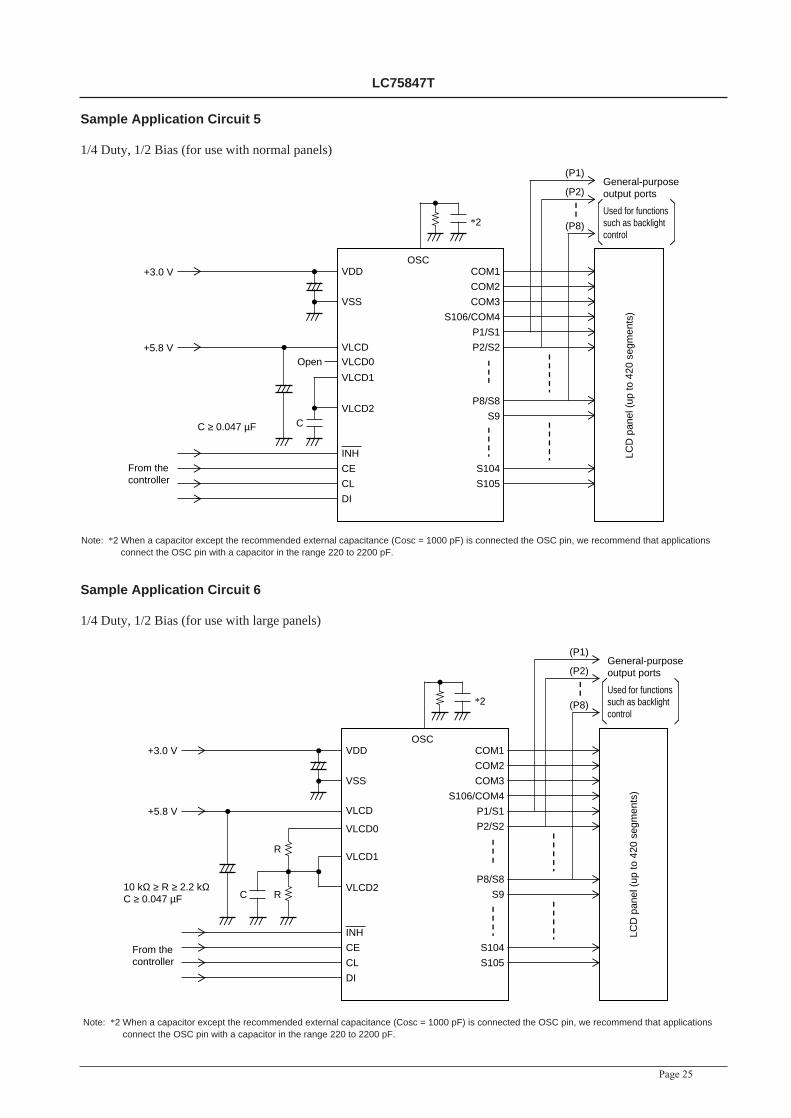
Note: *2 When a capacitor except the recommended external capacitance (Cosc = 1000 pF) is connected the OSC pin, we recommend that applicationsconnect the OSC pin with a capacitor in the range 220 to 2200 pF.
Note: *2 When a capacitor except the recommended external capacitance (Cosc = 1000 pF) is connected the OSC pin, we recommend that applicationsconnect the OSC pin with a capacitor in the range 220 to 2200 pF.

Page 24
LC75847T
Sample Application Circuit 3
1/3 Duty, 1/3 Bias (for use with nornal panels)
Sample Application Circuit 4
1/3 Duty, 1/3 Bias (for use with large panels)
CC ≥ 0.047 µF
+5.8 V
+3.0 V
*2
C
DI
CL
CE
INH
VLCD2
VLCD1
VLCD
VSS
COM4/S106
S105
S104
S9
P8/S8
P2/S2
P1/S1
COM3
COM2
COM1OSC
VDD
Used for functions such as backlight control
General-purposeoutput ports
(P8)
(P2)
(P1)
From the controller
LCD
pan
el (
up to
318
seg
men
ts)
VLCD0Open
C
+5.8 V
+3.0 V
*2
R
R
RC
From the controller
Used for functions such as backlight control
General-purposeoutput ports
(P8)
(P2)
(P1)
DI
CL
CE
INH
VLCD2
VLCD1
VLCD0
VLCD
VSS
COM4/S106
S105
S104
S9
P8/S8
P2/S2
P1/S1
COM3
COM2
COM1OSC
VDD
10 kΩ ≥ R ≥ 2.2 kΩC ≥ 0.047 µF
LCD
pan
el (
up to
318
seg
men
ts)
Note: *2 When a capacitor except the recommended external capacitance (Cosc = 1000 pF) is connected the OSC pin, we recommend that applicationsconnect the OSC pin with a capacitor in the range 220 to 2200 pF.
Note: *2 When a capacitor except the recommended external capacitance (Cosc = 1000 pF) is connected the OSC pin, we recommend that applicationsconnect the OSC pin with a capacitor in the range 220 to 2200 pF.
Page 25
LC75847T
Sample Application Circuit 5
1/4 Duty, 1/2 Bias (for use with normal panels)
Sample Application Circuit 6
1/4 Duty, 1/2 Bias (for use with large panels)
CC ≥ 0.047 µF
+5.8 V
*2
+3.0 V
From the controller
Used for functions such as backlight control
General-purposeoutput ports
(P8)
(P2)
(P1)
DI
CL
CE
INH
VLCD2
VLCD1
VLCD
VSS
S105
S104
S9
P8/S8
P1/S1
S106/COM4
P2/S2
COM3
COM2
COM1OSC
VDD
LCD
pan
el (
up to
420
seg
men
ts)
VLCD0Open
C
+5.8 V
+3.0 V
*2
R
R
From the controller
Used for functions such as backlight control
General-purposeoutput ports
(P8)
(P2)
(P1)
10 kΩ ≥ R ≥ 2.2 kΩC ≥ 0.047 µF
DI
CL
CE
INH
VLCD2
VLCD1
VLCD0
VLCD
VSS
S105
S104
S9
P8/S8
P1/S1
S106/COM4
P2/S2
COM3
COM2
COM1OSC
VDD
LCD
pan
el (
up to
420
seg
men
ts)
Note: *2 When a capacitor except the recommended external capacitance (Cosc = 1000 pF) is connected the OSC pin, we recommend that applicationsconnect the OSC pin with a capacitor in the range 220 to 2200 pF.
Note: *2 When a capacitor except the recommended external capacitance (Cosc = 1000 pF) is connected the OSC pin, we recommend that applicationsconnect the OSC pin with a capacitor in the range 220 to 2200 pF.

Page 26
LC75847T
Sample Application Circuit 7
1/4 Duty, 1/3 Bias (for use with nornal panels)
Sample Application Circuit 8
1/4 Duty, 1/3 Bias (for use with large panels)
C
+5.8 V
+3.0 V
*2
C
From the controller
Used for functions such as backlight control
General-purposeoutput ports
(P8)
(P2)
(P1)
C ≥ 0.047µF
DI
CL
CE
INH
VLCD2
VLCD1
VLCD
VSS
S105
S104
S9
P8/S8
P1/S1
S106/COM4
P2/S2
COM3
COM2
COM1OSC
VDD
LCD
pan
el (
up to
420
seg
men
ts)
VLCD0Open
C
+5.8 V
+3.0 V
*2
R
R
RC
DI
CL
CE
INH
VLCD2
VLCD1
VLCD0
VLCD
VSS
S105
S104
S9
P8/S8
P1/S1
S106/COM4
P2/S2
COM3
COM2
COM1OSC
VDD
From the controller
Used for functions such as backlight control
General-purposeoutput ports
(P8)
(P2)
(P1)
10 kΩ ≥ R ≥ 2.2 kΩC ≥ 0.047 µF
LCD
pan
el (
up to
420
seg
men
ts)
Note: *2 When a capacitor except the recommended external capacitance (Cosc = 1000 pF) is connected the OSC pin, we recommend that applicationsconnect the OSC pin with a capacitor in the range 220 to 2200 pF.
Note: *2 When a capacitor except the recommended external capacitance (Cosc = 1000 pF) is connected the OSC pin, we recommend that applicationsconnect the OSC pin with a capacitor in the range 220 to 2200 pF.
LC75847T
www.onsemi.com 27
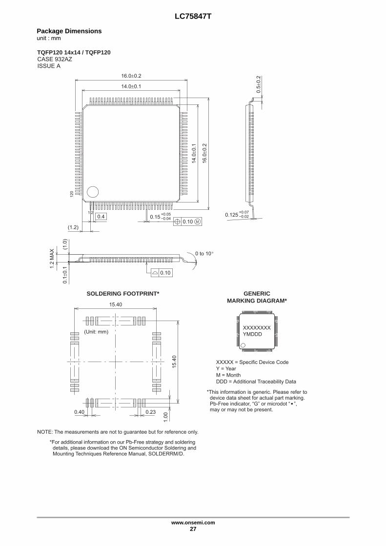
Package Dimensions unit : mm
TQFP120 14x14 / TQFP120CASE 932AZISSUE A
XXXXX = Specific Device CodeY = YearM = MonthDDD = Additional Traceability Data
GENERICMARKING DIAGRAM*
*This information is generic. Please refer todevice data sheet for actual part marking.
XXXXXXXXYMDDD
14.00.1
1 20.4
(1.2)0.10
14.00
.1
16.00
.2
16.00.212
0
0.15
0.10
1.2
MA
X (1.0
)0.
1 0.
1
0 to 10
0.125
0.5
0.2
(Unit: mm)
15.40
15.4
0
0.230.40
1.00
SOLDERING FOOTPRINT*
NOTE: The measurements are not to guarantee but for reference only.
*For additional information on our Pb-Free strategy and solderingdetails, please download the ON Semiconductor Soldering andMounting Techniques Reference Manual, SOLDERRM/D.

LC75847T
www.onsemi.com 28
ON Semiconductor and the ON Semiconductor logo are trademarks of Semiconductor Components Industries, LLC dba ON Semiconductor or its subsidiariesin the United States and/or other countries. ON Semiconductor owns the rights to a number of patents, trademarks, copyrights, trade secrets, and otherintellectual property. A listing of ON Semiconductor’s product/patent coverage may be accessed at www.onsemi.com/site/pdf/Patent-Marking.pdf. ONSemiconductor reserves the right to make changes without further notice to any products herein. ON Semiconductor makes no warranty, representation orguarantee regarding the suitability of its products for any particular purpose, nor does ON Semiconductor assume any liability arising out of the application oruse of any product or circuit, and specifically disclaims any and all liability, including without limitation special, consequential or incidental damages. Buyer isresponsible for its products and applications using ON Semiconductor products, including compliance with all laws, regulations and safety requirements orstandards, regardless of any support or applications information provided by ON Semiconductor. “Typical” parameters which may be provided in ONSemiconductor data sheets and/or specifications can and do vary in different applications and actual performance may vary over time. All operating parameters,including “Typicals” must be validated for each customer application by customer’s technical experts. ON Semiconductor does not convey any license under itspatent rights nor the rights of others. ON Semiconductor products are not designed, intended, or authorized for use as a critical component in life supportsystems or any FDA Class 3 medical devices or medical devices with a same or similar classification in a foreign jurisdiction or any devices intended forimplantation in the human body. Should Buyer purchase or use ON Semiconductor products for any such unintended or unauthorized application, Buyer shallindemnify and hold ON Semiconductor and its officers, employees, subsidiaries, affiliates, and distributors harmless against all claims, costs, damages, andexpenses, and reasonable attorney fees arising out of, directly or indirectly, any claim of personal injury or death associated with such unintended orunauthorized use, even if such claim alleges that ON Semiconductor was negligent regarding the design or manufacture of the part. ON Semiconductor is anEqual Opportunity/Affirmative Action Employer. This literature is subject to all applicable copyright laws and is not for resale in any manner.
ORDERING INFORMATION
Device Package Shipping (Qty / Packing)
LC75847T-E TQFP120 14x14 / TQFP120
(Pb-Free) 450 / Tray JEDEC
LC75847TS-E TQFP120 14x14 / TQFP120
(Pb-Free) 450 / Tray JEDEC