inverted gainp / (in)gaas / ingaas triple-junction solar cells with low-stress metamorphic bottom...
TRANSCRIPT

A national laboratory of the U.S. Department of EnergyOffice of Energy Efficiency & Renewable Energy
National Renewable Energy Laboratory Innovation for Our Energy Future
Inverted GaInP / (In)GaAs / InGaAs Triple-Junction Solar Cells with Low-Stress Metamorphic Bottom Junctions Preprint J.F. Geisz, S.R. Kurtz, M.W. Wanlass, J.S. Ward, A. Duda, D.J. Friedman, J.M. Olson, W.E. McMahon, T.E. Moriarty, J.T. Kiehl, M.J. Romero, A.G. Norman, and K.M. Jones National Renewable Energy Laboratory
Presented at the 33rd IEEE Photovoltaic Specialists Conference San Diego, California May 11–16, 2008
Conference Paper NREL/CP-520-42537 May 2008
NREL is operated by Midwest Research Institute ● Battelle Contract No. DE-AC36-99-GO10337

NOTICE
The submitted manuscript has been offered by an employee of the Midwest Research Institute (MRI), a contractor of the US Government under Contract No. DE-AC36-99GO10337. Accordingly, the US Government and MRI retain a nonexclusive royalty-free license to publish or reproduce the published form of this contribution, or allow others to do so, for US Government purposes.
This report was prepared as an account of work sponsored by an agency of the United States government. Neither the United States government nor any agency thereof, nor any of their employees, makes any warranty, express or implied, or assumes any legal liability or responsibility for the accuracy, completeness, or usefulness of any information, apparatus, product, or process disclosed, or represents that its use would not infringe privately owned rights. Reference herein to any specific commercial product, process, or service by trade name, trademark, manufacturer, or otherwise does not necessarily constitute or imply its endorsement, recommendation, or favoring by the United States government or any agency thereof. The views and opinions of authors expressed herein do not necessarily state or reflect those of the United States government or any agency thereof.
Available electronically at http://www.osti.gov/bridge
Available for a processing fee to U.S. Department of Energy and its contractors, in paper, from:
U.S. Department of Energy Office of Scientific and Technical Information P.O. Box 62 Oak Ridge, TN 37831-0062 phone: 865.576.8401 fax: 865.576.5728 email: mailto:[email protected]
Available for sale to the public, in paper, from: U.S. Department of Commerce National Technical Information Service 5285 Port Royal Road Springfield, VA 22161 phone: 800.553.6847 fax: 703.605.6900 email: [email protected] online ordering: http://www.ntis.gov/ordering.htm
Printed on paper containing at least 50% wastepaper, including 20% postconsumer waste

INVERTED GaInP / (In)GaAs / InGaAs TRIPLE-JUNCTION SOLAR CELLS WITH LOW-STRESS METAMORPHIC BOTTOM JUNCTIONS
J.F. Geisz, Sarah R. Kurtz, M.W. Wanlass, J.S. Ward, A. Duda, D.J. Friedman, J.M. Olson,
W.E. McMahon, T.E. Moriarty, J.T. Kiehl, M.J. Romero, A.G. Norman, K.M. Jones National Renewable Energy Laboratory, Golden, CO 80401 USA
ABSTRACT We demonstrate high efficiency performance in two ultra-thin, Ge-free III-V semiconductor triple-junction solar cell device designs grown in an inverted configuration. Low-stress metamorphic junctions were engineered to achieve excellent photovoltaic performance with less than 3 x 106 cm-2 threading dislocations. The first design with band gaps of 1.83/1.40/1.00 eV, containing a single metamorphic junction, achieved 33.8% and 39.2% efficiencies under the standard one-sun global spectrum and concentrated direct spectrum at 131 suns, respectively. The second design with band gaps of 1.83/1.34/0.89 eV, containing two metamorphic junctions achieved 33.2% and 40.1% efficiencies under the standard one-sun global spectrum and concentrated direct spectrum at 143 suns, respectively.
INTRODUCTION High-efficiency multijunction solar cells have greatly impacted the power capacities of satellites and future improvement in power-to-weight ratio is greatly anticipated. Further, the demand for high-efficiency solar cells for terrestrial concentrating solar systems is rapidly growing, with demonstration installations increasing and many new companies entering the market. The power delivered by these concentrating photovoltaic systems is directly related to the efficiency of the relatively small solar cells at the heart of the systems. Currently, state-of-the-art high efficiency III-V solar cells utilize a three-junction design that includes a Ge bottom junction formed in the Ge substrate in conjunction with lattice-matched Ga0.5In0.5P and Ga(In)As top junctions [1]. However, the Ge junction absorbs about twice the low energy photons than are needed for current matching with the Ga0.5In0.5P and GaAs junctions. Spectrolab has achieved a record 40.7% efficiency under 240X concentration by reducing the band gaps of the top GaInP and GaInAs junctions [1]. While this reduction in band gap increases the theoretical efficiency, the alloy compositions of these top two junctions are no longer lattice-matched to the Ge substrate, but are lattice-matched to each other. The misfit and threading dislocations that reduce solar cell performance have been minimized in this device using a composition-graded buffer in a metamorphic structure. Alternatively, Ga0.5In0.5P and GaAs top junctions lattice-matched to GaAs in conjunction with a 1.0 eV bottom junction increases the theoretical efficiency of a triple junction solar cell even more [2]. In0.3Ga0.7As can be used as the 1.0 eV junction, but it has a larger lattice constant than GaAs by about 2%. The dislocations generated by this large lattice mismatch can be reduced
through the use of graded composition buffer layers, but the remaining threading dislocations would significantly degrade any subsequently grown junctions with higher band gaps. By growing in an inverted configuration [3,4], this degradation of the top junctions can be avoided. We have demonstrated excellent solar cell performance in an inverted, monolithic triple-junction structure that combines a metamorphic 1.00 eV In0.27Ga0.73As junction with lattice-matched 1.83 eV Ga0.5In0.5P and 1.40 eV GaAs junctions [5]. Further gains in the theoretical efficiency of a triple junction solar cell can be made if the junction band gaps are not constrained by material properties such as lattice constants. Figure 1 shows realistic theoretical efficiencies of series-connected triple-junction solar cells with a fixed top band gap of 1.84 eV. Our calculations indicate a maximum theoretical efficiency using the band gap combination of 1.85 eV / 1.34 eV / 0.93 eV [2]. For these efficiency gains to be realized, though, these junctions must be formed with excellent material quality. Fortuitously, this top band gap can be grown as a lattice-matched GaInP junction on GaAs making the inverted approach ideally suited to this device. In this paper, we demonstrate excellent performance in an inverted, monolithic triple-junction structure that incorporates a lattice-matched GaInP junction with two independently metamorphic junctions (0.89 eV In0.37Ga0.63As and 1.34 eV In0.04Ga0.96As), thus achieving near optimal band gaps unconstrained by lattice matching.
Fig. 1. Theoretical isoefficiency plots of triple-junction solar cells with variable bottom and middle junction band gaps at 500X concentration under the low AOD direct spectrum (300K). The top band gap is fixed at 1.84 eV. The performance of actual metamorphic devices is also shown.
1

INVERTED DESIGN
The semiconductor devices described here were grown in a single process step by atmospheric-pressure organometallic vapor phase epitaxy (OMVPE) on a (001) GaAs substrate miscut 2° toward (111)B. The direction of growth is inverted relative to more conventional multijunction devices, thus the top (lattice-matched) junction is grown first and the bottom (most highly lattice-mismatched) junction is grown last. This direction of growth helps prevent the threading dislocations that inevitably originate during mismatched growth from degrading the higher band gap (and more power producing) junctions. The inverted growth and processing is shown schematically in figure 2. In order to minimize the dislocations in the metamorphic junctions, a step-graded (Al)GaInP buffer layer, which is transparent to the light intended for the junction, was grown. The grade was engineered as described in the next section to achieve a nearly strain-free metamorphic junction. The InxGa1-xAs junctions were clad with corresponding GaxIn1-xP window and back-surface-field layers with the same lattice constant. After OMVPE growth of the inverted semiconductor structure, gold was electroplated onto the exposed “back” surface of the inverted structure. The sample was then mounted with a low viscosity epoxy to a structural “handle,” in this case silicon wafers or glass slides, however a variety of materials could be used as a handle to optimize cost, heat management, and weight considerations [4]. The GaAs substrate was removed using a selective chemical etch that stops at a GaInP layer. As a possible future refinement, the GaAs substrate could, in principle, be reused for considerable cost savings, using a lift-off procedure [6] . The “front” grids and mesa isolation were completed using standard photolithography processing techniques. Initial devices used electroplated gold grids as an etch mask for the contact layer, but severe anisotropic etching under the grid fingers led us to transition to thinner, denser evaporated Ti/Pd/Ag/Pd grids for improved series
resistance. A Se-doped GaInNAs contact layer was employed at the front grids to inhibit Se diffusion during the subsequent inverted growth and thus maintain good contact resistance [7]. Appropriate grid designs were chosen for each measurement condition. Finally, a MgF2 / ZnS antireflective coating (ARC) was deposited by thermal evaporation.
Fig. 2. Schematic of growth and processing of inverted triple junction solar cell.
This process of growing an inverted solar cell and mounting on a handle is similar in concept to the common method of flip-chip LED processing. The process, therefore, should be similarly manufacturable, especially for the relatively small devices required for some concentrator systems.
STRESS AND STRAIN CONTROL The driving force for dislocation generation and glide in lattice mismatched semiconductor
layers is the film stress that results from attempting to grow a single crystal layer epitaxially on another crystal lattice with a different lattice constant. In order to grow a relatively thick strain-free 1.0 eV In0.27Ga0.73As junction on GaAs, a total of 1.9% misfit strain must be relaxed. By growing the compositionally step-graded GaxIn1-xP layers, most of the strain is relieved gradually while maintaining a relatively defect-free, flat growth surface. But a slight residual strain is always retained in reasonably thin graded layers. The strain of the 1.0 eV junction, though, can be reduced to zero by matching the relaxed lattice constant of the active junction to the in-plane lattice constant of the slightly strained top layer of the graded buffer. This technique was developed while studying lattice-mismatched thermophotovoltaic devices [8].
Fig. 3. Stress and strain of the active 1.0 eV solar cell (large points) and the top layer of the GaInP step-grade (small points) as a function of the composition of the top layer of the GaInP step-grade.
2

We have investigated the effects of stress and strain on the performance of 1.0 eV In0.3Ga0.7As solar cells [9]. The stress and strain of single-junction 1.0 eV devices were systematically varied by adjusting the maximum lattice constant of the top of the step-grade. The film stress was determined in situ at growth temperature using curvature measurements from a multi-beam optical stress sensor, while the strain was determined ex situ at room temperature from x-ray diffraction measurements. Figure 3 shows that the residual compressive stress in the top of the step-graded buffer remained constant for all samples at about 0.1 GPa, corresponding to about 0.15% strain. The stress and strain of the active 1.0 eV In0.3Ga0.7As junction was systematically varied from compressive to tensile. The stress-free 1.0 eV solar cells had very good performance with an open-circuit voltage (Voc) of about 0.54 V (see figure 4). The ideal Voc of a 1.0 eV junction is not much more than about 0.6 V. Plan-view cathodoluminescence (CL) measurements revealed a dislocation density in the low 106 cm-2 range. Similar results were observed for slightly compressively strained devices, but tensile strain quickly degraded the performance because of higher dislocation densities. These techniques were used to engineer nearly strain-free metamorphic InxGa1-xAs junctions with excellent performance within the triple junction devices.
MULTIJUNCTION DEVICE RESULTS Two different inverted triple-junction designs were fabricated. The first structure, described elsewhere [5], has only one low-stress metamorphic junction (hereafter referred to as 1MMJ) and two lattice-matched junctions. The junctions were 1.83 eV Ga0.51In0.49P, 1.40 eV GaAs,
and 1.00 eV In0.27Ga0.73As. Because of the non-optimal band gap combination, the top GaInP junction was thinned to 0.9 microns to current match all three junctions. This design is shown in figure 2. The second design contains 2 low-stress metamorphic junctions (hereafter referred to as 2MMJ) and only one lattice-matched junction. They were 1.83 eV Ga0.51In0.49P, 1.34 eV In0.04Ga0.96As, and 0.89 eV In0.37Ga0.63As. This band gap combination was nearly current-matched with optically thick junctions (2.5 - 3.0 microns). A transparent (Al)GaInP compositional step-grade was included between each junction of the 2MMJ design. This design is pictured in figure 5. Defect densities in the metamorphic junctions of actual triple-junction structures were characterized by plan-view CL and cross-sectional transmission
electron microscopy (TEM). TEM samples were prepared by focused ion-beam. The TEM was performed on orthogonal <110> sections using 220 dark field conditions. Images of the 2MMJ structure are shown in figure 5. The In0.37Ga0.63As (2MMJ) and In0.27Ga0.73As (1MMJ) bottom junctions had ~2-3 x 106 cm-2 threading dislocations, with only about one defect visible in the entire 30 micron length of cross-sections examined. The In0.04Ga0.96As (2MMJ) middle junction had only ~1x105 cm-2 threading dislocations, with none visible in the TEM. The defect density was very high within the step grades, but very low within the lattice-matched junctions.
Fig. 4. Voc of single-junction inverted 1.0 eV In0.27Ga0.63As solar cells as a function of film stress during growth. Inset TEM images illustrate greater defect densities under tension.
Official solar cell measurements were obtained from the independent measurements team at NREL. The
Fig. 5. Ion beam image and 220DF TEM of cross section of inverted 2MMJ device.
3

external quantum efficiency (QE) of each junction was measured separately by light biasing the other two junctions [10]. Current-voltage (IV) measurements were taken under a continuous multi-source solar simulator adjusted to the appropriate one-sun spectrum using three individual single-junction reference cells [10]. High irradiance IV measurements were taken under a flash simulator. The flash lamp voltage was adjusted to match the currents of the top two junctions under the AM1.5D spectrum (low AOD direct [11]) to their respective reference cells. This resulted in over-illuminating the bottom junction by approximately 30%. While this method was also used to measure record triple junction devices with Ge bottom junctions, the nearly current matched nature of our devices results in greater uncertainty. Future work for current matched multijunction devices must address this issue. The external QE of all three junctions of the two designs is shown in figure 6. Integrated QE results and an alternative IV technique [12] showed the three junctions to be current matched to each other within about 10% under the measurement conditions. The simple two layer ARC used here is becoming a limiting factor for such current matched devices, requiring research into new ultra-broadband AR coatings. The unexpectedly high QE response of the bottom and middle junction at energies higher than the band gap (Eg) of the filtering junctions above them may indicate substantial radiative coupling between the junctions [13]. The relatively low QE of the bottom junction of the 2MMJ device is not characteristic of all such devices. The current-voltage (IV) results for devices optimized for the AM1.5G spectrum with an area of 0.25 cm2 are shown in figure 7. The 2MMJ design resulted in lower voltage but higher current operation. The 1MMJ and 2MMJ triple-junction devices had efficiencies of 33.8% and 33.2%, respectively. These are the highest efficiencies ever recorded for any solar cell device under this spectrum. The previous record of 32.0% was achieved in
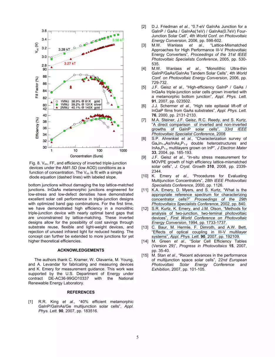
a III-V multijunction solar cell using a Ge bottom junction [14]. AM0 efficiencies of 31.9% have been reported using a similar structure which Emcore refers to as the inverted metamorphic (IMM) solar cell [15]. Smaller 0.1 cm2 devices, similar to the AM1.5G devices described above, were processed using a denser grid appropriate for concentration. Figure 8 shows the dependence of Voc, FF, and efficiency on concentration for the direct spectrum. The fill factor of all devices initially rises with concentration, but eventually falls off due to unavoidably finite series resistance. The previously reported maximum efficiency of 38.9% at 81 suns concentration [5] using the sparser undercut electroplated gold grids on the 1MMJ design was limited by such a series resistance. The use of denser evaporated metal grids reduced the series resistance of the 1MMJ design resulting in a peak efficiency of 39.2% at 131 suns and efficiencies over 37% out to ~500 suns. Continued reduction in series resistance will enable greater efficiencies at higher concentrations yet. While the 2MMJ device still used the old sparse
electroplated gold grids, it achieved 40.1% efficiency at 143 suns. In spite of the drop in fill factor below 100 suns, the relatively greater increase in voltage maintained high efficiencies to greater concentrations than in the 1MMJ device. The Voc of all devices increased logarithmically with concentration with a slope close to the predicted value of 3kT for three “ideal” diodes in series.
Fig. 6. External QE from both AM1.5G inverted triple-junction devices: 1MMJ (solid) and 2MMJ (dashed).
CONCLUSIONS
The inverted triple-junction solar cell design has many advantages over traditional triple-junction designs utilizing Ge substrates. We have demonstrated here a world-record efficiency at one-sun and > 40% efficiency under concentration. The inverted nature of the design has facilitated the ability to grow strain-free metamorphic
Fig. 7. IV results measured at AM1.5G (IEC 60904) conditions using 1000 W/m2 irradiance.
4
bottom junctions without damaging the top lattice-matched junctions. InGaAs metamorphic junctions engineered for low-stress and low-defect densities have demonstrated excellent solar cell performance in triple-junction designs with optimized band gap combinations. For the first time, we have demonstrated high efficiency in a monolithic triple-junction device with nearly optimal band gaps that are unconstrained by lattice-matching. These inverted designs allow for the possibility of cost savings through substrate reuse, flexible and light-weight devices, and rejection of unused infrared light for reduced heating. The concept can further be extended to more junctions for yet higher theoretical efficiencies.
ACKNOWLEDGEMENTS The authors thank C. Kramer, W. Olavarria, M. Young, and A. Levandar for fabricating and measuring devices and K. Emery for measurement guidance. This work was supported by the U.S. Department of Energy under contract DE-AC36-99GO10337 with the National Renewable Energy Laboratory.
REFERENCES [1] R.R. King et al., “40% efficient metamorphic
GaInP/GaInAs/Ge multijunction solar cells”, Appl. Phys. Lett. 90, 2007, pp. 183516.
[2] D.J. Friedman et al., “0.7-eV GaInAs Junction for a GaInP / GaAs / GaInAs(1eV) / GaInAs(0.7eV) Four-Junction Solar Cell”, 4th World Conf. on Photovoltaic Energy Conversion, 2006, pp. 598-602.
Fig. 8. Voc, FF, and efficiency of inverted triple-junction devices under the AM1.5D (low AOD) conditions as a function of concentration. The Voc is fit with a simple diode equation (dashed lines) with labeled slope.
[3] M.W. Wanlass et al., “Lattice-Mismatched Approaches for High Performance III-V Photovoltaic Energy Converters”, Proceedings of the 31st IEEE Photovoltaic Specialists Conference, 2005, pp. 530-535.
[4] M.W. Wanlass et al., “Monolithic Ultra-thin GaInP/GaAs/GaInAs Tandem Solar Cells”, 4th World Conf. on Photovoltaic Energy Conversion, 2006, pp. 729-732.
[5] J.F. Geisz et al., “High-efficiency GaInP / GaAs / InGaAs triple-junction solar cells grown inverted with a metamorphic bottom junction”, Appl. Phys. Lett. 91, 2007, pp. 023502.
[6] J.J. Schermer et al., “High rate epitaxial lift-off of InGaP films from GaAs substrates”, Appl. Phys. Lett. 76, 2000, pp. 2131-2133.
[7] M.A. Steiner, J.F. Geisz, R.C. Reedy, and S. Kurtz, “A direct comparison of inverted and non-inverted growths of GaInP solar cells”, 33rd IEEE Photovoltaic Specialist Conference, 2008
[8] S.P. Ahrenkiel et al., “Characterization survey of GaxIn1-xAs/InAsyP1-y double heterostructures and InAsyP1-y multilayers grown on InP”, J Electron Mater 33, 2004, pp. 185-193.
[9] J.F. Geisz et al., “In-situ stress measurement for MOVPE growth of high efficiency lattice-mismatched solar cells”, J. Cryst. Growth 310, 2008, pp. 2339-2344.
[10] K. Emery et al., “Procedures for Evaluating Multijunction Concentrators”, 28th IEEE Photovoltaic Specialists Conference, 2000, pp. 1126.
[11] K.A. Emery, D. Myers, and S. Kurtz, “What is the appropriate reference spectrum for characterizing concentrator cells?” Proceedings of the 29th Photovoltaics Specialists Conference, 2002, pp. 840.
[12] S.R. Kurtz, K. Emery, and J.M. Olson, “Methods for analysis of two-junction, two-teminal photovoltaic devices”, First World Conference on Photovoltaic Energy Conversion, 1994, pp. 1733-1737.
[13] C. Baur, M. Hermle, F. Dimroth, and A.W. Bett, “Effects of optical coupling in III-V multilayer systems”, Appl. Phys. Lett. 90, 2007, pp. 192109.
[14] M. Green et al., “Solar Cell Efficiency Tables (Version 29)”, Progress in Photovoltaics 15, 2007, pp. 35-40.
[15] M. Stan et al., “Recent advances in the performance of multijunction space solar cells”, 22nd European Photovoltaic Solar Energy Conference and Exhibition, 2007, pp. 101-105.
5

F1147-E(09/2007)
REPORT DOCUMENTATION PAGE Form Approved OMB No. 0704-0188
The public reporting burden for this collection of information is estimated to average 1 hour per response, including the time for reviewing instructions, searching existing data sources, gathering and maintaining the data needed, and completing and reviewing the collection of information. Send comments regarding this burden estimate or any other aspect of this collection of information, including suggestions for reducing the burden, to Department of Defense, Executive Services and Communications Directorate (0704-0188). Respondents should be aware that notwithstanding any other provision of law, no person shall be subject to any penalty for failing to comply with a collection of information if it does not display a currently valid OMB control number. PLEASE DO NOT RETURN YOUR FORM TO THE ABOVE ORGANIZATION. 1. REPORT DATE (DD-MM-YYYY)
May 2008 2. REPORT TYPE
Conference Paper 3. DATES COVERED (From - To)
11-16 May 2008 5a. CONTRACT NUMBER
DE-AC36-99-GO10337
5b. GRANT NUMBER
4. TITLE AND SUBTITLE Inverted GaInP / (In)GaAs / InGaAs Triple-Junction Solar Cells with Low-Stress Metamorphic Bottom Junctions: Preprint
5c. PROGRAM ELEMENT NUMBER
5d. PROJECT NUMBER NREL/CP-520-42547
5e. TASK NUMBER PVA74401
6. AUTHOR(S) J.F. Geisz, S.R. Kurtz, M.W. Wanlass, J.S. Ward, A. Duda, D.J. Friedman, J.M. Olson, W.E. McMahon, T.E. Moriarty, J.T. Kiehl, M.J. Romero, A.G. Norman, and K.M. Jones
5f. WORK UNIT NUMBER
7. PERFORMING ORGANIZATION NAME(S) AND ADDRESS(ES) National Renewable Energy Laboratory 1617 Cole Blvd. Golden, CO 80401-3393
8. PERFORMING ORGANIZATION REPORT NUMBER NREL/CP-520-42547
10. SPONSOR/MONITOR'S ACRONYM(S) NREL
9. SPONSORING/MONITORING AGENCY NAME(S) AND ADDRESS(ES)
11. SPONSORING/MONITORING AGENCY REPORT NUMBER
12. DISTRIBUTION AVAILABILITY STATEMENT National Technical Information Service U.S. Department of Commerce 5285 Port Royal Road Springfield, VA 22161
13. SUPPLEMENTARY NOTES
14. ABSTRACT (Maximum 200 Words) We demonstrate high efficiency performance in two ultra-thin, Ge-free III-V semiconductor triple-junction solar cell device designs grown in an inverted configuration. Low-stress metamorphic junctions were engineered to achieve excellent photovoltaic performance with less than 3 x 106 cm-2 threading dislocations. The first design with band gaps of 1.83/1.40/1.00 eV, containing a single metamorphic junction, achieved 33.8% and 39.2% efficiencies under the standard one-sun global spectrum and concentrated direct spectrum at 131 suns, respectively. The second design with band gaps of 1.83/1.34/0.89 eV, containing two metamorphic junctions achieved 33.2% and 40.1% efficiencies under the standard one-sun global spectrum and concentrated direct spectrum at 143 suns, respectively.
15. SUBJECT TERMS Ge free; inverted configuration; PV; triple-junction; solar cells; high efficiency; semiconductor; low-stress; metamorphic junction; solar spectrum;
16. SECURITY CLASSIFICATION OF: 19a. NAME OF RESPONSIBLE PERSON a. REPORT
Unclassified b. ABSTRACT Unclassified
c. THIS PAGE Unclassified
17. LIMITATION OF ABSTRACT
UL
18. NUMBER OF PAGES
19b. TELEPHONE NUMBER (Include area code)
Standard Form 298 (Rev. 8/98) Prescribed by ANSI Std. Z39.18