improved control for multilevel inverters in grid applications
TRANSCRIPT
Improved control for multilevel inverters in grid applications
Martin Hofmann
ADVERTIMENT La consulta d’aquesta tesi queda condicionada a l’acceptació de les següents condicions d'ús: La difusió d’aquesta tesi per mitjà del r e p o s i t o r i i n s t i t u c i o n a l UPCommons (http://upcommons.upc.edu/tesis) i el repositori cooperatiu TDX ( h t t p : / / w w w . t d x . c a t / ) ha estat autoritzada pels titulars dels drets de propietat intel·lectual únicament per a usos privats emmarcats en activitats d’investigació i docència. No s’autoritza la seva reproducció amb finalitats de lucre ni la seva difusió i posada a disposició des d’un lloc aliè al servei UPCommons o TDX. No s’autoritza la presentació del seu contingut en una finestra o marc aliè a UPCommons (framing). Aquesta reserva de drets afecta tant al resum de presentació de la tesi com als seus continguts. En la utilització o cita de parts de la tesi és obligat indicar el nom de la persona autora.
ADVERTENCIA La consulta de esta tesis queda condicionada a la aceptación de las siguientes condiciones de uso: La difusión de esta tesis por medio del repositorio institucional UPCommons (http://upcommons.upc.edu/tesis) y el repositorio cooperativo TDR (http://www.tdx.cat/?locale-attribute=es) ha sido autorizada por los titulares de los derechos de propiedad intelectual únicamente para usos privados enmarcados en actividades de investigación y docencia. No se autoriza su reproducción con finalidades de lucro ni su difusión y puesta a disposición desde un sitio ajeno al servicio UPCommons No se autoriza la presentación de su contenido en una ventana o marco ajeno a UPCommons (framing). Esta reserva de derechos afecta tanto al resumen de presentación de la tesis como a sus contenidos. En la utilización o cita de partes de la tesis es obligado indicar el nombre de la persona autora.
WARNING On having consulted this thesis you’re accepting the following use conditions: Spreading this thesis by the i n s t i t u t i o n a l r e p o s i t o r y UPCommons (http://upcommons.upc.edu/tesis) and the cooperative repository TDX (http://www.tdx.cat/?locale-attribute=en) has been authorized by the titular of the intellectual property rights only for private uses placed in investigation and teaching activities. Reproduction with lucrative aims is not authorized neither its spreading nor availability from a site foreign to the UPCommons service. Introducing its content in a window or frame foreign to the UPCommons service is not authorized (framing). These rights affect to the presentation summary of the thesis as well as to its contents. In the using or citation of parts of the thesis it’s obliged to indicate the name of the author.
Universitat Politecnica de Catalunya
Departament d’Enginyeria Electrica
PhD thesis
Improved Control for MultilevelInverters in Grid Applications
Autor: Martin Hofmann
Directors: Daniel Montesinos i MiracleAnsgar Ackva
Barcelona, July 2018

Universitat Politecnica de CatalunyaDepartament d’Enginyeria ElectricaCentre d’Innovacio Tecnologica en Convertidors Estatics i AccionamentAv. Diagonal, 647. Pl. 208028 Barcelona
Copyright c© Martin Hofmann, 2018

Acknowlegdements
The work presented in this thesis was carried out during my work asresearch assistant at the Technology Transfer Centre for E-mobility at theUniversity of Applied Sciences Wurzburg-Schweinfurt.
First of all, I would like to express my great thanks and gratitude to myadvisors, Ansgar Ackva and Daniel Montesinos i Miracle for their supportand advice during the last years.
I would also like to thank Markus Schafer and all my other colleagues atthe institute, who gave me their support in many technical discussions andoffered me a pleasant, collegial working environment.
Last, but not least, I would thank my family who supported me duringmy studies of electrical engineering and doctoral thesis.

ii
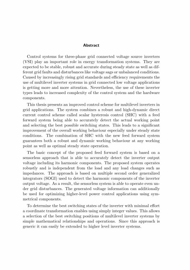
Abstract
Control systems for three-phase grid connected voltage source inverters(VSI) play an important role in energy transformation systems. They areexpected to be stable, robust and accurate during steady state as well as dif-ferent grid faults and disturbances like voltage sags or unbalanced conditions.Caused by increasingly rising grid standards and efficiency requirements theuse of multilevel inverter systems in grid connected low voltage applicationsis getting more and more attention. Nevertheless, the use of these invertertypes leads to increased complexity of the control system and the hardwarecomponents.
This thesis presents an improved control scheme for multilevel inverters ingrid applications. The system combines a robust and high-dynamic directcurrent control scheme called scalar hysteresis control (SHC) with a feedforward system being able to accurately detect the actual working pointand selecting the best possible switching states. This leads to a significantimprovement of the overall working behaviour especially under steady stateconditions. The combination of SHC with the new feed forward systemguarantees both a robust and dynamic working behaviour at any workingpoint as well as optimal steady state operation.
The basic concept of the proposed feed forward system is based on asensorless approach that is able to accurately detect the inverter outputvoltage including its harmonic components. The proposed system operatesrobustly and is independent from the load and any load changes such asimpedances. The approach is based on multiple second order generalizedintegrators (SOGI) used to detect the harmonic components of the inverteroutput voltage. As a result, the sensorless system is able to operate even un-der grid disturbances. The generated voltage information can additionallybe used for optimizing higher-level power control applications using sym-metrical components.
To determine the best switching states of the inverter with minimal efforta coordinate transformation enables using simply integer values. This allowsa selection of the best switching positions of multilevel inverter systems bysimple mathematical relationships and operations. Since this approach isgeneric it can easily be extended to higher level inverter systems.

Simulations and experimental measurements using a three- and five-levelinverter system are carried out to investigate and prove the proposed con-troller concept under steady state, harmonic distortions and unexpectedgrid disturbances. Compared to existing control systems it is shown thatthe proposed system demonstrates an improved working behaviour underthese operating conditions.
iv
Resum
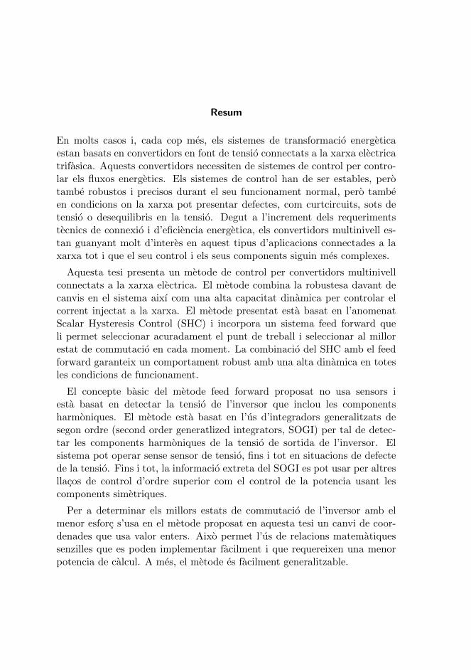
En molts casos i, cada cop mes, els sistemes de transformacio energeticaestan basats en convertidors en font de tensio connectats a la xarxa electricatrifasica. Aquests convertidors necessiten de sistemes de control per contro-lar els fluxos energetics. Els sistemes de control han de ser estables, perotambe robustos i precisos durant el seu funcionament normal, pero tambeen condicions on la xarxa pot presentar defectes, com curtcircuits, sots detensio o desequilibris en la tensio. Degut a l’increment dels requerimentstecnics de connexio i d’eficiencia energetica, els convertidors multinivell es-tan guanyant molt d’interes en aquest tipus d’aplicacions connectades a laxarxa tot i que el seu control i els seus components siguin mes complexes.
Aquesta tesi presenta un metode de control per convertidors multinivellconnectats a la xarxa electrica. El metode combina la robustesa davant decanvis en el sistema aixı com una alta capacitat dinamica per controlar elcorrent injectat a la xarxa. El metode presentat esta basat en l’anomenatScalar Hysteresis Control (SHC) i incorpora un sistema feed forward queli permet seleccionar acuradament el punt de treball i seleccionar al millorestat de commutacio en cada moment. La combinacio del SHC amb el feedforward garanteix un comportament robust amb una alta dinamica en totesles condicions de funcionament.
El concepte basic del metode feed forward proposat no usa sensors iesta basat en detectar la tensio de l’inversor que inclou les componentsharmoniques. El metode esta basat en l’us d’integradors generalitzats desegon ordre (second order generatlized integrators, SOGI) per tal de detec-tar les components harmoniques de la tensio de sortida de l’inversor. Elsistema pot operar sense sensor de tensio, fins i tot en situacions de defectede la tensio. Fins i tot, la informacio extreta del SOGI es pot usar per altresllacos de control d’ordre superior com el control de la potencia usant lescomponents simetriques.
Per a determinar els millors estats de commutacio de l’inversor amb elmenor esforc s’usa en el metode proposat en aquesta tesi un canvi de coor-denades que usa valor enters. Aixo permet l’us de relacions matematiquessenzilles que es poden implementar facilment i que requereixen una menorpotencia de calcul. A mes, el metode es facilment generalitzable.

En la tesi es presenten simulacions i resultats experimentals en conver-tidors multinivell de tres i cinc nivells per tal d’investigar i demostrar lesfuncionalitats del sistema de control proposat. Tant les simulacions com elsresultats experimentals es realitzen en totes les condicions possibles de laxarxa electrica, estat estacionari, sots i distorsions harmoniques.
vi
Contents
List of Figures xi
List of Tables xvii
1 Introduction 11.1 Background . . . . . . . . . . . . . . . . . . . . . . . . . . . . 11.2 Motivation of Research . . . . . . . . . . . . . . . . . . . . . . 31.3 Objectives of Research . . . . . . . . . . . . . . . . . . . . . . 41.4 Contributions of Research . . . . . . . . . . . . . . . . . . . . 51.5 Thesis Outline . . . . . . . . . . . . . . . . . . . . . . . . . . 6
2 Grid Connected Voltage Source Inverter Systems 92.1 Introduction . . . . . . . . . . . . . . . . . . . . . . . . . . . . 92.2 System Description and Modeling . . . . . . . . . . . . . . . . 11
2.2.1 Two-Level Voltage Source Inverter . . . . . . . . . . . 142.2.2 Space Vector Representation . . . . . . . . . . . . . . 17
2.3 Multilevel Inverters . . . . . . . . . . . . . . . . . . . . . . . . 202.4 Multilevel Topologies . . . . . . . . . . . . . . . . . . . . . . . 25
2.4.1 Diode Clamped Multilevel Inverter . . . . . . . . . . . 252.4.2 Flying Capacitor Multilevel Inverter . . . . . . . . . . 272.4.3 Cascaded H-Brigde Inverter . . . . . . . . . . . . . . . 282.4.4 Modular Multilevel Converter . . . . . . . . . . . . . . 29
2.5 Summary . . . . . . . . . . . . . . . . . . . . . . . . . . . . . 30
3 Control and Modulation Techniques for Multilevel Inverters 313.1 Indirect Control Techniques . . . . . . . . . . . . . . . . . . . 33
3.1.1 Carrier Based Modulation . . . . . . . . . . . . . . . . 333.1.2 Space Vector Pulse-Width Modulation . . . . . . . . . 35
3.2 Direct Control Techniques . . . . . . . . . . . . . . . . . . . . 393.2.1 Three-Phase Hysteresis Current Control . . . . . . . . 393.2.2 αβ Hysteresis Current Control . . . . . . . . . . . . . 423.2.3 Switched Diamond Hysteresis Current Control . . . . 443.2.4 Direct Power Control . . . . . . . . . . . . . . . . . . 49
vii
Contents
3.2.5 Scalar Hysteresis Control . . . . . . . . . . . . . . . . 52
3.3 Predictive Control . . . . . . . . . . . . . . . . . . . . . . . . 56
3.4 Summary . . . . . . . . . . . . . . . . . . . . . . . . . . . . . 59
4 Feed Forward Sector Control 614.1 Problem Statement . . . . . . . . . . . . . . . . . . . . . . . . 61
4.2 Voltage Synchronization Methods . . . . . . . . . . . . . . . . 63
4.2.1 Second Order Generalized Integrator . . . . . . . . . . 64
4.2.2 Frequency Readjustment . . . . . . . . . . . . . . . . . 66
4.2.3 Additional Harmonic Component Acquisition . . . . . 67
4.3 Sensorless Voltage Calculation . . . . . . . . . . . . . . . . . . 71
4.3.1 Simulation Results of Synchronization System . . . . . 75
4.4 Space Vector Selection . . . . . . . . . . . . . . . . . . . . . . 77
4.4.1 a∗b∗-Transformation . . . . . . . . . . . . . . . . . . . 77
4.4.2 Sector Selection . . . . . . . . . . . . . . . . . . . . . . 78
4.4.3 Generation of Switching States . . . . . . . . . . . . . 81
4.5 Summary . . . . . . . . . . . . . . . . . . . . . . . . . . . . . 83
5 Improved Direct Current Control 855.1 Simulation Parameters . . . . . . . . . . . . . . . . . . . . . . 86
5.2 Feed forward Control Within the Sector . . . . . . . . . . . . 88
5.3 Comparison of Switching Characteristics . . . . . . . . . . . . 91
5.3.1 Switching Characteristic of Three-Level NPC . . . . . 91
5.3.2 Switching Behaviour of Five-level DCI . . . . . . . . . 96
5.4 Sector Control under Dynamic Conditions . . . . . . . . . . . 99
5.4.1 Grid Voltage Sag . . . . . . . . . . . . . . . . . . . . . 101
5.4.2 Grid Frequency Jump . . . . . . . . . . . . . . . . . . 103
5.4.3 Set Current Jump . . . . . . . . . . . . . . . . . . . . 105
5.4.4 Unbalanced Grid Voltages . . . . . . . . . . . . . . . . 107
5.5 Operational Limitations . . . . . . . . . . . . . . . . . . . . . 109
5.6 Summary . . . . . . . . . . . . . . . . . . . . . . . . . . . . . 113
6 Grid Synchronization and Power Control 1156.1 Symmetrical Components . . . . . . . . . . . . . . . . . . . . 119
6.1.1 Filter Compensation . . . . . . . . . . . . . . . . . . . 120
6.1.2 Power Control with Symmetrical Components . . . . . 122
6.2 Summary . . . . . . . . . . . . . . . . . . . . . . . . . . . . . 128
7 Experimental Verification 1297.1 Test Bench and System Parameters . . . . . . . . . . . . . . . 129
viii
Contents
7.2 Measurement Results using a Three-Level NPC . . . . . . . . 1317.2.1 Standard Operating Point . . . . . . . . . . . . . . . . 1317.2.2 Harmonic distortion . . . . . . . . . . . . . . . . . . . 1337.2.3 Comparison of Operation Modes for Three-Level NPC 135
7.3 Measurements using a Five-Level DCI . . . . . . . . . . . . . 1377.3.1 Standard Operating Point . . . . . . . . . . . . . . . . 1377.3.2 Voltage Sag . . . . . . . . . . . . . . . . . . . . . . . . 1397.3.3 Harmonic Distortion . . . . . . . . . . . . . . . . . . . 1407.3.4 Frequency Jump . . . . . . . . . . . . . . . . . . . . . 1427.3.5 System Start Up . . . . . . . . . . . . . . . . . . . . . 1447.3.6 Comparison of SHC Operation Modes for 5-level DCI 146
7.4 Summary . . . . . . . . . . . . . . . . . . . . . . . . . . . . . 148
8 Conclusion and Future Works 1498.1 Conclusion . . . . . . . . . . . . . . . . . . . . . . . . . . . . 1498.2 Future Work . . . . . . . . . . . . . . . . . . . . . . . . . . . 1518.3 Publications and Patent Applications of the Author . . . . . 155
8.3.1 Results Related to Current Control Techniques forMultilevel Systems . . . . . . . . . . . . . . . . . . . . 155
8.3.2 Results Related to Applications for Current ControlTechniques . . . . . . . . . . . . . . . . . . . . . . . . 157
8.3.3 Patent Applications . . . . . . . . . . . . . . . . . . . 160
Bibliography 161
A Three-level SV-Diagram 173
B Transfer Function of Used MSOGI System 175
C Voltage Sag Classification 177
D Inverter Hardware and Testbench 181
ix

x
List of Figures
1.1 Development of gross energy production by renewable energysources in Germany from 1990 to 2017 . . . . . . . . . . . . . 2
2.1 Example of grid connected inverter system . . . . . . . . . . . 9
2.2 Equivalent circuit of a three-phase grid connected invertersystem with L-filter . . . . . . . . . . . . . . . . . . . . . . . . 11
2.3 Simplified equivalent circuit of a grid connected inverter sys-tem with L-filter . . . . . . . . . . . . . . . . . . . . . . . . . 13
2.4 Simplified model and generated output voltage of a single-phase two-level inverter . . . . . . . . . . . . . . . . . . . . . 15
2.5 Circuit diagram of a three-phase two-level inverter system . . 15
2.6 Geometrical representation of αβ-system . . . . . . . . . . . . 17
2.7 SV-diagram of a two-level inverter system with eight spacevectors . . . . . . . . . . . . . . . . . . . . . . . . . . . . . . . 19
2.8 Simplified model and output voltage of a single phase three-level inverter . . . . . . . . . . . . . . . . . . . . . . . . . . . 21
2.9 Simplified circuit diagram and generated output voltage of asingle phase five-level inverter . . . . . . . . . . . . . . . . . 22
2.10 SV-diagrams of selected multilevel inverters . . . . . . . . . . 24
2.11 Single-phase schematics of possible three-level NPC configu-rations using passive or active components . . . . . . . . . . . 26
2.12 Single-phase schematics of possible five-level configuration forthe DCI (NPC) topology . . . . . . . . . . . . . . . . . . . . . 26
2.13 One-phase schematic of three-level FCI . . . . . . . . . . . . . 27
2.14 Three-phase schematic of five-level H-bridge inverter system . 28
2.15 One-phase five-level MMC and possible submodules . . . . . 29
3.1 Simplified structure of indirect, direct and predictive controlsystems . . . . . . . . . . . . . . . . . . . . . . . . . . . . . . 32
3.2 Carrier based PWM modulator scheme . . . . . . . . . . . . . 34
3.3 Single-phase carrier based PWM and output voltage for athree-level inverter . . . . . . . . . . . . . . . . . . . . . . . . 35
xi
List of Figures
3.4 Controller scheme of SVPWM with current control circuit . . 36
3.5 SVPWM selection of used sector and required space vectorcombination for reproduction of the set voltage . . . . . . . . 37
3.6 Simplified multilevel SVPWM scheme for a three-level inverter 38
3.7 Three-phase hysteresis direct current controller scheme . . . . 40
3.8 Error current and generated output voltage for a two-levelinverter in phase U . . . . . . . . . . . . . . . . . . . . . . . . 40
3.9 Error current and generated output voltage by different tole-rance band types for a three-level inverter in phase U . . . . . 41
3.10 αβ hysteresis direct current controller scheme . . . . . . . . . 42
3.11 Rectangular tolerance area for a αβ hysteresis direct currentcontrol . . . . . . . . . . . . . . . . . . . . . . . . . . . . . . . 43
3.12 Switched Diamond Hysteresis controller scheme . . . . . . . . 45
3.13 Structure and orientation of preselecting sectors for the SDHCmethod in all three used coordinate systems . . . . . . . . . 46
3.14 Structure and orientation of current error and tolerance bandsfor the SDHC method in all three used coordinate systems . . 47
3.15 Structure and orientation of preselecting sectors for the SDHCmethod in standard αβ coordinate system for a three- andfive-level inverter . . . . . . . . . . . . . . . . . . . . . . . . . 48
3.16 Direct Power Control scheme . . . . . . . . . . . . . . . . . . 49
3.17 Structure of preselecting sectors and active power tolerancebands of VF-DPC for a three-level NPC . . . . . . . . . . . . 51
3.18 Structure of preselecting sectors and active power tolerancebands of VF-DPC for a five-level ANPC . . . . . . . . . . . . 51
3.19 Scalar Hysteresis controller scheme . . . . . . . . . . . . . . . 52
3.20 SHC selection mechanism and structure of inner toleranceband with highlighted space vector sections . . . . . . . . . . 53
3.21 SHC selection mechanism of outer tolerance band . . . . . . . 55
3.22 Hysteresis based predictive controller scheme . . . . . . . . . 56
3.23 Model based predictive controller scheme . . . . . . . . . . . 57
4.1 Simplified structure of scalar hysteresis controller (SHC) . . . 61
4.2 Circuit diagram of SRF-PLL . . . . . . . . . . . . . . . . . . 63
4.3 SOGI band-pass circuit . . . . . . . . . . . . . . . . . . . . . 64
4.4 Bode diagram of SOGI band-pass (left) and after second in-tegrator stage (right) with damping factor k = 1 . . . . . . . 66
4.5 Circuit diagram of FLL for a three-phase application withgain normalization . . . . . . . . . . . . . . . . . . . . . . . . 67
4.6 MSOGI band-pass circuit . . . . . . . . . . . . . . . . . . . . 68
xii
List of Figures
4.7 Top: magnitude responses of SOGI circuits for all selectedharmonics. Bottom: magnitude responses of MSOGI circuitsfor the fundamental component (left) and the 5th harmonic(right) . . . . . . . . . . . . . . . . . . . . . . . . . . . . . . . 70
4.8 Simplified equivalent circuit of a grid connected inverter sys-tem with voltage measurement points . . . . . . . . . . . . . 71
4.9 Current path of intermediate output state 0.5 [0 1 0 0], onlyS2 = ON for a three-level DCI with different current directions 74
4.10 Simplified circuit of sensorless inverter output voltage detec-tion concept . . . . . . . . . . . . . . . . . . . . . . . . . . . . 75
4.11 Simulation result for test of synchronization system. Left side:input voltage of MSOGI-system and detected fundamentalvoltage. Right side: sum of all MSOGI outputs and harmoniccomponents of phase U . . . . . . . . . . . . . . . . . . . . . . 76
4.12 Geometrical representation of ua∗b∗ system . . . . . . . . . . 78
4.13 Representation of feed forward voltage ~uff∗, selected sectorbase vectors ~Uff∗base and three-level SV-diagram in normalizedα∗β∗ coordinates . . . . . . . . . . . . . . . . . . . . . . . . . 80
4.14 Simplified circuit of the presented sensorless feed forward sec-tor selection system . . . . . . . . . . . . . . . . . . . . . . . 83
5.1 Simplified structure of SHC with feed forward sector control . 85
5.2 Impact of the feed forward voltage control on the angularsections of the tolerance circle within one sector . . . . . . . . 89
5.3 Three-level SV-diagram with feed forward voltage and mid-point voltage of triangle sectors selected by the outer toleranceband . . . . . . . . . . . . . . . . . . . . . . . . . . . . . . . . 91
5.4 Comparison of simulated three-level NPC output current andcurrent error at standard working point for SHC using outertolerance bands and feed forward control . . . . . . . . . . . . 93
5.5 Tolerance band areas and used space vectors of standard SHCof the two viewed sectors . . . . . . . . . . . . . . . . . . . . 94
5.6 Detail enlargement of current error at standard working pointfor SHC using outer tolerance bands and feed forward control 95
5.7 Detail enlargement of choosen SV-coordinates by using theouter tolerance band . . . . . . . . . . . . . . . . . . . . . . . 96
5.8 Five-level SV-diagram with feed forward voltage and mid-point voltage of triangle sectors selected by the outer toleran-ce band . . . . . . . . . . . . . . . . . . . . . . . . . . . . . . 97
xiii
List of Figures
5.9 Comparison of simulated five-level DCI output current andcurrent error at standard working point for SHC using outertolerance band and feed forward control . . . . . . . . . . . . 98
5.10 Simplified circuit of the proposed improved direct current con-trol system . . . . . . . . . . . . . . . . . . . . . . . . . . . . 100
5.11 Simulation results of three-level NPC reaction on three-phasevoltage sag (Type A) to 30 %. Left side: grid voltage andfeed forward signal. Right side: grid current and error current. 101
5.12 Three-level SV-diagram with feed forward voltage for a three-phase voltage sag (Type A) to 30 % . . . . . . . . . . . . . . 102
5.13 Simulation results of three-level NPC reaction on frequencyjump from 45 Hz to 55 Hz at t= 0.01 s. Left side: grid voltage,output current, error current. Right side: feed forward signal,detected phase angle, detected frequency. . . . . . . . . . . . 104
5.14 Simulation results of three-level NPC reaction on set currentjump from 20 A to −20 A. Left side: grid current and feedforward signal. Right side: detail enlargement of grid currentand error current. . . . . . . . . . . . . . . . . . . . . . . . . . 105
5.15 Three-level SV-diagram with feed forward voltage for an setcurrent jump from 20 A to −20 A . . . . . . . . . . . . . . . 106
5.16 Five-level SV-diagram for unbalanced grid condition with fe-ed forward voltage control and midpoint voltage of trianglesectors selected by the outer tolerance band . . . . . . . . . . 107
5.17 Simulation results of five-level DCI reaction on single-phasevoltage sag (Type B) to 0 % in phase U. Left side: grid voltageand feed forward signal. Right side: grid current and errorcurrent. . . . . . . . . . . . . . . . . . . . . . . . . . . . . . . 108
5.18 Simulation results of three-level NPC at a limited workingpoint. Left: three-phase output current. Right: error current 109
5.19 Simulation results of modified models with deactivated outertolerance band (left) and ideal hardware (right) . . . . . . . . 110
5.20 Simulation results of detected feed forward voltage and enlar-ged segment . . . . . . . . . . . . . . . . . . . . . . . . . . . . 111
6.1 Simplified equivalent circuit of a grid connected inverter sys-tem in αβ representation . . . . . . . . . . . . . . . . . . . . . 115
6.2 Relationship of generated feed forward voltage and grid vol-tage for pure active current . . . . . . . . . . . . . . . . . . . 116
xiv
List of Figures
6.3 Simulation results of realized power control with IARC. Leftside: grid voltage and active and reactive power. Right side:grid current and error current. . . . . . . . . . . . . . . . . . 118
6.4 Simplified schematic of BPSC method combined with the in-verter output voltage detection system . . . . . . . . . . . . . 123
6.5 Simulation results of realized BPSC power control. Left side:grid voltage and detected positive sequence. Right side: gridcurrent and active and reactive power. . . . . . . . . . . . . . 124
6.6 Simplified schematic of BPSC method combined with the in-verter output voltage detection system . . . . . . . . . . . . . 126
6.7 Simulation results of realized PNSC power control. Left side:grid voltage and detected negative sequence. Right side: gridcurrent and active and reactive power. . . . . . . . . . . . . . 127
7.1 Simplified structure of the test bench . . . . . . . . . . . . . . 129
7.2 Comparison of measured grid current, current error and resul-ting THDi under standard grid conditions for different controlschemes using a three-level NPC inverter . . . . . . . . . . . . 132
7.3 Three-level SV-diagram with standard and harmonic distor-ted grid voltage . . . . . . . . . . . . . . . . . . . . . . . . . . 133
7.4 Comparison of measured output current and calculated cur-rent spectrum under harmonic distorted grid voltage usingthe outer tolerance band (top), the fundamental componentas feed forward voltage (mid) and all harmonic componentsas feed forward voltage (bottom). . . . . . . . . . . . . . . . . 134
7.5 Three-level SV-diagram with tested modulation area . . . . . 136
7.6 Measured average switching frequency versus modulation in-dex for a three-level NPC when using the outer tolerance bandcontrol (red) and the feed forward sector control method (blue)136
7.7 Comparison of measured grid current, current error and resul-ting THDi under standard grid conditions for different controlschemes using a five-level DCI inverter . . . . . . . . . . . . . 138
7.8 Measurement results of five-level DCI reaction on voltage sag(type A) to 20 %. Left side: grid voltage, feed forward signal.Right side: output current, error current . . . . . . . . . . . . 139
7.9 Five-level SV-diagram with feed forward voltage for a three-phase voltage sag (type A) from 100 % to 20 % . . . . . . . . 140
7.10 Five-level SV-diagram with distorted grid voltage . . . . . . . 141
xv
List of Figures
7.11 Measurement results of five-level DCI system under harmonicgrid distortions. Left side: grid voltage, feed forward signal.Right side: output current, error current . . . . . . . . . . . . 142
7.12 Measurement results of three-level NPC reaction on a fre-quency jump from 45 Hz to 55 Hz. Left side: grid voltage,output current, error current. Right side: feed forward signal,detected phase, detected frequency. . . . . . . . . . . . . . . . 143
7.13 Measurement results of five-level DCI during startup. Leftside: output current, error current. Right side: feed forwardsignal, detected phase. . . . . . . . . . . . . . . . . . . . . . . 144
7.14 Five-level SV-diagram with feed forward voltage during startup1457.15 Five-level SV-diagram with marked area of tested modulation
indexes . . . . . . . . . . . . . . . . . . . . . . . . . . . . . . 1467.16 Measured average switching frequency versus modulation in-
dex for a five-level DCI when using the outer tolerance bandcontrol (red) and the feed forward sector control method (blue)147
8.1 Space vector positions for a five-level inverter system with aDC-link capacitor voltage deviation of 10 % (left) and 20 %(right) . . . . . . . . . . . . . . . . . . . . . . . . . . . . . . . 151
8.2 Simplified equivalent circuit of a grid connected inverter sys-tem with LCL-filter . . . . . . . . . . . . . . . . . . . . . . . . 152
8.3 Selected space vectors by extended selection method within afive-level SV-diagram . . . . . . . . . . . . . . . . . . . . . . 153
A.1 SV-diagram of three-level NPC system . . . . . . . . . . . . . 173
C.1 Example of transmission line . . . . . . . . . . . . . . . . . . 179
D.1 Grid simulator and DC-sources . . . . . . . . . . . . . . . . . 182D.2 Three-level NPC module . . . . . . . . . . . . . . . . . . . . . 183D.3 Phase module of five-level inverter . . . . . . . . . . . . . . . 184D.4 FPGA controller board . . . . . . . . . . . . . . . . . . . . . 186
xvi
List of Tables
2.1 Output voltage levels of a two-level inverter system in thethree-phase UVW-system for all possible switching combina-tions . . . . . . . . . . . . . . . . . . . . . . . . . . . . . . . . 16
2.2 Output voltage levels of two-level inverter system in the two-phase αβ system for all possible switch combinations . . . . . 18
2.3 Comparison of multilevel inverter topologies . . . . . . . . . . 30
3.1 αβ hysteresis control switching table . . . . . . . . . . . . . . 44
3.2 SDHC switching table for highlighted rectangular sector inFigure 3.13 . . . . . . . . . . . . . . . . . . . . . . . . . . . . 46
4.1 Output voltage states of a single-phase three-level invertersystem including current depending intermediate states . . . 73
4.2 Output voltage states of a single-phase five-level inverter sys-tem including current depending intermediate states . . . . . 73
5.1 Simulation parameters of three- and five-level DCI models . . 86
5.2 Angular ranges of the possible space vectors for the presentedvoltage points in Figure 5.2 . . . . . . . . . . . . . . . . . . . 90
6.1 Working behaviour of different active and reactive power cal-culations under unbalanced grid conditions . . . . . . . . . . 128
7.1 Parameters for three-level and five-level inverter test benches 130
7.2 Measurement results for standard operation of a three-levelNPC . . . . . . . . . . . . . . . . . . . . . . . . . . . . . . . 131
7.3 Measurement results for a three-level NPC under distortedgrid conditions . . . . . . . . . . . . . . . . . . . . . . . . . . 135
7.4 Measurement results for standard operation of a five-level DCI 137
7.5 Harmonic components of distorted grid voltage . . . . . . . . 141
A.1 Output voltage levels of three-level NPC system in the two-phase αβ-system for all possible switch combinations . . . . . 174
xvii

List of Tables
C.1 Change of voltage sag types caused by transformers in thetransmission line . . . . . . . . . . . . . . . . . . . . . . . . . 179
D.1 Parameters of the grid simulator . . . . . . . . . . . . . . . . 181D.2 Parameters of DC-sources . . . . . . . . . . . . . . . . . . . . 182D.3 Three-level inverter specification . . . . . . . . . . . . . . . . 183D.4 Five-level inverter specification . . . . . . . . . . . . . . . . . 184D.5 Parameters of the FPGA controller board . . . . . . . . . . . 185
xviii
Acronyms
µC Microcontroller.
A/D Analog to Digital.AC Alternating Current.ANPC Active Neutral Point Clamped.
BP Band-Pass.BPSC Balanced Positive Sequence Control.
D/A Digital to Analog.DC Direct Current.DCI Diode Clamped Inverter.DDSRF-PLL Decoupled Double Synchronos Refer-
ence Frame Phase Locked Loop.DIN German Institute for Standardization.DPC Direct Power Control.DSOGI Double Second Order Generalized In-
tegrator.DSP Digital Signal Processor.DTC Direct Torque Control.Dy Delta-Star.
EMI Electromagnetic Interference.EN European Norm.EPLL Enhanced Phase Locked Loop.
FCI Flying Capacitor Inverter.FLL Frequency Locked Loop.FPGA Field Programmable Gate Array.
GI Generalized Integrator.
xix
Acronyms
H-Bridge Half-Bridge.HV High Voltage.HVDC High Voltage Direct Current.
IARC Instantaneous Active and ReactiveControl.
IEEE Institute of Electrical and ElectronicsEngineers.
IGBT Insulated Gate Bipolar Transistor.
LVDS Low Voltage Differential Signaling.
MMC Modular Multilevel Converter.MOSFET Metal-Oxide-Semiconductor Field-
Effect Transistor.MPC Model Predictive Control.MSOGI Multi Second Order Generalized Inte-
grator.
NPC Neutral Point Clamped.
PCC Point of Common Coupling.PI Proportinal-Integral.PLL Phase Locked Loop.PNSC Positive and Negative Sequence Con-
trol.PWM Pulse-Width Modulation.
RAM Random Access Memory.RRF Rotating Reference Frame.
SDHC Switched Diamond Hysteresis Con-trol.
SHC Scalar Hysteresis Control.Si Silicon.SiC Silicon Carbide.SOGI Second Order Generalized Integrator.SRF Stationary Reference Frame.SRF-PLL Synchronos Reference Frame Phase
Locked Loop.
xx
Acronyms
STATCOM Static Synchronous Compensator.SV Space Vector.SVM Space Vector Modulation.SVPWM Space Vector Pulse-Width Modula-
tion.
THD Total Harmonic Distortion.T-NPC T-Type Neutral Point Clamped.TOSSI Third Order Sinussoidal Integrator.
VCO Voltage-Controlled Oscillator.VF Virtual-Flux.VF-DPC Virtual-Flux Direct Power Control.VHDL Very High Speed Integrated Circuit
Hardware Description Language.VOC Voltage Orientated Control.VSI Voltage Source Inverter.
WBG Wide-Bandgab.
xxi

xxii

List of Symbols
a∗, b∗, c∗ Normalised Components of the a∗b∗Coordinate System.
a∗, b∗, c∗ Components of the a∗b∗ System.
a Complex Phasor a = ej2π3 .
α, β, γ Clarke components.α′, β′, α′′, β′′ Components of the α′β′ and α′′β′′ Co-
ordinate System.
B Complex Tolerance Boundary.B Tolerance Boundary.
C Capacitance [F].
ζ Damping Ratio.
e Inner voltage source [V].
f Frequency [Hz].ψ Flux [Wb].
Γ FLL coefficient.g Cost Function.G Transfer Function.
I,i Current [A].I, i Complex Value of Current [A].Im Imaginary Part.
j Imaginary Unit.
k SOGI coefficient.
xxiii

List of Symbols
κ Level Count Dependent Normaliza-tion Factor for a∗b∗ → a∗b∗.
λ Power Factor.L Inductance [H].L1, L2, L3 Phase L1, L2, L3.
M Matrix M .M Modulation Index.
n Level Count.N Neutral Point.
ω Angular Frequency [rad/s].
P , p Active Power [W].π Pi - π ≈ 3.14159.
q Phase Shift of −90, q = e−jπ2 .
Q, q Reactive Power [var].
Re Real Part.R Resistance [Ω].
SV, ~SV Space Vector.s Switching Signal of Phase.
θ Phase Angle [rad].t Time.T Transformation Matrix T .T Sampling Time.
U, u Voltage [V].U, u Complex Value of Voltage [V].
Z Impedance.
xxiv
List of Subscripts
a, b, c Related to Phase a,b,c.
αβa∗b∗ Transformation Matrix from αβ →a∗b∗.
α, β, γ Clarke Components.a∗, b∗ Normalised Components of the a∗b∗
Coordinate System.
a∗, b∗ Components of the a∗b∗ System.α′, β′, α′′, β′′ Related to α′β′ and α′′β′′ Coordinate
System.avg Related to Average Value.
base Base Vector.block Block-Time.BPSC Related to Balanced Positive Se-
quence Control.
C Related to Capacitance.carr Related to Carrier Signal.c2 Related to Cosine Oscillation with
Double Fundamental Frequency.
DC Related to DC Side.dead Dead-Time.Diode Related to IGBT.d, q Park Components.
ε Error Signal.e Error Component.
F Related to Filter.f Related to Faulted Value.ff Related to Feedforward Value.
xxv
List of Subscripts
FLL Related to Frequency Locked Loop.fc Related to Flying Capacitor.
h Harmonic Component.hex Related to Hexagon.
IARC Related to Instantaneous Active andReactive Power Control.
IGBT Related to IGBT.i Related to Inner Tolerance Band.inv Inverter Output Voltage.
k Output Voltage Vector Index.
L Related to Inductance.
max Maximum.M Midpoint.min Minimum.m Phase to Neutral m = 1, 2, 3.MSOGI Related to MSOGI.
N Neutral.nom Related to Nominal Value.
opt Optimum.o Related to Outer Tolerance Band.
PNSC Related to Positive and Negative Se-quence Control.
pseudo Pseudo Reference Voltage.
q Related to Second SOGI output.
R Related to Resistance.real Related to Real Value.red Redundant Space Vector.ref Reference Component.
S Related to Sampling Time.
xxvi
List of Subscripts
set Settling Time.s2 Related to Sine Oscillation with Dou-
ble Fundamental Frequency.SOGI− BP Related to SOGI Band-Pass.SV Related to Space Vector.sw Related to Switch Offset Voltage.s Related to Switching Signal.
U,V,W Inverter Output Phase.
∗ Component in a∗b∗ Format.(1), (2), (0) Positive-, Negative-, Zero- Sequence
Components.
xxvii

xxviii
List of Superscripts
ˆ Peak Value.pred Predicted Value.
′ Related to SOGI, MSOGI and FLLOutput Value.
∗ Set Value.
xxix

xxx
Chapter 1
Introduction
1.1 Background
Within the last decades power electronic devices have become an integralpart for the conversion of electrical energy in all power classes. This startswith low power devices like small switching power supplies for mobile devices,drive systems in electric bikes and cars up to large inverters utilized indistribution grids. During this time many topologies and control schemeswere developed that can be used for one-phase systems up to any numberof phases applied in electrical motor drive systems, in industrial and gridapplications [1].
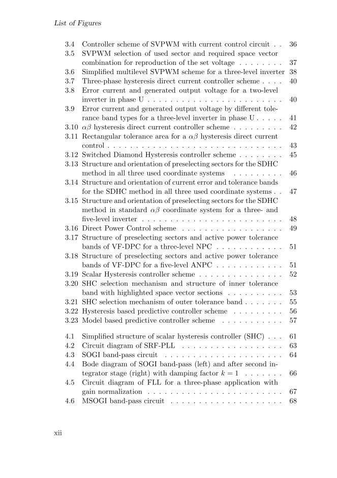
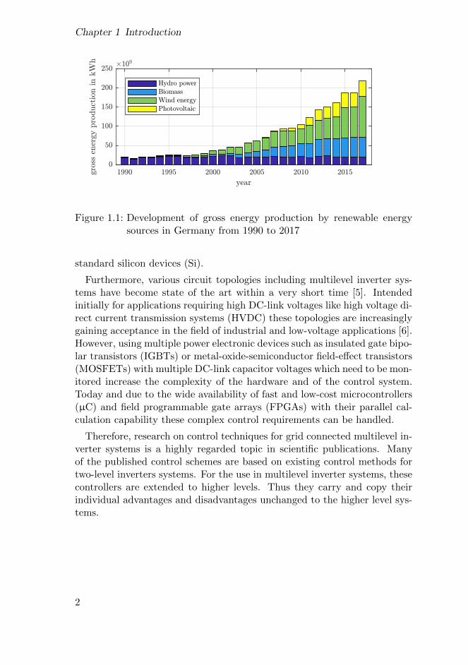
The increasing use of distributed power generation systems, leads to achanging workload and load flow within the grid. Instead of having a fewlarge power plants with rotating generators, a variety of small volatile feed-ers using power electronics are used [2]. In Germany the generation of re-newable energy, mainly by wind turbines and photovoltaics, has increasedsignificantly in the last years. Figure 1.1 shows the development of the grossenergy production by renewable sources [3]. As it can be seen the energygeneration by renewable sources has more than quintupled since 2000 andin 2017 already 36 percent of the total electric power consumption were gen-erated by renewable sources. This change of power generation puts highdemands on the grid stability [4].
To fulfil all grid standards and to increase the efficiency as well as thepower quality of the power conversion the development of power electronicdevices and topologies and the optimization and advancement of state of theart control concepts is being pursued intensively. These developments in-clude also new power electronic devices such as silicon carbide (SiC) or otherwide-bandgap semiconductors (WBG). The advantages of these devices are,among others, a higher blocking voltages and reduced losses compared to
1
Chapter 1 Introduction
Figure 1.1: Development of gross energy production by renewable energysources in Germany from 1990 to 2017
standard silicon devices (Si).
Furthermore, various circuit topologies including multilevel inverter sys-tems have become state of the art within a very short time [5]. Intendedinitially for applications requiring high DC-link voltages like high voltage di-rect current transmission systems (HVDC) these topologies are increasinglygaining acceptance in the field of industrial and low-voltage applications [6].However, using multiple power electronic devices such as insulated gate bipo-lar transistors (IGBTs) or metal-oxide-semiconductor field-effect transistors(MOSFETs) with multiple DC-link capacitor voltages which need to be mon-itored increase the complexity of the hardware and of the control system.Today and due to the wide availability of fast and low-cost microcontrollers(µC) and field programmable gate arrays (FPGAs) with their parallel cal-culation capability these complex control requirements can be handled.
Therefore, research on control techniques for grid connected multilevel in-verter systems is a highly regarded topic in scientific publications. Manyof the published control schemes are based on existing control methods fortwo-level inverters systems. For the use in multilevel inverter systems, thesecontrollers are extended to higher levels. Thus they carry and copy theirindividual advantages and disadvantages unchanged to the higher level sys-tems.
2
1.2 Motivation of Research
1.2 Motivation of Research
The requirements and the desired working behaviour for grid connected in-verters depends mainly on the final application. In addition to these in-dividual requirements, the stability and reliability of the inverter systemsitself play an important role regardless of the application. Thereby gridconnected inverters have to deal with a variety of unpredictable fault casesin their specific applications. The different grid faults defined in the gridstandards and are divided in continuous phenomena and voltage events [7].The most common grid faults and disturbances are:
• Continuous phenomena
– Fast voltage changes
– Harmonics and intermediate harmonics
– Grid frequency changes
– Grid voltage unbalance
– Standard signal transmission
• Voltage events
– Voltage interruption
– Voltage sags and overshoots
– Transient overvoltage
The response of the inverter system to the respective grid faults stronglydepends on the control method used. Due to their load-independent andhighly dynamic working behaviour, direct control methods are ideally suitedto handle those fault cases. Nevertheless, because of higher demands ontheir control system and a worse performance under steady state conditions,compared to indirect control techniques, they are only rarely used as controlscheme for inverter systems.
Another important aspect besides the optimal control method for gridconnected inverter systems is an appropriate grid synchronization method.The synchronization system must ensure that all informations about thegrid e.g. its phase voltages and frequency are correctly detected even duringa fault. This is absolutely necessary in order to guarantee a stable operationof the inverter system whenever possible. Especially when considering a gridvoltage sensorless inverter system the requirements for both the control andsynchronization method are very high.
3
Chapter 1 Introduction
1.3 Objectives of Research
The main objective of this thesis is the development and the verification of anadvancement for a direct current control scheme used in grid connected mul-tilevel inverter systems. The advancement is intended to improve the steadystate performance significantly while maintaining the excellent dynamic re-sponsiveness. These two features are essential and key characteristics forgrid connected inverters.
As mentioned above an exact detection of the grid voltage is an essentialpre-condition for controlling grid connected inverters. Therefore, a majorobjective of the thesis is to detect this voltage accurately and sensorless.Once this goal is achieved this voltage information can be used for boththe improvement of the current controller itself as well as for overall powercontrol. Thus the voltage information should be detected by a specific gridsynchronisation method and is used to improve the operating behaviour ofthe direct current controller under steady state conditions. For this purpose,the voltage informations are used to identify the actual working point of themultilevel inverter system and to select the best switching combinations.
For the selection of the correct switching combinations the high complex-ity of a multilevel inverter needs to be simplified in order to achieve shortcalculation times by avoiding high computational effort. These aims lead tothe following objectives:
• Straightforward and generic method to quick and simple determine thecorrect switching combinations.
• Harmonic voltage component detection capability to ensure the selec-tion of the correct switching combinations even in harmonic distortedgrids when using multilevel inverter systems.
• Once the synchronization method mentioned above is already an ob-jective of the thesis it should be used as well for higher-level set currentcalculation to achieve active and reactive power control methods.
• Since the complexity of higher level inverters increases significantlywith the level count the new current controller should easily be ex-pendable to multilevel inverter systems with higher level counts anddifferent topologies.
• The thesis is intended to analyse and validate the working behaviourunder steady state condition and under different dynamic grid faultconditions.
4
1.4 Contributions of Research
1.4 Contributions of Research
Based on the preceding objectives the main scientific contributions can besummarized to:
• The thesis introduces an approach to detect the average inverter out-put voltage without measurement informations. The presented combi-nation of a voltage sensorless synchronization system and direct cur-rent control method is able to deal with different fault conditions thatcan occur within the gird. To further improve the system performanceeven under harmonic distortions the presented system is able to detectthe fundamental component of the inverter output voltage and its gridspecific harmonic components.
• On the basis of the exact voltage informations a feed forward systemis set up that is able to accurately select the actual sector in the spacevector diagram. Under steady state conditions, this system enables adirect current controller to control the current with three neighbouringspace vectors without using additional outer tolerance bands. For thispurpose, a new coordinate transformation simplifies the representationof the sectors and switching states of multilevel inverter systems. Inaddition, the general integer-value based description of the multilevelinverter system enables a simple extension to higher level counts anddifferent topologies.
• To ensure the operational capability of the improved current controllerconcept during dynamic conditions the proposed system is combinedwith the standard outer tolerance band control concept known fromliterature. Depending on the actual working point the control systemcan dynamically choose one of the two sector selection methods toguarantee the best working behaviour under any condition.
• The proposed synchronization system can easily be extended for higher-level active and reactive power controllers. To compensate the filtercomponents a simple mathematical approach using the symmetricalcomponents is applied.
• Simulations and real laboratory measurements using a three- and five-level inverter system are carried out to investigate the behaviour ofthe new concept under real conditions and different working points.The measurements prove that the proposed system shows an excellentdynamic behaviour, high robustness and a significant improvement insteady state operation compared to the state of the art controllers.
5
Chapter 1 Introduction
1.5 Thesis Outline
Chapter 1 gives a short introduction to the subject and introduces thebackground of the thesis. In addition, the motivation, the objectives andthe contributions of the thesis are summarised.
Chapter 2 offers a brief survey of the basic functionality of grid connectedtwo-, three- and five-level inverter systems. Existing multilevel topologieswith their advantages and disadvantages are described.
Chapter 3 presents an overview of state of the art control techniques forthree-phase inverters. Thereby various indirect, direct and predictive con-trollers are described. Particular attention is given to the effort to extendthese controller types to multilevel inverter systems.
Chapter 4 proposes a sensorless voltage detection scheme. The aim of thismethod is to detect the average output voltage of the inverter includingspecific harmonic voltage components. With the knowledge of these voltageinformations a feed forward sector selection method is presented to improvethe working behaviour of a state of the art direct current controller. Forthis purpose a new coordinate transformation is introduced to simplify thecorrect selection of sectors and space vectors.
Chapter 5 investigates the improved functionality of the proposed directcurrent controller method. Different operating characteristics under steadystate conditions and during dynamic events are investigated. Simulationsof a three- and five-level inverter system using the standard direct currentcontroller and the improved direct current control are carried out and arecompared.
Chapter 6 considers the integration of overlaid power control techniquesin the proposed system. A short overview of power controllers used in gridapplication is provided. Compared to the preceding chapter the exact knowl-edge of the grid voltage needs to be determined. Therefore, the calculationof the grid voltage and the compensation of the inverter filter elements isshown using symmetrical components.
Chapter 7 presents experimental results with real hardware. For this pur-
6

1.5 Thesis Outline
pose, two test benches are set up in the laboratory. Various measurementson an off the shelf three-level and a self-built five level system with differentgrid distortions and faults are evaluated.
Chapter 8 summarizes the contributions of the thesis. Some additionalaspects of the proposed control concept are described which were discoveredduring the research work. A list of scientific publications of the author islisted in this chapter.
7

8
Chapter 2
Grid Connected Voltage SourceInverter Systems
2.1 Introduction
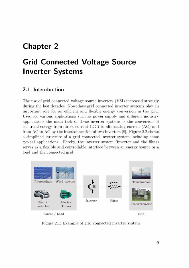
The use of grid connected voltage source inverters (VSI) increased stronglyduring the last decades. Nowadays grid connected inverter systems play animportant role for an efficient and flexible energy conversion in the grid.Used for various applications such as power supply and different industryapplications the main task of these inverter systems is the conversion ofelectrical energy from direct current (DC) to alternating current (AC) andfrom AC to AC by the interconnection of two inverters [8]. Figure 2.2 showsa simplified structure of a grid connected inverter system including sometypical applications. Hereby, the inverter system (inverter and the filter)serves as a flexible and controllable interface between an energy source or aload and the connected grid.
Electric
Vehicles
Electric
Drives
Photovoltaik Wind turbine
Source / Load
Inverter Filter
Transmission
Transformation
Grid
Figure 2.1: Example of grid connected inverter system
9
Chapter 2 Grid Connected Voltage Source Inverter Systems
The main application areas of grid connected inverter systems are
• Distributed energy generation, primary renewable energy sources suchas wind and solar power.
• Compensation of inductive and capacitive reactive power for grid sta-bilization (e.g. STATCOM).
• DC-link power supply for industry applications (e.g. electric drives).
• Parallel use in combination with non-linear loads (e.g. diode recti-fier) as shunt active filter to compensate harmonic components in theoutput current.
• Grid integration of energy storage systems (e.g. batteries) to compen-sate local peaks in power generation and consumption.
In the following sections the basic functionality of grid connected invertersare described. Furthermore, the advantages and disadvantages of multilevelinverter systems compared to two-level inverter systems are shown. There-fore, the structure and operation principle of different multilevel topologiesis presented.
10
2.2 System Description and Modeling
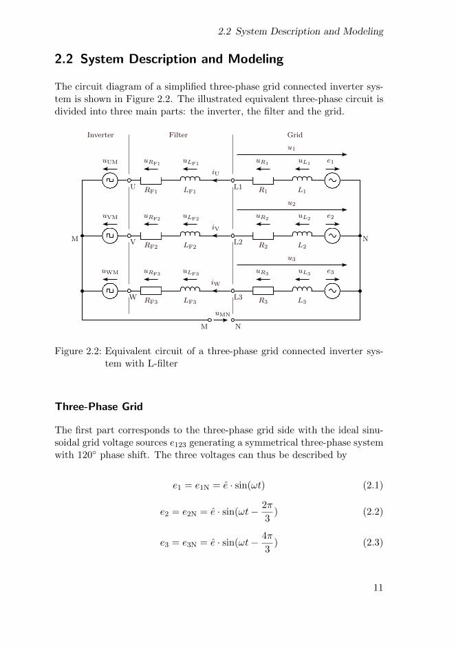
2.2 System Description and Modeling
The circuit diagram of a simplified three-phase grid connected inverter sys-tem is shown in Figure 2.2. The illustrated equivalent three-phase circuit isdivided into three main parts: the inverter, the filter and the grid.
LF1RF1
iU
uLF1
L1R1
e1uUM uRF1uR1
uL1
L1U
u1
LF2RF2
iV
uLF2
L2R2
e2uVM uRF2uR2 uL2
L2V
u2
LF3RF3
iW
uLF3
L3R3
e3uWM uRF3uR3
uL3
L3W
u3
N
NM
M
uMN
Inverter Filter Grid
Figure 2.2: Equivalent circuit of a three-phase grid connected inverter sys-tem with L-filter
Three-Phase Grid
The first part corresponds to the three-phase grid side with the ideal sinu-soidal grid voltage sources e123 generating a symmetrical three-phase systemwith 120 phase shift. The three voltages can thus be described by
e1 = e1N = e · sin(ωt) (2.1)
e2 = e2N = e · sin(ωt− 2π
3) (2.2)
e3 = e3N = e · sin(ωt− 4π
3) (2.3)
11
Chapter 2 Grid Connected Voltage Source Inverter Systems
The inductances L123 and resistances R123 correspond to the grid impedanceZ123 which represents the sum of all grid components such as electrical linesand transformers. Due to non-linear loads and other sources of harmoniccurrents connected to the grid, the voltage drop across the grid impedanceleads to distorted grid voltages. The grid connection points L1, L2 and L3represent the point of common coupling (PCC) and its voltages u123 can becalculated by [9]
u1 = u1N = e1 − uR1 − uL1 (2.4)
u2 = u2N = e2 − uR2 − uL2 (2.5)
u3 = u3N = e3 − uR3 − uL3 (2.6)
Filter
The filter serves as coupling element and energy storage between the twovoltage sources of the grid and the inverter system. In Figure 2.2 a firstorder L-filter represented by the inductive component LF and resistancecomponent RF is used. Due to the inductance of the filter and the switchingoperation of the inverter, the current flow and thus the power flow betweenthe grid and the system which is coupled to the DC-side of the inverter canbe controlled. The slope of the current can be calculated using the voltageuLF
applied to the inductance. This voltage corresponds to the differencebetween the grid and the inverter output voltage. The equation for thecurrent slope is defined by
di
dt=uLF
LF(2.7)
The size of the inductance must be chosen so, that all limits for the emittedcurrent and voltage harmonics defined in the grid standards at the PCC arefulfilled [10, 11]. Thereby, the in this case used L-filter is the simplest form.In grid applications other filter topologies like the third order LCL-filter areoften used as alternative. Compared to the first order L-filter this filtertopology offers some advantages such as a smaller inductance to meet thesame grid standards [12]. However, the disadvantages like possible systemoscillations and instability may increase the design effort and needs to beconsidered as well [13].
12
2.2 System Description and Modeling
Voltage Source Inverter
The voltage source inverter is the main element of the system and it isrepresented by the three voltage sources uUM, uVM and uWM. Since theneutral point N is not connected to M in the three-wire grid connection ofthe inverter system, Kirchhoffs law can be applied leading to
0 = iu + iv + iw (2.8)
This leads to the fact that the current slope to be controlled is limited to
0 =diUdt
+diVdt
+diWdt
(2.9)
A simplified representation of a grid connected inverter system is shownin Figure 2.3. The inverter side is represented by the voltage source uUVW
which is connected to the neutral point N of the grid.
LFRF 33
LOAD A
LFRF
iUVW
sUVWi∗UVWieUVW
u123uUVW
iUVW
uRFuLF
N N
Figure 2.3: Simplified equivalent circuit of a grid connected inverter systemwith L-filter
Since the neutral point N is not connected in the three-wire application theinverter output voltages uUM, uVM and uWM need to be summed up withthe auxiliary voltage uMN to calculate the voltages uU, uV and uW.
uU = uUN (2.10)
uV = uVN (2.11)
uW = uWN (2.12)
The grid side is represented by the voltage source u123 which is the voltageat the PCC. The inductive and resistive components of the grid impedanceare neglected in this simplified representation because they are not exactlyknown and much smaller than the filter components. Furthermore, it is
13
Chapter 2 Grid Connected Voltage Source Inverter Systems
assumed that the filter inductance LF and RF are constant in all threephases. Due to this simplification, the following equation can be used todescribe the overall system
u123 = uUVW +RF · iUVW + LF ·diUVW
dt(2.13)
Another common method to mathematically describe a grid connectedinverter system uses the virtual-flux (VF). This method is based on thefact that the simplified circuit diagram of an electric drive is identical tothat of a grid connected system [14]. Therefore, the inductive and resistivecomponents represent the stator resistance and leakage inductance of thevirtual motor. The phase voltages are considered to be generated by the airgap flux. This leads to the following expression
ψ123 =
∫(uUVW +RF · iUVW) dt+ LF · iUVW (2.14)
On the basis of this VF-modeling, it is possible to better describe and reg-ulate voltage sensorless systems due to the low-pass characteristics of theintegrator [15].
2.2.1 Two-Level Voltage Source Inverter
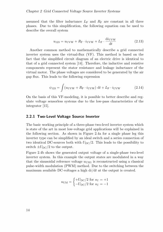
The basic working principle of a three-phase two-level inverter system whichis state of the art in most low-voltage grid applications will be explained inthe following section. As shown in Figure 2.4a for a single phase leg thisinverter type can be simplified by an ideal switch and a series connection oftwo identical DC-sources both with UDC/2. This leads to the possibility toswitch ±UDC/2 to the output.
Figure 2.4b shows the generated output voltage of a single-phase two-levelinverter system. In this example the output states are modulated in a waythat the sinusoidal reference voltage uUM1 is reconstructed using a classicalpulse-width modulation (PWM) method. Due to the switching between themaximum available DC-voltages a high di/dt at the output is created.
uUM =
+UDC/2 for sU = +1−UDC/2 for sU = −1
14
2.2 System Description and Modeling
LFRF
33
LOAD A
LFRF
iUVW
sUVWi∗UVWieUVW
u123uUVW
iUVW
uRFuLF
+1
−1
sU
uUM
M
UDC2
UDC2
(a) Simplified circuit diagram
0 0.005 0.01 0.015 0.02
t in s
-UDC
2
0
UDC
2
uUM uUM1
uU
M;u
UM
1in
V(b) Modulated output voltage uUM and
its reference voltage uUM1
Figure 2.4: Simplified model and generated output voltage of a single-phasetwo-level inverter
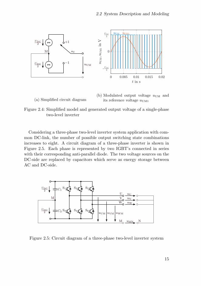
Considering a three-phase two-level inverter system application with com-mon DC-link, the number of possible output switching state combinationsincreases to eight. A circuit diagram of a three-phase inverter is shown inFigure 2.5. Each phase is represented by two IGBT’s connected in serieswith their corresponding anti-parallel diode. The two voltage sources on theDC-side are replaced by capacitors which serve as energy storage betweenAC and DC-side.
LFRF
33
LOAD A
LFRF
iUVW
sUVWi∗UVWieUVW
u123uUVW
iUVW
uRFuLF
+1
−1
sV
uUM
M
UDC2
UDC2
+1
−1
sU +1
−1
sU
S1
S2
S3
S4
C1
C2
M CfcUDC
C1
C2
M
S1 S3 S5
S2 S4 S6
M
U
V
W
uVM uWM
N
uW
uV
uU
uMN
Figure 2.5: Circuit diagram of a three-phase two-level inverter system
15
Chapter 2 Grid Connected Voltage Source Inverter Systems
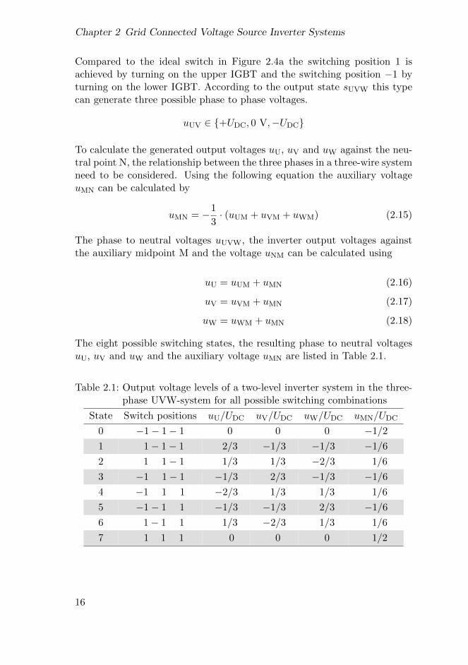
Compared to the ideal switch in Figure 2.4a the switching position 1 isachieved by turning on the upper IGBT and the switching position −1 byturning on the lower IGBT. According to the output state sUVW this typecan generate three possible phase to phase voltages.
uUV ∈ +UDC, 0 V,−UDC
To calculate the generated output voltages uU, uV and uW against the neu-tral point N, the relationship between the three phases in a three-wire systemneed to be considered. Using the following equation the auxiliary voltageuMN can be calculated by
uMN = −1
3· (uUM + uVM + uWM) (2.15)
The phase to neutral voltages uUVW, the inverter output voltages againstthe auxiliary midpoint M and the voltage uNM can be calculated using
uU = uUM + uMN (2.16)
uV = uVM + uMN (2.17)
uW = uWM + uMN (2.18)
The eight possible switching states, the resulting phase to neutral voltagesuU, uV and uW and the auxiliary voltage uMN are listed in Table 2.1.
Table 2.1: Output voltage levels of a two-level inverter system in the three-phase UVW-system for all possible switching combinations
State Switch positions uU/UDC uV/UDC uW/UDC uMN/UDC
0 −1− 1− 1 0 0 0 −1/2
1 1− 1− 1 2/3 −1/3 −1/3 −1/6
2 1 1− 1 1/3 1/3 −2/3 1/6
3 −1 1− 1 −1/3 2/3 −1/3 −1/6
4 −1 1 1 −2/3 1/3 1/3 1/6
5 −1− 1 1 −1/3 −1/3 2/3 −1/6
6 1− 1 1 1/3 −2/3 1/3 1/6
7 1 1 1 0 0 0 1/2
16
2.2 System Description and Modeling
As it is apparent, the eight possible switching combinations can generateseven different voltage levels. The output state 0 with the switching posi-tion [−1− 1− 1] and the output state 7 with the switching position [1 1 1]generate the same voltage in all three phases. Therefore, these two switch-ing combinations are called redundant states. In the case of the two-levelinverter system those states correspond to the zero voltage states.
2.2.2 Space Vector Representation
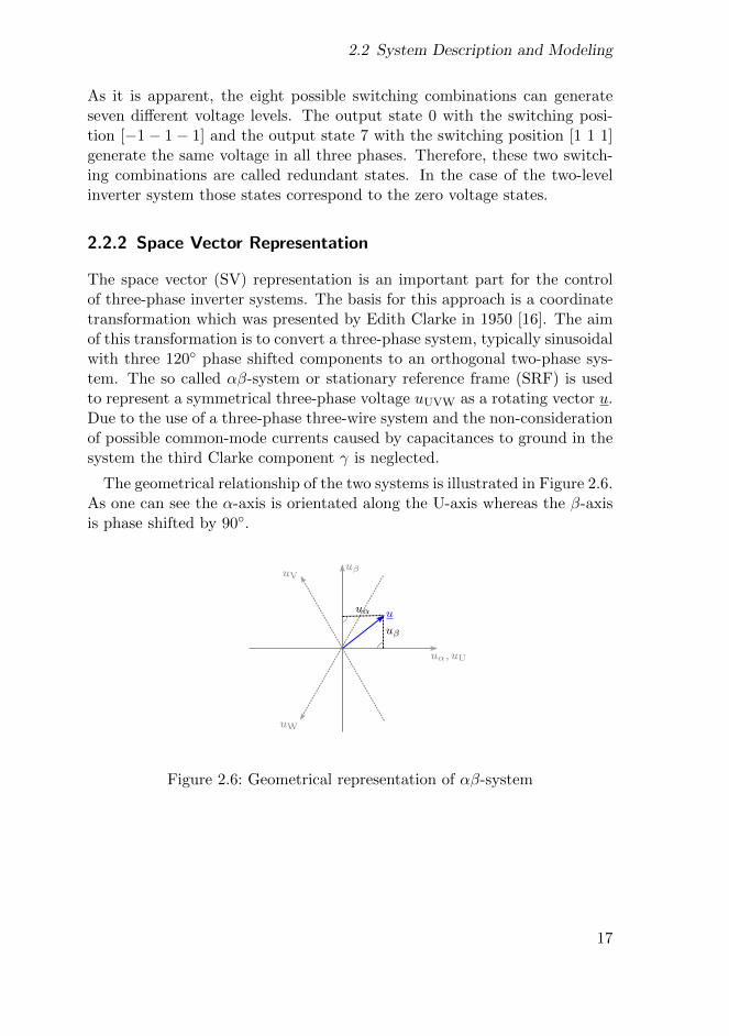
The space vector (SV) representation is an important part for the controlof three-phase inverter systems. The basis for this approach is a coordinatetransformation which was presented by Edith Clarke in 1950 [16]. The aimof this transformation is to convert a three-phase system, typically sinusoidalwith three 120 phase shifted components to an orthogonal two-phase sys-tem. The so called αβ-system or stationary reference frame (SRF) is usedto represent a symmetrical three-phase voltage uUVW as a rotating vector u.Due to the use of a three-phase three-wire system and the non-considerationof possible common-mode currents caused by capacitances to ground in thesystem the third Clarke component γ is neglected.
The geometrical relationship of the two systems is illustrated in Figure 2.6.As one can see the α-axis is orientated along the U-axis whereas the β-axisis phase shifted by 90.
π 2π
UPM
U∆
U∆
−U∆
−2U∆
0
Breite: 60 mm (halbseitig)uα
uβ
sector 9
sector 10
sector 11
sector 12
60 x 50
uα
uβ
sector 5
sector 6uα
uβ
SV1
SV2SV3
SV6SV5
SV4 SV0/7
u
uα
uβ
SV1
SV2SV3
SV6SV5
SV4
u′βu′′β
SV0/7
u′α
u′′α
uα
uβ
SV1SV4 SV0/7
u
SV2SV3
SV6SV5
uα
uβ
u
uα
uβ
u
uα, uU
uβ
u
uV
uW
uα
uβ
uα
uβ
SV1SV4 SV0/7
SV2SV3
SV6SV5
uα
uβ
uα
uβ
Figure 2.6: Geometrical representation of αβ-system
17
Chapter 2 Grid Connected Voltage Source Inverter Systems
The mathematical relationship to calculate the αβ components from theUVW components is given by
[uαuβ
]= Tαβ ·
uU
uV
uW
=2
3·
[1 −1
2 −12
0√
32 −
√3
2
]·
uU
uV
uW
(2.19)
The factor 2/3 is used to unify the amplitudes of the αβ and UVW coordi-nate systems. Due to the precondition that the sum of the three voltages iszero only two phases need to be measured. Therefore, the equation can besimplified to
[uαuβ
]=
2
3·
[1 01√3
2√3
]·[uU
uV
](2.20)
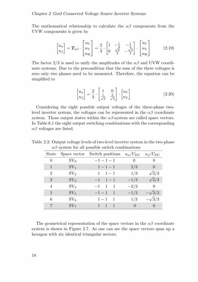
Considering the eight possible output voltages of the three-phase two-level inverter system, the voltages can be represented in the αβ coordinatesystem. Those output states within the αβ-system are called space vectors.In Table 6.1 the eight output switching combinations with the correspondingαβ voltages are listed.
Table 2.2: Output voltage levels of two-level inverter system in the two-phaseαβ system for all possible switch combinations
State Space vector Switch positions uα/UDC uβ/UDC
0 SV0 −1− 1− 1 0 0
1 SV1 1− 1− 1 2/3 0
2 SV2 1 1− 1 1/3√
3/3
3 SV3 −1 1− 1 −1/3√
3/3
4 SV4 −1 1 1 −2/3 0
5 SV5 −1− 1 1 −1/3 −√
3/3
6 SV6 1− 1 1 1/3 −√
3/3
7 SV7 1 1 1 0 0
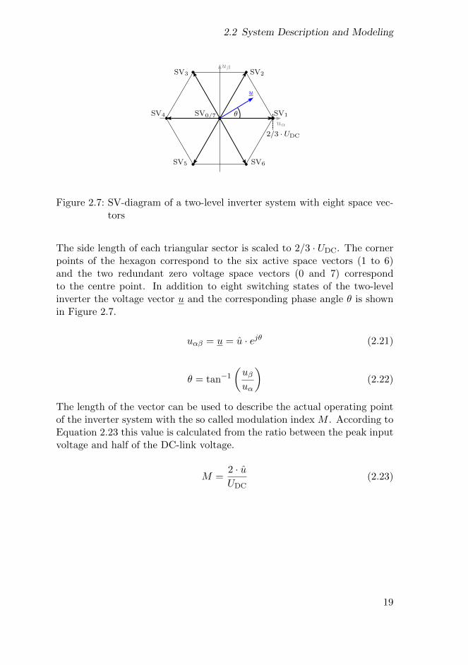
The geometrical representation of the space vectors in the αβ coordinatesystem is shown in Figure 2.7. As one can see the space vectors span up ahexagon with six identical triangular sectors.
18
2.2 System Description and Modeling
π 2π
UPM
U∆
U∆
−U∆
−2U∆
0
Breite: 60 mm (halbseitig)uα
uβ
sector 9
sector 10
sector 11
sector 12
60 x 50
uα
uβ
sector 5
sector 6uα
uβ
SV1
SV2SV3
SV6SV5
SV4 SV0/7
u
uα
uβ
SV1
SV2SV3
SV6SV5
SV4
u′βu′′β
SV0/7
u′α
u′′α
uα
uβ
SV1SV4 SV0/7
u
SV2SV3
SV6SV5
uα
uβ
u
uα
uβ
u
uα, uU
uβ
u
uV
uW
uα
uβ
uα
uβ
SV1SV4 SV0/7
SV2SV3
SV6SV5
θ
uα
uβ
uα
uβ
u
2/3 · UDC
2/3 · UDC
2/3 · UDC
Figure 2.7: SV-diagram of a two-level inverter system with eight space vec-tors
The side length of each triangular sector is scaled to 2/3 · UDC. The cornerpoints of the hexagon correspond to the six active space vectors (1 to 6)and the two redundant zero voltage space vectors (0 and 7) correspondto the centre point. In addition to eight switching states of the two-levelinverter the voltage vector u and the corresponding phase angle θ is shownin Figure 2.7.
uαβ = u = u · ejθ (2.21)
θ = tan−1
(uβuα
)(2.22)
The length of the vector can be used to describe the actual operating pointof the inverter system with the so called modulation index M . According toEquation 2.23 this value is calculated from the ratio between the peak inputvoltage and half of the DC-link voltage.
M =2 · uUDC
(2.23)
19
Chapter 2 Grid Connected Voltage Source Inverter Systems
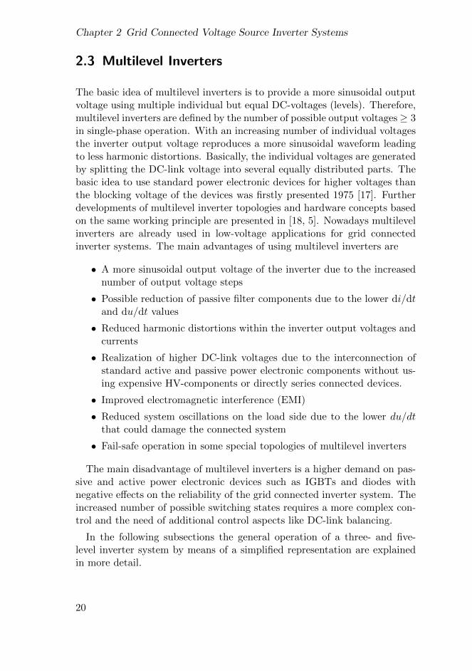
2.3 Multilevel Inverters
The basic idea of multilevel inverters is to provide a more sinusoidal outputvoltage using multiple individual but equal DC-voltages (levels). Therefore,multilevel inverters are defined by the number of possible output voltages≥ 3in single-phase operation. With an increasing number of individual voltagesthe inverter output voltage reproduces a more sinusoidal waveform leadingto less harmonic distortions. Basically, the individual voltages are generatedby splitting the DC-link voltage into several equally distributed parts. Thebasic idea to use standard power electronic devices for higher voltages thanthe blocking voltage of the devices was firstly presented 1975 [17]. Furtherdevelopments of multilevel inverter topologies and hardware concepts basedon the same working principle are presented in [18, 5]. Nowadays multilevelinverters are already used in low-voltage applications for grid connectedinverter systems. The main advantages of using multilevel inverters are
• A more sinusoidal output voltage of the inverter due to the increasednumber of output voltage steps
• Possible reduction of passive filter components due to the lower di/dtand du/dt values
• Reduced harmonic distortions within the inverter output voltages andcurrents
• Realization of higher DC-link voltages due to the interconnection ofstandard active and passive power electronic components without us-ing expensive HV-components or directly series connected devices.
• Improved electromagnetic interference (EMI)
• Reduced system oscillations on the load side due to the lower du/dtthat could damage the connected system
• Fail-safe operation in some special topologies of multilevel inverters
The main disadvantage of multilevel inverters is a higher demand on pas-sive and active power electronic devices such as IGBTs and diodes withnegative effects on the reliability of the grid connected inverter system. Theincreased number of possible switching states requires a more complex con-trol and the need of additional control aspects like DC-link balancing.
In the following subsections the general operation of a three- and five-level inverter system by means of a simplified representation are explainedin more detail.
20
2.3 Multilevel Inverters
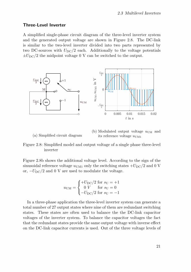
Three-Level Inverter
A simplified single-phase circuit diagram of the three-level inverter systemand the generated output voltage are shown in Figure 2.8. The DC-linkis similar to the two-level inverter divided into two parts represented bytwo DC-sources with UDC/2 each. Additionally to the voltage potentials±UDC/2 the midpoint voltage 0 V can be switched to the output.
LFRF
33
LOAD A
LFRF
iUVW
sUVWi∗UVWieUVW
u123uUVW
iUVW
uRFuLF
+1
−1
sU
uUM
M
UDC2
UDC2
0
(a) Simplified circuit diagram
0 0.005 0.01 0.015 0.02
t in s
-UDC
2
0
UDC
2
uUM
uUM1
uU
M;u
UM
1in
V
(b) Modulated output voltage uUM andits reference voltage uUM1
Figure 2.8: Simplified model and output voltage of a single phase three-levelinverter
Figure 2.8b shows the additional voltage level. According to the sign of thesinusoidal reference voltage uUM1 only the switching states +UDC/2 and 0 Vor, −UDC/2 and 0 V are used to modulate the voltage.
uUM =
+UDC/2 for sU = +1
0 V for sU = 0−UDC/2 for sU = −1
In a three-phase application the three-level inverter system can generate atotal number of 27 output states where nine of them are redundant switchingstates. These states are often used to balance the the DC-link capacitorvoltages of the inverter system. To balance the capacitor voltages the factthat the redundant states provide the same output voltage with inverse effecton the DC-link capacitor currents is used. Out of the three voltage levels of
21
Chapter 2 Grid Connected Voltage Source Inverter Systems
one phase leg the three-phase three-level inverter system can generate a totalnumber of five phase to phase voltages and nine phase to neutral voltages.
uUV ∈ +UDC,+UDC/2, 0 V,−UDC/2,−UDC
Five-Level Inverter System
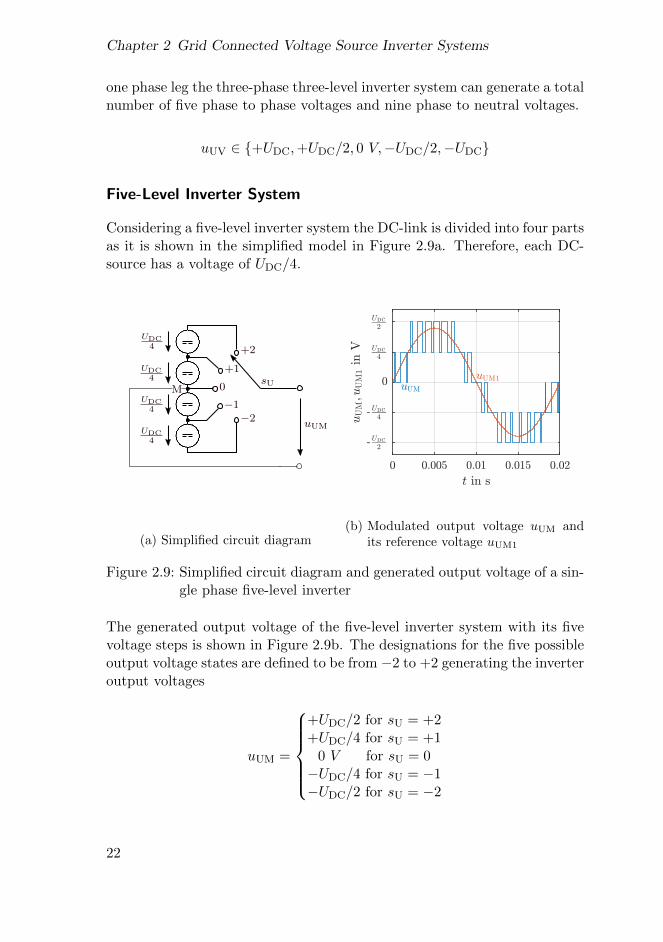
Considering a five-level inverter system the DC-link is divided into four partsas it is shown in the simplified model in Figure 2.9a. Therefore, each DC-source has a voltage of UDC/4.
LFRF
33
LOAD A
LFRF
iUVW
sUVWi∗UVWieUVW
u123uUVW
iUVW
uRFuLF
+2
−2
sU
uUM
M
UDC4
UDC4
0UDC4
UDC4
−1
+1
(a) Simplified circuit diagram
0 0.005 0.01 0.015 0.02
t in s
-UDC
2
-UDC
4
0
UDC
4
UDC
2
uUM
uUM1
uU
M;u
UM
1in
V
(b) Modulated output voltage uUM andits reference voltage uUM1
Figure 2.9: Simplified circuit diagram and generated output voltage of a sin-gle phase five-level inverter
The generated output voltage of the five-level inverter system with its fivevoltage steps is shown in Figure 2.9b. The designations for the five possibleoutput voltage states are defined to be from −2 to +2 generating the inverteroutput voltages
uUM =
+UDC/2 for sU = +2+UDC/4 for sU = +1
0 V for sU = 0−UDC/4 for sU = −1−UDC/2 for sU = −2
22
2.3 Multilevel Inverters
When using a five-level inverter in a three-phase system the total numberof possible output state combinations increases to 125. The related numberof phase to phase voltage levels is rising up to nine and the possible numberof phase to neutral voltages to 17 different voltages.
uUV ∈ +UDC,+3UDC/4,+UDC/2,+UDC/4, 0 V,
− UDC/4,−UDC/2,−3UDC/4,−UDC
For multilevel inverters with n-levels the step voltage can be calculatedby applying the following equation
uUM =UDC
n− 1(2.24)
Considering the three-phase application of a n-level inverter system the totalnumber of possible output states increases to n3, the associated number ofphase to phase voltages to 2 ·n− 1 and the total number of phase to neutralvoltages to 4 · n − 3. For the example of the 13-level inverter system 8192possible output state combinations with 49 possible phase to neutral voltagesneed to be considered.
Space Vector Representation of Three- and Five-Level Inverters
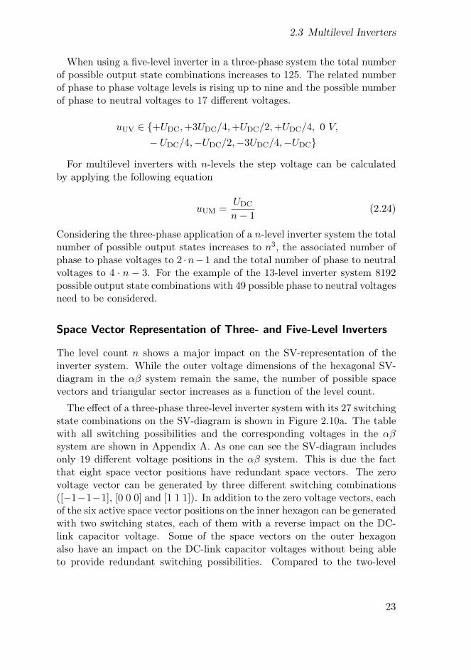
The level count n shows a major impact on the SV-representation of theinverter system. While the outer voltage dimensions of the hexagonal SV-diagram in the αβ system remain the same, the number of possible spacevectors and triangular sector increases as a function of the level count.
The effect of a three-phase three-level inverter system with its 27 switchingstate combinations on the SV-diagram is shown in Figure 2.10a. The tablewith all switching possibilities and the corresponding voltages in the αβsystem are shown in Appendix A. As one can see the SV-diagram includesonly 19 different voltage positions in the αβ system. This is due the factthat eight space vector positions have redundant space vectors. The zerovoltage vector can be generated by three different switching combinations([−1−1−1], [0 0 0] and [1 1 1]). In addition to the zero voltage vectors, eachof the six active space vector positions on the inner hexagon can be generatedwith two switching states, each of them with a reverse impact on the DC-link capacitor voltage. Some of the space vectors on the outer hexagonalso have an impact on the DC-link capacitor voltages without being ableto provide redundant switching possibilities. Compared to the two-level
23
Chapter 2 Grid Connected Voltage Source Inverter Systems
inverter the resulting size of the triangular sectors decreases whereas thenumber of sectors increases to 24.
A similar characteristic can be seen in the three-phase five-level invertersystem SV-diagram which is shown in Figure 2.10b. The 125 output switch-ing combinations can only generate 61 different voltages in the αβ system.The zero voltage vector can be generated with five different combinations.The number of possible redundant states decreases by one from midpoint tothe outer hexagon where no redundant space vectors are available.
π 2π
UPM
U∆
U∆
−U∆
−2U∆
0
Breite: 60 mm (halbseitig)uα
uβ
sector 9
sector 10
sector 11
sector 12
60 x 50
uα
uβ
sector 5
sector 6uα
uβ
SV1
SV2SV3
SV6SV5
SV4 SV0/7
u
uα
uβ
SV1
SV2SV3
SV6SV5
SV4
u′βu′′β
SV0/7
u′α
u′′α
uα
uβ
SV1SV4 SV0/7
u
SV2SV3
SV6SV5
uα
uβ
u
uα
uβ
u
uα, uU
uβ
u
uV
uW
uα
uβ
uα
uβ
SV1SV4 SV0/7
SV2SV3
SV6SV5
θ
uα
uβ
uα
uβ
u
2/3 · UDC
2/3 · UDC 2/3 · UDC
(a) Three-level SV-diagram
π 2π
UPM
U∆
U∆
−U∆
−2U∆
0
Breite: 60 mm (halbseitig)uα
uβ
sector 9
sector 10
sector 11
sector 12
60 x 50
uα
uβ
sector 5
sector 6uα
uβ
SV1
SV2SV3
SV6SV5
SV4 SV0/7
u
uα
uβ
SV1
SV2SV3
SV6SV5
SV4
u′βu′′β
SV0/7
u′α
u′′α
uα
uβ
SV1SV4 SV0/7
u
SV2SV3
SV6SV5
uα
uβ
u
uα
uβ
u
uα, uU
uβ
u
uV
uW
uα
uβ
uα
uβ
SV1SV4 SV0/7
SV2SV3
SV6SV5
θ
uα
uβ
uα
uβ
u
2/3 · UDC
2/3 · UDC
2/3 · UDC
(b) Five-level SV-diagram
Figure 2.10: SV-diagrams of selected multilevel inverters
The basic structure of the SV-diagram of a n-level inverter system withits voltage positions and number of redundant states remains the same re-gardless of the used hardware topology. However, the number of availablehardware switching states reproducing the n voltage levels can vary withdifferent topologies. In general, the total number of triangular sectors inthe SV-diagram increases quadratically with the level count n leading to thefollowing expression
Number of triangular sectors = 6 · (n− 1)2 (2.25)
The number of different space vector voltage positions increases accordinglywith n3− (n−1)3. The number of redundant space vectors rises to (n−1)3.
24
2.4 Multilevel Topologies
2.4 Multilevel Topologies
Since the first valuable concepts of multilevel hardware topologies were pro-posed in the 1980s the interest on these inverter types rapidly grows. Theconcepts leads to many different topologies that were introduced through thelast decades [18, 19]. Besides the ability to use standard power electronic de-vices in medium and high voltage applications the use of multilevel invertersystems in low-voltage applications such as photovoltaic systems is driven byincreased demands on the power quality and system costs. In the followingsections a selection of multilevel inverter structures is described. Thereby,the different topologies can be divided according to their basic setup. Thefirst group are special developments for multilevel inverters using active andpassive power electronic devices as clamping elements for the connectionto a subdivided common DC-link. The second group uses flying capacitorcells in each phase to produce intermediate voltage steps. The third groupwhich is mainly used for higher level counts is the cell based multilevel in-verter structure. This type uses a simple series connection of state of theart two-level inverter structures to guarantee the multilevel behavior.
2.4.1 Diode Clamped Multilevel Inverter
The neutral point clamped (NPC) multilevel inverter topology was first in-troduced in [20]. This state of the art concept belongs to the so calleddiode clamped inverters (DCI). As illustrated in Figure 2.11a, each phase ofa three-level NPC inverter consists of four transistors and six diodes. Thetwo clamping diodes connect the centre of the DC-link capacitors M to theconnection point between the outer and inner transistors. Compared to atwo-level inverter this structure provides the additional switching state 0 byselecting the two inner transistors. To switch ±UDC/2 the two upper (forstate 1) or two lower transistors (for state −1) have to be turned on.
A modification of the three-level NPC is the T-Type neutral point clampedinverter (T-NPC) which was introduced in [21]. In this configuration, IGBTsconnected in opposed direction are used to control the midpoint current. Toapply the full voltage to the output only one IGBT for state 1 and −1 hasto be switched on. Compared to the NPC topology this results in differentoperating characteristics and efficiency at varying modulation ranges andswitching frequencies for both configurations [22].
The extension of the NPC topology to higher level counts was presentedin [23]. The necessary number of components for n-level DCI inverters in-
25
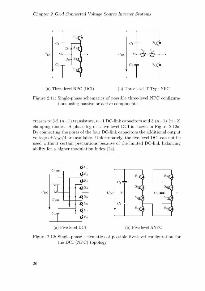
Chapter 2 Grid Connected Voltage Source Inverter Systems
π 2π
UPM
U∆
U∆
−U∆
−2U∆
0
Breite: 60 mm (halbseitig)
uα
uβ
SV1SV4 SV0/7
SV2SV3
SV6SV5
C U V W
S1
S2
S3
S4
C1
C2
M
S5
S6
S7
S8
C3
C4
S1
S2
S3
S4
C1
C2
M
S5
S6
S7
S8
C3
C4
S1
S2
S3
S4
D1
D2
C1
C2
M
Submodule
Submodule
Submodule
Submodule
Submodule
Submodule
Submodule
Submodule
Larm
Larm
S2
S1
CS2
S1
CS4
S3
Half-bridge Full-bridgemodule module
UDC
Submodule types
S1
S2
S3 S4
C1
C2
MUDC
S1
S2
S3
S4
C1
C2
M
S5
S6
S7
S8
CfcUDC
UDC
(a) Three-level NPC (DCI)
π 2π
UPM
U∆
U∆
−U∆
−2U∆
0
Breite: 60 mm (halbseitig)
uα
uβ
SV1SV4 SV0/7
SV2SV3
SV6SV5
C U V W
S1
S2
S3
S4
C1
C2
M
S5
S6
S7
S8
C3
C4
S1
S2
S3
S4
C1
C2
M
S5
S6
S7
S8
C3
C4
S1
S2
S3
S4
D1
D2
C1
C2
M
S1
S2
S3
S4
C1
C2
M
S5
S6
S7
S8
Cfc
Submodule
Submodule
Submodule
Submodule
Submodule
Submodule
Submodule
Submodule
Larm
Larm
S2
S1
CS2
S1
CS4
S3
Half-bridge Full-bridgemodule module
UDC
Submodule types
UDC
S1
S2
S3 S4
C1
C2
MUDC
(b) Three-level T-Type NPC
Figure 2.11: Single-phase schematics of possible three-level NPC configura-tions using passive or active components
creases to 3·2·(n−1) transistors, n−1 DC-link capacitors and 3·(n−1)·(n−2)clamping diodes. A phase leg of a five-level DCI is shown in Figure 2.12a.By connecting the ports of the four DC-link capacitors the additional outputvoltages ±UDC/4 are available. Unfortunately, the five-level DCI can not beused without certain precautions because of the limited DC-link balancingability for a higher modulation index [24].
π 2π
UPM
U∆
U∆
−U∆
−2U∆
0
Breite: 60 mm (halbseitig)
uα
uβ
SV1SV4 SV0/7
SV2SV3
SV6SV5
C U V W
S1
S2
S3
S4
C1
C2
M
S5
S6
S7
S8
C3
C4
S1
S2
S3
S4
C1
C2
M
S5
S6
S7
S8
C3
C4
Submodule
Submodule
Submodule
Submodule
Submodule
Submodule
Submodule
Submodule
Larm
Larm
S2
S1
CS2
S1
CS4
S3
Half-bridge Full-bridgemodule module
UDC
Submodule types
S1
S2
S3 S4
C1
C2
MUDC
S1
S2
S3
S4
C1
C2
M
S5
S6
S7
S8
CfcUDC
S1
S2
S3
S4
D1
D2
C1
C2
MUDC
UDC
UDC
(a) Five-level DCI
π 2π
UPM
U∆
U∆
−U∆
−2U∆
0
Breite: 60 mm (halbseitig)
uα
uβ
SV1SV4 SV0/7
SV2SV3
SV6SV5
C U V W
S1
S2
S3
S4
C1
C2
M
S5
S6
S7
S8
C3
C4
S1
S2
S3
S4
C1
C2
M
S5
S6
S7
S8
C3
C4
S1
S2
S3
S4
D1
D2
C1
C2
M
S1
S2
S3
S4
C1
C2
M
S5
S6
S7
S8
Cfc
Submodule
Submodule
Submodule
Submodule
Submodule
Submodule
Submodule
Submodule
Larm
Larm
S2
S1
CS2
S1
CS4
S3
Half-bridge Full-bridgemodule module
UDC
Submodule types
UDC
S1
S2
S3 S4
C1
C2
MUDC
(b) Five-level ANPC
Figure 2.12: Single-phase schematics of possible five-level configuration forthe DCI (NPC) topology
26
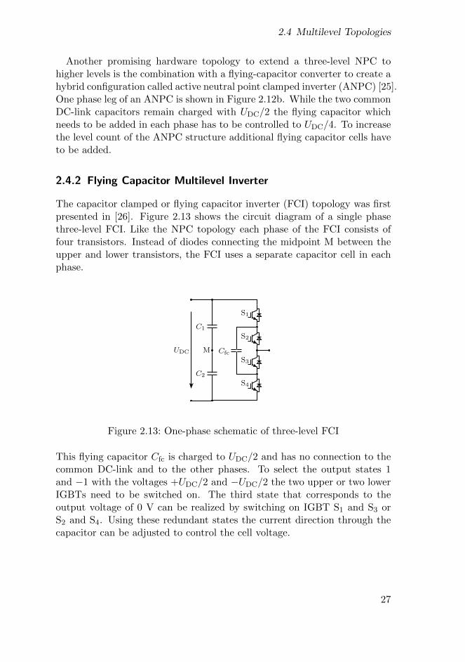
2.4 Multilevel Topologies
Another promising hardware topology to extend a three-level NPC tohigher levels is the combination with a flying-capacitor converter to create ahybrid configuration called active neutral point clamped inverter (ANPC) [25].One phase leg of an ANPC is shown in Figure 2.12b. While the two commonDC-link capacitors remain charged with UDC/2 the flying capacitor whichneeds to be added in each phase has to be controlled to UDC/4. To increasethe level count of the ANPC structure additional flying capacitor cells haveto be added.
2.4.2 Flying Capacitor Multilevel Inverter
The capacitor clamped or flying capacitor inverter (FCI) topology was firstpresented in [26]. Figure 2.13 shows the circuit diagram of a single phasethree-level FCI. Like the NPC topology each phase of the FCI consists offour transistors. Instead of diodes connecting the midpoint M between theupper and lower transistors, the FCI uses a separate capacitor cell in eachphase.
π 2π
UPM
U∆
U∆
−U∆
−2U∆
0
Breite: 60 mm (halbseitig)
uα
uβ
SV1SV4 SV0/7
SV2SV3
SV6SV5
C U V W
S1
S2
S3
S4
C1
C2
M
S5
S6
S7
S8
C3
C4
Submodule
Submodule
Submodule
Submodule
Submodule
Submodule
Submodule
Submodule
Larm
Larm
S2
S1
CS2
S1
CS4
S3
Half-bridge Full-bridgemodule module
UDC
Submodule types
S1
S2
S3 S4
C1
C2
MUDC
S1
S2
S3
S4
C1
C2
M
S5
S6
S7
S8
CfcUDC
S1
S2
S3
S4
D1
D2
C1
C2
MUDC
UDC
S1
S2
S3
S4
C1
C2
M
S5
S6
S7
S8
C3
C4
UDC
S1
S2
S3
S4
C1
C2
M CfcUDC
Figure 2.13: One-phase schematic of three-level FCI
This flying capacitor Cfc is charged to UDC/2 and has no connection to thecommon DC-link and to the other phases. To select the output states 1and −1 with the voltages +UDC/2 and −UDC/2 the two upper or two lowerIGBTs need to be switched on. The third state that corresponds to theoutput voltage of 0 V can be realized by switching on IGBT S1 and S3 orS2 and S4. Using these redundant states the current direction through thecapacitor can be adjusted to control the cell voltage.
27
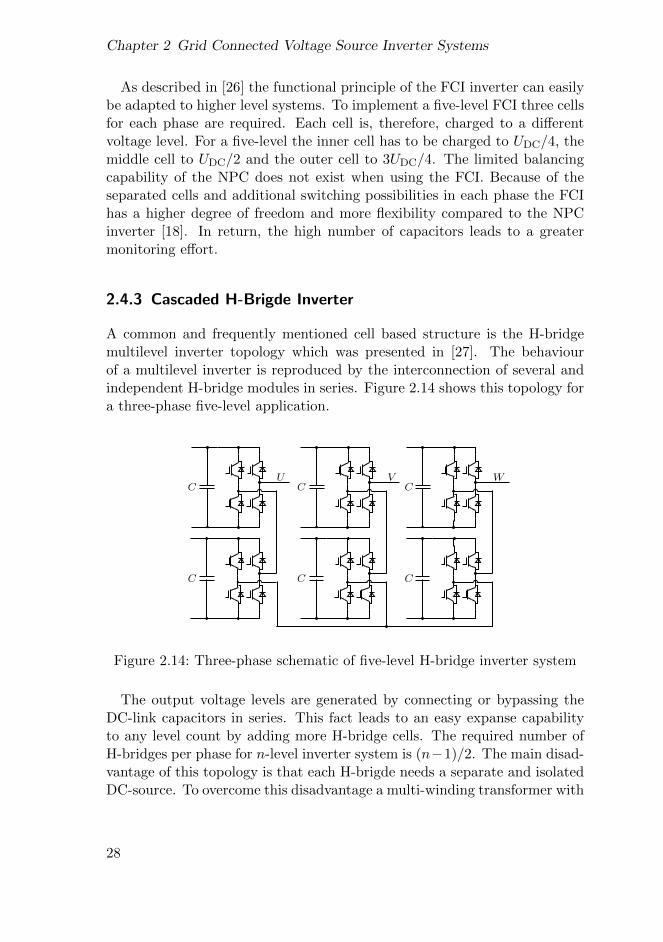
Chapter 2 Grid Connected Voltage Source Inverter Systems
As described in [26] the functional principle of the FCI inverter can easilybe adapted to higher level systems. To implement a five-level FCI three cellsfor each phase are required. Each cell is, therefore, charged to a differentvoltage level. For a five-level the inner cell has to be charged to UDC/4, themiddle cell to UDC/2 and the outer cell to 3UDC/4. The limited balancingcapability of the NPC does not exist when using the FCI. Because of theseparated cells and additional switching possibilities in each phase the FCIhas a higher degree of freedom and more flexibility compared to the NPCinverter [18]. In return, the high number of capacitors leads to a greatermonitoring effort.
2.4.3 Cascaded H-Brigde Inverter
A common and frequently mentioned cell based structure is the H-bridgemultilevel inverter topology which was presented in [27]. The behaviourof a multilevel inverter is reproduced by the interconnection of several andindependent H-bridge modules in series. Figure 2.14 shows this topology fora three-phase five-level application.
π 2π
UPM
U∆
U∆
−U∆
−2U∆
0
Breite: 60 mm (halbseitig)
uα
uβ
SV1SV4 SV0/7
SV2SV3
SV6SV5
C U V W
S1
S2
S3
S4
C1
C2
M
S5
S6
S7
S8
C3
C4
Submodule
Submodule
Submodule
Submodule
Submodule
Submodule
Submodule
Submodule
Larm
Larm
S2
S1
CS2
S1
CS4
S3
Half-bridge Full-bridgemodule module
UDC
Submodule types
S1
S2
S3 S4
C1
C2
MUDC
S1
S2
S3
S4
C1
C2
M
S5
S6
S7
S8
CfcUDC
S1
S2
S3
S4
D1
D2
C1
C2
MUDC
UDC
S1
S2
S3
S4
C1
C2
M
S5
S6
S7
S8
C3
C4
UDC
S1
S2
S3
S4
C1
C2
M CfcUDC
C
C C
C C
C
U V W
Figure 2.14: Three-phase schematic of five-level H-bridge inverter system
The output voltage levels are generated by connecting or bypassing theDC-link capacitors in series. This fact leads to an easy expanse capabilityto any level count by adding more H-bridge cells. The required number ofH-bridges per phase for n-level inverter system is (n−1)/2. The main disad-vantage of this topology is that each H-brigde needs a separate and isolatedDC-source. To overcome this disadvantage a multi-winding transformer with
28
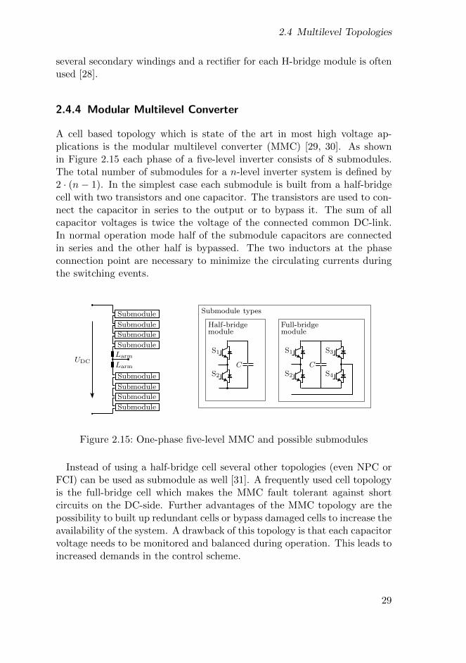
2.4 Multilevel Topologies
several secondary windings and a rectifier for each H-bridge module is oftenused [28].
2.4.4 Modular Multilevel Converter
A cell based topology which is state of the art in most high voltage ap-plications is the modular multilevel converter (MMC) [29, 30]. As shownin Figure 2.15 each phase of a five-level inverter consists of 8 submodules.The total number of submodules for a n-level inverter system is defined by2 · (n − 1). In the simplest case each submodule is built from a half-bridgecell with two transistors and one capacitor. The transistors are used to con-nect the capacitor in series to the output or to bypass it. The sum of allcapacitor voltages is twice the voltage of the connected common DC-link.In normal operation mode half of the submodule capacitors are connectedin series and the other half is bypassed. The two inductors at the phaseconnection point are necessary to minimize the circulating currents duringthe switching events.
π 2π
UPM
U∆
U∆
−U∆
−2U∆
0
Breite: 60 mm (halbseitig)
uα
uβ
SV1SV4 SV0/7
SV2SV3
SV6SV5
C U V W
S1
S2
S3 S4
C1
C2
M
S1
S2
S3
S4
C1
C2
M
S5
S6
S7
S8
C3
C4
S1
S2
S3
S4
C1
C2
M
S5
S6
S7
S8
C3
C4
S1
S2
S3
S4
D1
D2
C1
C2
M
S1
S2
S3
S4
C1
C2
M
S5
S6
S7
S8
Cfc
Submodule
Submodule
Submodule
Submodule
Submodule
Submodule
Submodule
Submodule
Larm
Larm
S2
S1
CS2
S1
CS4
S3
Half-bridge Full-bridgemodule module
UDC
Submodule types
Figure 2.15: One-phase five-level MMC and possible submodules
Instead of using a half-bridge cell several other topologies (even NPC orFCI) can be used as submodule as well [31]. A frequently used cell topologyis the full-bridge cell which makes the MMC fault tolerant against shortcircuits on the DC-side. Further advantages of the MMC topology are thepossibility to built up redundant cells or bypass damaged cells to increase theavailability of the system. A drawback of this topology is that each capacitorvoltage needs to be monitored and balanced during operation. This leads toincreased demands in the control scheme.
29
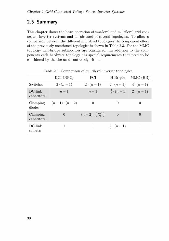
Chapter 2 Grid Connected Voltage Source Inverter Systems
2.5 Summary
This chapter shows the basic operation of two-level and multilevel grid con-nected inverter systems and an abstract of several topologies. To allow acomparison between the different multilevel topologies the component effortof the previously mentioned topologies is shown in Table 2.3. For the MMCtopology half-bridge submodules are considered. In addition to the com-ponents each hardware topology has special requirements that need to beconsidered by the the used control algorithm.
Table 2.3: Comparison of multilevel inverter topologies
DCI (NPC) FCI H-Brigde MMC (HB)
Switches 2 · (n− 1) 2 · (n− 1) 2 · (n− 1) 4 · (n− 1)
DC-linkcapacitors
n− 1 n− 1 32 · (n− 1) 2 · (n− 1)
Clampingdiodes
(n− 1) · (n− 2) 0 0 0
Clampingcapacitors
0 (n− 2) ·(n−1
2
)0 0
DC-linksources
1 1 32 · (n− 1) 1
30
Chapter 3
Control and Modulation Techniquesfor Multilevel Inverters
The control of grid connected inverter systems is subject of research anddiscussion since many decades [32, 33, 34]. The developments are drivenforward due to different requirements and specific use cases in grid connectedapplications. However, the main objective for grid connected inverters is toaccurately control the active power p and the reactive power q with a unitypower factor λ. Most of the control methods used today were originallydeveloped for electrical machines and were later adopted for grid application.In comparison to electric drives, a controller used in grid applications needsto include additional aspects like unknown grid conditions and unpredictabledisturbances caused by other loads and feeders in the system. Furthermore,the controller needs to be robust against dynamic grid faults like, typicalvoltage sags, short time interruptions or phase jumps as well as other systemvariations [7].
Based on their structure and basic characteristics, the controllers can besubdivided into three main groups. These groups are indirect, direct andpredictive control techniques. A simplified representation of the three dif-ferent types is shown in Figure 3.1. All three control techniques use thecurrent error signal ie as an input signal. The output signal is the actualoutput switching signal that has to be applied by the inverter. Necessarytransformations are neglected in this figure.
The most important component of indirect control systems is the innercurrent controller loop which generates the reference voltage. The modu-lator use this voltage as input to select the switching states to reproducethis voltage. Due to their easy application and the availability of suitablemicrocontrollers indirect control techniques have established themselves asstate of the art in most grid applications today. The rarely used group ofdirect controllers are applied in cases where very high dynamic performance
31
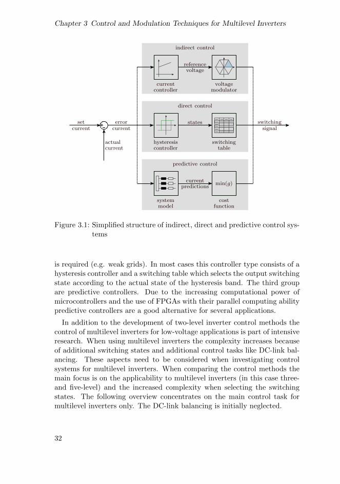
Chapter 3 Control and Modulation Techniques for Multilevel Inverters
LOAD
current
LFRF
sUVW
33u∗UVW
ucarr
controller modulator
hysteresiscontroller
switchingtable
referencevoltage
states switchingsignal
systemmodel
costfunction
min(g)current
predictions
voltage
errorcurrent
setcurrent
actualcurrent
indirect control
direct control
predictive control
Figure 3.1: Simplified structure of indirect, direct and predictive control sys-tems
is required (e.g. weak grids). In most cases this controller type consists of ahysteresis controller and a switching table which selects the output switchingstate according to the actual state of the hysteresis band. The third groupare predictive controllers. Due to the increasing computational power ofmicrocontrollers and the use of FPGAs with their parallel computing abilitypredictive controllers are a good alternative for several applications.
In addition to the development of two-level inverter control methods thecontrol of multilevel inverters for low-voltage applications is part of intensiveresearch. When using multilevel inverters the complexity increases becauseof additional switching states and additional control tasks like DC-link bal-ancing. These aspects need to be considered when investigating controlsystems for multilevel inverters. When comparing the control methods themain focus is on the applicability to multilevel inverters (in this case three-and five-level) and the increased complexity when selecting the switchingstates. The following overview concentrates on the main control task formultilevel inverters only. The DC-link balancing is initially neglected.
32
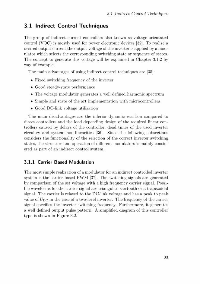
3.1 Indirect Control Techniques
3.1 Indirect Control Techniques
The group of indirect current controllers also known as voltage orientatedcontrol (VOC) is mostly used for power electronic devices [32]. To realize adesired output current the output voltage of the inverter is applied by a mod-ulator which selects the corresponding switching state or sequence of states.The concept to generate this voltage will be explained in Chapter 3.1.2 byway of example.
The main advantages of using indirect control techniques are [35]:
• Fixed switching frequency of the inverter
• Good steady-state performance
• The voltage modulator generates a well defined harmonic spectrum
• Simple and state of the art implementation with microcontrollers
• Good DC-link voltage utilization
The main disadvantages are the inferior dynamic reaction compared todirect controllers and the load depending design of the required linear con-trollers caused by delays of the controller, dead times of the used invertercircuitry and system non-linearities [36]. Since the following subsectionsconsiders the functionality of the selection of the correct inverter switchingstates, the structure and operation of different modulators is mainly consid-ered as part of an indirect control system.
3.1.1 Carrier Based Modulation
The most simple realization of a modulator for an indirect controlled invertersystem is the carrier based PWM [37]. The switching signals are generatedby comparison of the set voltage with a high frequency carrier signal. Possi-ble waveforms for the carrier signal are triangular, sawtooth or a trapezoidalsignal. The carrier is related to the DC-link voltage and has a peak to peakvalue of UDC in the case of a two-level inverter. The frequency of the carriersignal specifies the inverter switching frequency. Furthermore, it generatesa well defined output pulse pattern. A simplified diagram of this controllertype is shown in Figure 3.2.
33
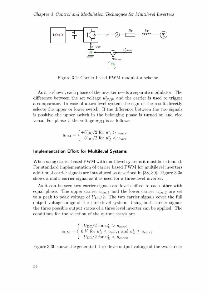
Chapter 3 Control and Modulation Techniques for Multilevel Inverters
LOAD A
LFRF
sUVW
33u∗UVW
ucarr
Figure 3.2: Carrier based PWM modulator scheme
As it is shown, each phase of the inverter needs a separate modulator. Thedifference between the set voltage u∗UVW and the carrier is used to triggera comparator. In case of a two-level system the sign of the result directlyselects the upper or lower switch. If the difference between the two signalsis positive the upper switch in the belonging phase is turned on and viceversa. For phase U the voltage uUM is as follows:
uUM =
+UDC/2 for u∗U > ucarr−UDC/2 for u∗U < ucarr
Implementation Effort for Multilevel Systems
When using carrier based PWM with multilevel systems it must be extended.For standard implementation of carrier based PWM for multilevel invertersadditional carrier signals are introduced as described in [38, 39]. Figure 3.3ashows a multi carrier signal as it is used for a three-level inverter.
As it can be seen two carrier signals are level shifted to each other withequal phase. The upper carrier ucarr1 and the lower carrier ucarr2 are setto a peak to peak voltage of UDC/2. The two carrier signals cover the fulloutput voltage range of the three-level system. Using both carrier signalsthe three possible output states of a three level inverter can be applied. Theconditions for the selection of the output states are
uUM =
+UDC/2 for u∗U > ucarr10 V for u∗U ≤ ucarr1 and u∗U ≥ ucarr2−UDC/2 for u∗U < ucarr2
Figure 3.3b shows the generated three-level output voltage of the two carrier
34
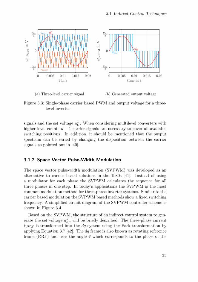
3.1 Indirect Control Techniques
0 0.005 0.01 0.015 0.02
t in s
-UDC
2
0
UDC
2
ucarr1
ucarr2
u$U
u$ U;u
carr
inV
(a) Three-level carrier signal
0 0.005 0.01 0.015 0.02
time in s
-UDC
2
0
UDC
2
uUM
u$U
u$ U;u
UM
inV
(b) Generated output voltage
Figure 3.3: Single-phase carrier based PWM and output voltage for a three-level inverter
signals and the set voltage u∗U . When considering multilevel converters withhigher level counts n − 1 carrier signals are necessary to cover all availableswitching positions. In addition, it should be mentioned that the outputspectrum can be varied by changing the disposition between the carriersignals as pointed out in [40].
3.1.2 Space Vector Pulse-Width Modulation
The space vector pulse-width modulation (SVPWM) was developed as analternative to carrier based solutions in the 1980s [41]. Instead of usinga modulator for each phase the SVPWM calculates the sequence for allthree phases in one step. In today’s applications the SVPWM is the mostcommon modulation method for three-phase inverter systems. Similar to thecarrier based modulation the SVPWM based methods show a fixed switchingfrequency. A simplified circuit diagram of the SVPWM controller scheme isshown in Figure 3.4.
Based on the SVPWM, the structure of an indirect control system to gen-erate the set voltage u∗αβ will be briefly described. The three-phase currentiUVW is transformed into the dq system using the Park transformation byapplying Equation 3.7 [42]. The dq frame is also known as rotating referenceframe (RRF) and uses the angle θ which corresponds to the phase of the
35
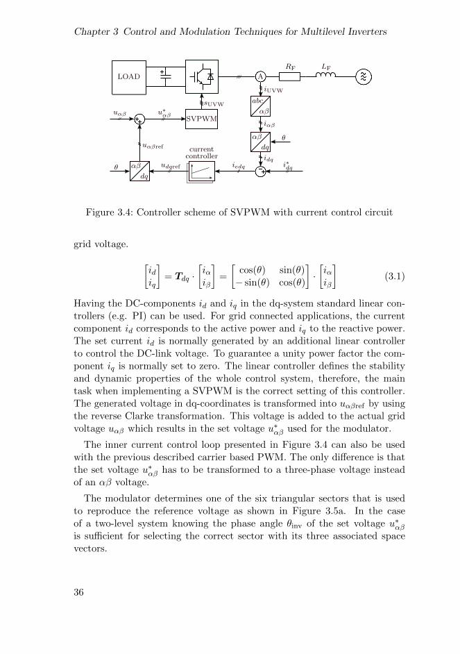
Chapter 3 Control and Modulation Techniques for Multilevel Inverters
LOAD A
LFRF
switchingtable
iUVW
sUVW
45
i∗dqiedq
iαβ
αβ
abc
sαβ
idq
dq
αβ
dq
αβ
SVPWM
currentcontroller
θ
θ
u∗αβ
uαβref
uαβ
udqref
Figure 3.4: Controller scheme of SVPWM with current control circuit
grid voltage. [idiq
]= Tdq ·
[iαiβ
]=
[cos(θ) sin(θ)− sin(θ) cos(θ)
]·[iαiβ
](3.1)
Having the DC-components id and iq in the dq-system standard linear con-trollers (e.g. PI) can be used. For grid connected applications, the currentcomponent id corresponds to the active power and iq to the reactive power.The set current id is normally generated by an additional linear controllerto control the DC-link voltage. To guarantee a unity power factor the com-ponent iq is normally set to zero. The linear controller defines the stabilityand dynamic properties of the whole control system, therefore, the maintask when implementing a SVPWM is the correct setting of this controller.The generated voltage in dq-coordinates is transformed into uαβref by usingthe reverse Clarke transformation. This voltage is added to the actual gridvoltage uαβ which results in the set voltage u∗αβ used for the modulator.
The inner current control loop presented in Figure 3.4 can also be usedwith the previous described carrier based PWM. The only difference is thatthe set voltage u∗αβ has to be transformed to a three-phase voltage insteadof an αβ voltage.
The modulator determines one of the six triangular sectors that is usedto reproduce the reference voltage as shown in Figure 3.5a. In the caseof a two-level system knowing the phase angle θinv of the set voltage u∗αβis sufficient for selecting the correct sector with its three associated spacevectors.
36
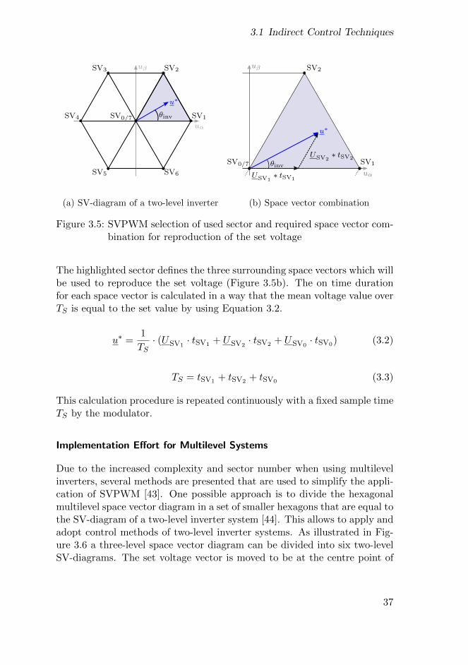
3.1 Indirect Control Techniques
π 2π
UPM
U∆
U∆
−U∆
−2U∆
0
Breite: 60 mm (halbseitig)uα
uβ
sector 9
sector 10
sector 11
sector 12
60 x 50
uα
uβ
SV1
SV2SV3
SV6SV5
SV4 SV0/7
u∗
uα
uβ
SV1
SV2
SV0/7
USV1∗ tSV1
u∗
USV2∗ tSV2
θinv
(a) SV-diagram of a two-level inverter
π 2π
UPM
U∆
U∆
−U∆
−2U∆
0
Breite: 60 mm (halbseitig)uα
uβ
sector 9
sector 10
sector 11
sector 12
60 x 50
uα
uβ
SV1
SV2SV3
SV6SV5
SV4 SV0/7
u∗
uα
uβ
SV1
SV2
SV0/7
USV1∗ tSV1
u∗
USV2∗ tSV2
θinv
θinv
(b) Space vector combination
Figure 3.5: SVPWM selection of used sector and required space vector com-bination for reproduction of the set voltage
The highlighted sector defines the three surrounding space vectors which willbe used to reproduce the set voltage (Figure 3.5b). The on time durationfor each space vector is calculated in a way that the mean voltage value overTS is equal to the set value by using Equation 3.2.
u∗ =1
TS· (USV1
· tSV1 + USV2· tSV2 + USV0
· tSV0) (3.2)
TS = tSV1 + tSV2 + tSV0 (3.3)
This calculation procedure is repeated continuously with a fixed sample timeTS by the modulator.
Implementation Effort for Multilevel Systems
Due to the increased complexity and sector number when using multilevelinverters, several methods are presented that are used to simplify the appli-cation of SVPWM [43]. One possible approach is to divide the hexagonalmultilevel space vector diagram in a set of smaller hexagons that are equal tothe SV-diagram of a two-level inverter system [44]. This allows to apply andadopt control methods of two-level inverter systems. As illustrated in Fig-ure 3.6 a three-level space vector diagram can be divided into six two-levelSV-diagrams. The set voltage vector is moved to be at the centre point of
37
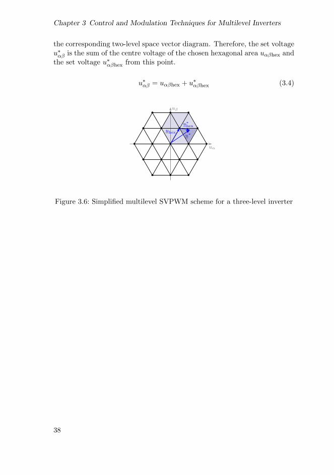
Chapter 3 Control and Modulation Techniques for Multilevel Inverters
the corresponding two-level space vector diagram. Therefore, the set voltageu∗αβ is the sum of the centre voltage of the chosen hexagonal area uαβhex andthe set voltage u∗αβhex from this point.
u∗αβ = uαβhex + u∗αβhex (3.4)
π 2π
UPM
U∆
U∆
−U∆
−2U∆
0
Breite: 60 mm (halbseitig)uα
uβ
sector 9
sector 10
sector 11
sector 12
60 x 50
uα
uβ
sector 5
sector 6uα
uβ
SV1
SV2SV3
SV6SV5
SV4 SV0/7
u
uα
uβ
SV1
SV2SV3
SV6SV5
SV4
u′βu′′β
SV0/7
u′α
u′′α
uα
uβ
SV1SV4 SV0/7
u
SV2SV3
SV6SV5
uα
uβ
u∗
u∗hex
uhex
Figure 3.6: Simplified multilevel SVPWM scheme for a three-level inverter
38
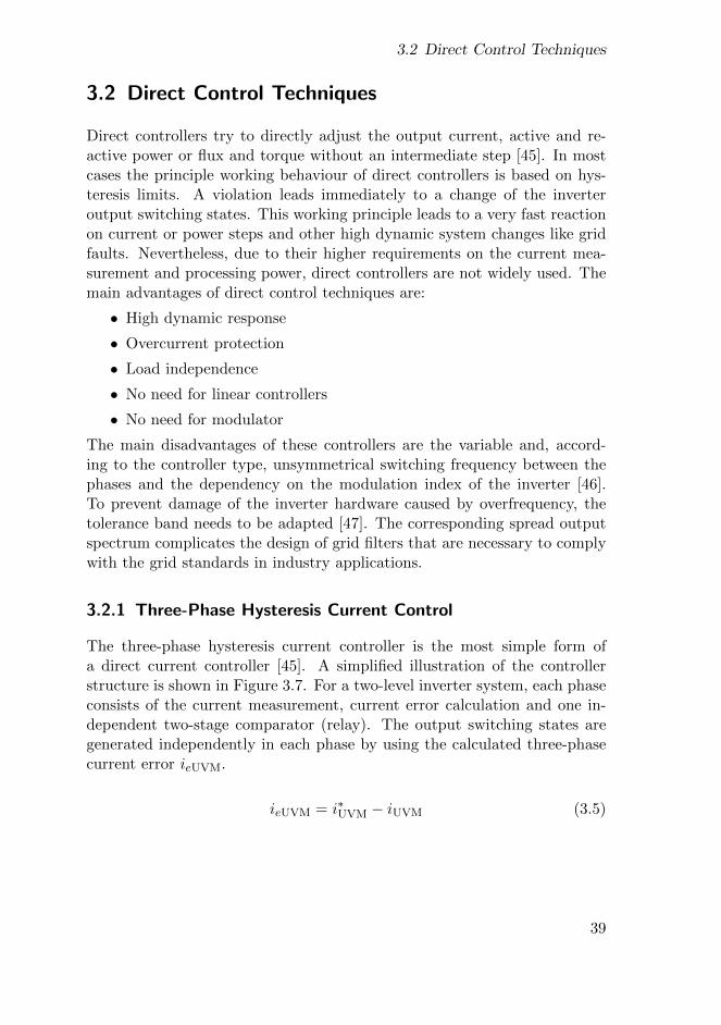
3.2 Direct Control Techniques
3.2 Direct Control Techniques
Direct controllers try to directly adjust the output current, active and re-active power or flux and torque without an intermediate step [45]. In mostcases the principle working behaviour of direct controllers is based on hys-teresis limits. A violation leads immediately to a change of the inverteroutput switching states. This working principle leads to a very fast reactionon current or power steps and other high dynamic system changes like gridfaults. Nevertheless, due to their higher requirements on the current mea-surement and processing power, direct controllers are not widely used. Themain advantages of direct control techniques are:
• High dynamic response
• Overcurrent protection
• Load independence
• No need for linear controllers
• No need for modulator
The main disadvantages of these controllers are the variable and, accord-ing to the controller type, unsymmetrical switching frequency between thephases and the dependency on the modulation index of the inverter [46].To prevent damage of the inverter hardware caused by overfrequency, thetolerance band needs to be adapted [47]. The corresponding spread outputspectrum complicates the design of grid filters that are necessary to complywith the grid standards in industry applications.
3.2.1 Three-Phase Hysteresis Current Control
The three-phase hysteresis current controller is the most simple form ofa direct current controller [45]. A simplified illustration of the controllerstructure is shown in Figure 3.7. For a two-level inverter system, each phaseconsists of the current measurement, current error calculation and one in-dependent two-stage comparator (relay). The output switching states aregenerated independently in each phase by using the calculated three-phasecurrent error ieUVM.
ieUVM = i∗UVM − iUVM (3.5)
39
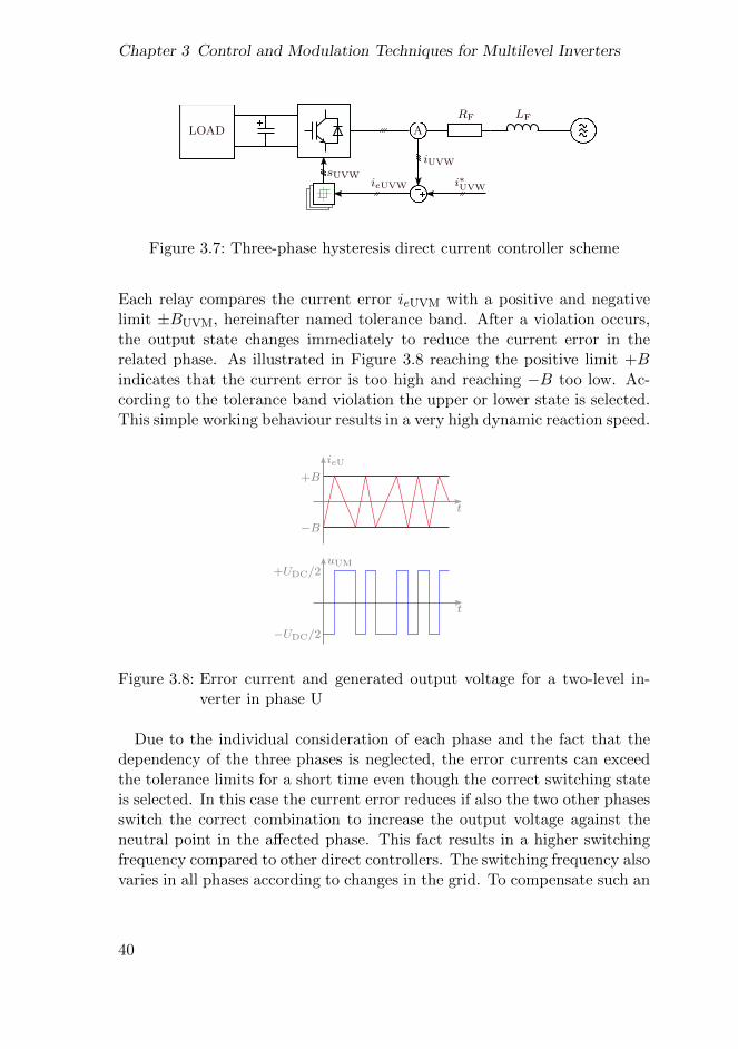
Chapter 3 Control and Modulation Techniques for Multilevel Inverters
LOAD A
LFRF
iUVW
sUVW
33
i∗UVWieUVW
Figure 3.7: Three-phase hysteresis direct current controller scheme
Each relay compares the current error ieUVM with a positive and negativelimit ±BUVM, hereinafter named tolerance band. After a violation occurs,the output state changes immediately to reduce the current error in therelated phase. As illustrated in Figure 3.8 reaching the positive limit +Bindicates that the current error is too high and reaching −B too low. Ac-cording to the tolerance band violation the upper or lower state is selected.This simple working behaviour results in a very high dynamic reaction speed.
π 2π
UPM
U∆
U∆
−U∆
−2U∆
0
Breite: 60 mm (halbseitig)uα
uβ
sector 9
sector 10
sector 11
sector 12
60 x 50
uα
uβ
sector 5
sector 6
uα
uβ
sector 5
sector 6
t
∆pup4
up3
up2
up1
lp1
lp2
lp3
lp4
poffset
t
ieU
+B
−B−Bs−1
poffset+Bs+1
t
ieU
+B
−B−Bs−1
+Bs+1
t
uUM
−UDC/2
+UDC/2
t
ieU
B+1
B0
B−1
t
uUM
−UDC/2
+UDC/2
iUoffset
t
ieU
+B
−B
t
uUM
−UDC/2
+UDC/2
Figure 3.8: Error current and generated output voltage for a two-level in-verter in phase U
Due to the individual consideration of each phase and the fact that thedependency of the three phases is neglected, the error currents can exceedthe tolerance limits for a short time even though the correct switching stateis selected. In this case the current error reduces if also the two other phasesswitch the correct combination to increase the output voltage against theneutral point in the affected phase. This fact results in a higher switchingfrequency compared to other direct controllers. The switching frequency alsovaries in all phases according to changes in the grid. To compensate such an
40
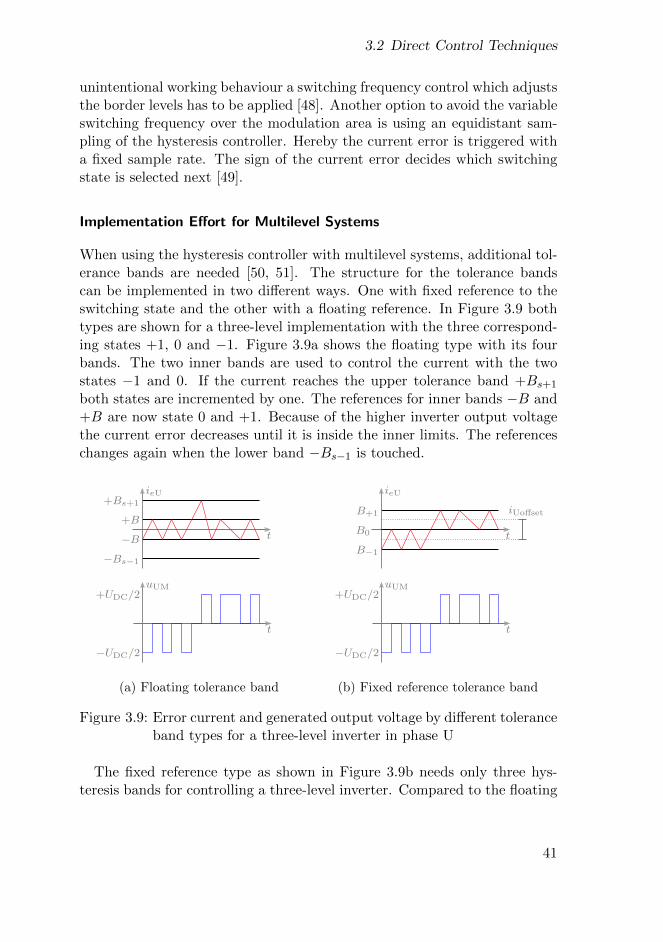
3.2 Direct Control Techniques
unintentional working behaviour a switching frequency control which adjuststhe border levels has to be applied [48]. Another option to avoid the variableswitching frequency over the modulation area is using an equidistant sam-pling of the hysteresis controller. Hereby the current error is triggered witha fixed sample rate. The sign of the current error decides which switchingstate is selected next [49].
Implementation Effort for Multilevel Systems
When using the hysteresis controller with multilevel systems, additional tol-erance bands are needed [50, 51]. The structure for the tolerance bandscan be implemented in two different ways. One with fixed reference to theswitching state and the other with a floating reference. In Figure 3.9 bothtypes are shown for a three-level implementation with the three correspond-ing states +1, 0 and −1. Figure 3.9a shows the floating type with its fourbands. The two inner bands are used to control the current with the twostates −1 and 0. If the current reaches the upper tolerance band +Bs+1
both states are incremented by one. The references for inner bands −B and+B are now state 0 and +1. Because of the higher inverter output voltagethe current error decreases until it is inside the inner limits. The referenceschanges again when the lower band −Bs−1 is touched.
π 2π
UPM
U∆
U∆
−U∆
−2U∆
0
Breite: 60 mm (halbseitig)uα
uβ
sector 9
sector 10
sector 11
sector 12
60 x 50
uα
uβ
sector 5
sector 6
uα
uβ
sector 5
sector 6
t
∆pup4
up3
up2
up1
lp1
lp2
lp3
lp4
poffset
t
ieU
+B
−B−Bs−1
poffset+Bs+1
t
ieU
+B
−B−Bs−1
+Bs+1
t
uUM
−UDC/2
+UDC/2
t
ieU
B+1
B0
B−1
t
uUM
−UDC/2
+UDC/2
iUoffset
t
ieU
+B
−B
t
uUM
−UDC/2
+UDC/2
(a) Floating tolerance band
π 2π
UPM
U∆
U∆
−U∆
−2U∆
0
Breite: 60 mm (halbseitig)uα
uβ
sector 9
sector 10
sector 11
sector 12
60 x 50
uα
uβ
sector 5
sector 6
uα
uβ
sector 5
sector 6
t
∆pup4
up3
up2
up1
lp1
lp2
lp3
lp4
poffset
t
ieU
+B
−B−Bs−1
poffset+Bs+1
t
ieU
+B
−B−Bs−1
+Bs+1
t
uUM
−UDC/2
+UDC/2
t
ieU
B+1
B0
B−1
t
uUM
−UDC/2
+UDC/2
iUoffset
t
ieU
+B
−B
t
uUM
−UDC/2
+UDC/2
(b) Fixed reference tolerance band
Figure 3.9: Error current and generated output voltage by different toleranceband types for a three-level inverter in phase U
The fixed reference type as shown in Figure 3.9b needs only three hys-teresis bands for controlling a three-level inverter. Compared to the floating
41
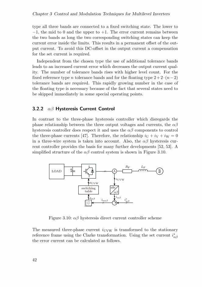
Chapter 3 Control and Modulation Techniques for Multilevel Inverters
type all three bands are connected to a fixed switching state. The lower to−1, the mid to 0 and the upper to +1. The error current remains betweenthe two bands as long the two corresponding switching states can keep thecurrent error inside the limits. This results in a permanent offset of the out-put current. To avoid this DC-offset in the output current a compensationfor the set current is required.
Independent from the chosen type the use of additional tolerance bandsleads to an increased current error which decreases the output current qual-ity. The number of tolerance bands rises with higher level count. For thefixed reference type n tolerance bands and for the floating type 2+2 · (n−2)tolerance bands are required. This rapidly growing number in the case ofthe floating type is necessary because of the fact that several states need tobe skipped immediately in some special operating points.
3.2.2 αβ Hysteresis Current Control
In contrast to the three-phase hysteresis controller which disregards thephase relationship between the three output voltages and currents, the αβhysteresis controller does respect it and uses the αβ components to controlthe three-phase currents [47]. Therefore, the relationship iU + iV + iW = 0in a three-wire system is taken into account. Also, the αβ hysteresis cur-rent controller provides the basis for many further developments [52, 53]. Asimplified structure of the αβ control system is shown in Figure 3.10.
LOAD A
LFRF
switchingtable
iUVW
sUVW
45
i∗αβieαβiαβ
αβ
abc
sαβ
Figure 3.10: αβ hysteresis direct current controller scheme
The measured three-phase current iUVW is transformed to the stationaryreference frame using the Clarke transformation. Using the set current i∗αβthe error current can be calculated as follows.
42
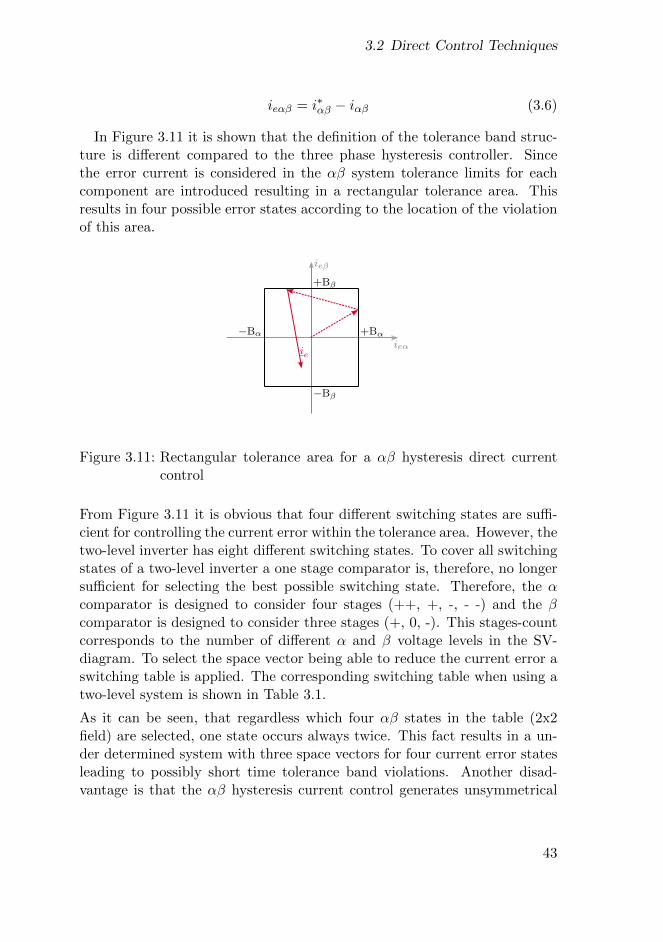
3.2 Direct Control Techniques
ieαβ = i∗αβ − iαβ (3.6)
In Figure 3.11 it is shown that the definition of the tolerance band struc-ture is different compared to the three phase hysteresis controller. Sincethe error current is considered in the αβ system tolerance limits for eachcomponent are introduced resulting in a rectangular tolerance area. Thisresults in four possible error states according to the location of the violationof this area.
π 2π
UPM
U∆
U∆
−U∆
−2U∆
0
Breite: 60 mm (halbseitig)uα
uβ
sector 9
sector 10
sector 11
sector 12
60 x 50
uα
uβ
sector 5
sector 6uα
uβ
SV1
SV2SV3
SV6SV5
SV4 SV0/7
u
uα
uβ
SV1
SV2SV3
SV6SV5
SV4
u′βu′′β
SV0/7
u′α
u′′α
uα
uβ
SV1SV4 SV0/7
u
SV2SV3
SV6SV5
ieα
ieβ
uα
uβ
u
ie
+Bα
−Bβ
+Bβ
−Bα
Figure 3.11: Rectangular tolerance area for a αβ hysteresis direct currentcontrol
From Figure 3.11 it is obvious that four different switching states are suffi-cient for controlling the current error within the tolerance area. However, thetwo-level inverter has eight different switching states. To cover all switchingstates of a two-level inverter a one stage comparator is, therefore, no longersufficient for selecting the best possible switching state. Therefore, the αcomparator is designed to consider four stages (++, +, -, - -) and the βcomparator is designed to consider three stages (+, 0, -). This stages-countcorresponds to the number of different α and β voltage levels in the SV-diagram. To select the space vector being able to reduce the current error aswitching table is applied. The corresponding switching table when using atwo-level system is shown in Table 3.1.
As it can be seen, that regardless which four αβ states in the table (2x2field) are selected, one state occurs always twice. This fact results in a un-der determined system with three space vectors for four current error statesleading to possibly short time tolerance band violations. Another disad-vantage is that the αβ hysteresis current control generates unsymmetrical
43
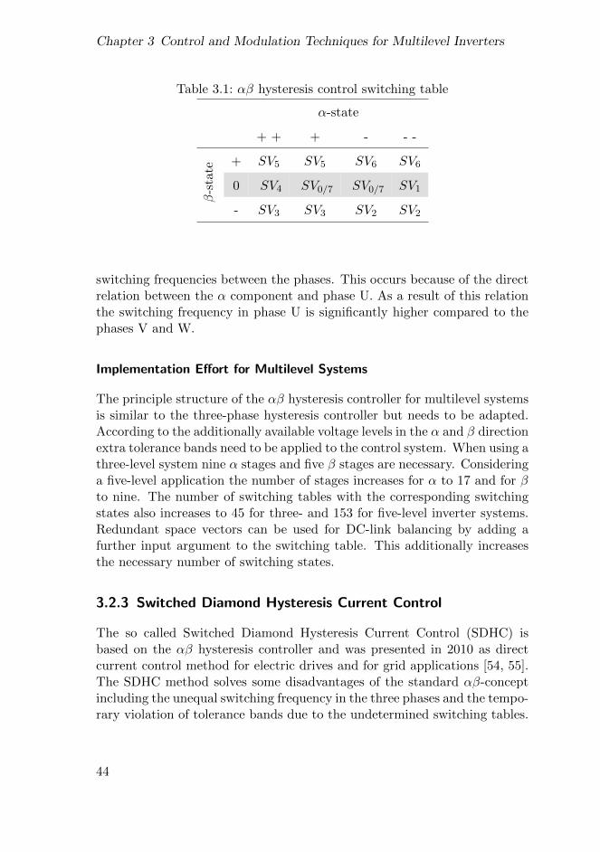
Chapter 3 Control and Modulation Techniques for Multilevel Inverters
Table 3.1: αβ hysteresis control switching table
α-state
+ + + - - -
β-s
tate
+ SV5 SV5 SV6 SV6
0 SV4 SV0/7 SV0/7 SV1
- SV3 SV3 SV2 SV2
switching frequencies between the phases. This occurs because of the directrelation between the α component and phase U. As a result of this relationthe switching frequency in phase U is significantly higher compared to thephases V and W.
Implementation Effort for Multilevel Systems
The principle structure of the αβ hysteresis controller for multilevel systemsis similar to the three-phase hysteresis controller but needs to be adapted.According to the additionally available voltage levels in the α and β directionextra tolerance bands need to be applied to the control system. When using athree-level system nine α stages and five β stages are necessary. Consideringa five-level application the number of stages increases for α to 17 and for βto nine. The number of switching tables with the corresponding switchingstates also increases to 45 for three- and 153 for five-level inverter systems.Redundant space vectors can be used for DC-link balancing by adding afurther input argument to the switching table. This additionally increasesthe necessary number of switching states.
3.2.3 Switched Diamond Hysteresis Current Control
The so called Switched Diamond Hysteresis Current Control (SDHC) isbased on the αβ hysteresis controller and was presented in 2010 as directcurrent control method for electric drives and for grid applications [54, 55].The SDHC method solves some disadvantages of the standard αβ-conceptincluding the unequal switching frequency in the three phases and the tempo-rary violation of tolerance bands due to the undetermined switching tables.
44
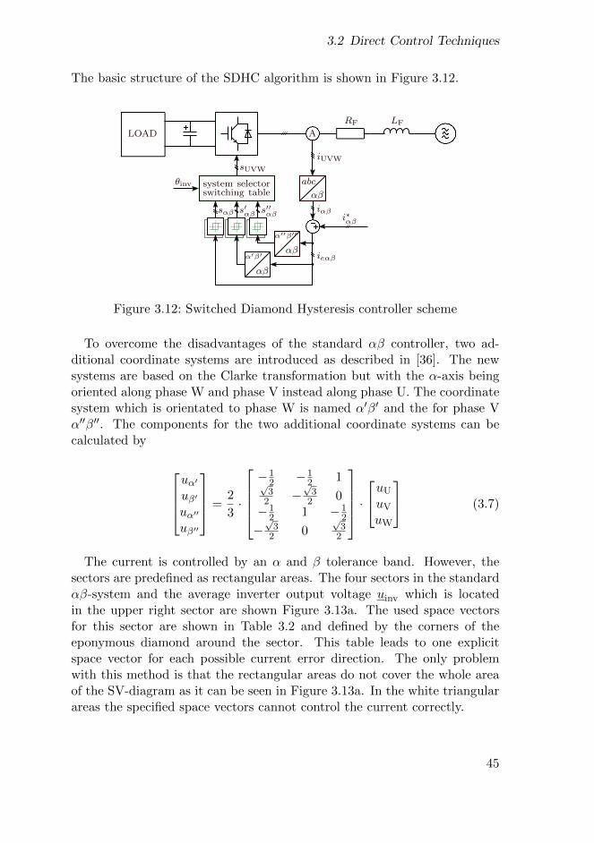
3.2 Direct Control Techniques
The basic structure of the SDHC algorithm is shown in Figure 3.12.
LOAD A
LFRF
system selectorswitching table 56
iUVW
i∗αβiαβ
abc
αβ
αβ
α′′β′′
αβ
α′β′
sUVW
θinv
ieαβ
s′′αβs′αβsαβ
Figure 3.12: Switched Diamond Hysteresis controller scheme
To overcome the disadvantages of the standard αβ controller, two ad-ditional coordinate systems are introduced as described in [36]. The newsystems are based on the Clarke transformation but with the α-axis beingoriented along phase W and phase V instead along phase U. The coordinatesystem which is orientated to phase W is named α′β′ and the for phase Vα′′β′′. The components for the two additional coordinate systems can becalculated by
uα′
uβ′
uα′′
uβ′′
=2
3·
−1
2 −12 1√
32 −
√3
2 0−1
2 1 −12
−√
32 0
√3
2
·uU
uV
uW
(3.7)
The current is controlled by an α and β tolerance band. However, thesectors are predefined as rectangular areas. The four sectors in the standardαβ-system and the average inverter output voltage uinv which is locatedin the upper right sector are shown Figure 3.13a. The used space vectorsfor this sector are shown in Table 3.2 and defined by the corners of theeponymous diamond around the sector. This table leads to one explicitspace vector for each possible current error direction. The only problemwith this method is that the rectangular areas do not cover the whole areaof the SV-diagram as it can be seen in Figure 3.13a. In the white triangularareas the specified space vectors cannot control the current correctly.
45
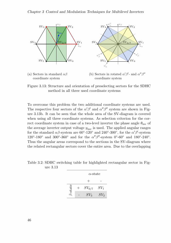
Chapter 3 Control and Modulation Techniques for Multilevel Inverters
Breite: 60 mm (halbseitig)
uα
uβ
SV1
SV2SV3
SV6SV5
SV4
u′βu′′
β
SV0/7
u′α
u′′α
uα
uβ
SV1SV4
uinv
SV2SV3
SV6SV5
SV0/7
uα
uβ
u
uα
uβ
u
ieα
ieβ
ie
+Biα
−Biβ
+Biβ
−Biα
i′′eα
i′′eβ
ie
+Bα
−Bβ
+Bβ
−Bα
ieα′′
ieβ′′
i′′e
+Biα′′
−Biβ′′
+Biβ′′
−Biα′′
ieα′
ieβ′
i′e
+Biα′
+Biβ′
−Biα′
−Biβ′
(a) Sectors in standard αβcoordinate system
Breite: 60 mm (halbseitig)
uα
uβ
SV1
SV2SV3
SV6SV5
SV4
u′βu′′
β
SV0/7
u′α
u′′α
uα
uβ
SV1SV4
uinv
SV2SV3
SV6SV5
SV0/7
uα
uβ
u
uα
uβ
u
ieα
ieβ
ie
+Biα
−Biβ
+Biβ
−Biα
i′′eα
i′′eβ
ie
+Bα
−Bβ
+Bβ
−Bα
ieα′′
ieβ′′
i′′e
+Biα′′
−Biβ′′
+Biβ′′
−Biα′′
ieα′
ieβ′
i′e
+Biα′
+Biβ′
−Biα′
−Biβ′
(b) Sectors in rotated α′β′- and α′′β′′
coordinate system
Figure 3.13: Structure and orientation of preselecting sectors for the SDHCmethod in all three used coordinate systems
To overcome this problem the two additional coordinate systems are used.The respective four sectors of the α′β′ and α′′β′′ system are shown in Fig-ure 3.13b. It can be seen that the whole area of the SV-diagram is coveredwhen using all three coordinate systems. As selection criterion for the cor-rect coordinate system in case of a two-level inverter the phase angle θinv ofthe average inverter output voltage uinv is used. The applied angular rangesfor the standard αβ-system are 60-120 and 240-300, for the α′β′-system120-180 and 300-360 and for the α′′β′′-system 0-60 and 180-240.Thus the angular areas correspond to the sections in the SV-diagram wherethe related rectangular sectors cover the entire area. Due to the overlapping
Table 3.2: SDHC switching table for highlighted rectangular sector in Fig-ure 3.13
α-state
+ -
β-s
tate + SV0/7 SV1
- SV3 SV2
46
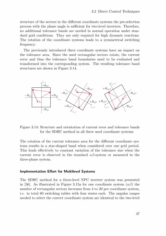
3.2 Direct Control Techniques
structure of the sectors in the different coordinate systems the pre-selectionprocess with the phase angle is sufficient for two-level inverters. Therefore,no additional tolerance bands are needed in normal operation under stan-dard grid conditions. They are only required for high dynamic reactions.The rotation of the coordinate systems leads to a symmetrical switchingfrequency.
The previously introduced three coordinate systems have an impact onthe tolerance area. Since the used rectangular sectors rotate, the currenterror and thus the tolerance band boundaries need to be evaluated andtransformed into the corresponding system. The resulting tolerance bandstructures are shown in Figure 3.14.
Breite: 60 mm (halbseitig)
uα
uβ
SV1
SV2SV3
SV6SV5
SV4
u′βu′′
β
SV0/7
u′α
u′′α
uα
uβ
SV1SV4
u
SV2SV3
SV6SV5
SV0/7
uα
uβ
u
uα
uβ
u
ieα
ieβ
ie
+Biα
−Biβ
+Biβ
−Biα
i′′eα
i′′eβ
ie
+Bα
−Bβ
+Bβ
−Bα
ieα′′
ieβ′′
i′′e
+Biα′′
−Biβ′′
+Biβ′′
−Biα′′
ieα′
ieβ′
i′e
+Biα′
+Biβ′
−Biα′
−Biβ′
Figure 3.14: Structure and orientation of current error and tolerance bandsfor the SDHC method in all three used coordinate systems
The rotation of the current tolerance area for the different coordinate sys-tems results in a star-shaped band when considered over one grid period.This leads effectively to constant variation of the tolerance size when thecurrent error is observed in the standard αβ-system or measured in thethree-phase system.
Implementation Effort for Multilevel Systems
The SDHC method for a three-level NPC inverter system was presentedin [56]. As illustrated in Figure 3.15a for one coordinate system (αβ) thenumber of rectangular sectors increases from 4 to 20 per coordinate system,i.e. in total 60 switching tables with four states each. The angular rangesneeded to select the correct coordinate system are identical to the two-level
47
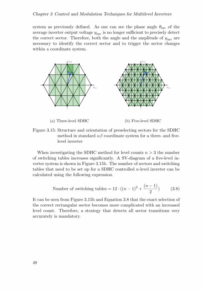
Chapter 3 Control and Modulation Techniques for Multilevel Inverters
system as previously defined. As one can see the phase angle θinv of theaverage inverter output voltage uinv is no longer sufficient to precisely detectthe correct sector. Therefore, both the angle and the amplitude of uinv arenecessary to identify the correct sector and to trigger the sector changeswithin a coordinate system.
Breite: 60 mm (halbseitig)
uα
uβ
SV1
SV2SV3
SV6SV5
SV4
u′βu′′
β
SV0/7
u′α
u′′α
uα
uβ
SV1SV4
uinv
SV2SV3
SV6SV5
SV0/7
uα
uβ
uinv
uα
uβ
uinv
ieα
ieβ
ie
+Biα
−Biβ
+Biβ
−Biα
i′′eα
i′′eβ
ie
+Bα
−Bβ
+Bβ
−Bα
ieα′′
ieβ′′
i′′e
+Biα′′
−Biβ′′
+Biβ′′
−Biα′′
ieα′
ieβ′
i′e
+Biα′
+Biβ′
−Biα′
−Biβ′
(a) Three-level SDHC
Breite: 60 mm (halbseitig)
uα
uβ
SV1
SV2SV3
SV6SV5
SV4
u′βu′′
β
SV0/7
u′α
u′′α
uα
uβ
SV1SV4
uinv
SV2SV3
SV6SV5
SV0/7
uα
uβ
uinv
uα
uβ
uinv
ieα
ieβ
ie
+Biα
−Biβ
+Biβ
−Biα
i′′eα
i′′eβ
ie
+Bα
−Bβ
+Bβ
−Bα
ieα′′
ieβ′′
i′′e
+Biα′′
−Biβ′′
+Biβ′′
−Biα′′
ieα′
ieβ′
i′e
+Biα′
+Biβ′
−Biα′
−Biβ′
(b) Five-level SDHC
Figure 3.15: Structure and orientation of preselecting sectors for the SDHCmethod in standard αβ coordinate system for a three- and five-level inverter
When investigating the SDHC method for level counts n > 3 the numberof switching tables increases significantly. A SV-diagram of a five-level in-verter system is shown in Figure 3.15b. The number of sectors and switchingtables that need to be set up for a SDHC controlled n-level inverter can becalculated using the following expression.
Number of switching tables = 12 · ((n− 1)2 +(n− 1)
2) (3.8)
It can be seen from Figure 3.15b and Equation 3.8 that the exact selection ofthe correct rectangular sector becomes more complicated with an increasedlevel count. Therefore, a strategy that detects all sector transitions veryaccurately is mandatory.
48
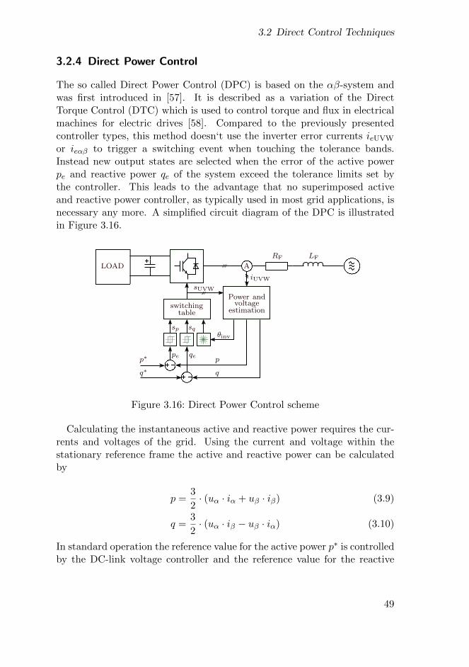
3.2 Direct Control Techniques
3.2.4 Direct Power Control
The so called Direct Power Control (DPC) is based on the αβ-system andwas first introduced in [57]. It is described as a variation of the DirectTorque Control (DTC) which is used to control torque and flux in electricalmachines for electric drives [58]. Compared to the previously presentedcontroller types, this method doesn‘t use the inverter error currents ieUVW
or ieαβ to trigger a switching event when touching the tolerance bands.Instead new output states are selected when the error of the active powerpe and reactive power qe of the system exceed the tolerance limits set bythe controller. This leads to the advantage that no superimposed activeand reactive power controller, as typically used in most grid applications, isnecessary any more. A simplified circuit diagram of the DPC is illustratedin Figure 3.16.
56
LOAD A
LFRF
switchingtable
p∗
q∗p
q
iUVW
sUVW
Power andvoltage
estimation
sp sq
56
θinv
pe qe
Figure 3.16: Direct Power Control scheme
Calculating the instantaneous active and reactive power requires the cur-rents and voltages of the grid. Using the current and voltage within thestationary reference frame the active and reactive power can be calculatedby
p =3
2· (uα · iα + uβ · iβ) (3.9)
q =3
2· (uα · iβ − uβ · iα) (3.10)
In standard operation the reference value for the active power p∗ is controlledby the DC-link voltage controller and the reference value for the reactive
49
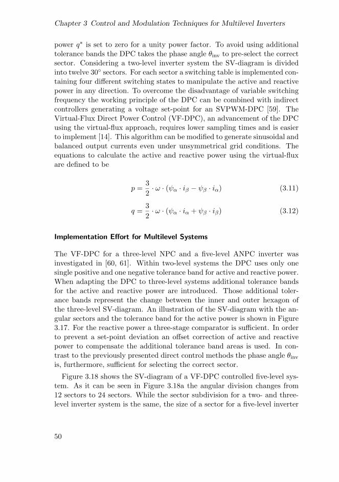
Chapter 3 Control and Modulation Techniques for Multilevel Inverters
power q∗ is set to zero for a unity power factor. To avoid using additionaltolerance bands the DPC takes the phase angle θinv to pre-select the correctsector. Considering a two-level inverter system the SV-diagram is dividedinto twelve 30 sectors. For each sector a switching table is implemented con-taining four different switching states to manipulate the active and reactivepower in any direction. To overcome the disadvantage of variable switchingfrequency the working principle of the DPC can be combined with indirectcontrollers generating a voltage set-point for an SVPWM-DPC [59]. TheVirtual-Flux Direct Power Control (VF-DPC), an advancement of the DPCusing the virtual-flux approach, requires lower sampling times and is easierto implement [14]. This algorithm can be modified to generate sinusoidal andbalanced output currents even under unsymmetrical grid conditions. Theequations to calculate the active and reactive power using the virtual-fluxare defined to be
p =3
2· ω · (ψα · iβ − ψβ · iα) (3.11)
q =3
2· ω · (ψα · iα + ψβ · iβ) (3.12)
Implementation Effort for Multilevel Systems
The VF-DPC for a three-level NPC and a five-level ANPC inverter wasinvestigated in [60, 61]. Within two-level systems the DPC uses only onesingle positive and one negative tolerance band for active and reactive power.When adapting the DPC to three-level systems additional tolerance bandsfor the active and reactive power are introduced. Those additional toler-ance bands represent the change between the inner and outer hexagon ofthe three-level SV-diagram. An illustration of the SV-diagram with the an-gular sectors and the tolerance band for the active power is shown in Figure3.17. For the reactive power a three-stage comparator is sufficient. In orderto prevent a set-point deviation an offset correction of active and reactivepower to compensate the additional tolerance band areas is used. In con-trast to the previously presented direct control methods the phase angle θinv
is, furthermore, sufficient for selecting the correct sector.
Figure 3.18 shows the SV-diagram of a VF-DPC controlled five-level sys-tem. As it can be seen in Figure 3.18a the angular division changes from12 sectors to 24 sectors. While the sector subdivision for a two- and three-level inverter system is the same, the size of a sector for a five-level inverter
50
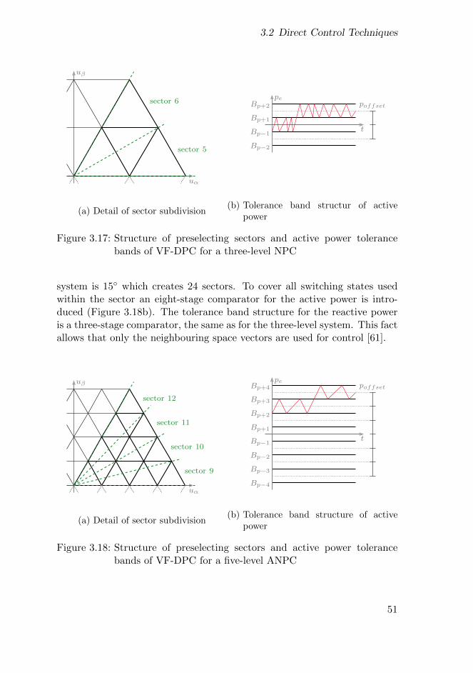
3.2 Direct Control Techniques
π 2π
UPM
U∆
U∆
−U∆
−2U∆
0
Breite: 60 mm (halbseitig)uα
uβ
sector 9
sector 10
sector 11
sector 12
60 x 50
uα
uβ
sector 5
sector 6
uα
uβ
sector 5
sector 6
(a) Detail of sector subdivision
π 2π
UPM
U∆
U∆
−U∆
−2U∆
0
Breite: 60 mm (halbseitig)
uα
uβ
sector 9
sector 10
sector 11
sector 12
60 x 50
uα
uβ
sector 5
sector 6
t
peBp+4
Bp+3
Bp+2
Bp+1
Bp−1
Bp−2
Bp−3
Bp−4
poffset
t
pe
Bp+1
Bp−1
Bp−2
poffsetBp+2
(b) Tolerance band structur of activepower
Figure 3.17: Structure of preselecting sectors and active power tolerancebands of VF-DPC for a three-level NPC
system is 15 which creates 24 sectors. To cover all switching states usedwithin the sector an eight-stage comparator for the active power is intro-duced (Figure 3.18b). The tolerance band structure for the reactive poweris a three-stage comparator, the same as for the three-level system. This factallows that only the neighbouring space vectors are used for control [61].
π 2π
UPM
U∆
U∆
−U∆
−2U∆
0
Breite: 60 mm (halbseitig)
uα
uβ
sector 9
sector 10
sector 11
sector 12
60 x 50
uα
uβ
sector 5
sector 6
uα
uβ
sector 5
sector 6
(a) Detail of sector subdivision
π 2π
UPM
U∆
U∆
−U∆
−2U∆
0
Breite: 60 mm (halbseitig)
uα
uβ
sector 9
sector 10
sector 11
sector 12
60 x 50
uα
uβ
sector 5
sector 6
t
peBp+4
Bp+3
Bp+2
Bp+1
Bp−1
Bp−2
Bp−3
Bp−4
poffset
t
pe
Bp+1
Bp−1
Bp−2
poffsetBp+2
(b) Tolerance band structure of activepower
Figure 3.18: Structure of preselecting sectors and active power tolerancebands of VF-DPC for a five-level ANPC
51
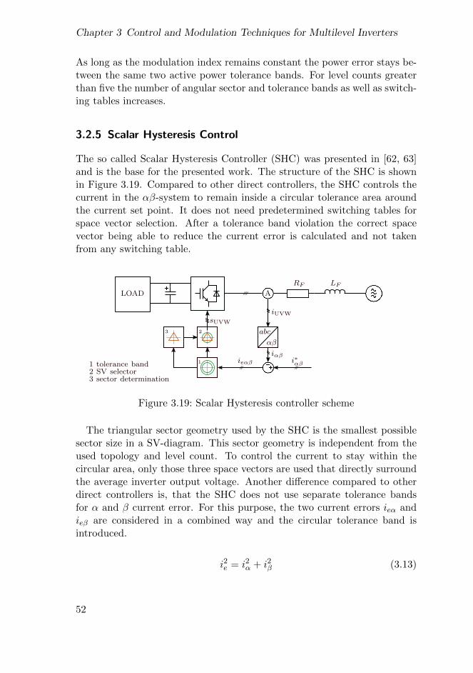
Chapter 3 Control and Modulation Techniques for Multilevel Inverters
As long as the modulation index remains constant the power error stays be-tween the same two active power tolerance bands. For level counts greaterthan five the number of angular sector and tolerance bands as well as switch-ing tables increases.
3.2.5 Scalar Hysteresis Control
The so called Scalar Hysteresis Controller (SHC) was presented in [62, 63]and is the base for the presented work. The structure of the SHC is shownin Figure 3.19. Compared to other direct controllers, the SHC controls thecurrent in the αβ-system to remain inside a circular tolerance area aroundthe current set point. It does not need predetermined switching tables forspace vector selection. After a tolerance band violation the correct spacevector being able to reduce the current error is calculated and not takenfrom any switching table.
LOAD A
LFRF
iUVW
sUVW
45
i∗αβieαβiαβ
αβ
abc3 2
11 tolerance band2 SV selector3 sector determination
Figure 3.19: Scalar Hysteresis controller scheme
The triangular sector geometry used by the SHC is the smallest possiblesector size in a SV-diagram. This sector geometry is independent from theused topology and level count. To control the current to stay within thecircular area, only those three space vectors are used that directly surroundthe average inverter output voltage. Another difference compared to otherdirect controllers is, that the SHC does not use separate tolerance bandsfor α and β current error. For this purpose, the two current errors ieα andieβ are considered in a combined way and the circular tolerance band isintroduced.
i2e = i2α + i2β (3.13)
52
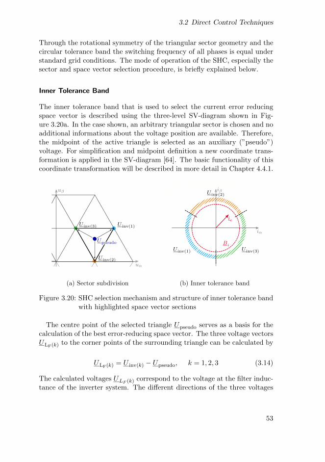
3.2 Direct Control Techniques
Through the rotational symmetry of the triangular sector geometry and thecircular tolerance band the switching frequency of all phases is equal understandard grid conditions. The mode of operation of the SHC, especially thesector and space vector selection procedure, is briefly explained below.
Inner Tolerance Band
The inner tolerance band that is used to select the current error reducingspace vector is described using the three-level SV-diagram shown in Fig-ure 3.20a. In the case shown, an arbitrary triangular sector is chosen and noadditional informations about the voltage position are available. Therefore,the midpoint of the active triangle is selected as an auxiliary (”pseudo”)voltage. For simplification and midpoint definition a new coordinate trans-formation is applied in the SV-diagram [64]. The basic functionality of thiscoordinate transformation will be described in more detail in Chapter 4.4.1.
Breite: 60 mm (halbseitig)
uα
uβ
sector 9
sector 10
sector 11
sector 12
60 x 50
x 5.5 y 4.5
uα
uβ
U inv(1)U inv(3)
U inv(2)
Upseudo
uα
uβ
U inv(1)U inv(3)
U inv(2)
Upseudo
Upseudo(1)
Upseudo(2)
Upseudo(3)
uα
U inv(2)
U inv(3)U inv(1)
uβ
ie
uα
uβ
ie
Upseudo(2)
Upseudo(3)Upseudo(1)
Bi
Bo
iα
iβ
ie
Upseudo(2)
Upseudo(3)Upseudo(1)
Bi
Bo
U inv(1)
iα
U inv(3)
U inv(2)iβ
ie
Bi
(a) Sector subdivision
Breite: 60 mm (halbseitig)
uα
uβ
sector 9
sector 10
sector 11
sector 12
60 x 50
x 5.5 y 4.5
uα
uβ
U inv(1)U inv(3)
U inv(2)
Upseudo
uα
uβ
U inv(1)U inv(3)
U inv(2)
Upseudo
Upseudo(1)
Upseudo(2)
Upseudo(3)
uα
U inv(2)
U inv(3)U inv(1)
uβ
ie
uα
uβ
ie
Upseudo(2)
Upseudo(3)Upseudo(1)
Bi
Bo
iα
iβ
ie
Upseudo(2)
Upseudo(3)Upseudo(1)
Bi
Bo
U inv(1)
iα
U inv(3)
U inv(2)iβ
ie
Bi
(b) Inner tolerance band
Figure 3.20: SHC selection mechanism and structure of inner tolerance bandwith highlighted space vector sections
The centre point of the selected triangle Upseudo serves as a basis for thecalculation of the best error-reducing space vector. The three voltage vectorsULF(k) to the corner points of the surrounding triangle can be calculated by
ULF(k) = U inv(k) − Upseudo, k = 1, 2, 3 (3.14)
The calculated voltages ULF (k) correspond to the voltage at the filter induc-tance of the inverter system. The different directions of the three voltages
53
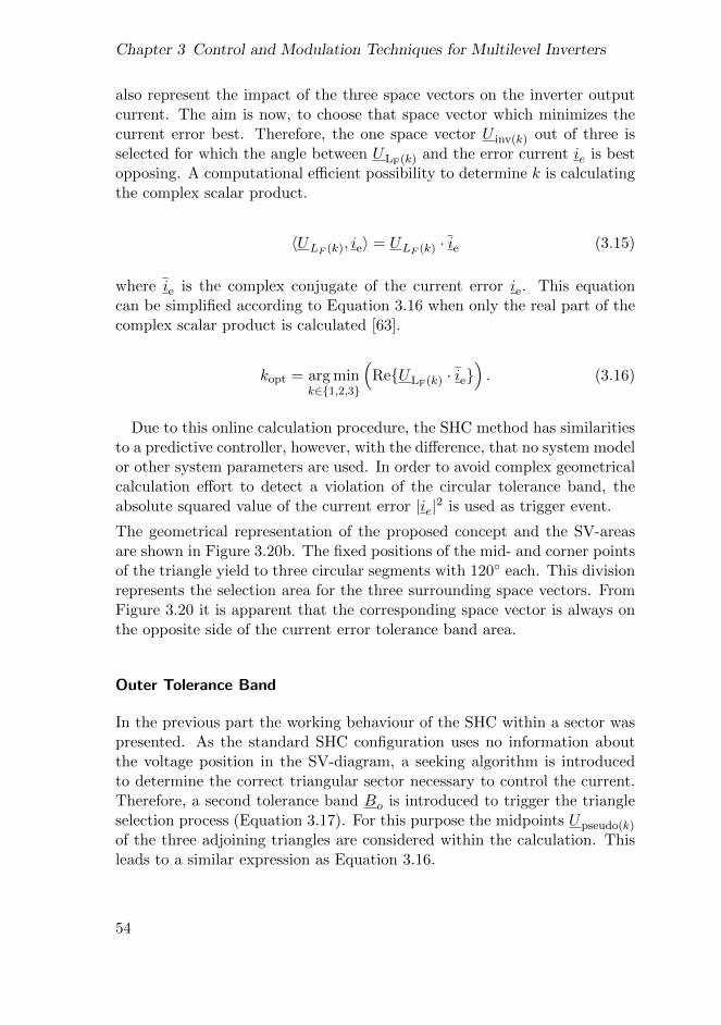
Chapter 3 Control and Modulation Techniques for Multilevel Inverters
also represent the impact of the three space vectors on the inverter outputcurrent. The aim is now, to choose that space vector which minimizes thecurrent error best. Therefore, the one space vector U inv(k) out of three isselected for which the angle between ULF(k) and the error current ie is bestopposing. A computational efficient possibility to determine k is calculatingthe complex scalar product.
〈ULF (k), ie〉 = ULF (k) · ie (3.15)
where ie is the complex conjugate of the current error ie. This equationcan be simplified according to Equation 3.16 when only the real part of thecomplex scalar product is calculated [63].
kopt = arg mink∈1,2,3
(ReULF(k) · ie
). (3.16)
Due to this online calculation procedure, the SHC method has similaritiesto a predictive controller, however, with the difference, that no system modelor other system parameters are used. In order to avoid complex geometricalcalculation effort to detect a violation of the circular tolerance band, theabsolute squared value of the current error |ie|2 is used as trigger event.
The geometrical representation of the proposed concept and the SV-areasare shown in Figure 3.20b. The fixed positions of the mid- and corner pointsof the triangle yield to three circular segments with 120 each. This divisionrepresents the selection area for the three surrounding space vectors. FromFigure 3.20 it is apparent that the corresponding space vector is always onthe opposite side of the current error tolerance band area.
Outer Tolerance Band
In the previous part the working behaviour of the SHC within a sector waspresented. As the standard SHC configuration uses no information aboutthe voltage position in the SV-diagram, a seeking algorithm is introducedto determine the correct triangular sector necessary to control the current.Therefore, a second tolerance band Bo is introduced to trigger the triangleselection process (Equation 3.17). For this purpose the midpoints Upseudo(k)
of the three adjoining triangles are considered within the calculation. Thisleads to a similar expression as Equation 3.16.
54
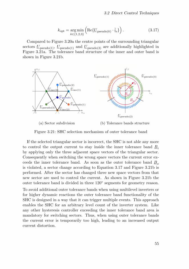
3.2 Direct Control Techniques
kopt = arg mink∈1,2,3
(ReUpseudo(k) · ie
). (3.17)
Compared to Figure 3.20a the centre points of the surrounding triangularsectors Upseudo(1), Upseudo(1) and Upseudo(3) are additionally highlighted inFigure 3.21a. The tolerance band structure of the inner and outer band isshown in Figure 3.21b.
Breite: 60 mm (halbseitig)
uα
uβ
sector 9
sector 10
sector 11
sector 12
60 x 50
x 5.5 y 4.5
uα
uβ
U inv(1)U inv(3)
U inv(2)
Upseudo uα
uβ
U inv(1)U inv(3)
U inv(2)
Upseudo
Upseudo(1)
Upseudo(2)
Upseudo(3)
uα
U inv(2)
U inv(3)U inv(1)
uβ
ie
uα
uβ
ie
Upseudo(2)
Upseudo(3)Upseudo(1)
Bi
Bo
iα
iβ
ie
Upseudo(2)
Upseudo(3)Upseudo(1)
Bi
Bo
U inv(1)
iα
U inv(3)
U inv(2)iβ
ie
Bi
(a) Sector subdivision
Breite: 60 mm (halbseitig)
uα
uβ
sector 9
sector 10
sector 11
sector 12
60 x 50
x 5.5 y 4.5
uα
uβ
U inv(1)U inv(3)
U inv(2)
Upseudo
uα
uβ
U inv(1)U inv(3)
U inv(2)
Upseudo
Upseudo(1)
Upseudo(2)
Upseudo(3)
uα
U inv(2)
U inv(3)U inv(1)
uβ
ie
uα
uβ
ie
Upseudo(2)
Upseudo(3)Upseudo(1)
Bi
Bo
iα
iβ
ie
Upseudo(2)
Upseudo(3)Upseudo(1)
Bi
Bo
U inv(1)
iα
U inv(2)
U inv(3)iβ
ie
Bi
(b) Tolerance bands structure
Figure 3.21: SHC selection mechanism of outer tolerance band
If the selected triangular sector is incorrect, the SHC is not able any moreto control the output current to stay inside the inner tolerance band Bi
by applying only the three adjacent space vectors of the triangular sector.Consequently when switching the wrong space vectors the current error ex-ceeds the inner tolerance band. As soon as the outer tolerance band Bo
is violated, a sector change according to Equation 3.17 and Figure 3.21b isperformed. After the sector has changed three new space vectors from thatnew sector are used to control the current. As shown in Figure 3.21b theouter tolerance band is divided in three 120 segments for geometry reason.
To avoid additional outer tolerance bands when using multilevel inverters orfor higher dynamic reactions the outer tolerance band functionality of theSHC is designed in a way that it can trigger multiple events. This approachenables the SHC for an arbitrary level count of the inverter system. Likeany other hysteresis controller exceeding the inner tolerance band area ismandatory for switching sectors. Thus, when using outer tolerance bandsthe current error is temporarily too high, leading to an increased outputcurrent distortion.
55
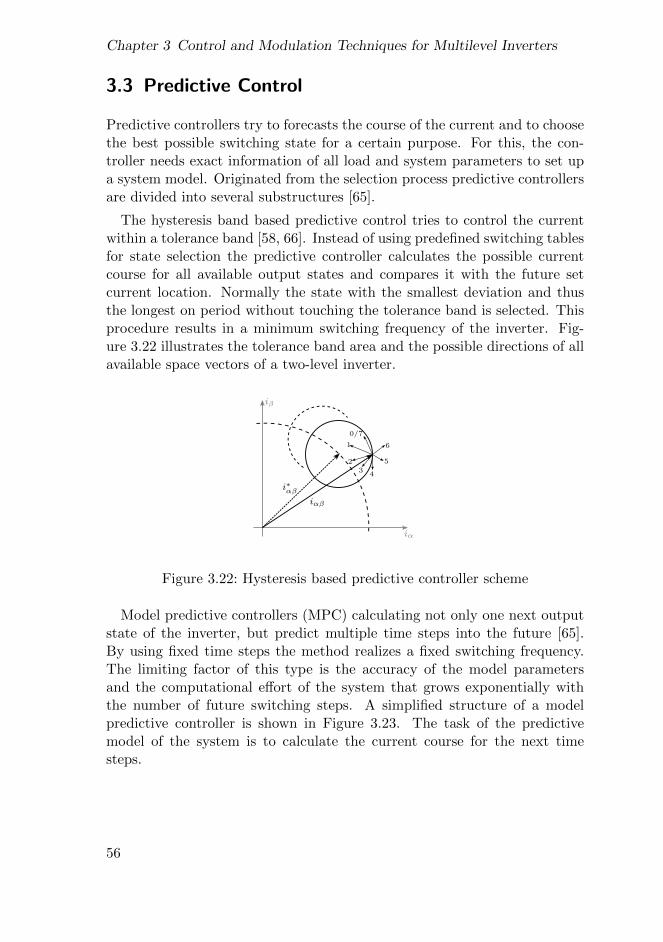
Chapter 3 Control and Modulation Techniques for Multilevel Inverters
3.3 Predictive Control
Predictive controllers try to forecasts the course of the current and to choosethe best possible switching state for a certain purpose. For this, the con-troller needs exact information of all load and system parameters to set upa system model. Originated from the selection process predictive controllersare divided into several substructures [65].
The hysteresis band based predictive control tries to control the currentwithin a tolerance band [58, 66]. Instead of using predefined switching tablesfor state selection the predictive controller calculates the possible currentcourse for all available output states and compares it with the future setcurrent location. Normally the state with the smallest deviation and thusthe longest on period without touching the tolerance band is selected. Thisprocedure results in a minimum switching frequency of the inverter. Fig-ure 3.22 illustrates the tolerance band area and the possible directions of allavailable space vectors of a two-level inverter.
π 2π
UPM
U∆
U∆
−U∆
−2U∆
0
Breite: 60 mm (halbseitig)uα
uβ
sector 9
sector 10
sector 11
sector 12
60 x 50
uα
uβ
sector 5
sector 6
iα
iβ
iαβ
i∗αβ
4
5
6
0/7
32
1
Figure 3.22: Hysteresis based predictive controller scheme
Model predictive controllers (MPC) calculating not only one next outputstate of the inverter, but predict multiple time steps into the future [65].By using fixed time steps the method realizes a fixed switching frequency.The limiting factor of this type is the accuracy of the model parametersand the computational effort of the system that grows exponentially withthe number of future switching steps. A simplified structure of a modelpredictive controller is shown in Figure 3.23. The task of the predictivemodel of the system is to calculate the current course for the next timesteps.
56
3.3 Predictive Control
LOAD A
LFRF
Minimizationof
iuvw(k)suvw
51
i∗αβ(k)
ieαβ
iαβ(k)
αβ
abc
7 ipredαβ (k + 1)
cost function
Predictivemodel
Figure 3.23: Model based predictive controller scheme
The major part of the MPC is the cost function which defines the aim ofthe control. An example of a cost function for controlling the grid current is
g =∣∣∣i∗α − ipredα
∣∣∣+∣∣∣i∗β − ipredβ
∣∣∣ (3.18)
where i∗α, i∗β are the reference values and ipredα , ipredβ are the predicted val-ues [67]. The best result for the controller would be zero current error afterthe used time step. Therefore, the state which minimizes g is selected andswitched to the output. Based on this equation the controller can select asequence of switching states for several time steps in future without reachinga tolerance band. The cost function is not limited to control currents. Tocontrol active and reactive power in grid applications the cost function canbe extended as predictive power controller resulting in [68]:
g =∣∣∣Q∗ −Qpred∣∣∣+
∣∣∣P ∗ − P pred∣∣∣ (3.19)
where Q∗, P ∗ are the reference and Qpred, P pred are the predicted powervalues. Both cost functions can thereby be optionally extended to fulfiladditional control properties like switching losses. When several controlfactors need to be considered weighting factors are introduced.
To sum up, predictive controllers have the following advantages:
• Simple handling
• No linear controllers or modulators are needed
• Non-linearities can be modelled and taken into account
57

Chapter 3 Control and Modulation Techniques for Multilevel Inverters
The main disadvantage is that an exact knowledge of all system parame-ters for setting up the model is required. Differences between model andreality could impair the stationary and dynamic behaviour of the controller.Furthermore, the increased computational effort depends strongly on thenumber of future steps that need to be considered.
Implementation Effort for Multilevel Systems
Predictive controllers for multilevel systems are part of intensive research [69,70]. The main challenge is the dramatic rise of possible switching states ton3 compared to the 23 for the two-level inverter. Thereby the required com-putational power increases even faster. Especially for online calculation ofthe current course several steps in the future would lead to an exponentialgrowth of switching possibilities. To reduce the calculation effort differentsimplification strategies for multilevel application are considered. One possi-bility is a heuristic pre-selection of relevant space vectors like using only theclosest ones to the actual sector [71]. Another method is an extrapolation ofadditional future current steps instead of an exact calculation of each stateto save computational resources. Additional to the high count of switchingpossibilities further control task must be implemented in the cost functionwhich complicates the setup. One of the main parts that must be addedto the cost function is thereby the DC-link balancing which is necessary inmost multilevel applications.
58
3.4 Summary
3.4 Summary
The previous chapter showed an overview of indirect, direct and predictivecontrol methods and the corresponding advantages and disadvantages. Thenecessary extensions of direct controllers for multilevel inverter applicationwere explained. Almost all methods show that the adaptation for higherlevels results in a significant increase of complexity. To detect the best pos-sible switching state in multilevel inverter systems the following approachesare used in direct controlled systems.
• Introduction of additional hysteresis bands for selection of the bestmatching state. However this results in rising current deviation withhigher level count.
• Simplification of the SV-diagram by its subdivision in angular areasusing the detected phase angle for pre-selection. Combination withmulti-stage hysteresis bands to subdivide the sector according the levelcount.
• Combination of hysteresis bands with exact sector pre-selection usingthe voltage information. Count of switching tables for the definedsectors increases rapidly with higher level count.
59

60
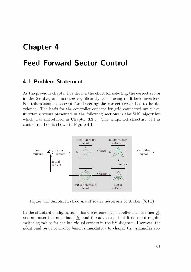
Chapter 4
Feed Forward Sector Control
4.1 Problem Statement
As the previous chapter has shown, the effort for selecting the correct sectorin the SV-diagram increases significantly when using multilevel inverters.For this reason, a concept for detecting the correct sector has to be de-veloped. The basis for the controller concept for grid connected multilevelinverter systems presented in the following sections is the SHC algorithmwhich was introduced in Chapter 3.2.5. The simplified structure of thiscontrol method is shown in Figure 4.1.
LOAD
LFRF
sUVW
33u∗UVW
ucarr
inner toleranceband
space vectorselection
trigger switchingsignal
outer toleranceband
sectorselection
trigger
errorcurrent
setcurrent
actualcurrent sector
Figure 4.1: Simplified structure of scalar hysteresis controller (SHC)
In the standard configuration, this direct current controller has an inner Bi
and an outer tolerance band Bo and the advantage that it does not requireswitching tables for the individual sectors in the SV-diagram. However, theadditional outer tolerance band is mandatory to change the triangular sec-
61
Chapter 4 Feed Forward Sector Control
tors, whereby the error current increases at each change for a short time.Considering a two-level inverter system, six sector changes are necessary,when using multilevel inverters the number of required sector changes in-creases significantly. This working behaviour leads to increased harmonicdistortion in the output current.
The aim of the proposed concept is to avoid the need of an outer toleranceband in steady state conditions by using a new intelligent feed forward sectorcontrol system. Considering a two-level inverter SV-diagram a feed forwardcontrol using the phase angle θinv of the average inverter output voltage isable to perform this task in a simple way. Nevertheless, the demands fora correct sector selection process increase with the number of levels. Forn ≥ 3 the quadratically increasing number of triangular sectors leads toinsufficient sector selection when only the phase angle θinv is used. Thus,for the precise feed forward control the exact knowledge of the phase angleand amplitude of the average inverter output voltage including the harmoniccomponents is necessary [72]. If only the fundamental voltage is used theharmonic components would negatively effect the feed forward control instandard grid applications. In case of indirect control methods, the feedforward voltage would be the input signal for the modulator. Since theSHC controls the current directly it does not provide information about itsselected average output voltage. This voltage must be generated in a properway. To achieve this the proposed feed forward sector control has to meetthe following requirements:
• In phase detection of the average inverter output voltage uinv for feedforward sector control.
• Detection of harmonic voltage components to improve the controllerperformance under harmonic distortions within the grid (optional).
• A simple derivation of the triangular sectors surrounding the detectedinverter output voltage.
• Additional use of the detected inverter output voltage for a higher-levelcontrol, e.g. generation of set current via a power control
62
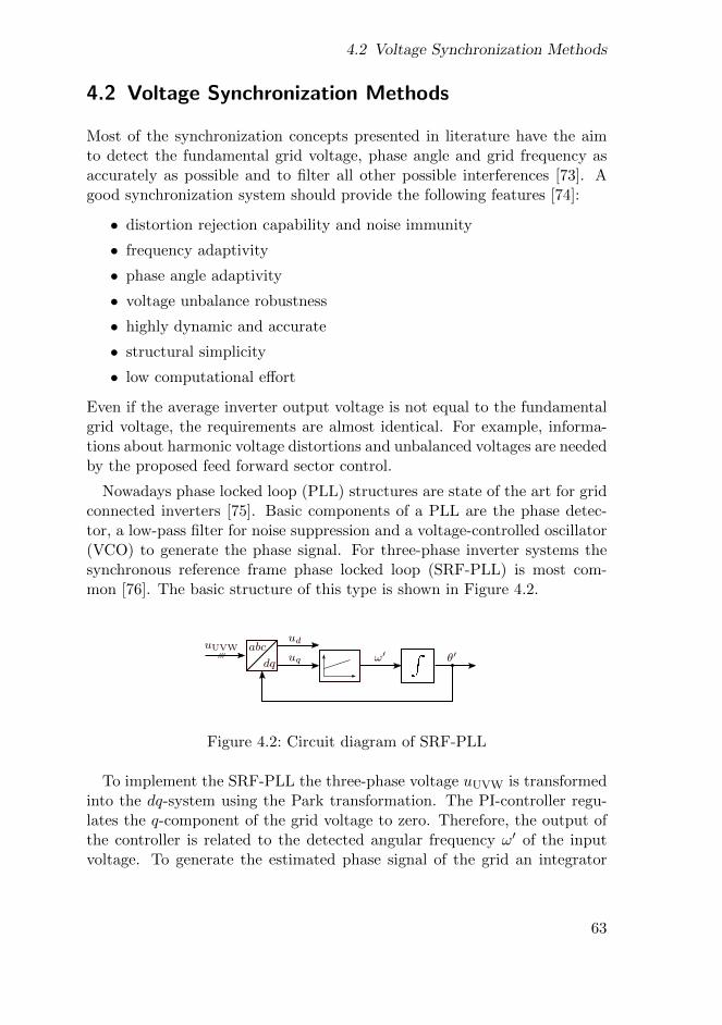
4.2 Voltage Synchronization Methods
4.2 Voltage Synchronization Methods
Most of the synchronization concepts presented in literature have the aimto detect the fundamental grid voltage, phase angle and grid frequency asaccurately as possible and to filter all other possible interferences [73]. Agood synchronization system should provide the following features [74]:
• distortion rejection capability and noise immunity
• frequency adaptivity
• phase angle adaptivity
• voltage unbalance robustness
• highly dynamic and accurate
• structural simplicity
• low computational effort
Even if the average inverter output voltage is not equal to the fundamentalgrid voltage, the requirements are almost identical. For example, informa-tions about harmonic voltage distortions and unbalanced voltages are neededby the proposed feed forward sector control.
Nowadays phase locked loop (PLL) structures are state of the art for gridconnected inverters [75]. Basic components of a PLL are the phase detec-tor, a low-pass filter for noise suppression and a voltage-controlled oscillator(VCO) to generate the phase signal. For three-phase inverter systems thesynchronous reference frame phase locked loop (SRF-PLL) is most com-mon [76]. The basic structure of this type is shown in Figure 4.2.
switchingtable
45
sαβ
dq
abcuUVWud
uq ω′ θ′
Figure 4.2: Circuit diagram of SRF-PLL
To implement the SRF-PLL the three-phase voltage uUVW is transformedinto the dq-system using the Park transformation. The PI-controller regu-lates the q-component of the grid voltage to zero. Therefore, the output ofthe controller is related to the detected angular frequency ω′ of the inputvoltage. To generate the estimated phase signal of the grid an integrator
63
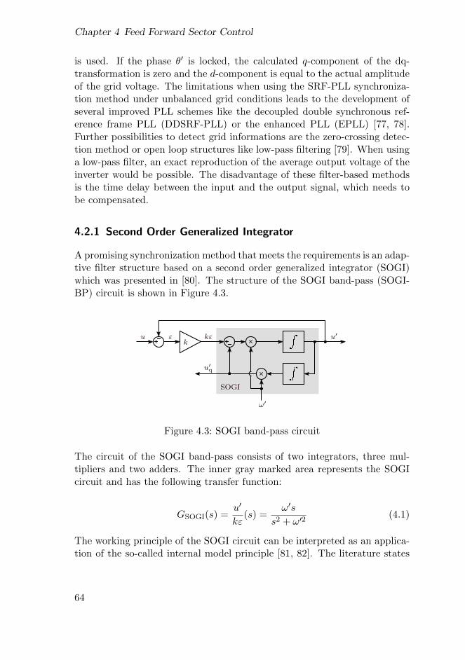
Chapter 4 Feed Forward Sector Control
is used. If the phase θ′ is locked, the calculated q-component of the dq-transformation is zero and the d-component is equal to the actual amplitudeof the grid voltage. The limitations when using the SRF-PLL synchroniza-tion method under unbalanced grid conditions leads to the development ofseveral improved PLL schemes like the decoupled double synchronous ref-erence frame PLL (DDSRF-PLL) or the enhanced PLL (EPLL) [77, 78].Further possibilities to detect grid informations are the zero-crossing detec-tion method or open loop structures like low-pass filtering [79]. When usinga low-pass filter, an exact reproduction of the average output voltage of theinverter would be possible. The disadvantage of these filter-based methodsis the time delay between the input and the output signal, which needs tobe compensated.
4.2.1 Second Order Generalized Integrator
A promising synchronization method that meets the requirements is an adap-tive filter structure based on a second order generalized integrator (SOGI)which was presented in [80]. The structure of the SOGI band-pass (SOGI-BP) circuit is shown in Figure 4.3.
33
u′uk
ε kε
u′q
ω′
SOGI
u′1
uk
ε kε
qu′
ω′
SOGI
qu′1
ε
kkε
SOGI
qu′1
Figure 4.3: SOGI band-pass circuit
The circuit of the SOGI band-pass consists of two integrators, three mul-tipliers and two adders. The inner gray marked area represents the SOGIcircuit and has the following transfer function:
GSOGI(s) =u′
kε(s) =
ω′ss2 + ω′2
(4.1)
The working principle of the SOGI circuit can be interpreted as an applica-tion of the so-called internal model principle [81, 82]. The literature states
64
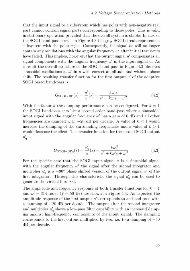
4.2 Voltage Synchronization Methods
that the input signal to a subsystem which has poles with non-negative realpart cannot contain signal parts corresponding to those poles. This is validin stationary operation provided that the overall system is stable. In case ofthe SOGI band-pass circuit in Figure 4.3 the gray SOGI circuit represents asubsystem with the poles ±jω′. Consequently, the signal kε will no longercontain any oscillations with the angular frequency ω′ after initial transientshave faded. This implies, however, that the output signal u′ compensates allsignal components with the angular frequency ω′ in the input signal u. Asa result the overall structure of the SOGI band-pass in Figure 4.3 observessinusoidal oscillations at ω′ in u with correct amplitude and without phaseshift. The resulting transfer function for the first output u′ of the adaptiveSOGI based band-pass is
GSOGI−BP(s) =u′
u(s) =
kω′ss2 + kω′s+ ω′2
(4.2)
With the factor k the damping performance can be configured. For k = 1the SOGI band-pass acts like a second order band-pass where a sinusoidalinput signal with the angular frequency ω′ has a gain of 0 dB and all otherfrequencies are damped with −20 dB per decade. A value of k < 1 wouldincrease the damping of the surrounding frequencies and a value of k > 1would decrease the effect. The transfer function for the second SOGI outputu′q is
GSOGI−BPq(s) =u′qu
(s) =kω′2
s2 + kω′s+ ω′2(4.3)
For the specific case that the SOGI input signal u is a sinusoidal signalwith the angular frequency ω′ the signal after the second integrator andmultiplier u′q is a −90 phase shifted version of the output signal u′ of thefirst integrator. Through this characteristic the signal u′q can be used togenerate the virtual-flux [83].
The amplitude and frequency response of both transfer functions for k = 1and ω′ = 314 rad/s (f = 50 Hz) are shown in Figure 4.4. As expected theamplitude response of the first output u′ corresponds to an band-pass witha damping of −20 dB per decade. The output after the second integratorand multiplier u′q shows a low-pass filter capability with an increased damp-ing against high-frequency components of the input signal. The dampingcorresponds to the first output multiplied by two, i.e. to a damping of −40dB per decade.
65
Chapter 4 Feed Forward Sector Control
Figure 4.4: Bode diagram of SOGI band-pass (left) and after second inte-grator stage (right) with damping factor k = 1
To use the SOGI band pass for synchronization of a three-phase invertersystem the input voltage uabc is transformed to the αβ-system. This reducesthe number of required SOGI-circuits to two. In literature this system isdenoted by double second order generalized integrator (DSOGI) [80].
4.2.2 Frequency Readjustment
The previous shown SOGI circuit can only be used in grid application witha fixed frequency e.g. 50 Hz. For the case that the grid frequency varies apermanent deviation in the output signal can occur. To extend the SOGIto a frequency adaptive system several possibilities are presented in litera-ture. One possibility could be using a standard SRF-PLL and its detectedfrequency ω′ as input to the SOGI circuit [80]. In this case the SRF-PLLuses the calculated positive sequence as input to detect the actual centrefrequency of the grid.
66
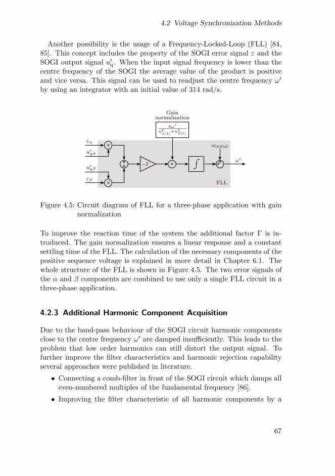
4.2 Voltage Synchronization Methods
Another possibility is the usage of a Frequency-Locked-Loop (FLL) [84,85]. This concept includes the property of the SOGI error signal ε and theSOGI output signal u′q. When the input signal frequency is lower than thecentre frequency of the SOGI the average value of the product is positiveand vice versa. This signal can be used to readjust the centre frequency ω′
by using an integrator with an initial value of 314 rad/s.
33
u′uk
ε kε
qu′
ω′
FLL
u′1
uk
ε kε
qu′
ω′
SOGI
qu′1
ε
kkε
SOGI
qu′1
−Γ
εα
εβ
u′qα
u′qβ
kω′u2α(1)
+u2β(1)
ωinitial
Gainnormalization
Figure 4.5: Circuit diagram of FLL for a three-phase application with gainnormalization
To improve the reaction time of the system the additional factor Γ is in-troduced. The gain normalization ensures a linear response and a constantsettling time of the FLL. The calculation of the necessary components of thepositive sequence voltage is explained in more detail in Chapter 6.1. Thewhole structure of the FLL is shown in Figure 4.5. The two error signals ofthe α and β components are combined to use only a single FLL circuit in athree-phase application.
4.2.3 Additional Harmonic Component Acquisition
Due to the band-pass behaviour of the SOGI circuit harmonic componentsclose to the centre frequency ω′ are damped insufficiently. This leads to theproblem that low order harmonics can still distort the output signal. Tofurther improve the filter characteristics and harmonic rejection capabilityseveral approaches were published in literature.
• Connecting a comb-filter in front of the SOGI circuit which damps alleven-numbered multiples of the fundamental frequency [86].
• Improving the filter characteristic of all harmonic components by a
67
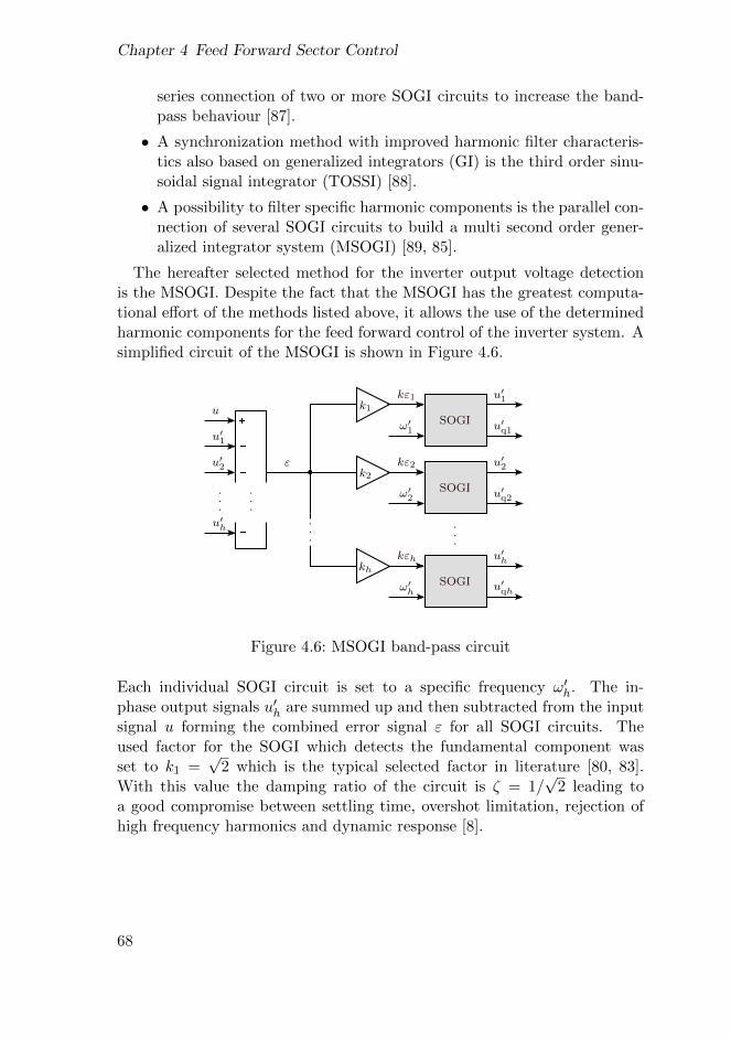
Chapter 4 Feed Forward Sector Control
series connection of two or more SOGI circuits to increase the band-pass behaviour [87].
• A synchronization method with improved harmonic filter characteris-tics also based on generalized integrators (GI) is the third order sinu-soidal signal integrator (TOSSI) [88].
• A possibility to filter specific harmonic components is the parallel con-nection of several SOGI circuits to build a multi second order gener-alized integrator system (MSOGI) [89, 85].
The hereafter selected method for the inverter output voltage detectionis the MSOGI. Despite the fact that the MSOGI has the greatest computa-tional effort of the methods listed above, it allows the use of the determinedharmonic components for the feed forward control of the inverter system. Asimplified circuit of the MSOGI is shown in Figure 4.6.
33
u′uk
ε kε
qu′
ω′
SOGI
u′1
uk
ε kε
qu′
ω′
SOGI
u′q1
ε
k1kε1
SOGIω′1
u′2
u′q2
k2kε2
SOGIω′2
u′h
u′qh
khkεh
SOGIω′h
.
.
.
u′1
u′2
u′h
.
.
.
.
.
....
u
ε
Figure 4.6: MSOGI band-pass circuit
Each individual SOGI circuit is set to a specific frequency ω′h. The in-phase output signals u′h are summed up and then subtracted from the inputsignal u forming the combined error signal ε for all SOGI circuits. Theused factor for the SOGI which detects the fundamental component wasset to k1 =
√2 which is the typical selected factor in literature [80, 83].
With this value the damping ratio of the circuit is ζ = 1/√
2 leading toa good compromise between settling time, overshot limitation, rejection ofhigh frequency harmonics and dynamic response [8].
68
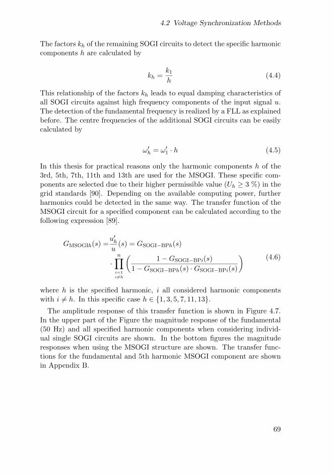
4.2 Voltage Synchronization Methods
The factors kh of the remaining SOGI circuits to detect the specific harmoniccomponents h are calculated by
kh =k1
h(4.4)
This relationship of the factors kh leads to equal damping characteristics ofall SOGI circuits against high frequency components of the input signal u.The detection of the fundamental frequency is realized by a FLL as explainedbefore. The centre frequencies of the additional SOGI circuits can be easilycalculated by
ω′h = ω′1 · h (4.5)
In this thesis for practical reasons only the harmonic components h of the3rd, 5th, 7th, 11th and 13th are used for the MSOGI. These specific com-ponents are selected due to their higher permissible value (Uh ≥ 3 %) in thegrid standards [90]. Depending on the available computing power, furtherharmonics could be detected in the same way. The transfer function of theMSOGI circuit for a specified component can be calculated according to thefollowing expression [89].
GMSOGIh(s) =u′hu
(s) = GSOGI−BPh(s)
·n∏i=1i6=h
(1−GSOGI−BPi(s)
1−GSOGI−BPh(s) ·GSOGI−BPi(s)
)(4.6)
where h is the specified harmonic, i all considered harmonic componentswith i 6= h. In this specific case h ∈ 1, 3, 5, 7, 11, 13.
The amplitude response of this transfer function is shown in Figure 4.7.In the upper part of the Figure the magnitude response of the fundamental(50 Hz) and all specified harmonic components when considering individ-ual single SOGI circuits are shown. In the bottom figures the magnituderesponses when using the MSOGI structure are shown. The transfer func-tions for the fundamental and 5th harmonic MSOGI component are shownin Appendix B.
69
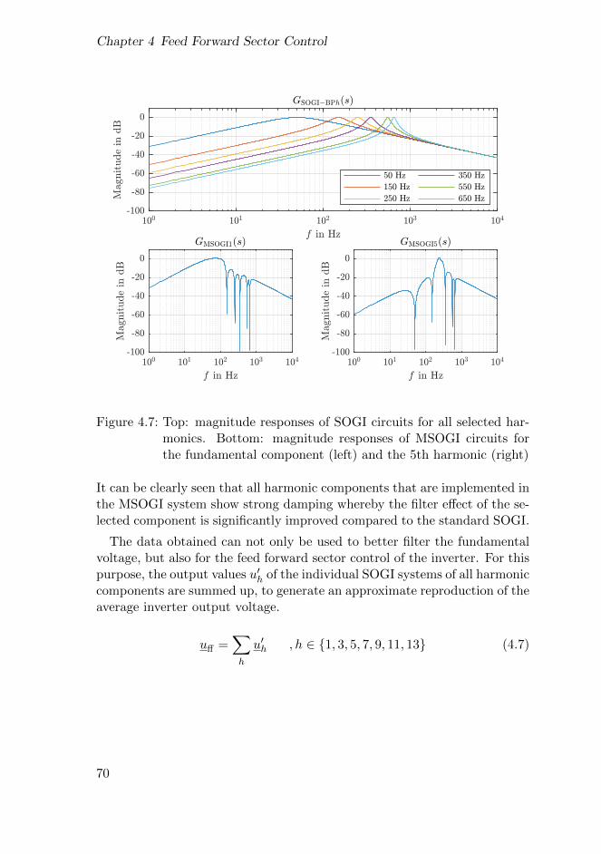
Chapter 4 Feed Forward Sector Control
Figure 4.7: Top: magnitude responses of SOGI circuits for all selected har-monics. Bottom: magnitude responses of MSOGI circuits forthe fundamental component (left) and the 5th harmonic (right)
It can be clearly seen that all harmonic components that are implemented inthe MSOGI system show strong damping whereby the filter effect of the se-lected component is significantly improved compared to the standard SOGI.
The data obtained can not only be used to better filter the fundamentalvoltage, but also for the feed forward sector control of the inverter. For thispurpose, the output values u′h of the individual SOGI systems of all harmoniccomponents are summed up, to generate an approximate reproduction of theaverage inverter output voltage.
uff =∑h
u′h , h ∈ 1, 3, 5, 7, 9, 11, 13 (4.7)
70
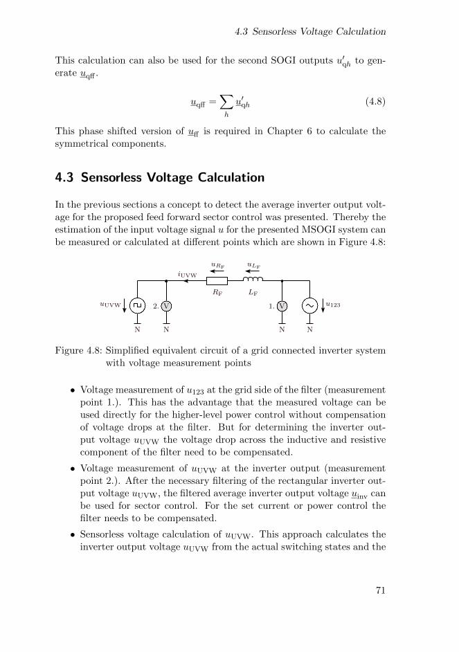
4.3 Sensorless Voltage Calculation
This calculation can also be used for the second SOGI outputs u′qh to gen-erate uqff .
uqff =∑h
u′qh (4.8)
This phase shifted version of uff is required in Chapter 6 to calculate thesymmetrical components.
4.3 Sensorless Voltage Calculation
In the previous sections a concept to detect the average inverter output volt-age for the proposed feed forward sector control was presented. Thereby theestimation of the input voltage signal u for the presented MSOGI system canbe measured or calculated at different points which are shown in Figure 4.8:
LFRF 33
LOAD A
LFRF
iUVW
sUVWi∗UVWieUVW
u123uUVW
iUVW
uRFuLF
N N
VV2. 1.
NN
Figure 4.8: Simplified equivalent circuit of a grid connected inverter systemwith voltage measurement points
• Voltage measurement of u123 at the grid side of the filter (measurementpoint 1.). This has the advantage that the measured voltage can beused directly for the higher-level power control without compensationof voltage drops at the filter. But for determining the inverter out-put voltage uUVW the voltage drop across the inductive and resistivecomponent of the filter need to be compensated.
• Voltage measurement of uUVW at the inverter output (measurementpoint 2.). After the necessary filtering of the rectangular inverter out-put voltage uUVW, the filtered average inverter output voltage uinv canbe used for sector control. For the set current or power control thefilter needs to be compensated.
• Sensorless voltage calculation of uUVW. This approach calculates theinverter output voltage uUVW from the actual switching states and the
71
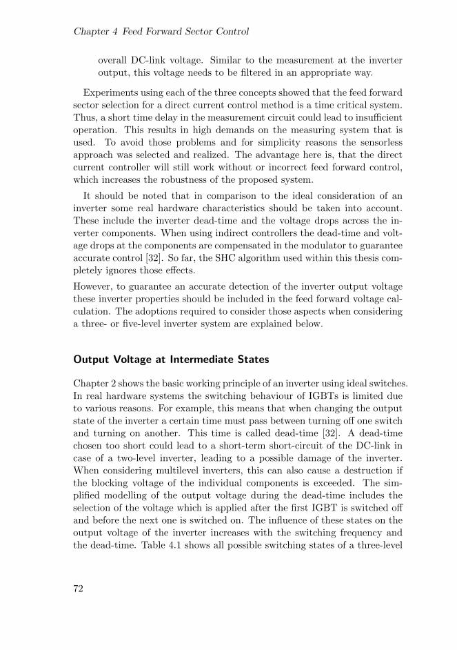
Chapter 4 Feed Forward Sector Control
overall DC-link voltage. Similar to the measurement at the inverteroutput, this voltage needs to be filtered in an appropriate way.
Experiments using each of the three concepts showed that the feed forwardsector selection for a direct current control method is a time critical system.Thus, a short time delay in the measurement circuit could lead to insufficientoperation. This results in high demands on the measuring system that isused. To avoid those problems and for simplicity reasons the sensorlessapproach was selected and realized. The advantage here is, that the directcurrent controller will still work without or incorrect feed forward control,which increases the robustness of the proposed system.
It should be noted that in comparison to the ideal consideration of aninverter some real hardware characteristics should be taken into account.These include the inverter dead-time and the voltage drops across the in-verter components. When using indirect controllers the dead-time and volt-age drops at the components are compensated in the modulator to guaranteeaccurate control [32]. So far, the SHC algorithm used within this thesis com-pletely ignores those effects.
However, to guarantee an accurate detection of the inverter output voltagethese inverter properties should be included in the feed forward voltage cal-culation. The adoptions required to consider those aspects when consideringa three- or five-level inverter system are explained below.
Output Voltage at Intermediate States
Chapter 2 shows the basic working principle of an inverter using ideal switches.In real hardware systems the switching behaviour of IGBTs is limited dueto various reasons. For example, this means that when changing the outputstate of the inverter a certain time must pass between turning off one switchand turning on another. This time is called dead-time [32]. A dead-timechosen too short could lead to a short-term short-circuit of the DC-link incase of a two-level inverter, leading to a possible damage of the inverter.When considering multilevel inverters, this can also cause a destruction ifthe blocking voltage of the individual components is exceeded. The sim-plified modelling of the output voltage during the dead-time includes theselection of the voltage which is applied after the first IGBT is switched offand before the next one is switched on. The influence of these states on theoutput voltage of the inverter increases with the switching frequency andthe dead-time. Table 4.1 shows all possible switching states of a three-level
72
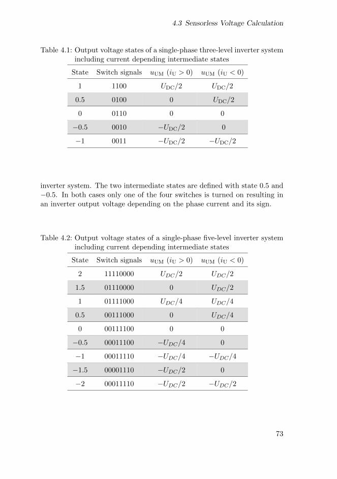
4.3 Sensorless Voltage Calculation
Table 4.1: Output voltage states of a single-phase three-level inverter systemincluding current depending intermediate states
State Switch signals uUM (iU > 0) uUM (iU < 0)
1 1100 UDC/2 UDC/2
0.5 0100 0 UDC/2
0 0110 0 0
−0.5 0010 −UDC/2 0
−1 0011 −UDC/2 −UDC/2
inverter system. The two intermediate states are defined with state 0.5 and−0.5. In both cases only one of the four switches is turned on resulting inan inverter output voltage depending on the phase current and its sign.
Table 4.2: Output voltage states of a single-phase five-level inverter systemincluding current depending intermediate states
State Switch signals uUM (iU > 0) uUM (iU < 0)
2 11110000 UDC/2 UDC/2
1.5 01110000 0 UDC/2
1 01111000 UDC/4 UDC/4
0.5 00111000 0 UDC/4
0 00111100 0 0
−0.5 00011100 −UDC/4 0
−1 00011110 −UDC/4 −UDC/4
−1.5 00001110 −UDC/2 0
−2 00011110 −UDC/2 −UDC/2
73
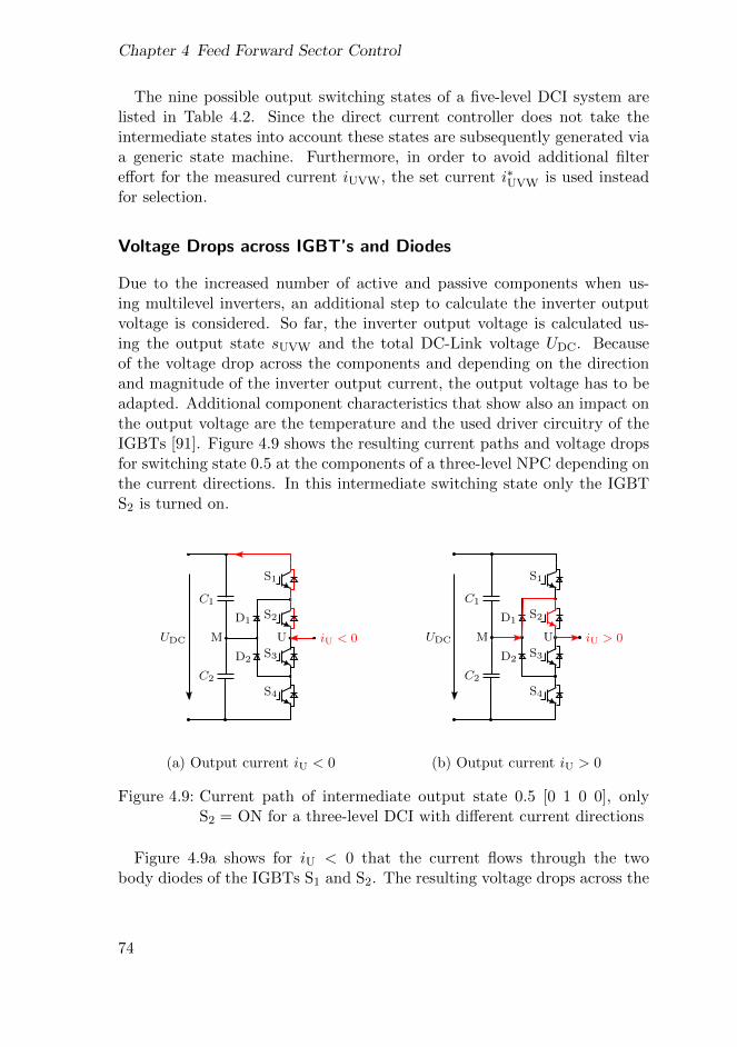
Chapter 4 Feed Forward Sector Control
The nine possible output switching states of a five-level DCI system arelisted in Table 4.2. Since the direct current controller does not take theintermediate states into account these states are subsequently generated viaa generic state machine. Furthermore, in order to avoid additional filtereffort for the measured current iUVW, the set current i∗UVW is used insteadfor selection.
Voltage Drops across IGBT’s and Diodes
Due to the increased number of active and passive components when us-ing multilevel inverters, an additional step to calculate the inverter outputvoltage is considered. So far, the inverter output voltage is calculated us-ing the output state sUVW and the total DC-Link voltage UDC. Becauseof the voltage drop across the components and depending on the directionand magnitude of the inverter output current, the output voltage has to beadapted. Additional component characteristics that show also an impact onthe output voltage are the temperature and the used driver circuitry of theIGBTs [91]. Figure 4.9 shows the resulting current paths and voltage dropsfor switching state 0.5 at the components of a three-level NPC depending onthe current directions. In this intermediate switching state only the IGBTS2 is turned on.
S1
S2
S3
S4
D1
D2
C1
C2
MUDC iU < 0
S1
S2
S3
S4
D1
D2
C1
C2
MUDC iU > 0U
U
(a) Output current iU < 0
S1
S2
S3
S4
D1
D2
C1
C2
MUDC iU < 0
S1
S2
S3
S4
D1
D2
C1
C2
MUDC iU > 0U
U
(b) Output current iU > 0
Figure 4.9: Current path of intermediate output state 0.5 [0 1 0 0], onlyS2 = ON for a three-level DCI with different current directions
Figure 4.9a shows for iU < 0 that the current flows through the twobody diodes of the IGBTs S1 and S2. The resulting voltage drops across the
74
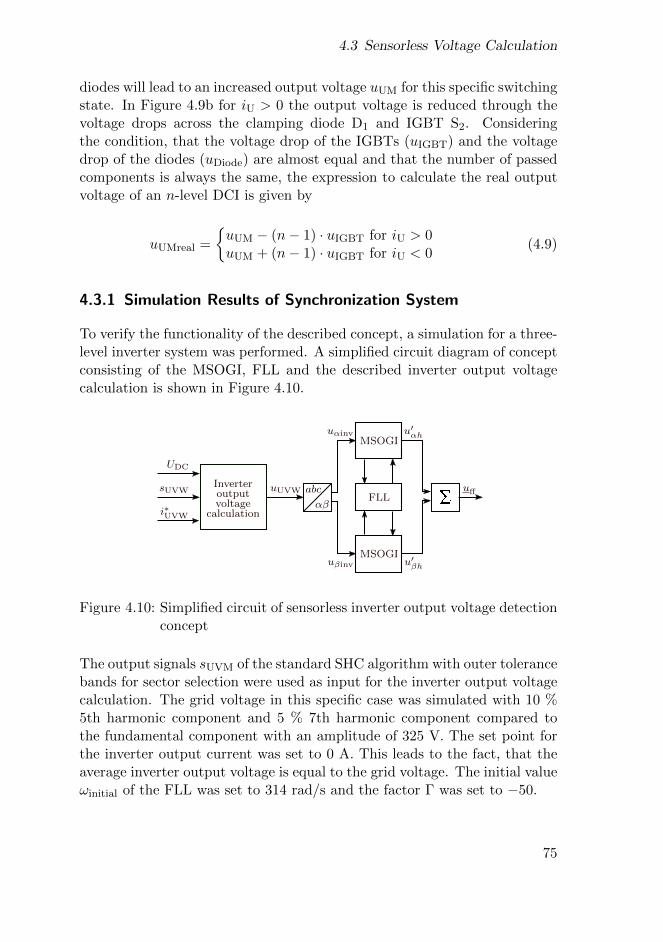
4.3 Sensorless Voltage Calculation
diodes will lead to an increased output voltage uUM for this specific switchingstate. In Figure 4.9b for iU > 0 the output voltage is reduced through thevoltage drops across the clamping diode D1 and IGBT S2. Consideringthe condition, that the voltage drop of the IGBTs (uIGBT) and the voltagedrop of the diodes (uDiode) are almost equal and that the number of passedcomponents is always the same, the expression to calculate the real outputvoltage of an n-level DCI is given by
uUMreal =
uUM − (n− 1) · uIGBT for iU > 0uUM + (n− 1) · uIGBT for iU < 0
(4.9)
4.3.1 Simulation Results of Synchronization System
To verify the functionality of the described concept, a simulation for a three-level inverter system was performed. A simplified circuit diagram of conceptconsisting of the MSOGI, FLL and the described inverter output voltagecalculation is shown in Figure 4.10.
33
u′uk
ε kε
qu′
ω′
SOGI
u′1
uk
ε kε
qu′
ω′
SOGI
qu′1
ε
k1
kε1
SOGIω1
u′2
qu′2
k2
kε2
SOGIω2
u′h
qu′h
khkεh
ωh
.
.
.
u′1
u′2
u′h
.
.
.
.
.
....
u
ε
MSOGI
FLL
MSOGI
αβ
abcInverteroutput
UDC
i∗UVW
sUVW uUVW
voltagecalculation
uαinv
uβinv
u′αh
u′βh
uff
Figure 4.10: Simplified circuit of sensorless inverter output voltage detectionconcept
The output signals sUVM of the standard SHC algorithm with outer tolerancebands for sector selection were used as input for the inverter output voltagecalculation. The grid voltage in this specific case was simulated with 10 %5th harmonic component and 5 % 7th harmonic component compared tothe fundamental component with an amplitude of 325 V. The set point forthe inverter output current was set to 0 A. This leads to the fact, that theaverage inverter output voltage is equal to the grid voltage. The initial valueωinitial of the FLL was set to 314 rad/s and the factor Γ was set to −50.
75
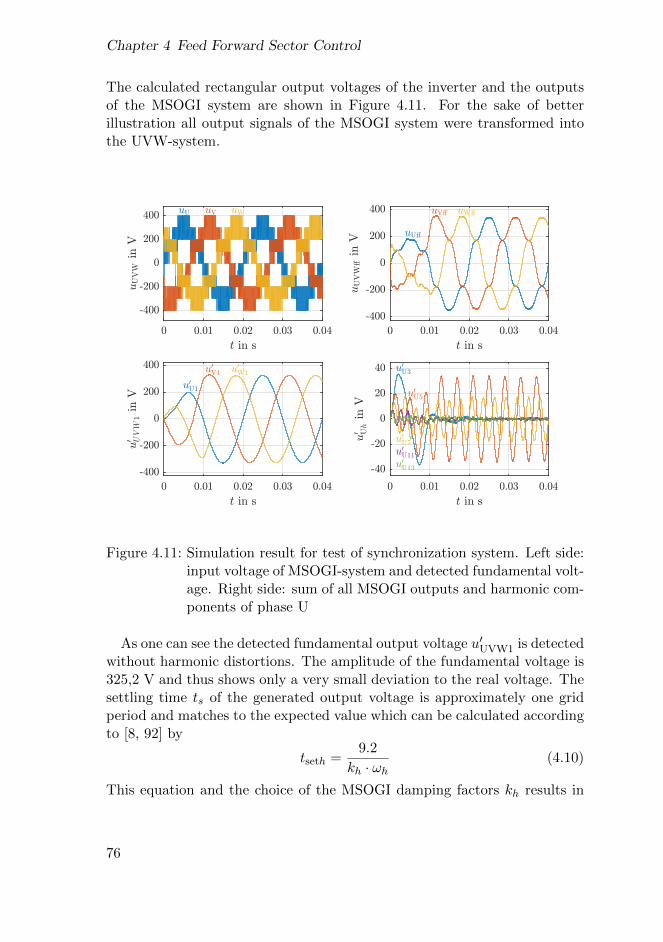
Chapter 4 Feed Forward Sector Control
The calculated rectangular output voltages of the inverter and the outputsof the MSOGI system are shown in Figure 4.11. For the sake of betterillustration all output signals of the MSOGI system were transformed intothe UVW-system.
0 0.01 0.02 0.03 0.04
t in s
-400
-200
0
200
400 uU uV uW
uU
VW
inV
0 0.01 0.02 0.03 0.04
t in s
-400
-200
0
200
400
u0U1
u0V1 u0
W1
u0 U
VW
1in
V
0 0.01 0.02 0.03 0.04
t in s
-400
-200
0
200
400
uU
VW,
inV
uU,
uV, uW,
0 0.01 0.02 0.03 0.04
t in s
-40
-20
0
20
40u
0 Uh
inV
u0U3
u0U5
u0U7
u0U11
u0U13
Figure 4.11: Simulation result for test of synchronization system. Left side:input voltage of MSOGI-system and detected fundamental volt-age. Right side: sum of all MSOGI outputs and harmonic com-ponents of phase U
As one can see the detected fundamental output voltage u′UVW1 is detectedwithout harmonic distortions. The amplitude of the fundamental voltage is325,2 V and thus shows only a very small deviation to the real voltage. Thesettling time ts of the generated output voltage is approximately one gridperiod and matches to the expected value which can be calculated accordingto [8, 92] by
tseth =9.2
kh · ωh(4.10)
This equation and the choice of the MSOGI damping factors kh results in
76
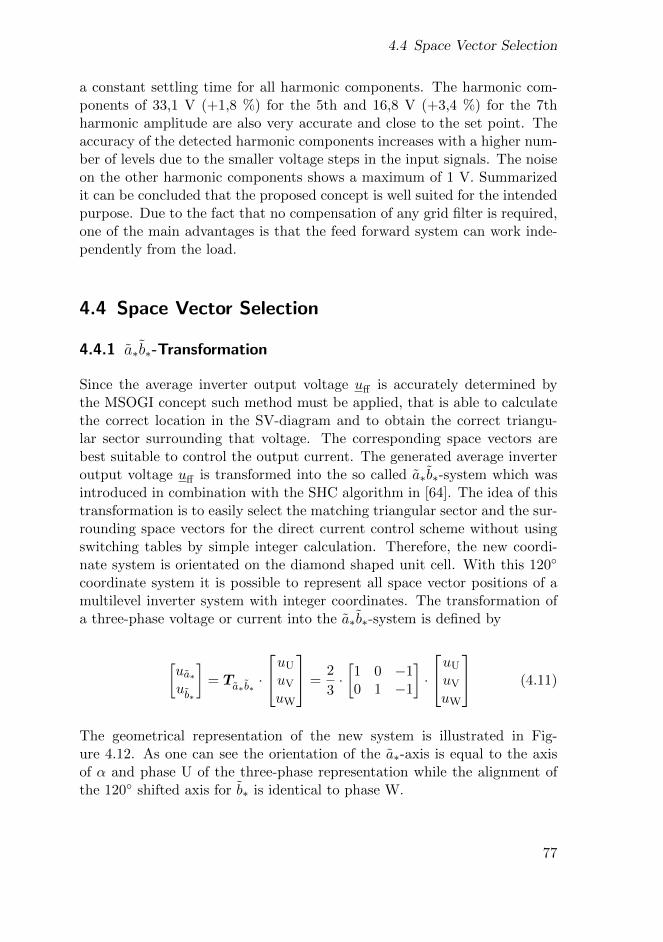
4.4 Space Vector Selection
a constant settling time for all harmonic components. The harmonic com-ponents of 33,1 V (+1,8 %) for the 5th and 16,8 V (+3,4 %) for the 7thharmonic amplitude are also very accurate and close to the set point. Theaccuracy of the detected harmonic components increases with a higher num-ber of levels due to the smaller voltage steps in the input signals. The noiseon the other harmonic components shows a maximum of 1 V. Summarizedit can be concluded that the proposed concept is well suited for the intendedpurpose. Due to the fact that no compensation of any grid filter is required,one of the main advantages is that the feed forward system can work inde-pendently from the load.
4.4 Space Vector Selection
4.4.1 a∗b∗-Transformation
Since the average inverter output voltage uff is accurately determined bythe MSOGI concept such method must be applied, that is able to calculatethe correct location in the SV-diagram and to obtain the correct triangu-lar sector surrounding that voltage. The corresponding space vectors arebest suitable to control the output current. The generated average inverteroutput voltage uff is transformed into the so called a∗b∗-system which wasintroduced in combination with the SHC algorithm in [64]. The idea of thistransformation is to easily select the matching triangular sector and the sur-rounding space vectors for the direct current control scheme without usingswitching tables by simple integer calculation. Therefore, the new coordi-nate system is orientated on the diamond shaped unit cell. With this 120
coordinate system it is possible to represent all space vector positions of amultilevel inverter system with integer coordinates. The transformation ofa three-phase voltage or current into the a∗b∗-system is defined by
[ua∗ub∗
]= Ta∗b∗ ·
uU
uV
uW
=2
3·[1 0 −10 1 −1
]·
uU
uV
uW
(4.11)
The geometrical representation of the new system is illustrated in Fig-ure 4.12. As one can see the orientation of the a∗-axis is equal to the axisof α and phase U of the three-phase representation while the alignment ofthe 120 shifted axis for b∗ is identical to phase W.
77
Chapter 4 Feed Forward Sector Control
ua∗ , uα, uU
uβ
ua∗ b∗
ub∗ , uV
uW
ua∗
ub∗~uff∗
[2,0][1,0][0,0][-1,0][-2,0]
[-2,-1]
[-2,-2]
[-1,-1]
[-1,-2]
[0,-1]
[0,-2]
[1,-1]
[-1,1] [0,1] [1,1] [2,1]
[0,2] [1,2] [2,2]
a∗, α
βb∗
Figure 4.12: Geometrical representation of ua∗b∗ system
To easily combine this system with the MSOGI output voltages the trans-formation from the αβ-system to the a∗b∗-system is required and given by
[ua∗ub∗
]= Tαβa∗b∗ ·
[uαuβ
]= Ta∗b∗ · T
−1αβ ·
[uαuβ
]=
[1 1√
3
0 2√3
]·[uαuβ
](4.12)
4.4.2 Sector Selection
To allow a simplified selection of the sector within the SV-diagram the a∗b∗voltage needs to be normalized. Therefore, the factor κ which depends onthe level count of the inverter is introduced to calculate the normalized a∗b∗components [
ua∗ub∗
]= κ · Tαβa∗b∗ ·
[uαuβ
](4.13)
The factor κ depends on the level count n and the overall DC-link voltageUDC and can be calculated by
κ =3 · (n− 1)
2 · UDC(4.14)
This transformation can now be used to convert all space vector positionsfrom the αβ-system into the a∗b∗-system represented with integer coordi-nates only.
78
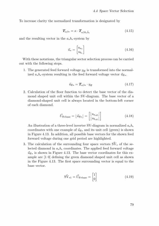
4.4 Space Vector Selection
To increase clarity the normalized transformation is designated by
Tαβ∗ = κ · Tαβa∗b∗ (4.15)
and the resulting vector in the a∗b∗-system by
~u∗ =
[ua∗ub∗
](4.16)
With these notations, the triangular sector selection process can be carriedout with the following steps.
1. The generated feed forward voltage uff is transformed into the normal-ized a∗b∗-system resulting in the feed forward voltage vector ~uff∗.
~uff∗ = Tαβ∗ · uff (4.17)
2. Calculation of the floor function to detect the base vector of the dia-mond shaped unit cell within the SV-diagram. The base vector of adiamond-shaped unit cell is always located in the bottom-left cornerof each diamond.
~Uff∗base = b~uff∗c =
[bua∗ff cbub∗ff c
](4.18)
An illustration of a three-level inverter SV-diagram in normalized a∗b∗coordinates with one example of ~uff∗ and its unit cell (green) is shownin Figure 4.13. In addition, all possible base vectors for the shown feedforward voltage during one grid period are highlighted.
3. The calculation of the surrounding four space vectors ~SV∗ of the se-lected diamond in a∗b∗ coordinates. The applied feed forward voltage~uff∗ is shown in Figure 4.13. The base vector coordinates for this ex-ample are [1 0] defining the green diamond shaped unit cell as shownin the Figure 4.13. The first space surrounding vector is equal to thebase vector.
~SV∗1 = ~Uff∗base =
[10
](4.19)
79
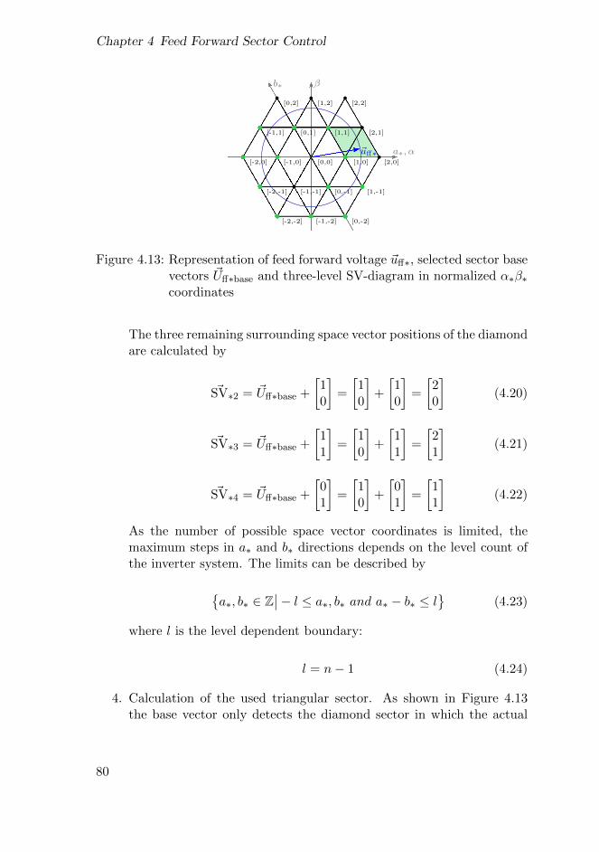
Chapter 4 Feed Forward Sector Control
ua∗ , uα, uU
uβ
ua∗ b∗
ub∗ , uV
uW
ua∗
ub∗
~uff∗[2,0][1,0][0,0][-1,0][-2,0]
[-2,-1]
[-2,-2]
[-1,-1]
[-1,-2]
[0,-1]
[0,-2]
[1,-1]
[-1,1] [0,1] [1,1] [2,1]
[0,2] [1,2] [2,2]
a∗, α
βb∗
Figure 4.13: Representation of feed forward voltage ~uff∗, selected sector basevectors ~Uff∗base and three-level SV-diagram in normalized α∗β∗coordinates
The three remaining surrounding space vector positions of the diamondare calculated by
~SV∗2 = ~Uff∗base +
[10
]=
[10
]+
[10
]=
[20
](4.20)
~SV∗3 = ~Uff∗base +
[11
]=
[10
]+
[11
]=
[21
](4.21)
~SV∗4 = ~Uff∗base +
[01
]=
[10
]+
[01
]=
[11
](4.22)
As the number of possible space vector coordinates is limited, themaximum steps in a∗ and b∗ directions depends on the level count ofthe inverter system. The limits can be described by
a∗, b∗ ∈ Z
∣∣− l ≤ a∗, b∗ and a∗ − b∗ ≤ l (4.23)
where l is the level dependent boundary:
l = n− 1 (4.24)
4. Calculation of the used triangular sector. As shown in Figure 4.13the base vector only detects the diamond sector in which the actual
80
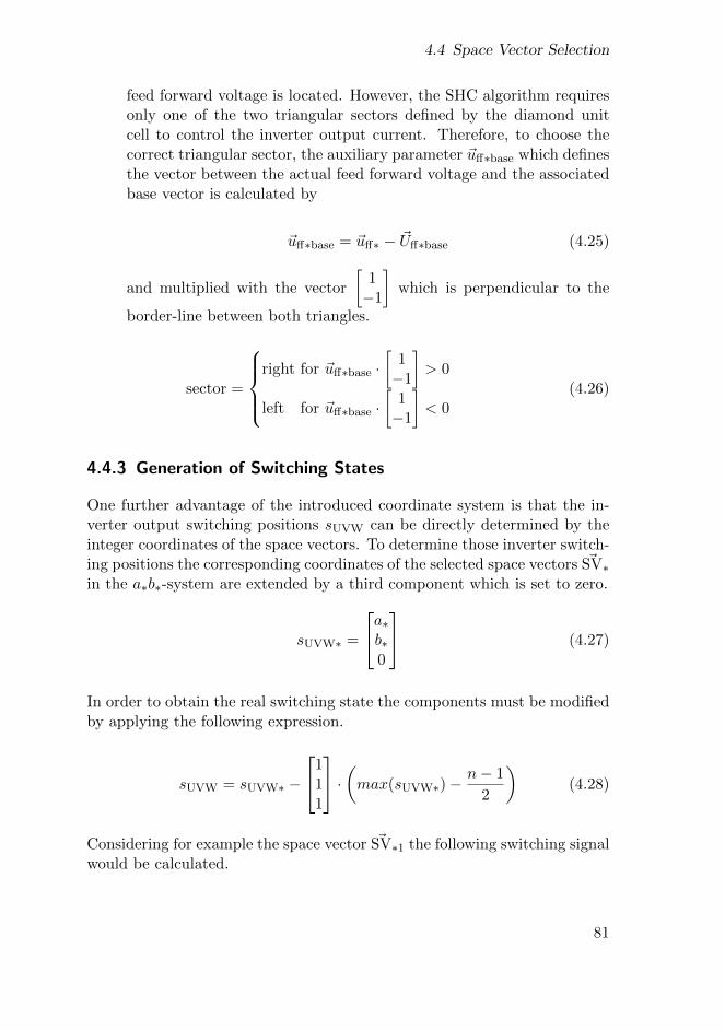
4.4 Space Vector Selection
feed forward voltage is located. However, the SHC algorithm requiresonly one of the two triangular sectors defined by the diamond unitcell to control the inverter output current. Therefore, to choose thecorrect triangular sector, the auxiliary parameter ~uff∗base which definesthe vector between the actual feed forward voltage and the associatedbase vector is calculated by
~uff∗base = ~uff∗ − ~Uff∗base (4.25)
and multiplied with the vector
[1−1
]which is perpendicular to the
border-line between both triangles.
sector =
right for ~uff∗base ·
[1−1
]> 0
left for ~uff∗base ·[
1−1
]< 0
(4.26)
4.4.3 Generation of Switching States
One further advantage of the introduced coordinate system is that the in-verter output switching positions sUVW can be directly determined by theinteger coordinates of the space vectors. To determine those inverter switch-ing positions the corresponding coordinates of the selected space vectors ~SV∗in the a∗b∗-system are extended by a third component which is set to zero.
sUVW∗ =
a∗b∗0
(4.27)
In order to obtain the real switching state the components must be modifiedby applying the following expression.
sUVW = sUVW∗ −
111
· (max(sUVW∗)−n− 1
2
)(4.28)
Considering for example the space vector ~SV∗1 the following switching signalwould be calculated.
81
Chapter 4 Feed Forward Sector Control
~SV∗1 =
[10
]⇒ sUVW∗ =
100
⇒ sUVW =
100
(4.29)
The redundant switching states can also be calculated using the rela-tionship. The available number of possible switching positions is limiteddepending on the level count n as defined before. For a three-level inverter,the switching positions are ±1 and 0, and for a five-level inverter ±2, ±1and 0. In general, the following condition can be used for odd-numberedlevel counts.
s ∈ Z
∣∣− n− 1
2≤ s ≤ n− 1
2
(4.30)
To calculate all possible redundant states the vector [1 1 1] is added orsubtracted as long as one of the three components reaches the describedmaximum condition. For ~SV∗1 in the above example, one redundant switch-ing position exists. The redundant switching position sUVWred is thereforecalculated by
sUVWred = sUVW −
111
=
100
−1
11
=
0−1−1
(4.31)
82
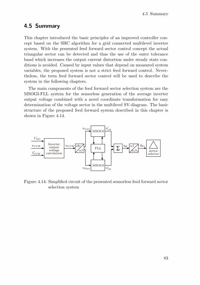
4.5 Summary
4.5 Summary
This chapter introduced the basic principles of an improved controller con-cept based on the SHC algorithm for a grid connected multilevel invertersystem. With the presented feed forward sector control concept the actualtriangular sector can be detected and thus the use of the outer toleranceband which increases the output current distortion under steady state con-ditions is avoided. Caused by input values that depend on measured systemvariables, the proposed system is not a strict feed forward control. Never-theless, the term feed forward sector control will be used to describe thesystem in the following chapters.
The main components of the feed forward sector selection system are theMSOGI-FLL system for the sensorless generation of the average inverteroutput voltage combined with a novel coordinate transformation for easydetermination of the voltage sector in the multilevel SV-diagram. The basicstructure of the proposed feed forward system described in this chapter isshown in Figure 4.14.
33
u′uk
ε kε
qu′
ω′
SOGI
u′1
uk
ε kε
qu′
ω′
SOGI
qu′1
ε
k1
kε1
SOGIω1
u′2
qu′2
k2
kε2
SOGIω2
u′h
qu′h
khkεh
MSOGI
ωh
.
.
.
u′1
u′2
u′h
.
.
.
.
.
....
u
ε
FLL
MSOGI
αβ
abcInverteroutput
UDC
i∗UVW
sUVW uUVW
voltagecalculation
uαinv
uβinv
u′αh
u′βh
a∗b∗
αβuff ~uff∗
sectorselector
Figure 4.14: Simplified circuit of the presented sensorless feed forward sectorselection system
83

84
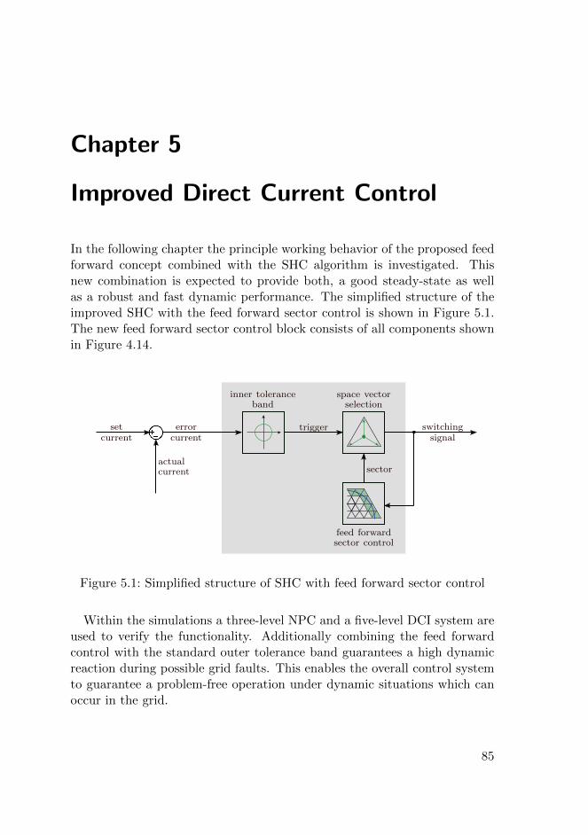
Chapter 5
Improved Direct Current Control
In the following chapter the principle working behavior of the proposed feedforward concept combined with the SHC algorithm is investigated. Thisnew combination is expected to provide both, a good steady-state as wellas a robust and fast dynamic performance. The simplified structure of theimproved SHC with the feed forward sector control is shown in Figure 5.1.The new feed forward sector control block consists of all components shownin Figure 4.14.
LOAD
LFRF
sUVW
33u∗UVW
ucarr
inner toleranceband
space vectorselection
trigger switchingsignal
feed forwardsector control
errorcurrent
setcurrent
actualcurrent sector
Figure 5.1: Simplified structure of SHC with feed forward sector control
Within the simulations a three-level NPC and a five-level DCI system areused to verify the functionality. Additionally combining the feed forwardcontrol with the standard outer tolerance band guarantees a high dynamicreaction during possible grid faults. This enables the overall control systemto guarantee a problem-free operation under dynamic situations which canoccur in the grid.
85
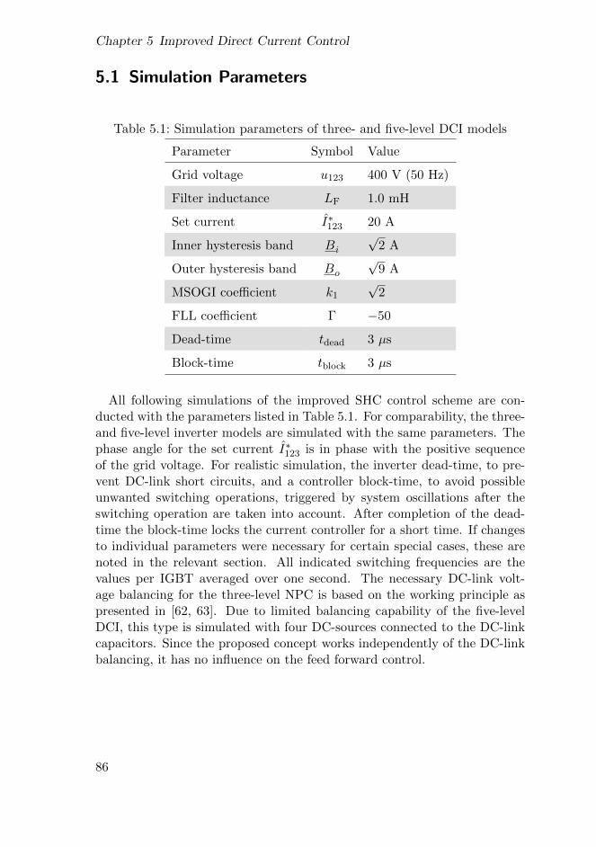
Chapter 5 Improved Direct Current Control
5.1 Simulation Parameters
Table 5.1: Simulation parameters of three- and five-level DCI models
Parameter Symbol Value
Grid voltage u123 400 V (50 Hz)
Filter inductance LF 1.0 mH
Set current I∗123 20 A
Inner hysteresis band Bi
√2 A
Outer hysteresis band Bo
√9 A
MSOGI coefficient k1
√2
FLL coefficient Γ −50
Dead-time tdead 3 µs
Block-time tblock 3 µs
All following simulations of the improved SHC control scheme are con-ducted with the parameters listed in Table 5.1. For comparability, the three-and five-level inverter models are simulated with the same parameters. Thephase angle for the set current I∗123 is in phase with the positive sequenceof the grid voltage. For realistic simulation, the inverter dead-time, to pre-vent DC-link short circuits, and a controller block-time, to avoid possibleunwanted switching operations, triggered by system oscillations after theswitching operation are taken into account. After completion of the dead-time the block-time locks the current controller for a short time. If changesto individual parameters were necessary for certain special cases, these arenoted in the relevant section. All indicated switching frequencies are thevalues per IGBT averaged over one second. The necessary DC-link volt-age balancing for the three-level NPC is based on the working principle aspresented in [62, 63]. Due to limited balancing capability of the five-levelDCI, this type is simulated with four DC-sources connected to the DC-linkcapacitors. Since the proposed concept works independently of the DC-linkbalancing, it has no influence on the feed forward control.
86

5.1 Simulation Parameters
All simulations in the next chapters were carried out using MATLAB/SIMULINK. To ensure a good compatibility with the measurements withinthe experimental verification, the simulation models for the current con-troller and synchronization method were build up compatible to the HDLcoder toolbox. This means that almost all delay times necessary for calcu-lations in the final FPGA hardware implementation are also implementedin the simulation model. This procedure has the further advantage thatthe simulation model can directly be used to generate the VHDL code fromSIMULINK. In the final hardware implementation on the FPGA platformthis code is directly used to generate the program code with XILINX Vi-vado. For realistic simulation of the non-ideal properties in the experimentalinverter hardware the Simscape Power Systems toolbox was used.
87
Chapter 5 Improved Direct Current Control
5.2 Feed forward Control Within the Sector
All space vector based direct current or power controllers presented in chap-ter 3.2 show one common characteristic. If the correct sector in the SV-diagram for controlling the current inside a tolerance band or tolerance areais selected, no further benefit of the voltage information within the sector isobtained. Only the current or power error is used to set the output switchingstates using predefined switching tables for space vector selection.
In addition to the feed forward control of the sector described in Chapter 4,the SHC enables the use of the feed forward voltage uff within the sectorinstead of the pseudo voltage Upseudo. This can be realized by replacing thetriangle midpoint voltage Upseudo within Equation 3.14 by the generatedfeed forward voltage.
uLFff(k) = U inv(k) − uff , k = 1, 2, 3 (5.1)
The one space vector that reduces the current error best can be calculatedby
koptff = arg mink∈1,2,3
(ReuLFff(k) · ie
). (5.2)
This relationship shows a dependency of the three angular ranges around thecircular tolerance band on the actual voltage position within a sector. Theyidentify the best space vector. Figure 5.2 shows an example of the effects onthe angular ranges of the tolerance band when passing through a triangularsector. For better illustration, the figure is divided into the following threevoltage operating points.
• Operating point one (Figure 5.2a). At this point the feed forwardvoltage uff is located near the space vector position U inv(1). Accordingto Equation 5.2 the resulting optimal angular range of the toleranceband increases to 142 for U inv(1) while the other two angular areas forU inv(2) and U inv(3) decrease. Compared to the fixed centre position ofUpseudo from the standard SHC where each angular range is 120, uff
leads to varying ranges.
• Operating point two (Figure 5.2c). The feed forward voltage is closeto the centre of the triangle. This results almost in the same angularranges around the tolerance band like the standard SHC controllerwith its pseudo reference voltage.
88
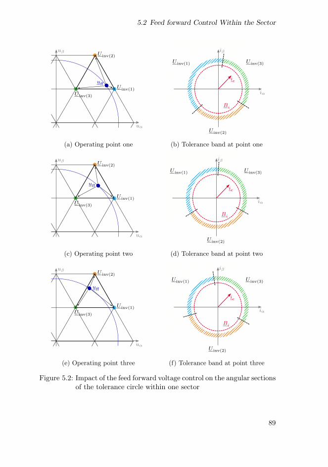
5.2 Feed forward Control Within the Sector
π 2π
UPM
U∆
U∆
−U∆
−2U∆
0
Breite: 60 mm (halbseitig)
uα
uβ
sector 9
sector 10
sector 11
sector 12
60 x 50
uα
uβ
sector 5
sector 6
uα
uβ
uα
uβ
U inv(1)
U inv(3)
U inv(2)
uff
x 5.5 y 4.5
uα
uβ
U inv(1)
U inv(3)
U inv(2)
uff
uα
uβ
U inv(1)
U inv(3)
U inv(2)
uff
uα
U inv(2)
U inv(3)U inv(1)
uβ
ie
uα
U inv(2)
U inv(3)U inv(1)
uβ
ie
Bi
uα
U inv(2)
U inv(3)U inv(1)
uβ
ie
Bi
uα
U inv(2)
U inv(3)U inv(1)
uβ
ie
Bi
iα
U inv(2)
U inv(3)U inv(1)
iβ
ie
Bi
U inv(1)
iα
U inv(2)
U inv(3)U inv(1)
iβ
ie
Bi
iα
U inv(2)
U inv(3)
iβ
ie
Bi
U inv(1)
(a) Operating point one
π 2π
UPM
U∆
U∆
−U∆
−2U∆
0
Breite: 60 mm (halbseitig)
uα
uβ
sector 9
sector 10
sector 11
sector 12
60 x 50
uα
uβ
sector 5
sector 6
uα
uβ
uα
uβ
U inv(1)
U inv(3)
U inv(2)
uff
x 5.5 y 4.5
uα
uβ
U inv(1)
U inv(3)
U inv(2)
uff
uα
uβ
U inv(1)
U inv(3)
U inv(2)
uff
uα
U inv(2)
U inv(3)U inv(1)
uβ
ie
uα
U inv(2)
U inv(3)U inv(1)
uβ
ie
Bi
uα
U inv(2)
U inv(3)U inv(1)
uβ
ie
Bi
uα
U inv(2)
U inv(3)U inv(1)
uβ
ie
Bi
iα
U inv(2)
U inv(3)U inv(1)
iβ
ie
Bi
iα
U inv(2)
U inv(3)
U inv(1)
iβ
ie
Bi
iα
U inv(2)
U inv(3)U inv(1)
iβ
ie
Bi
U inv(1)
(b) Tolerance band at point one
π 2π
UPM
U∆
U∆
−U∆
−2U∆
0
Breite: 60 mm (halbseitig)
uα
uβ
sector 9
sector 10
sector 11
sector 12
60 x 50
uα
uβ
sector 5
sector 6
uα
uβ
uα
uβ
U inv(1)
U inv(3)
U inv(2)
uff
x 5.5 y 4.5
uα
uβ
U inv(1)
U inv(3)
U inv(2)
uff
uα
uβ
U inv(1)
U inv(3)
U inv(2)
uff
uα
U inv(2)
U inv(3)U inv(1)
uβ
ie
uα
U inv(2)
U inv(3)U inv(1)
uβ
ie
Bi
uα
U inv(2)
U inv(3)U inv(1)
uβ
ie
Bi
uα
U inv(2)
U inv(3)U inv(1)
uβ
ie
Bi
iα
U inv(2)
U inv(3)U inv(1)
iβ
ie
Bi
U inv(1)
iα
U inv(2)
U inv(3)U inv(1)
iβ
ie
Bi
iα
U inv(2)
U inv(3)
iβ
ie
Bi
U inv(1)
(c) Operating point two
π 2π
UPM
U∆
U∆
−U∆
−2U∆
0
Breite: 60 mm (halbseitig)
uα
uβ
sector 9
sector 10
sector 11
sector 12
60 x 50
uα
uβ
sector 5
sector 6
uα
uβ
uα
uβ
U inv(1)
U inv(3)
U inv(2)
uff
x 5.5 y 4.5
uα
uβ
U inv(1)
U inv(3)
U inv(2)
uff
uα
uβ
U inv(1)
U inv(3)
U inv(2)
uff
uα
U inv(2)
U inv(3)U inv(1)
uβ
ie
uα
U inv(2)
U inv(3)U inv(1)
uβ
ie
Bi
uα
U inv(2)
U inv(3)U inv(1)
uβ
ie
Bi
uα
U inv(2)
U inv(3)U inv(1)
uβ
ie
Bi
iα
U inv(2)
U inv(3)U inv(1)
iβ
ie
Bi
iα
U inv(2)
U inv(3)
U inv(1)
iβ
ie
Bi
iα
U inv(2)
U inv(3)U inv(1)
iβ
ie
Bi
U inv(1)
(d) Tolerance band at point two
π 2π
UPM
U∆
U∆
−U∆
−2U∆
0
Breite: 60 mm (halbseitig)
uα
uβ
sector 9
sector 10
sector 11
sector 12
60 x 50
uα
uβ
sector 5
sector 6
uα
uβ
uα
uβ
U inv(1)
U inv(3)
U inv(2)
uff
x 5.5 y 4.5
uα
uβ
U inv(1)
U inv(3)
U inv(2)
uff
uα
uβ
U inv(1)
U inv(3)
U inv(2)
uff
uα
U inv(2)
U inv(3)U inv(1)
uβ
ie
uα
U inv(2)
U inv(3)U inv(1)
uβ
ie
Bi
uα
U inv(2)
U inv(3)U inv(1)
uβ
ie
Bi
uα
U inv(2)
U inv(3)U inv(1)
uβ
ie
Bi
iα
U inv(2)
U inv(3)U inv(1)
iβ
ie
Bi
U inv(1)
iα
U inv(2)
U inv(3)U inv(1)
iβ
ie
Bi
iα
U inv(2)
U inv(3)
iβ
ie
Bi
U inv(1)
(e) Operating point three
π 2π
UPM
U∆
U∆
−U∆
−2U∆
0
Breite: 60 mm (halbseitig)
uα
uβ
sector 9
sector 10
sector 11
sector 12
60 x 50
uα
uβ
sector 5
sector 6
uα
uβ
uα
uβ
U inv(1)
U inv(3)
U inv(2)
uff
x 5.5 y 4.5
uα
uβ
U inv(1)
U inv(3)
U inv(2)
uff
uα
uβ
U inv(1)
U inv(3)
U inv(2)
uff
uα
U inv(2)
U inv(3)U inv(1)
uβ
ie
uα
U inv(2)
U inv(3)U inv(1)
uβ
ie
Bi
uα
U inv(2)
U inv(3)U inv(1)
uβ
ie
Bi
uα
U inv(2)
U inv(3)U inv(1)
uβ
ie
Bi
iα
U inv(2)
U inv(3)U inv(1)
iβ
ie
Bi
iα
U inv(2)
U inv(3)
U inv(1)
iβ
ie
Bi
iα
U inv(2)
U inv(3)U inv(1)
iβ
ie
Bi
U inv(1)
(f) Tolerance band at point three
Figure 5.2: Impact of the feed forward voltage control on the angular sectionsof the tolerance circle within one sector
89
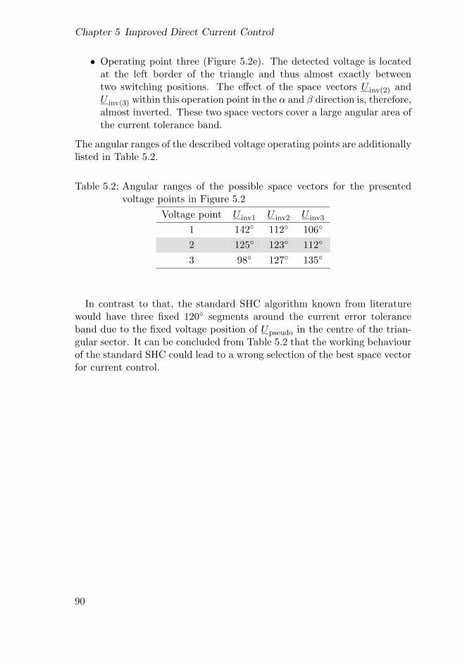
Chapter 5 Improved Direct Current Control
• Operating point three (Figure 5.2e). The detected voltage is locatedat the left border of the triangle and thus almost exactly betweentwo switching positions. The effect of the space vectors U inv(2) andU inv(3) within this operation point in the α and β direction is, therefore,almost inverted. These two space vectors cover a large angular area ofthe current tolerance band.
The angular ranges of the described voltage operating points are additionallylisted in Table 5.2.
Table 5.2: Angular ranges of the possible space vectors for the presentedvoltage points in Figure 5.2
Voltage point U inv1 U inv2 U inv3
1 142 112 106
2 125 123 112
3 98 127 135
In contrast to that, the standard SHC algorithm known from literaturewould have three fixed 120 segments around the current error toleranceband due to the fixed voltage position of Upseudo in the centre of the trian-gular sector. It can be concluded from Table 5.2 that the working behaviourof the standard SHC could lead to a wrong selection of the best space vectorfor current control.
90
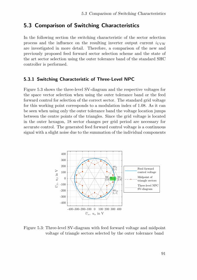
5.3 Comparison of Switching Characteristics
5.3 Comparison of Switching Characteristics
In the following section the switching characteristic of the sector selectionprocess and the influence on the resulting inverter output current iUVW
are investigated in more detail. Therefore, a comparison of the new andpreviously proposed feed forward sector selection scheme and the state ofthe art sector selection using the outer tolerance band of the standard SHCcontroller is performed.
5.3.1 Switching Characteristic of Three-Level NPC
Figure 5.3 shows the three-level SV-diagram and the respective voltages forthe space vector selection when using the outer tolerance band or the feedforward control for selection of the correct sector. The standard grid voltagefor this working point corresponds to a modulation index of 1.08. As it canbe seen when using only the outer tolerance band the voltage location jumpsbetween the centre points of the triangles. Since the grid voltage is locatedin the outer hexagon, 18 sector changes per grid period are necessary foraccurate control. The generated feed forward control voltage is a continuoussignal with a slight noise due to the summation of the individual components
Figure 5.3: Three-level SV-diagram with feed forward voltage and midpointvoltage of triangle sectors selected by the outer tolerance band
91
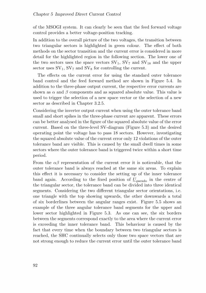
Chapter 5 Improved Direct Current Control
of the MSOGI system. It can clearly be seen that the feed forward voltagecontrol provides a better voltage-position tracking.
In addition to the overall picture of the two voltages, the transition betweentwo triangular sectors is highlighted in green colour. The effect of bothmethods on the sector transition and the current error is considered in moredetail for the highlighted region in the following section. The lower one ofthe two sectors uses the space vectors SV1, SV7 and SV18 and the uppersector uses SV1, SV7 and SV8 for controlling the current.
The effects on the current error for using the standard outer toleranceband control and the feed forward method are shown in Figure 5.4. Inaddition to the three-phase output current, the respective error currents areshown as α and β components and as squared absolute value. This value isused to trigger the selection of a new space vector or the selection of a newsector as described in Chapter 3.2.5.
Considering the inverter output current when using the outer tolerance bandsmall and short spikes in the three-phase current are apparent. These errorscan be better analysed in the figure of the squared absolute value of the errorcurrent. Based on the three-level SV-diagram (Figure 5.3) and the desiredoperating point the voltage has to pass 18 sectors. However, investigatingthe squared absolute value of the current error only 12 violations of the outertolerance band are visible. This is caused by the small dwell times in somesectors where the outer tolerance band is triggered twice within a short timeperiod.
From the αβ representation of the current error it is noticeable, that theouter tolerance band is always reached at the same six areas. To explainthis effect it is necessary to consider the setting up of the inner toleranceband again. According to the fixed position of Upseudo in the centre ofthe triangular sector, the tolerance band can be divided into three identicalsegments. Considering the two different triangular sector orientations, i.e.one triangle with the top showing upwards, the other downwards a totalof six borderlines between the angular ranges exist. Figure 5.5 shows anexample of the three angular tolerance band segments for the upper andlower sector highlighted in Figure 5.3. As one can see, the six bordersbetween the segments correspond exactly to the area where the current erroris exceeding the inner tolerance band. This behaviour is caused by thefact that every time when the boundary between two triangular sectors isreached, the SHC continually selects only those two space vectors that arenot strong enough to reduce the current error until the outer tolerance band
92
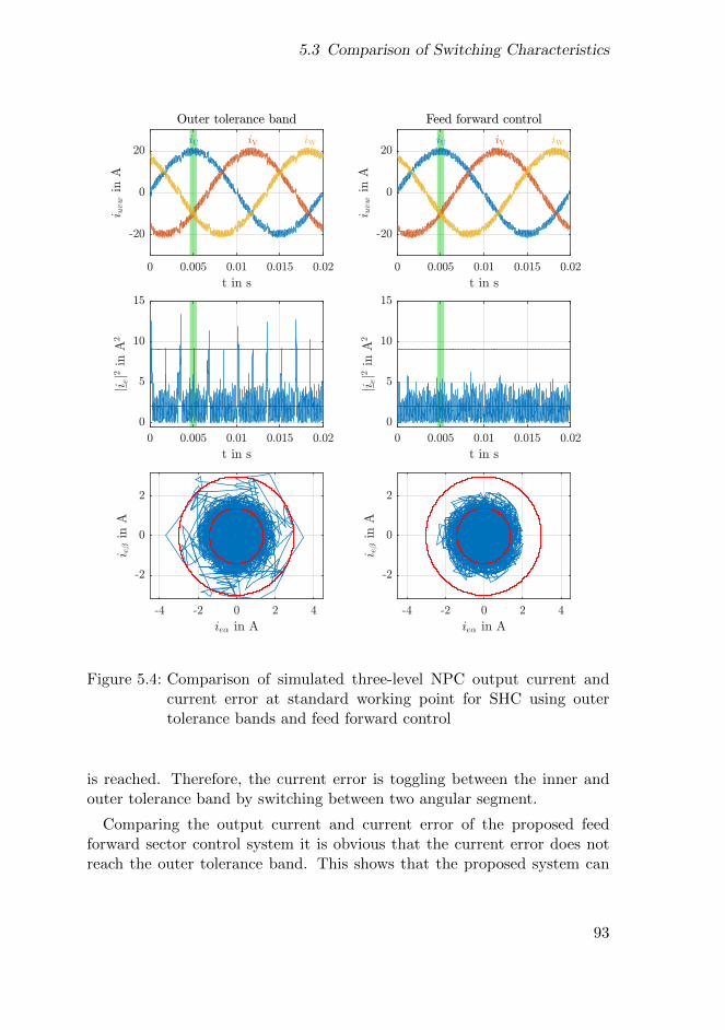
5.3 Comparison of Switching Characteristics
0 0.005 0.01 0.015 0.02
t in s
-20
0
20
i uvw
inA
Outer tolerance band
iU iV iW
0 0.005 0.01 0.015 0.02
t in s
0
5
10
15
ji ej2
inA
2
-4 -2 0 2 4
ie, in A
-2
0
2
i e-
inA
0 0.005 0.01 0.015 0.02
t in s
-20
0
20
i uvw
inA
Feed forward control
iU iV iW
0 0.005 0.01 0.015 0.02
t in s
0
5
10
15
ji ej2
inA
2
-4 -2 0 2 4
ie, in A
-2
0
2
i e-
inA
Figure 5.4: Comparison of simulated three-level NPC output current andcurrent error at standard working point for SHC using outertolerance bands and feed forward control
is reached. Therefore, the current error is toggling between the inner andouter tolerance band by switching between two angular segment.
Comparing the output current and current error of the proposed feedforward sector control system it is obvious that the current error does notreach the outer tolerance band. This shows that the proposed system can
93
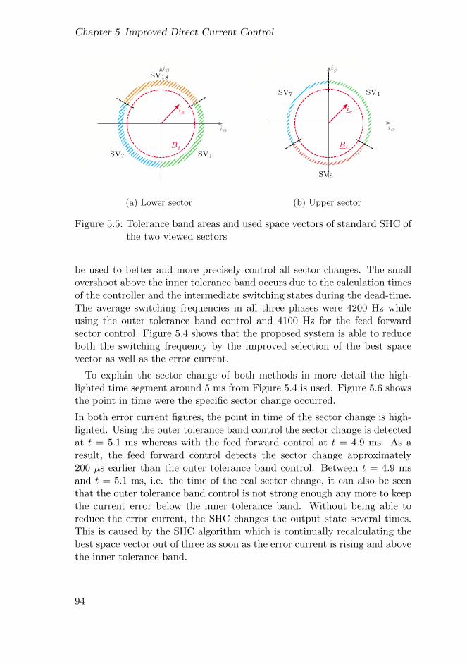
Chapter 5 Improved Direct Current Control
Breite: 60 mm (halbseitig)
uα
uβ
sector 9
sector 10
sector 11
sector 12
60 x 50
x 5.5 y 4.5
uα
uβ
U inv(1)U inv(3)
U inv(2)
Upseudo
uα
uβ
U inv(1)U inv(3)
U inv(2)
Upseudo
Upseudo(1)
Upseudo(2)
Upseudo(3)
uα
U inv(2)
U inv(3)U inv(1)
uβ
ie
uα
uβ
ie
Upseudo(2)
Upseudo(3)Upseudo(1)
Bi
Bo
uα
uβ
ie
Upseudo(2)
Upseudo(3)Upseudo(1)
Bi
Bo
SV7
iα
SV1
SV8
iβ
ie
Bi
SV7
iα
SV1
SV18
iβ
ie
Bi
(a) Lower sector
Breite: 60 mm (halbseitig)
uα
uβ
sector 9
sector 10
sector 11
sector 12
60 x 50
x 5.5 y 4.5
uα
uβ
U inv(1)U inv(3)
U inv(2)
Upseudo
uα
uβ
U inv(1)U inv(3)
U inv(2)
Upseudo
Upseudo(1)
Upseudo(2)
Upseudo(3)
uα
U inv(2)
U inv(3)U inv(1)
uβ
ie
uα
uβ
ie
Upseudo(2)
Upseudo(3)Upseudo(1)
Bi
Bo
uα
uβ
ie
Upseudo(2)
Upseudo(3)Upseudo(1)
Bi
Bo
SV7
iα
SV1
SV8
iβ
ie
Bi
SV7
iα
SV1
SV18
iβ
ie
Bi
(b) Upper sector
Figure 5.5: Tolerance band areas and used space vectors of standard SHC ofthe two viewed sectors
be used to better and more precisely control all sector changes. The smallovershoot above the inner tolerance band occurs due to the calculation timesof the controller and the intermediate switching states during the dead-time.The average switching frequencies in all three phases were 4200 Hz whileusing the outer tolerance band control and 4100 Hz for the feed forwardsector control. Figure 5.4 shows that the proposed system is able to reduceboth the switching frequency by the improved selection of the best spacevector as well as the error current.
To explain the sector change of both methods in more detail the high-lighted time segment around 5 ms from Figure 5.4 is used. Figure 5.6 showsthe point in time were the specific sector change occurred.
In both error current figures, the point in time of the sector change is high-lighted. Using the outer tolerance band control the sector change is detectedat t = 5.1 ms whereas with the feed forward control at t = 4.9 ms. As aresult, the feed forward control detects the sector change approximately200 µs earlier than the outer tolerance band control. Between t = 4.9 msand t = 5.1 ms, i.e. the time of the real sector change, it can also be seenthat the outer tolerance band control is not strong enough any more to keepthe current error below the inner tolerance band. Without being able toreduce the error current, the SHC changes the output state several times.This is caused by the SHC algorithm which is continually recalculating thebest space vector out of three as soon as the error current is rising and abovethe inner tolerance band.
94
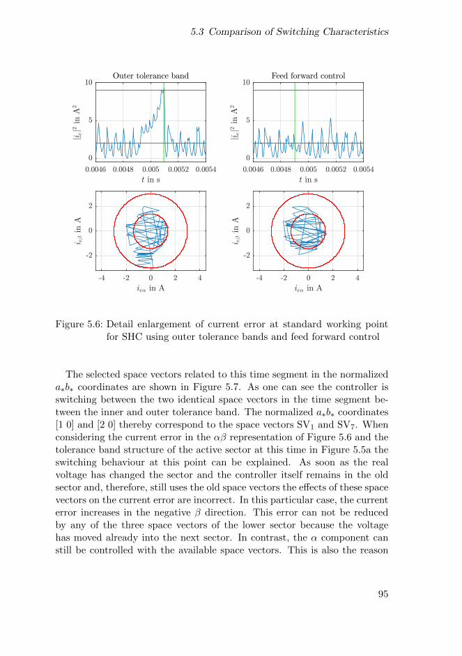
5.3 Comparison of Switching Characteristics
0.0046 0.0048 0.005 0.0052 0.0054
t in s
0
5
10ji e
j2in
A2
Outer tolerance band
-4 -2 0 2 4
ie, in A
-2
0
2
i e-
inA
0.0046 0.0048 0.005 0.0052 0.0054
t in s
0
5
10
ji ej2
inA
2
Feed forward control
-4 -2 0 2 4
ie, in A
-2
0
2
i e-
inA
Figure 5.6: Detail enlargement of current error at standard working pointfor SHC using outer tolerance bands and feed forward control
The selected space vectors related to this time segment in the normalizeda∗b∗ coordinates are shown in Figure 5.7. As one can see the controller isswitching between the two identical space vectors in the time segment be-tween the inner and outer tolerance band. The normalized a∗b∗ coordinates[1 0] and [2 0] thereby correspond to the space vectors SV1 and SV7. Whenconsidering the current error in the αβ representation of Figure 5.6 and thetolerance band structure of the active sector at this time in Figure 5.5a theswitching behaviour at this point can be explained. As soon as the realvoltage has changed the sector and the controller itself remains in the oldsector and, therefore, still uses the old space vectors the effects of these spacevectors on the current error are incorrect. In this particular case, the currenterror increases in the negative β direction. This error can not be reducedby any of the three space vectors of the lower sector because the voltagehas moved already into the next sector. In contrast, the α component canstill be controlled with the available space vectors. This is also the reason
95
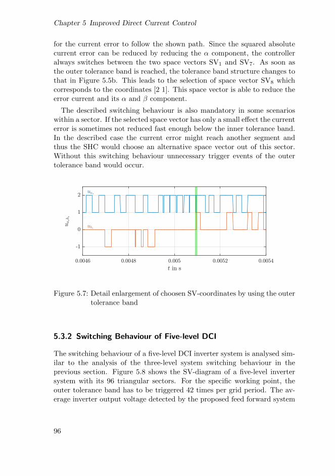
Chapter 5 Improved Direct Current Control
for the current error to follow the shown path. Since the squared absolutecurrent error can be reduced by reducing the α component, the controlleralways switches between the two space vectors SV1 and SV7. As soon asthe outer tolerance band is reached, the tolerance band structure changes tothat in Figure 5.5b. This leads to the selection of space vector SV8 whichcorresponds to the coordinates [2 1]. This space vector is able to reduce theerror current and its α and β component.
The described switching behaviour is also mandatory in some scenarioswithin a sector. If the selected space vector has only a small effect the currenterror is sometimes not reduced fast enough below the inner tolerance band.In the described case the current error might reach another segment andthus the SHC would choose an alternative space vector out of this sector.Without this switching behaviour unnecessary trigger events of the outertolerance band would occur.
0.0046 0.0048 0.005 0.0052 0.0054
t in s
-1
0
1
2ua$
ub$
ua$b $
Figure 5.7: Detail enlargement of choosen SV-coordinates by using the outertolerance band
5.3.2 Switching Behaviour of Five-level DCI
The switching behaviour of a five-level DCI inverter system is analysed sim-ilar to the analysis of the three-level system switching behaviour in theprevious section. Figure 5.8 shows the SV-diagram of a five-level invertersystem with its 96 triangular sectors. For the specific working point, theouter tolerance band has to be triggered 42 times per grid period. The av-erage inverter output voltage detected by the proposed feed forward system
96
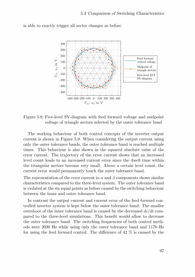
5.3 Comparison of Switching Characteristics
is able to exactly trigger all sector changes as before.
Figure 5.8: Five-level SV-diagram with feed forward voltage and midpointvoltage of triangle sectors selected by the outer tolerance band
The working behaviour of both control concepts of the inverter outputcurrent is shown in Figure 5.9. When considering the output current usingonly the outer tolerance bands, the outer tolerance band is reached multipletimes. This behaviour is also shown in the squared absolute value of theerror current. The trajectory of the error current shows that an increasedlevel count leads to an increased current error since the dwell time withinthe triangular sectors become very small. Above a certain level count, thecurrent error would permanently touch the outer tolerance band.
The representation of the error current in α and β components shows similarcharacteristics compared to the three-level system. The outer tolerance bandis violated at the six equal points as before caused by the switching behaviourbetween the inner and outer tolerance band.
In contrast the output current and current error of the feed forward con-trolled inverter system is kept below the outer tolerance band. The smallerovershoot of the inner tolerance band is caused by the decreased di/dt com-pared to the three-level simulations. This benefit would allow to decreasethe outer tolerance band. The switching frequencies of both control meth-ods were 2030 Hz while using only the outer tolerance band and 1170 Hzfor using the feed forward control. The difference of 42 % is caused by the
97
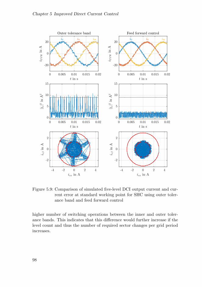
Chapter 5 Improved Direct Current Control
0 0.005 0.01 0.015 0.02
t in s
-20
0
20i U
VW
inA
Outer tolerance band
iU iV iW
0 0.005 0.01 0.015 0.02
t in s
0
5
10
15
ji ej2
inA
2
-4 -2 0 2 4
ie, in A
-2
0
2
i e-
inA
0 0.005 0.01 0.015 0.02
t in s
-20
0
20
i UV
Win
A
Feed forward control
iU iV iW
0 0.005 0.01 0.015 0.02
t in s
0
5
10
15
ji ej2
inA
2
-4 -2 0 2 4
ie, in A
-2
0
2
i e-
inA
Figure 5.9: Comparison of simulated five-level DCI output current and cur-rent error at standard working point for SHC using outer toler-ance band and feed forward control
higher number of switching operations between the inner and outer toler-ance bands. This indicates that this difference would further increase if thelevel count and thus the number of required sector changes per grid periodincreases.
98
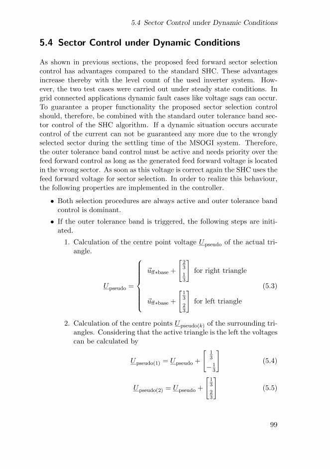
5.4 Sector Control under Dynamic Conditions
5.4 Sector Control under Dynamic Conditions
As shown in previous sections, the proposed feed forward sector selectioncontrol has advantages compared to the standard SHC. These advantagesincrease thereby with the level count of the used inverter system. How-ever, the two test cases were carried out under steady state conditions. Ingrid connected applications dynamic fault cases like voltage sags can occur.To guarantee a proper functionality the proposed sector selection controlshould, therefore, be combined with the standard outer tolerance band sec-tor control of the SHC algorithm. If a dynamic situation occurs accuratecontrol of the current can not be guaranteed any more due to the wronglyselected sector during the settling time of the MSOGI system. Therefore,the outer tolerance band control must be active and needs priority over thefeed forward control as long as the generated feed forward voltage is locatedin the wrong sector. As soon as this voltage is correct again the SHC uses thefeed forward voltage for sector selection. In order to realize this behaviour,the following properties are implemented in the controller.
• Both selection procedures are always active and outer tolerance bandcontrol is dominant.
• If the outer tolerance band is triggered, the following steps are initi-ated.
1. Calculation of the centre point voltage Upseudo of the actual tri-angle.
Upseudo =
~uff∗base +
[23
13
]for right triangle
~uff∗base +
[13
23
]for left triangle
(5.3)
2. Calculation of the centre points Upseudo(k) of the surrounding tri-angles. Considering that the active triangle is the left the voltagescan be calculated by
Upseudo(1) = Upseudo +
[13
−13
](5.4)
Upseudo(2) = Upseudo +
[13
23
](5.5)
99
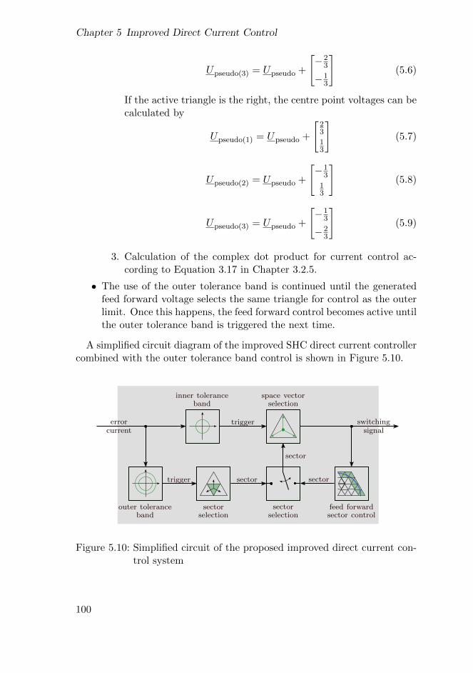
Chapter 5 Improved Direct Current Control
Upseudo(3) = Upseudo +
[−2
3
−13
](5.6)
If the active triangle is the right, the centre point voltages can becalculated by
Upseudo(1) = Upseudo +
[23
13
](5.7)
Upseudo(2) = Upseudo +
[−1
3
13
](5.8)
Upseudo(3) = Upseudo +
[−1
3
−23
](5.9)
3. Calculation of the complex dot product for current control ac-cording to Equation 3.17 in Chapter 3.2.5.
• The use of the outer tolerance band is continued until the generatedfeed forward voltage selects the same triangle for control as the outerlimit. Once this happens, the feed forward control becomes active untilthe outer tolerance band is triggered the next time.
A simplified circuit diagram of the improved SHC direct current controllercombined with the outer tolerance band control is shown in Figure 5.10.
LOAD
LFRF
sUVW
33u∗UVW
ucarr
inner toleranceband
space vectorselection
trigger switchingsignal
outer toleranceband
sectorselection
trigger
errorcurrent
sector
feed forwardsector control
sector sector
sectorselection
Figure 5.10: Simplified circuit of the proposed improved direct current con-trol system
100
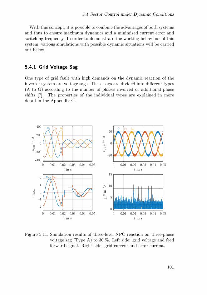
5.4 Sector Control under Dynamic Conditions
With this concept, it is possible to combine the advantages of both systemsand thus to ensure maximum dynamics and a minimized current error andswitching frequency. In order to demonstrate the working behaviour of thissystem, various simulations with possible dynamic situations will be carriedout below.
5.4.1 Grid Voltage Sag
One type of grid fault with high demands on the dynamic reaction of theinverter system are voltage sags. These sags are divided into different types(A to G) according to the number of phases involved or additional phaseshifts [7]. The properties of the individual types are explained in moredetail in the Appendix C.
0 0.01 0.02 0.03 0.04 0.05
t in s
-400
-200
0
200
400 u1 u2 u3
u123in
A
0 0.01 0.02 0.03 0.04 0.05
t in s
-2
-1
0
1
2 ua$, ub$,
ua$b $,
0 0.01 0.02 0.03 0.04 0.05
t in s
-20
0
20
i UV
Win
A
iU iV iW
0 0.01 0.02 0.03 0.04 0.05
t in s
0
5
10
15
ji ej2
inA
2
Figure 5.11: Simulation results of three-level NPC reaction on three-phasevoltage sag (Type A) to 30 %. Left side: grid voltage and feedforward signal. Right side: grid current and error current.
101
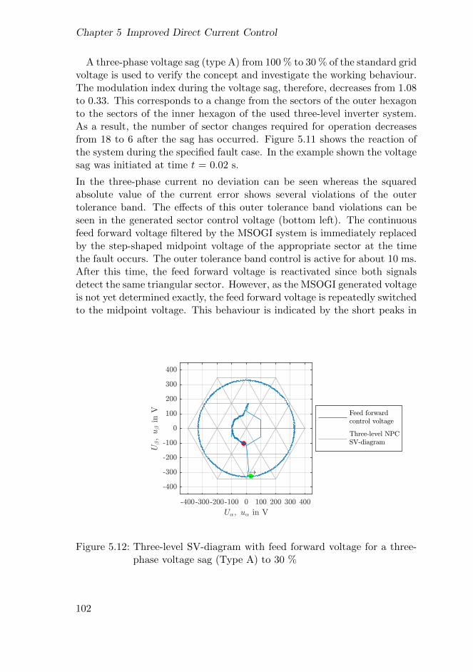
Chapter 5 Improved Direct Current Control
A three-phase voltage sag (type A) from 100 % to 30 % of the standard gridvoltage is used to verify the concept and investigate the working behaviour.The modulation index during the voltage sag, therefore, decreases from 1.08to 0.33. This corresponds to a change from the sectors of the outer hexagonto the sectors of the inner hexagon of the used three-level inverter system.As a result, the number of sector changes required for operation decreasesfrom 18 to 6 after the sag has occurred. Figure 5.11 shows the reaction ofthe system during the specified fault case. In the example shown the voltagesag was initiated at time t = 0.02 s.
In the three-phase current no deviation can be seen whereas the squaredabsolute value of the current error shows several violations of the outertolerance band. The effects of this outer tolerance band violations can beseen in the generated sector control voltage (bottom left). The continuousfeed forward voltage filtered by the MSOGI system is immediately replacedby the step-shaped midpoint voltage of the appropriate sector at the timethe fault occurs. The outer tolerance band control is active for about 10 ms.After this time, the feed forward voltage is reactivated since both signalsdetect the same triangular sector. However, as the MSOGI generated voltageis not yet determined exactly, the feed forward voltage is repeatedly switchedto the midpoint voltage. This behaviour is indicated by the short peaks in
Figure 5.12: Three-level SV-diagram with feed forward voltage for a three-phase voltage sag (Type A) to 30 %
102
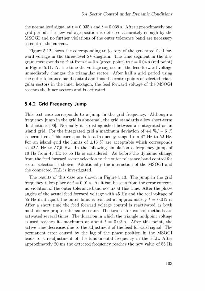
5.4 Sector Control under Dynamic Conditions
the normalized signal at t = 0.035 s and t = 0.039 s. After approximately onegrid period, the new voltage position is detected accurately enough by theMSOGI and no further violations of the outer tolerance band are necessaryto control the current.
Figure 5.12 shows the corresponding trajectory of the generated feed for-ward voltage in the three-level SV-diagram. The time segment in the dia-gram corresponds to that from t = 0 s (green point) to t = 0.04 s (red point)in Figure 5.11. At the time the voltage sag occurs, the feed forward voltageimmediately changes the triangular sector. After half a grid period usingthe outer tolerance band control and thus the centre points of selected trian-gular sectors in the inner hexagon, the feed forward voltage of the MSOGIreaches the inner sectors and is activated.
5.4.2 Grid Frequency Jump
This test case corresponds to a jump in the grid frequency. Although afrequency jump in the grid is abnormal, the grid standards allow short-termfluctuations [90]. Normally it is distinguished between an integrated or anisland grid. For the integrated grid a maximum deviation of +4 %/ − 6 %is permitted. This corresponds to a frequency range from 47 Hz to 52 Hz.For an island grid the limits of ±15 % are acceptable which correspondsto 42,5 Hz to 57,5 Hz. In the following simulation a frequency jump of10 Hz from 45 Hz to 55 Hz is considered. As before the dynamic changefrom the feed forward sector selection to the outer tolerance band control forsector selection is shown. Additionally the interaction of the MSOGI andthe connected FLL is investigated.
The results of this case are shown in Figure 5.13. The jump in the gridfrequency takes place at t = 0.01 s. As it can be seen from the error current,no violation of the outer tolerance band occurs at this time. After the phaseangles of the actual feed forward voltage with 45 Hz and the real voltage of55 Hz drift apart the outer limit is reached at approximately t = 0.012 s.After a short time the feed forward voltage control is reactivated as bothmethods are propose the same sector. The two sector control methods areactivated several times. The duration in which the triangle midpoint voltageis used reaches its maximum at about t = 0.02 s. After this point, theactive time decreases due to the adjustment of the feed forward signal. Thepermanent error caused by the lag of the phase position in the MSOGIleads to a readjustment of the fundamental frequency in the FLL. Afterapproximately 20 ms the detected frequency reaches the new value of 55 Hz
103
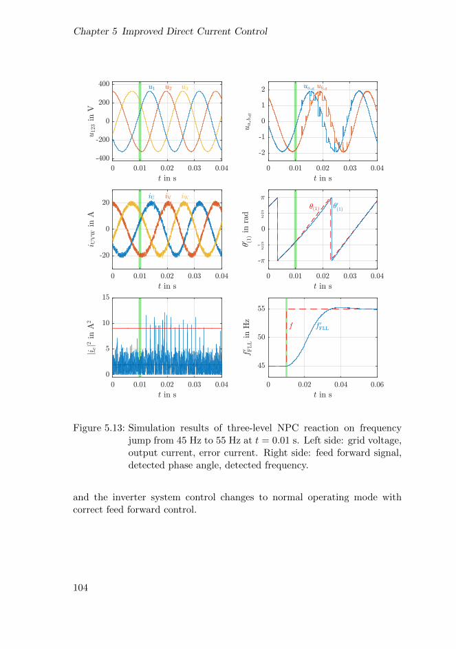
Chapter 5 Improved Direct Current Control
0 0.01 0.02 0.03 0.04
t in s
-400
-200
0
200
400 u1 u2 u3u
123in
V
0 0.01 0.02 0.03 0.04
t in s
-20
0
20iU iV iW
i UV
Win
A
0 0.01 0.02 0.03 0.04
t in s
0
5
10
15
ji ej2
inA
2
0 0.01 0.02 0.03 0.04
t in s
-2
-1
0
1
2 ua$, ub$,
ua$b $,
0 0.01 0.02 0.03 0.04
t in s
-:
-:2
0
:2
:30(1)3(1)
30 (1
)in
rad
0 0.02 0.04 0.06
t in s
45
50
55
f 0FLLf
f0 FLL
inH
z
Figure 5.13: Simulation results of three-level NPC reaction on frequencyjump from 45 Hz to 55 Hz at t = 0.01 s. Left side: grid voltage,output current, error current. Right side: feed forward signal,detected phase angle, detected frequency.
and the inverter system control changes to normal operating mode withcorrect feed forward control.
104
5.4 Sector Control under Dynamic Conditions
5.4.3 Set Current Jump
This test case is used to analyse the reaction of the control system to a jumpof the set current. In this test, the set current amplitude was set from 20 A to−20 A at the time t = 0.01 s. Figure 5.14 shows the inverter output current,the error current and the sector control voltage in normalized coordinates.
0 0.005 0.01 0.015 0.02
t in s
-20
0
20
iU
iV iW
i UV
Win
A
0 0.005 0.01 0.015 0.02
t in s
-2
-1
0
1
2
ua$,ub$,
ua$b $,
9.6 9.8 10 10.2 10.4
t in s #10!3
-20
0
20
i UV
Win
A
iU
iV
iW
9.6 9.8 10 10.2 10.4
t in s #10!3
0
5
10
15
20
ji ej2
inA
2
Figure 5.14: Simulation results of three-level NPC reaction on set currentjump from 20 A to −20 A. Left side: grid current and feedforward signal. Right side: detail enlargement of grid currentand error current.
Immediately after the set point change the error current increases signif-icantly, causing a single sector change. After this no further sector changeis triggered as the error is decreasing after the first sector change. Afterthe error current is below the inner tolerance band, the SHC algorithm trig-gers a new space vector within this sector. However, since the real voltageis in another sector, the SHC can not operate properly, causing the errorcurrent to trigger the outer tolerance band at t = 0.0101 s. After this the
105
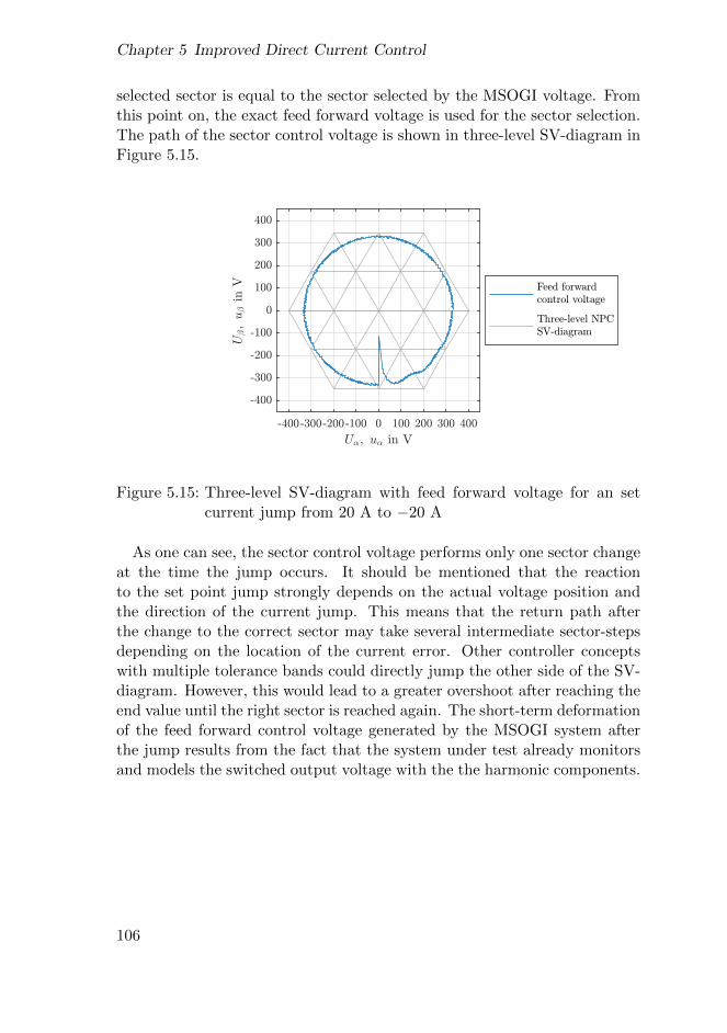
Chapter 5 Improved Direct Current Control
selected sector is equal to the sector selected by the MSOGI voltage. Fromthis point on, the exact feed forward voltage is used for the sector selection.The path of the sector control voltage is shown in three-level SV-diagram inFigure 5.15.
Figure 5.15: Three-level SV-diagram with feed forward voltage for an setcurrent jump from 20 A to −20 A
As one can see, the sector control voltage performs only one sector changeat the time the jump occurs. It should be mentioned that the reactionto the set point jump strongly depends on the actual voltage position andthe direction of the current jump. This means that the return path afterthe change to the correct sector may take several intermediate sector-stepsdepending on the location of the current error. Other controller conceptswith multiple tolerance bands could directly jump the other side of the SV-diagram. However, this would lead to a greater overshoot after reaching theend value until the right sector is reached again. The short-term deformationof the feed forward control voltage generated by the MSOGI system afterthe jump results from the fact that the system under test already monitorsand models the switched output voltage with the the harmonic components.
106
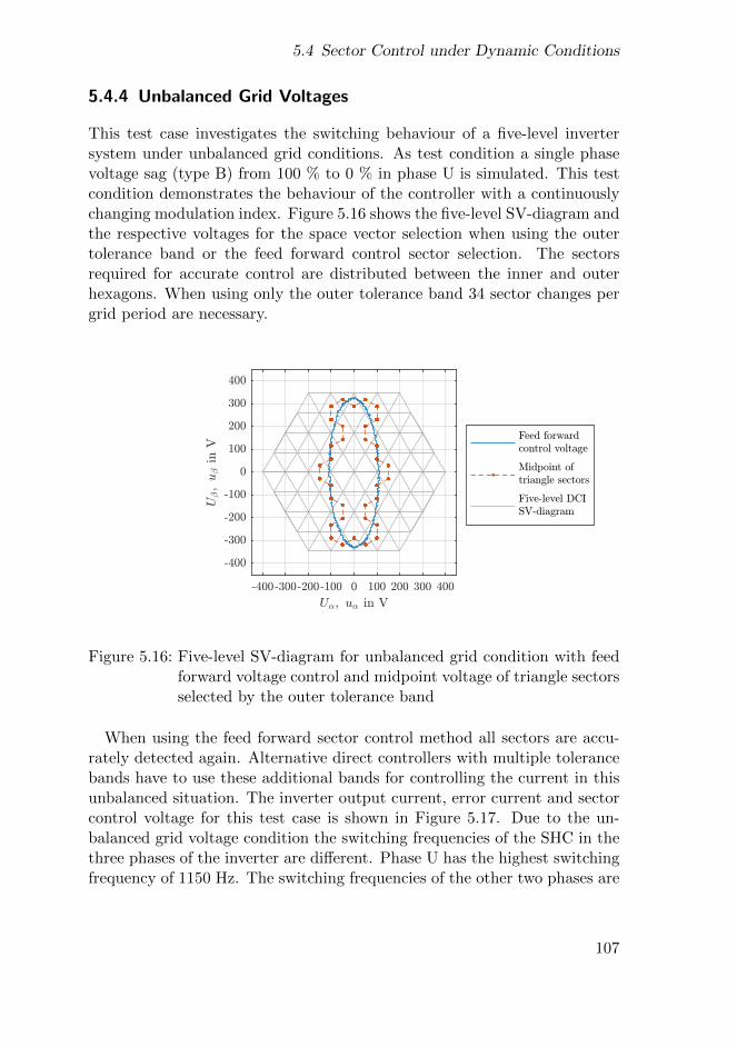
5.4 Sector Control under Dynamic Conditions
5.4.4 Unbalanced Grid Voltages
This test case investigates the switching behaviour of a five-level invertersystem under unbalanced grid conditions. As test condition a single phasevoltage sag (type B) from 100 % to 0 % in phase U is simulated. This testcondition demonstrates the behaviour of the controller with a continuouslychanging modulation index. Figure 5.16 shows the five-level SV-diagram andthe respective voltages for the space vector selection when using the outertolerance band or the feed forward control sector selection. The sectorsrequired for accurate control are distributed between the inner and outerhexagons. When using only the outer tolerance band 34 sector changes pergrid period are necessary.
Figure 5.16: Five-level SV-diagram for unbalanced grid condition with feedforward voltage control and midpoint voltage of triangle sectorsselected by the outer tolerance band
When using the feed forward sector control method all sectors are accu-rately detected again. Alternative direct controllers with multiple tolerancebands have to use these additional bands for controlling the current in thisunbalanced situation. The inverter output current, error current and sectorcontrol voltage for this test case is shown in Figure 5.17. Due to the un-balanced grid voltage condition the switching frequencies of the SHC in thethree phases of the inverter are different. Phase U has the highest switchingfrequency of 1150 Hz. The switching frequencies of the other two phases are
107
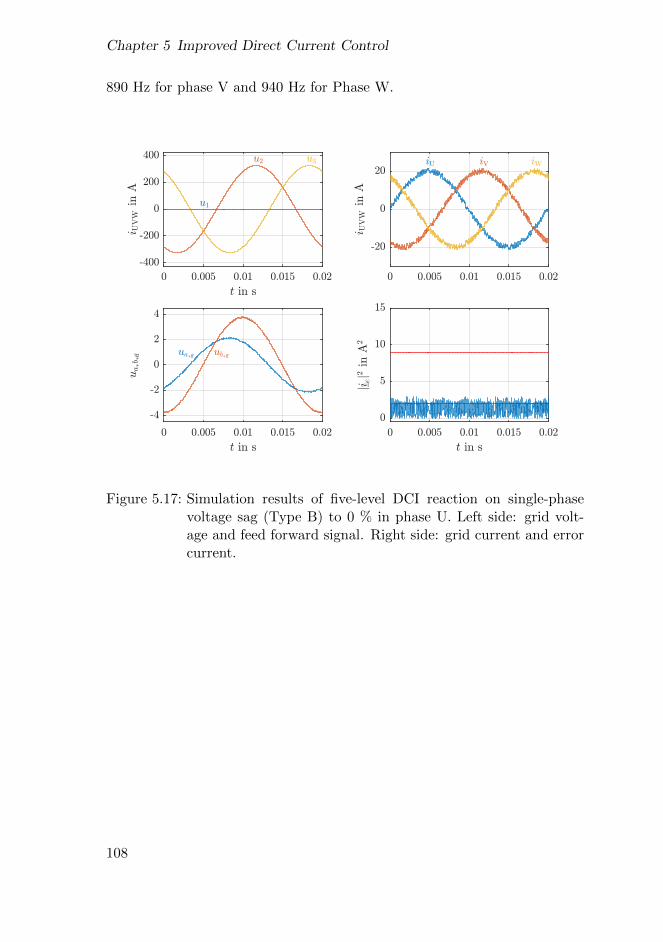
Chapter 5 Improved Direct Current Control
890 Hz for phase V and 940 Hz for Phase W.
0 0.005 0.01 0.015 0.02
t in s
-400
-200
0
200
400
u1
u2 u3
i UV
Win
A
0 0.005 0.01 0.015 0.02
t in s
-4
-2
0
2
4
ua$, ub$,
ua$b $,
0 0.005 0.01 0.015 0.02
-20
0
20
i UV
Win
A
iU iV iW
0 0.005 0.01 0.015 0.02
t in s
0
5
10
15
ji ej2
inA
2
Figure 5.17: Simulation results of five-level DCI reaction on single-phasevoltage sag (Type B) to 0 % in phase U. Left side: grid volt-age and feed forward signal. Right side: grid current and errorcurrent.
108
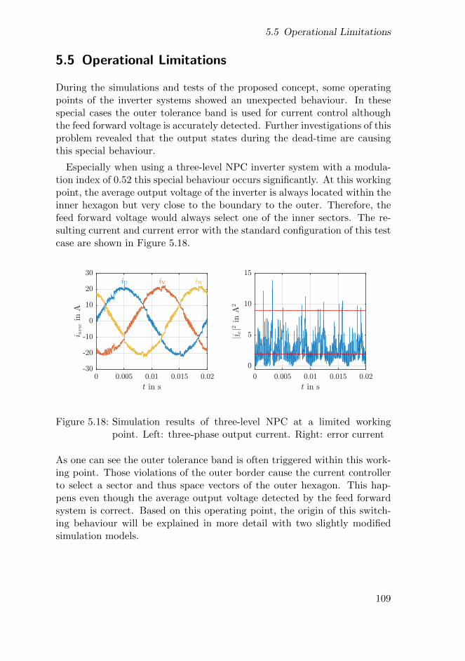
5.5 Operational Limitations
5.5 Operational Limitations
During the simulations and tests of the proposed concept, some operatingpoints of the inverter systems showed an unexpected behaviour. In thesespecial cases the outer tolerance band is used for current control althoughthe feed forward voltage is accurately detected. Further investigations of thisproblem revealed that the output states during the dead-time are causingthis special behaviour.
Especially when using a three-level NPC inverter system with a modula-tion index of 0.52 this special behaviour occurs significantly. At this workingpoint, the average output voltage of the inverter is always located within theinner hexagon but very close to the boundary to the outer. Therefore, thefeed forward voltage would always select one of the inner sectors. The re-sulting current and current error with the standard configuration of this testcase are shown in Figure 5.18.
0 0.005 0.01 0.015 0.02
t in s
-30
-20
-10
0
10
20
30iU iV iW
i uvw
inA
0 0.005 0.01 0.015 0.02
t in s
0
5
10
15
ji ej2
inA
2
Figure 5.18: Simulation results of three-level NPC at a limited workingpoint. Left: three-phase output current. Right: error current
As one can see the outer tolerance band is often triggered within this work-ing point. Those violations of the outer border cause the current controllerto select a sector and thus space vectors of the outer hexagon. This hap-pens even though the average output voltage detected by the feed forwardsystem is correct. Based on this operating point, the origin of this switch-ing behaviour will be explained in more detail with two slightly modifiedsimulation models.
109
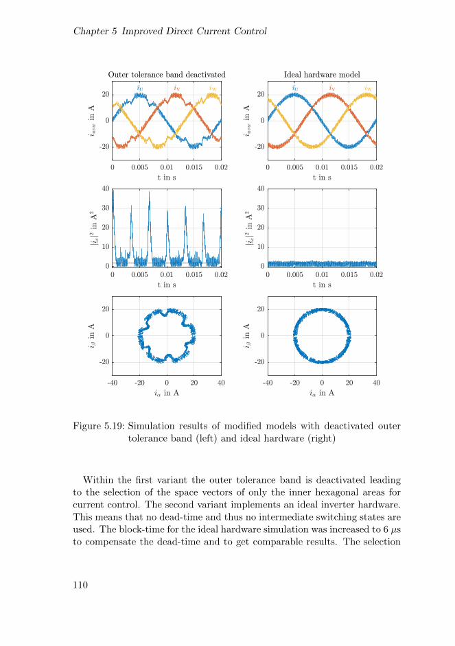
Chapter 5 Improved Direct Current Control
0 0.005 0.01 0.015 0.02
t in s
-20
0
20i u
vw
inA
Outer tolerance band deactivated
iU iV iW
0 0.005 0.01 0.015 0.02
t in s
0
10
20
30
40
ji ej2
inA
2
-40 -20 0 20 40
i, in A
-20
0
20
i -in
A
0 0.005 0.01 0.015 0.02
t in s
-20
0
20
i uvw
inA
Ideal hardware model
iU iV iW
0 0.005 0.01 0.015 0.02
t in s
0
10
20
30
40
ji ej2
inA
2
-40 -20 0 20 40
i, in A
-20
0
20
i -in
A
Figure 5.19: Simulation results of modified models with deactivated outertolerance band (left) and ideal hardware (right)
Within the first variant the outer tolerance band is deactivated leadingto the selection of the space vectors of only the inner hexagonal areas forcurrent control. The second variant implements an ideal inverter hardware.This means that no dead-time and thus no intermediate switching states areused. The block-time for the ideal hardware simulation was increased to 6 µsto compensate the dead-time and to get comparable results. The selection
110
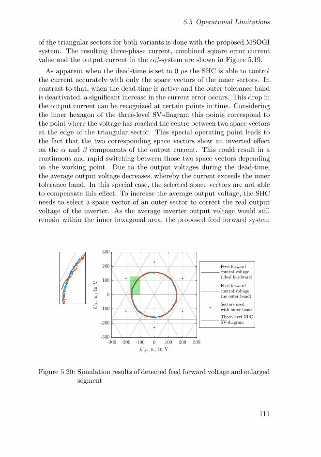
5.5 Operational Limitations
of the triangular sectors for both variants is done with the proposed MSOGIsystem. The resulting three-phase current, combined square error currentvalue and the output current in the αβ-system are shown in Figure 5.19.
As apparent when the dead-time is set to 0 µs the SHC is able to controlthe current accurately with only the space vectors of the inner sectors. Incontrast to that, when the dead-time is active and the outer tolerance bandis deactivated, a significant increase in the current error occurs. This drop inthe output current can be recognized at certain points in time. Consideringthe inner hexagon of the three-level SV-diagram this points correspond tothe point where the voltage has reached the centre between two space vectorsat the edge of the triangular sector. This special operating point leads tothe fact that the two corresponding space vectors show an inverted effecton the α and β components of the output current. This could result in acontinuous and rapid switching between those two space vectors dependingon the working point. Due to the output voltages during the dead-time,the average output voltage decreases, whereby the current exceeds the innertolerance band. In this special case, the selected space vectors are not ableto compensate this effect. To increase the average output voltage, the SHCneeds to select a space vector of an outer sector to correct the real outputvoltage of the inverter. As the average inverter output voltage would stillremain within the inner hexagonal area, the proposed feed forward system
Figure 5.20: Simulation results of detected feed forward voltage and enlargedsegment
111
Chapter 5 Improved Direct Current Control
is not able to indicate the necessary sector changes to an outer sector. Thefeed forward voltages for the two test cases are shown in Figure 5.20. Inaddition, the six triangle centre points selected by the outer tolerance bandcontrol are highlighted.
The slight drop in the detected feed forward voltage for the variant withdeactivated outer tolerance band can also be seen, but since it is alwaysonly a single short drop this can not be completely displayed with the usedMSOGI configuration.
The occurrence of the described effect depends on several properties ofthe inverter system, including
• the amplitude of grid voltage and used grid filter. Both propertiesinfluence the output voltage and generated di/dt of the available threespace vectors of the inverter.
• the level count and DC-link voltage defining the size of the triangularsectors and thus the average time within a triangular sector. The countalso decreases the di/dt and the resulting switching frequency.
• the implemented dead-time in the inverter system which has directimpact on the switching duration of intermediate switching states.
• the amplitude and power factor of the set current. This defines thecurrent rise at each point in the SV-diagram.
The described switching behaviour could lead to the selection of the wrongsector as the resulting output voltage is shifted by the selected switchingoperations during the dead-time. In this situations the generated voltage bythe MSOGI system is still correct but not used for sector control. However,in combination with the outer tolerance band a stable control of the outputcurrent under these cases is possible.
112

5.6 Summary
5.6 Summary
This chapter investigates the proposed feed forward sector control systemwith several special operating points. The improved switching behaviour iscompared with the standard SHC method which uses only the outer toler-ance band for sector changes. The simulations show a significant improve-ment in the working behaviour when using multilevel inverters. Especially,the current error can be significantly reduced when higher level counts areused. Furthermore, the reaction of the system to grid fault cases are inves-tigated. For this purpose, the feed forward control system was combinedwith the outer tolerance band control in a way that all dynamic errors canbe applied. By using the proposed selection process for the sector, the ad-vantages of both systems in steady and dynamic operation can be optimallycombined.
113

114
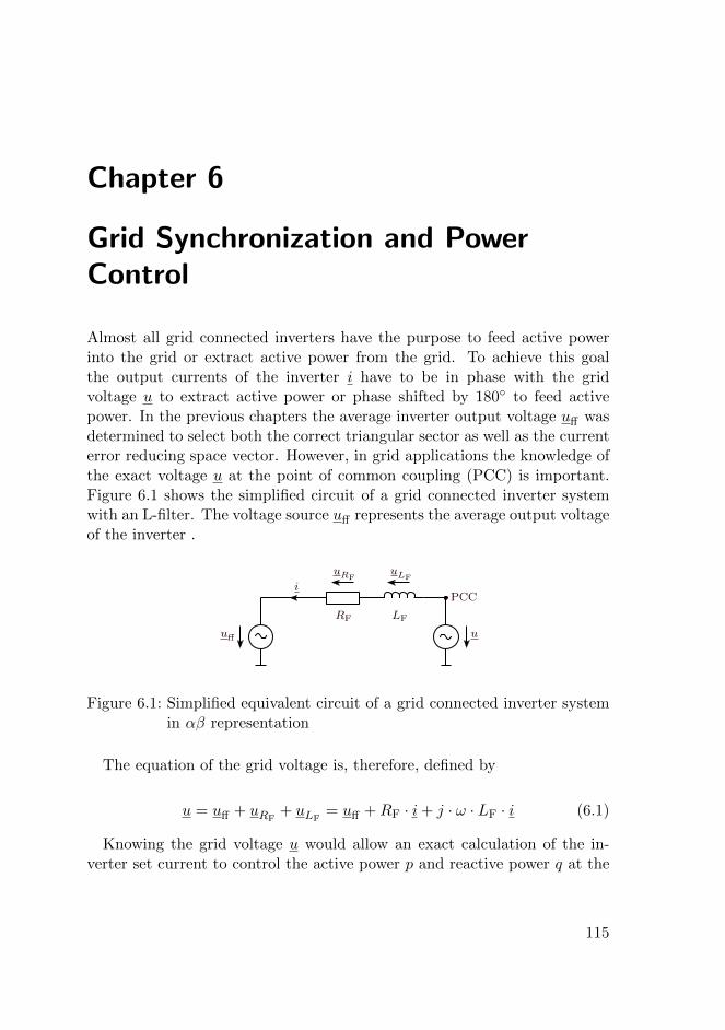
Chapter 6
Grid Synchronization and PowerControl
Almost all grid connected inverters have the purpose to feed active powerinto the grid or extract active power from the grid. To achieve this goalthe output currents of the inverter i have to be in phase with the gridvoltage u to extract active power or phase shifted by 180 to feed activepower. In the previous chapters the average inverter output voltage uff wasdetermined to select both the correct triangular sector as well as the currenterror reducing space vector. However, in grid applications the knowledge ofthe exact voltage u at the point of common coupling (PCC) is important.Figure 6.1 shows the simplified circuit of a grid connected inverter systemwith an L-filter. The voltage source uff represents the average output voltageof the inverter .
LFRF 33
LOAD A
LFRF
iUVW
sUVWi∗UVWieUVW
uuff
i
uRFuLF
PCC
Figure 6.1: Simplified equivalent circuit of a grid connected inverter systemin αβ representation
The equation of the grid voltage is, therefore, defined by
u = uff + uRF+ uLF
= uff +RF · i+ j · ω · LF · i (6.1)
Knowing the grid voltage u would allow an exact calculation of the in-verter set current to control the active power p and reactive power q at the
115
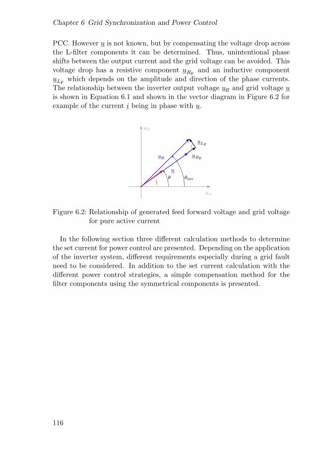
Chapter 6 Grid Synchronization and Power Control
PCC. However u is not known, but by compensating the voltage drop acrossthe L-filter components it can be determined. Thus, unintentional phaseshifts between the output current and the grid voltage can be avoided. Thisvoltage drop has a resistive component uRF
and an inductive componentuLF
which depends on the amplitude and direction of the phase currents.The relationship between the inverter output voltage uff and grid voltage uis shown in Equation 6.1 and shown in the vector diagram in Figure 6.2 forexample of the current i being in phase with u.
uα
uβ
u
ua∗
ub∗
~uff∗[2,0][1,0][0,0][-1,0][-2,0]
[-2,-1]
[-2,-2]
[-1,-1]
[-1,-2]
[0,-1]
[0,-2]
[1,-1]
[-1,1] [0,1] [1,1] [2,1]
[0,2] [1,2] [2,2]
a∗, α
βb∗
uff
uLF
uRF
iθ θinv
Figure 6.2: Relationship of generated feed forward voltage and grid voltagefor pure active current
In the following section three different calculation methods to determinethe set current for power control are presented. Depending on the applicationof the inverter system, different requirements especially during a grid faultneed to be considered. In addition to the set current calculation with thedifferent power control strategies, a simple compensation method for thefilter components using the symmetrical components is presented.
116
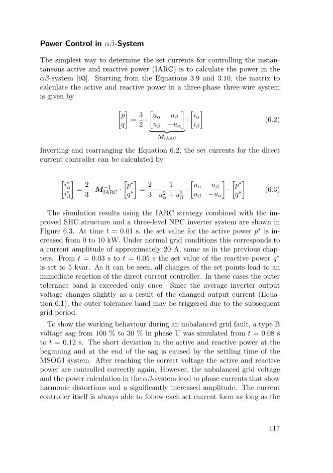
Power Control in αβ-System
The simplest way to determine the set currents for controlling the instan-taneous active and reactive power (IARC) is to calculate the power in theαβ-system [93]. Starting from the Equations 3.9 and 3.10, the matrix tocalculate the active and reactive power in a three-phase three-wire systemis given by [
pq
]=
3
2·[uα uβuβ −uα
]︸ ︷︷ ︸
MIARC
·[iαiβ
](6.2)
Inverting and rearranging the Equation 6.2, the set currents for the directcurrent controller can be calculated by
[i∗αi∗β
]=
2
3·M−1
IARC ·[p∗
q∗
]=
2
3· 1
u2α + u2
β
·[uα uβuβ −uα
]·[p∗
q∗
](6.3)
The simulation results using the IARC strategy combined with the im-proved SHC structure and a three-level NPC inverter system are shown inFigure 6.3. At time t = 0.01 s, the set value for the active power p∗ is in-creased from 0 to 10 kW. Under normal grid conditions this corresponds toa current amplitude of approximately 20 A, same as in the previous chap-ters. From t = 0.03 s to t = 0.05 s the set value of the reactive power q∗
is set to 5 kvar. As it can be seen, all changes of the set points lead to animmediate reaction of the direct current controller. In these cases the outertolerance band is exceeded only once. Since the average inverter outputvoltage changes slightly as a result of the changed output current (Equa-tion 6.1), the outer tolerance band may be triggered due to the subsequentgrid period.
To show the working behaviour during an unbalanced grid fault, a type Bvoltage sag from 100 % to 30 % in phase U was simulated from t = 0.08 sto t = 0.12 s. The short deviation in the active and reactive power at thebeginning and at the end of the sag is caused by the settling time of theMSOGI system. After reaching the correct voltage the active and reactivepower are controlled correctly again. However, the unbalanced grid voltageand the power calculation in the αβ-system lead to phase currents that showharmonic distortions and a significantly increased amplitude. The currentcontroller itself is always able to follow each set current form as long as the
117
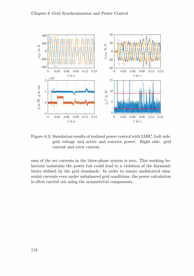
Chapter 6 Grid Synchronization and Power Control
0 0.03 0.06 0.09 0.12 0.15
t in s
-400
-200
0
200
400 u1
u2
u3u
123in
A
0 0.03 0.06 0.09 0.12 0.15
t in s
-1
0
1
2#104
p
q
pin
W,q
inva
r
0 0.03 0.06 0.09 0.12 0.15
t in s
-40
-20
0
20
40
i UV
Win
A
iU
iV
iW
0 0.03 0.06 0.09 0.12 0.15
t in s
0
5
10
15
ji ej2
inA
2
Figure 6.3: Simulation results of realized power control with IARC. Left side:grid voltage and active and reactive power. Right side: gridcurrent and error current.
sum of the set currents in the three-phase system is zero. This working be-haviour maintains the power but could lead to a violation of the harmoniclimits defined by the grid standards. In order to ensure undistorted sinu-soidal currents even under unbalanced grid conditions, the power calculationis often carried out using the symmetrical components.
118
6.1 Symmetrical Components
6.1 Symmetrical Components
The concept of the symmetrical components was first introduced by Fortes-cue in 1918 [94]. The main property of the proposed system is the possibilityto transform an unbalanced m-phase system into m − 1 balanced m-phasesystems and one additional zero-system with m phases having identical mag-nitudes and phase angles [95]. With the help of this representation, systemfault conditions can be easier visualized, analysed and calculated.
Considering the standard grid with its three-phase system, two balancedsystems which are known as positive and negative sequence and the zerosystem can be set up using this theory [96]. The components of the positive,negative and zero sequence can thereby calculated byu1(1)
u2(1)
u3(1)
= T(1) ·
u1
u2
u3
=1
3·
1 a a2
a2 1 aa a2 1
·u1
u2
u3
(6.4)
u1(2)
u2(2)
u3(2)
= T(2) ·
u1
u2
u3
=1
3·
1 a2 aa 1 a2
a2 a 1
·u1
u2
u3
(6.5)
u1(0)
u2(0)
u3(0)
= T(0) ·
u1
u2
u3
=1
3·
1 1 11 1 11 1 1
·u1
u2
u3
(6.6)
where a = ej2π/3 is the rotation operator. The sum of those componentsleads to the three-phase grid voltage.
u123 = u123(0) + u123(1) + u123(2) (6.7)
To avoid additional calculation effort within the proposed controller sys-tem the transformations are converted into the αβ-system. The positive andnegative sequence are given by
[uα(1)
uβ(1)
]= Tαβ(1) ·
[uαuβ
]= Tαβ ·T(1) ·T−1
αβ ·[uαuβ
]=
1
2·[1 −qq 1
]·[uαuβ
](6.8)
[uα(2)
uβ(2)
]= Tαβ(2) ·
[uαuβ
]= Tαβ ·T(2) ·T−1
αβ ·[uαuβ
]=
1
2·[
1 q−q 1
]·[uαuβ
](6.9)
119
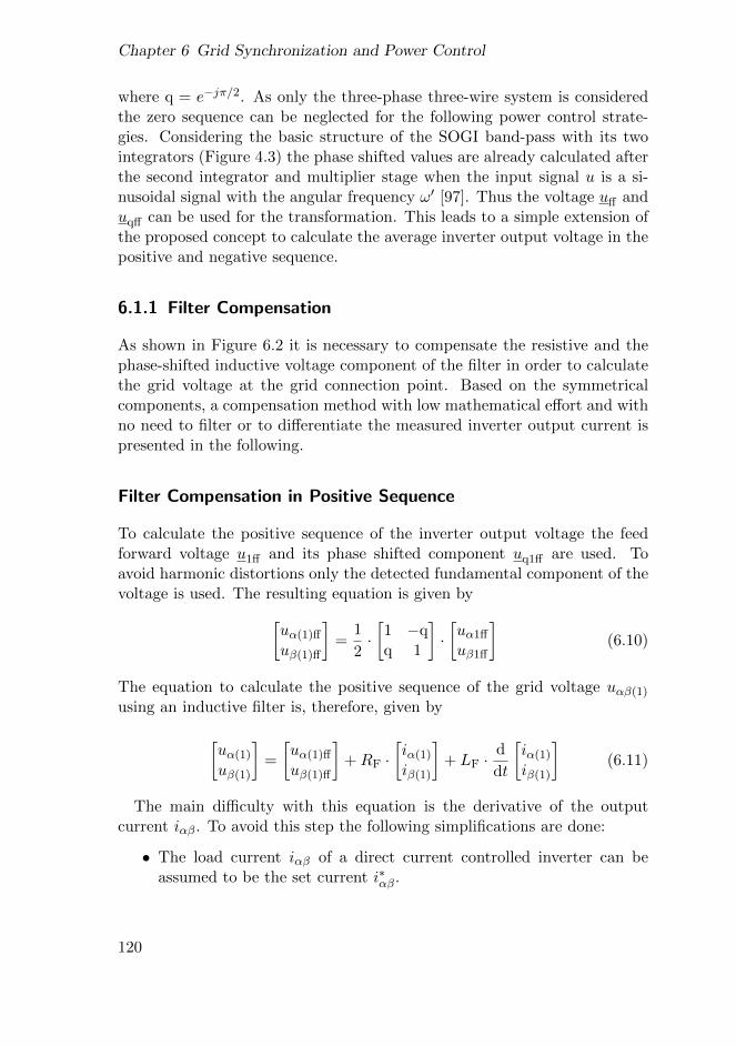
Chapter 6 Grid Synchronization and Power Control
where q = e−jπ/2. As only the three-phase three-wire system is consideredthe zero sequence can be neglected for the following power control strate-gies. Considering the basic structure of the SOGI band-pass with its twointegrators (Figure 4.3) the phase shifted values are already calculated afterthe second integrator and multiplier stage when the input signal u is a si-nusoidal signal with the angular frequency ω′ [97]. Thus the voltage uff anduqff can be used for the transformation. This leads to a simple extension ofthe proposed concept to calculate the average inverter output voltage in thepositive and negative sequence.
6.1.1 Filter Compensation
As shown in Figure 6.2 it is necessary to compensate the resistive and thephase-shifted inductive voltage component of the filter in order to calculatethe grid voltage at the grid connection point. Based on the symmetricalcomponents, a compensation method with low mathematical effort and withno need to filter or to differentiate the measured inverter output current ispresented in the following.
Filter Compensation in Positive Sequence
To calculate the positive sequence of the inverter output voltage the feedforward voltage u1ff and its phase shifted component uq1ff are used. Toavoid harmonic distortions only the detected fundamental component of thevoltage is used. The resulting equation is given by[
uα(1)ff
uβ(1)ff
]=
1
2·[1 −qq 1
]·[uα1ff
uβ1ff
](6.10)
The equation to calculate the positive sequence of the grid voltage uαβ(1)
using an inductive filter is, therefore, given by
[uα(1)
uβ(1)
]=
[uα(1)ff
uβ(1)ff
]+RF ·
[iα(1)
iβ(1)
]+ LF ·
d
dt
[iα(1)
iβ(1)
](6.11)
The main difficulty with this equation is the derivative of the outputcurrent iαβ. To avoid this step the following simplifications are done:
• The load current iαβ of a direct current controlled inverter can beassumed to be the set current i∗αβ.
120
6.1 Symmetrical Components
• All phase currents of the positive sequence are symmetrical and haveidentical and constant amplitudes and phases.
Due to these simplifications, the following relationship can be made toavoid the derivation of the current:
d
dt(i∗α(1) + j · i∗β(1)) =
d
dt
(I∗(1)e
jωt
)= j · ω · I∗(1)e
jωt
di∗α(1)
dt+ j ·
di∗β(1)
dt=− ω · i∗β(1) + j · ω · i∗α(1)
(6.12)
From the relationship of real and imaginary part from Equation 6.12 thefollowing expression to replace the derivation of the current can be made:
d
dt
[i∗α(1)
i∗β(1)
]= ω ·
[−i∗β(1)
i∗α(1)
](6.13)
which leads to the following equation to calculate the grid voltage.
[uα(1)
uβ(1)
]=
[uα(1)ff
uβ(1)ff
]+RF ·
[i∗α(1)
i∗β(1)
]+ ω′ · LF ·
[−i∗β(1)
i∗α(1)
](6.14)
For the required angular frequency ω the angular frequency ω′ detected bythe FLL is used.
Filter Compensation in Negative Sequence
The filter compensation in the negative sequence can be realized in a similarway. The first step is the transformation of the fundamental component ofthe feed forward voltage to the negative sequence using Equation 6.9.
[uα(2)ff
uβ(2)ff
]=
1
2·[1 −qq 1
]·[uα1ff
uβ1ff
](6.15)
With the negative sequence of the feed forward voltage the equation for thenegative sequence of the grid can be set up.
[uα(2)
uβ(2)
]=
[uα(2)ff
uβ(2)ff
]+RF ·
[iα(2)
iβ(2)
]+ LF ·
d
dt
[iα(2)
iβ(2)
](6.16)
121
Chapter 6 Grid Synchronization and Power Control
As introduced before the following relationship for the set currents can bedone. At this step the reversed phase order of the negative sequence needsto be considered.
d
dt(i∗α(2) + j · i∗β(2)) =
d
dt
(I∗(2)e
−jωt)
= −j · ω · I∗(2)ejωt
di∗α(2)
dt+ j ·
di∗β(2)
dt=ω · i∗β(2) − j · ω · i
∗α(2)
(6.17)
Based on this relationship the derivative of the current in the negative se-quence can be replaced with
d
dt
[i∗α(2)
i∗β(2)
]= ω ·
[i∗β(2)
−i∗α(2)
](6.18)
Combining this in Equation 6.16 results in
[uα(2)
uβ(2)
]=
[uα(2)ff
uβ(2)ff
]+RF ·
[i∗α(2)
i∗β(2)
]+ ω′ · LF ·
[i∗β(2)
−i∗α(2)
](6.19)
6.1.2 Power Control with Symmetrical Components
Power Control with Positive Sequence
One possibility to realize a power control using the symmetrical componentsis called balanced positive-sequence control (BPSC) [8]. Basis for this controlstrategy are the same equations as for the IARC concept. But instead ofthe grid voltage in the αβ-system the positive sequence of the grid voltageis used. Accordingly the equations for the active and reactive power in thepositive sequence can be set up by
p(1) = uα(1) · iα(1) + uβ(1) · iβ(1) (6.20)
q(1) = uβ(1) · iα(1) − uα(1) · iβ(1) (6.21)
This leads to the following calculation matrix for the active and reactivepower.
122
6.1 Symmetrical Components
[p(1)
q(1)
]=
3
2·[uα(1) uβ(1)
uβ(1) −uα(1)
]︸ ︷︷ ︸
MBPSC
·[iα(1)
iβ(1)
](6.22)
Rearranging the equation leads to the following equation to calculate the setvalues.
[i∗αi∗β
]=
[i∗α(1)
i∗β(1)
]=
2
3·M−1
BPSC ·
[p∗(1)
q∗(1)
]
=2
3· 1
u2α(1) + u2
β(1)
·[uα(1) uβ(1)
uβ(1) −uα(1)
]·
[p∗(1)
q∗(1)
] (6.23)
A simplified schematic of the BPSC method combined with the sensorlessinverter output voltage detection system is shown in Figure 6.4. In thisfigure the MSOGI-FLL is represented as one block. Besides the MSOGI andFLL this block contains the Clarke transformation of the calculated inverteroutput voltage uUVW and the calculation of the feed forward voltage uff andits phase shifted version uqff .
33
Inverteroutput
UDC
i∗UVW
sUVW uUVW
voltagecalculation
uαβ(1)ff
FLLMSOGI
sequencePositive
calculation
uff
uqff
BPSC
u(1)ff u(1)
u(1)RFLF
p∗(1)
q∗(1)
i∗(1)
= i∗
comp.Filter
αβ
abc
ω′
Figure 6.4: Simplified schematic of BPSC method combined with the in-verter output voltage detection system
The algebraic loop created by the simplified filter compensation is resolvedby the implementation in the FPGA. Because calculations of voltage at theinductive and resistive part of the filter u(1)RFLF
require several clock cycles,a delayed value of the voltage drop at the filter is generated and added tou(1)ff . Due to the high clock speed of the FPGA of 40 MHz compared to therate of change of the grid voltage the resulting error in u(1) can be neglected.
123
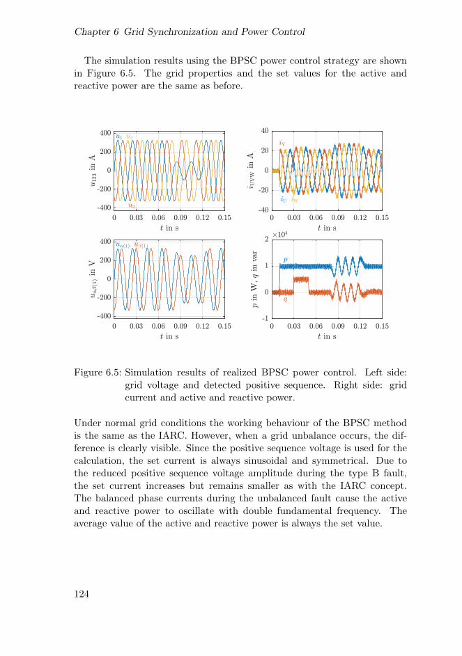
Chapter 6 Grid Synchronization and Power Control
The simulation results using the BPSC power control strategy are shownin Figure 6.5. The grid properties and the set values for the active andreactive power are the same as before.
0 0.03 0.06 0.09 0.12 0.15
t in s
-400
-200
0
200
400 u1
u2
u3
u123in
A
0 0.03 0.06 0.09 0.12 0.15
t in s
-400
-200
0
200
400 u,(1) u-(1)
u,-(1
)in
V
0 0.03 0.06 0.09 0.12 0.15
t in s
-40
-20
0
20
40
i UV
Win
A
iU
iV
iW
0 0.03 0.06 0.09 0.12 0.15
t in s
-1
0
1
2
pin
W,q
inva
r
#104
p
q
Figure 6.5: Simulation results of realized BPSC power control. Left side:grid voltage and detected positive sequence. Right side: gridcurrent and active and reactive power.
Under normal grid conditions the working behaviour of the BPSC methodis the same as the IARC. However, when a grid unbalance occurs, the dif-ference is clearly visible. Since the positive sequence voltage is used for thecalculation, the set current is always sinusoidal and symmetrical. Due tothe reduced positive sequence voltage amplitude during the type B fault,the set current increases but remains smaller as with the IARC concept.The balanced phase currents during the unbalanced fault cause the activeand reactive power to oscillate with double fundamental frequency. Theaverage value of the active and reactive power is always the set value.
124
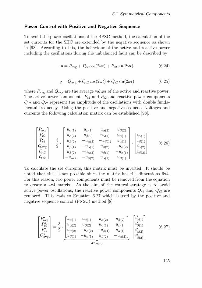
6.1 Symmetrical Components
Power Control with Positive and Negative Sequence
To avoid the power oscillations of the BPSC method, the calculation of theset currents for the SHC are extended by the negative sequence as shownin [98]. According to this, the behaviour of the active and reactive powerincluding the oscillations during the unbalanced fault can be described by
p = Pavg + Pc2 cos(2ωt) + Ps2 sin(2ωt) (6.24)
q = Qavg +Qc2 cos(2ωt) +Qs2 sin(2ωt) (6.25)
where Pavg and Qavg are the average values of the active and reactive power.The active power components Pc2 and Ps2 and reactive power componentsQc2 and Qs2 represent the amplitude of the oscillations with double funda-mental frequency. Using the positive and negative sequence voltages andcurrents the following calculation matrix can be established [98].
Pavg
Pc2
Ps2
Qavg
Qc2
Qs2
=3
2·
uα(1) uβ(1) uα(2) uβ(2)
uα(2) uβ(2) uα(1) uβ(1)
uβ(2) −uα(2) −uβ(1) uα(1)
uβ(1) −uα(1) uβ(2) −uα(2)
uβ(2) −uα(2) uβ(1) −uα(1)
−uα(2) −uβ(2) uα(1) uβ(1)
·iα(1)
iβ(1)
iα(2)
iβ(2)
(6.26)
To calculate the set currents, this matrix must be inverted. It should benoted that this is not possible since the matrix has the dimensions 6x4.For this reason, two power components must be removed from the equationto create a 4x4 matrix. As the aim of the control strategy is to avoidactive power oscillations, the reactive power components Qc2 and Qs2 areremoved. This leads to Equation 6.27 which is used by the positive andnegative sequence control (PNSC) method [8].
P ∗avg
P ∗c2
P ∗s2Q∗avg
=3
2·
uα(1) uβ(1) uα(2) uβ(2)
uα(2) uβ(2) uα(1) uβ(1)
uβ(2) −uα(2) −uβ(1) uα(1)
uβ(1) −uα(1) uβ(2) −uα(2)
︸ ︷︷ ︸
MPNSC
·
i∗α(1)
i∗β(1)
i∗α(2)
i∗β(2)
(6.27)
125
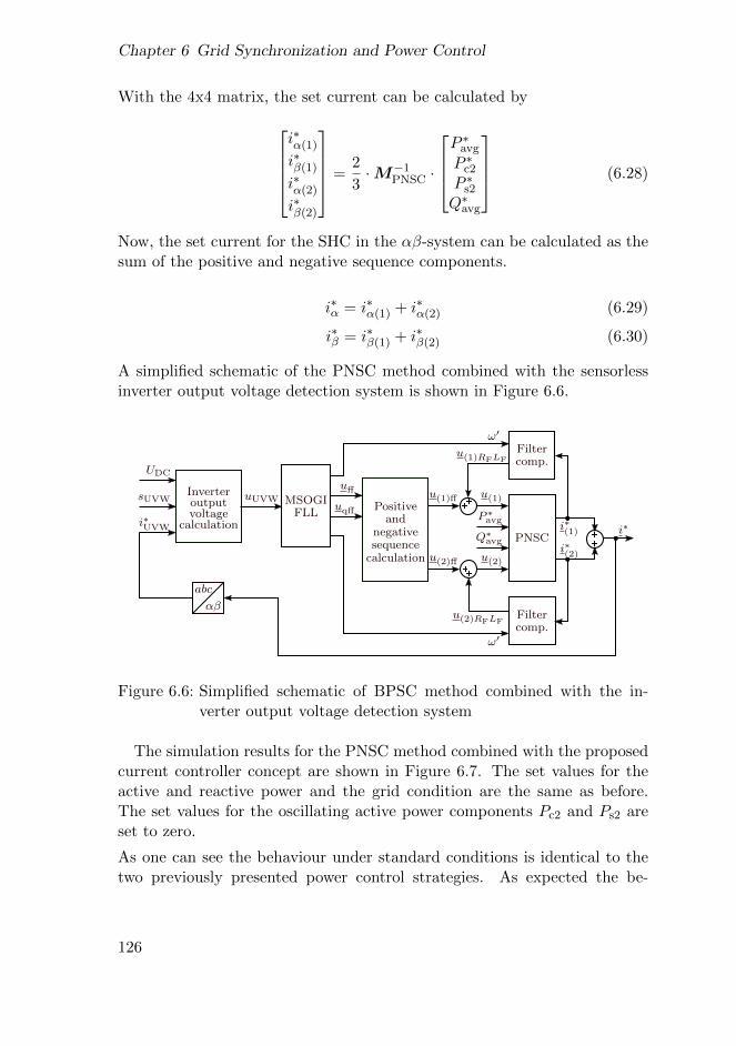
Chapter 6 Grid Synchronization and Power Control
With the 4x4 matrix, the set current can be calculated byi∗α(1)
i∗β(1)
i∗α(2)
i∗β(2)
=2
3·M−1
PNSC ·
P ∗avg
P ∗c2
P ∗s2Q∗avg
(6.28)
Now, the set current for the SHC in the αβ-system can be calculated as thesum of the positive and negative sequence components.
i∗α = i∗α(1) + i∗α(2) (6.29)
i∗β = i∗β(1) + i∗β(2) (6.30)
A simplified schematic of the PNSC method combined with the sensorlessinverter output voltage detection system is shown in Figure 6.6.
33
Inverteroutput
UDC
i∗UVW
sUVW uUVW
voltagecalculation
uαβ(1)ff
FLLMSOGI
andPositive
negative
uff
uqff
PNSC
u(1)ff u(1)
u(1)RFLF
P ∗avg
Q∗avgi∗
comp.Filter
αβ
abc
ω′
u(2)ff u(2)
sequencecalculation
ω′comp.Filter
i∗(1)
i∗(2)
u(2)RFLF
Figure 6.6: Simplified schematic of BPSC method combined with the in-verter output voltage detection system
The simulation results for the PNSC method combined with the proposedcurrent controller concept are shown in Figure 6.7. The set values for theactive and reactive power and the grid condition are the same as before.The set values for the oscillating active power components Pc2 and Ps2 areset to zero.
As one can see the behaviour under standard conditions is identical to thetwo previously presented power control strategies. As expected the be-
126
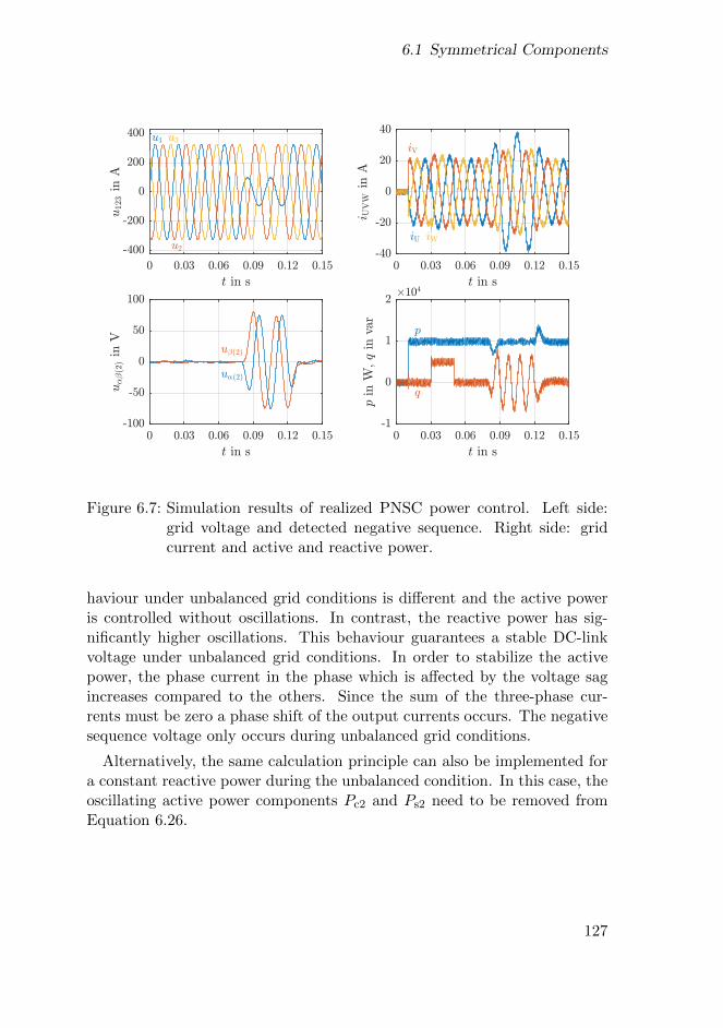
6.1 Symmetrical Components
0 0.03 0.06 0.09 0.12 0.15
t in s
-400
-200
0
200
400 u1
u2
u3
u123in
A
0 0.03 0.06 0.09 0.12 0.15
t in s
-100
-50
0
50
100
u,(2)
u-(2)
u,-(2
)in
V
0 0.03 0.06 0.09 0.12 0.15
t in s
-40
-20
0
20
40
i UV
Win
A
iU
iV
iW
0 0.03 0.06 0.09 0.12 0.15
t in s
-1
0
1
2
pin
W,q
inva
r
#104
p
q
Figure 6.7: Simulation results of realized PNSC power control. Left side:grid voltage and detected negative sequence. Right side: gridcurrent and active and reactive power.
haviour under unbalanced grid conditions is different and the active poweris controlled without oscillations. In contrast, the reactive power has sig-nificantly higher oscillations. This behaviour guarantees a stable DC-linkvoltage under unbalanced grid conditions. In order to stabilize the activepower, the phase current in the phase which is affected by the voltage sagincreases compared to the others. Since the sum of the three-phase cur-rents must be zero a phase shift of the output currents occurs. The negativesequence voltage only occurs during unbalanced grid conditions.
Alternatively, the same calculation principle can also be implemented fora constant reactive power during the unbalanced condition. In this case, theoscillating active power components Pc2 and Ps2 need to be removed fromEquation 6.26.
127
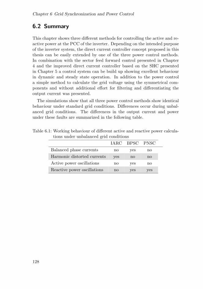
Chapter 6 Grid Synchronization and Power Control
6.2 Summary
This chapter shows three different methods for controlling the active and re-active power at the PCC of the inverter. Depending on the intended purposeof the inverter system, the direct current controller concept proposed in thisthesis can be easily extended by one of the three power control methods.In combination with the sector feed forward control presented in Chapter4 and the improved direct current controller based on the SHC presentedin Chapter 5 a control system can be build up showing excellent behaviourin dynamic and steady state operation. In addition to the power controla simple method to calculate the grid voltage using the symmetrical com-ponents and without additional effort for filtering and differentiating theoutput current was presented.
The simulations show that all three power control methods show identicalbehaviour under standard grid conditions. Differences occur during unbal-anced grid conditions. The differences in the output current and powerunder these faults are summarized in the following table.
Table 6.1: Working behaviour of different active and reactive power calcula-tions under unbalanced grid conditions
IARC BPSC PNSC
Balanced phase currents no yes no
Harmonic distorted currents yes no no
Active power oscillations no yes no
Reactive power oscillations no yes yes
128
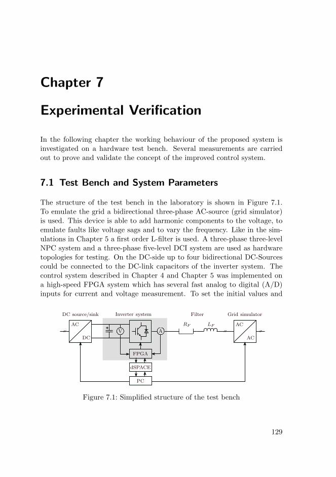
Chapter 7
Experimental Verification
In the following chapter the working behaviour of the proposed system isinvestigated on a hardware test bench. Several measurements are carriedout to prove and validate the concept of the improved control system.
7.1 Test Bench and System Parameters
The structure of the test bench in the laboratory is shown in Figure 7.1.To emulate the grid a bidirectional three-phase AC-source (grid simulator)is used. This device is able to add harmonic components to the voltage, toemulate faults like voltage sags and to vary the frequency. Like in the sim-ulations in Chapter 5 a first order L-filter is used. A three-phase three-levelNPC system and a three-phase five-level DCI system are used as hardwaretopologies for testing. On the DC-side up to four bidirectional DC-Sourcescould be connected to the DC-link capacitors of the inverter system. Thecontrol system described in Chapter 4 and Chapter 5 was implemented ona high-speed FPGA system which has several fast analog to digital (A/D)inputs for current and voltage measurement. To set the initial values and
A
LFRF
V
DC
AC
Grid simulatorInverter systemDC source/sink Filter
AC
AC
FPGA
dSPACE
PC
Figure 7.1: Simplified structure of the test bench
129
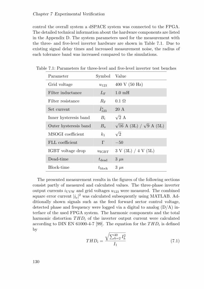
Chapter 7 Experimental Verification
control the overall system a dSPACE system was connected to the FPGA.The detailed technical information about the hardware components are listedin the Appendix D. The system parameters used for the measurement withthe three- and five-level inverter hardware are shown in Table 7.1. Due toexisting signal delay times and increased measurement noise, the radius ofeach tolerance band was increased compared to the simulations.
Table 7.1: Parameters for three-level and five-level inverter test benches
Parameter Symbol Value
Grid voltage u123 400 V (50 Hz)
Filter inductance LF 1.0 mH
Filter resistance RF 0.1 Ω
Set current I∗123 20 A
Inner hysteresis band Bi√
2 A
Outer hysteresis band Bo√
16 A (3L) /√
9 A (5L)
MSOGI coefficient k1
√2
FLL coefficient Γ −50
IGBT voltage drop uIGBT 3 V (3L) / 4 V (5L)
Dead-time tdead 3 µs
Block-time tblock 3 µs
The presented measurement results in the figures of the following sectionsconsist partly of measured and calculated values. The three-phase inverteroutput currents iUVW and grid voltages u123 were measured. The combinedsquare error current |ie|2 was calculated subsequently using MATLAB. Ad-ditionally shown signals such as the feed forward sector control voltage,detected phase and frequency were logged via a digital to analog (D/A) in-terface of the used FPGA system. The harmonic components and the totalharmonic distortion THDi of the inverter output current were calculatedaccording to DIN EN 61000-4-7 [99]. The equation for the THDi is definedby
THDi =
√∑40h=2 I
2h
I1(7.1)
130
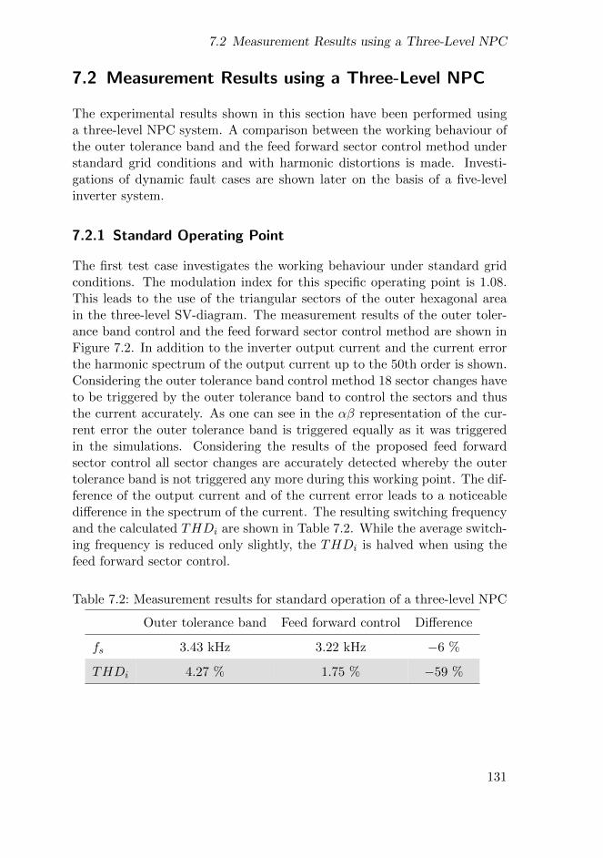
7.2 Measurement Results using a Three-Level NPC
7.2 Measurement Results using a Three-Level NPC
The experimental results shown in this section have been performed usinga three-level NPC system. A comparison between the working behaviour ofthe outer tolerance band and the feed forward sector control method understandard grid conditions and with harmonic distortions is made. Investi-gations of dynamic fault cases are shown later on the basis of a five-levelinverter system.
7.2.1 Standard Operating Point
The first test case investigates the working behaviour under standard gridconditions. The modulation index for this specific operating point is 1.08.This leads to the use of the triangular sectors of the outer hexagonal areain the three-level SV-diagram. The measurement results of the outer toler-ance band control and the feed forward sector control method are shown inFigure 7.2. In addition to the inverter output current and the current errorthe harmonic spectrum of the output current up to the 50th order is shown.Considering the outer tolerance band control method 18 sector changes haveto be triggered by the outer tolerance band to control the sectors and thusthe current accurately. As one can see in the αβ representation of the cur-rent error the outer tolerance band is triggered equally as it was triggeredin the simulations. Considering the results of the proposed feed forwardsector control all sector changes are accurately detected whereby the outertolerance band is not triggered any more during this working point. The dif-ference of the output current and of the current error leads to a noticeabledifference in the spectrum of the current. The resulting switching frequencyand the calculated THDi are shown in Table 7.2. While the average switch-ing frequency is reduced only slightly, the THDi is halved when using thefeed forward sector control.
Table 7.2: Measurement results for standard operation of a three-level NPC
Outer tolerance band Feed forward control Difference
fs 3.43 kHz 3.22 kHz −6 %
THDi 4.27 % 1.75 % −59 %
131
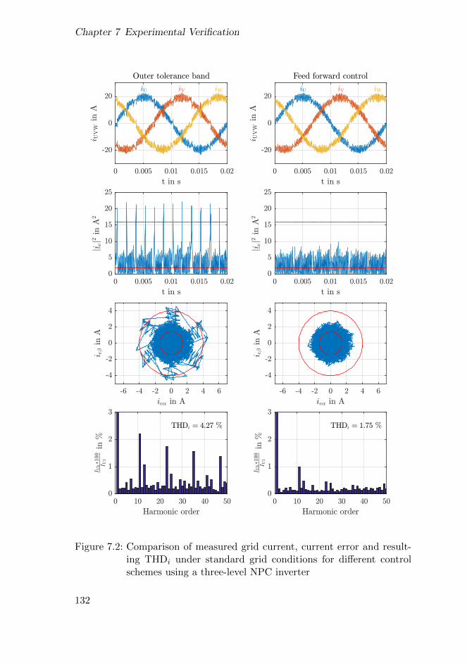
Chapter 7 Experimental Verification
0 0.005 0.01 0.015 0.02
t in s
-20
0
20i UVWinA
Outer tolerance band
iU iV iW
0 0.005 0.01 0.015 0.02
t in s
0
5
10
15
20
25
ji ej2inA2
-6 -4 -2 0 2 4 6
ie, in A
-4
-2
0
2
4
i e-inA
0 10 20 30 40 50
Harmonic order
0
1
2
3
I Uh$100
I U1in%
THDi = 4:27 %
0 0.005 0.01 0.015 0.02
t in s
-20
0
20
i UVWinA
Feed forward control
iU iV iW
0 0.005 0.01 0.015 0.02
t in s
0
5
10
15
20
25
ji ej2inA2
-6 -4 -2 0 2 4 6
ie, in A
-4
-2
0
2
4
i e-inA
0 10 20 30 40 50
Harmonic order
0
1
2
3
I Uh$100
I U1in%
THDi = 1:75 %
Figure 7.2: Comparison of measured grid current, current error and result-ing THDi under standard grid conditions for different controlschemes using a three-level NPC inverter
132
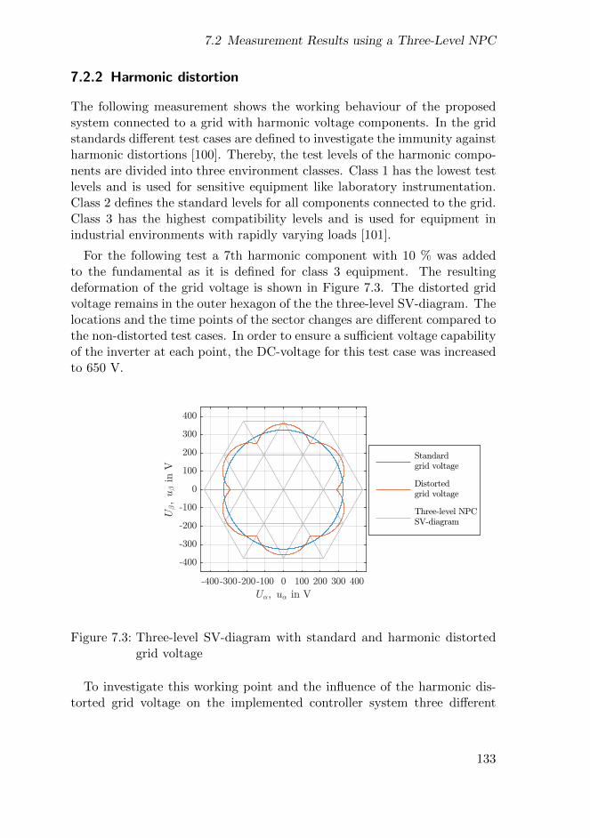
7.2 Measurement Results using a Three-Level NPC
7.2.2 Harmonic distortion
The following measurement shows the working behaviour of the proposedsystem connected to a grid with harmonic voltage components. In the gridstandards different test cases are defined to investigate the immunity againstharmonic distortions [100]. Thereby, the test levels of the harmonic compo-nents are divided into three environment classes. Class 1 has the lowest testlevels and is used for sensitive equipment like laboratory instrumentation.Class 2 defines the standard levels for all components connected to the grid.Class 3 has the highest compatibility levels and is used for equipment inindustrial environments with rapidly varying loads [101].
For the following test a 7th harmonic component with 10 % was addedto the fundamental as it is defined for class 3 equipment. The resultingdeformation of the grid voltage is shown in Figure 7.3. The distorted gridvoltage remains in the outer hexagon of the the three-level SV-diagram. Thelocations and the time points of the sector changes are different compared tothe non-distorted test cases. In order to ensure a sufficient voltage capabilityof the inverter at each point, the DC-voltage for this test case was increasedto 650 V.
-400-300-200-100 0 100 200 300 400
U,; u, in V
-400
-300
-200
-100
0
100
200
300
400
U-;
u-
inV
Standardgrid voltage
Distortedgrid voltage
Three-level NPCSV-diagram
Figure 7.3: Three-level SV-diagram with standard and harmonic distortedgrid voltage
To investigate this working point and the influence of the harmonic dis-torted grid voltage on the implemented controller system three different
133
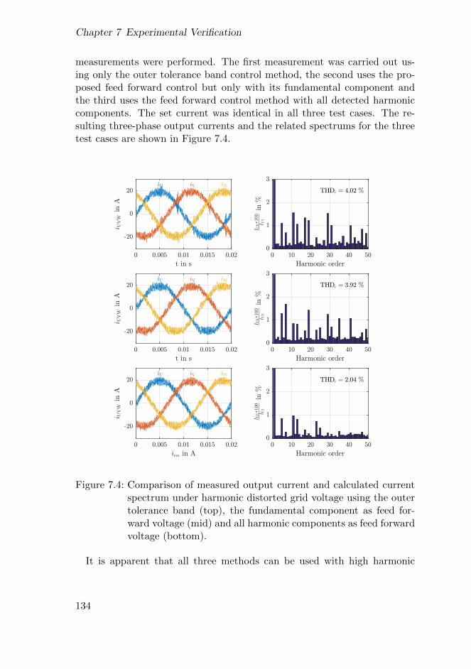
Chapter 7 Experimental Verification
measurements were performed. The first measurement was carried out us-ing only the outer tolerance band control method, the second uses the pro-posed feed forward control but only with its fundamental component andthe third uses the feed forward control method with all detected harmoniccomponents. The set current was identical in all three test cases. The re-sulting three-phase output currents and the related spectrums for the threetest cases are shown in Figure 7.4.
0 0.005 0.01 0.015 0.02
t in s
-20
0
20
i UV
Win
A
iU iV iW
0 0.005 0.01 0.015 0.02
t in s
-20
0
20
i UV
Win
A
iU iV iW
0 0.005 0.01 0.015 0.02
ie, in A
-20
0
20
i UV
Win
A
iU iV iW
0 10 20 30 40 50
Harmonic order
0
1
2
3
I Uh$100
I U1
in%
THDi = 4:02 %
0 10 20 30 40 50
Harmonic order
0
1
2
3
I Uh$100
I U1
in%
THDi = 3:92 %
0 10 20 30 40 50
Harmonic order
0
1
2
3
I Uh$100
I U1
in%
THDi = 2:04 %
Figure 7.4: Comparison of measured output current and calculated currentspectrum under harmonic distorted grid voltage using the outertolerance band (top), the fundamental component as feed for-ward voltage (mid) and all harmonic components as feed forwardvoltage (bottom).
It is apparent that all three methods can be used with high harmonic
134
7.2 Measurement Results using a Three-Level NPC
distortions. However, the average switching frequencies of the inverter andthe resulting THDi differ significantly. The values for the average switchingfrequencies and THDi are listed in Table 7.3.
Table 7.3: Measurement results for a three-level NPC under distorted gridconditions
Outer tolerance band Feed forward control Feed forward control
(only fundamental) (with all harmonics)
fs 4.70 kHz 4.48 kHz 4.36 kHz
THDi 4.02 % 3.92 % 2.04 %
When using only the fundamental component as feed forward signal theouter tolerance band is touched several times whereby the switching fre-quency is reduced by 5 % and the THDi by 2.5 % compared to the use ofthe outer tolerance band. In contrast, when using all harmonic componentsfor the feed forward control the switching frequency is reduced by 7 % andthe THDi by 49 %.
7.2.3 Comparison of Operation Modes for Three-Level NPC
The following measurement shows the variation of the average switchingfrequency over the modulation index. Therefore, the grid voltage withoutharmonics was increased by 25 V steps from 25 V to 350 V in amplitudewhich corresponds to 8 % to 108 % of the nominal grid voltage. Figure 7.5shows the covered area for this test in a three-level SV-diagram. The setcurrent amplitude for all measurements was 10 A.
The resulting average switching frequencies of the two operation modes areshown in Figure 7.6. Considering the basic structure of the three-level SV-diagram with its inner and outer hexagonal area two maxima in the switchingfrequency are visible for both control methods. These points are reachedwhen the inverter output voltage is located in the centre of the triangularsectors. Due to the voltage relationship of the surrounding space vectorsand the average inverter output voltage the switching frequency is higherat these operating points. As one can see the feed forward sector controlmethod has the smallest switching frequency over the entire modulation
135
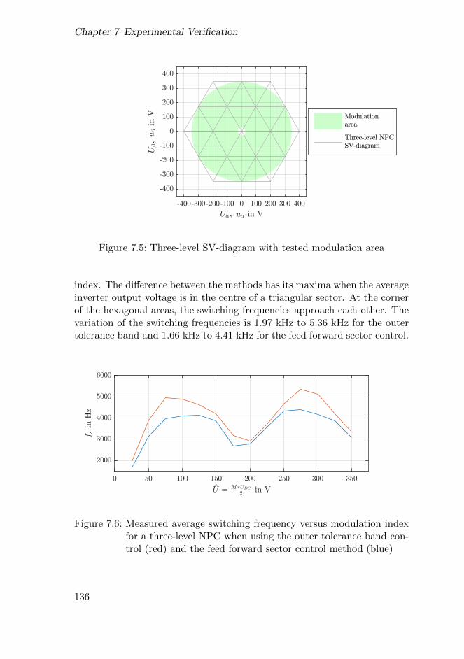
Chapter 7 Experimental Verification
-400-300-200-100 0 100 200 300 400
U,; u, in V
-400
-300
-200
-100
0
100
200
300
400
U-;
u-
inV Modulation
area
Three-level NPCSV-diagram
Figure 7.5: Three-level SV-diagram with tested modulation area
index. The difference between the methods has its maxima when the averageinverter output voltage is in the centre of a triangular sector. At the cornerof the hexagonal areas, the switching frequencies approach each other. Thevariation of the switching frequencies is 1.97 kHz to 5.36 kHz for the outertolerance band and 1.66 kHz to 4.41 kHz for the feed forward sector control.
0 50 100 150 200 250 300 350
U = M$UDC
2in V
2000
3000
4000
5000
6000
f sin
Hz
Figure 7.6: Measured average switching frequency versus modulation indexfor a three-level NPC when using the outer tolerance band con-trol (red) and the feed forward sector control method (blue)
136
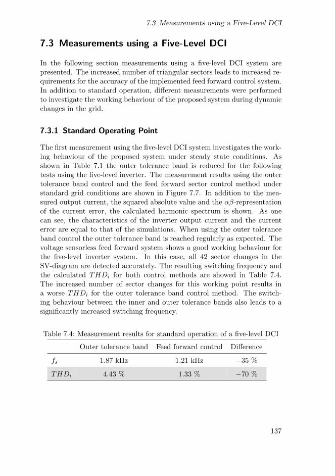
7.3 Measurements using a Five-Level DCI
7.3 Measurements using a Five-Level DCI
In the following section measurements using a five-level DCI system arepresented. The increased number of triangular sectors leads to increased re-quirements for the accuracy of the implemented feed forward control system.In addition to standard operation, different measurements were performedto investigate the working behaviour of the proposed system during dynamicchanges in the grid.
7.3.1 Standard Operating Point
The first measurement using the five-level DCI system investigates the work-ing behaviour of the proposed system under steady state conditions. Asshown in Table 7.1 the outer tolerance band is reduced for the followingtests using the five-level inverter. The measurement results using the outertolerance band control and the feed forward sector control method understandard grid conditions are shown in Figure 7.7. In addition to the mea-sured output current, the squared absolute value and the αβ-representationof the current error, the calculated harmonic spectrum is shown. As onecan see, the characteristics of the inverter output current and the currenterror are equal to that of the simulations. When using the outer toleranceband control the outer tolerance band is reached regularly as expected. Thevoltage sensorless feed forward system shows a good working behaviour forthe five-level inverter system. In this case, all 42 sector changes in theSV-diagram are detected accurately. The resulting switching frequency andthe calculated THDi for both control methods are showed in Table 7.4.The increased number of sector changes for this working point results ina worse THDi for the outer tolerance band control method. The switch-ing behaviour between the inner and outer tolerance bands also leads to asignificantly increased switching frequency.
Table 7.4: Measurement results for standard operation of a five-level DCI
Outer tolerance band Feed forward control Difference
fs 1.87 kHz 1.21 kHz −35 %
THDi 4.43 % 1.33 % −70 %
137
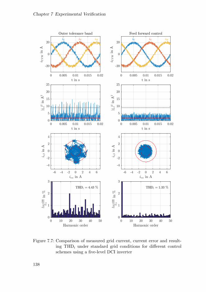
Chapter 7 Experimental Verification
0 0.005 0.01 0.015 0.02
t in s
-20
0
20i UVWinA
Outer tolerance band
iU iV iW
0 0.005 0.01 0.015 0.02
t in s
0
5
10
15
20
25
ji ej2inA2
-6 -4 -2 0 2 4 6
ie, in A
-4
-2
0
2
4
i e-inA
0 10 20 30 40 50
Harmonic order
0
1
2
3
I Uh$100
I U1in%
THDi = 4:43 %
0 0.005 0.01 0.015 0.02
t in s
-20
0
20
i UVWinA
Feed forward control
iU iV iW
0 0.005 0.01 0.015 0.02
t in s
0
5
10
15
20
25
ji ej2inA2
-6 -4 -2 0 2 4 6
ie, in A
-4
-2
0
2
4
i e-inA
0 10 20 30 40 50
Harmonic order
0
1
2
3
I Uh$100
I U1in%
THDi = 1:33 %
Figure 7.7: Comparison of measured grid current, current error and result-ing THDi under standard grid conditions for different controlschemes using a five-level DCI inverter
138
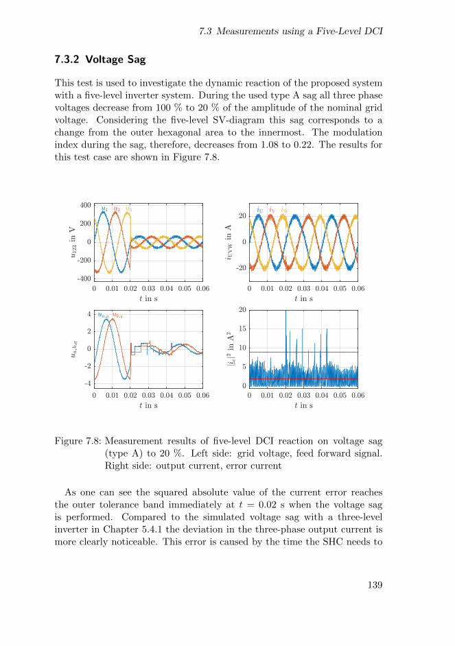
7.3 Measurements using a Five-Level DCI
7.3.2 Voltage Sag
This test is used to investigate the dynamic reaction of the proposed systemwith a five-level inverter system. During the used type A sag all three phasevoltages decrease from 100 % to 20 % of the amplitude of the nominal gridvoltage. Considering the five-level SV-diagram this sag corresponds to achange from the outer hexagonal area to the innermost. The modulationindex during the sag, therefore, decreases from 1.08 to 0.22. The results forthis test case are shown in Figure 7.8.
0 0.01 0.02 0.03 0.04 0.05 0.06
t in s
-400
-200
0
200
400 u1 u2 u3
u123in
V
0 0.01 0.02 0.03 0.04 0.05 0.06
t in s
-4
-2
0
2
4 ua$, ub$,
ua$b $,
0 0.01 0.02 0.03 0.04 0.05 0.06
t in s
-20
0
20
i UV
Win
A
iU iV iW
0 0.01 0.02 0.03 0.04 0.05 0.06
t in s
0
5
10
15
20
ji ej2
inA
2
Figure 7.8: Measurement results of five-level DCI reaction on voltage sag(type A) to 20 %. Left side: grid voltage, feed forward signal.Right side: output current, error current
As one can see the squared absolute value of the current error reachesthe outer tolerance band immediately at t = 0.02 s when the voltage sagis performed. Compared to the simulated voltage sag with a three-levelinverter in Chapter 5.4.1 the deviation in the three-phase output current ismore clearly noticeable. This error is caused by the time the SHC needs to
139
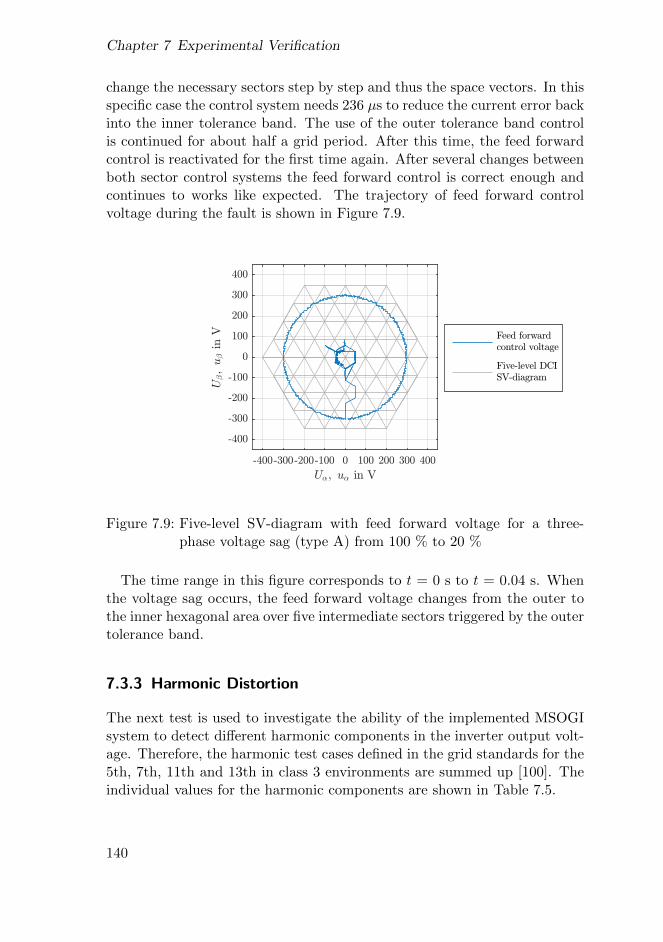
Chapter 7 Experimental Verification
change the necessary sectors step by step and thus the space vectors. In thisspecific case the control system needs 236 µs to reduce the current error backinto the inner tolerance band. The use of the outer tolerance band controlis continued for about half a grid period. After this time, the feed forwardcontrol is reactivated for the first time again. After several changes betweenboth sector control systems the feed forward control is correct enough andcontinues to works like expected. The trajectory of feed forward controlvoltage during the fault is shown in Figure 7.9.
-400-300-200-100 0 100 200 300 400
U,; u, in V
-400
-300
-200
-100
0
100
200
300
400
U-;
u-
inV Feed forward
control voltage
Five-level DCISV-diagram
Figure 7.9: Five-level SV-diagram with feed forward voltage for a three-phase voltage sag (type A) from 100 % to 20 %
The time range in this figure corresponds to t = 0 s to t = 0.04 s. Whenthe voltage sag occurs, the feed forward voltage changes from the outer tothe inner hexagonal area over five intermediate sectors triggered by the outertolerance band.
7.3.3 Harmonic Distortion
The next test is used to investigate the ability of the implemented MSOGIsystem to detect different harmonic components in the inverter output volt-age. Therefore, the harmonic test cases defined in the grid standards for the5th, 7th, 11th and 13th in class 3 environments are summed up [100]. Theindividual values for the harmonic components are shown in Table 7.5.
140
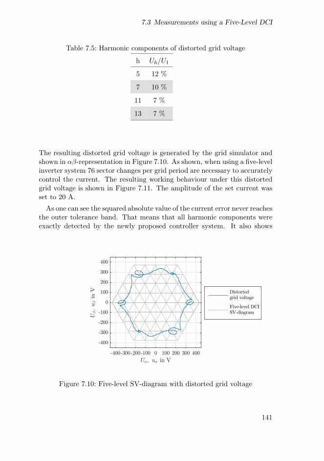
7.3 Measurements using a Five-Level DCI
Table 7.5: Harmonic components of distorted grid voltage
h Uh/U1
5 12 %
7 10 %
11 7 %
13 7 %
The resulting distorted grid voltage is generated by the grid simulator andshown in αβ-representation in Figure 7.10. As shown, when using a five-levelinverter system 76 sector changes per grid period are necessary to accuratelycontrol the current. The resulting working behaviour under this distortedgrid voltage is shown in Figure 7.11. The amplitude of the set current wasset to 20 A.
As one can see the squared absolute value of the current error never reachesthe outer tolerance band. That means that all harmonic components wereexactly detected by the newly proposed controller system. It also shows
-400-300-200-100 0 100 200 300 400
U,; u, in V
-400
-300
-200
-100
0
100
200
300
400
U-;
u-
inV Distorted
grid voltage
Five-level DCISV-diagram
Figure 7.10: Five-level SV-diagram with distorted grid voltage
141
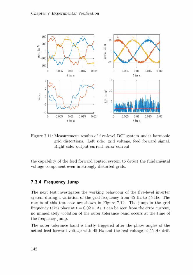
Chapter 7 Experimental Verification
0 0.005 0.01 0.015 0.02
t in s
-400
-200
0
200
400 u2 u3 u1u
123in
V
0 0.005 0.01 0.015 0.02
t in s
-4
-2
0
2
4
ua$,
ub$,
ua$b $,
0 0.005 0.01 0.015 0.02
t in s
-20
0
20
i UV
Win
A
iV iW iU
0 0.005 0.01 0.015 0.02
t in s
0
5
10
15
ji ej2
inA
2
Figure 7.11: Measurement results of five-level DCI system under harmonicgrid distortions. Left side: grid voltage, feed forward signal.Right side: output current, error current
the capability of the feed forward control system to detect the fundamentalvoltage component even in strongly distorted grids.
7.3.4 Frequency Jump
The next test investigates the working behaviour of the five-level invertersystem during a variation of the grid frequency from 45 Hz to 55 Hz. Theresults of this test case are shown in Figure 7.12. The jump in the gridfrequency takes place at t = 0.02 s. As it can be seen from the error current,no immediately violation of the outer tolerance band occurs at the time ofthe frequency jump.
The outer tolerance band is firstly triggered after the phase angles of theactual feed forward voltage with 45 Hz and the real voltage of 55 Hz drift
142
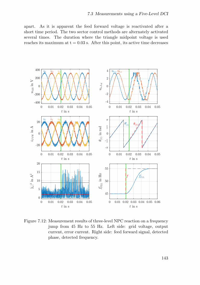
7.3 Measurements using a Five-Level DCI
apart. As it is apparent the feed forward voltage is reactivated after ashort time period. The two sector control methods are alternately activatedseveral times. The duration where the triangle midpoint voltage is usedreaches its maximum at t = 0.03 s. After this point, its active time decreases
0 0.01 0.02 0.03 0.04 0.05
t in s
-400
-200
0
200
400 u1 u2 u3
u123in
V
0 0.01 0.02 0.03 0.04 0.05
t in s
-20
0
20iU iV iW
i UV
Win
A
0 0.01 0.02 0.03 0.04 0.05
t in s
0
5
10
15
20
ji ej2
inA
2
0 0.01 0.02 0.03 0.04 0.05
t in s
-4
-2
0
2
4 ua$, ub$,
ua$b $,
0 0.01 0.02 0.03 0.04 0.05
t in s
-:
-:2
0
:2
:30(1) 3(1)
3 (1)in
rad
0 0.01 0.02 0.03 0.04 0.05 0.06
t in s
45
50
55
f 0FLLf
f0 FLL
inH
z
Figure 7.12: Measurement results of three-level NPC reaction on a frequencyjump from 45 Hz to 55 Hz. Left side: grid voltage, outputcurrent, error current. Right side: feed forward signal, detectedphase, detected frequency.
143
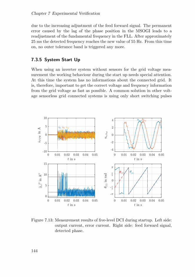
Chapter 7 Experimental Verification
due to the increasing adjustment of the feed forward signal. The permanenterror caused by the lag of the phase position in the MSOGI leads to areadjustment of the fundamental frequency in the FLL. After approximately25 ms the detected frequency reaches the new value of 55 Hz. From this timeon, no outer tolerance band is triggered any more.
7.3.5 System Start Up
When using an inverter system without sensors for the grid voltage mea-surement the working behaviour during the start up needs special attention.At this time the system has no informations about the connected grid. Itis, therefore, important to get the correct voltage and frequency informationfrom the grid voltage as fast as possible. A common solution in other volt-age sensorless grid connected systems is using only short switching pulses
0 0.01 0.02 0.03 0.04 0.05
t in s
-:
-:2
0
:2
:
30(1)3(1)
3 (1)in
rad
0 0.01 0.02 0.03 0.04 0.05
t in s
-4
-2
0
2
4 ua$,ub$,
ua$b $,
0 0.01 0.02 0.03 0.04 0.05
t in s
-10
-5
0
5
10
i UV
Win
A iU iV iW
0 0.01 0.02 0.03 0.04 0.05
t in s
0
5
10
15
ji ej2
inA
2
Figure 7.13: Measurement results of five-level DCI during startup. Left side:output current, error current. Right side: feed forward signal,detected phase.
144
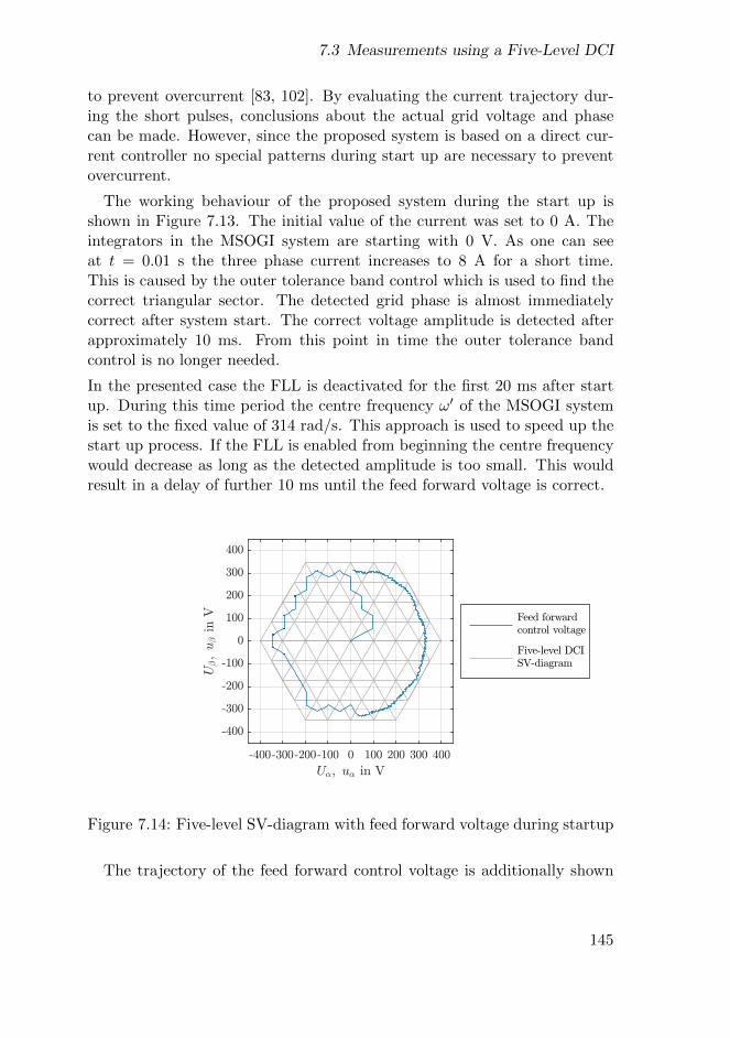
7.3 Measurements using a Five-Level DCI
to prevent overcurrent [83, 102]. By evaluating the current trajectory dur-ing the short pulses, conclusions about the actual grid voltage and phasecan be made. However, since the proposed system is based on a direct cur-rent controller no special patterns during start up are necessary to preventovercurrent.
The working behaviour of the proposed system during the start up isshown in Figure 7.13. The initial value of the current was set to 0 A. Theintegrators in the MSOGI system are starting with 0 V. As one can seeat t = 0.01 s the three phase current increases to 8 A for a short time.This is caused by the outer tolerance band control which is used to find thecorrect triangular sector. The detected grid phase is almost immediatelycorrect after system start. The correct voltage amplitude is detected afterapproximately 10 ms. From this point in time the outer tolerance bandcontrol is no longer needed.
In the presented case the FLL is deactivated for the first 20 ms after startup. During this time period the centre frequency ω′ of the MSOGI systemis set to the fixed value of 314 rad/s. This approach is used to speed up thestart up process. If the FLL is enabled from beginning the centre frequencywould decrease as long as the detected amplitude is too small. This wouldresult in a delay of further 10 ms until the feed forward voltage is correct.
-400-300-200-100 0 100 200 300 400
U,; u, in V
-400
-300
-200
-100
0
100
200
300
400
U-;
u-
inV Feed forward
control voltage
Five-level DCISV-diagram
Figure 7.14: Five-level SV-diagram with feed forward voltage during startup
The trajectory of the feed forward control voltage is additionally shown
145
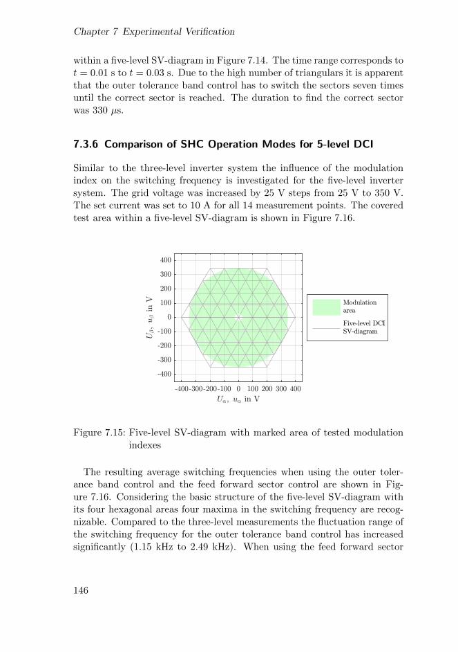
Chapter 7 Experimental Verification
within a five-level SV-diagram in Figure 7.14. The time range corresponds tot = 0.01 s to t = 0.03 s. Due to the high number of triangulars it is apparentthat the outer tolerance band control has to switch the sectors seven timesuntil the correct sector is reached. The duration to find the correct sectorwas 330 µs.
7.3.6 Comparison of SHC Operation Modes for 5-level DCI
Similar to the three-level inverter system the influence of the modulationindex on the switching frequency is investigated for the five-level invertersystem. The grid voltage was increased by 25 V steps from 25 V to 350 V.The set current was set to 10 A for all 14 measurement points. The coveredtest area within a five-level SV-diagram is shown in Figure 7.16.
-400-300-200-100 0 100 200 300 400
U,; u, in V
-400
-300
-200
-100
0
100
200
300
400
U-;
u-
inV Modulation
area
Five-level DCISV-diagram
Figure 7.15: Five-level SV-diagram with marked area of tested modulationindexes
The resulting average switching frequencies when using the outer toler-ance band control and the feed forward sector control are shown in Fig-ure 7.16. Considering the basic structure of the five-level SV-diagram withits four hexagonal areas four maxima in the switching frequency are recog-nizable. Compared to the three-level measurements the fluctuation range ofthe switching frequency for the outer tolerance band control has increasedsignificantly (1.15 kHz to 2.49 kHz). When using the feed forward sector
146
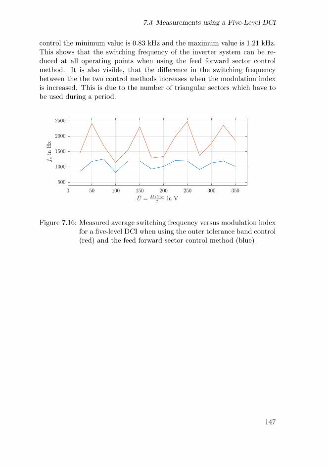
7.3 Measurements using a Five-Level DCI
control the minimum value is 0.83 kHz and the maximum value is 1.21 kHz.This shows that the switching frequency of the inverter system can be re-duced at all operating points when using the feed forward sector controlmethod. It is also visible, that the difference in the switching frequencybetween the the two control methods increases when the modulation indexis increased. This is due to the number of triangular sectors which have tobe used during a period.
0 50 100 150 200 250 300 350
U = M$UDC
2in V
500
1000
1500
2000
2500
f sin
Hz
Figure 7.16: Measured average switching frequency versus modulation indexfor a five-level DCI when using the outer tolerance band control(red) and the feed forward sector control method (blue)
147
Chapter 7 Experimental Verification
7.4 Summary
This chapter shows the working behaviour of the improved control systemfor multilevel inverters consisting of the direct current controller SHC and anovel feed forward sector control based on real hardware measurements. Allmeasurements show advancements of the new system and a good conformitywith the simulations in Chapter 5. On the basis of the measurements itcan be concluded that with higher level counts and thus a higher numberof required sector changes, the advantage of feed forward control systemincreases.
148
Chapter 8
Conclusion and Future Works
8.1 Conclusion
This thesis proposes an improved direct current controller concept basedon the SHC method for multilevel inverter systems in grid applications.The advancement compared to the state of the art concept is based on theuse of the average inverter output voltage to determine the exact locationwithin the SV-diagram of multilevel inverter systems and thus to improve thespace vector selection process for the direct current controller. For detectionof the average inverter output voltage a sensorless voltage synchronizationsystem based on the second order generalized integrator (SOGI) structurewas introduced. By using multiple interconnected SOGI circuits the systemis able to detect not only the fundamental but also specific harmonic voltagecomponents.
To realize a simple adaptation of the improved current control concept to anyinverter level count a novel integer number based coordinate transformationto simplify the representation of the inverter switching states is used. Byusing this integer representation a general approach to select the correctsectors for multilevel inverter systems is presented. In addition, differentpossibilities to realize a higher-level power control are shown.
The working behaviour of the improved SHC using the new feed forwardsector control from this thesis is investigated and proved with different simu-lations and measurements on real hardware test benches. As inverter topolo-gies for the simulation and measurements a three-level NPC and a five-levelDCI system are used. The results of the simulation and real measurementspresented in this thesis show an excellent working behaviour under steadystate conditions and a high dynamic reaction speed under different faultcases.
The exact knowledge of the average inverter output voltage leads to a signifi-
149
Chapter 8 Conclusion and Future Works
cantly improved working behaviour of the control system under steady stateconditions. By minimising the use of the outer tolerance band from the stateof the art SHC controller the switching frequency, the current error and thusthe total harmonic distortion (THDi) of the inverter output current are re-duced with the proposed new controller. When using a three-level invertersystem under steady-state conditions in the investigated operating points theimproved SHC algorithm reduces the average switching frequency by 6 %and the THDi by 59 % compared to the standard SHC concept presentedin literature [62, 63]. These advantages of the working behaviour increasewith higher level count of the inverter system significantly. For a five-levelinverter system measured at typical operating points results show a 35 %reduction of the average switching frequency with simultaneous reduction ofthe THDi by 70 %. Due to the detection of the harmonic components inthe average inverter output voltage the improved current controller systemis able to maintain this advantages even in highly harmonic distorted grids.
Summarising the main properties of the proposed control system and com-paring the achievements with the objectives of the thesis laid out in Chap-ter 1 one can conclude that the goals are accomplished with the presentedwork:
• Improved working behaviour under steady state conditions with re-duced current error and THDi and at the same time reduction of theaverage switching frequency.
• Stable and accurate working behaviour under dynamic changes in thesystem.
• The voltage sensorless approach reduces system complexity and costs.
• The detection of harmonic voltage components improves the function-ality under harmonic distorted grid conditions.
• The feed forward sector control is independent from the connectedfilter and impedance of the grid.
• Since the feed forward sector control is already implemented for currentcontrol, it can easily be used as well for power control purposes.
• Simple adaptability to higher level inverter systems due to a generalapproach for describing and selecting correct sectors and space vectorsfor current control.
150
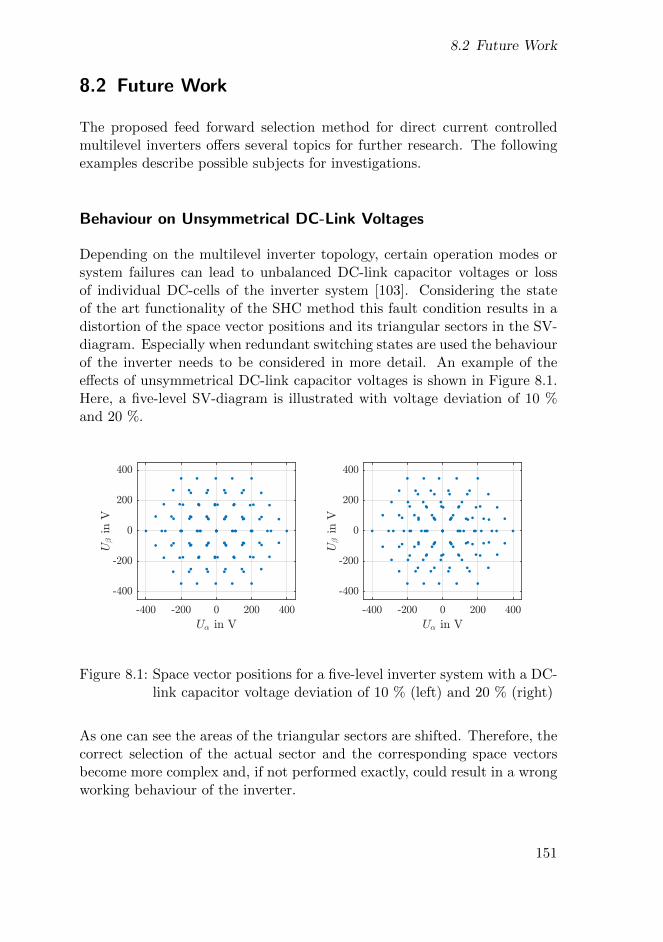
8.2 Future Work
8.2 Future Work
The proposed feed forward selection method for direct current controlledmultilevel inverters offers several topics for further research. The followingexamples describe possible subjects for investigations.
Behaviour on Unsymmetrical DC-Link Voltages
Depending on the multilevel inverter topology, certain operation modes orsystem failures can lead to unbalanced DC-link capacitor voltages or lossof individual DC-cells of the inverter system [103]. Considering the stateof the art functionality of the SHC method this fault condition results in adistortion of the space vector positions and its triangular sectors in the SV-diagram. Especially when redundant switching states are used the behaviourof the inverter needs to be considered in more detail. An example of theeffects of unsymmetrical DC-link capacitor voltages is shown in Figure 8.1.Here, a five-level SV-diagram is illustrated with voltage deviation of 10 %and 20 %.
-400 -200 0 200 400
U, in V
-400
-200
0
200
400
U-
inV
-400 -200 0 200 400
U, in V
-400
-200
0
200
400
U-
inV
Figure 8.1: Space vector positions for a five-level inverter system with a DC-link capacitor voltage deviation of 10 % (left) and 20 % (right)
As one can see the areas of the triangular sectors are shifted. Therefore, thecorrect selection of the actual sector and the corresponding space vectorsbecome more complex and, if not performed exactly, could result in a wrongworking behaviour of the inverter.
151
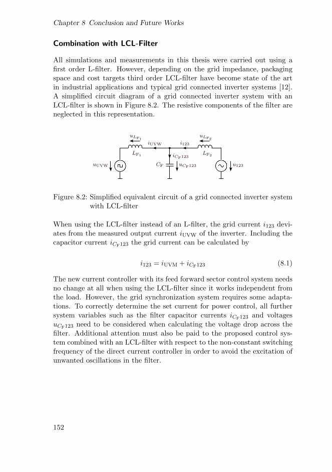
Chapter 8 Conclusion and Future Works
Combination with LCL-Filter
All simulations and measurements in this thesis were carried out using afirst order L-filter. However, depending on the grid impedance, packagingspace and cost targets third order LCL-filter have become state of the artin industrial applications and typical grid connected inverter systems [12].A simplified circuit diagram of a grid connected inverter system with anLCL-filter is shown in Figure 8.2. The resistive components of the filter areneglected in this representation.
LOAD A
LFRF
iUVW
sUVWi∗UVWieUVW
LF2 33u123uUVW
iUVW
uLF2uLF1
i123
LF1
CF uCF123
iCF123
Figure 8.2: Simplified equivalent circuit of a grid connected inverter systemwith LCL-filter
When using the LCL-filter instead of an L-filter, the grid current i123 devi-ates from the measured output current iUVW of the inverter. Including thecapacitor current iCF123 the grid current can be calculated by
i123 = iUVM + iCF123 (8.1)
The new current controller with its feed forward sector control system needsno change at all when using the LCL-filter since it works independent fromthe load. However, the grid synchronization system requires some adapta-tions. To correctly determine the set current for power control, all furthersystem variables such as the filter capacitor currents iCF123 and voltagesuCF123 need to be considered when calculating the voltage drop across thefilter. Additional attention must also be paid to the proposed control sys-tem combined with an LCL-filter with respect to the non-constant switchingfrequency of the direct current controller in order to avoid the excitation ofunwanted oscillations in the filter.
152
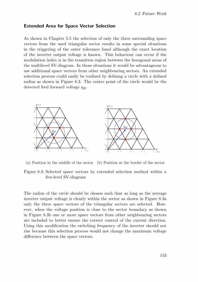
8.2 Future Work
Extended Area for Space Vector Selection
As shown in Chapter 5.5 the selection of only the three surrounding spacevectors from the used triangular sector results in some special situationsin the triggering of the outer tolerance band although the exact locationof the inverter output voltage is known. This behaviour can occur if themodulation index is in the transition region between the hexagonal areas ofthe multilevel SV-diagram. In those situations it would be advantageous touse additional space vectors from other neighbouring sectors. An extendedselection process could easily be realized by defining a circle with a definedradius as shown in Figure 8.3. The centre point of the circle would be thedetected feed forward voltage uff .
uα
uβ
60 x 50
uff
uα
uβ
60 x 50
uff
(a) Position in the middle of the sector
uα
uβ
60 x 50
uff
uα
uβ
60 x 50
uff
(b) Position at the border of the sector
Figure 8.3: Selected space vectors by extended selection method within afive-level SV-diagram
The radius of the circle should be chosen such that as long as the averageinverter output voltage is clearly within the sector as shown in Figure 8.3aonly the three space vectors of the triangular sectors are selected. How-ever, when the voltage position is close to the sector boundary as shownin Figure 8.3b one or more space vectors from other neighbouring sectorsare included to better ensure the correct control of the current direction.Using this modification the switching frequency of the inverter should notrise because this selection process would not change the maximum voltagedifference between the space vectors.
153
Chapter 8 Conclusion and Future Works
Fixed frequency operation
One of the disadvantages of direct controllers is the variable switching fre-quency over the modulation index. Especially for the design and use of LCLgrid filters this behaviour might cause problems since certain switching timesand frequencies may cause oscillations in the LCL-filter. Possible solutionsto eliminate this switching behaviour of direct controllers is to work with afixed switching frequency by using an equidistant sampling or a readjustmentof the tolerance band.
The online calculation of the best possible space vector known from SHCcould easily be performed equidistantly. However, it has to be ensured thatthe same space vector must not be selected twice in order to prevent lowswitching frequencies critical for the filter. Investigations of such a controllermodification needs to be done with special attention on the current error.
154
8.3 Publications and Patent Applications of the Author
8.3 Publications and Patent Applications of theAuthor
8.3.1 Results Related to Current Control Techniques forMultilevel Systems
1. M. Schaefer, W. Goetze, M. Hofmann, D. Montesinos-Miracle, A. Ack-va, ”Three Phase Transformation for Simplified Space Vector Controlof Multilevel Inverters”, 16th IEEE Workshop on Control and Modelingfor Power Electronics, COMPEL 2015
Abstract - Multilevel inverters provide numerous advantages com-pared to standard type inverters, most importantly a line voltage withlow harmonic distortion through multiple output voltage levels. Thecontrol of such a system with space vector modulation techniques leadsto more complex algorithms for determining the correct switching be-haviour. This paper presents a new three phase transformation withthe ability to simplify space vector based control schemes for multilevelinverters. Based on that transformation transistor switching states, re-dundant switching states and gate signals can easily be determined.
2. M. Schaefer, M. Hofmann, S. Raab, A. Ackva, ”Multilevel direct cur-rent control for grid connected inverters”, 17th European Conferenceon Power Electronics and Applications, EPE 2015
Abstract - One of the most important requirements for grid-connectedinverters is an accurate control of the line currents. Applying theswitched diamond hysteresis control (SDHC) to multilevel inverterscombines the advantages of both techniques and is an enabling steptowards a better inverter performance than using state of the art con-trollers.
3. M. Hofmann, M. Schaefer, A. Ackva, ”Optimization of direct currentcontrolled multilevel inverters under distorted conditions” 18th Euro-pean Conference on Power Electronics and Applications, EPE 2016
Abstract - Nowadays current controlled inverters need to be dynamicand robust even under grid disturbances and different grid faults. Be-sides a robust control method the requirements for the synchronizationof the system become more and more important especially when mul-tilevel inverter topologies are used.
155
Chapter 8 Conclusion and Future Works
4. M. Schaefer, Wolf Goetze, M. Hofmann, F. Bayer, D. Montesinos-Miracle, A. Ackva, ”Direct Current Control for Grid-Connected Diode-Clamped Inverters” IEEE Transactions on Industrial Electronics, Vol-ume: 64, Issue: 4, April 2017
Abstract - The accurate control of the line current, robust and dy-namic behaviour even under distorted grids and other system faultsare the most important requirements for grid-connected inverters. Ap-plying direct current control to multilevel inverters combines the ad-vantages of both and is an enabling step towards improved inverterperformance. Direct current controllers suffer from high complexity atincreased level count, which is resolved by using geometrical principlesand simple analytical calculations for switching vector selection withinthe space vector diagram. The simplified, novel parametric controllerconcept is scalable to inverters with arbitrary level count, which doesnot require any switching tables and the new fully symmetric setupguarantees equal switching frequencies among the three phases. Thehypotheses are further confirmed on a real hardware test setup on theexample of a three-level NPC inverter hardware and a Xilinx devel-opment platform. Experimental results prove the expected behaviourof the direct current control under various conditions, which shows ageneral approach to balance the dc-link capacitors of diode-clampedinverters within the theoretical limits and demonstrates the benefitsof using field programmable gate arrays as a controller platform.
5. M. Schaefer, M. Hofmann, S. Raab, A. Ackva, ”FPGA Based Controlof an Three Level Neutral Point Clamped Inverter” Power conversionand Intelligent Motion Conference, PCIM Europe 2017
Abstract - The accurate control of the line current, the robustnessand the dynamic behaviour are major factors when benchmarking gridconnected inverters. Due to weak grids even fast reactions on distor-tions and other system faults are required properties. Direct currentcontrol in combination with multilevel inverters could combine the ad-vantages and give opportunities for future systems designs. As thecomplexity, the speed and the calculation effort increases within thosesystems very fast data processing is indispensable. To meet the men-tioned demands Field Programmable Gate Arrays (FGPAs) are analternative to state of the art Microcontroller Units (MCUs).
156
8.3 Publications and Patent Applications of the Author
6. M. Hofmann, M. Schaefer, A. Ackva, ”Sensor-less Grid Voltage Syn-chronization of Direct Current Controlled Multilevel Converters” 19th
European Conference on Power Electronics and Applications, EPE 17
Abstract - The accurate control of the line current, robust and dy-namic behaviour even under distorted grids and the behaviour on otherfaults are important requirements for grid connected inverter systems.This paper presents a sensorless grid voltage determination systemin combination with an direct current control method optimized formultilevel inverters.
7. M. Schaefer, M. Hofmann, S. Raab, A. Kraemer, A. Ackva, ”Hoch-dynamisches und robustes Stromregelverfahren fuer Umrichter unter-schiedlicher Topologien” Elektrische Antriebstechnologie fuer Hybrid-und Elektrofahrzeuge HdT
8.3.2 Results Related to Applications for Current ControlTechniques
1. A. Ackva, J. Endres, M. Hofmann, ”Novel line-side inverter with activefilter option: Two paralleled inverters with high speed direct currentcontrol algorithms” 4th International Symposium on Power Electronicsfor distributed Generation Systems (PEDG), 2013, Rogers, AR, USA
Abstract - This paper presents a novel direct current control al-gorithm for Voltage Source Inverters (VSI) which combines the ad-vantages of common space vector pulse-width modulation (SVPWM)techniques with the outstanding dynamic performance of direct cur-rent control methods. An implementation on a grid-connected line-sideinverter is introduced followed by corresponding measurement results.In this connection an active filter option for improved power quality isdiscussed.
2. M. Hofmann, S. Raab, M. Schaefer, P. Ponomarov, A. Ackva, ”Mea-surements on vehicle to grid application in industrial power grid forpeak load reduction”, 6th International Symposium on Power Elec-tronics for distributed Generation Systems (PEDG), 2016, Aachen,Germany
Abstract - The combination of ”electric mobility” and ”renewableenergy production” heavily demands for energy storage systems. In-vestigations of technical possibilities to use the stored energy of electricvehicles (EV) and so called plug-in hybrid electric vehicles (PHEVs)
157
Chapter 8 Conclusion and Future Works
for smoothing the grid load and reduce power peaks are inalienable.Within the limits given by the cars battery management system con-sumption driven charge and discharge signals could be used for effectiveintegration in V2G systems. This paper will give a detailed overviewof a system for bidirectional charging in an industrial grid. First realmeasurements and test results are given to proof the concept and showthe opportunities.
3. S. Raab, M. Hofmann, M. Schaefer, A. Ackva, ”V2G-faehige bidi-rektionale Schnellladestation fuer Elektrofahrzeuge”, EMA-Nuernberg2014 Elektromobilitaetsausstellung und Fachtagung
Abstract - Die ungeregelte, wetterabhaengige Einspeisung von Pho-tovoltaikanlagen in das Energienetz sorgt fuer einen immensen Aus-baubedarf der Elektrizitaetsversorgungsnetze. Dieser Ausbau kanndurch den gezielten Einsatz von Speichersyste-men stark reduziert wer-den. Die Untersuchung der technischen Moeglichkeiten, um Elektro-fahrzeuge und auch Plug-In Hybridfahrzeuge, die ueber einen enormeSpeicherkapazitaet verfuegen, als Speichersysteme einzusetzen, wirdsomit unabdingbar. Innerhalb der vom fahrzeuginternen Batterie-managementsystem vorgegebenen Grenzen kann der Fahrzeug akku-mulator ueber verbrauchsgesteuerte Lade- und Entladesignale effektivin zukuenftige V2G- Systeme integriert werden. Um die technischenMoeglichkeiten einer solchen Technologie auszuloten, wurde in derHochschule fuer Angewandte Wissenschaften Wuerzburg - Schweinfurtder Prototyp einer V2G- faehigen, bidirektionalen Schnellladestationfuer Elektrofahrzeuge entwickelt.
4. M. Hofmann, M. Schaefer, A. Ackva, ”Bi-directional charging systemfor electric vehicles”, 3rd International Energy Transfer for ElectricVehicles Conference, Nuremberg, Germany
Abstract - The combination of ”electric mobility” and ”renewableenergy production” heavily demands for energy storage systems. In-vestigations of technical possibilities to use electric vehicles (ev) andso called plug-in hybrid electric vehicles (phevs), containing a relevantamount of storage capacity, as storage systems are inalienable. Withinthe limits given by the car’s battery management system consumption-driven charge and discharge signals could be used for effective integra-tion in future V2G systems. This paper will give a detailed overviewabout a concept for bi-directional charging and first test results.
158
8.3 Publications and Patent Applications of the Author
5. S. Raab, P. Ponomarov, M. Hofmann, M. Schaefer, A. Ackva, ”Per-formance evaluations of load balancing in industrial power grids usingvehicle to grid technology”, 19th European Conference on Power Elec-tronics and Applications, EPE 17
Abstract - The presented paper evaluates measurement results andreports about further development from the vehicle to grid system pre-sented. It uses a number of mass-production electric vehicles in sinkand source mode to balance the load of an industrial plant by cuttingoff its peak loads. The actual load is detected and the balancing poweris calculated by a predictive algorithm which keeps the total load be-low the setpoint. Analysis show that the goal of peak load shavingis reached using the presented control strategy. Although mean avail-ability of balancing performance is lower than assumed. Improvementswere made, reducing DC link ripple current by passively low pass filter-ing. After evaluating proportion of stations’ active to passive times, astandby mode was implemented improving efficiency of overall system.
6. S. Raab, P. Ponomarov, M. Hofmann, M. Schaefer, A. Kraemer, A.Ackva, ”Vehicle to Grid Anwendung zur Spitzenlastreduktion in In-dustrienetzen” Elektrische Antriebstechnologie fuer Hybrid- und Elek-trofahrzeuge HdT
7. M. Schaefer, M. Hofmann, F. Bayer, B. Mueller, A. Ackva, ”DirectCurrent Control Method for Three-Phase Motor Drives” 13th Inter-national Conference on Ecological Vehicles and Renewable Energies,EVER2018
Abstract - The requirements of three-phase motor drives in terms ofreliability, efficiency, robustness, dynamic as well as cost efficiency arecontinuously increasing within the last years. To meet this demandthe hardware components and motor drives are used in non-linear andspecial operating points leading to increased requirements for the con-trol method. This paper presents a new direct current control methodthat is able to work at these operating points. It is robust, able todeal with non-linear loads and that overcomes some disadvantages ofexisting direct current control methods. The generic approach wouldeven allow to use inverter systems with more than two levels.
159

Chapter 8 Conclusion and Future Works
8.3.3 Patent Applications
1. Patent Application: M. Hofmann, J. Koch, L. Neumann, M. Schae-fer, H. Wiessmann, ”REGELUNG EINES DREI-LEVEL WECHSEL-RICHTERS”, Application Number: 16190787.8-1809
160
Bibliography
[1] F. Blaabjerg, R. Teodorescu, M. Liserre, and A. V. Timbus, “Overviewof Control and Grid Synchronization for Distributed Power GenerationSystems,” IEEE Transactions on Industrial Electronics, vol. 53, no. 5,pp. 1398–1409, Oct. 2006. 1
[2] F. Blaabjerg, Z. Chen, and S. B. Kjaer, “Power electronics as efficientinterface in dispersed power generation systems,” IEEE Transactionson Power Electronics, vol. 19, no. 5, pp. 1184–1194, Sep. 2004. 1
[3] Zentrum fuer Sonnenenergie- und Wasserstoff-Forschung Baden-Wuerttemberg und Umweltbundesamt (Hrsg.), Erneuerbare En-ergien in Deutschland 2017 Daten zur Entwicklung imJahr 2017. Umweltbundesamt, Mar. 2018. [Online]. Avail-able: https://www.umweltbundesamt.de/sites/default/files/medien/376/publikationen/180315 uba hg eeinzahlen 2018 bf.pdf 1
[4] F. Blaabjerg, “Editorial special section on harmonics stability and mit-igation in power electronics,” IEEE Journal of Emerging and SelectedTopics in Power Electronics, vol. 4, no. 1, pp. 1–2, March 2016. 1
[5] J. Rodriguez, J.-S. Lai, and F. Z. Peng, “Multilevel inverters: a sur-vey of topologies, controls, and applications,” IEEE Transactions onIndustrial Electronics, vol. 49, no. 4, pp. 724–738, Aug. 2002. 2, 20
[6] S. Kouro, M. Malinowski, K. Gopakumar, J. Pou, L. G. Franquelo,B. Wu, J. Rodriguez, M. A. Perez, and J. I. Leon, “Recent Advancesand Industrial Applications of Multilevel Converters,” IEEE Trans-actions on Industrial Electronics, vol. 57, no. 8, pp. 2553–2580, Aug.2010. 2
[7] M. H. Bollen, Understanding Power Quality Problems: Voltage Sagsand Interruptions. Wiley-IEEE Press, Oct. 1999. 3, 31, 101, 177
[8] R. Teodorescu, M. Liserre, and P. Rodriguez, Grid Convertersfor Photovoltaic and Wind Power Systems, ser. Wiley - IEEE.Wiley, 2011. [Online]. Available: https://books.google.de/books?id=5k4tmcVIaM0C 9, 68, 76, 122, 125
161
Bibliography
[9] PQ-Harmonics Working Group, “IEEE Recommended Practice andRequirements for Harmonic Control in Electric Power Systems,” IEEEStd 519-2014 (Revision of IEEE Std 519-1992), pp. 1–29, Jun. 2014.12
[10] DIN EN 61000-3-2, Electromagnetic compatibility (EMC) - Part 3-2: Limits - Limits for harmonic current emissions (equipment inputcurrent <= 16 A per phase) (IEC 61000-3-2:2014); German versionEN 61000-3-2:2014. Beuth Verlag, Mar. 2015. 12
[11] DIN EN 61000-3-12, Electromagnetic compatibility (EMC) - Part 3-12:Limits - Limits for harmonic currents produced by equipment connectedto public low-voltage systems with input current > 16 A and <= 75A per phase (IEC 61000-3-12:2004); German version EN 61000-3-12:2005. Beuth Verlag, Sep. 2005. 12
[12] H. Cha and T. K. Vu, “Comparative analysis of low-pass output fil-ter for single-phase grid-connected photovoltaic inverter,” in Proc.Twenty-Fifth Annual IEEE Applied Power Electronics Conf. and Ex-position (APEC), Feb. 2010, pp. 1659–1665. 12, 152
[13] M. Liserre, F. Blaabjerg, and S. Hansen, “Design and control of anLCL-filter-based three-phase active rectifier,” IEEE Transactions onIndustry Applications, vol. 41, no. 5, pp. 1281–1291, Sep. 2005. 12
[14] M. Malinowski, M. P. Kazmierkowski, S. Hansen, F. Blaabjerg, andG. D. Marques, “Virtual-flux-based direct power control of three-phasePWM rectifiers,” IEEE Transactions on Industry Applications, vol. 37,no. 4, pp. 1019–1027, Jul. 2001. 14, 50
[15] M. Malinowski, “Sensorless Control Strategies for Three - PhasePWM Rectifiers,” Ph.D. dissertation, Warsaw University of Technol-ogy, Poland, 2001. 14
[16] E. Clarke, Circuit Analysis of A-C Power Systems, ser. Circuit Analy-sis of A-C Power Systems. J. Wiley & sons, Incorporated, 1950. [On-line]. Available: http://books.google.de/books?id=JB4hAAAAMAAJ17
[17] Baker, R.H. and Bannister, L.H., “Electric power converter (U.S.Patent 3 867 643),” U.S. Patent U.S. Patent 3 867 643, 1975. [Online].Available: https://patents.google.com/patent/US3867643A/en 20
[18] J.-S. Lai and F. Z. Peng, “Multilevel converters-a new breed of powerconverters,” IEEE Transactions on Industry Applications, vol. 32,no. 3, pp. 509–517, May 1996. 20, 25, 28
162
Bibliography
[19] J. Rodriguez, S. Bernet, P. K. Steimer, and I. E. Lizama, “A Survey onNeutral-Point-Clamped Inverters,” IEEE Transactions on IndustrialElectronics, vol. 57, no. 7, pp. 2219–2230, Jul. 2010. 25
[20] A. Nabae, I. Takahashi, and H. Akagi, “A New Neutral-Point-ClampedPWM Inverter,” IEEE Transactions on Industry Applications, vol. IA-17, no. 5, pp. 518–523, Sep. 1981. 25
[21] M. Schweizer and J. W. Kolar, “Design and Implementation of aHighly Efficient Three-Level T-Type Converter for Low-Voltage Ap-plications,” IEEE Transactions on Power Electronics, vol. 28, no. 2,pp. 899–907, Feb. 2013. 25
[22] A. Wilson and S. Bernet, “Comparative evaluation of multilevel con-verters with IGBT modules for low voltage applications,” in Proc. 19thEuropean Conf. Power Electronics and Applications (EPE’17 ECCEEurope), Sep. 2017, pp. 1–8. 25
[23] N. S. Choi, J. G. Cho, and G. H. Cho, “A general circuit topologyof multilevel inverter,” in Proc. nd Annual IEEE Power ElectronicsSpecialists Conf. PESC ’91 Record, Jun. 1991, pp. 96–103. 25
[24] M. Saeedifard, R. Iravani, and J. Pou, “Analysis and Controlof DC-Capacitor-Voltage-Drift Phenomenon of a Passive Front-EndFive-Level Converter,” IEEE Transactions on Industrial Electronics,vol. 54, no. 6, pp. 3255–3266, Dec. 2007. 26
[25] P. Barbosa, P. Steimer, J. Steinke, M. Winkelnkemper, andN. Celanovic, “Active-neutral-point-clamped (ANPC) multilevel con-verter technology,” in Proc. European Conf. Power Electronics andApplications, Sep. 2005, pp. 10–10. 27
[26] T. A. Meynard and H. Foch, “Multi-level conversion: high voltagechoppers and voltage-source inverters,” in Proc. rd Annual IEEEPower Electronics Specialists Conf. PESC ’92 Record, vol. 1, Jun.1992, pp. 397–403. 27, 28
[27] F. Z. Peng, J.-S. Lai, J. McKeever, and J. VanCoevering, “A multi-level voltage-source inverter with separate DC sources for static VArgeneration,” in Proc. Conf Industry Applications Conf. Thirtieth IASAnnual Meeting, IAS ’95. Record of the 1995 IEEE, vol. 3, Oct. 1995,pp. 2541–2548. 28
[28] M. Malinowski, K. Gopakumar, J. Rodriguez, and M. A. Perez, “ASurvey on Cascaded Multilevel Inverters,” IEEE Transactions on In-dustrial Electronics, vol. 57, no. 7, pp. 2197–2206, Jul. 2010. 29
163
Bibliography
[29] A. Lesnicar and R. Marquardt, “An innovative modular multilevelconverter topology suitable for a wide power range,” in Proc. IEEEBologna Power Tech, vol. 3, Jun. 2003, p. 6. 29
[30] Siemens AG, “Stromrichterschaltungen mit verteilten Energiespe-ichern,” DE Patent DE20 122 923U1, Feb. 25, 2010, dE Patent20,122,923. [Online]. Available: https://www.google.com/patents/DE20122923U1?cl=de 29
[31] M. A. Perez, S. Bernet, J. Rodriguez, S. Kouro, and R. Lizana, “Cir-cuit Topologies, Modeling, Control Schemes, and Applications of Mod-ular Multilevel Converters,” IEEE Transactions on Power Electronics,vol. 30, no. 1, pp. 4–17, Jan. 2015. 29
[32] S. Bernett, Selbstgefuehrte Stromrichter am Spannungszwischenkreis -Funktion, Modulation und Regelung. Springer Vieweg, 2012. 31, 33,72
[33] J. Holtz, “Pulsewidth modulation-a survey,” IEEE Transactions onIndustrial Electronics, vol. 39, no. 5, pp. 410–420, Oct. 1992. 31
[34] D. M. Brod and D. W. Novotny, “Current Control of VSI-PWM Invert-ers,” IEEE Transactions on Industry Applications, vol. IA-21, no. 3,pp. 562–570, May 1985. 31
[35] M. P. Kazmierkowski and L. Malesani, “Current control techniques forthree-phase voltage-source PWM converters: a survey,” IEEE Trans-actions on Industrial Electronics, vol. 45, no. 5, pp. 691–703, Oct.1998. 33
[36] H. Wiessmann, “Hochdynamisches direktes Stromregelverfahren fuerPulswechselrichter im Vergleich zu PWM-Verfahren,” Ph.D. dis-sertation, Hochschule fuer angewandte Wissenschaften Wuerzburg-Schweinfurt, 2012. 33, 45
[37] J. C. Salmon, “A 3-Phase Pwm Modulator Using a Trapezoidal Ref-erence Signal,” in Proc. 14 Annual Conf. of Industrial Electronics So-ciety, vol. 3, Oct. 1988, pp. 623–627. 33
[38] B. P. McGrath and D. G. Holmes, “Multicarrier PWM strategies formultilevel inverters,” IEEE Transactions on Industrial Electronics,vol. 49, no. 4, pp. 858–867, Aug. 2002. 34
[39] G. Carrara, S. Gardella, M. Marchesoni, R. Salutari, and G. Sciutto,“A new multilevel PWM method: a theoretical analysis,” IEEE Trans-actions on Power Electronics, vol. 7, no. 3, pp. 497–505, Jul. 1992. 34
164
Bibliography
[40] B. P. McGrath and D. G. Holmes, “A comparison of multicarrier PWMstrategies for cascaded and neutral point clamped multilevel invert-ers,” in Proc. (Cat. No.00CH37018) 2000 IEEE 31st Annual PowerElectronics Specialists Conf, vol. 2, 2000, pp. 674–679. 35
[41] H. W. van der Broeck, H. C. Skudelny, and G. V. Stanke, “Analysisand realization of a pulsewidth modulator based on voltage space vec-tors,” IEEE Transactions on Industry Applications, vol. 24, no. 1, pp.142–150, Jan. 1988. 35
[42] R. H. Park, “Two-reaction theory of synchronous machines generalizedmethod of analysis-part I,” Transactions of the American Institute ofElectrical Engineers, vol. 48, no. 3, pp. 716–727, Jul. 1929. 35
[43] Q. M. Attique, Y. Li, and K. Wang, “A survey on space-vector pulsewidth modulation for multilevel inverters,” Transactions on PowerElectronics and Applications, vol. 2, no. 3, pp. 226–236, Sep. 2017. 37
[44] J.-H. Suh, C.-H. Choi, and D.-S. Hyun, “A new simplified space-vectorPWM method for three-level inverters,” in Proc. Fourteenth AnnualApplied Power Electronics Conf. and Exposition APEC ’99, vol. 1,Mar. 1999, pp. 515–520. 37
[45] M. P. Kazmierkowski and M. A. Dzieniakowski, “Review of currentregulation techniques for three-phase PWM inverters,” in Proc. th IntIndustrial Electronics, Control and Instrumentation IECON ’94. Conf,vol. 1, Sep. 1994, pp. 567–575. 39
[46] A. Tripathi and P. C. Sen, “Comparative analysis of fixed and sinu-soidal band hysteresis current controllers for voltage source inverters,”IEEE Transactions on Industrial Electronics, vol. 39, no. 1, pp. 63–73,Feb. 1992. 39
[47] F. Jenny and D. Wueest, Steuerverfahren fuer selbstgefuehrte Strom-richter. vdf Hochschulverlag, 1995. 39, 42
[48] B. K. Bose, “An adaptive hysteresis-band current control technique ofa voltage-fed PWM inverter for machine drive system,” IEEE Trans-actions on Industrial Electronics, vol. 37, no. 5, pp. 402–408, Oct.1990. 41
[49] M. A. Dzieniakowski and M. P. Kazmierkowski, “Microprocessor-basednovel current regulator for VSI-PWM inverters,” in Proc. 23rd AnnualIEEE Power Electronics Specialists Conf. PESC ’92 Record, vol. 1,Jun. 1992, pp. 459–464. 41
[50] F. Zare and G. Ledwich, “A hysteresis current control for single-phase
165
Bibliography
multilevel voltage source inverters: PLD implementation,” IEEETransactions on Power Electronics, vol. 17, no. 5, pp. 731–738, Sep.2002. 41
[51] M. Marchesoni, “High-performance current control techniques for ap-plication to multilevel high-power voltage source inverters,” IEEETransactions on Power Electronics, vol. 7, no. 1, pp. 189–204, Jan.1992. 41
[52] A. Ackva, H. Reinold, and R. Olesinski, “A simple and self-adaptinghigh-performance current control scheme for three phase voltage sourceinverters,” in Proc. rd Annual IEEE Power Electronics SpecialistsConf. PESC ’92 Record, vol. 1, Jun. 1992, pp. 435–442. 42
[53] D. Wuest and F. Jenni, “Space vector based current control schemesfor voltage source inverters,” in Proc. 24th Annual IEEE Power Elec-tronics Specialists Conf. PESC ’93 Record, Jun. 1993, pp. 986–992.42
[54] H. Wiessmann, A. Ackva, and J. Baumeister, “Switched diamond hys-teresis control,” in Power Conversion and Intelligent Motion, PCIMEurope, 2010. 44
[55] A. Ackva, J. Endres, and M. Hofmann, “Novel line-side inverter withactive filter option: Two paralleled inverters with high speed directcurrent control algorithms,” in Proc. 4th IEEE Int. Symp. Power Elec-tronics for Distributed Generation Systems (PEDG), Jul. 2013, pp.1–6. 44
[56] M. Schaefer, M. Hofmann, S. Raab, and A. Ackva, “Multilevel directcurrent control for grid-connected inverters,” in Proc. 17th EuropeanConf. Power Electronics and Applications (EPE’15 ECCE-Europe),Sep. 2015, pp. 1–7. 47
[57] T. Noguchi, H. Tomiki, S. Kondo, and I. Takahashi, “Direct power con-trol of PWM converter without power-source voltage sensors,” IEEETransactions on Industry Applications, vol. 34, no. 3, pp. 473–479,May 1998. 49
[58] I. Takahashi and T. Noguchi, “A New Quick-Response and High-Efficiency Control Strategy of an Induction Motor,” IEEE Transac-tions on Industry Applications, vol. IA-22, no. 5, pp. 820–827, Sep.1986. 49, 56
[59] M. Malinowski, M. Jasinski, and M. P. Kazmierkowski, “Simple directpower control of three-phase PWM rectifier using space-vector mod-
166
Bibliography
ulation (DPC-SVM),” IEEE Transactions on Industrial Electronics,vol. 51, no. 2, pp. 447–454, Apr. 2004. 50
[60] L. A. Serpa, “Current Control Strategies for Multilevel Grid ConnectedInverters,” Ph.D. dissertation, SWISS FEDERAL INSTITUTE OFTECHNOLOGY ZURICH, 2007. 50
[61] L. A. Serpa, P. M. Barbosa, P. K. Steimer, and J. W. Kolar, “Five-levelvirtual-flux direct power control for the active neutral-point clampedmultilevel inverter,” in Proc. IEEE Power Electronics Specialists Conf,Jun. 2008, pp. 1668–1674. 50, 51
[62] M. Schaefer, W. Goetze, M. Hofmann, F. Bayer, D. Montesinos-Miracle, and A. Ackva, “Direct Current Control for Grid-ConnectedDiode-Clamped Inverters,” IEEE Transactions on Industrial Electron-ics, vol. 64, no. 4, pp. 3067–3074, Apr. 2017. 52, 86, 150
[63] M. Schaefer, “Direct Current Control for Grid Connected MultilevelInverters,” Ph.D. dissertation, Universitat Politecnica de Catalunya,Departament d’Enginyeria Electrica, Barcelona, Spain, 2017. 52, 54,86, 150
[64] M. Schaefer, W. Goetze, M. Hofmann, D. Montesinos-Miracle, andA. Ackva, “Three phase transformation for simplified space vectorcontrol of multilevel inverters,” in Proc. IEEE 16th Workshop Controland Modeling for Power Electronics (COMPEL), Jul. 2015, pp. 1–7.53, 77
[65] R. Kennel and A. Linder, “Predictive control of inverter supplied elec-trical drives,” in Proc. (Cat. No.00CH37018) 2000 IEEE 31st AnnualPower Electronics Specialists Conf, vol. 2, 2000, pp. 761–766. 56
[66] J. Holtz and S. Stadtfeld, “A predictive controller for the stator currentvector of ac-machines fed from a switched voltage source,,” in Proc.IEEE International Power Electronics Conference (IPEC’83),, vol. 2,1983, pp. 1665–1675. 56
[67] J. Rodriguez, J. Pontt, C. A. Silva, P. Correa, P. Lezana, P. Cortes,and U. Ammann, “Predictive Current Control of a Voltage SourceInverter,” IEEE Transactions on Industrial Electronics, vol. 54, no. 1,pp. 495–503, Feb. 2007. 57
[68] J. Rodriguez, J. Pontt, P. Correa, P. Lezana, and P. Cortes, “Predic-tive power control of an AC/DC/AC converter,” in Proc. FourtiethIAS Annual Meeting. Conf. Record of the 2005 Industry ApplicationsConf, vol. 2, Oct. 2005, pp. 934–939. 57
167
Bibliography
[69] L. Tarisciotti, P. Zanchetta, A. Watson, S. Bifaretti, and J. C. Clare,“Modulated Model Predictive Control for a Seven-Level Cascaded H-Bridge Back-to-Back Converter,” IEEE Transactions on IndustrialElectronics, vol. 61, no. 10, pp. 5375–5383, Oct. 2014. 58
[70] G. Perantzakis, F. Xepapas, S. Papathanassiou, and S. N. Manias, “APredictive Current Control Technique for Three-Level NPC VoltageSource Inverters,” in Proc. IEEE 36th Power Electronics SpecialistsConf, Jun. 2005, pp. 1241–1246. 58
[71] P. Stolze, P. Landsmann, R. Kennel, and T. Mouton, “Finite-set modelpredictive control of a flying capacitor converter with heuristic voltagevector preselection,” in Proc. 8th Int. Conf. Power Electronics - ECCEAsia, May 2011, pp. 210–217. 58
[72] M. Hofmann, M. Schaefer, and A. Ackva, “Optimization of directcurrent controlled multilevel inverters under distorted conditions,”in Proc. 18th European Conf. Power Electronics and Applications(EPE’16 ECCE Europe), Sep. 2016, pp. 1–7. 62
[73] A. Timbus, M. Liserre, R. Teodorescu, and F. Blaabjerg, “Synchro-nization methods for three phase distributed power generation systems- An overview and evaluation,” in Proc. IEEE 36th Power ElectronicsSpecialists Conf, Jun. 2005, pp. 2474–2481. 63
[74] M. Boyra and J. L. Thomas, “A review on synchronization methodsfor grid-connected three-phase VSC under unbalanced and distortedconditions,” in Proc. 14th European Conf. Power Electronics and Ap-plications, Aug. 2011, pp. 1–10. 63
[75] G.-C. Hsieh and J. C. Hung, “Phase-locked loop techniques. A survey,”IEEE Transactions on Industrial Electronics, vol. 43, no. 6, pp. 609–615, Dec. 1996. 63
[76] V. Kaura and V. Blasko, “Operation of a phase locked loop systemunder distorted utility conditions,” in Proc. 1996. Eleventh AnnualApplied Power Electronics Conf and Exposition APEC ’96, vol. 2, Mar.1996, pp. 703–708. 63
[77] P. Rodriguez, J. Pou, J. Bergas, J. I. Candela, R. P. Burgos, andD. Boroyevich, “Decoupled Double Synchronous Reference Frame PLLfor Power Converters Control,” IEEE Transactions on Power Electron-ics, vol. 22, no. 2, pp. 584–592, Mar. 2007. 64
[78] M. Karimi-Ghartemani and M. R. Iravani, “A nonlinear adaptive fil-ter for online signal analysis in power systems: applications,” IEEE
168
Bibliography
Transactions on Power Delivery, vol. 17, no. 2, pp. 617–622, Apr.2002. 64
[79] J. Svensson, “Synchronisation methods for grid-connected voltagesource converters,” Transmission and Distribution IEE Proceedings-Generation, vol. 148, no. 3, pp. 229–235, May 2001. 64
[80] P. Rodriguez, R. Teodorescu, I. Candela, A. V. Timbus, M. Liserre,and F. Blaabjerg, “New positive-sequence voltage detector for gridsynchronization of power converters under faulty grid conditions,” inProc. 37th IEEE Power Electronics Specialists Conf, Jun. 2006, pp.1–7. 64, 66, 68
[81] B. Francis and W. Wonham, “The internal model principle ofcontrol theory,” Automatica, vol. 12, no. 5, pp. 457 – 465, 1976.[Online]. Available: http://www.sciencedirect.com/science/article/pii/0005109876900066 64
[82] J. Lunze, Regelungstechnik 1 - Systemtheoretische Grundlagen, Anal-yse und Entwurf einschleifiger Regelungen. Springer, 2014, vol. 10.64
[83] J. A. Suul, “Control of Grid Integrated Voltage Source Convertersunder Unbalanced Conditions,” Ph.D. dissertation, Norwegian Uni-versity of Science and Technology, 2012. 65, 68, 145
[84] P. Rodriguez, A. Luna, M. Ciobotaru, R. Teodorescu, and F. Blaab-jerg, “Advanced Grid Synchronization System for Power Convert-ers under Unbalanced and Distorted Operating Conditions,” in Proc.IECON 2006 - 32nd Annual Conf. IEEE Industrial Electronics, Nov.2006, pp. 5173–5178. 67
[85] P. Rodriguez, A. Luna, I. Candela, R. Mujal, R. Teodorescu, andF. Blaabjerg, “Multiresonant Frequency-Locked Loop for Grid Syn-chronization of Power Converters Under Distorted Grid Conditions,”IEEE Transactions on Industrial Electronics, vol. 58, no. 1, pp. 127–138, Jan. 2011. 67, 68
[86] H. Liu, Y. Xing, and H. Hu, “Enhanced Frequency-Locked Loop Witha Comb Filter Under Adverse Grid Conditions,” IEEE Transactionson Power Electronics, vol. 31, no. 12, pp. 8046–8051, Dec. 2016. 67
[87] J. Matas, M. Castilla, J. Miret, L. G. de Vicuna, and R. Guzman, “AnAdaptive Prefiltering Method to Improve the Speed/Accuracy Trade-off of Voltage Sequence Detection Methods Under Adverse Grid Con-ditions,” IEEE Transactions on Industrial Electronics, vol. 61, no. 5,
169
Bibliography
pp. 2139–2151, May 2014. 68
[88] R. Chilipi, N. A. Sayari, K. A. Hosani, and A. R. Beig, “Controlscheme for grid-tied distributed generation inverter under unbalancedand distorted utility conditions with power quality ancillary services,”IET Renewable Power Generation, vol. 10, no. 2, pp. 140–149, 2016.68
[89] P. Rodriguez, A. Luna, I. Candela, R. Teodorescu, and F. Blaabjerg,“Grid synchronization of power converters using multiple second ordergeneralized integrators,” in Proc. 34th Annual Conf. of IEEE Indus-trial Electronics, Nov. 2008, pp. 755–760. 68, 69
[90] DIN EN 50160, Voltage characteristics of electricity supplied by publicelectricity networks; German version EN 50160:2010/A1:2015. BeuthVerlag, Feb. 2016. 69, 103
[91] A. Wintrich, U. Nicolai, W. Tursky and T. Reimann, Applikation-shandbuch Leistungshalbleiter. Verlag ISLE, 2015, vol. 2. 74
[92] G. Franklin, J. Powell, and A. Emami-Naeini, Feedback Controlof Dynamic Systems, 4th Ed., Solutions Manual. Prentice HallPTR, 2002. [Online]. Available: https://books.google.de/books?id=kSXhPAAACAAJ 76
[93] H. Akagi, E. Watanabe, and M. Aredes, Instantaneous PowerTheory and Applications to Power Conditioning, ser. IEEE PressSeries on Power Engineering. Wiley, 2007. [Online]. Available:https://books.google.de/books?id=yO0EUhCUQaAC 117
[94] C. L. Fortescue, “Method of Symmetrical Co-Ordinates Applied tothe Solution of Polyphase Networks,” Transactions of the AmericanInstitute of Electrical Engineers, vol. XXXVII, no. 2, pp. 1027–1140,Jul. 1918. 119
[95] P. Anderson, Analysis of faulted power systems, ser. IEEE Press powersystem engineering series. IEEE Press, 1995. [Online]. Available:https://books.google.de/books?id=0ugeAQAAIAAJ 119
[96] G. C. Paap, “Symmetrical components in the time domain and theirapplication to power network calculations,” IEEE Transactions onPower Systems, vol. 15, no. 2, pp. 522–528, May 2000. 119
[97] P. Rodriguez, A. V. Timbus, R. Teodorescu, M. Liserre, and F. Blaab-jerg, “Flexible Active Power Control of Distributed Power GenerationSystems During Grid Faults,” IEEE Transactions on Industrial Elec-tronics, vol. 54, no. 5, pp. 2583–2592, Oct. 2007. 120
170
Bibliography
[98] H.-S. Song and K. Nam, “Dual current control scheme for PWM con-verter under unbalanced input voltage conditions,” IEEE Transactionson Industrial Electronics, vol. 46, no. 5, pp. 953–959, Oct. 1999. 125
[99] DIN EN 61000-4-7, Electromagnetic compatibility (EMC) - Part 4-7: Testing and measurement techniques - General guide on harmon-ics and interharmonics measurements and instrumentation, for powersupply systems and equipment connected thereto (IEC 61000-4-7:2002+ A1:2008); German version EN 61000-4-7:2002 + A1:2009. BeuthVerlag, Dec. 2009. 130
[100] DIN EN 61000-4-13, Electromagnetic compatibility (EMC) - Part 4-13:Testing and measurement techniques - Harmonics and interharmonicsincluding mains signalling at a.c. power port, low frequency immunitytests (IEC 61000-4-13:2002 + A1:2009 + A2:2015); German versionEN 61000-4-13:2002 + A1:2009 + A2:2016. Beuth Verlag, Oct. 2016.133, 140
[101] DIN EN 61000-2-4, Electromagnetic compatibility (EMC) - Part 2-4: Environment; Compatibility levels in industrial plants for low-frequency conducted disturbances (IEC 61000-2-4:2002); German ver-sion EN 61000-2-4:2002. Beuth Verlag, May 2003. 133
[102] A. Kulka, “Sensorless digital control of grid connected three phaseconverters for renewable sources,” Ph.D. dissertation, Norwegian Uni-versity of Science and Technology, 2009. 145
[103] P. Lezana and G. Ortiz, “Extended operation of cascade multicell con-verters under fault condition,” IEEE Transactions on Industrial Elec-tronics, vol. 56, no. 7, pp. 2697–2703, Jul. 2009. 151
[104] M. Bollen and L. Zhang, “Different methods for classification ofthree-phase unbalanced voltage dips due to faults,” Electric PowerSystems Research, vol. 66, no. 1, pp. 59 – 69, 2003, power Quality.[Online]. Available: http://www.sciencedirect.com/science/article/pii/S0378779603000725 179
[105] SEMIKRON INTERNATIONAL GmbH, 3L SKiiP28MLI07E3V1Evaluation Inverter, Jul. 2014, rev. 02. [Online]. Avail-able: http://www.shop.semikron.com/out/media/ds/SEMIKRONDataSheet SKiiP28MLI07E3V1 Applicat Kit 91287001.pdf 183
171

172
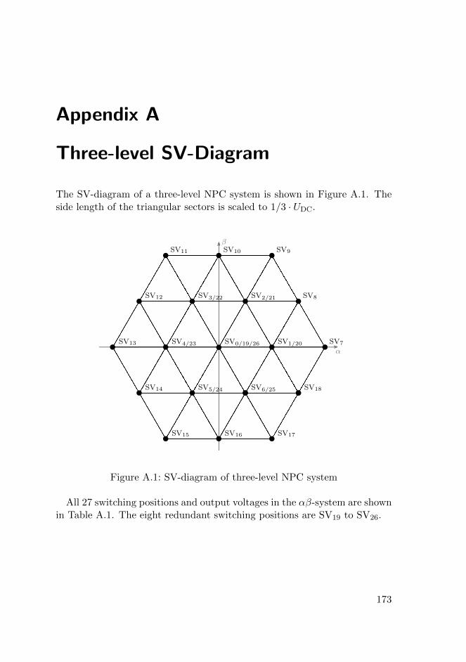
Appendix A
Three-level SV-Diagram
The SV-diagram of a three-level NPC system is shown in Figure A.1. Theside length of the triangular sectors is scaled to 1/3 · UDC.
ua∗ , uα, uU
uβ
ua∗ b∗
ub∗ , uV
uW
ua∗
ub∗
β
α
SV9SV10SV11
SV8
SV7
SV18
SV17SV16
SV1/20
SV2/21SV3/22
SV4/23
SV5/24 SV6/25
SV0/19/26
SV12
SV13
SV14
SV15
Figure A.1: SV-diagram of three-level NPC system
All 27 switching positions and output voltages in the αβ-system are shownin Table A.1. The eight redundant switching positions are SV19 to SV26.
173
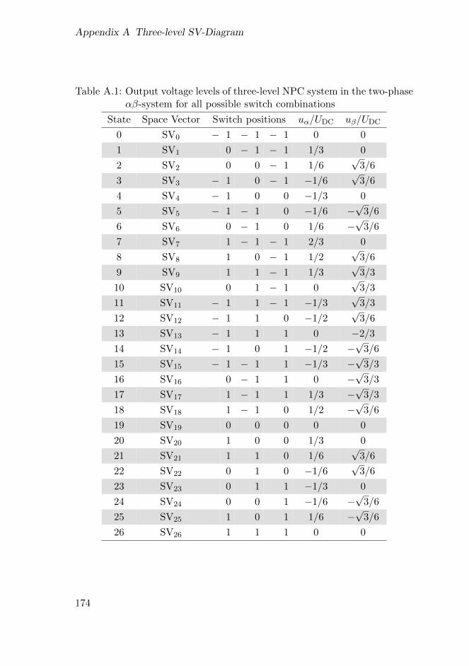
Appendix A Three-level SV-Diagram
Table A.1: Output voltage levels of three-level NPC system in the two-phaseαβ-system for all possible switch combinations
State Space Vector Switch positions uα/UDC uβ/UDC
0 SV0 − 1 − 1 − 1 0 0
1 SV1 0 − 1 − 1 1/3 0
2 SV2 0 0 − 1 1/6√
3/6
3 SV3 − 1 0 − 1 −1/6√
3/6
4 SV4 − 1 0 0 −1/3 0
5 SV5 − 1 − 1 0 −1/6 −√
3/6
6 SV6 0 − 1 0 1/6 −√
3/6
7 SV7 1 − 1 − 1 2/3 0
8 SV8 1 0 − 1 1/2√
3/6
9 SV9 1 1 − 1 1/3√
3/3
10 SV10 0 1 − 1 0√
3/3
11 SV11 − 1 1 − 1 −1/3√
3/3
12 SV12 − 1 1 0 −1/2√
3/6
13 SV13 − 1 1 1 0 −2/3
14 SV14 − 1 0 1 −1/2 −√
3/6
15 SV15 − 1 − 1 1 −1/3 −√
3/3
16 SV16 0 − 1 1 0 −√
3/3
17 SV17 1 − 1 1 1/3 −√
3/3
18 SV18 1 − 1 0 1/2 −√
3/6
19 SV19 0 0 0 0 0
20 SV20 1 0 0 1/3 0
21 SV21 1 1 0 1/6√
3/6
22 SV22 0 1 0 −1/6√
3/6
23 SV23 0 1 1 −1/3 0
24 SV24 0 0 1 −1/6 −√
3/6
25 SV25 1 0 1 1/6 −√
3/6
26 SV26 1 1 1 0 0
174

Appendix B
Transfer Function of Used MSOGISystem
The following two functions show the transfer function of the fundamentaland fifth component of the MSOGI system used to detect the harmoniccomponents of the average inverter output voltage in the simulations andmeasurements.
GMSOGI1(s) =
443s31 + 1.962e06s30 + 3.674e10s29 + 1.427e14s28 + 1.281e18s27
s32 + 7087s31 + 9.678e07s30 + 5.357e11s29 + 3.82e15s28 + 1.689e19s27
+4.343e21s26 + 2.459e25s25 + 7.216e28s24 + 2.861e32s23 + 7.192e35s22
+8.124e22s26 + 2.9e26s25 + 1.032e30s24 + 2.984e33s23 + 8.177e36s22
+2.104e39s21 + 4.47e42s20 + 9.939e45s19 + 1.756e49s18 + 3.013e52s17
+1.913e40s21 + 4.118e43s20 + 7.753e46s19 + 1.319e50s18 + 1.982e53s17
+4.346e55s16 + 5.777e58s15 + 6.643e61s14 + 6.794e64s13 + 6.043e67s12
+2.655e56s16 + 3.144e59s15 + 3.285e62s14 + 3.011e65s13 + 2.409e68s12
+4.663e70s11 + 3.085e73s10 + 1.726e76s9 + 8.01e78s8 + 3.029e81s7
+1.671e71s11 + 9.975e73s10 + 5.08e76s9 + 2.185e79s8 + 7.849e81s7
+9.167e83s6 + 2.173e86s5 + 3.911e88s4 + 5.081e90s3 + 4.304e92s2
+2.327e84s6 + 5.602e86s5 + 1.072e89s4 + 1.576e91s3 + 1.685e93s2
+1.849e94s
+1.178e95s+ 4.12e96
175
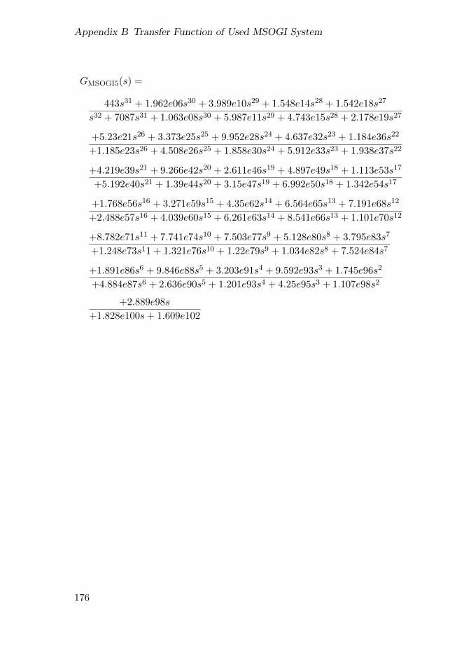
Appendix B Transfer Function of Used MSOGI System
GMSOGI5(s) =
443s31 + 1.962e06s30 + 3.989e10s29 + 1.548e14s28 + 1.542e18s27
s32 + 7087s31 + 1.063e08s30 + 5.987e11s29 + 4.743e15s28 + 2.178e19s27
+5.23e21s26 + 3.373e25s25 + 9.952e28s24 + 4.637e32s23 + 1.184e36s22
+1.185e23s26 + 4.508e26s25 + 1.858e30s24 + 5.912e33s23 + 1.938e37s22
+4.219e39s21 + 9.266e42s20 + 2.611e46s19 + 4.897e49s18 + 1.113e53s17
+5.192e40s21 + 1.39e44s20 + 3.15e47s19 + 6.992e50s18 + 1.342e54s17
+1.768e56s16 + 3.271e59s15 + 4.35e62s14 + 6.564e65s13 + 7.191e68s12
+2.488e57s16 + 4.039e60s15 + 6.261e63s14 + 8.541e66s13 + 1.101e70s12
+8.782e71s11 + 7.741e74s10 + 7.503e77s9 + 5.128e80s8 + 3.795e83s7
+1.248e73s11 + 1.321e76s10 + 1.22e79s9 + 1.034e82s8 + 7.524e84s7
+1.891e86s6 + 9.846e88s5 + 3.203e91s4 + 9.592e93s3 + 1.745e96s2
+4.884e87s6 + 2.636e90s5 + 1.201e93s4 + 4.25e95s3 + 1.107e98s2
+2.889e98s
+1.828e100s+ 1.609e102
176
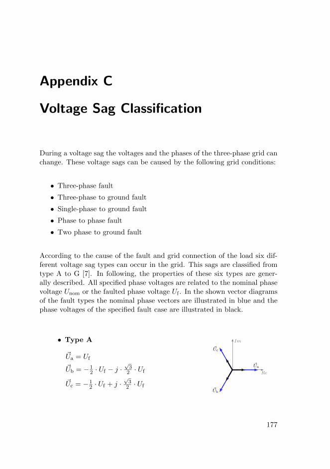
Appendix C
Voltage Sag Classification
During a voltage sag the voltages and the phases of the three-phase grid canchange. These voltage sags can be caused by the following grid conditions:
• Three-phase fault
• Three-phase to ground fault
• Single-phase to ground fault
• Phase to phase fault
• Two phase to ground fault
According to the cause of the fault and grid connection of the load six dif-ferent voltage sag types can occur in the grid. This sags are classified fromtype A to G [7]. In following, the properties of these six types are gener-ally described. All specified phase voltages are related to the nominal phasevoltage Unom or the faulted phase voltage Uf . In the shown vector diagramsof the fault types the nominal phase vectors are illustrated in blue and thephase voltages of the specified fault case are illustrated in black.
• Type A
~Ua = Uf
~Ub = −12 · Uf − j ·
√3
2 · Uf
~Uc = −12 · Uf + j ·
√3
2 · Uf
B
! ! !UR a
! ! !UR b
! ! !UR c
C
! ! !UR a
! ! !UR b
! ! !UR c
D
! ! !UR a
! ! !UR b
! ! !UR c
E
! ! !UR a
! ! !UR b
! ! !UR c
F
! ! !UR a
! ! !UR b
! ! !UR c
G
! ! !UR a
! ! !UR b
! ! !UR c
A~Ua
~Uc
~Ub
Re
Im
177
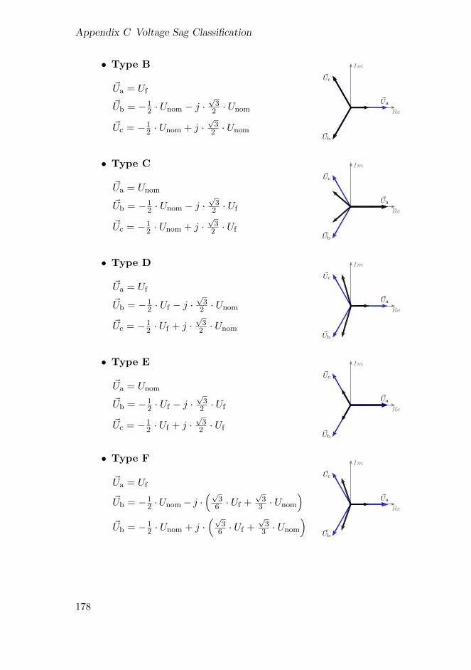
Appendix C Voltage Sag Classification
• Type B
~Ua = Uf
~Ub = −12 · Unom − j ·
√3
2 · Unom
~Uc = −12 · Unom + j ·
√3
2 · Unom
B
C D
E F
G
A~Ua
~Uc
~Ub
Re
Im
• Type C
~Ua = Unom
~Ub = −12 · Unom − j ·
√3
2 · Uf
~Uc = −12 · Unom + j ·
√3
2 · Uf
B
C D
E F
G
A~Ua
~Uc
~Ub
Re
Im
• Type D
~Ua = Uf
~Ub = −12 · Uf − j ·
√3
2 · Unom
~Uc = −12 · Uf + j ·
√3
2 · Unom
B
C D
E F
G
A~Ua
~Uc
~Ub
Re
Im
• Type E
~Ua = Unom
~Ub = −12 · Uf − j ·
√3
2 · Uf
~Uc = −12 · Uf + j ·
√3
2 · Uf
B
C D
E F
G
A~Ua
~Uc
~Ub
Re
Im
• Type F
~Ua = Uf
~Ub = −12 ·Unom− j ·
(√3
6 · Uf +√
33 · Unom
)~Ub = −1
2 · Unom + j ·(√
36 · Uf +
√3
3 · Unom
)
B
C D
E F
G
A~Ua
~Uc
~Ub
Re
Im
178
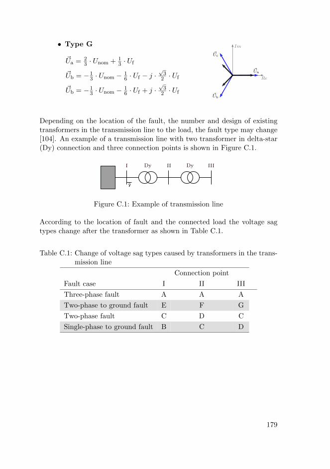
• Type G
~Ua = 23 · Unom + 1
3 · Uf
~Ub = −13 · Unom − 1
6 · Uf − j ·√
32 · Uf
~Ub = −13 · Unom − 1
6 · Uf + j ·√
32 · Uf
B
C D
E F
G
A~Ua
~Uc
~Ub
Re
Im
Depending on the location of the fault, the number and design of existingtransformers in the transmission line to the load, the fault type may change[104]. An example of a transmission line with two transformer in delta-star(Dy) connection and three connection points is shown in Figure C.1.
LOAD
current
LFRF
sUVW
33u∗UVW
ucarr
controller modulator
hysteresisband
switchingtable
referencevoltage
states switchingsignal
system
I
costfunction
min(g)predictivecurrents
voltage
errorcurrent
setcurrent
actualcurrent
indirect control
direct control
predictive control
II IIIDyDy
Figure C.1: Example of transmission line
According to the location of fault and the connected load the voltage sagtypes change after the transformer as shown in Table C.1.
Table C.1: Change of voltage sag types caused by transformers in the trans-mission line
Connection point
Fault case I II III
Three-phase fault A A A
Two-phase to ground fault E F G
Two-phase fault C D C
Single-phase to ground fault B C D
179

180
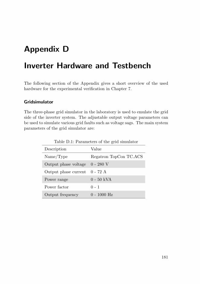
Appendix D
Inverter Hardware and Testbench
The following section of the Appendix gives a short overview of the usedhardware for the experimental verification in Chapter 7.
Gridsimulator
The three-phase grid simulator in the laboratory is used to emulate the gridside of the inverter system. The adjustable output voltage parameters canbe used to simulate various grid faults such as voltage sags. The main systemparameters of the grid simulator are:
Table D.1: Parameters of the grid simulator
Description Value
Name/Type Regatron TopCon TC.ACS
Output phase voltage 0 - 280 V
Output phase current 0 - 72 A
Power range 0 - 50 kVA
Power factor 0 - 1
Output frequency 0 - 1000 Hz
181
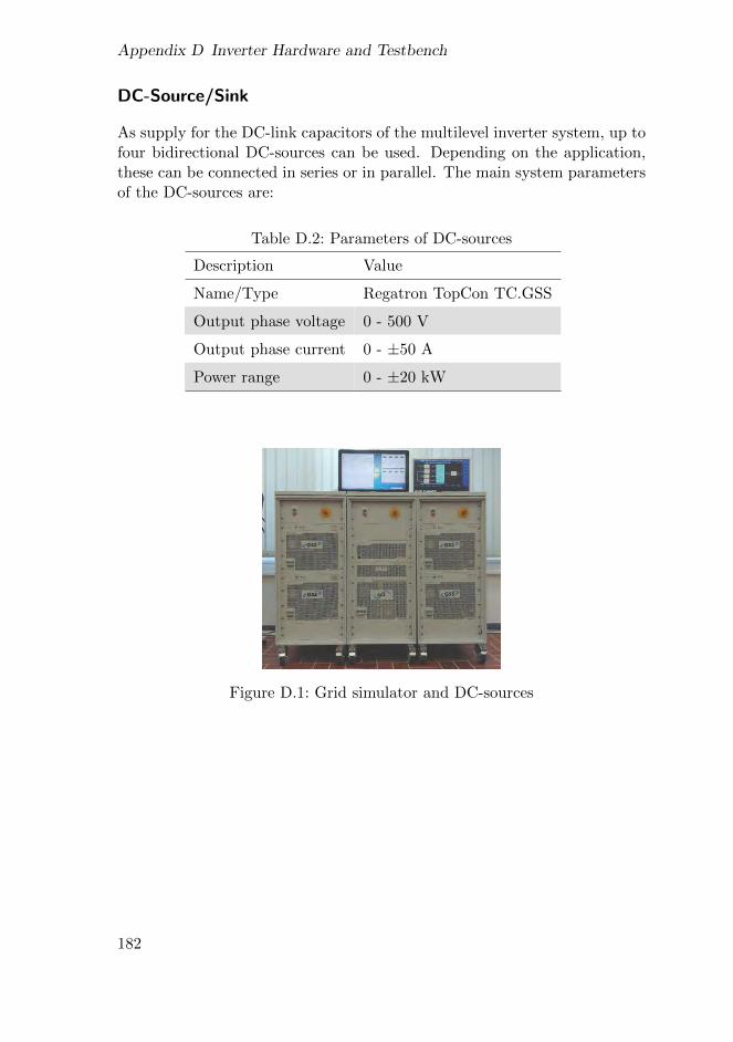
Appendix D Inverter Hardware and Testbench
DC-Source/Sink
As supply for the DC-link capacitors of the multilevel inverter system, up tofour bidirectional DC-sources can be used. Depending on the application,these can be connected in series or in parallel. The main system parametersof the DC-sources are:
Table D.2: Parameters of DC-sources
Description Value
Name/Type Regatron TopCon TC.GSS
Output phase voltage 0 - 500 V
Output phase current 0 - ±50 A
Power range 0 - ±20 kW
Figure D.1: Grid simulator and DC-sources
182
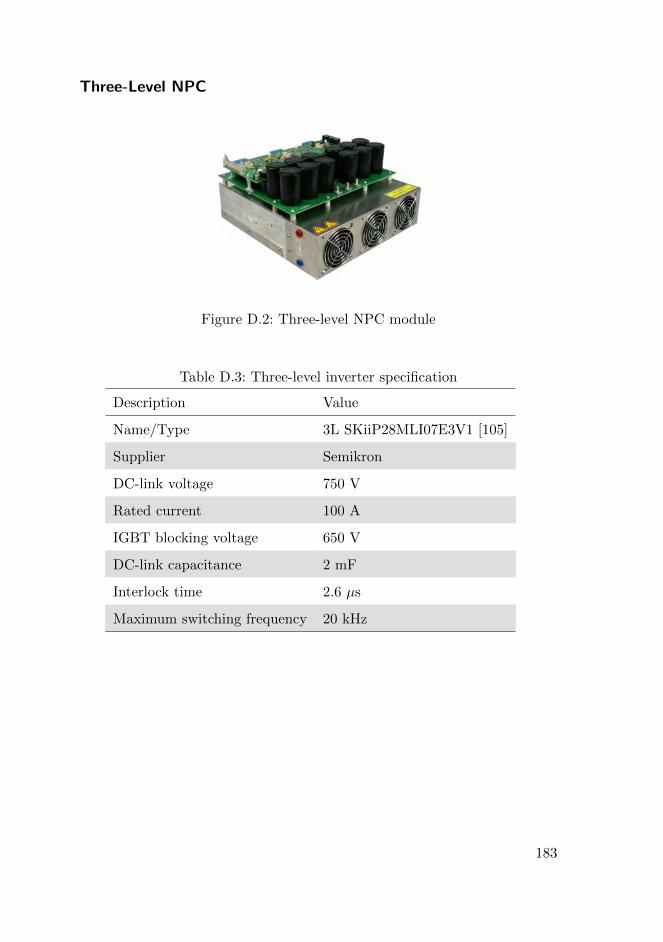
Three-Level NPC
Figure D.2: Three-level NPC module
Table D.3: Three-level inverter specification
Description Value
Name/Type 3L SKiiP28MLI07E3V1 [105]
Supplier Semikron
DC-link voltage 750 V
Rated current 100 A
IGBT blocking voltage 650 V
DC-link capacitance 2 mF
Interlock time 2.6 µs
Maximum switching frequency 20 kHz
183
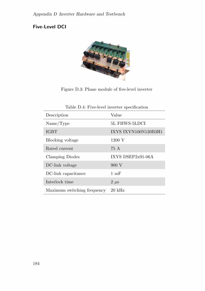
Appendix D Inverter Hardware and Testbench
Five-Level DCI
Figure D.3: Phase module of five-level inverter
Table D.4: Five-level inverter specification
Description Value
Name/Type 5L FHWS-5LDCI
IGBT IXYS IXYN100N120B3H1
Blocking voltage 1200 V
Rated current 75 A
Clamping Diodes IXYS DSEP2x91-06A
DC-link voltage 900 V
DC-link capacitance 1 mF
Interlock time 2 µs
Maximum switching frequency 20 kHz
184
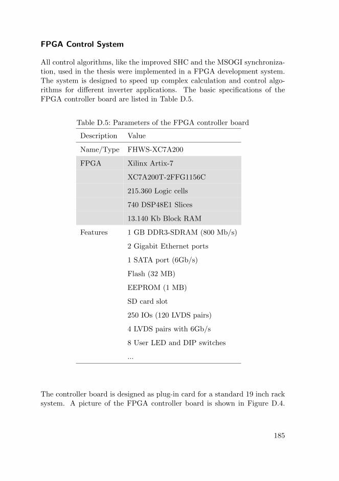
FPGA Control System
All control algorithms, like the improved SHC and the MSOGI synchroniza-tion, used in the thesis were implemented in a FPGA development system.The system is designed to speed up complex calculation and control algo-rithms for different inverter applications. The basic specifications of theFPGA controller board are listed in Table D.5.
Table D.5: Parameters of the FPGA controller board
Description Value
Name/Type FHWS-XC7A200
FPGA Xilinx Artix-7
XC7A200T-2FFG1156C
215.360 Logic cells
740 DSP48E1 Slices
13.140 Kb Block RAM
Features 1 GB DDR3-SDRAM (800 Mb/s)
2 Gigabit Ethernet ports
1 SATA port (6Gb/s)
Flash (32 MB)
EEPROM (1 MB)
SD card slot
250 IOs (120 LVDS pairs)
4 LVDS pairs with 6Gb/s
8 User LED and DIP switches
...
The controller board is designed as plug-in card for a standard 19 inch racksystem. A picture of the FPGA controller board is shown in Figure D.4.
185
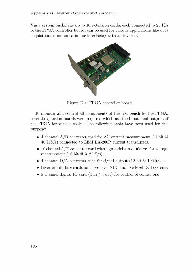
Appendix D Inverter Hardware and Testbench
Via a system backplane up to 10 extension cards, each connected to 25 IOsof the FPGA controller board, can be used for various applications like dataacquisition, communication or interfacing with an inverter.
Figure D.4: FPGA controller board
To monitor and control all components of the test bench by the FPGA,several expansion boards were required which use the inputs and outputs ofthe FPGA for various tasks. The following cards have been used for thispurpose:
• 4 channel A/D converter card for AC current measurement (14 bit @40 MS/s) connected to LEM LA-200P current transducers.
• 10 channel A/D converter card with sigma-delta modulators for voltagemeasurement (16 bit @ 312 kS/s).
• 4 channel D/A converter card for signal output (12 bit @ 192 kS/s).
• Inverter interface cards for three-level NPC and five-level DCI systems.
• 8 channel digital IO card (4 in / 4 out) for control of contactors.
186