high-resolution x-ray diffraction characterization ... - cea-leti
TRANSCRIPT
High-Resolution X-ray Diffraction Characterization and Metrology for Advanced Logic
Dr. Juliette van der Meer
Acknowledgements
• Colleagues
• Paul Ryan & John Wall (BSEMI UK)
• Matthew Wormington, Peter Gin & Kevin Matney (BSEMI US)
• Nikolai Kasper & Sven Krannich (BSEMI Germany)
• Collaborators
• Andreas Schulze formerly of IMEC (now at AMAT)
• The study on sGe nanowires and III-V materials in confined volumes was undertaken as part of the ongoing 3DAM Project (https://cordis.europa.eu/project/rcn/202643_en.html).
• This project has received funding from the Electronic Component Systems for European Leadership Joint Undertaking under grant agreement No 692527. This Joint Undertaking receives support from the European Union’s Horizon 2020 research and innovation programme and Netherlands, Belgium, France, Hungary, Ireland, Denmark, Israel.
15.03.2019 23DAM Workshop 15th March 2019
Outline
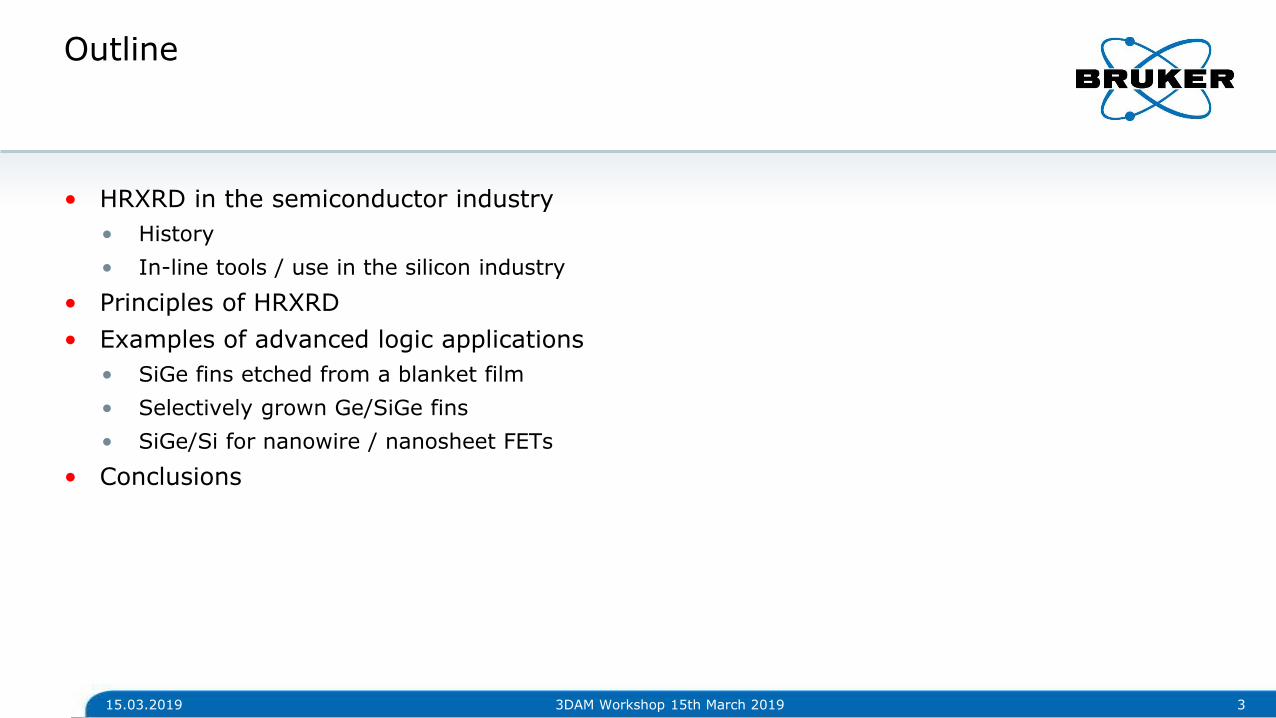
• HRXRD in the semiconductor industry
• History
• In-line tools / use in the silicon industry
• Principles of HRXRD
• Examples of advanced logic applications
• SiGe fins etched from a blanket film
• Selectively grown Ge/SiGe fins
• SiGe/Si for nanowire / nanosheet FETs
• Conclusions
15.03.2019 33DAM Workshop 15th March 2019
What can HRXRD give us, who uses it and for what?
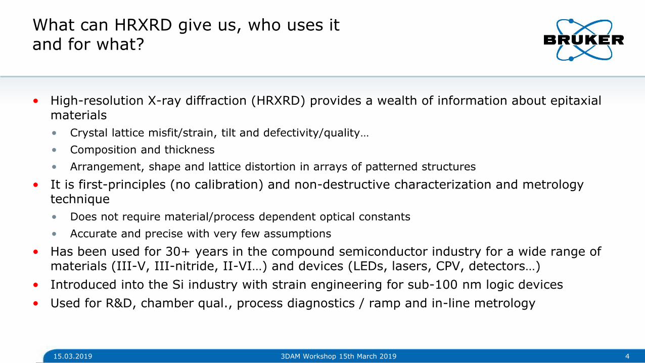
• High-resolution X-ray diffraction (HRXRD) provides a wealth of information about epitaxial materials
• Crystal lattice misfit/strain, tilt and defectivity/quality…
• Composition and thickness
• Arrangement, shape and lattice distortion in arrays of patterned structures
• It is first-principles (no calibration) and non-destructive characterization and metrology technique
• Does not require material/process dependent optical constants
• Accurate and precise with very few assumptions
• Has been used for 30+ years in the compound semiconductor industry for a wide range of materials (III-V, III-nitride, II-VI…) and devices (LEDs, lasers, CPV, detectors…)
• Introduced into the Si industry with strain engineering for sub-100 nm logic devices
• Used for R&D, chamber qual., process diagnostics / ramp and in-line metrology
15.03.2019 43DAM Workshop 15th March 2019
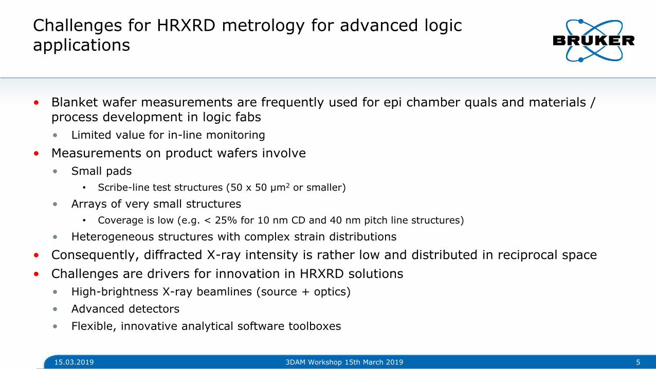
Challenges for HRXRD metrology for advanced logic applications
• Blanket wafer measurements are frequently used for epi chamber quals and materials / process development in logic fabs
• Limited value for in-line monitoring
• Measurements on product wafers involve
• Small pads
• Scribe-line test structures (50 x 50 µm2 or smaller)
• Arrays of very small structures
• Coverage is low (e.g. < 25% for 10 nm CD and 40 nm pitch line structures)
• Heterogeneous structures with complex strain distributions
• Consequently, diffracted X-ray intensity is rather low and distributed in reciprocal space
• Challenges are drivers for innovation in HRXRD solutions
• High-brightness X-ray beamlines (source + optics)
• Advanced detectors
• Flexible, innovative analytical software toolboxes
15.03.2019 53DAM Workshop 15th March 2019
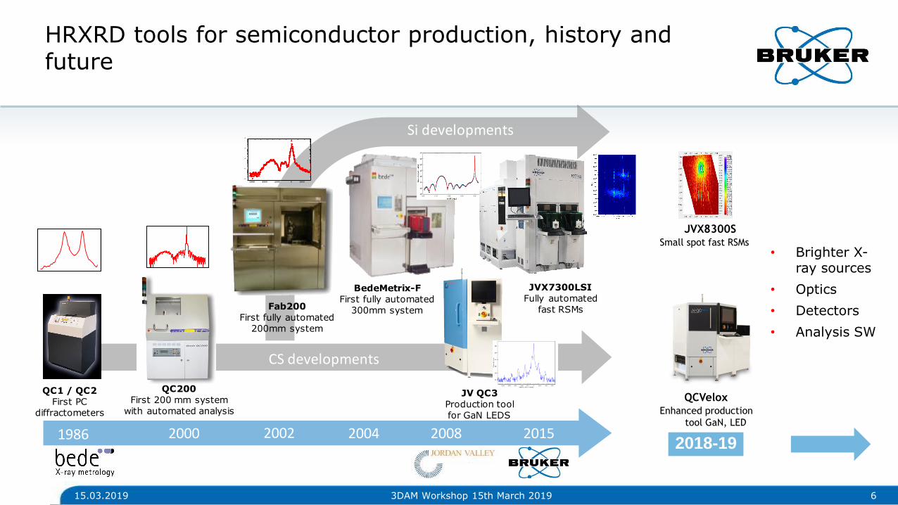
HRXRD tools for semiconductor production, history and future
15.03.2019 63DAM Workshop 15th March 2019
2000
QC200First 200 mm system
with automated analysis
2002 2004 2008 2015
QC1 / QC2
First PC diffractometers
JV QC3Production tool for GaN LEDS
BedeMetrix-FFirst fully automated
300mm system
JVX7300LSI
Fully automated fast RSMsFab200
First fully automated 200mm system
CS developments
Si developments
-3000 -2000 -1000 0 1000
- 6
- 5
- 4
- 3
- 2
1986
QCVeloxEnhanced production
tool GaN, LED
JVX8300SSmall spot fast RSMs
2018-19
• Brighter X-ray sources
• Optics
• Detectors
• Analysis SW
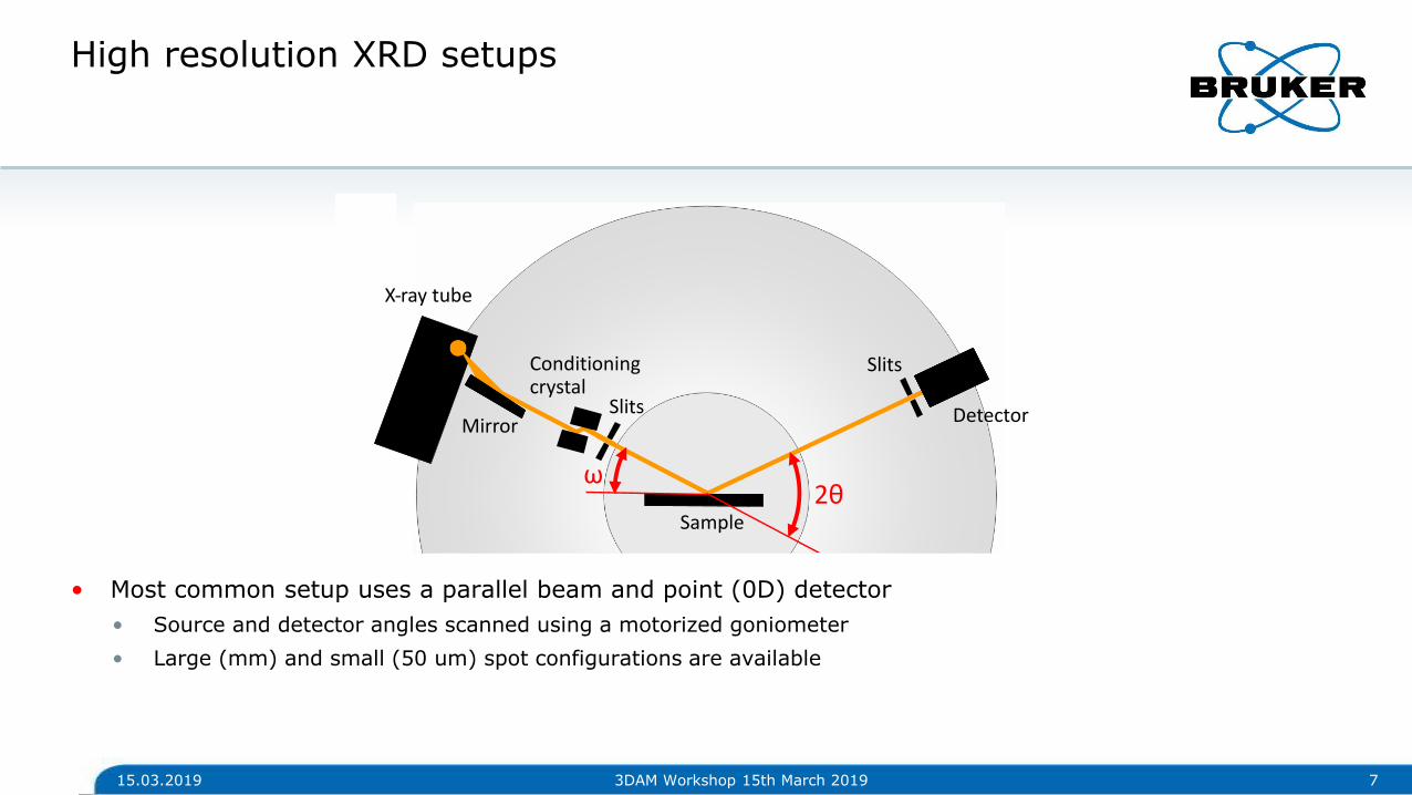
High resolution XRD setups
• Most common setup uses a parallel beam and point (0D) detector
• Source and detector angles scanned using a motorized goniometer
• Large (mm) and small (50 um) spot configurations are available
15.03.2019 73DAM Workshop 15th March 2019
X-ray tube
Conditioningcrystal
Slits
Sample
Mirror
Slits
Detector
2θω
(a)
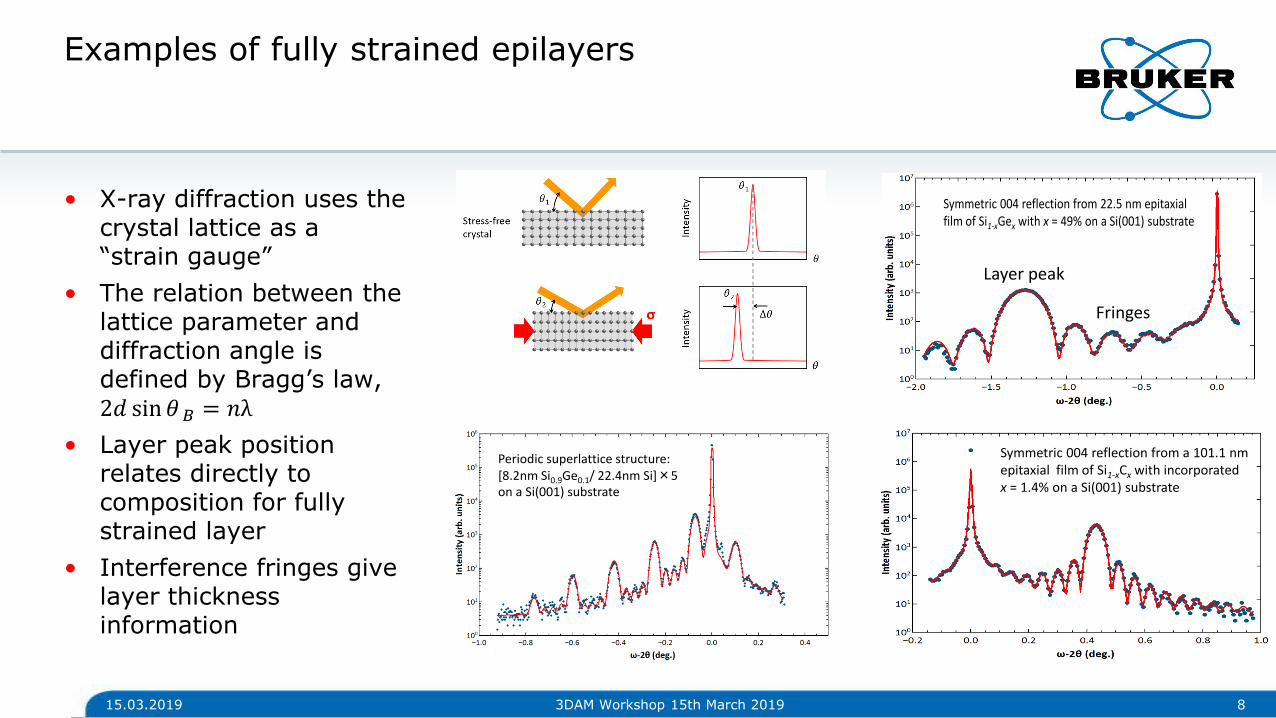
Examples of fully strained epilayers
• X-ray diffraction uses the crystal lattice as a “strain gauge”
• The relation between the lattice parameter and diffraction angle is defined by Bragg’s law, 2𝑑 sin 𝜃𝐵 = 𝑛λ
• Layer peak position relates directly to composition for fully strained layer
• Interference fringes give layer thickness information
15.03.2019 83DAM Workshop 15th March 2019
Symmetric 004 reflection from 22.5 nm epitaxial film of Si1-xGex with x = 49% on a Si(001) substrate
MeasurementSimulation
Symmetric 004 reflection from a 101.1 nm epitaxial film of Si1-xCx with incorporated x = 1.4% on a Si(001) substrate
MeasurementSimulation
Symmetric 004 reflection from 22.5 nm epitaxial film of Si1-xGex with x = 49% on a Si(001) substrate
MeasurementSimulation
Periodic superlattice structure: [8.2nm Si0.9Ge0.1/ 22.4nm Si]×5 on a Si(001) substrate
NIST SRM2000 standard: 23.7nm Si/ 48.2nm Si0.84Ge0.16 on Si(001)
Symmetric 004 reflection from a 101.1 nm epitaxial film of Si1-xCx with incorporated x = 1.4% on a Si(001) substrate
MeasurementSimulation
Layer peak
Fringes
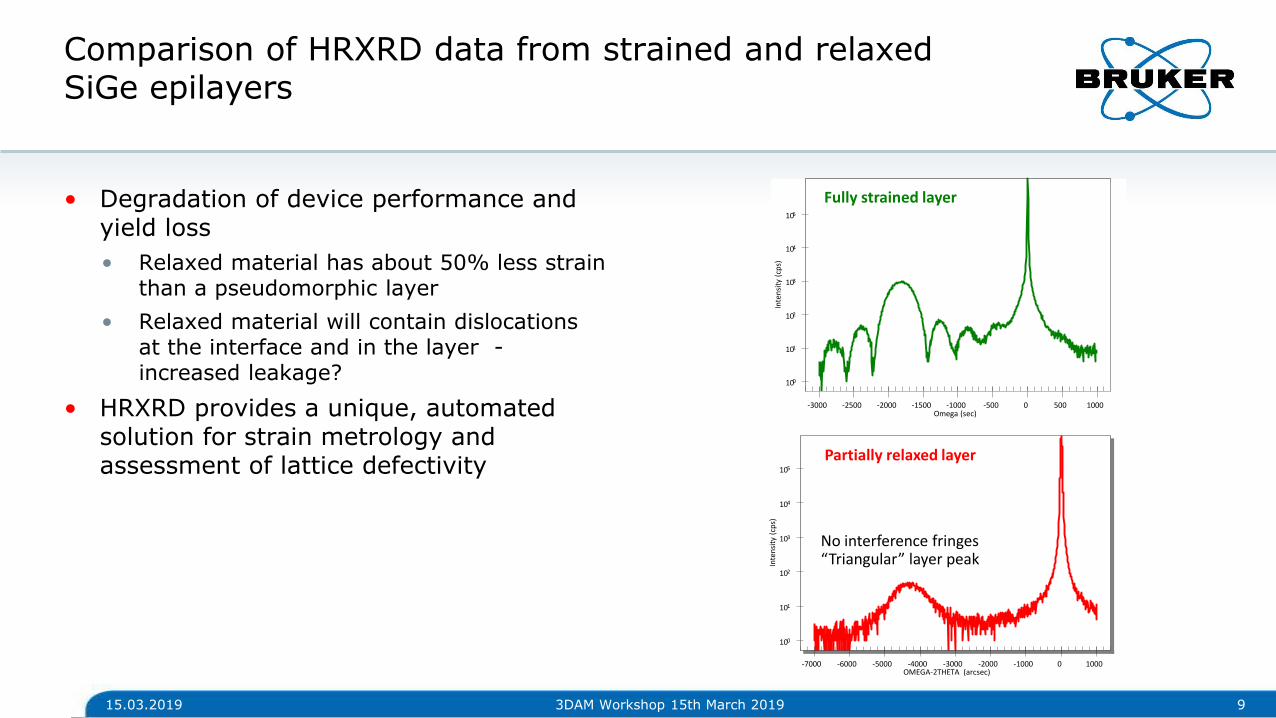
Comparison of HRXRD data from strained and relaxed SiGe epilayers
• Degradation of device performance and yield loss
• Relaxed material has about 50% less strain than a pseudomorphic layer
• Relaxed material will contain dislocations at the interface and in the layer -increased leakage?
• HRXRD provides a unique, automated solution for strain metrology and assessment of lattice defectivity
010
110
210
310
410
510
-7000 -6000 -5000 -4000 -3000 -2000 -1000 0 1000
Inte
nsi
ty (
cps)
OMEGA-2THETA (arcsec)
Partially relaxed layer
t ~ 350 Å (XRR), x > 50%
No interference fringes
“Triangular” layer peak
010
110
210
310
410
510
-3000 -2500 -2000 -1500 -1000 -500 0 500 1000
Inte
nsi
ty (
cps)
Omega (sec)
Fully strained layer
t = 492 Å, x = 19.6%
Interference fringes
No interference fringes“Triangular” layer peak
15.03.2019 93DAM Workshop 15th March 2019
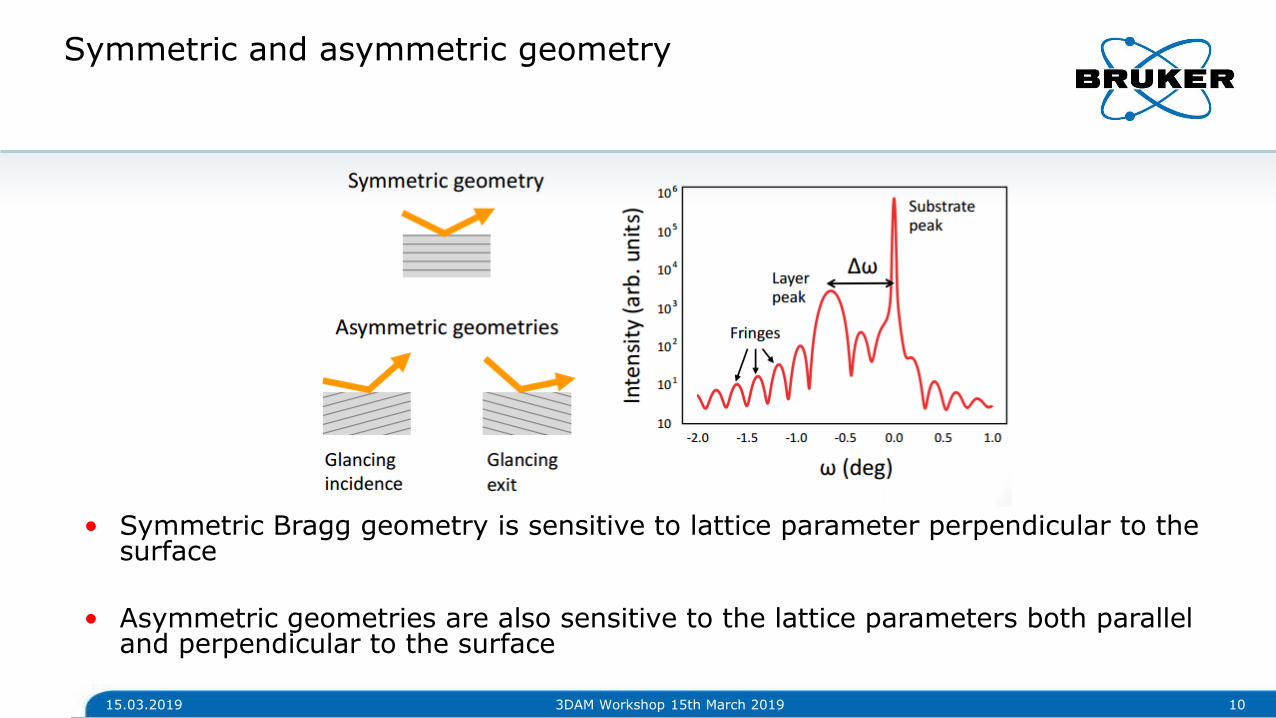
Symmetric and asymmetric geometry
15.03.2019 103DAM Workshop 15th March 2019
• Symmetric Bragg geometry is sensitive to lattice parameter perpendicular to the surface
• Asymmetric geometries are also sensitive to the lattice parameters both parallel and perpendicular to the surface
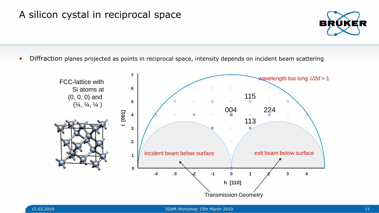
A silicon cystal in reciprocal space
• Diffraction planes projected as points in reciprocal space, intensity depends on incident beam scattering
3DAM Workshop 15th March 2019
FCC-lattice with
Si atoms at
(0, 0, 0) and
(¼, ¼, ¼ )
1-4 0-1-2-3 2 3 4
0
1
3
2
4
5
h [110]
l [
001]
6
7
incident beam below surface exit beam below surface
wavelength too long l/2d > 1
Transmission Geometry
224004
115
113
15.03.2019 11
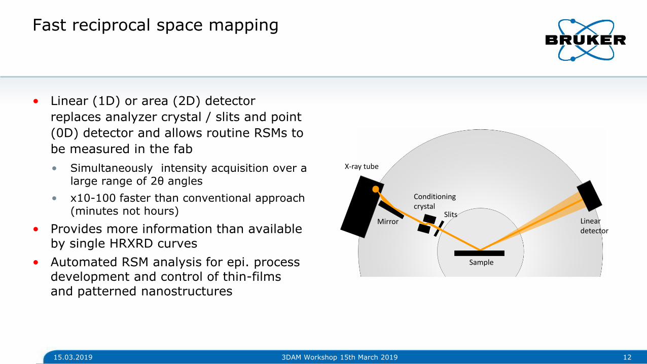
Fast reciprocal space mapping
• Linear (1D) or area (2D) detector
replaces analyzer crystal / slits and point
(0D) detector and allows routine RSMs to
be measured in the fab
• Simultaneously intensity acquisition over a large range of 2θ angles
• x10-100 faster than conventional approach (minutes not hours)
• Provides more information than available by single HRXRD curves
• Automated RSM analysis for epi. process development and control of thin-films and patterned nanostructures
X-ray tube
Conditioningcrystal
Slits
Sample
Mirror Linear detector
15.03.2019 123DAM Workshop 15th March 2019
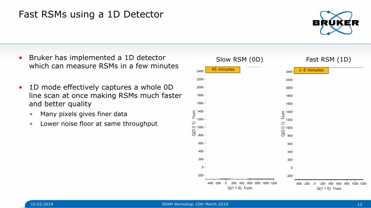
Fast RSMs using a 1D Detector
• Bruker has implemented a 1D detector which can measure RSMs in a few minutes
• 1D mode effectively captures a whole 0D line scan at once making RSMs much faster and better quality
• Many pixels gives finer data
• Lower noise floor at same throughput
15.03.2019 133DAM Workshop 15th March 2019
Slow RSM (0D) Fast RSM (1D)
45 minutes 1-5 minutes
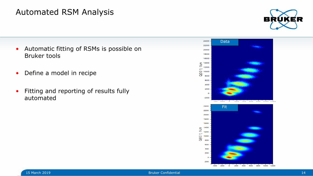
Automated RSM Analysis
• Automatic fitting of RSMs is possible on Bruker tools
• Define a model in recipe
• Fitting and reporting of results fully automated
15 March 2019 14Bruker Confidential
Data
Fit
SiGe fins etched a from blanket layer
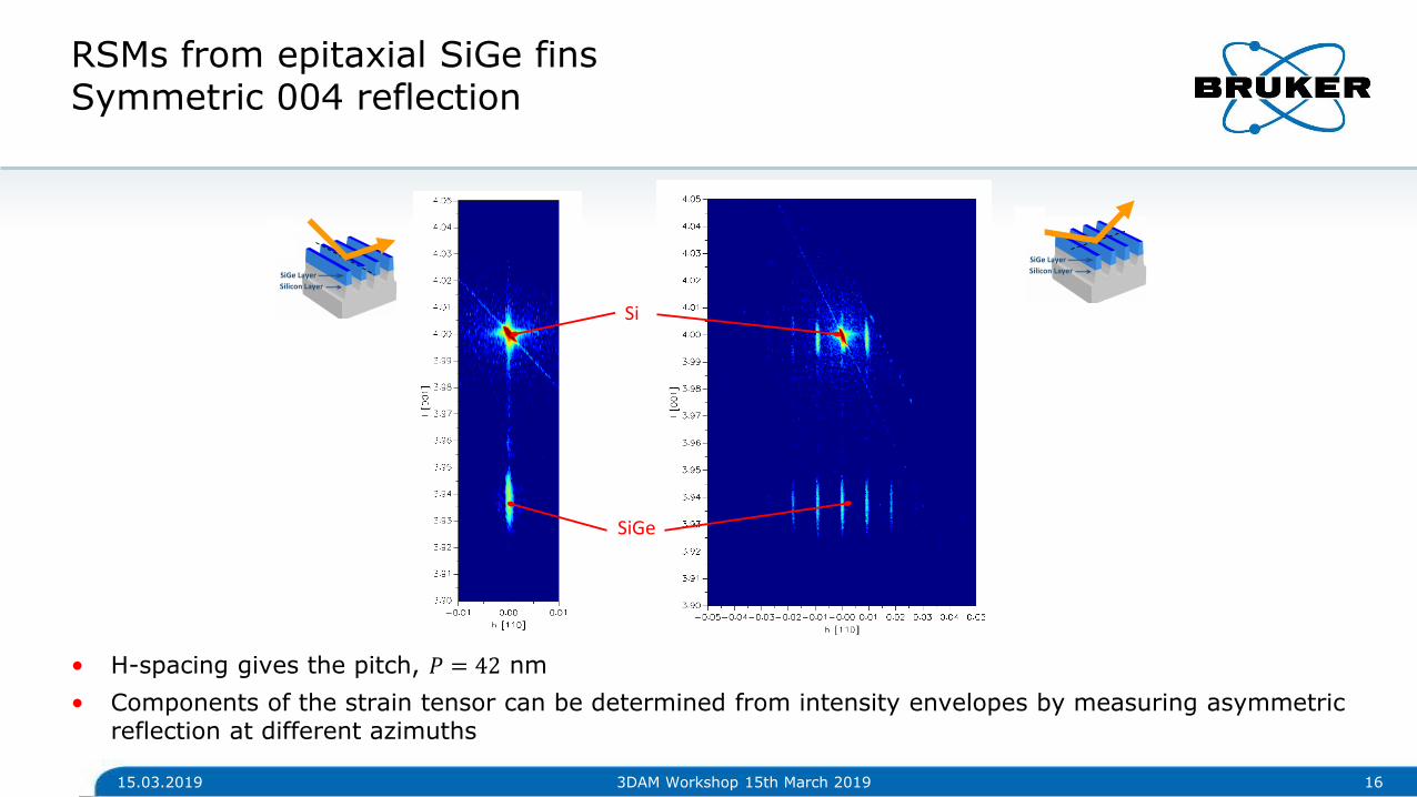
RSMs from epitaxial SiGe finsSymmetric 004 reflection
• H-spacing gives the pitch, 𝑃 = 42 nm
• Components of the strain tensor can be determined from intensity envelopes by measuring asymmetric reflection at different azimuths
15.03.2019 163DAM Workshop 15th March 2019
x1
x2
x3
Si fins SiGe fins
Thin-film Planar
(a) (b)
(c) (d)
x1
x2
x3
Si fins SiGe fins
Thin-film Planar
(a) (b)
(c) (d)
Si
SiGe
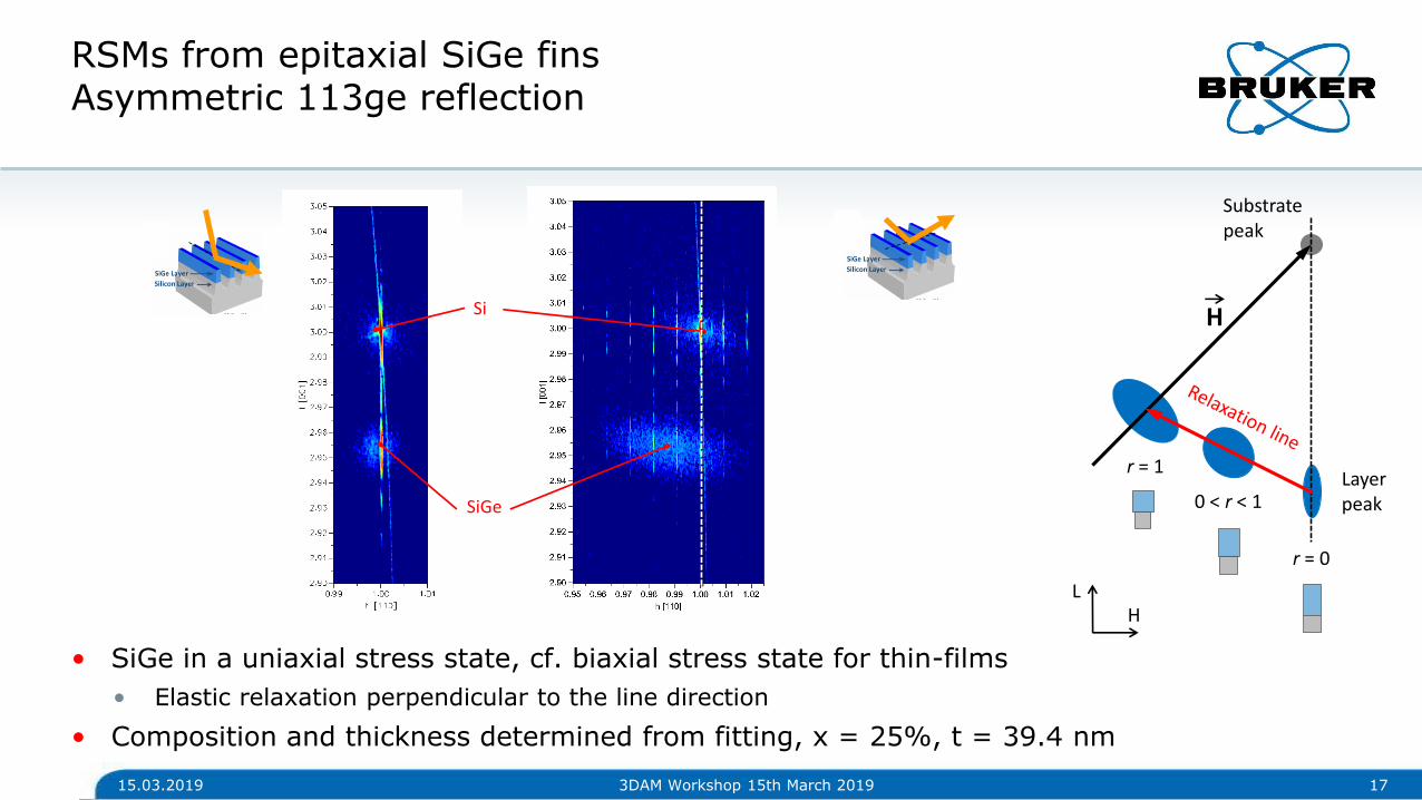
RSMs from epitaxial SiGe finsAsymmetric 113ge reflection
• SiGe in a uniaxial stress state, cf. biaxial stress state for thin-films
• Elastic relaxation perpendicular to the line direction
• Composition and thickness determined from fitting, x = 25%, t = 39.4 nm
15.03.2019 173DAM Workshop 15th March 2019
x1
x2
x3
Si fins SiGe fins
Thin-film Planar
(a) (b)
(c) (d)
x1
x2
x3
Si fins SiGe fins
Thin-film Planar
(a) (b)
(c) (d)
Si
SiGe
Substratepeak
Layerpeak
r = 1
r = 0
0 < r < 1
H
LH
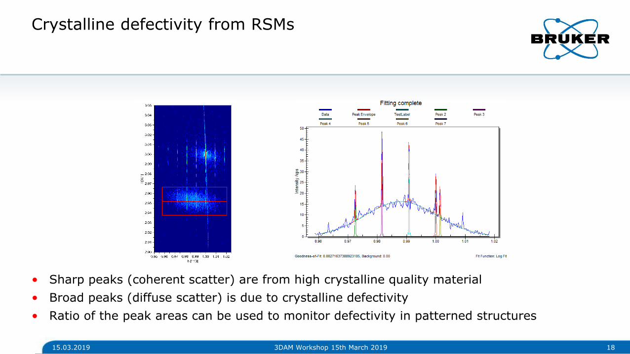
Crystalline defectivity from RSMs
• Sharp peaks (coherent scatter) are from high crystalline quality material
• Broad peaks (diffuse scatter) is due to crystalline defectivity
• Ratio of the peak areas can be used to monitor defectivity in patterned structures
15.03.2019 183DAM Workshop 15th March 2019
Selectively grown Ge/SiGe fins
Patterned epitaxial nanostructures
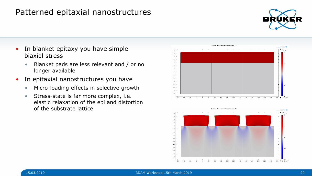
• In blanket epitaxy you have simple biaxial stress
• Blanket pads are less relevant and / or no longer available
• In epitaxial nanostructures you have
• Micro-loading effects in selective growth
• Stress-state is far more complex, i.e. elastic relaxation of the epi and distortion of the substrate lattice
15.03.2019 203DAM Workshop 15th March 2019
Ge/SiGe fins
• Compressive sGe can provide higher mobility than bulk Si for pFETs
• Two integration schemes for creating sGe have been studied
• Etching of thin, blanket Ge layer grown atop a thick blanket SiGe strain relaxed buffer (SRB) a few microns thickness to reduce the misfit dislocation density at the top of the SRB
• Selective growth of thin Ge on a relaxed SiGe buffer in narrow trenches patterned in STI. Extended defects are trapped by Aspect Ratio trapping (ART) mechanism and terminate at the STI sidewalls
• Selective growth scheme is favored for CMOS
• Allows co-integration with Si or III-V nFETs required for CMOS
15.03.2019 213DAM Workshop 15th March 2019
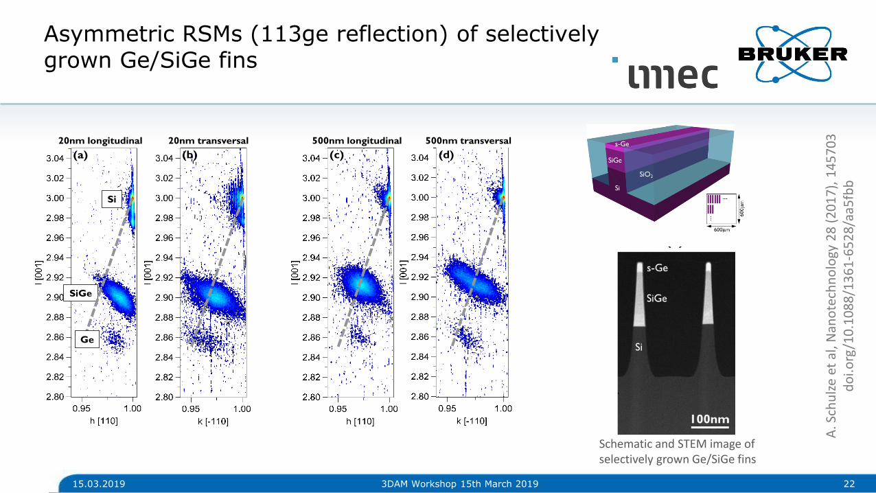
Asymmetric RSMs (113ge reflection) of selectively grown Ge/SiGe fins
15.03.2019 223DAM Workshop 15th March 2019
20nm longitudinal 20nm transversal 500nm longitudinal 500nm transversal
Si
SiGe
(a) (b) (c) (d)
Ge
Schematic and STEM image of selectively grown Ge/SiGe fins
A. S
chu
lze
et a
l, N
ano
tech
no
logy
28
(2
01
7),
14
57
03
do
i.org
/10
.10
88
/13
61
-65
28
/aa5
fbb
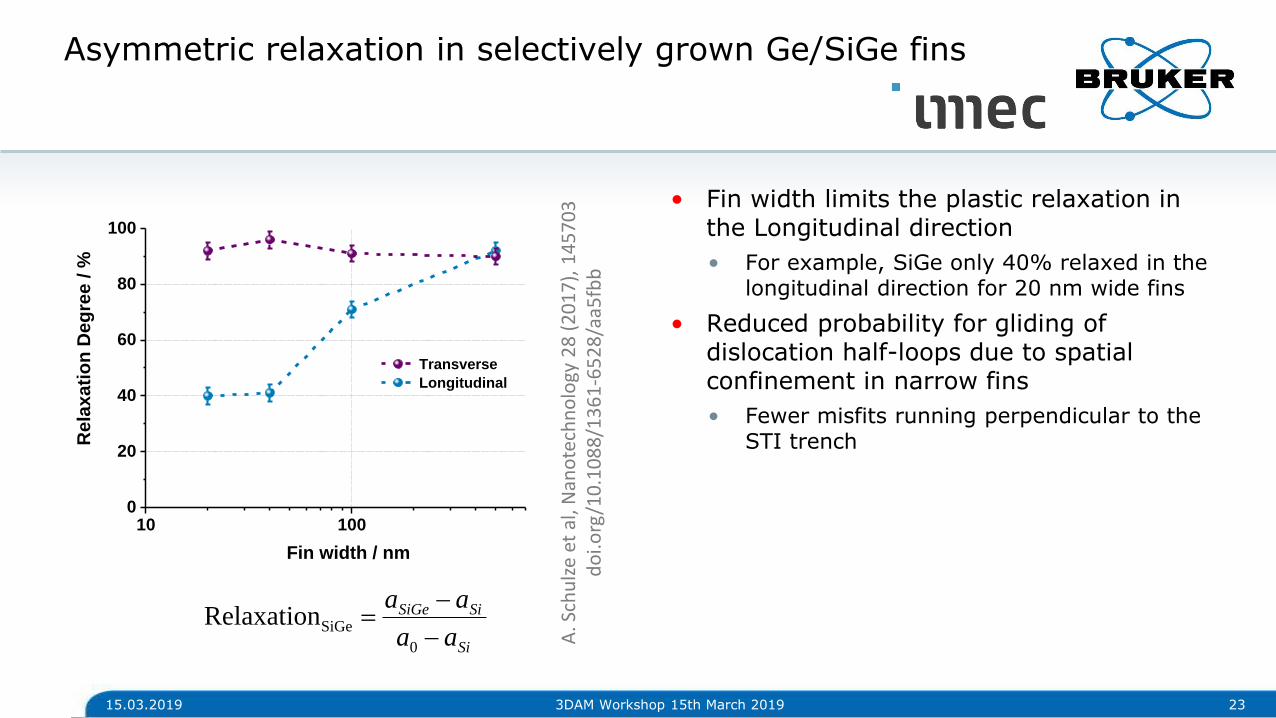
Asymmetric relaxation in selectively grown Ge/SiGe fins
10 1000
20
40
60
80
100
Transverse
Longitudinal
Re
lax
ati
on
De
gre
e / %
Fin width / nm
• Fin width limits the plastic relaxation in the Longitudinal direction
• For example, SiGe only 40% relaxed in the longitudinal direction for 20 nm wide fins
• Reduced probability for gliding of dislocation half-loops due to spatial confinement in narrow fins
• Fewer misfits running perpendicular to the STI trench
15.03.2019 233DAM Workshop 15th March 2019
Si
SiSiGe
aa
aa
0
SiGeRelaxation
A. S
chu
lze
et a
l, N
ano
tech
no
logy
28
(2
01
7),
14
57
03
do
i.org
/10
.10
88
/13
61
-65
28
/aa5
fbb
SiGe/Si for nanowire / nanosheet FETs

What device architecture comes after finFETs?
• New architecture after finFETs will likely be needed below 7 nm node
• Gate-all-around (GAA) architectures seem to be the most likely at this time
• Further improves electrostatic control and reduces short channel effects by wrapping the gate completely around the channel
• Shares many of the same process steps, materials and tools as finFETs
• Scaled finFETs incorporating sGe and III-V high-mobility channel materials are also being investigated
• Regardless, process complexity and costs will continue to escalate
• HRXRD is used for both R&D and production control of advanced logic technology
• Composition and strain metrology
15.03.2019 253DAM Workshop 15th March 2019
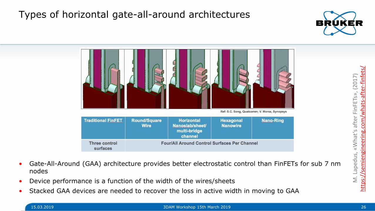
Types of horizontal gate-all-around architectures
• Gate-All-Around (GAA) architecture provides better electrostatic control than FinFETs for sub 7 nm nodes
• Device performance is a function of the width of the wires/sheets
• Stacked GAA devices are needed to recover the loss in active width in moving to GAA
15.03.2019 263DAM Workshop 15th March 2019
M. L
aped
us,
«W
hat
’s a
fter
Fin
FETs
», (
20
17
)h
ttp
s://
sem
ien
gin
eeri
ng.
com
/wh
ats-
afte
r-fi
nfe
ts/
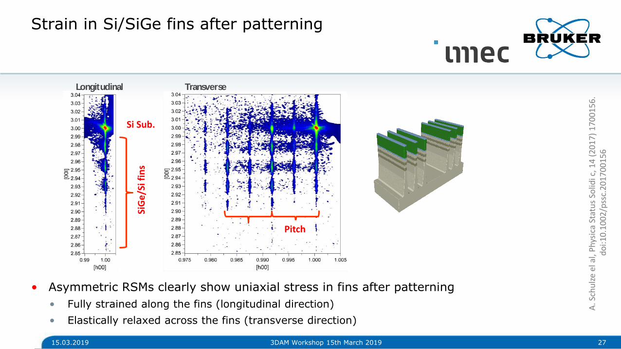
Strain in Si/SiGe fins after patterning
• Asymmetric RSMs clearly show uniaxial stress in fins after patterning
• Fully strained along the fins (longitudinal direction)
• Elastically relaxed across the fins (transverse direction)
15.03.2019 273DAM Workshop 15th March 2019
TransverseLongitudinal
Pitch
Si Sub.
SiG
e/S
i fin
s
Pitch
A. S
chu
lze
el a
l, P
hys
ica
Stat
us
Solid
i c, 1
4 (
20
17
) 1
70
01
56
. d
oi:1
0.1
00
2/p
ssc.
20
17
00
15
6
e 28
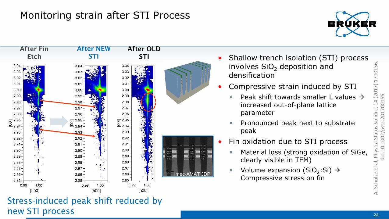
After NEW
STI
After Fin
Etch
Imec-AMAT JDP
After OLD
STI
Monitoring strain after STI Process
Stress-induced peak shift reduced by
new STI process
• Shallow trench isolation (STI) process involves SiO2 deposition and densification
• Compressive strain induced by STI
• Peak shift towards smaller L values
increased out-of-plane lattice parameter
• Pronounced peak next to substrate peak
• Fin oxidation due to STI process
• Material loss (strong oxidation of SiGe, clearly visible in TEM)
• Volume expansion (SiO2:Si)
Compressive stress on fin
A. S
chu
lze
el a
l, P
hys
ica
Stat
us
Solid
i c, 1
4 (
20
17
) 1
70
01
56
. d
oi:1
0.1
00
2/p
ssc.
20
17
00
15
6
Conclusions
• High-resolution XRD delivers valuable information on epitaxial thin-films and arrays of nanostructures
• Materials include: SiGe, Si:C(P), Ge and III-Vs for current and future technology nodes
• Parameters (depending on sample) include: strain / stress components, composition, thickness, pitch, pitch-walk, crystalline quality…
• Complements traditional techniques such as SE / scatterometry and SEM / TEM
• The latest generation of lab / fab tools can yield good quality data in minutes not several hours
• From patterned wafers with a 50 μm spot-size
• Including reciprocal space mapping using linear detectors
• In-line X-ray metrology tools, enable materials and process development and production monitoring for advanced logic and other applications
15.03.2019 293DAM Workshop 15th March 2019

© Copyright Bruker Corporation. All rights reserved.
www.bruker.com