high frequency surface acoustic waves excited on thin oriented linbo3 single crystal layers...
TRANSCRIPT

870 ieee transactions on ultrasonics, ferroelectrics, and frequency control, vol. 54, no. 4, april 2007
High-Frequency Surface Acoustic WavesExcited on Thin-Oriented LiNbO3
Single-Crystal Layers Transferred Onto SiliconThomas Pastureaud, Marc Solal, Member, IEEE, Beatrice Biasse, Bernard Aspar, Jean-Bernard Briot,
William Daniau, William Steichen, Raphael Lardat, Vincent Laude, Member, IEEE, Alain Laens,Jean-Michel Friedt, and Sylvain Ballandras
Abstract—The need for high-frequency, wide-band filtershas instigated many developments based on combining thinpiezoelectric films and high acoustic velocity materials (sap-phire, diamond-like carbon, silicon, etc.) to ease the man-ufacture of devices operating above 2 GHz. In the presentwork, a technological process has been developed to achievethin-oriented, single-crystal lithium niobate (LiNbO3) lay-ers deposited on (100) silicon wafers for the fabrication ofradio-frequency (RF) surface acoustic wave (SAW) devices.The use of such oriented thin films is expected to favorlarge coupling coefficients together with a good control ofthe layer properties, enabling one to chose the best combi-nation of layer orientation to optimize the device. A theo-retical analysis of the elastic wave assumed to propagate onsuch a combination of material is first exposed. Technologi-cal aspects then are described briefly. Experimental resultsare presented and compared to the state of art.
I. Introduction
Because the early developments of surface acousticwave (SAW) devices [1], many advances have been
achieved to answer the continuous demand for components(filters, resonators) exhibiting improved properties (lowlosses, large bandwidth, strong rejection, high-spectral pu-rity, etc.). These improvements were required because ofthe increased capabilities of electronic systems integratingthese passive devices to handle more and more data withenhanced information flows. Particularly in the telecom-munication domain, the researchers and engineers mustprovide a significant effort to innovate and answer the de-mand for high-frequency, wide-band filters.
Manuscript received April 3, 2006; accepted October 27, 2006. Thiswork was partly supported by the French National Network for Re-search in Communication (RNRT) as the OASIS project under grant#98 S 0324.
T. Pastureaud, W. Steichen, J.-B. Briot, R. Lardat, and A. Laensare with TEMEX, F-06904 Sophia-Antipolis Cedex, France.
M. Solal is with SAWTEK Inc., Orlando, FL.B. Biasse is with the Comissariat a l’Energie Atomique (CEA)-
DRT—Laboratoire d’Electronique et de Traitement de l’InformationF-38054 Grenoble Cedex 9, France.
B. Aspar is CEO of TRACIT, Grenoble, France.J.-M. Friedt is with SENSEOR, F-06904 Sophia-Antipolis Cedex,
France.W. Daniau, V. Laude, and S. Ballandras are with the Institut
FEMTO-ST, UMR CNRS 6174, UFC-ENSMM-UTBM, F-25044 Be-sancon Cedex, France (e-mail: [email protected]).
Digital Object Identifier 10.1109/TUFFC.2007.321
In this context, a lot of work has been devoted to thefabrication of radio-frequency (RF) passive devices builton layered substrates, taking advantage of the combinationof piezoelectric layers and high acoustic velocity materialslike sapphire, carbon-diamond thick layers or silicon [1],[2]. Those piezoelectric layers generally are obtained us-ing sputtering or various chemical vapor deposition tech-niques, generally providing C-oriented films with mod-erately controlled piezoelectric properties. Furthermore,most of these deposition techniques requires specific sub-strate orientations, or at least buffer layers (for instanceplatinum, titanium, etc.) for lattice matching reasons.
Many results have been published concerning AlN, ZnOor even lithium niobate (LiNbO3) layers on the above-mentioned substrates, and some advances have been re-ported on crystal orientation control these very last years[3]–[5]. However, surface wave devices built along thisapproach poorly fit the RF filter requirements in termsof electromechanical coupling (always smaller than 5%),propagation losses and frequency stability simultaneously.
Especially for LiNbO3 (but also for most of the highlycoupled piezoelectric materials), the deposition of C-oriented layers does not provide the best configurationfor the excitation of SAW, yielding coupling coefficientsfor both Rayleigh and shear polarized waves much smallerthan those of SAW propagating on standard, single-crystalcuts as YZ or (YXl)/128 LiNbO3 or even (YXl)/42
lithium tantalate (LiTaO3).In this work, we use a layer transfer process in-
vented at Comissariat a l’Energie Atomique-Directionde la Recherche Technologique-Laboratoire d’Electroniqueet des Technologies de l’Information (CEA-DRT-LETI)based on ion implantation and direct wafer bonding to ob-tain oriented piezoelectric layers on (100) silicon. The com-bination of LiNbO3 and silicon is particularly consideredfor the excitation and propagation of highly coupled shearwaves (the most preferred solution for RF applications). Inthis process, a very good adhesion between LiNbO3 andsilicon is achieved, without any intermediate layer. The ad-hesion force is found to be compatible with acoustic waveguide applications.
In the first section of this article, theoretical predictionsof elastic waves excited and guided in the considered struc-ture [i.e., (YX) LiNbO3 on (100) silicon] are reported. Thesecond part of the paper is dedicated to the main tech-
0885–3010/$25.00 c© 2007 IEEE

pastureaud et al.: high frequency saw and single-crystal layers on silicon 871
Fig. 1. Scheme of the general geometry of the addressed problem.
nological aspects of the developed process. Experimentalmeasurements of guided elliptic and shear polarized waveson four-inches (YX) LiNbO3/(100) silicon wafers are ex-posed and compared to theoretical predictions. These mea-surements have been performed using 1 and 2 GHz single-port resonators allowing for an accurate characterization ofthe wave-guide in terms of phase velocity, electromechani-cal coupling, electrode grating reflection, and propagationlosses. Some particular properties of the corresponding de-vices are also reported. Experimental results are discussedregarding theoretical predictions, as well as the best re-sults obtained for SAW devices on silicon-based, layeredsubstrates.
II. Theoretical Analysis
The analysis of the combination of oriented LiNbO3(YX) thin layer on (100) silicon takes advantage of allthe developments previously presented for layered struc-tures [6]. A stable scattering-matrix method [7] is usedto compute the Green’s function and the surface permit-tivity of the multilayer. Included in a mixed finite el-ement/boundary integral Method (FEA/BIM) approach[6], the harmonic admittance then is calculated. Amongall standard LiNbO3 crystal orientations [namely, (YX),(YXl)/41, (YXl)/64 and (YXl)/128 cuts], the (YX) cutwas found to be the most interesting solution for shearwave guiding because of its large coupling coefficient andphase velocity. The leaky shear wave on (YX) cut is knownto exhibit a strong leakage, expected to be suppressed bythe guiding effect. The general geometry of the problem isdepicted in Fig. 1. As shown further, elastic wave guidesbuilt using thin LiNbO3 layers atop silicon can supportRayleigh-like wave as well as shear wave propagation, thelater being particularly considered in this work.
Silicon (100) is particularly well suited for fabricatingelastic shear wave guides because transversely polarizedbulk acoustic waves exhibits velocity propagation in thevicinity of 5800 m/s, larger than shear polarized leaky-SAWs on any singly rotated LiNbO3. Nevertheless, it alsois reasonably low to avoid large acoustic mismatches be-
tween the layer and the substrate, yielding a too strongdependence of the wave characteristics (particularly thephase velocity and the electromechanical coupling) on thepiezoelectric layer thickness. Three different electrical con-ditions have been considered at the interface between theLiNbO3 thin layer and the silicon wafer. Silicon is firstassumed intrinsic (dielectric) or ideally conductive (metal-like), then its actual conductivity is taken into account.This later point is achieved considering the following rela-tions between the electric field Ei and the electrical chargeρ in silicon:
σ div.E + jωρ = 0 and ε div.E = ρ. (1)
This relation yields the definition of an effective dielec-tric constant pointing out the effect of silicon conductivityas an equivalent frequency-dependent source of dielectriclosses:
εeff = ε − jσ
ω. (2)
These relations can be exploited for both effective per-mittivity and harmonic admittance approaches that havebeen used in the present study to predict wave charac-teristics. The first parameter allows one to first identifythe best operating conditions in regard with wave guiding.The second is preferably used to predict actual electricalproperties of the guided wave (coupling, velocity, reflec-tion, directivity, losses).
The computations have been performed using the Smithand Welsh data set for LiNbO3 [8], and elastic characteris-tics of silicon as given in Landolt-Bornstein tables [9]. Theresults are reported in Fig. 2, showing the evolution of themain characteristics of the second guided mode (shear po-larized), extracted from the effective permittivity, versusLiNbO3 thickness considering intrinsic (a) or conductive(b) silicon. In both cases, an optimal frequency-thicknessproduct f.t can be found to take advantage of the largestcoupling coefficient [more than 20% in the case of (YX)LiNbO3/(100) intrinsic silicon]. One can easily see that, fora given operating frequency, the optimal LiNbO3 thicknessis smaller when using intrinsic silicon rather than conduc-tive silicon. In the frequency range 1–2 GHz, the typicalLiNbO3 thickness should be equal to 0.75 µm for intrinsicsilicon, but it should be more than 2 µm for conductivesilicon. However, the velocity dispersion is smaller in thelater case than it is for intrinsic silicon-based devices.
The case of partially conducting silicon then is ad-dressed separately. Due to the piezoelectric coupling ofLiNbO3, the electrical field associated with the wave ex-citation and propagation within the piezoelectric layer—and which penetrates into the silicon—is strong enoughto generate an electric current within the semiconduc-tor substrate. This later drains a part of the energy ofthe guided wave, yielding propagation losses. The evolu-tion of these losses, of the electromechanical coupling andthe phase velocity versus silicon resistivity is reported inFigs. 3 and 4 for different frequency-thickness products(0.5 and 1 GHz.µm or km.s−1 respectively) close to the

872 ieee transactions on ultrasonics, ferroelectrics, and frequency control, vol. 54, no. 4, april 2007
Fig. 2. Velocity and coupling coefficient of shear polarized wave on(YX)LiNbO3/(100) Si (a) intrinsic (b) perfectly conductive, resultsextracted from effective permittivity.
ones tested experimentally. One can see that intermedi-ate situations between conductive and intrinsic substratesshould be avoided to minimize propagation losses.
In order to try and benefit from the largest acces-sible coupling factor, and considering technology con-straints about LiNbO3 thickness, the combination of high-resistivity silicon (typically 1 kΩ.cm) and (YX) LiNbO3would be preferred for the fabrication of experimentaltest devices. Practically, tests were most of the time per-formed on available standard conductivity silicon wafers(14 Ω.cm). As shown by theoretical predictions, it is nota very favorable working point, but experimental resultsshow that, in such a configuration, the losses due to sub-strate conductivity are not large enough to prevent eitherthe propagation or the accurate characterization of themode. The harmonic admittance of the stratified struc-ture [10] also has been computed for these configurationsto identify the most important parameters of the wave (ve-locity, coupling coefficient, propagation losses, reflectioncoefficient, and directivity) and to compare them to ex-perimental measurements in the next section. We also havecomputed the sensitivity S of the wave velocity V versusthe LiNbO3 thickness t, defined as the ratio of the rela-tive velocity change versus the relative error on thickness(∆V/V = S×∆t/t). Values of 22% and 13% were found forf.t products, respectively, equal to 1 and 2 GHz.µm. Evenif not negligible, one can consider these operating pointsas moderately sensitive to the LiNbO3 layer thickness.
Fig. 3. Evolution of the propagation losses, coupling coefficient andphase velocity versus the silicon resistivity-shear polarized wave on(YX)LiNbO3/(100), f.t = 1 GHz.µm.
III. Experiments
A. Technological Aspects
The transfer process is mainly based on an ion im-plantation step followed by a direct wafer bonding [11].It is comparable to the UNIBONDTM process developedby SOITEC (Grenoble, France). It can be decomposed infour major steps, as shown in Fig. 5:
• Ion implantation is performed in the LiNbO3 wafer.This step induces formation of an in-depth weakenedlayer.
• The LiNbO3 wafer is bonded to a silicon wafer by di-rect wafer bonding.
• The splitting step is thermally induced in the weak-ened layer [see Fig. 6(a)].
• The rough surface left after splitting is removed bysoft-touch polishing [see Fig. 6(b)].
This process has been successfully implemented, provid-ing almost perfectly transferred LiNbO3 layer on a 4-inchsilicon wafer (see Fig. 7).
Single-port synchronous resonators have been used tocharacterize the two first modes excited in the compound(YX) LiNbO3/(100) silicon wave guide. The inter-digital

pastureaud et al.: high frequency saw and single-crystal layers on silicon 873
Fig. 4. Evolution of the propagation losses, coupling coefficient, andphase velocity versus the silicon resistivity-shear polarized wave on(YX)LiNbO3/(100), f.t = 2 GHz.µm.
transducer (IDT) was composed of 100 finger pairs, with50 strip in the mirror. The grating periods were 2 and 1 µm(yielding acoustic wavelengths, respectively, equal to 4 and2 µm), the electrode height was set to 100 nm (h/2p =2.5% and 5%), and the metallization ratio a/p = 0.5 at1 GHz and 0.4, 0.5, and 0.6 at 2 GHz. Different attemptshave been performed according to technological advance-ments, providing a wide set of experimental results.
B. Experiments at 1 GHz
As shown in Fig. 7, the optimization of the process en-abled the transfer of a 0.5-µm thick (YX) LiNbO3 layer on4-in. silicon wafers (silicon resistivity still about 14 Ω.cm).A first set of experiments has been performed, takingadvantage of these wafers compatible with the TEMEX(Sophia Antipolis, France) product line. SAW devices con-sequently were manufactured using the TEMEX stan-dard process (stepper 5X and dry etching of the Al elec-trodes). Once the devices achieved, they were tested ona Suss Microtec (Saint-Jeoire, France) RF probe station(Fig. 8), and a fit procedure of the two guided modesusing a mixed-matrix model [12] was used to extractthe effective propagation parameters from the electrical
Fig. 5. Principle of the fabrication process of LiNbO3/silicon com-pounds.
(a) (b)
Fig. 6. XTEM views of the LiNbO3 layer after splitting (a) and touchpolishing (b).
Fig. 7. Photo of a 4-in. wafer with almost perfectly transferred Y-cutLiNbO3 top layer.
874 ieee transactions on ultrasonics, ferroelectrics, and frequency control, vol. 54, no. 4, april 2007
Fig. 8. Admittance of the 1 GHz devices.
measurements. The effective mixed-matrix parameters ofthe Rayleigh-like mode have been found similar to thetheoretical predictions: the wave actually propagates at4198 m.s−1 and exhibits a coupling factor K2
s of 2.0%.The temperature dependence of the resonator on this modeleads to a first order temperature coefficient of frequency(TCF = −42 ppm/K) very close to what is expected(−38 ppm/K). However, the phase velocity of the shearmode was found significantly different from the theoreticalcalculations (experimental velocity 4384 m.s−1 comparedto 4825 m.s−1 theoretically predicted) [13]. But the elec-tromechanical coupling coefficient as well as the reflectioncoefficient are closer to theoretical predictions (K2
s ∼ 6%and |R| ∼ 7.7% compared to 7 and 9.3%, respectively).The temperature dependence of the shear mode of theresonator has been measured as well, and leads to a TCFequal to −40 ppm/K, smaller than the theoretical pre-dictions. It should be noted also that, due to variations ofsilicon conductivity with incident light intensity, photosen-sitive phenomena also were observed. The best Q-factorswere consequently measured with no light sources. All thewave characteristics were found larger than those alreadyobtained with most of the piezoelectric thin films depositedon silicon.
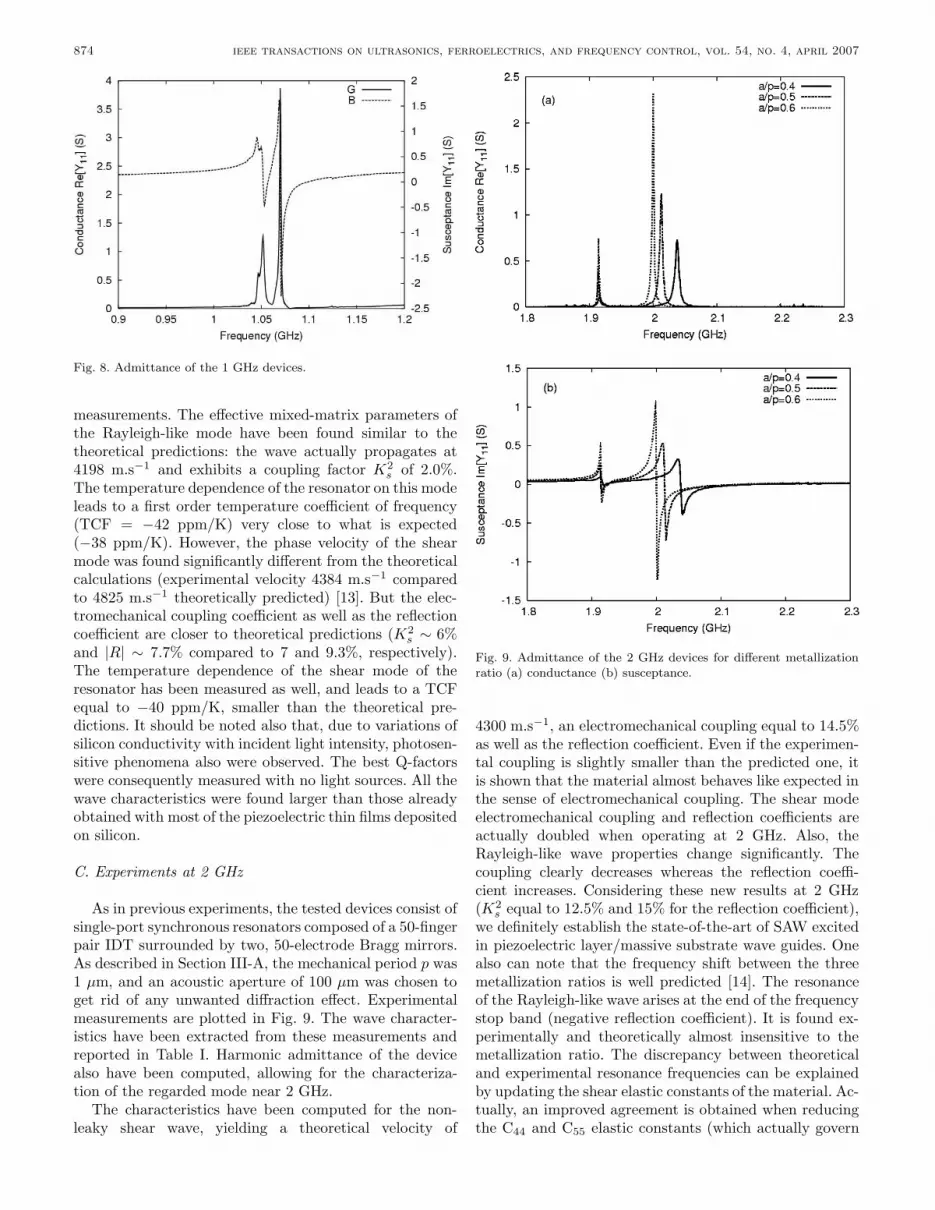
C. Experiments at 2 GHz
As in previous experiments, the tested devices consist ofsingle-port synchronous resonators composed of a 50-fingerpair IDT surrounded by two, 50-electrode Bragg mirrors.As described in Section III-A, the mechanical period p was1 µm, and an acoustic aperture of 100 µm was chosen toget rid of any unwanted diffraction effect. Experimentalmeasurements are plotted in Fig. 9. The wave character-istics have been extracted from these measurements andreported in Table I. Harmonic admittance of the devicealso have been computed, allowing for the characteriza-tion of the regarded mode near 2 GHz.
The characteristics have been computed for the non-leaky shear wave, yielding a theoretical velocity of
Fig. 9. Admittance of the 2 GHz devices for different metallizationratio (a) conductance (b) susceptance.
4300 m.s−1, an electromechanical coupling equal to 14.5%as well as the reflection coefficient. Even if the experimen-tal coupling is slightly smaller than the predicted one, itis shown that the material almost behaves like expected inthe sense of electromechanical coupling. The shear modeelectromechanical coupling and reflection coefficients areactually doubled when operating at 2 GHz. Also, theRayleigh-like wave properties change significantly. Thecoupling clearly decreases whereas the reflection coeffi-cient increases. Considering these new results at 2 GHz(K2
s equal to 12.5% and 15% for the reflection coefficient),we definitely establish the state-of-the-art of SAW excitedin piezoelectric layer/massive substrate wave guides. Onealso can note that the frequency shift between the threemetallization ratios is well predicted [14]. The resonanceof the Rayleigh-like wave arises at the end of the frequencystop band (negative reflection coefficient). It is found ex-perimentally and theoretically almost insensitive to themetallization ratio. The discrepancy between theoreticaland experimental resonance frequencies can be explainedby updating the shear elastic constants of the material. Ac-tually, an improved agreement is obtained when reducingthe C44 and C55 elastic constants (which actually govern

pastureaud et al.: high frequency saw and single-crystal layers on silicon 875
TABLE ITheory-Experiment Assessment for Rayleigh and Shear Wave Characteristics on (YX)LiNbO3/Standard Resistivity Silicon
for a f.t Product Equal to 0.5 and 1 GHz.µm.1
ThermalVelocity Coupling sensitivity
(metallized) coefficient Reflectivity (TCF1)m.s−1 % % ppm/K
Rayleigh at 1 GHz (theory) a/p = 0.5, h/λ = 2.5% 4163 2.15 0.39 (90) −38Rayleigh at 1 GHz (experiments) 4198 2.0 0.4 (90) −42
Rayleigh at 2 GHz (theory) a/p = 0.6, h/λ = 5% 3749 1.7 2.83 (90) −43Rayleigh at 2 GHz (experiments) 3777 1.3 4.2 (90) —
Shear at 1 GHz (theory) a/p = 0.5, h/λ = 2.5% 4825 7.0 9.3 −65Shear at 1 GHz (experiments) 4384.5 6 7.7 (0) −40
Shear at 2 GHz (theory) a/p = 0.6, h/λ = 5% 4311 15.4 15.85 (0) −75Shear at 2 GHz (experiments) 4200 12.5 15 (0) −50
1Theoretical data computed using Smith and Welsh’s coefficients for LiNbO3 [8].
the shear wave velocity) from 10% of their initial values(55 GPa instead of 59.5 GPa). Because these coefficientsinfluence the Rayleigh wave too, the C66 elastic constantalso was increased by an amount of 10% of its initial value(80.85 GPa instead of 72.85 GPa), yielding a good match-ing between theoretical and experimental resonance fre-quencies. Also, a better agreement is obtained when as-suming a smaller silicon resistivity (ρ = 0.1 Ω.cm) thanthe one previously considered (14 Ω.cm). The theoreti-cal previsions considering these parameters are reportedin Fig. 10.
We also have measured the first order TCF of the non-leaky shear mode. This result is reported in Fig. 11. Theprevious TCF characterizations, which were performed onsmall LiNbO3/Si parts, did provide a value of −40 ppm/K(section B), which was twice smaller as expected theoret-ically. In the set of experiments performed at 2 GHz, theTCF is found in the range of −50 ppm/K (see Fig. 11).Such a value also is quite different from theoretical pre-dictions, and it tends to indicate either that the theoreti-cal assumptions of the TCF calculation do not match thereal situation, or that some thermoelastic properties areaffected by the bonding process. The second hypothesisis coherent with the fact that discrepancies still persistbetween theory and experiment concerning the phase ve-locities of the nonleaky shear guided wave. Table I sum-marized all the experimental data for the different modes,compared with theoretical predictions.
IV. Conclusions
A novel technological process has been developedand successfully tested for the transfer of single-crystal,LiNbO3-oriented layers on (100) silicon. Four-inch wafershave been achieved, allowing the fabrication of SAW de-vices using industrial techniques. Using a standard con-ductivity silicon substrate almost behaving like a conduc-
Fig. 10. Theoretical harmonic admittance corresponding to the ex-perimental devices of Fig. 11 after updating the LiNbO3 elastic con-stant (a) conductance (b) susceptance.

876 ieee transactions on ultrasonics, ferroelectrics, and frequency control, vol. 54, no. 4, april 2007
Fig. 11. Temperature coefficients of frequency of the 2 GHz res-onators.
tive one, a good agreement is found between theoreticallypredicted and experimental electromechanical coupling co-efficient of the nonleaky shear wave (the second mode ofthe structure). Two sets of resonators, respectively, oper-ating in the vicinity of 1 and 2 GHz have been fabricatedand characterized. The electromechanical coupling coeffi-cient of the nonleaky shear wave is doubled when mul-tiplying the operating frequency by a factor of 2, and areflection factor equal to 15% has been measured for the2 GHz resonators. Theoretical predictions of these char-acteristics are in good agreement with experiments. As aconsequence, improving the knowledge of the elastic prop-erties of the compound substrate remains the main dif-ficulty to enable the use of such substrates for real fil-tering applications. Moreover, as shown theoretically, thetested operating points are far from the optimal one con-sidering conductive silicon, corresponding to a frequency-thickness product equal to 3 GHz.µm. Consequently, wecan expect better results if using thicker niobate layers.Another way to benefit from the optimal operating con-ditions would consist in reducing the grating period (forinstance, a period of 0.2 µm and a film thickness equal to0.6 µm would yield operating frequencies close to 5 GHz).In both cases, technological difficulties have to be over-come, but one should note that the obtained character-istics are quite sufficient to address modern filter require-ments, yielding an interest for this above-integrated circuitsolution for integrated signal processing devices.
Acknowledgment
The authors would like to thank Jean-Michel Hode forhis efforts in setting up the project.
References
[1] D. L. Dreifus, R. J. Higgins, R. B. Henard, R. Almar, andL. P. Solie, “Experimental observation of high velocity pseudo-SAWs in ZnO/diamond/Si multilayers,” in Proc. IEEE Ultra-son. Symp., 1997, pp. 191–194.
[2] J. Lee, N. Little, T. Rabson, and M. Robert, “Thin-film Lithiumniobate on diamond-coated silicon substrates for surface acousticwave applications,” in Proc. IEEE Ultrason. Symp., 1999, pp.269–272.
[3] F. S. Hickernell, “Thin-film for SAW devices,” Int. J. High SpeedElectron. Syst., vol. 10, no. 3, pp. 603–652, 2000.
[4] H. Nakahata, A. Hachigo, K. Itakura, S. Fujii, and S. Shikata,“SAW resonators of SiO2/ZnO/diamond structure in GHzrange,” in Proc. IEEE Int. Freq. Contr. Symp., 2000, pp. 315–319.
[5] Y.-Y. Chen, T.-T. Wu, and T.-T. Chou, “Analysis of the fre-quency response of a dispersive IDT/ZnO/sapphire SAW filterusing effective permittivity and the coupling of modes model,” J.Phys. D, Appl. Phys., vol. 37, pp. 120–127, 2004.
[6] S. Ballandras, A. Reinhardt, V. Laude, A. Soufyane, S. Camou,W. Daniau, T. Pastureaud, W. Steichen, R. Lardat, M. Solal,and P. Ventura, “Simulations of surface acoustic wave devicesbuilt on stratified media using a mixed finite element/boundaryintegral formulation,” J. Appl. Phys., vol. 96, no. 12, pp. 7731–7741, 2004.
[7] T. Pastureaud, V. Laude, and S. Ballandras, “Stable scattering-matrix method for acoustic waves in piezoelectric multilay-ers,” Appl. Phys. Lett., vol. 80, pp. 2544–2546, 2002.
[8] R. T. Smith and F. S. Welsh, “Temperature dependence of elas-tic, piezoelectric, and dielectric constants of lithium tantalateand lithium niobate,” J. Appl. Opt., vol. 42, pp. 2219–2230,May 1971.
[9] Landolt-Bornstein, Numerical Data and Functional Relation-ships in Science and Technology. vol. 11, Group III, Crystal andSolid State Physics K. H. Hellwege and A. M. Hellwege, Eds.Berlin: Springer-Verlag, 1979.
[10] S. Ballandras, A. Reinhardt, V. Laude, A. Soufyane, S. Camou,W. Daniau, T. Pastureaud, W. Steichen, R. Lardat, M. Solal,and P. Ventura, “Simulations of surface acoustic wave devicesbuilt on stratified media using a mixed finite element/boundaryintegral formulation,” J. Appl. Phys., vol. 96, no. 12, pp. 7731–7741, 2004.
[11] B. Aspar, H. Moriceau, E. Jalaguier, C. Lagahe, A. Soubie, B.Biasse, A. M. Papon, A. Claverie, J. Grisolia, G. Benassayag, F.Letertre, O. Rayssac, T. Barge, C. Maleville, and B. Ghyselen,J. Electron. Mater., vol. 30, no. 7, pp. 834–838, 2001.
[12] J. M. Hode, J. Desbois, P. Dufilie, M. Solal, and P. Ventura,“SPUDT-based filters: Design, principles and optimization,” inProc. IEEE Ultrason. Symp., 1995, pp. 39–47.
[13] M. Solal, T. Pastureaud, S. Ballandras, B. Aspar, B. Biasse, W.Daniau, W. Steichen, V. Laude, and A. Laens, “Oriented lithiumniobate layers transferred on 4′′ (100) silicon wafer for RF SAWdevices,” in Proc. IEEE Ultrason. Symp., 20022, pp. 128–131.
[14] T. Pastureaud, B. Biasse, B. Aspar, W. Daniau, W. Steichen,V. Laude, R. Lardat, A. Laens, J.-B. Briot, J.-M. Friedt, and S.Ballandras, “New theoretical and experimental results on highfrequency surface acoustic waves excited on oriented LiNbO3single crystal layers transferred onto silicon,” in Proc. IEEE Ul-trason. Symp., vol. 2, pp. 930–933, 2005.