hef memory - baixardoc
TRANSCRIPT
2 200114 4 MMiiccrroocchhiip p TTeecchhnnoollooggy y IInncc.. DDSS0000000011667733AA--ppaagge e 11
AN1673 AN1673
INTRODUCTIONINTRODUCTION
The PIC16F1XXX family of general purpose FlashThe PIC16F1XXX family of general purpose Flash
microcontrollers features the 8-bit PICmicrocontrollers features the 8-bit PIC®® MCUMCU
enhanced mid-range core. Carefully tradingenhanced mid-range core. Carefully trading
functionality versus cost, several members of thisfunctionality versus cost, several members of this
family, including the PIC16F14XX, PIC16F15XX andfamily, including the PIC16F14XX, PIC16F15XX and
PIC16F17XX, have made a departure from the usualPIC16F17XX, have made a departure from the usual
set of peripherals found in set of peripherals found in previous models to achieveprevious models to achieve
a lower price point while still offering a compelling newa lower price point while still offering a compelling new
set of features. Among the several new peripheralsset of features. Among the several new peripherals
introduced, it is worth noting:introduced, it is worth noting:
•• ConfConfiguraigurable Logible Logic Cell – a sc Cell – a small small set of loget of logicic
blocks (unlike a small PLD) that can hblocks (unlike a small PLD) that can help directlyelp directly
interconnect various interconnect various peripherals inputs/outputsperipherals inputs/outputs
without CPU without CPU intervention.intervention.
•• CompComplemenlementary Otary Outpuutput Generat Generator – the frtor – the front endont end
of a traditional PWM module, now decoupled fromof a traditional PWM module, now decoupled from
the timing generator and, therefore, available forthe timing generator and, therefore, available for
direct connection to other direct connection to other modules (includingmodules (including
analog comparators).analog comparators).
•• NumerNumericalically Controly Controlled Osclled Oscillatillator – a or – a frequfrequencyency
synthesizsynthesizer that allows linear control er that allows linear control of theof the
frequency output.frequency output.
•• High-High-EndurEndurance Flance Flash (HEFash (HEF) Block – rep) Block – replacilacingng
the data EEPROM present on previous modelsthe data EEPROM present on previous models
with a block of Flash memory that is with a block of Flash memory that is ensured toensured to
provide the same high endurance (100,000 erase/provide the same high endurance (100,000 erase/
write cycles).write cycles).
This application note This application note illustrates the benefits offered byillustrates the benefits offered by
the high-endurance Flash block and the high-endurance Flash block and describes a smalldescribes a small
C library which allows a simple and safe use of itsC library which allows a simple and safe use of its
capabilities.capabilities.
FLASH VS. HIGH-ENDURANCEFLASH VS. HIGH-ENDURANCEFLASHFLASH
Like most other PIC microcontrollers in FlashLike most other PIC microcontrollers in Flash
technology, the PIC16F1XXX series features atechnology, the PIC16F1XXX series features a
single-voltage self-write Flash program single-voltage self-write Flash program memory array.memory array.
This means that, without additional external hardwareThis means that, without additional external hardware
support, these devices can modify the contents of their support, these devices can modify the contents of their
Flash memory at runtime, under firmware control.Flash memory at runtime, under firmware control.
As an example, this As an example, this capability is conveniently used tocapability is conveniently used to
implement boot loaders, enabling embeddedimplement boot loaders, enabling embedded
application that can be reprogrammed in the field via application that can be reprogrammed in the field via aa
simple serial connection (UART, SPI, Isimple serial connection (UART, SPI, I22C™, USB, etc.)C™, USB, etc.)
and without requiring the use of a dedicated in-circuitand without requiring the use of a dedicated in-circuit
programmer/debugger device.programmer/debugger device.
This capability can also be used to store and/or updateThis capability can also be used to store and/or update
calibration data in program memory (obtained at thecalibration data in program memory (obtained at the
end of a end of a production line or after product installation).production line or after product installation).
However, the main limitation of the self-write FlashHowever, the main limitation of the self-write Flash
program memory array lies in the relatively smallprogram memory array lies in the relatively small
number of possible number of possible erase/write cycles.erase/write cycles.
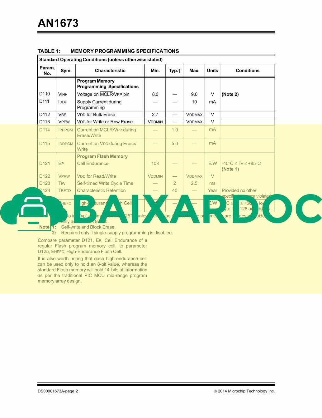
For example, the PIC16(L)F1508/9 data sheetFor example, the PIC16(L)F1508/9 data sheet
(DS40001609) specifies a minimum of 10K cycles in(DS40001609) specifies a minimum of 10K cycles in
the industrial temperature range (-40the industrial temperature range (-40˚̊C to +85C to +85˚̊C) (seeC) (see
http://www.microchip.com/wwwproducts/http://www.microchip.com/wwwproducts/
Devices.aspx?dDocName=en553471Devices.aspx?dDocName=en553471). This is an). This is an
order of magnitude smaller than the traditional valueorder of magnitude smaller than the traditional value
offered by most data EEPROM modules andoffered by most data EEPROM modules and
stand-alone devices.stand-alone devices.
The high-endurance block is a block of 128 memoryThe high-endurance block is a block of 128 memory
locations, found at the top of the Flash programlocations, found at the top of the Flash program
memory that is ensured to provide a superior memory that is ensured to provide a superior
endurance, equal to that of a endurance, equal to that of a traditional data EEPROMtraditional data EEPROM
memory within a given temperature range (0memory within a given temperature range (0˚̊C to 60C to 60˚̊C)C)
(see(see TTablablee 11 below from the PIC16(L)F1508/9 data below from the PIC16(L)F1508/9 data
sheet).sheet).
Author: Author: Lucio Di JasLucio Di Jasioio
Microchip Technology Inc.Microchip Technology Inc.
Using the PIC16F1XXX High-Endurance Flash (HEF) Block Using the PIC16F1XXX High-Endurance Flash (HEF) Block
AN1673
DS00001673A-page 2 2014 Microchip Technology Inc.
Compare parameter D121, EP, Cell Endurance of a
regular Flash program memory cell, to parameter
D125, EHEFC, High-Endurance Flash Cell.
It is also worth noting that each high-endurance cell
can be used only to hold an 8-bit value, whereas the
standard Flash memory will hold 14 bits of information
as per the traditional PIC MCU mid-range program
memory array design.
TABLE 1: MEMORY PROGRAMMING SPECIFICATIONS
Standard Operating Conditions (unless otherwise stated)
Param.
No.Sym. Characteristic Min. Typ.† Max. Units Conditions
Program Memory
Programming Specifications
D110 VIHH Voltage on MCLR/VPP pin 8.0 — 9.0 V (Note 2)
D111 IDDP Supply Current during
Programming
— — 10 mA
D112 VBE VDD for Bulk Erase 2.7 — VDDMAX V
D113 VPEW VDD for Write or Row Erase VDDMIN — VDDMAX V
D114 IPPPGM Current on MCLR/VPP during
Erase/Write
— 1.0 — mA
D115 IDDPGM Current on VDD during Erase/
Write
— 5.0 — mA
Program Flash Memory
D121 EP Cell Endurance 10K — — E/W -40C T A +85C
(Note 1)
D122 VPRW VDD for Read/Write VDDMIN — VDDMAX V
D123 TIW Self-timed Write Cycle Time — 2 2.5 ms
D124 TRETD Characteristic Retention — 40 — Year Provided no other
specifications are violated
D125 EHEFC High-Endurance Flash Cell 100K — — E/W 0°C T A +60°C, lower
byte last 128 addresses
† Data in “Typ” column is at 3.0V, 25°C unless otherwise stated. These parameters are for design guidance
only and are not tested.
Note 1: Self-write and Block Erase.
2: Required only if single-supply programming is disabled.
2014 Microchip Technology Inc. DS00001673A-page 3
AN1673
FLASH VS. EEPROM
Both the high-endurance Flash and the regular Flash
memory arrays differ from a data EEPROM module in
two important ways:
a) Data must be manually erased before a
write and this can be performed only in
blocks (referred to as rows) of a fixed size
determined by the Flash array inner design.
b) Writing to Flash stalls the MCU for a few
milliseconds (see parameter D123 in
Table 1).
By contrast, true data EEPROMs are designed to allow
byte-by-byte erase and do not stall the MCU execution
during a write cycle, although, for simplicity reasons,
most applications will include a delay loop to ensure a
(byte) write has been completed before the next one
can be initiated.
The differences noted above have implications for the
design of the embedded application, which need to be
fully understood whether considering the use of regular
or high-endurance Flash in lieu of a true EEPROM.
Row Erase/Write
Notice that no restrictions exist on the amount of data
fetched during a read operation or its alignment with
row boundaries.
When writing a block of data to a Flash memory, it is
important to ensure alignment with the array row
boundaries. When the data block does not entirely fit
inside a single row, multiple write operations can be
required to store sequential rows, which explains why it
is essential to know the size of the Flash memory array
(row size). The user needs to ensure that the data is
aligned with the row size, especially if data spans more
than one row.
Stall During Write
In contrast with the behavior of a data EEPROM, the
MCU is unable to fetch new instructions from the Flash
memory array during a self-write cycle and it is,
therefore, stalled. This means that no other work can
be performed in parallel during an erase or write
operation, nor can the application respond to interrupts.
In fact, these are delayed until the MCU code execution
resumes. The designer must, therefore, take into
account the potentially-introduced additional jitter or
the momentary application freeze during the
nonvolatile memory updates.
Note that the delay duration is independent of the
amount of data actually written in a row, be it a single
byte or the entire row.
Finally, note that no delays or penalties are incurred by
reading the content of the Flash memory arrays.
Note: To speed up the writing process, external
serial EEPROM devices will often include
a page mechanism that is not too
dissimilar in principle to the rows of a
Flash array.
AN1673
DS00001673A-page 4 2014 Microchip Technology Inc.
A FLASH SUPPORT LIBRARY
The flash.c module has been written to simplify the
use of the self-write Flash memory in embedded
applications written in C (see Listing B-2). It can be
used to operate independently on the normal Flash
array as well as on the high-endurance Flash block.
Five basic functions are prototyped and documented in
flash.h (see Listing B-1).
The first three functions provide read capability (see
Function 1 through Function 3).
FUNCTION 1: FLASH_read
The FLASH_read function reads a 14-bit word from a
given address in the device program Flash memory. It
can be used to read very large tables of data from
memory.
FUNCTION 2: FLASH_readConfig
The FLASH_readConfig function is a variant of the
previous function that allows access to addresses
above the 0x8000 threshold where the IDLOC
information, processor Configuration bits and
calibration data are found.
FUNCTION 3: FLASH_readBlock
The FLASH_readBlock function will perform a read
operation from the main program memory array of the
device transferring a number of 14-bit words (up to
255) into a buffer of 16-bit unsigned integers.
The last two functions provide the write and erase
capability (see Function 4 and Function 5).
FUNCTION 4: FLASH_write
The FLASH_write function offers the smallest atomic
unit required to perform an actual write operation.
Depending on the value passed as the latch parameter,
it can simply load a latch or initiate a write cycle during
which all values previously loaded in a row get written
at once. Refer to Section 10.0, Flash Program
Memory Control, of the device data sheet for more
details on the low-level sequence of operation required
(see http://ww1.microchip.com/downloads/en/
DeviceDoc/40001609C.pdf ).
FUNCTION 5: FLASH_erase
The FLASH_erase function performs the erase of a
single row of the program memory Flash array. The
address provided can be relative to any of the locations
contained in the row. This function performs a brief
unlock sequence and then proceeds to stall the MCU
for the self-write cycle time. Any interrupt event occur-
ring during such time will be served after execution is
resumed.
/*** Read a word from program Flash memory** @param address source address (absolute
Flash memory address)* @return word retrieved from
Flash memory*/
unsigned FLASH_read (unsigned address);
/**
* Read a word from configuration Flash memory
*
* @param address source address (absolute
Flash memory address)
* @return word retrieved from
Flash memory
*/
unsigned FLASH_readConfig (unsigned address);
/**
* Read a block of words from program Flash memory
*
* @param buffer destination buffer (must be
sufficiently large)
* @param address source address (absolute
Flash memory address)
* @param count number of words to be
retrieved
*/
void FLASH_readBlock (unsigned* buffer, unsigned address, char count);
Note: When latching, the function performs a
short unlock sequence which includes the
temporary disabling of interrupts, but no
delay (MCU stall) is incurred. During an
actual write operation, the function
performs the unlock sequence, but it also
stalls the MCU for the self-write cycle
time. Any interrupt event occurring during
such time will be served after execution is
resumed.
/**
* Write a word of data to Flash memory (latches)
* if parameter latch = 1, data is only latched
and no actual write cycle
* is initiated until a subsequent call with
latch = 0
*
* @param address destination address (absolute
Flash memory)
* @param data word of data to be written
(latched)
* @param latch
*/
void FLASH_write (unsigned address, unsigned data, byte latch);
/**
* Erase a row of Flash memory
*
* @param address absolute address in Flash
contained in selected row
*/
void FLASH_erase (unsigned address);
2014 Microchip Technology Inc. DS00001673A-page 5
AN1673
Write operations can be performed sequentially or
simultaneously on one or more locations within a row
(using the latching mechanism) without any specific
order. Each memory location can be written to several
times, as long as each time, only bit-clear operations
are requested (‘1’’0’).
EEPROM-LIKE USE OF THE HIGH-ENDURANCE FLASH
Utilizing the five functions presented in the previous
section, it is possible to implement any number of
strategies for the implementation and management of
a nonvolatile storage system on Flash.
Several application notes and articles have already
presented solutions to help emulate a high-endurance
block using multiple locations of (lower endurance)
Flash memory. See AN1095 for use with PIC18, PIC24
and dsPIC33FJ devices (http://ww1.microchip.com/
downloads/en/AppNotes/01095D.pdf ).
The “High-Endurance Flash Block” application note will
instead take advantage of the superior characteristics
of the high-endurance Flash array, available on the
current PIC16F1XXX family and its future derivatives.
Since high endurance is already ensured by design,
the approach presented will require no additional Flash
memory space outside of the high-endurance Flash
region and no additional resources.
A simple library module (HEFlash.c, HEFlash.h)
has been prepared to provide the simplest and most
intuitive use of the high-endurance Flash region for
data EEPROM-like nonvolatile storage (admittedly
more similar to a paged data EEPROM use).
For maximum efficiency, the high-endurance Flash
library handles the high-endurance Flash as a small
array of data blocks, mapping each block to a row,
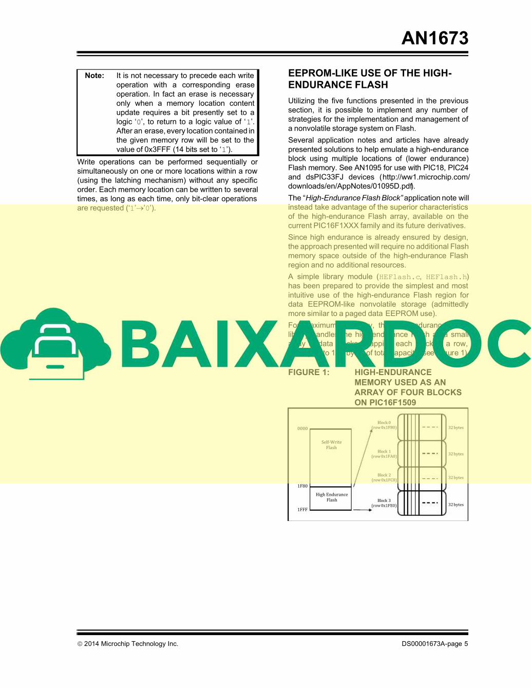
adding up to 128 bytes of total capacity (see Figure 1).
FIGURE 1: HIGH-ENDURANCE
MEMORY USED AS AN
ARRAY OF FOUR BLOCKS
ON PIC16F1509
Note: It is not necessary to precede each write
operation with a corresponding erase
operation. In fact an erase is necessary
only when a memory location content
update requires a bit presently set to a
logic ‘0’, to return to a logic value of ‘1’.
After an erase, every location contained in
the given memory row will be set to the
value of 0x3FFF (14 bits set to ‘1’).
0000
1F80
1FFF
High Endurance
Flash
Self Write
Flash
Block 0(row 0x1F80)
Block 2(row 0x1FC0)
Block 3
(row 0x1FE0)
Block 1(row 0x1FA0)
32 bytes
32 bytes
32 bytes
32 bytes
AN1673
DS00001673A-page 6 2014 Microchip Technology Inc.
The actual capacity of each data block is dictated by
the dimensions of the high-endurance Flash memory
row in the given microcontroller model:
• PIC16F1XXX models with 4K words of Flash (7K
bytes), or more, have a row size of 32 bytes.
• Smaller devices use a row size of 16 bytes.
This means that 4K words and larger models will offer
only four independent data blocks (32 bytes each) of
nonvolatile storage, while smaller devices will offer
eight independent data blocks (16 bytes each).
Each data block can be modified any number of times
up to the maximum specified endurance of the high-
endurance Flash memory (100,000 times) without
influencing any of the neighboring data blocks.
FUNCTION 6: writeBlock()
The writeBlock() function takes the contents of a
data structure pointed to by buffer and writes it into the
selected high-endurance Flash block. Blocks are
atomically updated. All the contents of a block are
erased first and then written to, even if only a portion of
the block capacity (count<ROWSIZE) is used.
The function will return a parameter error (‘-1’) if any of
the input parameters are out of bounds, such as data
too large or invalid block number. The function will
return a write error (‘1’) if the write sequence failed for
any reason.
The value zero (‘0’) will be returned in case of success
(see Function 6).
FUNCTION 7: readBlock()
The readBlock() function matches the functionality
of the writeBlock() function by extracting a block of
data from high-endurance Flash and placing the
contents into a structure pointed to by buffer .
This function will return a parameter error (‘-1’) if any
of the input parameters is out of bounds, such as data
too large or invalid block number (see Function 7).
FUNCTION 8: readByte()
For further convenience, the readByte() function
provides the ability to read any individual byte
contained in a high-endurance Flash memory by
passing a block number and an offset (see Function 8).
/**
* Write a block of data to High Endurance Flash
* the entire block must fit within a row
*
* @param radd HE Flash block number
(0 - MAXROWS-1)
* @param buffer source buffer
* @param count number of bytes to write to
block (< ROWSIZE)
* @return 0 if successful, -1 if
parameter error
*/
char HEFLASH_writeBlock (char radd,
char* buffer, char count);
/**
* Read a block of data from HE Flash memory
*
* @param buffer destination buffer (must be
sufficiently large)
* @param radd source block of HE Flash memory
(0 - MAXROWS-1)
* @param count number of bytes to be retrieved
(< ROWSZE)
* @return 0 if successful, -1 if parameter
error
*/
char HEFLASH_readBlock (char* buffer, char radd,
char count);
/**
* Read a byte of data from HE Flash memory
*
* @param radd source block of HE Flash memory
(0 - MAXROWS-1)
* @param offset offset within the HE block
(0 - ROWSIZE-1)
* @return byte of data retrieved
*/
char HEFLASH_readByte (char radd,
char offset);
2014 Microchip Technology Inc. DS00001673A-page 7
AN1673
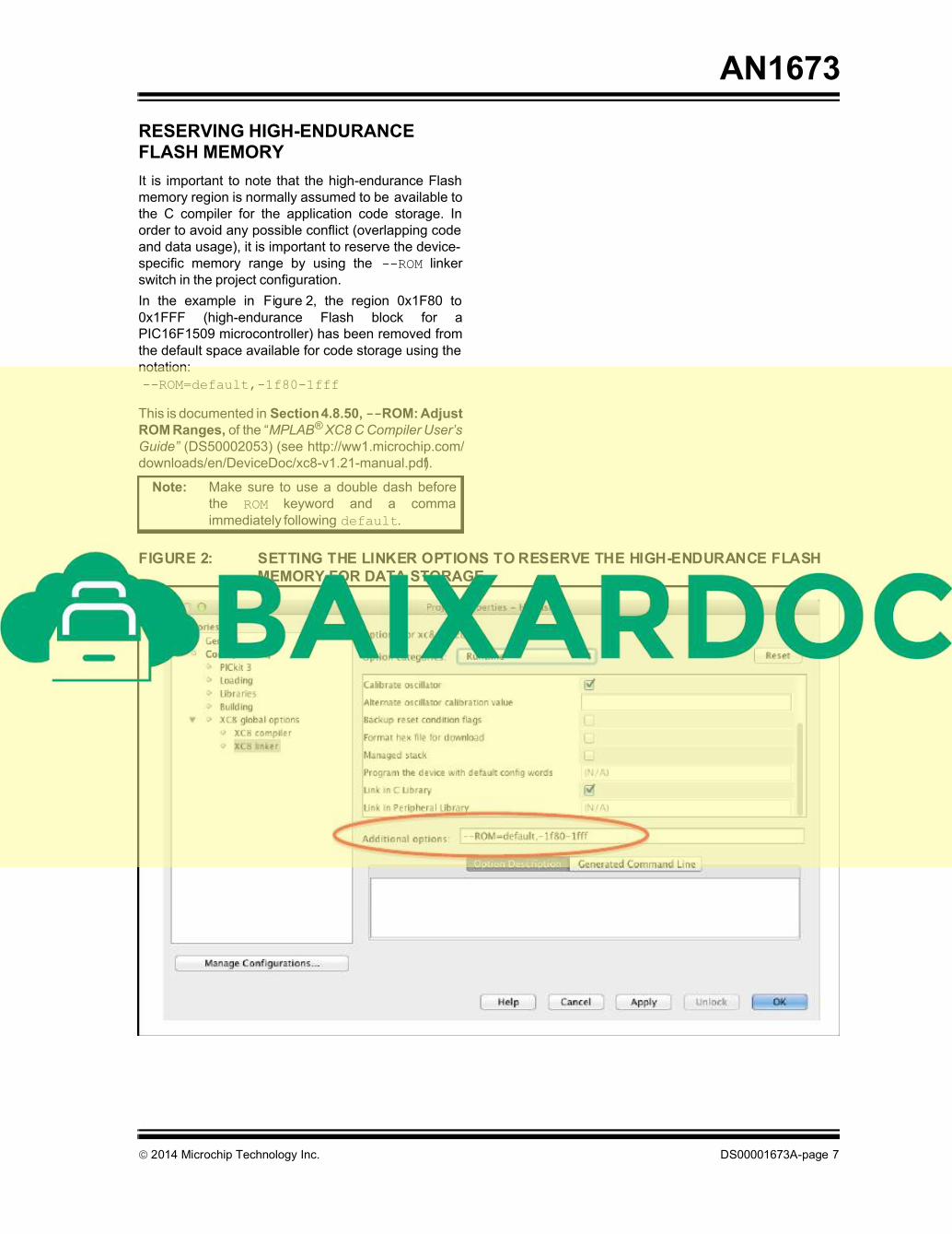
RESERVING HIGH-ENDURANCEFLASH MEMORY
It is important to note that the high-endurance Flash
memory region is normally assumed to be available to
the C compiler for the application code storage. In
order to avoid any possible conflict (overlapping code
and data usage), it is important to reserve the device-
specific memory range by using the --ROM linker
switch in the project configuration.
In the example in Figure 2, the region 0x1F80 to
0x1FFF (high-endurance Flash block for a
PIC16F1509 microcontroller) has been removed from
the default space available for code storage using the
notation:
This is documented in Section 4.8.50, --ROM: Adjust
ROM Ranges, of the “MPLAB® XC8 C Compiler User’s
Guide” (DS50002053) (see http://ww1.microchip.com/
downloads/en/DeviceDoc/xc8-v1.21-manual.pdf ).
FIGURE 2: SETTING THE LINKER OPTIONS TO RESERVE THE HIGH-ENDURANCE FLASH
MEMORY FOR DATA STORAGE
Note: Make sure to use a double dash before
the ROM keyword and a comma
immediately following default.
--ROM=default,-1f80-1fff
AN1673
DS00001673A-page 8 2014 Microchip Technology Inc.
Device Configuration
The device Configuration bits WRT<1:0>, contained in
Configuration Word CONFIG2, control the Flash
memory self-write protection. Such protection should
be set to off (‘11’) or limited to the lower portion of the
Flash memory array (‘10’, ‘01’).
An Example of Use
Listing A-1 provides a simple test program that can be
used to validate the library operation using a PICkit™
Low Pin Count Explorer Board (DM164130-9) in
conjunction to a PIC16F1509 device and a PICkit 3
debugger/programmer.
The PIC16F1509 has 8K words of program memory
and a row size of 32 bytes.
The high-endurance Flash memory is managed as four
blocks (0-3) capable of 32 bytes of data each.
Example 1 includes the definition of a simple data
structure called data of type Record.
EXAMPLE 1:
This can be saved to a block (‘1’) of the high-endurance
Flash (see Example 2).
EXAMPLE 2:
Note the use of the void* cast to pass the record-type
contents to the write function.
The returned value indicates whether the
writeBlock() function accepted and completed the
requested operation.
The contents of the high-endurance Flash block (‘1’)
can be read back into a record-type variable using the
command in Example 3.
EXAMPLE 3:
Once more, the returned value indicates whether the
function accepted the parameters and completed the
requested operation (see Figure 3).
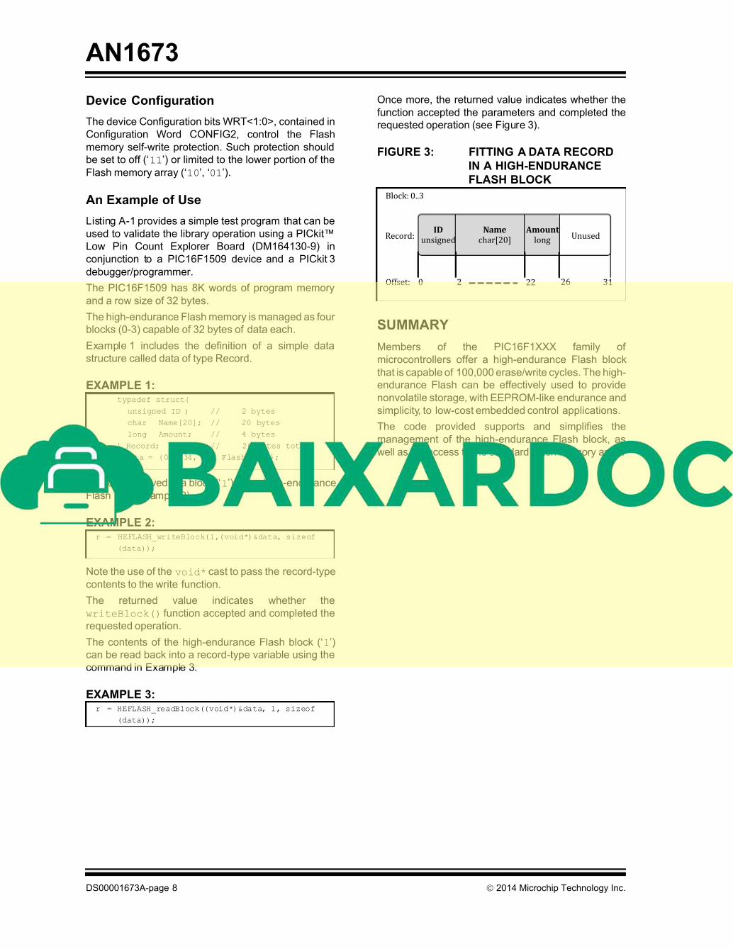
FIGURE 3: FITTING A DATA RECORD
IN A HIGH-ENDURANCE
FLASH BLOCK
SUMMARY
Members of the PIC16F1XXX family of
microcontrollers offer a high-endurance Flash block
that is capable of 100,000 erase/write cycles. The high-
endurance Flash can be effectively used to provide
nonvolatile storage, with EEPROM-like endurance and
simplicity, to low-cost embedded control applications.
The code provided supports and simplifies the
management of the high-endurance Flash block, as
well as the access to the standard Flash memory array.
typedef struct{
unsigned ID ; // 2 bytes
char Name[20]; // 20 bytes
long Amount; // 4 bytes
} Record; // 26 bytes total
Record data = {0x1234, "HE Flash", 42};
r = HEFLASH_writeBlock(1,(void*)&data, sizeof
(data));
r = HEFLASH_readBlock((void*)&data, 1, sizeof
(data));
Block: 0..3
Record:ID
unsigned
Name
char[20]
Amount
longnused
0 2 2 31Offset: 2

2014 Microchip Technology Inc. DS00001673A-page 9
AN1673
APPENDIX A: EXAMPLE PROJECT
Software License Agreement
The software supplied herewith by Microchip Technology Incorporated (the “Company”) is intended and supplied to you, theCompany’s customer, for use solely and exclusively with products manufactured by the Company.
The software is owned by the Company and/or its supplier, and is protected under applicable copyright laws. All rights are reserved. Any use in violation of the foregoing restrictions may subject the user to criminal sanctions under applicable laws, as well as to civilliability for the breach of the terms and conditions of this license.
THIS SOFTWARE IS PROVIDED IN AN “AS IS” CONDITION. NO WARRANTIES, WHETHER EXPRESS, IMPLIED OR STATU-
TORY, INCLUDING, BUT NOT LIMITED TO, IMPLIED WARRANTIES OF MERCHANTABILITY AND FITNESS FOR A PARTICU-
LAR PURPOSE APPLY TO THIS SOFTWARE. THE COMPANY SHALL NOT, IN ANY CIRCUMSTANCES, BE LIABLE FOR
SPECIAL, INCIDENTAL OR CONSEQUENTIAL DAMAGES, FOR ANY REASON WHATSOEVER.
AN1673
DS00001673A-page 10 2014 Microchip Technology Inc.
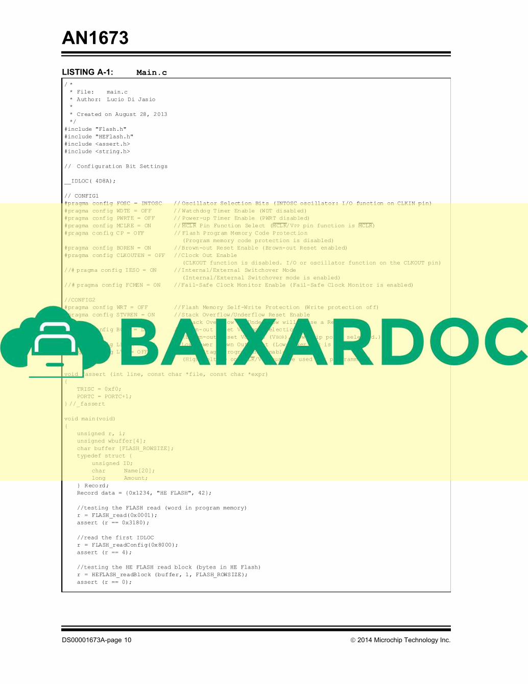
LISTING A-1: Main.c
/ *
* File: main.c
* Author: Lucio Di Jasio
*
* Created on August 28, 2013
*/
#include "Flash.h"
#include "HEFlash.h"
#include <assert.h>
#include <string.h>
// Configuration Bit Settings
__IDLOC( 4D8A);
// CONFIG1
#pragma config FOSC = INTOSC // Oscillator Selection Bits (INTOSC oscillator: I/O function on CLKIN pin)
#pragma config WDTE = OFF // Watchdog Timer Enable (WDT disabled)
#pragma config PWRTE = OFF // Power-up Timer Enable (PWRT disabled)
#pragma config MCLRE = ON // MCLR Pin Function Select (MCLR/VPP pin function is MCLR)
#pragma config CP = OFF // Flash Program Memory Code Protection
(Program memory code protection is disabled)
#pragma config BOREN = ON //Brown-out Reset Enable (Brown-out Reset enabled)
#pragma config CLKOUTEN = OFF //Clock Out Enable
(CLKOUT function is disabled. I/O or oscillator function on the CLKOUT pin)
//# pragma config IESO = ON //Internal/External Switchover Mode
(Internal/External Switchover mode is enabled)
//# pragma config FCMEN = ON //Fail-Safe Clock Monitor Enable (Fail-Safe Clock Monitor is enabled)
//CONFIG2
#pragma config WRT = OFF //Flash Memory Self-Write Protection (Write protection off)
#pragma config STVREN = ON //Stack Overflow/Underflow Reset Enable
(Stack Overflow or Underflow will cause a Reset)
#pragma config BORV = LO //Brown-out Reset Voltage Selection
(Brown-out Reset Voltage (VBOR), low trip point selected.)
#pragma config LPBOR = OFF //Low-Power Brown Out Reset (Low-Power BOR is disabled)
#pragma config LVP = OFF //Low-Voltage Programming Enable
(High-voltage on MCLR/VPP must be used for programming)
void_fassert (int line, const char *file, const char *expr)
{
TRISC = 0xf0;
PORTC = PORTC+1;
} //_fassert
void main(void)
{
unsigned r, i;
unsigned wbuffer[4];
char buffer [FLASH_ROWSIZE];
typedef struct {
unsigned ID;
char Name[20];
long Amount;
} Record;
Record data = {0x1234, "HE FLASH", 42};
//testing the FLASH read (word in program memory)
r = FLASH_read(0x0001);
assert (r == 0x3180);
//read the first IDLOC
r = FLASH_readConfig(0x8000);
assert (r == 4);
//testing the HE FLASH read block (bytes in HE Flash)
r = HEFLASH_readBlock (buffer, 1, FLASH_ROWSIZE);
assert (r == 0);