gate driver unit 4duc51016xfa2 for 3-level igbt
TRANSCRIPT
4DUC51016xFA2 Datasheet
■Overview
4DUC51016xFA2 is a quad channel gate driver designed for Fuji Electric's
IGBT power module 4MBI900VB-120RA-50 .
This gate driver unit contains a built-in isolated DC/DC converter and gate drive circuit.
It is ready to use by mounting it on the IGBT power module.
■Features
・Ideal for drive of 3-Level inverter
・Ideal for drive of IGBT Power module 4MBI900VB-120RA-50 (Fuji Electric)
・Gate voltage : +15V/-10V
・Gate resistor (T1,T4) : +3.9Ω/-1.0Ω(TYP)
・Gate resistor (T2,T3) : +2.7Ω/-15Ω(TYP)
・Short circuit detection voltage : 10V(TYP)
・ALL-IN-ONE (Built-in isolated DC / DC converter and gate drive circuit)
・Low parasitic capacitance (12pF(TYP)) ; highly resistant to common-mode noise.
・Fast response : About 130nsec(typ)
・The isolation for primary-secondary signal used fast response isolator.
・Dielectric withstand voltage : AC5000V
・Insulation distance (clearance / creepage) : 14mm/14mm
・DC/DC converter input voltage : 13~28V
・Power supply for gate driver input voltage : 13~28V
・Signal input voltage : 3.3V~15V or 15V
・Overload protection (DC/DC converter)
・Overheat protection (DC/DC converter)
・Desaturation protection (Gate drive circuit / T1, T4)
・Soft turn-off function (Gate drive circuit / T1, T4)
・Fault signal output function (Gate drive circuit)
・Under-voltage lockout(UVLO) (Gate drive circuit)
・Safety standards:UL508(file no.E243511) (DC/DC converter only)
・UL1741, UL508, IEC62109-1, EN50178 compliant (Reinforced isolation according to IEC 60664-1)
■Application
Industrial inverter, power conditioner, etc …
■Module information
/ TAMURA CORPORATION TMRDM0032EN
Rev.1.01 Jan, 2021
Gate Driver Unit 4DUC51016xFA2 for 3-Level IGBT
1 12
Part number
4DUC51016CFA2
Sample4DUC51016DFA2
Signal input voltage Active clamp Status
3.3 to 15V None Active
15V None
4DUC51016xFA2 Datasheet
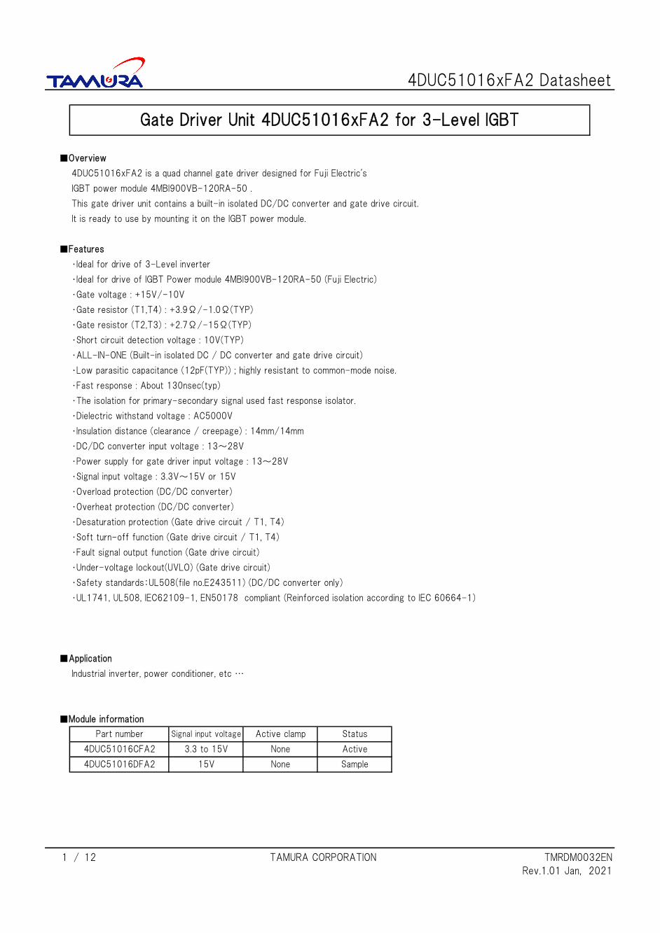
■Circuit Image
■Pin Connection
CN101 : RA-H201SD (JST), 71922-120LF (FCI) or PS-20PE-D4LT2-M1E (JAE)
※Recommend receptacle : RA-S201T (JST), 71600-020LF(FCI) or PS-20SM-D4P1-1*(JAE)
CN102 : S2B-XH-A For thermistor ※Recommend receptacle : XHP-2 (JST)
Connection on the power module
/ TAMURA CORPORATION TMRDM0032EN
Rev.1.01 Jan, 2021
6 T2E T2 Emitter connection
7 T2G T2 Gate connection
8 TH For thermistor
9
T3 Emitter connection
20 GND Ground for drive circuit
14 GND Ground for drive circuit
16 GND Ground for drive circuit
Ground for drive circuitGND
Pin No. Name Function
11 T3G T3 Gate connection
5 T1C T1 Collector connection
2 12
3 T1E T1 Emitter connection
4 T1G T1 Gate connection
1 T4E T4 Emitter connection
2 T4G T4 Gate connection
Pin No. Name Function
Ground for drive circuit
6 GND Ground for drive circuit
8 GND Ground for drive circuit
10 GND Ground for drive circuit
GND
IN1 Control input 1
11 IN4 Control input 4
13 IN3 Control input 3
18
Control input 2
7 VCC Power supply for drive circuit
5 VCC Power supply for drive circuit
9 ALM Alarm signal output
Pin No. Name Function Pin No. Name Function
3 VIN(+) Power supply for DC/DC converter(+)
15 IN2
2 VIN(-) Power supply for DC/DC converter(-)
4 VIN(-) Power supply for DC/DC converter(-)
12
TH For thermistor
10 T3E
19 RTC Recovery time of protection circuit control
17
1 VIN(+) Power supply for DC/DC converter(+)
4DUC/4DUD series for T-Type
T4G 2
CN101
CN102
1 TH1
2 TH2
T4E 1
T1C 5
T1G 4
T1E 3
T2G 7
T2E 6
T3G 11
T3E 10
TH 8
TH 9
5
4
3
7
6
11
10
2
1
8
9
15
13
14/16
Power module
12
1,3 VIN+
2,4 VIN-
19 RTC
12 GND
17 IN1
14 GND
15 IN2
16 GND
13 IN3
18 GND
11 IN4
15V24V
9 ALM
10 GND
5,7 VCC
6,8 GND
0 3.3V-15V
0 3.3V-15V
0 3.3V-15V
0 3.3V-15V
20 GND
4DUC51016xFA2 Datasheet
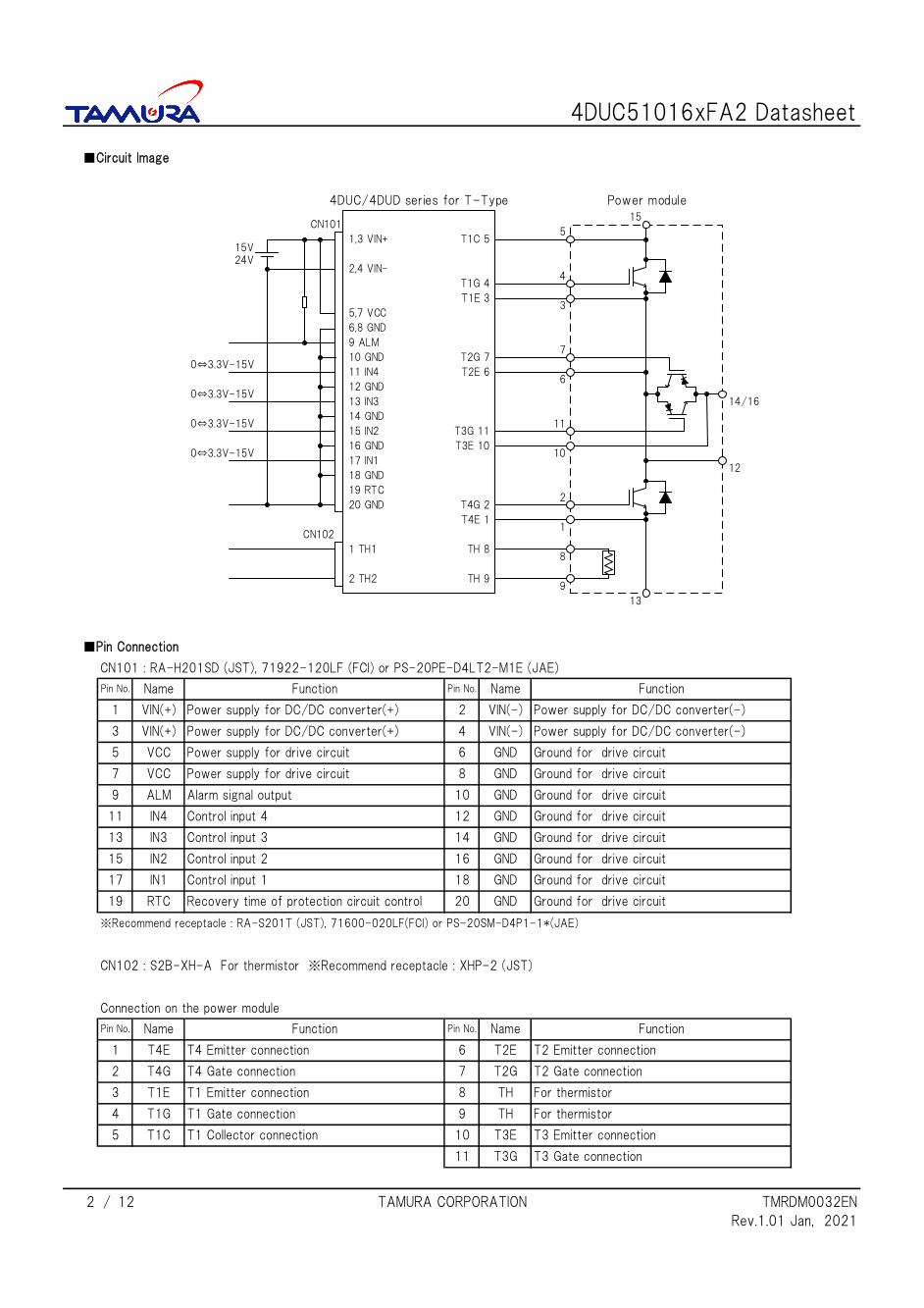
■Internal Block Diagram
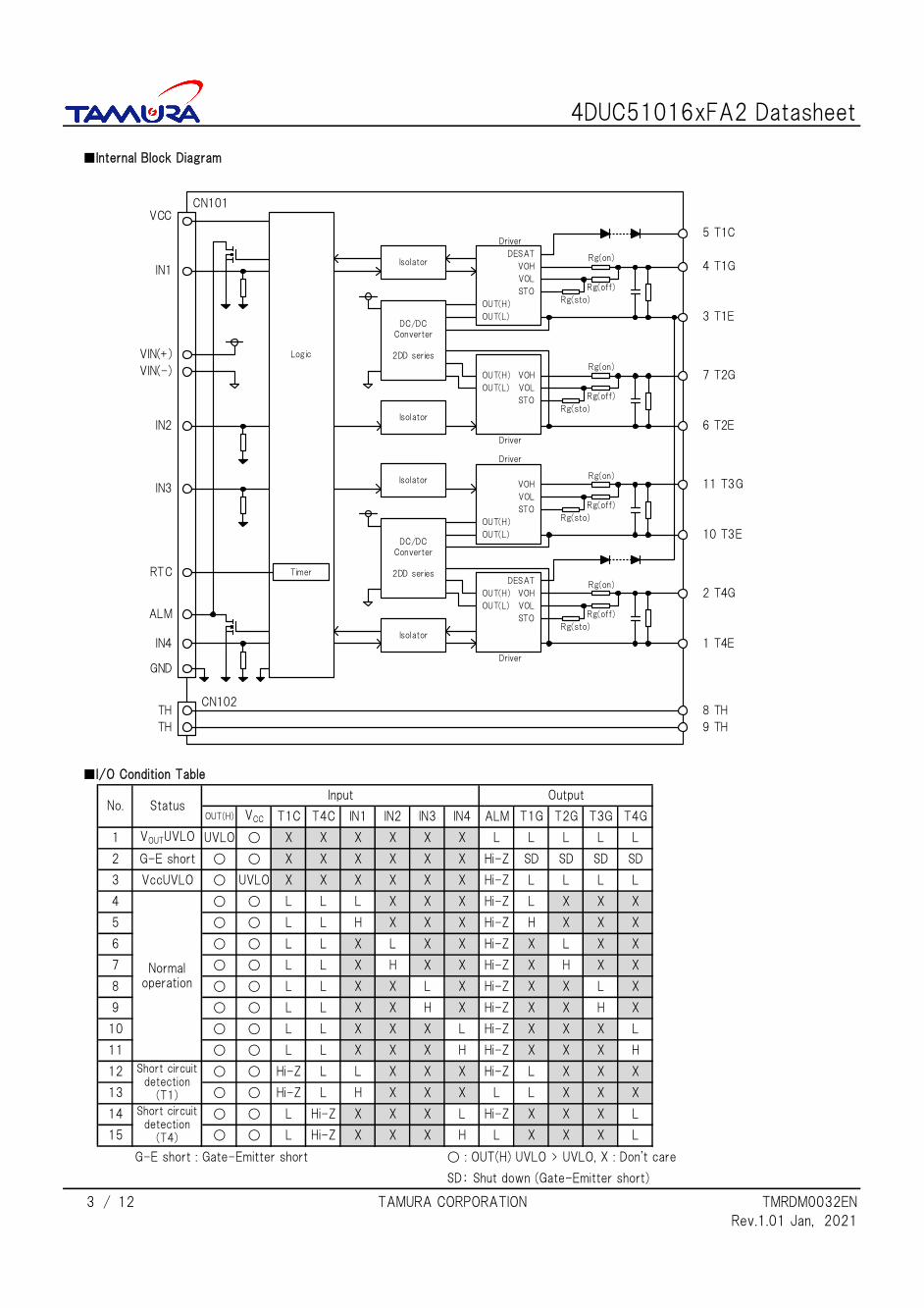
■I/O Condition Table
G-E short : Gate-Emitter short ○ : OUT(H) UVLO > UVLO, X : Don't care
SD: Shut down (Gate-Emitter short)
/ TAMURA CORPORATION TMRDM0032EN
Rev.1.01 Jan, 2021
L X X X L
X X L
X X X H
X L
X X
X L X X
H X X
X X L X
Hi-Z H X X X
X Hi-Z
X Hi-Z
X X H X
Hi-Z
Hi-Z
7 ○ ○ L L X H X X Hi-Z X
9 ○ ○ L
X L X Hi-Z
Hi-Z
X
8 ○
L X
T4G
X L L L L L
X X
X Hi-Z L
Output
L
ALM T1G T2G T3G
○ L L X
L L X
L L X X
○ ○
No. Status
6
2 G-E short ○ ○ X X X
Input
OUT(H) VCC T1C T4C
3 12
1 VOUTUVLO UVLO ○ X X X X X
4
Normaloperation
○ ○ L
L X
X
L L
SD
Hi-Z L12 Short circuitdetection
(T1)
X X
L L X
Hi-Z X X
X Hi-Z SD SD SD
X
10 ○ ○ L L
5 ○ ○ L L H X X
3 VccUVLO ○ UVLO X X X X
L X
X X
IN1 IN2 IN3 IN4
11 ○ ○ L L X X X H
X H X
X X X L
○ L L X
X
X
13 ○ ○ Hi-Z L H X X X
14 Short circuitdetection
(T4)
○ ○ L Hi-Z X X
○
15 ○ ○ L Hi-Z X X X H
Hi-Z XX
L
VIN(+)
VIN(-)
RTC
IN1
IN2
IN3
IN4
2 T4G
ALM
VCC
GND
CN101
TH
TH
1 T4E
5 T1C
4 T1G
3 T1E
7 T2G
6 T2E
11 T3G
10 T3E
8 TH
9 TH
VOH
VOL
STO
Timer
VOH
VOL
VOH
VOL
Isolator
VOH
VOL
STO
Isolator
DC/DC Converter
2DD series
Isolator
Logic
Isolator
DC/DC Converter
2DD series
Driver
DESAT
DESAT
Driver
Driver
Driver
CN102
STO
STO
OUT(H)
OUT(L)
OUT(H)
OUT(L)
OUT(H)
OUT(L)
OUT(H)
OUT(L)
Rg(on)
Rg(off)
Rg(sto)
Rg(on)
Rg(off)
Rg(sto)
Rg(on)
Rg(off)
Rg(sto)
Rg(on)
Rg(off)
Rg(sto)
4DUC51016xFA2 Datasheet
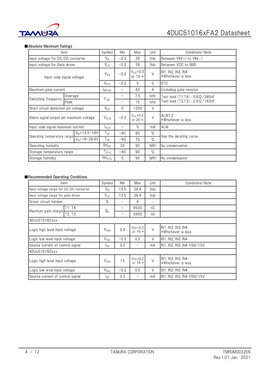
■Absolute Maximum Ratings
■Recommended Operating Conditions
/ TAMURA CORPORATION TMRDM0032EN
Rev.1.01 Jan, 2021
Logic high level input voltage VSGH 13Vcc+0.3 or 16 *
VIN1, IN2, IN3, IN4*Whichever is less
5 V
28 Vdc Between VCC to GND
Conditions・Note
4DUx51016Cxxx
4 12
Logic low level input voltage VSGL -0.3
Driver circuit number N - 4 -
VIN1, IN2, IN3, IN4*Whichever is less
Logic low level input voltage VSGL -0.3 0.5 V IN1, IN2, IN3, IN4
VSGH 3.3Vcc+0.3 or 16 *
nC
Logic high level input voltage
nC
Input voltage range for gate driver VCC 13.5 26.4 Vdc
Input voltage range for DC/DC converter VIN 13.5 26.4 Vdc
Storage temperature range TSTG -40 90 ℃
Storage humidity RHSTG 5 95 %RH No condensation
VSG -0.3VCC+0.3
or 18 *V
IN1, IN2, IN3, IN4*Whichever is less
15
8500
TOP -40 85 ℃
%RH No condensation
7.5 kHzFSW
Test load (T1,T4) : 0.8Ω/340nFTest load (T2,T3) : 2.8Ω/162nF- kHz
-
RTC
Input-side signal maximum current IALM - 5 mA ALM
See the derating curve
VRTC -0.3
ALM1,2*Whichever is less
Excluding gate resistor
Operating temperature rangeVIN=13.5-18V
AverageSwitching frequency
Peak
VIN=18-26.4V TOP -40 75 ℃
Item Symbol
Input voltage for DC/DC converter VIN -0.3 28 Vdc Between VIN(+) to VIN(-)
-
0
Maximum gate chargeT1, T4
QG
Input voltage for Gate driver VCC -0.3
Min Max Unit Conditions・Note
Operating humidity RHOP 20 95
Unit
Input-side signal voltage
Alarm signal output pin maximum voltage VALM -0.3VCC+0.3
or 28 *V
Maximum gate current IGPEAK - 43 A
Short circuit detection pin voltage VSD
Item Symbol Min Max
1200 V
- mA IN1, IN2, IN3, IN4 VSG=15V
0.5 V IN1, IN2, IN3, IN4
Source current of control signal ISG 3.3 - mA IN1, IN2, IN3, IN4 VSG=15V
T2, T3 - 3900
4DUx51016Dxxx
Source current of control signal ISG 3.2
4DUC51016xFA2 Datasheet
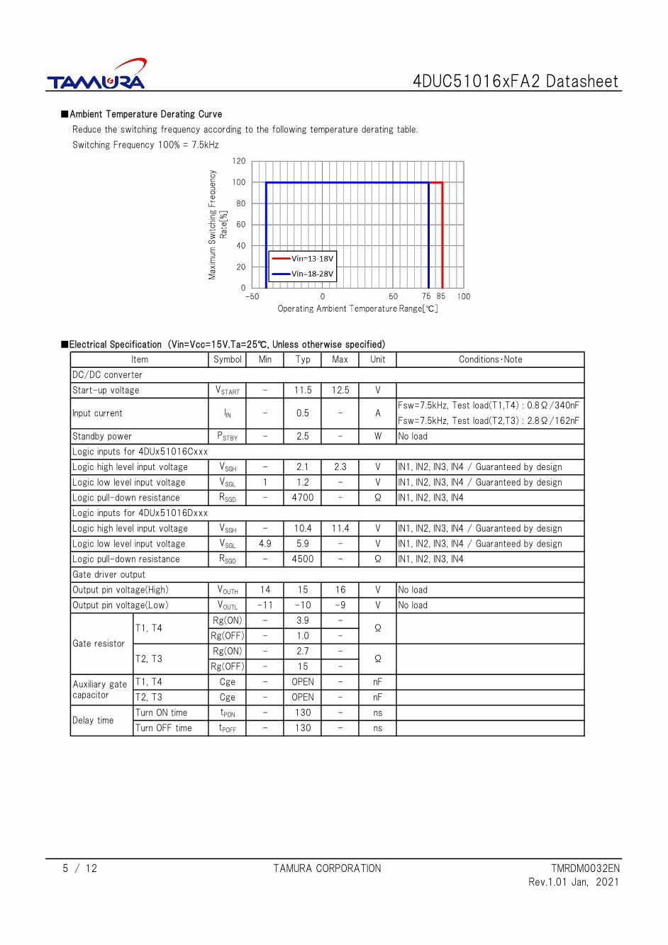
■Ambient Temperature Derating Curve
Reduce the switching frequency according to the following temperature derating table.
Switching Frequency 100% = 7.5kHz
■Electrical Specification (Vin=Vcc=15V.Ta=25℃, Unless otherwise specified)
/ TAMURA CORPORATION TMRDM0032EN
Rev.1.01 Jan, 2021
Fsw=7.5kHz, Test load(T2,T3) : 2.8Ω/162nFA-0.5-
Fsw=7.5kHz, Test load(T1,T4) : 0.8Ω/340nF
Turn OFF time tPOFF - 130 - ns
- ns
5 12
Auxiliary gatecapacitor
T1, T4
Delay timeTurn ON time tPON - 130
Cge - OPEN
T2, T3 Cge - OPEN
- nF
Output pin voltage(Low) VOUTL -11 -10 -9 V
Gate resistor
T1, T4
T2, T3Rg(ON) - 2.7 -
ΩRg(OFF) - 15 -
No load
Rg(ON) - 3.9 -Ω
Rg(OFF) - 1.0 -
Gate driver output
Output pin voltage(High) VOUTH 14 15 16 V No load
IN1, IN2, IN3, IN4 / Guaranteed by design
Logic inputs for 4DUx51016Dxxx
Logic high level input voltage VSGH - 10.4 11.4 V IN1, IN2, IN3, IN4 / Guaranteed by design
Logic low level input voltage
Logic pull-down resistance RSGD - 4500 - Ω
IN1, IN2, IN3, IN4 / Guaranteed by design
Logic pull-down resistance RSGD - 4700 - Ω IN1, IN2, IN3, IN4
VSGL 4.9 5.9 - V IN1, IN2, IN3, IN4 / Guaranteed by design
1 1.2 - V
Logic high level input voltage VSGH - 2.1 2.3 V
Item Symbol Min Typ
- W No load
Max Unit Conditions・Note
12.5 V
DC/DC converter
IIN
IN1, IN2, IN3, IN4
Logic inputs for 4DUx51016Cxxx
Logic low level input voltage
- nF
Standby power PSTBY - 2.5
Input current
Start-up voltage VSTART - 11.5
VSGL
4DUC51016xFA2 Datasheet
■Protection
■Insulation
/ TAMURA CORPORATION TMRDM0032EN
Rev.1.01 Jan, 2021
- 4
Gate driver
DC/DC converter
Between Input-Output
Dielectric withstand voltage AC5000V 1min, Cutoff 2mA
Soft turn-off resistance RSTO - 15 - Ω
Restart time tRESTART - 110 - ms
Minimum creepage distances 8mm
6 12
IALM=5mA
Alarm signal output time tALM - 0.2 - us
Alarm signal output L voltage VALML - - 0.5 V
Collector openShort circuit detection filter time tSHORTFIL - 4.5 - us
Guaranteed by design
Short circuit detection voltage VSD - 10 - V
Output voltage(H) UVLO ON voltage VUVLOOHL 12.2 12.5 12.8 V
Output voltage(H) UVLO OFF voltage VUVLOOHH 13.2 13.5 13.8 V Guaranteed by design
VCC UVLO ON voltage VUVLOVCCL - 7.3 - V
VCC UVLO OFF voltage VUVLOVCCH -
Item Symbol Min Typ Max Unit Conditions・Note
Auto recovery
9.1 - V
Soft turn-off duration tSTO
℃ Auto recovery, Internal temperature
Item Specification Conditions・Note
Minimum clearance distances 8mm
Minimum creepage distances 14mm
Between Output-Output
100MΩ or more DC500V
Minimum clearance distances 14mm
Partial discharge extinction voltage 1768Vpeak or more According to EN50178/IEC 60270
Insulation resistance
Common-mode transient immunity (CMTI) 70kV/us
- us
Overheat protection - 120
W
- 150
Overload protection - 10.5 - -
Between Thermistor-Output
Minimum clearance distances 8mm
Minimum creepage distances 8mm
4DUC51016xFA2 Datasheet
■Pin Function
・VIN(+), VIN(-) (Power supply pin for DC/DC converter)
・VCC(Power supply pin for drive circuit)
・GND(Ground pin for drive circuit)
・IN1, IN2, IN3, IN4(Control input pin)
The IN1, IN2, IN3 and IN4 pin is a pin used to determine output logic.
・RTC(Recovery time of protection circuit control pin)
When abnormality occurs (UVLO, short circuit detected),this pin is used to adjust the recovery time.
・ALM(Alarm signal output pin)
When abnormality occurs (UVLO, short circuit detected),This pin outputs an alarm signal. (Open drain)
/ TAMURA CORPORATION TMRDM0032EN
Rev.1.01 Jan, 2021
7 12
X X H X X
L
X X H
X
X X L
UVLO, When detecting short circuit L
X X X H X
X X X L X
Status ALM
While in normal operation Hi-Z
X
X LX X
X L X X X
X H X X X
H X X X H
L X X X L X X X
X X X
IN1 IN2 IN3
H X X
X
X
X H X
L X
IN4 T1G T2G T3G T4G
4DUC51016xFA2 Datasheet
■Description
1. Undervoltage Lockout (UVLO) function
The control circuit incorporates the undervoltage lockout (UVLO) function both on the VCC and the OUT(H) sides.
When the OUT(H) voltage drops to the UVLO ON voltage, the Output pin and the ALM pin both will output the “L” signal.
When the VCC voltage drops to the UVLO ON voltage, the Output pin will output the “L” signal.
When the VCC or the OUT(H) voltage rises to the UVLO OFF voltage, these pins will be reset.
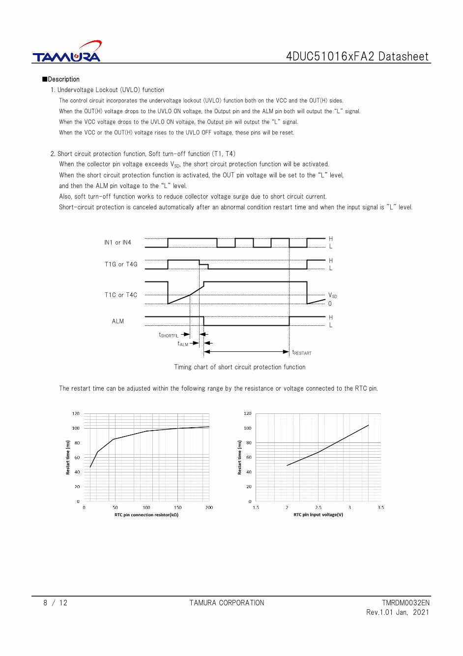
2. Short circuit protection function, Soft turn-off function (T1, T4)
When the collector pin voltage exceeds VSD, the short circuit protection function will be activated.
When the short circuit protection function is activated, the OUT pin voltage will be set to the “L” level,
and then the ALM pin voltage to the “L” level.
Also, soft turn-off function works to reduce collector voltage surge due to short circuit current.
Short-circuit protection is canceled automatically after an abnormal condition restart time and when the input signal is "L" level.
Timing chart of short circuit protection function
The restart time can be adjusted within the following range by the resistance or voltage connected to the RTC pin.
/ TAMURA CORPORATION TMRDM0032EN
Rev.1.01 Jan, 2021
8 12
IN1 or IN4
T1C or T4C
T1G or T4G
ALM
HL
HL
HL
tSHORTFIL
tALM
tRESTART
VSD
0
4DUC51016xFA2 Datasheet
■Description
3. Active clamp gate function
None
■Reliability
※After each test, exposure at room temperature and humidity condition for 24 hours.
There shall be no abnormality on the electrical specification and appearance.
/ TAMURA CORPORATION TMRDM0032EN
Rev.1.01 Jan, 2021
9 12
Cross-over frequency: 8.4Hz, , Displacement amplitude(5 to 8,4Hz): ±3.5mm,
Acceleration amplitude(8.4 to 200Hz):1G, Test duration: 20sweeps, Axis: X, Y and Z, ※
Impact IEC 60068-2-27:2008-02, Pulse shape: Half-sine, Corresponding duration: 11ms,
Vibration IEC 60068-2-6:2007-12, Frequency range: 10 to 55Hz, Sweep rate: 1.0oct/min,
Displacement amplitude: ±0.75mm, Test duration: 120min, Axis: X,Y and Z, ※
Exposure in high temperature IEC60068-2-2:2007: Test: Bb, 90℃, 240H, ※
IEC 60068-2-6:2007-12, Frequency range: 5 to 200Hz, Sweep rate: 1.0oct/min,
85℃, 240H, ※
high temperature IEC60068-2-78:2012-10, Input voltage: DC24V, Output current: Rated Load
and high humidity operation 85℃, 85%RH, 240H, ※
-40℃, 240H, ※
High temperature operation IEC60068-2-2:2007: Test: Be, Input voltage: DC24V, Output current: Rated Load
Low temperature operation IEC60068-2-1:2007: Test: Ae, Input voltage: DC24V, Output current: Rated Load
Exposure in low temperature IEC60068-2-1:2007: Test: Ab, -40℃, 240H, ※
Exposure in high temperature and high humidity IEC60068-2-78:2012-10, 60℃, 90~95%RH, 240H, ※
Thermal shock IEC60068-2-14:2009-01: Test: Na, -40℃/30min to 100℃/30min, 500cycles, ※
Item Test condition and acceptance criterion
IEC 60068-2-27:2008-02, Pulse shape: Half-sine, Corresponding duration: 6ms,
Peak acceleration: 15G, Number of shocks:100, Axis: ±X, Y and Z, ※
Peak acceleration: 50G, Number of shocks:3, Axis: ±X, Y and Z, ※
4DUC51016xFA2 Datasheet
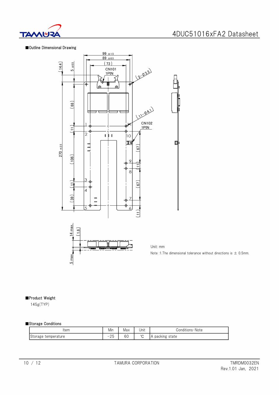
■Outline Dimensional Drawing
Unit: mm
Note :1.The dimensional tolerance without directions is ± 0.5mm.
■Product Weight
145g(TYP)
■Storage Conditions
/ TAMURA CORPORATION TMRDM0032EN
Rev.1.01 Jan, 2021
10 12
Item Min Max Unit Conditions・Note
Storage temperature -25 60 ℃ A packing state
4DUC51016xFA2 Datasheet
■Usage Cautions
● Always mount fuse on the plus side of input for ensuring safety because the fuse is not built-in the product.
Please select the fuse considering conditions such as steady current, inrush current, and ambient temperature.
When using a fuse having large rated current or high capacity input electrolytic condenser, by combining
another converter and input line and input electrolytic condenser, fuse may not blow off in the case of abnormality.
Do not combine high voltage line and fuse.
● Make sure the rise/fall time of the input signal is 500ns or less.
Also, keep input wiring as far as possible from noise sources.
To prevent malfunction due to noise, we recommend the highest possible signal voltage within the recommended range.
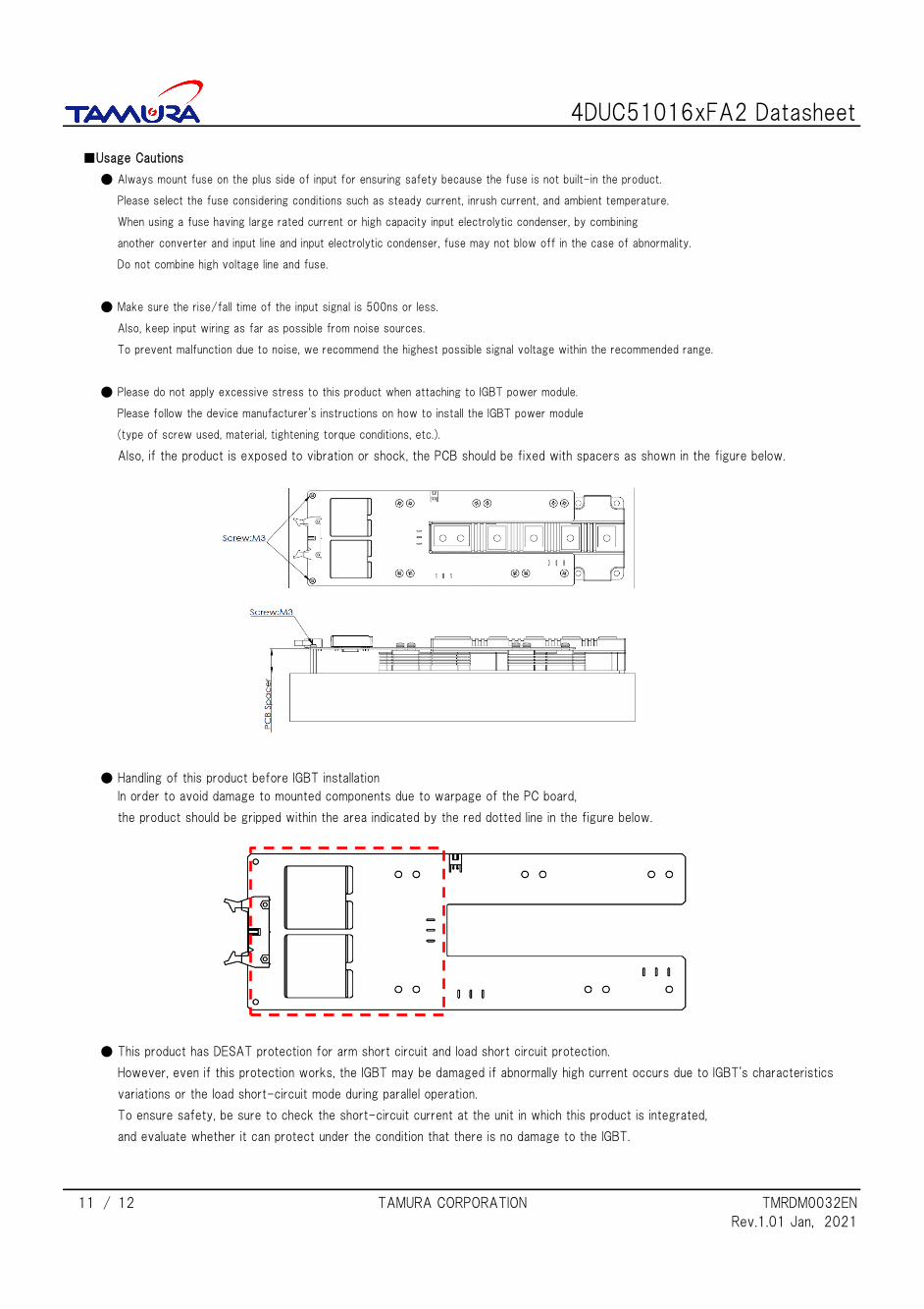
● Please do not apply excessive stress to this product when attaching to IGBT power module.
Please follow the device manufacturer's instructions on how to install the IGBT power module
(type of screw used, material, tightening torque conditions, etc.).
Also, if the product is exposed to vibration or shock, the PCB should be fixed with spacers as shown in the figure below.
● Handling of this product before IGBT installation
In order to avoid damage to mounted components due to warpage of the PC board,
the product should be gripped within the area indicated by the red dotted line in the figure below.
● This product has DESAT protection for arm short circuit and load short circuit protection.
However, even if this protection works, the IGBT may be damaged if abnormally high current occurs due to IGBT's characteristics
variations or the load short-circuit mode during parallel operation.
To ensure safety, be sure to check the short-circuit current at the unit in which this product is integrated,
and evaluate whether it can protect under the condition that there is no damage to the IGBT.
/ TAMURA CORPORATION TMRDM0032EN
Rev.1.01 Jan, 2021
11 12
4DUC51016xFA2 Datasheet
■Important Notice
● This information and product are subject to change without prior notice for the purpose of improvements, etc.
Ensure that you are in possession of the most up-to-date information when using this product.
● The operation examples and circuit examples shown in this document are for reference purposes only, and TAMURA Corporation disclaims
all responsibility for any violations of industrial property rights, intellectual property rights and any other rights owned by TAMURA Corporation
or third parties that these may entail.
● The circuit examples and part constants listed in this document are provided as reference for the verification of
characteristics. You are to perform design, verification, and judgment at your own responsibility, taking into account the various conditions.
● TAMURA has evaluated the efficiency and performance of this product in a usage environment determined by us.
Depending on your usage environment or usage method, there is the possibility that this product will not perform sufficiently as shown in
the specifications, or may malfunction.
When applying this product to your devices or systems, please ensure that you conduct evaluations of their state when integrated with
this product. You are responsible for judging its applicability.
TAMURA bears no responsibility whatsoever for any problems with your devices,
systems or this product which are caused by your usage environment or usage method.
● TAMURA Corporation constantly strives to improve quality and reliability, but malfunction or failures are bound to occur with some
probability in power products. To ensure that failures do not cause accidents resulting in injury or death, fire accidents, social damage,
and so on, you are to thoroughly verify the safety of their designs in devices and/or systems, at your own responsibility.
● This product is intended for use in consumer electronics (electric home appliances, business equipment, Information equipment, communication
terminal equipment, measuring devices, and so on.) If considering use of this product in equipment or devices that require high reliability
(medical devices, transportation equipment, traffic signal control equipment, fire and crime prevention equipment, aeronautics and space
devices, nuclear power control, fuel control, in-vehicle equipment, safety devices, and so on), please consult a TAMURA sales representative
in advance. Do not use this product for such applications without written permission from TAMURA Corporation.
● This product is intended for use in environments where consumer electronics are commonly used.
It is not designed for use in special environments such as listed below, and if such use is considered,
you are to perform thorough safety and reliability checks at your own responsibility.
・ Use in liquids such as water, oil, chemical solutions, or organic solvents, and use in locations
where the product will be exposed to such liquids.
・ Use that involves exposure to direct sunlight, outdoor exposure, or dusty conditions.
・ Use in locations where corrosive gases such as salt air, C12, H2S, NH3, SO2, or NO2, are present.
・ Use in environments with strong static electricity or electromagnetic radiation.
・ Use that involves placing inflammable material next to the product.
・ Use of this product either sealed with a resin filling or coated with resin.
・ Use of water or a water soluble detergent for flux cleaning.
・ Use in locations where condensation is liable to occur.
● This product is not designed to resist radiation.
● This product is not designed to be connected in series or parallel.
Do not operate this product in a series, parallel, or N+1 redundant configuration.
● Do not use or otherwise make available the TAMURA products or the technology described in this document for any military purposes,
including without limitation, for the design, development, use, stockpiling or manufacturing of mass destruction weapons
(e.g. nuclear, chemical, or biological weapons or missile technology products).
When exporting and re-exporting the products or technology described in this document, you should comply with the applicable export
control laws and regulations and follow the procedures required by such laws and regulations including, without limitation,
Japan -Foreign Exchange and Foreign Trade Control Law and U.S.- Export Administration Regulations.
The TAMURA products and related technology should not be used for or incorporated into any products or systems whose manufacture,
use, or sale is prohibited under any applicable domestic or foreign laws or regulations.
● Please contact your TAMURA sales office for details as to environmental matters such as the RoHS compatibility of product.
Please use TAMURA products in compliance with all applicable laws and regulations that regulate the inclusion or use of controlled substances,
including without limitation, the EU RoHS Directive.
TAMURA assumes no liability for damages or losses occurring as a result of your noncompliance with applicable laws and regulations.
● TAMURA assumes no liability for damages or losses incurred by you or third parties as a result of unauthorized use of TAMURA products.
● This document and any information herein may not be reproduced in whole or in part without prior written permission from TAMURA.
/ TAMURA CORPORATION TMRDM0032EN
Rev.1.01 Jan, 2021
12 12