for more free e-books visit - acemu
TRANSCRIPT

For more Free E-books
Visit http://ali-almukhtar.blogspot.com

Advanced PIC MicrocontrollerProjects in C

This page intentionally left blank
Advanced PIC MicrocontrollerProjects in C
From USB to RTOS with the PIC18F Series
Dogan Ibrahim
Newnes is an imprint of Elsevier
30 Corporate Drive, Suite 400, Burlington, MA 01803, USA
Linacre House, Jordan Hill, Oxford OX2 8DP, UK
Copyright # 2008, Elsevier Ltd. All rights reserved.
No part of this publication may be reproduced, stored in a retrieval system, or transmitted in any form or by any
means, electronic, mechanical, photocopying, recording, or otherwise, without the prior written permission of
the publisher.
Permissions may be sought directly from Elsevier s Science & Technology Rights Department in Oxford,
UK: phone: (þ44) 1865 843830, fax: (þ44) 1865 853333, E-mail: [email protected]. You may
also complete your request online via the Elsevier homepage (http://elsevier.com), by selecting “Support &
Contact” then “Copyright and Permission” and then “Obtaining Permissions.”
Recognizing the importance of preserving what has been written, Elsevier prints its books on acid-free
paper whenever possible.
Library of Congress Cataloging-in-Publication Data
Ibrahim, Dogan.
Advanced PIC microcontroller projects in C: from USB to RTOS with the PIC18F series/Dogan Ibrahim
p. cm.
Includes bibliographical references and index.
ISBN-13: 978-0-7506-8611-2 (pbk. : alk. paper) 1. Programmable controllers. 2. C (Computer program
language) I. Title.
TJ223.P76I268 2008
629.8095––dc222007050550
British Library Cataloguing-in-Publication Data
A catalogue record for this book is available from the British Library.
ISBN: 978-0-7506-8611-2
For information on all Newnes publicationsvisit our Web site at www.books.elsevier.com
Printed in the United States of America
08 09 10 11 12 13 9 8 7 6 5 4 3 2 1
Contents
Preface............................................................................................. xiii
Acknowledgments ................................................................................ xv
Chapter 1: Microcomputer Systems.......................................................... 11.1 Introduction..................................................................................................11.2 Microcontroller Systems ...............................................................................1
1.2.1 RAM .................................................................................................51.2.2 ROM .................................................................................................51.2.3 PROM...............................................................................................51.2.4 EPROM.............................................................................................61.2.5 EEPROM ..........................................................................................61.2.6 Flash EEPROM .................................................................................6
1.3 Microcontroller Features...............................................................................61.3.1 Supply Voltage ..................................................................................71.3.2 The Clock..........................................................................................71.3.3 Timers ...............................................................................................71.3.4 Watchdog ..........................................................................................81.3.5 Reset Input ........................................................................................81.3.6 Interrupts ...........................................................................................81.3.7 Brown-out Detector ...........................................................................91.3.8 Analog-to-Digital Converter ...............................................................91.3.9 Serial Input-Output ............................................................................91.3.10 EEPROM Data Memory ..................................................................101.3.11 LCD Drivers....................................................................................101.3.12 Analog Comparator..........................................................................101.3.13 Real-time Clock...............................................................................111.3.14 Sleep Mode .....................................................................................111.3.15 Power-on Reset................................................................................11
www.newnespress.com
1.3.16 Low-Power Operation ....................................................................111.3.17 Current Sink/Source Capability ......................................................111.3.18 USB Interface ................................................................................121.3.19 Motor Control Interface .................................................................121.3.20 CAN Interface ...............................................................................121.3.21 Ethernet Interface...........................................................................121.3.22 ZigBee Interface ............................................................................12
1.4 Microcontroller Architectures....................................................................121.4.1 RISC and CISC ...............................................................................13
1.5 Number Systems.......................................................................................131.5.1 Decimal Number System .................................................................141.5.2 Binary Number System....................................................................141.5.3 Octal Number System ......................................................................151.5.4 Hexadecimal Number System ..........................................................15
1.6 Converting Binary Numbers into Decimal.................................................161.7 Converting Decimal Numbers into Binary.................................................161.8 Converting Binary Numbers into Hexadecimal..........................................181.9 Converting Hexadecimal Numbers into Binary..........................................201.10 Converting Hexadecimal Numbers into Decimal .......................................211.11 Converting Decimal Numbers into Hexadecimal .......................................221.12 Converting Octal Numbers into Decimal...................................................231.13 Converting Decimal Numbers into Octal...................................................231.14 Converting Octal Numbers into Binary .....................................................241.15 Converting Binary Numbers into Octal .....................................................261.16 Negative Numbers ....................................................................................261.17 Adding Binary Numbers ...........................................................................271.18 Subtracting Binary Numbers .....................................................................291.19 Multiplication of Binary Numbers.............................................................291.20 Division of Binary Numbers .....................................................................311.21 Floating Point Numbers ............................................................................311.22 Converting a Floating Point Number into Decimal ....................................33
1.22.1 Normalizing Floating Point Numbers .............................................341.22.2 Converting a Decimal Number into Floating Point .........................341.22.3 Multiplication and Division of Floating Point Numbers ..................361.22.4 Addition and Subtraction of Floating Point Numbers ......................37
1.23 BCD Numbers ..........................................................................................381.24 Summary..................................................................................................401.25 Exercises ..................................................................................................40
Chapter 2: PIC18F Microcontroller Series .............................................. 432.1 PIC18FXX2 Architecture..........................................................................46
2.1.1 Program Memory Organization ........................................................50
www.newnespress.com
vi Contents
2.1.2 Data Memory Organization ..............................................................512.1.3 The Configuration Registers.............................................................522.1.4 The Power Supply ...........................................................................572.1.5 The Reset ........................................................................................572.1.6 The Clock Sources...........................................................................602.1.7 Watchdog Timer ..............................................................................672.1.8 Parallel I/O Ports .............................................................................682.1.9 Timers .............................................................................................742.1.10 Capture/Compare/PWM Modules (CCP) ..........................................842.1.11 Analog-to-Digital Converter (A/D) Module ......................................932.1.12 Interrupts ....................................................................................... 101
2.2 Summary.................................................................................................. 1152.3 Exercises .................................................................................................. 115
Chapter 3: C Programming Language....................................................1193.1 Structure of a mikroC Program................................................................. 120
3.1.1 Comments ..................................................................................... 1213.1.2 Beginning and Ending of a Program .............................................. 1213.1.3 Terminating Program Statements.................................................... 1213.1.4 White Spaces ................................................................................. 1223.1.5 Case Sensitivity ............................................................................. 1223.1.6 Variable Names ............................................................................. 1233.1.7 Variable Types .............................................................................. 1233.1.8 Constants ....................................................................................... 1263.1.9 Escape Sequences .......................................................................... 1283.1.10 Static Variables.............................................................................. 1293.1.11 External Variables ......................................................................... 1293.1.12 Volatile Variables .......................................................................... 1303.1.13 Enumerated Variables .................................................................... 1303.1.14 Arrays ........................................................................................... 1313.1.15 Pointers ......................................................................................... 1333.1.16 Structures ...................................................................................... 1353.1.17 Unions........................................................................................... 1383.1.18 Operators in C ............................................................................... 1393.1.19 Modifying the Flow of Control ...................................................... 1483.1.20 Mixing mikroC with Assembly Language Statements ..................... 159
3.2 PIC Microcontroller Input-Output Port Programming ................................ 1603.3 Programming Examples ............................................................................ 1613.4 Summary.................................................................................................. 1653.5 Exercises .................................................................................................. 165
www.newnespress.com
viiContents
Chapter 4: Functions and Libraries in mikroC.........................................1694.1 mikroC Functions ..................................................................................... 169
4.1.1 Function Prototypes ......................................................................... 1734.1.2 Passing Arrays to Functions............................................................. 1774.1.3 Passing Variables by Reference to Functions.................................... 1804.1.4 Variable Number of Arguments ....................................................... 1814.1.5 Function Reentrancy ........................................................................ 1844.1.6 Static Function Variables ................................................................. 184
4.2 mikroC Built-in Functions ........................................................................ 1844.3 mikroC Library Functions......................................................................... 188
4.3.1 EEPROM Library ............................................................................ 1894.3.2 LCD Library.................................................................................... 1924.3.3 Software UART Library .................................................................. 1994.3.4 Hardware USART Library ............................................................... 2044.3.5 Sound Library.................................................................................. 2064.3.6 ANSI C Library............................................................................... 2084.3.7 Miscellaneous Library...................................................................... 212
4.4 Summary.................................................................................................. 2184.5 Exercises .................................................................................................. 219
Chapter 5: PIC18 Development Tools ...................................................2215.1 Software Development Tools .................................................................... 222
5.1.1 Text Editors..................................................................................... 2225.1.2 Assemblers and Compilers............................................................... 2225.1.3 Simulators ....................................................................................... 2235.1.4 High-Level Language Simulators ..................................................... 2245.1.5 Integrated Development Environments (IDEs).................................. 224
5.2 Hardware Development Tools................................................................... 2245.2.1 Development Boards........................................................................ 2255.2.2 Device Programmers........................................................................ 2395.2.3 In-Circuit Debuggers ....................................................................... 2425.2.4 In-Circuit Emulators ........................................................................ 2455.2.5 Breadboards..................................................................................... 248
5.3 mikroC Integrated Development Environment (IDE) ................................. 2515.3.1 mikroC IDE Screen ......................................................................... 2515.3.2 Creating and Compiling a New File................................................. 2585.3.3 Using the Simulator ......................................................................... 2655.3.4 Using the mikroICD In-Circuit Debugger......................................... 2725.3.5 Using a Development Board ............................................................ 277
5.4 Summary.................................................................................................. 2855.5 Exercises .................................................................................................. 285
www.newnespress.com
viii Contents
Chapter 6: Simple PIC18 Projects ........................................................2876.1 Program Description Language (PDL) ...................................................... 288
6.1.1 START-END .................................................................................. 2886.1.2 Sequencing...................................................................................... 2886.1.3 IF-THEN-ELSE-ENDIF .................................................................. 2886.1.4 DO-ENDDO ................................................................................... 2896.1.5 REPEAT-UNTIL............................................................................. 290
Project 6.1—Chasing LEDs ............................................................................ 290Project 6.2—LED Dice ................................................................................... 295Project 6.3—Two-Dice Project........................................................................ 301Project 6.4—Two-Dice Project Using Fewer I/O Pins ..................................... 303Project 6.5—7-Segment LED Counter............................................................. 313Project 6.6—Two-Digit Multiplexed 7-Segment LED...................................... 319Project 6.7—Two-Digit Multiplexed 7-Segment LED Counter
with Timer Interrupt...................................................................................... 326Project 6.8—Voltmeter with LCD Display ...................................................... 334Project 6.9—Calculator with Keypad and LCD ............................................... 341Project 6.10—Serial Communication–Based Calculator ................................... 352
Chapter 7: Advanced PIC18 Projects—SD Card Projects .........................3717.1 The SD Card ............................................................................................ 371
7.1.1 The SPI Bus.................................................................................... 3737.1.2 Operation of the SD Card in SPI Mode ........................................... 377
7.2 mikroC Language SD Card Library Functions .......................................... 384Project 7.1—Read CID Register and Display on a PC Screen ......................... 385Project 7.2—Read/Write to SD Card Sectors................................................... 392Project 7.3—Using the Card Filing System ..................................................... 392Project 7.4—Temperature Logger ................................................................... 397
Chapter 8: Advanced PIC18 Projects—USB Bus Projects .........................4098.1 Speed Identification on the Bus ................................................................ 4138.2 USB States ............................................................................................... 4138.3 USB Bus Communication......................................................................... 414
8.3.1 Packets............................................................................................ 4148.3.2 Data Flow Types............................................................................. 4168.3.3 Enumeration.................................................................................... 417
8.4 Descriptors ............................................................................................... 4188.4.1 Device Descriptors .......................................................................... 4188.4.2 Configuration Descriptors................................................................ 4218.4.3 Interface Descriptors ....................................................................... 4238.4.4 HID Descriptors .............................................................................. 4258.4.5 Endpoint Descriptors ....................................................................... 426
www.newnespress.com
ixContents
8.5 PIC18 Microcontroller USB Bus Interface ................................................ 4278.6 mikroC Language USB Bus Library Functions ......................................... 429Project 8.1—USB-Based Microcontroller Output Port ..................................... 430Project 8.2—USB-Based Microcontroller Input/Output .................................... 456Project 8.3—USB-Based Ambient Pressure Display on the PC........................ 464
Chapter 9: Advanced PIC18 Projects—CAN Bus Projects ........................4759.1 Data Frame............................................................................................. 481
9.1.1 Start of Frame (SOF) .................................................................... 4829.1.2 Arbitration Field............................................................................ 4829.1.3 Control Field................................................................................. 4849.1.4 Data Field ..................................................................................... 4849.1.5 CRC Field..................................................................................... 4849.1.6 ACK Field .................................................................................... 485
9.2 Remote Frame ........................................................................................ 4859.3 Error Frame............................................................................................ 4859.4 Overload Frame...................................................................................... 4859.5 Bit Stuffing ............................................................................................ 4869.6 Types of Errors ...................................................................................... 4869.7 Nominal Bit Timing ............................................................................... 4869.8 PIC Microcontroller CAN Interface ........................................................ 4899.9 PIC18F258 Microcontroller..................................................................... 491
9.9.1 Configuration Mode ...................................................................... 4939.9.2 Disable Mode................................................................................ 4939.9.3 Normal Operation Mode................................................................ 4939.9.4 Listen-only Mode .......................................................................... 4939.9.5 Loop-Back Mode .......................................................................... 4949.9.6 Error Recognition Mode................................................................ 4949.9.7 CAN Message Transmission.......................................................... 4949.9.8 CAN Message Reception............................................................... 4949.9.9 Calculating the Timing Parameters ................................................ 496
9.10 mikroC CAN Functions .......................................................................... 4989.10.1 CANSetOperationMode ............................................................... 4999.10.2 CANGetOperationMode .............................................................. 5009.10.3 CANInitialize .............................................................................. 5009.10.4 CANSetBaudRate ........................................................................ 5019.10.5 CANSetMask .............................................................................. 5019.10.6 CANSetFilter .............................................................................. 5029.10.7 CANRead.................................................................................... 5029.10.8 CANWrite................................................................................... 503
9.11 CAN Bus Programming .......................................................................... 504Project 9.1—Temperature Sensor CAN Bus Project ........................................ 504
www.newnespress.com
x Contents
Chapter 10: Multi-Tasking and Real-Time Operating Systems....................51510.1 State Machines ....................................................................................... 51610.2 The Real-Time Operating System (RTOS) .............................................. 518
10.2.1 The Scheduler.............................................................................. 51810.3 RTOS Services ....................................................................................... 52110.4 Synchronization and Messaging Tools .................................................... 52110.5 CCS PIC C Compiler RTOS................................................................... 522
10.5.1 Preparing for RTOS .................................................................... 52310.5.2 Declaring a Task ......................................................................... 524
Project 10.1—LEDs........................................................................................ 524Project 10.2—Random Number Generator....................................................... 528Project 10.3—Voltmeter with RS232 Serial Output ......................................... 532
Index...............................................................................................541
www.newnespress.com
xiContents

This page intentionally left blank
Preface
A microcontroller is a microprocessor system which contains data and program
memory, serial and parallel I/O, timers, and external and internal interrupts—all
integrated into a single chip that can be purchased for as little as two dollars. About 40
percent of all microcontroller applications are found in office equipment, such as PCs,
laser printers, fax machines, and intelligent telephones. About one third of all
microcontrollers are found in consumer electronic goods. Products like CD players,
hi-fi equipment, video games, washing machines, and cookers fall into this category.
The communications market, the automotive market, and the military share the rest of
the applications.
This book is written for advanced students, for practicing engineers, and for hobbyists
who want to learn more about the programming and applications of PIC18F-series
microcontrollers. The book assumes the reader has taken a course on digital logic
design and been exposed to writing programs using at least one high-level programming
language. Knowledge of the C programming language will be useful, and familiarity
with at least one member of the PIC16F series of microcontrollers will be an advantage.
Knowledge of assembly language programming is not required since all the projects in
the book are based on the C language.
Chapter 1 presents the basic features of microcontrollers, discusses the important
topic of numbering systems, and describes how to convert between number bases.
Chapter 2 reviews the PIC18F series of microcontrollers and describes various
features of these microcontrollers in detail.
Chapter 3 provides a short tutorial on the C language and then examines the features
of the mikroC compiler.
www.newnespress.com
Chapter 4 covers advanced features of the mikroC language. Topics such as built-in
functions and libraries are discussed in this chapter with examples.
Chapter 5 explores the various software and hardware development tools for the
PIC18F series of microcontrollers. Various commercially available development kits
as well as development tools such as simulators, emulators, and in-circuit debuggers
are described with examples.
Chapter 6 provides some simple projects using the PIC18F series of microcontrollers
and the mikroC compiler. All the projects are based on the PIC18F452 micro-
controller, and all of them have been tested. This chapter should be useful for those
who are new to PIC microcontrollers as well as for those who want to extend their
knowledge of programming PIC18F microcontrollers using the mikroC language.
Chapter 7 covers the use of SD memory cards in PIC18F microcontroller projects.
The theory of these cards is given with real working examples.
Chapter 8 reviews the popular USB bus, discussing the basic theory of this bus
system with real working projects that illustrate how to design PIC18F-based projects
communicating with a PC over the USB bus.
The CAN bus is currently used in many automotive applications. Chapter 9 presents
a brief theory of this bus and also discusses the design of PIC18F microcontroller-
based projects with CAN bus interface.
Chapter 10 is about real-time operating systems (RTOS) and multi-tasking. The
basic theory of RTOS systems is described and simple multi-tasking applications are
given.
The CD-ROM that accompanies this book contains all the program source files and
HEX files for the projects described in the book. In addition, a 2K size limited version
of the mikroC compiler is included on the CD-ROM.
Dogan Ibrahim
London, 2007
www.newnespress.com
xiv Preface
Acknowledgments
The following material is reproduced in this book with the kind permission of the
respective copyright holders and may not be reprinted, or reproduced in any other way,
without their prior consent.
Figures 2.1–2.10, 2.22–2.36, 2.37, 2.38, 2.41–2.55, 5.2–5.4, 5.17, 5.20, 8.8, and 9.13,
and Table 2.2 are taken from Microchip Technology Inc. data sheets PIC18FXX2
(DS39564C) and PIC18F2455/2550/4455/4550 (DS39632D).
Figure 5.5 is taken from the web site of BAJI Labs.
Figures 5.6–5.8 are taken from the web site of Shuan Shizu Ent. Co., Ltd.
Figures 5.9, 5.13, 5.18 are taken from the web site of Custom Computer Services Inc.
Figures 5.10, 5.19, and 6.43 are taken from the web site of mikroElektronika Ltd.
Figure 5.11 is taken from the web site of Futurlec.
Figure 5.21 is taken from the web site of Smart Communications Ltd.
Figure 5.22 is taken from the web site of RF Solutions.
Figure 5.23 is taken from the web site of Phyton.
Figures 5.1 and 5.14 are taken from the web site of microEngineering Labs Inc.
Figure 5.16 is taken from the web site of Kanda Systems.
Thanks is due to mikroElektronika Ltd. for their technical support and for permission to
include a limited size mikroC compiler on the CD-ROM that accompanies this book.
PICW, PICSTARTW, and MPLABW are all registered trademarks of Microchip
Technology Inc.
www.newnespress.com
CHAP T E R 1
Microcomputer Systems
1.1 Introduction
The term microcomputer is used to describe a system that includes at minimum a
microprocessor, program memory, data memory, and an input-output (I/O) device.
Some microcomputer systems include additional components such as timers, counters,
and analog-to-digital converters. Thus, a microcomputer system can be anything from a
large computer having hard disks, floppy disks, and printers to a single-chip embedded
controller.
In this book we are going to consider only the type of microcomputers that consist of
a single silicon chip. Such microcomputer systems are also called microcontrollers, and
they are used in many household goods such as microwave ovens, TV remote control
units, cookers, hi-fi equipment, CD players, personal computers, and refrigerators.
Many different microcontrollers are available on the market. In this book we shall be
looking at programming and system design for the PIC (programmable interface
controller) series of microcontrollers manufactured by Microchip Technology Inc.
1.2 Microcontroller Systems
A microcontroller is a single-chip computer. Micro suggests that the device is
small, and controller suggests that it is used in control applications. Another term for
microcontroller is embedded controller, since most of the microcontrollers are built
into (or embedded in) the devices they control.
A microprocessor differs from a microcontroller in a number of ways. The main
distinction is that a microprocessor requires several other components for its operation,
www.newnespress.com
such as program memory and data memory, input-output devices, and an external clock
circuit. A microcontroller, on the other hand, has all the support chips incorporated
inside its single chip. All microcontrollers operate on a set of instructions (or the user
program) stored in their memory. A microcontroller fetches the instructions from its
program memory one by one, decodes these instructions, and then carries out the
required operations.
Microcontrollers have traditionally been programmed using the assembly language
of the target device. Although the assembly language is fast, it has several
disadvantages. An assembly program consists of mnemonics, which makes learning
and maintaining a program written using the assembly language difficult. Also,
microcontrollers manufactured by different firms have different assembly languages,
so the user must learn a new language with every new microcontroller he or
she uses.
Microcontrollers can also be programmed using a high-level language, such as BASIC,
PASCAL, or C. High-level languages are much easier to learn than assembly languages.
They also facilitate the development of large and complex programs. In this book we
shall be learning the programming of PIC microcontrollers using the popular C
language known as mikroC, developed by mikroElektronika.
In theory, a single chip is sufficient to have a running microcontroller system. In
practical applications, however, additional components may be required so the
microcomputer can interface with its environment. With the advent of the PIC family of
microcontrollers the development time of an electronic project has been reduced to
several hours.
Basically, a microcomputer executes a user program which is loaded in its program
memory. Under the control of this program, data is received from external devices
(inputs), manipulated, and then sent to external devices (outputs). For example, in a
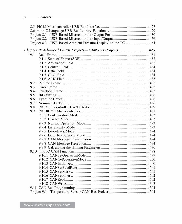
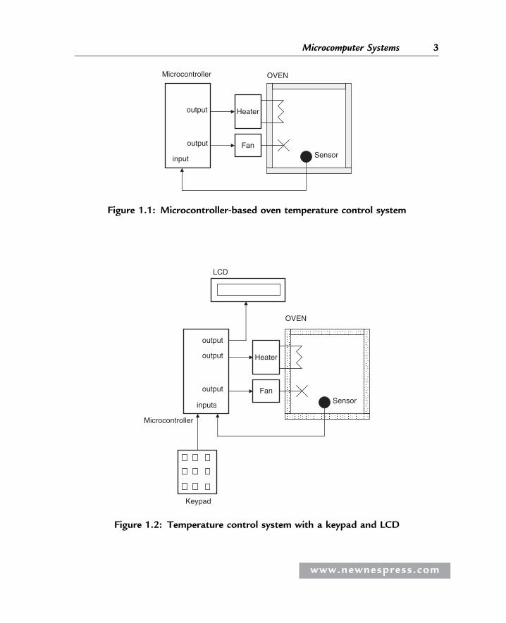
microcontroller-based oven temperature control system the microcomputer reads the
temperature using a temperature sensor and then operates a heater or a fan to keep
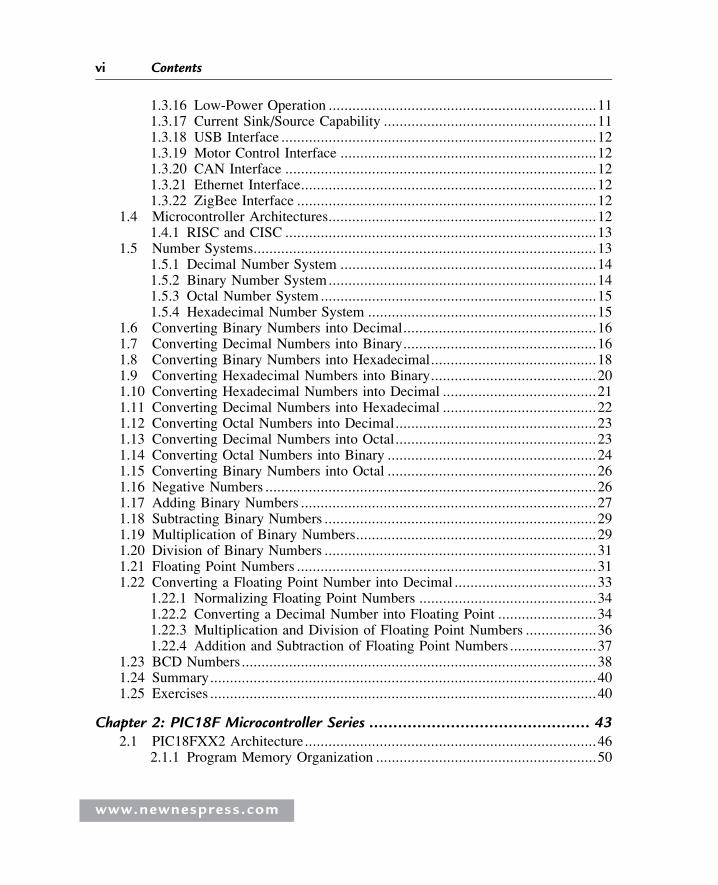
the temperature at the required value. Figure 1.1 shows a block diagram of a simple
oven temperature control system.
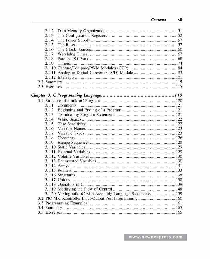
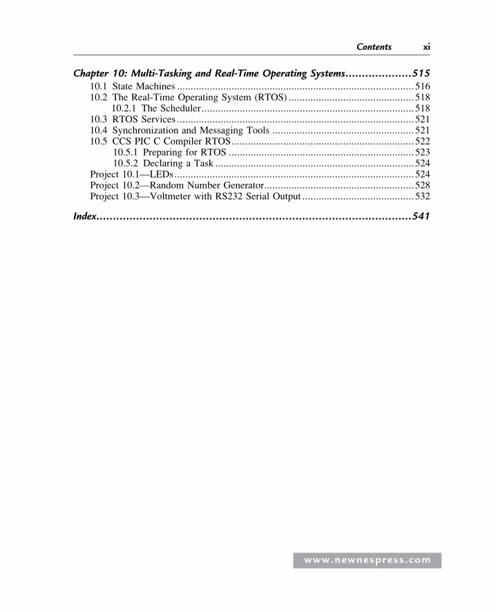
The system shown in Figure 1.1 is very simple. A more sophisticated system may
include a keypad to set the temperature and an LCD to display it. Figure 1.2 shows a
block diagram of this more sophisticated temperature control system.
www.newnespress.com
2 Chapter 1
Heater
FanSensorinput
output
output
OVENMicrocontroller
Figure 1.1: Microcontroller-based oven temperature control system
Heater
FanSensor
inputs
output
output
OVEN
Microcontroller
LCD
output
Keypad
Figure 1.2: Temperature control system with a keypad and LCD
www.newnespress.com
3Microcomputer Systems
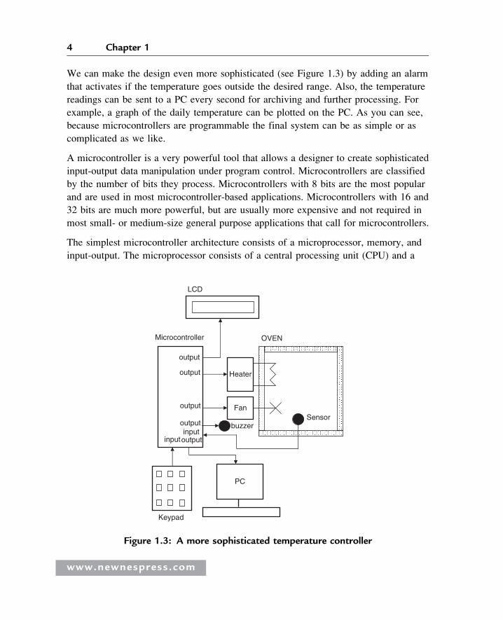
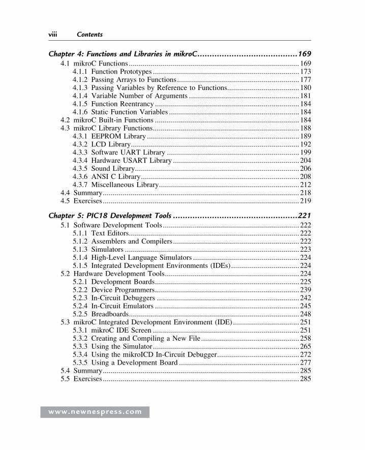
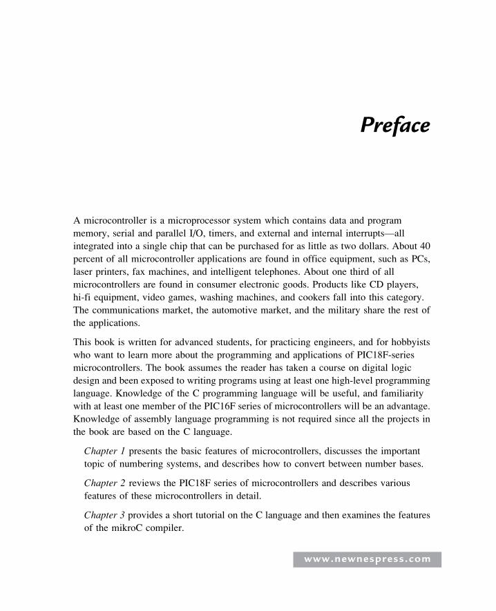
We can make the design even more sophisticated (see Figure 1.3) by adding an alarm
that activates if the temperature goes outside the desired range. Also, the temperature
readings can be sent to a PC every second for archiving and further processing. For
example, a graph of the daily temperature can be plotted on the PC. As you can see,
because microcontrollers are programmable the final system can be as simple or as
complicated as we like.
A microcontroller is a very powerful tool that allows a designer to create sophisticated
input-output data manipulation under program control. Microcontrollers are classified
by the number of bits they process. Microcontrollers with 8 bits are the most popular
and are used in most microcontroller-based applications. Microcontrollers with 16 and
32 bits are much more powerful, but are usually more expensive and not required in
most small- or medium-size general purpose applications that call for microcontrollers.
The simplest microcontroller architecture consists of a microprocessor, memory, and
input-output. The microprocessor consists of a central processing unit (CPU) and a
Heater
FanSensor
input
output
output
OVENMicrocontroller
LCD
output
Keypad
output
PC
buzzeroutput input
Figure 1.3: A more sophisticated temperature controller
www.newnespress.com
4 Chapter 1
control unit (CU). The CPU is the brain of the microcontroller; this is where all the
arithmetic and logic operations are performed. The CU controls the internal operations
of the microprocessor and sends signals to other parts of the microcontroller to carry out
the required instructions.
Memory, an important part of a microcontroller system, can be classified into two
types: program memory and data memory. Program memory stores the program written
by the programmer and is usually nonvolatile (i.e., data is not lost after the power is
turned off). Data memory stores the temporary data used in a program and is usually
volatile (i.e., data is lost after the power is turned off).
There are basically six types of memories, summarized as follows:
1.2.1 RAM
RAM, random access memory, is a general purpose memory that usually stores the
user data in a program. RAM memory is volatile in the sense that it cannot retain
data in the absence of power (i.e., data is lost after the power is turned off). Most
microcontrollers have some amount of internal RAM, 256 bytes being a common
amount, although some microcontrollers have more, some less. The PIC18F452
microcontroller, for example, has 1536 bytes of RAM. Memory can usually be extended
by adding external memory chips.
1.2.2 ROM
ROM, read only memory, usually holds program or fixed user data. ROM is
nonvolatile. If power is removed from ROM and then reapplied, the original data
will still be there. ROM memory is programmed during the manufacturing process,
and the user cannot change its contents. ROM memory is only useful if you have
developed a program and wish to create several thousand copies of it.
1.2.3 PROM
PROM, programmable read only memory, is a type of ROM that can be
programmed in the field, often by the end user, using a device called a PROM
programmer. Once a PROM has been programmed, its contents cannot be changed.
PROMs are usually used in low production applications where only a few such
memories are required.
www.newnespress.com
5Microcomputer Systems
1.2.4 EPROM
EPROM, erasable programmable read only memory, is similar to ROM, but EPROM
can be programmed using a suitable programming device. An EPROM memory has a
small clear-glass window on top of the chip where the data can be erased under strong
ultraviolet light. Once the memory is programmed, the window can be covered with
dark tape to prevent accidental erasure of the data. An EPROM memory must be erased
before it can be reprogrammed. Many developmental versions of microcontrollers are
manufactured with EPROM memories where the user program can be stored. These
memories are erased and reprogrammed until the user is satisfied with the program.
Some versions of EPROMs, known as OTP (one time programmable), can be
programmed using a suitable programmer device but cannot be erased. OTP memories
cost much less than EPROMs. OTP is useful after a project has been developed
completely and many copies of the program memory must be made.
1.2.5 EEPROM
EEPROM, electrically erasable programmable read only memory, is a nonvolatile
memory that can be erased and reprogrammed using a suitable programming device.
EEPROMs are used to save configuration information, maximum and minimum values,
identification data, etc. Some microcontrollers have built-in EEPROM memories. For
instance, the PIC18F452 contains a 256-byte EEPROM memory where each byte can be
programmed and erased directly by applications software. EEPROM memories are
usually very slow. An EEPROM chip is much costlier than an EPROM chip.
1.2.6 Flash EEPROM
Flash EEPROM, a version of EEPROM memory, has become popular in microcontroller
applications and is used to store the user program. Flash EEPROM is nonvolatile and
usually very fast. The data can be erased and then reprogrammed using a suitable
programming device. Some microcontrollers have only 1K flash EEPROM while others
have 32K or more. The PIC18F452 microcontroller has 32K bytes of flash memory.
1.3 Microcontroller Features
Microcontrollers from different manufacturers have different architectures and different
capabilities. Some may suit a particular application while others may be totally
www.newnespress.com
6 Chapter 1
unsuitable for the same application. The hardware features common to most
microcontrollers are described in this section.
1.3.1 Supply Voltage
Most microcontrollers operate with the standard logic voltage of þ5V. Some
microcontrollers can operate at as low as þ2.7V, and some will tolerate þ6V without
any problem. The manufacturer’s data sheet will have information about the allowed
limits of the power supply voltage. PIC18F452 microcontrollers can operate with a
power supply of þ2V to þ5.5V.
Usually, a voltage regulator circuit is used to obtain the required power supply voltage
when the device is operated from a mains adapter or batteries. For example, a 5V
regulator is required if the microcontroller is operated from a 5V supply using a 9V
battery.
1.3.2 The Clock
All microcontrollers require a clock (or an oscillator) to operate, usually provided by
external timing devices connected to the microcontroller. In most cases, these external
timing devices are a crystal plus two small capacitors. In some cases they are resonators
or an external resistor-capacitor pair. Some microcontrollers have built-in timing
circuits and do not require external timing components. If an application is not time-
sensitive, external or internal (if available) resistor-capacitor timing components are the
best option for their simplicity and low cost.
An instruction is executed by fetching it from the memory and then decoding it. This
usually takes several clock cycles and is known as the instruction cycle. In PIC
microcontrollers, an instruction cycle takes four clock periods. Thus the microcontroller
operates at a clock rate that is one-quarter of the actual oscillator frequency. The
PIC18F series of microcontrollers can operate with clock frequencies up to 40MHz.
1.3.3 Timers
Timers are important parts of any microcontroller. A timer is basically a counter which
is driven from either an external clock pulse or the microcontroller’s internal oscillator.
A timer can be 8 bits or 16 bits wide. Data can be loaded into a timer under program
control, and the timer can be stopped or started by program control. Most timers can be
www.newnespress.com
7Microcomputer Systems
configured to generate an interrupt when they reach a certain count (usually when they
overflow). The user program can use an interrupt to carry out accurate timing-related
operations inside the microcontroller. Microcontrollers in the PIC18F series have at
least three timers. For example, the PIC18F452 microcontroller has three built-in
timers.
Some microcontrollers offer capture and compare facilities, where a timer value can be
read when an external event occurs, or the timer value can be compared to a preset
value, and an interrupt is generated when this value is reached. Most PIC18F
microcontrollers have at least two capture and compare modules.
1.3.4 Watchdog
Most microcontrollers have at least one watchdog facility. The watchdog is basically a
timer that is refreshed by the user program. Whenever the program fails to refresh
the watchdog, a reset occurs. The watchdog timer is used to detect a system problem,
such as the program being in an endless loop. This safety feature prevents runaway
software and stops the microcontroller from executing meaningless and unwanted
code. Watchdog facilities are commonly used in real-time systems where the
successful termination of one or more activities must be checked regularly.
1.3.5 Reset Input
A reset input is used to reset a microcontroller externally. Resetting puts the
microcontroller into a known state such that the program execution starts from address
0 of the program memory. An external reset action is usually achieved by connecting
a push-button switch to the reset input. When the switch is pressed, the microcontroller
is reset.
1.3.6 Interrupts
Interrupts are an important concept in microcontrollers. An interrupt causes the
microcontroller to respond to external and internal (e.g., a timer) events very quickly.
When an interrupt occurs, the microcontroller leaves its normal flow of program
execution and jumps to a special part of the program known as the interrupt service
routine (ISR). The program code inside the ISR is executed, and upon return from the
ISR the program resumes its normal flow of execution.
www.newnespress.com
8 Chapter 1
The ISR starts from a fixed address of the program memory sometimes known as the
interrupt vector address. Some microcontrollers with multi-interrupt features have just
one interrupt vector address, while others have unique interrupt vector addresses, one
for each interrupt source. Interrupts can be nested such that a new interrupt can suspend
the execution of another interrupt. Another important feature of multi-interrupt
capability is that different interrupt sources can be assigned different levels of priority.
For example, the PIC18F series of microcontrollers has both low-priority and high-
priority interrupt levels.
1.3.7 Brown-out Detector
Brown-out detectors, which are common in many microcontrollers, reset the
microcontroller if the supply voltage falls below a nominal value. These safety features
can be employed to prevent unpredictable operation at low voltages, especially to
protect the contents of EEPROM-type memories.
1.3.8 Analog-to-Digital Converter
An analog-to-digital converter (A/D) is used to convert an analog signal, such as
voltage, to digital form so a microcontroller can read and process it. Some
microcontrollers have built-in A/D converters. External A/D converter can also be
connected to any type of microcontroller. A/D converters are usually 8 to 10 bits,
having 256 to 1024 quantization levels. Most PIC microcontrollers with A/D features
have multiplexed A/D converters which provide more than one analog input channel.
For example, the PIC18F452 microcontroller has 10-bit 8-channel A/D converters.
The A/D conversion process must be started by the user program and may take several
hundred microseconds to complete. A/D converters usually generate interrupts when a
conversion is complete so the user program can read the converted data quickly.
A/D converters are especially useful in control and monitoring applications, since most
sensors (e.g., temperature sensors, pressure sensors, force sensors, etc.) produce analog
output voltages.
1.3.9 Serial Input-Output
Serial communication (also called RS232 communication) enables a microcontroller
to be connected to another microcontroller or to a PC using a serial cable. Some
www.newnespress.com
9Microcomputer Systems
microcontrollers have built-in hardware called USART (universal synchronous-
asynchronous receiver-transmitter) to implement a serial communication interface.
The user program can usually select the baud rate and data format. If no serial
input-output hardware is provided, it is easy to develop software to implement serial
data communication using any I/O pin of a microcontroller. The PIC18F series of
microcontrollers has built-in USART modules. We shall see in Chapter 6 how to write
mikroC programs to implement serial communicationwith andwithout aUSARTmodule.
Some microcontrollers (e.g., the PIC18F series) incorporate SPI (serial peripheral
interface) or I2C (integrated interconnect) hardware bus interfaces. These enable a
microcontroller to interface with other compatible devices easily.
1.3.10 EEPROM Data Memory
EEPROM-type data memory is also very common in many microcontrollers. The
advantage of an EEPROM memory is that the programmer can store nonvolatile data
there and change this data whenever required. For example, in a temperature monitoring
application, the maximum and minimum temperature readings can be stored in an
EEPROMmemory. If the power supply is removed for any reason, the values of the latest
readings are available in the EEPROMmemory. The PIC18F452 microcontroller has 256
bytes of EEPROM memory. Other members of the PIC18F family have more EEPROM
memory (e.g., the PIC18F6680 has 1024 bytes). The mikroC language provides special
instructions for reading and writing to the EEPROM memory of a PIC microcontroller.
1.3.11 LCD Drivers
LCD drivers enable a microcontroller to be connected to an external LCD display
directly. These drivers are not common since most of the functions they provide can be
implemented in software. For example, the PIC18F6490 microcontroller has a built-in
LCD driver module.
1.3.12 Analog Comparator
Analog comparators are used where two analog voltages need to be compared.
Although these circuits are implemented in most high-end PIC microcontrollers, they
are not common in other microcontrollers. The PIC18F series of microcontrollers has
built-in analog comparator modules.
www.newnespress.com
10 Chapter 1
1.3.13 Real-time Clock
A real-time clock enables a microcontroller to receive absolute date and time
information continuously. Built-in real-time clocks are not common in most
microcontrollers, since the same function can easily be implemented by either a
dedicated real-time clock chip or a program written for this purpose.
1.3.14 Sleep Mode
Some microcontrollers (e.g., PICs) offer built-in sleep modes, where executing this
instruction stops the internal oscillator and reduces power consumption to an extremely
low level. The sleep mode’s main purpose is to conserve battery power when the
microcontroller is not doing anything useful. The microcontroller is usually woken up
from sleep mode by an external reset or a watchdog time-out.
1.3.15 Power-on Reset
Some microcontrollers (e.g., PICs) have built-in power-on reset circuits which keep the
microcontroller in the reset state until all the internal circuitry has been initialized. This
feature is very useful, as it starts the microcontroller from a known state on power-up.
An external reset can also be provided, where the microcontroller is reset when an
external button is pressed.
1.3.16 Low-Power Operation
Low-power operation is especially important in portable applications where
microcontroller-based equipment is operated from batteries. Some microcontrollers
(e.g., PICs) can operate with less than 2mA with a 5V supply, and around 15mA at a 3V
supply. Other microcontrollers, especially microprocessor-based systems with several
chips, may consume several hundred milliamperes or even more.
1.3.17 Current Sink/Source Capability
Current sink/source capability is important if the microcontroller is to be connected
to an external device that might draw a large amount of current to operate. PIC
microcontrollers can source and sink 25mA of current from each output port pin. This
current is usually sufficient to drive LEDs, small lamps, buzzers, small relays, etc. The
www.newnespress.com
11Microcomputer Systems
current capability can be increased by connecting external transistor switching circuits
or relays to the output port pins.
1.3.18 USB Interface
USB is currently a very popular computer interface specification used to connect
various peripheral devices to computers and microcontrollers. Some PIC
microcontrollers provide built-in USB modules. The PIC18F2x50, for example,
has built-in USB interface capabilities.
1.3.19 Motor Control Interface
Some PIC microcontrollers, for example the PIC18F2x31, provide motor control
interface capability.
1.3.20 CAN Interface
CAN bus is a very popular bus system used mainly in automation applications. Some
PIC18F-series microcontrollers (e.g., the PIC18F4680) provide CAN interface
capability.
1.3.21 Ethernet Interface
Some PIC microcontrollers (e.g., the PIC18F97J60) provide Ethernet interface
capabilities and thus are easily used in network-based applications.
1.3.22 ZigBee Interface
ZigBee, an interface similar to Bluetooth, is used in low-cost wireless home automation
applications. Some PIC18F-series microcontrollers provide ZigBee interface
capabilities, making the design of such wireless systems very easy.
1.4 Microcontroller Architectures
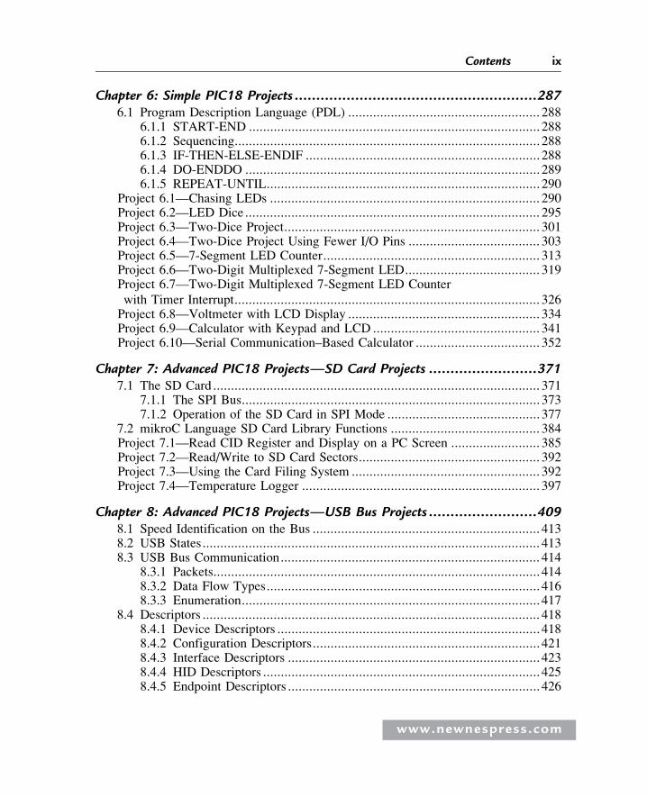
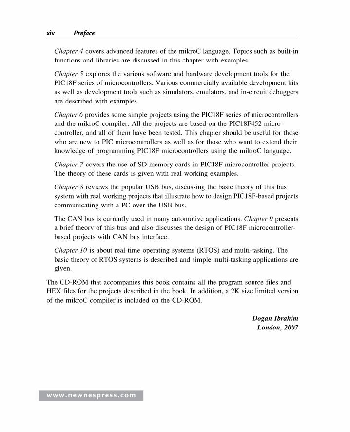
Two types of architectures are conventional in microcontrollers (see Figure 1.4).
Von Neumann architecture, used by a large percentage of microcontrollers, places
all memory space on the same bus; instruction and data also use the same bus.
www.newnespress.com
12 Chapter 1
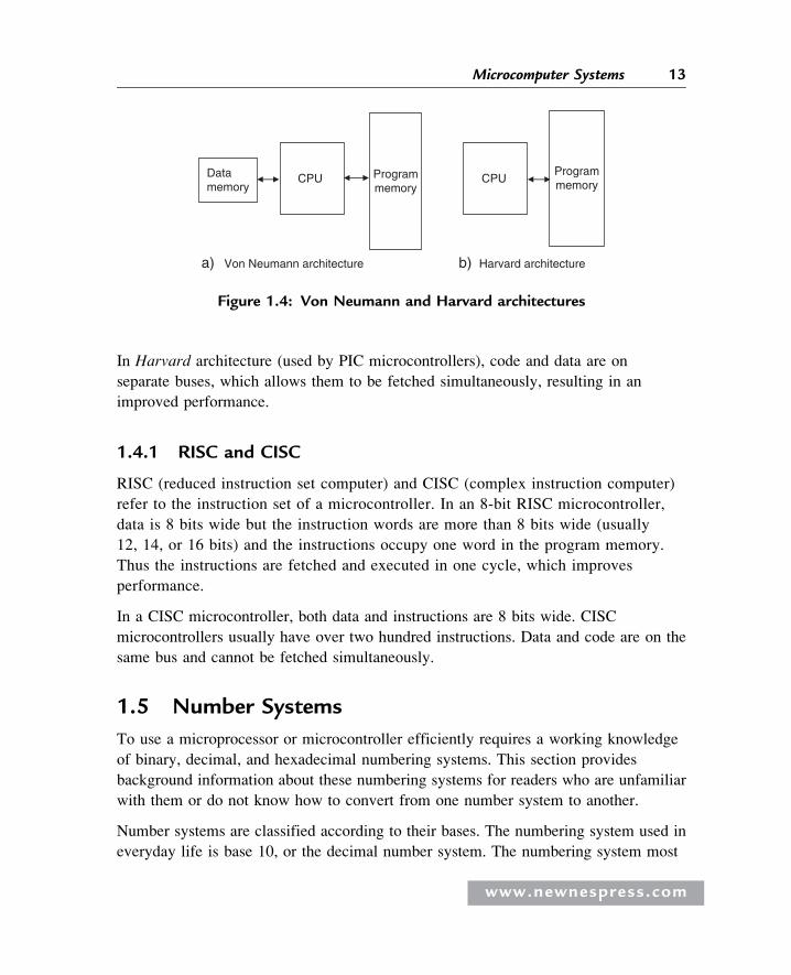
In Harvard architecture (used by PIC microcontrollers), code and data are on
separate buses, which allows them to be fetched simultaneously, resulting in an
improved performance.
1.4.1 RISC and CISC
RISC (reduced instruction set computer) and CISC (complex instruction computer)
refer to the instruction set of a microcontroller. In an 8-bit RISC microcontroller,
data is 8 bits wide but the instruction words are more than 8 bits wide (usually
12, 14, or 16 bits) and the instructions occupy one word in the program memory.
Thus the instructions are fetched and executed in one cycle, which improves
performance.
In a CISC microcontroller, both data and instructions are 8 bits wide. CISC
microcontrollers usually have over two hundred instructions. Data and code are on the
same bus and cannot be fetched simultaneously.
1.5 Number Systems
To use a microprocessor or microcontroller efficiently requires a working knowledge
of binary, decimal, and hexadecimal numbering systems. This section provides
background information about these numbering systems for readers who are unfamiliar
with them or do not know how to convert from one number system to another.
Number systems are classified according to their bases. The numbering system used in
everyday life is base 10, or the decimal number system. The numbering system most
CPU Datamemory
Programmemory
CPU Programmemory
Von Neumann architecture Harvard architecture a) b)
Figure 1.4: Von Neumann and Harvard architectures
www.newnespress.com
13Microcomputer Systems

commonly used in microprocessor and microcontroller applications is base 16,
or hexadecimal. Base 2, or binary, and base 8, or octal, number systems are
also used.
1.5.1 Decimal Number System
The numbers in the decimal number system, of course, are 0, 1, 2, 3, 4, 5, 6, 7, 8, 9. The
subscript 10 indicates that a number is in decimal format. For example, the decimal
number 235 is shown as 23510.
In general, a decimal number is represented as follows:
an � 10n þ an�1 � 10n�1 þ an�2 � 10n�2 þ ::::::::: þ a0 � 100
For example, decimal number 82510 can be shown as:
82510 ¼ 8 � 102 þ 2 � 101 þ 5 � 100
Similarly, decimal number 2610 can be shown as:
2610 ¼ 2 � 101 þ 6 � 100
or
335910 ¼ 3 � 103 þ 3 � 102 þ 5 � 101 þ 9 � 100
1.5.2 Binary Number System
The binary number system consists of two numbers: 0 and 1. A subscript 2 indicates that a
number is in binary format. For example, the binary number 1011 would be 10112.
In general, a binary number is represented as follows:
an � 2n þ an�1 � 2n�1 þ an�2 � 2n�2 þ ::::::::: þ a0 � 20
For example, binary number 11102 can be shown as:
11102 ¼ 1 � 23 þ 1 � 22 þ 1 � 21 þ 0 � 20
www.newnespress.com
14 Chapter 1
Similarly, binary number 100011102 can be shown as:
100011102 ¼ 1 � 27 þ 0 � 26 þ 0 � 25 þ 0 � 24 þ 1 � 23
þ 1 � 22 þ 1 � 21 þ 0 � 20
1.5.3 Octal Number System
In the octal number system, the valid numbers are 0, 1, 2, 3, 4, 5, 6, 7. A subscript
8 indicates that a number is in octal format. For example, the octal number 23 appears
as 238.
In general, an octal number is represented as:
an � 8n þ an�1 � 8n�1 þ an�2 � 8n�2 þ ::::::::: þ a0 � 80
For example, octal number 2378 can be shown as:
2378 ¼ 2 � 82 þ 3 � 81 þ 7 � 80
Similarly, octal number 17778 can be shown as:
17778 ¼ 1 � 83 þ 7 � 82 þ 7 � 81 þ 7 � 80
1.5.4 Hexadecimal Number System
In the hexadecimal number system, the valid numbers are: 0, 1, 2, 3, 4, 5, 6, 7, 8, 9, A,
B, C, D, E, F. A subscript 16 or subscript H indicates that a number is in hexadecimal
format. For example, hexadecimal number 1F can be written as 1F16 or as 1FH.
In general, a hexadecimal number is represented as:
an � 16n þ an�1 � 16n�1 þ an�2 � 16n�2 þ ::::::::: þ a0 � 160
For example, hexadecimal number 2AC16 can be shown as:
2AC16 ¼ 2 � 162 þ 10 � 161 þ 12 � 160
Similarly, hexadecimal number 3FFE16 can be shown as:
3FFE16 ¼ 3 � 163 þ 15 � 162 þ 15 � 161 þ 14 � 160
www.newnespress.com
15Microcomputer Systems
1.6 Converting Binary Numbers into Decimal
To convert a binary number into decimal, write the number as the sum of the powers of 2.
Example 1.1
Convert binary number 10112 into decimal.
Solution 1.1
Write the number as the sum of the powers of 2:
10112 ¼ 1 � 23 þ 0 � 22 þ 1 � 21 þ 1 � 20
¼ 8 þ 0 þ 2 þ 1
¼ 11
or; 10112 ¼ 1110
Example 1.2
Convert binary number 110011102 into decimal.
Solution 1.2
Write the number as the sum of the powers of 2:
110011102 ¼ 1 � 27 þ 1 � 26 þ 0 � 25 þ 0 � 24
þ 1 � 23 þ 1 � 22 þ 1 � 21 þ 0 � 20
¼ 128 þ 64 þ 0 þ 0 þ 8 þ 4 þ 2 þ 0
¼ 206
or; 110011102 ¼ 20610
Table 1.1 shows the decimal equivalent of numbers from 0 to 31.
1.7 Converting Decimal Numbers into Binary
To convert a decimal number into binary, divide the number repeatedly by 2 and take
the remainders. The first remainder is the least significant digit (LSD), and the last
remainder is the most significant digit (MSD).
Example 1.3
Convert decimal number 2810 into binary.
www.newnespress.com
16 Chapter 1
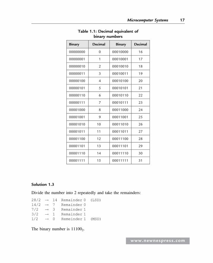
Solution 1.3
Divide the number into 2 repeatedly and take the remainders:
28/2 ! 14 Remainder 0 (LSD)14/2 ! 7 Remainder 07/2 ! 3 Remainder 13/2 ! 1 Remainder 11/2 ! 0 Remeinder 1 (MSD)
The binary number is 111002.
Table 1.1: Decimal equivalent ofbinary numbers
Binary Decimal Binary Decimal
00000000 0 00010000 16
00000001 1 00010001 17
00000010 2 00010010 18
00000011 3 00010011 19
00000100 4 00010100 20
00000101 5 00010101 21
00000110 6 00010110 22
00000111 7 00010111 23
00001000 8 00011000 24
00001001 9 00011001 25
00001010 10 00011010 26
00001011 11 00011011 27
00001100 12 00011100 28
00001101 13 00011101 29
00001110 14 00011110 30
00001111 15 00011111 31
www.newnespress.com
17Microcomputer Systems
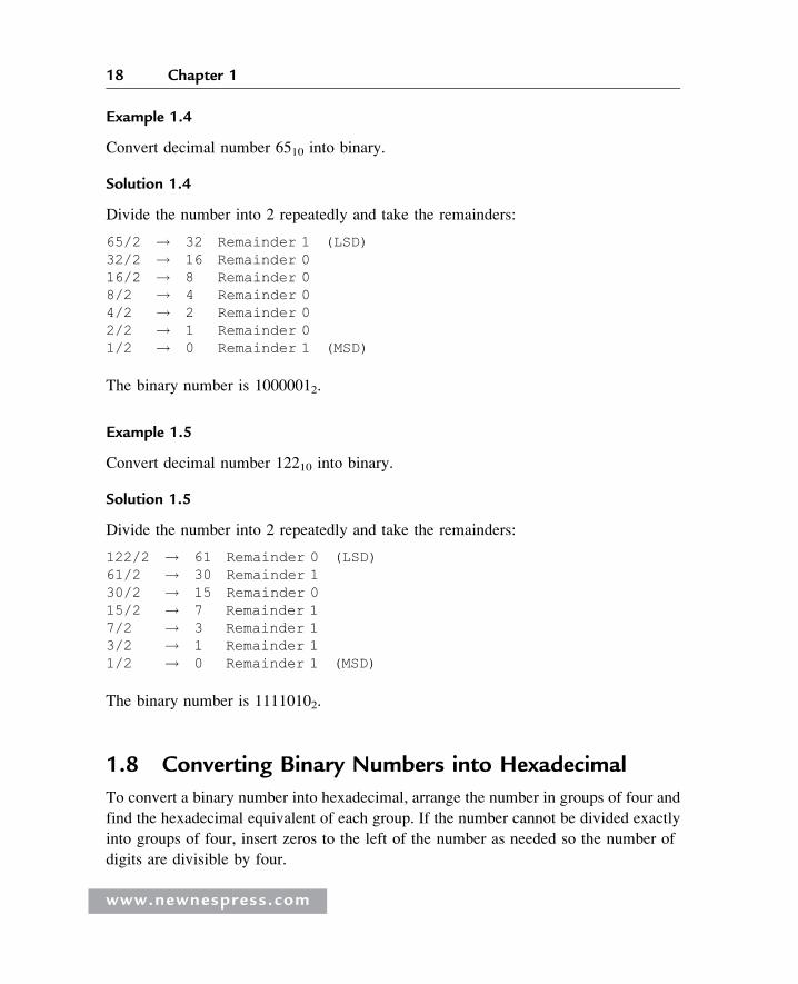
Example 1.4
Convert decimal number 6510 into binary.
Solution 1.4
Divide the number into 2 repeatedly and take the remainders:
65/2 ! 32 Remainder 1 (LSD)32/2 ! 16 Remainder 016/2 ! 8 Remainder 08/2 ! 4 Remainder 04/2 ! 2 Remainder 02/2 ! 1 Remainder 01/2 ! 0 Remainder 1 (MSD)
The binary number is 10000012.
Example 1.5
Convert decimal number 12210 into binary.
Solution 1.5
Divide the number into 2 repeatedly and take the remainders:
122/2 ! 61 Remainder 0 (LSD)61/2 ! 30 Remainder 130/2 ! 15 Remainder 015/2 ! 7 Remainder 17/2 ! 3 Remainder 13/2 ! 1 Remainder 11/2 ! 0 Remainder 1 (MSD)
The binary number is 11110102.
1.8 Converting Binary Numbers into Hexadecimal
To convert a binary number into hexadecimal, arrange the number in groups of four and
find the hexadecimal equivalent of each group. If the number cannot be divided exactly
into groups of four, insert zeros to the left of the number as needed so the number of
digits are divisible by four.
www.newnespress.com
18 Chapter 1
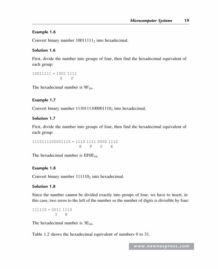
Example 1.6
Convert binary number 100111112 into hexadecimal.
Solution 1.6
First, divide the number into groups of four, then find the hexadecimal equivalent of
each group:
10011111 = 1001 11119 F
The hexadecimal number is 9F16.
Example 1.7
Convert binary number 11101111000011102 into hexadecimal.
Solution 1.7
First, divide the number into groups of four, then find the hexadecimal equivalent of
each group:
1110111100001110 = 1110 1111 0000 1110E F 0 E
The hexadecimal number is EF0E16.
Example 1.8
Convert binary number 1111102 into hexadecimal.
Solution 1.8
Since the number cannot be divided exactly into groups of four, we have to insert, in
this case, two zeros to the left of the number so the number of digits is divisible by four:
111110 = 0011 11103 E
The hexadecimal number is 3E16.
Table 1.2 shows the hexadecimal equivalent of numbers 0 to 31.
www.newnespress.com
19Microcomputer Systems
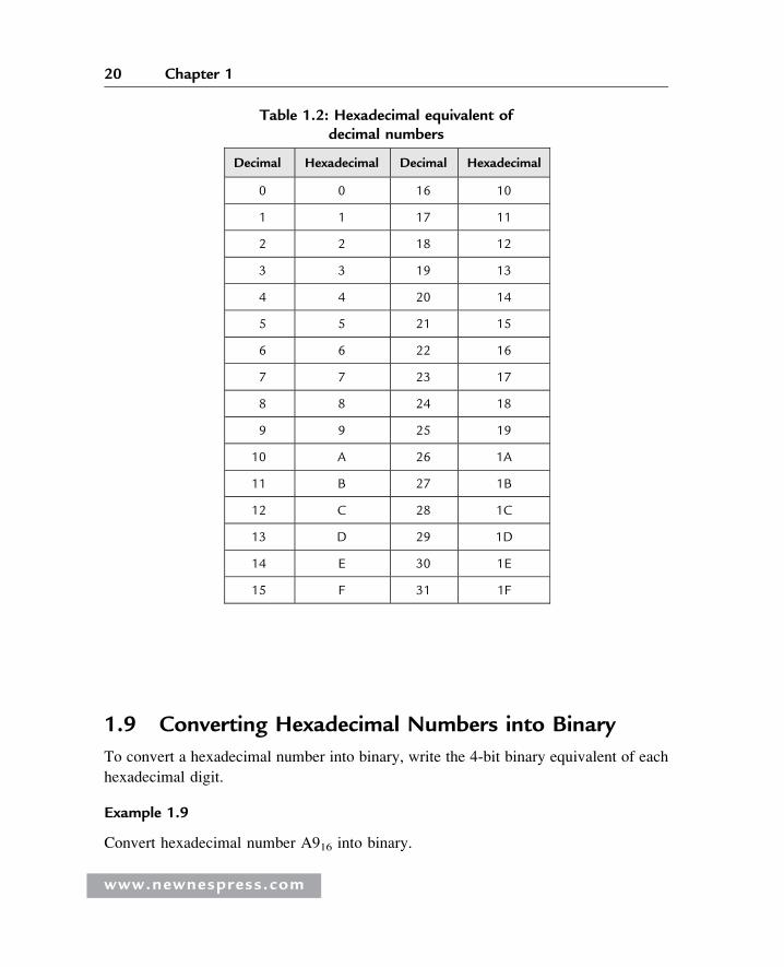
1.9 Converting Hexadecimal Numbers into Binary
To convert a hexadecimal number into binary, write the 4-bit binary equivalent of each
hexadecimal digit.
Example 1.9
Convert hexadecimal number A916 into binary.
Table 1.2: Hexadecimal equivalent ofdecimal numbers
Decimal Hexadecimal Decimal Hexadecimal
0 0 16 10
1 1 17 11
2 2 18 12
3 3 19 13
4 4 20 14
5 5 21 15
6 6 22 16
7 7 23 17
8 8 24 18
9 9 25 19
10 A 26 1A
11 B 27 1B
12 C 28 1C
13 D 29 1D
14 E 30 1E
15 F 31 1F
www.newnespress.com
20 Chapter 1

Solution 1.9
Writing the binary equivalent of each hexadecimal digit:
A = 10102 9 = 10012
The binary number is 101010012.
Example 1.10
Convert hexadecimal number FE3C16 into binary.
Solution 1.10
Writing the binary equivalent of each hexadecimal digit:
F = 11112 E = 11102 3 = 00112 C = 11002
The binary number is 11111110001111002.
1.10 Converting Hexadecimal Numbers into Decimal
To convert a hexadecimal number into decimal, calculate the sum of the powers of
16 of the number.
Example 1.11
Convert hexadecimal number 2AC16 into decimal.
Solution 1.11
Calculating the sum of the powers of 16 of the number:
2AC16 ¼ 2 � 162 þ 10 � 161 þ 12 � 160
¼ 512 þ 160 þ 12
¼ 684
The required decimal number is 68410.
Example 1.12
Convert hexadecimal number EE16 into decimal.
www.newnespress.com
21Microcomputer Systems
Solution 1.12
Calculating the sum of the powers of 16 of the number:
EE16 ¼ 14 � 161 þ 14 � 160
¼ 224 þ 14
¼ 238
The decimal number is 23810.
1.11 Converting Decimal Numbers into Hexadecimal
To convert a decimal number into hexadecimal, divide the number repeatedly by 16 and
take the remainders. The first remainder is the LSD, and the last remainder is the MSD.
Example 1.13
Convert decimal number 23810 into hexadecimal.
Solution 1.13
Dividing the number repeatedly by 16:
238/16 ! 14 Remainder 14 (E) (LSD)14/16 ! 0 Remainder 14 (E) (MSD)
The hexadecimal number is EE16.
Example 1.14
Convert decimal number 68410 into hexadecimal.
Solution 1.14
Dividing the number repeatedly by 16:
684/16 ! 42 Remainder 12 (C) (LSD)42/16 ! 2 Remainder 10 (A)2/16 ! 0 Remainder 2 (MSD)
The hexadecimal number is 2AC16.
www.newnespress.com
22 Chapter 1
1.12 Converting Octal Numbers into Decimal
To convert an octal number into decimal, calculate the sum of the powers of 8 of the
number.
Example 1.15
Convert octal number 158 into decimal.
Solution 1.15
Calculating the sum of the powers of 8 of the number:
158 ¼ 1 � 81 þ 5 � 80
¼ 8 þ 5
¼ 13
The decimal number is 1310.
Example 1.16
Convert octal number 2378 into decimal.
Solution 1.16
Calculating the sum of the powers of 8 of the number:
2378 ¼ 2 � 82 þ 3 � 81 þ 7 � 80
¼ 128 þ 24 þ 7
¼ 159
The decimal number is 15910.
1.13 Converting Decimal Numbers into Octal
To convert a decimal number into octal, divide the number repeatedly by 8 and take the
remainders. The first remainder is the LSD, and the last remainder is
the MSD.
Example 1.17
Convert decimal number 15910 into octal.
www.newnespress.com
23Microcomputer Systems
Solution 1.17
Dividing the number repeatedly by 8:
159/8 ! 19 Remainder 7 (LSD)19/8 ! 2 Remainder 32/8 ! 0 Remainder 2 (MSD)
The octal number is 2378.
Example 1.18
Convert decimal number 46010 into octal.
Solution 1.18
Dividing the number repeatedly by 8:
460/8 ! 57 Remainder 4 (LSD)57/8 ! 7 Remainder 17/8 ! 0 Remainder 7 (MSD)
The octal number is 7148.
Table 1.3 shows the octal equivalent of decimal numbers 0 to 31.
1.14 Converting Octal Numbers into Binary
To convert an octal number into binary, write the 3-bit binary equivalent of each
octal digit.
Example 1.19
Convert octal number 1778 into binary.
Solution 1.19
Write the binary equivalent of each octal digit:
1 = 0012 7 = 1112 7 = 1112
The binary number is 0011111112.
www.newnespress.com
24 Chapter 1
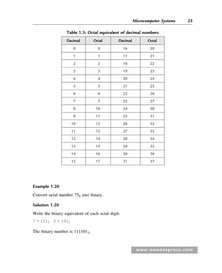
Example 1.20
Convert octal number 758 into binary.
Solution 1.20
Write the binary equivalent of each octal digit:
7 = 1112 5 = 1012
The binary number is 1111012.
Table 1.3: Octal equivalent of decimal numbers
Decimal Octal Decimal Octal
0 0 16 20
1 1 17 21
2 2 18 22
3 3 19 23
4 4 20 24
5 5 21 25
6 6 22 26
7 7 23 27
8 10 24 30
9 11 25 31
10 12 26 32
11 13 27 33
12 14 28 34
13 15 29 35
14 16 30 36
15 17 31 37
www.newnespress.com
25Microcomputer Systems
1.15 Converting Binary Numbers into Octal
To convert a binary number into octal, arrange the number in groups of three and write
the octal equivalent of each digit.
Example 1.21
Convert binary number 1101110012 into octal.
Solution 1.21
Arranging in groups of three:
110111001 = 110 111 0016 7 1
The octal number is 6718.
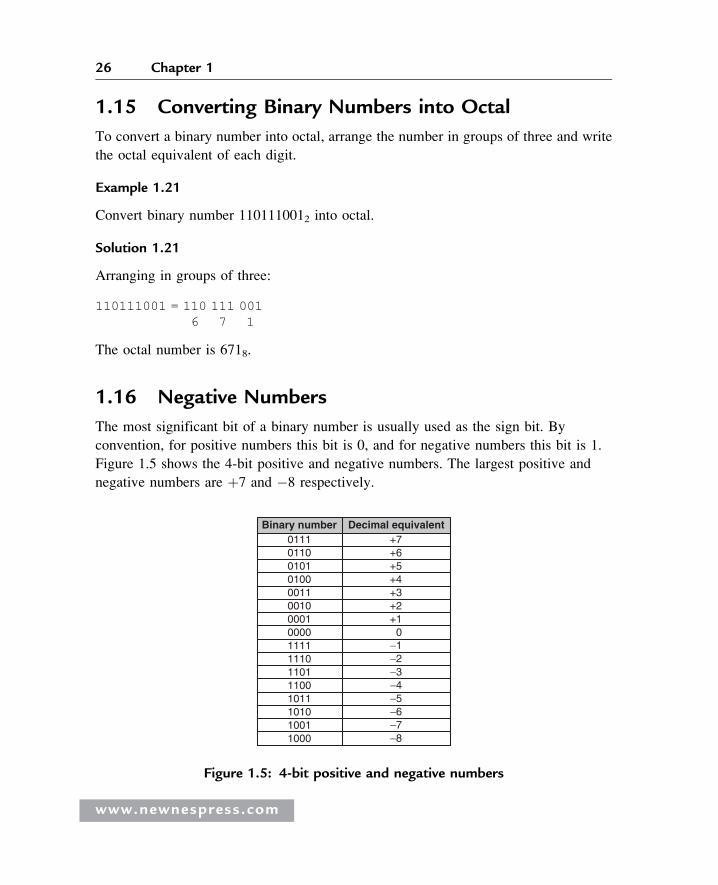
1.16 Negative Numbers
The most significant bit of a binary number is usually used as the sign bit. By
convention, for positive numbers this bit is 0, and for negative numbers this bit is 1.
Figure 1.5 shows the 4-bit positive and negative numbers. The largest positive and
negative numbers are þ7 and �8 respectively.
+5+4+3+2+1
0−1−2−3−4−5−6 −7−8
0111 +70110 +601010100001100100001000011111110110111001011101010011000
Decimal equivalent Binary number
Figure 1.5: 4-bit positive and negative numbers
www.newnespress.com
26 Chapter 1
To convert a positive number to negative, take the complement of the number
and add 1. This process is also called the 2’s complement of the
number.
Example 1.22
Write decimal number �6 as a 4-bit number.
Solution 1.22
First, write the number as a positive number, then find the complement and
add 1:
0110 þ6
1001 complement
1 add 1––––
1010 which is �6
Example 1.23
Write decimal number �25 as a 8-bit number.
Solution 1.23
First, write the number as a positive number, then find the complement and
add 1:
00011001 þ25
11100110 complement
1 add 1–––––––
11100111 which is �25
1.17 Adding Binary Numbers
The addition of binary numbers is similar to the addition of decimal numbers. Numbers
in each column are added together with a possible carry from a previous column. The
primitive addition operations are:
www.newnespress.com
27Microcomputer Systems

0 þ 0 = 00 þ 1 = 11 þ 0 = 11 þ 1 = 10 generate a carry bit1 þ 1 þ 1 = 11 generate a carry bit
Some examples follow.
Example 1.24
Find the sum of binary numbers 011 and 110.
Solution 1.24
We can add these numbers as in the addition of decimal numbers:
011 First column: 1 þ 0 ¼ 1
þ 110 Second column: 1 þ 1 ¼ 0 and a carry bit––––– Third column: 1 þ 1 ¼ 10
1001
Example 1.25
Find the sum of binary numbers 01000011 and 00100010.
Solution 1.25
We can add these numbers as in the addition of decimal numbers:
01000011 First column: 1 þ 0 ¼ 1
þ 00100010 Second column: 1 þ 1 ¼ 10–––––––––- Third column: 0 þ carry ¼ 1
01100101 Fourth column: 0 þ 0 ¼ 0
Fifth column: 0 þ 0 ¼ 0
Sixth column: 0 þ 1 ¼ 1
Seventh column: 1 þ 0 ¼ 1
Eighth column: 0 þ 0 ¼ 0
www.newnespress.com
28 Chapter 1
1.18 Subtracting Binary Numbers
To subtract one binary number from another, convert the number to be subtracted into
negative and then add the two numbers.
Example 1.26
Subtract binary number 0010 from 0110.
Solution 1.26
First, convert the number to be subtracted into negative:
0010 number to be subtracted
1101 complement
1 add 1––––
1110
Now add the two numbers:
0110þ 1110––––––
0100
Since we are using only 4 bits, we cannot show the carry bit.
1.19 Multiplication of Binary Numbers
Multiplication of two binary numbers is similar to the multiplication of two decimal
numbers. The four possibilities are:
0 � 0 ¼ 0
0 � 1 ¼ 0
1 � 0 ¼ 0
1 � 1 ¼ 1
Some examples follow.
www.newnespress.com
29Microcomputer Systems
Example 1.27
Multiply the two binary numbers 0110 and 0010.
Solution 1.27
Multiplying the numbers:
0110
0010-- -- -- --
0000
0110
0000
0000-- -- -- -- -- --
001100 or 1100
In this example 4 bits are needed to show the final result.
Example 1.28
Multiply binary numbers 1001 and 1010.
Solution 1.28
Multiplying the numbers:
1001
1010-- -- -- --0000
1001
0000
1001-- -- -- -- -- --
1011010
In this example 7 bits are required to show the final result.
www.newnespress.com
30 Chapter 1

1.20 Division of Binary Numbers
Division with binary numbers is similar to division with decimal numbers. An example
follows.
Example 1.29
Divide binary number 1110 into binary number 10.
Solution 1.29
Dividing the numbers:
111
10 j―――111010-- -- -- --
11
10-- -- -- --
10
10-- -- -- --
00
gives the result 1112.
1.21 Floating Point Numbers
Floating point numbers are used to represent noninteger fractional numbers, for
example, 3.256, 2.1, 0.0036, and so forth. Floating point numbers are used in most
engineering and technical calculations. The most common floating point standard is the
IEEE standard, according to which floating point numbers are represented with 32 bits
(single precision) or 64 bits (double precision).
In this section we are looking at the format of 32-bit floating point numbers only and
seeing how mathematical operations can be performed with such numbers.
www.newnespress.com
31Microcomputer Systems
According to the IEEE standard, 32-bit floating point numbers are represented as:
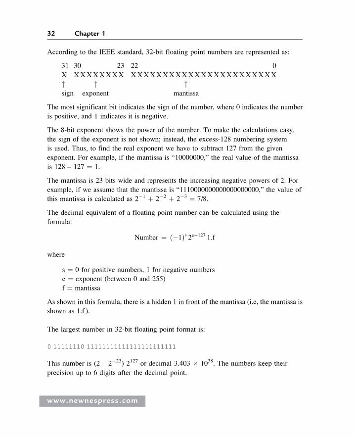
31 30 23 22 0
X XXXXXXXX XXXXXXXXXXXXXXXXXXXXXXX
" " "sign exponent mantissa
The most significant bit indicates the sign of the number, where 0 indicates the number
is positive, and 1 indicates it is negative.
The 8-bit exponent shows the power of the number. To make the calculations easy,
the sign of the exponent is not shown; instead, the excess-128 numbering system
is used. Thus, to find the real exponent we have to subtract 127 from the given
exponent. For example, if the mantissa is “10000000,” the real value of the mantissa
is 128 – 127 ¼ 1.
The mantissa is 23 bits wide and represents the increasing negative powers of 2. For
example, if we assume that the mantissa is “1110000000000000000000,” the value of
this mantissa is calculated as 2�1 þ 2�2 þ 2�3 ¼ 7/8.
The decimal equivalent of a floating point number can be calculated using the
formula:
Number ¼ �1ð Þs 2e�127 1:f
where
s ¼ 0 for positive numbers, 1 for negative numbers
e ¼ exponent (between 0 and 255)
f ¼ mantissa
As shown in this formula, there is a hidden 1 in front of the mantissa (i.e, the mantissa is
shown as 1.f ).
The largest number in 32-bit floating point format is:
0 11111110 11111111111111111111111
This number is (2 – 2�23) 2127 or decimal 3.403 � 1038. The numbers keep their
precision up to 6 digits after the decimal point.
www.newnespress.com
32 Chapter 1

The smallest number in 32-bit floating point format is:
0 00000001 00000000000000000000000
This number is 2�126 or decimal 1.175 � 10�38.
1.22 Converting a Floating Point Number into Decimal
To convert a given floating point number into decimal, we have to find the mantissa and
the exponent of the number and then convert into decimal as just shown.
Some examples are given here.
Example 1.30
Find the decimal equivalent of the floating point number: 0 10000001
10000000000000000000000
Solution 1.30
Here
sign = positiveexponent = 129 – 127 = 2mantissa = 2-1 = 0.5
The decimal equivalent of this number is þ1.5 � 22 ¼ þ6.0.
Example 1.31
Find the decimal equivalent of the floating point number: 0 10000010
11000000000000000000
Solution 1.31
In this example,
sign = positiveexponent = 130 – 127 = 3mantissa = 2-1 þ 2-2 = 0.75
The decimal equivalent of the number is þ1.75 � 23 ¼ 14.0.
www.newnespress.com
33Microcomputer Systems

1.22.1 Normalizing Floating Point Numbers
Floating point numbers are usually shown in normalized form. A normalized number
has only one digit before the decimal point (a hidden number 1 is assumed before the
decimal point).
To normalize a given floating point number, we have to move the decimal point
repeatedly one digit to the left and increase the exponent after each move.
Some examples follow.
Example 1.32
Normalize the floating point number 123.56
Solution 1.32
If we write the number with a single digit before the decimal point we get:
1.2356 x 10²
Example 1.33
Normalize the binary number 1011.12
Solution 1.33
If we write the number with a single digit before the decimal point we get:
1.0111 x 23
1.22.2 Converting a Decimal Number into Floating Point
To convert a given decimal number into floating point, carry out the following steps:
� Write the number in binary.
� Normalize the number.
� Find the mantissa and the exponent.
� Write the number as a floating point number.
Some examples follow:
www.newnespress.com
34 Chapter 1

Example 1.34
Convert decimal number 2.2510 into floating point.
Solution 1.34
Write the number in binary:
2:2510 ¼ 10:012
Normalize the number:
10:012 ¼ 1:0012 � 21
Here, s ¼ 0, e – 127 ¼ 1 or e ¼ 128, and f ¼ 00100000000000000000000.
(Remember that a number 1 is assumed on the left side, even though it is not shown in
the calculation). The required floating point number can be written as:
s e f0 10000000 (1)001 0000 0000 0000 0000 0000
or, the required 32-bit floating point number is:
01000000000100000000000000000000
Example 1.35
Convert the decimal number 134.062510 into floating point.
Solution 1.35
Write the number in binary:
134.062510 = 10000110.0001
Normalize the number:
10000110.0001 = 1.00001100001 x 27
Here, s ¼ 0, e – 127 ¼ 7 or e ¼ 134, and f ¼ 00001100001000000000000.
www.newnespress.com
35Microcomputer Systems

The required floating point number can be written as:
s e f0 10000110 (1)00001100001000000000000
or, the required 32-bit floating point number is:
01000011000001100001000000000000
1.22.3 Multiplication and Division of Floating Point Numbers
Multiplication and division of floating point numbers are rather easy. Here are the steps:
� Add (or subtract) the exponents of the numbers.
� Multiply (or divide) the mantissa of the numbers.
� Correct the exponent.
� Normalize the number.
� The sign of the result is the EXOR of the signs of the two numbers.
Since the exponent is processed twice in the calculations, we have to subtract 127 from
the exponent.
An example showing the multiplication of two floating point numbers follows.
Example 1.36
Show the decimal numbers 0.510 and 0.7510 in floating point and then calculate their
multiplication.
Solution 1.36
Convert the numbers into floating point as:
0.510 = 1.0000 x 2-1
here, s = 0, e – 127 = -1 or e = 126 and f = 0000or,
0.510 = 0 01110110 (1)000 0000 0000 0000 0000 0000Similarly,
0.7510 = 1.1000 x 2-1
www.newnespress.com
36 Chapter 1

here, s = 0, e = 126 and f = 1000or,
0.7510 = 0 01110110 (1)100 0000 0000 0000 0000 0000
Multiplying the mantissas results in “(1)100 0000 0000 0000 0000 0000.” The sum
of the exponents is 126 þ 126 ¼ 252. Subtracting 127 from the mantissa, we obtain
252 – 127 ¼ 125. The EXOR of the signs of the numbers is 0. Thus, the result can
be shown in floating point as:
0 01111101 (1)100 0000 0000 0000 0000 0000
This number is equivalent to decimal 0.375 (0.5 � 0.75 ¼ 0.375), which is the correct
result.
1.22.4 Addition and Subtraction of Floating Point Numbers
The exponents of floating point numbers must be the same before they can be added or
subtracted. The steps to add or subtract floating point numbers are:
� Shift the smaller number to the right until the exponents of both numbers are the
same. Increment the exponent of the smaller number after each shift.
� Add (or subtract) the mantissa of each number as an integer calculation, without
considering the decimal points.
� Normalize the result.
An example follows.
Example 1.37
Show decimal numbers 0.510 and 0.7510 in floating point and then calculate the sum of
these numbers.
Solution 1.37
As shown in Example 1.36, we can convert the numbers into floating point as:
0.510 = 0 01110110 (1)000 0000 0000 0000 0000 0000
www.newnespress.com
37Microcomputer Systems
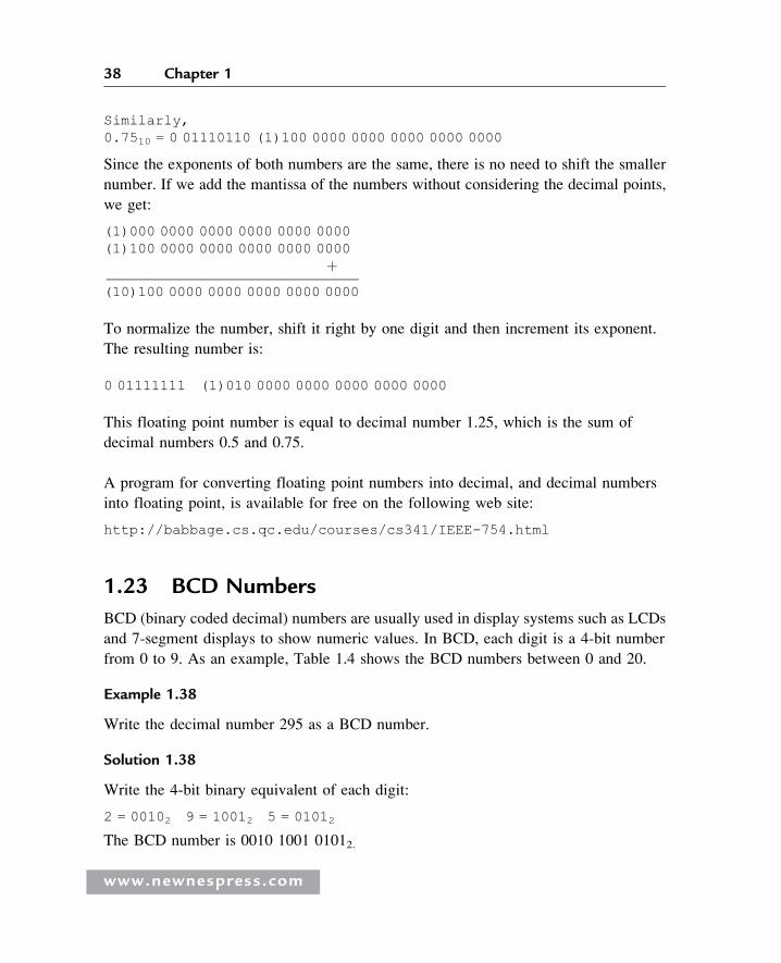
Similarly,0.7510 = 0 01110110 (1)100 0000 0000 0000 0000 0000
Since the exponents of both numbers are the same, there is no need to shift the smaller
number. If we add the mantissa of the numbers without considering the decimal points,
we get:
(1)000 0000 0000 0000 0000 0000(1)100 0000 0000 0000 0000 0000
þ(10)100 0000 0000 0000 0000 0000
To normalize the number, shift it right by one digit and then increment its exponent.
The resulting number is:
0 01111111 (1)010 0000 0000 0000 0000 0000
This floating point number is equal to decimal number 1.25, which is the sum of
decimal numbers 0.5 and 0.75.
A program for converting floating point numbers into decimal, and decimal numbers
into floating point, is available for free on the following web site:
http://babbage.cs.qc.edu/courses/cs341/IEEE-754.html
1.23 BCD Numbers
BCD (binary coded decimal) numbers are usually used in display systems such as LCDs
and 7-segment displays to show numeric values. In BCD, each digit is a 4-bit number
from 0 to 9. As an example, Table 1.4 shows the BCD numbers between 0 and 20.
Example 1.38
Write the decimal number 295 as a BCD number.
Solution 1.38
Write the 4-bit binary equivalent of each digit:
2 = 00102 9 = 10012 5 = 01012
The BCD number is 0010 1001 01012.
www.newnespress.com
38 Chapter 1
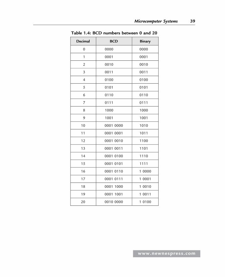
Table 1.4: BCD numbers between 0 and 20
Decimal BCD Binary
0 0000 0000
1 0001 0001
2 0010 0010
3 0011 0011
4 0100 0100
5 0101 0101
6 0110 0110
7 0111 0111
8 1000 1000
9 1001 1001
10 0001 0000 1010
11 0001 0001 1011
12 0001 0010 1100
13 0001 0011 1101
14 0001 0100 1110
15 0001 0101 1111
16 0001 0110 1 0000
17 0001 0111 1 0001
18 0001 1000 1 0010
19 0001 1001 1 0011
20 0010 0000 1 0100
www.newnespress.com
39Microcomputer Systems
Example 1.39
Write the decimal equivalent of BCD number 1001 1001 0110 00012.
Solution 1.39
Writing the decimal equivalent of each group of 4-bit yields the decimal number:
9961
1.24 Summary
Chapter 1 has provided an introduction to the microprocessor and microcontroller
systems. The basic building blocks of microcontrollers were described briefly.
The chapter also provided an introduction to various number systems, and
described how to convert a given number from one base into another.
The important topics of floating point numbers and floating point arithmetic
were also described with examples.
1.25 Exercises
1. What is a microcontroller? What is a microprocessor? Explain the main difference
between a microprocessor and a microcontroller.
2. Identify some applications of microcontrollers around you.
3. Where would you use an EPROM memory?
4. Where would you use a RAM memory?
5. Explain the types of memory usually used in microcontrollers.
6. What is an input-output port?
7. What is an analog-to-digital converter? Give an example of how this converter is
used.
8. Explain why a watchdog timer could be useful in a real-time system.
9. What is serial input-output? Where would you use serial communication?
10. Why is the current sink/source capability important in the specification of an
output port pin?
www.newnespress.com
40 Chapter 1

11. What is an interrupt? Explain what happens when an interrupt is recognized by a
microcontroller?
12. Why is brown-out detection important in real-time systems?
13. Explain the difference between an RISC-based microcontroller and a CISC-based
microcontroller. What type of microcontroller is PIC?
14. Convert the following decimal numbers into binary:
a) 23 b) 128 c) 255 d) 1023
e) 120 f) 32000 g) 160 h) 250
15. Convert the following binary numbers into decimal:
a) 1111 b) 0110 c) 11110000
d) 00001111 e) 10101010 f) 10000000
16. Convert the following octal numbers into decimal:
a) 177 b) 762 c) 777 d) 123
e) 1777 f) 655 g) 177777 h) 207
17. Convert the following decimal numbers into octal:
a) 255 b) 1024 c) 129 d) 2450
e) 4096 f) 256 g) 180 h) 4096
18. Convert the following hexadecimal numbers into decimal:
a) AA b) EF c) 1FF d) FFFF
e) 1AA f) FEF g) F0 h) CC
19. Convert the following binary numbers into hexadecimal:
a) 0101 b) 11111111 c) 1111 d) 1010
e) 1110 f) 10011111 g) 1001 h) 1100
20. Convert the following binary numbers into octal:
a) 111000 b) 000111 c) 1111111 d) 010111
e) 110001 f) 11111111 g) 1000001 h) 110000
www.newnespress.com
41Microcomputer Systems

21. Convert the following octal numbers into binary:
a) 177 b) 7777 c) 555 d) 111
e) 1777777 f) 55571 g) 171 h) 1777
22. Convert the following hexadecimal numbers into octal:
a) AA b) FF c) FFFF d) 1AC
e) CC f) EE g) EEFF h) AB
23. Convert the following octal numbers into hexadecimal:
a) 177 b) 777 c) 123 d) 23
e) 1111 f) 17777777 g) 349 h) 17
24. Convert the following decimal numbers into floating point:
a) 23.45 b) 1.25 c) 45.86 d) 0.56
25. Convert the following decimal numbers into floating point and then calculate
their sum:
0.255 and 1.75
26. Convert the following decimal numbers into floating point and then calculate
their product:
2.125 and 3.75
27. Convert the following decimal numbers into BCD:
a) 128 b) 970 c) 900 d) 125
www.newnespress.com
42 Chapter 1
CHAP T E R 2
PIC18F Microcontroller Series
PIC16-series microcontrollers have been around for many years. Although these are
excellent general purpose microcontrollers, they have certain limitations. For example,
the program and data memory capacities are limited, the stack is small, and the interrupt
structure is primitive, all interrupt sources sharing the same interrupt vector. PIC16-
series microcontrollers also do not provide direct support for advanced peripheral
interfaces such as USB, CAN bus, etc., and interfacing with such devices is not easy.
The instruction set for these microcontrollers is also limited. For example, there are no
multiplication or division instructions, and branching is rather simple, being a
combination of skip and goto instructions.
Microchip Inc. has developed the PIC18 series of microcontrollers for use in high-pin-
count, high-density, and complex applications. The PIC18F microcontrollers offer cost-
efficient solutions for general purpose applications written in C that use a real-time
operating system (RTOS) and require a complex communication protocol stack such as
TCP/IP, CAN, USB, or ZigBee. PIC18F devices provide flash program memory in sizes
from 8 to 128Kbytes and data memory from 256 to 4Kbytes, operating at a range of
2.0 to 5.0 volts, at speeds from DC to 40MHz.
The basic features of PIC18F-series microcontrollers are:
� 77 instructions
� PIC16 source code compatible
� Program memory addressing up to 2Mbytes
� Data memory addressing up to 4Kbytes
www.newnespress.com
� DC to 40MHz operation
� 8 � 8 hardware multiplier
� Interrupt priority levels
� 16-bit-wide instructions, 8-bit-wide data path
� Up to two 8-bit timers/counters
� Up to three 16-bit timers/counters
� Up to four external interrupts
� High current (25mA) sink/source capability
� Up to five capture/compare/PWM modules
� Master synchronous serial port module (SPI and I2C modes)
� Up to two USART modules
� Parallel slave port (PSP)
� Fast 10-bit analog-to-digital converter
� Programmable low-voltage detection (LVD) module
� Power-on reset (POR), power-up timer (PWRT), and oscillator start-up timer (OST)
� Watchdog timer (WDT) with on-chip RC oscillator
� In-circuit programming
In addition, some microcontrollers in the PIC18F family offer the following special
features:
� Direct CAN 2.0 bus interface
� Direct USB 2.0 bus interface
� Direct LCD control interface
� TCP/IP interface
� ZigBee interface
� Direct motor control interface
www.newnespress.com
44 Chapter 2
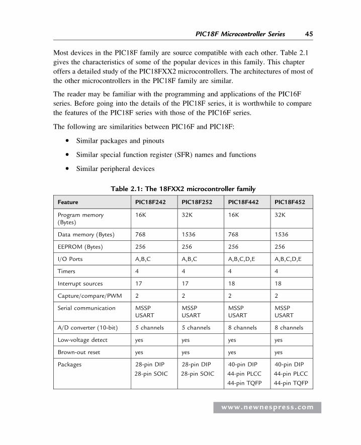
Most devices in the PIC18F family are source compatible with each other. Table 2.1
gives the characteristics of some of the popular devices in this family. This chapter
offers a detailed study of the PIC18FXX2 microcontrollers. The architectures of most of
the other microcontrollers in the PIC18F family are similar.
The reader may be familiar with the programming and applications of the PIC16F
series. Before going into the details of the PIC18F series, it is worthwhile to compare
the features of the PIC18F series with those of the PIC16F series.
The following are similarities between PIC16F and PIC18F:
� Similar packages and pinouts
� Similar special function register (SFR) names and functions
� Similar peripheral devices
Table 2.1: The 18FXX2 microcontroller family
Feature PIC18F242 PIC18F252 PIC18F442 PIC18F452
Program memory(Bytes)
16K 32K 16K 32K
Data memory (Bytes) 768 1536 768 1536
EEPROM (Bytes) 256 256 256 256
I/O Ports A,B,C A,B,C A,B,C,D,E A,B,C,D,E
Timers 4 4 4 4
Interrupt sources 17 17 18 18
Capture/compare/PWM 2 2 2 2
Serial communication MSSPUSART
MSSPUSART
MSSPUSART
MSSPUSART
A/D converter (10-bit) 5 channels 5 channels 8 channels 8 channels
Low-voltage detect yes yes yes yes
Brown-out reset yes yes yes yes
Packages 28-pin DIP
28-pin SOIC
28-pin DIP
28-pin SOIC
40-pin DIP
44-pin PLCC
44-pin TQFP
40-pin DIP
44-pin PLCC
44-pin TQFP
www.newnespress.com
45PIC18F Microcontroller Series
� Subset of PIC18F instruction set
� Similar development tools
The following are new with the PIC18F series:
� Number of instructions doubled
� 16-bit instruction word
� Hardware 8 � 8 multiplier
� More external interrupts
� Priority-based interrupts
� Enhanced status register
� Increased program and data memory size
� Bigger stack
� Phase-locked loop (PLL) clock generator
� Enhanced input-output port architecture
� Set of configuration registers
� Higher speed of operation
� Lower power operation
2.1 PIC18FXX2 Architecture
As shown in Table 2.1, the PIC18FXX2 series consists of four devices. PIC18F2X2
microcontrollers are 28-pin devices, while PIC18F4X2 microcontrollers are 40-pin devices.
The architectures of the two groups are almost identical except that the larger devices have
more input-output ports and more A/D converter channels. In this section we shall be looking
at the architecture of the PIC18F452 microcontroller in detail. The architectures of other
standard PIC18F-series microcontrollers are similar, and the knowledge gained in this section
should be enough to understand the operation of other PIC18F-series microcontrollers.
The pin configuration of the PIC18F452 microcontroller (DIP package) is shown in
Figure 2.1. This is a 40-pin microcontroller housed in a DIL package, with a pin
configuration similar to the popular PIC16F877.
www.newnespress.com
46 Chapter 2
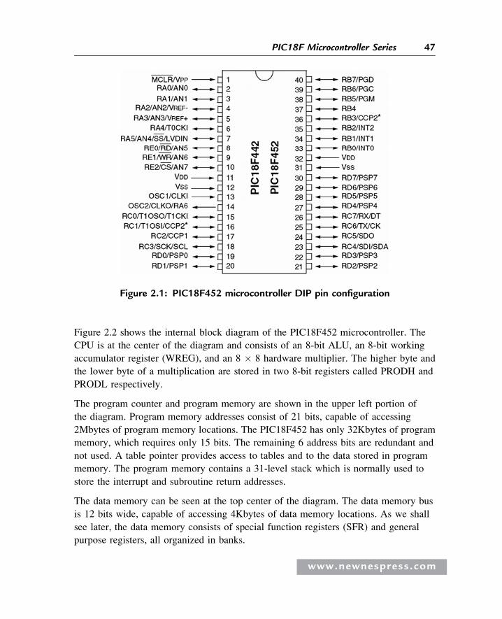
Figure 2.2 shows the internal block diagram of the PIC18F452 microcontroller. The
CPU is at the center of the diagram and consists of an 8-bit ALU, an 8-bit working
accumulator register (WREG), and an 8 � 8 hardware multiplier. The higher byte and
the lower byte of a multiplication are stored in two 8-bit registers called PRODH and
PRODL respectively.
The program counter and program memory are shown in the upper left portion of
the diagram. Program memory addresses consist of 21 bits, capable of accessing
2Mbytes of program memory locations. The PIC18F452 has only 32Kbytes of program
memory, which requires only 15 bits. The remaining 6 address bits are redundant and
not used. A table pointer provides access to tables and to the data stored in program
memory. The program memory contains a 31-level stack which is normally used to
store the interrupt and subroutine return addresses.
The data memory can be seen at the top center of the diagram. The data memory bus
is 12 bits wide, capable of accessing 4Kbytes of data memory locations. As we shall
see later, the data memory consists of special function registers (SFR) and general
purpose registers, all organized in banks.
Figure 2.1: PIC18F452 microcontroller DIP pin configuration
www.newnespress.com
47PIC18F Microcontroller Series
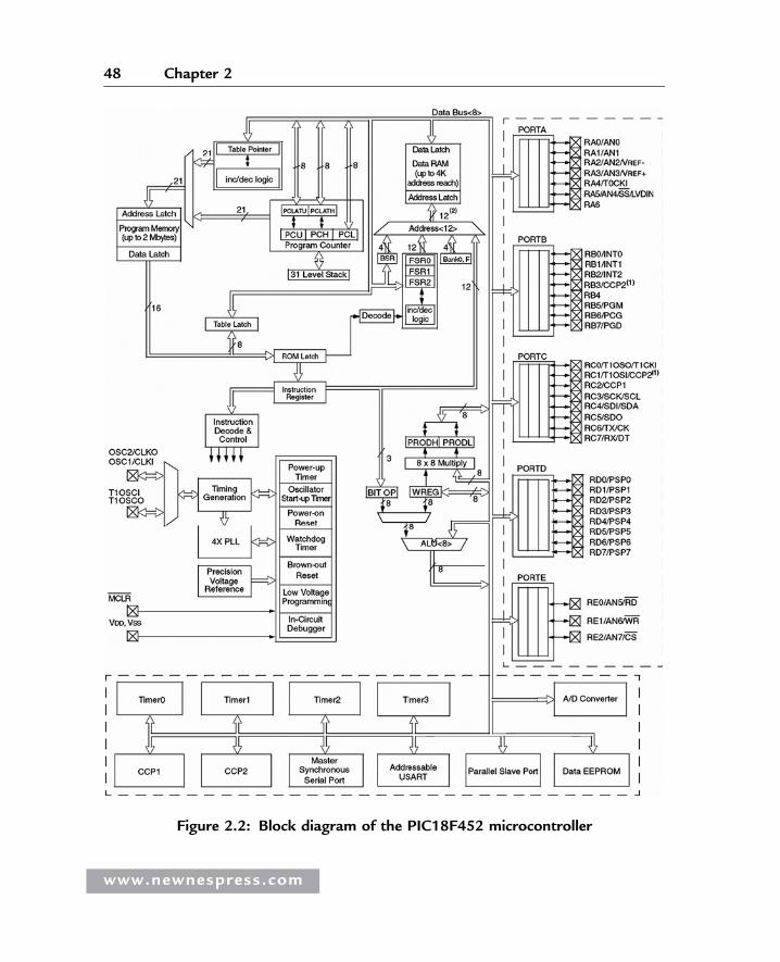
Figure 2.2: Block diagram of the PIC18F452 microcontroller
www.newnespress.com
48 Chapter 2
The bottom portion of the diagram shows the timers/counters, capture/compare/PWM
registers, USART, A/D converter, and EEPROM data memory. The PIC18F452
consists of:
� 4 timers/counters
� 2 capture/compare/PWM modules
� 2 serial communication modules
� 8 10-bit A/D converter channels
� 256 bytes EEPROM
The oscillator circuit, located at the left side of the diagram, consists of:
� Power-up timer
� Oscillator start-up timer
� Power-on reset
� Watchdog timer
� Brown-out reset
� Low-voltage programming
� In-circuit debugger
� PLL circuit
� Timing generation circuit
The PLL circuit is new to the PIC18F series and provides the option of multiplying up the
oscillator frequency to speed up the overall operation. The watchdog timer can be used to
force a restart of the microcontroller in the event of a program crash. The in-circuit
debugger is useful during program development and can be used to return diagnostic data,
including the register values, as the microcontroller is executing a program.
The input-output ports are located at the right side of the diagram. The PIC18F452
has five parallel ports named PORTA, PORTB, PORTC, PORTD, and PORTE. Most
port pins have multiple functions. For example, PORTA pins can be used as parallel
inputs-outputs or analog inputs. PORTB pins can be used as parallel inputs-outputs or
as interrupt inputs.
www.newnespress.com
49PIC18F Microcontroller Series
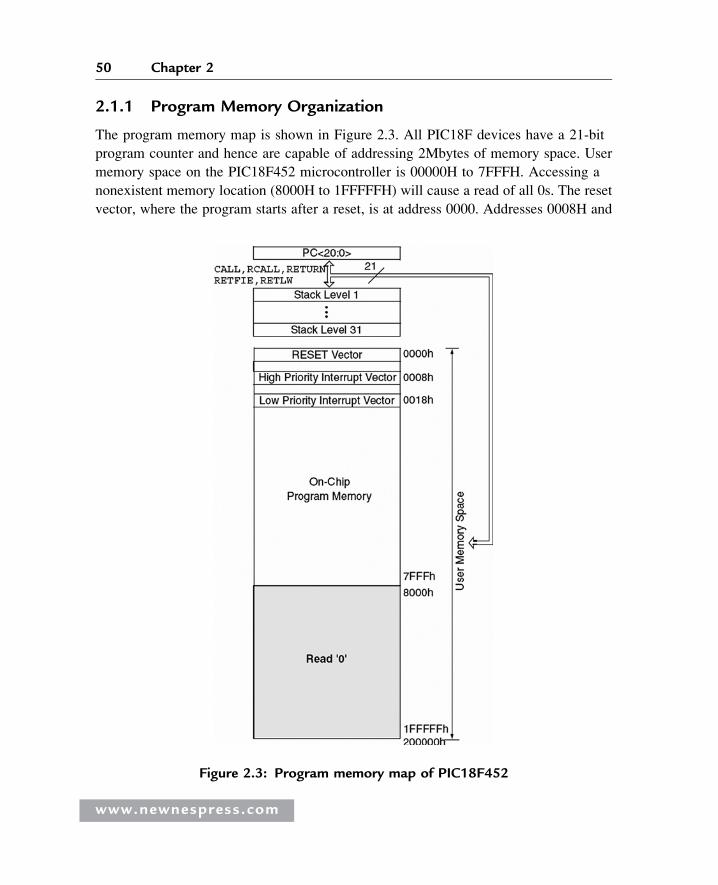
2.1.1 Program Memory Organization
The program memory map is shown in Figure 2.3. All PIC18F devices have a 21-bit
program counter and hence are capable of addressing 2Mbytes of memory space. User
memory space on the PIC18F452 microcontroller is 00000H to 7FFFH. Accessing a
nonexistent memory location (8000H to 1FFFFFH) will cause a read of all 0s. The reset
vector, where the program starts after a reset, is at address 0000. Addresses 0008H and
Figure 2.3: Program memory map of PIC18F452
www.newnespress.com
50 Chapter 2
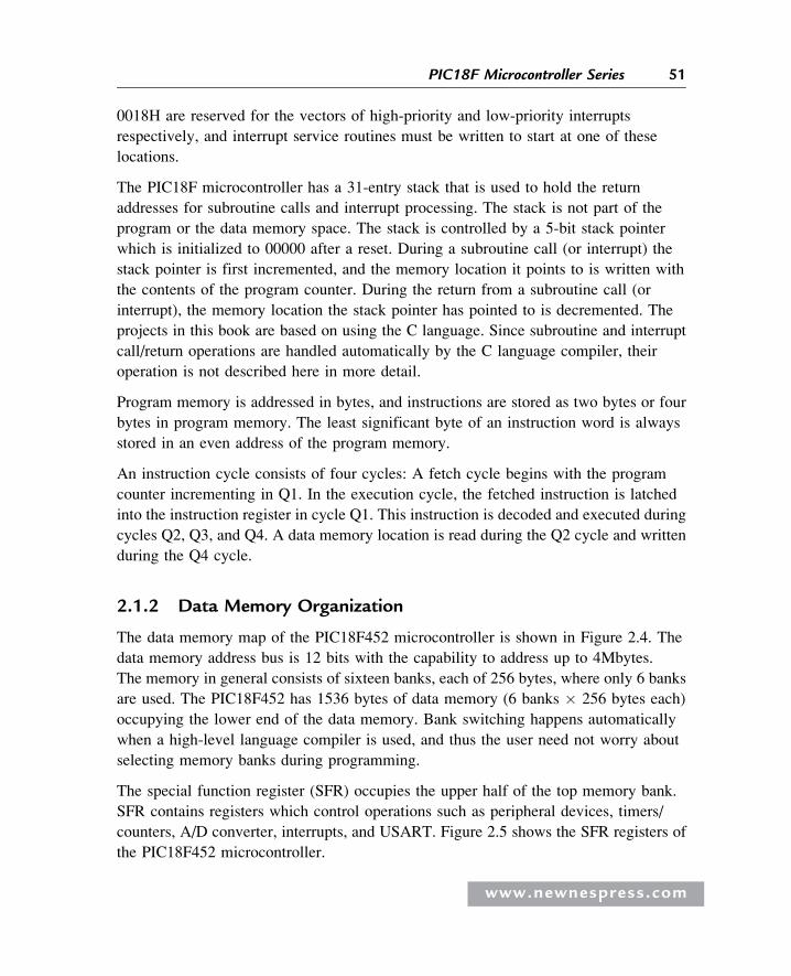
0018H are reserved for the vectors of high-priority and low-priority interrupts
respectively, and interrupt service routines must be written to start at one of these
locations.
The PIC18F microcontroller has a 31-entry stack that is used to hold the return
addresses for subroutine calls and interrupt processing. The stack is not part of the
program or the data memory space. The stack is controlled by a 5-bit stack pointer
which is initialized to 00000 after a reset. During a subroutine call (or interrupt) the
stack pointer is first incremented, and the memory location it points to is written with
the contents of the program counter. During the return from a subroutine call (or
interrupt), the memory location the stack pointer has pointed to is decremented. The
projects in this book are based on using the C language. Since subroutine and interrupt
call/return operations are handled automatically by the C language compiler, their
operation is not described here in more detail.
Program memory is addressed in bytes, and instructions are stored as two bytes or four
bytes in program memory. The least significant byte of an instruction word is always
stored in an even address of the program memory.
An instruction cycle consists of four cycles: A fetch cycle begins with the program
counter incrementing in Q1. In the execution cycle, the fetched instruction is latched
into the instruction register in cycle Q1. This instruction is decoded and executed during
cycles Q2, Q3, and Q4. A data memory location is read during the Q2 cycle and written
during the Q4 cycle.
2.1.2 Data Memory Organization
The data memory map of the PIC18F452 microcontroller is shown in Figure 2.4. The
data memory address bus is 12 bits with the capability to address up to 4Mbytes.
The memory in general consists of sixteen banks, each of 256 bytes, where only 6 banks
are used. The PIC18F452 has 1536 bytes of data memory (6 banks � 256 bytes each)
occupying the lower end of the data memory. Bank switching happens automatically
when a high-level language compiler is used, and thus the user need not worry about
selecting memory banks during programming.
The special function register (SFR) occupies the upper half of the top memory bank.
SFR contains registers which control operations such as peripheral devices, timers/
counters, A/D converter, interrupts, and USART. Figure 2.5 shows the SFR registers of
the PIC18F452 microcontroller.
www.newnespress.com
51PIC18F Microcontroller Series
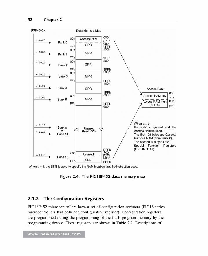
2.1.3 The Configuration Registers
PIC18F452 microcontrollers have a set of configuration registers (PIC16-series
microcontrollers had only one configuration register). Configuration registers
are programmed during the programming of the flash program memory by the
programming device. These registers are shown in Table 2.2. Descriptions of
Figure 2.4: The PIC18F452 data memory map
www.newnespress.com
52 Chapter 2
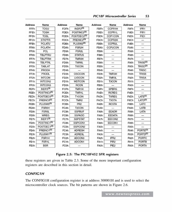
these registers are given in Table 2.3. Some of the more important configuration
registers are described in this section in detail.
CONFIG1H
The CONFIG1H configuration register is at address 300001H and is used to select the
microcontroller clock sources. The bit patterns are shown in Figure 2.6.
Figure 2.5: The PIC18F452 SFR registers
www.newnespress.com
53PIC18F Microcontroller Series
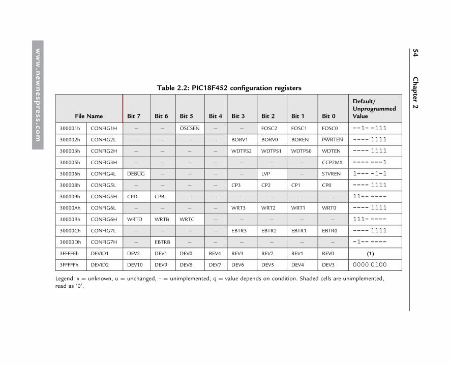
Table 2.2: PIC18F452 configuration registers
File Name Bit 7 Bit 6 Bit 5 Bit 4 Bit 3 Bit 2 Bit 1 Bit 0
Default/UnprogrammedValue
300001h CONFIG1H — — OSCSEN — — FOSC2 FOSC1 FOSC0 --1- -111
300002h CONFIG2L — — — — BORV1 BORV0 BOREN PWRTEN ---- 1111
300003h CONFIG2H — — — — WDTPS2 WDTPS1 WDTPS0 WDTEN ---- 1111
300005h CONFIG3H — — — — — — — CCP2MX ---- ---1
300006h CONFIG4L DEBUG — — — — LVP — STVREN 1--- -1-1
300008h CONFIG5L — — — — CP3 CP2 CP1 CP0 ---- 1111
300009h CONFIG5H CPD CPB — — — — — — 11-- ----
30000Ah CONFIG6L — — — — WRT3 WRT2 WRT1 WRT0 ---- 1111
30000Bh CONFIG6H WRTD WRTB WRTC — — — — — 111- ----
30000Ch CONFIG7L — — — — EBTR3 EBTR2 EBTR1 EBTR0 ---- 1111
30000Dh CONFIG7H — EBTRB — — — — — — -1-- ----
3FFFFEh DEVID1 DEV2 DEV1 DEV0 REV4 REV3 REV2 REV1 REV0 (1)
3FFFFFh DEVID2 DEV10 DEV9 DEV8 DEV7 DEV6 DEV5 DEV4 DEV3 0000 0100
Legend: x ¼ unknown, u ¼ unchanged, – ¼ unimplemented, q ¼ value depends on condition. Shaded cells are unimplemented,read as ‘0’.
www.n
ewnespre
ss.com
54
Chap
ter2
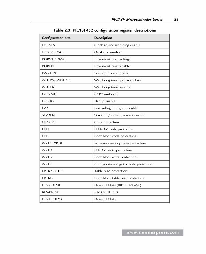
Table 2.3: PIC18F452 configuration register descriptions
Configuration bits Description
OSCSEN Clock source switching enable
FOSC2:FOSC0 Oscillator modes
BORV1:BORV0 Brown-out reset voltage
BOREN Brown-out reset enable
PWRTEN Power-up timer enable
WDTPS2:WDTPS0 Watchdog timer postscale bits
WDTEN Watchdog timer enable
CCP2MX CCP2 multiplex
DEBUG Debug enable
LVP Low-voltage program enable
STVREN Stack full/underflow reset enable
CP3:CP0 Code protection
CPD EEPROM code protection
CPB Boot block code protection
WRT3:WRT0 Program memory write protection
WRTD EPROM write protection
WRTB Boot block write protection
WRTC Configuration register write protection
EBTR3:EBTR0 Table read protection
EBTRB Boot block table read protection
DEV2:DEV0 Device ID bits (001 = 18F452)
REV4:REV0 Revision ID bits
DEV10:DEV3 Device ID bits
www.newnespress.com
55PIC18F Microcontroller Series
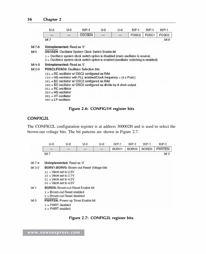
CONFIG2L
The CONFIG2L configuration register is at address 300002H and is used to select the
brown-out voltage bits. The bit patterns are shown in Figure 2.7.
Figure 2.6: CONFIG1H register bits
Figure 2.7: CONFIG2L register bits
www.newnespress.com
56 Chapter 2
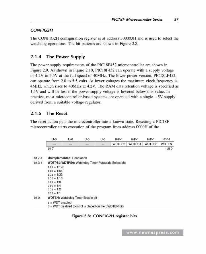
CONFIG2H
The CONFIG2H configuration register is at address 300003H and is used to select the
watchdog operations. The bit patterns are shown in Figure 2.8.
2.1.4 The Power Supply
The power supply requirements of the PIC18F452 microcontroller are shown in
Figure 2.9. As shown in Figure 2.10, PIC18F452 can operate with a supply voltage
of 4.2V to 5.5V at the full speed of 40MHz. The lower power version, PIC18LF452,
can operate from 2.0 to 5.5 volts. At lower voltages the maximum clock frequency is
4MHz, which rises to 40MHz at 4.2V. The RAM data retention voltage is specified as
1.5V and will be lost if the power supply voltage is lowered below this value. In
practice, most microcontroller-based systems are operated with a single þ5V supply
derived from a suitable voltage regulator.
2.1.5 The Reset
The reset action puts the microcontroller into a known state. Resetting a PIC18F
microcontroller starts execution of the program from address 0000H of the
Figure 2.8: CONFIG2H register bits
www.newnespress.com
57PIC18F Microcontroller Series
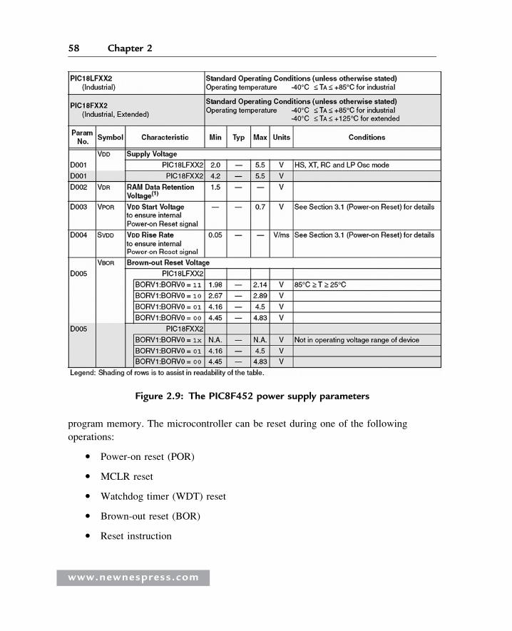
program memory. The microcontroller can be reset during one of the following
operations:
� Power-on reset (POR)
� MCLR reset
� Watchdog timer (WDT) reset
� Brown-out reset (BOR)
� Reset instruction
Figure 2.9: The PIC8F452 power supply parameters
www.newnespress.com
58 Chapter 2
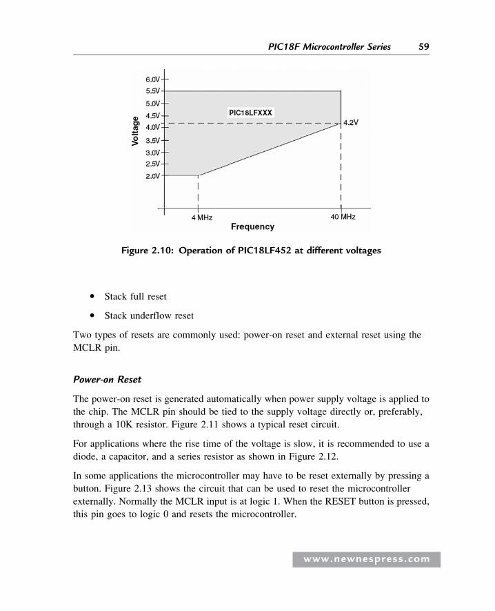
� Stack full reset
� Stack underflow reset
Two types of resets are commonly used: power-on reset and external reset using the
MCLR pin.
Power-on Reset
The power-on reset is generated automatically when power supply voltage is applied to
the chip. The MCLR pin should be tied to the supply voltage directly or, preferably,
through a 10K resistor. Figure 2.11 shows a typical reset circuit.
For applications where the rise time of the voltage is slow, it is recommended to use a
diode, a capacitor, and a series resistor as shown in Figure 2.12.
In some applications the microcontroller may have to be reset externally by pressing a
button. Figure 2.13 shows the circuit that can be used to reset the microcontroller
externally. Normally the MCLR input is at logic 1. When the RESET button is pressed,
this pin goes to logic 0 and resets the microcontroller.
Figure 2.10: Operation of PIC18LF452 at different voltages
www.newnespress.com
59PIC18F Microcontroller Series
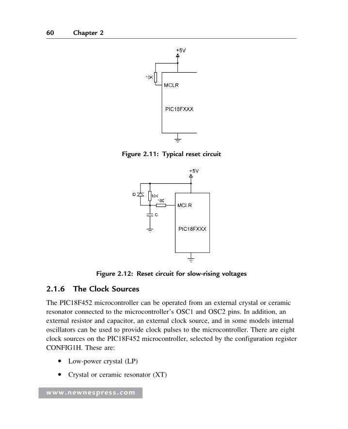
2.1.6 The Clock Sources
The PIC18F452 microcontroller can be operated from an external crystal or ceramic
resonator connected to the microcontroller’s OSC1 and OSC2 pins. In addition, an
external resistor and capacitor, an external clock source, and in some models internal
oscillators can be used to provide clock pulses to the microcontroller. There are eight
clock sources on the PIC18F452 microcontroller, selected by the configuration register
CONFIG1H. These are:
� Low-power crystal (LP)
� Crystal or ceramic resonator (XT)
Figure 2.12: Reset circuit for slow-rising voltages
Figure 2.11: Typical reset circuit
www.newnespress.com
60 Chapter 2
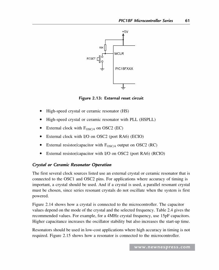
� High-speed crystal or ceramic resonator (HS)
� High-speed crystal or ceramic resonator with PLL (HSPLL)
� External clock with FOSC/4 on OSC2 (EC)
� External clock with I/O on OSC2 (port RA6) (ECIO)
� External resistor/capacitor with FOSC/4 output on OSC2 (RC)
� External resistor/capacitor with I/O on OSC2 (port RA6) (RCIO)
Crystal or Ceramic Resonator Operation
The first several clock sources listed use an external crystal or ceramic resonator that is
connected to the OSC1 and OSC2 pins. For applications where accuracy of timing is
important, a crystal should be used. And if a crystal is used, a parallel resonant crystal
must be chosen, since series resonant crystals do not oscillate when the system is first
powered.
Figure 2.14 shows how a crystal is connected to the microcontroller. The capacitor
values depend on the mode of the crystal and the selected frequency. Table 2.4 gives the
recommended values. For example, for a 4MHz crystal frequency, use 15pF capacitors.
Higher capacitance increases the oscillator stability but also increases the start-up time.
Resonators should be used in low-cost applications where high accuracy in timing is not
required. Figure 2.15 shows how a resonator is connected to the microcontroller.
Figure 2.13: External reset circuit
www.newnespress.com
61PIC18F Microcontroller Series
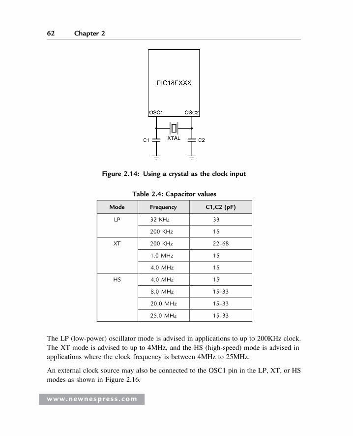
The LP (low-power) oscillator mode is advised in applications to up to 200KHz clock.
The XT mode is advised to up to 4MHz, and the HS (high-speed) mode is advised in
applications where the clock frequency is between 4MHz to 25MHz.
An external clock source may also be connected to the OSC1 pin in the LP, XT, or HS
modes as shown in Figure 2.16.
Figure 2.14: Using a crystal as the clock input
Table 2.4: Capacitor values
Mode Frequency C1,C2 (pF)
LP 32 KHz 33
200 KHz 15
XT 200 KHz 22–68
1.0 MHz 15
4.0 MHz 15
HS 4.0 MHz 15
8.0 MHz 15–33
20.0 MHz 15–33
25.0 MHz 15–33
www.newnespress.com
62 Chapter 2
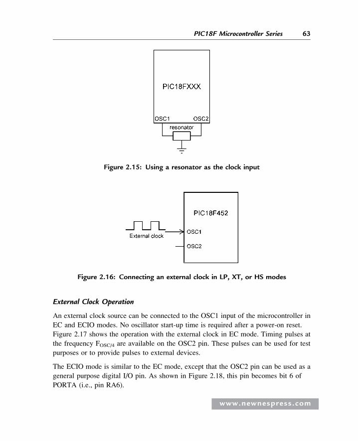
External Clock Operation
An external clock source can be connected to the OSC1 input of the microcontroller in
EC and ECIO modes. No oscillator start-up time is required after a power-on reset.
Figure 2.17 shows the operation with the external clock in EC mode. Timing pulses at
the frequency FOSC/4 are available on the OSC2 pin. These pulses can be used for test
purposes or to provide pulses to external devices.
The ECIO mode is similar to the EC mode, except that the OSC2 pin can be used as a
general purpose digital I/O pin. As shown in Figure 2.18, this pin becomes bit 6 of
PORTA (i.e., pin RA6).
Figure 2.15: Using a resonator as the clock input
Figure 2.16: Connecting an external clock in LP, XT, or HS modes
www.newnespress.com
63PIC18F Microcontroller Series
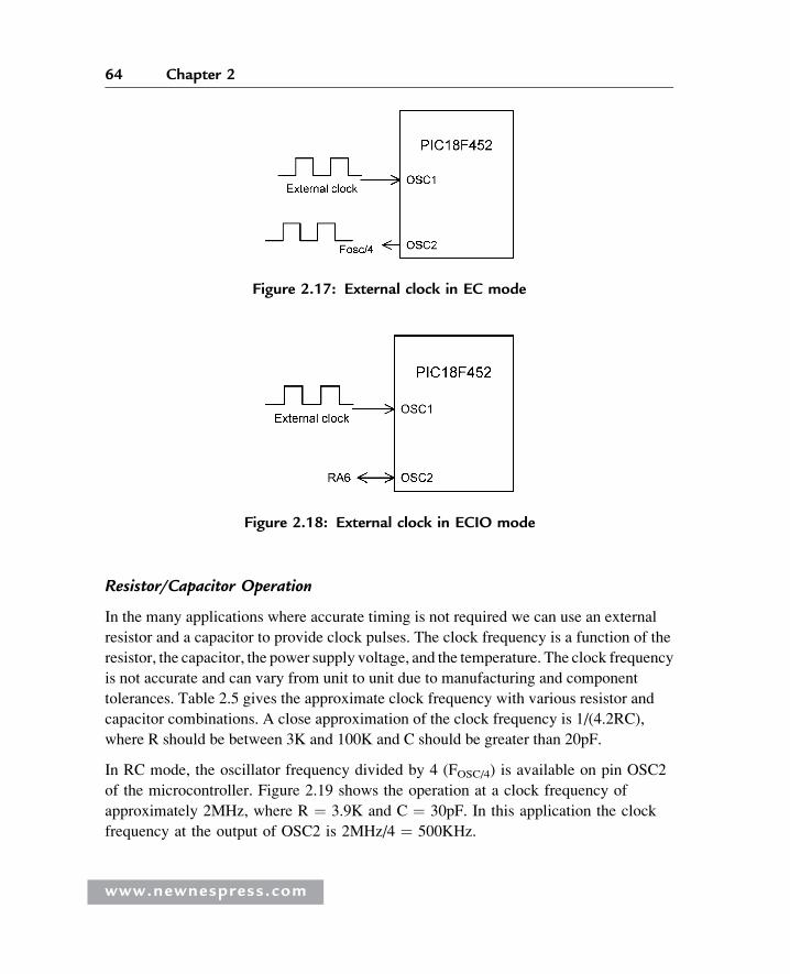
Resistor/Capacitor Operation
In the many applications where accurate timing is not required we can use an external
resistor and a capacitor to provide clock pulses. The clock frequency is a function of the
resistor, the capacitor, the power supply voltage, and the temperature. The clock frequency
is not accurate and can vary from unit to unit due to manufacturing and component
tolerances. Table 2.5 gives the approximate clock frequency with various resistor and
capacitor combinations. A close approximation of the clock frequency is 1/(4.2RC),
where R should be between 3K and 100K and C should be greater than 20pF.
In RC mode, the oscillator frequency divided by 4 (FOSC/4) is available on pin OSC2
of the microcontroller. Figure 2.19 shows the operation at a clock frequency of
approximately 2MHz, where R ¼ 3.9K and C ¼ 30pF. In this application the clock
frequency at the output of OSC2 is 2MHz/4 ¼ 500KHz.
Figure 2.17: External clock in EC mode
Figure 2.18: External clock in ECIO mode
www.newnespress.com
64 Chapter 2
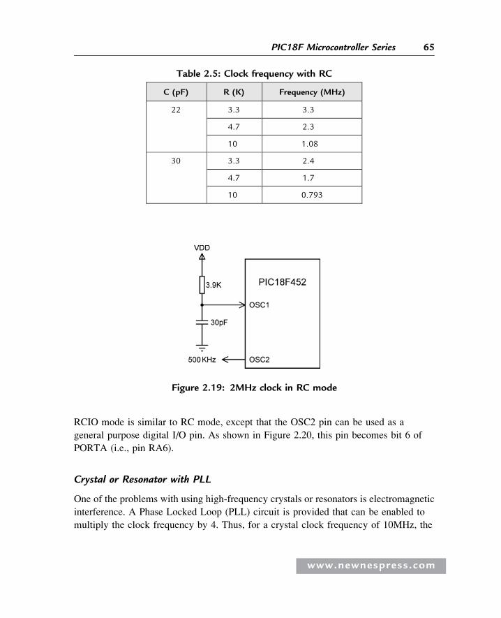
RCIO mode is similar to RC mode, except that the OSC2 pin can be used as a
general purpose digital I/O pin. As shown in Figure 2.20, this pin becomes bit 6 of
PORTA (i.e., pin RA6).
Crystal or Resonator with PLL
One of the problems with using high-frequency crystals or resonators is electromagnetic
interference. A Phase Locked Loop (PLL) circuit is provided that can be enabled to
multiply the clock frequency by 4. Thus, for a crystal clock frequency of 10MHz, the
Table 2.5: Clock frequency with RC
C (pF) R (K) Frequency (MHz)
22 3.3 3.3
4.7 2.3
10 1.08
30 3.3 2.4
4.7 1.7
10 0.793
Figure 2.19: 2MHz clock in RC mode
www.newnespress.com
65PIC18F Microcontroller Series
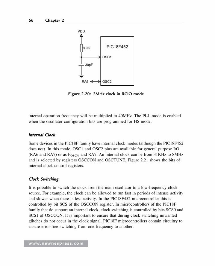
internal operation frequency will be multiplied to 40MHz. The PLL mode is enabled
when the oscillator configuration bits are programmed for HS mode.
Internal Clock
Some devices in the PIC18F family have internal clock modes (although the PIC18F452
does not). In this mode, OSC1 and OSC2 pins are available for general purpose I/O
(RA6 and RA7) or as FOSC/4 and RA7. An internal clock can be from 31KHz to 8MHz
and is selected by registers OSCCON and OSCTUNE. Figure 2.21 shows the bits of
internal clock control registers.
Clock Switching
It is possible to switch the clock from the main oscillator to a low-frequency clock
source. For example, the clock can be allowed to run fast in periods of intense activity
and slower when there is less activity. In the PIC18F452 microcontroller this is
controlled by bit SCS of the OSCCON register. In microcontrollers of the PIC18F
family that do support an internal clock, clock switching is controlled by bits SCS0 and
SCS1 of OSCCON. It is important to ensure that during clock switching unwanted
glitches do not occur in the clock signal. PIC18F microcontrollers contain circuitry to
ensure error-free switching from one frequency to another.
Figure 2.20: 2MHz clock in RCIO mode
www.newnespress.com
66 Chapter 2
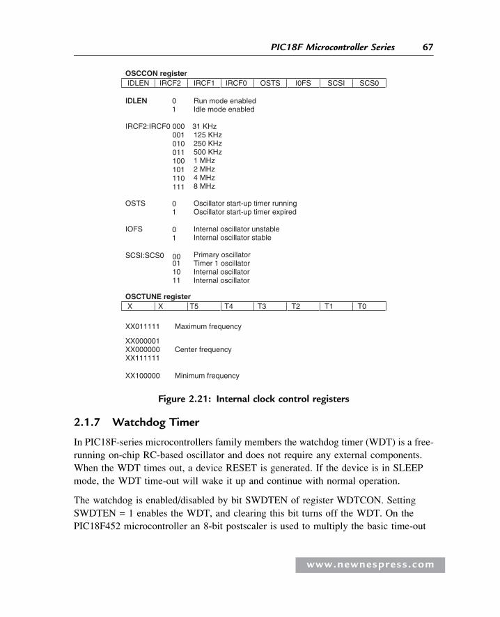
2.1.7 Watchdog Timer
In PIC18F-series microcontrollers family members the watchdog timer (WDT) is a free-
running on-chip RC-based oscillator and does not require any external components.
When the WDT times out, a device RESET is generated. If the device is in SLEEP
mode, the WDT time-out will wake it up and continue with normal operation.
The watchdog is enabled/disabled by bit SWDTEN of register WDTCON. Setting
SWDTEN = 1 enables the WDT, and clearing this bit turns off the WDT. On the
PIC18F452 microcontroller an 8-bit postscaler is used to multiply the basic time-out
OSCCON register
IDLEN
31 KHz125 KHz250 KHz500 KHz1 MHz2 MHz4 MHz8 MHz
Oscillator start-up timer running Oscillator start-up timer expired
Internal oscillator unstable Internal oscillator stable
Primary oscillator 01 Timer 1 oscillator 10 Internal oscillator 11 Internal oscillator
OSCTUNE register
Maximum frequency
XX000001 Center frequency
XX111111
Minimum frequency
IDLEN
IDLEN
IRCF2 IRCF1 IRCF0 OSTS I0FS SCSI SCS0
01
01
01
Run mode enabled Idle mode enabled
IRCF2:IRCF0 000001010011100101110111
OSTS
IOFS
SCSI:SCS0 00
XX011111
XX000000
XX100000
X X T5 T4 T3 T2 T1 T0
Figure 2.21: Internal clock control registers
www.newnespress.com
67PIC18F Microcontroller Series
period from 1 to 128 in powers of 2. This postscaler is controlled from configuration
register CONFIG2H. The typical basic WDT time-out period is 18ms for a postscaler
value of 1.
2.1.8 Parallel I/O Ports
The parallel ports in PIC18F microcontrollers are very similar to those of the PIC16
series. The number of I/O ports and port pins varies depending on which PIC18F
microcontroller is used, but all of them have at least PORTA and PORTB. The pins of a
port are labeled as RPn, where P is the port letter and n is the port bit number. For
example, PORTA pins are labeled RA0 to RA7, PORTB pins are labeled RB0 to RB7,
and so on.
When working with a port we may want to:
� Set port direction
� Set an output value
� Read an input value
� Set an output value and then read back the output value
The first three operations are the same in the PIC16 and the PIC18F series. In some
applications we may want to send a value to the port and then read back the value just
sent. The PIC16 series has a weakness in the port design such that the value read from
a port may be different from the value just written to it. This is because the reading
is the actual port bit pin value, and this value can be changed by external devices
connected to the port pin. In the PIC18F series, a latch register (e.g., LATA for
PORTA) is introduced to the I/O ports to hold the actual value sent to a port pin.
Reading from the port reads the latched value, which is not affected by any external
device.
In this section we shall be looking at the general structure of I/O ports.
PORTA
In the PIC18F452 microcontroller PORTA is 7 bits wide and port pins are shared with
other functions. Table 2.6 shows the PORTA pin functions.
www.newnespress.com
68 Chapter 2
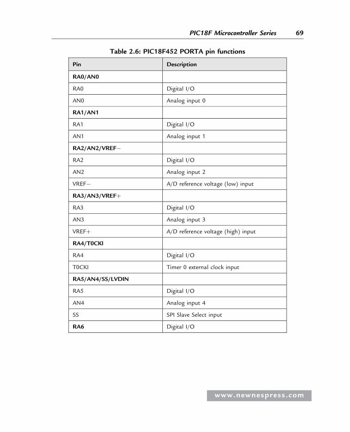
Table 2.6: PIC18F452 PORTA pin functions
Pin Description
RA0/AN0
RA0 Digital I/O
AN0 Analog input 0
RA1/AN1
RA1 Digital I/O
AN1 Analog input 1
RA2/AN2/VREF�RA2 Digital I/O
AN2 Analog input 2
VREF� A/D reference voltage (low) input
RA3/AN3/VREFþRA3 Digital I/O
AN3 Analog input 3
VREFþ A/D reference voltage (high) input
RA4/T0CKI
RA4 Digital I/O
T0CKI Timer 0 external clock input
RA5/AN4/SS/LVDIN
RA5 Digital I/O
AN4 Analog input 4
SS SPI Slave Select input
RA6 Digital I/O
www.newnespress.com
69PIC18F Microcontroller Series
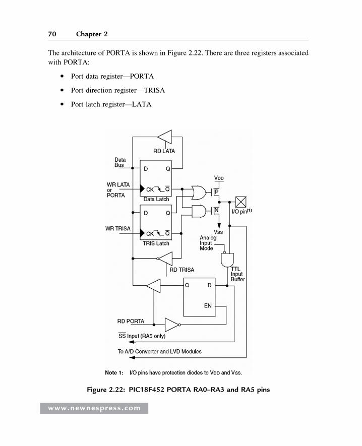
The architecture of PORTA is shown in Figure 2.22. There are three registers associated
with PORTA:
� Port data register—PORTA
� Port direction register—TRISA
� Port latch register—LATA
Figure 2.22: PIC18F452 PORTA RA0–RA3 and RA5 pins
www.newnespress.com
70 Chapter 2
PORTA is the name of the port data register. The TRISA register defines the direction
of PORTA pins, where a logic 1 in a bit position defines the pin as an input pin, and a
0 in a bit position defines it as an output pin. LATA is the output latch register which
shares the same data latch as PORTA. Writing to one is equivalent to writing to the
other. But reading from LATA activates the buffer at the top of the diagram, and the
value held in the PORTA/LATA data latch is transferred to the data bus independent of
the state of the actual output pin of the microcontroller.
Bits 0 through 3 and 5 of PORTA are also used as analog inputs. After a device
reset, these pins are programmed as analog inputs and RA4 and RA6 are configured
as digital inputs. To program the analog inputs as digital I/O, the ADCON1 register
(A/D register) must be programmed accordingly. Writing 7 to ADCON1 configures
all PORTA pins as digital I/O.
The RA4 pin is multiplexed with the Timer 0 clock input (T0CKI). This is a Schmitt
trigger input and an open drain output.
RA6 can be used as a general purpose I/O pin, as the OSC2 clock input, or as a clock
output providing FOSC/4 clock pulses.
PORTB
In PIC18F452 microcontroller PORTB is an 8-bit bidirectional port shared with
interrupt pins and serial device programming pins. Table 2.7 gives the PORTB bit
functions.
PORTB is controlled by three registers:
� Port data register—PORTB
� Port direction register—TRISB
� Port latch register—LATB
The general operation of PORTB is similar to that of PORTA. Figure 2.23 shows
the architecture of PORTB. Each port pin has a weak internal pull-up which can
be enabled by clearing bit RBPU of register INTCON2. These pull-ups are disabled
on a power-on reset and when the port pin is configured as an output. On a power-on
reset, PORTB pins are configured as digital inputs. Internal pull-ups allow input devices
such as switches to be connected to PORTB pins without the use of external pull-up
resistors. This saves costs because the component count and wiring requirements are
reduced.
www.newnespress.com
71PIC18F Microcontroller Series
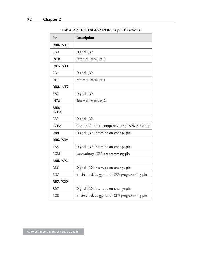
Table 2.7: PIC18F452 PORTB pin functions
Pin Description
RB0/INT0
RB0 Digital I/O
INT0 External interrupt 0
RB1/INT1
RB1 Digital I/O
INT1 External interrupt 1
RB2/INT2
RB2 Digital I/O
INT2 External interrupt 2
RB3/CCP2
RB3 Digital I/O
CCP2 Capture 2 input, compare 2, and PWM2 output
RB4 Digital I/O, interrupt on change pin
RB5/PGM
RB5 Digital I/O, interrupt on change pin
PGM Low-voltage ICSP programming pin
RB6/PGC
RB6 Digital I/O, interrupt on change pin
PGC In-circuit debugger and ICSP programming pin
RB7/PGD
RB7 Digital I/O, interrupt on change pin
PGD In-circuit debugger and ICSP programming pin
www.newnespress.com
72 Chapter 2
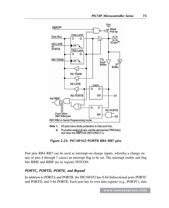
Port pins RB4–RB7 can be used as interrupt-on-change inputs, whereby a change on
any of pins 4 through 7 causes an interrupt flag to be set. The interrupt enable and flag
bits RBIE and RBIF are in register INTCON.
PORTC, PORTD, PORTE, and Beyond
In addition to PORTA and PORTB, the PIC18F452 has 8-bit bidirectional ports PORTC
and PORTD, and 3-bit PORTE. Each port has its own data register (e.g., PORTC), data
Figure 2.23: PIC18F452 PORTB RB4–RB7 pins
www.newnespress.com
73PIC18F Microcontroller Series
direction register (e.g., TRISC), and data latch register (e.g., LATC). The general
operation of these ports is similar to that of PORTA.2.1.
In the PIC18F452 microcontroller PORTC is multiplexed with several peripheral
functions as shown in Table 2.8. On a power-on reset, PORTC pins are configured as
digital inputs.
In the PIC18F452 microcontroller, PORTD has Schmitt trigger input buffers. On a
power-on reset, PORTD is configured as digital input. PORTD can be configured as an
8-bit parallel slave port (i.e., a microprocessor port) by setting bit 4 of the TRISE
register. Table 2.9 shows functions of PORTD pins.
In the PIC18F452 microcontroller, PORTE is only 3 bits wide. As shown in Table 2.10,
port pins are shared with analog inputs and with parallel slave port read/write control
bits. On a power-on reset, PORTE pins are configured as analog inputs and register
ADCON1 must be programmed to change these pins to digital I/O.
2.1.9 Timers
The PIC18F452 microcontroller has four programmable timers which can be used in
many tasks, such as generating timing signals, causing interrupts to be generated at
specific time intervals, measuring frequency and time intervals, and so on.
This section introduces the timers available in the PIC18F452 microcontroller.
Timer 0
Timer 0 is similar to the PIC16 series Timer 0, except that it can operate either in 8-bit
or in 16-bit mode. Timer 0 has the following basic features:
� 8-bit or 16-bit operation
� 8-bit programmable prescaler
� External or internal clock source
� Interupt generation on overflow
Timer 0 control register is T0CON, shown in Figure 2.24. The lower 6 bits of this
register have similar functions to the PIC16-series OPTION register. The top two
bits are used to select the 8-bit or 16-bit mode of operation and to enable/disable
the timer.
www.newnespress.com
74 Chapter 2
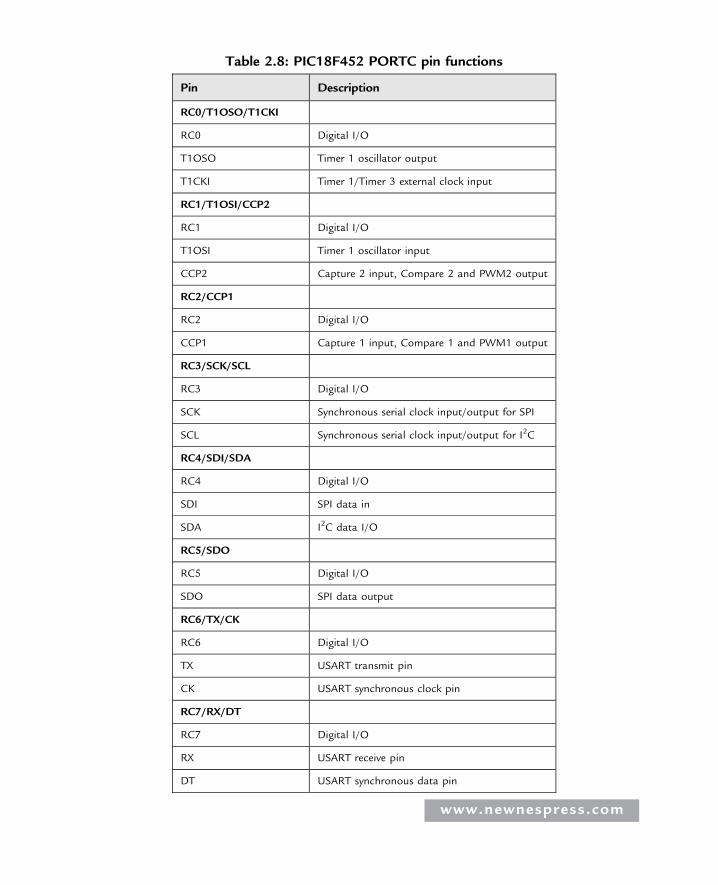
Table 2.8: PIC18F452 PORTC pin functions
Pin Description
RC0/T1OSO/T1CKI
RC0 Digital I/O
T1OSO Timer 1 oscillator output
T1CKI Timer 1/Timer 3 external clock input
RC1/T1OSI/CCP2
RC1 Digital I/O
T1OSI Timer 1 oscillator input
CCP2 Capture 2 input, Compare 2 and PWM2 output
RC2/CCP1
RC2 Digital I/O
CCP1 Capture 1 input, Compare 1 and PWM1 output
RC3/SCK/SCL
RC3 Digital I/O
SCK Synchronous serial clock input/output for SPI
SCL Synchronous serial clock input/output for I2C
RC4/SDI/SDA
RC4 Digital I/O
SDI SPI data in
SDA I2C data I/O
RC5/SDO
RC5 Digital I/O
SDO SPI data output
RC6/TX/CK
RC6 Digital I/O
TX USART transmit pin
CK USART synchronous clock pin
RC7/RX/DT
RC7 Digital I/O
RX USART receive pin
DT USART synchronous data pin
www.newnespress.com
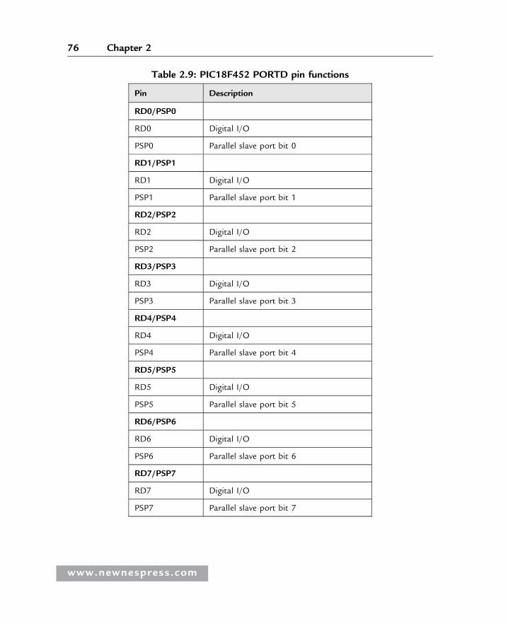
Table 2.9: PIC18F452 PORTD pin functions
Pin Description
RD0/PSP0
RD0 Digital I/O
PSP0 Parallel slave port bit 0
RD1/PSP1
RD1 Digital I/O
PSP1 Parallel slave port bit 1
RD2/PSP2
RD2 Digital I/O
PSP2 Parallel slave port bit 2
RD3/PSP3
RD3 Digital I/O
PSP3 Parallel slave port bit 3
RD4/PSP4
RD4 Digital I/O
PSP4 Parallel slave port bit 4
RD5/PSP5
RD5 Digital I/O
PSP5 Parallel slave port bit 5
RD6/PSP6
RD6 Digital I/O
PSP6 Parallel slave port bit 6
RD7/PSP7
RD7 Digital I/O
PSP7 Parallel slave port bit 7
www.newnespress.com
76 Chapter 2
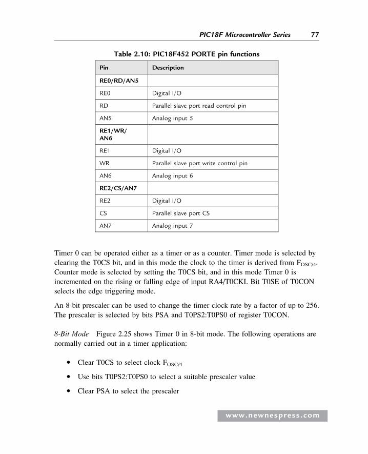
Timer 0 can be operated either as a timer or as a counter. Timer mode is selected by
clearing the T0CS bit, and in this mode the clock to the timer is derived from FOSC/4.
Counter mode is selected by setting the T0CS bit, and in this mode Timer 0 is
incremented on the rising or falling edge of input RA4/T0CKI. Bit T0SE of T0CON
selects the edge triggering mode.
An 8-bit prescaler can be used to change the timer clock rate by a factor of up to 256.
The prescaler is selected by bits PSA and T0PS2:T0PS0 of register T0CON.
8-Bit Mode Figure 2.25 shows Timer 0 in 8-bit mode. The following operations are
normally carried out in a timer application:
� Clear T0CS to select clock FOSC/4
� Use bits T0PS2:T0PS0 to select a suitable prescaler value
� Clear PSA to select the prescaler
Table 2.10: PIC18F452 PORTE pin functions
Pin Description
RE0/RD/AN5
RE0 Digital I/O
RD Parallel slave port read control pin
AN5 Analog input 5
RE1/WR/AN6
RE1 Digital I/O
WR Parallel slave port write control pin
AN6 Analog input 6
RE2/CS/AN7
RE2 Digital I/O
CS Parallel slave port CS
AN7 Analog input 7
www.newnespress.com
77PIC18F Microcontroller Series
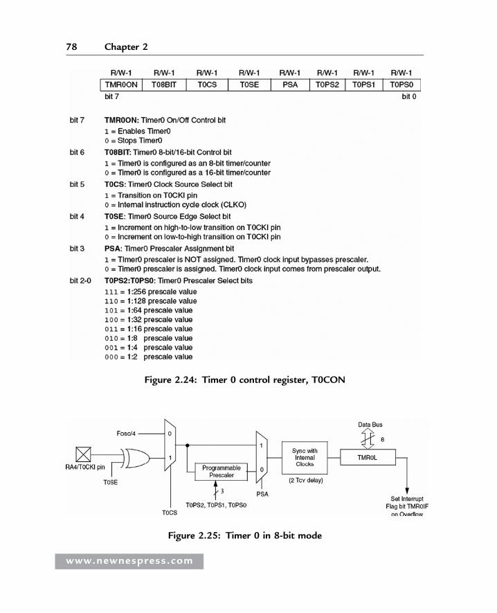
Figure 2.24: Timer 0 control register, T0CON
Figure 2.25: Timer 0 in 8-bit mode
www.newnespress.com
78 Chapter 2
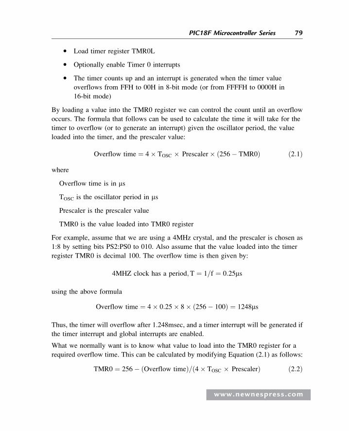
� Load timer register TMR0L
� Optionally enable Timer 0 interrupts
� The timer counts up and an interrupt is generated when the timer value
overflows from FFH to 00H in 8-bit mode (or from FFFFH to 0000H in
16-bit mode)
By loading a value into the TMR0 register we can control the count until an overflow
occurs. The formula that follows can be used to calculate the time it will take for the
timer to overflow (or to generate an interrupt) given the oscillator period, the value
loaded into the timer, and the prescaler value:
Overflow time ¼ 4� TOSC � Prescaler� 256� TMR0ð Þ ð2:1Þ
where
Overflow time is in ms
TOSC is the oscillator period in ms
Prescaler is the prescaler value
TMR0 is the value loaded into TMR0 register
For example, assume that we are using a 4MHz crystal, and the prescaler is chosen as
1:8 by setting bits PS2:PS0 to 010. Also assume that the value loaded into the timer
register TMR0 is decimal 100. The overflow time is then given by:
4MHZ clock has a period;T ¼ 1=f ¼ 0:25ms
using the above formula
Overflow time ¼ 4� 0:25� 8� 256� 100ð Þ ¼ 1248ms
Thus, the timer will overflow after 1.248msec, and a timer interrupt will be generated if
the timer interrupt and global interrupts are enabled.
What we normally want is to know what value to load into the TMR0 register for a
required overflow time. This can be calculated by modifying Equation (2.1) as follows:
TMR0 ¼ 256� Overflow timeð Þ= 4� TOSC � Prescalerð Þ ð2:2Þ
www.newnespress.com
79PIC18F Microcontroller Series
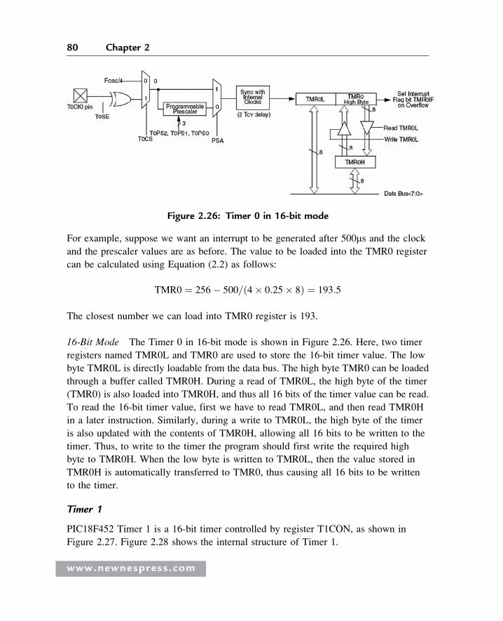
For example, suppose we want an interrupt to be generated after 500ms and the clock
and the prescaler values are as before. The value to be loaded into the TMR0 register
can be calculated using Equation (2.2) as follows:
TMR0 ¼ 256� 500= 4� 0:25� 8ð Þ ¼ 193:5
The closest number we can load into TMR0 register is 193.
16-Bit Mode The Timer 0 in 16-bit mode is shown in Figure 2.26. Here, two timer
registers named TMR0L and TMR0 are used to store the 16-bit timer value. The low
byte TMR0L is directly loadable from the data bus. The high byte TMR0 can be loaded
through a buffer called TMR0H. During a read of TMR0L, the high byte of the timer
(TMR0) is also loaded into TMR0H, and thus all 16 bits of the timer value can be read.
To read the 16-bit timer value, first we have to read TMR0L, and then read TMR0H
in a later instruction. Similarly, during a write to TMR0L, the high byte of the timer
is also updated with the contents of TMR0H, allowing all 16 bits to be written to the
timer. Thus, to write to the timer the program should first write the required high
byte to TMR0H. When the low byte is written to TMR0L, then the value stored in
TMR0H is automatically transferred to TMR0, thus causing all 16 bits to be written
to the timer.
Timer 1
PIC18F452 Timer 1 is a 16-bit timer controlled by register T1CON, as shown in
Figure 2.27. Figure 2.28 shows the internal structure of Timer 1.
Figure 2.26: Timer 0 in 16-bit mode
www.newnespress.com
80 Chapter 2
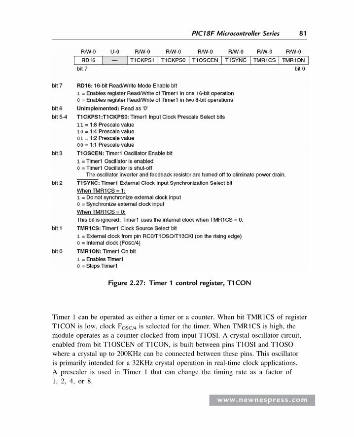
Timer 1 can be operated as either a timer or a counter. When bit TMR1CS of register
T1CON is low, clock FOSC/4 is selected for the timer. When TMR1CS is high, the
module operates as a counter clocked from input T1OSI. A crystal oscillator circuit,
enabled from bit T1OSCEN of T1CON, is built between pins T1OSI and T1OSO
where a crystal up to 200KHz can be connected between these pins. This oscillator
is primarily intended for a 32KHz crystal operation in real-time clock applications.
A prescaler is used in Timer 1 that can change the timing rate as a factor of
1, 2, 4, or 8.
Figure 2.27: Timer 1 control register, T1CON
www.newnespress.com
81PIC18F Microcontroller Series
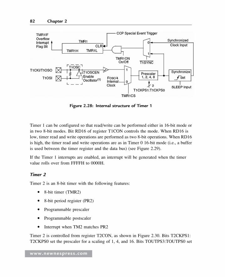
Timer 1 can be configured so that read/write can be performed either in 16-bit mode or
in two 8-bit modes. Bit RD16 of register T1CON controls the mode. When RD16 is
low, timer read and write operations are performed as two 8-bit operations. When RD16
is high, the timer read and write operations are as in Timer 0 16-bit mode (i.e., a buffer
is used between the timer register and the data bus) (see Figure 2.29).
If the Timer 1 interrupts are enabled, an interrupt will be generated when the timer
value rolls over from FFFFH to 0000H.
Timer 2
Timer 2 is an 8-bit timer with the following features:
� 8-bit timer (TMR2)
� 8-bit period register (PR2)
� Programmable prescaler
� Programmable postscaler
� Interrupt when TM2 matches PR2
Timer 2 is controlled from register T2CON, as shown in Figure 2.30. Bits T2CKPS1:
T2CKPS0 set the prescaler for a scaling of 1, 4, and 16. Bits TOUTPS3:TOUTPS0 set
Figure 2.28: Internal structure of Timer 1
www.newnespress.com
82 Chapter 2
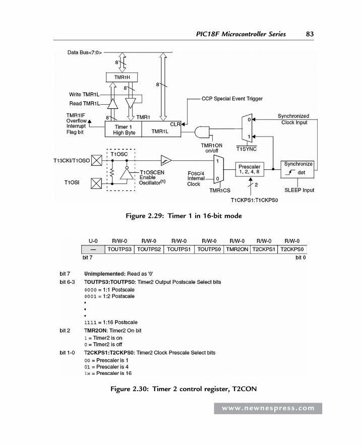
Figure 2.29: Timer 1 in 16-bit mode
Figure 2.30: Timer 2 control register, T2CON
www.newnespress.com
83PIC18F Microcontroller Series
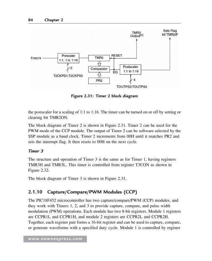
the postscaler for a scaling of 1:1 to 1:16. The timer can be turned on or off by setting or
clearing bit TMR2ON.
The block diagram of Timer 2 is shown in Figure 2.31. Timer 2 can be used for the
PWM mode of the CCP module. The output of Timer 2 can be software selected by the
SSP module as a baud clock. Timer 2 increments from 00H until it matches PR2 and
sets the interrupt flag. It then resets to 00H on the next cycle.
Timer 3
The structure and operation of Timer 3 is the same as for Timer 1, having registers
TMR3H and TMR3L. This timer is controlled from register T3CON as shown in
Figure 2.32.
The block diagram of Timer 3 is shown in Figure 2.33.
2.1.10 Capture/Compare/PWM Modules (CCP)
The PIC18F452 microcontroller has two capture/compare/PWM (CCP) modules, and
they work with Timers 1, 2, and 3 to provide capture, compare, and pulse width
modulation (PWM) operations. Each module has two 8-bit registers. Module 1 registers
are CCPR1L and CCPR1H, and module 2 registers are CCPR2L and CCPR2H.
Together, each register pair forms a 16-bit register and can be used to capture, compare,
or generate waveforms with a specified duty cycle. Module 1 is controlled by register
Figure 2.31: Timer 2 block diagram
www.newnespress.com
84 Chapter 2
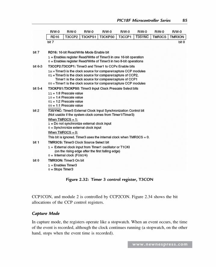
CCP1CON, and module 2 is controlled by CCP2CON. Figure 2.34 shows the bit
allocations of the CCP control registers.
Capture Mode
In capture mode, the registers operate like a stopwatch. When an event occurs, the time
of the event is recorded, although the clock continues running (a stopwatch, on the other
hand, stops when the event time is recorded).
Figure 2.32: Timer 3 control register, T3CON
www.newnespress.com
85PIC18F Microcontroller Series
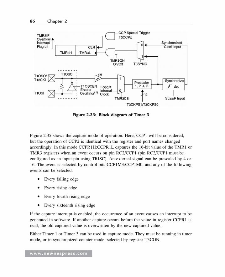
Figure 2.35 shows the capture mode of operation. Here, CCP1 will be considered,
but the operation of CCP2 is identical with the register and port names changed
accordingly. In this mode CCPR1H:CCPR1L captures the 16-bit value of the TMR1 or
TMR3 registers when an event occurs on pin RC2/CCP1 (pin RC2/CCP1 must be
configured as an input pin using TRISC). An external signal can be prescaled by 4 or
16. The event is selected by control bits CCP1M3:CCP1M0, and any of the following
events can be selected:
� Every falling edge
� Every rising edge
� Every fourth rising edge
� Every sixteenth rising edge
If the capture interrupt is enabled, the occurrence of an event causes an interrupt to be
generated in software. If another capture occurs before the value in register CCPR1 is
read, the old captured value is overwritten by the new captured value.
Either Timer 1 or Timer 3 can be used in capture mode. They must be running in timer
mode, or in synchronized counter mode, selected by register T3CON.
Figure 2.33: Block diagram of Timer 3
www.newnespress.com
86 Chapter 2
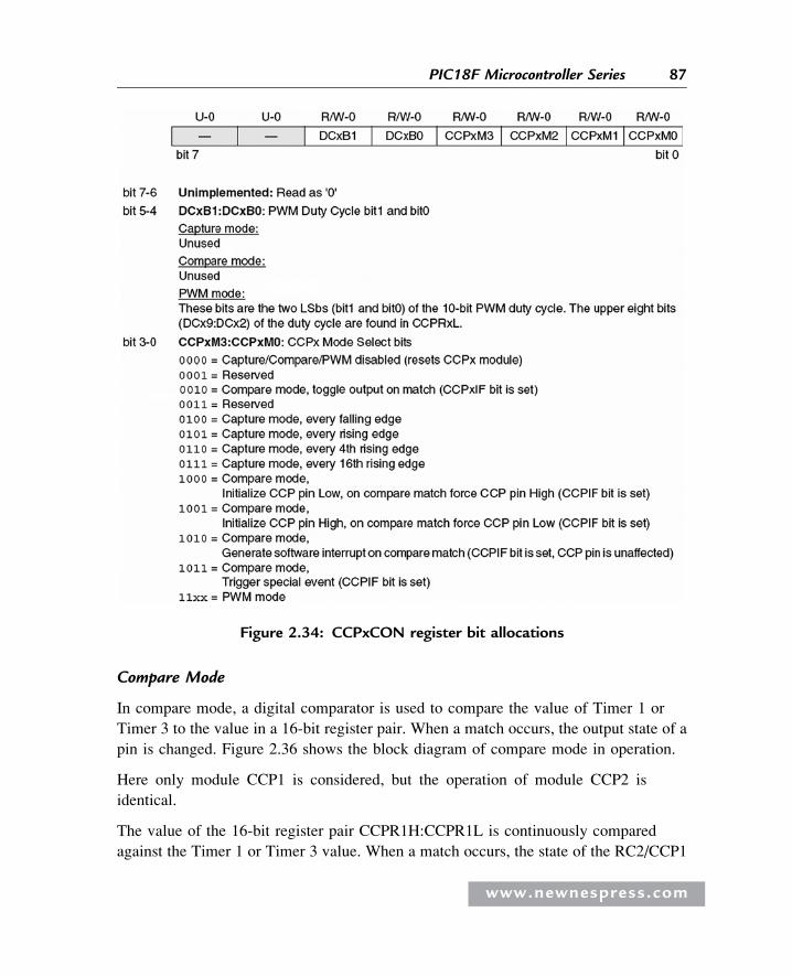
Compare Mode
In compare mode, a digital comparator is used to compare the value of Timer 1 or
Timer 3 to the value in a 16-bit register pair. When a match occurs, the output state of a
pin is changed. Figure 2.36 shows the block diagram of compare mode in operation.
Here only module CCP1 is considered, but the operation of module CCP2 is
identical.
The value of the 16-bit register pair CCPR1H:CCPR1L is continuously compared
against the Timer 1 or Timer 3 value. When a match occurs, the state of the RC2/CCP1
Figure 2.34: CCPxCON register bit allocations
www.newnespress.com
87PIC18F Microcontroller Series
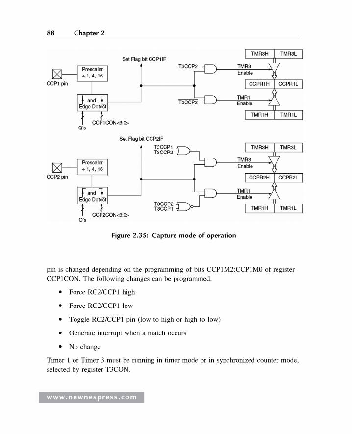
pin is changed depending on the programming of bits CCP1M2:CCP1M0 of register
CCP1CON. The following changes can be programmed:
� Force RC2/CCP1 high
� Force RC2/CCP1 low
� Toggle RC2/CCP1 pin (low to high or high to low)
� Generate interrupt when a match occurs
� No change
Timer 1 or Timer 3 must be running in timer mode or in synchronized counter mode,
selected by register T3CON.
Figure 2.35: Capture mode of operation
www.newnespress.com
88 Chapter 2
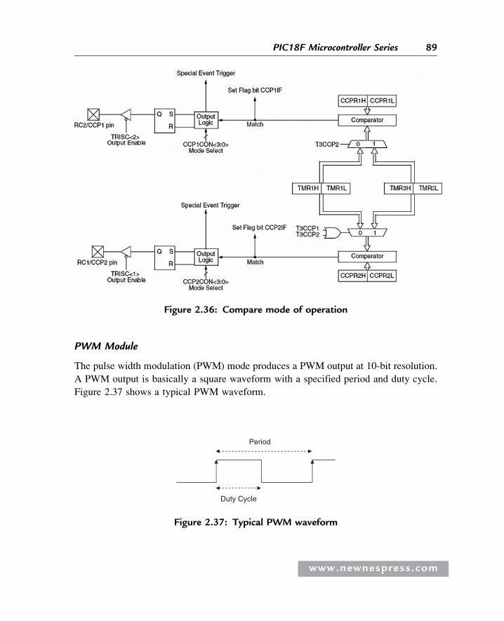
PWM Module
The pulse width modulation (PWM) mode produces a PWM output at 10-bit resolution.
A PWM output is basically a square waveform with a specified period and duty cycle.
Figure 2.37 shows a typical PWM waveform.
Figure 2.36: Compare mode of operation
Period
Duty Cycle
Figure 2.37: Typical PWM waveform
www.newnespress.com
89PIC18F Microcontroller Series
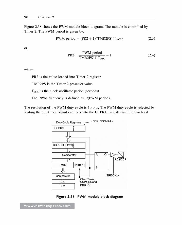
Figure 2.38 shows the PWM module block diagram. The module is controlled by
Timer 2. The PWM period is given by:
PWM period ¼ PR2þ 1ð Þ�TMR2PS�4�TOSC ð2:3Þ
or
PR2 ¼ PWM period
TMR2PS�4�TOSC
� 1 ð2:4Þ
where
PR2 is the value loaded into Timer 2 register
TMR2PS is the Timer 2 prescaler value
TOSC is the clock oscillator period (seconds)
The PWM frequency is defined as 1/(PWM period).
The resolution of the PWM duty cycle is 10 bits. The PWM duty cycle is selected by
writing the eight most significant bits into the CCPR1L register and the two least
Figure 2.38: PWM module block diagram
www.newnespress.com
90 Chapter 2
significant bits into bits 4 and 5 of CCP1CON register. The duty cycle (in seconds) is
given by:
PWM duty cycle ¼ CCPR1L :CCP1CON < 5 :4 >ð Þ�TMR2PS�TOSC ð2:5Þ
or
CCPR1L :CCP1CON < 5 :4 >¼ PWM duty cycle
TMR2PS�TOSC
ð2:6Þ
The steps to configure the PWM are as follows:
� Specify the required period and duty cycle.
� Choose a value for the Timer 2 prescaler (TMR2PS).
� Calculate the value to be written into the PR2 register using Equation (2.2).
� Calculate the value to be loaded into the CCPR1L and CCP1CON registers
using Equation (2.6).
� Clear bit 2 of TRISC to make CCP1 pin an output pin.
� Configure the CCP1 module for PWM operation using register CCP1CON.
The following example shows how the PWM can be set up.
Example 2.1
PWM pulses must be generated from pin CCP1 of a PIC18F452 microcontroller. The
required pulse period is 44ms and the required duty cycle is 50%. Assuming that the
microcontroller operates with a 4MHz crystal, calculate the values to be loaded into the
various registers.
Solution 2.1
Using a 4MHz crystal;TOSC ¼ 1=4 ¼ 0:25� 10�6
The required PWM duty cycle is 44/2 = 22ms.
From Equation (2.4), assuming a timer prescaler factor of 4, we have:
PR2 ¼ PWM period
TMR2PS�4�TOSC
� 1
www.newnespress.com
91PIC18F Microcontroller Series
or
PR2 ¼ 44�10�6
4�4�0:25�10�6� 1 ¼ 10 i:e:; 0AH
and from Equation (2.6)
CCPR1L :CCP1CON < 5 :4 >¼ PWM duty cycle
TMR2PS�TOSC
or
CCPR1L :CCP1CON < 5 :4 >¼ 22�10�6
4�0:25�10�6¼ 22
But the equivalent of number 22 in 10-bit binary is:
“00 00010110”
Therefore, the value to be loaded into bits 4 and 5 of CCP1CON is “00.” Bits 2 and 3 of
CCP1CON must be set to high for PWM operation. Therefore, CCP1CON must be set
to bit pattern (“X” is “don’t care”):
XX001100
Taking the don’t-care entries as 0, we can set CCP1CON to hexadecimal 0CH.
The value to be loaded into CCPR1L is “00010110” (i.e., hexadecimal number 16H).
The required steps are summarized as follows:
� Load Timer 2 with prescaler of 4 (i.e., load T2CON) with 00000101 (i.e., 05H).
� Load 0AH into PR2.
� Load 16H into CCPR1L.
� Load 0 into TRISC (make CCP1 pin output).
� Load 0CH into CCP1CON.
One period of the generated PWM waveform is shown in Figure 2.39.
www.newnespress.com
92 Chapter 2
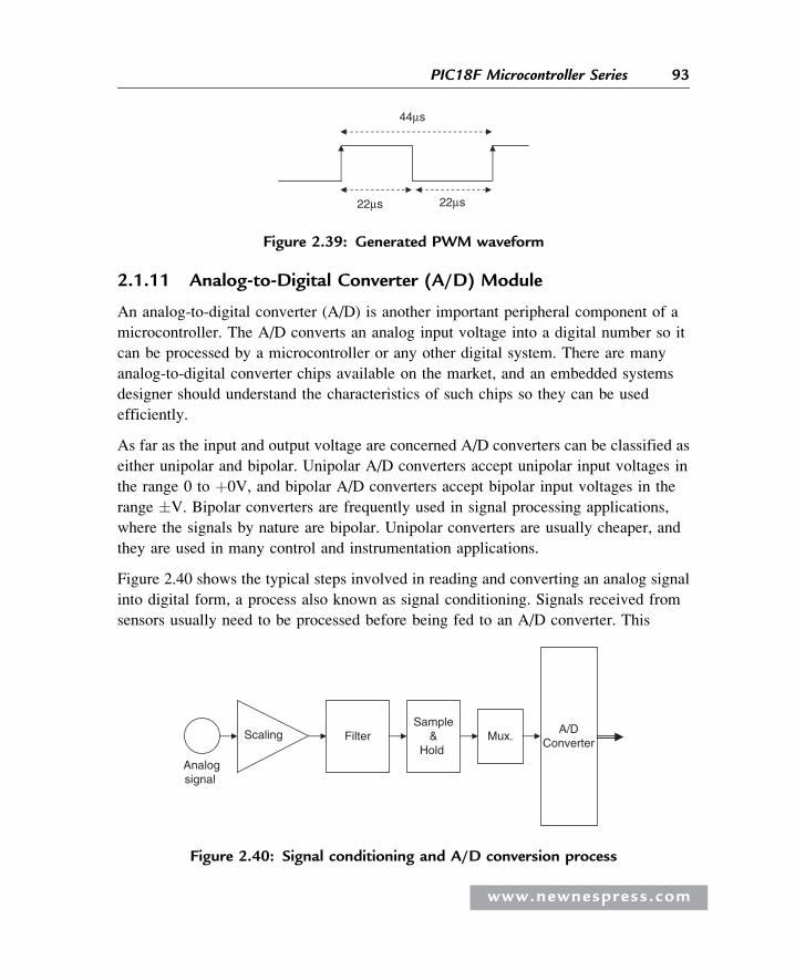
2.1.11 Analog-to-Digital Converter (A/D) Module
An analog-to-digital converter (A/D) is another important peripheral component of a
microcontroller. The A/D converts an analog input voltage into a digital number so it
can be processed by a microcontroller or any other digital system. There are many
analog-to-digital converter chips available on the market, and an embedded systems
designer should understand the characteristics of such chips so they can be used
efficiently.
As far as the input and output voltage are concerned A/D converters can be classified as
either unipolar and bipolar. Unipolar A/D converters accept unipolar input voltages in
the range 0 to þ0V, and bipolar A/D converters accept bipolar input voltages in the
range �V. Bipolar converters are frequently used in signal processing applications,
where the signals by nature are bipolar. Unipolar converters are usually cheaper, and
they are used in many control and instrumentation applications.
Figure 2.40 shows the typical steps involved in reading and converting an analog signal
into digital form, a process also known as signal conditioning. Signals received from
sensors usually need to be processed before being fed to an A/D converter. This
44µs
22µs 22µs
Figure 2.39: Generated PWM waveform
Analogsignal
Scaling FilterSample
&Hold
Mux.A/D
Converter
Figure 2.40: Signal conditioning and A/D conversion process
www.newnespress.com
93PIC18F Microcontroller Series
processing usually begins with scaling the signal to the correct value. Unwanted signal
components are then removed by filtering the signal using classical filters (e.g., a low-
pass filter). Finally, before feeding the signal to an A/D converter, the signal is passed
through a sample-and-hold device. This is particularly important with fast real-time
signals whose value may be changing between the sampling instants. A sample-and-
hold device ensures that the signal stays at a constant value during the actual conversion
process. Many applications required more than one A/D, which normally involves using
an analog multiplexer at the input of the A/D. The multiplexer selects only one signal at
any time and presents this signal to the A/D converter. An A/D converter usually has a
single analog input and a digital parallel output. The conversion process is as follows:
� Apply the processed signal to the A/D input
� Start the conversion
� Wait until conversion is complete
� Read the converted digital data
The A/D conversion starts by triggering the converter. Depending on the speed of the
converter, the conversion process itself can take several microseconds. At the end of
the conversion, the converter either raises a flag or generates an interrupt to indicate
that the conversion is complete. The converted parallel output data can then be read
by the digital device connected to the A/D converter.
Most members of the PIC18F family contain a 10-bit A/D converter. If the chosen
voltage reference is +5V, the voltage step value is:
5V
1023
� �¼ 0:00489V or 4:89mV
Therefore, for example, if the input voltage is 1.0V, the converter will generate a digital
output of 1.0/0.00489 = 205 decimal. Similarly, if the input voltage is 3.0V, the
converter will generate 3.0/0.00489 = 613.
The A/D converter used by the PIC18F452 microcontroller has eight channels, named
AN0–AN7, which are shared by the PORTA and PORTE pins. Figure 2.41 shows the
block diagram of the A/D converter.
www.newnespress.com
94 Chapter 2
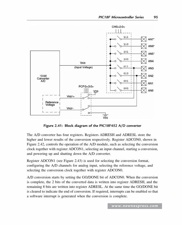
The A/D converter has four registers. Registers ADRESH and ADRESL store the
higher and lower results of the conversion respectively. Register ADCON0, shown in
Figure 2.42, controls the operation of the A/D module, such as selecting the conversion
clock together with register ADCON1, selecting an input channel, starting a conversion,
and powering up and shutting down the A/D converter.
Register ADCON1 (see Figure 2.43) is used for selecting the conversion format,
configuring the A/D channels for analog input, selecting the reference voltage, and
selecting the conversion clock together with register ADCON0.
A/D conversion starts by setting the GO/DONE bit of ADCON0. When the conversion
is complete, the 2 bits of the converted data is written into register ADRESH, and the
remaining 8 bits are written into register ADRESL. At the same time the GO/DONE bit
is cleared to indicate the end of conversion. If required, interrupts can be enabled so that
a software interrupt is generated when the conversion is complete.
Figure 2.41: Block diagram of the PIC18F452 A/D converter
www.newnespress.com
95PIC18F Microcontroller Series
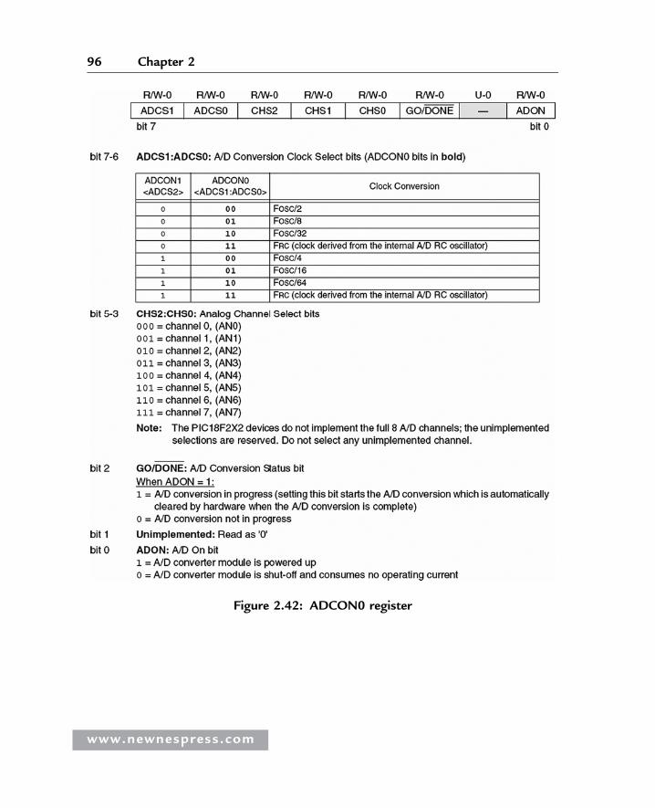
Figure 2.42: ADCON0 register
www.newnespress.com
96 Chapter 2
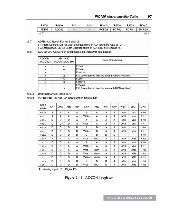
Figure 2.43: ADCON1 register
www.newnespress.com
97PIC18F Microcontroller Series
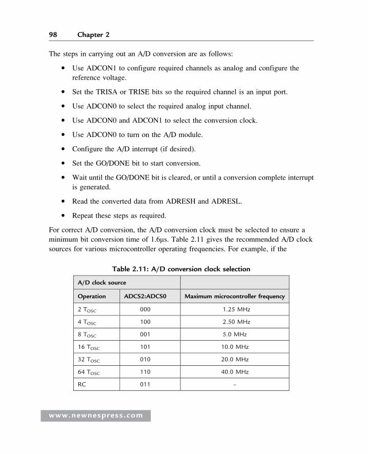
The steps in carrying out an A/D conversion are as follows:
� Use ADCON1 to configure required channels as analog and configure the
reference voltage.
� Set the TRISA or TRISE bits so the required channel is an input port.
� Use ADCON0 to select the required analog input channel.
� Use ADCON0 and ADCON1 to select the conversion clock.
� Use ADCON0 to turn on the A/D module.
� Configure the A/D interrupt (if desired).
� Set the GO/DONE bit to start conversion.
� Wait until the GO/DONE bit is cleared, or until a conversion complete interrupt
is generated.
� Read the converted data from ADRESH and ADRESL.
� Repeat these steps as required.
For correct A/D conversion, the A/D conversion clock must be selected to ensure a
minimum bit conversion time of 1.6ms. Table 2.11 gives the recommended A/D clock
sources for various microcontroller operating frequencies. For example, if the
Table 2.11: A/D conversion clock selection
A/D clock source
Operation ADCS2:ADCS0 Maximum microcontroller frequency
2 TOSC 000 1.25 MHz
4 TOSC 100 2.50 MHz
8 TOSC 001 5.0 MHz
16 TOSC 101 10.0 MHz
32 TOSC 010 20.0 MHz
64 TOSC 110 40.0 MHz
RC 011 –
www.newnespress.com
98 Chapter 2
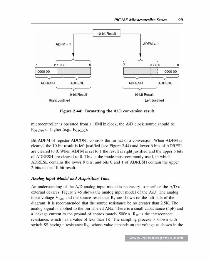
microcontroller is operated from a 10MHz clock, the A/D clock source should be
FOSC/16 or higher (e.g., FOSC/32).
Bit ADFM of register ADCON1 controls the format of a conversion. When ADFM is
cleared, the 10-bit result is left justified (see Figure 2.44) and lower 6 bits of ADRESL
are cleared to 0. When ADFM is set to 1 the result is right justified and the upper 6 bits
of ADRESH are cleared to 0. This is the mode most commonly used, in which
ADRESL contains the lower 8 bits, and bits 0 and 1 of ADRESH contain the upper
2 bits of the 10-bit result.
Analog Input Model and Acquisition Time
An understanding of the A/D analog input model is necessary to interface the A/D to
external devices. Figure 2.45 shows the analog input model of the A/D. The analog
input voltage VAIN and the source resistance RS are shown on the left side of the
diagram. It is recommended that the source resistance be no greater than 2.5K. The
analog signal is applied to the pin labeled ANx. There is a small capacitance (5pF) and
a leakage current to the ground of approximately 500nA. RIC is the interconnect
resistance, which has a value of less than 1K. The sampling process is shown with
switch SS having a resistance RSS whose value depends on the voltage as shown in the
Figure 2.44: Formatting the A/D conversion result
www.newnespress.com
99PIC18F Microcontroller Series
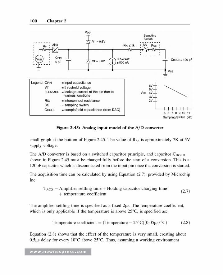
small graph at the bottom of Figure 2.45. The value of RSS is approximately 7K at 5V
supply voltage.
The A/D converter is based on a switched capacitor principle, and capacitor CHOLD
shown in Figure 2.45 must be charged fully before the start of a conversion. This is a
120pF capacitor which is disconnected from the input pin once the conversion is started.
The acquisition time can be calculated by using Equation (2.7), provided by Microchip
Inc:
TACQ ¼ Amplifier settling timeþ Holding capacitor charging time
þ temperature coefficientð2:7Þ
The amplifier settling time is specified as a fixed 2ms. The temperature coefficient,
which is only applicable if the temperature is above 25�C, is specified as:
Temperature coefficient ¼ Temperature� 25�Cð Þ 0:05ms=�Cð Þ ð2:8Þ
Equation (2.8) shows that the effect of the temperature is very small, creating about
0.5ms delay for every 10�C above 25�C. Thus, assuming a working environment
Figure 2.45: Analog input model of the A/D converter
www.newnespress.com
100 Chapter 2
between 25�C and 35�C, the maximum delay due to temperature will be 0.5ms, whichcan be ignored for most practical applications.
The holding capacitor charging time as specified by Microchip Inc is:
Holding capacitor charging time ¼ � 120pFð Þ 1Kþ RSS þRSð ÞLn 1=2048ð Þ ð2:9Þ
Assuming that RSS ¼ 7K, RS ¼ 2.5K, Equation (2.9) gives the holding capacitor
charging time as 9.6ms.
The acquisition time is then calculated as:
TACQ ¼ 2þ 9:6þ 0:5 ¼ 12:1ms
A full 10-bit conversion takes 12 A/D cycles, and each A/D cycle is specified at a
minimum of 1.6ms. Thus, the fastest conversion time is 19.2ms. Adding this to the
best possible acquisition time gives a total time to complete a conversion of 19.2 þ 12.1
¼ 31.3ms.
When a conversion is complete, it is specified that the converter should wait for two
conversion periods before starting a new conversion. This corresponds to 2� 1.6¼ 3.2ms.Adding this to the best possible conversion time of 31.3ms gives a complete conversion
time of 34.5ms. Assuming the A/D converter is used successively, and ignoring the
software overheads, this implies a maximum sampling frequency of about 29KHz.
2.1.12 Interrupts
An interrupt is an event that requires the CPU to stop normal program execution and
then execute a program code related to the event causing the interrupt. Interrupts can
be generated internally (by some event inside the chip) or externally (by some external
event). An example of an internal interrupt is a timer overflowing or the A/D completing a
conversion. An example of an external interrupt is an I/O pin changing state.
Interrupts can be useful in many applications such as:
� Time critical applications. Applications which require the immediate attention
of the CPU can use interrupts. For example, in an emergency such as a power
failure or fire in a plant the CPU may have to shut down the system immediately
in an orderly manner. In such applications an external interrupt can force the
CPU to stop whatever it is doing and take immediate action.
www.newnespress.com
101PIC18F Microcontroller Series
� Performing routine tasks. Many applications require the CPU to perform routine
work at precise times, such as checking the state of a peripheral device exactly
every millisecond. A timer interrupt scheduled with the required timing can
divert the CPU from normal program execution to accomplish the task at the
precise time required.
� Task switching in multi-tasking applications. In multi-tasking applications, each
task may have a finite time to execute its code. Interrupt mechanisms can be
used to stop a task should it consume more than its allocated time.
� To service peripheral devices quickly. Some applications may need to know
when a task, such as an A/D conversion, is completed. This can be
accomplished by continuously checking the completion flag of the A/D
converter. A more elegant solution would be to enable the A/D completion
interrupt so the CPU is forced to read the converted data as soon as it becomes
available.
The PIC18F452 microcontroller has both core and peripheral interrupt sources. The
core interrupt sources are:
� External edge-triggered interrupt on INT0, INT1, and INT2 pins.
� PORTB pins change interrupts (any one of the RB4–RB7 pins changing state)
� Timer 0 overflow interrupt
The peripheral interrupt sources are:
� Parallel slave port read/write interrupt
� A/D conversion complete interrupt
� USART receive interrupt
� USART transmit interrupt
� Synchronous serial port interrupt
� CCP1 interrupt
� TMR1 overflow interrupt
� TMR2 overflow interrupt
� Comparator interrupt
www.newnespress.com
102 Chapter 2
� EEPROM/FLASH write interrupt
� Bus collision interrupt
� Low-voltage detect interrupt
� Timer 3 overflow interrupt
� CCP2 interrupt
Interrupts in the PIC18F family can be divided into two groups: high priority and low
priority. Applications that require more attention can be placed in the higher priority
group. A high-priority interrupt can stop a low-priority interrupt that is in progress
and gain access to the CPU. However, high-priority interrupts cannot be stopped by
low-priority interrupts. If the application does not need to set priorities for interrupts,
the user can choose to disable the priority scheme so all interrupts are at the same
priority level. High-priority interrupts are vectored to address 00008H and low-priority
ones to address 000018H of the program memory. Normally, a user program code
(interrupt service routine, ISR) should be at the interrupt vector address to service
the interrupting device.
In the PIC18F452 microcontroller there are ten registers that control interrupt
operations. These are:
� RCON
� INTCON
� INTCON2
� INTCON3
� PIR1, PIR2
� PIE1, PIE2
� IPR1, IPR2
Every interrupt source (except INT0) has three bits to control its operation. These
bits are:
� A flag bit to indicate whether an interrupt has occurred. This bit has a name
ending in . . .IF
www.newnespress.com
103PIC18F Microcontroller Series
� An interrupt enable bit to enable or disable the interrupt source. This bit has the
name ending in . . .IE
� A priority bit to select high or low priority. This bit has a name ending in . . .IP
RCON Register
The top bit of the RCON register, called IPEN, is used to enable the interrupt priority
scheme. When IPEN ¼ 0, interrupt priority levels are disabled and the microcontroller
interrupt structure is similar to that of the PIC16 series. When IPEN ¼ 1, interrupt
priority levels are enabled. Figure 2.46 shows the bits of register RCON.
Enabling/Disabling Interrupts—No Priority Structure
When the IPEN bit is cleared, the priority feature is disabled. All interrupts branch
to address 00008H of the program memory. In this mode, bit PEIE of register
INTCON enables/disables all peripheral interrupt sources. Similarly, bit GIE of
INTCON enables/disables all interrupt sources. Figure 2.47 shows the bits of
register INTCON.
Figure 2.46: RCON register bits
www.newnespress.com
104 Chapter 2
Figure 2.47: INTCON register bits
www.newnespress.com
105PIC18F Microcontroller Series
For an interrupt to be accepted by the CPU the following conditions must be
satisfied:
� The interrupt enable bit of the interrupt source must be enabled. For example, if
the interrupt source is external interrupt pin INT0, then bit INT0IE of register
INTCON must be set to 1.
� The interrupt flag of the interrupt source must be cleared. For example, if the
interrupt source is external interrupt pin INT0, then bit INT0IF of register
INTCON must be cleared to 0.
� The peripheral interrupt enable/disable bit PEIE of INTCON must be set to 1 if
the interrupt source is a peripheral.
� The global interrupt enable/disable bit GIE of INTCON must be set to 1.
With an external interrupt source we normally have to define whether the interrupt
should occur on the low-to-high or high-to-low transition of the interrupt source.
With INT0 interrupts, for example, this is done by setting/clearing bit INTEDG0 of
register INTCON2.
When an interrupt occurs, the CPU stops its normal flow of execution, pushes the return
address onto the stack, and jumps to address 00008H in the program memory where the
user interrupt service routine program resides. Once the CPU is in the interrupt service
routine, the global interrupt enable bit (GIE) is cleared to disable further interrupts.
When multiple interrupt sources are enabled, the source of the interrupt can be
determined by polling the interrupt flag bits. The interrupt flag bits must be cleared in
the software before reenabling interrupts to avoid recursive interrupts. When the CPU
has returned from the interrupt service routine, the global interrupt bit GIE is
automatically set by the software.
Enabling/Disabling Interrupts—Priority Structure
When the IPEN bit is set to 1, the priority feature is enabled and the interrupts
are grouped into two: low priority and high priority. Low-priority interrupts branch
to address 00008H and high-priority interrupts branch to address 000018H of the
program memory. Setting the priority bit makes the interrupt source a high-priority
interrupt, and clearing this bit makes the interrupt source a low-priority interrupt.
www.newnespress.com
106 Chapter 2

Setting the GIEH bit of INTCON enables all high-priority interrupts that have the
priority bit set. Similarly, setting the GIEL bit of INTCON enables all low-priority
interrupts (the priority is bit cleared).
For a high-priority interrupt to be accepted by the CPU, the following conditions must
be satisfied:
� The interrupt enable bit of the interrupt source must be enabled. For example, if
the interrupt source is external interrupt pin INT1, then bit INT1IE of register
INTCON3 must be set to 1.
� The interrupt flag of the interrupt source must be cleared. For example, if the
interrupt source is external interrupt pin INT1, then bit INT1IF of register
INTCON3 must be cleared to 0.
� The priority bit must be set to 1. For example, if the interrupt source is external
interrupt INT1, then bit INT1P of register INTCON3 must be set to 1.
� The global interrupt enable/disable bit GIEH of INTCON must be set to 1.
For a low-priority interrupt to be accepted by the CPU, the following conditions must
be satisfied:
� The interrupt enable bit of the interrupt source must be enabled. For example, if
the interrupt source is external interrupt pin INT1, then bit INT1IE of register
INTCON3 must be set to 1.
� The interrupt flag of the interrupt source must be cleared. For example, if the
interrupt source is external interrupt pin INT1, then bit INT1IF of register
INTCON3 must be cleared to 0.
� The priority bit must be cleared to 0. For example, if the interrupt source
is external interrupt INT1, then bit INT1P of register INTCON3 must be
cleared to 0.
� Low-priority interrupts must be enabled by setting bit GIEL of INTCON to 1.
� The global interrupt enable/disable bit GIEH of INTCON must be set to 1.
Table 2.12 gives a listing of the PIC18F452 microcontroller interrupt bit names and
register names for every interrupt source.
www.newnespress.com
107PIC18F Microcontroller Series
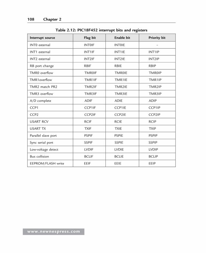
Table 2.12: PIC18F452 interrupt bits and registers
Interrupt source Flag bit Enable bit Priority bit
INT0 external INT0IF INT0IE –
INT1 external INT1IF INT1IE INT1IP
INT2 external INT2IF INT2IE INT2IP
RB port change RBIF RBIE RBIP
TMR0 overflow TMR0IF TMR0IE TMR0IP
TMR1overflow TMR1IF TMR1IE TMR1IP
TMR2 match PR2 TMR2IF TMR2IE TMR2IP
TMR3 overflow TMR3IF TMR3IE TMR3IP
A/D complete ADIF ADIE ADIP
CCP1 CCP1IF CCP1IE CCP1IP
CCP2 CCP2IF CCP2IE CCP2IP
USART RCV RCIF RCIE RCIP
USART TX TXIF TXIE TXIP
Parallel slave port PSPIF PSPIE PSPIP
Sync serial port SSPIF SSPIE SSPIP
Low-voltage detect LVDIF LVDIE LVDIP
Bus collision BCLIF BCLIE BCLIP
EEPROM/FLASH write EEIF EEIE EEIP
www.newnespress.com
108 Chapter 2
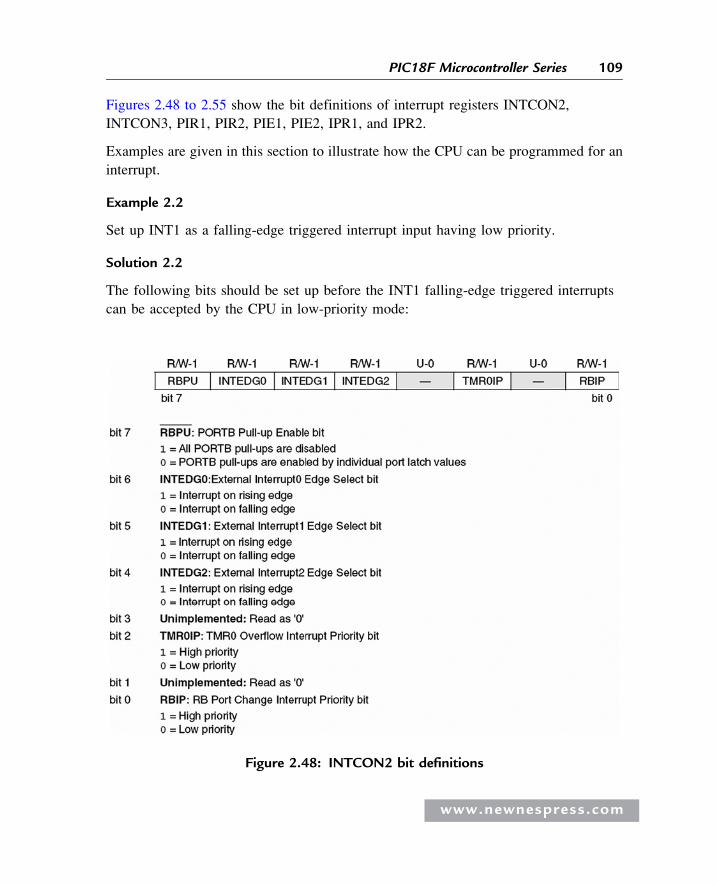
Figures 2.48 to 2.55 show the bit definitions of interrupt registers INTCON2,
INTCON3, PIR1, PIR2, PIE1, PIE2, IPR1, and IPR2.
Examples are given in this section to illustrate how the CPU can be programmed for an
interrupt.
Example 2.2
Set up INT1 as a falling-edge triggered interrupt input having low priority.
Solution 2.2
The following bits should be set up before the INT1 falling-edge triggered interrupts
can be accepted by the CPU in low-priority mode:
Figure 2.48: INTCON2 bit definitions
www.newnespress.com
109PIC18F Microcontroller Series
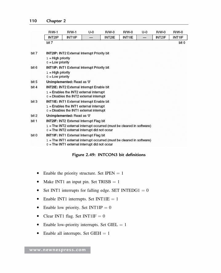
� Enable the priority structure. Set IPEN ¼ 1
� Make INT1 an input pin. Set TRISB ¼ 1
� Set INT1 interrupts for falling edge. SET INTEDG1 ¼ 0
� Enable INT1 interrupts. Set INT1IE ¼ 1
� Enable low priority. Set INT1IP ¼ 0
� Clear INT1 flag. Set INT1IF ¼ 0
� Enable low-priority interrupts. Set GIEL ¼ 1
� Enable all interrupts. Set GIEH ¼ 1
Figure 2.49: INTCON3 bit definitions
www.newnespress.com
110 Chapter 2
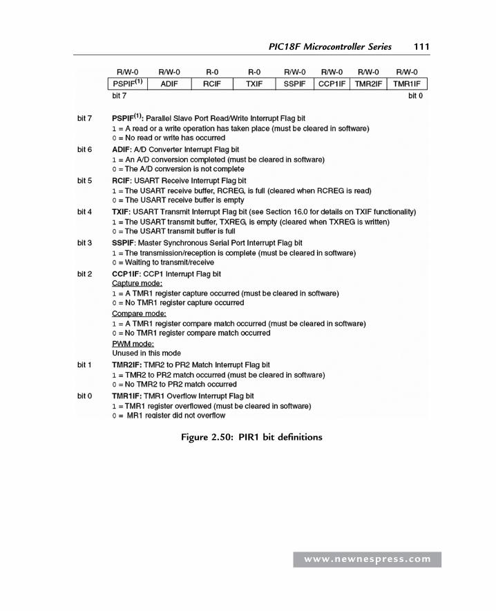
Figure 2.50: PIR1 bit definitions
www.newnespress.com
111PIC18F Microcontroller Series
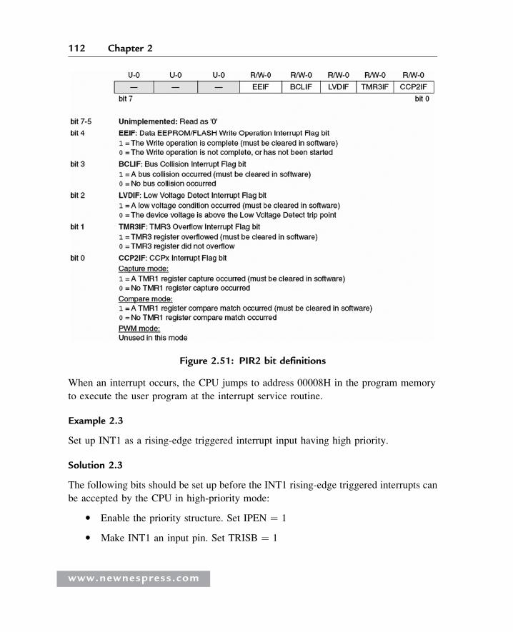
When an interrupt occurs, the CPU jumps to address 00008H in the program memory
to execute the user program at the interrupt service routine.
Example 2.3
Set up INT1 as a rising-edge triggered interrupt input having high priority.
Solution 2.3
The following bits should be set up before the INT1 rising-edge triggered interrupts can
be accepted by the CPU in high-priority mode:
� Enable the priority structure. Set IPEN ¼ 1
� Make INT1 an input pin. Set TRISB ¼ 1
Figure 2.51: PIR2 bit definitions
www.newnespress.com
112 Chapter 2
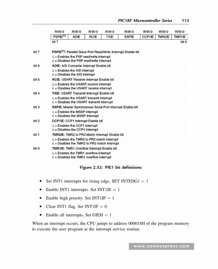
� Set INT1 interrupts for rising edge. SET INTEDG1 ¼ 1
� Enable INT1 interrupts. Set INT1IE ¼ 1
� Enable high priority. Set INT1IP ¼ 1
� Clear INT1 flag. Set INT1IF ¼ 0
� Enable all interrupts. Set GIEH ¼ 1
When an interrupt occurs, the CPU jumps to address 000018H of the program memory
to execute the user program at the interrupt service routine.
Figure 2.52: PIE1 bit definitions
www.newnespress.com
113PIC18F Microcontroller Series
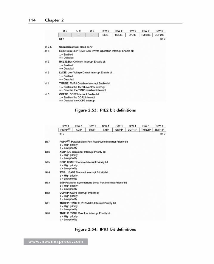
Figure 2.53: PIE2 bit definitions
Figure 2.54: IPR1 bit definitions
www.newnespress.com
114 Chapter 2
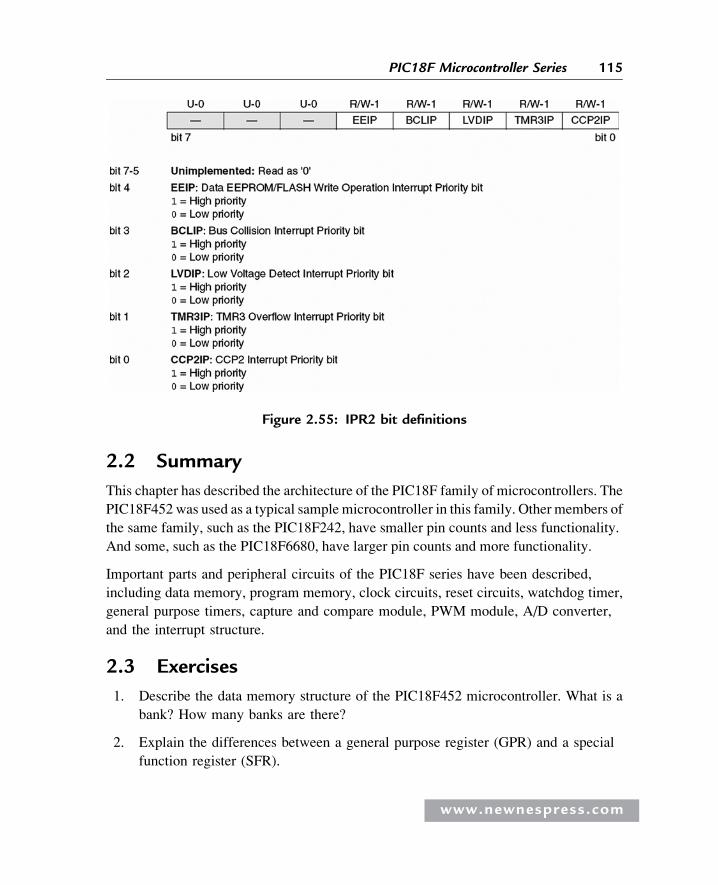
2.2 Summary
This chapter has described the architecture of the PIC18F family of microcontrollers. The
PIC18F452 was used as a typical sample microcontroller in this family. Other members of
the same family, such as the PIC18F242, have smaller pin counts and less functionality.
And some, such as the PIC18F6680, have larger pin counts and more functionality.
Important parts and peripheral circuits of the PIC18F series have been described,
including data memory, program memory, clock circuits, reset circuits, watchdog timer,
general purpose timers, capture and compare module, PWM module, A/D converter,
and the interrupt structure.
2.3 Exercises
1. Describe the data memory structure of the PIC18F452 microcontroller. What is a
bank? How many banks are there?
2. Explain the differences between a general purpose register (GPR) and a special
function register (SFR).
Figure 2.55: IPR2 bit definitions
www.newnespress.com
115PIC18F Microcontroller Series
3. Explain the various ways the PIC18F microcontroller can be reset. Draw a circuit
diagram to show how an external push-button switch can be used to reset the
microcontroller.
4. Describe the various clock sources that can be used to provide a clock to a
PIC18F452 microcontroller. Draw a circuit diagram to show how a 10MHz crystal
can be connected to the microcontroller.
5. Draw a circuit diagram to show how a resonator can be connected to a PIC18F
microcontroller.
6. In a non-time-critical application a clock must be provided for a PIC18F452
microcontroller using an external resistor and a capacitor. Draw a circuit diagram
to show how this can be done and find the component values for a required clock
frequency of 5MHz.
7. Explain how an external clock can provide clock pulses to a PIC18F
microcontroller.
8. What are the registers of PORTA? Explain the operation of the port by drawing
the port block diagram.
9. The watchdog timer must be set to provide an automatic reset every 0.5 seconds.
Describe how to do this, including the appropriate register bits.
10. PWM pulses must be generated from pin CCP1 of a PIC18F452 microcontroller.
The required pulse period is 100ms, and the required duty cycle is 50%. Assuming
the microcontroller is operating with a 4MHz crystal, calculate the values to be
loaded into the various registers.
11. Again, with regard to PWM pulses generated from pin CCP1 of a PIC18F452
microcontroller: If the required pulse frequency is 40KHz, and the required duty
cycle is 50%, and assuming the microcontroller is operating with a 4MHz crystal,
calculate the values to be loaded into the various registers.
12. An LM35DZ-type analog temperature sensor is connected to analog port AN0 of a
PIC18F452 microcontroller. The sensor provides an analog output voltage
proportional to the temperature (i.e., V0 = 10 mV/�C). Show the steps required to
read the temperature.
13. Explain the difference between a priority interrupt and a nonpriority interrupt.
www.newnespress.com
116 Chapter 2

14. Show the steps required to set up INT2 as a falling-edge triggered interrupt input
having low priority. What is the interrupt vector address?
15. Show the steps required to set up both INT1 and INT2 as falling-edge triggered
interrupt inputs having low priority.
16. Show the steps required to set up INT1 as falling-edge triggered and INT2 as
rising-edge triggered interrupt inputs having high priorities. Explain how to find
the source of the interrupt when an interrupt occurs.
17. Show the steps required to set up Timer 0 to generate interrupts every millisecond
with a high priority. What is the interrupt vector address?
18. In an application the CPU registers have been configured to accept interrupts from
external sources INT0, INT1, and INT2. An interrupt has been detected. Explain
how to find the source of the interrupt.
www.newnespress.com
117PIC18F Microcontroller Series

This page intentionally left blank
CHAP T E R 3
C Programming Language
There are several C compilers on the market for the PIC18 series of microcontrollers.
These compilers have many similar features, and they can all be used to develop
C-based high-level programs for PIC18 microcontrollers.
Some of the C compilers used most often in commercial, industrial, and educational
PIC18 microcontroller applications are:
� mikroC
� PICC18
� C18
� CCS
The popular and powerful mikroC, developed by MikroElektronika (web site:
www.microe.com), is easy to learn and comes with rich resources, such as a large
number of library functions and an integrated development environment with a built-in
simulator and an in-circuit debugger (e.g., mikroICD). A demo version of the compiler
with a 2K program limit is available from MikroElektronika.
PICC18, another popular C compiler, was developed by Hi-Tech Software (web site:
www.htsoft.com) and is available in two versions: standard and professional.
A powerful simulator and an integrated development environment (Hi-Tide) are
provided by the company. PICC18 is supported by the PROTEUS simulator
(www.labcenter.co.uk) which can be used to simulate PIC microcontroller–based
systems. A limited-period demo version of this compiler is available on the developer’s
web site.
www.newnespress.com
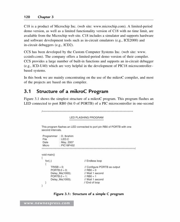
C18 is a product of Microchip Inc. (web site: www.microchip.com). A limited-period
demo version, as well as a limited functionality version of C18 with no time limit, are
available from the Microchip web site. C18 includes a simulator and supports hardware
and software development tools such as in-circuit emulators (e.g., ICE2000) and
in-circuit debuggers (e.g., ICD2).
CCS has been developed by the Custom Computer Systems Inc. (web site: www.
ccsinfo.com). The company offers a limited-period demo version of their compiler.
CCS provides a large number of built-in functions and supports an in-circuit debugger
(e.g., ICD-U40) which are very helpful in the development of PIC18 microcontroller–
based systems.
In this book we are mainly concentrating on the use of the mikroC compiler, and most
of the projects are based on this compiler.
3.1 Structure of a mikroC Program
Figure 3.1 shows the simplest structure of a mikroC program. This program flashes an
LED connected to port RB0 (bit 0 of PORTB) of a PIC microcontroller in one-second
/∗∗∗∗∗∗∗∗∗∗∗∗∗∗∗∗∗∗∗∗∗∗∗∗∗∗∗∗∗∗∗∗∗∗∗∗∗∗∗∗∗∗∗∗∗∗∗∗∗∗∗∗∗∗∗∗∗∗∗∗∗∗∗∗∗∗∗∗
LED FLASHING PROGRAM *********************************
This program flashes an LED connected to port pin RB0 of PORTB with onesecond intervals.
ProgrammerFileDateMicro
∗∗∗∗∗∗∗∗∗∗∗∗∗∗∗∗∗∗∗∗∗∗∗∗∗∗∗∗∗∗∗∗∗∗∗∗∗∗∗∗∗∗∗∗∗∗∗∗∗∗∗∗∗∗∗∗∗∗∗∗∗∗∗∗∗∗∗∗∗∗/
void main() {
for(;;) // Endless loop {
TRISB = 0; // Configure PORTB as output PORTB.0 = 0; // RB0 = 0Delay_Ms(1000); // Wait 1 second PORTB.0 = 1; // RB0 = 1 Delay_Ms(1000); // Wait 1 second
} // End of loop }
: D. Ibrahim : LED.C : May, 2007 : PIC18F452
Figure 3.1: Structure of a simple C program
www.newnespress.com
120 Chapter 3
intervals. Do not worry if you don’t understand the operation of the program at this
stage, as all will come clear as this chapter progresses. Some of the programming
elements in Figure 3.1 are described in detail here.
3.1.1 Comments
Comments are used to clarify the operation of the program or a programming
statement. Comment lines are ignored and not compiled by the compiler. In mikroC
programs comments can be of two types: long comments, extending several lines, and
short comments, occupying only a single line. Comment lines at the beginning of a
program can describe briefly the program’s operation and provide the author’s name,
the program filename, the date the program was written, and a list of version numbers,
together with the modifications in each version. As shown in Figure 3.1, comments can
also be added after statements to describe the operations that the statements perform.
Clear and succinct comment lines are important for the maintenance and thus the lifetime
of a program, as a program with good comments is easier to modify and/or update.
As shown in Figure 3.1, long comments start with the character “/*” and terminate with
the character “*/”. Similarly, short comments start with the character “//” and do not
need a terminating character.
3.1.2 Beginning and Ending of a Program
In C language, a program begins with the keywords:
void main ()
After this, a curly opening bracket is used to indicate the beginning of the program
body. The program is terminated with a closing curly bracket. Thus, as shown in
Figure 3.1, the program has the following structure:
void main(){
program body}
3.1.3 Terminating Program Statements
In C language, all program statements must be terminated with the semicolon (“;”)
character; otherwise a compiler error will be generated:
www.newnespress.com
121C Programming Language
j ¼ 5; // correctj ¼ 5 // error
3.1.4 White Spaces
White spaces are spaces, blanks, tabs, and newline characters. The C compiler ignores
all white spaces. Thus, the following three sequences are identical:
int i; char j;orint i;char j;orint i;
char j;
Similarly, the following sequences are identical:
i ¼ j þ 2;ori ¼ j
þ 2;
3.1.5 Case Sensitivity
In general, C language is case sensitive and variables with lowercase names are
different from those with uppercase names. Currently, however, mikroC variables are
not case sensitive (although future releases of mikroC may offer case sensitivity) so
the following variables are equivalent:
total TOTAL Total ToTal total totaL
The only exception is the identifiers main and interrupt, which must be written in
lowercase in mikroC. In this book we are assuming that the variables are case sensitive,
for the sake of compatibility with other C compilers, and variables with the same name
but different cases are not used.
www.newnespress.com
122 Chapter 3
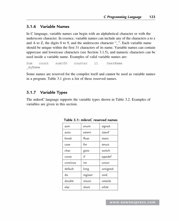
3.1.6 Variable Names
In C language, variable names can begin with an alphabetical character or with the
underscore character. In essence, variable names can include any of the characters a to z
and A to Z, the digits 0 to 9, and the underscore character “_”. Each variable name
should be unique within the first 31 characters of its name. Variable names can contain
uppercase and lowercase characters (see Section 3.1.5), and numeric characters can be
used inside a variable name. Examples of valid variable names are:
Sum count sum100 counter i1 UserName_myName
Some names are reserved for the compiler itself and cannot be used as variable names
in a program. Table 3.1 gives a list of these reserved names.
3.1.7 Variable Types
The mikroC language supports the variable types shown in Table 3.2. Examples of
variables are given in this section.
Table 3.1: mikroC reserved names
asm enum signed
auto extern sizeof
break float static
case for struct
char goto switch
const if typedef
continue int union
default long unsigned
do register void
double return volatile
else short while
www.newnespress.com
123C Programming Language
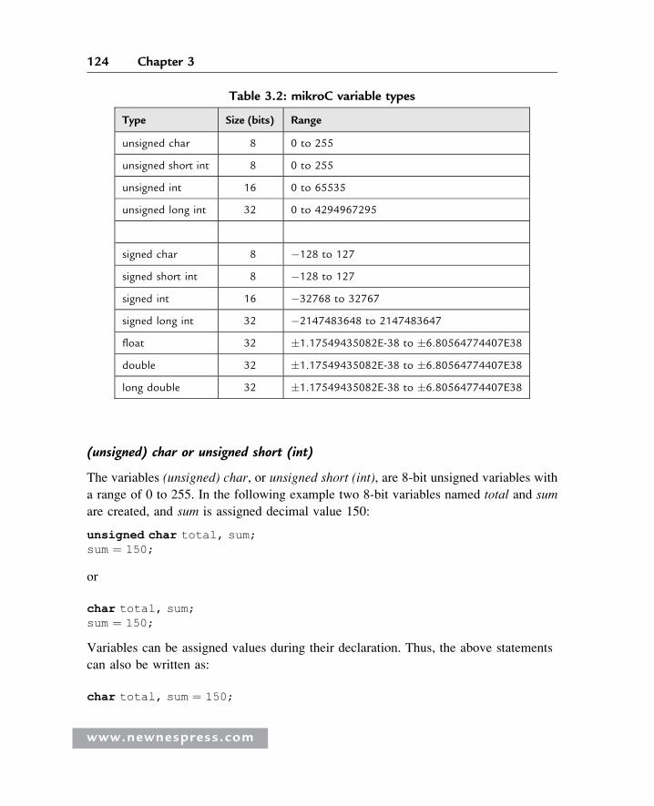
(unsigned) char or unsigned short (int)
The variables (unsigned) char, or unsigned short (int), are 8-bit unsigned variables with
a range of 0 to 255. In the following example two 8-bit variables named total and sum
are created, and sum is assigned decimal value 150:
unsigned char total, sum;sum ¼ 150;
or
char total, sum;sum ¼ 150;
Variables can be assigned values during their declaration. Thus, the above statements
can also be written as:
char total, sum ¼ 150;
Table 3.2: mikroC variable types
Type Size (bits) Range
unsigned char 8 0 to 255
unsigned short int 8 0 to 255
unsigned int 16 0 to 65535
unsigned long int 32 0 to 4294967295
signed char 8 �128 to 127
signed short int 8 �128 to 127
signed int 16 �32768 to 32767
signed long int 32 �2147483648 to 2147483647
float 32 �1.17549435082E-38 to �6.80564774407E38
double 32 �1.17549435082E-38 to �6.80564774407E38
long double 32 �1.17549435082E-38 to �6.80564774407E38
www.newnespress.com
124 Chapter 3
signed char or (signed) short (int)
The variables signed char, or (signed) short (int), are 8-bit signed character variables
with a range of �128 to þ127. In the following example a signed 8-bit variable named
counter is created with a value of �50:
signed char counter ¼ �50;
or
short counter ¼ �50;
or
short int counter ¼ �50;
(signed) int
Variables called (signed) int are 16-bit variables with a range �32768 to þ32767. In the
following example a signed integer named Big is created:
int Big;
unsigned (int)
Variables called (unsigned) int are 16-bit unsigned variables with a range 0 to 65535. In
the following example an unsigned 16-bit variable named count is created and is
assigned value 12000:
unsigned int count ¼ 12000;
(signed) long (int)
Variables called (signed) long (int) are 32 bits long with a range �2147483648 to
þ2147483647. An example is:
signed long LargeNumber;
unsigned long (int)
Variables called (unsigned) long (int) are 32-bit unsigned variables having the
range 0 to 4294967295. An example is:
unsigned long VeryLargeNumber;
www.newnespress.com
125C Programming Language
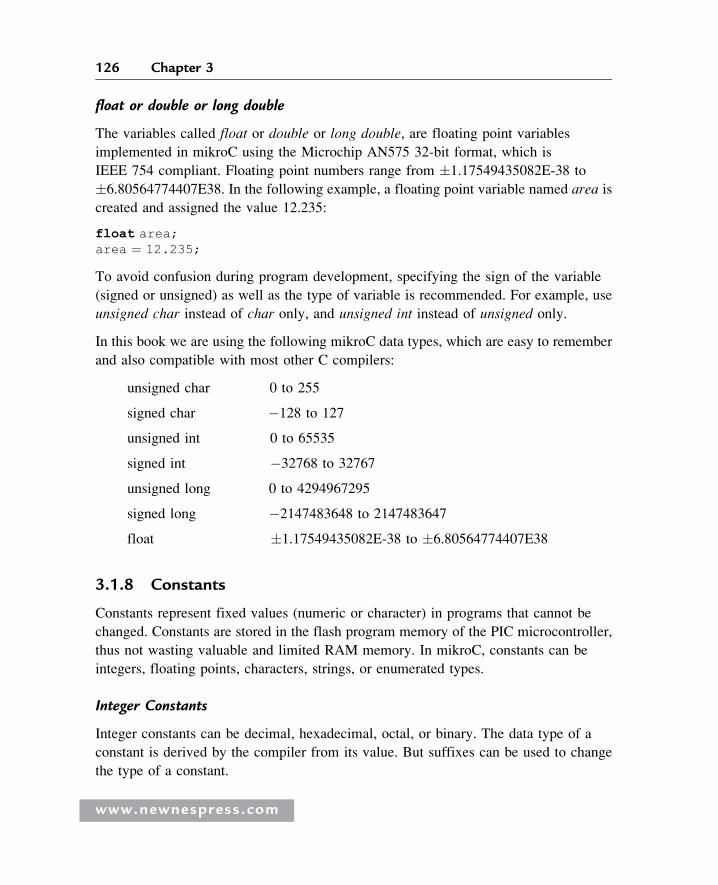
float or double or long double
The variables called float or double or long double, are floating point variables
implemented in mikroC using the Microchip AN575 32-bit format, which is
IEEE 754 compliant. Floating point numbers range from �1.17549435082E-38 to
�6.80564774407E38. In the following example, a floating point variable named area is
created and assigned the value 12.235:
float area;area ¼ 12.235;
To avoid confusion during program development, specifying the sign of the variable
(signed or unsigned) as well as the type of variable is recommended. For example, use
unsigned char instead of char only, and unsigned int instead of unsigned only.
In this book we are using the following mikroC data types, which are easy to remember
and also compatible with most other C compilers:
unsigned char 0 to 255
signed char �128 to 127
unsigned int 0 to 65535
signed int �32768 to 32767
unsigned long 0 to 4294967295
signed long �2147483648 to 2147483647
float �1.17549435082E-38 to �6.80564774407E38
3.1.8 Constants
Constants represent fixed values (numeric or character) in programs that cannot be
changed. Constants are stored in the flash program memory of the PIC microcontroller,
thus not wasting valuable and limited RAM memory. In mikroC, constants can be
integers, floating points, characters, strings, or enumerated types.
Integer Constants
Integer constants can be decimal, hexadecimal, octal, or binary. The data type of a
constant is derived by the compiler from its value. But suffixes can be used to change
the type of a constant.
www.newnespress.com
126 Chapter 3
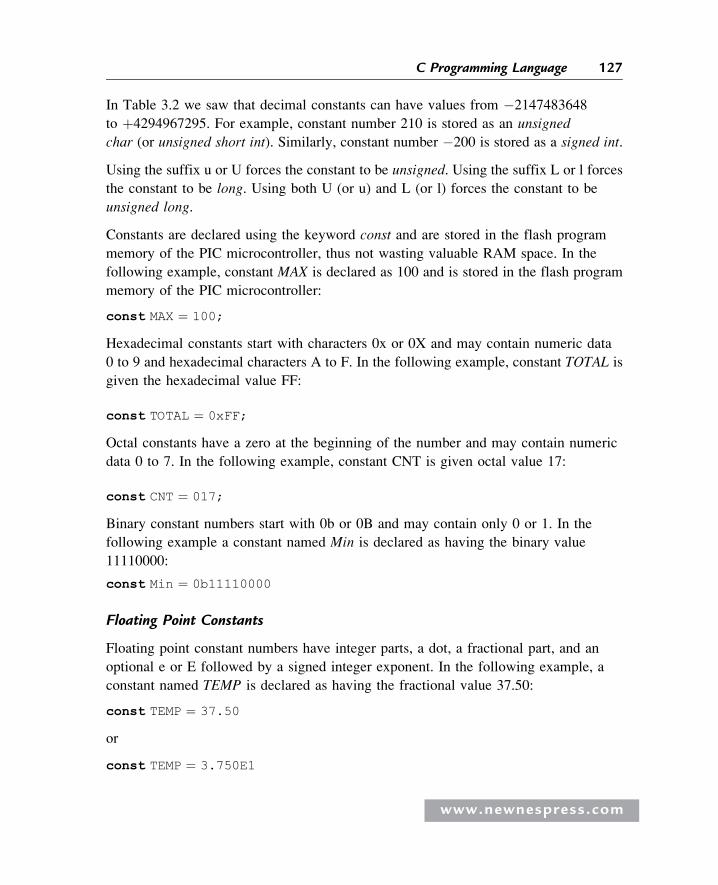
In Table 3.2 we saw that decimal constants can have values from �2147483648
to þ4294967295. For example, constant number 210 is stored as an unsigned
char (or unsigned short int). Similarly, constant number �200 is stored as a signed int.
Using the suffix u or U forces the constant to be unsigned. Using the suffix L or l forces
the constant to be long. Using both U (or u) and L (or l) forces the constant to be
unsigned long.
Constants are declared using the keyword const and are stored in the flash program
memory of the PIC microcontroller, thus not wasting valuable RAM space. In the
following example, constant MAX is declared as 100 and is stored in the flash program
memory of the PIC microcontroller:
const MAX ¼ 100;
Hexadecimal constants start with characters 0x or 0X and may contain numeric data
0 to 9 and hexadecimal characters A to F. In the following example, constant TOTAL is
given the hexadecimal value FF:
const TOTAL ¼ 0xFF;
Octal constants have a zero at the beginning of the number and may contain numeric
data 0 to 7. In the following example, constant CNT is given octal value 17:
const CNT ¼ 017;
Binary constant numbers start with 0b or 0B and may contain only 0 or 1. In the
following example a constant named Min is declared as having the binary value
11110000:
const Min ¼ 0b11110000
Floating Point Constants
Floating point constant numbers have integer parts, a dot, a fractional part, and an
optional e or E followed by a signed integer exponent. In the following example, a
constant named TEMP is declared as having the fractional value 37.50:
const TEMP ¼ 37.50
or
const TEMP ¼ 3.750E1
www.newnespress.com
127C Programming Language
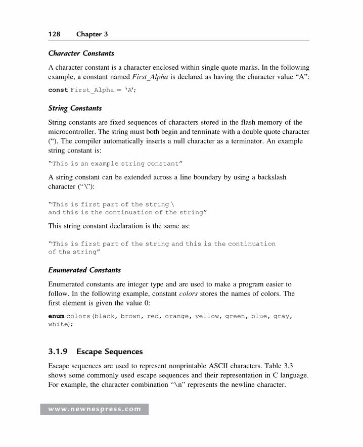
Character Constants
A character constant is a character enclosed within single quote marks. In the following
example, a constant named First_Alpha is declared as having the character value “A”:
const First_Alpha ¼ ‘A’;
String Constants
String constants are fixed sequences of characters stored in the flash memory of the
microcontroller. The string must both begin and terminate with a double quote character
(“). The compiler automatically inserts a null character as a terminator. An example
string constant is:
“This is an example string constant”
A string constant can be extended across a line boundary by using a backslash
character (“ \”):
“This is first part of the string \and this is the continuation of the string”
This string constant declaration is the same as:
“This is first part of the string and this is the continuationof the string”
Enumerated Constants
Enumerated constants are integer type and are used to make a program easier to
follow. In the following example, constant colors stores the names of colors. The
first element is given the value 0:
enum colors {black, brown, red, orange, yellow, green, blue, gray,white};
3.1.9 Escape Sequences
Escape sequences are used to represent nonprintable ASCII characters. Table 3.3
shows some commonly used escape sequences and their representation in C language.
For example, the character combination “ \ n” represents the newline character.
www.newnespress.com
128 Chapter 3
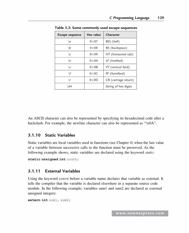
An ASCII character can also be represented by specifying its hexadecimal code after a
backslash. For example, the newline character can also be represented as “\x0A”.
3.1.10 Static Variables
Static variables are local variables used in functions (see Chapter 4) when the last value
of a variable between successive calls to the function must be preserved. As the
following example shows, static variables are declared using the keyword static:
static unsigned int count;
3.1.11 External Variables
Using the keyword extern before a variable name declares that variable as external. It
tells the compiler that the variable is declared elsewhere in a separate source code
module. In the following example, variables sum1 and sum2 are declared as external
unsigned integers:
extern int sum1, sum2;
Table 3.3: Some commonly used escape sequences
Escape sequence Hex value Character
\a 0�07 BEL (bell)
\b 0�08 BS (backspace)
\t 0�09 HT (horizontal tab)
\n 0�0A LF (linefeed)
\v 0�0B VT (vertical feed)
\f 0�0C FF (formfeed)
\r 0�0D CR (carriage return)
\xH String of hex digits
www.newnespress.com
129C Programming Language
3.1.12 Volatile Variables
Volatile variables are especially important in interrupt-based programs and input-output
routines. Using the keyword volatile indicates that the value of the variable may change
during the lifetime of the program independent of the normal flow of the program.
Variables declared as volatile are not optimized by the compiler, since their values can
change unexpectedly. In the following example, variable Led is declared as a volatile
unsigned char:
volatile unsigned char Led;
3.1.13 Enumerated Variables
Enumerated variables are used to make a program more readable. In an enumerated
variable, a list of items is specified and the value of the first item is set to 0, the next
item is set to 1, and so on. In the following example, type Week is declared as an
enumerated list and MON ¼ 0, TUE ¼ 1, WED ¼ 2, and so on):
enum Week {MON, TUE, WED, THU, FRI, SAT, SUN};
It is possible to imply the values of the elements in an enumerated list. In the
following example, black ¼ 2, blue ¼ 3, red ¼ 4, and so on.
enum colors {black ¼ 2, blue, red, white, gray};
Similarly, in the following example, black ¼ 2, blue ¼ 3, red ¼ 8, and gray ¼ 9:
enum colors {black ¼ 2, blue, red ¼ 8, gray};
Variables of type enumeration can be declared by specifying them after the list of
items. For example, to declare variable My_Week of enumerated type Week, use the
following statement:
enum Week {MON, TUE, WED, THU, FRI, SAT, SUN} My_Week;
Now we can use variable My_Week in a program:
My_Week ¼ WED // assign 2 to My_Week
or
My_Week ¼ 2 // same as above
www.newnespress.com
130 Chapter 3
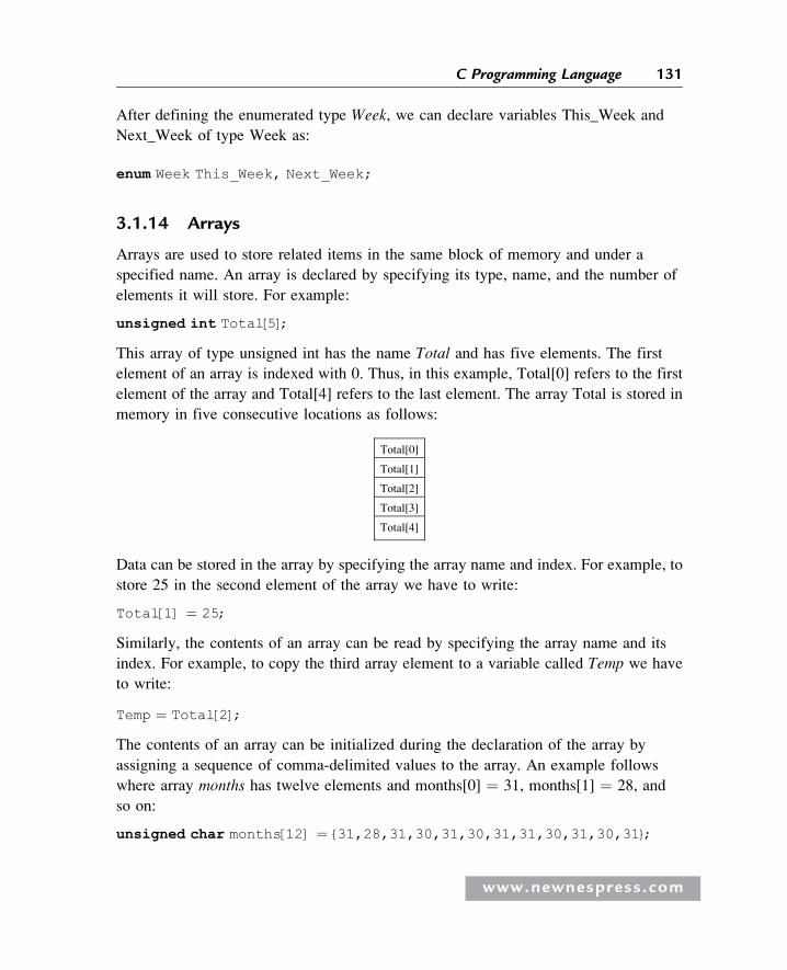
After defining the enumerated type Week, we can declare variables This_Week and
Next_Week of type Week as:
enum Week This_Week, Next_Week;
3.1.14 Arrays
Arrays are used to store related items in the same block of memory and under a
specified name. An array is declared by specifying its type, name, and the number of
elements it will store. For example:
unsigned int Total[5];
This array of type unsigned int has the name Total and has five elements. The first
element of an array is indexed with 0. Thus, in this example, Total[0] refers to the first
element of the array and Total[4] refers to the last element. The array Total is stored in
memory in five consecutive locations as follows:
Total[0]
Total[1]
Total[2]
Total[3]
Total[4]
Data can be stored in the array by specifying the array name and index. For example, to
store 25 in the second element of the array we have to write:
Total[1] ¼ 25;
Similarly, the contents of an array can be read by specifying the array name and its
index. For example, to copy the third array element to a variable called Temp we have
to write:
Temp ¼ Total[2];
The contents of an array can be initialized during the declaration of the array by
assigning a sequence of comma-delimited values to the array. An example follows
where array months has twelve elements and months[0] ¼ 31, months[1] ¼ 28, and
so on:
unsigned char months[12] ¼ {31,28,31,30,31,30,31,31,30,31,30,31};
www.newnespress.com
131C Programming Language
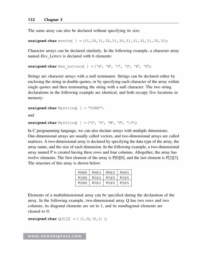
The same array can also be declared without specifying its size:
unsigned char months[ ] ¼ {31,28,31,30,31,30,31,31,30,31,30,31};
Character arrays can be declared similarly. In the following example, a character array
named Hex_Letters is declared with 6 elements:
unsigned char Hex_Letters[ ] ¼ {‘A’, ‘B’, ‘C’, ‘D’, ‘E’, ‘F’};
Strings are character arrays with a null terminator. Strings can be declared either by
enclosing the string in double quotes, or by specifying each character of the array within
single quotes and then terminating the string with a null character. The two string
declarations in the following example are identical, and both occupy five locations in
memory:
unsigned char Mystring[ ] ¼ “COMP”;
and
unsigned char Mystring[ ] ¼ {‘C’, ‘O’, ‘M’, ‘P’, ‘\0’};
In C programming language, we can also declare arrays with multiple dimensions.
One-dimensional arrays are usually called vectors, and two-dimensional arrays are called
matrices. A two-dimensional array is declared by specifying the data type of the array, the
array name, and the size of each dimension. In the following example, a two-dimensional
array named P is created having three rows and four columns. Altogether, the array has
twelve elements. The first element of the array is P[0][0], and the last element is P[2][3].
The structure of this array is shown below:
P[0][0] P[0][1] P[0][2] P[0][3]
P[1][0] P[1][1] P[1][2] P[1][3]
P[2][0] P[2][1] P[2][2] P[2][3]
Elements of a multidimensional array can be specified during the declaration of the
array. In the following example, two-dimensional array Q has two rows and two
columns, its diagonal elements are set to 1, and its nondiagonal elements are
cleared to 0:
unsigned char Q[2][2] ¼ { {1,0}, {0,1} };
www.newnespress.com
132 Chapter 3
3.1.15 Pointers
Pointers are an important part of the C language, as they hold the memory addresses
of variables. Pointers are declared in the same way as other variables, but with the
character (“*”) in front of the variable name. In general, pointers can be created to point
to (or hold the addresses of) character variables, integer variables, long variables,
floating point variables, or functions (although mikroC currently does not support
pointers to functions).
In the following example, an unsigned character pointer named pnt is declared:
unsigned char *pnt;
When a new pointer is created, its content is initially unspecified and it does not hold
the address of any variable. We can assign the address of a variable to a pointer using
the (“&”) character:
pnt ¼ &Count;
Now pnt holds the address of variable Count. Variable Count can be set to a value by
using the character (“*”) in front of its pointer. For example, Count can be set to 10
using its pointer:
*pnt ¼ 10; // Count ¼ 10
which is the same as
Count ¼ 10; // Count ¼ 10
Or, the value of Count can be copied to variable Cnt using its pointer:
Cnt ¼ *pnt; // Cnt ¼ Count
Array Pointers
In C language the name of an array is also a pointer to the array. Thus, for the array:
unsigned int Total[10];
The name Total is also a pointer to this array, and it holds the address of the first
element of the array. Thus the following two statements are equal:
Total[2] ¼ 0;
www.newnespress.com
133C Programming Language

and
*(Total þ 2) ¼ 0;
Also, the following statement is true:
&Total[j] ¼ Total þ j
In C language we can perform pointer arithmetic which may involve:
� Comparing two pointers
� Adding or subtracting a pointer and an integer value
� Subtracting two pointers
� Assigning one pointer to another
� Comparing a pointer to null
For example, let’s assume that pointer P is set to hold the address of array
element Z[2]:
P ¼ &Z[2];
We can now clear elements 2 and 3 of array Z, as in the two examples that follow. The
two examples are identical except that in the first example pointer P holds the address
of Z[3] at the end of the statements, and it holds the address of Z[2] at the end of the
second set of statements:
*P ¼ 0; // Z[2] ¼ 0P ¼ P þ 1; // P now points to element 3 of Z*P ¼ 0; // Z[3] ¼ 0
or
*P ¼ 0; // Z[2] ¼ 0*(P þ 1) ¼ 0; // Z[3] ¼ 0
A pointer can be assigned to another pointer. In the following example, variables Cnt
and Tot are both set to 10 using two different pointers:
unsigned int *i, *j; // declare 2 pointersunsigned int Cnt, Tot; // declare two variables
www.newnespress.com
134 Chapter 3
i ¼ &Cnt; // i points to Cnt*i ¼ 10; // Cnt ¼ 10j ¼ i; // copy pointer i to pointer jTot ¼ *j; // Tot ¼ 10
3.1.16 Structures
A structure can be used to collect related items that are then treated as a single object.
Unlike an array, a structure can contain a mixture of data types. For example, a
structure can store the personal details (name, surname, age, date of birth, etc.) of a
student.
A structure is created by using the keyword struct, followed by a structure name and a
list of member declarations. Optionally, variables of the same type as the structure can
be declared at the end of the structure.
The following example declares a structure named Person:
struct Person{
unsigned char name[20];unsigned char surname[20];unsigned char nationality[20];unsigned char age;
}
Declaring a structure does not occupy any space in memory; rather, the compiler
creates a template describing the names and types of the data objects or member
elements that will eventually be stored within such a structure variable. Only
when variables of the same type as the structure are created do these variables
occupy space in memory. We can declare variables of the same type as the
structure by giving the name of the structure and the name of the variable.
For example, two variables Me and You of type Person can be created by
the statement:
struct Person Me, You;
Variables of type Person can also be created during the declaration of the structure
as follows:
www.newnespress.com
135C Programming Language
struct Person{
unsigned char name[20];unsigned char surname[20];unsigned char nationality[20];unsigned char age;
} Me, You;
We can assign values to members of a structure by specifying the name of the structure,
followed by a dot (“.”) and the name of the member. In the following example, the age
of structure variable Me is set to 25, and variable M is assigned to the value of age in
structure variable You:
Me.age ¼ 25;M ¼ You.age;
Structure members can be initialized during the declaration of the structure. In the
following example, the radius and height of structure Cylinder are initialized to 1.2 and
2.5 respectively:
struct Cylinder{
float radius;float height;
} MyCylinder ¼ {1.2, 2.5};
Values can also be set to members of a structure using pointers by defining the variable
types as pointers. For example, if TheCylinder is defined as a pointer to structure
Cylinder, then we can write:
struct Cylinder{
float radius;float height;
} *TheCylinder;
TheCylinder �> radius ¼ 1.2;TheCylinder �> height ¼ 2.5;
The size of a structure is the number of bytes contained within the structure. We can use
the sizeof operator to get the size of a structure. Considering the above example,
sizeof(MyCylinder)
returns 8, since each float variable occupies 4 bytes in memory.
www.newnespress.com
136 Chapter 3
Bit fields can be defined using structures. With bit fields we can assign identifiers to
bits of a variable. For example, to identify bits 0, 1, 2, and 3 of a variable as LowNibble
and to identify the remaining 4 bits as HighNibble we can write:
struct{
LowNibble : 4;HighNibble : 4;
} MyVariable;
We can then access the nibbles of variable MyVariable as:
MyVariable.LowNibble ¼ 12;MyVariable.HighNibble ¼ 8;
In C language we can use the typedef statements to create new types of variables. For
example, a new structure data type named Reg can be created as follows:
typedef struct{
unsigned char name[20];unsigned char surname[20];unsigned age;
} Reg;
Variables of type Reg can then be created in the same way other types of variables are
created. In the following example, variables MyReg, Reg1, and Reg2 are created from
data type Reg:
Reg MyReg, Reg1, Reg2;
The contents of one structure can be copied to another structure, provided that both
structures are derived from the same template. In the following example, structure
variables of the same type, P1 and P2, are created, and P2 is copied to P1:
struct Person{
unsigned char name[20];unsigned char surname[20];unsigned int age;unsigned int height;unsigned weight;
}struct Person P1, P2;
www.newnespress.com
137C Programming Language
. . . . . . . . . . . . . . . . . . . . . . . .
. . . . . . . . . . . . . . . . . . . . . . . .P2 ¼ P1;
3.1.17 Unions
Unions are used to overlay variables. A union is similar to a structure and is even
defined in a similar manner. Both are based on templates, and the members of both are
accessed using the “.” or “->” operators. A union differs from a structure in that all
variables in a union occupy the same memory area, that is, they share the same storage.
An example of a union declaration is:
union flags{
unsigned char x;unsigned int y;
} P;
In this example, variables x and y occupy the same memory area, and the size of this
union is 2 bytes long, which is the size of the biggest member of the union. When
variable y is loaded with a 2-byte value, variable x will have the same value as the low
byte of y. In the following example, y is loaded with 16-bit hexadecimal value
0xAEFA, and x is loaded with 0xFA:
P.y ¼ 0xAEFA;
The size of a union is the size (number of bytes) of its largest member. Thus, the
statement:
sizeof(P)
returns 2.
This union can also be declared as:
union flags{
unsigned char x;unsigned int y;
}union flags P;
www.newnespress.com
138 Chapter 3
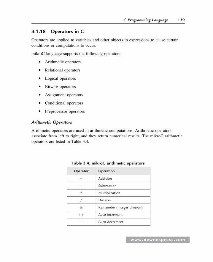
3.1.18 Operators in C
Operators are applied to variables and other objects in expressions to cause certain
conditions or computations to occur.
mikroC language supports the following operators:
� Arithmetic operators
� Relational operators
� Logical operators
� Bitwise operators
� Assignment operators
� Conditional operators
� Preprocessor operators
Arithmetic Operators
Arithmetic operators are used in arithmetic computations. Arithmetic operators
associate from left to right, and they return numerical results. The mikroC arithmetic
operators are listed in Table 3.4.
Table 3.4: mikroC arithmetic operators
Operator Operation
þ Addition
� Subtraction
* Multiplication
/ Division
% Remainder (integer division)
þþ Auto increment
�� Auto decrement
www.newnespress.com
139C Programming Language

The following example illustrates the use of arithmetic operators:
/* Adding two integers */5 þ 12 // equals 17
/* Subtracting two integers */
120 – 5 // equals 11510 – 15 // equals �5
/* Dividing two integers */
5 / 3 // equals 112 / 3 // equals 4
/* Multiplying two integers */
3 * 12 // equals 36
/* Adding two floating point numbers */
3.1 þ 2.4 // equals 5.5
/* Multiplying two floating point numbers */
2.5 * 5.0 // equals 12.5
/* Dividing two floating point numbers */
25.0 / 4.0 // equals 6.25
/* Remainder (not for float) */
7 % 3 // equals 1
/* Post-increment operator */
j ¼ 4;k ¼ jþþ; // k ¼ 4, j ¼ 5
/* Pre-increment operator */
j ¼ 4;k ¼ þþj; // k ¼ 5, j ¼ 5
/* Post-decrement operator */
j ¼ 12;k ¼ j��; // k ¼ 12, j ¼ 11
www.newnespress.com
140 Chapter 3
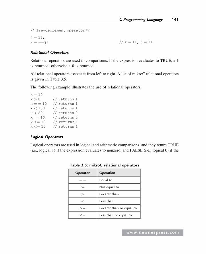
/* Pre-decrement operator */
j ¼ 12;k ¼ ��j; // k ¼ 11, j ¼ 11
Relational Operators
Relational operators are used in comparisons. If the expression evaluates to TRUE, a 1
is returned; otherwise a 0 is returned.
All relational operators associate from left to right. A list of mikroC relational operators
is given in Table 3.5.
The following example illustrates the use of relational operators:
x ¼ 10x > 8 // returns 1x ¼ ¼ 10 // returns 1x < 100 // returns 1x > 20 // returns 0x !¼ 10 // returns 0x >¼ 10 // returns 1x <¼ 10 // returns 1
Logical Operators
Logical operators are used in logical and arithmetic comparisons, and they return TRUE
(i.e., logical 1) if the expression evaluates to nonzero, and FALSE (i.e., logical 0) if the
Table 3.5: mikroC relational operators
Operator Operation
¼ ¼ Equal to
!¼ Not equal to
> Greater than
< Less than
>¼ Greater than or equal to
<¼ Less than or equal to
www.newnespress.com
141C Programming Language
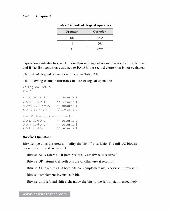
expression evaluates to zero. If more than one logical operator is used in a statement,
and if the first condition evaluates to FALSE, the second expression is not evaluated.
The mikroC logical operators are listed in Table 3.6.
The following example illustrates the use of logical operators:
/* Logical AND */x ¼ 7;
x > 0 && x < 10 // returns 1
x > 0 || x < 10 // returns 1x >¼0 && x <¼10 // returns 1x >¼0 && x < 5 // returns 0
a ¼ 10; b ¼ 20; c ¼ 30; d ¼ 40;
a > b && c > d // returns 0b > a && d > c // returns 1a > b || d > c // returns 1
Bitwise Operators
Bitwise operators are used to modify the bits of a variable. The mikroC bitwise
operators are listed in Table 3.7.
Bitwise AND returns 1 if both bits are 1, otherwise it returns 0.
Bitwise OR returns 0 if both bits are 0, otherwise it returns 1.
Bitwise XOR returns 1 if both bits are complementary, otherwise it returns 0.
Bitwise complement inverts each bit.
Bitwise shift left and shift right move the bits to the left or right respectively.
Table 3.6: mikroC logical operators
Operator Operation
&& AND
|| OR
! NOT
www.newnespress.com
142 Chapter 3
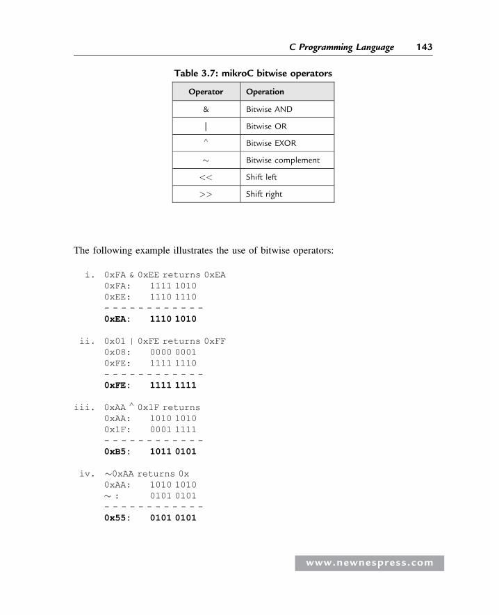
The following example illustrates the use of bitwise operators:
i. 0xFA & 0xEE returns 0xEA0xFA: 1111 10100xEE: 1110 1110- - - - - - - - - - - -0xEA: 1110 1010
ii. 0x01 | 0xFE returns 0xFF0x08: 0000 00010xFE: 1111 1110- - - - - - - - - - - -0xFE: 1111 1111
iii. 0xAA ∧ 0x1F returns0xAA: 1010 10100x1F: 0001 1111- - - - - - - - - - - -0xB5: 1011 0101
iv. �0xAA returns 0x0xAA: 1010 1010� : 0101 0101- - - - - - - - - - - -0x55: 0101 0101
Table 3.7: mikroC bitwise operators
Operator Operation
& Bitwise AND
| Bitwise OR
∧ Bitwise EXOR
� Bitwise complement
<< Shift left
>> Shift right
www.newnespress.com
143C Programming Language
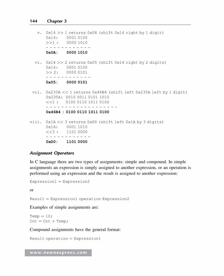
v. 0x14 >> 1 returns 0x08 (shift 0x14 right by 1 digit)0x14: 0001 0100>>1 : 0000 1010- - - - - - - - - - - -0x0A: 0000 1010
vi. 0x14 >> 2 returns 0x05 (shift 0x14 right by 2 digits)0x14: 0001 0100>> 2: 0000 0101- - - - - - - - - - - -0x05: 0000 0101
vii. 0x235A << 1 returns 0x46B4 (shift left 0x235A left by 1 digit)0x235A: 0010 0011 0101 1010<<1 : 0100 0110 1011 0100- - - - - - - - - - - - - - - - - - -0x46B4 : 0100 0110 1011 0100
viii. 0x1A << 3 returns 0xD0 (shift left 0x1A by 3 digits)0x1A: 0001 1010<<3 : 1101 0000- - - - - - - - - - - -0xD0: 1101 0000
Assignment Operators
In C language there are two types of assignments: simple and compound. In simple
assignments an expression is simply assigned to another expression, or an operation is
performed using an expression and the result is assigned to another expression:
Expression1 ¼ Expression2
or
Result ¼ Expression1 operation Expression2
Examples of simple assignments are:
Temp ¼ 10;Cnt ¼ Cnt þ Temp;
Compound assignments have the general format:
Result operation ¼ Expression1
www.newnespress.com
144 Chapter 3
Here the specified operation is performed on Expression1 and the result is stored in
Result. For example:
j þ¼ k; is same as: j ¼ j þ k;
also
p *¼ m; is same as p ¼ p * m;
The following compound operators can be used in mikroC programs:
þ¼ �¼ *¼ /¼ %¼&¼ |¼ ∧¼ >>¼ <<¼
Conditional Operators
The syntax of a conditional operator is:
Result ¼ Expression1 ? Expression2 : Expression3
Expression1 is evaluated first, and if its value is true, Expression2 is assigned to Result,
otherwise Expression3 is assigned to Result. In the following example, the maximum
of x and y is found where x is compared with y and if x > y then max ¼ x,
otherwise max ¼ y:
max ¼ ðx > yÞ ? x : y;
In the following example, lowercase characters are converted to uppercase. If the
character is lowercase (between a and z), then by subtracting 32 from the character
we obtain the equivalent uppercase character:
c ¼ ðc > ¼ a && c < ¼ zÞ ? ðc� 32 ) : c;
Preprocessor Operators
The preprocessor allows a programmer to:
� Compile a program conditionally, such that parts of the code are not compiled
� Replace symbols with other symbols or values
� Insert text files into a program
www.newnespress.com
145C Programming Language
The preprocessor operator is the (“#”) character, and any line of code leading with a
(“#”) is assumed to be a preprocessor command. The semicolon character (“;”) is not
needed to terminate a preprocessor command.
mikroC compiler supports the following preprocessor commands:
#define #undef#if #elif #endif#ifdef #ifndef#error#line
#define, #undef, #ifdef, #ifndef The #define preprocessor command provides macro
expansion where every occurrence of an identifier in the program is replaced with
the value of that identifier. For example, to replace every occurrence of MAX
with value 100 we can write:
#define MAX 100
An identifier that has already been defined cannot be defined again unless both
definitions have the same value. One way to get around this problem is to remove the
macro definition:
#undef MAX
Alternatively, the existence of a macro definition can be checked. In the following
example, if MAX has not already been defined, it is given value 100, otherwise the
#define line is skipped:
#ifndef MAX#define MAX 100
#endif
Note that the #define preprocessor command does not occupy any space in memory.
We can pass parameters to a macro definition by specifying the parameters in a
parenthesis after the macro name. For example, consider the macro definition:
#define ADD(a, b) (a þ b)
When this macro is used in a program, (a, b) will be replaced with (a þ b) as shown:
p ¼ ADD(x, y) will be transformed into p ¼ (x þ y)
www.newnespress.com
146 Chapter 3
Similarly, we can define a macro to calculate the square of two numbers:
#define SQUARE(a) (a * a)
We can now use this macro in a program:
p ¼ SQUARE(x) will be transformed into p ¼ (x * x)
#include The preprocessor directive #include is used to include a source file in our
program. Usually header files with extension “.h” are used with #include. There are two
formats for using #include:
#include <file>
and
#include “file”
In first option the file is searched in the mikroC installation directory first and then
in user search paths. In second option the specified file is searched in the mikroC
project folder, then in the mikroC installation folder, and then in user search paths.
It is also possible to specify a complete directory path as:
#include “C:\temp\last.h”
The file is then searched only in the specified directory path.
#if, #elif, #else, #endif The preprocessor commands #if, #elif, #else, and #endif are
used for conditional compilations, where parts of the source code can be compiled only
if certain conditions are met. In the following example, the code section where variables
A and B are cleared to zero is compiled if M has a nonzero value, otherwise the
code section where A and B are both set to 1 is compiled. Notice that the #if must
be terminated with #endif:
#if MA ¼ 0;B ¼ 0;
#elseA ¼ 1;B ¼ 1;
#endif
www.newnespress.com
147C Programming Language
We can also use the #elif condition, which tests for a new condition if the previous
condition was false:
#if MA ¼ 0;B ¼ 0;
#elif NA ¼ 1;B ¼ 1;
#elseA ¼ 2;B ¼ 2;
#endif
In the above example, if M has a nonzero value code section, A ¼ 0; B ¼ 0; are
compiled. Otherwise, if N has a nonzero value, then code section A ¼ 1; B ¼ 1; is
compiled. Finally, if both M and N are zero, then code section A ¼ 2; B ¼ 2; is
compiled. Notice that only one code section is compiled between #if and #endif and
that a code section can contain any number of statements.
3.1.19 Modifying the Flow of Control
Statements are normally executed sequentially from the beginning to the end of
a program. We can use control statements to modify this normal sequential flow
in a C program. The following control statements are available in mikroC programs:
� Selection statements
� Unconditional modifications of flow
� Iteration statements
Selection Statements
There are two selection statements: if and switch.
if Statement The general format of the if statement is:
if(expression)
Statement1;
www.newnespress.com
148 Chapter 3
else
Statement2;
or
if(expression)Statement1; else Statement2;
If the expression evaluates to TRUE, Statement1 is executed, otherwise Statement2 is
executed. The else keyword is optional and may be omitted. In the following example,
if the value of x is greater than MAX then variable P is incremented by 1, otherwise it is
decremented by 1:
if(x > MAX)Pþþ;
elseP��;
We can have more than one statement by enclosing the statements within curly
brackets. For example:
if(x > MAX){
Pþþ;Cnt ¼ P;Sum ¼ Sum þ Cnt;
}else
P��;
In this example, if x is greater than MAX then the three statements within the curly
brackets are executed, otherwise the statement P�� is executed.
Another example using the if statement is:
if(x > 0 && x < 10){
Total þ¼ Sum;Sumþþ;
}else{
Total ¼ 0;Sum ¼ 0;
}
www.newnespress.com
149C Programming Language
switch Statement The switch statement is used when a number of conditions and
different operations are performed if a condition is true. The syntax of the switch
statement is:
switch (condition){
case condition1:Statements;break;
case condition2:Statements;break;
. . . . . . . . . . . . . . . . . . . . .
. . . . . . . . . . . . . . . . . . . . .case condition:
Statements;break;
default:Statements;
}
The switch statement functions as follows: First the condition is evaluated. The
condition is then compared to condition1 and if a match is found, statements in that case
block are evaluated and control jumps outside the switch statement when the break
keyword is encountered. If a match is not found, condition is compared to condition2
and if a match is found, statements in that case block are evaluated and control jumps
outside the switch statements, and so on. The default is optional, and statements
following default are evaluated if the condition does not match any of the conditions
specified after the case keywords.
In the following example, the value of variable Cnt is evaluated. If Cnt ¼ 1, A is set to
1. If Cnt ¼ 10, B is set to 1, and if Cnt ¼ 100, C is set to 1. If Cnt is not equal to 1, 10,
or 100 then D is set to 1:
switch (Cnt){
case 1:A ¼ 1;break;
case 10:B ¼ 1;break;
www.newnespress.com
150 Chapter 3

case 100:C ¼ 1;break;
default:D ¼ 1;
}
Because white spaces are ignored in C language we can also write the preceding
code as:
switch (Cnt){
case 1: A ¼ 1; break;case 10: B ¼ 1; break;case 100: C ¼ 1; break;default: D ¼ 1;
}
Example 3.1
In an experiment the relationship between X and Y values are found to be:
X Y1 3.22 2.53 8.94 1.25 12.9
Write a switch statement that will return the Y value, given the X value.
Solution 3.1
The required switch statement is:
switch (X){
case 1:Y ¼ 3.2;break;
case 2:Y ¼ 2.5;break;
www.newnespress.com
151C Programming Language
case 3:Y ¼ 8.9;break;
case 4:Y ¼ 1.2;break;
case 5:Y ¼ 12.9;
}
Iteration Statements
Iteration statements enable us to perform loops in a program, where part of a code must
be repeated a number of times. In mikroC iteration can be performed in four ways. We
will look at each one with examples:
� Using for statement
� Using while statement
� Using do statement
� Using goto statement
for Statement The syntax of a for statement is:
for(initial expression; condition expression; increment expression){
Statements;}
The initial expression sets the starting variable of the loop, and this variable is
compared against the condition expression before entry into the loop. Statements inside
the loop are executed repeatedly, and after each iteration the value of the increment
expression is incremented. The iteration continues until the condition expression
becomes false. An endless loop is formed if the condition expression is always true.
The following example shows how a loop can be set up to execute 10 times. In this
example, variable i starts from 0 and increments by 1 at the end of each iteration. The
loop terminates when i ¼10, in which case the condition i < 10 becomes false. On exit
from the loop, the value of i is 10:
www.newnespress.com
152 Chapter 3
for(i ¼ 0; i < 10; i þþ){
statements;}
This loop could also be started by an initial expression with a nonzero value. Here, i
starts with 1 and the loop terminates when i ¼ 11. Thus, on exit from the loop, the value
of i is 11:
for(i ¼ 1; i <¼ 10; iþþ){
Statements;}
The parameters of a for loop are all optional and can be omitted. If the condition
expression is left out, it is assumed to be true. In the following example, an endless loop
is formed where the condition expression is always true and the value of i starts with
0 and is incremented after each iteration:
/* Endless loop with incrementing i */for(i=0; ; iþþ){
Statements;}
In the following example of an endless loop all the parameters are omitted:
/* Example of endless loop */for(; ;){
Statements;}
In the following endless loop, i starts with 1 and is not incremented inside
the loop:
/* Endless loop with i ¼ 1 */for(i=1; ;){
Statements;}
www.newnespress.com
153C Programming Language

If there is only one statement inside the for loop, he curly brackets can be omitted as
shown in the following example:
for(k ¼ 0; k < 10; kþþ)Total ¼ Total þ Sum;
Nested for loops can also be used. In a nested for loop, the inner loop is executed for
each iteration of the outer loop. In the following example the inner loop is executed five
times and the outer loop is executed ten times. The total iteration count is fifty:
/* Example of nested for loops */for(i ¼ 0; i < 10; iþþ){
for(j ¼ 0; j < 5; jþþ){
Statements;}
}
In the following example, the sum of all the elements of a 3 � 4 matrix M is calculated
and stored in a variable called Sum:
/* Add all elements of a 3x4 matrix */Sum ¼ 0;for(i ¼ 0; i < 3; iþþ){
for(j ¼ 0; j < 4; jþþ){
Sum ¼ Sum þ M [i][j];}
}
Since there is only one statement to be executed, the preceding example could also be
written as:
/* Add all elements of a 3x4 matrix */Sum ¼ 0;for(i ¼ 0; i < 3; iþþ){
for(j ¼ 0; j < 4; jþþ) Sum ¼ Sum þ M [i][j];}
www.newnespress.com
154 Chapter 3
while Statement The syntax of a while statement is:
while (condition){
Statements;}
Here, the statements are executed repeatedly until the condition becomes false, or the
statements are executed repeatedly as long as the condition is true. If the condition is
false on entry to the loop, then the loop will not be executed and the program will
continue from the end of the while loop. It is important that the condition is changed
inside the loop, otherwise an endless loop will be formed.
The following code shows how to set up a loop to execute 10 times, using the while
statement:
/* A loop that executes 10 times */k ¼ 0;while (k < 10){
Statements;kþþ;
}
At the beginning of the code, variable k is 0. Since k is less than 10, the while loop
starts. Inside the loop the value of k is incremented by 1 after each iteration. The loop
repeats as long as k < 10 and is terminated when k ¼ 10. At the end of the loop the
value of k is 10.
Notice that an endless loop will be formed if k is not incremented inside the loop:
/* An endless loop */k ¼ 0;while (k < 10){
Statements;}
An endless loop can also be formed by setting the condition to be always true:
/* An endless loop */while (k ¼ k){
Statements;}
www.newnespress.com
155C Programming Language
Here is an example of calculating the sum of numbers from 1 to 10 and storing the
result in a variable called sum:
/* Calculate the sum of numbers from 1 to 10 */unsigned int k, sum;k ¼ 1;sum ¼ 0;while(k <¼ 10){
sum ¼ sum þ k;kþþ;
}
It is possible to have a while statement with no body. Such a statement is useful, for
example, if we are waiting for an input port to change its value. An example follows
where the program will wait as long as bit 0 of PORTB (PORTB.0) is at logic 0. The
program will continue when the port pin changes to logic 1:
while(PORTB.0 ¼¼ 0); // Wait until PORTB.0 becomes 1
or
while(PORTB.0);
It is also possible to have nested while statements.
do Statement A do statement is similar to a while statement except that the loop
executes until the condition becomes false, or, the loop executes as long as the
condition is true. The condition is tested at the end of the loop. The syntax of a do
statement is:
do{
Statements;} while (condition);
The first iteration is always performed whether the condition is true or false. This is the
main difference between a while statement and a do statement.
The following code shows how to set up a loop to execute 10 times using the do
statement:
www.newnespress.com
156 Chapter 3
/* Execute 10 times */k ¼ 0;do{
Statements;kþþ;
} while (k < 10);
The loop starts with k ¼ 0, and the value of k is incremented inside the loop after each
iteration. At the end of the loop k is tested, and if k is not less than 10, the loop
terminates. In this example because k ¼ 0 is at the beginning of the loop, the value of k
is 10 at the end of the loop.
An endless loop will be formed if the condition is not modified inside the loop, as
shown in the following example. Here k is always less than 10:
/* An endless loop */k ¼ 0;do{
Statements;} while (k < 10);
An endless loop can also be created if the condition is set to be true all the time:
/* An endless loop */do{
Statements;} while (k ¼ k);
It is also possible to have nested do statements.
Unconditional Modifications of Flow
goto Statement A goto statement can be used to alter the normal flow of control in a
program. It causes the program to jump to a specified label. A label can be any
alphanumeric character set starting with a letter and terminating with the colon (“:”)
character.
Although not recommended, a goto statement can be used together with an if statement
to create iterations in a program. The following example shows how to set up a loop to
execute 10 times using goto and if statements:
www.newnespress.com
157C Programming Language
/* Execute 10 times */k ¼ 0;Loop:
Statements;kþþ;
if(k < 10)goto Loop;
The loop starts with label Loop and variable k ¼ 0 at the beginning of the loop. Inside
the loop the statements are executed and k is incremented by 1. The value of k is then
compared with 10 and the program jumps back to label Loop if k < 10. Thus, the loop
is executed 10 times until the condition at the end becomes false. At the end of the loop
the value of k is 10.
continue and break Statements continue and break statements can be used inside
iterations to modify the flow of control. A continue statement is usually used with an if
statement and causes the loop to skip an iteration. An example follows that calculates
the sum of numbers from 1 to 10 except number 5:
/* Calculate sum of numbers 1,2,3,4,6,7,8,9,10 */Sum ¼ 0;i ¼ 1;for(i ¼ 1; i <¼ 10; iþþ){
if(i ¼¼ 5) continue; // Skip number 5Sum ¼ Sum þ i;
}
Similarly, a break statement can be used to terminate a loop from inside the loop. In the
following example, the sum of numbers from 1 to 5 is calculated even though the loop
parameters are set to iterate 10 times:
/* Calculate sum of numbers 1,2,3,4,5 */Sum ¼ 0;i ¼ 1;for(i ¼ 1; i <¼ 10; iþþ){
if(i > 5) break; // Stop loop if i > 5Sum ¼ Sum þ i;
}
www.newnespress.com
158 Chapter 3
3.1.20 Mixing mikroC with Assembly Language Statements
It sometimes becomes necessary to mix PIC microcontroller assembly language
statements with the mikroC language. For example, very accurate program delays can
be generated by using assembly language statements. The topic of assembly language
is beyond the scope of this book, but techniques for including assembly language
instructions in mikroC programs are discussed in this section for readers who are
familiar with the PIC microcontroller assembly languages.
Assembly language instructions can be included in a mikroC program by using the
keyword asm (or _asm, or __asm). A group of assembly instructions or a single such
instruction can be included within a pair of curly brackets. The syntax is:
asm{
assembly instructions}
Assembly language style comments (a line starting with a semicolon character) are not
allowed, but mikroC does allow both types of C style comments to be used with
assembly language programs:
asm{
/* This assembly code introduces delay to the program*/MOVLW 6 // Load W with 6. . . . . . . . . . . . . . .. . . . . . . . . . . . . . .
}
User-declared C variables can be used in assembly language routines, but they must be
declared and initialized before use. For example, C variable Temp can be initialized and
then loaded to the W register as:
unsigned char Temp ¼ 10;asm{
MOVLW Temp // W ¼ Temp ¼ 10. . . . . . . . . . . . . . . . . .. . . . . . . . . . . . . . . . . .
}
www.newnespress.com
159C Programming Language
Global symbols such as predefined port names and register names can be used in
assembly language routines without having to initialize them:
asm{
MOVWF PORTB. . . . . . . . . . . . . . . . . . . . .. . . . . . . . . . . . . . . . . . . . .
}
3.2 PIC Microcontroller Input-OutputPort Programming
Depending on the type of microcontroller used, PIC microcontroller input-output ports
are named as PORTA, PORTB, PORTC, and so on. Port pins can be in analog or digital
mode. In analog mode, ports are input only and a built-in analog-to-digital converter
and multiplexer circuits are used. In digital mode, a port pin can be configured as either
input or output. The TRIS registers control the port directions, and there are TRIS
registers for each port, named as TRISA, TRISB, TRISC, and so on. Clearing a TRIS
register bit to 0 sets the corresponding port bit to output mode. Similarly, setting a TRIS
register bit to 1 sets the corresponding port bit to input mode.
Ports can be accessed as a single 8-bit register, or individual bits of a port can be
accessed. In the following example, PORTB is configured as an output port and all its
bits are set to a 1:
TRISB ¼ 0; // Set PORTB as outputPORTB ¼ 0xFF; // Set PORTB bits to 1
Similarly, the following example shows how the 4 upper bits of PORTC can be set as
input and the 4 lower bits of PORTC can be set as output:
TRISC ¼ 0xF0;
Bits of an input-output port can be accessed by specifying the required bit number. In
the following example, variable P2 is loaded with bit 2 of PORTB:
P2 ¼ PORTB.2;
All the bits of a port can be complemented by the statement:
PORTB ¼ �PORTB;
www.newnespress.com
160 Chapter 3
3.3 Programming Examples
In this section, some simple programming examples are given to familiarize the reader
with programming in C.
Example 3.2
Write a program to set all eight port pins of PORTB to logic 1.
Solution 3.2
PORTB is configured as an output port, and then all port pins are set to logic 1 by
sending hexadecimal number 0xFF:
void main(){
TRISB ¼ 0; // Configure PORTB as outputPORTB ¼ 0xFF; // Set all port pins to logic a
}
Example 3.3
Write a program to set the odd-numbered PORTB pins (bits 1, 3, 5, and 7) to logic 1.
Solution 3.3
Odd-numbered port pins can be set to logic 1 by sending the bit pattern 10101010
to the port. This bit pattern is the hexadecimal number 0xAA and the required
program is:
void main(){
TRISB ¼ 0; // Configure PORTB as outputPORTB ¼ 0xAA; // Turn on odd numbered port pins
}
Example 3.4
Write a program to continuously count up in binary and send this data to PORTB. Thus
PORTB requires the binary data:
www.newnespress.com
161C Programming Language
00000000000000010000001000000011. . . . . . . . . . . .. . . . . . . . . . . .111111101111111100000000. . . . . . . . . . . .
Solution 3.4
A for loop can be used to create an endless loop, and inside this loop the value of a
variable can be incremented and then sent to PORTB:
void main(){
unsigned char Cnt ¼ 0;for(;;) // Endless loop{
PORTB ¼ Cnt; // Send Cnt to PORTBCntþþ; // Increment Cnt
}}
Example 3.5
Write a program to set all bits of PORTB to logic 1 and then to logic 0, and to repeat
this process ten times.
Solution 3.5
A for statement can be used to create a loop to repeat the required operation ten times:
void main(){
unsigned char j;for(j ¼ 0; j < 10; jþþ) // Repeat 10 times{PORTB ¼ 0xFF; // Set PORTB pins to 1
PORTB ¼ 0; // Clear PORTB pins}
}
www.newnespress.com
162 Chapter 3
Example 3.6
The radius and height of a cylinder are 2.5cm and 10cm respectively. Write a program
to calculate the volume of this cylinder.
Solution 3.6
The required program is:
void main(){
float Radius ¼ 2.5, Height ¼ 10;float Volume;Volume ¼ PI *Radius*Radius*Height;
}
Example 3.7
Write a program to find the largest element of an integer array having ten elements.
Solution 3.7
At the beginning, variable m is set to the first element of the array. A loop is then
formed and the largest element of the array is found:
void main(){
unsigned char j;int m, A[10];m ¼ A[0]; // First element of arrayfor(j ¼ 1; j < 10; jþþ){
if(A[j]> m)m ¼ A[j];}
}
Example 3.8
Write a program using a while statement to clear all ten elements of an integer
array M.
www.newnespress.com
163C Programming Language
Solution 3.8
As shown in the program that follows, NUM is defined as 10 and variable j is used as
the loop counter:
#define NUM 10void main(){
int M[NUM];unsigned char j ¼ 0;while (j < NUM){
M[j] ¼ 0;jþþ;
}}
Example 3.9
Write a program to convert the temperature from �C to �F starting from 0�C, in steps of
1�C up to and including 100�C, and store the results in an array called F.
Solution 3.9
Given the temperature in �C, the equivalent in �F is calculated using the formula:
F ¼ C� 32:0ð Þ=1:8
A for loop is used to calculate the temperature in �F and store in array F:
void main(){
float F[100];unsigned char C;for(C ¼ 0; C <¼ 100; Cþþ){
F[C] ¼ (C – 32.0) / 1.8;}
}
www.newnespress.com
164 Chapter 3
3.4 Summary
There are many assembly and high-level languages for the PIC18 series of
microcontrollers. This book focuses on the mikroC compiler, since it is easy to learn
and a free demo version is available that allows users to develop programs as large as
2K in size.
This chapter presented an introduction to the mikroC language. A C program may
contain a number of functions and variables plus a main program. The beginning of the
main program is indicated by the statement void main().
A variable stores a value used during the computation. All variables in C must be declared
before they are used. A variable can be an 8-bit character, a 16-bit integer, a 32-bit long,
or a floating point number. Constants are stored in the flash program memory of PIC
microcontrollers, so using them avoids using valuable and limited RAM memory.
Various flow control and iteration statements such as if, switch, while, do, break, and so
on have been described in the chapter, with examples.
Pointers are used to store the addresses of variables. As we shall see in the next chapter,
pointers can be used to pass information back and forth between a function and its
calling point. For example, pointers can be used to pass variables between a main
program and a function.
3.5 Exercises
1. Write a C program to set bits 0 and 7 of PORTC to logic 1.
2. Write a C program to count down continuously and send the count to PORTB.
3. Write a C program to multiply each element of a ten element array by 2.
4. Write a C program to add two matrices P and Q. Assume that the dimension of
each matrix is 3 � 3 and store the result in another matrix called W.
5. Repeat Exercise 4 but this time multiply matrices P and Q and store the product in
matrix R.
6. What do the terms variable and constant mean?
7. What does program repetition mean? Describe the operation of while, do-while,
and for loops in C.
www.newnespress.com
165C Programming Language

8. What is an array? Write example statements to define the following arrays:
a) An array of ten integers
b) An array of thirty floats
c) A two-dimensional array having six rows and ten columns
9. Trace the operation of the following loops. What will be the value of variable z at
the end of each loop?
a) unsigned char j ¼ 0, z ¼ 0;while(j < 10)
{zþþ;
jþþ;}
b) unsigned char z ¼ 10;for(j ¼ 0; j < 10; jþþ)z��;
10. Given the following variable definitions, list the outcome of the following
conditional tests in terms of “true” or “false”:
unsigned int a ¼ 10, b ¼ 2;if(a > 10)if(b >¼ 2)if(a ¼¼ 10)if(a > 0)
11. Write a program to calculate whether a number is odd or even.
12. Determine the value of the following bitwise operations using AND, OR, and
EXOR operations:
Operand 1: 00010001Operand 2: 11110001
13. How many times does each of the following loops iterate, and what is the final
value of the variable j in each case?
a) for(j ¼ 0; j < 5; jþþ)b) for(j ¼ 1; j < 10; jþþ)c) for(j ¼ 0; j <¼ 10; jþþ)d) for(j ¼ 0; j <¼ 10; j þ¼ 2)e) for(j ¼ 10; j > 0; j �¼ 2)
www.newnespress.com
166 Chapter 3

14. Write a program to calculate the sum of all positive integer numbers from 1 to 100.
15. Write a program to evaluate factorial n, where 0! and 1! evaluate to 1 and
n! ¼ n � (n – 1)!
16. Write a program to calculate the average value of the numbers stored in an array.
Assume that the array is called M and has twenty elements.
17. Modify the program in Exercise 16 to find the smallest and largest values of the
array. Store the smallest value in a variable called Sml and the largest value in a
variable called Lrg.
18. Derive equivalent if-else statements for the following tests:
a) (a > b) ? 0 : 1b) (x < y) ? (a > b) : (c > d)
19. Given that f1 and f2 are both floating point variables, explain why the following
test expression controlling the while loop may not be safe:
do{
. . . . . . . . . . . . . . .
. . . . . . . . . . . . . . .} while(f1 !¼ f2);
Why would the problem not occur if both f1 and f2 were integers? How would you
correct this while loop?
20. What can you say about the following while loop?
k ¼ 0;Total ¼ 0;while (k < 10){
Sumþþ;Total þ¼ Sum;
}
21. What can you say about the following for loop?
Cnt ¼ 0;for(;;){
Cntþþ;}
www.newnespress.com
167C Programming Language

This page intentionally left blank
CHAP T E R 4
Functions and Libraries in mikroC
4.1 mikroC Functions
A function is a self-contained section of code written to perform a specifically defined
action. Functions are usually created when a single operation must be performed in
different parts of the main program. It is, moreover, good programming practice to
divide a large program into a number of smaller, independent functions. The statements
within a function are executed by calling (or invoking) the function.
The general syntax of a function definition is shown in Figure 4.1. The data type
indicates the type of data returned by the function. This is followed by the name of the
function and then a set of parentheses, within which the arguments, separated by
commas, are declared. The body of the function, which includes the function’s
operational code, is written inside a set of curly brackets.
In the sample function definition that follows, the function, named Mult, receives two
integer arguments, a and b, and returns their product. Note that using parentheses in a
return statement is optional:
int Mult(int a, int b){
return (a*b);}
When a function is called, it generally expects to be given the number of arguments
expressed in the function’s argument list. For example, the preceding function can be
called as:
z ¼ Mult(x, y);
www.newnespress.com
where variable z has the data type int. Note that the arguments declared in the
function definition and the arguments passed when the function is called are
independent of each other, even if they have the same name. In the preceding example,
when the function is called, variable x is copied to a and variable y is copied to b on
entry into function Mult.
Some functions do not return any data. The data type of such functions must be declared
as void. For example:
void LED(unsigned char D){
PORTB ¼ D;}
void functions can be called without any assignment statements, but the parentheses are
needed to tell the compiler that a function call is made:
LED( );
Also, some functions do not have any arguments. In the following example, the
function, named Compl, complements PORTC of the microcontroller. It returns no data
and has no arguments:
void Compl( ){
PORTC ¼ �PORTC;}
This function can be called as:
Compl( );
Functions are normally defined before the start of the main program.
Some function definitions and their use in main programs are illustrated in the
following examples:
type name (parameter1, parameter2,…..) {
…………. function body ………….
}
Figure 4.1: General syntax of a function definition
www.newnespress.com
170 Chapter 4
Example 4.1
Write a function called Circle_Area to calculate the area of a circle where the radius is
to be used as an argument. Use this function in a main program to calculate the area of a
circle whose radius is 2.5cm. Store the area in a variable called Circ.
Solution 4.1
The data type of the function is declared as float. The area of a circle is calculated
by the formula:
Area ¼ pr2
where r is the radius of the circle. The area is calculated and stored in a local
variable called s, which is then returned from the function:
float Circle_Area(float radius)
{float s;
s ¼ PI * radius * radius;return s;
}
Figure 4.2 shows how the function Circle_Area can be used in a main program to
calculate the area of a circle whose radius is 2.5cm. The function is defined before
the main program. Inside the main program the function is called to calculate and
store the area in variable Circ.
Example 4.2
Write a function called Area and a function called Volume to calculate the area and
volume of a cylinder respectively. Then write a main program to calculate the area
and the volume of cylinder whose radius is 2.0cm and height is 5.0cm. Store the area
in variable cyl_area and the volume in variable cyl_volume.
Solution 4.2
The area of a cylinder is calculated by the formula:
Area ¼ 2prh
www.newnespress.com
171Functions and Libraries in mikroC
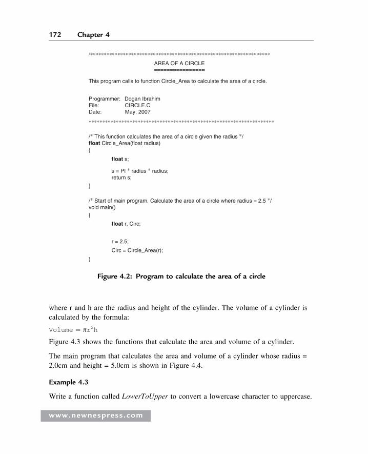
where r and h are the radius and height of the cylinder. The volume of a cylinder is
calculated by the formula:
Volume ¼ pr2h
Figure 4.3 shows the functions that calculate the area and volume of a cylinder.
The main program that calculates the area and volume of a cylinder whose radius =
2.0cm and height = 5.0cm is shown in Figure 4.4.
Example 4.3
Write a function called LowerToUpper to convert a lowercase character to uppercase.
/∗∗∗∗∗∗∗∗∗∗∗∗∗∗∗∗∗∗∗∗∗∗∗∗∗∗∗∗∗∗∗∗∗∗∗∗∗∗∗∗∗∗∗∗∗∗∗∗∗∗∗∗∗∗∗∗∗∗∗∗∗∗∗∗∗∗
AREA OF A CIRCLE================
This program calls to function Circle_Area to calculate the area of a circle.
Programmer: Dogan IbrahimFile: CIRCLE.CDate: May, 2007
∗∗∗∗∗∗∗∗∗∗∗∗∗∗∗∗∗∗∗∗∗∗∗∗∗∗∗∗∗∗∗∗∗∗∗∗∗∗∗∗∗∗∗∗∗∗∗∗∗∗∗∗∗∗∗∗∗∗∗∗∗∗∗∗∗∗∗∗
/∗ This function calculates the area of a circle given the radius ∗/float Circle_Area(float radius){
float s;
s = PI ∗ radius ∗ radius;return s;
}
/∗ Start of main program. Calculate the area of a circle where radius = 2.5 ∗/void main(){
float r, Circ;
r = 2.5;
Circ = Circle_Area(r);
}
Figure 4.2: Program to calculate the area of a circle
www.newnespress.com
172 Chapter 4
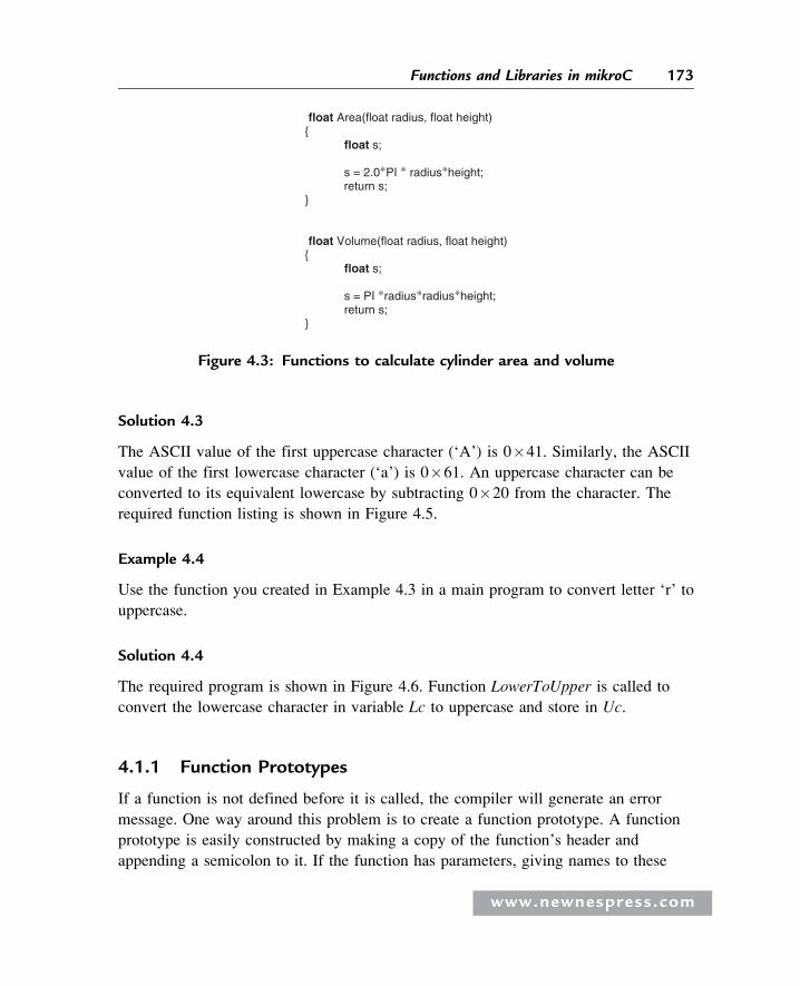
Solution 4.3
The ASCII value of the first uppercase character (‘A’) is 0�41. Similarly, the ASCII
value of the first lowercase character (‘a’) is 0�61. An uppercase character can be
converted to its equivalent lowercase by subtracting 0�20 from the character. The
required function listing is shown in Figure 4.5.
Example 4.4
Use the function you created in Example 4.3 in a main program to convert letter ‘r’ to
uppercase.
Solution 4.4
The required program is shown in Figure 4.6. Function LowerToUpper is called to
convert the lowercase character in variable Lc to uppercase and store in Uc.
4.1.1 Function Prototypes
If a function is not defined before it is called, the compiler will generate an error
message. One way around this problem is to create a function prototype. A function
prototype is easily constructed by making a copy of the function’s header and
appending a semicolon to it. If the function has parameters, giving names to these
float Area(float radius, float height){
float s;
s = 2.0∗PI ∗ radius∗height; return s;
}
float Volume(float radius, float height){
float s;
s = PI ∗radius∗radius∗height;return s;
}
Figure 4.3: Functions to calculate cylinder area and volume
www.newnespress.com
173Functions and Libraries in mikroC
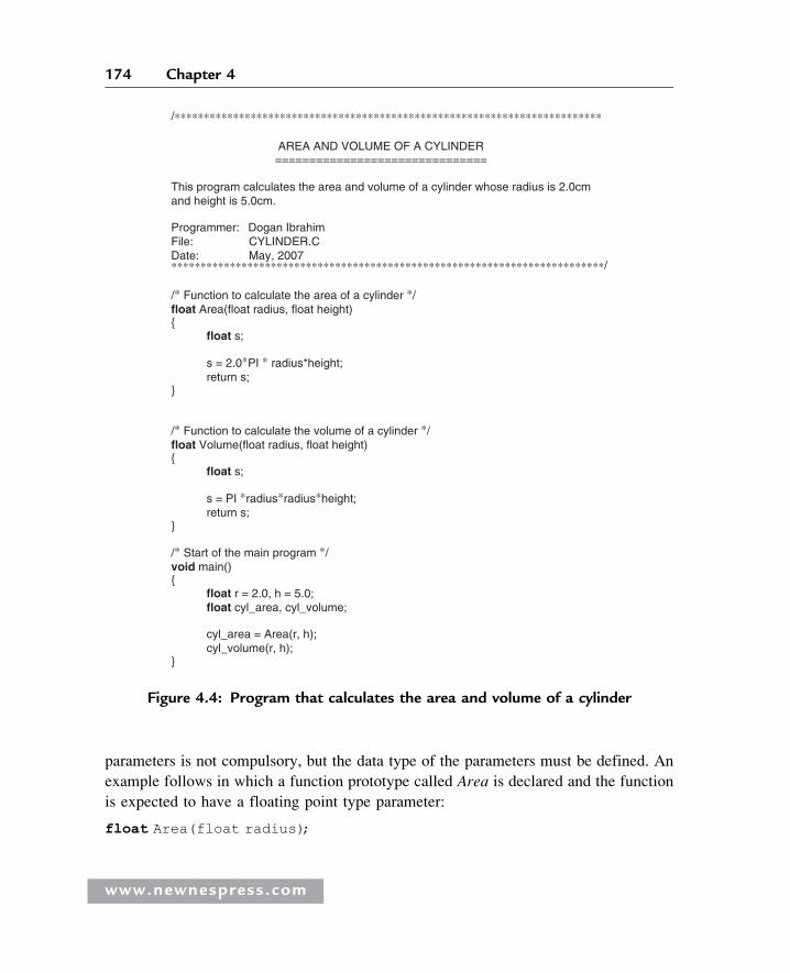
parameters is not compulsory, but the data type of the parameters must be defined. An
example follows in which a function prototype called Area is declared and the function
is expected to have a floating point type parameter:
float Area(float radius);
/∗∗∗∗∗∗∗∗∗∗∗∗∗∗∗∗∗∗∗∗∗∗∗∗∗∗∗∗∗∗∗∗∗∗∗∗∗∗∗∗∗∗∗∗∗∗∗∗∗∗∗∗∗∗∗∗∗∗∗∗∗∗∗∗∗∗∗∗∗∗∗∗∗
AREA AND VOLUME OF A CYLINDER ===============================
This program calculates the area and volume of a cylinder whose radius is 2.0cm and height is 5.0cm.
Programmer: Dogan Ibrahim File: CYLINDER.C Date: May, 2007 ∗∗∗∗∗∗∗∗∗∗∗∗∗∗∗∗∗∗∗∗∗∗∗∗∗∗∗∗∗∗∗∗∗∗∗∗∗∗∗∗∗∗∗∗∗∗∗∗∗∗∗∗∗∗∗∗∗∗∗∗∗∗∗∗∗∗∗∗∗∗∗∗∗∗/
/∗ Function to calculate the area of a cylinder ∗/ float Area(float radius, float height) {
float s;
s = 2.0∗PI ∗ radius*height; return s;
}
/∗ Function to calculate the volume of a cylinder ∗/ float Volume(float radius, float height) {
float s;
s = PI ∗radius∗radius∗height; return s;
}
/∗ Start of the main program ∗/ void main() {
float r = 2.0, h = 5.0; float cyl_area, cyl_volume;
cyl_area = Area(r, h); cyl_volume(r, h);
}
Figure 4.4: Program that calculates the area and volume of a cylinder
www.newnespress.com
174 Chapter 4
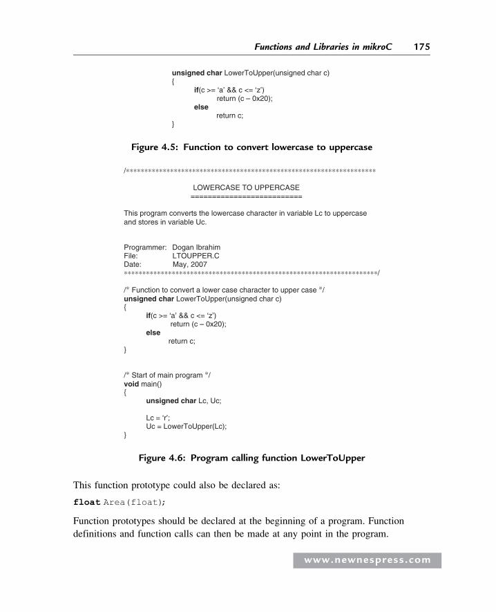
This function prototype could also be declared as:
float Area(float);
Function prototypes should be declared at the beginning of a program. Function
definitions and function calls can then be made at any point in the program.
/∗∗∗∗∗∗∗∗∗∗∗∗∗∗∗∗∗∗∗∗∗∗∗∗∗∗∗∗∗∗∗∗∗∗∗∗∗∗∗∗∗∗∗∗∗∗∗∗∗∗∗∗∗∗∗∗∗∗∗∗∗∗∗∗∗∗∗∗
LOWERCASE TO UPPERCASE ==========================
This program converts the lowercase character in variable Lc to uppercaseand stores in variable Uc.
Programmer: Dogan Ibrahim File: LTOUPPER.C Date: May, 2007 ∗∗∗∗∗∗∗∗∗∗∗∗∗∗∗∗∗∗∗∗∗∗∗∗∗∗∗∗∗∗∗∗∗∗∗∗∗∗∗∗∗∗∗∗∗∗∗∗∗∗∗∗∗∗∗∗∗∗∗∗∗∗∗∗∗∗∗∗∗/
/∗ Function to convert a lower case character to upper case ∗/ unsigned char LowerToUpper(unsigned char c) {
if(c >= ‘a’ && c <= ‘z’) return (c – 0x20);
else return c; }
/∗ Start of main program ∗/ void main() {
unsigned char Lc, Uc;
Lc = ‘r’; Uc = LowerToUpper(Lc);
}
Figure 4.6: Program calling function LowerToUpper
unsigned char LowerToUpper(unsigned char c) {
if(c >= ‘a’ && c <= ‘z’) return (c – 0x20);
else return c;
}
Figure 4.5: Function to convert lowercase to uppercase
www.newnespress.com
175Functions and Libraries in mikroC
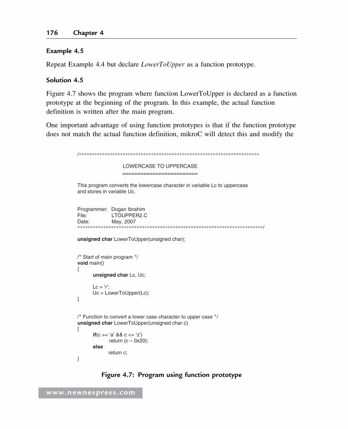
Example 4.5
Repeat Example 4.4 but declare LowerToUpper as a function prototype.
Solution 4.5
Figure 4.7 shows the program where function LowerToUpper is declared as a function
prototype at the beginning of the program. In this example, the actual function
definition is written after the main program.
One important advantage of using function prototypes is that if the function prototype
does not match the actual function definition, mikroC will detect this and modify the
/∗∗∗∗∗∗∗∗∗∗∗∗∗∗∗∗∗∗∗∗∗∗∗∗∗∗∗∗∗∗∗∗∗∗∗∗∗∗∗∗∗∗∗∗∗∗∗∗∗∗∗∗∗∗∗∗∗∗∗∗∗∗∗∗∗∗∗∗∗∗
LOWERCASE TO UPPERCASE =========================
This program converts the lowercase character in variable Lc to uppercase and stores in variable Uc.
Programmer: Dogan Ibrahim File: LTOUPPER2.C Date: May, 2007 ∗∗∗∗∗∗∗∗∗∗∗∗∗∗∗∗∗∗∗∗∗∗∗∗∗∗∗∗∗∗∗∗∗∗∗∗∗∗∗∗∗∗∗∗∗∗∗∗∗∗∗∗∗∗∗∗∗∗∗∗∗∗∗∗∗∗∗∗∗∗∗∗/
unsigned char LowerToUpper(unsigned char);
/∗ Start of main program ∗/ void main() {
unsigned char Lc, Uc;
Lc = ‘r’; Uc = LowerToUpper(Lc);
}
/∗ Function to convert a lower case character to upper case ∗/ unsigned char LowerToUpper(unsigned char c) {
if(c >= ‘a’ && c <= ‘z’) return (c – 0x20);
else return c;
}
Figure 4.7: Program using function prototype
www.newnespress.com
176 Chapter 4
data types in the function call to match the data types declared in the function prototype.
Suppose we have the following code:
unsigned char c ¼ ‘A’;unsigned int x ¼ 100;long Tmp;long MyFunc(long a, long b); // function prototype
void main()
{. . . . . . . . . . . . . . .. . . . . . . . . . . . . . .Tmp ¼ MyFunc(c, x);. . . . . . . . . . . . . . .. . . . . . . . . . . . . . .
}
In this example, because the function prototype declares the two arguments as long,
variables c and x are converted to long before they are used inside function MyFunc.
4.1.2 Passing Arrays to Functions
There are many applications where we may want to pass arrays to functions. Passing a
single array element is straightforward, as we simply specify the index of the array
element to be passed, as in the following function call which passes the second element
(index ¼ 1) of array A to function Calc. It is important to realize that an individual array
element is passed by value (i.e., a copy of the array element is passed to the function):
x ¼ Calc(A [1]);
In some applications we may want to pass complete arrays to functions. An array name
can be used as an argument to a function, thus permitting the entire array to be passed.
To pass a complete array to a function, the array name must appear by itself within the
brackets. The size of the array is not specified within the formal argument declaration.
In the function header the array name must be specified with a pair of empty brackets.
It is important to realize that when a complete array is passed to a function, what is
actually passed is not a copy of the array but the address of the first element of the array
(i.e., the array elements are passed by reference, which means that the original array
elements can be modified inside the function).
Some examples follow that illustrate the passing of a complete array to a function.
www.newnespress.com
177Functions and Libraries in mikroC
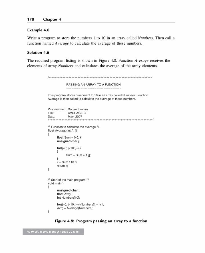
Example 4.6
Write a program to store the numbers 1 to 10 in an array called Numbers. Then call a
function named Average to calculate the average of these numbers.
Solution 4.6
The required program listing is shown in Figure 4.8. Function Average receives the
elements of array Numbers and calculates the average of the array elements.
/∗∗∗∗∗∗∗∗∗∗∗∗∗∗∗∗∗∗∗∗∗∗∗∗∗∗∗∗∗∗∗∗∗∗∗∗∗∗∗∗∗∗∗∗∗∗∗∗∗∗∗∗∗∗∗∗∗∗∗∗∗∗∗∗∗∗∗∗
PASSING AN ARRAY TO A FUNCTION ===============================
This program stores numbers 1 to 10 in an array called Numbers. FunctionAverage is then called to calculate the average of these numbers.
Programmer: Dogan Ibrahim File: AVERAGE.C Date: May, 2007 ∗∗∗∗∗∗∗∗∗∗∗∗∗∗∗∗∗∗∗∗∗∗∗∗∗∗∗∗∗∗∗∗∗∗∗∗∗∗∗∗∗∗∗∗∗∗∗∗∗∗∗∗∗∗∗∗∗∗∗∗∗∗∗∗∗∗∗∗∗/
/∗ Function to calculate the average ∗/ float Average(int A[ ]) {
float Sum = 0.0, k; unsigned char j;
for(j=0; j<10; j++) {
Sum = Sum + A[j]; } k = Sum / 10.0; return k;
}
/∗ Start of the main program ∗/ void main() {
unsigned char j; float Avrg; int Numbers[10];
for(j=0; j<10; j++)Numbers[j] = j+1; Avrg = Average(Numbers);
}
Figure 4.8: Program passing an array to a function
www.newnespress.com
178 Chapter 4
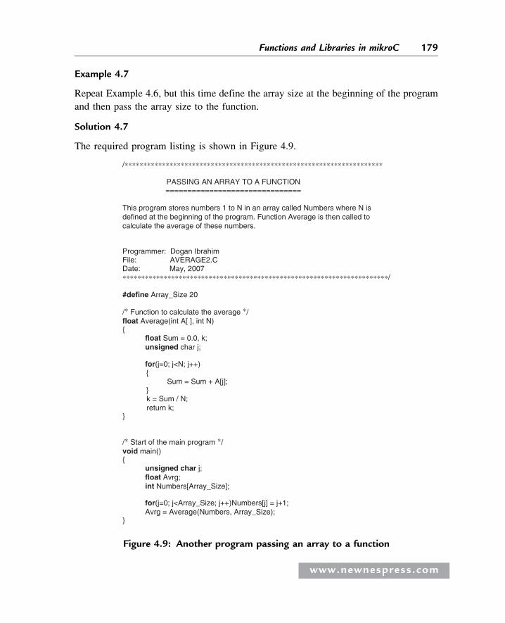
Example 4.7
Repeat Example 4.6, but this time define the array size at the beginning of the program
and then pass the array size to the function.
Solution 4.7
The required program listing is shown in Figure 4.9.
/∗∗∗∗∗∗∗∗∗∗∗∗∗∗∗∗∗∗∗∗∗∗∗∗∗∗∗∗∗∗∗∗∗∗∗∗∗∗∗∗∗∗∗∗∗∗∗∗∗∗∗∗∗∗∗∗∗∗∗∗∗∗∗∗∗∗∗∗∗
PASSING AN ARRAY TO A FUNCTION ===============================
This program stores numbers 1 to N in an array called Numbers where N is defined at the beginning of the program. Function Average is then called to calculate the average of these numbers.
Programmer: Dogan IbrahimFile: AVERAGE2.CDate: May, 2007∗∗∗∗∗∗∗∗∗∗∗∗∗∗∗∗∗∗∗∗∗∗∗∗∗∗∗∗∗∗∗∗∗∗∗∗∗∗∗∗∗∗∗∗∗∗∗∗∗∗∗∗∗∗∗∗∗∗∗∗∗∗∗∗∗∗∗∗∗∗∗/
#define Array_Size 20
/∗ Function to calculate the average ∗/float Average(int A[ ], int N){
float Sum = 0.0, k; unsigned char j;
for(j=0; j<N; j++) {
Sum = Sum + A[j]; } k = Sum / N; return k;
}
/∗ Start of the main program ∗/ void main() {
unsigned char j; float Avrg; int Numbers[Array_Size];
for(j=0; j<Array_Size; j++)Numbers[j] = j+1; Avrg = Average(Numbers, Array_Size);
}
Figure 4.9: Another program passing an array to a function
www.newnespress.com
179Functions and Libraries in mikroC
It is also possible to pass a complete array to a function using pointers. The address of
the first element of the array is passed to the function, and the function can then
manipulate the array as required using pointer operations. An example follows.
Example 4.8
Repeat Example 4.6, but this time use a pointer to pass the array elements to the
function.
Solution 4.8
The required program listing is given in Figure 4.10. An integer pointer is used to pass
the array elements to the function, and the function elements are manipulated using
pointer operations. Notice that the address of the first element of the array is passed as
an integer with the statement: &Numbers[0].
4.1.3 Passing Variables by Reference to Functions
By default, arguments to functions are passed by value. Although this method has many
distinct advantages, there are occasions when it is more appropriate and also more
efficient to pass the address of the arguments instead, that is, to pass the argument by
reference. When the address of an argument is passed, the original value of that
argument can be modified by the function; thus the function does not have to return any
variables. An example follows which illustrates how the address of arguments can be
passed to a function and how the values of these arguments can be modified inside the
function.
Example 4.9
Write a function named Swap to accept two integer arguments and then to swap the
values of these arguments. Use this function in a main program to swap the values of
two variables.
Solution 4.9
The required program listing is shown in Figure 4.11. Function Swap is defined as void
since it does not return any value. It has two arguments, a and b, and in the function
header two integer pointers are used to pass the addresses of these variables. Inside the
function body, the value of an argument is accessed by inserting the “*” character in
www.newnespress.com
180 Chapter 4
front of the argument. Inside the main program, the addresses of the variables are
passed to the function using the “&” character in front of the variable names. At the end
of the program, variables p and q are set to 20 and 10 respectively.
4.1.4 Variable Number of Arguments
The ellipsis character (“.. .”) consists of three successive periods with no spaces
between them. An ellipsis can be used in the argument lists of function prototypes to
/∗∗∗∗∗∗∗∗∗∗∗∗∗∗∗∗∗∗∗∗∗∗∗∗∗∗∗∗∗∗∗∗∗∗∗∗∗∗∗∗∗∗∗∗∗∗∗∗∗∗∗∗∗∗∗∗∗∗∗∗∗∗∗∗∗∗∗∗
This program stores numbers 1 to 10 in an array called Numbers. FunctionAverage is then called to calculate the average of these numbers.
Programmer: Dogan IbrahimFile: AVERAGE3.CDate: May, 2007∗∗∗∗∗∗∗∗∗∗∗∗∗∗∗∗∗∗∗∗∗∗∗∗∗∗∗∗∗∗∗∗∗∗∗∗∗∗∗∗∗∗∗∗∗∗∗∗∗∗∗∗∗∗∗∗∗∗∗∗∗∗∗∗∗∗∗∗∗/
/∗ Function to calculate the average ∗/float Average(int ∗A){
float Sum = 0.0, k;unsigned char j;
for(j=0; j<10; j++){
Sum = Sum + ∗(A + j);} k = Sum / 10.0;return k;
}
/∗ Start of the main program ∗/void main(){
unsigned char j;float Avrg;int Numbers[10];
for(j=0; j<10; j++)Numbers[j] = j+1;Avrg = Average(&Numbers[0]);
}
PASSING AN ARRAY TO A FUNCTION===============================
Figure 4.10: Program passing an array using pointers
www.newnespress.com
181Functions and Libraries in mikroC
indicate a variable number of arguments or arguments with varying types. An example
of a declaration of a function prototype with ellipsis follows. In this declaration, when
the function is called we must supply at least two integer type arguments, and we can
also supply any number of additional arguments:
unsigned char MyFunc(int a, int b,. . .);
The header file stdarg.h must be included at the beginning of a program that uses a
variable number of arguments. This header file defines a new data type called va_list,
which is essentially a character pointer. In addition, macro va_start() initializes an
object of type va_list to point to the address of the first additional argument presented to
the function. To extract the arguments, successive calls to the macro va_arg() must be
/*************************************************************
PASSING VARIABLES BY REFERENCE ===============================
This program shows how the address of variables can be passed to functions.The function in this program swaps the values of two integer variables.
Programmer: Dogan Ibrahim File: SWAP.C Date: May, 2007 ***************************************************************/
/* Function to swap two integers */ void Swap(int *a, int *b) {
int temp;
temp = *a; // Store a in temp *a = *b; // Copy b to a *b = temp; // Copy temp to b
}
/* Start of the main program */ void main() {
int p, q;
p = 10; // Set p = 10 q = 20; // Set q = 20 swap(&p, &q); // Swap p and q (p=20, q=10)
}
Figure 4.11: Passing variables by reference to a function
www.newnespress.com
182 Chapter 4
made, with the character pointer and the type of the parameter as the arguments of
va_arg().
An example program is given in Figure 4.12. In this program the function header
declares only one parameter of type int, and an ellipsis is used to declare a variable
/∗∗∗∗∗∗∗∗∗∗∗∗∗∗∗∗∗∗∗∗∗∗∗∗∗∗∗∗∗∗∗∗∗∗∗∗∗∗∗∗∗∗∗∗∗∗∗∗∗∗∗∗∗∗∗∗∗∗∗∗∗∗∗∗∗∗∗∗∗
PASSING VARIABLE NUMBER OF ARGUMENTS =======================================
This program shows how variable number of arguments can be passed to a function. The function header declares one integer variable and an ellipsis is used to declare variable number of parameters. The function adds all the arguments and returns the sum as an integer. The number of arguments is supplied by the calling program as the first argument to the function.
∗∗∗∗∗∗∗∗∗∗∗∗∗∗∗∗∗∗∗∗∗∗∗∗∗∗∗∗∗∗∗∗∗∗∗∗∗∗∗∗∗∗∗∗∗∗∗∗∗∗∗∗∗∗∗∗∗∗∗∗∗∗∗∗∗∗∗∗∗∗∗/
#include <stdarg.h>
/∗ Function with variable number of parameters ∗/int Sum(int num,…){
unsigned char j;va_list ap;int temp = 0;
va_start(ap, num);
for(j = 0; j < num; j++) {
temp = temp + va_arg(ap, int); }
va_end(ap);return temp;
}
/∗ Start of the main program ∗/ void main(){
int p;
p = Sum(2, 3, 5); // 2 arguments. p=3+5=8 p = Sum(3, 2, 5, 6); // 3 arguments, p=2+5+6=13
}
Programmer: Dogan IbrahimFile: VARIABLE.CDate: May, 2007
Figure 4.12: Passing variable number of arguments to a function
www.newnespress.com
183Functions and Libraries in mikroC
number of parameters. Variable num is the argument count passed by the calling
program. The arguments are read by using the macro va_arg(ap, int) and then summed
using variable temp and returned by the function.
4.1.5 Function Reentrancy
The mikroC compiler supports only a limited function reentrancy. Functions that have
no arguments and local variables can be called both from the interrupt service routines
and from the main program. Functions that have arguments and/or local variables can
only be called from the interrupt service routines or from the main program.
4.1.6 Static Function Variables
Normally, variables declared at the beginning of a program, before the main program,
are global, and their values can be accessed and modified by all parts of the program.
Declaring a variable used in a function as global ensures that its value is retained from
one call of the function to another, but this also undermines the variable’s privacy and
reduces the portability of the function to other applications. A better approach is to
declare such variables as static. Static variables are mainly used in function definitions.
When a variable is declared as static, its value is retained from one call of the function
to another. In the example code that follows, variable k is declared as static and
initialized to zero. This variable is then incremented before exiting from the function,
and the value of k remains in existence and holds its last value on the next call to the
function (i.e., on the second call to the function the value of k will be 1):
void Cnt(void){
static int k ¼ 0; // Declare k as static. . . . . . . . . . . . . . . . . .. . . . . . . . . . . . . . . . . .kþþ; // increment k
}
4.2 mikroC Built-in Functions
The mikroC compiler provides a set of built-in functions which can be called from the
program. These functions are listed in Table 4.1, along with a brief description of each.
Most of these functions can be used in a program without having to include header files.
www.newnespress.com
184 Chapter 4
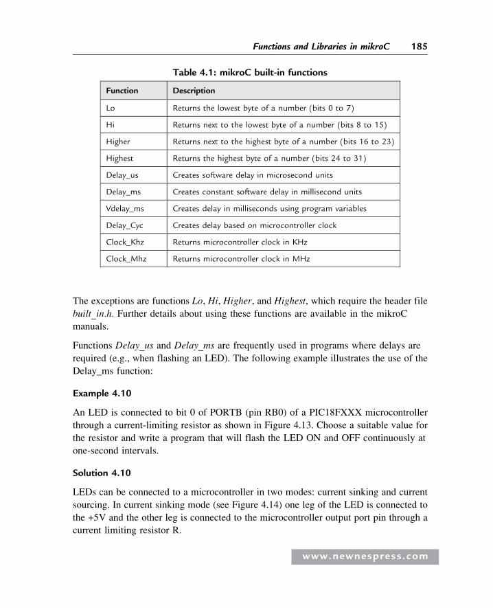
The exceptions are functions Lo, Hi, Higher, and Highest, which require the header file
built_in.h. Further details about using these functions are available in the mikroC
manuals.
Functions Delay_us and Delay_ms are frequently used in programs where delays are
required (e.g., when flashing an LED). The following example illustrates the use of the
Delay_ms function:
Example 4.10
An LED is connected to bit 0 of PORTB (pin RB0) of a PIC18FXXX microcontroller
through a current-limiting resistor as shown in Figure 4.13. Choose a suitable value for
the resistor and write a program that will flash the LED ON and OFF continuously at
one-second intervals.
Solution 4.10
LEDs can be connected to a microcontroller in two modes: current sinking and current
sourcing. In current sinking mode (see Figure 4.14) one leg of the LED is connected to
the +5V and the other leg is connected to the microcontroller output port pin through a
current limiting resistor R.
Table 4.1: mikroC built-in functions
Function Description
Lo Returns the lowest byte of a number (bits 0 to 7)
Hi Returns next to the lowest byte of a number (bits 8 to 15)
Higher Returns next to the highest byte of a number (bits 16 to 23)
Highest Returns the highest byte of a number (bits 24 to 31)
Delay_us Creates software delay in microsecond units
Delay_ms Creates constant software delay in millisecond units
Vdelay_ms Creates delay in milliseconds using program variables
Delay_Cyc Creates delay based on microcontroller clock
Clock_Khz Returns microcontroller clock in KHz
Clock_Mhz Returns microcontroller clock in MHz
www.newnespress.com
185Functions and Libraries in mikroC
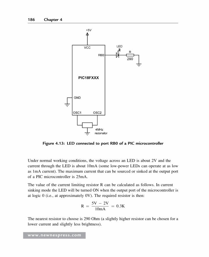
Under normal working conditions, the voltage across an LED is about 2V and the
current through the LED is about 10mA (some low-power LEDs can operate at as low
as 1mA current). The maximum current that can be sourced or sinked at the output port
of a PIC microcontroller is 25mA.
The value of the current limiting resistor R can be calculated as follows. In current
sinking mode the LED will be turned ON when the output port of the microcontroller is
at logic 0 (i.e., at approximately 0V). The required resistor is then:
R ¼ 5V � 2V
10mA¼ 0:3K
The nearest resistor to choose is 290 Ohm (a slightly higher resistor can be chosen for a
lower current and slightly less brightness).
Figure 4.13: LED connected to port RB0 of a PIC microcontroller
www.newnespress.com
186 Chapter 4
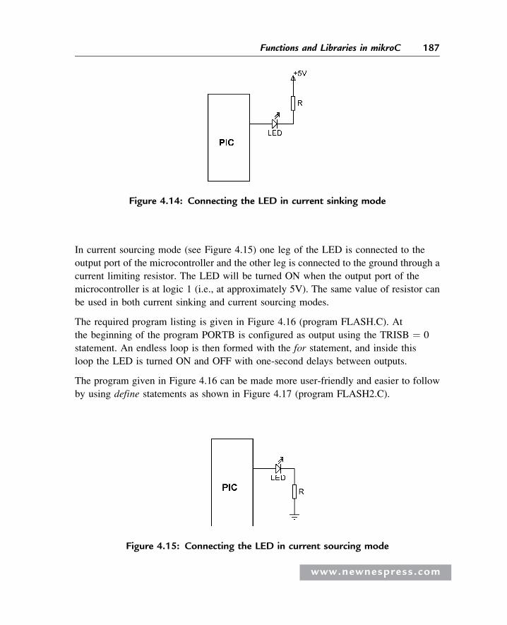
In current sourcing mode (see Figure 4.15) one leg of the LED is connected to the
output port of the microcontroller and the other leg is connected to the ground through a
current limiting resistor. The LED will be turned ON when the output port of the
microcontroller is at logic 1 (i.e., at approximately 5V). The same value of resistor can
be used in both current sinking and current sourcing modes.
The required program listing is given in Figure 4.16 (program FLASH.C). At
the beginning of the program PORTB is configured as output using the TRISB ¼ 0
statement. An endless loop is then formed with the for statement, and inside this
loop the LED is turned ON and OFF with one-second delays between outputs.
The program given in Figure 4.16 can be made more user-friendly and easier to follow
by using define statements as shown in Figure 4.17 (program FLASH2.C).
Figure 4.14: Connecting the LED in current sinking mode
Figure 4.15: Connecting the LED in current sourcing mode
www.newnespress.com
187Functions and Libraries in mikroC
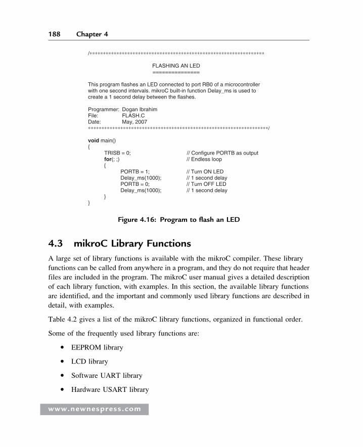
4.3 mikroC Library Functions
A large set of library functions is available with the mikroC compiler. These library
functions can be called from anywhere in a program, and they do not require that header
files are included in the program. The mikroC user manual gives a detailed description
of each library function, with examples. In this section, the available library functions
are identified, and the important and commonly used library functions are described in
detail, with examples.
Table 4.2 gives a list of the mikroC library functions, organized in functional order.
Some of the frequently used library functions are:
� EEPROM library
� LCD library
� Software UART library
� Hardware USART library
/∗∗∗∗∗∗∗∗∗∗∗∗∗∗∗∗∗∗∗∗∗∗∗∗∗∗∗∗∗∗∗∗∗∗∗∗∗∗∗∗∗∗∗∗∗∗∗∗∗∗∗∗∗∗∗∗∗∗∗∗∗∗∗∗∗
FLASHING AN LED===============
This program flashes an LED connected to port RB0 of a microcontrollerwith one second intervals. mikroC built-in function Delay_ms is used tocreate a 1 second delay between the flashes.
Programmer: Dogan IbrahimFile: FLASH.CDate: May, 2007∗∗∗∗∗∗∗∗∗∗∗∗∗∗∗∗∗∗∗∗∗∗∗∗∗∗∗∗∗∗∗∗∗∗∗∗∗∗∗∗∗∗∗∗∗∗∗∗∗∗∗∗∗∗∗∗∗∗∗∗∗∗∗∗∗∗∗/
void main() {
TRISB = 0; // Configure PORTB as outputfor(; ;) // Endless loop{
PORTB = 1; // Turn ON LEDDelay_ms(1000); // 1 second delayPORTB = 0; // Turn OFF LEDDelay_ms(1000); // 1 second delay
}}
Figure 4.16: Program to flash an LED
www.newnespress.com
188 Chapter 4
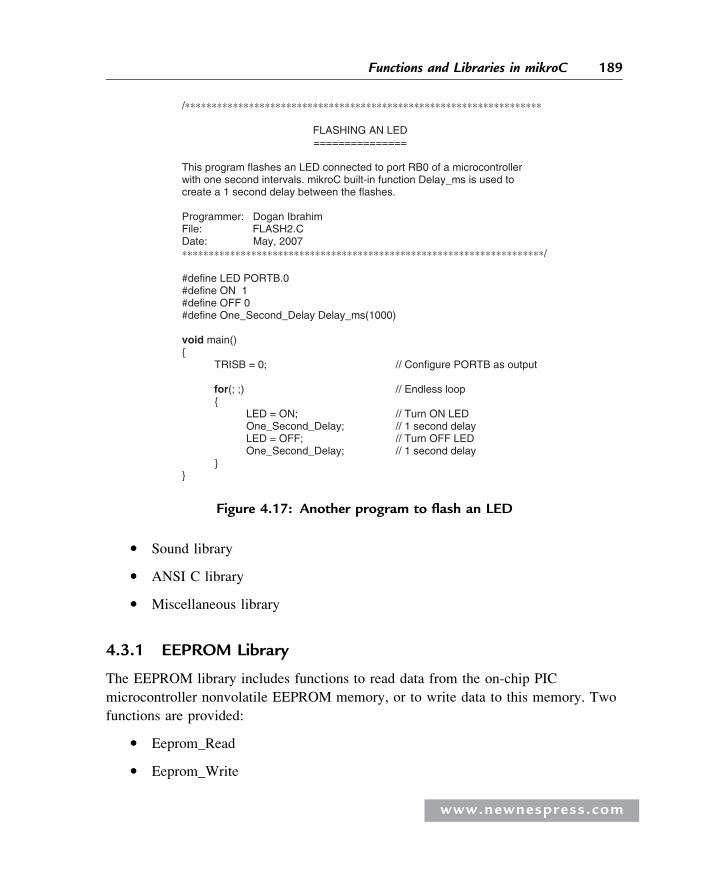
� Sound library
� ANSI C library
� Miscellaneous library
4.3.1 EEPROM Library
The EEPROM library includes functions to read data from the on-chip PIC
microcontroller nonvolatile EEPROM memory, or to write data to this memory. Two
functions are provided:
� Eeprom_Read
� Eeprom_Write
/∗∗∗∗∗∗∗∗∗∗∗∗∗∗∗∗∗∗∗∗∗∗∗∗∗∗∗∗∗∗∗∗∗∗∗∗∗∗∗∗∗∗∗∗∗∗∗∗∗∗∗∗∗∗∗∗∗∗∗∗∗∗∗∗∗∗∗
FLASHING AN LED ===============
This program flashes an LED connected to port RB0 of a microcontrollerwith one second intervals. mikroC built-in function Delay_ms is used tocreate a 1 second delay between the flashes.
Programmer: Dogan Ibrahim File: FLASH2.C Date: May, 2007 ∗∗∗∗∗∗∗∗∗∗∗∗∗∗∗∗∗∗∗∗∗∗∗∗∗∗∗∗∗∗∗∗∗∗∗∗∗∗∗∗∗∗∗∗∗∗∗∗∗∗∗∗∗∗∗∗∗∗∗∗∗∗∗∗∗∗∗∗/
#define LED PORTB.0 #define ON 1 #define OFF 0 #define One_Second_Delay Delay_ms(1000)
void main(){
TRISB = 0;
for(; ;) {
LED = ON;One_Second_Delay;LED = OFF;One_Second_Delay;
} }
// 1 second delay// Turn OFF LED// 1 second delay// Turn ON LED
// Endless loop
// Configure PORTB as output
Figure 4.17: Another program to flash an LED
www.newnespress.com
189Functions and Libraries in mikroC
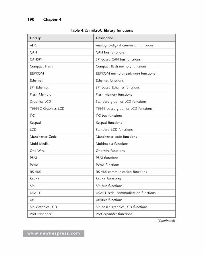
Table 4.2: mikroC library functions
Library Description
ADC Analog-to-digital conversion functions
CAN CAN bus functions
CANSPI SPI-based CAN bus functions
Compact Flash Compact flash memory functions
EEPROM EEPROM memory read/write functions
Ethernet Ethernet functions
SPI Ethernet SPI-based Ethernet functions
Flash Memory Flash memory functions
Graphics LCD Standard graphics LCD functions
T6963C Graphics LCD T6963-based graphics LCD functions
I2C I2C bus functions
Keypad Keypad functions
LCD Standard LCD functions
Manchester Code Manchester code functions
Multi Media Multimedia functions
One Wire One wire functions
PS/2 PS/2 functions
PWM PWM functions
RS-485 RS-485 communication functions
Sound Sound functions
SPI SPI bus functions
USART USART serial communication functions
Util Utilities functions
SPI Graphics LCD SPI-based graphics LCD functions
Port Expander Port expander functions
(Continued)
www.newnespress.com
190 Chapter 4
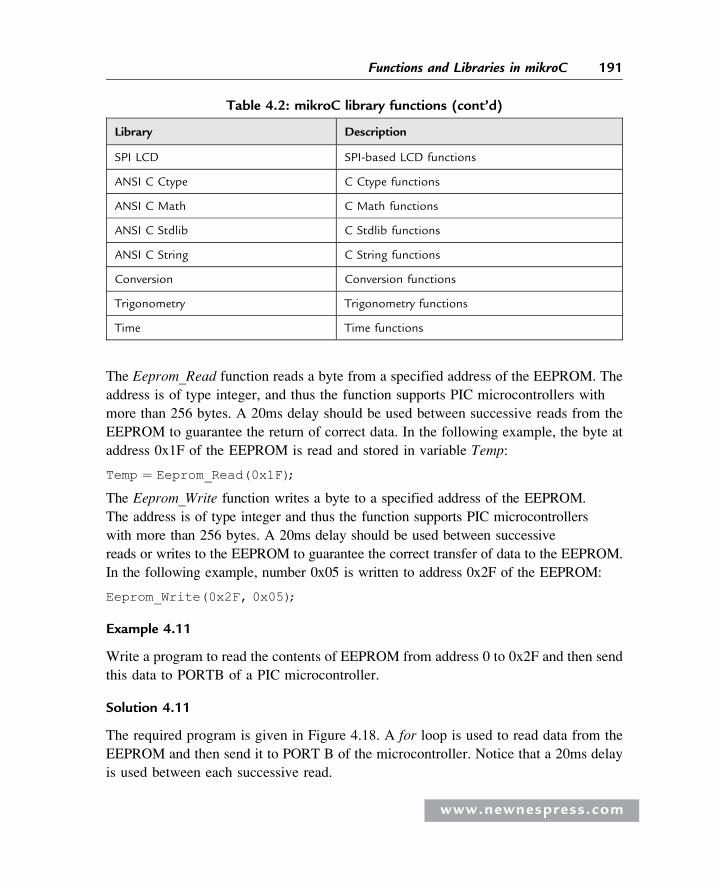
The Eeprom_Read function reads a byte from a specified address of the EEPROM. The
address is of type integer, and thus the function supports PIC microcontrollers with
more than 256 bytes. A 20ms delay should be used between successive reads from the
EEPROM to guarantee the return of correct data. In the following example, the byte at
address 0x1F of the EEPROM is read and stored in variable Temp:
Temp ¼ Eeprom_Read(0x1F);
The Eeprom_Write function writes a byte to a specified address of the EEPROM.
The address is of type integer and thus the function supports PIC microcontrollers
with more than 256 bytes. A 20ms delay should be used between successive
reads or writes to the EEPROM to guarantee the correct transfer of data to the EEPROM.
In the following example, number 0x05 is written to address 0x2F of the EEPROM:
Eeprom_Write(0x2F, 0x05);
Example 4.11
Write a program to read the contents of EEPROM from address 0 to 0x2F and then send
this data to PORTB of a PIC microcontroller.
Solution 4.11
The required program is given in Figure 4.18. A for loop is used to read data from the
EEPROM and then send it to PORT B of the microcontroller. Notice that a 20ms delay
is used between each successive read.
Table 4.2: mikroC library functions (cont’d)
Library Description
SPI LCD SPI-based LCD functions
ANSI C Ctype C Ctype functions
ANSI C Math C Math functions
ANSI C Stdlib C Stdlib functions
ANSI C String C String functions
Conversion Conversion functions
Trigonometry Trigonometry functions
Time Time functions
www.newnespress.com
191Functions and Libraries in mikroC
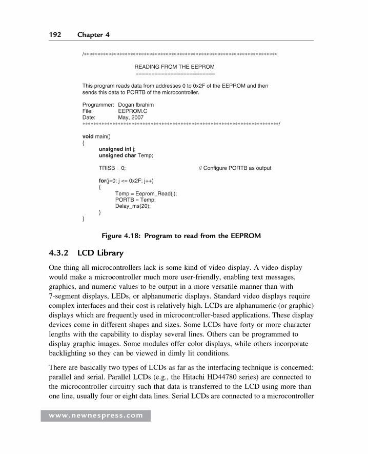
4.3.2 LCD Library
One thing all microcontrollers lack is some kind of video display. A video display
would make a microcontroller much more user-friendly, enabling text messages,
graphics, and numeric values to be output in a more versatile manner than with
7-segment displays, LEDs, or alphanumeric displays. Standard video displays require
complex interfaces and their cost is relatively high. LCDs are alphanumeric (or graphic)
displays which are frequently used in microcontroller-based applications. These display
devices come in different shapes and sizes. Some LCDs have forty or more character
lengths with the capability to display several lines. Others can be programmed to
display graphic images. Some modules offer color displays, while others incorporate
backlighting so they can be viewed in dimly lit conditions.
There are basically two types of LCDs as far as the interfacing technique is concerned:
parallel and serial. Parallel LCDs (e.g., the Hitachi HD44780 series) are connected to
the microcontroller circuitry such that data is transferred to the LCD using more than
one line, usually four or eight data lines. Serial LCDs are connected to a microcontroller
/∗∗∗∗∗∗∗∗∗∗∗∗∗∗∗∗∗∗∗∗∗∗∗∗∗∗∗∗∗∗∗∗∗∗∗∗∗∗∗∗∗∗∗∗∗∗∗∗∗∗∗∗∗∗∗∗∗∗∗∗∗∗∗∗∗∗∗∗∗∗∗
READING FROM THE EEPROM =========================
This program reads data from addresses 0 to 0x2F of the EEPROM and thensends this data to PORTB of the microcontroller.
Programmer:File:Date:∗∗∗∗∗∗∗∗∗∗∗∗∗∗∗∗∗∗∗∗∗∗∗∗∗∗∗∗∗∗∗∗∗∗∗∗∗∗∗∗∗∗∗∗∗∗∗∗∗∗∗∗∗∗∗∗∗∗∗∗∗∗∗∗∗∗∗∗∗∗∗∗/
void main() {
unsigned int j; unsigned char Temp;
for(j=0; j <= 0x2F; j++) {
} }
Dogan IbrahimEEPROM.CMay, 2007
TRISB = 0; // Configure PORTB as output
Temp = Eeprom_Read(j);PORTB = Temp;Delay_ms(20);
Figure 4.18: Program to read from the EEPROM
www.newnespress.com
192 Chapter 4
using one data line only, and data is transferred using the RS232 asynchronous data
communications protocol. Serial LCDs are generally much easier to work with but more
costly than parallel ones. In this book only parallel LCDs are discussed, as they are used
more often in microcontroller-based projects.
Low-level programming of a parallel LCD is usually a complex task and requires
a good understanding of the internal operation of the LCD, including the timing
diagrams. Fortunately, mikroC language provides functions for both text-based
and graphic LCDs, simplifying the use of LCDs in PIC-microcontroller-based projects.
The HD44780 controller is a common choice in LCD-based microcontroller
applications. A brief description of this controller and information on some
commercially available LCD modules follows.
The HD44780 LCD Controller
The HD44780 is one of the most popular LCD controllers, being used both in industrial
and commercial applications and also by hobbyists. The module is monochrome and
comes in different shapes and sizes. Modules with 8, 16, 20, 24, 32, and 40 characters
are available. Depending on the model, the display provides a 14-pin or 16-pin
connector for interfacing. Table 4.3 shows the pin configuration and pin functions of
a typical 14-pin LCD.
VSS is the 0V supply or ground. The VDD pin should be connected to the positive
supply. Although the manufacturers specify a 5V DC supply, the modules usually work
with as low as 3V or as high as 6V.
Pin 3 is named as VEE and is the contrast control pin. It is used to adjust the contrast of
the display and should be connected to a DC supply. A potentiometer is usually
connected to the power supply with its wiper arm connected to this pin and the other leg
of the potentiometer connected to the ground. This way the voltage at the VEE pin, and
hence the contrast of the display, can be adjusted as desired.
Pin 4 is the register select (RS) and when this pin is LOW, data transferred to the LCD
is treated as commands. When RS is HIGH, character data can be transferred to and
from the module.
Pin 5 is the read/write (R/W) pin. This pin is pulled LOW in order to write commands
or character data to the LCD module. When this pin is HIGH, character data or status
information can be read from the module.
www.newnespress.com
193Functions and Libraries in mikroC
Pin 6 is the enable (EN) pin, which is used to initiate the transfer of commands or data
between the module and the microcontroller. When writing to the display, data is
transferred only on the HIGH to LOW transition of this pin. When reading from the
display, data becomes available after the LOW to HIGH transition of the enable pin,
and this data remains valid as long as the enable pin is at logic HIGH.
Pins 7 to 14 are the eight data bus lines (D0 to D7). Data can be transferred between the
microcontroller and the LCD module using either a single 8-bit byte or two 4-bit
nibbles. In the latter case, only the upper four data lines (D4 to D7) are used. The 4-bit
mode has the advantage of requiring fewer I/O lines to communicate with the LCD.
The mikroC LCD library provides a large number of functions to control text-based
LCDs with 4-bit and 8-bit data interfaces, and for graphics LCDs. The most common
Table 4.3: Pin configuration of theHD44780 LCD module
Pin no. Name Function
1 VSS Ground
2 VDD +ve supply
3 VEE Contrast
4 RS Register select
5 R/W Read/write
6 EN Enable
7 D0 Data bit 0
8 D1 Data bit 1
9 D2 Data bit 2
10 D3 Data bit 3
11 D4 Data bit 4
12 D5 Data bit 5
13 D6 Data bit 6
14 D7 Data bit 7
www.newnespress.com
194 Chapter 4
are the 4-bit-interface text-based LCDs. This section describes the available mikroC
functions for these LCDs. Further information on other text- or graphics-based LCD
functions are available in the mikroC manual.
The following are the LCD functions available for 4-bit-interface text-based
LCDs:
� Lcd_Config
� Lcd_Init
� Lcd_Out
� Lcd_Out_Cp
� Lcd_Chr
� Lcd_Chr_Cp
� Lcd_Cmd
Lcd_Config The Lcd_Config function is used to configure the LCD interface. The
default connection between the LCD and the microcontroller is:
LCD Microcontroller port pin
RS 2EN 3D4 4D5 5D6 6D7 7
The R/W pin of the LCD is not used and should be connected to the ground.
This function should be used to change the default connection. It should be called with
the parameters in the following order:
port name, RS pin, EN pin, R/W pin, D7 pin, D6 pin, D5 pin, D4 pin
The port name should be specified by passing its address. For example, if the RS pin is
connected to RB0, EN pin to RB1, D7 pin to RB2, D6 pin to RB3, D5 pin to RB4, and
the D4 pin to RB5, then the function should be called as follows:
Lcd_Config(&PORTB, 0, 1, 2, 3, 4, 5);
www.newnespress.com
195Functions and Libraries in mikroC
Lcd_Init The Lcd_Init function is called to configure the interface between the
microcontroller and the LCD when the default connections are made as just illustrated.
The port name should be specified by passing its address. For example, assuming that
the LCD is connected to PORTB and the preceding default connections are used, the
function should be called as:
Lcd_Init(&PORTB);
Lcd_Out The Lcd_Out function displays text at the specified row and column position
of the LCD. The function should be called with the parameters in the following order:
row, column, text
For example, to display text “Computer” at row 1 and column 2 of the LCD we should
call the function as:
Lcd_Out(1, 2, “Computer”);
Lcd_Out_Cp The Lcd_Out_Cp function displays text at the current cursor position.
For example, to display text “Computer” at the current cursor position the function
should be called as:
Lcd_Out_Cp(“Computer”);
Lcd_Chr The Lcd_Chr function displays a character at the specified row and column
position of the cursor. The function should be called with the parameters in the
following order:
row, column, character
For example, to display character “K” at row 2 and column 4 of the LCD we should call
the function as:
LCD_Chr(2, 4, ‘K’);
Lcd_Chr_Cp The Lcd_Chr_Cp function displays a character at the current cursor
position. For example, to display character “M” at the current cursor position the
function should be called as:
Lcd_Chr_Cp(‘M’);
Lcd_Cmd The Lcd_Cmd function is used to send a command to the LCD. With the
commands we can move the cursor to any required row, clear the LCD, blink the cursor,
www.newnespress.com
196 Chapter 4
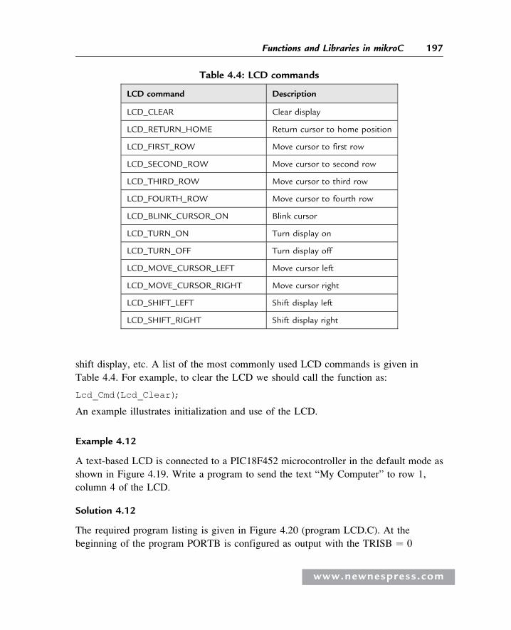
shift display, etc. A list of the most commonly used LCD commands is given in
Table 4.4. For example, to clear the LCD we should call the function as:
Lcd_Cmd(Lcd_Clear);
An example illustrates initialization and use of the LCD.
Example 4.12
A text-based LCD is connected to a PIC18F452 microcontroller in the default mode as
shown in Figure 4.19. Write a program to send the text “My Computer” to row 1,
column 4 of the LCD.
Solution 4.12
The required program listing is given in Figure 4.20 (program LCD.C). At the
beginning of the program PORTB is configured as output with the TRISB ¼ 0
Table 4.4: LCD commands
LCD command Description
LCD_CLEAR Clear display
LCD_RETURN_HOME Return cursor to home position
LCD_FIRST_ROW Move cursor to first row
LCD_SECOND_ROW Move cursor to second row
LCD_THIRD_ROW Move cursor to third row
LCD_FOURTH_ROW Move cursor to fourth row
LCD_BLINK_CURSOR_ON Blink cursor
LCD_TURN_ON Turn display on
LCD_TURN_OFF Turn display off
LCD_MOVE_CURSOR_LEFT Move cursor left
LCD_MOVE_CURSOR_RIGHT Move cursor right
LCD_SHIFT_LEFT Shift display left
LCD_SHIFT_RIGHT Shift display right
www.newnespress.com
197Functions and Libraries in mikroC
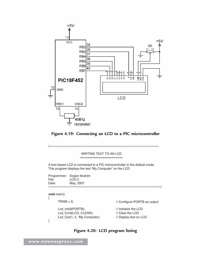
Figure 4.19: Connecting an LCD to a PIC microcontroller
/∗∗∗∗∗∗∗∗∗∗∗∗∗∗∗∗∗∗∗∗∗∗∗∗∗∗∗∗∗∗∗∗∗∗∗∗∗∗∗∗∗∗∗∗∗∗∗∗∗∗∗∗∗∗∗∗∗∗∗∗∗∗∗∗∗∗∗∗∗
WRITING TEXT TO AN LCD =======================
A text based LCD is connected to a PIC microcontroller in the default mode.This program displays the text “My Computer” on the LCD.
Programmer:File:Date:∗∗∗∗∗∗∗∗∗∗∗∗∗∗∗∗∗∗∗∗∗∗∗∗∗∗∗∗∗∗∗∗∗∗∗∗∗∗∗∗∗∗∗∗∗∗∗∗∗∗∗∗∗∗∗∗∗∗∗∗∗∗∗∗∗∗∗∗∗∗∗/
void main() {
TRISB = 0;
Lcd_Init(&PORTB);Lcd_Cmd(LCD_CLEAR); // Clear the LCD
// Display text on LCD Lcd_Out(1, 4, “My Computer); }
// Configure PORTB as output
// Initialize the LCD
Dogan IbrahimLCD.CMay, 2007
Figure 4.20: LCD program listing
www.newnespress.com
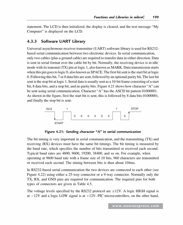
statement. The LCD is then initialized, the display is cleared, and the text message “My
Computer” is displayed on the LCD.
4.3.3 Software UART Library
Universal asynchronous receiver transmitter (UART) software library is used for RS232-
based serial communication between two electronic devices. In serial communication,
only two cables (plus a ground cable) are required to transfer data in either direction. Data
is sent in serial format over the cable bit by bit. Normally, the receiving device is in idle
mode with its transmit (TX) pin at logic 1, also known asMARK. Data transmission starts
when this pin goes to logic 0, also known as SPACE. The first bit sent is the start bit at logic
0. Following this bit, 7 or 8 data bits are sent, followed by an optional parity bit. The last bit
sent is the stop bit at logic 1. Serial data is usually sent as a 10-bit frame consisting of a start
bit, 8 data bits, and a stop bit, and no parity bits. Figure 4.21 shows how character “A” can
be sent using serial communication. Character “A” has the ASCII bit pattern 01000001.
As shown in the figure, first the start bit is sent, this is followed by 8 data bits 01000001,
and finally the stop bit is sent.
The bit timing is very important in serial communication, and the transmitting (TX) and
receiving (RX) devices must have the same bit timings. The bit timing is measured by
the baud rate, which specifies the number of bits transmitted or received each second.
Typical baud rates are 4800, 9600, 19200, 38400, and so on. For example, when
operating at 9600 baud rate with a frame size of 10 bits, 960 characters are transmitted
or received each second. The timing between bits is then about 104ms.
In RS232-based serial communication the two devices are connected to each other (see
Figure 4.22) using either a 25-way connector or a 9-way connector. Normally only the
TX, RX, and GND pins are required for communication. The required pins for both
types of connectors are given in Table 4.5.
The voltage levels specified by the RS232 protocol are �12V. A logic HIGH signal is
at �12V and a logic LOW signal is at þ12V. PIC microcontrollers, on the other hand,
START
IDLE 1
0 0 0 0 0 0
1
0
STOP
Figure 4.21: Sending character “A” in serial communication
www.newnespress.com
199Functions and Libraries in mikroC
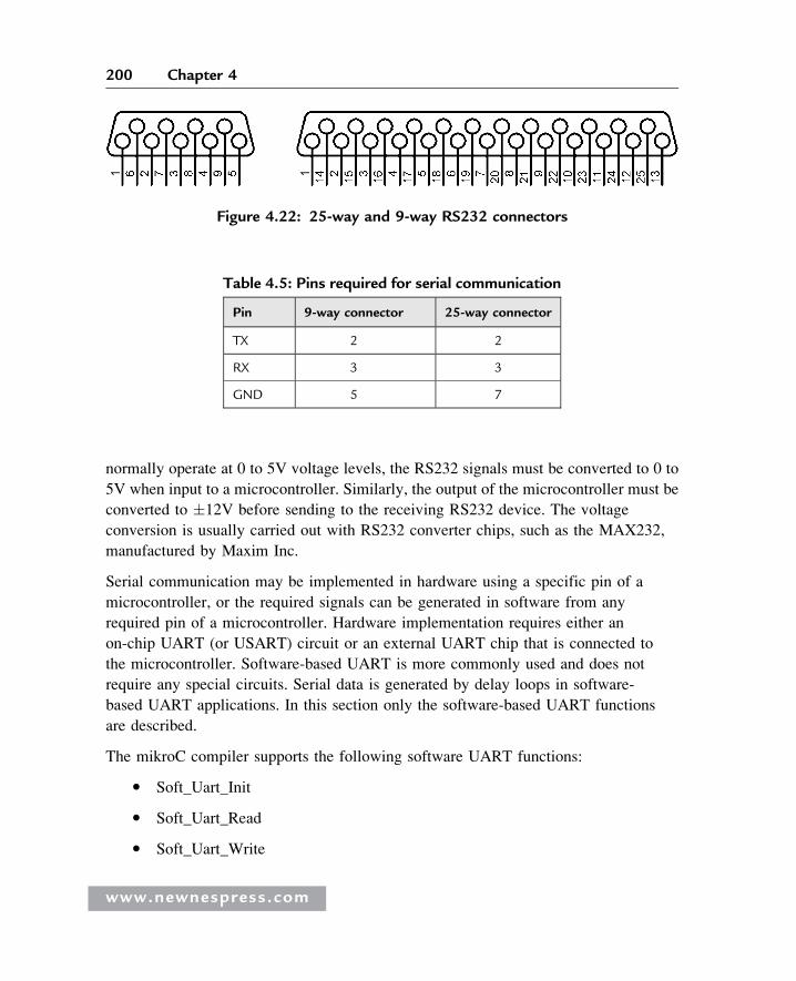
normally operate at 0 to 5V voltage levels, the RS232 signals must be converted to 0 to
5V when input to a microcontroller. Similarly, the output of the microcontroller must be
converted to �12V before sending to the receiving RS232 device. The voltage
conversion is usually carried out with RS232 converter chips, such as the MAX232,
manufactured by Maxim Inc.
Serial communication may be implemented in hardware using a specific pin of a
microcontroller, or the required signals can be generated in software from any
required pin of a microcontroller. Hardware implementation requires either an
on-chip UART (or USART) circuit or an external UART chip that is connected to
the microcontroller. Software-based UART is more commonly used and does not
require any special circuits. Serial data is generated by delay loops in software-
based UART applications. In this section only the software-based UART functions
are described.
The mikroC compiler supports the following software UART functions:
� Soft_Uart_Init
� Soft_Uart_Read
� Soft_Uart_Write
Table 4.5: Pins required for serial communication
Pin 9-way connector 25-way connector
TX 2 2
RX 3 3
GND 5 7
Figure 4.22: 25-way and 9-way RS232 connectors
www.newnespress.com
200 Chapter 4
Soft_Uart_Init
The Soft_Uart_Init function specifies the serial communications parameters and does so
in the following order:
port, rx pin, tx pin, baud rate, mode
port is the port used as the software UART (e.g., PORTB), rx is the receive pin number,
tx is the transmit pin number, baud rate is the chosen baud rate where the maximum
value depends on the clock rate of the microcontroller, and mode specifies whether
or not the data should be inverted at the output of the port. A 0 indicates that it
should not be inverted, and a 1 indicates that it should be inverted. When an RS232
voltage level converter chip is used (e.g., MAX232) then the mode must be set to 0.
Soft_Uart_Init must be the first function called before software-based serial
communication is established.
The following example configures the software UART to use PORTB as the serial port,
with RB0 as the RX pin and RB1 as the TX pin. The baud rate is set to 9600 with the
mode noninverted:
Soft_Uart_Init(PORTB, 0, 1, 9600, 0);
Soft_Uart_Read
The Soft_Uart_Read function receives a byte from a specified serial port pin. The
function returns an error condition and the data is read from the serial port. The function
does not wait for data to be available at the port, and therefore the error parameter must
be tested if a byte is expected. The error is normally 1 and becomes 0 when a byte is
read from the port.
The following example illustrates reading a byte from the serial port configured
by calling the function Soft_Uart_Init. The received byte is stored in variable Temp:
doTemp ¼ Soft_Uart_Read(&Rx_Error);
while (Rx_Error);
Soft_Uart_Write
The Soft_Uart_Write function transmits a byte to a configured serial port pin. The data
to be sent must be specified as a parameter in the call to the function.
www.newnespress.com
201Functions and Libraries in mikroC
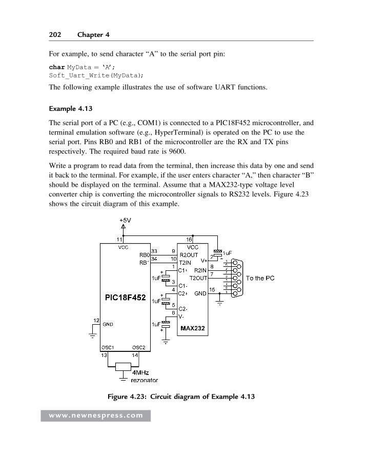
For example, to send character “A” to the serial port pin:
char MyData ¼ ‘A’;Soft_Uart_Write(MyData);
The following example illustrates the use of software UART functions.
Example 4.13
The serial port of a PC (e.g., COM1) is connected to a PIC18F452 microcontroller, and
terminal emulation software (e.g., HyperTerminal) is operated on the PC to use the
serial port. Pins RB0 and RB1 of the microcontroller are the RX and TX pins
respectively. The required baud rate is 9600.
Write a program to read data from the terminal, then increase this data by one and send
it back to the terminal. For example, if the user enters character “A,” then character “B”
should be displayed on the terminal. Assume that a MAX232-type voltage level
converter chip is converting the microcontroller signals to RS232 levels. Figure 4.23
shows the circuit diagram of this example.
Figure 4.23: Circuit diagram of Example 4.13
www.newnespress.com
202 Chapter 4
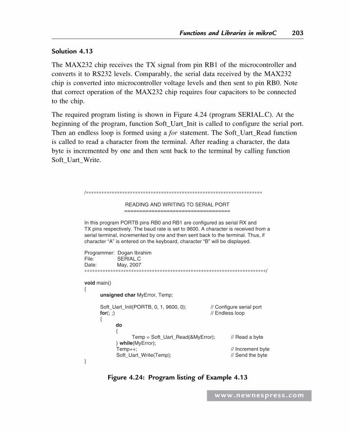
Solution 4.13
The MAX232 chip receives the TX signal from pin RB1 of the microcontroller and
converts it to RS232 levels. Comparably, the serial data received by the MAX232
chip is converted into microcontroller voltage levels and then sent to pin RB0. Note
that correct operation of the MAX232 chip requires four capacitors to be connected
to the chip.
The required program listing is shown in Figure 4.24 (program SERIAL.C). At the
beginning of the program, function Soft_Uart_Init is called to configure the serial port.
Then an endless loop is formed using a for statement. The Soft_Uart_Read function
is called to read a character from the terminal. After reading a character, the data
byte is incremented by one and then sent back to the terminal by calling function
Soft_Uart_Write.
/∗∗∗∗∗∗∗∗∗∗∗∗∗∗∗∗∗∗∗∗∗∗∗∗∗∗∗∗∗∗∗∗∗∗∗∗∗∗∗∗∗∗∗∗∗∗∗∗∗∗∗∗∗∗∗∗∗∗∗∗∗∗∗∗∗∗∗∗
READING AND WRITING TO SERIAL PORT ===================================
In this program PORTB pins RB0 and RB1 are configured as serial RX andTX pins respectively. The baud rate is set to 9600. A character is received from aserial terminal, incremented by one and then sent back to the terminal. Thus, ifcharacter “A” is entered on the keyboard, character “B” will be displayed.
Programmer: Dogan Ibrahim File: SERIAL.C Date: May, 2007 ∗∗∗∗∗∗∗∗∗∗∗∗∗∗∗∗∗∗∗∗∗∗∗∗∗∗∗∗∗∗∗∗∗∗∗∗∗∗∗∗∗∗∗∗∗∗∗∗∗∗∗∗∗∗∗∗∗∗∗∗∗∗∗∗∗∗∗∗∗∗/
void main() {
unsigned char MyError, Temp;
Soft_Uart_Init(PORTB, 0, 1, 9600, 0);for(; ;) {
do {
// Read a byte Temp = Soft_Uart_Read(&MyError);} while(MyError); Temp++; Soft_Uart_Write(Temp); // Send the byte
// Increment byte
}
// Configure serial port // Endless loop
Figure 4.24: Program listing of Example 4.13
www.newnespress.com
203Functions and Libraries in mikroC
4.3.4 Hardware USART Library
The universal synchronous asynchronous receiver transmitter (USART) hardware
library contains a number of functions to transmit and receive serial data using the
USART circuits built on the PIC microcontroller chips. Some PIC18F-series
microcontrollers have only one USART (e.g., PIC18F452), while others have two
USART circuits (e.g., PIC18F8520). Hardware USART has an advantage over
software-implemented USART, in that higher baud rates are generally available and
the microcontroller can perform other operations while data is sent to the USART.
The hardware USART library provides the following functions:
� Usart_Init
� Usart_Data_Ready
� Usart_Read
� Usart_Write
Usart_Init
The Usart_Init function initializes the hardware USART with the specified baud rate.
This function should be called first, before any other USART functions. The only
parameter required by this function is the baud rate. The following example call sets the
baud rate to 9600:
Usart_Init(9600);
Usart_Data_Ready
The Usart_Data_Ready function can be called to check whether or not a data byte has
been received by the USART. The function returns a 1 if data has been received and a
0 if no data has been received. The function has no parameters. The following code
checks if a data byte has been received or not:
if(Usart_Data_Ready( ))
Usart_Read
TheUsart_Read function is called to read a data byte from the USART. If data has not been
received, a 0 is returned. Note that reading data from the USART is nonblocking (i.e., the
www.newnespress.com
204 Chapter 4
function always returnswhether or not theUSARThas received a data byte). TheUsart_Read
function should be called after calling the functionUsart_Data_Ready to make sure that data
is available at theUSART.Usart_Read has no parameters. In the following example,USART
is checked and if a data byte has been received it is copied to variableMyData:
char MyData;if(Usart_Data_Read( )) MyData = Usart_Read();
Usart_Write
The Usart_Write function sends a data byte to the USART, and thus a serial data is sent
out of the USART. The data byte to be sent must be supplied as a parameter to the
function. In the following example, character “A” is sent to the USART:
char Temp = ‘A’;Usart_Write(Temp);
The following example illustrates how the hardware USART functions can be used in a
program.
Example 4.14
The serial port of a PC (e.g., COM1) is connected to a PIC18F452 microcontroller, and
terminal emulation software (e.g., HyperTerminal) is operated on the PC to use the serial
port. The microcontroller’s hardware USART pins RC7 (USART receive pin, RX)
and RC6 (USART transmit pin, TX) are connected to the PC via a MAX232-type RS232
voltage level converter chip. The required baud rate is 9600. Write a program to read data
from the terminal, then increase this data by one and send it back to the terminal. For
example, if the user enters character “A,” then character “B” should be displayed on the
terminal. Figure 4.25 shows the circuit diagram of this example.
Solution 4.14
The required program listing is shown in Figure 4.26 (program SERIAL2.C). At the
beginning of the program, function Usart_Init is called to set the baud rate to 9600.
Then an endless loop is formed using a for statement. The Usart_Data_Ready function
is called to check whether a character is ready, and the character is read by calling
function Usart_Read. After reading a character, the data byte is incremented by one and
then sent back to the terminal by calling function Usart_Write.
In PIC microcontrollers that have more than one USART, the second USART is accessed
by appending a “2” to the end of the function (e.g., Usart_Write2, Usart_Read2, etc.).
www.newnespress.com
205Functions and Libraries in mikroC
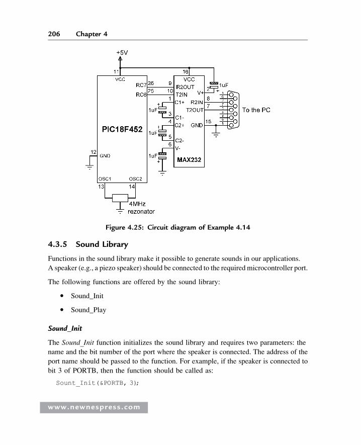
4.3.5 Sound Library
Functions in the sound library make it possible to generate sounds in our applications.
A speaker (e.g., a piezo speaker) should be connected to the required microcontroller port.
The following functions are offered by the sound library:
� Sound_Init
� Sound_Play
Sound_Init
The Sound_Init function initializes the sound library and requires two parameters: the
name and the bit number of the port where the speaker is connected. The address of the
port name should be passed to the function. For example, if the speaker is connected to
bit 3 of PORTB, then the function should be called as:
Sount_Init(&PORTB, 3);
Figure 4.25: Circuit diagram of Example 4.14
www.newnespress.com
206 Chapter 4
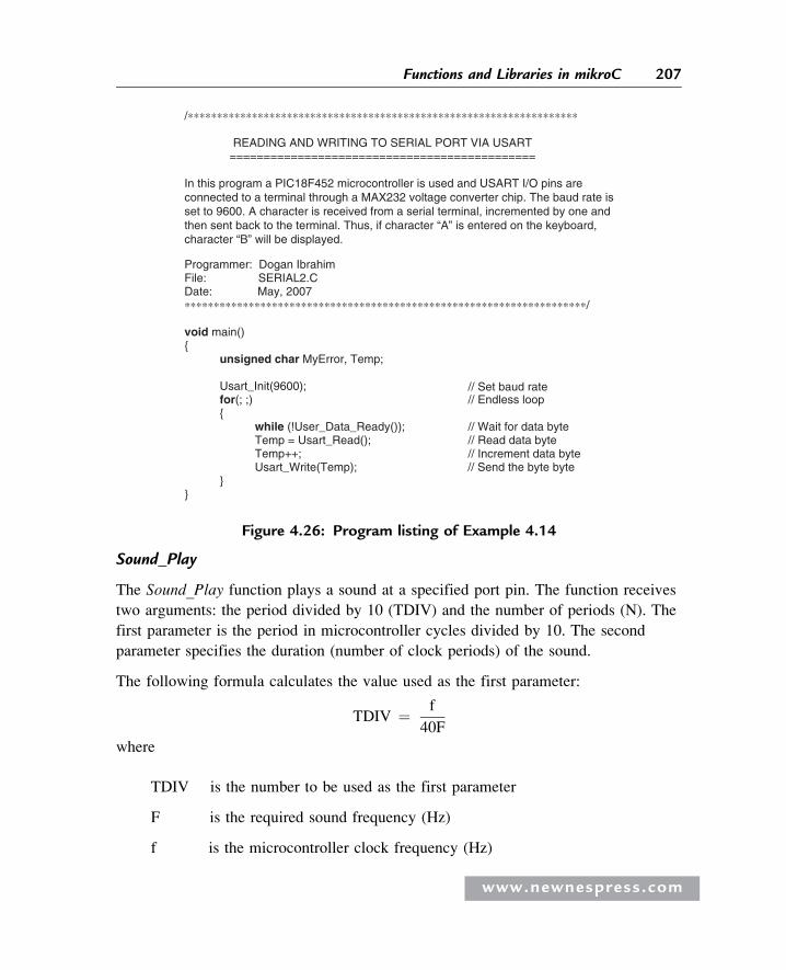
Sound_Play
The Sound_Play function plays a sound at a specified port pin. The function receives
two arguments: the period divided by 10 (TDIV) and the number of periods (N). The
first parameter is the period in microcontroller cycles divided by 10. The second
parameter specifies the duration (number of clock periods) of the sound.
The following formula calculates the value used as the first parameter:
TDIV ¼ f
40F
where
TDIV is the number to be used as the first parameter
F is the required sound frequency (Hz)
f is the microcontroller clock frequency (Hz)
/∗∗∗∗∗∗∗∗∗∗∗∗∗∗∗∗∗∗∗∗∗∗∗∗∗∗∗∗∗∗∗∗∗∗∗∗∗∗∗∗∗∗∗∗∗∗∗∗∗∗∗∗∗∗∗∗∗∗∗∗∗∗∗∗∗∗∗
READING AND WRITING TO SERIAL PORT VIA USART =============================================
In this program a PIC18F452 microcontroller is used and USART I/O pins areconnected to a terminal through a MAX232 voltage converter chip. The baud rate isset to 9600. A character is received from a serial terminal, incremented by one andthen sent back to the terminal. Thus, if character “A” is entered on the keyboard,character “B” will be displayed.
Programmer: Dogan Ibrahim File: SERIAL2.C Date: May, 2007 ∗∗∗∗∗∗∗∗∗∗∗∗∗∗∗∗∗∗∗∗∗∗∗∗∗∗∗∗∗∗∗∗∗∗∗∗∗∗∗∗∗∗∗∗∗∗∗∗∗∗∗∗∗∗∗∗∗∗∗∗∗∗∗∗∗∗∗∗∗/
void main() {
unsigned char MyError, Temp;
Usart_Init(9600); for(; ;){
while (!User_Data_Ready()); // Wait for data byte // Read data byteTemp = Usart_Read();
Temp++; // Increment data byte Usart_Write(Temp); // Send the byte byte
} }
// Set baud rate // Endless loop
Figure 4.26: Program listing of Example 4.14
www.newnespress.com
207Functions and Libraries in mikroC
Example 4.15
Write a program to play a sound at 1KHz, assuming the clock frequency is 4MHz.
The required duration of the sound is 250 periods.
Solution 4.15
The first parameter is calculated as follows:
TDIV ¼ f
40F¼ 4�106
40�103¼ 100
Since the required duration is 250 periods, the function is called with the
parameters:
Sound_Play(100, 250);
4.3.6 ANSI C Library
The ANSI C library consists of the following libraries (further details on these libraries
are available in the mikroC user manual):
� Ctype library
� Math library
� Stdlib library
� String library
Ctype Library
The functions in the Ctype library are mainly used for testing or data conversion.
Table 4.6 lists the commonly used functions in this library.
Math Library
The functions in the Math library are used for floating point mathematical operations.
Table 4.7 lists the commonly used functions in this library.
www.newnespress.com
208 Chapter 4
Stdlib Library
The Stdlib library contains standard library functions. Table 4.8 lists the commonly
used functions in this library.
Example 4.16
Write a program to calculate the trigonometric sine of the angles from 0� to 90� in steps
of 1� and store the result in an array called Trig_Sine.
Solution 4.16
The required program listing is shown in Figure 4.27 (program SINE.C). A loop is
created using a for statement, and inside this loop the sine of the angles are calculated
and stored in array Trig_Sine. Note that the angles must be converted into radians
before they are used in function sin.
String Library
The functions in the String library are used to perform string and memory manipulation
operations. Table 4.9 lists the commonly used functions in this library.
Table 4.6: Commonly used Ctype library functions
Function Description
isalnum Returns 1 if the specified character is alphanumeric (a�z, A�Z, 0�9)
isalpha Returns 1 if the specified character is alphabetic (a�z, A�Z)
isntrl Returns 1 if the specified character is a control character (decimal 0�31 and 127)
isdigit Returns 1 if the specified character is a digit (0�9)
islower Returns 1 if the specified character is lowercase
isprint Returns 1 if the specified character is printable (decimal 32�126)
isupper Returns 1 if the specified character is uppercase
toupper Convert a character to uppercase
tolower Convert a character to lowercase
www.newnespress.com
209Functions and Libraries in mikroC
Example 4.17
Write a program to illustrate how the two strings “MY POWERFUL” and
“COMPUTER” can be joined into a new string using String library functions.
Solution 4.17
The required program listing is shown in Figure 4.28 (program JOIN.C). The
mikroC String library function strcat is used to join the two strings pointed to by
p1 and p2 into a new string stored in a character array called New_String.
Table 4.7: Commonly used Math library functions
Function Description
acos Returns in radians the arc cosine of its parameter
asin Returns in radians the arc sine of its parameter
atan Returns in radians the arc tangent of its parameter
atan2 Returns in radians the arc tangent of its parameter where the signs of bothparameters are used to determine the quadrant of the result
cos Returns the cosine of its parameter in radians
cosh Returns the hyperbolic cosine of its parameter
exp Returns the exponential of its parameter
fabs Returns the absolute value of its parameter
log Returns the natural logarithm of its parameter
Log10 Returns the logarithm to base 10 of its parameter
pow Returns the power of a number
sin Returns the sine of its parameter in radians
sinh Returns the hyperbolic sine of its parameter
sqrt Returns the square root of its parameter
tan Returns the tangent of its parameter in radians
tanh Returns the hyperbolic sine of its parameter
www.newnespress.com
210 Chapter 4
/∗∗∗∗∗∗∗∗∗∗∗∗∗∗∗∗∗∗∗∗∗∗∗∗∗∗∗∗∗∗∗∗∗∗∗∗∗∗∗∗∗∗∗∗∗∗∗∗∗∗∗∗∗∗∗∗∗∗∗∗∗∗∗∗∗∗
TRIGONOMETRIC SINE OF ANGLES 0 to 90 DEGREES ===========================================
This program calculates the trigonometric sine of angles from 0 degrees to90 degrees in steps of 1 degree. The results are stored in an array calledTrig_Sine.
Programmer: Dogan Ibrahim File: SINE.C Date: May, 2007 ∗∗∗∗∗∗∗∗∗∗∗∗∗∗∗∗∗∗∗∗∗∗∗∗∗∗∗∗∗∗∗∗∗∗∗∗∗∗∗∗∗∗∗∗∗∗∗∗∗∗∗∗∗∗∗∗∗∗∗∗∗∗∗∗∗∗∗∗/
void main() {
unsigned char j; double PI = 3.14159, rads;
for(j = 0; j <= 90; j++) {
rads = j ∗ PI /180.0; angle = sin(rad); Trig_Sine[j] = angle;
} }
Figure 4.27: Calculating the sine of angles 0� to 90�
Table 4.8: Commonly used Stdlib library functions
Function Description
abs Returns the absolute value
atof Converts ASCII character into floating point number
atoi Converts ASCII character into integer number
atol Converts ASCII character into long integer
max Returns the greater of two integers
min Returns the lesser of two integers
rand Returns a random number between 0 and 32767; function srand must be called toobtain a different sequence of numbers
srand Generates a seed for function rand so a new sequence of numbers is generated
xtoi Convert input string consisting of hexadecimal digits into integer
www.newnespress.com
211Functions and Libraries in mikroC
4.3.7 Miscellaneous Library
The functions in the Miscellaneous library include routines to convert data from one
type to another type, as well as to perform some trigonometric functions. Table 4.10
lists the commonly used functions in this library.
The following general programs illustrate the use of various library routines available
with the mikroC language.
Table 4.9: Commonly used String library functions
Function Description
strcat, strncat Append two strings
strchr, strpbrk Locate the first occurrence of a character in a string
strcmp, strncmp Compare two strings
strcpy, strncpy Copy one string into another one
strlen Return the length of a string
/∗∗∗∗∗∗∗∗∗∗∗∗∗∗∗∗∗∗∗∗∗∗∗∗∗∗∗∗∗∗∗∗∗∗∗∗∗∗∗∗∗∗∗∗∗∗∗∗∗∗∗∗∗∗∗∗∗∗∗∗∗∗∗∗∗∗
JOINING TWO STRINGS ===================
This program shows how two strings can be joined to obtain a new string.mikroC library function strcat is used to join the two strings pointed to byp1 and p2 into a new string stored in character array New_String.
Programmer: File: Date: ∗∗∗∗∗∗∗∗∗∗∗∗∗∗∗∗∗∗∗∗∗∗∗∗∗∗∗∗∗∗∗∗∗∗∗∗∗∗∗∗∗∗∗∗∗∗∗∗∗∗∗∗∗∗∗∗∗∗∗∗∗∗∗∗∗∗∗/
void main(){
const char ∗p1 = “MY POWERFUL “; // First string const char ∗p2 = “COMPUTER”; // Second string char New_String[80];
strcat(strcat(New_String, p1), p2); // join the two strings }
Dogan IbrahimJOIN.CMay, 2007
Figure 4.28: Joining two strings using function strcat
www.newnespress.com
212 Chapter 4
Example 4.18
Write a function to convert the string pointed to by p into lowercase or uppercase,
depending on the value of a mode parameter passed to the function. If the mode
parameter is nonzero, then convert to lowercase, otherwise convert it to uppercase. The
function should return a pointer to the converted string.
Solution 4.18
The required program listing is given in Figure 4.29 (programCASE.C). The program checks
the value of the mode parameter, and if this parameter is nonzero the string is converted to
lowercase by calling function ToLower, otherwise the function ToUpper is called to convert
the string to uppercase. The program returns a pointer to the converted string.
Example 4.19
Write a program to define a complex number structure, then write functions to add and
subtract two complex numbers. Show how you can use these functions in a main program.
Solution 4.19
Figure 4.30 shows the required program listing (program COMPLEX.C). At the
beginning of the program, a data type called complex is created as a structure having
a real part and an imaginary part. A function called Add is then defined to add two
complex numbers and return the sum as a complex number. Similarly, the function
Table 4.10: Commonly used Miscellaneouslibrary functions
Function Description
ByteToStr Convert a byte into string
ShortToStr Convert a short into string
WordToStr Convert an unsigned word into string
IntToStr Convert an integer into string
LongToStr Convert a long into string
FloatToStr Convert a float into string
Bcd2Dec Convert a BCD number into decimal
Dec2Bcd Convert a decimal number into BCD
www.newnespress.com
213Functions and Libraries in mikroC
Subtract is defined to subtract two complex numbers and return the result as a complex
number. The main program uses two complex numbers, a and b, where,
a ¼ 2.0 � 3.0jb ¼ 2.5 þ 2.0j
Two other complex numbers, c and d, are also declared, and the following complex
number operations are performed:
The program calculates, c ¼ a þ b and, d ¼ a � b
Example 4.20
A projectile is fired at an angle of y degrees at an initial velocity of v meters per
second. The distance traveled by the projectile (d), the flight time (t), and the
maximum height reached (h) are given by the following formulas:
h ¼ v2 sinðyÞg
t ¼ 2v sinðyÞg
d ¼ v2 sinð2yÞg
/∗∗∗∗∗∗∗∗∗∗∗∗∗∗∗∗∗∗∗∗∗∗∗∗∗∗∗∗∗∗∗∗∗∗∗∗∗∗∗∗∗∗∗∗∗∗∗∗∗∗∗∗∗∗∗∗∗∗∗∗∗∗∗∗∗∗∗∗∗
CONVERT A STRING TO LOWER/UPPERCASE ======================================
This program receives a string pointer and a mode parameter. If the mode is 1Then the string is converted to lowercase, otherwise the string is converted touppercase.
Programmer:File:Date: ∗∗∗∗∗∗∗∗∗∗∗∗∗∗∗∗∗∗∗∗∗∗∗∗∗∗∗∗∗∗∗∗∗∗∗∗∗∗∗∗∗∗∗∗∗∗∗∗∗∗∗∗∗∗∗∗∗∗∗∗∗∗∗∗∗∗∗∗∗∗∗/
unsigned char ∗Str_Convert(unsigned char ∗p, unsigned char mode) {
unsigned char ∗ptr = p;
if (mode != 0){
while(∗p != ‘\0’) ∗p++ = ToLower(∗p);}
}
else {
while(∗p != ‘\0’) ∗p++ = ToUpper(∗p);
return ptr; }
Dogan Ibrahim CASE.C May, 2007
Figure 4.29: Program for Example 4.18
www.newnespress.com
214 Chapter 4
/∗∗∗∗∗∗∗∗∗∗∗∗∗∗∗∗∗∗∗∗∗∗∗∗∗∗∗∗∗∗∗∗∗∗∗∗∗∗∗∗∗∗∗∗∗∗∗∗∗∗∗∗∗∗∗∗∗∗∗∗∗
COMPLEX NUMBER ADDITION AND SUBTRACTION ===========================================
This program creates a data structure called complex having a real part andan imaginary part. Then, functions are defined to add or subtract two complexnumbers and store the result in another complex number.
The first complex number is, a = 2.0 – 2.0j The second complex number is, b = 2.5 + 2.0j
The program calculates, c = a + b and, d = a − b
Programmer: Dogan Ibrahim File: COMPLEX.C Date: May, 2007 ∗∗∗∗∗∗∗∗∗∗∗∗∗∗∗∗∗∗∗∗∗∗∗∗∗∗∗∗∗∗∗∗∗∗∗∗∗∗∗∗∗∗∗∗∗∗∗∗∗∗∗∗∗∗∗∗∗∗∗∗∗∗∗/
/∗ Define a new data type called complex ∗/ typedef struct {
float real; float imag;
} complex;
/∗ Define a function to add two complex numbers and return the result as a complex number ∗/ complex Add(complex i, complex j) {
complex z;
z.real = i.real + j.real; z.imag = i.imag + j.imag
return z; }
/∗ Define a function to subtract two complex numbers and return the result as a complex number ∗/ complex Subtract(complex i, complex j) {
complex z;
z.real = i.real – j.real; z.imag = i.imag – j.imag;
return z;
Figure 4.30: Program for Example 4.19(Continued)
www.newnespress.com
215Functions and Libraries in mikroC
Write functions to calculate the height, flight time, and distance traveled. Assuming
that g ¼ 9.81m/s2, v ¼ 12 m/s, and y ¼ 45�, call the functions to calculate the three
variables. Figure 4.31 shows the projectile pattern.
Solution 4.20
The required program is given in Figure 4.32 (program PROJECTILE.C).
Three functions are defined: Height calculates the maximum height of the
v
h
Distance
Height
Figure 4.31: Projectile pattern
}
/∗ Main program ∗/void main(){
complex a,b,c, d;
a.real = 2.0; a.imag =−3.0; // First complex numberb.real = 2.5; b.imag = 2.0; // second complex number
c = Add(a, b); // Add numbersd = Subtract(a, b); // Subtract numbers
}
Figure 4.30: (Cont’d)
www.newnespress.com
216 Chapter 4
/∗∗∗∗∗∗∗∗∗∗∗∗∗∗∗∗∗∗∗∗∗∗∗∗∗∗∗∗∗∗∗∗∗∗∗∗∗∗∗∗∗∗∗∗∗∗∗∗∗∗∗∗∗∗∗∗∗∗∗∗∗∗∗∗∗∗∗∗∗∗
PROJECTILE CALCULATION========================
This program calculates the maximum height, distance traveled, and the flighttime of a projectile. Theta is the firing angle, and v is the initial velocity of theprojectile respectively.
Programmer: Dogan IbrahimFile: PROJECTILE.CDate: May, 2007∗∗∗∗∗∗∗∗∗∗∗∗∗∗∗∗∗∗∗∗∗∗∗∗∗∗∗∗∗∗∗∗∗∗∗∗∗∗∗∗∗∗∗∗∗∗∗∗∗∗∗∗∗∗∗∗∗∗∗∗∗∗∗∗∗∗∗∗∗∗∗/
#define gravity 9.81
/∗ This function converts degrees to radians ∗/float Radians(float y){
float rad;
rad = y ∗ 3.14159 / 180.0;
return rad;}
/∗ Flight time of the projectile ∗/float Flight_time(float theta, float v) {
float t, rad;
rad = Radians(theta);t = (2.0∗v∗sin(rad)) / gravity;
return t;}
float Height(float theta, float v){
float h, rad;
rad = Radians(theta);h = (v∗v∗sin(rad)) / gravity;
return h;}
float Distance(float theta, float v){
Figure 4.32: Program for Example 4.20
(Continued)
www.newnespress.com
217Functions and Libraries in mikroC
projectile, Flight_time calculates the flight time, and Distance calculates the
distance traveled. In addition, a function called Radians converts degrees into
radians to use in the trigonometric function sine. The height, distance traveled,
and flight time are calculated and stored in floating point variables h, d,
and t respectively.
4.4 Summary
This chapter has discussed the important topics of functions and libraries. Functions
are useful when part of a code must be repeated several times from different points
of a program. They also make programs more readable and easier to manage
and maintain. A large program can be split into many functions that are tested
independently and, once all of them are working, are combined to produce the
final program.
The mikroC language library functions have also been described briefly, along with
examples of how to use several of these functions in main programs. Library functions
simplify programmers’ tasks by providing ready and tested routines that can be called
and used in their programs.
float d, rad;
rad = radians(theta);d = (v∗v∗sin(2∗rad)) / gravity;
return d;}
/∗ Main program ∗/ void main(){
float theta, v, h, d, t;
theta = 45.0;v = 12.0;h = Height(theta, v);d = Distance(theta, v);t = Flight_time(theta, v);
}
Figure 4.32: (Cont’d)
www.newnespress.com
218 Chapter 4
4.5 Exercises
1. Write a function to calculate the circumference of a rectangle. The function should
receive the two sides of the rectangle as floating point numbers and return the
circumference as a floating point number.
2. Write a main program to use the function you developed in Exercise 1. Find the
circumference of a rectangle whose sides are 2.3cm and 5.6cm. Store the result in
a floating point number called MyResult.
3. Write a function to convert inches to centimeters. The function should receive
inches as a floating point number and then calculate the equivalent centimeters.
4. Write a main program to use the function you developed in Exercise 3. Convert
12.5 inches into centimeters and store the result as a floating point number.
5. An LED is connected to port pin RB0 of a PIC18F452-type microcontroller
through a current limiting resistor in current sinking mode. Write a program to
flash the LED in five-second intervals.
6. Eight LEDs are connected to PORTB of a PIC18F452-type microcontroller. Write
a program so that the LEDs count up in binary sequence with a one-second delay
between outputs.
7. An LED is connected to port pin RB7 of a PIC18F452 microcontroller. Write a
program to flash the LED such that the ON time is five seconds, and the OFF time
is three seconds.
8. A text-based LCD is connected to a PIC18F452-type microcontroller in 4-bit data
mode. Write a program that will display a count from 0 to 255 on the LCD with a
one-second interval between counts.
9. A text-based LCD is connected to a PIC microcontroller as in Exercise 8. Write a
program to display the text “Exercise 9” on the first row of the LCD.
10. Repeat Exercise 9 but display the message on the first row, starting from column 3
of the LCD.
11. A two-row text-based LCD is connected to a PIC18F452-type microcontroller in
4-bit-data mode. Write a program to display the text “COUNTS:” on row 1 and
then to count repeatedly from 1 to 100 on row 2 with two-second intervals.
www.newnespress.com
219Functions and Libraries in mikroC

12. Write a program to calculate the trigonometric cosine of angles from 0� to 45� insteps of 1� and store the results in a floating point array.
13. Write a function to calculate and return the length of the hypotenuse of a right-
angle triangle, given its two sides. Show how you can use the function in a main
program to calculate the hypotenuse of a right-angle triangle whose two sides are
4.0cm and 5.0cm.
14. Write a program to configure port pin RB2 of a PIC18F452 microcontroller as the
RS232 serial output port. Send character “X” to this port at 4800 baud.
15. Port RB0 of a PIC18F452 microcontroller is configured as the RS232 serial output
port. Write a program to send out string “SERIAL” at 9600 baud.
16. Repeat Exercise 15 but use the hardware USART available on the microcontroller
chip.
17. Explain the differences between software-implemented serial data communication
and USART hardware-based serial communication.
18. Write a function to add two arrays that are passed to the function as arguments.
Store the sum in one of these arrays.
19. Write a function to perform the following operations on two-dimensional matrices:
a) Add matrices
b) Subtract matrices
c) Multiply matrices
20. Write a function to convert between polar and rectangular coordinates.
21. Write functions to convert temperature expressed in Celsius to Fahrenheit and vice
versa. Show how these functions can be called from main programs to convert
20�C to �F and also 100�F to �C.
22. Write a program to store the value of function f(x) in an array as x is varied from
0 to 10 in steps of 0.5. Assume that:
fðxÞ ¼ 1:3x3 � 2:5x2 þ 3:1x� 4:5
www.newnespress.com
220 Chapter 4
CHAP T E R 5
PIC18 Development Tools
The development of a microcontroller-based system is a complex process. Development
tools are hardware and software tools designed to help programmers develop and test
systems in a relatively short time. There are many such tools, and a discussion of all of
them is beyond the scope of this book. This chapter offers a brief review of the most
common tools.
The tools for developing software and hardware for microcontroller-based systems
include editors, assemblers, compilers, debuggers, simulators, emulators, and device
programmers. A typical development cycle starts with writing the application
program using a text editor. The program is then translated into an executable code
with the help of an assembler or compiler. If the program has several modules, a
linker is used to combine them into a single application. Any syntax errors are
detected by the assembler or compiler and must be corrected before the executable
code can be generated. Next, a simulator is used to test the application program
without the target hardware. Simulators are helpful in checking the correctness of an
algorithm or a program with limited or no input-outputs, and most errors can be
removed during simulation. Once the program seems to be working and the
programmer is happy with it, the executable code is loaded to the target
microcontroller chip using a device programmer, and the system logic is tested.
Software and hardware tools such as in-circuit debuggers and in-circuit emulators can
analyze the program’s operation and display the variables and registers in real time
with the help of breakpoints set in the program.
www.newnespress.com
5.1 Software Development Tools
Software development tools are computer programs, usually run on personal computers,
that allow the programmer (or system developer) to create, modify, and test applications
programs. Some common software development tools are:
� Text editors
� Assemblers/compilers
� Simulators
� High-level language simulators
� Integrated development environments (IDEs)
5.1.1 Text Editors
A text editor is used to create or edit programs and text files. The Windows operating
system comes with a text editor program called Notepad. Using Notepad, we can create
a new program file, modify an existing file, or display or print the contents of a file. It is
important to realize that programs used for word processing, such as Microsoft Word,
cannot be used for this purpose, since they embed word formatting characters such as
bold, italic, and underline within the text.
Most assemblers and compilers come with built-in text editors, making it possible
to create a program and then assemble or compile it without having to exit from the
editor. These editors provide additional features as well, such as automatic keyword
highlighting, syntax checking, parenthesis matching, and comment line identification.
Different parts of a program can be shown in different colors to make the program
more readable (e.g., comments in one color and keywords in another). Such features
help to eliminate syntax errors during the programming stage, thus speeding up the
development process.
5.1.2 Assemblers and Compilers
Assemblers generate executable code from assembly language programs, and that
generated code can then be loaded into the flash program memory of a PIC18-based
microcontroller. Compilers generate executable code from high-level language programs.
The compilers used most often for PIC18 microcontrollers are BASIC, C, and PASCAL.
www.newnespress.com
222 Chapter 5
Assembly language is used in applications where processing speed is critical and the
microcontroller must respond to external and internal events in the shortest possible
time. However, it is difficult to develop complex programs using assembly language,
and assembly language programs are not easy to maintain.
High-level languages, on the other hand, are easier to learn, and complex programs can
be developed and tested in a much shorter time. High-level programs are also
maintained more easily than assembly language programs.
Discussions of programming in this book are limited to the C language. Many different
C language compilers are available for developing PIC18 microcontroller-based
programs. Some of the popular ones are:
� CCS C (http://www.ccsinfo.com)
� Hi-Tech C (http://htsoft.com)
� C18 C (http://www.microchip.com)
� mikroC C (http://www.mikroe.com)
� Wiz-C C (http://www.fored.co.uk)
Although most C compilers are essentially the same, each one has its own additions or
modifications to the standard language. The C compiler used in this book is mikroC,
developed by mikroElektronika.
5.1.3 Simulators
A simulator is a computer program that runs on a PC without the microcontroller
hardware. It simulates the behavior of the target microcontroller by interpreting
the user program instructions using the microcontroller instruction set. Simulators can
display the contents of registers, memory, and the status of input-output ports as
the user program is interpreted. Breakpoints can be set to stop the program and
check the contents of various registers at desired locations. In addition, the user
program can be executed in a single-step mode, so the memory and registers
can be examined as the program executes one instruction at a time as a key is
pressed.
Some assembler programs contain built-in simulators. Three popular PIC18
microcontroller assemblers with built-in simulators are:
www.newnespress.com
223PIC18 Development Tools
� MPLAB IDE (http://www.microchip.com)
� Oshon Software PIC18 simulator (http://www.oshonsoft.com)
� Forest Electronics PIC18 assembler (http://www.fored.co.uk)
5.1.4 High-Level Language Simulators
High-level language simulators, also known as source-level debuggers, are programs that
run on a PC and locate errors in high-level programs. The programmer can set breakpoints
in high-level statements, execute the program up to a breakpoint, and then view the values
of program variables, the contents of registers, and memory locations at that breakpoint.
A source-level debugger can also invoke hardware-based debugging using a hardware
debugger device. For example, the user program on the target microcontroller can be
stopped and the values of various variables and registers can be examined.
Some high-level language compilers, including the following three, have built-in
source-level debuggers:
� C18 C
� Hi-Tech PIC18 C
� mikroC C
5.1.5 Integrated Development Environments (IDEs)
Integrated development environments (IDEs) are powerful PC-based programs which
include everything to edit, assemble, compile, link, simulate, and source-level debug
a program, and then download the generated executable code to the physical
microcontroller chip using a programmer device. These programs are in graphical user
interface (GUI), where the user can select various options from the program without
having to exit it. IDEs can be extremely useful when developing microcontroller-based
systems. Most PIC18 high-level language compilers are IDEs, thus enabling the
programmer to do most tasks within a single software development tool.
5.2 Hardware Development Tools
Numerous hardware development tools are available for the PIC18 microcontrollers.
Some of these products are manufactured by Microchip Inc., and some by third-party
companies. The most ones are:
www.newnespress.com
224 Chapter 5
� Development boards
� Device programmers
� In-circuit debuggers
� In-circuit emulators
� Breadboards
5.2.1 Development Boards
Development boards are invaluable microcontroller development tools. Simple
development boards contain just a microcontroller and the necessary clock circuitry.
Some sophisticated development boards contain LEDs, LCD, push buttons, serial
ports, USB port, power supply circuit, device programming hardware, and so on.
This section is a survey of various commercially available PIC18 microcontroller
development boards and their specifications.
LAB-XUSB Experimenter Board
The LAB-XUSB Experimenter board (see Figure 5.1), manufactured by
microEngineering Labs Inc., can be used in 40-pin PIC18-based project development.
The board is available either assembled or as a bare board.
The board contains:
� 40-pin ZIF socket for PIC microcontroller
� 5-volt regulator
� 20MHz oscillator
� Reset button
� 16-switch keypad
� Two potentiometers
� Four LEDs
� 2-line by 20-character LCD module
� Speaker
www.newnespress.com
225PIC18 Development Tools
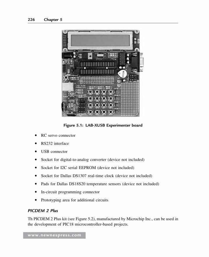
� RC servo connector
� RS232 interface
� USB connector
� Socket for digital-to-analog converter (device not included)
� Socket for I2C serial EEPROM (device not included)
� Socket for Dallas DS1307 real-time clock (device not included)
� Pads for Dallas DS18S20 temperature sensors (device not included)
� In-circuit programming connector
� Prototyping area for additional circuits
PICDEM 2 Plus
Th PICDEM 2 Plus kit (see Figure 5.2), manufactured by Microchip Inc., can be used in
the development of PIC18 microcontroller-based projects.
Figure 5.1: LAB-XUSB Experimenter board
www.newnespress.com
226 Chapter 5
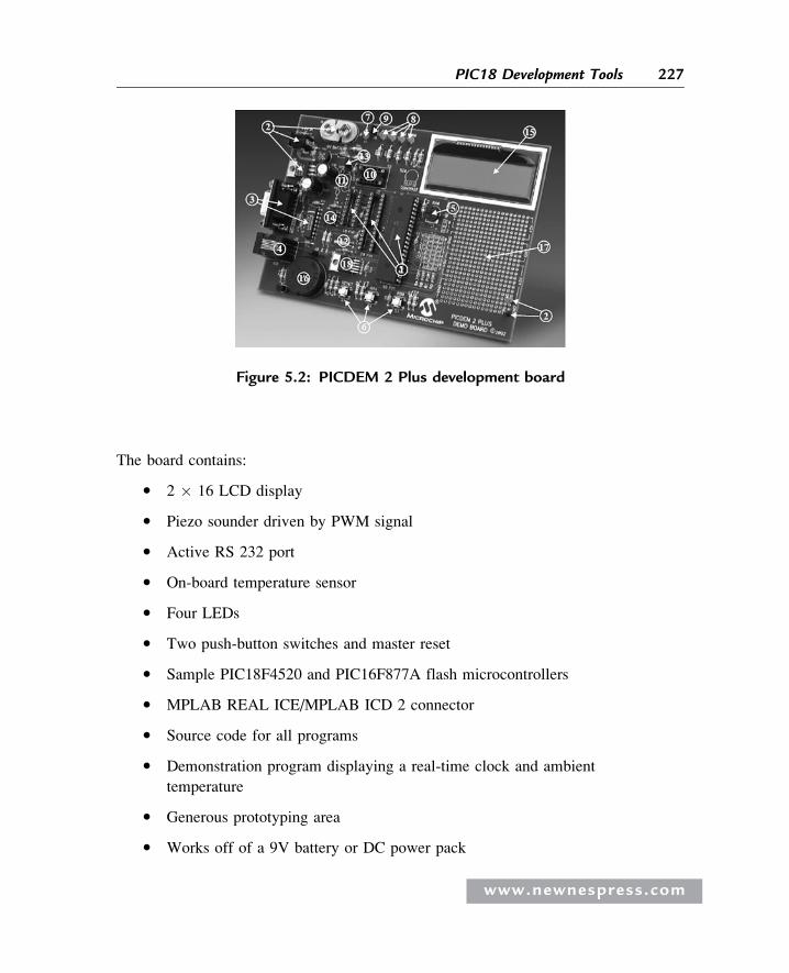
The board contains:
� 2 � 16 LCD display
� Piezo sounder driven by PWM signal
� Active RS 232 port
� On-board temperature sensor
� Four LEDs
� Two push-button switches and master reset
� Sample PIC18F4520 and PIC16F877A flash microcontrollers
� MPLAB REAL ICE/MPLAB ICD 2 connector
� Source code for all programs
� Demonstration program displaying a real-time clock and ambient
temperature
� Generous prototyping area
� Works off of a 9V battery or DC power pack
Figure 5.2: PICDEM 2 Plus development board
www.newnespress.com
227PIC18 Development Tools
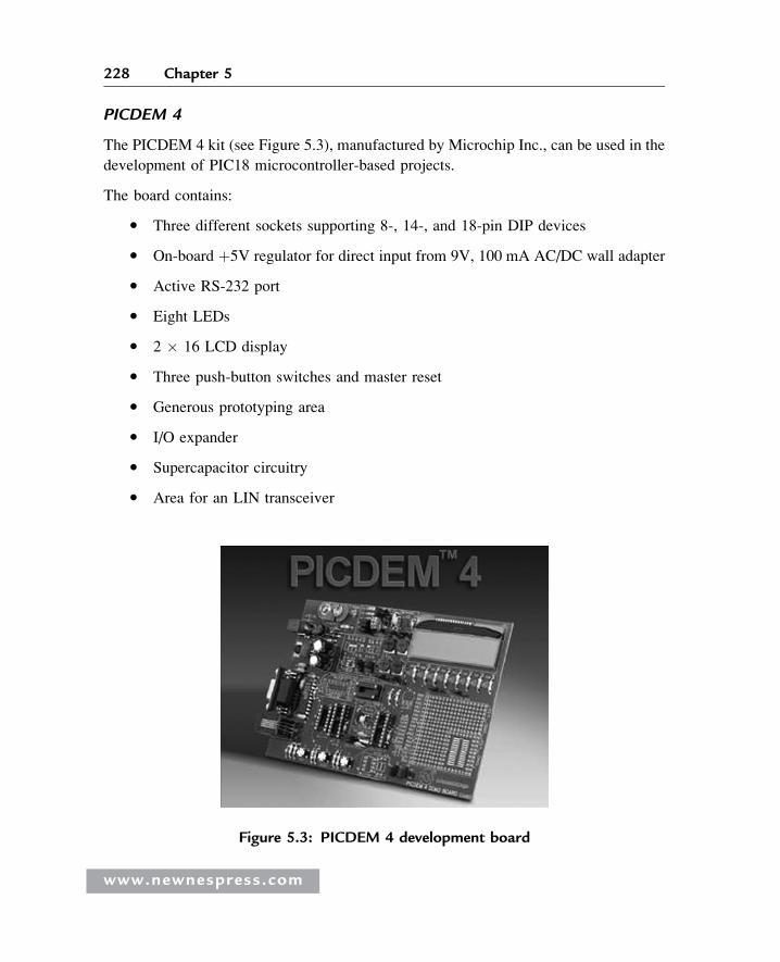
PICDEM 4
The PICDEM 4 kit (see Figure 5.3), manufactured by Microchip Inc., can be used in the
development of PIC18 microcontroller-based projects.
The board contains:
� Three different sockets supporting 8-, 14-, and 18-pin DIP devices
� On-board þ5V regulator for direct input from 9V, 100 mA AC/DC wall adapter
� Active RS-232 port
� Eight LEDs
� 2 � 16 LCD display
� Three push-button switches and master reset
� Generous prototyping area
� I/O expander
� Supercapacitor circuitry
� Area for an LIN transceiver
Figure 5.3: PICDEM 4 development board
www.newnespress.com
228 Chapter 5
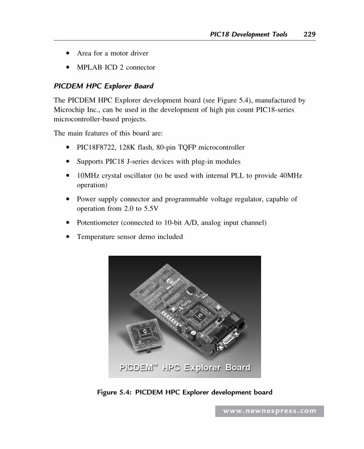
� Area for a motor driver
� MPLAB ICD 2 connector
PICDEM HPC Explorer Board
The PICDEM HPC Explorer development board (see Figure 5.4), manufactured by
Microchip Inc., can be used in the development of high pin count PIC18-series
microcontroller-based projects.
The main features of this board are:
� PIC18F8722, 128K flash, 80-pin TQFP microcontroller
� Supports PIC18 J-series devices with plug-in modules
� 10MHz crystal oscillator (to be used with internal PLL to provide 40MHz
operation)
� Power supply connector and programmable voltage regulator, capable of
operation from 2.0 to 5.5V
� Potentiometer (connected to 10-bit A/D, analog input channel)
� Temperature sensor demo included
Figure 5.4: PICDEM HPC Explorer development board
www.newnespress.com
229PIC18 Development Tools
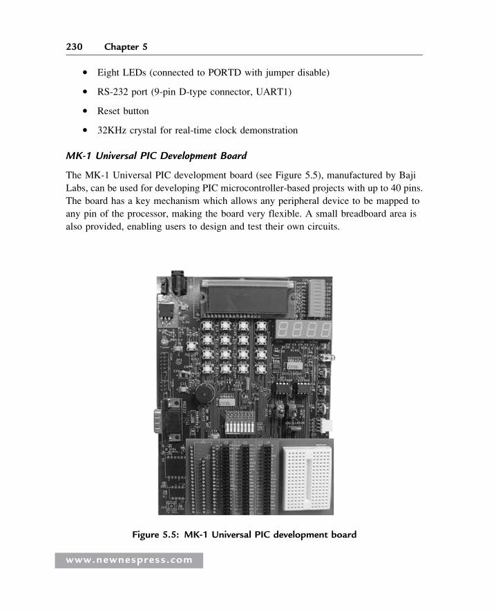
� Eight LEDs (connected to PORTD with jumper disable)
� RS-232 port (9-pin D-type connector, UART1)
� Reset button
� 32KHz crystal for real-time clock demonstration
MK-1 Universal PIC Development Board
The MK-1 Universal PIC development board (see Figure 5.5), manufactured by Baji
Labs, can be used for developing PIC microcontroller-based projects with up to 40 pins.
The board has a key mechanism which allows any peripheral device to be mapped to
any pin of the processor, making the board very flexible. A small breadboard area is
also provided, enabling users to design and test their own circuits.
Figure 5.5: MK-1 Universal PIC development board
www.newnespress.com
230 Chapter 5
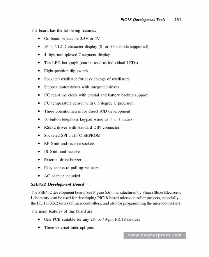
The board has the following features:
� On-board selectable 3.3V or 5V
� 16 � 2 LCD character display (8- or 4-bit mode supported)
� 4-digit multiplexed 7-segment display
� Ten LED bar graph (can be used as individual LEDs)
� Eight-position dip switch
� Socketed oscillator for easy change of oscillators
� Stepper motor driver with integrated driver
� I2C real-time clock with crystal and battery backup support
� I2C temperature sensor with 0.5 degree C precision
� Three potentiometers for direct A/D development
� 16-button telephone keypad wired as 4 � 4 matrix
� RS232 driver with standard DB9 connector
� Socketed SPI and I2C EEPROM
� RF Xmit and receive sockets
� IR Xmit and receive
� External drive buzzer
� Easy access to pull up resistors
� AC adapter included
SSE452 Development Board
The SSE452 development board (see Figure 5.6), manufactured by Shuan Shizu Electronic
Laboratory, can be used for developing PIC18-based microcontroller projects, especially
the PIC18FXX2 series of microcontrollers, and also for programming the microcontrollers.
The main features of this board are:
� One PCB suitable for any 28- or 40-pin PIC18 devices
� Three external interrupt pins
www.newnespress.com
231PIC18 Development Tools
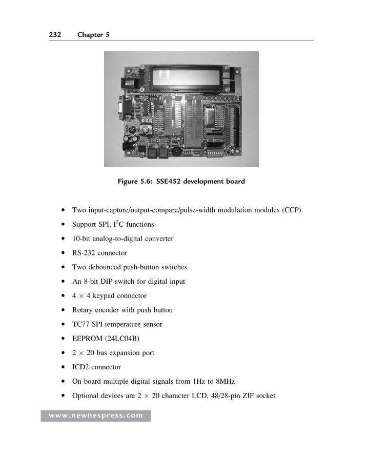
� Two input-capture/output-compare/pulse-width modulation modules (CCP)
� Support SPI, I2C functions
� 10-bit analog-to-digital converter
� RS-232 connector
� Two debounced push-button switches
� An 8-bit DIP-switch for digital input
� 4 � 4 keypad connector
� Rotary encoder with push button
� TC77 SPI temperature sensor
� EEPROM (24LC04B)
� 2 � 20 bus expansion port
� ICD2 connector
� On-board multiple digital signals from 1Hz to 8MHz
� Optional devices are 2 � 20 character LCD, 48/28-pin ZIF socket
Figure 5.6: SSE452 development board
www.newnespress.com
232 Chapter 5
SSE8720 Development Board
The SSE8720 development board (see Figure 5.7), manufactured by Shuan Shizu
Electronic Laboratory, can be used for the development of PIC18-based microcontroller
projects. A large amount of memory and I/O interface is provided, and the board can
also be used to program microcontrollers.
The main features of this board are:
� 20MHz oscillator with socket
� One DB9 connector provides EIA232 interface
� In-circuit debugger (ICD) connector
� Four debounced switches, and one reset switch
� 4 � 4 keypad connector
� One potentiometer for analog-to-digital conversion
� Eight red LEDs
� 8-bit DIP switch for digital inputs
� 2 � 20 character LCD module
� Twenty-four different digital signals, from 1Hz to 16MHz
Figure 5.7: SSE8720 development board
www.newnespress.com
233PIC18 Development Tools
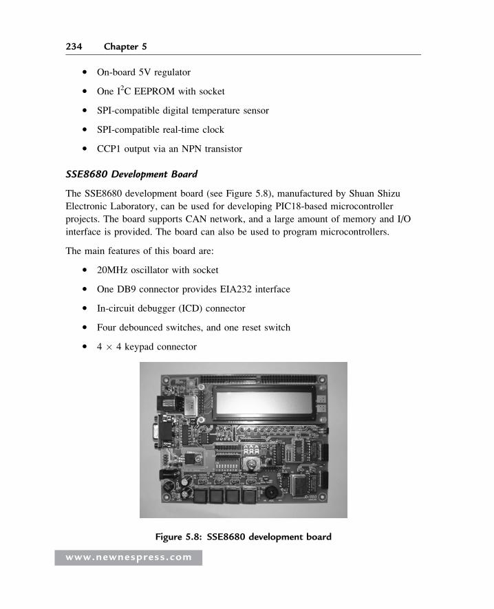
� On-board 5V regulator
� One I2C EEPROM with socket
� SPI-compatible digital temperature sensor
� SPI-compatible real-time clock
� CCP1 output via an NPN transistor
SSE8680 Development Board
The SSE8680 development board (see Figure 5.8), manufactured by Shuan Shizu
Electronic Laboratory, can be used for developing PIC18-based microcontroller
projects. The board supports CAN network, and a large amount of memory and I/O
interface is provided. The board can also be used to program microcontrollers.
The main features of this board are:
� 20MHz oscillator with socket
� One DB9 connector provides EIA232 interface
� In-circuit debugger (ICD) connector
� Four debounced switches, and one reset switch
� 4 � 4 keypad connector
Figure 5.8: SSE8680 development board
www.newnespress.com
234 Chapter 5
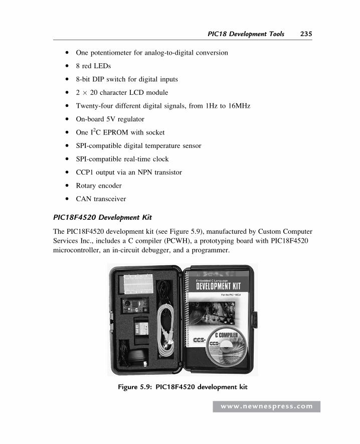
� One potentiometer for analog-to-digital conversion
� 8 red LEDs
� 8-bit DIP switch for digital inputs
� 2 � 20 character LCD module
� Twenty-four different digital signals, from 1Hz to 16MHz
� On-board 5V regulator
� One I2C EPROM with socket
� SPI-compatible digital temperature sensor
� SPI-compatible real-time clock
� CCP1 output via an NPN transistor
� Rotary encoder
� CAN transceiver
PIC18F4520 Development Kit
The PIC18F4520 development kit (see Figure 5.9), manufactured by Custom Computer
Services Inc., includes a C compiler (PCWH), a prototyping board with PIC18F4520
microcontroller, an in-circuit debugger, and a programmer.
Figure 5.9: PIC18F4520 development kit
www.newnespress.com
235PIC18 Development Tools
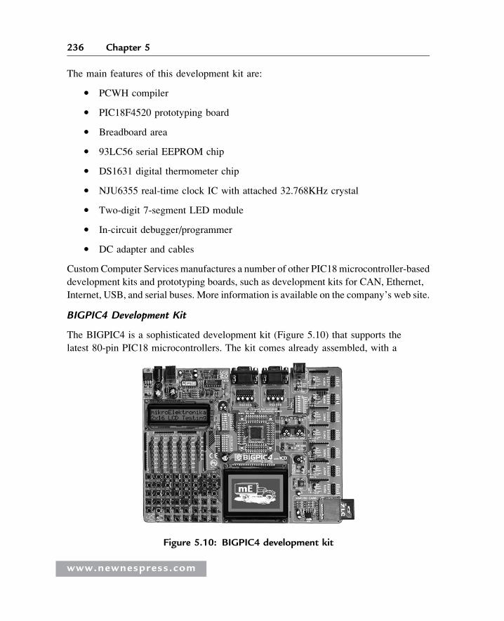
The main features of this development kit are:
� PCWH compiler
� PIC18F4520 prototyping board
� Breadboard area
� 93LC56 serial EEPROM chip
� DS1631 digital thermometer chip
� NJU6355 real-time clock IC with attached 32.768KHz crystal
� Two-digit 7-segment LED module
� In-circuit debugger/programmer
� DC adapter and cables
Custom Computer Services manufactures a number of other PIC18microcontroller-based
development kits and prototyping boards, such as development kits for CAN, Ethernet,
Internet, USB, and serial buses. More information is available on the company’s web site.
BIGPIC4 Development Kit
The BIGPIC4 is a sophisticated development kit (Figure 5.10) that supports the
latest 80-pin PIC18 microcontrollers. The kit comes already assembled, with a
Figure 5.10: BIGPIC4 development kit
www.newnespress.com
236 Chapter 5
PIC18F8520 microcontroller installed and working at 10MHz. It includes an
on-board USB port, an on-board programmer, and an in-circuit debugger. The
microcontroller on the board can be replaced easily.
The main features of this development kit are:
� Forty-six buttons
� Forty-six LEDs
� USB connector
� External or USB power supply
� Two potentiometers
� Graphics LCD
� 2 � 16 text LCD
� MMC/SD memory card slot
� Two serial RS232 ports
� In-circuit debugger
� Programmer
� PS2 connector
� Digital thermometer chip (DS1820)
� Analog inputs
� Reset button
The BIGPIC4 is used in some of the projects in this book.
FUTURLEC PIC18F458 Training Board
The FUTURLEC PIC18F458 training board is a very powerful development kit
(see Figure 5.11) based on the PIC18F458 microcontroller and developed by
Futurlec (www.futurlec.com). The kit comes already assembled and tested. One
of its biggest advantages is its low cost, at under $45.
www.newnespress.com
237PIC18 Development Tools
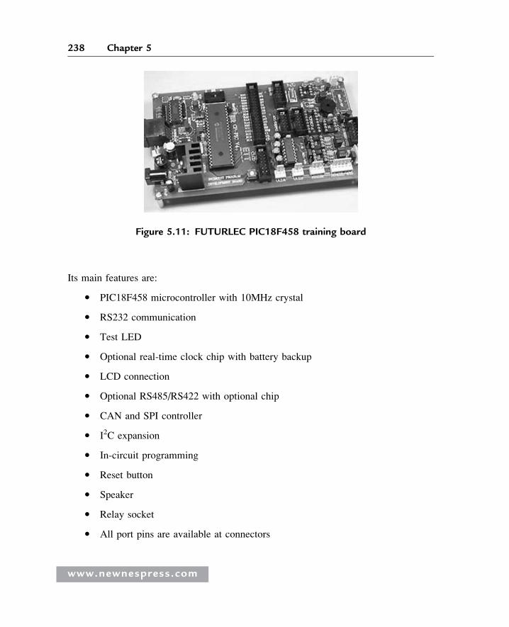
Its main features are:
� PIC18F458 microcontroller with 10MHz crystal
� RS232 communication
� Test LED
� Optional real-time clock chip with battery backup
� LCD connection
� Optional RS485/RS422 with optional chip
� CAN and SPI controller
� I2C expansion
� In-circuit programming
� Reset button
� Speaker
� Relay socket
� All port pins are available at connectors
Figure 5.11: FUTURLEC PIC18F458 training board
www.newnespress.com
238 Chapter 5
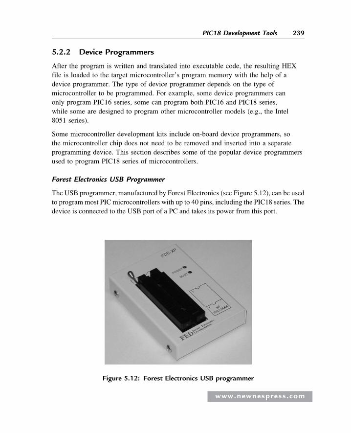
5.2.2 Device Programmers
After the program is written and translated into executable code, the resulting HEX
file is loaded to the target microcontroller’s program memory with the help of a
device programmer. The type of device programmer depends on the type of
microcontroller to be programmed. For example, some device programmers can
only program PIC16 series, some can program both PIC16 and PIC18 series,
while some are designed to program other microcontroller models (e.g., the Intel
8051 series).
Some microcontroller development kits include on-board device programmers, so
the microcontroller chip does not need to be removed and inserted into a separate
programming device. This section describes some of the popular device programmers
used to program PIC18 series of microcontrollers.
Forest Electronics USB Programmer
The USB programmer, manufactured by Forest Electronics (see Figure 5.12), can be used
to program most PIC microcontrollers with up to 40 pins, including the PIC18 series. The
device is connected to the USB port of a PC and takes its power from this port.
Figure 5.12: Forest Electronics USB programmer
www.newnespress.com
239PIC18 Development Tools
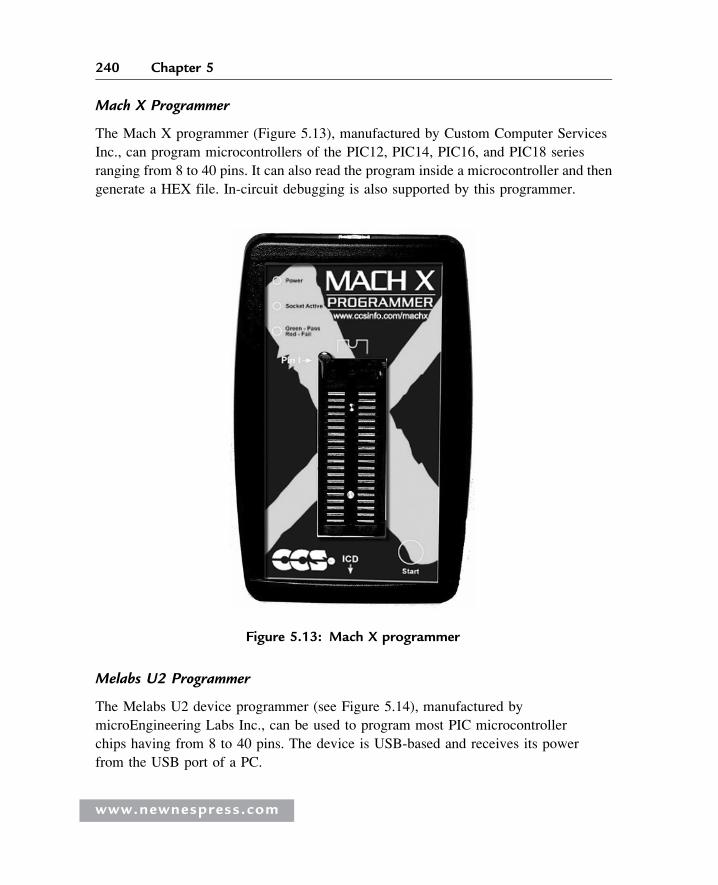
Mach X Programmer
The Mach X programmer (Figure 5.13), manufactured by Custom Computer Services
Inc., can program microcontrollers of the PIC12, PIC14, PIC16, and PIC18 series
ranging from 8 to 40 pins. It can also read the program inside a microcontroller and then
generate a HEX file. In-circuit debugging is also supported by this programmer.
Melabs U2 Programmer
The Melabs U2 device programmer (see Figure 5.14), manufactured by
microEngineering Labs Inc., can be used to program most PIC microcontroller
chips having from 8 to 40 pins. The device is USB-based and receives its power
from the USB port of a PC.
Figure 5.13: Mach X programmer
www.newnespress.com
240 Chapter 5
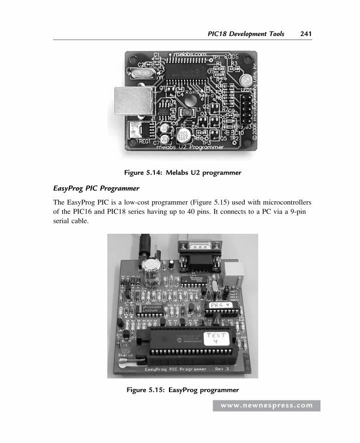
EasyProg PIC Programmer
The EasyProg PIC is a low-cost programmer (Figure 5.15) used with microcontrollers
of the PIC16 and PIC18 series having up to 40 pins. It connects to a PC via a 9-pin
serial cable.
Figure 5.14: Melabs U2 programmer
Figure 5.15: EasyProg programmer
www.newnespress.com
241PIC18 Development Tools
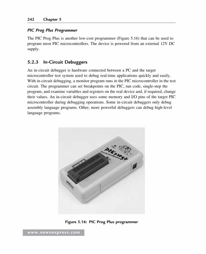
PIC Prog Plus Programmer
The PIC Prog Plus is another low-cost programmer (Figure 5.16) that can be used to
program most PIC microcontrollers. The device is powered from an external 12V DC
supply.
5.2.3 In-Circuit Debuggers
An in-circuit debugger is hardware connected between a PC and the target
microcontroller test system used to debug real-time applications quickly and easily.
With in-circuit debugging, a monitor program runs in the PIC microcontroller in the test
circuit. The programmer can set breakpoints on the PIC, run code, single-step the
program, and examine variables and registers on the real device and, if required, change
their values. An in-circuit debugger uses some memory and I/O pins of the target PIC
microcontroller during debugging operations. Some in-circuit debuggers only debug
assembly language programs. Other, more powerful debuggers can debug high-level
language programs.
Figure 5.16: PIC Prog Plus programmer
www.newnespress.com
242 Chapter 5
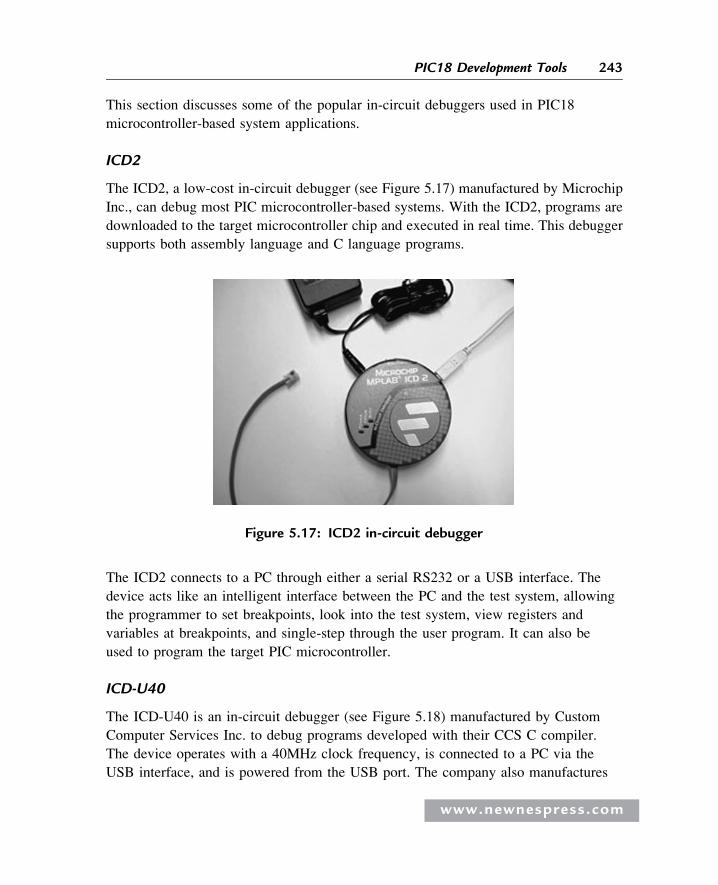
This section discusses some of the popular in-circuit debuggers used in PIC18
microcontroller-based system applications.
ICD2
The ICD2, a low-cost in-circuit debugger (see Figure 5.17) manufactured by Microchip
Inc., can debug most PIC microcontroller-based systems. With the ICD2, programs are
downloaded to the target microcontroller chip and executed in real time. This debugger
supports both assembly language and C language programs.
The ICD2 connects to a PC through either a serial RS232 or a USB interface. The
device acts like an intelligent interface between the PC and the test system, allowing
the programmer to set breakpoints, look into the test system, view registers and
variables at breakpoints, and single-step through the user program. It can also be
used to program the target PIC microcontroller.
ICD-U40
The ICD-U40 is an in-circuit debugger (see Figure 5.18) manufactured by Custom
Computer Services Inc. to debug programs developed with their CCS C compiler.
The device operates with a 40MHz clock frequency, is connected to a PC via the
USB interface, and is powered from the USB port. The company also manufactures
Figure 5.17: ICD2 in-circuit debugger
www.newnespress.com
243PIC18 Development Tools
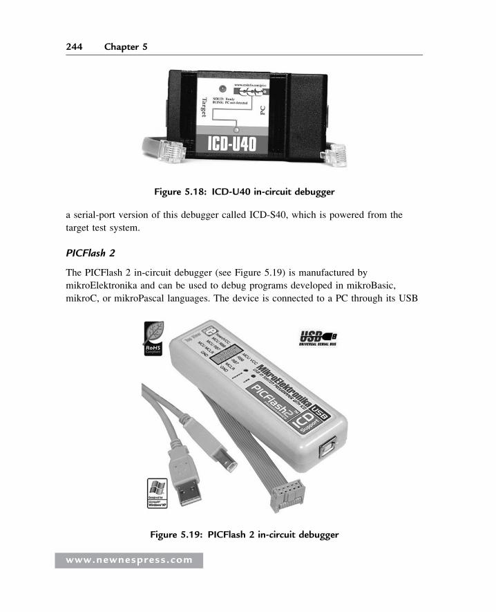
a serial-port version of this debugger called ICD-S40, which is powered from the
target test system.
PICFlash 2
The PICFlash 2 in-circuit debugger (see Figure 5.19) is manufactured by
mikroElektronika and can be used to debug programs developed in mikroBasic,
mikroC, or mikroPascal languages. The device is connected to a PC through its USB
Figure 5.18: ICD-U40 in-circuit debugger
Figure 5.19: PICFlash 2 in-circuit debugger
www.newnespress.com
244 Chapter 5
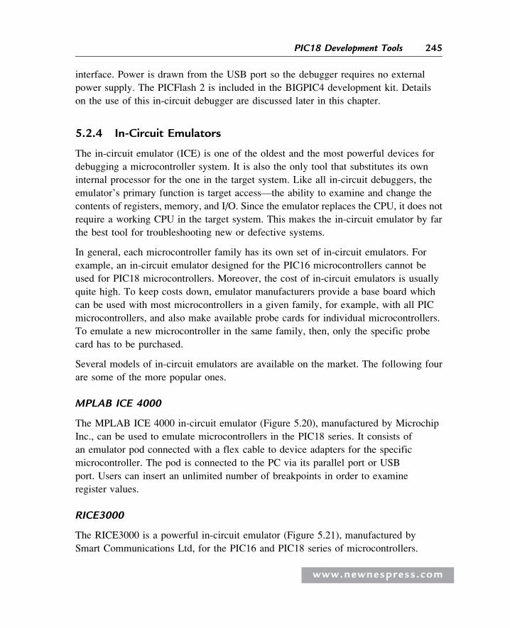
interface. Power is drawn from the USB port so the debugger requires no external
power supply. The PICFlash 2 is included in the BIGPIC4 development kit. Details
on the use of this in-circuit debugger are discussed later in this chapter.
5.2.4 In-Circuit Emulators
The in-circuit emulator (ICE) is one of the oldest and the most powerful devices for
debugging a microcontroller system. It is also the only tool that substitutes its own
internal processor for the one in the target system. Like all in-circuit debuggers, the
emulator’s primary function is target access—the ability to examine and change the
contents of registers, memory, and I/O. Since the emulator replaces the CPU, it does not
require a working CPU in the target system. This makes the in-circuit emulator by far
the best tool for troubleshooting new or defective systems.
In general, each microcontroller family has its own set of in-circuit emulators. For
example, an in-circuit emulator designed for the PIC16 microcontrollers cannot be
used for PIC18 microcontrollers. Moreover, the cost of in-circuit emulators is usually
quite high. To keep costs down, emulator manufacturers provide a base board which
can be used with most microcontrollers in a given family, for example, with all PIC
microcontrollers, and also make available probe cards for individual microcontrollers.
To emulate a new microcontroller in the same family, then, only the specific probe
card has to be purchased.
Several models of in-circuit emulators are available on the market. The following four
are some of the more popular ones.
MPLAB ICE 4000
The MPLAB ICE 4000 in-circuit emulator (Figure 5.20), manufactured by Microchip
Inc., can be used to emulate microcontrollers in the PIC18 series. It consists of
an emulator pod connected with a flex cable to device adapters for the specific
microcontroller. The pod is connected to the PC via its parallel port or USB
port. Users can insert an unlimited number of breakpoints in order to examine
register values.
RICE3000
The RICE3000 is a powerful in-circuit emulator (Figure 5.21), manufactured by
Smart Communications Ltd, for the PIC16 and PIC18 series of microcontrollers.
www.newnespress.com
245PIC18 Development Tools
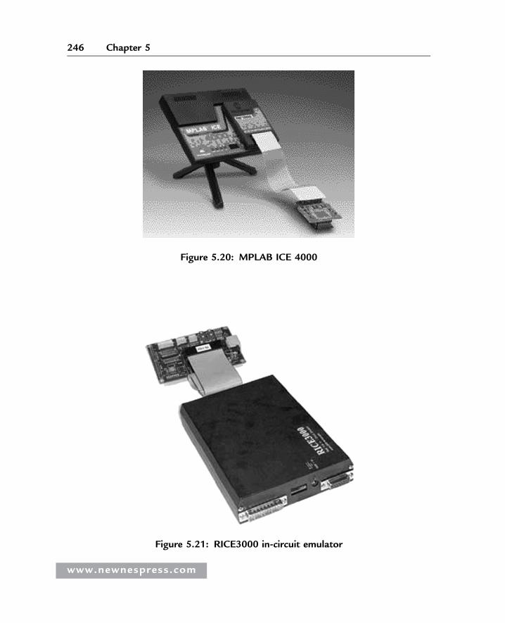
Figure 5.20: MPLAB ICE 4000
Figure 5.21: RICE3000 in-circuit emulator
www.newnespress.com
246 Chapter 5
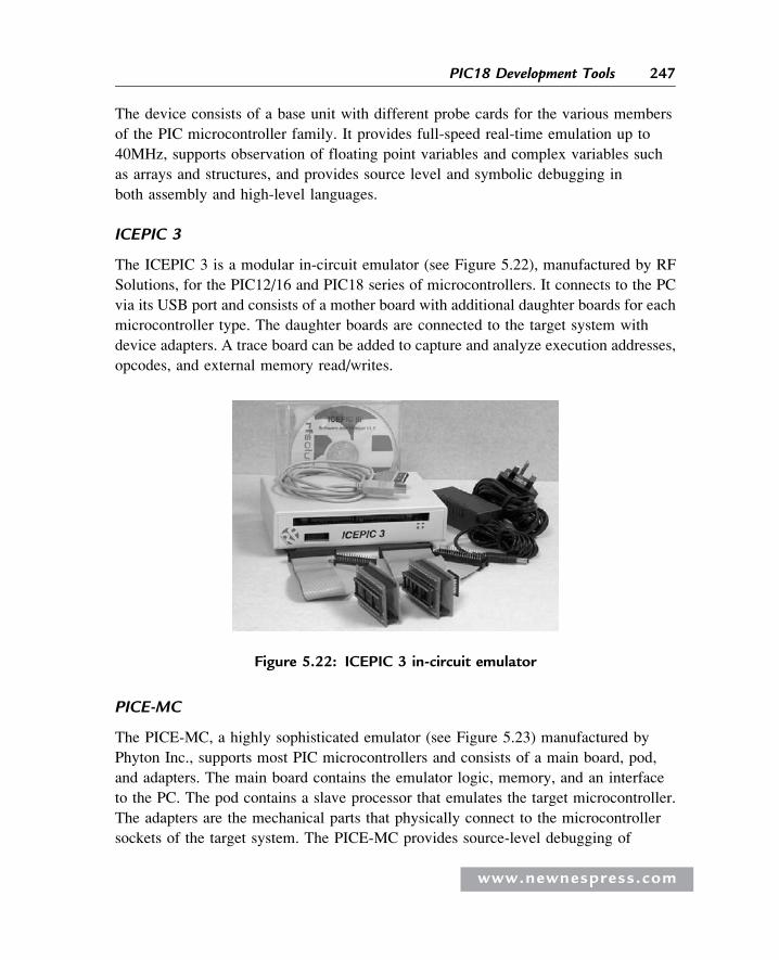
The device consists of a base unit with different probe cards for the various members
of the PIC microcontroller family. It provides full-speed real-time emulation up to
40MHz, supports observation of floating point variables and complex variables such
as arrays and structures, and provides source level and symbolic debugging in
both assembly and high-level languages.
ICEPIC 3
The ICEPIC 3 is a modular in-circuit emulator (see Figure 5.22), manufactured by RF
Solutions, for the PIC12/16 and PIC18 series of microcontrollers. It connects to the PC
via its USB port and consists of a mother board with additional daughter boards for each
microcontroller type. The daughter boards are connected to the target system with
device adapters. A trace board can be added to capture and analyze execution addresses,
opcodes, and external memory read/writes.
PICE-MC
The PICE-MC, a highly sophisticated emulator (see Figure 5.23) manufactured by
Phyton Inc., supports most PIC microcontrollers and consists of a main board, pod,
and adapters. The main board contains the emulator logic, memory, and an interface
to the PC. The pod contains a slave processor that emulates the target microcontroller.
The adapters are the mechanical parts that physically connect to the microcontroller
sockets of the target system. The PICE-MC provides source-level debugging of
Figure 5.22: ICEPIC 3 in-circuit emulator
www.newnespress.com
247PIC18 Development Tools
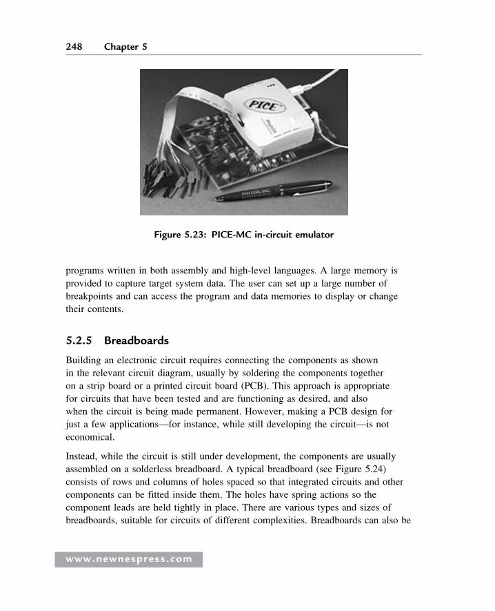
programs written in both assembly and high-level languages. A large memory is
provided to capture target system data. The user can set up a large number of
breakpoints and can access the program and data memories to display or change
their contents.
5.2.5 Breadboards
Building an electronic circuit requires connecting the components as shown
in the relevant circuit diagram, usually by soldering the components together
on a strip board or a printed circuit board (PCB). This approach is appropriate
for circuits that have been tested and are functioning as desired, and also
when the circuit is being made permanent. However, making a PCB design for
just a few applications—for instance, while still developing the circuit—is not
economical.
Instead, while the circuit is still under development, the components are usually
assembled on a solderless breadboard. A typical breadboard (see Figure 5.24)
consists of rows and columns of holes spaced so that integrated circuits and other
components can be fitted inside them. The holes have spring actions so the
component leads are held tightly in place. There are various types and sizes of
breadboards, suitable for circuits of different complexities. Breadboards can also be
Figure 5.23: PICE-MC in-circuit emulator
www.newnespress.com
248 Chapter 5
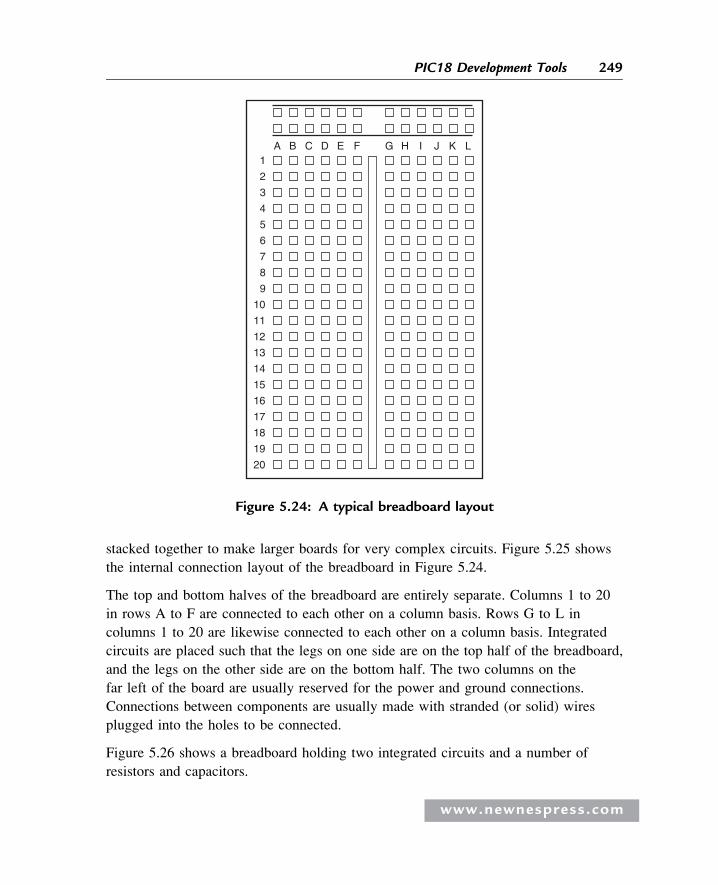
stacked together to make larger boards for very complex circuits. Figure 5.25 shows
the internal connection layout of the breadboard in Figure 5.24.
The top and bottom halves of the breadboard are entirely separate. Columns 1 to 20
in rows A to F are connected to each other on a column basis. Rows G to L in
columns 1 to 20 are likewise connected to each other on a column basis. Integrated
circuits are placed such that the legs on one side are on the top half of the breadboard,
and the legs on the other side are on the bottom half. The two columns on the
far left of the board are usually reserved for the power and ground connections.
Connections between components are usually made with stranded (or solid) wires
plugged into the holes to be connected.
Figure 5.26 shows a breadboard holding two integrated circuits and a number of
resistors and capacitors.
BA C D E F HG I J K L1
2
3
4
5
6
7
8
9
10
11
12
13
14
15
16
17
18
19
20
Figure 5.24: A typical breadboard layout
www.newnespress.com
249PIC18 Development Tools
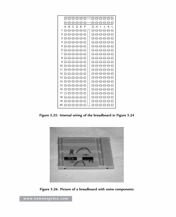
1
2
3
4
5
6
7
8
9
10
11
12
13
14
15
16
17
18
19
20
A B C D E F G H I J K L
Figure 5.25: Internal wiring of the breadboard in Figure 5.24
Figure 5.26: Picture of a breadboard with some components
www.newnespress.com

The nice thing about breadboard design is that the circuit can be modified
easily and quickly, and ideas can be tested without having to solder the
components. Once a circuit has been tested and is working satisfactorily,
the components are easily removed and the breadboard can be used for other
projects.
5.3 mikroC Integrated DevelopmentEnvironment (IDE)
In this book we are using the mikroC compiler developed by mikroElektronika.
Before using this compiler, we need to know how the mikroC integrated
development environment (IDE) is organized and how to write, compile, and
simulate a program in the mikroC language. In this section we will look at the
operation of the mikroC IDE in detail.
A free 2K program size limited version of the mikroC IDE, available on the
mikroElektronika web site (www.mikroe.com), is adequate for most small or medium-
sized applications. Alternatively, you can purchase a license and turn the limited
version into a fully working, unlimited IDE to use for projects of any size
and complexity.
After installing the mikroC IDE, a new icon should appear by default on your
desktop. Double-click this icon to start the IDE.
5.3.1 mikroC IDE Screen
After the mikroC icon is double-clicked to start the IDE, the screen shown in
Figure 5.27 is displayed by default.
The screen is divided into four areas: the top-left section, the bottom-left section, the
middle section, and the bottom section.
Top-Left Section
The top left, the Code Explorer section, displays every declared item in the source
code. In the example in Figure 5.28, main is listed under Functions and variables
Sum and i are listed under main.
www.newnespress.com
251PIC18 Development Tools
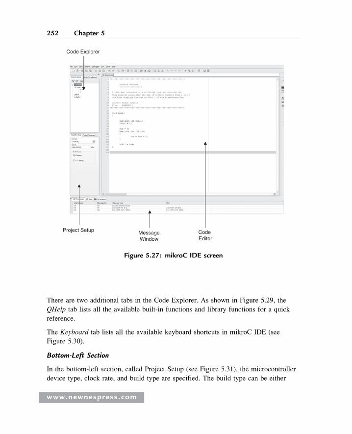
There are two additional tabs in the Code Explorer. As shown in Figure 5.29, the
QHelp tab lists all the available built-in functions and library functions for a quick
reference.
The Keyboard tab lists all the available keyboard shortcuts in mikroC IDE (see
Figure 5.30).
Bottom-Left Section
In the bottom-left section, called Project Setup (see Figure 5.31), the microcontroller
device type, clock rate, and build type are specified. The build type can be either
Code Explorer
Project Setup Message Window
Code Editor
Figure 5.27: mikroC IDE screen
www.newnespress.com
252 Chapter 5
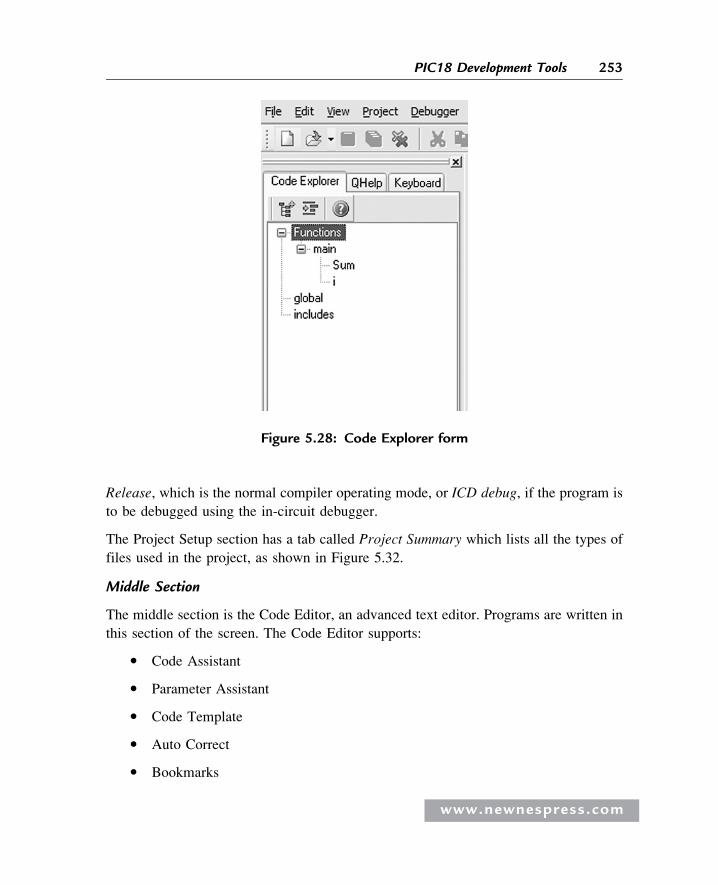
Release, which is the normal compiler operating mode, or ICD debug, if the program is
to be debugged using the in-circuit debugger.
The Project Setup section has a tab called Project Summary which lists all the types of
files used in the project, as shown in Figure 5.32.
Middle Section
The middle section is the Code Editor, an advanced text editor. Programs are written in
this section of the screen. The Code Editor supports:
� Code Assistant
� Parameter Assistant
� Code Template
� Auto Correct
� Bookmarks
Figure 5.28: Code Explorer form
www.newnespress.com
253PIC18 Development Tools
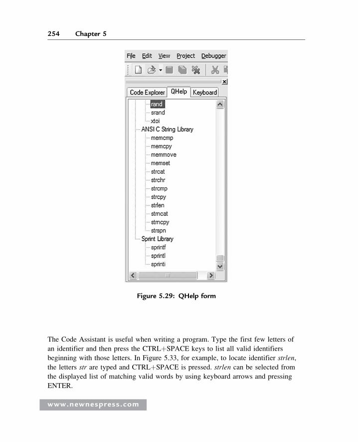
The Code Assistant is useful when writing a program. Type the first few letters of
an identifier and then press the CTRLþSPACE keys to list all valid identifiers
beginning with those letters. In Figure 5.33, for example, to locate identifier strlen,
the letters str are typed and CTRLþSPACE is pressed. strlen can be selected from
the displayed list of matching valid words by using keyboard arrows and pressing
ENTER.
Figure 5.29: QHelp form
www.newnespress.com
254 Chapter 5
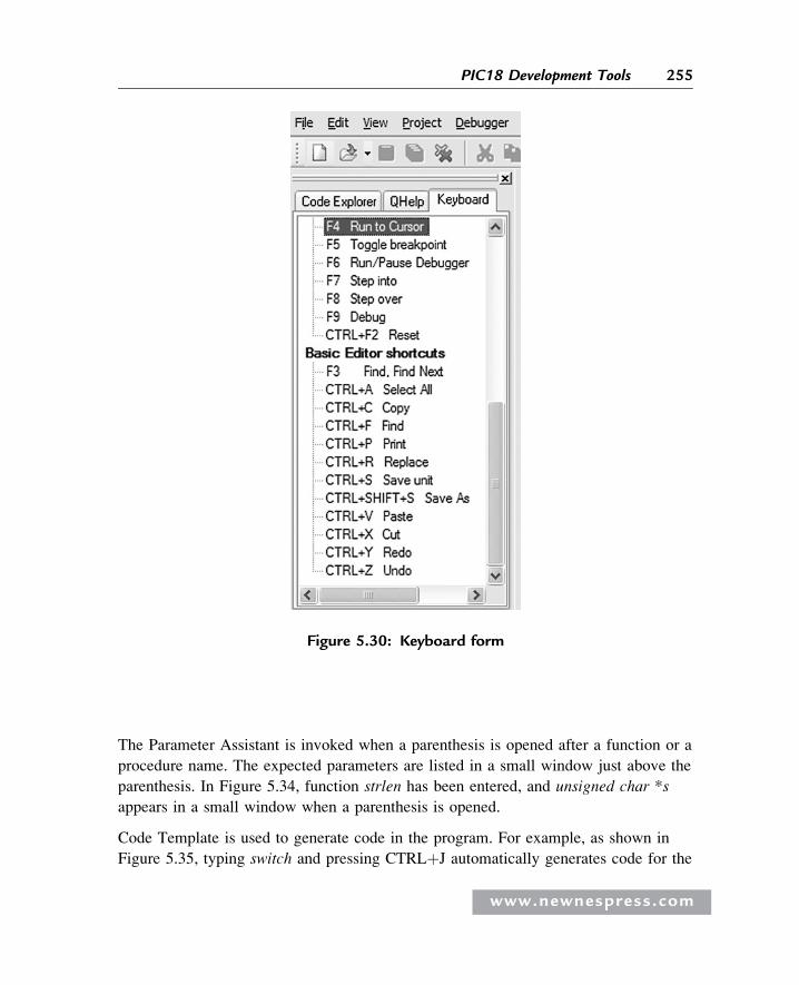
The Parameter Assistant is invoked when a parenthesis is opened after a function or a
procedure name. The expected parameters are listed in a small window just above the
parenthesis. In Figure 5.34, function strlen has been entered, and unsigned char *s
appears in a small window when a parenthesis is opened.
Code Template is used to generate code in the program. For example, as shown in
Figure 5.35, typing switch and pressing CTRLþJ automatically generates code for the
Figure 5.30: Keyboard form
www.newnespress.com
255PIC18 Development Tools
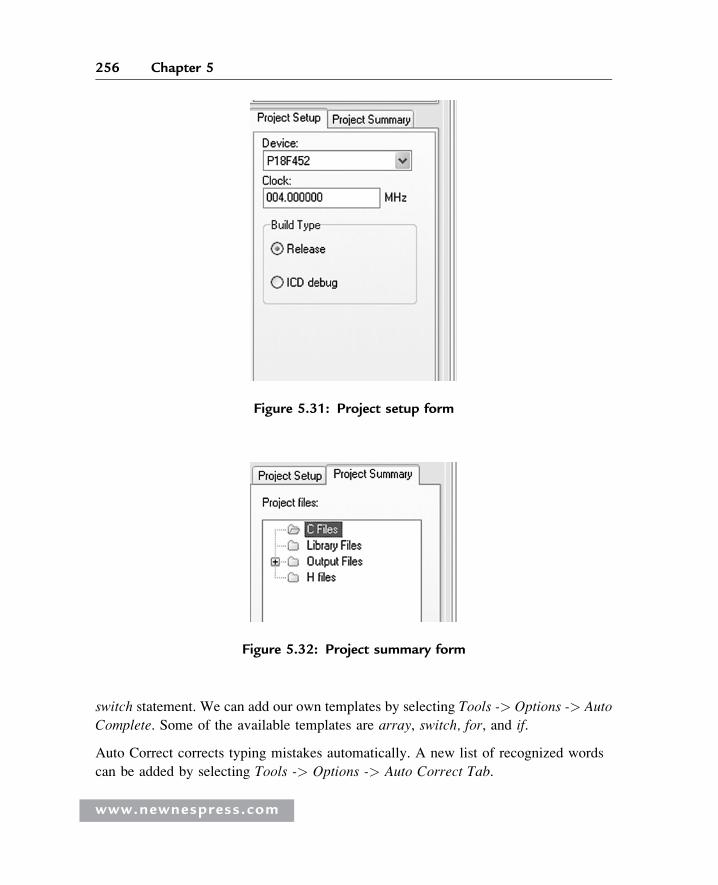
switch statement. We can add our own templates by selecting Tools -> Options -> Auto
Complete. Some of the available templates are array, switch, for, and if.
Auto Correct corrects typing mistakes automatically. A new list of recognized words
can be added by selecting Tools -> Options -> Auto Correct Tab.
Figure 5.31: Project setup form
Figure 5.32: Project summary form
www.newnespress.com
256 Chapter 5
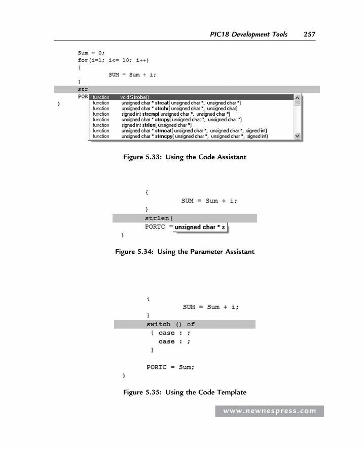
Figure 5.33: Using the Code Assistant
Figure 5.34: Using the Parameter Assistant
Figure 5.35: Using the Code Template
www.newnespress.com
257PIC18 Development Tools
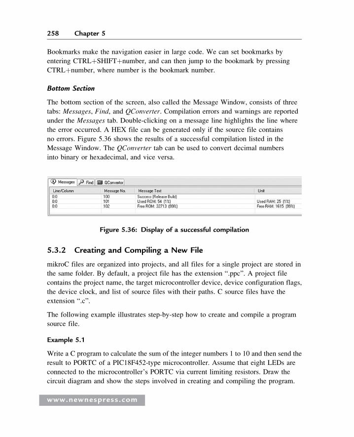
Bookmarks make the navigation easier in large code. We can set bookmarks by
entering CTRLþSHIFTþnumber, and can then jump to the bookmark by pressing
CTRLþnumber, where number is the bookmark number.
Bottom Section
The bottom section of the screen, also called the Message Window, consists of three
tabs: Messages, Find, and QConverter. Compilation errors and warnings are reported
under the Messages tab. Double-clicking on a message line highlights the line where
the error occurred. A HEX file can be generated only if the source file contains
no errors. Figure 5.36 shows the results of a successful compilation listed in the
Message Window. The QConverter tab can be used to convert decimal numbers
into binary or hexadecimal, and vice versa.
5.3.2 Creating and Compiling a New File
mikroC files are organized into projects, and all files for a single project are stored in
the same folder. By default, a project file has the extension “.ppc”. A project file
contains the project name, the target microcontroller device, device configuration flags,
the device clock, and list of source files with their paths. C source files have the
extension “.c”.
The following example illustrates step-by-step how to create and compile a program
source file.
Example 5.1
Write a C program to calculate the sum of the integer numbers 1 to 10 and then send the
result to PORTC of a PIC18F452-type microcontroller. Assume that eight LEDs are
connected to the microcontroller’s PORTC via current limiting resistors. Draw the
circuit diagram and show the steps involved in creating and compiling the program.
Figure 5.36: Display of a successful compilation
www.newnespress.com
258 Chapter 5
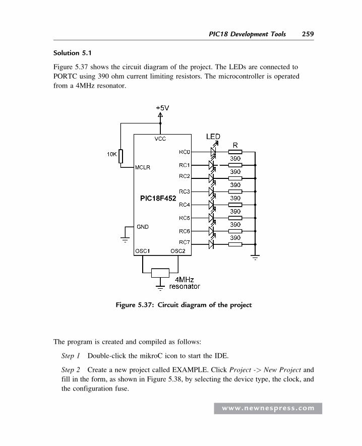
Solution 5.1
Figure 5.37 shows the circuit diagram of the project. The LEDs are connected to
PORTC using 390 ohm current limiting resistors. The microcontroller is operated
from a 4MHz resonator.
The program is created and compiled as follows:
Step 1 Double-click the mikroC icon to start the IDE.
Step 2 Create a new project called EXAMPLE. Click Project -> New Project and
fill in the form, as shown in Figure 5.38, by selecting the device type, the clock, and
the configuration fuse.
Figure 5.37: Circuit diagram of the project
www.newnespress.com
259PIC18 Development Tools
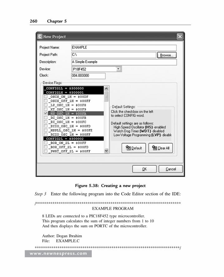
Step 3 Enter the following program into the Code Editor section of the IDE:
/**********************************************************************
EXAMPLE PROGRAM
8 LEDs are connected to a PIC18F452 type microcontroller.
This program calculates the sum of integer numbers from 1 to 10
And then displays the sum on PORTC of the microcontroller.
Author: Dogan Ibrahim
File: EXAMPLE.C
**********************************************************************/
Figure 5.38: Creating a new project
www.newnespress.com
260 Chapter 5
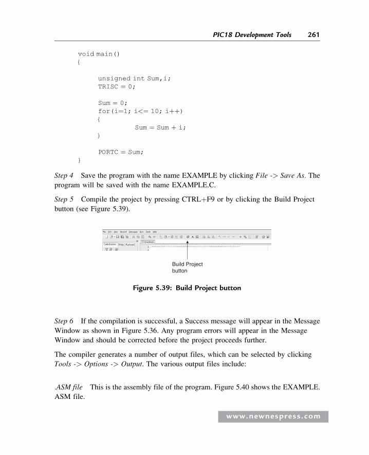
void main(){
unsigned int Sum,i;TRISC ¼ 0;
Sum ¼ 0;for(i¼1; i<¼ 10; iþþ){
Sum ¼ Sum þ i;}
PORTC ¼ Sum;}
Step 4 Save the program with the name EXAMPLE by clicking File -> Save As. The
program will be saved with the name EXAMPLE.C.
Step 5 Compile the project by pressing CTRLþF9 or by clicking the Build Project
button (see Figure 5.39).
Step 6 If the compilation is successful, a Success message will appear in the Message
Window as shown in Figure 5.36. Any program errors will appear in the Message
Window and should be corrected before the project proceeds further.
The compiler generates a number of output files, which can be selected by clicking
Tools -> Options -> Output. The various output files include:
.ASM file This is the assembly file of the program. Figure 5.40 shows the EXAMPLE.
ASM file.
Build Projectbutton
Figure 5.39: Build Project button
www.newnespress.com
261PIC18 Development Tools
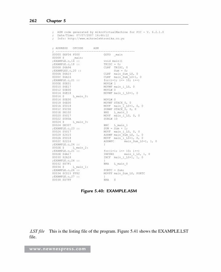
.LST file This is the listing file of the program. Figure 5.41 shows the EXAMPLE.LST
file.
; ASM code generated by mikroVirtualMachine for PIC - V. 6.2.1.0 ; Date/Time: 07/07/2007 16:46:12 ; Info: http://www.mikroelektronika.co.yu
; ADDRESS OPCODE ASM ; ---------------------------------------------- $0000 $EF04 F000 GOTO _main $0008 $ _main: ;EXAMPLE.c,14 :: void main() ;EXAMPLE.c,18 :: TRISC = 0; $0008 $6A94 CLRF TRISC, 0 ;EXAMPLES.c,20 :: Sum = 0; $000A $6A15 CLRF main_Sum_L0, 0 $000C $6A16 CLRF main_Sum_L0+1, 0 ;EXAMPLE.c,21 :: for(i=1; i<= 10; i++) $000E $0E01 MOVLW 1 $0010 $6E17 MOVWF main_i_L0, 0 $0012 $0E00 MOVLW 0 $0014 $6E18 MOVWF main_i_L0+1, 0 $0016 $ L_main_0: $0016 $0E00 MOVLW 0 $0018 $6E00 MOVWF STACK_0, 0 $001A $5018 MOVF main_i_L0+1, 0, 0 $001C $5C00 SUBWF STACK_0, 0, 0 $001E $E102 BNZ L_main_3 $0020 $5017 MOVF main_i_L0, 0, 0 $0022 $080A SUBLW 10 $0024 $ L_main_3: $0024 $E307 BNC L_main_1 ;EXAMPLE.c,23 :: SUM = Sum + i; $0026 $5017 MOVF main_i_L0, 0, 0 $0028 $2615 ADDWF main_Sum_L0, 1, 0 $002A $5018 MOVF main_i_L0+1, 0, 0 $002C $2216 ADDWFC main_Sum_L0+1, 1, 0 ;EXAMPLE.c,24 :: } $002E $ L_main_2: ;EXAMPLE.c,21 :: for(i=1; i<= 10; i++) $002E $4A17 INFSNZ main_i_L0, 1, 0 $0030 $2A18 INCF main_i_L0+1, 1, 0 ;EXAMPLE.c,24 :: } $0032 $D7F1 BRA L_main_0 $0034 $ L_main_1: ;EXAMPLE.c,26 :: PORTC = Sum; $0034 $C015 FF82 MOVFF main_Sum_L0, PORTC ;EXAMPLE.c,27 :: } $0038 $D7FF BRA $
Figure 5.40: EXAMPLE.ASM
www.newnespress.com
262 Chapter 5
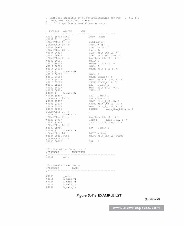
; ASM code generated by mikroVirtualMachine for PIC - V. 6.2.1.0 ; Date/Time: 07/07/2007 17:07:12 ; Info: http://www.mikroelektronika.co.yu
; ADDRESS OPCODE ASM ; ---------------------------------------------- $0000 $EF04 F000 GOTO _main $0008 $ _main: ;EXAMPLE.c,14 :: void main() ;EXAMPLE.c,18 :: TRISC = 0; $0008 $6A94 CLRF TRISC, 0 ;EXAMPLE.c,20 :: Sum = 0; $000A $6A15 CLRF main_Sum_L0, 0 $000C $6A16 CLRF main_Sum_L0+1, 0 ;EXAMPLE.c,21 :: for(i=1; i<= 10; i++) $000E $0E01 MOVLW 1 $0010 $6E17 MOVWF main_i_L0, 0 $0012 $0E00 MOVLW 0 $0014 $6E18 MOVWF main_i_L0+1, 0 $0016 $ L_main_0: $0016 $0E00 MOVLW 0 $0018 $6E00 MOVWF STACK_0, 0 $001A $5018 MOVF main_i_L0+1, 0, 0 $001C $5C00 SUBWF STACK_0, 0, 0 $001E $E102 BNZ L_main_3 $0020 $5017 MOVF main_i_L0, 0, 0 $0022 $080A SUBLW 10 $0024 $ L_main_3: $0024 $E307 BNC L_main_1 ;EXAMPLE.c,23 :: SUM = Sum + i; $0026 $5017 MOVF main_i_L0, 0, 0 $0028 $2615 ADDWF main_Sum_L0, 1, 0 $002A $5018 MOVF main_i_L0+1, 0, 0 $002C $2216 ADDWFC main_Sum_L0+1, 1, 0 ;EXAMPLE.c,24 :: } $002E $ L_main_2: ;EXAMPLE.c,21 :: for(i=1; i<= 10; i++) $002E $4A17 INFSNZ main_i_L0, 1, 0 $0030 $2A18 INCF main_i_L0+1, 1, 0 ;EXAMPLE.c,24 :: } $0032 $D7F1 BRA L_main_0 $0034 $ L_main_1: ;EXAMPLE.c,26 :: PORTC = Sum; $0034 $C015 FF82 MOVFF main_Sum_L0, PORTC ;EXAMPLE.c,27 :: } $0038 $D7FF BRA $
//** Procedures locations ** //ADDRESS PROCEDURE //---------------------------------------------- $0008 main
//** Labels locations ** //ADDRESS LABEL //----------------------------------------------
$0008 _main: $0016 L_main_0: $0024 L_main_3: $002E L_main_2: $0034 L_main_1:
Figure 5.41: EXAMPLE.LST(Continued)
www.newnespress.com
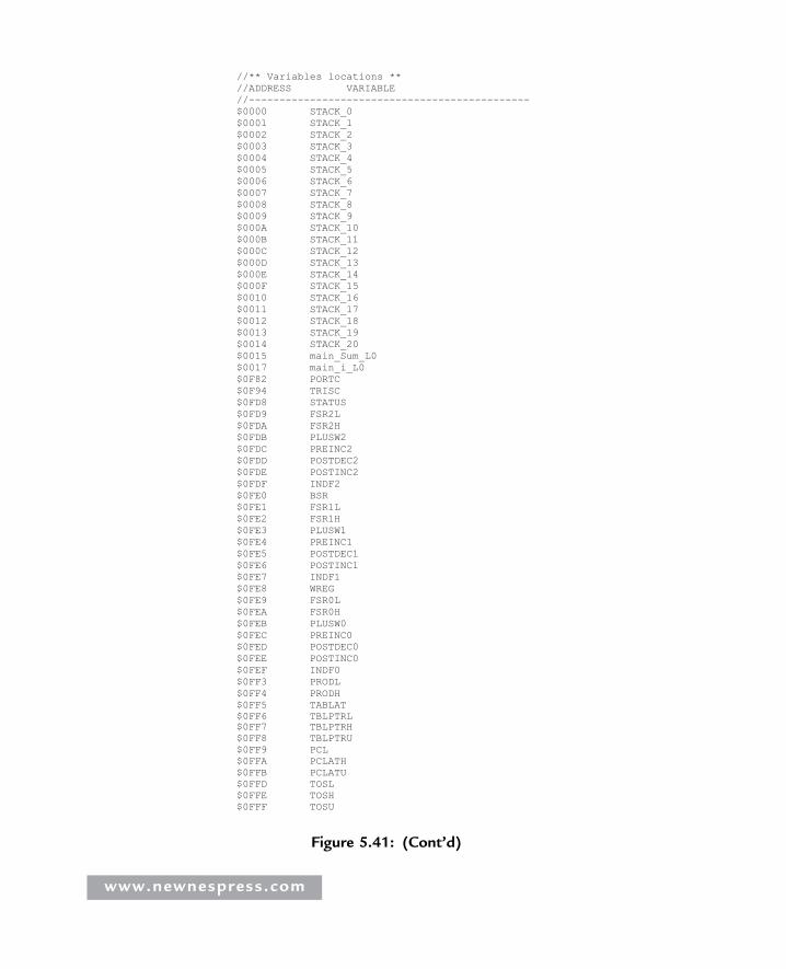
//** Variables locations ** //ADDRESS VARIABLE //---------------------------------------------- $0000 STACK_0 $0001 STACK_1 $0002 STACK_2 $0003 STACK_3 $0004 STACK_4 $0005 STACK_5 $0006 STACK_6 $0007 STACK_7 $0008 STACK_8 $0009 STACK_9 $000A STACK_10 $000B STACK_11 $000C STACK_12 $000D STACK_13 $000E STACK_14 $000F STACK_15 $0010 STACK_16 $0011 STACK_17 $0012 STACK_18 $0013 STACK_19 $0014 STACK_20 $0015 main_Sum_L0 $0017 main_i_L0 $0F82 PORTC $0F94 TRISC $0FD8 STATUS $0FD9 FSR2L $0FDA FSR2H $0FDB PLUSW2 $0FDC PREINC2 $0FDD POSTDEC2 $0FDE POSTINC2 $0FDF INDF2 $0FE0 BSR $0FE1 FSR1L $0FE2 FSR1H $0FE3 PLUSW1 $0FE4 PREINC1 $0FE5 POSTDEC1 $0FE6 POSTINC1 $0FE7 INDF1 $0FE8 WREG $0FE9 FSR0L $0FEA FSR0H $0FEB PLUSW0 $0FEC PREINC0 $0FED POSTDEC0 $0FEE POSTINC0 $0FEF INDF0 $0FF3 PRODL $0FF4 PRODH $0FF5 TABLAT $0FF6 TBLPTRL $0FF7 TBLPTRH $0FF8 TBLPTRU $0FF9 PCL $0FFA PCLATH $0FFB PCLATU $0FFD TOSL $0FFE TOSH $0FFF TOSU
Figure 5.41: (Cont’d)
www.newnespress.com
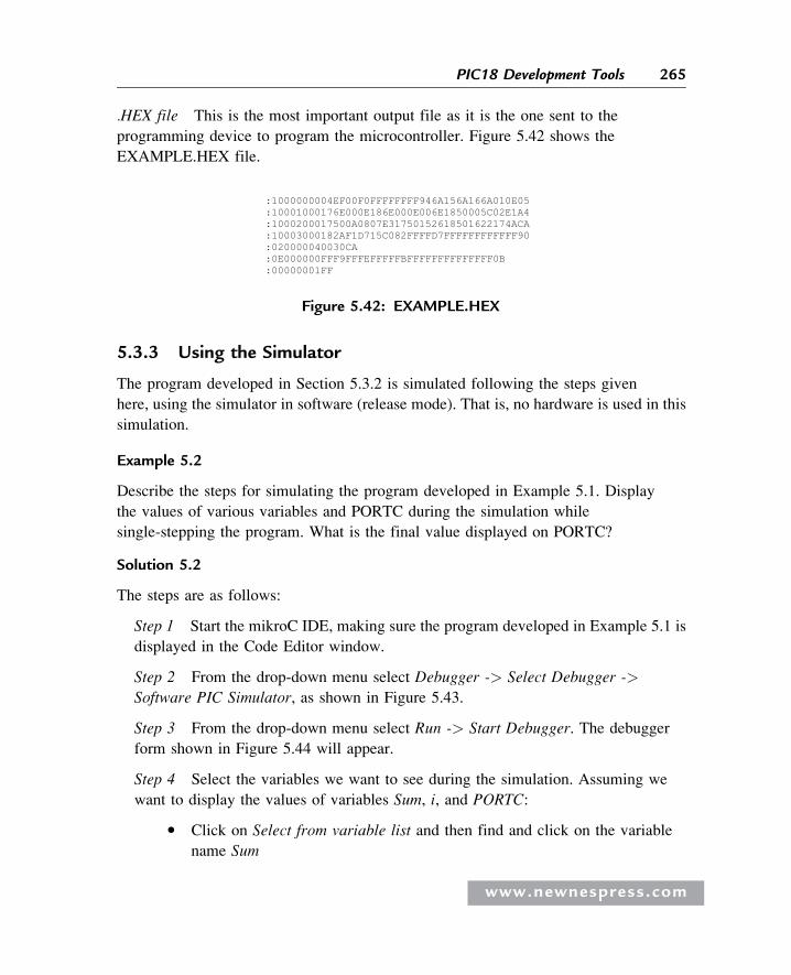
.HEX file This is the most important output file as it is the one sent to the
programming device to program the microcontroller. Figure 5.42 shows the
EXAMPLE.HEX file.
5.3.3 Using the Simulator
The program developed in Section 5.3.2 is simulated following the steps given
here, using the simulator in software (release mode). That is, no hardware is used in this
simulation.
Example 5.2
Describe the steps for simulating the program developed in Example 5.1. Display
the values of various variables and PORTC during the simulation while
single-stepping the program. What is the final value displayed on PORTC?
Solution 5.2
The steps are as follows:
Step 1 Start the mikroC IDE, making sure the program developed in Example 5.1 is
displayed in the Code Editor window.
Step 2 From the drop-down menu select Debugger -> Select Debugger ->
Software PIC Simulator, as shown in Figure 5.43.
Step 3 From the drop-down menu select Run -> Start Debugger. The debugger
form shown in Figure 5.44 will appear.
Step 4 Select the variables we want to see during the simulation. Assuming we
want to display the values of variables Sum, i, and PORTC:
� Click on Select from variable list and then find and click on the variable
name Sum
:1000000004EF00F0FFFFFFFF946A156A166A010E05 :10001000176E000E186E000E006E1850005C02E1A4 :1000200017500A0807E31750152618501622174ACA :10003000182AF1D715C082FFFFD7FFFFFFFFFFFF90 :020000040030CA :0E000000FFF9FFFEFFFFFBFFFFFFFFFFFFFF0B :00000001FF
Figure 5.42: EXAMPLE.HEX
www.newnespress.com
265PIC18 Development Tools
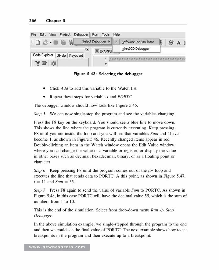
� Click Add to add this variable to the Watch list
� Repeat these steps for variable i and PORTC
The debugger window should now look like Figure 5.45.
Step 5 We can now single-step the program and see the variables changing.
Press the F8 key on the keyboard. You should see a blue line to move down.
This shows the line where the program is currently executing. Keep pressing
F8 until you are inside the loop and you will see that variables Sum and i have
become 1, as shown in Figure 5.46. Recently changed items appear in red.
Double-clicking an item in the Watch window opens the Edit Value window,
where you can change the value of a variable or register, or display the value
in other bases such as decimal, hexadecimal, binary, or as a floating point or
character.
Step 6 Keep pressing F8 until the program comes out of the for loop and
executes the line that sends data to PORTC. A this point, as shown in Figure 5.47,
i ¼ 11 and Sum ¼ 55.
Step 7 Press F8 again to send the value of variable Sum to PORTC. As shown in
Figure 5.48, in this case PORTC will have the decimal value 55, which is the sum of
numbers from 1 to 10.
This is the end of the simulation. Select from drop-down menu Run -> Stop
Debugger.
In the above simulation example, we single-stepped through the program to the end
and then we could see the final value of PORTC. The next example shows how to set
breakpoints in the program and then execute up to a breakpoint.
Figure 5.43: Selecting the debugger
www.newnespress.com
266 Chapter 5
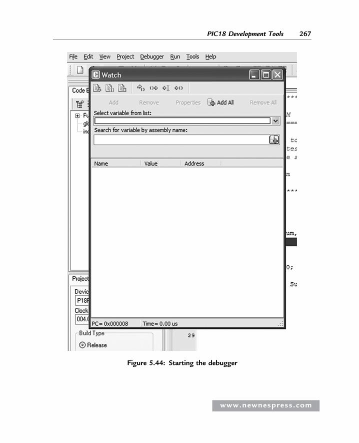
Figure 5.44: Starting the debugger
www.newnespress.com
267PIC18 Development Tools
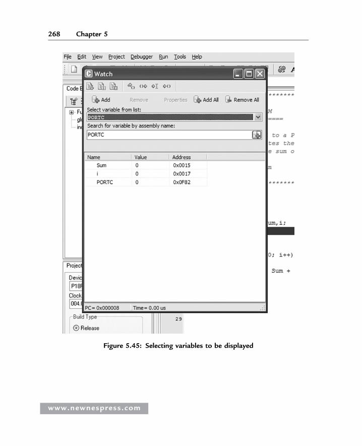
Figure 5.45: Selecting variables to be displayed
www.newnespress.com
268 Chapter 5
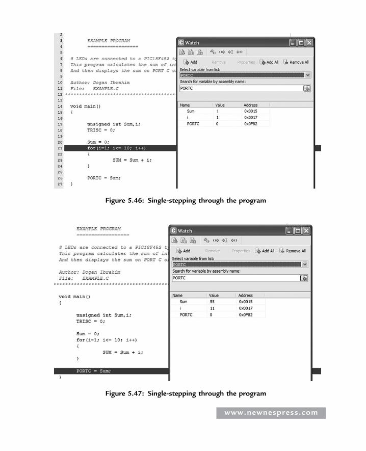
Figure 5.46: Single-stepping through the program
Figure 5.47: Single-stepping through the program
www.newnespress.com
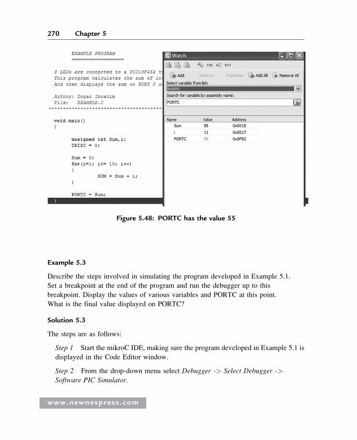
Example 5.3
Describe the steps involved in simulating the program developed in Example 5.1.
Set a breakpoint at the end of the program and run the debugger up to this
breakpoint. Display the values of various variables and PORTC at this point.
What is the final value displayed on PORTC?
Solution 5.3
The steps are as follows:
Step 1 Start the mikroC IDE, making sure the program developed in Example 5.1 is
displayed in the Code Editor window.
Step 2 From the drop-down menu select Debugger -> Select Debugger ->
Software PIC Simulator.
Figure 5.48: PORTC has the value 55
www.newnespress.com
270 Chapter 5
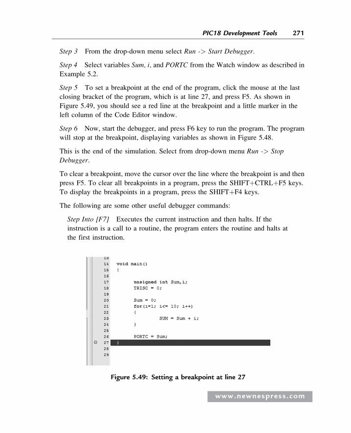
Step 3 From the drop-down menu select Run -> Start Debugger.
Step 4 Select variables Sum, i, and PORTC from the Watch window as described in
Example 5.2.
Step 5 To set a breakpoint at the end of the program, click the mouse at the last
closing bracket of the program, which is at line 27, and press F5. As shown in
Figure 5.49, you should see a red line at the breakpoint and a little marker in the
left column of the Code Editor window.
Step 6 Now, start the debugger, and press F6 key to run the program. The program
will stop at the breakpoint, displaying variables as shown in Figure 5.48.
This is the end of the simulation. Select from drop-down menu Run -> Stop
Debugger.
To clear a breakpoint, move the cursor over the line where the breakpoint is and then
press F5. To clear all breakpoints in a program, press the SHIFTþCTRLþF5 keys.
To display the breakpoints in a program, press the SHIFTþF4 keys.
The following are some other useful debugger commands:
Step Into [F7] Executes the current instruction and then halts. If the
instruction is a call to a routine, the program enters the routine and halts at
the first instruction.
Figure 5.49: Setting a breakpoint at line 27
www.newnespress.com
271PIC18 Development Tools
Step Over [F8] Executes the current instruction and then halts. If the
instruction is a call to a routine, it skips it and halts at the first instruction
following the call.
Step Out [CTRLþF8] Executes the current instruction and then halts. If the
instruction is within a routine, it executes the instruction and halts at the first
instruction following the call.
Run to Cursor [F4] Executes all instructions between the current instruction
and the cursor position.
Jump to Interrupt [F2] Jumps to the interrupt service routine address (address
0x08 for PIC18 microcontrollers) and executes the procedure located at that
address.
5.3.4 Using the mikroICD In-Circuit Debugger
This section discusses how to use the mikroICD in-circuit debugger (also called
the PICFlash 2 programmer) to debug the program developed in Example 5.1.
First of all, we have to build the hardware and then connect the in-circuit debugger
device. In this example, the hardware is built on a breadboard, and a PICFlash
2 mikroICD in-circuit debugger is used to debug the system. Note that pins RB6
and RB7 are used by the mikroICD and are not available for I/O while mikroICD
is active.
The Circuit Diagram
The project’s circuit diagram is shown in Figure 5.50. The mikroICD in-circuit
debugger is connected to the development circuit using the following pins of the
microcontroller:
� MCLR
� RB6
� RB7
� þ5V
� GND
www.newnespress.com
272 Chapter 5
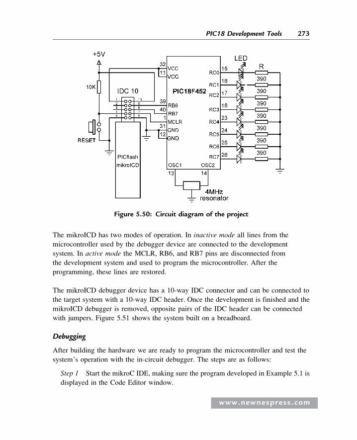
The mikroICD has two modes of operation. In inactive mode all lines from the
microcontroller used by the debugger device are connected to the development
system. In active mode the MCLR, RB6, and RB7 pins are disconnected from
the development system and used to program the microcontroller. After the
programming, these lines are restored.
The mikroICD debugger device has a 10-way IDC connector and can be connected to
the target system with a 10-way IDC header. Once the development is finished and the
mikroICD debugger is removed, opposite pairs of the IDC header can be connected
with jumpers. Figure 5.51 shows the system built on a breadboard.
Debugging
After building the hardware we are ready to program the microcontroller and test the
system’s operation with the in-circuit debugger. The steps are as follows:
Step 1 Start the mikroC IDE, making sure the program developed in Example 5.1 is
displayed in the Code Editor window.
Figure 5.50: Circuit diagram of the project
www.newnespress.com
273PIC18 Development Tools
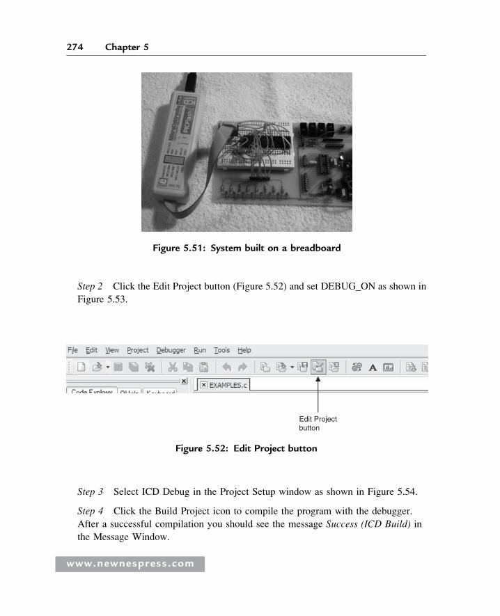
Step 2 Click the Edit Project button (Figure 5.52) and set DEBUG_ON as shown in
Figure 5.53.
Step 3 Select ICD Debug in the Project Setup window as shown in Figure 5.54.
Step 4 Click the Build Project icon to compile the program with the debugger.
After a successful compilation you should see the message Success (ICD Build) in
the Message Window.
Figure 5.51: System built on a breadboard
Edit Projectbutton
Figure 5.52: Edit Project button
www.newnespress.com
274 Chapter 5
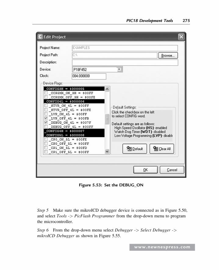
Step 5 Make sure the mikroICD debugger device is connected as in Figure 5.50,
and select Tools -> PicFlash Programmer from the drop-down menu to program
the microcontroller.
Step 6 From the drop-down menu select Debugger -> Select Debugger ->
mikroICD Debugger as shown in Figure 5.55.
Figure 5.53: Set the DEBUG_ON
www.newnespress.com
275PIC18 Development Tools
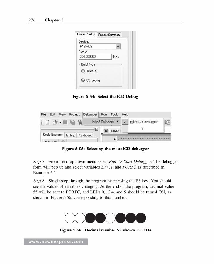
Step 7 From the drop-down menu select Run -> Start Debugger. The debugger
form will pop up and select variables Sum, i, and PORTC as described in
Example 5.2.
Step 8 Single-step through the program by pressing the F8 key. You should
see the values of variables changing. At the end of the program, decimal value
55 will be sent to PORTC, and LEDs 0,1,2,4, and 5 should be turned ON, as
shown in Figure 5.56, corresponding to this number.
Figure 5.54: Select the ICD Debug
Figure 5.55: Selecting the mikroICD debugger
Figure 5.56: Decimal number 55 shown in LEDs
www.newnespress.com
276 Chapter 5
Step 9 Stop the debugger.
In routines that contain delays, the Step Into [F7] and Step Over [F8]
commands can take a long time. Run to Cursor [F4] and breakpoints should
be used instead.
5.3.5 Using a Development Board
It is easy to develop microcontroller-based applications with the help of a development
board. This section explains how to use the development board BIGPIC4, described
earlier in this chapter. The program written in Example 5.1 is compiled and then loaded
to the microcontroller using the on-board mikroICD in-circuit emulator. Then the
program runs and displays the sum of the numbers 1 to 10 on the LEDs connected to
PORTC.
However, before using the development board we need to know how the BIGPIC4 is
organized and how to use the various devices on the board.
BIGPIC4 Development Board
Figure 5.57 shows the BIGPIC4 development board with the functions of various
devices identified with arrows. The board can be powered either from an external
power supply (8- to 16-C AC/DC) or from the USB port of a computer, using a
jumper. In this application, the board is powered from a USB port.
A 2-row by 16-column LCD can be connected in the board’s upper left corner. The
contrast of the LCD can be adjusted with a small potentiometer.
The forty-six LEDs on the board can be connected to the output ports of the
microcontroller, selected by switch S2. Figure 5.58 shows how to select the LEDs,
using PORTC as an example. 1K resistors are used in series with the LEDs to limit
the current. For example, to connect eight LEDs to PORTC we have to set the
switch arm marked PORTC of switch S2 to the ON position.
The forty-six push-button switches on the board can be used to program digital
inputs to the microcontroller. There is also a push-button switch that acts as the
RESET. Jumper J12 determines whether a button press will bring logical 0 or
logical 1 to the microcontroller. When the button is not pressed, the pin state is
determined by jumper J5.
www.newnespress.com
277PIC18 Development Tools
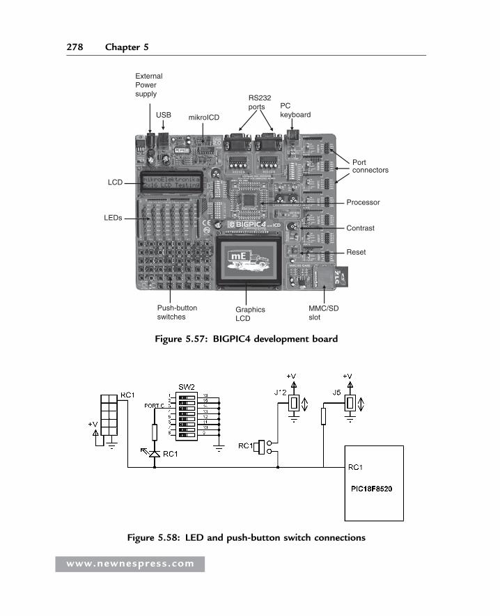
Figure 5.58: LED and push-button switch connections
ExternalPowersupply
USB
LEDs
Push-buttonswitches
GraphicsLCD
MMC/SDslot
RS232ports PC
keyboard mikroICD
Reset
Processor
Port connectors
LCD
Contrast
Figure 5.57: BIGPIC4 development board
www.newnespress.com
278 Chapter 5
At the bottom central position, a 128 � 64 pixel graphics LCD can be connected
to the board. The contrast of the LCD can be adjusted by a small potentiometer.
The MMC/SD card slot at the bottom right-hand corner of the board supports
cards up to 2GB storage capacity.
The RESET button is located just above the MMC/SD card slot.
Above the RESET button are two potentiometers for analog-to-digital converter
applications.
All of the microcontroller port pins are available at the connectors situated along
the right-hand side of the board. In the top middle portion of the board are two
RS232 ports and a connection to a PC keyboard.
The board supports both 64-pin and 80-pin microcontrollers. The board comes with
a PIC18F8520 microcontroller connected to the board, operating with a 10MHz crystal.
Further details about the operation of the board can be found in the BIGPIC4
user’s manual.
The steps in developing an application using the BIGPIC4 board are as follows:
Step 1 Double-click the mikroC icon to start the IDE.
Step 2 Create a new project called EXAMPLE2 (see Figure 5.59) and select the
microcontroller type as PIC18F8520, the clock as 10MHz, and device flags as:
� _OSC_HS_1H
� _WDT_OFF_2H
� _LVP_OFF_4L
� _DEBUG_ON_4L
www.newnespress.com
279PIC18 Development Tools
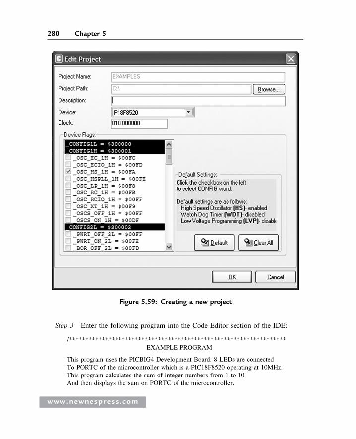
Step 3 Enter the following program into the Code Editor section of the IDE:
/******************************************************************
EXAMPLE PROGRAM
This program uses the PICBIG4 Development Board. 8 LEDs are connected
To PORTC of the microcontroller which is a PIC18F8520 operating at 10MHz.
This program calculates the sum of integer numbers from 1 to 10
And then displays the sum on PORTC of the microcontroller.
Figure 5.59: Creating a new project
www.newnespress.com
280 Chapter 5
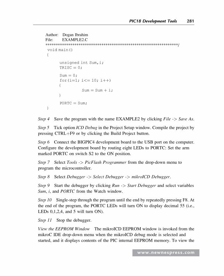
Author: Dogan Ibrahim
File: EXAMPLE2.C
****************************************************************/void main(){
unsigned int Sum,i;TRISC ¼ 0;
Sum ¼ 0;for(i¼1; i<¼ 10; iþþ){
Sum ¼ Sum þ i;}
PORTC ¼ Sum;}
Step 4 Save the program with the name EXAMPLE2 by clicking File -> Save As.
Step 5 Tick option ICD Debug in the Project Setup window. Compile the project by
pressing CTRLþF9 or by clicking the Build Project button.
Step 6 Connect the BIGPIC4 development board to the USB port on the computer.
Configure the development board by routing eight LEDs to PORTC: Set the arm
marked PORTC on switch S2 to the ON position.
Step 7 Select Tools -> PicFlash Programmer from the drop-down menu to
program the microcontroller.
Step 8 Select Debugger -> Select Debugger -> mikroICD Debugger.
Step 9 Start the debugger by clicking Run -> Start Debugger and select variables
Sum, i, and PORTC from the Watch window.
Step 10 Single-step through the program until the end by repeatedly pressing F8. At
the end of the program, the PORTC LEDs will turn ON to display decimal 55 (i.e.,
LEDs 0,1,2,4, and 5 will turn ON).
Step 11 Stop the debugger.
View the EEPROM Window The mikroICD EEPROM window is invoked from the
mikroC IDE drop-down menu when the mikroICD debug mode is selected and
started, and it displays contents of the PIC internal EEPROM memory. To view the
www.newnespress.com
281PIC18 Development Tools
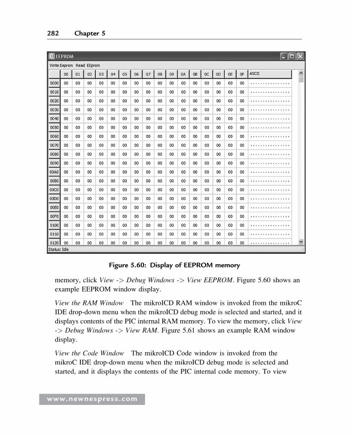
memory, click View -> Debug Windows -> View EEPROM. Figure 5.60 shows an
example EEPROM window display.
View the RAM Window The mikroICD RAM window is invoked from the mikroC
IDE drop-down menu when the mikroICD debug mode is selected and started, and it
displays contents of the PIC internal RAM memory. To view the memory, click View
-> Debug Windows -> View RAM. Figure 5.61 shows an example RAM window
display.
View the Code Window The mikroICD Code window is invoked from the
mikroC IDE drop-down menu when the mikroICD debug mode is selected and
started, and it displays the contents of the PIC internal code memory. To view
Figure 5.60: Display of EEPROM memory
www.newnespress.com
282 Chapter 5
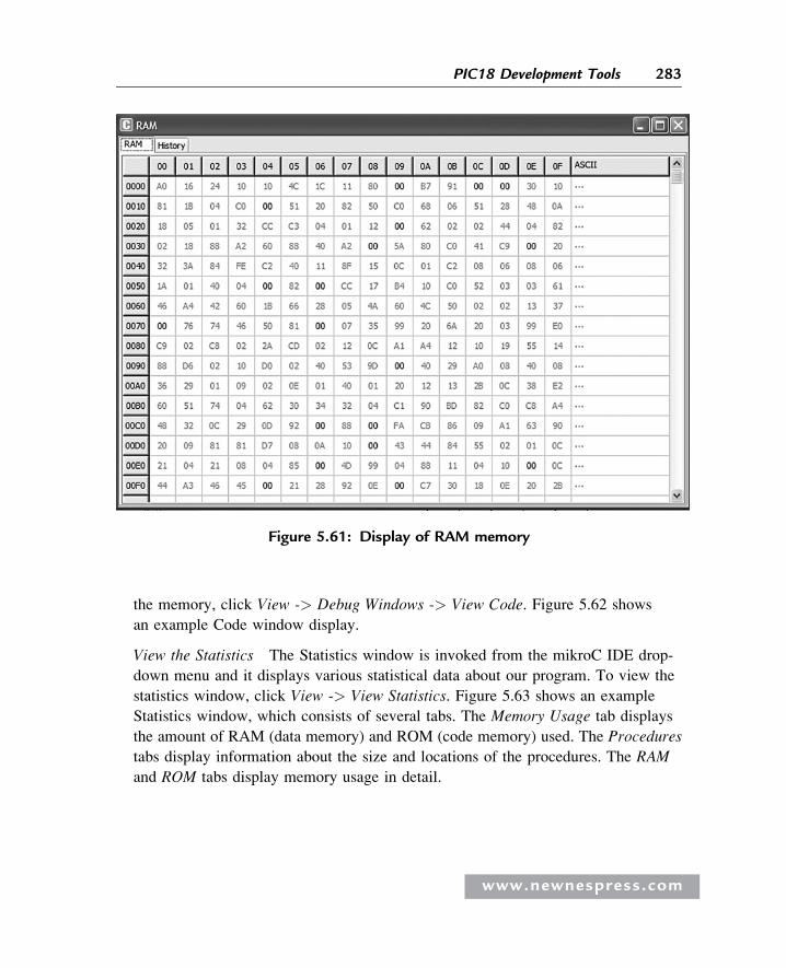
the memory, click View -> Debug Windows -> View Code. Figure 5.62 shows
an example Code window display.
View the Statistics The Statistics window is invoked from the mikroC IDE drop-
down menu and it displays various statistical data about our program. To view the
statistics window, click View -> View Statistics. Figure 5.63 shows an example
Statistics window, which consists of several tabs. The Memory Usage tab displays
the amount of RAM (data memory) and ROM (code memory) used. The Procedures
tabs display information about the size and locations of the procedures. The RAM
and ROM tabs display memory usage in detail.
Figure 5.61: Display of RAM memory
www.newnespress.com
283PIC18 Development Tools
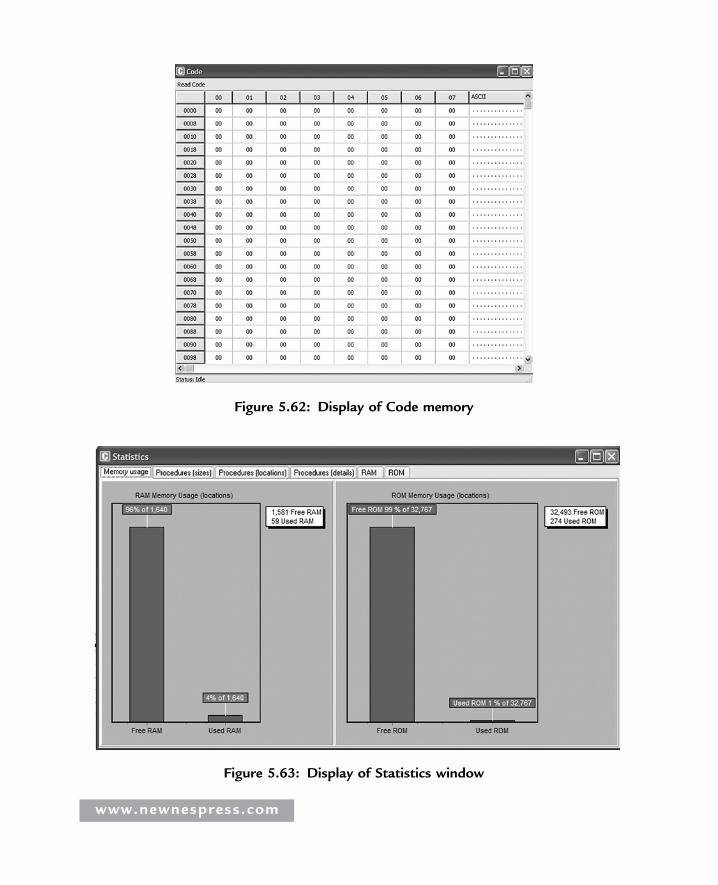
Figure 5.63: Display of Statistics window
Figure 5.62: Display of Code memory
www.newnespress.com
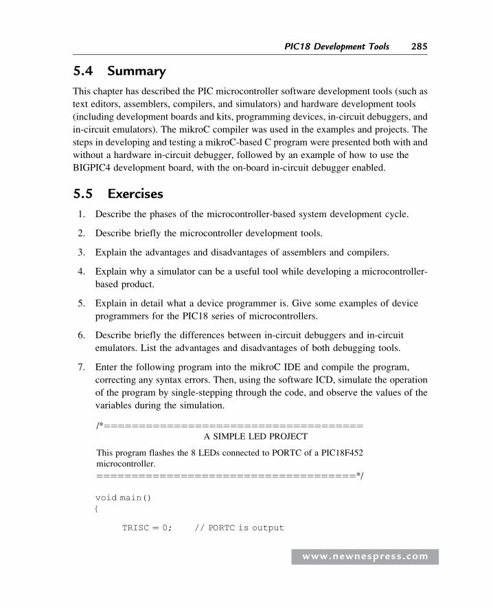
5.4 Summary
This chapter has described the PIC microcontroller software development tools (such as
text editors, assemblers, compilers, and simulators) and hardware development tools
(including development boards and kits, programming devices, in-circuit debuggers, and
in-circuit emulators). The mikroC compiler was used in the examples and projects. The
steps in developing and testing a mikroC-based C program were presented both with and
without a hardware in-circuit debugger, followed by an example of how to use the
BIGPIC4 development board, with the on-board in-circuit debugger enabled.
5.5 Exercises
1. Describe the phases of the microcontroller-based system development cycle.
2. Describe briefly the microcontroller development tools.
3. Explain the advantages and disadvantages of assemblers and compilers.
4. Explain why a simulator can be a useful tool while developing a microcontroller-
based product.
5. Explain in detail what a device programmer is. Give some examples of device
programmers for the PIC18 series of microcontrollers.
6. Describe briefly the differences between in-circuit debuggers and in-circuit
emulators. List the advantages and disadvantages of both debugging tools.
7. Enter the following program into the mikroC IDE and compile the program,
correcting any syntax errors. Then, using the software ICD, simulate the operation
of the program by single-stepping through the code, and observe the values of the
variables during the simulation.
/*¼¼¼¼¼¼¼¼¼¼¼¼¼¼¼¼¼¼¼¼¼¼¼¼¼¼¼¼¼¼¼¼¼¼¼¼¼A SIMPLE LED PROJECT
This program flashes the 8 LEDs connected to PORTC of a PIC18F452
microcontroller.
¼¼¼¼¼¼¼¼¼¼¼¼¼¼¼¼¼¼¼¼¼¼¼¼¼¼¼¼¼¼¼¼¼¼¼¼¼*/
void main(){
TRISC ¼ 0; // PORTC is output
www.newnespress.com
285PIC18 Development Tools

do{
PORTC ¼ 0xFF; // Turn ON LEDs on PORTCPORTC ¼ 0; // Turn OFF LEDs on PORTC} while(1); // Endless loop
}
8. Describe the steps in using the mikroICD in-circuit debugger.
9. The following C program contains some deliberately introduced errors. Compile
the program to find and correct the errors.
void main(){
unsigned char i,j,ki ¼ 10;j ¼ i þ 1;
for(i ¼ 0; i < 10; iþþ){
Sum ¼ Sum þ i;jþþ
}}
}
10. The following C program contains some deliberately introduced errors. Compile
the program to find and correct the errors.
int add(int a, int b){
result ¼ a þ b}
void main(){
int p,q;p ¼ 12;q ¼ 10;z ¼ add(p, q)zþþ;for(i ¼ 0; i < z; iþþ)pþþ
}}
www.newnespress.com
286 Chapter 5
CHAP T E R 6
Simple PIC18 Projects
In this chapter we will look at the design of simple PIC18 microcontroller-based
projects, with the idea of becoming familiar with basic interfacing techniques and
learning how to use the various microcontroller peripheral registers. We will look
at the design of projects using LEDs, push-button switches, keyboards, LED arrays,
sound devices, and so on, and we will develop programs in C language using the
mikroC compiler. The hardware is designed on a low-cost breadboard, but development
kits such as BIGPIC4 can be used for these projects. We will start with very simple
projects and proceed to more complex ones. It is recommended that the reader
moves through the projects in their given order. The following are provided for
each project:
� Description of the program
� Description of the hardware
� Circuit diagram
� Algorithm description (in PDL)
� Program listing
� Suggestions for further development
The program’s algorithm can be described in a variety of graphic and text-based
methods, some of the common ones being a flow diagram, a structure chart, and
program description language. In this book we are using program description
language (PDL).
www.newnespress.com
6.1 Program Description Language (PDL)
Program description language (PDL) is free-format English-like text which describes
the flow of control in a program. PDL is not a programming language but rather is
a tool which helps the programmer to think about the logic of the program before
the program has been developed. Commonly used PDL keywords are described
as follows.
6.1.1 START-END
Every PDL program description (or subprogram) should begin with a START
keyword and terminate with an END keyword. The keywords in a PDL code should
be highlighted in bold to make the code more clear. It is also a good practice to
indent program statements between PDL keywords in order to enhance the
readability of the code.
Example:START
. . . . . .
. . . . . .END
6.1.2 Sequencing
For normal sequencing in a program, write the statements as short English text as if you
are describing the program.
Example:Turn on the LED
Wait 1 second
Turn off the LED
6.1.3 IF-THEN-ELSE-ENDIF
Use IF, THEN, ELSE, and ENDIF keywords to describe the flow of control in a
program.
www.newnespress.com
288 Chapter 6
Example:IF switch ¼ 1 THEN
Turn on LED 1ELSE
Turn on LED 2Start the motor
ENDIF
6.1.4 DO-ENDDO
Use Do and ENDDO keywords to show iteration in the PDL code.
Example:To create an unconditional loop in a program we can write:
Turn on LEDDO 10 times
Set clock to 1Wait for 10msSet clock to 0
ENDDO
A variation of the DO-ENDDO construct is to use other keywords like DO-FOREVER,
DO-UNTIL, etc. as shown in the following examples.
Example:To create a conditional loop in a program we can write:
Turn off buzzerIF switch ¼ 1 THEN
DO UNTIL Port 1 ¼ 1Turn on LEDWait for 10msRead Port 1
ENDDOENDIF
www.newnespress.com
289Simple PIC18 Projects
The following construct can be used when an endless loop is required:
DO FOREVERRead data from Port 1Send data to PORT 2Wait for 1 second
ENDDO
6.1.5 REPEAT-UNTIL
REPEAT-UNTIL is another control construct used in PDL codes. In the following
example the program waits until a switch value is equal to 1.
Example:
REPEATTurn on buzzerRead switch value
UNTIL switch ¼ 1
Notice that the REPEAT-UNTIL loop is always executed at least once, and more than
once if the condition at the end of the loop is not met.
PROJECT 6.1—Chasing LEDs
Project Description
In this project eight LEDs are connected to PORTC of a PIC18F452-type microcontroller,
and the microcontroller is operated from a 4MHz resonator. When power is applied to
the microcontroller (or when the microcontroller is reset), the LEDs turn ON alternately
in an anticlockwise manner where only one LED is ON at any time. There is a one-second
delay between outputs so the LEDs can be seen turning ON and OFF.
An LED can be connected to a microcontroller output port in two different modes:
current sinking and current sourcing.
Current Sinking Mode
As shown in Figure 6.1, in current sinking mode the anode leg of the LED is connected
to the þ5V supply, and the cathode leg is connected to the microcontroller output port
through a current limiting resistor.
www.newnespress.com
290 Chapter 6
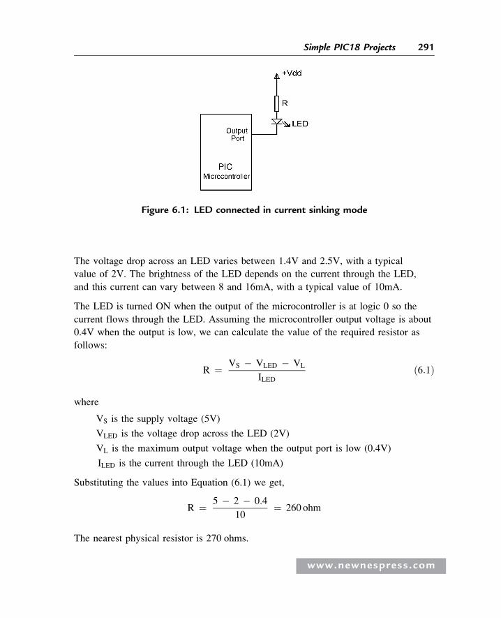
The voltage drop across an LED varies between 1.4V and 2.5V, with a typical
value of 2V. The brightness of the LED depends on the current through the LED,
and this current can vary between 8 and 16mA, with a typical value of 10mA.
The LED is turned ON when the output of the microcontroller is at logic 0 so the
current flows through the LED. Assuming the microcontroller output voltage is about
0.4V when the output is low, we can calculate the value of the required resistor as
follows:
R ¼ VS � VLED � VL
ILEDð6:1Þ
where
VS is the supply voltage (5V)
VLED is the voltage drop across the LED (2V)
VL is the maximum output voltage when the output port is low (0.4V)
ILED is the current through the LED (10mA)
Substituting the values into Equation (6.1) we get,
R ¼ 5 � 2 � 0:4
10¼ 260 ohm
The nearest physical resistor is 270 ohms.
Figure 6.1: LED connected in current sinking mode
www.newnespress.com
291Simple PIC18 Projects
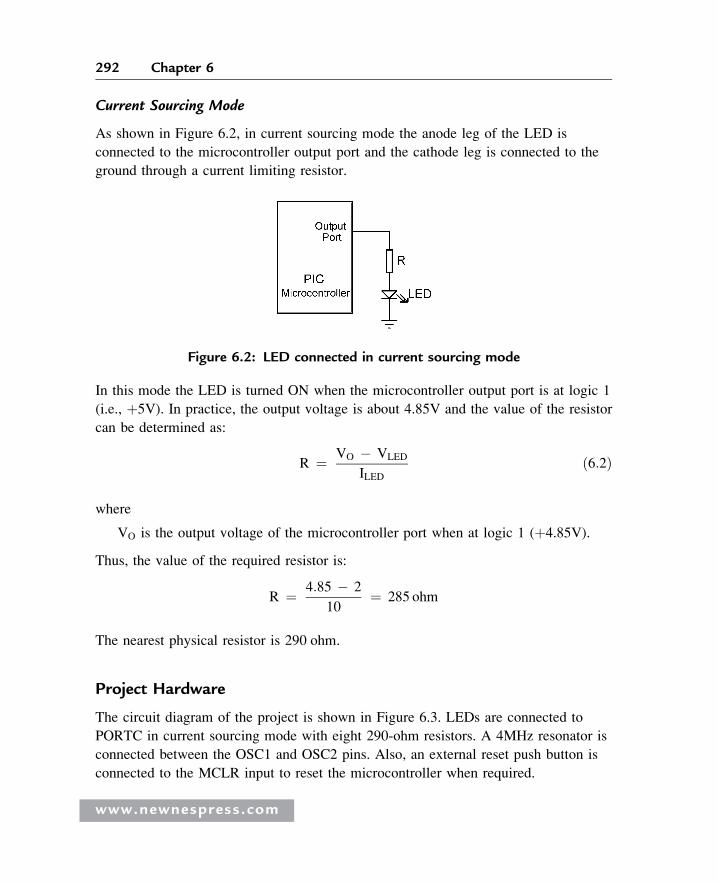
Current Sourcing Mode
As shown in Figure 6.2, in current sourcing mode the anode leg of the LED is
connected to the microcontroller output port and the cathode leg is connected to the
ground through a current limiting resistor.
In this mode the LED is turned ON when the microcontroller output port is at logic 1
(i.e., þ5V). In practice, the output voltage is about 4.85V and the value of the resistor
can be determined as:
R ¼ VO � VLED
ILEDð6:2Þ
where
VO is the output voltage of the microcontroller port when at logic 1 (þ4.85V).
Thus, the value of the required resistor is:
R ¼ 4:85 � 2
10¼ 285 ohm
The nearest physical resistor is 290 ohm.
Project Hardware
The circuit diagram of the project is shown in Figure 6.3. LEDs are connected to
PORTC in current sourcing mode with eight 290-ohm resistors. A 4MHz resonator is
connected between the OSC1 and OSC2 pins. Also, an external reset push button is
connected to the MCLR input to reset the microcontroller when required.
Figure 6.2: LED connected in current sourcing mode
www.newnespress.com
292 Chapter 6
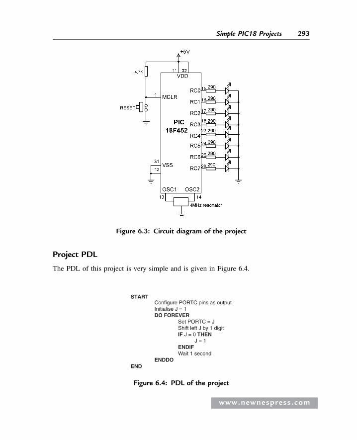
Project PDL
The PDL of this project is very simple and is given in Figure 6.4.
Figure 6.3: Circuit diagram of the project
START
Initialise J = 1DO FOREVER
Set PORTC = JShift left J by 1 digitIF J = 0 THEN
J = 1ENDIFWait 1 second
ENDDOEND
Configure PORTC pins as output
Figure 6.4: PDL of the project
www.newnespress.com
293Simple PIC18 Projects
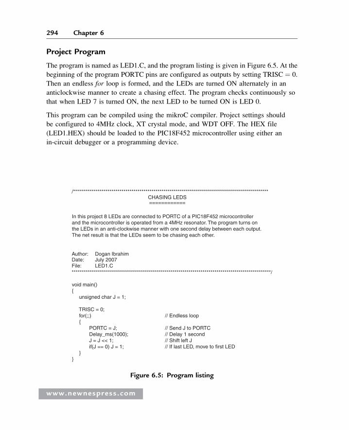
Project Program
The program is named as LED1.C, and the program listing is given in Figure 6.5. At the
beginning of the program PORTC pins are configured as outputs by setting TRISC ¼ 0.
Then an endless for loop is formed, and the LEDs are turned ON alternately in an
anticlockwise manner to create a chasing effect. The program checks continuously so
that when LED 7 is turned ON, the next LED to be turned ON is LED 0.
This program can be compiled using the mikroC compiler. Project settings should
be configured to 4MHz clock, XT crystal mode, and WDT OFF. The HEX file
(LED1.HEX) should be loaded to the PIC18F452 microcontroller using either an
in-circuit debugger or a programming device.
CHASING LEDS
Author: Dogan IbrahimDate: July 2007File: LED1.C
/*************************************************************************************************
============
In this project 8 LEDs are connected to PORTC of a PIC18F452 microcontrollerand the microcontroller is operated from a 4MHz resonator. The program turns onthe LEDs in an anti-clockwise manner with one second delay between each output. The net result is that the LEDs seem to be chasing each other.
***************************************************************************************************/
void main(){ unsigned char J = 1; TRISC = 0; for(;;) // Endless loop { PORTC = J; // Send J to PORTC Delay_ms(1000); // Delay 1 second J = J << 1; // Shift left J if(J == 0) J = 1; // If last LED, move to first LED }}
Figure 6.5: Program listing
www.newnespress.com
294 Chapter 6
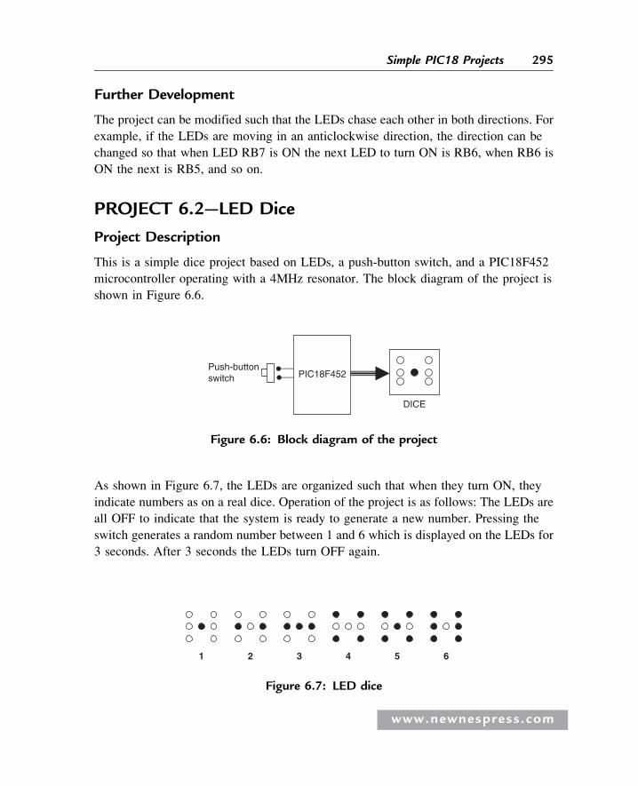
Further Development
The project can be modified such that the LEDs chase each other in both directions. For
example, if the LEDs are moving in an anticlockwise direction, the direction can be
changed so that when LED RB7 is ON the next LED to turn ON is RB6, when RB6 is
ON the next is RB5, and so on.
PROJECT 6.2—LED Dice
Project Description
This is a simple dice project based on LEDs, a push-button switch, and a PIC18F452
microcontroller operating with a 4MHz resonator. The block diagram of the project is
shown in Figure 6.6.
As shown in Figure 6.7, the LEDs are organized such that when they turn ON, they
indicate numbers as on a real dice. Operation of the project is as follows: The LEDs are
all OFF to indicate that the system is ready to generate a new number. Pressing the
switch generates a random number between 1 and 6 which is displayed on the LEDs for
3 seconds. After 3 seconds the LEDs turn OFF again.
PIC18F452Push-buttonswitch
DICE
Figure 6.6: Block diagram of the project
1 2 3 4 5 6
Figure 6.7: LED dice
www.newnespress.com
295Simple PIC18 Projects
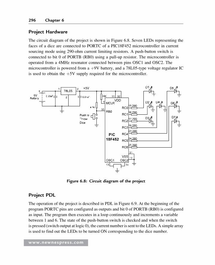
Project Hardware
The circuit diagram of the project is shown in Figure 6.8. Seven LEDs representing the
faces of a dice are connected to PORTC of a PIC18F452 microcontroller in current
sourcing mode using 290-ohm current limiting resistors. A push-button switch is
connected to bit 0 of PORTB (RB0) using a pull-up resistor. The microcontroller is
operated from a 4MHz resonator connected between pins OSC1 and OSC2. The
microcontroller is powered from a þ9V battery, and a 78L05-type voltage regulator IC
is used to obtain the þ5V supply required for the microcontroller.
Project PDL
The operation of the project is described in PDL in Figure 6.9. At the beginning of the
program PORTC pins are configured as outputs and bit 0 of PORTB (RB0) is configured
as input. The program then executes in a loop continuously and increments a variable
between 1 and 6. The state of the push-button switch is checked and when the switch
is pressed (switch output at logic 0), the current number is sent to the LEDs. A simple array
is used to find out the LEDs to be turned ON corresponding to the dice number.
Figure 6.8: Circuit diagram of the project
www.newnespress.com
296 Chapter 6
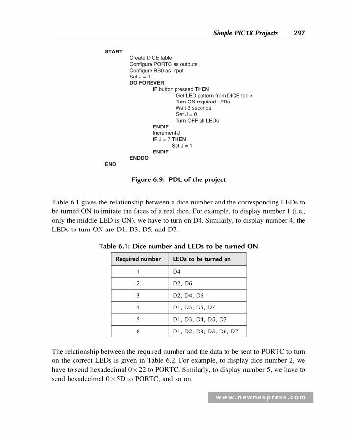
Table 6.1 gives the relationship between a dice number and the corresponding LEDs to
be turned ON to imitate the faces of a real dice. For example, to display number 1 (i.e.,
only the middle LED is ON), we have to turn on D4. Similarly, to display number 4, the
LEDs to turn ON are D1, D3, D5, and D7.
The relationship between the required number and the data to be sent to PORTC to turn
on the correct LEDs is given in Table 6.2. For example, to display dice number 2, we
have to send hexadecimal 0�22 to PORTC. Similarly, to display number 5, we have to
send hexadecimal 0�5D to PORTC, and so on.
START Create DICE table Configure PORTC as outputs Configure RB0 as input Set J = 1 DO FOREVER IF button pressed THEN Get LED pattern from DICE table Turn ON required LEDs Wait 3 seconds Set J = 0 Turn OFF all LEDs ENDIF Increment J IF J = 7 THEN Set J = 1 ENDIF ENDDOEND
Figure 6.9: PDL of the project
Table 6.1: Dice number and LEDs to be turned ON
Required number LEDs to be turned on
1 D4
2 D2, D6
3 D2, D4, D6
4 D1, D3, D5, D7
5 D1, D3, D4, D5, D7
6 D1, D2, D3, D5, D6, D7
www.newnespress.com
297Simple PIC18 Projects
Project Program
The program is called LED2.C, and the program listing is given in Figure 6.10. At the
beginning of the program Switch is defined as bit 0 of PORTB, and Pressed is defined
as 0. The relationships between the dice numbers and the LEDs to be turned on are
stored in an array called DICE. Variable J is used as the dice number. Variable Pattern
is the data sent to the LEDs. Program then enters an endless for loop where the value of
variable J is incremented very fast between 1 and 6. When the push-button switch is
pressed, the LED pattern corresponding to the current value of J is read from the array
and sent to the LEDs. The LEDs remain in this state for 3 seconds (using function
Delay_ms with the argument set to 3000ms), after which they all turn OFF. The system
is then ready to generate a new dice number.
Using a Pseudorandom Number Generator
In the preceding project the value of variable J changes very fast among the numbers
between 1 and 6, so we can say that the numbers generated are random (i.e., new
numbers do not depend on the previous numbers).
A pseudorandom number generator function can also be used to generate the dice
numbers. The modified program listing is shown in Figure 6.11. In this program a
function called Number generates the dice numbers. The function receives the upper
limit of the numbers to be generated (6 in this example) and also a seed value which
Table 6.2: Required number and PORTC data
Required number PORTB data (Hex)
1 0�08
2 0�22
3 0�2A
4 0�55
5 0�5D
6 0�77
www.newnespress.com
298 Chapter 6
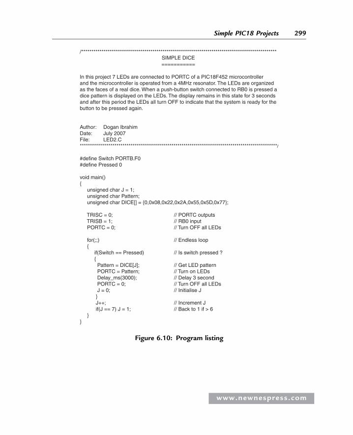
/************************************************************************************************
In this project 7 LEDs are connected to PORTC of a PIC18F452 microcontrollerand the microcontroller is operated from a 4MHz resonator. The LEDs are organizedas the faces of a real dice. When a push-button switch connected to RB0 is pressed a dice pattern is displayed on the LEDs. The display remains in this state for 3 secondsand after this period the LEDs all turn OFF to indicate that the system is ready for the button to be pressed again.
Author: Dogan IbrahimDate: July 2007File: LED2.C*************************************************************************************************/
#define Switch PORTB.F0#define Pressed 0
void main(){ unsigned char J = 1; unsigned char Pattern; unsigned char DICE[] = {0,0x08,0x22,0x2A,0x55,0x5D,0x77}; TRISC = 0; // PORTC outputs TRISB = 1; // RB0 input PORTC = 0; // Turn OFF all LEDs for(;;) // Endless loop { if(Switch == Pressed) // Is switch pressed ? { Pattern = DICE[J]; // Get LED pattern PORTC = Pattern; // Turn on LEDs Delay_ms(3000); // Delay 3 second PORTC = 0; // Turn OFF all LEDs J = 0; // Initialise J } J++; // Increment J if(J == 7) J = 1; // Back to 1 if > 6 }}
SIMPLE DICE===========
Figure 6.10: Program listing
www.newnespress.com
299Simple PIC18 Projects
/******************************************************************************************
In this project 7 LEDs are connected to PORTC of a PIC18F452 microcontrollerand the microcontroller is operated from a 4MHz resonator. The LEDs are organizedas the faces of a real dice. When a push-button switch connected to RB0 is pressed a dice pattern is displayed on the LEDs. The display remains in this state for 3 secondsand after this period the LEDs all turn OFF to indicate that the system is ready for the button to be pressed again.
In this program a pseudorandom number generator function isused to generate the dice numbers between 1 and 6.
Author: Dogan IbrahimDate: July 2007File: LED3.C*******************************************************************************************/
#define Switch PORTB.F0#define Pressed 0
//// This function generates a pseudo random integer number// between 1 and Lim//unsigned char Number(int Lim, int Y){ unsigned char Result; static unsigned int Y; Y = (Y * 32719 + 3) % 32749; Result = ((Y % Lim) + 1); return Result;}
//// Start of MAIN program//void main(){ unsigned char J,Pattern,Seed = 1; unsigned char DICE[] = {0,0x08,0x22,0x2A,0x55,0x5D,0x77};
TRISC = 0; // PORTC outputs TRISB = 1; // RB0 input PORTC = 0; // Turn OFF all LEDs
for(;;) // Endless loop
SIMPLE DICE===========
Figure 6.11: Dice program using a pseudorandom number generator
www.newnespress.com
300 Chapter 6
defines the number set to be generated. In this example, the seed is set to 1. Every time
the function is called, a number between 1 and 6 is generated.
The operation of the program is basically same as in Figure 6.10. When the push-button
switch is pressed, function Number is called to generate a new dice number between
1 and 6, and this number is used as an index in array DICE in order to find the bit
pattern to be sent to the LEDs.
PROJECT 6.3—Two-Dice Project
Project Description
This project is similar to Project 2, but here a pair of dice are used—as in many dice
games such as backgammon—instead of a single dice.
The circuit shown in Figure 6.8 can be modified by adding another set of seven LEDs
for the second dice. For example, the first set of LEDs can be driven from PORTC, the
second set from PORTD, and the push-button switch can be connected to RB0 as
before. Such a design requires fourteen output ports just for the LEDs. Later on we will
see how the LEDs can be combined in order to reduce the input/output requirements.
Figure 6.12 shows the block diagram of the project.
Project Hardware
The circuit diagram of the project is shown in Figure 6.13. The circuit is basically
same as in Figure 6.8, with the addition of another set of LEDs connected
to PORTD.
{ if(Switch == Pressed) // Is switch pressed ? { J = Number(6,seed); // Generate a number between 1 and 6 Pattern = DICE[J]; // Get LED pattern PORTC = Pattern; // Turn on LEDs Delay_ms(3000); // Delay 3 second PORTC = 0; // Turn OFF all LEDs } }}
Figure 6.11: (Cont’d)
www.newnespress.com
301Simple PIC18 Projects
Project PDL
The operation of the project is very similar to that for Project 2. Figure 6.14 shows the
PDL for this project. At the beginning of the program the PORTC and PORTD pins
are configured as outputs, and bit 0 of PORTB (RB0) is configured as input. The
program then executes in a loop continuously and checks the state of the push-button
switch. When the switch is pressed, two pseudorandom numbers between 1 and 6 are
Figure 6.13: Circuit diagram of the project
PIC18F452Push-buttonswitch
DICE
Figure 6.12: Block diagram of the project
www.newnespress.com
302 Chapter 6
generated, and these numbers are sent to PORTC and PORTD. The LEDs remain at
this state for 3 seconds, after which all the LEDs are turned OFF to indicate that the
push-button switch can be pressed again for the next pair of numbers.
Project Program
The program is called LED4.C, and the program listing is given in Figure 6.15. At
the beginning of the program Switch is defined as bit 0 of PORTB, and Pressed is
defined as 0. The relationships between the dice numbers and the LEDs to be turned
on are stored in an array called DICE, as in Project 2. Variable Pattern is the data sent
to the LEDs. Program enters an endless for loop where the state of the push-button
switch is checked continuously. When the switch is pressed, two random numbers
are generated by calling function Number. The bit patterns to be sent to the LEDs
are then determined and sent to PORTC and PORTD. The program then repeats
inside the endless loop, checking the state of the push-button switch.
PROJECT 6.4—Two-Dice Project Using Fewer I/O Pins
Project Description
This project is similar to Project 3, but here LEDs are shared, which uses fewer input/
output pins.
START Create DICE table Configure PORTC as outputs Configure PORTD as outputs Configure RB0 as input DO FOREVER IF button pressed THEN Get a random number between 1 and 6 Find bit pattern Turn ON LEDs on PORTC Get second random number between 1 and 6 Find bit pattern Turn on LEDs on PORTD Wait 3 seconds Turn OFF all LEDs ENDIF ENDDO END
Figure 6.14: PDL of the project
www.newnespress.com
303Simple PIC18 Projects
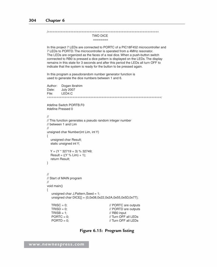
/∗∗∗∗∗∗∗∗∗∗∗∗∗∗∗∗∗∗∗∗∗∗∗∗∗∗∗∗∗∗∗∗∗∗∗∗∗∗∗∗∗∗∗∗∗∗∗∗∗∗∗∗∗∗∗∗∗∗∗∗∗∗∗∗∗∗∗∗∗ TWO DICE ========
In this project 7 LEDs are connected to PORTC of a PIC18F452 microcontroller and 7 LEDs to PORTD. The microcontroller is operated from a 4MHz resonator.The LEDs are organized as the faces of a real dice. When a push-button switch connected to RB0 is pressed a dice pattern is displayed on the LEDs. The displayremains in this state for 3 seconds and after this period the LEDs all turn OFF to indicate that the system is ready for the button to be pressed again.
In this program a pseudorandom number generator function isused to generate the dice numbers between 1 and 6.
Author: Dogan IbrahimDate: July 2007File: LED4.C∗∗∗∗∗∗∗∗∗∗∗∗∗∗∗∗∗∗∗∗∗∗∗∗∗∗∗∗∗∗∗∗∗∗∗∗∗∗∗∗∗∗∗∗∗∗∗∗∗∗∗∗∗∗∗∗∗∗∗∗∗∗∗∗∗∗∗∗∗∗∗/
#define Switch PORTB.F0#define Pressed 0
//// This function generates a pseudo random integer number// between 1 and Lim//unsigned char Number(int Lim, int Y){ unsigned char Result; static unsigned int Y;
Y = (Y * 32719 + 3) % 32749; Result = ((Y % Lim) + 1); return Result;}
//// Start of MAIN program//void main(){ unsigned char J,Pattern,Seed = 1; unsigned char DICE[] = {0,0x08,0x22,0x2A,0x55,0x5D,0x77};
TRISC = 0; // PORTC are outputs TRISD = 0; // PORTD are outputs TRISB = 1; // RB0 input PORTC = 0; // Turn OFF all LEDs PORTD = 0; // Turn OFF all LEDs
Figure 6.15: Program listing
www.newnespress.com
304 Chapter 6
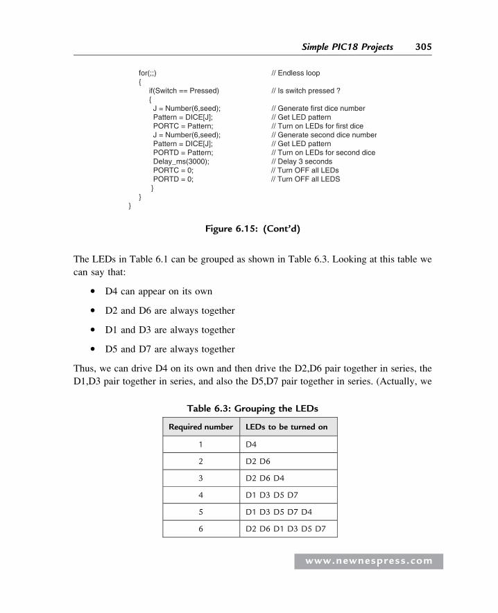
The LEDs in Table 6.1 can be grouped as shown in Table 6.3. Looking at this table we
can say that:
� D4 can appear on its own
� D2 and D6 are always together
� D1 and D3 are always together
� D5 and D7 are always together
Thus, we can drive D4 on its own and then drive the D2,D6 pair together in series, the
D1,D3 pair together in series, and also the D5,D7 pair together in series. (Actually, we
Table 6.3: Grouping the LEDs
Required number LEDs to be turned on
1 D4
2 D2 D6
3 D2 D6 D4
4 D1 D3 D5 D7
5 D1 D3 D5 D7 D4
6 D2 D6 D1 D3 D5 D7
for(;;) // Endless loop { if(Switch == Pressed) // Is switch pressed ? { J = Number(6,seed); // Generate first dice number Pattern = DICE[J]; // Get LED pattern PORTC = Pattern; // Turn on LEDs for first dice J = Number(6,seed); // Generate second dice number Pattern = DICE[J]; // Get LED pattern PORTD = Pattern; // Turn on LEDs for second dice Delay_ms(3000); // Delay 3 seconds PORTC = 0; // Turn OFF all LEDs PORTD = 0; // Turn OFF all LEDS } }}
Figure 6.15: (Cont’d)
www.newnespress.com
305Simple PIC18 Projects
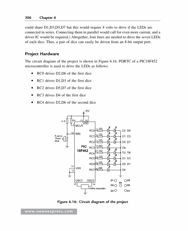
could share D1,D3,D5,D7 but this would require 8 volts to drive if the LEDs are
connected in series. Connecting them in parallel would call for even more current, and a
driver IC would be required.) Altogether, four lines are needed to drive the seven LEDs
of each dice. Thus, a pair of dice can easily be driven from an 8-bit output port.
Project Hardware
The circuit diagram of the project is shown in Figure 6.16. PORTC of a PIC18F452
microcontroller is used to drive the LEDs as follows:
� RC0 drives D2,D6 of the first dice
� RC1 drives D1,D3 of the first dice
� RC2 drives D5,D7 of the first dice
� RC3 drives D4 of the first dice
� RC4 drives D2,D6 of the second dice
Figure 6.16: Circuit diagram of the project
www.newnespress.com
306 Chapter 6
� RC5 drives D1,D3 of the second dice
� RC6 drives D5,D7 of the second dice
� RC7 drives D4 of the second dice
Since two LEDs are being driven on some outputs, we can calculate the required value
of the current limiting resistors. Assuming that the voltage drop across each LED
is 2V, the current through the LED is 10mA, and the output high voltage of the
microcontroller is 4.85V, the required resistors are:
R ¼ 4:85 � 2 � 2
10¼ 85 ohms
We will choose 100-ohm resistors.
We now need to find the relationship between the dice numbers and the bit pattern to be
sent to the LEDs for each dice. Table 6.4 shows the relationship between the first
dice numbers and the bit pattern to be sent to port pins RC0-RC3. Similarly, Table 6.5
shows the relationship between the second dice numbers and the bit pattern to be
sent to port pins RC4-RC7.
We can now find the 8-bit number to be sent to PORTC to display both dice numbers as
follows:
� Get the first number from the number generator, call this P
� Index the DICE table to find the bit pattern for low nibble (i.e., L ¼ DICE[P])
� Get the second number from the number generator, call this P
Table 6.4: First dice bit patterns
Dice number RC3 RC2 RC1 RC0 Hex value
1 1 0 0 0 8
2 0 0 0 1 1
3 1 0 0 1 9
4 0 1 1 0 6
5 1 1 1 0 E
6 0 1 1 1 7
www.newnespress.com
307Simple PIC18 Projects
� Index the DICE table to find the bit pattern for high nibble (i.e., U ¼ DICE[P])
� Multiply high nibble by 16 and add low nibble to find the number to be sent
to PORTC (i.e., R ¼ 16*U þ L), where R is the 8-bit number to be sent to
PORTC to display both dice values.
Project PDL
The operation of this project is very similar to that of Project 2. Figure 6.17 shows
the PDL of the project. At the beginning of the program the PORTC pins are
Table 6.5: Second dice bit patterns
Dice number RC7 RC6 RC5 RC4 Hex value
1 1 0 0 0 8
2 0 0 0 1 1
3 1 0 0 1 9
4 0 1 1 0 6
5 1 1 1 0 E
6 0 1 1 1 7
START Create DICE table Configure PORTC as outputs Configure RB0 as input DO FOREVER IF button pressed THEN Get a random number between 1 and 6 Find low nibble bit pattern Get second random number between 1 and 6 High high nibble bit pattern Calculate data to be sent to PORTC Wait 3 seconds Turn OFF all LEDs ENDIF ENDDO END
Figure 6.17: PDL of the project
www.newnespress.com
308 Chapter 6
configured as outputs, and bit 0 of PORTB (RB0) is configured as input. The program
then executes in a loop continuously and checks the state of the push-button switch.
When the switch is pressed, two pseudorandom numbers between 1 and 6 are generated,
and the bit pattern to be sent to PORTC is found by the method just described. This bit
pattern is then sent to PORTC to display both dice numbers at the same time. The
display shows the dice numbers for 3 seconds, and then all the LEDs turn OFF to
indicate that the system is waiting for the push-button to be pressed again to display
the next set of numbers.
Project Program
The program is called LED5.C, and the program listing is given in Figure 6.18.
At the beginning of the program Switch is defined as bit 0 of PORTB, and Pressed
is defined as 0. The relationships between the dice numbers and the LEDs to be
turned on are stored in an array called DICE as in Project 2. Variable Pattern is the
data sent to the LEDs. The program enters an endless for loop where the state of
the push-button switch is checked continuously. When the switch is pressed, two
random numbers are generated by calling function Number. Variables L and U store
the lower and higher nibbles of the bit pattern to be sent to PORTC. The bit pattern
to be sent to PORTC is then determined using the method described in the
Project Hardware section and stored in variable R. This bit pattern is then sent to
PORTC to display both dice numbers at the same time. The dice numbers are
displayed for 3 seconds, after which the LEDs are turned OFF to indicate that the
system is ready.
Modifying the Program
The program given in Figure 6.18 can made more efficient by combining the two dice
nibbles into a single table value as described here.
There are thirty-six possible combinations of the two dice values. Referring to
Table 6.4, Table 6.5, and Figure 6.16, we can create Table 6.6 to show all the possible
two-dice values and the corresponding numbers to be sent to PORTC.
The modified program (program name LED6.C) is given in Figure 6.19. In this program
array DICE contains the thirty-six possible dice values. The program enters an endless
www.newnespress.com
309Simple PIC18 Projects
/∗∗∗∗∗∗∗∗∗∗∗∗∗∗∗∗∗∗∗∗∗∗∗∗∗∗∗∗∗∗∗∗∗∗∗∗∗∗∗∗∗∗∗∗∗∗∗∗∗∗∗∗∗∗∗∗∗∗∗∗∗∗∗∗∗∗∗∗∗∗∗
In this project LEDs are connected to PORTC of a PIC18F452 microcontrollerand the microcontroller is operated from a 4MHz resonator. The LEDs areorganized as the faces of a real dice. When a push-button switch connected toRB0 is pressed a dice pattern is displayed on the LEDs. The display remainsin this state for 3 seconds and after this period the LEDs all turn OFF to indicatethat the system is ready for the button to be pressed again.
In this program a pseudorandom number generator function isused to generate the dice numbers between 1 and 6.
Author: Dogan IbrahimDate: July 2007File: LED5.C∗∗∗∗∗∗∗∗∗∗∗∗∗∗∗∗∗∗∗∗∗∗∗∗∗∗∗∗∗∗∗∗∗∗∗∗∗∗∗∗∗∗∗∗∗∗∗∗∗∗∗∗∗∗∗∗∗∗∗∗∗∗∗∗∗∗∗∗∗∗∗/
#define Switch PORTB.F0#define Pressed 0
//// This function generates a pseudo random integer number// between 1 and Lim//unsigned char Number(int Lim, int Y){ unsigned char Result; static unsigned int Y;
Y = (Y * 32719 + 3) % 32749; Result = ((Y % Lim) + 1); return Result;}
//// Start of MAIN program//void main(){ unsigned char J,L,U,R,Seed = 1; unsigned char DICE[] = {0,0x08,0x01,0x09,0x06,0x0E,0x07};
TRISC = 0; // PORTC are outputs TRISB = 1; // RB0 input PORTC = 0; // Turn OFF all LEDs
for(;;) // Endless loop
TWO DICE - USING FEWER I/O PINS==============================
Figure 6.18: Program listing
www.newnespress.com
310 Chapter 6
{ if(Switch == Pressed) // Is switch pressed ? { J = Number(6,seed); // Generate first dice number L = DICE[J]; // Get LED pattern J = Number(6,seed); // Generate second dice number U = DICE[J]; // Get LED pattern R = 16*U + L; // Bit pattern to send to PORTC PORTC = R; // Turn on LEDs for both dice Delay_ms(3000); // Delay 3 seconds PORTC = 0; // Turn OFF all LEDs } }}
Figure 6.18: (Cont’d)
Table 6.6: Two-dice combinations and the number to be sent to PORTC
Dice numbers PORTC value Dice numbers PORTC value
1,1 0�88 4,1 0�86
1,2 0�18 4,2 0�16
1,3 0�98 4,3 0�96
1,4 0�68 4,4 0�66
1,5 0�E8 4,5 0�E6
1,6 0�78 4,6 0�76
2,1 0�81 5,1 0�8E
2,2 0�11 5,2 0�1E
2,3 0�91 5,3 0�9E
2,4 0�61 5,4 0�6E
2,5 0�E1 5,5 0�EE
2,6 0�71 5,6 0�7E
3,1 0�89 6,1 0�87
3,2 0�19 6,2 0�17
3,3 0�99 6,3 0�97
3,4 0�69 6,4 0�67
3,5 0�E9 6,5 0�E7
3,6 0�79 6,6 0�77
www.newnespress.com
/*****************************************************************************************
In this project LEDs are connected to PORTC of a PIC18F452 microcontrollerand the microcontroller is operated from a 4MHz resonator. The LEDs areorganized as the faces of a real dice. When a push-button switch connected toRB0 is pressed a dice pattern is displayed on the LEDs. The display remains inthis state for 3 seconds and after this period the LEDs all turn OFF to indicatethat the system is ready for the button to be pressed again.
In this program a pseudorandom number generator function isused to generate the dice numbers between 1 and 6.
Author: Dogan IbrahimDate: July 2007File: LED6.C******************************************************************************************/
#define Switch PORTB.F0#define Pressed 0
//// Start of MAIN program//void main(){ unsigned char Pattern, J = 1; unsigned char DICE[] = {0,0x88,0x18,0x98,0x68,0xE8,0x78, 0x81,0x11,0x91,0x61,0xE1,0x71, 0x89,0x19,0x99,0x69,0xE9,0x79, 0x86,0x16,0x96,0x66,0xE6,0x76, 0x8E,0x1E,0x9E,0x6E,0xEE,0x7E, 0x87,0x17,0x97,0x67,0xE7,0x77};
TRISC = 0; // PORTC are outputs TRISB = 1; // RB0 input PORTC = 0; // Turn OFF all LEDs
for(;;) // Endless loop { if(Switch == Pressed) // Is switch pressed ? { Pattern = DICE[J]; // Number to send to PORTC PORTC = Pattern; // send to PORTC Delay_ms(3000); // 3 seconds delay PORTC = 0; // Clear PORTC } J++; // Increment J if(J == 37) J = 1; // If J = 37, reset to 1 }}
=============================TWO DICE - USING FEWER I/O PINS
Figure 6.19: Modified program
www.newnespress.com
312 Chapter 6
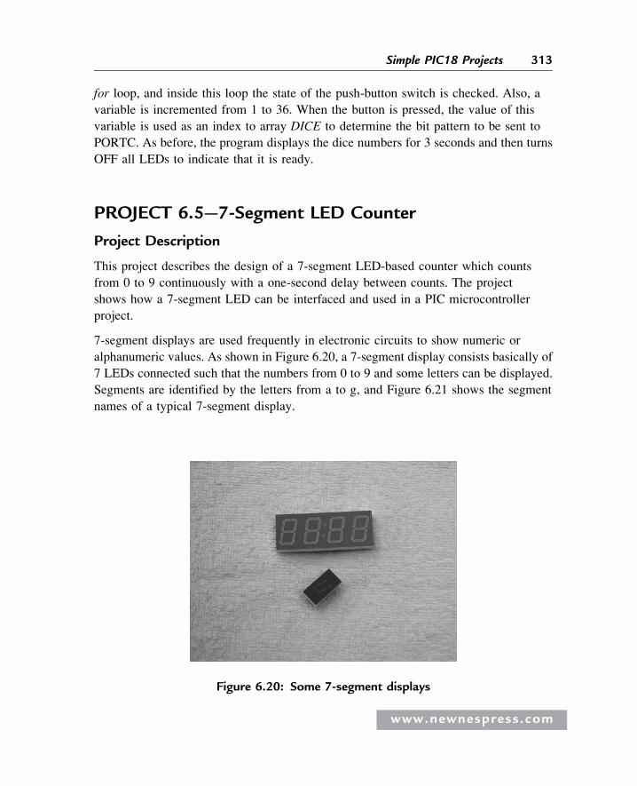
for loop, and inside this loop the state of the push-button switch is checked. Also, a
variable is incremented from 1 to 36. When the button is pressed, the value of this
variable is used as an index to array DICE to determine the bit pattern to be sent to
PORTC. As before, the program displays the dice numbers for 3 seconds and then turns
OFF all LEDs to indicate that it is ready.
PROJECT 6.5—7-Segment LED Counter
Project Description
This project describes the design of a 7-segment LED-based counter which counts
from 0 to 9 continuously with a one-second delay between counts. The project
shows how a 7-segment LED can be interfaced and used in a PIC microcontroller
project.
7-segment displays are used frequently in electronic circuits to show numeric or
alphanumeric values. As shown in Figure 6.20, a 7-segment display consists basically of
7 LEDs connected such that the numbers from 0 to 9 and some letters can be displayed.
Segments are identified by the letters from a to g, and Figure 6.21 shows the segment
names of a typical 7-segment display.
Figure 6.20: Some 7-segment displays
www.newnespress.com
313Simple PIC18 Projects
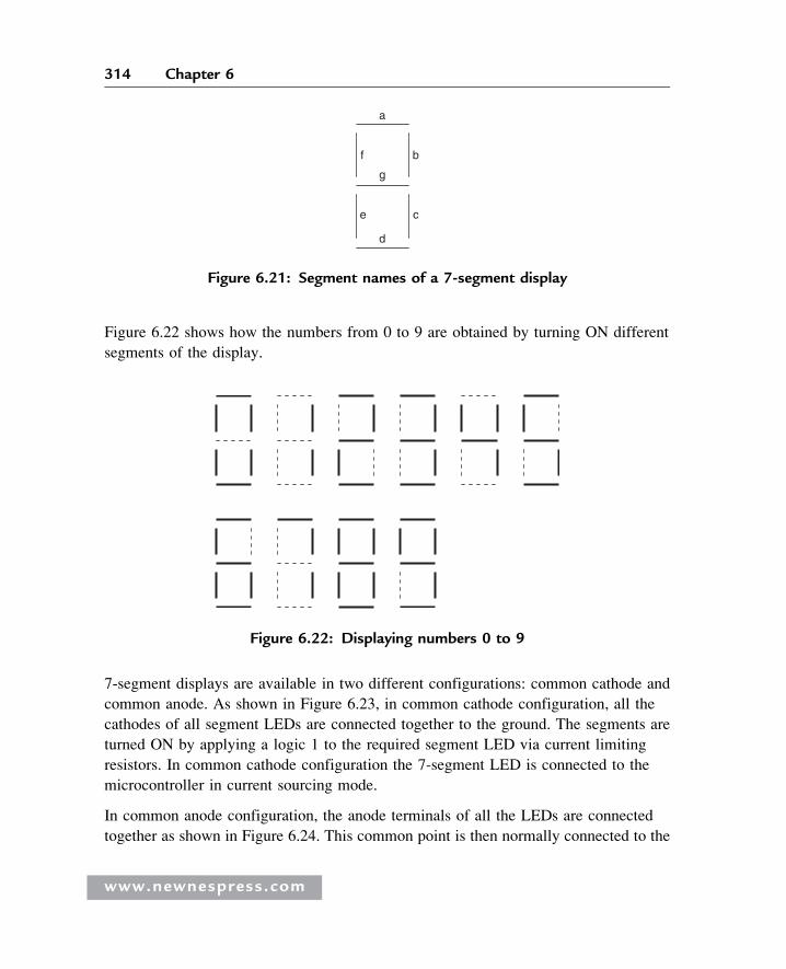
Figure 6.22 shows how the numbers from 0 to 9 are obtained by turning ON different
segments of the display.
7-segment displays are available in two different configurations: common cathode and
common anode. As shown in Figure 6.23, in common cathode configuration, all the
cathodes of all segment LEDs are connected together to the ground. The segments are
turned ON by applying a logic 1 to the required segment LED via current limiting
resistors. In common cathode configuration the 7-segment LED is connected to the
microcontroller in current sourcing mode.
In common anode configuration, the anode terminals of all the LEDs are connected
together as shown in Figure 6.24. This common point is then normally connected to the
f
g
e
d
a
b
c
Figure 6.21: Segment names of a 7-segment display
Figure 6.22: Displaying numbers 0 to 9
www.newnespress.com
314 Chapter 6
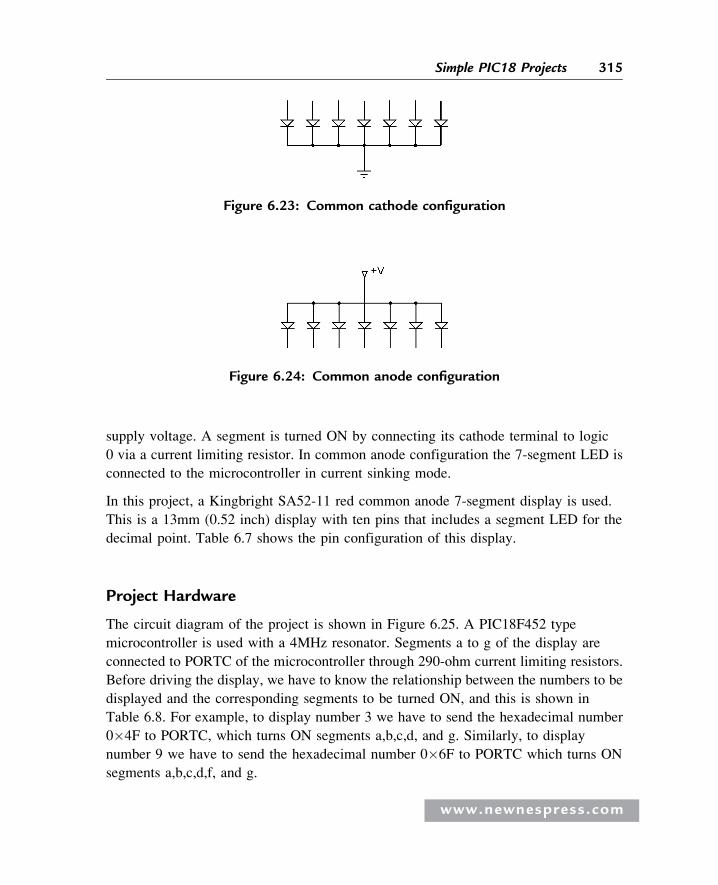
supply voltage. A segment is turned ON by connecting its cathode terminal to logic
0 via a current limiting resistor. In common anode configuration the 7-segment LED is
connected to the microcontroller in current sinking mode.
In this project, a Kingbright SA52-11 red common anode 7-segment display is used.
This is a 13mm (0.52 inch) display with ten pins that includes a segment LED for the
decimal point. Table 6.7 shows the pin configuration of this display.
Project Hardware
The circuit diagram of the project is shown in Figure 6.25. A PIC18F452 type
microcontroller is used with a 4MHz resonator. Segments a to g of the display are
connected to PORTC of the microcontroller through 290-ohm current limiting resistors.
Before driving the display, we have to know the relationship between the numbers to be
displayed and the corresponding segments to be turned ON, and this is shown in
Table 6.8. For example, to display number 3 we have to send the hexadecimal number
0�4F to PORTC, which turns ON segments a,b,c,d, and g. Similarly, to display
number 9 we have to send the hexadecimal number 0�6F to PORTC which turns ON
segments a,b,c,d,f, and g.
Figure 6.24: Common anode configuration
Figure 6.23: Common cathode configuration
www.newnespress.com
315Simple PIC18 Projects
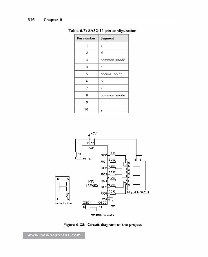
Table 6.7: SA52-11 pin configuration
Pin number Segment
1 e
2 d
3 common anode
4 c
5 decimal point
6 b
7 a
8 common anode
9 f
10 g
Figure 6.25: Circuit diagram of the project
www.newnespress.com
316 Chapter 6
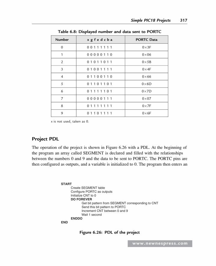
Project PDL
The operation of the project is shown in Figure 6.26 with a PDL. At the beginning of
the program an array called SEGMENT is declared and filled with the relationships
between the numbers 0 and 9 and the data to be sent to PORTC. The PORTC pins are
then configured as outputs, and a variable is initialized to 0. The program then enters an
Table 6.8: Displayed number and data sent to PORTC
Number x g f e d c b a PORTC Data
0 0 0 1 1 1 1 1 1 0�3F
1 0 0 0 0 0 1 1 0 0�06
2 0 1 0 1 1 0 1 1 0�5B
3 0 1 0 0 1 1 1 1 0�4F
4 0 1 1 0 0 1 1 0 0�66
5 0 1 1 0 1 1 0 1 0�6D
6 0 1 1 1 1 1 0 1 0�7D
7 0 0 0 0 0 1 1 1 0�07
8 0 1 1 1 1 1 1 1 0�7F
9 0 1 1 0 1 1 1 1 0�6F
x is not used, taken as 0.
START Create SEGMENT table Configure PORTC as outputs Initialize CNT to 0 DO FOREVER Get bit pattern from SEGMENT corresponding to CNT Send this bit pattern to PORTC Increment CNT between 0 and 9 Wait 1 second ENDDOEND
Figure 6.26: PDL of the project
www.newnespress.com
317Simple PIC18 Projects
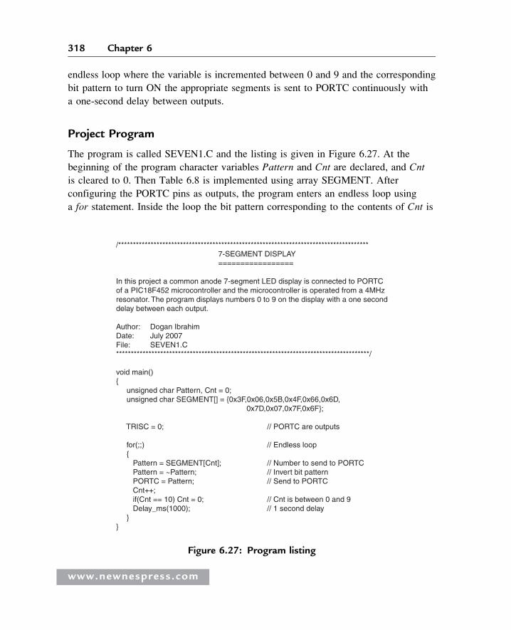
endless loop where the variable is incremented between 0 and 9 and the corresponding
bit pattern to turn ON the appropriate segments is sent to PORTC continuously with
a one-second delay between outputs.
Project Program
The program is called SEVEN1.C and the listing is given in Figure 6.27. At the
beginning of the program character variables Pattern and Cnt are declared, and Cnt
is cleared to 0. Then Table 6.8 is implemented using array SEGMENT. After
configuring the PORTC pins as outputs, the program enters an endless loop using
a for statement. Inside the loop the bit pattern corresponding to the contents of Cnt is
/************************************************************************************* 7-SEGMENT DISPLAY =================
In this project a common anode 7-segment LED display is connected to PORTCof a PIC18F452 microcontroller and the microcontroller is operated from a 4MHz resonator. The program displays numbers 0 to 9 on the display with a one seconddelay between each output.
Author: Dogan IbrahimDate: July 2007File: SEVEN1.C**************************************************************************************/
void main(){ unsigned char Pattern, Cnt = 0; unsigned char SEGMENT[] = {0x3F,0x06,0x5B,0x4F,0x66,0x6D, 0x7D,0x07,0x7F,0x6F};
TRISC = 0; // PORTC are outputs
for(;;) // Endless loop { Pattern = SEGMENT[Cnt]; // Number to send to PORTC Pattern = ~Pattern; // Invert bit pattern PORTC = Pattern; // Send to PORTC Cnt++; if(Cnt == 10) Cnt = 0; // Cnt is between 0 and 9 Delay_ms(1000); // 1 second delay }}
Figure 6.27: Program listing
www.newnespress.com
318 Chapter 6
found and stored in variable Pattern. Because we are using a common anode display,
a segment is turned ON when it is at logic 0 and thus the bit pattern is inverted before
it is sent to PORTC. The value of Cnt is then incremented between 0 and 9, after
which the program waits for a second before repeating the above sequence.
Modified Program
Note that the program can be made more readable if we create a function to display the
required number and then call this function from the main program. Figure 6.28 shows
the modified program (called SEVEN2.C). A function called Display is created with an
argument called no. The function gets the bit pattern from local array SEGMENT
indexed by no, inverts it, and then returns the resulting bit pattern to the calling
program.
PROJECT 6.6—Two-Digit Multiplexed 7-Segment LED
Project Description
This project is similar to Project 6.5, but here multiplexed two digits are used instead of
just one digit and a fixed number. In this project the number 25 is displayed. In
multiplexed LED applications (see Figure 6.29) the LED segments of all the digits are
tied together and the common pins of each digit are turned ON separately by the
microcontroller. When each digit is displayed only for several milliseconds, the eye
cannot tell that the digits are not ON all the time. This way we can multiplex any
number of 7-segment displays together. For example, to display the number 53, we have
to send 5 to the first digit and enable its common pin. After a few milliseconds, number
3 is sent to the second digit and the common point of the second digit is enabled. When
this process is repeated continuously, it appears to the user that both displays are ON
continuously.
Some manufacturers provide multiplexed multidigit displays, such as 2-, 4-, or 8-digit
multiplexed displays, in single packages. The display used in this project is the DC56-
11EWA, which is a red 0.56-inch common-cathode two-digit display having 18 pins
and the pin configuration as shown in Table 6.9. This display can be controlled from the
microcontroller as follows:
� Send the segment bit pattern for digit 1 to segments a to g
� Enable digit 1
www.newnespress.com
319Simple PIC18 Projects
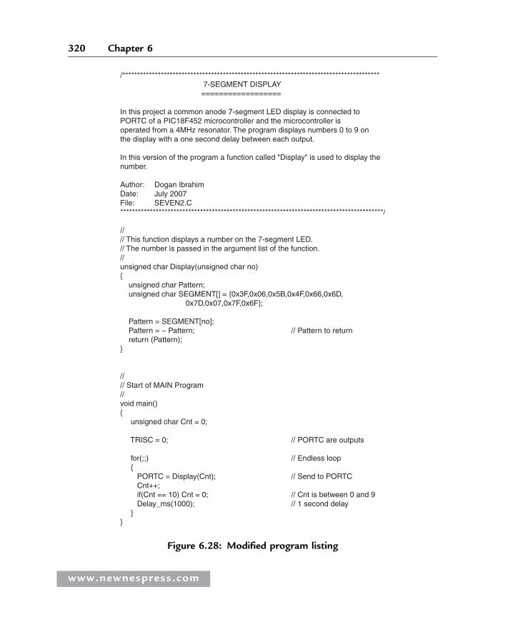
/*************************************************************************************** 7-SEGMENT DISPLAY ==================
In this project a common anode 7-segment LED display is connected toPORTC of a PIC18F452 microcontroller and the microcontroller isoperated from a 4MHz resonator. The program displays numbers 0 to 9 onthe display with a one second delay between each output.
In this version of the program a function called "Display" is used to display thenumber.
Author: Dogan IbrahimDate: July 2007File: SEVEN2.C*****************************************************************************************/
//// This function displays a number on the 7-segment LED.// The number is passed in the argument list of the function.//unsigned char Display(unsigned char no){ unsigned char Pattern; unsigned char SEGMENT[] = {0x3F,0x06,0x5B,0x4F,0x66,0x6D, 0x7D,0x07,0x7F,0x6F};
Pattern = SEGMENT[no]; Pattern = ~ Pattern; // Pattern to return return (Pattern);}
//// Start of MAIN Program//void main(){ unsigned char Cnt = 0;
TRISC = 0; // PORTC are outputs
for(;;) // Endless loop { PORTC = Display(Cnt); // Send to PORTC Cnt++; if(Cnt == 10) Cnt = 0; // Cnt is between 0 and 9 Delay_ms(1000); // 1 second delay }}
Figure 6.28: Modified program listing
www.newnespress.com
320 Chapter 6
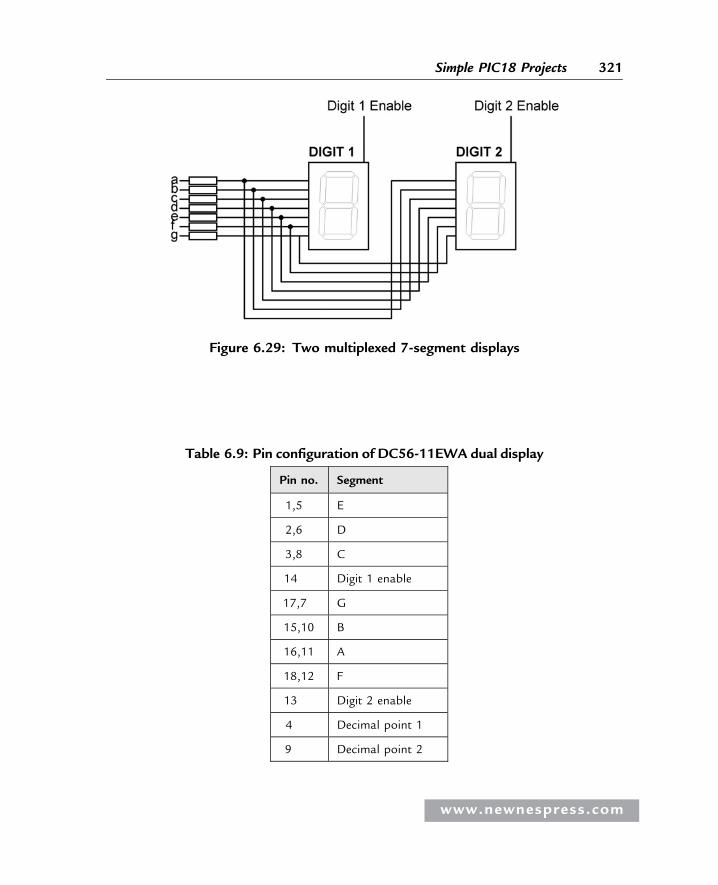
Figure 6.29: Two multiplexed 7-segment displays
Table 6.9: Pin configuration of DC56-11EWA dual display
Pin no. Segment
1,5 E
2,6 D
3,8 C
14 Digit 1 enable
17,7 G
15,10 B
16,11 A
18,12 F
13 Digit 2 enable
4 Decimal point 1
9 Decimal point 2
www.newnespress.com
321Simple PIC18 Projects
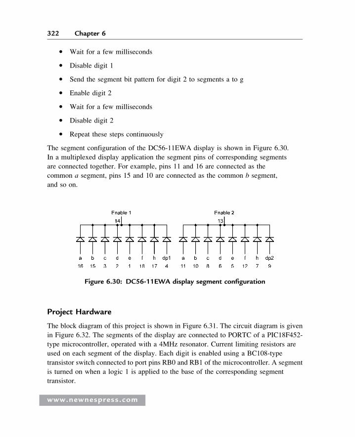
� Wait for a few milliseconds
� Disable digit 1
� Send the segment bit pattern for digit 2 to segments a to g
� Enable digit 2
� Wait for a few milliseconds
� Disable digit 2
� Repeat these steps continuously
The segment configuration of the DC56-11EWA display is shown in Figure 6.30.
In a multiplexed display application the segment pins of corresponding segments
are connected together. For example, pins 11 and 16 are connected as the
common a segment, pins 15 and 10 are connected as the common b segment,
and so on.
Project Hardware
The block diagram of this project is shown in Figure 6.31. The circuit diagram is given
in Figure 6.32. The segments of the display are connected to PORTC of a PIC18F452-
type microcontroller, operated with a 4MHz resonator. Current limiting resistors are
used on each segment of the display. Each digit is enabled using a BC108-type
transistor switch connected to port pins RB0 and RB1 of the microcontroller. A segment
is turned on when a logic 1 is applied to the base of the corresponding segment
transistor.
Figure 6.30: DC56-11EWA display segment configuration
www.newnespress.com
322 Chapter 6
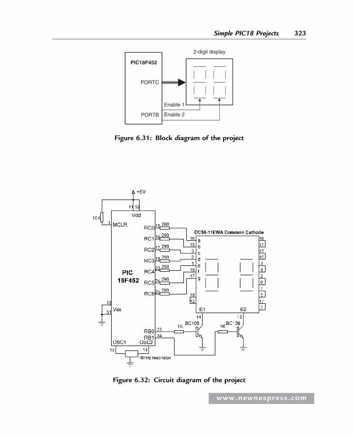
PORTB
PORTC
Enable 2
Enable 1
PIC18F452
2-digit display
Figure 6.31: Block diagram of the project
Figure 6.32: Circuit diagram of the project
www.newnespress.com
323Simple PIC18 Projects
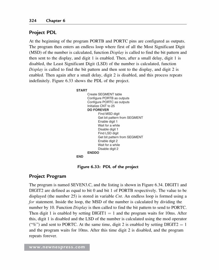
Project PDL
At the beginning of the program PORTB and PORTC pins are configured as outputs.
The program then enters an endless loop where first of all the Most Significant Digit
(MSD) of the number is calculated, function Display is called to find the bit pattern and
then sent to the display, and digit 1 is enabled. Then, after a small delay, digit 1 is
disabled, the Least Significant Digit (LSD) of the number is calculated, function
Display is called to find the bit pattern and then sent to the display, and digit 2 is
enabled. Then again after a small delay, digit 2 is disabled, and this process repeats
indefinitely. Figure 6.33 shows the PDL of the project.
Project Program
The program is named SEVEN3.C, and the listing is shown in Figure 6.34. DIGIT1 and
DIGIT2 are defined as equal to bit 0 and bit 1 of PORTB respectively. The value to be
displayed (the number 25) is stored in variable Cnt. An endless loop is formed using a
for statement. Inside the loop, the MSD of the number is calculated by dividing the
number by 10. Function Display is then called to find the bit pattern to send to PORTC.
Then digit 1 is enabled by setting DIGIT1 ¼ 1 and the program waits for 10ms. After
this, digit 1 is disabled and the LSD of the number is calculated using the mod operator
(“%”) and sent to PORTC. At the same time, digit 2 is enabled by setting DIGIT2 ¼ 1
and the program waits for 10ms. After this time digit 2 is disabled, and the program
repeats forever.
START Create SEGMENT table Configure PORTB as outputs Configure PORTC as outputs Initialize CNT to 25 DO FOREVER Find MSD digit Get bit pattern from SEGMENT Enable digit 1 Wait for a while Disable digit 1 Find LSD digit Get bit pattern from SEGMENT Enable digit 2 Wait for a while Disable digit 2 ENDDO END
Figure 6.33: PDL of the project
www.newnespress.com
324 Chapter 6
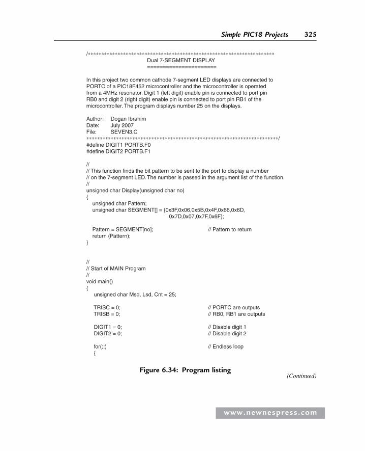
/∗∗∗∗∗∗∗∗∗∗∗∗∗∗∗∗∗∗∗∗∗∗∗∗∗∗∗∗∗∗∗∗∗∗∗∗∗∗∗∗∗∗∗∗∗∗∗∗∗∗∗∗∗∗∗∗∗∗∗∗∗∗∗∗∗∗∗∗∗ Dual 7-SEGMENT DISPLAY ======================
In this project two common cathode 7-segment LED displays are connected toPORTC of a PIC18F452 microcontroller and the microcontroller is operatedfrom a 4MHz resonator. Digit 1 (left digit) enable pin is connected to port pinRB0 and digit 2 (right digit) enable pin is connected to port pin RB1 of themicrocontroller. The program displays number 25 on the displays.
Author: Dogan IbrahimDate: July 2007File: SEVEN3.C∗∗∗∗∗∗∗∗∗∗∗∗∗∗∗∗∗∗∗∗∗∗∗∗∗∗∗∗∗∗∗∗∗∗∗∗∗∗∗∗∗∗∗∗∗∗∗∗∗∗∗∗∗∗∗∗∗∗∗∗∗∗∗∗∗∗∗∗∗∗∗/#define DIGIT1 PORTB.F0#define DIGIT2 PORTB.F1
//// This function finds the bit pattern to be sent to the port to display a number// on the 7-segment LED. The number is passed in the argument list of the function.//unsigned char Display(unsigned char no){ unsigned char Pattern; unsigned char SEGMENT[] = {0x3F,0x06,0x5B,0x4F,0x66,0x6D, 0x7D,0x07,0x7F,0x6F};
Pattern = SEGMENT[no]; // Pattern to return return (Pattern);}
//// Start of MAIN Program//void main(){ unsigned char Msd, Lsd, Cnt = 25;
TRISC = 0; // PORTC are outputs TRISB = 0; // RB0, RB1 are outputs
DIGIT1 = 0; // Disable digit 1 DIGIT2 = 0; // Disable digit 2 for(;;) // Endless loop {
Figure 6.34: Program listing(Continued)
www.newnespress.com
325Simple PIC18 Projects
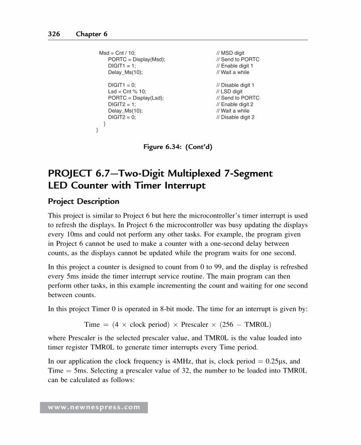
PROJECT 6.7—Two-Digit Multiplexed 7-SegmentLED Counter with Timer Interrupt
Project Description
This project is similar to Project 6 but here the microcontroller’s timer interrupt is used
to refresh the displays. In Project 6 the microcontroller was busy updating the displays
every 10ms and could not perform any other tasks. For example, the program given
in Project 6 cannot be used to make a counter with a one-second delay between
counts, as the displays cannot be updated while the program waits for one second.
In this project a counter is designed to count from 0 to 99, and the display is refreshed
every 5ms inside the timer interrupt service routine. The main program can then
perform other tasks, in this example incrementing the count and waiting for one second
between counts.
In this project Timer 0 is operated in 8-bit mode. The time for an interrupt is given by:
Time ¼ ð4 � clock periodÞ � Prescaler � ð256 � TMR0LÞwhere Prescaler is the selected prescaler value, and TMR0L is the value loaded into
timer register TMR0L to generate timer interrupts every Time period.
In our application the clock frequency is 4MHz, that is, clock period ¼ 0.25ms, andTime ¼ 5ms. Selecting a prescaler value of 32, the number to be loaded into TMR0L
can be calculated as follows:
Msd = Cnt / 10; // MSD digit PORTC = Display(Msd); // Send to PORTC DIGIT1 = 1; // Enable digit 1 Delay_Ms(10); // Wait a while DIGIT1 = 0; // Disable digit 1 Lsd = Cnt % 10; // LSD digit PORTC = Display(Lsd); // Send to PORTC DIGIT2 = 1; // Enable digit 2 Delay_Ms(10); // Wait a while DIGIT2 = 0; // Disable digit 2 }}
Figure 6.34: (Cont’d)
www.newnespress.com
326 Chapter 6
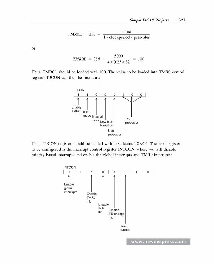
TMR0L ¼ 256 � Time
4 � clockperiod � prescaler
or
TMR0L ¼ 256 � 5000
4 � 0:25 � 32 ¼ 100
Thus, TMR0L should be loaded with 100. The value to be loaded into TMR0 control
register T0CON can then be found as:
T0CON1 1 0 0 0 1 0 0
EnableTMR0 8-bit
mode Internalclock Low-high
transition
Useprescaler
1:32prescaler
Thus, T0CON register should be loaded with hexadecimal 0�C4. The next register
to be configured is the interrupt control register INTCON, where we will disable
priority based interrupts and enable the global interrupts and TMR0 interrupts:
INTCON
1 X 1 0 0 0 X X
Enableglobalinterrupts
EnableTMR0int.
DisableINT0int.
DisableRB changeint.
ClearTMR0IF
www.newnespress.com
327Simple PIC18 Projects
Taking the don’t-care entries (X) as 0, the hexadecimal value to be loaded into
register INTCON is 0�A0.
When an interrupt occurs, the program automatically jumps to the interrupt
service routine. Inside this routine we have to reload register TMR0L, reenable
the TMR0 interrupts, and clear the TMR0 interrupt flag bit. Setting INTCON
register to 0�20 reenables the TMR0 interrupts and at the same time clears the
TMR0 interrupt flag.
The operations to be performed can thus be summarized as follows:
In the main program:
� Load TMR0L with 100
� Set T0CON to 0�C4
� Set INTCON to 0�A0
� Increment the counter with 1-second delays
In the interrupt service routine:
� Re-load TMR0L to 100
� Refresh displays
� Set INTCON to 0�20 (reenable TMR0 interrupts and clear timer interrupt
flag)
Project Hardware
The circuit diagram of this project is same as in Figure 6.32 where a dual 7-segment
display is connected to PORTB and PORTC of a PIC18F452 microcontroller.
Project PDL
The PDL of the project is shown in Figure 6.35. The program is in two sections: the
main program and the interrupt service routine. Inside the main program, TMR0 is
configured to generate interrupts every 5ms and the counter is incremented with a one-
second delay. Inside the interrupt service routine, the timer interrupt is reenabled and
the display digits are refreshed alternately every 5ms.
www.newnespress.com
328 Chapter 6
Project Program
The program is called SEVEN4.C, and the program listing is given in Figure 6.36.
At the beginning of the main program PORTB and PORTC are configured as
outputs. Then register T0CON is loaded with 0�C4 to enable the TMR0 and set the
prescaler to 32. TMR0L register is loaded with 100 so that an interrupt is generated
after 5ms. The program then enters an endless loop where the value of Cnt is
incremented every second.
Inside the interrupt service routine, register TMR0L is reloaded, TMR0 interrupts are
reenabled, and the timer interrupt flag is cleared so that further timer interrupts can be
generated. The display digits are then updated alternately. A variable called Flag is used
to determine which digit to update. Function Display is called, as in Project 6, to find
the bit pattern to be sent to PORTC.
Modifying the Program
In Figure 6.36 the display counts as 00 01. . .09 10 11. . .99 00 01. . . (i.e., the first digit
is shown as 0 for numbers less than 10). The program could be modified so the first
MAIN PROGRAM:
START Configure PORTB as outputs Configure PORTC as outputs Clear variable Cnt to 0 Configure TMR0 to generate interrupts every 5ms DO FOREVER Increment Cnt between 0 and 99 Delay 1 second ENDO END
INTERRUPT SERVICE ROUTINE: START Re-configure TMR0 IF Digit 1 updated THEN Update digit 2 ELSE Update digit 1 END END
Figure 6.35: PDL of the project
www.newnespress.com
329Simple PIC18 Projects
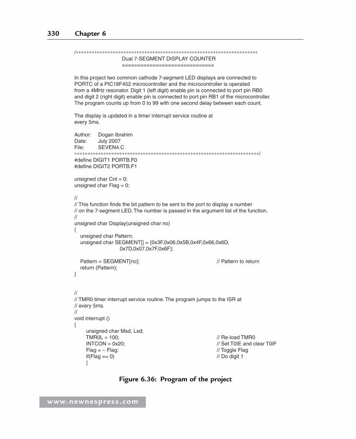
/∗∗∗∗∗∗∗∗∗∗∗∗∗∗∗∗∗∗∗∗∗∗∗∗∗∗∗∗∗∗∗∗∗∗∗∗∗∗∗∗∗∗∗∗∗∗∗∗∗∗∗∗∗∗∗∗∗∗∗∗∗∗∗∗∗∗∗∗∗ Dual 7-SEGMENT DISPLAY COUNTER ==============================
In this project two common cathode 7-segment LED displays are connected toPORTC of a PIC18F452 microcontroller and the microcontroller is operatedfrom a 4MHz resonator. Digit 1 (left digit) enable pin is connected to port pin RB0 and digit 2 (right digit) enable pin is connected to port pin RB1 of the microcontroller. The program counts up from 0 to 99 with one second delay between each count.
The display is updated in a timer interrupt service routine atevery 5ms.
Author: Dogan IbrahimDate: July 2007File: SEVEN4.C∗∗∗∗∗∗∗∗∗∗∗∗∗∗∗∗∗∗∗∗∗∗∗∗∗∗∗∗∗∗∗∗∗∗∗∗∗∗∗∗∗∗∗∗∗∗∗∗∗∗∗∗∗∗∗∗∗∗∗∗∗∗∗∗∗∗∗∗∗∗/#define DIGIT1 PORTB.F0#define DIGIT2 PORTB.F1
unsigned char Cnt = 0;unsigned char Flag = 0;
//// This function finds the bit pattern to be sent to the port to display a number// on the 7-segment LED. The number is passed in the argument list of the function.//unsigned char Display(unsigned char no){ unsigned char Pattern; unsigned char SEGMENT[] = {0x3F,0x06,0x5B,0x4F,0x66,0x6D, 0x7D,0x07,0x7F,0x6F};
Pattern = SEGMENT[no]; // Pattern to return return (Pattern);}
//// TMR0 timer interrupt service routine. The program jumps to the ISR at// every 5ms.//void interrupt (){ unsigned char Msd, Lsd; TMR0L = 100; // Re-load TMR0 INTCON = 0x20; // Set T0IE and clear T0IF Flag = ~ Flag; // Toggle Flag if(Flag == 0) // Do digit 1 {
Figure 6.36: Program of the project
www.newnespress.com
330 Chapter 6
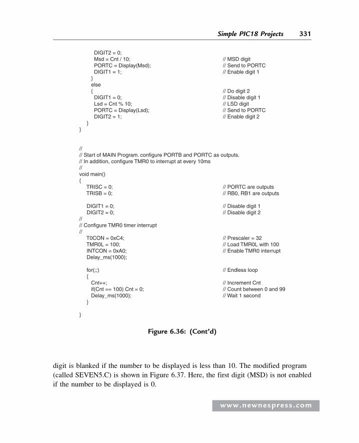
digit is blanked if the number to be displayed is less than 10. The modified program
(called SEVEN5.C) is shown in Figure 6.37. Here, the first digit (MSD) is not enabled
if the number to be displayed is 0.
DIGIT2 = 0; Msd = Cnt / 10; // MSD digit PORTC = Display(Msd); // Send to PORTC DIGIT1 = 1; // Enable digit 1 } else { // Do digit 2 DIGIT1 = 0; // Disable digit 1 Lsd = Cnt % 10; // LSD digit PORTC = Display(Lsd); // Send to PORTC DIGIT2 = 1; // Enable digit 2 }}
//// Start of MAIN Program. configure PORTB and PORTC as outputs.// In addition, configure TMR0 to interrupt at every 10ms//void main(){ TRISC = 0; // PORTC are outputs TRISB = 0; // RB0, RB1 are outputs
DIGIT1 = 0; // Disable digit 1 DIGIT2 = 0; // Disable digit 2//// Configure TMR0 timer interrupt// T0CON = 0xC4; // Prescaler = 32 TMR0L = 100; // Load TMR0L with 100 INTCON = 0xA0; // Enable TMR0 interrupt Delay_ms(1000);
for(;;) // Endless loop { Cnt++; // Increment Cnt if(Cnt == 100) Cnt = 0; // Count between 0 and 99 Delay_ms(1000); // Wait 1 second }
}
Figure 6.36: (Cont’d)
www.newnespress.com
331Simple PIC18 Projects
/∗∗∗∗∗∗∗∗∗∗∗∗∗∗∗∗∗∗∗∗∗∗∗∗∗∗∗∗∗∗∗∗∗∗∗∗∗∗∗∗∗∗∗∗∗∗∗∗ Dual 7-SEGMENT DISPLAY COUNTER ==============================
In this project two common cathode 7-segment LED displays areconnected to PORTC of a PIC18F452 microcontroller and themicrocontroller is operated from a 4MHz resonator. Digit 1 (leftdigit) enable pin is connected to port pin RB0 and digit 2(right digit) enable pin is connected to port pin RB1 of themicrocontroller. The program counts up from 0 to 99 with onesecond delay between each count.
The display is updated in a timer interrupt service routine atevery 5ms.
In this version of the program the first digit is blanked if thenumber is 0.
Author: Dogan IbrahimDate: July 2007File: SEVEN5.C∗∗∗∗∗∗∗∗∗∗∗∗∗∗∗∗∗∗∗∗∗∗∗∗∗∗∗∗∗∗∗∗∗∗∗∗∗∗∗∗∗∗∗∗∗∗∗∗/#define DIGIT1 PORTB.F0#define DIGIT2 PORTB.F1
unsigned char Cnt = 0;unsigned char Flag = 0;
//// This function finds the bit pattern to be sent to the port to display a number// on the 7-segment LED. The number is passed in the argument list of the function.//unsigned char Display(unsigned char no){ unsigned char Pattern; unsigned char SEGMENT[] = {0x3F,0x06,0x5B,0x4F,0x66,0x6D, 0x7D,0x07,0x7F,0x6F};
Pattern = SEGMENT[no]; // Pattern to return return (Pattern);}
//// TMR0 timer interrupt service routine. The program jumps to the// ISR at every 5ms.//void interrupt (){ unsigned char Msd, Lsd;
Figure 6.37: Modified program
www.newnespress.com
332 Chapter 6
TMR0L = 100; // Re-load TMR0 INTCON = 0x20; // Set T0IE and clear T0IF Flag = ~ Flag; // Toggle Flag if(Flag == 0) // Do digit 1 { DIGIT2 = 0; Msd = Cnt / 10; // MSD digit if(Msd != 0) { PORTC = Display(Msd); // Send to PORTC DIGIT1 = 1; // Enable digit 1 } } else { // Do digit 2 DIGIT1 = 0; // Disable digit 1 Lsd = Cnt % 10; // LSD digit PORTC = Display(Lsd); // Send to PORTC DIGIT2 = 1; // Enable digit 2 }}
//// Start of MAIN Program. configure PORTB and PORTC as outputs.// In addition, configure TMR0 to interrupt at every 10ms//void main(){ TRISC = 0; // PORTC are outputs TRISB = 0; // RB0, RB1 are outputs
DIGIT1 = 0; // Disable digit 1 DIGIT2 = 0; // Disable digit 2//// Configure TMR0 timer interrupt// T0CON = 0xC4; // Prescaler = 32 TMR0L = 100; // Load TMR0 with 100 INTCON = 0xA0; // Enable TMR0 interrupt Delay_ms(1000);
for(;;) // Endless loop { Cnt++; // Increment Cnt if(Cnt == 100) Cnt = 0; // Count between 0 and 99 Delay_ms(1000); // Wait 1 second }
}
Figure 6.37: (Cont’d)
www.newnespress.com
333Simple PIC18 Projects
PROJECT 6.8—Voltmeter with LCD Display
Project Description
In this project a voltmeter with LCD display is designed. The voltmeter
can be used to measure voltages 0–5V. The voltage to be measured is applied
to one of the analog inputs of a PIC18F452-type microcontroller. The
microcontroller reads the analog voltage, converts it into digital, and then
displays it on an LCD.
In microcontroller systems the output of a measured variable is usually
displayed using LEDs, 7-segment displays, or LCD displays. LCDs make it
possible to display alphanumeric or graphical data. Some LCDs have forty or
more character lengths with the capability to display several lines. Other LCD
displays can be used to display graphics images. Some modules offer color
displays, while others incorporate backlighting so they can be viewed in dimly
lit conditions.
There are basically two types of LCDs as far as the interface technique is
concerned: parallel and serial. Parallel LCDs (e.g., Hitachi HD44780) are
connected to a microcontroller by more than one data line and the data is transferred
in parallel form. Both four and eight data lines are commonly used. A four-wire
connection saves I/O pins but is slower since the data is transferred in two stages.
Serial LCDs are connected to the microcontroller by only one data line, and
data is usually sent to the LCD using the standard RS-232 asynchronous data
communication protocol. Serial LCDs are much easier to use, but they cost more
than the parallel ones.
The programming of a parallel LCD is a complex task and requires a good
understanding of the internal operation of the LCD controllers, including the timing
diagrams. Fortunately, the mikroC language provides special library commands for
displaying data on alphanumeric as well as graphic LCDs. All the user has to do is
connect the LCD to the microcontroller, define the LCD connection in the software, and
then send special commands to display data on the LCD.
HD44780 LCD Module
The HD44780 is one of the most popular alphanumeric LCD modules and is used both
in industry and by hobbyists. This module is monochrome and comes in different sizes.
www.newnespress.com
334 Chapter 6
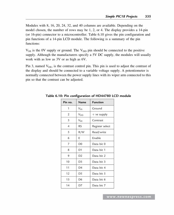
Modules with 8, 16, 20, 24, 32, and 40 columns are available. Depending on the
model chosen, the number of rows may be 1, 2, or 4. The display provides a 14-pin
(or 16-pin) connector to a microcontroller. Table 6.10 gives the pin configuration and
pin functions of a 14-pin LCD module. The following is a summary of the pin
functions:
VSS is the 0V supply or ground. The VDD pin should be connected to the positive
supply. Although the manufacturers specify a 5V DC supply, the modules will usually
work with as low as 3V or as high as 6V.
Pin 3, named VEE, is the contrast control pin. This pin is used to adjust the contrast of
the display and should be connected to a variable voltage supply. A potentiometer is
normally connected between the power supply lines with its wiper arm connected to this
pin so that the contrast can be adjusted.
Table 6.10: Pin configuration of HD44780 LCD module
Pin no. Name Function
1 VSS Ground
2 VDD þ ve supply
3 VEE Contrast
4 RS Register select
5 R/W Read/write
6 E Enable
7 D0 Data bit 0
8 D1 Data bit 1
9 D2 Data bit 2
10 D3 Data bit 3
11 D4 Data bit 4
12 D5 Data bit 5
13 D6 Data bit 6
14 D7 Data bit 7
www.newnespress.com
335Simple PIC18 Projects
Pin 4 is the register select (RS), and when this pin is LOW, data transferred to the
display is treated as commands. When RS is HIGH, character data can be transferred to
and from the module.
Pin 5 is the read/write (R/W) line. This pin is pulled LOW in order to write commands
or character data to the LCD module. When this pin is HIGH, character data or status
information can be read from the module.
Pin 6 is the enable (E) pin, which is used to initiate the transfer of commands or data
between the module and the microcontroller. When writing to the display, data is
transferred only on the HIGH-to-LOW transition of this line. When reading from the
display, data becomes available after the LOW-to-HIGH transition of the enable pin,
and this data remains valid as long as the enable pin is at logic HIGH.
Pins 7 to 14 are the eight data bus lines (D0 to D7). Data can be transferred between
the microcontroller and the LCD module using either a single 8-bit byte or as two
4-bit nibbles. In the latter case, only the upper four data lines (D4 to D7) are used.
The 4-bit mode means that four fewer I/O lines are used to communicate with the
LCD. In this book we are using only an alphanumeric-based LCD and only the 4-bit
interface.
Connecting the LCD
The mikroC compiler assumes by default that the LCD is connected to the
microcontroller as follows:
LCD Microcontroller port
D7 Bit 7 of the portD6 Bit 6 of the portD5 Bit 5 of the portD4 Bit 4 of the portE Bit 3 of the portRS Bit 2 of the port
where port is the port name specified using the Lcd_Init statement.
For example, we can use the statement Lcd_Init(&PORTB) if the LCD is connected to
PORTB with the default connection.
www.newnespress.com
336 Chapter 6
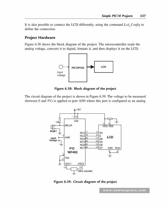
It is also possible to connect the LCD differently, using the command Lcd_Config to
define the connection.
Project Hardware
Figure 6.38 shows the block diagram of the project. The microcontroller reads the
analog voltage, converts it to digital, formats it, and then displays it on the LCD.
The circuit diagram of the project is shown in Figure 6.39. The voltage to be measured
(between 0 and 5V) is applied to port AN0 where this port is configured as an analog
PIC18F452 LCD
Inputvoltage
Figure 6.38: Block diagram of the project
Figure 6.39: Circuit diagram of the project
www.newnespress.com
337Simple PIC18 Projects
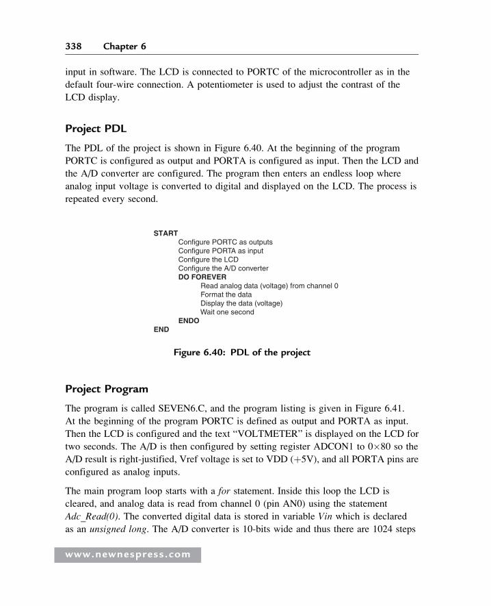
input in software. The LCD is connected to PORTC of the microcontroller as in the
default four-wire connection. A potentiometer is used to adjust the contrast of the
LCD display.
Project PDL
The PDL of the project is shown in Figure 6.40. At the beginning of the program
PORTC is configured as output and PORTA is configured as input. Then the LCD and
the A/D converter are configured. The program then enters an endless loop where
analog input voltage is converted to digital and displayed on the LCD. The process is
repeated every second.
Project Program
The program is called SEVEN6.C, and the program listing is given in Figure 6.41.
At the beginning of the program PORTC is defined as output and PORTA as input.
Then the LCD is configured and the text “VOLTMETER” is displayed on the LCD for
two seconds. The A/D is then configured by setting register ADCON1 to 0�80 so the
A/D result is right-justified, Vref voltage is set to VDD (þ5V), and all PORTA pins are
configured as analog inputs.
The main program loop starts with a for statement. Inside this loop the LCD is
cleared, and analog data is read from channel 0 (pin AN0) using the statement
Adc_Read(0). The converted digital data is stored in variable Vin which is declared
as an unsigned long. The A/D converter is 10-bits wide and thus there are 1024 steps
START Configure PORTC as outputs Configure PORTA as input Configure the LCD Configure the A/D converter DO FOREVER Read analog data (voltage) from channel 0 Format the data Display the data (voltage) Wait one second ENDO END
Figure 6.40: PDL of the project
www.newnespress.com
338 Chapter 6
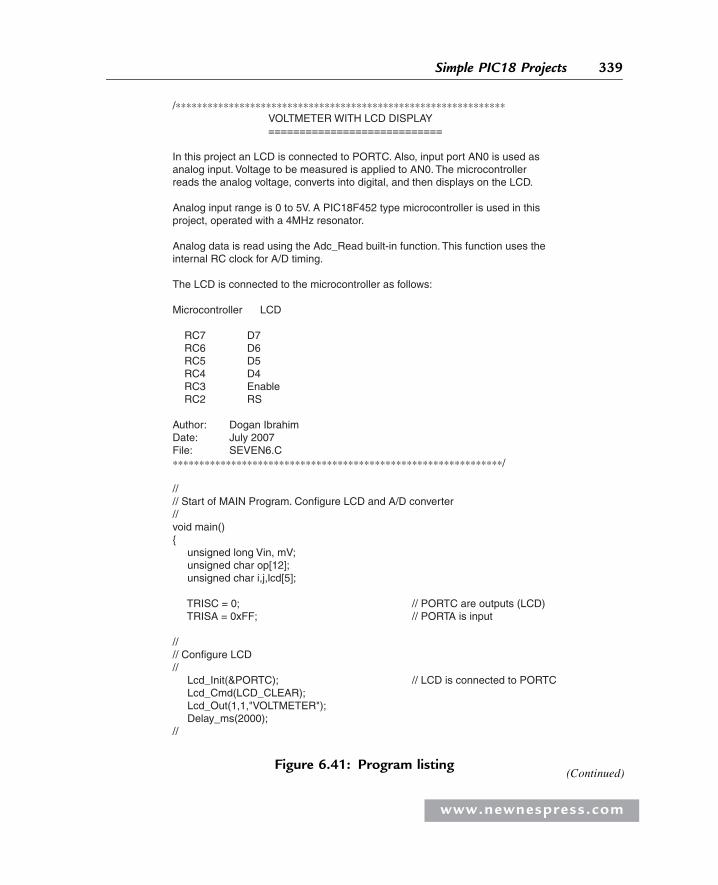
/∗∗∗∗∗∗∗∗∗∗∗∗∗∗∗∗∗∗∗∗∗∗∗∗∗∗∗∗∗∗∗∗∗∗∗∗∗∗∗∗∗∗∗∗∗∗∗∗∗∗∗∗∗∗∗∗∗∗∗∗∗∗ VOLTMETER WITH LCD DISPLAY ============================
In this project an LCD is connected to PORTC. Also, input port AN0 is used as analog input. Voltage to be measured is applied to AN0. The microcontrollerreads the analog voltage, converts into digital, and then displays on the LCD.
Analog input range is 0 to 5V. A PIC18F452 type microcontroller is used in this project, operated with a 4MHz resonator.
Analog data is read using the Adc_Read built-in function. This function uses the internal RC clock for A/D timing.
The LCD is connected to the microcontroller as follows:
Microcontroller LCD
RC7 D7 RC6 D6 RC5 D5 RC4 D4 RC3 Enable RC2 RS
Author: Dogan IbrahimDate: July 2007File: SEVEN6.C∗∗∗∗∗∗∗∗∗∗∗∗∗∗∗∗∗∗∗∗∗∗∗∗∗∗∗∗∗∗∗∗∗∗∗∗∗∗∗∗∗∗∗∗∗∗∗∗∗∗∗∗∗∗∗∗∗∗∗∗∗∗/
//// Start of MAIN Program. Configure LCD and A/D converter//void main(){ unsigned long Vin, mV; unsigned char op[12]; unsigned char i,j,lcd[5]; TRISC = 0; // PORTC are outputs (LCD) TRISA = 0xFF; // PORTA is input
//// Configure LCD// Lcd_Init(&PORTC); // LCD is connected to PORTC Lcd_Cmd(LCD_CLEAR); Lcd_Out(1,1,"VOLTMETER"); Delay_ms(2000);//
Figure 6.41: Program listing(Continued)
www.newnespress.com
339Simple PIC18 Projects
(0 to 1023) corresponding to the reference voltage of 5000mV. Each step corresponds to
5000mV/1024 ¼ 4.88mV. Inside the loop, variable Vin is converted into millivolts by
multiplying by 5000 and dividing into 1024. The division is done by shifting right by 10
digits. At this point variable mV contains the converted data in millivolts.
Function LongToStr is called to convert mV into a string in character array op.
LongToStr converts a long variable into a string having a fixed width of eleven
characters. If the resulting string is fewer than eleven characters, the left column of
the data is filled with space characters.
// Configure A/D converter. AN0 is used in this project// ADCON1 = 0x80; // Use AN0 and Vref=+5V//// Program loop// for(;;) // Endless loop { Lcd_Cmd(LCD_CLEAR); Vin = Adc_Read(0); // Read from channel 0 (AN0) Lcd_Out(1,1,"mV = "); // Display "mV = " mV = (Vin * 5000) >> 10; // mv = Vin x 5000 / 1024 LongToStr(mV,op); // Convert to string in "op"//// Remove leading blanks// j=0; for(i=0;i<=11;i++) { if(op[i] != ' ') // If a blank { lcd[j]=op[i]; j++; } }//// Display result on LCD// Lcd_Out(1,6,lcd); // Output to LCD Delay_ms(1000); // Wait 1 second }
}
Figure 6.41: (Cont’d)
www.newnespress.com
340 Chapter 6
The leading blanks are then removed and the data is stored in a variable called lcd.
Function Lcd_Out is called to display the data on the LCD starting from column 5 of
row 1. For example, if the measured voltage is 1267mV, it is displayed on the LCD as:
mV ¼ 1267
A More Accurate Display
The voltage displayed in Figure 6.41 is not very accurate, since integer arithmetic
has been performed in the calculation and the voltage is calculated by multiplying
the A/D output by 5000 and then dividing the result by 1024 using integer division.
Although the multiplication is accurate, the accuracy of the measurement is lost when
the number is divided by 1024. A more accurate result can be obtained by scaling the
number before it is displayed, as follows.
First, multiply the number Vin by a factor to remove the integer division. For example,
since 5000/1024 ¼ 4.88, we can multiply Vin by 488. For the display, we can calculate
the integer part of the result by dividing the number into 100, and then the fractional
part can be calculated as the remainder. The integer part and the fractional part can be
displayed with a decimal point in between. This technique has been implemented in
program SEVEN7.C as shown in Figure 6.42. In this program variables Vdec and Vfrac
store the integer and the fractional parts of the number respectively. The decimal part is
then converted into a string using function LongToStr and leading blanks are removed.
The parts of the fractional number are called ch1 and ch2. These are converted into
characters by adding 48 (i.e., character “0”) and then displayed at the next cursor
positions using the LCD command Lcd_Chr_Cp.
We could also calculate and display more accurate results by using floating point
arithmetic, but since this uses huge amounts of memory it should be avoided if possible.
PROJECT 6.9—Calculator with Keypad and LCD
Project Description
Keypads are small keyboards used to enter numeric or alphanumeric data into
microcontroller systems. Keypads are available in a variety of sizes and styles, from
2 � 2 to 4 � 4 or even bigger.
This project uses a 4 � 4 keypad (shown in Figure 6.43) and an LCD to design a simple
calculator.
www.newnespress.com
341Simple PIC18 Projects
/************************************************************** VOLTMETER WITH LCD DISPLAY ============================
In this project an LCD is connected to PORTC. Also, input portAN0 is used as analog input. Voltage to be measured is appliedto AN0. The microcontroller reads the analog voltage, convertsinto digital, and then displays on the LCD.
Analog input range is 0 to 5V. A PIC18F452 type microcontrolleris used in this project, operated with a 4MHz resonator.
Analog data is read using the Adc_Read built-in function. Thisfunction uses the internal RC clock for A/D timing.
The LCD is connected to the microcontroller as follows:
Microcontroller LCD
RC7 D7 RC6 D6 RC5 D5 RC4 D4 RC3 Enable RC2 RS
This program displays more accurate results than program SEVEN6.C.The voltage is displayed as follows:
mV = nnnn.mm Author: Dogan IbrahimDate: July 2007File: SEVEN7.C**************************************************************/
//// Start of MAIN Program. Configure LCD and A/D converter//void main(){ unsigned long Vin, mV,Vdec,Vfrac; unsigned char op[12]; unsigned char i,j,lcd[5],ch1,ch2;
TRISC = 0; // PORTC are outputs (LCD) TRISA = 0xFF; // PORTA is input
//// Configure LCD
Figure 6.42: A more accurate program
www.newnespress.com
342 Chapter 6
// Lcd_Init(&PORTC); // LCD is connected to PORTC Lcd_Cmd(LCD_CLEAR); Lcd_Out(1,1,"VOLTMETER"); Delay_ms(2000);//// Configure A/D converter. AN0 is used in this project// ADCON1 = 0x80; // Use AN0 and Vref=+5V//// Program loop// for(;;) // Endless loop { Lcd_Cmd(LCD_CLEAR); Vin = Adc_Read(0); // Read from channel 0 (AN0) Lcd_Out(1,1,"mV = "); // Display "mV = " Vin = 488*Vin; // Scale up the result Vdec = Vin / 100; // Decimal part Vfrac = Vin % 100; // Fractional part LongToStr(Vdec,op); // Convert Vdec to string in "op"//// Remove leading blanks// j=0; for(i=0;i<=11;i++) { if(op[i] != ' ') // If a blank { lcd[j]=op[i]; j++; } }//// Display result on LCD// Lcd_Out(1,6,lcd); // Output to LCD Lcd_Out_Cp("."); // Display "." ch1 = Vfrac / 10; // Calculate fractional part ch2 = Vfrac % 10; // Calculate fractional part Lcd_Chr_Cp(48+ch1); // Display fractional part Lcd_Chr_Cp(48+ch2); // Display fractional part Delay_ms(1000); // Wait 1 second }
}
Figure 6.42: (Cont’d)
www.newnespress.com
343Simple PIC18 Projects
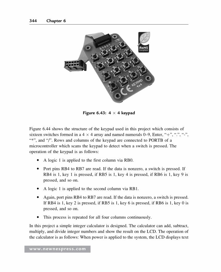
Figure 6.44 shows the structure of the keypad used in this project which consists of
sixteen switches formed in a 4 � 4 array and named numerals 0–9, Enter, “þ”, “.”, “-”,
“*”, and “/”. Rows and columns of the keypad are connected to PORTB of a
microcontroller which scans the keypad to detect when a switch is pressed. The
operation of the keypad is as follows:
� A logic 1 is applied to the first column via RB0.
� Port pins RB4 to RB7 are read. If the data is nonzero, a switch is pressed. If
RB4 is 1, key 1 is pressed, if RB5 is 1, key 4 is pressed, if RB6 is 1, key 9 is
pressed, and so on.
� A logic 1 is applied to the second column via RB1.
� Again, port pins RB4 to RB7 are read. If the data is nonzero, a switch is pressed.
If RB4 is 1, key 2 is pressed, if RB5 is 1, key 6 is pressed, if RB6 is 1, key 0 is
pressed, and so on.
� This process is repeated for all four columns continuously.
In this project a simple integer calculator is designed. The calculator can add, subtract,
multiply, and divide integer numbers and show the result on the LCD. The operation of
the calculator is as follows: When power is applied to the system, the LCD displays text
Figure 6.43: 4 � 4 keypad
www.newnespress.com
344 Chapter 6
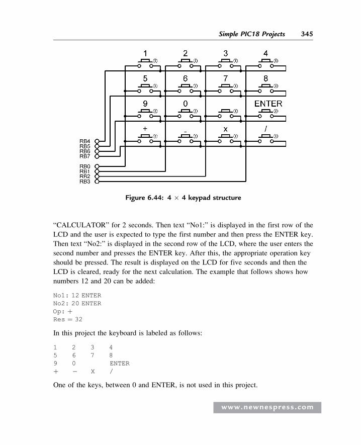
“CALCULATOR” for 2 seconds. Then text “No1:” is displayed in the first row of the
LCD and the user is expected to type the first number and then press the ENTER key.
Then text “No2:” is displayed in the second row of the LCD, where the user enters the
second number and presses the ENTER key. After this, the appropriate operation key
should be pressed. The result is displayed on the LCD for five seconds and then the
LCD is cleared, ready for the next calculation. The example that follows shows how
numbers 12 and 20 can be added:
No1: 12 ENTERNo2: 20 ENTEROp: þRes ¼ 32
In this project the keyboard is labeled as follows:
1 2 3 45 6 7 89 0 ENTERþ � X /
One of the keys, between 0 and ENTER, is not used in this project.
Figure 6.44: 4 � 4 keypad structure
www.newnespress.com
345Simple PIC18 Projects
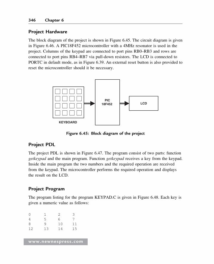
Project Hardware
The block diagram of the project is shown in Figure 6.45. The circuit diagram is given
in Figure 6.46. A PIC18F452 microcontroller with a 4MHz resonator is used in the
project. Columns of the keypad are connected to port pins RB0–RB3 and rows are
connected to port pins RB4–RB7 via pull-down resistors. The LCD is connected to
PORTC in default mode, as in Figure 6.39. An external reset button is also provided to
reset the microcontroller should it be necessary.
Project PDL
The project PDL is shown in Figure 6.47. The program consist of two parts: function
getkeypad and the main program. Function getkeypad receives a key from the keypad.
Inside the main program the two numbers and the required operation are received
from the keypad. The microcontroller performs the required operation and displays
the result on the LCD.
Project Program
The program listing for the program KEYPAD.C is given in Figure 6.48. Each key is
given a numeric value as follows:
0 1 2 34 5 6 78 9 10 1112 13 14 15
PIC18F452 LCD
KEYBOARD
Figure 6.45: Block diagram of the project
www.newnespress.com
346 Chapter 6
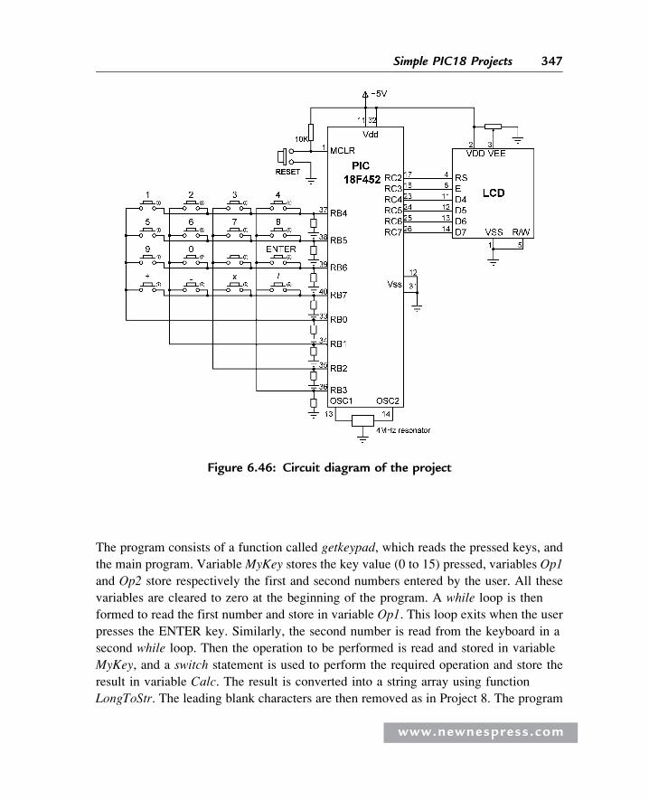
The program consists of a function called getkeypad, which reads the pressed keys, and
the main program. Variable MyKey stores the key value (0 to 15) pressed, variables Op1
and Op2 store respectively the first and second numbers entered by the user. All these
variables are cleared to zero at the beginning of the program. A while loop is then
formed to read the first number and store in variable Op1. This loop exits when the user
presses the ENTER key. Similarly, the second number is read from the keyboard in a
second while loop. Then the operation to be performed is read and stored in variable
MyKey, and a switch statement is used to perform the required operation and store the
result in variable Calc. The result is converted into a string array using function
LongToStr. The leading blank characters are then removed as in Project 8. The program
Figure 6.46: Circuit diagram of the project
www.newnespress.com
347Simple PIC18 Projects
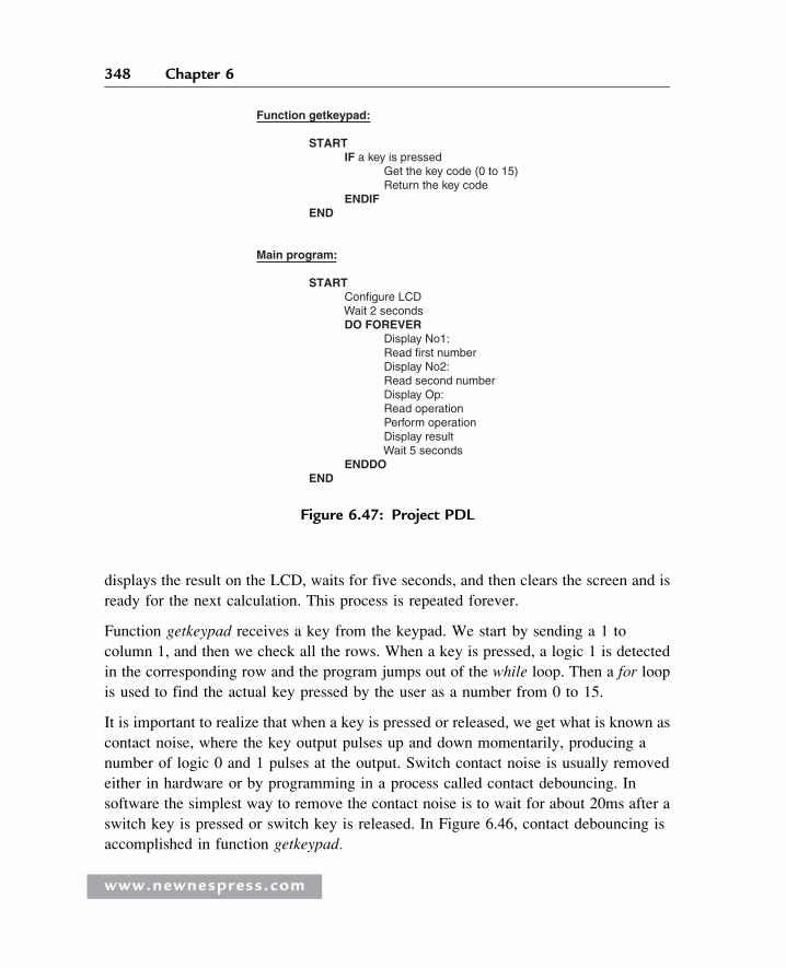
displays the result on the LCD, waits for five seconds, and then clears the screen and is
ready for the next calculation. This process is repeated forever.
Function getkeypad receives a key from the keypad. We start by sending a 1 to
column 1, and then we check all the rows. When a key is pressed, a logic 1 is detected
in the corresponding row and the program jumps out of the while loop. Then a for loop
is used to find the actual key pressed by the user as a number from 0 to 15.
It is important to realize that when a key is pressed or released, we get what is known as
contact noise, where the key output pulses up and down momentarily, producing a
number of logic 0 and 1 pulses at the output. Switch contact noise is usually removed
either in hardware or by programming in a process called contact debouncing. In
software the simplest way to remove the contact noise is to wait for about 20ms after a
switch key is pressed or switch key is released. In Figure 6.46, contact debouncing is
accomplished in function getkeypad.
Function getkeypad:
START IF a key is pressed Get the key code (0 to 15) Return the key code ENDIF END
Main program:
START Configure LCD Wait 2 seconds DO FOREVER Display No1: Read first number Display No2: Read second number Display Op: Read operation Perform operation Display result Wait 5 seconds ENDDO END
Figure 6.47: Project PDL
www.newnespress.com
348 Chapter 6
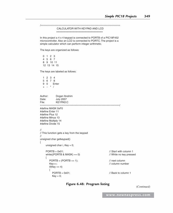
/∗∗∗∗∗∗∗∗∗∗∗∗∗∗∗∗∗∗∗∗∗∗∗∗∗∗∗∗∗∗∗∗∗∗∗∗∗∗∗∗∗∗∗∗∗∗∗∗∗∗∗∗∗∗∗∗∗∗∗∗∗∗
In this project a 4 x 4 keypad is connected to PORTB of a PIC18F452 microcontroller. Also an LCD is connected to PORTC. The project is a simple calculator which can perform integer arithmetic.
The keys are organized as follows:
0 1 2 3 4 5 6 7 8 9 10 11 12 13 14 15 The keys are labeled as follows:
1 2 3 4 5 6 7 8 9 0 Enter + − * / Author: Dogan IbrahimDate: July 2007File: KEYPAD.C∗∗∗∗∗∗∗∗∗∗∗∗∗∗∗∗∗∗∗∗∗∗∗∗∗∗∗∗∗∗∗∗∗∗∗∗∗∗∗∗∗∗∗∗∗∗∗∗∗∗∗∗∗∗∗∗∗∗∗∗∗∗/#define MASK 0xF0#define Enter 11#define Plus 12#define Minus 13#define Multiply 14#define Divide 15
//// This function gets a key from the keypad//unsigned char getkeypad(){ unsigned char i, Key = 0; PORTB = 0x01; // Start with column 1 while((PORTB & MASK) == 0) // While no key pressed { PORTB = (PORTB << 1); // next column Key++; // column number if(Key == 4) { PORTB = 0x01; // Back to column 1 Key = 0;
CALCULATOR WITH KEYPAD AND LCD===============================
Figure 6.48: Program listing(Continued)
www.newnespress.com
349Simple PIC18 Projects
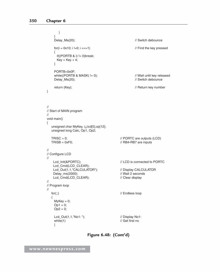
} } Delay_Ms(20); // Switch debounce for(i = 0x10; i !=0; i <<=1) // Find the key pressed { if((PORTB & i) != 0)break; Key = Key + 4; }
PORTB=0x0F; while((PORTB & MASK) != 0); // Wait until key released Delay_Ms(20); // Switch debounce return (Key); // Return key number}
//// Start of MAIN program//void main(){ unsigned char MyKey, i,j,lcd[5],op[12]; unsigned long Calc, Op1, Op2;
TRISC = 0; // PORTC are outputs (LCD) TRISB = 0xF0; // RB4-RB7 are inputs //// Configure LCD// Lcd_Init(&PORTC); // LCD is connected to PORTC Lcd_Cmd(LCD_CLEAR); Lcd_Out(1,1,"CALCULATOR"); // Display CALCULATOR Delay_ms(2000); // Wait 2 seconds Lcd_Cmd(LCD_CLEAR); // Clear display//// Program loop// for(;;) // Endless loop { MyKey = 0; Op1 = 0; Op2 = 0; Lcd_Out(1,1,"No1: "); // Display No1: while(1) // Get first no {
Figure 6.48: (Cont’d)
www.newnespress.com
350 Chapter 6
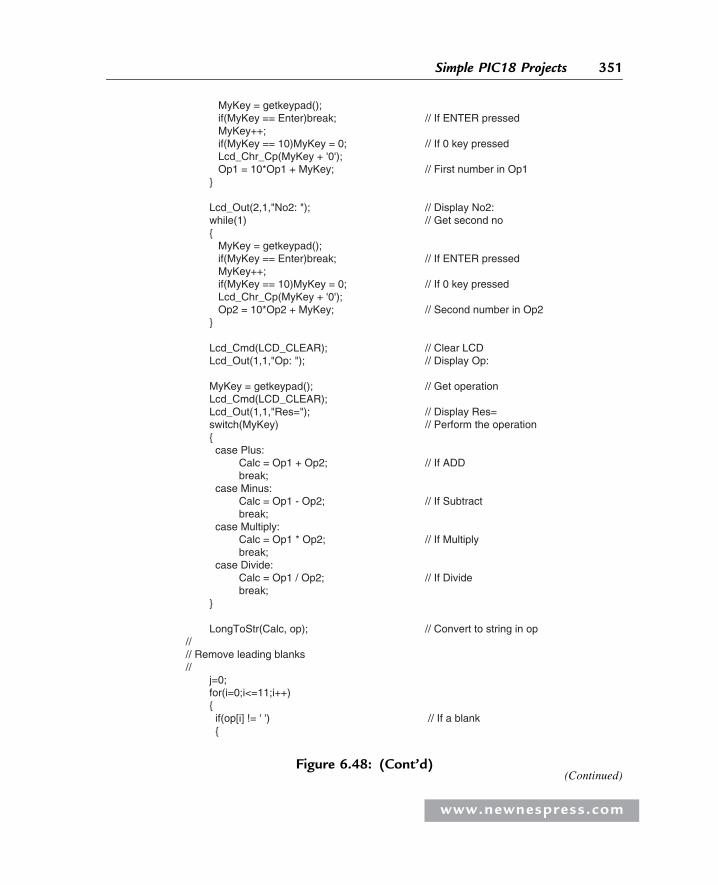
MyKey = getkeypad(); if(MyKey == Enter)break; // If ENTER pressed MyKey++; if(MyKey == 10)MyKey = 0; // If 0 key pressed Lcd_Chr_Cp(MyKey + '0'); Op1 = 10*Op1 + MyKey; // First number in Op1 } Lcd_Out(2,1,"No2: "); // Display No2: while(1) // Get second no { MyKey = getkeypad(); if(MyKey == Enter)break; // If ENTER pressed MyKey++; if(MyKey == 10)MyKey = 0; // If 0 key pressed Lcd_Chr_Cp(MyKey + '0'); Op2 = 10*Op2 + MyKey; // Second number in Op2 } Lcd_Cmd(LCD_CLEAR); // Clear LCD Lcd_Out(1,1,"Op: "); // Display Op: MyKey = getkeypad(); // Get operation Lcd_Cmd(LCD_CLEAR); Lcd_Out(1,1,"Res="); // Display Res= switch(MyKey) // Perform the operation { case Plus: Calc = Op1 + Op2; // If ADD break; case Minus: Calc = Op1 - Op2; // If Subtract break; case Multiply: Calc = Op1 * Op2; // If Multiply break; case Divide: Calc = Op1 / Op2; // If Divide break; }
LongToStr(Calc, op); // Convert to string in op//// Remove leading blanks// j=0; for(i=0;i<=11;i++) { if(op[i] != ' ') // If a blank {
Figure 6.48: (Cont’d)(Continued)
www.newnespress.com
351Simple PIC18 Projects
Program Using a Built-in Keypad Function
In the program listing in Figure 6.48, a function called getkeypad has been developed to
read a key from the keyboard. The mikroC language has built-in functions called
Keypad_Read and Keypad_Released to read a key from a keypad when a key is pressed
and when a key is released respectively. Figure 6.49 shows a modified program
(KEYPAD2.C) listing using the Keypad_Released function to implement the preceding
calculator project. The circuit diagram is the same as in Figure 6.46.
Before using the Keypad_Released function we have to call the Keypad_Init function to
tell the microcontroller what the keypad is connected to. Keypad_Released detects
when a key is pressed and then released. When released, the function returns a number
between 1 and 16 corresponding to the key pressed. The remaining parts of the program
are the same as in Figure 6.48.
PROJECT 6.10—Serial Communication–Based Calculator
Project Description
Serial communication is a simple means of sending data long distances quickly and
reliably. The most common serial communication method is based on the RS232
standard, in which standard data is sent over a single line from a transmitting device to a
receiving device in bit serial format at a prespecified speed, also known as the baud
rate, or the number of bits sent each second. Typical baud rates are 4800, 9600, 19200,
38400, etc.
RS232 serial communication is a form of asynchronous data transmission where data is
sent character by character. Each character is preceded with a start bit, seven or eight
lcd[j]=op[i]; j++; } } Lcd_Out_Cp(lcd); // Display result Delay_ms(5000); // Wait 5 seconds Lcd_Cmd(LCD_CLEAR); }}
Figure 6.48: (Cont’d)
www.newnespress.com
352 Chapter 6
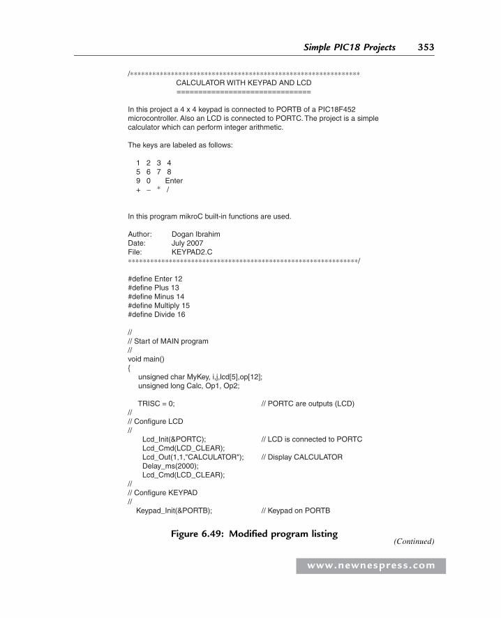
/∗∗∗∗∗∗∗∗∗∗∗∗∗∗∗∗∗∗∗∗∗∗∗∗∗∗∗∗∗∗∗∗∗∗∗∗∗∗∗∗∗∗∗∗∗∗∗∗∗∗∗∗∗∗∗∗∗∗∗∗∗∗
In this project a 4 x 4 keypad is connected to PORTB of a PIC18F452 microcontroller. Also an LCD is connected to PORTC. The project is a simple calculator which can perform integer arithmetic.
The keys are labeled as follows:
1 2 3 4 5 6 7 8 9 0 Enter + − ∗ /
In this program mikroC built-in functions are used.
Author: Dogan IbrahimDate: July 2007File: KEYPAD2.C∗∗∗∗∗∗∗∗∗∗∗∗∗∗∗∗∗∗∗∗∗∗∗∗∗∗∗∗∗∗∗∗∗∗∗∗∗∗∗∗∗∗∗∗∗∗∗∗∗∗∗∗∗∗∗∗∗∗∗∗∗∗/
#define Enter 12#define Plus 13#define Minus 14#define Multiply 15#define Divide 16
//// Start of MAIN program//void main(){ unsigned char MyKey, i,j,lcd[5],op[12]; unsigned long Calc, Op1, Op2;
TRISC = 0; // PORTC are outputs (LCD)//// Configure LCD// Lcd_Init(&PORTC); // LCD is connected to PORTC Lcd_Cmd(LCD_CLEAR); Lcd_Out(1,1,"CALCULATOR"); // Display CALCULATOR Delay_ms(2000); Lcd_Cmd(LCD_CLEAR);//// Configure KEYPAD// Keypad_Init(&PORTB); // Keypad on PORTB
CALCULATOR WITH KEYPAD AND LCD===============================
Figure 6.49: Modified program listing(Continued)
www.newnespress.com
353Simple PIC18 Projects
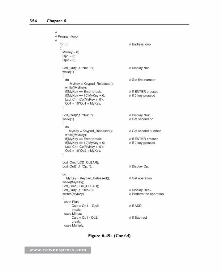
//// Program loop// for(;;) // Endless loop { MyKey = 0; Op1 = 0; Op2 = 0;
Lcd_Out(1,1,"No1: "); // Display No1: while(1) { do // Get first number MyKey = Keypad_Released(); while(!MyKey); if(MyKey == Enter)break; // If ENTER pressed if(MyKey == 10)MyKey = 0; // If 0 key pressed Lcd_Chr_Cp(MyKey + '0'); Op1 = 10*Op1 + MyKey; }
Lcd_Out(2,1,"No2: "); // Display No2: while(1) // Get second no { do MyKey = Keypad_Released(); // Get second number while(!MyKey); if(MyKey == Enter)break; // If ENTER pressed if(MyKey == 10)MyKey = 0; // If 0 key pressed Lcd_Chr_Cp(MyKey + '0'); Op2 = 10*Op2 + MyKey; }
Lcd_Cmd(LCD_CLEAR); Lcd_Out(1,1,"Op: "); // Display Op:
do MyKey = Keypad_Released(); // Get operation while(!MyKey); Lcd_Cmd(LCD_CLEAR); Lcd_Out(1,1,"Res="); // Display Res= switch(MyKey) // Perform the operation { case Plus: Calc = Op1 + Op2; // If ADD break; case Minus: Calc = Op1 - Op2; // If Subtract break; case Multiply:
Figure 6.49: (Cont’d)
www.newnespress.com
354 Chapter 6
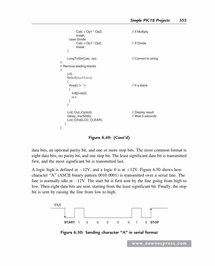
data bits, an optional parity bit, and one or more stop bits. The most common format is
eight data bits, no parity bit, and one stop bit. The least significant data bit is transmitted
first, and the most significant bit is transmitted last.
A logic high is defined at �12V, and a logic 0 is at þ12V. Figure 6.50 shows how
character “A” (ASCII binary pattern 0010 0001) is transmitted over a serial line. The
line is normally idle at �12V. The start bit is first sent by the line going from high to
low. Then eight data bits are sent, starting from the least significant bit. Finally, the stop
bit is sent by raising the line from low to high.
Calc = Op1 * Op2; // If Multiply break; case Divide: Calc = Op1 / Op2; // If Divide break; } LongToStr(Calc, op); // Convert to string//// Remove leading blanks// j=0; for(i=0;i<=11;i++) { if(op[i] != ' ') // If a blank { lcd[j]=op[i]; j++; } }
Lcd_Out_Cp(lcd); // Display result Delay_ms(5000); // Wait 5 seconds Lcd_Cmd(LCD_CLEAR); }}
Figure 6.49: (Cont’d)
IDLE
START 0 0 0 0 0 STOP1 1 0
Figure 6.50: Sending character “A” in serial format
www.newnespress.com
355Simple PIC18 Projects
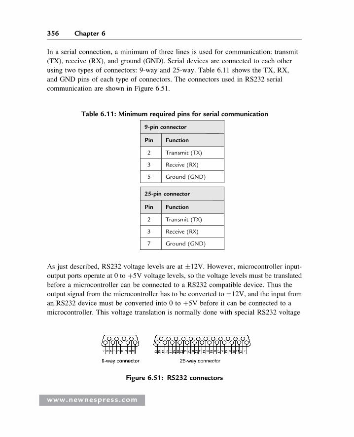
In a serial connection, a minimum of three lines is used for communication: transmit
(TX), receive (RX), and ground (GND). Serial devices are connected to each other
using two types of connectors: 9-way and 25-way. Table 6.11 shows the TX, RX,
and GND pins of each type of connectors. The connectors used in RS232 serial
communication are shown in Figure 6.51.
As just described, RS232 voltage levels are at �12V. However, microcontroller input-
output ports operate at 0 to þ5V voltage levels, so the voltage levels must be translated
before a microcontroller can be connected to a RS232 compatible device. Thus the
output signal from the microcontroller has to be converted to �12V, and the input from
an RS232 device must be converted into 0 to þ5V before it can be connected to a
microcontroller. This voltage translation is normally done with special RS232 voltage
Table 6.11: Minimum required pins for serial communication
9-pin connector
Pin Function
2 Transmit (TX)
3 Receive (RX)
5 Ground (GND)
25-pin connector
Pin Function
2 Transmit (TX)
3 Receive (RX)
7 Ground (GND)
Figure 6.51: RS232 connectors
www.newnespress.com
356 Chapter 6
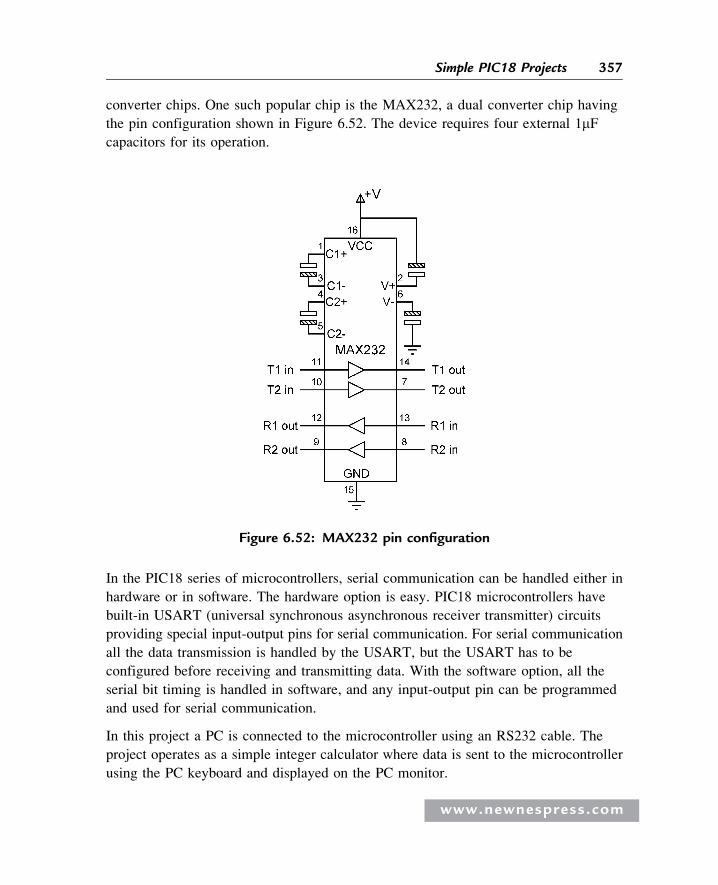
converter chips. One such popular chip is the MAX232, a dual converter chip having
the pin configuration shown in Figure 6.52. The device requires four external 1mFcapacitors for its operation.
In the PIC18 series of microcontrollers, serial communication can be handled either in
hardware or in software. The hardware option is easy. PIC18 microcontrollers have
built-in USART (universal synchronous asynchronous receiver transmitter) circuits
providing special input-output pins for serial communication. For serial communication
all the data transmission is handled by the USART, but the USART has to be
configured before receiving and transmitting data. With the software option, all the
serial bit timing is handled in software, and any input-output pin can be programmed
and used for serial communication.
In this project a PC is connected to the microcontroller using an RS232 cable. The
project operates as a simple integer calculator where data is sent to the microcontroller
using the PC keyboard and displayed on the PC monitor.
Figure 6.52: MAX232 pin configuration
www.newnespress.com
357Simple PIC18 Projects
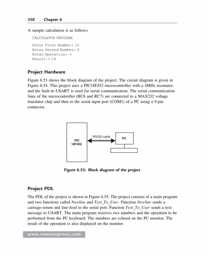
A sample calculation is as follows:
CALCULATOR PROGRAM
Enter First Number: 12Enter Second Number: 2Enter Operation: þResult ¼ 14
Project Hardware
Figure 6.53 shows the block diagram of the project. The circuit diagram is given in
Figure 6.54. This project uses a PIC18F452 microcontroller with a 4MHz resonator,
and the built-in USART is used for serial communication. The serial communication
lines of the microcontroller (RC6 and RC7) are connected to a MAX232 voltage
translator chip and then to the serial input port (COM1) of a PC using a 9-pin
connector.
Project PDL
The PDL of the project is shown in Figure 6.55. The project consists of a main program
and two functions called Newline and Text_To_User. Function Newline sends a
carriage-return and line-feed to the serial port. Function Text_To_User sends a text
message to USART. The main program receives two numbers and the operation to be
performed from the PC keyboard. The numbers are echoed on the PC monitor. The
result of the operation is also displayed on the monitor.
PIC18F452
PC RS232 cable
Figure 6.53: Block diagram of the project
www.newnespress.com
358 Chapter 6
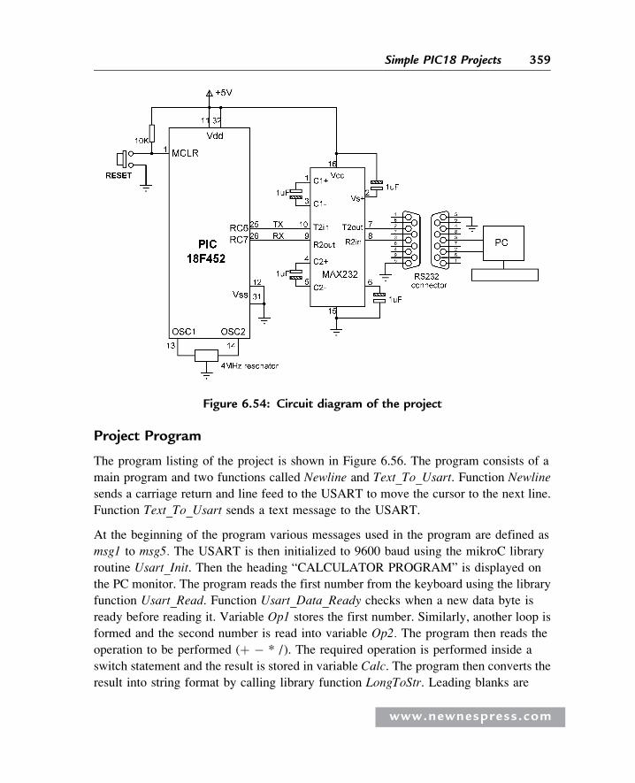
Project Program
The program listing of the project is shown in Figure 6.56. The program consists of a
main program and two functions called Newline and Text_To_Usart. Function Newline
sends a carriage return and line feed to the USART to move the cursor to the next line.
Function Text_To_Usart sends a text message to the USART.
At the beginning of the program various messages used in the program are defined as
msg1 to msg5. The USART is then initialized to 9600 baud using the mikroC library
routine Usart_Init. Then the heading “CALCULATOR PROGRAM” is displayed on
the PC monitor. The program reads the first number from the keyboard using the library
function Usart_Read. Function Usart_Data_Ready checks when a new data byte is
ready before reading it. Variable Op1 stores the first number. Similarly, another loop is
formed and the second number is read into variable Op2. The program then reads the
operation to be performed (þ � * /). The required operation is performed inside a
switch statement and the result is stored in variable Calc. The program then converts the
result into string format by calling library function LongToStr. Leading blanks are
Figure 6.54: Circuit diagram of the project
www.newnespress.com
359Simple PIC18 Projects
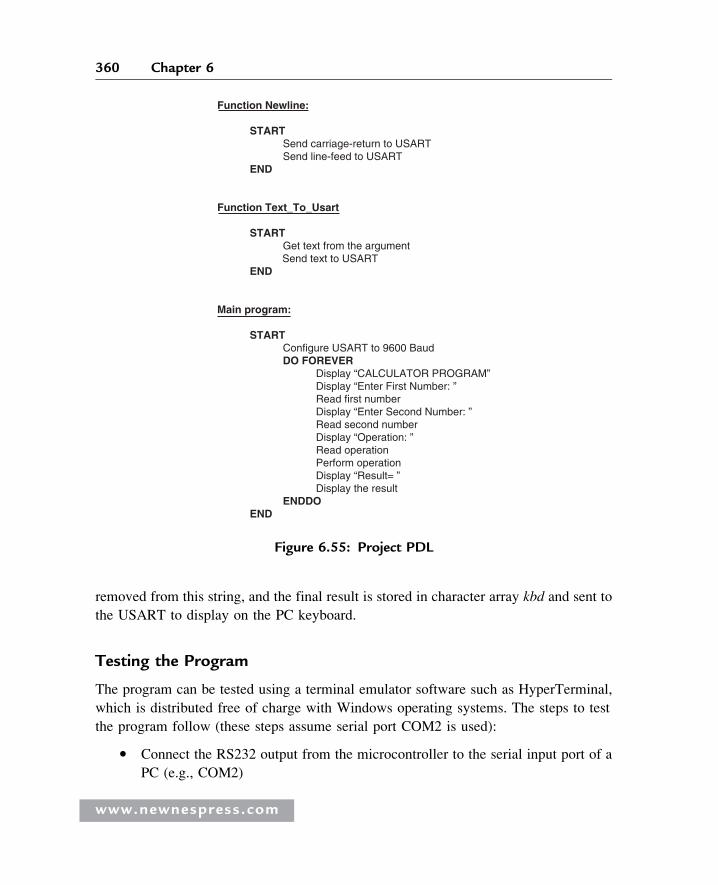
removed from this string, and the final result is stored in character array kbd and sent to
the USART to display on the PC keyboard.
Testing the Program
The program can be tested using a terminal emulator software such as HyperTerminal,
which is distributed free of charge with Windows operating systems. The steps to test
the program follow (these steps assume serial port COM2 is used):
� Connect the RS232 output from the microcontroller to the serial input port of a
PC (e.g., COM2)
Function Newline:
START Send carriage-return to USART Send line-feed to USART END
Function Text_To_Usart
START Get text from the argument Send text to USART END
Main program:
START Configure USART to 9600 Baud DO FOREVER Display “CALCULATOR PROGRAM” Display “Enter First Number: ” Read first number Display “Enter Second Number: ” Read second number Display “Operation: ” Read operation Perform operation Display “Result= ” Display the result ENDDO END
Figure 6.55: Project PDL
www.newnespress.com
360 Chapter 6
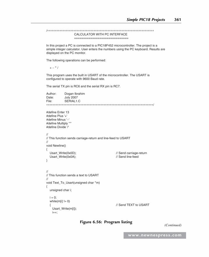
/∗∗∗∗∗∗∗∗∗∗∗∗∗∗∗∗∗∗∗∗∗∗∗∗∗∗∗∗∗∗∗∗∗∗∗∗∗∗∗∗∗∗∗∗∗∗∗∗∗∗∗∗∗∗∗∗∗∗∗∗∗∗∗∗∗∗∗∗∗ CALCULATOR WITH PC INTERFACE ==============================
In this project a PC is connected to a PIC18F452 microcontroller. The project is a simple integer calculator. User enters the numbers using the PC keyboard. Results are displayed on the PC monitor.
The following operations can be performed:
+ − ∗ / This program uses the built in USART of the microcontroller. The USART is configured to operate with 9600 Baud rate.
The serial TX pin is RC6 and the serial RX pin is RC7.
Author: Dogan IbrahimDate: July 2007File: SERIAL1.C∗∗∗∗∗∗∗∗∗∗∗∗∗∗∗∗∗∗∗∗∗∗∗∗∗∗∗∗∗∗∗∗∗∗∗∗∗∗∗∗∗∗∗∗∗∗∗∗∗∗∗∗∗∗∗∗∗∗∗∗∗∗∗∗∗∗∗∗∗/
#define Enter 13#define Plus '+'#define Minus '−'#define Multiply '∗'#define Divide '/'
//// This function sends carriage-return and line-feed to USART//void Newline(){ Usart_Write(0x0D); // Send carriage-return Usart_Write(0x0A); // Send line-feed}
//// This function sends a text to USART//void Text_To_Usart(unsigned char ∗m){ unsigned char i; i = 0; while(m[i] != 0) { // Send TEXT to USART Usart_Write(m[i]); i++;
Figure 6.56: Program listing(Continued)
www.newnespress.com
361Simple PIC18 Projects
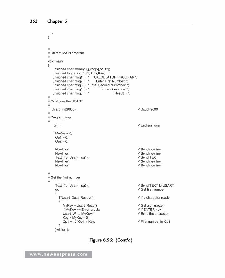
}}
//// Start of MAIN program//void main(){ unsigned char MyKey, i,j,kbd[5],op[12]; unsigned long Calc, Op1, Op2,Key; unsigned char msg1[] = " CALCULATOR PROGRAM"; unsigned char msg2[] = " Enter First Number: "; unsigned char msg3[]= "Enter Second Nummber: "; unsigned char msg4[] = " Enter Operation: "; unsigned char msg5[] = " Result = ";//// Configure the USART// Usart_Init(9600); // Baud=9600//// Program loop// for(;;) // Endless loop { MyKey = 0; Op1 = 0; Op2 = 0; Newline(); // Send newline Newline(); // Send newline Text_To_Usart(msg1); // Send TEXT Newline(); // Send newline Newline(); // Send newline
//// Get the first number// Text_To_Usart(msg2); // Send TEXT to USART do // Get first number { if(Usart_Data_Ready()) // If a character ready { MyKey = Usart_Read(); // Get a character if(MyKey == Enter)break; // If ENTER key Usart_Write(MyKey); // Echo the character Key = MyKey - '0'; Op1 = 10∗Op1 + Key; // First number in Op1 } }while(1);
Figure 6.56: (Cont’d)
www.newnespress.com
362 Chapter 6
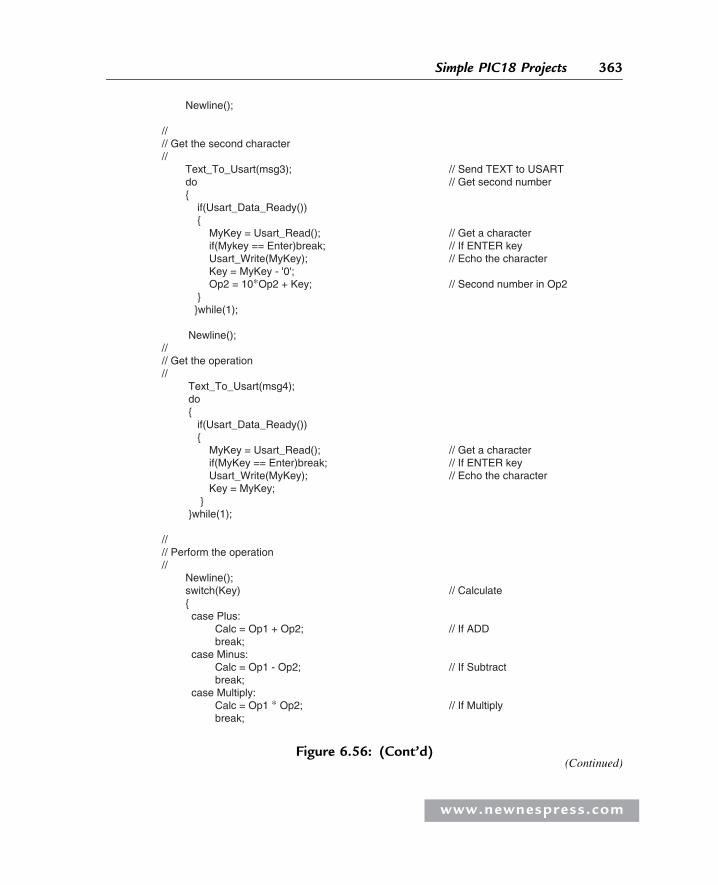
Newline(); //// Get the second character// Text_To_Usart(msg3); // Send TEXT to USART do // Get second number { if(Usart_Data_Ready()) { MyKey = Usart_Read(); // Get a character if(Mykey == Enter)break; // If ENTER key Usart_Write(MyKey); // Echo the character Key = MyKey - '0'; Op2 = 10∗Op2 + Key; // Second number in Op2 } }while(1); Newline();//// Get the operation// Text_To_Usart(msg4); do { if(Usart_Data_Ready()) { MyKey = Usart_Read(); // Get a character if(MyKey == Enter)break; // If ENTER key Usart_Write(MyKey); // Echo the character Key = MyKey; } }while(1);
//// Perform the operation// Newline(); switch(Key) // Calculate { case Plus: Calc = Op1 + Op2; // If ADD break; case Minus: Calc = Op1 - Op2; // If Subtract break; case Multiply: Calc = Op1 ∗ Op2; // If Multiply break;
Figure 6.56: (Cont’d)(Continued)
www.newnespress.com
363Simple PIC18 Projects
� Start HyperTerminal terminal emulation software and give a name to
the session
� Select File -> New connection -> Connect using and select COM2
� Select the baud rate as 9600, data bits as 8, no parity bits, and 1 stop bit
� Reset the microcontroller
An example output from the HyperTerminal screen is shown in Figure 6.57.
Using Software-Based Serial Communication
The preceding example made use of the microcontroller’s USART and thus its special
serial I/O pins. Serial communication can also be handled entirely in software, without
using the USART. In this method, any pin of the microcontroller can be used for serial
communication.
case Divide: Calc = Op1 / Op2; // If Divide break; }
LongToStr(Calc, op); // Convert to string//// Remove leading blanks// j=0; for(i=0;i<=11;i++) { if(op[i] != ' ') // If a blank { kbd[j]=op[i]; j++; } } Text_To_Usart(msg5); for(i=0; i<j;i++)Usart_Write(kbd[i]); // Display result
}}
Figure 6.56: (Cont’d)
www.newnespress.com
364 Chapter 6
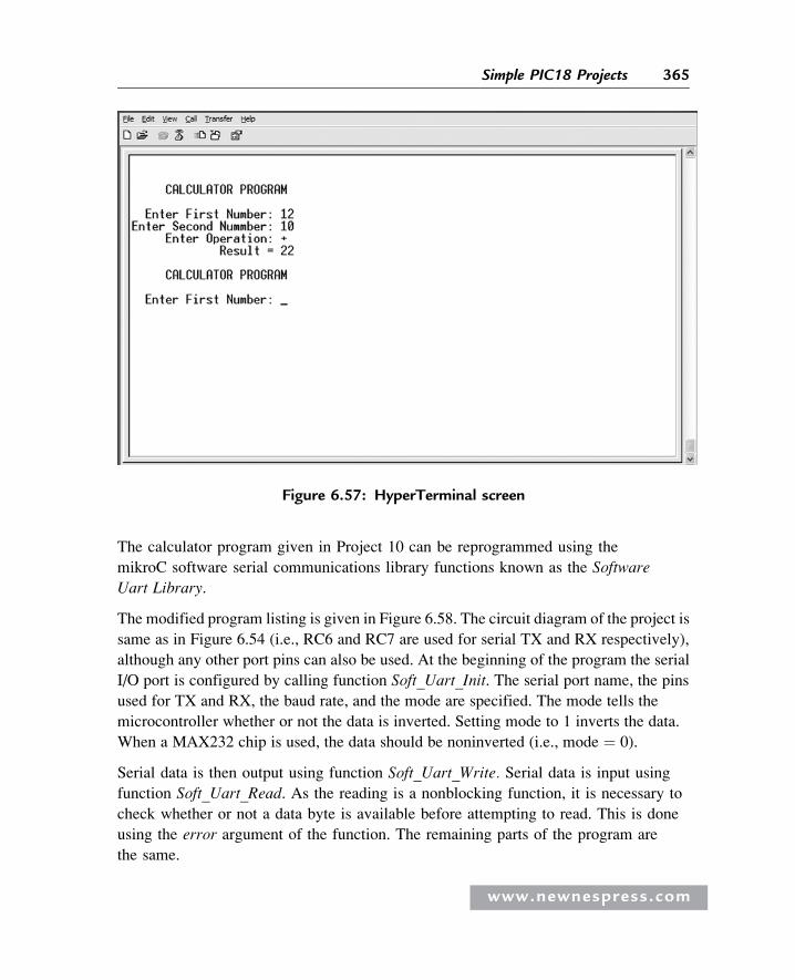
The calculator program given in Project 10 can be reprogrammed using the
mikroC software serial communications library functions known as the Software
Uart Library.
The modified program listing is given in Figure 6.58. The circuit diagram of the project is
same as in Figure 6.54 (i.e., RC6 and RC7 are used for serial TX and RX respectively),
although any other port pins can also be used. At the beginning of the program the serial
I/O port is configured by calling function Soft_Uart_Init. The serial port name, the pins
used for TX and RX, the baud rate, and the mode are specified. The mode tells the
microcontroller whether or not the data is inverted. Setting mode to 1 inverts the data.
When a MAX232 chip is used, the data should be noninverted (i.e., mode ¼ 0).
Serial data is then output using function Soft_Uart_Write. Serial data is input using
function Soft_Uart_Read. As the reading is a nonblocking function, it is necessary to
check whether or not a data byte is available before attempting to read. This is done
using the error argument of the function. The remaining parts of the program are
the same.
Figure 6.57: HyperTerminal screen
www.newnespress.com
365Simple PIC18 Projects
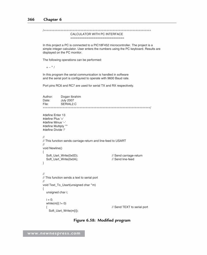
/∗∗∗∗∗∗∗∗∗∗∗∗∗∗∗∗∗∗∗∗∗∗∗∗∗∗∗∗∗∗∗∗∗∗∗∗∗∗∗∗∗∗∗∗∗∗∗∗∗∗∗∗∗∗∗∗∗∗∗∗∗∗∗∗∗∗∗∗∗∗ CALCULATOR WITH PC INTERFACE ==============================
In this project a PC is connected to a PIC18F452 microcontroller. The project is a simple integer calculator. User enters the numbers using the PC keyboard. Results are displayed on the PC monitor.
The following operations can be performed:
+ − ∗ /
In this program the serial communication is handled in softwareand the serial port is configured to operate with 9600 Baud rate.
Port pins RC6 and RC7 are used for serial TX and RX respectively.
Author: Dogan IbrahimDate: July 2007File: SERIAL2.C∗∗∗∗∗∗∗∗∗∗∗∗∗∗∗∗∗∗∗∗∗∗∗∗∗∗∗∗∗∗∗∗∗∗∗∗∗∗∗∗∗∗∗∗∗∗∗∗∗∗∗∗∗∗∗∗∗∗∗∗∗∗∗∗∗∗∗∗∗∗/
#define Enter 13#define Plus '+'#define Minus '−'#define Multiply '∗'#define Divide '/'
//// This function sends carriage-return and line-feed to USART//void Newline(){ Soft_Uart_Write(0x0D); // Send carriage-return Soft_Uart_Write(0x0A); // Send line-feed}
//// This function sends a text to serial port//void Text_To_Usart(unsigned char ∗m){ unsigned char i;
i = 0; while(m[i] != 0) { // Send TEXT to serial port Soft_Uart_Write(m[i]);
Figure 6.58: Modified program
www.newnespress.com
366 Chapter 6
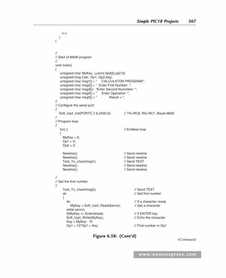
i++; }}
//// Start of MAIN program//void main(){ unsigned char MyKey, i,j,error,kbd[5],op[12]; unsigned long Calc, Op1, Op2,Key; unsigned char msg1[] = " CALCULATOR PROGRAM"; unsigned char msg2[] = " Enter First Number: "; unsigned char msg3[]= "Enter Second Nummber: "; unsigned char msg4[] = " Enter Operation: "; unsigned char msg5[] = " Result = ";//// Configure the serial port// Soft_Uart_Init(PORTC,7,6,2400,0); // TX=RC6, RX=RC7, Baud=9600//// Program loop// for(;;) // Endless loop { MyKey = 0; Op1 = 0; Op2 = 0;
Newline(); // Send newline Newline(); // Send newline Text_To_Usart(msg1); // Send TEXT Newline(); // Send newline Newline(); // Send newline
//// Get the first number// Text_To_Usart(msg2); // Send TEXT do // Get first number { do // If a character ready MyKey = Soft_Uart_Read(&error); // Get a character while (error); if(MyKey == Enter)break; // If ENTER key Soft_Uart_Write(MyKey); // Echo the character Key = MyKey - '0'; Op1 = 10*Op1 + Key; // First number in Op1
Figure 6.58: (Cont’d)(Continued)
www.newnespress.com
367Simple PIC18 Projects
}while(1);
Newline();
//// Get the second character// Text_To_Usart(msg3); // Send TEXT do // Get second number { do MyKey = Soft_Uart_Read(&error); // Get a character while(error); if(Mykey == Enter)break; // If ENTER key Soft_Uart_Write(MyKey); // Echo the character Key = MyKey - '0'; Op2 = 10∗Op2 + Key; // Second number in Op2
}while(1);
Newline();//// Get the operation// Text_To_Usart(msg4); do { do MyKey = Soft_Uart_Read(&error); // Get a character while(error); if(MyKey == Enter)break; // If ENTER key Soft_Uart_Write(MyKey); // Echo the character Key = MyKey;
}while(1);
//// Perform the operation// Newline(); switch(Key) // Calculate { case Plus: Calc = Op1 + Op2; // If ADD break; case Minus: Calc = Op1 − Op2; // If Subtract break; case Multiply: Calc = Op1 ∗ Op2; // If Multiply
Figure 6.58: (Cont’d)
www.newnespress.com
368 Chapter 6
break; case Divide: Calc = Op1 / Op2; // If Divide break; }
LongToStr(Calc, op); // Convert to string//// Remove leading blanks// j=0; for(i=0;i<=11;i++) { if(op[i] != ' ') // If a blank { kbd[j]=op[i]; j++; } }
Text_To_Usart(msg5); for(i=0; i<j;i++)Soft_Uart_Write(kbd[i]); // Display result
}}
Figure 6.58: (Cont’d)
www.newnespress.com
369Simple PIC18 Projects

This page intentionally left blank
CHAP T E R 7
Advanced PIC18 Projects—SDCard Projects
In this and the remaining chapters we will look at the design of more complex
PIC18 microcontroller–based projects. This chapter discusses the design of Secure
Digital (SD) memory card–based projects. The remaining chapters of the book
describe the basic theory and design of projects based on the popular USB bus and
CAN bus protocols.
7.1 The SD Card
Before going into the design details of SD card–based projects, we should take a look
at the basic principles and operation of SD card memory devices. Figure 7.1 shows
a typical SD card.
The SD card is a flash memory storage device designed to provide high-capacity,
nonvolatile, and rewritable storage in a small size. These devices are frequently used
in many electronic consumer goods, such as cameras, computers, GPS systems,
mobile phones, and PDAs. The memory capacity of the SD cards is increasing all
the time. Currently they are available at capacities from 256MB to 8GB. The SD
cards come in three sizes: standard, mini, and micro. Table 7.1 lists the main
specifications of the most common standard SD and miniSD cards.
SD card specifications are maintained by the SD Card Association, which has over
six hundred members. MiniSD and microSD cards are electrically compatible with
the standard SD cards and can be inserted in special adapters and used as standard
SD cards in standard card slots.
www.newnespress.com
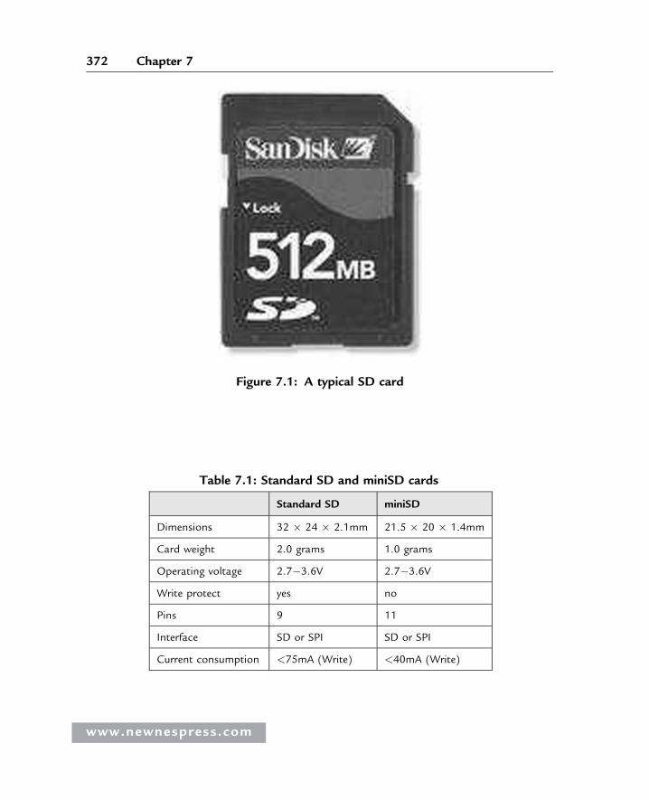
Figure 7.1: A typical SD card
Table 7.1: Standard SD and miniSD cards
Standard SD miniSD
Dimensions 32 � 24 � 2.1mm 21.5 � 20 � 1.4mm
Card weight 2.0 grams 1.0 grams
Operating voltage 2.7�3.6V 2.7�3.6V
Write protect yes no
Pins 9 11
Interface SD or SPI SD or SPI
Current consumption <75mA (Write) <40mA (Write)
www.newnespress.com
372 Chapter 7
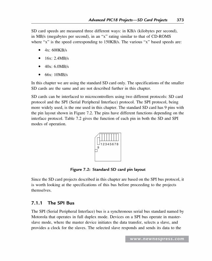
SD card speeds are measured three different ways: in KB/s (kilobytes per second),
in MB/s (megabytes per second), in an “x” rating similar to that of CD-ROMS
where “x” is the speed corresponding to 150KB/s. The various “x” based speeds are:
� 4x: 600KB/s
� 16x: 2.4MB/s
� 40x: 6.0MB/s
� 66x: 10MB/s
In this chapter we are using the standard SD card only. The specifications of the smaller
SD cards are the same and are not described further in this chapter.
SD cards can be interfaced to microcontrollers using two different protocols: SD card
protocol and the SPI (Serial Peripheral Interface) protocol. The SPI protocol, being
more widely used, is the one used in this chapter. The standard SD card has 9 pins with
the pin layout shown in Figure 7.2. The pins have different functions depending on the
interface protocol. Table 7.2 gives the function of each pin in both the SD and SPI
modes of operation.
Since the SD card projects described in this chapter are based on the SPI bus protocol, it
is worth looking at the specifications of this bus before proceeding to the projects
themselves.
7.1.1 The SPI Bus
The SPI (Serial Peripheral Interface) bus is a synchronous serial bus standard named by
Motorola that operates in full duplex mode. Devices on a SPI bus operate in master-
slave mode, where the master device initiates the data transfer, selects a slave, and
provides a clock for the slaves. The selected slave responds and sends its data to the
91 2 3 4 5 6 7 8
Figure 7.2: Standard SD card pin layout
www.newnespress.com
373Advanced PIC18 Projects—SD Card Projects
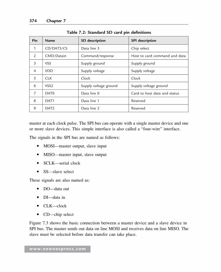
master at each clock pulse. The SPI bus can operate with a single master device and one
or more slave devices. This simple interface is also called a “four-wire” interface.
The signals in the SPI bus are named as follows:
� MOSI—master output, slave input
� MISO—master input, slave output
� SCLK—serial clock
� SS—slave select
These signals are also named as:
� DO—data out
� DI—data in
� CLK—clock
� CD—chip select
Figure 7.3 shows the basic connection between a master device and a slave device in
SPI bus. The master sends out data on line MOSI and receives data on line MISO. The
slave must be selected before data transfer can take place.
Table 7.2: Standard SD card pin definitions
Pin Name SD description SPI description
1 CD/DAT3/CS Data line 3 Chip select
2 CMD/Datain Command/response Host to card command and data
3 VSS Supply ground Supply ground
4 VDD Supply voltage Supply voltage
5 CLK Clock Clock
6 VSS2 Supply voltage ground Supply voltage ground
7 DAT0 Data line 0 Card to host data and status
8 DAT1 Data line 1 Reserved
9 DAT2 Data line 2 Reserved
www.newnespress.com
374 Chapter 7
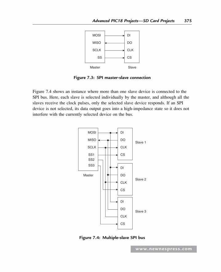
Figure 7.4 shows an instance where more than one slave device is connected to the
SPI bus. Here, each slave is selected individually by the master, and although all the
slaves receive the clock pulses, only the selected slave device responds. If an SPI
device is not selected, its data output goes into a high-impedance state so it does not
interfere with the currently selected device on the bus.
SS
SCLK
MISO
MOSI
CS
CLK
DO
DI
Master Slave
Figure 7.3: SPI master-slave connection
SS3
SS2
SS1
SCLK
MISO
MOSI DI
DO
CLK
CS
DI
DO
CLK
CS
CS
CLK
DO
DI
Slave 1
MasterSlave 2
Slave 3
Figure 7.4: Multiple-slave SPI bus
www.newnespress.com
375Advanced PIC18 Projects—SD Card Projects
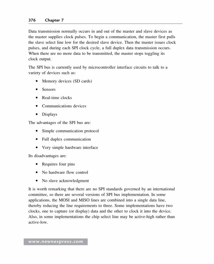
Data transmission normally occurs in and out of the master and slave devices as
the master supplies clock pulses. To begin a communication, the master first pulls
the slave select line low for the desired slave device. Then the master issues clock
pulses, and during each SPI clock cycle, a full duplex data transmission occurs.
When there are no more data to be transmitted, the master stops toggling its
clock output.
The SPI bus is currently used by microcontroller interface circuits to talk to a
variety of devices such as:
� Memory devices (SD cards)
� Sensors
� Real-time clocks
� Communications devices
� Displays
The advantages of the SPI bus are:
� Simple communication protocol
� Full duplex communication
� Very simple hardware interface
Its disadvantages are:
� Requires four pins
� No hardware flow control
� No slave acknowledgment
It is worth remarking that there are no SPI standards governed by an international
committee, so there are several versions of SPI bus implementation. In some
applications, the MOSI and MISO lines are combined into a single data line,
thereby reducing the line requirements to three. Some implementations have two
clocks, one to capture (or display) data and the other to clock it into the device.
Also, in some implementations the chip select line may be active-high rather than
active-low.
www.newnespress.com
376 Chapter 7
7.1.2 Operation of the SD Card in SPI Mode
When the SD card is operated in SPI mode, only seven pins are used. Three (pins 3,
4, and 6) are used for the power supply, leaving four pins (pins 1, 2, 5, and 7) for
the SPI mode of operation:
� Two power supply ground (pins 3 and 6)
� Power supply (pin 4)
� Chip select (pin 1)
� Data out (pin 7)
� Data in (pin 2)
� CLK (pin 5)
At power-up, the SD card defaults to the SD bus protocol. The card is switched to
SPI mode if the Chip Select (CS) signal is asserted during reception of the reset
command. When the card is in SPI mode, it only responds to SPI commands. The host
may reset a card by switching the power supply off and then on again.
ThemikroC compiler provides a library of commands for initializing, reading, and writing
to SD cards. It is not necessary to know the internal structure of an SD card in detail
before using one, since the library functions are available. However, a basic understanding
of the internal structure of an SD card is helpful in making the best use of the card. In
this section we will look briefly at the internal architecture and operation of SD cards.
An SD card has a set of registers that provide information about the status of the card.
When the card is operated in SPI mode these are:
� Card identification register (CID)
� Card specific data register (CSD)
� SD configuration register (SCR)
� Operation control register (OCR)
The CID register consists of 16 bytes and contains the manufacturer ID, product name,
product revision, card serial number, manufacturer date code, and a checksum byte.
Table 7.3 shows the structure of the CID register.
www.newnespress.com
377Advanced PIC18 Projects—SD Card Projects
The CSD register consists of 16 bytes and contains card-specific data such as the card
data transfer rate, read/write block lengths, read/write currents, erase sector size, file
format, write protection flags, and checksum. Table 7.4 shows the structure of the CSD
register.
The SCR register is 8 bytes long and contains information about the SD card’s special
features and capabilities, such as security support and data bus widths supported.
The OCR register is only 4 bytes long and stores the VDD voltage profile of the card.
The OCR shows the voltage range in which the card data can be accessed.
All SD-card SPI commands are 6 bytes long, with the MSB transmitted first. Figure 7.5
shows the command format. The first byte is known as the command byte, and the
remaining five bytes are called command arguments. Bit 6 of the command byte is set
to 1 and the MSB bit is always 0. With the remaining six bits we have sixty-four
possible commands, named CMD0 to CMD63. Some of the important commands are:
� CMD0 GO_IDLE_STATE (resets the SD card)
� CMD1 SEND_OP_COND (initializes the card)
� CMD9 SEND_CSD (gets CSD register data)
Table 7.3: Structure of the CID register
Name Type Width Comments
Manufacturer ID (MID) Binary 1 byte Manufacturer ID (e.g., 0�03 forSanDisk)
OEM/Application ID (OID) ASCII 2 bytes Identifies card OEM and/or cardcontents
Product Name (PNM) ASCII 5 bytes Product name
Product Revision (PRV) BCD 1 byte Two binary coded digits
Serial Number (PSN) Binary 4 bytes 32 bits unsigned integer
Reserved 4 bits Upper 4 bits
Manufacture Date Code (MDT) BCD 12 bits Manufacture date (offset from 2000)
CRC-7 Checksum Binary 7 bits Checksum
Not used Binary 1 bit Always 1
www.newnespress.com
378 Chapter 7
Table 7.4: Structure of the CSD register
Bytes
Byte 0 0 0 XXXXXX
Byte 1 TAAC [7:0]
Byte 2 NSAC [7:0]
Byte 3 TRAN_SPEED [7:0]
Byte 4 CCC [11:4]
Byte 5 CCC [3:0] READ_BL_LEN [3:0]
Byte 6 READ_BL_PARTIAL WRITE_BLK_MISALIGN READ_BLK_MISALIGN DSR_IMP X XC_SIZE (11:10)
Byte 7 C_SIZE [9:2]
Byte 8 C_SIZE [1:0] VDD_R_CURR_MIN (2:0) VDD_R_CURR_MAX (2:0)
Byte 9 VDD_W_CURR_MIN (2:0) VDD_W_CURR_MAX (2:0) C_SIZE_MULT (2:1)
Byte 10 ERASE_BLK_EN SECTOR_SIZE (6:1)
Byte 11 SECTOR_SIZE (0) WP_GRP_SIZE (6:0)
Byte 12 WP_GRP_ENABLE X X R2W_FACTOR( 2:0)
Byte 13 WRITE_BL_LEN (1:0) 0 X X X X X
Byte 14 FILE_FORMAT_GRP COPY PERM_WRITE_PROTECT TMP_WRITE_PROTECTFILE_FORMAT (1:0) X X
Byte 15 CRC (6:0) 1
Field definitions
TAAC data read access time 1 (e.g., 1.5ms)
NSAC data read access time in CLK cycles
TRAN_SPEED max data transfer rate
CCC card command classes
READ_BL_LEN max read data block length (e.g., 512 bytes)
READ_BL_PARTIAL partial blocks for read allowed
(Continued)
www.newnespress.com
379Advanced PIC18 Projects—SD Card Projects
Table 7.4: (Cont’d)
Field definitions
WRITE_BLK_MISALIGN write block misalignment
READ_BLK_MISALIGN read block misalignment
DSR_IMP DSR implemented
C_SIZE device size
VDD_R_CURR_MIN max read current at VDD min
VDD_R_CURR_MAX max read current at VDD max
VDD_W_CURR_MIN max write current at VDD min
VDD_W_CURR_MAX max write current at VDD max
C_SIZE_MULT device size multiplier
ERASE_BLK_EN erase single block enable
SECTOR_SIZE erase sector size
WP_GRP_SIZE write protect group size
WP_GRP_ENABLE write protect group enable
R2W_FACTOR write speed factor
WRITE_BL_LEN max write data block length (e.g., 512 bytes)
WRITE_BL_PARTIAL partial blocks for write allowed
FILE_FORMAT_GRP file format group
COPY copy flag
PERM_WRITE_PROTECT permanent write protect
TMP_WRITE_PROTECT temporary write protect
FILE_FORMAT file format
Byte 1 Byte 2 - 5 Byte 6 7 6 0 731 00 1 Command Command argument CRC 1
Figure 7.5: SD card SPI command format
www.newnespress.com
380 Chapter 7
� CMD10 SEND_CID (gets CID register data)
� CMD16 SET_BLOCKLEN (selects a block length in bytes)
� CMD17 READ_SINGLE_BLOCK (reads a block of data)
� CMD24 WRITE_BLOCK (writes a block of data)
� CMD32 ERASE_WR_BLK_START_ADDR (sets the address of the first
write block to be erased)
� CMD33 ERASE_WR_BLK_END_ADDR (sets the address of the last write
block to be erased)
� CMD38 ERASE (erases all previously selected blocks)
In response to a command, the card sends a status byte known as R1. The MSB
bit of this byte is always 0 and the other bits indicate the following error
conditions:
� Card in idle state
� Erase reset
� Illegal command
� Communication CRC error
� Erase sequence error
� Address error
� Parameter error
Reading Data
The SD card in SPI mode supports single-block and multiple-block read operations.
The host should set the block length. After a valid read command the card responds
with a response token, followed by a data block and a CRC check. The block length
can be between 1 and 512 bytes. The starting address can be any valid address in
the address range of the card.
In multiple-block read operations, the card sends data blocks with each block having
its own CRC check attached to the end of the block.
www.newnespress.com
381Advanced PIC18 Projects—SD Card Projects
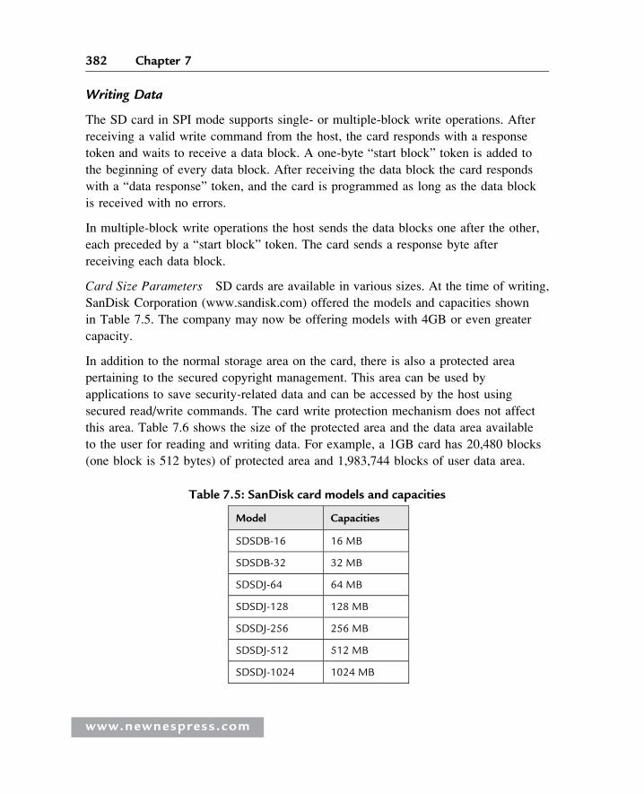
Writing Data
The SD card in SPI mode supports single- or multiple-block write operations. After
receiving a valid write command from the host, the card responds with a response
token and waits to receive a data block. A one-byte “start block” token is added to
the beginning of every data block. After receiving the data block the card responds
with a “data response” token, and the card is programmed as long as the data block
is received with no errors.
In multiple-block write operations the host sends the data blocks one after the other,
each preceded by a “start block” token. The card sends a response byte after
receiving each data block.
Card Size Parameters SD cards are available in various sizes. At the time of writing,
SanDisk Corporation (www.sandisk.com) offered the models and capacities shown
in Table 7.5. The company may now be offering models with 4GB or even greater
capacity.
In addition to the normal storage area on the card, there is also a protected area
pertaining to the secured copyright management. This area can be used by
applications to save security-related data and can be accessed by the host using
secured read/write commands. The card write protection mechanism does not affect
this area. Table 7.6 shows the size of the protected area and the data area available
to the user for reading and writing data. For example, a 1GB card has 20,480 blocks
(one block is 512 bytes) of protected area and 1,983,744 blocks of user data area.
Table 7.5: SanDisk card models and capacities
Model Capacities
SDSDB-16 16 MB
SDSDB-32 32 MB
SDSDJ-64 64 MB
SDSDJ-128 128 MB
SDSDJ-256 256 MB
SDSDJ-512 512 MB
SDSDJ-1024 1024 MB
www.newnespress.com
382 Chapter 7
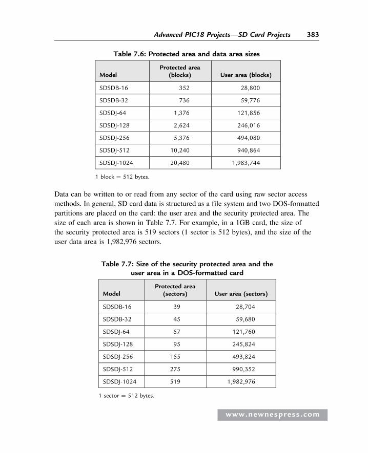
Data can be written to or read from any sector of the card using raw sector access
methods. In general, SD card data is structured as a file system and two DOS-formatted
partitions are placed on the card: the user area and the security protected area. The
size of each area is shown in Table 7.7. For example, in a 1GB card, the size of
the security protected area is 519 sectors (1 sector is 512 bytes), and the size of the
user data area is 1,982,976 sectors.
Table 7.6: Protected area and data area sizes
ModelProtected area
(blocks) User area (blocks)
SDSDB-16 352 28,800
SDSDB-32 736 59,776
SDSDJ-64 1,376 121,856
SDSDJ-128 2,624 246,016
SDSDJ-256 5,376 494,080
SDSDJ-512 10,240 940,864
SDSDJ-1024 20,480 1,983,744
1 block ¼ 512 bytes.
Table 7.7: Size of the security protected area and theuser area in a DOS-formatted card
ModelProtected area
(sectors) User area (sectors)
SDSDB-16 39 28,704
SDSDB-32 45 59,680
SDSDJ-64 57 121,760
SDSDJ-128 95 245,824
SDSDJ-256 155 493,824
SDSDJ-512 275 990,352
SDSDJ-1024 519 1,982,976
1 sector ¼ 512 bytes.
www.newnespress.com
383Advanced PIC18 Projects—SD Card Projects
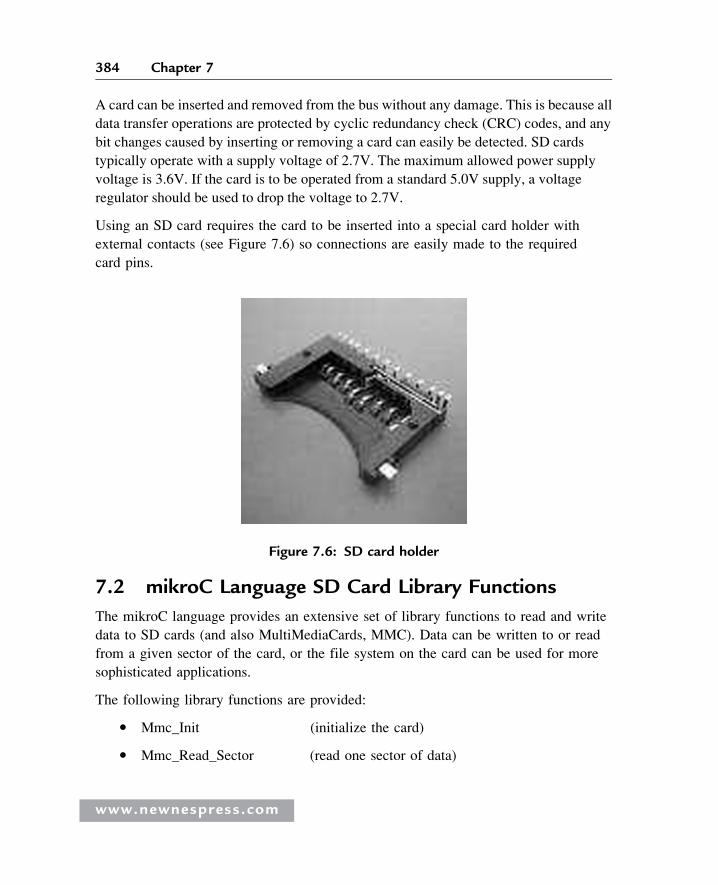
A card can be inserted and removed from the bus without any damage. This is because all
data transfer operations are protected by cyclic redundancy check (CRC) codes, and any
bit changes caused by inserting or removing a card can easily be detected. SD cards
typically operate with a supply voltage of 2.7V. The maximum allowed power supply
voltage is 3.6V. If the card is to be operated from a standard 5.0V supply, a voltage
regulator should be used to drop the voltage to 2.7V.
Using an SD card requires the card to be inserted into a special card holder with
external contacts (see Figure 7.6) so connections are easily made to the required
card pins.
7.2 mikroC Language SD Card Library Functions
The mikroC language provides an extensive set of library functions to read and write
data to SD cards (and also MultiMediaCards, MMC). Data can be written to or read
from a given sector of the card, or the file system on the card can be used for more
sophisticated applications.
The following library functions are provided:
� Mmc_Init (initialize the card)
� Mmc_Read_Sector (read one sector of data)
Figure 7.6: SD card holder
www.newnespress.com
384 Chapter 7
� Mmc_Write_Sector (write one sector of data)
� Mmc_Read_Cid (read CID register)
� Mmc_Read_Csd (read CSD register)
� Mmc_Fat_Init (initialize FAT)
� Mmc_Fat_QuickFormat (format the card to FAT16)
� Mmc_Fat_Assign (assign the file we will be working with)
� Mmc_Fat_Reset (reset the file pointer; opens the currently assigned
file for reading)
� Mmc_Fat_Rewrite (reset the file pointer and clear assigned file; opens
the assigned file for writing)
� Mmc_Fat_Append (move file pointer to the end of assigned file so
new data can be appended to the file)
� Mmc_Fat_Read (read the byte the file pointer points to)
� Mmc_Fat_Write (write a block of data to the assigned file)
� Mmc_Set_File_Date (write system timestamp to a file)
� Mmc_Fat_Delete (delete a file)
� Mmc_Fat_Get_File_Date (read file timestamp)
� Mmc_Fat_Get_File_Size (get file size in bytes)
� Mmc_Fat_Get_Swap_File (create a swap file)
In the remainder of this chapter we will look at some SD-card and PIC18
microcontroller-based projects.
PROJECT 7.1—Read CID Register and Displayon a PC Screen
In this project a SD card is interfaced to a PIC18F452-type microcontroller. The
serial output port of the microcontroller is connected to the serial input port (e.g.,
www.newnespress.com
385Advanced PIC18 Projects—SD Card Projects
COM1) of a PC. The microcontroller reads the contents of the card CID register
and sends this data to the PC so it can be displayed on the PC screen.
Figure 7.7 shows the block diagram of the project.
The circuit diagram of the project is shown in Figure 7.8. The SD card is inserted
into a card holder and then connected to PORTC of a PIC18F452 microcontroller
through 2.2K and 3.3K resistors, using the following pins:
� Card CS to PORTC pin RC2
� Card CLK to PORTC pin RC3
� Card DO to PORTC pin RC4
� Card DI to PORTC pin RC5
According to the SD card specifications, when the card is operating with a supply
voltage of VDD ¼ 3.3V, the input-output pin voltage levels are as follows:
� Minimum produced output HIGH voltage, VOH ¼ 2.475V
� Maximum produced output LOW voltage, VOL ¼ 0.4125V
� Minimum required input HIGH voltage, VIH ¼ 2.0625
� Maximum input HIGH voltage, VIH ¼ 3.6V
� Maximum required input LOW voltage, VIL ¼ 0.825V
PIC18F452
MAX232
PC
SDcard
RS232
Figure 7.7: Block diagram of the project
www.newnespress.com
386 Chapter 7
Although the output produced by the card (2.475V) is sufficient to drive the input port
of a PIC microcontroller, the logic HIGH output of the microcontroller (about 4.3V)
is too high for the SD card inputs (maximum 3.6V). Therefore, a potential divider is
set up at the three inputs of the SD card using 2.2K and 3.3K resistors. This limits the
maximum voltage at the inputs of the SD card to about 2.5V:
SD card input voltage ¼ 4:3V � 3:3K=ð2:2K þ 3:3KÞ ¼ 2:48V
Serial output port pin RC6 (TX) of the microcontroller is connected to a MAX232-type
RS232 voltage level converter chip and then to a 9-way D-type connector so it can be
connected to the serial input port of a PC.
The microcontroller is powered from a 5V supply which is obtained via a 7805-type 5V
regulator with a 9V input. The 2.7V–3.6V supply required by the SD card is obtained
via an MC33269DT-3.3 regulator with 3.3V output and is driven from the 5V
input voltage.
The program listing of the project is given in Figure 7.9 (program SD1.C). At the
beginning of the main program, character array CID is declared to have 16 bytes.
Figure 7.8: Circuit diagram of the project
www.newnespress.com
387Advanced PIC18 Projects—SD Card Projects
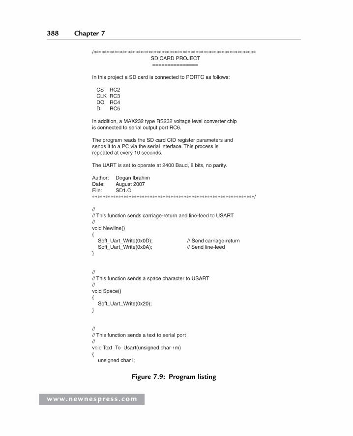
/∗∗∗∗∗∗∗∗∗∗∗∗∗∗∗∗∗∗∗∗∗∗∗∗∗∗∗∗∗∗∗∗∗∗∗∗∗∗∗∗∗∗∗∗∗∗∗∗∗∗∗∗∗∗∗∗∗∗∗∗∗∗ SD CARD PROJECT ===============
In this project a SD card is connected to PORTC as follows:
CS RC2 CLK RC3 DO RC4 DI RC5
In addition, a MAX232 type RS232 voltage level converter chipis connected to serial output port RC6.
The program reads the SD card CID register parameters andsends it to a PC via the serial interface. This process isrepeated at every 10 seconds.
The UART is set to operate at 2400 Baud, 8 bits, no parity.
Author: Dogan IbrahimDate: August 2007File: SD1.C∗∗∗∗∗∗∗∗∗∗∗∗∗∗∗∗∗∗∗∗∗∗∗∗∗∗∗∗∗∗∗∗∗∗∗∗∗∗∗∗∗∗∗∗∗∗∗∗∗∗∗∗∗∗∗∗∗∗∗∗∗∗/
//// This function sends carriage-return and line-feed to USART//void Newline(){ Soft_Uart_Write(0x0D); // Send carriage-return Soft_Uart_Write(0x0A); // Send line-feed}
//// This function sends a space character to USART//void Space(){ Soft_Uart_Write(0x20);}
//// This function sends a text to serial port//void Text_To_Usart(unsigned char ∗m){ unsigned char i;
Figure 7.9: Program listing
www.newnespress.com
388 Chapter 7
i = 0; while(m[i] != 0) { // Send TEXT to serial port Soft_Uart_Write(m[i]); i++; }}
//// This function sends string to serial port. The string length is passed as an argument//void Str_To_Usart(unsigned char ∗m,unsigned char 1){ unsigned char i; unsigned char txt[4]; i=0; for(i=0; i<l; i++) { ByteToStr(m[i],txt); Text_To_Usart(txt); Space(); }}
//// Start of MAIN program//void main(){ unsigned char error,CID[16]; unsigned char msg[] = " SD CARD CID REGISTER";
//// Configure the serial port// Soft_Uart_Init(PORTC,7,6,2400,0); // TX=RC6//// Initialise the SD card// Spi_Init_Advanced(MASTER_OSC_DIV16,DATA_SAMPLE_MIDDLE, CLK_IDLE_LOW, LOW_2_HIGH);//// Initialise the SD bus// while(Mmc_Init(&PORTC,2));//// Start of MAIN loop. Read the SD card CID register and send the data
Figure 7.9: (Cont’d)
www.newnespress.com
389Advanced PIC18 Projects—SD Card Projects
Variable msg is loaded with the message that is to be displayed when power is
applied to the system. Then the UART is initialized at PORTC with a baud rate
of 2400.
Before the SD card library functions are used, the function Spi_Init_Advanced
must be called with the given arguments. Then the SD card bus is initialized by
calling function Mmc_Init, where it is specified that the card is connected to
PORTC. The program then enters an endless loop that repeats every ten seconds.
Inside this loop the heading message is displayed followed by two new-line
characters. The program then reads the contents of register CID by calling function
Mmc_Read_Cid and stores the data in character array CID. The data is then sent
to the serial port by calling function Str_To_Usart. At the end of the loop two
new-line characters are displayed, the program waits for ten seconds, and the
loop is repeated.
The operation of the project can be tested by connecting the device to a PC and
starting the HyperTerminal terminal emulation program on the PC. Set the
communications parameters to 2400 baud, 8 data bits, 1 stop bit, and no parity bit.
An example output on the screen is shown in Figure 7.10.
// to serial port every 10 seconds// for(;;) // Endless loop {
Text_To_Usart(msg); // Send TEXT Newline(); // Send newline Newline(); // Send newline error = Mmc_Read_Cid(CID); // Read CID register into CID//// Send the data to RS232 port// Str_To_Usart(CID,16); // Send CID contents to UART Delay_Ms(10000); // Wait 10 seconds Newline(); Newline(); }}
Figure 7.9: (Cont’d)
www.newnespress.com
390 Chapter 7
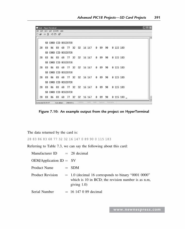
The data returned by the card is:
28 83 86 83 68 77 32 32 16 147 0 89 90 0 115 183
Referring to Table 7.3, we can say the following about this card:
Manufacturer ID ¼ 28 decimal
OEM/Application ID ¼ SV
Product Name ¼ SDM
Product Revision ¼ 1.0 (decimal 16 corresponds to binary “0001 0000”
which is 10 in BCD; the revision number is as n.m,
giving 1.0)
Serial Number ¼ 16 147 0 89 decimal
Figure 7.10: An example output from the project on HyperTerminal
www.newnespress.com
391Advanced PIC18 Projects—SD Card Projects
Reserved ¼ “0000” bits (4 bits only)
Manufacture Date Code ¼ 073 (this 12-bit parameter has the binary value “0000
0111 0011” where the upper 4 bits are derived from the
lower 4 bits of the reserved field and the lower 8 bits are
decimal 115. This gives BCD value 073. The date is in
YYM format since 2000. Thus, this card was
manufactured in 2007, March).
CRC ¼ “1011100” binary (the LSB bit is always 1)
PROJECT 7.2—Read/Write to SD Card Sectors
The hardware of this project is the same as for Project 7.1 (i.e., as shown in Figure 7.8).
In this project, sector 10 of the SD card is filled with “C” characters, and then this
sector is read and the card data is sent to the UART.
The program listing of this project is given in Figure 7.11 (program SD2.C).
Two character arrays called data1 and data2, of 512 bytes each, are declared at
the beginning of the program. Array data1 is loaded with character “C,” and
the contents of this array are written to sector 10 of the SD card. Then the
contents of sector 10 are read into character array data2 and sent to the UART,
displaying 512 “C” characters on the PC screen. Normally, only one array is
used to read and write to the SD card. Two arrays are used here to make it
clear that what is sent to the UART is the card data, not the contents of
array data1.
PROJECT 7.3—Using the Card Filing System
The hardware of this project is the same as for Project 7.1 (i.e., as shown in Figure 7.8).
In this project, a file called MYFILE55.TXT is created on the SD card. String
“This is MYFILE.TXT” is written to the file initially. Then the string “This is the
added data. . .” is appended to the file. The program then reads the contents of
the file and sends the string “This is MYFILE.TXT. This is the added data. . .” to
the UART, enabling the data to be displayed on the PC screen when HyperTerminal
is run.
www.newnespress.com
392 Chapter 7
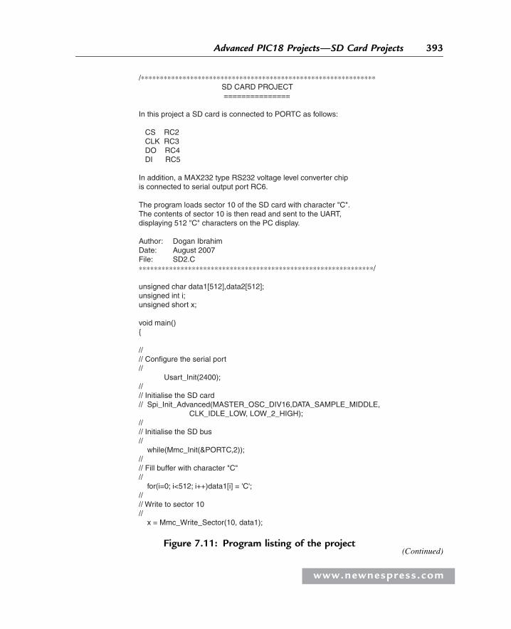
/∗∗∗∗∗∗∗∗∗∗∗∗∗∗∗∗∗∗∗∗∗∗∗∗∗∗∗∗∗∗∗∗∗∗∗∗∗∗∗∗∗∗∗∗∗∗∗∗∗∗∗∗∗∗∗∗∗∗∗∗∗∗ SD CARD PROJECT ===============
In this project a SD card is connected to PORTC as follows:
CS RC2 CLK RC3 DO RC4 DI RC5
In addition, a MAX232 type RS232 voltage level converter chipis connected to serial output port RC6.
The program loads sector 10 of the SD card with character "C".The contents of sector 10 is then read and sent to the UART,displaying 512 "C" characters on the PC display.
Author: Dogan IbrahimDate: August 2007File: SD2.C∗∗∗∗∗∗∗∗∗∗∗∗∗∗∗∗∗∗∗∗∗∗∗∗∗∗∗∗∗∗∗∗∗∗∗∗∗∗∗∗∗∗∗∗∗∗∗∗∗∗∗∗∗∗∗∗∗∗∗∗∗∗/
unsigned char data1[512],data2[512];unsigned int i;unsigned short x;
void main(){
//// Configure the serial port// Usart_Init(2400);//// Initialise the SD card// Spi_Init_Advanced(MASTER_OSC_DIV16,DATA_SAMPLE_MIDDLE, CLK_IDLE_LOW, LOW_2_HIGH);//// Initialise the SD bus// while(Mmc_Init(&PORTC,2));//// Fill buffer with character "C"// for(i=0; i<512; i++)data1[i] = 'C';//// Write to sector 10// x = Mmc_Write_Sector(10, data1);
Figure 7.11: Program listing of the project(Continued)
www.newnespress.com
393Advanced PIC18 Projects—SD Card Projects
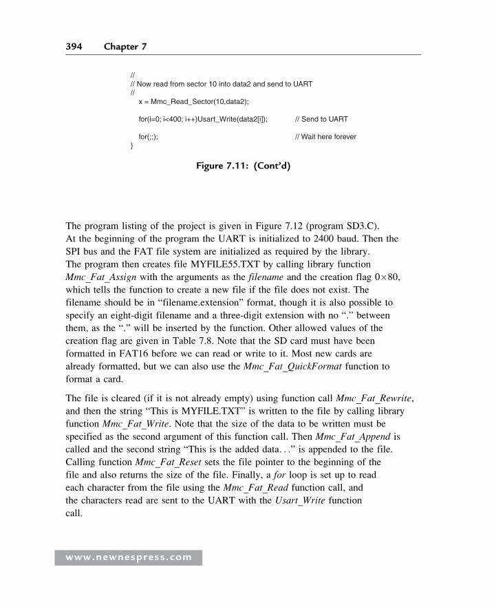
The program listing of the project is given in Figure 7.12 (program SD3.C).
At the beginning of the program the UART is initialized to 2400 baud. Then the
SPI bus and the FAT file system are initialized as required by the library.
The program then creates file MYFILE55.TXT by calling library function
Mmc_Fat_Assign with the arguments as the filename and the creation flag 0�80,
which tells the function to create a new file if the file does not exist. The
filename should be in “filename.extension” format, though it is also possible to
specify an eight-digit filename and a three-digit extension with no “.” between
them, as the “.” will be inserted by the function. Other allowed values of the
creation flag are given in Table 7.8. Note that the SD card must have been
formatted in FAT16 before we can read or write to it. Most new cards are
already formatted, but we can also use the Mmc_Fat_QuickFormat function to
format a card.
The file is cleared (if it is not already empty) using function call Mmc_Fat_Rewrite,
and then the string “This is MYFILE.TXT” is written to the file by calling library
function Mmc_Fat_Write. Note that the size of the data to be written must be
specified as the second argument of this function call. Then Mmc_Fat_Append is
called and the second string “This is the added data. . .” is appended to the file.
Calling function Mmc_Fat_Reset sets the file pointer to the beginning of the
file and also returns the size of the file. Finally, a for loop is set up to read
each character from the file using the Mmc_Fat_Read function call, and
the characters read are sent to the UART with the Usart_Write function
call.
//// Now read from sector 10 into data2 and send to UART// x = Mmc_Read_Sector(10,data2);
for(i=0; i<400; i++)Usart_Write(data2[i]); // Send to UART
for(;;); // Wait here forever}
Figure 7.11: (Cont’d)
www.newnespress.com
394 Chapter 7
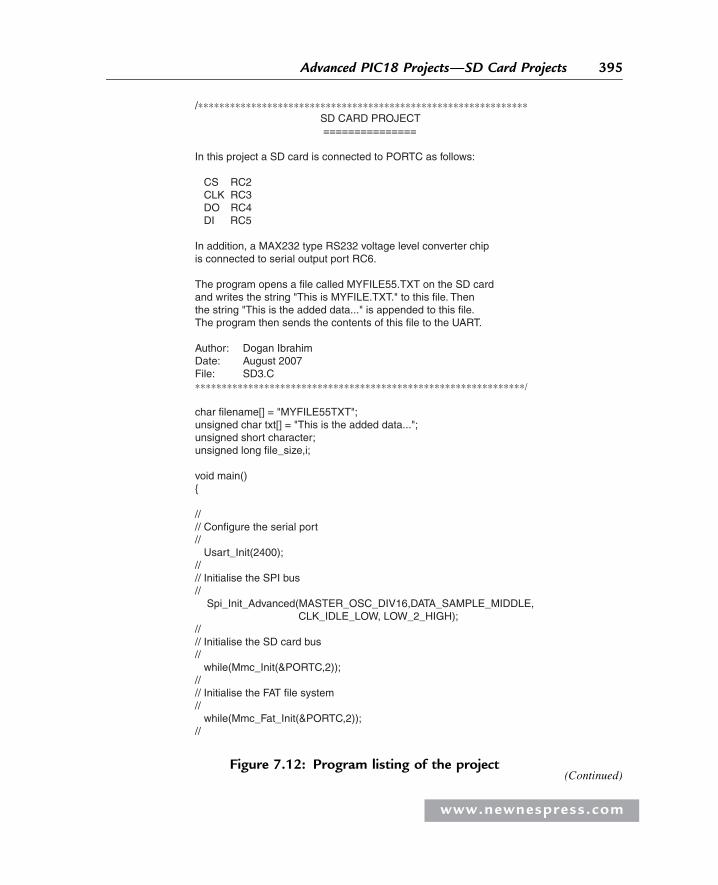
/∗∗∗∗∗∗∗∗∗∗∗∗∗∗∗∗∗∗∗∗∗∗∗∗∗∗∗∗∗∗∗∗∗∗∗∗∗∗∗∗∗∗∗∗∗∗∗∗∗∗∗∗∗∗∗∗∗∗∗∗∗∗ SD CARD PROJECT ===============
In this project a SD card is connected to PORTC as follows:
CS RC2 CLK RC3 DO RC4 DI RC5
In addition, a MAX232 type RS232 voltage level converter chipis connected to serial output port RC6.
The program opens a file called MYFILE55.TXT on the SD cardand writes the string "This is MYFILE.TXT." to this file. Thenthe string "This is the added data..." is appended to this file.The program then sends the contents of this file to the UART.
Author: Dogan IbrahimDate: August 2007File: SD3.C∗∗∗∗∗∗∗∗∗∗∗∗∗∗∗∗∗∗∗∗∗∗∗∗∗∗∗∗∗∗∗∗∗∗∗∗∗∗∗∗∗∗∗∗∗∗∗∗∗∗∗∗∗∗∗∗∗∗∗∗∗∗/
char filename[] = "MYFILE55TXT";unsigned char txt[] = "This is the added data...";unsigned short character;unsigned long file_size,i;
void main(){
//// Configure the serial port// Usart_Init(2400);//// Initialise the SPI bus// Spi_Init_Advanced(MASTER_OSC_DIV16,DATA_SAMPLE_MIDDLE, CLK_IDLE_LOW, LOW_2_HIGH);//// Initialise the SD card bus// while(Mmc_Init(&PORTC,2));//// Initialise the FAT file system// while(Mmc_Fat_Init(&PORTC,2));//
Figure 7.12: Program listing of the project(Continued)
www.newnespress.com
395Advanced PIC18 Projects—SD Card Projects
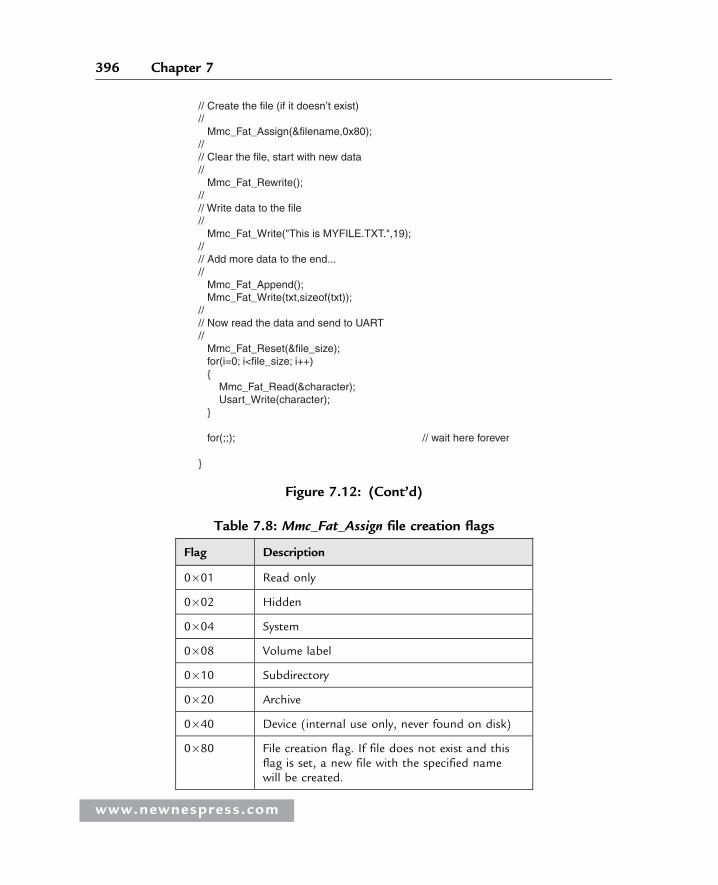
// Create the file (if it doesn’t exist)// Mmc_Fat_Assign(&filename,0x80);//// Clear the file, start with new data// Mmc_Fat_Rewrite();//// Write data to the file// Mmc_Fat_Write("This is MYFILE.TXT.",19);//// Add more data to the end...// Mmc_Fat_Append(); Mmc_Fat_Write(txt,sizeof(txt));//// Now read the data and send to UART// Mmc_Fat_Reset(&file_size); for(i=0; i<file_size; i++) { Mmc_Fat_Read(&character); Usart_Write(character); } for(;;); // wait here forever }
Figure 7.12: (Cont’d)
Table 7.8: Mmc_Fat_Assign file creation flags
Flag Description
0�01 Read only
0�02 Hidden
0�04 System
0�08 Volume label
0�10 Subdirectory
0�20 Archive
0�40 Device (internal use only, never found on disk)
0�80 File creation flag. If file does not exist and thisflag is set, a new file with the specified namewill be created.
www.newnespress.com
396 Chapter 7
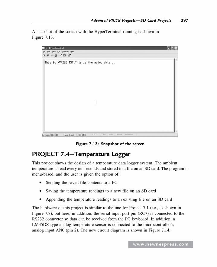
A snapshot of the screen with the HyperTerminal running is shown in
Figure 7.13.
PROJECT 7.4—Temperature Logger
This project shows the design of a temperature data logger system. The ambient
temperature is read every ten seconds and stored in a file on an SD card. The program is
menu-based, and the user is given the option of:
� Sending the saved file contents to a PC
� Saving the temperature readings to a new file on an SD card
� Appending the temperature readings to an existing file on an SD card
The hardware of this project is similar to the one for Project 7.1 (i.e., as shown in
Figure 7.8), but here, in addition, the serial input port pin (RC7) is connected to the
RS232 connector so data can be received from the PC keyboard. In addition, a
LM35DZ-type analog temperature sensor is connected to the microcontroller’s
analog input AN0 (pin 2). The new circuit diagram is shown in Figure 7.14.
Figure 7.13: Snapshot of the screen
www.newnespress.com
397Advanced PIC18 Projects—SD Card Projects
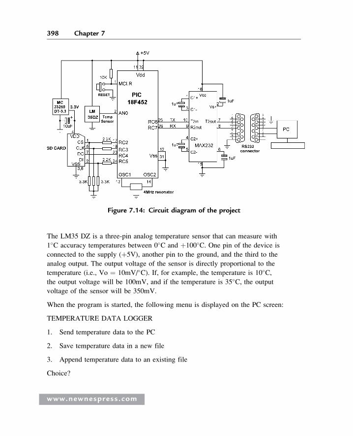
The LM35 DZ is a three-pin analog temperature sensor that can measure with
1�C accuracy temperatures between 0�C and þ100�C. One pin of the device is
connected to the supply (þ5V), another pin to the ground, and the third to the
analog output. The output voltage of the sensor is directly proportional to the
temperature (i.e., Vo ¼ 10mV/�C). If, for example, the temperature is 10�C,the output voltage will be 100mV, and if the temperature is 35�C, the output
voltage of the sensor will be 350mV.
When the program is started, the following menu is displayed on the PC screen:
TEMPERATURE DATA LOGGER
1. Send temperature data to the PC
2. Save temperature data in a new file
3. Append temperature data to an existing file
Choice?
Figure 7.14: Circuit diagram of the project
www.newnespress.com
398 Chapter 7
The user then chooses one of the three options. When an option is completed, the
program does not return to the menu. To display the menu again the system has to
be restarted.
The program listing of the project is shown in Figure 7.15 (program SD4.C). In
this project, a file called TEMPERTRTXT is created on the SD card to store the
temperature readings (the library function call will insert the “.” to make the
filename “TEMPERTR.TXT”), if it does not already exist.
The following functions are created at the beginning of the program, before the main
program:
Newline sends a carriage return and a line feed to the UART so the cursor moves
to the next line.
Text_To_Usart receives a text string as its argument and sends it to the UART
to display on the PC screen.
Get_Temperature starts the A/D conversion and receives the converted data into
a variable called Vin. The voltage corresponding to this value is then calculated in
millivolts and divided by 10 to find the actual measured temperature in �C. Thedecimal part of the found temperature is then converted into string form using
function LongToStr. The leading spaces are removed from this string, and the
resulting string is stored in character array temperature. Then the fractional parts
of the measured temperature, a carriage return, and a line feed are added to this
character array, which is later written to the SD card.
The following operations are performed inside the main program:
� Initialize the UART to 2400 baud
� Initialize the SPI bus
� Initialize the FAT file system
� Display menu on the PC screen
� Get a choice from the user (1, 2, or 3)
� If the choice ¼ 1, assign the temperature file, read the temperature records, and
display them on the PC screen
www.newnespress.com
399Advanced PIC18 Projects—SD Card Projects
/∗∗∗∗∗∗∗∗∗∗∗∗∗∗∗∗∗∗∗∗∗∗∗∗∗∗∗∗∗∗∗∗∗∗∗∗∗∗∗∗∗∗∗∗∗∗∗∗∗∗∗∗∗∗∗∗∗∗∗∗∗∗ TEMPERATURE LOGGER PROJECT ============================
In this project a SD card is connected to PORTC as follows:
CS RC2 CLK RC3 DO RC4 DI RC5
In addition, a MAX232 type RS232 voltage level converter chipis connected to serial ports RC6 and RC7. Also, a LM35DZ typeanalog temperature sensor is connected to analog input AN0 ofthe microcontroller.
The program is menu based. The user is given options of eitherto send the saved temperature data to the PC, or to read andsave new data on the SD card, or to read temperature data andappend to the existing file. Temperature is read at every 10seconds.
The temperature is stored in a file called "TEMPERTR.TXT"
Author: Dogan IbrahimDate: August 2007File: SD4.C∗∗∗∗∗∗∗∗∗∗∗∗∗∗∗∗∗∗∗∗∗∗∗∗∗∗∗∗∗∗∗∗∗∗∗∗∗∗∗∗∗∗∗∗∗∗∗∗∗∗∗∗∗∗∗∗∗∗∗∗∗∗/
char filename[] = "TEMPERTRTXT";unsigned short character;unsigned long file_size,i,rec_size;unsigned char ch1,ch2,flag,ret_status,choice;unsigned char temperature[10],txt[12];
//// This function sends carriage-return and line-feed to USART//void Newline(){ Usart_Write(0x0D); // Send carriage-return Usart_Write(0x0A); // Send line-feed}
//// This function sends a space character to USART//void Space(){
Figure 7.15: Program listing of the project
www.newnespress.com
400 Chapter 7

Usart_Write(0x20);}
//// This function sends a text to serial port//void Text_To_Usart(unsigned char ∗m){ unsigned char i;
i = 0; while(m[i] != 0) { // Send TEXT to serial port Usart_Write(m[i]); i++; }}
//// This function reads the temperature from analog input AN0//void Get_Temperature(){ unsigned long Vin, Vdec,Vfrac; unsigned char op[12]; unsigned char i,j;
Vin = Adc_Read(0); // Read from channel 0 (AN0) Vin = 488∗Vin; // Scale up the result Vin = Vin /10; // Convert to temperature in C Vdec = Vin / 100; // Decimal part Vfrac = Vin % 100; // Fractional part LongToStr(Vdec,op); // Convert Vdec to string in "op"//// Remove leading blanks// j=0; for(i=0;i<=11;i++) { if(op[i] != ' ') // If a blank { temperature[j]=op[i]; j++; } } temperature[j] = '.'; // Add “.” ch1 = Vfrac / 10; // fractional part ch2 = Vfrac % 10;
Figure 7.15: (Cont’d)
www.newnespress.com
401Advanced PIC18 Projects—SD Card Projects
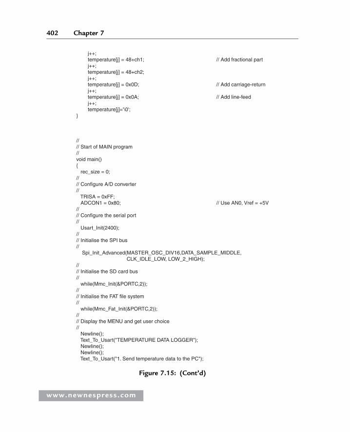
j++; temperature[j] = 48+ch1; // Add fractional part j++; temperature[j] = 48+ch2; j++; temperature[j] = 0x0D; // Add carriage-return j++; temperature[j] = 0x0A; // Add line-feed j++; temperature[j]='\0';}
//// Start of MAIN program//void main(){ rec_size = 0;//// Configure A/D converter// TRISA = 0xFF; ADCON1 = 0x80; // Use AN0, Vref = +5V//// Configure the serial port// Usart_Init(2400);//// Initialise the SPI bus// Spi_Init_Advanced(MASTER_OSC_DIV16,DATA_SAMPLE_MIDDLE, CLK_IDLE_LOW, LOW_2_HIGH);//// Initialise the SD card bus// while(Mmc_Init(&PORTC,2));//// Initialise the FAT file system// while(Mmc_Fat_Init(&PORTC,2));//// Display the MENU and get user choice// Newline(); Text_To_Usart("TEMPERATURE DATA LOGGER"); Newline(); Newline(); Text_To_Usart("1. Send temperature data to the PC");
Figure 7.15: (Cont’d)
www.newnespress.com
402 Chapter 7
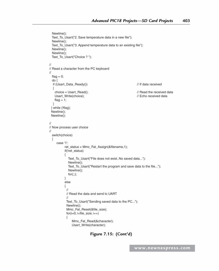
Newline(); Text_To_Usart("2. Save temperature data in a new file"); Newline(); Text_To_Usart("3. Append temperature data to an existing file"); Newline(); Newline(); Text_To_Usart("Choice ? ");
//// Read a character from the PC keyboard// flag = 0; do { if (Usart_Data_Ready()) // If data received { choice = Usart_Read(); // Read the received data Usart_Write(choice); // Echo received data flag = 1; } } while (!flag); Newline(); Newline();
//// Now process user choice// switch(choice) { case '1': ret_status = Mmc_Fat_Assign(&filename,1); if(!ret_status) { Text_To_Usart("File does not exist..No saved data..."); Newline(); Text_To_Usart("Restart the program and save data to the file..."); Newline(); for(;;); } else { // // Read the data and send to UART // Text_To_Usart("Sending saved data to the PC..."); Newline(); Mmc_Fat_Reset(&file_size); for(i=0; i<file_size; i++) { Mmc_Fat_Read(&character); Usart_Write(character);
Figure 7.15: (Cont’d)
www.newnespress.com
403Advanced PIC18 Projects—SD Card Projects
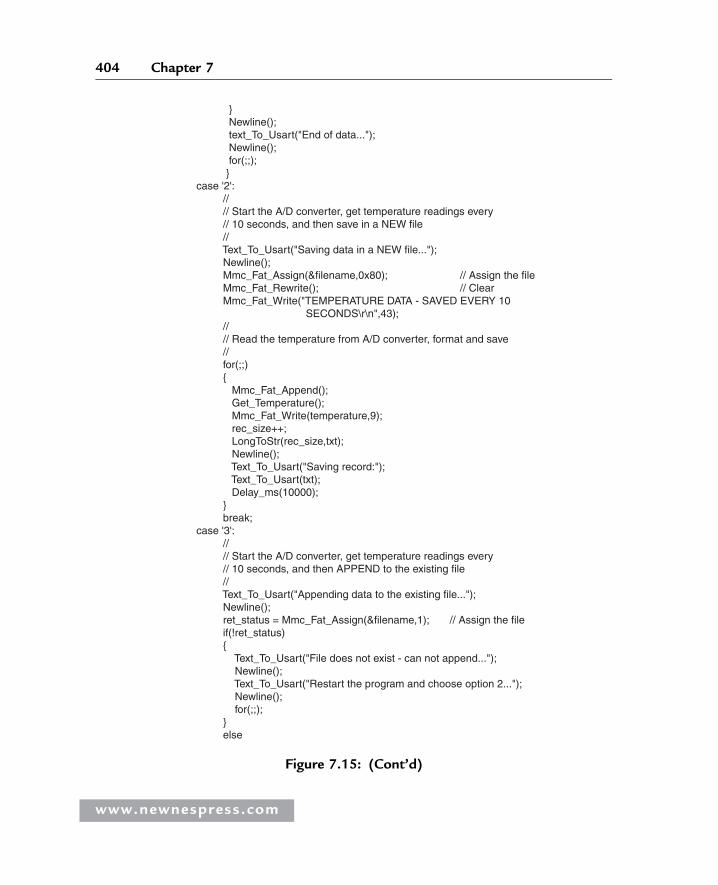
} Newline(); text_To_Usart("End of data..."); Newline(); for(;;); } case '2': // // Start the A/D converter, get temperature readings every // 10 seconds, and then save in a NEW file // Text_To_Usart("Saving data in a NEW file..."); Newline(); Mmc_Fat_Assign(&filename,0x80); // Assign the file Mmc_Fat_Rewrite(); // Clear Mmc_Fat_Write("TEMPERATURE DATA - SAVED EVERY 10 SECONDS\r\n",43); // // Read the temperature from A/D converter, format and save // for(;;) { Mmc_Fat_Append(); Get_Temperature(); Mmc_Fat_Write(temperature,9); rec_size++; LongToStr(rec_size,txt); Newline(); Text_To_Usart("Saving record:"); Text_To_Usart(txt); Delay_ms(10000); } break; case '3': // // Start the A/D converter, get temperature readings every // 10 seconds, and then APPEND to the existing file // Text_To_Usart("Appending data to the existing file..."); Newline(); ret_status = Mmc_Fat_Assign(&filename,1); // Assign the file if(!ret_status) { Text_To_Usart("File does not exist - can not append..."); Newline(); Text_To_Usart("Restart the program and choose option 2..."); Newline(); for(;;); } else
Figure 7.15: (Cont’d)
www.newnespress.com
404 Chapter 7
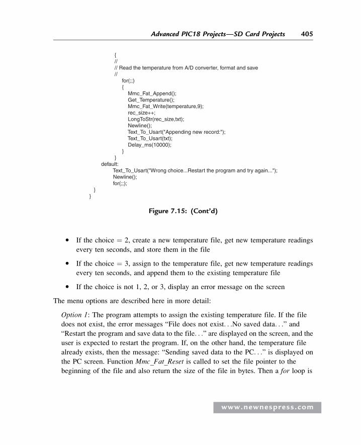
� If the choice ¼ 2, create a new temperature file, get new temperature readings
every ten seconds, and store them in the file
� If the choice ¼ 3, assign to the temperature file, get new temperature readings
every ten seconds, and append them to the existing temperature file
� If the choice is not 1, 2, or 3, display an error message on the screen
The menu options are described here in more detail:
Option 1: The program attempts to assign the existing temperature file. If the file
does not exist, the error messages “File does not exist. . .No saved data. . .” and
“Restart the program and save data to the file. . .” are displayed on the screen, and the
user is expected to restart the program. If, on the other hand, the temperature file
already exists, then the message: “Sending saved data to the PC. . .” is displayed on
the PC screen. Function Mmc_Fat_Reset is called to set the file pointer to the
beginning of the file and also return the size of the file in bytes. Then a for loop is
{ // // Read the temperature from A/D converter, format and save // for(;;) { Mmc_Fat_Append(); Get_Temperature(); Mmc_Fat_Write(temperature,9); rec_size++; LongToStr(rec_size,txt); Newline(); Text_To_Usart("Appending new record:"); Text_To_Usart(txt); Delay_ms(10000); } } default: Text_To_Usart("Wrong choice...Restart the program and try again..."); Newline(); for(;;); }}
Figure 7.15: (Cont’d)
www.newnespress.com
405Advanced PIC18 Projects—SD Card Projects
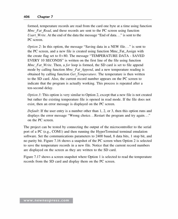
formed, temperature records are read from the card one byte at a time using function
Mmc_Fat_Read, and these records are sent to the PC screen using function
Usart_Write. At the end of the data the message “End of data. . .” is sent to the
PC screen.
Option 2: In this option, the message “Saving data in a NEW file. . .” is sent to
the PC screen, and a new file is created using function Mmc_Fat_Assign with
the create flag set to 0�80. The message “TEMPERATURE DATA - SAVED
EVERY 10 SECONDS” is written on the first line of the file using function
Mmc_Fat_Write. Then, a for loop is formed, the SD card is set to file append
mode by calling function Mmc_Fat_Append, and a new temperature reading is
obtained by calling function Get_Temperature. The temperature is then written
to the SD card. Also, the current record number appears on the PC screen to
indicate that the program is actually working. This process is repeated after a
ten-second delay.
Option 3: This option is very similar to Option 2, except that a new file is not created
but rather the existing temperature file is opened in read mode. If the file does not
exist, then an error message is displayed on the PC screen.
Default: If the user entry is a number other than 1, 2, or 3, then this option runs and
displays the error message “Wrong choice. . .Restart the program and try again. . .”
on the PC screen.
The project can be tested by connecting the output of the microcontroller to the serial
port of a PC (e.g., COM1) and then running the HyperTerminal terminal emulation
software. Set the communications parameters to 2400 baud, 8 data bits, 1 stop bit, and
no parity bit. Figure 7.16 shows a snapshot of the PC screen when Option 2 is selected
to save the temperature records in a new file. Notice that the current record numbers
are displayed on the screen as they are written to the SD card.
Figure 7.17 shows a screen snapshot where Option 1 is selected to read the temperature
records from the SD card and display them on the PC screen.
www.newnespress.com
406 Chapter 7
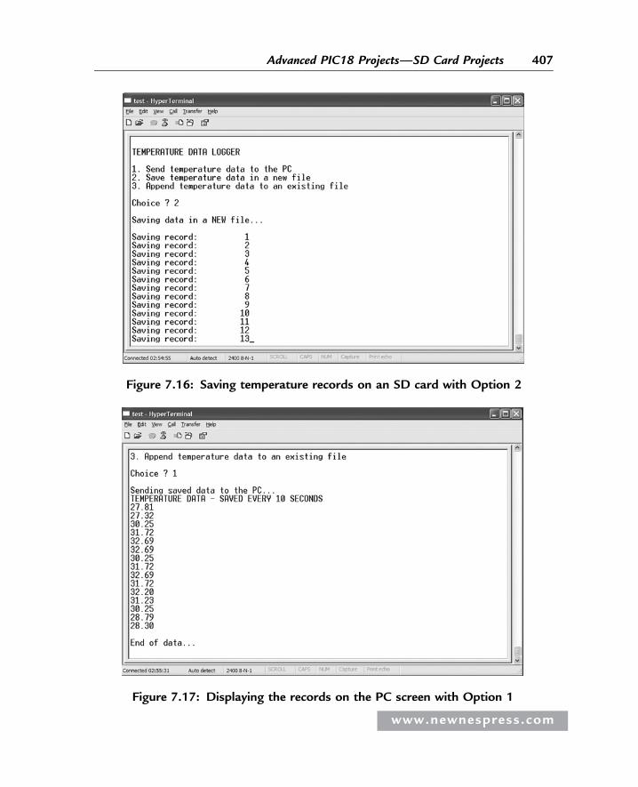
Figure 7.16: Saving temperature records on an SD card with Option 2
Figure 7.17: Displaying the records on the PC screen with Option 1
www.newnespress.com
407Advanced PIC18 Projects—SD Card Projects
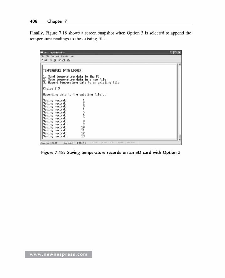
Finally, Figure 7.18 shows a screen snapshot when Option 3 is selected to append the
temperature readings to the existing file.
Figure 7.18: Saving temperature records on an SD card with Option 3
www.newnespress.com
408 Chapter 7
CHAP T E R 8
Advanced PIC18 Projects—USBBus Projects
The Universal Serial Bus (USB) is one of the most common interfaces used in
electronic consumer products today, including PCs, cameras, GPS devices, MP3
players, modems, printers, and scanners, to name a few.
The USB was originally developed by Compaq, Microsoft, Intel, and NEC, and later by
Hewlett-Packard, Lucent, and Philips as well. These companies eventually formed the
nonprofit corporation USB Implementers Forum Inc. to organize the development
and publication of USB specifications.
This chapter describes the basic principles of the USB bus and shows how to use
USB-based applications with PIC microcontrollers. The USB bus is a complex
protocol. A complete discussion of its design and use is beyond the scope of this
chapter. Only the basic principles, enough to be able to use the USB bus, are
outlined here. On the other hand, the functions offered by the mikroC language that
simplify the design of USB-based microcontroller projects are described in some detail.
The USB is a high-speed serial interface that can also provide power to devices
connected to it. A USB bus supports up to 127 devices (limited by the 7-bit address
field—note that address 0 is not used as it has a special purpose) connected through a
four-wire serial cable of up to three or even five meters in length. Many USB devices
can be connected to the same bus with hubs, which can have 4, 8, or even 16 ports.
A device can be plugged into a hub which is plugged into another hub, and so on.
The maximum number of tiers permitted is six. According to the specification, the
maximum distance of a device from its host is about thirty meters, accomplished by
www.newnespress.com
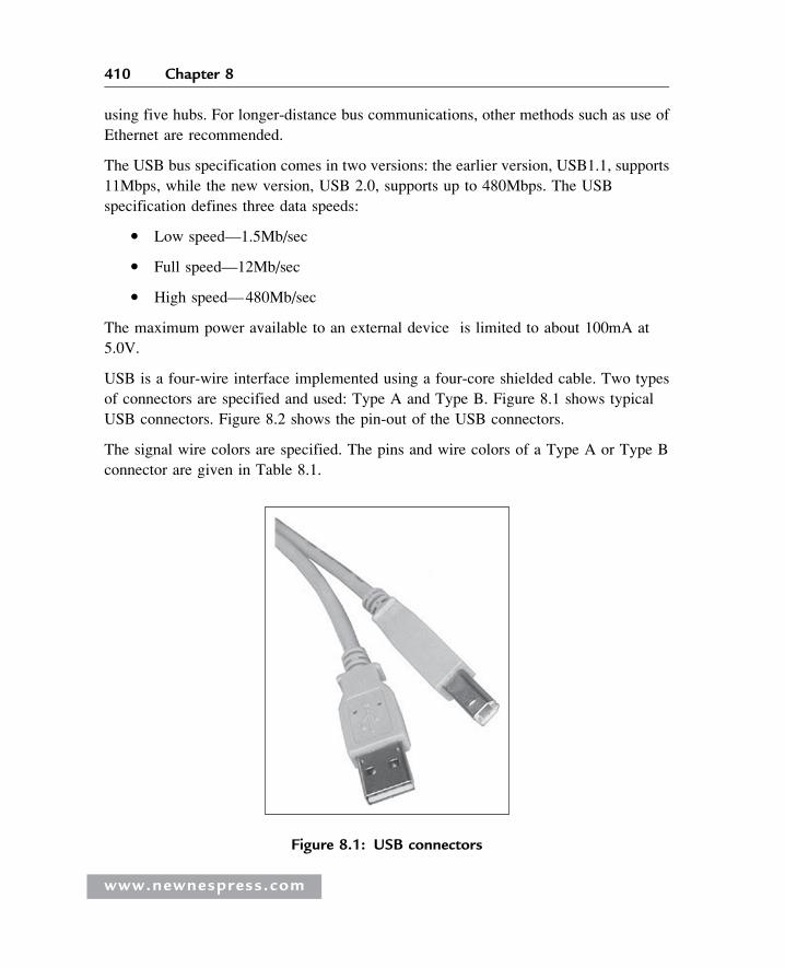
using five hubs. For longer-distance bus communications, other methods such as use of
Ethernet are recommended.
The USB bus specification comes in two versions: the earlier version, USB1.1, supports
11Mbps, while the new version, USB 2.0, supports up to 480Mbps. The USB
specification defines three data speeds:
� Low speed—1.5Mb/sec
� Full speed—12Mb/sec
� High speed—480Mb/sec
The maximum power available to an external device is limited to about 100mA at
5.0V.
USB is a four-wire interface implemented using a four-core shielded cable. Two types
of connectors are specified and used: Type A and Type B. Figure 8.1 shows typical
USB connectors. Figure 8.2 shows the pin-out of the USB connectors.
The signal wire colors are specified. The pins and wire colors of a Type A or Type B
connector are given in Table 8.1.
Figure 8.1: USB connectors
www.newnespress.com
410 Chapter 8
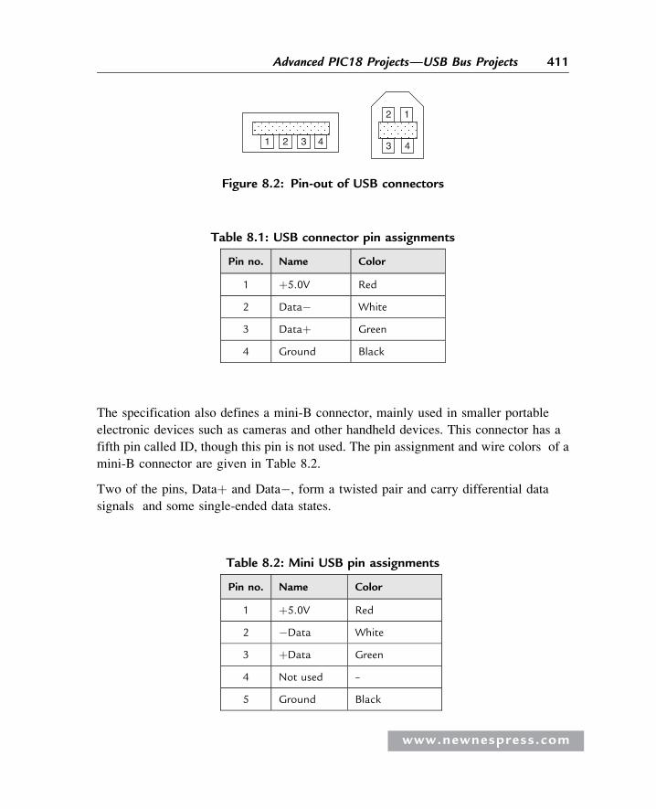
The specification also defines a mini-B connector, mainly used in smaller portable
electronic devices such as cameras and other handheld devices. This connector has a
fifth pin called ID, though this pin is not used. The pin assignment and wire colors of a
mini-B connector are given in Table 8.2.
Two of the pins, Dataþ and Data�, form a twisted pair and carry differential data
signals and some single-ended data states.
43
12
4321
Figure 8.2: Pin-out of USB connectors
Table 8.1: USB connector pin assignments
Pin no. Name Color
1 þ5.0V Red
2 Data� White
3 Dataþ Green
4 Ground Black
Table 8.2: Mini USB pin assignments
Pin no. Name Color
1 þ5.0V Red
2 �Data White
3 þData Green
4 Not used –
5 Ground Black
www.newnespress.com
411Advanced PIC18 Projects—USB Bus Projects
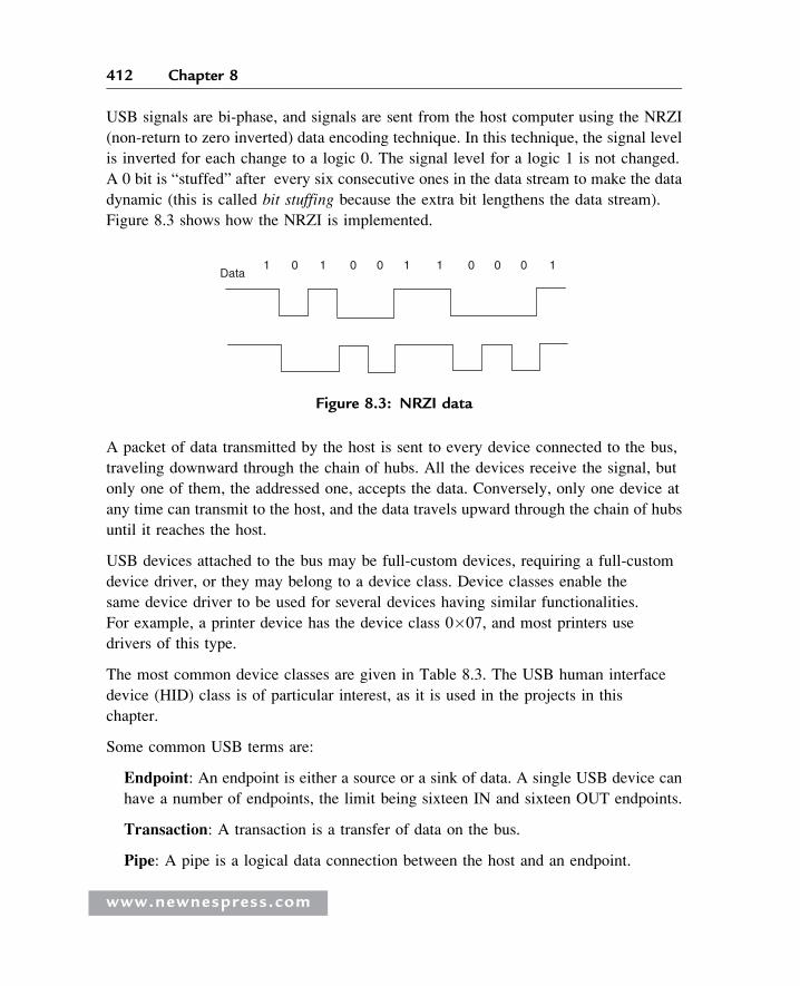
USB signals are bi-phase, and signals are sent from the host computer using the NRZI
(non-return to zero inverted) data encoding technique. In this technique, the signal level
is inverted for each change to a logic 0. The signal level for a logic 1 is not changed.
A 0 bit is “stuffed” after every six consecutive ones in the data stream to make the data
dynamic (this is called bit stuffing because the extra bit lengthens the data stream).
Figure 8.3 shows how the NRZI is implemented.
A packet of data transmitted by the host is sent to every device connected to the bus,
traveling downward through the chain of hubs. All the devices receive the signal, but
only one of them, the addressed one, accepts the data. Conversely, only one device at
any time can transmit to the host, and the data travels upward through the chain of hubs
until it reaches the host.
USB devices attached to the bus may be full-custom devices, requiring a full-custom
device driver, or they may belong to a device class. Device classes enable the
same device driver to be used for several devices having similar functionalities.
For example, a printer device has the device class 0�07, and most printers use
drivers of this type.
The most common device classes are given in Table 8.3. The USB human interface
device (HID) class is of particular interest, as it is used in the projects in this
chapter.
Some common USB terms are:
Endpoint: An endpoint is either a source or a sink of data. A single USB device can
have a number of endpoints, the limit being sixteen IN and sixteen OUT endpoints.
Transaction: A transaction is a transfer of data on the bus.
Pipe: A pipe is a logical data connection between the host and an endpoint.
Data1 0 1 0 0 1 1 0 0 0 1
Figure 8.3: NRZI data
www.newnespress.com
412 Chapter 8
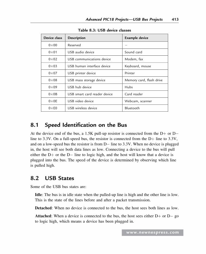
8.1 Speed Identification on the Bus
At the device end of the bus, a 1.5K pull-up resistor is connected from the Dþ or D�line to 3.3V. On a full-speed bus, the resistor is connected from the Dþ line to 3.3V,
and on a low-speed bus the resistor is from D� line to 3.3V. When no device is plugged
in, the host will see both data lines as low. Connecting a device to the bus will pull
either the Dþ or the D� line to logic high, and the host will know that a device is
plugged into the bus. The speed of the device is determined by observing which line
is pulled high.
8.2 USB States
Some of the USB bus states are:
Idle: The bus is in idle state when the pulled-up line is high and the other line is low.
This is the state of the lines before and after a packet transmission.
Detached: When no device is connected to the bus, the host sees both lines as low.
Attached: When a device is connected to the bus, the host sees either Dþ or D� go
to logic high, which means a device has been plugged in.
Table 8.3: USB device classes
Device class Description Example device
0�00 Reserved �0�01 USB audio device Sound card
0�02 USB communications device Modem, fax
0�03 USB human interface device Keyboard, mouse
0�07 USB printer device Printer
0�08 USB mass storage device Memory card, flash drive
0�09 USB hub device Hubs
0�0B USB smart card reader device Card reader
0�0E USB video device Webcam, scanner
0�E0 USB wireless device Bluetooth
www.newnespress.com
413Advanced PIC18 Projects—USB Bus Projects
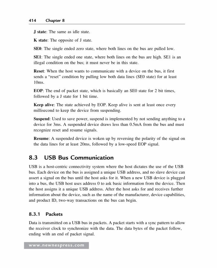
J state: The same as idle state.
K state: The opposite of J state.
SE0: The single ended zero state, where both lines on the bus are pulled low.
SE1: The single ended one state, where both lines on the bus are high. SE1 is an
illegal condition on the bus; it must never be in this state.
Reset: When the host wants to communicate with a device on the bus, it first
sends a “reset” condition by pulling low both data lines (SE0 state) for at least
10ms.
EOP: The end of packet state, which is basically an SE0 state for 2 bit times,
followed by a J state for 1 bit time.
Keep alive: The state achieved by EOP. Keep alive is sent at least once every
millisecond to keep the device from suspending.
Suspend: Used to save power, suspend is implemented by not sending anything to a
device for 3ms. A suspended device draws less than 0.5mA from the bus and must
recognize reset and resume signals.
Resume: A suspended device is woken up by reversing the polarity of the signal on
the data lines for at least 20ms, followed by a low-speed EOP signal.
8.3 USB Bus Communication
USB is a host-centric connectivity system where the host dictates the use of the USB
bus. Each device on the bus is assigned a unique USB address, and no slave device can
assert a signal on the bus until the host asks for it. When a new USB device is plugged
into a bus, the USB host uses address 0 to ask basic information from the device. Then
the host assigns it a unique USB address. After the host asks for and receives further
information about the device, such as the name of the manufacturer, device capabilities,
and product ID, two-way transactions on the bus can begin.
8.3.1 Packets
Data is transmitted on a USB bus in packets. A packet starts with a sync pattern to allow
the receiver clock to synchronize with the data. The data bytes of the packet follow,
ending with an end of packet signal.
www.newnespress.com
414 Chapter 8
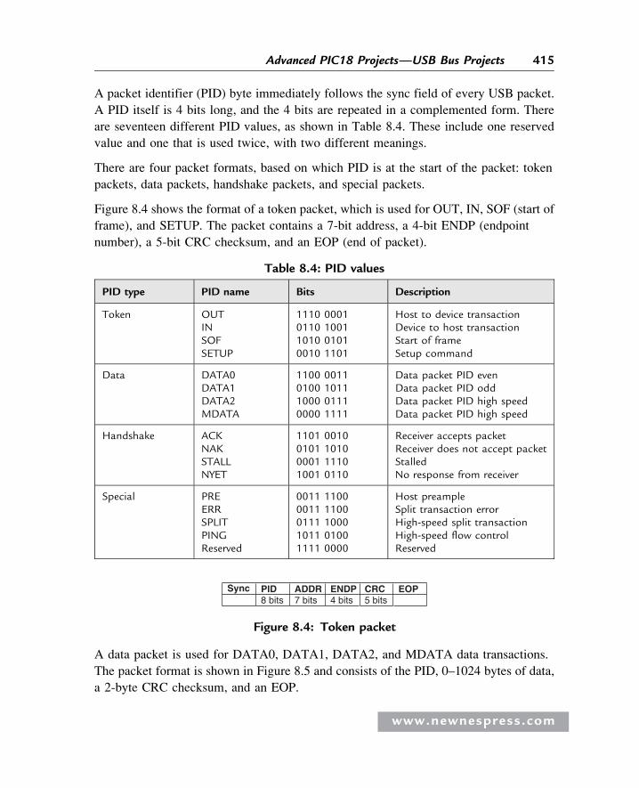
A packet identifier (PID) byte immediately follows the sync field of every USB packet.
A PID itself is 4 bits long, and the 4 bits are repeated in a complemented form. There
are seventeen different PID values, as shown in Table 8.4. These include one reserved
value and one that is used twice, with two different meanings.
There are four packet formats, based on which PID is at the start of the packet: token
packets, data packets, handshake packets, and special packets.
Figure 8.4 shows the format of a token packet, which is used for OUT, IN, SOF (start of
frame), and SETUP. The packet contains a 7-bit address, a 4-bit ENDP (endpoint
number), a 5-bit CRC checksum, and an EOP (end of packet).
A data packet is used for DATA0, DATA1, DATA2, and MDATA data transactions.
The packet format is shown in Figure 8.5 and consists of the PID, 0–1024 bytes of data,
a 2-byte CRC checksum, and an EOP.
Table 8.4: PID values
PID type PID name Bits Description
Token OUTINSOFSETUP
1110 00010110 10011010 01010010 1101
Host to device transactionDevice to host transactionStart of frameSetup command
Data DATA0DATA1DATA2MDATA
1100 00110100 10111000 01110000 1111
Data packet PID evenData packet PID oddData packet PID high speedData packet PID high speed
Handshake ACKNAKSTALLNYET
1101 00100101 10100001 11101001 0110
Receiver accepts packetReceiver does not accept packetStalledNo response from receiver
Special PREERRSPLITPINGReserved
0011 11000011 11000111 10001011 01001111 0000
Host preampleSplit transaction errorHigh-speed split transactionHigh-speed flow controlReserved
Sync PID ADDR ENDP CRC EOP8 bits 7 bits 4 bits 5 bits
Figure 8.4: Token packet
www.newnespress.com
415Advanced PIC18 Projects—USB Bus Projects
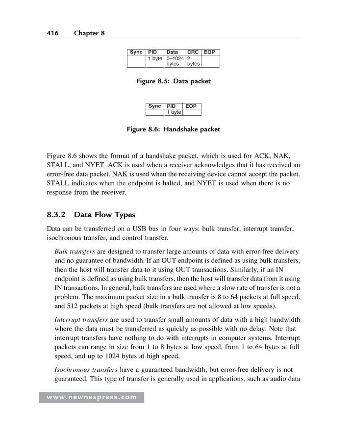
Figure 8.6 shows the format of a handshake packet, which is used for ACK, NAK,
STALL, and NYET. ACK is used when a receiver acknowledges that it has received an
error-free data packet. NAK is used when the receiving device cannot accept the packet.
STALL indicates when the endpoint is halted, and NYET is used when there is no
response from the receiver.
8.3.2 Data Flow Types
Data can be transferred on a USB bus in four ways: bulk transfer, interrupt transfer,
isochronous transfer, and control transfer.
Bulk transfers are designed to transfer large amounts of data with error-free delivery
and no guarantee of bandwidth. If an OUT endpoint is defined as using bulk transfers,
then the host will transfer data to it using OUT transactions. Similarly, if an IN
endpoint is defined as using bulk transfers, then the host will transfer data from it using
IN transactions. In general, bulk transfers are used where a slow rate of transfer is not a
problem. The maximum packet size in a bulk transfer is 8 to 64 packets at full speed,
and 512 packets at high speed (bulk transfers are not allowed at low speeds).
Interrupt transfers are used to transfer small amounts of data with a high bandwidth
where the data must be transferred as quickly as possible with no delay. Note that
interrupt transfers have nothing to do with interrupts in computer systems. Interrupt
packets can range in size from 1 to 8 bytes at low speed, from 1 to 64 bytes at full
speed, and up to 1024 bytes at high speed.
Isochronous transfers have a guaranteed bandwidth, but error-free delivery is not
guaranteed. This type of transfer is generally used in applications, such as audio data
Sync PID Data CRC EOP1 byte 0–1024
bytes2bytes
Figure 8.5: Data packet
Sync PID EOP1 byte
Figure 8.6: Handshake packet
www.newnespress.com
416 Chapter 8
transfer, where speed is important but the loss or corruption of some data is not. An
isochronous packet may contain 1023 bytes at full speed or up to 1024 bytes at high
speed (isochronous transfers are not allowed at low speeds).
A control transfer is a bidirectional data transfer, using both IN and OUT endpoints.
Control transfers are generally used for initial configuration of a device by the host.
The maximum packet size is 8 bytes at low speed, 8 to 64 bytes at full speed, and
64 bytes at high speed. A control transfer is carried out in three stages: SETUP,
DATA, and STATUS.
8.3.3 Enumeration
When a device is plugged into a USB bus, it becomes known to the host through a
process called enumeration. The steps of enumeration are:
� When a device is plugged in, the host becomes aware of it because one of the
data lines (Dþ or D�) becomes logic high.
� The host sends a USB reset signal to the device to place the device in a known
state. The reset device responds to address 0.
� The host sends a request on address 0 to the device to find out its maximum
packet size using a Get Descriptor command.
� The device responds by sending a small portion of the device descriptor.
� The host sends a USB reset again.
� The host assigns a unique address to the device and sends a Set Address request
to the device. After the request is completed, the device assumes the new
address. At this point the host is free to reset any other newly plugged-in
devices on the bus.
� The host sends a Get Device Descriptor request to retrieve the complete device
descriptor, gathering information such as manufacturer, type of device, and
maximum control packet size.
� The host sends a Get Configuration Descriptors request to receive the device’s
configuration data, such as power requirements and the types and number of
interfaces supported.
� The host may request any additional descriptors from the device.
www.newnespress.com
417Advanced PIC18 Projects—USB Bus Projects
The initial communication between the host and the device is carried out using the
control transfer type of data flow.
Initially, the device is addressed, but it is in an unconfigured state. After the host gathers
enough information about the device, it loads a suitable device driver which configures
the device by sending it a Set Configuration request. At this point the device has been
configured, and it is ready to respond to device-specific requests (i.e., it can receive data
from and send data to the host).
8.4 Descriptors
All USB devices have a hierarchy of descriptors that describe various features of
the device: the manufacturer ID, the version of the device, the version of USB it
supports, what the device is, its power requirements, the number and type of
endpoints, and so forth.
The most common USB descriptors are:
� Device descriptors
� Configuration descriptors
� Interface descriptors
� HID descriptors
� Endpoint descriptors
The descriptors are in a hierarchical structure as shown in Figure 8.7. At the top of the
hierarchy we have the device descriptor, then the configuration descriptors, followed
by the interface descriptors, and finally the endpoint descriptors. The HID descriptor
always follows the interface descriptor when the interface belongs to the HID class.
All descriptors have a common format. The first byte (bLength) specifies the
length of the descriptor, while the second byte (bDescriptorType) indicates
the descriptor type.
8.4.1 Device Descriptors
The device descriptor is the top-level set of information read from a device and the first
item the host attempts to retrieve.
www.newnespress.com
418 Chapter 8
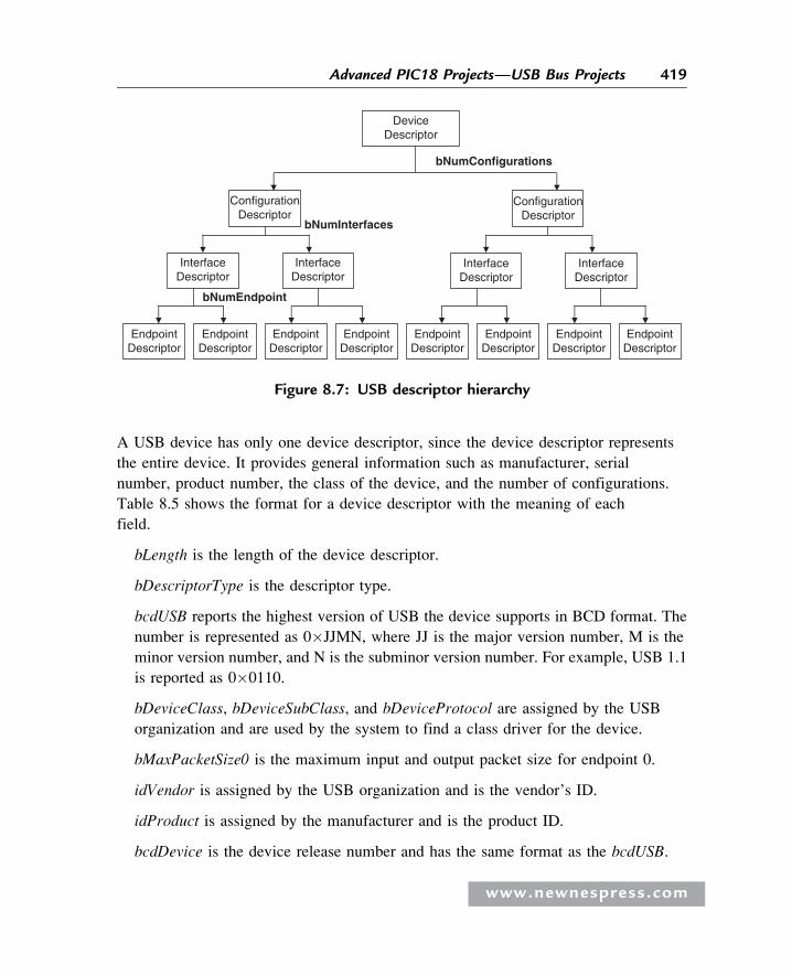
A USB device has only one device descriptor, since the device descriptor represents
the entire device. It provides general information such as manufacturer, serial
number, product number, the class of the device, and the number of configurations.
Table 8.5 shows the format for a device descriptor with the meaning of each
field.
bLength is the length of the device descriptor.
bDescriptorType is the descriptor type.
bcdUSB reports the highest version of USB the device supports in BCD format. The
number is represented as 0�JJMN, where JJ is the major version number, M is the
minor version number, and N is the subminor version number. For example, USB 1.1
is reported as 0�0110.
bDeviceClass, bDeviceSubClass, and bDeviceProtocol are assigned by the USB
organization and are used by the system to find a class driver for the device.
bMaxPacketSize0 is the maximum input and output packet size for endpoint 0.
idVendor is assigned by the USB organization and is the vendor’s ID.
idProduct is assigned by the manufacturer and is the product ID.
bcdDevice is the device release number and has the same format as the bcdUSB.
bNumConfigurations
DeviceDescriptor
ConfigurationDescriptor
ConfigurationDescriptor
bNumInterfaces
bNumEndpoint
InterfaceDescriptor
InterfaceDescriptor
InterfaceDescriptor
InterfaceDescriptor
EndpointDescriptor
EndpointDescriptor
EndpointDescriptor
EndpointDescriptor
EndpointDescriptor
EndpointDescriptor
EndpointDescriptor
EndpointDescriptor
Figure 8.7: USB descriptor hierarchy
www.newnespress.com
419Advanced PIC18 Projects—USB Bus Projects
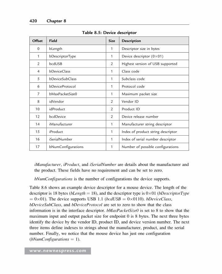
iManufacturer, iProduct, and iSerialNumber are details about the manufacturer and
the product. These fields have no requirement and can be set to zero.
bNumConfigurations is the number of configurations the device supports.
Table 8.6 shows an example device descriptor for a mouse device. The length of the
descriptor is 18 bytes (bLength ¼ 18), and the descriptor type is 0�01 (bDescriptorType
¼ 0�01). The device supports USB 1.1 (bcdUSB ¼ 0�0110). bDeviceClass,
bDeviceSubClass, and bDeviceProtocol are set to zero to show that the class
information is in the interface descriptor. bMaxPacketSize0 is set to 8 to show that the
maximum input and output packet size for endpoint 0 is 8 bytes. The next three bytes
identify the device by the vendor ID, product ID, and device version number. The next
three items define indexes to strings about the manufacturer, product, and the serial
number. Finally, we notice that the mouse device has just one configuration
(bNumConfigurations ¼ 1).
Table 8.5: Device descriptor
Offset Field Size Description
0 bLength 1 Descriptor size in bytes
1 bDescriptorType 1 Device descriptor (0�01)
2 bcdUSB 2 Highest version of USB supported
4 bDeviceClass 1 Class code
5 bDeviceSubClass 1 Subclass code
6 bDeviceProtocol 1 Protocol code
7 bMaxPacketSize0 1 Maximum packet size
8 idVendor 2 Vendor ID
10 idProduct 2 Product ID
12 bcdDevice 2 Device release number
14 iManufacturer 1 Manufacturer string descriptor
15 iProduct 1 Index of product string descriptor
16 iSerialNumber 1 Index of serial number descriptor
17 bNumConfigurations 1 Number of possible configurations
www.newnespress.com
420 Chapter 8
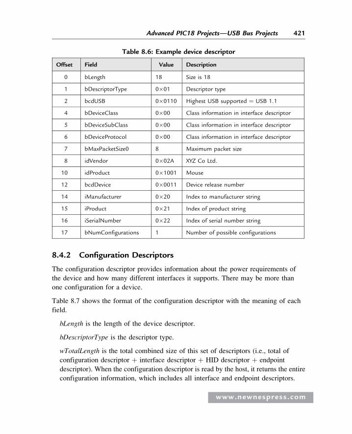
8.4.2 Configuration Descriptors
The configuration descriptor provides information about the power requirements of
the device and how many different interfaces it supports. There may be more than
one configuration for a device.
Table 8.7 shows the format of the configuration descriptor with the meaning of each
field.
bLength is the length of the device descriptor.
bDescriptorType is the descriptor type.
wTotalLength is the total combined size of this set of descriptors (i.e., total of
configuration descriptor þ interface descriptor þ HID descriptor þ endpoint
descriptor). When the configuration descriptor is read by the host, it returns the entire
configuration information, which includes all interface and endpoint descriptors.
Table 8.6: Example device descriptor
Offset Field Value Description
0 bLength 18 Size is 18
1 bDescriptorType 0�01 Descriptor type
2 bcdUSB 0�0110 Highest USB supported ¼ USB 1.1
4 bDeviceClass 0�00 Class information in interface descriptor
5 bDeviceSubClass 0�00 Class information in interface descriptor
6 bDeviceProtocol 0�00 Class information in interface descriptor
7 bMaxPacketSize0 8 Maximum packet size
8 idVendor 0�02A XYZ Co Ltd.
10 idProduct 0�1001 Mouse
12 bcdDevice 0�0011 Device release number
14 iManufacturer 0�20 Index to manufacturer string
15 iProduct 0�21 Index of product string
16 iSerialNumber 0�22 Index of serial number string
17 bNumConfigurations 1 Number of possible configurations
www.newnespress.com
421Advanced PIC18 Projects—USB Bus Projects
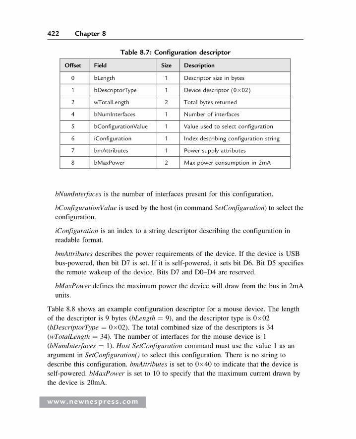
bNumInterfaces is the number of interfaces present for this configuration.
bConfigurationValue is used by the host (in command SetConfiguration) to select the
configuration.
iConfiguration is an index to a string descriptor describing the configuration in
readable format.
bmAttributes describes the power requirements of the device. If the device is USB
bus-powered, then bit D7 is set. If it is self-powered, it sets bit D6. Bit D5 specifies
the remote wakeup of the device. Bits D7 and D0–D4 are reserved.
bMaxPower defines the maximum power the device will draw from the bus in 2mA
units.
Table 8.8 shows an example configuration descriptor for a mouse device. The length
of the descriptor is 9 bytes (bLength ¼ 9), and the descriptor type is 0�02
(bDescriptorType ¼ 0�02). The total combined size of the descriptors is 34
(wTotalLength ¼ 34). The number of interfaces for the mouse device is 1
(bNumInterfaces ¼ 1). Host SetConfiguration command must use the value 1 as an
argument in SetConfiguration() to select this configuration. There is no string to
describe this configuration. bmAttributes is set to 0�40 to indicate that the device is
self-powered. bMaxPower is set to 10 to specify that the maximum current drawn by
the device is 20mA.
Table 8.7: Configuration descriptor
Offset Field Size Description
0 bLength 1 Descriptor size in bytes
1 bDescriptorType 1 Device descriptor (0�02)
2 wTotalLength 2 Total bytes returned
4 bNumInterfaces 1 Number of interfaces
5 bConfigurationValue 1 Value used to select configuration
6 iConfiguration 1 Index describing configuration string
7 bmAttributes 1 Power supply attributes
8 bMaxPower 2 Max power consumption in 2mA
www.newnespress.com
422 Chapter 8
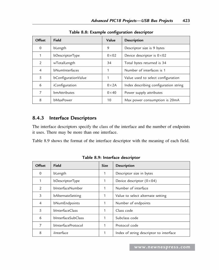
8.4.3 Interface Descriptors
The interface descriptors specify the class of the interface and the number of endpoints
it uses. There may be more than one interface.
Table 8.9 shows the format of the interface descriptor with the meaning of each field.
Table 8.8: Example configuration descriptor
Offset Field Value Description
0 bLength 9 Descriptor size is 9 bytes
1 bDescriptorType 0�02 Device descriptor is 0�02
2 wTotalLength 34 Total bytes returned is 34
4 bNumInterfaces 1 Number of interfaces is 1
5 bConfigurationValue 1 Value used to select configuration
6 iConfiguration 0�2A Index describing configuration string
7 bmAttributes 0�40 Power supply attributes
8 bMaxPower 10 Max power consumption is 20mA
Table 8.9: Interface descriptor
Offset Field Size Description
0 bLength 1 Descriptor size in bytes
1 bDescriptorType 1 Device descriptor (0�04)
2 bInterfaceNumber 1 Number of interface
3 bAlternateSetting 1 Value to select alternate setting
4 bNumEndpoints 1 Number of endpoints
5 bInterfaceClass 1 Class code
6 bInterfaceSubClass 1 Subclass code
7 bInterfaceProtocol 1 Protocol code
8 iInterface 1 Index of string descriptor to interface
www.newnespress.com
423Advanced PIC18 Projects—USB Bus Projects
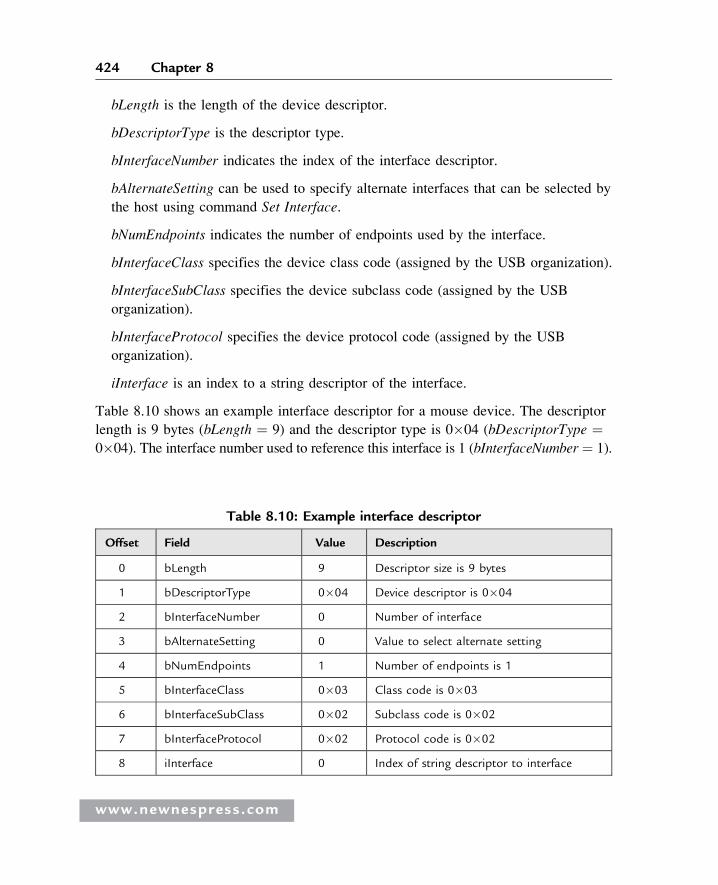
bLength is the length of the device descriptor.
bDescriptorType is the descriptor type.
bInterfaceNumber indicates the index of the interface descriptor.
bAlternateSetting can be used to specify alternate interfaces that can be selected by
the host using command Set Interface.
bNumEndpoints indicates the number of endpoints used by the interface.
bInterfaceClass specifies the device class code (assigned by the USB organization).
bInterfaceSubClass specifies the device subclass code (assigned by the USB
organization).
bInterfaceProtocol specifies the device protocol code (assigned by the USB
organization).
iInterface is an index to a string descriptor of the interface.
Table 8.10 shows an example interface descriptor for a mouse device. The descriptor
length is 9 bytes (bLength ¼ 9) and the descriptor type is 0�04 (bDescriptorType ¼0�04). The interface number used to reference this interface is 1 (bInterfaceNumber¼ 1).
Table 8.10: Example interface descriptor
Offset Field Value Description
0 bLength 9 Descriptor size is 9 bytes
1 bDescriptorType 0�04 Device descriptor is 0�04
2 bInterfaceNumber 0 Number of interface
3 bAlternateSetting 0 Value to select alternate setting
4 bNumEndpoints 1 Number of endpoints is 1
5 bInterfaceClass 0�03 Class code is 0�03
6 bInterfaceSubClass 0�02 Subclass code is 0�02
7 bInterfaceProtocol 0�02 Protocol code is 0�02
8 iInterface 0 Index of string descriptor to interface
www.newnespress.com
424 Chapter 8
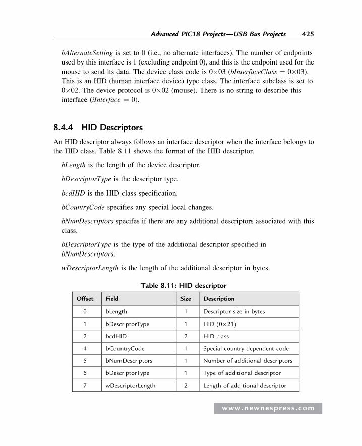
bAlternateSetting is set to 0 (i.e., no alternate interfaces). The number of endpoints
used by this interface is 1 (excluding endpoint 0), and this is the endpoint used for the
mouse to send its data. The device class code is 0�03 (bInterfaceClass ¼ 0�03).
This is an HID (human interface device) type class. The interface subclass is set to
0�02. The device protocol is 0�02 (mouse). There is no string to describe this
interface (iInterface ¼ 0).
8.4.4 HID Descriptors
An HID descriptor always follows an interface descriptor when the interface belongs to
the HID class. Table 8.11 shows the format of the HID descriptor.
bLength is the length of the device descriptor.
bDescriptorType is the descriptor type.
bcdHID is the HID class specification.
bCountryCode specifies any special local changes.
bNumDescriptors specifes if there are any additional descriptors associated with this
class.
bDescriptorType is the type of the additional descriptor specified in
bNumDescriptors.
wDescriptorLength is the length of the additional descriptor in bytes.
Table 8.11: HID descriptor
Offset Field Size Description
0 bLength 1 Descriptor size in bytes
1 bDescriptorType 1 HID (0�21)
2 bcdHID 2 HID class
4 bCountryCode 1 Special country dependent code
5 bNumDescriptors 1 Number of additional descriptors
6 bDescriptorType 1 Type of additional descriptor
7 wDescriptorLength 2 Length of additional descriptor
www.newnespress.com
425Advanced PIC18 Projects—USB Bus Projects
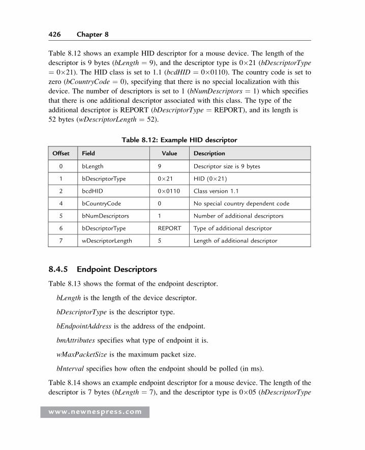
Table 8.12 shows an example HID descriptor for a mouse device. The length of the
descriptor is 9 bytes (bLength ¼ 9), and the descriptor type is 0�21 (bDescriptorType
¼ 0�21). The HID class is set to 1.1 (bcdHID ¼ 0�0110). The country code is set to
zero (bCountryCode ¼ 0), specifying that there is no special localization with this
device. The number of descriptors is set to 1 (bNumDescriptors ¼ 1) which specifies
that there is one additional descriptor associated with this class. The type of the
additional descriptor is REPORT (bDescriptorType ¼ REPORT), and its length is
52 bytes (wDescriptorLength ¼ 52).
8.4.5 Endpoint Descriptors
Table 8.13 shows the format of the endpoint descriptor.
bLength is the length of the device descriptor.
bDescriptorType is the descriptor type.
bEndpointAddress is the address of the endpoint.
bmAttributes specifies what type of endpoint it is.
wMaxPacketSize is the maximum packet size.
bInterval specifies how often the endpoint should be polled (in ms).
Table 8.14 shows an example endpoint descriptor for a mouse device. The length of the
descriptor is 7 bytes (bLength ¼ 7), and the descriptor type is 0�05 (bDescriptorType
Table 8.12: Example HID descriptor
Offset Field Value Description
0 bLength 9 Descriptor size is 9 bytes
1 bDescriptorType 0�21 HID (0�21)
2 bcdHID 0�0110 Class version 1.1
4 bCountryCode 0 No special country dependent code
5 bNumDescriptors 1 Number of additional descriptors
6 bDescriptorType REPORT Type of additional descriptor
7 wDescriptorLength 5 Length of additional descriptor
www.newnespress.com
426 Chapter 8
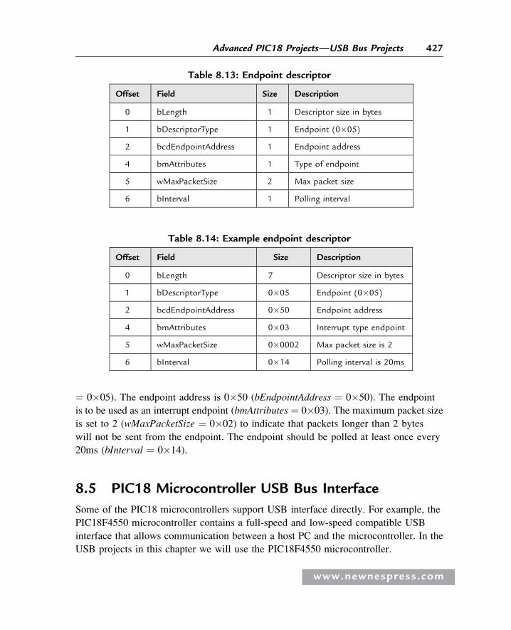
¼ 0�05). The endpoint address is 0�50 (bEndpointAddress ¼ 0�50). The endpoint
is to be used as an interrupt endpoint (bmAttributes ¼ 0�03). The maximum packet size
is set to 2 (wMaxPacketSize ¼ 0�02) to indicate that packets longer than 2 bytes
will not be sent from the endpoint. The endpoint should be polled at least once every
20ms (bInterval ¼ 0�14).
8.5 PIC18 Microcontroller USB Bus Interface
Some of the PIC18 microcontrollers support USB interface directly. For example, the
PIC18F4550 microcontroller contains a full-speed and low-speed compatible USB
interface that allows communication between a host PC and the microcontroller. In the
USB projects in this chapter we will use the PIC18F4550 microcontroller.
Table 8.13: Endpoint descriptor
Offset Field Size Description
0 bLength 1 Descriptor size in bytes
1 bDescriptorType 1 Endpoint (0�05)
2 bcdEndpointAddress 1 Endpoint address
4 bmAttributes 1 Type of endpoint
5 wMaxPacketSize 2 Max packet size
6 bInterval 1 Polling interval
Table 8.14: Example endpoint descriptor
Offset Field Size Description
0 bLength 7 Descriptor size in bytes
1 bDescriptorType 0�05 Endpoint (0�05)
2 bcdEndpointAddress 0�50 Endpoint address
4 bmAttributes 0�03 Interrupt type endpoint
5 wMaxPacketSize 0�0002 Max packet size is 2
6 bInterval 0�14 Polling interval is 20ms
www.newnespress.com
427Advanced PIC18 Projects—USB Bus Projects
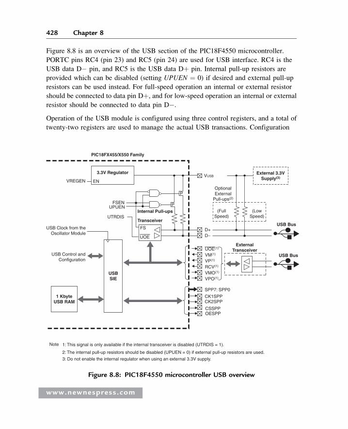
Figure 8.8 is an overview of the USB section of the PIC18F4550 microcontroller.
PORTC pins RC4 (pin 23) and RC5 (pin 24) are used for USB interface. RC4 is the
USB data D� pin, and RC5 is the USB data Dþ pin. Internal pull-up resistors are
provided which can be disabled (setting UPUEN ¼ 0) if desired and external pull-up
resistors can be used instead. For full-speed operation an internal or external resistor
should be connected to data pin Dþ, and for low-speed operation an internal or external
resistor should be connected to data pin D�.
Operation of the USB module is configured using three control registers, and a total of
twenty-two registers are used to manage the actual USB transactions. Configuration
PIC18FX455/X550 Family
3.3V Regulator
ENVREGEN
FSEN
VUSB
P
P(Full
Speed)
External 3.3VSupply(3)
UOE(1)
D+D−
VM(1)
VP(1)
RCV(1)
VMO(1)
VPO(1)
SPP7: SPP0
CK1SPPCK2SPP
CSSPPOESPP
Note
(LowSpeed)
OptionalExternal
Pull-ups(2)
UPUEN
UTRDIS
UOE
USB Bus
USB Bus
ExternalTransceiver
FS
Transceiver
USB Clock from theOscillator Module
USB Control andConfiguration
USBSIE
1 KbyteUSB RAM
Internal Pull-ups
1: This signal is only available if the internal transceiver is disabled (UTRDIS = 1).
2: The internal pull-up resistors should be disabled (UPUEN = 0) if external pull-up resistors are used.
3: Do not enable the internal regulator when using an external 3.3V supply.
Figure 8.8: PIC18F4550 microcontroller USB overview
www.newnespress.com
428 Chapter 8
of these registers is a highly complex task and is not covered in this book. Interested
readers should refer to the PIC18F4550 data sheet and to books on USB internals.
In this chapter we are using the mikroC language USB library functions to
implement USB transactions. The details of these functions are given in the next
section.
8.6 mikroC Language USB Bus Library Functions
The mikroC language supports a number of functions for USB HID-type
communications. Each project based on the USB library should include a descriptor
source file which contains vendor ID and name, product ID and name, report length,
and other relevant information. To create a descriptor source file we can use mikroC’s
integrated USB HID terminal tool (see Tools ! HID Terminal). The default name for
descriptor file is USBdsc.c, but it can be renamed if required. The USBdsc.c file must
be included in USB-based projects either via the mikroC IDE tool, or as an #include
option in the program source file.
The mikroC language supports the following USB bus library functions when a PIC
microcontroller with built-in USB is used (e.g., PIC18F4550), and port pins RC4 and
RC5 are connected to the Dþ and D� pins of the USB connector respectively:
Hid_Enable: This function enables USB communication and requires two
arguments: the read-buffer address and the write-buffer address. It must be called
before any other functions of the USB library, and it returns no data.
Hid_Read: This function receives data from the USB bus and stores it in the receive-
buffer. It has no arguments but returns the number of characters received.
Hid_Write: This function sends data from the write-buffer to the USB bus. The
name of the buffer (the same buffer used in the initialization) and the length of
the data to be sent must be specified as arguments to the function. The function
does not return any data.
Hid_Disable: This function disables the USB data transfer. It has no arguments and
returns no data.
The USB interface of a PIC18F4550 microcontroller is shown in Figure 8.9. As the
figure shows, the interface is very simple. In addition to the power supply and
ground pins, it requires just two pins to be connected to the USB connector. The
microcontroller receives power from the USB port.
www.newnespress.com
429Advanced PIC18 Projects—USB Bus Projects
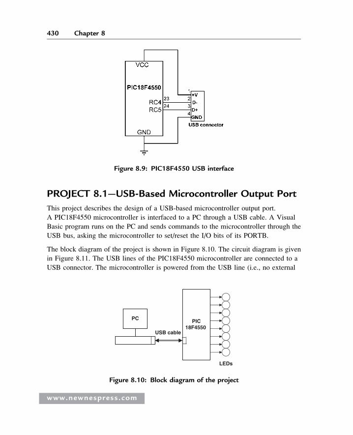
PROJECT 8.1—USB-Based Microcontroller Output Port
This project describes the design of a USB-based microcontroller output port.
A PIC18F4550 microcontroller is interfaced to a PC through a USB cable. A Visual
Basic program runs on the PC and sends commands to the microcontroller through the
USB bus, asking the microcontroller to set/reset the I/O bits of its PORTB.
The block diagram of the project is shown in Figure 8.10. The circuit diagram is given
in Figure 8.11. The USB lines of the PIC18F4550 microcontroller are connected to a
USB connector. The microcontroller is powered from the USB line (i.e., no external
Figure 8.9: PIC18F4550 USB interface
PIC18F4550
PC
USB cable
LEDs
Figure 8.10: Block diagram of the project
www.newnespress.com
430 Chapter 8
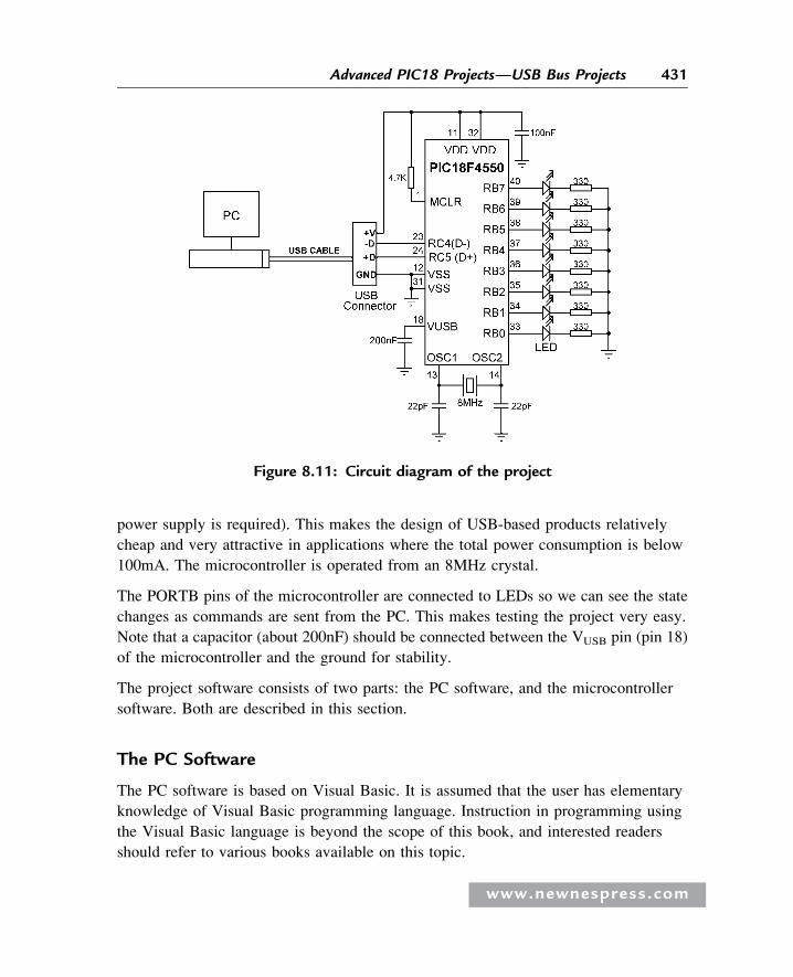
power supply is required). This makes the design of USB-based products relatively
cheap and very attractive in applications where the total power consumption is below
100mA. The microcontroller is operated from an 8MHz crystal.
The PORTB pins of the microcontroller are connected to LEDs so we can see the state
changes as commands are sent from the PC. This makes testing the project very easy.
Note that a capacitor (about 200nF) should be connected between the VUSB pin (pin 18)
of the microcontroller and the ground for stability.
The project software consists of two parts: the PC software, and the microcontroller
software. Both are described in this section.
The PC Software
The PC software is based on Visual Basic. It is assumed that the user has elementary
knowledge of Visual Basic programming language. Instruction in programming using
the Visual Basic language is beyond the scope of this book, and interested readers
should refer to various books available on this topic.
Figure 8.11: Circuit diagram of the project
www.newnespress.com
431Advanced PIC18 Projects—USB Bus Projects
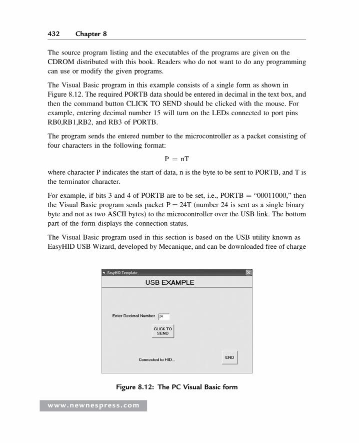
The source program listing and the executables of the programs are given on the
CDROM distributed with this book. Readers who do not want to do any programming
can use or modify the given programs.
The Visual Basic program in this example consists of a single form as shown in
Figure 8.12. The required PORTB data should be entered in decimal in the text box, and
then the command button CLICK TO SEND should be clicked with the mouse. For
example, entering decimal number 15 will turn on the LEDs connected to port pins
RB0,RB1,RB2, and RB3 of PORTB.
The program sends the entered number to the microcontroller as a packet consisting of
four characters in the following format:
P ¼ nT
where character P indicates the start of data, n is the byte to be sent to PORTB, and T is
the terminator character.
For example, if bits 3 and 4 of PORTB are to be set, i.e., PORTB ¼ “00011000,” then
the Visual Basic program sends packet P ¼ 24T (number 24 is sent as a single binary
byte and not as two ASCII bytes) to the microcontroller over the USB link. The bottom
part of the form displays the connection status.
The Visual Basic program used in this section is based on the USB utility known as
EasyHID USB Wizard, developed by Mecanique, and can be downloaded free of charge
Figure 8.12: The PC Visual Basic form
www.newnespress.com
432 Chapter 8
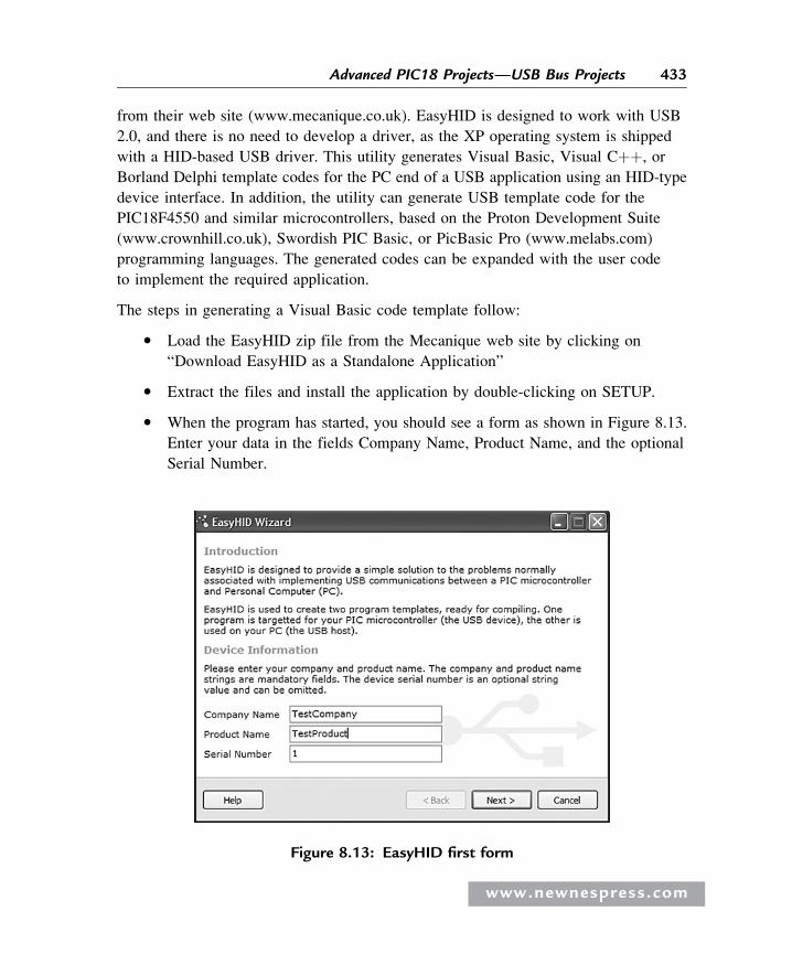
from their web site (www.mecanique.co.uk). EasyHID is designed to work with USB
2.0, and there is no need to develop a driver, as the XP operating system is shipped
with a HID-based USB driver. This utility generates Visual Basic, Visual Cþþ, or
Borland Delphi template codes for the PC end of a USB application using an HID-type
device interface. In addition, the utility can generate USB template code for the
PIC18F4550 and similar microcontrollers, based on the Proton Development Suite
(www.crownhill.co.uk), Swordish PIC Basic, or PicBasic Pro (www.melabs.com)
programming languages. The generated codes can be expanded with the user code
to implement the required application.
The steps in generating a Visual Basic code template follow:
� Load the EasyHID zip file from the Mecanique web site by clicking on
“Download EasyHID as a Standalone Application”
� Extract the files and install the application by double-clicking on SETUP.
� When the program has started, you should see a form as shown in Figure 8.13.
Enter your data in the fields Company Name, Product Name, and the optional
Serial Number.
Figure 8.13: EasyHID first form
www.newnespress.com
433Advanced PIC18 Projects—USB Bus Projects
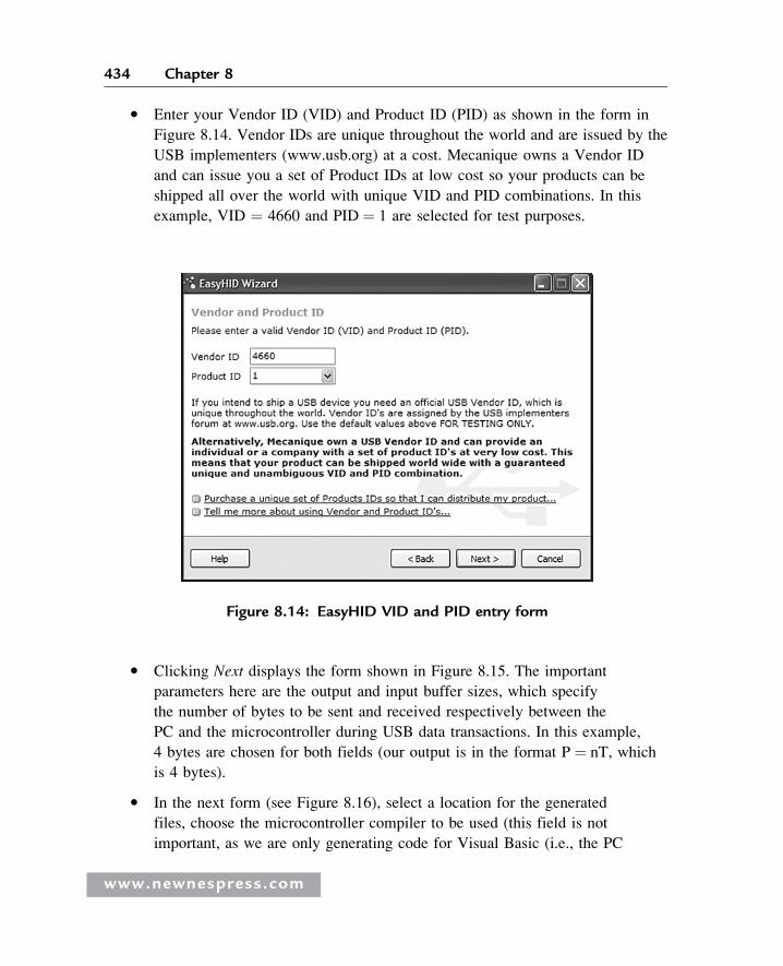
� Enter your Vendor ID (VID) and Product ID (PID) as shown in the form in
Figure 8.14. Vendor IDs are unique throughout the world and are issued by the
USB implementers (www.usb.org) at a cost. Mecanique owns a Vendor ID
and can issue you a set of Product IDs at low cost so your products can be
shipped all over the world with unique VID and PID combinations. In this
example, VID ¼ 4660 and PID ¼ 1 are selected for test purposes.
� Clicking Next displays the form shown in Figure 8.15. The important
parameters here are the output and input buffer sizes, which specify
the number of bytes to be sent and received respectively between the
PC and the microcontroller during USB data transactions. In this example,
4 bytes are chosen for both fields (our output is in the format P ¼ nT, which
is 4 bytes).
� In the next form (see Figure 8.16), select a location for the generated
files, choose the microcontroller compiler to be used (this field is not
important, as we are only generating code for Visual Basic (i.e., the PC
Figure 8.14: EasyHID VID and PID entry form
www.newnespress.com
434 Chapter 8
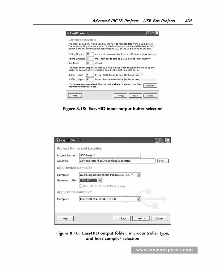
Figure 8.15: EasyHID input-output buffer selection
Figure 8.16: EasyHID output folder, microcontroller type,and host compiler selection
www.newnespress.com
435Advanced PIC18 Projects—USB Bus Projects
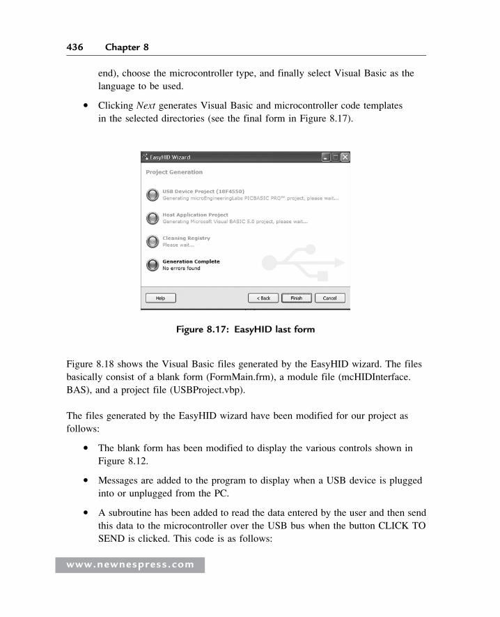
end), choose the microcontroller type, and finally select Visual Basic as the
language to be used.
� Clicking Next generates Visual Basic and microcontroller code templates
in the selected directories (see the final form in Figure 8.17).
Figure 8.18 shows the Visual Basic files generated by the EasyHID wizard. The files
basically consist of a blank form (FormMain.frm), a module file (mcHIDInterface.
BAS), and a project file (USBProject.vbp).
The files generated by the EasyHID wizard have been modified for our project as
follows:
� The blank form has been modified to display the various controls shown in
Figure 8.12.
� Messages are added to the program to display when a USB device is plugged
into or unplugged from the PC.
� A subroutine has been added to read the data entered by the user and then send
this data to the microcontroller over the USB bus when the button CLICK TO
SEND is clicked. This code is as follows:
Figure 8.17: EasyHID last form
www.newnespress.com
436 Chapter 8
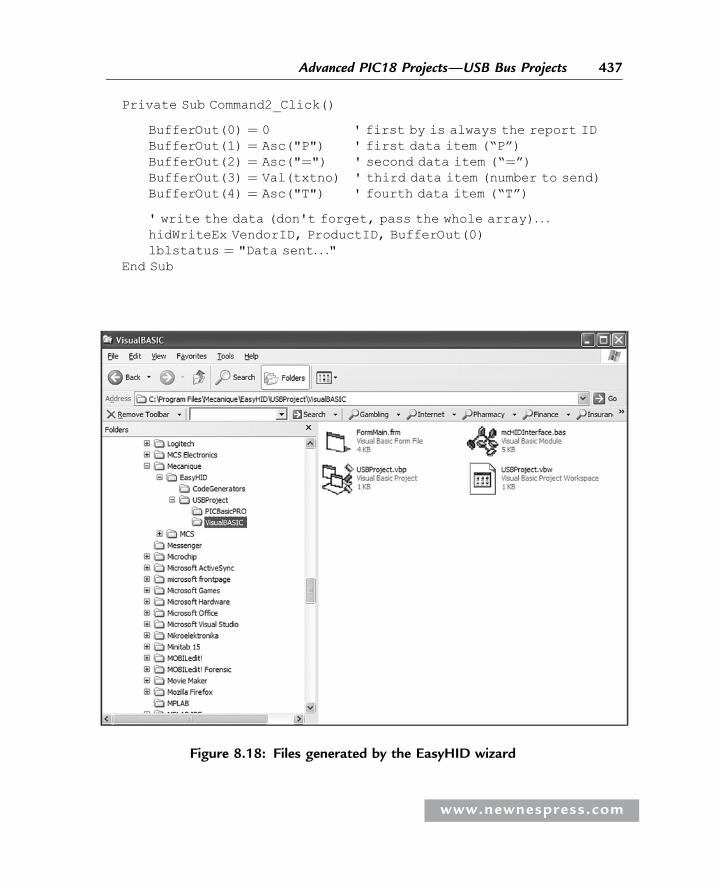
Private Sub Command2_Click()
BufferOut(0) ¼ 0 ' first by is always the report IDBufferOut(1) ¼ Asc("P") ' first data item (“P”)BufferOut(2) ¼ Asc("¼") ' second data item (“¼”)BufferOut(3) ¼ Val(txtno) ' third data item (number to send)BufferOut(4) ¼ Asc("T") ' fourth data item (“T”)
' write the data (don't forget, pass the whole array). . .hidWriteEx VendorID, ProductID, BufferOut(0)lblstatus ¼ "Data sent. . ."
End Sub
Figure 8.18: Files generated by the EasyHID wizard
www.newnespress.com
437Advanced PIC18 Projects—USB Bus Projects
BufferOut stores the data to be sent to the microcontroller over the USB bus. Notice that
the first byte of this buffer is the report ID and must be set to 0. The actual data starts
from address BufferOut(1) of the array and the data sent is in the format P ¼ nT as
described before. After the data is sent, the message “Data sent. . .” appears at the
bottom part of the display.
Figure 8.19 shows the final listing of the Visual Basic program. The program is in
two parts: the form USB1.FRM and the module USB1.BAS. The programs should be
loaded and used in the Visual Basic development environment. An installable version
of this program (in folder USB1) comes with the CDROM included with this book
for those who do not have the Visual Basic development environment. This program
should be installed as a normal Windows software installation.
The Microcontroller Software
The microcontroller receives the command P ¼ nT from the PC and sends data byte
n to PORTB. The listing of the microcontroller program (USB.C) without the USB code
is shown in Figure 8.20. The program configures PORTB as digital
output.
Generating the USB Descriptor File
The USB descriptor file must be included at the beginning of the mikroC program.
This descriptor file is created using the Tools menu option of the mikroC compiler
as follows:
� Select Tools -> HID Terminal
� A new form should be displayed. Click on the Descriptor tab and the form
shown in Figure 8.21 is displayed.
� The important parameters to enter here are vendor ID (VID), product ID (PID),
input buffer size, output buffer size, vendor name (VN), and product name
(PN). Note that the VID and PID are in hexadecimal format and that the values
entered here must be the same as the ones used in the Visual Basic program
when generating the code using the EasyHID wizard. Choose VID ¼ 1234
(equivalent to decimal 6460), PID ¼ 1, input buffer size ¼ 4, output buffer
size ¼ 4, and any names you like for the VN and PN fields.
� Check the mikroC compiler.
www.newnespress.com
438 Chapter 8
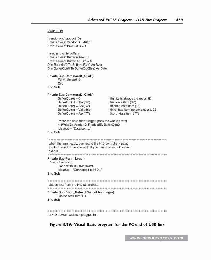
USB1.FRM
' vendor and product IDsPrivate Const VendorID = 4660Private Const ProductID = 1
' read and write buffersPrivate Const BufferInSize = 8Private Const BufferOutSize = 8Dim BufferIn(0 To BufferInSize) As ByteDim BufferOut(0 To BufferOutSize) As Byte
Private Sub Command1_Click() Form_Unload (0) EndEnd Sub
Private Sub Command2_Click() BufferOut(0) = 0 ' first by is always the report ID BufferOut(1) = Asc("P") ' first data item (“P”) BufferOut(2) = Asc("=") ' second data item (“-“) BufferOut(3) = Val(txtno) ' third data item (to send over USB) BufferOut(4) = Asc("T") ' fourth data item (“T”) ' write the data (don't forget, pass the whole array)... hidWriteEx VendorID, ProductID, BufferOut(0) lblstatus = "Data sent..."End Sub
' ∗∗∗∗∗∗∗∗∗∗∗∗∗∗∗∗∗∗∗∗∗∗∗∗∗∗∗∗∗∗∗∗∗∗∗∗∗∗∗∗∗∗∗∗∗∗∗∗∗∗∗∗∗∗∗∗∗∗∗∗∗∗∗∗∗∗∗∗∗∗∗∗∗∗∗' when the form loads, connect to the HID controller - pass' the form window handle so that you can receive notification' events...'∗∗∗∗∗∗∗∗∗∗∗∗∗∗∗∗∗∗∗∗∗∗∗∗∗∗∗∗∗∗∗∗∗∗∗∗∗∗∗∗∗∗∗∗∗∗∗∗∗∗∗∗∗∗∗∗∗∗∗∗∗∗∗∗∗∗∗∗∗∗∗∗∗∗∗∗Private Sub Form_Load() ' do not remove! ConnectToHID (Me.hwnd) lblstatus = "Connected to HID..."End Sub
'∗∗∗∗∗∗∗∗∗∗∗∗∗∗∗∗∗∗∗∗∗∗∗∗∗∗∗∗∗∗∗∗∗∗∗∗∗∗∗∗∗∗∗∗∗∗∗∗∗∗∗∗∗∗∗∗∗∗∗∗∗∗∗∗∗∗∗∗∗∗∗∗∗∗∗∗' disconnect from the HID controller...'∗∗∗∗∗∗∗∗∗∗∗∗∗∗∗∗∗∗∗∗∗∗∗∗∗∗∗∗∗∗∗∗∗∗∗∗∗∗∗∗∗∗∗∗∗∗∗∗∗∗∗∗∗∗∗∗∗∗∗∗∗∗∗∗∗∗∗∗∗∗∗∗∗∗∗∗Private Sub Form_Unload(Cancel As Integer) DisconnectFromHIDEnd Sub
'∗∗∗∗∗∗∗∗∗∗∗∗∗∗∗∗∗∗∗∗∗∗∗∗∗∗∗∗∗∗∗∗∗∗∗∗∗∗∗∗∗∗∗∗∗∗∗∗∗∗∗∗∗∗∗∗∗∗∗∗∗∗∗∗∗∗∗∗∗∗∗∗∗∗∗∗' a HID device has been plugged in...
Figure 8.19: Visual Basic program for the PC end of USB link
www.newnespress.com
439Advanced PIC18 Projects—USB Bus Projects
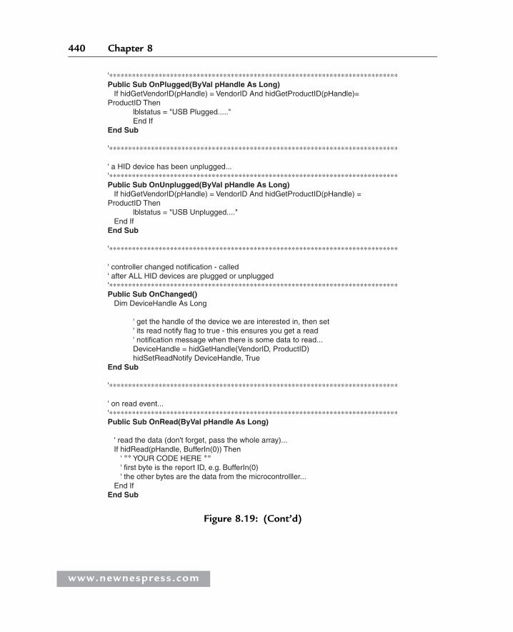
'∗∗∗∗∗∗∗∗∗∗∗∗∗∗∗∗∗∗∗∗∗∗∗∗∗∗∗∗∗∗∗∗∗∗∗∗∗∗∗∗∗∗∗∗∗∗∗∗∗∗∗∗∗∗∗∗∗∗∗∗∗∗∗∗∗∗∗∗∗∗∗∗∗∗∗∗Public Sub OnPlugged(ByVal pHandle As Long) If hidGetVendorID(pHandle) = VendorID And hidGetProductID(pHandle)=ProductID Then lblstatus = "USB Plugged....." End IfEnd Sub
'∗∗∗∗∗∗∗∗∗∗∗∗∗∗∗∗∗∗∗∗∗∗∗∗∗∗∗∗∗∗∗∗∗∗∗∗∗∗∗∗∗∗∗∗∗∗∗∗∗∗∗∗∗∗∗∗∗∗∗∗∗∗∗∗∗∗∗∗∗∗∗∗∗∗∗∗
' a HID device has been unplugged...'∗∗∗∗∗∗∗∗∗∗∗∗∗∗∗∗∗∗∗∗∗∗∗∗∗∗∗∗∗∗∗∗∗∗∗∗∗∗∗∗∗∗∗∗∗∗∗∗∗∗∗∗∗∗∗∗∗∗∗∗∗∗∗∗∗∗∗∗∗∗∗∗∗∗∗∗Public Sub OnUnplugged(ByVal pHandle As Long) If hidGetVendorID(pHandle) = VendorID And hidGetProductID(pHandle) =ProductID Then lblstatus = "USB Unplugged...." End IfEnd Sub
'∗∗∗∗∗∗∗∗∗∗∗∗∗∗∗∗∗∗∗∗∗∗∗∗∗∗∗∗∗∗∗∗∗∗∗∗∗∗∗∗∗∗∗∗∗∗∗∗∗∗∗∗∗∗∗∗∗∗∗∗∗∗∗∗∗∗∗∗∗∗∗∗∗∗∗∗
' controller changed notification - called' after ALL HID devices are plugged or unplugged'∗∗∗∗∗∗∗∗∗∗∗∗∗∗∗∗∗∗∗∗∗∗∗∗∗∗∗∗∗∗∗∗∗∗∗∗∗∗∗∗∗∗∗∗∗∗∗∗∗∗∗∗∗∗∗∗∗∗∗∗∗∗∗∗∗∗∗∗∗∗∗∗∗∗∗∗Public Sub OnChanged() Dim DeviceHandle As Long ' get the handle of the device we are interested in, then set ' its read notify flag to true - this ensures you get a read ' notification message when there is some data to read... DeviceHandle = hidGetHandle(VendorID, ProductID) hidSetReadNotify DeviceHandle, TrueEnd Sub
'∗∗∗∗∗∗∗∗∗∗∗∗∗∗∗∗∗∗∗∗∗∗∗∗∗∗∗∗∗∗∗∗∗∗∗∗∗∗∗∗∗∗∗∗∗∗∗∗∗∗∗∗∗∗∗∗∗∗∗∗∗∗∗∗∗∗∗∗∗∗∗∗∗∗∗∗
' on read event...'∗∗∗∗∗∗∗∗∗∗∗∗∗∗∗∗∗∗∗∗∗∗∗∗∗∗∗∗∗∗∗∗∗∗∗∗∗∗∗∗∗∗∗∗∗∗∗∗∗∗∗∗∗∗∗∗∗∗∗∗∗∗∗∗∗∗∗∗∗∗∗∗∗∗∗∗Public Sub OnRead(ByVal pHandle As Long) ' read the data (don't forget, pass the whole array)... If hidRead(pHandle, BufferIn(0)) Then ' ∗∗ YOUR CODE HERE ∗∗ ' first byte is the report ID, e.g. BufferIn(0) ' the other bytes are the data from the microcontrolller... End IfEnd Sub
Figure 8.19: (Cont’d)
www.newnespress.com
440 Chapter 8
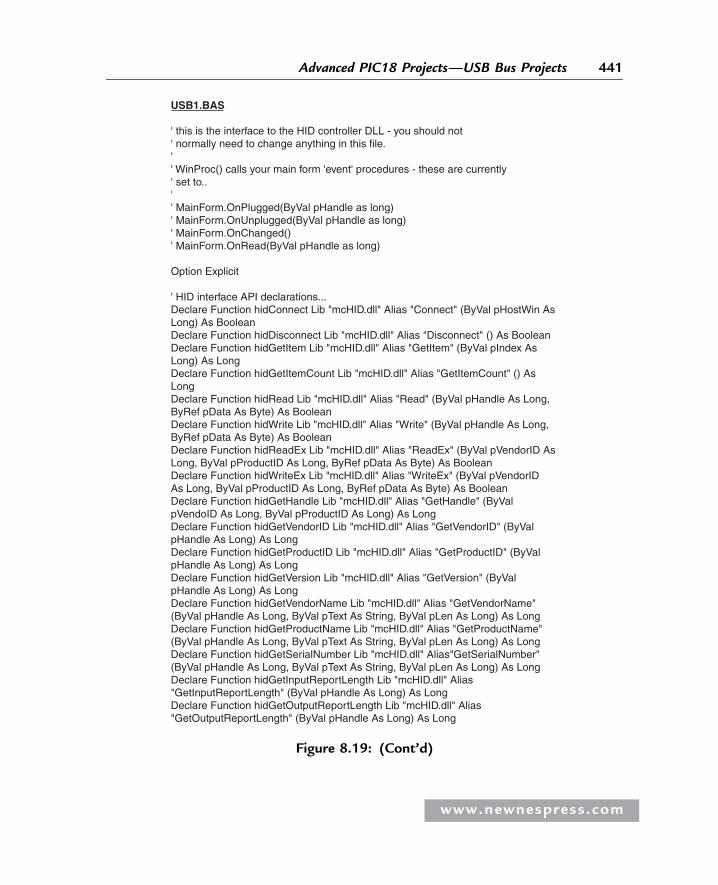
USB1.BAS
' this is the interface to the HID controller DLL - you should not' normally need to change anything in this file.'' WinProc() calls your main form 'event' procedures - these are currently' set to..'' MainForm.OnPlugged(ByVal pHandle as long)' MainForm.OnUnplugged(ByVal pHandle as long)' MainForm.OnChanged()' MainForm.OnRead(ByVal pHandle as long)
Option Explicit
' HID interface API declarations...Declare Function hidConnect Lib "mcHID.dll" Alias "Connect" (ByVal pHostWin As Long) As BooleanDeclare Function hidDisconnect Lib "mcHID.dll" Alias "Disconnect" () As BooleanDeclare Function hidGetItem Lib "mcHID.dll" Alias "GetItem" (ByVal pIndex As Long) As LongDeclare Function hidGetItemCount Lib "mcHID.dll" Alias "GetItemCount" () AsLongDeclare Function hidRead Lib "mcHID.dll" Alias "Read" (ByVal pHandle As Long,ByRef pData As Byte) As BooleanDeclare Function hidWrite Lib "mcHID.dll" Alias "Write" (ByVal pHandle As Long,ByRef pData As Byte) As BooleanDeclare Function hidReadEx Lib "mcHID.dll" Alias "ReadEx" (ByVal pVendorID AsLong, ByVal pProductID As Long, ByRef pData As Byte) As BooleanDeclare Function hidWriteEx Lib "mcHID.dll" Alias "WriteEx" (ByVal pVendorIDAs Long, ByVal pProductID As Long, ByRef pData As Byte) As BooleanDeclare Function hidGetHandle Lib "mcHID.dll" Alias "GetHandle" (ByValpVendoID As Long, ByVal pProductID As Long) As LongDeclare Function hidGetVendorID Lib "mcHID.dll" Alias "GetVendorID" (ByValpHandle As Long) As LongDeclare Function hidGetProductID Lib "mcHID.dll" Alias "GetProductID" (ByValpHandle As Long) As LongDeclare Function hidGetVersion Lib "mcHID.dll" Alias "GetVersion" (ByValpHandle As Long) As LongDeclare Function hidGetVendorName Lib "mcHID.dll" Alias "GetVendorName"(ByVal pHandle As Long, ByVal pText As String, ByVal pLen As Long) As LongDeclare Function hidGetProductName Lib "mcHID.dll" Alias "GetProductName"(ByVal pHandle As Long, ByVal pText As String, ByVal pLen As Long) As LongDeclare Function hidGetSerialNumber Lib "mcHID.dll" Alias"GetSerialNumber" (ByVal pHandle As Long, ByVal pText As String, ByVal pLen As Long) As LongDeclare Function hidGetInputReportLength Lib "mcHID.dll" Alias"GetInputReportLength" (ByVal pHandle As Long) As LongDeclare Function hidGetOutputReportLength Lib "mcHID.dll" Alias"GetOutputReportLength" (ByVal pHandle As Long) As Long
Figure 8.19: (Cont’d)
www.newnespress.com
441Advanced PIC18 Projects—USB Bus Projects
Declare Sub hidSetReadNotify Lib "mcHID.dll" Alias "SetReadNotify" (ByValpHandle As Long, ByVal pValue As Boolean)Declare Function hidIsReadNotifyEnabled Lib "mcHID.dll" Alias"IsReadNotifyEnabled" (ByVal pHandle As Long) As BooleanDeclare Function hidIsAvailable Lib "mcHID.dll" Alias "IsAvailable" (ByValpVendorID As Long, ByVal pProductID As Long) As Boolean
' windows API declarations - used to set up messaging...Private Declare Function CallWindowProc Lib "user32" Alias "CallWindowProcA"(ByVal lpPrevWndFunc As Long, ByVal hwnd As Long, ByVal Msg As Long, ByVal wParam As Long, ByVal lParam As Long) As LongPrivate Declare Function SetWindowLong Lib "user32" Alias "SetWindowLongA"(ByVal hwnd As Long, ByVal nIndex As Long, ByVal dwNewLong As Long) AsLong
' windows API ConstantsPrivate Const WM_APP = 32768Private Const GWL_WNDPROC = -4
' HID message constantsPrivate Const WM_HID_EVENT = WM_APP + 200Private Const NOTIFY_PLUGGED = 1Private Const NOTIFY_UNPLUGGED = 2Private Const NOTIFY_CHANGED = 3Private Const NOTIFY_READ = 4
' local variablesPrivate FPrevWinProc As Long ' Handle to previous window procedurePrivate FWinHandle As Long ' Handle to message window
' Set up a windows hook to receive notification' messages from the HID controller DLL - then connect' to the controllerPublic Function ConnectToHID(ByVal pHostWin As Long) As Boolean FWinHandle = pHostWin ConnectToHID = hidConnect(FWinHandle) FPrevWinProc = SetWindowLong(FWinHandle, GWL_WNDPROC, AddressOfWinProc)End Function
' Unhook from the HID controller and disconnect...Public Function DisconnectFromHID() As Boolean DisconnectFromHID = hidDisconnect SetWindowLong FWinHandle, GWL_WNDPROC, FPrevWinProcEnd Function
' This is the procedure that intercepts the HID controller messages...Private Function WinProc(ByVal pHWnd As Long, ByVal pMsg As Long,ByVal wParam As Long, ByVal lParam As Long) As Long If pMsg = WM_HID_EVENT Then
Figure 8.19: (Cont’d)
www.newnespress.com
442 Chapter 8
� Clicking the CREATE button will ask for a folder name and then create
descriptor file USBdsc in this folder. Rename this file to have extension “.C”
(i.e., the full file name should be USBdsc.C) and then copy it to the following
folder (other required mikroC files are already in this folder, so it makes sense
to copy USBdsc.C here as well).
C:\Program Files\Mikroelektronika\mikroC\Examples\EasyPic4\extra_examples\HID-library\USBdsc.c
Do not modify the contents of file USBdsc.C. A listing of this file is given on the
CDROM.
The microcontroller program listing with the USB code included is shown in
Figure 8.22 (program USB1.C). At the beginning of the program the USB descriptor
file USBdsc.C is included. The operation of the USB link requires the microcontroller
to keep the connection alive by sending keep-alive messages to the PC every several
milliseconds. This is achieved by setting up a timer interrupt service routine using
Select Case wParam ' HID device has been plugged message... Case Is = NOTIFY_PLUGGED MainForm.OnPlugged (lParam)
' HID device has been unplugged Case Is = NOTIFY_UNPLUGGED MainForm.OnUnplugged (lParam) ' controller has changed... Case Is = NOTIFY_CHANGED MainForm.OnChanged
' read event... Case Is = NOTIFY_READ MainForm.OnRead (lParam) End Select End If ' next... WinProc = CallWindowProc(FPrevWinProc, pHWnd, pMsg, wParam, lParam) End Function
Figure 8.19: (Cont’d)
www.newnespress.com
443Advanced PIC18 Projects—USB Bus Projects
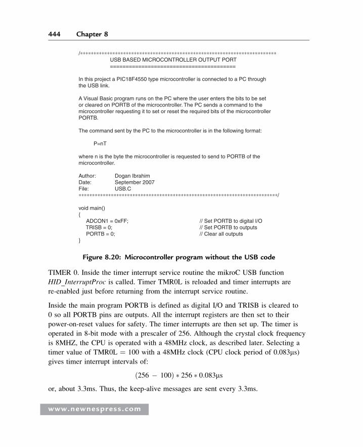
TIMER 0. Inside the timer interrupt service routine the mikroC USB function
HID_InterruptProc is called. Timer TMR0L is reloaded and timer interrupts are
re-enabled just before returning from the interrupt service routine.
Inside the main program PORTB is defined as digital I/O and TRISB is cleared to
0 so all PORTB pins are outputs. All the interrupt registers are then set to their
power-on-reset values for safety. The timer interrupts are then set up. The timer is
operated in 8-bit mode with a prescaler of 256. Although the crystal clock frequency
is 8MHZ, the CPU is operated with a 48MHz clock, as described later. Selecting a
timer value of TMR0L ¼ 100 with a 48MHz clock (CPU clock period of 0.083ms)gives timer interrupt intervals of:
ð256 � 100Þ � 256 � 0:083msor, about 3.3ms. Thus, the keep-alive messages are sent every 3.3ms.
/∗∗∗∗∗∗∗∗∗∗∗∗∗∗∗∗∗∗∗∗∗∗∗∗∗∗∗∗∗∗∗∗∗∗∗∗∗∗∗∗∗∗∗∗∗∗∗∗∗∗∗∗∗∗∗∗∗∗∗∗∗∗∗∗∗∗∗∗∗∗∗∗∗ USB BASED MICROCONTROLLER OUTPUT PORT ========================================
In this project a PIC18F4550 type microcontroller is connected to a PC throughthe USB link.
A Visual Basic program runs on the PC where the user enters the bits to be setor cleared on PORTB of the microcontroller. The PC sends a command to themicrocontroller requesting it to set or reset the required bits of the microcontrollerPORTB.
The command sent by the PC to the microcontroller is in the following format:
P=nT
where n is the byte the microcontroller is requested to send to PORTB of themicrocontroller.
Author: Dogan IbrahimDate: September 2007File: USB.C∗∗∗∗∗∗∗∗∗∗∗∗∗∗∗∗∗∗∗∗∗∗∗∗∗∗∗∗∗∗∗∗∗∗∗∗∗∗∗∗∗∗∗∗∗∗∗∗∗∗∗∗∗∗∗∗∗∗∗∗∗∗∗∗∗∗∗∗∗∗∗∗∗∗/
void main(){ ADCON1 = 0xFF; // Set PORTB to digital I/O TRISB = 0; // Set PORTB to outputs PORTB = 0; // Clear all outputs }
Figure 8.20: Microcontroller program without the USB code
www.newnespress.com
444 Chapter 8
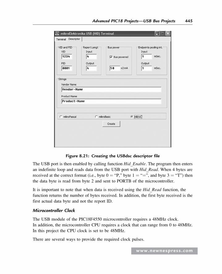
The USB port is then enabled by calling function Hid_Enable. The program then enters
an indefinite loop and reads data from the USB port with Hid_Read. When 4 bytes are
received at the correct format (i.e., byte 0 ¼ “P,” byte 1 ¼ “¼”, and byte 3 ¼ “T”) then
the data byte is read from byte 2 and sent to PORTB of the microcontroller.
It is important to note that when data is received using the Hid_Read function, the
function returns the number of bytes received. In addition, the first byte received is the
first actual data byte and not the report ID.
Microcontroller Clock
The USB module of the PIC18F4550 microcontroller requires a 48MHz clock.
In addition, the microcontroller CPU requires a clock that can range from 0 to 48MHz.
In this project the CPU clock is set to be 48MHz.
There are several ways to provide the required clock pulses.
Figure 8.21: Creating the USBdsc descriptor file
www.newnespress.com
445Advanced PIC18 Projects—USB Bus Projects
/∗∗∗∗∗∗∗∗∗∗∗∗∗∗∗∗∗∗∗∗∗∗∗∗∗∗∗∗∗∗∗∗∗∗∗∗∗∗∗∗∗∗∗∗∗∗∗∗∗∗∗∗∗∗∗∗∗∗∗∗∗∗∗∗∗∗∗∗∗∗∗∗∗∗∗ USB BASED MICROCONTROLLER OUTPUT PORT ========================================
In this project a PIC18F4550 type microcontroller is connectedto a PC through the USB link.
A Visual Basic program runs on the PC where the user enters the bits to be set orcleared on PORTB of the microcontroller. The PC sends a command to themicrocontroller requesting it to set or reset the required bits of the microcontrollerPORTB.
A 8MHz crystal is used to operate the microcontroller. The actual CPU clock is raisedto 48MHz by setting configuration bits. Also, the USB module is operated with48MHz.
The command sent by the PC to the microcontroller is in the following format:
P=nT
where n is the byte the microcontroller is requested to send to PORTB of themicrocontroller.
This program includes the USB code.
Author: Dogan IbrahimDate: September 2007File: USB1.C∗∗∗∗∗∗∗∗∗∗∗∗∗∗∗∗∗∗∗∗∗∗∗∗∗∗∗∗∗∗∗∗∗∗∗∗∗∗∗∗∗∗∗∗∗∗∗∗∗∗∗∗∗∗∗∗∗∗∗∗∗∗∗∗∗∗∗∗∗∗∗∗∗∗∗∗/
#include "C:\ProgramFiles\Mikroelektronika\mikroC\Examples\EasyPic4\extra_examples\HID-library\USBdsc.c"
unsigned char Read_buffer[64];unsigned char Write_buffer[64];unsigned char num;//// Timer interrupt service routine//void interrupt(){ HID_InterruptProc(); // Keep alive TMR0L = 100; // Re-load TMR0L INTCON.TMR0IF = 0; // Re-enable TMR0 interrupts}
//// Start of MAIN program
Figure 8.22: Microcontroller program with USB code
www.newnespress.com
446 Chapter 8
//void main(){
ADCON1 = 0xFF; // Set PORTB to digital I/O TRISB = 0; // Set PORTB to outputs PORTB = 0; // Clear all outputs//// Set interrupt registers to power-on defaults// Disable all interrupts// INTCON=0; INTCON2=0xF5; INTCON3=0xC0; RCON.IPEN=0; PIE1=0; PIE2=0; PIR1=0; PIR2=0;//// Configure TIMER 0 for 3.3ms interrupts. Set prescaler to 256// and load TMR0L to 100 so that the time interval for timer// interrupts at 48MHz is 256∗(256-100)∗0.083 = 3.3ms//// The timer is in 8-bit mode by default// T0CON = 0x47; // Prescaler = 256 TMR0L = 100; // Timer count is 256-156 = 100 INTCON.TMR0IE = 1; // Enable T0IE T0CON.TMR0ON = 1; // Turn Timer 0 ON INTCON = 0xE0; // Enable interrupts
//// Enable USB port// Hid_Enable(&Read_buffer, &Write_buffer); Delay_ms(1000); Delay_ms(1000);//// Read from the USB port. Number of bytes read is in num//
for(;;) // do forever{ num=0; while(num != 4) // Get 4 characters {num = Hid_Read(); } if(Read_buffer[0] == 'P' && Read_buffer[1] == '=' && Read_buffer[3] == 'T') { PORTB = Read_buffer[2]; } } Hid_Disable();
}
Figure 8.22: (Cont’d)
www.newnespress.com
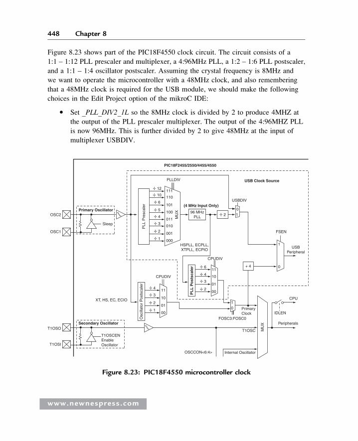
Figure 8.23 shows part of the PIC18F4550 clock circuit. The circuit consists of a
1:1 – 1:12 PLL prescaler and multiplexer, a 4:96MHz PLL, a 1:2 – 1:6 PLL postscaler,
and a 1:1 – 1:4 oscillator postscaler. Assuming the crystal frequency is 8MHz and
we want to operate the microcontroller with a 48MHz clock, and also remembering
that a 48MHz clock is required for the USB module, we should make the following
choices in the Edit Project option of the mikroC IDE:
� Set _PLL_DIV2_1L so the 8MHz clock is divided by 2 to produce 4MHZ at
the output of the PLL prescaler multiplexer. The output of the 4:96MHZ PLL
is now 96MHz. This is further divided by 2 to give 48MHz at the input of
multiplexer USBDIV.
PIC18F2455/2550/4455/4550
PLLDIV
PLL
Pre
scal
er
MU
X
PL
L P
ost
scal
er
(4 MHz Input Only)
USB Clock Source
USBDIV
FSEN
CPU
1
0
Peripherals
USBPeripheral
96 MHzPLL
CPUDIV
CPUDIV
OSCCON<6:4>
FOSC3:FOSC0IDLEN
MU
X
T1OSC
Internal Oscillator
Secondary Oscillator
Osc
illat
or P
osts
cale
r
XT, HS, EC, ECIO
T1OSO
T1OSI
T1OSCENEnableOscillator
Primary Oscillator
Sleep
OSC2
OSC1
PrimaryClock
HSPLL, ECPLL,XTPLL, ECPIO
111÷ 12
01÷ 2
÷ 10
÷ 6
÷ 5
÷ 4
÷ 3
÷ 2
÷ 6
÷ 4
+ 4
÷ 3
÷ 2÷ 4
÷ 3
÷ 2
÷ 1
÷ 1
110
101
100
011
010
001
11
10
01
0011
10
01
00
10
000
Figure 8.23: PIC18F4550 microcontroller clock
www.newnespress.com
448 Chapter 8
� Check _USBDIV_2_1L to provide a 48MHz clock to USB module and to select
�2 for the PLL postscaler.
� Check CPUDIV_OSC1_PLL2_1L to select PLL as the clock source.
� Check _FOSC_HSPLL_HS_1H to select a 48MHz clock for the CPU.
� Set the CPU clock to 48MHz in mikroC IDE (using Edit Project).
The clock bits selected for the 48MHz USB operation with a 48MHz CPU clock are
shown in Figure 8.24.
Setting other configuration bits in addition to the clock bits is recommended.
The following list gives all the bits that should be set in the Edit Project option of
the IDE (most of these settings are the power-on-reset values of the bits):
PLLDIV_2_1LCPUDIV_OSC1_PLL2_1LUSBDIV_2_1L
FOSC_HSPLL_HS_1HFCMEM_OFF_1HIESO_OFF_1H
PWRT_ON_2LBOR_ON_2LBORV_43_2LVREGEN_ON_2L
WDT_OFF_2HWDTPS_256_2H
MCLRE_ON_3HLPT1OSC_OFF_3HPBADEN_OFF_3HCCP2MX_ON_3H
STVREN_ON_4LLVP_OFF_4LICPRT_OFF_4LXINST_OFF_4LDEBUG_OFF_4L
www.newnespress.com
449Advanced PIC18 Projects—USB Bus Projects
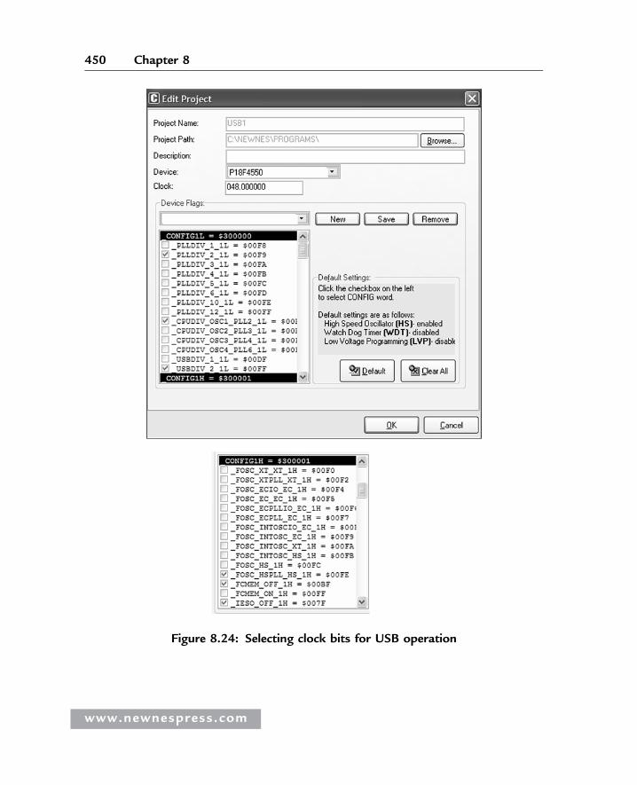
Figure 8.24: Selecting clock bits for USB operation
www.newnespress.com
450 Chapter 8
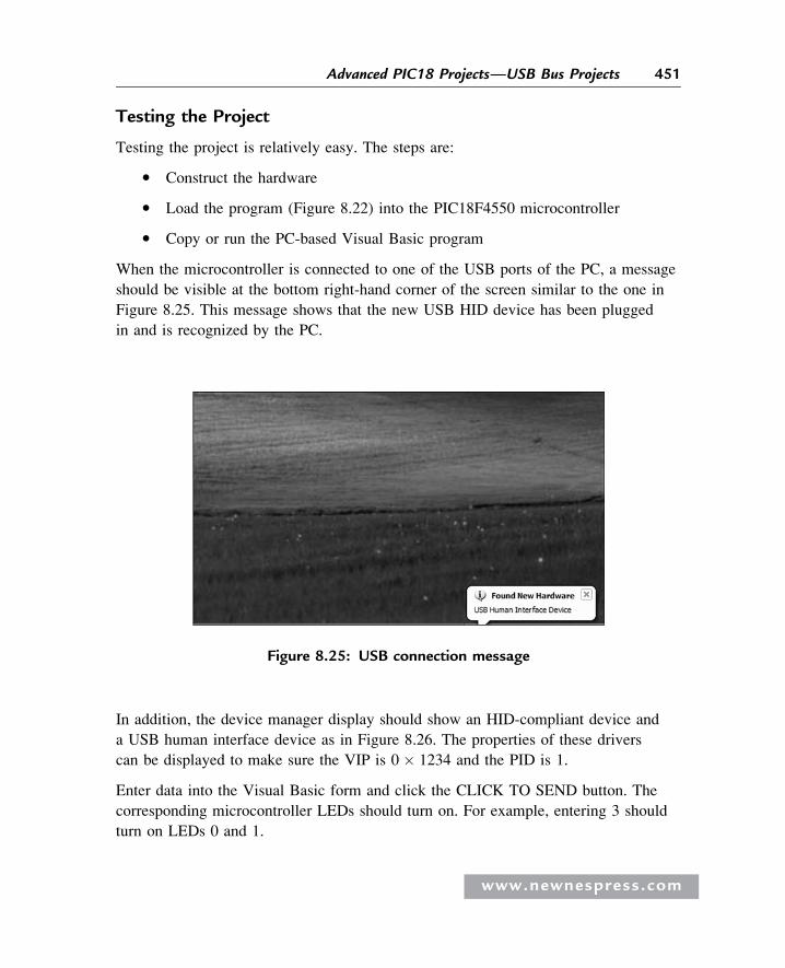
Testing the Project
Testing the project is relatively easy. The steps are:
� Construct the hardware
� Load the program (Figure 8.22) into the PIC18F4550 microcontroller
� Copy or run the PC-based Visual Basic program
When the microcontroller is connected to one of the USB ports of the PC, a message
should be visible at the bottom right-hand corner of the screen similar to the one in
Figure 8.25. This message shows that the new USB HID device has been plugged
in and is recognized by the PC.
In addition, the device manager display should show an HID-compliant device and
a USB human interface device as in Figure 8.26. The properties of these drivers
can be displayed to make sure the VIP is 0 � 1234 and the PID is 1.
Enter data into the Visual Basic form and click the CLICK TO SEND button. The
corresponding microcontroller LEDs should turn on. For example, entering 3 should
turn on LEDs 0 and 1.
Figure 8.25: USB connection message
www.newnespress.com
451Advanced PIC18 Projects—USB Bus Projects
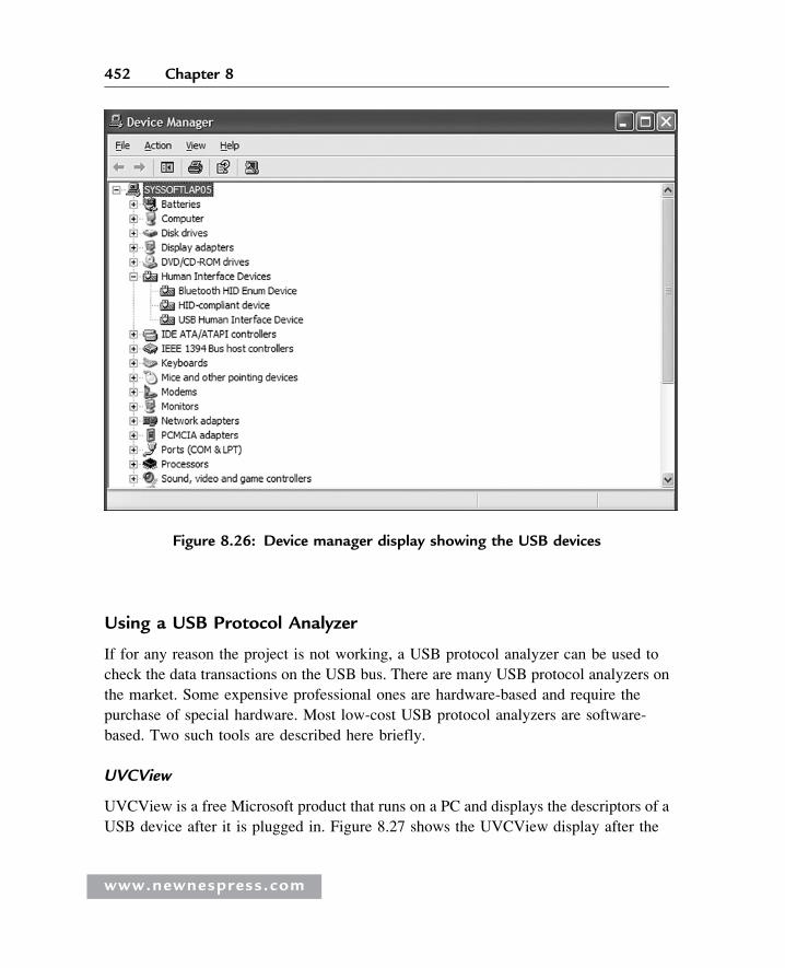
Using a USB Protocol Analyzer
If for any reason the project is not working, a USB protocol analyzer can be used to
check the data transactions on the USB bus. There are many USB protocol analyzers on
the market. Some expensive professional ones are hardware-based and require the
purchase of special hardware. Most low-cost USB protocol analyzers are software-
based. Two such tools are described here briefly.
UVCView
UVCView is a free Microsoft product that runs on a PC and displays the descriptors of a
USB device after it is plugged in. Figure 8.27 shows the UVCView display after the
Figure 8.26: Device manager display showing the USB devices
www.newnespress.com
452 Chapter 8
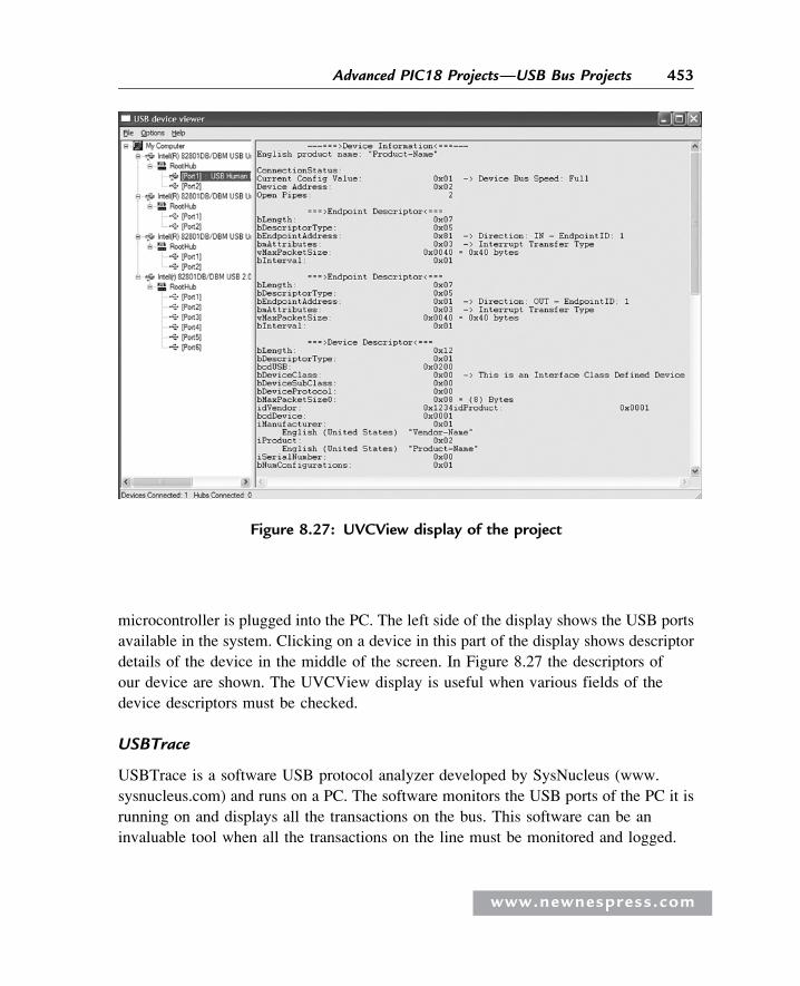
microcontroller is plugged into the PC. The left side of the display shows the USB ports
available in the system. Clicking on a device in this part of the display shows descriptor
details of the device in the middle of the screen. In Figure 8.27 the descriptors of
our device are shown. The UVCView display is useful when various fields of the
device descriptors must be checked.
USBTrace
USBTrace is a software USB protocol analyzer developed by SysNucleus (www.
sysnucleus.com) and runs on a PC. The software monitors the USB ports of the PC it is
running on and displays all the transactions on the bus. This software can be an
invaluable tool when all the transactions on the line must be monitored and logged.
Figure 8.27: UVCView display of the project
www.newnespress.com
453Advanced PIC18 Projects—USB Bus Projects
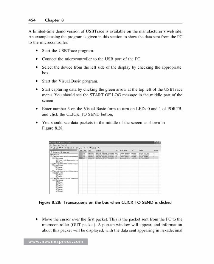
A limited-time demo version of USBTrace is available on the manufacturer’s web site.
An example using the program is given in this section to show the data sent from the PC
to the microcontroller:
� Start the USBTrace program.
� Connect the microcontroller to the USB port of the PC.
� Select the device from the left side of the display by checking the appropriate
box.
� Start the Visual Basic program.
� Start capturing data by clicking the green arrow at the top left of the USBTrace
menu. You should see the START OF LOG message in the middle part of the
screen
� Enter number 3 on the Visual Basic form to turn on LEDs 0 and 1 of PORTB,
and click the CLICK TO SEND button.
� You should see data packets in the middle of the screen as shown in
Figure 8.28.
� Move the cursor over the first packet. This is the packet sent from the PC to the
microcontroller (OUT packet). A pop-up window will appear, and information
about this packet will be displayed, with the data sent appearing in hexadecimal
Figure 8.28: Transactions on the bus when CLICK TO SEND is clicked
www.newnespress.com
454 Chapter 8
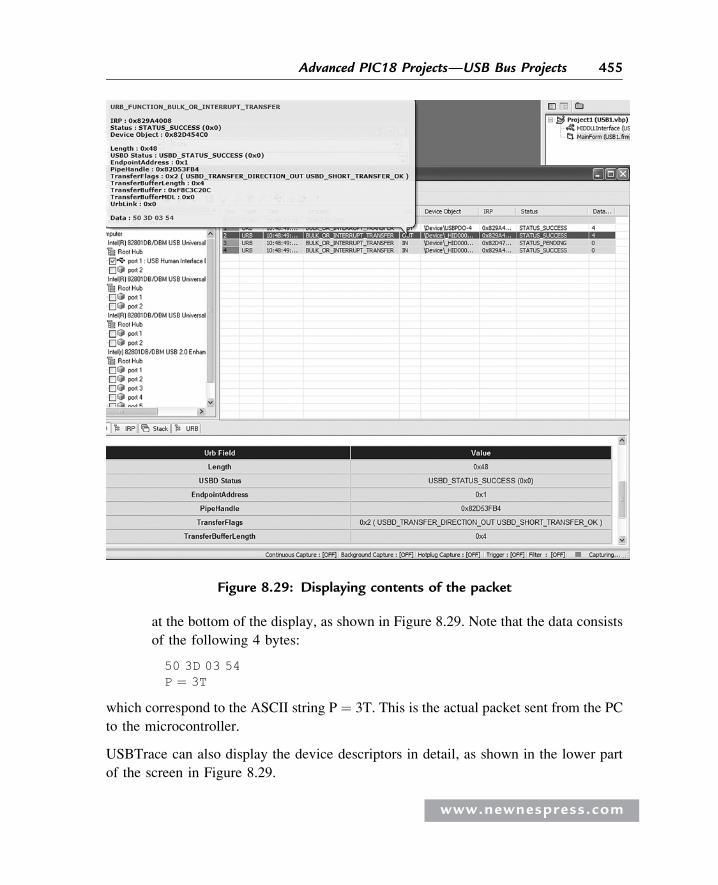
at the bottom of the display, as shown in Figure 8.29. Note that the data consists
of the following 4 bytes:
50 3D 03 54P ¼ 3T
which correspond to the ASCII string P ¼ 3T. This is the actual packet sent from the PC
to the microcontroller.
USBTrace can also display the device descriptors in detail, as shown in the lower part
of the screen in Figure 8.29.
Figure 8.29: Displaying contents of the packet
www.newnespress.com
455Advanced PIC18 Projects—USB Bus Projects
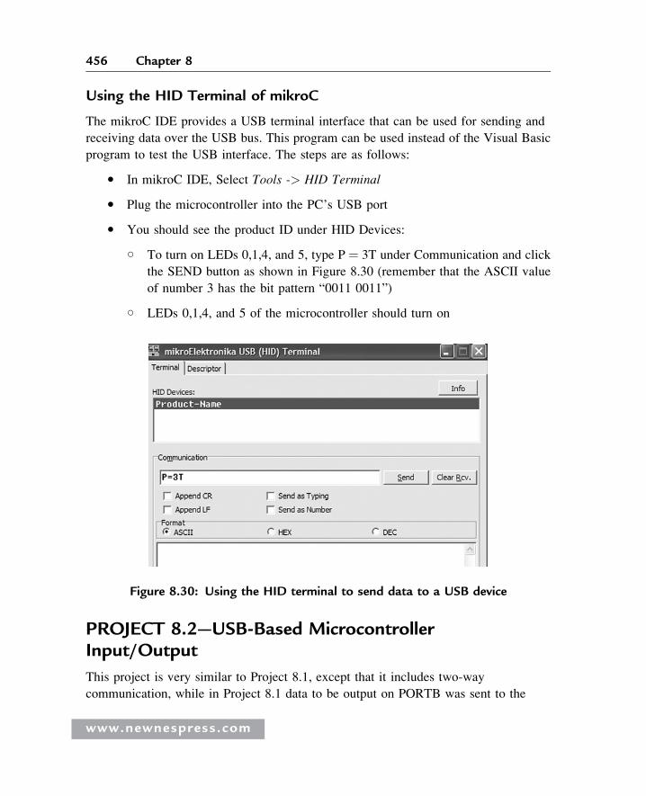
Using the HID Terminal of mikroC
The mikroC IDE provides a USB terminal interface that can be used for sending and
receiving data over the USB bus. This program can be used instead of the Visual Basic
program to test the USB interface. The steps are as follows:
� In mikroC IDE, Select Tools -> HID Terminal
� Plug the microcontroller into the PC’s USB port
� You should see the product ID under HID Devices:
○ To turn on LEDs 0,1,4, and 5, type P ¼ 3T under Communication and click
the SEND button as shown in Figure 8.30 (remember that the ASCII value
of number 3 has the bit pattern “0011 0011”)
○ LEDs 0,1,4, and 5 of the microcontroller should turn on
PROJECT 8.2—USB-Based MicrocontrollerInput/Output
This project is very similar to Project 8.1, except that it includes two-way
communication, while in Project 8.1 data to be output on PORTB was sent to the
Figure 8.30: Using the HID terminal to send data to a USB device
www.newnespress.com
456 Chapter 8
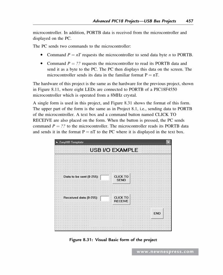
microcontroller. In addition, PORTB data is received from the microcontroller and
displayed on the PC.
The PC sends two commands to the microcontroller:
� Command P ¼ nT requests the microcontroller to send data byte n to PORTB.
� Command P ¼ ?? requests the microcontroller to read its PORTB data and
send it as a byte to the PC. The PC then displays this data on the screen. The
microcontroller sends its data in the familiar format P ¼ nT.
The hardware of this project is the same as the hardware for the previous project, shown
in Figure 8.11, where eight LEDs are connected to PORTB of a PIC18F4550
microcontroller which is operated from a 8MHz crystal.
A single form is used in this project, and Figure 8.31 shows the format of this form.
The upper part of the form is the same as in Project 8.1, i.e., sending data to PORTB
of the microcontroller. A text box and a command button named CLICK TO
RECEIVE are also placed on the form. When the button is pressed, the PC sends
command P ¼ ?? to the microcontroller. The microcontroller reads its PORTB data
and sends it in the format P ¼ nT to the PC where it is displayed in the text box.
Figure 8.31: Visual Basic form of the project
www.newnespress.com
457Advanced PIC18 Projects—USB Bus Projects
Figure 8.32 shows the mikroC program of the project. The program is named
USB2.C and is very similar to the one for the previous project. But here, in
addition, when the command P ¼ ?? is received from the PC, the microcontroller
reads PORTB data and sends it to the PC in the format using the mikroC function
Hid_Write.
The program checks the format of the received command. For P ¼ ?? type commands,
PORTB is configured as inputs, PORTB data is read into Write_buffer[2], and
Write_buffer is sent to the PC, where Write_buffer[0] ¼ “P,” Write_buffer[1] ¼ “¼”,
and Write_buffer[3] ¼ “T” as follows:
if(Read_buffer [0] ¼¼ ‘P‘ && Read_buffer [1] ¼¼ ‘¼‘ &&Read_buffer [2] ¼¼ ‘?‘ && Read_Buffer [3] ¼¼ ‘?‘){TRISB ¼ 0�FF;Write_buffer [0] ¼ ‘P‘; Write_buffer [1] ¼ ‘¼‘; Write_buffer [2] ¼
PORTB; Write_buffer [3] ¼ ‘T‘;Hid_Write(&Write_buffer,4);}
For P ¼ nT type commands, PORTB is configured as outputs and Read_buffer[2] is
sent to PORTB as follows:
if(Read_buffer [0] ¼¼ ‘P‘ && Read_buffer [1] ¼¼ ‘¼‘ &&Read_buffer [3] ¼¼ ‘T‘){TRISB ¼ 0;PORTB ¼ Read_buffer [2];}
The microcontroller clock should be set as in Project 8.1 (i.e., both the CPU and the
USB module should have 48MHz clocks). The other configurations bits should also be
set as described in the previous problem.
Testing the Project
The project can be tested using one of the methods described in the previous project.
If you are using the Visual Basic program, send data to the microcontroller and make
sure the correct LEDs are turned on. Then connect some of the PORTB pins to
logic 0 and click the CLICK TO RECEIVE button. The microcontroller will read its
PORTB data and send it to the PC, where it will be displayed on the PC screen.
www.newnespress.com
458 Chapter 8
/∗∗∗∗∗∗∗∗∗∗∗∗∗∗∗∗∗∗∗∗∗∗∗∗∗∗∗∗∗∗∗∗∗∗∗∗∗∗∗∗∗∗∗∗∗∗∗∗∗∗∗∗∗∗∗∗∗∗∗∗∗∗∗∗∗∗∗∗∗∗∗ USB BASED MICROCONTROLLER INPUT/OUTPUT PORT ==============================================
In this project a PIC18F4550 type microcontroller is connectedto a PC through the USB link.
A Visual Basic program runs on the PC where the user enters thebits to be set or cleared on PORTB of the microcontroller. ThePC sends a command to the microcontroller requesting it to setor reset the required bits of the microcontroller PORTB. In addition,the PORTB data can be requested from the microcontroller and displayedon the PC.
The microcontroller is operated from a 8MHz crystal, but the CPUclock frequency is increased to 48MHz. Also, the USB module operateswith 48MHz.
The commands are:
From PC to microcontroller: P=nT (Send data byte n to PORTB) P=?? (Give me PORTB data)
From microcontroller to PC: P=nT (Here is my PORTB data)
Author: Dogan IbrahimDate: September 2007File: USB2.C∗∗∗∗∗∗∗∗∗∗∗∗∗∗∗∗∗∗∗∗∗∗∗∗∗∗∗∗∗∗∗∗∗∗∗∗∗∗∗∗∗∗∗∗∗∗∗∗∗∗∗∗∗∗∗∗∗∗∗∗∗∗∗∗∗∗∗∗∗∗∗∗∗/
#include "C:\ProgramFiles\Mikroelektronika\mikroC\Examples\EasyPic4\extra_examples\HID-library\USBdsc.c"
unsigned char Read_buffer[64];unsigned char Write_buffer[64];unsigned char num,i;//// Timer interrupt service routine//void interrupt(){ HID_InterruptProc(); // Keep alive TMR0L = 100; // Reload TMR0L INTCON.TMR0IF = 0; // Re-enable TMR0 interrupts}
//// Start of MAIN program
Figure 8.32: mikroC program listing of the project(Continued)
www.newnespress.com
459Advanced PIC18 Projects—USB Bus Projects
//void main(){
ADCON1 = 0xFF; // Set PORTB to digital I/O TRISB = 0; // Set PORTB to outputs PORTB = 0; // PORTB all 0s to start with
//// Set interrupt registers to power-on defaults// Disable all interrupts// INTCON=0; INTCON2=0xF5; INTCON3=0xC0; RCON.IPEN=0; PIE1=0; PIE2=0; PIR1=0; PIR2=0;//// Configure TIMER 0 for 20ms interrupts. Set prescaler to 256// and load TMR0L to 156 so that the time interval for timer// interrupts at 8MHz is 256∗156∗0.5 = 20ms//// The timer is in 8-bit mode by default// T0CON = 0x47; // Prescaler = 256 TMR0L = 100; // Timer count is 256-156 = 100 INTCON.TMR0IE = 1; // Enable T0IE T0CON.TMR0ON = 1; // Turn Timer 0 ON INTCON = 0xE0; // Enable interrupts
//// Enable USB port// Hid_Enable(&Read_buffer, &Write_buffer); Delay_ms(1000); Delay_ms(1000);//// Read from the USB port. Number of bytes read is in num//
for(;;) // do forever{ num=0; while(num != 4) {num = Hid_Read(); }
Figure 8.32: (Cont’d)
www.newnespress.com
460 Chapter 8
The project can also be tested using the HID terminal of mikroC IDE. The steps are:
� Start the HID terminal.
� Send a command to the microcontroller to turn on the LEDs (e.g., P ¼ 1T ) and
make sure the correct LEDs are turned on (in this case, LEDs 0, 4, and 5 should
turn on, corresponding to the data pattern “0011 0001”).
� Connect bits 2 and 3 of PORTB to logic 1 and the other six bits to ground.
� Send command P ¼ ?? to the microcontroller.
� The PC will display the number 12, corresponding to bit pattern “0000 1100”.
The Visual Basic program listing of the project is given in Figure 8.33. Only the main
program is given here, as the library declarations are the same as in Figure 8.19. The
program jumps to subroutine OnRead when data arrives at the USB bus. The format
of this data is checked to be in the format P ¼ nT, and if the format is correct, the
received data byte is displayed in the text box.
An installable version of the Visual Basic PC program is available in folder USB2
on the CDROM included with this book.
if(Read_buffer[0] == 'P' && Read_buffer[1] == '=' && Read_buffer[2] == '?' && Read_Buffer[3] == '?') { TRISB = 0xFF; Write_buffer[0] = 'P'; Write_buffer[1] = '='; Write_buffer[2] = PORTB; Write_buffer[3] = 'T'; Hid_Write(&Write_buffer,4); } else { if(Read_buffer[0] == 'P' && Read_buffer[1] == '=' && Read_buffer[3] == 'T') { TRISB = 0; PORTB = Read_buffer[2]; } } } Hid_Disable();
}
Figure 8.32: (Cont’d)
www.newnespress.com
461Advanced PIC18 Projects—USB Bus Projects
' vendor and product IDsPrivate Const VendorID = 4660Private Const ProductID = 1
' read and write buffersPrivate Const BufferInSize = 8Private Const BufferOutSize = 8Dim BufferIn(0 To BufferInSize) As ByteDim BufferOut(0 To BufferOutSize) As Byte
Private Sub Command1_Click() Form_Unload (0)EndEnd Sub
Private Sub Command2_Click() BufferOut(0) = 0 ' first byte is always the report ID BufferOut(1) = Asc("P") ' first data item (“P”) BufferOut(2) = Asc("=") ' second data item (“=”) BufferOut(3) = Val(txtno) ' third data item (data) BufferOut(4) = Asc("T") ' fourth data item (“T”) ' write the data (don't forget, pass the whole array)... hidWriteEx VendorID, ProductID, BufferOut(0) lblstatus = "Data sent..."
End Sub' ∗∗∗∗∗∗∗∗∗∗∗∗∗∗∗∗∗∗∗∗∗∗∗∗∗∗∗∗∗∗∗∗∗∗∗∗∗∗∗∗∗∗∗∗∗∗∗∗∗∗∗∗∗∗∗∗∗∗∗∗∗∗∗∗∗∗∗∗∗∗∗∗∗∗∗∗
' Send command P=?? to the microcontroller to request its PORTB data'∗∗∗∗∗∗∗∗∗∗∗∗∗∗∗∗∗∗∗∗∗∗∗∗∗∗∗∗∗∗∗∗∗∗∗∗∗∗∗∗∗∗∗∗∗∗∗∗∗∗∗∗∗∗∗∗∗∗∗∗∗∗∗∗∗∗∗∗∗∗∗∗∗∗∗∗∗
∗Private Sub Command3_Click() BufferOut(0) = 0 ' first byte is always the report ID BufferOut(1) = Asc("P") ' first data item ("P") BufferOut(2) = Asc("=") ' second data item ("=") BufferOut(3) = Asc("?") ' third data item ("?") BufferOut(4) = Asc("?") ' fourth data item ("?") ' write the data (don't forget, pass the whole array)... hidWriteEx VendorID, ProductID, BufferOut(0) lblstatus = "Data requested..."
End Sub
' ∗∗∗∗∗∗∗∗∗∗∗∗∗∗∗∗∗∗∗∗∗∗∗∗∗∗∗∗∗∗∗∗∗∗∗∗∗∗∗∗∗∗∗∗∗∗∗∗∗∗∗∗∗∗∗∗∗∗∗∗∗∗∗∗∗∗∗∗∗∗∗∗' when the form loads, connect to the HID controller - pass' the form window handle so that you can receive notification' events...'∗∗∗∗∗∗∗∗∗∗∗∗∗∗∗∗∗∗∗∗∗∗∗∗∗∗∗∗∗∗∗∗∗∗∗∗∗∗∗∗∗∗∗∗∗∗∗∗∗∗∗∗∗∗∗∗∗∗∗∗∗∗∗∗∗∗∗∗∗∗∗∗∗Private Sub Form_Load()
Figure 8.33: Visual Basic program listing of the project
www.newnespress.com
462 Chapter 8
' do not remove! ConnectToHID (Me.hwnd) lblstatus = "Connected to HID..."End Sub
'∗∗∗∗∗∗∗∗∗∗∗∗∗∗∗∗∗∗∗∗∗∗∗∗∗∗∗∗∗∗∗∗∗∗∗∗∗∗∗∗∗∗∗∗∗∗∗∗∗∗∗∗∗∗∗∗∗∗∗∗∗∗∗∗∗∗∗∗∗
' disconnect from the HID controller...'∗∗∗∗∗∗∗∗∗∗∗∗∗∗∗∗∗∗∗∗∗∗∗∗∗∗∗∗∗∗∗∗∗∗∗∗∗∗∗∗∗∗∗∗∗∗∗∗∗∗∗∗∗∗∗∗∗∗∗∗∗∗∗∗∗∗∗∗∗Private Sub Form_Unload(Cancel As Integer) DisconnectFromHIDEnd Sub
'∗∗∗∗∗∗∗∗∗∗∗∗∗∗∗∗∗∗∗∗∗∗∗∗∗∗∗∗∗∗∗∗∗∗∗∗∗∗∗∗∗∗∗∗∗∗∗∗∗∗∗∗∗∗∗∗∗∗∗∗∗∗∗∗∗∗∗∗∗
' a HID device has been plugged in...'∗∗∗∗∗∗∗∗∗∗∗∗∗∗∗∗∗∗∗∗∗∗∗∗∗∗∗∗∗∗∗∗∗∗∗∗∗∗∗∗∗∗∗∗∗∗∗∗∗∗∗∗∗∗∗∗∗∗∗∗∗∗∗∗∗∗∗∗∗Public Sub OnPlugged(ByVal pHandle As Long) If hidGetVendorID(pHandle) = VendorID And hidGetProductID(pHandle) = ProductID Then lblstatus = "USB Plugged....." End IfEnd Sub
'∗∗∗∗∗∗∗∗∗∗∗∗∗∗∗∗∗∗∗∗∗∗∗∗∗∗∗∗∗∗∗∗∗∗∗∗∗∗∗∗∗∗∗∗∗∗∗∗∗∗∗∗∗∗∗∗∗∗∗∗∗∗∗∗∗∗∗∗∗
' a HID device has been unplugged...'∗∗∗∗∗∗∗∗∗∗∗∗∗∗∗∗∗∗∗∗∗∗∗∗∗∗∗∗∗∗∗∗∗∗∗∗∗∗∗∗∗∗∗∗∗∗∗∗∗∗∗∗∗∗∗∗∗∗∗∗∗∗∗∗∗∗∗∗∗Public Sub OnUnplugged(ByVal pHandle As Long) If hidGetVendorID(pHandle) = VendorID And hidGetProductID(pHandle) = ProductID Then lblstatus = "USB Unplugged...." End IfEnd Sub
'∗∗∗∗∗∗∗∗∗∗∗∗∗∗∗∗∗∗∗∗∗∗∗∗∗∗∗∗∗∗∗∗∗∗∗∗∗∗∗∗∗∗∗∗∗∗∗∗∗∗∗∗∗∗∗∗∗∗∗∗∗∗∗∗∗∗∗∗∗
' controller changed notification - called' after ALL HID devices are plugged or unplugged'∗∗∗∗∗∗∗∗∗∗∗∗∗∗∗∗∗∗∗∗∗∗∗∗∗∗∗∗∗∗∗∗∗∗∗∗∗∗∗∗∗∗∗∗∗∗∗∗∗∗∗∗∗∗∗∗∗∗∗∗∗∗∗∗∗∗∗∗∗Public Sub OnChanged() Dim DeviceHandle As Long ' get the handle of the device we are interested in, then set ' its read notify flag to true - this ensures you get a read ' notification message when there is some data to read... DeviceHandle = hidGetHandle(VendorID, ProductID) hidSetReadNotify DeviceHandle, TrueEnd Sub
'∗∗∗∗∗∗∗∗∗∗∗∗∗∗∗∗∗∗∗∗∗∗∗∗∗∗∗∗∗∗∗∗∗∗∗∗∗∗∗∗∗∗∗∗∗∗∗∗∗∗∗∗∗∗∗∗∗∗∗∗∗∗∗∗∗∗∗∗∗
' on read event...'∗∗∗∗∗∗∗∗∗∗∗∗∗∗∗∗∗∗∗∗∗∗∗∗∗∗∗∗∗∗∗∗∗∗∗∗∗∗∗∗∗∗∗∗∗∗∗∗∗∗∗∗∗∗∗∗∗∗∗∗∗∗∗∗∗∗∗∗∗Public Sub OnRead(ByVal pHandle As Long)
Figure 8.33: (Cont’d)
www.newnespress.com
PROJECT 8.3—USB-Based Ambient PressureDisplay on the PC
In this project, an ambient atmospheric pressure sensor is connected to a PIC18F4550
microcontroller, and the measured pressure is sent and displayed on a PC every second
using a USB link.
An MPX4115A-type pressure sensor is used in this project. This sensor generates an
analog voltage proportional to the ambient pressure. The device is available in either a
6-pin or an 8-pin package.
The pin configuration of a 6-pin sensor is:
Pin Description1 Output voltage2 Ground3 þ5V supply4–6 not used
and for an 8-pin sensor:
Pin Description1 not used2 þ5V supply3 Ground4 Output voltage5–8 not used
' read the data (don't forget, pass the whole array)... If hidRead(pHandle, BufferIn(0)) Then ' The data is received in the format: P=nT where the first byte ' is the report ID. i.e. BufferIn(0)=reportID, BufferIn(0)="P" and so on ' Check to make sure that received data is in correct format If (BufferIn(1) = Asc("P") And BufferIn(2) = Asc("=") And BufferIn(4) = Asc("T")) Then txtreceived = Str$(BufferIn(3)) lblstatus = "Data received..." End If End IfEnd Sub
Figure 8.33: (Cont’d)
www.newnespress.com
464 Chapter 8
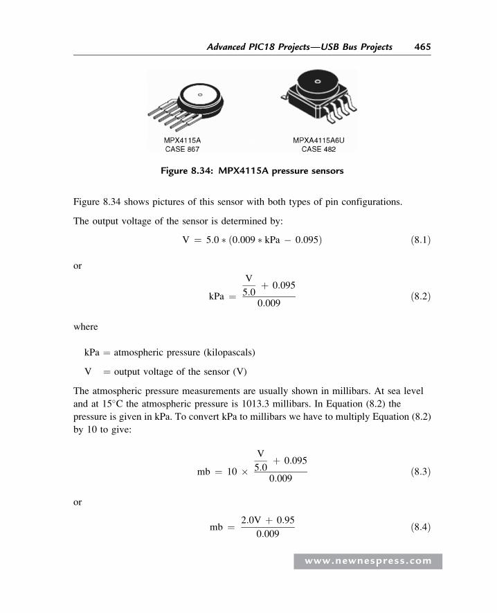
Figure 8.34 shows pictures of this sensor with both types of pin configurations.
The output voltage of the sensor is determined by:
V ¼ 5:0 � ð0:009 � kPa � 0:095Þ ð8:1Þ
or
kPa ¼V
5:0þ 0:095
0:009ð8:2Þ
where
kPa ¼ atmospheric pressure (kilopascals)
V ¼ output voltage of the sensor (V)
The atmospheric pressure measurements are usually shown in millibars. At sea level
and at 15�C the atmospheric pressure is 1013.3 millibars. In Equation (8.2) the
pressure is given in kPa. To convert kPa to millibars we have to multiply Equation (8.2)
by 10 to give:
mb ¼ 10 �V
5:0þ 0:095
0:009ð8:3Þ
or
mb ¼ 2:0V þ 0:95
0:009ð8:4Þ
Figure 8.34: MPX4115A pressure sensors
www.newnespress.com
465Advanced PIC18 Projects—USB Bus Projects

Figure 8.35 shows the variation of the output voltage of MPX4115A sensor as the
pressure varies. We are interested in the range of pressure between 800 and 1100
millibars.
The steps to calculate the pressure in millibars are:
� Read the output voltage of the pressure sensor using one of the A/D channels of
the microcontroller
� Use Equation (8.4) to convert the voltage into pressure in millibars
The block diagram of the project is shown in Figure 8.36.
0
1
2
3
4
5
Millibars
Vol
ts
200 300 400 500 600 700 800 900 1000 1100
Figure 8.35: Variation of sensor output voltage with pressure
MPX4115
PIC18F4550 PC
USB cable
Pressure sensor
Figure 8.36: Block diagram of the project
www.newnespress.com
466 Chapter 8
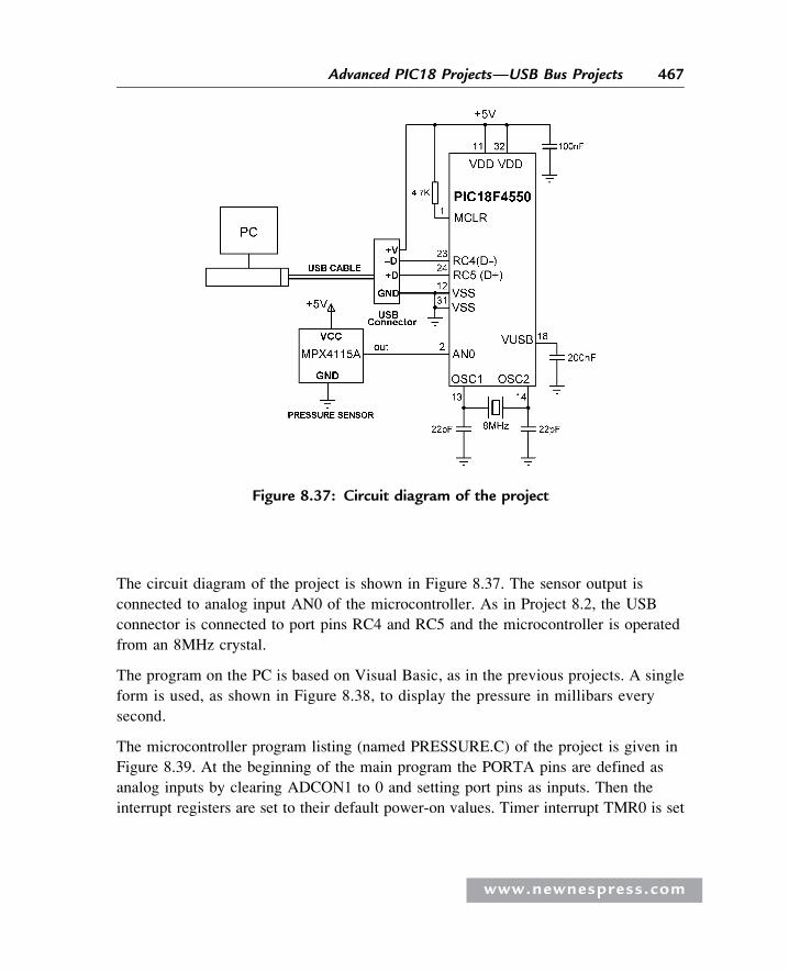
The circuit diagram of the project is shown in Figure 8.37. The sensor output is
connected to analog input AN0 of the microcontroller. As in Project 8.2, the USB
connector is connected to port pins RC4 and RC5 and the microcontroller is operated
from an 8MHz crystal.
The program on the PC is based on Visual Basic, as in the previous projects. A single
form is used, as shown in Figure 8.38, to display the pressure in millibars every
second.
The microcontroller program listing (named PRESSURE.C) of the project is given in
Figure 8.39. At the beginning of the main program the PORTA pins are defined as
analog inputs by clearing ADCON1 to 0 and setting port pins as inputs. Then the
interrupt registers are set to their default power-on values. Timer interrupt TMR0 is set
Figure 8.37: Circuit diagram of the project
www.newnespress.com
467Advanced PIC18 Projects—USB Bus Projects
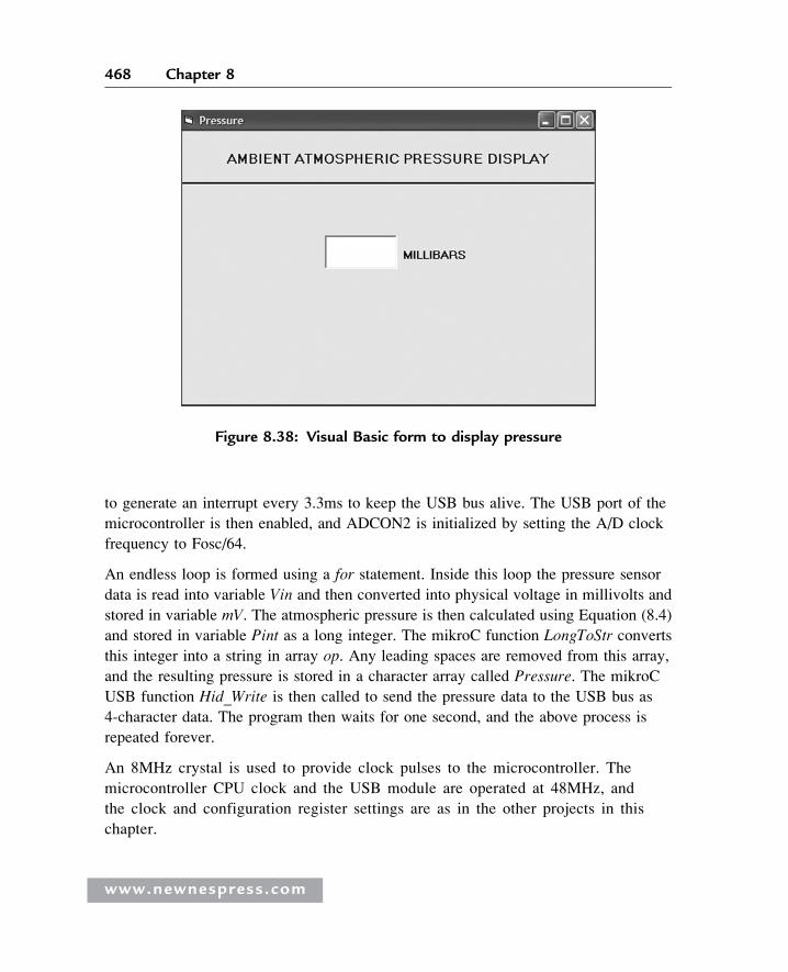
to generate an interrupt every 3.3ms to keep the USB bus alive. The USB port of the
microcontroller is then enabled, and ADCON2 is initialized by setting the A/D clock
frequency to Fosc/64.
An endless loop is formed using a for statement. Inside this loop the pressure sensor
data is read into variable Vin and then converted into physical voltage in millivolts and
stored in variable mV. The atmospheric pressure is then calculated using Equation (8.4)
and stored in variable Pint as a long integer. The mikroC function LongToStr converts
this integer into a string in array op. Any leading spaces are removed from this array,
and the resulting pressure is stored in a character array called Pressure. The mikroC
USB function Hid_Write is then called to send the pressure data to the USB bus as
4-character data. The program then waits for one second, and the above process is
repeated forever.
An 8MHz crystal is used to provide clock pulses to the microcontroller. The
microcontroller CPU clock and the USB module are operated at 48MHz, and
the clock and configuration register settings are as in the other projects in this
chapter.
Figure 8.38: Visual Basic form to display pressure
www.newnespress.com
468 Chapter 8
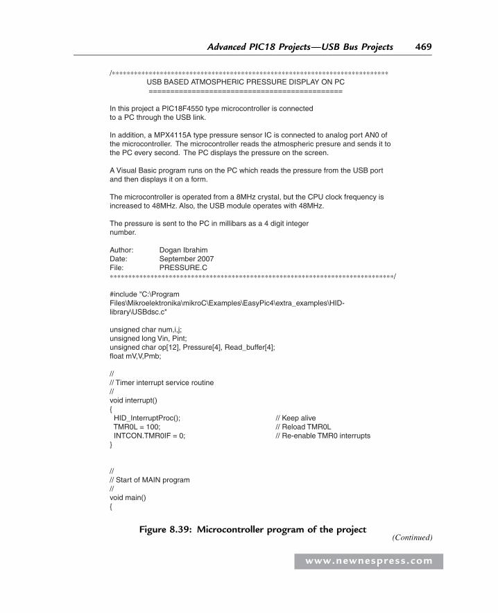
/∗∗∗∗∗∗∗∗∗∗∗∗∗∗∗∗∗∗∗∗∗∗∗∗∗∗∗∗∗∗∗∗∗∗∗∗∗∗∗∗∗∗∗∗∗∗∗∗∗∗∗∗∗∗∗∗∗∗∗∗∗∗∗∗∗∗∗∗∗∗∗∗∗∗∗ USB BASED ATMOSPHERIC PRESSURE DISPLAY ON PC =============================================
In this project a PIC18F4550 type microcontroller is connectedto a PC through the USB link.
In addition, a MPX4115A type pressure sensor IC is connected to analog port AN0 ofthe microcontroller. The microcontroller reads the atmospheric presure and sends it tothe PC every second. The PC displays the pressure on the screen.
A Visual Basic program runs on the PC which reads the pressure from the USB portand then displays it on a form.
The microcontroller is operated from a 8MHz crystal, but the CPU clock frequency isincreased to 48MHz. Also, the USB module operates with 48MHz.
The pressure is sent to the PC in millibars as a 4 digit integernumber.
Author: Dogan IbrahimDate: September 2007File: PRESSURE.C∗∗∗∗∗∗∗∗∗∗∗∗∗∗∗∗∗∗∗∗∗∗∗∗∗∗∗∗∗∗∗∗∗∗∗∗∗∗∗∗∗∗∗∗∗∗∗∗∗∗∗∗∗∗∗∗∗∗∗∗∗∗∗∗∗∗∗∗∗∗∗∗∗∗∗∗∗/
#include "C:\ProgramFiles\Mikroelektronika\mikroC\Examples\EasyPic4\extra_examples\HID-library\USBdsc.c"
unsigned char num,i,j;unsigned long Vin, Pint;unsigned char op[12], Pressure[4], Read_buffer[4];float mV,V,Pmb;
//// Timer interrupt service routine//void interrupt(){ HID_InterruptProc(); // Keep alive TMR0L = 100; // Reload TMR0L INTCON.TMR0IF = 0; // Re-enable TMR0 interrupts}
//// Start of MAIN program//void main(){
Figure 8.39: Microcontroller program of the project(Continued)
www.newnespress.com
469Advanced PIC18 Projects—USB Bus Projects
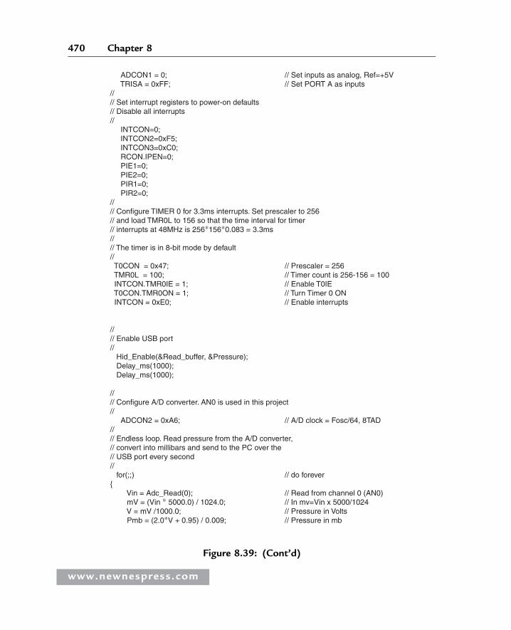
ADCON1 = 0; // Set inputs as analog, Ref=+5V TRISA = 0xFF; // Set PORT A as inputs//// Set interrupt registers to power-on defaults// Disable all interrupts// INTCON=0; INTCON2=0xF5; INTCON3=0xC0; RCON.IPEN=0; PIE1=0; PIE2=0; PIR1=0; PIR2=0;//// Configure TIMER 0 for 3.3ms interrupts. Set prescaler to 256// and load TMR0L to 156 so that the time interval for timer// interrupts at 48MHz is 256∗156∗0.083 = 3.3ms//// The timer is in 8-bit mode by default// T0CON = 0x47; // Prescaler = 256 TMR0L = 100; // Timer count is 256-156 = 100 INTCON.TMR0IE = 1; // Enable T0IE T0CON.TMR0ON = 1; // Turn Timer 0 ON INTCON = 0xE0; // Enable interrupts
//// Enable USB port// Hid_Enable(&Read_buffer, &Pressure); Delay_ms(1000); Delay_ms(1000);
//// Configure A/D converter. AN0 is used in this project// ADCON2 = 0xA6; // A/D clock = Fosc/64, 8TAD//// Endless loop. Read pressure from the A/D converter,// convert into millibars and send to the PC over the// USB port every second// for(;;) // do forever{ Vin = Adc_Read(0); // Read from channel 0 (AN0) mV = (Vin ∗ 5000.0) / 1024.0; // In mv=Vin x 5000/1024 V = mV /1000.0; // Pressure in Volts Pmb = (2.0∗V + 0.95) / 0.009; // Pressure in mb
Figure 8.39: (Cont’d)
www.newnespress.com
470 Chapter 8
The PC program, based on Visual Basic, is called PRESSURE. Subroutine OnRead
receives the data arriving at the USB port of the PC and then displays it on the screen
form. The program does not send any data to the USB bus. The program listing (except
the global variable declarations) is given in Figure 8.40.
Figure 8.41 shows a typical output from the Visual Basic program, displaying the
atmospheric pressure.
An installable version of the Visual Basic program is provided on the CDROM that
comes with this book, in folder PRESSURE.
Pint = (int)Pmb; // As an integer number LongToStr(Pint,op); // Convert to string in "op"//// Remove leading blanks// for(j=0; j<4; j++)Pressure[j]=' '; j=0; for(i=0;i<=11;i++) { if(op[i] != ' ') // If a blank { Pressure[j]=op[i]; j++; } }//// Send pressure (in array Pressure) to the PC// Hid_Write(&Pressure,4); // Send to USB as 4 characters Delay_ms(1000); // Wait 1 second } Hid_Disable();
}
Figure 8.39: (Cont’d)
www.newnespress.com
471Advanced PIC18 Projects—USB Bus Projects
' vendor and product IDsPrivate Const VendorID = 4660Private Const ProductID = 1
' read and write buffersPrivate Const BufferInSize = 8Private Const BufferOutSize = 8Dim BufferIn(0 To BufferInSize) As ByteDim BufferOut(0 To BufferOutSize) As Byte
Private Sub Command1_Click() Form_Unload (0)EndEnd Sub
' ∗∗∗∗∗∗∗∗∗∗∗∗∗∗∗∗∗∗∗∗∗∗∗∗∗∗∗∗∗∗∗∗∗∗∗∗∗∗∗∗∗∗∗∗∗∗∗∗∗∗∗∗∗∗∗∗∗∗∗∗∗∗∗∗∗∗∗
' when the form loads, connect to the HID controller - pass' the form window handle so that you can receive notification' events...'∗∗∗∗∗∗∗∗∗∗∗∗∗∗∗∗∗∗∗∗∗∗∗∗∗∗∗∗∗∗∗∗∗∗∗∗∗∗∗∗∗∗∗∗∗∗∗∗∗∗∗∗∗∗∗∗∗∗∗∗∗∗∗∗∗∗∗∗Private Sub Form_Load() ' do not remove! ConnectToHID (Me.hwnd) lblstatus = "Connected to HID..."End Sub
'∗∗∗∗∗∗∗∗∗∗∗∗∗∗∗∗∗∗∗∗∗∗∗∗∗∗∗∗∗∗∗∗∗∗∗∗∗∗∗∗∗∗∗∗∗∗∗∗∗∗∗∗∗∗∗∗∗∗∗∗∗∗∗∗∗∗∗∗
' disconnect from the HID controller...'∗∗∗∗∗∗∗∗∗∗∗∗∗∗∗∗∗∗∗∗∗∗∗∗∗∗∗∗∗∗∗∗∗∗∗∗∗∗∗∗∗∗∗∗∗∗∗∗∗∗∗∗∗∗∗∗∗∗∗∗∗∗∗∗∗∗∗∗Private Sub Form_Unload(Cancel As Integer) DisconnectFromHIDEnd Sub
'∗∗∗∗∗∗∗∗∗∗∗∗∗∗∗∗∗∗∗∗∗∗∗∗∗∗∗∗∗∗∗∗∗∗∗∗∗∗∗∗∗∗∗∗∗∗∗∗∗∗∗∗∗∗∗∗∗∗∗∗∗∗∗∗∗∗∗∗
' a HID device has been plugged in...'∗∗∗∗∗∗∗∗∗∗∗∗∗∗∗∗∗∗∗∗∗∗∗∗∗∗∗∗∗∗∗∗∗∗∗∗∗∗∗∗∗∗∗∗∗∗∗∗∗∗∗∗∗∗∗∗∗∗∗∗∗∗∗∗∗∗∗∗Public Sub OnPlugged(ByVal pHandle As Long) If hidGetVendorID(pHandle) = VendorID And hidGetProductID(pHandle) =ProductID Then lblstatus = "USB Plugged....." End IfEnd Sub
Figure 8.40: Visual Basic program of the project
www.newnespress.com
472 Chapter 8
lblstatus = "USB Unplugged...." End IfEnd Sub
'∗∗∗∗∗∗∗∗∗∗∗∗∗∗∗∗∗∗∗∗∗∗∗∗∗∗∗∗∗∗∗∗∗∗∗∗∗∗∗∗∗∗∗∗∗∗∗∗∗∗∗∗∗∗∗∗∗∗∗∗∗∗∗∗∗∗∗∗
' controller changed notification - called' after ALL HID devices are plugged or unplugged'∗∗∗∗∗∗∗∗∗∗∗∗∗∗∗∗∗∗∗∗∗∗∗∗∗∗∗∗∗∗∗∗∗∗∗∗∗∗∗∗∗∗∗∗∗∗∗∗∗∗∗∗∗∗∗∗∗∗∗∗∗∗∗∗∗∗∗∗Public Sub OnChanged() Dim DeviceHandle As Long ' get the handle of the device we are interested in, then set ' its read notify flag to true - this ensures you get a read ' notification message when there is some data to read... DeviceHandle = hidGetHandle(VendorID, ProductID) hidSetReadNotify DeviceHandle, TrueEnd Sub
'∗∗∗∗∗∗∗∗∗∗∗∗∗∗∗∗∗∗∗∗∗∗∗∗∗∗∗∗∗∗∗∗∗∗∗∗∗∗∗∗∗∗∗∗∗∗∗∗∗∗∗∗∗∗∗∗∗∗∗∗∗∗∗∗∗∗∗∗
' on read event...'∗∗∗∗∗∗∗∗∗∗∗∗∗∗∗∗∗∗∗∗∗∗∗∗∗∗∗∗∗∗∗∗∗∗∗∗∗∗∗∗∗∗∗∗∗∗∗∗∗∗∗∗∗∗∗∗∗∗∗∗∗∗∗∗∗∗∗∗Public Sub OnRead(ByVal pHandle As Long) Dim pressure As String If hidRead(pHandle, BufferIn(0)) Then ' The first byte is the report ID. i.e. BufferIn(0)=reportID pressure = Chr(BufferIn(1)) & Chr(BufferIn(2)) & Chr(BufferIn(3)) &Chr(BufferIn(4)) txtno = pressure End IfEnd Sub
' a HID device has been unplugged...'∗∗∗∗∗∗∗∗∗∗∗∗∗∗∗∗∗∗∗∗∗∗∗∗∗∗∗∗∗∗∗∗∗∗∗∗∗∗∗∗∗∗∗∗∗∗∗∗∗∗∗∗∗∗∗∗∗∗∗∗∗∗∗∗∗∗∗∗Public Sub OnUnplugged(ByVal pHandle As Long) If hidGetVendorID(pHandle) = VendorID And hidGetProductID(pHandle) =ProductID Then
∗∗∗∗∗∗∗∗∗∗∗∗∗∗∗∗∗∗∗∗∗∗∗∗∗∗∗∗∗∗∗∗∗∗∗∗∗∗∗∗∗∗∗∗∗∗∗∗∗∗∗∗∗∗∗∗∗∗∗∗∗∗∗∗∗∗∗∗
Figure 8.40: (Cont’d)
www.newnespress.com
473Advanced PIC18 Projects—USB Bus Projects
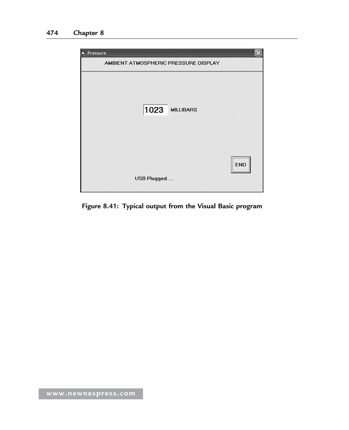
Figure 8.41: Typical output from the Visual Basic program
www.newnespress.com
474 Chapter 8
CHAP T E R 9
Advanced PIC18 Projects—CANBus Projects
The Controller Area Network (CAN) is a serial bus communications protocol developed
by Bosch (an electrical equipment manufacturer in Germany) in the early 1980s.
Thereafter, CAN was standardized as ISO-11898 and ISO-11519, establishing itself as
the standard protocol for in-vehicle networking in the auto industry. In the early days of
the automotive industry, localized stand-alone controllers had been used to manage
various actuators and electromechanical subsystems. By networking the electronics in
vehicles with CAN, however, they could be controlled from a central point, the engine
control unit (ECU), thus increasing functionality, adding modularity, and making
diagnostic processes more efficient.
Early CAN development was mainly supported by the vehicle industry, as it was used in
passenger cars, boats, trucks, and other types of vehicles. Today the CAN protocol is
used in many other fields in applications that call for networked embedded control,
including industrial automation, medical applications, building automation, weaving
machines, and production machinery. CAN offers an efficient communication protocol
between sensors, actuators, controllers, and other nodes in real-time applications, and is
known for its simplicity, reliability, and high performance.
The CAN protocol is based on a bus topology, and only two wires are needed for
communication over a CAN bus. The bus has a multimaster structure where each device
on the bus can send or receive data. Only one device can send data at any time while
all the others listen. If two or more devices attempt to send data at the same time,
the one with the highest priority is allowed to send its data while the others return to
receive mode.
www.newnespress.com
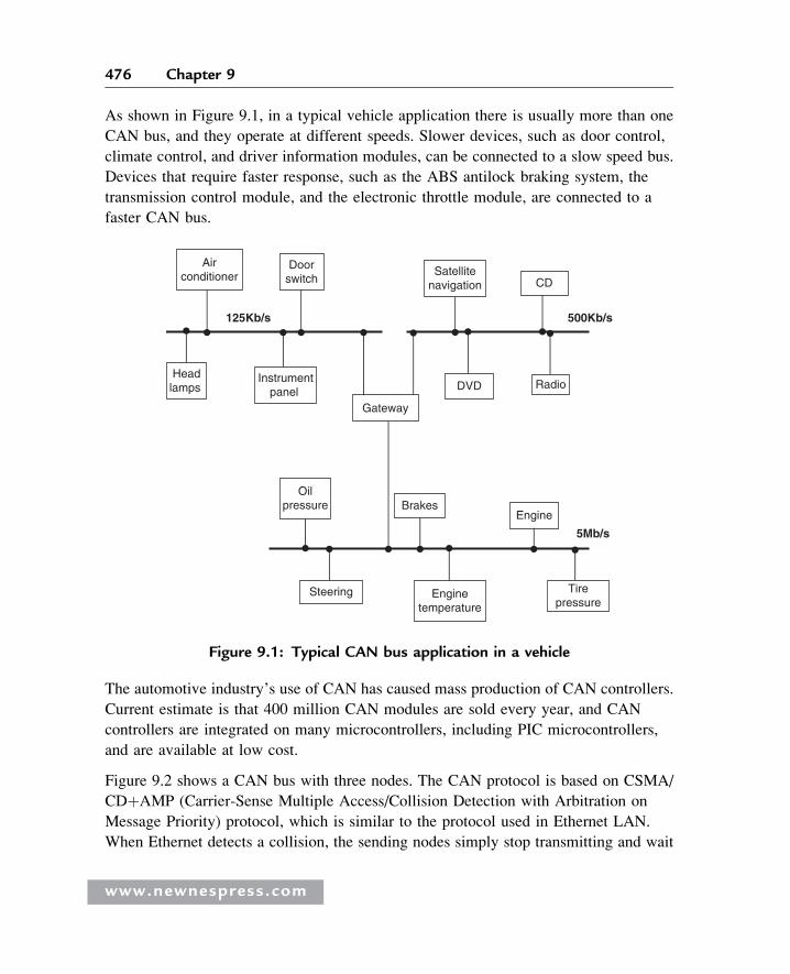
As shown in Figure 9.1, in a typical vehicle application there is usually more than one
CAN bus, and they operate at different speeds. Slower devices, such as door control,
climate control, and driver information modules, can be connected to a slow speed bus.
Devices that require faster response, such as the ABS antilock braking system, the
transmission control module, and the electronic throttle module, are connected to a
faster CAN bus.
The automotive industry’s use of CAN has caused mass production of CAN controllers.
Current estimate is that 400 million CAN modules are sold every year, and CAN
controllers are integrated on many microcontrollers, including PIC microcontrollers,
and are available at low cost.
Figure 9.2 shows a CAN bus with three nodes. The CAN protocol is based on CSMA/
CDþAMP (Carrier-Sense Multiple Access/Collision Detection with Arbitration on
Message Priority) protocol, which is similar to the protocol used in Ethernet LAN.
When Ethernet detects a collision, the sending nodes simply stop transmitting and wait
Airconditioner
Doorswitch
Instrumentpanel
500Kb/s
Satellitenavigation
DVD Radio
5Mb/s
Engine
Oilpressure Brakes
Gateway
125Kb/s
CD
Headlamps
Steering Enginetemperature
Tirepressure
Figure 9.1: Typical CAN bus application in a vehicle
www.newnespress.com
476 Chapter 9
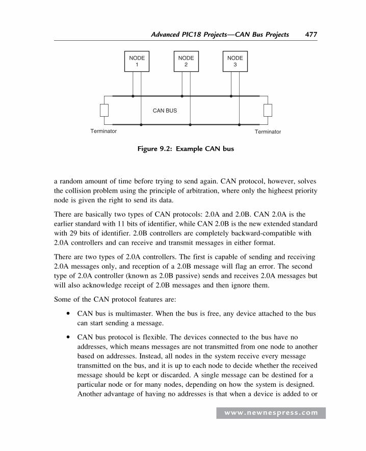
a random amount of time before trying to send again. CAN protocol, however, solves
the collision problem using the principle of arbitration, where only the higheest priority
node is given the right to send its data.
There are basically two types of CAN protocols: 2.0A and 2.0B. CAN 2.0A is the
earlier standard with 11 bits of identifier, while CAN 2.0B is the new extended standard
with 29 bits of identifier. 2.0B controllers are completely backward-compatible with
2.0A controllers and can receive and transmit messages in either format.
There are two types of 2.0A controllers. The first is capable of sending and receiving
2.0A messages only, and reception of a 2.0B message will flag an error. The second
type of 2.0A controller (known as 2.0B passive) sends and receives 2.0A messages but
will also acknowledge receipt of 2.0B messages and then ignore them.
Some of the CAN protocol features are:
� CAN bus is multimaster. When the bus is free, any device attached to the bus
can start sending a message.
� CAN bus protocol is flexible. The devices connected to the bus have no
addresses, which means messages are not transmitted from one node to another
based on addresses. Instead, all nodes in the system receive every message
transmitted on the bus, and it is up to each node to decide whether the received
message should be kept or discarded. A single message can be destined for a
particular node or for many nodes, depending on how the system is designed.
Another advantage of having no addresses is that when a device is added to or
CAN BUS
NODE2
NODE3
NODE1
Terminator Terminator
Figure 9.2: Example CAN bus
www.newnespress.com
477Advanced PIC18 Projects—CAN Bus Projects
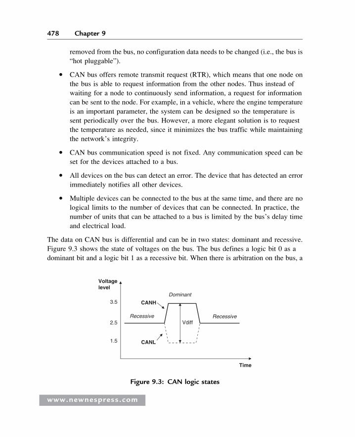
removed from the bus, no configuration data needs to be changed (i.e., the bus is
“hot pluggable”).
� CAN bus offers remote transmit request (RTR), which means that one node on
the bus is able to request information from the other nodes. Thus instead of
waiting for a node to continuously send information, a request for information
can be sent to the node. For example, in a vehicle, where the engine temperature
is an important parameter, the system can be designed so the temperature is
sent periodically over the bus. However, a more elegant solution is to request
the temperature as needed, since it minimizes the bus traffic while maintaining
the network’s integrity.
� CAN bus communication speed is not fixed. Any communication speed can be
set for the devices attached to a bus.
� All devices on the bus can detect an error. The device that has detected an error
immediately notifies all other devices.
� Multiple devices can be connected to the bus at the same time, and there are no
logical limits to the number of devices that can be connected. In practice, the
number of units that can be attached to a bus is limited by the bus’s delay time
and electrical load.
The data on CAN bus is differential and can be in two states: dominant and recessive.
Figure 9.3 shows the state of voltages on the bus. The bus defines a logic bit 0 as a
dominant bit and a logic bit 1 as a recessive bit. When there is arbitration on the bus, a
Voltagelevel
VdiffRecessiveRecessive
CANL
CANH
Dominant3.5
2.5
1.5
Time
Figure 9.3: CAN logic states
www.newnespress.com
478 Chapter 9
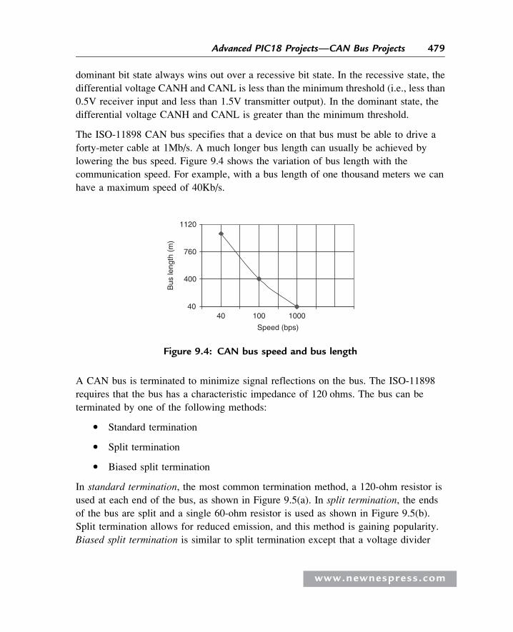
dominant bit state always wins out over a recessive bit state. In the recessive state, the
differential voltage CANH and CANL is less than the minimum threshold (i.e., less than
0.5V receiver input and less than 1.5V transmitter output). In the dominant state, the
differential voltage CANH and CANL is greater than the minimum threshold.
The ISO-11898 CAN bus specifies that a device on that bus must be able to drive a
forty-meter cable at 1Mb/s. A much longer bus length can usually be achieved by
lowering the bus speed. Figure 9.4 shows the variation of bus length with the
communication speed. For example, with a bus length of one thousand meters we can
have a maximum speed of 40Kb/s.
A CAN bus is terminated to minimize signal reflections on the bus. The ISO-11898
requires that the bus has a characteristic impedance of 120 ohms. The bus can be
terminated by one of the following methods:
� Standard termination
� Split termination
� Biased split termination
In standard termination, the most common termination method, a 120-ohm resistor is
used at each end of the bus, as shown in Figure 9.5(a). In split termination, the ends
of the bus are split and a single 60-ohm resistor is used as shown in Figure 9.5(b).
Split termination allows for reduced emission, and this method is gaining popularity.
Biased split termination is similar to split termination except that a voltage divider
4040
400
100 1000
760
1120
Speed (bps)
Bus
leng
th (
m)
Figure 9.4: CAN bus speed and bus length
www.newnespress.com
479Advanced PIC18 Projects—CAN Bus Projects
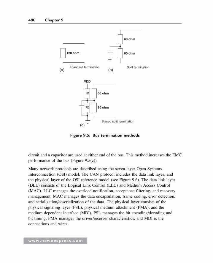
circuit and a capacitor are used at either end of the bus. This method increases the EMC
performance of the bus (Figure 9.5(c)).
Many network protocols are described using the seven-layer Open Systems
Interconnection (OSI) model. The CAN protocol includes the data link layer, and
the physical layer of the OSI reference model (see Figure 9.6). The data link layer
(DLL) consists of the Logical Link Control (LLC) and Medium Access Control
(MAC). LLC manages the overload notification, acceptance filtering, and recovery
management. MAC manages the data encapsulation, frame coding, error detection,
and serialization/deserialization of the data. The physical layer consists of the
physical signaling layer (PSL), physical medium attachment (PMA), and the
medium dependent interface (MDI). PSL manages the bit encoding/decoding and
bit timing. PMA manages the driver/receiver characteristics, and MDI is the
connections and wires.
120 ohm
Standard termination (a)
60 ohm
60 ohm
Split termination (b)
VDD
60 ohm
Biased split termination
R2
R1
60 ohm
(c)
Figure 9.5: Bus termination methods
www.newnespress.com
480 Chapter 9
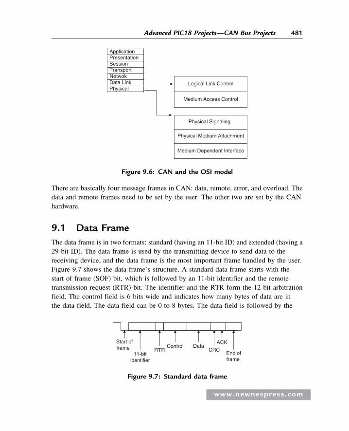
There are basically four message frames in CAN: data, remote, error, and overload. The
data and remote frames need to be set by the user. The other two are set by the CAN
hardware.
9.1 Data Frame
The data frame is in two formats: standard (having an 11-bit ID) and extended (having a
29-bit ID). The data frame is used by the transmitting device to send data to the
receiving device, and the data frame is the most important frame handled by the user.
Figure 9.7 shows the data frame’s structure. A standard data frame starts with the
start of frame (SOF) bit, which is followed by an 11-bit identifier and the remote
transmission request (RTR) bit. The identifier and the RTR form the 12-bit arbitration
field. The control field is 6 bits wide and indicates how many bytes of data are in
the data field. The data field can be 0 to 8 bytes. The data field is followed by the
Application Presentation SessionTransportNetwokData Link Physical
Medium Access Control
Medium Dependent Interface
Physical Medium Attachment
Physical Signaling
Logical Link Control
Figure 9.6: CAN and the OSI model
RTRControl
11-bitidentifier
Start offrame Data
CRC
ACK
End offrame
Figure 9.7: Standard data frame
www.newnespress.com
481Advanced PIC18 Projects—CAN Bus Projects
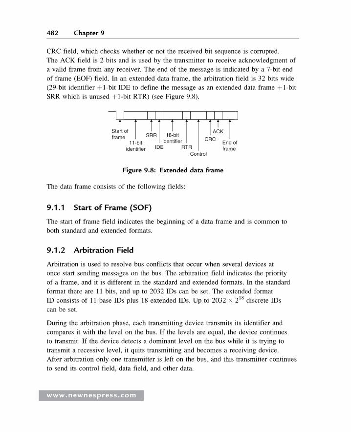
CRC field, which checks whether or not the received bit sequence is corrupted.
The ACK field is 2 bits and is used by the transmitter to receive acknowledgment of
a valid frame from any receiver. The end of the message is indicated by a 7-bit end
of frame (EOF) field. In an extended data frame, the arbitration field is 32 bits wide
(29-bit identifier þ1-bit IDE to define the message as an extended data frame þ1-bit
SRR which is unused þ1-bit RTR) (see Figure 9.8).
The data frame consists of the following fields:
9.1.1 Start of Frame (SOF)
The start of frame field indicates the beginning of a data frame and is common to
both standard and extended formats.
9.1.2 Arbitration Field
Arbitration is used to resolve bus conflicts that occur when several devices at
once start sending messages on the bus. The arbitration field indicates the priority
of a frame, and it is different in the standard and extended formats. In the standard
format there are 11 bits, and up to 2032 IDs can be set. The extended format
ID consists of 11 base IDs plus 18 extended IDs. Up to 2032 � 218 discrete IDs
can be set.
During the arbitration phase, each transmitting device transmits its identifier and
compares it with the level on the bus. If the levels are equal, the device continues
to transmit. If the device detects a dominant level on the bus while it is trying to
transmit a recessive level, it quits transmitting and becomes a receiving device.
After arbitration only one transmitter is left on the bus, and this transmitter continues
to send its control field, data field, and other data.
11-bitidentifier
SRR 18-bitidentifier
IDE RTR
CRC
Control
ACK
End offrame
Start offrame
Figure 9.8: Extended data frame
www.newnespress.com
482 Chapter 9
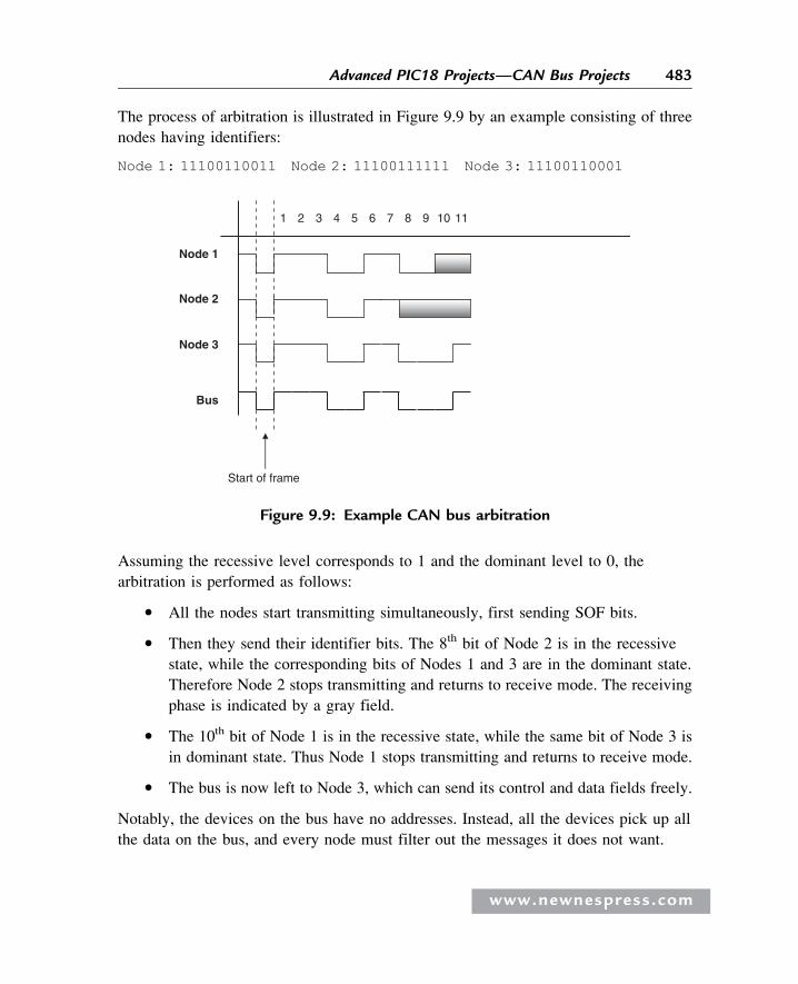
The process of arbitration is illustrated in Figure 9.9 by an example consisting of three
nodes having identifiers:
Node 1: 11100110011 Node 2: 11100111111 Node 3: 11100110001
Assuming the recessive level corresponds to 1 and the dominant level to 0, the
arbitration is performed as follows:
� All the nodes start transmitting simultaneously, first sending SOF bits.
� Then they send their identifier bits. The 8th bit of Node 2 is in the recessive
state, while the corresponding bits of Nodes 1 and 3 are in the dominant state.
Therefore Node 2 stops transmitting and returns to receive mode. The receiving
phase is indicated by a gray field.
� The 10th bit of Node 1 is in the recessive state, while the same bit of Node 3 is
in dominant state. Thus Node 1 stops transmitting and returns to receive mode.
� The bus is now left to Node 3, which can send its control and data fields freely.
Notably, the devices on the bus have no addresses. Instead, all the devices pick up all
the data on the bus, and every node must filter out the messages it does not want.
Bus
Node 3
Node 2
Node 1
Start of frame
1 2 3 4 5 6 7 8 9 10 11
Figure 9.9: Example CAN bus arbitration
www.newnespress.com
483Advanced PIC18 Projects—CAN Bus Projects
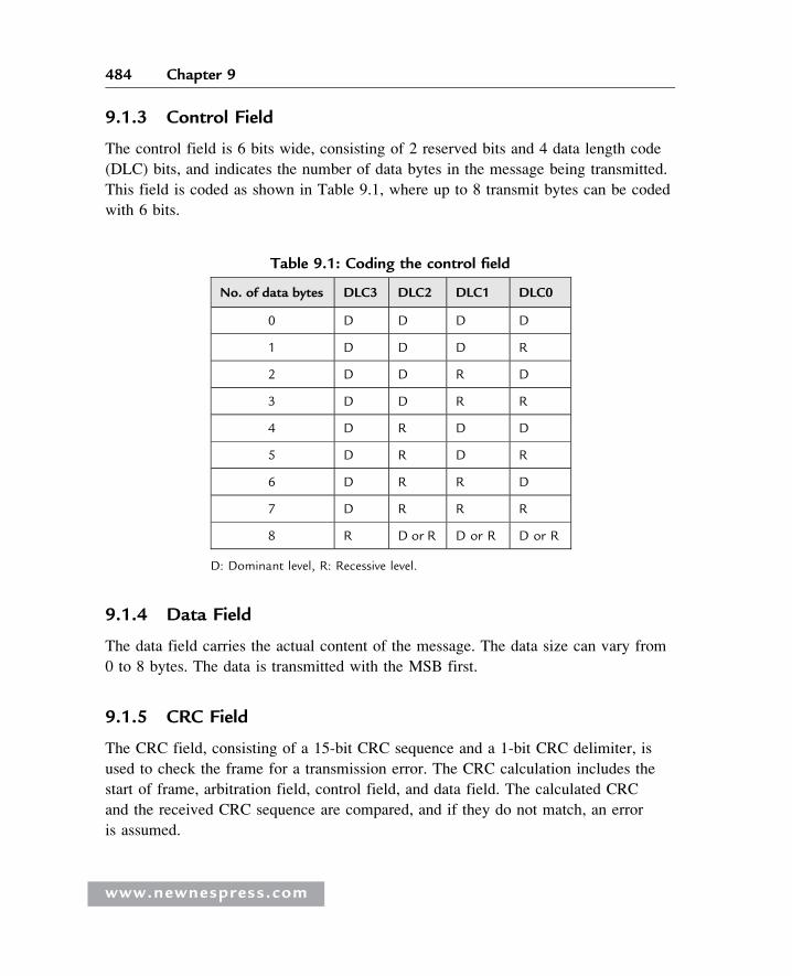
9.1.3 Control Field
The control field is 6 bits wide, consisting of 2 reserved bits and 4 data length code
(DLC) bits, and indicates the number of data bytes in the message being transmitted.
This field is coded as shown in Table 9.1, where up to 8 transmit bytes can be coded
with 6 bits.
9.1.4 Data Field
The data field carries the actual content of the message. The data size can vary from
0 to 8 bytes. The data is transmitted with the MSB first.
9.1.5 CRC Field
The CRC field, consisting of a 15-bit CRC sequence and a 1-bit CRC delimiter, is
used to check the frame for a transmission error. The CRC calculation includes the
start of frame, arbitration field, control field, and data field. The calculated CRC
and the received CRC sequence are compared, and if they do not match, an error
is assumed.
Table 9.1: Coding the control field
No. of data bytes DLC3 DLC2 DLC1 DLC0
0 D D D D
1 D D D R
2 D D R D
3 D D R R
4 D R D D
5 D R D R
6 D R R D
7 D R R R
8 R D or R D or R D or R
D: Dominant level, R: Recessive level.
www.newnespress.com
484 Chapter 9
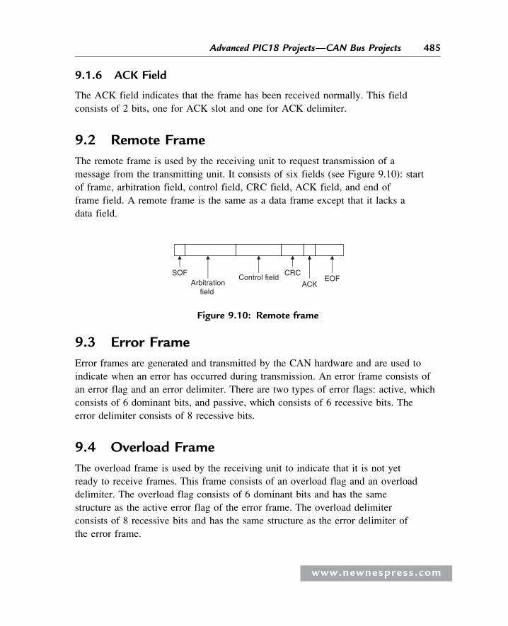
9.1.6 ACK Field
The ACK field indicates that the frame has been received normally. This field
consists of 2 bits, one for ACK slot and one for ACK delimiter.
9.2 Remote Frame
The remote frame is used by the receiving unit to request transmission of a
message from the transmitting unit. It consists of six fields (see Figure 9.10): start
of frame, arbitration field, control field, CRC field, ACK field, and end of
frame field. A remote frame is the same as a data frame except that it lacks a
data field.
9.3 Error Frame
Error frames are generated and transmitted by the CAN hardware and are used to
indicate when an error has occurred during transmission. An error frame consists of
an error flag and an error delimiter. There are two types of error flags: active, which
consists of 6 dominant bits, and passive, which consists of 6 recessive bits. The
error delimiter consists of 8 recessive bits.
9.4 Overload Frame
The overload frame is used by the receiving unit to indicate that it is not yet
ready to receive frames. This frame consists of an overload flag and an overload
delimiter. The overload flag consists of 6 dominant bits and has the same
structure as the active error flag of the error frame. The overload delimiter
consists of 8 recessive bits and has the same structure as the error delimiter of
the error frame.
SOFArbitration
field
Control fieldACK
CRCEOF
Figure 9.10: Remote frame
www.newnespress.com
485Advanced PIC18 Projects—CAN Bus Projects
9.5 Bit Stuffing
The CAN bus makes use of bit stuffing, a technique to periodically synchronize
transmit-receive operations to prevent timing errors between receive nodes. After 5
consecutive bits with the same level, one bit of inverted data is added to the sequence.
If, during sending of a data frame or remote frame, the same level occurs in 5
consecutive bits anywhere from the start of frame to the CRC sequence, an inverted
bit is inserted in the next (i.e., the sixth) bit. If, during receiving of a data frame or
remote frame, the same level occurs in 5 consecutive bits anywhere from the start of
frame to CRC sequence, the next (sixth) bit is deleted from the received frame. If the
deleted sixth bit is at the same level as the fifth bit, an error (stuffing error) is detected.
9.6 Types of Errors
The CAN bus identifies five types of errors:
� Bit error
� CRC error
� Form error
� ACK error
� Stuffing error
Bit errors are detected when the output level and the data level on the bus do not
match. Both transmit and receive units can detect bit errors. CRC errors are detected
only by receiving units. CRC errors are detected if the calculated CRC from the
received message and the received CRC do not match. Form errors are detected
by the transmitting or receiving units when an illegal frame format is detected.
ACK errors are detected only by the transmitting units if the ACK field is found
recessive. Stuffing errors are detected when the same level of data is detected for 6
consecutive bits in any field that should have been bit-stuffed. This error can be
detected by both the transmitting and receiving units.
9.7 Nominal Bit Timing
The CAN bus nominal bit rate is defined as the number of bits transmitted every
second without resynchronization. The inverse of the nominal bit rate is the nominal
bit time. All devices on the CAN bus must use the same bit rate, even though each
www.newnespress.com
486 Chapter 9
device can have its own different clock frequency. One message bit consists of four
nonoverlapping time segments:
� Synchronization segment (Sync_Seg)
� Propagation time segment (Prop_Seg)
� Phase buffer segment 1 (Phase_Seg1)
� Phase buffer segment 2 (Phase_Seg2)
The Sync_Seg segment is used to synchronize various nodes on the bus, and an edge
is expected to lie within this segment. The Prop_Seg segment compensates for
physical delay times within the network. The Phase_Seg1 and Phase_Seg2 segments
compensate for edge phase errors. These segments can be lengthened or shortened by
synchronization. The sample point is the point in time where the actual bit value is
located and occurs at the end of Phase_Seg1. A CAN controller can be configured
to sample three times and use a majority function to determine the actual bit value.
Each segment is divided into units known as time quantum, or TQ. A desired bit
timing can be set by adjusting the number of TQ’s that comprise one message bit
and the number of TQ’s that comprise each segment in it. The TQ is a fixed unit
derived from the oscillator period, and the time quantum of each segment can vary
from 1 to 8. The lengths of the various time segments are:
� Sync_Seg is 1 time quantum long
� Prop_Seg is programmable as 1 to 8 time quanta long
� Phase_Seg1 is programmable as 1 to 8 time quanta long
� Phase_Seg2 is programmable as 2 to 8 time quanta long
By setting the bit timing, a sampling point can be set so multiple units on the bus can
sample messages with the same timing.
The nominal bit time is programmable from a minimum of 8 time quanta to a maximum
of 25 time quanta. By definition, the minimum nominal bit time is 1ms, correspondingto a maximum 1Mb/s rate. The nominal bit time (TBIT) is given by:
TBIT ¼ TQ � ðSync Seg þ Prop Seg þ Phase Seg1 þ Phase Seg2Þ ð9:1Þ
www.newnespress.com
487Advanced PIC18 Projects—CAN Bus Projects
and the nominal bit rate (NMR) is
NBR ¼ 1=TBIT ð9:2Þ
The time quantum is derived from the oscillator frequency and the programmable
baud rate prescaler, with integer values from 1 to 64. The time quantum can be
expressed as:
TQ ¼ 2 � ðBRP þ 1Þ=FOSC ð9:3Þ
where TQ is in ms, FOSC is in MHz, and BRP is the baud rate prescaler (0 to 63).
Equation (9.2) can be written as
TQ ¼ 2 � ðBRP þ 1Þ � TOSC ð9:4Þ
where TOSC is in ms.
An example of the calculation of a nominal bit rate follows.
Example 9.1
Assuming a clock frequency of 20MHz, a baud rate prescaler value of 1, and a
nominal bit time of TBIT ¼ 8 * TQ, determine the nominal bit rate.
Solution 9.1
Using equation (9.3),
TQ ¼ 2 � ð1 þ 1Þ=20 ¼ 0:2ms
also
TBIT ¼ 8 � TQ ¼ 8 � 0:2 ¼ 1:6ms
From Equation (9.2),
NBR ¼ 1=TBIT ¼ 1=1:6ms ¼ 625; 000bites=s or 625Kb=s
www.newnespress.com
488 Chapter 9
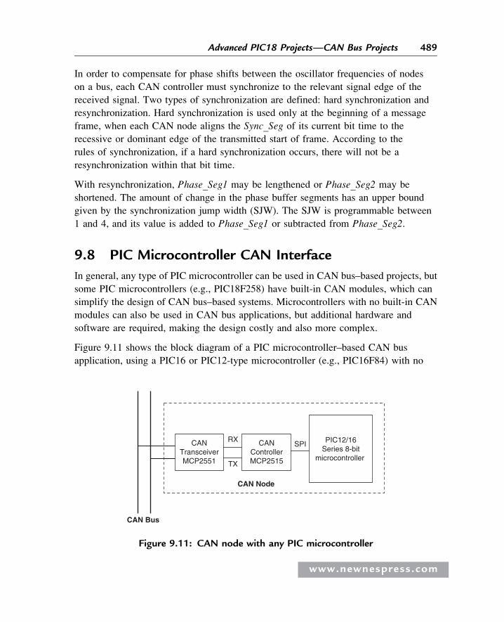
In order to compensate for phase shifts between the oscillator frequencies of nodes
on a bus, each CAN controller must synchronize to the relevant signal edge of the
received signal. Two types of synchronization are defined: hard synchronization and
resynchronization. Hard synchronization is used only at the beginning of a message
frame, when each CAN node aligns the Sync_Seg of its current bit time to the
recessive or dominant edge of the transmitted start of frame. According to the
rules of synchronization, if a hard synchronization occurs, there will not be a
resynchronization within that bit time.
With resynchronization, Phase_Seg1 may be lengthened or Phase_Seg2 may be
shortened. The amount of change in the phase buffer segments has an upper bound
given by the synchronization jump width (SJW). The SJW is programmable between
1 and 4, and its value is added to Phase_Seg1 or subtracted from Phase_Seg2.
9.8 PIC Microcontroller CAN Interface
In general, any type of PIC microcontroller can be used in CAN bus–based projects, but
some PIC microcontrollers (e.g., PIC18F258) have built-in CAN modules, which can
simplify the design of CAN bus–based systems. Microcontrollers with no built-in CAN
modules can also be used in CAN bus applications, but additional hardware and
software are required, making the design costly and also more complex.
Figure 9.11 shows the block diagram of a PIC microcontroller–based CAN bus
application, using a PIC16 or PIC12-type microcontroller (e.g., PIC16F84) with no
CAN Node
CAN Bus
CANTransceiverMCP2551 TX
RX PIC12/16Series 8-bit
microcontroller
CANControllerMCP2515
SPI
Figure 9.11: CAN node with any PIC microcontroller
www.newnespress.com
489Advanced PIC18 Projects—CAN Bus Projects
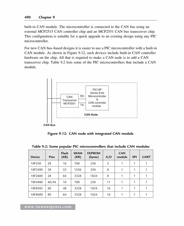
built-in CAN module. The microcontroller is connected to the CAN bus using an
external MCP2515 CAN controller chip and an MCP2551 CAN bus transceiver chip.
This configuration is suitable for a quick upgrade to an existing design using any PIC
microcontroller.
For new CAN bus–based designs it is easier to use a PIC microcontroller with a built-in
CAN module. As shown in Figure 9.12, such devices include built-in CAN controller
hardware on the chip. All that is required to make a CAN node is to add a CAN
transceiver chip. Table 9.2 lists some of the PIC microcontrollers that include a CAN
module.
CAN Node
TX
CAN Bus
RXCANTransceiverMCP2551
PIC18FSeries 8-bit
Microcontroller&
CAN controllermodule
Figure 9.12: CAN node with integrated CAN module
Table 9.2: Some popular PIC microcontrollers that include CAN modules
Device PinsFlash(KB)
SRAM(KB)
EEPROM(bytes) A/D
CANmodule SPI UART
18F258 28 16 768 256 5 1 1 1
18F2580 28 32 1536 256 8 1 1 1
18F2680 28 64 3328 1024 8 1 1 1
18F4480 40/44 16 768 256 11 1 1 1
18F8585 80 48 3328 1024 16 1 1 1
18F8680 80 64 3328 1024 16 1 1 1
www.newnespress.com
490 Chapter 9
9.9 PIC18F258 Microcontroller
Later in this chapter the PIC18F258 microcontroller is used in a CAN bus–based
project. This section describes this microcontroller and its operating principles with
respect to its built-in CAN bus. The principles here are in general applicable to other
PIC microcontrollers with CAN modules.
The PIC18F258 is a high performance 8-bit microcontroller with integrated CAN
module. The device has the following features:
� 32K flash program memory
� 1536 bytes RAM data memory
� 256 bytes EEPROM memory
� 22 I/O ports
� 5-channel 10-bit A/D converters
� Three timers/counters
� Three external interrupt pins
� High-current (25mA) sink/source
� Capture/compare/PWM module
� SPI/I2C module
� CAN 2.0A/B module
� Power-on reset and power-on timer
� Watchdog timer
� Priority level interrupts
� DC to 40MHz clock input
� 8 � 8 hardware multiplier
� Wide operating voltage (2.0V to 5.5V)
� Power-saving sleep mode
www.newnespress.com
491Advanced PIC18 Projects—CAN Bus Projects
The features of the PIC18F258 microcontroller’s CAN module are as follows:
� Compatible with CAN 1.2, CAN 2.0A, and CAN 2.0B
� Supports standard and extended data frames
� Programmable bit rate up to 1Mbit/s
� Double-buffered receiver
� Three transmit buffers
� Two receive buffers
� Programmable clock source
� Six acceptance filters
� Two acceptance filter masks
� Loop-back mode for self-testing
� Low-power sleep mode
� Interrupt capabilities
The CAN module uses port pins RB3/CANRX and RB2/CANTX for CAN bus receive
and transmit functions respectively. These pins are connected to the CAN bus via an
MCP2551-type CAN bus transceiver chip.
The PIC18F258 microcontroller supports the following frame types:
� Standard data frame
� Extended data frame
� Remote frame
� Error frame
� Overload frame
� Interframe space
A node uses filters to decide whether or not to accept a received message. Message
filtering is applied to the whole identifier field, and mask registers are used to specify
which bits in the identifier the filters should examine.
www.newnespress.com
492 Chapter 9
The CAN module in the PIC18F258 microcontroller has six modes of operation:
� Configuration mode
� Disable mode
� Normal operation mode
� Listen-only mode
� Loop-back mode
� Error recognition mode
9.9.1 Configuration Mode
The CAN module is initialized in configuration mode. The module is not allowed to
enter configuration mode while a transmission is taking place. In configuration mode
the module will neither transmit nor receive, the error counters are cleared, and the
interrupt flags remain unchanged.
9.9.2 Disable Mode
In disable mode, the module will neither transmit nor receive. In this mode the internal
clock is stopped unless the module is active. If the module is active, it will wait for
11 recessive bits on the CAN bus, detect that condition as an IDLE bus, and then accept
the module disable command. The WAKIF interrupt (wake-up interrupt) is the only
CAN module interrupt that is active in disable mode.
9.9.3 Normal Operation Mode
The normal operation mode is the CAN module’s standard operating mode. In this
mode, the module monitors all bus messages and generates acknowledge bits, error
frames, etc. This is the only mode that can transmit messages.
9.9.4 Listen-only Mode
The listen-only mode allows the CAN module to receive messages, including
messages with errors. It can be used to monitor bus activities or to detect the baud
rate on the bus. For automatic baud rate detection, at least two other nodes must be
www.newnespress.com
493Advanced PIC18 Projects—CAN Bus Projects
communicating with each other. The baud rate can be determined by testing
different values until valid messages are received. The listen-only mode cannot
transmit messages.
9.9.5 Loop-Back Mode
In the loop-back mode, messages can be directed from internal transmit buffers to
receive buffers without actually transmitting messages on the CAN bus. This mode
is useful during system developing and testing.
9.9.6 Error Recognition Mode
The error recognition mode is used to ignore all errors and receive all messages. In
this mode, all messages, valid or invalid are received and copied to the receive buffer.
9.9.7 CAN Message Transmission
The PIC18F258 microcontroller implements three dedicated transmit buffers: TXB0,
TXB1, and TXB2. Pending transmittable messages are in a priority queue. Before
the SOF is sent, the priorities of all buffers queued for transmission are compared.
The transmit buffer with the highest priority is sent first. If two buffers have the
same priority, the one with the higher buffer number is sent first. There are four
levels of priority.
9.9.8 CAN Message Reception
Reception of a message is a more complex process. The PIC18F258 microcontroller
includes two receive buffers, RXB0 and RXB1, with multiple acceptance filters
for each (see Figure 9.13). All received messages are assembled in the message
assembly buffer (MAB). Once a message is received, regardless of the type of
identifier and the number of data bytes, the entire message is copied into the MAB.
Received messages have priorities. RXB0 is the higher priority buffer, and it has two
message acceptance filters, RXF0 and RXF1. RXB1 is the lower priority buffer and
has four acceptance filters: RXF2, RXF3, RXF4, and RXF5. Two programmable
acceptance filter masks, RXM0 and RXM1, are also available, one for each receive
buffer.
www.newnespress.com
494 Chapter 9
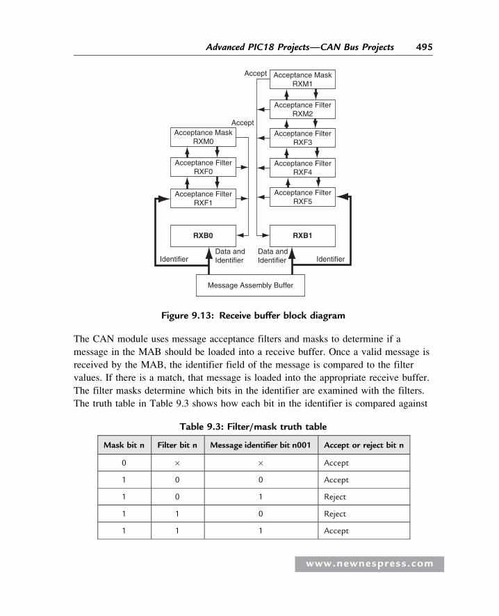
The CAN module uses message acceptance filters and masks to determine if a
message in the MAB should be loaded into a receive buffer. Once a valid message is
received by the MAB, the identifier field of the message is compared to the filter
values. If there is a match, that message is loaded into the appropriate receive buffer.
The filter masks determine which bits in the identifier are examined with the filters.
The truth table in Table 9.3 shows how each bit in the identifier is compared against
Message Assembly Buffer
IdentifierData andIdentifier
Data andIdentifier Identifier
RXB0 RXB1
Acceptance FilterRXF1
Acceptance FilterRXF4
Acceptance FilterRXF5
Acceptance FilterRXF0
Acceptance FilterRXF3
Acceptance FilterRXM2
Acceptance MaskRXM0
Acceptance MaskRXM1
Accept
Accept
Figure 9.13: Receive buffer block diagram
Table 9.3: Filter/mask truth table
Mask bit n Filter bit n Message identifier bit n001 Accept or reject bit n
0 � � Accept
1 0 0 Accept
1 0 1 Reject
1 1 0 Reject
1 1 1 Accept
www.newnespress.com
495Advanced PIC18 Projects—CAN Bus Projects
the masks and filters to determine if the message should be accepted. If a mask
bit is set to 0, that bit in the identifier is automatically accepted regardless of the
filter bit.
9.9.9 Calculating the Timing Parameters
Setting the nodes’ timing parameters is essential for the bus to operate reliably. Given
the microcontroller clock frequency and the required CAN bus bit rate, we can calculate
the values of the following timing parameters:
� Baud rate prescaler value
� Prop_Seg value
� Phase_Seg1 value
� Phase_Seg2 value
� SJW value
Correct timing requires that
� Prop_Seg þ Phase_Seg1 � Phase_Seg2
� Phase_Seg2 � SJW
The following example illustrates the calculation of these timing parameters.
Example 9.2
Assuming the microcontroller oscillator clock rate is 20MHz and the required CAN bit
rate is 125KHz, calculate the timing parameters.
Solution 9.2
With a 20MHz clock rate, the clock period is 50ns. Choosing a baud rate prescaler
value of 4, from Equation (9.4), TQ ¼ 2 * (BRP þ 1) * TOSC, gives a time
quantum of TQ ¼ 500ns. To obtain a nominal bit rate of 125KHz, the nominal bit
time must be:
TBIT ¼ 1=0:125MHz ¼ 8ms; or 16TQ
www.newnespress.com
496 Chapter 9
The Sync_Segment is 1TQ. Choosing 2TQ for the Prop_Seg, and 7TQ for Phase_Seg1
leaves 6TQ for Phase_Seg2 and places the sampling point at 10TQ at the end of
Phase_Seg1.
By the rules described earlier, the SJW can be the maximum allowed (i.e., 4). However,
a large SJW is only necessary when the clock generation of different nodes is not
stable or accurate (e.g., if ceramic resonators are used). Typically, a SJW of 1 is
enough. In summary, the required timing parameters are:
Baud rate prescaler (BRP) ¼ 4Sync_Seg ¼ 1Prop_Seg ¼ 2Phase_Seg1 ¼ 7Phase_Seg2 ¼ 6SJW ¼ 1
The sampling point is at 10TQ which corresponds to 62.5% of the total bit time.
There are several tools available for free on the Internet for calculating CAN bus timing
parameters. One such tool is the CAN Baud Rate Calculator, developed by Artic
Consultants Ltd (http://www.articconsultants.co.uk). An example using this tool
follows.
Example 9.3
Assuming the microcontroller oscillator clock rate is 20MHz and the required CAN
bit rate is 125KHz, calculate the timing parameters using the CAN Baud Rate
Calculator.
Solution 9.3
Figure 9.14 shows the output of the CAN Baud Rate Calculator program. The device
type is selected as PIC18Fxxx8, the oscillator frequency is entered as 20MHz, and the
CAN bus baud rate is entered as 125KHz.
Clicking the Calculate Settings button calculates and displays the recommended timing
parameters. In general, there is more than one solution, and different solutions are given
in the Calculated Solutions field’s drop-down menu.
In choosing Solution 2 from the drop-down menu, the following timing parameters are
recommended by the program:
www.newnespress.com
497Advanced PIC18 Projects—CAN Bus Projects
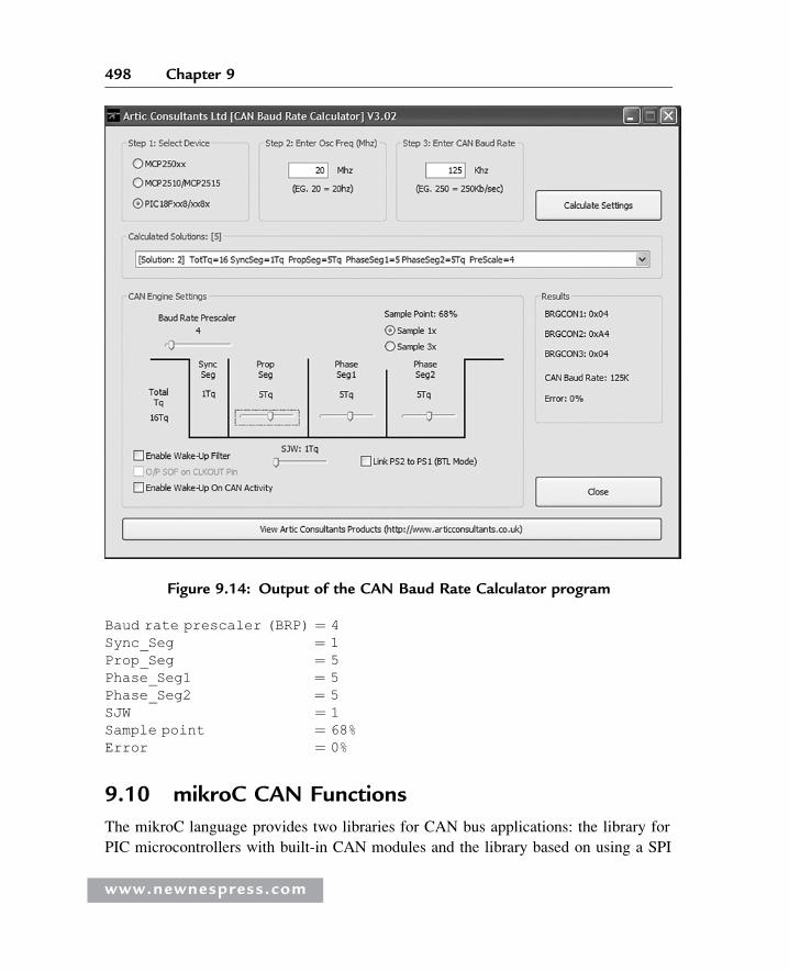
Baud rate prescaler (BRP) ¼ 4Sync_Seg ¼ 1Prop_Seg ¼ 5Phase_Seg1 ¼ 5Phase_Seg2 ¼ 5SJW ¼ 1Sample point ¼ 68%Error ¼ 0%
9.10 mikroC CAN Functions
The mikroC language provides two libraries for CAN bus applications: the library for
PIC microcontrollers with built-in CAN modules and the library based on using a SPI
Figure 9.14: Output of the CAN Baud Rate Calculator program
www.newnespress.com
498 Chapter 9
bus for PIC microcontrollers having no built-in CAN modules. In this section we
will discuss only the library functions available for PIC microcontrollers with built-in
CAN modules. Similar functions are available for the PIC microcontrollers with no
built-in CAN modules.
The mikroC CAN functions are supported only by PIC18XXX8 microcontrollers
with MCP2551 or similar CAN transceivers. Both standard (11 identifier bits) and
extended format (29 identifier bits) messages are supported.
The following mikroC functions are provided:
� CANSetOperationMode
� CANGetOperationMode
� CANInitialize
� CANSetBaudRAte
� CANSetMask
� CANSetFilter
� CANRead
� CANWrite
9.10.1 CANSetOperationMode
The CANSetOperationMode function sets the CAN operation mode. The function
prototype is:
void CANSetOperationMode(char mode, char wait_flag)
The parameter wait_ flag is either 0 or 0 � FF. If it is set to 0 � FF, the function blocks
and will not return until the requested mode is set. If it is set to 0, the function returns as
a nonblocking call.
The mode can be one of the following:
� CAN_MODE_NORMAL Normal mode of operation
� CAN_MODE_SLEEP Sleep mode of operation
� CAN_MODE_LOOP Loop-back mode of operation
www.newnespress.com
499Advanced PIC18 Projects—CAN Bus Projects
� CAN_MODE_LISTEN Listen-only mode of operation
� CAN_MODE_CONFIG Configuration mode of operation
9.10.2 CANGetOperationMode
The CANGetOperationMode function returns the current CAN operation mode. The
function prototype is:
char CANGetOperationMode(void)
9.10.3 CANInitialize
The CANInitialize function initializes the CAN module. All mask registers are cleared
to 0 to allow all messages. Upon execution of this function, the normal mode is set. The
function prototype is:
void CANInitialize(char SJW, char BRP, char PHSEG1, char PHSEG2,char PROPEG, char CAN_CONFIG_FLAGS)
where
SJW is the synchronization jump width
BRP is the baud rate prescaler
PHSEG1 is the Phase_Seg1 timing parameter
PHSEG2 is the Phase_Seg2 timing parameter
PROPSEG is the Prop_Seg
CAN_CONFIG_FLAGS can be one of the following configuration flags:
� CAN_CONFIG_DEFAULT Default flags
� CAN_CONFIG_PHSEG2_PRG_ON Use supplied PHSEG2 value
� CAN_CONFIG_PHSEG2_PRG_OFF Use maximum of PHSEG1 or
information processing time (IPT),
whichever is greater
� CAN_CONFIG_LINE_FILTER_ON Use CAN bus line filter for wake-up
� CAN_CONFIG_FILTER_OFF Do not use CAN bus line filter
www.newnespress.com
500 Chapter 9
� CAN_CONFIG_SAMPLE_ONCE Sample bus once at sample point
� CAN_CONFIG_SAMPLE_THRICE Sample bus three times prior to
sample point
� CAN_CONFIG_STD_MSG Accept only standard identifier
messages
� CAN_CONFIG_XTD_MSG Accept only extended identifier
messages
� CAN_CONFIG_DBL_BUFFER_ON Use double buffering to receive
data
� CAN_CONFIG_DBL_BUFFER_OFF Do not use double buffering
� CAN_CONFIG_ALL_MSG Accept all messages including
invalid ones
� CAN_CONFIG_VALID_XTD_MSG Accept only valid extended
identifier messages
� CAN_CONFIG_VALID_STD_MSG Accept only valid standard
identifier messages
� CAN_CONFIG_ALL_VALID_MSG Accept all valid messages
These configuration values can be bitwise AND’ed to form complex configuration
values.
9.10.4 CANSetBaudRate
The CANSetBaudRate function is used to set the CAN bus baud rate. The function
prototype is:
void CANSetBaudRate(char SJW, char BRP, char PHSEG1, char PHSEG2,char PROPSEG, char CAN_CONFIG_FLAGS)
The arguments of the function are as in function CANInitialize.
9.10.5 CANSetMask
The CANSetMask function sets the mask for filtering messages. The function
prototype is:
www.newnespress.com
501Advanced PIC18 Projects—CAN Bus Projects
void CANSetMask(char CAN_MASK, long value, charCAN_CONFIGFLAGS)
CAN_MASK can be one of the following:
� CAN_MASK_B1 Receive buffer 1 mask value
� CAN_MASK_B2 Receive buffer 2 mask value
value is the mask register value. CAN_CONFIG_FLAGS can be either
CAN_CONFIG_XTD (extended message), or CAN_CONFIG_STD (standard
message).
9.10.6 CANSetFilter
The CANSetFilter function sets filter values. The function prototype is:
void CANSetFilter(char CAN_FILTER, long value, charCAN_CONFIG_FLAGS)
CAN_FILTER can be one of the following:
� CAN_FILTER_B1_F1 Filter 1 for buffer 1
� CAN_FILTER_B1_F2 Filter 2 for buffer 1
� CAN_FILTER_B2_F1 Filter 1 for buffer 2
� CAN_FILTER_B2_F2 Filter 2 for buffer 2
� CAN_FILTER_B2_F3 Filter 3 for buffer 2
� CAN_FILTER_B2_F4 Filter 4 for buffer 2
CAN_CONFIG_FLAGS can be either CAN_CONFIG_XTD (extended message) or
CAN_CONFIG_STD (standard message).
9.10.7 CANRead
The CANRead function is used to read messages from the CAN bus. If no message is
available, 0 is returned. The function prototype is:
char CANRead(long *id, char *data, char *datalen, char*CAN_RX_MSG_FLAGS)
www.newnespress.com
502 Chapter 9
id is the CAN message identifier. Only 11 or 29 bits may be used depending on
message type (standard or extended). data is an array of bytes up to 8 where the
received data is stored. datalen is the length of the received data (1 to 8).
CAN_RX_MSG_FLAGS can be one of the following:
� CAN_RX_FILTER_1 Receive buffer filter 1 accepted this message
� CAN_RX_FILTER_2 Receive buffer filter 2 accepted this message
� CAN_RX_FILTER_3 Receive buffer filter 3 accepted this message
� CAN_RX_FILTER_4 Receive buffer filter 4 accepted this message
� CAN_RX_FILTER_5 Receive buffer filter 5 accepted this message
� CAN_RX_FILTER_6 Receive buffer filter 6 accepted this message
� CAN_RX_OVERFLOW Receive buffer overflow occurred
� CAN_RX_INVALID_MSG Invalid message received
� CAN_RX_XTD_FRAME Extended identifier message received
� CAN_RX_RTR_FRAME RTR frame message received
� CAN_RX_DBL_BUFFERED This message was double buffered
These flags can be bitwise AND’ed if desired.
9.10.8 CANWrite
The CANWrite function is used to send a message to the CAN bus. A zero is returned
if message can not be queued (buffer full). The function prototype is:
char CANWrite(long id, char *data, char datalen, charCAN_TX_MSG_FLAGS)
id is the CAN message identifier. Only 11 or 29 bits may be used depending on message
type (standard or extended). data is an array of bytes up to 8 where the data to be sent is
stored. datalen is the length of the data (1 to 8).
CAN_TX_MSG_FLAGS can be one of the following:
� CAN_TX_PRIORITY_0 Transmit priority 0
� CAN_TX_PRIORITY_1 Transmit priority 1
www.newnespress.com
503Advanced PIC18 Projects—CAN Bus Projects
� CAN_TX_PRIORITY_2 Transmit priority 2
� CAN_TX_PRIORITY_3 Transmit priority 3
� CAN_TX_STD_FRAME Standard identifier message
� CAN_TX_XTD_FRAME Extended identifier message
� CAN_TX_NO_RTR_FRAME Non RTR message
� CAN_TX_RTR_FRAME RTR message
These flags can be bitwise AND’ed if desired.
9.11 CAN Bus Programming
To operate the PIC18F258 microcontroller on the CAN bus, perform the following
steps:
� Configure the CAN bus I/O port directions (RB2 and RB3)
� Initialize the CAN module (CANInitialize)
� Set the CAN module to CONFIG mode (CANSetOperationMode)
� Set the mask registers (CANSetMask)
� Set the filter registers (CANSetFilter)
� Set the CAN module to normal mode (CANSetOperationMode)
� Write/read data (CANWrite/CANRead)
PROJECT 9.1—Temperature Sensor CANBus Project
The following is a simple two-node CAN bus–based project. The block diagram of
the project is shown in Figure 9.15. The system is made up of two CAN nodes.
One node (called DISPLAY node) requests the temperature every second and
displays it on an LCD. This process is repeated continuously. The other node
(called COLLECTOR node) reads the temperature from an external semiconductor
temperature sensor.
www.newnespress.com
504 Chapter 9
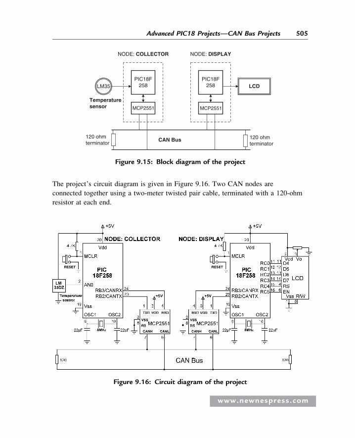
The project’s circuit diagram is given in Figure 9.16. Two CAN nodes are
connected together using a two-meter twisted pair cable, terminated with a 120-ohm
resistor at each end.
NODE: COLLECTOR NODE: DISPLAY
PIC18F258 LCD
120 ohmterminator
PIC18F258LM35
MCP2551 MCP2551
CAN Bus
Temperaturesensor
120 ohmterminator
Figure 9.15: Block diagram of the project
Figure 9.16: Circuit diagram of the project
www.newnespress.com
505Advanced PIC18 Projects—CAN Bus Projects
The DISPLAY Processor
Like the COLLECTOR processor, the DISPLAY processor consists of a PIC18F258
microcontroller with a built-in CAN module and an MCP2551 transceiver chip. The
microcontroller is operated from an 8MHz crystal. The MCLR input is connected to
an external reset button. The CAN outputs (RB2/CANTX and RB3/CANRX) of the
microcontroller are connected to the TXD and RXD inputs of the MCP2551. Pins
CANH and CANL of the transceiver chip are connected to the CAN bus. An
HD44780-type LCD is connected to PORTC of the microcontroller to display the
temperature values.
The COLLECTOR Processor
The COLLECTOR processor consists of a PIC18F258 microcontroller with a
built-in CAN module and an MCP2551 transceiver chip. The microcontroller is
operated from an 8MHz crystal. The MCLR input is connected to an external reset
button. Analog input AN0 of the microcontroller is connected to a LM35DZ-type
semiconductor temperature sensor. The sensor can measure temperature in the range
of 0�C to 100�C and generates an analog voltage directly proportional to the
measured temperature (i.e., the output is 10mV/�C). For example, at 20�C the
output voltage is 200mV.
The CAN outputs (RB2/CANTX and RB3/CANRX) of the microcontroller are
connected to the TXD and RXD inputs of an MCP2551-type CAN transceiver
chip. The CANH and CANL outputs of this chip are connected directly to a twisted
cable terminating at the CAN bus. The MCP2551 is an 8-pin chip that supports
data rates up to 1Mb/s. The chip can drive up to 112 nodes. An external resistor
connected to pin 8 of the chip controls the rise and fall times of CANH and
CANL so that EMI can be reduced. For high-speed operation this pin should be
connected to ground. A reference voltage equal to VDD/2 is output from pin 5 of
the chip.
The program listing is in two parts: the DISPLAY program and the COLLECTOR
program. The operation of the system is as follows:
� The DISPLAY processor requests the current temperature from the
COLLECTOR processor over the CAN bus
www.newnespress.com
506 Chapter 9
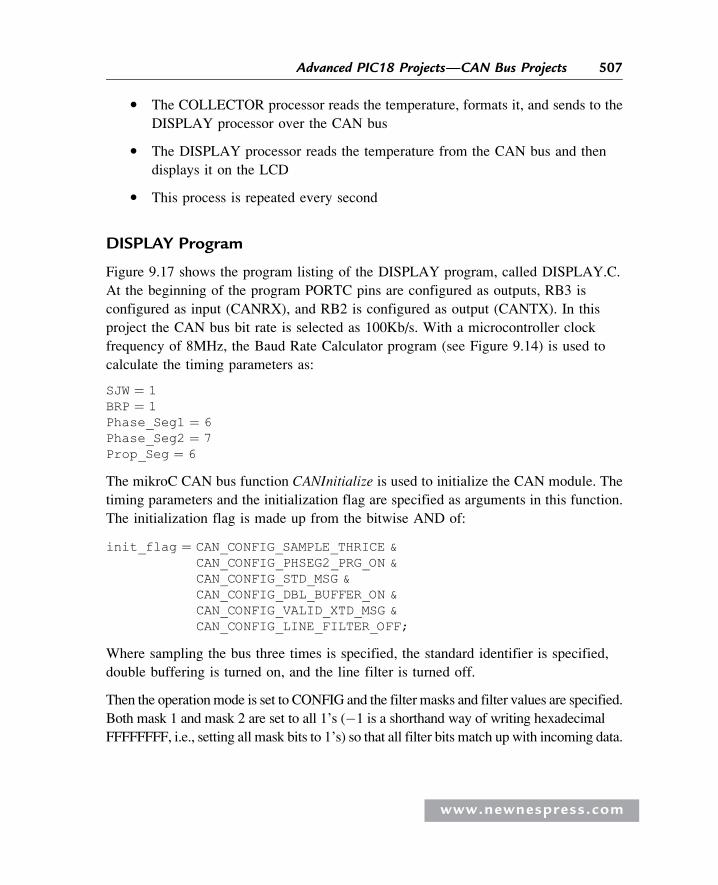
� The COLLECTOR processor reads the temperature, formats it, and sends to the
DISPLAY processor over the CAN bus
� The DISPLAY processor reads the temperature from the CAN bus and then
displays it on the LCD
� This process is repeated every second
DISPLAY Program
Figure 9.17 shows the program listing of the DISPLAY program, called DISPLAY.C.
At the beginning of the program PORTC pins are configured as outputs, RB3 is
configured as input (CANRX), and RB2 is configured as output (CANTX). In this
project the CAN bus bit rate is selected as 100Kb/s. With a microcontroller clock
frequency of 8MHz, the Baud Rate Calculator program (see Figure 9.14) is used to
calculate the timing parameters as:
SJW ¼ 1BRP ¼ 1Phase_Seg1 ¼ 6Phase_Seg2 ¼ 7Prop_Seg ¼ 6
The mikroC CAN bus function CANInitialize is used to initialize the CAN module. The
timing parameters and the initialization flag are specified as arguments in this function.
The initialization flag is made up from the bitwise AND of:
init_flag ¼ CAN_CONFIG_SAMPLE_THRICE &CAN_CONFIG_PHSEG2_PRG_ON &CAN_CONFIG_STD_MSG &CAN_CONFIG_DBL_BUFFER_ON &CAN_CONFIG_VALID_XTD_MSG &CAN_CONFIG_LINE_FILTER_OFF;
Where sampling the bus three times is specified, the standard identifier is specified,
double buffering is turned on, and the line filter is turned off.
Then the operationmode is set to CONFIG and the filter masks and filter values are specified.
Both mask 1 and mask 2 are set to all 1’s (�1 is a shorthand way of writing hexadecimal
FFFFFFFF, i.e., setting all mask bits to 1’s) so that all filter bits match up with incoming data.
www.newnespress.com
507Advanced PIC18 Projects—CAN Bus Projects
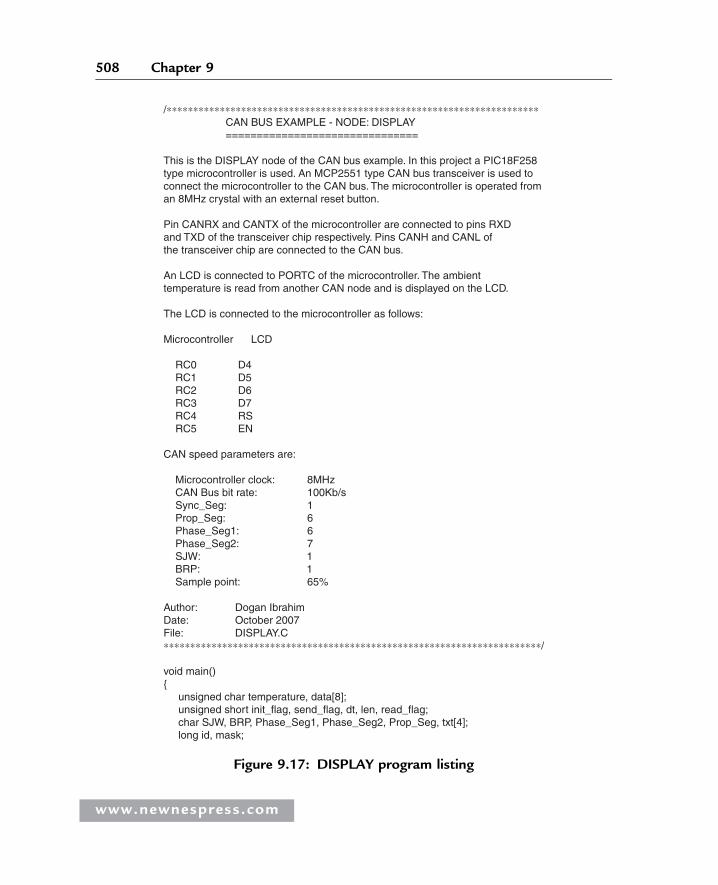
/∗∗∗∗∗∗∗∗∗∗∗∗∗∗∗∗∗∗∗∗∗∗∗∗∗∗∗∗∗∗∗∗∗∗∗∗∗∗∗∗∗∗∗∗∗∗∗∗∗∗∗∗∗∗∗∗∗∗∗∗∗∗∗∗∗∗∗∗∗∗ CAN BUS EXAMPLE - NODE: DISPLAY ===============================
This is the DISPLAY node of the CAN bus example. In this project a PIC18F258type microcontroller is used. An MCP2551 type CAN bus transceiver is used toconnect the microcontroller to the CAN bus. The microcontroller is operated froman 8MHz crystal with an external reset button.
Pin CANRX and CANTX of the microcontroller are connected to pins RXDand TXD of the transceiver chip respectively. Pins CANH and CANL ofthe transceiver chip are connected to the CAN bus.
An LCD is connected to PORTC of the microcontroller. The ambienttemperature is read from another CAN node and is displayed on the LCD.
The LCD is connected to the microcontroller as follows:
Microcontroller LCD
RC0 D4 RC1 D5 RC2 D6 RC3 D7 RC4 RS RC5 EN
CAN speed parameters are:
Microcontroller clock: 8MHz CAN Bus bit rate: 100Kb/s Sync_Seg: 1 Prop_Seg: 6 Phase_Seg1: 6 Phase_Seg2: 7 SJW: 1 BRP: 1 Sample point: 65%
Author: Dogan IbrahimDate: October 2007File: DISPLAY.C∗∗∗∗∗∗∗∗∗∗∗∗∗∗∗∗∗∗∗∗∗∗∗∗∗∗∗∗∗∗∗∗∗∗∗∗∗∗∗∗∗∗∗∗∗∗∗∗∗∗∗∗∗∗∗∗∗∗∗∗∗∗∗∗∗∗∗∗∗∗∗/
void main(){ unsigned char temperature, data[8]; unsigned short init_flag, send_flag, dt, len, read_flag; char SJW, BRP, Phase_Seg1, Phase_Seg2, Prop_Seg, txt[4]; long id, mask;
Figure 9.17: DISPLAY program listing
www.newnespress.com
508 Chapter 9
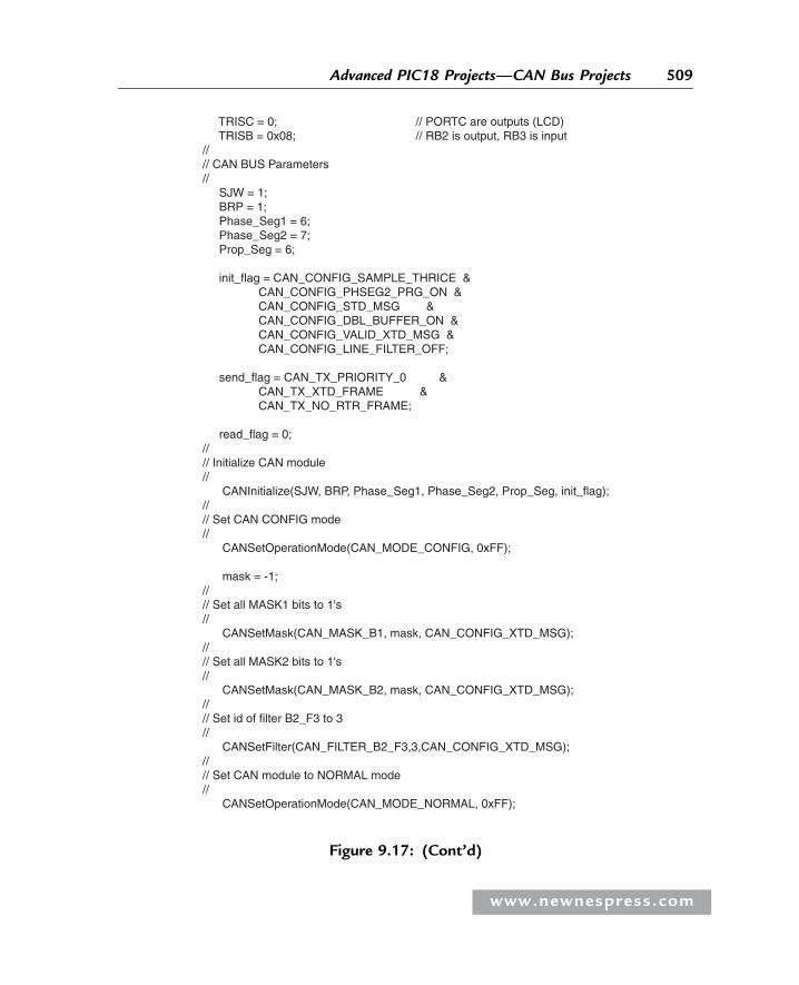
TRISC = 0; // PORTC are outputs (LCD) TRISB = 0x08; // RB2 is output, RB3 is input//// CAN BUS Parameters// SJW = 1; BRP = 1; Phase_Seg1 = 6; Phase_Seg2 = 7; Prop_Seg = 6; init_flag = CAN_CONFIG_SAMPLE_THRICE & CAN_CONFIG_PHSEG2_PRG_ON & CAN_CONFIG_STD_MSG & CAN_CONFIG_DBL_BUFFER_ON & CAN_CONFIG_VALID_XTD_MSG & CAN_CONFIG_LINE_FILTER_OFF;
send_flag = CAN_TX_PRIORITY_0 & CAN_TX_XTD_FRAME & CAN_TX_NO_RTR_FRAME;
read_flag = 0;//// Initialize CAN module// CANInitialize(SJW, BRP, Phase_Seg1, Phase_Seg2, Prop_Seg, init_flag);//// Set CAN CONFIG mode// CANSetOperationMode(CAN_MODE_CONFIG, 0xFF); mask = -1;//// Set all MASK1 bits to 1's// CANSetMask(CAN_MASK_B1, mask, CAN_CONFIG_XTD_MSG);//// Set all MASK2 bits to 1's// CANSetMask(CAN_MASK_B2, mask, CAN_CONFIG_XTD_MSG);//// Set id of filter B2_F3 to 3// CANSetFilter(CAN_FILTER_B2_F3,3,CAN_CONFIG_XTD_MSG);//// Set CAN module to NORMAL mode// CANSetOperationMode(CAN_MODE_NORMAL, 0xFF);
Figure 9.17: (Cont’d)
www.newnespress.com
509Advanced PIC18 Projects—CAN Bus Projects
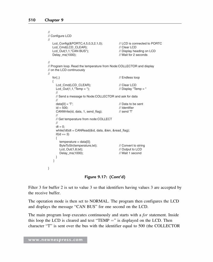
Filter 3 for buffer 2 is set to value 3 so that identifiers having values 3 are accepted by
the receive buffer.
The operation mode is then set to NORMAL. The program then configures the LCD
and displays the message “CAN BUS” for one second on the LCD.
The main program loop executes continuously and starts with a for statement. Inside
this loop the LCD is cleared and text “TEMP ¼” is displayed on the LCD. Then
character “T” is sent over the bus with the identifier equal to 500 (the COLLECTOR
//// Configure LCD// Lcd_Config(&PORTC,4,5,0,3,2,1,0); // LCD is connected to PORTC Lcd_Cmd(LCD_CLEAR); // Clear LCD Lcd_Out(1,1,"CAN BUS"); // Display heading on LCD Delay_ms(1000); // Wait for 2 seconds
//// Program loop. Read the temperature from Node:COLLECTOR and display// on the LCD continuously// for(;;) // Endless loop { Lcd_Cmd(LCD_CLEAR); // Clear LCD Lcd_Out(1,1,"Temp = "); // Display "Temp = " // // Send a message to Node:COLLECTOR and ask for data // data[0] = 'T'; // Data to be sent id = 500; // Identifier CANWrite(id, data, 1, send_flag); // send 'T' // // Get temperature from node:COLLECT // dt = 0; while(!dt)dt = CANRead(&id, data, &len, &read_flag); if(id == 3) { temperature = data[0]; ByteToStr(temperature,txt); // Convert to string Lcd_Out(1,8,txt); // Output to LCD Delay_ms(1000); // Wait 1 second } }
}
Figure 9.17: (Cont’d)
www.newnespress.com
510 Chapter 9
/∗∗∗∗∗∗∗∗∗∗∗∗∗∗∗∗∗∗∗∗∗∗∗∗∗∗∗∗∗∗∗∗∗∗∗∗∗∗∗∗∗∗∗∗∗∗∗∗∗∗∗∗∗∗∗∗∗∗∗∗∗∗∗∗∗∗∗∗∗∗∗ CAN BUS EXAMPLE - NODE: COLLECTOR =================================
This is the COLLECTOR node of the CAN bus example. In this project a PIC18F258 type microcontroller is used. An MCP2551 type CAN bus transceiveris used to connect the microcontroller to the CAN bus. The microcontroller is operated from an 8MHz crystal with an external reset button.
Pin CANRX and CANTX of the microcontroller are connected to pins RXDand TXD of the transceiver chip respectively. Pins CANH and CANL of the transceiver chip are connected to the CAN bus.
An LM35DZ type analog temperature sensor is connected to port AN0 of the microcontroller. The microcontroller reads the temperature when a request isreceived and then sends the temperature value as a byte to Node:DISPLAY onthe CAN bus.
CAN speed parameters are:
Microcontroller clock: 8MHz CAN Bus bit rate: 100Kb/s Sync_Seg: 1 Prop_Seg: 6 Phase_Seg1: 6 Phase_Seg2: 7 SJW: 1 BRP: 1 Sample point: 65%
Author: Dogan IbrahimDate: October 2007File: COLLECTOR.C∗∗∗∗∗∗∗∗∗∗∗∗∗∗∗∗∗∗∗∗∗∗∗∗∗∗∗∗∗∗∗∗∗∗∗∗∗∗∗∗∗∗∗∗∗∗∗∗∗∗∗∗∗∗∗∗∗∗∗∗∗∗∗∗∗∗∗∗∗∗∗/
void main(){ unsigned char temperature, data[8]; unsigned short init_flag, send_flag, dt, len, read_flag; char SJW, BRP, Phase_Seg1, Phase_Seg2, Prop_Seg, txt[4]; unsigned int temp; unsigned long mV; long id, mask;
TRISA = 0xFF; // PORTA are inputs TRISB = 0x08; // RB2 is output, RB3 is input//// Configure A/D converter// ADCON1 = 0x80;
Figure 9.18: COLLECTOR program listing(Continued)
www.newnespress.com
511Advanced PIC18 Projects—CAN Bus Projects
//// CAN BUS Timing Parameters// SJW = 1; BRP = 1; Phase_Seg1 = 6; Phase_Seg2 = 7; BRP = 1; Prop_Seg = 6;
init_flag = CAN_CONFIG_SAMPLE_THRICE & CAN_CONFIG_PHSEG2_PRG_ON & CAN_CONFIG_STD_MSG & CAN_CONFIG_DBL_BUFFER_ON & CAN_CONFIG_VALID_XTD_MSG & CAN_CONFIG_LINE_FILTER_OFF;
send_flag = CAN_TX_PRIORITY_0 & CAN_TX_XTD_FRAME & CAN_TX_NO_RTR_FRAME;
read_flag = 0;//// Initialise CAN module// CANInitialize(SJW, BRP, Phase_Seg1, Phase_Seg2, Prop_Seg, init_flag);//// Set CAN CONFIG mode// CANSetOperationMode(CAN_MODE_CONFIG, 0xFF);
mask = -1;//// Set all MASK1 bits to 1's// CANSetMask(CAN_MASK_B1, mask, CAN_CONFIG_XTD_MSG);//// Set all MASK2 bits to 1's// CANSetMask(CAN_MASK_B2, mask, CAN_CONFIG_XTD_MSG);//// Set id of filter B1_F1 to 3// CANSetFilter(CAN_FILTER_B2_F3,500,CAN_CONFIG_XTD_MSG);//// Set CAN module to NORMAL mode// CANSetOperationMode(CAN_MODE_NORMAL, 0xFF);
//
Figure 9.18: (Cont’d)
www.newnespress.com
512 Chapter 9
// Program loop. Read the temperature from analog temperature// sensor// for(;;) // Endless loop { // // Wait until a request is received // dt = 0; while(!dt) dt = CANRead(&id, data, &len, &read_flag); if(id == 500 && data[0] == 'T') { // // Now read the temperature // temp = Adc_Read(0); // Read temp mV = (unsigned long)temp ∗ 5000 / 1024; // in mV temperature = mV/10; // in degrees C // // send the temperature to Node:Display // data[0] = temperature; id = 3; // Identifier CANWrite(id, data, 1, send_flag); // send temperature } }}
Figure 9.18: (Cont’d)
Node: DISPLAY Node: COLLECTOR
Initialize CAN module Initialize CAN moduleSet mode to CONFIG Set mode to CONFIGSet Mask bits to 1’s Set Mask bits to 1’sSet Filter value to 3 Set Filter value to 500Set mode to NORMAL Set mode to NORMAL
DO FOREVER DO FOREVER Send character “T” with identifier 500 Read a character Read temperature with identifier 3 IF character is “T” Convert temperature to string Read temperature Display temperature on LCD Convert to digital Wait 1 second Convert to ºCENDDO Send with identifier 3 ENDIF ENDDO
Figure 9.19: Operation of both nodes
www.newnespress.com
513Advanced PIC18 Projects—CAN Bus Projects
node filter is set to accept identifier 500). This is a request to the COLLECTOR
node to send the temperature reading. The program then reads the temperature from
the CAN bus, converts it to a string in array txt, and displays it on the LCD. This
process repeats after a one-second delay.
COLLECTOR Program
Figure 9.18 shows the program listing of the COLLECTOR program, called
COLLECTOR.C. The initial part of this program is the same as the DISPLAY
program. The receive filter is set to 500 so that messages with identifier 500 are
accepted by the program.
Inside the program loop, the program waits until it receives a request to send the
temperature. Here the request is identified by the reception of character “T”. Once a
valid request is received, the temperature is read and converted into �C (stored in
variable temperature) and then sent to the CAN bus as a byte with an identifier value
equal to 3. This process repeats forever.
Figure 9.19 summarizes the operation of both nodes.
www.newnespress.com
514 Chapter 9
CHAP T E R 1 0
Multi-Tasking and Real-TimeOperating Systems
Nearly all microcontroller-based systems perform more than one activity. For example,
a temperature monitoring system is made up of three tasks that normally repeat after a
short delay, namely:
� Task 1 Reads the temperature
� Task 2 Formats the temperature
� Task 3 Displays the temperature
More complex systems may have many complex tasks. In a multi-tasking system,
numerous tasks require CPU time, and since there is only one CPU, some form of
organization and coordination is needed so each task has the CPU time it needs. In
practice, each task takes a very brief amount of time, so it seems as if all the tasks are
executing in parallel and simultaneously.
Almost all microcontroller-based systems work in real time. A real-time system is a
time responsive system that can respond to its environment in the shortest possible time.
Real time does not necessarily mean the microcontroller should operate at high speed.
What is important in a real-time system is a fast response time, although high speed can
help. For example, a real-time microcontroller-based system with various external
switches is expected to respond immediately when a switch is activated or some other
event occurs.
A real-time operating system (RTOS) is a piece of code (usually called the kernel) that
controls task allocation when the microcontroller is operating in a multi-tasking
www.newnespress.com
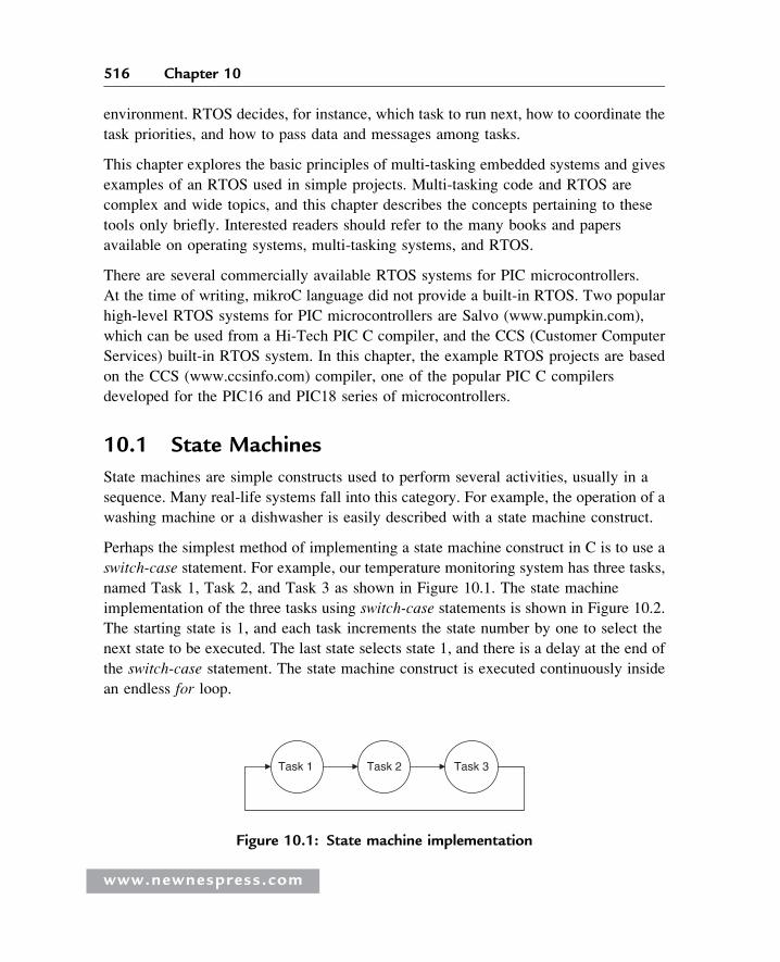
environment. RTOS decides, for instance, which task to run next, how to coordinate the
task priorities, and how to pass data and messages among tasks.
This chapter explores the basic principles of multi-tasking embedded systems and gives
examples of an RTOS used in simple projects. Multi-tasking code and RTOS are
complex and wide topics, and this chapter describes the concepts pertaining to these
tools only briefly. Interested readers should refer to the many books and papers
available on operating systems, multi-tasking systems, and RTOS.
There are several commercially available RTOS systems for PIC microcontrollers.
At the time of writing, mikroC language did not provide a built-in RTOS. Two popular
high-level RTOS systems for PIC microcontrollers are Salvo (www.pumpkin.com),
which can be used from a Hi-Tech PIC C compiler, and the CCS (Customer Computer
Services) built-in RTOS system. In this chapter, the example RTOS projects are based
on the CCS (www.ccsinfo.com) compiler, one of the popular PIC C compilers
developed for the PIC16 and PIC18 series of microcontrollers.
10.1 State Machines
State machines are simple constructs used to perform several activities, usually in a
sequence. Many real-life systems fall into this category. For example, the operation of a
washing machine or a dishwasher is easily described with a state machine construct.
Perhaps the simplest method of implementing a state machine construct in C is to use a
switch-case statement. For example, our temperature monitoring system has three tasks,
named Task 1, Task 2, and Task 3 as shown in Figure 10.1. The state machine
implementation of the three tasks using switch-case statements is shown in Figure 10.2.
The starting state is 1, and each task increments the state number by one to select the
next state to be executed. The last state selects state 1, and there is a delay at the end of
the switch-case statement. The state machine construct is executed continuously inside
an endless for loop.
Task 3Task 2Task 1
Figure 10.1: State machine implementation
www.newnespress.com
516 Chapter 10
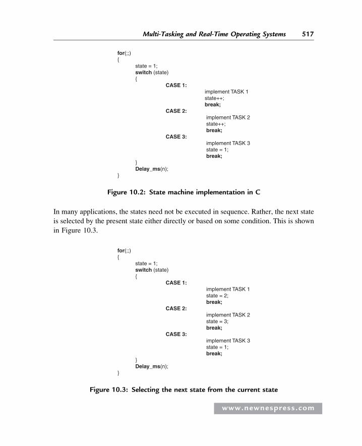
In many applications, the states need not be executed in sequence. Rather, the next state
is selected by the present state either directly or based on some condition. This is shown
in Figure 10.3.
for(;;){ state = 1; switch (state) { CASE 1: implement TASK 1 state++; break; CASE 2: implement TASK 2 state++; break; CASE 3: implement TASK 3 state = 1; break; } Delay_ms(n);}
Figure 10.2: State machine implementation in C
for(;;){ state = 1; switch (state) { CASE 1: implement TASK 1 state = 2; break; CASE 2: implement TASK 2 state = 3; break; CASE 3: implement TASK 3 state = 1; break; } Delay_ms(n);}
Figure 10.3: Selecting the next state from the current state
www.newnespress.com
517Multi-Tasking and Real-Time Operating Systems
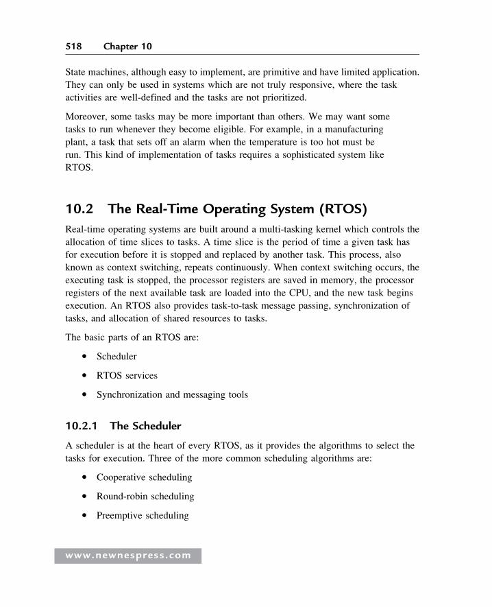
State machines, although easy to implement, are primitive and have limited application.
They can only be used in systems which are not truly responsive, where the task
activities are well-defined and the tasks are not prioritized.
Moreover, some tasks may be more important than others. We may want some
tasks to run whenever they become eligible. For example, in a manufacturing
plant, a task that sets off an alarm when the temperature is too hot must be
run. This kind of implementation of tasks requires a sophisticated system like
RTOS.
10.2 The Real-Time Operating System (RTOS)
Real-time operating systems are built around a multi-tasking kernel which controls the
allocation of time slices to tasks. A time slice is the period of time a given task has
for execution before it is stopped and replaced by another task. This process, also
known as context switching, repeats continuously. When context switching occurs, the
executing task is stopped, the processor registers are saved in memory, the processor
registers of the next available task are loaded into the CPU, and the new task begins
execution. An RTOS also provides task-to-task message passing, synchronization of
tasks, and allocation of shared resources to tasks.
The basic parts of an RTOS are:
� Scheduler
� RTOS services
� Synchronization and messaging tools
10.2.1 The Scheduler
A scheduler is at the heart of every RTOS, as it provides the algorithms to select the
tasks for execution. Three of the more common scheduling algorithms are:
� Cooperative scheduling
� Round-robin scheduling
� Preemptive scheduling
www.newnespress.com
518 Chapter 10
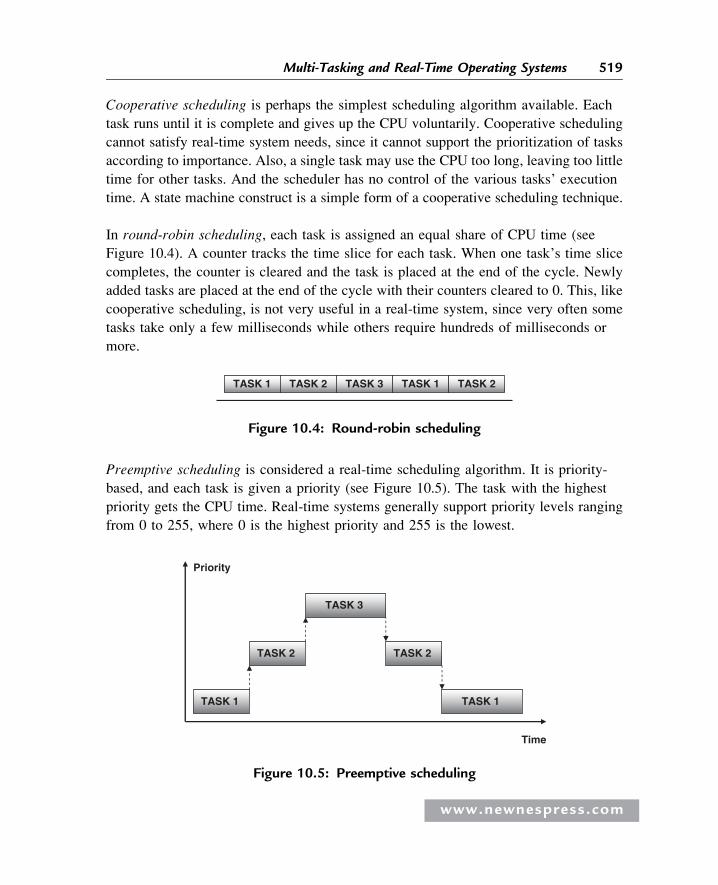
Cooperative scheduling is perhaps the simplest scheduling algorithm available. Each
task runs until it is complete and gives up the CPU voluntarily. Cooperative scheduling
cannot satisfy real-time system needs, since it cannot support the prioritization of tasks
according to importance. Also, a single task may use the CPU too long, leaving too little
time for other tasks. And the scheduler has no control of the various tasks’ execution
time. A state machine construct is a simple form of a cooperative scheduling technique.
In round-robin scheduling, each task is assigned an equal share of CPU time (see
Figure 10.4). A counter tracks the time slice for each task. When one task’s time slice
completes, the counter is cleared and the task is placed at the end of the cycle. Newly
added tasks are placed at the end of the cycle with their counters cleared to 0. This, like
cooperative scheduling, is not very useful in a real-time system, since very often some
tasks take only a few milliseconds while others require hundreds of milliseconds or
more.
Preemptive scheduling is considered a real-time scheduling algorithm. It is priority-
based, and each task is given a priority (see Figure 10.5). The task with the highest
priority gets the CPU time. Real-time systems generally support priority levels ranging
from 0 to 255, where 0 is the highest priority and 255 is the lowest.
TASK 2TASK 1TASK 3TASK 2TASK 1
Figure 10.4: Round-robin scheduling
TASK 1
TASK 2
TASK 3
TASK 2
Priority
TASK 1
Time
Figure 10.5: Preemptive scheduling
www.newnespress.com
519Multi-Tasking and Real-Time Operating Systems
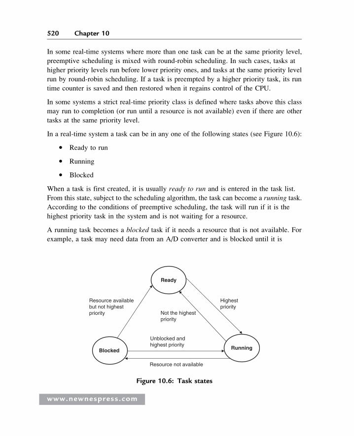
In some real-time systems where more than one task can be at the same priority level,
preemptive scheduling is mixed with round-robin scheduling. In such cases, tasks at
higher priority levels run before lower priority ones, and tasks at the same priority level
run by round-robin scheduling. If a task is preempted by a higher priority task, its run
time counter is saved and then restored when it regains control of the CPU.
In some systems a strict real-time priority class is defined where tasks above this class
may run to completion (or run until a resource is not available) even if there are other
tasks at the same priority level.
In a real-time system a task can be in any one of the following states (see Figure 10.6):
� Ready to run
� Running
� Blocked
When a task is first created, it is usually ready to run and is entered in the task list.
From this state, subject to the scheduling algorithm, the task can become a running task.
According to the conditions of preemptive scheduling, the task will run if it is the
highest priority task in the system and is not waiting for a resource.
A running task becomes a blocked task if it needs a resource that is not available. For
example, a task may need data from an A/D converter and is blocked until it is
Blocked
Resource availablebut not highestpriority
Unblocked andhighest priority
Not the highestpriority
Highestpriority
Running
Ready
Resource not available
Figure 10.6: Task states
www.newnespress.com
520 Chapter 10
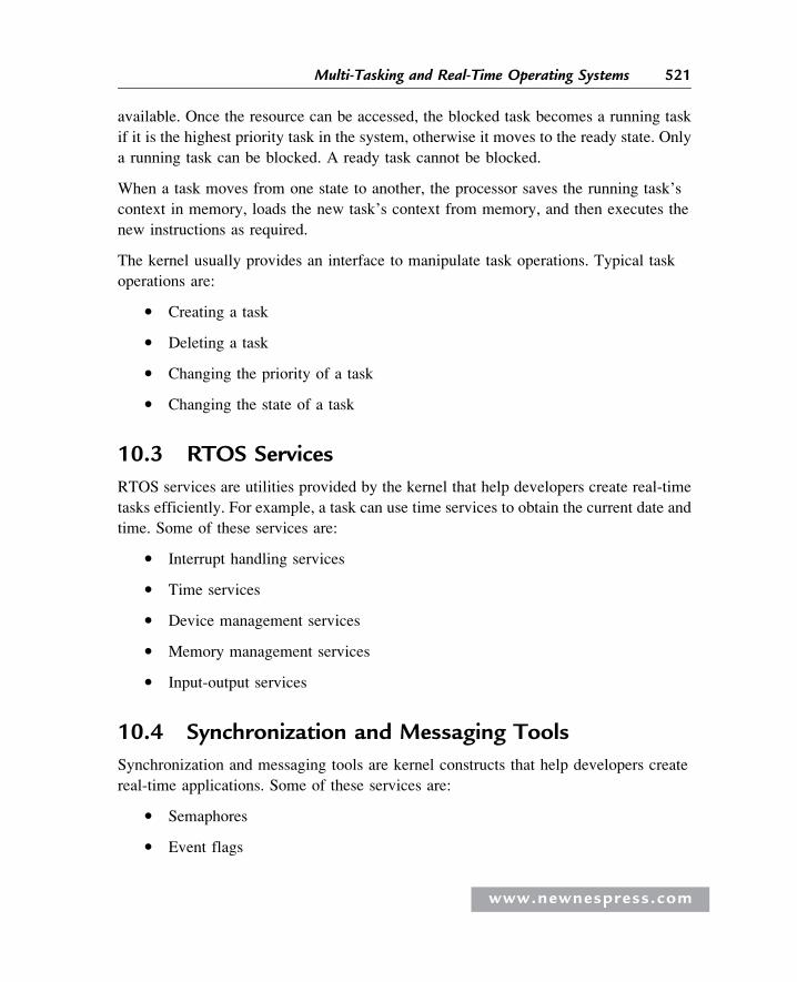
available. Once the resource can be accessed, the blocked task becomes a running task
if it is the highest priority task in the system, otherwise it moves to the ready state. Only
a running task can be blocked. A ready task cannot be blocked.
When a task moves from one state to another, the processor saves the running task’s
context in memory, loads the new task’s context from memory, and then executes the
new instructions as required.
The kernel usually provides an interface to manipulate task operations. Typical task
operations are:
� Creating a task
� Deleting a task
� Changing the priority of a task
� Changing the state of a task
10.3 RTOS Services
RTOS services are utilities provided by the kernel that help developers create real-time
tasks efficiently. For example, a task can use time services to obtain the current date and
time. Some of these services are:
� Interrupt handling services
� Time services
� Device management services
� Memory management services
� Input-output services
10.4 Synchronization and Messaging Tools
Synchronization and messaging tools are kernel constructs that help developers create
real-time applications. Some of these services are:
� Semaphores
� Event flags
www.newnespress.com
521Multi-Tasking and Real-Time Operating Systems
� Mailboxes
� Pipes
� Message queues
Semaphores are used to synchronize access to shared resources, such as common data
areas. Event flags are used to synchronize the intertask activities. Mailboxes, pipes, and
message queues are used to send messages among tasks.
10.5 CCS PIC C Compiler RTOS
The CCS PIC C compiler is one of the popular C compilers for the PIC16 and PIC18
series of microcontrollers. In addition to their PIC compilers, Customer Computer
Services offers PIC in-circuit emulators, simulators, microcontroller programmers, and
various development kits. The syntax of the CCS C language is slightly different from
that of the mikroC language, but readers who are familiar with mikroC should find CCS
C easy to use.
CCS C supports a rudimentary multi-tasking cooperative RTOS for the PIC18 series of
microcontrollers that uses their PCW and PCWH compilers. This RTOS allows a PIC
microcontroller to run tasks without using interrupts. When a task is scheduled to run,
control of the processor is given to that task. When the task is complete or does not
need the processor any more, control returns to a dispatch function, which gives control
of the processor to the next scheduled task. Because the RTOS does not use interrupts
and is not preemptive, the user must make sure that a task does not run forever.
Further details about the RTOS are available in the compiler’s user manual.
The CCS language provides the following RTOS functions in addition to the normal C
functions:
rtos_run() initiates the operation of RTOS. All task control operations are
implemented after calling this function.
rtos_terminate() terminates the operation of RTOS. Control returns to the
original program without RTOS. In fact, this function is like a return from
rtos_run().
rtos_enable() receives the name of a task as an argument. The function enables the
task so function rtos_run() can call the task when its time is due.
www.newnespress.com
522 Chapter 10
rtos_disable() receives the name of a task as an argument. The function disables the
task so it can no longer be called by rtos_run() unless it is re-enabled by calling
rtos_enable().
rtos_ yield(), when called from within a task, returns control to the dispatcher. All
tasks should call this function to release the processor so other tasks can utilize the
processor time.
rtos_msg_send() receives a task name and a byte as arguments. The function sends
the byte to the specified task, where it is placed in the task’s message queue.
rtos_msg_read() reads the byte located in the task’s message queue.
rtos_msg_ poll() returns true if there is data in the task’s message queue. This
function should be called before reading a byte from the task’s message queue.
rtos_signal() receives a semaphore name and increments that semaphore.
rtos_wait() receives a semaphore name and waits for the resource associated with the
semaphore to become available. The semaphore count is then decremented so the
task can claim the resource.
rtos_await() receives an expression as an argument, and the task waits until the
expression evaluates to true.
rtos_overrun() receives a task name as an argument, and the function returns true if
that task has overrun its allocated time.
rtos_stats() returns the specified statistics about a specified task. The statistics can be
the minimum and maximum task run times and the total task run time. The task name
and the type of statistics are specified as arguments to the function.
10.5.1 Preparing for RTOS
In addition to the preceding functions, the #use rtos() preprocessor command must be
specified at the beginning of the program before calling any of the RTOS functions. The
format of this preprocessor command is:
#use rtos(timer¼n, minor_cycle¼m)
where timer is between 0 and 4 and specifies the processor timer that will be used by
the RTOS, and minor_cycle is the longest time any task will run. The number entered
here must be followed by s, ms, us, or ns.
www.newnespress.com
523Multi-Tasking and Real-Time Operating Systems
In addition, a statistics option can be specified after the minor_cycle option, in which
case the compiler will keep track of the minimum and maximum processor times the
task uses at each call and the task’s total time used.
10.5.2 Declaring a Task
A task is declared just like any other C function, but tasks in a multi-tasking application
do not have any arguments and do not return any values. Before a task is declared, a
#task preprocessor command is needed to specify the task options. The format of this
preprocessor command is:
#task(rate¼n, max¼m, queue¼p)
where rate specifies how often the task should be called. The number specified must
be followed by s, ms, us, or ns. max specifies how much processor time a task will
use in one execution of the task. The time specifed here must be equal to or less than
the time specified by minor_cycle. queue is optional and if present specifies the
number of bytes to be reserved for the task to receive messages from other tasks.
The default value is 0.
In the following example, a task called my_ticks is every 20ms and is expected to use no
more than 100ms of processor time. This task is specified with no queue option:
#task(rate¼20ms, max¼100ms)void my_ticks(){
...........
...........}
PROJECT 10.1—LEDs
In the following simple RTOS-based project, four LEDs are connected to the lower half
of PORTB of a PIC18F452-type microcontroller. The software consists of four tasks,
where each task flashes an LED at a different rate:
� Task 1, called task_B0, flashes the LED connected to port RB0 at a rate
of 250ms.
� Task 2, called task_B1, flashes the LED connected to port RB1 at a rate
of 500ms.
www.newnespress.com
524 Chapter 10
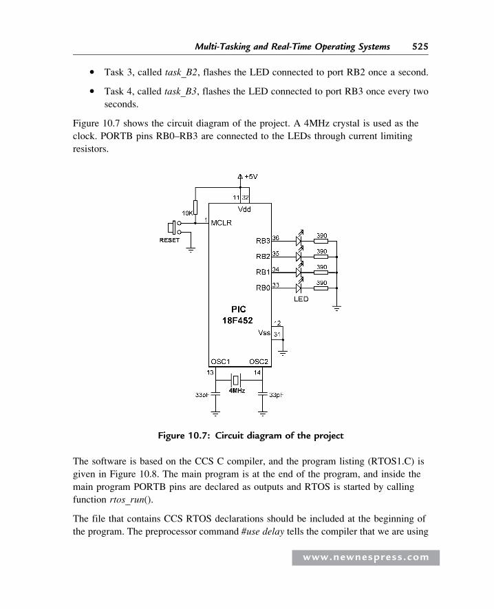
� Task 3, called task_B2, flashes the LED connected to port RB2 once a second.
� Task 4, called task_B3, flashes the LED connected to port RB3 once every two
seconds.
Figure 10.7 shows the circuit diagram of the project. A 4MHz crystal is used as the
clock. PORTB pins RB0–RB3 are connected to the LEDs through current limiting
resistors.
The software is based on the CCS C compiler, and the program listing (RTOS1.C) is
given in Figure 10.8. The main program is at the end of the program, and inside the
main program PORTB pins are declared as outputs and RTOS is started by calling
function rtos_run().
The file that contains CCS RTOS declarations should be included at the beginning of
the program. The preprocessor command #use delay tells the compiler that we are using
Figure 10.7: Circuit diagram of the project
www.newnespress.com
525Multi-Tasking and Real-Time Operating Systems
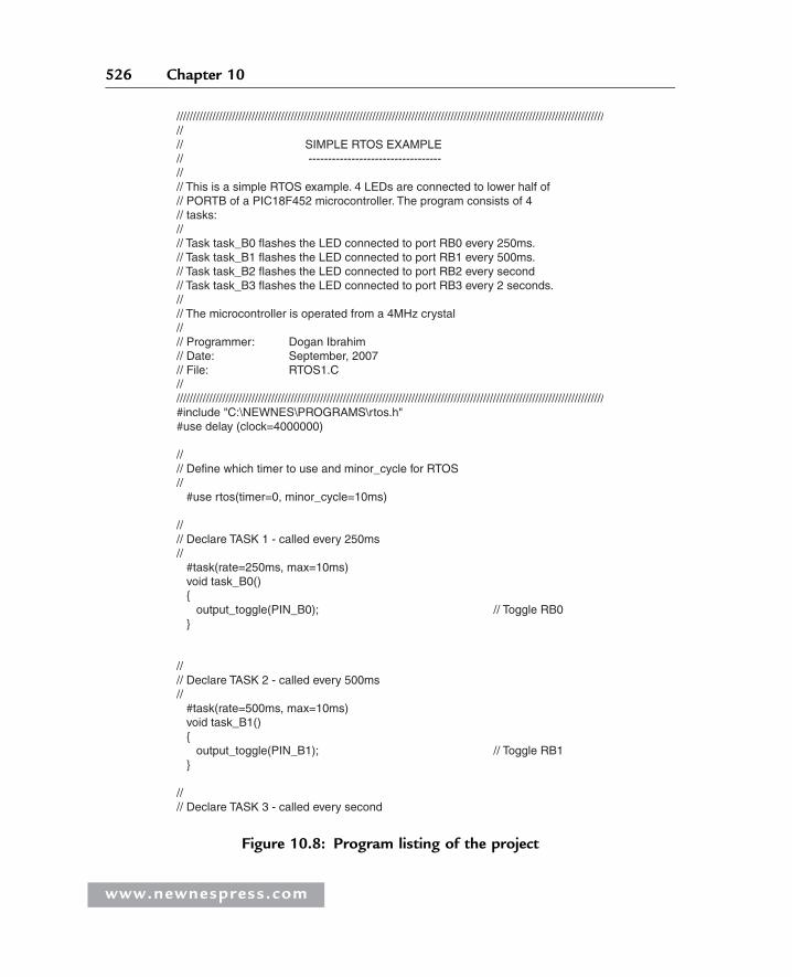
/////////////////////////////////////////////////////////////////////////////////////////////////////////////////////////////////////// SIMPLE RTOS EXAMPLE// ----------------------------------//// This is a simple RTOS example. 4 LEDs are connected to lower half of // PORTB of a PIC18F452 microcontroller. The program consists of 4// tasks://// Task task_B0 flashes the LED connected to port RB0 every 250ms. // Task task_B1 flashes the LED connected to port RB1 every 500ms. // Task task_B2 flashes the LED connected to port RB2 every second// Task task_B3 flashes the LED connected to port RB3 every 2 seconds.//// The microcontroller is operated from a 4MHz crystal//// Programmer: Dogan Ibrahim// Date: September, 2007// File: RTOS1.C/////////////////////////////////////////////////////////////////////////////////////////////////////////////////////////////////////#include "C:\NEWNES\PROGRAMS\rtos.h"#use delay (clock=4000000)
//// Define which timer to use and minor_cycle for RTOS// #use rtos(timer=0, minor_cycle=10ms)
//// Declare TASK 1 - called every 250ms// #task(rate=250ms, max=10ms) void task_B0() { output_toggle(PIN_B0); // Toggle RB0 }
//// Declare TASK 2 - called every 500ms// #task(rate=500ms, max=10ms) void task_B1() { output_toggle(PIN_B1); // Toggle RB1 }
//// Declare TASK 3 - called every second
Figure 10.8: Program listing of the project
www.newnespress.com
526 Chapter 10
a 4MHz clock. Then the RTOS timer is declared as Timer 0, and minor_cycle time is
declared as 10ms using the preprocessor command #use rtos.
The program consists of four similar tasks:
� task_B0 flashes the LED connected to RB0 at a rate of 250ms. Thus, the LED is
ON for 250ms, then OFF for 250ms, and so on. CCS statement output_toggle is
used to change the state of the LED every time the task is called. In the CCS
compiler PIN_B0 refers to port pin RB0 of the microcontroller.
� task_B1 flashes the LED connected to RB1 at a rate of 500ms as described.
� task_B2 flashes the LED connected to RB2 every second as described.
� Finally, task_B3 flashes the LED connected to RB3 every two seconds as
described.
// #task(rate=1s, max=10ms) void task_B2() { output_toggle(PIN_B2); // Toggle RB2 } //// Declare TASK 4 - called every 2 seconds// #task(rate=2s, max=10ms) void task_B3() { output_toggle(PIN_B3); // Toggle RB3 } //// Start of MAIN program//void main(){ set_tris_b(0); // Configure PORTB as outputs rtos_run(); // Start RTOS}
Figure 10.8: (Cont’d)
www.newnespress.com
527Multi-Tasking and Real-Time Operating Systems
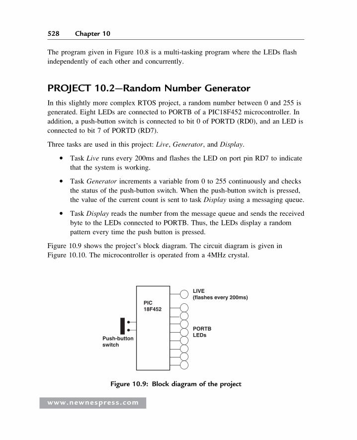
The program given in Figure 10.8 is a multi-tasking program where the LEDs flash
independently of each other and concurrently.
PROJECT 10.2—Random Number Generator
In this slightly more complex RTOS project, a random number between 0 and 255 is
generated. Eight LEDs are connected to PORTB of a PIC18F452 microcontroller. In
addition, a push-button switch is connected to bit 0 of PORTD (RD0), and an LED is
connected to bit 7 of PORTD (RD7).
Three tasks are used in this project: Live, Generator, and Display.
� Task Live runs every 200ms and flashes the LED on port pin RD7 to indicate
that the system is working.
� Task Generator increments a variable from 0 to 255 continuously and checks
the status of the push-button switch. When the push-button switch is pressed,
the value of the current count is sent to task Display using a messaging queue.
� Task Display reads the number from the message queue and sends the received
byte to the LEDs connected to PORTB. Thus, the LEDs display a random
pattern every time the push button is pressed.
Figure 10.9 shows the project’s block diagram. The circuit diagram is given in
Figure 10.10. The microcontroller is operated from a 4MHz crystal.
Push-buttonswitch
PIC18F452
LIVE(flashes every 200ms)
PORTBLEDs
Figure 10.9: Block diagram of the project
www.newnespress.com
528 Chapter 10
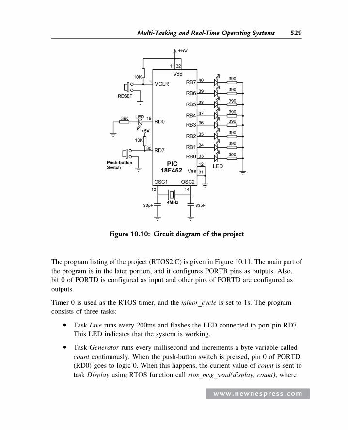
The program listing of the project (RTOS2.C) is given in Figure 10.11. The main part of
the program is in the later portion, and it configures PORTB pins as outputs. Also,
bit 0 of PORTD is configured as input and other pins of PORTD are configured as
outputs.
Timer 0 is used as the RTOS timer, and the minor_cycle is set to 1s. The program
consists of three tasks:
� Task Live runs every 200ms and flashes the LED connected to port pin RD7.
This LED indicates that the system is working.
� Task Generator runs every millisecond and increments a byte variable called
count continuously. When the push-button switch is pressed, pin 0 of PORTD
(RD0) goes to logic 0. When this happens, the current value of count is sent to
task Display using RTOS function call rtos_msg_send(display, count), where
Figure 10.10: Circuit diagram of the project
www.newnespress.com
529Multi-Tasking and Real-Time Operating Systems
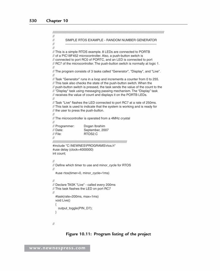
/////////////////////////////////////////////////////////////////////////////////////////////////////////////////////////////// SIMPLE RTOS EXAMPLE - RANDOM NUMBER GENERATOR// ------------------------------------------------------------------------------------//// This is a simple RTOS example. 8 LEDs are connected to PORTB// of a PIC18F452 microcontroller. Also, a push-button switch is// connected to port RC0 of PORTC, and an LED is connected to port// RC7 of the microcontroller. The push-button switch is normally at logic 1.//// The program consists of 3 tasks called "Generator", "Display", and "Live".//// Task "Generator" runs in a loop and increments a counter from 0 to 255.// This task also checks the state of the push-button switch. When the// push-button switch is pressed, the task sends the value of the count to the// "Display" task using messaging passing mechanism. The “Display” task// receives the value of count and displays it on the PORTB LEDs.//// Task "Live" flashes the LED connected to port RC7 at a rate of 250ms.// This task is used to indicate that the system is working and is ready for// the user to press the push-button.//// The microcontroller is operated from a 4MHz crystal//// Programmer: Dogan Ibrahim// Date: September, 2007// File: RTOS2.C////////////////////////////////////////////////////////////////////////////////////#include "C:\NEWNES\PROGRAMS\rtos.h"#use delay (clock=4000000)int count;
//// Define which timer to use and minor_cycle for RTOS// #use rtos(timer=0, minor_cycle=1ms)
//// Declare TASK "Live" - called every 200ms// This task flashes the LED on port RC7// #task(rate=200ms, max=1ms) void Live() { output_toggle(PIN_D7); }
//
Figure 10.11: Program listing of the project
www.newnespress.com
530 Chapter 10
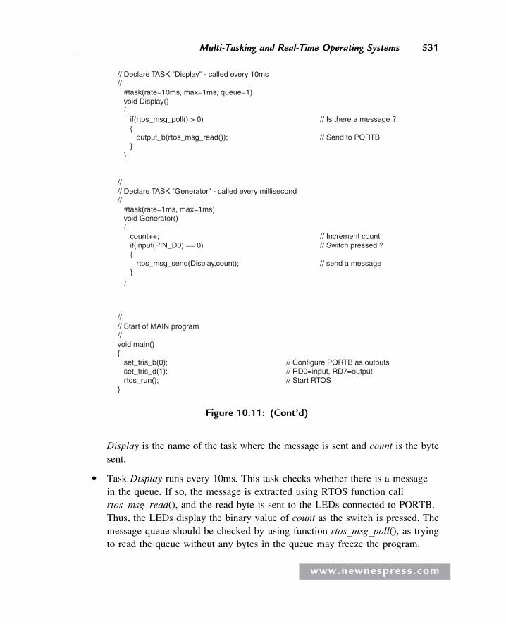
Display is the name of the task where the message is sent and count is the byte
sent.
� Task Display runs every 10ms. This task checks whether there is a message
in the queue. If so, the message is extracted using RTOS function call
rtos_msg_read(), and the read byte is sent to the LEDs connected to PORTB.
Thus, the LEDs display the binary value of count as the switch is pressed. The
message queue should be checked by using function rtos_msg_poll(), as trying
to read the queue without any bytes in the queue may freeze the program.
// Declare TASK "Display" - called every 10ms// #task(rate=10ms, max=1ms, queue=1) void Display() { if(rtos_msg_poll() > 0) // Is there a message ? { output_b(rtos_msg_read()); // Send to PORTB } }
//// Declare TASK "Generator" - called every millisecond// #task(rate=1ms, max=1ms) void Generator() { count++; // Increment count if(input(PIN_D0) == 0) // Switch pressed ? { rtos_msg_send(Display,count); // send a message } }
//// Start of MAIN program//void main(){ set_tris_b(0); // Configure PORTB as outputs set_tris_d(1); // RD0=input, RD7=output rtos_run(); // Start RTOS}
Figure 10.11: (Cont’d)
www.newnespress.com
531Multi-Tasking and Real-Time Operating Systems
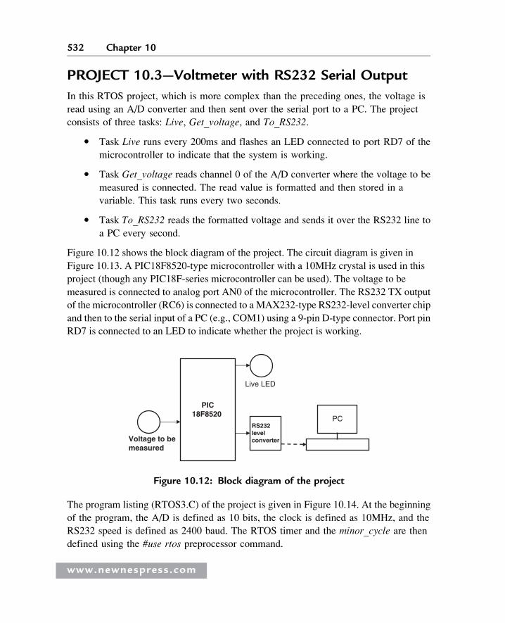
PROJECT 10.3—Voltmeter with RS232 Serial Output
In this RTOS project, which is more complex than the preceding ones, the voltage is
read using an A/D converter and then sent over the serial port to a PC. The project
consists of three tasks: Live, Get_voltage, and To_RS232.
� Task Live runs every 200ms and flashes an LED connected to port RD7 of the
microcontroller to indicate that the system is working.
� Task Get_voltage reads channel 0 of the A/D converter where the voltage to be
measured is connected. The read value is formatted and then stored in a
variable. This task runs every two seconds.
� Task To_RS232 reads the formatted voltage and sends it over the RS232 line to
a PC every second.
Figure 10.12 shows the block diagram of the project. The circuit diagram is given in
Figure 10.13. A PIC18F8520-type microcontroller with a 10MHz crystal is used in this
project (though any PIC18F-series microcontroller can be used). The voltage to be
measured is connected to analog port AN0 of the microcontroller. The RS232 TX output
of the microcontroller (RC6) is connected to a MAX232-type RS232-level converter chip
and then to the serial input of a PC (e.g., COM1) using a 9-pin D-type connector. Port pin
RD7 is connected to an LED to indicate whether the project is working.
The program listing (RTOS3.C) of the project is given in Figure 10.14. At the beginning
of the program, the A/D is defined as 10 bits, the clock is defined as 10MHz, and the
RS232 speed is defined as 2400 baud. The RTOS timer and the minor_cycle are then
defined using the #use rtos preprocessor command.
PIC18F8520
RS232levelconverter
PC
Live LED
Voltage to bemeasured
Figure 10.12: Block diagram of the project
www.newnespress.com
532 Chapter 10
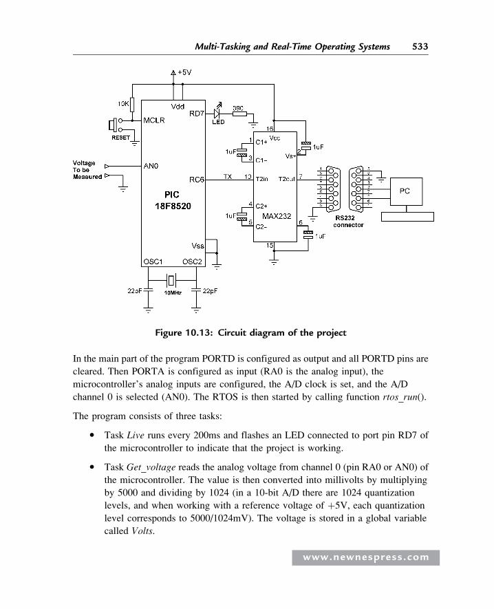
In the main part of the program PORTD is configured as output and all PORTD pins are
cleared. Then PORTA is configured as input (RA0 is the analog input), the
microcontroller’s analog inputs are configured, the A/D clock is set, and the A/D
channel 0 is selected (AN0). The RTOS is then started by calling function rtos_run().
The program consists of three tasks:
� Task Live runs every 200ms and flashes an LED connected to port pin RD7 of
the microcontroller to indicate that the project is working.
� Task Get_voltage reads the analog voltage from channel 0 (pin RA0 or AN0) of
the microcontroller. The value is then converted into millivolts by multiplying
by 5000 and dividing by 1024 (in a 10-bit A/D there are 1024 quantization
levels, and when working with a reference voltage of þ5V, each quantization
level corresponds to 5000/1024mV). The voltage is stored in a global variable
called Volts.
Figure 10.13: Circuit diagram of the project
www.newnespress.com
533Multi-Tasking and Real-Time Operating Systems
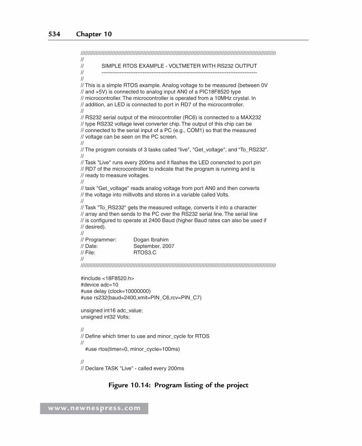
/////////////////////////////////////////////////////////////////////////////////////////////////////////////////////////////////////// SIMPLE RTOS EXAMPLE - VOLTMETER WITH RS232 OUTPUT// ---------------------------------------------------------------------------------------//// This is a simple RTOS example. Analog voltage to be measured (between 0V// and +5V) is connected to analog input AN0 of a PIC18F8520 type// microcontroller. The microcontroller is operated from a 10MHz crystal. In // addition, an LED is connected to port in RD7 of the microcontroller. //// RS232 serial output of the mirocontroller (RC6) is connected to a MAX232// type RS232 voltage level converter chip. The output of this chip can be// connected to the serial input of a PC (e.g., COM1) so that the measured// voltage can be seen on the PC screen.//// The program consists of 3 tasks called "live", "Get_voltage", and “To_RS232”.//// Task "Live" runs every 200ms and it flashes the LED conencted to port pin// RD7 of the microcontroller to indicate that the program is running and is// ready to measure voltages.//// task "Get_voltage" reads analog voltage from port AN0 and then converts// the voltage into millivolts and stores in a variable called Volts.//// Task "To_RS232" gets the measured voltage, converts it into a character// array and then sends to the PC over the RS232 serial line. The serial line// is configured to operate at 2400 Baud (higher Baud rates can also be used if// desired).//// Programmer: Dogan Ibrahim// Date: September, 2007// File: RTOS3.C/////////////////////////////////////////////////////////////////////////////////////////////////////////////////////////////////////
#include <18F8520.h>#device adc=10#use delay (clock=10000000)#use rs232(baud=2400,xmit=PIN_C6,rcv=PIN_C7)
unsigned int16 adc_value;unsigned int32 Volts;
//// Define which timer to use and minor_cycle for RTOS// #use rtos(timer=0, minor_cycle=100ms)
//// Declare TASK "Live" - called every 200ms
Figure 10.14: Program listing of the project
www.newnespress.com
534 Chapter 10
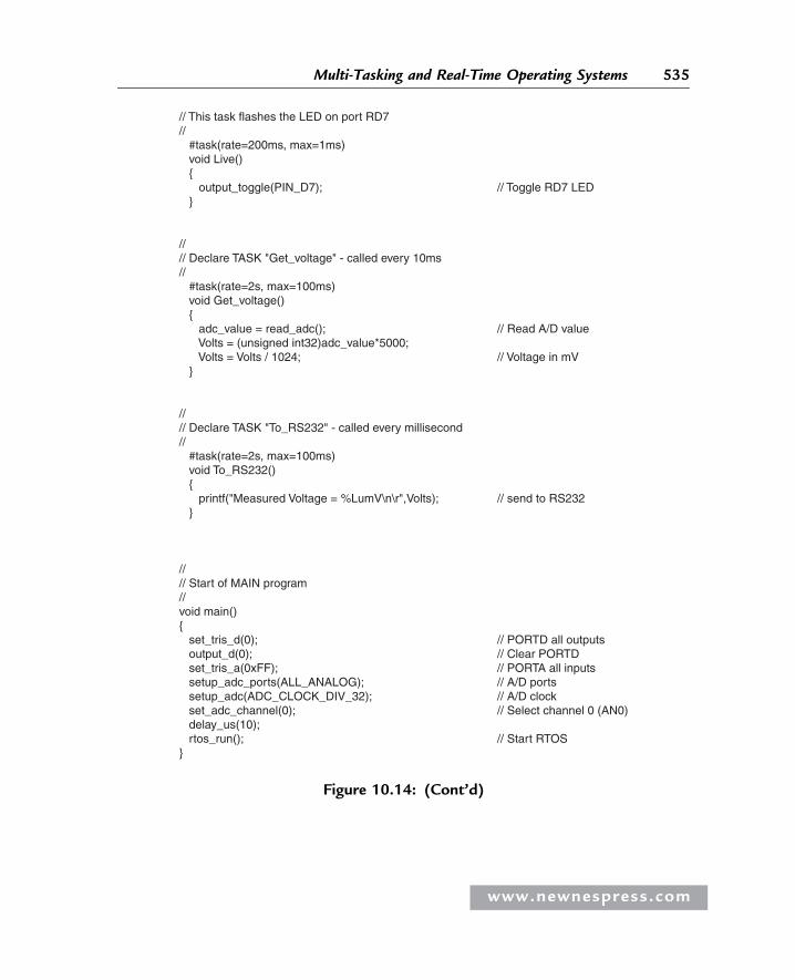
// This task flashes the LED on port RD7// #task(rate=200ms, max=1ms) void Live() { output_toggle(PIN_D7); // Toggle RD7 LED }
//// Declare TASK "Get_voltage" - called every 10ms// #task(rate=2s, max=100ms) void Get_voltage() { adc_value = read_adc(); // Read A/D value Volts = (unsigned int32)adc_value*5000; Volts = Volts / 1024; // Voltage in mV }
//// Declare TASK "To_RS232" - called every millisecond// #task(rate=2s, max=100ms) void To_RS232() { printf("Measured Voltage = %LumV\n\r",Volts); // send to RS232 }
//// Start of MAIN program//void main(){ set_tris_d(0); // PORTD all outputs output_d(0); // Clear PORTD set_tris_a(0xFF); // PORTA all inputs setup_adc_ports(ALL_ANALOG); // A/D ports setup_adc(ADC_CLOCK_DIV_32); // A/D clock set_adc_channel(0); // Select channel 0 (AN0) delay_us(10); rtos_run(); // Start RTOS}
Figure 10.14: (Cont’d)
www.newnespress.com
535Multi-Tasking and Real-Time Operating Systems
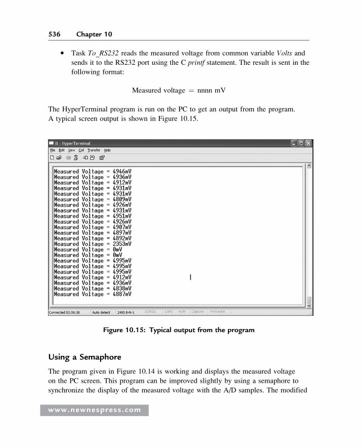
� Task To_RS232 reads the measured voltage from common variable Volts and
sends it to the RS232 port using the C printf statement. The result is sent in the
following format:
Measured voltage ¼ nnnn mV
The HyperTerminal program is run on the PC to get an output from the program.
A typical screen output is shown in Figure 10.15.
Using a Semaphore
The program given in Figure 10.14 is working and displays the measured voltage
on the PC screen. This program can be improved slightly by using a semaphore to
synchronize the display of the measured voltage with the A/D samples. The modified
Figure 10.15: Typical output from the program
www.newnespress.com
536 Chapter 10
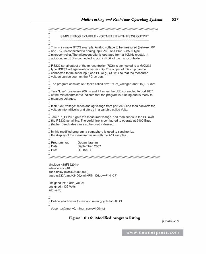
///////////////////////////////////////////////////////////////////////////////////////////////////////////////////////////////////// SIMPLE RTOS EXAMPLE - VOLTMETER WITH RS232 OUTPUT// ---------------------------------------------------------------------------------------//// This is a simple RTOS example. Analog voltage to be measured (between 0V// and +5V) is connected to analog input AN0 of a PIC18F8520 type// microcontroller. The microcontroller is operated from a 10MHz crystal. In // addition, an LED is connected to port in RD7 of the microcontroller. //// RS232 serial output of the mirocontroller (RC6) is connected to a MAX232// type RS232 voltage level converter chip. The output of this chip can be// connected to the serial input of a PC (e.g., COM1) so that the measured// voltage can be seen on the PC screen.//// The program consists of 3 tasks called "live", "Get_voltage", and "To_RS232".//// Task "Live" runs every 200ms and it flashes the LED connected to port RD7// of the microcontroller to indicate that the program is running and is ready to// measure voltages.//// task "Get_voltage" reads analog voltage from port AN0 and then converts the// voltage into millivolts and stores in a variable called Volts.//// Task "To_RS232" gets the measured voltage and then sends to the PC over// the RS232 serial line. The serial line is configured to operate at 2400 Baud// (higher Baud rates can also be used if desired).//// In this modified program, a semaphore is used to synchronize// the display of the measured value with the A/D samples.//// Programmer: Dogan Ibrahim// Date: September, 2007// File: RTOS4.C//////////////////////////////////////////////////////////////////////////////////////////////////////////////////////////////////////
#include <18F8520.h>#device adc=10#use delay (clock=10000000)#use rs232(baud=2400,xmit=PIN_C6,rcv=PIN_C7)
unsigned int16 adc_value;unsigned int32 Volts;int8 sem;
//// Define which timer to use and minor_cycle for RTOS// #use rtos(timer=0, minor_cycle=100ms)
Figure 10.16: Modified program listing(Continued)
www.newnespress.com
537Multi-Tasking and Real-Time Operating Systems
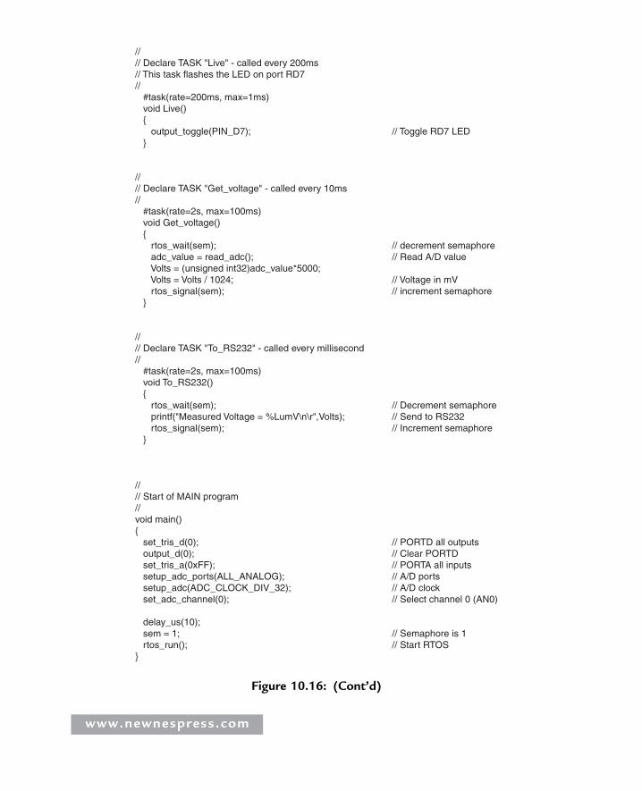
//// Declare TASK "Live" - called every 200ms// This task flashes the LED on port RD7// #task(rate=200ms, max=1ms) void Live() { output_toggle(PIN_D7); // Toggle RD7 LED }
//// Declare TASK "Get_voltage" - called every 10ms// #task(rate=2s, max=100ms) void Get_voltage() { rtos_wait(sem); // decrement semaphore adc_value = read_adc(); // Read A/D value Volts = (unsigned int32)adc_value*5000; Volts = Volts / 1024; // Voltage in mV rtos_signal(sem); // increment semaphore }
//// Declare TASK "To_RS232" - called every millisecond// #task(rate=2s, max=100ms) void To_RS232() { rtos_wait(sem); // Decrement semaphore printf("Measured Voltage = %LumV\n\r",Volts); // Send to RS232 rtos_signal(sem); // Increment semaphore }
//// Start of MAIN program//void main(){ set_tris_d(0); // PORTD all outputs output_d(0); // Clear PORTD set_tris_a(0xFF); // PORTA all inputs setup_adc_ports(ALL_ANALOG); // A/D ports setup_adc(ADC_CLOCK_DIV_32); // A/D clock set_adc_channel(0); // Select channel 0 (AN0)
delay_us(10); sem = 1; // Semaphore is 1 rtos_run(); // Start RTOS}
Figure 10.16: (Cont’d)
www.newnespress.com
program (RTOS4.C) is given in Figure 10.16. The operation of the new program
is as follows:
� The semaphore variable (sem) is set to 1 at the beginning of the program.
� Task Get_voltage decrements the semaphore (calls rtos_wait) variable so
that task To_RS232 is blocked (semaphore variable sem ¼ 0) and cannot
send data to the PC. When a new A/D sample is ready, the semaphore variable
is incremented (calls rtos_signal) and task To_RS232 can continue. Task
To_RS232 then sends the measured voltage to the PC and increments the
semaphore variable to indicate that it had access to the data. Task Get_voltage
can then get a new sample. This process is repeated forever.
www.newnespress.com
539Multi-Tasking and Real-Time Operating Systems

This page intentionally left blank
Index
A
Acquisition time, 99-101
A/D converter, 9, 46, 93-95, 100
A/D conversion clock, 98
A/D model, 100
ADCON0 register, 95, 96, 98
ADCON1 register, 95, 97, 99
ADFM, 99
ADRESH register, 95, 98, 99
ADRESL register, 95, 98, 99
AND operator, 142
Arithmetic operator, 139
Arrays, 131
character, 132
passing to functions, 176
ANSI C, 189
B
Barometric pressure, 464
Baud rate, 198, 200-206
Binary number, 14
adding, 27
converting into decimal, 16
converting into
hexadecimal, 18
converting into octal, 26
division, 31
multiplication, 29
negative, 26
normalizing, 34
subtracting, 29
Bit error, 486
Bit staffing, 486
Bit timing, 486
Bitwise operators, 139, 143
Breadboard, 247
Break statement, 150-152
Brown-out detector, 9
Built-in functions, in C, 183
C
C compiler, 187, 222, 250
CAN. See Controller area
network
CANGetOperationMode, 500
CANH, 479
CANInitialize, 500
CANL, 479
CANRead, 502
CANSetBaudrate, 501
CANSetFilter, 502
CANSetMask, 501
CANSetOperationMode, 499
CANWrite, 503
Capture mode, 85, 86, 88
Card filing system, 392
Case sensitivity, 122
Char, 124
CID register (SD card), 378
CISC, 13
C library functions, 187
Clock, 7, 60-67
Clock switching, 66
Code assistant, 257
Code explorer, 253
Conditional operator;139, 145
CONFIG1H register, 53
CONFIG2H register, 57
CONFIG2L register, 56
Configuration descriptor
(USB), 421
Configuration mode (CAN), 493
Configuration registers, 52
Cooperative scheduling, 518
Constants, in C, 126
Continue statement, 158
Control field (CAN), 484
Controller area network, 481
ACK field, 485
Arbitration, 482
Configuration mode, 493
control frame, 484
CRC field, 484
data frame, 484
disable mode, 493
error frame, 485
error recognition mode, 494
listen only mode, 494
message bit timing, 486
message reception, 494
message transmission, 494
modes of operation, 493
normal operation mode, 493
overload frame, 485
remote frame, 485
start of frame, 482
CCP1CON, 91
CCPR1L, 91
www.newnespress.com
Crystal, 60, 61, 65
CSD register, 379
Current sink, 185, 186
Current source, 187
D
Data memory, 51
EEPROM, 6, 10, 149
Data memory organization, 51
Data types, in C, 126, 135
Debugging, 223, 229
in-circuit debugger, 241
Delay functions, in C, 184
Decimal number, 14, 16
Descriptor, 418
device, 418
configuration, 421
interface, 423
HID, 425
endpoint, 426
Development board, 225
BIGPIC4 development kit, 236
Futurlec PIC18F458 training
board, 237
LAB-USB experimenter kit, 225
MK-1 development board, 230
PIC18F452 development
kit, 235
PICDEM 2 Plus, 226
PICDEM 4, 228
PICDEM HPC explorer
board, 229
SSE452 development
board, 231, 232
SSE8680 development
board, 234
SSE8720 development
board, 233
Development tools, 220
hardware, 224
software, 221
Device descriptor (USB), 418
Device programmer, 238
Disable mode (CAN), 493
Do-enddo, 289
Do-while statement, 152, 155, 156
E
EasyProg PIC programmer, 241
EEPROM, 6, 10
Eeprom read, 189, 191
Eeprom write, 189, 191
Emulator, 220
In-circuit, 244
End point descriptor (HID), 425
Endless loop, 157, 187
Enumerated variable, 126, 128
Enumeration (USB), 417
Error detection (CAN), 480
Error recognition mode
(CAN), 493
Error frame (CAN), 485
Escape sequence, 128, 129
External reset, 8, 11, 51
External variable, 129
F
Flash memory, 6, 128
Floating point number, 31, 32
addition, 37
converting into decimal, 33
division, 36
multiplication, 36
normalizing, 34
subtraction, 37
For-loop statement, 153, 154
Functions, in C, 168, 171, 183
G
Goto statement, 123, 152, 157
H
Hardware development
tools, 220, 223
debuggers, 223, 229
device programmers
224, 238
in-circuit emulators, 244
HD44780 LCD controller, 192
Hexadecimal number, 13, 15
HID, 425
enable, 429
disable, 429
read, 429
write, 429
HID descriptor (USB), 419
Hyperterminal, 365
I
ICD2, 243
ICD-U40, 243
ICEPIC 3, 247
If-else statement, 148,
149, 157
In-circuit debugger, 241
In-circuit emulator, 244
INTCON register, 73, 103, 104
Integrated development
environment, 119, 224
Interface descriptor (USB), 423
Internal clock, 66
Int, 126, 127
Interrupts, 8, 43, 101
Interrupt priority, 44, 51, 103
Interrupt service, 103,
106, 112
Interrupt vector, 9, 43, 103
INT0, 102, 103, 106
INT1, 102, 107
INT2, 72
Iteration statements, 148, 152
K
Keypad, 342
L
Label field, 157, 158
LCD, 192
controller, 193
LCD library, 192
LED, 11, 120, 170
Library functions, in C, 168, 171,
183
Listen-only mode (CAN), 493
LM35DZ, 506
www.newnespress.com
542 Index
Logical operators, 139, 142
Long, 123, 125, 126
Loopback mode (CAN), 494
M
Mach X programmer, 240
Math library, 208, 210
MAX232, 200-205, 357
MCP2551 CAN
transceiver, 489, 490
Melabs U2 programmer, 240
Memory organization, 50
data, 51
program, 250
Message bit timing
(CAN), 486
Message filtering (CAN), 493
Message transmission (CAN), 494
mikroC, 119
arithmetic operators, 139
arrays, 131
bitwise operators, 139, 143
comments, 121
constants, 126
control flow, 152
do-while statements, 152,
155, 156
for-loop statements,
153, 154
goto statement, 123,
152, 157
if-else statement, 148, 149,
157
switch statement, 150
while statement, 155
data types, 126, 135
functions, 168, 171, 183
library functions, 168, 171,
183
MMC library (SD card), 371, 384
MPLAB ICD2 in-circuit
debugger, 120, 227
MPLAB ICE 4000, 245
MPX4115, 464
Multiplexed LED, 231, 319
Multi-tasking, 515
N
Node (CAN), 476, 477
Nominal bit time (CAN), 486
Normal mode (CAN), 493
NRZI, 412
O
Octal number, 15
Operators, in C, 139
OR operator, 142
Oscillator, 7, 49, 60
OSI model, 481
Overload frame (CAN), 485
P
PDL, 288
PICFlash, 2, 244
PICE-MC, 247
PIC18 parallel ports, 49,68
PORT A, 68
PORT B, 71
PORT C, 73
PORT D, 73
PORT E, 73
PIC18 CAN module.
See Controller area network
PIC18 interrupts. See Interrupts
PIC18 Timers, 74
Timer 0, 74
Timer 1, 80
Timer 2, 82
Timer 3, 84
PIC Prog Plus programmer, 242
PLL, 49, 61, 65
Pointers, 133
Pull-up resistor, 71
Power-on reset, 11, 44, 49
Power supply, 57, 59, 64
Program memory
organization, 47, 50
Pre-emptive scheduling, 518, 519
PROM, 5
Preprocessor operator, 139, 146
#define, 146
#else, 147
#endif, 147
#if, 147
#ifndef, 146
#include, 147
#undef, 146
Pressure sensor, 464
PWM, 49, 84, 190
Q
QHelp, 254
R
Random number generator, 528
RAM, 5
RCON register, 103, 104
Real-time clock, 11, 226, 230
Real-time operating system, 515,
518
Registers
ADCON0, 95, 96
ADCON1, 71, 97-99
Internal RAM, 5, 283
Relational operators, in C, 139,
141
Remote frame (CAN), 485
Repeat-until, 290
Reset, 8
power on, 11
Rezonator, 60-63, 66
RICE 3000, 246
RISC, 13
ROM, 5
Round robin scheduling, 519
RS232, 9, 193, 199, 355
RTOS, 521
S
Scheduler, 518
SD card, 371
configuration register, 377
filing system, 392
identification register, 377
library functions, 384
reading data, 377
operation, 377
www.newnespress.com
543Index
SD card(Continued)operation control
register, 377
sector, 383-385
temperature logger, 397
writing data, 382
Semaphore, 522
Serial communication
9, 193, 199
Short, 123-125
Simulators, 221-223
Sizeof, 123, 136
Sleep mode, 11, 67
Software tools, 221
assemblers, 221
compilers, 221
Simulators, 221-223
text editors, 221, 222
Sound library, 189, 206
SPI bus, 190, 373
Static variable, 129
State machine, 516
Structures, in C, 135
Switch statement, 150, 151
T
Temperature logger, 397
Temperature sensor, 397
Text editor, 221, 222
Time delay, 185
Timers, 7
TIMER 0, 74
TIMER 1, 80
TIMER 2, 82
TIMER 3, 84
Transmit buffer (CAN), 492, 494
U
UART, 188
Unions, 123, 138
Universal serial bus, 410
Unsigned char, 124, 126
Unsigned int, 124-126
Unsigned long, 124, 125
Unsigned short, 124
USART, 188, 190, 200
USB, 409
bulk transfer, 416
bus communication
410, 414
bus specification, 410
cable, 410
connector pin assignment
410, 411
control transfer, 416, 417
data packet, 415, 416
descriptors, 418
device classes, 418
handshake packet, 416
interrupt transfer, 416, 417
isochronous transfer, 416
NRZI data, 412
programmer, 239
states, 413
token packet, 415
V
Variables, in C, 122, 123
Void, 121, 123, 161
Volatile variable, 130
W
Watchdog timer, 8, 40, 49, 55,
58, 67
While statement, 152, 155
White space, 122
X
XOR operator, 142, 143
Z
ZigBee, 12
www.newnespress.com
544 Index