engineering multi-walled carbon nanotube
TRANSCRIPT
ENS’06 Paris, France, 14-15 December 2006
©TIMA Editions/ENS 2006 -page- ISBN:
ENGINEERING MULTI-WALLED CARBON NANOTUBE SHELLS
BY ELECTRIC BREAKDOWN
Lixin Dong, Arunkumar Subramanian, Kaiyu Shou, and Bradley J. Nelson
Institute of Robotic and Intelligent Systems, ETH Zurich, Zurich, Switzerland ldong, arun, kshou, [email protected]
ABSTRACT
This paper presents the controlled peeling and thinning of the shells of multi-walled carbon nanotubes (MWNTs) by electric breakdown. Investigations inside a transmission electron microscope (TEM) are used to correlate the changes in MWNT structure with the electrical measurements. Such electrically engineered nanotubes can be used as rotational or linear bearings and sharpened tips in nanoelectromechanical systems (NEMS). MWNT arrays, assembled using dielectrophoresis, are used to investigate the batch fabrication of such structures and initial experiments demonstrate the fabrication of MWNT linear bearings in parallel. This represents the first effort at engineering the shell structure on MWNTs deposited by a controlled batch process which, can be used to realize arrays of nanoscale bearings.
1. INTRODUCTION Controllable exposure of the shells of multi-walled carbon nanotubes (MWNTs) has evoked interest because of the possibility of their application in nanoelectromechanical systems (NEMS) such as ultra-low friction bearings [1-4], GHz nanooscillators [5-8], nanometer scale actuators [9], switches [10, 11], variable resistors [12], and tunable resonators [13]. In situ manipulation of the nanotube core allows controlled reversible telescoping motion and, furthermore, allows the associated forces to be quantified [14]. The steady-state resistance to interlayer sliding motion has been measured to be 0.08-0.3 MPa [15]. Robust ultralow-friction linear nanobearings and rotary microactuators have been demonstrated on the basis of interlayer rotation of a MWNT [16-18].
Open-ended MWNTs have been created by removing the commonly capped ends with oxidization [19, 20], acid etching [21], saturated current [22, 23], electric pulse [24], mechanical strain [25], or site-selective mechanical breaking [26, 27], thus providing access to inner-core nanotube cylinders. Acid etching is effective for opening nanotube caps but does not expose
inner layers in a controlled way. Whereas electric pulse and mechanical strain are convenient in situ processes for atomic level imaging and property characterization in a transmission electron microscope (TEM), electric breakdown with saturated current is potentially a large-scale manufacturing method.
Controllably locating and aligning MWNTs is important for both realizing electric breakdown in a massive scale and understanding their behavior. Most previous investigations of devices involving NTs have employed random dispersions of nanotubes onto silicon chips, imaging the entire chip to locate the NTs and, then, fabrication of devices at these locations [17]. Though this method can be used to build single devices and for proving concepts in prototype studies, a deeper understanding of device performance and eventual commercialization of NEMS requires processes for handling, locating and aligning nanomaterials in a massively parallel fashion.
Several techniques have been explored to address this challenge. Direct growth of SWNTs onto pre-patterned catalysts on a silicon substrate using chemical vapor deposition has been demonstrated [28]. However, this requires high deposition temperatures which restrict the compatibility of other materials towards integration with nanotubes. Other reports have employed deposition of nanotubes onto chemically functionalized substrates [29, 30] . Such chemistry could potentially limit the performance of nanotubes. More recently, arrays of nanoscale torsional actuators were realized by selectively positioning MWNTs onto regions of polymer residue activated by an electron beam inside an SEM [18].
Assembly by dielectrophoresis (DEP) is another important bottom-up technique [31-33]. Previous investigations have shown the feasibility of this technique on the assembly of individual MWNT arrays across nanosized electrodes using this composite dielectrophoretic assembly method and explored their performance as lateral emitters with potential use in vacuum sensing applications [34, 35].
In this paper, time-resolved imaging and electric property characterization of the current driven MWNT breakdown process is shown in Section 2. This experiment was performed inside a TEM and provides
Lixin Dong, Arunkumar Subramanian, Kaiyu Shou, and Bradley J. Nelson Engineering multi-walled carbon nanotube shells by electric breakdown
©TIMA Editions/ENS 2006 -page- ISBN:
important insights into the MWNT breakdown process. Peeling of a single layer allows the investigation of the interlayer coupling of a MWNT. Electric breakdown of the innermost layer resembles a single-walled nanotube, and shows a different mode in morphology change, i.e., thinning. In section 3, initial results from efforts at extending this technique to arrays of MWNTs are discussed. Specifically, linear bearings formed by the breakdown of DEP assembled MWNTs in parallel are presented. This is the first time that such structures have been realized on nanotubes deposited by a controlled method which can be used to realize arrays of nanoscale devices. 2. ELECTRIC BREAKDOWN INVESTIGATED IN
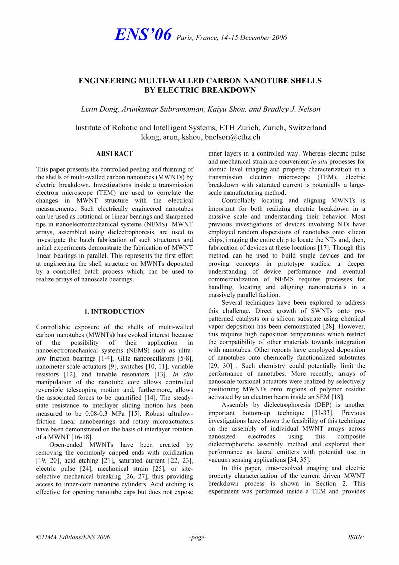
A TEM Electric breakdown experiments were performed in a CM30 TEM equipped with a STM built in a TEM holder (Nanofactory Instruments AB, ST-1000) serving as a manipulator as shown in Figure 1 (a) or schematically in Figure 1 (b). The material consisting of a CNT bundle is attached to a 0.35mm thick Au wire using silver paint, and the wire is held in the specimen holder. The probe is an etched 10 µm thick tungsten wire with a tip radius of approximately 100nm (Picoprobe, T-4-10-1mm). The probe can be positioned in a millimeter-scale workspace with sub-nanometer resolution with the STM unit actuated by a three-degree-of-freedom piezo-tube, making it possible to select a specific CNT. Physical contact can be made between the probe and the tip of a nanotube. Applying a voltage between the probe and the sample holder establishes an electrical circuit through a CNT.
Figure 1. Nanorobotic manipulation system in a TEM. (a) ST1000 STM-TEM holder (Nanofactory). (b) Schematic experiment setup.
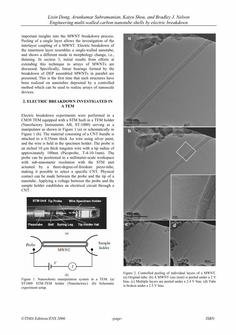
Figure 2. Controlled peeling of individual layers of a MWNT. (a) Original tube. (b) A MWNT (see inset) is peeled under a 2 V bias. (c) Multiple layers are peeled under a 2.4 V bias. (d) Tube is broken under a 2.5 V bias.
Lixin Dong, Arunkumar Subramanian, Kaiyu Shou, and Bradley J. Nelson Engineering multi-walled carbon nanotube shells by electric breakdown
©TIMA Editions/ENS 2006 -page- ISBN:
-80000
-40000
0
40000
80000
-2000 -1000 0 1000 2000
Voltage [mV]
Cur
rent
[nA
]
-150000
-75000
0
75000
150000
-2000 -1000 0 1000 2000
Voltage [mV]
Cur
rent
[nA]
70
75
80
85
0 10 20 30 40 50
Time [s]
Cur
rent
[ µA
]
0
20
40
60
80
0 10 20 30 40 50 60
Time [s]
Cur
rent
[ µA
]
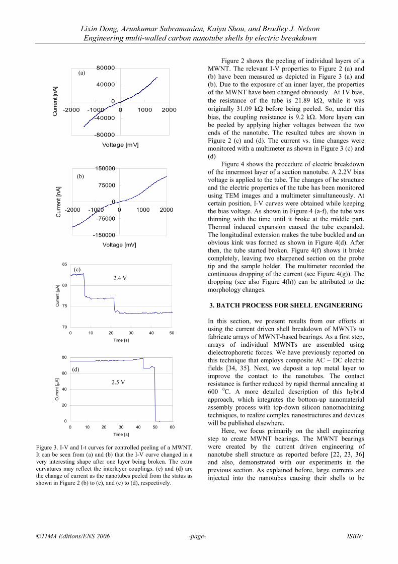
Figure 3. I-V and I-t curves for controlled peeling of a MWNT. It can be seen from (a) and (b) that the I-V curve changed in a very interesting shape after one layer being broken. The extra curvatures may reflect the interlayer couplings. (c) and (d) are the change of current as the nanotubes peeled from the status as shown in Figure 2 (b) to (c), and (c) to (d), respectively.
Figure 2 shows the peeling of individual layers of a MWNT. The relevant I-V properties to Figure 2 (a) and (b) have been measured as depicted in Figure 3 (a) and (b). Due to the exposure of an inner layer, the properties of the MWNT have been changed obviously. At 1V bias, the resistance of the tube is 21.89 kΩ, while it was originally 31.09 kΩ before being peeled. So, under this bias, the coupling resistance is 9.2 kΩ. More layers can be peeled by applying higher voltages between the two ends of the nanotube. The resulted tubes are shown in Figure 2 (c) and (d). The current vs. time changes were monitored with a multimeter as shown in Figure 3 (c) and (d)
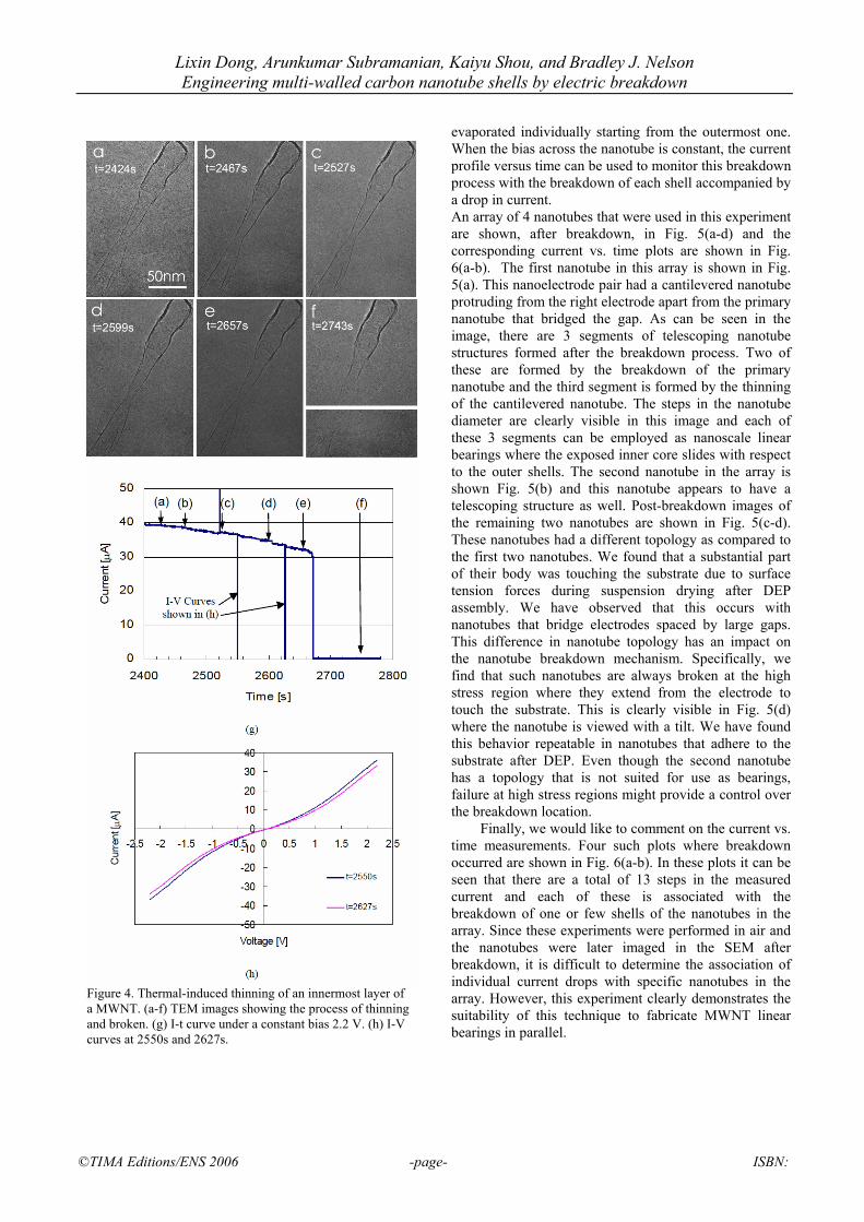
Figure 4 shows the procedure of electric breakdown of the innermost layer of a section nanotube. A 2.2V bias voltage is applied to the tube. The changes of he structure and the electric properties of the tube has been monitored using TEM images and a multimeter simultaneously. At certain position, I-V curves were obtained while keeping the bias voltage. As shown in Figure 4 (a-f), the tube was thinning with the time until it broke at the middle part. Thermal induced expansion caused the tube expanded. The longitudinal extension makes the tube buckled and an obvious kink was formed as shown in Figure 4(d). After then, the tube started broken. Figure 4(f) shows it broke completely, leaving two sharpened section on the probe tip and the sample holder. The multimeter recorded the continuous dropping of the current (see Figure 4(g)). The dropping (see also Figure 4(h)) can be attributed to the morphology changes.
3. BATCH PROCESS FOR SHELL ENGINEERING In this section, we present results from our efforts at using the current driven shell breakdown of MWNTs to fabricate arrays of MWNT-based bearings. As a first step, arrays of individual MWNTs are assembled using dielectrophoretic forces. We have previously reported on this technique that employs composite AC – DC electric fields [34, 35]. Next, we deposit a top metal layer to improve the contact to the nanotubes. The contact resistance is further reduced by rapid thermal annealing at 600 0C. A more detailed description of this hybrid approach, which integrates the bottom-up nanomaterial assembly process with top-down silicon nanomachining techniques, to realize complex nanostructures and devices will be published elsewhere.
Here, we focus primarily on the shell engineering step to create MWNT bearings. The MWNT bearings were created by the current driven engineering of nanotube shell structure as reported before [22, 23, 36] and also, demonstrated with our experiments in the previous section. As explained before, large currents are injected into the nanotubes causing their shells to be
(a)
(b)
(c)
(d)
2.5 V
2.4 V
Lixin Dong, Arunkumar Subramanian, Kaiyu Shou, and Bradley J. Nelson Engineering multi-walled carbon nanotube shells by electric breakdown
©TIMA Editions/ENS 2006 -page- ISBN:
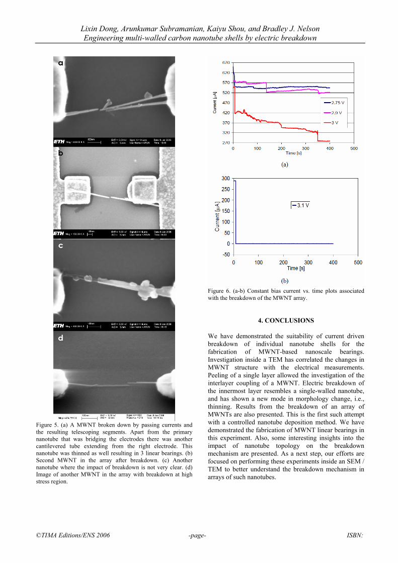
evaporated individually starting from the outermost one. When the bias across the nanotube is constant, the current profile versus time can be used to monitor this breakdown process with the breakdown of each shell accompanied by a drop in current. An array of 4 nanotubes that were used in this experiment are shown, after breakdown, in Fig. 5(a-d) and the corresponding current vs. time plots are shown in Fig. 6(a-b). The first nanotube in this array is shown in Fig. 5(a). This nanoelectrode pair had a cantilevered nanotube protruding from the right electrode apart from the primary nanotube that bridged the gap. As can be seen in the image, there are 3 segments of telescoping nanotube structures formed after the breakdown process. Two of these are formed by the breakdown of the primary nanotube and the third segment is formed by the thinning of the cantilevered nanotube. The steps in the nanotube diameter are clearly visible in this image and each of these 3 segments can be employed as nanoscale linear bearings where the exposed inner core slides with respect to the outer shells. The second nanotube in the array is shown Fig. 5(b) and this nanotube appears to have a telescoping structure as well. Post-breakdown images of the remaining two nanotubes are shown in Fig. 5(c-d). These nanotubes had a different topology as compared to the first two nanotubes. We found that a substantial part of their body was touching the substrate due to surface tension forces during suspension drying after DEP assembly. We have observed that this occurs with nanotubes that bridge electrodes spaced by large gaps. This difference in nanotube topology has an impact on the nanotube breakdown mechanism. Specifically, we find that such nanotubes are always broken at the high stress region where they extend from the electrode to touch the substrate. This is clearly visible in Fig. 5(d) where the nanotube is viewed with a tilt. We have found this behavior repeatable in nanotubes that adhere to the substrate after DEP. Even though the second nanotube has a topology that is not suited for use as bearings, failure at high stress regions might provide a control over the breakdown location.
Finally, we would like to comment on the current vs. time measurements. Four such plots where breakdown occurred are shown in Fig. 6(a-b). In these plots it can be seen that there are a total of 13 steps in the measured current and each of these is associated with the breakdown of one or few shells of the nanotubes in the array. Since these experiments were performed in air and the nanotubes were later imaged in the SEM after breakdown, it is difficult to determine the association of individual current drops with specific nanotubes in the array. However, this experiment clearly demonstrates the suitability of this technique to fabricate MWNT linear bearings in parallel.
Figure 4. Thermal-induced thinning of an innermost layer of a MWNT. (a-f) TEM images showing the process of thinning and broken. (g) I-t curve under a constant bias 2.2 V. (h) I-V curves at 2550s and 2627s.
Lixin Dong, Arunkumar Subramanian, Kaiyu Shou, and Bradley J. Nelson Engineering multi-walled carbon nanotube shells by electric breakdown
©TIMA Editions/ENS 2006 -page- ISBN:
Figure 5. (a) A MWNT broken down by passing currents and the resulting telescoping segments. Apart from the primary nanotube that was bridging the electrodes there was another cantilevered tube extending from the right electrode. This nanotube was thinned as well resulting in 3 linear bearings. (b) Second MWNT in the array after breakdown. (c) Another nanotube where the impact of breakdown is not very clear. (d) Image of another MWNT in the array with breakdown at high stress region.
Figure 6. (a-b) Constant bias current vs. time plots associated with the breakdown of the MWNT array.
4. CONCLUSIONS We have demonstrated the suitability of current driven breakdown of individual nanotube shells for the fabrication of MWNT-based nanoscale bearings. Investigation inside a TEM has correlated the changes in MWNT structure with the electrical measurements. Peeling of a single layer allowed the investigation of the interlayer coupling of a MWNT. Electric breakdown of the innermost layer resembles a single-walled nanotube, and has shown a new mode in morphology change, i.e., thinning. Results from the breakdown of an array of MWNTs are also presented. This is the first such attempt with a controlled nanotube deposition method. We have demonstrated the fabrication of MWNT linear bearings in this experiment. Also, some interesting insights into the impact of nanotube topology on the breakdown mechanism are presented. As a next step, our efforts are focused on performing these experiments inside an SEM / TEM to better understand the breakdown mechanism in arrays of such nanotubes.
Lixin Dong, Arunkumar Subramanian, Kaiyu Shou, and Bradley J. Nelson Engineering multi-walled carbon nanotube shells by electric breakdown
©TIMA Editions/ENS 2006 -page- ISBN:
REFERENCES [1] J. Cumings and A. Zettl, "Low-friction nanoscale linear bearing
realized from multiwall carbon nanotubes," Science, vol. 289, no. 5479, pp. 602-604, Jul 2000.
[2] A. N. Kolmogorov and V. H. Crespi, "Smoothest bearings: Interlayer sliding in multiwalled carbon nanotubes," Physical Review Letters, vol. 85, no. 22, pp. 4727-4730, Nov 2000.
[3] A. Kis, K. Jensen, S. Aloni, W. Mickelson, and A. Zettl, "Interlayer forces and ultralow sliding friction in multiwalled carbon nanotubes," Physical Review Letters, vol. 97, no. 2, p. 025501, Jul 2006.
[4] P. Tangney, S. G. Louie, and M. L. Cohen, "Dynamic sliding friction between concentric carbon nanotubes," Physical Review Letters, vol. 93, no. 6, p. 065503, Aug 2004.
[5] Q. S. Zheng and Q. Jiang, "Multiwalled carbon nanotubes as gigahertz oscillators," Physical Review Letters, vol. 88, no. 4, p. 045503, Jan 2002.
[6] Q. S. Zheng, J. Z. Liu, and Q. Jiang, "Excess van der Waals interaction energy of a multiwalled carbon nanotube with an extruded core and the induced core oscillation," Physical Review B, vol. 65, no. 24, p. 245409, Jun 2002.
[7] J. L. Rivera, C. McCabe, and P. T. Cummings, "Oscillatory behavior of double-walled nanotubes under extension: A simple nanoscale damped spring," Nano Letters, vol. 3, no. 8, pp. 1001-1005, Aug 2003.
[8] W. L. Guo, Y. F. Guo, H. J. Gao, Q. S. Zheng, and W. Y. Zhong, "Energy dissipation in gigahertz oscillators from multiwalled carbon nanotubes," Physical Review Letters, vol. 91, no. 12, p. 125501, Sep 2003.
[9] L. X. Dong, B. J. Nelson, T. Fukuda, and F. Arai, "Towards nanotube linear servomotors," IEEE Transactions on Automation Science and Engineering, vol. 3, no. 3, pp. 228-235, Jul 2006.
[10] L. Forro, "Nanotechnology - Beyond Gedanken experiments," Science, vol. 289, no. 5479, pp. 560-561, Jul 2000.
[11] V. V. Deshpande, H. Y. Chiu, H. W. C. Postma, C. Miko, L. Forro, and M. Bockrath, "Carbon nanotube linear bearing nanoswitches," Nano Letters, vol. 6, no. 6, pp. 1092-1095, Jun 2006.
[12] J. Cumings and A. Zettl, "Localization and nonlinear resistance in telescopically extended nanotubes," Physical Review Letters, vol. 93, no. 8, p. 086801, Aug 2004.
[13] K. Jensen, C. Girit, W. Mickelson, and A. Zettl, "Tunable nanoresonators constructed from telescoping nanotubes," Physical Review Letters, vol. 96, no. 21, p. 215503, Jun 2006.
[14] M. F. Yu, O. Lourie, M. J. Dyer, K. Moloni, T. F. Kelly, and R. S. Ruoff, "Strength and breaking mechanism of multiwalled carbon nanotubes under tensile load," Science, vol. 287, no. 5453, pp. 637-640, Jan 2000.
[15] M. F. Yu, B. I. Yakobson, and R. S. Ruoff, "Controlled sliding and pullout of nested shells in individual multiwalled carbon nanotubes," Journal of Physical Chemistry B, vol. 104, no. 37, pp. 8764-8767, Sep 2000.
[16] A. M. Fennimore, T. D. Yuzvinsky, W. Q. Han, M. S. Fuhrer, J. Cumings, and A. Zettl, "Rotational actuators based on carbon nanotubes," Nature, vol. 424, no. 6947, pp. 408-410, Jul 2003.
[17] B. Bourlon, D. C. Glattli, C. Miko, L. Forro, and A. Bachtold, "Carbon nanotube based bearing for rotational motions," Nano Letters, vol. 4, no. 4, pp. 709-712, Apr 2004.
[18] T. D. Yuzvinsky, A. M. Fennimore, A. Kis, and A. Zettl, "Controlled placement of highly aligned carbon nanotubes for the manufacture of arrays of nanoscale torsional actuators," Nanotechnology, vol. 17, no. 2, pp. 434-438, Jan 2006.
[19] P. M. Ajayan, T. W. Ebbesen, T. Ichihashi, S. Iijima, K. Tanigaki, and H. Hiura, "Opening Carbon Nanotubes with Oxygen and
Implications for Filling," Nature, vol. 362, no. 6420, pp. 522-525, 1993.
[20] S. C. Tsang, P. J. F. Harris, and M. L. H. Green, "Thinning and Opening of Carbon Nanotubes by Oxidation Using Carbon-Dioxide," Nature, vol. 362, no. 6420, pp. 520-522, 1993.
[21] S. C. Tsang, Y. K. Chen, P. J. F. Harris, and M. L. H. Green, "A Simple Chemical Method of Opening and Filling Carbon Nanotubes," Nature, vol. 372, no. 6502, pp. 159-162, Nov 1994.
[22] P. G. Collins, M. S. Arnold, and P. Avouris, "Engineering carbon nanotubes and nanotube circuits using electrical breakdown," Science, vol. 292, no. 5517, pp. 706-709, Apr 2001.
[23] P. G. Collins, M. Hersam, M. Arnold, R. Martel, and P. Avouris, "Current saturation and electrical breakdown in multiwalled carbon nanotubes," Physical Review Letters, vol. 86, no. 14, pp. 3128-3131, Apr 2001.
[24] J. Cumings, P. G. Collins, and A. Zettl, "Materials - Peeling and sharpening multiwall nanotubes," Nature, vol. 406, no. 6796, pp. 586-586, Aug 2000.
[25] H. D. Wagner, O. Lourie, Y. Feldman, and R. Tenne, "Stress-induced fragmentation of multiwall carbon nanotubes in a polymer matrix," Applied Physics Letters, vol. 72, no. 2, pp. 188-190, Jan 1998.
[26] L. X. Dong, F. Arai, and T. Fukuda, "Three-dimensional nanoassembly of multi-walled carbon nanotubes through nanorobotic manipulations by using electron-beam-induced deposition," in Proc. of 2001 1st IEEE Conf. on Nanotechnology (IEEE-NANO2001), MAUI, HAWAII, 2001, pp. 93-98.
[27] L. X. Dong, F. Arai, and T. Fukuda, "Destructive constructions of nanostructures with carbon nanotubes through nanorobotic manipulation," IEEE/ASME Transactions on Mechatronics, vol. 9, no. 2, pp. 350-357, Jun 2004.
[28] Y. Tseng, P. Xuan, A. Javey, R. Malloy, Q. Wang, J. Bokor, and H. Dai, "Monolithic integration of carbon nanotube devices with silicon MOS technology," Nano Lett., vol. 4, no. 1, pp. 123-127, 2004.
[29] J. Liu, M. J. Casavant, M. Cox, D. A. Walters, P. Boul, W. Lu, A. J. Rimberg, K. A. Smith, T. Colbert, and R. E. Smalley, "Controlled deposition of individual single-walled carbon nanotubes on chemically functionalized templates," Chem. Phys. Lett., vol. 303, pp. 125-129, 1999.
[30] S. G. Rao, L. Huang, W. Setyawan, and S. Hong, "Large-scale assembly of carbon nanotubes," Nature, vol. 425, pp. 36-37, 2003.
[31] K.Yamamoto, S. Akita, and Y. J. Nakayama, "Orientation and purification of carbon nanotubes using ac electrophoresis," J. Phys. D - Appl. Phys., vol. 31, no. 8, pp. L34-L36, 1998.
[32] S. B. Asokan, L. Jawerth, R. L. Carroll, R. E. Cheney, S. Washburn, and R. Superfine, "Two-dimensional manipulation and orientation of actin-myosin systems with dielectrophoresis," Nano Lett., vol. 3, no. 4, pp. 431-437, 2003.
[33] C. S. Lao, J. Liu, P. Gao, L. Zhang, D. Davidovic, R. Tummala, and Z. L. Wang, "ZnO nanobelt/nanowire Schottky diodes formed by dielectrophoresis alignment across Au electrodes," Nano Lett., vol. 6, no. 2, pp. 263-266, 2006.
[34] A. Subramanian, L. X. Dong, and B. J. Nelson, "Assembly of arrays of individual lateral nanotube emitters on nanoelectrodes," in Proc. of 2005 5th IEEE Int. Conf. on Nanotechnology (IEEE-NANO2005) 2005, pp. 362-365.
[35] A. Subramanian, B. Vikramaditya, L. X. Dong, D. J. Bell, and B. J. Nelson, "Micro and Nanorobotic Assembly Using Dielectrophoresis," in Robotics: Science and Systems I, S. Thrun, G. S. Sukhatme, S. Schaal, and O. Brock, Eds.: MIT Press, 2005, pp. 327-334.
[36] J. Y. Huang, S. Chen, S. H. Jo, Z. Wang, D. X. Han, G. Chen, M. S. Dresselhaus, and Z. F. Ren, "Atomic-scale imaging of wall-by-wall breakdown and concurrent transport measurements in multiwall carbon nanotubes," Physical Review Letters, vol. 94, no. 23, p. 236802, Jun 2005.