EMC - system immunity against electrostatic discharges webinar
45
EMC - system immunity against electrostatic discharges webinar How to protect applications against ESD Estelle ASTAR Mathieu ROUVIERE Vladimir JANOUSEK
EMC - system immunity against electrostatic discharges webinarHow to protect applications against ESD
Estelle ASTAR
Mathieu ROUVIERE
Vladimir JANOUSEK
Presenter
Presentation Notes
OLM
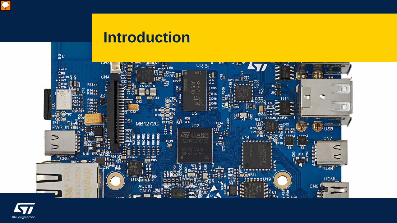
Introduction
Presenter
Presentation Notes
Estelle Thank-you (Yvonne) for this introduction. Hello everyone and thanks for attending this webinar. My name is Estelle Astar and I am glad to start this seminar about EMC systems immunity against ESD. As an introduction lets define what is EMS immunity and what it means for you when you design an electronic Printed Circuit Board
• EMC Immunity is the ability of an equipment to properly operate in its electromagnetic environment by limiting the interference of electromagnetic energy that may cause physical damage.
Defining EMC immunity
3
What is EMC immunity ?
Electronic application
Radiated emissionRadiated immunity
Conducted emissionConducted immunity
Presenter
Presentation Notes
Estelle : EMC stands for ElectroMagnetic Compatibility. EMC Immunity is the ability for an equipment to properly operate in its electromagnetic environement by limiting the reception of electromagnetic energy that may cause physical damages. Electrostatic Discharge called ESD fall into this category. ESD can be either conducted under the form of a Transient Voltage, but it can be also radiated due to its fast raising time, generating harmonics, powerfull enough to generate erratic behavior of your application by coupling with other signals. It means that ESD is a threat against which your printed Circuit Boards must be protected
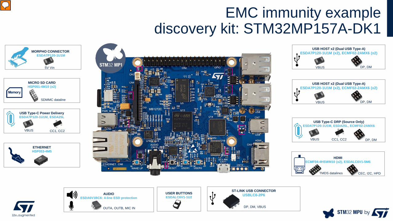
USB HOST x2 (Dual USB Type-A)ESDA7P120-1U1M (x2), ECMF02-2AMX6 (x2)
VBUS DP, DM
USB Type-C DRP (Source Only)ESDA7P120-1U1M, ESDA25L, ECMF02-2AMX6
CC1, CC2VBUS
USB HOST x2 (Dual USB Type-A)ESDA7P120-1U1M (x2), ECMF02-2AMX6 (x2)
VBUS DP, DM
DP, DM
HDMIECMF04-4HSWM10 (x2), ESDALC6V1-5M6
CEC, I2C, HPDTMDS datalines
MORPHO CONNECTORESDA7P120-1U1M
5V Vin
USER BUTTONSESDALC6V1-1U2
MICRO SD CARDHSP051-4M10 (x2)
SDMMC dataline
ST-LINK USB CONNECTORUSBLC6-2P6
ETHERNETHSP053-4M5
DP, DM, VBUS
Presenter
Presentation Notes
Here is an example of EMC Immunity. At STMicroelectronics, we ensure that our Printed Circuit Boards embed ESD protections for all connectors that may be subjected to Electrostatic discharges. As you can see there are many ESD protection references in this board, so for a HW PCB designer it can be a tricky job to select the correct ESD protection according to the connector. Source: Schematic in STM32MP157A-DK1: Discovery kit with STM32MP157A MPU https://www.st.com/content/ccc/resource/technical/layouts_and_diagrams/schematic_pack/group0/36/8e/ea/7a/ca/ca/4b/e4/mb1272-dk2-c01_schematic/files/MB1272-DK2-C01_Schematic.pdf/jcr:content/translations/en.MB1272-DK2-C01_Schematic.pdf
• ESD Protection at System Level• How to select an ESD protection device?• ESD Layout Guidelines• Application Examples
Agenda
5
Presenter
Presentation Notes
So let’s review today what ESD protection at system level means and what are the different standards behind. Then we will explain you the selection steps for an ESD protection component. Finally we will detail the layout guidelines to properly fit the ESD protection in your design.
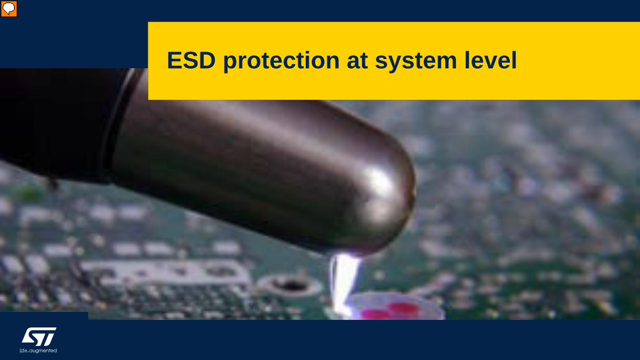
ESD protection at system level
Presenter
Presentation Notes
In this first part, I would like to remind you how ESD is generated in everyday’s life and why we should care about it in our electronic applications
ESD is the result of static electricity discharges. Static electricity is the collection of electrically charged particles on the surface of a material. Various materials have a tendency of either - giving up electrons and gaining positive (+) charges or - attracting electrons and gaining negative (-) charges. The list of these materials in the order of how much they become positive (+) or negative (-) is called the Triboelectric Series. A discharge of tens of kilo-volts may occur and the arc that appears is called “ESD”. Here are some examples of voltage levels. For instance, walking across a carpet is a worse case, generating up to 35 kilo Volt Discharging that amount into Integrated Circuits is not without risk !
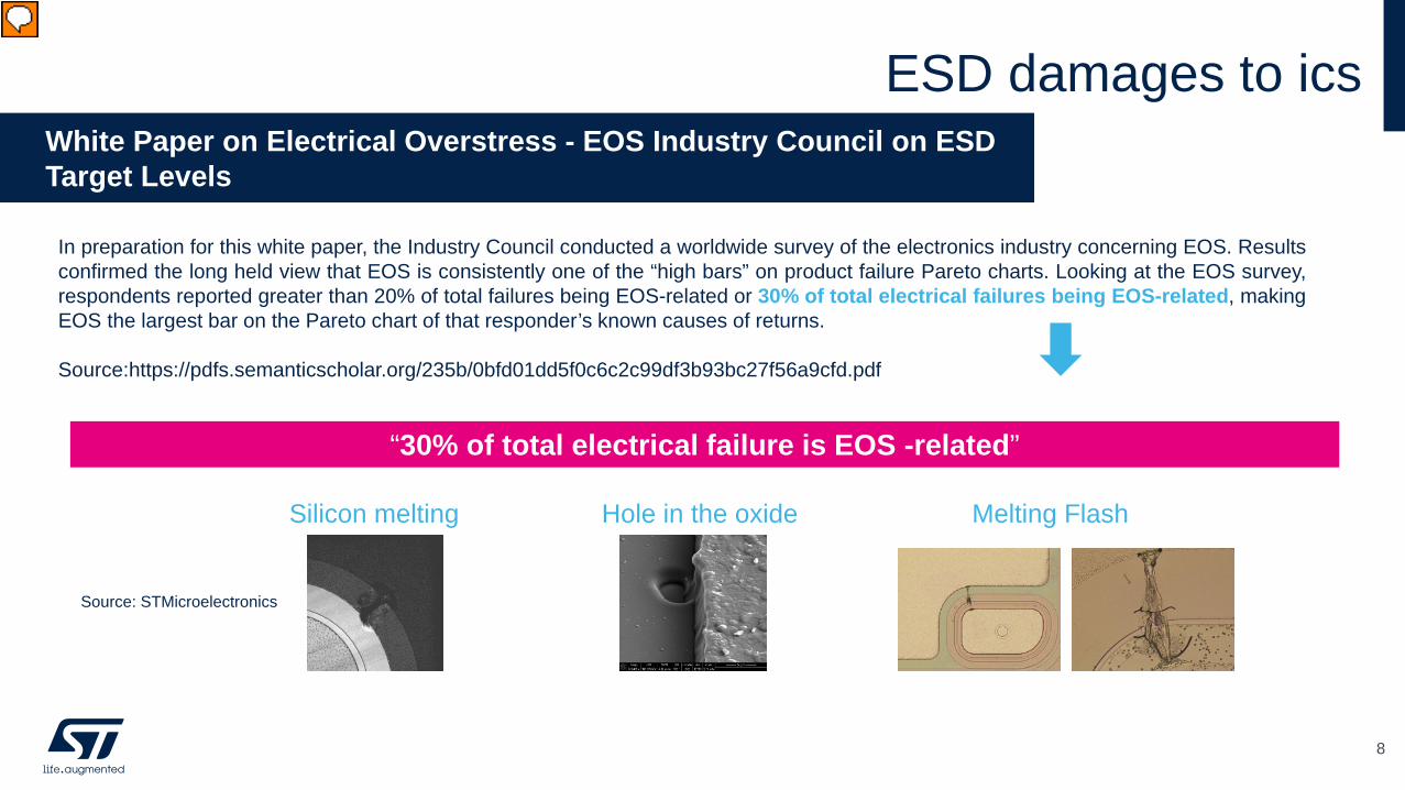
White Paper on Electrical Overstress - EOS Industry Council on ESD Target Levels
In preparation for this white paper, the Industry Council conducted a worldwide survey of the electronics industry concerning EOS. Resultsconfirmed the long held view that EOS is consistently one of the “high bars” on product failure Pareto charts. Looking at the EOS survey,respondents reported greater than 20% of total failures being EOS-related or 30% of total electrical failures being EOS-related, makingEOS the largest bar on the Pareto chart of that responder’s known causes of returns.
Electrostatic Discharge will cause potential failure on the Integrated Circuits of your PCB. These failures are called Electrical Over Stress or EOS, resulting in Silicon melting, oxide punch-through, junction damage, metallization damage or degradation affecting the long-term reliability of your electronic system. A Survey from the EOS Industry Council shows that 30% of customer claims are due to ESD or EOS. Furthermore, the miniaturization of the components is increasing the integrated circuits sensitivity to ESD
ESD sensitivity is increasing
9
Vdd = power supply voltageVBD = breakdown voltage
V
2V
8V
Presenter
Presentation Notes
Here is a graph, showing power supply voltage (VDD) and breakdown voltage (VBD) of various semiconductor technologies used for Integrated Circuits. The breakdown voltage (VBD), and the power supply line (Vdd) are decreasing year after year. The ESD design window, that is the difference between VBD and Vdd, is also decreasing drastically from 8V margin in 1999 to only 2V margin in nowadays technologies. This illustrates that ESD sensitivity is increasing in Integrated Circuits and that it is necessary to protect these sensitive ICs with a specific, external ESD protection.
ESD and EOS standards
10
ESD and EOS standards
ESDElectro-Static Discharge
EOSElectrical Over
Stress
Component levelto ensure manufacturability
System levelto assure
robustness
HBMHuman Body
Model
CDMCharged Device
model
MMMachine Model
ISO7637ISO16750
IEC 61000-4-2ISO10605 (auto)
Final user simulation
System robustness for end users. Uncontrolled environment.These standards have low-level surges as factories are well-controlled environments.
System levelto simulate car
behavior
Presenter
Presentation Notes
Now, there are different standards for ESD, and two major cases: The first one on the left side is related to component-level ESD. This is to ensure the manufacturability of Integrated Circuits. These standards reproduce ESD during manufacturing processes which means the ESD risk is mitigated by using specific equipment in a controlled environment for manufacturing. For example, technicians can wear anti-static shoes, and there are De-ionizers to avoid air-charging. Each person or equipment must be connected to the ground in order to allow a discharge path. The related standards are: - HBM (Human Body Model) that simulates ESD due to discharge from human being, - MM (Machine Model) that simulates a machine ESD discharging through a device to ground - CDM (Charged Device Model) that simulates ESD due to mechanical device handling The ESD protection according to these standards concerns any Integrated Circuit. It is called on-chip ESD protection. - The second case on the right side, is related to System-Level ESD and this is the case that occurs in our everyday’s life. The IEC61000-4-2 standard simulates a whole system that may be subjected to ESD. For instance, walking on a carpet with a vinyl suit could generate, on a dry environment, several tens of kilovolt of electrostatic discharges as presented in the introduction. In this case, the only way to manage an ESD event is to add a dedicated ESD Protection mounted on the PCB and placed in the critical discharge path. The automotive standard ISO10605 is also part of System-Level ESD.
Energy for 8kV IEC 61000-4-2Energy for 8kV HBMEnergy for 2kV HBM
HV supply
R(MΩ) 1500Ω
DUT100pF
Human Body Model for IC(+/-2kV for most of IC)
HV supply
R(MΩ) 330Ω
DUT150pF
IEC 61000-4-2 for system(+/-8kV for level 4)
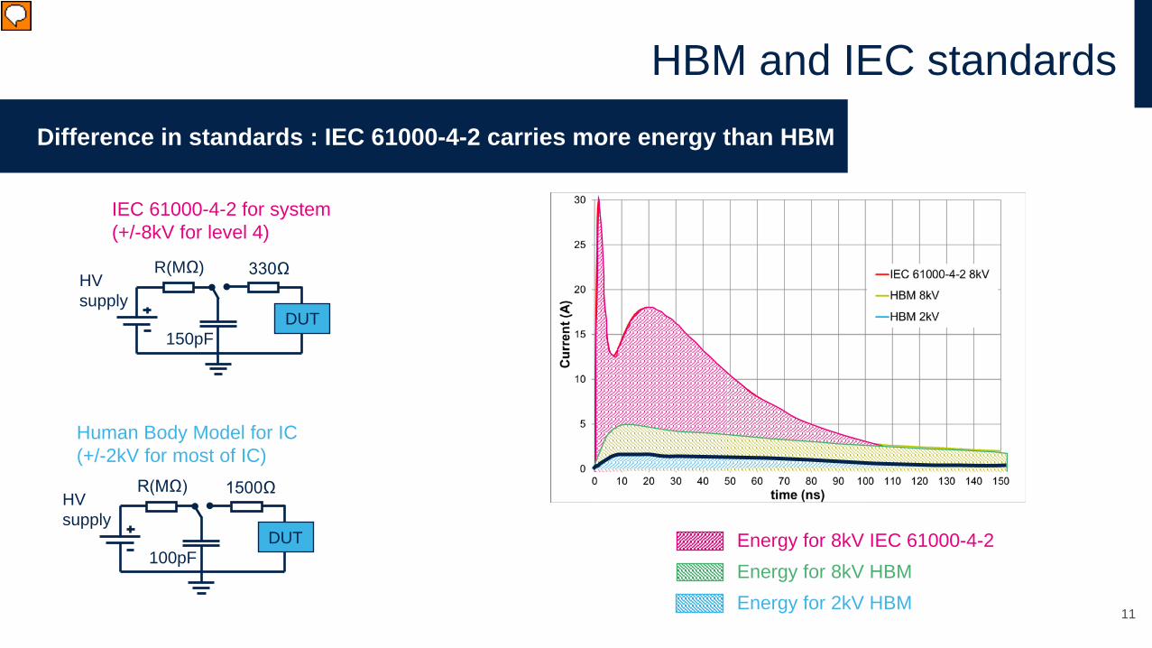
HBM and IEC standards
11
Difference in standards : IEC 61000-4-2 carries more energy than HBM
Presenter
Presentation Notes
What are the main differences between HBM (Human Body Model) and IEC standards ? From our experience, people do not often understand the difference between these 2 standards. On the left side, the electrical circuits modelize the equivalent ESD waveform associated to each standard. The IEC standard is modelized by a larger capacitance discharge (150 pF for IEC vs 100 pF for HBM) and this capacitance is discharged through a much lower resistor (330 ohms for IEC compared to 1.5 kilo-ohm for HBM). On the right side, we compare the energy carried by the current waveform of these two standards - For the 8 kV IEC, the current is in red here - With same 8 kV voltage, HBM current is in green - for 2 kV HBM that is the most common level specified for Integrated Circuits, we obtain the blue curve The energy of ESD, that corresponds to the surface bellow the curves, is much lower for 2kV HBM compared to 8kV IEC 61000-4-2. As consequence, IEC 61000-4-2 CARRIES MORE ENERGY THAN HBM This is why an Integrated Circuit exposed to ESD and specified with HBM will still require an external ESD protection rated per the IEC standard.
Silicon die area for component level ESD
(2 kV HBM)
Silicon die area for system level ESD
(8 kV IEC contact)
Component level vs system levelsilicon die area comparison
12
Presenter
Presentation Notes
You may wonder why Integrated Circuits do not feature system-level ESD protection ? So let’s try to figure out what would be the size of a system-level ESD Protection integrated in a IC : Here we show two integrated circuit protection layout using the same scale thanks to pad surface. On the right side, you can see the size of an IEC Protection 8 KV which is much bigger than the size of the 2 KV HBM protection at the left. This means integrating 8kV IEC protection is not cost effective in expensive advanced MOS technologies. This is why the system level ESD Protection is kept external, using specific silicon technologies.
13
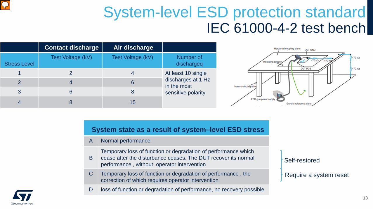
System-level ESD protection standardIEC 61000-4-2 test bench
Contact discharge Air discharge
Stress Level Test Voltage (kV) Test Voltage (kV) Number of
dischargeq
1 2 4 At least 10 singledischarges at 1 Hz in the most sensitive polarity
2 4 6
3 6 8
4 8 15
System state as a result of system–level ESD stress A Normal performance
BTemporary loss of function or degradation of performance which cease after the disturbance ceases. The DUT recover its normal performance , without operator intervention
C Temporary loss of function or degradation of performance , the correction of which requires operator intervention
D loss of function or degradation of performance, no recovery possible
Self-restored
Require a system reset
Presenter
Presentation Notes
Now let’s review the IEC61000-4-2 standard. This is a system level standard, it is not related to component, so it applies to a complete application, with its enclosure. This standard defines 4 stress levels and 4 levels of results. The most severe level is level 4 with 8 KV contact and 15 KV air applied. The test result is rated A when the Device Under Test performs normally without any disturbances At STMicroelectronics, all ESD protection components comply or exceed this level 4.
Configuration ModeComponent acessible
from:
Test(A= Air
C= contact)Capacitance Resistance Max test
voltageOperatingconditions
Min number
of dischar
ges
Min. time interval
Max suggested
severity levels (ISO10605 Annex C)
Component Direct Inside A & C 330 pF 330 ohm - Powered 3 1s 15 kV C25kV A
Component Direct Outside A & C 150 pF 330 ohm - Powered 3 1s 15 kV C25kV A
Component Indirect Inside C 330 pF 330 ohm - Powered 50 50ms 20kV C
Component Indirect Outside C 150 pF 330 ohm - Powered 50 1s 20kV C
Component packaging and handling
Direct NA A & C 150 pF 330 or 2000 ohm - Unpowered 3 1s
Vehicle test Direct Inside A & C 330 pF 330 or 2000 ohm 15 kV Engine drive or idle 3 1s 8kV C
15kV A
Vehicle test Direct Outside A & C 150 pF 330 or 2000 ohm 25 kV Engine drive or idle 3 1s 8kV C
25kV A
ESD in automotive: ISO10605
14
Presenter
Presentation Notes
For Automotive applications, the ISO10605 standard applies. It is more severe than IEC standard because of - a higher capacitance used for discharge: three hundred thirty pico farad instead of 150pF for IEC - a higher number of discharges: 50 instead of 10 for IEC - A higher frequency to apply the ESD pulse to the component - A higher level of applied voltage: up to 25kV at contact discharge instead of 8kV for IEC On top of specific semiconductor reliability testing, automotive ESD protection are usually priced higher than ESD protections used in consumer or industrial applications. So now, let’s review how to select the right ESD protection component for your application.
How to select ESD protection device
Presenter
Presentation Notes
Mathieu Now, we will present on this section the key parameters of an ESD protection. How these parameters can impact your system performance, And, at the end, I will give you some basic advices to select the right ESD protection component.
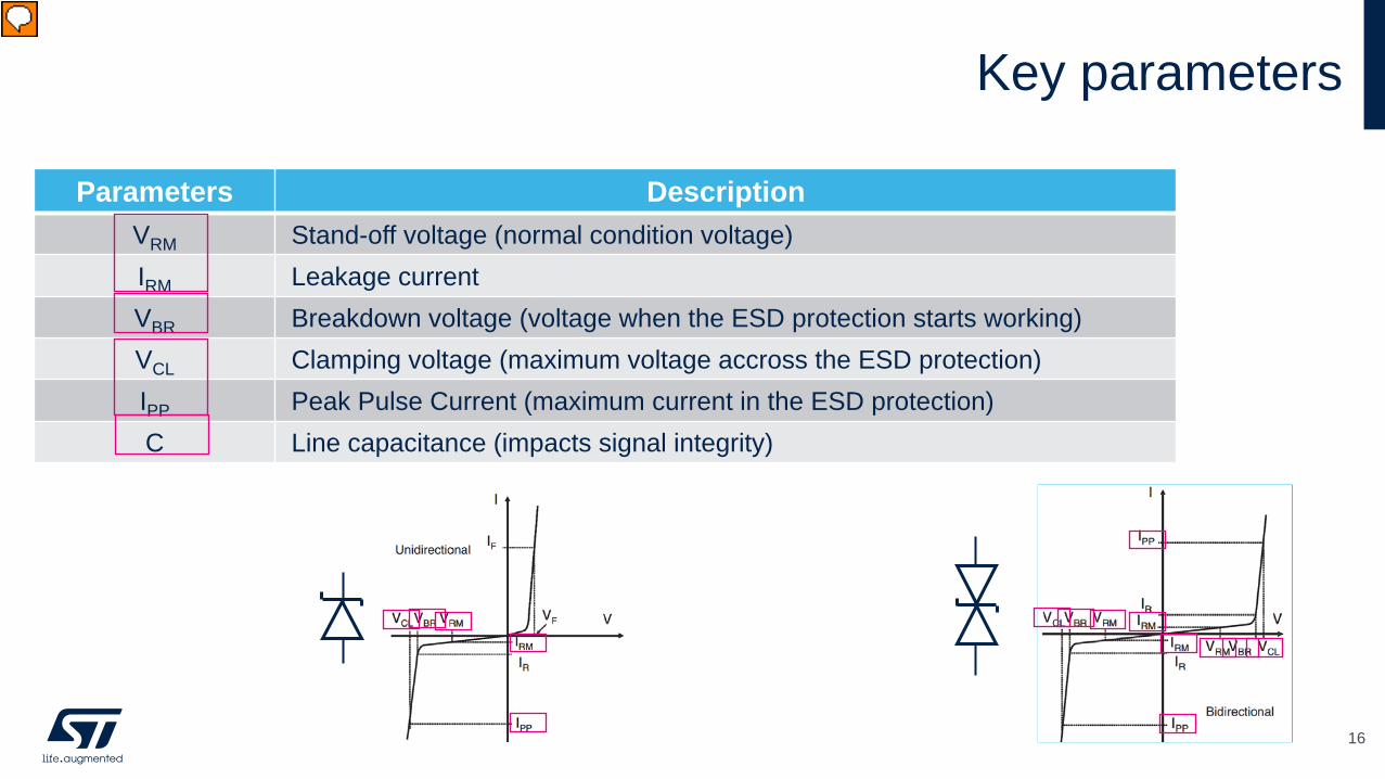
Parameters DescriptionVRM Stand-off voltage (normal condition voltage)IRM Leakage currentVBR Breakdown voltage (voltage when the ESD protection starts working)VCL Clamping voltage (maximum voltage accross the ESD protection)IPP Peak Pulse Current (maximum current in the ESD protection)C Line capacitance (impacts signal integrity)
Key parameters
16
Presenter
Presentation Notes
Mathieu Here are the key electrical symbols and abbreviations we will use so that you can get familiar with the vocabulary. Let’s review in detail each parameter. CLICK VRM stands for maximum reverse voltage. It corresponds to the maximum voltage of the protected line on normal operating condition. It is associated to IRM : the leakage current of the ESD protection. This current is very low to not impact the system consumption. It is typically much lower than 100nA. CLICK ESD protection starts to conduct at Breakdown voltage or VBR. This static voltage is usually measured at 1mA. It can be used to validate that the ESD protection is well mounted on the printed circuit board. CLICK During an ESD event, the surge current is flowing into the ESD protection. The maximum current that can flows into the ESD protection is called Peak pulse current. The associated voltage is called clamping voltage, VCL. The clamping voltage is the remaining voltage measured after the ESD protection. The lower the clamping voltage, the better the protection efficiency. CLICK The last key parameter is the line capacitance. In the frequency domain, an ESD protection can be modelized by a diode with a junction capacitance. This capacitance can impact the line signal intergrity as any extra-capacitor placed on a signal line. ESD protection can be uni-directional like I/V curve on the left or CLICK bi-directional like I/V curve on the right
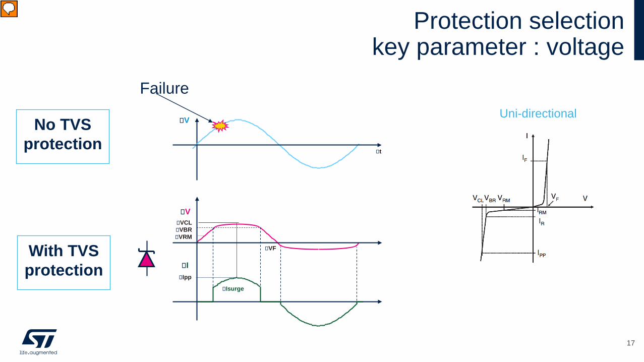
Protection selectionkey parameter : voltage
17
VBR
Isurge
VF
Ipp
VNo TVS protection
Failure
VCL
t
VRM
V
Uni-directional
IWith TVS protection
Presenter
Presentation Notes
Here is the principle of Transient Voltage Suppressor also called TVS. Keep in mind, that ESD protection is a sub class of TVS. Let’s consider an electrical signal, In blue. This is a Voltage curve function of time without TVS. Unfortunately, at a voltage higher than destruction voltage the system fails (animation). To avoid this system failure a protection is required (animation) A TVS is then used to clamp the voltage in pink and then to protect system. At Vbr or breakdown voltage, the TVS starts to conduct in green The current flows into the TVS and the resulting voltage is the clamping voltage. The forward voltage, Vf, of the TVS clamps the negative signal for a unidirectional protection. Another key parameter is the leakage current of the TVS itself. It’s the Irm defined at the maximum reverse DC voltage on normal operating condition, Vrm.
• Mandatory for audio and RF signals
Bi-directional
VBR
Isurge
Ipp
V
Failure
VCL
t
VRM
V
I
No TVS protection
With TVS protection
Key parametersvoltage polarity
18
Presenter
Presentation Notes
In case of a signal polarity which is both positive and negative, the TVS must be bi-directional In bi-directional TVS, the voltage thresholds are usually the same in both direction.
Time domain Frequency domain
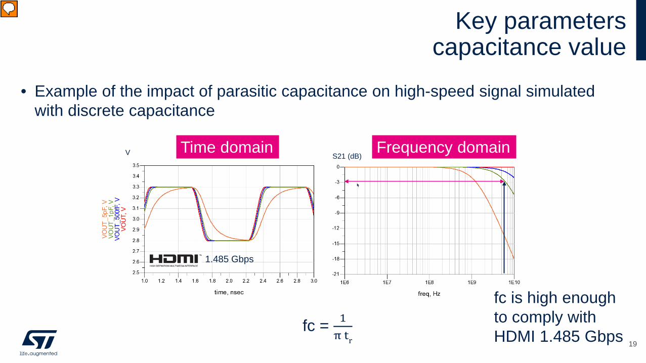
• Example of the impact of parasitic capacitance on high-speed signal simulated with discrete capacitance
Key parameterscapacitance value
19
fc = 1π tr
S21 (dB)V
1.485 Gbps
fc is high enough to comply with HDMI 1.485 Gbps
Presenter
Presentation Notes
The ESD protection must protect the IC or the application, but, must not impact the application in normal operation. For example, the parasitic capacitance of ESD protection devices must be low enough to allow USB 2.0 high-speed signals to be transmitted without degradation. A high parasitic capacitance of the ESD protection devices would increase too much the signal rise/fall time and prevent good communications. In one word, if the capacitance is too high, the rise and fall timeq will be too high and then the signal integrity will be impacted. To guarantee the Digital signal integrity, the following equation (animation) is used with Fc : cutoff frequency and tr : rise time The ESD Protection cut-off Frequency must be lower than the application operating Frequency (animation) A lower capacitance allows a larger bandwidth and a better signal integrity In our example, we can see that the orange curve representing 5pF capacitance is too high for USB2.0 signal. We can also see that a 1pF ESD Protection capacitance is OK.
Eye diagramwhat is an eye diagram?
20
1 0 1
0 1 0
0 1 1
1 1 0
0 0 1
1 0 0
0 0 0
1 1 1
0 0 0
0 0 1
0 1 0
0 1 1
1 0 0
1 0 1
1 1 0
1 1 1
Presenter
Presentation Notes
Indeed, eye diagram or eye pattern measurement is a tool to characterize the transmission quality. Click In digital communications the "eye diagram" is used to visualize how the waveforms used to send multiple bits of data can potentially lead to errors in the interpretation of those bits An eye diagram is produced by repetitively sampling a digital signal on an oscilloscope's vertical axis, while triggering the horizontal sweep with the data rate. Click Acceptable signal are often defined with the use of a mask, here in blue The mask usually consists of a polygon in the middle of the eye and rectangles above and below the eye. If the measured traces cross the mask boundaries the signal quality is considered unacceptable. High speed buses standards like HDMI, USB and so on… often specify eye diagram mask: if the measured traces cross the mask boundaries, the signal quality is considered unacceptable.
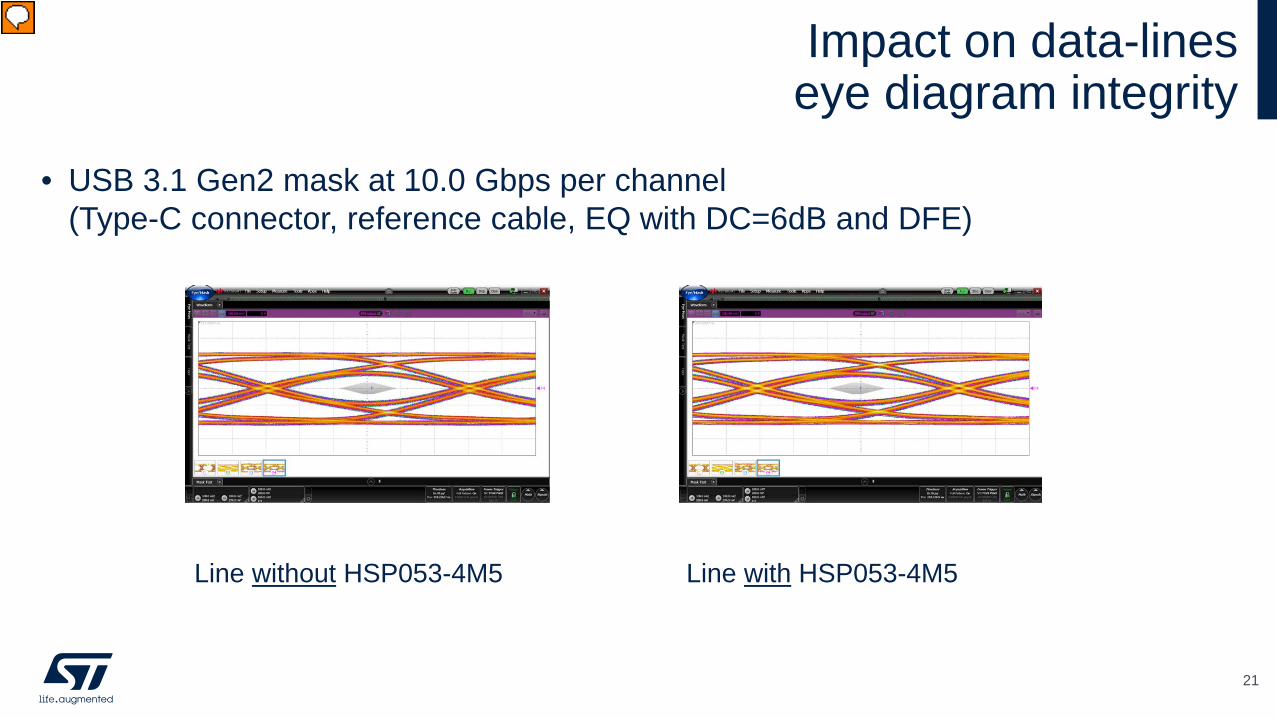
• USB 3.1 Gen2 mask at 10.0 Gbps per channel(Type-C connector, reference cable, EQ with DC=6dB and DFE)
Impact on data-lineseye diagram integrity
21
Line without HSP053-4M5 Line with HSP053-4M5
Presenter
Presentation Notes
On datasheets of ESD protection for high speed buses, eye diagrams are reported for various standards In this example, USB 3.1 Gen2 at 10.0Gbps per channel is reported. The measurement is performed on a line without ESD protection on left and with ESD protection on right We can visualize that there is no impact of the HSP053-4M4 on the USB 3.1 at 10GB/s per chanel signal. The signal integrity is respected.
Impact on data-linestime domain reflectometer impedance
22
TDR with 200ps pule rise time impedance of100Ω line without / with HSP053-4M5
ZLOAD
Step generator
50ΩZ0
Transmission Line
Oscilloscope Mainframe
SamplerZLOAD
Step generator
50ΩZ0
Transmission Line
Oscilloscope Mainframe
Sampler
Step generator
50ΩZ0
Transmission Line
Oscilloscope Mainframe
Sampler
HDMI 2.0b TDR specification : 100Ω ±15Ω
Incident step Reflected step
TDR voltage
Presenter
Presentation Notes
Another key parameters for high speed buses is the time domain reflectometer impedance or TDR impedance. It is specified on standards where long cables are used such as HDMI but it is not mentioned on any USB standard. The TDR impedance is measured thanks CLICK to a incident step with well controlled rise time that is CLICK reflected on the unmatched load. Both signals are measured CLICK with a high bandwidth and high sample rate oscilloscope and a post calculation extract the impedance of the load. It is also reported on datasheets of ESD protection for high speed buses according to standards constrains. CLICK As example, a line with and without HSP053-4M5 is characterized according to HDMI 2.0b TDR specification.
• ESDARF02-1BU2CK S21• 30 GHz at -3 dB• 8 GHz at -0.5 dB
• Negligible impact major frequencies for telecom• FM radio : 87.5 MHz - 108.0 MHz• Numerical TV : 400 MHz – 900 MHz• Cellular phones : 700 MHz … 4.7 GHz• GNSS : 1.6 GHz• Bluetooth : 2.4 GHz• Sub-GHz industrial : 400 MHz … 1.1GHz• WiFi : 2.4 / 5.0 GHz
For analog signal, S21 parameter, on dB, is also reported on datasheet. It corresponds to the signal attenuation due to the protection. As example, ESDARF02-1BU2CK that can be used to protect antennas. It has a negligible impact on major frequencies used for wireless telecommunications
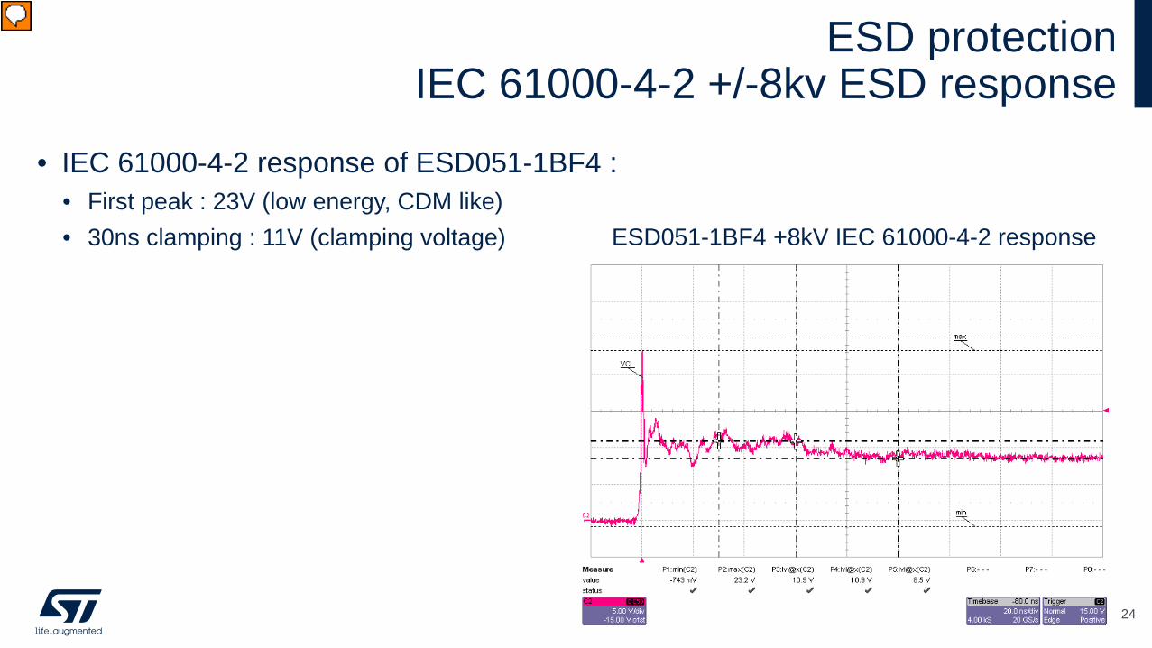
Now, let’s focus on ESD protection quality The key parameters is the ESD response to a electrostatic discharge of 8000 Volts As exemple, ESD051-1BF4 temporal response is presented They are two noticeable values : The first, is the Peak voltage at beginning of the response It is low energy peak due to its duration of few ns Its waveform correspond to CMD ESD event For ESD051-1BF4 is the 23V Second, is the clamping voltage defined at 30ns It’s 11V for ESD051-1BF4 It’s much more energetic du to the duration This temporal response at 8kV is usually reported on datasheet because, it corresponds to the IEC61000-4-2 level 4.
• IEC 61000-4-2 8 kV 30 ns clamping voltage ↔ TLP* 16 A 100 ns 70 - 90% voltage
ESD protectiontransmission line pulse*
25
Injected current :16A – 100ns square current
Measured voltage on 70% – 90% windowson ESD051-1BF4 : 10.5V
*ANSI / ESD STM5.5.1-2014
Presenter
Presentation Notes
To perform ESD analysis, transmission line pulse is used An square current pulse of 100ns is injected into the protection And the remaining voltage is then measure between 70% and 90% of the incident pulse duration. For ESD051-1BF4, with 16A incident current the TLP voltage is 10.5V It’s about the clamping voltage measures with 8kV IEC 61000-4-2
• I/V TLP* curve is done with several pulses
ESD protectiontransmission line pulse* I/V curve
26*ANSI / ESD STM5.5.1-2014
ESD051-1BF4 TLP* I/V curve
Presenter
Presentation Notes
With several pulses at various incident currents, it is possible to make a TLP I/V curve As example, ESD051-1BF4 TLP I/V curve is presented.
• TLP input current shared between high performance MCU FT input and ESDA5-1BF4
• High performance MCU + ESDA5-1BF4 robustness reach more than 8kV IEC 61000-4-2• Even if, ESD5-1BF4 clamping voltage > High Performance MCU FT input AMR
System-efficient ESD design methodology
27
• ESD051-1BF4• 11V clamping voltage at +8kV ESD 61000-4-2
• High Performance MCU FT input• 3.6 V max operating• 2 kV HBM ESD• 250 V CMD ESD• 5.5 V AMR
MCU working voltage : 3.3VMCU destruction voltage : 12.5V
Presenter
Presentation Notes
On same graphic, a TLP I/V curve of high performance MCU input is plotted in blue 3 voltages are noticeable for high performance MCU : The first one is the working voltage, 3.3V The second one is the absolute maximum rating of this input, 5.5V The third one is the MCU destruction, 12.5V TLP destruction voltage of the MCU is higher than AMR of the MCU because TLP duration is 100ns while AMR is continuous This graphic shows that current coming from ESD event is shared between MCU internal protection and ESD051-1B4 When the sum of current into ESD051-1BF4 and MCU is higher than 16A, the system can resist to 8kV IEC 61000-4-2 It is the system efficient ESD design mythology The approach shows the current repartition between external ESD protection and the protected pin
• Snap-back protection (ESDZV5-1BF4) clamping voltage lower than standard protection (ESD051-1BF4) clamping voltage
• Protected line DC voltage MUST be lower than holding voltage• To avoid protection latch-up
i.e. continuous leakage current flowing into the protection
Snap-back protectionssystem integration
28ESDZV5-1BF4 holding voltage
ESDZV5-1BF4 turn-on voltage
Presenter
Presentation Notes
Instead of standard ESD protection, green TLP I/V curve, snap-back ESD protection can be use, red TLP I/V curve. Snap back protections present lower clamping voltage than standard protection thanks to the snap-back effect that lower the clamping once the protection has turn-on. At 16A, ESDZV5-1BF4 presents a clamping voltage nearly 2V lower than ESD051-1BF4 But, the protected line DC voltage, if present, must be lower than holding voltage of the snap-back ESD protection. Indeed, if DC voltage is higher than holding voltage and if ESD event is present, the protection will turn-on and a current coming from the DC voltage source will flow continuously into the protection. The protection will then be latched. If no DC voltage or no DC voltage higher than holding voltage, these is no latch risk.
• Transparency :• Capacitance must be in-line with application bandwidth / data rate
• Efficiency :• VRM must be slightly higher than maximum line voltage
To obtain a low clamping voltage
• System integration of snap-back protection :• Holding voltage must be higher than DC voltage
AN5241, Fundamentals of ESD protection at system level
Presenter
Presentation Notes
To select the right ESD protection, 3 parameters must be validated The ESD protection must be transparent for the application To do that the protection capacitance must be in-line with application bandwidth if analog or data rate if digital These curves are reported on datasheet The ESD protection must be efficient when ESD event is present. TLP I/V curves are present on ESD datasheet but there is no TLP information on circuit to be protected. To select the protection with a good clamping, it is recommended to select an ESD protection with a Vrm just above maximum line voltage To avoid snap-back protection latch-up once turn-on, holding voltage must be higher than DC line voltage to grant a good system integration. All these information are available on the application note, Fundamentals of ESD protection at system level on st.com
Vladimir Protection requirements are becoming more and more well known and are often defined by rules or standards as we described so far. To satisfy these requirements, there is in the majority of cases a standard solution or a dedicated protection product. However, knowledge of the disturbances and the use of a suitable protection devices are not sufficient in themselves to solve the problem. In many applications, the correct design of the PCB layout is essential for success. Let’s have a look on a particular example for the PCB layout consideration.
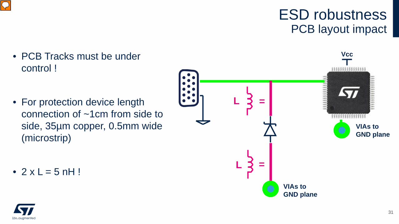
• PCB Tracks must be under control !
• For protection device length connection of ~1cm from side to side, 35µm copper, 0.5mm wide (microstrip)
• 2 x L = 5 nH !
ESD robustness PCB layout impact
31
Vcc
VIAs to GND plane
L
L
=
=
VIAs to GND plane
Presenter
Presentation Notes
Let’s try to understand why it is very important to have the application PCB layout under control for a good ESD robustness . The circuit presented in this figure shows the classic approach for the protection placement in the application circuit. Here the protection device is located between the connector and the IC device we want to protect. What is not visible in the first view is the fact , that during the ESD disturbance, the PCB track impedance starts to play an important role. High currents and the trace impedance causes unwanted overvoltage at the protected IC pins. Depending on the PCB technology, the PCB track impedance of around 1nH per its mm of length is introduced. This problem is specifically important for the PCB track parts colored in red in our figure. Let’s consider for the next exercise, that the single PCB track inductance L is 5nH.
𝐿𝐿𝑑𝑑𝑑𝑑𝑑𝑑𝑑𝑑
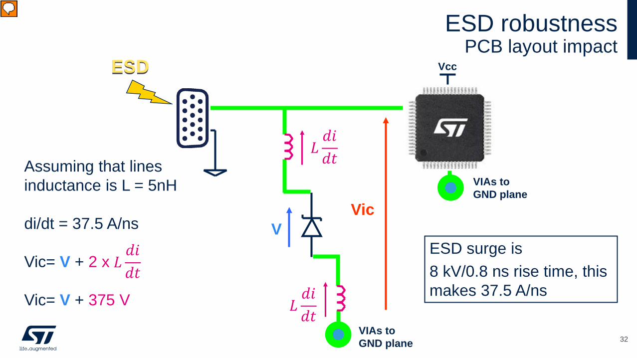
ESD robustness PCB layout impact
32
VVic
ESD surge is 8 kV/0.8 ns rise time, this makes 37.5 A/ns
ESD
VIAs to GND plane
VIAs to GND plane
Vcc
𝐿𝐿𝑑𝑑𝑑𝑑𝑑𝑑𝑑𝑑
Assuming that lines inductance is L = 5nH
di/dt = 37.5 A/ns
Vic= V + 2 x
Vic= V + 375 V
𝐿𝐿𝑑𝑑𝑑𝑑𝑑𝑑𝑑𝑑
Presenter
Presentation Notes
When an ESD disturbance occurs on the PCB track from the connector on the left side, the protection device clamps the surge at its maximum clamping voltage and thus we expect it protects our sensitive IC. It is not really true in this particular PCB layout because during this clamping action there is a high current going through the protection device and also through the PCB tracks around it. This phenomenon introduces a voltage on the PCB tracks equal to the track impedance an the current change. If we consider 5nH inductances and the current change of 37.5A/ns, the resulting Vic, visible by the protected IC pin, is simply a sum of the protection device clamping voltage and the voltage introduced on the PCB tracks. In our case the Vic is in hundreds of Volts and apparently these levels can be still crucial for the protected IC. So what should we do ?
33VIAs to GND plane as close as possible to the product GND
ESD
VIAs to GND plane
Vcc
ESD robustness PCB layout recommendation
VIAs to GND plane
Presenter
Presentation Notes
The solution is simple. Our application PCB Tracks must be under control ! In particular, we have to shorten the PCB tracks and route them through the protection device pins as visible in the figure . Connections to the grounds must be also short and specifically the Vias to GND planes must be as close as possible to the protection device and to the protected IC ground pins to limit the parasitic inductances.
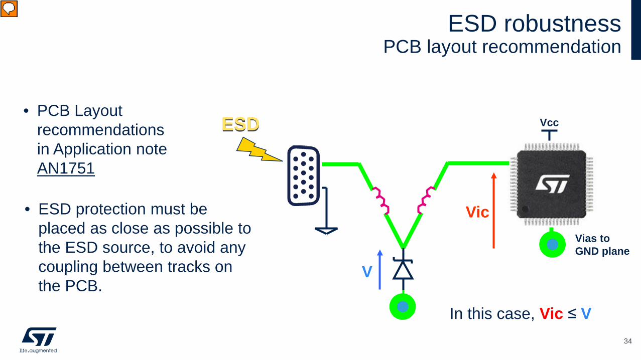
• PCB Layout recommendations in Application note AN1751
34
Vic
In this case, Vic ≤ V
• ESD protection must be placed as close as possible to the ESD source, to avoid any coupling between tracks on the PCB.
ESD
V
Vias to GND plane
Vcc
ESD robustness PCB layout recommendation
Presenter
Presentation Notes
In detail view, the PCB tracks inductance stay out from the risky area and does not contribute to the potential overvoltage visible by the protected IC pins during the ESD event. With the optimized PCB layout, the Vic on the protected IC pin is the wanted clamping voltage of the protection device. It is also recommended that the protection device is located as close as possible to the disturbance source. In our example, close to the connector. For more detailed information on the PCB layout recommendations for your ESD robust application PCB design you can consult our application note AN1751.
Application examplesrecommended protection devices and PCB layouts
Presenter
Presentation Notes
Vladimir Now, let’s have a look through several application examples showing recommended protection devices for particular application cases along with the recommended PCB layouts
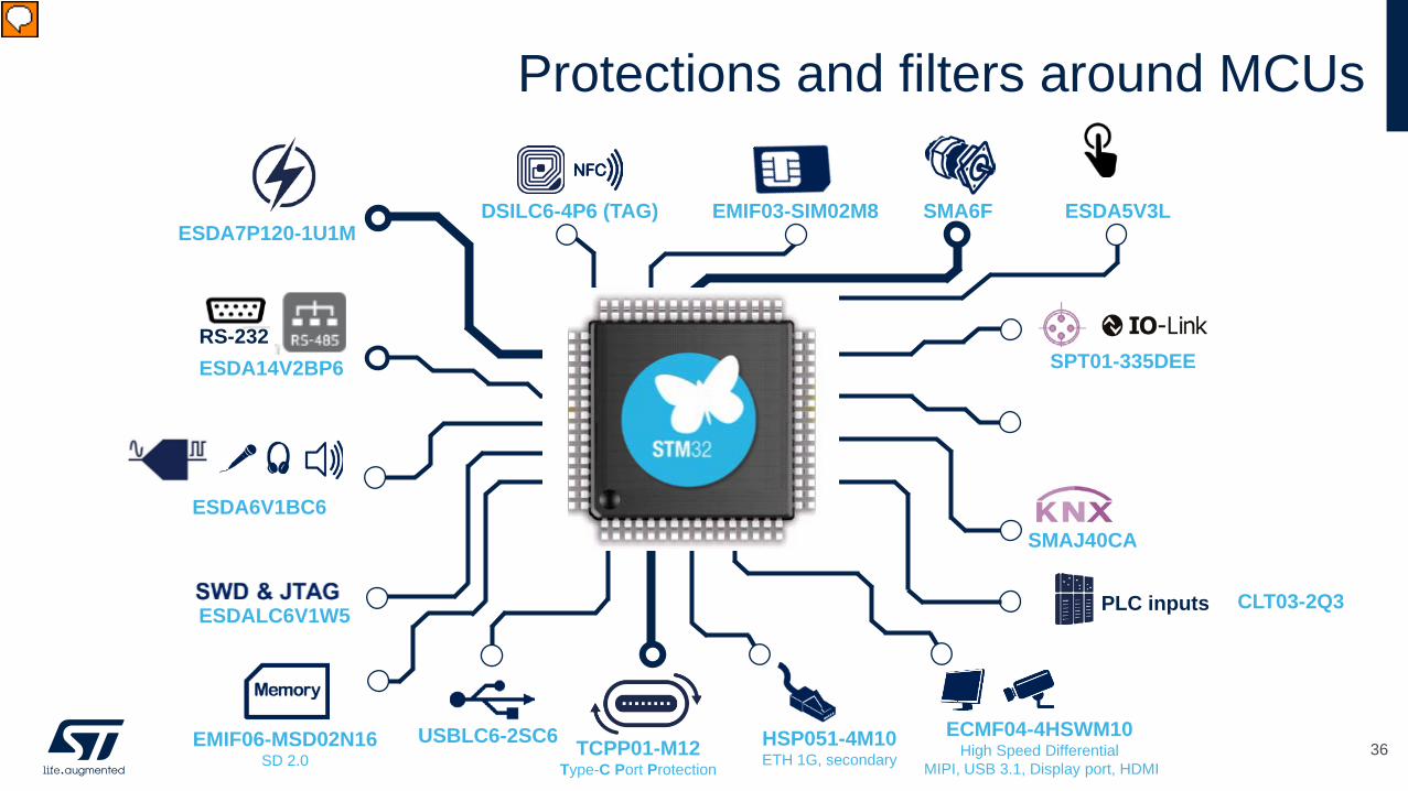
Protections and filters around MCUs
36ECMF04-4HSWM10
High Speed DifferentialMIPI, USB 3.1, Display port, HDMI
ESDALC6V1W5
ESDA6V1BC6
SPT01-335DEE
HSP051-4M10ETH 1G, secondary
ESDA7P120-1U1M
USBLC6-2SC6 TCPP01-M12Type-C Port Protection
EMIF06-MSD02N16SD 2.0
EMIF03-SIM02M8 ESDA5V3LDSILC6-4P6 (TAG) SMA6F
ESDA14V2BP6RS-232
SMAJ40CA
CLT03-2Q3PLC inputs
Presenter
Presentation Notes
The application core product is usually the microcontroller. It features many peripherals which are in the final application naturally exposed to the surrounding environment. As an example, we all know many different communication buses like USB, RS232, Ethernet with their connectors accessible to outside environment. We have also audio connectors, slots for memory cards or just simple push buttons in our applications. All of these peripherals should be protected in an ESD robust design. Let’s go now through several concrete examples.
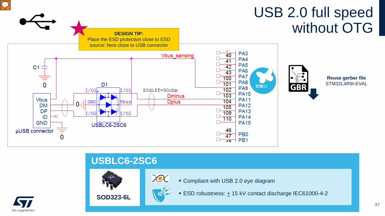
DESIGN TIP:Place the ESD protection close to ESD source: here close to USB connector
Presenter
Presentation Notes
First example is the USB connector which should be equipped with a protection device which is capable to protect the microcontroller pins against ESD but also at the same time the protection device should not introduce high capacitance to the communication lines in order to stay compliant to the USB eye diagram. USBLC6 protection device can do the job and you can find recommended schematic and PCB layout at our reference designs for STM32L4 microcontroller.
ESD protection as per IEC61000-4-2 Level 4: + 8kV contact
ESDA14V2BP6
SOT666-6L
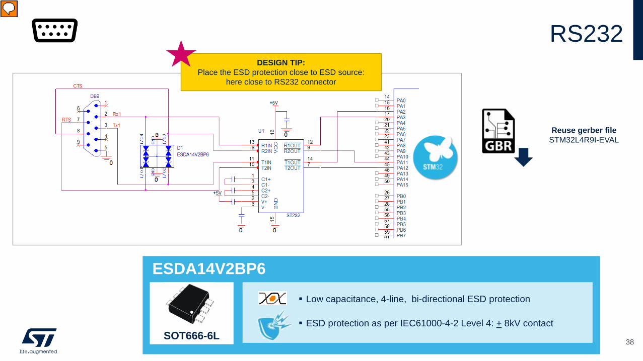
DESIGN TIP:Place the ESD protection close to ESD source:
here close to RS232 connector
Presenter
Presentation Notes
Similar for RS232, in this case the RS232 transceiver is the most exposed application IC outside the application through the connector and also in this case as it was mentioned for the USB connectivity, there are two main functions or needs of the protection device required. The first one is the ESD protection functionality itself. The second key requirement is again the capacitance of the protection devices itself introduced to the communication lines, which must be low, to keep the RS232 protocol compliancy. Also in this case you can find recommended schematic and layout in our STM32L4 reference board resources.
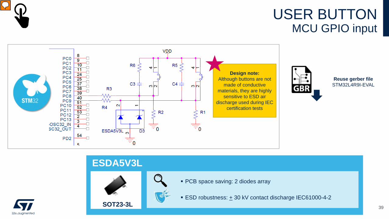
Last example we selected are the user buttons and consequently protection of the microcontroller GPIO inputs. Also these mechanical buttons being part of the application are exposed outside to the environment. The buttons are not made from conductive materials, nevertheless they are still highly sensitive to the ESD and they are also stressed during the IEC certification tests. Beside the ESD robustness level, such protection device requirement is usually also on the size of the package, to keep the PCB space occupation small. The small package size is often a general customer requirement for any protection device.
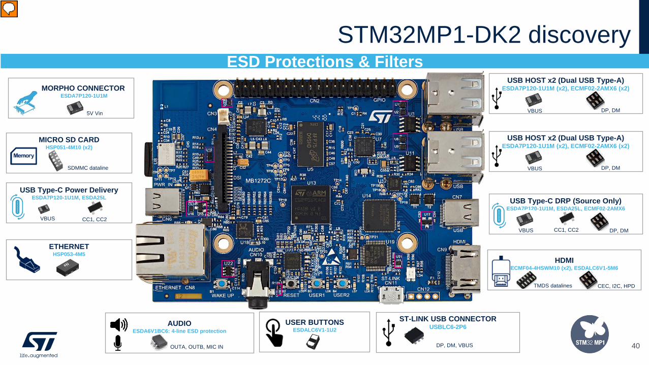
USB HOST x2 (Dual USB Type-A)ESDA7P120-1U1M (x2), ECMF02-2AMX6 (x2)
VBUS
VBUS DP, DM
USB Type-C DRP (Source Only)ESDA7P120-1U1M, ESDA25L, ECMF02-2AMX6
CC1, CC2VBUS
USB HOST x2 (Dual USB Type-A)ESDA7P120-1U1M (x2), ECMF02-2AMX6 (x2)
VBUS DP, DM
DP, DM
AUDIOESDA6V1BC6: 4-line ESD protection
OUTA, OUTB, MIC IN
HDMIECMF04-4HSWM10 (x2), ESDALC6V1-5M6
CEC, I2C, HPDTMDS datalines
MORPHO CONNECTORESDA7P120-1U1M
5V Vin
USER BUTTONSESDALC6V1-1U2
MICRO SD CARDHSP051-4M10 (x2)
SDMMC dataline
ST-LINK USB CONNECTORUSBLC6-2P6
ETHERNETHSP053-4M5
DP, DM, VBUS
ESD Protections & FiltersSTM32MP1-DK2 discovery
40
Presenter
Presentation Notes
Now let’s have a closer look on concrete application boards. The first mentioned already at the beginning of our webinar is showing the ESD protections suitable for our STM32 MP1 microprocessor. As you may see, all exposed connectors are equipped with ESD protections. In addition to the connectors, we have also added protections to other susceptible areas such as the user input buttons and the SD card slots. The protections added to this board ensure system-level protection in compliance with the previously mentioned ESD standard IEC61000-4-2.
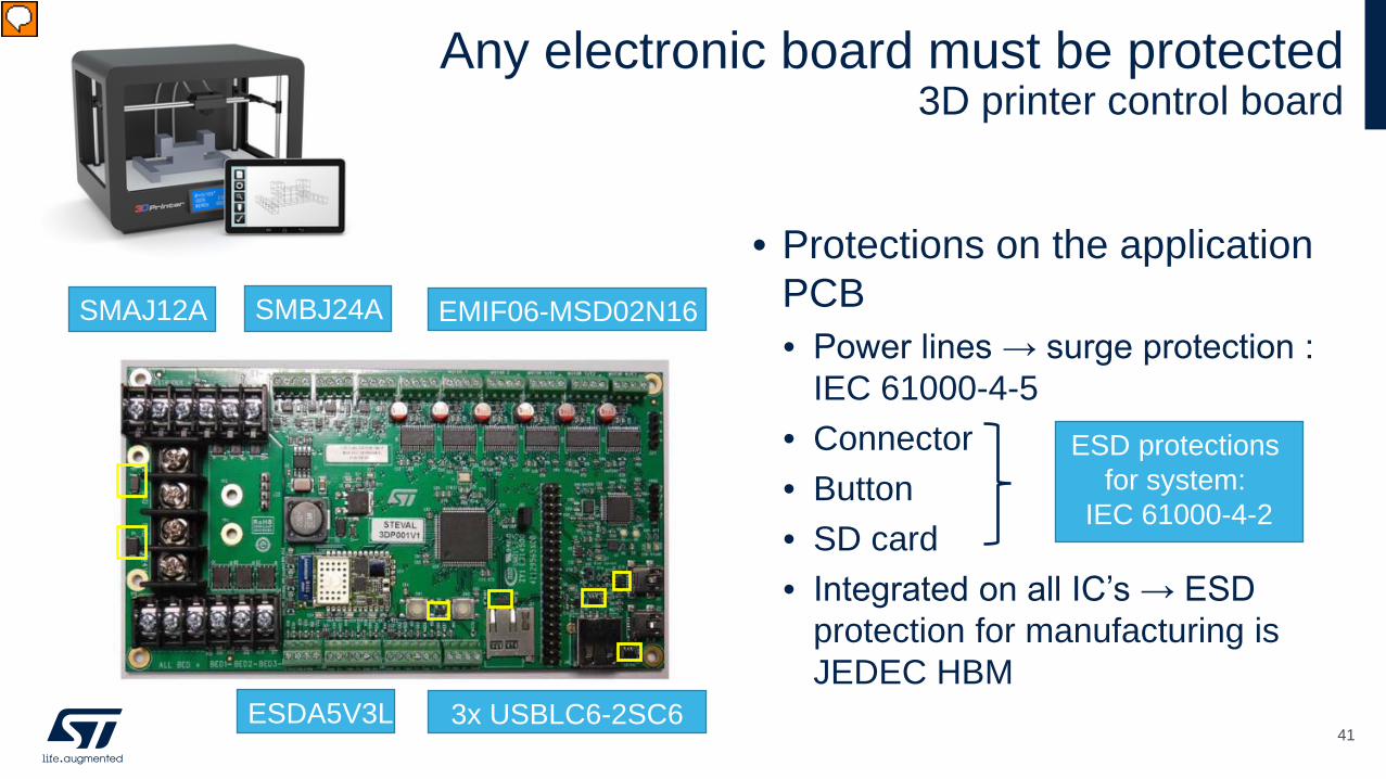
• Protections on the application PCB• Power lines → surge protection :
IEC 61000-4-5• Connector • Button• SD card• Integrated on all IC’s → ESD
protection for manufacturing is JEDEC HBM
Any electronic board must be protected3D printer control board
41
SMAJ12A SMBJ24A EMIF06-MSD02N16
3x USBLC6-2SC6ESDA5V3L
ESD protections for system:
IEC 61000-4-2
Presenter
Presentation Notes
Any electronic board must be protected. This second example is showing a 3D printer control board. On this board, both input power lines of 12V and 24V are protected against surge, means according to IEC 61000-4-5, as you can see on the left side of the PCB. In addition there are several ESD protection devices on the board. ESDA5V3L is used for the user buttons, EMIF06 is protecting the SD Card slot including also the EMI filter and finally the USBLC6 protection devices are used for all three USB connectors populated on the PCB.
• AN5241, Fundamentals of ESD protection at system level• AN4871, USB Type-C protection and filtering• AN5121, HDMI ESD protection and signal conditioning products for STBs• AN3353, IEC 61000-4-2 standard testing• AN2689, Protection of automotive electronics from electrical hazards, guidelines
for design and component selection• AN1826, TRANSIENT PROTECTION SOLUTIONS: Transil™ diode versus
Varistor• AN5241 : Fundamentals of ESD Protection• Video - ESD Protection: why and how to protect microcontrollers efficiently
ResourcesApplication notes and Videos
42
Presenter
Presentation Notes
We have mentioned some application notes already in our webinar, here is the recommended list of our documents you may check to make your application design robust and optimized from the beginning at the schematic level already. We also invite you to watch our Video about ESD protections explaining why and how you can protect your application ICs, e.g. the microcontrollers ,in an efficient way.
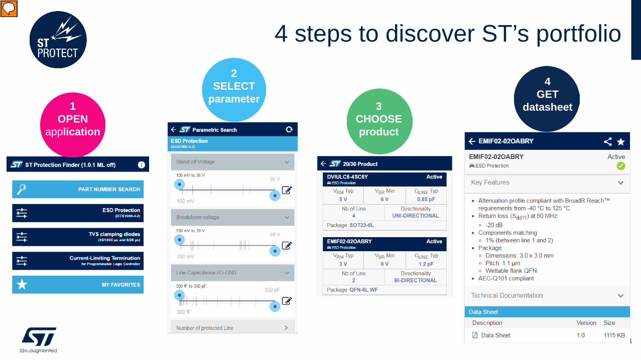
• ST PROTECTION FINDER is an application available for Android™ and iOS™that allows you to explore ST’s TVS product portfolio.• Parametric or series search engine• Efficient part number search engine
ST protection finder mobile App
43
Presenter
Presentation Notes
ST Protection finder is the SW application available for Android™ and iOS™ that allows you to explore the ST’s protection portfolio. You can easily define the device that best fits your application using the parametric or series search engine. You can also find your product thanks to the efficient part number search engine. To find the right device for your application, it is just enough to and fill through four particular steps.
4 steps to discover ST’s portfolio
44
1 OPEN
application
2 SELECT
parameter 3CHOOSEproduct
4GET
datasheet
Presenter
Presentation Notes
You need to just open the ST protection Finder application on your phone ing the product family you want to search in (for example ESD Protection). In the second step you narrow the parameters needed for your application and you select from the preselected protection devices the best fitting product for your needs. Web links to the datasheet and the online documentation are also reachable.