elektrotechnica & elektronica e+e
TRANSCRIPT

ELEKTROTECHNICA & ELEKTRONICA E+E Vol. 49. No 5-6/2014 Monthly scientific and technical journal
Published by: The Union of Electronics, Electrical Engineering and Telecommunications /CEEC/, BULGARIA
Editor-in-chief:
Prof. Ivan Yatchev, Bulgaria
Deputy Editor-in-chief:
Assoc. Prof. Seferin Mirtchev, Bulgaria
Editorial Board:
Prof. Christian Magele, Austria Prof. Georgi Mladenov, Bulgaria Prof. Georgi Stoyanov, Bulgaria Prof. Ewen Ritchie, Denmark Prof. Hannes Toepfer, Germany Dr. Hartmut Brauer, Germany Prof. Maurizio Repetto, Italy Prof. Rumena Stancheva, Bulgaria Prof. Takeshi Tanaka, Japan Dr. Vladimir Shelyagin, Ukraine Acad. Prof. Yuriy I. Yakymenko, Ukraine Assoc. Prof. Zahari Zarkov, Bulgaria
Advisory Board:
Prof. Dimitar Rachev, Bulgaria Prof. Emil Vladkov, Bulgaria Prof. Emil Sokolov, Bulgaria Prof. Ervin Ferdinandov, Bulgaria Prof. Ivan Dotsinski, Bulgaria Assoc. Prof. Ivan Vassilev, Bulgaria Assoc. Prof. Ivan Shishkov, Bulgaria Prof. Jecho Kostov, Bulgaria Prof. Lyudmil Dakovski, Bulgaria Prof. Mintcho Mintchev, Bulgaria Prof. Nickolay Velchev, Bulgaria Assoc. Prof. Petar Popov, Bulgaria Prof. Sava Papazov, Bulgaria Prof. Stefan Tabakov, Bulgaria
Editor of this issue:
Corr. Memb. of BAS, Prof. Georgi Mladenov
Technical editor:
Assoc. Prof. Dr. Eng. Elena Koleva
Corresponding address:
108 “Rakovski” str. Sofia 1000 BULGARIA
Tel. +359 2 987 97 67 e-mail: [email protected] http://epluse.fnts.bg
ISSN 0861-4717
C O N T E N T S Special issue: Scientific papers from 11-th International Conference on Electron Beam Technologies – EBT 2014, Varna, BULGARIA Preface by Corr. Member of BAS, Prof. DSc. G. Mladenov 5
ELECTRON BEAM WELDING
A. Shcherbakov, A. Goncharov, A. Kozhechenko, A. Gordenko, A. Sliva, V. Balashov, V. Dragunov, V. Rubtsov Modern problems and development methods of electron beam welding systems 7
D. Trushnikov, G. Mladenov Numerical modeling of parameters of the plasma, generated during electron beam welding 13
D. Trushnikov, G. Mladenov, V. Belenkiy, E. Koleva Ion current collected from generated plasma during EBW 22
E. Koleva, D. Trushnikov, V. Belenkiy, G. Mladenov Control of electron beam welding of plates, using beam current of back plate side 30
D. Trushnikov, E. Salomatova, A. Tsaplin, V. Belenkiy Simulation evaporation processes in electron beam welding 34
U. Reisgen, S. Olschok, S. Ufer Accurate diagnostic of electron beam characteristics 40
E. Koleva, G. Mladenov, M. Kardjiev, D. Todorov Electron beam characterization at changes of EBW process parameters 46
V. Braverman, V. Belozertsev, V. Bogdanov, N. Uspenskiy, A. Beniyash Seam tracking during electron beam welding in air 56
V. Laptenok, A. Druzhinina, A. Murygin, Y. Seregin
Compensation of the effect of magnetic fields on the electron beam position in the process of electron beam welding
62
A. Vasilyev, V. Erofeev, V. Sudnik Mechanism of onset of keyhole depth fluctuations at beam welding process 68
A. Sliva, V. Dragunov, A. Goncharov, E. Terentyev, M. Gribkov Electron beam welding of elements supporting structure of the front wall module blanket ITER 75

“Е+Е”, 5-6/2014 2
P. Havlík, P. Šohaj, J. Kouřil, R. Foret, I. Dlouhý EBW of austenitic stainless steel and ODS ferritic steel 82
E. Koleva, D. Trushnikov, V. Belenkiy, G. Mladenov, S. Angelov, D. Todorov Model-based quality optimization of EBW of steel
90
T. Olshanskaya, G. Permyakov, V. Belenkiy, D. Trushnikov Influence of electron beam's oscillations on weld's structure formation of dissimilar materials on an example steel with bronze 97
I. Pobal, S. Yurevich Electron beam welding of superconducting cavities made of ultra-pure niobium 103
K. Frikach, J White, J. Houtz Prediction of the partial penetration depth on 15-5PH materials during electron beam welding 108
ELECTRON BEAM MELTING AND REFINING
M. Grechanyuk, A. Melnyk, I. Grechanyuk, V. Melnyk, D. Kovalchuk Modern electron beam technologies and equipment for melting and physical vapor deposition of different materials 115
V. Melnyk, I. Melnyk, B. Tugai, D. Kovalchuk Recent Progress in Development of Gas-Discharge Electron Beam Guns Providing Extension of Their Technological Capabilities 122
Sh. Shi, Y. Tan, D. Jiang, W. Dong, Sh. Wen Effects of beam patterns on removal of phosphorous in silicon by electron beam melting 126
V. Donchev, K. Vutova, T. Chernogorova Economic and conservative numerical scheme for non-stationary heat model for EBMR 132
V. Vassileva, K. Vutova, V. Donchev, A. Stoimenov, D. Amalnerkar, N. Munirathnam Electron beam melting and recycling of Nickel 138
M. Voron, A. Doniy Structure and properties management of cast α-Titanium alloys, produced by electron beam skull melting with electromagnetic stirring 144
ELECTRON ACCELERATOR APPLICATIONS
A. Ponomarev, P. Metreveli, A. Metreveli, A. Bludenko, V. Chulkov
Decomposition of a vegetative biomass by electron-beam irradiation and heating 150
P. Metreveli, A. Metreveli, A. Ponomarev, A. Frumkin The electron-beam treatment of water polluted by humic acids and lignin 157
B. Han, J. Kim, Y. Kim, S. Jung Electron Beam Technology for Environmental Conservation 163
N. Kuksanov, Yu. Golubenko, P. Nemytov, R. Salimov, S. Fadeev, A. Korchagin, D. Kogut, E.Domarov, A. Lavruchin, V. Cherepkov, V. Semenov Tendency of development of DC type ELV accelerators for industrial application and research experiments 168
I. Bataev, M. Golkovskii, N. Kuksanov, A. Ruktuev, I. Polyakov, A. Bataev, V. Samoilenko Surface alloying of titanium alloys with refractory elements by electron-beam processing 174
N. Kuksanov, M. Stepanov, A. Rojkh Experience of 30 years operation of EB treatment installation at PODOLSKKABEL plant 178
THIN FILMS, BULK MATERIAL DEPOSITION, MODIFICATION OF SOLID SURFACES
G. Mattausch, B. Zimmermann, F. Fietzke, J.-P. Heinss, B. Graffel, F. Winckler, F.-H. Roegner, Ch. Metzner Gas discharge electron sources - proven and novel tools for thin-film technologies 183
N. Grechanyuk, I. Grechanyuk, Е. Khomenko, A. Melnik, V. Grechanyuk Composite materials with a metal matrix condensed from vapor phase: Dispersion strengthened metals 196
N. Grechanyuk, I. Grechanyuk, Е. Khomenko, A. Melnik, V. Grechanyuk Composite materials with a metal matrix condensed from vapor phase: Microlayer materials 201
N. Grechanyuk, I. Grechanyuk, Е. Khomenko, A. Melnik, V. Grechanyuk Composite materials with a metal matrix condensed from vapor phase: Microporous materials 206
P. Zhemanyuk, I. Petrik, О. Gnatenko, Y. Marchenko Electron beam heat treatment of aircraft engine combustion chamber casings, made of precipitation-hardened heat-resistant Chrome-Nickel alloys 212
R. Fetzer, A. Weisenburger, G. Mueller Surface layer modification by large-area pulsed electron beams
216
T. Pinto, A. Buxton, K. Neailey, S. Barnes Surface engineering improvements and opportunities with electron beams 221

“Е+Е”, 5-6/2014 3
K. Vutova, V. Vassileva, A. Stoimenov, E. Koleva, T. Ivanova, G. Bodurov, K. Gesheva,G. Mladenov Optical and structural investigation of WOx films, deposited by electron beam evaporation process
226
ELECTRON OPTICS, ELECTRON GUNS AND ELECTRON BEAM MASHINES
C. Ribton High angle, high integrity beam deflection 231
V. Engelko Source of radial converging electron beam for modification of long-length cylindrical targets 236
N. Rempe, S. Kornilov, A. Beniyash, N. Murray, T. Hassel, C. Ribton Characterisation of electron beams generated by a plasma cathode gun 242
S. del Pozo, C. Ribton, D. Smith A novel RF excited plasma cathode electron beam gun design 249
I. Melnyk Simulation of time of current increasing in impulse triode high voltage glow discharge electron guns
254
A. Goncharov, V. Dragunov, A. Sliva, M. Portnov, E. Terentyev, A.. Scherbakov Technological electron beams parameters evaluation based on the optical radiation in vacuum 259
V. Gruzdev, V. Zalesski Electro-optical characteristics of the beams generated by the electron plasma sources 264
S. Belyuk, I. Osipov, A. Rau, G. Semenov Electron beam welding machines with plasma cathode gun 269
M. Radchenko, Yu. Shevtsov, T. Radchenko, D. Nagorniy The exploitation of concentrated energy flows for welding and protective coating production 274
ELECTRON LITHOGRAPHY, ELECTRO-OPTICAL DEVICES AND POLYMER MODIFICATION
I. Kostic, A. Bencurova, A. Konecnikova, P. Nemec, A. Ritomsky, E. Koleva, K. Vutova, G. Mladenov Study of electron beam resists: Negative tone HSQ and positive tone SML300 279
V. Kazmiruk, I. Kurganov, T. Savitskaja
Mask less lithography cluster for low and medium volume manufacturing 284
U. Maschke, M. Bouchakoura, Y. Derouichea, Z. Bouberka Electro-optical devices by electron beam technique: polymer dispersed liquid crystal materials 290
Z. Bouberka, A. Nadim, A. Benabbou, U. Maschke Radiation-induced degradation of two organic pollutants from aqueous solutions of TiO2 nanocomposites 297
COMPLEMENTARY TECHNOLOGIES BASED ON USE OF ELECTRONS, IONS, PLASMA AND LASERS
T. Hassel, N. Murray, A. Beniyash, N. Rempe, S. Kornilov
Non-vacuum electron beam cutting - a new high performance process 303
L. Dupák Electron beam micromachining of plastics 310
А. S. Klimov, А. А. Zenin, Е. М. Oks, О. L. Khasanov, E. S. Dvilis, A. О. Khasanov Electron beam sintering of ceramics 315
V. Sheliagin, V. Spivac, A. Bematskyy, M. Tirsu The microstructure of the surface layers by laser and laser-microplasma doping 319
V. Spivak, V. Khaskin, M. Tirshu Laser scalpel 324
K. Shimono, N. Fujimura, H. Noguchi, H. Toyota, Y. Shiray, T. Tanaka, K. Vutova Pulse width dependence of the self-ignited plasma using a plasma-based ion implantation 329
H. Kozai, N. Fujimura, H. Noguchi, H. Toyota, Y. Shirai, T. Tanaka, K. Vutova Preliminary estimation of incident ion energy by using simulation software (PEGASUS) 334
H. Noguchi, N. Fujimura, K. Shimono, H. Toyota, Y. Shirai, T. Tanaka Comparison of plasma spectral characteristics using a plasma-based ion implantation 339
K. Kakugawa, M. Kubo, H. Noguchi, K. Shimono, N.Fujimura, Y. Tsuchiya, T. Tanaka Spore-forming bacteria sterilization using Plasma-based ion implantation 343
N. Fujimura, K. Shimono, H. Noguchi, H. Toyota, Y. Shirai, T. Tanaka Estimation of self-ignited plasma density by using plasma-based ion implantation 348
E. Krivonosova, A. Gorchakov, I. Ponomarev Micro-arc oxidation of aluminum alloy 352

“Е+Е”, 5-6/2014 4
V. Spivak, E. Koleva, A. Vlasiuk Development and generalization of scientific and educational information book in the field of nanoelectronics 356
COMPANY PRESENTATIONS
M. Neumann Von Ardenne GmbH, Dresden, Germany 360
W. Dorl, H. Schacke, I. Stolberg Variable shaped beam lithography for micro- and nanotechnology - Vistec Electron Beam GmbH, Jena, Germany 368
T. Vesely, M. Herynk Reconstruction of Irradiated Specimens - UJV Řež,
a. s. Husinec - Řež, Czech Republic 372
P. Szanto Kurt J. Lesker Co. Ltd. 373
J. Sanderson TWI Ltd. – Materials joining and engineering technologies
374
Authors’ Index 378
Съдържание 380

SPECIAL ISSUE The Eleventh International Conference on Electron Beam Technologies (EBT 2014)
8-12 June 2014, Varna, Bulgaria
Preface
This issue contains the papers, presented on the
International Conference on Electron Beam Technologies (EBT 2014) that was held in Varna, Bulgaria. The papers are accepted for publication from International Organizing Committee after reviewing.
The history of EBT Conferences dates back to 1985, when the first meeting in the series was held in Varna. The conferences with EBT logo are organized by me and my colleagues from the Institute of Electronics at Bulgarian Academy of Sciences and the created by me Technology Centre of Electron Beam and Plasma Technologies and Techniques, with a co-organizer the Bulgarian Union of Electrical engineering, Electronics and Tele-communications. Since 1985 up to tenth one (EBT 2012) these conferences were triennial. The EBT 2014 is eleventh from this series and now the period between conferences was changed to two years.
Varna seaside was the venue of all of these conferences. The professional meetings of academic scientists and industrial experts in the specific area of electron beam technologies demonstrate viability despite the political changes in Eastern Europe and the economy depressions in the world.
This year the Bulgarian Academy of Sciences is on 145 years and Bulgarian organizers hold the light for that celebrating jubilee, accepting the EBT 2014 as scientific-technical meeting, devoted to this jubilee of BAS.
During the twenty nine years from the First International Conference on EBT in Varna we had witnessed and participated in the great advance in the electron beam equipment, technologies and applications. The majority of participants in our series of conferences now are yang researchers and scientists from the next generations, appearing after the participants of the very first conferences.
The founding idea standing behind the EBT meetings is to bring together researchers sharing interest in
the variety of aspects of development, technologies and applications of electron beams and of the complementary technologies, utilizing lasers, ions and plasma. These conferences also give them possibilities to discuss the recent developments of the subject. A joint feature of the conferences is the fact that they provide a friendly and supportive forum for yang researchers to present their results.
This and the previous ten conferences of these series demonstrate the multidiscipline character of our field, the great potential of new applications of electron beams, the increased knowledge of understanding the processes of formation of intense electron beams and their interaction with materials. The core areas of EBT 2014 papers are the physical investigations and new technologies in electron beam welding, application of electron accelerators, electron beam non-thermal modification of materials, electron optics and especially electron guns with plasma emitters, some examples of adjacent technologies with lasers, ion beams and plasma flows.
The Proceedings of EBT 2014 are printed for forth time as regular issue of one of the most respectful Bulgarian scientific and technical journals: “Electrotechnica and Electronica” (The Electro-technical Engineering and Electronics), published by Union of Electronics, Electrical engineering and Telecommunications of Bulgaria. Before that, two volumes of “Vacuum”, with the Proceedings of our conference were also published.
As an Editor of this issue I hope, that the papers, published here will provide to the subscribers of “Electrotechnica and Electronica”, as well to the readers in Bulgarian libraries a new portion of state-of-the-art information on the science and applications of electron beams.
On behalf of the International Organizing Committee of the EBT 2014 and of behalf of the Editorial Board of the journal “Electrotechnica and Electronica” I express my thanks to all the participants and their Institutions for contribution to the realization of the conference and cooperation to prepare this issue. My thanks go also to Assoc. Prof. E. Koleva for Technical editing this issue as well to E. Koleva together with Prof. K. Vutova for executing various activities for the successful organization of this conference.
Prof. Georgy Mladenov Chairman of the EBT’2014, Editor of this issue, Corresponding member of BAS. e-mail: [email protected]

The conference is devoted to
145 Jubilee of Bulgarian Academy of Sciences

“E+E”, 5-6/2014 7
ELECTRON BEAM WELDING
Modern Problems and Development Methods of Electron Beam Welding Systems
Alexey V. Shcherbakov, Alexey L. Goncharov, Alexey S. Kozhechenko, Alexey K. Gordenko, Andrei P. Sliva, Vladimir N. Balashov, Victor K. Dragunov, Viktor P.
Rubtsov
At present the area of industrial application of electron beam technology is constantly expanding.
Today, there are new materials, technologies and standards, and thus approaches to the design of electron beam systems must be rebuilt. In order to meet the technological and technical requirements, which are often contradictory, it is necessary to implement integrated design techniques based on the solution of interdisciplinary problems. Precision calculation method of electron-optical systems must take account of the specific features of technological processes, such as the effect of space charge in the cathode region and the formation of ion beams in the accelerating field. It is absolutely necessary to consider the influence of the dynamic processes in the supply sources on the electron gun operation. Especially critical influence of transients in power supplies with pulse control of the beam parameters. In the paper the main problems of building welding technological complexes and methods for their solution are considered.
Модерни проблеми и методи на разработка на системи за електроннолъчево заваряване (А. Щербаков, А. Гончаров, А. Козеченко, А. Горденко, А. Слива, В. Балашов, В. Драгунов, В. Рубцов). Понастоящем областта на индустриални приложения на електроннолъчевите технологии постоянно расте. Днес има нови материали, технологии и стандарти, и така подходите за конструиране на електроннолъчеви системи трябва да се обновят. За да се посрещнат технологичните и технически изисквания, които често си противоречат, е необходима да се въведе техника за интегрално конструиране, базирана на решения на интердисциплинни проблеми. Прецизното пресмятане на електронно-оптични системи трябва да е съобразено със специфичните особености на технологичните процеси, такива като обемния заряд в катодната област и формирането на йонен сноп в ускоряващото поле. Абсолютно е необходимо да се разгледа влиянието на динамичните процеси в захранващите източници върху работата на електронните пушки и по-специално критичното влияние на преходните процеси в мощните захранвания с импулсно управление на параметрите на снопа. В работата са разгледани главните проблеми на създаване технологични комплекси за заваряване и методите за тяхното решаване.
Introduction It is known that the design of the electron beam
welding system is a very sophisticated problem. Since 1950s, when the first industrial welding machines were built [1], to present time, the elementary bases of electronics, mechanics and vacuum equipment were totally changed several times. It is obvious that in such circumstances the
development of welding machines needed to involve specialists from various fields - electron optics and beam physics, materials science, power electronics and electrical engineering, vacuum technology and control systems. Such specialists will find the best solutions for your area that will economically and technically justified. However, developing meet specific requirements coming from the technology, often contradictory. Such as the requirement to

“E+E”, 5-6/2014 8
reduce the output capacitance of high-voltage power supply to reduce the stored energy released in the breakdown [2], contrary to the requirement to smoothing the output voltage, or a request to increase the working distance of the electron gun contrary to the requirement to minimize the size of the gun. Most of these requirements lies in the construction of the components: electron beam gun, power supplies, control system.
For many years, the task to harmonize these requirements and alignment of construction welding machines were placed on the unique interdisciplinary experts of world renown, guided by a rich experience of such developments. Today the development of modeling techniques can solve most of these complex problems, which of course does not exclude the need to participate in the development of high-class specialists, but can reduce the complexity of the task of designing equipment.
Development methods The first task in developing complex equipment for
electron beam welding is the choice of design and modes of operation of the electron beam gun. To establish modes of power supplies that meet the requirements of the process, it is needed to analyze the characteristics of the electron beam.
In accordance with the classification given in [3] , technological welding guns by the influence of the space charge of the beam on its geometric characteristics intermediate between the guns used in analytical equipment (electron microscopes, X-ray, etc.) and powerful melting guns. In such systems needs simultaneous consideration of the space-charge spread of charged particles from the initial velocity and shape of the emitter [4].
To take into account all these factors is necessary to solve the problem of calculating the trajectories of the electrons leaving the cathode with an initial energy spread from 0 to a few eV (depending on the temperature of the cathode) , and the emission angle scatter ± π / 2 . Electrons move in vacuum Lorentz force electric field described in the computational domain (Fig. 1 , pos. 6) in the case of axial symmetry of the field , the equation
(1) 0
2
2
2
2 1ερ−=
∂∂+
∂∂+
∂∂
z
U
r
U
rr
U
where r and z - radial and axial coordinates, respectively, U(r, z)- electric potential, ρ(r,z) - the density of the space charge created by the beam of
charged particles located in the area of the field , ε0 - dielectric constant
For modeling the processes in the electron beam guns in the department of automated electrotechnological complexes of the Moscow power engineering institute, we often use software packages “WinCharge” [5], developed in Research centre “Orion” and “Elion” – our own software product.
First software uses the method is implemented for the numerical solution of the problem of self-consistent calculation of the electron guns, free from any a priori assumptions about the nature of the formation of the electron beam in the cathode region. Effect of space charge on the beam path of the electrons carried by an iterative method (on the first iteration space charge density created by the beam, assumed to be zero).
The second software implements the plurality of particles, or in some cases, larger particles and processes of ionization of residual gas atoms by electron impact, and also modeling an ion beams moving towards the cathode. This approach eliminates the iterative method for modeling electron and ion beams, to investigate the processes of influence of the Coulomb field of the particles with different charge values on each other, taking into account the energy aspects of the passage of charged particles through a rarefied gas on the basis of cross-sections for the various interactions as well.
The purpose of modeling is to determine the dependence of the energy and geometric characteristics of the beam from the control actions and the choice of rational modes of power supply.
As an example, Fig. 1a shows a family of current-voltage characteristics of the gun ELA-50/5M calculated in the software package WinCharge for different temperatures of the emitting surfaces. The figure shows that the same current values may be obtained at various temperatures and various cathode bias voltages. Therefore, it is of interest to consider not only energy, but also the geometric characteristics of the beam. Fig. 1b shows the dependence of the maximum beam current density on the bias voltage at different temperatures of the emitter. These curves have a maximum at a bias voltage of about 300 V. The current density increases in the interval 0 ... 300 due to the fact that under the action of the field control electrode "emission spot" of the cathode is reduced, and reduces the effect of beam space charge. In the interval 300-900 V, current density decreases. In this range there is a reduction of current and displacement of the crossover to the cathode in a region where the

“E+E”, 5-6/2014 9
electron velocity is smaller and space charge effects more significantly.
a
b
Fig. 1. Electron beam current I vs bias voltage Uc (a) and the maximum beam current density j vs the bias voltage Uc (b) calculated at different temperatures of the cathode; 1 -
2600 K; 2 - 2700 K; 3 - 2820 K;
For example, in welding at a current of 20 mA maximum current density will be provided at a temperature of 2700 K and the cathode bias voltage of 400 V. At small values of currents (e.g. 12 mA), the maximum density is observed at the lower temperature of the cathode - 2600 K and a bias voltage of 300 V. At the maximum temperature of the cathode - 2820 K and a bias voltage of 300 V is achieved maximum beam current density - 4.7 A/mm2 at a current of 38 mA.
Analysis is performed in a wide range of variable parameters - temperature of the cathode, bias voltage, cathode distance from the control electrode, etc. Using computer simulation calculations can be carried out such important geometric characteristics of the beam, the position and the radius of the virtual crossover [3], the aperture angle in the focusing lens and the current
density distribution in selected sections. The aim was to determine the characteristics and modes of supply sources, ensuring the formation of beam control his power in a given range with the required accuracy and stability and trouble-free operation.
«Elion» program designed to calculate the motion of charged particles - electrons and ions. As is known, the trajectories of charged particles in axis-symmetric electrostatic fields are flat and lie in a curved plane passing through the axis of symmetry [4]. Acceleration components purchased particle motion in axis-symmetric electrostatic field due to the Coulomb force, are the projections of the electric field vector E.
(2) gradUE −=r
For modeling various processes of electron scattering by atoms and molecules of residual gases, the program used the Monte Carlo method [6,7]. Figure 2a shows the shape of the electron beam in a modernized gun ELA-60. Figure 2b shows the distribution of the density of the positive ions formed in the ionization of gas at a pressure of 0.1 Pa - much more than typical pressure.
The model also takes into account that in the process by the ionization of neutral particles is reduced leading to reduced particle concentration, and reduction in the pressure in the gun. Energy losses are calculated discretely for each act of ionization.
It is obvious that the number of ionization increases with increasing pressure, but the interesting fact that the maximum number of particles is a function of pressure originates near the cathode. With decreasing pressure gas density distribution of ionization is stretched along the axis z, due to the increase of the free path of the particles. This means that increasing the average energy of ions bombarding the cathode.
Analysis of the results showed that at pressures of 1 • 10-3 Pa and below the formation of ion beams can be ignored (ion beam current is less than 0.05% of the primary electron beam current), and at pressures above 1 • 10-1 Pa ion current value commensurate with the current of the electron beam. Under this pressure the probability of high voltage breakdown is very high, that is why the larger pressures are not considered.

“E+E”, 5-6/2014 10
a
b
Fig. 2. Distribution of the charge density of the particles in the welding electron gun: a - electrons at an accelerating
voltage of 60 kV and a beam current - 400 mA; B - positive ions, formed with the same parameters of electron beam and the nitrogen pressure in the gun PN2 = 0,1 Pa; 1 -
equipotential surfaces; 2 - the density of the electron beam; 3 - cross-section with a maximum current density of the
electron beam
Method for the simultaneous modeling of many trajectories of charged particles can also assess the degree of compensation of the space charge of the electron beam space charge of positive ions in the cathode region. It is known that this effect is widely used in the ion injection electron beam guns [8] and plasma emitter electron beam guns.
Thus, these programs can be used to calculate the geometric and energy characteristics of electron
beams to specify the potentials of the electrodes, the cathode temperature and gas pressure in the electron gun. These results can be used for designing the power supplies, control systems, vacuum systems and mechanical parts of the welding machine.
Developing the power supplies In the Department of Metals Technology of
Moscow Power engineering institute together with ElectroIntel company [8], a stabilized inverter power source with digital control and continuously variable accelerating voltage from 0 to 60 kV was developed. Simplified schematic diagramm is shown in Fig . 3 .
Fig. 3. Inverter power source prototype with an accelerating voltage of 60 kV
Through a high voltage cable 2 conductors 1 and 3 connected to the cathode and the 4 - to the control electrode of the gun ELA-50/5M. One feature of the design is the location of the source inverter to power the heater circuits and offset directly in high-voltage circuits. In this scheme, the currents and voltages of the heater power source and the bias voltage are measured on the load circuit and transmitted in a digital form on the optical cables 5 and 6 to the control system. Besides, control signals are transmitted by the cables 5 and 6 to the heater 7 and bias 8 stabilizers. Channel and control the accelerating voltage measurement 9 and 10 and the channel 11 of the beam current measurement is necessary for controlling the main power inverter 12 regulating the voltage across the primary winding of the transformer-

“E+E”, 5-6/2014 11
rectifier unit 13. Auxiliary power inverters inverter 14 obtains filament and bias using a transformer with high voltage insulation. The control system 15 provides the main inverter stabilization accelerating voltage feedback signal from the divider installed in the transformer - rectifier unit. Breakdown protection system 16 detects overcurrent above values set by the operator and interrupts the transmission of power from the inverter to the load. Restart the inverter automatically after 2.5 ms.
To analyze the dynamic characteristics of the source used models developed in MATHLAB system based on the current-voltage characteristics of the gun. Thus was created a computerized system for the development of complex electronic guns and Electronic Equipment, which allows installing acceptable modes of power supplies and stabilizers for the effects of their work on the geometric parameters and energy beams.
One of the basic model is shown in Fig. 4.
Fig. 4. The basic model of power sources with PID
controllers operating with electron gun built in MATHLAB
Transformers and inverters of accelerating voltage and the bias voltage power sources are presented by transfer functions and the filament current source is presented by the step function. The internal load of the accelerating voltage power supply is modeled by Gain function. This simple model is suitable for setting PID sources with the influence of transients on beam current. In more complex models consider transitional processes in the transformer- rectifier unit (for example, in resonance control), as well as changes in the geometric characteristics of the beam.
The prototype source is shown in Fig. 5. Transformer-rectifier unit is made in a modular scheme and protected by patent [8]. All power sources have external inputs for analog or digital signals, which provides integration executive regulators in the
process control system. Source parameters were determined based on
analysis of the characteristics of the electron gun (Fig. 1) . The maximum value of the bias voltage - 900 V. The maximum load obtained experimentally at an accelerating voltage of 60 kV - 100 mA. Filament current range and its regulation was chosen experimentally for tungsten foil cathodes with a thickness of 80 microns with a size of the emitting site 1,5 × 1,5 mm. By comparing the experimentally obtained and the calculated current-voltage characteristics, it was found that the working range of the filament current regulation is 16 ... 21 A. The maximum filament current source - 25 A.
Fig. 5. Inverter power source prototype; a - section of the
transformer-rectifier unit; b - basic and auxiliary inverters; c - transformer-rectifier unit
At the next stage it is possible to design the electromechanical complex of the welding machine. It includes a vacuum chamber with a fixture and a manipulator and vacuum pumping system.
Conclusions The technique of creating dynamic models of
power supplies connected to the electron gun, which allows assessing the impact of static and dynamic errors in regulating current stresses on the geometric and energy beam parameters. Based on this procedure

“E+E”, 5-6/2014 12
a prototype power supply for the electron gun was created. This work is described for verification techniques allows to consider this promising line of research.
Acknowledgements The research project supported by the Grant of the
President of the Russian Federation. Grant number MD-1366.2014.8
REFERENCES [1] Steigerwald К.Н., Sayegh G., Powers D. and
others. An International History Of Electron Beam Welding. - Munchen: Pro Beam, 2007
[2] Nazarenko O.K., Lokshin V.E. Dynamic characteristics of high-voltage power supply for electron beam welding / / Avtomaticheskaya svarka (Paton’s welding journal) #1, 2005. - P. 36-38.
[3] Muraviev A.G. Mathematical modeling of cathode electron guns with arbitrary shape. Abstract of the thesis for the degree of Ph. D. Moscow, MIPT, 2001
[4] Zhigarev A.A. Electron optics and electron-beam instruments. Textbook for technical colleges. - Moscow, 1972
[5] Filachev A.M., Andreev S.V., Monastyrsky M.A., etc. Development of computational methods and software package for modeling electron beam technological units / / Prikladnaya Fizika, #2, 1998. - P. 5-18.
[6] Zolotukhin D.B., Burdovitsin V.A. Monte Carlo simulation of elastic and inelastic scattering of the electron beam in a gas // TUSUR Reports, #2 (26), Part 2, December 2012, Tomsk, Russia, pp. 55-57
[7] M. Bart. Electron-impact ionization: Measurement of absolute cross-sections and cross-beam studies / Thesis for the degree of Ph. D., University of Canterbury, New Zealand, 2013
[8] Akimov P.I., Bogoslovskaya A.B. Using ions for amplification of current in electron beam guns / / Prikladnaya Fizika, 2002, P.90-101
[9] Benevolsky E.S., Gladyshev O.M., Dragunov V.K. Medvedev E.I., Shcherbakov A.V. Transformer-rectifier unit high voltage power electron beam gun. Russian patent number 105213, B23K 15/02, H01F 27/06, H01F 38/28. publ. 10.06.2011.- Bul. Number 16.
Prof. Dr.Sci.(Tech.) Alexey V. Shcherbakov – head of the department of the Moscow power engineering institute(MPEI), completed the education in MPEI in 2005, Scientific interests: vacuum furnaces, electron beam welding, power sources, control and monitoring
tel.:+7(495)3627059 е-mail: [email protected]
Assoc. Prof. Ph.D. Alexey L. Goncharov - deputy head of department of MPEI, completed the education in MPEI in 2002, Scientific interests: electron beam welding, metallurgy, process monitoring
е-mail:[email protected]
Alexey S. Kozhechenko - assistant of department of MPEI, completed the education in MPEI in 2013, Scientific interests: electron beam welding, metallurgy, process monitoring
е-mail:[email protected]
Alexey K. Gordenko - head of the commercial and development group of Vekshinsky state research institute of vacuum technology, completed the education in Bauman Moscow State technical university in 2011, Scientific interests: vacuum furnaces, ion sources, vacuum systems
е-mail:[email protected]
Assoc. Prof. Ph.D. Andrei P. Sliva - assoc. prof. of department of MPEI, completed the education in MPEI in 2003, Scientific interests: electron beam welding, metallurgy, process monitoring
е-mail:[email protected]
Prof. Dr.Sci.(Tech.) Vladimir N. Balashov –professor of MPEI. Scientific interests: electron optics, electron beam lithography, electron beam gun development
е-mail: [email protected]
Prof. Dr.Sci.(Tech.) Viktor K. Dragunov –vice rector of MPEI, head of the department. Scientific interests: electron beam welding, electron beam equipment
е-mail: [email protected]
Prof. Dr.Sci.(Tech.) Viktor P. Rubtsov – professor of MPEI, deputy head of the department. Scientific interests: control systems, stepping motor systems, automation
е-mail: [email protected]

“E+E”, 5-6/2014 13
Numerical modeling of the plasma parameters, generated during
electron beam welding
Dmitriy N. Trushnikov, Georgi M. Mladenov
It is described a model of plasma formation in the crater in liquid metal as well as above electron
beam welding zone. Model is based on solution of two equations for density of electrons and mean electron energy. The mass transfer of plasma heavier particles (neutral atoms, excited atoms and ions) is taken in the analysis by diffusion equation for multicomponent mixture. Electrostatic field is calculated by Poisson equation. On crater wall is calculated thermion electron emission. Ionization intensity of vapor by beam electrons and high-energy secondary and back-scattered electrons is calibrated using plasma parameters in the case of lack of polarized collector electrode above welding zone. The calculated data are in good agreement with experimental ones. The results of plasma parameters in the case of excitation of non-independent discharge are given. There is shown need to take in account effect strong electric field in the crater near the crater wall on electron emission (effect Schottky) at calculation of current non-independent discharge. Calculated electron draft velocities much bigger than velocity, at which is arising current instabilities. This confirm assumed idea for beginning ion-acoustic instabilities, observed also experimentally.
Числено моделиране на формирането и параметрите на плазмата, генерирана по време на електронно-лъчево заваряване (Д. Трушников, Г. Младенов). Описан е модел на формирането на плазма в кратера в течния метал над зоната на заваряване с електронен лъч. Моделът се основава на решаване на две уравнения за електроните и за средната електронна енергия. Масовия пренос от тежките плазмени частици (неутрални атоми, възбудени атоми и йони) е анализиран от дифузионното уравнение за много-компонентна смес. Електростатичното поле се пресмята с уравнението на Поасон. Термоелектронна емисия от стените на кратера се отчита. Интензитета на йонизация на парите от електроните на снопа и от обратно-отразените електрони се калибрира, използвайки параметрите на плазмата в отсъствие на колектиращ електрод над зоната на заваряване. Пресметнатите данни са в добро съответствие с експерименталните данни. Дадени са плазмените параметри, пресметнати при възбуждане на не-самостоятелен разряд. Показана е необходимостта да се отчита силното електрическо поле около стените на кратера върху електронната емисия (ефект на Шотки) при пресмятане на несамостоятелния разряд. Пресметнатите дрейфови скорости на електроните са много по-високи от скоростите, при които възникват токови неустойчивости. Това подкрепя представата за възбуждане на йонно-акустични вълни, които са наблюдавани и експериментално.
Introduction
Electron beam welding is wide distributed technology for joining of metals due to numerous advances in comparison with other welding technologies. In the same time, optimization and quality improvement are empirical or based on applications of statistical methods, due to complex character and lack of models of physical processes in
the crater in welding bath. One of phenomena during interaction of concentrated energy beam with metal sample is generation of low temperature plasma in welding zone [1-10]. Study of plasma parameters and their relation with process product performances will help to extend knowledge for control of electron beam welding and approaches for its optimization. Difficulties of experimental measurement of plasma parameters in the crater in the welding bath forced the investigators to estimate

“E+E”, 5-6/2014 14
plasma parameters in the crater based on few experiments in plasma plume above the welding zone [2,3] or using indirect data [9,11].
Electron current, collected from plasma, generated during electron beam welding
One application of plasma, generated in electron beam welding zone by powerful beam of accelerated electrons is to carry information for interaction of beam with material and to be used for control of the technology process. In the case of situated a polarized from +50V to +100V metallic collector electrode in the plasma plume above welding zone, the electro-conductive plasma provide conduction of enough big current. This current can be considered as non independent discharge with hot cathode (overheated spots of the crater walls on which beam transfer kinetic electron energy into heat) and anode-collector electrode.
The non independent discharge in metal vapor and removed gases during electron beam welding is dominated by intense electron beam, which play the next functions: • provide quasi-steady input of the metal vapor in
the discharge zone; • stimulate generation of the low temperature
plasma in welding zone by ionization of the metal vapor through electron-atom collisions;
• lead to intensive thermion electron emission from overheated areas liquid or solid metal surfaces.
In former time was achieved success in studies and use of non independent electron current for control of the beam focus during EBW [12-15]. In the same time some difficulties of interpretation of obtained results is existed. There is a lack of models, determining formation of non independent discharge.
Description of the mathematic model In the last years a wide distribution have the
packages of applied software. In this paper is described At simulation collecting electron current on positive electrode in plasma above welding zone was used package applied programs Comsol 4.3, Plasma Module, extension DC Discharge[16].
Scheme of registration non independent discharge current is shown on fig.1. Discharge glows between two electrodes – grounded sample (cathode) and ring collector of plasma electrons (anode). Collector 4 is situated bellows the end of electron gun in the grounded vacuum metallic chamber. In the outer collector circuit trough load resistor 6 of 50 Ω is connected positive voltage of 50 V.
5
6
7
4
8
2
1
3 Ik
Ik
Fig.1. Scheme of registration of non independent discharge
current in plasma, generated above the interaction zone during electron beam welding:1 – electron gun; 2 –
focusing lens; 3 – plasma, generated above the welding zone; 4 – collector ; 5 – registration of data; 6 – load
resistor; 7 – voltage source; 8– welded sample
Calculations are executed in axis-symmetrical cylindrical coordinate system. Plasma is generated due to vapor flow ionization by electron beam and by accelerated from outer electrostatic field thermion
The electron density and mean electron energy in plasma, generated during EBW are computed by solving drift-diffusion equations for the electron density and mean electron energy. [17-21]. Convection of electrons due to ion motion, drifted with gas flow is neglected.
eee R
t
n =Γ⋅∇+∂
∂ r)( (1)
[ ] ee REnDEnt
n =Γ⋅+∇−−⋅∇+∂
∂ rrr
εεεεε µ )()(
(2)
There ne is electron density, µe – electron mobility, Re – electron source intensity, nε - volumetric density of the electron energy and Rε - energy loss due to inelastic collisions, E – electrostatic field intensity.
Electron flux eΓr
can be determined as׃
eeeee nDEn ∇−−=Γ )(rr
µ (3) Electron source Re and energy loss due to inelastic
collisions Rε will be defined later. The electron diffusivity De, energy mobility µε and
energy diffusivity Dε are computed from the electron
“E+E”, 5-6/2014 15
mobility µe using relations:
.,35
, eeeee TDTD εεε µµµµ === (4)
The source coefficients in the equations (1, 2) are determined, using rate coefficients. In the case of rate coefficients, the electron source term in equation (1) is given by:
enj
M
jje nNkxR ∑
=
=1
(5)
where xj is the mole fraction of the target species for reaction j, kj is the rate coefficient for reaction j (m3/s), and Nn is the total neutral number density (1/m3).
The electron energy loss is obtained by summing the collisional energy loss over all reactions:
jnj
M
jj nNkxR εεε ∆=∑
=1
(6)
where ∆εj is the energy loss from reaction j (eV). The rate coefficients may be computed from cross
section data by the following integral:
∫∞
=0
)()( εεεεσγ dfk kk (7)
where γ = (2q/me)1/2 (C1/2/kg1/2), me is the electron mass (kg), ε is energy (eV), σk is the collision cross section of molecule or ion (m2) and f(ε) is the electron energy distribution function. In this case a Maxwellian distribution of electron energy is assumed.
For the mass transport description of non-electron species in the plasma (ions, neutral atoms and excited neutral atoms), the diffusion equation for multi-component mixture is solved for the mass fraction of each species ׃
kkkk Rju
t+⋅∇=∇+
∂∂ rr ωρωρ )(
(8)
where: kjr
is vector of the diffusion flow; Rk - source
intensity for component k (kg / (m3 · s)); ur
–average velocity environment vector (m / s); ρ - denotes the
density of the mixture (kg/m3); ωk – mass portion of k-component .
The vector of diffusion flux can be calculated as:
kkk Vjrr
ωρ= (9)
where and kVr
is the multicomponent diffusion
velocity for species k. The electrostatic field is computed using the
Poisson equation:
0
02
ερ−=∇ U (10)
There U is potential of electrostatic field. The space charge density ρ0 is computed based on the reactions specified in the model using the formula:
−= ∑=
ek
N
kk nnZq
10ρ (11)
The drift-diffusion equations (1) and (2) are applicable only in the cases of calculation for plasma with collisions between plasma particles (the effective cross-sections for collisions of electrons, ions and neutral atoms are leads to mean free paths smaller than container dimensions). These conditions are satisfied only at vapor densities in the crater in welding bath. At retirement from the crater output plasma becomes collisionless [7]. Expansion of the plasma there is described continuity equation׃
dtdj /0ρ=⋅∇r
(12)
After exchange Eqnj e
rrµ= and dividing two sides
by q is resulting to eq. (1) without diffusion, that together with Poisson equation (10) determine electron motion in collisionless conditions. In our case the values 0 was given to diffusion coefficient in equations (1) and (2).
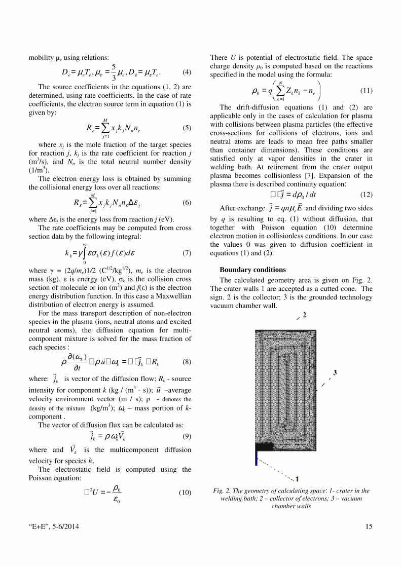
Boundary conditions The calculated geometry area is given on Fig. 2.
The crater walls 1 are accepted as a cutted cone. The sign. 2 is the collector; 3 is the grounded technology vacuum chamber wall.
Fig. 2. The geometry of calculating space1 ׃- crater in the
welding bath; 2 – collector of electrons; 3 – vacuum chamber walls

“E+E”, 5-6/2014 16
Non-independent discharge is connected with thermion electron emission from overheated by electron beam spots of crater wall. At polarized from +50 to +100 V collector and self-determinate detaining potential for keeping the plasma electrons of +1 V to +3 V all thermion emitted electrons are accelerated and can ionized vapor particles. In this way the charged particles near hot spots increased. The current in circuit with voltage source and any outer resistance is determined generally by the ratio of the difference between voltage of outer source and plasma potential to the sum of inner and outer resistances.
The electron are loosed on chamber walls, as well as on crater walls in result of random movement (transverse velocity bigger one threshold) and gained due to beam electron ionization, secondary emission effects, resulting in the following boundary conditions for electron flux:
)()2/1( , nnn pp
pethee
rrrr Γ−=Γ⋅− ∑γν , (13)
and for electron energy flux:
)()6/5( , nnn pp
ppthe
rrrr Γ−=Γ⋅− ∑ γεν εε . (14)
the,ν is the thermal velocity. The second term in right
hand side of equation (13) is describing electron generation due to secondary effects of discharge radiation, γр is coefficient of secondary emission. The second term in equation (14) is the energy flux of beam and secondary irradiations, εp – is average energy of electrons.
The ions are loosed on walls due to surface reactions (recombination) and that electrostatic field is directed to the walls.
[ ]0)()( >⋅⋅+=⋅− nEZnEZcMRMjn kkkkkkk
rrrrrr µµωω (15)
Thermion electron emission from the overheated crater wall is determined by Richardson-Dushman equation )/exp(2 kTeATj ϕ−= , where ϕe is work function of the emitter, Т is temperature, A is constant; k is Boltzmann constant.
The boundary conditions for electron flux in/from the crater are described
ejn e /=Γ⋅−rr
(16)
Reaction of gaining electrons During EBW of alloys in the vapor could be
various chemical elements. As example at welding of chromium-nickel steel in the vapor there are similar
portions iron, chrome and manganese [11]. In [9] is proposed to use the mean values for the
mass and for the ionization energy. In Table 1 the accepted reactions and the values of
energies loosed or gained during these reactions are given. The reactions between the electrons and the excited or ionized atoms are neglected due to their small quantity in the vapor. With A is signed the an average atom, participating in reactions governed plasma parameters.
Table 1. Accepted reactions for calculations of the parameters of the
non independent discharge
Reaction Formulation Kind interaction
energy ∆ε (eV)
1 e+A=>e+A elastic 0 2 e+A=>2e+A+ ionization 7.35 3 e+А=>e+А* excitation 3.084
4 A=>e+A+ Beam
electron ionization
-7.35
Reactions on boundaries are listed in Table 2.
Probability of de-excitation or de-ionization (recombination) of excited or ionized atoms is given by their sticking coefficients
Table 2. Sticking coefficient of atoms on wall surfaces
Reaction formulation Sticking coefficient
1 A*=>A 1 2 A+=>A 1
Results of calculations in case without collector (collector is grounded)
Vapor ionization by the beam electrons is described with reaction 4 (Table 1), realized along the beam axis. The negative absorbed energy of created electrons is the accepted as their mean energy. Additionally important role take ionization of secondary and back scattered electrons. Distribution of these electrons was chosen as cosine one in respect on the local surface.
Intensities of reaction sources were chosen taking in account the cross section of these reactions at mean energy of the ionizing electrons, concentration of particles. The results were calibrated by the experimental data.

“E+E”, 5-6/2014 17
Fig.3. Dependence of plasma concentration on distance
from interaction zone on welded sample surface
On fig.3 are shown the results of simulation the concentration of the plasma above welding bath. Points on the same figure are experimental values of dependence of the concentration of plasma on the distances from welding bath. There the distance
2 2R z r= + were changed in direction of 45o respectively sample surface; z is distance between the collector electrode and sample surface and r is distance of center of the collector electrode and beam axis. On fig.4 are given the dependence of distribution of electron density on distance from welding zone R in log scale. The character of dependence is in good agreement with generalized experimental as well calculated data in [7] on expansion of the plasma column under electron beam metal interaction.
Fig. 4. Dependence of electron density above sample on
distance R from welding zone
Fig. 5. Dependence of the electron density on beam axis z
in the welding crater
Fig. 6. Ionization degree from coordinate z in the crater
and above sample surface
On fig. 5 and fig.6 are shown the plasma density and ionization degree along beam axis. The origin of the coordinate z (z=0) is situated on sample surface. The positive values of z are above the sample surface (respectively above the welding zone). The ionization degree in the crater in liquid welding bath is of order of 10-2, that is in good agreement with experimental data [2]. Above the crater in welding bath the ionization degree decreases quickly.

“E+E”, 5-6/2014 18
Fig.7 Electron temperature in the crater and above the
welding zone
Fig. 8 Potential distribution in the crater in welding bath
and above the welding zone On fig. 7 and fig.8 are shown the results of
calculation of the electron temperature distribution and respectively the plasma potential distribution in the case of electron beam welding with grounded collector. The plasma potential values and the electron temperature values becomes maximal in the upper part of the crater, near the crater orifice. Above the crater the plasma is around 1V and electron temperature is of order of 3 000 K, that is in good agreement with data in [2, 3, 7].
Calculation results of the plasma parameters in the case of non-independent discharge
The computer simulation results in the previous part are presenting the case of usual situation of electron beam welding. The obtained results for lack of positively polarized collector are also results of lack of non-independent discharge and a calibration of the following calculations. At excitation of non-
independent discharge by polarization the collector with positive potential of + 50 V. This case is situation in experimental papers studying the oscillations of the collecting by plasma current [13, 14, 15], when the collector was connected to a voltage source through a load resistor of 50 Ω.
Fig.9 Potential distribution at excitation of non-
independent discharge: (а) in the vacuum chamber space (b) magnified fragment
The changes are seen in plasma potential
distribution (Fig. 9). The plasma potential practically in the whole space becomes similar to the collector potential. In concrete simulation plasma potential is 20 V that is corresponding to the collected current of 0.6 А. The plasma potential value decreases due to voltage drop on load resistor in the collector circuit serially to voltage source.
Near sample surface there is a layer, were the potential is falling to zero. On the upper part of the crater this layer becomes very thin, that leads to a

“E+E”, 5-6/2014 19
strong electrostatic field there. The calculations show, that in this part of the crater wall the intensity of electrical field can reach 106 V/m. This strong electric field decrease the height of potential barrier on liquid metal surface and electron emission in this case is described by Richardson- Schottki
)/(exp(2 kTeEeATj k−−= ϕ (17)
where Ek – electrostatic field intensity. The thermion current value increases from about three way near the crater bottom and about 7 way around the crater orifice.
Fig. 10 Potential distribution on radius of the crater in one
half of the crater cross-section in the middle part of the depth of the crater
On Fig. 11 is given distribution of the electron temperature at excitation in the plasma non-independent discharge. разряда. One can see, that temperature is about 104 K (about 1 eV). Near the crater orifice have a drop of electron temperature and a increase near the vacuum chamber walls.
At this position of collector the increase of non-independent discharge current is limited from transformation of plasma state to an anomalous resistance state and excitation of current high frequency oscillations [21].
The calculation of draft electron velocity shows, that its value in all studied space is about 0,8-1.106 m/s . This is much more than critical values of phase velocity at which the anomalous conductivity of the plasma is observable [21-24]. As a result, some impulses instead a steady current are observable.
For ionic-acoustic oscillations, in the case of large wavelengths, the dispersion relation takes the form of a linear dependence, which is characteristic of sound waves. If a consistent frequency and arbitrary velocities are typical for Langmuir ionic oscillations,
then in ionic-sonic waves the speed is constant, but the frequencies may take on a wide range of values, depending on the wavelength. We will assume a wavelength equal to the typical size of the system (a working distance of 100 mm). In this case, the frequency turns out to be equal to f=Vs/λ~16 kHz, что хорошо согласуется с работами [25, 26].
Fig.11. Distribution of the electron temperature in crater in
welded sample and vacuum chamber at excitation in the plasma a non-independent discharge.
Conclusion 1. It is described a model of plasma formation in the
crater in liquid metal as well as above electron beam welding zone. Model is based on solution of two equations for density of electrons and mean electron energy. The mass transfer of plasma heavier particles (neutral atoms, excited atoms and ions) is taken in the analysis by diffusion equation for multicomponent mixture. Electrostatic field is calculated by Poisson equation. On crater wall is calculated thermion electron emission.
2. Ionization intensity of vapor by beam electrons and high-energy secondary and back-scattered electrons is calibrated using plasma parameters in the case of lack of polarized collector electrode above welding zone. The calculated data are in good agreement with experimental ones.
3. The results of plasma parameters in the case of excitation of non-independent discharge are given. There is shown need to take in account effect strong electric field in the crater near the crater wall on electron emission (effect Schottky) at calculation of current non-independent discharge. Calculated electron draft velocities much bigger than velocity, at which is arising current

“E+E”, 5-6/2014 20
instabilities. This confirms assumed idea for beginning ion-acoustic instabilities, observed also experimentally.
Acknowledgements The authors would like to express gratitude for the
financial support by RFBR 13-08-00397, 14-08-96008_a_ural and by Ministry of Perm district Education.
REFERENCES [1] Ледовской В., Г.Младенов. Учет влияния
плазменых явлений на взаимодействие мощных электронных пучков с веществом, Ж Т Ф, т 40, N 10, 1970, 2260
[2] Ледовской В., Г.Младенов. О параметрах плазмы, генерируемой электронным лучом в технологической камере, Известия ЛЭТИ, в. 126, 1972, 96.
[3] Dyakov T., M.Bielawski, M.Kardjiev, B.Djakov, G.Mladenov. Electronic Probe Studies of the Metal Vapour accompaning Electron Beam Welding, Intern. Conf. on Electron Beam Technol., EBT-85, Varna, BAS Publ. Hause, 1985, 199.
[4] Г.И.Лесков, В.М.Нестеренков, Управление электронными пучками по параметрами плазмы, Вторая международная конференция по ЭЛТ, Варна, 31 мая-4 июня 1988, ИЕ БАН,София, 1988,стр.106-112
[5] V.O.Tokarev, O. E. Ostrovskii, V .A . Kazakov and I .V. Alekseev, Control of low‐temperature plasma when electron beam welding non‐ferrous metals and their alloys in an intermediate vacuum, Welding International, 9,12,1995, pp. 987-988
[6] G. Mladenov and S. Sabchevski: Potential distribution and space-charge neutralization in technological intense electron beams — an overview // Vacuum, v. 62, 2001, 113–122.
[7] I.A.Krinberg, G.M.Mladenov, Formation and expansion of the plasma column under electron beam-metal interaction, Vacuum, 77, 2005, pp.407-411.
[8] C.Y.Ho, M.Y.Wen, and C.Ma, Plasma from EB evaporation of a Metal Target, Advanced Materials Research, v.83-86, 2010, pp.1190-1196
[9] V. V. Novokreshchenov, R. V. Rodyakina, Yu.V.Myakishev and A.P.Sliva, Determination of the degree of ionization of the vapour phase of the penetration channel in electron beam welding, Welding International,v.27, No3, PP.238-242, 2013
[10] V.M. Yazovskikh, D.N. Trushnikov, V.Y. Belen'kii. The mechanism of secondary emission processes in electron beam welding with the modulation of the electron beam //«Welding International», 2004, v. 8, 9, p. 724-729.
[11] Trushnikov, D. N., E. S. Salomatova, and V. Ya Belenkiy. "Estimation of the Temperature in the Weld
Penetration Channel in Electron Beam Welding." Journal of Power and Energy Engineering 1 (2013) p. 51-54.
[12] Беленький В.Я., Язовских В.М. Контроль электронно-лучевой сварки с использованием плазменных явлений в области сварочной ванны // Сварочное производство, 1997. - 1, с.7-9.
[13] Trushnikov D.N., Belenkiy V.Ya., Mladenov G.M., Portnov N.S., Secondary – Emission signal for weld formation monitoring and control in electron beam welding (EBW) // Materialwissenschaft und Werkstofftechnik. 2012. Vol. 43. Iss.10. p.892-897.
[14] D. Trushnikov, V. Belenkiy, V. Schavlev, A. Piskunov, A. Abdulin and G. Mladenov. Plasma charge current for control and monitoring at electron beam welding with the beam oscillation // Sensors. 2012, 12(12), 17433-17445; doi:10.3390/s121217433.
[15] D.N. Trushnikov, V.Ya. Belen’kii. Investigation of the formation of the secondary current signal in plasma in electron beam welding with oscillations of the electron beam // Welding International. Volume 27, Issue 11, 2013, pages 877-880. doi:10.1080/09507116.2013.796645.
[16] COMSOL Plasma Module reference guide.
[17] Teng, W. A. N. G., G. A. O. Xiangdong, Katayama Seiji, and J. I. N. Xiaoli. «Study of dynamic features of surface plasma in high-power disk laser welding.» Plasma Science and Technology 14, no. 3 (2012): 245.
[18] Ho, C. Y., M. Y. Wen, Y. H. Tsai, and C. Ma. "Potential and electron density calculated for freely expanding plasma by an electron beam." Journal of Applied Physics 110, no. 1 (2011): 013306-013306.
[19] Raizer, Y.P., Gas Discharge Physics, Springer (1991).
[20] M.A. Lieberman and A.J. Lichtenberg, “Principles of Plasma Discharges and Materials Processing,” Willey, Hoboken, New Jersey, 2nd edition, 2005.
[21] D. N. Trushnikov, G. M. Mladenov, V. Ya. Belenkiy, E. G. Koleva, and S. V. Varushkin. Current-Driven Ion-Acoustic and Potential-Relaxation Instabilities Excited in Plasma plume during Electron Beam Welding. AIP Advances 4, 047105 (2014); doi: 10.1063/1.4870944
[22] V. Kadomtsev, Collective phenomena in plasma. Russia, Moscow (In Russian) (1976).
[23] A. Artsimovich, R.Sagdeev, Plasma physics for physicists. Russia, Moscow (In Russian) (1979).
[24] A. Akhiezer, Ion-acoustic oscillations. Electrodynamics plasma. Moscow: Russia, Nauka (In Russian) (1974).
[25] S. Iizuka, K. Takada, N. Sato,A relation between current-driven ion-acoustic instability and potential-relaxation instability excited by a positive biased electrode in a plasma, J. Plasma Fusion Res. Series4, 492495 (2001).
[26] H. Tanaca, A. Hirose, M. Koganex, Ion-wave instabilities in mercury-vapor plasma, Phys. Review161(1), 94-101 (1967).

“E+E”, 5-6/2014 21
Dr. Dmitriy N. Trushnikov - Department of Applied physics, Department of Welding production and technology of construction materials, Perm National Research Polytechnic University, Perm, Russian Federation; Education - 1999 Department of Aerospace, Perm National Research Polytechnic University; Research Areas – control, monitoring and simulation of electron beam welding;
tel.: +79194785031, e-mail: [email protected]
Corr. Memb. of BAS, Prof. DSc. Georgi M. Mladenov - Institute of Electronics – Bulgarian Academy of Sciences, Bulgaria
Technological Center on Electron Beam and Plasma Technologies and Techniques, Bulgaria
He is the author of 10 books, 26 inventions and more than 200 articles. His research interests include electron beam microscope accelerators, electron beam technologies, electron devices physics, electron beam welding, melting and refining metals in vacuum, electron spectroscopy simulation, electron lithography, vacuum technology.
Tel. +359 899902510, е-mail: [email protected]
.

“E+E”, 5-6/2014 22
Ion Current, Collected from Plasma above the Welding Zone during Electron Beam Welding
Dmitriy N. Trushnikov, Georgi M. Mladenov, Vladimir Ya.Belenkiy, Elena G. Koleva
Мeasurements of fluctuations of the ion current, collected by the plasma, generated during
electron beam welding and treatment of the acquired data with modern digital methods are executed. Through the application of Coherent accumulation the random impulses of ion current are transformed in well determined probability of excitation of instabilities of ion current. In the paper experimental data at electron beam welding of chromium-nickel steel with the following composition: up to 0.12 % carbon, 18 % chrome, and 0.8 % titanium are analysed and the functions of evaluated probability, obtained by Matlab computer software and data for the dimensions of the crater in welding bath, obtained on this base, are presented. There are also given amplitudes of maxima of the probability of excitation of instabilities of ion current and time lags of these maxima towards the moments of change of the direction of deflection current. These data can be used as base of remote control of electron beam welding process in real time.
Йонен ток, получен от плазмата над зоната на заваряване при електроннолъчево заваряване (Д. Трушников, Г. Младенов, В. Бененкий, Е. Колева). Направени са измервания на флуктуациите на йонния ток, течащ към отрицателен колектор от плазмата, генерирана по време на електроннолъчево заваряване и обработка на събраните данни с модерни числени методи. Чрез прилагане на метода „Кохерентно набиране“ случайните импулси на йонния ток се превръщат в добре детерминирани вероятности на възбуждане на нестабилности на йонния ток. В работата са анализирани експериментални данни от електроннолъчево заваряване на хром-никелова стомана със следното съдържание: до 0.12 % въглерод, 18 % хром, и 0.8 % титан и е представена функцията на оценената вероятност, получена чрез компютърния софтуер Matlab и данни за размерите на кратера в заваръчната вана, получени на тази основа. Дадени са също амплитудите на максимумите на вероятността на възбуждане на нестабилности на йонния ток и времената на закъсняване на тези максимуми по отношение на моментите на промяна на посоката на тока през отклоняващите бобини. Тези данни могат да се използват като база за дистанционен контрол на заваръчния процес в реално време.
Introduction Electron beam welding has been developed over
the years into a flexible and economic manufacturing tool. Due to the deep penetration in the work-piece, the electron beam is able to generate narrow weld with minimal thermal affected zone and without the usage of welding consumables. The high vacuum required by the method prevents the heated and melted material from oxidizing and affecting by atmosphere’s pollutions. The complex processes of energy deposition in narrow crater in welding bath make difficulties for clear understanding of the all approaches of electron beam welding optimization.
Experiments to receive new information for the processes in welding crater through studying the collected secondary charged particle currents above the welding zone is realized from many years [1-13]. In the papers from 80-th and 90-th years of 20-thies century were searched a coincidence of separated fluctuations of the collected current and the root peaks or weld defects as gas voids in the weld metal [1-7]. In later investigations [8-13] is accepted, that due to interaction between various factors, the behavior of the instabilities of collected current is more complex and there is searched more complicated correlations between the measured signals and the welding results.
From the some pioneer investigations [14, 15,

“E+E”, 5-6/2014 23
4, 5] had been understood, that in interaction zone is generated plasma and the crater in the welding zone is filled by vapor and plasma. In the earlier investigations by intuition was accepted, that the instabilities in the crater shape are resulted in variations of fluctuations of vapor-plasma flow and respectively lead to instabilities of the collected currents. But in former time were appointed, that propagation of plasma and vapor above the welding zone are governed by various natural laws [16]. Thus in the last time new investigations of collected currents by plasma above the welding zone had been provided [10-13] at use of modern computer modes of data acquisition, accumulation and analysis. There are studied the collected electron current by a positively polarized ring metal electrode, situated down of the electron gun end. At welding with stationary electron beam and at local deflection oscillations of the beam was observed that oscillations of the current, collected by plasma above welding zone containing low frequency and high frequency components. The low frequency oscillations are envelope of high frequency oscillations of collected current and are explained by instabilities of crater shape and length. The high frequency component, representing short impulses of collected from plasma current, with amplitude reaching to 0.5 A, is connected with instabilities thermionic emission of electrons in cathode region of a not independent discharge with hot cathode (overheated areas by beam of crater liquid wall) and anode (collector electrode). In [17] as second reason of generating high frequency oscillations of collected by plasma current are appointed the relaxation processes in the plasma plume above the welding zone. In the high frequency spectra are observed peaks, first is of which of frequency 16-17 kHz and harmonic components at 33 kHz and 50 kHz. Analogical signal spectrum with first harmonic in region of 15-25 kHz was observed in various regimes of electron beam welding and at use of different welded materials. These frequency peaks was independent from the beam power and focus position. In the case of welding with deflection oscillations of the beam the excitation probability of such high frequency signal oscillations increases at beam position on the upper part of the crater wall.
In this paper the fluctuation of ion current, collected by plasma from a negatively polarized electrode are studied. In the papers where are registered the ion current is accepted, that ions are generated mainly in interaction zone beam-crater wall. In [2,3,5] is accepted also that ions are carry out by gas flows and in this way the ion current oscillation
are indicator of the instabilities of crater shape and length. Ion current have less amplitude and instabilities in comparison with electron current. The registered ion current if the collector potential is 50 V-150 V is of order of 2-3 mA. In [8] is shown, that at electron beam welding of steel with thickness up to 50 mm, the ion current is collected as impulses of various amplitudes and width 1÷8.10-3s. At increase the crater depth the direct ion current component and amplitude of the low-frequency oscillations grow. Behavior of the collected ion current depends on welding regime and mainly from the position of the beam focus.
Experiment Block-scheme of experiment is shown on Fig.1.
There the collector of ions is polarized with negative potential of -50 V. Signs D, W and L are respectively thickness, width and length of the welded sample, R is distance between sample and collector of ions from plasma. For shielding collector from back-scattered electrons, between the collector and sample, on distance r that is bigger than Debye radius is situated grounded shielding metal electrode. At beam current 46 mA spiking of the weld root reach the back side of sample without to open crater there (Fig.2).
Fig.1. Block scheme of measuring ion current collected
from plasma above interaction zone of beam with sample during electron beam welding
Fig. 2. Image of back side of the welded sample in the case
of reaching the penetration of electron beam just to that sample surface, but do not opening the crater from this side

“E+E”, 5-6/2014 24
The photo-image of the polished back side of welded sample is shown on Fig.2. Holes that can be seen there are of micrometer range.
Records of the ion current, collected from the plasma above the sample and current on the electrode, situated on back side of the welded sample are shown on fig.3a and fig.3b respectively. In the beginning of treatment crater reach the back side surface only some times and back-side electrode do not register current. The ion current records contain short peaks with random amplitudes. In case of more long time opening of the crater from back side of sample, the observed ion current decreases (see about 0.13 s, when back side current is shown). These current changes could be used for identification of regime deviation and control of weld penetration, exactly to back side of sample and lack of liquid metal flowing from back side crater opening.
The digital data of ion current, acquired at beam deflection oscillation in longitude or transverse directions of welding bath are recorded in computer memory and then are processed by coherent accumulation method [13]. As a result functions of probability of excitation of ion current peaks S on time τ of sweep period T is created. This function S(τ) as well as its presentation in phase space ‘‘signal-deflection of the beam’’ are shown on fig.4. In former representation on abscissa are given the beam deflection values representing beam position at its traveling across or along crater in the liquid metal. In these fig.4a and fig.4b the beam oscillations are along seam, the focusing current was If=820.303 mА; oscillation frequency was 675.6 Hz; amplitude of deflection was 1 mm; beam current was 32 Ma; welding velocity was 5 mm/s. The collector position (its center) was in coordinates׃ x=-5 mm, y=-40 mm,
z=60 mm. The straight lines are deflection along the joint; the curves are the probability of excitation ion instabilities.
a)
b)
Fig.4. Function S(τ) and a) beam deflection on time τ at If=820.303 mА, b) depending on beam deflection
Fig.3. Record ion current fluctuations in case of full thickness beam penetration of the sample
(a); below (b) is shown record of current from the back sample side

“E+E”, 5-6/2014 25
On Fig.5 and fig.6 are shown provided by coherent accumulation functions S(τ), if the focusing currents are: 826.834 mА and 833.349 mА. The other characteristics of the process are the same as for Fig.4.
Fig.5 Function S(τ) at If=826.834 mА
Fig.6. Function S(τ) at If=833.349 mА
Analogically to collecting electrons from plasma above welding zone, at study ion current on collector, at every passage through the crater in inward or outward direction is appearing maximum probability excitation instabilities of the ion current connected with passage of front and trailing crater’s wall. There, analogically to the electron current collecting the amplitude of the maximum, when the beam is situated on the front wall of the welding crater is bigger, than in case of beam irradiating the trailing wall.
In the case of collecting ion current is observed not full symmetry of maxima delay from beam deflection changes from inward to outward and opposite directions. In one of the cases (fig.6) a small maximum is appeared in the region near the maximal beam deflection. At increase focusing current the distributions around these maxima become more narrows.
On fig.7 to fig.10 are shown S(τ), obtained through coherent accumulation of instabilities the ion current, collected shielding collector electrode from plasma above interaction zone beam and sample. The beam deflection oscillations are across the joint, the beam current is 30 mА, the coordinates of collector center are x=5 mm; y=-40 mm; z=35 mm. Frequency of the beam deflection is 675,6 Hz; the deflection oscillations amplitude is 1mm.
Fig.7 Function S(τ)׃ If=832.431 mA
Fig.8 Function S(τ)׃ If=838.952 mA
Fig.9 Function S(τ); If=845.467 mА

“E+E”, 5-6/2014 26
Fig.10. S(τ); If=851.98 mA
The straight lines are deflection across the joint; the curves are the probability of excitation ion instabilities.
There on functions S(τ), created by coherent accumulation method from digital files containing data for ion current at transverse scanning of the crater, the maxima S(τ) situated symmetrically respectively the points of change direction of deflection current in every semi-period. At various deflection current the lagging behind of 1.4908.10-4 s to 3.4075.10-4 s (at period deflection current Т=1.4801.10-3 s). The reason for different amplitudes observed maxima from the left and right side of crater in welding bath for first three focusing currents. Due to this it was executed new trial of electron beam welding with deflection oscillations across the joint. Parameters oscillation and sample material were the same as in previous experiments; beam current 33 mА, coordinates collector center- х=-5 mm; у=-40 mm; z =60 mm.
Fig.11. Function S(τ); If=821mА
Fig.12. Function S(τ); If=826.765mА
Fig.13. Function S(τ); If=833.277mА
At this record series the function S of the coherently accumulated ion current on time τ is shown, that together with decrease of dispersion the ion current distribution and observed before (fig.7 – fig.10) inequality of both maxima can be seen, but in this case higher is the left-hand (instead the right front). The explanation, that there collector is on a higher distance from the welding bath is un-probable. This was reason to produce one more experiment on collection of ion current at electron beam welding with the beam oscillation across the joint. In this case beam current was 35 mА; the center of the ion current collector is in coordinates х=0 mm; у=-25 mm; z =40 mm. Oscillation frequency is 675.6 Hz, and the amplitude of deflections is 1 mm. At beam situated on left-hand front of the crater the ion current fluctuations again obey a bigger maximum, than at the beam, situated on the right hand front. It can be seen, that at increase the focusing current and respectively elevation the focus position from crater bottom to sharp focus regime, this difference becomes visible, together with decrease of the ion current dispersion.

“E+E”, 5-6/2014 27
Fig.14 Function S(τ); If=820.25 mА
Fig.15 Function S(τ); If=826.784 mА
The method coherent accumulation is based on the law of large numbers of discrete random variables and on central limit theorem of probability theory.
Fig.16. Function S(τ) of the ion current; the beam
oscillations are across the joint: If=833.297mА, А=1 mm
The law of large numbers is a theorem of probability theory that describes the result of performing the same experiment a large number of times. According to the law, the average value of the results obtained from a large number of trials should be close to the expected value, and will tend to become closer as more trials are performed. In our case the impulses of the collected current are results of the trials. In this way nevertheless that result of various observations of current impulses, collected at equal conditions are strongly various, as result of effects of large amount of random factors, as the number of impulses increases, the average of the values will tend to a stable result, weakly depending from the value of a single impulse. The reason of this stability and possibility to predict the average result of
Table 1. Amplitude of the maxima and lag of their delay, together with the width of the crater in the liquid bath during
electron beam welding with oscillations of steel samples
Kind of
oscillation
Figure Lag1, sec
Max.1 Lag2. sec
Max.2 Crater width, mm
Longitudinal fig.4 3,17.10-4 0,15 5,6.10-4 0,13 1,3143 „ „ fig.5 1,90.10-4 0,165 3,17.10-4 0,96 1,1715 „ „ fig.6 1,27.10-4 0,144 2,64.10-4 0,81 1,1713 Transverse fig.7 2,13.10-4 0,055 2,13.10-4 0,06 0,978 „ „ fig.8 1,49.10-4 0,05 1,49.10-4 0,06 0,977 „ „ fig.9 1,49.10-4 0,068 1,49.10-4 0,078 0,965 „ „ fig.10 3,407.10-4 0,09 3,194.10-4 0,09 0,963 Transverse fig.11 4,23.10-4 0,13 4,23.10-4 0,125 1,0 „ „ fig.12 2,55.10-4 0,113 2,768.10-4 0,83 1,0 „ „ fig.13 1,903.10-4 0,1 1,903.10-4 0,075 1,0 Transverse fig.14 3,194.10-4 0,33 5,11.10-4 0,274 1,237 „ „ fig.15 2,326.10-4 0,3 4,02.10-4 0,21 1,2374 „ „ fig.16 1,93.10-4 0,25 2,83.10-4 0,153 1,086
“E+E”, 5-6/2014 28
large number trials is that combined effect of a great number of independent random factors lead to result which is not random value. An additional condition is that every random value is small in comparison with random values sum. In this way the observed fluctuations of the collected current are transformed by the coherent accumulation in average result, which is not random value, and tend to strongly defined probability.
The central limit theorem states that, given certain conditions, the arithmetic mean of a sufficiently large number of iterates of independent random variables, each with a well-defined expected value and well-defined variance, will be approximately normally distributed. So, the collected current impulses are form under interaction of few random compatibility factors, their distribution is normal one.
In the end of this study are given numeric data for amplitudes and lag of maxima of function S(τ), as well as the width crater (with exactness up to our incomplete understanding of sensitivity to excitations instability the ion current and exact positions of the beam with various focusing.
From data in Table 1 one can see some conformities: the crater dimension in longitudinal direction is longer from about 30-35 % for down position of the focus to about 18-15 % in the case of upper position of the focus in comparison with transverse direction of deflection oscillations; the time lag in respect to moments of the changes of deflection coil current directions is changing in analogous way in both kind of deflections; the rise of the focus position is connected with a decrease of the crater dimension for the beam oscillations along the crater and practically not changes of crater dimensions at oscillations in direction across the joint.
Conclusions This paper shows results of study of ion current
collected by negative electrode situated in plasma above the welding zone during electron beam welding with oscillations across and along the joint. By application of the method of coherent accumulation the random impulses of ion current are transformed in stable well determined by complementary factors probability of excitations of the current instability values and normal distributions of this probability. This permits to measure the maxima values difference, the time lags of these maxima respective to the moments of the changes of deflection coil current direction and the dimension of crater in liquid welding bath. In this way new approaches for the control of electron beam welding process as example the
determination of the beam focus position during the welding can be created. From the distortions of the base picture of functions S(τ) containing only two maxima and two minima is possible to study defects in formations of the welds.
Acknowledgements The authors would like to thank for the financial
support by RFBR 13-08-00397, 14-08-96008_a_ural and by Ministry of Perm district Education.
REFERENCES [1] K. O. Mauer, A method and device for charged
particles flow control, Patent No119363 / 20.04.1976, Germany.
[2] В.М.Нестеренков, Влияния геометрии шва на параметры ионного тока при электронно- лучевой сварке. Автомат.сварка, No3,1979,стр.4-6
[3] Г.И.Лесков, В.М.Нестеренков, Л.И.Живага. Процессы плавления металла и формирования шва при электронно-лучевой сварке. Автомат.сварка, No12, 1982,стр.34-36
[4] Belen’kii, V.Ya., Yazovskikh, V.M.; Zhuravlev, A.P. Nature of the secondary current in the plasma formed in the zone affected by the electron beam during welding. Phys. Chem. Mater. Treat. 1983, 6, 128–131.
[5] Г.И.Лесков, В.М.Нестеренков, Управление электронными пучками по параметрами плазмы, Вторая международная конференция по ЭЛТ, Варна, 31 мая-4 июня 1988, ИЕ БАН,София, 1988,стр.106-112
[6] K.Olszewska, A.Czopik, W.Sielanko, Secondary emission as the information source for optimizing EBW process,Proceedings of the Fifth international conference on electron beam technologies, Varna, 2-5 June1997, Publ.IE BAS, Sofia, Bulgaria, 1997, pp.149-154
[7] Belen’kii, V.Ya.; Yazovskikh, V.M. Control of electron beam welding using plasma phenomena in the molten pool region. Weld. Int. 1997, 11, 554–556.
[8] K. Olszewska, K. Friedel, Control of the electron beam active zone position in electron beam welding processes, Vacuum, 74, 2004, pp. 29–43
[9] Yazovskikh, V.M.; Trushnikov, D.N.; Belenk’iy, V.Ya. The mechanism of secondary emission processes in electron beam welding with the modulation of the electron beam. Weld. Int. 2004, 18, 724–729.
[10] Trushnikov, D.N.; Belen’kiy, V.Ya.; Yazovskikh, V.M.; Krotov, L.N. Formation of a secondary-emission signal in electron beam welding with continuous penetration. Weld. Int. 2007, 21, 384–386.
[11] Trushnikov, D.N.; Belenkiy, V.Ya.; Zikov, V.V. Secondary emission signal of electron-beam welding zone and its connection with weld joint geometric parameters. Intel. Syst. Manuf. 2011, 2, pp.214–221.

“E+E”, 5-6/2014 29
[12] D. N. Trushnikov, V. Ya. Belen’kiy, G.M.Mladenov, N.S.Portnov, Secondary emission signal for Weld formation monitoring and control in electron beam welding, Mat.-wiss.u.Werkstofftech, 43,10, 2012,pp.892-897.
[13] D.Trushnikov, V. Belenkiy, V. Shchavlev, A.Piskunov, A. Abdullin and G.Mladenov, Plasma Charge Current for Controlling and Monitoring Electron Beam Welding with Beam Oscillation, Sensors 2012, 12, 17433-17445.
[14] В.П.Ледовской, Г.М.Младенов. Учет влияния плазменых явлений на взаимодействие мощных электронных пучков с веществом, Ж Т Ф, т 40, N 10, 1970, стр.2260
[15] T.Dyakov, M.Belawski, M.Kardjiev, B.Djakov, G.Mladenov, Electronic Probe Studies of the Ionized Metal Vapor Accompanying Electron Beam Welding. Internat. Conference on Electron Beam Technologies, Varna , 26 May-2June 1985, Publ.house BAS,1985, pp.199-204.
[16] I.A.Krinberg, G.Mladenov , Formation and expansion of the plasma column under electron- beam interaction, Vacuum, v.77,No4, pp.407-412, 2005.
[17] D.N.Trushnikov, G.M.Mladenov, V.Ya.Belenkiy, E.G.Koleva, Current-Driven lon-Acoustic and Potential-Relaxation Instabilities Excited in Plasma plume during Electron Beam Welding, This Proceedings,
[18] Г.И.Лесков, В.М.Нестеренков, Управление электронными пучками по параметрами плазмы, Вторая международная конференция по ЭЛТ, Варна, 31 мая-4 июня 1988, ИЕ БАН,София, 1988,стр.106-112
[19] В.М.Нестеренков, Влияния геометрии шва на параметры ионного тока при электронно- лучевой сварке. Автомат.сварка, No3,1979,стр.4-6
[20] Г.И.Лесков, В.М.Нестеренков, Л.И.Живага. Процессы плавления металла и формирования шва при электронно-лучевой сварке. Автомат.сварка, No12, 1982,стр.34-36
[21] K.Olszewska, A.Czopik, W.Sielanko, Secondary emission as the information source for optimizing EBW process,Proceedings of the Fifth international conference on electron beam technologies, Varna, 2-5 June1997, Publ.IE BAS, Sofia, Bulgaria, 1997, pp.149-154
[22] K. Olszewska, K. Friedel, Control of the electron beam active zone position in electron beam welding processes, Vacuum, 74, 2004, pp. 29–43
Dr. Dmitriy N. Trushnikov - Department of Applied physics, Department of Welding production and technology of construction materials, Perm National Research Polytechnic University, Perm, Russian Federation; Education - 1999 Department of Aerospace, Perm National Research Polytechnic University; Research Areas – control, monitoring and simulation of electron beam welding;
tel.: +79194785031, e-mail: [email protected]
Corr. Memb. of BAS, Prof. DSc. Georgi Mladenov - Institute of Electronics – Bulgarian Academy of Sciences, Bulgaria
Technological Center on Electron Beam and Plasma Technologies and Techniques, Bulgaria
He is the author of 10 books, 26 inventions and more than 200 articles. His research interests include electron beam microscope accelerators, electron beam technologies, electron devices physics, electron beam welding, melting and refining metals in vacuum, electron spectroscopy simulation, electron lithography, vacuum technology.
Tel. +359 899902510, е-mail: [email protected]
Prof. Dsc. Vladimir Ya. Belenkiy - State National Research Polytechnic University of Perm, Department of Welding production and technology of construction materials, Perm, Russia;
Tel.: +7(342) 2403796, e-mail: [email protected]
Assoc Prof. Dr. Eng. Elena Koleva - Institute of Electronics, laboratory “Physical problems of electron beam technologies” – Bulgarian Academy of Sciences, Bulgaria,
Director of Technological Center on Electron Beam and Plasma Technologies and Techniques – TC EPTT Ltd., Bulgaria,
Lecturer at University of Chemical Technology and Metallurgy – Sofia, Bulgaria
Tel. : +359 895537899, е-mail: [email protected]

“E+E”, 5-6/2014 30
Control of Electron Beam Welding of Plates, Using Current of the Back Plate Side
Elena G. Koleva, Dmitriy N. Trushnikov, Vladimir Ya. Belenkiy, Georgi M. Mladenov
The conventional systems for control of throughout welds used beam current, that is passing
through the crater in the liquid metal to the space on the back side of sample. In this paper a collector, situated not opposite the crater orifice from the back side of sample measures non-independent discharge current between overheated spots on the crater wall through plasma to positively polarized collector. The features of the collected current and possibilities to its use in automation control system for improvement of the back side welding face are discussed.
Управление на електроннолъчево заваряване на пластини, използвайки тока от обратната страна на пластината (Е. Колева, Д. Трушников, В. Бененкий, Г. Младенов). Обикновено системите за управление на шевове с пълен провар използват тока, преминаващ през кратера в течната вана в пространството под заварявания образец. В тази работа колектор, разположен от обратната страна на заварявания образец (не под долния отвор на кратера) измерва тока на несамостоятелния разряд между прегретите петна върху стената на кратера през плазмата до положително поляризирания колектор. Обсъдени са особеностите на колектирания ток и възможностите за неговото използване в автоматизирана система за управление на лицето на шева от обратната страна на образеца.
Introduction Electron beam welding (EBW) is wide used for
executing of responsible and expensive joints. Due to that the quality improvement of the technology process is an actual task. The control of the welding depth is important action to ensure the quality of welding production.
One important case of electron beam welding is obtaining quality welds through the whole thickness of the plate [1-5]. Maximum attention is directed to form uniform weld surface from the back side of joint parts. It is known, that during electron beam welding the beam penetrates in the metal sample through a narrow crater. In the case, in which the weld root is reaching the back surface of welded sample or plate a hole is open there and then metal vapors from the crater flow away from two orifices and pressure in the crater is going down. As a result the beam current can be decreased about 5-25 % and nevertheless the weld continues to pass through the whole sample (plate). Often, if the sample thickness is more than 5-10 mm and EBW is performed with vertical beam, some of the liquid metal from the welding bath flows down
making irregular weld back face, that can be a problem, if the joint is used without further machining (see Fig.1).
Fig. 1. Image of the back side of seam with an irregular weld back face
For providing a regime of welding, that prevents the liquid metal flow through the orifice, the back side opening must be small. There is an invention [3], in which the beam current, propagating through the crater is collected by an electrode opposite the back

“E+E”, 5-6/2014 31
orifice, below the welded sample and the frequency of the beam deflection is controlled, changing the distribution of the beam energy in the crater. The mathematic model proposed with this invention is unclear and far from real applications as a base for automation.
Practically the passing through the sample current is used as indication that the regime of the throughout welding is reached. Plasma flux from the crater and the generated by the passing beam plasma bellow the sample add a component to the electron current and change the parameters of the measured collected current. In this way there is a necessity of frequent calibration of the control system and a large number of welding tests.
In this paper the plasma signal from the back side of welded sample is studied at both: electron beam welding with steady beam and welding with deflection oscillations of the beam and a discussion of the possibilities these signals to be used as feedback in suitable control systems is given.
Study of the non-independent discharge current from the back side of welded sample and some discussion
The current on a collector situated directly opposite to crater orifice from the back side of welded sample can become a considerable portion of the beam and to heat strongly the collector electrode. In the case of positively polarized collector, it can collect electrons from the plasma, flowing from the crater and generated from the beam electrons passing through the crater. There also [6, 7] will burn a non-independent discharge with the cathode – the overheated spots on the crater wall and the anode - the positively polarized collector. Under these circumstances there is no need the collector to be situated on the way of high-energy beam electrons.
Scheme of registration non-independent discharge current from the back side of the welded sample is shown on Fig.2. As measuring system a computer is used, equipped with multichannel analog-digital interface with acquiring system of frequency 400 Hz.
The collected from the plasma current represents impulses that obey a complex spectrum (Fig.3), which can be explained by the processes in the welding crater and the irregular opening of the crater orifice from the back side of sample. On Fig. 4 it is shown a record of the collected current from the sample back side plasma. There are peaks, presenting individual throughout penetrations of the beam.
Fig.2. Scheme for registration of the current, collected from plasma below the welded throughout sample: 1 - electron
gun; 2 - technology vacuum chamber; 3 - welded sample; 4 - collector of electron current from plasma; 5 - plasma
below the sample; 6 - voltage source; 7- load resistor; 8-current registration
Fig.3. Specter of current fluctuations from the back side of the sample
Fig.4. Record of the current, collected by plasma from the back side of sample

“E+E”, 5-6/2014 32
After that the collected current below the sample is registered at throughout welds in the cases in which the beam was with deflection oscillations. On Fig. 5 records of the current, collected from the plasma below the sample and the current of longitudinal beam deflection system, are shown. There the collected current obeys impulse character. Due to the appearance of series of few impulses connected with the frequency of the deflection oscillations, it is possible to conclude, that during concrete regime one series of current impulses is passing through one individual opening of the down orifice of the crater. The appearance of rare impulses with longer time (Fig.6) are connected with bigger opening of down orifice and lower quality of back side face of the weld due to liquid metal flowing there.
The abundance of parameters of the throughout current that can be used as feedback signals in the control system makes more complex the right choice of their values. The integral value of collected current, the number of pulses per one unit of time (namely its frequency), the time extension of each pulse or the average extension of these impulses for some time, the
product of the frequency of the pulses to its extensions – are the candidates for the control parameter of the back side current, collected from plasma. Some preliminary investigations focused our attention to the product of the frequency of pulses to their extension, but more investigations are needed. Another important feature of the designed controlling system must be taking into account the existence of two states in the controlled object – welds with open and closed orifice from back side of sample and as a result – hysteresis in the system behavior. That means: if the feedback signal has a value, then it is not possible to predict whether the orifice is on or off without knowing the history of the weld state. Hysteresis is the dependence of the system not only on its current circumstances but also on its past state. This dependence arises because the system can be in more than one internal state. To predict its future development, either its internal state or its history must be known.
Conclusions In the paper a new approach for control of the
Fig. 5. Record of the collected current from plasma below the welded sample and the current of the deflection coils
at EBW with beam deflection oscillations and throughout weld: 1 - throughout collected current Icoll; 2 – the current of the deflection coil Idefl
Fig. 6. Rare impulses of the current collected from plasma below the welded sample at large open orifice of the
crater in the liquid pool: 1 - the current collected from the back sample side, Icoll; 2 – the current of the deflection coils Idefl

“E+E”, 5-6/2014 33
beam penetration through the whole thickness of the welded sample and the formation of quality back sample side face of the throughout welds are described. The passing of the beam through the sample and opening the back side orifice of the crater in the liquid pool is the reason for the generation of plasma below the welded sample. This permits to burn non-independent discharge between a positive collector and superheated spots on the crater wall through plasma. The collected current from a positively polarized collector, situated not directly opposite the down orifice can be used as a feedback signal in suitable control system that keeps history of process, distinguishing if the orifice from the back sample side is open (weld is throughout) or the beam only partially penetrates in sample.
Acknowledgements The authors would like to express gratitude for the
financial support by RFBR 13-08-00397, 14-08-96008_a_ural and by Ministry of Perm district Education.
REFERENCES [1] Belen'kii V.Ya. Trushnikov D.N., Yazovskikh
V.M., Krotov L.N. Formation of a secondary-emission signal in electron beam welding with continuous penetration//Welding International, Сambridge, 2007, b. 21, pp. 384-386.
[2] Yazovskikh, V.M., Trushnikov, D.N., Belenkiy, V.Ya., Arjakin, A.N. Stolyarov, I.I., Krotov, L.N. Авторское свидетельство СССР 1106097, опубл.
15.06.90г., кл. В23К 15/00. (Патент РФ 2237557: Method of EBW)
[3] Yakushkin, B.F., Frolov, I.M., Morochko, V.P., Baranov, V.V., Ignatkov, N.A., Onin, V.G. Авторское свидетельство СССР 1685658, опубл. 23.10.91г., кл. В23К 15/00.
[4] Башенко В.В., Мауер К.О. Импульсный характер потоков заряженных частиц из канала при электронно-лучевой сварке // Автоматическая сварка, 8, 1976, с. 21-24.
[5] Трушников Д.Н., Беленький В.Я., Щавлев В.Е. и др. Использование параметров вторично-эмиссионного сигнала для управления проплавлением при электронно-лучевой сварке // Интеллектуальные системы в производстве, 2012, 1, c. 175-181.
[6] Trushnikov Dmitriy, Belenkiy Vladimir, Shchavlev Valeriy, Piskunov Anatoliy, Abdullin Aleksandr,
Mladenov Georgy, Plasma Charge Current for Controlling and Monitoring Electron Beam Welding with Beam Oscillation//Sensors 2012, No. 12, pp. 17433-17445.
[7] Koleva, Elena G., Mladenov, Georgi M., Trushnikov, Dmitriy N. , Belenkiy, Vladimir Ya.
[8] Signal emitted from plasma during electron-beam welding with deflection oscillations of the beam, Journal of Materials Processing Technology, 2014,
Assoc Prof. Dr. Eng. Elena Koleva - Institute of Electronics, laboratory “Physical problems of electron beam technologies” – Bulgarian Academy of Sciences, Bulgaria,
Director of Technological Center on Electron Beam and Plasma Technologies and Techniques – TC EPTT Ltd., Bulgaria,
Lecturer at University of Chemical Technology and Metallurgy – Sofia, Bulgaria
Tel. : +359 895537899, е-mail: [email protected]
Dr. Dmitriy N. Trushnikov - Department of Applied physics, Department of Welding production and technology of construction materials, Perm National Research Polytechnic University, Perm, Russian Federation; Education - 1999 Department of Aerospace, Perm National Research Polytechnic University; Research Areas – control, monitoring and simulation of electron beam welding;
tel.: +79194785031, e-mail: [email protected]
Prof. Dsc. Vladimir Ya. Belenkiy - State National Research Polytechnic University of Perm, Department of Welding production and technology of construction materials, Perm, Russia;
Tel.: +7(342) 2403796, e-mail: [email protected]
Corr. Memb. of BAS, Prof. DSc. Georgi Mladenov - Institute of Electronics – Bulgarian Academy of Sciences, Bulgaria
Technological Center on Electron Beam and Plasma Technologies and Techniques, Bulgaria
He is the author of 10 books, 26 inventions and more than 200 articles. His research interests include electron beam microscope accelerators, electron beam technologies, electron devices physics, electron beam welding, melting and refining metals in vacuum, electron spectroscopy simulation, electron lithography, vacuum technology.
Tel. +359 899902510, е-mail: [email protected]

“E+E”, 5-6/2014 34
Simulation Evaporation Processes in Electron Beam Welding
Dmitriy N. Trushnikov, Ekaterina S. Salomatova, Aleksey I. Tsaplin, Vladimir Ya. Belenkiy
In this paper the method of experimental estimation of the temperature in a keyhole in electron
beam welding is described on the basis of chemical elements concentration in the vapors above welding zone. The temperature of a vapor-gas phase in the keyhole is determined when equating calculated and experimental concentrations of the elements. Thermodynamic calculations are based on diffusion processes in the melt around the keyhole wall.
Моделиране на процесите на изпарение при електроннолъчево заваряване (Д. Н. Трушников, Е. С. Саломатова, А. И. Цаплин, В. Я. Беленкий). В тази статия е описан метод за експериментална оценка на температурата в канала на проникване на снопа при електроннолъчево заваряване, основан на измерване на концентрацията на химическите елементи в парите над зоната на заваряване. Температурата на парната фаза на газа в канала на проникване се определя при равенство на изчислените и експерименталните концентрации на елементите. Термодинамичните изчисления се основават на дифузионни процеси, протичащи в течния метал около стените на канала на проникване.
Introduction Electron-beam bonding plays a special role among
welding methods due to its high power concentration in electron welding beam and because of its capability to penetrate deep in the metal. These characteristics cause wide application of electron-beam welding in the production of critical parts from different alloys.
At electron-beam welding vapour and gas keyhole is formed, where an intensive evaporation of the material occurs. This may lead to the depletion with some elements in the melt metal comparing with the base metal. One can observe such process for metal alloys containing low-melting impurities. In turn, the pressure of the vapour leaving the melting zone at evaporation deflects the surface of a molten pool and the deep and narrow keyhole is formed, which liquid walls are hold by vapour pressure [1-3]. Therefore evaporation processes in electron-beam welding are interesting for the development of theoretical models of a weld joint formation process [4-5].
Evaporation processes are considered in the works [6], but the diffusion of impurities in the melt bulk is the base limiting process for the determination of the alloying components loss at electron-beam welding. The diffusion processes will occur in a thin layer near the keyhole. The problem becomes nonlinear in the
case of the strong (exponential) correlation between the diffusion coefficient and the temperature of the melt.
The purpose of the work is the construction of a theoretical model describing the chemical composition of a weld joint being in a liquid state at electron-beam welding. Such processes like the evaporation of the chemical elements from keyhole walls, condensation of elements of the alloy on the keyhole walls and the diffusion of the elements in the melt will have a great influence on the chemical composition of a weld joint.
Used data A number of simplifications are introduced to
construct the model. Firstly, the shape of a keyhole is approximated to a cylinder. The surface of the keyhole is considered to be isothermic at a given temperature being equal the temperature of the environment. Secondly, heat and mass transfer along the keyhole axis are neglected. Thus the problem comes to tow-dimensional formulation. Thirdly, the diffusion coefficient is used in the dependence of the melt temperature. Fourthly, whole medium is considered to be liquid because the depletion with alloying elements in the melt occurs in a thin layer near the keyhole surface. Fifthly, the pressure in the keyhole is different from the pressure under the

“E+E”, 5-6/2014 35
keyhole by several orders of magnitude, and metal vapour reaches sonic speed c in the outlet of the keyhole.
Thus the numerical method is used for the solution of the problem. This allows to solve quasistationary problem of evaporation, condensation and diffusion of the elements in the melt more accurately. Calculated geometry of the problem is represented in the Figure 1.
Fig. 1. Calculated geometry of the problem
To solve energy transfer equation (convective diffusion) it is necessary to know the velocity field in a molten pool. Hydrodynamic movement of a melt is described by Navier-Stokes equation:
(1) ( ) U
PUU
rrr∆+∇−=∇⋅ ν
ρ
where Ur
is a velocity field of the melt; P is a pressure in the melt; ρ is a melt density; ν is kinematic viscosity coefficient.
The solution of a heat problem comes to nonstationary energy transfer equation:
(2) ip CTUC 2∇⋅∇=∇⋅ λρr
where ρ is a melt density; Ur
is a liquid velocity; pC
is a heat capacity at constant pressure; λ is heat conduction coefficient; Сi is the concentration of an i-component in the alloy.
Convective diffusion equation for each element of the alloy has the following expression:
(3) CDCU ii
2∇⋅=∇⋅r
, 2
2
2
22
yx ∂∂+
∂∂=∇
where Ur
is a liquid velocity vector in the point (х, y); Сi is the concentration of an i-component in the alloy; Di is the diffusion coefficient of an i-element of the alloy, being determined in terms of the equation (4).
(4)
⋅⋅=
T
QDD i
ii 13,8exp0
where iD0 is the diffusion factor of an i-element of
the alloy (Table 1); iQ is the activation energy of an i-component in the alloy (Table 1).
Table 1.
Component characteristic of the diffusion coefficient [7]
Component characteristic of the diffusion coefficient
Basic alloying elements in the steel X12CrNiTi 18-10
Cr Mn
iD0
c
m2
1,318·10-7 2,515·10-7
iQ
kg
kJ 3,92 3,99
The solution of the problem of element
condensation is carried out with the use of flow density of the alloying elements on the keyhole wall, which is determined by sum of flow densities caused by evaporation (Jevi) and condensation (Jci):
(5) iii JcJevJ += Flow density of condensation Jevi is directly
proportional to impurity concentration and flow density of evaporation under an i-element J0i:
(6) i
iii C
CJJev
00 ⋅=
where iJ 0 is the diffusion flow density of an i-
element evaporation; iC0 , iC is the initial and current concentrations of an i-element in the alloy, respectively.
Current concentration of an i-element of the alloy on the keyhole wall is determined taking into account chemical composition of the sample with the use of the method described in the works [8].
In turn, the diffusion flow density of an i-element evaporation was determined on the basis of the works [9] according to equation:
(7) T
TPAJJ
i
iiiii ⋅
⋅⋅=⋅=µ
µνµ )(0

“E+E”, 5-6/2014 36
where iµ is the mass of an i-element of the alloy
taken in moles; iJν is the mole flow of an i-element
of the alloy; А is a dimension factor; )(TPi is the pressure of an i-element of the alloy under the melt, being determined with the use of the method described in the works [9]; Т is the temperature on the keyhole walls.
Flow density Jсi, being condensed from the vapour on the keyhole walls, is proportional to the average concentration of the elements in the vapour:
(8)
( )i
iic C
CfJ
0⋅=κ
where κ is the coefficient illustrating the part of the condensed vapour in respect to the evaporated one
(for the saturated vapour κ is equal 1); )( iСf is a calculation function of the average concentration of an i-element of the alloy on the keyhole surface.
The coefficient κ is determined by the method of the successive approximation on the basis of the equation of evaporated element mass:
(9) ( )
t
mSJcJev i
channelii ∂∂
=⋅−
where Schannel is a keyhole surface; t
mi
∂∂
is the mass flow of an i-element of the alloy.
The mass flow is determined in terms of the fifth assumption and it is expressed the following way:
(10)
2krс
t
m ⋅⋅⋅=∂∂ πρ
where rk is radius of a keyhole. Specify the following boundary conditions: On the boundaries 1 and 3 (Fig. 1) the boundary
conditions of the first type are Сi = С0i and T = T0, where Т0 is the temperature of medium.
(11) constq = q
n
T =∂∂− λ
0=
∂∂n
q
.
Also the condition of continuability ( constq = ) is kept on these boundaries:
(12) 0
2
2
=∂∂
n
T
2. The boundary 2 is adiabatic:
(13) 0=
∂∂
n
Т
3. The solutions being symmetric on x-axis, mass and heat energy flows on the boundary 4 are defined like zero:
(14) 0=
∂∂
n
Т
и 0=
∂∂
n
C i
4. Constant temperature is defined on the keyhole surface which corresponds with the boundary 5:
(15) 0ТТ = where Т0 is the temperature on the keyhole surface.
And the constant mass flow density is expressed:
(16) i
ii J
n
CD =
∂∂
Solution algorithm Take an initial value κ in the equation (8) being
equal 0.9 (the coefficient κ is 0.9 at vapour condensation being equal 90%). Carry out the calculation of the coupled problem of heat and mass transfer, which the solutions of hydrodynamic equation and energy transfer and conductivity equations for some defined temperatures on the keyhole walls are included in. On the basis of the solution of the coupled problem one determines the concentrations of alloying elements and pressures against the temperature. The cross point of the curves of the experimental and calculated concentration determines the temperature (T1) on the keyhole l walls. Also the cross point of the curves of the initial and calculated mass flow determines the temperature (T2). The process continues till reaching the required accuracy, i.e. till the approaching of T1 and T2.
Results The numerical investigation of the evaporation
process of chemical elements from the walls of the keyhole, condensation processes of the elements on the keyhole walls and the diffusion of the elements in the melt was carried out with the use of data represented in the Tables 2, 3.
Two curves are represented in the Figure 2, 3, including vapour pressure in the keyhole without regard for the diffusion and taking into account the diffusion processes in the melt. Vapour pressure in the keyhole including the diffusion processes is lower than vapour pressure in the keyhole without diffusion.

“E+E”, 5-6/2014 37
Table 2. Data used for the calculations in welding of X12CrNiTi 18-10
Property/ Parameter Value Density (kg/m3) 7810 Thermal conductivity (W/(m·K)) 30.6 Heat capacity at constant pressure (J/(kg·K)) 830
Dynamic viscosity (Pa·s) 10-3 Condensation coefficient 0.9 Ratio of specific heat 1.4
Medium temperature (T0, K) 200 Surface temperature of the keyhole (T0, K) 1400
Table 3.
Parameters of alloying elements
Enthalpies of evaporation of alloying elements (a) Element Enthalpy (kJ/kg) Iron 19.60 Manganese 12.07 Chromium 18.14
Experimental concentration of elements in vapour Element Concentration (%) atomic mass
(g/mole) Iron 0.676 55.85 Manganese 0.02 54.94 Chromium 0.19 51.99
(a) Ref.10 Then the results of thermodynamic calculation,
made with the use of the [10] were compared with the results of chemical analysis of the deposited coating to estimate the temperature of a vapor-gas phase in keyhole. Calculation results for the chemical composition of vapor-gas phase within the electron beam welding zone are represented in Figure 4 (only for iron, chrome and manganese, because the content of the other elements can be neglected), and the concentrations of chemical elements obtained with the use of roentgen fluorescent analysis at experimental research (horizontal lines) are also shown in the figure.
The temperature of a vapor-gas phase in the penetration channel is determined when equating calculated and experimental concentrations of the elements, and it was 2220 K (for Fe), 2250 K (for Cr) and 2300 K (for Mn). As it is clear from the data obtained the difference between the temperatures is insignificant (about 5 %) and it can be caused by indirect character of the applied method which accuracy is still difficult to estimate.
Fig. 2. Correlation between vapor pressure in the keyhole
and the temperature for X12CrNiTi 18-10, where PCr is chrome vapor pressure; PMn is manganese vapor pressure;
Ptotal – total vapor pressure.
Fig. 3. Vapour pressure in the keyhole including the
diffusion processes and the temperature for X12CrNiTi 18-10, where PCr is chrome vapor pressure; PMn is manganese
vapor pressure; Ptotal – total vapor pressure

“E+E”, 5-6/2014 38
Fig.4. Correlation between iron, manganese and chrome
concentrations in the channel for the X12CrNiTi 18-10 and the temperature
Fig.5. Eevaporated element mass (Mn) in the channel for
the X12CrNiTi 18-10 and the temperature
The cross point of the curves of the initial and calculated mass flow determines the temperature 2290 K (Fig.5).
Conclusions 1. The method of experimental estimation of the
pressure and temperature in the keyhole is given. The method is based on experimental determination of the element concentration in vapour and the numerical solution of thermal conductivity, hydrodynamic and diffusion problem.
2. The experimental results together with the results of numerical simulation show that the temperatures obtained with an allowance for the diffusion processes have a low influence in the comparison with the temperatures obtained without regard for the diffusion.
3. It was stated that vapour in the keyhole was
almost saturated. The mass flow removed from the outlet channel section was about 10% taken from total flow evaporated from the walls of the penetration channel.
4. In further work it is necessary to specify the interpretation of pressures and temperatures obtained and if these values refer to the top area of the keyhole near outlet section or they are effective characteristics of the whole channel. In further work it is projected to spread the described model to three-dimensional statement in order to take into account the convective transfer in vertical direction, which is caused by the convective and thermocapillary phenomena.
REFERENCES [1] Erofeev V.A., Logvinov R.V., Nesterenkov V.M.
Features of use of equivalent heat source, taking into account the deformation and stress in the process of electron beam welding / / Welding and diagnostics. 2010. 4. pp. 22-26.
[2] Yazovskih VM Model of deep penetration in electron beam svakre / / Welding. 2005. 8. pp. 16-20.
[3] Strakhov E.A., Erofeev V.A., V.A. Sudnik, V.P. Dulikov Numerical model of the process of electron beam welding with experimental verification / / Proceedings of the Tula State University. Engineering. 2008. 2. pp. 218 - 225.
[4] Mupaveva T.P,, Dpagunov V.K., Plum A.P. Gonchapov A.L. Features structs and properties of the welded joints of steel plates made electron-beam welding / / Welding. 2010. 6. pp. 38-42.
[5] W.-I. Cho, S.-J. Na, C. Thomy, F. Vollertsen Numerical simulation of molten pool dynamics in high power disk laser welding // Journal of Materials Processing Technology, 212 (2012), 262-275.
[6] Dilthey U., Goumeniouk A., Lopota V., Turichin G., Valdaitseva E. DEVELOPMENT OF A THEORY FOR ALLOYING ELEMENT LOSSES DURING LASER BEAM WELDING // Journal of Physics D: Applied Physics. 2001. Т. 34. 1. pp. 81-86.
[7] Yoichi Ono and Shuji Matsumoto Diffusion of Chromium, Manganese, and Nickel in Molten Iron / / Received April 11, 1974, pp.38-39.
[8] BY R. Ray, T.A. Palmer, J.W. Elmer, and T. Debroy Heat Transfer and Fluid Flow during Electron Beam Welding of 304L Stainless Steel Alloy // Welding Journal. Mach 2009, VOL. 88. P. 54-s – 61-s.
[9] M.M. Collur, A. Paul, and T. Debroy Mechanism of Alloying Element Vaporization during Laser Welding / / Metallurgical Transactions B, Volume 18B, December 1987, pp. 733-740.
[10] Turichin G.A., I.A. Cybulski, M.V. Kuznetsov, V.V. Solmonov, Valdaytseva E.A. Simulation of the dynamic behavior of the weld pool during laser hybrid

“E+E”, 5-6/2014 39
welding and deep penetration / / Scientific and technical statements STU. 2010. 110. Pp. 175 - 181.
[11] Salomatova E.S. Trushnikov D.N., Belenky V.Y., Varushkin S.V. Estimation temperature keyhole in electron beam welding of dissimilar materials //Modern problems of science and education 2, 2014.
Assoc. Prof. Dr. Dmitriy N. Trushnikov - Perm National Research Polytechnic University, Russia, Perm e-mail: [email protected]
Junior Researcher Ekaterina S. Salomatova - Perm National Research Polytechnic University, Russia, Perm e-mail: [email protected] Prof. Dr. Aleksey I. Tsaplin - Perm National Research Polytechnic University, Russia, Perm
е-mail: [email protected]
Prof. Dr. Vladimir Ya. Belenkiy Perm National Research Polytechnic University, Russia, Perm
е-mail: [email protected]

“E+E”, 5-6/2014 40
Accurate Diagnostic of Electron Beam Characteristics
U. Reisgen, S. Olschok, S. Ufer
Diabeam - potential for online quality control in electron beam welding
Currently, several hundred machines for electron beam welding are applied in Europe, especially in the fields of research and development, aircraft and aerospace industry and automotive. The industry requires a beam tool which meets the highest demands made to the reproducibility during serial production. In order to meet this requirement, extensive measurement and test welds are carried out after the beam generator has been manipulated. A core problem which is faced by all manufacturers of electron beam machines is the objective measurement and documentation of the quality of the electron beam which is being produced by these machines.
Since neither standardized methods nor neutral measuring technique products exist for manufacturer-specific beam measurement system, the significance of those quality-controlling measures and their documentation is difficult to recheck and it is not comparable. The ISF has been developing with the assistance of the company aixACCT a manufacturer-independent measuring system. Within the scope of this research work, beam sensors which are suitable to correctly measure an electron beam with high accuracy have been developed.
Точна диагностика на характеристиките на електронния сноп (У.Рейсген, С.Олшок, С.Уфер). Диабиим-потенциалът му за контрол при електроннолъчево заваряване.
Понастоящем няколко стотици машини за електроннолъчево заваряване се използват в Европа, по специално в областта на изследванията и технологиите, самолетната и космическа индустрия, както и в автомобилостроенето. Индустрията изисква лъчев инструмент, който посреща най-високите нужди за възпроизводимост в серийното производство. За да се посрещнат тези изисквания, интензивни експерименти и тестови заварявания се правят след всяко манипулиране на електронната пушка. Същностен проблем, срещан от всички производители на електроннолъчеви машини, е обективно измерване и документация на качеството на електронния лъч, който е получен на тези машини.
Тъй като няма стандартизиран метод или неутрална измерителна техника, която да съществува за специфични за производителите измервания, е трудно тези измервания и документирането на контрола на качеството да се повторят или сравняват. Институтът по заваряване в Аахенския Университет разработи съвместно с фирма aixACCT един измерител-независима измервателна система. В рамките на това изследване е разработен лъчев сензор, подходящ за коректни измервания на електронния сноп с висока точност.
Introduction The electron beam is a tool which is capable to
provide welds which meet highest standards of quality and reproducibility. In every modern production chain where special attention is set on consistent quality of production, the metrological supervision of the production tools is part of the standard. Currently, several hundred machines for electron beam welding are applied in Europe, especially in the fields of research and development, aircraft and aerospace
industry and also for special applications in the field of automotive. Particularly the joining tasks in the aircraft and aerospace industry require a beam tool which meets the highest demands made to the reproducibility during serial production. Especially there, a correctly-aligned and optimally stigmatized beam is necessary to achieve a consistent manufacturing standard. In order to meet this requirement, extensive measuring and test welds are carried out every time after the beam generator has been manipulated. A core problem which is faced by

“E+E”, 5-6/2014 41
all manufacturers of electron beam machines is the impartial measurement and documentation of the quality of the electron beam which is being produced by these machines. Within the scope of the routines of the automatic beam adjustment, the functional range of modern electron beam equipment comprises, as a rule, also a manufacturer-specific beam measurement system. Since neither standardized methods nor neutral measuring technique products exist for this type of application, the significance of those quality-controlling measures and their documentation is difficult to recheck and it is not comparable.
Necessity of beam diagnostics With an efficient beam diagnostic system it is
possible to guarantee high standards of seam quality and reproducibility. It is a basic requirement for the transferability of processes on different systems.
A simple case of application is for example the determination of the real focus position, even at high beam current. This knowledge is particularly needed for thick-plate welds. Furthermore the determination of the optimal performance range of EB generators and the best working distance for each specific application is possible. It can be established whether procedure was accurate after manipulations at the triode. Information about the change of the focus shift with increasing beam current directly correlate with the geometrical conditions in the triode (Figure 1). Incorrect installation of the cathode, incorrect spacing between Wehneltcylinder and Anode and incorrect filament current are immediately noticeable [1].
Options of beam measurement Measuring beam quality can be conducted by three
different basic approaches. The most simple method is the Arata Beam Test, where the penetration shape at specially geared test sheet is analyzed [2]. The surveying of the electron beam using photographic / optical methods is only possible for very low beam powers [3]. Furthermore, it is possible to infer on the beam quality using the backscattering electron image of a defined geometry while the beam is oscillated on a test setup. The measurement structure is composed of metals of different density and has different backscattering characteristics [4]. Alternatively there is the possibility of measuring the beam power density and its distribution directly. Thereby either a wire or slot sensor is moved relative to the beam or the beam oscillates above a hole or slit diaphragm sensor [5] [6].
Fig. 1. Correlation between change of focus shift with the
geometrical conditions in the triode
Options of beam measurement Measuring beam quality can be conducted by three
different basic approaches. The most simple method is the Arata Beam Test, where the penetration shape at specially geared test sheet is analyzed [2]. The surveying of the electron beam using photographic / optical methods is only possible for very low beam powers [3]. Furthermore, it is possible to infer on the beam quality using the backscattering electron image of a defined geometry while the beam is oscillated on a test setup. The measurement structure is composed of metals of different density and has different backscattering characteristics [4]. Alternatively there is the possibility of measuring the beam power density and its distribution directly. Thereby either a wire or slot sensor is moved relative to the beam or the beam oscillates above a hole or slit diaphragm sensor [5] [6].
Measurable variables and their influence After the analysis of the primary signal the base
measuring value is obtained as power density and its distribution.

“E+E”, 5-6/2014 42
Proceeding from this value it is possible to calculate the equivalent beam diameter. There are two different types of the diameter to be determined.
On the one hand there is the beam diameter d based on the maximum intensity and on the other hand there is the power density diameter dp (Figure 2). The power density diameter dp is one of the most important values for the quality of a weld [7].
The offset between the edge beam focus and the inner beam focus is also measurable. This offset is caused by spherical aberration of inhomogeneous fields of the focus lens and results in inadequate reproducibility when an unfavorable working distance is selected. With the measurements of the power density and its distribution possible astigmatism and the alignment condition can be evaluated.
Using repeated measurements in different working distances the beam caustic and the aperture angle can be surveyed (Figure 3).
With this values the emittance can be determined which can be declared as the geometrical beam parameter product [1][8].
−⋅=
− 20
22
1)( w
R
Total ePRP
4
1002
Px
sb
dxd
IUx
P⋅
⋅⋅=
π
Fig. 2. Principle of the equivalent beam diameter
Fig. 3. Context of beam caustic, the aperture angle and the Emittance
Diabeam; development of a beam measurement system
During the last 25 years, the ISF has been carrying out research developing manufacturer-independent, uniform standards and measuring methods which permit the objective characterisation of the beam quality and allow also the comparison between different beam generators. Within the scope of this research work, beam sensors as laboratory models which are suitable to correctly measure an electron beam in the plane have been developed. The developed measurement setup consists in a combined slit and hole aperture sensor. The beam oscillates above the sensor while the measurement. Between the single measurements the beam is deflected on a parking area. Using this laboratory system it is possible to carry out stable and reproducible measurements up to a beam power of 15 kW [7][9]. Although the system has proven itself for years in the laboratory operation, nevertheless it reveals some disadvantages. Extensive setup operations for calibration and adjustment were needed before any measurement. Because of the outdated controlling and measuring hardware there is a slow data processing.
Based on these findings, a market-driven product is currently being developed in cooperation with the company aixACCT as a developer of highly-accurate measuring devices.
To this end, the laboratory-tested aperture slit diaphragm sensor system has been further advanced.

“E+E”, 5-6/2014 43
The combined slit and hole aperture sensor is maintained but the two linear slits were replaced by a circular. The small construction enables even to measure in small chambers and with low deflection angles (Figure 4).
Fig. 4. Measurement-tool with and without translation
stage
Due to the actively cooled measuring device and the separation of signal recording, transmission, amplification, etc. beam measurements at high beam powers up to 30 kW are feasible. Between the single measurements the beam is deflected on the parking area. Measurements at high beam currents can be done by various strategies. At older beam generators without fast beam deflection the single line scan can be used (approx. 2-5 s per measurement). At new generation of beam generators with fast beam deflection the deflection field measurement can be used (approx. 0,08-0,3 s per measurement).
The system can be temporarily installed into existing electron beam welding machines. Also a permanent implementation via interface with the equipment control is possible. Thus, automated beam control in regular intervals is possible.
The operating software permits simple and clear assembly and also intuitive handling.
Different user-levels are created to use the system both as a decision assistance in industrial use as
well as a scientific instrument with the necessary adjustment possibilities.
The circular slit aperture enables an automatic determination of the calibration values and an automatic adjustment by measurement of the signal shift without extensive setup operations by the user (Figure 6). The beam measurement system is designed as a self-learning system. Errors during installation and calibration are avoided by using the circular reference geometry which allows an accurate determination of position and characteristics of the deflection amplifier/coil system. The measurements can be carried out as operator-independent sequences automatically between welding processes.
Movement in the Z direction allows the detection of a possible angular deviation of the beam from the central axis.
Fig. 5. Automatic calibration and adjustment
Fig. 6. Three-dimensional view of the power density
distribution

“E+E”, 5-6/2014 44
By online illustration of the beam diameter d (based on the maximum intensity) and power density diameter dp, the display and measurement of astigmatism is feasible.
The Z-axis drive unit enables the measurement of the beam caustic in definable steps.
Beam caustic measurements allow the easy determination of the focus shift with increasing beam current and the determination of the real focus point at any beam current (Figure 8).
With these values the identification of the offset between the edge beam focus and the inner beam focus and the calculation of the aperture angle are possible.
Figure 8. Surveying the beam caustic
The development of the sensors is addressed for different-use facilities.
Industrial use: Decision support in an industrial operation,
whether the tool “beam” meets the required demands. Scientific use: More profound knowledge of the welding tool
“beam”. The option of the implementation of additional
functions, especially based on demands of the product user, is one aspect of the system architecture respectively the functional structure.
Further suggestions regarding desirable features of the measurement system for use in industrial EB welding machines are welcome.
Acknowledgements The Welding and Joining Institute RWTH Aachen
University, would like to thank the participating partners from the industry for their support. This research project of the ERP Innovation Programme Central Innovation Programme for SMEs (ZIM) was carried out under the auspices of AiF and financed within the budget of the Federal Ministry of Economics and Technology (BMWi) through the program to promote joint industrial research and development.
REFERENCES [1] Ahmadian, M.-A. Konzeption und Realisierung
eines wissensbasierten Maschinendiagnosesystems beim Elektronenstrahlschweißen; Dissertation, RWTH Aachen, 1992
[2] Arata, Y. Evaluation of beam characteristics by the AB test method, IIW-Doc.IV-340-83 1983
[3] Kanaya, K. Measure of focus properties of an electron probe by means of a shadow image; Bulletin of the electrotechnical laboratory 31 (1967), Nr.2
[4] Löwer T. Verfahren zum Vermessen des Intensitätsprofils eines Elektronenstrahls, insbesondere eines Strahls eines Elektronenstrahlbearbeitungsgeräts, und/oder zum Vermessen einer Optik für einen Elektronenstrahl und/oder zum Justieren einer Optik für einen Elektronenstrahl, Meßstruktur für ein solches Verfahren und Elektronenstrahlbearbeitungsgerät, Deutsches Patentamt, Patentschrift, Aktenzeichen: DE000010232230A1, Inhaber: pro-beam AG & Co. KGaA., 05.02.2004
[5] B. Spies Beitrag zur Vermessung und Beeinflussung des Elektronenstrahls für eine gezielte Verbesserung der Technologie des Elektronenstrahlschweißens, Dissertation, RWTH Aachen, 1980
[6] M. Panten: Beitrag zur Realisierung eines Maschinendiagnosesystems und eines adaptiven Fugennachführsystems für das Elektronenstrahlschweißen, Dissertation, RWTH Aachen, 1988
[7] Weiser J. Untersuchungen zu Strahlcharakteristika und deren Auswirkungen auf die Schweißergebnisse beim Elektronenstrahlschweißen, Dissertation, RWTH Aachen, Shaker Verlag, 1994, ISBN: 3-8265-0420-8
[8] C.G. Menhard, T. Löwer Die Elektronenstrahlgeometrie – Definition, Vermessung und Bedeutung für den Schweißprozess. Mitteilung aus der pro-beam AG, Planegg, Schweißen und Schneiden 61, (2009), Heft 2
[9] Dilthey, U., Goumeniouk, A, Böhm, S., Welters, T. Electron beam diagnostics: a new release of the diabeam system. Vacuum, Volume. 62, No. 790, 77-85, 2000

“E+E”, 5-6/2014 45
Prof. Dr.-Ing. U. Reisgen - RWTH Aachen University - Welding and Joining Institute, Head of Welding and Joining Institute.
tel.: +49-241-809-3870/3871
е-mail: [email protected]
Dr.-Ing. S. Olschok - RWTH Aachen University - Welding and Joining Institute, Head of Department Power Beam Processes
tel.: +49 241 80-96253
е-mail: [email protected]
Dipl.-Ing. S. Ufer - RWTH Aachen University - Welding and Joining Institute, Research Engineer Power Beam Processes
tel.: +49 241 80-96323
е-mail: [email protected]
“E+E”, 5-6/2014 46
Electron Beam Characterization at Changes of EBW Process Parameters
Elena Koleva, Georgi Mladenov, Marin Kardjiev, Dimitar Todorov
The characterization of the radial and the angular space distribution of particle trajectories (or
respective current distributions) in powerful electron beams is an actual scientific and practical task, connected with the quality improvement of electron beam technologies, creating standards of electron beam welding machines and permitting transfer of concrete electron beam welding technology from one equipment to another.
For the applications of the advantages of electron beam welding it is necessary to know the properties of the electron beam. There are only standards for measurements of electron beam current and accelerating voltage as beam characteristics, applicable at the acceptance inspection of an electron beam welding machine or at investigations. These parameters cannot characterize the quality of produced electron beam in terms of the ability to be transported over long distances and to be focused into a small spot with a minimum of divergence.
During the last decade measurement of profile of intense electron beams by Enhanced modified Faraday cup were proposed. We develop further this tomography evaluation to be obtained the emittance of the beam, containing current distribution of the beam in studied cross-section, together with angular distribution of the beam electrons there. The emittance (or reciprocal value-the brightness normalized to one volt) is invariant value along the beam and could be used as а standard characteristic, for prognosis and optimization, as well as for transfer of technologies from one electron beam equipment to another.
Характеризиране на електронния лъч при промени на параметрите на процеса електроннолъчево заваряване (Е. Колева, Г. Младенов, М. Карджиев, Д. Тодоров). Характеризирането на радиалното и ъглово пространствено разпределение на траекториите (или съответното разпределение на тока) при интензивни електронни снопове е актуален научен и практически проблем, свързан с подобрение на качеството на електроннолъчевите технологии, създаване на стандарти при електроннолъчевите инсталации и трансфера на конкретни технологии от една електроннолъчева инсталация на друга.
За приложението на предимствата на електроннолъчевото заваряване е необходимо да се познават свойствата на електронния лъч. Има стандарти за измервания на тока на електронния лъч и ускоряващото напрежение, като характеристики, приложими при допусковия контрол на електроннолъчевите инсталации или при изследвания. Тези параметри не могат да характеризират качеството на генерирания електронен лъч, от гледна точка на възможността да бъдат пренасяни на дълги разстояния и да бъдат фокусирани върху малко петно с минимално отклонение.
През последното десетилетие е предложено измерване профила на интензивните електронни снопове чрез модифициран фарадеев цилиндър. Ние развиваме това томографско оценяване до определянето на емитанса на лъча, включваща разпределението на тока на лъча в дадено сечение, заедно с ъгловото разпределение на електроните. Емитансът (или реципрочната му стойност – нормализирана яркост за един волт) е инвариант по дължината на лъча и би могла да се използва като стандартна характеристика за прогнозиране и оптимизация, както и за трансфер на технологии от една електроннолъчева инсталация на друга.
“E+E”, 5-6/2014 47
Introduction The electron beam has developed over the years
into a flexible and economic manufacturing tool. Due to the deep penetration in the work-piece, the electron beam is able to generate narrow weld with minimal thermal affected zone and without the usage of welding consumables. The high vacuum required by the method prevents the heated and melted material from oxidizing and affecting by atmosphere’s pollutions. With the advanced development of computer control the number of electron beam applications has significantly increased. For the electron beam welding (EBW) technologies new applications the EBW plants has developed into a complex equipment containing highly stabilized power sources and electronic blocks, reliable and effective vacuum system, technology chamber with precision 3D manipulator, becoming truly software controlled programmed manufacturing tool with high efficiency and excellent reproducibility. Technological data gathered during the process enable quality monitoring and support to improve the testing process of the manufactured components as well as to be recorded for future analysis of the relations of adjusted process parameters and weld quality and stability.
The welding quality assurance contains the personnel, equipment and the welding process. For EBW process validation there are available norms and acceptation procedures (see Appendix 1).
The quality of the welds has, so far, shown to be enough adequate in the most cases in spite of the fact that the optimization of the welding process and effects of non-controlled process parameters are still uncompleted. In our opinion also there are not sufficient statistical data to make analysis of all kinds of weld defects and of the flawlessness of the long term weld safety in the critical applications. As a widely discussed tool to avoid root peaks (spiking) of the electron beam welds is the use of local deflection oscillation of the beam. There is also a lack of knowledge for the prediction of results at chosen beam deflection oscillation parameters and the recommendations for achieving optimal results from the published experimental works are controversial and often contradictory [1-4].
The quality control in electron beam welding is similar to that in other welding processes, where the primary goal is to consistently produce defect-free and structurally sound welds. Existing process controls in EB welding typically are directed at controlling the essential machine settings, which include the
accelerating voltage, beam current, focus coil current, vacuum level, travel speed, and work distance. Additional quality-control checks are performed after the completion of the weld, with non-destructive evaluation techniques to detect any potential defects in the components. In the case of critical applications preliminary destructive tests of welded samples to adjust welding regime to consumer requirements at real time equipment conditions are typical.
Measurements of accelerating voltage, beam current, focus coil current, and vacuum level provide little insight into the characteristics of the beam used to make the weld. The profile of the beam is monitored in the last time with the enhanced modified Faraday cup (EMFC) diagnostic tool, proposed from J. Elmer and co-workers [5,6]. The benefit of integrating this diagnostic tool into future process control regimes is that the beam radial current distribution characteristics as the peak power density, full width at half maximum and full width at 1/e2 values, can be quantified. Results show that machine performance, in terms of these measured beam characteristics, varies over time. Testing has shown that the variability of the beam characteristics can be measurably decreased with the use of the EMFC diagnostic tool. With the implementation of this diagnostic tool in the process control procedures, every electron beam weld, which encompassed approximately 90 welds over an 18 month time frame, met all of the requirements defined in the weld process specification and passed all of the postweld quality control checks [7].
For the weld quality assurance the right choice of the beam focus position in respect to the work-piece surface is important. The interaction of the beam with the welded material, different for various metals and for changed beam focus positions is a limiting factor to guarantee the right choice of the sharp focus by subjective operator decision. The visualization and the focusing of the beam spot could be done by directing beam on a block of refractory metal. When the metal become hot, the operator adjusts the beam focusing current until the spot’s optical brightness appear to be at maximum. The sharp focus beam position, evaluated more precisely by EMFC in absence of beam-sample metal interaction is also un-applicable for control of EBW due to changes from the beam scattering and from gas focusing of beam electrons in the metal vapors and the generated plasma in the interaction beam/metal-work-piece zone [8, 9].
It is known also, that there are methods of electron beam focus control and monitoring at electron-beam welding based on registration of secondary emissions

“E+E”, 5-6/2014 48
from the welding area [10]. The used relation between the secondary emissions and the focus lens current has an extreme character. Due to that this relation specifically has a dead zone and two current values of the focus lens current which provide equal value of secondary current signal parameters. Therefore adaptive systems of electron beam focus stabilization of that kind involve using low-frequency scanning which substantially limits fast operation speed of these systems and has a negative effect on the weld joint formation quality.
This paper is a review of our research results in development of further steps aiming quality improvement at electron beam welding.
Evaluation of intense electron beam quality The knowledge of radial current distribution in one
beam cross-section plane is not enough to characterize the beam/work-piece interaction along the beam penetration depth. Better understanding and ability to prognostication is simultaneously evaluation of radial and angular distribution of the beam electrons. The electron beam emittance is chosen as a suitable parameter for standardization of the electron optical technology systems. The evaluation of this parameter is a condition for achieving good quality, repeatability and reproducible performance of electron beam welds. This parameter forms the basis for transferring a concrete technology from one machine to another which will minimize the volume of preliminary experimental tests to adjust satisfactory regime parameters as well as will extend the capability of the expert systems to choose the process regimes of specific welds. In previous authors papers [11-25] the methods for intense beam emittance evaluation were analyzed. A new method for emittance determination utilizing three beam profile measurements along the beam axis was proposed. Another method using the changes of the beam focusing current during the beam profiles measurement utilizing non-movable modified Faraday cup was also developed.
Emittance and brightness
An ideal intensive electron beam is such laminar electron beam, in which the distribution of the velocities of the electrons is defined in every point, i.e. the trajectories of the electrons do not cross. In reality, the chaotic initial velocities of emission of the electrons, the aberrations of the forming electron-optic system and the non-homogenities lead to non-laminar movement of the electrons of the beam. In these cases for characterization of the beams is used the characteristic emittance, signed ε. In one axial-
symmetrical beam under use is the plane rr' and here every trajectory can be presented by a point of coordinates - radius r (namely distance between electron trajectory and beam axis) and divergence or convergence angle of trajectory to the normal of beam axis r'=(dr/dz).
Fig.1. Diagram of the electron beam emittance
The emittance is the divided to π area of the region on the plane rr' where are situated the points, representing the particles of the beam (Fig.1).
The stationary particles distribution function in one monochromatic stream there four variables: x,y,x',y'. For the geometry presentation more suitable is to use two-dimensional projections xx' and yy'. Here the sign ' means the first derivative of the corresponding value taken at a distance measured along the beam z (x' = dx/dz ; y' = dy/dz). There the projections, together with the beam cross-section are able to give sufficient visual aid.
The emittance is a quality characteristic of the beams that determines the non-laminarity of the particle trajectories in the beam. Smaller emmittance value means higher brightness of the beam. In general, the emittance diagram is elliptical and inclination of ellipse axis demonstrates the convergent or divergent beam trajectories. For real electron beams the emittance is always larger than 0. In these beams the beam region is not clearly limited, the distribution of the points of the diagram in the plane rr' id not uniform, and it has decreasing density near the boundary region. Then, for the definition of the emittance the area, which contains a certain part of these points, e.g. 90% is used.
Since the numerical value of the emittance depends on the velocity of the electrons Vz in the movement direction often it is used the characteristic normalized emittance:
ε
=εc
Vzn ,
where c is the velocity of light. From the Liouville’s theorem considering the

“E+E”, 5-6/2014 49
movement of particles in the phase space (the space of the coordinates and the impulses of movement of the particles) follows that the value of the normalized emittance should not change along the whole length of the beam. This is true only for ideal systems without aberrations and non-homogeneities, as well as without collisions between the electrons and the particles of the environment and interaction between separate electrons.
As were mentioned the emittance is connected with the electron brightness. The emittance and the electron brightness, considered as characteristics of the electron beam, have an advantage over the mentioned current density (or the power density) because these parameters contain also information about the direction of the impulses of the separate electrons. In most cases of technological applications these are important characteristics.
The pointed above disadvantage of the electron brightness as a characteristic of the gathering of moving electrons is that it is difficult to measure and mainly - more difficult and not generally accepted choice of the limits of averaging in any unspecified cross-section of the beam. In the characteristic cross-sections of the beam: at the cathode, at the narrowest place in front of it called crossover, at the place of the image of the cathode and in the focus spot after the focusing lens, the electron beams are better outlined and the choice of the area and the space angle for determination of the average electron brightness are not so undefined.
Fig. 2. Scheme of emittance measurement of an electron beam in the plane. (The screen A is immovable; B moves.
The position of the fissure in A defines r, and the one in B – the magnitude of r′ for a given value of r).
In order to avoid the difficulties when choosing the limits of averaging, it is accepted the following definition for the electron brightness:
(1) Ω∂∂
∂=s
IB
2
,
where ∂s and ∂Ω are small elements of the surface and the space angle. Here B characterizes the brightness in
definite direction z (Ω=0), and s is a corresponding normally placed surface. The brightness, corresponding to eq. (1) can be measured, by choosing and placing corresponding apertures and screens (Fig.2). Such brightness value is necessary for the determination and building a more detailed emittance diagram in which areas with various brightness ranges could be distinguished.
In that a way, at differentiating the areas on the diagram with equal brightnesses, the respective beam parts can be considered as separated-independent sub-beams.
Beams with large brightness have small area at the diagram of the emittance, and this means small emittance value.
An important characteristic of the electron guns and beams is the relative electron brightness B/U, which is calculated as the electron brightness divided by the accelerating voltage. This characteristic corresponds to the normalized emittance and is constant along the beam in elecrton beam systems without aberrations. In real technological electron beam systems with intensive electron beams this invariability is a result also of partial or full compensation of the space charge of the beam. The knowledge of B/U gives possibility to compare electron beam systems, to choose highly effective emitters for them and to define the maximum possible current density or the power in the focus and the length of the active interaction zone.
The increase of the current of the beam leads to an increase of the radius of the cathode and of the crossover (the minimum cross-section of the beam in front of it), where the electron trajectories cross and the aberrations increase, as well as the electron brightness decreases. The increase in the space charge in the beam acts in the same direction. In the case of higher voltage guns the electron brightness is higher. Using the relative brightness B/U values and the data for the aperture angle in the crossover (the angle between the outer trajectories 2αm), corresponding to
the spatial angle 2mπα=Ω , and maximal reachable
power density in the focus pmax can be calculated by:
2m
22mmax U
UB
BUp α
π=απ= .
The initial chaotic velocities of emitting electrons, the aberrations, diaphragms and the collisions of the electrons of the beam with other elements of the electron optic system decrease the maximum density of the real electron beams.

“E+E”, 5-6/2014 50
Fig.3. Block-scheme of beam current distribution (or radial
profile) monitor
The emittance of a beam is not a directly measured parameter. It can be inferred by beam current profile in the transverse cross-section (radial intensity profile) and by angular distributions of beam particles in that transverse position, evaluated or measured (see below).
A beam profile monitor placed in the beam path convert the beam flux density in a measurable signal that is a function of positions towards the beam axis. A schematic presentation of radial profile monitor is shown on Fig.3. There: I is objective (usually part of electron gun); II is scanning (modulation device); III is Faraday cup and IV is data processing and display system
When measuring beam profile of an intense beam (with power exceeding 1 kW and going to tens or hundreds of kW), the beam has enough energy to deteriorate most sensors or current collectors, that might be placed in the beam path. So, a sampling assembly, often consisting of a scanning (rotating, moving) wire, pinhole, drum or disc containing a knife-edge or a slit, permits to measure passed or absorbed part of the beam using one collector, Faraday cup or a sensor, irradiated with this small beam part at any time.
Measurement of the angular distribution of the beam particles and calculation the beam emittance
The base way to measure the angular distribution of the beam electrons is to use two movable pin-hole plates and one collector electrode (see Fig.2).
The pinhole method, shown in Fig. 2 is difficult for direct use in the case of characterization of powerful beams, due to the destroying of the first screen by the beam heating. Note, that as a result it was concluded, that a matrix of 32×32 sufficiently short sampling impulses and a transfer rate twice higher than the maximum spectrum frequency can create adequate detailed image of the beam current distributions. This means that for an enough adequate image a signal, collected from a lot of (namely hundreds thousand) measuring positions of both plates must be transferred
and treated. Another possibility to measure angular beam
electron distribution is to use pinhole beam modified profiler (see Fig. 4).
a)
b) Fig.4. a) Scheme of modified pinhole beam profiler. The
signs are: 1- input first water cooled plate; 2- second analyzing plate; 3- Faraday cup; 4-collector of deflected
EB; 6-focusing coil; 7- deflecting coils, b) Design of measuring slit in the first water cooled plate and position of
EB during the measurement
More practical approach for evaluation of the beam angular distribution (and estimation of the beam emittance) for powerful electron beams, based on multiple beam profile measurements, is proposed in [11]. The emittance calculation by: a) the measurement of two beam profiles and a known focusing plane position or b) by three measurements of the beam current density profiles at three locations along the beam axis was proposed.
There a 2D Gaussian distribution of the current in the phase plane is assumed. Disadvantage of that method is the need for mechanical movement of the measuring device along the beam axis. To avoid that authors proposed to evaluate emittance utilizing one

“E+E”, 5-6/2014 51
or two slits in static position (or enhanced modified faraday cup) and change of the beam focus.
Fig. 5. Measuring of the beam integral current distribution
by changing the position of the focal plane
Fig. 6. Experimental measuring device and two
measurements of the integral current distributions along X- and Y-axes.
In [15] a method for electron beam characterization based on the current distribution measurements at changes of the beam focus (Fig. 5) is considered. The measuring device used is shown in Fig. 6. During the experiments the ‘focus’ position of beam changes. Two scans are made – along X-axis and after that along Y-axis. The measured current distributions represent a set of linear integrals of the current distributions along the other axis. They are presented on a single bitmap for different focus positions also on Fig. 6. There, each line corresponds to the integral current distributions for different cross-sections and for different focus positions.
Tomographic approach
The measurement technique, using a Faraday cup and few radial slits in a disc, on which the monitored electron beam is rotated, actually measures the electron beam integrated radial current density distributions by integrating the current passing along these thin slits in projections of the beam intensity, taken at equally spaced angles around the beam (Fig.
7). Tomography is a technique for reconstruction a two-dimensional object image from a set of its one-dimensional projections, measured as an array of line integrals (or slices) of the studied object. This technique is widely used in different scientific areas, starting from medical applications, material sciences etc. There a Fourier transformation from real to frequency space and a consequent back Fourier transformation permits to reconstruct the beam cross-section current density image (beam radial intensity profile) with their asymmetry features.
Fig. 7. Tomographic approach – measurement of integral current densities at different angles and obtaining a set of
radial distribution images in the frequency domain for each angle θ
Fig. 8. Experimental measuring device
Fig. 9. The measured voltage from five slits
On the base of the tomographic approach the 3D beam radial current density distribution is reconstructed and the angular beam distribution and

“E+E”, 5-6/2014 52
the beam emittance are estimated. For the application of the computer tomographic approach for estimation of the radial current density distribution a refractory metal disk (W) with several radial slits is needed. The voltage signal is measured and the integral radial current density distributions are determined at the different angles of the slits (see Fig. 8 and Fig. 9).
Table 1. Experimental conditions
Fig. 10. The measured signal
Integral current densities at different angles: a) θ = 0°; b) θ = 51°; c) θ = 90°; d) θ = 102°; e) θ =
153°; f) θ = 204°; g) θ = 255°; h) θ = 306°. are obtained at variation of the parameters: If – focusing current, Ie – the beam current, Uv – venelt voltage and the distance to the measuring device H.
The regions for these parameters are given in Table
1. As a result 72 measurements (signals) are made and each signal containing the integral current density from all 8 different angles from the slits of the measuring device, like the one, presented on Fig. 10.
As a result from the application of thomograpic reconstruction algorithm the initial image of the beam radial current distributions are obtained for every set of experimental conditions (see Fig. 11 and Fig. 12).
Fig. 11. 2D reconstruction of the electron beam radial current distribution for If=221 mA, Ie=6 mA, Uv=-50 V,
H=350 mm
Fig. 12. 3D reconstruction of the electron beam radial current distribution for If=221 mA, Ie=6 mA, Uv=-50 V,
H=350 mm
The focus position can be determined after beam 2D and 3D reconstruction and the calculation of the emittance for every set of experimental conditions (24 sets) is determined. On Fig. 13 and Fig. 14 the emittance for If=221 mA, Ie=6 mA and Uv=-50 V is presented in 2D and 3D view.

“E+E”, 5-6/2014 53
Fig. 13. 2D view of beam emittance for If=221 mA, Ie=6
mA and Uv=-50 V
Fig. 14. 3D view of beam emittance for If=221 mA, Ie=6
mA and Uv=-50 V
Conclusion The management of quality of electron beam
welding directed to optimization of process parameters is an important way to improve the use of the expensive equipment and to make the EBW process more efficient in consuming materials, time and energy.
The beam emittance as well as the beam profile are significant and appropriate characteristics of the beam quality. The measurement of these characteristics will: (i) help standardization of electron optical systems, (ii) provide adequate conditions for welding production quality control by keeping a high reproducibility of the welds (iii) support the attempts to transfer the concrete technology from one welding machine to another and (iv) at creating expert systems for an operator choice of suitable regimes for gaining desirable welds.
Appendix 1
AWS C7.3:1999R - American National Standard “Process Specification for Electron Beam Welding”
1.1 ANSI Documents (American National Standards Institute, 11 W. 42nd Street, New York, NY 10036-8002)
1.1.1 ANSI Z49.1, Safety in Welding, Cutting, and Allied Processes
2.1.2 ANSI Z87.1, Occupational and Educational Eye and Face Protection
1. 2 AWS Documents (American Welding Society, 550 N.W. LeJeune Road, Miami, FL 33126)
1.2.1 AWS A2.4, Standard Symbols for Welding, Brazing, and Nondestructive Examination
1.2.2 AWS A3.0, Welding Terms and Definitions 1.2.3 AWS B2.1, Standard for Welding Procedure
and Performance Qualification 1.2.4 AWS C7.1, Recommended Practices for
Electron Beam Welding 1. 3 MSDS. Material Safety Data Sheet, available
from producer of chemical or other material. 1.4 AVS Documents (American Vacuum Society,
120 Wall Street, 32nd Floor, New York, NY 10005) American Vacuum Society Vacuum Hazards
Manual
Safety
These safe practice recommendations are abstracted from AWS C7.1. That document and the manufacturer’s manuals should be consulted for a more complete treatment of the subject. The following potential hazards are associated with electron beam welding: electric shock, toxic or hazardous materials (e.g. cleaning solutions, solvents, etc.), fumes and gases, X-radiation, visible radiation, and vacuum.
REFERENCES [1] Seregin Yu. N., V. D. Laptenok, N. V. Uspenskiy,
V. P. Nikitin, 2011, Experimental investigation on optimization technology of electron beam welding of aluminum alloys, Proceedings of International conference “Technologies and equipment of electron-beam welding, St. Petersburg, 23-26, 05, 2011, pp. 71-80.
[2] Rabkin D. M., A. A. Bondarew, V. V. Baranov, 1975,Mechanical properties of joints from the alloy 01420, created by electron beam welding and argon –arc welding, Avtomaticheskaya svarka, 7, pp.39-43, (In Russian).
[3] Rijkov F. N., V. S. Postnikov, 1969, Welding using oscillating along the seam electron beam, Avtomaticheskaya svarka, 7, pp.39-43, (In Russian).
[4] Nesterenkov V. M., 1978, Effects of oscillations of the electron beam on characters and intensivity plasma

“E+E”, 5-6/2014 54
flowsin the vapor-dynamic channel, Avtomaticheskaya svarka, 8, pp.69-71, (In Russian).
[5] J. W. Elmer, A. T. Teruya and D. W. O'Brien, " Tomographic Imaging of Non-Circular and Irregular Electron Beam Power Density Distributions," Welding Journal 72 (11), p 493-s, 1993.
[6] J. W. Elmer, A. T. Teruya, "Fast Method for Measuring Power-Density Distribution of Non-Circular and Irregular Electron Beams," Science and Technology of Welding and Joining, Vol 3, No. 2, p. 51, 1998.
[7] J. W. Elmer, T. A. Palmer, Improving Process Control in Electron Beam Welding Using the Enhanced Modified Faraday Cup J. Manuf. Sci. Eng. 130, 041008 (2008); http://dx.doi.org/10.1115/1.2950061
[8] V. P. Ledovskoy, G. M. Mladenov, A. A. Potsar. 1970, Influence of Ionizing Phenomena on Electron-Beam Penetration in Metal, IEEE Conference Publication, N 70, 510.
[9] V. P. Ledovskoy, G. M. Mladenov, 1970, Учет влияния плазменых явлений на взаимодействие мощных электронных пучков с веществом, Journal of Тechnical Physics (In Russian) v 40, N 10, p. 2260.
[10] K. O. Mauer,1976, A method and device for charged particles flow control, Patent No119363 / 20.04.1976, Germany
[11] E. Koleva, K. Vutova, S. Wojcicki and G. Mladenov, 2001, Use of radial distribution of the beam current density for evaluation of the beam emittance and brightness, Vacuum, v. 62, N2-3, 105 – 111
[12] E. Koleva, G. Mladenov, 2003, Quality analysis for the improvement of electron beam lithography Proc.7-th Internat. Conf. on EB techologies, 1-6 June, Varna, pp. 514-527.
[13] Koleva E, Vutova K, Mladenov G, 2005, Characterization of powerful electron beams, Proc DAE-BRNS Symp Electron Beam Technol. and Appl. SEBTA, Sept 2005, Mumbai, India, pp 307-322.
[14] Е. Koleva, G. Mladenov. 2005, Intensive electron beam diagnostics, IEEE, CPMT, Annual School. Lectures, v.25,No1,p.3-6
[15] E. Koleva, C. Menhard, T. Loewer, G. Mladenov. 2006, Emittance calculation based on the current distribution measurements at changes of the beam focusing, Eлектроника и Eлектротехника, 5-6, pp. 51-60.
[16] E. G. Koleva, G. M. Mladenov. 2006, Intense CW Beam Profile and Emittance. Russian Physics Journal, 11, pp. 49-53.
[17] G. Mladenov, E. Koleva, 2007, Evaluation and some applications of electron beam emittance, Proc. 7th Int. Confer. on Beam Technol., Halle,Germany, pp. 85-92.
[18] E. Koleva, G. Mladenov, 2009, Evaluation of EBquality, Proc. 1st Internat. Confer. Technol. And Equipment Electron Beam Welding, May 2008, St. Petersburg, Russia, pp.99-109.
[19] E. Koleva, G. Mladenov, K. Garkova, M. Kardjiev, Quality characterization of electron beams, Electronics and Electrical Engineering 5-6, pp.64-69.
[20] G. Mladenov, E. Koleva, 2010, Chapter1: Design of High Brightness Welding Electron Guns and Characterization of Intense Electron Beam Quality, Welding: Processes, Quality, and applications, Ed. Richard J. Klein, Nova Sci. Publishers, Seria Mechanical Engineering -Theory and Applications, New York, pp.1-99
[21] E. Koleva, K. Vutova, G. Mladenov, D. Todorov, 2010, “Method of emittance evaluation”, Proc. of 16th International SHCE and 10th International CMM, 19-24 September 2010, Tomsk, Russia, pp.31-34 .
[22] G. Mladenov, E. Koleva, 2010, Chapter1: Design of High Brightness Welding Electron Guns and Characterization of Intense Electron Beam Quality, Welding: Processes, Quality, and applications, Ed. Richard J.Klein, Nova Sci. Publishers, Seria Mechanical Engineering-Theory and Applications, New York, pp.1-99
[23] E. Koleva, G. Mladenov, 2011, Experience on electron beam welding, Chapter 4 in book “Practical Aspects and Applications of Electron Beam Irradiation”, Editors Team: M. Nemtanu, M. Brasoveanu, Transword Research Network, Trivandrum, India, pp. 95-133
[24] G. M. Mladenov, E. G. Koleva, K. Z. Vutova, 2011, Heat transfer and weld geometry at electron beam welding, International Review of Mechanical Engineering (I.RE.M.E.), Vol. 5 N° 2, (February 2011), pp.235-243.
[25] G. Mladenov, E. Koleva, 2009, Electron beam weld characterization and process parameter optimization, Proceedings of the 6th International conference “Beam technologies and laser applications”, St. Petersburg, September 23-25, 2009, Publ. Politechnical university, pp.115-121
Assoc Prof. Dr. Eng. Elena Koleva - Institute of Electronics, laboratory “Physical problems of electron beam technologies” – Bulgarian Academy of Sciences, Bulgaria,
Director of Technological Center on Electron Beam and Plasma Technologies and Techniques – TC EPTT Ltd., Bulgaria,
Lecturer at University of Chemical Technology and Metallurgy – Sofia, Bulgaria
Tel. : +359 895537899, е-mail: [email protected]
Corr. Memb. of BAS, Prof. DSc. Georgi Mladenov - Institute of Electronics – Bulgarian Academy of Sciences, Bulgaria
Technological Center on Electron Beam and Plasma Technologies and Techniques, Bulgaria
He is the author of 10 books, 26 inventions and more than 200 articles. His research interests include electron beam microscope accelerators, electron beam technologies, electron devices physics, electron beam welding, melting

“E+E”, 5-6/2014 55
and refining metals in vacuum, electron spectroscopy simulation, electron lithography, vacuum technology.
Tel. +359 899902510, е-mail: [email protected]
Marin Kardjiev – Institute of Electronics – Bulgarian Academy of Sciences, Bulgaria
Dimitar Todorov – PhD student at Institute of Electronics, laboratory “Physical problems of electron beam technologies” – Bulgarian Academy of Sciences, Bulgaria

“E+E”, 5-6/2014 56
Seam Tracking during Electron Beam Welding in Air
Vladimir Ya. Braverman, Vladimir S. Belozertsev,
Valeriy V. Bogdanov, Nikolay V. Uspenskiy, Alexander E. Beniyash
We study methods of beam positioning at the joint during Electron Beam Welding in air.
Traditional methods of automatic beam positioning at the joint are unacceptable during the Electron Beam Welding in air because of the significant dispersion of electrons and the impossibility of the beam deflection inside the electron beam gun due to presence of an airlock. For joint tracking, we propose using magnetic fields of the current in the welded parts created by the beam's current. It is established that the vertical component of the magnetic field of the current in the welded parts is proportionate to the beam deflection at the joint. Differential flux gate meter is used as a tracking device. We outline the functional diagram is of the joint tracking device and address issues with error prevention methods.
Следене за процепа при електроннолъчево заваряване на въздух (Владимир Я. Браверман, Владимир С. Белозерцев, Валерий В. Богданов, Николай В. Успенский, Александър Е. Бенияш). Ние изучаваме методи на позициониране на лъча върху съединението при електроннолъчево заваряване в атмосферата. Традиционните методи за автоматично позициониране на снопа върху процепа между съединяваните детайли са неприемливи при електроннолъчево заваряване във въздух, поради значително разсейване на електроните и невъзможното отклонение на снопа извън пушката, поради присъствие на ефект на аеро-заключване. За следене на заваръчния процеп ние предлагаме използване на магнитните полета от токовете във заварените части, създадени от тока на лъча. Намерено е, че вертикалната компонента на магнитното поле на токовете в заваряемите детайли е пропорционална на отклонението на лъча от заваръчния процеп. Диференциален поток-метър се използва като следящо устройство. Приведена е функционална диаграма на следящото процепа устройство и адресираме данните по метода на избягване на грешки.
Introduction Recently, the industrial use of Electron Beam
Welding in air has grown significantly. However, issues with precise positioning of the electron beam at the joint of the welded parts, are the same as in the Electron Beam Welding in the vacuum.
Traditional methods of automatic beam positioning at the joint are unacceptable during the Electron Beam Welding in air because of the significant dispersion of electrons and the impossibility of the beam deflection inside the electron beam gun due to presence of an airlock. For seam tracking we propose using magnetic fields of the current in the welded parts created by the beam's current. It is established that the vertical component of the magnetic field of the current in the welded parts is proportionate to the beam deflection along the seam. Differential flux gate meter is used as a tracking device. We outline the functional diagram
is of the seam tracking device and address issues with error prevention methods.
Several aspects of this subject are covered in this work [1]. We describe a method of determining the beam’s position along the seam and provide a functional diagram of the device to help apply this method in the Electron Beam Welding in air.
The method to determine beam’s position at the joint
The proposed method is based on identification of a magnetic field of the welding current (IB) and the beam’s coordinates. The main idea of this method is that when a beam deflection from the joint occurs, a redistribution of welding current components and the current-induced magnetic fields follows [2], [3].
The electron beam current IB is divided into two components I1 and I2 (Fig. 1) with the help of current collectors.

“E+E”, 5-6/2014 57
When the electron beam is located right above the joint then the magnetic-fields’ strengths Н1 and Н2 have equal values and opposite directions (Fig. 1, а). In this case, the resulting magnetic field is defined by current IB, and the vector of the magnetic-field strength is located in the horizontal plane. With the beam deflection (-ε) from the joint (Fig 1, b), the current I2 flows from the beam to the current collector through the welded part, and the magnetic-field strength produced by the current I2 is changed by the value of HV. The resulting magnetic field above the welded part of the joint is defined by the vertical component of the magnetic field strength HV from the current I2, flowing through welded part of the joint, and the horizontal component of magnetic field strength from the beam current IB.
When the beam deflection is in the opposite direction, the current I1 flows through the welded part of the joint and the magnetic field strength produced by current I1 is changed by the value of (-HV) (Fig. 1, c). The resulting magnetic field over the welded part of the joint is defined by vertical component of magnetic field strength (-HV) from the current I1, flowing through welded part of the joint, and horizontal component of magnetic field strength from beam current IB. Therefore, the vertical component of the magnetic field over the welded part of the joint carries the information about the beam’s position at the joint. If a magnetic field sensor (for example, fluxgate meter) is used in such a way that its sensitive axis is vertically placed, then it is possible to measure the vertical components (HV) and (-HV), which carry the information about the beam’s position at the joint.
Theoretical analysis Analytical definition of the magnetic field strength
dependence on the electron beam’s deflection from the joint is carried out with a 3D model, which simulates the welding process based on the electromagnetic properties of air restricted in the plane of the welded parts with coordinates determined by the two-dimensional model analysis. This dependence is defined by the following equation:
HV = F(x, y, hд, I),
where HV – vertical component of the magnetic field; х, у – beam coordinates; hS –height of the flux-gate meter’s position; I – welding current.
The simulation is based on Maxwell equations’ calculation [1].
Two parameters were modeled – the direct current in conducting medium and the electromagnetic field. The equations were solved with the finite elements
method.
Fig.1. Dependence of the magnetic field vertical component on the electron beam position relative to: a) – X=ε=0 (no
displacement); b - X=-ε (left displacement); с – X=+ε (right displacement)
The calculations were produced for aluminum alloy and steel materials under beam deflection variations.
The calculation results for the process of welding the parts made of the aluminum alloy with thickness of 10 mm with the IB = 250 mА and the welding process speed of SW = 0,5 sm/s are presented in Fig. 2. The lines represent currents and the shaded areas represent the magnetic field distribution.
This shows that when there is no beam deflection, the distribution of welding current components I1 and I2 and the magnetic fields produced by them are symmetrical relative to the joint (Fig. 2, а).
When there is deflection from the joint, the symmetry is disturbed (Fig 2, b), and some current created by the part with the beam deflection passes through the welding area. The larger the beam deflection is, the higher the symmetry disturbance is. The same effect is observed in the simulation described above.
As a result, the parity of the currents I1 and I2 no longer exists and the vertical component of the

“E+E”, 5-6/2014 58
magnetic field HV appears. The value of HV depends on the value and the direction of the beam deflection from the joint (Fig. 2). The calculation results have shown that beam deflection from the joint converts to deviation of vertical component of the magnetic field.
The calculations have shown, that magnetic field strength HV is almost proportionate to the beam deflection from the joint.
The research results provide evidence that it is possible to determine the beam’s position relative to the joint by the value and direction of the vertical component of the magnetic fields. Sensor’s installation at some distance from the beam does not lead to a systematic error because the vertical component HV appears when there is a beam
deflection form the joint.
The system for joint tracking Fig. 3 is the diagram of the system for automatic
joint tracking with flux gate as a sensor of beam position relatively to joint of welding parts is given.
The differential flux gate is used as a sensor for measuring the beam’s deflection from the seam. The signal, proportionate to the external magnetic field, forms in the measuring winding of the flux gate at frequency 2ω, where ω is the frequency of the flux gate excitation. At this frequency (2ω), it is important to differentiate signals for measuring constant and slowly changing magnetic fields.
a)
b)
Fig. 2. Magnetic fields distribution: а – ε =0; b – ε =0,1mm (ε – the beam deflection from the joint)
HV≠0
HV=0
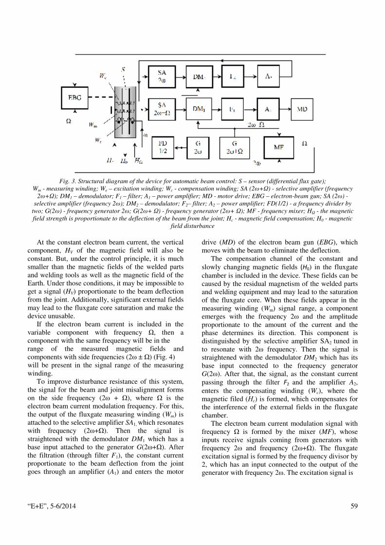
“E+E”, 5-6/2014 59
Fig. 3. Structural diagram of the device for automatic beam control: S – sensor (differential flux gate);
Wm - measuring winding; We – excitation winding; Wc - compensation winding; SA (2ω+Ω) - selective amplifier (frequency 2ω+Ω); DM1 – demodulator; F1 – filter; A1 – power amplifier; MD - motor drive; EBG – electron-beam gun; SA (2ω) -
selective amplifier (frequency 2ω); DM2 – demodulator; F2– filter; A2 – power amplifier; FD(1/2) - a frequency divider by two; G(2ω) - frequency generator 2ω; G(2ω+ Ω) - frequency generator (2ω+ Ω); MF - frequency mixer; HΩ - the magnetic field strength is proportionate to the deflection of the beam from the joint; Hc - magnetic field compensation; H0 - magnetic
field disturbance
At the constant electron beam current, the vertical component, HV of the magnetic field will also be constant. But, under the control principle, it is much smaller than the magnetic fields of the welded parts and welding tools as well as the magnetic field of the Earth. Under those conditions, it may be impossible to get a signal (HV) proportionate to the beam deflection from the joint. Additionally, significant external fields may lead to the fluxgate core saturation and make the device unusable.
If the electron beam current is included in the variable component with frequency Ω, then a component with the same frequency will be in the range of the measured magnetic fields and components with side frequencies (2ω ± Ω) (Fig. 4) will be present in the signal range of the measuring winding.
To improve disturbance resistance of this system, the signal for the beam and joint misalignment forms on the side frequency (2ω + Ω), where Ω is the electron beam current modulation frequency. For this, the output of the fluxgate measuring winding (Wm) is attached to the selective amplifier SA1, which resonates with frequency (2ω+Ω). Then the signal is straightened with the demodulator DM1 which has a base input attached to the generator G(2ω+Ω). After the filtration (through filter F1), the constant current proportionate to the beam deflection from the joint goes through an amplifier (A1) and enters the motor
drive (MD) of the electron beam gun (EBG), which moves with the beam to eliminate the deflection.
The compensation channel of the constant and slowly changing magnetic fields (Н0) in the fluxgate chamber is included in the device. These fields can be caused by the residual magnetism of the welded parts and welding equipment and may lead to the saturation of the fluxgate core. When these fields appear in the measuring winding (Wm) signal range, a component emerges with the frequency 2ω and the amplitude proportionate to the amount of the current and the phase determines its direction. This component is distinguished by the selective amplifier SA2 tuned in to resonate with 2ω frequency. Then the signal is straightened with the demodulator DM2 which has its base input connected to the frequency generator G(2ω). After that, the signal, as the constant current passing through the filter F2 and the amplifier A2, enters the compensating winding (Wc), where the magnetic filed (Нc) is formed, which compensates for the interference of the external fields in the fluxgate chamber.
The electron beam current modulation signal with frequency Ω is formed by the mixer (MF), whose inputs receive signals coming from generators with frequency 2ω and frequency (2ω+Ω). The fluxgate excitation signal is formed by the frequency divisor by 2, which has an input connected to the output of the generator with frequency 2ω. The excitation signal is

“E+E”, 5-6/2014 60
Fig. 4. Spectrum components of the Fluxgate measuring winding signal: a) - ε ≠ 0; Spectrum component of the
measuring winding signal with uncompensated frequency 2ω; b) - ε ≠ 0; Spectrum component of the measuring
winding signal with compensated frequency 2ω; с) - ε = 0; spectrum component of the signal with frequency 2ω -
compensated.
delivered to the fluxgate excitation winding We with the frequency divisor by 2 FD.
The device was tested in vacuum conditions. The error of the beam alignment with the joint did not exceed 0.3 mm, which is quite acceptable for the Electron Beam Welding in air.
Conclusions 1. We propose a method of electron beam
positioning relative to the joint during the electron beam welding in air. This method is based on identification of the magnetic fields and coordinates of the electron beam.
2. The proposed method allows controlling of the electron beam location and correcting it with the help of the automated system for joint tracking with no errors.
3. The noise immunity of the proposed system is improved, as the useful signal has the frequency different from frequencies of parasite magnetic fields.
4. During electron beam welding of dissimilar materials, when the beam is at the joint, the vertical component of the magnetic field does not have a zero value due to inequality of currents in the parts. This is explained by differences in the materials’
conductivity. In this case, the current’s strength, proportionate to the strength of the vertical component of the magnetic field, needs to be compensated for at the input of the electron beam gun motor drive.
REFERENCES [1] Braverman V., V. Belozertsev, T. Veisver, N.
Goryashin, A. Lelekov, V. Bashenko. The device with fluxgate sensor for joint tracking. Int. Conf. EBT'12. Varna, Bulgaria, “E+E”, 5-6, 2012, pp. 58-63.
[2] Braverman V., V. Laptyonok, V. Belozertsev, Fluxgate sensor for joint tracking. Copyright сertificate No. 941056 USSR, international classification index: B23К9/10, published on 07.07.82, bulletin No. 25.
[3] Braverman V., V. Laptyonok, V. Belozertsev, Method for measuring deviations of the electrode from the seam. Copyright certificate No. 941057 USSR, international classification index: B23К9/10, published on 07/07/82, bulletin No. 25.
Prof. Dr. Vladimir Ya. Braverman – graduated from Krasnoyarsk Polytechnic Institute in 1975 with engineering qualification and specialization in flying objects control systems. Now he works as the professor of Automatic Control Department at the Siberian State Aerospace University named after academician M.F. Reshetnev (Krasnoyarsk, Russia)/ His research interests: conversion energy, industrial automation.
tel. +79232979463 е-mail: [email protected]
Assoc. Prof. Vladimir S, Belozertsev – graduated from Krasnoyarsk Polytechnic Institute in 1974 with engineering qualification and specialization in flying objects control systems. Now he works as the associate professor of Automatic Control Department at the Siberian State Aerospace University named after academician M.F. Reshetnev (Krasnoyarsk, Russia)/ His research interests: conversion energy, industrial automation.
Assoc. Prof. Valeriy V. Bogdanov - graduated from Krasnoyarsk Polytechnic Institute in 1977 with engineering qualification and specialization in equipment and technologies of industrial welding. He now works as the chair for the Department of welding of flying objects at the Siberian State Aerospace University named after academician M.F. Reshetnev (Krasnoyarsk, Russia). His research interests: electron beam welding, indestructible control of welding joints.
Assoc. Prof. Nikolay V. Uspenskiy - graduated from Krasnoyarsk Polytechnic Institute in 1981 with engineering qualification and specialization in flying objects control systems. Now he works as the associate professor of the Department of welding of flying at the Siberian State Aerospace University named after academician M.F. Reshetnev (Krasnoyarsk, Russia)/ His research interests: electron beam and laser welding.

“E+E”, 5-6/2014 61
Dipl. – Ing. (FH) Alexander E. Beniyash - - graduated from Leningrad Polytechnic Institute named afterM.I. Kalinin in 1970 with engineering qualification and specialization “Technology of semiconductor materials”. Now he works as the research associate of the Institute of Materials Science of Leibniz University (Hanover). His research interests: electron beam welding.

“E+E”, 5-6/2014 62
Compensation of the Еffect of Magnetic Fields on the Position of the Electron Beam in the Process of Electron Beam Welding
Valery D. Laptenok, Alexandra A. Druzhinina, Alexander V. Murygin, Yury N. Seregin
The paper presents the approximate formulas for calculating the deflection angle and the
misalignment of the electron beam from the optical axis of the electron gun caused by the action of magnetic fields during the electron beam welding. Mathematical model of the effect of magnetic field induced by thermoelectric currents on the electron beam position in the process of electron beam welding of dissimilar materials is presented. The method of monitoring of the misalignment of the scanning electron beam and its mathematical model are proposed. Monitoring of the misalignment of the scanning electron beam is based on the processing of the signal of the collimated X-ray sensor directed to the optical axis of the electron gun by synchronous detection method. The method of compensation of the effect of magnetic fields by passing through the welded seam the currents which compensate thermoelectric currents is considered.
Компенсация на ефекта на магнитни полета върху позицията на електронния сноп в процеса на електроннолъчевото заваряване (Валери Лаптенок, Александра Дружинина, Алексанър Муригин, Юри Серегин). Работата представя апроксимиращи формули за пресмятане на ъгъла на отклонение и отместването на електронния лъч от оста на електронната пушка причинени от действието на магнитни полета при електроннолъчево заваряване. Представен е математически модел на влиянието на магнитното поле, индуцирано от термоелектрическия ток върху позицията на електронния лъч в процеса на електроннолъчево заваряване на разнородни материали. Предложен е метод за проследяване на отклонението на сканиращ електронен сноп и математическия му модел. Проследяването на това отклонение е основано на обработката по метода на синхронната детекция на сигнал от колимиран рентгенов сноп на рентгенов датчик, насочени по оптичната ос на пушката. Разгледан е метод за компенсация на влиянието на магнитни полета чрез пропускане през шева на ток, който компенсира термоелектронния ток.
Introduction One of the main causes of deflection of an electron
beam during electron beam welding (EBW) is the effect of magnetic fields. These fields can be caused by the magnetization of the equipment, the residual magnetization of welded products, the action of various electromagnetic devices, thermoelectric currents produced by temperature gradients in some dissimilar materials [1]. Different ways of reducing the effect of magnetic fields are used. There are demagnetization of products, shielding of electron beam, and the compensation of magnetic field in the welding zone. Demagnetization of products can significantly reduce the noise level, but it may be re-
magnetized. In addition, demagnetization of large parts is a labor-consuming and expensive process. Shielding of the electron beam by magnetic shield is the protection from external fields in the space of the shield location. This shield degrades possibility to monitor the process of EBW. Therefore, the compensation of magnetic field in the zone of magnetic field action is most appropriate [1].
Assessing the impact of the magnetic field To assess the effect of magnetic field on the
trajectory of the electron beam the formulas for calculating the deflection of the electron beam from the axis of the electron gun should be derived. Also, determination of the angle of the beam trajectory is an
“E+E”, 5-6/2014 63
interesting, because it characterizes deflection of the weld seam from the plane of the joint.
The action of magnetic fields in the space between the electron gun and the work piece during EBW can be described with sufficient accuracy by the equations [2]:
(1) ∫=ψz
dzzBmV
e
0
)( , ∫ ∫=z z
dzdzzBmV
eX
0 0
)( ,
where ψ – angle of inclination of the trajectory of the electron beam relative to the optical axis of the electron gun z; X – displacement of the electron beam from the joint; e – electron charge; m – mass of the electron; V – electron speed, which depends on the accelerating voltage; B(z) – projection of induction of the magnetic field in the plane of the joint as a function of the coordinate z.
The origin of coordinates (z=0) is the center of the focusing system.
The error of calculations according to formulas (1) for most cases occurring in practice doesn’t exceed 2.5 %.
A mathematical model of magnetic fields induced by thermoelectric currents
When welding dissimilar materials the deflection of the electron beam from the joint can be caused by magnetic field of thermoelectric currents. According to Ohm's law, the current I in a closed circuit is directly proportional to the electromotive force and inversely proportional to the total resistance R of the entire circuit. Value of arising thermoelectric power E depends on the material of welded products and temperatures of hot (T1) and cold (T2) contacts. In a small range of the temperature the thermoelectric power can be considered as proportional to the difference of the temperature.
When welding two dissimilar materials 1 and 2 the total resistance of the entire circuit is the sum of the resistances R1 and R2 of these materials. Resistance of the conductor constant cross-section depends on the properties of the material of the conductor, its length and cross-section.
Thus, the thermoelectric current is determined by the formula:
(2)
Rl
TTS
R
EI
2
)12(
21
12
ρ+ρ−α
== ,
where 12α – thermoelectricpower coefficient; ρ1, ρ2 – resistivities of welded materials; lR – length of the conductor; S – cross-sectional area of the conductor;
T1 – temperature at the center of the weld where the circuit of thermoelectric currents is closed; T2 – melting temperature.
For determining the temperature T1 the equation of the temperature distribution in the infinite plate heated by a fast-moving line source without the heat transfer from the surface can be used [3]:
(3)
−=
ay
vx
y
vTkyxT
4exp),(
2
max12 ,
where 12k – coefficient characterizing the thermophysical properties of welded materials; maxT – maximum temperature (evaporation temperature of welded materials); v – welding speed; a – coefficient of the temperature conductivity; x – coordinate across the joint; y – coordinate along the joint.
Equation (3) describes the temperature of an area which located behind the welding source.
Temperature at the center of the weld is determined by the formula
(4) y
vTkT
−= max12 .
Assume that the conductor with the thermoelectric current is an ellipse, as shown in Fig. 1. The length of the ellipse can be calculated from the approximate formula:
(5) ( )xyR aal +π= ,
where 2
wy
yya
−−= – semi-major axis of the
ellipse; wy – distance from the optical axis of the electron gun to the conductor with current (the length of the welding cavity along the axis y) ; ax – semi-minor axis of the ellipse.
Substitution of formulas 4 and 5 into expression 2, differentiation of the resulting expression with respect to y, equating of the derivative to zero allow to define coordinate ymax of closing the circuit of the maximal thermoelectric current I0. Semi-minor axis of the ellipse should be set.
Values of circulating thermoelectric currents are defined by the expression:
(6) ,2
22max21
maxmax12max1212
−+−−⋅π⋅ρ+ρ
−−−
+δα
=yx
w
yywx
n
nbayy
nby
vTk
nby
vTkb
I
where by – width of the conductor with current; δ – thickness of the product; n= 0, 1, 2, 3….

“E+E”, 5-6/2014 64
Fig.1. Schematic representation of the model
Contours with thermoelectric currents are approximated by rectangles of length
)2( max yw nbyy −−− and width )22( yx nbb − , where
n= 0, 1, 2, 3…. Components of magnetic field directed along the welding line, have the greatest impact on deflection of the electron beam from the joint. These magnetic fields are induced by line segments of current which are perpendicular to the weld.
According to the law of Biot-Savart-Laplace in the case when 21 α=α , 121 cos2coscos α=α−α the induction of magnetic field of the straight line segment of current having a finite length is described by the equation [4]
(7) 22
01
0
2cos
2 rb
b
r
I
r
IB
x
x
+⋅
πµ
=απ
µ= ,
where xb – half the length of the straight line segment of current; r – distance from the straight line segment of current to the point under consideration.
During the welding process conductors with a current are removed from the axis of the electron gun to distances )( yw nby + and )( max ynby −− , distance
from the point under consideration M to the surface of the welded parts is )( zl − , where l – distance from the surface of the welded parts to the electron gun, as shown in Fig. 1. Distance from the straight line segment of current to the point under consideration is determined by formula
(8) 22 )()( zlnbyr yw −++= .
Thus, the equation (7) can be written as
(9)
,)()()(
)()(2)(
222
22
0
zlnbynbb
nbb
zlnby
IzB
ywyx
yx
yw
nn
−+++−
−×
×−++π
µ=+
(10)
.)()()(
)()(2)(
22max
2
22max
0
zlnbynbb
nbb
zlnby
IzB
yyx
yx
y
nn
−+−−+−
−×
×−+−−π
µ=−
Indices «+» and «-» show that vectors of magnetic induction are directed oppositely to each other.
Using expressions (6), (9) and (10), total deflection can be calculated according to equation (1).
For comparative assessment of calculated and experimental data the materials and their characteristics considered in paper [5] are used. Properties of welded materials are presented in Table 1. The results of calculations produced for welding stainless steel SS 304 and low-carbon steel showed that at an accelerating voltage of 60 kV, a welding speed of 40 m/h, the product thickness of 2.5 cm deflection of the weld from the joint at the depth of 6 mm is 0.6 mm. The calculation results agree well with experimental data obtained in the work [5].
Table 1. Properties of alloys
Alloy T2 (K) a (m2/s) × 105 ρ (Ohm·m) × 10-7
Stainless steel SS 304
1700 0.45 6.667
Low-carbon steel
1783 1.28 1.136
System of control and compensation of deflection caused by the action of magnetic field
In the interaction of the electron beam with the processed material electrons lose their energy as a result of braking. This process is accompanied by the excitation of the X-ray radiation, localized in a place where the electron beam interacts with the material.
The ability to control the deflection of the electron beam from the optical axis of the gun by the X-ray radiation from the zone of braking of electrons is

“E+E”, 5-6/2014 65
based on the fact that the intensity of X-ray radiation depends from the surface area through which the radiation flux passes. Deflection of the beam from the axis of the electron gun caused by the action of magnetic fields, leads to a decrease of share of X-ray radiation passing through the crystal area of the sensor. Consequently, the intensity of X-ray radiation
dI measured by the sensor is reduced. X-ray sensor includes X-ray detector and
collimator, which is configured in the form of a blind with the slit oriented to the optical axis of the gun, as shown in Fig. 4.
For monitoring the beam deflection the technological scanning, which improves the quality of the welded joint is used.
A mathematical model of the X-ray sensor as an element having the frequency spectrum of the output signal at presence of the periodic signal of scanning of the electron beam is expressed by the relation [6]
(11) ( )∑∞
=++=
1
0 sincos2
)(n
nnd ntbntaa
tI ,
where coefficients of the series are given by the expressions:
(12) ∫π
π−π= dttIa d )(
10 ,
(13) ∫π
π−π= ntdttIa dn cos)(
1,
(14) ∫π
π−π= ntdttIb dn sin)(
1.
Here, the intensity of X-ray radiation from the surface of the work piece is determined by expression
(15) ( ),
2
sinexp)(
2
1
2
20
201
dxtx
xf
ZIUkkI
x
md
x
ed
∫∞
∞−
σωε−ε−
−×
×πσ
=
where )(xf d – function of the view area of the collimator of X-ray sensor; k =1.5⋅10-9 V-1 – proportionality coefficient; k1 – coefficient considering the orientation of the sensor in the space; Ie – electron beam current; Z – atomic number of the material of welded product;U0 – accelerating voltage; h – width of the slit of the collimator of X-ray sensor; l1 – length of the collimation channel; l2 – distance from the collimator to the workpiece surface; σx – root
mean square deflections of electrons from the axis of the beam along the x axis; ε0 – deflection of the beam from the optical axis of the electron gun; εm – amplitude of the beam scanning across the joint; εx – the position of the beam axis along the x axis.
Dependencies of odd and even harmonics from the beam deflection from the axis of the gun are shown in Fig. 2 and 3. The calculation of harmonics was produced by the formulas (13) and (14).
Fig.2. Dependence bn(ε0) at εm=1.
According to the developed mathematical model of X-ray sensor the first harmonic of frequency of scanning allows to determine the beam deflection from the axis of the electron gun.
Fig.3. Dependence an(ε0) at εm=1.
The amplitude of the second harmonic is proportional to the sensitivity of the measurement transducer. It can be used to stabilize the amplification factor of the compensation system and focusing the beam.

“E+E”, 5-6/2014 66
In welding of dissimilar materials magnetic field B(z) is induced by thermoelectric currents, which are distributed in welded products.
Functional block diagram of system of automatic compensation of effect of magnetic field of thermoelectric currents is shown in Fig. 4.
This system includes an electron gun 1, a focusing system 2, source of the current of focusing 3, deflecting coils 4 and 5, a generator 7 of scanning of the electron beam across the joint and along it, a block 16 aiming the electron beam at the joint, electric drive
15 moving the electron gun, the current sources 17 and 18, X-ray sensor 8, selective amplifier 9 tuned to the frequency of scanning of the electron beam across the joint, demodulator 10, the amplifier 13 with controlled amplification factor, the integrator 14, selective amplifier 11 of the second harmonic, and a rectifier 12.
Current sources 17 and 18 contain current leads which are located on the top and bottom surfaces of a welded product 6 and symmetrical to the weld in the zone of maximum temperature.
Fig. 4. Functional block diagram of system of automatic compensation of effect of magnetic field of thermoelectric currents

“E+E”, 5-6/2014 67
The method of compensation of the effect of magnetic fields caused by currents of thermopower includes monitoring the deflection of the electron beam from the optical axis of the electron gun by X-ray radiation from the processing zone and input into the welded product compensating currents directed oppositely thermoelectric currents. Compensating currents eliminate the beam deflection. Value of compensating currents varies depending on deflection of the electron beam from the optical axis of the electron gun.
Conclusions The conclusions drawn are the following: 1. The considered mathematical model allows
calculating deflection of the electron beam and angle of slope of the trajectory depending on the distribution of magnetic induction in the space between the electron gun and the work piece.
2. Modeling the impact of thermoelectric currents on deflection of the beam when welding dissimilar materials agrees well with the experimental data.
3. Application of method of synchronous detection of the signal of X-ray sensor of the beam deflection allows automating the process of compensation the impact of magnetic fields in EBW.
REFERENCES [1] Nazarenko, O. K. Avt. Svarka. 1982, No. 1, pp.
33-39. [2] Laptenok, V. D., Murygin, A. V., Seregin, Yu. N.,
Braverman, V. Ya. Control of electron beam welding. Krasnoyarsk, 2000, 234 p.
[3] Nerovnyy, V. M., Konovalov, A. V., Kurkin, A. S., Makarov, E. L., Yakushin, B. F. Theory of welding processes. Moscow, 2007, 752 p.
[4] Putilov, K. A. Course of physics. Vol. 2, Moscow, 1954.
[5] Wei, P. S., Chih-Wei Wen. Missed joint induced by thermoelectric magnetic field in electron-beam welding dissimilar metals – Experiment and scale analysis. Metallurgical and Materials Transactions B, 2002, Volume 33, Issue 5, pp 765-773.
[6] Druzhinina, A. A., Laptenok, V. D., Murygin, A. V., Seregin, Yu. N. Method for monitoring of impact of magnetic fields in the process of electron-beam welding by X-ray radiation from treatment area. Vestnik SibGAU. 2012, No. 5 (45), pp. 158-163.
Prof. Dr. Valery D. Laptenok – Doctor of Science (Engineering), professor of the chair of information management systems of the Siberian State Aerospace University named after academician M. F. Reshetnev. Graduated from plant technical college, the branch of Krasnoyarsk Polytechnic Institute, in 1968. Area of scientific interests – complex solution of problems of automation of electron beam welding, processes of argon-arc welding, aluminum soldering.
tel.: 8(391) 291-92-44 е-mail: [email protected]
Alexandra A. Druzhinina – senior teacher of the chair of automation of production processes and thermal technology in metallurgy of the Institute of Non-ferrous Metals and Material Science of the Siberian Federal University. Graduated from Krasnoyarsk State Academy of Non-ferrous Metals and Gold in 1997. Area of scientific interests - automation of metallurgical processes.
tel.: 8(391) 206-37-12 е-mail: [email protected]
Prof. Dr. Alexander V. Murygin – Doctor of Science (Engineering), professor, head of the chair of information control systems of the Siberian State Aerospace University named after academician M. F. Reshetnev. Graduated from plant technical college, the branch of Krasnoyarsk Polytechnic Institute, in 1980. Area of scientific interests – automation of electron beam welding.
tel.: 8(391) 291-92-44 е-mail: [email protected]
Assoc. Prof. Yury N. Seregin – Candidate of Sciences (Engineering), associated professor of the chair of management information systems of the Siberian State Aerospace University named after academician M. F. Reshetnev. Graduated from plant technical college, the branch of Krasnoyarsk Polytechnic Institute, in 1985. Area of scientific interests – equipment and technology of electron beam welding.
tel.: 8(391) 291-92-44 е-mail: [email protected]

“E+E”, 5-6/2014 68
Mechanism of Onset of Keyhole Depth Fluctuations at Beam Welding Processes
Andrey A. Vasilyev, Vladimir A. Erofeev, Vladislav A. Sudnik
The mechanisms of the beginning of depth oscillations of the vapour-gas channel are examined in
beam welding. It is assumed that the reasons of the root peaks are the evaporation and condensation of metal vapour in the channel. To test this assumption, a system of the non-stationary equations of energy and balance of pressure at the channel surfaces has been solved. The channel configuration is determined by the boiling temperature isotherm. The heat, spent for the production of the vapour, defined as the difference between the beam power and the heat sink power in metal. The heat distribution along the channel length is determined by the temperature difference between the actual value at a given point of the channel and the value required to maintain the pressure equilibrium. Solving this system of equations shows that the periodic collapse of the channel occurs in its neck when the pressure therein vanishes, and the vapour from the bottom of the whole channel completely condenses at its walls.
Механизъм на началото на флуктуациите на дълбочината на кратера при заваръчни лъчеви процеси (А. А. Василев, В. А. Ерофеев, В. А. Судник). Изследвани са механизмите на започване на колебания на газопаровия канал при лъчево заваряване. Прието е, че причината за остриета в корена на шева са изпарението и кондензацията на металните пари в кратера. За проверка на това допускане е решена една система от нестационарни уравнения за енергията и баланса на наляганията при повърхността на канала. Конфигурацията на канала се определя от изотермата на температурата на кипене. Топлината, изразходвана за изпарение, се определя като разлика между мощността на лъча и мощността на топлопредаване в метала. Топлоразпределението по дължината на канала е определена от температурната разлика между действителната стойност в дадена точка от канала и стойността, необходима да поддържа равновесие на налягането. Решавайки тази система от уравнения можем да видим, че периодични колапси на канала се получават в нейното гърло, когато налягането там изчезва и порите от дъното на канала изцяло кондензират на неговите стени.
Introduction The typical defects of beam welding methods are
root peaks of the penetration depth (spikes) and voids, Fig. 1. The occurrence of these voids is explained by repetitive processes leading to a periodic collapse of the neck portion of the vapor-gas channel (keyhole) [1]. Fig. 1 shows a metallographic section* of the seam end with a linear reduction of the beam current in the electron beam welding (EBW) of alpha titanium alloy Ti 6-2-4-2, which shows the independence of root defects from the input power.
*The contract between MTU Aero Engines, Munich, Germany and Tula State University, Russia, 1999-2000.
Fig. 1. Spikes in the titanium alloy Ti 6-2-4-2 weld
The first self-consistent model by Kroos et al. [2], taking into account the interaction of some phenomena of the process, such as non-equilibrium evaporation and the pressure balance components at the keyhole wall, allows for the calculation of the shape and size of the channel, as well as the temperature and pressure inside. Sudnik et al. [3]

“E+E”, 5-6/2014 69
improved the Kroos's model and for the first time calculated the process efficiency of process efficiency of energy absorption on the basis of the fundamental principles of radiation absorption and energy loss. Kaplan et al. [4] proposed an analytical model of keyhole collapse during pulsed laser welding, his calculations were compared with the results of X-ray transmission microscopy during irradiation of the liquid zinc. A good agreement between theoretically and experimentally received channel allowed the authors to propose a process model that takes into account re-condensation during rapid cooling by gas flow in the channel during the pause. Krivtsun et al. [5] developed a self-consistent mathematical models of evaporation processes of metal, surface condensation and gas dynamics of the metal vapour in the keyhole which is formed in melted metal during laser welding with a deep penetration and investigated the influence of gas-dynamic processes on the state of vapour in the channel, its pressure at the wall of the channel and heat transfer in the melt pool through the evaporation and condensation processes at its free surface. The authors have shown that there is a positive heat flux areas at the channel wall (heating due to surface condensation vapour and released while bond energy of atoms in the melt), and areas where the vapour carries energy (cooling the melt surface due to evaporation). Turichin et al. [6] have developed an analytical dynamic model for laser and hybrid welding taking into account the keyhole collapse. This model is based on variation principles and a formalism of the Lagrange mechanics. The authors have reduced the model to a system of the ordinary differential equations. They have shown that the unstable behavior of the channel during welding fiber laser is connected with the beam radius size and intensity distribution. Erofeev [7] has developed a simplified model of the channel collapse during EBW in which the penetration depth and channel formation was determined by the equality values of channel temperature boiling point volatile component of the alloy. The solution of the equations of the model had a relatively oscillatory nature for the channel depth, but because of the high frequency oscillations and thermal inertia of the process, temperature field outside of the weld pool during the oscillation period did not change. An agreement between the calculated cross-sectional profiles and seam macrosections achieved by the introduction of calibration coefficients to account for the effect of stirring of the melt and data errors for boiling temperature. These coefficients are defined for a concrete alloy during the comparison of calculated and experimental values for the joint width and
penetration depth. Experimental observations of the formation of spikes show that they are in the range of frequencies from a few Hz [8] to a few kHz [9].
However, these models are rather complicated and are not adequately addressed the contribution of condensation. In this paper, a simplified model of the formation the channel and its collapse is presented.
Physical phenomena The ultimate aim of physical and mathematical
modelling is to make a system of equations which will allow for analysing the processes of evaporation and condensation in the beam welding methods. This system of equations describes the most significant physical processes linking penetration depth with the technological parameters.
The beam interacts with the metal surface and deepens, Fig. 2a. The beam energy causes intense evaporation at the keyhole bottom, and forms vapour flow V, Fig. 2b. The recoil pressure of vapour creates pressure on the liquid metal. The beam gradually deepens, forming a keyhole, Fig. 2b. Part of the heat is absorbed by the metal, another is spent on evaporation. The keyhole sidewalls are held by the pressure of the vapour flow from its bottom Pv, Fig. 2, c. The keyhole walls cool down by a heat sink into the metal.
Vapor flow prevents cooling as the vapour condenses at the surface of the channel walls. While the thermal energy of the vapor flow is sufficient to maintain the wall temperature at a temperature at which the partial vapor pressure together with the reactive vapor recoil pressure is sufficient to counteract the forces of constriction the channel, the latter is stable and deepens into the metal. The vapor quantity exiting in the channel decreases as the channel deepens, because an increasing portion of this vapor condensed on the side surface of the channel.
At the moment at which the vapour flow has been completely absorbed by the keyholes wall, the vapour pressure in the keyhole neck disappears. The resistance to capillary forces disappears and they close the entrance to the keyhole, Fig. 2. Beam action on a keyhole bottom stops, evaporation at the keyhole bottom disappears. In the lower part of the keyhole remains a gas cavity if the metal cools down to the melting temperature earlier than the force of capillary pressure of the keyhole’s wall fills it with the melt. In this case defect in the form of a root pore is formed, Fig. 2. The repeated deepening of the beam and melting of the metal can fill the formed cavity. It depends on the welding speed and the period of oscillation of the keyhole depth.

“E+E”, 5-6/2014 70
Fig. 2. Keyhole formation stages during beam welding
process (a-e) according Erofeev [7].
Evaporation processes are characterized by the distribution of power in the beam keyhole Pb, Fig. 3a, and which is released on its bottom. The part Pvap(z) of this power is transferred by vapour and absorbed by keyholes wall. Unabsorbed vapour power Pext taken out from the keyhole. If the power of the whole vapour flow will be absorbed by the keyhole walls, Fig. 3b and disappear vapour pressure in the inlet channel, the surface tension will constrict the neck. Beam power in collapsing rapidly redistributed from the keyhole bottom Pbb at its neck Pbn. Despite this redistribution keyhole will snap due to the inertia of the melt.
Fig. 3. Power distribution in a keyhole: (а) stable and (b)
unstable keyhole.
Mathematical model Due to a small radius of the keyhole with its
considerable length, it is permissible to consider a cylinder of radius rc with its end in the form of a hemisphere, and the neck of a toroidal shape with the radii that equal to the weld pool width Zr and the difference Zr – rc. The above mentioned physical processes are considered by development of mathematical model of the weld formation. A feature of high-temperature laser technological processes is an interaction of the various physical phenomena proceeding in the heterogeneous environment. The
structure of this environment should be defined as a result of the solution of the model equations. The structure of the space for modelling is described by a discrete function, indicating the points of space identity to one or another area, where the medium has certain properties. Using a Cartesian coordinate system x, y, z with the centre at the intersection of the beam axis with the surface of welded sheet which moves along the x-axis with a welding speed w
ν .
Energy equation At all points of modelling state of a substance is
determined enthalpy calculated solution of non-stationary energy conservation equation:
(1) [ ] )()( w zQx
HgradTTdiv
t
H+
∂
∂+=
∂
∂νλ ,
where H is the volumetric enthalpy, t is the time, T is the temperature, λ(T) is the temperature-dependent thermal conductivity, Q(z) is the function describing the volume distribution of the beam power and vapour per volume keyhole along its length z.
Relationship between enthalpy and temperature is given by:
(2) ∫ ++=T
VH
VLH
LCdTH
0ψψ ,
where Lψ is the fraction of the liquid phase, vψ is the fraction of the vapor phase, C is the volumetric heat capacity, HL and HV are the melting heat and the vaporization heat.
Initial conditions: (3) 0),,( TzyxT = 0, =t
Boundary conditions. At the top and bottom surfaces radiating heat
transfer is considered as
(4) ),TT(T 40
40grad −=− εσλ Szrz == o0
where ε is the surface radiation emissivity, σ0 is the Stefan-Boltzmann constant and S is the sheet thickness.
In infinite is set
(5) :, ∞=±∞= yx , 0TT =The source Q(z) describes the absorption of the
beam power at the keyhole bottom
(6) 2
ll r/Pl
q π= ,
the power consumption of a beam on production of the vapour:
(7) Tl
qv
q gradλ−=

“E+E”, 5-6/2014 71
and the power distribution vapour flow PV(z) along the keyhole in order to maintain its equilibrium surface
(8) [ ] ,)(k
2c)( z
cHHr
tz
vP −
∂
∂= π
where Hk is the metal enthalpy at which the equilibrium the vapor pressure provides the keyhole and Hc is the actual value of the enthalpy at the depth z.
Power of vapor heat is transferred keyhole walls at metal vapor condensation, which expires from the bottom keyhole. As it moves from the bottom to the keyhole neck, power vapor flow decreases.
(9) ( ) ( ) ∫−=z
Zc
VcVV dzzPzqzq )(
Therefore, it follows from the keyhole flow vapor thermal power is significantly less than the power vapor flow to the bottom of it. Thus, the heat source is described by dependence:
(10) ( )
<<+<<
=c
ccclZ zz)(
rzzzqzQ
0atzq
at
v
Equation of motion According to this hypothesis, keyhole collapses
into the neck when the vapor heat liberated at the keyhole bottom, is insufficient to maintain the temperature of the walls, providing a vapor pressure equal to the sum of a capillary pressure and gravity. Vapor pressure is determined by the surface temperature of the keyhole, capillary - curvature radius of the surface keyhole, gravity - the depth of the arrangement. The internal pressure in the melt is neglected because of the small volume keyhole compared with the weld pool.
The loss of stability moment determined by the condition 0)( == rV Zzq , i.e. corresponds to the disappearance of vapor flow in the keyhole the neck, Fig. 3b. After stability loss process starts collapsing keyhole in his neck. Decrease of keyhole diameter in a neck is defined by the solution of the equation of metal movement under the action of capillary and gravitational pressures
(11) grzdt
rd
cr
c −= σρ1
2
2
,
where σ is the surface tension for the pair melt - vapour at a surface temperature keyhole Tc,, ρ is the melt density and zr is the depth of the keyhole neck.
At the moment of vapour flow disappearance:
00 ==dt
dr;t c .
The duration tc of the keyhole collapse is determined by the condition
0)( =
ñctr .
Thermophysical properties of the alloy The simulation was carried out for titanium alloy
Ti 6-2-4-2, Ts = 1230 °C and TL = 1575 °C, other thermal properties are taken from Ref. [10]. The temperature and enthalpy are connected piecewise-linear function T(H), Fig. 4.
Fig. 4. Enthalpy and thermal conductivity coefficient vs.
temperature for titanium alloy Ti 6-2-4-2.
Numerical solution At the computer simulation of a space is artificial
limited up to the parallelepiped shape. The dimensions of the simulation area and the center position coordinates therein are based on a preliminary calculation of the size of the high temperature zone where the temperature exceeds the melting point of 0.2. The heat conduction equation solved by finite difference method for 3-D uniform grid with a step of 0.25 beam diameter. The time step has been chosen on a physical condition of inadmissibility of phase change in metal volume for one step of a grid.
At the initial stage is accepted that metal is cold, a keyhole is absent, and beam power is allocated in superficial control volume. In the time cycle calculated the enthalpy and the temperature at the grid. Then, the channel defined by the nodes, wherein the temperature is more than the boiling point. Power is determined from the bottom vapor flow channel, which is then redistributed to control volumes along

“E+E”, 5-6/2014 72
its length, starting from the bottom. If this power is enough for all the nodes that lie in the beam path, the simulation cycle continues, during which deepens keyhole. If not, then simulated keyhole collapse, i.e. keyhole depth is taken equal to zero and starts the next cycle simulation of penetration of the beam.
Solution results The process of the keyhole forming and weld pool
during EBW for sheet thickness of 12 mm at the accelerating voltage of 140 kV and the current of 14.5 mA, beam diameter of 0, 75 mm, and welding speed of 1 cm/s has been reproduced, Fig. 6. Maximum keyhole depth reached 10.3 mm. The wall temperature was 2815 °C, and the bottom - 2904 °C. Excess vapor pressure at the bottom was 0.3 N/cm2, or ~ 3% above ambient pressure.
Fig. 6. Temperature distribution in the longitudinal section (a), on the sheet surface (b) and in the beam action plane
(c).
The numerical solution has shown that process has oscillatory character, at which keyhole depth continuously changes, Fig. 7a. This process passes after a while in the steady-state condition at which the oscillation amplitude of keyhole depth is stabilised. In the period of oscillation power of vaporization at the bottom of the keyhole changes slightly. The power flow effluent vapour changes from a maximum equal to the number of the resulting vapour to zero at the time of collapse, Fig. 7b. Keyhole depth varies periodically, Fig. 8.
The keyhole collapse modelling by the equation (11) has shown that the radius of his neck at the collapse beginning changes slowly, but by the end is strongly accelerated, Fig. 9.
The collapse time is comparable with the beam penetration duration into the metal and the channel formation. For this reason, the beam penetrates into the keyhole for a long time after the collapse beginning, which provides the depth of penetration
greater than would be expected from the equilibrium state.
Fig. 7. Change of the keyhole depth zc and the weld pool
depth zl, vapour power flow at the keyhole bottom Pvap and at the keyhole exit Pext.
Fig. 8. Longitudinal sections of the keyhole and the weld
pool in the timing t1 (a), t2 (b) and t3 (c), and also the same with spikes (d): 1 - the base metal, 2 – the melt, 3 – the weld metal of single melting, 4 – weld metal of periodic melting.
Fig. 9. Keyhole neck radius after vapour flow
disappearance at the welding of titanium alloy Ti 6-2-4-2.
It follows that the beam penetration depth into the metal is partly determined by hydrodynamic phenomena in weld pool. Oscillations in channel depth periodically change the depth weld pool and the weld root metal periodically melts and crystallizes,

“E+E”, 5-6/2014 73
Fig. 8. The emergence voids most likely in this area. This allows estimating the probability of occurrence of voids in thickness of this zone of periodic melting.
Modelling adequacy Determine the frequency of oscillation can be
keyhole on longitudinal metallographic section, Fig. 1. This is tentatively tens Hz. The calculated frequency is of the data in Fig. 8 of 15 Hz. These values correspond to the lower values given in the literature [8].
Conclusion The offered model gives understanding of the main
reason for beginning of the keyhole depth instability, but needs addition for the accounting of some physical phenomena in a channel, in particular redistributions of some fraction of beam power on the melting front at beam movement with a welding speed, the scattering of the beam energy in metal vapour, as well as improve the model of the collapse of the neck canal.
Summary 1. The hypothesis about the reasons of emergence
oscillations of depth keyhole is offered at beam welding methods according to which the periodic keyhole collapse arises during the moment when all vapour evaporating from a keyhole bottom, fully condenses on its walls.
2. The physical and mathematical model of keyhole formation is developed at the beam welding processes, considering evaporation processes and metal vapour condensations in the keyhole.
3. The numerical modelling of evaporation processes and a metal vapour condensation in the keyhole has confirmed emergence of periodic oscillations of keyhole depth according to the offered hypothesis.
4. It is shown that the offered model gives understanding of the possible reason of emergence of instability of the keyhole depth and the weld pool.
REFERENCES [1] Rykalin N.N., Zuev I.V., Uglov A.A. Basics of
electron-beam treatment of materials (in Russian). Moscow. Mashinostroenie.1978. 240 p.
[2] Kroos J., Gratzke U., Simon G. Towards a self-consistent model of the keyhole in penetration laser beam welding. Journal Physics D: Applied Physics, Vol. 26, 1993 pp. 474-480.
[3] Sudnik W., Radaj D., Erofeev W. Computerized simulation of laser beam welding, modeling and
verification. Journal Physics D: Applied Physics, Vol. 29, 1996, pp. 2811 - 2817.
[4] Kaplan A. F. H., Mizutani M. Katayama S. , Matsunawa A. Computerized Unbounded keyhole collapse and bubble formation during pulsed laser interaction with liquid zinc. Journal Physics D: Applied Physics, 35, 2002, pp. 1218-1228
[5] Krivtsun I.V., Sukhorukov S.B., Sidorets V.N., Kovalev O. B. Evaporation processes modeling of metal and metal vapor in the gas dynamics of vapor-gas channel in laser welding. Automatic Welding. 10, 2008, pp. 19 – 26 (in Russian)
[6] Turichin G., Valdaitseva E., Pozdeeva E. et al. Theoretical investigation of dynamic behavior of molten pool in laser and hybrid welding with deep penetration, Paton welding journal, 2008 (7), pp. 11-15
[7] Erofeev V. A. Modelling of formation features of a keyhole during electron beam welding. (In Russian).Welding and Diagnostics, 4, 2009, pp. 12 - 18.
[8] Cho M.H., Farson D.F., Kim J.I. Control of chaos in laser-induced vapour capillaries. J. Laser Appl., Vol. 15, No. 3, 2003, pp. 161-167.
[9] Volpp J., Gatzen M., Vollertsen F. Simplified analytical modelling of dynamic behaviour of the keyhole for different spatial laser intensity distributions during laser deep penetration welding. Intern. Conf. Mathematical Modelling and Information Technologies in Welding and Related Processes. Katsiveli, Crimea, Ukraine. E.O. Paton Electric Welding Institute, Kiev. 2012, pp. 27 – 30
[10] Sudnik V. A., Erofeev V. A., Richter K.-H., Heins K.-U. 2006. Numerical modelling of the EBW process. 16th Conf. Computer Technology in Welding and Manufacturing and 3rd Int. Conf. Mathematical Modelling and Information Technologies in Welding and Related Processes. Kiev, 2006. PWI. Pp. 295-300.
Ing. Andrey Vasilyev - has born in Stavropol/Russia, graduates as welding technology engineer at Tula State University in 2012. Since 2012, he is graduate student in dept. of welding, casting and technology of construction materials at Tula State University, Tula, Russia.
Tel: +74872331258 e-mail: [email protected]
.Prof. Dr. Vladimir Erofeev - received his diploma on automated control systems in 1972 at Tula Polytechnic Institute, Tula. He defended his PhD in the optimization of resistance spot welding in 1985 at Moscow Technical University n.a. Ciolkovskiy. From 1993 till 2008 he carried out joint researches with ISF RWTH, Aachen, Daimler AG, Stuttgart, Germany and EADS, Munich, Germany. His scientific interests lie in the field of numerical modeling of fusion and solid-state welding processes by building self-consistent mathematical models, their calibration and verification.
Tel: +74872331258, e-mail: [email protected]

“E+E”, 5-6/2014 74
Prof. Full Dr. Wladislaw Sudnik - received his Diploma in Welding Technology at Russian State Technological University of Aviation Technology, Moscow in 1965. His Doctorate in physics of metals at Tula State University in 1973, and his doctor habilitatus in Welding Technology at St. Petersburg State Polytechnic University in 1991. 1977/1978 he was a visitor researcher at the Max-Planck for Iron and Steel Research, Düsseldorf, Germany. From 1991 till 2001 it carried out joint researches on development of mathematical models and creation of the software for arc welding with ISF RWTH, Aachen,
Germany and for laser and electron beam welding with Daimler AG, Stuttgart. He is a first recipient of the Sossenheimer Software Innovation Award of International Institute of Welding (IIW) in 2003 for his outstanding technical-scientific work concerning modelling and simulation in the field of welding and allied processes.
Tel: +79105822257, e-mail: [email protected]

“E+E”, 5-6/2014 75
Electron Beam Welding of the Elements Module Blanket ITER
Andrey P. Sliva, Victor K. Dragunov, Alexey L. Goncharov, Egor V. Terent’ev, Maksim S. Gribkov
The article is devoted to research of electron beam welding construction elements for International Thermonuclear Experimental Reactor in National Resesrch University “Mocow Power Engineering Institute”. It reviews design and technology of electron beam welding elements ITER blanket module made of austenitic steel ANSI 316 L(N). This article provides information about using the EBW to joint channel covers of the heat carrier thickness from 5 to 10 mm of shield block and supporting structure of the first wall. It considers patented the construction of special root part grooving welded channel covers butt joint and demonstrates a possibility of the EBW longitudinal load-bearing joints 140 mm thick of shield blocks in narrow gap. The results of EBW research combined dissimilar weld joints of austenitic steel 316 L (N) with bronze CuAl10Ni5Fe4 30 mm thick.
Електроннолъчево заваряване на елементи от бланкетния модул на ИТЕР (Андрей П. Слива, Виктор К. Драгунов, Алексей Л. Гончаров, Егор В. Терентиев, Максим С. Грибков). Работата е посветена на изследване на електроннолъчево заваряване на конструктивни елементи на международния термоядрен експериментален реактор. Бланкетния модул е направен от аустенитна стомана ANSI 316 L(N). Дадена е информация за заваряването на канали, покрити с топло-отводен блок с дебелина 5 до 10 mm и поддържаща структура от първата стена. Разглежда се патентована конструкция на канавка в корневата част на съединяваните челно каналови покрития и е демонстрирана възможност за електроннолъчево заваряване на надлъжни тежко-натоварени съединения с дебелина 140 mm в екраниращия блок в тесен процеп. Резултати от електроннолъчево заваряване на разнородни метали – аустенитна стомана от типа316 L(N) с бронз CuAl10Ni5Fe4 30 mm дебел са представени също.
Introduction Development power engineering in future
associated with the creation of fusion power plants. The most significant project in this area is creation of the International Thermonuclear Experimental Reactor - ITER. Considered in this paper features of creation welds elements of the shield block and the supporting structure of the ITER module blanket.
Blanket module ITER construction. Blanket module consists of 440 modules (Fig. 1)
located on the inner surface of the toroidal vacuum chamber and perform following functions: neutron and heat protection of the vacuum chamber and the coils of the magnetic field from the impacts of a thermonuclear plasma; forms a first safety barrier; provides heat removal from the metal structures in all modes of operation of the plant; supports plasma filament stabilization; organizes various diagnostic systems.
Each blanket module (BM) (Figure 2) consists of Fig. 1. ITER vacuum chamber sector with blanket modules (BM).

“E+E”, 5-6/2014 76
the first wall (FW) - part facing to the plasma and the shield block (SB). FW mechanically mounted on the front (facing to the plasma) SB surface by the specifically required fixing unit.
FW has the following application: the formation of the surface facing to the plasma, using materials with low atomic number (e.g. beryllium); perception of the charged particles flow from the plasma and radiation exposure during normal operation of the ITER reactor; protection inner chamber components and the vacuum chamber from direct contact with the plasma at a deviation of normal operating conditions; forms first protective barrier against radiation damage.
FW consists of the supporting structure first wall
and the first wall panels (Fig. 3). The support structure of the first wall made from
austenitic stainless steel ANSI 316L (N)-IG. It contains channels used for heat carrier circulation. Channels are closed by covers is welded to the body hermetic joints by electron beam welding. Mechanical connection of the first wall panels and support structure of the first wall is carried by eight pin connection. Pins are made from nickel-based alloy Inconel 718. The top of the covers in the supporting structure of the first wall is bimetallic, it made from aluminum bronze CuAl10Ni5Fe4 and stainless steel 316L (N). The pin holes are made in the bronze elements covers. Aluminum bronze CuAl10Ni5Fe4 allow remove heat from pins effectively.
Shield block BM#17 consists of two heavy halves 1047 × 715 × 364 mm, which are made heat carrier circulator channels by machining (Fig. 4). Channels are closed by covers welded to the body hermetic joints by electron beam welding. Halves of the blocks are joined together by EBW.
The following tasks were solved in NRU "MPEI": obtains welded joints channel covers heat carrier circulator with the body of first wall support structure; obtains bimetallic welded covers 316L (N) - CuAl10Ni5Fe4; research and developed technology of welded joints 140 mm thick halves of shield blocks and welded joints cover channels of the heat carrier thickness 5 mm to the body of the SB.
Fig. 2. Shield block of BM#17.
Panel FW - Be
Pin - Inconel 718
Fig. 3. Structure of the first wall (a) and the appearance of the support
structure first wall (b)
Bracket - CuAl10 Ni5Fe4
Support structure first wall - 316L (N)-IG
Panel FW - 316L (N)-IG
Cover - 316L (N)-IG
a
b

“E+E”, 5-6/2014 77
The tasks of electron beam welding hermetic joints cover channels of the heat carrier in the support structure of the first wall and shield blocks are similar. Therefore it can be divided it into the following parts:
• development of the technology EBW hermetic joint 5 to 10 mm thick cover channels of the heat carrier in the support structure of the first wall and shield blocks made of steel ANSI 316L (N);
• development of the technology EBW 140 mm thick halves of shield blocks made of steel ANSI 316L (N);
• development of the technology EBW bimetallic welded covers made of steel ANSI 316L (N) and aluminum bronze CuAl10Ni5Fe4.
EBW of the covers channels of the heat carrier in the support structure first wall and shield blocks
Initially welding joints of the covers assumed lead by the scheme (Fig. 5a). The following requirements are applied to weld: joints should be made through the entire depth junction and free from leakage at workloads during the whole product life cycle; the understatement in welds is not allowed in relation to the
top surface; it is necessary to obtain weld penetration into the horizontal slit c (Fig. 5 a) between the cover and block body; exception of weld spatter in the inner cavities of cooling channels.
Obtaining fusion locking slit is difficult because it is necessary to reduce the parameter c to zero and proceed to the butt joint with edge of different thickness. In this case it is expedient to proceed to the joint of equal thickness (Fig, 5 b). However, in this case, large amount weld spatter forms a in the inner cavities of cooling channels. Authors proposed and patented in the Russian Federation [1] special shape edges in the root part of the joint (Fig. 5 c) which provides support the cover, except slit c and spatter in the heat carrier channel.
The installation based on energy complex ELA 60/60 with an accelerating voltage of 60 kV was used for electron beam welding. It was established experimentally that the optimal bevel angle α edges at the root portion should be 60°. Fig. 6 shows the weld cover 8 mm thickness with application of the developed forms bevels edges on the technology specimen. Welding conditions: beam current is 100 mA; a
Fig. 4. Shild block #17

“E+E”, 5-6/2014 78
welding speed is 100 m/hr; sharp focus on the 2/3 the thickness of the penetration. Fig. 7 shows the model of supporting structure of the first wall with welded joints of the covers.
EBW halves of the Shield blocks
The thickness of the weld shield block halves is 140 mm, moreover, the welded joint is complicated by the technologically gap width of 8 mm and a depth of 152 mm from one side and respectively
Fig. 5. Weld covers channels of the heat carrier to the body: a - into the lock, b - butt; c - with the bevel edges in the root; 1 - body, 2 - cover
с
2 α
2 1
2 1 1
а b c
Fig.6. Weld cover 8 mm thickness with application of the developed forms bevels edges
12
0,71
Fig. 7. - Model of the supporting structure first wall with welds

“E+E”, 5-6/2014 79
Gap of 8 мм
Vacuum cavities
Reinforcement of weld
Fig. 9. Formation of the joints 85 mm
depth in the welding gap 8 mm
the width of 16 mm and a depth of 72 mm on the other side (Fig. 4, 8).
It is preferable to produce a weld on both sides for aligning the angular deformation in such kind of structure. The significant reinforcement formation on the top surface of the weld of weld is typical for EBW with deep penetration. This is due to the occurrence of welding deformation as well as various density of the basic and cast metal. Thus, unlike the welding of the free surface, for a narrow gap welding with deep penetration liquid metal forming reinforcement is not fitted in the existing gap and periodically fills vapor gas passage increase probability of appearance of defects such as vacuum cavities (Fig. 9). It was proposed to make groove at the bottom of the narrow gap to reduce this effect (Fig. 8 b). The dimensions of groove are determined experimentally [2] on the basis of the size of the reinforcement of weld at the free surface. Thus, the usage of electron beam welding on both sides and forming groove in a narrow gap is allows to obtain welded construction of shield block with minimal deformation without defects, such as vacuum cavities (Fig. 10). Welding conditions: beam current is 780 mA; a
welding speed is 15 m/hr; sharp focus on the 2/3 the thickness of the weld penetration.
EBW welded bimetal covers made of steel 316L (N) and bronze CuAl10Fe5Ni4
Fig. 8. - Butt weld joint in EBW of narrow-gap: a - initial shape; b - with the groove at the top of the butt joint.
а
б
Fig. 10. Appearance of the shield block, the groove in the bottom of a narrow gap and macrosection of joint 140 mm thickness by welding on both sides

“E+E”, 5-6/2014 80
Welding considered materials is complicated by metallurgical incompatibility of this material in a liquid state. Iron and copper are the basis of alloys and practically insoluble in the liquid state at each other. So if the fusion welding is used it is necessary to seek the minimum mixing this metals in the weld pool. In addition, structural transformations of metals in the heat affected zone may lead to temper softening the weld joint as a whole. For qualitative welded joint you must change the process to welding-brazing with minimizing the melting of the steel. In this case welded joints are formed by diffusion processes at the interface between the liquid bronze with solid steel.
Researches EBW of steel with bronze carried out on samples of 30 mm thickness (Fig. 11), with varying degrees of melting steel. The criteria for assessing the quality of welded joints were defects and mechanical properties in local areas weld and joint as a whole. As a result, it is established that the application of the EBW allows to obtain defect-free welds CuAl10Ni5Fe4 bronze with steel 316 L (N). Mechanical testing tensile welded specimens have shown that the fracture predominantly located in the base metal of alloy steel. So the main determining factor of the mechanical properties is the chemical composition of the weld metal: the degree of steel melt - 0.2…0.35 in the weld which provides strength level of the base metal of 316 L (N) strength - 600 MPs with strength bronze base metal about 700 MPs. Heat treatment regime by tempering at 400° C for 40 minutes increases the ductility of the weld metal [3]. Fig. 12 shows a bimetallic weld cover model of CuAl10Ni5Fe4 bronze and steel 316 L (N).
Conclusions The investigations demonstrate a possibility of
producing welds elements of the first wall of the blanket module of ITER. Original patented special shape edges in the root location of the welded joint cover channel of the heat carrier with the support structure first wall and shield blocks thickness of 5 to 10 mm of steel ANSI 316L (N). The advantages of this solution: the root of the weld is formed and is practically excluded weld spatter in the internal channel; there is no lack of penetration at the slit; the positioning of covers is provided.
Proposed and patented the method of EBW halves of the shield block 140 mm thickness in a narrow gap with a predetermined size of groove. The full scale
models of shield block and support structure of the first wall was created.
The research results demonstrates the possibility of applying EBW for weld bimetallic covers of steel 316L (N) and bronze CuAl10Ni5Fe4.
REFERENCES [1] Dragunov V.K., Sliva A.P., Myasnikova A.M.
Method for production butt interlock welding joints different thicknesses of parts // Patent RU 2510316 C1, B23K 15/00, B23K 33/00, B23K 31/02; FSEE HE "NRU" MPEI" (Russian Federation); Publ. 03/27/2014 Bull. Number 9. 7 p.
[2] Dragunov V.K., Sliva A.P., Gavrilov N.N. Electron beam welding method. // Patent RU 24488216 C1, B23K 15/00, B23K 33/00, FSEE HE "NRU" MPEI" (Russian Federation); Publ. 04/27/2012 Bull. Number 12. 6 p.
[3] Electron beam welding of bronzes to 316 L(N) steel/ A. Goncharov, E. Terentyev, A. Marchenkov, M. Portnov // Elektrotechnica & Elektronica E+E, Pepers from 10-th International conference of electron beam technologies – EBT’2012. -Sofia, Bulgaria: Vol.47 2012 5-6, p. 123-128
Fig. 11. Appearance of the weld specimen of steel 316 L (N) with bronze CuAl10Ni5Fe4 and macrosection of joint
Fig. 12. Model bimetallic welded cover of bronze CuAl10Ni5Fe4and steel 316 L (N)

“E+E”, 5-6/2014 81
Prof. Dr. Viktor K. Dragunov – Head of Department of Metals Technology of National Research University “MPEI”, Moscow, Russian Federation.
e-mail: [email protected]
Assoc. Prof. Dr. Alexey L. Goncharov – Department of Metals Technology of National Research University “MPEI”, Moscow, Russian Federation.
e-mail: [email protected]
Assoc. Prof. Dr. Andrey P. Sliva – Department of Metals Technology of National Research University “MPEI”, Moscow, Russian Federation.
e-mail: [email protected]
Eng. Egor V. Terent’ev – Department of Machine design Fundamentals of National Research University “MPEI”, Moscow, Russian Federation.
e-mail: [email protected]
Eng. Maksim S. Gribkov – Department of Metals Technology of National Research University “MPEI”, Moscow, Russian Federation.
e-mail: [email protected]

“E+E”, 5-6/2014 82
EBW of Stainless Steels and ODS Ferritic Steel
Petr Havlík, Pavel Šohaj, Jan Kouřil, Rudolf Foret, Ivo Dlouhý
Dissimilar welds are the integral part of design in chemical, nuclear and energy industries. One
of the most common combinations is the joints between ferritic, austenitic and martensitic steels. These joints provide many advantages at the detriment of the worse weldability. Possible defects in dissimilar welds are caused by different physical properties of welded materials. Choice of electron beam welding (EBW) is achieved the reducing the amount of heat input into the weld and reduce the negative effects of the surrounding atmosphere. Suppression of defects can be done by the right settings of EBW parameters. Another way is right choice of the rolling direction of base materials against the orientation of weld joint, which is most occurs in a materials whose structure has grains with a large ratio length-to-width (e.g. extruded ODS steel). In this work were evaluated four heterogeneous welds of austenitic stainless steel, martensitic stainless steel and ODS ferritic steel, which vary in the used welding parameters and in the orientation of the base materials to the direction of welded joint. Optimization of welding conditions was performed on the basis of structural and hardness measurements.
Електроннолъчево заваряване на неръждаема стомана и феритна стомана (П. Хавлик, П. Сохай, Й. Курил, Р. Форет, И. Длоухи). Заваръчните шевове на разнородни метали са интегрална част от конструирането на химични, ядрени и енергийни инсталации. Една от най-използваните комбинации е съединението между феритна, аустенитна и мартенситна стомана. Тези съединения обезпечават много преимущества при затрудненията на лоша заваряемост. Възможните дефекти при несиметричните шевове са причинени от различните физически свойства на заваряваните материали. С изборът на електроннолъчево заваряване се постига намалено топло-влагане в шева и намаляват негативните ефекти от обкръжаващата среда. Редуциране на дефектите може да се постигне чрез правилният избор на параметрите на заваръчния процес. Друг подход е правилния избор на валцоване на основния материал по отношение на заваръчния шев, който най-често е в материал, структурата на който е със зърна с голямо отношение дължина към ширина (например екструдирана ОДС стомана). В тази работа са оценени четири шевове от аустенитна неръждаема стомана, които са направени с променящи се заваръчни параметри и ориентация на валцоване на базовия материал към направлението на шева. Оптимизация на заваръчните условия е направена на основата на структурни анализи и измерване на твърдостта.
Introduction Material use in applications for the chemical,
nuclear and energy industry is determined by their behavior and resistance under operating conditions. These conditions may be varying in the different stages during process. Present trend in improving the efficiency of these processes is associated with increase in temperature leads to the simultaneous use of conventional and advanced materials. This creates the requirements for heterogeneous welded joints between materials having different chemical composition and physical properties. Disadvantage
of these joints is the frequent presence of defects that may lead to weakening the weld joint and the entire structure [1].
As an example, the substitution of conventional heat resisting steels for advanced oxide dispersion strengthened (ODS) steels such as Fe-Cr-Al steel Incoloy MA 956 (chemical composition is given in Table 1). ODS steels exhibit excellent corrosion resistance at high temperatures due to Cr content above 16 wt. %. Al is added (about 5 wt. %) for further enhancement of high temperature corrosion resistance due to formation of the protective coating. Between other advantages of these alloys belongs

“E+E”, 5-6/2014 83
creep and radiation resistance. These properties are achieved by fine oxide dispersion (the most commonly is used Y2O3 with a diameter of several nm) inside the ferrite matrix. These oxides are still stable at 1330°C and creates obstacles for moving dislocations in the entire operating temperature range of ODS steels. The desired structure is achieved by the unconventional production method – by powder metallurgy. The production of these materials has been described in papers [2, 3]. The last step during production ODS steels is recrystallization annealing at temperatures between 1100°C and solidus temperature. The structure is formed by ferritic grains which are elongated in the direction of extrusion and characterized by the large length to width ratio of grains. Length to width ratio of grains varies from 10:1 to 100:1 [2, 3].
Any intervention in the microstructure leads to the degradation of the above mentioned properties. This restricts weldability and applicability of these steels. Fusion welding causes coarsening of strengthening particles. Another undesirable effect during fusion welding which is associated with production and chemical composition is pore formation. Like most ferritic steels are the ODS steels susceptible for diffusion of hydrogen into the weldments, therefore must be welded under protective atmosphere. In heterogeneous welds is danger to the formation of inter-crystalline cracks due to differences in thermal conductivity and expansion. For these reasons it appear that the most advantageous method for joining of ODS steels is friction stir welding. This method is not suitable for welding of complex shaped parts. In such cases it is not possible to avoid the use to fusion welding methods [4, 5].
The most suitable method for fusion welding of homogeneous and heterogeneous welds of ODS steels are high-energy techniques – laser or electron beam welding (EBW). EBW due to its principle is a suitable method for preventing hydrogen diffusion in to the weld joint and reduced the amount of the heat affected base material (BM). The occurrence of defects and undesirable phases can partially limit the appropriate choice of EB parameters and welding procedure [4].
In this work were studied the influence of parameters settings and welding procedure on the resulting structure of the heterogeneous EB welds. Furthermore the effect of an orientation of the extruded BM structure relative to the orientation of weld on the cracks formation was evaluated.
Experimental There were performed four heterogeneous EB
welds among the ferritic ODS steel MA 956 and the austenitic steel 316Ti (sample 1) or the martensitic steel X4CrNiMo16-5-1 (samples 2-4) to evaluating the influence of settings of EB parameters on the resulting welds. Chemical composition of used steels is shown on Table 1. Sample 1 is formed by circumferential weld which was made without filler metal between cylindrical samples with 12 mm diameter. This sample was performed on device FOCUS MEBW-60/2 in collaboration with Institute of Scientific Instruments of the Academy of Sciences of Czech Republic. Weld is oriented perpendicular to the direction of extrusion of BM of ODS steel. On samples 2-4 were made butt welds without filler metal which were made by two pass of EB. Samples were rotated by 180°after first pass of EB. Samples thickness was 6-8 mm. In this case was used the universal chamber EB machine Pro-Beam type K26. Orientation of the BM structure in the sample 2-4 is parallel to the weld. Orientation change of structure of BM was chosen to reduce the occurrence of cracks at the boundaries of ferritic grains described in [4]. Different procedures and parameters of EBW were selected order to reduce the pores formation in weld metal (WM) and at the WM/BM interface. Selected EBW parameters are described in Table 2. The location of the weld on sample 4 was shifted by 0.2 mm into the martensitic steel for the purpose of reducing the portion of melted ODS steel. Welds were evaluated in state after welding.
Microstructure of welded joints was evaluated using the light microscope Olympus GX-51 for detect the presence of undesirable structures and defects. Analysis of chemical composition of resulting welds was performed by the scanning electron microscope Philips XL which is equipped by the energy dispersive
Table 1.
Chemical composition of the used steels (wt. %)
Steel grade C Cr Ni Al Mo Mn Si Y2O3 Ti V Nb N MA 956 0.016 20.00 - 4.50 - - - 0.50 0.50 - - - 316Ti 0.02 17.10 11.80 - 2.25 1.83 0.60 - 0.19 0.14 0.02 0.06
X4CrNiMo16-5-1 0.06 16.00 5.00 - 1.15 1.45 0.7 - - - - -

“E+E”, 5-6/2014 84
spectrometer (EDS) EDAX. The aim of EDS analysis was determine the chemical composition of WM and presence of secondary phases at the BM/WM interface. These results were compared with microhardness measurement across the weld joints. Microhardness measurements HV 0.1 were performed on semiautomatic hardness tester LECO LM 247 AT in perpendicular direction to the axis of the weld.
Results ODS steel was welded in state after
recrystallization annealing (sample 1-4). Structure contains coarse ferritic grains (Fig. 1) with microhardness among 275 and 290 HV 0.1. Grains are elongated in the direction of extrusion and with the length to width ratio which is approaching to 100:1 (grains have width of the order 100 μm). Structure contains the entrapped gases originate from the production which leads to worse weldability. Structure of 316Ti steel is characterized by the fully austenitic structure (fig. 2) with average grain diameter around 50 μm. Austenite grains contain twins from previous processing; further contain the carbides and nitrides. Value of microhardness of this steel was determined by 220 HV 0.1. Martensitic steel used in samples 2-4 was welded in state after annealing in temperature range from 600 to 650°C. This heat treatment leads to the mixed structure of ferrite and tempered low-carbon martensite (sorbite) (fig. 3) with the resulting microhardness value in range from 220 to 260 HV 0.1.
EB welds exhibit classical nail-like appearance as well as in work [6] and their dimensions are shown in Table 3. Despite the smaller amount of energy delivered into the sample 1 is the head weld size comparable to the other samples. This is caused by lower thermal conductivity of steel 316Ti compared with ODS steel MA 956 and steel X4CrNiMo16-5-1. This is caused by lower thermal conductivity of 316Ti steel compared with MA 956 ODS steel and X4CrNiMo16-5-1 steel. This effect can be observed in the width of the weld joint.
Fig. 1. Structure of ODS alloy MA 956
Fig. 2. Structure of 316Ti steel
The selected parameters for circumferential weld allow penetration of EB to a depth of more than 6 mm, but did not allow escape of gases released during melting of ODS BM. At the same time there has been melting of aluminum protective coating and Y2O3 contained in ODS steel and this leads to formation of the oxide slags in WM which are described in [2].
Table 2. Used parameters during EB welding
Accelerating voltage [kV]
Beam current [mA]
Welding speed
[mm/s]
EB weld position relative to the interface
[mm]
Beam energy [kW/mm]
Beam energy per unit of length
[W/mm] Sample 1 55 15 10 0 0,825 82,5 Sample 2 60 21 15 0 1.26 84 Sample 3 80 15 15 0 1.2 80
Sample 4 80 15 15 0.2 into X4CrNiMo16-5-1 1.2 80
“E+E”, 5-6/2014 85
Differences in physical properties and in orientation of ODS BM led to formation of cracks along the boundaries of ferritic grains (fig. 4).
Fig. 3. Structure of X4CrNiMo16-5-1 steel.
Butt welds on samples 2-4 were made by the using double pass of EB. This process was chosen for facilitate escape gases from WM and for reducing cooling rate. Parallel orientation of ODS BM was chosen for limitations formation cracks along the boundaries if ferritic grains. In the sample 2 was observed crack along the boundary of ferritic grains. This was due to the width weld head witch crosses with grain boundary. Removal of porosity and slag contained in WM was not reached (fig. 8). Reducing the size and number of pores was achieved in the sample 3. In WM was observed large spherical slag particles (fig. 12 and 13).
Structure of WM of sample 1 is formed by the ferrite grains. Size of these grains is influenced by the cooling rate at a given location of the weld joint and by the structure at the BM/WM interface. Axis of weld with the slowest cooling rate is formed by the smallest grains. Vice versa the MA 956/WM interface is formed by large grains which continued in growth on grains of the original structure and were oriented in the direction of highest heat dissipation. Similar trend
was observed at the WM/316Ti interface – grain size is determined by lower cooling rate due to lower heat conductivity and due to original structure of 316Ti steel. At this interface was observed thin layer of secondary phase (fig. 5) which passes in to the narrow heat affected zone in the 316Ti steel. HAZ is characterized by larger austenite grains with smaller amount of twins. HAZ in the austenitic BM was confirmed when measuring the hardness (fig. 6). Slight decrease in microhardness was also observed at the MA 956/WM which was caused by coarsening of the oxide particles during melting of ODS BM. Average microhardness of WM was 497 ± 12 HV 0,1. EDS analysis of the content of alloying elements (Cr, Ni, Ti, Mo, Al – fig. 7) confirmed that there was a dilution of the both BM in WM.
Fig. 4. Structure of weld metal of sample 1(MA
956/316Ti).
Fig. 5. Structure at the WM/316Ti interface – sample 1.
Table 3. Dimension of EB welds
Width head of weld [mm]
Min. width in the weld centre [µm]
Sample 1 1,3/1,5 600 Sample 2 1,8/1,8 590 Sample 3 1,5/1,6 503 Sample 4 1,6/1,7 486

“E+E”, 5-6/2014 86
Fig. 6. Microhardness measurements across EB weld of
sample 1
WM of sample 2 contained the ferritic grains with fine-grain structure in the axis of weld. At the WM/MA 956 interface was observed the formation of large ferritic grains which again follows the original structure of BM (fig. 8). The interface X4CrNiMo16-5-1/WM was made up by grains which were elongated in the direction of highest heat dissipation (fig. 9). This is caused by higher cooling rate of X4CrNiMo16-5-1 steel in comparison with 316Ti steel. During microhardness measurement was observed the effect of second pass of EB (fig. 10) which is similar as well as effect of the post weld heat treatment [6]. The result was a decrease of microhardness in WM (values of microhardness were in range from 265 to 344 HV 0.1) in comparison with sample 1. The decrease in values of HV 0.1 was observed with increasing depth of weld. The significant change in values of microhardness was not observed at the X4CrNiMo16-5-1/WM interface that would describe the HAZ. At the WM/MA 956 interface did not occur significant decrease in the microhardness because WM affected only a little amount of BM grain boundaries and thus causes a coarsening of smaller amount of oxide particles in comparison with sample 1.
Fig. 7. The concentrations profile of alloying elements
across MA 956/316Ti weld (sample 1)
Fig. 8 Structure of weld metal of sample 2 (MA
956/X4CrNiMo16-5-1)
Fig. 9. Structure of weld head of sample 2 (MA
956/X4CrNiMo16-5-1)
Fig. 10. Microhardness measurements across EB weld of
sample 2
EDS analysis excluded the presence of undesirable phases on both WM/BM interfaces (fig. 11).

“E+E”, 5-6/2014 87
Fig. 11. Concentrations profile of alloying elements
across MA 956/X4CrNiMo16-5-1 weld (sample 2)
Structure of head of WM of sample 3 is comparable to structure of sample 2. During first pass of EB was occurred melting of higher amount of X4CrNiMo16-5-1 BM resulting in the formation of the belt in WM with structure formed by undesirable Widmannstätten morphology (fig. 12). At the WM/MA 956 interface was observed the fully ferritic structure which was created due to second pass of EB and allows resolution the structures after the individual passes of EB in the weld centre (fig. 13). Simultaneously, the annealing of WM due to second pass of EB did not remove the undesirable structure but was reduced microhardness (fig. 14). EDS analysis of chemical composition of sample 3 also excluded the presence of undesirable phases on both WM/BM interfaces (fig. 15).
Fig. 12. Structure of weld metal of sample 3 (MA
956/X4CrNiMo16-5-1)
The weld position of the sample 4 was shifted by 0.2 mm from interface basic materials in order to reduce the proportion of melted ODS steel. This caused a significant change in the structure of the weld metal in compared to samples 1 to 3.
Fig. 13. WM structure of sample 3 which allows
distinguished individual pass of EB
Fig. 14. Microhardness measurements across EB weld of
sample 3
Fig. 15. Concentrations profile of alloying elements
across MA 956/X4CrNiMo16-5-1 weld (sample 3)
WM is predominantly composed by ferrite with undesirable Widmannstätten structure (fig. 16). Only in the weld head was partially observed fully ferritic structure in comparison with the rest of the weld joint (fig. 17). These grains were followed by original structure of BM. The second pass of EB did not remove the unwanted Widmannstätten structure only was reduced microhardness in WM (fig. 18).

“E+E”, 5-6/2014 88
EDS analysis confirmed the larger amount of melted X4CrNiMo16-5-1 steel – the chemical composition of WM is comparable with BM (fig. 19). This affected the resulting WM structure.
Fig. 16. Structure of the weld centre (sample 4)
Fig. 17. Structure of weld metal of sample 4 (MA
956/X4CrNiMo16-5-1)
Fig. 18. Microhardness measurements across EB weld of
sample 4
Fig. 19. Concentrations profile of alloying elements
across MA 956/X4CrNiMo16-5-1 weld (sample 4)
Conclusions In this work we studied the influence of settings
parameters of EB and welding procedure to the resulting heterogeneous welded joints between MA 956/316Ti and MA 956/X4CrNiMo16-5-1 steels and their microstructure:
1) There was not observed effect of welding procedure (butt vs. circumferential weld) to the presence of pores and defects in the WM. By changing the orientation of the ODS BM was reduced presence of ferrite grains. Parallel orientation of ODS BM and weld joints reduces the number of grain boundaries which are interrupted by weld.
2) Control energy in EB can be affected the width of the resulting joints. Here, however, must be also consider the thermal conductivity of the materials that can enable the production of martensitic/ferritic welds of the same width as the austenitic/ferritic welds made by when using higher energy of EB. Selected parameters of EB were not completely removed the porosity in weld of ODS steels.
3) The double pass of EB in thinner samples can be used for annealing and to reduction the microhardness of weld metal but did not allow a better releasing of gases from WM during EBW.
4) The resulting structure of the weld joint is controlled by a cooling rate at a given point of weld and chemical composition of WM which is influenced by the proportion of melted BM.
5) During EBW of MA 956/316Ti and MA 956/X4CrNiMo16-5-1 did not observed the formation of undesirable phases at the WM/BM interface which would result in weakening of weld. EDS analysis of the chemical composition of WM of samples 1-4 showed a higher content of elements supporting the ferrite formation (Cr, Mo, Al)

“E+E”, 5-6/2014 89
than content of elements supporting the austenite formation. This promoted the formation of the resulting ferrite structures in WM.
Acknowledgements This work has been supported by the specific
research project no. FSI-S-14-2427 and the European Regional Development Fund in the framework of the research project NETME Centre. Part of this work was done in cooperation with Ing. Martin Zobač, Ph.D., from Institute of Scientific Instruments of the Academy of Sciences of Czech Republic.
REFERENCES [1] Raj, B., K. Bhanu Sankara Rao. Building on
knowledge base of sodium cooled fast spectrum reactors to develop materials technology for fusion reactors. Journal of Nuclear Materials, Vol. 386-388, 2009, pp. 935-943.
[2] El-Genk, M. S., J. M. Tournier. A review of refractory metal alloys and mechanically alloyed-oxide dispersion strengthened steels for space nuclear power systems. Journal of Nuclear Materials, Vol. 340, 2005, pp. 93-112.
[3] Czyrska-Filemonowicz, A., B. Dubiel. Mechanically alloyed, ferritic oxide dispersion strengthened alloys: structure and properties. Journal of Materials Processing Technology, Vol. 64, 1997, pp. 53-64.
[4] O’Donnell, D. Joining of oxide-dispersion-strengthened materials. ASM Handbook: Welding, Brazing and Soldering, Vol. 6, 1993, pp. 1037-1040.
[5] Chen, Ch. L., A. Richter, L. T. Wu, Y. M. Dong. Microstructural evolution and hardness of dissimilar lap joints of ODS/stainless steel by friction stir welding. Materials Transactions, Vol. 54, 2013, pp. 215-221.
[6] Filacchioni, G., R. Montanari, M. E. Tata, L. Pilloni. Structural and mechanical properties of welded joints of reduced activation martensitic steels. Journal of Nuclear Materials, Vol. 307-311, 2002, pp. 1563-1567.
Eng. Petr Havlík – doctoral student of material science at Institute of Materials Sciences and Engineering, Brno University of Technology. Master degree completed in 2012 at the Faculty of Mechanical Engineering, Institute of Materials Sciences and Engineering, Brno University of Technology. Scientific research is focused on the structure and properties of heterogeneous EB welds.
tel.:+420 776 247 820 е-mail:[email protected].
Eng. Pavel Šohaj – doctoral student of material science at Institute of Materials Sciences and Engineering, Brno University of Technology. Master degree completed in 2009 at the Faculty of Mechanical Engineering, Institute of Materials Sciences and Engineering, Brno University of Technology. Scientific research is focused on the modeling and study of structural stability of heterogeneous welds.
tel.: +420 541 143193 е-mail: [email protected]
Bc. Jan Kouřil – researcher at Institute of Materials Sciences and Engineering, Brno University of Technology. Bachelor degree is completed in 2009 at the faculty of Chemistry, Brno University of Technology. Scientific research is focused to the management and operation of EB welding machine.
tel.: +420 541 143193 е-mail: [email protected]
Prof. Ing. Rudolf Foret, CSc. – head of department of metallic materials at Institute of Materials Sciences and Engineering, Brno University of Technology. Professor’s degree gained in 2005 at the Faculty of Mechanical Engineering, Institute of Materials Sciences and Engineering, Brno University of Technology. Scientific research is focused on the relationship between structure and properties of metallic materials.
tel.: +420 541 143191 е-mail: [email protected]
Prof. Ing. Ivo Dlouhý, CSc. – Director of Institute of Materials Sciences and Engineering, Brno University of Technology. Professor’s degree gained in 2009 at the Faculty of Mechanical Engineering, Institute of Materials Sciences and Engineering, Brno University of Technology. Scientific research is focused on the fracture behavior of metallic and ceramic materials.
tel.: +420 541 143171 е-mail: [email protected]
“E+E”, 5-6/2014 90
Model-Based Quality Optimization of EBW of steel
E. Koleva, D. Trushnikov, V. Belenkiy, G. Mladenov, S. Angelov, D. Todorov
Experimental results (four series of experiments) for EBW of two types of steel - high strength
steel of 38Cr2Ni2Mo type and stainless steel are obtained and used for the estimation of models, describing the dependencies of the geometry characteristics of high-strength and stainless steel welds on the process parameters. Quality characteristics connected with the obtained shape of the weld cross-sections are also defined and estimated. Multi-criteria optimization is considered. Graphycal user interface aiming parameter optimization, helping the operator’s choice of appropriate work regime for obtaining required quality welds, education and investigation of EBW process is developed and presented.
Моделно базирана оптимизация на качеството при електроннолъчево заваряване на стомана (Е. Колева, Д. Трушников, В Беленкий, Г. Младенов, С. Ангелов, Д. Тодоров). Получени са експериментални резултати (четири серии експерименти) за електроннолъчево заваряване на два типа стомана – високоякостна стомана 38Cr2Ni2Mo и неръждаема стомана - и са използвани за оценка на модели, описващи зависимостите на геометричните характеристики на шевовете от високоякостна и неръждаема стомана от параметрите на процеса. Дефинирани и оценени са качествени характеристики, свързани с получената форма на напречните сечения на шевовете. Разгледана е многокритериална оптимизация. Разработен и представен е и графичен потребителски интерфейс, целящ параметрична оптимизация, помощ на оператора при избор на подходящ работен режим за получаване на шевове със зададено качество, обучение и изследване на процеса електронно-лъчево заваряване
Introduction The complexity of the processes occurring at
intensive electron beam interaction with the material in the welding pool and the vaporized treated material hinders the development of physical or heat models for enough accurate prediction of the geometry of the weld cross-section (particularly the weld width and depth), the dimensions of the heat affected zone (HAZ) and adequate electron beam welding process parameter selection. Concrete reason for the lack of adequate prognostication is the casual choice of the heat source intensity distribution, not taking into account the focus position toward the sample surface and the space and angle distribution of the electron beam power density (or at least the distance to the sample surface at constant beam formation conditions). Additional complexity comes from the various trajectories and oscillation parameters possible to apply. Our previous investigations [2] have shown that this approach directed toward given material, despite extending the application of solution of the heat transfer balance equations with the data of considerable number of experiments, results in
prognostication of the weld depth and width only in order of magnitude. Such models are not suitable for the contemporary computer expert system, directed toward the aid for welding installation operator at the process parameter choice. Even less acceptable this approach is for automation of electron beam welding process control.
In two book chapters [1, 2], in a journal article for scientific reviews for mechanical engineering [3] and in three presentations, made at the specialized conferences on Electron Beam Welding (EBW) in St. Petersburg, Russian Federation [4-6], are presented results for applying a thermal model of EBW for heating the sample by a linear moving heat source, as well as the developed in the laboratory and implemented by us statistical approach at prognostication of the geometry characteristics of the obtained welding joints. In the paper [6] an expert computer system helping the operators decision making, applicable for personnel education, as well as for computer control and optimization of the technological process was presented.

“E+E”, 5-6/2014 91
Experimental conditions Electron beam (EB) welding processes with
stationary (namely un-deflected by oscillations) beams have limited possibilities for optimization of the weld cross-section shape: by changing either the beam current, or the focusing current, the welding speed and/or the distance from electron gun to the welding sample surface.
The use of deflection oscillations, at which the beam is moved locally in directions along a chosen trajectory, determines a dynamic power distribution around the stationary basic position of the beam. This way of improvement the seam quality at electron beam welding is discussed from the beginning of the applications of the powerful electron beams in joining technology, but there are lack of knowledge for choice of the frequency, the trajectory and the amplitude of these oscillations. The research results and recommendations for optimal regimes from studies of application of beam deflection oscillations in electron beam welding technology are unarguable and often controversial.
The deflection oscillations are utilized: - to avoid the spiking in the root of the weld and
to make more equal the penetration depth [7], - to reduce a large amount of the weld porosity [8], - to create a more appropriate weld structure and
mechanical properties [9], - to improve the weld fracture toughness [10], - to avoid creation of globules, forming a ridge
along the top weld surface at high speed of welding [11].
The same results are aimed by applying the multi-pool welding, by deflection of the beam into parts.
Experiment 1 – high strength steel - longitudinal linear beam deflection oscillations
Samples of high strength steel of 38Cr2Ni2Mo type are welded. For exclusion of gap influence on the obtained results it was used blind welds (the weld depth were less than sample thickness). The beam deflection oscillations applied during the welding (in respect to the non-deflected beam position) are in longitudinal direction to the direction of welding sample movement. The beam accelerating voltage is 60 kV, the beam current is 45 mA and 50 mA and the distance from the end of the electron gun to the welded sample is 100 mm. The welding is performed by equipment ELA 6/60 (with electron gun produced by Electrical welding institute “E. O. Paton” in Kiev). The images and some geometry parameters of the weld cross-sections were reported in [12].
During the performed experiments the EBW
parameters that were varied [12, 13] are: the focusing current If, Foscil and Aoscil - the frequency and amplitude of deflection oscillations (Table 1).
Experiment 2 – high strength steel – sinusoidal transverse beam deflection oscillations
In this experiment the beam deflection oscillations applied during the welding (in respect to the non-deflected beam position) are in transverse direction to the direction of welding sample movement. The EBW parameter variation regions for the focusing current If, Foscil and Aoscil - the frequency and amplitude of deflection oscillations are presented in Table 1.
Table 1. EBW parameter variation regions – experiments 1 and 2
Expim. Param. If Fosc Aosc Dim. mA Hz mm
Exp. 1 min 820 90 0.27 max 850 1400 3.4
Exp. 2 min 820 200 0.07 max 848 22500 0.8
Experiment 3 – stainless steel
During this experiment the EBW of stainless steel is considered. The welding was performed with longitudinal beam deflection oscillations or without such oscillations (the amplitude 2A = 0 mA and the frequency F = 0 Hz). The welding speed v and the focusing current were also varied. The beam current was constant 31 mA. The regions of variation of these parameters are presented in Table 2.
Table 2. EBW parameter variation regions – experiment 3
Param. 2A F v If Dim. mA Hz mm/s mA min 0 0 5 815 max 20 686 7 854
Experiment 4 – stainless steel
The electron beam welding process was held with beam deflection into two parts thus performing dual-pool welding. Weld seam quality is the main advantage of multi-pool welding, at which more homogenous weld seams are produced. Porosity and the root spiking are considerably reduced. The deflection was performed by transmitting rectangular signal to the deflection coils. The energy distribution between the two resulting beams is determined by the parameter γ (gamma):

“E+E”, 5-6/2014 92
γ=(P2-P1)/(P1+P2), where P1 and P2 are the corresponding beam powers – on the front and on the back beams. If γ has a positive value then the back electron beam has more power than the front one. Parameter L [mm] is the distance between the two beams (pools), F [kHz] is the frequency of the deflection signal, Ib and If are the beam and the focusing currents and v is the welding speed. The focusing current was kept constant If = 835 mA. The EBW parameter variation regions for this experiment are presented in Table 3.
Table 3. EBW parameter variation regions – experiment 4
Param. L F γ v Ib Dim. mm kHz - mm/s mA min 2 3 -3 5 40 max 6 20 3 15 64.5
Weld geometry characteristics and quality characteristics
High strength steel of 38Cr2Ni2Mo type
The considered geometry parameters (experiment 1 and 2) are characteristics of the welded zone as well as the heat affected zone: H and B0,5H are respectively the weld depth and weld width, the former is measured on 1/2 of the wed depth; B SW and BSHAZ are surface widths of the weld only and of the weld together with the heat affected zone; B0,5H* is the weld width, calculated as the ratio of the surface of the weld transverse cross-section SW and penetration depth H; Bt is the weld width, calculated as ratio of the sum from the areas of the weld and of the HAZ (SW+SHAZ ) to the weld depth H.
The defined characteristics for welding seam geometry quality are:
∆1 – the difference between BSW and B0.5H; it characterizes the changes of the weld shape connected with the increase of the weld head. If this difference grows bigger, the head of the weld also is bigger;
∆2 – the difference between B0.5H and B0.5H*; it characterizes the difference of the weld shape compares with a triangular one. In the cases of big head the difference is negative and in the case of vertical weld walls this difference will be positive;
∆3 – the ratio between the weld depth and the weld width. The bigger value of this characteristic corresponds to obtaining of deeper and narrower welds. Two cases are considered for the weld width: ∆3a – for BSW and ∆3b – for B0.5H*;
∆4 – the ratio between SW and SHAZ. This characteristic can be used for minimization of the heat
affected zone cross-section area compared to the molten zone.
Stainless steel
The considered geometry characteristics here (experiment 3 and 4) are only characteristics of the welded zone: H, B and B0,5H are respectively the weld depth, weld width at the top and weld width, measured on 1/2 of the wed depth; the surface of the weld transverse cross-section is S.
Here the estimated characteristics for welding seam geometry quality are:
∆1 – the difference between B and B0.5H; it characterizes the changes of the weld shape connected with the increase of the weld head.
∆3 – the ratio between the weld depth H and the weld width B.
Statistical modeling and parameter optimization
Regression models are estimated for the above formulated geometry and quality characteristics. For High strength steel of 38Cr2Ni2Mo they are presented in [15]. The estimated models for stainless steel are presented in Table 4.
In the estimated models the process parameters (zi) are coded (xi) in the region [-1÷1] and can be obtained from the factors natural values (zi) by:
xi = (2zi – zi,min – zi,max)/(zi,max – zi,min). The corresponding values for zi,min and zi,max can be
seen in Tables 1 – 3. In the table are presented also the determination
coefficients R2 and adjusted R2 – the square of the multiple correlation coefficients, which is measure of the model accuracy (the closer 100% the better the model is).
For multi-criteria parameter optimization three approaches are considered: • Graphical optimization – useful when the obtained
welds geometry is defined by tolerance limits of acceptable characteristics of the type:
• Desirability function approach – applicable when requirements for the desired values within some acceptable tolerance region are defined,
• Pareto-optimization – applied when minimum or maximum of the characteristics are required. Then a group of compromise solutions is obtained, which are characterized by the following: if two solutions are compared and one of the criteria for one of them is better, at least one of the other criteria is worse than that of the other solution.
The parameter optimization is based on the estimated and verified regression models.

“E+E”, 5-6/2014 93
Expert system All the described features (investigation,
prediction, optimization, weld profile simulation), databases and the possibility to upgrade with new data and estimate new models are integrated into an expert system user interface that is applicable for education, operator advise, prognostication, optimization and quality improvement of the process electron beam welding.
The structure for the analysis of every experiment involves the following possibilities:
• Visualization – gives the possibility to analyse the response surfaces (the geometry or quality characteristics of the welds) depending on different combinations and values of the process parameters (for example see Fig. 1).
Fig. 1. Weld width B (stainless steel) depending on
frequency of the beam deflection oscillations F and the focusing current If at amplitude of oscillations 2A = 10 mA
and v = 6 mm/s.
Table 4. Regression models for the geometry and the quality characteristics for stainless steel
Case Param. Regressionmodel R2 % R2(adj)%
StainlessSteel (Experim. 3)
H y = 7.298-0.350x1-0.415x3-3.471x42-1.009x4
3-1.434x1x4+0.814x2x3x4+1.509x1x4
3
86.82 81.39
B y = 4.691+0.138x2-0.186x3+0.595x4+0.502x1x43-0.274x2x4
81.67 76.84 B0.5H y = 1.372+0.294x1-0.325x2-0.274x3+1.317x4
2+0.697x1x2x4-0.354x3x4
86.33 81.50
S y = 13.076-2.106x3-1.561x42-1.598x2x4-
1.449x3x4+1.667x2x42+1.666x3x4
2
85.11 79.86
∆1 y = 3.422+0.309x1+0.657x4-0.720x42+1.078x3x4
2+1.080x1x43 90.57 87.96
∆2 y = 1.561-0.129x1-0.248x4-0.750x42+0.313x1x3x4+0.164x2x4
2 81.80 77.01
StainlessSteel (Experim. 4)
H y = 6.0240497-1.5538136x2-1.2660566x4-1.2730741x22-
0.75642013x32+0.74811877x4
2-2.2328651x5
2+1.0759371x1x3+1.5261187x1x5
89.71 83.82
B y = 3.1284381-0.33067796x4+1.5101531x2
2+0.90666141x32+0.96667832x5
2
+0.60129891x1x2 +1.9340866x2x3+0.3591764x1x3-0.76705467x1x4-0.80546179x2x4+0.40000896x1x5
92.87 86.92
B0.5H y = 2.1667973+1.0604017x2-0.48543973x4+0.65886441x22-
0.21448466x42-0.51222493x1x3-0.32515473x2x4-
0.24717202x1x5
90.67 86.31
S y = 9.3363642-1.7263331x2-2.3912478x4+0.96117386x2
2+2.0609386x42+1.9856249x1x2-
2.9637337x1x4+3.8525491x1x5+0.81377072x1x3
91.93 87.32
∆1 y = 1.4309589-0.94991917x2-0.43386619x5+0.69609618x2
2+0.64505054x32+0.56125409x1x2
+2.0050606x2x3+0.89499757x1x3-0.68795635x1x4+1.0698641x1x5-0.52321814x2x4
91.20 83.87
∆2 y = 1.9111477-0.41791064x2-0.58482809x4+0.48305655x5-1.0134287x2
2-0.77930844x32+0.32738913x4
2-1.2724118x5
2+0.60150943x1x4-1.2997961x2x3
81.70 69.03

“E+E”, 5-6/2014 94
• Optimization – depending on the form of the actual requirements for the desired welds, one of the described three methods are chosen.
On Fig. 2 is presented the result at applying the desirability function approach for the simultaneous fulfillment of the following requirements (experiment 4):
H = 6 mm, B=4 mm, B0.5 = 2 mm.
The regions still acceptable for each of these characteristics are:
3≤H≤7 mm, 2≤B≤6 mm, 1≤B0.5≤3 mm.
Never the less within the acceptable regions, the individual desirability function has small values when the obtained characteristic is far from the desired value.
Fig. 2. The overall Desirability function D (Experiment 4)
Fig. 3. Calculator and weld simulation
a) Graphical optimization window
b) Desirability function multi-criteria optimization window
c) Pareto multi-criteria optimization window
Fig. 4. Displays of the computer expert system for education, operator advise, prognostication and
optimization
The maximum value for the overall Desirability function D, obtained under the formulated requirements (region of variation of D is 0-1) is D=0.9283 at L=4.4 mm, F=9.8 kHz, γ=0, v=2.5 mm/s, Ib = 46.125 mA.
• Calculator – calculates the obtained geometry and quality characteristics at given values of the process parameters (Fig. 3).
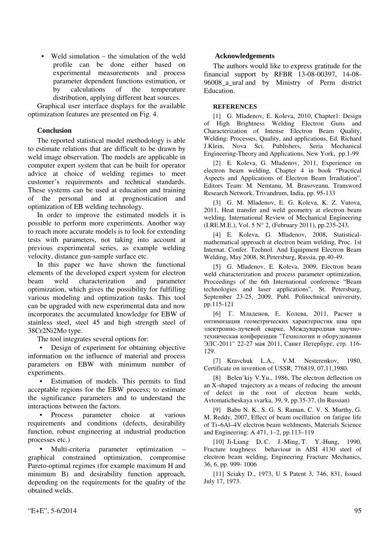
“E+E”, 5-6/2014 95
• Weld simulation – the simulation of the weld profile can be done either based on experimental measurements and process parameter dependent functions estimation, or by calculations of the temperature distribution, applying different heat sources.
Graphical user interface displays for the available optimization features are presented on Fig. 4.
Conclusion The reported statistical model methodology is able
to estimate relations that are difficult to be drawn by weld image observation. The models are applicable in computer expert system that can be built for operator advice at choice of welding regimes to meet customer’s requirements and technical standards. These systems can be used at education and training of the personal and at prognostication and optimization of EB welding technology.
In order to improve the estimated models it is possible to perform more experiments. Another way to reach more accurate models is to look for extending tests with parameters, not taking into account at previous experimental series, as example welding velocity, distance gun-sample surface etc.
In this paper we have shown the functional elements of the developed expert system for electron beam weld characterization and parameter optimization, which gives the possibility for fulfilling various modeling and optimization tasks. This tool can be upgraded with new experimental data and now incorporates the accumulated knowledge for EBW of stainless steel, steel 45 and high strength steel of 38Cr2Ni2Mo type.
The tool integrates several options for: • Design of experiment for obtaining objective
information on the influence of material and process parameters on EBW with minimum number of experiments.
• Estimation of models. This permits to find acceptable regions for the EBW process; to estimate the significance parameters and to understand the interactions between the factors.
• Process parameter choice at various requirements and conditions (defects, desirability function, robust engineering at industrial production processes etc.)
• Multi-criteria parameter optimization – graphical constrained optimization, compromise Pareto-optimal regimes (for example maximum H and minimum B) and desirability function approach, depending on the requirements for the quality of the obtained welds.
Acknowledgements The authors would like to express gratitude for the
financial support by RFBR 13-08-00397, 14-08-96008_a_ural and by Ministry of Perm district Education.
REFERENCES [1] G. Mladenov, E. Koleva, 2010, Chapter1: Design
of High Brightness Welding Electron Guns and Characterization of Intense Electron Beam Quality, Welding: Processes, Quality, and applications, Ed. Richard J.Klein, Nova Sci. Publishers, Seria Mechanical Engineering-Theory and Applications, New York, pp.1-99
[2] E. Koleva, G. Mladenov, 2011, Experience on electron beam welding, Chapter 4 in book “Practical Aspects and Applications of Electron Beam Irradiation”, Editors Team: M. Nemtanu, M. Brasoveanu, Transword Research Network, Trivandrum, India, pp. 95-133
[3] G. M. Mladenov, E. G. Koleva, K. Z. Vutova, 2011, Heat transfer and weld geometry at electron beam welding, International Review of Mechanical Engineering (I.RE.M.E.), Vol. 5 N° 2, (February 2011), pp.235-243.
[4] E. Koleva, G. Mladenov, 2008, Statistical-mathematical approach at electron beam welding, Proc. 1st Internat. Confer. Technol. And Equipment Electron Beam Welding, May 2008, St.Petersburg, Russia, pp.40-49.
[5] G. Mladenov, E. Koleva, 2009, Electron beam weld characterization and process parameter optimization, Proceedings of the 6th International conference “Beam technologies and laser applications”, St. Petersburg, September 23-25, 2009, Publ. Politechnical university, pp.115-121
[6] Г. Младенов, Е. Колева, 2011, Расчет и оптимизация геометрических характеристик шва при электронно-лучевой сварке, Международная научно-техническая конференция "Технологии и оборудования ЭЛС-2011" 22-27 мая 2011, Санкт Петербург, стр. 116-129.
[7] Kravchuk L.A., V.M. Nesterenkov, 1980, Certificate on invention of USSR, 776819, 07,11,1980.
[8] Belen’kiy V.Yu., 1986, The electron deflection on an X-shaped trajectory as a means of reducing the amount of defect in the root of electron beam welds, Avtomaticheskaya svarka, 39, 9, pp.35-37, (In Russian)
[9] Babu N. K., S. G. S. Raman, C. V. S. Murthy, G. M. Reddy, 2007, Effect of beam oscillation on fatigue life of Ti–6Al–4V electron beam weldments, Materials Science and Engineering: A 471, 1–2, pp.113–119
[10] Ji-Liang D, C. J.-Ming, T. Y.-Hung, 1990, Fracture toughness behaviour in AISI 4130 steel of electron beam welding, Engineering Fracture Mechanics, 36, 6, pp. 999- 1006
[11] Sciaky D., 1973, U S Patent 3, 746, 831, Issued July 17, 1973.

“E+E”, 5-6/2014 96
[12] D. Trushnikov, E. Koleva, V. Belenkiy, G. Mladenov. Experimental investigation of the weld cross section at electron beam welding of high-strength steel. Elektrotechnica & Elektronica E+E, v. 5-6, 2012, pp.108-114.
[13] E. Koleva, G. Mladenov, D. Trushnikov, V. Belenkiy. Model-based approach for investigation of electron beam welding of high-strength steel. Elektrotechnica & Elektronica E+E, v. 5-6, 2012, pp.115-118.
[14] E. Koleva, I. Vuchkov, Model-based approach for quality improvement of EBW applications in mass production, Vacuum 77, 2005, 423-428.
[15] E. G. Koleva, G. M. Mladenov, D. N. Trushnikov, V. Ya. Belen’kiy. Quality analysis for efficient electron beam welding process. Elektrotechnica & Elektronica - E+E, Vol.48, 5-6, Sofia, Publ.CEEC, (2013), 5-6, pp. 190-204. ISSN 0861-4717.
Assoc Prof. Dr. Eng. Elena Koleva - Institute of Electronics, laboratory “Physical problems of electron beam technologies” – Bulgarian Academy of Sciences, Bulgaria,
Director of Technological Center on Electron Beam and Plasma Technologies and Techniques – TC EPTT Ltd., Bulgaria,
Lecturer at University of Chemical Technology and Metallurgy – Sofia, Bulgaria
Tel. : +359 895537899, е-mail: [email protected]
Dr. Dmitriy N. Trushnikov - Department of Applied physics, Department of Welding production and technology of construction materials, Perm National Research Polytechnic University, Perm, Russian
Federation; Education - 1999 Department of Aerospace, Perm National Research Polytechnic University; Research Areas – control, monitoring and simulation of electron beam welding;
tel.: +79194785031, e-mail: [email protected]
Prof. Dsc. Vladimir Ya. Belenkiy - State National Research Polytechnic University of Perm, Department of Welding production and technology of construction materials, Perm, Russia;
Tel.: +7(342) 2403796, e-mail: [email protected]
Corr. Memb. of BAS, Prof. DSc. Georgi Mladenov - Institute of Electronics – Bulgarian Academy of Sciences, Bulgaria
Technological Center on Electron Beam and Plasma Technologies and Techniques, Bulgaria
He is the author of 10 books, 26 inventions and more than 200 articles. His research interests include electron beam microscope accelerators, electron beam technologies, electron devices physics, electron beam welding, melting and refining metals in vacuum, electron spectroscopy simulation, electron lithography, vacuum technology.
Tel. +359 899902510, е-mail: [email protected]
Stefan Angelov – student at University of Chemical Technology and Metallurgy – Sofia, Bulgaria, trainee at Institute of Electronics, laboratory “Physical problems of electron beam technologies” – Bulgarian Academy of Sciences, Bulgaria
Dimitar Todorov – PhD student at Institute of Electronics, laboratory “Physical problems of electron beam technologies” – Bulgarian Academy of Sciences, Bulgaria

“E+E”, 5-6/2014 97
Influence of Electron Beam's Oscillations on Weld's Structure Formation of Dissimilar Materials on an Example Steel with
Bronze
Tatiana V. Olshanskaya, Gleb L. Permyakov, Vladimir Y. Belenkiy, Dmitriy N. Trushnikov
The results of metallographic studies of dissimilar materials welds joint's structure are
presented. Welds were obtained from steel (12Х21Н5Т in Russian) and bronze (БрХ-06 in Russian), using EBW with the oscillation of beam (with transverse, and x-shaped trajectory, and beam's splitting into three). It is shown, that the use of beam's oscillations leads to mixing of metals in the weld pool, and formation of welds with strongly expressed inhomogeneous structure by the width. X-shaped oscillations, compared with transverse oscillations, cause more intensive mixing of welded materials. It is leads to the formation of the central part of the weld with more homogeneous mixing of phases during crystallization. Formation of such structures leads to considerable unevenness of weld's hardness by width and depth. Application of techniques of beam's splitting (into three), with concomitant heating of bronze, allows to obtain a homogeneous structure of the weld's metal. That is finely dispersed mechanical mixture of the two systems: 1) eutectic copper-based; 2) mixture of solid solutions based on α-Fe and γ-Fe. Formation of similar structure leads to the equalization of hardness in the weld by width and depth.
Влияние на осцилациите на електронния сноп върху формирането на структурата на шева на различни материали на примера на съединението стомана-бронз (Т. В. Олшанска, Г. Л. Пермяков, В. Я. Беленкий, Д. Н. Трушников). Резултатите от металургическите изследвания на структурата на заваръчни шевове са представени. Съединявани бяха стомана 12Х21Н5Т и бронз БрХ-06 с помощта на ЕЛЗ с осцилации на снопа (с напречни и Х-образни траектории и лъч разделен на три). Показано е, че осцилациите на снопа водят до смесване на метала в заваръчната вана и формиране на шев със силни нехомогенности по ширина на шева. Колебанията на лъча по Х-образна траектория, по сравнение с напречните осцилации причиняват по-интензивно смесване на заваряваните материали. Това води към образуване на централна част на лъча с по-хомогенно смесване на фази по време на кристализация. Формирането на такава структура води до значителна неравномерност на твърдостта на шева по ширина и по дълбочина. Прилагането на техниката на разделянето на снопа на три, със едновременно нагряване на бронза позволява да се наблюдава хомогенна структура на метала в заварявания шев. Това е фино разпределена механична смес на две системи: 1) евтектична базирана на мед; 2) смес на твърди разтвори основаващи се на α-Fe и γ-Fe. Формирането на тази структура води до изравняването на твърдостта на шева по ширина и дълбочина.
Introduction At manufacturing of responsible parts in
mechanical engineering, shipbuilding, aerospace and other industries it is often arises necessity of obtaining welded joints made of high corrosion resistant steel with copper and its alloys. Such products can work in corrosive environments, as at raised or at lowered
temperatures. Depending on the requirements imposed on the properties and conditions of use of products, the most commonly used steel austenitic, austenitic-ferritic and martensitic grades.
Fusion welding of steels with copper alloys is complicated by several factors: significant difference of thermophysical properties; high fluidity copper in the liquid state; low mutual solubility of copper and iron in the solid state; propensity of copper to the

“E+E”, 5-6/2014 98
porosity; a high affinity of copper to oxygen that causing the formation of eutectic (Cu + Cu2O) and embrittling metal. A typical defect arising in welding of steel with copper is the intergranular penetration of copper in steel. The presence of this defect significantly reduces the mechanical properties of the steel, particularly its plasticity [1].
Application of electron beam welding (EBW) for welded joints of steels with copper alloys can solve many problems due to of high capacity of input heat and the possibility of exact positioning of the electron beam. However, in EBW of steel with bronze remain number of challenges. These problems associated with the formation of structure of the weld, appearance of defects in the fusion zone and the root zone of the weld. Studies carried out in research [2, 3] showed that in EBW steel with bronze with introduction of electron beam in joint of welded parts in the weld formed a complex heterogeneous structure, by the depth and by the width of the weld. This leads to a deterioration in of weld's operational characteristics as a result heterogeneity of its mechanical properties and reduce resistance when working in aggressive environments. For full penetration, preventing processes of mixing steel with bronze and reduce the width of the zones of diffusion processes EBW carried with displacement of the electron beam from the joint in the side of steel or bronze [3, 4, 6]. But this technological method requires precise positioning of an electron beam because slight deviations may lead to incomplete fusion, or to the mixing of steel and
bronze and appearance of defects in the weld [3, 4, 5].
Theoretical aspects of crystallization of the welded joint "steel - bronze" at EBW
Formation of dissimilar complex structure of the weld's metal associated with periodicity of formation of metal's liquid phase and complicated character of hydrodynamic processes in the weld pool [7]. At high cooling rates and low time of existence of weld pool occurs only partial mixing of the melt, resulting in it has a high degree of heterogeneity. The presence of melt layers and droplets of liquid metal, different sizes and chemical compositions will greatly depend on the characteristics of hydrodynamic processes in the area of EBW. Affect these processes, by changing parameters of EBW such as the electron beam current and welding speed, is virtually impossible. This allows you to get a change in the degree of mixing and dispersity structures. While crystallization process in all cases accompanied by formation of the irregular structure of the weld metal's layers with typical hydrodynamic mixing on the basis of steel or bronze. To reduce the degree of heterogeneity of the structure of the weld metal is necessary that the liquid weld pool had a uniform homogeneous composition. Conditions for obtaining a homogeneous weld pool: intensive mixing and increasing its residence time in a liquid state.
Table 1. Chemical composition of welded materials, %
Material Content of elements % (wt.)
C Cr Ni Ti Si Mn S P Cu Al Fe Zn 12Х21Н5Т 0,09…0,14 20,0…22,0 4,8…5,8 0,25…0,5 – ≤0,8 ≤0,025 ≤0,035 – ≤ 0,8 – – БрХ-08 – 0,4…1 – – – – – – 98,5…99,6 – ≤0,08 ≤0,3
a b
Fig.1. Scheme splitting of electron beam at welding: a – longitudinal section, b – top view

“E+E”, 5-6/2014 99
At the same time need to reduce the temperature gradient between the steel and bronze to ensure an equal rate of heat removal in both metals. Such effects on the weld pool possibly by using different technological method: oscillation of the electron beam, concomitant heating of bronze, using split of the electron beam by several heat sources.
Objective Objective of this study was to investigate the
influence of different types of oscillations of the electron beam on the structure and properties of welded joints at EBW corrosion-resistant high-alloy steel with bronze.
Materials and Technique Experimental research was conducted using
corrosion-resistant high-alloy steel austenitic-ferritic
class (12Х21Н5Т in Russian) and chromic bronze (БрХ-06 in Russian). Chemical compositions of welded materials are presented in Tables 1. Welding was performed on electron-beam facility (ELA-60/6VCH) with the energy unit manufactured by company SELMI (Ukraine).
In conducting the experimental work were performed weld passes on annular junction of diameter of 120 mm with joint "into the lock". Thickness of the steel parts was 7.5 mm, bronze - 5.5 mm. During the research was carried EBW using different technological methods: oscillations of the electron beam across the joint, X-shaped trajectory of its movement and beam splitting into several heat sources providing molten metal and the concomitant heating of bronze (fig. 1). EBW modes in the experiments were chosen from the condition of full penetration and are presented in Тable 2.
Table 2. Modes of EBW steel with bronze
Type of sweep Beam parameters Oscillation parameters Distribution of beam's power %
U,kV I, mA Vw, mm / s Amplitude (а), mm
Frequency (f), Hz 1 beam 2 beam 3 beam 4 beam
Transverse 60 32…34 5 0,8 600 − − − − X-shaped 60 32…34 5 0,8 600 − − − −
Beam splitting 60 85 6 − − 21,1 29,6 18,3 31
a b c
Fig. 2. Macrostructure of welds (Increase x 5):
a − transverse oscillations, b − X-shaped oscillations, c – beam splitting
Fig. 3. Microstructure of upper part of weld obtained at transverse oscillations of the beam(Increase x 100)
“E+E”, 5-6/2014 100
Metallographic studies cross-section of welds were performed on a microscope MIM-10 by using the software package Video Test Metal. For etching was used reagent of Vasiliev. Evaluation of mechanical properties of the weld was carried by measuring of microhardness on appliance PMT-3.
Results and Discussion For experimental studies were obtained welded
joints, macrostructure of which are shown in Fig. 2. Metallographic analysis of the macrostructure welds has showed that the stirring of the metal occurs in process of welding in all the cases studied, but it has a different character. At EBW with lateral oscillations of the electron beam in the macrostructure of the weld is observed the metal layer of different color from side of steel and the large drip inclusion of the same color in the center of the upper part of the weld (Fig. 2a). At welding with X-shaped oscillations of the electron beam is also observed a similar layer of metal from the side of steel, but it has wavy, sawtooth border (Fig. 2b). At welding with the splitting of the beam
weld metal on macrosection looks homogeneous (Fig. 2c).
Research of weld's microstructure showed that the use of the transverse oscillations of the electron beam at welding leads to the formation of a heterogeneous structure by the depth and by the width of weld (Fig. 3).
In this case weld can be separated into three areas by the width. First area is formed from the side of steel, basis of weld's metal is steel , which is a mixture of two phases of austenite and ferrite with drip, inter-granular and interdendritic inclusions of bronze (Fig. 4a). The basis of the central area of the weld is bronze, and steel constitute in her inclusion of large form as droplets and, mostly, the dendrites (Fig. 4b). Inside the inclusions of steel are well visible intergrain and interdendritic interlayers of bronze. There is a sharp transition line between the first and second areas of the weld.
a b
c
Fig. 4. The weld's microstructure obtained by transverse oscillations of the beam (magnification x 600): a, b, c – first, second and third characteristic areas, respectively

“E+E”, 5-6/2014 101
Fig. 5. Microstructure of the middle part of the weld, obtained at the splitting of the beam (Increase x 100)
a b
Fig. 6. Weld's microstructure obtained at the beam splitting (Increase x 600) a, b - at the top and at the root part of the weld, respectively
a b
c
Fig. 7. Microhardness by width of the middle part of the welds: a – with transverse oscillations of the beam, b – with X-shaped oscillations, c – with the splitting of the beam

“E+E”, 5-6/2014 102
The third area is formed from the side of bronze, where Steel dendritic formation become larger and drip acquire an elongated shape (Fig. 4с). These areas are changing their dimensions by depth. The first system is dendrites based on steel, consisting of a mixture of solid solutions on the α-Fe and γ-Fe.
In general, there are the same characteristic structures with some differences in the weld obtained at welding with the X-shaped oscillations of the electron beam. The boundary between the first and second areas becomes curved, sawtooth. Drip and dendritic formation began increasing in size in the second area. Steel elongated formations became coalesce into one large on third area. It should be noted, that in structure of welds carried out with the oscillation of the electron beam was not detected typical defect such as intergranular penetration of copper in steel.
In the case of EBW with the splitting of the electron beam into three concentrated heat source and one raster which provides concomitant heating from the side of bronze, formed homogeneous structure by the width and by the depth of the weld (Fig. 5). The microstructure of the weld metal is a finely dispersed mechanical mixture of the two systems. The second system is the drip formation and interdendritic Cu-based layers. Obtained structure is changing its dispersion in the depth of the welded joint (Fig. 6).
Results of microhardness measurements by width of the middle part of the welds are presented in Fig. 7.
Conclusions EBW steel with bronze with transverse or X-
shaped oscillations do not provide a uniform structure and properties of the weld metal.
Obtaining of high quality welds of steel with bronze with high mechanical and operational characteristics due to the homogeneity of the weld metal is achieved by using splitting of electron beam into three concentrated heat source, and one raster which provides the concomitant heating of metal welded joint from the side of bronze.
REFERENCES [1] Volchenko V. N Welding and welding materials:
In three volumes. Volume I. Weldability of materials. Handbook. Moscow: Metallurgiya, 1991. (In Russian).
[2] I. Magnabosco, P. Ferro, F. Bonollo, L. Arnberg «An investigation of fusion zone microstructures in electronbeam welding of copper–stainless steel» Materials Science and Engineering A 424 (2006) 163–173
[3] L.A. Goncharov, E.V. Terentyev, A.U. Marchenkov, M.A. Portnov. Electron beam welding of bronzes to 316 L(N) steel. – Electrotechnica & Electronica, 2012, N 5-6, p. 123-127.
[4] Karcher C., Ziolowski M., Brauer H., “Seeback Effect during Electron Beam Welding”, Elektrotechnica & Electronica 44 5-6 2009
[5] Klimova O. G., Turichin G. A., Lopota V. A., Shamshurin A. I., Sizova I. A. Structure features of the metal welded by electron-beam welding of dissimilar materials//St. Petersburg State Polytechnical University Journal. Physics and Mathematics. 2013, #2, p. 125-132.
[6] Turichin G. A., Klimov O. G., Babkin K. D., Pevzner Ya. B Effect of thermal and diffusion processes on formation of the structure of weld metal due to laser welding of dissimilar materials// Metal Science and Heat Treatment. 2013, #10, p. 58-64
[7] Rykalin N. N., Uglov A. A., Zuev I. V., Kokora A. N. Laser and electron-beam processing of materials: Handbook. Moscow: Mashinostroyeniye, 1985. (in Russian).
Tatiana V. Olshanskaya - Candidate of Technical Sciences, Docent. Perm National Research Polytechnic University
е-mail: [email protected] Gleb L. Permyakov - Postgraduate student . Perm
National Research Polytechnic University
е-mail: [email protected] Vladimir Y. Belenkiy - Doctor of Technical Sciences,
Professor, Dean of Mechanical Engineering Faculty. Perm National Research Polytechnic University
е-mail: [email protected]
Dmitriy N. Trushnikov - Candidate of Technical Sciences, Docent. Perm National Research Polytechnic University
е-mail: [email protected]

“E+E”, 5-6/2014
103
Electron Beam Welding of Superconducting Cavities Made of Ultra-Pure Niobium
Igar L. Pobal, Siarhei V. Yurevich
Manufacture of superconducting radiofrequency (SRF) cavities for modern accelerators requires
ultra-purity niobium. Joining components of such cavities is only possible with the use of electron-beam welding. Investigations on this topic are carried out in the framework of activities of the Joint Institute for Nuclear Research (JINR, Dubna) for the project of the International Linear Collider (ILC). The aim is to manufacture the prototype of 1.3 GHz single-cell niobium SRF cavity.
In this paper the results of study of electron-beam welding of Nb sheets are presented. The analyses of important characteristics of the material (including residual resistance ratio (RRR), chemical composition, mechanical properties) from different niobium manufacturers were done. The modes for EBW of Nb sheet 2.8 mm thick were explored. Geometry of welds, macro- and microstructure, microhardness and superconducting characteristics of welded joints were investigated. The method of chemical treatment of niobium prior to welding was also elaborated.
Електроннолъчево заваряване на свръх-проводящи резонатори, направени от свръх-чист ниобий (И. Побал, С. Юревич). Производството на свръх-проводящи радиочестотни (СРЧ) резонатори за модерни ускорители изисква свръх-чист ниобий. Съединяването на компонентите на такива резонатори е възможно само с електронно-лъчево заваряване. Изследването е направено в рамките на провежданите работи от Обединения Институт по Ядрена физика в Дубна за проекта на Международния Линеен Колайдер. Целта е да се произведе прототип на 1.3 GHz едноклетъчен ниобиев СРЧ резонатор. В тази работа са представени резултатите от изследването на електроннолъчево заваряване на ниобиеви листове. Данните от анализът на важните характеристики на материала, включително остатъчното отношение на съпротивлението, химическия състав, механичните свойства от различни производители на ниобии са приведени. Изследвани са режими за електроннолъчево заваряване на ниобиеви листове дебели 2,8 мм. Геометрията на шевове, макро- и микро-структурата им, микротвърдостта и свръх-проводящите им характеристики на заварените шевове са изучени. Методите на химическата обработка на ниобия преди заваряване също са изследвани.
Introduction Superconducting radio frequency (SRF) cavities
are the central components of modern linear colliders. It is recognised now that SRF cavities must be fabricated from high purity niobium using deep drawing of half-cells from sheet material 2.8 mm thick and joined by electron beam welding (EBW) in high vacuum. The niobium used for the cavity is highly purified by several remelting cycles in a high vacuum electron beam furnace. Electron beam welding is used to obtain high quality welds that maintain the material high purity required for saving the niobium superconductivity. The EBW parameters must ensure
a full penetration of the joints and smooth weld seam of a few-millimeters width at the inner cavity surface.
Ultra-pure niobium for SRF cavity For production of the SRF cavities a niobium of
exceptional purity is required with a gaseous contamination below 10 ppm and a tantalum content less than 500 ppm. The purity of niobium can be indicated by the residual resistivity ratio (RRR).The RRR is the ratio between the resistances of the material at room temperature (300K) and 4.2K.The standard specification of niobium used for cavity fabrication is the RRR value equal to 300 or higher. The main dissolved impurities that reduce the RRR are shown in Table 1 [1].

“E+E”, 5-6/2014 104
Table 1. Impurities present in niobium used for SRF cavity
Element Impurity content in ppm Ta ≤500 W ≤70 Ti ≤50 Fe ≤30 Mo ≤50 Ni ≤30 H ≤2 N ≤10 O ≤10 C ≤10
Electron beam machine and samples preparation
The EBW installation based on the `ЭЛА-15` power source was used for welding. The main technical data of EBW equipment are listed in Table 2.
Table 2. Specifications of EB Facility
Voltage 60 kV Beam power max. 15 kW Beam current 0 - 250 mA Chamber size 2 500 × ø1 350 mm
Vacuum ca. 3×10⁻³ Pa The EBW joints made in the samples are of step
joint configurations (Fig.1). This type of joint made in cavities was used to avoid radial displacement in mating components. The thickness of weld area was 2.8 mm.
Fig.1. Cross section of the step joint.
For carrying out the electron beam welding, the samples were mounted on a clamping system made of stainless steel. After welding, the samples left in vacuum for at least two hours to cool down below 60°C before their removing.
The niobium surface morphology and structure of welded joints was investigated using an optical microscope. Microhardness was measured using hardness tester machine.
Superconducting properties of the welds were
studied by measuring RRR, superconducting transition temperature (TC) and critical magnetic fields of superconductor (HT). The samples in the form of strips 2.5-3 mm wide by 40 mm long for measurements of RRR were prepared using a precision diamond saw in the longitudinal direction to the weld with cooling by water. The samples for measurements of TC and HT were prepared by electro-erosion cutting in transverse directions to the weld seam with obtaining strips 2.5 mm wide, 40 mm long (Fig.2).The superconducting properties of the samples were tested using the equipment of DESY (Hamburg, Germany) and Scientific and Practical Materials Research Centre of NAS of Belarus (Minsk, Belarus).
Fig.2. Test samples of RRR, TC and HT.
The niobium sheets used for investigation were from the Tokyo Denkai and Ningxia OTIC manufactures.
The size of the niobium as-received material sheet (Fig.3) manufactured by Tokyo Denkai (Japan) is 265×265×2.8 mm with the surface roughness of Ra0.3-0.4 µm, average grain size of 50-110 µm and RRR value of around 400.
Fig.3. As-received Tokyo Denkai niobium surface.
Size of the niobium as-received material sheet (Fig.4) manufactured by Ningxia OTIC (China) is 290×290×2.8 mm with the surface roughness of Ra

“E+E”, 5-6/2014 105
0.6-0.9 µm, average grain size of 30-40 µm and RRR value of around 300.
Fig.4. As-received Ningxia OTIC niobium surface.
The mechanical properties of the niobium sheets are given in Table 3.
Table 3. Mechanical properties
Parameter ILC requirement [1]
Tokyo Denkai
Ningxia OTIC
Yield strength, MPa >50 70 98
Tensile strength, MPa >100 166 170
Elongation at break, % >30 57 35
Chemical etching Surface cleaning is a necessary step of SRF cavity
production that removes the surface layer of damaged material. A damage layer of 200 µm is removed from the inner cavity surface to obtain a good RF performance in the superconducting state [2]. The standard method applied for niobium cavities is buffered chemical polishing (BCP) that uses an acid mixture of HF (48% wt.), HNO3 (65% wt.) and H3PO4 (85% wt.) in the ratio 1:1:2 [2], [3]. The temperature control of chemical etching carried out by controlling the bath temperature to 14°C must done to avoid hydrogen contamination of the niobium.
In [4], we investigated the material removal rate depending on the treatment time for the standard mixture (1 part of HF, 1 par of HNO3 and 2 parts of H3PO4), the surface roughness depending on thickness of the removed layers, grain structure and surface quality of both supplied materials. After the BCP treatment, the grain structure is clearly visible. Fig. 5 and 6 show optical micrographs of the sample
surfaces of Ningxia OTIC and Tokyo Denkai niobium after surface removal of 200 µm by BCP. The removal rates by the standard BCP procedure of materials from Tokyo Denkai and Ningxia OTIC are 1.3µm and 1.2µm per minute. After 200 µm BCP the surface roughness is Ra 0.5-0.6 µm and 1.2 µm for materials from Ningxia OTIC and Tokyo Denkai, respectively.
Prior to EBW of the samples the surface layer of 40 µm was removed by BCP. After cutting of the samples for measurements of the superconducting properties the surface layer of 40 µm was also removed by standard BCP method.
Fig.5. Tokyo Denkai niobium surface after chemical
treatment (BCP 200 µm).
Fig.6. Ningxia OTIC niobium surface after chemical
treatment (BCP 200 µm).
Welding Relations between EBW parameters and
geometries of weld beads of the step joint are investigated. Welding was carried out in the vertical gun position and the horizontal welding direction. Full penetration of the joints and smooth weld seams of 3-4 mm width obtained at the inner surface of samples

“E+E”, 5-6/2014 106
ensure weld parameters: accelerating voltage of 60 kV; beam current of 53-55 mA; welding speed of 7-10 mm/sec; beam focus – defocusing; vacuum of 3-5×10⁻³Pa. Fig.7 shows relations between the weld bead
widths (e1 and e2, Fig.8) and the beam current with constant accelerating voltage and welding speed.
Fig.7. Width of the weld niobium Ningxia OTIC vs. the
welding current (accelerating voltage is 60 kV, welding speed is 10 mm / sec).
Fig.8. Studied geometry of the weld seam.
Structure of the welded joints Fig. 9 shows the weld of niobium from Ningxia
OTIC. The sample was welded with a beam voltage of 60 kV, a beam current and beam traveling speed were 53 mA and 10 mm/sec, respectively, beam was defocused. The welding was performed at 5×10⁻³ Pa residual pressure. The width of weld seams is about 3-4.5 mm. The overall width of the weld and heat affected zone is 12-12.5 mm. The weld has an equiaxed microstructure with a 1000 µm grain size in the fusion zone, 100-200 µm in the heat affected zone and 30-40 µm in the parent metal.
Fig.9. Ultra-pure niobium EB weld (1 – line of the
microhardness measuring).
Microhardness was measured across the weld pool of electron beam welded niobium sample. The measurement was taken through line 1 (Fig.9) started on weld pool and terminated on parent metal. The hardness of parent metal and weld zone showed the similar values with fluctuation in the60-75 HV range (Fig.10).
Fig.10. Vickers microhardness profile of EB welded
niobium sample.
Superconducting properties of the niobium welds
Table 3 shows the results of RRR measurements obtained on the samples cut in the longitudinal direction to the weld on different distances from center of the weld of the niobium sheet manufactured by Tokyo Denkai. RRR of weld metal is reduced to 300, heat affected zone RRR value just as for the base metal remains in the region of 400.
Table 4. RRR of the EB welding area at different distances from the
middle of welding seam
Position from weld center, mm RRR
-20 399,9 -10 421,5 -7 409,9 -4 406,0 0 295,8 4 414,2 7 424,9
10 412,2

“E+E”, 5-6/2014 107
Table 5 shows the measurement results of the superconducting transition temperature, TC, and critical magnetic fields of superconductor, HT, of the three types of the samples of Ningxia OTIC (RRR 300) niobium. Samples of 0 type are the reference samples cut from material not subjected to thermal influence; 1 type are samples cut from a solid plate on which the electron beam was impacted to the full penetration (accelerating voltage of 60 kV; beam current of 51 mA; beam traveling speed of 10 mm/sec; vacuum of 5×10⁻³ Pa); 2 type are samples cut from the welded joint (accelerating voltage of 60 kV; beam current of 53 mA; welding speed of 10 mm/sec, vacuum of 5×10⁻³ Pa).
Table 5. Superconducting properties of the niobium samples
Types of samples
Superconducting properties TC, K HT, T
0 8,8 0,5 1 8,6 0,4 2 8,6 0,4
As can be seen from the Table 5, in the niobium
welded joints of 1 and 2 types samples there is insignificant degradation of the superconducting properties: TC value is reduced to 8.6 K (0 samples, 8.8 K), HT value is reduced to 0.4 T (0 samples, 0.5 T). This insignificant degradation in the superconducting properties of the welded joints should not exert any influence on the performance of the cavity.
Conclusion The next step of this work is the production of
prototype of 1.3 GHz SRF single-cell cavity from the niobium produced by Ningxia OTIC.
Acknowledgements The work was performed under the contract
2012/17 `Research and development of technologies of hydraulic deep-drawing, electron beam welding and surface treatment of prototype of single-cell niobium cavity` with National scientific & educational center of Particle and High Energy Physics of Belarusian State University (NC PHEP BSU).
We thank many colleagues from our community:
N.I. Azaryan, J.A. Boudagov, D.L. Demin, G.D. Shirkov (Joint Institute for Nuclear Research, Dubna, Russia), M.A. Baturitsky, N.M. Shumeiko (NC PHEP BSU, Minsk, Belarus), A.A. Parshuto, V.S. Petrakovsky, A.Y. Zhuravsky (Physical Technical Institute of NAS of Belarus, Minsk, Belarus), S.E. Demyanov, E.Y. Kaniukov (Scientific and Practical Materials Research Centre of NAS of Belarus, Minsk, Belarus).
We would like to thank Xenia and Waldemar Singer (DESY, Hamburg, Germany) for providing us with many information.
REFERENCES [1] The International Linear Collider, Technical
Design Report, Volume 3: Accelerator, 2013.
[2] Padamsee H. RF Superconductivity: Science, Technology and Applications. John Wiley & Sons, 2009. 464 p.
[3] Antoine C. Materials and surface aspects in the development of SRF Niobium, 2012, internet: http://cern.ch/eucard.
[4] Yurevich S. et al. Surface preparation and electron-beam welding of niobium for SRF cavities, Proc. of VIII International Scientific-Technical Conference «Advanced methods and technologies of materials development and processing», September 18-20, 2013, Minsk, Belarus, PP 557 – 565.
DSc. Igar L. Pobal - Head of Electrophysics Laboratory of Physical-Technical Institute of NASB. Education: Belarusian State University (1974), specialty `Physics`, PhD (1986), DSc. (2007). Scientific interests – obtaining of joints, surface engineering, nano-materials, using of advanced materials in healthcare.
tel.:(+375 44)7870739, е-mail: [email protected]
Siarhei V. Yurevich - researcher of Electrophysics Laboratory of Physical Technical Institute of NASB, PhD student, specialty `Technology and equipment for Physicotechnical Processing`. Education: engineering degree (2010), specialty `Equipment and Technology of Welding Engineering`; Master of Engineering (2012), specialty `Working of constructional materials in machine building`, Belarusian National Technical University.
tel.:(+375 29)5012932, е-mail: [email protected]

“E+E”, 5-6/2014 108
Prediction of the Partial Penetration Depth on 15-5PH Materials during Electron Beam Welding
Kamal Frikach, Jamie White, Jeff Houtz
We report in this paper a systematic study for partial penetration of the electron beam welding
and its correlation with the beam power as a combination of beam voltage and current, welding speed and working distance. The experimental tests are performed using 15-5 PH stainless steel material at constant welding speed (24 in/min).
The tests are conducted on a 160 kV, 40 mA CVE Electron Beam Welder. To ensure beam quality, the electron beam is probed at different working distances as a function of accelerating voltage and beam current using MK2 modified Faraday Cup that is designed for electron beam diagnosis. The beam focus current that corresponds to the maximum beam density profile at sharp focus is determined accurately. By analyzing the energy density distribution of a given power density profile, a direct measurement of the beam diameter is performed accurately for each beam configuration. The measured beam diameter is used to predict the penetration depth.
The obtained experimental data for beam penetration depth are presented in terms of normalized beam power q/pkT versus dimensionless beam diameter vb/4a, where b is the diameter of the sharply focused electron beam. The show good agreement with the theoretical predictions using combination of the moving line source and the solution for a cylindrical cavity.
Прогноза на частичната дълбочина на проникване в 15-5PH материал при електроннолъчево заваряване (Камал Фрикач, Джейми Уайт, Джеф Хоутз). В тази работа е представено систематично изследване на частичното проникване при електроннолъчево заваряване и неговата корелация с мощността на лъча, като комбинация на ускоряващото напрежение и тока на лъча, скоростта на заваряване и работното разстояние. Експериментите са направени с 15-5 PH неръждаема стомана при неизменна скорост на заваряване (24 in/min). Тестовете са направени при 160 kV, 40 mA CVE електроннолъчева инсталация. За обезпечаване на качество на снопа, е измерен профилът на електронния лъч при различни работни разстояния, като функция на ускоряващото напрежение и тока на лъча, използвайки МК2 модифициран Фарадеев цилиндър конструиран за диагностика на лъча. Тока на фокусиращата система, който отговаря на максималния профил на лъча при остър фокус, е определен точно. Анализирайки разпределението на енергийната плътност на даден профил на плътността на мощност, директното измерване на диаметъра на лъча се постига точно, за всяка конфигурация на снопа. Измереният диаметър на снопа се използва при прогнозирането на дълбочината на проникване. Получените експериментални данни са представени в единиците на нормализираната мощност на лъча q/pkT, в зависимост от безразмерния диаметър на лъча vb/4a, където b е диаметъра на остро-фокусирания електронен сноп. Показано е добро съответствие с теоретичното предсказване, при използване на движещ се линеен източник и решението за цилиндрична празнота (кратер).
Introduction The penetration depth into the welded material is
of high importance in electron beam welding processes and involves number of machine independent variables. Usually extensive testing is required before appropriate welding parameters can be
determined. Determining the welding conditions for beam power, welding speed and beam focus current to achieve a specified penetration depth in a particular material has been studied extensively in the literature [1-8].

“E+E”, 5-6/2014 109
Two analytical solutions, shown in Fig. 1 and Fig. 2, have been presented in the literature in order to predict the penetration depth, a line source with constant infinite power density and elliptical cylinder cavity [1, 2] moving with constant speed relative to the work piece.
Bibliography Hashimoto et al [2, 3] studied the effect of anode
voltage, beam current, welding speed and beam diameter on the weld penetration on a stainless steel material and deduced an experimental expression between the weld penetration and the welding variables for stainless steel as:
∝ .. for ≤ 3 (1)
where p is the weld penetration, E is the accelerating voltage, I the beam current, v the welding speed and d the beam diameter. The authors considered the beam diameter as the width of the molten volume at the surface of the material.
Considering a constant thermal property moving line source and approximating the heat loss by conduction only and using the heat balance analysis they approximated the penetration with the general
equation:
∝ .
κ
. (2)
where c is the specific heat, ρ metal density, metal melting temperature, H latent heat of fusion and κ is metal thermal conductivity.
They obtained an acceptable correlation between the low voltage experimental data and the theoretical model. The general expression of the weld penetration p versus welding variables was good to estimate the penetration depth and represents the actual magnitude of p.
Swift-Hook et al [5] considered two dimensional quasi-steady conduction heat flow perpendicular to the moving line source solution. Assuming the heat losses at the surface of the material are negligible using a mean value of thermal properties in the calculations, explicit relations between the normalized beam power per unit depth of penetration and normalized melting width along the isotherms was derived for low and high welding speed limits respectively as:
∝ 0.483! (3)
and
Fig. 1. Schematic representation of a keyhole in electron beam welding from ref [8]
Fig. 2. Schematic representation of a line source and cylindrical cavity solutions from ref [8]

“E+E”, 5-6/2014 110
∝ exp(&'8 − ) − *+ )
γ : 0.577 is Euler constant (4)
Comparison of the experimental data from the literature showed good agreement with the approximation and all the data lie within ±20 % of the theoretical curve.
A different approach in applying moving elliptical cylinder source solution is presented by Miyazaki and Geidt [6]. Considering the cylinder is at constant temperature moving in an infinite plate with constant velocity and assuming constant thermal properties of the material they presented a solution for a two dimensional steady state heat flow temperature distribution.
Assuming triangular beam profile shape, they obtained an expression between the normalized beam power and the beam width of the form:
= . /0κ
12
= /45(6 4,8⁄ ) (5)
where :(;< 2>, ?⁄ ) is a function of (;/2>) and δ the cylinder cavity axis ratio, q is the beam power and p the penetration depth.
The relationship in equation 5 between dimensionless beam power Y and ;/2> for different values of δ were presented and showed that the effect of δ is not significant and then a mean curve could be used for general comparisons with experiment. Comparison of the experimental data with the predicted values showed acceptable agreement.
Giedt et al [7] considered partial penetration welding with elliptical cylinder cavity approach moving source with constant speed in an infinite plate [6] and the beam energy is deposited in the liquid surrounding the cavity that is in melting temperature and transferred to the liquid solid interface by convection. Same as in ref [6] the expression of weld penetration per unit depth is derived from the quasi-steady heat transfer rate and that the dimensions of the cylinder (a/b) and the source power (q/p) are constant in the depth direction and the width of the molten metal, considered as the beam diameter, is evaluated at the surface of the fusion zone which is assumed to be triangular in shape.
Variation of normalized beam power ( =@/κ) versus normalized width (! = ;</α) for elliptical cylinder axes ratio δ = 1, 2 and 4 were presented along with the moving line-source solution theory [5]. Fair correlation is obtained for lower values of X where the data fall between the elliptical cavity curves δ=1 to 4 within ±40%. At high welding
speed (high X values) the data fall above the curve δ=4 within ±20%.
Because of data scattering from theory, the authors investigated introducing a power curve equation representing the relation between the penetration and independent welding variables of the form:
= 3.33!.A (6)
To account for the possible deviation of machine setting, correction factors that accounts for optimum focus coil current and incorrect average of the thermal properties were added to the empirical equation. It was estimated from 5% variation in machine setting that the beam focus current is the most critical machine parameter that influences the penetration and that the work distance is the least important parameter.
Hemmer and Grong [8] used an approach based on a combination of the moving line source and a cylindrical cavity moving through a plate of finite thickness because of the analogy between the two solutions at a certain distance from the center of the source. This approach is applicable for conductive heat flow and in pseudo-steady state.
They calculated the relationships between the isotherms as a function of the normalized beam width and the normalized beam power from the line source and the cylindrical cavity theories respectively and then induced the relationship between the weld penetration and the welding process parameters (i.e. welding speed and beam diameter) and the material properties (i.e. thermal diffusivity and melting temperature).
For stainless steel, they obtained general formulas for weld penetration and beam diameter as follows:
= @ B2C>∆EF0.34 + 2.034(; 4>⁄ )H.IAJKL⁄ (7) and
= M4 N. /
*4∆0 − 0.341 .HOMP
H.IAJ⁄ (8)
The correlation between the predicted weld penetration from the empirical equation (1) and the actual penetration data from literature are within +/-20%.
Experimental conditions The experimental tests are performed using two
CVE Electron Beam welding machines. The beam source is using a cathode made from Tungsten/Rhenium alloy with emission area of 1. The machine maximum beam power is ~6.5 kW (160 kV and 40 mA beam current). All tests are done under 102M Millibar vacuum.

“E+E”, 5-6/2014 111
The beam penetration tests are done on different
material including stainless Steel, Aluminum and Inconel 718. In this article we present only the results obtained on the 15-5 PH Stainless Steel material. For simplicity the tests are done at a constant welding speed 24R'ST R'⁄ and constant accelerating voltage 140 kV. The variables are the working distance and beam current.
To ensure better weld quality, the beam is aligned previously with the center of the column using an electromagnetic coil, located directly below the electron beam gun. This operation is performed to ensure that the electron beam produced by the gun follows a path down through the electron beam column which coincides with the column and the focus centerlines.
Beam probing To measure the beam properties and quality, the
electron beam is characterized (probed) systematically at different working distances as a function of the accelerating voltage and the beam current using MK2 modified Faraday Cup made by CVE and utilizing direct measurement of the electron beam current to obtain a profile of the beam energy distribution as the beam passes across a slit as shown in Fig 3. The resulting signal provides information about the beam shape, size and the power density.
In this study the beam probing is used to characterize the beam produced by CVE welding machine over range of focus settings at different working distances. The working distance is defined as the distance from the top of the chamber (chamber seal) to the slit of the Faraday Cup. The sharp focus is
Fig. 3. a) Beam probing pattern. b) Measured probe signal (Insert shows typical probe signal
after removing the noise).
Table 1. Welding experimental conditions.
Table 2.
Physical and thermal properties of 15-5 PH material used in EB welding experiments.

“E+E”, 5-6/2014 112
obtained by measuring the beam properties at focus setting both above and below the sharp focus. The sharp focus setting corresponds to the setting at which the highest power density value is obtained. The data have been filtered using a high frequency cut-off filter to remove the unwanted electronic noise.
A typical two dimensional beam density distribution is shown in Fig. 3. The dimension A in the insert represents the time that the beam takes to cross the probe body (10 mm diameter) and the central peak, represented by the dimension B is the beam density profile as it crosses the slit.
By analyzing the energy density distribution of a given beam profile, a measurement of the beam diameter was performed. The full width of the beam is measured at 85% of the peak power density. This parameter is considered to be a suitable representation of the beam diameter at sharp focus.
The experimental conditions used in this study are summarized in table 1 and the physical and thermal properties of the material used are given in table 2.
Experimental results and discussions: The main interest in this study is the prediction of
the penetration depth in a used material corresponding to the electron beam size, beam power and welding speed. Fig 4 shows the variation of the beam diameter at sharp focus with working distance of the sample at constant beam current going from 0 to 40 mA.
Fig. 4. Beam diameter as measured from the beam probe
profile vs. working distance at 140kV for beam currents 10, 15, 25 and 35 and 40mA.
The diameter of the sharply focused beam decreases linearly with increasing working distance and the curves tend to converge to a constant value of .2 mm at 20 inches of working distance. As shown in this figure, at sharp focus, the working distance has major effect on the resulting beam parameters at
larger working distance displaying lower beam diameter and narrower beam distribution.
The variation of the beam diameter at sharp focus with beam current is presented in Fig 5 for working distances going from 11 to 18.75 inch.
The experimental penetration depth data measured on the stainless steel sample is plotted in Fig 6 and compared with theoretical data obtained from equation 7 in ref [8]. The data in diamond correspond to the beam diameter measured at half depth on the experimental sample while the circle data correspond to the beam diameter measured from the beam profile.
Fig. 5. Beam diameter as measured from the beam probe
profile vs. beam current at 140kV for working distances 11, 12.75, 17.5 and 18.75 inch.
Fig. 6. Measured weld penetration depth on the 15-5 PH sample vs. calculated depth. Triangle data is for probed beam diameter and the diamond is for beam diameter
measured at half depth on the sample.
A closer inspection of the Fig.6 show that the predicted weld depth from equation 7 with beam diameter measured at half depth is in good agreement

“E+E”, 5-6/2014 113
with the experimental data. The calculated penetration depth using beam diameter measured from the beam probe, triangle data, is higher than the actual depth by factor of 2. Knowing that the model developed for equation 7 assumed that the beam width as the width of the actual weld, therefore this model reproduces well the experimental results plotted in Fig 6 in diamond.
Noting that the beam width measured with beam probe represents the actual width and that this width is smaller than the weld width measured on the sample by almost one order of magnitude, this contribute to an increased in the weld penetration depth predicted by equation 7 by a factor of 2. This is correlated with the weld penetration results obtained in Fig 6 in triangle.
In order to compare our results with the literature, the experimental data are averaged and plotted in Fig 7a and 7b in dimensionless forms @/κ and @/2C>∆E as a function of ;</4> respectively with beam diameter b assumed as the weld width measured at half depth on the sample (diamond) and the one measured directly from the beam probe (triangle). The correlation presented in Fig 7a uses the same variables as the one reported by Giedt [6] and Miyazaki [7] except they used in the abscissa ;</> where the beam diameter is measured from the fusion zone at the surface of the actual sample assuming that the EB weld fusion zone is triangular in shape. In Fig 7b the data are also plotted using the same variables as the one reported by Hemmer and Grong [8].
Close inspection of Fig 7 reveals that the experimental data points agree well with the theoretical model reported in ref [8] which is derived from the cylindrical and line source solutions for parameter Ω = ( − H) ( − H)⁄ equal to 0.5766 and for ;</4> values ranging from 0.023 to 0.5. This value corresponds to melting and vaporization temperatures of 1450 and 2500 respectively which fall in the range of 15-5 PH Stainless material grade studied in this paper [9]. The predicted penetration depth reported in ref [6] is lower by factor 2.3. On the other hand the difference in the beam width form the data plotted in triangle and the diamond is only shifting the data to high values of @/κ and @/2C>∆E in Fig 7a and 7b respectively with deviation from equation 7.
Conclusions We investigated a systematic study of the electron
beam weld penetration and its correlation with the beam diameter, beam current and working distance for 15-5 material.
Fig. 7. Variation of beam power to weld penetration ratio
with a dimensionless beam diameter;</4>.
The beam diameter was directly measured with the use of sophisticated probing device. The measurements show that the increase in the working distance decreases linearly the width of the sharply focused beam in the working distance range studied in the present work. Increasing the beam current at constant working distance the beam width show a linear increase in the beam current range up to 30 mA. Our experimental weld penetration data on a 15-5 material can be predicted using the model presented by Hemmer et al [8] based on a combination of the moving line source and a cylindrical cavity moving through a plate of finite thickness.
More tests are currently conducted over wide range of working distances, beam power and beam current to validate the results obtained in this report.
Acknowledgments The authors acknowledge Technetics Group /
Enpro Industies Companies for financial support of this project. The authors also express appreciation to
“E+E”, 5-6/2014 114
Mr. JOHN COBBIN for assistance and useful discussions.
REFERENCES [1] H.S. Carslaw and J. C. Jeager, conduction of heat
in solids (2nd edn.), p. 390. Clarendon, Oxford (1962)
[2] T. Hashimoto and F. Matsuda, Effect of welding variables and materials upon bead shape in electron-beam welding, Trans. National Research Institute For Metals Vol. 7, No. 3, P. 22-35, 1965
[3] B. T. Lupin. 1966. A correlation of electron beam welding parameters. ASME paper 66-WA/MET-18
[4] H. Tong and W. H. Giedt, Depth of penetration during electron beam welding, Trans, Am. Soc. Mech. Engrs. Series C, J. Heat Transfer 93, 155 (1971).
[5] D. T. Swift –Hook and A. E. F. Gick. Weld. J., 1973, 52, 492s-499s.
[6] T. Miyazaki and W. H. Giedt, Heat transfert from an elliptical cylinder moving through an infinite plate applied to electron beam welding. Int. J. Heat Mass Transfer Vol. 25. No. 6. P. 807-814, 1982
[7] W. H. Giedt and L. N. Tallerico, Prediction of electron beam depth of penetration. Weld. J., 1988, 67, 299s-305s.
[8] H. Hemmer and O. Grong, Prediction of penetration depths during electron beam welding. Science and Technology of welding and Joining, 1999, Vol. 4. No. 4. P. 219-225
[9] Welding handbook, Vol. 3, 7th edition, 200, AWS, Miami, FL.
[10] T. A. Palmer et al, Welding Journal Vol. 86. 388-398.
Kamal Frikach, Technetics Group, EnPro Industries companies, 305 Fentress BLVD, Daytona Beach, FL 32114, USA
Jamie White, Technetics Group, EnPro Industries companies, 305 Fentress BLVD, Daytona Beach, FL 32114, USA
Jeff Houtz, Technetics Group, EnPro Industries companies, 305 Fentress BLVD, Daytona Beach, FL 32114, USA
“E+E”, 5-6/2014 115
ELECTRON BEAM MELTING AND REFINING
Modern Electron Beam Technologies and Equipment for Melting of Metals and Alloys, Deposition of Protective Coatings,
Production of Composites Condensed from Vapor Phase and Powders
M. I. Grechanyuk, A. G. Melnyk, I. M. Grechanyuk, V. G. Melnyk, D. V. Kovalchuk
Report is dedicated to the last achievements of Scientific and Production Enterprise Eltechmash in development of laboratory and industrial equipment for electron beam melting and physical vapor deposition of different materials. Developed equipment is intended for realization of advanced technological solutions in melting of different metals and alloys, refining of Silicon, physical vapor deposition of dispersion-hardened, microlayer and microporous composite materials in plates with diameter up to 1000 mm and thickness up to 10 mm.
Current state of research and development of new thermal barrier coatings, bulk nanocrystalline materials on the base of Copper and Molybdenum for electric contacts and electrodes, powders of high-doped Co-based alloys for plasma coating and other related technologies will be also presented.
Concrete fields of application of presented equipment and technologies will be suggested.
Модерни електроннолъчеви технологии и оборудване за топене на метали и сплави, за отлагане на защитни покрития, производство на композити, кондензирани от пари и за получаване на прахове (М. Гречанюк, А. Мелник, И. Гречанюк, В. Мелник, Д. Ковалчук). Работата е посветена на последните достижения на научно-производственото предприятие Електромаш в разработката на лабораторно и индустриално оборудване за електроннолъчево топене и физическо парно нанасяне на различни материали. Разработеното оборудване е предназначено за реализация на напредничави технологични решения в топене на различни метали и сплави, рафиниране на силиций, физическо парно отлагане на дисперсно-уякчени, микрослойни и микропорести композитни материали във вид на пластини с диаметър до 1000 mm и дебелина до 10 mm. Представено е също сегашното състояние на изследванията и разработките на нови покрития, служещи за термична бариера, обемни нанокристални материали на база на мед и молибден за електрически контакти и електроди, прахове от високо-легирани кобалтови сплави за плазмени покрития и други свързани технологии. Предложени са и конкретни области за приложения на представеното оборудване и технологии.
Introduction Electron beam impact on the metals leading to
their heating, melting and evaporation, as a new technological path in the field of material processing has been intensively developed from the middle of the twentieth century [1, 2].
Now all over the world any industry connected with reception, combination and material processing, does not manage electron beam heating. It is connected to characteristic advantages of this method, main of which - opportunity of concentration of energy from 103 up to 5 · 108 W/cm², i.e. in all range of thermal influence, conducting process in vacuum,

“E+E”, 5-6/2014 116
that provides cleanliness of processed material and complete automation of process.
Development of electron beam technology runs along three main directions: - melting and evaporation in vacuum for production of clean metal ingots, compound alloys, coverings condensed from vapour phase of composite materials [3, 4, 5]; using of powerful (up to 1 MW and more) electron beam installations at accelerating voltage 20-30 kV; the concentration of capacity is not very high (no more than 105 W/cm²); - welding of metals; equipment of three classes has been developed: low-, mean- and high-voltage, covering the accelerating voltage range from 20 to 150 kV; unit power is from 1 to 120 kW and higher at maximum power concentration of 105-106 W/cm²;
- precise treatment of materials (drilling, milling, cutting); units with high-voltage (80-150 kV) and low power (up to 1 kW) are used providing the specific power up to 5 · 108 W/cm².
Improvement of equipment [6, 7], heat sources [8, 9], metal vapour sources [10] and development of equipment for observation, monitoring and control of the process of electron beam impact is performed simultaneously.
SPC “ELTECHMASH” is intensively developing the first of above areas. Special attention is given to development and manufacturing of laboratory and production electron beam equipment for implementation of a number of new technological processes: - deposition of thermal barrier coating on gas turbine blades; - production of composite materials of dispersion-strengthened, microlayer and microporous types condensed from vapour phase; - production of pure metals, special alloys, ferroalloys, polycrystalline silicon of solar purity for the needs of mechanical engineering, aircraft, energetics, space engineering.
Protective coatings on gas turbine blades and equipment for their deposition
At SPC “ELTECHMASH” the protective coatings on turbine blades are produced by electron beam evaporation and subsequent condensation in vacuum of alloys MeCrAlY (where Me is Ni, Co, Fe), MeCrAlYHfSiZr alloys and ceramics ZrO2 - Y2O3. Alongside with traditional single-layer metal, two-layer metal-ceramics three variants of three-layer
External ceramic layer with columnar structure
External ceramic layer such as "zigzag"
External ceramic layer such as "zigzag" with elements of "self-
regulation" Intermediate heat-temperature layer dispersion-strengthned or
microlayers type
Intermediate heat-temperature layer dispersion-strengthned or
microlayers type
Intermediate heat-temperature layer dispersion-strengthned or
microlayers type Inner metallic damping layer Inner metallic damping layer Inner metallic damping layer
Base Base Base
Fig. 2. Industrial electron beam installation for deposition of protective metal thermal barrier composites, wear-resistant coatings on products.
Fig. 1.

“E+E”, 5-6/2014 117
thermal barrier coatings were developed, which circuits are given in Fig. 1.
The most simple is of three - layer coatings with internal metal (damping) MeCrAlY, MeCrAlYHfSiZr, intermediate composite MeCrAlY-MeО; MeCrAlYHfSiZr - MeО (where MeО is Al2O3, ZrO2 - Y2 O3) dispersion - strengthened or microlayers type and external ceramic (ZrO2 - Y2 O3) layers (fig. 1а) [11]. The second variant (fig. 1b) differs from the first themes, that the external ceramic layer is executed as "zigzag".
The most interesting is the third variant of a coating (fig. 1c), where dispersed particles of refractory borides are added to the external ceramic layer (ZrO2 - Y2O3), which also made executed as "zigzag". In operation of products with such coating at occurrence of microcracks in an external ceramic layer the particles refractory compounds at oxidation form appropriate oxides, which heal the developing microcracks. Thus, the similar coating has effect "self-healing" or "self-restoration".
Three types of the industrial electron beam equipment were created [5, 6] for realization of technological processes of deposition of thermal barrier coating. Last installation is universal industrial electron beam installation for deposition of protective metal thermal barrier composites, wear-resistant coatings on products. The design of installation is given in a Fig. 2 (1 - technological chamber; 2 - loading chamber; 3 - EB guns; 4 - charger; 5 - parts-feeder mechanism; 6 - ingots feeding mechanism;7 - crucibles; 8 - observation system; 9 - insulating gate; 10 - vacuum system; 11 - operating floor; 12 - control panel).
The installation represents the unit of vacuum chambers with mechanisms, devices and systems ensuring realization of technological process of deposition of coatings on various wares. From below of working chamber is located the unit for evaporation of metals, alloys, ceramics, metal-similar compounds which structure includes four copper water-cooled crucibles and four feeders of evaporated ingots.
Four gas-discharge electron beam guns with the cold cathode [9] for evaporation of initial materials are established in such manner that each gun can evaporate material from neighbour crucible. Such necessity can arise at change of location either quantity crucibles or requirements of technological process. Usage of gas-discharge EB guns which are capable to work stably under vacuum range 10 Pa within 250 hours provides possibility of oxygen presence in vapour cloud from ZrO2-Y2O3, and
reception of an external ceramic layer of dispersion-strengthened coating of stoichiometric composition.
For heating of covered products two similar EB guns are installed at the top part of technological chamber.
Two loading chambers are intended for an overload of covered parts. The disconnection of volumes of chambers is provided by two insulating gates. The presence of two loading chambers provides continuous cycle of deposition of coating as the deposition of coatings on parts feeding serially from loading chambers occurs without broken of vacuum in technological chamber.
In loading chambers the devices of the ionic cleaning of parts before deposition of coatings are stipulated. Separate power supplies for each EB gun with accelerating voltage 30 kV are used for the first time in design of installation. It provides constant level of accelerating voltage and stability of electron beam power during running of technological process.
The control system of installation carries out: - monitoring of technical condition of all systems of installation; - automatic preparation of installation for performance of technological process; - control from the board of the operator of units of installation at realization of process; - gathering, processing, display in real time and storage of technological parameters and actigram of process.
The application of one of three types of the industrial electron beam equipment for deposition of coatings is defined by concrete technological tasks. For their decision the closed cycle decision of coatings including melt of all types of ingots on nickel, cobalt and iron bases is created according to TU U 27.4-20113410-001-2001, use beads of ceramics according to TU U 13.2-20113410-004-2003.
Composite materials for electrical contacts and equipment for their production
The development of the composite materials condensed from vapour phase for electrical contacts of not containing noble metals is carried out in three directions: а) Composite materials for arcing contacts; b) Materials for sliding contacts; c) Materials for contacts of vacuum switches.
Serious scientific achievement is the development of scientific bases of formation microlayer materials including for electrical contacts with thickness of
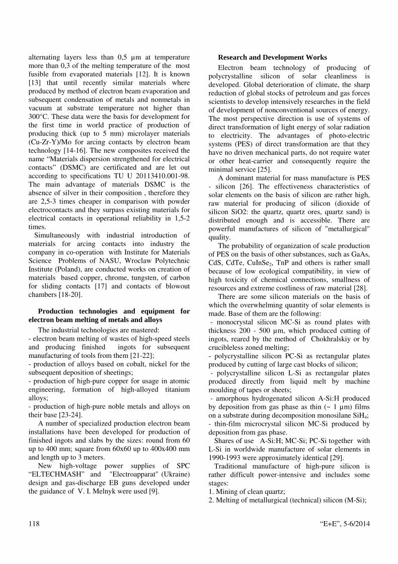
“E+E”, 5-6/2014 118
alternating layers less than 0,5 µm at temperature more than 0,3 of the melting temperature of the most fusible from evaporated materials [12]. It is known [13] that until recently similar materials where produced by method of electron beam evaporation and subsequent condensation of metals and nonmetals in vacuum at substrate temperature not higher than 300°С. These data were the basis for development for the first time in world practice of production of producing thick (up to 5 mm) microlayer materials (Cu-Zr-Y)/Mo for arcing contacts by electron beam technology [14-16]. The new composites received the name “Materials dispersion strengthened for electrical contacts” (DSMC) are certificated and are let out according to specifications TU U 20113410.001-98. The main advantage of materials DSMC is the absence of silver in their composition , therefore they are 2,5-3 times cheaper in comparison with powder electrocontacts and they surpass existing materials for electrical contacts in operational reliability in 1,5-2 times.
Simultaneously with industrial introduction of materials for arcing contacts into industry the company in co-operation with Institute for Materials Science Problems of NASU, Wroclaw Polytechnic Institute (Poland), are conducted works on creation of materials based copper, chrome, tungsten, of carbon for sliding contacts [17] and contacts of blowout chambers [18-20].
Production technologies and equipment for electron beam melting of metals and alloys
The industrial technologies are mastered: - electron beam melting of wastes of high-speed steels and producing finished ingots for subsequent manufacturing of tools from them [21-22]; - production of alloys based on cobalt, nickel for the subsequent deposition of sheetings; - production of high-pure copper for usage in atomic engineering, formation of high-alloyed titanium alloys; - production of high-pure noble metals and alloys on their base [23-24].
A number of specialized production electron beam installations have been developed for production of finished ingots and slabs by the sizes: round from 60 up to 400 mm; square from 60х60 up to 400x400 mm and length up to 3 meters.
New high-voltage power supplies of SPC “ELTECHMASH” and "Electroapparat" (Ukraine) design and gas-discharge EB guns developed under the guidance of V. I. Melnyk were used [9].
Research and Development Works Electron beam technology of producing of
polycrystalline silicon of solar cleanliness is developed. Global deterioration of climate, the sharp reduction of global stocks of petroleum and gas forces scientists to develop intensively researches in the field of development of nonconventional sources of energy. The most perspective direction is use of systems of direct transformation of light energy of solar radiation to electricity. The advantages of photo-electric systems (PES) of direct transformation are that they have no driven mechanical parts, do not require water or other heat-carrier and consequently require the minimal service [25].
A dominant material for mass manufacture is PES - silicon [26]. The effectiveness characteristics of solar elements on the basis of silicon are rather high, raw material for producing of silicon (dioxide of silicon SiO2: the quartz, quartz ores, quartz sand) is distributed enough and is accessible. There are powerful manufactures of silicon of "metallurgical" quality.
The probability of organization of scale production of PES on the basis of other substances, such as GaAs, CdS, CdTe, CuInSe2, TnP and others is rather small because of low ecological compatibility, in view of high toxicity of chemical connections, smallness of resources and extreme costliness of raw material [28].
There are some silicon materials on the basis of which the overwhelming quantity of solar elements is made. Base of them are the following: - monocrystal silicon МC-Si as round plates with thickness 200 - 500 µm, which produced cutting of ingots, reared by the method of Chokhralskiy or by crucibleless zoned melting; - polycrystalline silicon PC-Si as rectangular plates produced by cutting of large cast blocks of silicon; - polycrystalline silicon L-Si as rectangular plates produced directly from liquid melt by machine moulding of tapes or sheets; - amorphous hydrogenated silicon A-Si:Н produced by deposition from gas phase as thin (~ 1 µm) films on a substrate during decomposition monosilane SiH4; - thin-film microcrystal silicon MC-Si produced by deposition from gas phase.
Shares of use A-Si:H; MC-Si; PC-Si together with L-Si in worldwide manufacture of solar elements in 1990-1993 were approximately identical [29].
Traditional manufacture of high-pure silicon is rather difficult power-intensive and includes some stages: 1. Mining of clean quartz; 2. Melting of metallurgical (technical) silicon (M-Si);

“E+E”, 5-6/2014 119
3. Production and refining of silicon-inclusive gases (silanes); 4. Manufacture of high-pure polycrystalline rods (PC-Si); 5. Growing of monocrystal ingots (MC-Si).
The available data shows that for manufacture of solar elements the metallurgical silicon both with additional refining and without it can be used [29]. A rather prospective alternative chemical method for production of high-clean polycrystalline silicon is electron beam refining of technical (metallurgical) silicon [30]. The design of industrial electron beam installation for refining of technical (metallurgical) silicon is shown on fig.3 (1-technological chamber; 2-door; 3- observation system; 4-booster vacuum pump;5-EB gun; 6-large size charge feeding mechanism;7- small size charge feeding mechanism;8- cascade of intermediate cold hearths; 9- shaking feeder; 10- receiving bunker; 11- traversing chamber; 12- device for alloy addition).
Fig.3. Industrial electron beam installation for
refining of technical (metallurgical) silicon
The installation is supplied with the appropriate mechanisms and devices ensuring production of up to 800 kg refining silicon for 8 hours. The installation is supplied with three intermediate capacities (fig.3 item 8) in which remelting is carried out, overheating and refining of silicon. The refining silicon interflows in
special crucible where is carried out directed crystallization of liquid melt.
The realization of refining of silicon is consecutive in each of three intermediate capacities is carried out by a separate electron beam gun by capacity 100 kW. The feeding of modifiers for refining of silicon is carried out with the help batchers (fig.3 item12).
The installation is supplied with two feeders initial charge in a zone melting (fig.3 a position 6,7). The mechanism 6 is intended for feeding large lump charge. The mechanism is supplied by valve for additional charge without broken of vacuum in the working chamber.
The mechanism 7 is equipped by shaking feeder for submission in melting zone fine (5- 20mm) charge.
Electron beam technology of production of targets for magnetron dispersion
The technology of producing by evaporation and the subsequent condensation in vacuum targets from chrome for magnetron dispersions is mastered.
The appearance of targets is shown in a fig.4.
Fig.4. Targets
Electron beam technology of production of composite powders
The research works on producing of metal, ceramic and composite powders are carried out. The processes of evaporation and condensation in vacuum allow to producer practically any types of powders by the size from 0.3 up to 1.2 µm with productivity up to 15 kg of a powder at one hour.
According to technical process of condensation of a steam flow is carried out on a cooled rotating substrate. With the help of a special scraper the powder is removed from a substrate and on a special tray moves in the auxiliary chamber where special capacity for acceptance of powder is placed. Capacity evacuation is carried out after it filling. The powder in capacity is taken from the auxiliary chamber and transfers for further use.
“E+E”, 5-6/2014 120
REFERENCES [1] Movchan B.A., Malashenko I.S. Vacuum-
deposited heat-resistand coatanc. - Kiev:
[2] Naukova Dumka, 1983 – 230p.
[3] Zuev I.V. Treatment of materials by the concentrated energy flows. - Moscow:
[4] MEI, 1998 - 162с. [5] Movchan B.A., Tichonvsky А.L., Kurapov Y.А.
Electron beam melting of metals and alloys - Kiev: Naukova Dumka, 1973 – 230p.
[6] Grechanyuk N.I., Kucherenko P.P., Osokin V.A., Shpak P.А. State-of-the-art and prospects of development of thremal barrier coatings for gas turbine blade units and equipment for their despsition. Novyny Energetyky, 2000, 9 – p.32-37.
[7] Grechanyuk N.I., Osokin V.A., Grechanyuk I.N. New composite materials for electric contacts and way of their producing. Rynok metallov, 4, 1999 – p.58-60.
[8] Pat. US 6, 923, 868 BZ Installation for elektron - ray coatication of coatings/ M.Grechanyuk, P.Kucherenko. - Publ. 02.08.2005.
[9] Pat. 2265078 RF. Installation for electron beam deposition of coatings / N.I.Grechanyuk, P.P.Kucherenko. - Publ. 12.27.2005
[10] Patent of Ukraine 40664. Electronic gun with the linear thermocathode for electron beam heating / Grechanyuk N.I., Dyatlova O.K., Kucherenko P.P., Piyuk E.L., Publ. in bulletin 7, 2001.
[11] Denbnovetskiy S.V., Melnik V.G. Melnik I.V., Tygay B.A. Application of Glow Discharge Electron Guns for Plasma Activated Deposition of Coatings / Elektrotekhnika and Elektronika, 5-6, 2006, p.115 - 118.
[12] Zolkin A.S. Sources of metal vapors for researches and technologies. - Novosibirsk: Institute teplophiziki RAN, 1992, 75p.
[13] Patent of Ukraine 42052. Protective coating for gas turbine blads. / N.I.Grechanyuk, P.P.Kucherenko, V.A.Osokin, I.B.Afanacsiev, S.S.Belik, V.A.Akrymov, I.N.Grechanyuk. Publ. in bulletin 9, 2001.
[14] Patent 2271404 RF. Method of production of microlayer thermostabile materials. / N.I.Grechanyuk - Publ. 03.10.2006.
[15] Iliinsky А.I. Structure and strength of lamellar and dispersion-strengthened films . - G: Metallurgiya 1986 - 140p.
[16] Patent of Ukraine 34875. Composite material for electric contacts. / N.I.Grechanyuk, V.A.Osokin, I.B.Afanacsiev. Publ. in bulletin 2 - 2001.
[17] Grechanyuk N.I., Osokin V.A., Grechanyuk I.N. Minakova R.V. Composite materials on base of copper and molybdenum, condensed from vapor phase, for electric contacts. Structure, properties, technology. Part 1. State - of - the art and prospects of application of technology of electron beam high-rate evaporation-condensation for
producing materials of electric contacts. Advances in Electrometallurgy 2, 2005 p. 24-29.
[18] Grechanyuk N.I., Osokin V.A., Grechanyuk I.N., Kucherenko P.P., Minakova R.V. Golovkova M.E., Kopylova G.E. Composite materials on base of copper and molybdenum, condensed from vapor phase, for electric contacts. Structure, properties, technology. Part 2. Fundamentals of electron beam technology for producing materials for eltctric contacts.
[19] Miedzinski B., Okraszewsky Z., Grechanyuk N., Wandzio J. Performance of sliding contacts with Cu-Mo layers for transportation in mining industry. Elektricheskiye kontakty I elektrody. Sbornik trudov IPM NANU Kiev 2008 p. 150-155.
[20] Patent of Ukraine 32368А. Contact material for explosion chambers and way of its producing. / N.I.Grechanyuk, N.N.Plaschenko, V.A.Osokin, I.B.Afanacsiev, I.N.Grechanyuk. Publ. in bulletin 7 -11 15.12.2000.
[21] Patent of Ukraine 76737. Contact system of vacuum explosion chamber. / N.I.Grechanyuk, N.N.Plaschenko, А.V.Zvarich, V.A.Osokin. Publ. in bulletin 9 2006.
[22] Decision a 200703343 about distribution of the Patent of Ukraine from 29.11.2008. Composite material for electrical contacts and electrodes. / N.I.Grechanyuk, I.N.Grechanyuk, V.А.Denisenko, V.G. Grechanyuk.
[23] Shpak P.А., Grechanyuk V.G., Osokin V.A. Effect of electron beam remelting on structure and properties of high-speed steel Р6М5. / Advances in Electrometallurgy. 2002 - 3 – p.14-17.
[24] Patent of Ukraine 37658. Method of production of blanks for tools from high-speed steel. / N.I.Grechanyuk, I.B.Afanacsiev, P.А.Shpak. Publ. in bulletin 7 2003.
[25] Savenko V.А., Grechanyuk N.I., Churakov О.V. Electron beam refining in producing of platinum and alloys on its basis. Message 1. Electron beam refining of platinum. // Sovremennaya electrometallurgiya -2008 - 1 -p.16-18.
[26] Savenko V.А., Grechanyuk N.I., Churakov О.V. Electron beam refining of platinum and alloys on its basis. Message 2. Electron beam refining of alloys on the basis of platinum. // Sovremennaya electrometallurgiya - 2008 - 3 – p.38-41.
[27] Basin A.S., Shyshkin А.V. Producing of silicon plates for solar energy. RAN Novosibirsk 2000, 390p.
[28] Rohatgi A., Weber E.R., Kimerling L.C. Opportunities in silicon photovoltaics and defect control in photovoltaic materials. // J.Electron. Mater - 1993 - Vol. 22, 1. - p 65-72.
[29] Shan A., Meier T., Tsharner R., Wyrsch N. Photo-voltaic power generation. // Plasma Phys and Controlled Fusion. - 1992 - Vol 34. 13 – p.1837-1844.
[30] Eyer A., Rauber A., Goetzberger A. Silicon sheet materials for solar cells. // Optoelectronics Devices and Techol. - 1990. - Vol. 5, 2 -p 239-257.

“E+E”, 5-6/2014 121
[31] Surek T. NREL PV prodram overview. //Naticnal Renewable Energy Laboratory. - Golden, Colorado, USA., 1955 - 15p.
[32] Grechanyuk N.I., Kucherenko P.P., Grechanyuk I.N. New electron beam eguipment and technologies of producing advanced materials and coatings. //Paton Welding Journal - may 2007 – p.25-29.
M. I. Grechanyuk, SPE Eltechmash (25, Vatutina str., Vinnytsa, Ukraine)
A. G. Melnyk, SPE Eltechmash (25, Vatutina str., Vinnytsa, Ukraine)
I. M. Grechanyuk, SPE Eltechmash (25, Vatutina str., Vinnytsa, Ukraine)
V. G. Melnyk, JSC NVO Chervona Hvilya (15,Bozhenko str., Kyiv, 03680, Ukraine)
D. V. Kovalchuk - JSC NVO Chervona Hvilya (15,Bozhenko str., Kyiv, 03680, Ukraine).

“E+E”, 5-6/2014 122
Recent Progress in Development of Gas-Discharge Electron Beam Guns Providing Extension of
Their Technological Capabilities
V. G. Melnyk, I. V. Melnyk, B. A. Tugai, D. V. Kovalchuk
Long operating experience of gas-discharge electron beam guns in different technological
processes has allowed to investigate their special behavior features and to determine what must be improved in their design for providing the best operation reliability and extension of their technological applications. Appropriate theoretical and experimental R&D works were performed for this purpose.
Engineering upgrade of gas-discharge electron beam guns of BTP family with power from 60 kW to 450 kW was provided by these works resulting in better consistency and reliability of guns operation in extended limits of operating conditions. Gas-discharge electron beam gun BTP-600 with maximum power 600 kW and accelerating voltage 40 kV was developed for the first time also on the base of performed R&D works.
Последни усъвършенствания в разработката на газоразрядни електронни пушки, обезпечаващи разширение на технологичните им възможности (В. Мелник, И. Мелник, Б. Тугай, Д. Ковалчук). Дългогодишният опит с газоразрядни пушки в различни технологични процеси позволи да се изучат особеностите на тяхното специално поведение и да се определи какво трябва да се подобри в конструкцията им за обезпечаване на по-добра работна надеждност и разширение на техните приложения. За тази цел бяха изпълнени подходящи теоретични и експериментални изследвания и разработки. Бяха направени инженерни подобрения на газоразрядните електронни пушки от фамилията БТП с мощност от 60 kW до 450 kW и резултатът е по-добра съгласуваност и надеждност на работата на пушката в по-широки граници на работните условия. Газоразрядни пушки БТП 600 с максимална мощност 600 kW и ускоряващо напрежение 40 kV бяха разработени за първи път също на базата на изпълнените изследвания и разработки.
Introduction Gas-discharge electron beam guns are covering
more and more wide application in different industries – mainly thanks to their ability of stable operation in hard vacuum conditions which are typical to number of technological processes. Our own experience of operation of gas-discharge electron beam guns of BTP type with power range 60-450 kW during last decade has confirmed suitability and availability of their usage in such industrial applications as electron beam melting of titanium, tantalum, niobium, molybdenum, electron beam refining of silicon, specific kinds of electron beam welding, EB PVD processes as well [1, 2].
Fig.1. Gas-discharge EB guns BTP-100 (100 kW), BTP-300
(300 kW) and BTP-450 (450 kW)

“E+E”, 5-6/2014 123
Gas-discharge EB guns BTP-100 (100 kW), BTP-300 (300 kW) and BTP-450 (450 kW) developed in JSC NVO Chervona Hvilya are presented on Fig. 1.
Modern industrial equipment developed on the base of gas-discharge EB guns is distinguished by comparative simplicity, stable operation, easy maintenance, high production and economic efficiency. In addition some specific operation features of gas-discharge EB guns provide possibility to realize new technological modes of production technologies.
Actual operation experience with gas-discharge EB guns of BTP type has also enabled to investigate their running features in different running conditions. This important information helped us to determine the ways of perfection of gas-discharge EB guns to provide further increase of their technological and commercial attractiveness. Improvement of their operation stability, increase of general reliability, prolongation of lifetime of complete guns and separate parts, reduction of downtime by means of more easy maintenance procedure and less number of specific service requirements were the main directions of our development.
The main directions of R&D activity in improvement of gas-discharge EB guns
Fig.2. Construction scheme of gas-discharge EB gun BTP
type (1- cathode assembly; 2 – anodic assembly; 3 – insulator; 4 – beam transmission system; 5 – focusing coils;
6 – deflection coil)
Special theoretical research and experimental works were executed with the purpose of BTP guns perfection including investigations of the following aspects:
- analysis of cold cathode operation under condition of different characteristics of high voltage glow discharge in wide range of pressure and composition of gas medium,
- evaluation and testing of ultimate energy parameters of electrode systems,
- optimization of geometry characteristics of electrode systems and its electron-optic parameters,
- development of beam transportation system with big convergence angle from discharge zone to operation chamber as well.
Construction scheme of gas-discharge EB gun BTP type is presented on Fig. 2.
As a rule low-alloy aluminum alloys are used in production of cold cathodes mainly due to relatively high ion-electron emission coefficient (current density more than 0.1 A/sm²) and good heat conduction. Optimization of configuration of cathode assembly which all parts are under high negative voltage has provided uniform distribution of electric field in insulating vacuum gap resulting in decreased probability of arcing. Cathode is mounted directly at bottom end of high voltage insulator which eliminates presence of sealing gasket between vacuum space of gun and internal water cooling space of cathode excluding any probability of water vapor penetration to discharge chamber of the gun. Cold cathode of gas-discharge EB gun BTP-450 is presented on Fig. 3.
Optimization of geometry of anode disk has provided much better stability of focus distance of electron beam under different discharge current. This feature improves transportation of the beam through anode hole without significant energy losses and simplifies cooling of this unit accordingly.
Fig.3.Cold cathode of gas-discharge EB gun BTP-450 Suitable ultimate energy parameters of electrode
systems are provided by the optimized choice of material and geometry of cold cathode and hollow anode of BTP guns taking into account maximum permissible energy dissipation in the discharge chamber of the gun. The required power density depends on the ultimate power which can be extracted from the electrodes at their operating temperatures. Limiting current density depends on cold cathode

“E+E”, 5-6/2014 124
emission properties and quantity of power which can be extracted from cathode when heated by ion bombardment. Optimization of the main EB gun parameters was performed on the base of above mentioned consideration of physical properties and conditions.
Limitation of lateral dimension of beam transmitter which cross-section corresponds with shape of transmitted beam provides pressure differential between discharge chamber of the gun and operating chamber up to two orders under condition of proper pumping capacity. It allows evacuation of gun space together with operating chamber by general vacuum system of EB technological installation and expands range of operating vacuum level during technological processes.
Transportation of the beam from discharge chamber of the gun to operating chamber through beam transmitter with limited lateral dimension is provided by appropriate placement of two focusing coils.
Deflection system consisting of specified number of toroidal lenses mounted on ring-type magnet is applied for scanning of electron beam at the beam transmitter outlet. Beam transmitter is attached to gun’s base flange with which gun is mounted at operating chamber.
Reasonable accelerating voltage consideration Gas-discharge EB guns of BTP type with power range from tens to hundreds kW are working mainly under accelerating voltage within limits 25-30 kV, which basically meets specific operating conditions of guns
and their usage in different industrial equipment. In addition such voltage limits simplifies X-ray protection of equipment which is important for labor safety. But analysis of guns operation in some special technological processes has revealed that sometimes application of higher or lower accelerating voltage can provide more flexible and/or suitable heating conditions at the treated target. For example operation of high-power gas-discharge EB guns as heating component of extra large industrial electron beam melting furnaces requires higher accelerating voltage. Voltage rise provides better conditions of electron beam transportation on longer distance in bad vacuum for example when technological process is accompanied by intensive evaporation or gassing. In this case increased specific power is provided by higher accelerating voltage resulting in higher efficiency of heating processes. New gas-discharge EB gun BTP-600/40 with power 600 kW and accelerating voltage 40 kV was developed as result of these R&D works. Rise of accelerating voltage to 40 kV has allowed increase of ion-electron emission coefficient of cold cathode, which reduces energy loss on electrodes and improves energy and geometry parameters of electron beam. At the same time rise of accelerating voltage can cause more intensive arcing between cathode and anode resulting in less stable operation of the gun. Special design of cathode assembly configuration was developed to minimize intensity of arcing and it influence on operation of guns and complete installation.
Power, kW
Accelerating voltage, kV
Beam current, A
Beam diameter at the target, mm
Permitted range of pressure in operating chamber, Pa
Operating gases
Technologies and applications
1-10 10-40 0.1 -1 0.5-4 10-0.1 Air, Oxygen Argon Helium
Welding of thin-wall parts, brazing, surface treatment
30-100 25-30 1-4 5-8 10 - 10¯³ Hydrogen Oxygen
Welding of pressed materials, EB-PVD, single-crystal growing
100-450 30 3.3-15 8-20 5 - 10¯² Hydrogen with Oxygen addition
Melting and refining of refractory and reactive metals and alloys
600 40 15 15-20 5 - 10¯² Hydrogen with Oxygen addition
Melting and refining of refractory and reactive metals and alloys

“E+E”, 5-6/2014 125
There are many fine metallurgical processes which require very soft heating of targets such as thin parts or small zones of treatment. It could be welding of elements with very thin walls, brazing joints, surface treatment etc. Accelerating voltage within limits 10-20 kV can be applied in proper gas-discharge EB guns with good efficiency.
Gas-discharge EB guns as universal
technological instrument Gas-discharge EB guns of wide range of different
configurations and power were developed till now [3]. Base technical parameters of available gas-discharge EB guns for different applications are presented in Table 1.
Application of gas-discharge EB guns of BTP series in different industrial equipment is demonstrated on figures 4-6.
Fig.4. Gas-discharge EB gun BTP-300 at EBM installation
Fig.5. Gas-discharge EB guns BTP-100 at EB-PVD
installation
Fig.6. Gas-discharge EB gun BTP-60 at R&D installation
Currently we can state that gas-discharge EB guns can be considered as very reasonable and very prospective equipment for wide range of industrial application.
REFERENCES [1] Kovalchuk D.V., Kondratii M.P. Electron
Beam Melting of Titanium – Problems and Prospects of Development. – Titan, 1(23), 2009. – p.15-20.
[2] Denbnovetskiy S.V., Melnyk V.I., Melnyk I.V. High-Voltage Glow-Discharge Electron Sources and Possibilities of Its Application in Industry for Realizing of Different Technological Operations. – IEEE Transactions on Plasma Science. – Vol. 31, #5, October, 2003. – p. 987-993.
[3] Denbnovetskiy S.V., Melnyk V.I., Melnyk I.V., Tugai B.A. Technological Possibilities of High-Voltage Glow-Discharge Electron Guns. – Электротехника и электроника, 5-6, 2009. – p.189-192.
V. G. Melnyk - JSC NVO Chervona Hvilya
I. V. Melnyk - JSC NVO Chervona Hvilya
B. A. Tugai - JSC NVO Chervona Hvilya
D. V. Kovalchuk - JSC NVO Chervona Hvilya
JSC NVO Chervona Hvilya,
15,Bozhenko str., Kyiv, 03680, Ukraine.
Tel/fax: +380-44-2008946
e-mail: [email protected]
.

“E+E”, 5-6/2014 126
Effects of Beam Patterns on Removal of Phosphorous in Silicon by Electron Beam Melting
Shuang Shi, Yi Tan, Dachuan Jiang, Wei Dong, Shutao Wen
A heat transfer model for Si refining by electron beam melting is proposed to obtain the temperature distribution of the molten Si. The results show that the temperature distribution is extremely inhomogeneous, especially on the molten surface. Based on the temperature distribution, the evaporation rates of P and Si are also discussed and the corresponding experiment was carried out to be compared with the theoretical calculation. The results show that the evaporation rates of P and Si reduce and the ratio of the evaporation rate of P to Si increases with the increasing of the electron beam pattern radius. A critical molten pool with a large surface area exists when the pattern radius reaches to a certain value, which is considered to be the optimal pattern radius due to a relatively high removal efficiency of P and a low loss efficiency of Si.
Влияние на лъча върху отстраняването на фосфор в силиций чрез електроннолъчево топене (С. Ши, И. Тан, Д. Жианг, У. Донг, С. Уен). Предложен е модел за топлопренасянето при рафиниране на силиций за получаване на температурното разпределение на разтопения силиций. Резултатите показват, че температурното разпределение е изключително нехомогенно, особено на разтопената повърхност. На база на температурното разпределение са дискутирани също скоростите на изпарение на фосфор и силиций и е проведен съответстващ експеримент за сравнение с теоретичните изчисления. Резултатите показват, че скоростите на изпарение на фосфор и силиций намаляват и отношението на скоростта на изпарение на фосфор към тази на силиций се увеличава с увеличаване на радиуса на лъча. Съществува критична течна вана с голяма повърхност, когато радиуса стига до определена стойност, който се приема за оптимален радиус, благодарение на сравнително голямата ефективност на отстраняване на фосфор и на малките загуби на силиций.
Introduction In recent years, the requirement for solar-grade
silicon increases dramatically with the rapid development of the photovoltaic industry[1-3]. As one of the major impurities, P deteriorates the electrical properties of silicon materials, such as electrical resistivity and minority carrier lifetime. Therefore, it needs to be removed to less than 1×10⁻⁵ wt.%, to meet the performance requirement of solar cells.
Electron beam melting has been applied in purification of Si materials, which has been proved to be an effective method to remove volatile impurities[4-9]. During electron beam melting process, pattern radius, defined as the radius of electron beam scanning track, is an important factor that affects the state of the molten pool. Different pattern radiuses lead to different temperature and surface area at a certain power, so as to influence the
evaporation rate. However, the surface temperature of the molten pool is difficult to measure directly due to the characteristic of local high energy of electron beam melting, which is always roughly calculated by the loss of Si. So far, only few reports on the temperature distribution of the molten pool and the corresponding removal rate of P during electron beam melting are available to date.
In this paper, a model for Si refining by electron beam melting is proposed to obtain the temperature distribution in the molten silicon, especially on the surface of the molten pool. Based on the results, the evaporation rates of P and Si are also calculated to evaluate the removal efficiency of P and the loss of Si. Moreover, the optimal pattern radius at a certain electron beam power is discussed.
Mathematical model development A cylindrical ingot is considered in the
mathematical model to obtain the temperature

“E+E”, 5-6/2014 127
distribution on the silicon ingot during electron beam melting, as shown in Fig. 1. The bottom of the ingot contacts directly to a water-cooled copper crucible. As a heat source, the electron beam irradiates the top surface of the ingot in a circular trajectory.
Fig.1. Schematic illustration of the mathematical model
A heat transfer model is developed according to the following assumptions:
(a) The geometry of the model configuration is axisymmetric;
(b) Heat transfer occurs only along the axial and radial directions;
(c) The thermal and physical properties of the material are independent of time.
The heat flow in the radial direction, r, and in the axial direction, z, can be described by heat conduction equation as follows:
(1) Qz
Tk
zr
Tkr
rrt
TCP +
∂∂
∂∂+
∂∂
∂∂=
∂∂ 1ρ
where T (K) is the temperature, t (s) is the melting time, r (m) is the radius, z (m) is the axial height, ρ (g m-3) is the density, Cp (J kg-1 K-1) is the specific heat, k (W m-1 K-1) is the thermal conductivity, and Q (W m-
3) is the volumetric latent heat associated with the phase transformation. The input heat flux from the electron beam, qEB (W m-2) can be described by a normal distribution function[10]:
(2) ( ) ]2exp[ 22 σηµ RrCq EBEB −−=
where µEB is the electron beam power transfer efficiency, η is the normalized electron beam power, C (W m-2) is a pre-exponential constant, r (m) is the radius, R (m) is the center position of the beam pattern, and σ (m) is the standard deviation of the distribution.
For the calculation, the initial temperature of the ingot is set to 298 K. Since the copper crucible is far from the heat source, the temperature of the environment and the copper crucible are set to 298 K, respectively. The validity of this assumption is confirmed by the absence of temperature change in the water inlet and outlet of the crucible during refining.
The boundary conditions are given as follows: On the top surface of the ingot, the net heat flux
consists of two parts, the electron beam energy density, qEB (W m-2), and the surface heat irradiation flux, qrad (W m-2):
(3) radEB
zz
qqz
Tk +=
∂∂−
= 0
The surface heat irradiation flux can be expressed as
(4) ( )44 TTqrad −= ∞εσ
where ε is the emissivity of the Si surface, σ (5.67 × 10⁻⁸ W m-2 K-1) is the Stephan-Boltzmann constant, and T∞ (K) is the far-field temperature.
On the bottom surface of the ingot:
(5) ( )TThz
Tk Cu
z
−=∂∂−
=0
where h (W m-2 K-1) is the heat transfer coefficient and TCu (K) is the temperature of the water-cooled copper crucible.
On the outside surface of the ingot:
(6) ( )44
0
TTr
Tk
rr
−=∂∂− ∞
=
εσ
Based on the above boundary conditions, the temperature distribution in the vertical cross-section of the ingot during electron beam melting can be calculated.
Results and discussion
Temperature distribution
Two ingots with a same ratio of radius to height are calculated by the aforementioned model at a power of 6 kW. The typical steady state temperature distributions of the ingot cross-section are shown in Fig. 2.
Great temperature gradient exists in the axial direction of the ingot, which results from the heating on the top surface by the electron beam and the cooling on the bottom surface by the water-cooled

“E+E”, 5-6/2014 128
copper crucible. However, the temperature gradients in the radial direction are different along the height of the ingot. The area directly irradiated by the electron beam is within the range of the highest temperature due to high energy density input. With continuous irradiation by electron beam, heat energy transfers from the area to the surroundings. So the upper part of the ingot shows a great temperature gradient in the radial direction, especially on the top surface. In contrast, the bottom part of the ingot shows no temperature gradient in the radial direction.
Fig.2. Temperature distributions on the cross-section of the
ingots (left: radius 3.5cm, height 7cm; right: radius 5cm, height 10cm)
Change of pattern radius leads to a variation of the temperature distribution on the surface. Figure 3 shows five typical temperature distributions on the surface of the ingot with different pattern radiuses.
A peak shaped temperature distribution is formed with a high temperature in the central part and a low
temperature in the surrounding when the pattern radius is small, due to the relatively concentrated energy in the center nearby. With the pattern radius increases, the temperature of the central part decreases, and the peak value of the temperature moves peripheral so that an annular peak of temperature distribution is formed.
Fig. 3. Temperature distributions on the surface of the
ingots (left: radius 3.5cm, height 7cm; right: radius 5cm, height 10cm)
The temperature of the surface centre will reduce to the melting point when the pattern radius increases continually to a certain value. The molten pool in this state is called the critical molten pool and the patter radius is defined as the critical patter radius. If the pattern radius is larger than the critical value, the central part of the ingot doesn’t melt because the temperature is less than the melting point.
Characteristics of the molten pool
According to temperature distribution on the ingot surface, the surface area of the molten pool can be calculated, as shown in Fig.4.
A molten pool with a small surface area forms due to a relatively concentrated energy when the pattern radius is small. As the pattern radius increases, the surface area of the molten pool enlarges due to a
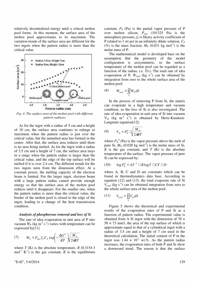
“E+E”, 5-6/2014 129
relatively decentralized energy until a critical molten pool forms. At this moment, the surface area of the molten pool approximates to its maximum. The variation trends of the surface area are different for the two ingots when the pattern radius is more than the critical value.
Fig. 4. The surface area of the molten pool with different
pattern radiuses
As for the ingot with a radius of 5 cm and a height of 10 cm, the surface area continues to enlarge to maximum when the pattern radius is just over the critical value, but the unmelted area has formed in the center. After that, the surface area reduces until there is no area being melted. As for the ingot with a radius of 3.5 cm and a height of 7 cm, the surface area stays in a range when the pattern radius is larger than the critical value, and the edge of the top surface will be melted if it is over 2.4 cm. The different trends for the two ingots stem from the dimension effect. At a constant power, the melting capacity of the electron beam is limited. For the larger ingot, electron beam with a large pattern radius cannot provide enough energy so that the surface area of the molten pool reduces until it disappears. For the smaller one, when the pattern radius is more than the critical value, the border of the molten pool is closed to the edge of the ingot, leading to a change of the heat transmission condition.
Analysis of phosphorous removal and loss of Si
The rate of idea evaporation in unit area of P into vacuum WP (kg m-2 s-1) varies with temperature can be expressed by[11]
(7) RT
M
RT
GCfPW P
PPatmP π2exp
0
∆−=
where T (K) is the absolute temperature, R (8.3154 J mol-1 K-1) is the gas constant, K is the equilibrium
constant, PP (Pa) is the partial vapor pressure of P over molten silicon, Patm (101325 Pa) is the atmosphere pressure, fP is Henry activity coefficient of P related to 1 wt pct in an infinitely dilute solution, CP (%) is the mass fraction, MP (0.031 kg mol-1) is the molar mass of P.
The mathematical model is developed base on the assumption that the geometry of the model configuration is axisymmetric, so the surface temperature of the molten pool can be regarded as a function of the radius, i.e. T(r). The total rate of idea evaporation of P, Wtotal (kg s-1) can be obtained by integration from zero to the whole surface area of the molten pool:
(8) dSWWS
Ptotal ∫∫=
In the process of removing P from Si, the matrix can evaporate in a high temperature and vacuum condition, so the loss of Si is also investigated. The rate of idea evaporation in unit area of Si into vacuum VSi (kg m-2 s-1) is obtained by Hertz-Knudsen-Langmuir equation[12]:
(9) RT
MPV Si
SiSi π20 ⋅=
where PSi0 (Pa) is the vapor pressure above the melt of
pure Si, MSi (0.028 kg mol-1) is the molar mass of Si, R is the gas constant, and T (K) is the absolute temperature of the surface. The vapor pressure of pure Si can be expressed by:
(10) DCTTBATPSi +++= − loglog 10
where A, B, C and D are constants which can be found in thermodynamics data base. According to equation (12) and (13), the total evaporate rate of Si Vtotal (kg s-1) can be obtained integration from zero to the whole surface area of the molten pool:
(11) dSVVS
Sitotal ∫∫=
Figure 5 shows the theoretical and experimental results of the evaporation rates of P and Si as a function of pattern radius. The experimental value is obtained from A Si ingot with the dimension of 70 × 58 × 73 mm3, the area of the top surface of which is approximate equal to that of a cylindrical ingot with a radius of 3.5 cm and a height of 7 cm used in the theoretical calculation. The initial content of P in the ingot was 1.44 × 10⁻² wt.%. As the pattern radius increases, the evaporation rates of both P and Si show a downward trend. The reason is that the surface

“E+E”, 5-6/2014 130
temperature of the molten pool reduces due to energy dispersion with a large beam pattern. The experimental values are consistent with the theoretical value in the range of permitted errors.
Fig. 5. The evaporation rate of P and Si with different
pattern radiuses
During electron beam melting process, P needs to be removed and Si needs to be reserved, so the ratio of evaporation rates of P to Si is also calculated. A small pattern radius leading to a high surface temperature is beneficial to the removal of P, but in this case, the loss of Si is also large. On the contrary, a large pattern radius can reduce the loss of Si, but when it is more than the critical value, a circular molten pool forms on the top of the ingot with the center part being unmelted. In consideration of the above factors, the critical molten pool with a large surface area is considered to be the optimal electron beam pattern radius during electron beam melting with a constant power.
However, it should be noted that all of the calculations are discussed in ideal conditions. In fact, the residual chamber pressure is comparable to the vapor pressure of evaporating species, so collisions between evaporant atoms and residual gas molecules or evaporant atoms themselves may change the evaporation rate by a small amount.
Conclusion According to the temperature distribution in the
molten pool based on a heat transfer model, the evaporation rates of P and Si during Si refining processing by electron beam melting is discussed. As the pattern radius increases, the evaporation rates of P and Si reduce, but the ratio of the evaporation rate of P to Si increases. There exists a critical molten pool when the pattern radius reaches a certain value. At this time, impurity P can be removed effectively and the
evaporation rate of Si is in a low level, leading to a relatively high removal efficiency of P and a low loss efficiency of Si.
Acknowledgements The author gratefully acknowledges financial
support from National Key Technology R & D Program (Grant No. 2011BAE03B01) and the Natural Science Foundation of China (Grant No. U1137601).
REFERENCES [1] T. Schutz-Kuchly, V. Sanzone, Y. Veschetti, N-
type solar-grade silicon purified via the metallurgical route: characterisation and fabrication of solar cells, Prog. Photovoltaics, 2013, 21, 1214.
[2] F. Tanay, S. Dubois, N. Enjalbert, J. Veirman, Low temperature-coefficient for solar cells processed from solar-grade silicon purified by metallurgical route, Prog. Photovoltaics, 2011, 19, 966.
[3] M.A. Martorano, J.B. Ferreira Neto, T.S. Oliveira, T.O. Tsubaki, Refining of metallurgical silicon by directional solidification, Mater. Sci. Eng. B, 2011, 176, 217.
[4] D.C. Jiang, S. Shi, Y. Tan, D.Y. Pang, W. Dong, Research on distribution of aluminum in electron beam melted silicon ingot, Vacuum, 2013, 96, 27.
[5] Y. Tan, S.T. Wen, S. Shi, D.C. Jiang, W. Dong, X.L. Guo, Numerical simulation for parameter optimization of silicon purification by electron beam melting, Vacuum, 2013, 95, 18.
[6] S. Shi, W. Dong, X. Peng, D.C. Jiang, Y. Tan, Evaporation and removal mechanism of phosphorus from the surface of silicon melt during electron beam melting, Applied Surface Science, 2013, 266, 344.
[7] Y. Tan, X.L. Guo, S. Shi, W. Dong, D.C. Jiang, Study on the removal process of phosphorus from silicon by electron beam melting, Vacuum, 2013, 93, 65.
[8] Q. Wang, W. Dong, Y. Tan, D.C. Jiang, C. Zhang and X. Peng: Impurities evaporation from metallurgical-grade silicon in electron beam melting process, Rare Metals, 2011, 30, 274.
[9] X. Peng, W. Dong, Y. Tan and D.C. Jiang: Removal of aluminum from metallurgical grade silicon using electron beam melting, Vacuum, 2011, 86, 471.
[10] D.M. Maijer, T. Ikeda, S.L. Cockcroft, M. Maeda and R.B. Rogge: Mathematical modeling of residual stress formation in electron beam remelting and refining of scrap silicon for the production of solar-grade silicon, Mater. Sci. Eng. B, 2005, 390, 188.
[11] T. Miki, K. Morita and N. Sano: Thermodynamics of phosphorus in molten silicon, Metall. Mater. Trans. B, 1996, 27B, 937.
[12] O.E. Shklyaev and E. Fried: Stability of an evaporating thin liquid film, J Fluid Mech., 2007, 584, 157.

“E+E”, 5-6/2014 131
Dr. S. Shi - School of Materials Science and Engineering, Dalian University of Technology, No. 2 Linggong Road, Ganjingzi District, Dalian 116023, China.
tel.:+86 411 84709784 е-mail: [email protected]
Prof. Y. Tan - School of Materials Science and Engineering, Dalian University of Technology, No. 2 Linggong Road, Ganjingzi District, Dalian 116023, China.
tel.:+86 411 84707583 е-mail: [email protected]
Dr. D. C. Jiang - School of Materials Science and Engineering, Dalian University of Technology, No. 2 Linggong Road, Ganjingzi District, Dalian 116023, China.
tel.:+86 411 84709784 е-mail: [email protected]
Assoc. Prof. W. Dong - School of Materials Science and Engineering, Dalian University of Technology, No. 2 Linggong Road, Ganjingzi District, Dalian 116023, China.
tel.:+86 411 84707455 е-mail: [email protected]
Dr. S. T. Wen - School of Materials Science and Engineering, Dalian University of Technology, No. 2 Linggong Road, Ganjingzi District, Dalian 116023, China.
tel.:+86 411 84709784 е-mail: [email protected]

“E+E”, 5-6/2014 132
Economic and Conservative Numerical Scheme for Non-Stationary Heat Model for EBMR
Veliko Donchev, Katia Vutova, Tatiana Chernogorova
Economic and conservative numerical method is proposed for discretization and numerical
simulation of non-stationary heat model concerning electron beam melting and refining (EBMR) of metals. The axis-symmetric problem is decomposed into two locally one-dimensional problems. For the two problems, implicit and absolutely stable schemes are built for which the decomposition method gives rate of convergence of order one for both the space and time variables. The obtained discrete problems lead to linear systems of equation with three-diagonal matrixes which are solved via Thomas method. Proposition for the stability and realization of Thomas method is proved for one of the two one-dimensional problems. Criteria, related to the geometry of the crystallization front, for improvement of the quality of the obtained material after EBMR are discussed. Approaches for discretization of the criteria over the numerical solution of the model are proposed. Comparison between experimental and simulation results is made and good correspondence is observed. Applying the developed numerical scheme and criteria, optimization of the EBMR of copper ingots is made. Results for the best technological regime parameters according to the chosen criteria for the investigated ranges of the beam power and the beam radius are given.
Икономичен и консервативен числен метод за нестационарен тополинен модел за ЕЛТР (Велико Дончев, Катя Вутова, Татяна Черногорова). Предложен е икономичен и консервативен числен метод за симулация на нестационарен тополинен модел за електронно-лъчево топене и рафиниране (ЕЛТР) на метали. Радиално симетричният модел е сведен до два локално едномерни проблема. За тях са построени неявни и абсолютно устойчиви числени схеми, за които локалният метод дава първи ред на сходимост по пространствените и времевата променливи. Получените дискретни проблеми водят до линейни системи с тридиагонални матрици, които се решават с метода на дясната прогонка. Доказано е твърдение за реализуемост и устойчивост на едната от двете локално едномерни задачи. Дискутирани са оптимизационни критерии за подобряване на качеството на получения метал, свързани с геометрията на кристализационния фронт. Направено е сравнение между експериментални и симулационни данни и е наблюдавано добро съответствие. Разработената числена схема и оптимизационни критерии са приложени за ЕЛТР на медни шайби. Съобразно избраните критерии са направени препоръки за оптимизиране на технологията при изследваните режими.
Introduction Despite the development оf Electron Beam
Melting and Refining (EBMR) technologies, a lot of unsolved problems still exist. For optimization and improvement of the technology, the knowledge of the temperature in the treated metal ingot is crucial. However, real time measurement of the temperature in the metal ingot, especially in the molten pool is hard to achieve. Therefore mathematical modeling of the thermal processes is essential for the improvement of EMBR technologies. In [1] non-stationary axis-symmetrical heat model with a
corresponding Pismen-Rekfort numerical method is proposed. Using the model [1], optimization problems are proposed and EBMR is optimized via developed criterion for achieving flatness of the molten pool and uniform impurities’ displacement in the metal ingot [2, 3]. In this paper the mathematical model proposed in [1] is treated by economic and conservative locally one-dimensional method in which the influence of the thermo-physical properties of the metal is more precisely taken into account. Another advantage of this method is that it can easily be continued to 1+3 dimensional method.

“E+E”, 5-6/2014 133
Mathematical heat Model and the corresponding locally one-dimensional problems
Recall the domain Ω of the problem (1) ( , , )|( , ) ,0 [0, ],r z t r z G t F G FΩ = ∈ ≤ ≤ = ×
where G is the domain in which the space variables ,r z are defined:
(2) ( , )|0 ,0 .G r z r R z H= ≤ ≤ ≤ ≤ The sets on which the boundary equations [1] are
defined are:
(3)
1 ( , ) |0 ,
2 ( , ) | ,
3 ( , ) |0 ,
4 ( ,0) |0 .
G r H r R
G R z H Q z H
G R z z H Q
G r r R
= ≤ ≤= − ≤ ≤= ≤ < −= ≤ ≤
With ( , , )T r z t we denote the temperature of the investigated metal in the point with polar radius r , height z in the moment of time t . The main equation [1] for T , which holds for ( , , ) (0, ]r z t G F∈ × , is:
(4)1
( ) ( ) ( ) ( ) ( )T T T T
T r T T V t Tt r r r z z z
∂ ∂ ∂ ∂ ∂ ∂κ = λ + λ + κ
∂ ∂ ∂ ∂ ∂ ∂
where ( ) ( ) ( )pT T C Tκ = ρ . 3[ ]gM −ρ is the density of the
metal, 1 1[ ]p WsG KC − − is the specific heat capacity, 1 1[ ]Wm K− −λ is the thermal conductivity and V is the
casting velocity. The local method that we use is applicable for
equations with random number of dimensions and with coefficients dependent on T, even non-continuous coefficients [4]. We split the space variables’ differential operator L in eq. (4, 0V = ) into two:
(5) 1 2
1 2
,
1( ) , ( ) .
L L L
T TL T r T L T T
r r r z z
= +∂ ∂ ∂ ∂ = λ = λ ∂ ∂ ∂ ∂
In [0, ]F we build a net with time step τ (6) , 0,1, , .nt n n Sτω = = τ = …
Each interval step 1[ , ]n nt t + is divided in two:
(7) 1/2
1, 0,1, , .
2n nt t n S+ = + τ = …
We replace the two-dimensional in space problem [1] with main equation (4) into two locally one-dimensional problems called “radial problem” for
1T and “vertical problem” – for 2T . The “radial problem” is the following:
(8)
( )
1 11 1 1/ 2
11 1/ 2
0
12 2 1/ 21
14 4
1 3 1/ 2
1
1 1( ) ( ) , ( , , ) ( , ],
2
lim ( ) 0, [0, ], [ , ],
, ( , , ) [ , ],( )
, ( , , ) [ , ],
( , ,
n n
n nr
watern n
room n n
T TT r T r z t G t t
t r r r
Tr T z H t t t
r
T Tr z t G t tT
T wallr
T T r z t G t t
T r z
+
+→
+
+
∂ ∂∂κ = λ ∈ ×
∂ ∂ ∂∂
λ = ∈ ∈∂
−λ ∈ ×∂
λ = ∆∂ −ασ − ∈ ×
00) ( , ), ( , ) .T r z r z G= ∈
The “vertical problem” is the following:
(9) ( )
2 2
2 2 1/ 2 1
22
2 2 4 1/ 2 1
4 42
2 2 2 2
1 1/ 2 1
2 1/ 2
1( ) ( ) , ( , , ) ( , ],
2
( ) , ( , , ) [ , ],
( ) ( , ) ( )· · ,
( , , ) [ , ],
( , , )
n n
water
n n
surf room p v
n n
n
T TT T r z t G t t
t z z
T TTT r z t G t t
z under
TT P r t T T C T W T
z
r z t G t t
T r z t T
+ +
+ +
+ +
+
∂ ∂∂κ = λ ∈ ×
∂ ∂ ∂
−∂λ = λ ∈ ×
∂ ∆∂
λ = − ασ − −∂
∈ ×
=
1 1/ 2( , , ), ( , ) .
nr z t r z G+ ∈
For 0n = we solve continuously the radial and vertical problem. For 1,2, , 1n S= … − we change the initial condition in the “radial problem” with (9) 1 2( , , ) ( , , ), ( , )n nT r z t T r z t r z G= ∈ and again the two problems continuously. An approximation of the solution T of the original problem is 1 2 1( , , ) ( , , )n nT r z t T r z t+ +≈ . For the rest of the paper instead of 21 ,T T we will use T and when we are in 1/2( , ]n nt t + we understand 1T T= and when in
1/2 1( , ]n nt t+ + : 2T T= .
Finite volume method for the locally one-dimensional problems
In G we define the net: (10) 1 2, ( 0.5) , 1, , , 0,( ) | ,
h i j ir z r i h i N z jh j Mω = = − = = =
where 1 2
2,
2 1R H
h hN M
= =−
and let 1 2( , )h h h= . The
general net onto which we discretize the problem is (11) , .h hτ τω = ω ×ω
For both local problems we derive implicit, linearized, absolutely stable numerical scheme with degree of convergence 1 2( )O h h+ + τ rate for discontinuous thermo-physical parameters. The finite volume method (FVM) constructs conservative schemes. We are going to demonstrate it for the “vertical problem”. When deriving the difference scheme for the “radial problem” we have that jz z= is fixed. Therefore T is a
function of r and t and we will skip the j-th index in ,n
i jT . Finally when we derive the difference equations

“E+E”, 5-6/2014 134
we will restore the j-th index. We will also keep the letter T for both the solution and the approximate solution of the initial problem. After writing the main equation in (8) in the form
(12) 1
( ) ( ) .2
T TT r r T
t r r
∂ ∂ ∂ κ = λ ∂ ∂ ∂
we integrate it in 1/2 1/2 1/2[ , ] [ , ]nr i i n nr r t t− + +Π = × :
(13) ( )1/2 1/2 1/2 1/2
1/2 1/2
( )1
( )2
i n n i
i n n i
r t t r
r t t r
Tr T
r
TT r
t rdtdr drdt
+ + + +
− −
∂λ
∂
∂ ∂κ
∂ ∂=∫ ∫ ∫ ∫
For the left hand side of (13), using an approximation of the intermediate value theorem we get
(14)
1/2 1/2 1/2
1/2 1/2
1/2
1/2 1/21 ,
1( ) ( )
2
1( )
2
1 1( ) ( ) ( ) ( ).
2 2
i n i
i n i
n
i i
n n
n n n n n n
i i i i i j i i i
r t r
r t r
TT r dtdr T r
tT T dr
T r T T h T r T T
+ + +
− −
+
+ +
∂κ κ
∂≈ − ≈
≈ κ − = κ −
∫ ∫ ∫
For the right hand side of (13) we obtain
(15)1/2 1/2 1/2
1/21/ 2 1/2( ) ( ) ,
n i n
n i ni i
t r t
t r t
Tr T drdt
rdt
r
+ + +
−+ −
∂λ
∂
∂≈ ω − ω
∂ ∫ ∫ ∫
where
(16) ( )T
r Tr
∂ω = λ∂
.
We integrate (16) in 1[ , ]i ir r +
(17) 1 1
( )i i
i i
r r
r r
Tdr dr
r T r+ +ω ∂=
λ ∂∫ ∫
in order to get approximations with 1/2i+ω . We get
(18) 1 11/21
1/2( ) ( ).
i i
i i
r ri
i ir ri
drdr T T
T r r T
+ +++
+
ωω ≈ = −λ λ∫ ∫
and 111/2 1/ 2
1
, 1, 1.o
i iii i
T Tr a i N
h+
++ +−ω ≈ = − Finally
using trapezoidal rule we get an approximation
(19)1
11 1
1
1
1
2 ( ) ( ), 1, 1
( ) ( )
1.
( )
oi i
i i
i i
i
i
r
r
T Ta a i N
T T
dr
h T
−
++ +
+
+ λ λ= ≈ ≡ = −
λ + λ λ ∫
The final difference equation obtained for (12) is
(20) 1/ 2 1/ 2 1/ 2 1/ 2
1, , , 1,
1/ 2 1 1/2
1 1 1
1/2, ,
,
1,
( )
1, 1, 1, 1, 0, 1.
n n n n
i j i j i j i j
i i i i
i
n ni j i jn
i j
T T T Tr a r a
r h h h
T TT
i N j M n S
+ + + ++ −
+ + −
+
− −−=
−κ =
τ
= − = − = −
For approximation of the boundary conditions ( 0, )r r R= = we integrate in different rectangles. For example lets integrate eq. (12) in 1 1/ 2[0, ] [ , ]n nh t t +× :
(21)1 1/2 1/2 1
0 0
1( ) ( ) .
2
n n
n n
h t t h
t t
T TT r dtdr r T drdt
t r r
+ +∂ ∂ ∂κ = λ
∂ ∂ ∂ ∫ ∫ ∫ ∫
The left hand side of (21) is approximated as follows:
(22)
1 11/2 1/21 10 0
1/21 1 1 1 1
1 1( ) ( ) ( )
2 2
1( ) ( ) .
2
n
n n n nh t h
t
n n n
TT r dtdr T r T T dr
t
T r T T h
+ +
+
∂κ ≈ κ − ≈
∂
≈ κ −
∫ ∫ ∫
For the right hand side we obtain
(23) 2 1
1
1/2 1 1/2
3/ 2 20( ) ( 0) .
n n
n n
t h t
t t
T TTr T
r r hdrdt r a dt
+ + −∂ ∂λ
∂ ∂= −
∫ ∫ ∫
Finally, the approximation for 0r = is
(24) 1/2 1/2 1/2
1, 1, 2, 1,1, 23/2
1 1 1
.1( )
n n n nj j j jn
j
T T T TT r a
r h h
+ + +− −κ =
τ
In analogous way we get approximation for ,r R= taking into account that
(25) 2( )( )N
water Nr N
wall
T TTr T r
r
−∂λ ≈ λ∂ ∆
in the case of G2 and
(26) 1/2 2 2
( )
( )( )(( ) )
( )Nr
n n nroom room roomN N N N
Tr T
rr T T T T T T+
∂λ ≈∂
≈ − ασ − + +
in the case of G3. For a fixed jz z= we obtain a linear
system of equations with three-diagonal matrixes. In the case jz Q< (G3) the system is
(27)
1/2 1/22 23/2 3/21, 1 1 1, 2, 1, 1 1 1,
1 1
1/2 1/211/2 1/2 1/2, ,1, 1
1 1
1/211/2, ,1, 1
1
( ) ( ) ,
( )
( ) , 2, 1,
( )
( )
n n n n nj j j j j
i in n nii i ii j i i ji j
n n niii j i i ji j
N
r a r aT r h T T T r hT
h h
r a r a r aT T h r T
h h
r aT T rhT i N
h
r
+ +
+ ++− + −−
++++
−
+
− τ + κ + τ = −κ
+τ − κ + τ
+ τ = −κ = −
τ 1/2 1/21/2 1/2 1, ,1,
1 1
1, ,
( )2
( ) .2
( )n n n nN NNjN N j N N jN j
n n nroomjN j N N j N
a r a hT r V T r T
h h
hT r T r V T
+ +−− − τ + τ + κ =
= −κ − τ
which is solved via progonka method. For the “vertical problem”, the same method is used. Proposition 1. The progonka method for the linearized vertical problem is stable and realizable. Proof. Let’s denote (28)
3/2 2 1/2 10
1 1
1/2 3/2 20 1, 1 1
1 1
1/2 1 1/2, 1
1
1 1/2 1,
1
2 1/2 2
1
1/2
1, , 2, 1,
, ( ) ,
( ) , 2, 1,
( ) ,2
,i ii
nN NN j
n i i i ii i j i
n nN NN N j N j N
N N NN
iii
r a r aB B i N
h h
r a r aA C T r h
h h
r a r aC T h r i N
h
r a hC r V T r
h
r a rC
h
r aA
h+ +
−
+ + −
−
−
−= τ = τ = −
= τ = τ + κ
+= κ + τ = −
= τ + τ + κ
λ= τ + τ
∆
= τ
1,( ) ,
2nN j N
wall
hT r+ κ

“E+E”, 5-6/2014 135
where 1NC and 2
NC correspond to the linear systems in
the case jz Q< and jz Q≥ , respectively. Where there
is no index, the coefficients in the linear systems don’t differ. A sufficient condition for stability and realizability is [5]
(29) 0
0 0
0, 0, 0, 0
, 1,2, , 1,
,
N i i
i i i
N N
C C A B
C A B i N
C B C A
≠ ≠ ≠ ≠≥ + = … −
≥ ≥
where at least one of the inequalities is not equality. We have
(30)
1/2 1 1/2, 1
1
, 1
3/2 20 1, 1 1 0 1, 1 1 0
1
1 1/2 2 1,
1
2 1,
| | ( )
| | | | ( ) | | | |,
| | ( ) | | ( ) | |,
| | ( )2
| | ( )2
n i i i ii i j i
ni i i j i i i
n nj j
nN N NN N j N
wall
nNN N j N
wall
r a r aC T h r
h
A B T h r A B
r aC T r h B T r h B
h
r a r hC T r
h
r hA T r
+ + −
−
+= κ + τ =
= + +κ > +
= τ + κ = +κ >
λ= τ + τ + κ =
∆λ
= +τ + κ >∆
2 1/2 1,
1
1,
| |,
| | ( )2
| | ( ) | | .2
N
n nN NN N j N j N
n nN N j N j N N
A
r a hC r V T r
h
hA r V T r A
−= τ + τ + κ =
= +τ + κ >
A similar proposition for the “vertical problem” is true.
Thermo-physical properties For many metals, the thermal conductivity and density are functions of the temperature T and have a discontinuity point at meltT T= . For some materials [6] at the melting point the heat capacity is modeled as Dirac delta function:
(31) ,1
,2
( ) ( ) ( ),
( ),( ) .
( ),
p p melt
p meltp
p melt
C T c T E T T
c T T Tc T
c T T T
= + ∆ δ −
<= >
E∆ is the enthalpy jump and ,1pc , ,2pc are usually
continuous. This is the case for copper [7]. We replace
pC with *pC , efficient heat capacity:
(32) ,1
*,
,2
( ), ,
( ) ( ), ,
( ), ,
p melt
p p e melt melt
p melt
c T T T d
C T c T T d T T d
c T T T d
< −= − ≤ ≤ + > +
where d is a semi-interval length. We choose ,p ec so
that the following holds true [6]
(33),
,1 ,2
( )
( ) ( ) .
melt
melt
melt melt
melt melt
T dp eT d
T T dp pT d T
c T dT
E c T dT c T dT
+
−
+
−
=
= ∆ + +
∫
∫ ∫
Optimization problems The knowledge of the geometry of the
crystallization front (liquid/solid boundary) is very important for studying and optimizing the quality of the obtained pure metal after the EBMR process. The flatness of the liquid/solid contour is directly connected to the quality of the structure of the obtained metal. The flat crystallization front permits the formation of vertical dendrite structure and uniform impurities' displacement toward the ingot top surface.
Let ( )m fS t and ( )m fV t be the area of the molten
pool on the top and the molten pool volume at a fixed moment of heating ft t= . The molten contour is
defined as a curve (Fig. 1) (34) ( ) ( , ( ; ))| ( , ( ; ), ) .meltt r z r t T r z r t t TΓ = =
at any moment of time t parameterized by the polar distance r . A tangent vector to ( )ftΓ is given by
(35) 1
( ; )( ; )
( )ff
r tz r t
= ′t
and a normal vector (Fig. 1) by
(36) ( ; )
( ; ) .1
( )ff
z r tr t
′=
−n
Let (0, 1)T= −w . For achieving flat crystallization front we define the following criteria
(37) 1( )
( ) : ,( )
m ff
m f
S tt max
V t=K ™
(38) 2[0, ]
( ) : min cos ( , ( ; )) ,m
f fr r
t r t max∈
= ∠ →w nK
Figure 1. Crystallization front. 1 - ( )tΓ , 2 – normal vector
in the point ( , ( ))r z r , 3 - ,w translated in ( , ( ))r z r .

“E+E”, 5-6/2014 136
To calculate an approximation of the curve ( )tΓ (eq. (34)) we use linear regression (Fig. 2).
Fig. 2. Approximation of ( )tΓ using the least squares
method with a polynomial of 4th degree. 1 – the approximated curve, 2 – points with temperature close to
meltT . The numerical experiment is for copper with
30 , 60 , 15 , 15 , 40b b fR mm H mm r mm P kW t s= = = = =
( , )b bT P r is the approximated temperature field determined by the proposed numerical method for the heat problem [1] for input parameters: the beam power bP and beam radius br and for all other technological parameters fixed. If we further choose one of the criteria (37) or (38) we obtain an optimization problem. Technologically, in the installation ELIT-60 at the Institute of Electronics, Bulgarian Academy of Sciences, bP can be set with precision of 0.5 kW and br - 1mm. Thus, for a solution of an optimization problem we will take that point
0( , )b b iP r of a net 1,2,...( , )b b iP r = in which the
chosen criterion has the best value. In order to solve the proposed optimization problems we approximate the criteria over the net (11).
Results and discussion For verification of the developed numerical scheme in the laboratory “Physical problems of electron beam technologies” experiments of “disks melting method” type were made for copper. Experiments are made for three technological regimes with the following dimensions of the copper samples:
33 ,H mm= 50D mm= , and beam radius 12br mm= . The beam power and heating time are different for the three experiments:
1. 5min, 7.5 , (0, ]bF P kW t F= = ∈ ,
2. 10 (0, / 2]
10 min,( / 2, ]
,,
12.5 ,b
kW t FF P
t F FkW
∈=
∈
=
3. 5min, 15 , (0, ]bF P kW t F= = ∈ .
After metallographic analysis of the samples the height and the diameter of the molten pool are measured. For the first experiment no liquid pool is observed. For the second the measured diameter and height are 12.5e
md mm= and 4emh mm= . For the third
experiment - 18 , 4e em md mm h mm= = .
Using the numerical method described in this paper simulations are made in the case of copper for the same technological regimes. In Table 1 a comparison between experimental and simulation data is made. A good correspondence is observed. In the Table 1, the upper cases denote that the data is from simulation or experiments.
Table 1. Comparison between experimental and simulation data
Exp. ,[ ]emh mm ,[ ]m
sh mm ,[ ]emd mm ,[ ]m
sd mm
1 0 0 0 0 2 4.00 3.88 12.5 12.0 3 3.94 4.85 18.0 16.0
For optimization of the EBM process experiments were made for copper disks with
33 , 25H mm R mm= = . The investigated beam radii are 10,11,12br mm= and the investigated beam powers are 12,13,14,15,16,17bP kW= . The heating time si
1minF = . The geometrical characteristics of the molten pool , , ,m m m mh d S V and also the values of the criteria 1 2( ), ( )F FK K are calculated.
Table 2. Geometrical characteristics of the molten pool and values
of the criteria
[ ]br mm [ ]bP kW ,[ ]msh mm ,[ ]m
sd mm 1( )FK 2 ( )FK
12 2.96 11 0.128 0.87 13 3.94 13 0.109 0.82
10 14 4.43 15 0.102 0.76 15 5.42 17 0.098 0.75 16 5.91 19 0.098 0.69 17 6.4 20 0.090 0.67 12 1.97 9 0.161 0.93 13 2.96 12 0.131 0.89
11 14 3.94 14 0.114 0.81 15 4.43 16 0.104 0.79 16 5.42 18 0.100 0.73 17 5.91 20 0.099 0.68 12 1.00 6 0.242 0.98 13 2.46 10 0.159 0.94
12 14 2.96 13 0.135 0.89 15 3.94 16 0.130 0.85 16 4.93 18 0.117 0.81 17 5.42 20 0.112 0.78

“E+E”, 5-6/2014 137
The results show that according to both criteria the flattest and vertically oriented molten pool is observed for 12 , 12bP kW r mm= = . Thus for the investigated regimes it is good to keep low beam power and defocused beam which compensates the small length of the ingot and the high conductivity of copper. This is in correspondence with the made chemical analysis of the copper samples before and after EBMR.
Conclusion A locally one-dimensional, economic and
conservative numerical scheme is built for an axi-symmetrical non-stationary heat model for EBMR of metals. It takes into account the discontinuous and complicated nature of the thermo-physical parameters of metals more precisely and can be easily built on in the case of three dimensional model. A comparison between experimental and simulation data is made and good correspondence is observed. The model, the developed numerical scheme and the proposed optimization problems are applied to study the heat processes and the geometry of the molten pool for “disks melting method” of copper and to propose better technological conditions. The results show that for the investigated regimes it is good to keep the beam power lower and beam defocused.
Acknowledgements The authors are thankful to Dr. Vania Vassileva,
Roman Nikolov, Teodor Bobev, Maria Naplatanova and Alexander Stoimenov for the experimental data and other assistance. This research was funded by the Bulgarian Science Fund under contract DO 02-127 (BIn-5/2009) and partially supported by Sofia University under contract 015/09.04.2014.
REFERENCES [1] Vutova, K., Donchev, V. Electron beam melting
and refining of metals: Computational modeling and optimization. Materials, Materials, 6:4626–4640, 2013.
[2] Donchev V. and Vutova K. Experimental and numerical investigation of the refinement of Hf by EBM. In Journal of Physics: Conference Series. Proceedings of the eighteen international summer school on vacuum, electron and ion technologies VEIT 2013, 7 - 11 October, Sozopol, Bulgaria, 1742-6596, vol. 490, 2014, doi:10.1088/1742-6596/490/1/012211
[3] Donchev V. and Vutova K. Optimization method for electron beam melting and refining of metals. In Journal of Physics: Conference Series. Proceedings of the 2nd International Conference on Mathematical Modeling in Physical Sciences, Praga, Czech Republic, 1-5 Septembrer, 2013, vol. 490, 2014. doi:10.1088/1742-6596/490/1/012211.
[4] Samarskii. A. Theory of Difference Schemes. CRC Press: New York, USA and Basel, Switzerland, Dekker, M. edition, 2001.
[5] Samarskii A. and Moiseenko B. An economic continuous calculation scheme for the stefan multidimensional problem. Zh. Vychisl. Mat. Mat. Fiz., 5:5:816–827, 1965
[6] C. Cagran. Thermal conductivity and thermal diffusivity of liquid copper. Master’s thesis, Institut für Experimentalphysik, Technische Universität, Graz, 2000.
Veliko Donchev – mathematician, Institute of Electronics, Bulgarian Academy of Sciences, 72 Tzarigradsko shosse blvd., 1784 Sofia, Bulgaria; Faculty of Mathematics and Informatics, Sofia University, 5 James Bauchier, 1164 - Sofia, Bulgaria
tel: +359-2-9795922; e-mail: [email protected];
Prof. DSc. Katia Vutova – Institute of Electronics, Bulgarian Academy of Sciences, 72 Tzarigradsko shosse blvd., 1784 Sofia, Bulgaria
tel: +359-2-9795900; e-mail: [email protected];
Assoc. Prof. PhD. Tatiana Chernogorova – Faculty of Mathematics and Informatics, Sofia University, 5 James Bauchier, 1164 - Sofia, Bulgaria
tel:+359-2-9711002-455; e-mail: [email protected];

“E+E”, 5-6/2014 138
Electron Beam Melting and Recycling of Nickel
Vania Vassileva, Katia Vutova, Veliko Donchev, Alexander Stoimenov, Dinesh Amalnerkar, Nagegownivari Munirathnam
Experimental and theoretical investigations of the process parameters at electron beam melting
and refining (EBMR) of nickel samples with the purpose of improving the composition of the performed ingots are presented and discussed. Dependencies of the purification for different inclusions on the important technological parameters (e-beam power, refining time, etc) are obtained and the achieved purification degree is 99.5 %.
Електроннолъчево топене и рециклиране на никел (Ваня Василева, Катя Вутова, Велико Дончев, Александър Стоименов, Динеш П. Амалнеркар, Нагеговнивари Муниратнам). Направено и дискутирано е експериментално и теоретично изследване на технологичните параметри при електроннолъчево топене и рафиниране (ЕЛТР) на никел с цел подобряване на химичния състав на изследваните слитъци. Получени са зависимости за рафинирането на различни примеси от важни технологични параметри (мощност на електронния лъч, време за рафиниране и др.). Получената степен на рафиниране е 99.5%.
Introduction Nickel is a metal suitable for producing special
alloys with good mechanical, anticorrosion, magnetic and thermoelectrically properties that are preserved at very low temperatures. Nickel alloys have also useful electronic and special magnetic properties. Those unique characteristics allow nickel and its alloys to have different applications. For example they are used in production of gas turbines, nuclear reactors, special chemistry apparatuses, vacuum devices and alkaline batteries. Nickel is appropriate for anticorrosion coverage and catalyzers.
Bulgaria is not a traditional producer of nickel due to lack of raw material. Years ago some non-ferrous metals enterprises in Bulgaria produced nickel in limited quantities as a concomitant procedure in production of other non-ferrous metals. In the recent years, due to a discontinued operation of large metallurgical plants and closing of entire sectors of the Bulgarian economy such as electro-vacuum and electronics manufacturing, there are accumulated significant amounts of metal and metal-containing wastes, which are expensive and strategically important. These are pure metals with valuable and unique properties the recycling and reuse of which became more imperative. There is a significant amount of nickel scrap with low concentrations of
impurities - waste from the electro-lamp manufacture, which can be recycled and reused.
Among the modern metallurgical methods the electron beam method (EB) for melting and refining in vacuum [1-4] has proven its advantages as effective, ecological and energy saving opportunity for recycling and processing of waste metals with unique properties and their reuse. One advantage of the method is that it effectively enough can be applied for refining of metals with a low content of impurities. Conditions for further refining of pure metals are much more specific and differ significantly from the conditions for the refining of metals with high content of impurities due to the specificity and diversity of concurrent refining processes.
This work presents the results of studies and analysis of the thermodynamic and kinetic conditions for the recycling of waste nickel (strips and screens from automobile lamps) with low content of impurities by electron beam melting and refining (EBMR) in vacuum.
Experiments: experimental conditions of EBMR of nickel
Two series of experiments on electron beam melting and refining were carried out using installation ELITE-60 in the laboratory "Physical problems of electron beam technologies" at the Institute of Electronics, Bulgarian academy of

“E+E”, 5-6/2014 139
Sciences (IE-BAS). Maximum power of the electron gun is 60 kW, and an accelerating voltage is 25 kV. The working vacuum pressure was 5-8x10⁻³ Pa (Fig.1).
Fig. 1. Principal scheme of the electron beam melting and
refining: (a) drip process: 1 - horizontal feeder of the started metal rod; 2 - generated droplets; 3 - molten pool (in the water-cooled crucible); (b) picture of a top surface of the formed ingot in the crucible during EBMR process.
In each of the experimental series values of
technological parameters were measured and controlled – e-beam power (Pb, kW), or energy density of the electron beam (pb, kW/cm2); melting rate (gG, g/min); dimensions and composition of the metal before and after refining. In the first series of experiments the goal is to determine the optimal values for which to achieve a high degree of refining with the least energy consumed in a single electron beam refining. In these EB recycling of nickel, the starting (raw) material is made from welded strips (diameter of 45mm) of nickel with a low content of impurities. The strips are fed horizontally into the melting zone, and the refined metal is crystallized in a crucible with a diameter of 50 mm. The experiments were carried out with a focused electron beam (Φb = 20mm) with Pb = 12, 15 and 17 kW, respectively, pb = 4, 5 and 6 kW/cm2. The rate of melting qG is: 63.8 , 106.3 and 148.8 g / min. The influence of the process parameters electron beam power Pb, respectively beam power density pb and melting rate qG, respectively duration of electron beam impact τ (in min) per gram liquid metal, on the changes in the concentration of impurities in the nickel is investigated.
In the second series of experiments nickel strips made from screens of scrapped automobile lamps are refined twice in the crucible (diameter of 60 mm). The beam power in the first refinement is 3.75 kW and in the second EBMR – 16.25 kW. The aim is to determine whether the multiple refining contributes for improving the quality of the new material - chemical composition and structure of the refined metal at EBMR with starting material with a low
content of impurities. Results for the chemical analysis of the samples before and after each electron beam melting are obtained by emission spectral analysis. The starting (initial, before EBMR) and the final (after EBMR) concentrations of Si, Fe, Mg, Co, Cu and Mn are measured.
The temperature of the molten metal is measured in the center of the molten pool surface (Fig.1b) twice: in the initial moment (τ = 0 min) and after 5 min heating of the metal surface (τ = 5 min). The beam diameter was 30 mm, the range of Pb is 8.75 – 18.75 kW. The measurements were made with optical pyrometer QP-31 using special correction filters during the experiments. Results concerning the formed structure of the metal samples are obtained via metallographic analysis.
Results and discussion The time for the refining of molten metal with
thickness lv = 1 cm from the molten pool is calculated by the formula:
(1) τkr = B.lv.qG-1,
where B is a constant determined by:
(2) B = .4
.. 2
A
D ρπ
ρ = 8.91 g/cm3 is the density of nickel; D is the diameter of the crucible; A = 1 is a coefficient related to the shape of the liquid pool [5].
The value of B in the case of nickel, casted into a copper crucible with a diameter of 5cm is 174.86 g / cm. The refining time in the crucible τkr is 2.7 min, 1.6 min and 1.2 min for melting rates (qG) 63.8 g / min; 106.3 g / min and 148.8 g / min, respectively. More precise values for τkr can be obtained using experimental or simulation data for the profile of the liquid zone in the upper portion of the formed ingot.
Chemical analysis data for the impurities’ concentration of the starting materials (before EBMR) and of the ingots after EBMR of Ni is obtained and analyzed. The removal of the impurities depends on the temperature up to which the molten metal is superheated and on the refining time.
The temperature of the metal in the center of the liquid pool is measured in the crucible while increasing the energy beam density (defined as the mean density of the beam spot on the molten metal) with ∆p = 0.2 kW/cm2 for pb in the range 1.2 kW / cm2 – 2.8 kW/cm2 and 5 min- heating at each value of p.
Figure 2 presents dependencies between the measured temperatures in the liquid pool and the heating time of the e-beam for three beam powers.

“E+E”, 5-6/2014 140
The results show that in the investigated technological range of the e-beam powers the temperature of the molten metal varies between 2000 and 2500 K with amplitude less than 50K for a fixed beam power.
EBMR of Ni
Т = f (τ,р) p = const
2000
2100
2200
2300
0 1 2 3 4 5
τ ,min
T, K
1,8 kW/cm2
2,1 kW/cm2
2,5 kW/cm2
Fig. 2. Temperature variation in the molten pool in terms of
pb and τ.
As metal used in the production with special requirements for chemical composition, nickel scrap used as starting material in both series experiments does not contain some of the most harmful to its properties metallic impurities such as Pb, Se and Bi, forming fast melting eutectic with nickel.
The results for the chemical analysis of the starting material show presence of impurities Co, Fe, Si, Cu, Mn, Mg and Al. It is studied if the concentrations of these impurities are changed for different EB regimes.
Refining in EB melting occurs in the volume of the liquid metal pool or on the reaction surfaces of liquid metal/ vacuum in several reaction zones. In the case of drip melting method (Fig.1a) the reactive zones are three: the front of the molten raw material, the molten metal drops and liquid pool in the water-cooled crucible [5,6]. The efficiency of the refining processes does not depend on the working pressure in the vacuum chamber. It depends on the partial pressure of the components involved in the chemical interactions.
Depending on the thermodynamic conditions of the melting and on the type of removed impurities, the electron beam refining may be carried out by distillation or degassing. Regardless of the manner of removal, the efficiency of refining depends on the ratio of the partial pressures of the impurities (pi) or of their compounds (pMeO), relative to the partial pressure of the refined metal (pR). It is possible to have an effective removal of impurities, which meet the ratios (pi) > (pR) and (pMeO)> (pR) [6].
Partial pressures of the elements and their compounds depend on the temperature in varying degrees. The vapor pressure of metals and their oxides play a decisive role in the EBMR process. If the vapor pressure of an impurity is significantly greater than
that of the base metal, the impurity may be distilled off, leaving the pure metal. Table 1 shows the values of the vapor pressures for Co, Si, Cu, Al, Fe, Mn, Mg and Ni during EBMR. For Al, Mn, Fe, and Mg, which can turn out to be impurities of Ni, vapor pressures at the measured temperature range (2000-2500 K) are significantly greater (2-4 orders) than the pressure of the base metal (Ni). At conditions of EBMR the refining occurs in evaporation of these impurities from the surface of the liquid metal. In this case the refining process is efficient and the losses of the base refining metal (Ni) are minimal.
Table 1. Vapor pressures pi, Pa of metals for the temperature range
of 2000 -2500K. [7].
2000 K 2500 K
Si 1 5.102
Co 10 1.103
Cu 7.102 1.104
Ni 10 2.103
Fe 1.102 4,5.103
Al 8.102 2.104
Mn 2.104 8.105
Mg 8.104 5,5.106
Removal of impurities depends on the temperature to which the molten metal is superheated, which depends on the e-beam power, and on the refining time. Obtained and analyzed data from chemical analysis of the started material (before EBMR) and ingots after EBMR for nickel is presented in Figure 3. It is found that the concentrations of the controlled impurities decrease during the first minute of the refining process. When increasing the beam power the refining time may be reduced to 0.4 s/g.
C of impurities in Ni
P=12.5 kW
0
0.1
0.2
0.3
0.4
0 0.2 0.4 0.6 0.8 1
τ, s/g
Ci,
%
Si,%
Fe,%
Mg,%
Al,%
Co,%
Zn,%
(a)

“E+E”, 5-6/2014 141
C of impurities in Ni
P=15 kW
0
0.1
0.2
0.3
0.4
0 0.2 0.4 0.6 0.8 1
τ, s/g
Ci,
%
Si,%
Fe,%
Mg,%
Co,%
Cu,%
Mn,%
(b)
C of impurities in Ni
P=17.5 kW
0
0.1
0.2
0.3
0.4
0 0.2 0.4 0.6 0.8
τ, s/g
Ci,
%
Si,%
Fe,%
Mg,%
Co,%
Cu,%
Mn,%
(c)
Fig. 3. Inclusions’ concentrations at EBMR of Ni. Dependence of impurity concentration C on process
parameters P and τ for Si, Fe, Mg, Co, Cu, Mn.
Table 2 shows the calculated values for the achieved degree of refinement for each of the studied technological regimes. The total concentration of the impurities in the initial material is 0.632% (the concentration of Ni in the initial material is 99.37%). The maximum degree of refining η=99.5% was achieved during treatment for 0.94s on every gram of metal with an electron beam power Pb = 15 kW (beam power density pb = 5 kW/cm2). The final concentrations of nickel in the obtained ingots after EBMR are also presented in table 2. Equally good refining can be achieved by continuous refining at low e-beam power density (4 kW/cm2; 0.94 s / g) or at the short-term impact of the electron beam with a higher energy density (6 kW/cm2; 0.4 s / g). Under optimum technological conditions of EBMR of nickel scrap 2N nickel with purity 4N is obtained.
Table 2. Degree of refining for metallic impurities at EBMR of Ni.
Concentration of Ni after EBMR
η=100.(C0-C)/C0, %
pb, kW/cm2 0.4 s/g 0.6 s/g 0.94 s/g
4kW/cm2 65.8 90.9 95.2
5kW/cm2 94.4 96.2 99.5 6kW/cm2 95.2 95.2 97.4
C of Ni % pb, kW/cm2 0.4 s/g 0.6 s/g 0.94 s/g 4kW/cm2 99.78 99.94 99.94 5kW/cm2 99.9 99.97 99.99 6kW/cm2 99.91 99.97 99.99
Metallographic analysis of different Ni samples,
refined under various process conditions is made. The structure of the nickel samples is developed using a solution of (HNO3 + 3 HCl). The metallographic pictures are obtained using Leica DM750M microscope and Leica EC3 colorful digital camera. Figure 4b shows structures in nickel ingots obtained after EBMR at electron beam power density p = 5 kW/cm2 and refining time τ = 0.4 s / g; 0.6 s / g and 0.94 s / g.
The results of the metallographic study of nickel after EBMR show that by increasing the purity of the metal, the structure is significantly improved. Impurities concentrate in the grain boundary and their amount gradually decreases and disappears yielding clean grain boundaries. One can observe the formation of grain clusters which is characteristic of the structures of the pure metals. This presents further evidence for the effective refining in electron beam metal recycling.
In Table 3 are presented results from chemical analysis of double-refined nickel screens from automobile lamps by EBMR as well as the initial concentration of impurities and the level of refining. The initial concentration of nickel is 99.7%. Impurities with a partial pressure less than or close to the value of the partial pressure of nickel, such as silicon, cobalt, and copper, do not change their concentrations. For volatile metallic impurities such as manganese, iron, magnesium and aluminum a degree of refining higher than 80% is achieved. A total degree of refining of 64% has been achieved and nickel with purity of 99.9% has been obtained.

“E+E”, 5-6/2014 142
C % Ni
99.2
99.4
99.6
99.8
100
0 0.2 0.4 0.6 0.8 1τ , s/g
C N
i, %
0 kW/cm2
4kW/cm2
5kW/cm2
6kW/cm2
(a)
(b)
C % impurites
0
0.2
0.4
0.6
0.8
0 0.2 0.4 0.6 0.8 1
τ, s/g
Ci,
%
0 kW/cm2
4kW/cm2
5kW/cm2
6kW/cm2
(c)
Fig.4. (a) concentration of Ni at EBMR; (b) metallographic pictures of Ni samples; (c) inclusions’ concentrations at
EBMR of Ni.
Table 3. Concentration changes of impurities in Ni ingots,
concentration of Ni and the total degree of impurities’ refining (ηsum) at EBMR of Ni at different beam powers. The
last column presents data for degree of impurity refining (η) after second EBMR of nickel (pb= 5.2 kW/cm2).
pb, kW/cm2 0 1.20 5.20 η, %
Si,% 0.025 0.029 0.031 no
Fe,% 0.18 0.1 0.012 93%
Mg,% 0.013 0.007 0.0014 89%
Al,% 0.03 0.0213 0.005 83%
Co,% 0.004 0.012 0.021 no
Cu,% 0.0003 0.004 0.027 no
Mn,% 0.024 0.0009 0.0009 96%
total impurities,% 0.2763 0.1742 0.0983 64%
ηsum, % 36.95% 43.57%
C of Ni, % 99.724 99.826 99.902
Conclusion A possibility to obtain a high purity nickel through
recycling of nickel scrap using EBMR in vacuum was shown. From the analysis of the results obtained it was found that in the case of a single EBMR of nickel the removal of impurities such as Si, Al, Mg, Fe, Co, Mn and Cu, depends on the e-beam power and on the refining time. Equally good results have been obtained at longer refining time with lower electron beam lower and at shorter heating with higher beam power. Which regime should be chosen becomes a matter of the specific case and specific calculations. From the regimes investigated, the best result is obtained at heating time of 1s for each gram of metal using an electron beam with density of 5 kW/cm2 - maximum degree of refining 99.5% and final substance nickel consistency of 99.99% with structure lacking impurities along the border of well formed large grains. In EBMR of nickel with low impurity content it is appropriate to apply repeating refining process (double refining), wherein the stronger influence comes from the beam power and not from the length of the refining time.
Impurities with thermodynamic limitations, i.e. their partial pressures are lower than the partial pressures of nickel, can not be removed. Such impurities are silicon, copper and cobalt.
The obtained results give the opportunity for the suitable technological regimes to be chosen so that pure Ni with improved composition can be obtained by EBMR.
Acknowledgements This research was funded by the Bulgarian Science
Fund under contract DO 02-127 (BIn-5/2009).
REFERENCES [1] Kalugin, Electron beam melting (Moscow:
Metallurgy, 1980) (in Russian).
[2] L. Tihanovskii, Kinetics of metallurgy processes taking in account reacting elements on the inter-phase surface (Kiev: Naukova dumka, 1974) (in Russian).
[3] R. Bakish, “Electron Beam Melting 1995 to 2005,” Proc. of the 7th Intern. EBT Conference, Varna, (2003), 233-240.
[4] Mladenov G., Electron and Ion Technologies (Sofia: Academic Publ. House, (2009).
[5] Mladenov G., E. Koleva, K. Vutova, V. Vasileva, Experimental and theoretical studies of electron beam melting and refining, Chapter in a special review book “Practical Aspects and Applications of Electron Beam Irradiation”, еds.: M.Nemtanu, M.Brasoveanu, publ.

“E+E”, 5-6/2014 143
Research Signpost/Transworld Research Network, pp 43-93, (2011).
[6] Mladenov G, Vassileva V., Vutova K.,Nikolov T.,Gef,gieva E., Electron Beam Melting and Refining of Refractory and Reactive Metals, “E+E”, N.5-6, p.13-21, (2006)
[7] G.. Samsonov, Chemo-physical Properties of Elements (Kiev: Naukova doumka Publ. House, 1965), 145.
[8] Tao Zhang, Zaiyan Shang, Ming Chen, Jinjiang He, Baoguo Lv, Xingquan Wang and Xiaodong Xiong, High-Purity Nickel Prepared by Electron Beam Melting:Purification Mechanism, Metallurgical and Materials Transactions B, Vol. 45, N 1, p.164-174, (2014)
Assoc. Prof. PhD Vania Vassileva – Institute of Electronics, Bulgarian Academy of Sciences, 72 Tzarigradsko shosse blvd., 1784 Sofia, Bulgaria
tel: +359-2-9795922; e-mail: [email protected];
Prof. DSc. Katia Vutova – Institute of Electronics, Bulgarian Academy of Sciences, 72 Tzarigradsko shosse blvd., 1784 Sofia, Bulgaria
tel: +359-2-9795900; e-mail: [email protected];
Veliko Donchev – mathematician, Institute of Electronics, Bulgarian Academy of Sciences, 72 Tzarigradsko shosse blvd., 1784 Sofia, Bulgaria; Faculty of Mathematics and Informatics, Sofia University, 5 James Bauchier, 1164 - Sofia, Bulgaria
tel: +359-2-9795922; e-mail: [email protected];
Alexander Stoimenov – technical stuff, Institute of Electronics, Bulgarian Academy of Sciences, 72 Tzarigradsko shosse blvd., 1784 Sofia, Bulgaria; tel: +359-2-9795922; e-mail: [email protected]
Dr. Dinesh P. Amalnerkar – Centre for Materials for Electronics Technology, Panchawati, Off Pashan Road, Pune-411008, India
Dr. Nagegownivari Munirathnam – Centre for Materials for Electronics Technology, IDA, Phase-III, Cherlapally, HCL Post, Hyderabad-500051, India
“E+E”, 5-6/2014 144
Structure and Properties Management of Cast α-Titanium Alloys, Produced by Electron Beam Skull Melting with Electromagnetic
Stirring
Mikhail M. Voron, Alexander N. Doniy _______________________
The influence of technological parameters of α-titanium alloys melting, obtained under EBSM+EMS technology was considered from the point of their structure and properties formation. Two-stage experiment with further data processing was done. The whole process consisted of experimental melting of pure Ti and Ti-Al alloys under different technological modes, data correlation analysis and regression analysis. As the result, it was discovered, how different technological parameters and their values can affect on structure parameters and hardness of cast titanium and some Ti-Al alloys. Corresponded mathematical models of materials structural parameters and hardness were built on the basis of experimental data.
Mechanical properties of cast pure titanium and commercial Ti-Al alloys were also investigated, and it was proved, that EBSM+EMS technology is useful for obtaining titanium alloys in the form of finished and semi-finished products, which can have mechanical properties that are not inferior to deformed. Besides all, it was shown, that EBSM+EMS allows to create conditions, under which structure and properties control could be obtained and realized.
Контрол на структурата и свойствата на ляти α-титанови сплави, получени с електроннолъчево топене в собствена кора с електромагнитно разбъркване (Михаил Ворон, Александър Доний). Влиянието на технологичните параметри на топене на α-титанова сплав, получена чрез електроннолъчево топене в собствена коричка с електромагнитно разбъркване (EBSM+EMS) е разгледано от позицията на формиране на структура и свойства. Двуетапен експеримент със следваща обработка на данни е изпълнен. Извършени бяха експериментално топене на чист Тi и Ti-Al сплави при различни условия, анализ на корелацията на данни и регресионен анализ. Като резултат бе изучено влиянието на различни технологични параметри и техните стойности на структурнитепараметри и на твърдостта на лятия титан и на Ti-Al сплави. На тази основа съответни математични модели са построени.
Механичните свойства на лят чист титан и комерсиални Ti-Al сплави са изследвани също, и бе намерено че EBSM+EMS технологията е полезна за получаване на титанови сплави в вид на завършени и полу-завършени продукти, които могат да имат механични свойства, които не са подходящи за следваща деформация. Освен това, показано е, че EBSM+EMS позволява да се подбират условия, в които управление на структурата и свойствата може да се прави.
Introduction Nowadays, there are many difficult requirements
to some modern materials and their production technologies. Titanium and its alloys, for example, belong to amount of widely used and expensive materials with wide field of applications, but there are only few main technologies of their production are well-developed. They are mainly intend for casting big ingots for further multistage deformation,
thermal treatment and machining [1]. It’s obvious, that the price of finished product is that higher that longer is the technological chain, which, in turn, depends on difference between sizes of casted ingot and finished detail.
Such circumstances create conditions for developing new casting and treatment technologies for Ti-based alloys. The main objective of such technological development bases on reduction of price and increasing the properties of finished

“E+E”, 5-6/2014 145
product. These price positions usually achieves because of technological stages amount decrease, and the properties task solution mainly bases on some specific methods as cold or fast deformation, melt treatment, ect.
Many modern workouts are devoted to effective titanium casting technologies, aimed on the production of finished details and semi-products with required properties [1, 2]. One of such technologies is electron-beam scull melting with electromagnetic stirring (EBSM+EMS). The application experience of this casting method is more than thirty years on the territory of Ukraine and noticeably less in some other countries over the world [3].
During years of application in field of production and experiments, some features about casting modes have been noticed in this technology. The deal is in different structures and properties of similar ingots, which were produced in almost similar conditions and melting modes. So, it was decided to investigate the reason and mechanism of technological parameters influence on titanium ingots structure and properties.
On a first sight it’s obvious, that the main deal is in time-temperature conditions of metal in liquid conditions and also in solidification dynamics. And the second reason particularly depends on first, but the problem to solve is in impossibility of long and correct measurement of liquid metal temperature, but it’s well known, from what it depends in our case. Reasoning from this, it was decided to describe dependence of structure and properties of cast titanium and some Ti-Al alloys from technological parameters of EBSM+EMS casting method.
The most widely used titanium alloys contain aluminum as the main alloying element. Pure titanium and Ti-alloys, mostly alloyed by Al, without β-stabilizing elements belong to a group of α-titanium alloys. They characterized by middle strength, high toughness, corrosion resistance and good weldability. Besides such advantages, this alloys are not heat treatable, what means that the only effective way for them to control main mechanical properties is connected with structure parameters management [4, 5]. The most popular way to control the structure in such case is deformation with further annealing, but it can be much more effective if the initial semi-product has fine-grained structure or if the cast detail could have a pre-set structure and mechanical properties.
Materials and methods To discover the ability of EBSM+EMS to affect
on structure and properties of cast Ti and α-alloys it was made more than 20 experiments with pure titanium and 5 experiments with Ti-Al alloys. In so doing, pure titanium was a model-like material and Ti-Al alloys contained 4-8 % mass of aluminium, what complies with standard commercial Al content in most of Ti-alloys.
The experiments were conducted by using pure Ti and Al in different types of charge – sponge, chips, scraps, lump waste, cast parts, etc. Some parts of experiment ingots were also remelted to discover possible structures changes after reprocessing.
All experiments were done on half-industrial installation “ELLU-4” in water-cooled copper skull crucible. Installation has got one axial thermo-cathode electron-beam gun, which serves as the main heating device. Crucible is equipped by electromagnetic stirring system that can generate strong electromagnetic field, which promotes fusion movement, when it’s necessary. General view of installation is shown on fig. 1.
Fig.1. General view of instalation “ELLU-4”.
All of the experimental ingots were pureed in cylindrical graphite or iron moulds with inner diameter 55, 65 and 75 mm and different height from 280 to 420 mm. Cast ingots were sawed up in a central part to get two washer-like specimens from every ingot for further investigations.
Hardness, macrostructure and microstructure were examined on primary specimens. After it they were also sawed up to get smaller parts for thermal treatment, strength test and electron microscopy structure analysis. Example of specimens production is shown on fig. 2.

“E+E”, 5-6/2014 146
Fig. 2. Scheme of specimens prepering and their general view.
Results and discussions The main objective of the reserch is in the
determination of possibillity to manage the structure and properties of cast titanium and some of its alloys by changing thechnological parameters during the melting process. That’s why it was desided to ascertain main technologycal parameters as mathematical factors. Such comparision gives possibility to create a suitable data array for further handling.
Table 1 Example of dataset for describing the technological
parameters of pure titanium melting process with the aid of EBSM+EMS
Factors Experiment number 1 2 EMS stirring duration, min 8,5 20 Regime 1 duration, min 3 8
Regime 1 power, kW 90 70
Regime 2 duration, min 5,65 4,5 Regime 2 power, kW 75 67
∆Т of cooling water, °С 16,5 16,5
Poured metal weight, kg 8,85 8,56 Mould material/Ø, mm steel, 75 graphite, 65
Pouring duration, sec 17 7 Vacuum while pouring, Pa 0,13 0,13
Responses Sample hardness, НВ 197 178
Macro grains dimensions, mm 2-3,5 1-4 Micro grains dimensions, mkm 50-85 45-110
So, every melting regime for cast ingots was written in tabular form and if power, time and other parameters were introdused like factors, structure parameters and hardness were written like mathematical responses in the same data array. Data set for pure Ti and for alloys had a difference: in second case there was a factor of alloying elemements conteinment.
The primary, data array for pure titanium contained fifteen factors, but after interfactor correlation analisis it was desided to leave ten of them. This ten factors composed new dataset for further regression analysis. The example of melting modes and metal properties interpretation is shown in Тable 1.
Notation of factors and responses, according to further regression analysis is given at Тable 2. Structures, corresponded to table 1 data are shown at fig. 3.
Table 2 Notation of technological parameters for
regression analysis
Notation of factors (X) and responses (Y)
Designation and measure units
High correlation
X1 EMS stirring duration, min
X2 Regime 1 duration, min X3 Regime 1 power, kW
X4 Regime 2 duration, min X5 Regime 2 power, kW
X6 ∆Т of cooling water, °С X7 Poured metal weight, kg
X8 Mould material/Ø, mm
X9 Pouring duration, sec
X10 Vacuum while pouring, Pa Y1 Sample hardness, НВ
Y2 Macro grains dimensions, mm
Y3 Micro grains dimensions, mkm

“E+E”, 5-6/2014 147
1
2
Fig. 3. Structures of experimental spesimens
After correlation analysis with optimized set of factors, the regression analysis was done by using multidimensional method of least squares [6, 7]. As the results, regression equations were get:
Y1=405,53+4,115•Х1–0,759•Х3–0,3737•Х5– –14,795•Х6+24,643•Х7–2,062•Х8+3,4986•Х9; δ=10% Y2=4,6529–4,916•10-2•Х1–0,10356•Х2– –6,179•10-3•Х5–1,733•10-2•Х7+1,1458•10-2•Х8– –7,607•10-2•Х9; δ=6% Y3=140,97+0,86•Х3–0,1347•Х5–1,98•Х6+ +5,315•Х7–1,626•Х8–2,6•Х9; δ=7% On a base of this regression equations, multi
criterion optimization was done to verify our conclusions and to make some basis for future structure and properties management under conditions of EBSM+EMS. As optimization method, the random search was chosen [8].
Optimization evaluations showed proximity between real and evaluated parameters. It proves principal possibility of cast titanium structure and properties management by regulating melting modes. The example of optimization evaluations is shown at table 3.
Table 3 Optimization results for producing cast pure Ti
with such properties: HB 140-180, macro grain size 1-3 mm, micro grain size 40-80 mkm.
Factors X1 31,2 14,4 21,5 21 32,9 29,8
X2 12 7 2,2 10,2 10,5 7,2
X3 58,3 45,3 45,9 45,4 60 46,6
X4 – – – – – –
X5 95,8 105,5 82,4 92,3 119,3 104,5
X6 12,4 10,1 11,5 10,3 6,7 9,2
X7 5,5 4,8 4 8 4,2 7,5
X8 55,1 56,5 64,9 65,9 74,4 74,8
X9 18,3 15,9 17,8 13,3 16 12,1
X10 – – – – – – Responses
Y1 143 173 140 150 175 142 Y2 1 2,6 2,7 2,2 1,5 2,2
Y3 59 72 50 81 52 68

“E+E”, 5-6/2014 148
The same researches, with quantity of five experiments, were carried out with Ti-Al alloys.
For example, structures or Ti-4,2Al alloy are shown on fig. 4.
Fig. 4. Macro- and microstructures of cast Ti-4,2Al alloy experimental spesimens
We can see fine homogeneous macrostructure of
primary β-phase and sufficiently fine microstructure with small lamellar colonies of α-phase plates. Any acicular structure parts are absent. Typical macrostructure for cast metal with three zones is absent in all cases.
Homogeneity of grain boundaries also indicates preconditions of high toughness and crack resistance. In this case, it’s also essential to notice the absence of markable impurities and pores on grain boundaries.
Previous experience, received by pure Ti investigations, and similar phase composition gives an approximate conception of how to control structure and hardness of titanium α-alloys with Al. Mostly the same actions, as with pure Ti, were done with alloys, but factor and response set had some differences and its shown in table 4.
Table 4 Example of some notation and values of factors
and responses
Notation and values of factors and responses Х1 Al content, % mass 5,85 6,95
Х2 EMS stirring duration, min 23 24 Х3 Regime 1 duration, min 2,5 4,5 Х4 Regime 1 power, kW 75 75
Х5 Regime 2 duration, min 5,5 4 Х6 Regime 2 power, kW 67,5 67,5
Х7 ∆Т of cooling water, °С 13 13,5 Х8 Poured metal weight, kg 7,35 4
Х9 Pouring duration, sec 9 7
Х10 Vacuum while pouring, Pa 65 60 HB Sample hardness, НВ 302 369 D Macro grains dimensions, mm 0,5-1,5 0,2-1 l α-colonies dimensions, mkm 4-15 3-8 L Micro grains dimensions, mkm 30-50 15
Corresponded regression equations are introduced
below. They describe dependence of chosen responses from technological regimes.
HB=345,3956+6,07•Х1+10,573•Х5–17,59•Х8; δ=3% D=–0,536+4,9•Х5•10-2+9,07•Х8•10-2+ 4,86•Х9•10-2; δ=2,85% l=8,0957–0,7736•Х1+0,31156•Х5+0,3465•Х8; δ=7,69% L=–68,252+0,6534•Х4+2,42065•Х5+6,11423•Х8; δ=5,88%
As in a previous case, multi criterion optimization
also was done and it showed good results. But, it’s necessary to mention, that ranges of responses values are shorter for Ti-Al alloys than for pure titanium. It means, that in case of alloys melting it’s much harder to control structure and properties of cast metal. First of all, it depends on alloying elements content, according to literature [9]. Also correlation and regression analysis proves it and views some direct pictures of structure management possible ranges.
Different mechanical properties of cast pure titanium and commercial alloy Ti-5Al were investigated under two conditions – only cast and cast with stress removal annealing. The results were compared to properties of similar alloys in other different conditions, what is presented at table 5 [3-5, 9].

“E+E”, 5-6/2014 149
Table 5 Mechanical properties comparison of pure Ti and Ti-5Al
alloy in different conditions
alloy condition НВ σ0,2, MPa
σв, MPa
δ, %
ψ, %
Pure Ti
EBSM 175 480 559 18 47 EBSM+TT* 155 447 515 19 52 Cast 145-
185 290-305
335 15-19
35-45
Deformed+ annealing
131-163
300-420
345-500
15 36-40
Increased quality
131-163
310-435
355-540
19-20
38-50
Ti-5Al EBSM 302-371
675 760 6-8,2
20
EBSM+TT* 352-365
610 725 7,3-10
28
Cast 278-338
646 800 5-6 19-23
Deformed+ annealing
229-321
630-685
685-735
6-8 15-20
Increased quality
229-321
700-800
735-950
10-14
20-32
TT* - thermal treatment (annealing for stress removing)
As we can see, the properties of cast Ti and Ti-5Al
alloy, produced be EBSM+EMS method, are similar and, in some cases, even better than the same ones in other conditions, depended on production and treatment methods.
Conclusions 1. EBSM+EMS technology can realize a good
alternative way of producing cast finished details and semi-products with required properties from titanium and its alloys.
2. This technology gives an ability to achieve cast metal with appropriate structure parameters and mechanical properties, which can be controlled by melting regime changings.
3. Researching in field of EBSM technology showed some influence features, that are described by correlation and regression analysis.
4. Multi criterion optimization approved practical possibility of structure and properties management of cast Ti and its alloys by changing melting regime.
5. Structure and properties investigations showed, that cast Ti and α-Ti alloy Ti-5Al, produced
by EBSM+EMS method, have comparable or even better mechanical properties, than similar alloys in other conditions (cast, deformed, etc.).
REFERENCES [1] I. J. Polmear. Light alloys: metallurgy of light
metals. 3rd ed. New york : j. Wiley & sons, 1995, 362 p. [2] R. Bakish. Electron beam melting 1995 to 2005.
Proceedings of 7th international conference on electron beam technologies. Varna, 1-6 june, 2003, pp. 233-240
[3] Электронно-лучевая плавка в литейном производстве. Под ред. Ладохина С.В. Киев: Изд-во «Сталь», 2007, 626 с.
[4] Titanium: a technical guide, 2nd edition. Edited by Metthew J. Donachie Jr. Winchester, USA.: ASM International, 2000, 380 p.
[5] Materials properties handbook. Titanium alloys. Editors: R.Boyer, G. Welsch, E.W. Collings. Winchester, USA.: ASM International. 1994, 1173 p.
[6] Стрижов В.В., Крымова Е.А. Методы выбора регрессионных моделей. М.: ВЦ РАН, 2010, 60 с.
[7] Радченко С. Г., Методология регрессионного анализа: Монография, К.: "Корнийчук", 2011, 376 с.
[8] F. J. Solis, R. J-B Wets. Minimization by random search techniques, Mathematics of operations research, Volume 6, #1, 1981, pp. 19-30.
[9] А.А. Ильин, Б.А. Колачев, И.С. Полькин. Титановые сплавы: Состав, структура, свойства. Справочник, М.: ВИЛС-МАТИ, 2009, 520 с.
Junior researcher. Mikhail M. Voron – Phisico-technological institute of metals and alloys National academy of science of Ukraine. Education – National technical university of Ukraine “Kiev polytechnic institute”, Physical engineering faculty. Received master’s degree in specialty “Metal science and thermal treatment” in 2010. Scientific interests – progressive and resource-saving technologies, titanium alloys, technological development and optimization.
tel.:+380509133230. е-mail:[email protected]
Senior researcher, PhD. Alexander N. Doniy - National technical university of Ukraine “Kiev polytechnic institute”, Physical engineering faculty, Department of metal science. Education – National technical university, received diploma of “engineer-researcher in radio physics and electronics” in 1976. Scientific interests – mathematical and imitation modeling, aluminum alloys, computer modeling of metal and alloys solidification, technological development and optimization.

“E+E”, 5-6/2014 150
Decomposition of a Vegetative Biomass by Electron-Beam Irradiation and Heating
А. V. Ponomarev, P. K. Metreveli, A. K. Metreveli, A. V. Bludenko, V. N. Chulkov
The electron-beam irradiation influences thermal decomposition of vegetative biomass. This influence is indicated by several effects. First, the initial thermal degradation temperature of both lignin and cellulose decreases. Secondly, the irradiation attenuates formation of wood charcoal and semi-chared compounds. In the third, the fraction of liquid organic products increases in distillate driven away. These effects result from radical processes initiated by radiation. In comparison with initial molecules the thermal stability of radicals is lower. The radicals originated both from cellulose and from lignin are involved into chain reactions. For example, chain decomposition of cellulose includes dehydration, decarboxylation and release of furan molecule simultaneously with reproduction of shorter radical capable to similar chain decomposition. Destruction of biomass under simultaneous influence by radiation and heat demands a smaller dose than post-radiation pyrolysis.
Декомпозиция на растителни биомаси с електроннолъчево облъчване и нагряване (А. Пономарев, П. Метревели, А. Метревели, А. Бледенко, В Чулков). Електронното облъчване влияе на термичната декомпозиция на растителни биомаси. Това влияние се проявява чрез няколко ефекта. Първо, първоначалните температури на термична деградация на лигнина и целулозата намаляват. Второ, облъчването забавя формирането на дървени въглища и полу-овъглени съединения. Трето, частта на течни органични продукти нараства в отведения дестила. Тези ефекти са резултат на радикалните процеси, започнати от радиацията. В сравнение с първоначалните молекули термичната стабилност на радикалите пада. Радикалите, произхождащи от целулоза и от лигнин са замесени във верижни реакции. Например, верижната декомпозиция на целулозата включва дехидриране, декарбиксилация и освобождаване на фюранови молекули, едновременно с репродукция на къси радикали, способни на подобна декомпозиция на веригите. Деструкцията на биомаси под едновременно влияние на облъчване на радиация и топлина изисква по-ниски дози отколкото при след-радиационен пиролиз.
Introduction The lignocelluloses containing in municipal and
industrial wastes are subject to processing and re-using. The high-temperature conversion of lignocelluloses is considered quite a promising process for producing various chemicals and fuel. Consequently, a search for the most productive conditions of the thermolysis of biomass in order to obtain valuable products in high yields is a problem of considerable current interest.
Earlier, it was shown that ionizing radiation affects considerably the molecular-weight distribution of cellulose and lignin [1, 2]. Various versions of a combination of radiation and thermal actions can be considered. As recently it has been shown [1], high temperature radiolysis of wood-biopolymers results in
effective chain process of organic liquid and gases formation. These results displayed, that electron-beam processing of lignocelluloses can play a progressive role in creation and upgrading of actual technologies of a vegetative biomass conversion.
The present work deals with analysis of the mech-anism of chain destruction of cellulose and lignin. Processes of pyrolysis and radiolytic decomposition are compared.
Experimental Experiments were performed using the 8 MeV
linear accelerator UELV-10-10 T (6 µs pulses with frequency 300 Hz, mean beam current 0.8 mA, beam scanning angle ±17°, and scanning frequency 1 Hz). For conventional distillation (i.e., pyrolysis), a vessel with sample was inserted into preheated muffle oven

“E+E”, 5-6/2014 151
(600 W), then was heated under rising temperature till distillation has been completed. Distillation under irradiation was carried out at the installation [3] including 100 ml quartz reactor, vapor condensers, and collecting vessels. A system of three consecutive condensers was used: cooled by air at 17±2 °C, by water at 15±2 °C, and by ice/water mixture at ~0 °C; the system being situated out of radiation area.
Pine lignin (from «ScienTech») and micro-crystalline cellulose (from «Alfa Aesar») were used for investigation. The primary analysis of products was carried out on a Perkin Elmer AutoSystem XL GC–MS using the Q-Mass program package, which includes the NIST library of mass spectra.
Results and discussion At present time, except for biological treatment
(fermentation), pyrolysis is the most developing process for industrial conversion of biomass [4, 5]. Pyrolysis is subdivided into fast, intermediate, slow pyrolysis, and gasification. Maximal yield of liquid fraction gives fast pyrolysis.
In spite of rather good results being obtained in laboratory and industrial applications of fast pyrolysis of biomass, it has some disadvantages, the most substantial of which is low quality of pyrolysis product: large amount of water, suspended organic phase that needs many stages of following treatment (cracking, hydrogenation, hydrotreatment, etc.) to obtain suitable end product.
The idea of electron-beam treatment is to enhance the quality of treatment product, thereby to reduce the price of consequent operations. The action of ionizing radiation itself, i.e., at ambient temperatures, has little effect because of rather low radiation-chemical yields of the process, however being sufficient to promote subsequent chemical or biological transformations [1, 2]. At elevated temperatures, above ~100 °C, the yields of radiation decomposition of biomass increase, which is due to chain process of thermal fragmenta-tion of radiation induced radicals [1].
Heating is one of the results of irradiation, because a major part of absorbed energy is converted to ther-mal vibrations (all the energy, except for that spent for chemical transformations in a matter under irradia-tion). At low dose rates it has no significant effect because of heat exchange with surrounding. But when the dose rate is high enough, e.g., under the action of intensive electron beams, the rise of temperature
during irradiation can amount to several hundreds degrees centigrade. That may be used for electron-beam distillation (EBD). Fig. 1 illustrates electron-beam heating of biomass at high dose rate in the process of electron-beam dry distillation (high-temperature decomposition of oxygen-free substance).
Fig. 1. Typical dynamics of electron-beam heating of pine biomass at bulk specific gravity 150 g/dm3 and beam current density 0.12 mA/cm2 (8 MeV, P = 1–3 kGy/s).
The figure shows that in the region of intensive fuming and vaporization the slope of temperature curve decreases due to endothermic processes. Further irradiation is realized in just a heating of charcoal formed. It is worth to mention that EBD terminates at temperature below a pyrolysis threshold (indicated by dotted line).
Another mode of EBD, with additional heating (by, e.g., electro-heater), appeared to be more effec-tive, for it does not need powerful accelerators, to save thereby on capital costs, and allows separate control of dose rate and heating, which facilitates choosing the conditions for optimal composition of the product of EBD. Absorbed dose in this case is ~50 kGy contrary to ~500 kGy in the case of just EBD.
Fig. 2 demonstrates phase distribution in products of EBD of cellulose at additional electro-heating. The curves for gaseous, liquid, and solid (char) products show that there is optimal value of heat power when organic liquid yield reaches a maximum. At further increase in heat power, an overheating takes place, which shifts the process of thermal-radiation decom-position to a region where just a pyrolysis prevails, the yield of organic liquid being decreased.
0,0 0,5 1,0 1,5 2,00
100
200
300
400
500
chared residue
Region of intensivefuming and vaporization
feedstock
Tem
pera
ture
, o CE , kW .h/kg
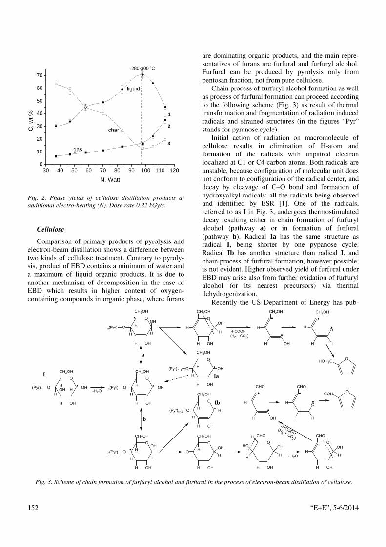
“E+E”, 5-6/2014 152
Fig. 2. Phase yields of cellulose distillation products at additional electro-heating (N). Dose rate 0.22 kGy/s.
Cellulose
Comparison of primary products of pyrolysis and electron-beam distillation shows a difference between two kinds of cellulose treatment. Contrary to pyroly-sis, product of EBD contains a minimum of water and a maximum of liquid organic products. It is due to another mechanism of decomposition in the case of EBD which results in higher content of oxygen-containing compounds in organic phase, where furans
are dominating organic products, and the main repre-sentatives of furans are furfural and furfuryl alcohol. Furfural can be produced by pyrolysis only from pentosan fraction, not from pure cellulose.
Chain process of furfuryl alcohol formation as well as process of furfural formation can proceed according to the following scheme (Fig. 3) as result of thermal transformation and fragmentation of radiation induced radicals and strained structures (in the figures “Pyr” stands for pyranose cycle).
Initial action of radiation on macromolecule of cellulose results in elimination of H-atom and formation of the radicals with unpaired electron localized at C1 or C4 carbon atoms. Both radicals are unstable, because configuration of molecular unit does not conform to configuration of the radical center, and decay by cleavage of C–O bond and formation of hydroxyalkyl radicals; all the radicals being observed and identified by ESR [1]. One of the radicals, referred to as I in Fig. 3, undergoes thermostimulated decay resulting either in chain formation of furfuryl alcohol (pathway a) or in formation of furfural (pathway b). Radical Ia has the same structure as radical I , being shorter by one pypanose cycle. Radical Ib has another structure than radical I , and chain process of furfural formation, however possible, is not evident. Higher observed yield of furfural under EBD may arise also from further oxidation of furfuryl alcohol (or its nearest precursors) via thermal dehydrogenization.
Recently the US Department of Energy has pub-
30 40 50 60 70 80 90 100 110 1200
10
20
30
40
50
60
70280-300 oC
char
gas
liguid
3
2
1
C, w
t %
N, Watt
O
CH2OH
HOH
H
H
OH
OHO(Pyr)n
H-H2O
O
CH2OH
H
H OH
OHOn(Pyr)
H
O
CH2OH
H
H OH
OH
On(Pyr)
H
O
CH2OH
H OH
H
O
CH2OH
H
H OH
OHO(Pyr)n-1
H
OH
H
CH2OH
H OH
H
CH2OH
H
HO
H
OHOH2C
-HCOOHH
O
CH2OH
H
H OH
OH
On(Pyr)
H H
O
CH2OH
H OH
O
O
CH2OH
H
H OH
HO(Pyr)n-1
H
OH
HH
CHO
H OH
H
CHO
H
H O
H
O
CHO
H OH
OH
H
HO
H
HO
CHO
H OH
OH
HH
- H2O
-HCOOH
OCOH
I Ia
Ib
a
b
(H2 + CO2)
(H2 + CO
2 )
Fig. 3. Scheme of chain formation of furfuryl alcohol and furfural in the process of electron-beam distillation of cellulose.

“E+E”, 5-6/2014 153
lished the top list of the most demanded products from a biomass [6]. Furfural and other furans take second place, right after ethanol. It makes EBD of cellulose rather promising method of high throughput furans production from widespread feedstock.
Lignin
Due to aromatic structure of lignin, just a radioly-sis of the compound has rather low effect. However, when combined with heating, the radiolytic decompo-sition is significantly enhanced. Unlike a pyrolysis, which results predominantly in charcoal or oligomeric pyro-lignin [7], the EBD of lignin produces three times more liquid methoxy-phenols, mainly guaiacol and creosol.
Formation of the compounds can be realized in the process, which scheme is presented in Fig. 4. The main precursor of guaiacol and creosol formed upon EBD of lignin is phenoxyl radical I . Appearance of such radicals as the major short-lived product of excitation and ionization has been observed in ESR study of irradiated lignin [1, 2]. Phenoxyl radical exists in several resonant structures, further transfor-mations of which determine the composition of final products. In particular, resonant structures II and III can undergo thermal-stimulated cleavage of β-bond in alkyl chain. Resulting isolated radical by scavenging an H-atom from neighboring molecule is converted correspondingly to guaiacol or creosol.
It is worth to mention that the phenolic tar pro-duced by EBD of lignin is extremely good antioxidant and inhibitor. For example, such a tar inhibits thermal polymerization of styrene better than industrial inhibi-tors and much better than pyrolysis tar.
Post-radiation thermolysis
The weights of the cellulose and lignin samples remained almost unchanged in the course of prelimi-nary irradiation: a decrease in the weights was no greater than 0.1 wt % at absorbed doses D to 3 MGy. The samples remained in a solid state of aggregation, in this case, the microcrystalline cellulose acquired a yellowish nuance.
Figures 5 and 6 show that, after irradiation, lower temperatures were required for the appearance of vapors in a distillation still and the appearance of the first drops of a distilled condensate in a receiving tank. At D = 2.2 MGy, the overpoints of lignin and cellulose decreased by ~80° and ~100°, respectively.
0 10 20 30 40 50 60
100
200
300
400
500
321
3
2
1
Tem
pera
ture
, o C
Yield, wt % Fig. 5. Relationship between the distillation still tempera-ture and the amount of condensate distilled from microcrys-talline cellulose at a heater power of 100 W and absorbed doses of (1) 0, (2) 0.55, and (3) 2.2 MGy.
O
OCH3
R
I
O
OCH3
R
III
O
R
II
O
OCH3
CH3
H3CO
O
H3CO
- R=CH2- R-CH=CH2
O
H3CO
O
OCH3
CH3
HH
OH
OCH3
CH3
OH
H3CO
Fig. 4. Scheme of guaiacol and creosol formation in the process of electron-beam distillation of lignin.

“E+E”, 5-6/2014 154
For the case of cellulose, a plot (curve 1 in Fig. 5) has a characteristic step, when the volume of the distilled condensate increased, but the temperature did not increase or even temporarily decreased. In this period, water was the main product distilled from nonirradiated microcrystalline cellulose. Regardless of D, a maximum condensate amount was distilled off in a temperature range of 300–370°С. The differential thermal analysis of distillation revealed intense exo-thermic peaks between 330 and 350°C, which suggest the formation and volatilization of gaseous degrada-tion products [8].
The intense color of the condensate and the ab-sence of clearly pronounced steps from the distillation curves of the irradiated samples suggest a change in the range of distilled products: heavier organic com-pounds with different vaporization temperatures appeared.
Fig. 6. Relationship between the distillation still tem-
perature and the amount of condensate distilled from lignin at a heater power of 100 W and absorbed doses of (1) 0, (2) 0.6, and (3) 2.0 MGy.
Condensates from the irradiated and nonirradiated cellulose spontaneously separated into a transparent aqueous organic solution (F1) and a dark opaque tar (F2). The color of F1 from the irradiated samples was much darker. At the same time, F2 from the irradiated cellulose also separated into two phases: the major portion of tar settled at the bottom, and a portion came to the surface. The total tar volume was to 7% on a
condensate volume basis. The composition of the bottom (heavier) fraction only slightly depended on D, and it was generally identical to the composition of tar distilled from nonirradiated cellulose. The major portion of this tar consisted of small oligomeric cellu-lose fragments, which underwent partial dehydration and decarboxylation.
The phase distribution of the products of cellulose changed only slightly: as the absorbed dose D was increased to 2.2 MGy, a monotonic decrease in the yield of charcoal to ~7 wt % with a simultaneous increase in the yield of condensate and an almost unchanged yield of gaseous products was observed.
An important change in the component composi-tion of F1 was observed: dissolved furfural and furyl-methanol appeared, which were almost absent upon the dry distillation of nonirradiated cellulose. At a dose of 2.2 MGy, the yield of furans reached ~22% on a cellulose weight basis. The composition of the condensate remained almost unchanged as the time interval between irradiation and distillation was in-creased from several minutes to several days. It is obvious that furans were predominantly formed in the process of the thermolysis of irradiated samples rather than on irradiation: the irradiated cellulose acquired only a slightly yellowish color, which is inconsistent with the observed amount of furans in the condensate. It is likely that, in the course of irradiation, com-pounds that possess low thermal stability and can be easily converted into furans on subsequent heating were formed.
An analysis of the product distillation sequence showed that, after the glycoside bond cleavage, the conversion of glucopyranose units into furans began from dehydration processes followed by decarboxyla-tion.
The decrease in the length of a polymer chain in cellulose did not cause effects produced by radiolysis: the distillation of the low-molecular-weight analogs of cellulose (cellobiose and cyclodextrins) did not lead to a considerable increase in the yield of furans. Obvi-ously, decomposition products containing new func-tional groups (carbonyl, carboxyl, and allyl), which were formed in the process of radiolysis, played a key role in the formation of furans. The thermally unstable products of radical recombination or the allyl products
O
O
CH2OH
OH
H
H
OH
H
H(Pyr)n
O
O
CH2OH
H OH
H
H
(Pyr)n- H2O
O
CHO
H OH
H
H HOH
(Pyr)nOH
CHO
H H
HO H
- H2O
OOHC
- H2CO
Fig. 7. Scheme of furfural formation in the process of post-radiation distillation of cellulose.
0 5 10 15 20200
250
300
350
400
450
500
3
2
1
Tem
pera
ture
, o C
Yield, wt %

“E+E”, 5-6/2014 155
of glycoside bond cleavage can be the precursors of furans. For example, furfural can be obtained from the allyl product due to the thermally stimulated elimina-tion of water and decarboxylation (See Fig. 7).
Upon the distillation of lignin two immiscible liq-uids were formed: a transparent aqueous organic solution with a yellowish brown nuance and increased acidity (pH 2.7–3.3) and a viscous dark brown organic liquid (tar). At D ≤ 1 MGy, a tendency toward in-creasing the yield of tar was observed. However, as the dose was further increased, the yield of tar and the total yield of condensate decreased. At D = 3 MGy, a decrease in the yields reached 6–7 wt %.
Chromatographic analysis indicated that guaiacol (2-methoxyphenol), creosol (2-methoxy-4-methyl-phenol), and 4-ethyl-2-methoxyphenol were the predominant components of tar. Acyclic and cyclic carbonyl compounds, methanol, benzene, toluene, phenol, and alkylphenols, a total of about 30 com-pounds with a total fraction of ~25%, were present along with methoxyphenols in the tar distilled from nonirradiated lignin. The fraction of methoxyphenols increased to 96% on a tar weight basis, as D was increased. At high doses, two compounds, guaiacol and creosol, predominantly formed the basis of tar. The bulk of the lignin condensate was distilled off at a temperature higher than 350°C. Under these condi-tions, the cleavage of Сα–Сβ bonds and O–CH3 bonds in methoxy groups was observed [9].
Unlike cellulose, which belongs to polymers that are predominantly destroyed under irradiation [1, 2], lignin has other nature. For aromatic intermediates formed upon the ionization and excitation of lignin, crosslinking processes are more probable than frag-mentation processes [2]. As a consequence, the more crosslinked structure of irradiated lignin can be re-sponsible for the observed decrease in the yield of tar and the increase in the yield of carbon residue with the absorbed dose.
Thus, irradiation differently affects the postradia-tion distillation of cellulose and lignin; this is im-portant from the point of view of wood distillation. Cellulose is characterized by an increase in the yield of liquid organic products, especially, the yield of furfural and its derivatives, with dose. In turn, a decrease in the yield of the liquid organic products of distillation is characteristic of lignin at 1 MGy ≤ D ≤ 3 MGy. In this case, the aromatic units of lignin, which play a role of the acceptor of excitation, ions, and radicals, can weaken cellulose degradation in irradiat-ed wood [2]. This effect was observed in the distilla-tion of irradiated pine sawdust [10]. At D = 2 MGy, the yield of the distilled condensate was found to 5.5
wt % lower than that from the nonirradiated sawdust; however, the furfural content of the condensate in-creased (from 5.7 to 11.3 wt %).
Conclusion Pyrolysis of cellulose and lignin may be upgraded
by the use of an electron-beam irradiation. The radia-tion-thermal destruction mode does more probable production of liquid low-molecular-weight products instead of solid pyrolitic oligomers. Furans and meth-oxyphenols are dominant products of high-temperature radiolysis of cellulose and lignine, respec-tively. Electron-beam distillation as a method of biomass conversion has the following advantages: it can be performed at moderate heating and low dose rate; it is a single-stage conversion of the high produc-tivity (~10 kg/kW h); the products being produced are highly demanded.
Preliminary irradiation reduces initial temperature (overpoint) of thermal degradation of lignin and cellulose. Distillation of the irradiated lignin produces lower amount of tar but with higher fraction of meth-oxy-phenols. In turn, dry distillation of the irradiated cellulose is characterized by higher yield of liquid organic products and higher fraction of furfural and furfuryl alcohol in condensate. However, such useful changes of lignine and cellulose demand rather high absorbed dose (2-3 MGy) of electron-beam radiation.
Acknowledgements This work was supported by Ministry of Education
and Science of Russian Federation (program 2014-14-576-0049).
REFERENCES [1] Ponomarev, A.V., Ershov, B.G. Fundamental as-
pects of radiation-thermal transformations of cellulose and plant biomass. Russian Chem. Rev., Volume 81, 2012, pages 918-935.
[2] Fengel, D., Wegener, G. Wood (Chemistry, Ultra-structure, Reactions). Walter de Gruyter, New York, 1984.
[3] Ponomarev, A.V., Kholodkova, E.M., Metreveli, P.K., et. al. Phase distribution of products of radiation and post-radiation distillation of biopolymers: cellulose, lignin and chitin. Radiat. Phys. Chem., Volume 80, 2011, pages 1186–1194.
[4] Bridgwater, A.V. Renewable fuels and chemicals by thermal processing of biomass. Chem. Eng. J., Volume 91, 2003, pages 87–102.
[5] Yaman, S. Pyrolysis of biomass to produce fuels and chemical feedstocks. Energy Convers. Manage, Vo-lume 45, 2004 , pages 651–671.

“E+E”, 5-6/2014 156
[6] Bozell, J.J., Petersen, G.R. Technology develop-ment for the production of biobased products from biorefin-ery carbohydrates—the US Department of Energy's “Top10”revisited. Green Chem., Volume 12, 2010, pages 539–554.
[7] Nowakowski, D.J., Bridgwater, A.V., Elliott, D.C., et. al. Lignin fast pyrolysis: results from an international collaboration. J. Anal. Appl. Pyrolysis, Volume 88, 2010, pages 53–72.
[8] Dejneko, I.P. Chemical transformations of cellu-lose under pyrolysis, Forestry Journal (ISSN: 0536-1036, in Russian), Volume 4, 2004, pages 96-112.
[9] Azarov, V.I., Burov, A.V., Obolenskaya, A.V. Chemistry of wood and synthetic polymers (Khimia drevesiny i sinteticheskikh polimerov). Lan’, S.Petersburg, 2010.
[10] Strizhakov, D. A., Solntsev, A. P., Agabekov, et. al. Effect of γ-irradiation on composition of pine sawdust pyrolysis liquid products. Proc. of the Natl. Academy of Sciences of Belarus, Ser. Chemical Sci., Volume 3, 2011, pages 64-69.
Prof. Dr. Alexander V. Ponomarev – Russian Academy of Sciences, Institute of Physical Chemistry and Electro-chemistry (since 1982). Head of laboratory of electron-beam conversion of energy carriers (since 2011). Graduat-ed from D.I.Mendeleev Russian Chemical-Technological University – radiation chemistry. tel.:+7 499 234 6244. е-mail: [email protected].
Polina K.Metreveli – the same laboratory (since 2011), Assoc. Res. Graduated from D.I.Mendeleev Russian Chem-ical-Technological University – ecology. tel.:+7 499 234 6244 е-mail: [email protected].
Alexandra K.Metreveli – the same laboratory (since 2011), Assoc. Res. Graduated from D.I.Mendeleev Russian Chemical-Technological University – ecology. tel.:+7 499 234 6244 е-mail: [email protected]
Dr. Alexei V. Bludenko – the same laboratory (since 1985), Senior Res. Graduated from D.I.Mendeleev Russian Chemical-Technological University – radiation chemistry. tel.:+7 499 234 6244. е-mail: [email protected].
Dr. Vladimir N. Chylkov – the same laboratory (since 1985), Senior Res. Graduated from D.I.Mendeleev Russian Chemical-Technological University – radiation chemistry. tel.:+7 499 234 6244. е-mail: [email protected].
“E+E”, 5-6/2014 157
The Electron-Beam Treatment of Water Polluted by Humic Acids and Lignin
Polina K. Metreveli, Alexandra K. Metreveli, Alexander V. Ponomarev
Both lignin and humic acids cause the raised colourity and turbidity of natural water and industrial wastewater. Electron-beam treatment reduces kinetic stability of aqueous dispersions of lignin and humic acids. The radiation-induced coagulation takes place because of a recharge of micelles, recombination and addition of macroradicals to nonsaturated macromolecules, and also because of mechanical capture of small molecules by a coarsen aggregates. However coagulation depends on a ratio of a thickness of water layer to depth of electron beam penetration. The maximum coagulation takes place on depths smaller than range of the accelerated electrons. Excess negative charge is temporarily acting in an area of final deceleration of electrons. This uncompensated charge interferes with coagulation of negatively charged micelles. The high absorbed dose also interferes with discoloration of water because of increase in fraction of soluble products of macromolecules decomposition.
Електроннолъчево третиране на вода, замърсена с хумусни киселини и лигнин (П. Метревели, А. Метревели, А. Паномарев). Двете съставки - лигнин и хумусни киселини причиняват нарастване на оцветяването и помътняването на естествената вода и индустриалната отпадъчна вода. Електроннолъчевото облъчване намалява кинетичната стабилност на водните дисперсии на лигнин и хумусни киселини. Индуцираната от радиацията коагулация започва поради презареждането с мицели, рекомбинация и добавяне на макрорадикали към ненаситените макромолекули, а също поради механично захващане на малки молекули от големи груби агрегати. Обаче коагулацията зависи от отношението на дебелината на водния слой и дълбочината на електронното проникване. Максимална коагулация има място при дебелини по-малки от пробега на ускорените електрони. Излишния негативен заряд е временно действащ в областта на крайното забавяне на електроните. Този некомпенсиран заряд взаимодейства с коагулацията на отрицателно заредените мицели. Големи дози на адсорбция също взаимодействат с обезцветяването на водата, защото нараства частта на разтворими продукти при макромолекулната декомпозиция.
Introduction Colloidal solutions and coarse suspensions are
radiation-sensitive. The phenomenon is of interest of electron-beam technologies for purification of natural water and industrial wastewater contaminated by dispersed organic compounds [1, 2]. In many cases superficial water has increased color and turbidity due to humic compounds and lignin, which is rather characteristic of river and lake water of northern regions of Russia [3], as well as of other surface waters [4]. The compounds often come with water from environing bogs or are dispersed from wood bottom sediment formed as a result of timber rafting, additional contamination results from activity of paper mills and other industrial enterprises. Conventional
water treatment based on continuous-flow filtering and chlorination does not often remove the color caused by ultra-dispersed phytogenous matter, one of results of which is deposit formation on inner surface of water pipeline systems.
Since electron accelerators are proposed to be the most actual sources of ionizing radiation in water treatment technologies, in the present work an attempt has been made to estimate specific action of electron irradiation on stability of aqueous dispersions of humic acids (HA) and lignin. Special attention was paid to influence of irradiation conditions on the process of natural organic matter coagulation, namely, to the effect of relationship between effective penetration of incident electrons and thickness of irradiated matter layer.

“E+E”, 5-6/2014 158
Experimental There were studied aqueous solutions of pine
lignin (commercial preparation “Polyphepan” by “Scientech” company) and of humic acids mixture (by “ACROS” company). The solutions were prepared by adding appropriate amount of powdered substance to distilled water and mixing. Colloid solutions (or dispersions) of HA (10–50 mg/L) and lignin (50–325 mg/L), prepared in such a way, were kinetically stable during more than 2 days. For that time optical spectra of the solutions, representing broad unstructured bands in the region of 200–900 nm (Fig. 1), remained unchangeable.
Two types of accelerated electrons sources were used in the experiments. Horizontal beam of 8MeV electrons from linear accelerator UELV-10-10T was used for irradiation in mode I . Range of such electrons in water is about 40 mm [1]. The samples were exposed to irradiation in open vials with irradiation width 15 mm. Under those irradiation conditions the samples were irradiated uniformly, and incident electrons left the samples. In irradiation mode II the transformer type pulsed accelerator URT-1 was used which generated vertical beam of electrons with continuous energy spectrum in the region of 0.2–0.7 MeV, ~90% of the electron’s energy being concentrated at 0.5–0.7 MeV. Range of electrons of such energies in water does not exceed 3 mm. Used in the experiments 3mm layer of aqueous solution completely absorbed all the incident electrons. All the solutions were irradiated in the presence of air.
200 300 400 500 6000,0
0,2
0,4
0,6
0,8
1,0
4
3
2
1
Abs
orba
nce,
rel
. uni
ts
Wavelength, nm Fig. 1. Apparent optical absorption spectra of solutions 11 mg/L HA (1, 3) and 63 mg/L lignin (2, 4): 1, 2 – initial solutions; 3, 4 – solutions irradiated at 30 kGy in mode I.
Dosimetric measurements were carried out with the help of film dosimeter based on copolymer with phenazine dye. UV-Vis spectrophotometer “Cary-100” was used for optical measurements. Apparent
absorption curves in Figs show both real light absorption and scattering. Quantitative determination of color of the solutions (in color degrees) was carried out by colorimetric analysis in a similar manner as described elsewhere [5].
Results and discussion
Irradiation in mode I
Irradiation of the solutions results in notable changes in their spectra. Maximal increase in optical transmittance of HA solutions under irradiation in mode I takes place at rather low absorbed doses (D). Thus, the most noticeable transmittance change for the solutions with concentration ≤ 50 mg/L (initial color 383 degrees) is observed at D ≈ 5–15 kGy. The highest discoloration quotient was estimated to be equal to 25 degree/kGy. Optical transmission upon irradiation increases in the entire region from 200 to 900 nm (see Fig. 1), being, mainly, the result of coagulation. Thereby, settling takes place.
0 20 40 60 800,0
0,5
1,0
12
Abs
orba
nce,
rel
. uni
ts
0 20 40 60 80
0,4
0,5
0,6
0,7
0,8
0,9
1,0
1,1
2'
1'
Dose, kGy Fig. 2. Effect of absorbed dose on apparent optical
absorption of 11 mg/L HA solution at 380 nm (1, 2) and 205 nm (1', 2') under irradiation in mode I (1, 1') and in
mode II (2, 2').
Effect of absorbed dose on discoloration depends on initial HA concentration. E.g., for solution 11 mg/L (initial color 85 degree) slow increase in optical

“E+E”, 5-6/2014 159
transmission is observed up to D ≈ 60 kGy (Fig. 2, curves 1, 1′). In the dose region 60 ≤ D ≤ 90 kGy changes in visible part of optical spectrum are comparatively small. However, increase in absorbed dose is accompanied by the rise of optical absorption at λ ≤ 240 nm which is due to appearance of soluble products of HA fragmentation (curve 1′). For HA solution with concentration 50 mg/L, color rising begins at absorbed dose D ≥ 30 kGy.
Similar coagulation processes are observed also in lignin solutions. However, these solutions appeared to be more stable to irradiation. For 63 mg/L lignin solution (initial color ~50 degrees) in the region of absorbed dose from 15 up to 90 kGy optical transmission at 380 nm remains practically unchanged (Fig. 3). Transmission in the UV region at doses higher than 45 kGy decreases with increasing the dose. Increase in transmission in the entire studied spectral region takes place also upon irradiation of lignin solutions with as high concentration as 325 mg/L (initial color ~265 degrees). At rather low absorbed dose (~10 kGy) near twofold reduction of the color is observed, initial discoloration quotient being about 13 degree/kGy. Irradiation at higher dose does not produce any appreciable spectral changes.
Irradiation of combined samples containing both lignin (65 mg/L) and HA (11 mg/L) results in spectral changes which are close to those for individual solutions. However, initial optical transmission of combined solution in the region of 200–900 nm is some higher than the sum of individual solutions transmissions (Fig. 4) which may be mainly due to formation of complex micelles of lignin and HA. At D ≤ 30 kGy a monotone rise of transmission in visible and UV region is observed. At higher doses (≥ 60 kGy) smoothed decrease in transmission takes place, like in individual HA solution. Initial discoloration quotient (at D < 10 kGy) is equal to about 14 degree/kGy, which is close to computed value based on the sum of the dependences for individual solutions. At D ≥ 10 kGy experimental and computed dependences of color on dose become differ. Dose effect on color of combined solution is weaker and maximal discoloration level is stabilized at 40% of initial value, being independent of dose from 30 up to 80 kGy. Possible reason for deteriorating the coagulation in combined solution may be a mixed type of micelles – a part of such micelles enriched with lignin possess higher radiation stability which makes coagulation worse.
Irradiation in mode II
Under irradiation in mode II effect of absorbed
dose on optical spectrum is diminished for both HA and lignin solutions. For example, at D=40 kGy
0 20 40 60 800,5
1,0
1,5
2,0
2,5
3,0
Dose, kGy
1
2
Abs
orba
nce,
rel
. uni
ts
0 20 40 60 800,6
0,7
0,8
0,9
1,0
1,1
1,2
2'
1'
Fig. 3. Effect of absorbed dose on apparent optical
absorption of 63 mg/L lignin solution at 380 nm (1, 2) and 205 nm (1', 2') under irradiation in mode I (1, 1') and in
mode II (2, 2').
0 20 40 60 800.2
0.4
0.6
0.8
1.0
4
3
2 1
Abs
orba
nce,
rel
. uni
ts
Dose, kGy
Fig. 4. Effect of absorbed dose on apparent optical absorption at 380 nm in combined solution containing 11 mg/L of HA and 63 mg/L of lignin under irradiation in
mode I (1, 3) and in mode II (2, 4). Curves 2 and 4 – summarized dependencies computed from data presented in
Fig. 2 and 3.

“E+E”, 5-6/2014 160
residual absorption at 380 nm in HA solution is almost three times higher than that in the solution irradiated in mode I (Fig. 2). In UV region an increase in optical transmission takes place only at D ≤ 15 kGy, and at D ≥ 30 kGy the transmission becomes lower than initial one. In the solutions of lignin irradiation in mode II changes the dose effect (in relation to irradiation in mode I ) to opposite one, i.e., even at low doses decrease in optical transmission is observed instead of increase (Fig. 3). Irradiation of combined solution at D ≤ 40 kGy results in rise of optical transmission in a visible region (Fig. 4) and its reduction in UV region, which is characteristic of lignin solution. Curve of color vs. dose in the case is practically parallel to computed curve i.e. in accordance with additivity principle. Initial discoloration quotient (about 5 degree/kGy) is three times lower than that for combined solution irradiated in mode I .
Discussion The stability of the solutions is due, mainly, to
strong interaction of dispersed particles with water [6]. The particles acquire, apparently, properties of micelles in which a nucleus and peripheral shell possess equal charge of opposite sign (let symbolize a micelle as M−n, where superscript denotes effective charge of the shell). Surface charge of micelles because of the reciprocal repulsion determines stability of dispersed systems. Both lignin and HA are present in the water, very likely, in the form of negative micelles. Spectra of the solutions (Fig. 1) are caused mainly by light scattering on the particles.
Radiation induced transformations in such diluted solutions as the systems under study are caused by indirect action of radiation. Primary radiolysis products are formed by ionization and excitation of water molecules. Among the products there are principal radical intermediates: hydrated electrons (eaq), H-atoms, and OH-radicals, as well as excess ions H+ and OH–. Radical intermediates (eaq, H and OH) are extremely reactive to unsaturated organic compounds, however in aerated solutions eaq and H are being converted by reaction with dissolved oxygen to correspondingly O2
− and HO2 radicals which possess much lower reactivity. Interaction of radicals and ions with micelles initiates various radiation chemical transformations in the system under irradiation, in particular – coagulation. One of the probable reasons for coagulation may be recharging the micelles by interaction with short-lived products of water radiolysis. Negatively charged micelles preferably interact with positively charged or
uncharged intermediates, participating, for example, in reactions of protonation by H+ ions or electron transfer to OH and HO2 radical:
(1) M−n + H+ → M−(n-1)
(2) M−n + OH → M−(n-1) + OH–
(3) M−n + HO2 → M−(n-1) + HO2−
Appearing misbalance in charges of nucleus and outer shell of micelle can promote consecutive combination with other micelles:
(4) mM−n + M−(n-1) → Mm+1−(m+n-1)
and, finally, formation of large aggregates settling down from the solution.
Another way to coagulation is the micelles bonding by a process of macro-radical addition to neighboring micelle, the process being facilitated by availability of double bonds (especially, in aromatic structures). Macro-radicals are formed, predominantly, in micelles reactions with OH radicals. Such poly-aromatic radicals possess rather long lifetime due to bulky and complicated structure which makes steric hindrances in the reactions of radical recombination. Coagulation of micelles by that mechanism is determined by the process of comparatively slow recombination of macro-radicals which realizes in observed short-term post-irradiation effect (up to 30 min). Radiation-induced polycondensation may be due, as well, to interaction of hydroxyl and carbonyl derivatives.
Thus, the process of micelles coagulation under irradiation may be caused by two main factors: (1) just a recharging the outer shell of micelles by interaction with ionic intermediates or by electron transfer reactions and (2) radiation-induced condensation via radical reactions. Significant difference in efficiencies of electron-beam action on the systems under study at two different modes of irradiation indicates that the first factor, i.e., micelles recharging, plays the dominant role in the case. This conclusion follows from the consideration that radiation chemical processes initiated by products of ionization and excitation of water molecules should not notably differ under irradiation in mode I and in mode II , because dose rates (and, consequently, stationary concentrations of intermediates) in both modes were similar, and ionization densities in water produced by electrons with energy 8 and 0.7 MeV differ insignificantly, linear energy transfer being equal correspondingly to 0.10 and 0.12 eV/nm. The most distinguishing feature of irradiation by low energy electrons, under condition of their complete

“E+E”, 5-6/2014 161
absorption in irradiated medium (mode II ), consists in accumulation of uncompensated charge due to incident electrons.
These electrons after dissipation of their energy in the processes of ionization (thereby, equal quantities of oppositely charged particles arise) and excitation are finally thermalized and localized in aqueous medium giving rise to formation of eaq, which carry excess negative charge. Fraction of eaq formed by deceleration of incident electrons is low relative to eaq formed by ionization (for 0.7 MeV electrons it is about 0.05%). However, while eaq themselves have very short lifetime because of high reactivity, additional charge can be eliminated only by diffusion of anions to vial walls and discharging into environment, which courses relatively slow. Therefore, stationary content of uncompensated negative charge during irradiation may be sufficiently high to have an influence on coagulation process by stabilizing negative micelles. The latter may serve as a confirmation that lignin, as well as HA, exist in water in the form of negative micelles, i.e., negatively charged groups of the compounds are oriented outwards. Both lignin and HA are poly-aromatic compounds which differ, in particular, by composition of lateral substituents. In macromolecules of lignin groups –OCH3 and –OH prevail, whereas in HA groups –COOH and –CH2OH are dominating [7]. Lower polarity of methoxyl and hydroxyl groups in lignin comparing to carboxyl and oxymethyl groups in HA makes lignin micelles less polar and more resistant to radiation induced coagulation.
Conclusions Results of the experiments show significant effect
of electron irradiation on stability of aqueous disperse systems of natural poly-phenol macromolecules. Predominant agglomeration, and subsequent settling, of dispersed particles takes place in solutions of HA and lignin under irradiation. Maximal result is achieved at absorbed dose 5–15 kGy. At the same time, the effect of electron-beam irradiation on kinetic stability of HA and lignin dispersions in water significantly changes depending on relationship between thickness of irradiated sample and electrons range. In the case of complete absorption of incident electrons in irradiated medium the efficiency of discoloration and coagulation processes in HA and lignin dispersions is minimal. The phenomenon discovered to a considerable degree may be attributed to effect of accumulating negative charge in the bulk of irradiated solution. The role of additional electrons due to the capture of incident electrons upon electron
irradiation was never taken into account in radiation chemistry of liquids because of their extremely low amount comparing to electrons formed by ionization. However, accumulating negative charge caused by those electrons can exert a notable influence on the stability of dispersed systems.
Acknowledgements This work was supported by Ministry of Education
and Science of Russian Federation (program 2014-14-576-0049).
REFERENCES [1] Woods, R.J., Pikaev, A.K. Applied Radiation
Chemistry: Radiation Processing. Wiley-Interscience, New York, 1994.
[2] Sampa, M.H.O., Takács, E.,Wojnárovits, L., et. al. Remediation of polluted waters and wastewater by radiation processing. Nukleonika, Volume 52 (4), 2007, pages 137–144.
[3] Lobbes, J.M., Fitznar, H.P., Kattner, G. Biogeochemical characteristics of dissolved and particulate organic matter in Russian rivers entering the Arctic Ocean. Geochim. Cosmochim. Acta, Volume 64 (17), 2000, pages 2973–2983.
[4] Perdue, E.M. Natural Organic Matter, Encyclopedia of Inland Waters. Academic Press, Oxford, 2009.
[5] Standard Methods for the Examination of Water & Wastewater, 22nd edition. APHA, AWWA & WEF, Washington, DC, 2012.
[6] Ottewill, R.H. Stability and instability in disperse systems. J. Colloid Interface Sci., Volume 58 (2), 1997, pages 357–373.
[7] Fengel, D., Wegener, G. Wood (Chemistry, Ultrastructure, Reactions). Walter de Gruyter, New York, 1984.
[8] Dole (Ed.). The Radiation Chemistry of Macromolecules, V.1. Academic Press, New York, 1972.
[9] Fendler, J.H., Gillis, H.A., Klassen, N.V. Pulse radiolysis study of the reactions of hydrated electrons with naphthalene, phenanthrene, biphenyl and fluorine in aqueous micellar solutions. J. Chem. Soc., Faraday Trans. I., Volume 70 (1), 1974, pages145–153.
[10] Gehringer, P., Eschweiler, H., Szinovatz,W., et. al. Radiation-induced OH radical generation and its use for groundwater remediation. Radiat. Phys. Chem., Volume 42 (4–6), 1993, pages 711–714.
Polina K.Metreveli – Russian Academy of Sciences, A.N. Frumkin Institute of Physical Chemistry and Electrochemistry. Laboratory of electron-beam conversion of energy carriers (since 2011), Assoc. Res. Graduated

“E+E”, 5-6/2014 162
from D.I.Mendeleev Russian Chemical-Technological University – ecology.
tel.:+7 499 234 6244 е-mail: [email protected].
Alexandra K.Metreveli – the same laboratory (since 2011), Assoc. Res. Graduated from D.I.Mendeleev Russian Chemical-Technological University – ecology.
tel.:+7 499 234 6244 е-mail: [email protected]
Prof. Dr. Alexander V. Ponomarev – the same Institute (since 1982). Head of laboratory of electron-beam conversion of energy carriers (since 2011). Graduated from D.I.Mendeleev Russian Chemical-Technological University – radiation chemistry. tel.:+7 499 234 6244. е-mail: [email protected].

“E+E”, 5-6/2014 163
Electron Beam Technology for Environmental Conservation
Bumsoo Han, Jinkyu Kim, Yuri Kim, SeungTae Jung
By rapid economic growth, fast urbanization and enhanced industrial activities all of which add
to the degradation of the environmental quality. The environmental pollution caused by industrial discharges and urbanization, among others, has becoming an acute problem in developing cities in the world. In the current prospect, the problem is projected to be amplified in the future if suitable mitigation measures would not be taken. The efficient treatment of pollutants discharged in various form and contents from the human activities could be an important contribution to the mitigation of the environmental quality management in the world. Over the last few decades, extensive work has been carried out on utilizing radiation technology for environmental remediation. This work includes the application of radiation technology for simultaneous removal of SOx and NOx from the flue gases, purification of drinking water, wastewater treatment and hygienization of sewage for use in agriculture. It is becoming increasingly clear that humankind’s environmental problems are no longer merely local or regional, but have become continental in scope. Economically and technically feasible technologies for controlling pollution from gaseous emissions and liquid effluent streams are being sought by technologists working in a variety of areas, including radiation technologists.
Електроннолъчева технология за съхранение на околната среда (Б. Хан, Ж. Ким, Ю. Ким, С. Джунг). Бързите икономически растеж, урбанизация и индустриална активност имат принос в деградирането на качеството на околната среда. Атмосферното замърсяване причинено от индустриалните източници и урбанизацията, наред с останалото стават остър проблем в напредналите градове в света. В сегашната перспектива се очаква проблемът да се усили в бъдеще, ако не се предприемат подходящи действия за намаляването му. Ефективна обработка на изпускането на замърсители в разнообразни форми и съдържания от човешката дейност може да бъде важен принос към мениджмънта на качеството на околната среда в света. През последните десетилетия интензивни резултати бяха получени чрез използването на радиационни технологии за възстановяване на околната атмосфера. Тази работа съдържа прилагането на радиационните технологии за едновременно отнемане на SOx и NOx от дима, очистване на вода за пиене, обработка на отпадъчни води и хигиенизиране на сточните води за използване в селското стопанство. Става все по ясно, че човешките екологични проблеми не са просто локални или регионални, но стават континентални по обхват. Икономически и технически възможни технологии за управление на замърсяването с газови емисии и течен изтичащ слой са търсени от технолозите, работещи в различни области, включително радиационните технологии.
Introduction The problems of environmental damage and
degradation of natural resources are receiving increasing attention throughout the world. The increased population, higher living standards, increased urbanization and enhanced industrial activities of humankind are all leading to degradation of the environment. Increasing urbanization has been accompanied by significant water pollution. Industrial activities to produce heat and electrical energy are responsible for emitting a large number and amount of
pollutants, such as fly ash, sulphur oxides (SO2 and SO3), nitrogen oxides (NOX = NO2 + NO) and volatile organic compounds, into the atmosphere.
Electrons interact with gas creating divergent ions and radicals including oxidizing radicals and excited species. These excited species react in a various ways of neutralization reactions and dimerization. The removal of SO2 using an electron was demonstrated in 1970 -1971. Irradiation of flue gas resulted in the conversion of SO2 to an aerosol of sulphuric acid droplets that were easily collected [1]. Ebara Co. used an electron accelerator (0.75 MeV, 45 kW) to convert

“E+E”, 5-6/2014 164
SO2 and NOX into a dry product containing (NH4)2SO4 and NH4NO3 that was usable as a fertilizer. Two larger scale plants were constructed in Indianapolis, USA [2] and Karlsruhe, Germany [3]. The Indianapolis plant was equipped with two electron accelerators (0.8 MeV, total power160 kW) and in Karlsruhe, two electron accelerators (0.3 MeV, total power 180 kW) were used. The engineering design technology for electric utility applications was established at the pilot plant in Kaweczyn, Poland (2 ×10⁴ Nm3/h) using two accelerators (50 kW, 700 keV each) [4].
Electron beam processing of wastewater is non-chemical, and uses fast formation of short-lived reactive radicals that can interact with a wide range of pollutants. Such reactive radicals are strong oxidizing or reducing agents that can transform the pollutants in the liquids wastes. The first studies on the radiation treatment of wastes were carried out in the 1950s principally for disinfection. In the 1960s, these studies were extended to the purification of water and wastewater. After some laboratory research on industrial wastewaters and polluted groundwater in 1970s and 1980s, several pilot plants were built for extended research in the 1990s. The first full-scale application was reported for the purification of wastewater at the Voronezh synthetic rubber plant in Russia. Two accelerators (50kW each) were used to convert the non-biodegradable emulsifier, ‘nekal’, present in the wastewater to a biodegradable form [5]. The installation treats up to 2,000 m3 of effluent per day. A pilot plant of 1,000 m3/d for treating textile-dyeing wastewater has been constructed in Daegu, Korea with 1MeV, 40kW electron accelerator [6].
Sewage is water borne waste from domestic premises and industry. Since it carries human waste, it is a source of various human pathogens that need to be controlled for safe disposal. The cleanup of sewage is a multi-stage process that includes primary and secondary treatment. Primary treatment removes the heaviest of the solid materials; the secondary stage includes the activated sludge and trickling filter processes. Sewage sludge, also known as bio-solids, is the solid waste yield after completion of the secondary stage of wastewater treatment. The annual production of sewage sludge has been increasing around the world as stricter clean water laws have begun to take effect. The USA and the countries Europe together produce approximately 13, 800 Mt of dry sewage sludge per year. It is a rich source of many micronutrients and a valuable source of fixed nitrogen, making it a valuable fertilizer.
(a): Industrial plant and irradiation process vessel with installed accelerator in Pomorzany, Poland [11]
(b): Industrial wastewater plant and injection system in Daegu, Korea [7]
(c): Industrial scale plant for sludge hygienization in Baroda, India [9]
Fig. 1. Industrial scale radiation treatment plant for flue gas, wastewater and sludge.
Flue Gas Treatment The treatment of flue gases with electron beam is
among the most promising advanced technologies of new generation. It is a dry scrubbing process for simultaneous SO2 and NOX removal, no generation of waste. Irradiation of flue gases with an electron beam can bring about chemical changes for ready removal of sulphur and nitrogen oxides. The main components of flue gas are N2, O2, H2O, and CO2, with much lower concentrations of SOX and NOX. Radiation energy is absorbed by gas components in proportion to their mass fraction in the mixture. In irradiation, fast electrons interact with gas creating divergent ions and radicals. The primary species formed include e‾, N2
+, N+, O2+, O+, H2O
+, OH+, H+, CO2+, CO+, N2*,
O2*, N, O, H, OH and CO. In the case of high water vapour concentration, oxidizing radicals OH˙ and HO2˙ and excited species such as O(3P) are the most

“E+E”, 5-6/2014 165
important products formed. These excited species react in a variety of ways such as ion-molecule reactions, neutralization reactions and dimerization [8]. The SO2, NO, NO2, and NH3 present cannot compete with these reactions because of their very low concentrations but react with N, O, •OH, and HO2• radicals. After humidification and lowering of temperature, flue gases flow to a reaction chamber, where irradiation by electron beam takes place. Ammonia is injected upstream the irradiation chamber. The main parameter in NOX removal is the irradiation dose. Other parameters play minor roles in the process. Moreover, in commercial application, dose distribution and gas flow distribution are important as well. The feasibility study for an industrial scale EB process for a 350 MW power plant treating a flue gas flow of 1.5×10⁶ m3/h (NTP) has carried out with a comprehensive engineering and cost study [10]. This study showed that the large-scale EB plants for flue gas cleaning have cost advantages over conventional technologies.
Fig.2. Schematic diagram for SO2 and NOX removal with electron beam
Full-scale plant in Chengdu, China mostly for SOX
removal has been constructed; the power of accelerators applied is 2 X 320 kW for treatment of 3×10⁵ Nm3/h flue gas. Reported efficiency is 80 %
for SOX and 20% for NOX. A utility scale installation is located in EPS Pomorzany in Poland [11]. The maximum flow rate of the gases is 2.7×10⁵ Nm3/h and the total beam power exceeds 1 MW. There are two reaction chambers each with nominal flow gas rate of 1.35×10⁵ Nm3/h. Two accelerators installed in series irradiate each chamber. The applied dose is in the range of 7-12 kGy. The removal of SO2 approaches 90% at this dose range, and that of NOX is 60%. The by-product is collected and is shipped to fertilizer plant.
Wastewater Treatment All Radiation technologists have been investigating
the use of high-energy radiation for treatment of wastewaters. The major advantage of radiation technology is that the reactive species are generated in-situ during the radiolysis process without addition of any chemicals. The results of practical applications have confirmed that radiation technology can be easily and effectively for treating large quantities of wastewater [5-7]. High-energy irradiation produces instantaneous radiolytical transformations by energy transfer from accelerated electrons to orbital electrons of water molecules. Absorbed energy disturbs the electron system of the molecule and results in breakage of inter-atomic bonds [12]. Hydrated electron eaq‾, H atom, •OH and HO2• radicals and hydrogen peroxide H2O2 and H2 are the most important products of the primary interactions (radiolysis products).
H2O eaq‾, •H, •OH, HO2•, H2O2, H2 with yields (G value, µmol/J) of 0.28(eaq‾), 0.062(H), 0.28(OH),
0.072(H2O2).
Wastewater inlet Wastewater
outlet
To ozone decomposer
To atmosphere (via stack)
Air from atmosphere
F1
F2
F3
F4
P1 P2
A
R
B1 B2 D2 D1
Fig. 3. Simplified technological scheme of industrial e-
beam wastewater treatment plant ; F1 -F4 – Air fans, P1 -P2 – Water pumps, D1 -D2 – Diffusers, A – Accelerator, R
– Reactor, B1 and B2 – Primary and secondary basins.
High reactivity is characteristic of water radiolysis
products [12]. Typical time of their reactions with the impurities in water is less than 1 microsecond.
Table 1. Pilot and industrial scale electron beam flue gas treatment
plant
Plant Flow rate (Nm3/hr)
Accelerator Dose (kGy)
SO2/NOX (ppm)
Indianapolis,USA(1984) 24,000 800 keV X 2, 160 kW 30 1,000/400
Badenwerk,Germany(1985) 20,000 300 keV, 180 kW - 500/500 Kawęczyn, Poland (1992) 20,000 700 keV X 2, 100 kW 18.8 600/250 Nagoya, Japan (1992) 12,000 800 keV X 3, 108 kW 10.5 1,000/300
EB-TECH, Korea (1995) 10,000 1000 keV, 50 kW 8 600/400 Chengdu, China (1997) 300,000 800 keV X 2, 400 mA, 640kW 3 1,800/400 Pomorzany, Poland (1999) 270,000 700 keV X4, 375mA, 1050kW 10 1630/540 Hangzhou, China (2002) 305,400 800 keV X 2, 400 mA 640 kW 3 1,800/400 Mariza, Bulgaria (2004) 10,000 800 keV X 3, 108 kW 4 1,000/300 Beijing, China (2006) 640,000 1000 keV X 2, 500 mA,
1000 keV, 300 mA, 2850 kW 3 1,900/400
Shandong, China (2007) 279,000 800keV, 200mA X 2, 1600kW 3 1900/400
“E+E”, 5-6/2014 166
Hydrogen peroxide H2O2 and •OH and HO2• radicals are oxidizing species, while H atom and eaq‾ are chemical reducing in nature [5]. The products of radiolytic oxidation differ from the initial pollutants in terms of their physicochemical properties and increased ability to biodegradation. Biodegradation of wastewater depends on oxidation level and structure of pollutants, and preliminary oxidation and fragmentation of biologically resistant molecules contribute to improvement in their biodegradability.
Radiolytical oxidation shows possibility for the required transformation of various pollutants. Pilot scale plant based on radiation technology has been in operation [6]. Convinced of feasibility via a pilot plant, an industrial plant for treating 10,000 m3/d of textile dyeing wastewater with electron beam (1MeV, 400kW) has been constructed and operated continuously since 2005 in Daegu, Korea [7]. This plant demonstrated a reduction of chemical reagent consumption and in retention time with the increase in
Fig. 4. Effect of electron-beam treatment on biological treatment of textile dyeing wastewater; Left: kinetics of
bio-treatment of irradiated () and un-irradiated () wastewater. Right: absorbed dose effect on combined
electron beam and biological treatment
efficiency of removal of CODCr and BOD5 up to 30~40%. Increase in removal efficiency after radiation treatment is due to radiolytical transformation of biodegradable compounds to more readily digestible forms.
Sludge Hygienization The sludge resulting from municipal wastewater
treatment is usually in the form of a liquid or semisolid liquid that typically contains 0.25–12% solids by weight, depending on the operations and processes used. Of the components removed in wastewater treatment, sludge is by far the greatest in volume, and the problems associated with its processing and disposal are complex because it is composed of the substances responsible for the
offensive character of untreated wastewater, and the portion of sludge produced from biological treatment and requiring disposal is composed of the organic matter contained in the wastewater, but in a form that can decompose and become offensive, and only a small portion of the sludge is solid matter.
The sludge can be used as a soil conditioner and as an additive to animal fodder. However, it contains bacteria, viruses and parasites (and possibly toxic compounds) and should be disinfected prior to any such use. Guidelines by the US Environmental Protection Agency (EPA) recommend that, in sewage sludge to be applied in agricultural practice, the number of E. coli bacteria (used as an indicator of the presence of pathogens) not exceed 1000 per gram of dry sludge [13]. Since large scale land application of sewage sludge is a relatively recent practice, this use may not have been considered in the design of sewage treatment plants. The utilization of sewage sludge on a large scale and in a safe manner will necessitate the development of technologies that can treat the sludge in a reliable, efficient and cost effective manner.
0 .5 1 .0 1.5 2 .0 2 .5 3.0
0 .1
1
10
1 00
% S
urvi
val
D ose (kG y)
Fig. 5. Survival of coli-form microbial population as a
function of radiation dose [15].
Many researchers have shown that sewage sludge can be successfully disinfected by exposure to ionizing radiation, and that irradiation often facilitates dewatering by accelerating sedimentation and filtration [14,15].
Conclusions It is becoming increasingly clear that humankind’s
environmental problems are no longer merely local or regional, but have become continental in scope. Technologists working in a variety of areas are seeking economically and technically feasible technologies for control of pollution from gaseous emissions and liquid effluent streams. Electron beam technologists are among these. Over the last few

“E+E”, 5-6/2014 167
decades, electron beam technology based techniques have been developed, demonstrated and deployed to alleviate some of environmental problems.
REFERENCES [1] S. Machi (1983), Radiation Physics and
Chemistry, 22(1-2), 91-97 [2] N.W. Frank (1995), Radiation Physics and
Chemistry, 45(6), 989-1002
[3] S. Wittig, G. Spiegel, K.-H., Platzer, U. Willibald (1988), KfK-PEF 45, 111
[4] A. G. Chmielewski, B. Tyminski, J. Licki, E. Iller, Z. Zimek, B. Radzio (1995), Radiation Physics and Chemistry, 46(46) 1067-1070
[5] R.J. Woods, A.K. Pikaev (1994) Applied Radiation Chemistry: Radiation Processing. Wiley-Interscience, New York
[6] B. Han, J. Ko, J. Kim, Y. Kim, W. Chung, I.E. Makarov, A.V. Ponomarev, A.K. Pikaev (2002), Radiation Physics and Chemistry, 64, 53-59
[7] B. Han, et. al (2005), Water Sciences and Technology, Vol.52 No.10-11, pp317-324
[8] J.C. Person, D.O. Ham (1988), Radiation Physics and Chemistry, 31, 1-8
[9] S. Sabharwal et. al (2004), Consultants Meeting on Radiation Processing of Gaseous and Liquid Effluents, IAEA.
[10] Radiation processing of flue gases : Guidelines for feasibility studies (2000), IAEA-TECDOC-1189, December 2000, IAEA
[11] A.G. Chmielewski, J. Licki, A. Pawelec, B. Tyminski, Z. Zimek (2004), Radiation Physics and Chemistry, 71(1-2) 441-444
[12] G.V. Buxton, C.L. Greenstock, W.P. Helman, A.B. Ross (1988), J .Phys. Chem. Ref. Data, 17, 513-886
[13] US EPA (1993), Standards for the Use and Disposal of Sewage Sludge, Washington DC.
[14] T. Lessel, A. Suess (1984), Radiat. Phys. Chem. 24 (1984) 3–16.
[15] K.P. Rawat, A. Sharma, S.M. Rao (1997), Water Res. 32 (1997) 737–740.
Prof. Dr. Bumsoo Han - is the CEO and President of EB TECH Co. Ltd., a company engaged in manufacturing of industrial electron beam accelerators. His major interest is the use of radiation technology for environmental remediation. Dr. Han was instrumental in setting up the first industrial scale electron beam treatment facility for treatment of textile dye waste water at a textile industry consortium. And he developed a mobile electron beam facility that can be taken to site locations to demonstrate the applicability of electron beam technology under working conditions to end users.
tel. : +82-42-930-7501 е-mail: [email protected].
Dr. Jinkyu Kim - has been working for electron beam flue gas treatment for over 20 years, and recently he conducted the flue gas treatment experiments with mobile e-beam facility together with Saudi Aramco..
tel.:+82-42-930-7507 е-mail: [email protected]
Dr. Yuri Kim - also has worked for treating various industrial waste water with e-beam since 1994, and participated in the designing and building of industrial scale plants
tel.:. +82-42-930-7508 е-mail: [email protected].
Mr. SeuingTae Jung - is a research scientists in EB TECH Co. in charge of technical analysis of irradiated products with e-beam.
tel.:. +82-42-930-7517 е-mail: [email protected].
“E+E”, 5-6/2014 168
Tendency of the Development of DC Type ELV Accelerators for Industrial Application and Research Experiments
N. K. Kuksanov, Yu. I. Golubenko, P. I.Nemytov, R. A. Salimov, S. N. Fadeev, A. I. Korchagin, D. A. Kogut, E. V. Domarov, A. V. Lavruchin, V. G. Cherepkov,
V. A. Semenov
ELV accelerators are D.C. machines. They were designed and manufactured by Budker Institute of
Nuclear Physics of Siberian Branch of Russian Academy of Science. These machines are well known in the world. They are operating from Germany in West to Indonesia and Malaysia in East. Main application of these accelerators is the treatment of polymers. Accelerators for the polymer treatment are equipped with the foil window extraction device. Some kinds of ELV accelerators were equipped with the device for focused beam extraction into atmosphere. It allows the treatment of material with a high beam power density under atmosphere pressure.
New development of ELV accelerators is concerning the low energy range and design of self-shielded accelerators. There are the set of self-shielded accelerators. The lowest energy is 150 - 200 keV. These machines are unified with usual ELV accelerators and extend their application area.
Тенденции на разработката на правотокови електронни ускорители за индустриални приложения и изследователски експерименти (Н. Куксанов, Ю. Голубенко, П. Немитов, Р. Салимов, С. Фадеев, А. Корчагин, Д. Когут, Е. Домаров, А. Лаврухин, В. Черепков, В. Семенов). ЕЛВ ускорителите са правотокови машини. Те бяха разработени и произведени в Института по ядрена физика „Будкер“ на Сибирското отделение на РАН . Тези машини са добре познати в света. Те се използват от Германия на Запад до Индонезия и Малайзия на Изток. Главното приложение на тези ускорители е обработка на полимери. Ускорителите за обработка на полимери се екипират с изходно устройство на снопа във вид на фолиен прозорец. Някой видове ЕЛВ ускорители имат устройство за екстракция на фокусиран лъч в атмосферата. Те позволяват обработка на материали с висока плътност на мощност на лъча при атмосферно налягане. Новите разработки на ЕЛВ ускорители са в областта на ниско енергийната област и самоекраниращите се ускорители. Има една серия от само-екраниращи се ускорители. Най-ниската енергия е 150-200 keV. Тези машини са унифицирани с обикновените ЕЛВ ускорители и разширяват тяхната област на приложения.
Introduction Radiation-chemical technology with the use of
electron accelerators as the sources of ionizing radiation had been widely developed. Budker Institute of Nuclear Physics of the Siberian Branch of Russian Academy of Sciences is one of the world leaders in the development, design, production and delivery to the industry of electron accelerators of different types (i.e. continuous accelerators based on high-voltage rectifier, high frequency, pulse, etc.), covering a wide range of accelerated electrons energy and power. ELV accelerators hold a specific place in the range of equipment manufactured by the Institute. Compact dimensions and high operational
qualities have allowed BINP take a leading position in the market of industrial accelerators, both in Russia and abroad. The ELV accelerators series has the range of accelerated electrons energy from 0.3 to 2.5 MeV, maximum beam power for separate machines from 20 to 100 kW and maximum beam current up to 100 mA. The special accelerator was designed and manufactured for ecological and research purposes with a beam power 400 kW.
Development of ELV accelerators family ELV accelerators high voltage source is a
generator with a cascade of parallel inductive links. НV rectifier column is installed inside the primary winding. The primary winding is powered by a

“E+E”, 5-6/2014 169
frequency converter on the base of IGBT transistors. The secondary winding of the coil have the maximum induced voltage of about 20 kV. This voltage is rectified by voltage doubling circuit. Rectifier unit connected in series or series-parallel to form the column of HV rectifier, ending with the high-voltage electrode. The injector control unit is located inside the high-voltage electrode. Accelerator tube is placed inside the rectifier column and the top of the tube is connected with the high-voltage electrode. All these elements are placed inside the pressure vessel filled with insulating gas (SF6). This design reduces the overall dimensions of ELV accelerators and makes them the most compact among the devices of this class. The accelerator is supplied with gas system that enables to save SF6 gas during maintenance and repair. Vacuum systems and the extraction device are attached to the bottom of the vessel. The cathode is placed at the upper end of the accelerator tube. The electrons emitted by the cathode have the full energy at the exit of the accelerator tube. They are passing through the system of scanning magnets that evenly distribute electrons on the foil window. The electron beam is scanned in 2 directions along and across the window. The material moves under the window in the transverse direction and is treated by extracted electrons. The beam position inside window is monitoring. The accelerator control is equipped with an automated system that enables not only to make the operator's job easy, but to synchronize the process equipment and the accelerator, or combine them into one complex.
The analysis of demands for accelerators (a market for accelerators) was made in 2011. As a result, the in-demand accelerators are distributed evenly for maximum energy from 1 MeV up to 2.5 MeV. Concerning the beam power – all queries on the boosters had 100 kW beam power. In accordance with the results of the analysis of ELV family was supplemented by accelerators with the maximum current up to 100 mA in the range 0.5-1.0 MeV, with max. current 80 mA in the range of 0.8-1.2 MeV, max. current 67 mA - in the range of 1.0-1.5 MeV. For the range of energy 1.0-2.5 MeV max. current is the same as previous - 50 mA. Maximum beam power for all of the accelerators is 100 kW.
Analysis of last years’ activity concludes the increasing requests of low-voltage machines (range 0.3-0.7 MeV). In all these settings, it was the wish of the local radiation protection. It should be noted that the increasing interest in low-voltage accelerators is caused by the mobile accelerators, among others. This mobile accelerator was developed together with our
South Korea partner EB-TECH Co Ltd.
Net chain
Fig. 1. 0.3MeV*100 mA accelerator for tire industries
Fig.2 Accelerator for producing of foamed polyethylene
was upgrade in 2012.
The main purpose of this machine is to demonstrate the advantages of electron beam technology for environmental purposes. As a result of the carried out research the Institute offers a series of accelerators in the local protection of overlapping energy range of 0.25-0.7 MeV. The value of the maximum current depends on the design of the extraction devices (length of foil windows, one window, two windows) and can reach up to 150 mA. The accelerator for rubber industry 0.3 MeV*100 mA is shown in Fig.1. The new concept enables to

“E+E”, 5-6/2014 170
upgrade accelerators produced by other manufacturers. Fig. 2 shows the accelerator which was manufactured by Efremov Electrophysical Institute (Russia) in 1970 and modernized by BINP in 2012. The scanning system of accelerator was upgraded in India.
Improving the parameters of EB processing ELV accelerators are used most widely in
technological processes in industry, using radiation cross-linking of polymer materials. The quality of such processing is determined by many factors. So, accelerators itself should ensure the stability of the electron beam parameters: energy, beam current, width and homogeneity of irradiation. The speed of transportation should be synchronized with a value of the beam current.
Cables and wires For qualitative processing of cable insulation in the
Institute a universal underbeam transportation system (UBS) had been designed and offered to customers. It transports the cable or wire or pipe through irradiation area. It is universal because it can operate with a big range of square and diameters of wire and cables. The UBS system is easy connected with pay off and take up technological equipment.
Fig.3 The view of UBS
The speed value is determined by control system of accelerator and its value is proportional to the beam current and ordered dose. The maximum winding speed is 250 m/min. Big diameters of the drums (900 mm) allow the treatment of monoconductor cable with 36 mm2 core. After exchanging of guide rollers it enable to treat multiconductor cables with the diameter up to 70 mm. The drive motor with 18 kW electric power has a large dynamic range, so the
proportionality between speed and beam current is stored in a large range of speeds. This allows the soft start of technology equipment and the value of absorbed dose became constant during start, finish or any changing of operation. Fig. 3 shows external view of UBS.
To improve the homogeneity of the absorbed dose accelerators can be equipped with a 4-sided irradiation system. Here the electron beam is extracted into atmosphere at an angle of +/-45 degrees to the vertical. The cable layout is such that at each turn of the upper and lower surfaces are swapped. As a result, after two passes of the cable under the extraction window of the accelerator the four quadrants of the cable cross section are treated. Fig. 4 shows a diagram explaining the principle of operation of the device, and Fig. 5 presents its schematic view.
Fig.4 The principle of 4 side irradiation
Fig.6 Schematic view of 4-side irradiation device
The accelerated electron beam is scanned by the electro-magnets 2 in the plane of the drawing. Later it passes through the magnetic field of banding magnets 4. This field changes the trajectory of electrons so that, regardless of the input, the output of all the electrons passing the left magnet angle with vertical axis -45, and for right magnet +45 respectively. The power supply of these magnets is DC 200 W and

“E+E”, 5-6/2014 171
configuration of magnetic field is determined by the shape of the poles of these magnets.
Fig.7 4-side irradiation and UBS
Fig 8.The ring irradiation system
Large diameter pipe and tape technology Application of accelerator can be extended by
using two-way irradiation systems (used for treatment of tapes) and the ring irradiation system (for modification of pipe). The ring irradiation system is used for the treatment of insulation of power cables of large diameter (up to 60 mm) and the thick-walled heat shrinkable tubing. The use of this system allows to obtain uniform in azimuth radiation insulation in one pass of the wires under the beam. The ring
irradiation system is schematically shown in Figure 6. Electrons after extraction window from accelerator enter the field electromagnets 3 with poles that turn trajectories of electrons in the air, as shown in the figure. This system ensures uniformity of dose azimuth wires no worse than15%. However, it has not high efficiency and the efficiency decreases with the decreasing of the wire diameter. At maximum diameter 60 mm does not exceed 50%. Another disadvantage is that a dose is obtained during one pass so there is limitation in the temperature and beam power.
Fig.9 Inhomogenity of the ring irradiation systems
Change the shape of the long pole pieces (Fig. 10) in the direction along the prom device, enables to obtain a system of bilateral exposures for thin wires and rather narrow ribbons.
Fig.10 Two-side irradiation system 1 – base, 2 – beam
deflection electromagnet coils, 3 – beam deflection electromagnet core, 4-5 – poles,6 - target
System works well with the energy of electrons above 1.2 Mev [2]. At low energies, they are functional, but reduces the efficiency coefficient due to the beam scattering in a foil and the air. Systems are supplied as accessories to the operating accelerators and can be easily installed and removed when changing technology.

“E+E”, 5-6/2014 172
Increasing the uniformity of the linear dose rate for sheets material
Irradiation of sheet products is very sensitive to dose distribution across the width of the product. Very often the technology requires high homogeneity of absorbed dose. For example, in some case the treatment of polyethylene the dose uniformity should be better than 4%. The main difficulty is in the fact that the scattering of electrons in the extraction window and air is significant. So we have the decreasing of dose near the end of the window.
The irradiation dose during one passing is determined by the density current and linear velocity scanning beam along the axis of the exhaust unit. The beam velocity depends from shape of scanning magnets pole and shape of scanning currents. Supply voltage of scanning magnets is rectangular and it produces triangular scanning current. To increase the value of the dose on the edges of the extraction window, one should reduce the speed of beam current near the edges of the extraction window. We have found the simplest way to make it. In series with scanning magnets coils were there are installed special capacitors. The measurement of the distribution of linear current density (it is proportional to dose during 1 pass) provd improving of homogeneity for low energies of electron beam.
Accelerators for environmental application ELV accelerators were used for environmental
application. There were 2 industrial scale installations for waste water treatment: in Voronezh city in Russia and in Taegu city in Republic of Korea. The machines which were installed in Russia in Voronezh city had finished their job because the task of purification of underground waters was successfully solved due to using of 2 accelerators.
ELV-12 accelerator with 400 kW power of electron beam is used for ecological purposes also. The installation for electron-beam waste water treatment was put in operation in Republic of Korea. This job was made together with EB-TECH Co Ltd – our partner from Republic of Korea. At current time it is the only accelerator which is installed in industrial plant. Fig.11 shows the hall of EB treatment for ELV-12 accelerator. Now we have no requests both for high power and usual power accelerators for environmental application.
Fig. 11 Irradiation hall of ELV-12 accelerator
Accelerators with focused beam ELV accelerators can be equipped by the system
for focused electron beam extraction into atmosphere. It allows using accelerator for other kind of applications such as: production of catalysts for the ammonia synthesis; evaporation of any materials for producing nanopowders; surfacing and hardening of metals; welding, melting and cutting of metals, producing the special types of ceramics and etc. Unfortunately such extraction device was not use in industry.
Conclusion Recently, radiation technique is developed very
good. There are many devices that make EB treatment easier. But, the industry is very conservative and it prefers the proven and tested technologies only. That is why there is no expansion of EB technologies in the industry.
Acknowledgements The work is supported by the Ministry of
Education and Science of the Russian Federation, NSh-4860.2014.2"
REFERENCES [1] N.K. Kuksanov, S.N. Fadeev, Y.I. Golubenko,
D.A. Kogut, A.I. Korchagin, A.V. Lavrukhin, P.I. Nemytov, R.A Salimov (BINP SB RAS, Novosibirsk) «High Power ELV Accelerators for Industries Application» // Proceeding of RuPAC-2010, Protvino, Russia, 2010.
[2] N.K. Kuksanov, R.A. Salimov (BINP SB RAS, Novosibirsk), B.S.Han, W.G.Kang, S.M.Kim EB TECH Co. Ltd., Daejeon, Republic of Korea «High Voltage ELV Accelerators for Industrial Application (Family of Accelerators and Tendency of Development) » Proceeding of RuPAC-2012, Peterhof, Russia, 2012.

“E+E”, 5-6/2014 173
[3] Kuksanov N. K., Fadeev S. N., Golubenko Yu. I., Kogut D. A., Korchagin A. I., Lavrukhin A. V., Nemytov P. I., Salimov R. A., Domarov E. V. Development of the model range and improve performance accelerators ELV. Probl. At. Sci. Tech. 2012. Issue 3. P. 15-18.
[4] Golubenko Yu.I., Kuksanov N.K., Salimov R.A., Nemytov P.I. Extraction of a powerful electron beam into the atmosphere through two parallel titanium foils Journal of Applied Mechanics and Technical Physics. 2010. Vol. 51, N 2. P. 145-147.
[5] Kuksanov N.K. [et al.] Surface Functionality Features of Nanosized Silica Obtained by Electron Beam Evaporation at Ambient Pressure / Kuksanov N.K. [et al.] Advances in Materials Science and Engineering. – 2010. – Article Number 241695.
Prof. Nikolay K. Kuksanov, head of laboratory of industrial accelerators of Budker Institute of Nuclear Physics Siberian Branch of Russian Academy of Science. tel.: off. +7 3833294365,
Mob. +79139489705
fax +73833307163
е-mail: [email protected]
Yu. I. Golubenko - Budker Institute of Nuclear Physics, Novosibirsk, Russian Federation
P. I. Nemytov - Budker Institute of Nuclear Physics, Novosibirsk, Russian Federation
R. A. Salimov - Budker Institute of Nuclear Physics, Novosibirsk, Russian Federation
S. N. Fadeev - Budker Institute of Nuclear Physics, Novosibirsk, Russian Federation
A. I. Korchagin - Budker Institute of Nuclear Physics, Novosibirsk, Russian Federation
D. A. Kogut - Budker Institute of Nuclear Physics, Novosibirsk, Russian Federation
E. V. Domarov - Budker Institute of Nuclear Physics, Novosibirsk, Russian Federation
A. V. Lavruchin - Budker Institute of Nuclear Physics, Novosibirsk, Russian Federation
V. G. Cherepkov - Budker Institute of Nuclear Physics, Novosibirsk, Russian Federation
V. A. Semenov - Budker Institute of Nuclear Physics, Novosibirsk, Russian Federation

“E+E”, 5-6/2014 174
Surface Alloying of Titanium Alloys with Refractory Elements by Non-Vacuum Electron-Beam Processing
A. Bataev, M. G. Golkovskii, N. K. Kuksanov, A. A. Ruktuev, V. V. Samoilenko, I. A. Polyakov, A. A. Bataev
Alloys of titanium with refractory elements such as tantalum, niobium, hafnium, zirconium, and
molybdenum have attracted increased attention of experts in various fields. Two- and three-component Ti-X and Ti-X-Y alloys (where X, Y = Ta, Nb, Hf, Mo, or Zr) are considered as promising materials for the chemical industry, nuclear power industry, and biomedicine. In this paper, we propose a new approach to producing cost-effective corrosion-resistant titanium alloys based on non-vacuum electron-beam cladding of plates of titanium alloys with the above-mentioned elements. It is shown that the proposed technology allows the production of high-quality alloyed layers with thickness up to 2 mm in a single pass of the electron beam. In some cases, the corrosion resistance of such coatings in nitric acid is 200 times higher than the corrosion resistance of pure titanium and is comparable to that of pure tantalum.
Повърхностно създаване на титанова сплав с труднотопими елементи чрез извън-вакуумна електроннолъчева обработка (И. Батаев, М. Голковски, Н. Куксанов, А. Руктуев, В. Самоиленко, И. Поляков, А. Батаев) . Сплав на титан с труднотопими елементи - такива като тантал, ниобий, хафний, цирконий и молибден получават все повече внимание от експерти от различни области. Дву- и три-компонентни Ti-X и Ti-X-Y сплави (където X, Y = Ta, Nb, Hf, Mo, или Zr) се разглеждат като обещаващи материали за химическата индустрия, ядрената енергетика и биомедицината. В тази работа ние предлагаме нов подход за получаване на евтини корозионно-устойчиви титанови сплави на основа на извън-вакуумна електроннолъчева обработка на листове от титанови сплави с горе-споменатите елементи. Показано е, че предлаганата технология позволява да се произвеждат висококачествени сплавени слоеве с дебелина до 2 мм при едно минаване на електронния сноп. В някои случаи корозионната устойчивост на такива покрития в азотна киселина е 200 пъти по-висока от корозионната устойчивост на чист титан и е сравнима с тази на чист тантал.
1. Introduction Titanium alloys with refractory elements such as
tantalum, niobium, hafnium, zirconium, and molybdenum have attracted increased attention of experts in various fields. As a rule, these alloys have high strength properties and better corrosion resistance than pure titanium. For this reason, two- and three-component Ti–X and Ti–X–Y alloys (where X, Y = Ta, Nb, Hf, Mo, or Zr) are considered as promising materials for the chemical industry, nuclear power industry, and biomedicine. It has been shown, for example, that a Ti–30% Ta alloy has almost the same corrosion resistance as pure tantalum [1]. Ti–5% Ta–1.8% Nb alloy studied by Raj et al. [2], was recommended for use in the nuclear power industry. It should be noted that the Ta, Nb, Hf, Mo, and Zr are
biocompatible materials, and are therefore widely used in the development of a new generation of alloys for medical applications [3].
Among the disadvantages of these alloys are their high melting point and active interaction between the metal melt and atmospheric oxygen. Production of these alloys requires the use of expensive vacuum furnaces or furnaces with inert gas atmosphere. It should also be noted that the cost of elements such as Ta, Nb, and Hf far exceeds the cost of titanium. Thus, from an economic point of view, the production of these alloys is of interest only in a limited number of cases.
In this paper, we propose a new approach to producing corrosion-resistant titanium alloys based on non-vacuum electron-beam cladding of plates of titanium alloys with the above-mentioned

“E+E”, 5-6/2014 175
elements. The high energy of the electron beam provides efficient melting of alloys of any chemical composition. No special vacuum requirement allows processing of surfaces of any size. Rapid heat transfer into the work-piece leads to rapid cooling of the melt due to a reduction in the time of contact of the hot material with the oxidizing atmosphere.
Materials and methods Non-vacuum electron-beam cladding was carried
out on an ELV-6 accelerator at the Institute of Nuclear Physics. The substrates were 50х100х10 mm plates of VT1-0 titanium alloy. The surface layer of the plates was treated mechanically to remove the oxide layer, and then degreased. The plates were coated with a layer of a powder mixture, whose composition was varied over a wide range in different experiments. In most experiments, the cladding mixture contained powders of titanium, flux (CaF2 and LiF), and one or two alloying elements. In experiments conducted since 2009, we have determined the cladding conditions, structure, and properties of the following systems: Ti–Ta, Ti–Nb, Ti–Ta–Nb, Ti–Zr, Ti–Ta–Zr, Ti–Hf, and Ti–Ta–Mo. More details of the technology used can be found in [4–6].
The structure of the obtained materials was investigated by optical microscopy, scanning electron microscopy, transmission electron microscopy, and X-ray diffraction. The chemical composition of the coatings was determined by electron microprobe analysis. The mechanical properties of the coatings were evaluated by microhardness measurements on cross sections. In order to determine the strength properties of the coatings, the cladding layers were cut from the blanks using a wire electrical discharge machine and subjected to tensile tests.
Fig.1. Structure of an cp-Ti sample with a Ti–Ta–Nb
cladding layer
The corrosion resistance of the coatings was investigated by a gravimetric method using a boiling solution of 68% HNO3 and by potentiodynamic measurements in an aqueous solution of NaCl.
Results and discussion Fig. 1 shows a typical structure of the titanium–
refractive element alloy formed on the surface of VT1-0 alloy. The thickness of the coatings obtained in a single pass of the electron beam typically reaches 2 mm. If thicker layers are needed, two- and three-layer coatings can be produced.
The above-mentioned elements are strong stabilizers of β-phase titanium. For this reason, the structure of the coatings changes from a mixture of α' +β-phases to the pure β-phase as the degree of doping is increased. Numerous metallographic and X-ray studies have shown that due to the nonequilibrium cooling of the cladding layers, the equilibrium α-phase structure is apparently not formed.
The mechanical properties and corrosion resistance of some coatings are illustrated in Fig. 2. From Fig. 2a, it follows that the microhardness of the cladding layers is about twice the microhardness of pure titanium. Furthermore, increasing the degree of alloying typically increases the strength of the cladding layers (Fig. 2b).
The corrosion resistance of the coatings is also significantly improved. Polarization curves show a decrease in the corrosion current with a simultaneous increase in the corrosion potential (Fig. 2d). Furthermore, the cladding layers exhibit a wide range of passivation. Thus, the electrochemical measurements indicate that the resulting materials have excellent corrosive properties. The results obtained are confirmed by gravimetric determination of the corrosion resistance (Fig. 2c). In the case of Ti–22% Ta coatings, the corrosion resistance of the material in boiling 68% nitric acid increased by a factor of 192 [4].
Conclusions Through systematic studies, we have gained
extensive experience in the production of coatings of “titanium-refractory element” systems by non-vacuum electron-beam cladding. It has been shown that the proposed technology allows the production of high-quality layers with thickness up to 2 mm in a single pass of the electron beam. In some cases, the corrosion resistance of such coatings in nitric acid is 200 times higher than the corrosion resistance of pure titanium and is comparable to that of pure tantalum.

“E+E”, 5-6/2014 176
Fig. 2. Some properties of the cladding layers. a - microhardness of Ti–Ta–Nb coatings, b - strength
properties of Ti–Ta coatings as a function of tantalum concentration [4], c - corrosion resistance of Ti–Ta alloys in boiling 68% nitric acid (1 - Cp–Ti, 2 - Ti–3.9% Ta, 3 -
Ti–17.3% Ta, 4 - Ti–22% Ta) [4], d - polarization curves of Cp-Ti and a Ti–Ta–Nb coating in an aqueous solution of
0.9% NaCl.
The materials developed can be used in the manufacture of highly responsible products operating in corrosive environments in the chemical industry and the various areas of the nuclear power industry.
REFERENCES [1] De Souza K.A., Robin A. Influence of
concentration and temperature on the corrosion behavior of titanium, titanium-20 and 40% tantalum alloys and tantalum in sulfuric acid solutions. Materials Chemistry and Physics, Volume 103, 2007, pages 351–360.
[2] Raj B., Mudali U.K. Materials development and corrosion problems in nuclear fuel reprocessing plants. Progress in Nuclear Energy, Volume 48, 2006, pages 283-313.
[3] Matsuno H., Yokoyama A., Watari F., Uo M., Kawasaki T. Biocompatibility and osteogenesis of refractory metal implants, titanium, hafnium, niobium, tantalum and rhenium. Biomaterials, Volume 22, 2001, pages 1253-1262.
[4] Golkovski M.G., Bataev I.A., Bataev A.A., Ruktuev A.A., Zhuravina T.V., Kuksanov N.K., Salimov R.A., Bataev V.A. Atmospheric electron-beam surface alloying of titanium with tantalum. Materials Science & Engineering A, Volume 578, 2013, pages 310–317.
[5] Bataev I.A., Bataev A.A., Golkovsky M.G., Teplykh A.Y., Burov V.G., Veselov S.V. Non-vacuum electron-beam boriding of low-carbon steel. Surface & Coatings Technology, Volume 207, 2012, pages 245–253.
[6] Bataev, I.A., Golkovskii M.G., Bataev A.A., Losinskaya A.A., Dostovalov R.A., Popelyukh A.I., Drobyaz E.A. Surface hardening of steels with carbon by non-vacuum electron-beam processing. Surface & Coatings Technology, Volume 242, 2014, pages 164–169.
[7] Bataev I.A., Golkovskii M.G., Bataev A.A., Losinskaya A.A., Dostovalov R.A., Popelyukh A.I., Drobyaz E.A. Surface & Coatings Technology, Volume 242, 2014, pages 164–169.
Dr. Ivan A. Bataev - Novosibirsk State Technical University, 20 K. Marksa prospect, Novosibirsk, 630073, Russia, e-mail: [email protected]
Dr. M. G. Golkovskii - Budker Institute of Nuclear Physics SB RAS, 11, Akademika Lavrentieva prospect, Novosibirsk, 630090 Russia
Prof. N. K. Kuksanov - Budker Institute of Nuclear Physics SB RAS, 11, Akademika Lavrentieva prospect, Novosibirsk, 630090 Russia
A. A. Ruktuev (PhD candidate) - Novosibirsk State Technical University, 20 K. Marksa prospect, Novosibirsk, 630073, Russia
V. V. Samoilenko (PhD candidate) - Novosibirsk State Technical University, 20 K. Marksa prospect, Novosibirsk, 630073, Russia

“E+E”, 5-6/2014 177
I. A. Polyakov (PhD candidate) - Novosibirsk State Technical University, 20 K. Marksa prospect, Novosibirsk, 630073, Russia
Prof. A. A. Bataev - Novosibirsk State Technical University, 20 K. Marksa prospect, Novosibirsk, 630073, Russia

“E+E”, 5-6/2014 178
Experience of 30 Years Operation of EB Treatment Installations at “PODOLSKKABEL” Plant
Nikolay K. Kuksanov, Alexander I. Rojkh, Mikhail N. Stepanov
Technology of radiation modification of cable and wire insulation had found wide application in
industries. The use of these technologies enabled to develop the manufacture of a wide range of wires, cables and heat-shrinking goods for different markets (power plant, telecommunications, electronics, oil industry, nuclear power plant, submarine and aircraft, etc). All of them are of high reliability, when being mounted and during operation as under standard and extreme operating conditions. The quality of radiation treatment depends on accelerator itself as well as on under-beam, pay off and take up equipment. The EB treatment of cable insulation in PODOLSKKABEL was started in 1972. This plant was one of the first industrial plants that used electron accelerators in former USSR. During the operation both accelerators and technology were being continuously modified. Now it is equipped with the most modern technology for EB crosslinking of polymers. It is equipped with 2 ELV accelerators with 4-side irradiation systems and maximum energy 1.5 and 2.5 Mev, 2 under-beam transportation system and 6 pay off and take up technological complexes. It enables to treat the cables with core from 0.12 to 120 mm2 for different purposes.
Опит от 30-годишното използване на електроннолъчева инсталация в завода „Подолсккабел“ (Н. К. Куксанов, А. И. Рожкх, М. Н. Степанов). Технологията на радиационна модификация на изолацията на кабели и проводници намира широко приложение в индустрията. Използването на тези технологии позволява разработката и производството на широк клас от проводници, кабели и топло-свиващи се изделия за различни пазари (електростанции, телекомуникации, електроника, петролна индустрия, ядрени електростанции, подводници и самолети, и др.) . Всички са с висока надеждност, когато са монтирани и работят в стандартни и екстремни условия. Качеството на радиационната обработка зависи от самия ускорител и на останалото осигуряващо обработката оборудване. Електроннолъчевата обработка на изолацията на кабели в „Подолсккабел“ започна през 1972. Този завод бе първият в бившия СССР, който индустриално приложи електронни ускорители.
По време на работа двата ускорителя и технологията бяха постоянно модифицирани. Сега те са екипирани с най-модерната технология за електроннолъчево съшиване на полимери. Заводът има 2 ЕЛВ ускорители с 4-странно облъчваща система, и с максимална енергия 1.5 и 2.5 MeV, 2 транспортни системи за движение на проводниците под лъча, 6 автоматизирани допълващи комплекси. Те позволяват облъчване на кабели с проводник от 0.12 до 120 mm2
за различни цели.
Introduction The crosslinking technologies are applied very
widely in industries. While the improved maximum operating temperature was one of the initial attractions of crosslinking, there are other important product advantages being the results of polymers’ crosslinking, such as: reduced deformation under load, improved chemical resistance, increased
abrasion resistance, improved impact properties, memory characteristics. At present the electron-beam technologies are extensively used in a cable industry for cross-linking of insulation made on the basis of polymer compositions. The use of these technologies enabled to develop the manufacture of a wide range of wires, cables and heat-shrinking goods for different markets (power plant, telecommunications, electronics, oil industry, nuclear power plant,

“E+E”, 5-6/2014 179
submarine and aircraft, etc). All of them are of high reliability, when being mounted and during operation as under standard and extreme operating conditions.
General The “Podolskkabel” plant was founded in 1941.
The EB treatment of cables and wires at “Podolskkabel” was started in 1982. That time electro technical ministry of USSR was equipping the cable industries with 15 accelerators. 2 of them were installed at “Podolskabel”. They were the first models of ELV accelerators: ELV-1 and ELV-2 with power of electron beam 20 kW per each. They have manual control of beam parameters. These accelerators were developed by the Institute of Nuclear Physics of Siberian Branch of Russian Academy of Science especially for cable industry. They were adapted for industrial applications. Now ELV accelerators are well known in the world. There were manufactured more than 140 ELV accelerators. They are the most popular Russian accelerators not only in Russia but in China, South Korea, etc.
Fig.1. ELV-8 accelerator
There was not a good time for Russian economics in 90-s. But due to accelerators the plant “Podolskkabel” remained under working conditions, saved its personal and machinery in contrast to many Russian plants. Later, when the economical situation began to be improved, the old accelerators were changed into new designed machines. It was ELV-4
and ELV-8 accelerators with maximum energy of 1.5 and 2.5 MeV and beam power 60 and 80 kW correspondingly. More active development began in early 2000-s due to active cooperation with Budker Institute of Nuclear Physics of SB RAS. The company became the place for testing new solutions and new techniques in the process of electron beam processing of cable products. This collaboration brings mutual benefits. The Institute validates the new solutions, and the factory gets improving the product quality and increasing in productivity.
4-side irradiation The modification of EB processing was 4-side
irradiation system. Such system was developed in 2003 under the request of “Podolskkabel”. It was tested and put into continuous operation at our plant for the first time in Russia. This system allows improving the quality of EB treatment. Fig. 2 demonstrates how to improve the homogeneity of dose distribution for different way of radiation (2-side, 3-side, 4-side, multiple sides).
Fig.2. Azimuth homogeneity of irradiation for different
ways of irradiation
Simultaneously with improving the azimuth dose homogeneity it facilitates to reduce the required energy and to use EB treatment for cables with big diameters. The maximum thickness of electron propagation in insulation is (D*w)1/2 for 2 side irradiation and 1.4w in case of 4-side. D is outer diameter of the cable, w is the thickness of insulation. New method have replaced usual (2 side) irradiation, improved the quality and productivity. Now both accelerators are operating in 4-side irradiation mode only. The cable under irradiation position was placed in such a way that at every turn the upper and lower surfaces cords were reversed. Electrons were extracted through the foil at an angle of +/-45 degrees to the vertical. Therefore, after the passage of one turn we got exposure with 4 different directions. Fig.3 shows the external view of 4-side irradiation system.

“E+E”, 5-6/2014 180
Fig.3. 4-side irradiation systems
Fig.4. Iirradiation of medium diameter cables
Fig.5 Irradiation of medium diameter cables
Other Russian manufacturers of cables for oil industries or atomic power station follow us and use 4-side irradiation and UBS designed by BINP.
Fig.6. Irradiation in Rosscat plant
Under Beam transportation System UBS is universal system which was designed for
transportation of cable products through the zone of treatment. The system consists of 2 drums: one is master and the other is slave. The main advantage of this system is the reduced tension of conductive core during transportation. This is due to the fact that instead of a large number of passive rollers the cable is driven by the drum. Tension is applied in parallel to all cables and cannot be combined sequentially as in case of passive separate rollers. The device is easily synchronized using tension with take up and pay off devices, and using an electric signal to the beam current and the required dose of radiation level. Speed of the engine, i.e. the speed of cable transportation, sets by the signal from the control system of the accelerator. Wide dynamic range ensures proportionality between the value of the beam current and speed, so the absorbed dose is constant during changing of speed (start and finish, for example).
Fig.7 Cable cooling system

“E+E”, 5-6/2014 181
In the manufacture of special cables with a large dose the treated insulation is heated. In this case, in order to avoid overheating there is repeated exposure. The cable bobbin is irradiated, then cools down and then repeatedly or more times is irradiated. In order to avoid this the system of drip-air (aerosol) cooling for cables on the drum was developed and widely used. In this case, the required dose is obtained in one pass, and the temperature is within tolerance. The Fig.7 shows a system configuration.
Complimentary equipment “Podolskkakabel” together with the BINP and
VNIIKPMASH (accelerators and technological equipment manufacturers) revised the take up and pay off equipment. The main objective of revision was performed by increasing the speed of processing and process automation of the entire installation. Here, both accelerator and technological equipment were controlled through computer. The accelerator was the master, and technological equipment was the host. Management of all these devices is carried out automatically.
Fig.8. Pay off “dancer”- the part of technological
equipment
As a result, for the first time in Russia in 2006, two accelerators implemented 6 technological complexes, with simultaneous work could be any 2 of them. Automated systems have increased the processing speed in 2 or more times, depending on the type of cable. It completely removed the elongation of core hood wires for single-core cables, there is no possibility of contamination. Synchronization is provided by the permanence of absorbed doses in the range of velocities, i.e. in transient modes. This approach has provided the highest quality of cable
processing which cannot compete in other ways: silane and peroxide crosslinking.
The operator does not need to be located near the control panel of the accelerator. An effective parameters control system by using the monitors in the technological room was introduced. Using the information the operator can monitor and adjust the parameters directly at take up and pay off machines. The information of processing is shown on illuminated indicator board. It’s dimensions allow reading the information from any point of operation hall. The following parameters are continuously displayed: energy, beam current, speed of the line, remainder of cable on bobbin, time to finish of bobbin.
Fig.9. Information monitor
The perfect quality of treatment is proved by reliable operation of cables in extreme conditions of oil industry.
Reliability of operation Mainly, the problems are arising inside the
irradiation room. Accelerators are operating continuously 2-3 shifts per day. Electron beam produces aggressive atmosphere inside this room. There is air mixture of ozone, nitrogen oxides, nitrogen acid. The penetration depth of 1 MeV electrons in air is 5 m so they can pass enough far from irradiation point. The periodical cleaning, painting or replacing of parts that can be damage due to chemical corrosion or irradiation by scattered electrons are needed. Nevertheless the lifetime of accelerator is over 20 years. Of course it requires the replacing of some parts with limited lifetime. The lifetime of control system is essentially smaller because electronics industry develops faster. As usually the control system of accelerator should be upgraded each 5 years.
All of the modernizations mentioned above

“E+E”, 5-6/2014 182
demanded high investments. But they all are paid off due to the quality of products and the productivity as well as due to operating costs reduction.
At present, the cooperation, which started many years ago, is successfully continuing. From time to time BINP makes accelerators upgrade and validates new projects, “Podolskkabel” has the newest hardware without considerable expenses incurring.
Conclusion The EB technologies are successfully used in
industries. The collaboration between industrial plant and research institute is fruitful for both partners.
Acknowledgements The work is supported by the Ministry of
Education and Science of the Russian Federation, NSh-4860.2014.2"
REFERENCES [1] Kuksanov N. K., Fadeev S. N., Golubenko Yu. I.,
Kogut D. A., Korchagin A. I., Lavrukhin A. V., Nemytov P. I., Salimov R. A., Domarov E. V. Development of the model range and improve performance accelerators ELV. Probl. At. Sci. Tech. 2012. Issue 3. P. 15-18.
[2] Golubenko Y.I., Kogut D.A., Kuksanov N.K., Nemytov P.I., Chakin I.V Information measuring support electron accelerators of ELV and related technology equipment /. // Probl. At. Sci. Tech. — 2012. — Issue 3. — P. 211-214
[3] Gromov N.I., Vankin V.G., Rojkh A.I., Lyschikov S.P., Stepanov M.N., Bubley A.V., Veis M.E., Kuksanov N.K., Lavruchin A.V., Nemytov P.I., Salimov R.A. Modified electron accelerators for treatment of cable insulation. Cable and Wire, 2004, N4, p.16 (In Russian)
[4] Aksamirsky P.V., Kuksanov N.K., Malinin A.B., Nemytov P.I., Salimopv R.A. 4-side irradiation system for treatment the cable and pipe. Electrotechnika, 1997, N7
Prof. Nikolay K. Kuksanov, head of laboratory of industrial accelerators of BINP SB of RAS
tel.: +7 3833294365, +79139489705,
fax: +73833307163
E-mail: [email protected]
Alexander I. Rojkh, technical director of Podolskkabel”
Mikhail N. Stepanov, head of EB treatment department of “Podolskkabel”

“E+E”, 5-6/2014 183
THIN FILMS, BULK MATERIAL DEPOSITION, MODIFICATION OF SOLID SURFACES
Gas discharge electron sources –
Proven and novel tools for thin-film technologies
Goesta Mattausch, Burkhard Zimmermann, Fred Fietzke, Jens-Peter Heinß, Benjamin Graffel, Falk Winckler, Frank-Holm Roegner, Christoph Metzner
Gas discharge-based electron sources represent high-power and low-cost tools for a variety of
processes regularly required in vacuum high-rate coating. Here, the fields of substrate pre-treatment, electron beam generation for materials evaporation, plasma activation in PVD, and post-treatment steps are of particular concern. In this paper, some of Fraunhofer FEP’s recently refined as well as novel tools shall be reviewed. These include low-voltage electron beam sources utilizing hollow-cathode arc discharges, high-voltage glow-discharge axial EB guns with a new hybrid cathode, and a short-pulsed high-intensity electron source which has evolved from channel-spark devices and features ablative vaporization of the target material. For sampling, development of new technologies and pre-production qualification of hardware key components, a cluster tool comprising all these electron sources has been commissioned recently.
Газоразрядни източници на електрони – доказани и нови инструменти за тънкослойни технологии (Г. Матауш, Б. Цимерман, Ф. Фиетзке, Й. Хейнц, Б. Граффел, Ф. Винклер, Ф. Роегнер, Х. Метцнер). Използващите газов разряд източници на електрони представляват мощни и евтини инструменти за различни процеси, редовно необходими при вакуумното високо-скоростно напластяване на слоеве. Тук, областите на предварителна обработка на подложката, генерирането на електронен сноп за изпарение на материала, плазменото активиране при физическото парно отлагане, следващата обработка са от особен интерес. В тази работа са разгледани, някои от скоро подобрените, както и нови инструменти във Фраунхоферовия институт по електроннолъчеви и плазмени технологии в Дрезден. Обзорът съдържа ниско-волтови източници на електронни снопове, използващи дъгови разряди в кух катод, аксиални електронни пушки с високо-волтови тлеещи разряди, с един нов хибриден катод, и един късо-импулсен електронен източник с висок интензитет, който е развитие на канално-искрово устройство и използва аблативното изпарение на материала на мишената. За изпитване и развитие на нови технологии и пред-производствена квалификация на ключовите хардуерни устройства, беше скоро окомплектован един клъстерен инструмент, включващ всички тези електронни източници.
Introduction and outline
The refinement of semi-finished products with decorative or functional layers is an important area of work in surface technology. Physical vapor deposition (PVD) processes in vacuum are versatile and environmentally-friendly. Economic characteristics, however, finally decide whether a desired technology can make its way into industrial mass production.
High area throughput is one approach to save costs. Therefore, high-productive substrate pre-treatment, PVD coating, and post-treatment methods are required. In this regard, electron beam (EB) technologies are very promising. Equipment investment and running costs, of course, matter as well and need to be addressed, too.
This paper shall give an overview of various types of electron sources which are in use at FEP for

“E+E”, 5-6/2014 184
different steps along the process chains in thin-film technology. The common link between the seemingly different tools selected for this review is revealed by the fact that the generation of free electrons is facilitated by gas discharges in all cases. The interested reader will certainly meet mature “work horses” of electron beam and plasma technology here but also some new, up-and-coming sources which are still in the development or qualification phase.
Versatile and compact low-voltage electron beam (LVEB) sources based on hollow-cathode arc discharges have proven their value in diverse applications but mostly as tools for plasma activation in high-rate PVD during the past years. By combining the hollow cathode source with pulsed power supplies, ignition of the discharge could be simplified and novel source designs became feasible recently.
The latest generation of high-power hollow cathode arc sources excels by magnetic enhancement which allows for creating plasmas with high and smoothly distributed ion densities in large volumes. They are tuneable within wide parameter ranges via the magnetic field strength and the working gas flow rate and can be adapted to various applications.
When used in plasma cleaning of metal sheets and strips, high etching rates have been measured - also with ferromagnetic substrates for which so-far established magnetron concepts usually fail. This opens the window to highly efficient and fast inline pre-treatment prior to coating.
Furthermore, new high-rate deposition methods as, e.g., the hollow-cathode arc-PECVD process could be developed and characterized utilizing a magnetically enhanced large-volume plasma source.
High-voltage glow-discharge EB sources with cold cathodes have previously been reported to provide an economically attractive alternative to conventional thermionic electron beam guns used in PVD. In this paper, a new type of discharge-based EB source with “hybrid cathode” will be discussed. It combines the simplicity of known cold cathode devices with beneficial performance parameters reached so far with traditional thermionic electron sources only.
Finally, a less-commonly known electron beam gun based on a modified channel-spark discharge device shall be introduced. This high-power / short-pulsed source features ablative vaporization of the target material thus preserving its composition and maintaining stoichiometry of the deposited layer. Further, this process is inherently tied-in with a high degree of ionization and energy of the generated vapor particles. Both effects promote the deposition of morphologically dense and well adhering thin films.
For development and pre-production qualification of novel technologies and enabling hardware key components, a cluster tool has been commissioned at FEP recently. The choice of instrumentation was determined by the desired main research focus of the new equipment, namely investigations in electron beam techniques and applications.
LVEB sources based on hollow cathode arc discharges as tools for plasma-activated PVD
For nearly two decades, hollow-cathode arc sources have been serving as universal tools for plasma activation in high-rate PVD to combine high growth rate with outstanding quality of the film by tailoring the energy of condensing particles and elevating reactivity when depositing compounds [1].
The hollow cathode arc discharge consists of two plasma regions: the internal and the external plasma (Fig.1). Within the hollow cathode tube, a dense plasma column (internal plasma) based on the flowing working gas provides ions, which are accelerated in the plasma sheath onto the cathode wall; the latter is heated to high temperatures by the ion bombardment. As a consequence, electrons are thermionically emitted by the cathode and accelerated by the cathode sheath potential into the plasma sustaining the discharge. A fraction of these electrons with energies of some tens of eV reaches the cathode orifice and drifts into the vacuum chamber. By a suitable arrangement of anodes (“annular anodes” integrated into the source or “booster anodes” placed in the vicinity of the evaporator), these electrons can be further accelerated and form a low-voltage electron beam (LVEB) which generates the technologically usable external plasma by collisions with the gas or vapor particles in the process chamber (Fig.2).
By combining the plasma source with bipolar pulsed power supplies, novel source arrangements became feasible such as the “Tandem Hollow Cathode” configuration (Fig.3). Here, instead of implementing external anodes for post-acceleration of the LVEB, two or more sources comprising a hollow cathode tube and an attached anode are used as discharge electrodes. The direction of the discharge is determined by the momentary polarity of the driving MF voltage pulses between opposite sources. Since no electrical isolation between a cathode and adjacent anode is needed, the design of the source compounds can be hold comparably simple and compact, whereas the acceleration of electrons across the process chamber ensures high ionization efficiency also under low-vacuum conditions as met, e.g., in “Directed Vapor Deposition” technology (Fig.4).

“E+E”, 5-6/2014 185
Fig.1.
Mechanisms contributing to the hollow cathode effect.
Fig.2.
Plasma-activation for high-rate EB-PVD of metal or compound films onto plastic webs by two hollow cathode arc sources, combined with external “booster anodes”
(mounted opposite to the cathodes, not visible in the process image). The spiraling of the LVEBs is caused by a horizontal “magnetic trap” field which keeps secondary
and backscattered electrons – which start at the evaporator upon impact of the high-power electron beam – away from
the thermally sensitive substrate.
Fig.3.
Tandem hollow cathode (THC) arrangement powered by a bipolar pulsed MF supply. The arc discharge reverses its
direction in sync with the time-dependent pulse polarity [2].
Fig.4.
Plasma-activation for “Directed Vapor Deposition” (a special EB-PVD method developed at the University of
Virginia for gas-flow assisted coating of shaped parts) by a coaxial “Multi-Jet Hollow-Cathode” [3].
The four individual hollow cathodes were mounted under an angle to direct the LVEBs towards the coating zone thus
increasing the plasma density nearby the substrate [2].

“E+E”, 5-6/2014 186
Large-volume plasma source based on hollow cathode arc discharge in an axial magnetic field
Plasma activation by means of hollow cathode arc discharges has been successfully applied in vacuum coating of plastic films and metal strips. Besides the main advantages such as the high plasma density and considerable self-bias potential as well as the comparatively simple, robust and cost-efficient structure of the plasma source and power supply, there are also a number of shortcomings which have hindered more widespread use of this technology. Noteworthy in this regard are in particular the locally concentrated inhomogeneous plasma, suboptimal ionization efficiency due to the low average energy of the emitted electrons and the high argon gas throughput of 100 ... 200 sccm required with traditional source designs (such as those in Fig.2) for stable operation, which makes the vacuum equipment of the coating plant considerably more expensive, and particularly so for systems having several sources as required in large-area coating. In order to overcome these disadvantages, the constructional design of a conventional hollow cathode plasma source was changed to allow a solenoid coil to be inserted into the annular anode surrounding the cathode tube [4].
The solenoid coil generates a toroidal magnetic field within the source and around the source (Fig.5). This field has two main effects. First, the anode is magnetically shielded, namely the path of the electrons from the cathode to the anode is made more difficult and the anode fall becomes more pronounced. Second, the hot cathode tube which emits the electrons is positioned in the center of the coil such that the magnetic field lines inside are essentially parallel to the cathode axis. In this way, the characteristic pendulum motion of the electrons inside the cathode tube which underlies the hollow cathode effect (Fig.1) is converted into a spiral motion around the magnetic field lines. This causes a lengthening of the electron trajectories and hence increased collisional ionization of the working gas forming the internal plasma. Thus, the magnetic field allows for reduction of the working gas flow rate through the hollow cathode tube resulting in a strongly enhanced cathode fall voltage drop and higher discharge power. Consequently, the plasma density, dissociation rates, or charge carrier energies in the external plasma can be significantly increased due to the higher kinetic energy of the electrons emitted by the hollow cathode.
The success of this measure can be seen from the ionization effect that is achieved in the space in front of the plasma source (Fig.5) and from the electrical characteristics of the discharge (Fig.6).
Fig.5.
Configuration and working principle of the magnetic field enhanced hollow cathode plasma source.
Fig.6.
With increasing magnetic field strength and decreasing gas flow the ion current extractable from the magnetic field
enhanced hollow cathode plasma increases dramatically and reaches values which are more than an order of magnitude greater than those in “classic” operations without a magnetic field in the vicinity of the cathode.
Fig.7.
Large-volume plasma source LAVOPLAS featuring magnetic field enhanced hollow cathode arc discharge.

“E+E”, 5-6/2014 187
Spatially-resolved measurement of the ion current density gave values of several mA/cm2, even at distances of more than 500 mm from the source exit and far outside the cathode axis [5].
The new plasma source has already demonstrated its effectiveness in long-term stable operation over several hours at more than 20 kW. Using the power supply developed for this, there is also immediate and reliable ignition of the arc discharge by high-voltage impulses at the push of a button, without the need for a laborious procedure to heat the cathode tube up to operating temperature by auxiliary heater coils. The first trial applications indicated there is much potential for the new hollow cathode plasma source. Two examples, namely the pretreatment of metal strips and a PECVD process, both utilizing hollow cathode arc plasmas, shall be introduced in the following.
Surface pretreatment in metal strip coating by sputter etching using hollow cathode arc discharge
When developing coating processes, the prior substrate pretreatment step is highly important. It very often determines the adhesion strength and hence also the quality of the deposited layers. In metal strip coating, a special magnetron configuration wherein the discharge burns directly at the surface to be cleaned is commonly used for efficient inline pre-treatment today. This principle, however, cannot be used for thick ferromagnetic strips. Therefore, FEP developed the idea of positioning a positively biased hollow-cathode arc-discharge source in front of the substrate to be coated - which, advantageously, may remain at ground potential - and to use this dense plasma for sputter-etching [6].
Fig.8 displays an image of the process. A schematic of the setup and electric circuitry is shown in Fig.9. Typical discharge parameters are U = 25 ... 70 V and I = 200 A. The bias voltage was chosen to 500 V. An argon flow of 20 ... 100 sccm is required for stable operation. In order to suppress undesired micro-arcs, a MF pulsed bias voltage supply was used.
The dependency of the (static) etching rate on applied discharge power is displayed in Fig.10. At the highest tested power levels, a (gravimetric) material removal of 15 nm off steel sheets travelling at a speed of 100 mm/s was found. Different materials gave different etching rates due to the specific sputter yields of the argon ions (Fig.11).
As hollow cathodes are point-like plasma sources, the etching effect is naturally inhomogeneous. For that reason, several hollow cathodes must be arranged as an array adapted to the strip width [7].
Fig.8.
Hollow cathode arc discharge during the sputter etching of a horizontally moving metal strip.
Fig.9.
Electrical arrangement of the hollow cathode arc discharge power source and of the MF pulsed bias power source
for the sputter etching of grounded substrates.
Fig.10.
Static etching rate of copper in dependence on the applied hollow cathode arc discharge power (working gas: Ar).

“E+E”, 5-6/2014 188
Introducing magnetic enhancement, there are also new perspectives on this. On the one side, the increased ion flow densities allow higher etching rates to be realized. At the same time, the directional characteristics are much broader, so that the number of hollow cathodes that have to be used across the strip width can be reduced. Further work on sputter-etching assisted by hollow cathodes will focus on further increasing the etching rate and the development of a cost-effective industrial usable unit.
Fig.11. Static etching rates achieved for different materials.
High-rate deposition of amorphous hydrogenated carbon films by hollow cathode arc PECVD
Amorphous carbon films exhibit a wide range of properties and are of high importance in various application fields. Dependent on deposition conditions, soft polymer-like, hard diamond-like or graphitic film properties can be obtained. Mostly, diamond-like carbon (DLC) layers are favored for tribological coatings in order to reduce friction and wear of components. Further applications of a-C:H coatings are biocompatible coatings on implants or transparent polymer-like anti-reflective layers.
A variety of techniques is being utilized for the deposition of carbon-based films: Radio frequency-powered plasma-enhanced chemical vapor deposition (RF-PECVD) processes are widely used due to their technological simplicity and represent the standard technology in the DLC deposition industry; however, they suffer from a low deposition rate and limited layer properties as, e.g., film hardness (typically in the range of 20 GPa). Similar limitations hold true for magnetron sputtering of carbon. Higher deposition rates have been achieved by thermal arc plasmas and arc evaporation techniques, which either succeeded only on a laboratory scale or exhibited a highly complex technological assembly.
Recently, a hollow-cathode arc-based PECVD process (“arcPECVD”) has been developed for deposition with very high rates on components or large flat areas. The experimental setup is shown in Fig.12: In front of the hollow cathode arc device, an annular gas shower injected the acetylene gas into the dense plasma flame in the vicinity of the cathode orifice. The acetylene flow rates were between 200 … 1000 sccm. Below the gas shower, a sputter magnetron source was placed, which was equipped with a titanium target and operated in unipolar pulsing mode with a power of 2 kW. At a distance of 42 cm from the plasma source, a water-cooled substrate holder was mounted to which a d.c. bias voltage of up to 200 V could be applied. The bias voltage was negative with respect to ground potential, thus attracting positively charged ions from the plasma onto the substrates. The substrates were mounted on the hollow cathode's axis face to face with its orifice, and their temperatures were measured by a thermocouple. Different substrate materials have been coated by arcPECVD with a-C:H layers: stainless steel, glass, and n-doped silicon wafers. The latter were used for film characterization (Fig.13).
Fig.12. Experimental setup of the arcPECVD process.
Fig.13.
SEM picture of a 250 nm thick a-C:H layer deposited by arcPECVD with a Ti interlayer on a silicon substrate.

“E+E”, 5-6/2014 189
After hollow cathode-based plasma pretreatment of the substrates, a 100 … 200 nm sputtered titanium layer was deposited on the substrates in order to enhance the a-C:H layer adhesion. Subsequently, the hollow cathode arcPECVD step was carried out with a deposition time of 1 min to create the a-C:H layer (Fig.13). Whereas the working gas flow rate through the hollow cathode was kept constant at 15 sccm, the gas flow rates of acetylene and additional argon as
well as the substrate bias voltage were varied. Energy-resolved mass spectrometry showed efficient dissociation of the acetylene molecules and subsequent polymerization. Reduction of the argon flow rate through the hollow cathode tube followed by increased energy of the electrons from the cathode strongly enhanced the acetylene dissociation (Fig.14). Moreover, the ion energy distributions revealed high energy tails of species (Fig.15).
Fig.14.
Mass spectra of the acetylene arcPECVD plasma for different working gas flow rates (argon) through the hollow cathode tube (constant total argon flow rate into the chamber 100 sccm, acetylene flow rate 200 sccm, chamber pressure 0.3 Pa).
The working gas flow rates are 100 sccm (black dashed line), 30 sccm (black continuous line), and 10 sccm (gray continuous line), respectively. The plasma power and hence the dissociation and ionization of acetylene is strongly increased by lowering the working gas flow rate through the hollow cathode tube. Not only dissociation, but also
polymerization products with up to four carbon atoms could be observed.
Fig.15. Ion energy spectra of dissociation and polymerization products in the hollow cathode arc PECVD plasma (argon gas flow
rate through the hollow cathode tube 15 sccm, acetylene 200 sccm, chamber pressure 0.1 Pa). The cathode and anode potentials are −20 V and 80 V, respectively, with respect to ground potential. The apparent negative energies arise from an
internal offset of the analyzer. The spectra consist of low-energy peaks of ions from the bulk plasma as well as of high-energy tails of ions generated in regions of elevated plasma potential by the LVEB close to the hollow cathode orifice.

“E+E”, 5-6/2014 190
By variation of the acetylene flow rate and of the substrate holder position, the deposition rate could be varied between 100 … 1000 nm/min; these high rates could be the key to industrial application of this process. Furthermore, the film properties could be controlled by the substrate bias voltage and substrate cooling between soft polymeric, graphitic, or hard diamond-like with a maximum hardness of 18.2 GPa (Fig.16). In comparison with typical RF-PECVD values, similar film hardness could be obtained at considerably higher deposition rate by arcPECVD [8].
Fig.16.
Properties of a-C:H films deposited by hollow cathode arc PECVD under different process conditions [8].
Fig.17.
Top: Schematic picture of a cold cathode (left) and of a hybrid cathode (right); Bottom: HVGD plasmas and
generated electron beams with both cathode types.
High-power EB guns with hybrid cathodes Electron beam sources provide the highest coating
rates for industrial-scale processes and simultaneously produce deposited layers of excellent uniformity and purity. They can also be used with reactive, ferromagnetic and high-melting point layer materials. The majority of electron beam sources currently established in industrial processes employ heated refractory metal cathodes, viz. thermionic emitters. This principle causes a certain sophistication of the source design and complexity of the vacuum as well as electrical supply system. To overcome this drawback, cost efficient electron sources with cold cathodes and greatly simplified control and supply schematic have been developed [9].
Inside the cathode compartment of these electron guns, a high-voltage glow-discharge (HVGD) is sustained. Ions from the plasma are accelerated in the cathode fall and hit the cathode thus releasing secondary electrons which are accelerated across the plasma sheaths and then form the beam (Fig.17, left).
Whereas thermionic emitters require a high vacuum of better than 10-3 Pa in the cathode compartment, the operating pressure of the cold-cathode is in the range from 2 … 5 Pa. Differential evacuation of the beam source can hence be omitted up to a pressure of 1 Pa in the coating compartment, without relinquishing the main advantages of axial EB guns – technological universality, high power density, spatial and vacuum-wise separation of evaporator and beam source, and the related gain in reliability of the beam generation. The high voltage power supply requires no additional heating current source, usually floating at high potential. Contrary to the refractory metals to be used for the thermionic cathode and its supports, shielding, etc., suitable cold cathodes can be easily manufactured of aluminum at favorable cost and quickly changed without complicated adjustments having to be undertaken.
The cathode fall dimension accommodates itself to a change in the acceleration voltage and maintains the electrical field strength suitable for electron extraction from the cathode. Hence, no mechanical means for adapting the anode-cathode distance – as typically used with thermionic high-power EB guns for variable perveance operation – are needed.
The thus improved economic viability of cold-cathode EB systems may provide that also markets and applications which are currently rather being served by competing heating sources as, e.g., plasma torches (in vacuum metallurgy), lasers (in fusion welding) or boat evaporators (in PVD) come, cost-wise, into the reach of EB technology now.
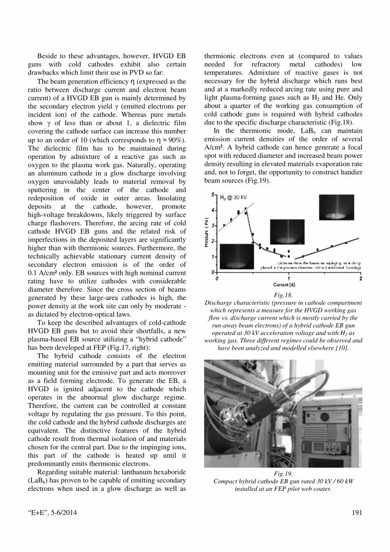
“E+E”, 5-6/2014 191
Beside to these advantages, however, HVGD EB guns with cold cathodes exhibit also certain drawbacks which limit their use in PVD so far:
The beam generation efficiency η (expressed as the ratio between discharge current and electron beam current) of a HVGD EB gun is mainly determined by the secondary electron yield γ (emitted electrons per incident ion) of the cathode. Whereas pure metals show γ of less than or about 1, a dielectric film covering the cathode surface can increase this number up to an order of 10 (which corresponds to η ≈ 90%). The dielectric film has to be maintained during operation by admixture of a reactive gas such as oxygen to the plasma work gas. Naturally, operating an aluminum cathode in a glow discharge involving oxygen unavoidably leads to material removal by sputtering in the center of the cathode and redeposition of oxide in outer areas. Insolating deposits at the cathode, however, promote high-voltage breakdowns, likely triggered by surface charge flashovers. Therefore, the arcing rate of cold cathode HVGD EB guns and the related risk of imperfections in the deposited layers are significantly higher than with thermionic sources. Furthermore, the technically achievable stationary current density of secondary electron emission is of the order of 0.1 A/cm² only. EB sources with high nominal current rating have to utilize cathodes with considerable diameter therefore. Since the cross section of beams generated by these large-area cathodes is high, the power density at the work site can only by moderate - as dictated by electron-optical laws.
To keep the described advantages of cold-cathode HVGD EB guns but to avoid their shortfalls, a new plasma-based EB source utilizing a “hybrid cathode” has been developed at FEP (Fig.17, right):
The hybrid cathode consists of the electron emitting material surrounded by a part that serves as mounting unit for the emissive part and acts moreover as a field forming electrode. To generate the EB, a HVGD is ignited adjacent to the cathode which operates in the abnormal glow discharge regime. Therefore, the current can be controlled at constant voltage by regulating the gas pressure. To this point, the cold cathode and the hybrid cathode discharges are equivalent. The distinctive features of the hybrid cathode result from thermal isolation of and materials chosen for the central part. Due to the impinging ions, this part of the cathode is heated up until it predominantly emits thermionic electrons.
Regarding suitable material: lanthanum hexaboride (LaB6) has proven to be capable of emitting secondary electrons when used in a glow discharge as well as
thermionic electrons even at (compared to values needed for refractory metal cathodes) low temperatures. Admixture of reactive gases is not necessary for the hybrid discharge which runs best and at a markedly reduced arcing rate using pure and light plasma-forming gases such as H2 and He. Only about a quarter of the working gas consumption of cold cathode guns is required with hybrid cathodes due to the specific discharge characteristic (Fig.18).
In the thermionic mode, LaB6 can maintain emission current densities of the order of several A/cm². A hybrid cathode can hence generate a focal spot with reduced diameter and increased beam power density resulting in elevated materials evaporation rate and, not to forget, the opportunity to construct handier beam sources (Fig.19).
Fig.18.
Discharge characteristic (pressure in cathode compartment which represents a measure for the HVGD working gas flow vs. discharge current which is mostly carried by the run-away beam electrons) of a hybrid cathode EB gun operated at 30 kV acceleration voltage and with H2 as
working gas. Three different regimes could be observed and have been analyzed and modelled elsewhere [10].
Fig.19.
Compact hybrid cathode EB gun rated 30 kV / 60 kW installed at an FEP pilot web coater.

“E+E”, 5-6/2014 192
Pulsed electron beam deposition
With the Pulsed Electron Beam Deposition (PED) process, a new field of work is evolving at FEP. This was enabled by a special EB source recently developed and delivered by Organic Spintronics srl. Its function principle relies on a channel-spark discharge. The source generates a short-pulsed, poly-energetic electron beam with a very high power density (≥ 108 W/cm² over a few nanoseconds). When directed to a target, the surface of the material is locally heated to an extent that ablation occurs, with subsequent propagation of the vapor towards the substrate in a directional flow [11].
As opposed to classic EB-PVD, the source material to be evaporated remains solid in PED. The advantage is that this allows for homogeneously depositing alloys in the proper stoichiometric ratio, because there is no accumulation of the less-volatile components due to the avoidance of a molten bath. Furthermore, the coating rate can be precisely adjusted facilitated by defined energy pulses.
When compared to alternative Pulsed Laser Deposition (PLD), PED excels by lower system costs. An essential feature of the PED process includes its high variability: nearly all materials (both electrically conductive and insulating materials) may be ablated, and the energy utilization efficiency is high. The undesired deposition of micro-particles (“droplets”) during layer formation can be markedly suppressed by optimizing the process parameters.
Beneficial particularities of PED include the formation of dense discharge plasma. It increases the energy of the ablated particles to several 10 eV and thus to a higher energy level than reached during electron beam evaporation or sputtering, for example. This positively influences the properties of the growing layers so that the substrate temperature can be kept low. Therefore, the growing of well-adhering, dense layers is also made possible on temperature-sensitive substrate materials – such as plastics, for example.
Moreover, reactive process control is possible by adding the corresponding gases. As a result, there are numerous different application possibilities such as the production of hard material layers, decorative layers, or transparent, conductive oxide layers. Further potential applications can be found in the field of flexible displays and in the domain of hetero-structured thermoelectric materials.
The first tests of the new source at FEP were intended to develop a general understanding of the PED process, as well as to investigate the suitability of the method for different applications.
For instance, the deposition of thin metal and semi-conductor layers was examined in process chains for photovoltaic applications. Furthermore, promising trials regarding the deposition of transparent conductive oxide layers were conducted.
Fig.20.
Setup of the pulsed electron beam deposition process and PED source in operation.
Fig.21.
Characteristic data of PED source and process [12].

“E+E”, 5-6/2014 193
ERICA cluster tool FEP’s ERICA cluster tool comprises a load-lock
and five separate process stations, arranged around a central chamber with a robot handler. This machine type allows the substrate to be transported in a continuous vacuum into the various process compartments in any desired sequence. Thus, complex production lines including pre-treatment, coating and thin-film processing steps can be simulated in a highly flexible way and at favorable cost. Regarding the implemented tools, special emphasize was put on various types of electron sources. For instance, the instrumentation of one chamber allows execution of high-rate EB-PVD processes. It comprises a hollow-cathode arc-plasma LVEB source (featuring, like-wise, pre-treatment by sputter etching or plasma-activated deposition) and a hybrid cathode EB gun for materials evaporation. In another chamber, the PED source and target manipulation system is installed.
Fig.22. ERICA cluster tool instrumentation.
Acknowledgements This research was partially funded by the European
Union and the Free State of Saxony and performed in various joint projects of FEP together with partners from industry, namely VON ARDENNE GmbH, ROTH & RAU AG, and CREAVAC GmbH.
Fruitful collaborations with J. Lehmann,
F. Munnik, and W. Moeller of Helmholtz Center Dresden-Rossendorf (on plasma diagnostics / a-C:H layer characterization), V.I. Melnyk, B.A. Tugay, and I.V. Melnyk of Kiev Polytechnic Institute (on HVGD cold cathode EB guns) as well as with the work group of H.N.G. Wadley at the University of Virginia (on plasma-activation methods for the DVD process) are particularly appreciated.
Further, we thank D. Yarmolich and C. Taliani of Organic Spintronics srl for their support in starting-up the new PED source.
Many unnamed colleagues at FEP contributed to the development work reviewed in this paper. We would like to express our thanks to all of them here.
REFERENCES
[1] H. Morgner, M. Neumann, S. Straach, M. Krug. The hollow cathode – a high performance tool for plasma activated deposition. Surf. Coat. Technol., vol. 108/109, 1998, pp. 513-519.
[2] H. Morgner, G. Mattausch, Chr. Metzner, M. Junghaehnel, R. Labitzke, L. Klose, T. Werner, J. Kubusch. Device for generating a hollow cathode arc discharge plasma. WO 2013/091927 Al.
[3] H. Wadley, G. Mattausch, H. Morgner, F.-H. Roegner. Coaxial hollow cathode plasma assisted directed vapor deposition and related method thereof. WO 2010/099218 A1.
[4] F. Fietzke, H. Morgner, S. Guenther. Magnetically enhanced hollow cathode – a new plasma source for high-rate deposition processes. Plasma Process. Polym., vol. 6, 2009, pp. S242-S246.
[5] F. Fietzke, B. Zimmermann. Plasma charac-terization and technological application of a hollow cathode plasma source with an axial magnetic field. Surf. Coat. Technol., vol. 205, 2010, pp. 1491-1496.
[6] J.-P. Heinß, V. Kirchhoff, L. Klose, Chr. Metzner, H. Morgner, B. Scheffel. Device for the pre-treatment of substrates. EP 2 087 503 B1, 2007.

“E+E”, 5-6/2014 194
[7] J.-P. Heinß. High-Rate Sputter Etching by using Hollow Cathode Arc Discharge for Metal Strip Coating. AEPSE 2011, Dalian, China.
[8] B. Zimmermann, F. Fietzke, H. Klostermann, J. Lehmann, F. Munnik, W. Möller. High rate deposition of amorphous hydrogenated carbon films by hollow cathode arc PECVD. Surf. Coat. Technol., vol. 212, 2012, pp. 67-71.
[9] S.V. Denbnovetsky, V.G. Melnyk, I.V. Melnyk. High-voltage, glow-discharge electron sources and possibilities of its application in industry for realizing different technological operations. IEEE Transactions on Plasma Science, vol. 31, 2003, pp. 987-993
[10] P. Feinaeugle, G. Mattausch, S. Schmidt, F.-H. Roegner. A new generation of plasma-based electron beam sources with high power density as a novel tool for high-rate PVD. Society of Vacuum Coaters 54th Annual Technical Conference Proceedings, Chicago, 2011, pp. 202-209.
[11] G. Müller, M. Konijnenberg, G. Krafft, and C. Schultheiss. Thin Film Deposition by Means of Pulsed Electron Beam Ablation. in: F.C. Matacotta and G. Ottaviani (eds). Science and Technology of Thin Films. World Scientific Publishing Co. Pte. Ltd., 1995, pp. 89-119.
[12] D. Yarmolich, P. Nozar, S. Gleizer, Y.E. Krasik, G. Mittica, C. Ancora, A. Brillante, I. Bilotti, and C. Taliani. Characterization of Deposited Films and the Electron Beam Generated in the Pulsed Plasma Deposition Gun. Japanese Journal of Applied Physics, vol. 50, 2011, 08JD03.
All authors are with the Fraunhofer Institute for Electron Beam and Plasma Technology (FEP).
address: Winterbergstr. 28, 01277 Dresden, Germany web: www.fep.fraunhofer.de
Dr. Goesta Mattausch received his Ph.D. degree in solid state / low-temperature physics from the University of Technology Dresden, Germany in 1997. He is employed at FEP since 1993 and was first involved in the development of production technologies and process control techniques utilizing high-speed beam scanning for thermal EB surface treatment and EB welding. Since 1999 he has been leading teams which developed customized electron beam and plasma systems for research and production purposes and dedicated to use in a variety of electron beam applications, such as welding, high-rate PVD, vacuum-metallurgical melting and refining, curing and crosslinking of polymers, sterilization, and fast CT x-ray imaging.
tel.: +49 351 2586 202 е-mail: [email protected]
Dr. Burkhard Zimmermann received the diploma and Ph.D. degrees in physics from the University of Technology Dresden, Germany in 2008 and 2012, respectively. Since 2008, he has been working at FEP on characterization and modeling of the magnetically enhanced hollow cathode arc discharge as well as its application for plasma pretreatment, plasma-activated PVD, and high-rate PECVD of amorphous hydrogenated carbon layers. In 2012 he joined the Department “Electron Beam Processes” of FEP. His current activities include the development of discharge-based EB gun systems, the realization of customized EB systems for high-rate PVD applications as well as further work on hollow cathode arc plasma sources.
tel.: +49 351 2586 386 е-mail: [email protected]
Dr. Fred Fietzke received the diploma and Ph.D. degrees in physics from the University of Technology Dresden, Germany (both on a research field in low temperature physics). In 1993 he joined the FEP where he is currently working as senior scientist in the department "Coating of Components and Tools". His main research areas are pulsed magnetron sputtering and plasma-activated evaporation. In particular, he led the development of the magnetically enhanced hollow-cathode source.
tel.: +49 351 2586 366 е-mail: [email protected]
Dr. Jens-Peter Heinß received his Ph.D. degree in physics with a thesis on “Heat transfer in cryogenic liquids” from the University of Technology Dresden, Germany in 1989. He developed and investigated capillary-porous coatings for the intensification of heat transfer and was involved in starting of operation of industrial equipment for air separation. In 1995 he joined FEP and has the position of a project leader. He is responsible for research and development projects in the department “Coating of Sheets and Metal Strips”. His main focus is on the adaptation and industrial implementation of plasma activated high rate electron beam deposition technologies.
tel.: +49 351 2586 244 е-mail: [email protected]
Dipl.-Phys. Benjamin Graffel received the diploma degree in physics from the University of Technology Chemnitz, Germany in 2006. Since 2007, he has been working in FEP’s department “Electron Beam Processing”. He leads development projects focused on customized electron beam technologies for local surface modification and structuring as well as thin film deposition, especially for applications in the field of renewable energies and energy efficiency.
tel.: +49 351 2586 212 е-mail: [email protected]

“E+E”, 5-6/2014 195
Dipl.-Ing. (FH) Falk Winckler received the diploma degree in electrical engineering from the University of Applied Sciences for Technology and Economics Dresden, Germany in 2008. He is working within FEP’s department “Electron Beam Processing” as project engineer and manager in the fields of electron beam welding, structuring and electron beam source development.
tel.: +49 351 2586 207 е-mail: [email protected]
Dipl.-Phys. Frank-Holm Roegner received his graduate physicist in solid state / low-temperature physics from the University of Technology Dresden, Germany in 1988. He is employed at FEP since 1998 and was the first ten years involved in the development of production technologies and process control techniques for physical vapor deposition of large metal surfaces using high power electron beam guns. 2008 he became the head of the department “Electron Beam Processing” therein he and his team are developing production technologies, process control modules and the related customized electron beam and plasma systems to use in a variety of electron beam applications, such as welding, high-rate PVD, vacuum-metallurgical melting and refining, curing and crosslinking of polymers, grafting, sterilization and fast CT x-ray imaging.
tel.: +49 351 2586 242 е-mail: [email protected]
Prof. Dr. Christoph Metzner received his Ph.D. degree in vacuum physics from the Otto-von-Guericke-University Magdeburg, Germany in 1999. Since 2008, he is Honorary Professor (for electron, laser and plasma beam technologies) at the University of Applied Sciences for Technology and Economics Dresden, Germany. At FEP, Christoph Metzner serves as Director of Division “Electron Beam” and manages numerous domestic and international projects and collaborations with industry and academia. His research interests span the fields of vacuum coating of metal strips and sheets, electron beam evaporation, plasma activation for PVD, electron beam melting and refining, as well as the physics of electron beams and gas discharges.
tel.: +49 351 2586 240 е-mail: [email protected]

“E+E”, 5-6/2014 196
Composite Materials with a Metal Matrix Condensed from Vapor Phase: Dispersion-Strengthened Metals
Nicolay I. Grechanyuk, Igor N. Grechanyuk, Elena V. Khomenko, Andrey G. Melnik, Vera G. Grechanyuk
Modern scientific level of dispersion-strengthened metals condensed from the vapor phase
engineering is presented. The physical and mechanical properties of these materials depend on selected matrix type (pure metal, metal alloy), particles reinforced composites (oxide, carbides, borides, refractory metals), interaction at matrix-particles boundaries, technological parameters (condensation temperature, degree level of vacuum, condensation speed of initial components and their chemical purity, roughness of substrate surface on which condensation is carried out, etc.) .
Композитни материали с метална матрица, кондензирана от парна фаза: Дисперсионно-уякчени метали (Н. Гречанюк, И. Гречанюк, Е. Хоменко, А. Мелник, В. Гречанюк). Представено е модерно научно равнище на инженеринга на дисперсно-уякчени метали, кондензирани от парна фаза. Физичните и механични свойства на тези материали зависят от типа на матрицата (чист метал или метална сплав), от частиците, заздравяващи композита (оксиди, карбиди, бориди, трудно-топими метали), взаимодействието на границите на частиците на матрицата, от технологичните параметри (температурата на кондензиране, степента на вакуума, скоростта на кондензиране на началния компонент и неговата химическа чистота, грапавините по повърхността на подложката на която се извършва кондензация и т.н.).
Introduction The appearance of electron beam (1956), plasma -
arc (1958) and laser (1964) technology in the mid-twentieth century raise issue the question before developers of new technologies for processing and welding materials: why traditional source of energy for these purposes - free burning welding arc melts metals "superficially" (ratio of the depth of the molten zone to its width <1) while the sources listed above - "daggermaw" (ratio of the depth of the molten zone to the width of <100).
Looking at those processing brought about a new understanding of concentrated energy fluxes (CEF) [1]. It turned out, if the power source develops power density ≥ 105-106 W/cm2 (electron beam, laser, plasma), laws of heat transfer in a heated object change sharply at excess of some threshold power density. The overcoming this threshold has opened up before technologists new opportunities.
Great scientific and technological experience with CEF showed that the most efficient source of energy at treatment is the electron beam. In the E.O. Paton Electric Welding Institute of National Academy of Sciences of Ukraine (EWI of NASU) and Research
and Production Association "Eltehmash" multipurpose two, three, fivecrucible electron beam installation on basis powerful electron beam guns for intense molecular beams obtaining. The intensity of these beams reaches 1020 particles per cm3/s. This quasimolecular beam which is characterized, on the one hand, by the properties of the molecular beam, namely the intensity distribution in a space of approximately obeys law of cosine, and on the other hand, this beam extends as a result internal collisions of atoms, and so it has some similarity steam flows in laminar flow.
The productivity of these installations reached the level 10-15 kg of steam per hour. In other words, during 8 hours of continuous operation can be obtained masse of condensate by 100 kg or more.
Fundamental researches of basic physical and mechanical laws that determine formation of thick condensates (0,01-2,0 mm ) in the Paton NASU under the guidance academician of NASU B.A. Movchan carried out [2, 3].
The basic physical and chemical mechanisms of formation of thick vacuum condensates from some pure metals, metal alloys, oxides, carbides were established, and their physical properties depending

“E+E”, 5-6/2014 197
on the composition and parameters of condensation were studied.
For new materials produced by the condensation of primarily should be attributed dispersion-strengthened materials, porous and micro-layered materials. Study of their structure and properties is the aim of this work.
Experimental part Dispersion-strengthened materials consist of
polycrystalline matrix with uniformly dispersed particles of second phase (Fig.1). The average dimensions of matrix crystallites and strengthened particle phase can by adjusted at wide range - from several hundred microns to several thousands angstroms by varying of substrate temperature and condensation rate.
Fig.1. Typical structure of dispersion-strengthened
material, condensed from vapor phase.
The structure and physico-mechanical properties of dispersion-strengthened condensed materials for systems: iron-carbide, iron-boride, iron-oxide, nickel-carbide, nickel-oxide, copper-oxide, tungsten-oxide were investigated by A.V. Demchishin [4].
The dispersion-strengthened materials based on complex alloys of nickel, chromium, copper, titanium were studied in details by author [5]. Scientific researches in those systems currently continue [6].
Mechanical characteristics of dispersion-strengthened materials depend on following factors: - type of selected matrix (pure metal, metal alloy); - type of dispersed particles (oxides, carbides, borides, refractory metals). - technological parameters of condensed materials obtaining (temperature of condensation, level of vacuum, chemical composition, condensation rate and purity of initial components, roughness of substrate on which the condensation occurs).
The main factor that determines structure and mechanical properties of dispersion-strengthened
condensed materials is contact interaction at particle-matrix interface. Quantitative criterion of interaction contact between melt and refractory compounds is angle of wetting [7]. This factor depends essentially on environment in which the melt reacts with a solid substrate (particle), the purity of melt and the particles, temperature, exposure time and other factors. In the literature there are many reference data, that determine angle of wetting in systems Me (alloy) - MeO, Me-C-MeB in vacuum, inert gases, etc. [7, 8].
For simple two-phase condensed system Me-MeO, where as a matrix were used commercially pure iron, nickel, copper, and as a second (hardening) phase - aluminum, yttrium, stabilized zirconium, can be achieved sufficiently high level of mechanical properties at narrow concentration range of second phase (to 0,6% mass.).
Fig. 2a, b, as an example, shows tensile strength (σВ), yield strength (σ0,2), elongation (δ) versus Al2O3
concentration in condensates Ni-Al2O3, obtained at temperatures of substrate 700 and 1000 ± 20 º C.
Fig.2. Tensile strength, yield strength and elongation
versus Al2O3 concentration in dispersion-strengthened material Ni-Al2O3,, obtained by condensation at substrate
temperatures 700 (a) and 1000 º C (b).

“E+E”, 5-6/2014 198
Analysis of these data shows dispersed particles Al2O3 particles at low concentrations leads to increase strength and to non monotonic decreasing of ductility. Maximum ductility is observed over a relatively narrow concentration range- 0,25÷ 0,4%wt Al2O3.. Increase in plasticity takes place when the structural conditions have performed: average grain size of metallic matrix is equal to average distance between dispersed particles [2]. It should be noted that a maximum of curves δ ƒ (% mass. Al2O3) is shifted towards higher concentration of Al2O3 with increasing temperature. Plasticity of two-phase materials Me-MeO with optimum concentration of dispersed particles increase with increasing of condensation temperature. For example, at condensation temperature 1000 ºC dispersion-strengthened materials Ni - (0,35 - 0,4 % mass.) Al2O3 have an elongation greater than that of pure nickel.
Similar changes of mechanical characteristics have observed for more complex condensed-phase systems based on solid solutions of MeCr, MeCrAl, MeCrY, where Me - Fe, Ni, Cu, qualitatively (Fig. 3, a, b).
Fig.3. Tensile strength, yield strength and elongation
versus Al2O3, concentration in dispersion-strengthened materials N i - 20 % mass. Сr –Al2O3, obtained
by condensation at substraite temperature 700 (a) and 1000 oC (b).
Increase in strength is observed in a range of Al2O3 concentration up to 1 % mass. However, condensates with these concentrations of dispersed refractory particles have low ductility. Similar changes of mechanical characteristics caused by absence of interaction at particle-matrix interface. Contact angle between Al2O3 and liquid Ni consist up 115 to 150 degrees, depending on experimental conditions [7]. The absence of interaction due to formation of pores in the condensates, what leads to loss of strength and ductility.
The improvement of interfacial interaction in system Cr-Ni-Al2O3 [7] (the contact angle is 85 degrees) leads to a certain increase of strength and ductility in a wider range of Al2O3 concentration compared with composites Ni-Al2O3.
The inflection on strength curves of two-phase systems metal (alloy – carbide (boride) shifts to higher concentrations of dispersed phase relative position on curves in system with oxide phase 3-7 % mass. Similar regularities are typical for condensed materials on nickel, iron or copper based, in which as dispersed particles were used titanium carbide (TiC), niobium carbide (NbC), zirconium carbide (ZrC), titanium diboride (TiV2), zirconium diboride (ZrV2) [5].
The regularities of mechanical characteristics change in composition Cu-ZrV2 show in Fig.4 for illustration. The increasing of ZrV2 concentration up to 0,8 % mass. leads to increase of yield strength and strength to 550 and 600 MPa, respectively, and when zirconium diboride content in condensate is 2,4 % mass., tensile strength reaches to 950 MPa.
Fig. 4. Tensile strength, yield strength and elongation versus ZrB2 concentration in dispersion-strengthened
materials Cu-ZrB2, obtained by condensation at substrate temperature 700ºC.
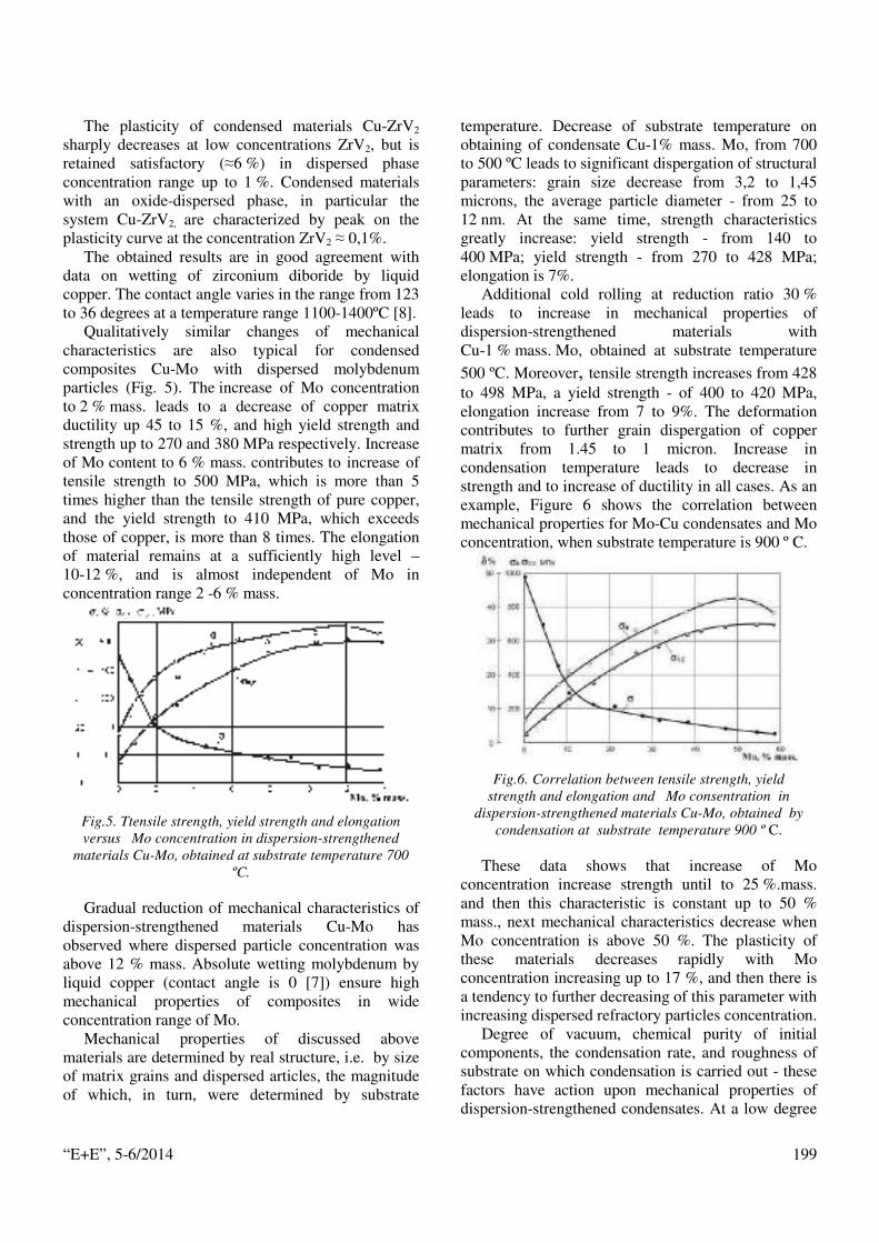
“E+E”, 5-6/2014 199
The plasticity of condensed materials Cu-ZrV2 sharply decreases at low concentrations ZrV2, but is retained satisfactory (≈6 %) in dispersed phase concentration range up to 1 %. Condensed materials with an oxide-dispersed phase, in particular the system Cu-ZrV2, are characterized by peak on the plasticity curve at the concentration ZrV2 ≈ 0,1%.
The obtained results are in good agreement with data on wetting of zirconium diboride by liquid copper. The contact angle varies in the range from 123 to 36 degrees at a temperature range 1100-1400ºC [8].
Qualitatively similar changes of mechanical characteristics are also typical for condensed composites Cu-Mo with dispersed molybdenum particles (Fig. 5). The increase of Mo concentration to 2 % mass. leads to a decrease of copper matrix ductility up 45 to 15 %, and high yield strength and strength up to 270 and 380 MPa respectively. Increase of Mo content to 6 % mass. contributes to increase of tensile strength to 500 MPa, which is more than 5 times higher than the tensile strength of pure copper, and the yield strength to 410 MPa, which exceeds those of copper, is more than 8 times. The elongation of material remains at a sufficiently high level – 10-12 %, and is almost independent of Mo in concentration range 2 -6 % mass.
Fig.5. Ttensile strength, yield strength and elongation versus Mo concentration in dispersion-strengthened
materials Cu-Mo, obtained at substrate temperature 700 ºC.
Gradual reduction of mechanical characteristics of dispersion-strengthened materials Cu-Mo has observed where dispersed particle concentration was above 12 % mass. Absolute wetting molybdenum by liquid copper (contact angle is 0 [7]) ensure high mechanical properties of composites in wide concentration range of Mo.
Mechanical properties of discussed above materials are determined by real structure, i.e. by size of matrix grains and dispersed articles, the magnitude of which, in turn, were determined by substrate
temperature. Decrease of substrate temperature on obtaining of condensate Cu-1% mass. Mo, from 700 to 500 ºC leads to significant dispergation of structural parameters: grain size decrease from 3,2 to 1,45 microns, the average particle diameter - from 25 to 12 nm. At the same time, strength characteristics greatly increase: yield strength - from 140 to 400 MPa; yield strength - from 270 to 428 MPa; elongation is 7%.
Additional cold rolling at reduction ratio 30 % leads to increase in mechanical properties of dispersion-strengthened materials with Cu-1 % mass. Mo, obtained at substrate temperature 500 ºC. Moreover, tensile strength increases from 428 to 498 MPa, a yield strength - of 400 to 420 MPa, elongation increase from 7 to 9%. The deformation contributes to further grain dispergation of copper matrix from 1.45 to 1 micron. Increase in condensation temperature leads to decrease in strength and to increase of ductility in all cases. As an example, Figure 6 shows the correlation between mechanical properties for Mo-Cu condensates and Mo concentration, when substrate temperature is 900 º C.
Fig.6. Correlation between tensile strength, yield
strength and elongation and Mo consentration in dispersion-strengthened materials Cu-Mo, obtained by
condensation at substrate temperature 900 º C.
These data shows that increase of Mo concentration increase strength until to 25 %.mass. and then this characteristic is constant up to 50 % mass., next mechanical characteristics decrease when Mo concentration is above 50 %. The plasticity of these materials decreases rapidly with Mo concentration increasing up to 17 %, and then there is a tendency to further decreasing of this parameter with increasing dispersed refractory particles concentration.
Degree of vacuum, chemical purity of initial components, the condensation rate, and roughness of substrate on which condensation is carried out - these factors have action upon mechanical properties of dispersion-strengthened condensates. At a low degree

“E+E”, 5-6/2014 200
of vacuum in the chamber, wherein the condensation is carried out, oxygen and nitrogen atoms interact with the metal atoms, that leads to oxides and nitrides formation. Thus, the mechanical properties of composites increase, but simultaneously ductility, conductivity and heat conductivity decrease.
The quantity of defects (microdroplets, nonmetallic inclusions) depends on purity of vaporized materials. The most rational for obtaining composites to use as initial metal ingots metal alloys after electron beam melting. This process reduces the amount of low-melting impurities, oxygen, nitrogen and hydrogen as compared to commercially pure metals and metal alloys.
The evaporation rate increase removal of impurities of liquid or solid phases during metal evaporation from the bath. Electron-beam remelting of leads to increase of pure metals and metal alloys condensation rate up 3.5 to 60 microns/min and dispersed phase – up 0.5 to 10 micron/min. In obtaining of composites to make the most efficient use the substrate surface roughness 0,63-1,2 Ra.
Conclusions It has been established that obtaining of dispersion-
strengthened materials, condensed from vapor phase, have suitable physical and mechanical properties, primarily depend on type of metal matrix and dispersed particles, substrate temperature, interfacial interaction between matrix - dispersed particles, substrate roughness, purity initial materials and evaporation speed and etc.
Method of high-speed evaporation of metals and non-metals in vacuum permit easy to construct new perspective dispersion-strengthened materials with predetermined physico-mechanical properties using estimation criterion of interaction at the matrix – particle boundary.
REFERENCE [1] Зуев, И. В. Обработка материалов концентри-
рованными потоками энергии. Москва, МЭИ, 1998, 162 с.
[2] Мовчан, Б.А., И.С. Малашенко. Жаростойкие покрытия осаждаемые в вакууме. Киев, издательство «Наукова думка», 1983, 230 с.
[3] Мовчан, Б.А. Неорганические материалы, осаждаемые из паровой фазы в вакууме. Современное материаловедение в XXI веке, Киев, издательство «Наукова думка», 1998, с.с. 318-332.
[4] Демчишин, А.В. Структура и свойства толстых вакуумных конденсатов металлических и неметаллических материалов и научные основы их
получения: Автореферат диссертации доктора технических наук, Киев, 1981, 35с.
[5] Гречанюк, Н.И. Новые конструкционные материалы, полученные путем конденсации паровой фазы в вакууме для изделий новой техники. Диссертация на соискание ученой степени доктора технических наук, Киев, 1988, 520 с.
[6] Гречанюк, Н.И., В.А. Осокин, И.Н. Гречанюк, и др. Композиционные материалы на основе меди и молибдена для электрических контактов, конденсированные из паровой фазы. Структура, свойства, технология. Часть 2. Основы электронно-лучевых технологий получения материалов для электрических контактов. Современная электрометаллургия, 2006, 2. с.с..9-19.
[7] Найдич, Ю.В. Контактные явления в металлических расплавах, Киев, издательство «Наукова думка», 1972, 196 с.
[8] Самсонов, Г.В., А.П. Эпик. Тугоплавкие покрытия. Москва, издательство «Металлургия», 1973, 398с.
Prof. Dr. Nicolay I. Grechanyuk – Doctor of Engineering, Leading Researcher of Frantsevich Institute for Problems of Materials Science of National Academy of Ukraine, graduated from the Kiev Polytechnic University in 1972 (Kiev, Ukraine), specialist in the field of electron-beam technologies and equipment for materials and coatings. Tel.(044)424-24-74,
e-mail: [email protected].
Igor N. Grechanyuk - Candidate Engineering, specialist in the field of technology for production of electrical contact materials, graduated from the Kiev Polytechnic University in 2004. (Kiev, Ukraine),
e-mail:[email protected].
Elena V. Khomenko – Candidate of Engineering, Senior Researcher of Frantsevich Institute for Problems of Materials Science of National Academy of Ukraine, graduated from the Kiev Polytechnic University in 1986, specialist in the field of electrical contact materials.
е-mail: [email protected]
Andrey G. Melnik - Candidate of Engineering, graduated from the Kiev Polytechnic University in 1999, specialist in the field of electron beam equipment designing for composite materials and coatings.
e-mail: [email protected].
Prof. Dr. Vera G. Grechanyuk - Doctor of Chemical Sciences, Associate Professor, Head of the Department of Kyiv National University of Construction and Architecture, graduated from the Kiev Polytechnic University in 1972, specialist in the field of corrosion of composite materials, condensed from vapor phase.
e-mail: [email protected].

“E+E”, 5-6/2014 201
Composite Materials with Metal Matrix Condensed from Vapor Phase: Microlayer Materials
Nicolay I. Grechanyuk, Igor N. Grechanyuk, Elena V. Khomenko, Andrey G. Melnik, Vera G. Grechanyuk
The problems of microlayer metal materials, obtained by condensation from vapor phase are
discussed. Example of copper-molybdenum materials obtaining was first shown possibility to produce composites having a layer thickness of less than 1 micrometer, condensed at substrate temperature above 0,3 melting point of fusible layer (Cu).
Композитни материали с метална матрица, кондензирана от парна фаза: Микрослойни материали (Н. Гречанюк, И. Гречанюк, Е. Хоменко, А. Мелник, В. Гречанюк). Дискутирани са проблемите на микрослойните материали, получени чрез кондензация от парна фаза. Примерът на медно-молибденов материал е първата показана възможност да се произведат композити с дебелина на слоевете под 1 микрометър кондензиран при температура над 0.3 от точката на топене на по-лесно стапящия се слой (Cu).
Introduction The more and more attention every year have paid
to metal matrix composite consisting of components with contrasting physical and mechanical properties. Depending on reinforcing phase shape metal matrix composite can be divided into two large classes: fibrous and layered (multilayered).
Multilayer composite with metal matrix have several advantages over fiber materials, particularly in terms of physical and mechanical properties management, in particular [1]:
- Upon receipt of reinforced fiber is difficult to obtain required external surface of layer, whereas it is known that the state and properties of those play a crucial role in behavior of material under load. Furthermore, by changing the sequence of alternating layers and their thickness, the mechanical properties under a load of various kinds of multilayer composites can be varied;
- Reinforcing phases of multilayer composites provide more uniform deformation, compared with fibrous materials at the same volume fraction
- Technology of multilayer composite is more simple and wide explored than those of fibrous materials.
Industrial multilayer composites are produced by different methods based on principles of joining strips, plates and foils of different metals, in particular hot rolling or pouring molten metal of solid plates with
the subsequent rolling ingots, explosion welding, brazing, directed eutectic crystallization etc. Detailed exposition of these methods, as well as some physical and mechanical properties of multilayer composites are presented in a number of reviews and monographs summarizing [1-6]. Eutectic superalloys multilayer composites are increasingly being used in modern aircraft engines production [6-8]. Above mentioned materials have advantages in comparison with single-layer materials, for example, they are characterized by higher values of strength, heat resistance, fracture toughness, etc. [7]. In most cases, the thickness of layers in fibrous material is greater on 3-4 orders of magnitude than average grain size in multilayer composites.
Exceptionally interest for modern technology development are layered materials, in which grain size is comparable or less than the thickness of alternating layers. In such materials, the tensile strength may reach lower limit of theoretical metal strength [9]. Those layered (multilayer) materials are often called in the technical literature as microlayer materials [10, 11].
Experimental part Extensive research of MLCM based on Cu, Pb, Sn,
Cr, Fe, Ni, Mg, An, Ag, C, Al2O3 with thickness of layer 0,1 microns or less, obtained by wire beam drawing and foil rolling carried out by V. S. Kopan [11]. He showed that microlayer thickness - one of the

“E+E”, 5-6/2014 202
main factors which determine the properties of microlayer materials. Usually such features as microhardness, tensile strength, elasticity and fatigue, thermo electro-dynamic force, induced deformation, electrical resistance, coercivity, continuity and fracture toughness and other properties tend to increase with decreasing microlayer thickness.
Electron-beam technology opens unlimited possibilities in designing microlayer materials. Improvements in methods and techniques of material condensation in a vacuum, mainly, particularly in developments of powerful electron-beam evaporators and magnetron systems, allow to creation of new materials with different structure types and layer thicknesses varying widely.
Today, rather conventionally can be distinct two classes of microlayer materials, obtained material condensation in a vacuum (Fig. 1):
- Microlayer condensates with a thickness of about 0,1-10 microns [10,12-16]. The structure of interface between layers likes to large-angle grain boundary in polycrystalline (Fig. 1a);
- Microlayer condensates with ultrathin layers up (6 ... 8) ⋅10-10 to (6 ... 8) ⋅10-8m). Depending on the structure of alternate layers, conjugation of atomic planes of crystal lattices of adjacent layers along coherent boundary occurs [17,18] (Fig. 1b), or creation of unified system of atomic planes [19, 20] (Fig.1, c).
- Technology of evaporation and condensation metallic and nonmetallic materials in a vacuum permit to realize two characteristic principles of microlayer condensates formation:
- 1) Condensation at relatively low temperatures, which allows to high density of crystal lattice defect for each layer.
- 2)Condensation at temperatures above melting point of 0,3 fusible layers, which leads to obtaining microlayer condensates with enough equilibrium structure.
Microlayer condensates, obtained at low temperatures, have been studied in detail under the guidance of L.S. Palatnik in 1964-1966 years in Kharkov Polytechnic Institute [21, 22].
The basic lows of changes of structure and physic and mechanical properties of condensed microlayer materials above-mentioned types were summarized A.I. Ilinskiy [12, 23]. Fundamental research of Cu-Cr and Ni-Si microlayer condensates with a small volume percent of reinforcing layers (up to 10%), with layer thickness does not exceed 0,1 microns, were carried out by the author. Summer thickness of the composites was not more than 50...100 mm. As in the
case of fibrous materials, obtained by conventional methods, there was a significant hardening of condensed microlayer materials with decreasing layer thickness. It is show that this size effect is caused mainly by influence of interfacial surfaces. As shown in [12, 23, 24] the change of total interfacial surface area can be accompanied by doubling the strength, as shown in example of microlayer materials Cu-Cr. Microlayer materials retain structural stability and high mechanical properties until temperatures 400º…500 oС. At higher temperatures the discontinuity (decomposition) alternate layers into separate blocks, fragments and formation of typical hetero-phase structure take place. Structure and properties of microlayer materials with alternate layer thickness more than 0,1 microns is not enough understood. Research of microlayer composites, are represented in literature fragmentary and concern essentially of materials Cu-Fe [12], Ag-Ni [21], Cu-Cr [25], condensed at substrate temperature not higher than 300 º C.
Fig.1. Structural schemes of microlayer materials. The classification of microlayer materials, shown
above, and brief overview of level, achieved in this most important area, indicate that a small part of model microlayer materials condensed at relatively low substrate temperatures (300 º C) only studied.
Considerable part of research of microlayer materials Fe-Cu, Cr-Cu, Ni-Cu, Mo-Cu, NiCrAlY-NiCrAlY-Al2O3, NiCrAlY/NiCrAlY-(ZrO2-Y2O3), Ti-TiAl, Ti3Al-TiAl, Ti4V6-AlTi, condensed at substrate temperature 500 …1000 º C is presented in [10, 26-30]. Materials with layer thickness up 0,1 to 30 microns were obtained in the form of blanks with dimensions 250x350x(0,5...1,5) mm, with had been cut for mechanical testing, physical and chemical structural studies. Generalization of these studies was done by the author in [31]. It is shown that by choice of alternating layer material and their thicknesses can be obtained a high structural stability, strength and ductility values adaptable in a wide range, low values

“E+E”, 5-6/2014 203
of high-temperature creep and low thermal conductivity as compared to those parameters of individual layers. In general, the tensile strength of investigated microlayer materials may be above 1,5 ... 4 times than similar values for individual layers of materials with alternate layers thickness smaller than 2 microns. Microlayer materials elongation tends to decrease and approaches the zero value for the thickness of alternate layers less than 1 micron. The structure, phase composition and mechanical properties of a new class - condensed materials metal/cermet NiCrAlY / NiCrAlY + Al2O3, NiCrAlY/ NiCrAlY + (ZrO2 - Y2O3) in thickness range up 0,2 to 25 micron with oxide content in alternative layers up 0 to 50 % wt were studied. Found that the main factor determining changes of properties is sintered oxide content in microlayer. When oxide concentration is 0,5 ... 4 % wt. and microlayer thickness is 1 ... 25 nm, value of tensile strength and ductility are more than 10 ÷ 20%, and the heat resistance – more than 5 ... 30%, as compared with conventional matrix alloys.
Disintegration of layers with a thickness less than 1 micron of single microlayer in all studied types microlayer materials, condensed at substrate temperatures above 0.3 of the melting temperature of least refractory layer, is observed. Thus, we can draw a general conclusion that in the literature there is no information about the microlayer materials with a thickness of layers less than 1 micron, condensed at substrate temperatures higher than 0,3 on the least refractory layer melting temperature . At the same time, it is expected that, by analogy with other types for microlayer materials with a layer thickness of less than 1,0 microns, condensed at temperatures ensured equilibrium structure formation (substrate temperature ≤ 0,3 least the melting point of refractory layer), can vary structurally sensitive physical and mechanical properties in wide limits by appropriate choice of components in alternate layers and substrate temperature. It is logical to assume that the microlayer materials, obtained at high substrate temperatures have a high level of structure thermal as compared with known materials. Similar materials with lots of layers, the total whose thickness is 100 microns or more may be in accordance with the classification given in [32], attributed to nanostructured systems, i.e. macroscopically homogeneous massive bodies having internal nanostructure. Basic technological conditions for obtaining such microlayer thermo-stable materials were formulated by the author in [33-35]. Practical implementation of these principles was carried out by obtaining of microlayer condensates Cu-Mo [35].
a) b) c)
Fig. 2. Typical structure of microlayer condensed materials Cu / Mo: a, b - original state; c - after vacuum
annealing at 900 ° C for 1 hour.
The typical structure of these microlayer condensates is shown in Figure 2, a, b. Microlayer composites were condensed at substrate temperature 700 ± 20 ° C, exceeded 0, 6 on the most fusible layer melting temperature (Cu). The copper layer thickness (gray layers) is approximately 500 nm, molybdenum layer thickness (dark layer) is 100 nm. Undulating profile layers repeats profiles substrate on which to condense. Vacuum annealing at 900 ° C for 1 hour practically no changes layer continuity (Fig. 2, c). The yield strength and tensile strength of Cu-Mo microlayer materials are 550 and 635 MPa respectively, that are 5 times than the same values for pure copper, and 2 time higher compared with pure molybdenum, whereas elongation those is 2.5 %. After vacuum annealing of 900 °C for 1 hour, mechanical properties of those materials were reduced approximately 10 %, at the same time, the elongation is increased to 7,5%.
Conclusions Thus, test mechanical properties results of
microlayer materials with internal nanostructure show the great possibilities of the method [33, 34] for layered compositions with controlled structure and properties obtaining.
REFERENCE [1] Бовина, Л., В.С. Иванова, Т.С. Малиновская.
Структура и свойства многослойной стали. Известия. АН СССР Металлы,1970, 3, с.с.146-151.
[2] Достижения в области композиционных материалов / Под ред. Дж Пиатты., М: Металлургия, 1982, 304с.
[3] Неупругие свойства композиционных материалов. Под ред. К. Гераковича, Москва, издательство Мир, 1978, 295с.
[4] Райт, Е., А. Левит Слоистые металлические композиционные материалы. Композиционные

“E+E”, 5-6/2014 204
материалы с металлической матрицей, Москва, издательство «Машиностроение», 1978, 105 с.
[5] Многослойные сварные конструкции и трубы. Под ред. Б.Е.Патона, Киев, издательство «: Наукова думка», 1984, 391с.
[6] Композиционные материалы. Под ред. Д.М.Карпиноса, Киев, издательство «Наукова думка», 1985, 591с.
[7] Применение композиционных материалов в технике.В 8-ми томах. / Под ред. Л.Брутмана, Р.Крока. Т. 3., Москва, издательство «Машиностроение»,1978, 508 с.
[8] Сомов А.И., М.А. Тихоновский Эвтектические композиты, Москва, издательство «Металлургия», 1975, 304с .
[9] Пинес, Б.Я., Нгуэнь Суан-Тянь. Деформация и прочность тонких пленок. Физика металлов и Металловедение, 1965, 19, с.с.899-907.
[10] Мовчан, Б.А , Н.И. Гречанюк. Структура и некоторые свойства многослойных конденсированных материалов. Проблемы специальной электрометаллургии, 1984, 2, с.с.68-73.
[11] Копань, В.С. Микрослоистые композиционные материалы на основе алюминия, меди и железа. Автореф. дисс. д-ра физ.-мат. наук, Киев, 1987, 45с.
[12] Палатник, Л.С., А.И. Ильинский. Механические свойства металлических пленок. Успехи физических наук, 1968, Т.65, 4, с.с.613-643.
[13] Ильинский, А.И. Прочность и структура пленочных композиционных материалов: Автореф. дисс. д-ра физ.-мат. наук, Харьков, 1982, 44с.
[14] Bunshah, R. F., R. Nimmagadda H.I. Doer, N. I. Grechayuk. Structure and property relationships in microlaminate Ni/Cu and Fe/Cu condensates. Thin Solid Films, 1980, Vol.72, issue 2, p.p.261-275.
[15] Bunshah, R. F. , R. , H. I. Doer, N. I. Grechayuk. Structure and property in Cr/Cu and Ti/Ni microlaminate composites, Thin Solid Films, 1984, Vol.72, issue 3, p.p. 227-236.
[16] Sprniger, R.W., D.S. Catlett. Structure and mechanical properties of Al/AlхOy vacuum deposited laminates. Thin Solid Films, 1978, Vol.54, issue 2, p.p.197-205.
[17] 17.Schuller, I.K., C.M. Falko Inhomogeneous superconductors. Amer Inst. Phys., New York:, 1980, p.197.
[18] Zheng, T.Q., J.B. Ketterson Superconducting and transport properties of Nв Ti layered metals. Physica, 1981, Vol.108, p.945-946.
[19] Felcher, G.P., T.W Cable, T.Q. Zheng. Neutron diffraction analysis of compositional modulated alloy of nickel-copper. J. Magnetism and Magnetic Materials, 1980, Vol. 21, p.p.1198-1202.
[20] Hilliard, T.E. Modulated structures. New York Amer. Inst. Phys:, 1979. 407 p.
[21] Палатник, Л.С., А.И. Ильинский. О стабилизации высокопрочных вакуумных конденсатов, ДАН СССР, 1964, т.154, 3, с.c. 575-577.
[22] Палатник, Л.С., А.И. Ильинский, Н.П. Сапелкин. О прочности многослойных вакуумных конденсатов. Физика твердого тела. 1966, 8. p.p.2515-2517.
[23] Ильинский, А. И. Структура и прочность слоистых и дисперсноупрочненных пленок. М., изд-во «Металлургия», 1986, 140 с.
[24] Палатник, Л.С., А.И. Ильинский, Н.М. Билетченко, О субструктуре и прочности многослойных вакуумных конденсатов. Украинский химический журнал, 1971, 12, с.с. 2077-2079.
[25] Ильинский, А.И., А.А. Подтележников, Ю.М. Шмыгарев, О влиянии структуры на предел текучести многослойной композиции медь-хром // Металлофизика. - 1981 - 5 , 5 . - С.133 -135
[26] Осокин, В.А. Структура, свойства и электронно - лучевая технология получения композиционных материалов на основе меди: Автореферат диссертация кандидата технических наук. - Киев, 1990 - 21с .
[27] Мовчан, Б.А., Е.В. Дабижа, , Н.И. Гречанюк, Исследование структуры и кратковременных механических свойств микрослойных конденсатов железо-медь // Металлофизика,1983, 5, 1, С.80 -84.
[28] Гречанюк, Н.И., Г.Г. Дидикин, Б.А. Мовчан, Исследование твердости, прочности и пластичности микрослойных конденсатов хром- медь. Проблемы специальной электрометаллургии,1983, 18,с.с. 57-59.
[29] Гречанюк, Н.И., А. К. Кривасов, , Б.А.Мовчан, Исследование структуры и свойств микрослойных вакуумных конденсатов Ti/Ti-1Al. Проблемы специальной электрометаллургии, 1984, 21, с.с. 50-52.
[30] Гречанюк, Н.И., В.В. Грабин, , Б.А. Мовчан, Исследование структуры и свойств микрослойных конденсатов NiCrAlY/NiCrAlY+Al2O3, полученных электронно-лучевыми испарением в вакууме. Специальная электрометаллургия, 1984, 55, с.с.64-73.
[31] Гречанюк, Н.И. Новые конструкционные материалы, полученные путем конденсации паровой фазы в вакууме для изделий новой техники. Дисс. на соиск. уч. степени д-ра техн. наук. Киев, 1988, 520 с.
[32] Скороход, В.В., И.В. Уварова, А.В.Рагуля. Физико-химическая кинетика в наноструктурных системах, Киев, издательство «Академпериодика», 2001, 179 с.
[33] Гречанюк, Н.И. Способ получения микрошаруватих термостабильных материалов. Патент Украины 74155 . Опубл. 5.11.2005.

“E+E”, 5-6/2014 205
[34] Гречанюк, Н.И. Способ получения микрослойных термостабильных материалов. Патент РФ 2271404 . Опубл. 03.10.2006г .
[35] Grechanyuk, N.I, V.A. Osokin, I. N. Grechanyuk, and et. Сomposite materials on base of copper and molybdenum condensed from vapor phase, for electric contacts. Part 2. Fundamentals of electron beam technology for producing materials for electric contacts, Advances in Electrometallurgy, 2006, 2 p.p.8-17.
Prof. Dr. Nicolay I. Grechanyuk – Doctor of Engineering, Leading Researcher of Frantsevich Institute for Problems of Materials Science of National Academy of Ukraine, graduated from the Kiev Polytechnic University in 1972 (Kiev, Ukraine), specialist in the field of electron-beam technologies and equipment for materials and coatings. Tel.(044)424-24-74,
e-mail: [email protected].
Igor N. Grechanyuk - Candidate Engineering, specialist in the field of technology for production of electrical contact materials, graduated from the Kiev Polytechnic University in 2004. (Kiev, Ukraine),
e-mail: [email protected].
Elena V. Khomenko – Candidate of Engineering, Senior Researcher of Frantsevich Institute for Problems of Materials Science of National Academy of Ukraine, graduated from the Kiev Polytechnic University in 1986, specialist in the field of electrical contact materials,
e-mail: [email protected]
Andrey G. Melnik - Candidate of Engineering, graduated from the Kiev Polytechnic University in 1999, specialist in the field of electron beam equipment designing for composite materials and coatings.
e-mail: [email protected].
Prof. Dr. Vera G. Grechanyuk - Doctor of Chemical Sciences, Associate Professor, Head of the Department of Kyiv National University of Construction and Architecture, graduated from the Kiev Polytechnic University in 1972, specialist in the field of corrosion of composite materials, condensed from vapor phase.
e-mail: [email protected].

“E+E”, 5-6/2014 206
Composite Materials with Metal Matrix Condensed from Vapor Phase: Microporous Materials
Nicolay I. Grechanyuk, Igor N. Grechanyuk, Elena V. Khomenko, Andrey G. Melnik, Vera G. Grechanyuk
The basic factors that affect the physical and mechanical properties of microporous material,
pore volume and pore size therein. The main factors that affect the physical and mechanical properties of the microporous material, pore volume and pore size were evaluated.
Композитни материали с метална матрица, кондензирана от парна фаза: Микропорести материали (Н. Гречанюк, И. Гречанюк, Е. Хоменко, А. Мелник, В. Гречанюк). Основният фактор който влияе на физичните и механични свойства на микропорестите материали са обема и размера на порите. Главните фактори, които влияят на физичните и механичните качества на микропорестите материали, на техните обем и размер на порите са оценени
Introduction
There are many technological methods of obtaining porous materials by powder metallurgy [1-4]. Conditionally there are three groups of methods [1, 2]:
1. Obtaining products without additional additives or fillers. These include: a) pressing in molds; b) hydrostatic pressing in flexible containers; c) vibratory pressing or compacting; d) extrusion; e) roll bending or plate rolling; e) slip molding; g) sintering of loose powder sintering.
2. Obtaining products with additional incorporation of additives or fillers: a) introduc-tion of fillers, intended for conservation of pores, which are completely removed during sintering, i.e. fillers not participate in the consolidation of material during sintering; b) introduction of fillers, intended for conservation of pores, and activation of sintering process (especially if products are obtained by sintering of loose powder, where due to the action of fillers may be certain strength of finished products; c) introduction of additives to obtain strong products by strengthening the interparticle contacts in process of liquid phase sintering.
3. Others methods, included obtaining of materials from fibers, metallic wire, grids. Vapour-phase technology clears the positive perspectives for obtaining material with predetermined volume and size pores.
Experimental part Processes of evaporation and subsequent
condensation of metals and non-metals in a vacuum allows for two typical approaches for porous (microporous) materials obtaining:
a) Obtaining materials used introduction of additional additives (dispersed inclusions), contributing to formation of porosity in material during condensation, and are stored in it;
b) Introduction of dispersed inclusions into the material, facilitated formation of porosity, with are completely removed from the material during subsequent thermal processing. In the process of heating the dispersed inclusions can participate or not participate in the process of pore formation. The authors [5] have shown that the interfacial interaction on particle boundaries can be characterized by a contact angle (Ө) between refractory metal and molten metal. So certain values of Ө will characterize the presence or absence of interaction at the interface. In [6, 7], it was found that the interfacial interaction is not observed in systems where the angle on a boundary between refractory compounds and molten metal materials were in interval 60÷180 ºC. Absence of interfacial interaction and as a consequence, of diffusion flow in the direction of the metallic phase in such systems leads to conservation of the shadow areas (pores), resulting in the condensation process (Fig. 1).

“E+E”, 5-6/2014 207
Fig.1. Scheme of pore formation in materials during condansation: 1- refractory particle; 2 - shadow areas; 3 - vapor stream.
In accordance with the above presented physical considerations about the mechanism of pores formation in materials with controlled open porosity, requires the following conditions: a) Right combination of condensed metal and refractory phases, should be based on selection of refractory compounds, which are wetted by molten metal. Such a choice for complex systems is carried out by experiment, and the choice for simple systems - with the available literature data more fully set forth in [8, 9]. b) High enough, with lower and overhead critical limits, amount of refractory phase, that is entered. Significant amount of shadow areas at certain lower phase concentration may by existed, which grow together, form an open porosity. The upper limit is determined by physical and mechanical properties of material (hardness, strength). c) High temperature of the substrate on which the condensation is carried out of the vapor flow, which enables the development of processes of coalescence (enlargement) of dispersed particles. Depending on the degree of integration of the unit volume shadow areas increases (Fig. 1). There is in parallel take plase coagulation existing through pores and opening of separated pores.
At low substrate temperatures (below 500 ºC) is difficult to ensure the formation of materials with controlled open porosity as opening additional channels on grain boundaries is observed due to a bad connection adjacent crystallites metallic phase. Deterioration of communication between the grains of the metal phase also leads to a loss of materials optimal physico-mechanical properties.
As a result many previous experiments it was found that the obtaining of materials with controlled porosity could be possible, provided concentration of refractory dispersed particles not less than 4 % wt. and the condensation temperature not lower than 600 ºC.
Considering laws of porous formation in composites, it is possible to regulate size and volume of through pores by three practical ways:
1) varying the substrate temperature if the concentration of refractory compound is constant;
2) changing the concentration of refractory phase, when the substrate temperature is constant;
3) varying these two parameters simultaneously during condensation process.
In the first case, with increasing substrate temperature mobility of refractory phase atoms increases and size of refractory particles also increases. The growth of particle size leads to coagulation of small through pores and additional separate pore opening. Depending on the degree of particle coarsening coagulation small through pores will occur and additional disclosure of separated pores, which in turn coalesce with increased through pores. Thus, increasing of opening porosity in material is accompanied by decreasing of number of observed pores and increasing of their sizes.
The refractory phase concentration in material effect on size and number of pores. The probability of meeting condensed atoms of refractory compound increase with increasing of entered phase concentration ft substrate temperature is constant.
Third variant regulation through porosity is the synthesis of above two, and may be used when necessary to create specific porous materials with desired physical and mechanical properties. Its use is dictated by the specific technological problems, such as the creation materials with a pore size and number gradient.
Discussed above physical features of through porosity formation and theirs regulation by technological techniques indicate the possibility of obtaining of very different porous materials with complex alloyed metal matrix, in which inclusions - dispersed refractory oxides or mixtures thereof, which are poorly wetted by the metal melt [5]. In [10-14] presents the results of studies of the structure and basic physical and mechanical properties of a series of such porous materials. The studies of composite porous materials on base of Ni-Ni-Al2O3, NiCr-Al2O3, NiCrY-Al2O3, NiCrAlTi-Al2O3, NiCrAl-Al2O3-TiC, NiCrAl-ZrO2; Cr-Cr-Al2O3, Cr-MgO-Al2O3 are presented in [15].
Is established that volume of open pores and the average pore size in studied systems can be controlled within a fairly wide range - from 0 to 50 % and 0 to 8 micron, respectively. by change matrix and dispersed inclusions, condensation temperature, introduced refractory phase

“E+E”, 5-6/2014 208
concentration, temperature and time of annealing in a vacuum. Fig.2 shows as an example correlation between open porosity and introduced refractory phase concentration in condensates Ni-Al2O3, obtained at a substrate temperature of 700 and 1000 ºC before and after annealing at 1200 ºC. Porosity changes in condensate, obtained at substrate temperature 700 and 1000 oC are very similar. In all cases, with increasing of condensation temperature and annealing time the volume of open pores also increases. As shown metallographic research of investigated condensate structure balance between open and closed porosity exists. The shift towards higher volumes of open pores occurs in the condensates obtained at the higher temperatures of the substrate (Fig. 2 b). Shift towards larger volume of open pores in the condensates, obtained at the higher substrate temperatures occurs (Fig. 2 b).
Fig.2. Open porosity versus Al2O3 concentration and vacuum annealing time in condensates Ni-Al2O3, obtained at substrate temperatures 700 (a) and 1000 º C (b). 1 – initial state;2 – after annealing at 1200 oC, 25 hours, 3 – after annealing at 1200 ºC for100 hours.
With increasing of annealing temperature coalescence process is intensified. Most of microvoids in the condensates containing 20-30% wt. of Al2O3 is transformed into an open porosity after vacuum annealing for 100 hours. However, the pore coalescence processes after vacuum annealing for 25 hours at temperature 1200 º C is substantially complete. This conclusion is confirmed by direct observations structure condensates Ni-20Cr-20Al2O3 (Fig. 3).
The figures micrographs quite clearly shows that the coalescence process since most intensively occur after 25 hours of annealing and significantly slow down the further exposure.
Figure 4 shows the dependence of changes in the average pore size in the condensates NiCr-Al2O3
obtained at substrate temperatures of 700 and 900 ºC.
Fig.3. Porous microstructure of condensates Ni-C-20 % wt. Al2O3, obtained at substrate temperature 900 º C and annealing at 1200 º C for 5 (a), 25 (b) and 100 hours (c).
The graphs show that the average pore size significantly affects the condensation temperature and the annealing temperature of vacuum condensates. Unfortunately, this technique of porous sintered metal obtaining is not perfect. When refractory compound concentration exceeds more than 10 % wt., porous composites have substantially zero ductility and low strength. Considerable interest cause obtaining porous condensed from the vapor phase with removed from the matrix dispersed particles during annealing or other ways. Most suitable for this purpose are chlorides and fluorides of S and P.
Fig.4. Correlation between average pore size and
Al2O3 concentration and annealing time in condensates NiCr-Al2O3, obtained at substrate temperatures 700 (a) and 900 oC (b): 1- initial state; 2- after annealing at 1200 oC; 3- after annealing at 1200 oC, 100 hours.
The first experimental results in this direction were obtained in [16]. Titanium condensates, contains sodium chloride (NaCl), were obtained at average substrate temperature 600 ºC in form of blanks diameter 800 mm and thickness 1-2 mm. Experimentally it has been determined that increasing titanium salt concentration in matrix more than 45 % wt. is undesirable, because denseness of the material is sufficiently disrupted. Table shows the results of investigations four samples from condensates with different contents NaCl as compared with a condensate from titanium.

“E+E”, 5-6/2014 209
Таble 1.
Physical and mechanical properties of porous composite materials on Ti based
Condensate state
Density, g/sм3 Mechanical properties Total pore
volume, %
Open pore volume,
%
Average pore size, мicron
Theore-tical
Experi-mental
σ0,2,
МPа σв,
МPa σ, %
Titanium condensate Condensation temperature 600 ± 10º oС
4,5 4,4,9 430 540 22 - - -
Condensate No 1 (Ті-96,3% mass., NaCl-3,7% mass.). Initial state.
4,41 4,19 270 320 2,5 5,7 - -
Condensate No 2 (Ті-88,2% mass., NaCl-11,8% mass.). Initial state.
4,22 3,87 190 210 1,5 8,3 - -
Condensate No 3 (Ті-80,8% mass., NaCl-19,2% mass.) Initial state
3,57 2,82 148 150 0,5 21,1 10,8 0,2
Condensate No 1. After exposition in run water: 20º С, 4 hours.
4,41 4,07 270 300 2,46 7,8 2,8 0,25÷-0,30
Condensate No 2. After exposition in run water: 20º С, 4 hours
4,22 3,62 190 210 1,5 14,3 5,5 0,26÷0,32
Condensate No 3. After exposition in run water: 20º С, 4 hours
3,57 2,43 148 150 0,5 32 26 0,3÷0,4
Condensate No 1. Vacuum annealing 2⋅10-4 mm.hg. Increasing the temperature from 600 to 850 º C at a speed 10 grad/s.
4,41 3,90 810 920 6,7 11,6 4,2 0,3÷0,35
Condensate No 1. Vacuum annealing 2⋅10-4 mm.hg. Increasing the temperature from 600 to 850 º C at a speed 20 grad/s.
4,41 3,89 760 870 5,3 11,8 5,3 0,35 ÷0,40
Condensate No 2. Vacuum annealing 2⋅10-4 mm.hg. Increasing the temperature from 600 to 850 º C at a speed 10 grad/s.
4,22 3,41 740 840 4,8 19,2 9,6 0,40÷ 0,50
Condensate No 2. Vacuum annealing 2⋅10-4 mm.hg. Increasing the temperature from 600 to 850 º C at a speed 20 grad/s.
4,22 3,40 720 830 4,5 19,5 12,7 0,45 ÷0,70
Condensate No 3. Vacuum annealing 2⋅10-4 mm.hg. Increasing the temperature from 600 to 850 º C at a speed 10 grad/s.
3,57 2,38 650 690 2,8 33,4 32,8 0,60÷0,70
Condensate No 3. Vacuum annealing 2⋅10-4 mm.hg. Increasing the temperature from 600 to 850 º C at a speed 20 grad/s.
3,57 2,38 630 650 2,4 33,4 33,0 0,45 ÷0,70
Note: annealing at temperature 850 ºС for 4 hours, cooling in furnace to room temperature.

“E+E”, 5-6/2014 210
Such compositions are fragile conglomerates with almost zero values of strength and ductility. Samples were prepared from obtained compositions for study of strength, ductility in the initial state, after exposure in distilled water, and after annealing in vacuum at 850 oC with different heating rates from 600 to 850 ºC. Determining the maximum heating temperature guided by several factors. Firstly, at heating temperature above 850 ºo C allotropic transformation occurs from a low temperature of titanium in high-temperature (α→ß modification) [17].
Phase transformation significantly affects the physical and mechanical properties of titanium. High-temperature modification of pure titanium at room temperature is not preserved even after super rapid quenching, which do not stop ß-conversion. Secondly, saturated vapor pressure of NaCl at a temperature 850 ºC reaches 1 mmHg, i.e. at this temperature is very high rate of salt removal is observed (explosive evaporation) which leads to swelling of matrix titanium. Size and pore volume in the condensate can be controlled by changing of NaCl removal rate. The table lists physical-mechanical properties of condensates in initial state, in water treatment and vacuum annealing. As seen from the table the mechanical properties of condensates in initial state, substantially depend on salt concentration. The general tendency - reducing of strength characteristics with increasing salt concentration.
Mechanical characteristics of pure titanium, obtained from vapor phase were similar to those, obtained by conventional metallurgical techniques. Introduction of the sodium chloride leads to drastic reduction of condensates strength in the initial state. Density of Ti-NaCl condensates in all cases was below than theoretical value, which indicating the formation of porosity during condensation process.
Exposure of samples in distilled water results in a further reduction of strength, which indicates the salts dissolution. However, as shown by chemical analysis is incomplete dissolution of salt samples, wherein the salt removal efficiency increases with increasing salt concentration in the condensates. The impossibility of complete removal of salt because the salt is in closed micropores condensates. Boiling of samples does not affect the change in the characteristics of strength, ductility, volume and pore size.
Unique results were obtained at vacuum annealing condensates. Vacuum annealing leads to a drastic increase in strength. Tensile strength (σv) reaches level of 650...920 MPa, yield strength (σ 0, 2) - 630...810 MPa, wherein relative elongation of condensates is
2.4...6.7%. It must be emphasized that the mechanical strength of the porous condensed material almost twice higher than that for molded titanium and reaches level of this characteristic of complexly titanium alloys. [17]. Today not fully understood mechanism of a sharp increase in strength. It can be assumed that with the removal of sodium chloride dramatically diffusion processes are activated in a titanium matrix. Increase the contact surface during sintering due to diffusion passage of a special kind of defects - vacancies of the places with a high concentration (in the contact region NaCl-Ti) in places with lower concentrations. An additional increase in strength can be caused by the interaction of sodium chloride with titanium. However, X-ray Analysis of annealed samples by energy dispersion showed no traces of chlorine and sodium.
Conclusion Thus, these results suggest the possibility of
obtaining, by condensing the vapor and sintered porous metal materials with controlled mechanical properties, volume and pore size.
REFERENCES [1] Витрянюк В.К., Орденко В.Б. Классификация
методов и технологии производства высокопористых металлокерамических материалов. / Сообщение 1 // Порошковая металлургия, 9 1967, с.10 ÷ 17.
[2] Витрянюк В.К., Орденко В.Б. Классификация методов и технологии производства высокопористых металлокерамических материалов / Сообщение 2 // Порошковая металлургия, 1, 1968 С.28 -36.
[3] Андриевский, Р.А. Пористые металло-керамические материалы. М. «Металлургия», 1964, 186с.
[4] Белов, С.В. Пористые материалы в машиностроении. М., «Машиностроение», 1976,184с.
[5] Гречанюк, Н.И., Дабижа, Е.В. Смачивания толстых вакуумных конденсатов Al2O3 сплавами на основе никеля. Проблемы специальной электрометаллургии, вып 6,1977 , С.56 -58 .
[6] Гречанюк, Н.И. Исследование структуры и свойств керамических и металлокерамических покрытий, полученных методом электронно-лучевого испарения. Автореферат дисерт. кандидата технических наук. г.Киев , 1979,20с
[7] Патон, Б.Е., Мовчан, Б.А., Гречанюк, Н.И., Демчишин А.В. Способ получения композиционных покрытий. А.С. СССР 762452.Зарегистрировано в государственном реестре изобретений СССР 16 мая 1980 года.

“E+E”, 5-6/2014 211
[8] Найдич, Ю. В. Контактные явления в металлических расплавах. К., «Наукова думка», 1972, 196 с.
[9] Физико-химические свойства окислов. Справочник. Под редакцией Г.В.Самсонова, М. Металлургия. 1978, 471с.
[10] Щербицкий, В.В., Гречанюк, Н.И. Пористые композиционные покрытия типа NiCrAlTi - Al2O3 // Специальная электрометаллургия – 1979- Вып 40. С.85 -89 .
[11] Гречанюк, Н.И., Мушегян, В.А., Мовчан, Б.А. Структура и свойства толстых конденсатов NiCrAl- Al2O3 // Cпециальная электрометаллургия. - 1981.- Вып. 47. С.84 -90.
[12] Гречанюк, Н.И., Мушегян, В.А., Мовчан, Б.А. Исследование структуры и свойств пористых конденсатов NiCr-Al2O3 // Специальная электрометаллургия. - 1984. - Вып 56. С.79 -84.
[13] Гречанюк, Н.И., Мушегян, В.А., Мовчан, Б.А. Структура и свойства пористых конденсатов NiCrY - Al2O3 // Cпециальная электрометаллургия. 1985. Вып.58 - С.63 -68.
[14] Гречанюк, Н.И., Мушегян, В.А., Мовчан, Б.А. Структура и некоторые свойства толстых конденсатов NiCrAl-ZrO2. Специальная электро-металлургия.1981.Вып 46. С.67 -72.
[15] Гречанюк, Н.И. Новые конструкционные материалы, полученные путем конденсации паровой фазы в вакууме для изделий новой техники. Диссертация на соискание ученой степени доктора технических наук. Киев 1988. - 520с.
[16] Гречанюк, Н.И., Осокин, В.А., Афанасьев, И.Б., Гречанюк И.Н., Пиюк Е.Л. Способ получения пористых
материалов. Патент Украины 46855. Опубликован в бюллетене 6, 2002 г.
[17] Лякишев, Н.П., Плинер, Ю.Л., Лапко, С.И. Сплавы и стали с титаном. М: Металлургия, 1985, 230с.
Prof. Dr. Nicolay I. Grechanyuk – Doctor of Engineering, Leading Researcher of Frantsevich Institute for Problems of Materials Science of National Academy of Ukraine, graduated from the Kiev Polytechnic University in 1972 (Kiev, Ukraine), specialist in the field of electron-beam technologies and equipment for materials and coatings. Tel.(044)424-24-74, e-mail: [email protected].
Igor N. Grechanyuk - Candidate Engineering, specialist in the field of technology for production of electrical contact materials, graduated from the Kiev Polytechnic University in 2004. (Kiev, Ukraine), E-mail: [email protected]. Elena V. Khomenko – Candidate of Engineering, Senior Researcher of Frantsevich Institute for Problems of Materials Science of National Academy of Ukraine, graduated from the Kiev Polytechnic University in 1986, specialist in the field of electrical contact materials. е-mail: [email protected] Andrey G. Melnik - Candidate of Engineering, graduated from the Kiev Polytechnic University in 1999, specialist in the field of electron beam equipment designing for composite materials and coatings.e-mail: [email protected]. Prof. Dr. Vera G. Grechanyuk - Doctor of Chemical Sciences, Associate Professor, Head of the Department of Kyiv National University of Construction and Architecture, graduated from the Kiev Polytechnic University in 1972, specialist in the field of corrosion of composite materials, condensed from vapor phase. e-mail: [email protected].

“E+E”, 5-6/2014 212
Electron Beam Heat Treatment of Aircraft Engine Combustion Chamber Casings, Made of Precipitation-Hardened Heat-
Resistant Chrome Nickel Alloys
P. D. Zhemanyuk, I. A. Petrik, О. V. Gnatenko, Y. А. Marchenko
Electron beam age hardening at repair of combustion chamber made of heat-resistant chrome
nickel alloys is studied. At replacing old flange with a new one (welded by electron beam) furnace heat treatment in terms of age hardening is not applicable. In the paper implementation of electron beam age hardening of the parts is studied. This new technology allows performing combustion chamber repair without degrading the properties of parent metal and weld.
Електроннолъчева обработка на обшивката на горивните камери самолетни мотори, направена от уякчена топло-устойчива хром-никелова сплав (П. Жеманюк, И. Петрик, О. Гнатенко, Ю. Марченко). Изучено е електроннолъчевото стареене и затвърдяване на горивните камери направени от топло-устойчива хром-никелова сплав. При замяна на износен фланец с нов (заварен с електронен лъч) термична обработка в пещ за да се постигне затвърдяване чрез стареене е неприменима. В работата приложение на електроннолъчево стареене и затвърдяване на частите е изучено. Тази нова технология позволява изпълнение на ремонт на горивни камери без влошаване на свойствата на основния метал и шева.
Introduction Today a problem of choice of repair methods using
welding processes for case-shaped parts, made of heat-resistant chrome nickel alloys, is still of vital importance in aircraft engine construction industry. Heat-resistant steels and alloys are disposed during welding to autocrack formation in a weld and heat-affected zone. Autocrack formation is caused by degradation of alloy ductility owing to high content of alloying elements, such as Ti, Al, W, Mo, etc., which form fusible eutectics along grain boundaries. Parts which have been in operation or undergone heat hardening (age hardening) are largely disposed to crack formation and have a limited weldability.
Description of mechanical strength improvement
At “Motor Sich” JSC combustion chamber casings of aircraft engines are made of heat-resistant steel ВЖ-102. This grade of steel has good weldability, but slightly reduced heat resistance. It is applied for manufacture of parts operating at temperatures up to 800 ºС. Chemical composition of this steel is listed in Table 1.
For the purpose of mechanical strength improvement as well as for ensuring capability of the parts made of ВЖ-102 steel to operate at high temperatures, furnace heat treatment in terms of age hardening is applied (furnace soak at a temperature of 750 ± 10 ºС during 16 hours).
Table 1. Chemical composition of ВЖ-102 steel, %
С Ni Cr W Mo Ti Si Mn S P Al Zr
< 0.1 27-30 14-16 4.5-
6.0
3.0-
4.0
1.8-
2.3 < 0.6 < 0.6 <0.015 <0.025 <0.5 <0.02
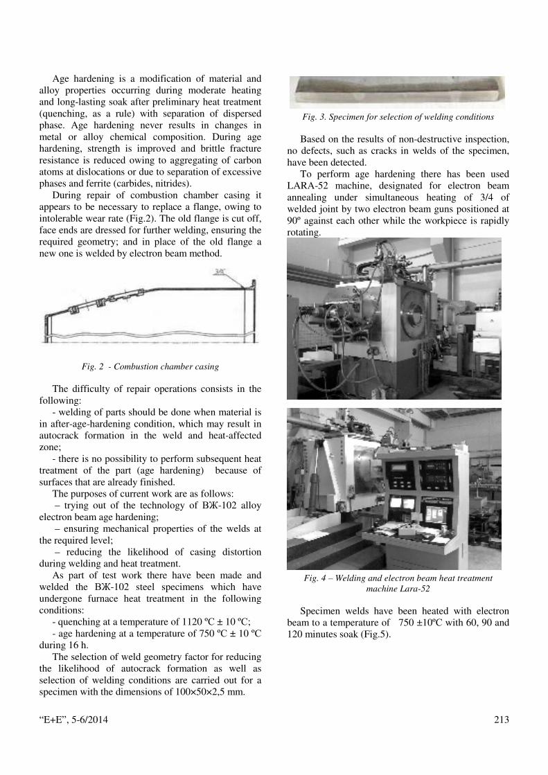
“E+E”, 5-6/2014 213
Age hardening is a modification of material and alloy properties occurring during moderate heating and long-lasting soak after preliminary heat treatment (quenching, as a rule) with separation of dispersed phase. Age hardening never results in changes in metal or alloy chemical composition. During age hardening, strength is improved and brittle fracture resistance is reduced owing to aggregating of carbon atoms at dislocations or due to separation of excessive phases and ferrite (carbides, nitrides).
During repair of combustion chamber casing it appears to be necessary to replace a flange, owing to intolerable wear rate (Fig.2). The old flange is cut off, face ends are dressed for further welding, ensuring the required geometry; and in place of the old flange a new one is welded by electron beam method.
Fig. 2 - Combustion chamber casing
The difficulty of repair operations consists in the following:
- welding of parts should be done when material is in after-age-hardening condition, which may result in autocrack formation in the weld and heat-affected zone;
- there is no possibility to perform subsequent heat treatment of the part (age hardening) because of surfaces that are already finished.
The purposes of current work are as follows: – trying out of the technology of ВЖ-102 alloy
electron beam age hardening; – ensuring mechanical properties of the welds at
the required level; – reducing the likelihood of casing distortion
during welding and heat treatment. As part of test work there have been made and
welded the ВЖ-102 steel specimens which have undergone furnace heat treatment in the following conditions:
- quenching at a temperature of 1120 ºС ± 10 ºС; - age hardening at a temperature of 750 ºС ± 10 ºС
during 16 h. The selection of weld geometry factor for reducing
the likelihood of autocrack formation as well as selection of welding conditions are carried out for a specimen with the dimensions of 100×50×2,5 mm.
Fig. 3. Specimen for selection of welding conditions
Based on the results of non-destructive inspection, no defects, such as cracks in welds of the specimen, have been detected.
To perform age hardening there has been used LARA-52 machine, designated for electron beam annealing under simultaneous heating of 3/4 of welded joint by two electron beam guns positioned at 90º against each other while the workpiece is rapidly rotating.
Fig. 4 – Welding and electron beam heat treatment
machine Lara-52
Specimen welds have been heated with electron beam to a temperature of 750 ±10ºС with 60, 90 and 120 minutes soak (Fig.5).

“E+E”, 5-6/2014 214
Fig. 5. Timing chart of electron beam age hardening of
ВЖ-102 steel welds
Mechanical tests of the welds showed that if the welded specimens are heated with electron beam to a temperature of 750 ±10 ºС and soaked for 60 min. and 90 min., the rupture occurs along the weld and ultimate strength and yield strength of ВЖ-102 steel
falls below the required limit. When the specimens are heated at a temperature of
750±10ºС and soaked during 120 minutes, an improvement of mechanical properties of steel is observed and the rupture occurs in the heat-affected zone of welded joints (Fig. 7).
The specimens mechanical test results are summarized in Table 2.
It can be clearly seen from the table that when the specimens are soaked at a temperature of 750±10ºС during 120 minutes, ultimate strength of the material grows steadily while its ductile properties slightly degrade.
Requirements as to mechanical properties of the welded joints after furnace age hardening are listed in Table 3.
Microstructure of weld and heat-affected zone are shown on Fig. 7.
Fig. 6. Broken specimen appearance Heating - 750 ±10 ºС, soak - 60 min.
Fig. 7. Broken specimen appearance. Heating - 750 ±10 ºС, soak - 120 min.
Table 2. Specimen test results after electron beam age hardening
No
Heatin
g time,
min
Ultimate
strength,
kgf/mm2
Yield
strength,
kgf/mm2
Elongation, % Transverse
contraction, %
Impact
strength, kgf-
m/cm2
НВ,
dent Ø, mm
1 60 87.9 70.7 14.4 33.4 10.00
3.60 87.4 70.7 11.6 33.4 3.5
2 90 87.6 76.4 11.2 39.2 5.5 3.60
3 120 92.3 67.9 12.8 36.0 6.0
- 91.2 66.9 11.2 39.2 5.33

“E+E”, 5-6/2014 215
As it can be seen, no visible changes in parent
metal microstructure occurred in the heat-affected zone. Grain growth is not observed.
Conclusion Implementation of electron beam welding and
electron beam age hardening of the parts which have been in operation and manufactured of ВЖ-102 steel allows performing their repair without degrading the properties of parent metal and weld.
P. D. Zhemanyuk, Motor Sich JSC,
I. A. Petrik, Motor Sich JSC,
О. V. Gnatenko, Motor Sich JSC,
Y. А. Marchenko - Motor Sich JSC, 15, Motorostroiteley Avenue Zaporozhye 69068, Ukraine Phone: +38 (061) 720-48-14 Fax: +38 (061) 720-50-05 Email: [email protected]
Table 3. – Properties of the welds after furnace age hardening
Ultimate
strength,
kgf/mm2,
не менее
Yield
strength,
kgf/mm2,
не менее
Elongation,
%,
minimum
Transverse
contraction,
%
minimum
Impact strength,
kgf-m/cm2
minimum
Brinelle hardness,
dent Ø, mm
minimum -
90 58 6 6 1,5
weld heat-affected zone
Fig. 7. Microstructure of the ВЖ-102 steel welded joint after electron beam age hardening.

“E+E”, 5-6/2014 216
Surface Layer Modification by Large-Area Pulsed Electron Beams
Renate Fetzer, Alfons Weisenburger, Georg Mueller
In liquid metal technology, steel corrosion is a well-known problem. Dissolution of alloying
elements into the liquid metal is prevented by the formation of a protective oxide layer on the steel surface. However, in high temperature applications, oxide layers grow fast, become brittle, and might spall. This can be avoided by surface coatings containing strong oxide formers such as Al in FeCrAl alloys. In order to guarantee long-term stability of the coating, pulsed electron beams are used to melt the coating, together with a few micrometers of the steel surface. Mixing of coating and steel and rapid solidification of the melt lead to a dense surface alloy with metallic bonding to the steel.
For re-melting of metal and metal alloy surface layers, large-area pulsed electron beams with power density 0.5-1.5 MW/cm², electron energy 120 keV and pulse duration 10-50 µs are generated by the GESA facility. Model targets from stainless steel SS 304, aluminum, and copper are used to study the processes of melting, evaporation, melt motion, and re-solidification. Profilometer measurements of the target topography after treatment are presented. The experimental investigations are accompanied by heat transfer simulations including melt motion using the code MEMOS. Although most of the experimental observations are reproduced by the simulations, some phenomena such as liquid splashing, material mixing and the development of surface waviness are not caught by the numerical calculations.
Модификация на повърхностния слой с електронен сноп с голямо напречно сечение (Р. Фецер, А. Уейзенбургер, Г. Мюелер). В технологията с течни метали корозията на стомани е добре известен проблем. Разтварянето на сплавяващи елементи е възпрепятстван от образуването на предпазен оксиден слой на повърхността на стоманата. Обаче, при високо-температурните приложения, оксидният слой расте бързо, става крехък и може да се разчупи. Това може да се избегне от повърхностно покритие, съдържащо силни оксидни формирователи, такива като Al в FeCrAl сплави. За да се гарантира дълготрайна стабилност на покритието, се използва импулсен електронен сноп, за да стопи покритието, заедно с няколко микрона от повърхността на стоманата. Смесването на покритието и стоманата и бързото затвърдяване на течния метал води до плътна повърхностна сплав с металически връзки към стоманата.
За претапяне на метала и металния повърхностен слой от сплавта, импулсен електронен сноп с голямо напречно сечение с плътност на мощност 0,5-1,5 MW/cm²,електронна енергия 120 kеV и продължителност на импулсите 10-50 µs се генерират от устройството GESA. Модели на мишени от неръждаема стомана SS 304, алуминий и мед са използвани за изучаване на процесите на топене, изпарение, смесване и повторно затвърдяване. Представени са измервания с профилометър на топографията на мишената след обработка. Експерименталните изследвания са придружени със симулация на топлинните процеси, включително и разбъркването на течния метал с компютърния софтуер MEMOS. Въпреки, че повечето експериментални наблюдения са репродуцирани от симулациите, смесването на материала и развитието на повърхностни вълни не се хващат от числената симулация.
Introduction The high solubility of steel alloying elements,
especially Ni, in heavy liquid metals (HLM) results in severe dissolution attack when steels are in contact
with HLM. To protect the structural material from corrosion attack, the formation of an oxide layer is targeted, which hinders ion diffusion. The growth of protective oxide scales can be achieved by a suitable level of oxygen in the liquid metal. Typically, a

“E+E”, 5-6/2014 217
multilayer oxide scale is formed on martensitic steel surfaces, consisting of magnetite on top, followed by a dense spinel layer and an internal oxidation zone [1,2]. In high temperature applications, however, the oxide layer grows fast and the brittle magnetite might spall. Therefore, thermally high loaded parts require a slowly growing, dense, and stable protective layer.
Suitable candidates to form thin, stable and protective oxide scales in HLM environment are metal alloys containing strong oxide formers such as Al. FeCrAl alloys have proven their capability to act as a reservoir for the formation of protective thin oxide layers in liquid lead or lead-bismuth environment. Due to their inferior mechanical properties, however, FeCrAl alloys cannot replace steel as structural material. FeCrAl coatings, on the other hand, might suffer from poor bonding to the steel and long term stability cannot be guaranteed. To solve this problem, pulsed electron beams are used to melt the 20-30 µm thick FeCrAl coating, together with a few micrometers of the underlying steel [3]. The large-area electron beams used for the treatment are generated by the GESA facility, with 120 kV acceleration voltage, 10-50 µs pulse duration, and up to 75 J/cm² energy density. Mixing of melted coating and steel and subsequent rapid solidification lead to a dense modified surface layer with metallic bonding to the steel, see Fig. 1. The bulk material remains unaffected by the treatment.
Fig.1. FeCrAl coating on stainless steel melted with pulsed electron beam and solidified into modified surface layer.
The major drawback of the described surface layer melting and alloying process by pulsed electron beam treatment is the topographical pattern that evolves on the target surface. Intense pulsed electron beams with parameters as used above cause the development of a topographical pattern on the target surface with tens of micrometers in height and hundreds of micrometers on the lateral scale. In the present study, the modified surface layers of model
targets from stainless steel, copper, and aluminum are characterized after the treatment; their topography is measured and cross section analysis is performed. The post-treatment analysis is accompanied by heat transfer simulations including fluid dynamics of the melted surface layer.
Methods Pulsed intense electron beams are generated in the
GESA I facility [4], a triode system consisting of an explosive emission cathode, a grid, and a ring-shaped anode. A high-voltage pulse (120 kV) is produced by a Marx generator and supplied to the triode. The homogeneously emitted electrons are guided by a magnetic field. The Gaussian beam profile found at the target surface has a diameter of about 6 cm and a power density of 1-2 MW/cm² in the beam center. The total energy density deposited in the central area can be adjusted to values between 10 and 80 J/cm². Triode and target are placed in a vacuum chamber.
Model targets are 15 x 15 mm² pieces cut from 1.5-2 mm thick sheet metal of stainless steel (SS 304), copper (Cu), and aluminum (AlMg3, 2.5-3.6 wt% Mg). The target surfaces are grinded to a roughness (root mean square) of 0.2-0.3 µm, cleaned with ethanol and mounted in the GESA treatment chamber. Weighing of the samples prior to and after the electron beam treatment allows information about the total material loss. A non-contact white light profilometer (µscan by NanoFocus) based on chromatic aberration is used to measure the topography of the target surfaces. Cross sections are cut from selected samples and analyzed optically and by scanning electron microscopy (SEM) including an attached energy dispersive X-ray detector.
The experimental investigations are accompanied by simulations using the code MEMOS [5], an in-house finite difference code which accounts for volumetric energy deposition of beam electrons into the target material, heat transfer including phase transitions of melting, evaporation, and solidification. Hydrodynamic motion of the melted surface layer is considered by means of a thin film model.
Results and discussion
Target topography
In Figure 2, typical profilometer images [6,7] of various targets after treatment with a GESA electron beam of energy density 56±2 J/cm² are depicted. The topographical pattern depends on the target material. A more or less isotropic pattern of rather regular ripples is observed on stainless steel and copper

“E+E”, 5-6/2014 218
surfaces, with a root mean square roughness Rq of 2.7 µm for SS and 3.9 µm for Cu. In contrast, aluminum shows an irregular pattern with a much larger roughness of Rq= 11.9 µm.
SS Cu Al
Fig.2. Profilometer images (4x4 mm²) of SS, Cu, and Al after treatment with a pulsed electron beam of energy
density 56 J/cm². The height scale is 20 µm for SS and Cu, and 50 µm for Al.
When using the same target material, the surface roughness generally increases with the heat load deposited by the beam, see Figure 3 for data of SS, Cu, and Al after treatment with a single GESA pulse. Due to the large scatter it is not clear whether saturation of the roughness is achieved for very high energy densities.
Fig.3. Roughness of SS, Cu, and Al target surfaces versus
energy density of the respective irradiation pulse.
Evaporation and melt thickness
From simulations, an evaporation rate of up to ~0.1 m/s is expected for SS, Cu and Al, which results in substantial vapor recoil pressure of several bar [7]. Random lateral fluctuations in evaporation and recoil pressure could drive horizontal flow of the melted surface layer, thus inducing hydrodynamic instability.
Due to intense evaporation, a rather dense vapor cloud builds up directly above the target surface. Simulations indicate a neutral density of ~1019 cm-3 [6]. Horizontal flow of vapor particles transfers shear forces to the free melt surface and might cause the development of Kelvin-Helmholtz instability.
Figure 4 (left) shows the total target material loss caused by the pulsed electron beam treatment, together with simulation results [7]. Al targets clearly
experience the highest loss of material in terms of thickness, followed by stainless steel. Cu shows the least amount of lost material.
Fig.4. Experimental and simulation results of material loss (left) and melting depth (right) for SS, Cu, and Al targets versus energy density of the respective irradiation pulse.
For all target materials, the simulation predicts evaporation of less material than lost in the experiments (Fig. 4, left). This is explained by splashing of liquid droplets not accounted for in the simulation, due to either explosive boiling, eruptions around inclusions, or Kelvin-Helmholtz instability. These phenomena add to the complex dynamics of the melted surface layers.
In Figure 4 (right), the melting depths (including the lost material), measured optically from cross sections as well as the predicted values from the simulations, are summarized for SS, Cu, and Al at various beam energy densities [7]. As expected, the melt layer thickness increases for increasing deposited energy density. Stainless steel targets have the thinnest melted layers, followed by Cu. Al targets exhibit the thickest melt layers. The simulation results agree very nicely with the measured data.
Although evaporation and material loss most probably have some effect on the surface topography as discussed above, surface roughness rather scales with the melt layer thickness (comparison of Figs. 3 and 4). Such scaling is generally expected for any hydrodynamic instability of thin liquid films.
Material inhomogeneity
After pulsed electron beam treatment, the cross sections of the targets are imaged by scanning electron microscopy. Results are summarized in Fig. 5 for SS and Al targets. Al without any special high purity grade (AlMg3, left image in Fig. 5) shows many inclusions and precipitates in the bulk material (Mg, Fe, Si, Mn). In the surface layer melted by electron beam treatment, almost none of the described impurities are found. Instead cracks are observed, running mainly perpendicular to the target surface.
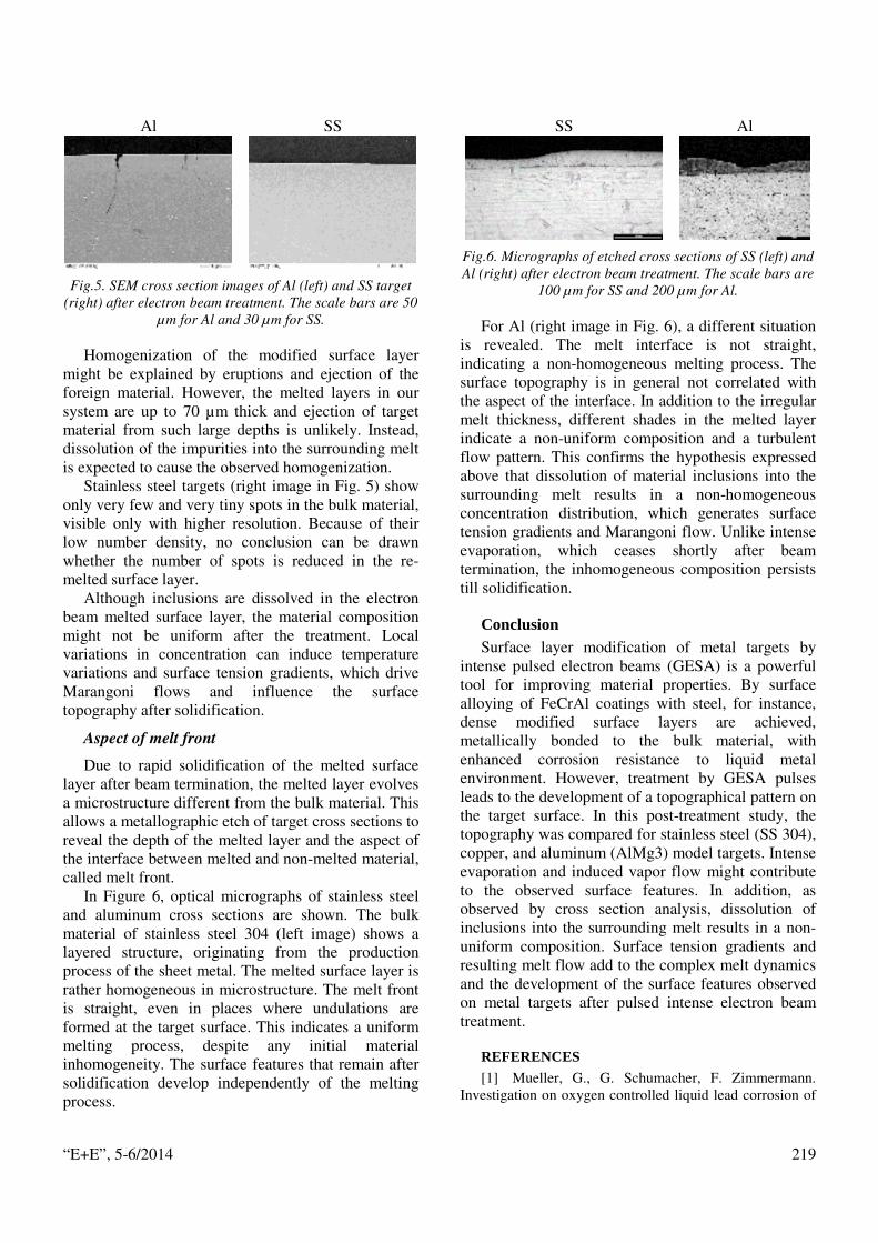
“E+E”, 5-6/2014 219
Al SS
Fig.5. SEM cross section images of Al (left) and SS target (right) after electron beam treatment. The scale bars are 50
µm for Al and 30 µm for SS.
Homogenization of the modified surface layer might be explained by eruptions and ejection of the foreign material. However, the melted layers in our system are up to 70 µm thick and ejection of target material from such large depths is unlikely. Instead, dissolution of the impurities into the surrounding melt is expected to cause the observed homogenization.
Stainless steel targets (right image in Fig. 5) show only very few and very tiny spots in the bulk material, visible only with higher resolution. Because of their low number density, no conclusion can be drawn whether the number of spots is reduced in the re-melted surface layer.
Although inclusions are dissolved in the electron beam melted surface layer, the material composition might not be uniform after the treatment. Local variations in concentration can induce temperature variations and surface tension gradients, which drive Marangoni flows and influence the surface topography after solidification.
Aspect of melt front
Due to rapid solidification of the melted surface layer after beam termination, the melted layer evolves a microstructure different from the bulk material. This allows a metallographic etch of target cross sections to reveal the depth of the melted layer and the aspect of the interface between melted and non-melted material, called melt front.
In Figure 6, optical micrographs of stainless steel and aluminum cross sections are shown. The bulk material of stainless steel 304 (left image) shows a layered structure, originating from the production process of the sheet metal. The melted surface layer is rather homogeneous in microstructure. The melt front is straight, even in places where undulations are formed at the target surface. This indicates a uniform melting process, despite any initial material inhomogeneity. The surface features that remain after solidification develop independently of the melting process.
SS Al
Fig.6. Micrographs of etched cross sections of SS (left) and Al (right) after electron beam treatment. The scale bars are
100 µm for SS and 200 µm for Al.
For Al (right image in Fig. 6), a different situation is revealed. The melt interface is not straight, indicating a non-homogeneous melting process. The surface topography is in general not correlated with the aspect of the interface. In addition to the irregular melt thickness, different shades in the melted layer indicate a non-uniform composition and a turbulent flow pattern. This confirms the hypothesis expressed above that dissolution of material inclusions into the surrounding melt results in a non-homogeneous concentration distribution, which generates surface tension gradients and Marangoni flow. Unlike intense evaporation, which ceases shortly after beam termination, the inhomogeneous composition persists till solidification.
Conclusion Surface layer modification of metal targets by
intense pulsed electron beams (GESA) is a powerful tool for improving material properties. By surface alloying of FeCrAl coatings with steel, for instance, dense modified surface layers are achieved, metallically bonded to the bulk material, with enhanced corrosion resistance to liquid metal environment. However, treatment by GESA pulses leads to the development of a topographical pattern on the target surface. In this post-treatment study, the topography was compared for stainless steel (SS 304), copper, and aluminum (AlMg3) model targets. Intense evaporation and induced vapor flow might contribute to the observed surface features. In addition, as observed by cross section analysis, dissolution of inclusions into the surrounding melt results in a non-uniform composition. Surface tension gradients and resulting melt flow add to the complex melt dynamics and the development of the surface features observed on metal targets after pulsed intense electron beam treatment.
REFERENCES [1] Mueller, G., G. Schumacher, F. Zimmermann.
Investigation on oxygen controlled liquid lead corrosion of

“E+E”, 5-6/2014 220
surface treated steels. Journal of Nuclear Materials, Vol. 278, 2000, pp. 85-95.
[2] Martinelli, L., F. Balbaud-Célérier, A. Terlain, S. Delpech, G. Santarini, J. Favergeon, G. Moulin, M. Tabarant, G. Picard. Oxidation mechanism of a Fe-9Cr-1Mo steel by liquid Pb-Bi eutectic alloy (Part I), Corrosion Science, Vol. 50, 2008, pp. 2523-2536.
[3] Fetzer, R., A. Weisenburger, A. Jianu, G. Mueller. Oxide scale formation of modified FeCrAl coatings exposed to liquid lead. Corrosion Science, Vol. 55, 2012, pp. 213-218.
[4] Engelko, V., B. Yatsenko, G. Mueller, H. Bluhm. Pulsed electron beam facility (GESA) for surface treatment of materials. Vacuum, Vol. 62, 2001, pp. 211-216.
[5] Bazylev, B., H. Wuerz. Melt layer erosion of metallic armour targets during off-normal events in tokamaks. Journal of Nuclear Materials, Vol. 307-311, 2002, pp. 69-73.
[6] An, W., Ya. Krasik, R. Fetzer, B. Bazylev, G. Mueller, A. Weisenburger, V. Bernshtam. Characterization
of high-current electron beam interaction with metal targets. Journal of Applied Physics, Vol. 110, 2011, 093304.
[7] Fetzer, R., W. An, A. Weisenburger, G. Mueller. Surface layer dynamics during e-beam treatment. IEEE Transactions on Plasma Science, Vol. 41, 2013, pp. 2858-2862.
Dr. Renate Fetzer – Karlsruhe Institute of Technology (KIT), Dept. of Pulsed Power and Microwave Technology, PO Box 3640, 76021 Karlsruhe, Germany.
tel.:+49 721 608 24263 е-mail: [email protected]
Dr. Alfons Weisenburger – Karlsruhe Institute of Technology (KIT), Dept. of Pulsed Power and Microwave Technology, PO Box 3640, 76021 Karlsruhe, Germany.
e-mail: [email protected]
Prof. Dr. Georg Mueller – Karlsruhe Institute of Technology (KIT), Dept. of Pulsed Power and Microwave Technology, PO Box 3640, 76021 Karlsruhe, Germany.
e-mail: [email protected]

“E+E”, 5-6/2014 221
Surface Engineering Improvements and Opportunities with Electron Beams
Thomas M. Pinto, Anita L. Buxton, Kevin Neailey, Stuart Barnes
Recent developments at TWI in electron beam technology demonstrate how an electron beam used
at lower power may be employed for a variety of purposes including a novel process, Surfi-Sculpt®. Surfi-Sculpt can neither be described as an additive nor machining process but rather as a process which relies on the interaction between the power beam and the workpiece to locally melt and move the parent material on the surface. This paper describes the mechanism of the Surfi-Sculpt process and discusses potential applications of the technology for heat exchangers and orthopaedic implants. The high level of reproducibility and material properties resulting from the process are addressed.
Подобрения и възможности на повърхностната обработка с електронен сноп (Томас Пинто, Анита Бъкстон, Кевин Ниайли, Стюарт Барнс). Последните разработки в Института по заваряване в Обединеното кралство в областта на електроннолъчевите технологии демонстрират как електронен лъч с ниска мощност може да бъде използван за различни процеси, включително за патентования Surfi-Sculpt. Този процес е нито добавящ, нито фрезоващ процес, а е основан на взаимодействието между мощния сноп и образеца за локално стапяне и предвижване на стопения метал по повърхността. Тази работа описва механизма на Surfi-Sculpt процеса и обобщава някои потенциални приложения на технологията за топлообменници и ортопедични импланти. Обсъдени са високата възпроизводимост и свойствата на материала в резултат на процеса.
Introduction
The Surfi-Sculpt process
When an electron beam interacts with a work piece, a capillary is generated. At the same time, a bulge of material is formed on the surface of the parent material [1].
Surfi-Sculpt® [2] is a novel process which manipulates this ‘bulge’ of the material. The electron beam interacts with the material surface to form a protrusion and a corresponding intrusion when the beam moves over the surface at low power, shown in Fig. 1. Surfi-Sculpt can be utilised to produce an area of features directly formed from the parent material. In order to be able to produce these features, a power beam, such as an electron beam, is deflected rapidly over a substrate surface to displace material in a controlled manner.
Surfi-Sculpt works by the following two means: • When the electron beam is paused temporarily,
rapid melting and evaporation of the parent material occurs giving rise to a partially penetrating capillary surrounded by solidified material;
• The manipulation of the electron beam, using a defined deflection pattern, causes material to be moved in the reverse direction. This harnesses the combined effects of temperature-variant surface tension and vapour pressure at the beam interaction site in order to create a protrusion and intrusion.
Fig.1. Schematic diagram of Surfi-Sculpt process
(reproduced by permission TWI Ltd).

“E+E”, 5-6/2014 222
Fig.2. Example cones produced by Surfi-Sculpt on Ti6Al4V
(reproduced by permission TWI Ltd).
Fig.3. A complex surface produced by multi-stage Surfi-Sculpt on Ti6Al4V (reproduced by permission TWI Ltd).
Fig.4. A honeycomb-like structure created by Surfi-Sculpt on Ti6Al4V (reproduced by permission TWI Ltd).
The success of Surfi-Sculpt is dependent on careful control of the above two means through manipulation
of electron beam parameters including, but not limited to, beam accelerating potential, beam current and focus, to produce features of the desired aspect ratio [3].
As a result, an array of protrusions or features above the original surface and a corresponding array of intrusions or cavities create complex textured surfaces, examples of which are shown in Figs. 2, 3 and 4. High aspect ratio protrusions a few millimetres in height, ridges, channels, cones and burr-free holes can be produced using the process. When interacting with an electron beam, the ability of a material to form a stable liquid phase is critical to the success of the process. To date, the materials which can be successfully processed include metals, polymers, ceramics and glasses. The best results so far, in terms of the quality of feature produced, have been achieved in metals such as stainless steel, titanium and copper. Surfaces can be processed in a matter of seconds per square centimetre.
Surfaces tailored for specific applications can be created due to the capability to significantly vary the size, shape and distribution of the features.
The control system relies upon a pattern of deflection, an example of which is shown in Fig. 5.
Application areas The Surfi-Sculpt process has shown particular
potential in the areas of heat exchange and orthopaedic implants. Work in these areas is described below.
Heat exchange
Previous research by Buxton et al. [4] has shown that, at low Reynolds numbers, there is nearly 50% improvement in the heat transfer coefficient with Surfi-Sculpt surfaces compared to non-textured surfaces. This work is currently under further investigation through an EC funded project ‘HeatSculptor’. This is aiming to create Surfi-Sculpt surfaces based upon thermal modelling to incorporate significant design and performance improvements to heat exchangers which could not be achieved by other traditional manufacturing routes such as milling or etching.
Orthopaedic implants
Interest has been shown in the use of Surfi-Sculpt to enhance the performance of bone/implant interface. Work is currently planned to investigate the following key areas:
• Primary fixation of cementless implants – through the ‘bite’ due to the roughness of the

“E+E”, 5-6/2014 223
surface; • Minimising bone resorption – through load
transfer over wider areas; • Accelerating bony ingrowth from the porosity of
the produced texture. As with all applications, the strength and integrity
of the features are critical, particularly the fatigue properties and the biological response to Surfi-Sculpt features.
Material properties It is recognised that the Surfi-Sculpt process alters
the microstructure of the parent material since it is thought that the microstructure of the protrusion is different to the parent metal due to the melting followed by very rapid cooling rate; however, this can be controlled through modification of the processing parameters [5].
Reproducibility A study was conducted to assess the
reproducibility of Surfi-Sculpt focusing on the following two elements:
• Spacing between consecutive Surfi-Sculpt features;
• Difference in volume of material in a protrusion compared to the volume of material displaced in the corresponding intrusion.
As part of the work, micro computed tomography (µCT) analysis was completed on a small section of
the Surfi-Sculpt sample shown in Fig. 6. Using approximated surface determination, the analysis indicated that the volume of material in the protrusion is similar to the volume of material removed from the intrusion as shown in Fig. 7. Further investigation is required to confirm the cause of the small difference in volume.
The deflection pattern was created with spacing of 4mm between each feature with the layout shown in Fig. 8 [6]. Measurements were taken using a shadowgraph of the feature spacing. The results presented in Fig. 9 show that there is no statistically significant variation (95% confidence limits) in the spacing between features within the rows.
Fig. 6. µCT scan of Surfi-Sculpt sample (reproduced by
permission TWI Ltd).
Fig.5. Screen shot of TWIs control software showing an example deflection pattern (reproduced by permission TWI Ltd).

“E+E”, 5-6/2014 224
Fig. 7. Volume of a Surfi-Sculpt feature and intrusion
(reproduced by permission TWI Ltd).
Fig. 8. Schematic diagram of Surfi-Sculpt feature locations highlighting how the sample was sectioned (reproduced by
permission TWI Ltd).
Fig. 9. Graph of average feature spacing on Surfi-Sculpt
sample (reproduced by permission TWI Ltd).
Summary It has been shown that the Surfi-Sculpt process has
potential for two particular applications discussed in
this paper. A selection of the wide range of possible surfaces has been presented.
The Surfi-Sculpt process offers: • Complex functional surfaces which can be
customised; • Features and intrusions from 10µm to a few mm
in height or depth; • Rapid and flexible processing (cm2/sec); • Applicability to a wide range of materials; • High degree of reproducibility; • Low overall heat input.
Acknowledgements The authors would like to thank the member
companies of TWI Ltd have provided funding for some of this work under TWI’s Core Research Programme. The authors would like to acknowledge funding from the European Union’s Seventh Framework Programme for research, technological development and demonstration under grant agreement no 606172. The µCT analysis was carried out at the University of Southampton.
REFERENCES [1] Meleka, A., Thermal effects. In: Electron-beam
welding: Principles and Practices. London: The Welding Institute by McGRAW-HILL, 1971, pp. 88-89.
[2] International Patent Publication Number WO 2004/028732 A1. ‘Workpiece structure modification’. Applicant: The Welding Institute. Inventors: Bruce Guy Irvine Dance and Ewen James Crawford Keller.
[3] Buxton, A. L. & Dance, B. G. I., The Potential of EB Surface Processing within the Aerospace Industry. Beijing, China, International Conference on Power Beam Processing Technologies, 2010.
[4] Buxton, A. L., Ferhati, A., McGlen, R. J., Dance, B. G. I., Mullen, D. & Karayiannis, T., EB Surface Engineering for High Performance Heat Exchangers. First Int. Electron Beam Welding Conf. Chicago IL, USA 2009
[5] Buxton, A. L., Oluleke, R. & Prangnell, P., Generating and Assessing the Quality and Functionality of EB Structured Surfaces for Dissimilar Material Joints. Aachen, Germany, Proceedings of the International Electron Beam Welding Conference, 2012.
[6] Pinto, T. M., Applied Statistical Methods Post Module Assignment, WMG, University of Warwick, 2013
Mr. Thomas Pinto is a Senior Medical Project Engineer at TWI Ltd. He has an MEng in Biomedical Engineering from the University of Birmingham. He is currently studying for an Engineering Doctorate on the topic of Surfi-Sculpt at WMG, University of Warwick

“E+E”, 5-6/2014 225
He is a Chartered Engineer (CEng), a Member of the Institution of Mechanical Engineers (IMechE), and a Member of the Welding Institute (MWeldI).
tel.: +44 1223 899000 е-mail: [email protected]
Dr. Anita Buxton is a Principal Project Leader at TWI Ltd working in the Electron Beam Processes Section. She has experience and expertise in applying Surfi-Sculpt to the heat exchanger market and has coordinated collaborative projects in the area of Surfi-Sculpt surface processing.
Anita Buxton is a Chartered Engineer and a Member of the IOM3.
tel.: +44 1223 899000 е-mail: [email protected]
Prof. Kevin Neailey has been at WMG, University of Warwick for over 25 years. His interests are in advanced processes and risk management.
tel.: +44 2476 524762 е-mail: [email protected]
Dr. Stuart Barnes is Director of Research Degrees for WMG, University of Warwick. He is a metallurgist by profession and has researched in the areas of laser processing and conventional machining.
He is a Chartered Engineer, a Fellow of the IOM3, a Member of the IET.
tel.: +44 24 7652 3134 е-mail: [email protected].

“E+E”, 5-6/2014 226
Optical and Structural Investigations of WOx Thin Films Deposited by Electron Beam Evaporation Process
Katia Vutova, Vania Vassileva, Alexander Stoimenov, Elena Koleva, Tatyana Ivanova, Georgi Bodurov, Kostadinka Gesheva, Georgi Mladenov
Thin films of tungsten oxide are obtained at different technological parameters using electron
beam evaporation process. Their optical and structure properties are investigated and the relation with process parameters is discussed. Optical transmittance of 75 % of as-deposited WOx films is achieved and found to be dependent on deposition process parameters. The electron beam power is found to be decisive parameter for the thin film surface roughness.
Оптично и структурно изследване на WOx тънки слоеве, отложени чрез електронно лъчево изпарение (К. Вутова, В. Василева, А. Стоименов, Е. Колева, Т. Иванова, Г. Бодуров, К. Гешева, Г. Младенов). Получени са тънки слоеве от волфрамов оксид чрез електроннолъчево изпарение при различни технологични условия. Оптическите и структурни характеристики на слоевете зависят силно от стойностите на технологичните параметри. Оптическа прозрачност от 75 % е измерена за свежо отложени WOx слоеве и е установена зависимост от условията на отлагане на слоевете. Мощността на електронния сноп е важен фактор за повърхностната грапавост на слоевете.
Introduction Transition metal oxides possessing specific
electronic structure are capable to exhibit electrochromic effect. This effect is defined as a change in the transmittance of the oxide film upon a small voltage applied across the film. Visually the film colors, and bleaches back to the initial transparence, if the voltage polarity is changed.
The effect has been first observed in WO3 by Satyen Deb [1]. A number of investigations have been carried out, and a valuable Handbook of Inorganic Electrochromic Materials by Claes-Goran Granqvist appeared [2]. A monography on fundamentals and applications of electrochromism was written by P.M.S. Monk, R.J. Mortimer, D. R. Rosseinsky [3]. Different techniques have been employed to deposit WO3 tungsten oxide films, and other types of transition metal oxides such as MoO3, TiO2, Cr2O3, etc. More recent book on Thin film Optical Coatings for Effective Solar Energy Utilization, Ed. K.A.Gesheva [4], describes results on electrochromic thin film materials produced by chemical vapor deposition at atmospheric pressure (APCVD) technology. The book [5] by G.Smith and C-G.Granqvist includes a profound description of the light and nanostructures interactions in all the aspects
related to spectral properties of uniform materials. The electrochromic device (ECD) is described as a functioning device. A standard device of an EC device as given in [2] is described as five layers backed by one substrate or positioned between two substrates, normally glass.
Practically ECD is two conductive glass substrates over one of which our transition metal oxide film is deposited, and over the second conductive glass an ion storage film is deposited. Usually, the second conductive glass is bare, and the two glass substrates are laminated by polymeric electrolyte with inserted Li (or other alkali ions) ions. If a small voltage is applied at the conductive glasses electrical charge transfer starts in the device: electrons from the conductive electrode are injected in the oxide film structure, ions from the electrolyte intercalate into the film structure, and this temporary film structure becomes absorptive, absorbs part of the solar light falling on the film, and coloring appears (a nice blue color for WO3). If the polarity of the applied voltage is changed the electrical charge goes back, and the device bleaches up.
An intensive research has been going in the last decades, at present the concerns are related to the comparatively high price of electrochromic devices, especially if applied as “Smart windows” in car

“E+E”, 5-6/2014 227
industry or solar buildings. The large area of window glazing requires cheap technology, stability, good adhesion, long cycling times. Employing new technologies is continuing. In the present work first experimental results for WOx thin films by electron beam deposition process are presented. Tungsten evaporation at different technological regimes is performed and the optical and structural characteristics of the deposited films are presented and discussed.
Experimental Electron beam (EB) deposition [6] of thin films in
vacuum allows fabricating high quality monolayers, sophisticated multilayer structures, new material and nano-structured products. The deposition of thin films using electron beam evaporation is the most widely used process among the technologies utilizing electron beams: electron lithography of submicron and nanometers patterns in micro- and nano-electronics, electron beam melting and refining of pure metals and alloys, electron beam welding of machine parts, modification of surfaces using thermal EB treatment, polymerization and cross-linking of polymer materials and coatings, production or sterilization of bio-products under electron bombardment. Thin films are largely used in electronic industry for metallization, isolation coatings, antireflection coatings and filters used in optics, some applications are known for space industry, as well as tool industry. At EB evaporation the utilization of water-cooled mold (crucible), where the evaporation material is situated and the electron beam heats directly the liquid pool surface, makes this technology with some advantages. The heat losses decrease due to lack of pre-heating stage. Another important advantage is the lack of impurities usually initiating from the used mold material. In addition the electron beam evaporation process offers possibility for growth-rate regulation by temperature changes in the liquid metal. This can be controlled by electron beam power, beam focusing and beam moving on the liquid metal surface [6].
In the present study first experiments for deposition of tungsten oxide thin films are performed utilizing electron beam deposition process. The employed machine is ELIT-60 equipped with one electron gun with power of 60 kW, accelerated voltage of 25 keV, working pressure in the vacuum chamber of 10-4 - 10-5 mbar. The electron beam was focused and the beam diameter was Φb = 20 mm. A pure tungsten rod (purity of 96%) was used as evaporation material. Oxidation is expected to proceed due to oxygen in the source material and the vapor
pressure of the residual oxygen in the vacuum chamber.
For each technological parameters combination (see Table 1), conductive glass substrate was used, and Si substrate, for Infrared and Raman measurements in transmittance mode. The following technological parameters were varied: the power of the electron beam (Pb), and evaporation time duration (τ). Their values are presented in Table 1, where H and L are the height and the radial distance of the sample position regarding the water-cooled copper crucible (where the evaporation material is situated).
Table 1. Technological parameters used in deposition of tungsten
oxide films on conductive glass substrates.
sample number
Pb, kW τ, min H, mm
L, mm
2 10.0 10 0 250 3 7.5 10 0 250 4 10.0 2 0 250
Optical characterization
Visible transmittance
The films deposited on Donnely type conductive glass substrates were subjected to optical transmittance measurements by SHIMADZU UV-VIS-NIR Spectrophotometer UV 3600.
300 400 500 600 700 800 9000
10
20
30
40
50
60
70
80
0
10
20
30
40
50
60
70
80
Sample 4
Sample 3
Reflectance [%
]Tra
nsm
ittan
ce [%
]
Wavelength [nm]
Sample 2
Fig. 1. VIS range transmittance of WOx deposited by electron beam evaporation at different technological
parameters (see Table 1).
The highest transmittance (see Fig.1) is found for sample 3, which is deposited for 10 minutes evaporation time at 300 mA, corresponding to 7.5 kW beam power. Transmittance of 75 % is high enough, suggesting high optical modulation and color

“E+E”, 5-6/2014 228
efficiency. These are the two basic electrochromic characteristics.
In the same figure the reflectance curves for the three samples are also presented. The reflectance values are below 5%, which shows that the films have smooth surfaces.
400 600 800 1000 1200 1400 1600 18000
10
20
30
40
50
60
70
80
90
100
0
10
20
30
40
50
60
70
80
90
100
Sample 4
Sample 3
Reflectance [%
]Tra
nsm
ittan
ce [%
]
Wavelength [nm]
Sample 2
Fig. 2. Optical transmittance in the visible and near infrared region for electron beam evaporated WOx thin
films
VIS-NIR infrared spectra are also measured and the results are presented in Fig.2. As can be seen the
reflectance starts decreasing at wavelength value higher than 900 nm.
400 500 600 700 800 900 1000 1100 1200
945
675
444
Sample 4
Sample 3Abs
orba
nce
[arb
.u.]
Wavenumber [cm-1]
Sample 2430
598
865
Fig.3. FTIR spectra of electron beam deposited WOx films, obtained at different technological conditions.
Infrared spectra measurements
The infrared spectra were measured on SHIMADZU FTIR Prestije-21, supplied with SHIMADZU specular reflectance attachment SRM-8000.
Table 2. Analysis of infrared absorbance bands of tungsten oxide thin films deposited by electron beam evaporation
(as described in Table 1).
Sample 2 Sample 3 Sample 4 Assignment 3727. 3 clear 3719.8 clear 3727 clear Stretching vibration of hydroxyl groups 3413.2 clear 1629 weak 1638 weak 1641 weak Bending mode of OH groups 998.1 weak
broad W=O terminal bonds
945 clear W=O terminal bonds 881 broad, weak
865 broad strong
W-O-W bridging mode
802 very weak stretching W-O modes of the crystal monoclinic structure of WO3
730 shoulder 729.3 clear W=O bending vibrations 673.5 strong 675 very
strong 675 strongest W–O–W stretching modes; which are assigned to the
stretching ν(O–W–O) modes of bridging oxygens of WO6 octahedra Monoclinic crystal structure of WO3
603 clear 601 clear disordered W-O framework 512.9 weak
444 clear 444 clear 444 clear W- O stretching mode 430 430

“E+E”, 5-6/2014 229
Due to vibration of atoms at chemical bonds, in the spectra characteristic absorption bands appear situated at specific points. We are looking to see the W-O bonds in different configurations depending on the structural modification of tungsten oxide. It is known that this material may exist in monoclinic or triclinic modifications. We note here that there is water incorporated in the films, characterized by the peaks at 3100 and 3500 cm-1 – stretching vibrations of hydroxyl groups. Very often absorbed from the air carbon dioxide exist in the films, and the characteristic peak for CO2 appears at 2900 cm-1.
FTIR study (see Fig.3 and Table 2) reveals that the observed absorption bands are characteristic for tungsten trioxide. A crystalline phase can exist in the film structure as there is IR lines which could be attributed to monoclinic WO3.
The IR bands below 400 cm-1 are due to bending vibrations δW-O [7]. Absorption bands at 653 cm-1 and 795 cm-1 are related to the stretching W-O modes of the crystal monoclinic structure of WO3 [8]. The absorption at 963 cm-1 is connected with WO terminal modes of surface grains. For comparison, FTIR spectra of sprayed and sol-gel WO3 films are very similar, revealing similar absorption bands. More pronounced absorption bands of the sprayed sample are ones in the spectral range 350-460 cm-1. The analysis of infrared absorbance bands of investigated WOx thin films as seen from Table 2 show a variety of peaks assigned to different modes – bridging, banding, stretching. Most pronounced is the strong absorption band at 675 cm-1, observed in the three studied samples revealing W–O–W stretching modes assigned to the stretching ν(O–W–O) modes of bridging oxygens of WO6 octahedra of monoclinic crystal structure of WO3 FTIR
.Atomic force microscopy studies The surface morphology of tungsten oxide thin
films (samples 3 and 4) was investigated by AFM measurements carried out using a Multimode V (Bruker Corporation Inc., Santa Barbara, CA). Imaging was performed in tapping mode and height, amplitude, and phase images were recorded. Scan rate was 1.7 - 2 Hz, the images resolution was 512 lines per scan direction. At least two different points on the sample surface were explored. Silicon cantilevers with a cantilever length of 125 µm and Al reflective coating on the backside (MPP-11120-10, Bruker) were used in the experiments. MPP-11120-10 probes have a nominal resonance frequency of 300 kHz and a typical force constant of 40 N/m. The tip nominal
radius for these probes is less than 10 nm. Roughness analysis was performed by means of Nanoscope 7.30 program. For this purpose, images were just flattened and no further processing was performed.
The AFM surface roughness estimations show that by changing the technological parameters the surface roughness of the films can be controlled. The calculated respective values for the surface roughness of WOx samples number 3 and 4 (Table 1) are 0.333 nm and 1.07 nm, respectively. Obviously the beam power is a decisive process parameter leading to rougher surface film for much shorter e-beam evaporation times.
a)
b)
Fig. 4. Three-dimensional AFM surface images of two WOx thin films, as numbered 3 (a) and 4 (b).
Conclusions By electron beam evaporation thin films of
tungsten oxide on conductive glass substrates are obtained at different technological parameters. It has been shown in our experiments, that the structure and optical properties of the films can be changed, and optimized with respect to electrochromic effect. For achieving better quality, good adhesion, uniformity and required thickness, in our future experiments special attention will be paid to improve the process conditions and the source material, namely better

“E+E”, 5-6/2014 230
shaped liquid pool of the evaporation metal assuring larger evaporation surface.
Acknowledgements This research was funded by the Bulgarian Science
Fund under contract DO 02-127 (BIn-5/2009) and partially supported by INERA project – Institute of solid state physics-BAS (ISSP-BAS). The authors express their thanks to Dr. Irina Bineva (ISSP-BAS) for AFM measurements.
REFERENCES [1] Satyen Deb in 1969 (S. K. Deb, Appl. Opt. Suppl.
1969, vol. 3193)
[2] Claes-Goran Granqvist, Handbook of Inorganic Electrochromic Materials, Elsevier, Amsterdam, 1995
[3] P.M.S. Monk, R.J. Mortimer, D. R. Rosseinsky, Electrochromism, Fundamentals and Applications, VCH, 1995.
[4] Thin film Optical Coatings for Effective Solar Energy Utilization, edited by K. A. Gesheva, Novapublishers, N.Y.2008
[5] Geofrey B. Smith, Claes G. Granqvist, Green Nanotechnology, published by CRC Press, Taylor and Francis Group, 2011
[6] G.Mladenov, Electron and Ion Beam technologies, Prof. Marin Drinov Academic Publ.house BAS, 2009
[7] G.N. Kustova, Yu.A. Chesalov, L.M. Plyasova, I.Yu. Моlinа, A.I. Nizovskii, Vibrational Spectroscopy 55 (2) (2011) 235–240
[8] J. Sungpanich, T. Thongtem, S. Thongtem, Ceramics International 38 (2012) 1051–1055
Prof. DSc. Katia Vutova – Institute of Electronics, Bulgarian Academy of Sciences, 72 Tzarigradsko shosse blvd., 1784 Sofia, Bulgaria
tel: +359-2-9795900; e-mail: [email protected]
Assoc. Prof. PhD Vania Vassileva – Institute of Electronics, Bulgarian Academy of Sciences, 72 Tzarigradsko shosse blvd., 1784 Sofia, Bulgaria
tel: +359-2-9795922; e-mail: [email protected]
Alexander Stoimenov – technical stuff, Institute of Electronics, Bulgarian Academy of Sciences, 72 Tzarigradsko shosse blvd., 1784 Sofia, Bulgaria;
tel: +359-2-9795922; e-mail: [email protected]
Assoc. Prof. Dr. Elena Koleva - Institute of Electronics, Bulgarian Academy of Sciences, Bulgaria, 72 Tzarigradsko shosse blvd., 1784 Sofia, Bulgaria tel: +359 895537899, е-mail: [email protected]
Georgi Bodurov – PhD student, Central Laboratory of Solar Energy and New Energy Sources, Bulgarian Academy of Sciences, 72 Tzarigradsko shosse blvd., 1784 Sofia, Bulgaria
tel: +359-2-9795947; e-mail: [email protected]
Assoc. Prof. Dr. Tatyana Ivanova – Central Laboratory of Solar Energy and New Energy Sources, Bulgarian Academy of Sciences, 72 Tzarigradsko shosse blvd., 1784 Sofia, Bulgaria
tel: +359-2-9795947; e-mail: [email protected]
Prof. DSc. Kostadinka Gesheva – Central Laboratory of Solar Energy and New Energy Sources, Bulgarian Academy of Sciences, 72 Tzarigradsko shosse blvd., 1784 Sofia, Bulgaria
tel: +359-2-9795947; e-mail: [email protected]
Corr. Memb. of BAS, DSc. Georgi Mladenov - Institute of Electronics, Bulgarian Academy of Sciences, 72 Tzarigradsko shosse blvd., 1784 Sofia, Bulgaria,
е-mail: [email protected]
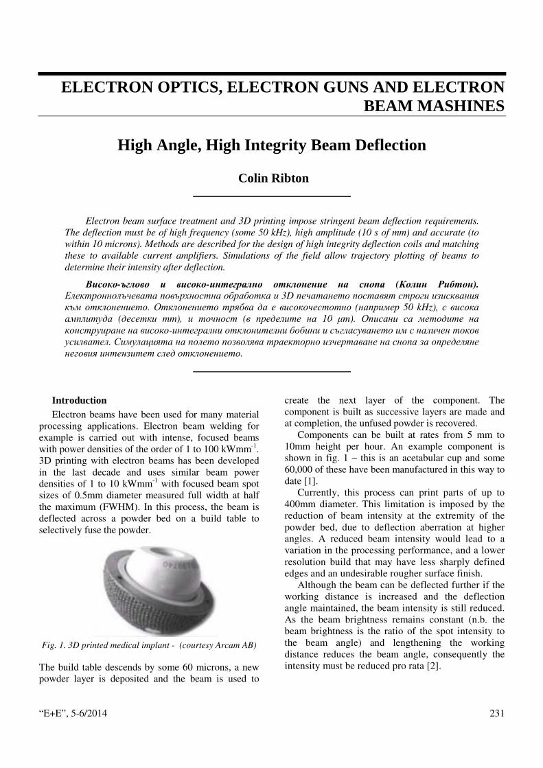
“E+E”, 5-6/2014 231
ELECTRON OPTICS, ELECTRON GUNS AND ELECTRON BEAM MASHINES
High Angle, High Integrity Beam Deflection
Colin Ribton
Electron beam surface treatment and 3D printing impose stringent beam deflection requirements. The deflection must be of high frequency (some 50 kHz), high amplitude (10 s of mm) and accurate (to within 10 microns). Methods are described for the design of high integrity deflection coils and matching these to available current amplifiers. Simulations of the field allow trajectory plotting of beams to determine their intensity after deflection.
Високо-ъглово и високо-интегрално отклонение на снопа (Колин Рибтон). Електроннолъчевата повърхностна обработка и 3D печатането поставят строги изисквания към отклонението. Отклонението трябва да е високочестотно (например 50 kHz), с висока амплитуда (десетки mm), и точност (в пределите на 10 µm). Описани са методите на конструиране на високо-интегрални отклонителни бобини и съгласуването им с наличен токов усилвател. Симулацията на полето позволява траекторно изчертаване на снопа за определяне неговия интензитет след отклонението.
Introduction Electron beams have been used for many material
processing applications. Electron beam welding for example is carried out with intense, focused beams with power densities of the order of 1 to 100 kWmm-1. 3D printing with electron beams has been developed in the last decade and uses similar beam power densities of 1 to 10 kWmm-1 with focused beam spot sizes of 0.5mm diameter measured full width at half the maximum (FWHM). In this process, the beam is deflected across a powder bed on a build table to selectively fuse the powder.
Fig. 1. 3D printed medical implant - (courtesy Arcam AB)
The build table descends by some 60 microns, a new powder layer is deposited and the beam is used to
create the next layer of the component. The component is built as successive layers are made and at completion, the unfused powder is recovered.
Components can be built at rates from 5 mm to 10mm height per hour. An example component is shown in fig. 1 – this is an acetabular cup and some 60,000 of these have been manufactured in this way to date [1].
Currently, this process can print parts of up to 400mm diameter. This limitation is imposed by the reduction of beam intensity at the extremity of the powder bed, due to deflection aberration at higher angles. A reduced beam intensity would lead to a variation in the processing performance, and a lower resolution build that may have less sharply defined edges and an undesirable rougher surface finish.
Although the beam can be deflected further if the working distance is increased and the deflection angle maintained, the beam intensity is still reduced. As the beam brightness remains constant (n.b. the beam brightness is the ratio of the spot intensity to the beam angle) and lengthening the working distance reduces the beam angle, consequently the intensity must be reduced pro rata [2].

“E+E”, 5-6/2014 232
A larger powder bed could be used if it were possible to deflect the beam to higher angles with lower aberration. Larger parts could then be built, allowing a broader range of applications to be addressed by the 3D printing process. Alternatively, more parts could be built simultaneously which makes a higher production rate from the machine – which can lower manufacturing costs significantly.
Similarly, for electron beam surface modification the beam must be of high intensity and is deflected at high frequency to melt and move material. The deflection system will be able to cover a patch on the work piece, which is up to 80×80 mm. When areas larger than a patch are required to be treated, the process has to be repeated and patches are knitted together. In these cases being able to deflect the beam at higher angle and maintain intensity would increase the production rate and subsequently reduce process cost.
Consequently, there are strong drivers for the development of high integrity, high angle beam deflection for the 3D printing and electron beam surface treatment processes.
Deflection coil design Deflection systems comprise a coil set (usually an
X and Y pair of coils) and a magnetic yoke. The coils are driven with a current to generate a magnetic field through which the electron beam passes and by which the electron trajectories are deflected. The magnetic yoke contains the field outside the beam path to prevent it passing through nearby metallic components. If this measure were not taken eddy currents would be generated in any conductors that the field passed through and the frequency response of the system would be reduced. The yoke also increases the amplitude of the field produced. The yoke must be made of a material with soft magnetic properties for accuracy and must have low electrical conductivity so that it has a high frequency response. The soft magnetic properties lead to low remanence fields that will ensure that the yoke does not get magnetised so that the accuracy of the landing position of the beam is maintained. The low conductance ensures that eddy currents are not produced in the yoke, which would otherwise reduce magnetic field at higher frequencies and thereby reduce beam deflection response at high frequency.
For bespoke coil designs the yoke is usually made from one or more rings of material, as the magnetic material is supplied in a limited variety of shapes and machining can be difficult and can affect the magnetic properties – particularly magnetic softness. Rings are
available in many sizes as they are widely required in the electrical industry for toroidal inductor and transformer cores.
The deflection amplitude obtained is a function of the field strength and the length of the beam trajectory through the field. As electrons pass through a field of strength B transverse to their direction they are acted upon by the Lorentz force [3], [4] and deflected into a circular path with a radius R given by:
(1) ∙
where: e is the electron charge p the electron momentum is given by
(2) where:
m0 is the electron rest mass V the acceleration potential
and:
(3) ε =
where c is the velocity of light in vacuum.
Fig. 2. Electron trajectory through a uniform transverse
field (reproduced by permission TWI Ltd)
The angle of the deflection, θ, can be found in terms of the length of the field along the direction of the beam axis and the beam bend radius – symbols are defined in fig. 2.
(4) The apparent position of deflection can be found
from:
(5) !
"#$%
In reality, this method provides a good approximation, although end effects and the non-

“E+E”, 5-6/2014 233
uniform distribution of the B field can cause small discrepancies between the calculated value and the value found from experiment.
To achieve the necessary magnetic field to produce a required deflection amplitude, a coil must be energised with a specific ampere-turns (the product of current and number of coil turns). This can be achieved for example with a few turns of high current or many turns of low current. The former is a low inductance configuration and requires a high current amplifier although this can be a lower voltage drive. The latter is a high inductance configuration and requires a high voltage driver although this can have a lower current capability. For a given magnetic circuit, for all coil energisations producing the same field and therefore the same beam deflection, the energy stored in the field is the same. In this work, by determining this stored energy, either through modelling of the coils, or through practical measurements on prototype deflection coils, it is demonstrated how to select the optimum coil turns to give the required field from a suitable coil current and the best inductance to impedance match to the deflection amplifier to give the highest frequency response. A plot is produced of the current vs. coil inductances that allows the optimum coil to be selected.
Finite element model In this example, a finite element field modeller [5]
has been used which can produce a 3 dimensional field distribution for a certain configuration and coil energisation. The software has the ability to plot electron trajectories through this field to indicate the beam deflection. During the design process the coil configuration and yoke size can be adjusted and the effect on the beam deflection observed. Once the required design is optimised it is then possible within the modelling software to integrate the field (H) across the model volume (v) to derive the energy (E) stored in the coil set.
(6) & ''()*)+
This energy is stored in the charged inductance and is equivalent to
(7) & ,∙-./
where: L is the coil inductance I is the coil currentл Consequently, the relationship between the
inductance and the current required to obtain the modelled deflection is:
(8) 0 1/∙''23435,
The modelling software uses a coil of a specified energisation, ϵ, which may be realised by many turns (n) of a low current or fewer turns of higher current.
(9) 0 6$
Prototyping As an alternative to using a finite element model it
is possible to derive the relationship between the inductance and the number of coil turns experimentally for a particular coil configuration and yoke. A prototype assembly is made by winding a coil and positioning it in the yoke. The number of turns is chosen to be convenient so that it can be energised with an available current source. The current required to obtain the specified deflection is determined by measuring the magnetic field in the area of the beam path, fig. 3, and comparing this value with the field estimated from calculation as shown in equations (1) to (5). The current can be adjusted to give the field estimated to be that required to produce the necessary deflection. Following this test the coil inductance is determined using an inductance bridge. Knowledge of the current and the inductance allows the energy stored to be determined for that particular magnetic field value, using equation (7).
Fig. 3. Prototyping to estimate the stored energy
(reproduced by permission TWI Ltd)
Impedance matching As described in the previous section, the current –
inductance relationship for the deflection coil can be derived for the maximum required deflection amplitude. Fast deflection requires the current to be established in the coil and the amplifier must have sufficient voltage (Vd) available to overcome the frequency (f) dependent impedance:

“E+E”, 5-6/2014 234
(10) 0 7/∙8∙9∙,
Amplifiers may also have a safe working area that is a relationship between the voltage and current. Figure 4 shows an example of the maximum current available from a 90 V rail amplifier at frequencies of 8 and 100 kHz. These limits are plotted with the line of constant field required to give a deflection of 56mm amplitude at 235 mm working distance (but with a range of values for the number of turns and consequently a range of inductance values).
Fig. 4. Example of current – inductance relationship for a coil and amplifier (reproduced by permission TWI Ltd.)
The amplifier will only be able to drive the deflection coil to give a specified deflection amplitude and frequency where the current for the required field is lower than the maximum current capability of the amplifier. In this case a coil of inductance less than 0.4 mH is required if it is to be driven at up to 8 kHz. This will require a drive current of 4.8 A. It also shows that at a frequency of 100 kHz this amplifier would be incapable of driving even the lowest coil inductances plotted (0.05 mH) to give the required deflection amplitude, as the current required would be over 10 A but the maximum from the amplifier at this frequency would be under 3A.
As the coil excitation must be constant along the line of constant field, the number of turns required to produce the inductance is readily determined from the ratio of this excitation to the coil current required at the selected inductance value. In the example shown in fig. 3, the coil excitation in the model to give this deflection was 96 A-turns, so a 0.4 mH coil requiring 4.8 A had 20 turns.
Deflection Coil Aberration and Correction The field distribution close to the centre of a
deflection coil with a ring yoke is near constant and which determines the circular path of an electron trajectory as it passes through this region. However, when a number of near parallel trajectories enter this
field the beam emerging from the deflection coils is no longer near parallel due to the focusing effect of the field [3]. The effect is exacerbated as the beam width increases. On the other hand, to maximise intensity at the surface of the powder bed or work piece for processes such as 3D printing and surface modification, a high angle beam is used, leading to a broad beam width in the deflection coils. As the beam is deflected away from the axis of the deflection coils the field may not stay constant. This has been modelled and a beam current density plot at the work piece surface is shown in fig. 5(a) for a square array of parallel trajectories, originally 6x6mm that have been deflected 60mm off-axis in both the X and Y directions over a working distance of 500 mm. The aberration from the coil field has caused flaring of the spot which has lost its original square shape (nb a square beam is not used in this application but is a useful diagnostic to indicate the extent of the beam aberration produced by the field).
(a) Conventional deflection coil - 60mm off-axis
(b) Modified deflection coil – 90 mm off-axis
Fig. 5. Beam current density plots – arbitrary units (reproduced by permission TWI Ltd.)
Although the field can be made more even across the beam trajectory path by enlarging the deflection coil bore, this inevitably leads to a higher inductance or current required to obtain the same deflection and consequently can lead to a reduced high frequency performance.
An approach used in particle accelerator and

“E+E”, 5-6/2014 235
nuclear magnetic resonance scanner designs is to use a ‘cosine (theta)’ winding pattern [6]. This involves a number of nested coils with different excitations and can be achieved practically by winding coils with a different number of turns and putting these in series. This was simulated for the same core geometry using 6 nested coils. The resulting field was much more even with field variation of less than 0.5% across 90% of the bore, compared with more than 10% for a conventionally wound coil. The beam current distribution after deflection – shown in fig. 5(b) – was much closer to the original square array of trajectories. It should also be noted that the beam footprint is being taken on the plane of the work piece and not in a plane perpendicular to the beam axis after deflection – so the footprint of a non-aberrated beam would be diamond shaped when viewed on the work piece surface plane. The advantages of this design of coil are apparent for high angle and high intensity beam deflection applications.
A number of these design of coils have been built and have been tested for electron beam texturing with excellent processing results, allowing larger angle deflection to be used without compromising the beam intensity.
Conclusions From the research and development reported in
this paper the following conclusions can be drawn: • High frequency, accurate and low aberration
beam deflection is required for 3D printing and surface modification by electron beams;
• Calculations have been described to allow estimation of the field required to produce a desired beam deflection;
• A design methodology has been developed for deflection coils to allow matching to amplifiers and optimisation of high frequency performance;
• The use of cosine(theta) winding distributions has been demonstrated to reduce beam aberration at high deflection angles.
REFERENCES [1] Ljungblad, U ‘Additive Manufacturing with EBM
- The Route to Production’ IFAM Industry Day February 2014
[2] Ribton, C N ‘Effective design of electron beam processing systems by trending’ Electrotechnica & Electronica E+E, 5-6, Sofia 2012
[3] Pierce, J R ‘Theory and Design of Electron Guns’ D. Van Nostrand Company, New York 1949
[4] Klemperer, O ‘Electron Physics’ Butterworth Scientific Publications, London 1959
[5] Software Opera-3d V15R3, Cobham Technical Services, Vector Fields Software, 2012
[6] Kwok, H M et al ‘Magnetic Field Studies of a Cos(theta) Coil’ SURE report, The Chinese University of Hong Kong, 2005
Colin Ribton - graduated from The University of Nottingham with a joint honours degree in pure and applied physics and later joined TWI’s Electron Beam group. He has also led development in a company developing novel antenna technologies, where he became Vice President of Application Engineering.
His roles at TWI have involved him in the computer modelling of electron optics and high voltage components, the design of high voltage power supplies, the design and optimization of radiation shielding, real-time control system architecture, and the design of digital and analogue electronics. In particular, this has been involved in the development of equipment and processes to manufacture major components in power generation, nuclear, aerospace and medical applications. He is presently a Technology Consultant in the EB group where he is active in promoting EB technology for new applications.
Colin Ribton is a Chartered Physicist (CPhys), a Chartered Engineer (CEng), a Member of the Institute of Physics (MInstP), and a Member of the Welding Institute (MWeldI).
е-mail: [email protected]

“E+E”, 5-6/2014 236
Source of Radial Converging Electron Beam for Modification of Long-Length Cylindrical Targets
V. Engelko
In previous period it was created a method of improving corrosion resistance of construction
steel tubes situated in liquid heavy metal coolants (as example Pb and Pb-Bi used in nuclear reactors). At beginning on the steel surface is deposited a layer from Al or Al-containing alloys in order to create Al2O3 barrier preventing the interaction of the steel with the liquid coolants. Then the surface layer and layer of the steel surface are melted by irradiation with microsecond pulse intense electron beams. For realization and optimization of this process a pulsed electron beam experimental facility GESA-4 was designed. In the paper are discussed main problems and achievements of developed facility.
Източник на радиално-събиращ се електронен сноп за модификация на дълги цилиндрични мишени (Владимир Енгелко). В предишния период бе създаден метод за подобряване на корозионната устойчивост на тръби от конструктивна стомана, намиращи се в корозивни течни тежки метали (например Pb и Pb-Bi използвани в ядрените реактори). Първоначално върху стоманената повърхност се отлага слой от Al или Al-съдържаща сплав с цел да образува Al2O3 бариера, предпазваща от взаимодействие с течния метал. Тогава повърхностния слой и слоя на повърхността на стоманената мишена се топят от облъчване на микросекунден импулсен електронен сноп. За реализация и оптимизация на този процес една импулсна електроннолъчева експериментална апаратура GESA-4 бе конструирана. Вработата се дискутират главните проблеми и постижения на разработеното устройство.
Introduction Over a period of years cooperation of teams from
KIT (Karlsruhe, Germany), Efremov Inst. of Electrophysycal Apparatus (St. Petersburg, Russia), A.I.Leypunsky Inst. For Physics and Power Engineering. (Obninsk, Russia) develop a method of improving corrosion resistance of construction steels in liquid heavy metal coolants (LHM) consisting in saturation of the steel surface layer by Al in order to create Al2O3 barrier preventing the interaction of the steel with LHM [1,2]. A thickness of the modified layer is 15-20 µm. The bulk of the steel keeps its initial mechanical and technological properties. The procedure consists in two steps: (i) coating the steel surface with Al or Al-containing alloy and (ii) melting both the coating and the steel surface by irradiation with microsecond intense electron beams (MIEB). Such treatment (so called GESA process) causes the mixing of the steel elements with the coating elements, finally leading to a modified Al-containing layer on the steel surface.
Main results of studies performed up to now are
the following [3]. The optimal procedural steps and MIEB parameters values were found providing rather uniform modified layer with a thickness 15-30 µm and required Al concentration. The general aspect of the alloyed surface layer (parameters: 25 µm, 45 J/cm2, 30 µs, 2 pulses) together with the Al concentration measured in different regions are shown in Fig. 1. The Al concentration in the alloyed layer varies from 15 - 20 wt%, near the surface, and 5-10 wt%, at the interior. The observed concentration oscillation along the thickness of the layer suggests a turbulent mixing process (Fig.1).
Results of corrosion tests allow to conclude that the application of the Al+MIEB modification of steels 316, T91, 1.4970 и EP 823 improves essentially their corrosion resistance in HLM in a wide range of oxygen concentration in LHM and temperature. The increase of the surface micro-hardness after AL+MIEP treatment allows to suppose that erosion resistance of steels can also be improved.

“E+E”, 5-6/2014 237
Specifics of equipment for pulsed electron beam modification
It is intended to apply the Al+MIEB modification primarily for the improvement the corrosion resistance of the fuel elements claddings. For this purpose a special source of MIEP was developed. Its scheme is presented in Fig.2 [4].
Radial converging electron flow is generated by the cylindrical plasma (multipoint) cathode and is accelerated in the cathode-grid and grid-anode gaps. A treated sample serves as the anode.
If the length of the sample exceeds the length of the source then the sample is moved along the source during irradiation through a vacuum sealing. As it was found from calculations and experimental investigations MIEP parameters at the target must be as follows: electron kinetic energy 120 keV, beam energy density at the target 40-45 J/cm2.
For optimization of the source design and modes of the treatment the experimental facility GESA-4 was created, photo of which is shown in Fig.3.
Fig. 1. SEM of the cross section of the 10 µm Al-coated T91 tube specimen and the profiles of Al concentration after
GESA-treatment (energy density of 45 J/cm2; two pulses
cathode C
pump
controlling grid G high voltage insulator
pump
treated tube R
Fig.2. Scheme of the source of radial converging electron beam

“E+E”, 5-6/2014 238
Fig.3. Photo of the GESA-4 facility
In Fig. 4 photo of the electron source is presented. Length of the cathode is 32 cm, diameter 28 cm.
Fig.4. Appearance of the source of the radial converging
electron beam
Already first experiments showed that the source operation and efficiency of the electron beam focusing to the target depend strongly on a target diameter and target material. In the case of 30 mm target the source operates as it was expected: pulse duration is determined by the Marx generator capacity, cathode and grid potentials, cathode and target currents are close to calculated ones. In the case of 10 mm target the pulse duration is shorter, cathode and target currents are smaller than calculated ones. Stability of the source operation is worse than in the case of 30 mm target. It was established [4] that the low efficiency of the beam focusing to the target of small diameter is caused by an initial angular spread of electron trajectories resulting from an inhomogeneity of the emission surface of the multipoint cathode. Because of the angular spread only part of electrons hits the target. The rest passes by the target and oscillates in the space between the target and the cathode resulting in an increase of the space charge
density both in the “cathode- grid” and “grid-target” gaps. An increase of the space charge in the “cathode-grid” gap results in decreasing the cathode emission current. Operation of an explosive emission cathode in long-pulse mode is based on the balance of the cathode plasma pressure and the extracting electric field pressure. A space charge of oscillating electrons destroys this balance. That leads to an increase of the cathode plasma expansion velocity and thereby to a decrease of the pulse duration.
One can improve the situation with the help of lamellae situated along the sample (Fig.5), which catch electrons that do not hit the sample. The location of the lamellae, their number and dimensions are determined by computational analysis of electron trajectories.
Fig.5. Intercepting lamellae
Another factor adversely affecting the operation of the electron source is gas emission from the sample surface. Gas ionization leads to formation of plasma above the sample, stimulating an electrical breakdown in the sample-grid gap. To reduce gas emission, one may pre-heat the sample to a temperature of 400-450 o
C before switching on the pulsed electron beam. By application mentioned above methods and also by using controlled multipoint cathode the duration of the MIEB pulse was increased to a value determined by the high voltage generator. Herewith the beam energy density on the target with diameter 10 mm exceeds 40 J/cm2 what is necessary for modification of steels.
Experiments with ribbed fuel element claddings showed that not only the tube surface but also ribs can be modified.
For industrial application of the described technology fuel claddings modification the length of the electron source Ls should be maximized, since this improves the efficiency of its operation. The main

“E+E”, 5-6/2014 239
factor limiting Ls is the influence of the intrinsic magnetic field on the electron trajectories. Large magnetic field cause peripheral electrons to move along the surface of the sample. Therefore, beyond a certain limit a further increase of Ls does not increase the length of the treated area of the sample Lt . Fig.6 shows the dependence of Lt on Ls for cladding tubes under the processing conditions for the GESA-4 parameter set. One can see that the largest treated length Lt = 0.7-0.8 m is achieved for Ls = 0.9-1.0 m.
Fig.6.Tthe dependence of Lt on Ls
Experimental facility for electron beam modification of fuel claddings of reactor installations with Pb and Pb-Bi coolants
On a base of considerations presented above in the Efremov Institute an experimental facility for electron beam modification of fuel claddings of reactor installations with Pb and Pb-Bi coolants was developed. For definiteness the development was done with orientation on the reactor facility SVBR-100. Initial requirements were the following. Productivity – up to 12000 claddings per year; cladding are pipes of 10-12 mm in diameter made from the EP823 steel ribbed with 4 spiral ribs. The thickness of the tube is 0,4 mm, the length – 2038 mm.
Modification must be done for the whole length of the cladding.
Several versions of the facility design was considered. In Fig.7 the version chosen for realization is shown. The facility consists of two modules: electron-beam module and sputtering one; system of sample preparation for modification; electrical power system and controlling system.
Fig.7. Scheme of the experimental facility for electron beam modification of fuel claddings

“E+E”, 5-6/2014 240
The main technical parameters of the electron-beam module: electron energy – 120 keV; energy density on the sample – 40 J/cm2; pulse duration 30-40 µs; length of the electron source – 100 cm; power consumption – 20 kW. The electron-beam module consist of: high voltage pulsed generator made accordance the Marx scheme with dimensions 2850 x 1400 x 1050 mm3 (Fig.8); vacuum chamber in which the electron source is situated (Fig.9), the length of the
chamber – 1200mm, diameter – 1000 mm; mechanical support with radiation protection; pumping system; controlling system; charging unit; locking unit; unit of linear movement of samples.
The scheme of the electron-beam treatment of a sample with pre-coating consists from the following main operations: connection of pumped container with cladding to the vacuum chamber of the electron-beam module; pumping of the locking unit; opening of
Fig.8. Appearance of the electron-beam module
Fig.9. Vacuum chamber with electron source

“E+E”, 5-6/2014 241
vacuum switches at the container and vacuum chamber; moving the cladding into the electron beam source for 250 mm; treatment of the cladding by four MIEB pulses; moving the cladding into the source 250 mm more and treatment by two MIEB pulses; repetition of the previous operation 8 times – last treatment is done by two pulses; return the cladding back into the container.
Calculations show that the facility consisting from four electron-beam modules and one sputtering module is able to treat during one year 12000 claddings. Herewith the price for the treatment of one cladding will be 2519 rubles.
Presently the facility is under construction in the Efremov Institute of Electrophysical Apparatus.
REFERENCES [1] Горынин И.В., Карзов Г.П., Марков В.Г.,
Яковлев В.А. Конструкционные материалы для атомных реакторов с жидкометаллическими теплоносителями в виде свинца или сплава свинец-висмут// Материаловедение и термическая обработка металлов.1999, 9, с.20. (In russian).
[2] Ячменев Г.С., Русанов А.Е., Громов Б.Ф. и др.// Конф. «Тяжелые жидкометаллические теплоносители в ядерных технологиях», Обниниск.1998: Сб. докладов в 2-х томах.- Обнинск, ГНЦ РФ ФЭИ, 1999б – Т.1, с. 136. (In Russian).
[3] Gromov B.F., Orlov Y.I., Martynov P.N., Gulevski V.A., // Proc. Of Heavy Liquid Metal Coolants in Nuclear Technology, HLMC98, October 5-9, 1998, Obninsk, Russia, 1999, p.87.
[4] Mueller G., Schumaher G., Zimmerman.// J. Nucl. Mater. 278 (1) (2000) 85.
[5] Mueller G., Heinzel A., Konys J., et al.// J. Nuckl. Mater. 335 (2004) 163.
[6] Engelko V., Mueller G., Rusanov A., et al. Surface modification/alloing using pulsed electron beam as a tool for improving the corrosion resistance of steels exposed to heavy liquid metals.//J. Nucl. Mat. 415 (2011) 270-275.
[7] Engelko V.I., Kuznezov V.S., Mueller G.// J. Appl. Phys. 105 (2) (2009) 023305 – 1.
V. Engelko - Efremov Institute of Electrophysical Apparatus, St. Petersburg, Metallostroy, Russia.

“E+E”, 5-6/2014 242
Characterisation of electron beams generated by a plasma-cathode gun
Nikolay Rempe, Sergey Kornilov, Alexander Beniyash, Nils Murray, Thomas Hassel, Colin Ribton
The paper is devoted to electron beam guns based on the emission of electrons from plasma of a
hollow-cathode reflective discharge. The measuring of the diameter and brightness of beam with the rotating wire sensor and scanning slit device were performed. A gun capable of producing strongly focused electron beams of power up to 6 kW and energy up to 60 keV. The test piece welding was confirmed a good beam quality. A key finding from these studies was that the brightness of the electron beam generated by the gun with a plasma cathode is not inferior brightness beams obtained by thermionic cathodes. For example, the brightness of the beam with power up to 4 kW and energy of 60 keV was approximately 1010 A·m-2·sr-1 at the focal distance of 0,5 m. Beam diameter does not exceed 460 µm.
Характеризиране на електронен сноп, генериран от пушка с плазмен катод (Н. Ремпе, С. Корнилов, А. Бениаш, Н. Муррай, Т. Хассел, К. Рибтон). Работата е посветена на електронна пушка, използваща емисията от плазма на отражателен разряд в кух катод. Измерването на диаметъра и яркостта на снопа е направено с въртяща се сонда от проводник или със сканиращ процеп. Пушката получава силно-фокусиран сноп с мощност до 6 kW и енергия до 60 keV. Заваряване на тестови образци потвърдиха доброто качество на лъча. Едно важно заключение от тези изследвания е, че яркостта на пушката с плазмен катод не е по-лоша от получената от термо-емисионен катод. Например, яркостта на сноп с мощност 4 kW и енергия от 60 keV е приблизително 1010 A·m-2·sr-1 при фокусно разстояние от 0,5 m. Диаметърът на снопа не превишава 460 µm.
Introduction Electron-beam guns with a plasma cathode based
on the emission of electrons from a low-voltage discharge with a hollow cathode [1] have long been used in the beam technologies [2, 3]. In contrast to the widespread triode guns, guns with a plasma cathode are designed by a diode scheme. Current control in such guns is performed without grid electrode. The advantage of such a beam current control [4] is, in contrast to hot cathode triode gun, the electron-optical properties of the focused beam remain practically unchanged at the beam current variation. Within the broad range of the electron-beam experts is widely believed that the guns of this type provide a low beam current density because of the high electrons temperature by the emitting plasma. According to our estimates, based on the known formula of Langmuir [5], for typical parameters of the plasma cathode, the minimum size of a focused electron beam must not exceed a few tens of microns [6].
However, in experiments such a small diameter has not been reached for a long time for beam emitters using discharge processes. The reason was the underestimation of the influence of the magnetic field of the discharge chamber on the properties of the electron beam in the accelerating gap and the drift space of the gun. After the optimization of the magnetic field, electron beams with a power density of up to 107 W/cm² at 60 keV electron energy can be generated. In addition to the power density in the focal spot, the brightness of the electron beam is equally important to evaluate the electron-optical parameters of the gun. High brightness makes it possible to use plasma-cathode EB guns for high-quality welding, applications involving pressure stage systems (non-vacuum, low-vacuum) or processes with high demands on beam quality such as EB drilling or rapid manufacturing or rapid prototyping. The results of our assessment of the beam generated by an electron gun with a plasma cathode are set out below.

“E+E”, 5-6/2014 243
Test setup and measurement techniques
The measurement of the beam radius fr at the
focal spot and the convergence angle of the focused electron beam on guns with a plasma cathode was carried out at the installation shown in Fig.1. The main parts of the installation are the electron-beam gun developed by Elion Ltd. (Russia) for Perndorfer Maschinenbau KG (Austria), the vacuum chamber and probing system (Fig.1a).
Electrons emitted from plasma caused by an electric field are required for the operation of a plasma cathode gun. The emitting plasma is produced by a low-voltage reflective discharge with a hollow cathode [1].
The basic component of a gun is the discharge chamber, a ceramic-metal unit. Its primary function is to produce charged particles in a Penning-type gas discharge. A schematic diagram of the electrode assembly of a plasma-cathode electron gun is given in Fig.1b.
The discharge chamber is formed by a hollow cathode (1), a cylindrical anode (2), and an emitter cathode (4). The voltage (DP) is necessary for the discharge initiation and operation. It is applied between the cathodes and the anode. A permanent magnet (3) creates a magnetic field of (0,8÷1)·10-1 T
in the space between the hollow cathode and the emitter cathode. The working gas (usually air) is fed into the discharge chamber through the hollow cathode channel and is pumped out through the channel in the emitter cathode. The accelerating voltage (HVP) up to 60 kV is applied to the emitter cathode (4) relative to the grounded accelerating electrode (5). The plasma electrons that leave the chamber through the emitter cathode channel accelerated in the high-voltage electric field and form a beam, which is focused by the magnetic field of the focusing lens (7). The deflection coils (8) are used for beam deflection. It is common to use a low-voltage form of glow discharge, i.e. with a voltage of 350÷450 V. The pressure in the discharge chamber is (0,5÷1)·10-1 mbar. The value of the gas flow is small and usually does not exceed (4,2÷5,6)·10-3 mbar·l/s. The maximum beam current is 150 mA.
Measurement of electron beam diameter One of the most important parameters of an
electron beam is its diameter. There are two groups of methods of measurement: the thin wire sensor is moving at high speed across the beam (rotating wire) or a beam intersects a stationary sensor with the deflection system (scanning slit). The current density of an electron beam is usually distributed in the form of a Gaussian curve. Depending on the application, a
Fig.1. Appearance (a) and configuration (b) of experimental setup: 1 – hollow cathode; 2 – anode; 3 – permanent
magnet; 4 – emitter cathode; 5 – accelerating electrode; 6 – vacuum chamber; 7 – focusing lens; 8 – deflection coils; 9 – electron beam; 10 – probing system; DPS – discharge power supply; HVPS – high-voltage power supply;
BCU – beam control unit.

“E+E”, 5-6/2014 244
diameter is defined as the width of an area covered with a fixed fraction of the maximum value or the integral of the distribution. The half value width (FWHM, Full Width at Half Maximum), well-established in industry and science for the characterization of electron beams, is used in this work. This is the width of the range in which the power density exceeds at least half the maximum value. In this paper, measuring the diameter of the electron beam was carried out both by the slit and by the rotating wire sensor.
For the first method (scanning slit), a system designed by TWI Ltd. was used (Fig.2).
The TWI EB probe system comprises the following:
• The two finger probe with integrated Faraday cup;
• A beam sink, or dump, capable of withstanding the maximum beam power for extended periods;
• A data acquisition system based around an industrial PC.
Fig.2. General view of the TWI EB probe device (deflection
patterns are shown by arrows).
The probe heads measure a sample of the beam current as it passes through a narrow slit, as the beam is swept across the probe in a direction orthogonal to the alignment of the slit (Fig.2). The main information gathered by the probe is the width of the beam in the direction of the sweep (Fig.3). Typically, this width is defined to be the full width of the beam at half of the maximum measured current (FWHM). A second probe is orientated perpendicular to the first and is used to measure the width in the orthogonal direction. In addition to the width of the beam, the beam speed can be measured by collecting current from the probe body. This allows an accurate measure of the velocity of the beam sweep, and enables the width measurements to be converted from a duration to a distance. The two-finger probe relies on the beam
moving over the slit at a constant speed to acquire good quality data. The speed should be consistent across both the X and Y finger to ensure that the probe data is comparable. A Faraday cup is designed as an optional feature, to allow the total beam current to be measured. The sensor is a cup with an aperture size sufficient to capture the entire beam as it is swept over – thus enabling the total beam current to be measured.
Fig.3. Schematic showing a passage of the beam over probe
finger and resulting data trace.
a) Beam first contacts the probe finger, with ~1 mA beam current. Sweep speed calibration, circuit saturates;
b) Beam first contacts slit. First part of beam shape signal is generated;
c) Most intense part of beam is over slit. Peak beam shape signal is generated;
d) Beam last contacts slit. Last part of beam shape signal is generated;
e) Beam’s last contact with probe finger, >1 mA beam current.
The beam path was chosen as a triangular pattern moving out over the X finger (1), tracking across the Faraday cup (2) and falling back to the free fall position across the Y finger (3) as shown by the line in Fig.2.
Fig.4 shows a view of the signal curve on the oscilloscope screen.
Fig.4. DSO display with measured signal: 1 – X-finger
probe; 2 – Faraday cup; 3 – Y-finger probe.

“E+E”, 5-6/2014 245
Elion Ltd. designed a measurement system with a rotating wire sensor (Fig.5) in collaboration with IW.
Fig.5. General view of the Elion EB probe device.
A unique feature of the designed system is the use of two parallel wires with 0,11 mm diameter. The measurement signals are recorded by digital storage oscilloscope (DSO). Both single wires produce distinct pulses. The length of the time interval between these pulses and the fixed spatial distance of 30mm give a value for the travel speed at the radial position. This value can used to convert the time-resolved signals of each individual wire to a spatially resolved power density distribution.
Measurement of electron beam diameter For a beam with Gaussian power distribution
brightness can be written as
(1) Ω
= maxJB ,
where
(2) 2f
beammax r
iJ
⋅=
π.
maxJ is the maximum current density in the focal
plane, beami is the beam current, fr is the beam
radius at the focal plane. The solid angle of the beam envelope is
(3) ( ) ( )2412 2 θπθπ sincos =−=Ω ,
where θ is the half angle of the beam divergence. For small angles, we can approximate that
(4) 2πθ=Ω .
Therefore, we can write
(5) ( )2θπ f
beam
r
iB = .
The brightness of the electron-beam gun with a plasma cathode can be calculated from equation (5) and using experimental values of the beam diameter at several positions.
Fig.6. Illustration of the method for calculating convergence angle.

“E+E”, 5-6/2014 246
In practice, the convergence angle of the electron beam was measured according to Fig.6.
At a given working distance and beam current the electron beam is sharply focused and the beam diameter is measured giving the so-called sharp-focus radius fr for this plane. After that, while keeping the
focusing current unchanged, the beam radius is measured along the beam axis by positioning the probing device at several planes.
Thus, a beam profile along the z-axis is obtained and it can be approximated by a linear dependence
(6) fbeam raz)z(r += .
The beam radius in the focusing lens lr can be calculated by
(7) b
rr)(tg fl −
=θ ,
where b is the distance of the sharp focus plane to the focusing lens and θ is the convergence angle of the electron beam.
Conclusion The brightness of the electron beam generated by
the gun with a plasma cathode, made at the beam current range of 10÷60 mA was measured. The measurement was carried out at the accelerating voltage 60 kV, the plasma gas flow rate 4,2·10-3 mbar·l/s and the focal plane of the electron beam was set to 520 mm. Table 1 shows the results of our measurement giving the diameter of the focused electron beam, as well as the calculated brightness, the beam diameter in the lens and the convergence angle, respectively.
As evident from Table 1, the brightness of an electron beam from the plasma cathode gun is not inferior compared to beams from thermionic cathodes
of LaB6 and of superior brightness compared to tungsten filament cathodes.
The test pieces were made for qualitative evaluation of the measured parameters of the electron beam. Macrosection of the sample is shown in Fig.7.
Fig.7. Crossection of the welds.
A narrow and deep penetration profile with parallel walls characterizes the beam with a small convergence angle, which correlates with the results of measurements the beam parameters.
This work was carrying out as a part of the FastEBM project in Seventh Framework Programme for Research (EU). The FastEBM project will develop a higher power electron-beam system for Additive Layered Manufacturing [8] without compromising the resolution through keeping the beam diameter small. This project requires a beam of a diameter 200 µm at a working distance of 520 mm from the lens center plane. As aberration of the beam is in part dependent upon its diameter in the deflection coils, which are sited just after the lens, this limits the maximum beam diameter in the lens. In practical terms, the beam diameter maximum in the lens center plane has been constrained to 10mm. This allows the beam angle and consequently the required brightness to be derived at the focal distance of 520 mm (at 60 kV, 60 mA the
Table 1 The results of measuring the electron beam brightness.
Beam current
(mA) Focus current
(mA) Beam diameter in lens (mm)
Beam diameter at focus (µm)
Convergence angle (rad)
Brightness (A·m-2·sr-1)
10 675 2,18 550 1,6·10-3 0,5·1010 20 675 1,90 560 1,5·10-3 1,2·1010 40 675 3,18 580 2,5·10-3 0,8·1010 60 675 3,06 460 2,7·10-3 1,6·1010
Tungsten hairpin filament cathode7 5·108 Tungsten hairpin tip cathode7 5·1010
LaB6 cathode7 5·1010 LaB6 sharp tip cathode7 5·1011

“E+E”, 5-6/2014 247
required brightness is 6,6·109 A·m-2·sr-1). The probing results have shown that the measured beam brightness at 60 kV is higher than the currently used thermal emitter triode gun and that the plasma cathode gun brightness (1,6·1010 A·m-2·sr-1) is greater than the project required beam brightness. The probing results also show that to meet the requirements alternative electron optics are required such that the beam diameter in the objective lens is expanded to some 10 mm to allow projection 520 mm and production of a 200 µm spot diameter.
The project aims to increase the power of the gun system to 10 kW. The probing measurements indicate that brightness is increasing with beam power and if this trend continues a brightness of 4·1010 A·m-2·sr-1
would be expected at 10 kW. The required brightness is 1,8·1010 A·m-2·sr-1 to achieve a focused beam diameter of 200 µm. Consequently, this looks promising, although measurements of higher power beams would be required to verify the performance of the gun at levels from 3,6 kW to 10 kW.
Acknowledgements The research leading to the measurement results
has received funding from the European Union's Seventh Framework Programme managed by REA - Research Executive Agency http://ec.europa.eu/research/rea [FP7/2007-2013] under grant agreement number 286695.
Acknowledgements are made to Mr. F. Perndorfer, Director of Perndorfer Maschienenbau KG for his support of this work.
REFERENCES [1] Galansky, V.L., V.A. Gruzdev, I.V. Osipov, and
N.G. Rempe. Physical processes in plasma electron emitters based on a hollow-cathode reflected discharge. J. Appl. Phys. Volume 27, 1994, pages 953-961.
[2] Rempe, N., S. Kornilov, A. Beniyash, and T. Hassel. Electron-beam facilities based on plasma-cathode guns. Welding and Cutting, Volume 11, Number 2, 2012, pages 122-127.
[3] Osipov, I.V. and N.G. Rempe. A plasma-cathode electron source designed for industrial use. Rev. Sci. Instrum., Volume 71, Number 4, 2000, pages 1638-1641.
[4] Molokovsky, S.I. and Sushkov, A.D. Intense electron and ion beams. Springer, 2005.
[5] Hawkes, P.W. Electron optics and electron microscopy. Taylor and Francis, 1972.
[6] Kornilov, S.Yu., I.V. Osipov, and N.G. Rempe. Generation of narrow focused beams in a plasma-cathode electron gun. Instrum. Exper. Tech., Volume 52, Number 3, 2009, pages 406-411.
[7] Reimer, L. Transmission electron microscopy. Springer, 1989.
[8] Murr, L.E., S.M. Gaytan, F. Medina, M.I. Lopez, E. Martinez, and R.B. Wicker. Additive layered manufacturing of reticulated Ti-6Al-4V biomedical mesh structures by electron beam melting. IFMBE 2009, Miami, Florida, USA, Vol.24, 2009, pp.23-28.
Prof. Dr. Nikolay Rempe was born in 1955 in Siberia/Russia, graduated as an electronic technology engineer at Tomsk State University of Control Systems and Radioelectronics (TUSUR, Tomsk, Russia). In 2010, he received his DPhil degree. He has been working as a professor at the physics department of TUSUR and as a director of Elion Ltd.
tel.: +73822414859 е-mail: [email protected]
Assoc. Prof. Dr.-Ing. Sergey Kornilov was born in 1984 in Ekibastuz/Kazakhstan, graduated as an electronic technology engineer at Tomsk State University of Control Systems and Radioelectronics (TUSUR, Tomsk, Russia). From 2006 to 2010, he was a postgraduate student and assistant at the physics department of TUSUR. In 2010, he received his PhD degree. Since 2011, he has been working as an associate professor at the physics department of TUSUR and as an executive director of Elion Ltd.
tel.: +73822701507 е-mail: [email protected]
Dipl.-Ing. Alexander Beniyash was born in 1946 in Galitsch/Russia, graduates as a semiconductor technology engineer at TU St. Petersburg in 1970. In 1996, he immigrated to Germany. Since 2000, he has been working at the Institute of Material Science at the Leibniz University of Hanover/Germany, as a researcher in the field of electron beam welding.
tel.: +4905117629820 е-mail: [email protected]
Dipl.-Phys. Nils Murray was born in 1978 in Hanover/Germany. He graduated as a physicist at Leibniz University of Hanover/Germany (LUH) in 2008. Since then he has been working as a researcher in the field electron beam welding and cutting at the Institute of Materials Science at LUH.
tel.: +4905117629843 е-mail: murrayiw.uni-hannover.de
Dr.-Ing. Thomas Hassel was born in 1969 in Merseburg/Germany, graduated as a doctor engineer focused in materials science at the Leibniz University of Hanover/Germany in 2008. After his professional education as a mechanic in 1988 and his further academic studies of materials science, since 2001 he worked as a scientific assistant at the department of materials science of the Leibniz University of Hanover/Germany. Since 2008, he has been the head of the underwater technology center of the institute of materials science. His research fields are welding and cutting technologies, especially thermal electron beam treatment of materials.
tel.: +4905117629813 е-mail: hasseliw.uni-hannover.de

“E+E”, 5-6/2014 248
Colin Ribton received the B.Sc. degree (Hons.) in pure and applied physics from the University of Nottingham, Nottingham, U.K., in 1984. He is currently a Technology Consultant with the Electron Beam Group, TWI Ltd., Cambridge, U.K.
tel.: +4401223899000 е-mail: [email protected]
“E+E”, 5-6/2014 249
An RF Excited Plasma Cathode Electron Beam Gun Design
Sofia del Pozo, Colin Ribton, David R. Smith
A plasma cathode electron beam (EB) gun is presented in this work. A radio frequency (RF) excited
plasma at 84 MHz was used as the electron source to produce a beam power of up to 3.2 kW at -60 kV accelerating voltage. The pressure in the plasma chamber is approximately 1 mbar. The electrons are extracted from the plasma chamber to the vacuum chamber (at 10-5 mbar) through a diaphragm with a 0.5 mm diameter nozzle. Advantages over thermionic cathode guns were demonstrated empirically. Maintenance costs are reduced, as the cathode does not wear out as quickly during use. RF modulation can be used for controlling the beam power and thus there is no requirement for a grid cup electrode. Rapid (sub 1 microsecond) beam pulsing is achievable. Optical emission spectroscopy has been used to study the plasma parameters that affect the level of beam current.
Конструиране на електронна пушка с РЧ плазмен катод (София дел Позо, Колин Рибтон, Дейвид Смит). В тази работа е представен електронен сноп с плазмен катод. Радио-честотно възбудена плазма при 84 MHz се използва като източник на електрони, произвеждайки мощност на лъча до 3.2 kW при -60 kV ускоряващо напрежение. Налягането в плазмената камера е около 1 mbar. Електроните са извлечени от плазмената камера във вакуумната технологична камера(при 10-5 mbar) през диафрагма с 0.5 mm отвор. Опитно бе демонстрирано предимството пред термо-катодите. Намалена е цената за поддържане, тъй като катодът не се износва по време на работа така бързо. РЧ модулация може да се използва за управление на мощността на лъча и затова тук няма нужда за решетъчен цилиндър. Очаква се бърз (под 1 µs) лъчев импулс. Използвана бе оптична емисионна спектроскопия за изучаване на плазмените параметри, които влияят на големината на тока на лъча.
Introduction Electron beam (EB) guns have been used for a
long time in material processing applications [1]. Welding, electron beam melting for additive manufacturing and surface modification are some examples of applications that require different beam powers and accelerating voltages. Generally, these types of electron guns use a thermionic cathode as the electron source. However, there are some limitations with thermionic cathodes. Firstly, the cathode wears [2] during processing and as a result the beam properties (e.g. intensity and focus position) are changing from the beginning to the end of its life and this introduces degradation of the quality of the processing. Secondly, in conventional guns a third electrode or grid cup is used to control the flow of electrons that form the beam, and this introduces beam aberration [3]. Thirdly, rapid pulsing of the beam requires complex electronics, which can be expensive and prone to failure.
In this work a plasma cathode gun [4] is presented
as a solution to the main problems encountered with thermionic guns. Since an ionized gas is used as the electron source instead of a thermionic material, the problems associated with cathode wear are substantially reduced. This allows repeatability for the material processing application from the start to the end. An RF signal is used for the plasma excitation, thus RF amplitude modulation can be used to control beam power without using a grid electrode (i.e. operating the gun as a fast diode) and this enables rapid beam pulsing up to 200 times faster than with thermionic guns.
Optical emission spectroscopy will be used to look at the plasma generated. This is one of the most established techniques in plasma diagnosis providing the possibility to extract information from the plasma in real-time and in a non-intrusive way so that the plasma is not affected [5]. Even though the preliminary results demonstrate that a beam can be extracted from the plasma cathode gun, the beam power is only sufficient for low power material processing applications. Higher power is needed for

“E+E”, 5-6/2014 250
other applications such as welding of metals. Thus the plasma parameters need to be studied in order to reach the optimum conditions to maximize electron extraction and thereby maximize beam power.
Description of the Electron Gun Design The electric schematic of the device is illustrated in
Figure 1 [6]. It shows an RF inductively coupled circuit with the left hand part of the circuit being the transmitter side and the right hand part the receiver. The first antenna and transmitter part of the circuit are inside the vacuum chamber. Inductive power transmission in this circuit brings important benefits for the performance of the gun; beam power control can be implemented at close to ground potential, and the isolation between this system and the -60 kV potential is provided by the vacuum environment of the gun. [6-8]
Fig.1. Electrical diagram of the plasma cathode electron
gun. Reproduced by permission of TWI Ltd.
Fig.2. Plasma cathode gun body showing top view (left) and front view (right). Reproduced by permission of TWI
Ltd.
The gas is fed through a fore line at a pressure of the order 1 bar and then this pressure is dropped down by a needle valve as the gas enters the plasma
chamber, which is at a pressure of the order 1 mbar. This is necessary in order to keep the plasma only inside the plasma chamber. Following the Paschen law [9], the plasma will most readily be initiated at the lowest voltage breakdown at a pressure in the range of mbars. Therefore, the plasma chamber is kept at this pressure, whereas the fore line and vacuum chamber are kept at high pressure (of the order of bars) and low pressure (10-5 mbar) respectively, so that the voltage breakdown value is much higher.
An RF signal of up to 50 W was applied and the voltage generated from the induction in the second antenna is applied to the plasma chamber. A high voltage gradient is applied between the plasma chamber and the anode. Thus, the electrons are extracted through the diaphragm and accelerated towards the anode to form a beam. The vacuum chamber is constantly evacuated by a turbo pump and backing pump in order to maintain a pressure of 10-5 mbar.
Figure 2 shows a picture of the EB gun body. The left hand view shows the second antenna and plasma chamber assembly fitting. This part was made from copper. The right hand view shows the –60 kV electrode which was made from stainless steel.
Experimental Methodology Figure 3 shows a diagram of an experimental set
up used in preliminary tests.
Fig.3. Diagram of the experimental set up for the test
carried out at -25 kV accelerating voltage and 84 MHz excitation signal. The electrons are extracted from the
plasma chamber (1) through the diaphragm and accelerated towards the anode (2) to form a beam.
Reproduced by permission of TWI Ltd.

“E+E”, 5-6/2014 251
The RF signal coming from an RF generator and amplifier is fed to the first antenna. Resonant coupling is used to maximize the power transmitted to the second antenna. In order to bring the system to its resonance frequency, a tuning mushroom can be used to tune the inductance of the second antenna. A variable capacitor is also connected in parallel to the first antenna. Once the system is in resonance, a current is induced in the second antenna and the voltage picked up is applied to the plasma chamber. A high voltage gradient is applied and the electrons extracted from the plasma chamber form a beam. The beam was collected in a Faraday cup and the current was measured on an oscilloscope. [6-8]
The design parameters involved in the beam generation tests are presented in Table 1. Different plasma chamber geometries were tested. Air, argon and neon were used in the experiments.
The diaphragm aperture diameter had to satisfy the compromise of being wide enough to allow electron extraction and at the same time not to let too much gas into the vacuum chamber, which would lead to a high voltage breakdown.
Table 1 Values of the main parameters involved in the plasma cathode EB gun operation.
RF output power amplitude Up to 50 W
Resonant frequency 84 MHz Induced RF signal 1-10 kV Diaphragm aperture diameter 0.1-1 mm Plasma chamber diameter <12 mm (1-3 mm) Accelerating voltage -25 kV to -60 kV Plasma chamber pressure 0.1 mbar to 1 mbar Gas feed pressure 1 bar
Preliminary Results and Discussion A test at -25 kV accelerating voltage and 84 MHz
plasma excitation frequency was carried out. Figure 4 shows the LO-HI transition of the beam
current. A current of -3 mA is on about 200 ns after the RF power is switched on. Figure 5 shows the HI-LO transition. The current is switched off in approximately 800 ns after the RF power is off. These switching times are over 100 times faster than times achieved with thermionic guns. [6]
Optical Emission Spectroscopy Measurements Optical emission spectroscopy is a passive method that allows studying the plasma without affecting it.
Fig.4. LO-HI transition of the electron beam controlled by modulation of the plasma excitation signal. Reproduced by
permission of TWI Ltd.
Fig.5. HI-LO transition of the electron beam controlled by modulation of the plasma excitation signal. Reproduced by
permission of TWI Ltd.
Radiation from atoms and molecules provide information on the plasma processes and plasma parameters, and observation is in real-time [5]. The light emitted from the plasma is recorded, generally using an optical spectrometer. The information included in a radiation line is shown in Figure 6.
In order to increase the beam power, a separate experimental set up has been put together to carry out optical emission spectroscopy measurements. This will allow a greater understanding to be gained about the plasma parameters that contribute to achieving the maximum beam power, such as electron density, plasma pressure and plasma chamber geometry. The aim is to find the optimum parameters in order to extract the maximum electron beam power.

“E+E”, 5-6/2014 252
Fig.6. Information included in line emission, where λ0 is the central wavelength of line emission, Imax is the relative
intensity of the line, ∆λ is the line width at half-maximum, Tgas is the temperature of the gas, n(p) is the particle
density, and Apk is the probability of the transition [5].
The experimental equipment for looking at the plasma generated comprised an Ocean Optics optical spectrometer USB4000 with enhanced sensitivity (~1.5 nm FWHM optical resolution) and an optical fibre with numerical aperture of 0.22 ± 0.02 (this yields an acceptance angle of 25.4° in air) [10]. These were used to record the emission radiation spectrum of the plasma from 200 nm to 850 nm
wavelength. The fibre was positioned perpendicular to the quartz window and opposite the diaphragm aperture in the plasma chamber.
A mass flow controller was used to accurately measure the amount of gas that was fed into the plasma device. By keeping the gas flow constant, the stability of the plasma was highly improved. With this arrangement it was possible to maintain the generation of a stable plasma for many hours.
Figure 7 shows the emission spectra of argon plasma generated at three different gas flow rates. The strong lines were identified using data from NIST [11].
Conclusion and Future Work A plasma cathode gun design has been presented
and preliminary results demonstrate empirically that it provides solutions to the main problems encountered with thermionic guns. The plasma cathode allows repeatable performance during the processing of a material. Modulation of the RF signal can be used to control beam power. This is very beneficial in some material processing applications such as additive manufacturing, since it can be desirable to switch the beam on and off as it is moved to different points in a powder bed. The cathode is not damaged by ion bombardment and thus EB processing at coarse vacuum can be considered. [7]
The present beam power achievable limits applications to those at lower power such as additive
Fig.7. Emission spectra of an argon plasma at different gas flow rates. Reproduced by permission of TWI Ltd.

“E+E”, 5-6/2014 253
manufacturing and surface modification. The setup used to carry out spectroscopic measurements of argon plasma has been described. The emission spectra of the argon plasma generated in the plasma gun device has been presented. Future work will use the optical emission spectroscopy system developed for this study to investigate the properties of other gases allowing a more detailed understanding of the effects of various parameters on the level of beam current produced.
REFERENCES [1] Schultz, H., Electron Beam Welding. Cambridge,
UK: Abington Publishing, 1993.
[2] Sanderson, A. Electron beam welding generators, U.S. Patent 4072356, 7 Feb. 1978.
[3] Pierce, J. Theory and design of electron beams, 2nd ed. New York, 1954.
[4] Rempe N. et al. Welding and Cutting, 11(2), 2012. [5] Fantz, U. Basics of plasma spectroscopy, Plasma
Sources Sci. Technol, Vol. 15, Oct. 2006, pp. S137–S147.
[6] Ribton, C.N. et al., Plasma source apparatus and method for generating charged particle beams, U.S. Patent GB1210607, Jan. 3, 2012.
[7] Del Pozo, S., Ribton, C. N., Smith, D. R. A novel RF excited plasma cathode electron beam gun design, IEEE Transactions on Electron Devices, DOI 10.1109/TED.2014.2299339.
[8] Del Pozo, S., Ribton, C. N., Smith, D. R. Spectroscopic Measurement in a Novel RF Excited Plasma Cathode Electron Beam Gun Design, accepted for presentation at IVEC’14, Monterey, CA, 2014.
[9] Paschen, F. Analytical Physics, Vol.37, 1889, p. 69.
[10] Ocean Optics Inc. Optical Fiber Assemblies, [Online]. Available: www.OceanOptics.com [2014, May 1].
[11] Kramida, A., Ralchenko, Y., Reader, J., and NIST ASD Team (2013). NIST Atomic Spectra Database (ver. 5.1), [Online]. Available: http://physics.nist.gov/asd [2014, April 11]. National Institute of Standards and Technology, Gaithersburg, MD.
Eng. Sofia del Pozo - received the B. Eng. degree with honours in industrial engineering in electronics from Castilla-La Mancha University, Toledo, Spain, in 2011, and the M.Sc. degree in advanced engineering design from Brunel University, London, UK, in 2012.
She is currently pursuing the Ph.D. degree in electronic and computer engineering with Brunel University and she is based for her research at The Welding Institute (TWI) Ltd, Cambridge, UK. She has been working on the design, development and testing of a thermionic-cathode electron
beam gun for the treatment of marine engine emissions as part of the DEECON project (FP7 programme). Her research interests include electron beam gun design, plasmas as electron sources, FE analysis, plasma diagnosis, and spectroscopy.
Ms. del Pozo is a student member of the Institute of Physics (AMInstP) and the Welding Institute (AWeldI), and she was awarded the ‘Alumni Prize for Advanced Engineering Design’ for her Masters project by Brunel University in 2013.
е-mail: [email protected]
Colin Ribton - graduated from the University of Nottingham with a joint honours degree in pure and applied physics and later joined TWI’s Electron Beam group. He has also led development in a company developing novel antenna technologies, where he became Vice President of Application Engineering.
His roles at TWI have involved him in the computer modelling of electron optics and high voltage components, the design of high voltage power supplies, the design and optimization of radiation shielding, real-time control system architecture, and the design of digital and analogue electronics. In particular, this has been involved in the development of equipment and processes to manufacture major components in power generation, nuclear, aerospace and medical applications. He is presently a Technology Consultant in the EB group where he is active in promoting EB technology for new applications.
Colin Ribton is a Chartered Physicist (CPhys), a Chartered Engineer (CEng), a Member of the Institute of Physics (MInstP), and a Member of the Welding Institute (MWeldI).
Dr. David R. Smith - received the M.Phys. honours degree in physics with space science and systems from the University of Kent, Canterbury, Kent, U.K., in 2000, and the Ph.D. degree from the University of Leicester, Leicester, U. K., in 2004. His Ph.D. thesis was entitled “Radiation damage in charge-coupled devices.”
He has continued to do research in the field of radiation dosimetry and radiation damage in silicon devices and is currently a Senior Lecturer in the School of Engineering and Design at Brunel University, Uxbridge, U.K. He has published a number of papers on the effects of proton damage on CCD operation, in particular the generation and characteristics of bright pixels exhibiting “random telegraph signal” behaviour, and the effects of radiation damage on the operational characteristics of electron-multiplication CCDs.
Dr. Smith is a Member of the Institute of Physics (MInstP), a Fellow of the British Interplanetary Society (FBIS) and a Fellow of the Higher Education Academy (FHEA).

“E+E”, 5-6/2014 254
Simulation of Time of Current Increasing in Impulse Triode High Voltage Glow Discharge Electron Guns
Igor V. Melnyk
In this article defining of the time of current increasing in triode high voltage glow discharge ele-
ctron guns for investigation its technological possibilities is considered. Provided analyse is based on calculation the parameters of anode plasma, namely its volume and ions concentration in it. These pa-rameters are defined by analysing balance of created and outgoing ions in the plasma volume. Provided theoretical investigation shown, for acceleration voltage 10 – 30 kV, operation pressure 0.1 – 1 Pa and for voltage on additional electrode range of 50 – 300 V, time of increasing of beam current is in range 20 – 250 µs. Therefore, high voltage glow discharge electron guns can successfully operated in the impulse regime on the industrial electron beam technological equipment.
Симулиране на времето на нарастване на тока в електронна пушка с импулсен триоден високоволтов тлеещ разряд (И. Мелник). В тази работа е разгледано определянето на времето на токовото нарастване в триодни електронни пушки с високоволтов тлеещ разряд за изследване на технологичните им възможности. Направения анализ се основава на пресмятане на параметрите на анодната плазма, преди всичко на на обема и и на йонната концентрация в него. Тези параметри са определени чрез анализ на баланса между създаваните и уходящите йони в плазмения обем. Направеното теоретично изследване за ускоряващи напрежения 10-30 kV, налягания 0,1-1 Ра и за напрежения на допълнителния електрод от 50 до 300 V, времето на нарастване на тока на лъча е от порядъка на 20-200 µs. Следователно, електронните пушки с високоволтов тлеещ разряд могат успешно да работят в импулсен режим в индустриалното електроннолъчево оборудване.
Introduction
High voltage glow discharge electron guns [1] are widely used in industry for providing complex tech-nological operations. Such guns are successfully ap-plied today for high rate electron beam welding, for annealing of small items, for films deposition in the medium of different gases, including noble and active ones, as well as for refusing of refractory metals in the soft vacuum. Such guns are characterised by high stability of operation, low costs of guns and of evacuation equipment, and by possibility of beam current control by changing the gas pressure in the guns chamber.
However, flow-dynamics control of beam current is not so fast, as required. Usually the time constant of current regulation is in range of hundreds ms [2]. Therefore, the electric method of beam current control, based on lighting of additional discharge, was proposed and investigated [3]. Such method allows realise the pulse regime of gun’s operation, which is
very perspective to using in the modern electron-beam technologies [4].
However, providing the estimations of the time of discharge current increasing in triode high-voltage glow discharge (HVGD) electrodes systems are still not investigated. This fact is deterrent the elaboration and providing in industry of perspective triode glow discharge electron guns. Therefore, obtaining of analytical expressions for estimation the time of incre-asing of discharge current with changing the voltage of additional electrode is the main aim of this article. Theoretical analyse is based on calculation the volume of anode plasma and ions concentration in it. These parameters are defined by solving the equation of ions balance. Therefore, the time of in-creasing of beam current is defined by the difference between ions’ concentration in anode plasma for different values of voltage on the additional elect-rode. The results of theoretical investigations for acceleration voltage 10 – 30 kV, operation pressure 0.1 – 1 Pa and for voltage on additional electrode range of 50 – 300 V are given and analysed.

“E+E”, 5-6/2014 255
Basic Geometry and Main Parameters of Simulated High Voltage Glow Discharge Electrodes System
Basic Conception of Elaborated Model
It is well-known fact from the theory of glow dis-charge, that the time of increasing of discharge current is depended from the time of development of ionizing processes and for the relaxation time, which is connected with the diffusion of particles in the dischar-ge gap. Therefore, for estimation of time of increasing of discharge current in HVGD most important is the concentration of the particles in anode plasma and it volume. For electrodes systems of impulse electron guns this parameters must be estimated for two regimes: for regime of minimal current in the pause between impulses, and for regime of maximal current during the impulse of voltage on additional electrode. It is clear, that the time of increasing of HVGD current is connected independently with the value of energy, which commutated in discharge, therefore considered in the paper [5] anode plasma parameters can be consi-dered as the initial data for creating the mathematical model, which allow estimating the dynamic of dischar-ge development. It is connected with the fact, that namely in the anode plasma taking place the main ionizing and diffusion processes. Therefore, in impulse regime of HVGD lighting, anode plasma boundary must be considered not only as the source of ions and as the moving electrode with the defined potential [6], it also considerably influence to the complex dynamic of gas discharge. The equation for defining anode plas-ma volume and concentration of ions in it will be considered in the next part of this article.
Basic Geometry and Parameters of Simulated Electrodes System
The scheme of simulated triode impulse HVGD electrodes’ system is presented in Fig. 1. One diffe-rence from simple HVGD triode electrodes system [6] is presence of impulse low-voltage power source for modulation the power of electron beam. It is clear, that geometry of HVGD electrodes’ systems is not depended from regime of its operation. The main parameters of simulated electrodes’ system are: longitude length of discharge gap l, longitude length of anode plasma dp, distance from the cathode surface to plasma boundary dcp, transversal length of discharge gap dtr, and transversal cathode radius rc.
The main electric parameters of considered electro-des system is accelerated voltage Uac, as well as the values of controlled voltage in the impulse Ud1 and in the pause between impulses Ud0. The important
internal parameter of simulated HVGD electrodes’ system is the reduced pressure inside the volume pa0. The values dp1 and dcp1, presented on Fig. 1, cor-responded to the plasma boundary position for the maximal discharge current in impulse, and values dp0 and dcp0 – to the its’ position for the minimal discharge current between impulses.
Fig.1 Scheme of simulated HVGD triode electrodes’ system. 1 – cathode; 2 – HVGD anode; 3 – electrode for
lighting of additional discharge; 4 – low-voltage insulator; 5 – high-voltage insulator; 6 – anode plasma; 7 – electron
beam; 8 – low-voltage impulse power source
Methodic of calculation of the time of increasing of discharge current
Therefore, for finding the time of rise of discharge current by action of voltage impulse on the additional electrode, first of all defining of plasma boundary position for minimal voltage on additional electrode between impulses Ud0 and for maximal voltage Ud1 is necessary. Corresponded relations for calculation of plasma boundary position in triode HVGD electrodes systems are presented in paper [6]. After that, concentrations of ions in anode plasma for both cases, for small and big value of discharge current, are calculated. Corresponded relations are presented in paper [7]. With known ion concentrations the discharge current and the current of formed electron beam can be defined [7]. And finally, with known plasma volume, ions concentration in anode plasma and discharge current, the relations for the time of increasing of discharge current can be obtained [8].
l
1 2 3 6 7
dp
dcp
–Uac dtr
5 4
r
Ud
Ud
8
dp
dc

“E+E”, 5-6/2014 256
All obtained mathematical relations are based on the equation of ion balance in anode plasma and on the equation of HVGD self-maintained. All corresponded equations will be presented in the next parts of the article.
Relations for Calculation of Anode Plasma Parameters and Current of Main Discharge
Defining of Plasma Boundary Position
As was pointed out in the pervious section, para-meters of anode plasma are defined from the equation of ion balance in it. In triode HVGD systems the residual gas ionized by fast beam electrons, by slow electrons, reflected from the anode, and in additional low voltage discharge. The equilibrium ions concentration in anode plasma is provided by creation of ions in considered above ionization processes and by leaving the ions from plasma as a result of diffusion process. The equation of ions equilibrium can be written in following form [6, 7]:
( )( ) ( )×+−
λγ++µπ
dee
tr
pa
dei eUkTd
dp
eUkT312
0
02
(1) ( )=
+−
π+
α×
de
i
e
dei
Ue
kT
U
m
eUkTeN exp
20
( ) ×π
+= −−
e
eaaci
aaci m
kTUAUA ii
21
( )( )( )ea
Uepapi kQpdf i−η−−η+× 00111 ,
where Te – temperature of slow electrons in anode plasma, k – Boltzmann constant, e and me – electron’s charge and mass correspondently, Ai and ai – em-pirical constants, ηi and ηU – coefficients of electrons reflection from the anode by the current and by the voltage correspondently, f – transparent coefficient for anode plasma, Qep0 – cross-section of ions scattering at the residual gas molecules, ke – coefficient of elect-rons’ trajectories longitude, ne – concentration of free electrons in anode plasma, Ui – potential of gas ionization, N0 – Loschmidt constant, αi – empirical constant for given operation gas, µi0 – mobility of ions’ in anode plasma, γa – secondary ion-electron emission coefficient from anode surface, λe – free path of electrons in anode plasma.
After substituting, transforming and simplifying, equation (1) can be rewritten in that way [6, 7]:
( )e
deaaci
aaci m
eUkTUAUAR ii
π+
+= −−
211 ,
ea
Ui kfR i−ηη=2 , 00215 epa QpRRR = ,
( ) ,exp2
3 03
+−
π+
α+=
de
i
e
deide
Ue
kT
U
m
eUkTNeUkTR (
2) ( )
λγ
+
π+µ=e
tr
adei
d
peUkTR 1
2
004 ,
5
2131
R
RRRRСeq
++−= ,
5
4
R
RDeq = ,
3
2eqС
p −= ,
eqeq
DС
q +=27
2 3
, 23
23
+
= qpD ,
3
2D
qu +−= , 3
2D
qv −−= , vuy += ,
3уС
yd p −= , plcp ddd −= ,
where R1, R2, R3, R4, R5, p, q, u, v and y – additional variables, Ceq and Deq – coefficient of solved cubic equation, obtained form (7), D – discriminant of this equation.
Analysing of theoretical results for plasma boundary position, which have been obtained from equations (2), presented in papers [4, 6].
Defining of Concentration of Ions in Anode Plasma and the current of HVGD
With known from relations (1) the longitudinal length of anode plasma dp, concentration of ions in plasma can be calculated from following equations [6, 7]:
( )×+= ii -aaci
-aaci UAUAC 11
( )( )( ),11ηη1 00 epap-aui Qpdfi −−+×
(3) ( ) ,γ
1µπ
420
02
2 Cd
pdC
e
tr
ap
i −
λ+=
( ) 23 exp C
Ue
kT
UeUkTC
de
ide
+−+= ,
( )e
dei m
eUkTeNC
π23 04
+α= ,
3
1
C
Cni = ,

“E+E”, 5-6/2014 257
where C1, C2, C3 and C4 is the additional variables.
Therefore, current of high voltage glow discharge simply defined as [6, 7]:
(4) ( ) ( )e
dep-aaciice m
eUkTedUAnrI i
2
π12 +
+= .
Simulation results for HVGD current are presented and analyzed in paper [7]. It was proving, that HVGD current-voltage characteristics in triode electrodes’ systems for given value of voltage at additional electrode Ud can be approximated by power dependence [7]:
(5) ( ) ,0na
macace pCUUI =
with empirical coefficients C, m and n. Coefficients m and n in equation (5) are usually greater, than 1, but smaller, than 2. Coefficients C, m and n for the given value of voltage at additional electrode Ud can be defined experimentally [7].
With known from equations (1 – 4) plasma pa-rameters and HVGD current corresponded relations for time of current increasing also can be obtained. Method of calculation the time of current increasing is described in the next section of this paper.
Relations for Calculation of Time of High Voltage Glow Discharge Current Increasing
Theoretical estimations for the time rise of HVGD current have been provided in the paper [8]. There was pointed out, that the time of HVGD lighting tl usually have two components: the time of statistic delay of discharge lighting td and the time of current impulse forming tf, namely;
(6) tl = td + tf.
For the analysed system, presented in Fig. 1, small discharge current, level of tens mA, is existed between impulses. For such model it is clear, that delay time is not existed, namely, td = 0.
For calculation the time of current impulse forming tf model of virtual anode, located on the defined dis-tance from the HVGD anode, is proposed [8]. Corresponding to the theory of virtual anode, dependence of electron current from the HVGD cathode described by the following equation:
(7) ( ) ( )( ),10 ie tGItI τ−++=
where 0eI – the current of primary electrons from HVGD cathode and iτ – average time of ions’ moving
from the plasma boundary to HVGD anode. Coefficient G in equation (7) defined as:
(8) ( )[ ][ ]11expexp −−βγ
+−= aci
de
i U
Ue
kT
UG ,
with iβ – coefficient of gas ionization.
For the stable regimes of HVGD lighting, when it τ>> , equation (7) can be rewritten as:
(9) ( )
−=
G
GtItI i
ee
τexp0 .
From equation (8, 9), taking into account (1 – 4), following equation for estimation average time of HVGD current increasing can be obtained [8]:
(10) ( )
( ) ( )
π∆
−γµπ
−=
0
33
01
5,1ln8
9
a
eio
ppef
p
UekTGe
ddkTt .
It is clear from equation (10) that average time of discharge current increasing is defined by changing of plasma volume, taking place with development of discharge, and by the ionising processes in the discharge gap.
The results of calculation of average time of HVGD current increasing with using equations (1 – 4, 10), will be presented in the next part of this paper.
The Simulation Results And Its Analyse Obtained equations (1 – 4, 10) allow providing the
approximated estimations of average time of HVGD current increasing. Furthermore, such approach allows making the quality estimations without making complex calculations. Approximated esti-mations are especially necessary on the first step af designing of HVGD electron guns.
Testing of obtained relations (1 – 4, 10) was provided for HVGD electrodes systems, presented in Fig. 1. Aluminum was considered as a cathode material, copper as an anode material, and nitrogen as operation gas. These materials and operation gas are usually used in HVGD electron guns. Therefore, in equations (1 – 4, 10), such coefficients were choosing: V; 18=iU
K; 800=eT ;343.0=ia ;452.1=α i ;7.0=ηi
;95.0=ηU ;99.0=f

“E+E”, 5-6/2014 258
;Vm
1027.12
40 si ⋅
⋅=µ − ;m103.5 2190
−−⋅=epQ
;108.3 6−⋅=iA ;6.4=γ .108.2 4−⋅=βi Simulation was provided for the reduced pressure in discharge gap pa0 = 0.1 – 1 Pa, acceleration voltages Uac = 10 – 30 kV, control voltages in impulse Ud1 = 50 – 350 V, and control voltages in pause Ud0 = 5 – 25 V. The di-mensions of simulated HVGD electrodes system were: l = 7 cm, dtr = 7 cm and rc = 5 cm. Such geometrical parameters of HVGD electrodes systems are typical for diode industrial guns.
Obtained simulation results are presented at Fig. 2. It is clear, that the time of HVGD current increasing is laid in the range 25–300 µs, and that the value of this time increasing with increasing of control voltage in impulse and of operation pressure. The experimental data for real electrodes system was the same, divergence between calculated and experi-mental data was smaller, then 40%, and this is a good agreement for gas discharge systems with complex processes of particles interaction in volume.
Main conclusion from the obtained simulation result is that time of HVGD current increasing became grater with increasing of control voltage in impulse. This fact can be explained by predominance of ionizing processes in HVGD anode plasma under diffusion processes.
Fig.2 Dependence of the time of HVGD current increasing from the maximal voltage at additional electrode. Reduced pressure is: 1 – 0.7 Pa; 2 – 0.6 Pa; 3 – 0.5 Pa; 4 – 0.4
Pa; 5 – 0.3 Pa; 6 – 0.2 Pa. Uac = 15 kV; Ud0 = 5 V
Conclusion Obtained simulation results are very important for
the designing of impulse HVGD electron guns and for analyzing the possibilities its’ using in the modern
electron-beam technologies. It is clear, that with the time of beam current switching range of tens µs apply-ing of impulse regime of heating for many technological processes is very perspective. For example, impulse electron beams can be successfully applied for obtaining polymetals alloys and polymetals films.
REFERENCES [1] Denbnovetsky S.V., Melnyk V.G., Melnyk I.V.
High voltage glow discharge electron sources and possibilities of its application in industry for realizing of different technological operations. – IEEE Transactions on plasma science. – Vol. 31, #5, October, 2003. – P. 987-993.
[2] Denbnovetsky S.V., Melnyk V.I., Melnyk I.V., Tugay B.A. Model of control of glow discharge electron gun current for microelectronics production applications. – Proceedings of SPIE. Sixth International Conference on “Material Science and Material Properties for Infrared Opto-electronics”. – Vol. 5065 (2003). – P. 64-76.
[3] Denbnovetsky S.V, Melnik V.I., Melnik I.V., Tugay B.A. Investigation of forming of electron beam in glow dis-charge electron guns with additional electrode. // Proceedings of XVIII-th International Symposium on Discharges and Ele-ctrical Insulation in Vacuum. – Vol.2. – Eindhoven, The Netherlands, 1998. – P. 637-640.
[4] Denbnovetskiy S.V., Melnyk V.G., Melnyk I.V., Tugay B.A., Tugay S.B. Investigation of Electron-Ion Optics of Pulse Technological Glow Discharge Electron Guns. // Pro-ceedings of the XXXIII IEEE International Scientific Confe-rence “Electronic And Nanotechnology (ELNANO)”. – Kyiv, Ukraine, April 16-19, 2013. – P. 420 – 424.
[5] Denbnovetsky S.V., Felba J., Melnik V.I., Melnik I.V. Model Of Beam Formation In A Glow Discharge Electron Gun With a Cold Cathode. – Applied Surface Science, 111 (1997). – P. 288-294.
[6] Melnik I.V. and Tugay S.B. Analytical Calculation of Anode Plasma Position in High-Voltage Discharge Range in Case Auxiliary Discharge Firing. – Radioelectronics and Communications Systems. – Vol. 55, #11, Nov., 2012. – P. 50-59.
[7] Melnik I.V. Simulation of Current-Coltage and Energetic Characteristics of Triode High Voltage Glow Discharge Electron Sources. – Successes in Applied Physics. – Vol. 1, #5, 2013. – P. 592-600. (Published in Russian)
[8] Melnik I.V. Estimation of Current Rise Time of Glow Discharge in Triode Electrode System in Casse of Control Pulsing. – Radioelectronics and Communications Systems. – Vol. 56, #12, Dec., 2013. – P. 51-61.

“E+E”, 5-6/2014 259
Technological Electron Beams Parameters Evaluation Based on the Optical Radiation in Vacuum
Alexey L. Goncharov, Victor K. Dragunov, Andrey P. Sliva, Maksim A. Portnov, Alexey V. Scherbakov, Ivan S. Сhulkov
The work is devoted to exploring the determining possibilities of the high-power technology
electron beams parameters by the beam glow image on the residual gases in the vacuum chamber. Digital camera is used to make images in the visible spectrum.
The method is established to be used to determine the position of the beam focal plane, as well as to identify power density distribution characteristics. The beam parameters for electron-beam apparatus with energy complex ELA 40I with an electron gun measurements results are shown.
The proposed method of estimating the electron beams parameters can be used for the process equipment operation controlling, for example, to assess gun alignment accuracy and the cathode state by the distribution of power density. Furthermore, the obtained dependence of the beam parameters on the electron gun operating mode can be used for selecting process parameters to reduce the amount of work on welding conditions experimental development.
Oценка на параметрите на технологичен електронен сноп на базата на оптичната радиация във вакуум (Алексей Гончаров, Виктор Драгунов, Андрей Слива, Максим Портнов, Алексей Щербаков, Иван Чулков). Работата е посветена на изучаване на параметрите на мощен технологичен електронен сноп по светенето на остатъчните газове във вакуумната камера, заснети с дигитална фото-камера. Предложения метод определя позицията на фокуса на лъча, както и характеристиките на плътността на мощност. Показани са резултати за електроннолъчева апаратура с енергиен комплекс ЕЛА401. Методът на оценка параметрите на лъча за управление на работата на оборудването, например за оценка точността на юстиране на пушката и състоянието на катода по разпределението на плътността на мощност. Нещо повече- получената зависимост на параметрите на снопа от режима на електронната пушка може да се използва за избор на параметрите на процеса и намаляване на експериментите по уточняване на заваръчните условия.
Introduction One of the main applications of the electron beam
in the material processing technologies is electron beam welding (EBW). This method allows connecting materials which thickness varies from a few tenths of a millimeter to several hundred millimeters with minimized thermal impact, while the spectrum of welded materials is very wide - from steel of different structural grades to light, color and refractory materials and their alloys [1].
The electron beam used for EBW as the process tool has a number of parameters to be provided for obtaining the welded joint with the desired characteristics. The main of these parameters are the beam diameter in any section, the position of the beam "focal" plane, and the power density
distribution in the beam cross section. The value of these parameters in the implementation of the welding process determines both the size and shape of the melting zone, and the occurrence of specific defects probability in welding EBW [1 - 3] .
Electron beam parameters study methods can be divided into theoretical and experimental. Theoretical methods are based on calculation of the electric and magnetic fields in the generation and beam transport area and the subsequent calculation of particle trajectories forms in the received fields. Besides particle trajectories the energy distribution, speeds, spatial coordinates and other parameters directly related to the electrons emitted by the cathode are studied. [4, 5].
The main difficulty in the implementation of these methods is the calculation of trajectories in real
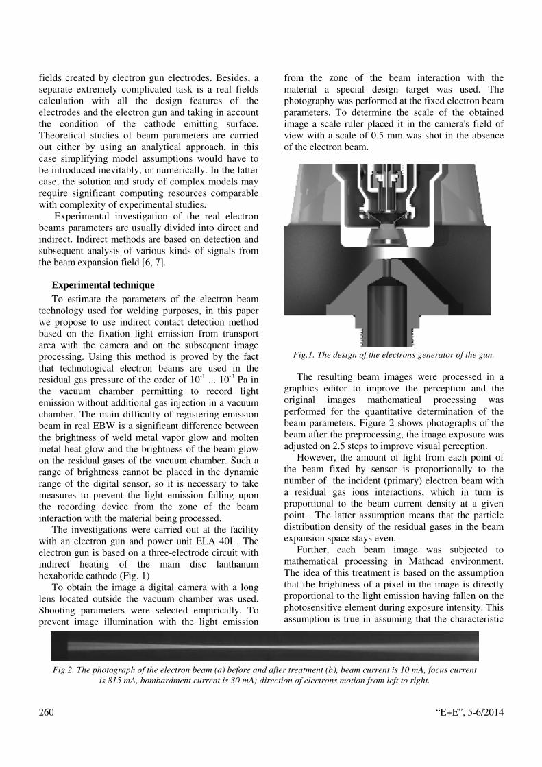
“E+E”, 5-6/2014 260
fields created by electron gun electrodes. Besides, a separate extremely complicated task is a real fields calculation with all the design features of the electrodes and the electron gun and taking in account the condition of the cathode emitting surface. Theoretical studies of beam parameters are carried out either by using an analytical approach, in this case simplifying model assumptions would have to be introduced inevitably, or numerically. In the latter case, the solution and study of complex models may require significant computing resources comparable with complexity of experimental studies.
Experimental investigation of the real electron beams parameters are usually divided into direct and indirect. Indirect methods are based on detection and subsequent analysis of various kinds of signals from the beam expansion field [6, 7].
Experimental technique To estimate the parameters of the electron beam
technology used for welding purposes, in this paper we propose to use indirect contact detection method based on the fixation light emission from transport area with the camera and on the subsequent image processing. Using this method is proved by the fact that technological electron beams are used in the residual gas pressure of the order of 10-1 ... 10-3 Pa in the vacuum chamber permitting to record light emission without additional gas injection in a vacuum chamber. The main difficulty of registering emission beam in real EBW is a significant difference between the brightness of weld metal vapor glow and molten metal heat glow and the brightness of the beam glow on the residual gases of the vacuum chamber. Such a range of brightness cannot be placed in the dynamic range of the digital sensor, so it is necessary to take measures to prevent the light emission falling upon the recording device from the zone of the beam interaction with the material being processed.
The investigations were carried out at the facility with an electron gun and power unit ELA 40I . The electron gun is based on a three-electrode circuit with indirect heating of the main disc lanthanum hexaboride cathode (Fig. 1)
To obtain the image a digital camera with a long lens located outside the vacuum chamber was used. Shooting parameters were selected empirically. To prevent image illumination with the light emission
from the zone of the beam interaction with the material a special design target was used. The photography was performed at the fixed electron beam parameters. To determine the scale of the obtained image a scale ruler placed it in the camera's field of view with a scale of 0.5 mm was shot in the absence of the electron beam.
Fig.1. The design of the electrons generator of the gun.
The resulting beam images were processed in a graphics editor to improve the perception and the original images mathematical processing was performed for the quantitative determination of the beam parameters. Figure 2 shows photographs of the beam after the preprocessing, the image exposure was adjusted on 2.5 steps to improve visual perception.
However, the amount of light from each point of the beam fixed by sensor is proportionally to the number of the incident (primary) electron beam with a residual gas ions interactions, which in turn is proportional to the beam current density at a given point . The latter assumption means that the particle distribution density of the residual gases in the beam expansion space stays even.
Further, each beam image was subjected to mathematical processing in Mathcad environment. The idea of this treatment is based on the assumption that the brightness of a pixel in the image is directly proportional to the light emission having fallen on the photosensitive element during exposure intensity. This assumption is true in assuming that the characteristic
Fig.2. The photograph of the electron beam (a) before and after treatment (b), beam current is 10 mA, focus current
is 815 mA, bombardment current is 30 mA; direction of electrons motion from left to right.

“E+E”, 5-6/2014 261
curve of the sensor is represented by a straight line. The study of the real beams photos made it
possible to reveal some of their features. The blue channel is established to be the “strongest”, and the image in this channel has the highest contrast ratio, so further transformations were performed above the image of the blue channel. Furthermore, on the image in the blue channel unwanted illumination beam from the contact with the target has the least impact.
It should be noted that in fact the resulting image is an integral projection of the detector beam on the plane (Fig. 3). Thus, the image contains information about the current density distribution in all the beam sections parallel to the density detector.
To recover the information of the current density distribution in the whole beam j (x, y, z) or in any part of its cross-section j (x, y) at a given z a problem of three - or two -dimensional tomographic reconstruction has to be solved [8, 9]. To solve this problem at least some of the projections of the object has to be obtained which in the given shooting conditions was not possible, however, even by a single beam projection a number of the quantitative beam characteristics was able to be identified.
Fig.3. The forming of the three-dimensional distribution on
the sensor planar surface projection diagram.
Results of experiment
The beam is found to have clear boundaries in the converging beam area (Fig. 4) , and the position of the boundary does not depend on the exposure magnitude, indicating the actual presence of the border, rather than its masking due to lack of exposure.
The "focal" plane position was determined by the distance from the gun case edge to the maximum brightness of the beam field middle. To determine the
maximum image brightness region position the processing in the graphical editor was performed. Fig. 5 shows the original image and the image of the beam after the treatment, as well as the pixel brightness in different sections profiles. Figure 6 shows the focal length on the focusing current dependence at a constant beam current.
Fig.4. .Larger beam boundary image.
Fig.5. Electron beam in the initial state and after the treatment photo; intensity profiles in different beam
sections ; beam current Ib = 50 mA.
Fig. 7 shows the intensity of the radiation beam integrated projection profiles calculated in different sections for the two bombardments of the cathode disk current values. The image was taken in the electron beam convergent part, the beam current was 48 mA, the current focus - 715 mA. This operation mode of

“E+E”, 5-6/2014 262
the electron gun provided a beam diameter of about 12 mm in the survey area.
At a beam bombardment current of 30 mA the beam has a distinct dip in the central portion current density, wherein the minimum density coordinate is shifted leftward on the value of about 1.5 mm. The current being increased to 46 mA, current density failure in the central part decreases, while the multiple local minima and maxima of the current density are being observed.
Fig.6. Dependence of the beam focus distance on focus
current at a beam current of 50 mA.
Fig. 7. Integrated projection beams Ib = 10 mA , If = 715 mA intensity profiles (beam image and cross sections, in which the profiles were built, are shown on the right): a -
the bombing current Ih = 30 mA ; b - Ih = 46 mA
Conclusions The bombing current influence on the power
density distribution effect can have the following main reasons:
1. Influence of volumetrical space beam charge; under certain conditions paraxial trajectories of electrons in the cathode are known to be estranged from one another under the influence of Coulomb repulsion forces. However, this effect is negligible at the test beam current value.
2. Crossover being too close to the cathode, whereby the trajectory of electrons in the crossover region converge and diverge at greater angles and in the anode region in the beam paraxial part a current density decrease is observed. The increase of bombardment current increases the primary cathode temperature and also the electrons initial velocity leading to crossover distancing and current density alignment over the cross section.
3. Planar shape modifying of the cathode surface, e.g. due to ion bombardment. Concave surface in the cathode central part also changes the convergence angle and crossover position, bringing it closer to the cathode, also contributing to the emergence of current density minimum in the axial part of the beam .
Regardless of the real reasons for the downward excursion in the central part of the beam, using close to the maximum current values regardless of the beam current can be recommended to obtain a more uniform distribution from a practical point of view. For the considered gun the maximum bombardment current value is 50 mA.
Overall, the proposed method of estimating the electron beams parameters can be used for the process equipment operation controlling, for example, to assess gun alignment accuracy and the cathode state by the distribution of power density. Furthermore, the obtained dependence of the beam parameters on the electron gun operating mode can be used for selecting process parameters to reduce the amount of work on welding conditions experimental development. The advantages of the method include the large capacity beams diagnostics ability, while probe methods are limited by the beam power associated with the probes destruction danger. Now experiments on the diagnostics of the beams with capacity up to 6 kW have been carried out. In the future we plan to continue experiments for beams up to 30 kW.
REFERENCES [1] Zuev I.V., Rykalin N.N., Uglov A.A.
Fundamentals of electron beam processing of materials, Moscow, Mechanical engineering, 1978, 239 pages.

“E+E”, 5-6/2014 263
[2] Nazarenko O.K., Kaydalov A.A., Kovbasenko S.N. Electron-beam welding, Kiev, 1987, 256 pages.
[3] Kasatkin B.S., Kovbasenko S.N., Nesterenko V.I. Single-pass electron beam welding of structural steels large thicknesses, Automatic welding, 1989, 4, pages 18 – 27.
[4] Monastyrsky M.A., Myraviov A.G., Tarasov V.A. Self-consistent numerical solution of the problem of calculating the electron guns in the cathode region of the iteration method, Applied Physics, 1998, 2, pages 22-32
[5] Andrev S.V., Monastyrsky M.A., Tarasov V.A., Myraviov A.G. Development of software for mathematical modeling of electron guns cathodes with arbitrary shape, Applied Physics, 2000, 2, pages 77-85.
[6] Vorobiov G.S., Drozdenko A.A., Pushkarev K.A., Barsuk I.V. Diagnostic methods and calculation of static characteristics of intense nonrelativistic electron beams (Review), Compressor and power engineering, 2007, 3(9), pages 79-91.
[7] Alyamovskiy I.V. Electron beams and electron guns, Moscow, Soviet radio, 1966, 455 pages.
[8] Pikalov V.V., Nepomnyaschiy A.V. Iterative algorithm with wavelet filtering in the problem of two-dimensional tomography, Computational methods and programming, new computing technologies, 2003, Vol. 4, 1, pages 244-253.
[9] Artemov A.S., Astrakhanchik G.F., Baygachev U.K., Gevorkov A.K. Diagnosis of H-ion beam on optical radiation in the transport path, Technical Physics, 2000, 1, pages 117-121.
Prof. Dr. Viktor K. Dragunov – Head of Department of Metals Technology of National Research University “MPEI”, Moscow, Russian Federation.
e-mail: [email protected]
Assoc. Prof. Dr. Alexey L. Goncharov – Department of Metals Technology of National Research University “MPEI”, Moscow, Russian Federation.
e-mail: [email protected]
Assoc. Prof. Dr. Andrey P. Sliva – Department of Metals Technology of National Research University “MPEI”, Moscow, Russian Federation.
e-mail: [email protected]
Prof. Dr. Alexey V. Scherbakov – Department of Electrotechnological automated installations and systems of National Research University “MPEI”, Moscow, Russian Federation.
e-mail: [email protected]
Eng. Maksim A. Portnov – Department of Machine design Fundamentals of National Research University “MPEI”, Moscow, Russian Federation.
e-mail: [email protected]
Tech. Ivan S. Chulkov – Department of Metals Technology of National Research University “MPEI”, Moscow, Russian Federation.
e-mail: [email protected]

“E+E”, 5-6/2014 264
Electron-Optical Characteristics of Beams Generated by Electron Plasma Sources
Vladimir A. Gruzdev, Vitali G. Zaleski
Electron-optical characteristics of electron beams generated in sources of two types are considered. One of these sources is based on reflected hollow cathode discharge and the other one rests on a modified reflected discharge. They differ in emitting plasma formation conditions and emitter electrode potentials. The discrepancies of electron-optical properties of the generated electron beams with high accelerating voltage are established. The analysis of the reasons determining these differences are presented.
Електронно-оптични характеристики на снопове, генерирани от плазмени източници на електрони (Владимир Груздев, Витали Залески). Електронно-оптичните характеристики на електронни снопове, генерирани в източници от два типа са разгледани. Единият от тези източници използва отражателен разряд с кух катод, а другият-модифициран отражателен разряд. Те се различават по състоянието на емитиращата плазма и електродния потенциал на емитера. Разликите на електронно-оптичните свойства на генерираните електронни снопове с висок ускоряващ потенциал са установени. Представен е анализ на причините, определящи тези различия.
Introduction Electron-optical systems (EOS) with plasma
emitter providing a constitutive increase of durability of electron-beam technological equipment, were developed as the alternative of EOS with thermocathode. At the same time, it was assumed that beams formed by EOS with plasma emitter were regarded to be less suitable for electron-beam technologies in comparison with beams formed by EOS with thermocathode. This opinion was based on the statement that the initial energy of electrons emitted by plasma is considerably higher than emitted by thermocathodes. But there was a theoretical possibility to reach that value of such a main parameter of the beam as brightness in EOS with plasma emitter up to values typical of EOS with thermocathode. The possibility consisted in the occurrence of much higher current density emission of plasma emitter. It stimulated the substantial volume of the experimental researches in the field of development of different types of EOS with plasma emitter and the evaluation quality of the electron beams formed by them.
As a result the possibility of realization of two
principally different plasma emitters was shown, and also the principal difference of EOS with plasma emitter and EOS with thermocathode. The essence of the latter difference consists in the fact that in EOS with thermocathodes beam crossover is formed due to beam acceleration. Then this crossover is imaged by the focusing system (usually magnetic) on the technological object. In EOS with plasma emitter due to high density current emission the plasma emitting surface is considerably smaller. At the further magnetic focusing, the beam section in the field of emission (small emitting surface) is imaged on the technological object. The square of this beam section, the position of the surface of emitting plasma and its shape essentially depend on the potential of the walls of emissive channel where the emitting plasma surface, plasma density, geometry of electrodes of EOS and their potentials form.
Besides, it was supposed that the realizable extracting mechanisms of the emitted electrons from plasma to the accelerating gap influence electron-optical characteristics of EOS with plasma emitter. It is possible to distinguish two extracting mechanisms to the main, fundamentally different, ones.

“E+E”, 5-6/2014 265
Their possibility depends on the type of discharge, which is used for the formation of emitted plasma (two types of the plasma emitters). Firstly, it is a thermal chaotic extraction (particularly discussed in [1]), secondly it’s a drift extraction [2] which appears as a result of emitting plasma perturbation by the emission.
In this article the results of the comparative analysis of electron-optical characteristics of beams formed in plasma sources (PES) with cathode [3], anode [2, 4] and the intermediate potential of emitter electrode formed in plasma sources on the basis of two types of discharges are presented [3,4].
Experimental method Electron beams were formed by two types of
plasma sources. The first type is based on the discharge with a hollow cathode (DHC) and the second one is in terms of the modified reflected discharge (MRD) [4] with the anodic or intermediate potential of emitter electrode (fig. 1). In the first source the axial heterogeneity of plasma concentration is created and the diffusion (thermal chaotic) extraction is realized. In the second source there is a drift extraction from the whole plasma volume in the conditions of the mobility limitation of plasma electrons by the magnetic field.
In MRD the emitter electrode potential change was provided by including it into the bias resistance circuit
[3,4] and took place by the value of the voltage drop within the range from 0 to 100 V. For receiving electron-optical beam characteristics the developed software-hardware complex was used [6]. It could measure the beam divergence and its emittance, build 3D phase beam portraits and calculate the brightness and other beam and emitting plasma parameters on their basis. The estimation of the position and shape of plasma surface and also the trajectory of the electron beam (the results introduced in [7]) were carried out with the use of the application software ELIS [8].
The experiment results and their discussion The dependences of the angular divergence of the
electron beam on the adduced electric field strength (relation the accelerating voltage to the length of the accelerating gap) in the acceleration gap are shown in fig. 2. The kind of the dependence of the electron beam angular spread on the adduced field strength Ea can be explained by the mobility of plasma surface emitting electrons [3].
But our calculations show that the reason for such a dependence can be the change of emitting surface shape [7]. Its displacement (deep into the channel with the growth of the adduced strength) leads to the change of emitting surface shape. At smaller Ea the displacement of the plasma border into the channel leads to the decrease of beam divergence up to the forming of a flat or convex shape [7].
a b
1,2 − cathode; 3 − anode; 4 − emitter electrode; 5 − emission channel; 6 − accelerating electrode; Ud − discharge voltage; Uac − accelerating voltage;
Rb − ballast resistance; Rs − bias resistance; B − induction of magnetic field
Fig. 1. Electrode structures of plasma sources on the basis of DHC (a) and MRD (b)
.
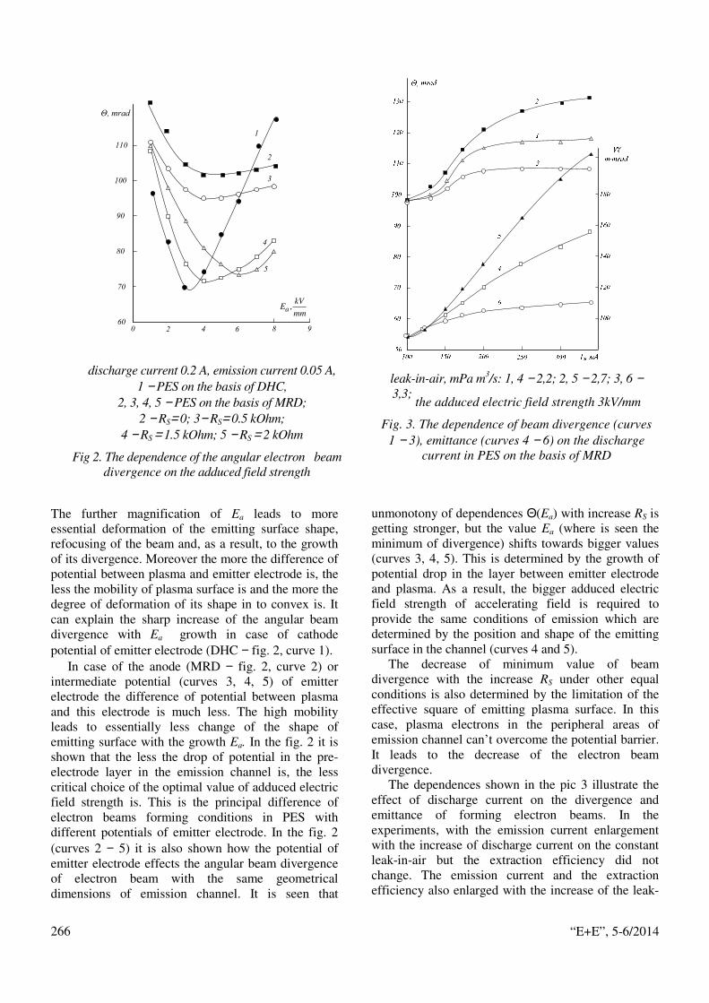
“E+E”, 5-6/2014 266
The further magnification of Ea leads to more essential deformation of the emitting surface shape, refocusing of the beam and, as a result, to the growth of its divergence. Moreover the more the difference of potential between plasma and emitter electrode is, the less the mobility of plasma surface is and the more the degree of deformation of its shape in to convex is. It can explain the sharp increase of the angular beam divergence with Ea growth in case of cathode potential of emitter electrode (DHC − fig. 2, curve 1).
In case of the anode (MRD − fig. 2, curve 2) or intermediate potential (curves 3, 4, 5) of emitter electrode the difference of potential between plasma and this electrode is much less. The high mobility leads to essentially less change of the shape of emitting surface with the growth Ea. In the fig. 2 it is shown that the less the drop of potential in the pre-electrode layer in the emission channel is, the less critical choice of the optimal value of adduced electric field strength is. This is the principal difference of electron beams forming conditions in PES with different potentials of emitter electrode. In the fig. 2 (curves 2 − 5) it is also shown how the potential of emitter electrode effects the angular beam divergence of electron beam with the same geometrical dimensions of emission channel. It is seen that
unmonotony of dependences Θ(Ea) with increase RS is getting stronger, but the value Ea (where is seen the minimum of divergence) shifts towards bigger values (curves 3, 4, 5). This is determined by the growth of potential drop in the layer between emitter electrode and plasma. As a result, the bigger adduced electric field strength of accelerating field is required to provide the same conditions of emission which are determined by the position and shape of the emitting surface in the channel (curves 4 and 5).
The decrease of minimum value of beam divergence with the increase RS under other equal conditions is also determined by the limitation of the effective square of emitting plasma surface. In this case, plasma electrons in the peripheral areas of emission channel can’t overcome the potential barrier. It leads to the decrease of the electron beam divergence.
The dependences shown in the pic 3 illustrate the effect of discharge current on the divergence and emittance of forming electron beams. In the experiments, with the emission current enlargement with the increase of discharge current on the constant leak-in-air but the extraction efficiency did not change. The emission current and the extraction efficiency also enlarged with the increase of the leak-
5
0 2 4 6 8
70
2
480
90
100
110
60
,akV
Emm
9
1
3
Θ, mrad
discharge current 0.2 A, emission current 0.05 A,
1 − PES on the basis of DHC, 2, 3, 4, 5 − PES on the basis of MRD;
2 − RS= 0; 3− RS= 0.5 kOhm; 4 − RS = 1.5 kOhm; 5 − RS = 2 kOhm
Fig 2. The dependence of the angular electron beam divergence on the adduced field strength
leak-in-air, mPa m3/s: 1, 4 − 2,2; 2, 5 − 2,7; 3, 6 − 3,3;
the adduced electric field strength 3kV/mm
Fig. 3. The dependence of beam divergence (curves 1 − 3), emittance (curves 4 − 6) on the discharge
current in PES on the basis of MRD

“E+E”, 5-6/2014 267
in-air. It is shown in the fig. 3 that with the increase of discharge current the divergence and emittance of electron beams are raising in some range of discharge currents. It can be determined by the deformation of the shape of plasma surface with the growth of its concentration. The further increasing of discharge current leads to the saturation of dependence Θ(Id) what is connected with the displacement of plasma border into the new position with less deformation of its shape. The fig. 3 also shows that the dependence of these parameters on leak-in-air has a nonmonotonic nature. With increasing of the leak-in-air the divergence first grows (curves 1 and 2), but then falls down (curve 3).
To find the reasons for determining a kind of dependences of divergence and emittance on discharge current the influence of extraction efficiency α on these parameters was investigated. It was established that at the smaller extraction efficiency the divergence and emittance first grow. At the bigger α >αcr they fall down, and at the bigger discharge currents the slope of those dependences Θ(α) and W(α) is essentially higher in comparison with the slope at the smaller discharge currents. This fact lets assume that at α>αcr plasma electrons get additional velocity in the weak electric field which facilitates its movement toward the emission channel [3, 4]. That’s why the beam brightness which is derived at α>αcr is also higher (fig. 4) than the brightness of electron beam derived at the smaller values of extraction efficiency. At the same time the more the discharge current, the higher the slope of this dependence. Thus, electron beams with the same brightness can be derived under different conditions (a dotted horizontal line in the fig.
4). For the illustration of other possibilities of soft-hardware complex (except for the determination of beams characteristics which are mentioned above) in the fig. 5 3D phase portraits of electron beams are shown. The beams form in the sources with the different potential of emitter electrode under other equal conditions. Such 3D images of phase portraits are easy to use for a visual comparison of beams, the valuation of the homogeneous distribution of the current density on the beam cross-section and express diagnostics of adjustment and focusing systems.
Conclusion The experiments and calculations proved the
assumption about the defining role of the emitting surface shape in the formation of electron beam with specified electron-optical characteristics. It was established that the soft-hardware complex [6] and application software [8] can be used for analysis of conditions of the emitting plasma surface formation and preliminary system optimization of the initial beam forming. The analysis of the main electron-optical characteristics showed the validity of PES on the basis of MRD with the anode potential of emitter electrode for getting welding type electron beams. The effect of the potential of emitter electrode on these characteristics allows assuming an effective method of controlling these characteristics in the sources based on MRD.
REFERENCES [1] Zharinov, A.V., Kovalenko, Yu.A. On the theory
of the electron collectors/ Technical physics. – 1986. – Т. 56, N. 4. – P. 681–686.
[2] Grusdev, V.A. Zalesski, V.G. Emission current formation in Plasma electron emitters. Plasma Physics – 2010. – vol. 36 (13). – P. 1191–1198.
[3] Galansky, V.L., and others. Physical processes in plasma electron emitters based on a hollow-cathode reflected discharge. Journal of Physics D : Appl. Phys. – 1994. – 27. – Р. 953–961.
[4] Grusdev, V.A. Zalesski, V.G., and others Universal plasma electron source. Vacuum (UK) 77 2005. –Р. 399–405.
[5] Zalesski, V.G., Rusetski, I.S. Ways of the plasma electron sources operation. Proc. VI Intern. Conf. on Plasma Physics and Plasma Technology, Minsk (Belarus), 2009. – Vol. I. – P. 173–176.
[6] Gruzdev, V.A., Zalesski, V.G., and others, Hardware and software system for the diagnosis of electron-optical systems and beams of charged particles, Pribory i tehnika experimenta (Russia), 2 (2009) p.177 – 178.
7
2 2
,
10
B
A
m rad⋅
discharge current, А: 1 – 0.15 A; 2 – 0.2 A; 3 – 0.25 A
Fig. 4. The dependence of the electron beam brightness on the extraction efficiency of electrons in
PES on the basis of MRD
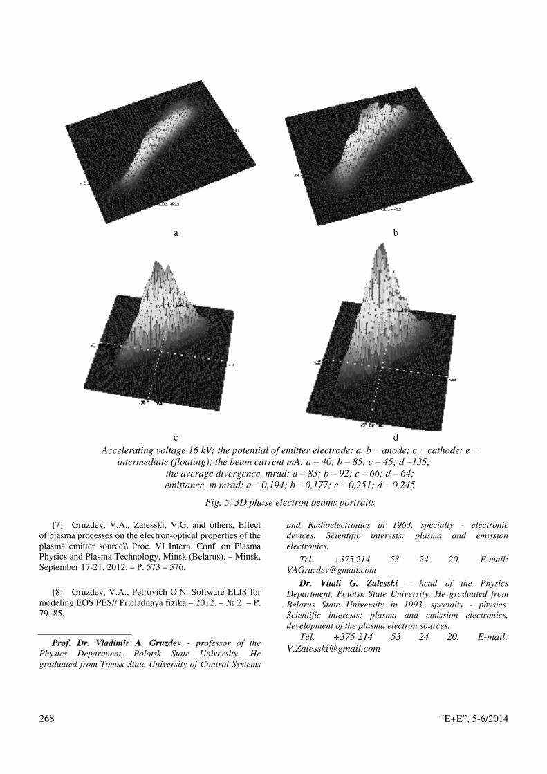
“E+E”, 5-6/2014 268
[7] Gruzdev, V.A., Zalesski, V.G. and others, Effect of plasma processes on the electron-optical properties of the plasma emitter source\\ Proc. VI Intern. Conf. on Plasma Physics and Plasma Technology, Minsk (Belarus). – Minsk, September 17-21, 2012. – Р. 573 – 576.
[8] Gruzdev, V.A., Petrovich O.N. Software ELIS for
modeling EOS PES// Pricladnaya fizika.– 2012. – 2. – P. 79–85.
Prof. Dr. Vladimir A. Gruzdev - professor of the Physics Department, Polotsk State University. He graduated from Tomsk State University of Control Systems
and Radioelectronics in 1963, specialty - electronic devices. Scientific interests: plasma and emission electronics.
Tel. +375 214 53 24 20, E-mail: [email protected]
Dr. Vitali G. Zalesski – head of the Physics Department, Polotsk State University. He graduated from Belarus State University in 1993, specialty - physics. Scientific interests: plasma and emission electronics, development of the plasma electron sources.
Tel. +375 214 53 24 20, E-mail: [email protected]
a b
c d
Accelerating voltage 16 kV; the potential of emitter electrode: a, b − anode; c − cathode; e − intermediate (floating); the beam current mA: a – 40; b – 85; c – 45; d –135;
the average divergence, mrad: a – 83; b – 92; c – 66; d – 64; emittance, m mrad: a – 0,194; b – 0,177; c – 0,251; d – 0,245
Fig. 5. 3D phase electron beams portraits

“E+E”, 5-6/2014 269
Electron Beam Welding Machines with Plasma Cathode Gun
Sergey I. Belyuk, Igor V. Osipov, Alexander G. Rau, Grigory V. Semenov
Electron beam machines with the plasma cathode guns are presented. All machines possess high
extent of automation. The high-voltage source has effective protection against breakdowns and small time of restoration. Machines are equipped with systems of coaxial to a beam optical targeting and targeting in the reflected electrons. In machines high-precision manipulators are used. Technological process is completely automated. There is a system of documenting of technological process.
The following features of the plasma cathode electron guns are in detail discussed: - High stability of optical parameters at current regulation from a targeting mode (0.1-0.5 mА) to
welding 150 mА. The position of the focal plane doesn't change. At current regulation optical properties of an electronic beam remain invariable;
- Tolerance to properties of welded materials. There are no heated details in guns, temperature of electrodes doesn't exceed 150 degrees Celsius;
- At breakdown current of a beam "breaks", on welded details doesn't remain traces; - The self-adjustment of a plasma emitting surface in the emission channel provides high optical
quality of a beam.
Електроннолъчеви машини за заваряване с пушки с плазмен катод (С. Белюк, И. Осипов, А. Рау, Г. Семенов). Представени са електроннолъчеви заваръчни машини с пушки с плазмен катод. Всички машини са високо-автоматизирани. Високоволтовият източник има ефективна защита против пробиви и малко време на възстановяване. Машините са снабдени със съосно оптично насочване на лъча и с насочване с отразени електрони. Използват се високо-точни манипулатори. Технологичният процес е напълно автоматизиран. Има система за документиране на технологичния процес. Следните особености на пушките с плазмен катод са обсъдени:
- Висока стабилност на оптичните параметри при токово регулиране от една мода от 0,1 до 0,5 mA при заваряване с 150 mA позицията на фокусната равнина не се променя и оптичните свойства на снопа са неизменни;
- Толеранс към свойствата на заварявания материал. Няма нагрети части на пушката, температурата на електродите не превишава 150 оС.
- При пробив в пушката не остават следи върху заваряваните детайли. - Саморегулирането на плазмената емитираща повърхност в емисионния канал
обезпечава високо оптично качество на снопа.
Introduction Work on the creation of plasma cathodes began
over thirty years ago. In our opinion, the greatest success has been achieved in creating a plasma cathode based on low-voltage glow discharge with a hollow cathode. During this time, have been studied the basic physical processes in the electron emitter plasma cathode [1-2], much attention is paid to the design and adaptation of industrial electron guns with such emitter [3] and even created a new scientific direction "plasma emission electronics" [4]. On the basis of the plasma cathode guns were created
machines for different purposes [5-7]. Hallmark machines presented in this article, is that they are mass-produced. Due to the specific characteristics of guns with plasma cathode these machines have a number of unique advantages.
Plasma cathode electron gun The principle of operation and construction of
plasma-cathode electron gun is in detail featured in [3,5]. A basis of gun is a no separable metal-ceramic unit (cathode unit). The cathode unit is a discharge chamber for low-voltage glow discharge with cold electrodes. In the one of electrodes there is an aperture

“E+E”, 5-6/2014 270
(emission channel) through which electrons is executed leave gas discharge plasma. The accelerating voltage is put between the cathode unit and anode.
The basic characteristics of gun: • Operating mode - stationary, pulsing; • Accelerating voltage 20-40kV; • Beam current 0-150mA.
The important property of plasma-cathode electron gun is stability of spatial beam characteristics at regulation of beam current. Unlike systems with a thermionic cathode, the standing of a beam focal plane does not vary at regulation beam current. Figure 1 shows the position of the focal plane of the beam from its current at constant values of the accelerating voltage and current focus.
Fig.1. Dependence distance between the gun and the focal plane of beam current.
Lack of dependence of the position of the focal plane of the beam current explained by the peculiarities of electron emission from the plasma. Position of the focal plane at a constant accelerating voltage and focus current is determined by the position of the emitting surface of the plasma in the emission channel. In turn, the position of the plasma is determined by Child-Langmuir equation for the gun accelerating gap . Channel dimensions are small, the plasma density is very high. Calculations done in [2] show that displacement of the emitting surface of the plasma is less than a millimeter in the whole range of beam current change. No dependence of the focal plane position of beam current simplifies operator electron beam i machines, and reduces the likelihood of errors in manual welding operation.
The second feature of the plasma cathode electron gun is self-adjustment emitting surface of the plasma in the emission channel. Emitting surface of the plasma is separated from the walls of the emission channel layer spatial potential drop. The length of this layer depends on the concentration of plasma and its potential. Characteristics of the plasma in the channel have axial symmetry. Consequently, the layer has the
same length and the emitting surface is always perfectly aligned in the emission electrode. When we configure a gun it is necessary to provide coaxiality only of the holes in the emission and accelerating electrodes. The need for adjustment of the cathode as in a thermocathode gun is missing.
The third feature consists in that, at electric breakdown current of a beam doesn't grow, but rather breaks. Increase the beam current cannot be performed, because the plasma cathode always operates in saturation mode. The beam current always has a maximum value and cannot be greater. At the breakdown potential of the emission electrode increases. This leads to the extinction of the discharge and reduce the beam current to zero. The described feature matters essentially important. Completely it is impossible to exclude breakdown in an electron guns. In a three-electrode gun with a thermocathode breakdown in the accelerating gap is almost always leads to irreparable defect - burn-through details.
The fourth feature of the plasma cathode – tolerance to couples of welded materials and vacuum conditions it was repeatedly mentioned practically in all works devoted to plasma cathodes. Nevertheless, we believe it is appropriate to note that the property in our work. There are no hot parts in the gun, temperature of electrodes doesn't exceed 150 degrees Celsius.
Fig. 2 shows the appearance of an electron gun with a plasma cathode.
Fig.2. The appearance of an electron gun with a plasma
cathode.
Cathode unit disposed in a metal housing. Electrical insulation and cooling transformer oil is provided, which, in turn, is cooled by water. Gun case provides the necessary biological protection against unused X-ray radiation.
0 1 20 30 40 50 104
108
112
116
I, mA
d, mm

“E+E”, 5-6/2014 271
Power supply modules The power supply system of the equipment
consists of an accelerating voltage unit, a discharge power supply unit, a beam focusing and deflection control unit, and a control unit of the gas flow controller. The accelerating voltage and discharge power supply units are made by the classical circuit design of a bridge inverter with the phase-shift control circuit. In the inverter, the resonance method of switching MOSFET transistors is realized that provides a low level of electromagnetic noise and reduced dynamic losses in switching power transistors. The high conversion frequency (50 kHz) makes it possible to reduce the output capacitance of the power supplies to 10 nF and to increase the rate of processing of control signals. The accelerating voltage unit can operate in one of the two modes: stabilization of the accelerating voltage and limitation of the output current. In the first mode, a given accelerating voltage is stabilized as the load current increases from 0 to 150 mA. This is the normal operation of the unit. As the load current increases to more than 150 mA, the accelerating voltage unit goes over to the current limitation mode within 50 µs. This makes it possible to protect the load and to prevent the development of an arc discharge in case of breakdown in the electron gun. As the load current decreases, the accelerating voltage unit is back to normal operation. Recovery time is 2-10 ms. The discharge power supply unit is a current source with the output voltage ranging between 50 and 1500 V. It operates in the current stabilization mode throughout the output voltage range.
Table 1. Basic characteristics of the power supply modules
Accelerating voltage range (10–40) kV Stability of accelerating voltage 0.1% Pulsations of accelerating voltage, no more then
0.1%
Maximum current 150 mA Beam current stabilization 0.1 mA
All power supplies are located in three cases of the
standard 19 inches tall 4U.
Vacuum chamber, vacuum system, manipulators and service functions
Vacuum chamber of our electron beam welding machines have internal dimensions 300×300×300 mm, 500×500×500 mm and 800×800×800 mm. Machines with the camera size 300×300×300 mm has almost tabletop pattern (Fig.3). Power supplies are located at the bottom of the unit. Operator workplace is near the unit.
Fig.3. View and form-factor of welding machines with vacuum chamber dimensions 300×300×300 mm.
Exterior of welding machines with cameras with dimensions 500×500×500 mm and 800×800×800 mm is shown in Fig.4.
Fore vacuum pumps are rotary or sliding vane rotary. High vacuum pumps may be turbo molecular or cryogenic type. Switching the vacuum system implemented pneumatic valves. The whole pumping process is fully automated. Pumping time is 5 to 15 minutes.
In welding machines use high precision manipulators. The basis of the manipulator is 2 or 3-axis system of movement. On system of movement the rotator with a changeable inclination of an axis of rotation or a multiposition revolver can be established. Accuracy of positioning makes 5-10 microns.

“E+E”, 5-6/2014 272
Fig.4. View and form-factor of welding machines with vacuum chamber dimensions 500×500×500 mm and
800×800×800 mm.
All machines are equipped with systems of supervision of two types: supervision in the reflected electrons and optical coaxial to beam video supervision. In the first case the image is formed with use of a signal of the electrons reflected from a welding surface. The size of scanned area is 25×25 mm, the size of the image is 25×25 cm. In the second case, the image through a special mirror (fig.5) is transferred to a video camera, and from the camera is displayed on the monitor. The system has six-fold optical zoom. The image size on the screen isn't limited. The mirror of system of video supervision is equipped dusting protection. Both systems of supervision allow to position a beam on a product surface with an accuracy not worse than 100 microns.
For welding of seams of a difficult configuration in welding machines equipped of the system for automatic beam joint. The principle of the system is as follows: the operator alternately directs the beam onto the joint welded parts at different points of the seam. The system memorizes the coordinates of these points. The system then constructs a spline between the points of the welding process and automatically conducts the beam from one point to another.
Fig.5. Principal of operation of coaxial to beam video supervision system.
The system of automation of technological process allows to create the special card for each technological process. In this card the order of movement of the manipulator, change of current of a beam, current of focusing is described. Possibility of creation of library of technological cards is provided.
All parameters of welding process register system of electronic documenting, collecting and storage of parameters of technological process. On each welded connection the passport is formed. Information in the passport is provided in numerical data and temporary charts of all parameters of welding.
Conclusion Presented in the report electron beam welding
machines are used in the nuclear, aerospace industry in Russia. Experience in operating systems based on plasma-cathode electron guns showed that they are reliable, meet all current requirements and provide high quality welds.
REFERENCES [1] V.L.Galansky, V.A.Gruzdev, I.V.Osipov and
N.G.Rempe. Physical Processes in Plasma Electron Emitters Based on a Hollow-Cathode Discharge. Journ. of Physics D: Appl. Phys. 27(1994) p.953-961.
[2] Galansky V.L., Gruzdev V.A., Zelensky V.I., Osipov I.V., Rempe N.G. Plasma characteristics in emission channel of plasma emitter Technical Physics. The Russian Journal of Applied Physics. 1990. Т. 60. p.168.
[3] Igor Osipov and Nikolay Rempe. A plasma-cathode electron source designed for industrial use Review of Scientific Instruments, 2000, V.71, 4, p.1638 -1641.
[4] Bugaev A.S. and others… Current Status of the Plasma Emission Electronics: I. Hardware. Laser and Particle Beams. Vol. 21. No. 2, pp. 139-156. (2003),
[5] S.I.Belyuk, .V.Osipov, A.G.Rau, N.G.Rempe Electron-Beam Equipment Based on a Plasma-Cathode Gun Elektrotehcnica&Eleltronica. Vol. 41. No. 5-6, pp. 98-100. (2006).
[6] S.I.Belyuk, I.V.Osipov, A.G.Rau, N.G.Rempe, V. F. Shevchenko, S.V. Skvortsov Electron Beam Facing

“E+E”, 5-6/2014 273
Machine Elektrotehcnica&Eleltronica. Vol. 41. No. 5-6, pp. 112-114. (2006).
[7] Kornilov S.Y., I.V.Osipov, Rempe N.G. Electron-beam equipment based on a plasma-cathode gun for science researches. Materials of 9-th International Conference on Electron Beam Technologies (EBT 2009). Varna, Bulgaria. 1–4 June 2009. 5-6/2009. pp. 201-203.
Ph.D. Sergey I. Belyuk - research associate of Tomsk Electron Technologies (TETa Ltd), graduated Tomsk State University of Automated Control Systems and Radioelectronics.
Assoc. Prof. Ph.D. Igor V. Osipov - commercial director of Tomsk Electron Technologies (TETa Ltd),
graduated Tomsk State University of Automated Control Systems and Radioelectronics. Area of scientific interests - the physicist of processes in plasma cathode electron guns, е-mail:[email protected]
Eng. Alexander G. Rau- director of Tomsk Electron Technologies (TETa Ltd), graduated Tomsk State Polytechnic University. Area of scientific interests - power supply systems and managements. е-mail:[email protected]
Eng. Grigory V. Semenov - Chairman board of directors “Tomsk Instrument”, graduated Novosibirsk State Polytechnic University. Area of scientific interests – plasma physics. е-mail:[email protected]

“E+E”, 5-6/2014 274
The Exploitation of Concentrated Energy Flows for Welding and Protective Coating Production
M. V. Radchenko, Yu. O. Shevtsov, T. B. Radchenko, D. A. Nagorniy
The results of coatings properties investigations, made by electron beam and gas powder
cladding process and technological demands as well, are presented in the article.
Експлоатация на концентрирани енергийни потоци за заваряване и продукция със защитни покрития (М. Радченко, Ю. Шевцов, Т. Радченко, Д. Нагорний). В работата са представени технологичните изисквания и резултатите от изследване на свойствата на покрития, получени с електроннолъчев или газов процес на прахово покритие.
The development of modern machine-yapreyavlyaet more stringent requirements for reliability and durability of the best response to Sven-parts and units, working in conditions of high temperatures, cyclic heating-loads, gas and abrasion. Their rabotospo-sobnost largely determined by the physical and mechanical properties of working surfaces of mating parts. Therefore, one of the main ways of increasing longevity, increasing the service life of the caught and mechanisms that reduce the amount of spare parts is used in the production and repair stve those vysokotehnoeffektivnyh-tech manufacturing processes-tion hardening and surfacing. In recent years, along with the traditionally used are all the bo-Lee widespread use of new progressive methods using nye vysokokontsen-centered energy sources (electron beam, thermal spray). The practice of internal engine ternal combustion engine (ICE), especially the bathroom, forcing diesel engines shows that the weakest area of pistons are annular grooves for compression rings. The formation of Me-gap limit forward compression ring and the annular piston ka-Navka largely determines the resources of the engine to the bulkhead, fuel and oil, as well as the repair costs. Therefore, the solution of problems of increasing the service life of piston ring grooves is the main nym direction for practical use of research results, both in Russia and abroad. A team of authors in the Problem Laboratory of la-welding processes and the creation of a coating-Szczytno AltSTU them.
II Polzunov based on more than 20 years of experience in the area of electron-beam technologies developed technology of electron-beam-tang hardening of the most technologically sophisticated piston-aluminum alloys nevyh hypereutectic composition brand AK21M2,5H2,5. The technology pack-hardening is a cathode layer remelting the metal in the place the piston, where the groove is performed in the subsequent ring grooves necessary geometrical dimensions.
As a result of complex experimental investigations have revealed an optimal process parameters of hardening of the regime, allowing to obtain practically flawless metal in the melting zone with high wear resistance. In the process of mining development and production of technology-beam-hardening elektronnolu pistons for diesel engines of "Barnaultransmash" it was revealed that in this technology-tion there is a strong reserve for increasing the wear resistance of the first ring grooves - namely, the hardening of the doping-em, which significantly expanded to domain of application of this method of hardening [1-5].
In the case of additional alloying of aluminum alloy in order to obtain an even higher wear resistance as the doping material is proposed to use nichrome or copper conduction loci, whose content in the weld a metal determines the required mehanicheskies-voystva, such as hardness, iznoststoy-bone. The appearance of piston blanks yn-hardening zones under the annular groove is shown in a riunke.

“E+E”, 5-6/2014 275
Fig. 1. Preparations of alloy pistons AK21M2, 5H2, 5 with the hardened zones under the groove grooves (indicated by
arrows)
Practical implementation of the developed method of hardening of grooves performed at JSC "Barnaultransmash" which was designed and manufactured by electron-beam equipment with 14-position the manipulator at a given size pistons. With the use of electron beam guns with a "cold cathode" and the manipulator, the appearance of which is shown in Figure 2, the production program performed by electron-beam hardening of piston technology without doping.
Past production testing reinforced pistons for diesel engines work on the forced increase of their service life has shown 3 times. The expected economic effect from introduction of the technology is 400 rubles for a reinforced piston in the prices of 2010.
Fig. 2. 14-position manipulator for welding and hardening
of the pistons
Due to the relatively high stand-Stu equipment, use of vysokokon-centered heat source - the electron beam in a vacuum - for welding and a y-rochnyayuschih and protective coatings expedient but in those cases where it leads to obtaining a qualitatively new NIJ results, the properties of welded, hardened and surfaced products, and it is not possible to use other methods of surface heating. In particular, the authors work for the company of "Bar-naultransmash" was performed a set of techno-logical work on electron-beam welding of the body of the cylinder liner with a mounting clamp. This determined the costly savings-doped steel 38H2MYUA up to 40% due to sharp decrease in wall thickness anyone harvesting and removal operations for turning [6].
In the development of electron-beam welding technology method of low-energy electron beams (up to 5 keV), developed by a team of authors, through a combination of advantages are powder-materials and vacuum protection of the metal creates a unique performance over time for the ex-hardening properties of the layers on the surfaces of various parts of diesel engines [7 11].
Very effectively with the hardening and electron beam welding the creation of protective layers on the surfaces with a high level of functional properties (hardness, wear and corrosion resistance), or on the details of procurements of relatively low-cost low-carbon steels. Thanks to the power supply of accurate dosage with an electron beam deposition (ELN) are formed uniformly in the thickness of the layers with minimal penetration basis, excludes non-rigid deformation of the parts. The strength of adhesion to the substrate by the deposited coatings ELN, is at the level of the metallic bond. Therefore, in contrast to the sputtered they do not crack or peel from exposure to intense multicycle contact loads. Can be repeated after rounding surfacing weld details. Practical experience has shown, the cost of repair parts is about 30% of the new at much higher rates of functional properties of the surface. For example, hardening to melting in the working edges of the matrix for the hot deformed Bani spray of diesel fuel made it possible for JSC "Altaydizel" to increase the height of the surface-resistance factor of 2. Particularly relevant is the practical application of electron beam welding technology of high-alloy powder on the basis of Ni Cr-B-Si for the repair and restoration of the worn surfaces of heavy-duty parts: Crankshaft and camshaft engines (Fig. 3, Fig. 4), frogs, ball bearings, roller camshaft tappets, V-belt pulley hub gears, spindles, etc.

“E+E”, 5-6/2014 276
Fig. 3. Crankshaft diesel engine with forced main and
connecting rod necks, hardened by electron-beam melting (arrows indicate the location of hardening)
Fig. 4. Camshaft engine after the repair method of electron-
beam deposition (arrow indicates the place of hard-wearing surfacing)
To meet the challenges of working on the wear surfaces of various parts and mechanisms, along with the use of electron beams in vacuum, the industry is often economically feasible to use relatively non-expensive technological options, among which ryh prominent place occupied by the processes of flaming gas-spraying and welding. At the same time last 10-12 years are increasingly beginning to develop the processes of applying protective coatings supersonic gas jets [12-17]. Forefront in the development of technologies and equipment occupied by large companies in Germany and the United States, as Deloro Stellite GmbH, Sultzer Metco, GTV, Praxair, etc. However, this applies mainly to the deposition process. As you know, all the deposition process, without exception, have one major drawback that limits the industrial use - otsloenoi coatings due to the relatively low bond strength. Therefore, the authors faced the task of a radical solution to this problem by eliminating the parameter "adhesion strength" through
the development of equipment and tech-energy supersonic gas-powder deposition (EGR-surfacing). As you know, foreign-up paratura intended for use as a spray material powder alloys with small fraction - less than 10 microns, are not commercially produced in Russia. Already in the first phase of research was formulated and solved the problem of use as on-plavochnyh domestic powder materials of new self-fluxing alloys, and alloys on the axle of iron, cobalt, tungsten grain size of 40-100 microns. In this case, depending on the operating conditions selected coating material having a complex of properties (wear resistance, heat resistance, cor-Rioni resistance, etc.) necessary for the protec-tion for the given conditions of operation. To implement this process in the company "Institute of High Technologies" (Barnaul) within the framework of Federal Programme "START05" was carried out complex investigations, including calculations of the Laval nozzle with different Mach numbers, making a series of nozzles and their experi-mental testing of the process deposition of the powder-nosostoykih alloys nye-worn surface of the parts [18]. As a result of research designed apparatus (Fig. 5), and it produced the first Russian patent on the technology EGR-deposition [19, 20]. A distinctive feature of technological equipment is to increase the concentration of energy gazoplpmennoy installation.
Fig. 5. A device for implementing a process of supersonic
gas-powder surfacing: 1 - housing 2 - nozzle, 3 - gas flame, 4 - shield, 5 - cooling nozzle 6 - channel of the powder, 7 -
working gas supply valves, 8 - supply of process gases
On this basis, were formed by technological advice, according to which, when used in future devices and technologies developed by EGR-surfacing can expect an additional increase in wear resistance of boiler tube panels "fluidized bed" in the 3-4.

“E+E”, 5-6/2014 277
Fig. 6. Wear protective coating on the surface of the tube panels performed by the method of gas-powder surfacing
In 2005, OAO "Biysk boiler over-water" technology developed for a subsonic gas-powder deposition were naplavleny of Szczytno-coating on the tube boilers with a panel of "fluidized bed" type of HF-F-10-115-STAP (ri-sunok 6) . Turnaround time of boiler tubes with unprotected screen, depending on the type of coal (bituminous or lignite) amounts to 1.5 ... 2.5 months. Performance tests of boilers coated for 2 years confirmed the results of laboratory tests - signs of wear on the pipes do not have lo-detected. At the same economic effect of the use of technology developed in the three boilers was about 10.8 million rubles a year. As you know, the Office of the Altai region of the Industry and Energy has initiated the development of energy strategy in the Altai region until 2020. One of perspective directions of this program is the construction of power plants using coal Solton field. These coals are low-grade, and their combustion boilers are used with a "fluidized bed". Presented in R & D results allow us to solve the problem of using low-grade coal mined in the Altai region, with a sharp increase of the resource and improve the technological characteristics of boilers. Along with these engineering solutions obtained allow to recommend the use of a supersonic gas-powder tion process to solve the problem surfacing worn parts, Lei machines in other industries the region. In the development of existing technological developments, the staff of the Problems Laboratory of welding processes and the creation of protective coatings is currently developing a competitive equipment and technological processes on the basis of a new method for creating multifunctional coatings - EGR-surfacing, diagnostics and quality control process and is directly protective coatings, automatic welding process control as a whole and its individual technological systems, as well as preparing highly qualified specialists for implementation of new technological processes in industrial enterprises of the Altai Territory.
REFERENCES [1] Patent 2148750. The method of hardening
zones grooves piston engine internal combustion engines / Radchenko, MV, N. Batyrev, Blood-ing KS, Shevtsov YO Appl. 12/21/1998. Publ. 05/10/2000
[2] . Radchenko, MV, KS Krovyakov Investigation of the structure and properties of piston aluminum alloy treated with electron beam / / Swa-rochnoe production. In 1998. Number 11. C.9-12.
[3] . Radchenko, MV, Radchenko VG, KS Krovyakov Getting the hardened layers on the surface of the piston silumins by electron-beam deposition / / Welding Production. In 1999. Number 11. P.48-51.
[4] Krovyakov KS, Radchenko MV Hardening of diesel piston ring grooves of electron-beam processing / / Video Engineering, 2000. Number 3. Pp.23-25.
[5] Radchenko, MV, AV Zubkov, EN Kosonogov Electron-beam hardening of the piston alloy AK21. - In.: Electron beam welding. M. 1986. P.27-30.
[6] Radchenko, MV, N. Batyrev About strukturoob-education in the process of electron-beam hardening of steel with a melting 55H2N2MFA surface. - Math. USSR Academy of Sciences. Sor. Technical. Sciences. In 1987. Number 4. No. A. 4 seconds.
[7] Olshansky, NA, Radchenko VG Radchenko, MV, Likhosherstov DM, Balayan, RF Electron beam welding of cylinder liners of diesel engines / / Proceedings of the 8-Union Conf. by electron-beam welding. M. 1983. P.16-19.
[8] Radchenko M.V., Shevtsov Yu.O., Batyrev N.I. Metallurgical coating made by electron beam surfacing / 5 Int. Conf. On Electron beam techn. Varna, Bulgaria, 1991. P.487.
[9] Radchenko, MV, Radchenko VG, Kiriyenko AM, Shevtsov YO Evaluation of hardness and plasticity of word-s, created by electron beam in vacuum fusing / / Metallurg. In 1997. Number 8. S. 33-35.
[10] MV Radchenko, TN Belyanina Investigation of the nature of corrosive wear of protective coatings by the method of electron beam welding of powder alloys in vacuum / / Advanced ma-rials. In 1997. Number 6. P.56-60.
[11] Radchenko, MV, JO Shevtsov, Radchenko VG Comprehensive analysis of wear-resistant protective coating a bearing, clad in a vacuum electron beams / / Journal Polzunovsky. In 2005. Number 2 (Part 2). Barnaul: Altai State Technical University Publishing House. P.67-71.
[12] . Kreye H. A Comparison of HVOF Systems - Behavior of Materials and Coating Properties / / 4th HVOF Colloquium at Erding. Munchen, Bavaria. Nov 13-14. In 1997. P 13-21.
[13] Borisov YS, Petrov SV The use of supersonic jets in the technology of thermal spraying / / Automatic welding. In 1995. 1. S. 41-44.
[14] From subsonic to supersonic gazopla mennomu-deposition coatings for restoration and hardening of

“E+E”, 5-6/2014 278
machine parts / Khromov VN, VG Vertsov, Korovin, AJ, N. Abasheev / / Welding of produc. In 2001. Number 2. S. 39-48.
[15] Technological features of coating by HVOF on the elements of gas turbine engines / Frolov, VA, VA Poklad, Ryabenko BV Viktorenkov DV, Shimbirev PA / / Welding Production. In 2003. Number 11. S. 26-30.
[16] Features high-speed flame spraying process / Baldaev LH, et al Shesterkin NG / / Welding Production. In 2003. Number 5. S. 43-46.
[17] Patent number 2037336 Russia, IPC V05V7/20. Installation for a supersonic gas-flame deposition-leniya / Voronetsky AV Voronetskaya ZI, Adam B., Adam S., Rachetkina AI, NN Babchenkova; appl. 29/12/1992, publ. 06/19/1995.
[18] Radchenko, MV, JO Shevtsov, Radchenko TB, Mankovsky SA, Nagorno-DA, PV Cheremisin Develop a set of automated equipment and technology of protective coatings on parts of boilers with a "fluidized bed": Report on research program 3438r/5897 "START-05" / Company "Institute of High Technology." Head M.V.Rad ¬ chenko. GR 0120.0 509 888. Inv. 02.2.007 00 277. Barnaul, 2006. - 82.
[19] Patent on useful model 60410 Ros-sion, V22V IPC 19/06. A device for a supersonic gas-powder surfacing / Radchenko, MV, Shevtsov, JO, Radchenko TB, Nagorniy DA, Mankovsky SA, appl. 07/04/2006, publ. 27/01/2007 in BI Number 3.
[20] Radchenko, MV, JO Shevtsov, Nagorniy DA, Mankovsky SA, Radchenko, TB The development of technological equipment for the supersonic gazoporoshko-hand welding / Metal, 2007. - 1 (34). - P. 19-23.
Radchenko, M.V., Doctor of Technical Sciences, prof., Head. department. "Small business in the welding industry," FGBOU VPO "Altai State Technical University. IIPolzunov ", tel. 8 (3852) 290-765, email account: [email protected];
Uvarova, S.G., Postgraduate Department. "Small busi-carried to the welding industry," FGBOU VPO "Altai State Technical University. IIPolzunov ", tel. 8 (3852) 290-765, email account: [email protected];
Shevtsov, J.O., PhD., Prof. department. "Small business in the welding industry," FGBOU VPO "Altai State Technical University. IIPolzunov ", tel. 8 (3852) 290-765, email account: [email protected];
Radchenko V.G., Prof.., department. "Small business in the welding industry," FGBOU VPO "Altai State Technical University. IIPolzunov ", tel. 8 (3852) 290-764, email account: [email protected];
Markov V.A., Dr. Sci., Prof. department. "Engineering and technology of equipment," FGBOU VPO "state-venny Altai Technical University. IIPolzunov ", tel. 8 (3852) 290-765, email account: [email protected]

“E+E”, 5-6/2014
279
ELECTRON LITHOGRAPHY, ELECTRO-OPTICAL DEVICES AND POLYMER MODIFICATION
Study of Electron Beam Resists: Negative Tone HSQ and
Positive Tone SML300
Ivan Kostic, Anna Bencurova, Anna Konecnikova, Pavol Nemec, Adrian Ritomsky, Elena Koleva, Katia Vutova, Georgi Mladenov
In this paper the contrast and sensitivity characteristics are investigated concerning the negative
tone electron beam resist HSQ (hydrogen silsesquioxane) and the positive tone SML300 electron beam organic resist, designed for a high-aspect ratio. Different developers were used for the HSQ resist – various concentrations of the tetramethyl ammonium hydroxide (TMAH) solutions and TMAH solutions with adding different concentration of NaCl. For the SML300 resist the development was performed for 30 sec in IPA:H2O (7:3), MIBK:IPA (1:3) and xylene. The addition of different concentration of NaCl to TMAH has different influence on the contrast characteristic of the HSQ in comparison with the case of using a mixture of NaOH and NaCl as a developer. The observed contrast value decreases with adding NaCl solutions to TMAH, while the addition of NaCl to NaOH improves the contrast. In the case of SML300 using the xylene as a developer, the sensitivity of SML resist is improved considerably and found to be comparable to benchmark poly(methyl methacrylate) (PMMA) resist.
Изследване на електронни резисти: негативен HSQ и позитивен SML300 (И. Костич, А. Бенкурова, А. Конечникова, П. Немек, А. Ритомски, Е. Колева, К. Вутова, Г. Младенов). В тази работа са изучени контрастните характеристики и чувствителността на негативния електронен резист HSQ (хидроген силсескюиоксан) и на позитивния електронно-чувствителен органичен резист SML300, който е направен за получаване на високи отношения на височина към ширина на проявения релеф. Като проявител за HSQ бе използван TMAH с различна концентрация и смес на TMAH с NaCl c променяща се концентрация. За SML300 като проявител бе използвана смес IPA:H2O в съотношение 7:3; MIBK:IPA 1:3 и Ксилен. Добавката на NaCl към TMAH има различно действие върху контрастната характеристика на HSQ проявяван със смес от NaOH и сол. Наблюдаваният контраст се влошава вместо да се подобри. В случая на SML300, използвайки Ксилен като проявител, чувствителността на SML бе подобрена значително и бе сравнима с използвания като образец за подражаване резист полиметил метакрилат (ПММА).
Introduction Electron beam lithography is a promising
technique, since an e-beam can easily be focused on a spot of 4 nm or less [1]. The second element in nanostructures fabrication is the so-called resist, the medium onto which the desired pattern is written by the electron beam. This electron-sensitive resist must be altered by the beam in such a way that, after development the portion exposed to the beam is
removed (positive tone resist) or remains on the substrate after the unexposed portion is removed (negative tone resist). The properties of the resist material used in the lithographic process are an important factor governing the resolution. In e-beam lithography, the resolution is not limited by the probe size but rather by electron scattering, both in the resist and in the substrate. Other factors, controlling resolution, sensitivity and contrast of the developed relief, are the length of the initial polymer resist

“E+E”, 5-6/2014 280
molecules and the strength of solution of the developer mixture, which determines the speed of development of the respective areas of the exposed resist layer.
The investigated electron beam sensitive resists: HSQ (negative tone) and SML300 (positive tone) were studied due to their application in nano-dimensional lithography. In the last decade, hydrogen silsesquioxane (HSQ, Flowable Oxide, FOx-12 from Dow Corning) became a serious candidate as high-resolution electron beam resist because of its small line edge roughness, high etching resistance and small molecular size [2]. HSQ’s main attraction is its extremely high resolution (<10 nm); however, its sensitivity is usually an order lower than that of PMMA [3]. After the electron exposure the samples covered by HSQ are developed by the conventional tetra methyl ammonium hydroxide (TMAH) and recently using a KOH based developer (AZ 400K from Clariant) or NaOH hydro-solutions.
The EBL resist ‘SML’ [4] has been introduced by EM Resist Ltd. (Macclesfield, UK) in thicknesses ranging from 50 to 2000 nm. SML is a positive-tone, organic resist that has been designed for high-aspect ratio patterning. The resist is anticipated to yield aspect ratios of up to 10:1 at 30 keV and exceeding 50:1 at 100 keV [5]. This represents a greater than two times improvement over benchmark PMMA resist; however, its sensitivity and resolution are lower than those of PMMA using supplier-recommended conditions. Similar to other positive-tone resists such as PMMA [5], and ZEP [6], SML may be developed in methyl isobutyl ketone
(MIBK)/isopropyl alcohol (IPA) (1:3) solution and rinsed in IPA [7].
This paper studies the effect of adding NaCl to TMAH on contrast curves because in [8,9] is shown, that development in a salty developer (NaOH + NaCl) enhances the contrast of HSQ. The explanation was, that during the development process, salt seems to have the role of modifying HSQ by breaking network bonds preferentially, leading to a continuous development rate. In the case of SML300 the tests were directed to search more sensitivity by using developer, other than IPA/water developer [3].
Experiment and discussions
Study of exposure and development of HSQ XR1541 with various concentrations
Silicon wafers were diced and cleaned with 100% fuming nitric acid, demineralized water and isopropanol for 2 min and finally blown dry with nitrogen gas. Next, the samples were baked at 200 °C for 2 min to remove residual moisture. For high resolution patterning, the silicon wafers were spin coated with a solution of 1:5 HSQ XR1541-006 (Dow Corning) in Methyl Isobutyl Ketone (MIBK). After spinning, the HSQ layer was prebaked on a hotplate for 2 min at 150 °C in order to get a high contrast and a good reproducibility, and the resulted thickness of the dry resist was 150 nm. The exposure was with 40 keV electrons using ZBA23 e-beam lithography system [10].
Fig.1. Contrast curves for the HSQ negative tone resist, developed in TMAH with different concentrations, for various
times at 21oC.

“E+E”, 5-6/2014
281
The contrast curves are executed using exposure of small rectangular pads with doses changing with a constant increment from the minimal to the maximal irradiation doses. These pads were separated on small distance. Development were executed for 30 sec and 120 sec in case of using developer TMAH of concentration 2.38% (in H2O), and 10 s, 20 s, 30 s and 120 s in case of TMAH of 25% concentration (solution in H2O). The development temperature was 21oC. The thicknesses of the resist in various pads after development were measured using alpha step profilometer. Rinsing of the developed structures took place with deionized water and lasted 10 s.
Fig.1 shows the contrast curves (normalized resist thickness vs. exposure doses) for HSQ XR1541-006 after development in TMAH. The obtained sensitivity is better at utilization as developer of TMAH 2.38 % concentration for 30 sec.
An application of HSQ resist structure, developed by TMAH and etched using reactive ion etching (RIE) is shown in Fig.2.
Study of HSQ developed in mixture of TMAH +NaCl
As mentioned earlier, the addition of salt (NaCl) in alkali developer NaOH improves the contrast. The developer TMAH is aqueous solution of tetra methyl ammonium hydroxide. The effect of adding NaCl on the contrast characteristics could be similar to the one
of using a mixture of NaON + NaCl, if the explanation in [8,9] is right.
Fig.2. Hetero-structure on GaAs etched (RIE) using HSQ XR1541 as masking layer. Tip diameter 360
nm [11].
In Fig. 3 the results of studied changes in contrast curves of HSQ XR1541-006 (Dow Corning) using TMAH 2.38% concentration in H2O and developing in mixtures of TMAH and NaCl of various concentrations, are shown. All other processing parameters are as already described in the previous test.
Fig.3. Contrast curves: dependences on NaCl concentrations in TMAH.

“E+E”, 5-6/2014 282
From curves, shown in fig.3 is seen, that just like contrast, sensitivity of the resist development is lower when the concentration of NaCl in TMAH is increased, which is contrary to the observation in [8,9]. From this it is possible to conclude that the explanation in [8,9] of observed increase of development rate and contrast needs improvement. Solubility rate at the use of NaON +NaCl must be increased selectively: only for initial changes of structure of oligomer, composed of a caged silsesquioxane along with a linear Si-O network. It seems that at the radiative reorganization of cages in highly cross-linked network, the scission of a last portion of Si-H parts of the chains is converted in silanol (Si-OH) in the beginning of the development process. Due to NaCl presence in the case of NaON the resist solution rate increases at the beginning of the development process (for example due to the delay of this transformation) and not in the case of use of aqueous solution of TMAH at the beginning of the development process (as a result of a quick conversion of Si-H in Si-OH).
Study of the contrast curves in the case of SML300 positive tone electron beam resist
The resist SML300 of thickness 350 nm deposited on Si substrate was irradiated with 40 keV electrons using ZBA21 Tool. The temperature of the developer was 21oC and the development time was 30 sec. The thicknesses were measured using alpha step profilometer. Rinse of developed structures was by IPA for 15 sec. The SML contrast curves in three used developers (MIBK+IPA 1:3; IPA+H2O 7:3; and Xylene) are shown in Fig.4.
The best result for sensitivity is observed when Xylene is used as a developer. This result is different from the investigation in [3] where the best result is achieved when the mixture IPA+H2O 7:3 as a developer is used.
From curves, shown in fig.4, can be concluded that the use of Xylene as a developer of SML300 resist structure relief (deposited on Si wafer) for 30 sec, after 40 keV electron exposure, provides a relatively high sensitivity and the contrast is compared to the other developers. The contrast curves of the supplier-recommended MIBK/IPA (1:3), and recommended by ref. [3] developer IPA: H2O 7:3 for 30 sec retreat from the point of view of sensitivity and have similar contrasts.
Fig.4. Contrast curves of SML300 using three developers.

“E+E”, 5-6/2014
283
Conclusions In this paper contrast characteristics of two
electron beam resists: the positive tone SML300 and negative tone HSQ are studied. It was shown that the best sensitivity and contrast are observed using HSQ developed in TMAH 2.38 % developer. Addition of NaCl in the TMAH does not improve the contrast of the developed structure. A new proposal of the role of NaCl changing the transformation of Si-H parts of the chains in silanol (Si-OH) in the beginning of the development process is made. This plays a different role in the case of base developers NaOH and TMAH. In the case of study of contrast curves of positive tone resist SML300 the use of Xylene as a developer shows better sensitivity at the same contrast, in comparison with the supplier recommended developer or with the one discussed in the studies of the other authors.
Acknowledgments Authors would like to express gratitude for the
financial support from the Bulgarian Science Fund under the contract between the Institute of electronics, Bulgarian Academy of Sciences and the Institute of informatics, Slovak Academy of Sciences for scientific collaboration between Republic of Bulgaria and Slovak Republic; the grant VEGA No 2/0021/12 and the ERDF project ITMS code 26240120019 supported by OPVaV (50%).
REFERENCES [1] K. Yamazaki, H. Namatsu, Jpn. J. Appl. Phys. 43,
3767 (2004)
[2] H. Namatsu, Y. Takahashi, K. Yamazaki, M. Nagase, K. Kurihara, Nanopatterning of a hydrogen silsesquioxane resist with reduced linewidth fluctuations,” Microelectron. Eng. 41/42 (1998) 331-334.
[3] M. A. Mohammad, S. K. Dew, M. Stepanova, SML resist processing for high-aspect-ratio and high-sensitivity electron beam lithography, Nanoscale Research Letters 2013, 8, p.139
[4] EM Resist Ltd: SML Resist Technology, http://www.emresist.com/technology.html
[5] Mohammad M.A., Dew S.K., Westra K., Li P., Aktary M., Lauw Y., Kovalenko A., Stepanova M.: Nanoscale resist morphologies of dense gratings using electron-beam lithography. J Vac Sci Technol B 2007, 25, pp.745-753.
[6] Koshelev K, Mohammad MA, Fito T, Westra KL, Dew SK, Stepanova M: Comparison between ZEP and PMMA resists for nanoscale electron beam lithography experimentally and by numerical modeling. J Vac Sci Technol B 2011, 29, 06F306.
[7] Lewis S, Jeanmaire D, Haynes V, McGovern P, Piccirillo L: Characterization of an ultra high aspect ratio electron beam resist for nano-lithography. In NSTI-Nanotech 2010: NanoFab: Manufacture, Instrumentation. 13th Nanotech Conference & Expo, June 21–24 2010; Anaheim. Cambridge: CRC; 2010, p.195.
[8] J. K. W. Yang and K. K. Berggren, Using high-contrast salty development of hydrogen silsesquioxane for sub-10-nm half-pitch lithography, J. Vac. Sci. Technol. B 25, 2025 (2007)
[9] Sung-Wook Nam, Michael J. Rooks, Joel K. W. Yang , Karl K. Berggren, Hyun-Mi Kim, Min-Hyun Lee, and Ki-Bum Kima, Jae Hwan Sim and Do Yeung Yoon, Contrast enhancement behavior of hydrogen silsesquioxane in a salty developer, J.Vac.Sci.Technol. B, B 27 (6), 2009
[10] R. Andok, L. Matay, I. Kostic, A. Bencurova, P. Nemec, A. Konecnikova, A. Ritomsky: Estimation of exposure parameters of chosen e-beam resists using variable shaped e-beam pattern generator. In Proc. ASDAM 2012, 9th Int. Conf. on Advanced Semiconductor Devices and Microsystems, Smolenice Nov 11-15, 2012. Piscataway : IEEE, 2012, p. 287-290.
[11] R. Andok et al. ZBA23 Exposures, Technical report 2013-25-1, UISAV, Bratislava, Slovakia
Dr. Ivan Kostic - Institute of Informatics, Slovak Academy of Sciences, Dubravska cesta 9, 845 07 Bratislava, Slovak Republic
е-mail: [email protected]
Anna Bencurova - Institute of Informatics, Slovak Academy of Sciences, Dubravska cesta 9, 845 07Bratislava, Slovak Republic
Anna Konecnikova - Institute of Informatics, Slovak Academy of Sciences, Dubravska cesta 9, 845 07 Bratislava, Slovak Republic
Pavol Nemec - Institute of Informatics, Slovak Academy of Sciences, Dubravska cesta 9, 845 07Bratislava, Slovak Republic
Adrian Ritomsky - Institute of Informatics, Slovak Academy of Sciences, Dubravska cesta 9, 845 07 Bratislava, Slovak Republic
Assoc. Prof. Dr. Elena Koleva - Institute of Electronics, Bulgarian Academy of Sciences, Bulgaria, 72 Tzarigradsko shosse blvd., 1784 Sofia, Bulgaria е-mail: [email protected]
Prof. DSc. Katia Vutova – Institute of Electronics, Bulgarian Academy of Sciences, 72 Tzarigradsko shosse blvd., 1784 Sofia, Bulgaria
e-mail: [email protected]
Corr. Memb. of BAS, DSc. Georgi Mladenov - Institute of Electronics, Bulgarian Academy of Sciences, Bulgaria, 72 Tzarigradsko shosse blvd., 1784 Sofia, Bulgaria,
е-mail: [email protected]

“E+E”, 5-6/2014 284
Mask Less Lithography Cluster for Low and Medium Volume Manufacturing
Viacheslav V. Kazmiruk, Ilya G. Kurganov, Tatiana N. Savitskaja
__________________
In the paper is presented a technological cluster for mask less e-beam lithography (ML2) and metrology for fast non destructive defect inspection and review, and for CD, 2D and 3D measurement.
The cluster potentialities comply ITRS targets for the next generations of microelectronics technologies up to 2020.
At the heart of cluster there are four dedicated e-beam based systems:
1. Electron Beam Direct Writer(EBDW)
2. Ultra fast SEM for CD, 2D, 2.5D and 3D measurements (UF SEM).
3. Defect inspection system (DIS)
4. Ultra low voltage SEM (ULV SEM) with electrons landing energy down to 1V.
Such a combination of lithography and metrology tools enables one to maximize productivity for particular application while maintaining acceptable cost of ownership.
The cluster forms the basis for start up factories and pilot lines when it is equipped with necessary standard tools for wafer processing. However, the cluster can be used successfully jointly with the mature factories for high volume production.
Безмасков литографски клъстер за ниско- и средно-серийно производство (В. Казмирюк, И. Курганов, Т. Савитская). В работата е представен технологичен клъстер за безмасковаелектронна литография и метрология за бързо неразрушително намиране на дефекти и обзор , както и за CD, 2D и 3D измервания. Клъстерът има потенциал да съответства на ITRSмишени за следващата генерация на микроелектронните технологии до 2020 г. В сърцето на клъстера има четири електроннолъчеви системи: а) Електроннолъчева експонираща машина; б) Свръх-бърз СЕМ за CD, 2D, 2.5D и 3D измервания; в) Система за инспекция на дефекти; г) СЕМ със свръх-ниска енергия на кацане на електроните – до 1eV. Тази комбинация от литографски и измерителни инструменти позволява да се повиши производителността при специфични приложения при приемлива цена на собственост. Клъстерът формира база за първоначално производство и пилотни линии, когато се екипира със стандартни инструменти за обработка на пластини. Обаче, клъстерът може да се използва успешно заедно с изпитана фабрика за производство на големи обеми микроелектронни изделия.
Introduction The electron beam lithography (EBL) and
metrology (EBM) are widely used in research laboratories and Universities to provide R&D for a large field of applications. However, their application for manufacturing purposes is limited because of low throughput and high cost of ownership. Nevertheless, the permanent trend of size decreasing leads to the
need for more complex optical lithography and masks, and it opens opportunities for high throughput electron beam direct writing (EBDW) systems. One of the possible solutions for EBDW to address ASIC manufacturing is presented in [1]. It was shown that high throughput mask less systems may represent a viable alternative to optical lithography and reduce manufacturing cost by mask budget reduction, especially in the case of ASIC makers and foundries.

“E+E”, 5-6/2014 285
Besides, it was proposed to use 10% of started wafers for prototyping purposes. However, such an approach is suitable for relatively big production volume – 10 000 wafers out per week, and cost of EBDW tools is between 10 to 30 M$. Therefore, it could be a solution for R&D departments at maturity factories.
EBM is used in most of the core technology processes [2]. Its applications beyond imaging include CD, 2D and 3D measurements along with defect detection, review and automatic classification. Conventional SEM based measurement methods have severe limitations when considering the issues presented by the 90 nm nodes and lower because of low throughput. The capability to improve throughput and perform a complete verification of the entire die was demonstrated in [3]. Optimization of e-beam systems for defect inspection and die-to- database verification was presented in [4], electron optics design of single beam and multi beam systems as well as their application have been considered in [5-7].
Presented work is focused on a methodology of joint application lithography and metrology tools at different stages of new product development (NPD) process, and mainly on the step of prototype development and fabrication. Also featuring a cluster
configuration and specification of the basic characteristics of electron-beam systems is presented.
Cluster Configuration The cluster could be configured from the following
e-beam tools (Fig.1): Electron Beam Direct Writer with single or multi
columns –EBDW–S, EBDW–M Ultra Fast SEM for CD, 2D and 3D measurements – UF SEM Ultra Low Voltage SEM with SE spectrometer and
Aberration Corrector – ULV SEM Defect Inspection System with single or multi
columns --- DIS-S, DIS-M The key feature of these e-beam tools is a modular
design which expanded on all sub-systems, including electron optics, control electronics, wafer stages and software. Such a way each tool can be additionally adapted to meet in the best way the user’s particular needs.
There are available single or multi column configuration both EBDW and DIS. The number of columns N depends of wafer size and such parameters as Writing Field Size (WFS) and HP size. Considering throughput and other technical parameters together
E B D W -M
U L V S E M
U L T R A L O W V O L T A G E S E M
D IS -S ,D IS -M
D E F E C T IN S P E C T IO N
S Y S T E M
U F S E M
E -B E A M S Y ST E M F O R 1 D (C D ), 2 D an d 3D M E A S U R E M E N T S
E B D W -S ,E B D W -M
E L E C T R O N B E A M D IR E C T W R IT E R
D E V E L O P IN GF IL M D E P O S IT IO N
L IF T -O F F
D E V E L O P IN GE T C H IN G
P A T T E R N T R A N S F E R
M E T R O L O G YR E V IE W
Q U A L IT Y C O N T R O LE -B E A M L IT H O G R A P H Y
C A DD A T A B A S E
A d d it io n a l e -b e a m m a c h in e s
S U P E R P CT h rou gh p u t: 1 ,2 3 T F lop s/sec 8 p rocesso rs A M D O p tero n 63 78 2 ,4 G G z K ern e ls : 128 R A M : 1 ,024 T b y te H ard d isk : 24 T b y te
E B D W -M
Fig. 1.Cluster configuration

“E+E”, 5-6/2014 286
with cost of ownership we have found that for HP=22 nm and 200 mm wafer optimal N is 9, and N =15 for 300 mm wafer.
Main system specifications • Accelerating voltage 1V to 5.0 kV • Beam current in lithography and defect inspection mode
10 – 50 nA
• Beam current in verification mode 1 – 10 nA • Beam current density 60 kA/cm2 • Resolution in verification mode 1 – 5 nm • Half Pitch Size 22 nm • Writing Field Size 400 x 400 µm2 • Dwell time min. 1,25 nsec • Beam velocity in vector scan mode 20 km/sec • Possibility to change dwell time for individual pixel
increment 1,25 nsec
• Acquisition rate 800 Mpixel/sec • Detector efficiency 95% for
SE&BSE • Throughput, wafers/hour 1 -10 • On line change focusing in selected area or individual
pixel • Dynamic distortions, astigmatism and focus correction
Further, depending on the task, the volume of production and the company's budget there are possible various combinations of e-beam systems. The workhorse of the cluster is a pair EBDW – UF SEM, although on a limited budget, one can start even from single UF SEM.
Electron optics control Control of electron optics is the same for all
instruments and performed by a separate local PC. In multi beam configuration is implemented super PC with throughput 1,3 TFlops/sec. In Fig. 2 is shown part of the fast electronics responsible for image acquisition as well as e-beam scanning and correction. For correction each DAC module has on board a memory up to 6 Gbytes wherein the correction data recorded .for e-beam position, focusing and stigmator. Such a way, when e-beam is addressed from CAD design to some point X0, Y0 these data are automatically converted into a space of the sample, and simultaneously determines focus and astigmatism correction. An advantage of this solution is that no additional time is required to set the desired parameters of the beam. Furthermore, it may be implemented a number of new algorithms. For example, the dwell time of each pixel can be set independently, which enables on line dose modulation for proximity effect correction or 3D lithography. Another advantage is the ability to minimize the diameter of the e- beam at a sufficiently large field of 400 x 400 µm2. In image acquisition mode, along with increased accuracy of 2D measurements focus control allows to obtain images of three-dimensional objects at precisely controlled height position of the beam focus point relative to the surface, and hence improve the accuracy of 3D reconstruction.
BEAM BLANKER
ELECTRON GUN
STIGMATOR X, Y
DEFLECTORS X, Y
FOCUSING
DETECTOR
2 DAC 12 BIT
2 DAC 18 BIT
DAC 12 BIT
ADC 12 BIT800 MHz
IMAGE MEMORY
8Gbyte
LOGIC 1 BITMATRIX 18 X 18 X 1 BIT
2 MATRIX 18 X 18 X 12 BIT
2 MATRIX 18 X 18 X 18 BIT
MATRIX 18 X 18 X 12 BIT
PATTERN GENERATOR
800 MHz
ELECTRON OPTICS CONTROL AND CORRECTION
SE + BSE
WAFER
e-beam
Fig.2. Control of e-beam tool electron optics in lithography and image acquisition mode

“E+E”, 5-6/2014 287
The results
To date has been designed, manufactured and fully tested a prototype of electron-optical system in configuration UF SEM (Fig.3). Basic parameters as resolution, scanning field and others were evaluated by standard methods. To verify the information capabilities was used methodology described in [4]. Estimates produced by the images of test structures - gold particles on carbon (see Fig.4) obtained under well-defined experimental conditions. The results are shown in Table 1.
Table 1. UF SEM
Parameter Value achieved Resolution, nm 2 Beam Current Density, kA/cm2 62 Detection Efficiency, % ~90 Acquisition rate, µC/sec d=2nm 1,17 x 10⁻²
d=20 nm 1,17 Dwell time, nsec for s/n = 10
d=2nm 1,4
d=20 nm 0,014
Quality factor (throughput/price), a.u. 2170 Scan field, µm x µm 400 x 400
Besides, there were developed and manufactured
the basic electron optical elements of ULV SEM and electron beam column for multi beam configuration.
Application of pair UF SEM – EBDW at the stage of microelectronics device prototype development and fabrication
The main objectives at the step of prototype development and fabrication: • Development of the complete technological
process, including process steps, process modules, and complete process sequences.
• Perform process integration for the development of a complete fabrication process
• Development detailed documentation, perform statistical analysis, and transition to production.
One of the most powerful methodologies for fast prototyping called Design for Manufacturing (DFM). As any statistical method it can not only determine the best conditions for particular case, but also to identify the common functional dependences of the process parameters. In turn, this helps to clarify the physical model for lithography, ion etching and implantation, and to adjust parameters of e-beam tools. In our case, these parameters are the distortions, astigmatism and correct focus position upon the whole writing field.
With respect to the development of microelectronic structures it may be implemented as follows: • For each elementary process step is performed lithography of test patterns with variable parameters. The total number of test pattern in one set is 80 – 100 pieces, which allows one to get representative data for statistical analysis. • After each technological step are acquired images of all the patterns with required lateral resolution and signal-to-noise ratio (s/n). • Carry out a full statistical analysis of the images
Fig.3. UF SEM prototype
Fig.4. Test Image. Sample – gold particles on carbon.
Image format: 8192x8192 pixels; field size – 690 nm; beam current -0,8 nA; acquisition rate – 200 MPixel/sec

“E+E”, 5-6/2014 288
Table 2. Comparison of the Standard EBL-SEM and EBDW-S, UF SEM pair at stage of prototyping
e-beam tool Exposure time HP= 22 nm
Writing field 200 x 200 µm2
Image acquisition time in 2D measuring mode, Resolution =1 nm
Image acquisition time in 3D measuring mode, Resolution =10 nm
Measured depth -50 µm 1 pattern 80 patterns 1 pattern 80 patterns 1 pattern 80 patterns
Standard EBL-SEM
10 sec ≈2 hours ≈111 hours
222 work weeks more than 4 years
555 hours 22,2 years
EBDW-S UF SEM
20 msec 1,5 min 200 sec 5,6 hours
1,11 hour ≈ 2 weeks
[1] Correct choice of resolution and s/n is very important because it has a significant impact on the throughput of metrology system. As for instance, if half pitch (HP) size is 22 nm and measurement accuracy has to be 5%, then both resolution and pixel size 1 nm should be selected. In other words, to see the spot exposured in resist by e-beam diameter of 20 nm in one shot, each spot must be scanned by matrix of 20 x 20 pixels with size of 1 nm This circumstance decreases the system throughput automatically at least to 400 times if dwell time for pixel irradiation both for lithography and image acquisition is the same. However, the current of the beam focused into spot 1 nm is much lower than for beam 20 nm. Therefore, in image acquisition mode (IAM) dwell time should be additionally increased in 10-50 times to get desirable s/n ratio. At whole, IAM is slower in 8000 – 20000 times than lithography.
At R&D step for lithography and image acquisition often is used the same commercially available lithography machine equipped with SE or BSE detector. To investigate the possibility of such a strategy at the step of prototyping, consider the time for lithography and image acquisition for set of 80 test patterns for such a system and compare it with time for presented pair EBDW–S as single beam lithography system and UF SEM as a metrology system.
At Table 2 is given a comparison of application standard combination EBL-SEM and presented pair EBDW-S and UF SEM at the stage of prototyping of two- and three dimensional structures with half pitch size 22 nm. It is assumed also that depth of 3D structure is 50 µm.
Discussion One can see from the Table 2 that at DFM process
of prototyping the main limiting factor is not low throughput of EBL tool, but low acquisition rate of SEM. Because of the last one, in fact, the feedback
between process parameters and experimental results is broken. Therefore, DFM methodology can not be implemented for standard combination EBL-SEM. Moreover, even for one test pattern image acquisition time is about 3 working weeks, which makes such a procedure impractical. In the contrast, presented UF SEM can do both lithography and imaging set of 80 test patterns in one working day. At 3D measurement mode, when a structure is deeper than 3-5 microns, the situation becomes hard even for UF SEM. Direct implementation of approach used in light confocal microscopy is very time consuming. Therefore, new approaches and image processing algorithms have to be developed.
Conclusion It is demonstrated high efficiency of developed e-
beam tools for application in production, especially at the stage of prototyping.
REFERENCES [1] L. Pain, S. Tedesco, C. Constancias Direct write lithography: the
global solution for R&D and manufacturing, C. R. Physique 7 (2006) 910–923
[2] http://www.itrs.net/Links/2013ITRS/Home2013.htm [3] T. Kitamura, K. Kubota, T. Hasebe, F. Sakai, S. Nakazawa, N.
Vohra, M. Yamamoto, M. Inoue, Introduction of a Die-to-Database Verification Tool for the Entire Printed Geometry of a Die. Geometry Verification System NGR2100 for DFM, Proceedings of SPIE Vol. 5853 (SPIE, Bellingham, WA, 2005), 988-999.
[4] V.V. Kazmiruk, M.Yu. Barabanenkov, Optimization of e-beam systems for wafer defect inspection and for die-to-database verification, ECS Transactions, V23(1), 43-52, (2009).
[5] Kazmiruk V.V., Savitskaja T.N. Consideration of Arrayed e-Beam Microcolumn Based Systems Potentialities for Wafer Defects Inspection. http://xxx.lanl.gov/abs/0805.0248
[6] Kazmiruk V.V., Savitskaja T.N. Electron Optic Design of Arrayed E-Beam Microcolumns Based Systems for Wafer Defects Inspection. http://xxx.lanl.gov/abs/0805.0248Y.
[7] M.Yu. Barabanenkov, V.V. Kazmiruk, Resonance optical effects and artificial microphotonic electromagnetic materials", ECS Transactions, V23(1), 469-478,(2009).

“E+E”, 5-6/2014 289
Viacheslav V. Kazmiruk - Institute of Microelectronics Technology And High Purity Materials, RAS Chernogolovka, Moscow district, Russia
tel: +7 903 259041
e-mail: [email protected]
Ilya G. Kurganov - Institute of Microelectronics Technology And High Purity Materials, RAS Chernogolovka, Moscow district, Russia
Tatiana N. Savitskaja - Institute of Microelectronics Technology And High Purity Materials, RAS Chernogolovka, Moscow district, Russia

“E+E”, 5-6/2014 290
Electro-Optical Devices by Electron Beam Technique: Polymer Dispersed Liquid Crystal Materials
Ulrich Maschke, Mohamed Bouchakour, Yazid Derouiche, Zohra Bouberka
This contribution focuses on a detailed investigation of polymerization/crosslinking process, either
induced by UV radiation (λ=365 nm), or by electron beam exposure of polypropyleneglycoldiacrylate monomers, in conjunction with the nematic liquid crystal E7, in order to compare the phase diagrams, kinetics of polymerization and electro-optical properties of the obtained Polymer dispersed liquid crystals (PDLC) films. The electro-optical responses of various PDLC systems exhibit remarkable differences between UV-cured and analogous Electron Beam (EB) cured samples. It is found that the threshold and saturation voltages are considerably increased in the case of UV-cured systems. Other results involving electro-optical characteristics such as the contrast ratio which is higher for EB-cured systems confirm the higher quality of EB-cured systems in addition to the advantage that EB curing leads to high monomer conversions without a photoinitiator which may act as impurity producing a strong impact on the electro-optical performance of the obtained PDLC’s.
Електро-оптични устройства – приложение на електроннолъчева техника: Течни кристали, дисперграни в полимери (Улрих Машке, Мохамед Бочакур, Язид Деруише, Зохра Буберка). Тази работа е фокусирана върху детайлно изследване на напречно-сшиване на полимерните молекули при полимеризация, индуцирана чрез ултравиолетова радиация (λ=365 nm ) или облъчване с електрони на мономер полипропиленглуколдиакрилат, в смес с нематичен течен кристал Е7, за да се сравнят фазовите диаграми, кинетиката на полимеризация и електро-оптичните свойства на получения дисперсен слой от течен кристал (ДСТК). Електро-оптичните свойства на ДСТК системите са много различни в зависимост от използването на УВ лъчение или електронен сноп. Намерено е, че прагът и напрежението на насищане са значително по-високи в случая на облъчена с УВ лъчение система. Друг резултат относно електро-оптичните характеристики – е например контрастното отношение, което е по-високо за облъчените с електрони системи, в допълнение на преимуществото, че електронното облъчване води към висока конверсия на мономера без фотоинициатор, който може да действа като източник на замърсявания, оказващ силно въздействие на електро-оптичните характеристики на получените ДСТК.
Introduction Polymer Dispersed Liquid Crystals (PDLC’s)
have been developed extensively within the past decades. They are made of micron to submicron sized droplets dispersed in a solid polymer matrix. These systems exhibit a remarkable electro-optical behaviour since they can be switched from an opaque to a transparent state simply by application of an alternative electric field. PDLC films are useful for various applications including optical shutters, privacy windows, telecommunications and information displays. The preparation of these films is often based on polymerization induced phase separation (PIPS) processes induced either by
Electron Beam (EB) exposure or UV light. EB curing leads to high monomer conversion without a photoinitiator which may act as impurity that has a strong impact on the electro-optical performance of the obtained PDLC’s [1-3]. Thiol-enes systems as well as mono- and multi-functional acrylates and methacrylates are the basic monomers used to prepare PDLC’s. During the polymerization reaction, the LC becomes less miscible with the growing polymer, and finally the mixture will separate into two phases. A proper control of the phase separation phenomena of polymer/LC composite systems is necessary to obtain different morphologies, depending essentially on the polymerization conditions [2].

“E+E”, 5-6/2014 291
Andrzejewska [4], Decker et al. [5,6], T. Scherzer et al. [7], and K. S. Anseth et al. [8] studied extensively the photopolymerization of multifunctional monomers. They found that it is a complicated process, especially with respect to reaction kinetics. The kinetics of network formation involve phenomena not observed for linear polymerizations, especially immediate onset of autoacceleration and radical trapping at early stages as well as a dominance of reaction diffusion as the means of migration of radical centers. In the later stages of polymerization, autodeceleration and incomplete functional group conversion occur, because of the extremely low mobility of reacting species in the crosslinked network.
Defoort et al. [9], Patacz et al. [10-11], Maschke et al. [12], and Knolle et al. [13], have deeply studied the polymerization of Tripropyleneglycol-diacrylate (TPGDA) under accelerated Electron beams. They found that EB-induced free radical polymerization of acrylic monomers is considered to follow the same reaction scheme as for UV-induced polymerization. The main difference between the two initiation processes lies in the energy deposition and the pathway for free radical generation. EB networks are usually uniformly cured due to the full-depth penetration of the electrons. Meanwhile, its UV counterparts tend to be less ‘‘cured’’ due to the photoinitiator which absorbs more of the UV radiation at the surface rather than in the core, resulting in non-uniform polymer networks from the surface to the core, especially for thick parts.
In this paper, two polypropyleneglycoldiacrylic monomers possessing the same chemical structures were studied. They differ only by their chain lengths between the reactive two double bonds, TPGDA (300 g/mol) and PPGDA900 (900 g/mol). PDLC systems made of TPGDA/E7 and PPGDA900/E7 are cured via PIPS processes using UV and EB radiations. In the first case, a small amount of photoinitiator is added to initiate the polymerization/crosslinking process.
Experimental Part
A. Materials Tripropyleneglycoldiacrylate (TPGDA) with
Mn=300 g/mol (n=3) and polypropyleneglycol-diacrylate (PPGDA900) with Mn=900 g/mol (n=12) was obtained from Sigma Aldrich. The nematic LC is an eutectic mixture called E7 (Merck Japan), containing four cyanoparaphenylene derivatives; 51 wt.% 4-cyano-4'-pentylbiphenyl (5CB), 25 wt.% 4-cyano-4'-heptyl-biphenyl (7CB), 16 wt.% 4-cyano-4'-
octyloxybiphenyl (8OCB), and 8 wt.% 4-cyano- 4"-pentyl-p-terphenyl (5CT). It exhibits a nematic-isotropic transition temperature at TNI=61°C and a positive dielectric anisotropy ∆ε=ε//−ε at T=20°C, where ε// and ε represent the parallel and perpendicular dielectric constants, respectively. The refractive indices of E7 at T=20°C are given as no=1.5183; ne=1.7378 (λ=632.8nm) leading to a birefringence of ∆n=ne-n0=0.2195. The chemical structures of the compounds are given in Fig. 1. Darocur 1173 (2-hydroxy-2-methyl-1-phenyl-propane-1-one) of Ciba (Italy) is used as a photoinitiator. All chemicals were used as received without any purification.
Fig.1. Chemical structures of (a) Polypropyleneglycol-diacrylate PPGDA, (b) the nematic LC mixture E7, (c) the photoinitiator 2-hydroxy-2-methyl-1-phenyl-propane-1-one
(Darocur 1173). For UV curing, 2 wt. % of Darocur 1173 compared
to that of the monomer, the LC E7 and the monomer were weighted and allowed to mix over night before use. For EB curing, no photoinitiator was needed. The PET (ITO) foils of 50 and 100 µm were supplied from Renker (Germany).

“E+E”, 5-6/2014 292
B. Ultraviolet Curing Two UV lamps of type TL08 (Philips), which have
an output power of 18 W each, were employed as UV light sources fixed inside a box and separated from each other by around 10 cm. They have a maximum output at a wavelength of λ=365 nm, and a dose rate of 44 mJ/cm2.min. The exposure times take some seconds up to several minutes depending on the monomer reactivity. This UV equipment was chosen deliberately to lead to a relatively slow photopolymerization process for better controlling of the phase separation phenomenon. Exposure to UV irradiation was conducted at room temperature and in some cases under nitrogen gas circulation.
C. Electron Beam Curing The generator used for these experiments is an
Electrocurtain Model CB 150 (Energy Sciences Inc.) with an operating high voltage up to 175 kV used for electrons acceleration, and to reach 100 µm of penetration depth. The samples less thick than 50 µm were covered by PET 50 µm and put on a tray which passed under the Electrocurtain by means of a conveyor belt. The received dose could be monitored by the current intensity and the conveyor belt speed.
D. Polarized Optical Microscopy Polarized optical microscopy (POM) is a common
technique that gives information about the morphology of materials. It is also used to study the phase transitions for monomer/LC mixtures and PDLC’s. The Olympus BX-41 is connected to a digital camera that can record images with a high resolution. A small droplet was put on a microscope glass plate inside the oven at a temperature around 50°C, where the mixture is isotropic, then transferred under the POM which was set at 60°C for about 5min. After that an upper glass plate was introduced before the sample was cooled down by a rate of 0.5°C/min in order to observe the transition from isotropic to nematic state.
E. Differential Scanning Calorimetry Differential scanning calorimetry (DSC)
measurements were performed on a Perkin Elmer Pyris Diamond calorimeter equipped with an Intracooler 2P system. A rate of 10°C/min during heating and cooling was used in the temperature range of -72 to 100°C. The program consisted first to cool the sample, of mass 8mg, to -72°C followed by three heating and cooling cycles. The results presented in this study were taken from the second heating cycles.
F. Infrared spectroscopy FTIR spectra of thin films (less than 10µm),
covered by PET 100 µm for UV curing, and PET 50 µm for EB curing, were recorded in the absorption mode by a Perkin Elmer 2000 model at room temperature using 16 scans and a resolution of 4 cm-1. Small cumulated doses were applied for both methods of elaboration. The time interval between the end of exposure and the infrared analysis was kept constant (around one minute). The experiments were repeated three times to check the reproducibility of the results.
G. Electro-Optical Measurements The electro-optical properties were analyzed by
using a set up described earlier in ref. [14]. A linearly collimated beam from He-Ne laser light (λ=632.8 nm) passes perpendicularly through the sample. The transmitted intensity was measured by a silicon photodiode. For the electro-optical measurements, an external electric field is applied across the PDLC film. The output of a frequency generator is amplified and used to drive the shutter device. Starting from the electrical off-state, the applied alternating sinusoidal voltage of 1 kHz frequency was increased linearly up to a desired maximum value Vmax, and then subsequently decreased in the same way to 0 volt. The whole scan up and down ramp took 120 s with an additional extra time of 60 s to allow the sample for relaxation. The same procedure was repeated several times using the appropriate increasing voltage values.
Results and discussion
Phase diagrams by POM and DSC Fig. 2 illustrates the phase diagrams of the two
monomeric TPGDA/E7 and PPGDA900/E7 mixtures.
30 40 50 60 70 80 90 100
-20
0
20
40
60
80
Isotropic+Nematic
Isotropic
Tem
pera
ture
(°C
)
LC concentration (wt.%)
TPGDA/E7 PPGDA900/E7
Fig.2. Phase diagrams of TPGDA /E7 (squared symbols)
and PPGDA900/E7 (triangular symbols). Empty and full symbols correspond to POM and DSC measurements,
respectively.

“E+E”, 5-6/2014 293
Empty and full symbols correspond to POM and DSC measurements, respectively, recorded following the procedure described above. The nematic/isotropic (N/I) transition temperature (TNI) decreases upon adding monomer to the LC E7. The depression of TNI follows a similar trend for the two monomers. The observations by POM were performed by varying temperature and concentration of the nematic LC E7, covering the range from 30 wt. % to 100 wt. % of E7, in order to detect the segregated LC domains in the (nematic+isotropic) bi-phase.
Fig. 3 shows the morphology corresponding to the monomeric PPGDA900/E7 system at a temperature of 20°C and for three different E7 concentrations. The micrographs reveal a clear variation of the LC domain sizes in the nematic state, depending on the E7 concentration. The choice of the right monomeric composition is crucial in terms of the phase separation induced by PIPS: good electro-optical results can generally be obtained if the initial reactive blend is in the homogeneous isotropic phase, close to the limit of LC solubility [2]. For this reason, 60 wt. % E7 was chosen which corresponds to the limit of its solubility in PPGDA900, and the same E7 concentration was maintained for all mixtures.
a) b)
c)
Fig.3. Morphologies of PPGDA900/E7 monomeric mixtures at 20°C: (a) 60, (b) 70 and (c) 80wt. % E7.
B. Infrared spectroscopy The kinetics of photopolymerization and phase
separation of monomer/LC mixtures govern the architecture of the obtained polymer network. Difunctional acrylic monomers lead to chemically crosslinked polymer networks. It is evident that high monomer conversions should be reached to minimize undesired effects of unreacted monomers. FTIR
spectroscopy is a versatile method used to investigate the extent of curing via carbon-carbon double bond consumption.
0 30 60 90 120 150 180 210 240 270 3000
10
20
30
40
50
60
70
80
90
100
Con
vers
ion
(%)
Reaction time (sec)
TPGDA TPGDA/E7 PPGDA900 PPGDA900/E7
UV
(a)
0 20 40 600
20
40
60
80
100
0 1 2 3 4 5 6 7 80
20
40
60
80
100
TPGDA TPGDA/E7 PPGDA900 PPGDA900/E7
Con
vers
ion
(%)
Reaction time (sec)(b)
0,0 0,4 0,8 1,2 1,6 2,0 2,40
20
40
60
80
100
EB
Fig.4. FTIR-analysis: Conversion of acrylic double bonds
of TPGDA, PPGDA900, TPGDA/60% E7, and PPGDA900/60% E7 prepared by (a) UV- and (b) EB
curing. The open squares and triangles refer to PPGDA900 and TPGDA, the full squares and triangles refer to
PPGDA900/E7 and TPGDA/E7, respectively.
Several absorption bands are available to monitor the polymerization/crosslinking processes and to evaluate the conversion of the acrylic double bonds of TPGDA and PPGDA900. One of the most characteristic absorption bands which is quite often used in FTIR-analysis of acrylates, is the one corresponding to the –CH=CH– deformation vibration at 810cm-1. Unfortunately, the LC E7 exhibits a strong absorption band near 810 cm-1 originating from the vibration of the phenyl group [15-17]. To circumvent this difficulty, coming from the overlap of these two bands, another peak emerging at 1638 cm-1 is used for the analysis of the monomer/E7 mixtures. The calculation of the monomer conversion is made by
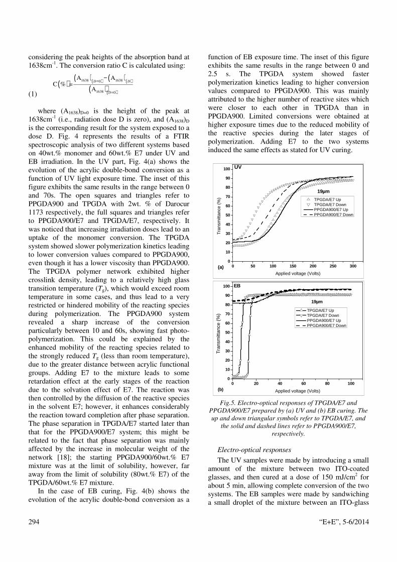
“E+E”, 5-6/2014 294
considering the peak heights of the absorption band at 1638cm-1. The conversion ratio C is calculated using:
(1) ( )
( )( ) ( )( )
( )( )
1638 16380
1638 0
A AC % =
AD D
D
=
=
−
where (A1638)D=0 is the height of the peak at
1638cm-1 (i.e., radiation dose D is zero), and (A1638)D is the corresponding result for the system exposed to a dose D. Fig. 4 represents the results of a FTIR spectroscopic analysis of two different systems based on 40wt.% monomer and 60wt.% E7 under UV and EB irradiation. In the UV part, Fig. 4(a) shows the evolution of the acrylic double-bond conversion as a function of UV light exposure time. The inset of this figure exhibits the same results in the range between 0 and 70s. The open squares and triangles refer to PPGDA900 and TPGDA with 2wt. % of Darocur 1173 respectively, the full squares and triangles refer to PPGDA900/E7 and TPGDA/E7, respectively. It was noticed that increasing irradiation doses lead to an uptake of the monomer conversion. The TPGDA system showed slower polymerization kinetics leading to lower conversion values compared to PPGDA900, even though it has a lower viscosity than PPGDA900. The TPGDA polymer network exhibited higher crosslink density, leading to a relatively high glass transition temperature (Tg), which would exceed room temperature in some cases, and thus lead to a very restricted or hindered mobility of the reacting species during polymerization. The PPGDA900 system revealed a sharp increase of the conversion particularly between 10 and 60s, showing fast photo-polymerization. This could be explained by the enhanced mobility of the reacting species related to the strongly reduced Tg (less than room temperature), due to the greater distance between acrylic functional groups. Adding E7 to the mixture leads to some retardation effect at the early stages of the reaction due to the solvation effect of E7. The reaction was then controlled by the diffusion of the reactive species in the solvent E7; however, it enhances considerably the reaction toward completion after phase separation. The phase separation in TPGDA/E7 started later than that for the PPGDA900/E7 system; this might be related to the fact that phase separation was mainly affected by the increase in molecular weight of the network [18]; the starting PPGDA900/60wt.% E7 mixture was at the limit of solubility, however, far away from the limit of solubility (80wt.% E7) of the TPGDA/60wt.% E7 mixture.
In the case of EB curing, Fig. 4(b) shows the evolution of the acrylic double-bond conversion as a
function of EB exposure time. The inset of this figure exhibits the same results in the range between 0 and 2.5 s. The TPGDA system showed faster polymerization kinetics leading to higher conversion values compared to PPGDA900. This was mainly attributed to the higher number of reactive sites which were closer to each other in TPGDA than in PPGDA900. Limited conversions were obtained at higher exposure times due to the reduced mobility of the reactive species during the later stages of polymerization. Adding E7 to the two systems induced the same effects as stated for UV curing.
0 50 100 150 200 250 3000
10
20
30
40
50
60
70
80
90
100
Tra
nsm
ittan
ce (
%)
Applied voltage (Volts)
TPGDA/E7 Up TPGDA/E7 Down PPGDA900/E7 Up PPGDA900/E7 Down
19µm
(a)
UV
0 20 40 60 80 1000
10
20
30
40
50
60
70
80
90
100
Tra
nsm
ittan
ce (
%)
Applied voltage (Volts)
TPGDA/E7 Up TPGDA/E7 Down PPGDA900/E7 Up PPGDA900/E7 Down
EB
(b)
19µm
Fig.5. Electro-optical responses of TPGDA/E7 and
PPGDA900/E7 prepared by (a) UV and (b) EB curing. The up and down triangular symbols refer to TPGDA/E7, and
the solid and dashed lines refer to PPGDA900/E7, respectively.
Electro-optical responses The UV samples were made by introducing a small
amount of the mixture between two ITO-coated glasses, and then cured at a dose of 150 mJ/cm2 for about 5 min, allowing complete conversion of the two systems. The EB samples were made by sandwiching a small droplet of the mixture between an ITO-glass

“E+E”, 5-6/2014 295
and a PET-ITO sheet, and then exposed to 120 kGy for about 2.45 s of residence time. This was achieved by fixing 2 mA of intensity and adjusting the speed of the conveyor belt.
Fig. 5 represents the electro-optical responses of UV and EB cured 19 µm thick samples. The up and down triangular symbols refer to TPGDA/E7, and the solid and dashed lines refer to PPGDA900/E7, respectively.
The plateau of the ON state transmission for UV systems was reached at higher voltages than that for EB systems. The threshold V10 and saturation V90 voltages increased strongly for UV systems than for EB systems i.e. UV systems require higher voltages to be activated. This might be related to the different types of morphologies obtained by the two curing methods. More regular morphology would be obtained in the case of EB [19-21]. Here, the higher crosslinking density of TPGDA/E7 and lower spacing between reactive double bonds yield smaller droplet sizes than for the PPGDA900/E7 system. For this reason the OFF state light transmission is reduced while the width of hysteresis is broadened. In the case of EB cured systems, one finds that V10 and V90 of TPGDA/E7 are much lower than for the PPGDA900/E7 system. The TOFF values remained near zero before and after applying the electric field meaning that there was practically no memory effect. Moreover, the maximum transmission TON of 90% can be achieved at a voltage as low as 17V and the width of hysteresis is also very narrow. The results found for the TPGDA/E7 system confirmed the conclusions made earlier by Gyselinck et al. [22] and Benkhaled et al. [23], that EB cured PDLC films exhibit better electro-optical responses compared to their analogous UV cured systems.
Conclusion In this study, some physical properties were
reported for the TPGDA/E7 and PPGDA900/E7 systems prepared by two different methods UV and EB curing. The investigation of the phase diagrams indicated that 60wt. % of E7 represents the limit of solubility for the PPGDA900/E7 mixture at room temperature. This composition was chosen also for the TPGDA/E7 mixture to work at the same E7 concentration. In the case of UV cured systems, the higher the molecular weight of the monomer (longer spacing between the two double bonds of the monomer or between two adjacent crosslinking points of the polymer network), the higher the mobility of reactive species, and the higher the rate of polymerization/crosslinking. In the case of the EB
cured systems, the lower the molecular weight of the monomer (shorter spacing between two adjacent crosslinking points), the higher the number of reactive species that are close to each other, and the higher the rate of polymerization/crosslinking. The LC E7 acts as a solvent for the reaction in the early stages of polymerization, and it enhances considerably the polymerization reactions for both methods of elaboration during the later stages of the reaction, due to its plasticizing effect. The electro-optical responses of the two systems showed that in the case of EB-curing, the lower the molar mass of the monomer (shorter spacing between adjacent crosslinking points), the better the electro-optical properties. However, in the case of UV curing, the longer the spacing between adjacent crosslinking points, the better the electro-optical properties.
Acknowledgements This work has been accomplished in the
framework of a french–algerian research program. The authors gratefully acknowledge the support of the C.N.R.S. and the Ministère Algérien de l'Enseignement Supérieur et de la Recherche Scientifique.
REFERENCES [1] Doane, J. W., Polymer dispersed liquid crystal
displays. In: Liquid Crystals –Applications and Uses, Bahadur, B. (Ed.), World Scientific: Singapore, 1990.
[2] Drzaic, P. S., Liquid Crystal Dispersions, World Scientific: Singapore, 1995.
[3] Kitzerow, H. S., Polymer-dispersed and polymer stabilized chiral liquid crystals. In: Liquid Crystals in Complex Geometries, G. P. Crawford, S. Zumer (Eds.), Taylor and Francis, London, 1996.
[4] Andrzejeewska, E., Prog. Polym. Sci., Vol. 26, 2001, pp.605-665.
[5] Decker, C., Prog. Polym. Sci., Vol. 21, 1996, pp.593-650.
[6] Decker, C., Elzaouk, B., Eur. Polym. J., Vol. 31, No 12, 1995, pp.1155-1163.
[7] Scherzer, T., Decker, U., Polymer, Vol. 41, 2000, pp.7681-7690.
[8] Anseth, K. S., Wang, C. M., Bowman, C. M., Macromolecules, Vol. 27, 1994, pp.650-655.
[9] Defoort, B., Defoort, D., Coqueret, X., Molecul. Theoret. Simul., Vol. 9, 2000, pp.725-734.
[10] Patasz, C., Defoort, B., Coqueret, X., Radiation Phys. Chem., Vol. 59, 2000, pp.329-337.
[11] Patasz, C., Coqueret, X., Decker, C., Radiation Phys. Chem., Vol. 62, 2001, pp.403-410.
“E+E”, 5-6/2014 296
[12] Maschke, U., Coqueret, X., Loucheux, C., Nuclear Instr. Meth. Phys. Res. B, Vol. 105, 1995, pp.262-266.
[13] Knolle, W., Mehnert, R., Nuclear Instr. Meth. Phys. Res. B, Vol. 105, 1995, pp.154-158.
[14] Méchernène, L., Benkhaled, L., Benaissa, D., Maschke, U., Opt. Mat., Vol. 31, 2009, pp.632-639.
[15] Bentley, W. G., Koenig, J.-L., Appl. Spectr., Vol. 51, 1997, p.1453.
[16] Derouiche, Y., Dubois, F., Douali, R., Legrand, C., Maschke, U., Mol. Cryst. Liq. Cryst., Vol. 541, 2011, pp. 201-210.
[17] Derouiche, Y., Ghefir, S. A. K., Dubois, F., Douali, R., Legrand, C., Azzaz, M., Maschke, U., I. R.E. PHY., Vol. 4, N.3, June 2010, pp.188-193.
[18] Berrayah, A., Zair, L., Olivier, A., Maschke, U., Phys Procedia, Vol. 2, 2009, pp.1119-1124.
[19] Lackner, A.-M., Margerum, J.-D., Ramos, E., Lim, K.-C., SPIE, Vol. 1080, 1989, p.53.
[20] Lackner, A.-M., Margerum, J.-D. Miller, L. J., Yamagishi, F.-G., Ramos, E., Lim, K.-C., Smith Jr., W.-H., van Ast, C.-I., Proceedings of the SID, Vol. 32, 1991, p.173.
[21] Carter, S.-A., LeGrange, J.-D., White, W., Boo, J., Wiltzius, P., J. Appl. Phys., Vol. 91, 1997, p.5992.
[22] Gyselinck, F., Maschke, U., Traisnel, A., Coqueret, X., Liq. Cryst., Vol. 27, 2000, p.421.
[23] Benkhaled, L., Méchernène, L., Traisnel, A., Benmouna, M., Gloaguen, J.-M., Coqueret, X., Maschke, U., Mol. Cryst. Liq. Cryst., Vol. 375, 2002, p.651.
Dr. Ulrich Maschke studied chemistry at the University
of Mainz (Germany) where he received his Master’s degree (Diploma) in 1989 working on the phase behavior of polymer blends (PMPS/PS). In 1992 he completed his PhD thesis at the Physics Department of the Max-Planck-Institut für Polymerforschung (MPI-P, Mainz) under the
supervision of Prof. Ewen on the ‘Static and dynamic properties of polymer melts studied by neutron scattering’. In 1992 he joined the Laboratory of Macromolecular Chemistry of the University of Sciences and Technologies of Lille (France) where he was offered a job (Chargé de Recherche) within the french national center of scientific research (CNRS). In 2001, he obtained the accreditation to supervise research from the University of Lille 1 (HDR). He is now Research Director of the CNRS (Directeur de Recherche) at the UMET (Unité Matériaux et Transformations – UMR 8207).
tel.:+33-3-20-33-63-81
е-mail:[email protected]
Prof. Dr. Zohra Bouberka - Laboratoire de Physico-Chimie des Matériaux, Université des Sciences et Techniques d’Oran (Algeria). Zohra Bouberka studied chemistry at the University of Science and Technology of Oran, USTO (Algeria), where she received her engineering degree in 1995. In 1998, she obtained her magister thesis at the University of Mostaganem (Algeria). Z. Bouberka got a permanent position as assistant professor at the chemistry department of the USTO while continuing to prepare her doctorate in chemical engineering under the supervision of Professor Zoubir Derriche. In 2005 she received her PhD degree at the Chemistry Department of the USTO on the ‘Study of pillared clay of Maghnia - applications’. In 2011 she was appointed full Professor at the USTO and is now leader of a laboratory working mainly on environmental issues. In particular she is interested in water pollution abatement by several methods including advanced oxidation methods.
е-mail: [email protected].
Mohammed Bouchakour – Department of Material Sciences, University of Djelfa, Djelfa (Algeria)
Dr. Yazid Derouiche – Department of Material Sciences, University of Djelfa, Djelfa (Algeria)

“E+E”, 5-6/2014 297
Radiation-Induced Degradation of Two Organic Pollutants from Aqueous Solution on Nanocomposites
Zohra Bouberka, Abdelouahab Nadim, A. Khalil Benabbou, Ulrich Maschke
TiO2 colloid / LDHs clay nanocomposites, prepared by direct coprecipitation method, were used
as photocatalysts in the reaction of (3-(4-chlorophenyl)-1,1-dimethylurea) and 4-chlorophenol decomposition in water. Mg2AlCO3 and Mg2FeCO3 were selected like support to different nature of TiO2 colloidal. The incorporation of TiO2 was confirmed by X-ray diffraction and BET specific surface area determination. The photodegradation rate of (3-(4-chlorophenyl)-1,1-dimethylurea (0,0044 min-
1) exceeds that of 4-chlorophenol (0,00075 min-1) under UV light irradiation on Mg2AlCO3 / TiO2, and the photoactivity of the supported catalyst Mg2FeCO3 / TiO2 was much higher for 4-chlorophenol (0,00135 min-1) than for 3-(4-chlorophenyl)-1,1-dimethylurea (negligible). The photodegradation rate of both pollutants using aged TiO2 colloidal particles was faster than that using supported catalysts.
Радиационно-индуцирана деградация на два органични замърсители от воден разтвор на нанокомпозити (З. Буберка, А. Надим, А. Бенабоу, У. Машке). Колоиден TiO2/слоест двоен хидроокис – нанокомпозит, приготвен чрез пряк копреципитатен метод бе използван за фотокатализатор при реакция на (3-(4-хлорфенил)-1,1-диметилурея) и 4-хлорфенолна декомпозиция във вода. Mg2AlCO3 и Mg2FeCO3 бяха избрани като основа за колоиден TiO2 с различна природа. Присъединението на TiO2 бе потвърдено с рентгенова дифракция и Brunauer–Emmett–Teller (BET) определяне на повърхностната площ. Скоростта на фото-деградиране на (3-(4-хлорфенил)-1,1-диметилурея (0,0044 min-1) превъзхожда тази на 4-хлорфенола (0,00075 min-1) под УВ радиация върху Mg2AlCO3/ TiO2, и фото-активността на катализа Mg2FeCO3 / TiO2 беше много по-висока за 4-хлорфенол (0,00135 min-1) отколкото за 3-(4-хлорфенил)-1,1-диметилуреята (пренебрежително малка). Скоростта на фото-деградация на двата замърсителя, използващи остарели TiO2 колоидни частици бе по-бърза отколкото тази, използваща катализ върху основа.
Introduction Numerous attacks are possible in nature, limiting
the growth of plants: insect pests, diseases (fungi, bacteria, viruses), weeds [1].
The pesticides belong to the category of chemicals used worldwide as herbicides, insecticides, fungicides, rodenticides, molluscicides, nematicides, and plant growth regulators in order to control weeds, pests and diseases in crops as well as for health care of humans and animals. A rapid emergence in pesticide use began mainly after World War II with the introduction of DDT (dichlorodiphenyltrichloroethane), BHC (benzene hexachloride), aldrin, dieldrin, endrin, and 2,4-D (2,4-dichlorophenoxyacetic acid) [2]. Herbici- des are applied for pre- or post-emergence control of weeds in cotton, fruit or cereal production, and also on non-cultivated areas such as roads and railways. They act as inhibitors of photosynthesis. In general, these
chemicals are characterized by long lifetimes in the environment and thus can be found as contaminants of surface and groundwater [3].
Among the herbicides, monuron and 2.4 dichlorophenol are already reported to be possibly carcinogenic for humans [4]. The other herbicides could also cause serious damage to humans [5].
The presence of herbicides in groundwaters, surface waters, effluents of wastewater treatment plants and other sources of drinking water indicates that conventional biological treatment processes are very slow or non-destructive for these kinds of compounds. A promising way to perform the mineralization of these type of substances is the application of advanced oxidation processes (AOP), that are characterized by the “in situ” production of •OH radicals under mild experimental conditions [6]. The photocatalysis has been successfully used for degradation of pesticides [7], polycyclic aromatic

“E+E”, 5-6/2014 298
hydrocarbons [8], textile dyes [9], spill oils [10], among other substrates of environmental relevance.
Many works have demonstrated the high degradation capacity of heterogeneous photocatalysis, mainly with the use of titanium dioxide (TiO2) as photocatalyst. TiO2 is the most preferable material due to its non-toxic, insoluble, stable, highly photoactive and inexpensive nature. Moreover, most of commercial TiO2 usually have small particle sizes so that TiO2 particles are difficult to recover from the suspension, such as by filtration [11]. To overcome these difficulties, many immobilized photocatalysts have been proposed, involving the use of glass-rings (Raschig rings) [12], glass-tubes [13], activated charcoal [14], and silica [15] among other support materials. In some situations, the use of immobilized photocatalysts reduces the efficiency of the degradation process, in view of the considerable reduction of disposable sites for adsorption and catalysis [16]. In other conditions, the use of immobilized photocatalysts enhances the efficiency of the degradation process, mainly on account of the preliminary adsorption of the substrates onto the support surface.
The layered double hydroxides (LDHs), also known as anionic clays or hydrotalcite-like compounds, could be suitable to smooth and even prevent the environmental impact caused by pesticides. These materials have very high exchange capacities. In this work, the potential of immobilized of TiO2 on LDHs was evaluated, toward the photocatalytic degradation of (3-(4-chlorophenyl)-1,1-dimethylurea), and 4-chlorophenol in aqueous solution.
Characterization of TiO2/HDLs photocatalysts will be reported employing powder X-ray diffraction (XRD), BET specific surface area determination, and the element content of solid catalyst was analyzed by X-ray fluorescence (XRF) spectrometer.
Experimental
A. Materials
The synthesis of Mg/Al-CO3 and Mg/Fe-CO3
LDHs with a molar ratio R= Al
Mg and
Fe
Mg =2 was
conducted using a constant-pH co-precipitation method. The pH of mixture was maintained at a value of 10 by the simultaneous addition of a (NaOH+Na2CO3) basic solution. The resulting precipitate was separated by three repeated washing/ centrifugation cycles and finally dried in air at room temperature.
The selected pesticides were (3-(4-chlorophenyl)-1,1-dimethylurea) (Monuron), and 4-chlorophenol. Fig. 1 shows the chemical structures of these substances.
(3-(4-chlorophenyl)-1,1-dimethylurea)
4-chlorophenol
Fig.1. Structures of pesticides used.
B. Preparation of colloidal photocatalysts
TiO2 colloids were prepared from hydrolysis of TiCl3. For rinsing purpose, triple distilled water was used. Concentrated TiCl3 of 3.5 ml was added to distilled water of 900 ml, drop-by-drop with vigorous stirring at 1°C, and a flaxen transparent TiO2 solution was obtained. The pH adjustment to 9 using 2M KOH was necessary to prevent the destruction of the structure of adsorbent due to reaction with acid. The TiO2 nanoparticles (12nm) were characterized by a Zetasizer Nano instrument. TiO2/LDHs were prepared by dropwise addition of a mixed salt solution (MII+MIII) into a reservoir containing 2 times the stoichiometric requirement of LDHs/TiO2 to maintain a constant pH at precipitation. The experimental setup for the synthesis of colloidal TiO2/LDHs is shown in Fig. 2.
Fig. 2. Experimental setup of synthesis of colloidal
TiO2/LDHs

“E+E”, 5-6/2014 299
C. Photocatalytic decomposition of azo dye
The experiments were carried out in a photocatalytic oxidation reactor. In the center of the cylindrical reactor, three 6W (Emax= 365 nm) UV lamps were used as light sources. The relative photocatalytic activities of various catalysts were evaluated by measuring the loss of pesticide in aqueous medium as a representative reaction. All irradiations were carried out under constant stirring. The photodegradation processes were cooled by water circulation to 20°C during the experiments. At given intervals of illumination, a sample of the catalysts particulate was collected, centrifuged, and the substrates were analyzed by UV–Vis spectroscopy using a UV spectrophotometer. The observed wavelength are 244 nm for Monuron and 224 nm for 4-Dichlorophenol, which corresponds to the maximum absorption wavelength.
Results and discussion
A. BET analysis
Nitrogen adsorption–desorption isotherms of Mg2AlCO3 and TiO2/Mg2AlCO3 samples are shown in Fig. 3. Their different appearances suggest the changes of the porosity characteristics when TiO2 is immobilized in the LDH network. For Mg2AlCO3, a type IV isotherm was observed according to the IUPAC classification [17] with a broad type H3 hysteresis loop, in the middle range of relative pressure.
Fig.3. Nitrogen isotherms of Mg2AlCO3 and TiO2/
Mg2AlCO3
The TiO2/Mg2AlCO3 composite presents particular characteristics: for P/P0 < 0.2, multilayer adsorption is present revealing microporous characteristics; for 0.2< P/P0< 0.8, the isotherm shape reveals the presence of a mesoporous material with a wide size range and for P/Po>0.8, the isotherm shape can be assimilated with
a type II isotherm, characteristic for adsorption in pores with sizes larger than 50 nm.
B. XRD analysis
From the XRD patterns (Fig. 4) of the synthesized samples, Mg2AlCO3, Mg2FeCO3, TiO2/Mg2AlCO3 and TiO2/Mg2FeCO3, it was observed that all samples possess reflections characteristic of the presence of a layered structure with sharp and intense lines at low values of 2θ angles, which were estimated from the peaks of (003), (006), and (009), and less intense and asymmetric ones (110) and (113) at higher values of 2θ angles, which are typical of a highly crystalline LDH structure [18]. The d003 spacing for the interlayered Mg2AlCO3, Mg2FeCO3, TiO2/Mg2AlCO3 and TiO2/Mg2FeCO3 are 7.61, 7.65, 7.41 and 7.56Å, respectively. Such values are close to the d-spacing values reported for the natural hydrotalcite with carbonate in the interlayer. The interlayer spacing of synthesized TiO2/Mg2AlCO3 and TiO2/Mg2FeCO3 materials remains practically unchanged compared to the original LDHs Mg2AlCO3 and Mg2FeCO3.
Fig.4. Powder X-ray diffraction patterns of Mg2AlCO3, Mg2FeCO3, TiO2/Mg2AlCO3, and TiO2/Mg2FeCO3.
Diffraction peaks characteristics of other solids were detected in the XRD spectra of TiO2/Mg2AlCO3 and TiO2/Mg2FeCO3, which correspond to the anatase
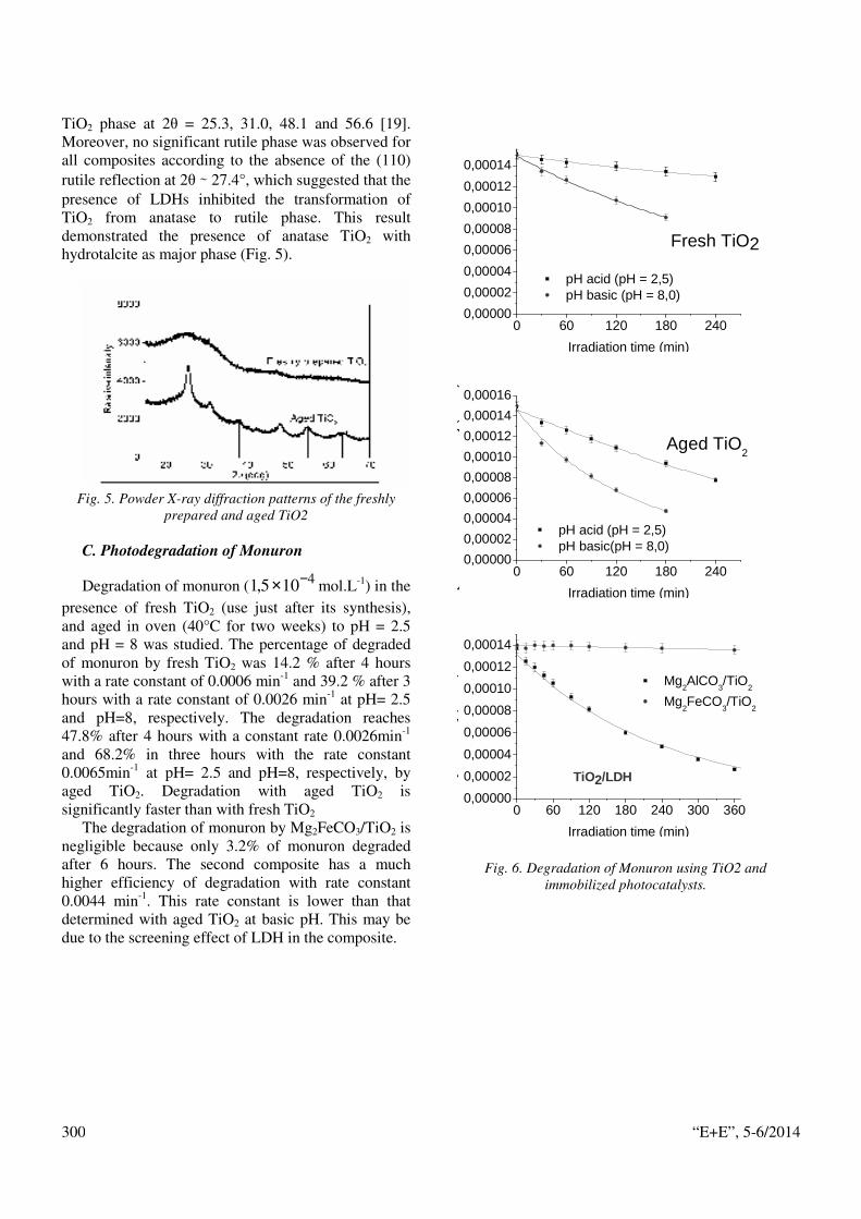
“E+E”, 5-6/2014 300
TiO2 phase at 2θ = 25.3, 31.0, 48.1 and 56.6 [19]. Moreover, no significant rutile phase was observed for all composites according to the absence of the (110) rutile reflection at 2θ ∼ 27.4°, which suggested that the presence of LDHs inhibited the transformation of TiO2 from anatase to rutile phase. This result demonstrated the presence of anatase TiO2 with hydrotalcite as major phase (Fig. 5).
Fig. 5. Powder X-ray diffraction patterns of the freshly
prepared and aged TiO2
C. Photodegradation of Monuron
Degradation of monuron ( 4105,1 −× mol.L-1) in the presence of fresh TiO2 (use just after its synthesis), and aged in oven (40°C for two weeks) to pH = 2.5 and pH = 8 was studied. The percentage of degraded of monuron by fresh TiO2 was 14.2 % after 4 hours with a rate constant of 0.0006 min-1 and 39.2 % after 3 hours with a rate constant of 0.0026 min-1 at pH= 2.5 and pH=8, respectively. The degradation reaches 47.8% after 4 hours with a constant rate 0.0026min-1 and 68.2% in three hours with the rate constant 0.0065min-1 at pH= 2.5 and pH=8, respectively, by aged TiO2. Degradation with aged TiO2 is significantly faster than with fresh TiO2
The degradation of monuron by Mg2FeCO3/TiO2 is negligible because only 3.2% of monuron degraded after 6 hours. The second composite has a much higher efficiency of degradation with rate constant 0.0044 min-1. This rate constant is lower than that determined with aged TiO2 at basic pH. This may be due to the screening effect of LDH in the composite.
Fig. 6. Degradation of Monuron using TiO2 and
immobilized photocatalysts.
0 60 120 180 240 300 3600,00000
0,00002
0,00004
0,00006
0,00008
0,00010
0,00012
0,00014
Mg2AlCO
3/TiO
2
Mg2FeCO
3/TiO
2
[mon
uron
] (m
ol/L
)
Irradiation time (min)
TiO2/LDH
0 60 120 180 2400,00000
0,00002
0,00004
0,00006
0,00008
0,00010
0,00012
0,00014
0,00016
pH acid (pH = 2,5) pH basic(pH = 8,0)
[con
cent
ratio
n en
mon
uron
] (m
ol/L
)
Irradiation time (min)
Aged TiO2
0 60 120 180 2400,00000
0,00002
0,00004
0,00006
0,00008
0,00010
0,00012
0,00014
pH acid (pH = 2,5) pH basic (pH = 8,0)
Irradiation time (min)
Fresh TiO2

“E+E”, 5-6/2014 301
D. Photodegradation of 4-chlorophenol
The degraded percentage of 4-chlorophenol 4105,1 −× mol. L-1) is 90.2 % by aged TiO2 with rate
constant 0.00708 min -1 and 52.6 % with rate constant 0.00258 min-1 at acid and basic pH, respectively.
For the Mg2FeCO3/TiO2 composite, 40.1% of 4-CP was degraded in 6 hours and 87.6 % in one day, the rate constant was 0.00135 min-1. For the TiO2/Mg2AlCO3 composite, 24.9% of 4-CP was degraded in 6 hours and 53.2% in one day, the rate constant was 0.00075 min-1.
The rate constant of 4-CP by Mg2FeCO3/TiO2 composite is greater than for the second composite. The composites exhibit a different behavior with the two pollutants studied. The Mg2FeCO3/TiO2 is not effective for monuron degradation but with 4-chlorophenol, the rate constant is higher than for the TiO2/Mg2AlCO3 composite.
Fig.7. Degradation of 4-chlorophenol using TiO2 and immobilized photocatalysts.
Conclusions
LDH supported catalysts (TiO2/Mg2Al, TiO2/Mg2Fe) were synthesized by using the co-precipitation at constant pH method, and characterized by different physical techniques. The supported catalysts effectively removed some pesticide from solution, and the rate of degradation was significantly better than that of bare colloidal TiO2. The
performance improvement can be attributed to the high surface areas of the adsorbent used, crystallinity, and particle size of deposited TiO2.
REFERENCES [1] E-C. Oerke, J. Agric Sci. 144 (2006) 31.
[2] A. Agrawal, RS.Panday, B. Sharma. J. water. res. Prot. 2 (2010) 432
[3] S. R. Sorensen, G.D. Bending, C.S. Jacobsen, A. Walker , J. Aamand. Chemosphere. 58 (2005) 1127.
[4] N.N. Ragsdale, R.E. Menzer. Am. Chem. Soc. Washington, DC. 1989.
[5] H. Lin, Y. Sung, S. Huang. J. Chroma. A.1012 (2003) 57.
[6] A. Topalov, B. Abramovi, D. Molnár-Gábor, J. Csanádi, O. Arcson, J. Photochem. Photobiol. A. Chem. 140 (2001) 249.
[7] S. Devipriya, S. Yesodharan. Sol Energy Mater. Sol. Cells. 86 (2005) 309.
[8] O. T. Woo, W. K. Chung, K. H Wong, A.T. Chow, P. K. Wong. J. Hazard Mater. 168 (2009) 1192.
[9] G. Zayani, L. Bousselmi, F. Mhenni, A. Ghrabi. Desalination 246 (2009) 344.
[10] Y.-Y. Hsu, T.-L. Hsiung, H.P. Wang, Y. Fukushima, Y.-L. Wei, J.-E. Chang, Mar. Pollut. Bull. 57 (2008) 873.
[11] M.J. Farre, X. Domenech, J. Pera. Water Res. 40 (2006) 2533
[12] M. C. Yeber , J.Rodríguez, J. Freer, N. Durán, H. D. Mansilla. Chemosphere 41 (2000) 1193.
[13] Lee, J.-C.; Kim, M-S.; Kim, B.-W.; Water Res. 2002, 36, 1776.
[14] X. Wang, Y. Liu, Z. Hu, Y. Chen, W. Liu, G. Zhao. J. Hazard Mater. 169 (2009) 1061.
[15] P. Pucher, M. Benmami, R. Azouani, G. Krammer, K. Chhor, J.-F. Bocquet, A. V. Kanaev. Appl. Catal., A. 332 (2007) 297.
[16] G. Mascolo, R. Comparelli, M.L. Curri, G. Lovecchio, A. Lopez, A. Agostiano, J. Hazard Mater. 142 (2007) 130.
[17] K.S.W. Sing, D.H. Everett, R.A.W. Hall, L. Moscou, R.A. Pierotti, J. Rouquérol, T. Siemieniewska, IUPAC Recommendations 1984, Pure Appl. Chem. 57 (1985) 603.
[18] S. Miyata, T. Kumura, Chem. Letters.1973, 843.
[19] J. Liqiang, S. Xiaojun, C.Weimin, X. Zili, D. Yaoguo, J. Phys. Chem. Solids. 64 (2003) 615.
Prof. Dr. Zohra Bouberka - Laboratoire de Physico-Chimie des Matériaux, Université des Sciences et Techniques d’Oran (Algeria). Zohra Bouberka studied chemistry at the University of Science and Technology of Oran, USTO (Algeria), where she received her engineering
0 60 120 180 240 300 3600,00000
0,00002
0,00004
0,00006
0,00008
0,00010
0,00012
0,00014
0,00016 pH acid (pH = 2,5) pH basic (pH = 8,0)
[4-C
P] (
mol
/L)
Irradiation time (min)
Aged TiO 2
0 60 120 180 240 300 3600,00000
0,00002
0,00004
0,00006
0,00008
0,00010
0,00012
0,00014
Mg2AlCO
3/TiO
2
Mg2FeCO
3/TiO
2
[con
cent
ratio
n en
4-C
P] (
mol
/L)
Irradiation time (min)
TiO2/LDHs

“E+E”, 5-6/2014 302
degree in 1995. In 1998, she obtained her magister thesis at the University of Mostaganem (Algeria). Z. Bouberka got a permanent position as assistant professor at the chemistry department of the USTO while continuing to prepare her doctorate in chemical engineering under the supervision of Professor Zoubir Derriche. In 2005 she received her PhD degree at the Chemistry Department of the USTO on the ‘Study of pillared clay of Maghnia - applications’. In 2011 she was appointed full Professor at the USTO and is now leader of a laboratory working mainly on environmental issues. In particular she is interested in water pollution abatement by several methods including advanced oxidation methods.
е-mail: [email protected].
Dr. Ulrich Maschke studied chemistry at the University of Mainz (Germany) where he received his Master’s degree (Diploma) in 1989 working on the phase behavior of polymer blends (PMPS/PS). In 1992 he completed his PhD thesis at the Physics Department of the Max-Planck-Institut für Polymerforschung (MPI-P, Mainz) under the supervision of Prof. Ewen on the ‘Static and dynamic
properties of polymer melts studied by neutron scattering’. In 1992 he joined the Laboratory of Macromolecular Chemistry of the University of Sciences and Technologies of Lille (France) where he was offered a job (Chargé de Recherche) within the french national center of scientific research (CNRS). In 2001, he obtained the accreditation to supervise research from the University of Lille (HDR). He is now Research Director of the CNRS (Directeur de Recherche) at the UMET.
tel.:+33-3-20-33-63-81
е-mail:[email protected]
Abdelouaheb Nadim - Unité Matériaux et Transformations – UMET (UMR CNRS N° 8207), Bâtiment C6, Université Lille 1 - Sciences et Technologies, 59655 Villeneuve d’Ascq Cedex (France).
A. Khalil Benabbou - Laboratoire de Physico-Chimie des Matériaux - Catalyse et Environnement, Université des Sciences et Technologies d’Oran (Algeria).

“E+E”, 5-6/2014 303
COMPLEMENTARY TECHNOLOGIES BASED ON USE OF ELECTRONS, IONS, PLASMA AND LASERS
Non-Vacuum Electron Beam Cutting - a New High Performance
Process
T. Hassel, N. Murray, A. Beniyash, N. Rempe, S. Kornilov
The electron beam is a tool with high energy conversion efficiency which is by and large
independent of the type of metal. Its high power density qualifies the non-vacuum electron beam as an outstanding energy source for the widely used NVEB welding as well as for a new high speed cutting tool. Experimental results for a new cutting process using the suction created by a local low vacuum underneath the work piece are shown. A co-moving cutting head with a sliding seal has been produced tested. Extremely high cutting speeds such as 17 m/min for 2.5 mm thick stainless steel producing high quality edges render this method a significant development for new NVEB applications. NVEB cutting and subsequent welding can be done on one integral machine realizing a fast and efficient twin process. Due to direct removal of fumes and dust, NVEBC with local suction is an exceptionally clean and fast process. Moreover, results of preliminary experiments are presented for a 60 kV glow discharge electron beam gun which was projected into open atmosphere, i.e. non-vacuum conditions. The potential directions of development of non-vacuum electron beam technologies using PC gun technology are discussed.
Извън-вакуумно електроннолъчево рязане-един нов високопроизводителен процес (Т. Хассел, Н. Муррай, А. Бениаш, Н. Ремпе,С. Корнилов). Електронният лъч е инструмент с висока ефективност на преобразуване на енергията, при практическа независимост от типа на метала. Голямата плътност на мощност класифицира извън-вакуумния електронен лъч, като изключителен енергиен източник за широки приложения като извън-вакуумно електроннолъчево заваряване и като нов високоскоростен източник за рязане. Показани са експериментални резултати за новия процес на рязане, използващ всмукване на течния метал, постигнато с локален нисък вакуум, отдолу на образеца. Тествана е едновременно движеща се режеща глава с плъзгащо се уплътнение. Много висока скорост на рязане, например 17 m/min за 2.5 mm дебела неръждаема стомана с висококачествени ръбове позволява този метод да се прилага при много нови приложения. Извън-вакуумното рязане и последващо заваряване може да се прави на една интегрална машина реализираща бърз и ефективен двоен процес. Поради едновременното отнемане на опушването и прашинките, извън-вакуумното електроннолъчево заваряване с локално всмукване е изключително чист и бърз процес. Нещо повече, резултатите от предварителните експерименти са представени за 60 kV пушка с тлеещ разряд, която бе използвана за създаване на сноп в откритата атмосфера, т.е. извън вакуума. Дискутирани са потенциалните направления на прилагането на извън-вакуумните електроннолъчеви технологии с компютърно управление.
Introduction The high efficiency of energy conversion of an
electron beam makes it a valuable tool for any kind of thermal treatment of metal. The electron beam is routinely used for welding in vacuum, in low
pressure and under atmospheric conditions. In all cases, the electron beam is inevitably generated in high vacuum. The welding process at atmospheric conditions is known as non-vacuum electron beam welding (NVEBW). Differentially pumped pressure

“E+E”, 5-6/2014 304
stages act as a beam guide between the high vacuum beam generator chamber and the atmosphere [5].
Thermal cutting with an electron beam as energy source has been shown by our group [1,2,4], indicating a high potential to establish the non-vacuum electron beam as a tool to allow cutting and welding on the same equipment with high efficiency and productivity. A new approach to realize high cutting speed and top quality cut surface properties will be presented in the following.
Most thermal cutting processes employ a concentrated gas jet directed onto the process zone to remove molten metal from the kerf. This is usually realized by a gas jet that is concentric to an energy source; for other variations it can be either trailing, leading, or from the side. In previous work we were able to show that such a cutting process can be realized for NVEB by adapting a trailing gas jet to existing technology [1,2]. A gas nozzle taken from a standard oxy-cutter was mounted on the NVEB-welder KU-175-25 (PTR Praezisionstechnik) with an acceleration voltage of 175 kV and a maximum beam power of 24.5 kW.
In another approach we were able to show a completely novel method of thermal cutting. By providing a local vacuum underneath the plate it is possible to remove molten material as well as fumes and dust without the need to use a high pressure gas jet.
NVEB-cutting by local suction A new approach to remove molten metal employs
a local low vacuum underneath the process zone. The electron beam is used to produce a cutting kerf and due to the pressure difference between both sides of the workpiece a strong gas flow is induced across the melting front, carrying molten and evaporated metal as well as smoke away from the process zone. This allows taking advantage of several aspects that permit very high cutting speeds. The gas flow can interact precisely at the melt front and will force the molten metal downwards. Other than for a trailing gas jet there is no dependence on the direction of the cut, so that curved contours can easily be realized. It is important to remark that this method requires no change to the beam generator or pressure stage system of the original NVEB welder. This means that the machine can be immediately used for both processes - cutting and welding.
Another advantage of this method is due to the pressure gradient along the kerf. The pressure decreases from atmospheric pressure to the low pressure underneath the workpiece, reducing the
collision frequency of electrons with gaseous atoms and molecules. This leads to higher power density in the process zone - compared to that of a NVEB welding process – so that even thicker sheets can be cut at higher speeds.
Static cutting box for parameter evaluation To evaluate the prospects of this method a small
air-tight box with a 3.5 x 20 cm sized slot is used as a small and simple testing rig (Fig. 1). The workpiece is placed to cover the slot. To provide low pressure at the lower side of the workpiece a pump taken from commercial vacuum clamping technology is used. A simple rubber gasket provides enough sealing that pressure regularly reaches 20-100 mbar depending on surface quality and deformation of the workpiece in less than one second. Deflector plates and fine steel mesh filters as well as 10 m long PVC-tubing were used to protect the vacuum pump from hot metal droplets.
Fig. 1. NVEB cutting process by local under-pressure.
Several specimens of different metals and thickness were cut with this installation. Among those were stainless steel, mild steel, aluminium, copper and molybdenum. Cutting speeds were higher and quality was better compared to the experiments with a trailing gas jet. The downward suction efficiently removes fumes and smoke, making it possible to position the beam nozzle closer to the work piece compared to the non-vacuum EB welding application without arcing in the generatorError! Reference source not found.. This allows taking advantage of the higher power density and smaller beam diameter. In addition to the effect of the aforementioned pressure gradient within the kerf both circumstances allow a faster feed rate as well as a narrower cut with little widening of the kerf and a conceivably smaller heat-affected zone.
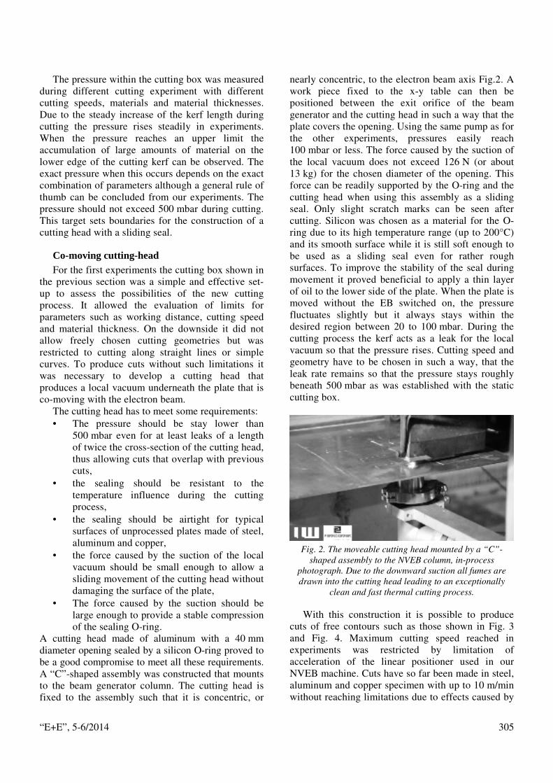
“E+E”, 5-6/2014 305
The pressure within the cutting box was measured during different cutting experiment with different cutting speeds, materials and material thicknesses. Due to the steady increase of the kerf length during cutting the pressure rises steadily in experiments. When the pressure reaches an upper limit the accumulation of large amounts of material on the lower edge of the cutting kerf can be observed. The exact pressure when this occurs depends on the exact combination of parameters although a general rule of thumb can be concluded from our experiments. The pressure should not exceed 500 mbar during cutting. This target sets boundaries for the construction of a cutting head with a sliding seal.
Co-moving cutting-head For the first experiments the cutting box shown in
the previous section was a simple and effective set-up to assess the possibilities of the new cutting process. It allowed the evaluation of limits for parameters such as working distance, cutting speed and material thickness. On the downside it did not allow freely chosen cutting geometries but was restricted to cutting along straight lines or simple curves. To produce cuts without such limitations it was necessary to develop a cutting head that produces a local vacuum underneath the plate that is co-moving with the electron beam.
The cutting head has to meet some requirements: • The pressure should be stay lower than
500 mbar even for at least leaks of a length of twice the cross-section of the cutting head, thus allowing cuts that overlap with previous cuts,
• the sealing should be resistant to the temperature influence during the cutting process,
• the sealing should be airtight for typical surfaces of unprocessed plates made of steel, aluminum and copper,
• the force caused by the suction of the local vacuum should be small enough to allow a sliding movement of the cutting head without damaging the surface of the plate,
• The force caused by the suction should be large enough to provide a stable compression of the sealing O-ring.
A cutting head made of aluminum with a 40 mm diameter opening sealed by a silicon O-ring proved to be a good compromise to meet all these requirements. A “C”-shaped assembly was constructed that mounts to the beam generator column. The cutting head is fixed to the assembly such that it is concentric, or
nearly concentric, to the electron beam axis Fig.2. A work piece fixed to the x-y table can then be positioned between the exit orifice of the beam generator and the cutting head in such a way that the plate covers the opening. Using the same pump as for the other experiments, pressures easily reach 100 mbar or less. The force caused by the suction of the local vacuum does not exceed 126 N (or about 13 kg) for the chosen diameter of the opening. This force can be readily supported by the O-ring and the cutting head when using this assembly as a sliding seal. Only slight scratch marks can be seen after cutting. Silicon was chosen as a material for the O-ring due to its high temperature range (up to 200°C) and its smooth surface while it is still soft enough to be used as a sliding seal even for rather rough surfaces. To improve the stability of the seal during movement it proved beneficial to apply a thin layer of oil to the lower side of the plate. When the plate is moved without the EB switched on, the pressure fluctuates slightly but it always stays within the desired region between 20 to 100 mbar. During the cutting process the kerf acts as a leak for the local vacuum so that the pressure rises. Cutting speed and geometry have to be chosen in such a way, that the leak rate remains so that the pressure stays roughly beneath 500 mbar as was established with the static cutting box.
Fig. 2. The moveable cutting head mounted by a “C”-
shaped assembly to the NVEB column, in-process photograph. Due to the downward suction all fumes are drawn into the cutting head leading to an exceptionally
clean and fast thermal cutting process.
With this construction it is possible to produce cuts of free contours such as those shown in Fig. 3 and Fig. 4. Maximum cutting speed reached in experiments was restricted by limitation of acceleration of the linear positioner used in our NVEB machine. Cuts have so far been made in steel, aluminum and copper specimen with up to 10 m/min without reaching limitations due to effects caused by

“E+E”, 5-6/2014 306
friction of the sliding seal. Upper limits for the performance of the sliding seal have yet to be established.
Fig. 3. Free contour cut by electron beam with a co-moving
cutting head.
Fig. 4. Oval cut-outs produced by NVEBC with co-moving
cutting head.
NVEB-Cutting of stainless steel Stainless steel plates with 2.5 mm thickness were
cut with 2 mm working distance with up to 18.5 m/min producing high quality edges with only moderate bevel and minimal residual melt drops at the lower edge (Fig. 5).
Metallographic examinations of the cut edges of 2.5 mm stainless steel are displayed in Fig. 6. A zone of 20-45 µm thickness exhibits alterations caused by the cutting process. Other than that, no further influence due to the process is discernible from this analysis.
In further experiments stainless steel plates of 30 mm thickness have been cut. A cutting speed of 600 mm/min at a working distance of 3 mm for 24.5 kW beam power was achieved. Some slag adhering to the bottom cut edge could not be avoided, Fig. 7.
Fig. 5. Profile of an NVEB cut of 2.5 mm stainless steel
(1.4301) with 17 m/min at 24.5 kW.
Fig. 6: Macro- and micrograph of NVEB cut edges of stainless steel (1.4301).
Fig. 7. NVEB cut of 30 mm stainless steel with 600 mm/min at 24.5 kW. The specimen was produced by cutting into the plate from the side; the photograph shows the start edge of
the cut.
NVEB-Cutting of copper Thermal cutting of copper has to meet the distinct
material properties of the material [3]. Above all, it has the second highest thermal conductivity of all metals. This leads to a high heat flux away from the melting front, making it necessary to employ a high power density process. The application of laser cutting is possible but impeded by the high reflectivity of copper for typical laser wavelengths.

“E+E”, 5-6/2014 307
In contrast to that, the efficiency of energy conversion of an electron beam is essentially independent of the type of metal or the surface finish. Cutting experiments haven been done with copper plates of 6 mm and 10 mm thickness. The 6 mm plates could be cut with a speed of 9 m/min at a working distance of 2 mm, Fig. 8.
Fig. 8. Macro-section of NVEB-cut of 6 mm thick ETP-
copper with 9 m/min at 24.5 kW.
Fig. 9. Micro-section of NVEB-cut of 6 mm thick ETP-
copper with 9 m/min at 24.5 kW.
Cutting and welding in subsequent steps on the same NVEB machine
One of the major advantages of non-vacuum electron beam welding is its insensitivity against imperfectly prepared edges. It was shown that
NVEB-cut plates could be welded in a subsequent step without altering the machine setup.
The non-vacuum electron beam welding process allows large tolerances due to the scattering of the beam in high pressure environments. The slightly beveled and imperfect surfaces of the NVEB-cuts by trailing gas jet can successfully be welded, using the atmospheric electron beam without further preparative steps. In that way a tool has been created that allows weld preparation and welding with the same equipment [2].
Non-vacuum EB cutting using a 60 kV beam generator with plasma cathode
The well-known NVEB welding process with 150-175 kV is usually applied with a stand-off distance (working distance) of typically 15-30 mm between exit orifice and work piece. In contrast to this, the NVEB cutting process with downward suction can be performed with much smaller working distances. In experiments we regularly used working distances in the range of 2-4 mm with no increase of HV breakdown rate or too much heat input into the exit orifice. This is due to efficient removal of fumes and dust resulting in less contamination of the vacuum within the beam generator as well as lower heat input into the beam exit assembly due to the absence of a melt pool. These factors lead to different demands on the range of the electrons in atmosphere and in turn on the high-voltage of the beam generator. It is feasible to perform NVEBC with downward suction with much lower high-voltage (e.g. 60 kV). To test this, a pressure stage system was constructed and then fitted to a 60 kV plasma cathode EB gun made by Elion Ltd provided by Perndorfer KG. This combination allows to profit from advantages of the plasma cathode technology: • Plasma cathode beam generator is more robust
and has a higher life time compared to thermionic sources
• Diode EB gun design leads to favorable beam shape (small opening angle) for the construction of pressure stage system
These specifications allowed the construction of a very compact and light-weight pressure stage system. A main feature of the pumping system is the use of a turbo pump for the second pumping stage. This reduces the overall power consumption of the pumping system. At the same time only one heavy and inflexible vacuum tube needs to be mounted to a fixed pumping station, all other forline pumping connections can be realized with highly flexible DN25 and DN40 PVC tubes. Despite the low

“E+E”, 5-6/2014 308
acceleration voltage of only 60 kV we were able to transmit up to 60-64% of the beam power through the pressure stage system. The new NVEB system was mounted to a KUKA KR150 industrial robot, Fig. 10. This set-up was then tested by cutting of 1.5 mm thick zinc-coated steel plates with a speed of 1.6 m/min at 45 mA (2.7 kW), Fig. 11.
Fig. 10: Electron beam from a 60 kV plasma cathode EB gun transmitted to the atmosphere by a light and compact
pressure stage system.
Fig. 11: NVEBC specimen made of 1.5 mm thick steel with
zinc coating. Cut with 45 mA with 1.6 mm/min.
It is well known, that higher acceleration voltage will lead to a larger range of electrons in atmosphere as well as within the pressure stages during transfer from vacuum. EB guns with plasma cathode with higher acceleration voltage are currently being developed and should vastly improve the transmission efficiency of the pressure stage system as well as the cutting performance of the NVEBC process. In this way, the advantages of the plasma cathode beam emitters can be exploited for a flexible and very efficient high-power cutting process.
Conclusions It has been shown that non-vacuum electron beam
cutting is a promising new process with high cutting speeds and efficiency. A movable cutting head for cutting of contours and shapes with this process has been shown. Future prospects of this technology employing plasma cathode electron beam emitters instead of conventional thermionic emitters have been shown. With the arrival of plasma cathode EB guns with higher acceleration voltage this can be major step towards a highly flexible, high-speed cutting process.
Acknowledgements We would like to thank our partners Perndorfer
Maschinenbau KG who support our research with great enthusiasm and expertise as well as the German Research Society (DFG) who fund a research project for a profound look into this promising technology.
REFERENCES [1] N. Murray, A. Beniyash, R. Konya, Fr.-W. Bach,
T. Hassel: Non-Vacuum Electron Beam Cutting; International Electron Beam Welding Conference, FABTECH International and AWS Welding Show, Chicago, 17.-18. Nov. 2009
[2] T. Hassel, N. Murray, R. Konya, A. Beniyash, Fr.-W. Bach: Nonvacuum electron beam cutting and welding—two partnering processes for fast and highly efficient metal working, Welding in the World, May 2013, Volume 57, Issue 3, pp 315-322
[3] Murray, R. Konya, A. Beniyash, Fr.-W. Bach, T. Hassel: Schneiden und Schweißen von Kupfer mit dem Nonvakuum-Elektronenstrahl; Metall – Fachzeitschrift fuer Metallurgie, 65. Jahrgang, pp. 451-454, ISSN 0026-0746, Giesel Verlag GmbH, Hannover, 2011
[4] N. Murray, R. Konya, A. Beniyash, Fr.-W. Bach and T. Hassel, New advances in non-vacuum electron beam cutting, 2nd International Electron Beam Welding Conference (Aachen, Germany), DVS-Berichte 285, ISBN: 978-3-87155-299-1, DVS Media GmbH, Düsseldorf, 2012
[5] K.-R. Schulze, Schweißen & Schneiden compact knowledge, Volume 1e - Electron beam technologies, p. 64-75, ISBN: 978-3-87155-227-4, DVS Media, Düsseldorf, 2012
Dr.-Ing. Thomas Hassel was born in 1969 in Merseburg/Germany, graduated as a doctor engineer focused in materials science at the Leibniz University of Hanover/Germany in 2008. After his professional education as a mechanic in 1988 and his further academic studies of materials science, since 2001 he worked as a scientific assistant at the department of materials science of the Leibniz University of Hanover/Germany. Since 2008, he has been the head of the underwater technology center of
“E+E”, 5-6/2014 309
the institute of materials science. His research fields are welding and cutting technologies, especially thermal electron beam treatment of materials.
tel.: +4905117629813 е-mail: hasseliw.uni-hannover.de
Dipl.-Phys. Nils Murray was born in 1978 in Hanover/Germany. He graduated as a physicist at Leibniz University of Hanover/Germany (LUH) in 2008. Since then he has been working as a researcher in the field electron beam welding and cutting at the Institute of Materials Science at LUH.
tel.: +4905117629843 е-mail: murrayiw.uni-hannover.de
Dipl.-Ing. Alexander Beniyash was born in 1946 in Galitsch/Russia, graduates as a semiconductor technology engineer at TU St. Petersburg in 1970. In 1996, he immigrated to Germany. Since 2000, he has been working at the Institute of Material Science at the Leibniz University of Hanover/Germany, as a researcher in the field of electron beam welding.
tel.: +4905117629820 е-mail: [email protected]
Prof. Dr. Nikolay Rempe was born in 1955 in Siberia/Russia, graduated as an electronic technology engineer at Tomsk State University of Control Systems and Radioelectronics (TUSUR, Tomsk, Russia). In 2010, he received his DPhil degree. He has been working as a professor at the physics department of TUSUR and as a director of Elion Ltd.
tel.: +73822414859 е-mail: [email protected]
Assoc. Prof. Dr.-Ing. Sergey Kornilov was born in 1984 in Ekibastuz/Kazakhstan, graduated as an electronic technology engineer at Tomsk State University of Control Systems and Radioelectronics (TUSUR, Tomsk, Russia). From 2006 to 2010, he was a postgraduate student and assistant at the physics department of TUSUR. In 2010, he received his PhD degree. Since 2011, he has been working as an associate professor at the physics department of TUSUR and as an executive director of Elion Ltd.
tel.: +73822701507 е-mail: [email protected]

“E+E”, 5-6/2014 310
Electron Beam Micromachining of Plastics
Libor Dupák
This paper describes some possibilities of using electron beam welder to machine plastics.
Several different types were tested including PC, PMMA, PVC, PTFE, PE and PP. For initial study how certain material reacts to the electron beam, the sets of lines were cut onto the surface. Lines were done by the deflection system by the electron beam with different parameters. The dimensions of the lines (depth, width, ridge height) were measurement. However, that was not always possible due to melted material refilling the grooves.
For further study of surface structuring a testing pattern was used. It consisted of 6×10 squares, each 1×1 mm in size. The squares were engraved line by line with pitch of 0.083 mm (i.e. 12 lines/mm). The intensity of the colour of the square determined the speed of the beam movement, thus the melted volume. This way a stepped structure was created. Profile of the engraved structure was measured on the contact profilometer. Depth of the steps ranges from several to hundreds micrometers depending on the beam speed and the plastics.
Електроннолъчева размерна обработка на пластмаси (Либор Дюпак). Тази работа описва някои възможности за използване на машина за електроннолъчево заваряване да обработва размерно (реже, пробива, фрезова) пластмаси. Няклко различни типове бяха тествани включително PC, PMMA, PVC, PTFE, PE и PP. Първоначално - за изясняване как всеки материал реагира на електронно облъчване, серия линии бяха фрезовани върху повърхността. Линиите се правеха от отклоняващата система със снопове с различни параметри. Размерите на линиите (дълбочина, ширина, височина на ръба) бяха измерени. Това не бе във всички случаи възможно, понеже стопен материал запълваше отново каналите.
Понататък бе използван един тестов рисунък. Той съдържа 6×10 квадрата, всеки с размери 1×1 mm. Квадратите се гравираха линия след линия на разстояние 0,83 mm (т.е. 12 линии/ mm). Интензитетът на цвета на квадрата определя както скоростта на преместването на лъча, така и обема на стопения метал. По този начин бе създадена една стъпало-образна структура. Профилът на получената структура бе измерен с контактен профилометър. Дълбочината на стъпалата се намира в областта от няколко до стотици микрометри в зависимост от скоростта на лъча и от пластмасата.
Introduction The name “plastics” generally refers to a variety of
synthetic or semisynthetic polymeric materials with various properties. The electron beam is often used to drilling and machining of various kinds of materials, both metals [1] and non-metals [2]. The plastics were neglected, mainly because they are insulators and contain a lot of gasses that get released when heated. The aim of this work was to find out some basics about machining of the plastics by the electron beam.
Experiments The presented experiments were performed on the
desktop electron beam welder MEBW-60/2 [3], [4]
developed at the Institute of Scientific Instruments AS CR, v.v.i. at Brno. It is also manufactured and sold by the Focus GmbH company [5] under licence. Our EB welder operates with accelerating voltage of up to 60 kV. The maximum power is 2 kW (33 mA at 60 kV or 40 mA at 50 kV). However, in the presented work only low beam powers were used (up to 1.0 mA at 50 kV).
The welder can be fully computer-controlled, including welding along a preset trajectory [6]. The software also includes diagnostic functions that allow easy measurement of the beam width using a Faraday cell.
For the initial study how certain plastics react to the electron beam, the sets of lines were cut onto the

“E+E”, 5-6/2014 311
surface. Lines were done by the deflection system by the electron beam with different parameters. However, that was not always possible due to melted material refilling the grooves. Thus the lines served as mainly as a starting point for pattern engraving.
For further study of surface structuring a testing pattern was used (Fig. 1.). It consisted of 6 lines with 10 squares; each square was 1x1 mm in size, so the size of the final structure was 10×6 mm. The squares were engraved line by line with pitch of 0.083 mm (i.e. 12 lines/mm). The intensity of the colour of the square determined the speed of the beam movement, thus the melted volume. The brighter the color, the faster the speed. This way a stepped structure was created. Profile of the engraved structure was measured on the contact profilometer KLA Tencor Alphastep D-120.
Beam parameters used for the engraving of the test patterns shown in this paper were: HV: 50 kV, beam current 0.3 mA, engraving speed 3000 mm/s.
Fig.1. Testing pattern for engraving
Results Plastics are usually very porous and are able to
absorb high volume of gases. After heating by the electron beam the gas is released and chamber pressure is rising. If the amount of released gas is low, vacuum system can pump it out. However if the rise is high, the safety electronics cuts out the HV and cathode heating. Also, there is a risk of discharges in HV part that cuts off the electron beam and therefore interrupts the machining for a short time. Due to these reasons only small amount of material should be heated at the same moment.
The trapped gasses were escaping from the molten material as bubbles. As it solidified, these bubbles couldn’t move more and thus creating the “bubbly” surface in the groove (Fig. 2). The specific texture depended on the plastics and used beam parameters.
Polytetrafluorethylen (PTFE, teflon)
Polytetrafluorethylene (Teflon) is probably the most common high temperature plastics with a wide variety of use. The set of lines (Fig. 3.) was created in Teflon block. Detail of one line is in Fig. 4.As with other materials part of the melted matter is pushed out of the groove and solidifies at the edges. However, in this case the ridge is very small, barely apparent. Width of the lines varied from 50 to 250 µm. Depth varied 30 to 500 µm for beam current ranging from 0.1 mA to 0.5 mA and beam speed from 100 mm/s to 5000 mm/s.
Fig.2. Surface of the groove (Teflon)
Fg.3. Lines in teflon, block width 30 mm, thickness 6 mm
The engraved testing pattern is shown Fig. 5 with the steps clearly visible. Each brightness step resulted in 9 μm step, so the deepest step was 45 μm. The roughness of the engraved structure was caused by bubbles and bursts of the melted plastic. Periodic linear ridges were caused by particular scan lines.

“E+E”, 5-6/2014 312
Fig.4. 3D confocal image of the line;
field of view 640×480 μm, depth 75 μm.
Fig.5. Engraved pattern in Teflon
Polyvinylchloride (PVC) Heating PVC with an electron beam change the
original color to white and light brown. At the same time the material expanded and small hump grew. Then the plastic started to melt and evaporate. It further darkened and solidified as a sponge-like ridge. With rising beam power the ridge grew bigger.
Fig.6. Lines in PVC block width 30 mm, thickness 4 mm
The large amount of released gases also often led to short burst damaging the sample (Fig.6). Therefore PVC is not very suitable for electron beam machining. However, it is possible to engrave it with labels and images. Engraved pattern (Fig.7.) could have stepped structure with some places above and below original surface.
Fig.7. Engraved pattern in PVC
Polymethylmethacrylate (PMMA) Electron beam penetrates PMMA very easily and
quickly melts it. For low beam power the created lines were uniform. Repeated passes deepened the groove without additional broadening. However, the melted material refilled the groove near the top, so measurement of groove dimension wasn’t possible.
By regulating beam power, engraving a structure in PMMA is possible (Fig.8.). Resulting structure was smooth and remained transparent except for the squares where the beam moved fast (20% grey). There only the surface layer was damaged without much melting resulting in rough surface. Each brightness step (but the 2 brightest) resulted in 20 μm step, so the deepest step was 90 μm.
Fig.8. Engraved pattern in PMMA
Polycarbonate (PC)) Polycarbonate degraded very fast when it was
heated by electron beam as can be seen on a set of lines in Fig. 9. With rising beam power, a large amount of PC was melted. The melted material even “boiled” for a few seconds after the beam left. The PC further degraded, turning brown and black. Dimensions of the lines couldn’t be obtained because of the formed bubbles and refilled grooves.

“E+E”, 5-6/2014 313
The fast engraving damaged the surface only slightly, so the result was a rough surface. In contrast to PMMA, no relief structure was engraved and the surface was matte and gray, even slightly brown (Fig.10.).
Fig.9. Lines in PC, block width 30 mm, thickness 4 mm
Fig.10. Engraved pattern in PVC
Polyethylene (PE) For lower beam power and higher beam speeds the
created lines were uniform without significant ridge. The groove could be deepened by repeated passes of the beam, but more melt was pushed out of the groove and boiled. Yet the material kept its original color or just turned white.
Fig.11. Engraved pattern in PE
Test pattern was engraved into the green PE. Low power, high speed beam only slightly whitened the surface. With lower speed and higher power, more material was melted and evaporated, creating a stepped structure (Fig. 11). Each brightness step
resulted in 30 μm step, so the deepest step was 150 μm.
Polypropylene (PP) PP melted very easily by the electron beam and the
melt flowed onto surroundings of the line, so creating a uniform groove wasn’t possible.
The result of engraving depended very much on the beam speed and power (Fig. 12). When low power and high speed was used, a white, raised, sponge-like structure was created. When the beam speed was slower, more material was heated and melted, the sponge-like structure and the relief structure deepened. However, the details of the engraved pattern vanished and large holes were formed because of the burst bubbles. The remelted spot also kept its grey color. The PP is not suitable to engraving a relief but the white, raised structure could be used for inscriptions.
Fig.12. Engraved patterns in PP by faster (left)
and slower beam (right)
Conclusion The possibilities of using the electron beam to
machine and engrave plastics were demonstrated. Thanks to their thermal properties plastics are easy to melt and evaporated by the electron beam. As plastics contain a lot of gasses, only a small spot should be heated at the same time to prevent vacuum issues.
Some plastics like PE, PTFE and PMMA can be machined by electron beam to create a relief structure. Other plastics like PP, PC and PVC can be engraved with contrast pattern that can be used e.g. as label.
Acknowledgements The authors acknowledge the support from Ministry of Education, Youth and Sports of the Czech Republic (LO1212) together with the European Commission (ALISI No. CZ.1.05/2.1.00/01.0017 and CZ.1.07/2.3.00/20.0103).
REFERENCES [1] Visser, A. Werkstoffabtrag durch Elektronen-und
Photonenstrahlen. Bern: Technishe Runhschau, 1972
[2] Dupák,L. Electron Beam Cutting of Non-metals. In Proc. EBT 2012. Varna, 2012. p.142-145.
“E+E”, 5-6/2014 314
[3] VLČEK, I., et all.: Prototype of desktop e-beam welder MEBW-60/2. Jemná mechanika a optika, 2008, vol. 53, no. 1, p. 27-29. (in Czech).
[4] DUPÁK, L., et all.: Experimental Device for Electron Beam Micromachining. In Proc. EBT 2006. Varna, 2006. p.272-275.
[5] Focus GmbH. Micro Electron Beam Welder MEBW-60/2 [online]. [cit. 20. 4. 2012]. http://www.focus-gmbh.com/
Dr. Libor Dupák - researcher at Institute of Scientific Instruments of Czech Academy of Science, finished his Ph.D in 2013 at Faculty of Mechanical Engineering of Brno University of Technology, working in the field of electron beam welding and machining and vacuum brazing.
tel.:+420541514316 е-mail:[email protected]

“E+E”, 5-6/2014 315
Electron Beam Sintering of Ceramics
А. S. Klimov, А. А. Zenin, Е. М. Oks, О. L. Khasanov, E. S. Dvilis, A. О. Khasanov
Results on application of electron beam in fore-vacuum for ceramic sintering are presented. Three types of ceramic were investigated: aluminum oxide Al2O3, zirconium oxide YSZ and silicon carbide SiC. Different behavior for all these materials is observed. Al2O3 tends to grain size growth during sintering. On the contrary, grain size of YSZ decreases with sintering duration. Both these materials become more dense after sintering. At the same time the structure of SiC becomes more porous. Properties differ significantly along the sample. Electron beam sintering is carried out at lower temperatures than usual sintering in furnace. Електроннолъчево синтероване на керамика (А. Климов, А. Зенин, Е. Окс, О. Хасанов, Е. Двилис, А. Хасанов). Представени са резултати от синтероването на керамика чрез приложение на електронен лъч при форвакуум. Изследвани са три типа керамика: алуминиев оксид Al2O3, циркониев оксид YSZ и силициев карбид SiC. Наблюдавано е различно поведение на всички тези материали. Al2O3 клони към нарастване на размера на зърната по време на синтероването. Обратно, размера на зърното на YSZ намалява по време на синтероването. И двата материала стават по-плътни след синтеруване. В същото време структурата на SiC става по-пореста. Свойствата се различават значимо по протежение на образеца. Електроннолъчевото синтероване се провежда при по-ниски температури от типичното синтероване в пещ.
Introduction The present stage of development of the electron-
beam technology is characterized by search of its new applications. One of them – electron beam sintering of ceramics. In works known so far sintering of ceramics was made by an electron beam with energy in some MeV [1] thanks to what electron free path approximately corresponded to thickness of samples. The used equipment is expensive and demands high personnel qualification. Application of electron beams with average energies (unit and ten kilo-electron-volt) for sintering of non-conducting ceramics is connected with a problem of a charge accumulation and braking of a beam [2]. The specified problem managed to be overcome creation of the electron gun, capable to form an electron beam with energy 5-15 keV in a forevacuum, i.e. in the pressure range of 5-20 Pa [3]. The purpose of the work consisted in research of possibility of electron beam sintering for oxide (Al2O3, YSZ) and carbide (SiC) ceramics.
Experiment description Sintering was carried out on installation
schematically represented in Оig. 1. On opposite walls of a vacuum chamber 1 two identical electron guns 2 supplied with systems of focusing and a deviation 3
were established. Their thermal protection was carried out by screens 4. As object for sintering the samples pressed from ceramic powder in the form of disks with a diameter 15 and 3 mm thick were used. For uniform heating of a sample radiation was carried out from two sides by identical electron beams 5. The sample 6 was located on a graphite crucible 7 in special holder and settled down in the plane of a perpendicular axis of electron beams 5. For visual observation through window 8 two mirrors 9 were mounted in the vacuum camera.
1
4
9
3
2
5
6
7
4
3
2
10
8 Fig. 1. Sintering scheme (top view): 1 – vacuum chamber,
2 – electron guns with the hollow cathode, 3 – deviation systems, 4 – thermo screen, 5 – electron beam, 6 –
compacted sample, 7 – graphite crucible, 8 – observation window, 9 – mirrors, 10 – pyrometer.

“E+E”, 5-6/2014 316
Measurement of a sample temperature was carried out by a contactless method by means of RAYTEK 1MH pyrometer. Electron energy was 10 keV. Modes of sintering varied depending on ceramics type. The sintered specimens were examined for their pore size and grain structures on free and cleavage surfaces (by scanning electron microscopy with an “ImageJ” program package), crystalline structure (by X-ray diffraction analysis, based on Inorganic Crystal Structure Database). The specimen density was determined from weight and volume measurements.
Results and discussion Results of sintering were various for different
ceramic types. Initial samples of aluminum oxide ceramics were prepared by pressing of oxide powder in a phase of the corundum consisting of two fractions mix. The first fraction with a size of particles about 1 micron (96%); the second - with a size of particles up to 0,1 microns (4%). Purity of aluminum oxide material was not less than 98%. There were inevitable impurity of magnesium and silicon oxides. Pressing pressure was 500 MPa. The equipment with a sample was located in the vacuum chamber and was pumped out up to the pressure of 10 Pa. Within 70 minutes heating of a sample to the necessary temperature by smooth increase of beam power on both electron guns was made. Then at the constant power the endurance of 20 minutes was made. Then the sintered sample was cooled. The aluminum oxide ceramics sintered at a temperature of 1100 °C, possessed with an average density of 88% at most reached 91,4%. After sintering surface of ceramic samples was glossy. The sintered material is packed by grains up to 10 microns in size (Fig.2). It indicates intensive process of the coagulation, being accompanied by grains growth.
Fig. 2. Micrograph of the Al2O3 surface area.
Fig. 3. X-ray pattern of electron beam sintered YSZ
ceramics.
a
b
Fig. 4. Images of the surface grain structure of ceramics after electron beam sintering at different exposure times: a
– 0 min; b – 60 min. Mechanical pressing at 480 MPa.
Samples of zirconium ceramics were sintered at a temperature of 1400-1450 oC during 20 - 60 min. For

“E+E”, 5-6/2014 317
all sintering conditions, it was possible to avoid melting and recrystallization of the zirconium dioxide (YSZ). X-ray diffraction analysis of the ceramics obtained, for all sintering modes, shows that the material fully consists of tetragonal modification of zirconium dioxide (Fig. 3). The YSZ ceramic specimens, after electron beam sintering, have an average density, measured geometrically, that is 95% of the theoretical value (the maximum density reaches 97.3%).
The remarkable result consists that duration growth of electron beam sintering from 0 to 60 minutes lead to decrease in the average grain size from 2,4 to 0,7 microns (Fig. 4). The average grain size and average density show a quite stable correlation (Fig. 5).
93 94 95 960
2
4
6
d, µ
m
ρ, %
Fig. 5. Dependence of the average grain size d on density ρ for YSZ ceramics.
1700 1800 1900 2000
1,4
1,5
1,6
1,7
ρ, g
/cm
3
T, oC Fig. 6. Dependence of average density ρ SiC ceramics on
temperature T of electron beam sintering. Duration of sintering is 10 min.
As it is known from literature, for silicon carbide sintering temperatures not less than 2000 oC [4] are required. On this basis temperature range for sintering was determined. Samples of SiC were prepared by
monoaxial pressing under pressure of 160 – 800 MPa at the room temperature. Average size of powder particles is 100 microns. Temperature at the electron beam sintering, taken by a pyrometer, varied within 1700 – 1950 oC. The main result distinguishing behavior of silicon carbide from considered above oxides, consists in decrease in density at sintering (Fig. 6). Average on all samples density before sintering was 1,9 g/cm3. Low density means existence of a porous microstructure. The pictures made in a scanning microscope (Fig. 7), confirm this assumption.
Fig. 7. The image of structure of the received ceramics of
SiC. T=1700 0C.
One more result distinguishing behavior of SiC ceramics from oxide ones, consists in essential radial heterogeneity of the sintered material. In a middle part of a sample fusion and recrystallization is observed (fig. 8a) while in peripheral area the beginning of sintering (fig. 8b) is looked only. Sintering oxide and carbide ceramics was made on the same installation at identical modes of electron beam focusing. In this regard distribution of current density on the beam cross section can't explain observed difference. It is necessary to assume that the different specific resistance of ZrO2 and SiC can be the cause. At a temperature of 1700 oC the specific resistance of silicon carbide is 0,05 Ohm·m, i.e. five times higher, than zirconium oxide (0,01 Ohm·m). For initial samples absolute values are repeatedly higher. It can mean that the current proceeding on an irradiated sample, can provide the additional Joule heating differing for different materials. Current spreading from the center to the periphery can become the reason of non-uniform distribution of temperature that finally results in heterogeneity of properties.

“E+E”, 5-6/2014 318
a
b
Fig. 8. The image of structure of the sintered ceramics SiC: a – the central area, b – peripheral area. T=1700 oC
Conclusion Electron beam sintering is perspective method for
different material preparation. Possibility of this method application for dielectric ceramics is due to fore-vacuum plasma cathode electron gun.
Work is performed with support of Russian Foundation for Basic Research, grant No. 14-08-00775. Material researches were performed on the equipment of Nano-center of National Research Tomsk Polytechnic University.
REFERENCES [1] Annenkov, Physical foundations for high-
temperature electron-beam modification of ceramics. Russian Physics Journal, 1996. Vol. 39. P. 1146-1159.
[2] Chen-Nan Sun, C. Gupta Mool, M. B. Karen. Electron Beam Sintering of Zirconium Diboride. Journal of the American Ceramic Society. 2010. Vol. 93, Iss. 9. P. 2484–2486.
[3] V. Burdovitsin, E. Dvilis, A. Zenin, A. Klimov, E. Oks, V. Sokolov, A. Kachaev. Electron beam sintering of zirconia ceramics. Advanced Materials Research. 2014. Vol. 872. P. 150-156.
[4] R.G. Munro. Material Properties of Sintered α-SiC. J. Phys. Chem. Ref. Data. 1997. Vol. 26. No. 5. P. 1195-1203.
Dr. Aleksandr S. Klimov – researcher. Education – Tomsk University of Control Systems and Radioelectronics, 2009. Scientific interests are gas discharge, electron emission from plasma.
tel. +73822413369. e-mail: [email protected]
Aleksey A. Zenin – PhD student. Education - Tomsk University of Control Systems and Radioelectronics, 2011. Scientific interests are plasma electron guns, their application.
tel. +73822413369. e-mail: [email protected].
Prof. Dr. Efim M. Oks – head of laboratory on plasma sources. Education- Tomsk University of Control Systems and Radioelectronics,1978. Scientific interests: arc and glow discharges, ion and electron emission from plasma. Ion and electron sources, their application.
tel. +73822414712. e-mail: [email protected]
Prof. Dr. Oleg L. Khasanov - head of the department “Nanomaterials and nanotechnology” of TPU, Professor, Higher Doctorate Degree. Education - Tomsk Polytechnic University. 1981. Science area: nanostructured ceramics, nanopowders, powder compaction, ultrasonic action
tel.: +7-3822-427242 е-mail: [email protected]
Senior researcher Edgar S. Dvilis - Senior researcher of department “Nanomaterials and nanotechnology” of TPU, Ph.d.; Education - Tomsk Polytechnic University. 1996. Science area: powder compaction, modelling process of compaction and deformation, microstructure, crystal structure, nanostructured materials, ultrasonic action.
tel.: +7-3822-606164 е-mail: [email protected]
Engineer Aleksei O. Khasanov - engineer of the Department “Nanomaterials and nanotechnology” of TPU. Education - Tomsk Polytechnic University. 2010. Science area: spark plasma sintering, ceramics, oxides, carbides, powder compaction, sintering, measurement of physical-mechanical properties.
tel.: +7-3822-606164 е-mail: [email protected]

“E+E”, 5-6/2014 319
The Microstructure of the Surface Layers by Laser and Laser-Mi сroplasma Alloying
Volodymyr D. Sheliagin, Victor M. Spivak, Artemii V . Bernatskyi, Mihai S.Tirsu
Considered are the technologies of laser and laser-microplasma alloying of surface layers of
38KhN3MFA structural steel specimens with introduction of powder filler materials based on tungsten and chromium carbide, promoting increase of physical-chemical properties of the parts, manufactured from these steels. Structural transformations, concentration variations and reasons of crack formation in treated surface layers were investigated at different modes of alloying using the methods of light microscopy and analytic scanning electron microscopy. It is shown that susceptibility to crack formation in laser and laser-microplasma alloying of specimens of 38KhN3MFA steel is caused, first of all, by structural (size of crystalline particles, coefficient of their shape) and concentration variations, related with redistribution of the elements, in particular, chromium, that results in formation of grain boundary concentration gradients. Absence of microcracks in a fusion zone at laser-microplasma method of alloying allows making a conclusion about perspective of application of this method for surface treatment of parts, manufactured from 38KhN3MFA steel.
Микроструктурата на повърхностните слоеве при лазерно и лазерно-микроплазмената легиране (Володимир Д. Шелягин, Виктор М. Спивак, Артемий В. Бернацкий, Михай С. Тыршу) Разгледани са технологиите на лазерно и лазерно-микроплазмено легиране на повърхностните слоеве на 38KhN3MFA структурни образци стомана с въвеждане на прахово- запълващи материали на основата на волфрамов карбид и хромов карбид, с което се постига увеличаване на физико-химичните свойства на части, произведени от тези стомани. Структурните трансформации, вариациите на концентрация и причините, свързани с образуване на пукнатини в третираните повърхностни слоеве са изследвани при различни режими на легиране с използване на методите на светлинната микроскопия и аналитичната сканираща електронна микроскопия. Показано е, че чувствителността към образуване на пукнатини при лазерно и лазерно-микроплазменото легиране на образци на 38KhN3MFA стомана се дължи на първо място, на структурни промяни (размер на кристалните частици, коефициент на формата) и на вариации на концентрацията, свързани с преразпределение на елементите, по-специално на хрома, което води до образуване на концентрационни градиенти на границите на зърната. Липсата на микропукнатини в зоната на синтез при лазерно-микроплазмения метод на легиране позволява да се направи заключение за перспективата на прилагане на този метод за третиране на повърхностите на части, произведени от 38KhN3MFA стомана.
Introduction General tendencies for development of current
machine building lie in intensifying of the production processes due to increase of main technological parameters (temperature, pressure, concentration of reacting substances, etc.). This provides for a rise of requirements to safe operation of equipment, mechanisms and machines. Constant reduction of weight and dimensions of mechanisms and increase of their power result in rise of loads and stresses in the parts, that, in turn, require development and shifting to
new, safer structural materials. Today, bulk alloying of steels becomes uneco-
nomical due to large consumption of expensive materials [1]. However, level of service properties of the unalloyed steels is not sufficient for their application in current industry. One of the solutions is an application of surface alloying of steels and alloys, that allows receiving the necessary surface properties at minimum consumption of alloying elements.
Most of the traditional methods of surface alloying are based, as a rule, on the processes of diffusion saturation with elements from gaseous or liquid phase

“E+E”, 5-6/2014 320
in combination with heat (chemical-heat) treatment [2]. However, application of traditionally used chemical-heat or bulk heat treatment is not sufficient in number of cases for receiving of set level of service properties.
Therefore, the development of surface engineering at present stage, considering the problems related with strengthening technologies applied now, assumes creation of new level technological processes allowing modification of a surface layer, changing of its structure and properties [3]. At that, the preference during modification of metal surfaces is given to the methods of strengthening treatment using as a heat source the concentrated energy flows, namely ion, laser, ultrasonic, electron beam and others.
Considering the fact that laser technologies allow successfully solving a problem of development of materials with set complex of properties by means of directed formation of necessary structure along the whole volume of metal, there is a possibility in application of laser treatment for strengthening of local volumes, in particular, surface layers of treated material. Application of such an approach of laser alloying develops the possibility for formation of surfaces characterizing by high level of hardness, heat, wear and corrosion resistance. Thus, present work is dedicated to the investigation of surface alloying of steel and surface structures being formed under different conditions of irradiation in order to optimize the technological modes of laser alloying.
Materials and methods of investigation Laser and laser-microplasma surface alloying of
end face of circular specimens from 38KhN3MFA structural steel were carried out in course of in-vestigations. Chemical composition of 38KhN3MFA steel (GOST 4543-71) is as follows, wt.%: 0,33-0,40 C; 0,17-0,37 Si; 0,25-0,50 Mn; 3,0-3,5 Ni; 1,2-1,5 Cr; 0,35-0,45 Mo; 0,10-0,18 V; <0,3 Cu; <0,025 S; <0,025 P.
Mechanical mixture of 0-40 um fraction powders of the following composition, wt.%: 46(WC-W2C) + 46Cr + + 4Al + 4Si, was used in laser alloying, and 48(WC-W2C) + 48Cr + 4Al composition was applied in laser-microplasma alloying.
ROFIN-SINAR Nd:YAG-laser DY044 (Germany) with irradiation wave length λ=1,06 um was used for laser alloying. Equipment and technologies of laser-plasma alloying were developed at the E.O. Paton Electric Welding Institute. A laboratory bench was assembled on the basis of three-coordinated manipulator «Lastochka-l».
Metallographic investigations for determination of general dependence of formation of surface structure in alloyed layers, received by different methods (laser and laser-microplasma alloying), were carried out by light microscopy method on Versamet-2. Content of elements in solid solution and in separate inclusions was investigated using analytical scanning microscopy method on Philips SEM-515 unit (Holland).
Nature of laser alloying effect Carried investigations of process of laser alloying
showed that active local heating of filler material, pro-moting formation of vapor-gas phase over liquid phase surface (melt pool), takes place at power irradiation densities of 104-106 W/cm2. At that, the latter includes the turbulent flows resulting in mixing of base and filler materials [4]. Besides, movement of laser beam results in difference of surface tension forces in central and tail parts of the melt pool. That in combination with effect of vapor pressure and turbulent flows of the melt promotes relatively uniform distribution of filler material through the whole depth of melt pool and formation of alloyed layer.
Investigations of structure The metallographic investigations were carried out
in different areas, namely alloyed layer → fusion zone → base metal of each of 11 specimens (differ by parameters of technological modes).
Laser treatment of the surface was performed with P=3,5 kW power at different alloying speed V=24-45 m/h as well as with increased power up to 4,4 kW at V=24-42 m/h.
Laser alloying. It was determined that thickness of surface alloyed layer changed from 2,1 to 1,55 mm in laser alloying with P=3,5 kW at increase of alloying speed V=24 m/h, V=30 m/h, V=45 m/h. Metal of the surface alloyed layer has a well-defined structure of elongated shape (lxh) of crystalline particles (where h is the width, and l is the crystalline particle elongation), size of which on average make l×h=80×20 um at V=24 m/h, 85×15 um for V=30 m/h and 100×15 with V=45 m/h (as shown in Fig.1). Thus, change of shape coefficients æ of crystalline particles is observed [5], the values of which on average are 4 for 24 m/h, 5,7 for 30 m/h, and it rises up to 6,7 with increase of speed of laser alloying to 45 m/h.

“E+E”, 5-6/2014 321
Fig.1. Microstructura (× 500) of surface layers of
structural steel 38KhN3MFA under conditions of laser alloying.
HAZ is observed from the side of 38KhN3MFA base metal directly near the fusion line. The width of the latter decreases from 1,65 to 1,30 mm with increase of microhardness in this zone at alloying speed rise from 24 to 45 m/h, respectively. It should be noted, in this case, that the structural mixture of sorbite and martensite is observed in the base metal, whereas HAZ metal has marten-site structure for all considered cases of alloying speed.
Besides, concentration variations in the treated surfaces were investigated and showed that the most uniform saturation of the surface layer by alloying elements is noted with V=30 m/h and P=3,5 kW. In this case, concentration of elements makes, wt.%: 70-75 Fe, 12-14 Cr, 7-8 W, without rapid gradient of concentration variations in a transfer zone (extension of which does not exceed 25 um) from the fusion line in a direction of outer surface of alloyed layer.
Investigations of nature of inclusions in the treated surfaces were carried in addition to the investigations of concentration variations. It is shown that coarse inclusions (shown in Fig.2) in the amount of up to 1 % and 25 um size are observed in the case of laser alloying of surface layer at all alloying speeds. These inclusions differ by high content of tungsten (up to 95-97 %), and, obviously, being the WC-W2C particles not dissolved during the alloying process.
he next stage of work was directed on investigation of presence and nature of cracks, zones of their distribution in the surface layers at P=3,5 kW. It was determined, as a result, that their maximum size (length up to 500 um) and amount (up to 10 %) is observed in the case of V=45 m/h, whereas length of crack propagation somewhat reduces and makes 50-450 um at their amount up to 2% (shown in Fig.3.a) with 24 m/h minimum speed.
Fig. 2. Microstructure of surface layer with WC-W2C
inclusions in laser alloying (× 1200)
It should be noted that content of chromium rises up to 20-26% in areas with microcracks, tungsten concentration at that makes around 2-5%. Increase of chromium content is sufficiently well observed at a map of concentration distribution of chemical elements in a central zone of the alloyed layer in the presence of crack (shown in Fig.3.b). However, the microcracks are virtually absent under conditions of average speeds ( V =30 m/ h) that indicates the optimum structural state of the alloyed layer from point of view of crack resistance.
Increase of irradiation power to 4,4 kW promotes reduction of thickness of the alloyed layer from 2,70 to 1,50 mm with rise of treatment speed from 24 to 42 m/h. Metal of the alloyed layer has defined crystalline structure (as in the case of alloying at P=3,5 kW), having large extension (elongation) at average shape coefficient æ=10 for all cases of treatment speeds. This is approximately 2 times higher in comparison with the structural variations observed in alloying using 3,5 kW power.
Reduction of hardness of the microalloyed layer on average to 26% is also observed depending on increase of alloying speed at P=4,4 kW. At that, for all cases of applied alloying speeds, the microhardness gradient AHV in the fusion line (namely, AHV between alloyed layer and base metal) reduces with increase of speed of laser alloying from 24 to 36 m/h. However, rapid rise of the microhardness gradient is observed in the case of maximum speed 42 m/h.
Investigation of concentration variations along the transfer zone, the size of which reduces from 60 to 40 um for P=4,4 kW (at speed changing from 24 to 42 m/h), showed insignificant variations of iron concentration in the alloyed layer → fusion zone → base metal transfer.

“E+E”, 5-6/2014 322
a
b
Fig. 3. Microstructura of alloyed layer with microcrack in central zone (a - × 1500), distribution of chromium along
given crack (b - × 1500).
Distribution of chromium concentration varies from 8 to 13% in the alloyed layer with rise of speed, with gradual reduction, approximately, to 8% in the transfer zone in approaching to the fusion line. Tungsten distribution also changes from 2 to 5% in the alloyed layer in the case of rise of laser alloying speed, and its concentration in the transfer zone gradually reduces, approximately, 2 times at transfer to the fusion line.
As for the presence of cracks and factors, related with crack formation, then the investigations determined presence of microcracks (in all investigated areas), length of which reduce from 500 to 40 um with increase of the treatment speed in all specimens, obtained with P = 4,4 kW. At that, the zone of crack formation exhibits a rise of chromium concentration from 17 to 26 % with increase of alloying speed, and content of tungsten remains at the level of 1,0-4,5% in all modes.
Laser-microplasma alloying. The following was determined in relation to structural-phase and concentration variations, and conditions of crack formation in the surfaces of 38KhN3MFA steel, treated by combined laser-microplasma source using
constant P=3 kW, but at different speed (from 30 to 45 m/h).
Thickness of the alloyed layers, obtained by method of laser-microplasma alloying, reduces from 1,75 to 1,58 mm with rise of alloying speed. Metal of alloyed surface layer, similar to laser treatment, has defined crystalline structure, but differ by more equiaxed and fine grain crystalline particles (see Fig.4) and coefficient of their shape rises from 4 at V=30 m/h to 8 at 45 m/h.
Fig. 4. Microstructura (× 500) of surface layers of
structural steel 38KhN3MFA under conditions of laser-microplasma alloying.
Investigations of concentration variations showed insignificant change on iron in all studied areas (from outer surface to base metal). At that, distribution of chromium in the alloyed layer changes from 6 to 18 % depending on increase of alloying speed and number of deposited paths, and tungsten distribution in the alloyed layer varies from 2-3 to 8%, respectively.
Alloyed layer, obtained by laser-microplasma alloying method, at all alloying speeds (as well as in laser alloying) demonstrates presence of inclusions, the volume fraction of which rises from 1 to 10% with increase of alloying speed from 30 to 45 m/h, respectively. These inclusions have 50-230 um size and consist mainly of WC-W2C with tungsten content on average 97%.
The investigation also determined presence of microcracks (volume fraction from 3 to 30%) under conditions of laser-microplasma alloying. However, in contract to modes of laser alloying, such defects are observed only in the alloyed layer along crystalline particle boundaries (Fig. 5), and they are virtually absent in the zone of fusion line, that indicate good cohesion of the alloyed layer with 38KhN3MFA steel. Increase of chromium content to 12-20% is registered in the areas of crack formation. It should be specifically outlined that no microcracks are present the case of laser-microplasma alloying with V=30 m/h.

“E+E”, 5-6/2014 323
Fig. 5. Microstructure (× 1550) of surface layer with
mi-crocrack after laser-microplasma alloying.
Thus, it was determined at present stage of investigation that the most optimum structural parameters of the alloyed layer are formed using P=3,5 kW, and V=30 m/ h mode for laser alloying, and P=3 kW, V=30 m/ h for laser-microplasma alloying.
Conclusions
1. Susceptibility to crack formation of specimens from 38KhN3MFA steel in laser and laser-micro-plasma alloying is caused, first of all, by structural (size of crystalline particles, coefficient of their shape) and concentration variations, related with redistribution of elements, in particular, chromium, that results in formation of sharp grain boundary concentration gradients.
2. Absence of microcracks in t h e fusion zone during laser-microplasma method allows making a conclusion about its perspective for parts manu-factured from 38KhN3MFA steel.
3. It was determined, at present stage of in-vestigation, that the most optimum structural parameters of the alloyed layer are formed using P=3,5 kW and V=30 m/h mode for laser alloying, and P=3 kW, V=30 m/h for laser-microplasma alloying.
REFERENCES [1] Isaev, G.P. Laser-ion alloying of metals and alloys.
Vestnik KamchatGTU, Volume 1, 2002, pages 160-164.
[2] Lakhtin, Yu.M., V.P. Leontieva. Materials science: Manual for institutions of higher education. Moscow: Mashinostroenie, 1980.
[3] Petrova, L.G. Practical application of models of chemical-heat treatment for development of surface strengthening technologies. Vestnik Kharkov NADI, Volume 51, 2010, pages 26-34.
[4] Grigoriants, A.G., I.N. Shiganov, A.I. Misyurov. Technological processes of laser treatment: Manual for institutions of higher education. Moscow: N.E. Bauman MGTU, 2006.
[5] Grabin, V.F. Metals science of fusion welding. Kiev: Naukova Dumka, 1982.
PhD. Volodymyr D. Sheliagin - Leading Researcher for department «Specialized high-voltage equipment and laser welding» the E. O. Paton Electric Welding Institute of NAS Ukraine. Graduated Kiev Polytechnic Institute in 1962. Field of scientific interests: laser technology, hybrid technology, power systems.
tel.: +380 44 200 65 66 е-mail: [email protected]
Prof. Dr. Victor M. Spivac - Professor for department of Sound technics and registration information Kiev Polytechnic Institute. Graduated Kiev Polytechnic Institute in 1968. Field of scientific interests: modeling of processes in semiconductor converters of electricity, and the latest in energy saving technologies, acoustics and sound engineering in the context of sustainable development, laser technology.
tel.: +380 44 236 60 93 е-mail: [email protected]
Eng. Artemii V. Bernatskyi - Junior Researcher The department «Specialized high-voltage equipment and laser welding» the E. O.Paton Electric Welding Institute of NAS Ukraine. Graduated Kiev Polytechnic Institute in 2001. Field of scientific interests: laser technology, hybrid technology.
tel.: +380 44 205 21 77 е-mail: [email protected]
PhD. Mihai S. Tirsu - Deputy Director for Science of the Institute of Power Engineering of Academy of Sciences of Moldova. Graduated Technical University of Moldova in 1994. Field of scientific interests: electromecanics, frequency transformation, the converting technics, power plants (an electric part), electric networks, electropower systems and management of them, рower on transport, laser technology.
tel.: +373 22 73 53 84 е-mail: [email protected]

“E+E”, 5-6/2014 324
Laser Scalpel
Viktor M. Spivak, Vladislav Y. Khaskin, Mikhay S. T irshu
It is shown that the laser scalpel can easily and without any mechanical force cut both soft and
hard (bone) living tissue. This is a low-impact operation with cutting width - 0.1 ... 0.5 mm. Evaporation mechanism of laser damage of biological tissues, which lead to instant blood vessels coagulation, causes no bleeding.
Лазерен скалпел (Виктор Спивак, Владислав Хаскин, Михай Tирсу). Показано е, че лазерният скалпел може лесно и без никаква механична сила да реже мека и твърда (кости) жива тъкан. Широчина на рязане е от 0,1 до 0,5 mm. Механизмът на лазерното рязане минимално уврежда биологичните тъкани около среза, а коагулацията на кръвта в прерязаните кръвоносни съдове спира кървенето в областта на лазерния срез.
Introduction With the improvement of laser technology and the
development of laser cutting, the idea of creating a laser scalpel has come. Back in the 1960s, it was found that a focused laser beam allows you to make bloodless cuts of living tissue. In the process of the incision at the edges of the wound occurs their coagulation, which "brews" the blood vessels along the way of the cut [1]. Another advantage of using laser in surgery is its transparency, which allows the doctor to see the operable place well. Conventional scalpel blade always obscures the surgeon operating areato some extent. Non-contact laser influence is also an important issue. Radiation dissects tissue within a distance, has no mechanical pressure and does not require sterilization. With laser surgery, the surgeon does not necessarily have to hold the cutting tissue by hand or any tool [2]. Another advantage of using laser radiation is high localization of its action. Tissue vaporization occurs only in the focal zone, which is a fraction of a millimeter in size. According to some researchers, the adjacent tissue sections are damaged considerably less than when using a conventional scalpel. As clinical practice shows, the cut from a laser scalpel heals faster. According to some reports, the healing process is increased twice. [3]
Works on the creation of a laser scalpel for soft tissues surgery started a long time ago - since the 1960s. They have been and are still conducted in all the developed countries of the world. For example, Moscow Research Cancer Institute studied the possibility of using laser radiation in clinical oncology since 1965 [4]. In the 1980s, a number of operations
with the use of a laser scalpel were conducted there. Laser scalpel models "Razbor" and "Raduga-1-F" were developed and tested. Research and production firm LINLINE was created in Germany in 1994. It is the one of the largest companies in the production of laser medical equipment, including laser scalpels. [5] New development (2012) of the Institute of Physics, National Academy of Sciences of Belarus is a laser scalpel, which combines three lasers, where one (pulsed solid-state one) is used as a primary energy source, performing the pumping of the another (femtosecond) laser [6]. This construction allows getting an ultra short laser pulse duration of 30 ... 50 femtoseconds, which opens new perspectives in laser surgery. This implies that the task of creating a laser scalpel is still relevant.
The purpose of this paper is to analyze the perspectives of using laser in surgery and to develop a universal laser scalpel, which would allow to cut both soft and hard (bone) living tissue without any mechanical force.
Laser scalpel Historically, the first laser to be applied for laser
surgery was a CO2 laser with a wavelength of 10.6 microns. The laser of this type is well absorbed by biological tissues containing water, since water is not transparent at this wavelength. CO2 was situated in the operating room next to the operating table, or in the next room with a laser radiation supply directly to the table. The first option is used nowadays. It has become possible owing to modern compact constructions of medical lasers and it significantly

“E+E”, 5-6/2014 325
simplifies work with laser system. The second option was used in the 1980s, when attempts to introduce more high-power CO2 lasers that require vacuum system, the gas mix, etc. were made. This option did not take root because of complexity of laser system’s maintenance.
CO2 laser radiation moved in the hinge fiber - a system of hollow tubes, which can be moved apart. Inside these tubes it spread, being reflected from the rotating mirror. Wherein the construction of mirrors was set in the following way: when you turn a light tube relatively to another, the reflective surface of the mirror was rotated with a twice smaller angle. This was achieved through the usage of special gear system and was necessary for compliance with the physical law of light reflection (the angle of incidence must always be equal to the angle of reflection). The light moved through the optical fiber into the outlet pipe, which surgeon could hold in his hand. He was able to move it in space, free to rotate in different directions, thus directing the laser beam to a desired location. Inside the outlet pipe a focusing lens was located with a small laser pointer at its’ end, which serves to beam pointing. The reason is a fact, that a laser pointer wavelength is approximately 0.64 (0.69) microns, which is situated in the red wavelength range of the visible spectrum, and the main CO2 laser radiation is situated in the far-end infrared region and is invisible. Usually, people try to combine the focus of CO2 laser radiation with the focus of the beam pointer. To simplify this, the main focus of radiation could be located at a point within a 3-5 mm distance from the end of the pointer.
With laser surgery the depth of the cut is usually 2-3 mm [3]. Most tissue dissection is performed with not one, but several passes, cutting tissues like layers. Unlike casual scalpel, laser scalpel not only cuts the tissue, but can also sew the edge of the cut, i.e. perform biological welding. Biological welding is performed by the coagulation of the liquid contained in the soft tissues. However, currently another method, the electric pressure contact welding of biological tissues, is usually used for living tissue welding. It was developed in The E.O. Paton Electric Welding Institute [7]. It is considered to be more promising than the laser method. For cutting tasks of such tissues, the laser one was established.
Recently solid (eg, ruby, alexandrite, garnet) and fiber lasers came to replace CO2 lasers to perform surgical tasks. Also the usage of diode lasers is possible. Their main advantage is the transfer of radiation through the optical fiber, which makes the work with a laser scalpel easier (Fig. 1). After all, the
waveguide of CO2 laser consisting of tubes and mirrors with turning mechanisms was quite bulky and heavy. Additional attachment on a tripod or to the ceiling was necessary for a surgeon’s work.
In contrast to the CO2 laser, the wavelength of surgery solid lasers is usually in the range of 0.5 ... 1.5 microns. The water in biological tissues is fully transparent for it. Therefore, the laser cutting mechanism of these tissues differ from that which holds radiation with a wavelength of 10.6 microns. It gave the possibility to expand the medical applications area of laser scalpel and use it in more "gentle" mode for vascular surgery, hair removal, tattoo removal etc. The appearance of new laser equipment also increased the possibilities of laser surgery - for example, erbium laser (Er: YAG) with a wavelength of 2.936 microns allowed to perform the ablation of soft tissue to remove wrinkles, skin rejuvenation, scar removal, rashes, etc. [5].
In the late 1990s works on the creation of the laser and plasma medical equipment started in E.O. Paton Electric Welding Institute of The National Academy of Sciences of Ukraine. In addition to the laser, the plasma scalpel was developed to dissect the soft biological tissues [8]. Due to the presence of high-temperature (about 10,000 ºC) plasma this scalpel also enables you to stop the bleeding on the cut surface (the effect of coagulation). Experiments on animals (rats, rabbits and pigs) with a developed set called "Plazmamed" showed that on the 21st day after surgery coagulation scab is missing and necrotic tissues are surrounded by a capsule, formed by granulation tissue. In all cases, neutronphilic infiltration was absent. However, despite this success, plasma scalpel did not get as widespread as a laser later on.
Unlike the "Plazmamed" appliance released one-off laser scalpel for gynecological surgery (cauterization of tumors) developed in E.O. Paton Electric Welding Institute was released in small series and implemented in health care programs. This tool was based on the low-power soldered type CO2 laser. However, by that time a sufficient number of laser equipment, oriented to work with soft tissues, already existed. Herewith, laser surgery of bone tissues actively developed mainly in dentistry. In human skeleton surgery the laser scalpel still had not received proper acceptance. The best option, according to Paton EWI experts would be versatile laser scalpel that allows you to cut both soft and bone tissue. Therefore, in 1999 Paton EWI jointly with the Institute of Traumatology and Orthopedics Medical Sciences of Ukraine started the development of a laser

“E+E”, 5-6/2014 326
scalpel, allowing cutting bone tissue. Preliminary experiments were done using a CO2
laser on pork, beef and rabbit bones. It was found that it is advisable to use periodical-pulsed radiation with frequencies of 200... 30 Hz in order to reduce the width of the cut and the necrotic area around it. The duty cycle in this case was chosen in the range of 1, 5 ... 2,0. Cutting speed was chosen in the range of 30 ... 60 meters/hour, which corresponds to a comfortable manual movement of a laser scalpel. As a result of a series of experiments on the mode selection the cut width 0.1 ... 0.3 mm was accepted.
The next series of experiments was conducted on live rabbits of Gray Giant breed. On the hind tibia of four rabbits by CO2 laser radiation squares in a 10 × 10 mm to the bone marrow to minimize injuries of marrow were cut. Operations were carried out in automatic mode using the three-axis CNC gantry robot. Before the surgery, the soft tissues were removed from the bones by the traditional surgical method. It was found that the average radiation power for solving this problem must be within 200 ... 300 Watts. The analysis of bone healing dynamics after the laser surgery showed no negative deviations compared to similar interference conducted using conventional machine tool.
After bone surgery a series of experimental cuts of soft tissues were performed to a depth of about 5 mm in one pass. It was found that in the case of CO2 laser radiation for this purpose average power of about 60 ... 100 watts is required. Area of necrosis in this case was about 0.3 ... 0.5 mm.
As noted above, the use of a CO2 laser radiation in a scalpel design is inefficient due to the construction of a light guide. It is much more promising to use more short-wave radiation (eg. solid-state and fiber lasers with a wavelength of 1.06 microns), which can be transmitted through a flexible optical fiber. Furthermore, modern solid-state, diode and fiber laser are significantly smaller and have much higher efficiency (up to 45 ... 50%) compared with CO2 lasers. Therefore, for the usage of lasers with shorter wavelengths, we have developed and tested a scalpel, shown in Fig. 2.
This scalpel comprises a desired length of optical fiber (typically 1 to 3 meters), the fiber node input to scalpel, focusing optics and inferential nozzle through which the radiation comes out of the scalpel. To reduce the pointing accuracy of scalpel cutting (focusing) area, the lens with 80 mm focus distance and radiation of fiber Yb: YAG-laser with a small (about 3 mm) aperture were used. It gave the possibility to achieve accurate focusing up to ± 5 mm,
greatly simplifying the task of the surgeon. Tests showed scalpel’s satisfactory ergonomics when working with both continuous and pulsed radiation with an average power of 200 watts. The use of high-powers was limited by capabilities of the optical fiber used in the design.
a)
b)
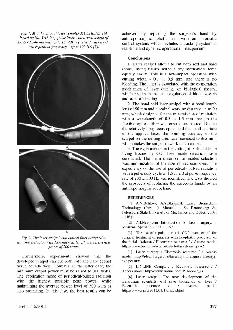
“E+E”, 5-6/2014 327
Fig. 1. Multifunctional laser complex MULTILINE TM based on Nd: YAP long pulse laser with a wavelength of
1.079 / 1.340 microns up to 40 (70) W (pulse duration - 0.3 ms, repetition frequency – up to 100 Hz) [5].
a)
b)
Fig. 2. The laser scalpel with optical fiber designed to transmit radiation with 1.06 microns length and an average
power of 200 watts.
Furthermore, experiments showed that the developed scalpel can cut both soft and hard (bone) tissue equally well. However, in the latter case, the minimum output power must be raised to 300 watts. The application mode of periodical-pulsed radiation with the highest possible peak power, while maintaining the average power level of 300 watts is also promising. In this case, the best results can be
achieved by replacing the surgeon’s hand by anthropomorphic robotic arm with an automatic control system, which includes a tracking system in real-time and dynamic operational management.
Conclusions 1. Laser scalpel allows to cut both soft and hard
(bone) living tissues without any mechanical force equally easily. This is a low-impact operation with cutting width - 0.1 ... 0.5 mm. and there is no bleeding. The latter is associated with the evaporation mechanism of laser damage on biological tissues, which results in instant coagulation of blood vessels and stop of bleeding.
2. The hand-held laser scalpel with a focal length lens of 80 mm and a scalpel working distance up to 20 mm, which designed for the transmission of radiation with a wavelength of 0.5 ... 1.5 mm through the flexible optical fiber was created and tested. Due to the relatively long-focus optics and the small aperture of the applied laser, the pointing accuracy of the scalpel on the cutting area was increased to ± 5 mm, which makes the surgeon's work much easier.
3. The experiments on the cutting of soft and bone living tissues by CO2 laser mode selection were conducted. The main criterion for modes selection was minimization of the size of necrosis zone. The expediency of the use of periodical- pulsed radiation with a pulse duty cycle of 1.5 ... 2.0 at pulse frequency rate of 200 ... 300 Hz was identified. The tests showed the prospects of replacing the surgeon's hands by an anthropomorphic robot hand.
REFERENCES [1] A.V.Belikov, A.V.Skrypnyk Laser Biomedical
Technology (Part 1): Manual. - St. Petersburg: St. Petersburg State University of Mechanics and Optics, 2008. - 116 p.
[2] A.I.Nevorotin Introduction to laser surgery. - Moscow: SpetsLit, 2000. - 176 p.
[3] The use of a pulse-periodic CO2 laser scalpel for surgical treatment of patients with neoplastic processes of the facial skeleton / Electronic resource / / Access mode: http://www.bisonmedical.ru/article/lazvstom/pipco2
[4] Laser surgery / Electronic resource / / Access mode: http://ideal-surgery.ru/lazernaja-hirurgija-i-lazernyj-skalpel.html
[5] LINLINE Company / Electronic resource / / Access mode: http://www.linline.com/RU/about_us
[6] Laser scalpel. The new development of the Belarusian scientists will save thousands of lives / Electronic resource / / Access mode: http://www.rg.ru/2012/01/19/lazer.html

“E+E”, 5-6/2014 328
[7] L.S.Kireєv, O.I.BabaevWorld welding technology leader / / Bulletin of the National Academy of Sciences. - 2009. - 10. - P. 46-53.
[8] Plasma Surgical Complex "Plazmamed" / B.E. Paton, V.S.Gvozdetsky, V.I.Dranovsky and others / / Automatic Welding, 2000, 1. - P. 46-47.
Assoc. Prof. Dr. Viktor Spivak - professor the National Technical University of Ukraine “Kiev Polytechnic Institute”.
He graduated from the Kiev Polytechnic Institute in 1968, specialty industrial electronics.
Works in the field of electronic circuitry systems and nanoelectronics. Author of over 300 publications and 15 patents.
tel.: +38 0505711642,
e -mail:[email protected].
Prof. Dr. Vladislav Khaskin - Senior Researcher, Institute of Electric welding behalf of the Paton (Ukraine). He graduated from the Kiev Polytechnic Institute in 1993 - processes of physical and technical processing . Works in the field oflaser treatment . Author of more than 120 publications and 6 patents.
tel.: +38 0973119263, e -mail: [email protected].
Prof., Dr. Mikhay Tirshu - Deputy Director of the Energy Institute of the Academy of Sciences of Moldova . Graduated from Kishinev Polytechnic Institute in 1990 in electrical engineering and electronics .
Works in the field of energy
Author of over 130 publications and 10 patents.
tel.: +37322 735384,
e-mail: [email protected]
“E+E”, 5-6/2014 329
Pulse Width Dependence of the Self-Ignited Plasma Using a Plasma-Based Ion Implantation
Kazuhiro Shimono, Nobuyuki Fujimura, Hiromitsu Noguchi, Hiroshi Toyota, Yoshito Shirai, Takeshi Tanaka, Katia Vutova
Plasma based ion implantation (PBII) with high negative pulsed voltage applied to the test specimen has been applied to the sterilization process as a technique suitable for three-dimensional work pieces. We found that the PBII process reduced the numbers of active Bacillus pumilus cell (The number of bacteria survivors was reduced by 105 with 5 min exposure) using N2 gas self-ignited plasma generated by only pulsed voltages. In this study, the PBII methods were compared using Ar gas and N2 gas for the minimum voltage necessary for the self-ignition plasma generation. After this, we examine a generation condition of the plasma, used for a sterilization process.
Зависимост на ширината на импулсите на самозапалването на плазма при йонна имплантация, използваща плазмата (К. Шимоно, Н. Фуджимура, Х. Ногучи, Х. Тойота, Й. Шираи, Т. Танака, К. Вутова). Йонна имплантация, използваща плазмата при прилагане на отрицателно импулсно напрежение, бе приложена за стерилизация, като техника подходяща за 3D образци. Процесът редуцира количеството активни Бацили Пумилас с 105 при 5 мин. eкспониране, използвайки N2 самозапалена плазма, генерирана само от импулсно напрежение. В тази работа се сравняват резултати при използване на Ar и N2 за минималното напрежение, необходимо за генериране на самозапалена плазма. След това ние изследваме едно условие на генериране на плазма използвана за процес на стерилизация.
Introduction Conventionally there is ethylene oxide gas
sterilization or high-pressure steam sterilization as a sterilization method that has been used primarily in the medical field or the manufacturing of medical products. Electron beam sterilization and radiation sterilization are employed industrially.
On the other hand, there is a low-temperature gas plasma sterilization method using hydrogen peroxide as a disinfectant which is known to be able to inactivate bacterial spores and is used for fast sterilization, pollution-free, and for low-temperature sterilization device. However, a harmful phenomenon of the exposure of hydrogen peroxide to a healthcare worker is confirmed by sterilization using hydrogen peroxide gas. Furthermore, it has been pointed out that it is possible for the patient to be exposed to hydrogen peroxide remaining behind in a sterilized medical appliance. [1, 2].
Plasma-based ion implantation (PBII) is a technique used to modify the surface of samples by immersion in plasma and application of a negative bias voltage to the target. Currently, the sterilization
process using a new method PBII as sterilization processes which can be low-temperature and short-time sterilization has been attempted [3].
There are modulator technology and plasma generation technology as elements of technology of plasma ion implantation. The modulator technology is one of the important techniques in the plasma ion implantation to affect the formation of the ion sheath at the board surface and the behavior of the ion in a formed sheath directly [4].
In this study, plasma-based ion implantation using N2 gas and Ar gas in (PBII) method is discussed and is compared to the minimum voltage required to turn on the self- ignition plasma.
Experimental Fig. 1 shows a schematic diagram of the
experimental apparatus. Stainless steel chamber material of the device is (SUS). The height is 450 mm, the width is 590 mm, the depth is 470 mm. SUS -made electrode is insulated from the chamber which is grounded and is placed at the center of the chamber. The high pressure pulse modulator (Kurita mill) which is used in this experiment has frequency up to 1000

“E+E”, 5-6/2014 330
pps, capacity of up to around 8 A repeatedly and can apply the negative pulse voltage of up to 15 kV to a target in pulse width 2~30 µs. High-voltage pulse voltage is controlled by a computer control system in the PC by (Fotgen 2). Evacuated to 1 × 10⁻³ Pa in the chamber, experiments are performed and gas pressure varying in the range from 10 Pa to 3 Pa is used by introducing N2 gas. Similarly, Ar gas is used to carry out experiments varying within the range from 10Pa to 3 Pa in gas pressure. The state of the lighting of Ar gas plasma and N2 gas plasma was visually checked and each plasma was examined for minimum voltage required for the plasma generation.
Fig. 1. Schematic diagram of experimental apparatus
Generation of plasma in this study uses only self-ignition plasma.
Results and discussion
Self-ignited plasma electric discharge properties
Fig. 2 shows the discharge characteristics of the self-ignition plasma N2 gas (gas pressure 3 Pa). It is possible without using the RF power and ion implantation and for the plasma to be maintained generating only negative pulse voltage. It is possible to obtain the effect of sterilization and sterilization of medical instruments. Further, using only the high-voltage negative pulse power source, provides the advantage of cutting down the power by half compared to the combination of the pulsed power supply and RF power.
The electric current grows bigger according to the increase in applied voltage when a current waveform is observed. After reaching the peak at the rise time of about 2.5 µs voltage is applied, and the
current is steady. Current does not flow upon termination of the applied voltage. The applied voltage is flowing about 5 A the steady current at the time of 8 kV.
Fig. 2. Self-ignition plasma discharge characteristic of
nitrogen gas
In the current waveform obtained by the plasma of the double structure of the self-ignition plasma (RF burst plasma) external plasma has an early peak after the reduction, and the current waveform is constant. Current with the initial peak is due to RF plasma. Current thereafter is due to self-ignition plasma.
Lighting of the self-ignition plasma was not observed in 0.8 kV in a self-ignition plasma generation of N2 gas. In 4 kV later, generation of clear self-ignition plasma was observed. Emission of self-firing plasma was observed visually when current flows at 0.26 A. By increasing the current further, strong light emission was observed.
The smallest voltage of the self-ignited arc plasma lighting by the change of the pulse width
Fig. 3 shows the comparison between each of the voltages of the minimum required lighting of the self-ignition plasma to the change in the pulse width of the Ar gas (gas pressure 3 Pa) and N2 gas (gas pressure 3 Pa).
The generation of the self-ignition plasma happens using the negative pulse voltage. Plasma is generated by negative pulse voltage of the first few µs. Injected progress is made towards the substrate by accelerating the ions in the plasma generated in the remaining time. Looking at the results obtained when varying the pulse width as the pulse width decreases, the minimum voltage required for self-ignition plasma lighting is high. From this it is suggested that the voltage required for the lighting of the self-ignition plasma by the pulse width is changed.

“E+E”, 5-6/2014 331
Fig. 3. Pulse width dependence of self-ignition plasma
The smallest voltage of the Self-ignited arc plasma lighting by the change in pressure
Fig. 4. Pressure dependence of self-ignition plasma.
Fig. 4 shows the difference in the minimum voltage required for self-ignition plasma lighting when changing the pressure for N2 gas and Ar gas. Pulse width is 6.3 µs with both Ar gas and N2 gas.
Looking at the results obtained by changing the pressure, the voltage value required for the lighting of the self-ignition plasma is reduced as the pressure increases. It can be seen that the plasma generation at low voltage is possible because with higher pressures the initial density is high.
It was suggested that in a self-ignition plasma when pressure is high, the voltage necessary for the plasma lighting is low.
Self-ignition plasma emission characteristics
Emission spectrum measurement of self-ignition plasma of Ar gas and N2 gas by using a plasma-based ion implantation method is carried out using spectrometer(Ocean Optics made, USB-2000) For
both N2 gas and Ar gas, in the 8 kV constant pulse voltage, varying between 1 µs~10 µs pulse width, the amount of light emission was compared.
Fig. 5. Emission characteristics of a pulse width of 10µs
Fig. 5 shows the emission characteristics of
nitrogen plasma at the time of the pulse width 10 µs. For N2 plasma a strong emission in the 427 nm and 391 nm was seen. According to data in the database of the atomic spectroscopy (NIST Atomic Spectra Database), 391 nm is the emission of N Ⅱ and 427 nm can be confirmed to be the emission of N Ⅰ. Fig 6 focuses on two wavelengths, indicating the difference in light emission amount at the time of changing the pulse width. Wavelengths of 427 nm and 391 nm confirmed an increase in the amount of light emission as pulse width increases.
Fig. 6. Pulse width dependence of the nitrogen plasma
emission characteristics
Fig.7 shows the emission characteristics of the Ar plasma.
Fig.7(a) shows the time emission characteristics of the pulse width 1µs.
Fig.7(b) shows the emission characteristics when the pulse width is 10µs.

“E+E”, 5-6/2014 332
(a) Emission characteristics of 1μsec.
(b) Emission characteristics of 10µsec.
Fig. 7. Emission characteristic of Argon plasma
Fig. 8. Pulse width dependence of argon plasma emission characteristics
In Ar plasma, we were able to see the strong emission in the 751 nm and 656 nm. According to the atom spectrum database, 751 nm can confirm that it is Ar I and 656 nm can confirm that it is ArⅡ. Fig.8 shows the case of changing the pulse width by focusing on the two wavelengths showing the difference in light intensity. Wavelengths of 656nm and 751 nm were observed, which confirmed an
increase in the amount of light emission as pulse width increases. When comparing the light emission characteristics of the pulse width 1 µs and 10 µs, it was possible to confirm the emission of the ArⅡ and ArⅠ between 400~500 nm and 700~800 nm as the pulse width increases.
Conclusion Plasma-based ion implantation methods using
argon gas and N2 gas were compared for the minimum required voltage to turn on the self-ignition plasma.
It was shown that the applied voltage required for self-ignition plasma lighting for argon gas is lower than for N2 gas. In the case of nitrogen gas or argon gas, as the pulse width decreases, the minimum voltage required to discharge is first observed is higher. The minimum voltage required for the discharge of the first one observed as the pressure gets higher is low.
Emission characteristics of self-ignition plasma of the N2 gas and Ar gas showed that the light intensity increases the larger the pulse width gets. It was confirmed that the pulse width of the Ar gas increases, when the spectrum is increased.
REFERENCES [1] R. Yoshida and H. Kobayashi: Japanese
Association for Operative Medicine, 33 (2012) 273. [2] M. Nagatsu: J. Plasma Fusion Res., 83 (2007)
601..
[3] T. Tanaka, T. Hironaka, S. Hayashi and I. Koyama: Elektrotechnica & Elektronica E+E, 47 (2012) 268.
[4] T. Tanaka, S. Watanabe, K. Shibahara, S. Yokoyama and T. Takagi: J. Vac. Sci. Technol. A, 23 (2005) 1018.
[5] T. Tanaka, S.Watanabe, G. Mizuno, T. Takagi, M. Yoshida, H. Horibe and K. Yukimura: The Papers of Technical Meeting on Electrical Discharges, IEE Japan, 83 (2002) 43.
[6] NIST Atomic Spectra Database Lines Form, [7] http://physics.nist.gov/PhysRefData/ASD/lines_for
m.html (Last accessed: 2014 02 28)
[8] D. Shibahara, H. Yasuda, N. Fujii, H. Kurita, K. Takashima and A. Mizuno: J. Inst. Electrostat. Jpn., 34 (2010) 2.
Kazuhiro Shimono - Major in Electrical and Electronic Engineering, Hiroshima Institute of Technology, 2-1-1, Miyake, Saeki-ku, Hiroshima, 731-5193, Japan

“E+E”, 5-6/2014 333
Nobuyuki Fujimura - Major in Electrical and Electronic Engineering, Hiroshima Institute of Technology, 2-1-1, Miyake, Saeki-ku, Hiroshima, 731-5193, Japan
Hiromitsu Noguchi - Major in Electrical and Electronic Engineering, Hiroshima Institute of Technology, 2-1-1, Miyake, Saeki-ku, Hiroshima, 731-5193, Japan
Hiroshi Toyota - Department of Electronics and Computer Engineering, Hiroshima Institute of Technology, 2-1-1, Miyake, Saeki-ku, Hiroshima, 731-5193, Japan
Yoshito Shirai - KOANKEISO, 2798-36, Minamiyoshida-cho, Matsuyama 791-8042, Japan
Takeshi Tanaka - Department of Electronics and Computer Engineering, Hiroshima Institute of Technology, 2-1-1, Miyake, Saeki-ku, Hiroshima, 731-5193, Japan
Katia Vutova - Institute of Electronics, Bulgarian Academy of Sciences, 72 Tzarigradsko shosse blvd., 1784 Sofia, Bulgaria

“E+E”, 5-6/2014 334
Preliminary Estimation of Incident Ion Energy by Using Simulation Software (PEGASUS)
Hideaki Kozai, Nobuyuki Fujimura, Mitsuhiro Noguchi , Hiroshi Toyota,
Yoshito Shirai, Takeshi Tanaka, Katia Vutova
Plasma base ion implantation (PBII) with self-ignited plasma generated by only pulsed voltages
to the test specimen has been applied to the sterilization process. We found that the PBII process reduced the numbers of active Bacillus pumilus cells using N2 gas. As the ion energy is the most important processing parameter, a discussion about the implanted surface is presented through measurements data using the Secondary Ion Mass Spectroscopy (SIMS). In this study, we simulated the incident ion energy to a target by the simulation software (PEGASUS). We compared the measurement data of SIMS and the simulation results. We were able to confirm correlation between these two pieces of data.
Предварителна оценка на проникващата йонна енергия с помощта на симулационната програма ПЕГАСУС (Х. Козаи, Н. Фужимура, М. Ногучи, Х. Тойота, Й. Шираи, Т. Танака, К. Вутова). Базирана на плазма йонна имплантация със самозапалваща се плазма бе приложена за процес на стерилизация. Открихме, че процеса редуцира количеството на активните Бацили пумилас, използвайки азот като плазмо-образуващ газ. Тъй като йонната енергия е най-важния параметър на процеса, обсъждането на имплантираната повърхност е представено чрез измерените данни с използване на йонна масс-спектроскопия (СИМС). В това изследване ние симулираме началната йонна енергия при мишената със симулационна програма ПЕГАСУС. Ние сравняваме измерените данни от СИМС и симулираните ресурси. Ние бяхме способни да потвърдим корелацията между тези данни.
Introduction Plasma-based ion implantation (PBII) method is
used to perform surface modification by the sample in the plasma and applying a high voltage negative pulse voltage. It has been applied to surface modification industrial machinery parts, metal material, and medical technology.
Sterilization process using a self- ignition plasma by PBII method has been attempted. It was found that by using N2 gas PBII process it is possible to reduce the number of Bacillus pumilus activity. It has been observed that the number of bacteria is reduced with the increase of pulse voltage. The number of viable bacteria was reduced by 5 orders of magnitude at 15 kV compared to the number of untreated bacteria. Due to the importance of the application of this method in the sterilization process, PBII method is investigated in [1].
In order the examine the mechanism through which the number of viable cells decreases in this
work are presented and discussed results for ion implantation depth profiles and the energy of the implanted ions in sterilization is evaluated.
Experiments
Fig. 1. Schematic diagram of experimental apparatus

“E+E”, 5-6/2014 335
Figure 1 shows a schematic diagram of the SIP PBII apparatus. No external rf excitation source was employed in the proposed procedure. The treatment chamber in the current experiments was 450 mm in height, 590 mm in width and 470 mm in depth.
Treatment is performed by applying a pulsed negative dc voltage of up to –15 kV to the target. The voltage waveform has a pulse width of about 5µs and repetition rate of 300 pulses/s, and is supplied by a high-voltage pulse modulator with a maximum current capacity of approximately 10 A. A pulsed dc voltage is employed in order to simplify the sterilization apparatus. A diffusion pump was used to evacuate the chamber to a base pressure of 4.0x10⁻⁴ Pa, and the nitrogen gas pressure during plasma generation was maintained at 2.4 Pa. The depth profile of nitrogen in Si implanted by PBII was measured by secondary-ion mass spectroscopy (SIMS) and High Resolution Rutherford Back Scattering (HR-RBS).
Bacillus pumilus (IFO No.14367) was employed as the microorganism for sterilization. A suspension of B. pumilus was diluted with 0.85% NaCl saline solution or distilled water to a concentration of 107 spores per 1 mL of suspension. A 100 mL dose of the suspension was pipetted onto a membrane filter (thickness, 145µm; permittivity, 2.25) and then washed with distilled water to remove the saline solution. The filter was used in this study instead of the glass plate used previously in [2] in order to spread the bacteria uniformly on the filter surface. All processes were performed in a clean room with sterile equipment.
After exposure to plasma and ion bombardment for at least 2 h, the samples were placed in 50 mL containers with 0.85% NaCl saline. The containers were then set in an ultrasonic vibration bath for 5 min to detach the spores into suspension. The suspension was repeatedly diluted in saline to achieve a concentration reduction of 10-5. A sample of 1 mL of the diluted suspension was pipetted onto 20–30 mL of sterile culture (standard agar) in a sterile Petri dish. Dishes were then incubated at 37 °C for 48 h. Colony-forming units were finally counted to determine the numbers of survivors of B. pumilus.
The simulation is made using a simulation software (PEGASUS) for nitrogen ion energy and the data is compared to the results of SIMS.
Results and discussion[1] In combination with rf excitation, SIPs have been
found to be generated around a substrate biased at negative voltages higher than −1.2 kV in a carbon-containing gas such as ethane or methane [3]. However, a much higher voltage was required in the
present experiments due to the omission of the rf excitation source. Figure 2 shows the wave forms of the pulsed dc voltage and the current used for both ion implantation and deposition. This voltage wave form was shown previously to be sufficient for generating a SIP around the target in N2 gas [2].
Fig. 2. SIP discharge characteristic
The number of B. pumilus survivors is shown in Fig. 3 as a function of the pulsed dc voltage. The efficiency of sterilization, given by the ratio of the number of B. pumilus surviving after treatment to that prior to treatment, increased almost exponentially with voltage. Sterilization was achieved at voltages higher than about −4 kV, which represents a threshold voltage for the PBII sterilization process. These results suggest that the energy of incident ions is more important for sterilization than the ion dose.
Fig. 3. B. pumilus survival after 5 min PBII
The efficiency of sterilization increased with voltage approximately exponentially, with a measurable sterilization effect starting at approximately –4 kV. Thus, the PBII sterilization process has a threshold voltage. These results suggest that the energy of incident ions is more important for sterilization than the ion flux.
The actual energy of nitrogen ions in the self- ignited plasma in PBII was estimated by treating an Si target and measuring the depth-wise ion distribution

“E+E”, 5-6/2014 336
by SIMS, because the difference of capacitance of the silicon substrate ( thickness is 0.6mm, dielectric constant is 11.9) and filter element ( thickness is 0.145mm, dielectric constant is 2.25) was not large. Figure 4 shows the depth profile of nitrogen concentration in the treated Si sample. The peak in the concentration profile occurs at approximately the same depth at voltages of –8, –12 and –15 kV, although concentrations at greater depth increase with voltage. The peak position corresponds to the penetration range of ions at the several hundred volts in conventional ion implantation. At the penetration depth of conventional ion implantation, the N2 concentration in the present sample is at least 1020 cm-3. Thus, the actual nitrogen ion energy is estimated to be much smaller than that calculated based on the voltage applied in treatment. The result that the ion energy is lower than that associated with the voltage applied during processing is to be expected for a number of reasons: First, the pressure is high (2.4Pa) and the plasma density is likely to be quite low since you are using the applied voltage to ignite plasma .Comparison of the mean free path in the background gas with the plasma sheath width would probably show that you have a collisional sheath so that ions lose energy as they move through the sheath. Second, you are using a short pulse length (5 microseconds) with a rise time of almost a microsecond. It is known that a substantial fraction of the ions is drawn in through the sheath during the pulse rise time (matrix sheath) when the applied voltage is much lower than that in the main part of the pulse [4]. Finally, the effect is probably stronger on your insulating substrates than on the silicon wafer you used to measure the implanted depths because there is significant reduction of voltage across the sheath when using insulating substrates [5].
Fig. 4. SIMS Depth profiles of nitrogen in a silicon
substrate for three applied voltages (-8, -12, and -15 kV)
The increased efficiency of sterilization by PBII is considered to be attributable to the good penetration of ions, as indicated by the long tail in the concentration profile in Fig. 3.
Estimation by simulation
A. For PIC-MCCM [6] In the PIC method, individual particles are not
followed in order to reduce the computation time. Instead, movements of super particles are followed. A super particle is a bunch of charged particles of the same kind. So, the charge and the mass of a super particle may be 108 to 1010 times those of the real particle depending on the statistical condition. The collision rates are calculated based on the energy-dependent cross section. The particle energy is calculated from the electromagnetic field, which is obtained from Poisson's equation using the densities of charged species.
B. Theory of Monte Carlo Collision method [7] 1) Null collision technique Between the successive collisions, which is
determined in the Monte Carlo method, the plasma-charged particles move according to the local Lorenz force. In order to reduce the computing time, the null collision technique was used.
The collision probability between time t and t+∆t is expressed as
v ? ? ,2
where, σt, vk, εk and Ngas are the total collision cross section, the velocity and the kinetic energy of the atom k, and the neutral gas density, respectively. The time step ∆t is to be set as so it satisfies the relation
At first, instead of v, vnull is used to determine
whether the collision occurs or not.
The null collision occurs when the following
condition is satisfied.
Only when the null collision occurs, next procedures are carried out. Here, ξ is a random number ( 0<ξ< 1 ).
? ?
1"#
・・・

“E+E”, 5-6/2014 337
2) Electron collisions with an atom and a molecule
During the flight of the charged particle, some essential elementary processes can occur. Electrons are expected to produce elastic encounters, excitation or ionization during their collisions with the neutral gas atoms.
Here, ε is energy of the incident electron and χ is
the scattering angle.
So,
Azimuth angle φ is obtained by the relation,
I? 2I? ?% .10 The velocity v' after the collision is obtained by the
relations.
For non-elastic collisions, analytical cross-sections
are used. For the case of excitation of struck atom, the electron energy after collision is given as
Where εin,e, εscat,e,and εexc are the electron energy
before and after the collision and the excitation energy. For the case of ionization,
where εej,e, and εion are the ejected electron and the ionization energy. εej,e is given as:
B is a parameter which depends on the gas atom or
the molecule.
3)Atomic collisions in the plasma For the collisions between particles in the plasma
gas, an elastic collision of hard spheres was assumed. Then, the scattered particle energy εscat is determined by:
where εin and χ are the incident energy and the scattering angle in the laboratory system. The scattering angle in the laboratory system is obtained from the scattering angle in the center-of-mass system, ϑ, by the relation
where ξ5 is a random number.
C. Simulation result
Fig. 5. Simulation model
In sterilization using PBII method, the energy is estimated using depth profile of the implanted ions by SIMS ion implantation simulation.
Fig.5 shows the applied voltage waveform and schematic diagram of the simulation.
The simulation results of energy are presented in Fig. 6. The simulation result of energy by N + are shown in Fig. 6. Figure 6b presents the simulation result of energy by N2+. Figure 6c reveals the combined simulation results of the N2 + and N +.
Conclusion
PBII method is efficient for sterilization and sterilization efficiency increases when the voltage increases and thus the ion energy is an important factor. The number of the viable bacteria is decreased when an increased voltage is applied, which results

“E+E”, 5-6/2014 338
from the penetration depth of the implanted ions measured by SIMS. The energy of the implanted ions in PBII method was evaluated using SIMS.
It was found that simulation result of depth profile using PEGASUS software for SIP-PBII method has a similar tendency of experimental data by SIMS method.
(a) Only the N+
(b) Only the N2+
(c) N+ and N2+
Fig. 6. Simulation results
REFERENCES [1] T. Tanaka, T. Hironaka, S. Hayashi and I.
Koyama: ELEKTROTECHNICA & ELEKTRONICA E+E, 47 (2012) 268.
[2] M. Yoshida, T. Tanaka, S. Watanabe, T. Takagi, M. Shinohara, S. Fujii, J. Vac. Sci. Technol., A21 (2003) 1230..
[3] S. Watanabe, T. Tanaka, T. Takagi, and K. Yukimura, Surface Coating Technology 186 (2004) 187.
[4] D.T.K.Kwok,M.Bilek,D.R.McKenzie,P.K.Chu,The importance of bias pulse rise time for determining shallow implanted dose in plasma immersion ion implantation,Applied Physics Letters,vol.82(12),pp.1827-1829
[5] T.W.H.Oates,j.Pigott,D.R.McKenzie,and M.Bilek,Electric Probe Measurements of High Voltage Sheath Collapse in Cathodic Arc Plasmas duetoSurface Charging of Insulators,IEEE Transactions on Plasma Science,vol.31(3),pp.438-443
[6] Y.Miyagawa, H.Nakadate, M.Tanaka, M.Ikeyama, S.Miyagawa, Surface & Coatings Technology 196(2005)155-161.
[7] Y. Miyagawaa, M. Tanakab, H. Nakadateb, S. Nakao, and S. Miyagawa, Proc. of Int. Conf. on Ion Implantation Technology 213, 2000 .
Hideaki Kozai - Department of Electronics and Computer Engineering, Hiroshima Institute of Technology, 2-1-1, Miyake, Saeki-ku, Hiroshima, 731-5193, Japan
Nobuyuki Fujimura - Major in Electrical and Electronic Engineering, Hiroshima Institute of Technology, 2-1-1, Miyake, Saeki-ku, Hiroshima, 731-5193, Japan
Hiromitsu Noguchi - Major in Electrical and Electronic Engineering, Hiroshima Institute of Technology, 2-1-1, Miyake, Saeki-ku, Hiroshima, 731-5193, Japan
Hiroshi Toyota - Department of Electronics and Computer Engineering, Hiroshima Institute of Technology, 2-1-1, Miyake, Saeki-ku, Hiroshima, 731-5193, Japan
Yoshito Shirai - KOANKEISO, 2798-36, Minamiyoshida-cho, Matsuyama 791-8042, Japan
Takeshi Tanaka - Department of Electronics and Computer Engineering, Hiroshima Institute of Technology, 2-1-1, Miyake, Saeki-ku, Hiroshima, 731-5193, Japan
Katia Vutova – Institute of Electronics, Bulgarian Academy of Sciences, 72 Tzarigradsko shosse blvd., 1784 Sofia, Bulgaria

“E+E”, 5-8/2014 339
Comparison of Plasma Spectral Characteristics Using a Plasma-Based Ion Implantation
Hiromitsu Noguchi, Nobuyuki Fujimura, Kazuhiro Shim ono, Hiroshi Toyota,
Yoshito Shirai and Takeshi Tanaka
Plasma-based ion implantation is a recently developed technique used to modify the surface of
materials by immersion in plasma coupled with the application of a negative bias voltage.
In this study, we compare the properties of the plasma spectrum with respect to the change in applied voltage as well as the difference in the plasma generation method used.
Spectra of 428 nm and 656 nm show the generation of Ar ions.[1] In addition, the strength of a spectrum emitted by the ion is proportional to the number of the generation of the ion. Comparisons of these spectra suggest that the number of ions increases in line with an increase in voltage. Moreover, our findings suggest that the number of ions increase for a combination of RF burst plasma and self-ignition plasma compared with the number of ions for only self-ignition plasma.
It was shown that we could estimate the property of the plasma ion by emission spectrum.
Сравнение на спектралните характеристики при използване на базирана на плазма йонна имплантация (Х. Ногучи, Н. Фужимура, К. Шимоно, Х. Тойота, Й. Шираи, Т. Танака). Базираната на плазма йонна имплантация е техника, разработена в последно време, която се използва за модификация повърхността на материалите чрез потапяне в плазма и съединение на отрицателен потенциал. В това изследване ние сравняваме особеностите на плазмения спектър, при промяна на приложеното напрежение, както и на начина на генериране на плазмата. При 428 nm и при 656 nm спектъра показва наличие на Ar йони. В допълнение, силата на емитирания спектър от йоните е пропорционален на числото генерирани йони. Сравнението на спектрите показва, че числото йони нараства линейно с увеличение на напрежението. Нещо повече, ние намерихме, че броят йони расте за комбинация от ВЧ разрядна плазма и само-запалваща се плазма сравнено с броя йони само за само-запалваща се плазма. Показано е, че оценка на свойствата на плазмените йони от емисионния спектър.
Introduction The gas-sterilization methods currently used at
hospitals include ethylene oxide gas sterilization and hydrogen peroxide gas sterilization. However, residual traces of chemical substances that have an adverse affect on the human body remain a problem with ethylene oxide sterilization.[2] In the case of hydrogen peroxide sterilization, there is a problem in that the process takes around 90 minutes. In addition, the sterilization of items such as fiber gauze, cotton, artificial blood vessels, and felt is difficult, and hydrogen peroxide—an expendable supply in the process—is expensive.
As a substitute sterilization method, the plasma-based ion implantation (PBII) method is tried. In the
PBII method, an ion and a radical are produced by applying a negative high-pressure pulse voltage to an item and the reaction by it inactivates bacteria spore. In this study, the methods of generating plasma suitable for sterilization using the PBII method was evaluated use emission spectroscopy.
Experimental A schematic of the experimental setup is shown in
Fig. 1. The chamber measures 450 mm in height, 590 mm in width, 470 mm in depth. The RF antenna (manufactured by American North Star Inc.) is a copper coil with five windings, and a diameter of approximately 250 mm. The RF antenna is electrically insulated from the chamber by glass, and this coiled

“E+E”, 5-6/2014 340
RF antenna produces the RF voltage (222 kHz) by an induction electric field.
Fig. 1. Experimental setup
The target electrode, made of SUS, is 140 mm in diameter, 18 mm thick, and it is insulated by a grounded chamber, and it is installed in the center of the chamber. The high-pressure pulse modulator (manufactured by KURITA Seisakusho CO.) can generate a frequency up to 1000 pps, a capacity of up to 8A and can irradiate a target with a negative pulse voltage of a maximum of 15 kV in a pulse width of 2 – 30 µs. The high-pressure pulse voltage is controlled by a computer control system (Fotgen2) running Windows 98. We installed extra boards in the expansion slots of the PC and used light as a control signal output through an optical fiber.
The vacuum exhaust used mass flow together with a rotary pump and a mechanical booster pump, and the chamber was filled with gas to a density of 99.9999%.
We measured the spectrum through the glass top of the target electrode. We used a USB2000 spectroscope and saved the data using spectroscope control software Overture running on Windows 7.
We measured RF burst plasma, self-ignition plasma, and a combination of RF burst plasma and self-ignition plasma with the chamber pressure maintained at 2 – 5 Pa.
Result and discussion
1) Change according to the plasma generation method of the spectrum
In this subsection, we show the results from the observation in the change of the spectrum by plasma generation method. In addition, we pay attention to the spectrum of 428 nm and 656 nm indicating the
generation of Ar ions, and suppose a change in the number of ions of produced plasma.
100
150
200
250
300 400 500 600 700 800 900Wavelength [nm]
Inte
nsit
y [a
.u.]
428nm656nm
Fig. 2. Self-ignition plasma only
100
150
200
250
200 300 400 500 600 700 800 900Wavelength [nm]
Inte
nsity
[a.u
.]428nm
656nm
Fig. 3. RF burst plasma only
100
150
200
250
200 300 400 500 600 700 800 900Wavelength [nm]
Inte
nsit
y [a
.u.]
428nm
656nm
Fig. 4. Combination of RF burst plasma and self-ignition
plasma
The spectrum when only self-ignition plasma is used is shown in Fig. 2, that for only RF burst plasma is shown in Fig. 3, and a combination of RF burst plasma and self-ignition plasma is shown in Fig. 4.
Fig.2 shows the typical emission spectrum in self-ignition plasma. Spectra of 428 nm and 656 nm show the generation of Ar ions.
It suggests that the self-ignition plasma generates ions contributing to sterilization.
It suggests that a sterilization effect enhances during increase the number of the generation of the ion.
Therefore we consider combination of RF burst plasma and self-ignition plasma as a method to increase the number of the ions.

“E+E”, 5-6/2014 341
Fig3 shows the typical emission spectrum in the RF burst plasma. As shown in Fig.3, it was found that spectra of 428 nm and 656 nm appeared in only RF burst plasma.
Fig.4 shows the typical emission spectrum in combination of RF burst plasma and self-ignition plasma.
Comparing with Fig. 4 and Fig. 2, the spectrum intensity of combination of RF burst plasma and self-ignition plasma is larger than that of the self-ignition plasma.
Because of this, it suggests that the number of ions contributing to sterilization become larger in the case of combination of RF burst plasma and self-ignition plasma.
2) Target voltage dependence of the spectrum
-1.5
-1.0
-0.5
0.0
0.5
1.0
1.5
-20 -10 0 10 20 30 40 50time[us]
RF
volta
ge [
kV]
Fig. 5. RF power supply voltage
-10.0
-8.0
-6.0
-4.0
-2.0
0.0
2.0
0.0 10.0 20.0 30.0 40.0 50.0 60.0 70.0time[us]
Tar
get v
olta
ge[k
V] 2kV
4kV6kV8kV
Fig. 6. Target power supply voltage
-0.1
0.1
0.3
0.5
0.7
0.9
0.0 10.0 20.0 30.0 40.0 50.0 60.0 70.0time[us]
Cur
ent[
A] 2kV
4kV6kV8kV
Fig. 7. Target electric current
100
150
200
250
300
300 400 500 600 700 800 900Wavelength [nm]
Inte
nsity
[a.
u.]
428nm
656nm
Fig. 8. Combination of RF burst plasma (60 V) and self-
ignition plasma (2 kV)
100
150
200
250
300
300 400 500 600 700 800 900Wavelength [nm]
Inte
nsity
[a.
u.]
428nm
656nm
Fig. 9. Combination of RF burst plasma (60 V) and self-
ignition plasma (4 kV)
100
150
200
250
300
300 400 500 600 700 800 900Wavelength [nm]
Inte
nsity
[a.
u.]
428nm
656nm
Fig. 10. Combination of RF burst plasma (60 V) and self-
ignition plasma (6 kV)
100
150
200
250
300
300 400 500 600 700 800 900Wavelength [nm]
Inte
nsity
[a.
u.]
428nm
656nm
Fig. 11. Combination of RF burst plasma (60 V) and self-
ignition plasma (8 kV)

“E+E”, 5-6/2014 342
In this subsection, we show the result observed for the change of the spectrum by the change of the target power supply voltage when we set the RF power supply voltage to 60 V and when we used RF burst plasma together with self-ignition plasma. In addition, we pay attention to the spectrum of 428 nm and 656 nm indicating the generation of Ar ions, and suppose a change in the number of ions of the produced plasma.
The RF power supply voltage is shown in Fig. 5, the target power supply voltage in Fig. 6, the target electric current in Fig. 7, and the spectrum when we used an RF power supply voltage of 60 V and a target voltage of 2 kV in Fig. 8, an RF power supply voltage of 60 V and a target voltage of 4 kV in Fig. 9, an RF power supply voltage of 60 V and a target voltage of 6 kV in Fig. 10, and an RF power supply voltage of 60 V and a target voltage of 8 kV in Fig. 11.
It suggests that the strength of the general spectrum increases with an increase in the target power supply voltage from a comparison of Figs. 8 - 11. Spectrum intensity of 428nm and 656nm becomes strong during increase of the power supply voltage. From these results, it is found that the number of the Ar ions increases with the power supply voltage.
Conclusion It was observed that the spectrum changed by
changing the plasma generation method and the target voltage. For the plasma generation method that we used in this paper, it is suggested that the combination of RF burst plasma and self-ignition plasma is the most suitable to sterilization. With respect to the target voltage, each spectrum strength became stronger by increasing the voltage.
In particular, as for the extreme change of these spectra, the number of Ar ions generated supposes that we have equilateral correlation when we pay attention to a spectrum of 428 nm and 65 nm. Thus, it is supposed by the change of the spectrum of 428 nm
and 656 nm that the number of Ar ions generated changes by changing the plasma generation method and the target voltage. In other words, it is supposed that it is combination of RF burst plasma and self-ignition plasma that produces the most ions, followed by only self-ignition plasma, and only RF burst plasma in order.
From the above, the possibility of examining a method of generating plasma suitable for sterilization using the PBII method was suggested by measuring the light emissions of produced plasma using a spectroscope.
REFERENCES [1] NIST Atomic Spectra Database (2013)
[2] T. Tanaka, T. Hironaka, S. Hayashi, and I. Koyama:Elektrotechnica & Elektronica E+E, 47 (2012) 268.
[3] I.S. EN ISO 10993-7 (2008) , pp.5-10
Hiromitsu Noguchi - Major in Electrical and Electronic Engineering, Hiroshima Institute of Technology, 2-1-1, Miyake, Saeki-ku, Hiroshima, 731-5193, Japan
Nobuyuki Fujimura - Major in Electrical and Electronic Engineering, Hiroshima Institute of Technology, 2-1-1, Miyake, Saeki-ku, Hiroshima, 731-5193, Japan
Kazuhiro Shimono - Major in Electrical and Electronic Engineering, Hiroshima Institute of Technology, 2-1-1, Miyake, Saeki-ku, Hiroshima, 731-5193, Japan
Hiroshi Toyota - Department of Electronics and Computer Engineering, Hiroshima Institute of Technology, 2-1-1, Miyake, Saeki-ku, Hiroshima, 731-5193, Japan
Yoshito Shirai - KOANKEISO, 2798-36, Minamiyoshida-cho, Matsuyama 791-8042, Japan
Takeshi Tanaka - Department of Electronics and Computer Engineering, Hiroshima Institute of Technology, 2-1-1, Miyake, Saeki-ku, Hiroshima, 731-5193, Japan

“E+E”, 5-6/2014 343
Spore-Forming Bacteria Sterilization Using Plasma-Based Ion Implantation
Koji Kakugawa, Masatoshi Kubo, Hiromitsu Noguchi, Kazuhiro Shimono, Nobuyuki Fujimura, Yoshinobu Tsuchiya, Takeshi Tanaka
A main purpose of sterilization is to kill the harmful microorganisms. In food industry, the representatives of microorganisms which are difficult to sterilize are spore-forming bacteria. Because these bacteria are extremely heat resistant. So it is no exaggeration to say high-pressure / high temperature sterilization method is the only method to sterilize spore-forming bacteria. By the way, plasma sterilization method is used to sterilize the medical equipment. However the present plasma sterilization method cannot be used for food because of containing hydrogen peroxide.
In this study, the authors tried to sterilize Bacillus subtilis which is model bacteria of spore-forming bacteria using plasma-based ion implantation (PBII) method which doesn’t use hydrogen peroxide. The result of experimentation, the living spore reduced from 1x10⁸ cfu/ml to 7.8x10⁴ cfu/ml with 20 min exposure. The authors showed that PBII treatment without hydrogen peroxide might be able to sterilize the heat tolerance spores.
Стерилизация на споро-образуващи бактерии с използване на плазма-базирана йонна имплантация (К. Какугава, М. Кубо, Х. Погучи, К. Шимоно, Н. Фуджимура, Й. Цучия, Т. Танака). Главната цел на стерилизацията е да убие вредните микроорганизми. В хранителната индустрия, представители на микроорганизмите, които е трудно да бъдат стерилизирани са споро-образуващите бактерии, защото тези бактерии са екстремно устойчиви при нагряване. Така не е преувеличено да се каже, че методите на стерилизация с високо-налягане и висока температура са единствени за стерилизиране на споро-образуващи бактерии. Впрочем, плазмен метод на стерилизация се използва за стерилизиране на медицински инструменти. Обаче, сегашните плазмени-стерилизационни методи не могат да се използват за храни, защото се използва водороден пероксид.
В тази работа авторите опитват да стерилизират Бацилиус сибтилис, който е моделна бактерия на споро-образуващи бактерии, с йонна имплантация, базирана на плазма, при който не се използва водороден пероксид. Резултатите от експериментите представят, че след 20 минутно експониране живеещите спори намаляват от 1х108 cfu/ml до 7.8х104 cfu/ml. Авторите показват, че с йонна имплантация, базирана на плазма без използване на водороден пероксид е възможно да се стерилизират издръжливи на нагряване спори.
Introduction In most of the food industries, food products have
been sterilized by moist heating (boiling or retort treatment). However, the excessive thermal conditions for ensuring the safety of microbial spoilage degrade the quality of products. Spores of Bacillus genus produce highly thermotolerance spores, and those spores often spoil heat sterilized foods. Bacillus genus is widely distributed in nature, and commonly associated with a variety of food products. Spore formation ability allows these
bacteria to survive in the environment and provides them with resistance to pasteurization treatments. Therefore, many studies on thermal sterilization of foods have conducted.
A very diverse range of pasteurized food products is now available to the consumer and with world-wide preferences for more highly spiced and flavored foods, these products are likely to contain many different ingredients which could be contaminated with Bacillus species. However, powdery spices are difficult to sterilize by using thermal sterilization methods. So it is expected to develop the newly

“E+E”, 5-6/2014 344
sterilization equipment which is able to sterilize the powdered spice.
By the way, plasma-based ion implantation (PBII) is potentially applicable for the sterilization of three-dimensional targets as a low-temperature, cost-efficient technique for medical equipment, containers and also powdery foods[1-3]. PBII can be used to sterilize three-dimensional shapes in a short time, without the use of toxic gases. However, the sterilization performance in conventional PBII, where the target is immersed in an rf burst inductively coupled plasma (ICP) that is generated externally, is somewhat limited in that certain areas may be shadowed from exposure due to the shape of the object, and the ion penetration depth may not be adequate for complete sterilization. These shortcomings can be overcome through the use of a self-ignited plasma (SIP), which can be generated around the workpiece as a transient ion sheath by applying a pulsed dc voltage to the target. Our group previously reported that PBII reduces Bacillus pumilus vegetative cells by 104–105 times in just 5 min, much faster than can be achieved by exposure to an external rf plasma source at 222 kHz[4].
In this study, the authors investigated the inactivating behavior of B. subtilis spores which were highly thermotolerance using plasma source ion implantation.
Materials and Methods
Spores of B. subtilis NITE 13719 were used as the test specimen. B. subtilis spores were grown on agar medium consisted of 1% polypeptone, 0.2 % yeast extract, 0.1 % MgSO4 and 1.5 % agar (spore forming medium) at 35 °C for 5 days. The spores were harvested adding a small amount of saline solution and heated at 65 °C for 30 min to eliminate the vegetative cells. Heated spores were washed three times by centrifugation in saline solution. After the final wash treatment, the spores were heated at 65 °C
for 30 min. The spore population of the suspension was determined by diluting the suspension and the concentration of spore suspension was diluted to 108 spores/ml with saline solution.
Fig.1. Schematic diagram of experimental apparatus
Figure 1 shows a schematic diagram of the PBII apparatus. The chamber is electrically grounded and has dimensions of 450 mm in height, 590 mm in width, and 470 mm in depth. The rf antenna for the inductively coupled plasma (ICP) source is wound on the inside of the upper lid, with one end grounded. The antenna itself is a 5-turn copper coil, approximately 250 mm in diameter and operating at 235 kHz.
In the experiment, the sample was placed on a stainless-steel electrode supported by an insulated stainless-steel rod at the center of the vacuum chamber. A negative pulsed voltage was applied to the electrode during sterilization.
A pulsed negative voltage of up to -4 kV with a pulse width of 6.3 µs was applied to the target by a high-voltage pulse modulator with a maximum current of approximately 8 A. A rf discharge of input power 160 W was applied in some cases to investigate the effect of ordinary external plasma with respect to
Table.1. Experiment conditions of parameter on this experiment
Case 1 Case 2 Case 3 Case 4 Gas O2 O2 O2 O2 Gas Pressure [Pa] 4 3 3 3 Pulse Width [ms] 6.3 6.3 6.3 6.3 Pulse Rate [pulses/s] 1000 1000 1000 1000 Pulse voltage(peak) [kV] -8 - -1 -6 - -2 -6 -4 Pulse current(peak) [A] 4 4 4 4 RF Power [W] - 160 160 160 Exposure time [min] 10 10 5-20 5-20

“E+E”, 5-6/2014 345
sterilization. The distance between the rf antenna and the target was about 200 mm, and no arcing or surface charging was observed for the samples employed.
100 µl of spore suspension applied on the sterile paper cup and the cup was sealed in sterile paper bag. A sealed bag was inserted into the chamber.
The target chamber was evacuated to a base pressure of 10 Pa and the oxygen gas is injected to a pressure of 1 kPa. This procedure was repeated three times. Finally, gas pressure during plasma generation was maintained at 3 Pa. A summary of the experimental sterilization conditions is shown in Table 1.
After exposure to plasma and ion bombardment, 100 µl of saline solution was added to treated paper cup. After pipetting, this saline solution was added into 900 µl of saline solution. The dilution series was made by using this solution and 100 µl of the diluted spore solution was spreaded on spore forming agar plate. After incubation at 37 °C for 12 hr, colony forming units were counted to determine the numbers of survivors of B. subtilis spore. All data are expressed as average ± standard deviation of triplet analysis.
Results and Discussion This experiment evaluated the effectiveness of
plasma-based ion implantation using a self-ignited O2 gas plasma againt B. subtilis spores. First of all, the Authors tried to case 1 experiment to examine the influence of pulse voltage. The result is shown in Fig.
Fig.2.Influence of Pulse Voltage
2. As shown in Fig.2, the number of survivors had
decreased when the pulse voltage was raised. This phenomena might be similar to our previous data[5]. The previous data show that the energy of incident ions is more important for sterilization than the ion
dose[5]. However a strong energy of ions caused to burn a hole on the surface of a sample bag at this time. So the data of -8 kV was not shown in Fig.1 because the sample bag was burned. And this means that food materials might also be burned. In further experiments, we decided the range of pulse voltage from -6 kV to 0 kV.
Next, the authors analyzed the influence of pulse burst rf plasma according to the condition of case 2. The result is shown in Fig.3.
Fig.3. Influence of pulse burst rf plasma
As shown in Fig.3, the higher pulse voltage, the
fewer survivors under the condition of adding pulse rf plasma. However, Comparison between Fig.2 and Fig.
Fig.4. Influence of exposure time
3, a significant difference of survivors was unable to confirm. So next experiment whose condition described as case 3, the authors try to extend the exposure time. The result is described as Fig.4.
As shown in Fig.4, the survivors seem not to have

“E+E”, 5-6/2014 346
changed over 10 min exposure. The authors thought that these data were inaccurate. Because the sealed bag burned and there was a possibility that the sterile condition was not maintained. In addition, it is thought that the application to powdery foods is impossible in this condition because those foods may burn. So the authors changed pulse voltage to -4 kV (case 4). The result is shown in Fig.5.
Fig.5 Influence of exposure time under the low pulse
voltage condition
As shown in Fig.5, most effective exposure time was 20 min and the survivors decreased from 1x10⁸
cfu/ml to 7.8x10⁴ cfu/ml. In this research, the authors tried to sterilize B.
subtilis spores, which were highly heat tolerance, using PBII apparatus. The survivors of B. subtilis decreased from 1x10⁸ cfu/ml to 7.8x10⁴ cfu/ml under the most effective condition (pulse voltage : -4KV, exposure time : 20min, pulse burst rf plasma : bombardment). The authors showed that PBII treatment without hydrogen peroxide might be able to sterilize the heat tolerance spores. However the ability of this condition is insufficient, because the survival curve shows a plateau as shown in Fig.5. The sterilization using PBII method may be caused by collision of ions and radicals, which are produced under a high-pressure pulse against the spores on the base. So when the density of ions and radicals are increased, the efficiency of sterilization would be expected to be improved. In this experiment, despite under the bombardment of pulse burst rf plasma, the spores did not decrease to the value below 104 cfu/ml. This may be caused by using paper cup as sample carriers. There is a possibility that the fiber in the paper cup influences the irradiation efficiency of the plasma. This phenomenon might be improved to change a paper cup to a glass plate. Including this
problem, our research is being continued to sterilize the heat tolerance spore completely.
Conclusion The authors tried to sterilize B. subtilis spores,
which were highly heat tolerance using PBII apparatus. The survivors of B. subtilis decreased from 1x10⁸ cfu/ml to 7.8x10⁴ cfu/ml at this time. We showed the possibility that the thermotolerance spores were able to sterilize using PBII apparatus without hydrogen peroxide. It is thought that this result shows the possibility of the development of a novel spice sterilizer.
REFERENCES [1] K. Kelly-Wintenberg, A. Hodge, T.C. Montie, L.
Deleanu, D. Sherman, J. Reece Roth, P. Tsai, L. Wadsworth, Journal of Vacuum Science & Technology A 17 (1999) 1539-1544.
[2] P.T. Jacobs, S.-M. Lin, in: R.L. Clough, S.W. Shalaby (Eds.), Irradiation of polymers : fundamentals and technological applications, American Chemical Society, Washington, DC, 1996, pp. 216-239.
[3] S. Moreau, M. Moisan, M. Tabrizian, J. Barbeau, J. Pelletier, A. Ricard, L.H. Yahia, Journal of Applied Physics 88 (2000) 1166-1174.
[4] M. Yoshida, T. Tanaka, S. Watanabe, T. Takagi, M. Shinohara, S. Fujii, Journal of Vacuum Science ; Technology A 21 (2003) 1230-1236.
[5] T. Tanaka, T. Hironaka, S. Hayashi, I. Koyama, ELECTROTECHNICA & ELECTRONICA 5-6 (2012) 268-272
Prof. Dr. Koji Kakugawa - Department of Food Science and Biotechnology, Faculty of Life Sciences, Hiroshima Institute of Technology, 2-1-1 Miyake, Saeki-ku, 731-5139, Hiroshima, Japan
Tel:+81-82-921-6472 е-mail: [email protected]
Student Masatoshi Kubo Department of Applied Information Science, Faculty of Applied Information Science, Hiroshima Institute of Technology, 2-1-1 Miyake, Saeki-ku, 731-5139, Hiroshima, Japan
Graduate Student Hiromitsu Noguchi. Major in Electrical and Electronic Engineering, Graduate School of Science and Technology, Hiroshima Institute of Technology, 2-1-1 Miyake, Saeki-ku, 731-5139, Hiroshima, Japan
Graduate Student Kazuhiro SHIMONO Major in Electrical and Electronic Engineering, Graduate School of Science and Technology, Hiroshima Institute of Technology, 2-1-1 Miyake, Saeki-ku, 731-5139, Hiroshima, Japan

“E+E”, 5-6/2014 347
Graduate Student Nobuyuki FUJIMURA. Major in Electrical and Electronic Engineering, Graduate School of Science and Technology, Hiroshima Institute of Technology, 2-1-1 Miyake, Saeki-ku, 731-5139, Hiroshima, Japan
Prof. Dr. Yoshinobu Tsuchiya - Department of Food Science and Biotechnology, Faculty of Life Sciences, Hiroshima Institute of Technology, 2-1-1 Miyake, Saeki-ku, 731-5139, Hiroshima, Japan
Tel:+81-82-921-9464 е-mail: [email protected]
Prof. Dr. Takeshi TANAKA Major in Electrical and Electronic Engineering, Graduate School of Science and Technology, Hiroshima Institute of Technology, 2-1-1 Miyake, Saeki-ku, 731-5139, Hiroshima, Japan
tel.: +81-82-921-4256 е-mail: [email protected]

“E+E”, 5-6/2014 348
Estimation of Self-Ignited Plasma Density Using Plasma-Based Ion Implantation
Nobuyuki Fujimura, Kazuhiro Shimono, Hiromitsu Noguchi, Hiroshi Toyota, Yoshito Shirai, Takeshi Tanaka
Plasma density is estimated from the target voltage and current characteristics of the pulse
modulator circuit in plasma-based ion implantation. The voltage recovery time constant directly reflects the ion sheath characteristics, and the sheath resistance is related to the ion density inside the transient sheath. The stationary current also provides information on the sheath parameters. From these viewpoints, we propose a method to estimate plasma density by equating the circuit. The plasma density can be obtained only by monitoring the voltage-current waveforms on an oscilloscope display, and the obtained ion density can be converted into plasma density using a continuity equation. The conventional method uses the dual structure of RF plasma and self-ignition plasma. In this study, the plasma density is calculated using only self-ignition plasma.
Оценка на плазмената плътност при самозапалване на плазма предназначена за йонна имплантация (Н. Фуджимура, К. Шимоно, Х. Ногучи, Х. Тойота, У. Шираи, Т. Танака). Плътността на плазмата е оценена от напрежението на мишената и токовите характеристики на импулсната модулаторна верига в базирана на плазма йонна имплантация. Константата за възстановяване на напрежението директно отразява параметрите на йонната обвивка, като съпротивлението е свързано с йонната плътност във временната обвивка. Стационарния ток също предоставя информация за параметрите на обвивката. Ние предлагаме метод за оценка плазмената плътност от уравненията на веригата. . Плазмената плътност може да се получи само от наблюдаваните волт-амперни форми на екрана на осцилоскопа и получената йонна плътност може да се преобразува в плазмена плътност използвайки уравнението за непрекъснатост. Конвенционалният метод използва двойна структура на РЧ плазма и само-запалваща се плазма. В това изследване плазмената плътност се пресмята използвайки само само-запалваща се плазма.
Introduction Plasma ion implantation was proposed by J.R.
Conrad in the 1980s [1]. Plasma-based ion implantation (PBII) is a recently developed technique which modifies sample surface using sheath formed along sample in a plasma applied negative high pulse voltage. Since sheath was formed along surface structure of sample, ions can be uniformly injected into the sample surface. PBII with good controllability is effective as a surface treatment method for samples with wide variety shapes.
Conventionally, the plasma sterilization process at hospitals uses hydrogen peroxide gas. This method achieves sterilization by the oxidation reaction of high concentration hydrogen peroxide. Currently, plasma
ion implantation is used to sterilize surgical instruments. The sterilization process using plasma ion implantation is composed of the following elements.
(1) Generation of ions using plasma (2) Acceleration of the generated ions (3) Interaction between samples and ion Therefore, it is important to control ion sheath at
sample surface, the quantity and energy of ions in an ion sheath [2].
In this paper, the density of ions in the sheath formed by self-ignition plasma for PBII was calculated using the basis of modulator circuit. The plasma density and the length of sheath of self-ignition plasma were also calculated.

“E+E”, 5-6/2014 349
Estimation of plasma density [3]
Fig. 1 Equivalent circuit of the modulator voltage
Fig. 1 shows an equivalent circuit representing the pulse modulator circuit used to apply a pulse voltage to a target immersed in plasma. Because the main load of the modulator output is the ion sheath formed around the target, which consists of resistance R1 and capacitance C1., the plasma impedance can be ignored. Although R1 and C1 are time-varying parameters, they are treated as constant for simplification during the pulsed ion implantation. In other words, R1 and C1 are said to be average values during the process. Generally, these are functions of the ion density in the sheath as shown below. In the modulator circuit, modulator output resistance R2 and circuit stray capacitance C2 exist in addition to R1 and C1, and are not dependent on the plasma parameters. These are constants. C2 exists between the apparatus and the ground of the system.
In order to know the ion density in the sheath, we need to know R2 and C2. To evaluate these parameters, a capacitor or a resistor is set to the modulator output instead of the plasma. R2 and C2 can be derived by measuring the rise time τr and fall time, i.e., recovery time τf. A resistor with a resistance of 10 kΩ and capacitor with a capacitance of 70 pF were used as dummy loads for evaluating the circuit parameters of R2 and C2. By observing the voltage and current waveforms for these loads, C2=220 pF for τf=2.2 µs and R2=2.2 kΩ for τr=0.88 µs, respectively, are obtained. C1 is thought to be approximately 10 pF or less. Thus, C2 >> C1 is satisfied. As a result, the ion sheath capacitance does not substantially contribute to the time constant in the voltage recovery region after the pulse.
When a planar sheath is formed around the target, the ion current density j at the target surface, the electrical field strength, is expressed as Vp/s,
s
Vj pσ= (1),
where σ is conductivity of the ion sheath, s is sheath thickness and Vp is applied voltage. When venj i= is assumed, where ni is the ion density at the target surface, and the ion velocity v at the target surface is
expressed as emVv p 2/= under a collisionless
field, ( )AsR σ=1 can be expressed as Eq. (2).
e
mV
AenR p
i 21
1 = (2),
where e is electron charge, ni is ion density at the target surface with a surface area A, and m is ion mass. From Eq. (2), it is seen that R1 is a function of ni for the experimental parameters. At the sheath edge, Eq. (3) is satisfied. Bi unvn 0= (3), where n0 is plasma density and uB is Bohm velocity. R1 can be experimentally obtained using τf, which is expressed as:
12 RCf ×=τ . (4)
By obtaining R1, the ion density can be estimated. This method of estimating the ion density is advantageous because only the voltage waveform need be observed. R1 can be also obtained by using the target voltage and the current through the target at the end of the pulse.
Experimental
Fig. 2. Schematic diagram of experimental setup
Figure 2 shows a schematic diagram of the self-ignited plasma (SIP) PBII apparatus. The treatment chamber in the experiments measured 450 mm in height, 590 mm in width and 470 mm in depth. The

“E+E”, 5-6/2014 350
electrode made of stainless steel (SUS) which is insulated for the treatment chamber was set at the center of treatment chamber. This charge is performed by applying a pulsed negative dc voltage of up to –12 kV to the target. The pulse width of the voltage waveform is about 6.3 µs and its repetition rate is 1000 pulses/s. The maximum current supplied by a high-voltage pulse modulator is approximately 8 A. A pulsed dc voltage is employed to simplify the sterilization apparatus. A diffusion pump was used to evacuate the chamber to a base pressure of 1.0 × 10⁻³ Pa, and the nitrogen gas pressure during plasma generation was maintained at 3 Pa.
Result and discussion The applied voltage is varied from 0.8 to 12 kV at
3 Pa. The applied voltage and current waveform is shown in Fig. 3. Then the generation of plasma is not observed at 0.8 kV. At more than 4 kV, generation of plasma was observed. It is impossible to observe a clear current waveform of less than 4 kV. The current waveform clearly appears at more than 8kV. The voltage waveforms shown in Fig. 3(a) have nearly rectangular forms. The steady current is about 4.4A for applied voltage of 8kV.
(a) Applied Voltage
(b) Current
Fig. 3 Self-ignition plasma discharging characteristic for N2
For metal materials, secondary electron emission coefficient is about 0.1 (less than 1 keV). For high ion energy (more than 1 keV), secondary electron emission coefficient become large. At 20 keV, the secondary electron emission coefficient of stainless steel is 4.8.[4]
Fig. 4 Currnet – applied voltage characteristic
Figure 4 shows the relation of current and applied voltage. When the plasma density is constant, the current is proportional to the applied voltage. However, the current drastically increases at more than 8 kV. At 8kV, measured current is approximately 4 times compared with current of plasma density constant. This suggested that the measured current increase with secondary emission electron coefficient. The secondary electron emission coefficient obtained by current as shown in Fig.4 is shown in Fig.5.
Fig. 5 Secondary electron yield
Using the time constant and C2, R1 is calculated by Eq.(4). Moreover, using calculated R1, the value of plasma density was calculated 4.4 × 109cm-3 at 8kV.
It suggests that the 2/3 of measured current at 8kV is due to secondary electron emission coefficient. The correction value and the calculation value of the plasma density are shown in Fig.6.

“E+E”, 5-6/2014 351
Fig. 6 Plasma density calculation for N2
Fig. 7 Sheath distance as a function of applied voltage
Fig. 8 Plasma density calculation for Ar
Fig.7 shows sheath length as a function of applied voltage. The sheath length was calculated by using Eq.(5).
Similary the calculated plasma density for Argon gas is shown in Fig. 8.
Finally, we concluded plasma density was estimated using only SIP.
Conclusion The plasma density in the ion sheath was able to
calculate using modulation equivalent circuit for PBII. The plasma density and sheath length was calculated by this method. The plasma density and length of sheath is important parameter to manufacture the apparatus. In the future, it is useful to a device design to calculated plasma density and sheath length.
REFERENCES [1] J.R. Conrad, J.L. Radtke, R.A. Dodd, F.J. Worzala,
and N.C. Tran : J. Appl. Phys., 62, 4591 (1987).
[2] T. Tanaka, T. Hironaka, S. Hayashi, and I. Koyama:Elektrotechnica & Elektronica E+E, 47 (2012) 268.
[3] S. Watanabe, T. Tanaka, T. Takagi and K. Yukimura : Surf. Coat. Technol., 186 (2004) 53-56
[4] Young, M. The Technical Writer's Handbook. Mill Valley. CA, University Science, 1989.
Nobuyuki Fujimura - Major in Electrical and Electronic Engineering, Hiroshima Institute of Technology, 2-1-1, Miyake, Saeki-ku, Hiroshima, 731-5193, Japan
Kazuhiro Shimono - Major in Electrical and Electronic Engineering, Hiroshima Institute of Technology, 2-1-1, Miyake, Saeki-ku, Hiroshima, 731-5193, Japan
Hiromitsu Noguchi - Major in Electrical and Electronic Engineering, Hiroshima Institute of Technology, 2-1-1, Miyake, Saeki-ku, Hiroshima, 731-5193, Japan
Hiroshi Toyota - Department of Electronics and Computer Engineering, Hiroshima Institute of Technology, 2-1-1, Miyake, Saeki-ku, Hiroshima, 731-5193, Japan
Yoshito Shirai - KOANKEISO, 2798-36, Minamiyoshida-cho, Matsuyama 791-8042, Japan
Takeshi Tanaka - Department of Electronics and Computer Engineering, Hiroshima Institute of Technology, 2-1-1, Miyake, Saeki-ku, Hiroshima, 731-5193, Japan

“E+E”, 5-6/2014 352
Micro-Arc Oxidation of Aluminum Alloy
E. Krivonosova, A. Gorchakov, I. Ponomarev
Micro-arc oxidation (MAO) technology allows getting ceramic coatings of Al2O3 with
composition, structure and properties controlled over a wide range and using them as wear-resistant, corrosion- resistant, heat- resistant and decorative coatings. This paper studies the dynamics of micro-arc discharges, the influence of time processes and electrolyte systems on the MAO process of aluminum alloy, micro-structure and properties of the formed coating. The possibilities of alloying through the electrolyte with the micro-arc oxidizing are investigated.
Микро-дъгово оксидиране на алуминиеви сплави (E. Кривоносова, А. Гончаков, И. Пономарев). Технологията на микро-дъгово оксидиране (МДО) позволява получаване на керамично покритие от Al2O3 със състав, структура и свойства управляеми в широк диапазон и използването му като устойчиви на триене, корозия и нагряване покрития, както и като декоративни покрития. Тази работа изучава динамиката на микро-дъговите разряди, влиянието на процесите зависими от времето и на електролитните системи върху МДО процесите на повърхността на алуминиева сплав, както и микро-структурата и свойствата на формираните повърхностни слоеве. Възможността за сплавяне през електролита при микро-дъгово оксидиране се изследва също.
Introduction Microarc oxidation ( MAO ) is currently almost the
only possible method of surface treatment of a variety of parts from aluminum and its alloys to produce multifunctional coatings. A distinctive feature is the formation of MAO in the formation of the coating surface microarc discharges, providing thermal, plasma-chemical and hydrodynamic effects on the formation of coatings. Keramik coatings have an order higher microhardness, wear resistance, corrosion resistance, etc. However, the practical application of MAO requires increasing productivity and improving the complex physical and mechanical properties of the coatings. Furthermore, the main problem lies in the micro-arc oxidation coating delivery insufficient thickness of the porous coating, which leads to a reduction or loss of performance properties.
The most accessible ways of increasing the thickness of the oxide layer, and technological factors: current modes, while the coating composition, density and temperature of the electrolyte (works of I.VSuminov, AV Epelfeld, A.I.Gorchakov, G.A.Markov, ES Atroshchanko, AI Mamaev) However, the increase of the current parameters leads to a change in the nature of the discharge, the transition of micro- discharge in the arc without
forming oxidized layer. One way of solving this problem is to change the nature of the pulse current signal, which, in our opinion, may lead to an increase of the effective time of oxidation and, therefore, the thickness and properties of the oxide layer [1-4]. An additional object is achieved by doping the oxide layer through the electrolyte, similarly as in the welding seam takes place the doping of the electrode coating component [5]. To do this, the electrolyte requires the addition of elements that are embedded in the structure of the coating, providing increase in growth velocity coating, its thickness and the formation of unique properties [6].
Method and results. Recent experimental data using a computer
information-measuring system and high-speed filming yielded qualitatively new information. It has been shown that the effective microarc discharge (Fig. 1), leading to the formation of a layer of corundum, exists within a very short time during successive short current pulses whose frequency is 50 Hz.
Physically micro-arc oxidation process is a gradual formation of micro-arcs on the surface and smooth fading in proportion to the instantaneous value of the voltage between the sample and the bathroom.
Micro-arc oxidation process visually within one
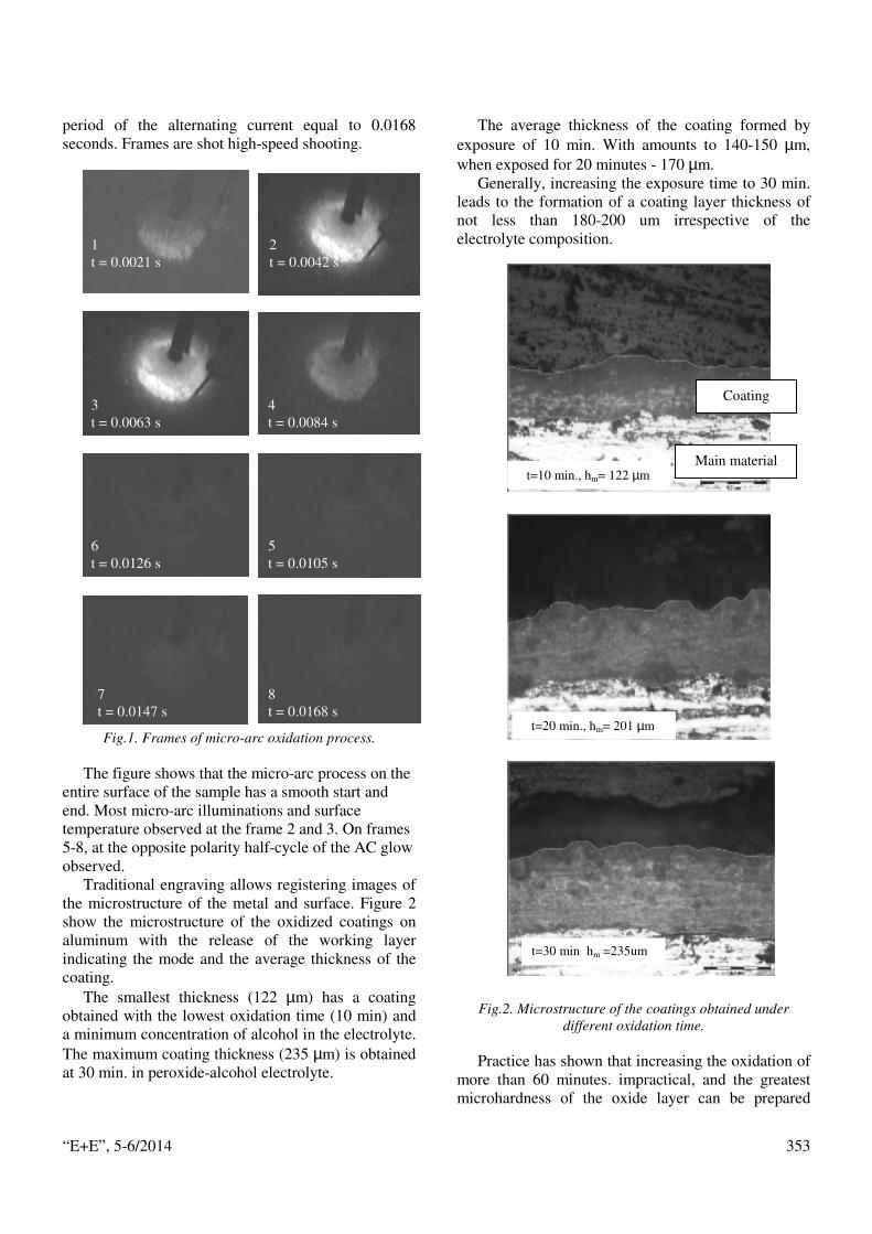
“E+E”, 5-6/2014 353
t=30 min hm =235um мин.,h =235мкм
period of the alternating current equal to 0.0168 seconds. Frames are shot high-speed shooting.
Fig.1. Frames of micro-arc oxidation process.
The figure shows that the micro-arc process on the entire surface of the sample has a smooth start and end. Most micro-arc illuminations and surface temperature observed at the frame 2 and 3. On frames 5-8, at the opposite polarity half-cycle of the AC glow observed.
Traditional engraving allows registering images of the microstructure of the metal and surface. Figure 2 show the microstructure of the oxidized coatings on aluminum with the release of the working layer indicating the mode and the average thickness of the coating.
The smallest thickness (122 µm) has a coating obtained with the lowest oxidation time (10 min) and a minimum concentration of alcohol in the electrolyte. The maximum coating thickness (235 µm) is obtained at 30 min. in peroxide-alcohol electrolyte.
The average thickness of the coating formed by exposure of 10 min. With amounts to 140-150 µm, when exposed for 20 minutes - 170 µm.
Generally, increasing the exposure time to 30 min. leads to the formation of a coating layer thickness of not less than 180-200 um irrespective of the electrolyte composition.
Fig.2. Microstructure of the coatings obtained under
different oxidation time.
Practice has shown that increasing the oxidation of more than 60 minutes. impractical, and the greatest microhardness of the oxide layer can be prepared
1 t = 0.0021 s
2 t = 0.0042 s
3 t = 0.0063 s
4 t = 0.0084 s
5 t = 0.0105 s
6 t = 0.0126 s
7 t = 0.0147 s
8 t = 0.0168 s
Coating
Main material t=10 min., hm= 122 µm
t=20 min., hm= 201 µm

“E+E”, 5-6/2014 354
using the composition of the electrolyte (КОН+Na2SiO3+NaAlO2+NaF).
Also, analyze of influence of alloying of coating through the electrolyte.
Analysis of the influence of alloying through showed that all compounds of electrolyte increases the thickness of the implanted layer.
Alloying by corundum A12O3, 80% leads to increase of coating thickness, as shown in Figs 3 and 4. Maximum coating thickness is 170 um without this.
Results of X-ray spectral analysis and fractal analysis shown that concentration of TiO2 and Cr2O3 should be maintained at 5 g/l, as with more content layer unit conglomerates beyond matrix breakdown channels formed.
Increasing the amount of corundum, 50 g / l does not cause a significant increase in the thickness, porosity is increased, which reduces the quality of the coating.
X-ray spectral analysis result showed that all alloying compounds of electrolyte contained in the composition of the oxide layer.
Some increase of microhardness on account of alloying occurs due to the additional phases of chromium oxide and titanium, which remain in the electrolysis process without changing of phase composition.
Reduced coefficient of friction and amount of wear explained by the presence of solid lubricant. Summary wear a pair of friction measured after 8 hours of testing without changing the load on the pair.
Table 1. Properties of MAO coating
Electrolyte MAO in the electrolyte without of alloying
MAO in the alloying
electrolyte
Maximum layer
thickness h, um
170 295
Microhardness midface, HV,
N/mm2
1 0 0 0 -1 4 0 0
1 6 0 0 -2 5 0 0
The wear of the friction
pair, um 35 21,5
Friction coefficient
after grinding couples
0,3 0,12
Fig.3 Dependence oxide thickness h, um, vs. concentration
of corundum C, g/l
Fig.4. Dependence oxide thickness (h) vs. oxidation time (t),
in the electrolyte with (1) and without (2) alloying.
Conclusion 1. With increasing oxidation time, the oxide layer
thickness increases. Increasing the duration of oxidation greater than 30 minutes only affects the presence of alloying elements.
2. Alloying through the electrolyte is an effective method for increasing the thickness of the oxide layer and its performance: The presence in the electrolyte elements TiO2 and Cr2O3 increases the thickness and microhardness of coating. Also, the presence of these elements reduces the coefficient of friction during the test.
3. The actual burning time of micro–arc surface substantially less than the time of the process. This is due to small time of micro–arc combustion surface, during the flow of general AC current.
REFERENCES [1] A. I. Gorchakov, E.A. Krivonosova/ To the
problem of the pore formation in Micro-arc oxidation coatings / Tyazheloe Mashinostroenie, 2008, N7, p. 26-29 (in russion)
1
2
C, g/l
t, min

“E+E”, 5-6/2014 355
[2] E.A. Krivonosova./ Application of theory of fraktals in the metallurgical science of welding and coatings // Welding and diagnostics, 1, 2008 г. с.2-5 (in russion)
[3] E.A. Krivonosova/ Fractal analysis of the formation of structure in welded joints//Welding International, 2005, vol.19, 12, р.976-970
[4] Krivonosova E.A., Rudakova O.A., Gorchakov A. I., Borodin N.M./ Fraktal analysis of the structurization of Micro-arc oxidation coatings // Welding and diagnostics, 1, 2010. p.37-41. (in russion)
[5] Mathematical model of the kinetics of growth of titanium nitride particles in a welded joint/E A Krivonosova, V M Yazovskikh, V V Utochkin & V I Shumyakov // Welding International. Volume 16, Issue 12, January 2002, pages 974-977
[6] Ye.A. Krivonosova, A.I. Gorchakov, Yu.V. Scherbakov//Structure and properties of coatings in microarc oxidation/Welding International., 2014, vol. in press.
Prof. Dr. Ekaterina A. Krivonosova – Perm National Research Polytechnic University; Russia, Perm region, perm, Komsomolskyi prospect st., 29; Welding production and Technology of construction materials faculty;
tel.: 7342)219–82–75 e-mail:[email protected]
Prof. Ph.D. Alexandr I. Gorchakov - Perm National Research Polytechnic University; Russia, Perm region, perm, Komsomolskyi prospect st., 29; Powder materials faculty;
tel.: 7(342)219–82–75 e-mail:no
Grad. St. Ilya S. Ponomarev – Perm National Research Polytechnic University; Russia, Perm region, perm, Komsomolskyi prospect st., 29; Welding production and Technology of construction materials faculty;
tel.: +7-908-24-42-310 e-mail.: [email protected]

“E+E”, 5-6/2014 356
Analysis and Generalization of Scientific and Educational Information Book in the Field of Nano-Electronics
Victor M. Spivak, Elena G. Koleva, Anna G. Vlasyuk
In this paper analysis and generalization of the scientific and educational properties of
information textbooks on nano-electronics, created from the scientists of the Institute of Electronics at Bulgarian Academy of Sciences, the Power Institute at the Academy of Sciences of Moldova, the National Technical Universities of Ukraine: "Kiev Polytechnic Institute" and "Polytechnic University of Lvov" is presented. The prepared monographs are also textbooks and they are based on the authors own most significant research results and on results obtained in leading companies and academia of various developed countries in the world.
Анализ и обобщение на научнте и методически информационни учебни пособия по наноелектроника (В. М. Спивак, Е. Г. Колева, А. Г. Власюк). В тази работа е представен анализ и са обобщени научните и учебните качества на информационните учебни пособия по наноелектроника, създадени от учените от Института по електроника на Българската академия на науките, Института по Енергетика на Академията на науките на Молдова, Националните Технически Университети на Украйна "Киевски Политехническия институт" и "Лвовска политехника". Издадените монографии са също учебници и те са основани на авторските собствени най-значими изследователски резултати, както и на резултатите от научните изследвания на някои водещи фирми и академичните организации на различни развити страни пo света.
Introduction Nanoelectronics is an undisputable new strategic
direction of the scientific and industrial development of the world. The nanoelectronics is based on the last technologies and research results of the developed countries. The progress of microelectronic technologies was one approach to develop nanotechnologies, but now the development of nanotechnologies is in close connection with the achievements of nanoelectronics. In the next decades nanotechnology development and applications will determine the position of every developed country in the world. This is the origin of sharp concurrent competition of corporations, the economic activities of which are in the field of national security and weapons. In the same time the existing experience in research and development indicates the need of: working out a strategy for the development nanotechnology devices and nano-materials; building a platform for joining and the coordinative use of the existing scientific, technology and educational resources; for the close cooperation of governments with business.
In this paper some information and analysis of monograph and text book [1-6] elaborated by the researchers and lecturers of few leading academic organizations in Bulgaria, Ukraine and Moldova are given.
Contents and matter of books The aim of published books was to introduce to the
possible readers - scientists, lecturers in Universities, experts in industry and students in technical specializations - the problems and the achievements of nanoelectronics and fabrications of nano-materials, nano-devices and nano-systems. The nanofabrication methods of nano-devices, nano-materials and systems, the methods of investigations and visualization of nano-objects, the physical processes in nano-devices are also presented.
In the beginning Prof. G. Mladenov wrote two books [1, 2] as an attempt to help students of Technical University - Sofia from specialty Microelectronics to understand better the important role of electron and ion beams in the going down competition in the submicron region of critical dimensions of the electronics circuits, as well as to

“E+E”, 5-6/2014 357
show the open room for nano-electronics as the near future of technology development. Then the scientists at the Institute of Electronics at Bulgarian Academy of Sciences and researchers and lecturers of Faculty of Electronics at National Technical University of Ukraine "Kiev Polytechnic Institute", together with scientists from Power Institute at Academy of Sciences of Moldova joined knowledge and experience in the published books [3-5] based on own more considerable research results and executed some generalization of the results of leading companies and research organizations from the developed industrial countries. An important achievement of these monographs [1-5] is the short, but substantial analysis of the methods of fabrication nano-dimensional thin films and structures. There is base information on deposition of thin films by thermal evaporation of materials in vacuum, by molecular-beam epitaxy, and by atomic layer deposition. In these monographs the physical processes at ion sputtering, at operation of triode-plasma-sputtering deposition system, at ion, high-frequency and magnetron sputtering deposition systems are recognized. Reviews are made on the processes at ion-beam, reactive ion and ion-plasma etching; the physical processes at penetration of accelerated ions and electrons in solid samples; peculiarities of ion implantation, conductivity of surface layers in implanted silicon, as well as ion-implantation equipment is described. In [1,3,5] the physical base of electron and ion lithography, data for application of these methods of submicron treatment of substrates, as well as the mechanical probe use for investigation of nano-dimensional reliefs and for nano-lithography are given. There experimental and computer-simulation results for modification electron resists by accelerated electrons and ions, some examples of regression analysis applications for improvement the results of electron exposure and development are also given. There the methods of use atomic-force and scanning tunneling microscopes for lithography goals are also described.
In the books [2, 3 and 5] the reasons for explosive development of nano-technologies and various approaches in fabrication of nano-dimensional nano-devices are presented. Description of the difficulties of development nano-dimensional critical element of semiconductor integral circuits and prospective of creation new building elements, based on new principles as tunneling effect, superconductive conductivity, electron magnetic spin transport, giant magneto-resistivity, application of quantum dots in cellular automata etc. is made. Methods of surface analysis of nano-materials and structures using
electron and ion beams, as well other methods for visualization and control characteristics of the nano-dimensional objects and particles are given.
The book [4] is written aiming to be a textbook in the region of nano-materials and functional devices nanoelectronics. There the information is a continuation of the data on the technologies and the ideas, developed in books [1-3]. In this monograph the principle of self-structuring of nano-dimensional structures on example of silicon with pores and nano-pores as well as silicon-based composites are described. Discussion on the connections of technology processes and properties of the obtained materials as some characteristics of the produced devices is made. Another important group of nano-materials is the carbon-based nano-materials as fullerenes, nanotubes, diamond like films, graphen. In [4] there are presented shortly the methods of fabrications and the base characteristics of these materials, as well as some their applications. There the functional devices of more important areas of nano-electronics as photonics, bio- crio- and molecular- electronics, magneto-electronics or spintronics, sensors and nano-electro-mechanical nano-components and systems are recognized.
At the end of presented series of books a group of lecturers from leading Technical Universities in Ukraine from Kiev and Lvov new text-book [6] was worked out, using the materials in [3-5] and own experience, devoted on quantum-mechanical base nanoelectronics. There are discussions on the base physical characteristics of semiconductor and carbon-based structures. The behavior and energy spectrum of quantum-mechanical particles in potential gap with various shape and dimensions, the peculiarities of tunneling of particles through potential barrier and resonance-tunneling structures are discussed. There are data on the density change of the free electrons at variations of the system dimensions and at strong outer magnetic fields. The base information on 2D-crystalles, semiconductor super-lattices and carbon-based nano-structures are presented. The specific physical properties and peculiarities of energy structure of these lattices and films are also discussed. After every chapter of [6] conclusions, questions and examples for calculations are given.
Discussion In the books [1-6] original authors results are
presented and the trends of the leading scientific school and industrial research in the world in field of nanoelectronics are analyzed. The created ideas help understanding the base technologies for fabrications

“E+E”, 5-6/2014 358
and the processes in nano-devices and nano-materials, as well as the processes of characterization and visualization of nano-dimensional materials and devices. Reading these books will permit engineers and aspirants of various specialties of Technical Universities in Ukraine, Bulgaria, Moldova and Rumania, probably in Russia too, to create new concurrent nano-materials and nano-devices.
In the books the difference of the behavior of nano-dimensional materials from the conventional materials due to dimensional effects, as from classic nature to quantum-mechanical nature are demonstrated. For example: solvent penetration, melting temperature, electro-conductivity and heat-conductivity as well as the electron tunneling, quantum energy-levels and density of particles in the gaps, electron spin’s role etc. are discussed. As a result, non-transparent materials could become transparent ones, the inert materials can display catalyst properties, some metal powders could be ignited, insolating materials could become electro-conductive and so on.
In [1] the presented original results are for example: electron beam space-charge compensation by generated ions; computer simulation of technology electron guns based on phase analysis, electron and ion lithography as well some data for ion implantation. In [2] the problems of microelectronics in its way to nano-dimensions, due to mentioned quantum effects are deeply discussed. Some new applications as spintronics, giant magneto-resistivity effect, tunneling, the two-pole devices applications including these of newly invented memristors are described. In [3] nano-electronics based on new building elements is presented. Specific interest presents the chapter on methods for investigation and analysis of nanostructure; the various technologies for realization of nano-structures and the chapter for lithography with mechanical sharp-probe (principle of AFM and STM). In [4] two main directions of investigations and development of nano-technology are marked: a) obtaining new materials with uncial properties due to morphology of structure, containing elements of 1 to 100 nm; and b) investigation the possibilities to utilize the conventional materials in nano-dimensional region. The important role of interfaces between micron’s part and nano-dimensional part of systems was appointed. This takes place also for nano-materials (nano-luminescent layers of the displays; nano-separators in electro-charging sources; electro-optic nano-coverage for windows; solar sources with nano-dimensional elements; nano-sensors and nano-electro-mechanical devices; nano-
additives to cosmetic and medical materials. Books [5, 6] are an extension of [3, 4] for readers
from Moldova (respectively Romania), as well from Ukraine. The progress due to use nano-component in information systems - as example magnetic heads and memories is appointed. There is success in the decrease of the used energy, increase in the functions, use of self-renovated materials and components for the development of the future less-defected adapting systems and not on least place - the future progress in quantum informatics and quantum computers.
Important aspect of the development of nano-materials, devices and systems is the optimization of the methods for investigation, modeling, visualization and quality improvement. The measurements of the distances must be of atomic dimension exactness, and time resolution in the near future will reach terra- or ato-seconds.
Conclusions The first attempt writing text-books in the field of
nano-electronics is met well in Ukraine, where the books [3, 4, 5] were awarded with honor diplomas and certificates from Ministry of educations and from Academy of pedagogics sciences. In Bulgaria few Technical Universities (in Sofia, Plovdiv, Varna) recommend the books [1,4] as textbooks for some educational courses for bachelor or master degrees in various specialties. The book [5] is a textbook for Technical University of Chisinau and for University “Polytechnics Bucharest”. Authors hope is that the books will be useful for improving the knowledge on nano-electronics of teachers, students and experts, transferring the last results and approaches, as well the scientific and technical benefits of nano-electronics development.
REFERENCES [1] Г. Младенов, Електронни и йонни технологии,
Академично издателство „проф. М.Дринов“, София, 2009, стр.388 (In Bulgarian)
[2] Г.Младенов, Нанотехнологии и наноелектроника, Академично издателство „проф. М.Дринов“, София, 2010, стр.116 (In Bulgarian)
[3] Г. М. Младенов, В. М. Спивак, Е. Г. Колева, А. В. Богдан, Наноэлектроника - в 2 - х книгах: Книга 1. Введение в наноэлектронные технологии – Издат. Аверс, София - Киев , 2010. - 332 с. (In Russian)
[4] Ю.И. Якименко, А.Н. Шмырева, Г.М. Младенов, В.М. Спивак, Е. Г. Колева, А. В. Богдан - Наноэлектроника - в 2 - х книгах: Книга 2 . Наноструктурированные материалы и функциональные устройства : под общей редакцией действительного

“E+E”, 5-6/2014 359
члена НАН Украины Ю.И. Якименко -Издат. Аверс, Киев- София, 2011. - 388 с. (In Russian)
[5] N.R. Andronati, V.M. Spivak, G.M. Mladenov, V.P. Berzan, A.V. Bogdan, E. G. Coleva, M.S. Tнrsu - Notiuni generale despre micro- si nanoelectronica moderna / Chисинау, Tipografнa Academiei de stiinte a Moldovei, 2013. - 340 p. (In Romanian)
[6] Д.М. Заячук, Ю.І. Якименко, В.М. Співак, О.В. Богдан, А.Т. Орлов, Наноелектроніка. Квантово-механічні засади, структури, фізичні властивості /.- К.: Кафедра, 2013.- 428 с. (In Ukrainian)
Assoc. Prof. Dr. Viktor Spivak is professor at the National Technical University of Ukraine “Kiev Polytechnic Institute”.
He graduated from the Kiev Polytechnic Institute in 1968, specialty industrial electronics.
Works in the field of electronic circuitry systems and nanoelectronics. Author of over 300 publications and 15 patents.
tel.: +38 0505711642,
e-mail:[email protected].
Assoc. Prof. Dr. E.Koleva is a senior researcher in the Institute of Electronics at Bulgarian Academy of Sciences and a lecturer in the University of Chemistry Technology and Metallurgy - Sofia.
e-mails: [email protected]; [email protected]
Prof. Dsc. Anna G. Vlasyuk - National Technical University of Ukraine “Kiev Polytechnic Institute” – Faculty of Electronics, Head of Department of Acoustic Engineering and Information Registration
e-mail: [email protected]

16.05.2014
1
1
5/16/2014 Company Presentation
© s
hutters
tock
2
HISTORY - MANFRED VON ARDENNE
Company Presentation
born 1907first patent at the age of 16
at the age of 90 over 600 patentsdied 1997
5/16/2014
© F
am
ilie v
on A
rdenn
e,
Rolf G
roß
er

16.05.2014
2
3
1955
1945
today
1991
1928
VON ARDENNE GmbH (Dresden)
VON ARDENNE Anlagentechnik GmbH (1991 – 2014)
Manfred von Ardenne Research Institute (Dresden)
Institute for industrial Isotope Separation (Suchumi)
VON ARDENNE Laboratory for Electron Physics (Berlin)
HISTORY - FROM LABORATORY TO HIGH-TECH COMPANY
5/16/2014 Company Presentation
4
WHO WE ARE AND WHAT WE DO
5/16/2014 Company Presentation
VON ARDENNE is a family-owned company
and manufactures
advanced coating equipment.
Our coating systems deposit thin functional
layers on materials such
as wafers, web, glass, metal strip and steel tubes.
These materials are the basis for products such as
solar modules,
architectural glass and touch screens.
© F
am
ilie v
on A
rdenn
e,
shutters
tock

16.05.2014
3
5
THE COMPANY - SHAREHOLDERS AND MANAGEMENT BOARD
5/16/2014 Company Presentation
Shareholders 100 % von Ardenne families
Hans-Christian Hecht — Chief Technology Officer (CTO)
Tino Hammer — Chief Financial Officer (CFO)
Management board Robin Schild — President & Chief Executive Officer (CEO)
6
KEY FIGURES AT A GLANCE
5/16/2014 Company Presentation
Operating performance — in million EUR
Capital expenditure — in million EUR
Export share — in %
Employees — average
Sales — in million EUR
249193.4199.7
12.2 7.64.3
78.490.179
650 631566
192.5261
156.6

16.05.2014
4
7
MSC1250 Multipurpose
MSC1250 Absorber
TSS4000
GLASS COATING
WAFER COATING
WEB COATING
METAL STRIP COATING
STEEL TUBE COATING
APPLICATIONS AND SYSTEMS
5/16/2014 Company Presentation
GC330H/GC254H
GC60V
PIA|nova
PIA|nova
WM70
FOSA1600
© s
hutters
tock
8
PRODUCT PORTFOLIO
5/16/2014 Company Presentation
for glass and web coating for glass coating
for large-area glass coating
for metal strip coating

16.05.2014
5
9
PRODUCT PORTFOLIO
5/16/2014 Company Presentation
for web coating
for research & developmentfor research & development for melting & evaporation
10
SALES STRUCTURE 2012
Company Presentation
Architectural Glass49.6 %
R&D and Pilot Systems2.8 %
Photovoltaics25.7 %
Other Markets9.5 %
Parts Service Upgrades12.4 %
5/16/2014

16.05.2014
6
11
GLOBAL NETWORK - PRODUCTION, SALES, SERVICE
Company Presentation5/16/2014
12
GLOBAL NETWORK - WORLDWIDE SERVICE
5/16/2014 Company Presentation
service center
endblock service center
warehouse

16.05.2014
7
13
ELECTRON BEAM EVAPORATION AND MELTING, ELECTRON BEAM SYSTEMS
5/16/2014 Company Presentation
© R
olf G
roß
er
14
MAGNETRON SPUTTERING, ROTATABLE AND PLANAR TARGETS
Company Presentation5/16/2014
© R
olf G
roß
er
16.05.2014
8
155/16/2014 Company Presentation
2008 20002003 2005
2008
2009
New Design Centerunder Construction
201320061998

Variable Shaped Beam
for Nano Lithography
www.vistec-semi.com
NANO IMPRINT
Semiconductor
2 µm
IMS
Chi
ps, G
erm
any
COMPOUND
SEMICONDUCTOR
III-V Device
WIN
Sem
icon
duct
ors
Cor
p., T
aiw
an
EBDW
CEA
-LET
I, Fr
ance
Early Device Evaluation – 22 nm SRAM Cell
STM
icro
elec
tron
ics,
CEA
-LET
I, Fr
ance
Cell Projection
Frau
nhof
er IO
F, G
erm
any
Gratings
Monolithic Mirror
IAP
Jena
, Ger
man
y
OPTICS
IAP
Jena
, Ger
man
y
Chiral Metamaterials
MASK WRITING
Mask Patterning
Phot
roni
cs M
ZD G
mbH
, Ger
man
y
1 µm
5 nm
We understand
E-Beam.

Vistec Electron Beam I www.vistec-semi.com
Based on broad experience gathered over many years of developing, manufacturing and world-wide servicing fi eld-proven electron-beam lithography systems, a team of highly-motivated employees, excellent researchers and creative engineers are constantly doing their best to fulfi l our customers‘ requirements.
We understand E-Beam.
Enjoy Infi nite Possibilities.

Vistec Electron Beam GmbH
As a long-standing equipment supplier, Vistec Electron Beam GmbH is providing leading technology solutions for advanced electron-beam lithography. Based on the Variable Shaped Beam (VSB) principle, the electron-beam lithography systems are mainly utilized for semiconductor applications and advanced research, as silicon and compound semiconductor direct write, mask making as well as integrated optics and several new emerging markets. Among standardized and proven systems, Vistec Electron Beam also provides and designs customized solutions according to special technology requirements.
Traditionally electron-beam lithography has been the core technology for fabrication of photo masks. Over the last decade 50 kV VSB systems dominate the mask making equipment market. Furthermore electron-beam lithography has established itself as a valuable technology for fine pattern generation both in advanced rese-arch and non-semiconductor science.
In the past years electron-beam lithography has also been introduced to industrial use as a direct write technology for silicon as well as III-V based products. In its application field electron-beam systems are used for fast-prototyping, design evaluation and low volume production. Using an advanced electron-beam writer in mix-and-match mode with an optical lithography system has proven itself as a practical and cost-efficient solution for these applications. Furthermore, the time to market for new integrated circuits can be significantly reduced.
In regard to optics, electron-beam lithography as a maskless technology has been established as a valuable technique. Electron-beam lithography, with its high resolution capability and flexibility allowing the manufacturing of optical elements with new optical properties.
Vistec SB254By courtesy of Vistec Electron Beam, Germany
Vistec SB3055 series By courtesy of LETI, France
Vistec Electron Beam’s roots go back to the 1950’s when the company was part of Carl Zeiss Jena where the first electron microscope was developed.In 1974, the first commercial Variable Shaped Beam system was launched on the basis of fundamental patents.
05/2
014
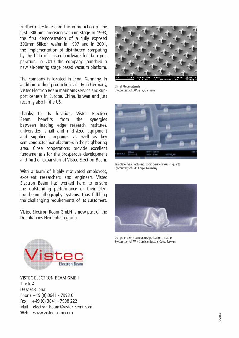
Further milestones are the introduction of the first 300 mm precision vacuum stage in 1993, the first demonstration of a fully exposed 300 mm Silicon wafer in 1997 and in 2001, the implementation of distributed computing by the help of cluster hardware for data pre-paration. In 2010 the company launched a new air-bearing stage based vacuum platform. The company is located in Jena, Germany. In addition to their production facility in Germany, Vistec Electron Beam maintains service and sup-port centers in Europe, China, Taiwan and just recently also in the US.
Thanks to its location, Vistec Electron Beam benefits from the synergies between leading edge research institutes, universities, small and mid-sized equipment and supplier companies as well as key semiconductor manufacturers in the neighboring area. Close cooperations provide excellent fundamentals for the prosperous development and further expansion of Vistec Electron Beam.
With a team of highly motivated employees, excellent researchers and engineers Vistec Electron Beam has worked hard to ensure the outstanding performance of their elec-tron-beam lithography systems, thus fulfilling the challenging requirements of its customers.
Vistec Electron Beam GmbH is now part of the Dr. Johannes Heidenhain group.
VISTEC ELECTRON BEAM GMBHIlmstr. 4 D-07743 JenaPhone +49 (0) 3641 - 7998 0Fax +49 (0) 3641 - 7998 222Mail [email protected] www.vistec-semi.com
Chiral Metamaterials By courtesy of IAP Jena, Germany
Template manufacturing. Logic device layers in quartz By courtesy of IMS Chips, Germany
Compound Semiconductor Application - T-Gate By courtesy of WIN Semiconductors Corp., Taiwan
05/2
014

INTRODUCTION
Since 1955 when nuclear research institute in Řež was
established, there were done research in field of nuclear
physics, radiochemistry and nuclear power industry. One by
one there was established production of many special
products for example radiopharmaceuticals. Nowadays in
ÚJV Řež, a. s. we are running two nuclear reactors and
many technological facilities working with radioactive
materials.
Special extensive research was done in preparation and
reprocessing of nuclear fuel, handling of radioactive waste,
research of decontamination techniques and technologies,
research and production of radionuclides and
radiopharmaceuticals, research in non-destructive and
mechanical tests of reactor components including
specimens of surveillance programs.
This poster will present only part of the whole project
dealing with surveillance program.
WHAT WE DO - GENERAL LAYOUT
The facility consists of 51 hot and semi-hot cells situated on
three floors.
Semi-hot cells with EBWs are connected with other hot and
semi-hot cells, where welded specimens are used for
testing and evaluation of mechanical properties of
structural materials from nuclear power plants. The cells
are equipped with all the necessary remote handling
equipment for standard methods of post irradiation
mechanical testing.
The face wall of the semi-hot cells is shielded with 150 mm
of the lead for handling of specimens with an activity of up
to 37 GBq.
Hot cells are used for preparatory and auxiliary operations
with irradiated materials, e.g. receiving of irradiated
materials, unloading of containers and evaluation of
detectors to determine the neutron fluence and the
irradiation temperature.
Another task solved in hot cells in ÚJV Řež, a. s. are the
problems of the effects of recovery heating on mechanical
properties after their irradiation. At present, the
reconstitution of radioactive specimens and the
supplementary surveillance programme of the WWER-440
and WWER-1000 reactor pressure vessel steels is realised.
WHAT WE DO - RECONSTITUTION
Recostitution is a very effective and valuable method for
the re-evaluation of specimens from the standard
surveillance programme. It is very important mainly for
determination of different material parameters from the
same specimens.
The studs that are welded to the inserts are from the same
type of material. After welding, the reconstituted
specimens are machined by an electric discharge machine,
the desired notch is cut and the specimens are polished for
pre-cracking (in the case of fracture toughness testing).
The welding reconstitution is performed in accordance with
the ASTM E 1253-13 standard, including periodical
measurement of the insert temperatures for the duration
of welding. The welding is done at a beam power of around
5kW and is suitable for the reconstitution of all specimen
types used in ÚJV Řež, a. s. hot laboratories. The welding is
performed by a computer controlled high vacuum electron
beam welding machine.
The use of this technique is an effective solution to the
shortage of surveillance materials and guarantees a lower
consumption of these scarce materials.
Currently many specimens for impact and fracture
toughness testing that are being irradiated in surveillance
programs are of the insert size and are reconstituted after
the irradiation process.
Eyeview trough lead-glass shielding window Control room of semi-hot cells Containers with specimens Welded specimens for surveillance program Remote handlers of new semi-hot cells
SURVEILLANCE PROGRAM IN ÚJV ŘEŽ, a. s.
To monitor changes in mechanical behaviour of materials in
the reactor pressure vessel (RPV) during operation is used
surveillance programs. This material specimens require
standards and regulations of the State Office for Nuclear
Safety (SONS) and the International Bureau for Nuclear
Safety (IAEA).
Effect of neutron radiation in the pressurized water reactor
vessel in the microstructure of the material occurs
irreversible changes that significantly affect the mechanical
and physical properties of the steel. To monitor the life and
serviceability of the reactor pressure vessel and therefore
of the entire plant, are the most important changes in the
elastic/plastic properties and increasing of critical
transition temperature and thus reducing the energy
required for crack propagation in plastic region at a high
temperature.
To monitor this changes is used a special surveillance
program designed for this type of reactor. The system of
surveillance species is hanged on the edge of the reactor
pressure vessel in special cylindrical containers connected
by a chain links. This surveillance containers are removed
after several years and reactor pressure vessel regularly
subjected to strict mechanical tests at the Nuclear Research
Institute in Řež near Prague.
PRINCIPLE OF RECONSTITUTION
1. Initial Charpy type specimen of standard dimensions
(10x10x55mm),
2. Broken sample after impact, dynamic or static fracture
toughness test,
3. Two inserts of standard dimensions (10x10x14 mm) can
be machined from the broken specimen,
4. Welding of unirradiated studs and irradiated insert. The
standard dimensions of the studs are: 10.05x10.05x22
mm,
5. After final machining the reconstituted specimen is
complete and available for further testing. The sample
has same properties as original specimen.
WHAT WE USE – EBW USED IN ÚJV ŘEŽ, a. s.
EBW-HC:
Year of construction: 2008
Source voltage: 60 kV
Beam current: 120 mA
Vacuum chamber: 500x500x500 mm
Operating vacuum: 2*10-5 mbar*l/s
ES-3:
Year of construction: 1997
Source voltage: 55 kV
Beam current: 30 mA
Vacuum chamber: 500x500x500 mm
Operating vacuum: 2*10-5 mbar*l/s
RECONSTRUCTION AND MAINTENANCE OF HOT AND
SEMI-HOT CELLS
The facility for hot and semi-hot cells was built in 1970.
After years of operation, the cells and technology are worn
and have to be reconstructed. Some of the old glove boxes
were completely removed and in their places were
constructed cells with modern apparatuses. In 2012 began
the reconstruction of hot cells, which includes replacement
of old halogen lamps for new LED lights; restoration of
power circuits; repair and replacement of shielding tanks
with zinc bromide; replacement of old force for new
master-slave manipulators and other minor repairs and
upgrades.
Fig. 1New semi-hot cell with 3 eyeviews and
mater-slave manipulators
Fig. 2 Hot cell with one old force and one new
master-slave manipulator
Fig. 4 Unirradiated specimen with thermocouple
Fig. 3 Irradiated Charpy type specimen after the reconstitution
Fig. 6 Scheme of recostituted specimen
Fig. 7 EBW-HC before instalation into semi-hot cell
Fig. 5 Principle of reconstitution

• Only KJLC® has ‘’Zero’’ Footprint Load Lock Design
• Revolutionary eKLipse System Control Software
• Purpose Built Chamber Design for Optimal Thin Film
Uniformity
• Developed with Over 80 New and Improved Product
Features for Enhanced Thin Film Performance
| Enabling Technology for a Better World | www.lesker.com
Innovation with Continuous ImprovementsThe All New PVD 75
TM
PRO Line
14-005
Wafer loaded into New LAS-150 Load Lock

TWI – Materials joining and
engineering technologies
An original spin-out from the University of Cambridge’s Engineering Department in the 1940s, TWI
and its professional institution The Welding Institute established a base at Abington Hall and have
since delivered a continuous output of technical advances in materials engineering and joining
technologies – critical to engineering design and industry practice across the globe.
The company is an independent research and technology organisation, responsible for establishing
world Standards and Codes of Practice, developing new joining processes such as electron beam
Surfi-sculpt and friction stir welding for multi-industry exploitation, working with industry to
improve existing processes or to develop tailored products, and applying its expertise to discover
why welded joints and engineering structures fail.
The first organisation dedicated to welding and joining research, TWI has grown its business as a
membership-based service, employing top engineers, materials scientists, chemists and physicists to
create a respected world authority in improved engineering design. It has five laboratories in the UK
and eight worldwide. Supported by its international training and examinations network, established
in the 1960s, TWI takes technical and practical knowhow to regions looking for growth through skills
development.
In 2015, TWI will open a postgraduate centre for structural integrity research at Abington, bringing
together academic study and industry-driven project work – the latest phase in its work to transfer
materials engineering and joining knowledge effectively into industry.

TWI’s Electron Beam (EB) services, delivered from Cambridge and Middlesbrough in the UK, cover a
wide spectrum of EB technology including:
Processing:
• Welding in-vacuum-chamber.
• Welding out-of-vacuum-chamber (enabled by reduced pressure technology).
• Non-additive surface texturing and sculpting (Surfi-Sculpt®).
• Additive wire-fed deposition/ manufacture.
• Low volume, very high value added or technically challenging production welding.
• And also to a lesser extent cutting, drilling and vacuum re-melting developments.
Equipment improvement:
• Gun and column design, analysis and optimisation.
• Equipment prototyping.
• Beam probe and analysis (BeamAssureTM
and others types).
• Specialist equipment solutions supply.
TWI is active in provision of EB research and development, consultancy and production support to its
Industrial Member companies. It also collaborates in appropriate national and international
government funded projects to further the state-of-the-art of EB technology.
TWI holds a number of patents/patents applications for EB equipment and processes which it
licences to machine builders and end users as appropriate.
Please contact TWI with any enquires where we may be able to assist:
Mike Nunn ([email protected]).
Colin Ribton ([email protected]).
Jason Sanderson ([email protected]).
www.twi.co.uk
00 44 (0) 1223 89 90 00
TM
A quality assurance tool helping to analyse
electron beam parameters, giving an effective
fingerprint of the beam and an independent monitor of beam characteristics.
BeamAssure™ provides unrivalled confidence in electron beam welding and processing performance ensuring the quality of your
product.
For further information please visit
www.beamassure.com
Electron beams are challenging to
measure and calibrate due to their nature, BeamAssure is able to capture
relevant data, giving assurance of beam power profile consistency and quality, time and time again.
Applicable Industries:
• Aerospace• Automotive• Defence• Electronics• Medical• Oil and Gas• Power
Electron Beam Welding Quality Assurance

Features and Benefits
• Simple mode of operation. Simple to understand outputs
• Probing is possible at full welding power up to 40kW (higher powers possible – please contact
TWI to discuss)• Addressing production and research needs• Supported by 10 years of research and
development• Proven endurance after 2 years and 30,000
welds in series aerospace production• Contributing towards elimination of high value
rework
• Non-intrusive or disruptive to the process or production
• Supporting weld penetration and shape consistency
• May be integrated with in-house quality assurance systems
• Electron Beam (EB) machine function and operator error checking
• Production monitoring and/or research analysis functions
• Real-time instantaneous results and measurements
• Suitable for EB welding, additive layer manufacturing and other EB processing systems
• Beam data and results analysis service and support available from the TWI team
• Beam probed and data captured in <1 minute• Viable for use as a go/no-go decision making
tool
• Evaluation of machine to machine variability issues
• Engineered and supported by TWI
Technical Specification
• High power capability, for use with 60kV to 150kV accelerating potential EB machines
• No thermal management or active cooling required
• Clearly defined measurements and graphical display of beam quality:- Beam current- Beam asymmetry- Beam profile- Beam focus- Beam diameter
• Association of part/serial number with data record via integrated bar code reader (or similar to complement end-user operations)
• May be integrated into the welding machine chamber and HMI PC (may also be supplied in a portable configuration or with a lower level of integration to meet end-user needs)
• Twin slit probe head with integrated Faraday cup
• Includes a beam sink capable of withstanding welding power for extended periods
• Mounting system for fitting probe head into vacuum chamber
• Data acquisition system based around the existing machines HMI PC or provided as a rack mounted industrial PC, minimum 17” monitor screen and preloaded software tools, enabling data capture and analysis
• Data export in a range of formats possible • Cabling connecting the probe head, both inside
and outside the vacuum chamber and to the existing machine control hardware/HMI PC
For further information please visit
www.beamassure.com

Authors’ Index
Amalnerkar D. 138
Angelov S. 90
Balashov V. 7
Barnes S. 221
Bataev A. 174
Bataev I. 174
Belenkiy V. 22, 30, 34, 90, 97
Belozertsev V. 56
Belyuk S. 269
Bematskyy A. 319
Benabbou A. 297
Bencurova A. 279
Beniyash A. 56, 242, 303
Bludenko A. 150
Bodurov G. 226
Bogdanov V. 56
Bouberka Z. 290, 297
Bouchakoura M.
290
Braverman V. 56
Buxton A. 221
Cherepkov V. 168
Chernogorova T.
132
Chulkov V. 150
Derouichea Y. 290
Dlouhý I. 82
Domarov E. 168
Donchev V. 132, 138
Dong W. 126
Doniy A. 144
Dorl W. 368
Dragunov V. 7, 75, 259
Druzhinina A. 62
Dupák L. 310
Dvilis E. 315
Engelko V. 236 Erofeev V. 68
Fadeev S. 168
Fetzer R. 216 Fietzke F. 183
Foret R. 82
Frikach K. 108
Frumkin A. 157
Fujimura N. 329, 334, 339, 343, 348
Gesheva K. 226
Gnatenko О. 212
Golkovskii M. 174
Golubenko Yu. 168
Goncharov A. 7, 75, 259, 352
Gordenko A. 7
Graffel B. 183
Grechanyuk I. 115, 196, 201, 206
Grechanyuk M. 115
Grechanyuk N. 196, 201, 206
Grechanyuk V. 196, 201, 206
Gribkov M. 75
Gruzdev V. 264
Han B. 163
Hassel T. 242, 303
Havlík P. 82
Heinss J.-P. 183
Herynk M. 372
Houtz J. 108
Ivanova T. 226
Jiang D. 126
Jung S. 163
Kakugawa K. 343
Kardjiev M. 46
Kazmiruk V. 284
Khasanov A. 315
Khasanov O. 315
Khaskin V. 324
Khomenko E. 196, 201, 206
Kim J. 163
Kim Y. 163
Klimov A. 315
Kogut D. 168
Koleva E. 22, 30, 46, 90, 226, 279, 356
Konecnikova A.
279
Korchagin A. 168
Kornilov S. 242, 303
Kostic I. 279
Kouřil J. 82
Kovalchuk D. 115, 122
Kozai H. 334
Kozhechenko A.
7

Krivonosova E. 352
Kubo M. 343
Kuksanov N. 168, 174, 178
Kurganov I. 284
Laptenok V. 62
Lavruchin A. 168
Marchenko Y. 212
Maschke U. 290, 297
Mattausch G. 183
Melnik A. 196, 201, 206
Melnyk A. 115
Melnyk I. 122, 254
Melnyk V. 115, 122
Metreveli A. 150, 157
Metreveli P. 150, 157
Metzner Ch. 183
Mladenov G. 13, 22, 30, 46, 90, 226, 279
Mueller G. 216
Munirathnam N.
138
Murray N. 242, 303
Murygin A. 62
Nadim A. 297
Nagorniy D. 274
Neailey K. 221
Nemec P. 279
Nemytov P. 168
Neumann M. 360
Noguchi H. 329, 334, 339, 343, 348
Oks E. 315
Olschok S. 40
Olshanskaya T.
97
Osipov I. 269
Permyakov G. 97
Petrik I. 212
Pinto T. 221
Pobal I. 103
Polyakov I. 174
Ponomarev A. 150, 157
Ponomarev I. 352
Portnov M. 259
Pozo S. 249
Radchenko M. 274
Radchenko T. 274
Rau A. 269
Reisgen U. 40
Rempe N. 242, 303
Ribton C. 231, 242, 249
Ritomsky A. 279
Roegner F.-H. 183
Rojkh A. 178
Rubtsov V. 7
Ruktuev A. 174
Salimov R. 168
Salomatova E. 34
Samoilenko V. 174
Savitskaja T. 284
Sanderson J. 374
Schacke H. 368
Scherbakov A. 259
Semenov G. 269
Semenov V. 168
Seregin Y. 62
Shcherbakov A.
7
Sheliagin V. 319
Shevtsov Yu. 274
Shi Sh. 126
Shimono K. 329, 339, 343, 348
Shirai Y. 334, 339, 348
Shiray Y. 329
Sliva A. 7, 75, 259
Smith D. 249
Šohaj P. 82
Spivac V. 319
Spivak V. 324, 356
Stepanov M. 178
Stoimenov A. 138
Stoimenov A. 226
Stolberg I. 368
Sudnik V. 68
Szanto P. 373
Tan Y. 126
Tanaka T. 329, 334, 339, 343, 348
Terentyev E. 75, 259
Tirshu M. 324
Tirsu M. 319
Todorov D. 46, 90
Toyota H. 329, 334, 339, 348
Trushnikov D. 13, 22, 30, 34, 90, 97
Tsaplin A. 34
Tsuchiya Y. 343
Tugai B. 122
Ufer S. 40
Uspenskiy N. 56
Vasilyev A. 68
Vassileva V. 138, 226
Vesely T. 372
Vlasiuk A. 356
Voron M. 144
Vutova K. 132, 138, 226, 279, 329, 334
Weisenburger A.
216
Wen Sh. 126
White J. 108
Winckler F. 183
Yurevich S. 103
Zalesski V. 264
Zenin A. 315
Zhemanyuk P. 212
Zimmermann B.
183

ЕЛЕКТРОТЕХНИКА И ЕЛЕКТРОНИКА E+E 49 год. 1-2/2014 Научно-техническо списание
Издание на: Съюза по електроника, електротехника и съобщения /CEEC/
Главен редактор:
Проф. дтн Иван Ячев, България
Зам. гл. редактор:
Доц. д-р Сеферин Мирчев, България
Редакционна колегия:
Д-р Владимир Шелягин, Украйна Чл. кор. проф. дфн Георги Младенов, България Проф. д-р Георги Стоянов, България Проф. Юън Ричи, Дания Доц. д-р Захари Зарков, България Проф. Кристиан Магеле, Австрия Проф. Маурицио Репето, Италия Проф. дтн Румяна Станчева, България Проф. Такеши Танака, Япония Проф. Ханес Топфер, Германия Д-р Хартмут Брауер, Германия Акад. проф. Юрий Якименко, Украйна
Консултативен съвет:
Проф. д-р Димитър Рачев, България Проф. дтн Емил Владков, България Проф. дтн Емил Соколов, България Проф. дтн Ервин Фердинандов, България Проф. д-р Жечо Костов, България Доц. д-р Иван Василев, България Проф. дтн Иван Доцински, България Доц. Иван Шишков, България Проф. дтн Людмил Даковски, България Проф. дтн Минчо Минчев, България Проф. дфн Николай Велчев, България Доц. д-р Петър Попов, България Проф. д-р Стефан Табаков, България Проф. д-р Сава Папазов, България
Редактор на броя:
Чл. кор. проф. дфн Георги Младенов
Технически редактор:
Доц. д-р инж. Елена Колева
Адрес:
ул. “Раковски” 108 ет. 5, стая 506 София 1000
тел.: +359 2 987 97 67 e-mail: [email protected] http://epluse.fnts.bg
ISSN 0861-4717
С Ъ Д Ъ Р Ж А Н И Е Специален брой: Научни статии от 11-та Международна конференция по Електронно-лъчеви технологии – ЕВТ 2014, Варна, БЪЛГАРИЯ Предговор от чл. кор. на БАН, проф. дфн Г. Младенов 4
ЕЛЕКТРОННОЛЪЧЕВО ЗАВАРЯВАНЕ
А. Щербаков, А. Гончаров, А. Козеченко, А. Горденко, А. Слива, В. Балашов, В. Драгунов, В. Рубцов
Модерни проблеми и методи на разработка на системи за електроннолъчево заваряване 7
Д. Трушников, Г. Младенов
Числено моделиране на формирането и параметрите на плазмата, генерирана по време на електронно-лъчево заваряване 13
Д. Трушников, Г. Младенов, В. Бененкий, Е. Колева
Йонен ток, получен от плазмата над зоната на заваряване при електроннолъчево заваряване 22
Е. Колева, Д. Трушников, В. Бененкий, Г. Младенов
Управление на електроннолъчево заваряване на пластини, използвайки тока от обратната страна на пластината 30
Д. Трушников, Е. Саломатова, А. Цаплин, В. Беленкий
Моделиране на процесите на изпарение при електроннолъчево заваряване 34
У.Рейсген, С.Олшок, С.Уфер
Точна диагностика на характеристиките на електронния сноп
40
Е. Колева, Г. Младенов, М. Карджиев, Д. Тодоров
Характеризиране на електронния лъч при промени на параметрите на процеса електроннолъчево заваряване 46
В. Браверман, В. Белозерцев, В. Богданов, Н. Успенский, А. Бенияш
Следене за процепа при електроннолъчево заваряване на въздух…………………………………………………………….56
В. Лаптенок, А. Дружинина, А. Муригин, Ю. Серегин

Компенсация на ефекта на магнитни полета върху позицията на електронния сноп в процеса на електроннолъчевото заваряване 62
А. Василев, В. Ерофеев, В. Судник
Механизъм на началото на флуктуациите на дълбочината на кратера при заваръчни лъчеви процеси 68
А. Слива, В. Драгунов, А. Гончаров, Е. Терентиев, М. Грибков
Електроннолъчево заваряване на елементи от бланкетния модул на ИТЕР 75
П. Хавлик, П. Сохай, Й. Курил, Р. Форет, И. Длоухи
Електроннолъчево заваряване на неръждаема стомана и феритна стомана 82
Е. Колева, Д. Трушников, В Беленкий, Г. Младенов, С. Ангелов, Д. Тодоров
Моделно базирана оптимизация на качеството при електроннолъчево заваряване на стомана 90
Т. Олшанска, Г. Пермяков, В. Беленкий, Д. Трушников
Влияние на осцилациите на електронния сноп върху формирането на структурата на шева на различни материали на примера на съединението стомана-бронз…………………………………….97
И. Побал, С. Юревич
Електроннолъчево заваряване на свръх-проводящи резонатори, направени от свръх-чист ниобий 103
К. Фрикач, Д. Уайт, Д. Хоутз
Прогноза на частичната дълбочина на проникване в 15-5PH материал при електроннолъчево заваряване 108
ЕЛЕКТРОННОЛЪЧЕВО ТОПЕНЕ И РАФИНИРАНЕ
М. Гречанюк, А. Мелник, И. Гречанюк, В. Мелник, Д. Ковалчук
Модерни електроннолъчеви технологии и оборудване за топене на метали и сплави, за отлагане на защитни покрития, производство на композити, кондензирани от пари и за получаване на прахове 115
В. Мелник, И. Мелник, Б. Тугай, Д. Ковалчук
Последни усъвършенствания в разработката на газоразрядни електронни пушки, обезпечаващи разширение на технологичните им възможности
122
С. Ши, И. Тан, Д. Жианг, У. Донг, С. Уен
Влияние на лъча върху отстраняването на фосфор в силиций чрез електроннолъчево топене 126
В. Дончев, К. Вутова, Т. Черногорова
Икономичен и консервативен числен метод за нестационарен тополинен модел за ЕЛТР 132
В. Василева, К. Вутова, В. Дончев, А. Стоименов, Д. Амалнеркар, Н. Муниратнам
Електроннолъчево топене и рециклиране на никел 138
М. Ворон, А. Доний
Контрол на структурата и свойствата на ляти α-титанови сплави, получени с електроннолъчево топене в собствена кора с електромагнитно разбъркване 144
ELECTRON ACCELERATOR APPLICATIONS
А. Пономарев, П. Метревели, А. Метревели, А. Бледенко, В Чулков
Декомпозиция на растителни биомаси с електроннолъчево облъчване и нагряване 150
П. Метревели, А. Метревели, А. Паномарев
Електроннолъчево третиране на вода, замърсена с хумусни киселини и лигнин 157
Б. Хан, Ж. Ким, Ю. Ким, С. Джунг
Електроннолъчева технология за съхранение на околната среда
163
Н. Куксанов, Ю. Голубенко, П. Немитов, Р. Салимов, С. Фадеев, А. Корчагин, Д. Когут, Е. Домаров, А. Лаврухин, В. Черепков, В. Семенов
Тенденции на разработката на правотокови електронни ускорители за индустриални приложения и изследователски експерименти 168
И. Батаев, М. Голковски, Н. Куксанов, А. Руктуев, В. Самоиленко, И. Поляков, А. Батаев
Повърхностно създаване на титанова сплав с труднотопими елементи чрез извън-вакуумна електроннолъчева обработка
174
Н. Куксанов, А. Рожкх, М. Степанов
Опит от 30-годишното използване на електроннолъчева инсталация в завода „Подолсккабел“ 178
ТЪНКИ СЛОЕВЕ, ОТЛАГАНЕ НА ПРАХОВЕ, МОДИФИКАЦИЯ НА ТВЪРДИ ПОВЪРХНОСТИ
Г. Матауш, Б. Цимерман, Ф. Фиетзке, Й. Хейнц, Б. Граффел, Ф. Винклер, Ф. Роегнер, Х. Метцнер
Газоразрядни източници на електрони – доказани и нови инструменти за тънкослойни технологии 183

Н. Гречанюк, И. Гречанюк, Е. Хоменко, А. Мелник, В. Гречанюк
Композитни материали с метална матрица, кондензирана от парна фаза: Дисперсионно-уякчени метали 196
Н. Гречанюк, И. Гречанюк, Е. Хоменко, А. Мелник, В. Гречанюк
Композитни материали с метална матрица, кондензирана от парна фаза: Микрослойни материали 201
Н. Гречанюк, И. Гречанюк, Е. Хоменко, А. Мелник, В. Гречанюк
Композитни материали с метална матрица, кондензирана от парна фаза: Микропорести материали 206
П. Жеманюк, И. Петрик, О. Гнатенко, Ю. Марченко
Електроннолъчева обработка на обшивката на горивните камери самолетни мотори, направена от уякчена топло-устойчива хром-никелова сплав
212
Р. Фецер, А. Уейзенбургер, Г. Мюелер
Модификация на повърхностния слой с електронен сноп с голямо напречно сечение 216
Т. Пинто, А. Бъкстон, К. Ниайли, С. Барнс
Подобрения и възможности на повърхностната обработка с електронен сноп 221
К. Вутова, В. Василева, А. Стоименов, Е. Колева, Т. Иванова, Г. Бодуров, К. Гешева, Г. Младенов
Оптично и структурно изследване на WOx тънки слоеве, отложени чрез електронно лъчево изпарение 226
ЕЛЕКТРОННА ОПТИКА, ЕЛЕКТРОННИ ПУШКИ И ЕЛЕКТРОННОЛЪЧЕВИ МАШИНИ
К. Рибтон
Високо-ъглово и високо-интегрално отклонение на снопа 231
В. Енгелко
Източник на радиално-събиращ се електронен сноп за модификация на дълги цилиндрични мишени 236
Н. Ремпе, С. Корнилов, А. Бениаш, Н. Муррай, Т. Хассел, К. Рибтон
Характеризиране на електронен сноп, генериран от пушка с плазмен катод 242
С. дел Позо, К. Рибтон, Д. Смит
Конструиране на електронна пушка с РЧ плазмен катод
249
И. Мелник
Симулиране на времето на нарастване на тока в електронна пушка с импулсен триоден високоволтов тлеещ разряд 254
А. Гончаров, В. Драгунов, А. Слива, М. Портнов, А. Щербаков, И. Чулков
Oценка на параметрите на технологичен електронен сноп на базата на оптичната радиация във вакуум 259
В. Груздев, В. Залески
Електронно-оптични характеристики на снопове, генерирани от плазмени източници на електрони 264
С. Белюк, И. Осипов, А. Рау, Г. Семенов
Електроннолъчеви машини за заваряване с пушки с плазмен катод 269
М. Радченко, Ю. Шевцов, Т. Радченко, Д. Нагорний
Експлоатация на концентрирани енергийни потоци за заваряване и продукция със защитни покрития 274
ЕЛЕКТРОННА ЛИТОГРАФИЯ, ЕЛЕКТРООПТИЧНИ УСТРАЙСТВА И ПОЛИМЕРНА МОДИФИКАЦИЯ
И. Костич, А. Бенкурова, А. Конечникова, П. Немек, А. Ритомски, Е. Колева, К. Вутова, Г. Младенов
Изследване на електронни резисти: негативен HSQ и позитивен SML300 279
В. Казмирюк, И. Курганов, Т. Савитская
Безмасков литографски клъстер за ниско- и средно-серийно производство 284
У. Машке, М. Бочакур, Я. Деруише, З. Буберка
Електро-оптични устройства – приложение на електроннолъчева техника: Течни кристали, дисперграни в полимери 290
З. Буберка, А. Надим, А. Бенабоу, У. Машке
Радиационно-индуцирана деградация на два органични замърсители от воден разтвор на нанокомпозити 297
ДРУГИ ТЕХНОЛОГИИ, БАЗИРАНИ НА ИЗПОЛЗВАНЕТО НА ЕЛЕКТРОНИ, ЙОНИ, ПЛАЗМА И ЛАЗЕРИ
Т. Хассел, Н. Муррай, А. Бениаш, Н. Ремпе,С. Корнилов
Извън-вакуумно електроннолъчево рязане-един нов високопроизводителен процес 303

Л. Дюпак
Електроннолъчева размерна обработка на пластмаси 310
А. Климов, А. Зенин, Е. Окс, О. Хасанов, Е. Двилис, А. Хасанов
Електроннолъчево синтероване на керамика
315
В. Шелягин, В. Спивак, А. Бернацкий, М. Тыршу
Микроструктурата на повърхностните слоеве при лазерно и лазерно-микроплазмената легиране 319
В. Спивак, В. Хаскин, М. Tирсу
Лазерен скалпел 324
К. Шимоно, Н. Фуджимура, Х. Ногучи, Х. Тойота, Й. Шираи, Т. Танака, К. Вутова
Зависимост на ширината на импулсите на самозапалването на плазма при йонна имплантация, използваща плазмата 329
Х. Козаи, Н. Фужимура, М. Ногучи, Х. Тойота, Й. Шираи, Т. Танака, К. Вутова
Предварителна оценка на проникващата йонна енергия с помощта на симулационната програма ПЕГАСУС 334
Х. Ногучи, Н. Фужимура, К. Шимоно, Х. Тойота, Й. Шираи, Т. Танака
Сравнение на спектралните характеристики при използване на базирана на плазма йонна имплантация 339
К. Какугава, М. Кубо, Х. Погучи, К. Шимоно, Н. Фуджимура, Й. Цучия, Т. Танака
Стерилизация на споро-образуващи бактерии с използване на плазма-базирана йонна имплантация 343
Н. Фуджимура, К. Шимоно, Х. Ногучи, Х. Тойота, У. Шираи, Т. Танака
Оценка на плазмената плътност при самозапалване на плазма предназначена за йонна имплантация 348
E. Кривоносова, А. Гончаков, И. Пономарев
Микро-дъгово оксидиране на алуминиеви сплави 352
В. Спивак, Е. Колева, А. Власюк
Анализ и обобщение на научнте и методически информационни учебни пособия по наноелектроника 356
ПРЕЗЕНТАЦИЯ НА КОМПАНИИ M. Нойман Von Ardenne GmbH, Дрезден, Германия 360
У. Дорл, Х. Шаке, И. Столберг Литография с различна форма на лъча за микро- и нано-технологии. Vistec Electron Beam GmbH, Йена, Германия 368
T. Весели, M. Херинк Реконструкция на облъчени образци - UJV Řež, a. s. Husinec - Řež, Чехия 372
P. Санто Kurt J. Lesker Co. Ltd. 373
Дж. Сандерсън
TWI Ltd. – Съединяване на материали и инженерни технологии
374
Индекс на авторите 378
Съдържание 380