electroabsorption dynamics in an ingaasp/ingaasp superlattice modulator
TRANSCRIPT

TOPS Volume XIII
Electronics and Optoelectronics
rel. Amplitude (dB)
OSA. Optical Society of America
Edited by Martin Nuss and John Bowers
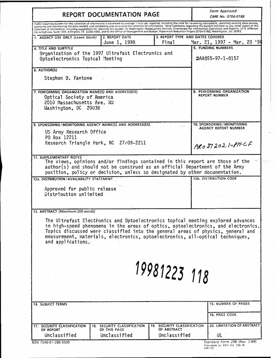
REPORT DOCUMENTATION PAGE Form Approved
OMB No. 0704-0788
Public reporting burden for this collection of information is estimated to average l hour per response, including the time for reviewing instructions, searching existing data sources, qathenng and maintaining the data needed, and completing and reviewing the collection of information. Send comments regarding this burden estimate or any other aspect of this collection of information, including suggestions for reducinq this burden, to Washington Headquarters Services, Directorate for Information Operations and Reports, 1215 Jefferson
' Davis Highway, Suite 1204. Arlington, VA 22202-4302, and to the Office of Management and Budget. Paperwork Reduction Project (0704-0188), Washington, DC 20503.
1. AGENCY USE ONLY (Leave blank) 2. REPORT DATE
June 1, 1998 3. REPORT TYPE AND DATES COVERED
Final Mar. 21, 1997 - Mar. 20 '9i 4. TITLE AND SUBTITLE
Organization of the 1997 Ultrafast Electronics and Optoelectronics Topical Meeting
6. AUTHOR(S)
Stephen D. Fantone
5. FUNDING NUMBERS
DAAG55-97-1-0157.
7. PERFORMING ORGANIZATION NAME(S) AND ADDRESS(ES)
Optical Society of America 2010 Massachusetts Ave. NW Washington,'DC 20036
PERFORMING ORGANIZATION REPORT NUMBER
9. SPONSORING/MONITORING AGENCY NAME(S) AND ADDRESS(ES)
US Army Research Office P0 Box 12211 Research Triangle Park, NC 27/09-2211
10. SPONSORING/MONITORING AGENCY REPORT NUMBER
^oSllöl.h^'^^
11. SUPPLEMENTARY NOTES The views, opinions and/or findings contained in this report are those of the author(s) and should not be construed as an official Department of the Army position, policy or decision, unless so designated by other documentation.
12a. DISTRIBUTION/AVAILABILITY STATEMENT
Approved for public release Distribution unlimited
12b. DISTRIBUTION CODE
13. ABSTRACT (Maximum 200 words)
The Ultrafast Electronics and Optoelectronics topical meeting explored advances in high-speed phenomena in the areas of optics, optoelectronics, and electronics. Topics discussed were classified into the general areas of physics, general and measurement, materials, electronics, optoelectronics, all-optical techniques, and applications.
MS1223 US
U. SUBJECT TERMS 15. NUMBER OF PAGES
16. PRICE CODE
17. SECURITY CLASSIFICATION OF REPORT
Unclassified
18. SECURITY CLASSIFICATION OF THIS PAGE
Unclassified
19. SECURITY CLASSIFICATION OF ABSTRACT
Unclassified
120. LIMITATION OF ABSTRACT
UL NSN 7540-01-280-5500 Standard Form 298 (Rev. 2-89)
Prescribea bv ANSI Std Z39-18 298-102

OSA Trends in Optics and Photonics Series
Series Editor Tingye Li AT&T Labs.
Volume 13
Ultrafast Electronics and Optoelectronics

Trends in Optics and Photonics Series Tingye Li, Series Editor
Vol. 1 Advanced Solid State Lasers (1996) Stephen A. Payne and Clifford R. Pollock, eds.
Vol. 2 Advances in Optical Imaging and Photon Migration R.. R.. Alfano and James G. Fujimoto, eds.
Vol. 3 Biomedical Optical Spectroscopy and Diagnostics Eva Sevick-Muraca and David Benaron, eds.
Vol. 4 Extreme Ultraviolet Lithography Glenn D. Kubiak and Don R. Kania, eds.
Vol. 5 Optical Amplifiers and Their Applications (1996) Edited by the 1996 OAA Program Committee
Vol. 6 Medical and Biological Applications Rinaldo Cubeddu, ed.
Vol. 7 Ultracold Atoms and Bose-Einstein Condensation Keith Burnett, ed.
Vol. 8 Environmental Monitoring and Instrumentation Frank Bucholtz, ed.
Vol. 9 Lasers and Optics for Manufacturing Andrew C. Tarn, ed.
Vol. 10 Advanced Solid State Lasers (1997) Clifford R. Pollock and Walter R. Bosenberg, eds.
Vol. 11 Noninvasive Assessment of the Visual System Dean Yager, ed.
Vol. 12 System Technologies, from OFC '97 Curtis R. Menyuk and Alan E. Willner, eds.
Vol. 13 Ultrafast Electronics and Optoelectronics Martin Nuss and John Bowers, eds.
Vol. 14 Spatial Light Modulators Geoffrey Burdge and Sadik C. Esener, eds.
Vol. 15 Advances in Vertical Cavity Surface Emitting Lasers, from CLEO '97 Connie Chang-Hasnain, ed.
Vol. 16 Optical Amplifiers and Their Applications (1997) Mikhail Zervas, Shinya Sasaki, and Alan Willner, eds.

OSA Trends in Optics and Photonics Series
Volume 13
Optical Society of America 2010 Massachusetts Avenue, NW Washington, DC 20036-1023 (202)223-8130
Ultrafast Electronics and Optoelectronics
Edited by
Martin Nuss and John Bowers
From the Topical Meeting Ultrafast Electronics and Optoelectronics March 17-19,1997 Incline Village, Nevada
Sponsored by Optical Society of America
Technically cosponsored by IEEE/Lasers and Electro-Optics Society IEEE Communications Society Institute of Electronics, Communication and Information Engineers (IECIE)
Articles in this publication may be cited in other publications. In order to facilitate access to the original publication source, the following form forthe citation is suggested:
Name of Author(s), Title of Paper, OS A Trends in Optics and Photonics Vol. 13, Ultrafast Electronics and Optoelectronics, Martin Nuss and John Bowers, eds. (Optical Society of America, Washington, DC 1997), pp. xx-xx.
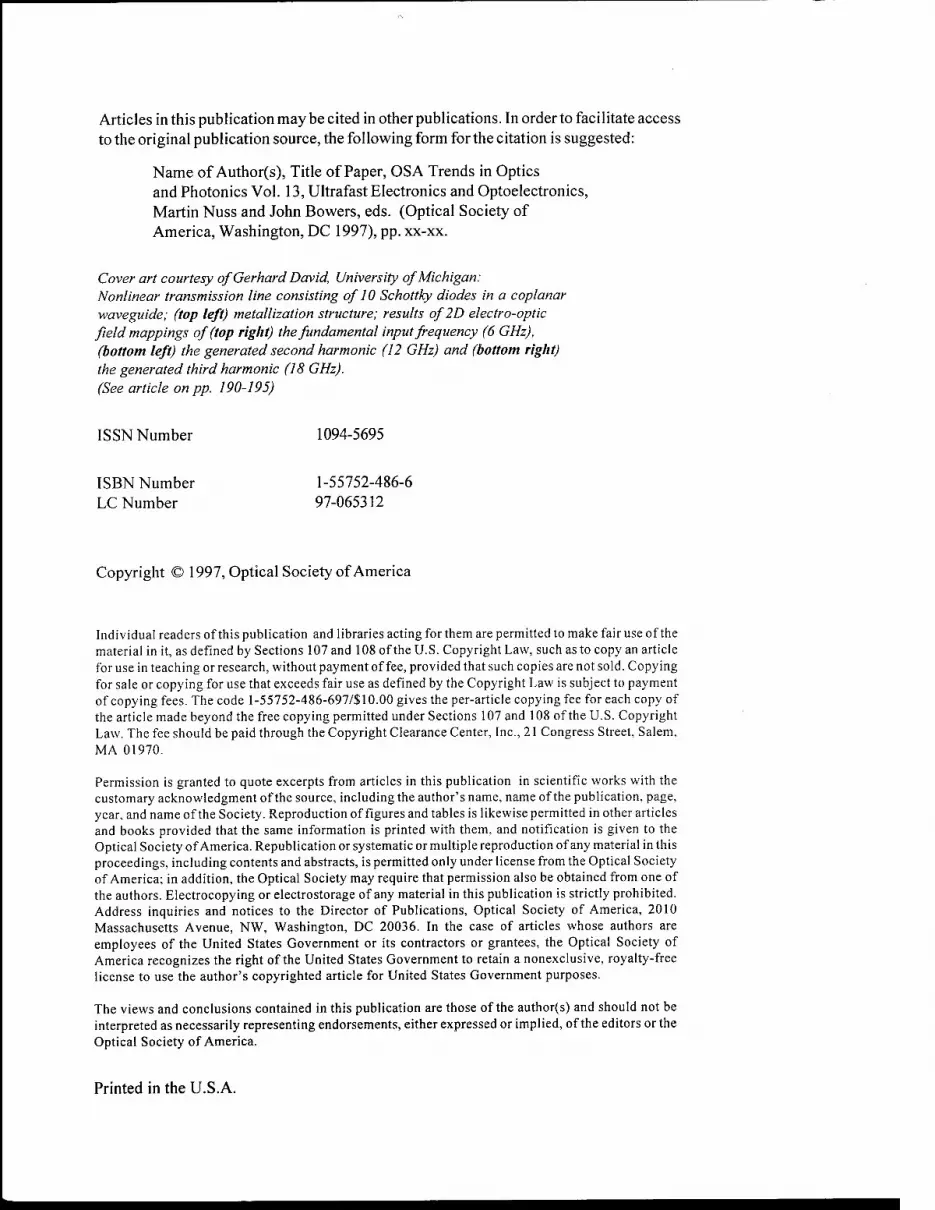
Cover art courtesy of Gerhard David, University of Michigan: Nonlinear transmission line consisting of 10 Schottky diodes in a coplanar waveguide; (top left) metallization structure; results of 2D electro-optic field mappings of (top right) the fundamental input frequency (6 GHz), (bottom left) the generated second harmonic (12 GHz) and (bottom right) the generated third harmonic (18 GHz). (See article on pp. 190-195)
ISSN Number 1094-5695
ISBN Number 1-55752-486-6 LC Number 97-065312
Copyright © 1997, Optical Society of America
Individual readers of this publication and libraries acting for them are permitted to make fair use of the material in it, as defined by Sections 107 and 108 of the U.S. Copyright Law, such as to copy an article for use in teaching or research, without payment of fee, provided that such copies are not sold. Copying for sale or copying for use that exceeds fair use as defined by the Copyright Law is subject to payment of copying fees. The code l-55752-486-697/$10.00 gives the per-article copying fee for each copy of the article made beyond the free copying permitted under Sections 107 and 108 of the U.S. Copyright Law. The fee should be paid through the Copyright Clearance Center, Inc., 21 Congress Street, Salem, MA 01970.
Permission is granted to quote excerpts from articles in this publication in scientific works with the customary acknowledgment of the source, including the author's name, name of the publication, page, year, and name of the Society. Reproduction of figures and tables is likewise permitted in other articles and books provided that the same information is printed with them, and notification is given to the Optical Society of America. Republication or systematic or multiple reproduction of any material in this proceedings, including contents and abstracts, is permitted only under license from the Optical Society of America; in addition, the Optical Society may require that permission also be obtained from one of the authors. Electrocopying or electrostorage of any material in this publication is strictly prohibited. Address inquiries and notices to the Director of Publications, Optical Society of America, 2010 Massachusetts Avenue, NW, Washington, DC 20036. In the case of articles whose authors are employees of the United States Government or its contractors or grantees, the Optical Society of America recognizes the right of the United States Government to retain a nonexclusive, royalty-free license to use the author's copyrighted article for United States Government purposes.
The views and conclusions contained in this publication are those of the author(s) and should not be interpreted as necessarily representing endorsements, either expressed or implied, of the editors or the Optical Society of America.
Printed in the U.S.A.

Contents
Preface x
Lasers Overview: Erich Ippen J_
Generation of sub-5 fs Light Pulses 2 M. Nisoli, S. De Silvestri, O. Svelto, R. Szipöcs, K. Ferencz, Ch. Spielmann, S. Sartania, andF. Krausz
Modelocked Fiber Ring Lasers 6 Hermann A. Haus and Erich P. Ippen
A Passive Harmonically Modelocked Multi-Gigahertz Cr4+:YAG Laser with Optically Phase- Locked Fundamental Solitons 14
B.C. Collings, K. Bergman and W.H. Knox
Intracavity Gain and Absorption Dynamics of Hybrid Modelocked Semiconductor Lasers using Multiple Quantum Well Saturable Absorbers 18
S. Gee, G. Alphonse, J. Connolly, andP.J. Delfyett
A Highly-Stable 59 GHz Soliton Source at 1550 nm 23 Glenn D. Bartolini, Darwin K. Serkland, William L. Kath, andPrem Kumar
Communications Overview: John Bowers 27
Terabit-per-second Transmission Experiments 28 A.R. Chraplyvy
100 Gb/s Optical Network Technology 31 K.L. Hall, K.A. Rauschenbach, S.G. Finn, R.A. Barry, N.S. Patel, andJ.D. Moores
Femtosecond Optical Code-Division Multiple-Access 37 A.M.Weiner, C.-C. Chang, and HP. Sardesai
Cascaded WDM Passive Optical Network with a Highly Shared Source 43 Jason B. Stark, Martin C, Nuss, Wayne H. Knox, Steve Cundiff, Luc Boivin, Steve Grubb, Don Tipton, David DiGiovanni, Uziel Koren, and Kevin Dreyer
Multiwavelength, 10 GHz Picosecond Pulse Generation from a Single-Stripe Semiconductor Traveling Wave Amplifier Using Active Modelocking in an External Cavity 46
H Shi, G.A. Alphonse, J.C. Connolly, andPJ. Delfyett
206-Channel Wavelength-Division Multiplexed Transmitter using a Single Femtosecond Laser 50 L. Boivin, M.C. Nuss, J.B. Stark, W.H. Knox, and ST. Cundiff
Nonlinear Optical Loop Mirror Switch (NOLM) for Coding High Repetition Mode-Locked Semiconductor Laser Pulses 54
M.R.H. Daza, HF. Liu, T. Hoshida, M. Tsuchiya, andT. Kamiya
Low Latency, Ultrafast Fiber Loop Mirror Switch using Orthogonally Polarized Signal and Control Solitons 57
L. Leng, S. D. Koehler, IN. Kutz, and K. Bergman

A Nonlinear Fiber-Optic Thresholder for Spectrally Coded Ultrashort Pulses with 36 dB Extinction Ratio 60
HP. Sardesai and A.M. Weiner
Optical Receiver Sensitivity Improvement by Impulsive Coding 63 L. Boivin, M.C Nuss, J. Shah, D.A.B. Miller, and H.A. Haus
Optimal Control of Femtosecond Solitons in Fiber Amplifier 68 V. Y. Khasilev
Nonlinear Spatio-Temporal Propagation of (2+l)-D Solitary 72 Steve Blair and Kelvin Wagner
An Optoelectronic RF Burst Communications System 75 Eric E. Funk and Chi H. Lee
Devices Overview: Peter Delfyett 79
High-Speed 850 nm Oxide-Confined Vertical Cavity Surface Emitting Lasers 80 K. L. Lear, V. M. Hietala, H. Q. Hou, J. Banas, B. E. Hammons, J. Zolper, andS. P. Kilcoyne
Uni-Traveling-Carrier Photodiodes 83 T. Ishibashi, N. Shimizu, S. Kodama, H. Ito, T. Nagatsuma, and T. Furuta
High Speed Resonant Cavity Enhanced Schottky Photodiodes 88 Saiful Islam, Ekmel Özbay, Orhan Aytur, Mutlu Gökkavas, Bora Onat, Selim Ünlü, Gary Tuttle, R.H. Henderson, and Elias Towe
A Complete Monolithically-Integrated Circuit for All Optical Generation of Millimeter-Wave Frequencies 91
G. Allen Vawter, Alan Mar, Vince Hietala, John Zolper, and John Hohimer
Ultrafast Photoconductive Switches with a Gap of 43 nm Fabricated by Atomic Force Microscope 95 Taro Itatani, Tadashi Nakagawa, Kazuhiko Matsumoto, Yuichi Kotaki, and Hisao Uchiki
Sandwich Microstrip Lines with Polymer Dielectric for High-Speed On-chip Interconnects 97 H.-M. Heiliger, M. Nagel, H.G. Roskos, R. Hey, andH. Kurz
An Ultrafast High-Tc Superconductiong Y-Ba-Cu-0 Photodetector 102 Mikael Lindgren, Wen-Sheng Zeng, Marc Currie, Carlo Williams, Thomas Y. Hsiang Philippe M. Fauchet, and Roman Sobolewski
Picosecond Photoresponse in Polycrystalline Silicon 106 K. Green, M. Lindgren, C.-C Wang, L. Fuller, T.Y. Hsiang, W. Seka, andR. Sobeolewski
A High-Performance Radiation-Immune GaAs Technology Using Low-Temperature Grown GaAs 110
Dale McMorrow, Joseph S. Melinger, Alvin R. Knudson, Stephen Büchner, Lan Huu Tran, Arthur B. Campbell, and Walter R. Curtice
Investigations of GaAs Implanted with Low-dosage Arsenic Ions as Ultrafast Photoconductors 116 Gong-Ru Lin and Ci-Ling Pan
20 GHz High Performance Planar Si/InGaAs P-I-n Photodetector 119 B. F. Levine, A. R. Hawkins, S. Hiu, B. J. Tseng, C A. King, L. A. Gruezke, R. W. Johnson, D. R. Zolnowski, andJ. E. Bowers
VI

High Speed Electronics Overview: Mark Rodwell 123
Si-Bipolar-A Potential Candidate for High-Speed Electronics in 20 and 40 Gb/s TDM Systems 124 H-M. Rein, E. Gottwald, and T.F. Meister
Utlra High Speed AlGaAs/GaAs HBT Circuits for Up to 40 Gb/s Optical Communications 129 K. Runge, R. Yu, S. M. Beccue, P. B. Thomas, P. J. Zampardi, R. L. Pierson, and K. C. Wang
InP/InGaAs DHBTs Technology for Single-Chip 20-Gbit/s Regeneration Reciever Circuits with Extremely Low Power Dissipation 135
Shoji Yamahata, Kenji Kurishima, Hiroki Nakajima, and Eiichi Sano
A New Concept for Ultrafast Digital Circuits: Traveling-Wave FET Logic 141 Koichi Narahara, Taiichi Otsuji, Tadao Nagatsuma, and Eiichi Sano
High Performance InP HBT Technology for Analog-to-Digital Conversion 145 Joseph F. Jensen, Gopal Raghavan, Bob Waiden, and Bill Stanchina
Submicron Lateral Scaling of Vertical-Transport Devices Transferred-Substrate Bipolar Transistors and Schottky-Collecto Tunnel Diodes 151
M. Rodwell, R. Pullela, B. Agarwal, M. Reddy, Q Lee, J. Guthrie, D. Mensa, L. Samosk, S.C. Martin, andR.P. Smith
Measurement Techniques Overview: Ted Norris ^ 155
Amplified Ultrafast All-Optical Switching using Fully-phasematched Cascaded Second-order Nonlinearities and a Polarization-gate Geometry 157
Marco A. Krumbügel, John N. Sweetser, and Rick Trebino
Multi-pulse Interferometric Frequency Resolved Optical Gating: Real-time Phase-sensitive Imaging of Ultrafast Dynamics 161
C.W. Siders, M.C. Downer, andA.J. Taylor
Optical Signal Measurement Using Electro-Absorption Sampling ' 167 Tadao Nagatsuma, Makato Yalta, and Katsumi Iwatsuki
Rapid Temporal Scanning of ultrafast Lasers 172 G. Sucha, M.E. Fermann, DJ. Harter, andM. Hofer
Terahertz Bandwidth Optical Sampling 175 Ranee. M. Fortenberry, David. K. Donald, and Steve. A. Newton
Ultrahigh-sensitivity, Ultafast-response Photoconductive Probe 177 Richard K. Lai. Jiunn-Ren Hwang, John Nees, Theodore B. Norris and John F. Whitaker
Picosecond/Nanometer Resolution with a Near-field Microwave/Scanning-force Microscope 180 D. W. van der Weide
Potential Image Observation with Ultra-high Space-time Resolution 185 Koichiro Takeuchi andAkira Mizuhara
Propagation of Microwaves in MMICs Studied by Time- and Frequency-Domain Electro-Optic Field Mapping 190
Th. Braasch, G David, R. Hülsewede, U. Auer, F.-J. Tegude, and D. Jäger
vu
Three-dimensional Experimental Analysis of the Near-field and Far-field Radiation of Planar Millimeter-wave Transmiters 196
T. Pfeifer, T. Löffler, KG. Roskos, H. Kurz, K.M. Strohm, andl-F. Luy
Subpicosecond Electro-optic Imaging Using Interferometric And Polarimetric Apparatus 202 D. Jacobs-Perkins, M. Currie, K.T. Tang, Q-C. Wang, C. Williams, W.R. Donaldson, R. Sobolewski, and T. Y. Hsiang
Measurement of Subpicosecond Electrical Pulses Using Optical Second-Harmonic Generation 208 Ajay Nakata and Tony F. Heinz
Terahertz Optoelectronics Overview: Martin Nuss 211
Ultrafast Electro-Optic Field Sensor and Its Image Applications 212 X.-C. Zhang
Generation and Detection of Wideband Terahertz Radiation Using Nonlinear Optical Media 218 Ajay Nahata and Tony F. Heinz
THz Impulse Ranging 222 R.A. Cheville, R.W. McGowan, andD. Grischkowsky
T-Ray Tomography 228 D.M. Mittleman, S. Hunsche, L. Boivin, andM.C. Nuss
Near-Field THz Imaging 233 S. Hunsche, M. Koch, I. Brener, and M.C. Nuss
Singular Electric Field Terahertz Emitters and Detectors 237 Y. Cai, I. Brener, J. Lopata, J. Wynn, L. Pfeiffer, andJ. Federici
All-solid-state, THz-radiation Source using a Saturable Bragg Reflector in a Mode-locked Laser 241
Zhenlin Liu, Hideyuki Ohtake, Shinji Izumuda, Takaya Yamanaka, Nobuhiko Sarakura, Yusaburo Segawa, Taro ItatanI, Takeyoshi Sugaya, Tadashi Nakagawa, and Yoshinobu Sugiyama
Generation of THz-Radiation Pulses by Optical Excitation of High-T£. Superconductor Microbridges 244
C. Jaekel, H.G. Roskos andH. Kurz
A Reliable Method for the Extraction of Material Parameters of Thick and Thin Samples in THz Time-Domain Spectroscopy 248
Lionel Duvillaret, Frederic Garet, Jean-Louis Coutaz, and John F. Whitaker
Terahertz Emission form YBa2Cu307_s Thin Films 252 Jennifer L. W. Siders, T.R. Gosnell, S.A. Trugman, andA.J. Taylor
Real-time Chemical Recognition of Gas Mixtures using Optoelectronic Terahertz Waveforms 257 Rune H. Jacobsen, Daniel M. Mittleman, and Martin C. Nuss
Ultrafast Dynamics Overview: Phillipe Fauchet 263
Ultrafast Semiconductor Carrier Dynamics Probed by Four-Wave Mixing and Application to All-Optical Signal Processing in WDM Systems 265
Kerry Vahala, Roberto Paiella, Guido Hunziker, Robert Lee, and David Geraghty
vni
Ultrafast Spin Relaxation in InGaAs/Inp Quantum Wells for Femtoseconds Switch Applications 268
Atsushi Tackeuchi, Osamu Wada and Yuji Nishikawa
Femtosecond Reflectivity of InP/InGaAs Nonlinear Bragg Reflector 272 K. Ogawa, Y. Matsui, TItatani, and K. Ouchi
Electroabsorption Dynamics in an InGaAsP/InGaAsp Superlattice Modulator 276 G.C. Cho, A. Ziebell, T. Dekorsy, H.J. Bakker, B. Optiz, A. Kohl, andH. Kurz
Femtosecond Infrared Spectroscopy of Hot Electrons in an In053Ga047As / In052 Al048As Multiple Quantum Well Structure. 280
T. A. Gardiner, Ju. V. Vandyshev, G. W. Wicks, and P. M. Fauchet
Subpicosecond Nonlinear Absorption Recovery Dynamics of Low-temperature-grown In0 53Ga0 47As/In0 52A10 48As Multiple Quantum Well p-i-n Structures 284
Paul W. Joudawlkis, Zhiping Zhou, Carl M. Verber, David T. Mclnturff, Marian C. Hargis, and Stephen E. Ralph
High-Carrier-Density Pump-Probe Measurements of Low-Temperature Grown GaAs 290 T.S. Sosnowski, T.B. Norris, H.H. Wang, P. Grenier, J.F. Whitaker, andC.Y. Sung
Femtosecond Carrier Dynamics of Low-temperature-grown GaAs Observed via Terahertz Spectroscopy 293
S.S. Prabhu, S.E. Ralph, M.R. Melloch, andE.S Harmon
Author Index 299
Subject Index 301
IX
Preface
Every two years, the Ultrafast Electronics and Optoelectronics (UEO) topical meeting features the state of the art in high-speed technology and applications. This meeting joins researchers from the optics and electronics community to exchange the latest advances in high-speed electronics, optical devices, and systems.
Fueled by advances in short-pulse lasers and novel high-speed electronics and opto- electronic devices, ultrafast technology is now becoming mature and cost effective for a wide range of applications. Most notable are the advances in high-speed communications, which have let to fiber optic demonstrations with over 1 Tb/sec capacity on a single optical fiber, and 100 Gb/sec all-optical transmission systems.
Many other applications are benefiting from the maturing ultrafast technology and are discussed in this Trends in Optics and Photonics (TOPS) volume. Examples are high-speed measurement techniques, all-optical switching, terahertz technology, and imaging. Interestingly enough, some of these applications have little to do with speed, but use some other characteristics of short laser pulses, like their large spectral bandwidth, spectral coherence, or high intensity.
High-speed electronics and optoelectronic devices and circuits continue to make advances in speed and functionality, and are prominently featured in this volume. These devices will be crucial in next generation communications and millimeter-wave systems. Even here, the most immediate applications of these high-speed circuits are not in high bit-rate systems, but in digital satellite communications systems requiring fast digitization rates.
Last but not least, the UEO meeting always has and continues to put significant emphasis on innovative and novel results in ultrafast physics, materials, and technology. It is this mix of cutting-edge research, new ideas, high-performance devices, and applications that attracts researchers to this meeting.
Martin Nuss, General Chair Bell Labs/Lucent Technologies
John Bowers, Program Chair University of California, Santa Barbara
Lasers
Erich Ippen
Massachusetts Institute of Technology Electrical Eng. and Computer Science Dept. 77 Massachusetts Ave. Cambridge, MA 02139 Phone: (617) 253-8504 Fax: (617)253-9611
This year has seen a new record set for ultrashort pulse generation. Two groups, one a collaboration between researchers in Austria, Hungary and Italy and the other a group in the Netherlands, have produced, for the first time, optical pulses shorter than 5 femtoseconds in duration. Such short pulses create new opportunities for femtosecond science. They make it possible to view even faster fundamental phenomena in materials. Their high peak powers will facilitate nonlinear conversion to the soft x-ray regime. And, the fact that they are comprised of less than 2 optical cycles makes it possible to think of applications where not only the duration but the actual field waveform of the optical pulse may be important.
The past year has also produced dramatic developments in the technology of more practical ultrashort pulse lasers. A variety of all-solid-state, diode-pumped, femtosecond lasers have now been demonstrated, with different wavelength options and with pulse durations of less than 100 fs. Optical parametric generation techniques for producing synchronized pulses over an even broader array of wavelengths have also been improved. As a result, novel applications for these sources are being conceived and pursued. Some of them take advantage of the newly achievable levels of stability and reliability for ultra-highspeed measurement; others are not related to time resolution at all, but simply make use of related inherent properties such as broad spectral emission, low temporal coherence, or high peak intensities with relatively low average powers. Advances in ultrashort pulse fiber lasers demonstrate a number of these points. Compact, and powered by diode lasers, they can be designed to produce a wide range of outputs, from relatively high power sub-femtosecond pulses at low repetition rates to picosecond solitons at high repetition rates. They are being used in applications ranging from femtosecond spectroscopy to ultrahigh-bit-rate communication demonstrations to wavelength-division- multiplexed system evaluations to optical coherence tomography. As these and other ultrashort pulse sources become even less expensive and widely available, the rate at which they find application can only be expected to accelerate.
Generation of Sub-5 fs Light Pulses
M. Nisoli, S. De Silvestri, and O. Svelto Centro di Elettronica Quantistica e Strumentazione Elettronica - CNR,
Dipartimento di Fisica, Politecnico, Piazza L. da Vinci 32, 20133 Milano, Italy R. Szipöcs and K. Ferencz
Szilärdtestfizikai Kutatöintezet, Pf. 49, H-1525 Budapest, Hungary Ch. Spielmann, S. Sartania, and F. Krausz
Abteilung Quantenelektronik und Lasertechnik Technische Universität Wien, Gusshausstr. 27, A-1040 Wien, Austria
Abstract
High energy 20-fs pulses were spectrally broadened to more than 250 nm by self-phase modulation in a hollow fiber filled with noble gases and subsequently compressed in a broadband high-throughput dispersive system. Pulses as short as 4.5 fs with 20-uJ energy were obtained with krypton.
Optical pulse compression. Ultrafast nonlinear optics. Ultrafast lasers.
One of the greatest challenges to ultrafast laser techniques these days is the possibility of tracking and controlling the electronic wave packet dynamics in atoms and molecules. To resolve these processes light pulses of a few femtoseconds or shorter are required. Moreover high energy pulses of a few femtosecond duration are expected to extend the generation of high order harmonics to the soft x-ray spectral region. Over the past few years new technology based on Ti: Sapphire laser systems allowed the generation of-20 fs pulses with gigawatt [1-2] or terawatt [3-4] peak power. Ultrashort pulses can also be generated by extracavity compression techniques, in which the pulses are spectrally broadened upon propagation in a suitable nonlinear waveguide and subsequently compressed in a carefully designed optical dispersive delay line. Spectral broadening of laser pulses by self-phase modulation (SPM) in a single-mode optical fiber is a well established technique: pulses down to 6 fs were obtained in 1987 from 50-fs pulses of a mode-locked dye laser [5],
More recently 13-fs pulses of a cavity-dumped Ti:Sapphire laser were compressed to 5 fs with the same technique [6[. However, the use of single-mode fibers limits the pulse energy to a few nanojoules. A powerful pulse compression technique based on spectral broadening in an hollow fiber filled with noble gases has demonstrated capability of handling high energy pulses (sub-mJ range) [7-8]. New concepts in the construction of dispersive delay lines have been applied with the development of specially designed chirped mirrors for fine control of cubic and quartic phase dispersion terms over a large spectral bandwidth [9].
In this work we show that combination of the hollow fiber technique with a broadband, high throughput dispersive system allows the compression of 20-fs input pulses down to a duration as short as 4.5 fs in the pulse- energy range of tens of microjoules. These pulses are the shortest generated to date at multigigawatt peak powers.
The use of hollow fibers allows both to keep the advantages of the optical fibers in terms of single-mode waveguiding. which results in a spatially uniform SPM. and to overcome the limitation in pulse energy as a result of the large and scalable mode diameter. Wave propagation along hollow fibers can be thought as occurring through grazing incidence reflections at the dielectric inner surface. Since the losses caused by these multiple reflections greatly discriminate against higher order modes, only the fundamental EHn mode can propagate in a sufficiently long fiber. This allows a large diameter hollow fiber to be used still maintaining high mode-discrimination.
The experiments reported in this work were carried out by using a Kerr-lens mode-locked mirror-dispersion-
OSA TOPS on Ultrafast Electronics and Optoelectronics, 1997 Vol. 13, Martin Nuss and John Bowers (ed.) ©1997 Optical Society of America

Ultrafast Electronics and Optoelectronics
controlled Ti: Sapphire oscillator, which provides nearly transform limited 8-fs pulses. These pulses were amplified at a repetition rate of 1 kHz in a multipass amplifier pumped by the second harmonic of a Q-switched Nd:YLF laser [1], The transform-limited output pulses have a duration of 20 fs, energy up to 300 pj and a spectrum centered at 780 nm. The amplified pulses were coupled into a 160-/mi-diameter. 60-cm-long fused-silica hollow fiber. The fiber was kept straight in a V-groove made in an aluminium bar which was placed in a pressurized chamber with fused-silica windows (1 mm thick) coated for broadband antireflection. The hollow fiber was filled with krypton at different pressures. By properly matching the input beam to the EHi i mode of the fiber, an overall fiber transmission of 65% was measured, which is close to the value (~ 73 %) predicted by the theory.
Wavelength [nm] 1100 1000 900 800 700 600
3
c: 0
300 350 400 450 Frequency (THz)
500
Figure l. Spectral broadening in krypton at 2.1 bar and input peak power Po= 2 GW. The spectrum of the input pulses is shown as dashed curve.
A typical broadened spectrum of the beam emerging from the fiber, as obtained for a krypton pressure of p =2.1 bar and an input peak power P0=2 GW, is shown in Fig. 1. The spectrum extends over more than a 250-nm bandwidth. The shape of the spectrum is quite uniform: this indicates that fiber dispersion, beside SPM. is playing an important role during pulse propagation. The relative weights of SPM and dispersion can be evaluated using characteristic parameters as the non-linear length L^ and the dispersion length LD, defined as [10]: LM = \jy P0 and
LD = T(f/\ß2\, where T0 is the half width (at 1/e intensity
point) of the pulse and ß2 = d2ß/dw2 is the group
velocity dispersion (GVD). The non-linear coefficient y is
given by: y = n2 w0/c Aeff , where n2 is the non-linear
index coefficient {n=n0+n2 I, where / is the field intensity), co0 is the laser central frequency, c is the speed of light in vacuum, and Aeg is the mode effective area. Optimum exploitation of the interplay between GVD and SPM for the generation of linearly chirped pulses calls for
a propagation length Lopl «(6 L^ LD) [11]. Assuming
for krypton, n2/p= 2.78xl0~23 m2/W bar [12] one obtains L^ « 1.1 cm. Upon considering the contributions to second order dispersion from both gas and waveguide one gets a value of ß2 « 60 fs2/m which gives LD «2 m. Then, the optimum length turns out to be Lop,« 36 cm. which is somewhat shorter than that used in the experiments. However if one takes into account the peak power reduction during propagation, which tends to increase Lm_, the length of the fiber is not too far from optimum.
The frequency broadened pulses emerging from the hollow fiber were collimated by a silver-coated spherical mirror and propagated through a dispersive delay line which introduced an appropriate group delay Tg= dip/dm (0(co) is the phase retardation). To compress the frequency broadened pulses to their transform limit, Tg must be precisely controlled over a bandwidth exceeding 130 THz.
Wavelength (nm)
900 850 800 750 700 650
-- desired delay — prisms only
- prisms & chirped mirror
325 350 375 400 425 450 Frequency (THz)
Figure 2. Group delay Tg vs. frequency: (i) (dotted line) desired Tg variation; (ii) (solid line) optimized variation of Tg of the entire system from the output of the waveguide to the second harmonic crystal in the autocorrelator; (iii) (dashed line) the same as above except that the chirped mirror was removed.
The ideal Tg variation of the compressor for optimum pulse shortening, shown as dotted line in Fig. 2, can be calculated by taking the opposite of the group delay of the pulse emerging from the output of hollow fiber (filled with krypton), as inferred from computer simulations. Over the

Ultrafast Electronics and Optoelectronics
deviates from a linear behavior due mainly to cubic dispersion in the nonlinear medium. To realise the ideal Tg a delay line was constructed, consisting of two pairs of fused silica prisms of small apex angle (20°) and a chirped mirror, specifically designed to introduce negative group delay dispersion (GDD) in combination with positive cubic and quartic dispersion. The use of thin prisms instead of Brewster-angle-prisms determines a substantial reduction of the positive material GDD in the system. As a result, less negative GDD is required and high-order phase errors (mainly cubic dispersion) of the prisms can be reduced in proportion to the reduced negative GDD. The variation of Tg with frequency of the entire system between the output of the fiber and the |3-BaB204 crystal in the autocorrelator (prism separation 1.8 m, total propagation in fused silica: 15 mm. total propagation length in air 6 m) is shown as solid line in Fig.2. The curve fits the required delay variation well over a bandwidth of 120 THz. The dispersive delay line has a high throughput (>85%) over the wavelength range of 630-1030 run. The combination of low loss and appropriate dispersion control over a relative bandwidth Aco/ro0> 0.3 offers the potential for bandwidth-limited single-cycle optical pulse generation.
8
=>. 6 CO
CD
GO
I... X = 4.5 fs E = 20 ^J
^MIIIIM^^ -20 -10 10 20
Delay (fs)
Figure 3. Measured (solid line) and calculated (dots) interferometric autocorrelation trace of the compressed pulses; and evaluation of the pulse duration is also given.
The compressed pulses were measured by an interferometric autocorrelator with silver mirrors and a very thin (15 p.m) |3-BaB204 crystal to minimize pulse distortion by group velocity dispersion. Figure 3 shows the measured second harmonic interferometric autocorrelation trace as measured under optimum conditions. To evaluate pulse duration, we took the inverse Fourier transform of the spectnim and allowed, as a fitting parameter, for some
residual cubic phase distortion, (cffrdco3). A good fitting was obtained with \d3^>/dca3\ = 10 fs3 and a corresponding pulse duration (FWHM) of 4.5 fs. The precision of this evaluation is mainly affected by possible errors in the measured spectral shape (the spectrograph was calibrated with a standard tungsten lamp) and in the assumed spectral phase; we expect to introduce errors of less than ±10%. The minimum pulse duration, as calculated upon assuming optimum phase compensation was 4.3 fs. Therefore the pulses can be considered to be almost transform limited. The pulse energy was -20 u.J. These pulses represent the shortest generated to date at the tens- of-microjoules energy level.
Increasing the input peak power to 4 GW and decreasing the pressure to 1.1 bar in order to maintain constant the Kerr non-linearity, slightly longer pulses (5.3 fs) with twice as much energy (40 pJ) were obtained.
E E,
To 4
E CO
b "o Q.
0.2 0.3 0.4 0.5 Propagation Length (m)
Figure 4. Measured full width at half maximum of the output beam (triangle) as a function of the distance from the tip of fiber; calculated values (dots) from free space propagation of a beam with an initial profile equal to the EHn mode of the fiber.
The beam at the output of the waveguide was found to be linearly polarized just like the input beam.The spatial coherence of the beam emerging from the fiber was tested measuring the transverse profile at different distances from the tip of the fiber using a CCD matrix detector without any optical systems in between, to avoid aberration effects due to the large spectral bandwidth of the pulses. The measured beam profiles were compared with the calculated intensity profiles assuming free space propagation of a beam with an initial shape equal to that of the EH,, mode of the fiber. The full width at half maximum of the measured beam profiles is plotted in Fig.4 as a function of the distance from the fiber tip

Ultrafast Electronics and Optoelectronics
together with the calculated values. The good agreement between the experimental and theoretical results demonstrates that the output beam is diffraction limited. This performance is expected even if the spatial coherence of the input beam is impaired because the hollow waveguide acts as a distributed spatial filter, suppressing high frequency spatial components possibly present in the input beam.
The scalability of the system towards higher pulse energy is an important issue considering the current availability of 20 fs laser pulses with peak powers beyond the terawatt level [3-4]. By a proper choice of fiber diameter, type of gas and pressure we feel confident that the present pulse compression system will be capable of producing 5-fs pulses approaching the terawatt level.
The generation of diffraction-limited multigigawatt light transients in the single-cycle regime promises to be a powerful tool for precisely triggering and controlling the evolution of atomic systems in strong laser fields. Many applications will benefit from this capability in the future. Perhaps one of the most challenging one is the generation and control of high-order harmonic radiation in the soft X-ray spectral region. With decreasing pulse duration the fractional number of atoms ionized by the leading edge of the pulse decreases, allowing higher peak laser intensities to be used and thus higher photon energies to be generated. In fact the shortest harmonic wavelength generated to date (« 6 run) have been produced using the shortest pulses (« 25 fs) available with sufficient energy so far 113]. It has been predicted by a number of theoretical works [14-15] that the strongly driven atoms emit soft X- rays as a train of short pulses separated by half optical cycle. Individual pulses in the train have a duration of 100 attosecond. Driving the atomic system with quasi-single- cycle pulses would allow also producing single attosecond pulses with a much higher efficiency.
Acknowledgments This research was supported by the CNR and the Istituto Nazionale per la Fisica della Materia in Italy, by the OTKA in Hungary, and by the FWF and the Ministry of Science and Arts in Austria under grants P9710 and PI 1109.
References 1. M. Lenzner. Ch. Spielmann. E. Wintner. F. Krausz.
and A. J. Schmidt. "Sub-20-fs, kilohertz-repetition- rate Ti:sapphire amplifier." Opt. Lett. 20. 1397 (1995).
2. S. Backus. J. Peatross. C. P. Huang. M. M. Murnane. and H. C. Kapteyn. " Ti:sapphire amplifier producing millijoule-level. 21-fs pulses at
1 kHz." Opt. Lett. 20. 2000 (1995). 3. J. Zhou. C. P. Huang. M. M. Murnane, and H. C.
Kapteyn, "Amplification of 26-fs, 2-TW pulses near the gain-narrowing limit in Ti:sapphire." Opt. Lett. 20, 64 (1995).
4. C. P. J. Barty. T. Guo, C. Le Blanc, F. Raksi, C. R- P. Petmck. J. Squier, K. R. Wilson. V. V. Yakovlev. and K. Yamakawa, "Ultrashort pulse, ultrahigh peak power Ti:sapphire lasers," Opt. Lett. 21, 668 (1996).
5. R. L. Fork, C. H. Brito Cruz. P. C. Becker, and C. V. Shank. "Compression of optical pulses to six femtoseconds by using cubic phase compensation." Opt. Lett. 12. 483 (1987).
6. M. S. Pshenichnikov, A. Baltuska. Z. Wei. and D. A. Wiersma, "Optical pulse compression to 5 fs at a 1-MHz repetition rate," Opt. Lett. 22. 102 (1997).
7. M. Nisoli. S. De Silvestri. and O. Svelto. "Generation of high energy 10 fs pulses by a new pulse compression technique." Appl. Phys. Lett. 68. 2793 (1996).
8. M. Nisoli. S. De Silvestri. O. Svelto, R. Szipöcs, K. Ferencz. Ch. Spielmann. S. Sartania, and F. Krausz. "Compression of high-energy laser pulses below 5 fs." Opt. Lett, (to be published).
9. R. Szipöcs. K. Ferencz. Ch. Spielmann, and F. Krausz. "Chirped multilayer bcoatings for broadband dispersion control in femtosecond lasers." Opt. Lett. 19. 201 (1994).
10. G. P. Agrawal. "Nonlinear Fiber Optics." 2nd. edn. (Academic. San Diego. 1995).
11. W. J. Tomlinson. R. H. Stolen, and C. V. Shank. "Compression of optical pulses chirped by self- phase modulation in fibers." J. Opt. Soc. Am. B L 139 (1984).
12. H. J. Lehmeier. W. Leupacher. and A. Penzkofer. "Nonresonant third order hyperpolarizability of rare gases and N2 determined by third harmonic generation." Opt. Commun. 56. 67 (1985).
13. J. Zhou. J. Peatross. M. M. Murnane. H. C. Kapteyn. and I. P. Christov. " Enhanced high- harmonic generatuion using 25 fs laser pulses." Phys. Rev. Lett. 76, 752 (1996).
14. M. Ivanov. P. B. Corkum. T. Zuo. and A. Bandrauk. "Routes to control of intense-field atomic polarizability," Phys. Rev. Lett. 74, 2933 (1995)
15. P. Antoine. A. L'Huillier, and M. Lewenstein. "Attosecond pulse trains using high-order harmonics." Phys. Rev. Lett. 77. 1234 (1996)
Modelocked Fiber Ring Lasers
Hermann A. Haus and Erich P. Ippen Department of Electrical Engineering and Computer Science and
Research Laboratory of Electronics, Massachusetts Institute of Technology Cambridge, MA 02139
Abstract
The MIT work on passively mode-locked erbium doped fiber ring lasers is reviewed. After a discussion of the polarization-additive pulse modelocking principle, the characteristics of a laser using the "soliton" principle of operation are presented, followed by those of the "stretched pulse" laser. The timing jitter in lasers of both types is exceptionally small and can be attributed solely to the spontaneous emission noise. It is shown that the ring configuration is conducive to self-starting. Finally we describe the operation of an environmentally stabilized version of the stretched pulse laser.
Key Words
Ultrafast lasers, Nonlinear optics - fibers, Mode- locked lasers, Ultrafast technology in general.
Introduction
In this paper we concentrate on the progress made at MIT using the erbium-doped fiber ring configuration for passive mode-locking. Whereas a great deal of work has been done on passively modelocked fiber lasers using the figure eight configuration [1], or linear resonators [2], we have concentrated on a version of the laser that delivers passively mode- locked pulses of relatively high energy with one single pulse in the resonator. In the interest of
brevity, we do not cover our work on harmonic mode-locking [3,4] here.
The fiber in the ring provides gain in the erbium doped section. The net group velocity dispersion in the ring is produced by both the active and passive sections of the fiber in the ring; the gain section is usually positively dispersive at 1.54 u.m wavelength due to the special index profile of the core in gain fibers. Effective saturable absorber action results from the Kerr effect of the fibers through nonlinear polarization rotation [5]. One difficulty encountered in fiber lasers is that the nonlinearity of the fiber tends to be excessive for respectable pulse energies and short pulse-widths. This fact favors a design in which the net length of the fiber is made as short as possible. However, since erbium-doped fibers usually possess positive dispersion at 1.5 u.m wave- length, the dispersion of the gain-fiber must be compensated by negatively dispersive standard fiber to achieve negative, or acceptably low positive, net dispersion. These considerations lead to net fiber lengths of the order of 4 meters or more.
We first describe the so called "soliton" fiber ring laser. Polarization Additive Pulse Mode-Locking (P-APM) is explained and the sideband generation of the soliton fiber ring laser is discussed. The sideband generation limits the peak pulse energies achievable with the soliton ring laser. The stretched pulse laser has reduced nonlinearity and the pulse energies achievable in such a laser are two orders of magnitude larger than those in the soliton laser. Next we present data on the timing jitter and amplitude fluctuations in these fiber ring lasers which show that the former are attributable to the fluctuations caused
OSA TOPS on Ultrafast Electronics and Optoelectronics, 1997 Vol. 13, Martin Nuss and John Bowers (ed.) ©1997 Optical Society of America

Ultrafast Electronics and Optoelectronics
by spontaneous emission. This is a unique example of a macroscopic laser whose noise is attributable to spontaneous emission (as opposed to the fundamentally noisy microscopic laser diodes). Fiber ring lasers are self-starting, they do not require movable etalons as triggers. The reasons for the self- starting behavior are presented. Finally, we describe an environmentally stable version of the stretched pulse ring laser.
The "Soliton" Laser and Polarization Additive Pulse Mode-Locking
Output
Figure 1. Schematic of soliton laser using polarization additive pulse mode-locking; insets are the SHG trace and the oscilloscope of pulse train.
Figure 1 shows the schematic of one realization of a fiber ring laser. The erbium fiber is diode pumped at 980 nm wavelength via a dichroic coupler. An isolator serves to suppress the counterclockwise traveling wave and also serves as a polarizer- analyzer. "Rabbit-ear" polarization controllers are positioned on both sides of the isolator to provide effective saturable absorber action via nonlinear polarization rotation. The effective saturable absorber action is illustrated in Fig. 2 which shows schematically how the linear polarization of a mode is transformed into elliptic polarization by a waveplate, rotated via the Kerr effect in a nonlinear medium, and then passed through an analyzer. The nonlinear induced polarization P± of an isotropic Kerr medium when written in the circular polarization basis is
wave plate Kerr medium analyzer
linearly polarized
wave
Figure 2. Effective saturable absorber action via polarization rotation in Kerr medium.
P± = e0- ,(3)
{|E±|2+2|ET|2}E± (1)
Here, £,_ are the field amplitudes of the circularly
polarized waves and X is me coefficient of the Kerr nonlinearity. This equation shows that the Kerr medium is nonlinearly, circularly birefringent. Circular polarizations are eigenmodes and experience only phase shifts upon travel through the medium. A mixture of both circular polarizations acquires relative phase shifts that are proportional to intensity. In this way one finds that elliptic polarization is rotated by an angle proportional to intensity. If followed by an analyzer this rotation produces intensity dependent transmission and thus an effective saturable absorber action. The transmitted pulse is therefore self-amplitude modulated as well as self-phase modulated.
The behavior of the mode-locked pulses is described well by the master equation for the envelope a (T, t) of the pulse [6]:
(
3T a = (g-*)a +
1
Qf
+ JD at
2a + (y-j8)|a| a
(2)
The equation contains two time scales, T on the scale of many round-trip times TR, and the short term time on the scale of the pulse itself.
The parameter g represents the amplitude gain 1 + g in one round-trip, / the loss. Qf is the filter bandwidth, D is the group velocity dispersion parameter, y and 8 are the self-amplitude and self- phase modulation (SAM and SPM) coefficients. Equation (2) has chirped sech-like solutions:

Ultrafast Electronics and Optoelectronics
a(t) = A0 \ sech ^tM('+Jß)
; (3)
where ß is the chirp parameter. Chirp is produced when the combination of SAM and amplitude filtering by itself would tend to produce a pulse different from that resulting from a balance between SPM and GVD. For a proper relative adjustment between SAM and amplitude filtering (Qf), the pulse can be made chirp free. In the usual case, when the negative group velocity dispersion and SPM predominate, the SAM and amplitude filterings are small perturbations and the pulses are essentially soliton-like. The erbium fiber in the laser of Fig. 1 happened to be negatively dispersive, as was the standard fiber connected to the coupler. Thus, a pulse traveling around the ring is shaped by self- phase modulation and negative group velocity dispersion to result in a soliton-like pulse.
a(T, t) = A0sech a A -J ,6|A„f
2 T„
with
P «.i i2
T
(4)
(5)
The constraint (5) is the so called area theorem that fixes the product of |A0ir to be a constant characteristic of the system. Figure 1 shows as insets the SHG trace of the pulse and a scope trace of the pulse train. The full width at half maximum of the sech2 pulse is inferred to be 450 fs. The pulses are basically unchirped and have the properties of solitons. Their spectra display the characteristic sidebands first decribed by Kelly [7] and predicted theoretically by Gordon [8] (see Fig. 3a). The sidebands are excitations of linear waves accompanying the soliton that are resonantly excited due to the phase matching illustrated in Fig. 4. The soliton has a phase change per pass that differs from that at the carrier frequency due to the nonlinear phase shift per pass of Eq. (4). The linear waves of frequencies other than the carrier frequency have a phase shift per pass that follows the parabolic dependence upon frequency IDIAra2 of Fig. 4. When the two phase shifts differ by 2n in one round trip,
Without Filter
With Filter
1540 1560 1580
nm
(b)
Figure 3. The spectrum of the pulse (a) without, and (b) with filtering.
soliton phase
shift per pass
linear dispersion curve (no Kerr)
—► AQ>
Figure 4. The phase matching condition between the soliton and the linear continuum.
the excitation is phase matched. The spectrum of the pulse in the resonator clearly shows such resonant sidebands. As a practical matter, they can be greatly suppressed by introducing amplitude filtering with a
Ultrafast Electronics and Optoelectronics
filter of appropriate width. It turns out that the filter need not increase the pulse duration. Experiments have shown that, with decreasing filter bandwidth, the pulse width actually shortens at first and the sidebands disappear (see Fig. 3b). Since the sidebands are a parasitic drain on the pulse energy, removal of the sidebands improves the performance and thus the pulsewidth need not be sacrificed, at least at sufficiently wide filter bandwidths. Of course, when the bandwidth is narrowed beyond the optimum value, the pulse does lengthen.
The trend of solitons to be driven unstable by periodic perturbations limits the peak intensity achievable with this kind of laser. It also limits the spectral width of the pulse. The spectra of pulses normally achieved in such soliton ring lasers are much narrower than the 60 nm bandwidth of the erbium gain medium. It is possible, therefore to tune the soliton laser over a range of 43 nm by tuning the filter in the resonator.
Stretched Pulse Laser Operation
The soliton laser self-limits when the nonlinear phase shift approaches a fraction of 2%. The stretched pulse laser greatly extends the energy at which self-limiting occurs. Figure 5 shows a schematic of a fiber ring composed of two pieces of equal and opposite GVD.
Figure 5. Schematic of fiber ring with positive and negative GVD.
A short pulse circulating in this ring alternately stretches and compresses as indicated. The degree of stretching and compression increases with decreasing pulse width, increasing pulse bandwidth. Thus, the shorter the pulse circulating in the ring, the stronger the effect. For a given peak intensity at the position of the shortest pulse, the net accumulation of
nonlinear phase decreases with decreasing pulse width. Thus, the effective nonlinearity of the ring is decreased with decreasing pulse-width. The instabilities produced by the nonlinearity, which limit the peak pulse energy, now occur at higher pulse energies than in the soliton laser ring.
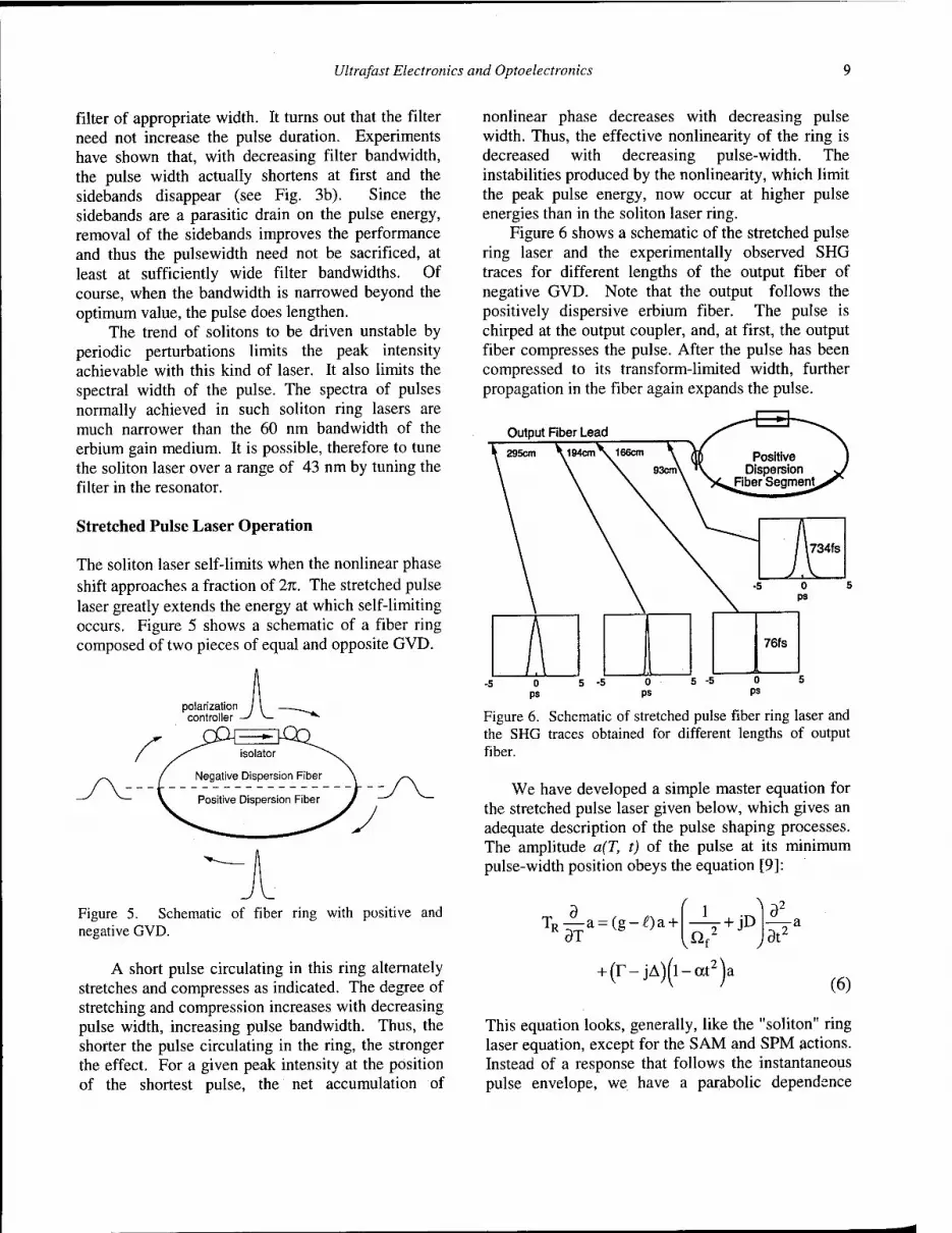
Figure 6 shows a schematic of the stretched pulse ring laser and the experimentally observed SHG traces for different lengths of the output fiber of negative GVD. Note that the output follows the positively dispersive erbium fiber. The pulse is chirped at the output coupler, and, at first, the output fiber compresses the pulse. After the pulse has been compressed to its transform-limited width, further propagation in the fiber again expands the pulse.
Output Fiber Lead
Figure 6. Schematic of stretched pulse fiber ring laser and the SHG traces obtained for different lengths of output fiber.
We have developed a simple master equation for the stretched pulse laser given below, which gives an adequate description of the pulse shaping processes. The amplitude a(T, t) of the pulse at its minimum pulse-width position obeys the equation [9]:
T4a=(g~H^7+jD at2
+ (r-jA)(l-oct2)a (6)
This equation looks, generally, like the "soliton" ring laser equation, except for the SAM and SPM actions. Instead of a response that follows the instantaneous pulse envelope, we have a parabolic dependence

10 Ultrafast Electronics and Optoelectronics
upon time. We use capital letters T and A for the SAM and SPM coefficients to indicate that they are related to the previously defined y and 8, but also that they are different in that they now depend upon the peak intensity of the pulse, whereas y and 8 were independent of the pulse parameters. The SAM and SPM actions are now due to an integration over the modulation effects of a pulse that continuously increases in width as it moves away from the position of the minimum pulse width. The temporal window of the modulation is now wider than the pulse and the temporal dependence has been expanded to second order in the time variable.
The solutions of (6) are chirped gaussian pulses
a - A0 exp A(1 + Jß) (7)
Experiments have shown that the temporal shape of the pulse is indeed well represented by a gaussian near the pulse peak, down to about 10 dB below the peak. The most spectacular consequence of the stretched pulse operation is its greatly increased average power and decreased pulse width relative to the "soliton" laser. Characteristics of the laser illustrated in Fig. 6 are given in Table I. More advanced versions of the stretched-pulse laser have yielded pulse durations as short as 63 fs [10] and pulse energies as high as 2.7 nJ [11].
Table I. Comparison of soliton ring laser and stretched pulse ring laser.
Erbium-doped fiber soliton laser
Erbium-doped stretched pulse laser
Pulse energy: 7pJ 125pJ
Output power: 300 uW 5mW
Peak power: 13.6 W 1 kW
Pulse width: 450 fs 76 fs
Spectral width: 9 nm 64 nm
Rep. rate: 42 MHz 45 MHz
The master equation (6) is, of course, an approximation. This is why the temporal profile appears gaussian only in the main part of the pulse and not in its wings, since the master equation describes best the central portion of the pulse. A pulse that is Gaussian-like in the central portion of the temporal profile, will have gaussian like spectral wings, even though the temporal wings may be other
than Gaussian. Figure 7 shows the measured spectra of both a "soliton" ring laser and a stretched pulse ring laser. The spectral fits for a Gaussian (solid line), and a (time-domain) sech (t/x) dashed line) are shown for comparison. One may observe the very strong sidebands of the soliton operation and the absence of sidebands in the stretched pulse case. This absence of sidebands can be attributed to the more rapid decrease of the spectral wings of the stretched pulse spectrum. It also turns out that a perturbational analysis of the master Equation (6) arrives at the same conclusion. It is found that a "lumped" perturbation of a stretched pulse, such as a lumped gain, loss, or filtering, does not cause side- band generation, the perturbation is fully contained in the modified pulse with no need of continuum generation, as is the case for solitons.
Soliton Operation
1500 1570
Wavelength (nm)
Non-Soiiton Operation (Stretched-Pulse)
1640
1500 1640 1570
Wavelength (nm)
Dotted: gaussian fit Dashed: sech fit
Figure 7. Comparison of spectra of (a) soliton laser and (b) stretched pulse laser.
The Noise
Von der Linde [12] has pioneered a simple measurement of the amplitude fluctuations and timing jitter of a modelocked pulse train. The pulse train is detected and the RF spectrum of the detector current is recorded. The spectral components are

Ultrafast Electronics and Optoelectronics 11
spaced by Af=27C/TR apart. The noise spectrum around each spectral component consists of a contribution due to the amplitude fluctuations that is independent of the order of the spectral component (the darkened portions in Fig. 8), and of a contribution of the timing jitter, that increases in
Frequency Figure 8. The general characteristics of the contributions of amplitude noise and timing jitter to the RF spectrum of detector current.
m -60 13
§ Q.
-80
-100
■120
/
tl-^v-W-J\ ̂ *****=■*
1.0
E m ■o
I o 0.
-r -1000 -500 0 500
Freq, Hz 1000
Figure 9. Spectrum of first and 35th components of RF spectrum of soliton laser.
intensity as the square of the order of the harmonic (the white portions in Fig. 8). Thus, one may separate the amplitude fluctuations from the timing
jitter contribution. Figure 9 shows the measured spectra of the fundamental and of the 31st harmonic with integration times of 0.1 sec. From the data we deduced an amplitude fluctuation of 0.2%. The timing jitter differed from laser to laser depending upon the net GVD in the ring in a way analogous to the Gordon-Haus effect in long distance soliton communications. The spontaneous emission of the gain medium causes random changes of both the position and the frequency of the pulse traveling through the medium. The frequency changes develop into timing changes via GVD. The smaller \D\, the smaller the conversion. In this way one finds that the stretched pulse with a small \D\ gave a timing jitter of 4 ppm of the round trip time in a 0.1 sec timing interval, wheras the soliton laser gave 27 ppm [13].
Self-starting
Self-starting requires the coherent excitation of at least three resonator modes adjacent in frequency. The coherent excitation is a form of injection locking. The injection signal is produced through the beating of two axial modes via the self-amplitude and self-phase modulation of the (artificial) saturable absorber. This mechanism is very weak at initiation of modelocking because the fluctuations, from which the process starts, are of long duration and weak peak intensities. Mechanisms that pull the mode- frequencies from their uniform frequency-spacing oppose self-starting. Spatial hole burning in linear resonators is such a mechanism that is avoided by the ring geometry. Another mechanism is back-scatter due to spurious reflections within the resonator that tend to produce a mode spectrum with non-uniformly spaced axial mode frequencies. In a uni-directional ring resonator two such backscatters are required to have an effect on the axial mode spacing. This should be contrasted with a standing wave resonator, in which a single backscatter can change the mode spacing. For both these reasons, ring lasers self-start and need no trigger (such as moving etalons).
Environmentally Stabilized Version of Stretched Pulse Laser
All of the lasers described thus far used nonpolarization preserving fiber. In fact, the simple operation of P-APM requires the use of such fiber. The lasers are reasonably stable to environmental changes if the fiber spool is properly wound. A

12 Ultrafast Electronics and Optoelectronics
version of the stretched pulse laser has been commercialized by Clark-MXR, Inc. Yet, in order to achieve the ultimate in environmental stability, the use of Polarization Maintaining (PM) fiber would be desirable. Unfortunately, the simple P-APM action based on the rotation of the polarization ellipse cannot be employed in such fibers. We have attempted to achieve P-APM action by interfering two Kerr-shifted polarization eigenmodes. These attempts failed on account of environmentally induced changes in the birefringence of the fiber. Eventually, a Sigma Laser similar to the one worked on by Duling et al. [14] proved successful. Our laser [15] differs from Duling's in using different GVD's in order to achieve stretched pulse operation (Fig. 10).
1.01~
W2 W4 W2
^OQEQ \\m V2
0- 5T BFP 2^S,
isolator
variable "" output
SMF 0.26 m
SMF 0.30 m .
^—D PFRI
El 1
FR AM
1.03 m Er*3-doped fiber (positive dispersion)
Non-PM
: Faraday Rotator : Amplitude Modulator
7.4 m SMF (negative dispersion)
Single Polarization (PM)
Figure 10. The stretched pulse sigma laser.
The ring contains regular PM fiber with negative GVD, the "pig-tail" contains the erbium doped non- PM fiber with positive GVD. Fluctuations of birefringence are balanced through counter propagation in the pig-tail equipped with two Faraday rotators [16]. We found the system to be exceptionally stable over a large temperature range (by heating the fiber with a hair-dryer). No changes in operation were observed. The SHG traces of the pulses compressed outside the laser, and the spectrum, are shown in Fig. 11. These results are preliminary and attempts are now under way to shorten the pulses further and to obtain a cleaner pulse spectrum. It should be mentioned that the Sigma Laser is not self-starting; it has to be triggered. In fact, this is a confirmation of the processes discussed earlier that prevent self-starting. Some spatial gain hole burning can occur in the erbium "pigtail" of the laser because of reflections. Further, the radiation passes in two directions in the fiber pig-tail. A single reflection in the "pigtail" can distort the mode spacing, as it does in a linear resonator.
0.0 L 1480 1520 1S60
Wavelength (nm) 1600
1.0
0.5
0.0 U
Grating Compression
At = 106fs
AtAv = 0.69
980 nm Pump Power
200 mW 320 mW
Time (psec)
Output Power
20 mW 28 mW
Pulse Energy
1.3 nJ 1.8 nJ
Figure 11. The SHG traces and spectrum of the pulse from the sigma laser.
Summary
We have given an overview of the operation of two types of P-APM mode-locked fiber ring lasers: the "soliton" laser, and the stretched pulse laser. Of these, the stretched pulse laser shows superior performance on three counts: (a) its power at single pulse operation is two orders of magnitude greater than that of the soliton laser; (b) it shows no evidence of sideband generation, (c) it shows lower timing jitter. Analysis has shown that the timing jitter in these lasers can be attributed to the spontaneous emission noise of the gain medium. We have shown why ring lasers are self-starting lasers. Finally, we presented an environmentally stabilized version of the stretched pulse laser.
Acknowledgment
The work reported here was accomplished by: Dr. Kohichi Tamura, presently at Nippon Telegraph and Telephone, Lynn E. Nelson, David Jones, Charles Yu and visiting scientist Shu Namiki. The work was supported in part by AFOSR, JSEP, ONR, and DARPA.
Ultrafast Electronics and Optoelectronics 13
References
1. I. N. Duling, El, "Subpicosecond all-fibre erbium laser," Electron. Lett. 27, 544-545 (1991).
2. M. E. Fermann, M. J. Andrejco, Y. Silberberg, and A. M. Weiner, "Generation of pulses shorter than 200 fs from a passively mode-locked Er fiber laser," Opt. Lett. 18, 48-50 (1993).
3. C. R. Doerr, H. A. Haus, E. P. Ippen, and M. Shirasaki, "Additive pulse limiting," Opt. Lett. 19,31-33,(1994).
4. C. R. Doerr, H. A. Haus, and E. P. Ippen, "Asynchronous soliton modelocking, Opt. Lett. 19, 1958-1960 (1994).
5. R. H. Stolen, J. Botineau, and A. Ashkin, "Intensity discrimenation of optical pules with birefringent fibers," Opt. Lett. 7, 512-514 (1982).
6. H. A. Haus, E. P. Ippen, and K. Tamura, "Additive pulse modelocking in fiber lasers," IEEE J. Quantum Electron. 30, 200-208, (1994).
7. S. M. J. Kelly, "Characteristic sideband instability of periodically amplified average soliton," Electron Lett. 28, 806-807 (1992).
8. J. P. Gordon, "Dispoersive perturbations of solitons of the nonlinear Schrödinger equation," J. Opt. Soc.B 9, 91-97 (1992).
9. H. A. Haus, K. Tamura, L. E. Nelson, and E. P. Ippen, "Stretched-pulse additive pulse mode-
locking in fiber ring lasers: theory and experi- ment," J. Quantum Electron. 31, 591-598 (1995).
10. K. Tamura, E. P. Ippen, and H. A. Haus, "Pulse dynamics in stretched-pulse fiber lasers," Appl. Phys. Lett. 67, 158-160 (1995).
11. L. E. Nelson, S. B. Fleischer, G. Lenz, and E. P. Ippen, "Efficient frequency doubling of a femtosecond fiber laser," Opt. Lett. 21, 1759- 1761 (1996).
12. D. Von der Linde, "Characterization of the noise in continuously operating mode-locked lasers," Appl. Phys. B 39, 201-217 (1996).
13. S. Namiki, C. X. Yu, and H. A. Haus, "Observation of nearly quantum-limited timing jitter in an all-fiber ring laser," J. Opt. Soc. Am. B 13, 2817-2823 (1996).
14. I. N. Duling, III, and R. D. Esman, "Single- polarisation fibre amplifier," Electron. Lett. 28, 1126-1128(1992).
15. D. J. Jones, L. E. Nelson, H. A. Haus, and E. P. Ippen, "Environmentally stable stretched-pulse fiber laser generating 120 fs pulses," Conference on Lasers and Electro-Optics (CLEO'97), Baltimore, MD, May 1997, to be presented.
16. M. E. Fermann, M. J. Andrejco, Y. Silberberg, and M. L. Stock, "Passive mode locking by using nonlinear polarization evollution in a polarization-maintaining erbium-doped fiber," Opt. Lett. 18, 894-896 (1993).

A Passive Harmonically Modelocked Multi-Gigahertz Cr^tYAG Laser with Optically Phase-Locked Fundamental Solitons
B.C. Collings and K. Bergman Princeton University, J303 Engineering Quad, Olden Street, Princeton, New Jersey 08544
(609)258-5151 FAX (609) 258-0463 [email protected]
W.H. Knox Lucent Technologies, Bell Laboratories, Holmdel, New Jersey 07733
(908)949-0958 FAX (908) 949-2473 [email protected]
Abstract
We present a multi-Gigahertz Cr4+:YAG laser passively modelocked by a saturable Bragg reflector operating with nearly equally spaced and optically phase-locked multiple fundamental soliton pulses.
Keywords
Mode locked lasers, Ultrafast lasers, Rare earth and transition metal solid state lasers
In solid state modelocked lasers, gain and cavity requirements frequently provide a upper limit on the length of the cavity and therefore on the laser's fundamental repetition rate. For this reason, harmonic modelocking, the operation with multiple pulses in the cavity, is often employed as a means of increasing the output repetition rate without reducing the physical size of the cavity. Synchronous pumping or active modulation driven at a harmonic of the cavity repetition rate are methods of forcing the pulses to be equally spaced in time such that the output pulsetrain has a single temporal period between adjacent pulses. However, in passively modelocked systems without any active control on the pulses' temporal positions, the period between adjacent pulses is frequently random and unstable. Equally spaced, harmonic modelocking has been observed in passively modelocked fiber lasers that utilize mechanisms such as nonlinear polarization rotation and saturable absorption.[1, 2] This phenomenon occurs in fiber lasers operating in both the soliton and non-soliton regimes.[3] Here we present a solid state Cr4+:YAG soliton laser passively modelocked with a saturable Bragg reflector (SBR) exhibiting harmonic modelocked operation at multi-Gigahertz repetition rates. [4- 5] Furthermore, the solitons generated by this cavity are optically phase-locked with respect to each other, a characteristic previously not reported to our knowledge. We find that the pulses are fixed at temporal locations within approximately 8 ps of ideal harmonic operation and remain phase-locked at that position, recovering that exact phase relationship between adjacent pulses after interruption and return of laser operation.
The laser cavity (see Figure 1) consists of an 18 mm long Cr4+:YAG crystal rod (IRE-Polus), one end polished flat and coated with a high reflector and the opposite is polished to Brewster's angle.[4-5] A 10 cm
radius of curvature high reflecting folding mirror provides astigmatic compensation and a 7.5 cm radius of curvature 0.2% output coupler focuses the cavity mode to a spot size of about 35 |J.m at the surface of the flat SBR. The structure of the SBR, (Figure 1) consists of a 99.5% reflecting Bragg mirror of alternating quarter-wave layers of GaAs and AlAs and two uncoupled Ino.52Gao.4sAs/InP quantum wells located 15 nm from the top surface of a half-wave strain relief layer grown on the final layer of the Bragg mirror. [4-8] The excitonic absorption of the quantum wells is centered near 1500 nm. The output of a diode pumped NdiYVQj. CW laser (Spectra Physics) at
Diode- Pumped Nd:YV04
7cm
AlAs/GaAs Bragg Reflector
R=99.5%
-10cm
SBR
InGaAs/ InP
Quantum Wells
Figure 1. SBR.
Diagram of the laser cavity and structure of the
OSA TOPS on Ultrafast Electronics and Optoelectronics, 1997 Vol. 13, Martin Nuss and John Bowers (ed.) ©1997 Optical Society of America
14

Ultrafast Electronics and Optoelectronics 15
Wavelength [nm]
-600 -400 -200 0 200 Delay [fs]
400 600
Figure 2. Autocorrelation and optical spectrum of the modelocked output. The 2.7 GHz pulsetrain is shown in the inset.
1062 nm is focused into the Cr4+:YAG crystal through its flat end with 40 and 15 cm lens. For compensation of the calculated 7 fs2/mm of normal group velocity dispersion (GVD) (ß2>0) of the Cr4+:YAG material at 1525 nm, bulk fused silica with -24.5 fs2/mm of anomalous GVD is inserted into the cavity between the two curved mirrors using two isosceles Brewster prisms (base widths of 18 mm) with as little tip-to-tip separation as possible (~1 cm) creating a variable thickness Brewster plate.
Simple CW cavity alignment produces self- starting modelocking of the laser believed to be initiated by the ultrafast saturation dynamics of the SBR.[6-8] With approximately 7 W of incident pump power, 200 fs pulses (FWHM assuming a sech2 pulseshape) are produced (see Figure 2). Due to the low cavity GVD and nonlinearities
260-
240-
-*—>
"3
220-
200- eg'
80-
160-
A Al
I I d?
Pulsewidth Time-Bandwidth
Product A 2.7GHz A D 1.8GHz ■ 0 0.9GHz •
0.8
0.
0.
HO.
0
0
6 tid »
51
< i-i o
,a 3 c o
0.2 -400 -450 -500 -550 -600
Cavity Dispersion [fs2] Figure 3. Plot of the pulsewidth (open markers, FWHM) and time-bandwidth product (solid markers) of the modelocked output with either one (circle), two (square) or three (triangle) pulses circulating in the cavity versus total cavity GVD. Bistable regions are indicated with dashed vertical lines.
resulting from the large cavity mode size and repetition rate, both the dispersive and nonlinear lengths are much longer than the cavity elements.[4-5,9] The intracavity pulses are found to be fundamental solitons over a wide range of anomalous cavity GVD and number of pulses circulating in the cavity. This is indicated by the maintenance of transform-limited pulse production and unity value of the calculated soliton parameter (N) for all values of cavity GVD and pulse energies (see Figure 3). The transition to multiple pulses is believed to be the result of a limited net gain bandwidth due to the excitonic absorption of the SBR around 1500 nm and the decreasing reflectivity of the output coupler at longer wavelengths. Also, the action of the SBR may impose a weak upper limit on the pulsewidth. For these reasons, the laser can operate with up to five pulses in the cavity reaching a repetition rate of 4.5 GHz and total output power of 80 mW at a center wavelength of 1525 nm. For some values of cavity GVD, the laser can operate in several different modes (multistable), each producing a different number of transform-limited fundamental soliton pulses of a different width indicated by the dashed lines in Figure 3.
To measure the optical phase relationship between the multiple pulses, interferometric cross-correlations were performed. Figure 4 shows cross correlations for the cases with three pulses in the cavity under perfect harmonic modelocking as well as for the case where the adjacent pulse spacings are not rigorously equal but are fixed, differing from ideal by approximately 3 ps. The approximate 8:1 fringe ratio of the cross-correlations demonstrates the full phase coherence of the cross-correlated pulses. Furthermore, the measured widths of both the autocorrelation and cross correlation are equal to +2.5 fs (measured with both interferometric and background free correlations) indicating a maximum possible pulse-to-pulse envelope jitter of less than 40 fs. The greater than 60 dB suppression of cavity harmonics in the RF spectrum of the detected output of the laser operating with four equally spaced pulses shown in Figure 5 also indicates that the magnitude of the envelope jitter is extremely low (if at all present!). To ensure that the coherence is maintained for times longer than required to record the correlation, the variable delay arm was fixed (shaker turned off) and manually translated to a fringe maximum near the center of the cross-correlation. The correlation signal then remained at that maximum for several minutes. With the fixed delay interferometer measuring the optical phase relationship between adjacent pulses, the operation of the laser was interrupted or heavily perturbed. When the laser was allowed to return to the original mode several seconds later, the phase relationship recovered its original state prior to the interruption as illustrated in Figure 6.
The optical phase-locking of the pulses occurs in both cases of equally, and non-equally spaced multiple pulses. This suggests the possibility of two separate mechanisms; one causing the nearly equal spacing of the pulse envelopes and a second forcing the optical phase- coherence, an effect insensitive to the pulses' relative

16 Ultrafast Electronics and Optoelectronics
T r -4000 -2000
Delay [fs] Figure 4. a) Interferometric cross-correlation trace of temporally adjacent and equally spaced multiple pulses. b) Autocorrelation trace with laser operating as in (a). c) Interferometric cross-correlation of adjacent multiple pulses with unequal temporal spacings. d) Same as (c) but with different relative pulse spacings. In all cases, there are three pulses in the cavity.
> • «—I
T3 O
<D
0 5 10 15 0 5 10 Frequency [GHz]
Figure 5. RF spectrum of the laser output detected by a fast photodiode illustrating at least 60 dB suppression of cavity harmonics. The unequal magnitudes of the peaks is due the response of an RF amplifier.
a i-l
<D
%—> P. o >
Pi
O0+7t
o.
2 Pulse Operation v
I—^4 1-S-l 1-1-1 I—* 1
Laser Disturbed/Interrupted 1 1 1—
150 0 50 100 Time [sec]
Figure 6. Relative optical phase relationship between adjacent multiple pulses versus time measured using a fixed delay cross-correlator. The relative phase is constant with time and returns to the previous relative phase relationship after a disruption of the laser's operation.
temporal positions. In previously reported passive harmonically modelocked lasers, the mechanisms stabilizing the temporal positions of the pulse envelopes were shown to be the long range soliton electrostriction effect in optical fiber[l] or an effective phase modulation occurring due to a long carrier lifetime in a semiconductor saturable absorber. [2] The reported increase in temporal jitter (relative to an external clock) associated with harmonic modelocking attributed to the jitter of adjacent multiple pulses is typically larger than the pulsewidth.[l,2] If multiple pulses are optically phase-locked with extremely low envelope jitter, harmonic modelocking will introduce no additional jitter. For this laser, electrostriction effects are not present due to the use of bulk components. Furthermore, the carrier lifetime of our saturable absorber was measured to be 14 ps, significantly shorter than the period between pulses (-200-500 ps). Experiments are currently investigating long range, pulse- to-pulse coupling effects via the CW background shed from the periodically perturbed solitons.[10] Also, pulse-to- pulse repulsion effects arising from gain dynamics are also currently under investigation as effects capable of the near equalization of the interpulse temporal spacing and some promising preliminary results have been obtained.
In conclusion, we have demonstrated a passive harmonically modelocked Cr4+:YAG soliton laser which exhibits optically phase-locked multiple pulsing for times longer than minutes. Furthermore, when the laser is interrupted, the optical phase relationship between adjacent pulses returns to its value prior to the interruption.
Acknowledgments The authors would like to thank E.P. Ippen, J.N. Kutz, C.R. Doerr and G.T. Harvey for very helpful discussion.
References 1. S. Gray, A.B. Grudinin, W.H. Loh and D.N. Payne,
Opt. Lett. 20, 189(1995). 2. M.E. Fermann and J.D. Minelly, Opt. Lett. 21, 970

Ultrafast Electronics and Optoelectronics 17
(1996). 3. E.P. Ippen, private communication. 4. B.C. Collings, K. Bergman and W.H. Knox, To appear
in Opt. Lett. (4/97). 5. B.C. Collings, K. Bergman and W.H. Knox, Advanced
Solid State Lasers Conference, Orlando, FL, 1997, paper MF6-1.
6. S. Tsuda, W.H. Knox, S.T. Cundiff, W.Y. Jan and J.E. Cunningham, To appear in IEEE J. of Quant. Electron. (1997).
7. S. Tsuda, W.H. Knox, E.A. de Souza, W.Y. Jan and
J.E. Cunningham, Opt. Lett. 20, 1406 (1995). 8. B.C. Collings, J.B. Stark, S. Tsuda, W.H. Knox, J.E.
Cunningham, W.Y. Jan, R. Pathak and K. Bergman, Opt. Lett. 21, 1171 (1996).
9. F. Krausz, M.E. Fermann, T. Barbec, P.F. Curley, M. Hofer, M.H. Ober, C. Spielmann, E. Wintner and A.J. Schmidt, IEEE J. of Quant. Electron. 28, 2097 (1992).
10. W.H. Loh, A.B. Grundinin, V.V. Afanasjev and D.N. Payne, Opt. Lett. 19, 698 (1994).

Intracavity Gain and Absorption Dynamics of Hybrid Modelocked Semiconductor Lasers using Multiple Quantum Well Saturable Absorbers
S. Geea, G. Alphonse\ J. Connolly", P. J. Delfyetf
Center for Research and Education in Optics and Lasers (CREOL)* University of Central Florida
Orlando, Fl
David Sarnoff Research Centerb
Princeton, NJ
Abstract
Time resolved intracavity gain and saturable absorption dynamics, along with intracavity intensity pulse profiles and their corresponding spectrograms, were measured in an external cavity hybrid modelocked semiconductor diode laser. These measurements were performed to obtain fundamental information regarding the modelocking dynamics and to determine their role in the pulse shaping and chirping dynamics. The results of these experiments show that the integrating nonlinearity associated with gain depletion, coupled with group velocity dispersion, leads to asymmetric intensity pulse profiles with predominantly cubic temporal phase, while saturable absorption coupled with group velocity dispersion tends to linearize the chirp. Exploitation of these dynamics may allow researcher to generate optical pulses with higher peak intensities than previously reported.
Key Words: Semiconductor laser dynamics, modelocking, ultrashort pulse generation
Introduction
Compact and efficient sources of ultrashort, high power optical pulses are necessary for realizing applications in nonlinear optical memories, near field imaging and other areas of applied nonlinear photonics. Semiconductor lasers are viable candidates owing to their small size, good wall plug efficiency and robustness. However, the dynamics of semiconductor laser media typically prevent the production of high power ultrashort optical pulses [1]. In this paper, we present experimental measurements of the intracavity gain and saturable absorber dynamics, in order to investigate their role in the pulse formation and chirping
dynamics in hybrid modelocked semiconductor diode lasers. To support these measurements, intracavity intensity pulse profiles and their corresponding spectrograms were measured to provide direct experimental observation of the effects suggested by the intracavity dynamics.
Experimental Set Up
The experimental set up is shown in Fig. 1.
To lock-in detection
•P
MQW
Delay stage
Probe beam
HI—i—W—• WP
SLA S PBS
To diagnostics
Output
Figure 1. Experimental setup for intracavity gain dynamic measurement. MQW: Multiple quantum well saturable absorber, PBS: Polarizing beam splitter, SLA: Semiconductor laser amplifier, OC: Output coupler, G: Diffraction grating, S: Slit, I: Optical isolator, P: Polarizer, WP: Half wave plate.
An external cavity hybrid modelocked semiconductor laser [2] producing ~ 700 fsec optical pulses at 300 MHz, centered at 830 nm. is the laser system under test. The output pulses from the laser system are used as the probing pulses. The pulses are attenuated, delayed, polarization
OSA TOPS on Ultrafast Electronics andOptoelectronics, 1997 Vol. 13, Martin Nuss and John Bowers (ed.) QI997 Optical Society of America
18

Ultrafast Electronics and Optoelectronics 19
rotated and injected into the laser oscillator using a polarization beam splitter. To monitor the gain dynamics, the transmitted probe beam is partially deflected from the cavity using a pellicle beam splitter and detected using standard lock-in techniques. To monitor the saturable absorption dynamics, the probe pulses are injected into the cavity using the PBS situated between the saturable absorber and the semiconductor laser amplifier (SLA). The resultant reflected are pulses deflected out of the cavity and into the lock-in detection system.
Intracavity Gain and Saturable Absorption
In Fig. 2(a) is the time resolved intracavity measurement. The salient features are the two transient reductions in the gain, superimposed on a sinusoidally varying gain. The transient gain reductions are owing to the intracavity pulse passing through the SLA. The important observation is that the carrier heating and cooling effects are not observed in the gain dynamics, i.e., the SLA exhibits conventional gain dynamics. This is important because frequency chirping mechanisms such as self phase modulation are strongly coupled to the gain dynamics. In addition, it should be noted that the gain has recovered to its initial value within 350 psec, in contrast to the gain recovery time constant of 1.1 nsec. This is owing to the time varying pumping rate associated with the RF bias current. It should also be noted that the pulses do not pass through the SLA device at the point of maximum gain. This is owing to the location of the SLA device with respect to the rear reflector. Since the SLA device is not located at the rear reflector, the displacement of the SLA forces the optical pulses to traverse the SLA at times when the optical gain is approximately equal for each pulse. This manifests itself as the optical pulse passing through the SLA at times symmetrically displaced from the point of maximum gain. In our case, this corresponds to the round trip delay between the SLA and the rear reflector.
In Fig 2(b) is the time resolved intracavity saturable absorption measurement. The time resolved reflectance from the MQW mirror exhibits a relative increase of 20% (base line not shown) with a rise time of 10 psec, corresponding to the integrated pulse intensity. The absorber exhibits a slow recovery, with an exponential absorption recovery time constant of 280 psec. It should be noted that the recovery time measured in these experiments differs as compared to previously measured absorber recovery times [3]. These differences may be attributed to differences in the MQW absorber design, post processing procedures, and differences in the optical transverse mode profile of the lasers used in this vs. prior measurements.
4.8E-04
4.6E-04
3.6E-04
Time Delay (54 ps/div.)
(a)
Time Delay (120 ps/div.)
(b)
Figure 2. Time resolved intracavity dynamic measurements: (a) SLA gain, (b) transmittance of saturable absorber.
To demonstrate the pulse shaping effects induced by the saturable absorber, input and output pulse intensity profiles were measured. This was achieved cross correlating the intracavity pulses with the compressed output optical pulse. Experimentally, this was achieved by using a scanning autocorrelator with a two-pulse input pulse train. In this case, the intracavity pulses were deflected from the cavity with a pellicle beamsplitter and combined with the compressed output laser pulse, separated by a short (30 psec) fixed delay. Cross correlation information is then obtained by examining the side lobes of the three-peak correlation signal. In Fig 3(a) is the intensity pulse profile of the optical pulse before the MQW saturable absorber, and Fig. 3(b) is the intensity pulse profile of the optical pulse after the MQW saturable absorber. The salient feature is the reduction of the rising edge of the optical pulse from 6 psec to 3 psec, representing a change of nominally 50% per round trip. It should be noted that the shoulders in the correlation traces are artifacts created by the two-pulse correlation technique employed.

20 Ultrafast Electronics and Optoelectronics
Time Delay (6.4 ps/div)
(a)
Time Delay (6.4 ps/div)
(b)
Figure 3. Temporal shape of pulses: (a) before saturable absorber, (b) after saturable absorber.
Spectrograms of Intracavity Pulses
In order to assess the effect of the nonlinear dynamics on the chirping properties of the generated optical pulses, the instantaneous frequency of the optical pulses were directly measured by spectrally resolving the cross-correlated intensity profiles at the second harmonic frequency. The resulting spectrograms are shown in Fig. 4(a-c). The spectrograms shown (from top to bottom) are that of a) the laser output pulse, b) the optical pulse before the saturable absorber and c) the optical pulse after the saturable absorber. In each case, the spectrograms show optical pulses with fast rising edges, with slower trailing edges. These effects were clearly observed in the cross correlation traces above. In addition, the spectrograms show that the instantaneous frequency of the optical pulses, are not constant, that is, the center or carrier wavelength varies throughout the pulse duration. In these traces, the center wavelength is upchirped, and tends to vary linearly over a major portion of the optical pulse, while small nonlinear chirp is seen to exist at times when the optical pulse energy is low. Quantitatively, the spectrograms show a total
wavelength variation of 0.8 nm at the second harmonic wavelength, implying a total wavelength chirp of 1.6 nm. at the fundamental wavelength. It should be noted that the chirp exists over the duration of the pulse, implying a nonlinear dispersion of ~ 5 ps/nm.
u c
411 415 Wavelength (nm)
(a)
419
411 415 Wavelength (nm)
(b)
419
411 415 419 Wavelength (nm)
(c)
Figure 4. Spectrally resolved cross correlation at different locations in cavity: (a) laser output, (b) before saturable absorber and (c) after saturable absorber.
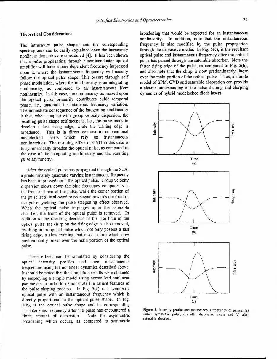
Ultrafast Electronics and Optoelectronics 21
Theoretical Considerations
The intracavity pulse shapes and the corresponding spectrograms can be easily explained once the intracavity nonlinear dynamics are considered [4]. It has been shown that a pulse propagating through a semiconductor optical amplifier will have a time dependent frequency impressed upon it, where the instantaneous frequency will exactly follow the optical pulse shape. This occurs through self phase modulation, where the nonlinearity is an integrating nonlinearity, as compared to an instantaneous Kerr nonlinearity. In this case, the nonlinearity impressed upon the optical pulse primarily contributes cubic temporal phase, i.e., quadratic instantaneous frequency variation. The immediate consequence of the integrating nonlinearity is that, when coupled with group velocity dispersion, the resulting pulse shape self steepens, i.e., the pulse tends to develop a fast rising edge, while the trailing edge is broadened. This is in direct contrast to conventional modelocked lasers which rely on instantaneous nonlinearities. The resulting effect of GVD in this case is to symmetrically broaden the optical pulse, as compared to the case of the integrating nonlinearity and the resulting pulse asymmetry.
After the optical pulse has propagated through the SLA, a predominately quadratic varying instantaneous frequency has been impressed upon the optical pulse. Group velocity dispersion slows down the blue frequency components at the front and rear of the pulse, while the center portion of the pulse (red) is allowed to propagate towards the front of the pulse, yielding the pulse steepening effect observed. When the optical pulse impinges upon the saturable absorber, the front of the optical pulse is removed. In addition to the resulting decrease of the rise time of the optical pulse, the chirp on the rising edge is also removed, resulting in an optical pulse which not only possess a fast rising edge, a slow training, but also a chirp which now predominantly linear over the main portion of the optical pulse.
These effects can be simulated by considering the optical intensity profiles and their instantaneous frequencies using the nonlinear dynamics described above. It should be noted that the simulation results were obtained by employing a simple model using normalized nonlinear parameters in order to demonstrate the salient features of the pulse shaping process. In Fig. 5(a) is a symmetric optical pulse with an instantaneous frequency which is directly proportional to the optical pulse shape. In Fig. 5(b), is the optical pulse shape and its corresponding instantaneous frequency after the pulse has encountered a finite amount of dispersion. Note the asymmetric broadening which occurs, as compared to symmetric
broadening that would be expected for an instantaneous nonlinearity. In addition, note that the instantaneous frequency is also modified by the pulse propagation through the dispersive media. In Fig. 5(c), is the resultant optical pulse and instantaneous frequency after the optical pulse has passed through the saturable absorber. Note the faster rising edge of the pulse, as compared to Fig. 5(b), and also note that the chirp is now predominantly linear over the main portion of the optical pulse. Thus, a simple model of SPM, GVD and saturable absorption can provide a clearer understanding of the pulse shaping and chirping dynamics of hybrid modelocked diode lasers.
Figure 5. Intensity profile and instantaneous frequency of pulses: (a) initial symmetric pulse, (b) after dispersive media and (c) after saturable absorber.
22 Ultrafast Electronics and Optoelectronics
Summary
In summary, experiments have been performed to measure the fundamental intracavity dynamics in order to provide a better understanding of the pulse shaping and chirping dynamics of hybrid modelocked semiconductor diode lasers. Our experiments suggest that the nonlinear dynamics associated with the integrating nonlinearity, coupled with group velocity dispersion and saturable absorption play important roles in the pulse shaping process. The important observation is that the integrating nonlinearity leads to asymmetric pulse broadening, while the linearization of the chirp is obtained by the combined effects of GVD and saturable absorption. These results provide a better picture of the fundamental mechanisms associated with the pulse production process and chirping mechanisms in hybrid modelocked lasers.
References
[1] K. Hall, J. Mark, E. Ippen, G. Eisenstein, Appl. Phys. Lett. 56, 1740 (1990). [2] P. J. Delfyett, et al., IEEE J. Quant. Electr, 28, 2203, (1992). [3] P. W. Smith, Y. Silberberg, D.A.B. Miller, JOSA B, 2, 1228,(1985). [4] P. J. Delfyett, et. al., Appl. Phys. B, 58, 183, (1994).

A Highly-Stable 59 GHz Soliton Source at 1550 nm
Glenn D. Bartolini, Darwin K. Serkland, William L. Kath, and Prem Kumar
Department of Electrical and Computer Engineering Northwestern University, 2145 N. Sheridan Road, Evanston, Illinois 60208-3118
Doug W. Anthon and Don L. Sipes
ATx Telecom Systems, Inc., 1251 Frontenac Road, Naperville, IL 60563
Abstract
A highly-stable soliton source is demonstrated by com- pressing the sinusoidal modulation in the output of a short-cavity Er/Yb bulk phosphate-glass laser operat- ing simultaneously at two frequencies. The 58.55 GHz modulation is converted into a train of 3.2 ps pulses by means of soliton pulse compression in a comb-like dispersion-tailored fiber. By spectrum analysis of the direct-detection photocurrent, the short-term stability of the repetition rate is shown to be 10 kHz.
Key Words
Nonlinear optics — fibers, Optical communications, Pulse propagation and solitons, Rare earth and tran- sition metal solid state lasers.
Soliton pulse compression of the beat modulation be- tween two optical carriers is an attractive method for generating high-repetition-rate pulse trains for applica- tion in time-division-multiplexed (TDM) optical com- munication systems.1'2 Several such sources have re- cently been demonstrated.3~8 In one approach, the out- puts of two distributed-feedback (DFB) lasers are com- bined to produce the beat modulation.3"5 This scheme allows for tunability of the repetition period, but the re- sulting pulse-train period is not very stable because of the large free-running DFB laser linewidth. In another approach, one starts from a single DFB laser (which can be an external-cavity laser with a narrow linewidth) and imparts the modulation externally with use of a stable
frequency source.6,7 This technique yields a very stable repetition period, but it is obtained at the expense of system complexity. Because of the need for a stable- frequency driver, the cost of such a source is high. An alternative approach employs a dual-frequency coupled- cavity erbium-doped fiber laser that is constructed with the use of intra-core fiber-grating reflectors.9 This tech- nique can potentially be of low cost, but somehow the stability of the 59.1 GHz pulse train in Ref. 8 was in the MHz range. One reason for the reduced stability might be the presence of additional noise processes in fibers such as guided acoustic-wave Brillouin scattering.10
In this paper we demonstrate a highly-stable, low- cost, simple and reliable, soliton source for ultra-high speed TDM network applications. The pulse train is produced by compressing the sinusoidal modulation in the output of a two frequency Er/Yb bulk-glass laser. Since the two frequencies are generated from two differ- ent longitudinal modes of the same short-cavity laser, their beat frequency is highly stable. In our experi- ment, a 58.55 GHz pulse train is produced with a short term frequency stability of 10kHz. This stability of 2 x 10~7 is obtained without active stabilization of the laser frequency or the cavity temperature; only the laser is allowed to warm up to an equilibrium temperature.
Our two-frequency source is a short-cavity Er/Yb- doped bulk phosphate-glass laser which is pumped by a NdYLF laser, which in turn is pumped by a semiconductor-diode laser.11 Although the Er/Yb glass laser is designed to normally operate in a single longitu- dinal mode, by adjusting the diode-laser power it can be made to läse simultaneously on two cavity modes that are five free-spectral ranges apart. The resulting wave- length separation is ~ 0.5nm with a center frequency near 1542 nm. The laser output is fiber pigtailed and typically 90 mW of power is emitted from the fiber end.
OSA TOPS on Uhrafast Electronics and Optoelectronics, 1997 Vol. 13, Martin Nuss and John Bowers (ed.) ©1997 Optical Society of America
23
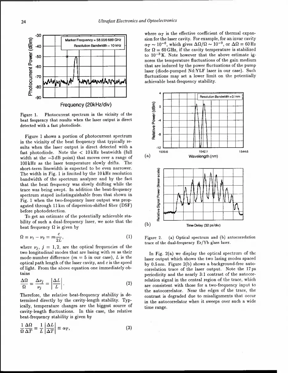
24 Ultrafast Electronics and Optoelectronics
E OQ
-30
-40
| -50 o £ -60 c
I -70 ü o
■5 -80
-90
—1 1 1 1—... 1 ■■
Marker Frequency = 58.556 689 GHz
1 *w pf% ̂ ^IU^A^AM
Frequency (20kHz/div)
Figure 1. Photocurrent spectrum in the vicinity of the beat frequency that results when the laser output is direct detected with a fast photodiode.
Figure 1 shows a portion of photocurrent spectrum in the vicinity of the beat frequency that typically re- sults when the laser output is direct detected with a fast photodiode. Note the < 10 kHz beatwidth (full width at the —3 dB point) that moves over a range of 100 kHz as the laser temperature slowly drifts. The short-term linewidth is expected to be even narrower. The width in Fig. 1 is limited by the 10 kHz resolution bandwidth of the spectrum analyzer and by the fact that the beat frequency was slowly drifting while the trace was being swept. In addition the beat-frequency spectrum stayed indistinguishable from that shown in Fig. 1 when the two-frequency laser output was prop- agated through 11km of dispersion-shifted fiber (DSF) before photodetection.
To get an estimate of the potentially achievable sta- bility of such a dual-frequency laser, we note that the beat frequency fi is given by
fi = i/i - i/2 = m —, (1)
where i/j, j = 1,2, are the optical frequencies of the two longitudinal modes that are lasing with m as their mode-number difference (m = 5 in our case), L is the optical path length of the laser cavity, and c is the speed of light. From the above equation one immediately ob- tains
AÜ Av ] _ AL (2)
Therefore, the relative beat-frequency stability is de- termined directly by the cavity-length stability. Typ- ically, temperature changes are the biggest source of cavity-length fluctuations. In this case, the relative beat-frequency stability is given by
1_AQ _ ± QAT ~ L
AL AT = <*T, (3)
where aj is the effective coefficient of thermal expan- sion for the laser cavity. For example, for an invar cavity aT ~ 10-6, which gives Afi/fi ~ 10~9, or Afi = 60Hz for ß = 60 GHz, if the cavity temperature is stabilized to 10-3K. Note however that the above estimate ig- nores the temperature fluctuations of the gain medium that are induced by the power fluctuations of the pump laser (diode-pumped Nd:YLF laser in our case). Such fluctuations may set a lower limit on the potentially achievable beat-frequency stability.
E m XI
o o. >
■£ -8
Resolution Bandwidth = 0.1 nm
n 1
\ |
w 1539.6 1542.1
Wavelength (nm) 1544.6
(b) Time Delay (32 ps/div)
Figure 2. (a) Optical spectrum and (b) autocorrelation trace of the dual-frequency Er/Yb glass laser.
In Fig. 2(a) we display the optical spectrum of the laser output which shows the two lasing modes spaced by 0.5 nm. Figure 2(b) shows a background-free auto- correlation trace of the laser output. Note the 17ps periodicity and the nearly 3:1 contrast of the autocor- relation signal in the central region of the trace, which are consistent with those for a two-frequency input to the autocorrelator. Near the edges of the trace, the contrast is degraded due to misalignments that occur in the autocorrelator when it sweeps over such a wide time range.

Ultrafast Electronics and Optoelectronics 25
Two-Frequency Er/Yb
CW Bulk-Glass Laser
Phase
Modulator
Er/Yb
Amplifier
Optical Spectrum
Analyzer
Auto-
correlator
Microwave Spectrum
Analyzer
Dispersion-Tailored
Fiber
Figure 3. Experimental setup. The phase modulator was driven at 100 MHz.
The output of the two-frequency laser was launched into a comb-like dispersion-tailored fiber (DTF), as shown in Fig. 3, after passing it through a phase modulator, which was driven at 100 MHz to spectrally broaden the two frequencies. Without phase modula- tion, a significant portion of the launched power was reflected back due to stimulated Brillouin scattering (SBS). In addition, the phase modulator introduced sig- nificant power loss requiring the use of an Er/Yb co- doped fiber amplifier to boost the power entering the DTF to 120 mW. We note here that the phase modu- lator and the subsequent amplifier were used only for convenience. As shown in Ref. 8, SBS can be suppressed by constructing the DTF from fiber segments contain- ing differing concentrations of Ge in their cores.
The comb-like DTF was constructed following the de- signs in Refs. 7 and 8 and consisted of 3 sets of alter- nate segments of DSF (Corning SMF/DS) and stan- dard telecommunication fiber (STF, Corning SMF-28 CPCS). The design of the DTF is indicated in Fig. 4, which shows the distance dependence of the disper- sion coefficient /?2 and the nonlinear coefficient 7 = n,2Uo/cAeft along the DTF. Here n^ is the nonlinear index, u>rj is the optical carrier frequency in radians/s, c is the speed of light in vacuum, and A^R is the effective core area of the fiber. The values of /?2 and 7 for the DSF and the STF were estimated by comparing the dis- tance dependence of the optical spectrum and the pulse autocorrelation with numerical simulations of the pulse propagation.
A typical optical spectrum of the pulses at the output of the DTF is shown in Fig. 5(a). As compared to the optical spectrum of the laser output in Fig. 2(a), the spectrum in Fig. 5(a) is considerably broadened with new peaks arising due to four-photon mixing caused by self-phase modulation. The resulting autocorrelation of the pulse train is shown by the solid trace in Fig. 5(b). [Note the logarithmic scale in Fig. 5(b) when compar- ing with the central region of the autocorrelation trace in Fig. 2(b).] The measured autocorrelation FWHM is
5.6 ps, which gives a pulsewidth of 3.2 ps, assuming a sech2 pulse-intensity shape for the evolved pulse. Also, by fitting a sech2 envelope to the peaks in Fig. 5(a), the FWHM of the evolved spectrum is determined to be 0.77 nm, which gives a time-bandwidth product of 0.31 ±0.02 for the soliton-like pulse train. Furthermore, since the repetition period is 17.1 ps, a mark-to-space ratio of > 5 is obtained. The mark-to-space ratio can be further increased by elongating the DTF with use of a larger number of paired segments (DSF followed by STF of appropriate length) in the DTF, as was the case in Refs. 7 and 8. Similarly, increasing the power launched into the DTF beyond the 120 mW used in our experiment by employing a higher-power optical ampli- fier would result in a larger mark-to-space ratio.
3.0
r 2.0-
1.0-
*D --5 «=• DSF V
■
DSF DSF
1 1 1 1 1
1 1 1 ■ ■
' 1 ■ 1 ■ 1
> 1 1 1
t
STF 1 i
|i 1 hJ i.
STF STF 1 1
10
-10
-20
o' 3 o o a 3
0 12 3 4 5 Propagation Distance (km)
Figure 4. Comb-like DTF design showing the distance de- pendence of the dispersion and nonlinear coefficients. The lengths of the DSF segments were 2, 1.2, and 0.4 km, re- spectively; and those of the STF segments were 0.6, 0.1, and 0.1km, respectively.
To compare the results of our experiment with the theory, we simulated the pulse propagation in the DTF by numerically solving the nonlinear Schödinger equa- tion including loss. The dashed curve in Fig. 5(b) is the theoretically predicted autocorrelation trace for the parameters in our experiment. The agreement with the experimentally observed autocorrelation is quite good, although discrepancies exist in the wings of the pulse profile below —15 dB. These discrepancies are proba- bly due to errors in our estimates of the various fiber parameters and the losses at the various fiber splices.
In conclusion, we have demonstrated a highly-stable, potentially low-cost, simple and reliable, 58.55 GHz soli- ton source for ultra-high speed TDM network applica- tions. The repetition rate exhibits stability of 2 x 10~7
because of the intrinsic stability of the axial mode spac- ing in the short-cavity diode-pumped solid-state laser. Such solid-state lasers can be manufactured with precise tolerances to obtain pre-determined fixed repetition- rate soliton sources that can be locked to each other at remote locations with minimal electronics. Such soli- ton sources would thus be analogous to quartz crystal

26 ültrafast Electronics and Optoelectronics
oscillators that are commonly employed in the telecom- munication networks of today.
either expressed or implied, of Rome Laboratory or the U.S. Government.
s fc
CO T7 -5 k- a> $ o 0. -15 Q > CO -25
*
1 1 1 1 TTTT
Resolution Bandwidth = 0.1 nm
r\ !\
f\i /\i v \j \
\j 1/ V \ (\) \ r Jji
(a)
-35 1539.5 1542.0 1544.5
Wavelength (nm)
(b) -0.8 -0.6 -0.4 -0.2 0 0.2 0.4 0.6 0.8 1
Normalized Time
Figure 5. (a) Optical spectrum and (b) autocorrelation trace of the pulse train at the output of the DTF. In (b), the dashed curve is a theoretical fit and the time scale on the abscissa is normalized to the pulse repetition period of 17.1 ps. Also in (b) the thin solid curve is the theoretical autocorrelation trace for a two-frequency laser source.
Acknowledgments
This work was supported in part by the Defense Sci- ences Office of the Advanced Research Projects Agency, through Rome Laboratory, Air Force Materiel Com- mand, U.S. Air Force, under grant number F30602- 94-1-0003. The U.S. Government is authorized to re- produce and distribute reprints for Governmental pur- poses notwithstanding any copyright notation thereon. The authors would like to acknowledge the assistance of Alan V. Sahakian in high-frequency beat-note measure- ments, that of Ramadas M. R. Pillai in construction of the Er/Yb optical amplifier, and that of David O. Ca- plan in optically measuring the various fiber lengths.
The views and conclusions contained herein are those of the authors and should not be interpreted as neces- sarily representing the official policies or endorsements,
References
1. E. M. Dianov, P. V. Mamyshev, A. M. Prokhorov, and S. V. Chernikov, "Generation of a train of fundamental solitons at a high repetition rate in optical fibers," Opt. Lett. 14, 1008-1010 (1989).
2. P. V. Mamyshev, S. V. Chernikov, and E. M. Dianov, "Generation of fundamental soliton trains for high- bit-rate optical fiber communication lines," IEEE J. Quant. Electron. 27, 2347-2355 (1991).
3. S. V. Chernikov, J. R. Taylor, P. V. Mamyshev, and E. M. Dianov, "Generation of soliton pulse train in optical fiber using two CW singlemode diode lasers," Electron. Lett. 28, 931-932 (1992).
4. S. V. Chernikov, D. J. Richardson, R. I. Laming, E. M. Dianov, and D. N. Payne, "70 Gbit/s fiber based source of fundamental solitons at 1550 nm," Electron. Lett. 28, 1210-1212 (1992).
5. E. A. Swanson and S. R. Chinn, "23-GHz and 123- GHz soliton pulse generation using two CW lasers and standard single-mode fiber," IEEE Photon. Technol. Lett., vol. 6, no. 7, pp. 796-798, 1994.
6. E. A. Swanson, S. R. Chinn, K. Hall, K. A. Rauschen- bach, R. S. Bondurant, and J. W. Miller, "100-GHz soliton pulse train generation using soliton compres- sion of two phase side bands from a single DFB laser," IEEE Photon. Technol. Lett., vol. 6, no. 10, pp. 1194- 1196, 1994.
7. E. A. Swanson and S. R. Chinn, "40-GHz pulse train generation using soliton compression of a Mach- Zehnder modulator output," IEEE Photon. Technol. Lett., vol. 7, no. 1, pp. 114-116, 1995.
8. S. V. Chernikov, J. R. Taylor, and R. Kashyap, "Inte- grated all optical fiber source of multigigahertz soliton pulse train," Electron. Lett. 29, 1788-1789 (1993).
9. S. V. Chernikov, J. R. Taylor, and R. Kashyap, "Cou- pled cavity erbium fiber lasers incorporating fiber grat- ing reflectors," Opt. Lett. 18, 2023-2025 (1993).
10. R. M. Shelby, M. D. Levenson, and P. W. Bayer, "Guided acoustic-wave forward Brillouin scattering," Phys. Rev. B 31, 5244-5252 (1985).
11. D. W. Anthon and T. J. Pier, "Diode-pumped erbium glass lasers," SPIE Vol. 1627 Solid State Lasers III, (1992).

Communications
John Bowers
Univ. of California, Santa Barbara Dept. of Electrical and Computer Engineering Santa Barbara, CA 93106 Phone: (805) 893-8447 Fax: (805) 893-8714
In the past 25 years, fiber optic communication has progressed from a concept to a multibillion dollar business. Advances in optical fibers have resulted in ultralow loss, below 0.2 dB/km. System bandwidths are rapidly increasing from 50 Mbit/s 15 years ago to 10 Gbit/s in 1996. Experimental demonstrations of 400 Gbit/s have been achieved using optical time division multiplexing. Further increases in fiber capacity have been demonstrated.
These increases in transmission capacity have been needed. The demand of our society for communication appears to be insatiable. Traffic on the Internet is growing at an exponential rate, and the transmission of data, e-mail and web traffic is overwhelming the core of this system, leading to significant congestion and delays. Yet, the demand will become far greater once video conferencing and other applications take off. Within a few years, an estimated additional 100 million homes will have access to a 10 Mbit/s Internet connection. There are great demands on transmission and even greater demands on switching this traffic.
The worldwide communications network is being transformed by optics; progressing from the use of individual links of fibers, with electrical regenerators placed periodically to boost and regenerate the signal, to the use of optical amplifiers allow the long distance transmission of signals without loss constraints. In the next millennium, extremely high capacity switches will be needed. The high reliability required of communication networks is transforming communication networks into bidirectional rings. Rings provide the capability of transmitting both directions around the ring. The fault must be repaired before another fault occurs, so a one-day repair time is enough to maintain 99.99% reliability. Nationwide networks of rings, or local area ring networks require add/drop components that are presently electronic. Within a few years, these elements will be optical.
These three stages of development have been implemented in local area networks, in commercial and fighter aircraft, and in the modern battlefield. Fly-by-light is a major innovation that results in lighter aircraft, better control and communication within the aircraft, and more reliable aircraft with less maintenance. An optical fiber carrying 10 Gbit/s of data from a radar is ten times lighter than the microwave equivalent. Eventually, optics will go beyond transmission into switching for these applications, and the optical switches will not only be lighter, smaller and more reliable, but also offer larger bandwidth.
27

Terabit-per-Second Transmission Experiments
A. R. Chraplyvy
Bell Laboratories, Lucent Technologies
791Holmdel-KeyportRd
P. O. Box 400
Holmdel, NJ 07733
In early 1996 groups from Fujitsu, NTT, and Bell Labs simultaneously announced Terabit/s lightwave transmission experiments. Each group achieved the Terabit/s plateau in a different way. This article describes the various Terabit/s experiments and other recent work in the field.
Figure 1 summarizes the progress in lightwave capacity over a single fiber both in the research/experimental area and in commercial systems. Both sets of points, until recently, have increased at a rate of nearly a factor of 100 every decade. Extrapolation of these results forecast that the first Terabit/s experiments would be demonstrated around the year 2000. Consequently, the simultaneous announcement of three independent experiments at the OFC'96 Conference startled the lightwave community. The change in slope in the experimental results that led to more rapid progress was due to the invention of an experimental trick which allowed large-scale WDM experiments without large-scale duplication of experimental apparatus. This experimental technique, used in all the Terabit/s experiments, involves using one external modulator to modulate all WDM channels simultaneously. The data in adjacent channels then need to be temporally decorrelated by transmission through a dispersive fiber. Other than using the same modulation technique the three Terabit/s experiments were quite different.
The Fujitsu experiment was a "straightforward" WDM experiment using 55 lasers with wavelengths spaced by 0.6 nm (75 GHz) between 1531.7 and 1564 nm. The signals were transmitted through three amplified fiber spans. Each span consisted of 50 km of conventional fiber (KQ = 1300 nm) and short lengths (7-8 km) of dispersion-compensating fiber with negative dispersion slope. This allowed simultaneous compensation of all channels. Power pre-emphasis was used to equalize received SNR.
The NTT experiment used a supercontinuum source and both WDM and OTDM (optical time-division multiplexing). The supercontinuum source was an erbium-doped fiber ring laser mode locked at 10 GHz pumping a 3-km dispersion-shifted fiber for supercontinuum generation. Ten wavelengths separated by 3.2 nm (400 GHz) and occupying the wavelength range between 1533.6 and 1563 nm were generated by passing the light through two arrayed waveguide routers. After external modulation the signals were time-division multiplexed to 100 Gb/s each by a 1 Ox planar lightwave circuit OTDM multiplexer. The ten channels were transmitted through 40 km of dispersion-shifted fiber (KQ = 1561.3 nm). Even though the transmission fiber was dispersion-shifted, dispersion-compensating fibers were required for the various channels because of the 3.5-ps pulse width of the signals. After wavelength demultiplexing the timing was recovered by a prescaled phase-locked loop and the 100 Gb/s bit streams were demultiplexed by an all-optical time-domain demultiplexer based of four-photon mixing.
The Bell Labs experiment combined WDM with polarization multiplexing. Twenty five wavelengths carried two 20-Gb/s signals in orthogonal polarizations (40 Gb/s per
28 OSA TOPS on Ultrafast Electronics and Optoelectronics, 1997 Vol. 13, Martin Nuss and John Bowers (ed.) ©1997 Optical Society of America

Ultrafast Electronics and Optoelectronics 29
wavelength). The wavelength spacing was 0.8 nm (100 GHz) between 1542 and 1561 nm. The signals were transmitted through 55 km of non-zero-dispersion fiber (KQ = 1523 nm). No dispersion compensation was required. At the receiver the signals were separated into two orthogonal polarizations and then wavelength demultiplexed.
More recently NEC has reported a 2.6 Terabit/s transmission experiment using 132 WDM channels each operating at 20 Gb/s. The channel spacing was 0.27 nm (33.3 GHz). The signals were transmitted through 120 km of conventional fiber with dispersion-compensating fiber at the receiver. The extremely small channel spacing that made this experiment possible was facilitated by a different modulation scheme, namely, duobinary modulation which was produced by filtering of the 20 Gb/s binary signals with a 5 GHz low-pass filter. This method of producing duobinary signals precludes using long-pattern-length signals containing low-frequency components. It is not clear whether coding schemes can overcome this shortcoming.
In conclusion, several groups have demonstrated Terabit/s transmission experiments "well ahead of schedule." It remains to be seen whether commercial Terabit/s systems will also arrive before the predicted date.
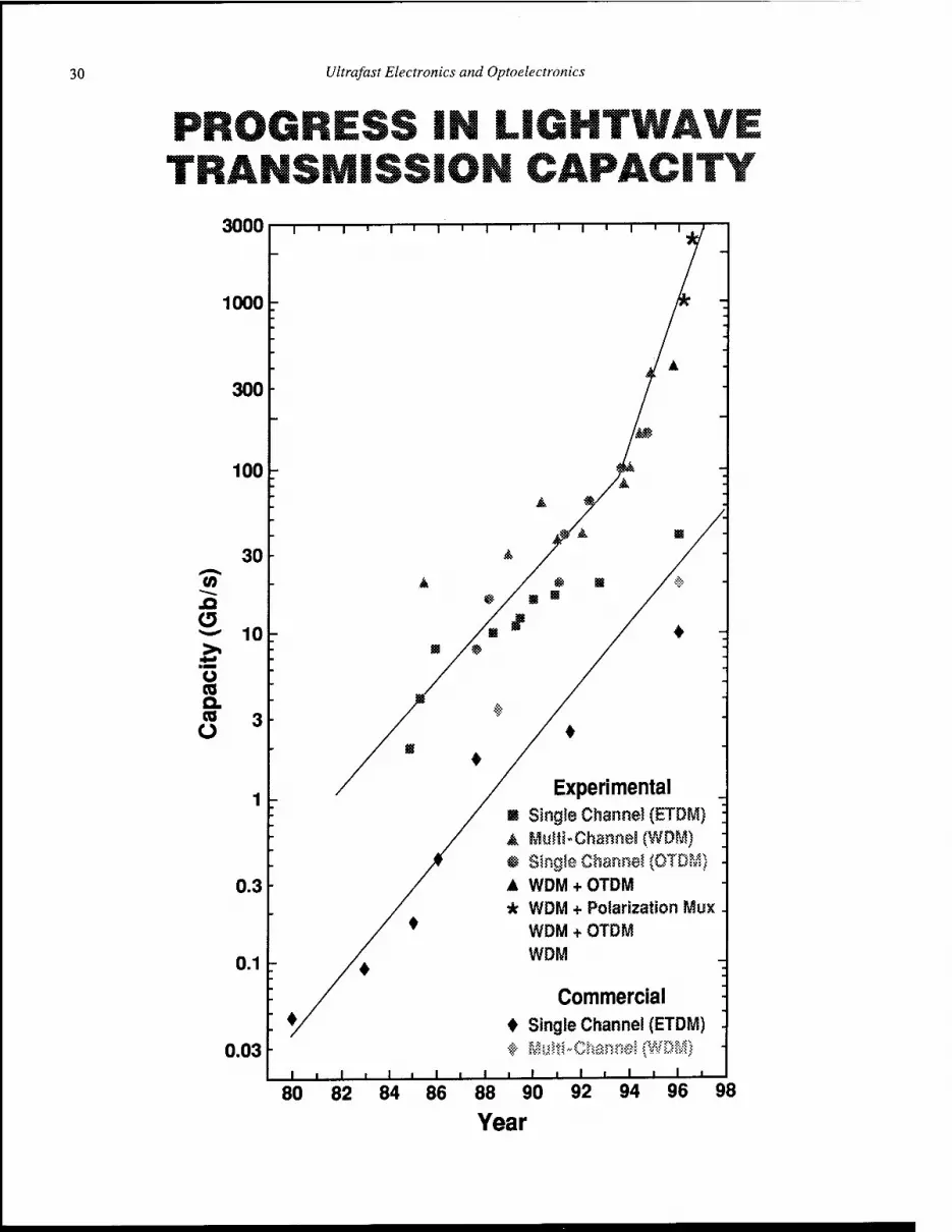
30 Ultrafast Electronics and Optoelectronics
Pairs S^m^T^
TsH» JP» j 899 HSB ^B i
Pi i«ttl%Xlo 1 C dritte gSSn&fc, flSSs jnS888bt
w% ^^fflp «^& « S 8St MM
auuu i ■ —i—i— i i i i i —i—1 1—1—r "1 i | J
1000 A ~
M A
300 1
m
100 - 7Z ■
A y '. jrA m / ■
30 k 7 / - 5T 4 / • & /% JQ # / s / O w 10 /» / ♦ -
Cap
acity
w
38 /w
/ ' * 1
' Experimental ü Single Channel (ETDfVI) ; A Muiti-Channel (¥*/Df\ri) ; # Single Channel (OTOy) -
0.3 ▲ WDM + OTDM * WDM + Polarization MUX .
X ♦ WDM + OTDM
0.1 /♦ WDM
Commercial
■ y ♦ Single Channel (ETDM) "
0.03 i ■ 1 . 1 . 1 1 1 ■ ' 1 1 1—1—1—1—1—
80 82 84 86 88 90
Year 92 94 96 98
100 Gb/s Optical Network Technology
K.L. Hall, K.A. Rauschenbach, S.G. Finn, R.A. Barry, N.S. Patel and J.D. Moores MIT Lincoln Laboratory
C-237 244 Wood Street
Lexington, MA 02173 tel: (617) 981-0229 fax:(617)981-4129
ABSTRACT
Ultra-high speed optical time-division- multiplexed (TDM) networks, operating at single stream data rates of 100 Gb/s, may offer unique advantages over wavelength division multiplexed systems. These advantages include the ability to provide integrated services (including packet service) to high-end users, multiple quality of service (QoS) levels and truly flexible bandwidth- on-demand. Realization of these high performance TDM networks requires development of a number of key technologies such as high-speed optical sources, all-optical switches, buffers and rate converters. In this paper, we will give an overview of an ultra-high-speed TDM network «architecture, as well as describe recent key technology developments.
Keywords: Optical logic, Nonlinear optical devices. Optical networks, Ultrafast technology.
Ultrafast optical time-division-multiplexed (TDM) networks have the potential to provide truly flexible bandwidth on demand at burst rates of 100 Gb/s. The total capacity of a single channel local or metropolitan area network may be the same as a number of wavelength division multiplexed (WDM) lower rate channels, but TDM networks provide potential improvements in terms of user access time, delay, and throughput, depending on the user rates and traffic statistics. In addition, end node equipment is conceptually simpler for single- channel versus multiple-channel approaches.
Recently, network subsystems for bit-interleaved TDM systems have been demonstrated [1-9]. However, it has been argued that for local area networks (LANs) and metropolitan area networks (MAN's) servicing a combination of high-speed and low-speed users, a 100 Gb/s slotted TDM network has several important operating advantages over bit-interleaved multiplexing approaches [10,11]. In this paper, we describe architecture and technology for single-stream, 100 Gb/s local/metropolitan area shared media networks with slotted TDM.
The network we describe runs at an aggregate rate of 100 Gb/s but will serve a heterogeneous population of users; high-end single users, high speed video servers, terabyte media banks and networks of supercomputers, that may operate at speeds from 1-100 Gb/s. The most important features of the network are to provide a backbone to interconnect high-speed networks, to transfer quickly very large data blocks, to switch large aggregations of traffic and to provide flexible, lower-rate access to users. Although we are designing a 100 Gb/s network, the architecture will be scaleable to much higher rates.
There are two characteristics of these 100 Gb/s slotted TDM networks that significantly impact the architectural design. First, they operate with long propagation delays, i.e., there are many data packets in flight at one time in the network- a high-latency environment. Second, there is a limited amount of processing that can be performed at the 100 Gb/s rate. These two characteristics make it difficult to provide simultaneously both guaranteed bandwidth and bandwidth on demand
OSA TOPS on Ultrafast Electronics and Optoelectronics, 1997 Vol. 13, Martin Nuss and John Bowers (ed.) ©1997 Optical Society of America
31

32 Ultrafast Electronics and Optoelectronics
services. Also, it is difficult to insure both efficient and "fair" bandwidth sharing in the presence of moderately loaded or overloaded network traffic conditions. A third difficulty is that algorithms designed to manage the network must be simple enough to be executable with a minimal amount of processing available at the optical bit rate. There have been some articles addressing these various problems in the literature [12,13], but they do not appear to satisfy simultaneously, all of the above criteria. We have developed a frame-based slotted architecture called HLAN (helical local area network) [11,14] which satisfies the above criteria. In early work, the HLAN architecture was implemented on a helical ring physical structure, but most recently has been explained using a unidirectional bus implementation.
HLAN is a frame-based architecture, which is implemented on a unidirectional bus as shown in Figure 1. A headend generates frames of empty slots and puts them on the bus. Guaranteed bandwidth (GBW) traffic is transmitted on the GBW segment, bandwidth on demand (BOD) traffic is transmitted on the BOD segment and data is received on the RCV segment. Note that only one bus is required and that all receivers are downstream of the transmitters.
Figure 1. HLAN topology
GBW services fire provided to users who request them by the headend. The headend allocates reserved slots to the node on the GBW segment. Users can access the HLAN at their guaranteed rate using only a counter, a flip-flop, a few gates and slot marker detection logic [14]. Using existing logic, HLAN slot rates of 10-100 Mslots/s can be supported.
Fair and efficient BOD service is provided via the BOD segment. The headend creates credits and distributes them at a given interval. A user who has data to send and who has a credit can burst data onto the network when the first empty slot comes by. Users with data to send but no credits, must wait for the headend to distribute more credits. Users who accumulate credits but have no data to send will be limited to a finite number of
reserve credits. To prevent lockouts from high- traffic upstream nodes, the headend monitors free slots at the end of the BOD segment. If no free slots are observed, the number of allocated credits is decreased, decreasing the bandwidth available to the individual nodes. If, on the other hand, multiple free slots are observed, the number of allocated credits is increased, returning more bandwidth to the individual nodes. The system is "fair" because all users will get equal throughput when they have data to send. The algorithm is also efficient because few slots that could be used are left empty. This simple HLAN algorithm performs like the "Greedy" algorithm under lightly loaded network conditions and transitions to fixed TDMA as the load increases [11].
Figure 2 shows a block diagram of some of the hardware components needed to implement this high-speed, yet simple network architecture. The block diagram shows the components in the receiver node, but the components in the transmitter node are almost identical. The components shown in the shaded boxes, at the interface between the optical bus, and the node electronics, are high performance optical devices that must operate at the optical data rate.
FROM NETWnOI
SLOW PROTOCOL
LOGIC
FAST PROTOCOL
LOGIC
INTERFACE
Figure 2. Block diagram of components in a user receiver node.
The data packets will enter the receiver node, via a passive tap, at the slot rate of 10-100 Mslots/s. The first function that must be performed is address/header recognition. In the transmitter nodes, header recognition includes determining if there is a credit marker present and if the slot is empty or full. In the receiver node, the incoming address must be compared with a local address to determine whether or not the packet requires further processing. Address recognition must be performed on-fhe-fly, at 100 Gb/s. Ultrahigh speed optical switches, configured as AND gates [3] and XOR gates [15] can be used for this purpose. There

Ultrafast Electronics and Optoelectronics 33
are currently many techniques being investigated for all-optical AND and XOR gating, including; four-wave-mixing in waveguides [5, 16,17], cross- phase/gain modulation in nonlinear optical loop mirrors (NOLM's) [18-20], semiconductor NOLM's [21,22], Mach-Zehnder devices [23,24], ultrafast nonlinear interferometers [25,26]. The referenced work is by no a complete listing of work in the field. Rather, it is a representative sampling of some of the more recent results.
It has been shown that self-synchronizing codes can be employed to eliminate the need for clock recovery in the address recognition circuits, if the frequency of the data bits is known. In these high speed networks, the self-synchronizing codes are uniquely spaced pulse pairs [3,5]. These pulse pairs must be generated with a well defined timing relation to the optical data packet. Once generated however, these timing pulses travel along with the packet and experience the same variable path delays, due to link temperature changes, for example. Therefore, when the pulse pair and the packet arrive at the receiver node, the uniquely spaced pulse pair can generate a timing pulse that is synchronous with the data packet. This pulse can be amplified, split, delayed and recombined in a "hardwired" lightwave circuit, to produce a synchronous local address, and then compared in an all-optical AND or XOR gate.
If the packet address matches the local address, the data packet must be stored while it is rate converted down to a rate that the node electronics can handle. In the transmitter node, lower rate optical data will be assembled (up- converted) in fiber loop buffers and stored while the user waits for access to the network. There have been a number of pulse storage experiments performed to date [27-43]. However, many of these experiments were designed to demonstrate long distance transmission. Single packet, single- wavelength buffers have been demonstrated in two implementations. One implementation, the uncompensated loop buffer [29-32], contains an input/output switch/coupler and a gain element. These loops have stored 2 packets of 2.5 Gb/s data for approximately 30 circulations [30]. This limited storage time may not be acceptable for some network applications.
Much longer storage times and much higher data rates have been demonstrated in active fiber loop buffers. In addition to the components in the passive loop buffers, these buffers contain an amplitude modulator, polarization controller and polarizing elements. These active loop buffers,
initially demonstrated at 1 Gb/s [37], and then extended to much higher rates, using a variety of modulation techniques [38-40,44], have a number of built in stabilizing mechanisms and have stored for many thousands of circulations. The built-in stabilizing mechanisms include timing stability due to the loss modulation by the amplitude modulator and pulse energy stability due to intensity- dependent absorption caused by nonlinear polarization rotation in the fiber loop. Loading of externally generated data packets has been demonstrated at packet rates up to 40 Gb/s [43].
Once the data have been loaded successfully into the buffer, rate conversion to the electronic rate in the user node must begin. One method for performing rate conversion is to demultiplex every Kth bit of an N-bit long data packet such that N and K are relatively prime. The time required to rate convert an entire packet using this scheme is NKTb, where Tb is the bit spacing of the original data stream. This method has the disadvantage that it scrambles the rate converted data bits and requires additional electronic processing to faithfully reconstruct the original data sequence.
An alternative method is data time dilation via optical sampling. This scheme has the advantage that the rate converted streams require no re-ordering of the bits. The essence of this scheme, used previously to characterize high speed clock and data streams on low-speed oscilloscopes [45-48], is that aliasing brought about by sampling a high speed optical stream at a rate lower than the Nyquist rate gives rise to a time dilated version of the packet. The sampling can be achieved in a nonlinear crystal or an optical switch, for example. The cross-correlated data are detected and low-pass filtered so that the cross-correlation signal envelope, and not the individual sampling pulse envelopes are measured. Note that both schemes for rate conversion require repeating input optical data patterns. Therefore, these schemes must be employed in conjunction with recirculating loop buffers.
In conclusion, we have described a candidate architecture, HLAN, for management and control of single-stream 100-Gb/s local and metropolitan area networks, providing packet switched services (slotted TDM) in a unidirectional bus topology. Key technologies, including 100 GHz optical sources [49-51], all-optical switches, active fiber loop buffers and rate conversion techniques have been demonstrated.

34 Ultrafast Electronics and Optoelectronics
Acknowledgments:
We <ire grateful to Erich P. Ippen and Hermann A. Haus for stimulating discussions and for important insights into device operation and performance. Also we thank Claudia I. Fennelly for her experimental contributions. This work was supported by the consortium on Wideband All- Optical Networks and the Defense Advanced Research Projects Agency (DARPA). Opinions, interpretations, conclusions and recommendations are those of the authors and are not necessarily endorsed by the United States Air Force.
New results for this ultrafast TDM network will be posted at www.ll.mit.edu.
REFERENCES
[1] A.D. Ellis, T. Widdowson, X. Shan and D.G. Moody, "Three-node 40 Gb/s OTDM network experiment using electro-optic switches", Electron. Lett., 30, p. 1333,(1994). [2] K. Suzuki, K. Iwatsuki, S. Nishi and M. Saruwatari, "Error-free demultiplexing of 160 Gbit/s pulse signal using optical loop mirror including semiconductor laser amplifier", Electron. Lett., 30, p. 1504,(1994). [3] D. Cotter, K. Smith, M. Shabeer, D.C. Rogers and D. Nesset, "Ultrafast self-routing packet networks", in Technical Digest of Optical Fiber Communications Conference (Optical Society of America, Washington, DC, 1995), paper WJ1. [4] T. Morioka, S. Kawanishi, H. Takara find M. Saruwatari, "Multiple-output 100 Gb/s all-optical demultiplexer based on multichannel four-wave mixing pumped by a linearly chirped square pulse". Electron. Lett.,J0, p. 1959, (1994). [5] D. Cotter, J.K. Lucek, M. Shabeer, K. Smith, D.C. Rogers. D. Nesset and P. Gunning, Electron. L(^.,31,p. 1475,(1995). [6] T. Yamamoto, T. Imai, T. Komukai, Y. Miyajima and M. Nakazawa, "Optical demultiplexing and routing of a TDM signal by using four-wave mixing and a novel wavelength router with optical circulators and fiber gratings", Electron. Lett., 3J_, no. 9, p. 744, (1995). [7] S. Kawanishi, H. Takara, T. Morioka, O. Kamatani, and M. Saruwatari, "200 Gb/s, 100 km time division multiplexed optical transmission using supercontinuum pulses with prescaled PLL timing extraction and all-optical demultiplexing", Electron. Lett., 31., no. 10, p. 816, (1995).
[8] A.D. Ellis, T. Widdowson, X. Shan, G.E. Wickens and D.M. Spirit, "Transmission of a true single polarization 40 Gb/s soliton data signal over 205 km using a stabilized erbium fiber ring laser and 40 GHz electronic timing recovery", Electron. Lett., 29, no. 11, p. 990, (1993). [9] A.D. Ellis, D.A.O. Davies, A. Kelly and W.A. Pender, "Data driven operation of semiconductor amplifier loop mirror at 40 Gb/s", Electron. Lett., 31_,no. 15, p. 1245,(1995). [10] S.G. Finn and R.A. Barry, "Optical Services in Future Broadband Networks", IEEE Network Magazine, November/December, p.7, (1996). [11] R.A. Barry, V.W.S. Chan, K.L. Kill, E.S. Kintzer, J.D. Moores, K.A. Rauschenbach, E.A. Swanson, L.E. Adams, C.R. Doerr, S.G. Finn, H.A. Haus, E.P. Ippen, W.S. Wong, and M. Haner, "All- Optical Network Consortium-Ultrafast TDM Networks", J Lightwave Technol. /IEEE J. Select. Areas Commun., 14, no. 5, p. 999, (1996). [12] C. Yeh, M. Lin, M. Gerla, and P. Rodrigues, "RATO-net: A random-access protocol for unidirectional ultra-high-speed optical fiber networks", J. Lightwave Technol., 8, no. 1, (1990). [13] G.C. Watson and S. Tohme, "S++-A new MAC protocol for Gb/s local area networks", IEEE J. Select. Areas Commun., JJ_, no. 4, (1993). [14] S.G. Finn, "HLAN-an architecture for optical multi-access networks", in Technical Digest for the LEOS Summer Top. Mtg., p. 45, (1995). [15] K.L. Hall and K.A. Rauschenbach, "All- optical bit pattern generation and matching" Electron. Lett., 32, no. 13, p. 1214, (1996). [16] S. Kawanishi and O. Kamatani, "All-optical time division multiplexing using four wave mixing". Electron. Lett., 30, no. 20, p. 1697, (1994). [17] M. Shabeer, J.K. Lucek, K. Smith, D. Cotter, find D.C. Rogers, "Self-synchronisation scheme for high-speed photonic networks", Electron. Lett., 31, no. 17, p. 1476,(1995). [18] N.J. Doran and D. Wood, "Nonlinear optical loop mirror", Opt. Lett., L3, no. 1, p. 56, (1988). [19] K.L. Kill, K.A. Rauschenbach, E.A. Swanson, S.R. Chinn, find G. Raybon, "Picosecond-accuracy all-optical bit phase comparison using a nonlinear
-optical loop mirror", IEEE Photon. Technol. Lett., 7, 935, (1995). [20] K.A. Rauschenbach, K.L. Hall, J.C. Livas and G. Raybon, "All-optical pulsewidth and wavelength conversion at 10 Gb/s using a nonlinear optical loop mirror", IEEE Photon. Technol. Lett., 6, p. 1130,(1994).

Ultrafast Electronics and Optoelectronics 35
[21] M. Eiselt, W. Pieper and H.G. Weber, "All- optical high speed demultiplexing with a semiconductor laser amplifier in a loop mirror configuration", Electron. Lett., 29, no. 13, p. 1167, (1993). [22] J.P. Sokoloff, P.R. Prucnal, I. Glesk and M. Kane, "A terahertz optical asymmetric demultiplexer (TOAD)", IEEE Photon. Technol. Lett., 5, p. 787, (1993). [23] K.I. Kang, T.G. Chang, I. Glesk and P.R. Prucnal, "Demonstration of ultrafast, all-optical low control energy, single wavelength polarization independent cascadable and integratable switch", Appl. Phys. Lett., 67, p. 605, (1995). [24] S. Nakamura and K. Tajima, "Analysis of subpicosecond full-switching with a symmetric Mach-Zehnder all-optical switch", Jap. J. Appl. Phys. 2, 35, no. 11, p. L1426, (1996). [25] N.S. Patel, K.L. Hall and K.A. Rauschenbach, "40 Gb/s cascadable all-optical logic with an ultrafast nonlinear interferometer", Opt. Lett., 21, no. 18, p. 1466,(1996). [26] N.S. Patel, K.A. Rauschenbach and K.L. Hall, "40 Gb/s demultiplexing using an ultrafast nonlinear interferometer", IEEE Photon. Technol. Lett., 8, no. 12, p. 1695,(1996). [27] L.F. Mollenauer, E. Lichtman, G.T. Harvey, M.J. Neubelt, and B.M. Nyman, "Demonstration of error free soliton transmission over more than 15000 km at 5 Gb/s, single channel and over more than 11000 km at 10 Gb/s in two channel WDM", Electron. Lett., 28, no. 8, p. 792, (1992). [28] M. Nakazawa, H. Kubota, E. Yamada, and K. Suzuki, "Infinite-distance soliton transmission with soliton controls in time and frequency domains", Electron. Lett., 28, no. 12, p. 1099, (1992). [29] W. Pieper, M. Eiselt, G. Grosskopf, R. Langenhorst, A. Errhart and H.G. Weber, "Investigation of crosstalk interference in a fiber loop optical buffer", Electron. Lett., 30, no. 5, p. 435, (1994). [30] Y. Yamada, K. Sasayama, K. Habara and K. Yukimatsu. "FDM optical loop buffer and its applications to photonic ATM switch: Frontier Net", in Technical Digest of Optical Fiber Communications Conference (Optical Society of America, Washington, DC, 1995), p. 140. [31] G. Bendelli et al., in Technical Digest of Optical Fiber Communications Conference (Optical Society of America, Washington, DC, 1995), p. 141. [32] R. Langenhorst et al., "Fiber loop optical buffer," J. Lightwave Technol., 14, no. 3, p. 324, (1996).
[33] V.l. Belotitskii, E.A. Kuzin, M.P. Petro, and V.V. Spirin, "Demonstration of over 100 million round-trips in recirculating fiber loop with all- optical regenerator", Electron. Lett., 29, no. 1, p. 49, (1993). [34] H. Avamopoulos and N. Whitaker, "Addressable fiber-loop buffer", Opt. Lett., 18, no. 1, p. 22, (1993). [35] N.A. Whitaker, M.C. Gabriel, H. Avrampoulos and A. Huang, "All-optical, all fiber circulating shift register with an inverter", Opt. Lett., 16, no. 24, p. 1999,(1991). [36] A.J. Poustie, R.J. Manning, and K.J. Blow, "All-optical circulating shift register using a semiconductor optical amplifier in a fiber loop mirror", Electron. Lett., 32, no. 13, p. 1215 (1996). [37] C.R. Doerr, W.S. Wong, H.A. Haus, and E.P. Ippen, "Additive pulse mode-locking/limiting storage ring", Opt. Lett., 19, no. 21, p. 1747, (1994). [38] J.D. Moores, K.L. Hall, S.M. LePage, K.A. Rauschenbach, W.S. Wong, H.A. Haus, and E.P. Ippen, "20-GHz optical storage loop/laser using amplitude modulation, filtering and fast saturable absorption", IEEE Photon. Technol. Lett., 7, no. 9, p. 1096, (1995). [39] K.L Hall, J.D. Moores, K.A. Rauschenbach, W.S. Wong, E.P. Ippen and H.A. Haus, "All- optical storage of a 1.25 kbit packet at 10 Gb/s", IEEE Photon. Technol. Lett., 7, no. 9, p. 1093, (1995). [40] J.D. Moores, W.S. Wong and K.L. Hall, "50 Gb/s optical pulse storage ring using novel rational- harmonic modulation", Opt. Lett., 20, no. 24, p. 2547, (1995). [41] K.L. Hall and K.A. Rauschenbach, "A fiber loop buffer storing variable length data packets at 18 Gb/s for 200 circulations", IEEE/LEOS Summer Top. Mtg, Tech. Dig., Broadband Optical Networks, MB2, p. 16, (1996). [42] J.D. Moores, "80-gbit/s 9-kbit optical pulse storage loop," in Technical Digest of Optical Fiber Communications Conference (Optical Society of America, Washington, DC, 1997) p. 88. [43] K.L. Hall, "40-Gbit/s optical packet buffering," in Technical Digest of Optical Fiber Communications Conference (Optical Society of America, Washington, DC, 1997), p. 251. [44] N. Onodera, A.J. Lowry, L. Zhai, Z. Ahmed and R.S. Tucker, "Frequency multiplication in actively modelocked semiconductor lasers", Appl. Phys. Lett., 62, no. 12, p. 1329, (1993). [45] T. Kanada and D.L. Frazen, "Optical waveform measurement by optical sampling with a
36 Ultrafast Electronics and Optoelectronics
mode-locked laser diode". Opt. Lett., JJ_, no. 1, p. 4, (1986). [46] B.P. Nelson and N.J. Doran, "Optical sampling oscilloscope using nonlinear fiber loop mirror". Electron. Lett., 27, p. 204, (1991). [47] P.A. Andrekson, "Picosecond optical sampling using four wave mixing in fibre", Electron. Lett.,.27, no. 16, p. 1440, (1991). [48] H. Takara, S. Kawanishi, T. Morioka, K. Mori and M. Saruwatari, "100 Gb/s optical waveform measurement with 0.6 ps resolution optical sampling using subpicosecond supercontinuum pulses", Electron. Lett., 30, no. 14, p. 1152,(1994). [49] E.A. Swanson and S.R. Chinn, "23-GHz and 123-GKz soliton pulse generation using two CW lasers and standard single-mode fiber", IEEE Photon. Technol. Lett., 6, no. 7, p. 796, (1994). [50] E.A. Swanson, S.R. Chinn, K.L. Hall, K.A. Rauschenbach, R.S. Bondurant and J.W. Miller, "100-GHz soliton pulse train generation using soliton compression of two phase side bands from a single DFB laser", IEEE Photon. Technol. Lett., 6, no. 10, p. 1194,(1994). [51] E.A. Swanson and S.R. Chinn, "40-GHz pulse train generation using soliton compression of a Mach-Zehnder modulator output", IEEE Photon. Technol. Lett., 7, no. 1, p. 114, (1995).
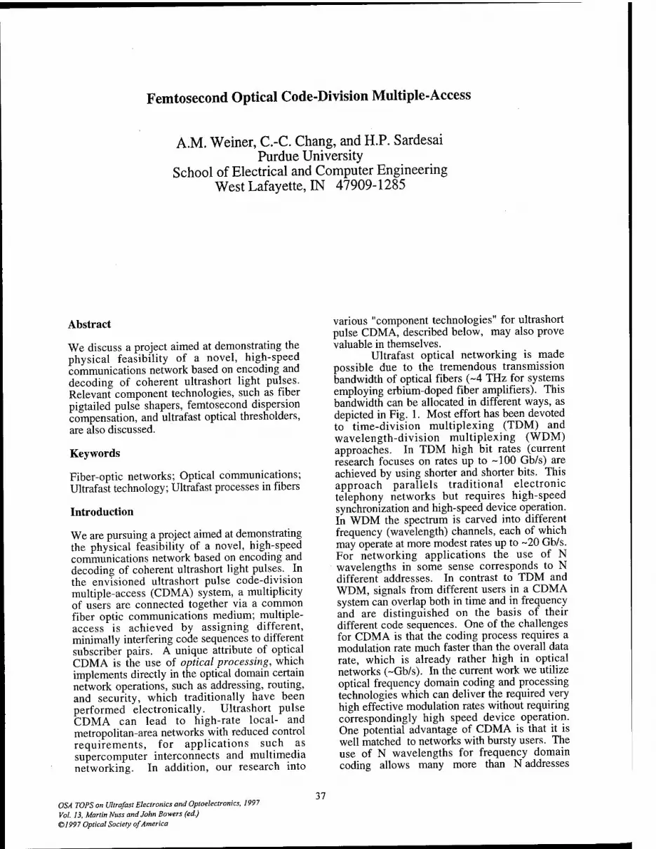
Femtosecond Optical Code-Division Multiple-Access
A.M. Weiner, C.-C. Chang, and H.P. Sardesai Purdue University
School of Electrical and Computer Engineering West Lafayette, IN 47909-1285
Abstract
We discuss a project aimed at demonstrating the physical feasibility of a novel, high-speed communications network based on encoding and decoding of coherent ultrashort light pulses. Relevant component technologies, such as fiber pigtailed pulse shapers, femtosecond dispersion compensation, and ultrafast optical thresholders, are also discussed.
Keywords
Fiber-optic networks; Optical communications; Ultrafast technology; Ultrafast processes in fibers
Introduction
We are pursuing a project aimed at demonstrating the physical feasibility of a novel, high-speed communications network based on encoding and decoding of coherent ultrashort light pulses. In the envisioned ultrashort pulse code-division multiple-access (CDMA) system, a multiplicity of users are connected together via a common fiber optic communications medium; multiple- access is achieved by assigning different, minimally interfering code sequences to different subscriber pairs. A unique attribute of optical CDMA is the use of optical processing, which implements directly in the optical domain certain network operations, such as addressing, routing, and security, which traditionally have been performed electronically. Ultrashort pulse CDMA can lead to high-rate local- and metropolitan-area networks with reduced control requirements, for applications such as supercomputer interconnects and multimedia networking. In addition, our research into
various "component technologies" for ultrashort pulse CDMA, described below, may also prove valuable in themselves.
Ultrafast optical networking is made possible due to the tremendous transmission bandwidth of optical fibers (-4 THz for systems employing erbium-doped fiber amplifiers). This bandwidth can be allocated in different ways, as depicted in Fig. 1. Most effort has been devoted to time-division multiplexing (TDM) and wavelength-division multiplexing (WDM) approaches. In TDM high bit rates (current research focuses on rates up to -100 Gb/s) are achieved by using shorter and shorter bits. This approach parallels traditional electronic telephony networks but requires high-speed synchronization and high-speed device operation. In WDM the spectrum is carved into different frequency (wavelength) channels, each of which may operate at more modest rates up to -20 Gb/s. For networking applications the use of N wavelengths in some sense corresponds to N different addresses. In contrast to TDM and WDM, signals from different users in a CDMA system can overlap both in time and in frequency and are distinguished on the basis of their different code sequences. One of the challenges for CDMA is that the coding process requires a modulation rate much faster than the overall data rate, which is already rather high in optical networks (~Gb/s). In the current work we utilize optical frequency domain coding and processing technologies which can deliver the required very high effective modulation rates without requiring correspondingly high speed device operation. One potential advantage of CDMA is that it is well matched to networks with bursty users. The use of N wavelengths for frequency domain coding allows many more than N addresses
OSA TOPS on Ultrafast Electronics and Optoelectronics, 1997 Vol. 13, Martin Nuss and John Bowers (ed.) ©1997 Optical Society of America
37

38 Ultrafast Electronics and Optoelectronics
TIME-DIVISION MULTIPLEXING
(TDM)
4THZ FREQUENCY
WAVELENGTH-DIVISION MULTIPLEXING
(WDM)
FREQUENCY
CODE-DIVISION MULTIPLE-ACCESS
(CDMA)
FREQUENCY
Figure 1 Schematic illustration of bandwidth allocation in TDM, WDM, and CDMA optical networks.
(codes), provided that the number of codes active at one time stays sufficiently low. This allows rapid access to the network without the need to reserve specific time or frequency slots. Ultrashort pulse CDMA appears to be best matched for applications like local area networking, supercomputer interconnects, and cluster computing.
The architecture for ultrashort pulse CDMA has been described in previous publications and is sketched in Fig. 2 [1, 2, 3]. In our scheme coherent ultrashort pulses are first encoded into pseudonoise bursts and then broadcast to all the users, most likely in a star topology. The receiver distinguishes the desired data from the multiple-access interference by decoding signals with the correct code back into ultrashort pulses [1, 2]. Encoding and decoding are based on a technique for shaping of femtosecond light pulses [4, 5]. Experiments demonstrating the required ability to encode and subsequently decode ultrashort light pulses were performed several years ago using the visible- wavelength femtosecond lasers which were then available [1, 4]. However, transmission of coded femtosecond pulses over optical fibers had not been reported, nor were any experiments stringently testing ultrashort pulse CDMA at the wavelengths compatible with fiber optic
technology. Advances in femtosecond laser and fiber optic technology now make it viable to perform ultrashort pulse CDMA experiments at the appropriate wavelengths for fiber optics. The goal of our research project is to assemble a simple ultrashort pulse CDMA testbed, including fiber transmission in 1.5 ixm band, in order to critically test the physical layer performance of this technique.
CDMA Component Technologies
In order to construct an ultrashort pulse CDMA testbed, we must first perform research into several of the necessary component technologies. These include compact femtosecond pulse sources, encoding and decoding devices, fiber dispersion compensation, and nonlinear optical thresholding devices. Our components research is summarized in the following:
Femtosecond pulse sources At present we are using a femtosecond stretched- pulse modelocked fiber ring laser [6] which produces very stable pulses -60 fsec in duration with -60 nm bandwidth and a 31 MHz repetition rate. For most CDMA system experiments we spectrally slice the pulses, resulting typically in 10 nm bandwidths and 250 fsec pulse durations. In some experiments the pulses are further broadened due to gain narrowing during fiber amplification. This source is well suited to our CDMA components research and should also be useful for initial CDMA systems experiments, but in the future will need to be replaced with a higher repetition rate source.
Encoding and decoding We perform encoding and decoding by using a multielement liquid crystal phase modulator (LCM) to filter the spectral phases of optical frequency components spatially dispersed within a simple bulk optics apparatus. The liquid crystal modulator array, previously developed at Bellcore for visible-wavelength pulse shaping, allows reprogramming on a millisecond time scale [5]. This technology has been commercialized and is available from at least two vendors. We have constructed a pair of fiber- pigtailed pulse shapers containing commercial 128-element phase modulator arrays with a measured fiber-to-fiber insertion loss as low as 5.7 dB for an individual pulse shaper. We have used these pulse shapers to demonstrate encoding and decoding at 1.56 urn. Figure 3(a) shows intensity autocorrelation data for an uncoded pulse, while 3(b) shows autocorrelation data for a

Ultrafast Electronics and Optoelectronics 39
Electronic Data Stream
Femtosecond Laser
1 " Encoded
Pulse
J Amplitude Femtosecond Encoder
»WWW**
1 Modulator
Transmitter
Desired Data
/ Multi-access j. 1 Interference
Optical Threshold
Device Electronics Decoder Optical
Amplifier _r
Other Subscribers
Receiver
Figure 2 Schematic diagram of an optical CDMA system based on encoding and decoding of coherent ultrashort light pulses.
1.0
coded pulse in which one of the LCMs is set according to a length-15 pseudorandom M- sequence phase code. The spectral encoding transforms the original pulse into a longer duration and lower intensity pseudonoise burst. Figure 3(c) shows a properly decoded pulse in which both LCMs are programmed for equal and opposite phase. This restores the original ultrashort pulsewidth and intensity comparable to that in Fig. 3(a). Finally, Fig. 3(d) shows data for an improperly decoded pulse for which the codes in the two pulse shapers do not match. A CDMA receiver could distinguish between properly and improperly decoded pulses on the basis of the contrast in their intensity. In previous visible- wavelength experiments coding and decoding was demonstrated using pseudorandom phase codes with lengths as long as 127 [4]. Experiments using longer codes in our current apparatus are now in progress. We note that in contrast to previous experiments [1] in which both coding and decoding masks were placed back to back within a single pulse shaper, the current work uses a separate coder and decoder pulse shapers connected by fiber.
As an aside, we note that we have also applied programmable pulse shapers for experiments demonstrating the application of phase coding to broadband incoherent light (amplified spontaneous emission from an erbium- doped fiber amplifier) [7]. Here we modify the optical coherence function rather than the pulse shape itself. This could be used for related
5.
c - 0.0
1.0
CO c o
- 0.0 1.0
-2-
co c <D
- 0.0 1.0
3
'en c B c
0.0
(a)
AX
(b)
(c)
(d)
-20 -10 -*r-
10 20
Time (ps) Figure 3 Femtosecond encoding and decoding using a pair of fiber-pigtailed pulse shapers. Data show intensity autocorrelations of (a) uncoded, (b) coded, (c) properly decoded, and (d) improperly decoded pulses.

40 Ultrafast Electronics and Optoelectronics
optical CDMA schemes based on coherence coding [8] since in this case the expensive femtosecond laser can be replaced by an inexpensive incoherent light source.
Dispersion compensation Dispersion will be the main effect limiting the distance between subscriber stations in ultrafast CDMA fiber networks. (Note that soliton effects cannot be employed in ultrashort pulse CDMA since successful decoding requires linear pulse propagation). Dispersion compensation techniques are currently receiving considerable attention for conventional high-bit-rate systems; some of these techniques can also be applied to femtosecond CDMA systems. One method, the use of special equalizing fibers [9] to compensate the dispersion of standard telecom fiber, may be particularly advantageous for femtosecond dispersion compensation due to the possibility of compensating both second and third order dispersion simultaneously. We initially tested this approach for femtosecond applications by propagating ~60-fsec pulses over a 42-m dispersion equalized link [10]. The pulses were first broadened and then recompressed by a factor of 300, resulting in ~110 fsec output pulses. The small broadening was caused by residual cubic dispersion (dispersion slope), which we were able to measure precisely using a spectral interferometry technique [11]. One interesting aspect of our method is that the use of a modelocked laser source allows measurements of fibers tens of meters in length, which usually cannot be measured using interferometric methods due to the need for a very long free- space delay arm. Our data indicated that the residual dispersion slope was ~6 times less than in dispersion shifted fiber. We can use these data to project dispersion-limited propagation distances for longer pulses. For example, a 250- fsec pulse is expected to experience similar broadening in a 2.8 km dispersion compensated link if the dispersion properties remain constant. We have recently performed experiments verifying this projection and demonstrating transmission of 250-fsec pulses over a 2.5 km link with roughly a factor of two broadening, as shown in Fig. 4. In these experiments the pulse is stretched and then recompressed by a factor of 800 in the link. Figure 4 also shows data for longer (470 fs) input pulses, which as expected exhibit a smaller amount of broadening. We plan to use this 2.5 dispersion compensated link for our initial ultrashort pulse CDMA local area networking experiments.
Optical thresholding devices Optical threshold devices are required in ultrashort pulse CDMA receivers to discriminate between intense properly decoded data signals and improperly decoded but equally energetic low-level interference signals. We are investigating the use of nonlinear frequency shifts in passive optical fibers as well as nonlinear waveguide photodetectors to perform this thresholding function.
For the fiber based thresholders, our CDMA receiver consists of a chirped pulse fiber amplifier, a fiber pigtailed spectral phase decoder, and the passive fiber followed by a filter and a photodetector. In the current thresholder experiments, we have only a single decoder as opposed to an encoder-decoder pair. We have performed two different fiber thresholding experiments. In the first the fiber is 500-m long and is dispersion shifted with a zero dispersion wavelength of 1559 nm, which is near the center of the amplified pulse spectrum. For sufficiently intense bandwidth-limited pulses, nonlinear propagation effects cause the spectrum to split and broaden [12]. The resulting nonlinear frequency shifts are detected by using a long wavelength pass filter followed by a photodetector. Coded pulses, which for the same pulse energy have much lower intensity, do not exhibit nonlinear frequency effects and are blocked by the filter. With 0.44 mW average power in the passive fiber, we achieve a contrast ratio of nearly 30 dB between coded and uncoded pulses [13]. In the second experiment we use 340-m of fiber with zero dispersion at 1547 nm. Since the pulse is now entirely in the anomalous dispersion regime, at sufficient intensity levels the spectrum shifts to longer wavelengths due to the Raman effect [14]. A contrast ratio of 36 dB is achieved at an average power level of 1.8 mW. Further details on the thresholder operation are given elsewhere in this volume [see article by H.P. Sardesai et al]. The high achieved contrast ratios should provide good suppression of multiple-access interference in a CDMA system.
In the waveguide photodetector experiments [15], we exploit the intensity dependence of the two-photon absorption photocurrent for GaAs p-i-n photodetectors used at 1.5 |im. For fixed pulse energy, we have verified that the photocurrent is proportional to the inverse of the optical pulsewidth over the range 180 fs to 4 ps. We have also observed a subnanosecond electrical response without any optimization of the device packaging. These results show the feasibility of applying such devices for ultrafast optical thresholding. Compared to the fiber devices, the nonlinear
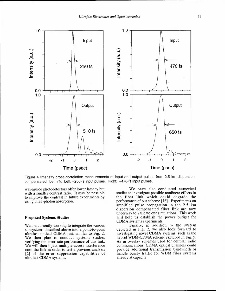
Ultrafast Electronics and Optoelectronics 41
-1 0 1
Time (psec)
-2-10 1
Time (psec)
Figure 4 Intensity cross-correlation measurements of input and output pulses from 2.5 km dispersion compensated fiber link. Left: ~250-fs input pulses. Right: ~470-fs input pulses.
waveguide photodetectors offer lower latency but with a smaller contrast ratio. It may be possible to improve the contrast in future experiments by using three-photon absorption.
Proposed Systems Studies
We are currently working to integrate the various subsystems described above into a point-to-point ultrafast optical CDMA link similar to Fig. 2. We then plan to conduct systems studies verifying the error rate performance of this link. We will then inject multiple-access interference onto the link in order to test a previous analysis [2] of the error suppression capabilities of ultrafast CDMA systems.
We have also conducted numerical studies to investigate possible nonlinear effects in the fiber link which could degrade the performance of our scheme [16]. Experiments on amplified pulse propagation in the 2.5 km dispersion compensated fiber link are now underway to validate our simulations. This work will help us establish the power budget for CDMA systems experiments.
Finally, in addition to the system depicted in Fig. 2, we also look forward to investigating novel CDMA systems, such as the hybrid WDM-CDMA scheme sketched in Fig. 5. As in overlay schemes used for cellular radio communications, CDMA optical channels could provide additional transmission bandwidth or handle bursty traffic for WDM fiber systems already at capacity.

42 Ultrafast Electronics and Optoelectronics
i
f \
3
O
Q. | WDMA channels ! A
CD s o a.
i r~
ra ! CDMA
D. o
■--—
y signals
frequency or wavelength
Figure 5 Proposed hybrid CDMA/WDM fiber communications scheme.
Acknowledgments
We gratefully acknowledge A. Vengsarkar for the dispersion compensating fiber, M. Newhouse and V. Da Silva for fibers used in the thresholding experiments, and J. Marsh for the p-i-n waveguide photodetector. This work was supported by NSF under grants ECS-9626967 and ECS-9312256 and by AFOSR under contract F49620-95-1-0533.
References
1. A. M. Weiner, J. P. Heritage, and J. A. Salehi, "Encoding and decoding of femtosecond pulses," Opt. Lett. 13, 300-302 (1988).
2. J. A. Salehi, A. M. Weiner, and J. P. Heritage, "Coherent ultrashort light pulse code-division multiple access communication systems," J. Lightwave Tech. 8, 478 (1990).
3. A. M. Weiner and J. A. Salehi, "Optical Code- Division Multiple-Access," in Photonics in Switching, J. Midwinter, ed. (Academic Press, San Diego, 1993), vol. II, pp. 73-118.
4. A. M. Weiner, J. P. Heritage, and E. M. Kirschner, "High-resolution femtosecond pulse shaping," J. Opt. Soc. Amer. B 5, 1563-1572 (1988).
5. A. M. Weiner, D. E. Leaird, J. S. Patel, and J. R. Wullert, "Programmable shaping of femtosecond pulses by use of a 128-element liquid-crystal phase modulator," IEEE J. Quantum Electron. 28, 908-920 (1992).
6. K. Tamura, E. P. Ippen, H. A. Haus, and L. E. Nelson, "77-fs pulse generation from a stretched-pulse mode-locked all-fiber ring laser," Opt. Lett. 18, 1080-1082 (1993).
7. V. Binjrajka, C.-C. Chang, A. W. R. Emanuel, D. E. Leaird, and A. M. Weiner, "Pulse Shaping of Incoherent Light by Use of a Liquid Crystal Modulator Array," Opt. Lett. 21, 1756-1758 (1996).
8. R. A. Griffin, D. D. Sampson, and D. A. Jackson, "Coherence Coding for Code-Division Multiple-Access Networks," IEEE J. Lightwave Technol. 13, 1826-1837 (1995).
9. C. D. Poole, J. M. Wiesenfeld, D. J. DiGiovanni, and A. M. Vengsarkar, "Optical fiber-based dispersion compensation using higher-order modes near cutoff," J. Lightwave Tech. 12, 1746-1758(1994).
10. C.-C. Chang, A. M. Weiner, A. M. Vengsarkar, and D. W. Peckham, "Broadband fiber dispersion compensation for sub-100-fs pulses with a compression ratio of 300," Optics Letters 21,1141-1143(1996).
11. L. Lepetit, G. Cheriaux, and M. Joffre, "Linear techniques of phase measurement by femtosecond spectral interferometry for applications in spectroscopy," J. Opt. Soc. Am. B 12, 2467-2474 (1995).
12. P. K. A. Wai, C. R. Menyuk, H. H. Chen, and Y. C. Lee, "Solitons at the zero-group- dispersion wavelength of a single-mode fiber," Opt. Lett. 12, 628-630 (1987).
13. H. P. Sardesai and A. M. Weiner, "A nonlinear fiber-optic receiver for ultrashort pulse code division multiple access communications," Elect. Lett., in press (1997).
14. J. P. Gordon, "Theory of the Soliton Self- Frequency Shift," Opt. Lett. 11, 665 (1986).
15. Z. Zheng, A. M. Weiner, J. H. Marsh, and M. M. Karkhanehchi, "Optical thresholding based on two-photon absorption GaAs waveguide photodetectors," IEEE Photonics Technology Letters , in press (1997).
16. V. Binjrajka and A. M. Weiner, "Effect of self- phase-modulation on ultrashort pulse transmission in dispersion compensated systems with large broadening and compression", Conference on Lasers and Electro-optics (Anaheim, CA, 1996).

Cascaded WDM Passive Optical Network with a Highly Shared Source
Jason B. Stark (a), Martin C. Nuss (b), Wayne H. Knox (b), Steve Cundiff (b), Luc Boivin (b), Steve Grubb (a),(c), Don Tipton (a), David DiGiovanni (a), Uziel Koren (b), and Kevin Dreyer (b)
(a) Bell Laboratories, Lucent Technologies, Murray Hill, NJ 07974 (b) Bell Laboratories, Lucent Technologies, Holmdel, NJ 07733
(c) present address: SDL Inc., 80 Rose Orchard Way, San Jose, CA 95134
Abstract
We propose and demonstrate a cascaded distribution fabric for WDM Passive Optical Networks (WDM-PON) that delivers distinct data to potentially tens of thousands of subscribers using a single, centralized WDM source. This is possible by assigning a unique time slot to each wavelength, and replicating this 'bit-interleaved' WDM signal in cascaded stages of amplification and power splitting, before data is encoded for each WDM-PON by a single TDM modulator.
Key Words
Optical fiber communications; fiber access; optical fiber amplifiers; wavelength division multiplexing; ultrafast optics.
Introduction
Passive Optical Networks (PONs) are attractive for delivery of high-bandwidth data directly to the home [1]. Such a PON consists of a transmitter at the Central Office (CO), distribution fiber, a remote branching device, and an Optical Network Unit (ONU) at the subscriber's location. In a conventional power-splitting PON, the transmitter emits an aggregated signal on a single wavelength, while the branching device is a power-splitter that distributes identical signals to each ONU, each receiving the aggregate bit-rate. Wavelength-division-multiplexed (WDM) PONs, in which each transmitted wavelength carries data for a single subscriber, are attractive because the branching device, a WDM router, establishes a point-to-point link between the transmitter and each subscriber, and hence offers many upgrade possibilities. However, the implementation of WDM-PONs is currently still hampered by the high cost of WDM sources.
We propose and demonstrate a novel scalable WDM optical distribution fabric, in which a centralized WDM light source serves a large number of WDM passive optical networks, leading to a significant cost sharing of the source. We accomplish this by using a source in which WDM channels are bit-interleaved, so that each time-slot is
occupied by only a single WDM signal. Data can then be encoded by a single modulator, operating at the aggregate bit rate, given by the number of WDM channels x bit rate in each channel [2]. Data encoding with the external modulator allows us to insert a cascade of amplifiers and power splitters to distribute the WDM carrier to a large number of modulators, each modulator encoding data for a single WDM-PON. Previously, amplifier cascades have been demonstrated for broadcast video distribution [3], where each subscriber receives the same data. Here, by using a bit-interleaved WDM source and an external modulator, we can utilize amplifier cascades to share the WDM source among potentially tens of thousands of network users while still sending distinct data to each subscriber.
System Architecture
The network architecture is schematically shown in Figure 1 and consists of the bit-interleaved WDM light source, a cascadable distribution fabric that delivers the bit- interleaved signal to many WDM-PONs, and a single data- encoding modulator for each PON. Each stage of the distribution fabric consists of a power splitter preceded by an optional optical amplifier to compensate for the splitting loss. Several of these stages can be concatenated by connecting other amplifier/power-split units to each port of the preceding power splitter. We envision a CO transmitter consisting of a bit-interleaved source, banks of amplifiers, splitters and modulators, which may reside in interconnected modules, as schematically indicated in Fig. 1. For k cascaded stages having M-fold power split and N WDM channels, a single light source serves
N • M subscribers. If we require roughly -10 dBm in each of 16 WDM channels at the central office, the output of a +21 dBm Erbium-doped amplifier (EDFA) can be power-split at least 16 times taking 7 dB of insertion loss for the modulator into account. For such a WDM-PON, a total of 65,536 subscribers could therefore be served using only three cascaded stages of splitting, and a single WDM light source.
OSA TOPS on Ultrafast Electronics and Optoelectronics, 1997 Vol. 13, Martin Nuss and John Bowers (ed.) ©1997 Optical Society of America
43
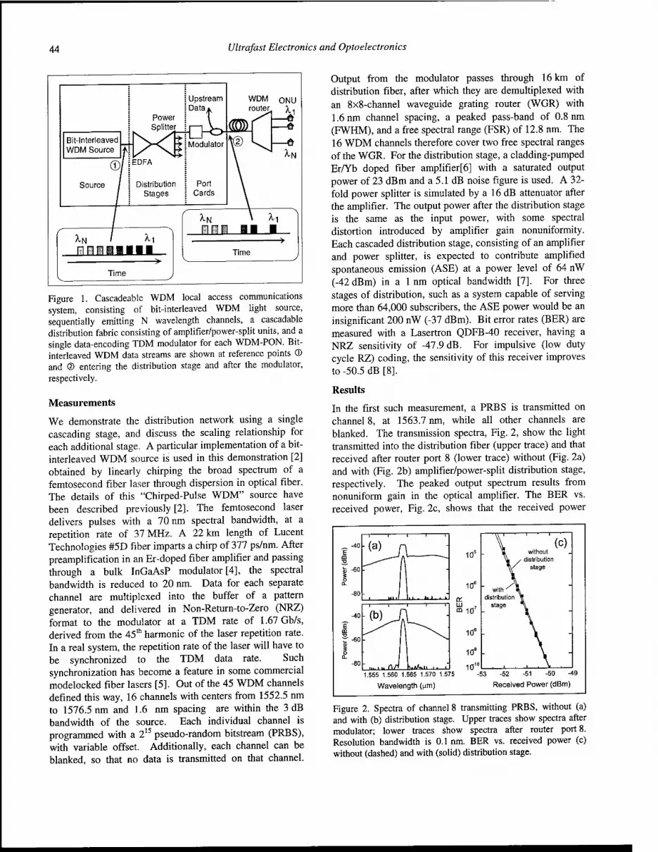
44 Ultrafast Electronics and Optoelectronics
WDM ONU
Bit-Interleaved WDM Source
Source
nnnum *
Time
nnn n ■ Time
Figure 1. Cascadeable WDM local access communications system, consisting of bit-interleaved WDM light source, sequentially emitting N wavelength channels, a cascadable distribution fabric consisting of amplifier/power-split units, and a single data-encoding TDM modulator for each WDM-PON. Bit- interleaved WDM data streams are shown at reference points © and © entering the distribution stage and after the modulator, respectively.
Measurements
We demonstrate the distribution network using a single cascading stage, and discuss the scaling relationship for each additional stage. A particular implementation of a bit- interleaved WDM source is used in this demonstration [2] obtained by linearly chirping the broad spectrum of a femtosecond fiber laser through dispersion in optical fiber. The details of this "Chirped-Pulse WDM" source have been described previously [2]. The femtosecond laser delivers pulses with a 70 nm spectral bandwidth, at a repetition rate of 37 MHz. A 22 km length of Lucent Technologies #5D fiber imparts a chirp of 377 ps/nm. After preamplification in an Er-doped fiber amplifier and passing through a bulk InGaAsP modulator [4], the spectral bandwidth is reduced to 20 nm. Data for each separate channel are multiplexed into the buffer of a pattern generator, and delivered in Non-Return-to-Zero (NRZ) format to the modulator at a TDM rate of 1.67 Gb/s, derived from the 45th harmonic of the laser repetition rate. In a real system, the repetition rate of the laser will have to be synchronized to the TDM data rate. Such synchronization has become a feature in some commercial modelocked fiber lasers [5]. Out of the 45 WDM channels defined this way, 16 channels with centers from 1552.5 nm to 1576.5 nm and 1.6 nm spacing are within the 3 dB bandwidth of the source. Each individual channel is programmed with a 215 pseudo-random bitstream (PRBS), with variable offset. Additionally, each channel can be blanked, so that no data is transmitted on that channel.
Output from the modulator passes through 16 km of distribution fiber, after which they are demultiplexed with an 8x8-channel waveguide grating router (WGR) with 1.6 nm channel spacing, a peaked pass-band of 0.8 nm (FWHM), and a free spectral range (FSR) of 12.8 nm. The 16 WDM channels therefore cover two free spectral ranges of the WGR. For the distribution stage, a cladding-pumped Er/Yb doped fiber amplifier[6] with a saturated output power of 23 dBm and a 5.1 dB noise figure is used. A 32- fold power splitter is simulated by a 16 dB attenuator after the amplifier. The output power after the distribution stage is the same as the input power, with some spectral distortion introduced by amplifier gain nonuniformity. Each cascaded distribution stage, consisting of an amplifier and power splitter, is expected to contribute amplified spontaneous emission (ASE) at a power level of 64 nW (-42 dBm) in a 1 nm optical bandwidth [7]. For three stages of distribution, such as a system capable of serving more than 64,000 subscribers, the ASE power would be an insignificant 200 nW (-37 dBm). Bit error rates (BER) are measured with a Lasertron QDFB-40 receiver, having a NRZ sensitivity of -47.9 dB. For impulsive (low duty cycle RZ) coding, the sensitivity of this receiver improves to-50.5 dB [8].
Results
In the first such measurement, a PRBS is transmitted on channel 8, at 1563.7 nm, while all other channels are blanked. The transmission spectra, Fig. 2, show the light transmitted into the distribution fiber (upper trace) and that received after router port 8 (lower trace) without (Fig. 2a) and with (Fig. 2b) amplifier/power-split distribution stage, respectively. The peaked output spectrum results from nonuniform gain in the optical amplifier. The BER vs. received power, Fig. 2c, shows that the received power
-i 1 1 r
1.555 1.560 1.565 1.570 1.575
Wavelength (|im)
-53 -52 -51 -50 -49
Received Power (dBm)
Figure 2. Spectra of channel 8 transmitting PRBS, without (a) and with (b) distribution stage. Upper traces show spectra after modulator; lower traces show spectra after router port 8. Resolution bandwidth is 0.1 nm. BER vs. received power (c) without (dashed) and with (solid) distribution stage.

Ultrafast Electronics and Optoelectronics 45
1.555 1.560 1.565 1.570 1.575
Wavelength (urn)
-53 -52 -51 -50 -49
Received Power (dBm)
Figure 3. Spectra of channels 1-15 transmitting, without (a) and with (b) distribution stage. Upper traces show spectra after modulator; lower traces show spectra after router port 8. Resolution bandwidth 0.1 nm. BER vs. received power (c) without (dashed) and with (solid) distribution stage.
level for 10"9 BER is -50.3 dBm, both with and without distribution stage. Within experimental uncertainties, no power penalty is incurred by the introduction of the distribution stage.
The effects of crosstalk are measured by transmitting a PRBS on each of channels 1-15, while receiving through router port 8. Channel 16, one FSR away, is blanked in this experiment. Each PRBS is offset by 736 bits, relative to the previous channel. The spectra without (Fig. 3a) and with distribution stage (Fig. 3b) are again shown after the modulator (upper traces) and after demultiplexing (lower traces). The BER measurements, Fig. 3c, indicate a negative power penalty of 0.2 dB in the presence of the distribution stage. On the other hand, transmission measurements on channel 1 show a 1 dB power penalty. This leads us to conclude that the -0.2 dB negative power penalty in channel 8 results again from the peaked spectrum of the distribution stage, which suppresses the crosstalk levels away from the signal channel. The opposite is true for the weak channel 1, where there is increased crosstalk from the stronger neighboring channels.
The measured power penalties can be largely eliminated using a true 1x16 router instead of utilizing two free spectral ranges of a 1x8 WGR. Penalties associated with non-uniform gain in the amplifier stage can be eliminated by using gain-flattened amplifiers, or by feed- forward equalization of the spectrum [9].
Conclusion
In summary, we propose and demonstrate an optically transparent cascaded distribution fabric that distributes a centralized bit-interleaved WDM source to potentially tens of thousands of subscribers. The fabric can be grown simply by adding amplifiers and splitters. This novel
cascaded distribution fabric enables large-scale sharing of the WDM light source, promising a significant cost reduction for the introduction of WDM in passive optical networks.
References
1. Y.-K. M. Lin, and D. R. Spears, "Passive Optical Subscriber Loops with Multiaccess," Journ. Lightwave Techn., vol. 7, p.1769-1777 (1989); T. H. Wood, and R. D. Feldman, "Fiber Access in the USA: Systems and Implications for Devices," IEICE Trans. Electron., vol. E80 C, p. 9-16, (1997)
2. M. C. Nuss, W. H. Knox, and U. Koren, "Scalable 32 channel chirped-pulse WDM source," Electr. Lett., vol. 32, p. 1311-1312,(1996)
3. P. M. Gabla, C. Bastide, Y. Cretin, P. Bousselet, A. Pitel, and J. P. Blondel, "45 dB Power Budget in a 30- Channel AM-VSB Distribution System with Three Cascaded Erbium-Doped Fiber Amplifiers," IEEE Phot. Techn. Lett!., vol. 4, p. 510-512, (1992)
4. U. Koren, R. Ben Michael, B. I. Miller, M. G. Young, M. Chien, H. H. Yaffe, G. Raybon, and K. Dreyer, "Electroabsorption modulator with passive waveguide spotsize converters," Electr. Lett., vol. 30, p. 1852- 1853, (1994)
5. private communications, G. Sucha, D. Harter, IMRA America; Tony H. Lin, Calmar Optcom
6. S. G. Grubb, W. H. Humer, R. S. Cannon,, S. W. Vendetta, K. L. Sweeney, P. A. Leilabady, M. R. Keur, J. G. Kwasegroch, T. C. Munks, and D. W. Anthon, "+24.6 dBm Output Power Er/Yb Codoped Optical Amplifier Pumped by a Diode-Pumped Nd:YLF Laser," Electr. Lett., vol. 28, p. 1275-1276, (1992).
7. J. B. Stark, M. C. Nuss, W. H. Knox, S. T. Cundiff, L. Boivin, S. G. Grubb, D. Tipton, D. DiGiovanni, U. Koren, and K. Dreyer, "Cascaded WDM Passive Optical Network with a Highly Shared Source," IEEE Phot. Techn. Lett., vol 9 (8), (1997).
8. L. Boivin, M. C. Nuss, J. Shah, D. A. B. Miller, and H. Haus, "Receiver Sensitivity Improvement by Impulsive Coding," IEEE Phot. Techn. Lett., vol. 9, p. 684-686, (1997).
9. S. T. Cundiff, W. H. Knox, and M. C. Nuss, "Active feed-forward channel equalization for chirped pulse wavelength division multiplexing," Electr. Lett., vol. 33, p. 10-11,(1997).

Multiwavelength, 10 GHz Picosecond Pulse Generation from a Single-Stripe Semiconductor Traveling Wave Amplifier Using Active Modelocking
in an External Cavity
H. Shi, G.A. Alphonse*, J.C. Connolly*, P.J. Delfyett Center for Research and Education in Optics and Lasers (CREOL),
Department of Electrical and Computer Engineering, University of Central Florida, Orlando, FL 32816
* David Sarnoff Research Center, CN 5300, Princeton, NJ 08543-5300
Abstract
Single stripe GaAs/AlGaAs semiconductor traveling wave amplifiers have been used to generate four tunable, synchronized WDM channels simultaneously, each transmitting 18 picosecond pulses at 2.5GHz for an aggregate pulse rate of 10GHz.
Keywords: multiwavelength lasers, semiconductor optical amplifiers, modelocked semiconductor lasers, WDM-TDM network sources.
Multiwavelength optical signal sources capable of generating ultrahigh speed and highly synchronized picosecond pulses are of great interest in novel photonic networks utilizing combined optical wavelength division multiplexed (WDM) and time division multiplexed (TDM) data formats. To date, multiwavelength picosecond pulse generation has been demonstrated by using a variety of techniques by many research groups [1-6]. For semiconductor laser based devices, recent efforts in this field have focused on the use of semiconductor laser arrays. Single-stripe semiconductor lasers have been thought as unfeasible for simultaneous multiwavelength oscillations owing to the strong gain competition between the oscillating modes.
In this paper, we demonstrate a tunable four- channel modelocked laser suitable for WDM-TDM networks, based on a single-stripe semiconductor laser amplifier (SLA). By active harmonic modelocking the grating-loaded external cavity laser system at 2.5 GHz, stable pulses have been generated at four wavelengths simultaneously. Pulsewidths of ~18 ps have been demonstrated for the composite four-wavelength output, and for each individual wavelength output. In this approach, the main concept to be stressed is the exploitation of the active modelocking induced transient unsaturated gain in a
single-stripe device to achieve stable multiwavelength picosecond pulses generation.
Figure 1 schematically shows the setup of the four wavelength laser. Actively modelocked optical pulses are generated from the laser diode by incorporating an intracavity spectral filter to define the individual spectral components. The end mirror M2 reflects the four selected spectral components back to the gain device to complete the four wavelength channel generation. A colinear composite four-wavelength pulse train is coupled out from the zeroth order grating reflection. Modelocking is made by injecting ~1 W rf sinusoidal signal at a frequency of 2.5GHz with 175mA of dc bias current into the diode chip. The position of the diode in the cavity is chosen to enhance the eighth harmonic modelocking frequency, which in this case, is designed to be 2.5GHz.
STWA
M2
DIAGNOSTICS
M1
Figure l. Schematic of the experiment setup. STWA— single-angled-stripe semiconductor traveling wave amplifier; G--grating (1800 line/mm); SF-spatial filter; L--I50mm achromatic lens; M~end mirrors.
Figure 2 illustrates the output four wavelength spectra in active modelocking (upper) and in cw operation (lower). Stable four wavelength lasing was demonstrated at a pulse repetition rate of 600 MHz, 2.1 GHz, and 2.5 GHz. In comparison,
OSA TOPS on Ultrafast Electronics and Optoelectronics, 1997 Vol. 13, Martin Nuss and John Bowers (ed.) ©1997 Optical Society of America
46

Ultrafast Electronics and Optoelectronics Al
gain competition prevents the stable operation of the laser in a multiwavelength cw mode.
In figure 3 are autocorrelation traces of the composite four-wavelength output and of each individual wavelength component.
modelocked condition
X\ X2 XZ X4
JU w u _1 I l_
ro >. | ., CD
C
-2
cw condition
Ljul wavelength (1.5nm/div)
Figure 2. Output spectra of four wavelengths.
delay time (15ps/div)
Figure 3. Autocorrelation traces of output pulses at each wavelength channel and composite four- wavelength channel.
It is observed from these data that the temporal profiles of the pulses are identical and synchronized, with a deconvolved pulsewidth of 18 ps. The peaks impressed on the composite four-
wavelength pulse show a correlated phase relation between each wavelength channel, where the temporal modulation is proportional to the wavelength separation between channels.
Figure 4(a) shows the tuning characteristic of the composite four wavelength output, with a fixed spectral separation of ~lnm, and tuned over the gain bandwidth of the SLA (>20nm). Figure 4(a) suggests that as many as 19 wavelengths separated by lnm could be supported from this device. In Figure 4(b), the tuning characteristic is shown where the individual wavelength separation is varied from ~0.8nm to ~2nm. Notice that in both cases, the spectral intensities decrease with large detuning, showing the influence of the gain spectrum of the SLA.
AAÜ /
IMl / .
I
111 ill .
AAAA wavelength (3nm/div)
(a)
wavelength (1.5nm/div) (b)
Figure 4. Tuning of the four wavelength spectra.
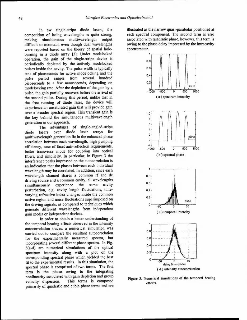
48 Ultrafast Electronics and Optoelectronics
In cw single-stripe diode lasers, the competition of lasing wavelengths is quite strong, making simultaneous multiwavelength output difficult to maintain, even though dual wavelengths were reported based on the theory of spatial hole- burning in a diode array [3]. Under modelocked operation, the gain of the single-stripe device is periodically depleted by the actively modelocked pulses inside the cavity. The pulse width is typically tens of picoseconds for active modelocking and the pulse period ranges from several hundred picoseconds to a few nanoseconds, depending on modelocking rate. After the depletion of the gain by a pulse, the gain partially recovers before the arrival of the second pulse. During this period, unlike that in the free running of diode laser, the device will experience an unsaturated gain that will provide gain over a broader spectral region. This transient gain is the key behind the simultaneous multiwavelength generation in our approach.
The advantages of single-angled-stripe diode lasers over diode laser arrays for multiwavelength generation lie in the enhanced phase correlation between each wavelength, high pumping efficiency, ease of facet anti-reflection requirements, better transverse mode for coupling into optical fibers, and simplicity. In particular, in Figure 3 the interference peaks impressed on the autocorrelation is an indication that the phases between each individual wavelength may be correlated. In addition, since each wavelength channel shares a common rf and dc driving source and a common cavity, all wavelengths simultaneously experience the same cavity perturbation, e.g. cavity length fluctuations, time- varying refractive index changes inside the common active region and noise fluctuations superimposed on the driving signals, as compared to techniques which generate different wavelengths from independent gain media or independent devices.
In order to obtain a better understanding of the temporal beating effects observed in the intensity autocorrelation traces, a numerical simulation was carried out to compare the resultant autocorrelation for the experimentally measured spectra, but incorporating several different phase spectra. In Fig. 5(a-d) are numerical simulations of the optical spectrum intensity along with a plot of the corresponding spectral phase which yielded the best fit to the experimental results. In this simulation, the spectral phase is comprised of two terms. The first term is the phase owing to the integrating nonlinearity associated with gain depletion and group velocity dispersion. This terms is composed primarily of quadratic and cubic phase terms and are
illustrated as the narrow quasi-parabolas positioned at each spectral component. The second term is also associated with quadratic phase, however, this term is owing to the phase delay impressed by the intracavity spectrometer.
0.8 1' ■
0.6
0.4
0.2
-A ) 1 I) -
00 - 500 0 500 10
(a) spectrum intensity
-1000 -500 0 500 1000
(b ) spectral phase
1
0.8
0.6
0.4
0.2
Jl I L -50 0 50
( c ) temporal intensity
-50 0 50 delay time (psec)
( d ) intensity autocorrelation
Figure 5. Numerical simulations of the temporal beating effects.

Ultrafast Electronics and Optoelectronics 49
This is seen as the parabolic envelop superimposed on the individual spectral phase components (see Fig. 5(b)). In Figs. 5(c,d) are the resultant temporal pulse intensity and its corresponding intensity autocorrelation. To clearly observe the agreement between the experimental autocorrelation and the simulation, a plot of both are shown in Fig. 6.
delay time (ps) Figure 6. Experiment autocorrelation and the simulation
comparison. Solid line is the experiment data.
It should be noted that the individual pulses both spatially and temporally overlap. One salient feature in the correlation trace is the identical pulsewidth of each of the four individual wavelengths, as well as the composite four- wavelength pulse train. This shows that any random timing jitter between each wavelength signal is highly correlated, since uncorrelated jitter would broaden the composite autocorrelation trace.
In order to obtain a clearer understanding of the possible spectral phase correlation, the multiwavelength laser was configured to operate with only two wavelengths. This would imply that the temporal beat signal would be sinusoidal. We then measured the interferometric autocorrelation, which is shown in Fig. 7, with the corresponding spectrum as the inset.
This figure clearly shows the standard 8:1 contrast ratio for the temporal beat components, suggesting complete phase correlation between the two wavelength signals.
In conclusion, the dynamics of multiwavelength operation in a single-stripe semiconductor laser has been described. By taking advantage of the active modelocking induced transient unsaturated gain, simultaneous four wavelength optical signal generation has been demonstrated in single-stripe laser diodes. The tuning characteristics suggest that additional channels can be produced based on this approach. The ultrafast temporal modulation also suggests that the intracavity dynamics play a role in establishing phase coherence and temporal correlation across the composite four-wavelength spectrum. These results show that modelocked single-stripe diode lasers with intracavity spectral filtering may be useful sources for novel WDM-TDM networks.
REFERENCES:
[1]. T. Morioka, K. Mori, S. Kawanishi, and M. Saruwatari, Photon. Techn. Lett, Vol.6, No.3, 365-368, 1994.
[2]. D. Burns, G. Hay, and W. Sibbett, CLEO/93 Digest, vol.11, JTHA3, 444-446, 1993.
[3]. C-L Wang and C-L Pan, Opt. Lett., Vol. 19, 1456-1458,1994.
[4]. Zhu, K. O. Nyairo and I. H. White, Photon. Techn. Lett., Vol.6, No.3, 348-351, 1994.
[5]. M.H. Ober, G. Sucha and M.E. Fermann, Opt. Lett., Vol.20, No.2, 195-197, 1995
[6]. H. Lotem, Z. Pan and M. Dagenais, Appl. Opt., Vol.32, No.27, 5270-5273, 1993
Figure 7. Interferometric autocorrelation of temporal beat signal of two wavelengths.

206-ChanneI Wavelength-Division Multiplexed Transmitter
using a Single Femtosecond Laser
L. Boivin, M. C. Nuss, J. B. Stark, W. H. Knox, S. T. Cundiff Bell Labs, Lucent Technologies, 101 Crawfords Corner Road, Room 4B-433, Holmdel, NJ 07733-3030
(908) 949-9406, FAX: (908) 949-2473; [email protected]
ABSTRACT- We demonstrate a 206-channeI wavelength division multiplexed transmitter using a single femtosecond laser at 1.55 urn and a single modulator. The channel spacing is 0.3 nm, and the bit rate of each channel is 36.7 Mb/s.
KEY WORDS-Wavelength-division multiplexing, fiber communication, ultrafast optics.
Introduction
In this paper, we demonstrate that CPWDM can be scaled to a record 206 WDM channels, with independent data transmitted on each channel. To our knowledge, this is the largest number of channels ever reported for a WDM source. The bit rate on each channel is 36.7 Mb/s, and the channel spacing is about 37 GHz (0.3 nm), with wavelengths ranging from 1535.3 nm to 1596.3 nm.
Transmitter Set-Up
Figure 1 shows a schematic of our transmitter.
Wavelength-division multiplexing (WDM) provides an attractive way to increase the capacity of optical fiber networks. Recently, there has been a push toward systems with very large numbers of WDM channels [1,2,3,4]. The network capacity, in these highly granular systems, can be shared more easily among many users, increasing the flexibility of the network. In addition, as the remote nodes operate at a bit rate lower than the aggregate bit rate, slower and cheaper electronics can be used at these cost sensitive locations.
Wavelength stabilization and data encoding of a large number of narrowband lasers (e.g. distributed-feedback lasers) can lead to cumbersome transmitters. Spectral slicing of a spectrally broadband source, on the other hand, provides a simple alternative for generating many WDM channels [5,6,7,8,9,10]. Chirped-pulse-WDM (CPWDM) is a particularly flexible technique to define and encode data on a large number of WDM channels using a single modelocked laser [8]. In this approach, laser pulses are chirped by propagation in a dispersive fiber so as to introduce a linear time-delay between their frequency components. Because each wavelength channel occupies a unique time slot, a single modulator operating in time- division multiplexed mode can be used to encode data sequentially onto each channel.
9.94 GHz
271SI RF
harm.
Ext. Clock ►
Pulse Pattern Generator
9.94 Gb/s Data
4 km DSF (-340ps/nm)
Is Fiber Laser
36.7MHz &-*£
dynamic bias
adjustment^
TDM
100 fs 27.2 ns
•« ►
time
Tx Output
InGaAsP Modulator
{ 27.2 ns, 24.2 ns ^ !■*£ z*^ ►)
time
, Power
Di time
Fig. 1 Schematic of the 206-channel chirped-pulse WDM transmitter.
A stretched-pulse modelocked Erbium-doped fiber ring laser with a repetition rate of 36.7 MHz is used as a spectrally broadband source [ 11,12,13]. Figure 2 shows a schematic of the laser cavity and a typical output spectrum. Passive modelocking is achieved through nonlinear
OSA TOPS on Ultrafast Electronics and Optoelectronics, 1997 Vol. 13, Martin Nuss and John Bowers (ed.) ©1997 Optical Society of America
50

Ultrafast Electronics and Optoelectronics 51
polarization rotation, and the so-called "rejection port" of the laser is used to couple as much as 40 mW of average power in a single mode fiber [12]. Pulses with a bandwidth in excess of 70 nm are extracted from this laser.
Cavity Schematic: 980 nm pump
Erbium doped fiber
(D<0)
WDM 1 WP PBS BRF
WP
=^= 1550nm s.—r^r output
g 7
SMF-28 fiber (D>0)
Optical Spectrum:
1500 1550 1600 Wavelength (nm)
Figure 2: Cavity schematic of a stretched-pulse modelocked erbium-doped fiber laser along with a typical optical spectrum obtained from the rejection port.
The spectrum is mapped onto the time axis by propagation through a single-mode fiber with total dispersion D B -340 ps/nm. This stretches out the pulses to a
duration of about 24.2 ns with a nearly linear time- wavelength relationship. Figure 3 compares the optical spectrum at the output of the chirping fiber with the temporal pulse train. About 3.5 stretched pulses are displayed on the lower panel. The features of the optical spectrum are clearly mapped onto the time axis, with the long wavelength preceding the shorter ones. A certain amount of overlap between adjacent pulses is also apparent, spoiling the wavelength-to-time relationship at the edges of the pulses. The corresponding frequencies are not used below.
Optical Spectrum (linear):
1560
Wavelength
Pulse train: ?,7.?,n s
f\ *— -»j.
.A / /1 \ h I V2 / fe\ \J»?Y. \r2
one pulse
Time
Figure 3: Optical spectrum and pulse train at the output of the chirping fiber.
An InGaAsP electro-absorption modulator with a 12 GHz bandwidth [14] is inserted at the output of the fiber for data encoding. A pattern generator synchronized to the 271stharmonic (y A = 9 942 GHz ) of thelaser
repetition rate is used to drive the modulator. The modulator undergoes 271 clock cycles as each chirped pulse passes through, defining 271 frequency bands on their spectrum. By turning on and off the modulator during these cycles, independent messages are encoded onto each channel. As the WDM channels are addressed sequentially in time every 271st clock cycle, their data streams must be time-division multiplexed (TDM) at the modulator.
The short wavelength absorption edge of the modulator results in spectral narrowing of the pulses to about 24 nm. To partially restore the original bandwidth and to equalize the transmitted spectrum, the modulator bias is adjusted dynamically as each pulse passes through, using feed- forward equalization [15]. The feed-forward set-up is shown on Figure 4. A fiber tap inserted at the output of the chirping fiber extracts 10 % of the optical power which is

52 Ultrafast Electronics and Optoelectronics
used to provide the feed-forward signal. The extracted pulses are fed to a second (reference) electro-absorption modulator with absorption characteristics similar to those of the data encoding modulator. Only a DC bias is applied to the reference modulator, and its output is detected with a 100 MHz inverting receiver. After proper RF delay, the output of the receiver is finally combined with the 9.94 Gb/s TDM data stream using a resistive power combiner.
10%, , chirped / reference pulse J mod.
bias ,. 0E. , RF delay (inverting) ■
9.94 Gb/s data
£ ] Pwr combiner
bias teem—»-1.3V
data mod.
Figure 4: Feed-forward equalization set-up.
Figure 5 shows that our feed-forward technique restores the transmitted optical bandwidth to about 60 nm, corresponding to 20.7 ns pulses with a duty cycle of 76 percent.
Without bias adjustment: -30
B m 2- Q 00 OH
-80
2< I nn l
>
■
■
With bias adjustment:
■
-MT— 60 nm ^~
■ ■
■ ■
Wavelength (nm) 1600 Figure 5: Optical spectra without encoded data at the transmitter output with and without feed-forward equalization.
Transmitter Performance
We first repetitively encode the same 271-bit TDM word onto each pulse, so that any given channel carries either one of the bit sequences "000..." or "111...". Figure 6 shows the optical spectrum obtained at the output of the
transmitter when the TDM word "11001100...11" is repetitively encoded onto every pulse.
X3
20 1 • 1 < r
Word "11001100... 11"
1540 1560 1580 1600
Wavelength (nm) Figure 6: Optical spectrum at the output of the transmitter when the same TDM word "11001100... 11" is encoded on every pulse. The 52 peaks seen here imply 206 WDM channels within the 3 dB bandwidth.
As can be seen, TDM bits "1" and "0" are converted into frequency bands of high and low intensity respectively. A series of equally spaced peaks and valleys are thus obtained, corresponding to the "11" and "00" sections of the TDM word. Out of the 271 possible wavelength slots defined by the modulator, 206 can be identified with less than 3dB channel-to-channel power variation (in Fig. 4, the outermost channels with insufficient power are "blanked" by zero padding the first and last few digits of the TDM word). The channel center wavelengths range from 1535.3 nm to 1596.3 and channel spacing increases from 0.29 nm for wavelengths around 1596 nm, to 0.31 nm for wavelengths around 1535 nm. We attribute this variation to third order dispersion in the chirping fiber. Third-order dispersion introduces a linear dependence of the dispersion coefficient, D, on wavelength, and therefore of the channel spacing governed by AX = 1 / DLvmoi , whereL is the length of the chirping fiber.
Next, we use different 271-bit TDM words for every pulse so as to encode independent messages on every channel. Pseudo-random bit streams (PRBS) with a length of 2'' for every channel are time-division multiplexed and stored in the pulse-pattern generator memory. A tunable filter with a bandwidth of 1.5 nm and a tunable Fabry-Perot filter with a bandwidth of 0.097 nm and a free spectral range of 2020 GHz are used to filter out a single channel at the output of the transmitter. Figure 7 shows a plot of the bit-error-rate as a function of received power for channel 92 centered at 1562.4 nm (multiplex mode).
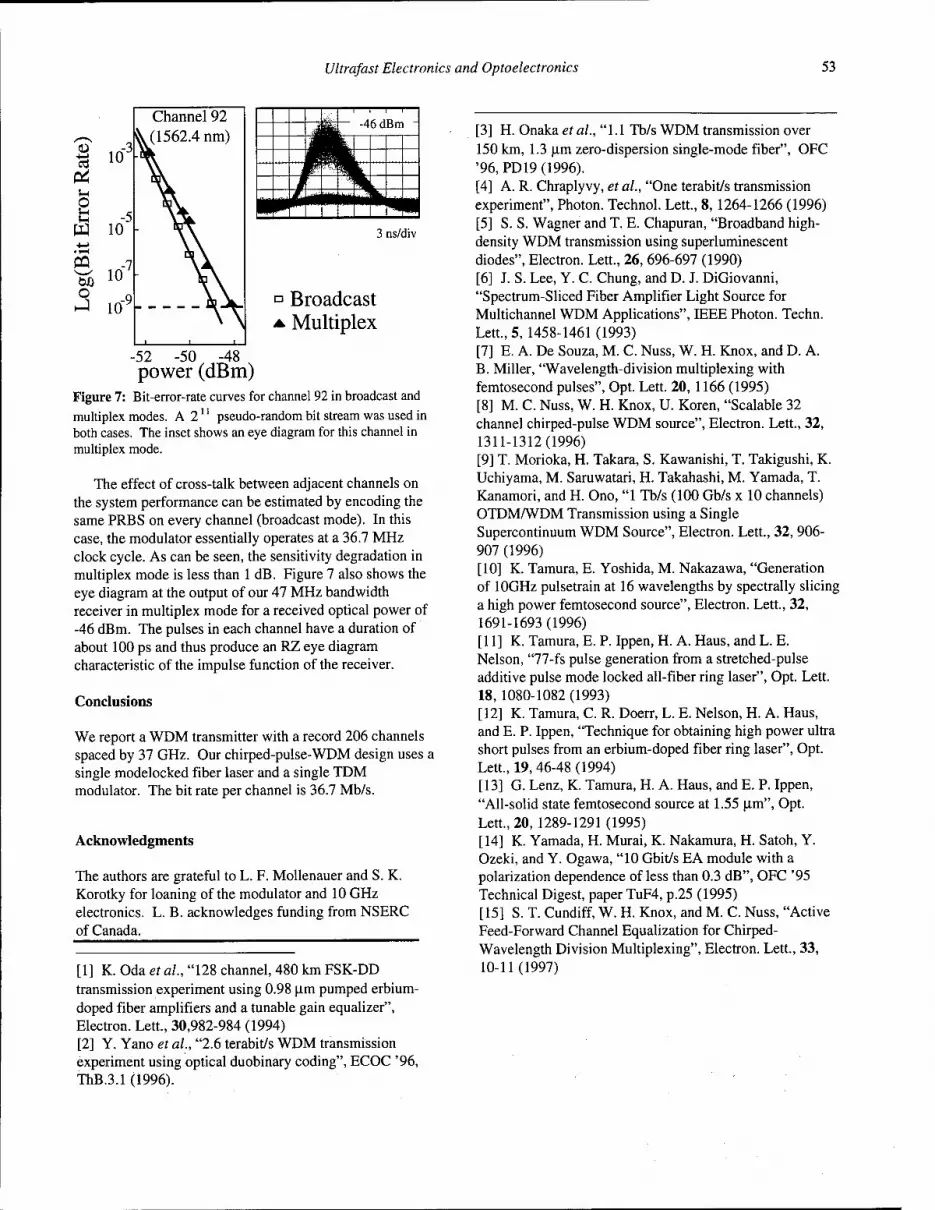
Ultrafast Electronics and Optoelectronics 53
Channel 92 ^ \( 1562.4 nm)
(1) ,^-3 td 10 (* ^ p fa -5 w 10 NA ■4-1
•I—I
PQ -7 W) 10 V] \
o io9
• i i
-to QDm
t m r :-,_,. 1
IPI''"-!fSI
■IIWM"""""™*»*. TMWBI ^FT" II M 1 l~*"W
3 ns/div
n Broadcast A Multiplex
-52 -50 -48 power (dBm)
Figure 7: Bit-error-rate curves for channel 92 in broadcast and multiplex modes. A 211 pseudo-random bit stream was used in both cases. The inset shows an eye diagram for this channel in multiplex mode.
The effect of cross-talk between adjacent channels on the system performance can be estimated by encoding the same PRBS on every channel (broadcast mode). In this case, the modulator essentially operates at a 36.7 MHz clock cycle. As can be seen, the sensitivity degradation in multiplex mode is less than 1 dB. Figure 7 also shows the eye diagram at the output of our 47 MHz bandwidth receiver in multiplex mode for a received optical power of -46 dBm. The pulses in each channel have a duration of about 100 ps and thus produce an RZ eye diagram characteristic of the impulse function of the receiver.
Conclusions
We report a WDM transmitter with a record 206 channels spaced by 37 GHz. Our chirped-pulse-WDM design uses a single modelocked fiber laser and a single TDM modulator. The bit rate per channel is 36.7 Mb/s.
Acknowledgments
The authors are grateful to L. F. Mollenauer and S. K. Korotky for loaning of the modulator and 10 GHz electronics. L. B. acknowledges funding from NSERC of Canada.
[1] K. Oda et ah, "128 channel, 480 km FSK-DD transmission experiment using 0.98 u.m pumped erbium- doped fiber amplifiers and a tunable gain equalizer", Electron. Lett., 30,982-984 (1994) [2] Y. Yano et ah, "2.6 terabit/s WDM transmission experiment using optical duobinary coding", ECOC '96, ThB.3.1 (1996).
[3] H. Onaka et ah, "1.1 Tb/s WDM transmission over 150 km, 1.3 u,m zero-dispersion single-mode fiber", OFC '96, PD19 (1996). [4] A. R. Chraplyvy, et ah, "One terabit/s transmission experiment", Photon. Technol. Lett., 8, 1264-1266 (1996) [5] S. S. Wagner and T. E. Chapuran, "Broadband high- density WDM transmission using superluminescent diodes", Electron. Lett., 26, 696-697 (1990) [6] J. S. Lee, Y. C. Chung, and D. J. DiGiovanni, "Spectrum-Sliced Fiber Amplifier Light Source for Multichannel WDM Applications", IEEE Photon. Techn. Lett, 5, 1458-1461(1993) [7] E. A. De Souza, M. C. Nuss, W. H. Knox, and D. A. B. Miller, "Wavelength-division multiplexing with femtosecond pulses", Opt. Lett. 20, 1166 (1995) [8] M. C. Nuss, W. H. Knox, U. Koren, "Scalable 32 channel chirped-pulse WDM source", Electron. Lett., 32, 1311-1312(1996) [9] T. Morioka, H. Takara, S. Kawanishi, T. Takigushi, K. Uchiyama, M. Saruwatari, H. Takahashi, M. Yamada, T. Kanamori, and H. Ono, "1 Tb/s (100 Gb/s x 10 channels) OTDM/WDM Transmission using a Single Supercontinuum WDM Source", Electron. Lett., 32, 906- 907 (1996) [10] K. Tamura, E. Yoshida, M. Nakazawa, "Generation of 10GHz pulsetrain at 16 wavelengths by spectrally slicing a high power femtosecond source", Electron. Lett., 32, 1691-1693 (1996) [11] K. Tamura, E. P. Ippen, H. A. Haus, and L. E. Nelson, "77-fs pulse generation from a stretched-pulse additive pulse mode locked all-fiber ring laser", Opt. Lett. 18, 1080-1082 (1993) [12] K. Tamura, C. R. Doerr, L. E. Nelson, H. A. Haus, and E. P. Ippen, "Technique for obtaining high power ultra short pulses from an erbium-doped fiber ring laser", Opt. Lett., 19, 46-48 (1994) [13] G. Lenz, K. Tamura, H. A. Haus, and E. P. Ippen, "All-solid state femtosecond source at 1.55 |im", Opt. Lett., 20, 1289-1291 (1995) [14] K. Yamada, H. Murai, K. Nakamura, H. Satoh, Y. Ozeki, and Y. Ogawa, "10 Gbit/s EA module with a polarization dependence of less than 0.3 dB", OFC '95 Technical Digest, paper TuF4, p.25 (1995) [15] S. T. Cundiff, W. H. Knox, and M. C. Nuss, "Active Feed-Forward Channel Equalization for Chirped- Wavelength Division Multiplexing", Electron. Lett., 33, 10-11(1997)
Nonlinear Optical Loop Mirror Switch (NOLM) for Coding High Repetition Mode-Locked Semiconductor Laser Pulses
M.R.H. Daza°, H.F. Liu2), T. Hoshida, M. Tsuchiya and T. Kamiya Department of Electronic Engineering, University of Tokyo
7-3-1 Hongo, Bunkyo-ku, Tokyo 113, Japan Phone: +81-3-3812-2111 ext. 6779, Fax: +81-3-5684-3984
Abstract
A high frequency (33 GHz) optical pulse train from a monolithic mode-locked semiconductor laser at A, = 1554 nm was modulated by pulses from a low repetition rate (1 GHz) gain-switched distributed feedback laser (DFB) at a different wavelength k= 1542 nm by using a nonlinear optical loop mirror (NOLM). This technique provides a scheme of optical coding of a high repetition rate optical pulse source and can simultaneously perform N x 1 multi-wavelength conversion.
Key Words
Optical coding, Semiconductor laser, Hybrid mode- locking, Nonlinear optical loop mirror, Wavelength conversion
Introduction
The key components of optical transmitters for high bit rate time division multiplexing (TDM) are a high frequency optical pulse generator and a high speed modulator [1]. Recently developed monolithic hybrid mode-locked semiconductor lasers (HML-SL) can generate low jitter, nearly transform limited pulses with repetition frequencies beyond 30 GHz [2-3]. At these frequencies, coding of information into the pulse train using modulators becomes difficult due to limitations in the driving electronics. An alternative approach is to use all-optical switches. Instead of handling very high speed electrical signals by modulators, the control optical signals can be generated by combining several low bit rate data channels using all-optical switches. The NOLM switch [4] is especially attractive for this purpose. Previous works on NOLM have demonstrated its capability as a high speed demultiplexer in high bit rate transmission systems [5-6]. However, no trial has been reported on the combination of HML-SL and NOLM as a
coding device for TDM and, at the same time, as an N x 1 wavelength converter.
In this paper, we report the successful coding of a 33 GHz pulse train from a monolithic HML-SL using a NOLM switch. The all-optical coding offers an additional advantage of providing WDM-to-TDM conversion, where multi-low bit rate channels of different wavelengths are converted into a high bit rate channel of unified wavelength.
Experimental Set-up
The experimental configuration of the optical coding demonstration is shown in Fig. 1. Nearly transform limited pulses are generated from a monolithic HML-SL at 33 GHz repetition frequency with a pulsewidth of 6 ps and a center wavelength of 1554 nm. These pulses are used as 'probe' for the NOLM switch.
Data pulses are generated by gain-switching a 1.542 urn DFB laser at 1 GHz and linearly compressed to 7 ps. These pulses are split by a fiber coupler, with one pulse train delayed by an optical delay line and then re- combined to simulate two data channels. An electrical delay line is also used to further adjust these data pulses relative to the probe pulses.
The NOLM switch is composed of a 1 km-long polarization maintaining fiber (PANDA) with zero dispersion wavelength at 1545 nm, in which the data and probe pulses experience normal and anomalous dispersion, respectively, while having nearly the same propagation speed. Hence, the walk-off effect is negligible. Two polarization controllers are used to align the polarization of signal pulses to the fiber polarization axis. We estimated the required switching energy using 7 ps pulses in this NOLM as 4.2 pJ. Finally, the coded pulses are extracted from the transmitted port of the switch using a 3 nm bandpass filter centered at 1554 nm. These are then monitored by a 45 GHz pin photodiode in conjunction with a 50 GHz sampling scope.
OSA TOPS on Ultrafast Electronics and Optoelectronics, 1997 Vol. 13, Martin Nuss and John Bowers (ed.) ©1997 Optical Society of America
54
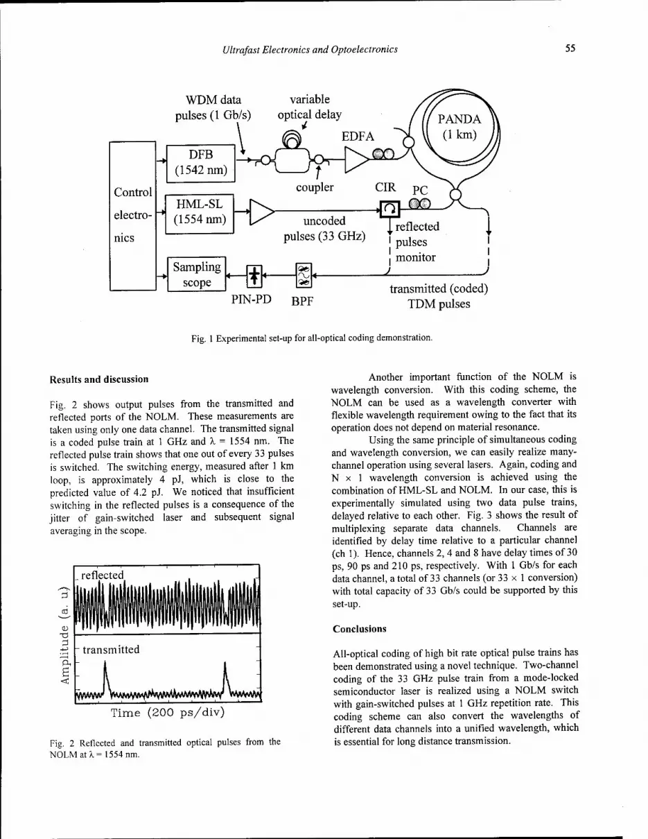
Ultrafast Electronics and Optoelectronics 55
Control
electro-
nics
WDM data pulses (1 Gb/s)
variable optical delay
DFB (1542 nm)
EDFA
W>H> HML-SL (1554 nm)
coupler
> uncoded pulses (33 GHz)
Sampling scope -ft
9»
reflected pulses monitor
J-. -J
PIN-PD BPF transmitted (coded)
TDM pulses
Fig. 1 Experimental set-up for all-optical coding demonstration.
Results and discussion
Fig. 2 shows output pulses from the transmitted and reflected ports of the NOLM. These measurements are taken using only one data channel. The transmitted signal is a coded pulse train at 1 GHz and \= 1554 nm. The reflected pulse train shows that one out of every 33 pulses is switched. The switching energy, measured after 1 km loop, is approximately 4 pJ, which is close to the predicted value of 4.2 pJ. We noticed that insufficient switching in the reflected pulses is a consequence of the jitter of gain-switched laser and subsequent signal averaging in the scope.
ft
reflected
transmitted
yvwwJ WM^/\M^^^^vw^^^
Time (200 ps/div)
Fig. 2 Reflected and transmitted optical pulses from the NOLM at X= 1554 nm.
Another important function of the NOLM is wavelength conversion. With this coding scheme, the NOLM can be used as a wavelength converter with flexible wavelength requirement owing to the fact that its operation does not depend on material resonance.
Using the same principle of simultaneous coding and wavelength conversion, we can easily realize many- channel operation using several lasers. Again, coding and N x 1 wavelength conversion is achieved using the combination of HML-SL and NOLM. In our case, this is experimentally simulated using two data pulse trains, delayed relative to each other. Fig. 3 shows the result of multiplexing separate data channels. Channels are identified by delay time relative to a particular channel (ch 1). Hence, channels 2, 4 and 8 have delay times of 30 ps, 90 ps and 210 ps, respectively. With 1 Gb/s for each data channel, a total of 33 channels (or 33 x 1 conversion) with total capacity of 33 Gb/s could be supported by this set-up.
Conclusions
All-optical coding of high bit rate optical pulse trains has been demonstrated using a novel technique. Two-channel coding of the 33 GHz pulse train from a mode-locked semiconductor laser is realized using a NOLM switch with gain-switched pulses at 1 GHz repetition rate. This coding scheme can also convert the wavelengths of different data channels into a unified wavelength, which is essential for long distance transmission.

56 Ultrafast Electronics and Optoelectronics
CO
-a
a,
ch2 tr_, c ch44l 1
v fv/w»>hr«*v
Ch8 ,
1 ! 1 1 1 1 1
time (200ps/div)
Fig. 3 Multiplexed channels for a simulated WDM-to-TDM conversion with a total capacity of 33 Gb/s.
Acknowledgments
M. R. H. Daza thanks the Department of Science and Technology (DOST) for the financial support during his stay at the University of Tokyo. The authors wish to thank Y. Ogawa of Oki Electric Industry Co Ltd. for providing us with the semiconductor laser.
''National Institute of Physics, University of the Philippines, Diliman, Quezon City 1101, Philippines. 2)Australian Photonics Cooperative Research Center, Photonics Research Laboratory, University of Melbourne, Parkville, Vic 3052, Australia.
References
[1] D. M. Spirit, A. D. Ellis, and P. E. Barnslet, "Optical time-division multiplexing: Systems and networks," IEEE Commun. Mag, 1994, 32, pp. 56-62.
[2] D. Y. Kim, M. D. Pelusi, Z. Ahmed, D. Novak H. F. Liu, and Y. Ogawa, "Ultra stable millimeter wave signal generation using hybrid mode-locking of a monolithic DBR laser," Electron. Lett, 1995, 31, pp. 733-734.
[3] T. Hoshida, H. F. Liu, M. R. H. Daza, M. Tsuchiya, T. Kamiya, and Y. Ogawa, "Generation of 33 GHz stable pulse trains by subharmonic electrical modulation of a monolithic passively mode-locked semiconductor laser," Electron. Lett, 1995, 32, pp. 572-573.
[4] K. J. Blow, N. J. Doran, B. K. Nayar, and B. P. Nelson, "Two-wavelength operation of the nonlinear fiber loop mirror," Opt. Lett, 1990,15, pp. 248-250.
[5] D. M. Patrick, A. D. Ellis, and D. M. Spirit, "Bit-rate flexible all-optical demultiplexing using a nonlinear optical loop mirror," Electron. Lett, 1993, 29, pp. 702-703.
[6] K. Uchiyama, S. Kawanishi, H. Takara, T. Morioka, and M. Saruwatari, "100 Gbit/s to 6.3 Gbit/s demultiplexing experiment using polarization- independent nonlinear optical loop mirror," Electron. Lett, 1994, 30, pp. 873-875.
Low latency, ultrafast fiber loop mirror switch using orthogonally polarized signal and control solitons
L. Leng, S. D. Koehler*, J. N. Kutz**, and K. Bergman Department of Electrical Engineering, Center for Photonics and Optoelectronic Materials, Princeton University,
Princeton, New Jersey 08544 TEL (609) 258-1174 FAX (609) 258-0463
*now with Telesis Technologies Laboratory San Ramon, CA 94583
**Program in Applied mathematics, Princeton University, Princeton, NJ 08544 and Bell Laboratories, Lucent Technologies and AT&T Research, Murray Hill, NJ 07974
Abstract
We present an ultrafast nonlinear optical loop mirror (NOLM) switch based on multiple collisions between orthogonally polarized signal and control solitons in highly birefringent optical fiber. The 8-m circumference switch has an on/off ratio of 80:1 and exhibits tolerance to timing jitter of 1.2 ps.
Key Words
Couplers, switches and multiplexers, Pulse propagation and solitons, Ultrafast all-optical devices.
Introduction
Since the nonlinear optical loop mirror (NOLM) was proposed as a device for ultrafast all-optical signal processing by Doran et al. [1], it has been extensively investigated. Because it is a fiber ring, the NOLM does not require interferometric alignment and is insensitive to changes in the linear refractive index due to temperature fluctuations and other environmental effects. The NOLM has been demonstrated as an ultrafast all-optical switch for high-speed optical time division multiplexed (TDM) systems [2,3] and shown to have wide applications in networks as a timing jitter recovery device [4], an optical logic gate [5,6], and as a wavelength/pulsewidth converter [7,8]. One of the main drawbacks of NOLMs has been the long fiber lengths required to implement complete switching due to the extremely small nonlinearity of silica fiber. Non-fiber nonlinear elements such as semiconductor amplifiers [9] have been employed to enhance the nonlinearity but have led to slower switching speeds and high cost.
NOLM based on soliton collisions
One solution is a NOLM design that employs multiple soliton-soliton collisions in highly birefringent,
polarization maintaining (PM) fiber to accumulate large nonlinear phase shifts in relatively short fiber lengths [10- 12]. Two orthogonally polarized soliton pulses can exchange a nonlinear phase shift when they collide in PM fiber but remain almost unaffected by the collision in terms of their temporal and spectral shapes, group velocities, and central frequencies if the exchanged phase shift is small compared to TC [10,11]. We have extensively modeled collisions between a continuous range of solitary wave control pulse energies up to fourth-order soliton energy and a first order signal soliton in PM optical fiber [12]. The results indicate that the pulse shape of the signal is virtually unaffected by the collision, as it acquires a collisional phase shift, A4>con, approximated by
AO 1.17 A 2IDIA2
coll5 (1) n An T
where X is the center wavelength, D is the dispersion parameter, A is the control pulse amplitude (normalized to N=l soliton) of the control pulse, An is the birefringence, and x is the temporal pulse full width at half maximum (FWHM). As might be expected, the nonlinear phase shift is proportional to the pulse peak power A2 and inversely proportional to the pulse width x, as high peak power and narrow pulse width incur large nonlinearity and therefore large nonlinear phase shift. We have experimentally and numerically confirmed the validity of the analytic expression of equation (1) in the A<3.5 regime [12]. At higher control pulse energies, Raman effects begin to adversely affect the switching.
Experiment
Based on our modeling, we have constructed the NOLM shown in Figure 1. A 3-dB PM fiber coupler splits the signal into two counterpropagating half-signals. A fiber polarizing beam splitter (PBS) introduces an othogonally polarized control pulse into the loop and a second fiber PBS extracts the control pulse. The loop consists of eight ~ 1-m-long fiber segments. We employ a cross-splicing
OSA TOPS on Ultrafast Electronics and Optoelectronics, 1997 Vol. 13, Martin Nuss and John Bowers (ed.) ©1997 Optical Society of America
57
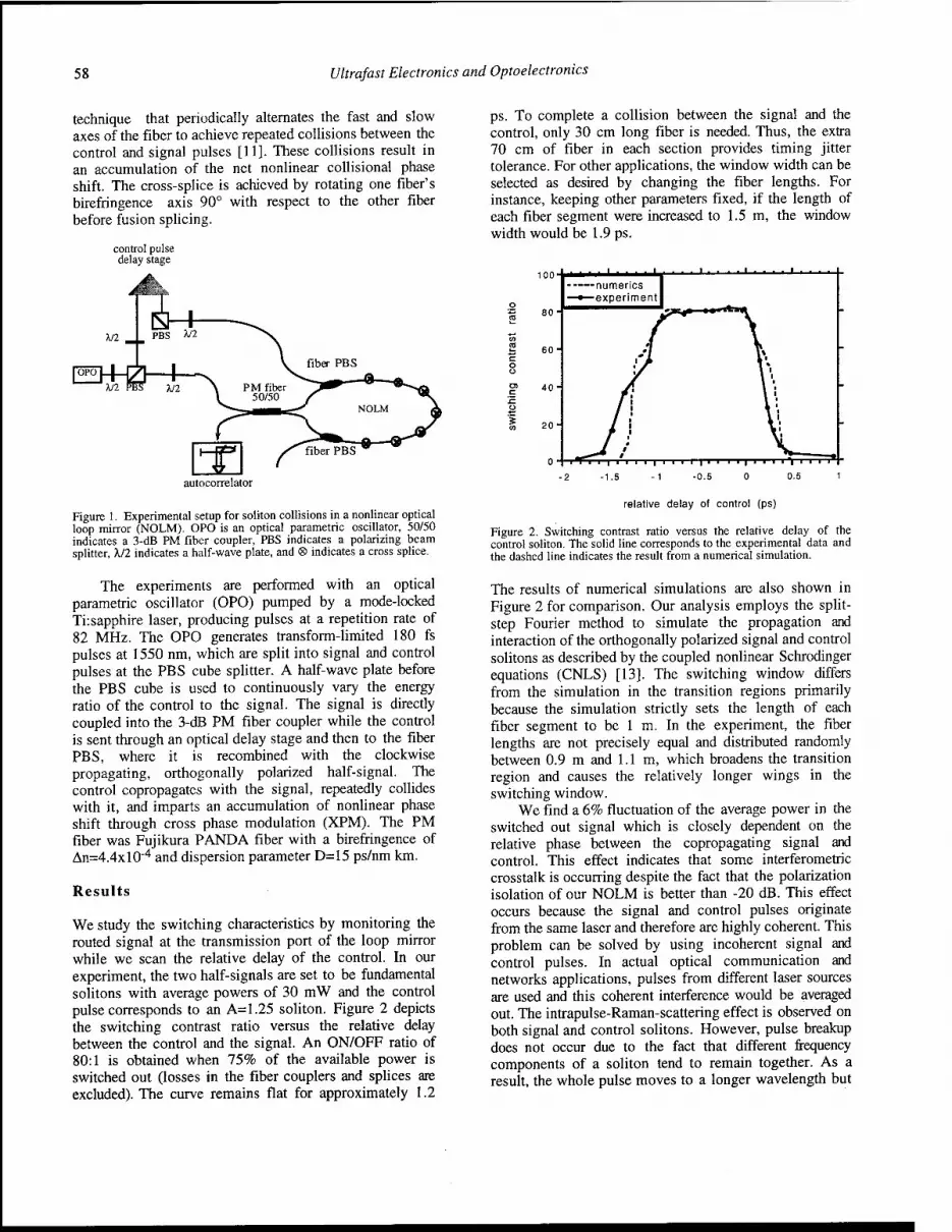
58 Ultrafast Electronics and Optoelectronics
technique that periodically alternates the fast and slow axes of the fiber to achieve repeated collisions between the control and signal pulses [11]. These collisions result in an accumulation of the net nonlinear collisional phase shift. The cross-splice is achieved by rotating one fiber's birefringence axis 90° with respect to the other fiber before fusion splicing.
control pulse delay stage
autocorrelator
Figure 1. Experimental setup for soliton collisions in a nonlinear optical loop mirror (NOLM). OPO is an optical parametric oscillator, 50/50 indicates a 3-dB PM fiber coupler, PBS indicates a polarizing beam splitter, X/2 indicates a half-wave plate, and ® indicates a cross splice.
The experiments are performed with an optical parametric oscillator (OPO) pumped by a mode-locked Ti:sapphire laser, producing pulses at a repetition rate of 82 MHz. The OPO generates transform-limited 180 fs pulses at 1550 nm, which are split into signal and control pulses at the PBS cube splitter. A half-wave plate before the PBS cube is used to continuously vary the energy ratio of the control to the signal. The signal is directly coupled into the 3-dB PM fiber coupler while the control is sent through an optical delay stage and then to the fiber PBS, where it is recombined with the clockwise propagating, orthogonally polarized half-signal. The control copropagates with the signal, repeatedly collides with it, and imparts an accumulation of nonlinear phase shift through cross phase modulation (XPM). The PM fiber was Fujikura PANDA fiber with a birefringence of An=4.4xl0'4 and dispersion parameter D=15 ps/nm km.
Results
We study the switching characteristics by monitoring the routed signal at the transmission port of the loop mirror while we scan the relative delay of the control. In our experiment, the two half-signals are set to be fundamental solitons with average powers of 30 mW and the control pulse corresponds to an A=1.25 soliton. Figure 2 depicts the switching contrast ratio versus the relative delay between the control and the signal. An ON/OFF ratio of 80:1 is obtained when 75% of the available power is switched out (losses in the fiber couplers and splices are excluded). The curve remains flat for approximately 1.2
ps. To complete a collision between the signal and the control, only 30 cm long fiber is needed. Thus, the extra 70 cm of fiber in each section provides timing jitter tolerance. For other applications, the window width can be selected as desired by changing the fiber lengths. For instance, keeping other parameters fixed, if the length of each fiber segment were increased to 1.5 m, the window width would be 1.9 ps.
100'
ra 40
relative delay of control (ps)
Figure 2. Switching contrast ratio versus the relative delay of the control soliton. The solid line corresponds to the experimental data and the dashed line indicates the result from a numerical simulation.
The results of numerical simulations are also shown in Figure 2 for comparison. Our analysis employs the split- step Fourier method to simulate the propagation and interaction of the orthogonally polarized signal and control solitons as described by the coupled nonlinear Schrodinger equations (CNLS) [13]. The switching window differs from the simulation in the transition regions primarily because the simulation strictly sets the length of each fiber segment to be 1 m. In the experiment, the fiber lengths are not precisely equal and distributed randomly between 0.9 m and 1.1m, which broadens the transition region and causes the relatively longer wings in the switching window.
We find a 6% fluctuation of the average power in the switched out signal which is closely dependent on the relative phase between the copropagating signal and control. This effect indicates that some interferometric crosstalk is occurring despite the fact that the polarization isolation of our NOLM is better than -20 dB. This effect occurs because the signal and control pulses originate from the same laser and therefore are highly coherent. This problem can be solved by using incoherent signal and control pulses. In actual optical communication and networks applications, pulses from different laser sources are used and this coherent interference would be averaged out. The intrapulse-Raman-scattering effect is observed on both signal and control solitons. However, pulse breakup does not occur due to the fact that different frequency components of a soliton tend to remain together. As a result, the whole pulse moves to a longer wavelength but
Ultrafast Electronics and Optoelectronics 59
remains as a unit without noticeable distortion in the pulse shape.
A pulse train with deconvolved widths of -180 fs (a sech shape is assumed) are regenerated at the transmission port of the 3-dB coupler. The autocorrelation traces of the switched out signal is shown in Figure 3 (dotted curve). It closely matches the autocorrelation trace of the original OPO pulse (solid line), clearly illustrating that the switched out signal is fully recovered and corresponds to a first order soliton.
3C -—switched/off
OPO pulse
• switched/on
!■■■■!«*«
_J_ J_ _L _l_
-800 -600 -400 -200 0 200 400 600 800
time (fs)
Figure 3. Autocorrelation traces of the switched signal pulse measured at the transmission port of the 3-dB fiber coupler. The dashed line: control pulse absent. The dots: control pulse present. The autocorrelation of the original OPO pulses (solid line) is presented for comparison.
Conclusion
In conclusion, we have achieved an ON/OFF ratio of 80:1 with a cross-spliced NOLM. Since the collision interaction length is 30 cm and can occur anywhere within the individual fiber sections, the NOLM is fairly tolerant to timing jitter between the control and the signal pulses. In our case, each fiber segment is approximately 1 m and the entire loop is only 8 m long. We have demonstrated timing jitter tolerance of 1.2 ps by scanning the relative delay of the control and obtained an ON/OFF switching ratio of 80:1.
Acknowledgments
We would like to acknowledge support from the National Science Foundation (ECS-9502491) and the Office of
Naval Research (N00014-96-1-0773). INK acknowledges support from the National Science Foundation for University-Industry Postdoctoral Fellowship (DMS- 9508684).
References
1. N. J. Doran and David Wood, "Nonlinear-optical loop mirror," Opt. Lett. 13, 56(1988).
2. P. A. Andrekson, et al., "64 Gb/s all-optical demultiplexing with the nonlinear optical loop mirror," IEEE Photon. Technol. Lett. Vol.4, p.644, 1992.
3. M. L. Dennis, M. F. Arend, and I. N. Ill, "Soliton loop mirror demultiplexer using orthogonally polarized signal and control," IEEE Photon. Technol. Lett. Vol.8, p.906, 1996.
4. M. Eiselt, W. Pieper, and H. G. Weber, Electron. Lett., Vol. 28, p. 1350, 1992.
5. K. L. Hall and K. A. Rauschenbach, paper WH3, p. 133, OFC Technical Digest (1996).
6. M. N. Islam, "All-optical cascadable NOR gate with gain," Opt. Lett. 15, 417(1990).
7. K. J. Blow, N. J. Doran, B. K. Nayar, and B. P. Nelson, Opt. Lett. 15, 248(1990).
8. K. A. Rauschenbach, K. L. Hall, J. C. Livas, and G. Raybon, "All-optical pulse width and wavelength conversion at 10 Gb/s using a nonlinear optical loop mirror," IEEE Photon. Tech. Lett. Vol. 6, No. 9, p.1130, 1994.
9. M. Eiselt, W. Pieper, H. G. Weber, "All-optical high speed demultiplexing with a semiconductor laser amplifier in a loop mirror configuration," Electron. Lett., Vol. 29, p. 1167-1168, 1993.
10. J. D. Moores, K. Bergman, H. A. Haus, and E. P. Ippen, "Demonstration of optical switching by means of solitary wave collisions in a fiber ring reflector," Opt. Lett. 16, 138(1991).
11. J. D. Moores, K. Bergman, H. A. Haus, and E. P. Ippen, "Optical switching using fiber ring reflectors," J. Opt. Soc. Am. B, 8, 594(1991).
12. J. N. Kutz, S. D. Koehler, L. Leng and K. Bergman, "Analytic study of orthogonally polarized solitons interacting in highly birefringent optical fibers," J. Opt. Soc. Am. B(to be published).
13. C. R. Menyuk, "Pulse propagation in an elliptically birefringent Kerr medium," IEEE J. Quantum Electron., QE-25, 2674 (1989).
A Nonlinear Fiber-Optic Thresholder for Spectrally Coded Ultrashort Pulses with 36 dB Extinction Ratio
H. P. Sardesai and A. M. Weiner School of Electrical and Computer Engineering
Purdue University West Lafayette, Indiana 47907-1285
Abstract
We report experimental results on a nonlinear fiber-optic receiver which uses the Raman self-frequency shift effects in optical fibers to perform intensity thresholding with femtosecond response times. The receiver exhibits a contrast ratio of 36 dB for received pulse energies of ~ 1 pj.
Key Words
Raman effects, thresholders, optical fibers, receivers.
Summary
Optical Code Division Multiple Access (CDMA) communication systems are an interesting choice for local area optical networks due to their unique attributes of optical processing, asynchronous transmission, high information security and the capability for multiple access which results in high overall data transmission rates [1]. Here we report results on a nonlinear fiber-optic receiver for an optical CDMA scheme based on encoding and decoding of coherent ultrashort pulses. As proposed previously [1], ultrashort pulse CDMA transmitters would use a spectral phase encoder to convert input femtosecond pulses into a low intensity pseudonoise burst. Multiple- access would be accomplished by assigning different, minimally interfering phase codes to different users. Correctly coded signals are converted back into femtosecond pulses by a spectral phase decoder in the CDMA receiver, while incorrectly coded signals remain as low intensity pseudonoise bursts. The desired data can be then detected using a nonlinear optical thresholder. The
key requirement for the ultrashort pulse CDMA receiver/ thresholder is the ability to discriminate between properly decoded femtosecond pulses and the equally energetic but improperly decoded picosecond interference signals. We describe such a receiver which uses intensity dependent nonlinear frequency shift effects (Raman effects) in optical fibers to achieve thresholding with a high contrast ratio of nearly 36 dB for received pulse energies as low as ~ lpJ. To our knowledge, these are the first experiments demonstrating a high contrast thresholder for ultrafast optical pulses.
The Raman effect on ultrashort optical pulses propagating in silica fibers and the resulting soliton self frequency shift effect have been quite well investigated [2,3]. An optical intensity dependent switch using the soliton self-frequency shift has also been reported [4]. Although the soliton self frequency shift effect is considered a detrimental effect in high bit rate communication systems since it is a potential source of jitter, its pulse-width and intensity dependent frequency conversion characteristics can be exploited to perform a new function, namely thresholding, for an ultrashort pulse CDMA receiver. A block diagram of the receiver is shown in fig. 1. Input pulses to the experiment are generated by a stretched pulse modelocked fiber ring laser [5] and are spectrally filtered to yield pulse durations of
Filtered input pulses
\ Two-Stage Chirped Pulse Er+3
Amplifier
Decoder _| (Pulse |4
Shaper)
Passive Fiber
Spectral Filter & Photodetector
Output
i Nonlinear Thresholder
Figure 1. Block diagram of experimental arrangement
OSA TOPS on Ultrafast Electronics and Optoelectronics, 1997 Vol. 13, Martin Nuss and John Bowers (ed.) C/1997 Optical Society of America
60

Ultrafast Electronics and Optoelectronics 61
~ 275 fs with a repetition rate of ~ 30 MHz and an average power 30 |iW. These pulses are amplified by ~ 27 dB by a two stage chirped pulse (CPA) erbium doped fiber amplifier. Unlike previous fiber CPA experiments [6], here we use a dispersion compensating fiber for the pulse compression stage. The combined effects of gain narrowing in the amplifier and fiber nonlinearities in the compression stage broadens the pulses to ~ 1 ps with a spectral bandwidth of - 3 nm centered at 1559 nm. The amplified pulses are then passed through a fiber pigtailed pulse shaper containing a multi-element liquid crystal phase modulator as a programmable spectral encoder [7]. We have measured the fiber-to-fiber insertion loss as low as 5.7 dB. Although fiber pigtailed pulse shapers have been previously demonstrated for WDM applications [8], to our knowledge, this is the first demonstration of fiber pigtailed pulse shaping for actual time domain pulse shaping experiments. The spectral phases are set either to a length 63 m-sequence pseudorandom phase code which encodes the pulses into 10 -12 ps wide pseudorandom bursts or held constant leading to unchanged ~ lps uncoded pulses.
Coded or uncoded pulses from the pulse shaper are connected to the nonlinear thresholder which is simply a 340 m length of optical fiber with zero dispersion wavelength Xo ~ 1547 nm followed by a long pass filter and photodetector. The nonlinear Raman self-frequency shift effect causes the mean wavelength of the high intensity shorter duration uncoded pulse to shift to a longer wavelength [2,3]. The magnitude of the spectral shift can be controlled by varying the intensity, pulse duration, and propagation distance through the fiber. The coded pulse with a lower intensity and larger time duration propagates through the same length of the thresholder fiber but exhibits negligible spectral shifts. Figs. 2 (c) and 2 (d) show the power spectral data for 1.84 mW average power in the thresholder fiber clearly revealing the differences in the output spectra for coded and uncoded pulses. The input spectra at the same power levels are shown in Figs. 2(a) and 2(b) for comparison. These frequency shifts are converted into a contrast in energy by using a long wavelength pass filter followed by a slower photodetector operating at speeds comparable to the repetition rate of the system. By optimally choosing the average power and the filter cutoff wavelength a high contrast ratio between coded and uncoded pulses is obtained as shown in Fig. 3 for a fixed m-sequence code. A contrast ratio of nearly 36 dB is achieved for a 1577 nm cutoff wavelength and 1.84 mW average power. In the future we intend to use these thresholders in system experiments testing ultrashort pulse CDMA systems over distances suitable for local area networks.
1
I i2 0.8 c 3
(b)
xi 0.6 CO
£0.4 c <D c0.2 . J .
1520 1540 1560 1580 1600 wavelength (nm)
1520 1540 1560 1580 1600 wavelength (nm)
1
J2Ü.8 c 3
(d) I f 0.6 a
£0.4 10 c <D
10.2 K 1520 1540 1560 1580
wavelength (nm) 1600 1520 1540 1560 1580 1600
wavelength (nm)
Figure 2. (a) power spectrum of the coded signal at the input of the nonlinear thresholder, (b) power spectrum of the uncoded signal at the input of the nonlinear thresholder. (c) and (d) power spectrum at the output of the thresholder corresponding to (a) and (b) respectively. Average power in the nonlinear thresholder fiber is 1.84 mW for each case.
40
35
30
-1571nm
1.2 1.4 1.6 average power (mW)
2.2
Figure 3. Contrast ratio of the nonlinear receiver for different cut-off wavelengths of the long wavelength pass filter as a function of average signal power in the thresholder fiber.

62 Ultrafast Electronics and Optoelectronics
Acknowledgments
We would like to acknowledge C. C. Chang for building the fiber ring laser and I. Duling for helpful discussions related to erbium amplifiers. This work was supported by the National Science Foundation under grants ECS - 9626967 and ECS- 9312256.
References
1. A. M. Weiner, ''Femtosecond optical pulse shaping and processing," Progress in Quantum Elect. 19, pp. 161- 237, (1995).
2. F. M. Mitschke & L. F. Mollenauer, "Discovery of the soliton self-frequency shift," Opt. Lett, U, pp. 659- 661, (1986).
3. K. J. Blow & D. Wood, "Theoretical Description of Transient Stimulated Scattering in Optical Fibers," IEEE J. Quantum Electron. 25, pp. 2665-2673, (1989).
4. J. K. Lucek & K. J. Blow, "Optical-Intensity Dependent Switching Using Soliton Self-Frequency Shift," Elect. Lett. 27, pp. 882-884, (1991).
5. Tamura, E. P. Ippen, H. A. Haus and L. E. Nelson, "77-fs pulse generation from a stretched-pulse mode- locked all-fiber ring laser," Opt. Lett. 18, pp. 1080- 1082, (1993).
6. A. Galvanauskas, M. E. Fermann, & D. Harter, "High power amplification of femtosecond optical pulses in a diode-pumped fiber system." Opt. Lett. 19, pp. 1201- 1203, (1994).
7. A. M. Weiner, D. E. Leaird, J. S. Patel, & J. R. Wullert, "Programmable Shaping of Femtosecond Optical Pulses by use of 128-Element Liquid Crystal Phase Modulator," IEEE J. Quantum Electron. 28, pp. 908-920, (1992).
8. J. E. Ford, J. A. Walker, M. C. Nuss & D. A. B. Miller, "32 Channel WDM Graphic Equalizer," Summer Topical Meeting on Broadband Networks, (IEEE/LEOS, Keystone, CO, 1996).

Optical Receiver Sensitivity Improvement by Impulsive Coding
L. Boivin, M. C. Nuss, J. Shah, D. A. B. Miller, H. A. Haus Bell Labs, Lucent Technologies, 101 Crawfords Corner Road, Room 4B-433, Holmdel, New Jersey 07733,
phone: (908) 949-9406, FAX: (908) 949-2473; [email protected]
ABSTRACT- Impulsive operation of receivers is shown to result in better sensitivities compared to NRZ. We show that contrary to conventional wisdom, the optimum detection bandwidth for impulsive coding is larger than for NRZ.
KEY WORDS: Optical receiver, ultrafast technology.
Introduction
Non-return-to-zero (NRZ) coding, in which optical pulses occupy a full bit period, is the most widely used format in optical fiber communication. The popularity of NRZ stems, in part, from its minimum use of electronic bandwidth to modulate the output of a continuous-wave laser at a given bit rate. New transmitters using modelocked lasers are however being considered for which "impulsive coding" is a more natural format. Contrary to NRZ, the optical power of an impulsively encoded pulse train occupies only a small fraction of the bit periods (Fig.l).
optical power
optical power
NRZ
_t
10 110 0
Impulsive
time
10 110 0 time
Figure 1: Pictorial representation of NRZ and impulsively encoded optical data streams. T is the bit period.
In this paper, we show that impulsive coding results in better receiver sensitivities compared to NRZ. We report impulsive sensitivity improvements as large as 4.7 dB and 5.8 dB for two pin-FET front-ends [1]. These values are in good agreement with a model of the response and noise characteristics of the receivers. They also confirm a
prediction by Personick that the impulse excitation of a receiver produces the best signal-to-noise ratio for a given pulse energy [2]. As explained below, however, we find the Personick theory to be of limited help in predicting quantitatively the magnitude of the impulsive sensitivity improvement for specific receiver front-ends. In addition to being ambiguous, it suggests that the optimum receiver bandwidth for impulsive detection is narrower than for NRZ. contrary to what we find experimentally.
Receiver Model
The origin of the improved sensitivity achieved with impulsive coding can be understood qualitatively from an /?C-circuit model of the receiver front-end. The 3 dB bandwidth of the circuit shown in Figure 2 is
I
pinTC— |R
V™
Figure 2: Simple RC model of a receiver front-end.
For NRZ, the input photocurrent, /, is either 0 or r0,
depending on the logical state transmitted (binary 0 or binary 1 respectively). These levels define two input voltage values, 0 and Ri0 respectively, between which Vin
transits with a time constant given by the RC product of the front-end (Figure 3). These asymptotic values are reached for long strings of zeros or ones, when the photocurrent is essentially DC and flows entirely through the resistor. For impulsive coding, the photocurrent is a series of delta functions in time, weighted by the photocharge per bit, i0/B, which is the same as for NRZ. This photocharge
appears suddenly at one terminal of the capacitor, creating a voltage swing i0/BC. This value is 3.63 f3dB/B times
larger than the peak NRZ input voltage. The larger signal obtained with impulsive coding translates into better receiver sensitivities.
OSA TOPS on Ultrafast Electronics and Optoelectronics, 1997 Vol. 13, Martin Nuss and John Bowers (ed.) ©1997 Optical Society of America
63
64 Ultrafast Electronics and Optoelectronics
Photocurrent: Voltage swing:
It
NRZ
r^T" "i—i
Vi,, NRZ
RL
1 0 1 time time
Imp. B *)
Imp. BC B
time 1 0 1 tlme
Figure 3: Input photocurrent and corresponding input voltage for NRZ and impulsive coding. B is the bit rate.
Although qualitatively correct, the RC model presented above overestimates the impulsive signal enhancement factor by 60 to 70 percent for standard pin-FET transimpedance receivers. To obtain better quantitative agreement of our model with experiment, we consider the transimpedance circuit of Figure 4.
e-e- .R
-A(f)
"out
Figure 4: Equivalent circuit of a transimpedance front-end. Cs is
the shunt capacitance across the feedback resistor. ia and ib are
current noise sources discussed in the text.
The transfer function for this circuit is [3]:
Rjn(f)Mf) "(/)=- (1)
l + j2xfCT(f)Rin(f)
where the open-loop gain is A{f) = AQ/{{ + j f / f0), and
where we defined the functions /?,„(/) = R/(l + A(f)) and
CT(f)=Cin+(l + A(f))Cs. The Fourier transform of
//(/) is a damped sinusoidal function of the form:
h{t) = /iQ0(f)exp t
i(fity). (2)
where 6{t) is the step function. Expressions for h^, t0
and C0Q in terms of circuit parameters can be found in [4].
Increasing the feedback amplifier bandwidth reduces the oscillation frequency ü)0, which becomes imaginary for a
very fast preamplifier. In general however, the open-loop bandwidth is such that the "ringing" parameter, x0 = a)0t0 , is
close to unity. The output voltage for any optical excitation is obtained by convolution of the corresponding photocurrent with h(t). The output voltage for a short
pulse excitation, for example, is ioh(t)/B. Figure 5 shows
excellent agreement between this expression and the voltage measured at the output of a 140 MHz pin-FET front-end (see next section).
5 10 time (ns)
15
Figure 5: Measured and modeled output voltage of a Lasertron QDFB-100 pin-FET receiver front-end excited with a short pulse. The parameters R = 321kQ , Cin =\pf , Cs=54fF, AQ=\2Q,
and /0 = 23MHz correspond to a 140 MHz bandwidth.
Using (1) and (2), the peak of ioh(t)/B can be related to the
peak output voltage for NRZ , Vp*f=-RiQ, by the
relation:
C£ = K*o)^C? (3)
where 7<^)=l) = 1.2^/v3 . Figure 6 shows that y depends
only weakly on xQ. As for the /?C-circuit model, the
impulsive signal grows linearly with the receiver bandwidth. The present model, however, estimates correctly the proportionality constant y, which is indeed 60 percent less than the value predicted by the RC model (i.e. 3.63).
Y""
/ 2.15- ' 1 1 1 , ,
1.2A-
Figure 6: Proportionality factor y appearing in Eq. (3), as a
function of the "ringing" parameter x0 .
In fact, we find that, as long as eq. (3) is obeyed with y = 2.17, the exact temporal shape of the receiver impulse
function is not crucial to the evaluation of signal-to-noise ratios. One can use, for example, the impulse function of an flC-circuit, h(t) = -(R9(t)/r)exp(rt/ r), and simply
scale down the predicted impulsive signal by 60 percent. This simpler impulse function allows to find closed-form expressions for the impulsive and NRZ inter-symbol interference penalties by considering only the receiver response to the words "...0001000..." and "...1110111..."
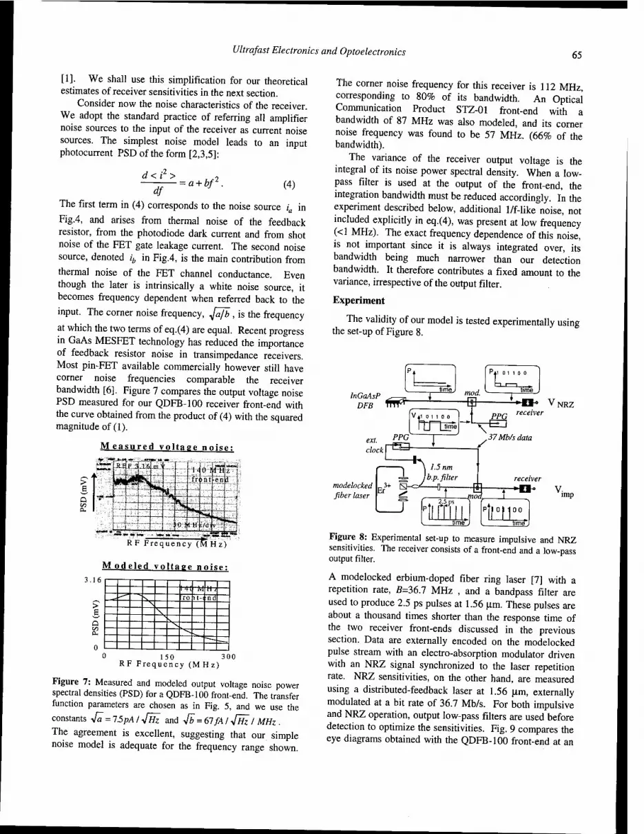
Ultrafast Electronics and Optoelectronics 65
[1]. We shall use this simplification for our theoretical estimates of receiver sensitivities in the next section.
Consider now the noise characteristics of the receiver. We adopt the standard practice of referring all amplifier noise sources to the input of the receiver as current noise sources. The simplest noise model leads to an input photocurrent PSD of the form [2,3,5]:
d<i2>
df = a + bf (4)
The first term in (4) corresponds to the noise source ia in
Fig.4, and arises from thermal noise of the feedback resistor, from the photodiode dark current and from shot noise of the FET gate leakage current. The second noise source, denoted ib in Fig.4, is the main contribution from
thermal noise of the FET channel conductance. Even though the later is intrinsically a white noise source, it becomes frequency dependent when referred back to the
input. The corner noise frequency, Ja[b , is the frequency
at which the two terms of eq.(4) are equal. Recent progress in GaAs MESFET technology has reduced the importance of feedback resistor noise in transimpedance receivers. Most pin-FET available commercially however still have corner noise frequencies comparable the receiver bandwidth [6]. Figure 7 compares the output voltage noise PSD measured for our QDFB-100 receiver front-end with the curve obtained from the product of (4) with the squared magnitude of (1).
M easured volta ee noise:
RE F3 .16 '.mJ ' 1 01 t-Hjz \
> >nt •enu
Q 1/3
"'
V |" - -1H tli\ ?° ' •£•• » «• ■ •— »♦ •*» 3 wHllxi
RF Frequency (M Hz)
Modeled voltage noise: 3.16
Q on a.
141 "M tt-J V TO )t-< nd
S S,
■• *, "v
.
0 150 300 RF Frequency (MHz)
Figure 7: Measured and modeled output voltage noise power spectral densities (PSD) for a QDFB-100 front-end. The transfer function parameters are chosen as in Fig. 5, and we use the
constants yfa = 7.5 pA I 4H~Z and S=61fAI V#z / MHz .
The agreement is excellent, suggesting that our simple noise model is adequate for the frequency range shown.
The corner noise frequency for this receiver is 112 MHz, corresponding to 80% of its bandwidth. An Optical Communication Product STZ-01 front-end with a bandwidth of 87 MHz was also modeled, and its corner noise frequency was found to be 57 MHz. (66% of the bandwidth).
The variance of the receiver output voltage is the integral of its noise power spectral density. When a low- pass filter is used at the output of the front-end, the integration bandwidth must be reduced accordingly. In the experiment described below, additional 1/f-like noise, not included explicitly in eq.(4), was present at low frequency (<1 MHz). The exact frequency dependence of this noise, is not important since it is always integrated over, its bandwidth being much narrower than our detection bandwidth. It therefore contributes a fixed amount to the variance, irrespective of the output filter.
Experiment
The validity of our model is tested experimentally using the set-up of Figure 8.
InGaAsP *-*r DFB TTTr^
modelocked fiber laser
HB" VNRZ
imp
Figure 8: Experimental set-up to measure impulsive and NRZ sensitivities. The receiver consists of a front-end and a low-pass output filter.
A modelocked erbium-doped fiber ring laser [7] with a repetition rate, ß=36.7 MHz , and a bandpass filter are used to produce 2.5 ps pulses at 1.56 urn. These pulses are about a thousand times shorter than the response time of the two receiver front-ends discussed in the previous section. Data are externally encoded on the modelocked pulse stream with an electro-absorption modulator driven with an NRZ signal synchronized to the laser repetition rate. NRZ sensitivities, on the other hand, are measured using a distributed-feedback laser at 1.56 u.m, externally modulated at a bit rate of 36.7 Mb/s. For both impulsive and NRZ operation, output low-pass filters are used before detection to optimize the sensitivities. Fig. 9 compares the eye diagrams obtained with the QDFB-100 front-end at an

66 Ultrafast Electronics and Optoelectronics
average power of -46dBm for NRZ and for impulsive coding. These data clearly show a larger eye opening in the case of impulsive coding.
>
>
o CO
time
Tm 9^ lsi ̂ £-
T3
> . i i i i i i
bi
1 JiW/l re— 1 >•
J I15>/U U \
-56 -54 -52 -50 -48 Received Power (dBm)
46
Figure 9: NRZ and impulsive eye diagrams obtained with the QDFB-100 front-end for an optical power of -46 dBm. The inset on the NRZ panel shows the same eye diagram with a 10X resolution. 22 MHz and 300 MHz low-pass filters are used at the output of the receiver front-end for NRZ and impulsive coding respectively. The lower panel compares the bit-error rata curves for both types of coding.
Figure 9 also compares the bit-error rate curves obtained with this front-end using either types of coding. As can be seen an impulsive sensitivity improvement of 5.8 dB is found in this case. The PRBS pattern length used for these
measurements is 2n-l. Table 1 summarizes our experimental results and shows good agreement with our
model. TABLE 1- TN/1PITT STVF. SENSITIVITY IMPROVEMENTS r-=r—. rr—i TT^5 1 i i^i,^ Moaci ir»H Prprtifter
Front-end
STZ-01
QDFB 100
" Output filter bandwidth
(MHz)
22
300
Detection bandwdth
(MHz)
22
_az_ 22 300
NRZ sensitivity
(dBm)
-44.8
22
140
Impulsive sensitivity
(dBm
-49.5
-45.4
Measured improvement
(dB)
4.7
-51.2 5.8
Predicted improvement
(dB)
4.3
5.7
The Personick Theory
As already mentioned, Personick predicted that short input pulses produce better receiver sensitivities than long ones [2]. The Personick-Smith (PS) theory [2,5] is however of limited use for a quantitative analysis of the impulsive sensitivity improvement for actual receivers. A central feature of the this approach is its use of a fixed raised- cosine output voltage for any input pulse. This restriction greatly simplifies the analysis of receiver sensitivity as it eliminates completely the effect of inter-symbol interference. Even though approximate, this theory was found useful due to its mathematical simplicity and to its reasonable agreement with experiment. The PS theory has however come under scrutiny recently [4]. For our purpose, a comparison of NRZ and impulsive coding sensitivities based on the PS theory would be a comparison between different receiver circuits. It is clear for example that very different receiver transfer functions are required to connect the two input pulse trains of Fig.l to the same output voltage waveform. Another problem of the PS theory is that, strictly speaking, no physical receiver can generate a raised-cosine extending over the whole time axis as this would require a non-causal impulse response. Finally, as one might expect, different choices of raised- cosine outputs (i.e. different values for the parameter ß in [5]) lead to different predictions for the impulsive sensitivity improvement. In this sense, the PS theory is ambiguous. The approach adopted in this paper is based on a pre-specified receiver circuit, and does not suffer from the above problems.
It is generally believed that the optimum receiver bandwidth for RZ coding is narrower than the optimum receiver bandwidth for NRZ. This belief, based on the PS theory, is predicated on the simple observation that shorter input pulses require less receiver bandwidth to achieve a given output pulse shape [8]. Our measurements, however, contradict this conventional wisdom, the optimum impulsive receiver sensitivities being always obtained with little filtering at the output of the front-end. The best NRZ sensitivities, on the other hand, are obtained with detection bandwidths on the order of 60% of the bit rate. As Figure 10 shows, our receiver model predicts the correct dependence of the receiver sensitivity on the detection bandwidth for either NRZ or impulsive coding. The front- end in this Figure is fixed, and we varied the bandwidth of the low-pass output filter. The optimum filter for NRZ has a bandwidth of 22 MHz, whereas the impulsive one is nearly opened (300 MHz bandwidth).
Consider first the behavior of the NRZ curve. As long as the output filter bandwidth is much larger than the bit rate, the output voltage reaches its top or bottom rails (
V™zk and 0 respectively) in every bit period. Tighter
filtering in this case reduces the noise bandwidth without

Ultrafast Electronics and Optoelectronics 67
affecting the signal, leading to better sensitivities. When the output filter bandwidth falls below the bit rate, the output voltage for isolated "1" and "0" cannot quite reach the top and bottom rails, leading to inter-symbol interference. The reduction of the noise bandwidth is then increasingly offset by a reduction in signal, leading to a minimum in the sensitivity curve. The filter bandwidth at which this minimum occurs depends on the exact frequency dependence of the noise. It is 37 % of the bit rate when the corner noise frequency is zero, and 68 % of the bit rate when the quadratic noise term in eq.(4) is absent [1].
E m •a
0 100 200 300 400 500 600 Low-Pass Filter Bandwidth (MHz)
Figure 10: Sensitivity of the STZ-01 receiver front-end (87 MHz bandwidth) for NRZ and impulsive coding as a function of the output low-pass filter bandwidth. The curves are predictions from our model and the squares and circles are actual measurements for NRZ and impulsive coding respectively.
The situation for impulsive coding is quite different since, in this case, the signal itself depends linearly on the receiver bandwidth. In the limiting case where the front- end input current noise is white (infinite corner noise frequency), the root-mean-square deviation of the voltage fluctuations increases only with the square root of the receiver bandwidth. In this limit, the impulsive signal-to noise ratio increases with the square root of the detector
bandwidth! The presence of f2 noise in eq. (4) however produces a faster increase of receiver noise with bandwidth for realistic receivers, leading to a finite value for the optimum impulse receiver bandwidth. It can be shown, nevertheless, that for any noise corner frequency, the optimum impulsive bandwidth is larger than the corresponding NRZ one [1].
The two receiver front-ends considered here clearly have excess bandwidth for NRZ operation at 37Mb/s. Typical NRZ receiver front-ends have a bandwidth roughly equal to 80% of the bit rate to allow for component variation and aging. In addition, their corner noise frequency is about 75% of their bandwidth. For these conditions, our model predicts an impulsive sensitivity improvement of 2.5 dB.
Conclusions
We observe large sensitivity improvements (5.8 dB and 4.7 dB) for two pin-FET receivers operated impulsively at 37 Mb/s. These measurements are well described by a simple model of the receiver response and noise characteristics. Contrary to what is suggested by the Personick-Smith theory, the optimum impulsive receiver bandwidth is found to be larger than the corresponding NRZ one. We finally note that the concept of short pulse excitation has also been investigated in the context of nuclear instrumentation [9] and optical interconnections [10]
Acknowledgments
The authors acknowledge discussions with B. Kasper, M. Zirngibl, G. L. Miller, T. van Muoi and Y. Ota. We are also grateful to U. Koren, R. E. Behringer, and K. Dreyer for their help with the DFB laser. L. B. acknowledges support from NSERC of Canada.
References
[1] L. Boivin, M. C. Nuss, J. Shah, D. A. B. Miller, and H. A. Haus, "Receiver sensitivity improvement by impulsive coding", IEEE Photon. Techn. Lett., Vol. 9, May 1997 [2] S. D. Personick, "Receiver design for optical fiber systems", Bell Syst. Tech. Journ., vol. 52, 843 (1973) [3] J. L. Hullett, and T. V. Muoi, "A feedback receive amplifier for optical transmission systems", IEEE Trans. Commun., COM-24, 1180-1185 (1976) [4] J. J. Morikuni, A. Dharchoudhury, Y. Leblebici, and S. M. Kang, "Improvements to the standard theory for photoreceiver noise", J. Lightwave Technol, LT-12, 1174- 1184(1994) [5] R. G. Smith, and S. D. Personick, "Receiver design for optical fiber communication systems", in Topics in Applied Physics, 39, 89-160, H. Kressel, Ed (Springer-Verlag, New York, 1980) [6] T. V. Muoi, "Receiver design for high-speed optical fiber systems", J. Lightwave techn. LT-2, 243-267 (1984) [7] G. Lenz, K. Tamura, H. A. Haus, and E. P. Ippen, " All-solid-state femtosecond source at 1.55 |im" , Opt. Lett. 20, 1289-1291 (1995) [8] B. Kasper, "Receiver design", in Optical Fiber Telecommunication II, Edited by S. E. Miller and I. P. Kaminow, pp. 689-722 (Acadamic Press, San Diego 1991) [9] E. Gatti and P. F. Manfredi, "Processing the signal from solid-state detectors in elementary particle physics", Riv. Nuevo Cimento, 9, 1-146 (1986) [10] A. L. Lentine, L. M. Chirovsky, and T. K. Woodward, "Optical Energy considerations for diode- clamped smart pixel optical receivers", IEEE j. Quantum Electron., 30, 1167-1170 (1994)

Optimal control of femtosecond solitons in fiber amplifier.
V. Y. Khasilev 344090, Rostov on Don, Russia,
Abstract
Theory of optimal control of distributed me- dia is applyed for optimization of soliton prop- agation in optical-fiber amplifier. The goal of optimization was to eliminate nonsoliton radi- ation which arises during soliton amplification and disturbs the soliton sequence. Analytical solution of optimal control problem describing ideal soliton amplification was obtained. Meth- ods of optimal control may be applyed to other high bit rate nonlinear optical communication
systems. Key Words: Fiber optics-amplifiers, Soli-
tons, Optimal control
0.1 Introduction
Use of femtosecond soliton pulses in optical fiber communication systems may lead to ultra- high transmission rates. Optical solitary waves enable the localized pulse to propagate through the fiber without distortion due to dispersion effect [1]. However, soliton pulses can become distorted as a result of fiber loss. Methods for handling fiber loss use all-optical amplifiers to strengthen the soliton every several of tens of kilometers. The propagation of soliton pulses in lossless optical fiber can be described by non- linear Schroedinger equation (NSE) which may be solved using Inverse Scattering Transform (1ST) method. When soliton propagate in the
optical fiber with inserted optical amplifiers, it lose their ideal soliton shape due to amplifica- tion and nonsoliton radiation appears. A topic of particular interest is the development of the methods of the theory of optimal control of distributed media for the nonlinear equations solvable by the 1ST method. In this paper we report the solution to the problem which de- scribe the amplification of the solitons by op- timal manner without formation of nonsoliton radiation. The idea of the method is to choose the spatial dependence of the gain coefficient so that the amplified solitary wave remains an exact soliton at each point of fiber amplifier.
0.2 Balance of energy in fiber- optical amplifier
When soliton propagated in lossy fiber, and loss are small, the process is adiabatically slow, and the pulse is soliton in each point of fiber-optical amplifier. In other words, decrease of ampli- tude and increase of width of pulse are self- consistent and pulse can be considered as soli- ton with slowly varying parameters. However, when soliton is amplified in fiber-optical ampli- fier, the gain may be considerable, and increase of amplitude is quick. But, soliton cannot de- crease its width quickly, so, after amplification we have not soliton but lump. From point of view of the 1ST method we can consider this lump as new initial condition, which include
OSA TOPS on Ultrafast Electronics and Optoelectronics, 1997 Vol. 13. Martin Nuss and John Bowers (ed.) ©1997 Optical Society of America
68

Ultrafast Electronics and Optoelectronics 69
soliton(s) and nonsoliton component. Consider NSE with variable coefficients:
iuz + a(z)utt + ß(z)\u\2u = n(z)u
where subscripts denotes partial differentiation with respect to spatial coordinate z and time t , 7(0) is gain (loss). Energy of pulse can be expressed in the following form:
\U(z,t)\2 dt -00
where U(z,t) is a solution of above NSE equa- tion, and ■d is constant. This expression include both soliton Es and nonsoliton Er components, E(z) = Es{z) + Er(z). Using NSE we can ob- tain the following equation for E(z) :
dE_ 2j(z)E
which have the solution
|£i = exp(2/\(z) d*)
On the other hand, we can determine an en- ergy of ideal soliton. Let it have the shape
. _ A(z) \Uopt{z,t)\ - cosh[A{z)t]
then its energy is
\Uopt(z,t)\2 dt = 2ßA{z) -<x>
Es(z) = A(z)
Es(Zl) A(Zl)
0.3 Goal of optimization
In ideal situation, which we want obtain, non- soliton component is to be vanished, ET{z) = 0, or, in any case, Er(z2) = 0. Thus, in this ideal case we have
A(z) = A(zi)exp(2 f 7(2) dz) J Z\
or
However, this is ideal case, real solution of NSE may have deviation from the goal. But, in any case, we want this deviation to be minimal. So, we can express the goal of optimization in the following form
/CO
{\U(t,z2)\2-\Uopt(t,z2)\2)2dt = mm
-00
where U(t,z) is real solution of NSE, Uopt(t,z) is the ideal solution, and z2 is output point of fiber-optical amplifier. Above expression is considered as the cost functional to be mini- mized. The minimization takes place in the space of all functions U(z,t) that satisfy end- point constraints and are solutions of NSE for some control {a(z), ß(z),-y(z)}. As it will be shown, ideal solution is possible in special case
a(z) = 1 = ß(z).
0.4 Optimal control problem
Thus, optimal control problem is reduced to standard form
Goal:
minimize (\U(t,z2)\2-\Uopt(t,z2)\2)2dt
-00
Dynamics:
iUx + a{z)Utt + ß(z) \U\2 U = i7(z)U
Initial conditions:
Termination conditions:
lU{z^-cosh[A(z2)t]
Boundary conditions:
Control:
U(z,±oo) = 0
{a(z),ß{z)M*))

70 Ultrafast Electronics and Optoelectronics
We consider the more general variational problem, to minimize the functional:
J= T fZ\\U(z,t)\2-\Uopt(z,t)\2)2dtdz J — co Jz
subject to the following control NSE equation with variable coefficient:
lUz + a(z)Utt + ß(z)\U\2U = z1(z)U
where a(z),ß(z),i(z) are the distributed dis- persion, nonlinearity and loss (gain) parame-
ters,
J — 7J = const z0 < z < z1 7(2) = \ %(z) z1<Z<z2
initial condition:
\U{z1,t)\ = A{z1)cosh{A(z1)t),
with gain function 72(z) as control.
0.5 Method
The Lagrange multiplier rule [4], [5], [7] and the new modifications of the 1ST method with vari- able spectral parameter [8], [12], [14] enabled us to obtain integrable equations with time- and spatial-dependent coefficients describing the dynamics of spatially inhomogeneous fiber- optical systems [13], [3]. The remarkable fact is that the solution of optimal control problem can be obtained analytically. These solutions describe the propagation of the solitons in dis- persive nonlinear media with inserted amplifi- cation regions. It was found that J possess a minimum and, for some special gain functions 72(2), J vanishes, that implies soliton ampli- fication by the optimal manner without for- mation of nonsoliton radiation. The analyt- ical solution for the soliton in the fiber with the variable gain coefficient 7(2) can be ex- pressed as follows: a(z) = ß(z) = 1; 7(2) =
-i/(2(* + z3));
^(M) = ^ech(^g »C+iJ
exp i[(t+t0)>-2a?]
4(z+z3 )
where a, t0 and z3 are the arbitrary constants. The advantage of this method of ideal soliton amplification is that it does not require opti- cal fiber with varying dispersion or nonlinear coefficient. The variable gain factor 7(2) can be obtained by means of changing of erbium concentration along fiber or power of 1.48 /.im pumping radiation.
G( z)
1 J 0.8
/ 0.6 / 0.4
0.2
Figure 1: The dependence of optimized gain of fiber-optical amplifier on distance
The vector NSE describing parallel process in nonlinear media is also considered [2]. Soliton solutions in planar waveguides display interest- ing signal dynamics. Interaction of these soli- tons can be used as multiplexers and demulit- plexers in a number of potential soliton commu- nication applications. A large class of optimiza- tion problems in optimal control theory, and its applications to the signal processing and image processing is considered. Application of opti- mal control theory to eliminate timing jitter effect [9], [10], [11].The new results have inter- disciplinary character and include the soliton theory, theory of optimal control of distributed media and numerous applications to the math- ematical models of distributed systems, such as parallel and distributed computing.

Ultrafast Electronics and Optoelectronics 71
Figure 2: Soliton propagation in fiber-optical amplifier with optimized gain
References
[1] L. F. Mollenauer, R. H. Stolen, and J. P. Gordon, "Experimental observation of pi- cosecond pulse narrowing and solitons in optical fibers," Phys. Rev. Lett., 45, pp. 1095-1098, 1980.
[2] V. Y. Khasilev, "Envelope solitons with different carrier frequencies in a dispersive nonlinear medium", JETP Lett. 56, pp. 194-197, 1992."
[3] Optimal control of all-optical communica- tion soliton systems " SPIE Proceedings, All-Optical Communication Systems: Ar- chitecture, Control, and Network Issues II, 2919, pp.177-188, 1996.
[4] Bryson, Arthur E. and Ho, Yu-Chi, Ap- plied optimal control, Hemisphere Pub- lishing Corporation, 1988.
[5] Sussman H., Jurdjevic V., Controllabil- ity of nonlinear systems.- J. Differential Equations, 12, 95-116, 1972.
[6] Wendell H. Fleming, Future Directions in Control Theory. A Mathematical Perspec- tive. Siam. Philadelphia, 1988.
[7] Butkovskiy A.G. Distributed Control Systems.-New-York, Elsevier. 1969
[8] S.P. Burtsev, A.V. Mikhailov, V.E. Za- kharov, Sov. TMP, 70, 227,1987.
[9] J. Gordon, H. Haus, Opt. Lett, 11, 665, 1986.
[10] L.F.Mollenauer, J.P.Gordon, S.G.Evangelides, Opt. Lett,
17, 1575,1992.
[11] L.F. Mollenauer, P.V. Mamushev, M.J. Newbelt, Measurement of timing jitter in filter-guided soliton. Opt. Lett, 19, 704- 706, 1994.
[12] S. Burtsev, D.J.Kaup, B.A.Malomed, Op- timum reshaping of optical soliton by a nonlinear amplifier. J. Opt. Soc. Am. B, 3, 888-893, 1996.
[13] S.P.Burtsev, D.J. Kaup, Integrable stim- ulated Raman scattering systems with damping. J. Phys. A: Math. Gen., 27, 5623-5635, 1994.
[14] V. Khasilev, Inverse scattering transform method and solitons in Nonlinear wave propagation. In Proceedings of the Inter- national Symposium on Methods and Ap- plication of Analysis, Hong-Kong, Decem- ber 16-19, 1994, p. 24.
Nonlinear Spatio-Temporal Propagation of (2+l)-D Solitary Waves
Steve Blair and Kelvin Wagner
Optoelectronic Computing Systems Center University of Colorado, Boulder, CO 80309-0525 303-492-0886 [email protected]
Abstract Stable numerical propagation of a (2+l)-D spatio-temporal solitary wave is presented which includes the higher-order effects of third-order dispersion, space-time focusing, opti- cal shock, Raman scattering, and ultrafast index saturation.
Key Words: Ultrafast Nonlinear Optics, Raman Effect
The study of multidimensional spatio-temporal optical solitary waves, or light bullets, formed by the balance between diffraction/dispersion and self-focusing/self-phase modulation, has been a curiosity of recent theoretical in- terest [1,2] for applications in ultrafast all-optical switch- ing and logic [3]. A low energy optical soliton based logic gate should be based on one of the three geometries that allow complete three-dimensional confinement [3]: (1+1)- D temporal solitons in fiber, (2+l)-D spatio-temporal soli- tary waves in slab waveguides, and (3+l)-D light bullets. Here, we numerically explore the propagation of the (2+1)- D spatio-temporal solitary wave for application in optical switching. This type of numerical analysis will also be useful to describe propagation in short-pulse laser gain me- dia [4].
It is well known that higher-dimensional solitary waves, as described by the direct extension of the (1+1)-D Non- linear Schrödinger (NLS) equation to (2+l)-D, are unsta- ble to propagation. Multidimensional propagation can be stabilized by the inclusion of a suitable nonlinear index saturation mechanism [3], such as ultrafast quintic nonlin- earity of opposite sign to the cubic Kerr nonlinearity, i.e. n — no + ni \A I + «4 \A | where A is a sealer field and «4 < 0 accounts for the refractive part of the quintic nonlinearity. Along with the quintic term, we include the additional ul-
trafast terms of third-order dispersion (TOD), space-time fo- cusing [5], optical shock, and stimulated Raman scattering. In the reduced time coordinate frame, where T = t — k^z and &o is the group delay at the center frequency coo, the (2+l)-D sealer nonlinear evolution equation takes the form
2iko dA d2A
dz dx2 ~k^dT2
2(
d2A k0k0"d3A k' d*A
k2
+ 2^ "0 I h
«0
c 2
ar3
_a_ dT
k0 dx2dT
An(\A\)A
(1)
= 0,
where the electric field E(x,z,t) = ±A(x,z,f)e*>z-C0»'] +cc, kf and ko are the free-space and material propagation phase factors for the carrier, k1^ is the group-delay dispersion, k1^ is the TOD, and the time derivative of the nonlinear polar- ization is the first-order shock term. The nonlinear index change is written
An(\A(T)\) = nK\A(T)\2 (2) 1 r°°
4n0 Jo
Here, HK is the nonlinear Kerr index, the integral accounts for the third-order Raman response, and «4 is the quintic in- dex. The Raman response function RR(T) is given by
/?0e_yT/2sin(QRx)
{x)\A{T-x)\2dT + n4\A{T)
RR(T) = nß (3)
with Ü.R = \/Qf — Y2/4; Glf is the natural oscillation fre- quency and Y is the damping constant. In the numerics, the Raman response integral is evaluated in the temporal fre- quency domain using the Raman susceptibility
x*(n) n/' -Q2-(Oy'
(4)
OSA TOPS on Ultrafast Electronics and Optoelectronics, 1997 Vol. 13, Martin Nuss and John Bowers (ed.) ©1997 Optical Society of America
72
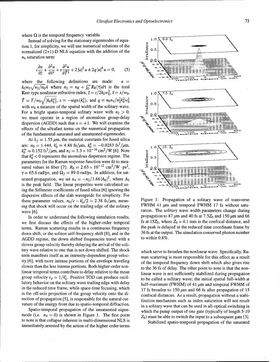
Ultrafast Electronics and Optoelectronics 73
where Q. is the temporal frequency variable. Instead of solving for the stationary eigenmodes of equa-
tion 1, for simplicity, we will use numerical solutions of the normalized (2+l)-D NLS equation with the addition of the M4 saturation term:
du d2u d2u „, ,2 „ , ,4 ldz + W+sdP+ '"' "+29l"r" = o, (5)
where the following definitions are made: u = koWo^/ri2/noA where «2 = nK + JO^R{
X)^
X *
S
l^e total Kerr-type nonlinear refractive index, z = Z/2^WQ, X — X/WQ,
T = T/w0^\kok'^\, s = -sign(^o'), and q = n0"4/"2*owo with w0 a measure of the spatial width of the solitary-wave. For a bright spatio-temporal solitary wave with «2 > 0, we must operate in a region of anomalous group-delay dispersion (AGDD) such that j = +1. We will examine the effects of the ultrafast terms on the numerical propagation of the fundamental saturated and unsaturated eigenmodes.
At Xf = 1.55 jum, the material constants for fused silica are: n0 = 1.444, Aß = 4.88 fs/pm, Aß = -0.0283 fs2//im, Aß" = 0.152 fs3/7mi, and n2 = 3.3 x 10~16 cm2/W [6]. Note that Aß < 0 represents the anomalous dispersion regime. The parameters for the Raman response function were fit to mea- sured values in fiber [7]: R0 = 2.63 x 10⁻¹² cm2/Wps2, y= 65.6 rad/ps, and Q.f = 89.0 rad/ps. In addition, for sat-
urated propagation, we set «4 = — 712/1.66 |/4o| , where Ao is the peak field. The linear properties were calculated us- ing the Sellmeier coefficients of fused silica [6] ignoring the dispersive effects of the slab waveguide for simplicity. For these parameter values, no/c — Aß/2 = 2.38 fs/^/m, mean- ing that shock will occur on the trailing edge of the solitary wave [6].
In order to understand the following simulation results, we first discuss the effects of the higher-order temporal terms. Raman scattering results in a continuous frequency down shift, or the soliton self-frequency shift [8], and in the AGDD regime, the down shifted frequencies travel with a slower group velocity thereby delaying the arrival of the soli- tary wave relative to one that is not down shifted. The shock term manifests itself as an intensity-dependent group veloc- ity [6], with more intense portions of the envelope traveling slower than the less intense portions. Both higher-order non- linear temporal terms contribute to delay relative to the mean group velocity vg = 1/Aß. Positive TOD can produce oscil- latory behavior on the solitary wave trailing edge with delay in the reduced time frame, while space-time focusing, which is the off-axis projection of the group velocity onto the di- rection of propagation [5], is responsible for the natural cur- vature of the energy front due to spatio-temporal diffraction.
Spatio-temporal propagation of the unsaturated eigen- mode (i.e. «4 = 0) is shown in Figure 1. The first point to note is that collapse inherent in multi-dimensional NLS is immediately arrested by the action of the higher-order terms
Figure 1: Propagation of a solitary wave of transverse FWHM 41 ^m and temporal FWHM 17 fs without satu- ration. The solitary wave width parameters change during propagation to 87 ym and 40 fs at 7.5Zo and 150 /urn and 66 fs at 15Zo, where ZQ = 4.1 mm is the confocal distance, and the peak is delayed in the reduced time coordinate frame by 36 fs at the output. The simulation conserved photon number to within 0.8%.
which serve to broaden the nonlinear wave. Specifically, Ra- man scattering is most responsible for this effect as a result of the temporal frequency down shift which also gives rise to the 36 fs of delay. The other point to note is that the non- linear wave is not sufficiently stabilized during propagation to be called a solitary wave; the initial spatial full-width at half-maximum (FWHM) of 41 /jm and temporal FWHM of 17 fs broaden to 150 pm and 66 fs after propagation of 15 confocal distances. As a result, propagation without a stabi- lization mechanism such as index saturation will not result in a solitary wave that can be used in all-optical switching in which the pump output of one gate (typically of length 5-10 Zo) must be able to switch the input to a subsequent gate [3].
Stabilized spatio-temporal propagation of the saturated

74 Ultrafast Electronics and Optoelectronics
eigenmode (i.e. n4 < 0) is shown in figure 2, where the most noticeable effect is that, over propagation of 15 con- focal distances, the spatial and temporal broadening of the wave (and corresponding reduction of the peak intensity) is much less than the unsaturated case (note the different spa- tial scales). In the saturated case, the solitary wave broadens only slightly to 47 /m\ and 29 fs. The delay of 260 fs relative to the mean group velocity \/k!0 is again due mostly to Ra- man scattering. The reason for the larger time delay is that, due to stabilization, the effects of Raman scattering persist for much longer distances. This is evidenced by the fact that the temporal down shift of the peak in this case is about 21 THz, versus 3.1 THz as in the unsaturated case.
Initially the solitary wave has a transverse FWHM spa- tial extent of 41 /urn and temporal duration 17 fs, and con- tains 14 nJ of energy if confined by a 2.0 /jm thick slab waveguide. This energy can be reduced by 3-4 orders of magnitude by using media with enhanced nonresonant non- linearity such as AlGaAs at sub-half bandgap or PTS. Due to nonlinear spatio-temporal propagation, the curvature of the solitary wave is opposite to that which would be caused by space-time focusing alone. This is a result of the effect of both the shock term, which delays the center portion more than the wings and overtakes space-time focusing, and Ra- man scattering, which will down shift, and hence delay, the central portion more than the wings. Like the linear effect of space-time focusing, this is a true spatio-temporal effect and has no analog in the (1+1)-D temporal case. The main point to be extracted from figure 2 through, is that even in the presence of the higher-order temporal effects, the soli- tary wave does not break up or diffract/disperse as quickly as propagation without saturation, and can thus be readily used for switching applications.
In conclusion, the use of spatio-temporal solitary waves in optical switching will allow for low energy, ultrafast, spa- tially and temporally parallel operation. We have shown that weak index saturation via «4 < 0 provides stabilization in the presence of higher-order linear and nonlinear effects of third-order dispersion, space-time focusing, optical shock, and stimulated Raman scattering.
References [1] Y. Silberberg "Collapse of optical pulses," Optics Letters
15,1282-1284(1990).
[2] A. B. Blagoeva, S. G. Dinev, A. A. Dreischuh, and A. Naidenov "Light bullets formation in bulk media," IEEE Journal of Quantum Electronics 27, 2060-2065 (1991).
[3] R. McLeod, K. Wagner, and S. Blair "(3+l)-dimensional optical soliton dragging logic," Physical Review A 52, 3254-3278(1995).
[4] I. P. Christov, H. C. Kapteyn, M. M. Murnane, C.-P. Huang, and J. Zhou "Space-time focusing of femtosec-
l.o >
0.5
0.0
Figure 2: Propagation of a solitary wave of transverse FWHM 41 pm and temporal FWHM 17 fs with saturation. The solitary wave width parameters change during propaga- tion to 43 ^m and 24 fs at 7.5Z0 and 47 pm and 29 fs at 15Z0, where ZQ = 5.5 mm is the confocal distance, and the peak is delayed in the reduced time coordinate frame by 260 fs at the output. The simulation conserved photon number to within 0.5%.
ond pulses in a Ti: Sapphire laser," Optics Letters 20, 309-311(1995).
[5] J. E. Rothenberg "Space-time focusing: breakdown of the slowly varying envelope approximation in the self- focusing of femtosecond pulses," Optics Letters 17, 1340-1342(1992).
[6] G. P. Agrawal Nonlinear Fiber Optics. Academic Press 1989.
[7] R. H. Stolen, C. Lee, and R. K. Jain "Development of the stimulated Raman spectrum in single-mode silica fibers," Journal of the Optical Society of America B 1, 652-657 (1984).
[8] J. P. Gordon "Theory of the soliton self-frequency shift," Optics Letters 11,662-664 (1986).

An Optoelectronic RF Burst Communications System
Eric E. Funk and Chi H. Lee Department of Electrical Engineering
University of Maryland, College Park, MD 20742
Abstract
We describe a new RF spread-spectrum communications system. The system exploits the proven capability of picosecond conductivity to serve in both generation and sampling of precisely timed RF bursts. We also present initial results from a proof-of-principle system.
Key Words: optoelectronics, photoconductive, spread- spectrum
Introduction
Spread-spectrum (SS) modulation techniques are commonly used in RF/wireless communications systems that are designed for low probability of detection (LPD), and low probability of jamming (LPJ). SS modulation seeks to confuse an unintended receiver through the use of a signal that appears as wideband and random, while remaining deterministic at a friendly receiver.
A variety of well established SS modulation techniques [1] are used in both commercial and military communications systems including direct sequence (DS), and frequency hopping (FH). Conventional SS transmitters and receivers such as the DS architecture shown in Fig. 1 employ digital signal processing (DSP) to perform baseband spectrum spreading and despreading. However, as spreading bandwidths increase, the dynamic range of receiver components (such as front-end mixers and amplifiers) decreases accordingly. If spreading bandwidths are to extend beyond a few GHz it becomes advantageous to perform spectrum despreading as close to the receiver front end as possible. Front-end despreading allows the following receiver stages to operate at the information bandwidth rather than the (large) spread bandwidth.
DS presents the additional challenge that the spreading chip rate must be on the order of the spreading bandwidth, hence, processor speeds become unrealistic at spreading bandwidths beyond a few GHz.
Time-hopped, Burst Mode Spread-spectrum
An optoelectronic approach that uses time hopping (TH) rather than DS or FH allows both the dynamic range and processing speed requirements to be met. The design is based on the impulse modulator (IM) as described by Viterbi [1] and others [2].
A time-hopped (TH) SS signal consists of short wideband or ultra-wideband RF bursts. The timing of the bursts is pseudo-random. This implies that an unintended receiver must listen constantly over the entire spread bandwidth in order to intercept all of the signal energy. However, if the pseudo-random TH sequence is known to an intended receiver, that receiver can be configured to listen only during the transmission bursts. Hence, the intended receiver exhibits a signal to noise ratio (SNR) that can be improved by up to Gp, the processing gain, over the
receiver that listens constantly. In the ideal case, the unintended receiver SNR, (SNR)u,
is
(SNR)u(dB) = (SNR),(äB)-GP(dB), where Gp(dB) = -10 log (5),
and (SNR), is the SNR seen by an intended receiver, 8 is the signal duty factor.
In addition, TH burst transmissions [3] are particularly robust against below-the-noise non-linear total power radiometric detection while direct sequence signals can be detected quite easily. According to Nicholson [4],
OS A TOPS on Ultrafast Electronics and Optoelectronics, 1997 Vol. 13, Martin Nuss and John Bowers (ed.) ©1997 Optical Society of America
75
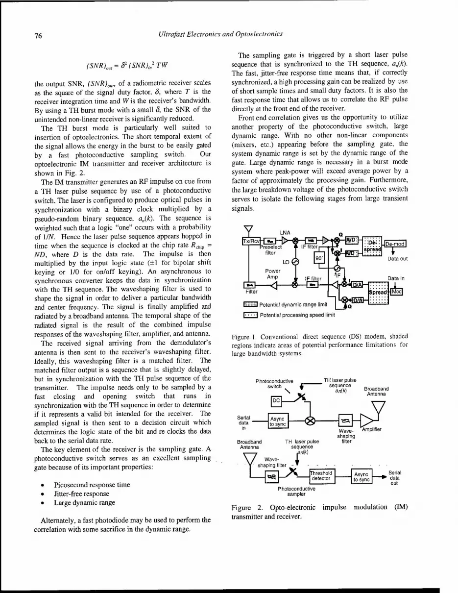
76 Ultrafast Electronics and Optoelectronics
(SNR)m„=#(SNR)in2TW
the output SNR, (SNR)out, of a radiometric receiver scales as the square of the signal duty factor, <5, where T is the receiver integration time and W is the receiver's bandwidth. By using a TH burst mode with a small S, the SNR of the unintended non-linear receiver is significantly reduced.
The TH burst mode is particularly well suited to insertion of optoelectronics. The short temporal extent of the signal allows the energy in the burst to be easily gated by a fast photoconductive sampling switch. Our optoelectronic IM transmitter and receiver architecture is shown in Fig. 2.
The IM transmitter generates an RF impulse on cue from a TH laser pulse sequence by use of a photoconductive switch. The laser is configured to produce optical pulses in synchronization with a binary clock multiplied by a pseudo-random binary sequence, a„{k). The sequence is weighted such that a logic "one" occurs with a probability of \IN. Hence the laser pulse sequence appears hopped in time when the sequence is clocked at the chip rate /?chip = ND, where D is the data rate. The impulse is then multiplied by the input logic state (+1 for bipolar shift keying or 1/0 for on/off keying). An asynchronous to synchronous converter keeps the data in synchronization with the TH sequence. The waveshaping filter is used to shape the signal in order to deliver a particular bandwidth and center frequency. The signal is finally amplified and radiated by a broadband antenna. The temporal shape of the radiated signal is the result of the combined impulse responses of the waveshaping filter, amplifier, and antenna.
The received signal arriving from the demodulator's antenna is then sent to the receiver's waveshaping filter. Ideally, this waveshaping filter is a matched filter. The matched filter output is a sequence that is slightly delayed, but in synchronization with the TH pulse sequence of the transmitter. The impulse needs only to be sampled by a fast closing and opening switch that runs in synchronization with the TH sequence in order to determine if it represents a valid bit intended for the receiver. The sampled signal is then sent to a decision circuit which determines the logic state of the bit and re-clocks the data back to the serial data rate.
The key element of the receiver is the sampling gate. A photoconductive switch serves as an excellent sampling gate because of its important properties:
• Picosecond response time • Jitter-free response • Large dynamic range
Alternately, a fast photodiode may be used to perform the correlation with some sacrifice in the dynamic range.
The sampling gate is triggered by a short laser pulse sequence that is synchronized to the TH sequence, an{k). The fast, jitter-free response time means that, if correctly synchronized, a high processing gain can be realized by use of short sample times and small duty factors. It is also the fast response time that allows us to correlate the RF pulse directly at the front end of the receiver.
Front end correlation gives us the opportunity to utilize another property of the photoconductive switch, large dynamic range. With no other non-linear components (mixers, etc.) appearing before the sampling gate, the system dynamic range is set by the dynamic range of the gate. Large dynamic range is necessary in a burst mode system where peak-power will exceed average power by a factor of approximately the processing gain. Furthermore, the large breakdown voltage of the photoconductive switch serves to isolate the following stages from large transient signals.
Potential dynamic range limit i AQ
Potential processing speed limit
Figure 1. Conventional direct sequence (DS) modem, shaded regions indicate areas of potential performance limitations for large bandwidth systems.
Photoconductive switch f
[DC]_yX_
TH laser pulse ' sequence
anW
Serial data '
in
Async to sync
TH laser pulse sequence
artk)
Wave- shaping
filter
Amplifier
f Wave- shaping filter
371 X^ Threshold detector
Async to sync
Serial ' data
out Photoconductive
sampler
Figure 2. Opto-electronic impulse modulation (IM) transmitter and receiver.

Ultrafast Electronics and Optoelectronics 77
Experiment/Results
Many aspects of this system have now been realized in a system that uses a diode-laser-pumped mode-locked laser and regenerative amplifier that is configured to produce a TH optical pulse train. While we began with a demonstration of the physical layer similar to that described above, we have now interfaced this system [5] with a pair of personal computers (PCs) in order to demonstrate wireless SS messaging. Figure 3 shows the first message sent across our laboratory between PCs.
We experimented with both a packet (AX.25) and a serial wireless data link. Both links were set up to transmit data at 1.2 kB/s with a moderate transmission bandwidth of 350 MHz as determined by the waveshaping filter and antenna of our transmitter. The packet system used time hopping with a clock running at 19.2 kHz.
Without forward error correction coding, a transmitter final-stage average RF output power of less than 1 ^iW provided a reliable link. The serial link produced no errors when sending several pages of text across the laboratory (2 m), however a true bit-error-rate test must be performed in the future to determine the actual error rate. The packet link sent >90% of all packets (16 bytes/ data frame) without error. However, the packet errors appeared to have been caused by a problem with the interface to the packet controller.
In this first demonstration, synchronization was maintained by operating both the transmitter and receiver with pulses from the same master laser. However, the next generation system that we have designed will use an external global positioning system time reference to aid in gaining and maintaining synchronization.
In order to demonstrate the benefits of processing gain, we attempted to jam the signal with a 10 mW, 1.2 GHz narrowband carrier. The jamming signal was sent from an antenna identical to the transmitter's antenna and co- located with the transmitter. The jamming signal caused no noticeable change in the transmission of data.
Conclusion
We have proposed a new technique for the generation and correlated reception of time-hopped spread-spectrum signals. This technique uses the large frequency bandwidth and the temporal precision available from optoelectronic sampling to generate, radiate, and correlate a precise TH RF pulse sequence. A key feature of this approach is that correlation can take place in the front-end of the receiver.
We have demonstrated many of the critical features of such a system in a simple communications link between a pair of computers. The "proof-of-principle" data rate was limited to 1.2 kB/s as a result of the limited laser regenerative amplifier repetition rate.
However by use of small (<10 |im) photoconductive sampling gaps, laser pulse energies on the order of nJ can be used to perform sampling. Hence, the system can be driven by laser diodes, resulting in much higher data rates and a much smaller package.
I ̂ ^^^^^H ̂ ^H 1 ^^■■1 ■
/ARl>CQ:UWB test nessage 1
m''IJJ '',JJ ~~~ ■ Figure 3. Test message sent between computers over opto- electronic spread-spectrum link.
Acknowledgments
The authors wish to thank L. J. Jasper Jr., S. E. Saddow, and Scott Ramsey for their assistance and insightful discussions.
References
1. Andrew J. Viterbi, Principles of Spread Spectrum Communications. (Addison-Wesley Publishing Company, New York, 1995).
2. R. A. Scholtz, "Multiple Access with time-hopping impulse modulation," in MILCOM '93 Conference Record. (IEEE, New York, 1993).
3. Paul Withington II and Larry W. Fullerton, "An impulse radio communications system," in Ultra- wideband Short-pulse Electromagnetics. Henry L. Bertoni, Lawrence Carin, and Leopold B. Felsen, eds. (Plenum, New York, 1993) pp. 113-120.
4. David L. Nicholson, Spread Spectrum Signal Design, (Computer Science Press, Rockville, MD, 1988)Ch 4.
5. E. E. Funk, Stephen E. Saddow, L. J. Jasper, Jr., and Chi H. Lee "Optically controlled spread-spectrum RF data link," IEEE MTT-S Digest, 1996, pp. 1563-65.

Devices
Peter Delfyett
CREOL University of Central Florida 4000 Central Florida Blvd. Orlando, FL 32816 Phone: (407) 823-6800
This section of the TOPS Volume focuses on recent advances in ultrahigh speed device technology. This area spans technologies ranging from novel, high speed vertical cavity surface emitting semiconductor lasers to ultrafast photodetectors and devices for generating ultrashort electrical pulses. The importance of these devices is that they will serve as key components in ultrahigh speed measurement, test and diagnostic equipment as well as play vital roles in computing, communications and signal processing applications.
From the technical papers presented within this section of TOPS, one will notice that the development of new devices comes on the heels of advancements in areas of material growth, material processing, and fabrication techniques. This synergistic interaction between material science, device design and fabrication engineering, and systems integration are allowing new material and devices to be used in compact laser sources, high speed optical interconnects, millimeter wave generation, and high speed electro-optic sampling oscilloscopes.
Several years ago, researchers in the field of ultrafast electronics and optoelectronics promised new devices which would play important roles in high speed commercial applications. From the recent developments and breakthroughs which are summarized in this section, it is clear that these researchers have definitely hit their mark. It remains to be seen what these new advances in materials, fabrication and device technology will bring for the next millennium.
79

High-Speed 850 nm Oxide-Confined Vertical Cavity Surface Emitting Lasers
K. L. Lear, V. M. Hietala, H. Q. Hou, J. Banas, B. E. Hammons, J. Zolper, and S. P. Kilcoyne
Sandia National Laboratories MS 0603 / PO Box 5800 / Albuquerque, NM 87185-0603
Phone: 505-844-6635 Fax: 505-844-8985 E-mail: [email protected]
We have previously demonstrated record modulation bandwidths for oxide-confined vertical cavity surface emitting lasers (VCSELs) based on strained InGaAs/GaAs quantum wells[ 1]. The monolithic oxide-confined structure^] provides good optical confinement, low thresholds, efficient operation, and acceptable thermal resistance; these qualities promote high speed operation. Here we report work on nominally 850 nm wavelength oxide-confined VCSELs with modulation bandwidths in excess of 20 GHz. This is believed to be the highest frequency reported to date for any GaAs quantum well laser diode[3].
High modulation bandwidths were achieved with an oxide confined VCSEL structure modified to decrease parasitic circuit elements. Figure 1 shows a schematic cross section of the VCSEL with a corresponding small signal equivalent circuit. Coplanar waveguide pads designed for on wafer probing were placed on a 5 urn thick polyimide to reduce the capacitance between the pad and the conducting substrate to approximately 50 fF. The device capacitance was further reduced by implanting the mesa area lying outside the active region. This was necessary due to the high capacitance of the thin oxide layer. The non-radiative recombination associated with the deep implant damage may also reduce the charge storage associated with diffusion underneath the oxide region. Finally, the sheet resistance of the upper mirror layer was reduced to ~30Q/square by making it n-type instead of the conventional p-up structure.
conducting substrate
Figure 1. Schematic cross section of high speed VCSEL structure with superposed equivalent circuit.
Reprinted from Ultrafast Electronics and Optoelectronics 1997 Topical Meeting Technical Digest 01997 Optical Society of America
80
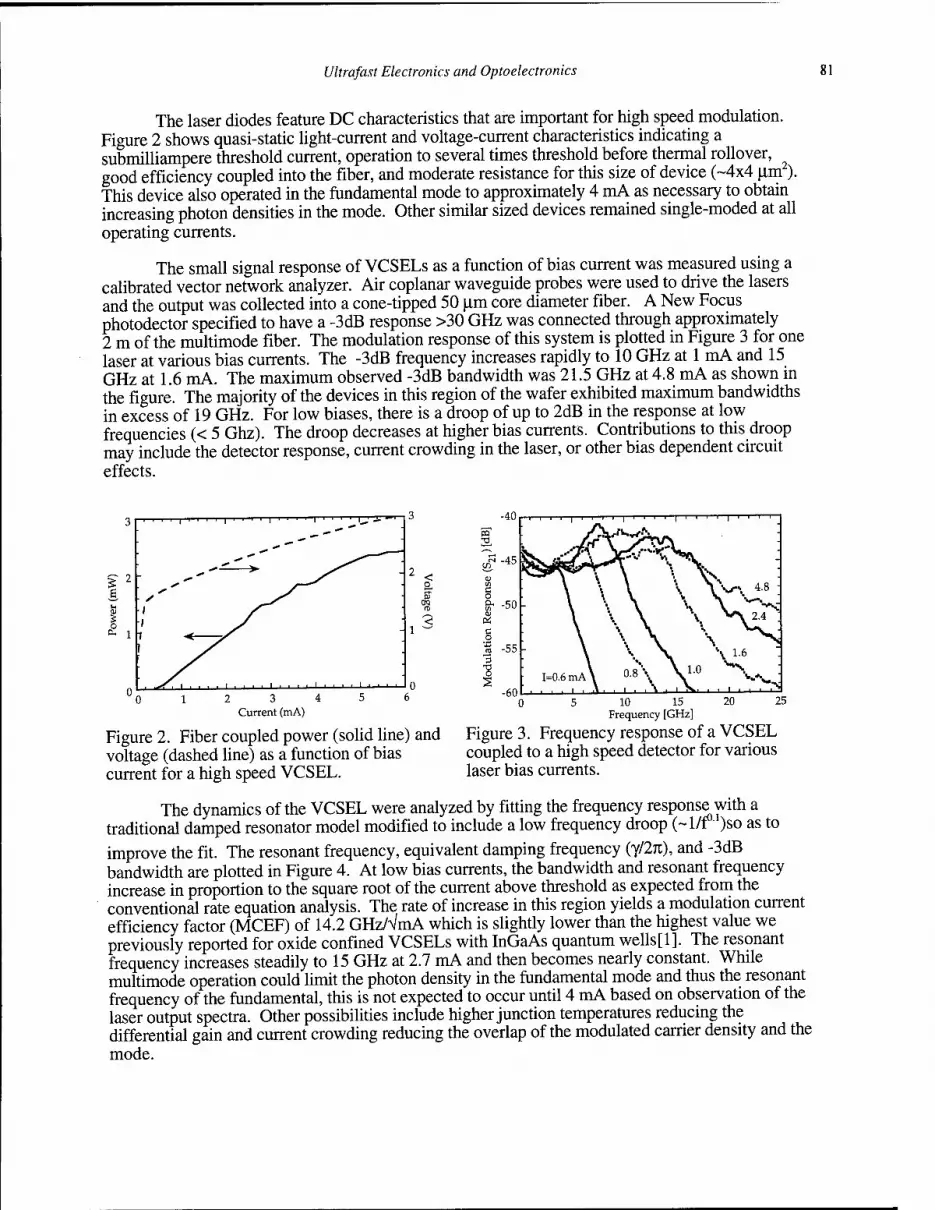
Ultrafast Electronics and Optoelectronics 81
The laser diodes feature DC characteristics that are important for high speed modulation. Figure 2 shows quasi-static light-current and voltage-current characteristics indicating a submilliampere threshold current, operation to several times threshold before thermal rollover, good efficiency coupled into the fiber, and moderate resistance for this size of device (-4x4 um). This device also operated in the fundamental mode to approximately 4 mA as necessary to obtain increasing photon densities in the mode. Other similar sized devices remained single-moded at all operating currents.
The small signal response of VCSELs as a function of bias current was measured using a calibrated vector network analyzer. Air coplanar waveguide probes were used to drive the lasers and the output was collected into a cone-tipped 50 um core diameter fiber. A New Focus photodector specified to have a -3dB response >30 GHz was connected through approximately 2 m of the multimode fiber. The modulation response of this system is plotted in Figure 3 for one laser at various bias currents. The -3dB frequency increases rapidly to 10 GHz at 1 mA and 15 GHz at 1.6 mA. The maximum observed -3dB bandwidth was 21.5 GHz at 4.8 mA as shown in the figure. The majority of the devices in this region of the wafer exhibited maximum bandwidths in excess of 19 GHz. For low biases, there is a droop of up to 2dB in the response at low frequencies (< 5 Ghz). The droop decreases at higher bias currents. Contributions to this droop may include the detector response, current crowding in the laser, or other bias dependent circuit effects.
I 1 ■<—-pS
< o, 3"
2 3 4 Current (mA)
10 15 Frequency [GHz]
Figure 2. Fiber coupled power (solid line) and Figure 3. Frequency response of a VCSEL voltage (dashed line) as a function of bias coupled to a high speed detector for various current for a high speed VCSEL. laser bias currents.
The dynamics of the VCSEL were analyzed by fitting the frequency response with a traditional damped resonator model modified to include a low frequency droop (~l/f° )so as to improve the fit. The resonant frequency, equivalent damping frequency (y/27t), and -3dB bandwidth are plotted in Figure 4. At low bias currents, the bandwidth and resonant frequency increase in proportion to the square root of the current above threshold as expected from the conventional rate equation analysis. The rate of increase in this region yields a modulation current efficiency factor (MCEF) of 14.2 GHzWmA which is slightly lower than the highest value we previously reported for oxide confined VCSELs with InGaAs quantum wells[l]. The resonant frequency increases steadily to 15 GHz at 2.7 mA and then becomes nearly constant. While multimode operation could limit the photon density in the fundamental mode and thus the resonant frequency of the fundamental, this is not expected to occur until 4 mA based on observation of the laser output spectra. Other possibilities include higher junction temperatures reducing the differential gain and current crowding reducing the overlap of the modulated carrier density and the mode.

82 Ultrafast Electronics and Optoelectronics
25 60
45
"30 -
'5.15
K=0.159 ns
Yn=18.8/ns u intrinsic f = 58 GHz max
Figure 4. Resonance frequency (squares), -3dB frequency (circles), and equivalent damping frequency(y/27t) (triangles) as a function of square root of current above threshold.
5 10 Resonance Frequency [GHz]
15
Figure 5. Fit of damping rate's (y's) parabolic dependence on resonance frequency to determine the intrinsic frequency response of the laser.
The dependence of the damping rate on resonance frequency was examined to determine the intrinsic frequency response of the laser. A fit of the data for resonance frequencies below 15 GHz, as shown in Figure 5, produced a K-factor of 0.159 ns corresponding to a maximum intrinsic bandwidth of 58 GHz. Damping rates for higher resonance frequencies fell above this fit yielding a K-factor of 0.227 ns. The actual bandwidth is limited to less than 58 GHz by heating, multimode operation, and electrical circuit effects. Higher bandwidths should be achieved by combining better heating sinking, designs for extended single-mode operation, and fabrication on semi-insulating substrates to reduce pad capacitance.
The authors gratefully acknowledge the technical contributions of M. Armendariz, F. Cajas, M. Housel, J. Nevers, and C. Tigges. This work was supported by the United States Department of Energy under Contract DE-AC04-94AL85000.
[1] K. L. Lear et al., Electron. Lett. 32(5), 457 (1996). [2] K. D. Choquette et al., Photon. Tech. Lett, 7(11), 1237 (1995). [3] J. D. Ralston et al., IEEE J. Quantum Electron., 29, 1648 (1993).
Uni-Traveling-Carrier Photodiodes
T. Ishibashi, N. Shimizu, S. Kodama, H. Ito, T. Nagatsuma and T. Furuta NTT System Electronics Laboratories
Morinosato-Wakamiya 3-1, Atsugi-shi, Kanagawa 243-01, Japan +81 462 40-2888, +81 462 40-4306(Fax), [email protected]
Abstract A new ultrafast photodiode, uni-traveling-carrier photodiode (UTC-PD) is proposed, and its photoresponse characterization on fabricated devices is presented. The prime feature of this PD is much higher output saturation current than that in a conventional pin-PD. This is achieved by reducing the space charge effect by utilizing electron velocity overshoot in the carrier collecting layer. A 20 nm2-area UTC-PD fabricated with MOVPE-grown InP/InGaAs heterostructure generated an output voltage as high as 2 V for a 25 Q load while maintaining an f3dB of
80 GHz. Proper device operations at high photocurrent densities up to 400 kA/cm2 were observed.
Key Words Detectors, Optoelectronics, Ultrafast Devices.
Introduction It is very important to achieve high saturation power and broad bandwidth simultaneously in the photodetectors used in various fiber-optic communication systems and for ultrafast measurements. A high output voltage with no post-amplification, for example, would enable us to simplify the receiver configurations in ultrahigh-bit-rate TDM systems. Major constraints on meeting the above requirement are the absorption volume vs. CR time constant tradeoff and the current density limitation caused by the space charge effect. Distributed photodetector design is one direction which would overcome such constraints. [1,2]
In a conventional pin-PD structure, both electrons and holes photogenerated in the depletion layer produce space charges, resulting in field modulation and limitations
in possible current densities during high frequency operations. Because of the much lower drift velocity, holes are responsible for the dominant space charge, and induced field modulation can more easily decelerate low-mobility holes. Another important fact is that photoresponse speed is mostly determined by hole transport due to the same reasons. However, when only high-velocity electrons are used, it is possible to delay the onset of the space charge effect, which can lead to much easier high current operations.
This paper proposes a uni-traveling-carrier photodiode (UTC-PD) in which only electrons are used as active carriers for enhancing saturation output current. The key to the higher output is superior high-field electron transport properties to those for hole in InP/InGaAs materials. We also study photoresponse speed of the UTC-PDs by small signal analysis. The analysis predicts the response to be sufficiently fast. A preliminary experiment on InP/InGaAs PDs showed that a photocurrent density in the mid 105
A/cm2 range permitted an output voltage as high as 2 V for a 25 Q load as well as a 3-dB bandwidth of 80 GHz.
Design Considerations UTC-PD Structure The UTC-PD is basically a pin-PD, and it has an active layer comprised of a p-type absorption layer and a widegap carrier collecting layer (Fig.l). Although similar structures have been developed by Peasall et al. to suppress dark current [3] and by Davis et al. to reduce diode capacitance[4], these have not been regarded as having ultrafast photoresponse. Holes photogenerated in the absorption layer are majority carriers, so they can respond very quickly with dielectric relaxation time. Electrons, on the other hand, diffuse (and drift) toward the carrier collecting layer. The bandgap-grading to
OSA TOPS on Ultrafast Electronics and Optoelectronics, 1997 Vol. 13, Martin Nuss and John Bowers (ed.) ©1997 Optical Society of America
83
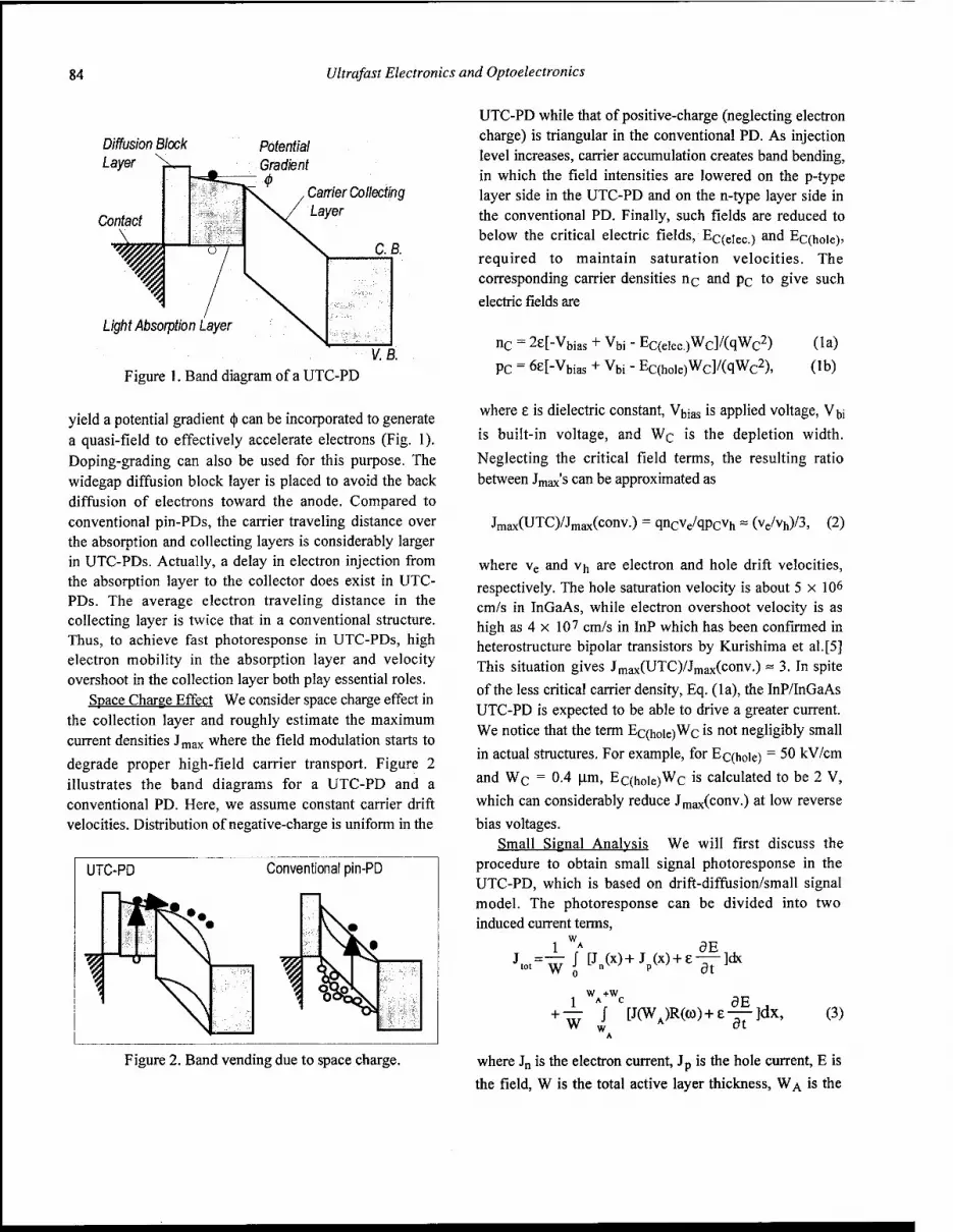
84 Ultrafast Electronics and Optoelectronics
Diffusion Block Layer
Potential Gradient 4
Carrier Collecting Layer
C.B.
1 Light Absorption Layer
Figure 1. Band diagram of a UTC-PD V.B.
yield a potential gradient (|> can be incorporated to generate a quasi-field to effectively accelerate electrons (Fig. 1). Doping-grading can also be used for this purpose. The widegap diffusion block layer is placed to avoid the back diffusion of electrons toward the anode. Compared to conventional pin-PDs, the carrier traveling distance over the absorption and collecting layers is considerably larger in UTC-PDs. Actually, a delay in electron injection from the absorption layer to the collector does exist in UTC- PDs. The average electron traveling distance in the collecting layer is twice that in a conventional structure. Thus, to achieve fast photoresponse in UTC-PDs, high electron mobility in the absorption layer and velocity overshoot in the collection layer both play essential roles.
Space Charge Effect We consider space charge effect in the collection layer and roughly estimate the maximum current densities Jmax where the field modulation starts to
degrade proper high-field carrier transport. Figure 2 illustrates the band diagrams for a UTC-PD and a conventional PD. Here, we assume constant carrier drift velocities. Distribution of negative-charge is uniform in the
UTC-PD while that of positive-charge (neglecting electron charge) is triangular in the conventional PD. As injection level increases, carrier accumulation creates band bending, in which the field intensities are lowered on the p-type layer side in the UTC-PD and on the n-type layer side in the conventional PD. Finally, such fields are reduced to below the critical electric fields, Ec(eiec.) an^ Ec(hole)> required to maintain saturation velocities. The corresponding carrier densities nc and pc to give such
electric fields are
nC = 2e[-Vbias + Vbi - EC(eiec.)WC]/(qWc2) (la)
PC = 6e[-Vbias + Vbi - EC(hole)Wc]/(qWc2), (lb)
where e is dielectric constant, V^ is applied voltage, Vbj
is built-in voltage, and Wc is the depletion width.
Neglecting the critical field terms, the resulting ratio between Jmax's can be approximated as
Jmax(UTC)/Jmax(conv.) = qncve/qpcvh = (ve/vh)/3, (2)
where ve and Vh are electron and hole drift velocities,
respectively. The hole saturation velocity is about 5 x 10⁶
cm/s in InGaAs, while electron overshoot velocity is as high as 4 x 107 cm/s in InP which has been confirmed in heterostructure bipolar transistors by Kurishima et al.[5] This situation gives Jmax(UTC)/Jmax(conv.) = 3. In spite
of the less critical carrier density, Eq. (la), the InP/InGaAs UTC-PD is expected to be able to drive a greater current. We notice that the term Ec(hole)Wc is not negligibly small
in actual structures. For example, for Ec(hole) = 50 kV/cm
and Wc = 0.4 um, Ec(hole)Wc is calculated to be 2 V,
which can considerably reduce Jmax(conv.) at low reverse
bias voltages. Small Signal Analysis We will first discuss the
procedure to obtain small signal photoresponse in the UTC-PD, which is based on drift-diffusion/small signal model. The photoresponse can be divided into two induced current terms,
1 W* dE , J [J (x)+J (x) + e — ]dx
W at
1 W*+WC ÖE + "^ / [J(WA)R(co)+e —]dx, (3)
Figure 2. Band vending due to space charge. where Jn is the electron current, Jp is the hole current, E is
the field, W is the total active layer thickness, WA is the
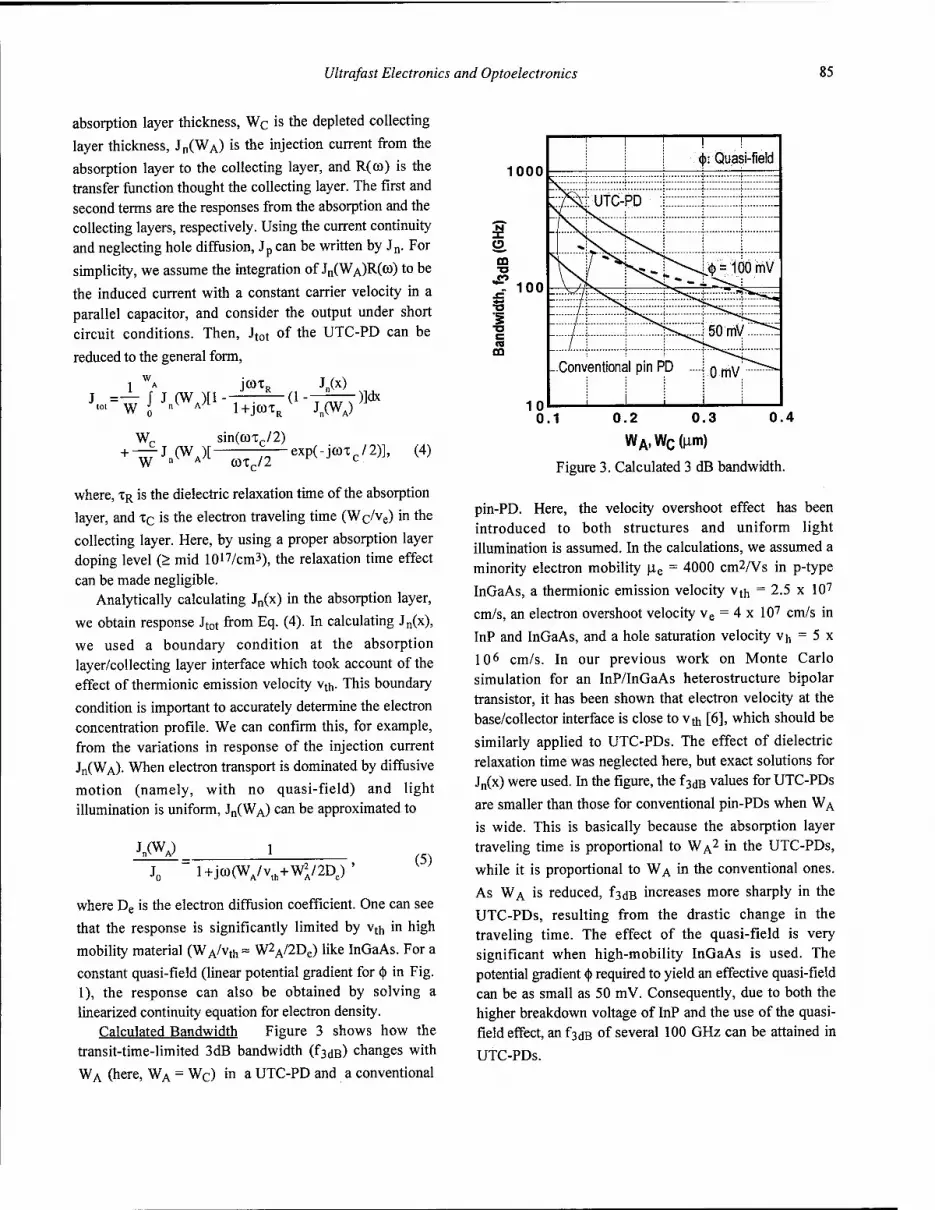
Ultrafast Electronics and Optoelectronics 85
absorption layer thickness, Wc is the depleted collecting
layer thickness, J„(WA) is the injection current from the
absorption layer to the collecting layer, and R(co) is the transfer function thought the collecting layer. The first and second terms are the responses from the absorption and the collecting layers, respectively. Using the current continuity and neglecting hole diffusion, Jp can be written by Jn. For
simplicity, we assume the integration of Jn(WA)R(co) to be
the induced current with a constant carrier velocity in a parallel capacitor, and consider the output under short circuit conditions. Then, Jtot of the UTC-PD can be
reduced to the general form,
1 WA JC0XR /, J"(x) s,, •(l-,mM )]dx J =— f J (WA)[1
tot W J nv A/L
—£J (WJ[
1+J<ÖTR
sin(coTc/2)
coxc/2
J„(WA)
exp(-j(öir/2)], (4)
where, TR is the dielectric relaxation time of the absorption
layer, and 1Q is the electron traveling time (Wc/ve) in the
collecting layer. Here, by using a proper absorption layer doping level (> mid 1017/cm3), the relaxation time effect can be made negligible.
Analytically calculating Jn(x) in the absorption layer,
we obtain response Jtot from Eq. (4). In calculating Jn(x),
we used a boundary condition at the absorption layer/collecting layer interface which took account of the effect of thermionic emission velocity vth. This boundary
condition is important to accurately determine the electron concentration profile. We can confirm this, for example, from the variations in response of the injection current Jn(WA). When electron transport is dominated by diffusive
motion (namely, with no quasi-field) and light illumination is uniform, Jn(WA) can be approximated to
J„(WA) 1 l+jco(WA/vlh+WA/2De) '
(5)
where De is the electron diffusion coefficient. One can see
that the response is significantly limited by vth in high
mobility material (WA/vth = W2A/2De) like InGaAs. For a
constant quasi-field (linear potential gradient for § in Fig. 1), the response can also be obtained by solving a linearized continuity equation for electron density.
Calculated Bandwidth Figure 3 shows how the transit-time-limited 3dB bandwidth (f3dß) changes with
WA (here, WA = Wc) in a UTC-PD and a conventional
1000
N x
CO ■a
re m
100
0.1 0.4 0.2 0.3
WA,WC(M Figure 3. Calculated 3 dB bandwidth.
pin-PD. Here, the velocity overshoot effect has been introduced to both structures and uniform light illumination is assumed. In the calculations, we assumed a minority electron mobility |J.e = 4000 cm2/Vs in p-type
InGaAs, a thermionic emission velocity vth = 2.5 x 10⁷
cm/s, an electron overshoot velocity ve = 4 x 107 cm/s in
InP and InGaAs, and a hole saturation velocity V(, = 5 x
106 cm/s. In our previous work on Monte Carlo simulation for an InP/InGaAs heterostructure bipolar transistor, it has been shown that electron velocity at the base/collector interface is close to vth [6], which should be
similarly applied to UTC-PDs. The effect of dielectric relaxation time was neglected here, but exact solutions for Jn(x) were used. In the figure, the f3JB values for UTC-PDs
are smaller than those for conventional pin-PDs when WA
is wide. This is basically because the absorption layer traveling time is proportional to WA
2 in the UTC-PDs,
while it is proportional to WA in the conventional ones.
As WA is reduced, f3dB increases more sharply in the
UTC-PDs, resulting from the drastic change in the traveling time. The effect of the quasi-field is very significant when high-mobility InGaAs is used. The potential gradient <|) required to yield an effective quasi-field can be as small as 50 mV. Consequently, due to both the higher breakdown voltage of InP and the use of the quasi- field effect, an f3dB of several 100 GHz can be attained in
UTC-PDs.
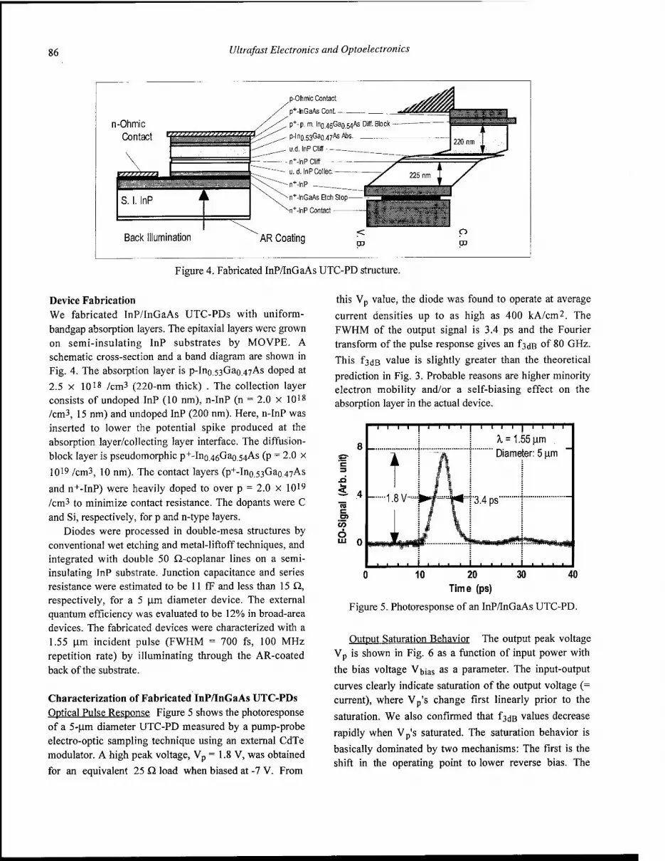
86 Ultrafast Electronics and Optoelectronics
n-Ohmic Contact "i
S. I. InP
p-Ohmic Contact
p+-lnGaAs Cont
p+-p. m. lno.43Gao.54As Diff. Block
- u.d. InP Cliff
- n+-lnP Cliff
-n+-lnGaAs Etch Stop-
Ni+-lnP Contact
Back Illumination AR Coating < DO
p CD
Figure 4. Fabricated InP/InGaAs UTC-PD structure.
Device Fabrication We fabricated InP/InGaAs UTC-PDs with uniform- bandgap absorption layers. The epitaxial layers were grown on semi-insulating InP substrates by MOVPE. A schematic cross-section and a band diagram are shown in Fig. 4. The absorption layer is p-Ino.53Gao.47As doped at
2.5 x 10¹⁸ /cm3 (220-nm thick) . The collection layer consists of undoped InP (10 nm), n-InP (n = 2.0 x 10¹⁸
/cm3, 15 nm) and undoped InP (200 nm). Here, n-InP was inserted to lower the potential spike produced at the absorption layer/collecting layer interface. The diffusion- block layer is pseudomorphic p+-Ino.46Gao.54As (p = 2.0 x
1019 /cm3, 10 nm). The contact layers (p+-Ino.53Gao.47As
and n+-InP) were heavily doped to over p = 2.0 x 10¹⁹
/cm3 to minimize contact resistance. The dopants were C and Si, respectively, for p and n-type layers.
Diodes were processed in double-mesa structures by conventional wet etching and metal-liftoff techniques, and integrated with double 50 Q-coplanar lines on a semi- insulating InP substrate. Junction capacitance and series resistance were estimated to be 11 fF and less than 15 Q, respectively, for a 5 (im diameter device. The external quantum efficiency was evaluated to be 12% in broad-area devices. The fabricated devices were characterized with a 1.55 nm incident pulse (FWHM = 700 fs, 100 MHz repetition rate) by illuminating through the AR-coated back of the substrate.
Characterization of Fabricated InP/InGaAs UTC-PDs Optical Pulse Response Figure 5 shows the photoresponse of a 5-ftm diameter UTC-PD measured by a pump-probe electro-optic sampling technique using an external CdTe modulator. A high peak voltage, Vp = 1.8 V, was obtained
for an equivalent 25 Q load when biased at -7 V. From
this Vp value, the diode was found to operate at average
current densities up to as high as 400 kA/cm2. The FWHM of the output signal is 3.4 ps and the Fourier transform of the pulse response gives an f3<jB of 80 GHz.
This f3dB value is slightly greater than the theoretical
prediction in Fig. 3. Probable reasons are higher minority electron mobility and/or a self-biasing effect on the absorption layer in the actual device.
10 20 Time (ps)
Figure 5. Photoresponse of an InP/InGaAs UTC-PD.
Output Saturation Behavior The output peak voltage Vp is shown in Fig. 6 as a function of input power with
the bias voltage Vt,ias as a parameter. The input-output
curves clearly indicate saturation of the output voltage (= current), where Vp's change first linearly prior to the
saturation. We also confirmed that f3dB values decrease
rapidly when Vp's saturated. The saturation behavior is
basically dominated by two mechanisms: The first is the shift in the operating point to lower reverse bias. The
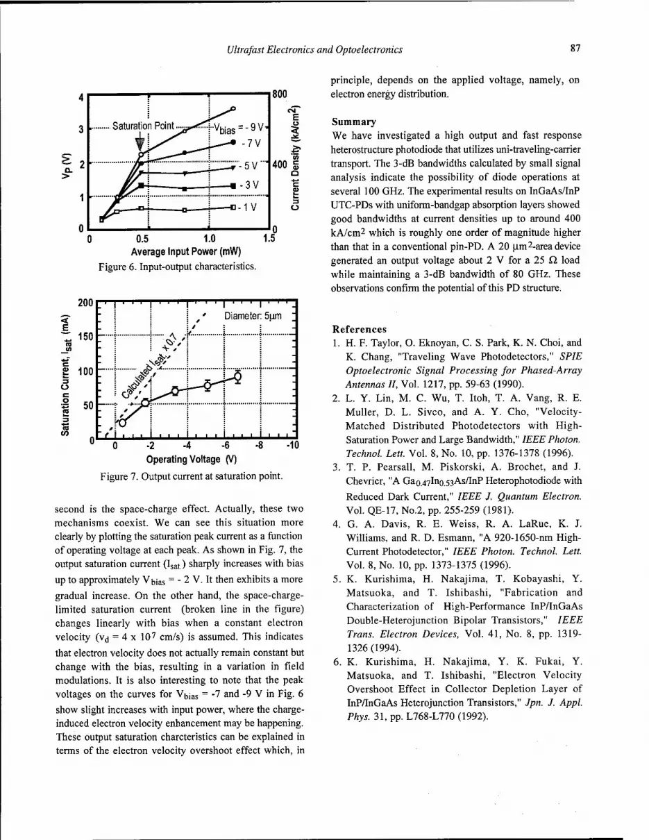
Ultrafast Electronics and Optoelectronics 87
3 ■
Q. >
1 -
Saturation Point 4vbias = -9V^
.J-"--'* "7V
_J «-3V -m—
,,,
j
CM E o
400 i
0.5 1.0 Average Input Power (mW)
Figure 6. Input-output characteristics.
1.5
principle, depends on the applied voltage, namely, on 800 electron energy distribution.
Summary We have investigated a high output and fast response heterostructure photodiode that utilizes uni-traveling-carrier transport. The 3-dB bandwidths calculated by small signal analysis indicate the possibility of diode operations at
£ several 100 GHz. The experimental results on InGaAs/InP o UTC-PDs with uniform-bandgap absorption layers showed
good bandwidths at current densities up to around 400 kA/cm2 which is roughly one order of magnitude higher than that in a conventional pin-PD. A 20 u.m2-area device generated an output voltage about 2 V for a 25 £1 load while maintaining a 3-dB bandwidth of 80 GHz. These observations confirm the potential of this PD structure.
200
ra CO
I I I I I I I I I I I I I I I I
\ / Diameter: 5pm ;
' '■■■!■■ ■ -2 -4 -6 -8 -10 Operating Voltage (V)
Figure 7. Output current at saturation point.
second is the space-charge effect. Actually, these two mechanisms coexist. We can see this situation more clearly by plotting the saturation peak current as a function of operating voltage at each peak. As shown in Fig. 7, the output saturation current (Isat.) sharply increases with bias
up to approximately Vbias = - 2 V. It then exhibits a more
gradual increase. On the other hand, the space-charge- limited saturation current (broken line in the figure) changes linearly with bias when a constant electron velocity (vj = 4 x 107 cm/s) is assumed. This indicates
that electron velocity does not actually remain constant but change with the bias, resulting in a variation in field modulations. It is also interesting to note that the peak voltages on the curves for Vbias = -7 and -9 V in Fig. 6
show slight increases with input power, where the charge- induced electron velocity enhancement may be happening. These output saturation charcteristics can be explained in terms of the electron velocity overshoot effect which, in
References 1. H. F. Taylor, O. Eknoyan, C. S. Park, K. N. Choi, and
K. Chang, "Traveling Wave Photodetectors," SPIE Optoelectronic Signal Processing for Phased-Array Antennas II, Vol. 1217, pp. 59-63 (1990).
2. L. Y. Lin, M. C. Wu, T. Itoh, T. A. Vang, R. E. Müller, D. L. Sivco, and A. Y. Cho, "Velocity- Matched Distributed Photodetectors with High- Saturation Power and Large Bandwidth," IEEE Photon, Technol. Lett. Vol. 8, No. 10, pp. 1376-1378 (1996).
3. T. P. Pearsall, M. Piskorski, A. Brochet, and J. Chevrier, "A Gao.47Ino.53As/InP Heterophotodiode with
Reduced Dark Current," IEEE J. Quantum Electron. Vol. QE-17, No.2, pp. 255-259 (1981).
4. G. A. Davis, R. E. Weiss, R. A. LaRue, K. J. Williams, and R. D. Esmann, "A 920-1650-nm High- Current Photodetector," IEEE Photon. Technol. Lett. Vol. 8, No. 10, pp. 1373-1375 (1996).
5. K. Kurishima, H. Nakajima, T. Kobayashi, Y. Matsuoka, and T. Ishibashi, "Fabrication and Characterization of High-Performance InP/InGaAs Double-Heterojunction Bipolar Transistors," IEEE Trans. Electron Devices, Vol. 41, No. 8, pp. 1319- 1326 (1994).
6. K. Kurishima, H. Nakajima, Y. K. Fukai, Y. Matsuoka, and T. Ishibashi, "Electron Velocity Overshoot Effect in Collector Depletion Layer of InP/InGaAs Heterojunction Transistors," Jpn. J. Appl. Phys. 31, pp. L768-L770 (1992).
High-Speed Resonant Cavity Enhanced Schottky Photodiodes
Saiful Islam, Ekmel Özbay , Orhan Aytur Department of Physics, Bilkent University, Bilkent Ankara 06533 TURKEY
Mutlu Gökkavas, Bora Onat, Selim Ünlü Department of Electrical and Computer Engineering Boston University, Boston, Massachusetts 02215 USA
Gary Tuttle Department of Electrical Engineering
Iowa State University, Ames IA 50011 USA
R.H. Henderson, Elias Towe Department of Electrical Engineering
University of Virginia, Charlottesville, VA 22903 USA
Abstract
Design, fabrication and testing of a GaAs-based high- speed resonant cavity enhanced (RCE) Schottky photodiode is reported. The top-illuminated RCE detector is constructed by integrating a Schottky contact, a thin absorption region (Ino.osGao.92As) and a distributed AlAs/GaAs Bragg mirror. The Schottky contact metal serves as a high reflectivity top mirror in the RCE detector structure. The devices were fabricated by using a microwave-compatible fabrication process. The resulting spectral photoresponse had a resonance around 895 nm, in good agreement with our simulations. The full-width- at-half-maximum (FWHM) was 15 nm, and the enhancement factor was in excess of 6. The photodiode had an experimental set-up limited temporal response of 18 psec FWHM, corresponding to a 3-dB bandwidth of 20 GHz.
Key Words
Photonic integrated circuits, Ultrafast devices, Schottky photodiodes, Resonant cavity enhancement.
Introduction
High-speed, high-efficiency photodetectors play an important role in optical communication and measurement systems. The high-speed properties of Schottky photodiodes have already been shown with reported 3-dB operating bandwidths exceeding 200 GHz [1-2]. However, the efficiency of these detectors have been typically limited to less than 10%, mostly due to the thin absorption region needed for short transit times. One can increase the absorption region thickness to achieve higher efficiencies. But this also means longer transit times which will degrade the high-speed performance of the devices. Resonant cavity enhanced (RCE) photodetectors
potentially offer the possibility of overcoming this limitation of the bandwidth-efficiency product of conventional photodetectors[3-5]. The RCE detectors are based on the enhancement of the optical field within a Fabry-Perot resonant cavity. The increased field allows the usage of thin absorbing layers, which minimizes the transit time of the photo-carriers without hampering the quantum efficiency. High-speed RCE photodetector research has mainly concentrated on using p-i-n type photodiodes, where near 100% quantum efficiencies along with a 3-dB bandwidth of 17 GHz have been reported [6]. There are only a few reports on RCE Schottky photodiodes, where a 2-fold enhancement has been observed for RCE InGaAs/InAlAs based Schottky photodiodes[7]. In this paper, we report our work on design, fabrication and testing of high-speed RCE Schottky photodiodes for operation at 900 nm.
Design
We used an S-matrice method to design the epilayer structure of the RCE Schottky photodiodes. The structure was optimized for top-illumination and it consisted of a bottom Bragg mirror integrated with a Schottky diode structure. The mirror was formed by 15 pair AlAs(755 Ä)/GaAs(637 Ä) quarter wave stack designed to operate at 900 nm. The Schottky diode region had a 0.630 iim thick N+ (ND= 3xl0181/cm3) layer for ohmic contacts, and a 0.3 |nm thick N" (ND = 1.2 x 10¹⁷ 1/cm3) region for the generation and transport of photogenerated carriers. The N" region consisted of a 1300 Ä thick photoactive Ino.ogGao.92As region, sandwiched between two GaAs N" layers. The top GaAs N" layer between the Schottky metal and the Ino.osGao.92As region had a thickness of 500 A, while the other N" region had a thickness of 1200 A. The photoactive Ino.osGao.92As region was placed closer to the metal contact in order to equalize the transit times of photogenerated electrons and holes. The
OSA TOPS on Ultrafast Electronics and Optoelectronics, 1997 Vol. 13, Martin Nuss and John Bowers (ed.) ©1997 Optical Society of America
88

Ultrafast Electronics and Optoelectronics 89
Ino.08Gao.92As/GaAs interfaces were graded to avoid hole- trapping. The total length of the cavity was designed to get the resonance to occur at 900 nm.
Fabrication
The epitaxial layers are grown by a solid-source MBE on semi-insulating GaAs substrates. We fabricated the epitaxial wafers using a monolithic microwave-compatible fabrication process. A microphotograph of the fabricated photodiodes is shown in Figure 1. First, ohmic contacts to the N+ layers were formed by a recess etch through the 0.3 micron N- layer. This was followed by a self-aligned Au- Ge-Ni liftoff and a rapid thermal anneal. The semi- transparent Schottky contact was formed by deposition of 200 Ä Au. Using an isolation mask, we etched away all of the epilayers except the active areas. Then, we evaporated Ti/Au interconnect metal which formed coplanar waveguide (CPW) transmission lines on top of the semi- insulating substrate. The next step was the deposition and patterning of a 2000 A thick silicon nitride layer. The thickness of the nitride layer was chosen to act as an antireflection coating for the RCE Schottky photodiode at the design wavelength. Besides passivation and protection of the surface, the nitride was also used as the dielectric of the metal-insulator-metal bias capacitors. Finally, 1.5 micron thick Au layer was used as an airbridge to connect the center of the CPW to the top Schottky metal. The resulting Schottky diodes had breakdown voltages larger than 12 V. The dark-current of a 150x150 |^m device at - IV bias was 30 nA. Using the forward current-voltage characteristics, we measured the barrier height of the Schottky junction to be 0.83 eV.
Schottky metal Bas capacitor Bas resistor
RF Output DC Bas
Figure 1. Microphotograph of the fabricated RCE photodiode
Experiment
For photoresponse measurements, white-light from a tungsten lamp was passed through a monochromator. The output of the monochromator was then coupled into a
multi-mode fiber, and the other end of the fiber, was brought in close proximity to the wafer, where a circular region with ~ 75 (im diameter was illuminated. The spectral response of the photocurrent obtained from this set-up was corrected by first measuring the optical power coming out of the fiber with a power meter. For photospectral measurements, we used a 150x150 |im photodiode biased at -2.0 Volts.
>« u c <u
"o »^ LU
E 3 +•* c re 3 o
0.2
0.1
800 850 900 Wavelength (nm)
950
800 850 900 Wavelength (nm)
950
Figure 2. (a) Measured, and (b) simulated photoresponse of the RCE photodiode.
The photoresponse of the device obtained by using the aforementioned set up is shown in Figure 2(a). For comparison purposes, the simulated quantum efficiency of the epitaxial structure is shown in Figure 2(b). There is a reasonable agreement between the calculated and the measured spectral responses. The resonant wavelength of the device is 895 nm, which is very close to the design wavelength of 900 nm. When compared with a single- pass structure, the enhancement factor of the device is in excess of 6 at the resonant wavelength. The full-width at half maximum was 15 nm, corresponding to a -1.6% spectral width. Although we predicted a peak quantum efficiency of 70%, the measured peak quantum efficiency was around 18%. The discrepancy between the
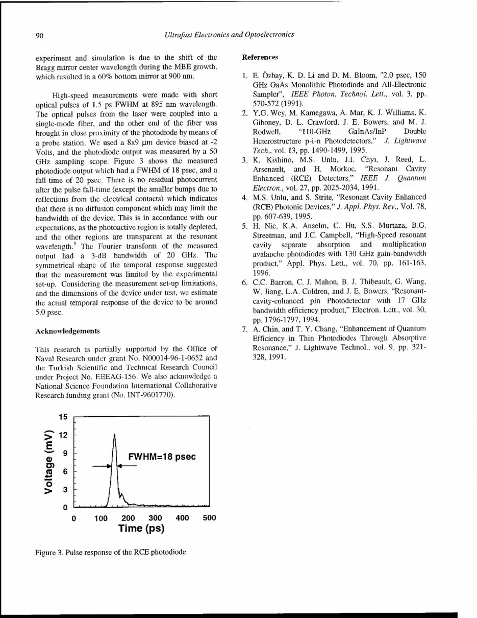
90 Ultrafast Electronics and Optoelectronics
experiment and simulation is due to the shift of the Bragg mirror center wavelength during the MBE growth, which resulted in a 60% bottom mirror at 900 nm.
High-speed measurements were made with short optical pulses of 1.5 ps FWHM at 895 nm wavelength. The optical pulses from the laser were coupled into a single-mode fiber, and the other end of the fiber was brought in close proximity of the photodiode by means of a probe station. We used a 8x9 |im device biased at -2 Volts, and the photodiode output was measured by a 50 GHz sampling scope. Figure 3 shows the measured photodiode output which had a FWHM of 18 psec, and a fall-time of 20 psec. There is no residual photocurrent after the pulse fall-time (except the smaller bumps due to reflections from the electrical contacts) which indicates that there is no diffusion component which may limit the bandwidth of the device. This is in accordance with our expectations, as the photoactive region is totally depleted, and the other regions are transparent at the resonant wavelength.5 The Fourier transform of the measured output had a 3-dB bandwidth of 20 GHz. The symmetrical shape of die temporal response suggested that the measurement was limited by the experimental set-up. Considering the measurement set-up limitations, and die dimensions of the device under test, we estimate die actual temporal response of the device to be around 5.0 psec.
Acknowledgements
This research is partially supported by the Office of Naval Research under grant No. N00014-96-1-0652 and die Turkish Scientific and Technical Research Council under Project No. EEEAG-156. We also acknowledge a National Science Foundation International Collaborative Research funding grant (No. INT-9601770).
References
1. E. Özbay, K. D. Li and D. M. Bloom, "2.0 psec, 150 GHz GaAs Monolithic Photodiode and All-Electronic Sampler", IEEE Photon. Technol. Lett., vol. 3, pp. 570-572 (1991).
2. Y.G. Wey, M. Kamegawa, A. Mar, K. J. Williams, K. Giboney, D. L. Crawford, J. E. Bowers, and M. J. Rodwell, "110-GHz GalnAs/InP Double Heterostructure p-i-n Photodetectors," ./. Lightwave Tech., vol. 13, pp. 1490-1499, 1995.
3. K. Kishino, M.S. Unlu, J.I. Chyi, J. Reed, L. Arsenault, and H. Morkoc, "Resonant Cavity Enhanced (RCE) Detectors," IEEE J. Quantum Electron., vol. 27, pp. 2025-2034, 1991.
4. M.S. Unlu, and S. Strite, "Resonant Cavity Enhanced (RCE) Photonic Devices," J. Appl. Phys. Rev., Vol. 78, pp. 607-639, 1995.
5. H. Nie, K.A. Anselm, C. Hu, S.S. Murtaza, B.G. Streetman, and J.C. Campbell, "High-Speed resonant cavity separate absorption and multiplication avalanche photodiodes with 130 GHz gain-bandwidth product," Appl. Phys. Lett., vol. 70, pp. 161-163, 1996.
6. C.C. Barron, C. J. Mahon, B. J. Thibeault, G. Wang, W. Jiang, L.A. Coldren, and J. E. Bowers, "Resonant- cavity-enhanced pin Photodetector with 17 GHz bandwidth efficiency product," Electron. Lett., vol. 30, pp. 1796-1797, 1994.
7. A. Chin, and T. Y. Chang, "Enhancement of Quantum Efficiency in Thin Photodiodes Through Absorptive Resonance," J. Lightwave Technol., vol. 9, pp. 321- 328, 1991.
15
> 12
E w 9
(0 6
$ 3
FWHM=18psec
—— ■ '- ' ■ J ■
100 200 300 400 500 Time (ps)
Figure 3. Pulse response of the RCE photodiode

A Complete Monolithically-Integrated Circuit for All Optical Generation of Millimeter-Wave Frequencies
G. Allen Vawter, Alan Mar, Vincent M. Hietala, John Zolper and John Hohimer
Sandia National Laboratories Albuquerque, NM87185-0603
USA
Abstract
The first monolithic integrated circuit for all-optical generation of millimeter wave signals is reported. The design integrates a mode-locked semiconductor ring diode laser with an optical amplifier and high-speed photodetector into a single optical integrated circuit. Signal generation is demonstration is demonstrated at 30, 60 and 90 GHz frequencies.
Key Words
Integrated optoelectronic circuits, mode locked lasers, semiconductor lasers, semiconductor optical amplifiers, ultrafast lasers.
Introduction
Today, the generation of mm-wave signals typically uses discrete negative differential resistance diodes coupled to a metallic waveguide cavity resonant at the desired frequency. At frequencies near 100 GHz, the output power and efficiency of these sources is low (typically 10 mW output power and 21% efficiency); and higher frequencies are only accessible by frequency multiplying. Demonstration of passive mode-locking
of semiconductor ring lasers at high pulse repetition rates1
suggests the possibility of a photonic integrated circuit (PIC) comprising a mode-locked ring laser and traveling-wave
photodiode 2'4 (TWPD) for direct generation of mm-wave electrical signals. Such a PIC could be much more compact and efficient compared to current technology and operate in the regime above 60 GHz where existing semiconductor-based mm- wave sources are inefficient or simply non-existent. In particular, Gunn diodes and IMPATT devices are limited to efficiencies of only a few percent. GaAs mm-wave integrated circuit (MMIC) oscillators are limited to roughly 5% and InP MMICs are limited to between 5 and 25% efficiency. Power output and efficiency of these devices drops rapidly above 100 GHz. By contrast a ring laser- and TWPD-based PIC could eventually reach efficiencies up to 50% at frequencies above 100 GHz. In addition, such a PIC may be cleaved to separate the TWPD from the amplifier and
an optical fiber used to transport the mm-wave power over large distances before conversion to mm-waves at the point of use.
We demonstrate the first monolithic PIC for generation of mm-wave signals. This new PIC integrates a passively mode- locked semiconductor ring laser, optical amplifier and high-speed photodiode for generation, amplification and detection of an optical pulse train with 30 to 90 GHz pulse-repetition frequency. Output is an electrical signal, generated by the photodiode, whose fundamental frequency is the pulse repetition rate of the mode-locked laser. The circuit uses a novel waveguide photodiode (WGPD) integrated with a mm-wave transmission line specifically designed for high-speed operation and signal extraction on a heavily-doped GaAs substrate.
ring laser amplifier L>K
ami
■y waveguide photodiode
transmission line saturable absorber probe pads
Figure 1. Schematic of actual mm-wave generation circuit.
The mm-wave signal generation PIC design for 60 and 90 GHz signals is shown in Fig. 1. A closed-ring GaAs/AlGaAs diode laser with a separately contacted, reverse-biased saturable absorber is passively mode locked generating a continuous train of short (1 to 10 ps) optical pulses in the ring cavity. Output of the ring laser is coupled to optical waveguide amplifier using a multi-mode Y-junction. A direct-waveguide photodetector (WGPD) converts the optical pulse train emerging from the amplifier to a mm-wave electrical output. Finally, a 50-Ohm transmission line is integrated with the WGPD for removal of the electrical signal. A WGPD was chosen rather than a velocity- matched TWPD so that the PIC requires only one epitaxial growth sequence. The pn-junction design is optimized for laser and amplifier operation and does not have a large enough depletion width to accommodate a velocity-matched photodetector. An alternate configuration was used for 30 GHz
OS A TOPS on Ultrafast Electronics and Optoelectronics. 1997 Vol. 13, Martin Nuss and John Bowers (ed.) ©1997 Optical Society of America
91

92 Ultrafast Electronics and Optoelectronics
signals wherein the reverse-biased saturable absorber also functions as a high-speed photodetector, converting a fraction the lasing pulse train into a mm-wave electrical output. Although more simple, this configuration does not offer the output power potential of the PIC using an optical amplifier and WGPD.
Design
The pulse repetition frequency, / of the mode-locked laser is fixed by the cavity round trip time which is determined by the diameter of the ring according to (1)
Contact Meta!
SiC-2
p-type Upper AIGaAs Cladding
GRINSCH-SQW Waveguide/Active
yf Lay /ers
n-type Lower AIGaAs Cladding
(a) n+ GaAs Substrate
"off n d
(1)
where c is the vacuum speed of light, nefT the group effective refractive index of the multimode ring waveguide and d the ring diameter. Using the known 86 GHz rate for a 300 urn ring employing 6-um wide multilateral-moded rib waveguides, rings of nominally 30, 60 and 90 GHz pulse-repetition frequency were designed having diameters of 860, 430 and 290 urn respectively. Light output from the ring laser is coupled by an equal-width branching Y-junction into a 1-mm long waveguide optical amplifier providing optical gain to the pulse train prior to coupling into the WGPD. Fig. 2 shows cross sections of the four circuit elements.
The WGPD was designed for high-speed operation and minimum capacitive loading caused by the n-type doped substrate. The WGPD, Fig. 2b, has a small active area and is coupled directly into a 50 Ohm transmission line, Fig. 2c, and ground-signal-ground contact pads. Dimensions of the transmission line were selected to give low loss and 50 Ohm characteristic impedance. The WGPD is fabricated by inserting the pn-junction waveguide material between the center electrode and ground plane of the transmission line. The additional loss and capacitance of the diode lowers the characteristic impedance and raises the effective refractive index sufficiently that device lengths below 200 urn are adequately viewed as lumped photodiodes. Both 10 and 80 urn WGPD lengths were integrated with the 60 and 90 GHz lasers. All detectors are 6 um wide, matching the width of the laser and amplifier waveguides. Calculated optical absorption within the waveguide due to the reverse-biased quantum well is 430 dB/cm. At this absorption level 10% of the light intensity will be absorbed by the photodiode in 10 urn of waveguide length and 55% in 80 urn. These values are the upper limit of WGPD efficiency. The end
of the WGPD was etched at an angle^ to suppress reflections and feedback to the ring laser.
Fabrication
The epitaxial structure for our mm-wave generation OEIC is a single-quantum-well (10 nm) graded index separate-confmement- heterostructure in GaAs/AIxGa,.xAs with x=0.6 cladding layers. Overall thickness of the undoped graded layers and quantum well is 0.41 urn. Oxygen ion implantation of the p-type layers in the regions between circuit elements was used to provide electrical isolation. The implant was annealed at 850°C for 30 s to recover
optical transparency while maintaining high-resistivity.6' ' The
(c)
Figure 2. Cross-section views of the three principle circuit elements comprising the all-optical mm-wave signal generator, (a) Laser and amplifier active waveguide. (b) Waveguide photodiode. (c) Millimeter-wave transmission line. Key dimensions are: W = 12 urn, S = 5 u.m and G = 10 urn.
Figure 3. Electron micrograph view of complete all-optical mm- wave signal generation PIC. Total length of the circuit is less than 2 mm.
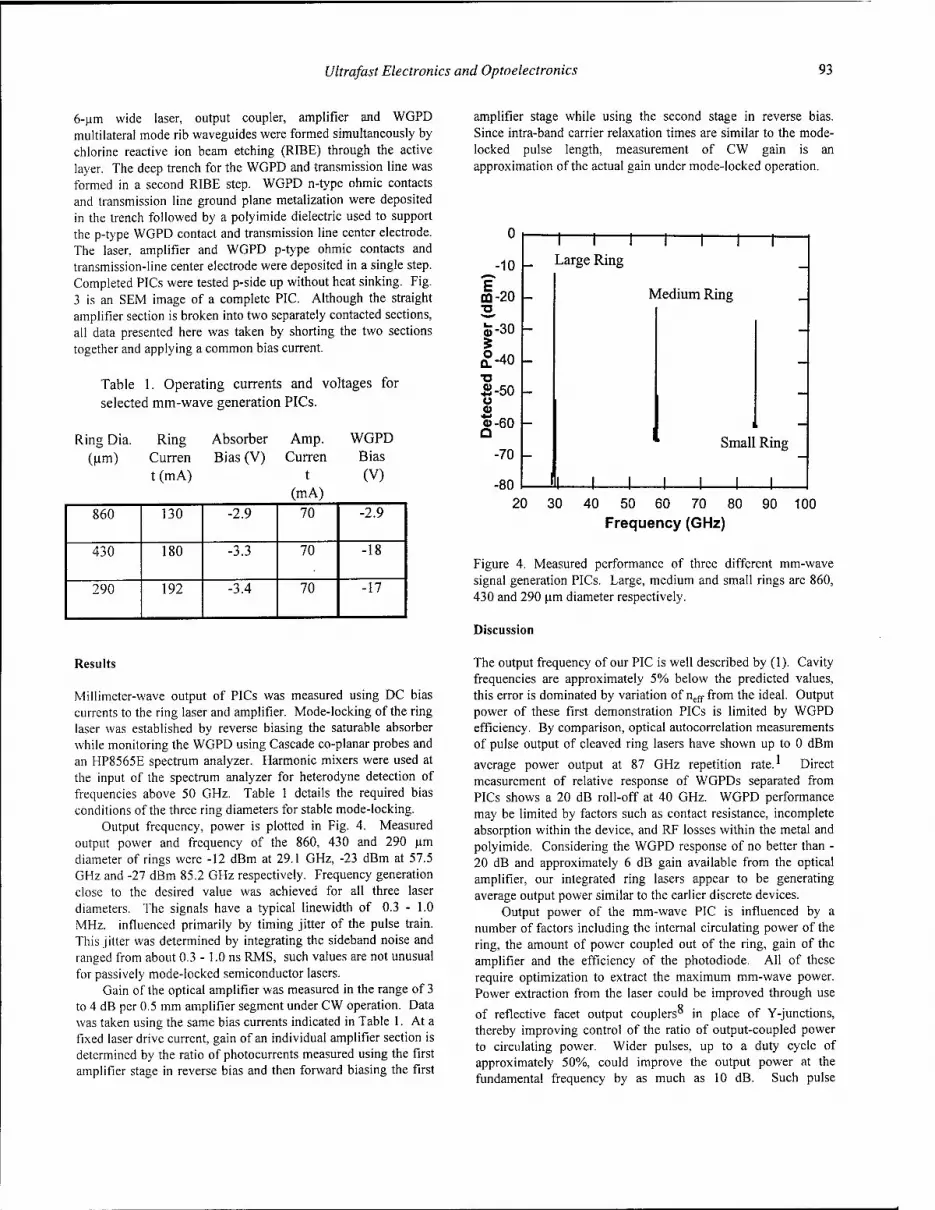
Ultrafast Electronics and Optoelectronics 93
6-um wide laser, output coupler, amplifier and WGPD multilateral mode rib waveguides were formed simultaneously by chlorine reactive ion beam etching (RIBE) through the active layer. The deep trench for the WGPD and transmission line was formed in a second RIBE step. WGPD n-type ohmic contacts and transmission line ground plane metalization were deposited in the trench followed by a polyimide dielectric used to support the p-type WGPD contact and transmission line center electrode. The laser, amplifier and WGPD p-type ohmic contacts and transmission-line center electrode were deposited in a single step. Completed PICs were tested p-side up without heat sinking. Fig. 3 is an SEM image of a complete PIC. Although the straight amplifier section is broken into two separately contacted sections, all data presented here was taken by shorting the two sections together and applying a common bias current.
Table 1. Operating currents and voltages for selected mm-wave generation PICs.
Ring Dia. Ring (urn) Curren
t(mA)
Absorber Bias (V)
Amp. Curren
t (mA)
WGPD Bias
(V)
860 130 -2.9 70 -2.9
430 180 -3.3 70 -18
290 192 -3.4 70 -17
amplifier stage while using the second stage in reverse bias. Since intra-band carrier relaxation times are similar to the mode- locked pulse length, measurement of CW gain is an approximation of the actual gain under mode-locked operation.
-10
"I 1 1 _ Large Ring
I "I 1 1
■—■
m-20 T3
Medium Ring _
fe-30
2-40 ■o .2-50 u 0) «-60 Q
-70
i ""■
1 Small Ring
-80 "I I I J 1 1 1 20 30 40 50 60 70 80 90 100
Frequency (GHz)
Figure 4. Measured performance of three different mm-wave signal generation PICs. Large, medium and small rings are 860, 430 and 290 urn diameter respectively.
Discussion
Results
Millimeter-wave output of PICs was measured using DC bias currents to the ring laser and amplifier. Mode-locking of the ring laser was established by reverse biasing the saturable absorber while monitoring the WGPD using Cascade co-planar probes and an HP8565E spectrum analyzer. Harmonic mixers were used at the input of the spectrum analyzer for heterodyne detection of frequencies above 50 GHz. Table 1 details the required bias conditions of the three ring diameters for stable mode-locking.
Output frequency, power is plotted in Fig. 4. Measured output power and frequency of the 860, 430 and 290 urn diameter of rings were -12 dBm at 29.1 GHz, -23 dBm at 57.5 GHz and -27 dBm 85.2 GHz respectively. Frequency generation close to the desired value was achieved for all three laser diameters. The signals have a typical linewidth of 0.3 - 1.0 MHz, influenced primarily by timing jitter of the pulse train. This jitter was determined by integrating the sideband noise and ranged from about 0.3 - 1.0 ns RMS, such values are not unusual for passively mode-locked semiconductor lasers.
Gain of the optical amplifier was measured in the range of 3 to 4 dB per 0.5 mm amplifier segment under CW operation. Data was taken using the same bias currents indicated in Table 1. At a fixed laser drive current, gain of an individual amplifier section is determined by the ratio of photocurrents measured using the first amplifier stage in reverse bias and then forward biasing the first
The output frequency of our PIC is well described by (1). Cavity frequencies are approximately 5% below the predicted values, this error is dominated by variation of neff from the ideal. Output power of these first demonstration PICs is limited by WGPD efficiency. By comparison, optical autocorrelation measurements of pulse output of cleaved ring lasers have shown up to 0 dBm
average power output at 87 GHz repetition rate. Direct measurement of relative response of WGPDs separated from PICs shows a 20 dB roll-off at 40 GHz. WGPD performance may be limited by factors such as contact resistance, incomplete absorption within the device, and RF losses within the metal and polyimide. Considering the WGPD response of no better than - 20 dB and approximately 6 dB gain available from the optical amplifier, our integrated ring lasers appear to be generating average output power similar to the earlier discrete devices.
Output power of the mm-wave PIC is influenced by a number of factors including the internal circulating power of the ring, the amount of power coupled out of the ring, gain of the amplifier and the efficiency of the photodiode. All of these require optimization to extract the maximum mm-wave power. Power extraction from the laser could be improved through use
of reflective facet output couplers" in place of Y-junctions, thereby improving control of the ratio of output-coupled power to circulating power. Wider pulses, up to a duty cycle of approximately 50%, could improve the output power at the fundamental frequency by as much as 10 dB. Such pulse
94 Ultrafast Electronics and Optoelectronics
broadening may be achievable using grating or waveguide- coupler filters within the ring cavity to reduce the lasing spectral bandwidth. Improvements in amplifier gain, detector efficiency and detector power handling capability would also increase the output power of the PIC. Use of a TWPD would increase the output by as much as a factor of 10 at these demonstration frequencies and may be required above 100 GHz due to the poor WGPD efficiency. A flared amplifier with one or more photodiodes operating in parallel at the wide amplifier output end may result in dramatic power enhancements. Finally, pulse-to- pulse timing jitter could be reduced to the femtosecond regime through the use of an electronic phase-lock loop providing feedback from the pulse output to the saturable absorber section.
Conclusion
In summary, we have demonstrated the first PIC for direct generation of mm-wave frequencies. This PIC integrates a passively mode-locked semiconductor ring laser with an optical amplifier and high-speed waveguide photodiode. By generating and amplifying a train of optical pulses and using and integrated waveguide photodiode to convert the optical pulses into an electrical signal, this circuit has been used to generate -23 and - 27 dBm of mm-wave power at 57.5 and 85.2 GHz respectively. Similarly, direct sampling of the saturable absorber has generated -12 dBm at 29.1 GHz. PICs using this concept can used in a wide variety of applications where a very compact, lightweight mm-wave source is required.
Acknowledgments
The authors would like to thank D. Tibbetts-Russell, B. Fuchs for technical assistance. This work was supported by United States Department of Energy under Contract DE-AC04- 94AL85000. Sandia is a multiprogram laboratory operated by Sandia Corporation, a Lockheed-Martin Company, for the United States Department of Energy.
References
[1] J. P. Hohimer and G. A. Vawter,"Passive mode locking of monolithic semiconductor ring lasers at 86 GHz," Appl. Phys. Lett., vol. 63, pp. 1598-1600, 1993.
[2] V. M. Hietala, G. A. Vawter, T. M. Brennan and B. E. Hammons,"Traveling-wave photodetectors for high-power large-bandwidth applications," IEEE Trans, on Microwave Th. and Tech., vol. 43, pp. 2291-2297, 1995.
[3] K. S. Giboney, R. L. Nagarajan, T. E. Reynolds, S. T. Allen, R. P. Mirin, M. J. Rodwell and J. E. Bowers,"Travelling- wave photodetectors with 172-GHz bandwidth and 76 GHz bandwidth-efficiency product," IEEE Phot. Technol. Lett., vol. 7, pp. 412-414, 1995.
[4] L. Y. Lin, M. C. Wu, T. Itoh, T. A. Vang, R. E. Muller, D. L. Sivco and A. Y. Cho,"Velocity-Matched Distributed Photodetectors with High-Saturation power and large bandwidth," IEEE Phot. Technol. Lett., vol. 8, pp. 1376- 1378, 1996.
[5] J. P. Hohimer, G. A. Vawter, D. C. Craft and G. R. Hadley,"Improving the Performance of Ring Diode Lasers by Controlled Reflection Feedback," Appl. Phys. Lett., vol. 61, pp. 1013-1015, 1992.
[6] J. C. Zolper, A. G. Baca and S. A. Chalmers,"Thermally Stable Oxygen Implant Isolation of p-type AlGaAs," Appl. Phys. Lett, vol. 62, pp. 2536-2538, 1993.
[7] R. P. Bryan, J. J. Coleman, L. M. Miller, M. E. Givens, R. S. Averback and J. L. Klatt,"Impurity induced disordered quantum well heterostructure stripe geometry lasers by MeV oxygen implantation," Appl. Phys. Lett., vol. 55, pp. 94-96, 1989.
[8] J. P. Hohimer, G. R. Hadley and G. A. Vawter, "Semi- conductor Ring Lasers With Reflection Output Couplers," Appl. Phys. Lett, vol. 63, pp. 278-280, 1993.

Ultrafast Photoconductive Switches with a Gap of 43 nm Fabricated by an Atomic Force Microscope
Taro Itatani, Tadashi Nakagawa and Kazuhiko Matsumoto Electrotechnical Laboratory,
1-14 Umezono Tsukuba-shi, Ibaraki, 305 Japan
Yuichi Kotaki and Hisao Uchiki Nagaoka University of Technology,
Kamitomioka 1603-1, Nagaoka, 940-21 Japan
Abstract
Photoconductive switches with a gap of 43 nm have been fabricated by using an atomic force microscope. Ultrafast response of the switches have been measured by electrooptic sampling method. Intrinsic response of the switch has been estimated as 210 fs by extrapolation of impulse response at zero distance.
Key Words
Photoconductive switch, Atomic force Microscopy, Electrooptic sampling, Ultrafast.
I. Introduction
Metal-semiconductor-metal(MSM) photoconductive switches have been developed as a source of high speed electrical signals. Electrical signals in femtosecond region have been generated from MSM photoconductive switches. It is efficient to decrease carrier life time and transit time of electrons and holes to achieve ultrafast MSM photoconductive switches. Low temperature crystal growth[l] and ion implantation[2] have been also utilized to decrease carrier life time in femtosecond region. Nano-meter fabrication technology has been utilized to decrease transit time of carriers. Electron beam lithographyfl] and scanning probe process[3] have been developed to realize narrow photoconductive gaps. The probe process based on a scanning tunneling microscope(STM) or an atomic force microscope(AFM) has been developed rapidly in recent years. We made 43-nm-gap photoconductive switches by the oxidation process which is recently proposed[4] and developed[5].
II. Fabrication Process
The sample was set in an air-ambient AFM after the deposition of a 4 nm thick titanium layer on an unintentionally-doped semi-insulating GaAs substrate. The oxide line was formed by moving the cantilever at the bias voltage of 8 V negatively to the sample. The scan speed for this sample is 10 nm/sec. We formed narrower oxidized wire(43 nm) by reducing the bias voltage compared to the line of 100 nm at the bias voltage of 10V[3]. The relation between the dark current and the bias voltage is shown in Figure 1. The resistance is 2 M£2 at low bias condition, and is 773 k£2 at the bias voltage of 2 V. The resistance is smaller than the reported value of 10 Mfl for the photoconductive switch with a gap of 100 nm[3]. The decrease of Schottkey-barrier height is enhanced due to the strong electric field between the electrodes at the same bias condition compared to a 100-nm-gap-switch. The excess capacitance due to the oxidized titanium is calculated to be 0.14 fF from the measured dielectric constant(er = 24)[5], which is much smaller than the capacitance caused by the GaAs substrate. This oxide wire is not only transparent to the excitation beam but also a good insulator. After the oxidization, we formed coplanar transmission lines. The transmission lines were made of Ti / Au, and they were 10 ^m wide and 200 nm thick. The line separation was 10 (im. We removed the excess titanium thin film except for the part of the photoconductive switch by reactive ion etching.
III. Measurement
The ultrafast electrical pulses from the photoconductive switch were measured on the coplanar transmission line by the electrooptic sampling system[6] which can estimate both transverse component and longitudinal component of electric field without changing the configuration of the device under test. The longitudinal component cannot be ignored since electrical signals in femtosecond region cannot be expressed by a simple TEM approximation. The electrooptic sampling system is based on a colliding pulse
OSA TOPS on Ultrafast Electronics and Optoelectronics, 1997
Vol. 13, Martin Nuss and John Bowers (ed.) ©1997 Optical Society of America
95
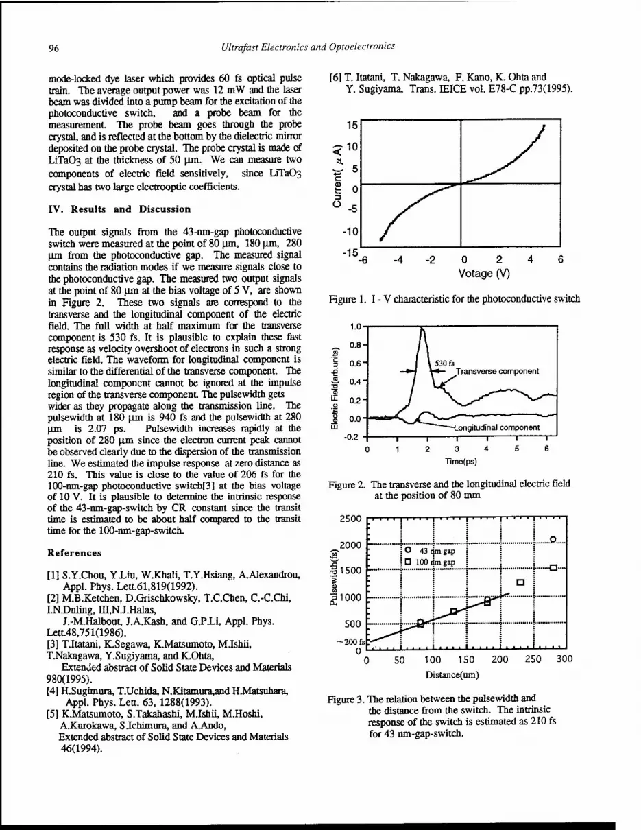
96 Ultrafast Electronics and Optoelectronics
mode-locked dye laser which provides 60 fs optical pulse train. The average output power was 12 mW and the laser beam was divided into a pump beam for the excitation of the photoconductive switch, and a probe beam for the measurement The probe beam goes through the probe crystal, and is reflected at the bottom by the dielectric mirror deposited on the probe crystal. The probe crystal is made of LiTa03 at the thickness of 50 \im. We can measure two components of electric field sensitively, since LiTaOß crystal has two large electrooptic coefficients.
IV. Results and Discussion
The output signals from the 43-nm-gap photoconductive switch were measured at the point of 80 urn, 180 |xm, 280 jim from the photoconductive gap. The measured signal contains the radiation modes if we measure signals close to the photoconductive gap. The measured two output signals at the point of 80 um at the bias voltage of 5 V, are shown in Figure 2. These two signals are correspond to the transverse and the longitudinal component of the electric field. The full width at half maximum for the transverse component is 530 fs. It is plausible to explain these fast response as velocity overshoot of electrons in such a strong electric field. The waveform for longitudinal component is similar to the differential of the transverse component. The longitudinal component cannot be ignored at the impulse region of the transverse component The pulsewidth gets wider as they propagate along the transmission line. The pulsewidth at 180 fjjn is 940 fs and the pulsewidth at 280 Urn is 2.07 ps. Pulsewidth increases rapidly at the position of 280 um since the electron current peak cannot be observed clearly due to the dispersion of the transmission line. We estimated the impulse response at zero distance as 210 fs. This value is close to the value of 206 fs for the 100-nm-gap photoconductive switch[3] at the bias voltage of 10 V. It is plausible to determine the intrinsic response of the 43-nm-gap-switch by CR constant since the transit time is estimated to be about half compared to the transit time for the 100-nm-gap-switch.
References
[1] S.Y.Chou, YJLiu, W.Khali, T.Y.Hsiang, A.Alexandrou, Appl. Phys. Lett61,819(1992).
[2] M.B.Ketchen, D.Grischkowsky, T.C.Chen, C.-C.Chi, I.N.Duling, m,NJ.Halas,
J.-M.Halbout J.A.Kash, and CPU, Appl. Phys. Lett48,751(1986). [3] T.Itatani, K.Segawa, K.Matsumoto, MJshii, TNakagawa, Y.Sugiyama, and K.Ohta,
Extended abstract of Solid State Devices and Materials 980(1995). [4] H.Sugimura, T.Uchida, N.Kitamura,and H.Matsuhara,
Appl. Phys. Lett. 63, 1288(1993). [5] K.Matsumoto, S.Takahashi, Mishii, MHoshi,
A.Kurokawa, SJchimura, and A.Ando, Extended abstract of Solid State Devices and Materials 46(1994).
[6] T. Itatani, T. Nakagawa, F. Kano, K. Ohta and Y. Sugiyama, Trans. IEICE vol. E78-C pp.73(1995).
15
is I 0 ü -5
-10
-15 -2024
Votage (V)
Figure 1. I - V characteristic for the photoconductive switch
B
-e
ID il
J 0.0' 111
-0.2
Transverse component
.ongitudinal component —1 1 1
3 4
Time(ps)
Figure 2. The transverse and the longitudinal electric field at the position of 80 mm
2500
2000
iisoo '$ 8 g1000
500
-200 fs 0
! O 43 dm gap I ;D 100 am gap
] |.......P.....
a 1
i^D""
50 100 150 200 Distance(um)
250 300
Figure 3. The relation between the pulsewidth and the distance from the switch. The intrinsic response of the switch is estimated as 210 fs for 43 nm-gap-switch.

Sandwich microstrip lines with polymer dielectric for high—speed on—chip interconnects
H.-M. Heiliger, M. Nagel, H. G. Roskos*, R. Hey**, and H. Kurz Institut für Halbleitertechnik II, RWTH Aachen, Sommerfeldstraße 24, D-52056 Aachen, Germany
*Physikalisches Institut, Johann Wolf gang Goethe-Universität, D-60323 Frankfurt, Germany **Paul-Drude-Institut, Hausvogteiplatz 5-7, D-10117 Berlin, Germany.
Abstract
Polymer-based sandwich microstrip transmission lines are investigated for the use as ultrafast interconnects in microelectronic circuits. Electronic-grade Benzocy- clobutene (Cyclotene) is applied as dielectric medium. Optoelectronic pulse-propagation measurements com- paring the microstrip lines with standard coplanar waveguides show that the waveguides are free of modal dispersion up to the highest frequencies of 1.2 THz. Signal attenuation is low (<1 dB/mm at 0.1 THz, « 6 dB/mm at 1.2 THz), dominated by conductor losses. Radiation losses are negligible for all sandwich mi- crostrip lines tested. Shielding by the ground conductor ensures that the waveguides are immune against Drude absorption in lossy substrates.
Keywords
Thin-film microstrip lines, Ultrafast measurements, Polymer waveguides, Optoelectronics
Introduction
The continuing rise in operation frequency of the fastest microelectonic circuits [1] necessitates a reevaluation of the way how devices are interconnected on chip. At present, the coplanar waveguide (CPW) design concept is applied in GHz applications. CPWs have widely replaced the classic microstrip line (MSL) approaches with the signal conductor on the front and the ground conductor on the backside of the wafer. This choice has been made mainly for two reasons: (i) to avoid the need for via holes for contacting of the ground conductor and (ii) because the conventional MSL requires a conduc- tor width comparable to the thickness of the substrate in order to obtain the conventional 50 Q, impedance.
Since substrate thinning has its limitations, the con- ductor width remains fairly large. As a consequence, higher transverse modes can propagate already at fre- quencies on the order of tens of GHz, leading to pro- nounced modal dispersion (see, e.g. [2]) that makes con- ventional MSLs unsuitable for applications in the range at and above tens of GHz. CPWs, however, also have their problems. As they consist of three conductors, undesired modes with antisymmetric field distributions and different propagation constants can be excited [3]. These modes must be suppressed by equilibration of the ground potential via incorporation of air bridges. Furthermore, CPWs are prone to radiation losses that must be minimized by chosing suitably small waveguide dimensions [4].
In recent years, an alternative microstrip concept has emerged that avoids the fundamental problems of MSLs and CPWs: thin-film microstrip lines (TFMSLs), also known as sandwich microstrip lines [2], [5], [6]. Both signal and ground conductors are located on the wafer surface separated by a thin dielectric insulator layer. Because the width of the dielectric can be chosen over quite a wide range, there is considerable freedom for the selection of the width of the signal conductor. It can be realized with lateral dimensions down to the 1- /xm scale allowing to adjust the impedance while min- imizing the line width and the modal dispersion. An important consequence of the mode confinement above the substrate is that sandwich MSLs are unaffected by substrate properties, such as electric conductivity or high permittivity, that would be detrimental to CPWs. The mode confinement furthermore promises reduced crosstalk between neighboring lines and thus high pack- ing densities in integrated circuits. Another advan- tage is that the availability of various suitable poly- mers makes TFMSL fabrication nearly as easy as that of CPWs while improving the range of possible applica-
OSA TOPS on Ultrafast Electronics and Optoelectronics, 1997 Vol. 13, Martin Nuss and John Bowers (ed.) ©1997 Optical Society of America
97

98 Ultrafast Electronics and Optoelectronics
tions considerably [6]. In this paper, we discuss the fab- rication technology of TFMSLs based on the polymer Cyclotene. Comparative electrooptic sampling mea- surements show that the TFMSLs exhibit superior at- tenuation and dispersion properties over the whole GHz frequency range making them attractive candidates for ultrahigh-frequency interconnects [7].
Fabrication
Our TFMSLs (see Fig. 1) are fabricated on low- resistivity (5-8 Ocm) Si substrates. First, an 800- nm-thick Al ground-conductor metallization is de- posited onto the Si wafer by electron beam evapora- tion. Then, the insulator material, commercially avail- able Cyclotene 3022-46 from Dow Chemicals, is spin- deposited. Cyclotene is a resin based on Bisbenzocy- clobutene (BCB) momomers developed for applications in microelectronics such as passivation coatings and di- electrics for inter-chip connects in multi-chip modules [8]. It is cured for 60 minutes at 250°C in a N2 ambi- ent. After polymerization, the signal conductor with an integrated photoconductive (PC) switch is fabri- cated. First, a 500x500 /im2 piece of 500-nm-thick lift-off LT-GaAs (LT: low-temperature-grown) is van- der-Waals bonded onto the polymer at the position in- tended for the PC switch (see below). After removal
Cross Section Probe
EO Crystal
Aluminum
Fig. 1. Schematic representation of the waveguide in cross section (upper part) and of the experimental setup for the electrooptic on-wafer pulse propagation measurements (lower part).
of the Apiezon coating utilized for handling of the LT- GaAs, the latter one is patterned into a 20-/im-small stripe. Finally, an 800-nm-thick Al film is deposited and patterned by lift-off technique into an 8-jum-wide signal conductor with a 5 jum PC gap on top of the LT- GaAs. We have prepared two samples, one with 1.7- jum-thick Cyclotene (spin-coating at 9000 rpm for 30 s) and the other with 5.4-/mi-thick polymer (1000 rpm for 30 s). Because the signal conductors have the same width, the characteristic impedance varies. Simulations yield 35 Q for the 1.7 /mi sample and 70 O for the 5.4 /mi version.
Compared to polyimides that may be employed as dielectrics in waveguides as well, cured Cyclotene resin supposedly absorbs less moisture while it exhibits a static dielectric constant as low as that of polyimides {er,stat = 2.7 for Cyclotene) [9].
The piece of LT-GaAs layer utilized in the PC switch is taken from a wafer that has been grown by molec- ular beam epitaxy at 200°C on (lOO)-oriented semi- insulating GaAs after following deposition of a layer of 100 nm sacrifical AlAs at 550°C. The wafer has been annealed in situ at 615°C for 15 minutes in an As- rich atmosphere. The epitaxial lift-off process and the bonding of LT-GaAs on Cyclotene follow the proce- dure first presented in Ref. [10]. Small pieces are coated on top with Apiezon W for better mechanical stability and handling of the LT-GaAs films after lift-off. The LT-GaAs/Apiezon stack is lifted off by dissolving the AlAs layer in diluted (10%) HF at 0°C over several hours. The LT-GaAs/Apiezon film is placed onto the substrate and van-der-Waals bonded during a drying step at 85° C.
Electrooptic characterization
The waveguides are characterized by time-domain elec- trooptic (EO) sampling (see Fig. 1) with 150-fs pulses from a 76-MHz Tirsapphire laser operating at a wave- length of 780 nm. Two excitation schemes are em- ployed. In the measurements on the TFMSLs, a pump beam (4 mW average power) illuminates the 15-V- biased integrated PC gap generating picosecond electric pulses directly on the TFMSL. The time-delayed pulses of the probe beam detect the electric transients after a propagation distance zi with the help of a LiTaOs EO transducer. In the measurement on the CPW, that does not contain an integrated PC switch, excitation is achieved with the help of a freely positionable PC probe [11], [12].
Figure 2 displays detected pulses in the time do- main for the 35-ft TFMSL (upper graph) and the 70-fi TFMSL (lower graph) at various positions zi, (I = 1, 2, 3, ...) along the lines. The values of zt are given in mm from the first sampling position z\ = 0. Effects of finite propagation velocity, attenuation and dispersion are directly obvious from the time-domain data. With increasing propagation length, the pulses decrease in amplitude and increase in pulse width. For the 35-fi line, losses and dispersion are more pronounced. In ad- dition, we observe for both lines pulse pedestals that increase slightly with increasing zi. The pedestals are barely discernible in the case of the 70-0 line but clearly visible for the 35-fi line. Finally, a closer look at the first three locations on the 70-ft TFMSL (for zt = 0, 0.4,1.7 mm) reveals a ringing in the decaying part of the pulse. It is caused by excitation of polariton modes in the LiTa03 detector crystal. These are mixed modes of

Ultrafast Electronics and Optoelectronics 99
the electromagnetic signal with lattice vibrations whose propagation direction is oriented perpendicular to the wafer surface [13]. Reflection at the topside of the elec- trooptic crystal results in a standing-wave resonance.
c 3
<D -Ö 3
-t->
"EH
CO C
1.0
0.8
0.6
0.4
0.2
0.0
1.4
1.2
1.0
0.8
0.6
0.4
0!2
0.0
35 n TFM3L~
y40itol<Mmww& z. =0.0 mm
10 20 30
Time (ps)
40
Fig. 2. Electric signals probed at several positions Z/ (given in mm) on the 35-H TFMSL (upper graph) and on the 70-fi TFMSL (lower graph). The signals are normalized to the maxi- mum of the first pulse.
For our probe, the resonance occurs at a frequency of 1.25 THz. The polariton feature is not observed on the 35-fi TFMSL because a different EO transducer has been used.
For a more detailed analysis, the frequency- dependent propagation constants are extracted up to 1.2 THz from the time-domain data. The complex propagation constant 7(/) = a(f) + i ■ ß{f), with a describing the attenuation and ß the dispersion as a function of frequency /, is determined from the Fourier transforms of the time-domain data.
Figure 3 displays er.,e//(/) for the two TFMSLs. In accordance with the low optical dielectric constant of Cyclotene (er,stQt = 2.7, eoo = 2.43) the values of er,eff{f) in the (sub)millimeterwave regime are fairly low leading to high signal velocities on the order of 0.2 mm/ps. For both lines, eT,eff decreases monotoni- cally with increasing frequency. There is no indication for modal dispersion that would reveal itself by an in-
crease of er>e// with rising / when the cut-off frequency for the next highest mode is approached [2], [5]. The rise of erteff for / —>■ 0 results from the finite conductiv- ity of the metallization (skin effect) and is well known in the analysis of waveguides including low-dispersive
3.6
3.4
3.2
3.0
2.8
2.6
2.4
2.2
- 35 n TFMSL
- 70 fi. TFMSL
0.0 0.2 0.4 0.6 0.8
Frequency (THz) 1.0 1.2
Fig. 3. Frequency dependence of the effective permittivity of both TFMSLs.
CPWs [14]. The more pronounced dispersive behavior of the 35-fi line as compared to 70-fi TFMSL reflects the expected trend that the rise of er,e// for / -> 0 is more pronounced when the conductor losses are higher.
Fig. 4 presents the attenuation a(f) as a function of frequency for the two TFMSLs. In both cases, a(f)
/—N 10 " 1 1 1 ' ( ' 1 ' 1
1^ s s 70 n TFMSL s-1 ■
PQ 8 -
a 6 c / 0 *S *' s ' ^'
4 «1 3 J ^ s - * c 2 - / --' -
-*-* < -.1.1.1.1.1
0.0 0.2 0.4 0.6 0.8 1.0
Frequency (THz) 1.2
Fig. 4. Frequency dependence of the attenuation of both TFM- SLs.
rises strongly from the low-frequency values to about ten times these values at 1.2 THz. The relative differ- ences between the two TFMSLs are more pronounced in a(f) than in cr,e//(/)- Over the entire frequency range, the attenuation of the 35-0 line is about twice that of the 70-fi TFMSL. This is consistent with the ex- pectation that a ~ R' /Z, where R' denotes the Ohmic resistance per length of the signal line and Z is the characteristic impedance.
Comparison of the experimental data with results of method-of-lines simulations (not shown here) yield good agreement if a frequency-independent loss tan-

100 Ultrafast Electronics and Optoelectronics
gent with a value tan<5£ = 0.015 and negligible radia- tion losses are assumed [7]. Conductor losses (scaling with y/f) dominate over dielectric losses (alphadiel ~ / tan je) over the full frequency range of the measure- ments. Dielectric loss is more significant for the high- impedance line, where it amounts about one third of the attenuation at 1.0 THz.
Comparison with coplanar waveguides
For a comparison of the pulse-propagation properties of TFMSLs with those of CPWs, we have performed EO- sampling studies on a state-of-the-art 50-fi CPW. Its signal conductor is 12 /an wide and 20 mm long, the signal-ground separation is 8 /im. Conductor losses are minimized by employing a thick 800-nm Au met- allization, radiation loss is reduced by selecting a small ground-conductor width of 12 /im. For low dielectric losses, a high-resistivity (1000-5000 Hem) Si substrate is chosen. The metallization is deposited directly onto the Si without an insulating layer inbetween.
Because the CPW does not contain an integrated PC switch, electric-pulse generation is performed with the help of a freely positionable PC probe as illus- trated in Fig. 5. We employ a second-generation probe that has been improved compared to earlier silicon-on-
Optical Probe Pulse
Optical Pump Pulse
Fig. 5. Pulse propagation experiment on the CPW: A freely po- sitionable probe injects electric pulses that are detected with an EO crystal.
sapphire-based probes with respect to probe invasive- ness and switching efficiency [11], [12]. These advances are achieved by employing thin and narrow slabs of quartz glass as probe substrates (lower dielectric con- stant than sapphire) and lift-off LT-GaAs as PC mate- rial (higher switched voltages). The electrode consists of a 600-nm-thick and 15-/xm-wide Au metallization with a gap at the PC switch close to the end of the probe. The gap is realized as an interdigitated finger structure with finger widths and spacings of 3 /um. For contacting of the sample, a Ni tip (5-/xm diameter, 1- fxra high) is deposited onto the short electrode stub by electroplating.
Figure 6 displays a pulse detected on the CPW at a distance of 750 /im away from the injection point. Care has been taken to place the probe tip onto the very end of the signal conductor of the CPW in order to inject only a single pulse instead of two counterpropagating
pulses that might interfere with each other. The ampli- tude of the detected signal is 800 mV (bias on the PC gap: 15 V), the full width at half maximum is 750 fs. To our knowledge, this is the shortest pulse ever ob-
800
600-
4) "§ 400
S 200 <
0
o ItHXI ■
3 \^^
1
Four
ier
Am
plitu
de
^\ 7snfs 1,
V 0 0.5 1.0 1.5
Frequency (THz)
i . i . i i . i . i
-2 2 4 6
Time (ps) 10
Fig. 6. Electrooptically detected transient on a 50-fi CPW after pulse injection with a freely positionable PC probe. Inset: Fourier spectrum.
tained by external injection with a probe. The Fourier transform of the pulse, displayed in the inset of Fig. 6, shows that the pulse has an extremely large bandwidth with useful frequency components up to 1.5 THz.
0.0 0.2 0.4 0.6 0.8 1.0 1.2 1.4 Frequency (THz)
Fig. 7. Frequency-dependent wave propagation characteristics of the CPW.
Measurements of the waveform at different positions along the line allow us to extract the attenuation and permittivity functions of the CPW. The data are shown in Fig. 7 over the large frequency range 0-1.5 THz. Up to 0.9 THz, the attenuation exhibits the (sub)linear fre- quency dependence typical for the dominance of con- ductor and dielectric losses. The rise at higher frequen- cies is characteristic for the onset of radiation losses. The permittivity data reveal significant dispersion of the line over the full frequency range except for a win- dow between 200 and 350 GHz. Dispersion is skin- effect related below that frequency window [14], while it results from the onset of higher-order modes for fre- quencies above.

Ultrafast Electronics and Optoelectronics 101
Comparing the permittivity of the CPW with that of the TFMSLs as displayed in Fig. 3, we find that the performance of the CPW is in all respects inferior to that of the TFMSLs: The permittivity is generally higher and has a stronger frequency dependence. The higher values are a consequence of the high static di- electric constant of Si as compared to Cyclotene. This is also revealed in the lower pulse propagation velocity of 0.12 mm/ps. While the CPW exhibits modal disper- sion at very high frequencies, the TFMSL do not. On the low frequency-side, that is more important for ap- plications, the CPW is hampered by more pronounced skin-effect-related dispersion.
With respect to attenuation, the differences between the CPW and the TFMSLs are minor. While the 35- Ü TFMSL has about twice higher overall losses than the CPW, signal attenuation on the 70-ft TFMSL up to 1.2 THz is comparable to that on the CPW. Signal propagation on a properly designed 50-fi TFMSL will surely be more lossy than on the CPW, although the difference should be moderate .
Conclusions
Thin-film microstrip lines (TFMSLs) with Cyclotene dielectric exhibit low-dispersive quasi-TEM properties with negligible radiation loss up to frequencies of 1.2 THz. Since the waveguide structure is confined to the top of the substrate, TFMSLs can readily be em- ployed on low-resistivity substrates. These proper- ties make the TFMSL a highly attractive candidate as transmission-line element in GHz integrated circuits.
Acknowledgments
We are grateful to Dow Chemicals for supplying us with free samples of Cyclotene. This project has been funded by the DFG under contract Ku 540/22-1.
References
1. See, e.g., the contribution by the group of M. Rod- well in this book.
2. H. Roskos, M. C. Nuss, K. W. Goossen, D. W. Kisker, A. E. White, K. T. Short, D. C. Jacobson, and J. M. Poate, "Propagation of picosecond elec- trical pulses on a silicon-based microstrip line with buried cobalt silicide ground plane", Appl. Phys. Lett. 58 2604 (1991).
3. S. Alexandrou, R. Sobolewsky, and T. Y. Hsiang, "Time-domain characterization of bent coplanar waveguides", IEEE J. Quantum Electronics, 28 2325 (1992).
4. S. Alexandrou, C.-C. Wang, M. Cur- rie, R. Sobolewski, and T. Y. Hsiang, "Loss and dispersion at subterahertz frequencies in coplanar
waveguides with varying ground-plane width," in SPIE-OE/LASE '94, Proc. Tech. Optical Fiber Communication (Los Angeles CA, pp. 108, 1994).
5. J. Gondermann, E. Stein von Kamienski, H. G. Roskos, and H. Kurz, "Al-Si02-Al sandwich microstrip lines for high-frequency on-chip inter- connects" , IEEE Trans. Microwave Theory Tech. MTT-41 2087 (1993).
6. S. Banba and H. Ogawa, "Small-sized MMIC am- plifiers using thin dielectric layers", IEEE Trans. Microwave Theory Tech. MTT-43 485 (1995).
7. H.-M. Heiliger, M. Nagel, H. G. Roskos, H. Kurz, F. Schnieder, W. Heinrich, R. Hey, and K. Ploog, "Low-dispersion thin-film microstrip lines with Cyclotene (Benzocyclobutene) as dielectric medium", Appl. Phys. Lett. 70 (17), 28 April (1997).
8. P. B. Chinoy and J. Tajadod, "Processing and microwave characterization of multilevel intercon- nects using Benzocyclobutene dielectric", IEEE Trans. Components, Hybrids, and Manufactoring Tech. 16 704 (1993).
9. Data taken from Dow Chemical's product informa- tion sheet "Cyclotene Advanced Electronic Resin Introduction".
10. E. Yablonovitch, D. M. Hwang, T. J. Gmitter, L. T. Florez, and J. P. Harbison, "Van der Waals bonding of GaAs epitaxial liftoff films onto arbi- trary substrates", Appl. Phys. Lett. 56 2419 (1990).
11. H.-M. Heiliger, M. Vossebürger, H. G. Roskos, H. Kurz, R. Hey, and K. Ploog, "Application of liftoff low-temperature-grown GaAs on transpar- ent substrates for THz signal generation", Appl. Phys. Lett. 69 2903 (1996).
12. T. Pfeifer, H.-M. Heiliger, T. Löffler, C. Ohlhoff, C. Meyer, G. Lüpke, H. G. Roskos, and H. Kurz, "Optoelectronic On-Chip Characterization of Ul- trafast Electric Devices: Measurement Techniques and Applications", IEEE Selected Topics in Quan- tum Electronics, April 1997 edition.
13. O. Hollricher, "Elektrooptische Höchstfrequenzun- tersuchungen an Supraleitern und Halbleitern", Ph.D. dissertation (University of Cologne, 1993).
14. W. Heinrich, "Full-wave analysis of conductor losses on MMIC transmission lines", IEEE Trans. Microwave Theory Tech. MTT-38 1468 (1990).

An ultrafast high-jTc superconducting Y-Ba-Cu-O photodetector
Mikael Lindgren*, Wen-Sheng Zeng, Marc Currie, Carlo Williams, Thomas Y. Hsiang, Philippe M. Fauchet, and Roman Sobolewski
Department of Electrical Engineering and Laboratory for Laser Energetics, University of Rochester, Rochester, NY 14627, USA
Steven H. Moffat, Robert A. Hughes, and John S. Preston Brockhouse Institute for Materials Research, McMaster University, Hamilton, Ontario L8S 4M 1, Canada
Frank A. Hegmann Quantum Institute, University of California, Santa Barbara, CA 93106-5100, USA
Abstract
The single-picosecond photoresponse of a YBa2Cu307.;t
photodetector has been measured using electro-optic sam- pling and modeled by the Rothwarf-Taylor equations de- scribing nonequilibrium conditions in the superconductor.
Key Words
Ultrafast processes in condensed matter, Detectors-infrared, Optoelectronics, Detector materials.
Introduction
The photoresponse based on nonequilibrium processes in high Tc superconducting YBa2Cu307.;( (YBCO) thin films has been studied extensively, aimed at determining the maximum possible speed of a photodetector fabricated in this material [1-4]. The experimentally observed response has been attributed to nonequilibrium electron heating (near the critical temperature Tc) and superconducting kinetic in- ductance (far below Tc). In recent work, we have shown that both mechanisms have single-picosecond speed [5]. Thus, the intrinsic speed of a YBCO photodetector allows bit rates exceeding 100 Gbit/s, making it well suited for digital and communication applications. When considering applicability of YBCO for such high repetition-rate sig- nals, the electron-heating mechanism has a drawback, since it is associated with some temperature rise of the entire de- tector element, due to the bolometric response. In this re- spect, the kinetic inductive photoresponse mechanism is much better suited for very high speed photodetectors.
In this work we report the ultrafast response of a cur- rent-biased YBCO microbridge, fabricated from a very-high-
* E-mail: [email protected]
quality epitaxial YBCO film, irradiated by femtosecond op- tical pulses. The sample was biased in the superconducting state, with a current significantly smaller than the mi- crobridge critical current. We find that the response can be modeled using the Rothwarf-Taylor equations, which are fundamental for describing nonequilibrium conditions in a superconductor [6, 7]. All our experiments were performed using a cryogenic electro-optic (EO) experimental setup, characterized by <300-fs temporal resolution and <150-|J.V voltage sensitivity.
Experimental method
In order to measure the intrinsic speed of YBCO photore- sponse, the detector element was integrated with a coplanar waveguide (CPW). The CPW constituted a very convenient configuration for the EO sampling measurement technique. Since it is very difficult to accurately terminate the CPW for a broadband signal such as the picosecond electrical pulse, we made the transmission line as long as possible and achieved in that way an 80-ps-long reflection-free time window for the EO measurements, eliminating artifacts that may be caused by reflections at the end of the trans- mission line.
We used high-quality, 100-nm-thick epitaxial YBCO films, grown on 0.5-mm-thick, 6 x 6-mm2 LaA103 sub- strates using pulsed laser deposition. The experimental structure (shown as inset in Fig. 1) consisted of a 4-mm- long CPW with a 30-jlm-wide center line and 7-|im-wide gaps to the ground planes. A 5-|lm-wide, 7-|am-long mi- crobridge was placed in the middle of the CPW center line. The sample was mounted on a copper block inside an ex- change-gas, liquid-helium dewar, with optical access. One end of the CPW was wirebonded directly to a semirigid, 50- Q. coaxial cable, while the other end was wirebonded to ground. As shown in the Fig. 1 inset, the entire test struc-
OSA TOPS on Ultrafast Electronics and Optoelectronics, 1997 Vol. 13, Martin Nuss and John Bowers (ed.) ©1997 Optical Society of America
102

Ultrafast Electronics and Optoelectronics 103
O 0 > AH/MJ
Sampling beam
Excitation ^ beam
YBCO coplanar waveguide
Vvv^AA/W,^/vWvv
T=50K
Time (2 ps/div)
Figure 1. Photoresponse transient measured at T = 50 K. The inset shows the sample configuration and the electro- optic sampling beams.
1 1 1 1 1 1
_ m
E 2 - at / » \ Phonons T—
_
X,
// f Quasiparticles c a> TJ o u 1 _ - r CO a. m a 3 tr - - W Vt a o X /' w
0 ^W > / %% Generation rate/qp
1 I I I I I .1...
1 >
a ■o c o
Time (1 ps/div)
Figure 2. Solution of the Rothwarf-Taylor equations used to model the photoresponse. The solid lines are the excess quasi- particle and phonon densities, and the dashed line is the quasi- particle generation term.
ture was overlaid with an electro-optic LiTa03 crystal to facilitate the EO sampling measurements. The EO sam- pling setup has been described in detail previously [8]. In short, the detector was excited with ~100-fs wide pulses at 400 nm wavelength, with -60 (iW average power. The propagating pulse was probed with an 800-nm wavelength beam only -20 |im from the detector element, see Fig. 1 inset. During the measurements, the microbridge was cur- rent-biased through a microwave bias-tee and kept at a con- stant temperature T<TC.
Results
We observed a ~l-ps-wide transient of the shape shown in Fig. 1. This bipolar signal is characteristic for the kinetic inductive response [1]. Nearly identical transients were ob- served for all different bias currents in the entire tempera- ture range from 20 K to 80 K. After the main transient, a small oscillatory signal can be observed. These trailing os- cillations were present in all traces, but their origin is not understood at this point. The period of these oscillations does not correspond to any feature size, as it would if tran- sient reflections were the cause.
Nonequilibrium conditions in superconductors are of- ten described by the use of the Rothwarf-Taylor equations [6, 7]. The two coupled differential equations describe the interplay between the quasiparticles (QPs) and the phonons with an energy greater than or equal to twice the supercon- ducting gap A (called 2A phonons):
—^---1 -RNl+—N Jqp qp ' dt
dN„
0) "B
^r-\< (1)
Afqp and Na are the number per unit volume of QPs and of 2A phonons, respectively. /qp is the external generation rate for the QPs. In our simulation, 7qp is assumed to be a broadened Gaussian-shaped pulse, generating a maximum number of QPs -200 x 106 in the microbridge. R repre- sents the recombination rate for the QPs into Cooper pairs, and TB and Tes are the phonon pair breaking and the phonon escape times, respectively. Fig. 2 shows a typical solution of Eq. (1). The quasiparticle and phonon densities reach a plateau due to the slow process of phonon escape. Tes is on the order of nanoseconds [3], so the densities will decay back to their thermal equilibrium values before the next laser pulse.
Physically, a nonequilibrium condition is induced by photons breaking Cooper pairs into highly excited QPs. Next, the excess energy is rapidly redistributed within the electron system through electron-electron interactions, de- scribed by us as the broadening of the Gaussian generation term and defined by the electron thermalization time, Tet
[5]. As the system evolves, the population of QPs grows and the population of Cooper pairs decreases. The excited QPs interact with the phonons and transfer their energy to the lattice. The speed of this latter process is determined in

104 Ultrafast Electronics and Optoelectronics
>
a o >
-i—i—i—i—i—i—i—i—r -\—i—i—r
T=20K
./ *A * % v
_l I I L. _l I I I L. Time (1 ps/div)
Figure 3. Measured transient (dots) at T = 20 K and the results from the simulation (solid line).
the model by TB, while the excess heat transfer between the microbridge and the substrate is defined by Tes.
According to kinetic inductance theory [1], a photoin- duced change in the Cooper pair density gives rise to a voltage transient
K,„ = / dLkin
d/
where the kinetic inductance can be calculated as
•Mein
Nn
£<,«P ™Cp-Nqpwd
(2)
(3)
where e„ is the vacuum permittivity, cop = 1.67 x 10¹⁵ s"1
is the plasma frequency of YBCO, N0 is the total carrier density, NCp is the number of Cooper-pairs at the operating temperature, and /, w, and d are the bridge length, width, and film thickness, respectively. The photoresponse volt- age can thus be calculated as
parameters extracted from the fit were TB =2.0 ps and R = 3.8 x 10¹⁷ ps"1 cm3.
Conclusions and outlook
We have demonstrated that electrical transients of single- picosecond duration can be generated by a YBCO mi- crobridge biased in the superconducting state. Nonequili- brium conditions govern the observed photoresponse and can be accurately modeled by the Rothwarf-Taylor equa- tions. From our experiments we have extracted the charac- teristic time constants Tel = 0.93 ps and TB = 2.0 ps, which must be regarded as the intrinsic speed for a YBCO kinetic inductive photodetector. The mechanism for the photore- sponse is spectrally very broadband and detection from ul- traviolet to 10 |J.m wavelengths has been experimentally demonstrated [4, 5].
Our studies prove the high-speed capabilities of YBCO photodetectors, opening the door to many interesting appli- cations in the area of superconducting optoelectronics. The measured time constants demonstrate that such photodetec- tors can operate in digital applications requiring data rates far exceeding 100 Gbit/s. YBCO detectors, based on kinetic inductive response, operate in the fully superconducting regime, with extremely low power consumption (no ther- mal background) and low noise. The output signal is di- rectly proportional to the bias current, so implementation of films with high critical current densities ensure high re- sponsivity and long-term stability. The biasing scheme is simple and the material has a high absorption coefficient in the wavelength range from the ultraviolet to 10 p.m. It is expected that YBCO fiberoptic communication receivers with Gbit/s rates find applications as ultrafast optical-to- electrical transducers for digital electronics using rapid sin- gle-flux quantum (RSFQ) circuits and optical fibers for high-speed data transmission into the cryogenic environ- ment.
Acknowledgments
This research was supported by the Office of Naval Re- search grant N00014-96-1-1027. C. W. acknowledges sup- port from the U.S. Army Research Office AASERT grant DAAH04-95-1-0428.
1 I Nn aW„,
e0colwd{2NCv-N^) & (4)
Figure 3 shows a photoresponse signal (dots), very similar to that presented in Fig. 1, but acquired at T = 20 K. The solid line is a fit to the waveform, and was obtained by solving Eqs. (1) and (4). From this simulation, by us- ing a least-square fit, Tet was found to be 0.93 ps. Other
References
1.
2.
N. Bluzer, "Temporal relaxation of nonequilibrium in Y-Ba-Cu-0 measured from transient photoimpedance response," Phys. Rev. B, 44, 10222 (1991). F. A. Hegmann, D. Jacobs-Perkins, C.-C. Wang, S. H. Moffat, R. A. Hughes, J. S. Preston, M. Currie, P. M. Fauchet, T. Y. Hsiang, and R. Sobolewski, "Electro-optic sampling of 1.5-ps photoresponse sig-
Ultrafast Electronics and Optoelectronics 105
nal from YBa2Cu307.5 thin films," Appl. Phys. Lett., 67, 285 (1995).
3. M. Lindgren, M. A. Zorin, V. Trifonov, M. Danerud, D. Winkler, B. S. Karasik, G. N. Gol'tsman, and E. M. Gershenzon, "Optical mixing in a patterned YBa2Cu307.athin film," Appl. Phys. Lett., 65, 3398 (1994).
4. V. A. Trifonov, B. S. Karasik, M. A. Zorin, G. N. Gol'tsman, E. M. Gershenzon, M. Lindgren, M. Danerud, and D. Winkler, "9.6 um wavelength mixing in a patterned YBa2Cu307.A thin film," Appl. Phys. Lett, 68, 1418 (1996)."
5. M. Lindgren, M. Currie, C. Williams, T. Y. Hsiang, P. M. Fauchet, Roman Sobolewski, S. H. Moffat, R. A. Hughes, and J. S. Preston, and F. A. Hegmann, "Intrinsic photoresponse of a Y-Ba-Cu-0 superconduc- tor," submitted to Phys. Rev. Lett., July 1996.
6. A. Rothwarf and B. N. Taylor, "Measurement of re- combination lifetimes in superconductors," Phys. Rev. Lett. 19, 27 (1967).
7. C. C. Chi, M. M. T. Loy, and D. C. Cronemeyer, "Transient responses of superconducting lead films measured with picosecond laser pulses," Phys. Rev. B 23, 124 (1981).
8. M. Lindgren, M. Currie, C. Williams, T. Y. Hsiang, P. M. Fauchet, Roman Sobolewski, S. H. Moffat, R. A. Hughes, and J. S. Preston, and F. A. Hegmann, "Ultrafast Photoresponse in Microbridges and Pulse Propagation in Transmission Lines Made from High- Tc Superconducting Y-Ba-Cu-0 Thin Films," to be published in J. Sei. Top. Quantum Electron., Septem- ber 1996.
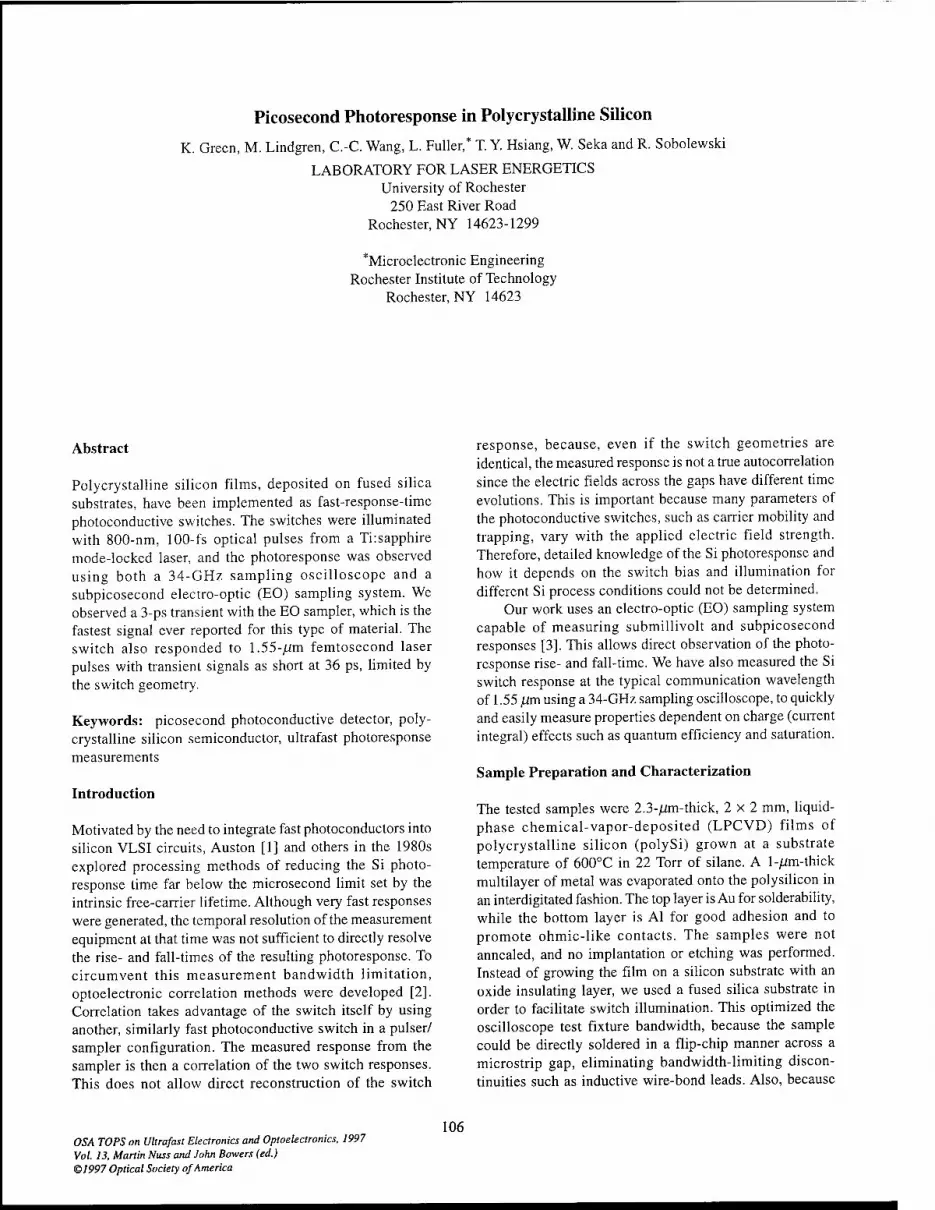
Picosecond Photoresponse in Polycrystalline Silicon
K. Green, M. Lindgren, C.-C. Wang, L. Fuller,* T. Y. Hsiang, W. Seka and R. Sobolewski
LABORATORY FOR LASER ENERGETICS University of Rochester
250 East River Road Rochester, NY 14623-1299
*Microelectronic Engineering Rochester Institute of Technology
Rochester, NY 14623
Abstract
Polycrystalline silicon films, deposited on fused silica substrates, have been implemented as fast-response-time photoconductive switches. The switches were illuminated with 800-nm, 100-fs optical pulses from a Ti:sapphire mode-locked laser, and the photoresponse was observed using both a 34-GHz sampling oscilloscope and a subpicosecond electro-optic (EO) sampling system. We observed a 3-ps transient with the EO sampler, which is the fastest signal ever reported for this type of material. The switch also responded to 1.55-jUm femtosecond laser pulses with transient signals as short at 36 ps, limited by the switch geometry.
Keywords: picosecond photoconductive detector, poly- crystalline silicon semiconductor, ultrafast photoresponse measurements
Introduction
Motivated by the need to integrate fast photoconductors into silicon VLSI circuits, Auston [1] and others in the 1980s explored processing methods of reducing the Si photo- response time far below the microsecond limit set by the intrinsic free-carrier lifetime. Although very fast responses were generated, the temporal resolution of the measurement equipment at that time was not sufficient to directly resolve the rise- and fall-times of the resulting photoresponse. To circumvent this measurement bandwidth limitation, optoelectronic correlation methods were developed [2]. Correlation takes advantage of the switch itself by using another, similarly fast photoconductive switch in a pulser/ sampler configuration. The measured response from the sampler is then a correlation of the two switch responses. This does not allow direct reconstruction of the switch
response, because, even if the switch geometries are identical, the measured response is not a true autocorrelation since the electric fields across the gaps have different time evolutions. This is important because many parameters of the photoconductive switches, such as carrier mobility and trapping, vary with the applied electric field strength. Therefore, detailed knowledge of the Si photoresponse and how it depends on the switch bias and illumination for different Si process conditions could not be determined.
Our work uses an electro-optic (EO) sampling system capable of measuring submillivolt and subpicosecond responses [3]. This allows direct observation of the photo- response rise- and fall-time. We have also measured the Si switch response at the typical communication wavelength of 1.55 /im using a 34-GHz sampling oscilloscope, to quickly and easily measure properties dependent on charge (current integral) effects such as quantum efficiency and saturation.
Sample Preparation and Characterization
The tested samples were 2.3-fJm-thick, 2x2 mm, liquid- phase chemical-vapor-deposited (LPCVD) films of polycrystalline silicon (polySi) grown at a substrate temperature of 600°C in 22 Torr of silane. A l-/im-fhick multilayer of metal was evaporated onto the polysilicon in an interdigitated fashion. The top layer is Au for solderability, while the bottom layer is Al for good adhesion and to promote ohmic-like contacts. The samples were not annealed, and no implantation or etching was performed. Instead of growing the film on a silicon substrate with an oxide insulating layer, we used a fused silica substrate in order to facilitate switch illumination. This optimized the oscilloscope test fixture bandwidth, because the sample could be directly soldered in a flip-chip manner across a microstrip gap, eliminating bandwidth-limiting discon- tinuities such as inductive wire-bond leads. Also, because
OSA TOPS on ultrafast Electronics and Optoelectronics, 1997 Vol. 13, Martin Nuss ami John Bowers (ed.) ©1997 Optical Society of America
106

Ultrafast Electronics and Optoelectronics 107
the sample was illuminated through the substrate for the scope measurements, reflection of the incident laser illumination from the metal contacts improved the quantum efficiency rather than lowering it, as front-side illumination would have done.
For characterization purposes, the polySi surface was etched preferentially at the grain boundaries, and a scanning electron microscope (SEM) image was taken of the surface (see Fig. 1), revealing a grain size of approximately 30 nm. A sample was also cleaved, and a 4-nm conductive silver layer was evaporated onto the exposed face, allowing a high- resolution SEM photograph of the switch cross section to be taken (see Fig. 2). The image shows the silica substrate at the bottom, 2.3 jim of polySi, and on top a multilayer of metal to allow a robust, repeatable low-temperature-solder contact between the polySi and the microstrip transmission line. Some evidence of granularity in the growth direction of the Si grains can be observed; however, this did not affect the measurements as the current flow was primarily in the direction normal to the silicon growth.
In order to independently confirm the polySi grain size and obtain preliminary data on absorption depth, a Perkin- Elmer Lambda 9 spectrophotometer was used to measure the transmission of the polySi-on-silica sample (see Fig. 3). The interpolated data, corrected for thin-film etalon fringes, show a broadened absorption band edge and a small but
Ki|
£j\ Kp y|
&£K*9
lm
u^M •
vspfc^OI
m im^fflL-1
1
t'pj|
Ü5
SS*
m* i" A *** *
P^ntsKSy
E
measurable amount of absorption in the energy bandgap, which is consistent with the small-grain microcrystalline film morphology observed earlier in the SEM.
Measurement and Experimental Results
A 34-GHz (10-ps internal rise time) sampling oscilloscope measurement setup, shown in Fig. 4, allowed convenient measurement of relative quantum efficiencies for various laser wavelengths, since our EO sampling system operated up to only near-infrared wavelengths and did not extend into the fiber optic communication wavelengths. The oscilloscope
Figure 2. An SEM cross-section image showing some columnarity in the 23-nm polySi layer.
400 600 800 1000 1200 1400 1600
Wavelength (nm)
Figure I. The SEM image of the polysilicon surface after preferential etching at grain boundaries reveals grain sizes on the order of 30 nm.
Figure 3. The solid line shows transmission spectra of polySi sample, after accounting for the thin-film etalon effects (dashed line).

108 Ultrafast Electronics and Optoelectronics
measurements also permitted convenient testing of the switch signal dependence on voltage bias (Fig. 5) and illumination power (Fig. 6). These two plots, taken at a laser wavelength of 800 nm, show that the switch response is linear with both the voltage bias and incident laser fluence, indicating that the switch was not saturated. Additionally, the pulse-width dependence (Fig. 7) on bias voltage was nearly nonexistent, indicating that the photoresponse time was not due to carrier sweep-out but either limited by free-carrier lifetime or the RC time constant of the switch. Since, as we will demonstrate later, EO sampling measurements show that the material response is in the 3-ps range, we can conclude that the observed photoresponse of our polySi switch is limited by the switch interdigitated geometry and the switch fixture RC time constants.
To measure the response at 1.55 /im, an optical parametric amplifier (OPA) pumped by an 810-nm
regenerative amplifier and a white-light continuum system at 1-kHz repetition rate were used. Since our switch was not processed to improve its subband absorption charac- teristics, the quantum efficiency of the device in the infrared was less than 10~4. We were able, however, to observe a response at 1.55 ,um (Fig. 8), which was again a switch- limited signal of 36-ps full-width at half-maximum (FWHM). This result indicates that with suitable efficiency improvement, a high-speed monolithic all-silicon opto- electronic integrated circuit is feasible, using, for example, porous silicon [4] as the transmitter and a type of polySi material for the detector.
Our switch configuration was not designed for EO measurements [3]. Nevertheless, we managed to get preliminary results by connecting the switch as a meander- type slot line. The signal was generated and measured entirely on the face of the switch structure. It propagated in
100fs-wide laser pulse I
PolySi
34 GHz sampling oscilloscope
Microstrip transmission line
Figure 4. Sampling oscilloscope measurement setup. Inset shows the interdigitated switch geometry. Switch dimensions 2 mm x 2 mm; finger separation 100 /im.
> E,
(0 c o a (0 0) cc
- Bias
20 V^ LI •*-»
-
~ 16V^
- 12V-^
1 =5.2 U) < 0
U (
- D 1 : 2-
8V-^ Bias (V)
4V\ -
iiii i
>
0) w c o a w a> cc
5 =
3 -
"[IIII
Avg. power A 'J I > >> E 6
I % 4
' ^^800 nm -
"210 mW^
-180mW->
_125mW-»- 20 40 60 80
: 1 L Fluence (nJ/cm2)
l60mW\l JS&flU
Time (20 ps/div)
Figure 6. The photoresponse at 800 nm illumination wavelength measured for different pulse average power levels. Inset shows linear response versus illumination fluence.
(0 Q.
U.
Time (20 ps/div)
Figure 5. The photoresponse at 800-nm illumination wavelength measured for different switch bias levels. The inset plots a linear dependence on gap voltage bias.
Figure 7. The photoresponse FWHM at 800-nm wavelength and 40 nJ/cm2 fluence versus the switch bias.

Ultrafast Electronics and Optoelectronics 109
60
~ 40 > E
(0 e o a (0 0)
DC
20
-20
1.55 (xm -i—i—i—i—i—i—i-
FWHM = 36 ps
_I I I L_
Time (50 ps/div)
1.00
-0.25
FWHM = 3 ps
_I_I I_I I I.... _1 L_l L_l_
Time (1 ps/div)
Figure 8. The photoresponse at 1.55-jUm illumination wavelength. The quantum efficiency was less than 10"4.
Figure 9. Electro-optically measured signal from a polySi switch connected as a meander-type slot line.
a meander line fashion along the gap from one end of the switch to the other. The transient measured before entering the first band is shown in Fig. 9. We note a subpicosecond (system limited) rise time, followed by a decay with an initial fall-time of approximately 3 ps.
Conclusions
A standard fabrication technique was implemented to design small-grain polySi photoconductive switches fully compatible with Si VLSI processing. By means of EO sampling, a material photoresponse of 3-ps FWHM was observed. The switch responded to 800 nm and 1.55-jUm femtosecond laser illumination with switch-geometry- limited photocurrent pulses shorter than 40-ps FWHM. The far-infrared response time was generated in material that was not implanted or damaged, with ohmic-like metal- semiconductor contacts, indicating the response was limited by the relaxation time of the extended-state (free) carriers into localized (nonmobile) states. Our preliminary results indicate that simple process changes such as annealing at moderate temperatures, sputter-etching for surface damage, or Fe and Au deep-level defect doping should allow the response time and efficiency to be optimized while still allowing the switch to be integrated with Si IC's.
Acknowledgments
This work was supported by the U. S. Department of Energy Office of Inertial Confinement Fusion under Cooperative Agreement No. DE-FC03-92SF19460 and the University of Rochester. The support of DOE does not constitute an endorsement by DOE of the views expressed in this article. K. Green also acknowledges the support of the Frank Horton Graduate Fellowship Program. Addi- tional support was provided by NSF Grant ECS-9413989.
References
1.
2.
D. H. Auston, P. Lavallard, N. Sol, and D. Kaplan, "An amorphous silicon photodetector for picosecond pulses," Appl. Phys. Lett. 36, 66-68 (1980). R. B. Hammond and N. M. Johnson, "Impulse photoconductance of thin-film polycrystalline silicon," J. Appl. Phys. 59, 3155-3159 (1986). S. Alexandrou, R. Sobolewski, and T. Y. Hsiang, "Time- domain characterization of bent coplanar waveguides," IEEE J. Quantum Electron. 28, 2325-2332 (1992). K. D. Hirschman, L. Tsybeskov, S. P. Duttagupta, and P. M. Fauchet, "Silicon-based visible light-emitting devices integrated into microelectronic circuits," Nature 384, 338-341 (1996).
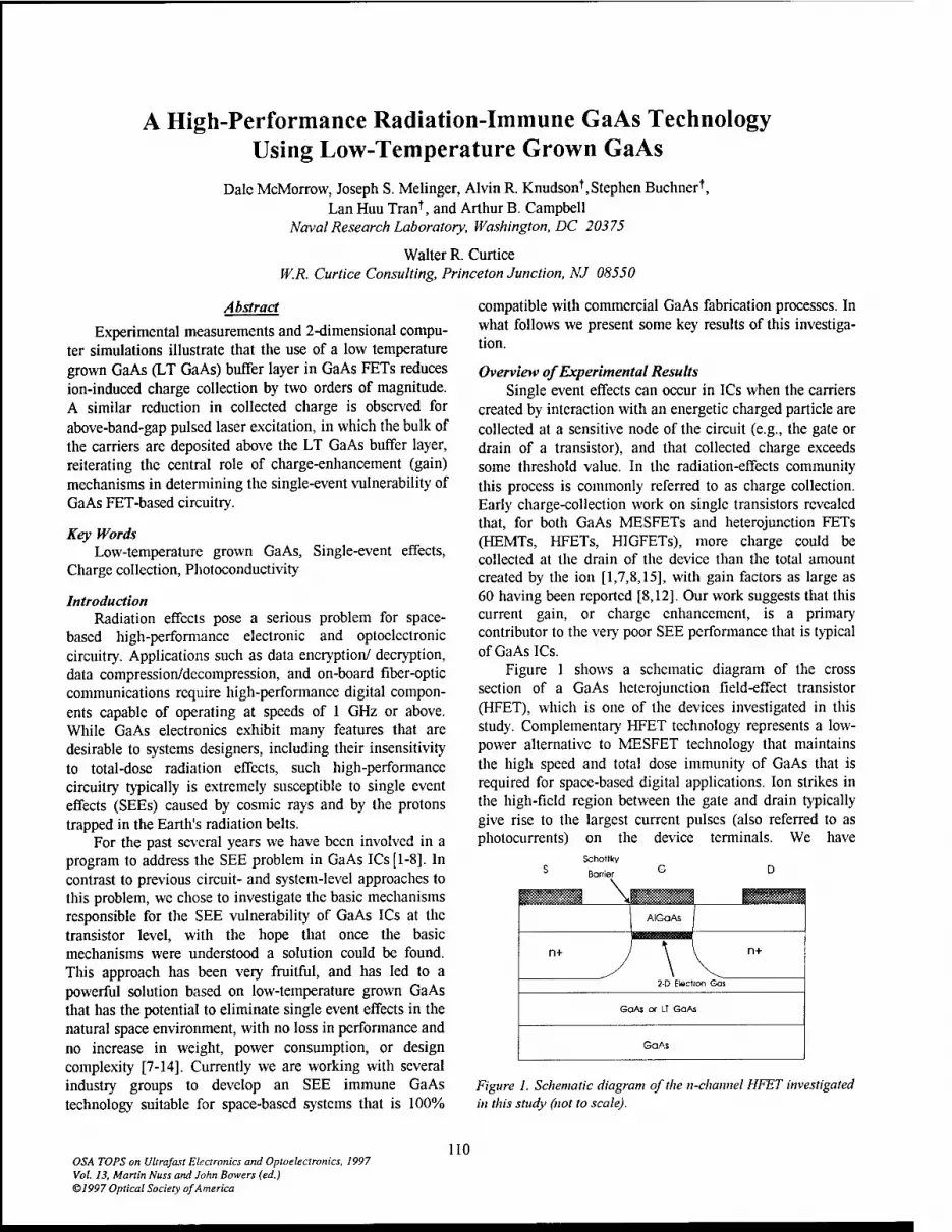
A High-Performance Radiation-Immune GaAs Technology Using Low-Temperature Grown GaAs
Dale McMorrow, Joseph S. Melinger, Alvin R. Knudson*, Stephen Büchner*, Lan Huu Tran*, and Arthur B. Campbell
Naval Research Laboratory, Washington, DC 20375
Walter R. Curtice W.R. Curtice Consulting, Princeton Junction, NJ 08550
Abstract
Experimental measurements and 2-dimensional compu- ter simulations illustrate that the use of a low temperature grown GaAs (LT GaAs) buffer layer in GaAs FETs reduces ion-induced charge collection by two orders of magnitude. A similar reduction in collected charge is observed for above-band-gap pulsed laser excitation, in which the bulk of the carriers are deposited above the LT GaAs buffer layer, reiterating the central role of charge-enhancement (gain) mechanisms in determining the single-event vulnerability of GaAs FET-based circuitry.
Key Words Low-temperature grown GaAs,
Charge collection, Photoconductivity Single-event effects,
Introduction Radiation effects pose a serious problem for space-
based high-performance electronic and optoelectronic circuitry. Applications such as data encryption/ decryption, data compression/decompression, and on-board fiber-optic communications require high-performance digital compon- ents capable of operating at speeds of 1 GHz or above. While GaAs electronics exhibit many features that are desirable to systems designers, including their insensitivity to total-dose radiation effects, such high-performance circuitry typically is extremely susceptible to single event effects (SEEs) caused by cosmic rays and by the protons trapped in the Earth's radiation belts.
For the past several years we have been involved in a program to address the SEE problem in GaAs ICs [1-8]. In contrast to previous circuit- and system-level approaches to this problem, we chose to investigate the basic mechanisms responsible for the SEE vulnerability of GaAs ICs at the transistor level, with the hope that once the basic mechanisms were understood a solution could be found. This approach has been very fruitful, and has led to a powerful solution based on low-temperature grown GaAs that has the potential to eliminate single event effects in the natural space environment, with no loss in performance and no increase in weight, power consumption, or design complexity [7-14]. Currently we are working with several industry groups to develop an SEE immune GaAs technology suitable for space-based systems that is 100%
compatible with commercial GaAs fabrication processes. In what follows we present some key results of this investiga- tion.
Overview of Experimental Results Single event effects can occur in ICs when the carriers
created by interaction with an energetic charged particle are collected at a sensitive node of the circuit (e.g., the gate or drain of a transistor), and that collected charge exceeds some threshold value. In the radiation-effects community this process is commonly referred to as charge collection. Early charge-collection work on single transistors revealed that, for both GaAs MESFETs and heterojunction FETs (HEMTs, HFETs, HIGFETs), more charge could be collected at the drain of the device than the total amount created by the ion [1,7,8,15], with gain factors as large as 60 having been reported [8,12]. Our work suggests that this current gain, or charge enhancement, is a primary contributor to the very poor SEE performance that is typical of GaAs ICs.
Figure 1 shows a schematic diagram of the cross section of a GaAs heterojunction field-effect transistor (HFET), which is one of the devices investigated in this study. Complementary HFET technology represents a low- power alternative to MESFET technology that maintains the high speed and total dose immunity of GaAs that is required for space-based digital applications. Ion strikes in the high-field region between the gate and drain typically give rise to the largest current pulses (also referred to as photocurrents) on the device terminals. We have
Figure 1. Schematic diagram of the n-channel HFET investigated in this study (not to scale).
OSA TOPS on Ultrafast Electronics and Optoelectronics, 1997 Vol. 13, Martin Nuss and John Bowers (ed.) ©1997 Optical Society of America
110
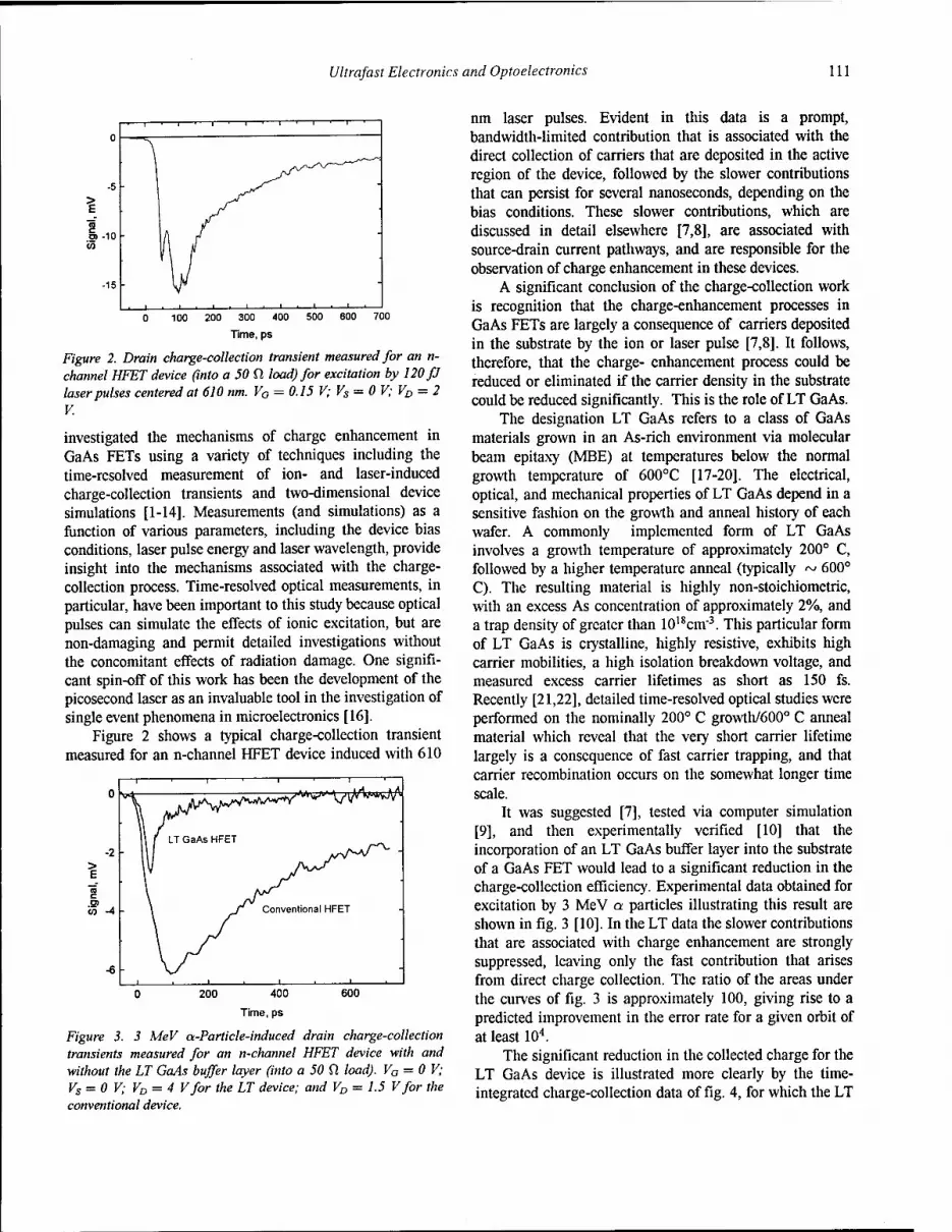
Ultrafast Electronics and Optoelectronics 111
0 100 200 300 400 500 600 700
Time, ps
Figure 2. Drain charge-collection transient measured for an n- channel HFET device (into a 50 Q. load) for excitation by 120 fJ laser pulses centered at 610 nm. Va = 0.15 V; Vs = 0 V; VD = 2 V.
investigated the mechanisms of charge enhancement in GaAs FETs using a variety of techniques including the time-resolved measurement of ion- and laser-induced charge-collection transients and two-dimensional device simulations [1-14]. Measurements (and simulations) as a function of various parameters, including the device bias conditions, laser pulse energy and laser wavelength, provide insight into the mechanisms associated with the charge- collection process. Time-resolved optical measurements, in particular, have been important to this study because optical pulses can simulate the effects of ionic excitation, but are non-damaging and permit detailed investigations without the concomitant effects of radiation damage. One signifi- cant spin-off of this work has been the development of the picosecond laser as an invaluable tool in the investigation of single event phenomena in microelectronics [16].
Figure 2 shows a typical charge-collection transient measured for an n-channel HFET device induced with 610
■v^i/AwvAA
200 400 600
Time, ps
Figure 3. 3 MeV a-Particle-induced drain charge-collection transients measured for an n-channel HFET device with and without the LT GaAs buffer layer (into a 50 fi load). VG = 0 V; Vs = 0 V; VD = 4 Vfor the LT device; and VD = 1.5 V for the conventional device.
nm laser pulses. Evident in this data is a prompt, bandwidth-limited contribution that is associated with the direct collection of carriers that are deposited in the active region of the device, followed by the slower contributions that can persist for several nanoseconds, depending on the bias conditions. These slower contributions, which are discussed in detail elsewhere [7,8], are associated with source-drain current pathways, and are responsible for the observation of charge enhancement in these devices.
A significant conclusion of the charge-collection work is recognition that the charge-enhancement processes in GaAs FETs are largely a consequence of carriers deposited in the substrate by the ion or laser pulse [7,8]. It follows, therefore, that the charge- enhancement process could be reduced or eliminated if the carrier density in the substrate could be reduced significantly. This is the role of LT GaAs.
The designation LT GaAs refers to a class of GaAs materials grown in an As-rich environment via molecular beam epitaxy (MBE) at temperatures below the normal growth temperature of 600°C [17-20]. The electrical, optical, and mechanical properties of LT GaAs depend in a sensitive fashion on the growth and anneal history of each wafer. A commonly implemented form of LT GaAs involves a growth temperature of approximately 200° C, followed by a higher temperature anneal (typically ~ 600° C). The resulting material is highly non-stoichiometric, with an excess As concentration of approximately 2%, and a trap density of greater than 1018cm"3. This particular form of LT GaAs is crystalline, highly resistive, exhibits high carrier mobilities, a high isolation breakdown voltage, and measured excess carrier lifetimes as short as 150 fs. Recently [21,22], detailed time-resolved optical studies were performed on the nominally 200° C growth/6000 C anneal material which reveal that the very short carrier lifetime largely is a consequence of fast carrier trapping, and that carrier recombination occurs on the somewhat longer time scale.
It was suggested [7], tested via computer simulation [9], and then experimentally verified [10] that the incorporation of an LT GaAs buffer layer into the substrate of a GaAs FET would lead to a significant reduction in the charge-collection efficiency. Experimental data obtained for excitation by 3 MeV a particles illustrating this result are shown in fig. 3 [10]. In the LT data the slower contributions that are associated with charge enhancement are strongly suppressed, leaving only the fast contribution that arises from direct charge collection. The ratio of the areas under the curves of fig. 3 is approximately 100, giving rise to a predicted improvement in the error rate for a given orbit of at least 104.
The significant reduction in the collected charge for the LT GaAs device is illustrated more clearly by the time- integrated charge-collection data of fig. 4, for which the LT
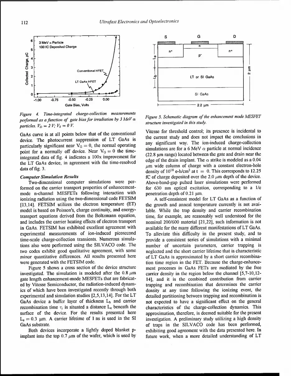
112 Ultrafast Electronics and Optoelectronics
6
5
n ö 3 "8 1 2
§1
o
3 MeV a Particle 100 fC Deposited Charge
Conventional HFET
LT GaAs HFET
—^
-1.00 -0.75 -0.50 -0.25
Gate Bias, Volts
0.00
Figure 4. Time-integrated charge-collection measurements
performed as a function of gate bias for irradiation by 3 MeV a
particles. VD = 2 V; Vs = 0V.
GaAs curve is at all points below that of the conventional device. The photocurrent suppression of LT GaAs is particularly significant near VG = 0, the normal operating point for a normally off device. Near VG = 0 the time- integrated data of fig. 4 indicates a lOOx improvement for the LT GaAs device, in agreement with the time-resolved data of fig. 3.
Computer Simulation Results Two-dimensional computer simulations were per-
formed on the carrier transport properties of enhancement- mode n-channel MESFETs following interaction with ionizing radiation using the two-dimensional code FETSIM [13,14]. FETSIM utilizes the electron temperature (ET) model is based on Poisson's, charge continuity, and energy- transport equations derived from the Boltzmann equation, and includes the carrier heating effects of electron transport in GaAs. FETSIM has exhibited excellent agreement with experimental measurements of ion-induced picosecond time-scale charge-collection transients. Numerous simula- tions also were performed using the SILVACO code. The two codes exhibit good qualitative agreement, with some minor quantitative differences. All results presented here were generated with the FETSIM code.
Figure 5 shows a cross section of the device structure investigated. The simulation is modeled after the 0.8 /jm gate length enhancement-mode MESFETs that are fabricat- ed by Vitesse Semiconductor, the radiation-induced dynam- ics of which have been investigated recently through both experimental and simulation studies [2,5,13,14]. For the LT GaAs device a buffer layer of thickness Lb and carrier recombination time Tr is situated a distance Le beneath the surface of the device. For the results presented here Le = 0.3 urn. A carrier lifetime of 1 ns is used in the SI GaAs substrate.
Both devices incorporate a lightly doped blanket p- implant into the top 0.7 /zm of the wafer, which is used by
s G D
CD J
-1
n*
n n*
P"
LT or SI GaAs
SI GaAs
E a.
CM
-A I 22 ^m
Figure 5. Schematic diagram of the enhancement mode MESFET
structure investigated in this study.
Vitesse for threshold control; its presence is incidental to the current study and does not impact the conclusions in any significant way. The ion-induced charge-collection simulations are for a 6 MeV a particle at normal incidence (22.8 um range) located between the gate and drain near the edge of the drain implant. The a strike is modeled as a 0.04 (im wide column of charge with a constant electron-hole density of 1018 e-h/cm2 at t = 0. This corresponds to 12.25 fC of charge deposited over the 2.0 /im depth of the device. Above-band-gap pulsed laser simulations were performed for 630 nm optical excitation, corresponding to a 1/e penetration depth of 0.21 urn.
A self-consistent model for LT GaAs as a function of the growth and anneal temperature currently is not avai- lable. While the trap density and carrier recombination time, for example, are reasonably well understood for the nominal 200/600 material [21,22], such information is not available for the many different manifestations of LT GaAs. To alleviate this difficulty in the present study, and to provide a consistent series of simulations with a minimal number of uncertain parameters, carrier trapping is neglected and the short carrier lifetime that is characteristic of LT GaAs is approximated by a short carrier recombina- tion time region in the FET. Because the charge-enhance- ment processes in GaAs FETs are mediated by the free carrier density in the region below the channel [5,7-10,12- 14], and it is the combined contribution from carrier trapping and recombination that determines the carrier density at any time following the ionizing event, the detailed partitioning between trapping and recombination is not expected to have a significant effect on the general characteristics of the charge-collection dynamics. This approximation, therefore, is deemed suitable for the present investigation. A preliminary study utilizing a high density of traps in the SILVACO code has been performed, exhibiting good agreement with the data presented here. In future work, when a more detailed understanding of LT

Ultrafast Electronics and Optoelectronics 113
GaAs exists, the interplay between carrier trapping and recombination, and their influence on charge collection and SEU, will be investigated. In what follows, for clarity, we refer to this fast recombination region as the LT GaAs region.
The process of developing an SEE immune LT GaAs technology suitable for space applications requires an understanding of how the SEE performance is affected by the thickness, location, and growth characteristics of the buffer layer. The dependence of the charge-collection dynamics on the carrier lifetime for the 1 urn thick buffer layer device is presented in linear and logarithmic format in fig. 6. According to the data of reference [18], for example, carrier lifetimes of 1 ps and 10 ps correspond to growth temperatures of approximately 230°C and 285°C, respect- ively; extrapolation of that data suggests that a 100 ps carrier lifetime would be obtained for a growth temperature in the vicinity of 340°C. In all of the simulations presented here, a rather conservative carrier recombination time of 1 ns is used as to represent SI GaAs. We note that the carrier lifetime of LT GaAs material is a sensitive function of numerous parameters associated with the growth and annealing history of the sample, and that accurate determination and control of the substrate temperature during growth is difficult at these low temperatures. Consequently, lifetime values reported by different laboratories under apparently similar growth conditions can vary significantly.
The data of fig. 6 illustrate a sensitive dependence of the charge-collection dynamics on the carrier lifetime in the buffer layer for a-particle excitation. In particular, while the charge-collection transient of the 1 ps lifetime device exhibits a rapid decay to the baseline, the 10 ps lifetime device exhibits significant broadening at shorter times, and a distinct tail that relaxes on a timescale of approximately 100 picoseconds. The temporal characteristics of the 100 ps lifetime device closely resemble those of the non-LT (1 ns) device. This behavior is consistent with the presence of charge-enhancement processes in the longer lifetime devices. Note that there is little variation in the peak amplitude of the prompt component with changes in the buffer layer carrier lifetime. This indicates that the prompt component of both LT and non-LT devices is associated with the direct collection of charge that is deposited in the active region of the device, as has been suggested previously [8,9]. While the results of fig. 6 reiterate the expectation that the optimal SEU performance is obtained with the shortest carrier lifetime material, the significant broadening observed when the lifetime is increased to only 10 ps suggests that buffer layer carrier lifetimes of < 1 ps should be targeted for SEE hardened circuits (LT GaAs material with carrier lifetimes as short as 150 fs have been reported).
The use of pulsed laser excitation provides additional insight into the mechanisms of charge collection in the LT
E 1000
800 -
~ 600
I 400 Ü
1 200 D 0
- ' - 1 1 1 1
- (a) ■_
- 1 \\ t = 1 ns
~
■ 100 ps
1 \ips ^"^■-JiLEs__ ' ■ :
i . i 1
20 40 60
c V i— i— 3 O
(0
Q c
100 150 200 250 300
Time, ps
Figure 6. Drain charge-collection transients calculated as a function of the carrier recombination time, r„ in the 1 ftm thick buffer layer. Le = 0.3 jum; VD = 2.5 V; Va = 0.05 V; Vs = 0 V.
GaAs devices. Laser simulations illustrate clearly that the reduction in charge collection efficiency for the LT GaAs devices is largely a consequence of a reduction in the efficiency of charge enhancement mechanisms. For this study, laser excitation at 630 nm was used. At this excitation wavelength the 1/e penetration depth is 0.21 urn. Therefore, for Le = 0.3 urn, 76% of the charge created by the laser pulse is deposited above the LT GaAs buffer layer. It might be expected, therefore, that for 630 nm pulsed laser excitation, the LT GaAs buffer layer will exhibit only a moderate effect in reducing the collected charge. Both simulation [9,13] and experimental results [12], however, suggest that this is not the case. In this section we address the reasons for this behavior.
Charge-collection transients calculated for the case of 630 nm optical excitation illustrate the qualitative charac- teristics of the a-particle data of fig. 6. Even with 76% of the charge deposited above the LT GaAs buffer layer, a significant reduction in the collected charge is observed when compared to the non-LT device. Such results indicate that the LT GaAs buffer layer is not simply acting as a barrier to charge collection, as might be anticipated from simple sensitive volume (rectangular parallel piped) consid- erations.
Figure 7 shows electron density contours for the two devices 10 ps after the ionizing event [13]. At this point in

114 Ultrafast Electronics and Optoelectronics
(a) 0
0.8 1.2 1.6
Distance, |xm
Figure 7. Constant electron density contours (cm'3) at 10 ps after the laser pulse for structures (a) without and (b) with a 0.5 fim thick buffer layer with a 1 ps lifetime. Le = 0.3 fim; VD = 2.5 V; Va = 0.05 V; and Vs = 0V.
the simulation the very significant effects of the LT buffer layer are clearly evident. For the LT device, the carrier density in the excitation region is 1 to 2 orders-of- magnitude lower than that of the conventional device, and the drain current is lower by a factor of 3. Figure 7a shows early evidence for a source-drain current pathway beneath the channel. In [14] this current pathway, which can be identified in fig. 7a as the high carrier density region connecting the source and drain through the substrate, was identified with a bipolar gain mechanism that is believed to be responsible for charge enhancement in the first 100 to 150 ps. In contrast, for the LT device, the high-carrier- density region connecting the source and drain is forced up toward the surface of the device, closer to the channel, and the electron density in this region is reduced significantly. These considerations suggest that, 10 ps after the ionizing event, the LT GaAs buffer layer is central in suppressing the bipolar gain mechanism that has been implicated as a significant contributor to charge collection in GaAs FETs.
Figure 8 shows the electron density 100 ps after the arrival of the laser pulse [13]. The contrast between the LT and non LT devices is striking. For the non-LT device the electron and hole {not shown) densities are quite high throughout the device, and the drain current remains significant. For the LT device both electron and hole densities are several orders-of-magnitude lower throughout
™^jf!
0.8 1.2 1.6
Distance, urn
Figure 8. Constant electron density contours (cm'3) at 100 ps after the laser pulse for structures (a) without and (b) with a 0.5 fim thick buffer layer with a 1 ps lifetime. Le — 0.3 fim; VD = 2.5 V; V0 = 0.05 V; and Vs = 0 V.
the device. For the LT device at 100 ps there is no evidence for the bipolar gain mechanism, which is largely suppressed within the first 15 ps after the arrival of the laser pulse.
The considerations of this section have significant implications for interpretation of the charge-collection results in LT GaAs FETs. It is evident that the LT GaAs buffer layer can not be regarded as a simple barrier to charge collection. If this were the case, then for 630 nra laser excitation, the presence of a buffer layer 0.3 um beneath the surface of the device would have only a minimal impact on the charge-collection efficiency. Also, the LT GaAs FET can not be considered simply in terms of a reduced charge-collection volume in which only that charge deposited above the buffer layer is collected. Again, the predictions of such a model are at odds with the experimental and simulation results. Rather, it must be recognized that the LT GaAs buffer layer plays an integral role in the charge-collection processes. In non-LT GaAs FETs the charge-enhancement mechanisms are mediated by carriers that accumulate in the substrate, below the active region of the device. The carrier density plots of this section illustrate clearly how the LT GaAs buffer layer serves to reduce the free carrier density in the device, effectively inhibiting the development of the charge-enhancement mechanisms.

Ultrafast Electronics and Optoelectronics 115
Conclusions The reduction in charge-collection efficiency for LT
GaAs devices described here translates into improved SEE performance for integrated circuits fabricated with LT GaAs buffer layers. Ground-based heavy-ion and pulsed laser SEU tests have been performed on GaAs complementary HFET serial shift registers fabricated with and without LT GaAs buffer layers [11]. Those tests indicate a significant improvement in the SEE performance for the LT GaAs parts, resulting in an improvement of several orders-of magnitude in the error rate predicted for space-based applications.
The current results illustrate the potential of LT GaAs technology as a solution to the SEU problem in GaAs. Work currently is in progress to further characterize the SEE properties of LT GaAs devices and circuits as a function of various parameters, including the growth temperature and annealing history of the LT GaAs buffers, and to address the manufacturability issues associated with the development of a commercial technology.
Acknowledgments The authors wish to thank Cheryl Marshall and Paul
Marshall for useful discussions throughout the different stages of this work.
References ^SFA Inc., handover, MD
1. A.B. Campbell, A. Rnudson, D. McMorrow, W. Anderson, J. Roussos, S. Espy, S. Büchner, K. Kang, D. Kems, and S. Kems, IEEE Trans. Nuc. Sei. NS-36,2292 (1989). 2. D. McMorrow, A.R. Knudson, and A.B. Campbell, IEEE Trans. Nucl. Sei NS-37,1902 (1990). 3. D. McMorrow, A.B. Campbell, A.R. Knudson, and T.R. Weatherford, in OSA Proceedings on Picosecond Electronics and Optoelectronics, (Optical Society of America, Washington, DC, 1991) pp. 119-125. 4. T.R. Weatherford, L. Tran, W.J. Stapor, E.L. Petersen, J.B. Langworthy, D. McMorrow, W.G. Abdel-Kader, and J.P. McNulty, IEEE Trans. Nuc. Sei. NS-38, 1450 (1991). 5. D. McMorrow, J.S. Melinger, A.R. Knudson, A.B. Campbell, T.R. Weatherford, L.H. Tran, and W.R. Curtice, IEEE Trans. Nuc. Sei. NS-39( 1992). 6. J. Cutchin, P. Marshall, T.R. Weatherford, J. Langworthy, E.L. Petersen, A.B. Campbell, S. Hanka, and A. Peczalski, IEEE Trans. Nucl. Sei., NS-40, 1660 (1993). 7. D. McMorrow, J.S. Melinger, N. Thantu, A.B. Campbell, T.R. Weatherford, A.R. Knudson, L.H. Tran, and A. Peczalski, IEEE
Trans. Nuc. Sei. NS-41,2055 (1994). 8. D. McMorrow, T.R. Weatherford, S. Buchner, A.R. Knudson, J.S. Melinger, L.H. Tran, and A.B. Campbell, IEEE Trans. Nuc. Sei. NS-43, 628 (1996). 9. T.R. Weatherford, D. McMorrow, A.B. Campbell, and W.R. Curtice, Appl. Phys. Lett. 67,703 (1995). 10. D. McMorrow, T.R. Weatherford, W.R. Curtice, A.R. Knudson, S. Büchner, J.S. Melinger, L.H. Tran, and A.B; Campbell, IEEE Trans. Nucl. Sei. NS-42,1837 (1995). 11. P.W. Marshall, C.J. Dale, T.R. Weatherford, M. Carts, D. McMorrow, A. Peczalski, S. Baier, J. Nohava, and J. Skogen, IEEE Trans. Nuc. Sei. NS-42,1850 (1995). 12. D. McMorrow, T.R. Weatherford, A.R. Knudson, S. Büchner, J.S. Melinger, L.H. Tran, A.B. Campbell, P.W. Marshall, C.J. Dale, and A. Peczalski, S. Baier, IEEE Trans. Nuc. Sei., NS-43, 918(1996). 13. D. McMorrow, W.R. Curtice, S. Buchner, A.R. Knudson, J.S. Melinger, and A.B. Campbell, IEEE Trans. Nuc. Sei. NS-43, 2904 (1996). 14. T.R. Weatherford, D. McMorrow, W.R. Curtice, A.R. Knudson, and A.B. Campbell, IEEE Trans. Nucl. Sei. NS-40, 1867(1993). 15. Y. Umemoto, N. Matsunaga, and K. Mitsusada, IEEE Trans. Elect. Dev. ED-16, 864 (1989); B.W. Hughlock, T. Williams, A.H Johnston and R.E. Plaag, IEEE Trans. Nuc. Sei. NS-38 1442(1991). 16. J.S. Melinger, S. Büchner, D. McMorrow, W.J. Stapor, T.R. Weatherford, A.B. Campbell, and H. Eisen, IEEE Trans. Nuc. Sei. NS-41, 2574 (1994). 17. F.W. Smith, A.R. Calawa, C.L. Chen, M.J. Manfra, and L.J. Mahoney, IEEE Elect. Dev. Lett. EDL-9, 77 (1988). 18. Z. Liliental-Weber, J. Alger, D. Look, X.W. Lin, X. Liu, J. Nishio, K. Nichols, W. Schaff, W. Swider, K. Wang, J. Wasburn, E.R. Webber, and J. Whitaker, Semi-insulating HI-VMaterials, Proceedings of the 8th Conference (World Scientific, Singapore, 1994) pp. 305-317. 19. S. Gupta, J. Pamulapati, J. Chwalek, P.K. Bhattacharya, and G. Mourou, in Ultrafast Phenomena VII (Springer-Verlag, Berlin, 1990) pp. 297-299. 20. A. Krotkus, T. Viselga, K Bertulis, V. Jasutis, S. Marcinkevi- cius, and U. Olin, Appl. Phys. Lett. 66,1939 (1995). 21. P. Fauchet, G. Wicks, A. Lobad, and T. Gardiner, "Trapping and Recombination in LT JU-Vs", presented at: Workshop on Non- Stoichiometric GaAs and Related Materials, March 6, 1996, Santa Barbra, CA; to be published. 22. T. Norris, J. Whitiker, C. Sung, H. Wang, and T Sosnowski, "Time-Resolved Electron and Hole Trapping and Trap Saturation Dynamics in LT-GaAs", presented at: Workshop on Non- Stoichiometric GaAs and Related Materials, March 6, 1996, Santa Barbra, CA; to be published.
Investigations of GaAs Implanted with Low-Dosage Arsenic Ions as Ultrafast Photoconductors
Gong-Ru Lin, and Ci-Ling Pan Institute of Electro-optical Engineering, National Chiao Tung University 1001 Ta Hsueh Rd., Hsinchu, Taiwan 30010 Tel: +886-3-5731921, Fax:+886-3-5716631, E-mail: [email protected]
Abstract We report picosecond switching responses for photoconductive switches
fabricated on annealed arsenic-ion-implanted GaAs at dosage as low as 1013 ions/cm2.
Summary Recently an alternative arsenic-rich material, arsenic-ion-implanted GaAs or
GaAs:As+, has emerged as a potential candidate for ultrafast optoelectronic applications. Subpicosecond carrier lifetimes [1] and photoconductive responses comparable to that of LT (low-temperature) MBE-GaAs [2] were reported for GaAs:As+
prepared by bombarding semi-insulating (S.I.) GaAs substrates with 200 keV arsenic ions at the dosage of 1016 ions/cm2. We have previously shown that the photoexcited carrier lifetime of GaAs:As+ is already ultrashort ( « 220 fs) for sample prepared at the relatively low dosage of 1013 ions/cm2.[1] In this work, the feasibility of fabricating ultrafast photoconductive devices on such low-dosage-implanted GaAs:As+ materials is demonstrated.
The photoconductive switches (PCS) were prepared by first implanting LEC-grown semi-insulating (S.I.) GaAs substrate with 200 keV arsenic ions at a dose of 1013
ions/cm2. The samples were then annealed at 600ex-situ either by rapid thermal annealing (RTA) for 30 seconds or in a furnace for 30 minutes. The device structure consists of coplanar waveguide (CPW) transmission lines 30 [im in widths and a spacing of 15 (im between the lines. The contact metal was Au/Ti. Carrier lifetimes of annealed GaAs:As+ were determined by time-resolved reflectivity measurement using a typical pump-probe setup with a temporal resolution of ~ 200 fs.[1] The laser wavelength was 865 nm. The photoconductive switching responses of the GaAs:As+
PCS's were characterized by an external electro-optic sampling system ( = 0.8 mm ) with temporal and spatial resolutions estimated to be 0.9 ps and 3 urn respectively. The probe point was about 1 mm from the excitation spot.
The transient reflectivity (AR/R) data for as-implanted, RTA-annealed, and furnace- annealed low-dose GaAs:As+ ( 200 keV and 1013 ions/cm2 ) are shown in Fig. 1. The carrier lifetimes, TC, are ~ 0.25 ps, 0.85 to 0.9 ps, and 3 ps for as-implanted, RTA- annealed (600 for 30 s), and furnace-annealed GaAs:As+ (600 for 30 min) respectively. In Fig. 2, we have plotted the electro-optically sampled electrical waveforms generated by RTA-annealed and furnace-annealed GaAs:As+ PCS.s biased at 20 V. For the former, the full width at half-maximum (FWFM) is ~ 2.7 to 3 ps. The rise time is about 1.4 ps. The trailing edge is best fitted by dual exponential functions with time constants of about 1.8 and 10 ps respectively. The relative weight of the two components is 9:1. For the latter, the FWHM is about 7.7 + 0.3 ps. The rise time is the same as the RTA-
116 OSA TOPS on Ultrafast Electronics and Optoelectronics, 1997 Vol. 13, Martin Nuss and John Bowers (ed.) &1997 Optical Society of America

Ultrafast Electronics and Optoelectronics 117
annealed sample. The trailing edge of the electrical pulse also consists of two components but with approximately equal weight and time constants of ~ 5 and 120 ps. The dark current (Id) characteristics of Auston-type PCS.s are plotted in Fig. 3. At a bias voltage of 20 V, ld ~ 30 mA and 30 nA for RTA-annealed and furnace-annealed GaAs:As+ PCS's respectively. For comparison, the dark current characteristics of a similar PCS fabricated on S.I. GaAs is also shown in Fig. 3. The responsivity of the RTA-annealed and furnace-annealed GaAs:As+ PCS under pulse excitation of 100 mW is s7 mA/W and >10 mA/W respectively.
In summary, we demonstrate picosecond switching responses for lowdose- implanted GaAs:As+ photoconductive switches. We anticipate a multiple-low-dose implantation recipe should further improve switching times. This work was supported in part by the National Science Council of the Republic of China under grant NSC84-2215- E-009-092.
References 1. F. Ganikhanov, G.-R. Lin, W.-C. Chen, C.-S. Chang, and C.-L. Pan, Appl. Phys. Lett,
vol. 67, pp. 3465-3467, 1995. 2. H. H. Wang, J. F. Whittaker, H. Fujicka, and Z. Liliental-Weber, in Ultrafast
Electronics and Optoelectronics, OSA Technical Digest Series (OSA, Washington, D.C., 1995), vol. 13, pp. 32-34.
1.2
1.0
0.8
oc 0.6
< x, 0.4 Qi N
I 0.2 o z 0.0
-0.2 -
-0.4 -
-
I.I.
k fth
;■: ty
_ 1 s
- 1 ': %\
• \ \ (o)
VA-'"-'^
\<b> '~""-v--\,-^..A.../—~.'"v.
' ^ J\ wr^v V^ W-A I ■ I ■ • ■ ' • 1 ■ 1 ' 1 ■ 1 ■
4 6 8 10 Delay Time (ps)
12 14 16
Fig. 1 Normalized time-resolved reflectivity of (a) as-implanted (200 keV and 1043
ions/cm2), (b) RTA-annealed (600 for 30 s), and (C) furnaceannealed (600 for 30
minutes )GaAs:As+ samples.

118 Ultrafast Electronics and Optoelectronics
-a -♦—*
"Q. E < O HI
a:
Delay Time (ps)
Fig. 2 Eiectro-opticaily sampled switching responses of (a) RTA-annealed and (b) furnace-annealed low-dose-implanted GaAs:As+ PCS's.
c L_
3 Ü
ca Q
8.0x10⁻⁵
6.0x10-s -
4.0x10⁻⁵
2.0x10⁻⁵
0.0
-2.0X10⁻⁵
-4.0x10⁻⁵
-6.0X10⁻⁵
-8.0x10⁻⁵
(C) .-
1.0x10*
-40 -20
20 40
40
Bias Voltage (volt)
Fig. 3 Dark current characteristics of an Auston-type PCS fabricated on (a) S. I. GaAs substrate (dotted line), (b) furnace-annealed (solid line), and (c) RTA-annealed (dashed line) low-dose-implanted GaAs:As+
samples. The inset is a magnified view of traces (a) and (b).
20 GHz High Performance Planar Si/lnGaAs P-i-n Photodetector
B. F. Levine, A. R. Hawkins3, S. Hiu, B. J. Tseng, C. A. King, L. A. Gruezke,
R. W. Johnson, D. R. Zolnowski, and J.E. Bowers3
Bell Laboratories, Lucent Technologies, 700 Mountain Ave
Murray Hill, NJ 07974
Abstract
Planar Si/lnGaAs wafer fused p-i-n photodetectors were fabricated. They show high
internal quantum efficiency, high speed, record low dark current, and no evidence of
charge trapping, recombination centers or a bandgap discontinuity at the heterointerface.
Electrical and Computer Engineering Dept. University of California, Santa Barbara
Santa Barbara, CA 93106
119 Reprinted from Uilrqfast Electronics and Optoelectronics 1997 Topical Meeting Technical Digest ©1997 Optical Society of America
120 Ultrafast Electronics and Optoelectronics
The advantages of directly bonding lll-V and Si wafers to fabricate devices which
optimize the characteristics of each material are well known1"2. We demonstrate here high
performance A = 1.55 fjm telecommunication p-i-n photodetectors on a Si substrate. These
devices are then used to investigate the characteristics of the wafer fused Si/lnGaAs
interface, which are important for both p-i-ns and avalanche photodiodes (APDs). The
planar detectors, consisted of a 24 urn Zn diffused active region in a 0.5pm Si/1 urn
lnGaAs/0.6 urn InP bonded wafer (shown in Fig.1).
The DC photocurrent and the reverse dark current were measured as a function of
• bias voltage from Vb = 0 to 10 V (shown in Fig. 2). Note that the photocurrent is constant
with Vb even down to zero bias, suggesting that there is no significant charge
accumulation or trapping at the interface. Further, the dark current is a record low for
Si: lll-V bonded wafers, (lD = 100 pA at Vb = 4 V), and is in fact comparable to standard
InP/lnGaAs p-i-ns, again indicating the excellent quality of the interface. Additional
support for this conclusion is supplied by forward l-V measurements, which over the range
Vb = 0.1 to 0.4 V are given by / = l0 exp(qV/nkT), with a near unity ideality factor n = 1.1
to 1.2. The absolute value of the quantum efficiency n =Hi Ha (where r^ = 1-eaL, is the
absorption quantum efficiency, and Hi is the internal quantum efficiency, i.e. the fraction
of the photogenerated carriers which are collected) was accurately measured at A = 1.55
urn. After correcting for the reflectivity of the incident Si surface, and the thickness of the
InGaAs absorption layer, the internal quantum efficiency was determined to be r|j = 100
% to within the accuracy of our experiment ( 5 % ). This result clearly demonstrates that
there is no measurable loss of photogenerated carriers across the Si/lnGaAs, further

Ultrafast Electronics and Optoelectronics 121
confirming the nearly ideal interface.
The capacitance was measured as a function of voltage (Fig. 3), and shows a
smooth decrease with increasing Vb, with no indication of a change of slope, demonstrating
that there is no excess charge at the interface. Combining C = 100 fF (at Vb= 10 V) with
the measured contact resistance Rc = 40 Q [i.e. a total circuit resistance of R = (50 + Rc)
Q = 90 Q], results in a calculated RC frequency response of fRC = 1/(2nRC) = 18 GHz,
which is expected to dominate the response speed, since the transit time limited
frequency is calculated to be fT = 38 GHz. The measured 3 dB bandwidth which was found
to be 21 GHz, is shown in Fig. 4. This good agreement with fRCi again demonstrates that
there is no trapping at the interface due to either defects or a hetero-bandgap AEC
discontinuity. Thus, the Si/lnGaAs interface seems nearly ideal not only in the lack of any
defects or charge trapping, but also in having a small discontinuity AEC - 0.
As a final characterization of the interface, we measured the absolute photocurrent
noise power using a noise figure meter at a frequency of 30 MHZ and a bandwidth of 4
MHZ. The current noise power is linear in lp, as expected, with a slope of 3.4x10"3 kT/uA
in good agreement with the minimum shot noise limit of 2qRlp/kT = 3.9x10⁻³ kT/uA, (for R
= 50 Q); thus, showing no excess noise and no evidence of traps.
In conclusion, we have fabricated and measured novel planar Si/lnGaAs p-i-ns. We
find that the photocurrent is flat with voltage down to Vb = 0, the reverse bias dark current
is extremely low (100 pA at Vb = 4 V), the forward bias current has an ideality factor n near
unity, the capacitance C(Vb) shows no indication of trapped charge at the interface, the
internal quantum efficiency is = 100%, the high speed response is RC limited at 21 GHz,
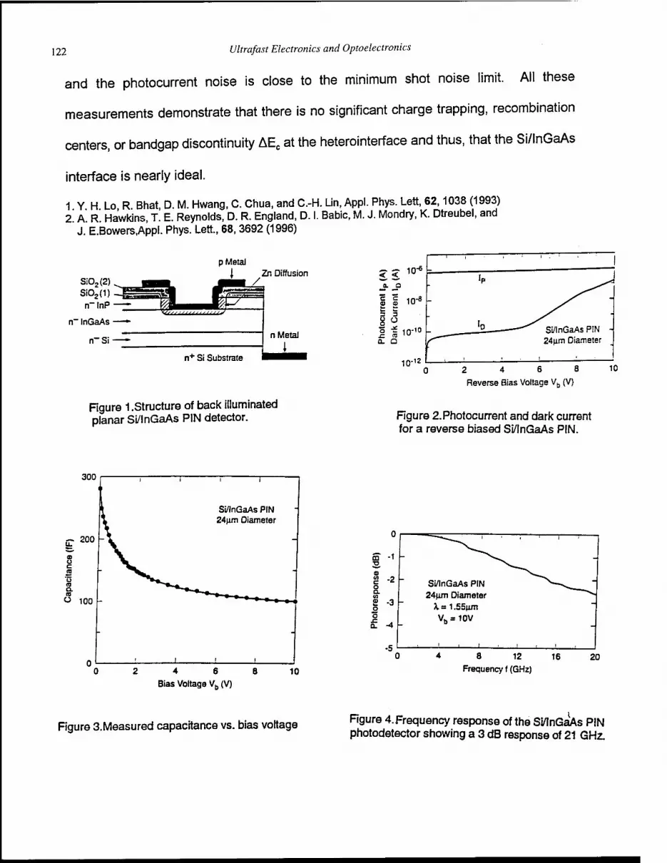
122 Ultrafast Electronics and Optoelectronics
and the photocurrent noise is close to the minimum shot noise limit. All these
measurements demonstrate that there is no significant charge trapping, recombination
centers, or bandgap discontinuity AEC at the heterointerface and thus, that the Si/lnGaAs
interface is nearly ideal.
1 Y H Lo R. Bhat, D. M. Hwang, C. Chua, and C.-H. Lin, Appl. Phys. Lett, 62,1038 (1993) 2 A R Hawkins, T. E. Reynolds, D. R. England, D. I. Babic, M. J. Mondry, K. Dtreubel, and
J. E.Bowers,Appl. Phys. Lett., 68, 3692 (1996)
p Metal
< < 1<r*
1 I 10-8 L_ k. fa» k- 3 3
2 2 I 5 10-'° o. a
10-'2
C
1— '■••'■■■■ |
Si02(2) |— SiO Ml _JM ■' ~
«. Jri^/ in Diffusion
n Metal
1
Ip ^*
l° ^ Si/lnGaAs PIN - 24um Diameter
n~ InP —- ^J Wf/Ji /
n~ InGaAs —*■
n~Si —-
n+ Si Substrate
) 2 4 6 8 10
Reverse Bias Voltage Vb (V)
Figure 1 .Structure of back illuminated planar Si/lnGaAs PIN detector. Figure 2. Photocurrent and dark current
for a reverse biased Si/lnGaAs PIN.
300
" 100
Si/lnGaAs PIN 24nm Diameter
2 4 6 8 Bias Voltage V„ (V)
10
u
^^\^ CO -1
— ^^^.^^ - ■o
a> ^\„^^ c « Si/lnGaAs PIN ^~N--v^__~
ores
p 24um Diameter ^^ X a 1.55(im
o Vb = 10V o. -4
.5 -■ ! 1 '
4 8 12 Frequency t (GHz)
16 20
Figure 3.Measured capacitance vs. bias voltage Figure 4.Frequency response of the Si/lnGaAs PIN photodetector showing a 3 dB response of 21 GHz.

High Speed Electronics
Mark Rodwell
University of California, Santa Barbara Dept. of Electrical and Computer Engineering Santa Barbara, CA 93106 Phone: (805) 893-3244 Fax: (805) 893-3262
The conference saw the presentation of several key results in wideband electronics, with particular emphasis on optical fiber communication ICs. Realization of compact & robust chip sets for fiber transmission at 20 to 40 Gb/s rates is a competitive arena, the contending technologies being submicron silicon bipolar, GaAs/AlGaAs and InGaAs/InP heterojunction bipolar, and even ion- implanted GaAs MESFETs.
Rein et. al. have shown impressive results in silicon bipolar ICs for fiber transmission. Of particular significance is their demonstration of multiplexer/demultiplexer and decision circuits operating at a very high fraction of the transistor current-gain cutoff frequency. Moving to AlGaAs/GaAs HBTs, Runge et. al. of Rockwell have also demonstrated many of the component circuits required for 30 to 40 Gb/s fiber transmission, including demultiplexers, multiplexers, gain blocks, and timing recovery. Packaging, testing, and complete systems-level demonstration are serious issues for GHz optical transmission. Large scales of integration are desirable, but larger ICs demand wide circuit operating margins. Drawing upon their record high bandwidth InP based HBTs, Yamahata et. al. of NTT have demonstrated fully integrated and fully functional 20 Gigabit/second optical receivers. The power consumption is impressively low.
A second major application area of wideband HBTs is in high performance analog-digital converters. In both radar and wireless RF networks, the trend is toward increasing levels of digital processing. The ultimate goal is an all-digital receiver, consisting of an analog-digital converter and a digital signal processor. Towards this goal, Jensen et. al. of Hughes have demonstrated very high resolution low-pass and bandpass delta-sigma ADCs implemented in an InP-based HBT technology.
On a more basic technology level, Rodwell et. al. of UCSB have demonstrated modified versions of resonant tunnel diodes and heterojunction bipolar transistors. The goal is to render the devices scaleable, such that increased bandwidths are obtained by combined lateral and vertical scaling. Finally, Narahara et. al. of NTT discuss a number of novel applications of traveling-wave concepts to high speed electronics.
123
Si-Bipolar - A Potential Candidate for High-Speed Electronics in 20 and 40 Gb/s TDM Systems ?
H.-M. Rein, Ruhr-University Bochum, AG Halbleiterbauelemente, D-44780 Bochum, Germany, Tel: +49-234-700-5406, FAX: +49-234-7094-102
E. Gottwald, Siemens AG, Public Communication Networks Group, Hofmannstr. 51, D-81379 Munich
T. F. Meister, Siemens AG, Corporate Research & Development Microelectronics, Otto-Hahn-Ring 6, D-81739 Munich
Abstract
It is shown that the ICs in 10 Gb/s TDM systems can be fabricated with Si-bipolar production technologies while for 20 Gb/s systems present laboratory technologies are required. From the design of ICs for 40 Gb/s systems it is expected that this data rate can really be achieved using further improved Si-based technologies. However, the other circuit specifications must be relaxed compared to ICs in 10 and 20 Gb/s systems, which is possible by use of optical-fiber amplifiers and improved opto-electronic components. Moreover, speed critical circuits should be eliminated as far as possible.
Keywords: Fiber-optic circuits, ultrafast electronics.
I. Introduction
There is no doubt that the data rate in long-haul opti- cal-fiber transmission links will be further increased. However, an open question for future systems is at which data rates the system designer has to change from time- division multiplexing (TDM) to wavelength-division mul- tiplexing (WDM). These "interface data rates" depend on the upper limit for an economical solution of the disper- sion problems in optical fibers, on the upper speed limit of the electronic and opto-electronic components, and on the progress in future all-optical networks. Today, in practical systems the interface data rate is 2.5 Gb/s and 10 Gb/s, respectively. For future systems, 40 Gb/s are under dis- cussion.
Moreover, caused by the increasing transmission ca- pacity of long-haul systems, there is a demand for optical ultra-high-speed links in switching networks. The next generation of switching cores will have a throughput of several Terabit/s (e.g., [1]). At present the data inter-
connection within the switching core is based on 3.3 Gb/s links. A dramatical reduction of cabling complexity and costs could be achieved by using 20 to 40 Gb/s bus systems and ultra-high-speed add-drop multiplexers instead.
Therefore, an urgent question is whether 20 or even 40 Gb/s TDM links can be realized in near future at rea- sonable costs [2]. The intention of the authors is to give a contribution to this topic: They will first show the state-of- the-art and then the present speed limit of Si-based ICs for long-haul optical-fiber systems.
II. State-of-the-Art: Si-Based ICs for 10 and 20 Gb/s Systems
Table 1 shows the state-of-the-art of the circuits required in the signal path of an optical-fiber link and the data achieved with present Si-bipolar production technologies (apart from the last column, see below). The circuits were designed in cooperation between the Ruhr-University Bochum (RUB) and several industrial partners, and then fabricated in advanced production technologies, mostly with the B6HF of Siemens. For references see [3]. The maximum data rates measured on mounted chips are given in the second and some further specifications in the third column. Note especially the high output voltage swing of the modulator driver, the high transimpedance and low equivalent input noise current density (jN, averaged over the whole band width) of the preamplifier, and the high gain and dynamic range of the (AGC and limiting) main amplifiers.
These data show that there is enough speed margin to fabricate all ICs in the signal path of 10 Gb/s systems in available Si-bipolar production technologies, as long as the circuits are carefully designed [3]. The same is true for the ICs in the clock extraction circuitry as shown by other authors (e.g. [4]).
The situation looks quite different for 20 Gb/s. Here,
OSA TOPS on Ultrafast Electronics and Optoelectronics, 1997 Vol. 13, Martin Nuss and John Bowers (ed.) ©1997 Optical Society of America
124

Ultrafast Electronics and Optoelectronics 125
Circuit Max. Speed / Prod. T. Remarks Labor. T. Multiplexer 30 Gb/s (RUB + HP) 2:1 60 Gb/s
Demultiplexer 32 Gb/s (RUB + Siemens) 1:2 46 Gb/s
Decision Circuit 22 Gb/s (RUB + Siemens) CPM = 180° 25 Gb/s
Static Freq. Divider 19 GHz (RUB + Siemens) 2:1, 2 Outputs (0° and 90°) 33 GHz
Laser/Modul. Driver 14 Gb/s (RUB + Siemens) Swing AVQ = 3.6 V (50 Q) 20 Gb/s
Preamplifier (Transimp. Type)
13 Gb/s (RUB + ANT + Siemens)
Transimp. Zn = 615 Q fc = 10 GHz Noise jN = 10.5 pA/VHz
20 Gb/s
Main Amplifier, AGC
Main Amplifier, | limiting
13 Gb/s (RUB + ANT + Motorola)
15 Gb/s (RUB + ANT + Siemens)
S21 = 37 dB, fc = 10 GHz Dynamic Range = 41 dB
S21 = 52 dB (max.) Dynamic Range = 46 dB
Table 1. High-speed ICs for optical- fiber systems in Si-bipolar technologies. The data rates in the second column were achieved with production technologies, those in the last column with Siemens laboratory technologies.
advanced laboratory technologies are required to achieve this data rate with the speed-critical circuits, as long as the other specifications are not essentially relaxed. Recent measurement results of mounted Si-bipolar chips are shown in Fig. 1 [5-7]. The circuits, again developed in cooperation between RUB and Siemens, are listed in the last column of Table 1. They were fabricated either with an improved laboratory version of the B6HF [8] (DEMUX), a former epitaxial-base technology (decision circuit), or a recent SiGe technology [9] (rest). All these ICs are used in an experimental 20 Gb/s TDM transmis- sion system [2].
For generating the eye diagrams in Fig. 1, the circuits were driven by a pseudo-random bit sequence generator with a word length of 215-1 bits [6]. The 60 Gb/s of the MUX, presented in [6], is the highest data rate ever gen- erated by an IC in any technology and the DEMUX [5], too, is far above the required data rate, despite of the slower (implanted base) technology applied. The excellent retiming capability of the DEMUX at the record input data rate of 46 Gb/s is demonstrated in Fig. lb for an intentionally degraded input eye diagram. The output eye diagrams of the speed-critical circuits, transimpedance preamplifier and modulator driver, are given at 20 Gb/s. Here, the photo diode, which drives the amplifier, is modeled by an electrical network realized on the measu- ring substrate [10]. The high gain (58 dBQ) and low noise
(estimated JN » 12 pAJ-Jttz) of the transimpedance pre-
amplifier (due to the high shunt feedback resistance of
900 Q in the first stage) as well as the comparatively high output voltage swing of the modulator driver (maximum values: 2.3 V for single-ended and 4.6 V for differential operation) are record values for 20 Gb/s Si ICs [7].
The results clearly show that 40 Gb/s can not be achieved with the speed-critical ICs (like amplifier and modulator driver) by further improvement of the technolo- gy only. Additional measures'to achieve this data rate must be taken as discussed in the next section.
a
\J^Wm.Jm'.Mk*. Mm. JmJ
r~T—r—r
$ t * $ * t i ♦ $
i . 1
W jfc."*W jt*.'W J**^W A' V Tf ^P 1V JL JL jL 'A_ M. **■ Jt -v * ~' 4k ^
r 1 ! ; 1 : 1 ' '. 1
-^^i^^U^
^YY^/A
MUX 60 Gb/s
in
46 Gb/s
DEMUX
out 23 Gb/s
Preamp. 20 Gb/s
Driver 20 Gb/s
Fig. 1. Measured eye diagrams of mounted Si/SiGe-bipolar ICs (AVQ is the output voltage swing): a) 2:1 MUX, 60 Gb/s (10 ps/div.), AV0 = 0.5 V. b) 1:2 DEMUX, 46 Gb/s input (top) and 23 Gb/s output (bottom),
20 ps/div„ AV0 = 0.5 V c) Transimpedance preamplifier, 20 Gb/s (20 ps/div.),
gain 58 dBQ (= 800 Q), AVCmjI = 0.2 V. d) Modulator driver, 20 Gb/s (20 ps/div.), AVQ = 2 V.

126 Ultrafast Electronics and Optoelectronics
III. How to Achieve 40 Gb/s with Si/SiGe-Bipolar Technologies ?
Of course, as an important precondition to achieve 40 Gb/s with the speed-critical ICs the worldwide best laboratory technologies must be applied. Several promising approa- ches for very-high-speed Si-based bipolar technologies have been reported: Pure silicon technology with very steep and shallow emitter/base profile [11], SiGe HBT technology ("real HBT") [12], and SiGe drift-transistor technology [9]. (For a rough comparison of SiGe technolo- gies see [13].) For the choice of the adequate technology the designer should not consider fT and fmax only but also the specific basic transistor parameters (e.g. rB and CCB related to the emitter length), the current carrying capability of the transistors (high admissible collector current density JCK),
and the number of available metallization layers [3, 13]. For the design of 40 Gb/s ICs within the current German R&D program PHOTONIK II a SiGe laboratory techno- logy is used, which has been presented in [9]. It is a self- aligned double-polysilicon technology with 0.6 fim litho- graphy (resulting in an effective emitter width of bE = 0.3 fim) and 3 metallization layers. A Ge gradient in the epitaxial base causes an accelerating drift field which reduces the transit time xf and thus increases fT. The speed
10 o
10 Gb/s o-
40
TRANSMITTER
4:1 MUX
power MUX
laser diode
H>h
2:1
2:1
2:1
T 20 GHz clock
40 Gb/s EAM
I^OA
optical fiber (40 Gb/s)
1:4DEMUX
opt. amp.
RECEIVER /
clock extract.
20 GHz freq. divider clock
Technol. (Siemens) bE
l>rn] fT
[GHz] [PS]
rB (forw.) [Q]
CEB [fF]
CcB [fF]
Ccs [fF]
JCK [mA/nm2]
Prod. Techn. (B6HF) 0.4 27 4.5 = 45 35 20 56 = 0.75
Labor. Techn. (SiGe) 0.3 64 2 = 40 28 19 28 = 2
Fig. 2. Scheme of a 40 Gb/s optical-fiber TDM system
Table 2. Transistor data of the laboratory SiGe-bipolar technology applied and their comparison with those of an advanced production technology (CBEB configura- tion with 10 um emitter length). The junction capacitances are zero-bias values and JCK is given for VCE = IV.
potential is further increased by the high admissible collector current density. An example for the transistor data used for the circuit designs is given in Table 2 and compared there with the data of the production technology B6HF.
As discussed in Section II and as also obvious from a comparison of the transistor data in Table 2, 40 Gb/s electronics can not be achieved by technology improve- ments only. Additional measures, all applied in this work, are required like: - Elimination of speed-critical circuits as far as possible. - Relaxed specifications for the remaining speed-critical
circuits (in favor of speed). - Improved models for circuit simulation (especially for
transistors, on- and off-chip wiring, substrate coupling, etc., [3]).
- Improved mounting technique (especially shorter bond wires and improved decoupling methods).
As a main simplification compared to 10 Gb/s sys-
tems, the decision function is now performed by the first stage of the two-stage 1 : 4 DEMUX. As demonstrated by Fig. lb, such a 1 : 2 DEMUX stage stands out for a high intrinsic operating speed and an excellent retiming capa- bility, and, moreover, has a high input sensitivity. As a consequence, speed-critical single master-slave D-flip- flops (clocked at 40 GHz) for both 40 Gb/s decision and 40 GHz frequency division are no longer needed. Moreover, clock extraction is now restricted to 20 GHz, essentially relaxing the demands on this circuitry (cf. [4]).
Due to the use of a gain-controlled optical amplifier (OA) the specifications of the electronic amplifier in the receiver can be essentially relaxed: Gain and dynamic range can be reduced considerably (e.g. compared to 10 Gb/s systems without OA) and the input sensitivity (mainly determined by the equivalent input noise current density) is no longer a severe restricting condition. As a consequence, the whole amplifier can be put on a single chip.
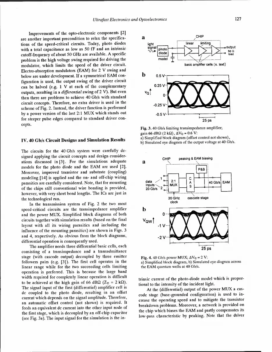
Ultrafast Electronics and Optoelectronics 127
Improvements of the opto-electronic components [2] are another important precondition to relax the specifica- tions of the speed-critical circuits. Today, photo diodes with a total capacitance as low as 50 fF and an intrinsic cutoff-frequency of about 50 GHz are available. A specific problem is the high voltage swing required for driving the modulator, which limits the speed of the driver circuit. Electro-absorption modulators (EAM) for 2 V swing and below are under development. If a symmetrical EAM con- figuration is used, the output swing of the driver circuit can be halved (e.g. 1 V at each of the complementary outputs, resulting in a differential swing of 2 V). But even then there are problems to achieve 40 Gb/s with standard circuit concepts. Therefore, no extra driver is used in the scheme of Fig. 2. Instead, the driver function is performed by a power version of the last 2:1 MUX which stands out for steeper pulse edges compared to standard driver con- cepts.
IV. 40 Gb/s Circuit Designs and Simulation Results
The circuits for the 40 Gb/s system were carefully de- signed applying the circuit concepts and design consider- ations discussed in [3]. For the simulations adequate models for the photo diode and the EAM are used [2]. Moreover, improved transistor and substrate (coupling) modeling [14] is applied and the on- and off-chip wiring parasitics are carefully considered. Note, that for mounting of the chips still conventional wire bonding is provided, however, with very short bond lengths. The ICs are just in the technological run.
In the transmission system of Fig. 2 the two most speed-critical circuits are the transimpedance amplifier and the power MUX. Simplified block diagrams of both circuits together with simulation results (based on the final layout with all its wiring parasitics and including the influence of the mounting parasitics) are shown in Figs. 3 and 4, respectively. As obvious from the block diagrams, differential operation is consequently used.
The amplifier needs three differential basic cells, each consisting of a transimpedance and a transadmittance stage (with cascode output) decoupled by three emitter followers pairs (e.g. [3]). The first cell operates in the linear range while for the two succeeding cells limiting operation is preferred. This is because the large band width required for completely linear operation is difficult to be achieved at the high gain of 66 dBQ (Zn = 2 kQ). The signal input of the first (differential) amplifier cell is dc coupled to the photo diode, resulting in an offset current which depends on the signal amplitude. Therefore, an automatic offset control (not shown) is required. It feeds an equivalent dc current into the other input node of the first stage, which is decoupled by an off-chip capacitor (see Fig. 3a). The input signal for the simulation is the in-
a CHIP
light signal
linear
photo diode
model r
limiting
X Ss-4—o output >: 50 n
••^1—° load
basic amplifier cells (s. text)
25 ps
Fig. 3. 40 Gb/s limiting transimpedance amplifier; gain 66 dBß (2 kQ), AVQ = 0.6 V: a) Simplified block diagram (offset control not shown), b) Simulated eye diagram of the output voltage at 40 Gb/s.
a CHIP peaking & EAM biasing
data / inputs \ 20 Gb/s 2^
2:1 MUX
'QW
25 ps
Fig. 4. 40 Gb/s power MUX; AVQ = 2 V: a) Simplified block diagram, b) Simulated eye diagram across the EAM quantum wells at 40 Gb/s.
trinsic current of the photo-diode model which is propor- tional to the intensity of the incident light.
At the (differential) output of the power MUX a cas- code stage (base-grounded configuration) is used to in- crease the operating speed and to mitigate the transistor breakdown problems. Moreover, a network is provided on the chip which biases the EAM and partly compensates its low-pass characteristic by peaking. Note that the driver
128 Ultrafast Electronics and Optoelectronics
must be optimized with respect to the signal voltage across the quantum wells of the EAM rather than to the EAM input.
The eye diagrams at 40 Gb/s, simulated with nominal parameters for transistors and opto-electronic components but with all (known) on- and off-chip parasitics included, look reasonable and let us expect that there is a chance to really achieve this data rate with Si-based technologies.
V. Conclusions
It has been shown by measurements of mounted chips that even the speed-critical ICs in 20 Gb/s TDM systems can be realized with today's Si-based laboratory technologies. From careful simulations of recently designed SiGe ICs we expect that there is a fair chance to realize all ICs also in 40 Gb/s systems, using improved opto-electronic compo- nents and at relaxed circuit specifications. However, the simulations also show that we are just at the speed-limit of today's best laboratory Si-based technologies. Therefore, a further improvement of the speed potential of these tech- nologies seems to be mandatory in order to pay for the design insecurities and fabrication spread. For a more reliable statement we have to wait for the technological realization and measurements of the designed ICs.
Acknowledgments
The autors would like to thank all people at Siemens and RUB who have been involved in this work. Part of the work was supported by the German Federal Ministry BMBF within the framework of the PHOTONIK II pro- gram.
References
[1] J. Pietzsch, H. Burghardt, and P. Herger, "ATM switching network for Multigigabit/s throughput", submitted to ISS '97, Toronto, Canada, Sept. 1997.
[2] E. Gottwald et al., "Towards a 40 Gbit/s electrical time division multiplexed optical transmission sys- tem", in Proc. ICCT '96, Beijing, China, May 1996, pp. 60-63.
[3] H.-M. Rein and M. Möller, "Design Considerations of 10 to 50 Gb/s digital and analog Si-bipolar ICs", IEEE J. Solid-State Circuits, vol. 31, pp. 1976- 1990, Aug. 1996.
[4] E. Müllner, "A 20 Gbit/s parallel phase detector and demultiplexer circuit in a production silicon bipolar technology with fT = 25GHz", in Proc. IEEE BCTM '96, Minneapolis, Sept. 1996, pp. 43- 45.
[5] A. Felder, M. Möller, J. Popp, J. Bock, and H.-M. Rein, "46 Gb/s DEMUX, 50 Gb/s MUX, and 30 GHz static frequency divider in silicon bipolar technology", IEEE J. Solid-State Circuits, vol.31, pp. 481-486, April 1996.
[6] M. Möller, H.-M. Rein, A. Felder, and T. F. Meis- ter, "60 Gb/s SiGe time-division multiplexer", submitted to Electron. Lett..
[7] R. Schmid, T. F. Meister, M. Neuhauser, A. Felder, W. Bogner and H.-M. Rein, "20 Gb/s transimped- ance amplifier and modulator driver in SiGe- bipolar technology", to be published.
[8] J. Bock et al., "A 0.6 ftm Si bipolar technology with 17 ps CML gate delay and 30 GHz static frequency divider," in Proc. ESSDERC '95, The Hague, The Netherlands, Sept. 1995, pp. 421-424.
[9] T. F. Meister et al., "SiGe base bipolar technology with 74 GHz fmax and 11 ps gate delay", in Proc. IEDM '95, Washington, Dec. 1995, pp. 739-742.
[10] M. Neuhauser, H.-M. Rein, H. Wernz, and A. Felder, "A 13 Gbit/s Si bipolar preamplifier for op- tical front ends", Electron. Lett., vol. 29, pp. 492- 493, March 1993.
[11] Y. Kiyota et al., "Lamp-heated rapid vapor-phase doping technology for 100-GHz Si bipolar transis- tors", in Proc. IEEE BCTM '96, Minneapolis, Sept. 1996, pp. 173-176.
[12] A. Schuppen et al., "SiGe-technology and compo- nents for mobile communication systems", in Proc. IEEE BCTM'96, Minneapolis, Sept. 1996, pp. 130-133.
[13] H.-M. Rein," Very-high-speed Si and SiGe bipolar ICs", in Proc. ESSDERC '95, The Hague, The Neth- erlands, Sept. 1995, pp. 45-56.
[14] M. Pfost, H.-M. Rein, T. Holzwarth, "Modeling Substrate Effects in the Design of High-Speed Si-Bipolar ICs", IEEE J. Solid-State Circuits, vol. 31, pp. 1493-1501, Oct. 1996.

Ultra Highspeed AlGaAs/GaAs HBT Circuits For Up To 40 Gb/s Optical Communications
K. Runge, R. Yu, S.M. Beccue, P.B. Thomas, PJ. Zampardi, R.L. Pierson, and K. C. Wang Rockwell International Science Center
1049 Camino Dos Rios Thousand Oaks, California, 91360
Abstract
High speed circuits such as multiplexer/demultiplexers, variable-gain limiting amplifiers (VGAs), and transimpedance amplifiers operating at high bit rates (>30 Gb/s) are required for the realization of high performance lightwave systems using TDM or WDM. We have demonstrated 40 Gb/s multiplexers, 30 Gb/s data and clock regeneration, DC-26 GHz VGA's (variable gain amplifiers), and transimpedance amplifiers with 3 dB bandwidth in excess of 20 GHz for use in such systems using a manufacturable hybrid digital/microwave HBT process.
Processing Description
Circuits and devices were fabricated on 3" commercially available, carbon-doped MOCVD-grown AlGaAs/GaAs HBT wafers. A schematic cross section of this process is shown in Fig. 1. This HBT process relies on self-alignment of the emitter-base structure and extrinsic 0» reduction via implant. The fabrication process includes the use of a mesa for base isolation, which is then planarized using Rockwell's SADAP process (1,2). The monolithic integration of Schottky diodes is critical for the design and fabrication of A/D converters and shock-line structures with these ultrahigh speed HBTs.
Circuit Speed Power 4:1 MUX 40 Gb/s 2.5W 1:4DEMUX >30Gb/s 2.7W Variable Gain Amplifier 26 GHz BW 0.9W Transimpedance Preamplifier
25 GHz 0.3W
Data Regenerator 30 Gb/s 2.1W
eK Implantation to reduce Cbc 1
latMatal 1 ^^ c Kl "• ■ ■ *w^' r^x^ M
S kNl KVi ft
Collector mm m$ /ts$s\ / v /^K S.I. GaAs Substrate
Figure 1. Schematic cross section of an HBT monolithically integrated with a Schottky diode
Circuit Performance
Using this process, we have demonstrated many key circuits for lightwave communications above 30 Gb/s (Table 1.). Among those presented here are a 40 Gb/s multiplexer, a DC-26 GHz VGA and a >20 GHz bandwidth pre-amplifier. In addition to these, a >30 Gb/s 1:4 demultiplexing chip has been demonstrated.
Table 1. Summary of high speed circuits
4:1 Multiplexer High speed MUX circuits are important for both Time Division Multiplexing (TDM) and Wavelength Division Multiplexing (WDM). We have demonstrated a 4:1 multiplexer that operates at 40 Gb/s using our hybrid digital/microwave process. A block diagram of this circuit is shown in Fig. 2. The architecture used requires only the last 2:1 MUX stage to operate at the maximum bit rate. The rest of the circuit operates at half the bit rate. Another outstanding feature of this design is the low device count and low power consumption compared to multiplexing with four MS-DFFs. The circuit was tested on-wafer, using RF probes. The test data signals were generated by a 10 Gb/s bit-error- rate tester. The 4:1 multiplexer operated up to a maximum bit rate of 40 Gb/s, with data input levels of 125 mVp.p per channel, and a single-ended clock input level of 500 mVp_p. A microphotograph of this 4:1 multiplexer is shown in Fig. 3, the output eye diagram and output waveforms when operating at 40 Gb/s are shown in Fig, 4a. and Fig. 4b. To our knowledge, this is the fastest 4:1 MUX reported (3).
-o
Figure 2. Block diagram of 4:1 multiplexer circuit
OSA TOPS on Ultrafast Electronics and Optoelectronics, 1997 Vol. 13, Martin Nuss and John Bowers (ed.) ©1997 Optical Society of America
129

130 Ultrafast Electronics and Optoelectronics
SHätÄ'
safe*
'38'"' <V"' ||
5?C'?;------}-^-.-i^5^;
'M. i£..i.,;j»i-i-»..--s ̂ .^^3ä^Ä^
Figure 3. Microphotograph of 4:1 multiplexer chip.
16.0000 ns 16.0500 ns
(a)
16.1000 ns
16.0000nS 16.0500nS 16.1000nS
fl>
Figure 4. Output eye diagrams (data and inverted data) at 40 Gb/s. Vertical scale:400mV/div.
Transisitors in the 4:1 MUX had an ft of 40 GHz and f^ of 105 GHz at the bias point. The peak ft for these devices was 60 GHz, with f^ 125 GHz at 1.2 xlO5 A/cm2.
The 4:1 MUX design was also fabricated at Rockwell Semiconductor Systems GaAs production facility in Newbury Park CA. (5). Operation beyond 30 Gb/s was measured with the resulting data eye diagrams and divided clock output shown in Figure. 5.
^ss mmmwmm ^_ ■*"".**■ Mfc. - ''.jiv. -«*. dMbk
FWW .*7* 5? •"*#■**.- -V'.J** ■b. •*;r-.-ifc,..,«r r jgfc."
j*mp~'** ^««■PV ^WV
HI Hü w Si ss*i H m 9 ppf ■^T< ^ V g^
16.0000 118 16.1000 ns 16.2000 ns
Figure 5. Output eye diagrams (data and inverted data), and divided clock output at 30 Gb/s. Vertical scale:400mV/div.
1:4 Demultiplexer The 1:4 demultiplexer was designed with similar multifunctional circuits as the 4:1 MUX (3,4). Figure 6. shows the circuit principle, which features a novel two-stage architecture (6).
Data In <
Clock In (CK1K-
Clock fn (CKT)^
MS
Divider CK2
MS :&::
_}1
04
CK1
mi 02
Q3
II
F
H IV Q1
r
CK1 * CK1
Figure 6.1:4 DMUX schematic block diagram
The master-slave (MS) flipflops are used in the initial 1:2 demultiplexing to regenerate and stabilize the incoming data. A slave {S} D-type latch is added to the lower master- slave D-type flip-flop (MS-DFF) for bit alignment. The final stage of demultiplexing is accomplished with six freeze-type {F} latches (7). The input clock CK1 (with a frequency half that of the data rate) is used to time all latches (D and F type). CK2 is used as a select signal by the F latches, and is delayed relative to CK1 by the gate delay of the frequency divider. Because only one phase of the divided clock (CK2) is used, a dynamic frequency divider may be used in place of the conventional MS static frequency divider with reduced power dissipation and potentially increased circuit operating speed. However, in this implementation a MS-DFF divider was used to generate CK2, to maximize the operating frequency range of the circuit. The simulated output eye diagrams (15 Gb/s), with 60 Gb/s input data, are shown in Figure 7.
Figure 7. Simulated output eye diagrams for 1:4 DMUX
Ultrafast Electronics and Optoelectronics 131
The circuit was tested on-wafer using a 30 Gb/s test signal generated by connecting an on-wafer 4:1 MUX and 1:4 DMUX with 0.8m of semirigid cable. The input test signal is shown in Fig. 8. The resulting demultiplexed output eye diagrams (CH1-3) and divided clock outputs are shown in Fig. 9. The divided clock output was designed with a falling edge, which is independent of data rate, in its relative position to the output data channel eyes, and is used to time subsequent circuits.
IB.IBB« no
Figure 8. Input test signal to 1:4 DMUX at 30 Gb/s. Vertical scale:160 mV/div.
16.0000 ns 16.2500 ns 16.5000 ns
Figure 9. Output demultiplexed eye diagrams (CH1-3) and output divided clock. Vertical scale: 600 mV/div.
The MUX/DMUX pair were measured back-to-back with a BER test set to have error-free performance at 30 Gb/s. The transistors in the 1:4 DMUX were identical to those in the 4:1 MUX. A microphotograph of the DMUX is shown in Fig. 10.
Clock and Data Regenerator We have designed a multifunctional circuit, fabricated in a baseline heterojunction bipolar transistor (HBT) technology, for use in laboratory system experiments (8). The IC, when combined with an external transimpedance amplifier, and a high-Q filter (PLL or dielectric resonator) can be used as a regenerator for non-return to zero (NRZ) lightwave systems.
I I Bdoml 1—' Comp merit
^yj)—»-(X)—»-|Speclnjin Analyzer
Figure 11. Block diagram of the data regeneration/clock extraction chip, including external PLL as narrow band filter.
Data entering the input port of the circuit (Fig. 11) was on- chip terminated into 50 Q, and amplified by a two stage (37dB) limiting amplifier. Each stage was implemented with localized series feedback followed by localized shunt feedback (9) (Fig. 12). The series feedback utilizes transistor emitter resistance (rE), while the shunt feedback had emitter follower feedback for improved bandwidth (10). Amplified data was then applied to the on-chip master-slave D-type flip-flop (MSDFF), and to the timing recovery portion of the IC.
The decision circuit (data regeneration and retiming) was implemented in a master-slave configuration with static D- type latches, with two emitter followers in the feedback path for maximum speed. The decision circuit operated up to 22 Gbit/s, under a full rate clock and data input.
i*'^'u* *'
■smiiM:
wm
Figure 10. Die microphotograph of 1:4 DMUX
Figure 12. Limiting amplifier circuit detail.

132 Ultrafast Electronics and Optoelectronics
Timing recovery used nonlinear processing (an on-chip differentiate-and-rectify circuit), to generate a clock spectral component at the bit rate (Fig. 13). The differentiator was a differential pair with its emitters connected by BE and BC junction transistor capacitors (11). The capacitance was adjustable, with an externally applied reverse bias. Its operation was very insensitive to the applied voltage. Rectification was implemented with two transistors connected at both the collectors and the emitters. A series 39Q resistor matched this output (single-ended) to 50 Q. An optional differential output was generated with an on-chip single-ended to differential converter with open collector output drivers. The converter acted as an amplifier, and bandlimited the differential output to about 15 GHz.
Q ~n f
i [
? >i
P
\>i
Figure 13. Timing recovery circuit detail.
The clock input signal is on-chip terminated into 50 Q, and is amplified by two stages of limiting amplification (similar to the data path), before being applied to the input of the on-chip MSDFF. If the recovered clock, after external high-Q filtering, is placed through a 1:N frequency divider, then the output of the MSDFF will be one of the N constituent data streams multiplexed together in the input data. In our case N=4 (the PLL provided an internal divide- by-two, together with an external 1:2 divider).
For use in system experiments, the IC was mounted in a research package (12), similar to a hybrid circuit module (13). The microwave package consisted of eight high-speed inputs and one DC input for VEE, in a square shaped package. The high-speed signals propagated on coplanar waveguides etched on a 25 mil. quartz substrate. The IC was flush mounted to the substrate and ribbon bonded to the coplanar waveguides. Through line measurements indicated that the modules exhibit a bandwidth of 40 GHz, with K connector input/output connections. Measured data was derived from packaged parts.
S0mV/dW 200pi/div
Figure 14. Output waveform of on-chip d/dt+rectify.
The output of the on-chip differentiate and rectify circuit at 10
24 Gb/s is shown in Fig. 14., with a 2 -1 pseudorandom bit sequence (PRBS) at the input to the MUX. The recovered spectral component at 24 Gb/s is shown in Figure 15, with a 215-1 PRBS input to the MUX. The 24 Gbit/s spectrum was measured, with a down conversion mixer (20 dB conversion loss, 10 dBm LO at 19.63 GHz), to have a power level of -32.27 dBm (a front-end down conversion mixer was used due to spectrum analyzer limitations). The spurious clock spectral component generated from nondata sources (primarily MUX clock feedthrough) was measured to be - 47.35 dBm at 24 Gb/s. At 30 Gb/s, the signal and spurious levels were measured to be -47.33 and -53.76 dBm, respectively. No measures were taken to reduce the magnitude of the spurious component.
fH.fl i i di
[V 52.2.
MCI dB«
QURVE
STUN
*
H.fl Ufa
i 1
■■ \ ! | w-\—\ i
hfethl Jt-L~ Jh*>#» [
i [ [ 1
i 3m 9.3 Hi
69 39 S 11 VB ti
SPflH ST
SO! GBB.i ate
Figure 15. Output spectrum of d/dt+rectify.
The recovered clock spectral component generated on-chip was high-Q filtered with an off-chip PLL constructed from discrete microwave components. The PLL consisted of a third-order loop with a YIG oscillator VCO, a microwave mixer, power divider, and a loop filter using a commercial operational amplifier. The loop bandwidth was 300 kHz. Because the PLL required an input signal of between -10 dBm to +10 dBm, the differentiate-and-rectify output of the IC was amplified by microwave amplifiers. The output power of the VCO was +13 dBm. A frequency doubler within the PLL loop allows for an inherent frequency division by two.

Ultrafast Electronics and Optoelectronics 133
The PLL readily acquired and maintained phase lock, demonstrating the suitability for system applications of this component.
As a single-channel demultiplexer (N=4, divided clock rate of 7.5 GHz), error-free operation was measured up to a maximum bit rate of 30 Gbit/s. With a 30 Gbit/s test signal generated by the 4:1 MUX, the resulting demultiplexed output data channel is shown in Fig. 16. The differential data input sensitivity of the IC was 200 mV at 2 -1 PRBS, with a differential clock amplitude of 0.9 V and a phase
margin of 22° in the 7.5 GHz clock (1/4 the 30 Gb/s input data period). The differential data input sensitivity was approximately 15 mV at 10 Gb/s, and the phase margin was 310 degrees (under full-rate clock).
_^^ »«■*■■ _ii*i^ akiu. mttittm
1 ■ ■ ■ ■ ■ ■ ■ ■ ■ ■ ■ ■ ■ ■ ■ ■ ■ ■ ■ TrlrChl 100 mV/dlv -2O0mVref
Os 53.333 ps/div
Figure 16. Output 7.5 Gb/s demultiplexed eye diagram with 30 Gb/s input data.
Gain Control Amplifier Broadband variable gain amplifiers are also key elements for optical communication systems. Receivers for such systems require linear channel response with little magnitude variation, constant group delay, and frequency response down to DC to achieve good bit error rates. We have demonstrated a packaged amplifier with these properties from DC to 26 GHz (14). A microphotograph of this chip is shown in Fig. 17a. The circuit consists of an input buffer, two amplifier stages connected by emitter follower buffers, and an output buffer. The input and output buffers provide good terminations for 50 ohm source and load. Fig. 17b. shows a simplified circuit diagram for one of the amplifier stages. This is a modified transadmittance/transimpedance (TA/TI) amplifier pair (9). Ql and Q2 form the TA portion, while
Figure 17. Microphotograph of VGA and simplified circuit diagram of TA/TI stage.
Q3-Q6 and the Rf's form the TI portion. Variation of Ii by an external gain controlled voltage changes the transimpedance (gm) of the TA amplifier which in turn varies the overall gain of the amplifier. Q5 and Q6 in the parallel feedback path of the TI amplifier buffer the output from the feedback network which results in higher gain, wider bandwidth, and constant output DC voltage independent of the gain-controlled voltages (15). The emitter followers between the stages provide level shifting and improve the input/output impedance matching between the output TI portion of the first amplifier stage and the input TA portion of the second amplifier stage. The measured performance of this VGA is shown in Fig. 18. Note that this circuit has a gain variation of only + 1 dB, constant group delay within the passband, and a gain controlled range of 10-16 dB. This performance is suitable for use in > 30 Gb/s fiber-optic TDM transmission systems (16). The AGC amplifier was fabricated with a transistor structure which exhibited a ft of 60 GHz and f^ of 111 GHz at the amplifier bias point. The peak ft was 95 GHz at 1.2xl05 A/cm2 with f™, of 130 GHz
SYi.V „„„j'f «■* „f-rS"*. ^, "•ssi".
v^v ̂ —*■■ vgc :tv
—o—vgc = iv
—•— vgc = 0v
Silmag
S22mag
VN ̂ \
/""""- •W ̂ / / /,
/ : ' : v-A \\j
/ j \f > y. \^
Q 5 10 15 20 35 30 35 10
Frequency, GHz
Figure 18. VGA output after packaging.

134 Ultrafast Electronics and Optoelectronics
Pre-amplifier The pre-amplifier was a transimpedance amplifier designed to have maximum flatness (± 0.5 dB) from 0 to 30 GHz. The chip presented here was a probeable version of this part. The other two versions consisted of a flip-chip compatible Tz amp and an integrated Tz amp+Schottky detector (for 1=0.86 ^.m) circuit. A microphotograph of the 0.86 um version is shown in Fig. 19. and the schematic in Fig. 20. The chip was measured using an optical spectrum analyzer. The results are shown in Fig. 21. The 3 dB bandwidth of this chip was 25 GHz. Note the excellent gain flatness and good phase response. The preamplifier was fabricated with a transistor structure which had an ft of 53 GHz and W of 120 GHz (at Jc=5xl04 A/cm2) with the peak ft, f^ of 96 GHz, 160 GHz at 1.67xl05 A/cm2.
Figure 19 Microphotograph of pre-amplifier circuit.
Figure 20. Schematic diagram of pre-amplifier circuit
54 - _-».„. "*™ -•P«*r;«!d8o!
—1— 4- 50 :
i 52 -
50 -
48 -
-" .rs'~ - "'"**■
JSV_
■W ""'-
i
46 - *3 H'S^e
__1 _j - 1-50 5 10 15
Figure 21. Transimpedance and phase for transimpedance amplifier.
Conclusion
We have demonstrated several ultra-high-speed AlGaAs/GaAs HBT circuits using a robust process. With this technology, we have fabricated key experimental circuits for
next generation fiber optic systems, with multifunctional circuits operating up to 40 Gb/s. We have als& fabricated a 30 Gb/s 4:1 multiplexer IC in our
production facility (using a different process).
Acknowledgment
We would like to thank the processing staff at Rockwell Science Center for their efforts and acknowledge the support and guidance of Jon Rode, John Bowers, and Michael Melliar-Smith. This work is supported by ARPA under contract DABT63-93-C0039, Thunder and Lightning Program.
References
1. M.F. Chang, et. al, 'Self-aligned dielectric assisted planarization process (SADAP)'. US Patent No. 4,996,165.
2. P.J. Zampardi, R.L. Pierson, K. Runge, R. Yu, S.M. Beccue, J. Yu, and K.C. Wang, "Hybrid Digital/Microwave HBTs for >30 Gb/s Optical Communication", IEDM Technical Digest, pp. 803-806, 1995.
3. K. Runge, R.L. Pierson, P.J. Zampardi, P.B. Thomas, J.Yu, and K.C. Wang, "40 Gbit/s AlGaAs/GaAs HBT 4:1 multiplexer IC", Electronics Letters, Vol. 31, No. 11, pp. 876-877, 1995.
4. K. Runge, accepted for publication in Electronic Letters. 5. Fabricated under a DARPA/NRaD ADC program. Contract # N66001-
94-C-6000. 6. K. Runge, "1:4 Demultiplexer Architecture For Gbit/s Lightwave
Systems", Electronics Letters, Vol. 27., No. 9, April 1991. 7. R.G. Swartz, "Ultra-High-Speed Multiplexer/Demultiplexer
Architectures", International Journal Of High Speed Circuits, Vol. 1., No. 1., 1990.
8. K. Runge, R. Y. Yu, P. J. Zampardi, R.L. Pierson, K. C. Wang, "Packaged 30 Gbit/s data demultiplexing and clock extraction IC fabricated in a AlGaAs/GaAs HBT technology", Electronics Letters, Vol. 32, No. 6, March 1996.
9. B.M. Cherry and D.E. Hooper, "The design of wide-band transistor feedback amplifiers", Proc. IEE, 1963, pp. 375-389.
10. H. Ichino, N. Ishihara, M. Suzuki, S. Konaka, "18 GHz 1/8 Dynamic Frequency Divider Using Si Bipolar Technologies", IEEE Journal of Solid-State Circuits, Vol. 24, No. 6, Dec. 1989.
11. Z. G. Wang, U. Langmann, B. G. Bosch, "MuKi-Gb/s Silicon Bipolar Clock Recovery IC", IEEE Journal on Selected Areas in Communications, Vol. 9, No. 5, June 1991.
12. A K. Petersen, R Y. Yu, K. Runge, J. E. Bowers, K. C. Wang "Microwave Packages For 30 Gbit/s Analog and Digital Circuits", Proceedings, Electrical Performance of Electronic Packaging, Portland Oregon, October 1995.
13. K. Runge, M. Bagheri, J. Young, "High Performance Hybrid Circuit Modules for Lightwave Systems Operating at Data Rates of 10 Gb/s and Higher", Electronics Letters, Vol. 27, No. 3, January 1991.
14. R. Yu, S. Beccue, P. Zampardi, R. Pierson, A Petersen, K.C. Wang, and J. Bower, "A Packaged Broadband Monolithic Variable Gain Amplifier Implemented in AlGaAs/GaAs HBT Technology", Proceedings of the 1995 GaAs IC Symposium.
15. N. Ishihara, O. Nakajima, H. Ichino, and Y. Yamauchi, "9 GHz bandwidth, 8-20 dB controllable-gain monolithic amplifier using AlGaAs/GaAs HBT Technology", Elec. Lett. vol. 25, no. 19, pp. 1317- 1318, 1989.
16. A Petersen, et. al, "3 MHz-30GHz Traveling-Wave Optical Front-End Receiver", Proceedings of OFC 95', pp. 157-158, San Diego, CA Feb. 1995.

InP/InGaAs DHBTs Technology for Single-Chip 20-Gbit/s
Regenerative Receiver Circuits with Extremely Low Power Dissipation
Shoji Yamahata, Kenji Kurishima, Hiroki Nakajima, and Eiichi Sano
NTT System Electronics Laboratories
3-1 Morinosato Wakamiya, Atsugi-shi, Kanagawapre/., 243-01 Japan
Telephone: +81 462 40 2891, Fax: +81 462 40 2872, E-mail: [email protected]
Abstract
An ultrahigh-speed monolithic regenerative receiver IC is successfully fabricated by using self-aligned InP/InGaAs DHBTs with a hexagonal emitter. An InxGai.xAs graded base, an InGaAs/InP composite collector, and an InP subcollector layer are characteristic of these DHBTs, which have excellent performance: peak ft of 183 GHz and fmax of 235 GHz. The receiver IC is constructed with a pre-ampli- fier, post-amplifier, automatic offset controller, PLL-based timing recovery circuit, and D-type flip-flop. A 20-Gbit/s error-free operation is achieved with an extremely low power dissipation of 0.6 W at -5 V supply. This is the first demon- stration of a single-chip 20-Gbit/s receiver IC having such a low power dissipation.
Key Words: regenerative receiver, InP/InGaAs, DHBT, low power dissipation
1. INTRODUCTION
Electronic ICs in lightwave communication systems play an important role in regenerating a digital signal by using the clock extracted from the signal. Future multimedia commu- nication services will still require enormous large-capacity lightwave communication systems. To meet such large-ca- pacity systems, not only achieving high speed operation but also reducing the size and power dissipation of the lightwave communication ICs are inevitable. In 1995, hybrid integra- tion of a 10-Gbit/s transmitter and receiver was demonstrated using GaAs MESFET ICs [1], However, these packages, 200 x 280 mm in size, dissipate a large power of 25 W. A large amount of the power was dissipated at the input and output interfaces in the hybrid integration. Therefore, mono- lithic integration and scaling down of the transistor dimen-
sions are needed to reduce the power dissipation of the lightwave communication ICs.
The InP-based heterojunction bipolar transistor (HBT) is an attractive candidate to satisfy such demands be- cause of its lower turn-on voltage compared with GaAs-based devices. In addition, it is compatible with opto-electronic integrated circuits. Furthermore, remarkable progress in its speed has been made [2, 3].
We have been working at scaling down and improv- ing the performance of InP/InGaAs double-heterostructure bipolar transistors (DHBTs) which overcome the problem in terms of breakdown behavior. The results of our work indi- cate record high-frequency characteristics: a cutoff frequency fT of 228 GHz and a maximum oscillation frequency fmax of 227 GHz for a DHBT with a 45-nm-thick base and 280-nm- thick collector layers, and an fT / fmax of 163 / 300 GHz for a 55-nm-thick base and 430-nm-thick collector layers [4, 5]. Recently, these DHBTs have been used in a pin-photodetec- tor (PD) / decision circuit with a maximum operating speed of 17 Gbit/s [6], a 20-Gbit/s pin-PD [7], and a 20-Gbit/s op- tical modulator driver with a driving voltage of 2 V [8].
This paper describes further promising results for a monolithic 20-Gbit/s regenerative receiver circuit, including a pre-amplifier, post-amplifier, automatic offset controller, PLL-based timing recovery circuit, and D-type flip-flop, us- ing InP/InGaAs DHBTs. The 1.6 x 1.6 mm chip has an ex- tremely low power dissipation of 0.6 W at -5 V supply. Our 20-Gbit/s regenerative receiver circuit is superior to other receiver circuits fully integrating 3R functions (reshaping, retiming, and regenerating), not only in terms of operating speed but also low power dissipation, due to the use of small- dimension ultra-high performance DHBTs. The features of the InP/InGaAs DHBTs used in this study are as follows: self-aligned processing using a hexagonal emitter geometry, novel epitaxial layer structures with the InxGai_xAs graded base layer structure and the InGaAs/InP composite collector
OSA TOPS on Ultrafast Electronics and Optoelectronics, 1997 Vol. 13, Martin Nuss and John Bowers (ed.) ©1997 Optical Society of America
135

136 Ultrafast Electronics and Optoelectronics
layer structure, and a thick InP subcollector layer with high thermal conductivity.
2. DEVICE TECHNOLOGY
The DHBT epitaxial layer structure shown in Table 1 was grown by low-pressure metalorganic vapor phase epitaxy (MOVPE). The Zn doped p+-InxGa]-xAs compositionally graded base layer structure (In-As composition ranging from 0.53 at the B/C interface to 0.47 at E/B one) was used to reduce the electron transit time and to lower the extrinsic base contact resistivity. The potential drop across the graded base layer is 34 mV [9]. The InGaAs/InP composite collec- tor layer structures are designed to improve the collector breakdown behavior without any significant current block- ing effects, and to reduce the transit time [10]. The 20-nm- thick n+-InGaAs layer was inserted to lower the collector contact resistivity. The 400-nm-thick InP subcollector layer was employed on behalf of the conventional InGaAs subcollector to lower the junction temperature because InP has over-one-order-higher thermal conductivity than InGaAs (0.68 versus 0.05 W/cm-K at 300 K) [11]. Thermal design is important for achieving high-density ICs.
Table 1. Epitaxial layer structures for the InP/InGaAs DHBT.
Layer Material Doping (cm-')
Thickness (nm)
Emitter-Cap n+-InGaAs n+-InP
4E19 4E19
70 30
Emitter n-InP 3E17 70
Spacer Base
un-InGaAs p+-In Ga, As
undoped 3.5E19
5 45
Collector un-InGaAs n-InP n-InP
undoped 8E17 1E17
300 20
100
Subcollector n+-InP n*-InGaAs n*-InP n+-InP
1E19 1E19 1E19 5E18
30 20 30
400
Base electrode
Emitter electrode
Emitter-Cap
Collector electrode I Base Collector
The small-scale InP/InGaAs DHBTs were fabricated by self-aligned processing as reported previously [4, 5]. A schematic cross-sectional view of the fabricated DHBTs is shown in Fig. 1. Using the lift-off Ti/Pt/Au emitter electrode metal as a mask, the E/B mesa-etching was carried out by a combination of Cl2-based ECR-RIE and selective wet etch- ing (citric acid:H202:H20 and HC1:H3P04 for the InGaAs and InP layers, respectively). The Pt/Ti/Pt/Au base electrode metal was then evaporated on the area including the emitter metal. The TLM measurements of the extrinsic base layers exhibited good sheet resistance of 616 Q/square and specific contact resistivity of 2.4 x 10~7 Qcm2.
Rectangular Emitter Hexagonal Emitter
Fie. 1. Schematic cross-sectional view of the fabricated DHBTs
Fig. 2. Schematic cross-sectional views of the E/B mesa profiles for a rectangular emitter geometry (left) and a hexagonal one (right).
A problem during selective wet etching of the InGaAs and InP layers is that the etching profile is strongly dependent on the crystal orientation. With the conventional rectangular emitter, excess side-etching of the InGaAs cap and the InP layers is needed to prevent the E/B touch caused by the over-cut profile in the [011] direction (See Fig. 2). However, this excess side-etching leads to incremental para- sitic base resistance and B/C capacitance between the base electrode metal and the emitter-mesa region underneath the emitter electrode. In contrast, the use of a hexagonal emitter makes etching controllable with no excessive side-etching (See Fig. 2). This completely eliminates the possibility of E/B touch because there is no periphery along the (011) sur- face. Consequently, the hexagonal emitter geometry inher- ently fits the InP side-etching shape thereby reducing the parasitic base resistance and B/C capacitance and improving the uniformity across the wafers. The advantage of a hex- agonal emitter is especially beneficial in producing small- scale transistors.
The B/C mesa was also formed using the selective wet-etching process. Ti/Pt/Au collector electrode metal was evaporated and deep mesa-etching of the InP subcollector layer was carried out for isolation. Then, 700-nm-thick Benzocyclobutene (BCB) films were used for device passi-
Ultrafast Electronics and Optoelectronics 137
vation and planarization of the mesa-type device structure. To fabricate the ICs, two-level interconnections of
Ti/Pt/Au metals were used. The lower metal was formed on the BCB passivation films. MIM capacitors were formed by placing 300-nm-thick silicon-dioxide films between the two interconnection metals, and the load resistors were formed from a thin NiCr layer with a sheet resistance of 90 Q/square. Photosensitive polyimide films were used as the insulator to reduce the parasitic capacitances between the two-level in- terconnections. All the transistors in the internal circuits, except those in the output driver, have a 6-fim2 hexagonal emitter metal with an emitter width of 1.2-|0.m. The transis- tors in the output driver have a 20-|J.m2 hexagonal emitter metal with an emitter width of 2-|J.m.
3. DEVICE CHARACTERISTICS
Figure 3 shows typical common-emitter/collector I-V char- acteristics for a DHBT with a 6-(im2 emitter metal with an emitter width of 1.2 |im, corresponding to the emitter dimen- sions in the internal circuits. The current gain is over 50. For DHBTs in internal circuits, Ic ranges from 0.3 to 3.5 mA as a VCE ranges from 1.6 to 1.1 V to reduce the power dissi- pation of the IC. It is found that these DHBT characteristics indicate a good collector breakdown behavior at least within the bias conditions for the IC operation. This is due to the InP/InGaAs composite collector layer structure and InP subcollector layer. Average and standard deviations of cur- rent gains at a collector current density Jc of lxlO5 A/cm2
across 2-inch wafers were 60.1 and 4.8, respectively.
2 3 VCE (V)
Fig. 3. Common-emitter collector I-V characteristics of DHBTs showing the load line.
In this study, an InP subcollector layer was used. To compare a self-heating effect in this InP-subcollector DHBT to that in the conventional InGaAs-subcollector one, two DHBTs with a 400-nm-thick InP and an InGaAs subcollector layers were fabricated. These DHBT layer struc- tures have the same ones shown in Table 1 except a base layer (65-nm-thick InGaAs uniform base structure). Figure 4 exhibits Ic-VCE characteristics for an InP- and an InGaAs-
subcollector DHBTs with a 20-|am2 emitter. In result, a col- lector breakdown behavior of an InP subcollector is clearly superior to that of an InGaAs one although current gains slightly differ from each other. The junction temperature dif- ference between them is approximated to 28 degrees at Jc of 5x10⁴ A/cm2 and VCE of 1.5 V
< E
Fig. 4. IC-VCE characteristics of an InP-subcollector (solid line) and an InGaAs-subcollector (dotted line) DHBTs with 20- um2 emitter.
40
m
n (5
—i—I I I I ni| 1—I l I J 1111 1—I I I I ni| 1—r-r;
.........j..!...!,^-..! U-gain[
0.1 1 10 100 Frequency (GHz)
Fig. 5. The current gain H121I2, maximum stable gain/maximum avail- able gain (MSG/MAG), and Mason's unilateral gain (U-gain) as a function of frequency.
The microwave DHBTs were characterized by S- parameters, measured on a wafer, from 0.5 to 50 GHz. Fig- ure 5 shows current gain lh.2il2, maximum stable gain/maxi- mum available gain (MSG/MAG), and Mason's unilateral gain (U-gain) as a function of frequency at Ic of 7.7 mA and VCE of 1.3 V. The measured DHBT has a 6-(im2 emitter. We estimated fr of 183 GHz and fmax of 229 GHz by extrapola- tion assuming a 6-dB per octave falloff of H121I2 and U-gain. To evaluate the intrinsic high-frequency characteristics, we measured the S-parameters of the open and short pads on the same wafer, aiming to subtract parasitic components from the interconnected metals.
Figure 6 shows the dependences of fr and fmax on

138 Ultrafast Electronics and Optoelectronics
\Q at VCE of 1.3 V for a DHBT with a 6-|im2 emitter. In spite of using the 420-nm-thick InP/InGaAs composite collector layers, the peak fT of 183 GHz is quite high, due to the 45- nm-thick InxGai_xAs graded base structure. Also, the de- pendences of fr and fmax on VCE at Ic of 3 mA and 6 mA for the same DHBT are shown in Fig. 7. fr's rapidly increases from a low VCE of 0.6 V The peak fmax is as high as 235 GHz at Ic of 6 mA since the extrinsic base resistivity of the InxGai-xAs graded base layer is very low [9]. A further nar- rowing of the emitter width will enable our DHBTs to en- hance fmax values [12].
300
-N 200 X (3
100
I III l li| i ' i i i 111 . : VCE=1.3 v
ax O
■~
I
frr °°i • •«• . O • ..-
- O! • - - - •i - .
i iii . . .1 . i i i ■
0.1 1 0 lc (™A)
Fig. 6. IT and fmax dependences on Ic for the DHBT.
300
N 200 X
100
-y-i—I—I—i—|—I I I—I | I I—I
o o C1..D...D.
9 *' *
■ fT: 3mA D fmax: 3mA • fT: 6mA O fmax: 6mA
O O p o .Q-n-i,
• • "0""Ö" o'i"
■ ■:
0 1 2 VCE (V)
Fig. 7. fj and fmax dependences on VCE for the DHBT.
': f
- i !
■ . mi
SEM: 6-nm2
r--| : " 3 : Tmax
l| .L :
150 200 Frequency (GHz)
150 200 Frequency (GHz)
Fig. 8. Histograms of fr's and fmax's for the 6- and 20-um2 emitter DHBTs.
Figure 8 shows histograms of fr's and fmax's across the 2-inch wafer at Ic of 3 and 10 mA for 6- and 20-|am2
emitter DHBTs (with emitter widths of 1.2 and 2 (im), re- spectively. Excellent standard deviations of 4.3 and 8.5 GHz, and 7.2 and 6.0 GHz for fr and fmax. were obtained for 6- and 20-|im2 emitter DHBTs, respectively. A hexagonal emit- ter geometry improves the controllability of the emitter width and the yield of transistors.
4. CIRCUIT DESIGN AND PERFORMANCES
Figure 9 shows a block diagram of a regenerative receiver IC. The IC consists of a transimpedance-type preamplifier, cascode-type postamplifier, automatic offset controller (AOC), 90-degree delay, phase detector, lag-lead low-pass filter (LPF), hysterisis-comparator-type voltage-controlled os- cillator (VCO), master-slave D-type flip-flop (D-F/F). and output driver [13]. The VCO was designed to oscillate in the frequency range from 19 to 21 GHz. The reshaping is per- formed by a preamplifier, postamplifier, and AOC. The retiming is accomplished by a phase-locked loop (PLL) to extract clock signal. The D-F/F regenerates the NRZ data using the clock signal extracted from the PLL.
Pre Amp. Post Amp.
[ Data ■ [Ni> T p^ t »-j Master
T3=
Data In o
Data Out
L/v/vJ
Delay \k
Slave F/F
Output Driver
Phase Detector
Fig. 9. Block diagram of the regenerative receiver IC.
Figure 10 exhibits a microphotograph of the fabri- cated IC. It is 1.6 x 1.6 mm in size and includes 190 active devices. All the transistors except the output driver have 6- |im2 emitter metal with 12-[im width, and the transistors in the output driver have 20-|im2 emitter with 2-|im width. The controllability improvement of the E/B mesa profile by a hex- agonal emitter geometry, on behalf of a conventional rectan- gular emitter, led to successful operation of the receiver IC. Accordingly, this hexagonal emitter is very effective for en- hancing the integration level of the IC as long as a self-align process is used for the InP/InGaAs HBTs.
Circuit performance was measured on-wafer using RF probes. A complementary pair of 10-Gbit/s pseudoran- dom bit streams with a length of 27-l were multiplexed by a GaAs MESFET 2:1 multiplexer and fed to the IC via a vari- able attenuator. The output from the IC was demultiplexed by a GaAs MESFET D-F/F and input to an error detector. The upper trace of Fig. 11 shows the measured eye diagrams of 20-Gbit/s data from the IC, and the lower trace shows

Ultrafast Electronics and Optoelectronics 139
demultiplexed 10-Gbit/s data from the D-F/F [8]. Error-free operation is obtained for an input dynamic range of 13 dB. The power dissipation is 0.6 W at a supply voltage VEE of -5 V.
Fig. 10. Microphotograph of the fabricated IC (1.6 x 1.6 mm in size).
£ 400 mV
Fig. 11. Eye diagrams of 20-Gbit/s data from the IC (upper trace) and demultiplexed 10-Gbit/s data from the GaAs MESFET D-F/F (lower trace).
1 00
o ■D 0) a a.
u> c o
a. O
10
"I I 1 I I ® Monolithic
1 Hybrid
0.1 1 10 Power Dissipation (W)
1 00
Fig. 12. Performance comparison between our regenerative receiver and other receivers.
A performance comparison between our regenera- tive receiver and other receivers is shown in Fig. 11. Circle and square symbols indicate the performances for monolithic and hybrid receivers, respectively. The present regenerative receiver has the highest figure-of-merit, even though the re- ceivers using Si bipolar transistors [13] and GaAs HEMTs [14] include 1:5 and 1:4 DEMUXs. The total power dissipa- tion of the 10-Gbit/s hybrid module using GaAs MESFET ICs, comparable to our receiver, is 13 W. Therefore, our monolithic IC succeeds in reducing the operating energy to 1/40. This result demonstrates the feasibility of InP/InGaAs DHBTs for high-speed, low-power lightwave communica- tion ICs.
5. CONCLUSIONS
An ultrahigh-speed monolithic regenerative receiver IC was successfully fabricated by using InP/InGaAs DHBTs. The features of the DHBT are self-aligned processing using a hexagonal emitter, novel epitaxial layer structures with an InxGai_xAs graded base layer and an InGaAs/InP composite collector layer, and a thick InP subcollector layer with a high thermal conductivity. These small DHBTs with a 6-(J.m2 emit- ter have excellent performance: peak fr of 183 GHz and fmax
of 235 GHz. In addition, the hexagonal-shaped emitter ge- ometry used in this study is very effective for enhancing an integration level of the IC.
The receiver IC (its chip size is 1.6 x 1.6 mm) is constructed with a pre-amplifier, post-amplifier, automatic offset controller, PLL-based timing recovery circuit, and D- type flip-flop. The result is that a 20-Gbit/s error-free opera- tion is achieved with an extremely low power dissipation of 0.6 W at -5 V supply. This is the first demonstration of a 20- Gbit/s receiver IC having such a low power dissipation.
ACKNOWLEDGMENTS
The authors wish to thank H. Yokohama, M. Fujisaki, and Y. Suzuki for their support in the fabrication; Y Matsuoka, N. Shigekawa, and K. Ishii for valuable discussions; and S. Horiguchi, Y Imamura, Y Ishii, and H. Yoshimura for con- tinuous encouragement.
REFERENCES
1. Y Kobayashi, Y Akatsu, K. Nakagawa, H. Kikuchi, and Y Imai, "Compact 10-Gbit/s optical transmitter and
receiver circuit packs," IEEE Trans. Microwave Theory Tech., 43, pp. 1916-1922 (1995).
2. J. F Jensen, M. Hafizi, W. E. Stanchina, R. A. Metzger, and D. B. Rensch, "39.5 GHz Static Frequency Divider Implemented in AlInAs/GalnAs HBT Technology," in TF.F.F GaAs IC Svmp. Tech. Dig., pp. 101-104(1992).

140 Ultrafast Electronics and Optoelectronics
3. H-F. Chau and Y-C. Kao, "High fmax InAlAs/InGaAs Heterojunction Bipolar Transistors," in IEDM Tech. Dig., pp. 783-786 (1993).
4. S. Yamahata, K. Kurishima, H. Ito, and Y. Matsuoka, "Over-220-GHz-fT-and-fmax InP/InGaAs double-
heterojunction bipolar transistors with a new hexagonal- shaped emitter," in IEEE GaAs IC Symp. Tech. Dig..
pp. 163-166(1995). 5. Y. Matsuoka, S. Yamahata, K. Kurishima, and H. Ito,
"Ultrahigh-Speed InP/InGaAs Double-Heterostructure Bipolar Transistors and Analyses of Their Operation," Jpn. J. Appl. Phys., 35, pp. 5646-5654 (1996).
6. M. Yoneyama, E. Sano, S. Yamahata, and Y Matsuoka, "17 Gbit/s pin-PD/decision circuit using InP/InGaAs double-heterojunction bipolar transistors," Electron.
Lett.,32, (4), pp. 393-394 (1996). 7. E. Sano, M. Yoneyama, S. Yamahata, and Y Matsuoka,
"InP/InGaAs Double-Heterojunction Bipolar Transistors for High-Speed Optical Receivers," IEEE Trans. Electron Devices, vol. 43, pp. 1826-1832 (1996).
8. E. Sano, K. Kurishima, H. Nakajima, and S. Yamahata, "High-Speed, Low-Power Lightwave Communication IC's Using InP/InGaAs Double-Heterojunction Bipolar Transistors," IEEE Trans. VLSI System., to be submitted (1997).
9. K. Kurishima, H. Nakajima, S. Yamahata, T Kobayashi, and Y Matsuoka, "Effects of a Compositionally-Graded
InxGai-xAs Base in Abrupt-Emitter InP/InGaAs Heterojunction Bipolar Transistors," Jpn. J. Appl. Phys., 34, PP- 1221-1227(1995).
10. Y Matsuoka and E. Sano, "InP/InGaAs Double- Heterostructure Bipolar Transistors for High-Speed ICs and OEICs," Solid-State Electronics, 38 (9). pp. 1703-
1709 (1995). 11. H. F. Chau, W. Liu, and E. A. Beam III, "InP-based HBTs
and their perspective for microwave applications," in Proc.7th Int. Conf. on InP and Related Materials, pp.640- 643 (1995).
12. S. Yamahata, K. Kurishima, H. Nakajima, T Kobayashi, and Y. Matsuoka, "Ultra-high fmax and ft InP/InGaAs double-heterojunction bipolar transistors with step-
graded InGaAsP collector," in IEEE GaAs IC Symp. Tech. Dig., pp. 345-348(1994).
13. N. Ishihara, S. Fujita, M. Togashi, S. Hino, Y Arai, N. Tanaka, Y Kobayashi, and Y Akazawa, "3.5-Gb/s x 4-ch Si bipolar LSFs for optical interconnection," IEEE J. Solid-State Circuits, 30, pp. 1493-1501 (1995).
14. Z. -G. Wang, V. Hurm, M. Lang, M. Berroth, M. Ludwig, T. Fink, K. Köhler, and B. Raynor, "10 Gb/s monolithic optoelectronic integrated receiver with clock recovery, data decision, and 1:4 demultiplexer," in Proc.
ESSCIRC95, pp. 354-357 (Sept. 1995).

A New Concept for Ultrafast Digital Circuits: Traveling-Wave FET Logic
Koichi Narahara, Taiichi Otsuji, Tadao Nagalsuma and Eiichi Sano NTT System Electronics Laboratories
3-1, Morinosato-Wakamiya, Atsugi-shi, Kanagawa Pre!'., 243-01 Japan
Abstract
A new concept lor ultrafast design methodology for logic circuits using traveling-wave FETs (TW-FETs) is proposed. In this article, we discuss how and why TW-FETs arc best to employ to develop ultrafast digital circuits through our theoretical and experimental investigations.
Key Words
Ultrafast devices, Ultrafast measurement, Semiconductors, Ultrafast technology in general
Introduction
It is well known that the operating speed of the D-type Rip flop is only 30 % of the current-gain cutoff frequency, IT, of the transistors employed.
One reason for this is the exposure of the distribution effects. Considering the physical dimensions of currently available semiconductor devices, we cannot design digital circuits operating at the bit rates close to 100 Gbit/s without taking into account the distribution effects for both passive and active elements of the circuits.
A NLTL based 100 Gbit/s DEMUX has been demonstrated! 11, hut a transistor based 100 Gbil/s-class digital circuits has never been reported.
^OUT
We have newly developed a potential ultrafast digital circuit in which the traveling-wave field effect transistors (TW-FETs) are employed as the core elements in order to fully utilize the distribution effects of the active devices in the circuits.
TW-FETs are fully-distributed devices thai use the FET's electrodes not only as the electrical contacts but also as the transmission lincs[2]. They have been mainly employed as broadband amplifiers in MMICs.
rTlie symbol of the TW-FET- ,drain line
»OUT
gate line
J]_—->m >TT
Figure I. Traveling-wave FET.
Figure 2. Traveling-wave inverter.
Each electrode line is terminated with the matched impedance for the suppression of signal reflection. And the signal propagation velocity on the gale line is set equal to that on the drain line to yield the broadband amplification through the in-phase superposition of the infinitesimally small waves induced along the drain line (See Fig. 1). However, they arc regarded as unpractical devices because of the large losses of the gate electrodes.
This paper describes the design concept, and theoretical and experimental investigations of TW-FET logic.
TW-FET Logic
Basic Configuration The circuit configuration of the traveling-wave inverter is shown in Fig. 2 as the most basic logic cell. Ideally, the incident signal propagates'on the gale line without being distorted. Moreover, with the aid of the traveling-wave operation, an amplified, non-distorted signal is output from
OSA TOPS on Ultrafast Electronics and Optoelectronics, 1997 Vol. 13, Martin Nuss and John Bowers (ed.) ©1997 Optical Society of America
141
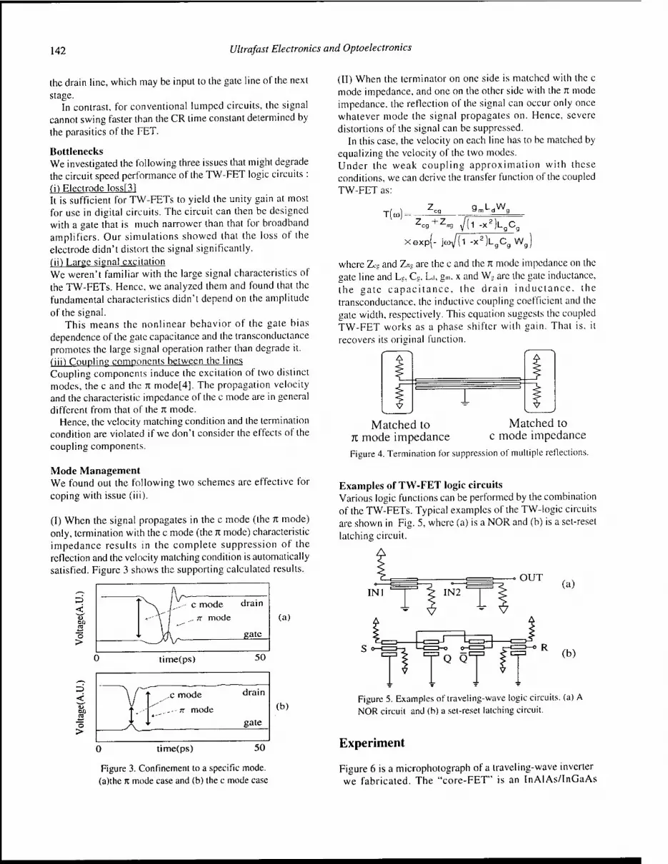
142 Ultrafast Electronics and Optoelectronics
the drain line, which may be input to the gate line of the next
stage. In contrast, for conventional lumped circuits, the signal
cannot swing faster than the CR time constant determined by the parasitics of the FET.
Bottlenecks We investigated the following three issues that might degrade the circuit speed performance of the TW-FET logic circuits: (T) Electrode lossßl It is sufficient for TW-FETs to yield the unity gain at most for use in digital circuits. The circuit can then be designed with a gate that is much narrower than that for broadband amplifiers. Our simulations showed that the loss of the electrode didn't distort the signal significantly. (ih Large signal excitation We weren't familiar with the large signal characteristics of the TW-FETs. Hence, we analyzed them and found that the fundamental characteristics didn't depend on the amplitude of the signal.
This means the nonlinear behavior of the gate bias dependence of the gate capacitance and the transconductance promotes the large signal operation rather than degrade it. (iii) Coupling components between the lines Coupling components induce the excitation of two distinct modes, the c and the n mode[4]. The propagation velocity and the characteristic impedance of the c mode are in general different from that of the n mode.
Hence, the velocity matching condition and the termination condition are violated if we don't consider the effects of the coupling components.
Mode Management We found out the following two schemes are effective for coping with issue (iii).
(I) When the signal propagates in the c mode (the n mode) only, termination with the c mode (the n mode) characteristic impedance results in the complete suppression of the reflection and the velocity matching condition is automatically satisfied. Figure 3 shows the supporting calculated results.
<
O >
3 <
o >
c mode drain
, n mode
gate
(a)
time(ps) 50
T 4*
,,c mode
..-■■■ n mode
drain
gate
(b)
0 time(ps) 50
Figure 3. Confinement to a specific mode. (a)the 7i mode case and (b) the c mode case
(II) When the terminator on one side is matched with the c mode impedance, and one on the other side with the it mode impedance, the reflection of the signal can occur only once whatever mode the signal propagates on. Hence, severe distortions of the signal can be suppressed.
In this case, the velocity on each line has to be matched by equalizing the velocity of the two modes. Under the weak coupling approximation with these conditions, we can derive the transfer function of the coupled TW-FET as:
Tco=- gmLdw8
Zcg+Z^ {( L„Cn
xexp - joWl1 Vö L„C„ W„
where Zc= and Z*s are the c and the n mode impedance on the gate line and Ls, Cs, LJ, gm. x and W» are the gate inductance, the gate capacitance, the drain inductance, the transconductance, the inductive coupling coefficient and the gate width, respectively. This equation suggests the coupled TW-FET works as a phase shifter with gain. That is, it recovers its original function.
Matched to Matched to 71 mode impedance c mode impedance Figure 4. Termination for suppression of multiple reflections.
Examples of TW-FET logic circuits Various logic functions can be performed by the combination of the TW-FETs. Typical examples of the TW-logic circuits are shown in Fig. 5, where (a) is a NOR and (b) is a set-reset latching circuit.
-OUT
INI (a)
(b)
Figure 5. Examples of traveling-wave logic circuits, (a) A NOR circuit and (b) a set-reset latching circuit.
Experiment
Figure 6 is a microphotograph of a traveling-wave inverter we fabricated. The "core-FET" is an InAIAs/InGaAs

Ultrafast Electronics and Optoelectronics 143
heterojunction field effect transistor (HFET) having a IT of 80 GHz. The terminal resistances were monolithically integrated and were connected with the TW-FET throughout the coplanar waveguides (CPWs).The characteristic impedance of the TW-FET is 5 D. for the c mode and 90 D. for the K mode. The calculated fraction of the c mode to the n mode was large, and the effective characteristic impedance of the TW-FET was considered to be very small. Therefore, we designed the characteristic impedance of the CPWs to be 25 Q, which was the lowest value our process could produce maturely. A conventional DCFL inverter was also fabricated on the same wafer for comparison.
Gate IN
Drain IN
Drain OUT
fiälüf*"** li' ll ■?% ■"ISsasjBft "jU M =&.§ai" Gate
OUT '*"»• .'Äi
as: m a iiF«r
Figure 6. Microphotograph of a fabricated traveling-wave inverter.
The impulse response of the traveling-wave inverter was measured using electo-optic sampling (EOS) with an optical- to-eleclrical (OE) conversion probe.
Fig.7 shows the measurement scheme. We generated optical pulses with a lull width at half maximum (FWHM) of 300 fs by compressing lOps pulses produced by a semiconductor laser. The pulses were split into two. One half went to OE conversion probe, and the other was used to probe the DUT.
O-E conversion
probe Termination robe
_Q MJ Pulse Compression
JL Optical
Delay Line
Photo - detector "T
Semiconductor Laser]
Signal Gener ator
Figure 7. Measurement scheme.
The temporal resolution of the EOS is about 300 fs. and its spatial resolution is about 1 p.m. The impulse generated by the OE conversion probe has a rise time of 5 ps, a fall time of 8 ps, FWHM of 7 ps and 200 mVpp swing (inset of Figure 9(a)). The transition of the waveform propagating along the drain line is shown in Fig. 8. The dotted, dashed and solid lines correspond to the measured waveforms probed at the input, the middle port and the output, respectively.
The forward-going wave preserves the shape of the input signal as a result of the in-phase superposition of induced waves on the drain line. In contrast, the backward-going wave is distorted by the out-of-phase supcrposion of these waves.
Hence, the rise and fall time become sleeper and the amplitude becomes larger when the signal propagates forward on the drain line. We can see both of these fundamental characteristics of the TW-FET in Fig. 8. To our knowledge, this is the first ever observation of the traveling-wave operation of a FET in the time-domain.
<
"3 >
~v I r , . . . . . l^VJI '
- input center --<-■■ output
-
■■■■y 5ps -. ^
. .. i. ...
-*—►
Time
Figure 8 Transition of the signal on the drain line.
Figure9(a) shows the measured output waveform with the numerically calculated ones and (b) shows the transfer functions of the traveling-wave inverter and the conventional inverter, which were evaluated from the Fourier transform of the leading edges of the measured waveform.
These indicate the following, (i) The measured bandwidth of the traveling-wave inverter exceeds 125 GHz, which is limited by the OE conversion probe cutoff frequency, (ii) The bandwidth of the traveling-wave inverter overcomes the IT of the "core-FET" defined as a lumped FET, which limits the speed of the conventional circuits, (iii) The calculated results well describe the measured data.
In comparison to the short rise time, the output waveform has a relatively long tail. This tail is generated by the multiple reflections on the gate and the drain line.
The dotted line in Fig. 9(a) is the calculated waveform obtained under the complete impedance matched boundary condition. In this case, the long tail disappeared.
<
o >
, T~—1 1 T-
/ \\ !
-, 1 ! 1 • r—1 . 1 1
_4 j,— FWHM \j 7ps
20ps
-""N^p^ . . .
(a)
Time
<
in
^ ,
- -
- 1 - This work
10 100
(b)
Frequency (GHz)
Figure 9 Response of ther traveling-wave inverter. (a) Measured and calculated waveforms and (b) frequency dependence of ther transfer function.

144 Ultrafast Electronics and Optoelectronics
Based on these experimental analyses, the calculated maximum speed of the NOR and latch circuit (Fig. 5) tend to exceed 100 Gbit/s. We believe that the proposed circuits will usher in the use of 100 Gbit/s-class logic ICs in the real world.
Acknowledgement
We thank H. Yoshimura, O. Karatsu and S. Horiguchi for their continuous encouragements.
References
1. M.J.W. Rodwell, et al., Proc. IEEE, VOL.82, NO.7, 10371059(1994) 2. G.W. Mclver, Proc. IEEE, VOL53, 17471748 (1965) 3. A.S. Podgorski and L.Y. Wei, IEEE Trans. Electron Devices, Vol.ET>29, 1845(1982) 4. K.C. Gupta,et al. p.rls.. Microstrip Lines and Slotlines (ARTECH HOUSE INC., 1979)
High Performance InP HBT Technology for Analog-to-Digital Conversion
Joseph F. Jensen, Gopal Raghavan, Bob Waiden, and Bill Stanchina
Hughes Research Laboratories, 3011 Malibu Canyon Rd. CA, 90265 E-mail:[email protected]
Abstract
The trend in modern communications and radar systems is to move the analog-to digital interface as far forward in the signal path as possible toward the antenna or sensor. Moving the digital interface forward in the signal path eliminates stages of downconversion and analog filtering that are bulky, expensive, drift with temperature, and require calibration. Ultra-fast device technologies are required to perform direct analog-to-digital conversion on radio frequency (RF) or intermediate frequency (IF) signals that enables moving the digital interface forward in the signal path. This paper describes the performance limits of current analog-to-digital converters (ADCs) and shows how the ultra-fast performance of InP HBT technology is extending the performance of ADCs to higher levels to enable all digital approaches to communications receivers.
Introduction
A typical receiver for digital communications is shown in Figure 1. It uses multiple levels of down conversion to optimize sensitivity and interference rejection. A simplistic approach to a future all digital receiver is shown in Figure 2. This receiver digitizes the input signal at the antenna and performs all other receiver functions in software. All digital receivers such as the receiver shown in Figure 2 are robust. Performing IF filtering in software enables changing the filter coefficients. Digital programmability allows a single radio to work in several countries or for several types of communications. Analog IF filters have poor or poorly controlled phase performance and introduce inter-symbol interference, whereas digital filters can have exact linear phase. Receivers with high signal-to-noise (SNR) requirements have tight filtering, gain control (AGC) and gain matching requirements before the ADC that drive the
size, weight, power and cost of conventional analog receivers up. Digital implementations of receiver functions in software are exact and matching between channels can be perfect. Eliminating the analog functions of conventional receivers can significantly reduce the size, weight and cost for receivers in high end systems.
IF1 IF2
1
1 I L-SKakrS-1
in— Ftef
Digital Video HI«
Figure 1. A conventional analog I/Q digital communication receiver.
RF r^ Tuneable
"^ I Filtftr
ADC Digital
l/Q Dec. Filter
I/O and
Video Filter
-l/Q
Figure 2. An all digital implementation of a communications receiver.
The challenge to implementing the receiver in Figure 2 is obtaining an ADC with performance capabilities that can meet the receiver requirements. An all digital receiver approach drives ADCs to high sample rates. A sample rate of twice the IF or RF frequency is required to replace stages of down conversion based on Nyquist. More than twice the IF of RF is required when practical anti-aliasing filters in front of the ADC are considered. Sub-sampling at twice the signal bandwidth of interest to fold the signal band down to baseband still requires a narrow aperature sample-and-hold. The sample-and-hold function is key to most ADC
OSA TOPS on Vltrafast Electronics and Optoelectronics, 1997 Vol. 13, Martin Nuss and John Bowers (ed.) 01997 Optical Society of America
145

146 Ultrafast Electronics and Optoelectronics
architectures. Sub-sampling the RF or IF requires a sample- and-hold with an equivalent aperature as Nyquist sampling. The dynamic range of the ADC at the IF or RF frequency needs to be at least equal to the dynamic range of the ADC being replaced. Additional ADC dynamic range is needed to replace analog AGC functions in software. Increasing the sample rate of ADCs generally decreases the ADC dynamic range. High performance all digital receivers stress ADC fundamental limits. Ultra-fast IC technology will have a major impact in digital receiver technology. This paper will examine the impact of ultra-high speed InP HBT IC technology on ADCs and digital receivers.
InP HBT IC Technology
HBTs use energy gap variations along with electric fields as forces acting on electrons and holes to control their distribution and flow. This property provides substantial leverage over conventional bipolar transistors [1]. The wide bandgap emitter enables the use of very high base doping, allowing low base resistance to be obtained even with small base widths. In an HBT, lowering the emitter doping to moderate levels reduces the base-emitter capacitance while maintaining high current gain (ß). With InP based HBTs, we use AlInAs as the semiconductor for the wide bandgap emitter. We use GalnAs as the semiconductor for the narrow bandgap base. We use GalnAs or InP as the semiconductor in the collector to build single heterojunction (SHBTs) or double heterojunction (DHBTs), respectively.
The material properties of InP-based semiconductors provide attractive features for high speed devices and circuit development. The GalnAs base and collector layers have high electron mobility and velocity leading to small transit times, low device capacitances, and low access resistances. Using an InP collector sacrifices some of the high electron velocity in the collector for higher breakdown voltage and lower output conductance. The GalnAs base has a small bandgap allowing for a low VDe drop (0.7V for InP based HBTs versus 1.4V for GaAs based HBTs). The surface recombination velocity of the GalnAs base is three orders of
magnitude lower (103 cm/s vs. 10^ cm/s) than GaAs based HBTs leading to lower 1/f noise, lower phase noise, and high current gain at low current densities. The thermal conductivity of the InP substrate is nearly 50% larger than GaAs allowing for a lower sensitivity of device parameters to temperature, such as self heating under bias or negative output conductance.
The IC process utilized for the fabrication the ICs reported here is the Hughes Research Laboratories' baseline 3-inch AlInAs/GalnAs heterojunction bipolar transistor (HBT) IC process [2]. It utilizes npn HBTs with an AlInAs emitter, a GalnAs base, and a GalnAs collector. The IC fabrication process (Figure 3) features mesa isolated
transistors on a semi-insulating InP substrate, self-aligned base contacts for high speed operation, thin film TaN resistors and high resistivity epitaxial resistors, Si3N4 and polyimide capacitors, and two levels of interconnects. The IC fabrication process constructs the individual HBTs first (typically 2x2 urn2 through 2x20 um2) followed by the passive elements. Then the wafers are planarized with polyimide and vias are formed through the polyimide to expose buried electrodes which are contacted with second level interconnects (overlay metal).
POLYIMIDE OVERLAY I TOP
VIA METAL / PLATE
SiN DIELECTRIC
FIRST LEVEL METAL
THIN FILM RESISTOR' / / / 0HMIC BONDING DIELECTRIC' / / METAL pAD
EPI RESISTOR MIM CAPACITOR
Figure 3. Cross Section of our InP HBT IC fabrication process.
The transistor characteristics of HBTs with 2x2 urn2
emitters include common emitter current gain in excess of 40. RF characteristics include peak unity current gain cutoff frequency, fr, of 80 GHz.
ADC Perfomance Limitations
ADCs quantize continuous time signals into discrete time and amplitude. Figure 4 is a example of a digitized waveform. The quantization error is the difference between the analog signal waveform and the digitzed waveform. The signal-to-noise-ratio (SNR) is approximately equal to
SNR=6.02N+1.76
where N is the effective number of bits. Figure 5 is a example of the frequency spectrum of a digitzed signal. The quantization noise is uniformly spread from 0 to Fs/2. Distortion in the ADC will produce frequency spurs above the quantization noise floor. The spur free dynamic range (SFDR) is the ratio of the full scale input power to the highest spur power and determines the minimum detectable signal. The dynamic range of an ADC is often expressed as
SFDR(bits)=SFDR(dBc)/6.
The performance of ADCs are limited by a number of factors. The component in an ADC that makes the decision as to whether a signal is above or below a threshold is called the comparator. The time a comparator takes to make an

Ultrafast Electronics and Optoelectronics 147
unambiguous decision is limited by the comparator regeneration time. The time it takes a comparator to recover from a previous decision is called the track recovery time. The regeneration time or the track recovery time may limit the speed of the comparator depending on the comparator design. Both the regeneration and track recovery time of the comparator are proportional to the cutoff frequency (fT) of the transistor technology used to implement the ADC. An approximation to the maximum number of bits versus sample rate due to comparator speed is given by
Bmax=7TfT/6.02fsamp-1.40 where f is the Nyquist sampling rate.
analog waveform
t—digitized waveform
B„ =lo&(V_2/16kTRd£«^lfl-l.
/ l.'l / i :
I !
quantization error Figure 4. ADC quantize analog signal into discrete voltage and time intervals.
SFDR
SNR=6.02N+1.76 A
Sum Components from 0 to F,/2 ' '
Figure 5. Frequency spectrum of a quantized signal.
Another limit to ADC performance is circuit generated noise. The equivalent input-referred thermal noise of an ADC is given by
<vn2>=4kTRefffsamp/2
where Reff includes contributions due to thermal noise, shot noise, ficker noise, and input referred noise terms. An approximation to the maximum number of bits versus sample rate due thermal noise limitations is
Uncertainty in sampling time or aperture jitter (xj is the most significant limit to ADC performance. Aperture jitter includes phase noise on the sample clock, circuit noise, power-line noise, digital feedthrough noise, and phase noise on the input signal. An approximation to the maximum number of bits versus sample rate is
Braax=log2(2/fsamp7tTa)-l
Figure 6 is a plot of sample rate versus effective number of bits (SNR) for a number of ADC reported in the literature over the past several years [3]. Over 100 converters, including experimental ICs, and commercially available parts, are represented in the graph. Also shown on the graph are curves corresponding to various values of comparator regeneration times, thermal noise and aperture jitter limits as described above. As shown in the graph the current state-of- the-art is described by an aperture jitter of ~3ps and a regeneration time constant that corresponds to a value of f-r-50 GHz.
InP HBT ADC IC Results
To extend ADC performance to higher levels we have fabricated ADCs using InP HBT IC technology with a variety of ADC architectures. Figure 7 is an example of a 3- bit flash ADC architecture. The flash architecture utilizes 2b" 1 (where b= number of bits) comparators, which sample the analog input voltage simultaneously, and, therefore this type of converter is inherently fast. The parallelism in this architecture has a significant drawback when high resolution conversion is desired, the number of comparators grows exponentially with b. In addition, the smaller separation (AVref) of adjacent reference voltages grows smaller exponentially. The consequences are: very large ICs, high power dissipation, difficulty in matching components, and the increasingly large input capacitance reduces analog input bandwidth. Most flash converters available today have < 8- bit resolution.
As a demonstrator we developed a 3-bit flash ADC in our InP HBT IC technology [4]. A die photo of the ADC is shown in Figure 8. The circuit contains approximately 900 transistors and has a die size of 2.2 mm x 2.7 mm. The power dissipated (including testing functions) is 3.5 W. The converter demonstrated an SNR equal to 18.1 dB (2.71 ENOB) up to a clock rate of 12.7 GHz for a low input frequency sinewave (27 MHz). A beat frequency method was used with an offset frequency of 27 MHz for Nyquist testing. The SNR is found to be 16.1 dB giving an effective number of bits equal to 2.4 bits for Nyquist testing up to a sampling rate of 8 Gsamples/sec.

148 Ultrafast Electronics and Optoelectronics
1E+4 1E+5 1E+6 1E+7 1E+8 1E+9 Sample Rate (Samples/s)
1E+10 1E+11
Figure 6. Survey of ADCs as a function of SNR bits and ADC limitations.
* n
3-bit Quantizer
Figure 7. An example of a 3-bit flash ADC.
Figure 8. Die photo of 3-bit flash ADC implemented in InP HBTIC technology.
Linearity of multibit quantizers are limited by accuracy of voltage thresholds which are determined by the uniformity of the process technology used in ADC fabrication. A single bit ADC is iinherently linear but posses high quantization noise. We can increase the resolution of a single bit ADC by using oversampling. Since the quantization noise of a Nyquist ADC is uniformly spread
from 0 to Fs/2, oversampling (averaging) can improve the SNR by 3dB (0.5 bits) for every doubling of the clock rate. Using this technique, however, requires very high oversampling rates. For example, to achieve 10 bit resolution on a 50 MHz signal with a single bit ADC requires a 12.5 THz sample rate. A more practical solution to oversampling with a single bit ADC is to add a loop filter inside a feedback loop. This is the basic concept behind delta-sigma modulation [5].
Figure 9 show a basic 1st order AS modulator. An integrator is used inside the feedback loop as the loop filter. The feedback loop provides a high pass characteristic to the quantization noise and a low pass characeristic to the input signal. We still achieve 3 dB (0.5 bit) improvement in resolution for each doubling of the clock rate from oversampling, however; we achieve an additional 6 dB (1 bit) improvement from the integrator for a total improvement of 9 dB for each doubling of the clock rate. Higher order modulators use additional integrators and increase resolution by 6 dB per doubling of clock rate for each integrator. Modulator orders greater than two are potentially unstable. A 2nd order AS modulator achieves 15 dB improvement for each doubling of the clock rate. The quantization noise is now reduced in the signal band. A digital filter is used to filter the high frequency quantization noise outside the signal band. AS modulators reduce the integrator non-linearity by feedback, they do not require sample-and-hold circuitry and they require only low precision analog circiuts. Most of the complexity of a AS ADC is in the digital circuits. AS ADCs require ultra high speed IC technology for RF applications.
We have also demonstrated a 2nd order AS modulator in InP HBT IC technology [6]. We used continuous-time Gm- C fully differential circuitry to implement the 2nd order AS

Ultrafast Electronics and Optoelectronics 149
modulator (Figure 10). Figure 11 is a die photo of the InP HBT 2nd order AI modulator. The chip operates from ± 5 volt supplies and dissipates 1W. At a sample rate of 3.2 GHz and a signal bandwidth of 50 MHz (OSR of 32 and 100 MSPS Nyquist rate) the modulator demonstrates a SFDR of 71 dB (12-bits dynamic range and the ideal signal-to-noise ratio of 55 dB for a second-order modulator at an oversampling ratio of 32. For an oversampling ratio of 256, the modulator achieves a peak SNR of 70 dB.).
x(t) +/T\_JT- n One Bit —(+H Integrator}—! Quar| |—. Digital
LP Filter Jl»)
1 One Bill 1 D/A 1
The region of surpressed quantization noise can be tuned from DC to IF by replacing the integrator with a bandpass filter. Figure 13 shows a bandpass AS modulator topology with the resulting noise power spectrum. The primary motivation of bandpass converters is the simplicity they impart to systems dealing with narrow-band signals. The use of a bandpass AS modulator permits a direct conversion of an analog signal to digital form at IF for RF communication and radar systems.
x(tLi{+)- Band PassU One Bit 1 Filter n Quant 1
Digital BP Filter
J(n)
H lone Bit 1 1 D/A 1
Frequency Frequency
Figure 9. 1st order AS modulator loop and the resulting noise power spectrum of its output.
ta a>o
El »J5I E_^J £^
"V Figure 10. Block diagram of a continuous time 2"d
order AS modulator implemented with Gm-C techniques.
Figure 11. Die photograph of the InP HBT 2nd order AS modulator.
Figure 12. Bandpass AS modulator loop and the resulting noise power spectrum of its output.
Figure 13 shows the architecture of our fully differential realization of a second order 1-bit output bandpass AS modulator [7], which is an extension of the design in [6] and is similar to the architecture proposed by Shoaei and Snelgrove [8]. Performance of this architecture is determined primarily by the Q of the resonator. The major changes from the architecture described in [8] are the insertion of tunable transconductance (gj cells in the feedback path of the resonator, inclusion of an extra half clock cycle delay following the comparator and use of current-mode logic in the design. The first of these changes permits the resonator center frequency to be varied from DC to a maximum designed value. The extra half clock cycle delay following the comparator results in matched output rise and fall times which allows us to use a NRZ DAC. The use of current- mode logic reduces switching noise and also eliminates the requirement for high gain operational amplifiers in the design. Figure 14 is a micrograph of the die containing the modulator and a 1:16 DEMUX. The modulator is located in the bottom right hand corner of the die. The modulator measures 750um x 750 urn and dissipates 1.4 Watts. The 1- to-16 DEMUX dissipates 0.5 Watts, and the 16 ECL output buffer dissipate 2 Watts.
150 Ultrafast Electronics and Optoelectronics
POSITIVE CURRENT SOURCE POSITIVE CURRENT SOURCE
ZEJ
intermediate frequency (IF) signals that enables moving the digital interface forward in the signal path. We have demonstrated an 8 GSPS 3-bit flash ADC, a low pass 2nd
order AS modulator sampling at 3.2 GHz producing 70 dB dynamic range for 50 MHz signal bandwidth, and 4 GSPS sample rate 2nd order bandpass AS modulator producing SNR values ranging from 89 dB over a 366 kHz bandwidth to 42 dB over a 62.6 MHz bandwidth centered at an IF of 60 MHz. The ultra-fast InP HBT technology demonstrated in this work has establish the feasibility for all digital receivers.
Figure 13. The architecture of a fully differential realization of a second order 1-bit output bandpass AS modulator.
Figure 14. A photograph of the InP HBT bandpass AS modulator and a 1:16 DEMUX.
Measurements on this bandpass modulator yield SNR values ranging from 89 dB over a 366 kHz bandwidth to 42 dB over a 62.6 MHz bandwidth. Figure 15 shows the output spectrum for various center frequencies and demonstrates notch tunability. A peak SNR of 84.9 dB, 81.2 dB and 80.5 dB was obtained corresponding to notch positions of 62.5 MHz, 41.4 MHz and 24.4 MHz respectively.
_ o m 2--25
myi fyl 0 50 100
Frequency (MHz) 0 50 100 0 50 100
Frequency (MHz) Frequency (MHz) 32 K FFT, Kaisar Window a = 20
Figure 15. The output spectrum of the tunable 2nd order bandpass AS modulator for various center frequencies.
Conclusions
The trend in modern communications and radar systems is to move the analog-to digital interface as far forward in the signal path as possible toward the antenna or sensor. Ultra-fast device technologies are required to perform direct analog-to-digital conversion on radio frequency (RF) or
Acknowledgment
The authors would like to thank R. Martinez, A. Arthur, and W. Hoefer for their help in the fabrication of the IC and A. Kramer and F. William for their help in testing. We would also like to thank Norm Moyer of Sunshine Semiconductor for his help in IC layout and Z. Lemnios of DARPA for supporting the InP fabrication line.
References
1. H. Kroemer, "Heterostructure bipolar transistors and integrated circuits, " Proc. IEEE, Vol. 70, pp. 13, 1982.
2. W. Stanchina et al., Technical Digest, GaAs IC Symposium, 1995, pp 31-34.
3. RH. Waiden, "Analog-to-Digital Converter Technology Comparison," Technical Digest, GaAs IC Symposium, 1994, pp217-219
4. C. Baringer, J. Jensen, L. Burns, B. Waiden, "3-bit, 8 GSPS Flash ADC," 1996 Indium Phosphide and Related Material Technical Digest, pp. 64-67.
5. J. C. Candy, G. C. Temes, "Oversampling Methods for A/D and D/A Conversion," IEEE Press Collection of Papers, "Oversampling Delta-Sigma Data Converters Theory Design and Simulation," 1992, pp 1-25.
6. J. F. Jensen, G. Raghavan, A. E. Cosand and R. H. Waiden, 'A 3.2-GHz Second-Order Delta-Sigma Modulator Implemented in InP HBT Technology," IEEE J. Solid State Circuits, Vol 30, No. 10, October 1995, pp. 1119-1127.
7. G. Raghavan, J.F. Jensen, R.H. Waiden, W.P. Posey, "A Bandpass AS Modulator with 92 dB SNR and Center Frequency Continuously Programmable from 0 to 70 MHz," 1997 ISSCC Technical Digest, pp. 214- 215
8. O. Shoaei and W. M. Snelgrove, 1994 IEEE Symposium on Circuits and Systems, Vol. 5, Pg. 489.
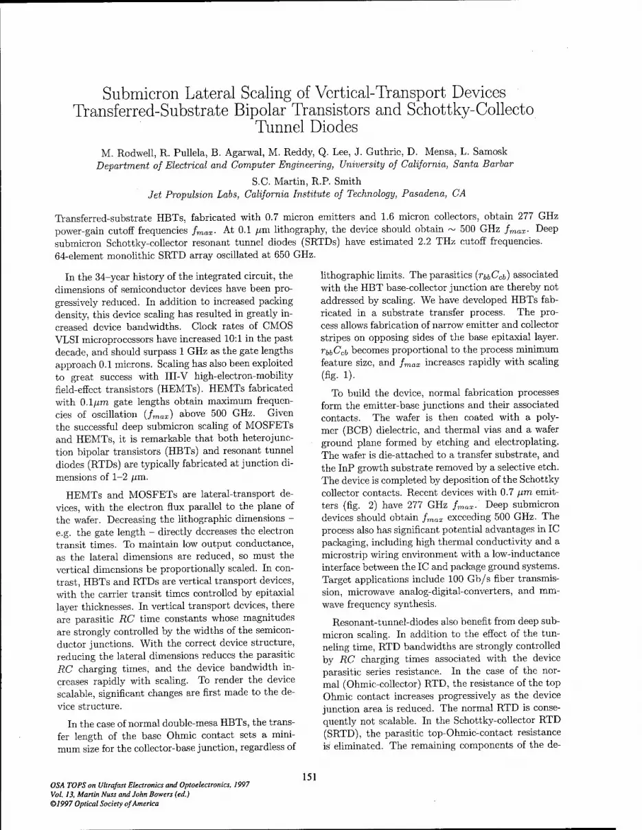
Submicron Lateral Scaling of Vertical-Transport Devices Transferred-Substrate Bipolar Transistors and Schottky-Collecto
Tunnel Diodes M. Rodwell, R. Pullela, B. Agarwal, M. Reddy, Q. Lee, J. Guthrie, D. Mensa, L. Samosk
Department of Electrical and Computer Engineering, University of California, Santa Barbar
S.C. Martin, R.R Smith Jet Propulsion Labs, California Institute of Technology, Pasadena, CA
Transferred-substrate HBTs, fabricated with 0.7 micron emitters and 1.6 micron collectors, obtain 277 GHz power-gain cutoff frequencies fmax. At 0.1 ^m lithography, the device should obtain ~ 500 GHz fmax. Deep submicron Schottky-collector resonant tunnel diodes (SRTDs) have estimated 2.2 THz cutoff frequencies. 64-element monolithic SRTD array oscillated at 650 GHz.
In the 34-year history of the integrated circuit, the dimensions of semiconductor devices have been pro- gressively reduced. In addition to increased packing density, this device scaling has resulted in greatly in- creased device bandwidths. Clock rates of CMOS VLSI microprocessors have increased 10:1 in the past decade, and should surpass 1 GHz as the gate lengths approach 0.1 microns. Scaling has also been exploited to great success with III-V high-electron-mobility field-effect transistors (HEMTs). HEMTs fabricated with 0.1//m gate lengths obtain maximum frequen- cies of oscillation (fmax) above 500 GHz. Given the successful deep submicron scaling of MOSFETs and HEMTs, it is remarkable that both heterojunc- tion bipolar transistors (HBTs) and resonant tunnel diodes (RTDs) are typically fabricated at junction di- mensions of 1-2 fim.
HEMTs and MOSFETs are lateral-transport de- vices, with the electron flux parallel to the plane of the wafer. Decreasing the lithographic dimensions - e.g. the gate length - directly decreases the electron transit times. To maintain low output conductance, as the lateral dimensions are reduced, so must the vertical dimensions be proportionally scaled. In con- trast, HBTs and RTDs are vertical transport devices, with the carrier transit times controlled by epitaxial layer thicknesses. In vertical transport devices, there are parasitic RC time constants whose magnitudes are strongly controlled by the widths of the semicon- ductor junctions. With the correct device structure, reducing the lateral dimensions reduces the parasitic RC charging times, and the device bandwidth in- creases rapidly with scaling. To render the device scalable, significant changes are first made to the de- vice structure.
In the case of normal double-mesa HBTs, the trans- fer length of the base Ohmic contact sets a mini- mum size for the collector-base junction, regardless of
lithographic limits. The parasitics (rbbCcb) associated with the HBT base-collector junction are thereby not addressed by scaling. We have developed HBTs fab- ricated in a substrate transfer process. The pro- cess allows fabrication of narrow emitter and collector stripes on opposing sides of the base epitaxial layer. TbbCcb becomes proportional to the process minimum feature size, and fmax increases rapidly with scaling
(fig- I)-
To build the device, normal fabrication processes form the emitter-base junctions and their associated contacts. The wafer is then coated with a poly- mer (BCB) dielectric, and thermal vias and a wafer ground plane formed by etching and electroplating. The wafer is die-attached to a transfer substrate, and the InP growth substrate removed by a selective etch. The device is completed by deposition of the Schottky collector contacts. Recent devices with 0.7 \im emit- ters (fig. 2) have 277 GHz fmax- Deep submicron devices should obtain fmax exceeding 500 GHz. The process also has significant potential advantages in IC packaging, including high thermal conductivity and a microstrip wiring environment with a low-inductance interface between the IC and package ground systems. Target applications include 100 Gb/s fiber transmis- sion, microwave analog-digital-converters, and mm- wave frequency synthesis.
Resonant-tunnel-diodes also benefit from deep sub- micron scaling. In addition to the effect of the tun- neling time, RTD bandwidths are strongly controlled by RC charging times associated with the device parasitic series resistance. In the case of the nor- mal (Ohmic-collector) RTD, the resistance of the top Ohmic contact increases progressively as the device junction area is reduced. The normal RTD is conse- quently not scalable. In the Schottky-collector RTD (SRTD), the parasitic top-Ohmic-contact resistance is eliminated. The remaining components of the de-
OSA TOPS on Ultrafast Electronics and Optoelectronics, 1997 Vol. 13, Martin Nuss and John Bowers (ed.) ©1997 Optical Society of America
151

152 Ultrafast Electronics and Optoelectronics
vice parasitic series resistance are minimized by scal- ing the device to deep submicron dimensions. The SRTD fmax increases rapidly (fig. 1). With these devices, we have recently constructed submillimeter- wave monolithic quasi-optical array oscillators (fig. 3). The arrays incorporate 0.1 fim SRTDs, resistors, Si3N4 MIM capacitors, airbridges, and Schottky- diode bias regulators, fabricated in an 8-mask pro- cess. A 64-element SRTD array oscillated at 650 GHz.
Acknowledgements
The HBT work at UCSB was supported by the ONR under grant # N00014-95-1-0688, by the AFOSR un- der grant # F49620-96-1-0019, and by the DARPA Optoelectronics Technology Center. The RTD work at UCSB was supported by the ONR under grant ONR N00014-93-1-0378, and by the AFOSR under grant # F49620-92-J-0469. The JPL work was per- formed at the JPL Center for Space Microelectronics Technology, and was sponsored by NASA.
References
[1] E.R. Brown, J.R. Soderstorm, CD. Parker, L.J. Mahoney, K.M. Molvar and T.C. Mcgill, "Os- cillations up to 712 GHz in InAs/AlSb resonant- tunneling diodes," Appl. Phys. Lett., vol. 58, no. 20, pp 2291-2293, May, 1991.
[2] C. Kidner, I. Mehdi, J.R. East and G.I. Had- dad, "Bias circuit instabilities and their effect on dc current-voltage characteristics of double- barrier resonant tunneling diodes," Solid-State Electron., vol. 34, no. 2, pp 149-156, Feb., 1991.
[3] M. Reddy, R.Y. Yu, H. Kroemer, M.J.W. Rod- well, S.C. Martin, R.E. Muller and R.P. Smith, "Bias stabilization for resonant tunnel diode os- cillators," IEEE Microwave and Guided Wave Lett., vol. 5, no. 7, pp. 219-221, July, 1995.
[4] M.P. De Lisio, J.F. Davis, S.J. Li, D.B. Rutledge and J.J. Rosenberg, "A 16-element tunnel diode grid oscillator," IEEE AP-S International Sym- posium, Newport Beach, CA, June, 1995.
[5] Y. Konishi, S.T. Allen, M. Reddy, M.J.W. Rod- well, R.P. Smith k J. Liu, "AlAs/GaAs Schottky -Collector Resonant -Tunnel-Diodes" Solid-State Electronics, Vol. 36, No. 12, pp. 1673-1676, 1993
[6] R.P. Smith, S.T. Allen, M. Reddy, S.C. Mar- tin, J. Liu, R.E. Muller, and M.J.W. Rodwell,
"0.1 /um Schottky-Collector AlAs/GaAs Reso- nant Tunneling Diodes" IEEE Electron Device Letters, Vol. 15, No. 8, August 1994
[7] M. Reddy, M.J. Mondry, M.J.W. Rodwell, S.C. Martin, R.E. Muller, R.P. Smith, D.H. Chow, and J.N. Schulman, "Fabrication and DC, Mi- crowave Characteristics of Submicron Schottky- Collector AlAs/In0.53Ga0.47As/InP Resonant Tunneling Diodes", Journal of Applied Physics, Vol 77, No. 9, pp. 4819-4821, May 1, 1994
[8] A.C. Molnar, M. Reddy, M.J. Mondry, M.J.W. Rodwell, and S. J. Allen, Jr., "Large Submm- wave Monolithic RTD Oscillator Arrays to 650 GHz", Postdeadline Paper , 1996 IEEE Electron Device Meeting, San Francisco, December.
[9] W. E. Stanchina, J. F. Jensen, R. H. Waiden, M. Hafizi, H. -C. Sun, T. Liu, G. Raghavan, K. E. Elliott, M. Kardos, A. E. Schmitz, Y. K. Brown, M. E. Montes and M.Young, "An InP- Based HBT Fab for High-Speed Digital, Analog, Mixed-Signal and Optoelectronic ICs", GaAs IC Symp. Tech. Dig., 1995, pp. 31-34.
[10] S. Yamahata, K. Kurishima, H. Ito and Y. Matsuoka, "Over-220-GHz-/T-and- fmax InP/InGaAs Double-Heterojunction Bipo- lar Transistors with a New Hexagonal-Shaped Emitter", GaAs IC Symp. Tech. Dig., 1995, pp. 163-166.
[11] S. Yamahata, K. Kurishima, H, Nakajima, T. Kobayashi and Y. Matsuoka, "Ultra-High fmax
and fT InP/InGaAs Double-Heteroj unction Bipolar Transistors with Step-Graded InGaAsP Collector", GaAs IC Symp. Tech. Dig., 1994, pp. 345-348.
[12] U. Bhattacharya, M. J. Mondry, G. Hurtz, I. -H. Tan, R. Pullela, M. Reddy, J. Guthrie, M. J. W. Rodwell and J. E. Bowers, "Transferred-Substrate Schottky-Collector Het- erojunction Bipolar Transistors : First Results and Scaling Laws for High fmax"> IEEE Elec- tron Device Lett., vol. 16, pp. 357-359, 1995.
[13] U. Bhattacharya, L. Samoska, R. Pullela, J. Guthrie, Q. Lee, B. Agarwal, D. Mensa and M. J. W. Rodwell, "170 GHZ transferred-substrate heterojunction bipolar transistor", Electron. Lett, vol. 32, pp. 1405-1406, 1996.

Ultrafast Electronics and Optoelectronics 153
Schottky-Collector RTD Bandwidth & Submicron Scaling
Collector Width (urn) ■ Top contact resitance eliminated • Bottom contact resistance reduces with scaling:^ > Bandwidth increases rapidly with scaling.
Transferred-Substrate HBT Bandwidth & Submicron Scaling 500 ■ Transferred-
Substrate HBT
100
0.5 1 1.5 emitter and collector width, urn
■w Collector capacitance reduces with scaling:C(/, <* Wc
Bandwidth increases rapidly with scaling:/,,^ =-J\jWl
Figure 1: RTD and HBT scaling laws
Transferred-Substrate Heterojunction Bipolar Transistor Schottky collector contact
1 BCB
gold thermal
via
: I BCB
gold ground plane
carrier
emitter |V] airbridge |||| polyimide |
metaljJJ base §JH SigN^H collector \
■■ f =277 GHz max
f =128 GHz '•
"1 ' '—' i i > " i—
10 100 Frequency, GHz
Figure 2: Transferred-Substrate HBT; cross-section, SEM, and performance
64-element Schottky-RTD oscillator at 650 GHz
array oscillator
SRTD slot oscillator
0.1 jim, 2.2 THz Schottky-RTD
Figure 3: 650 GHz SRTD oscillators; device, oscillator, and array
Measurement Techniques
Theodore Norris
Uuniversity of Michigan Center for Ultrafast Optical Science Rm 1006,1 St. Bldg 2200 Bonisteel Dr. Ann Harbor, MI 48109 Phone: (313) 763-4875 Fax: (313) 763-4876
The measurement of short optical and electrical pulses is at the heart of ultrafast optoelectronics. In recent years, complete characterization of short optical pulses has been made possible through the development of frequency-resolved optical gating (FROG) and related techniques. Techniques for measuring picosecond electrical transients via ultrafast sampling using either mode-locked lasers or nonlinear transmission lines have also become widely available over the past decade or so.
The development and refinement of these tools for high-speed optoelectronics continues apace, along several important frontiers, including (i) development of new optical gating techniques, (ii) improved simplicity and practicality for real-world high-speed device and circuit testing, (iii) improved sensitivity, and (iv) coupling of ultrafast sampling to imaging with high spatial resolution. For (i), new developments reported here include the application of cascaded second-order nonlinearities for optical gating, the development of real-time phase-sensitive FROG, and high-speed electro-optic gating for measurement of optical pulses. For (ii), new compact sources of ultrashort pulses as well as new methods for performing pump-probe sampling measurements are needed. Papers are presented here showing new phase-sensitive measurements as well as sampling without the need for optical delay lines. For (iii), the need for high sensitivity arises partly from the need to minimize signal acquisition time, but perhaps more importantly so that small signal levels on the next generation of ultra-submicron (or "mesoscopic") devices and circuits can be measured.
Considerable progress in this direction has been made, with the improvement of photoconductive sampling sensitivity to less than 10 nW(Hz) . Finally, (iv), rapid progress has been made in coupling ultrafast sampling to imaging using a number of approaches. Electro- optic sampling can be performed in an optical imaging geometry with CCD detection to image electrical transients in circuits. For investigation of ultra-submicron devices and circuits, spatial
155

156
resolution below the optical limit is required. Several reports are given on various techniques for coupling ultrafast sampling measurements with scanning-force microscopy (SFM). The SFM may either be used as the voltage probe itself, with time resolution obtained using a nonlinear transmission line, or the SFM may be used in conjunction with a contacting photoconductive probe which is gated with a short-pulse laser. These exciting new techniques will be the building blocks for the high-speed test and measurement systems which the next generation of ultra- submicron devices and circuits will require.

Amplified ultrafast all-optical switching using fully-phasematched cascaded second-order nonlinearities and a polarization-gate geometry
Marco A. Krumbügel, John N. Sweetser, and Rick Trebino
Combustion Research Facility, MS9057, Sandia National Laboratories, Livermore, CA 94551-0969
Abstract
We demonstrate amplified all-optical switching of ultrashort laser pulses using two different types of cascaded second-order nonlinear optical processes simultaneously in a polarization-gate geometry. The first process rotates the input-pulse polarization, thus achieving optical gating. At high intensities, this signal pulse is then amplified by a different process involving parametric amplification, yielding switching efficiencies up to 320% and an on-off ratio of 6xl05
with 250-fs pulses.
Keywords:
Ultrafast nonlinear optics, All-optical devices, Modulators, Optical communications.
Introduction
Combining the advantages of both second-order and third-order processes, cascaded second-order nonlinear- optical (CSN) processes offer high efficiency using readily available materials, versatility, and same- wavelength input and output beams. Numerous sophisticated devices and setups based on CSN processes have been demonstrated recently, e.g., pulse shortening [1,2], soliton excitation [3], and an optical transistor [4,5]. All-optical switching and modulation has been discussed and demonstrated by several scientists [6-9], and Danielius et al. [10] have shown that CSN processes can simulate a self-diffraction process, achieving an efficiency several orders of magnitude larger than is attainable with third-order self- diffraction techniques. In their and also in other CSN
arrangements that could be used for all-optical switching, however, at most one of the second-order processes could be phase-matched; approximate phase- matching was maintained by using a small beam interaction angle.
In this paper, we demonstrate a convenient and efficient CSN setup in which both second-order processes are simultaneously phase-matched and which is ideal for ultrafast all-optical switching.
Experimental setup
Our scheme employs a polarization-gate beam geometry identical to that commonly used for optical switching using third-order optical-Kerr media [11]; however, a second-order type II BBO crystal replaces the third-order nonlinear-optical medium (Figure 1).
type II BBO crystal
Figure 1. Polarization-gate setup.
The optical switch demonstrated here yields the same effect as the third-order Kerr gate — rotating the input beam polarization when a 45-degree-polarized gating pulse is present — and therefore shares its advantages of simple arrangement, collinear input and signal beams, and non-interferometric interaction. It is distinguished from the third-order optical-Kerr effect, however, by a strong angular dependence of the switching efficiency (we found an acceptance angle of
OSA TOPS on Ultrafast Electronics and Optoelectronics, 1997 Vol. 13, Martin Nuss and John Bowers (ed.) ©1997 Optical Society of America
157
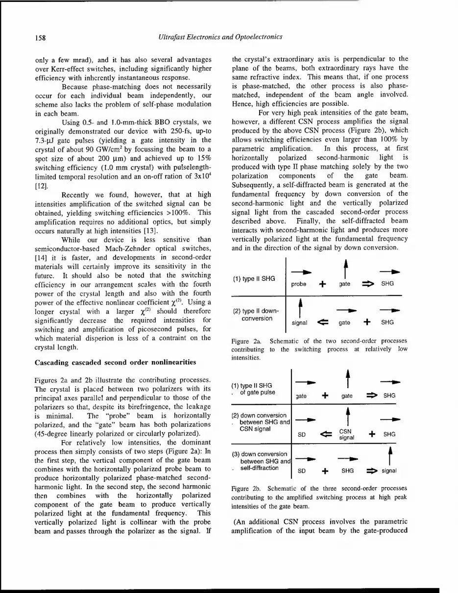
158 Ultrafast Electronics and Optoelectronics
only a few mrad), and it has also several advantages over Kerr-effect switches, including significantly higher efficiency with inherently instantaneous response.
Because phase-matching does not necessarily occur for each individual beam independently, our scheme also lacks the problem of self-phase modulation in each beam.
Using 0.5- and 1.0-mm-thick BBO crystals, we originally demonstrated our device with 250-fs, up-to 7.3-foJ gate pulses (yielding a gate intensity in the crystal of about 90 GW/cm2 by focussing the beam to a spot size of about 200 |J.m) and achieved up to 15% switching efficiency (1.0 mm crystal) with pulselength- limited temporal resolution and an on-off ration of 3xl04
[12]. Recently we found, however, that at high
intensities amplification of the switched signal can be obtained, yielding switching efficiencies >100%. This amplification requires no additional optics, but simply occurs naturally at high intensities [13].
While our device is less sensitive than semiconductor-based Mach-Zehnder optical switches, [14] it is faster, and developments in second-order materials will certainly improve its sensitivity in the future. It should also be noted that the switching efficiency in our arrangement scales with the fourth power of the crystal length and also with the fourth power of the effective nonlinear coefficient %(2). Using a longer crystal with a larger %{2) should therefore significantly decrease the required intensities for switching and amplification of picosecond pulses, for which material disperion is less of a contraint on the crystal length.
Cascading cascaded second order nonlinearities
Figures 2a and 2b illustrate the contributing processes. The crystal is placed between two polarizers with its principal axes parallel and perpendicular to those of the polarizers so that, despite its birefringence, the leakage is minimal. The "probe" beam is horizontally polarized, and the "gate" beam has both polarizations (45-degree linearly polarized or circularly polarized).
For relatively low intensities, the dominant process then simply consists of two steps (Figure 2a): In the first step, the vertical component of the gate beam combines with the horizontally polarized probe beam to produce horizontally polarized phase-matched second- harmonic light. In the second step, the second harmonic then combines with the horizontally polarized component of the gate beam to produce vertically polarized light at the fundamental frequency. This vertically polarized light is collinear with the probe beam and passes through the polarizer as the signal. If
the crystal's extraordinary axis is perpendicular to the plane of the beams, both extraordinary rays have the same refractive index. This means that, if one process is phase-matched, the other process is also phase- matched, independent of the beam angle involved. Hence, high efficiencies are possible.
For very high peak intensities of the gate beam, however, a different CSN process amplifies the signal produced by the above CSN process (Figure 2b), which allows switching efficiencies even larger than 100% by parametric amplification. In this process, at first horizontally polarized second-harmonic light is produced with type II phase matching solely by the two polarization components of the gate beam. Subsequently, a self-diffracted beam is generated at the fundamental frequency by down conversion of the second-harmonic light and the vertically polarized signal light from the cascaded second-order process described above. Finally, the self-diffracted beam interacts with second-harmonic light and produces more vertically polarized light at the fundamental frequency and in the direction of the signal by down conversion.
(1)typellSHG
(2) type II down- conversion
probe gate SHG
signal gate SHG
Figure 2a. Schematic of the two second-order processes contributing to the switching process at relatively low intensities.
(1) type II SHG . of gate pulse
(2) down conversion between SHG and CSN signal
(3) down conversion between SHG and self-diffraction
gate gate SHG
SD CSN signal + SHG
SD + SHG signal
Figure 2b. Schematic of the three second-order processes contributing to the amplified switching process at high peak intensities of the gate beam.
(An additional CSN process involves the parametric amplification of the input beam by the gate-produced

Ultrafast Electronics and Optoelectronics 159
second harmonic beam, yielding another beam collinear with the self-diffracted beam but of opposite polarization.)
Results
Figure 3 shows the switching efficiency r\, defined as the ratio between the intensity of the vertically polarized signal beam and the intensity of the horizontally polarized probe beam, as a function of the peak intensity of the gate beam. For small gate intensities (first two data points), a dependence of r| on the square of the gate intensity is observed, characteristic for second-order processes. For higher gate intensities (next two data points) the increase of r| is at first slower than expected from a square dependence, which can be attributed to depletion effects in the crystal. Finally, for very large intensities of the gate beam (last point), a strong increase of the switching efficiency is observed, which is caused by the self-diffraction process with parametric amplification described above. The highest observed efficiency was 320% for a crystal length of 1.0 mm and 60% for a crystal length of 0.5 mm, using a gate-pulse peak intensity of 800 GW/cm2. The 1-kHz train pulses were obtained from a regeneratively-amplified Ti:Sapphire laser operating near 850 nm. The pulses had a length of about 250 fs and were focussed to a spot size (FWHM) of about 200 urn in the BBO crystal.
100
10
tr 1
0.1
0.01
1 ] —i—i—i—i—i .A :
! ! .▼ : ; ...A"
. -At'" .-■
_.-■ • .--▼* • | _.A'
.▼!"'' *
\ k' .- --A--L = 1.0 mm I .▼' --Y--L = 0.5 mm :
: t'' ■ i . . . . i
•
off ratio of this switching device was as large as 6.4x10⁵
for the observed 320% switching efficiency. It appears to be a general characteristic of fully
phase-matched CSN processes and can be easily derived from the coupled equations for both processes [12] that the switching efficiency depends on the fourth power of the crystal length L and also on the fourth power of %(2). It is therefore interesting to note that for the lowest gate-beam intensities (10 GW/cm2 and 27 GW/cm2), where depletion effects in the crystal are not prominent, a dependence of r\ on the fourth power of the crystal length was indeed observed, i.e., an increase of the efficiency by 17 and 15, respectively, was measured, when the crystal length was doubled.
Applications
Besides potential applications in optical computing and optical communications, the amplified switching process can be used, e.g., for the measurement of ultrashort laser pulses by means of frequency-resolved- optical-gating (FROG) [15].
Spectrally resolving the switched signal pulse as a function of delay is equivalent to a polarization- gate FROG measurement using an optical Kerr medium (PG-FROG), but achieves a higher sensitivity. It is interesting to note, however, that the same setup also simultaneously allows two different types of FROG measurements, thus combining three FROG geometries in a single setup (Figure 4): Spectrally resolving the self-diffracted pulse from the parametric amplification process vs. delay gives a SD-FROG trace, whereas spectrally resolving the second-harmonic between gate and probe gives a SHG FROG-trace [16].
crystal
-PH PG-FROG _ _ "j signal I I
10 100 1000 Igate [GW/cm2
<a,e+Probe) SHG-FROG
SD-FROG
Figure 3. Measured switching efficiency vs. intensity for two different crystal lengths.
gate-beam
In the absence of the gate pulse, we found that the birefringent BBO crystal, oriented with its principal axes parallel to those of the polarizers, introduced minimal polarizer-leakage background to the signal light. The fraction of the probe beam leaking through the polarizers was 5xl0~6. As a result, the maximum on-
Figure 4: Schematic diagram of the three beams that can be employed for a FROG measurement (S = spectrometer).
We measured the PG- and SD-FROG traces of the amplified laser pulses used in our switching experiment. Figure 5 shows the measured PG-FROG trace obtained by spectrally resolving the polarization- rotated signal (the SD-FROG trace looks similar); Figure 6 shows the retrieved intensity and phase of the

160 Ultrafast Electronics and Optoelectronics
pulse obtained from both geometries, showing the good agreement between the two independent measurements
e c
c S >
875-
-400 -200 0 Delay (fs)
Figure 5. PG-FROG trace measured by spectrally resolving the signal in the polarization-gate geometry. (Contour lines at 5%, 10%, 20%, 40%, 60%, and 80% of the maximum intensity.)
835 840 845 850 Wavelength (nm)
Figure 6. Spectral intensity and phase of the amplified laser pulses measured by spectrally resolving the signal in the polarization-gate setup (PG) and the related self-diffracted signal (SD).
Conclusion
We conclude that a polarization-gate geometry using entirely phase-matched cascaded second-order nonlinearities with type II phase matching provides a highly efficient all-optical switch, with an on/off ratio of more than 6xl05. The demonstrated ability of this arrangement to simultaneously amplify the switched signal makes the device especially appealing for several applications.
In particular, we believe that a CSN setup will allow unambiguous FROG measurements of unamplified
Ti:Sapphire laser pulses (currently performed using second-harmonic generation and hence with an ambiguity in the direction of time).
Acknowledgments
This work was partially supported by the U.S. Department of Energy, Basic Energy Sciences, Chemical Sciences Division. M. A. Krumbügel gratefully acknowledges the support of the Alexander von Humboldt Foundation under the Feodor Lynen program.
References
1. A. Stabinis, G. Valiulis, E. A. Ibragimov, Opt. Comm. 86, 301 (1991).
2. A. Dubietis, G. Valiulis, R. Danielius, A Piskarskas, Opt. Lett. 21, 1262 (1996).
3. L. Torner, C. R. Menyuk, G. I. Stegeman, Opt. Lett. 19, 1615 (1994).
4. D. J. Hagan, et ah, Opt. Lett. 19, 1305 (1994). 5. G. Assanto, Z. Wang, D. J. Hagan, E. W. Van
Stryland, Appl. Phys. Lett. 67, 2120 (1995). 6. R. Schiek, et al„ Opt. Lett. 21, 940 (1996). 7. A. Kobyakov, et al, Opt. Lett. 20, 1686 (1995). 8. L. Lefort, A. Barthelemy, Opt. Lett. 20, 1749 (1995). 9. G. Assanto, I. Torelli, S. Trillo, Opt. Lett. 19, 1720
(1994). 10. R. Danielius, et al, Opt. Lett. 18, 574 (1993). 11. T. Kaino, M. Asobe, S. Tomaru, T. Kurihara, T
Kanamori, NTT Review 7, 47 (1995).
12. M. A. Krumbügel, J. N. Sweetser, D. N. Fittinghoff, K. W. DeLong, R. Trebino, Opt. Lett. 22, 245 (1997).
13. J. N. Sweetser, M. A. Krumbügel, R. Trebino, "Amplified ultrafast optical switching by cascading cascaded second-order nonlinearities in a polarization-gate geometry," submitted to Optics Letters.
14. K. Tajima, S. Nakamura, Y. Sugimoto, Optoelectronics—Devices & Techn. 10, 505 (1995).
15. R.Trebino, D. J. Kane, J. Opt. Soc. Am. A 10, 1101 (1993).
16. K. W. DeLong, R. Trebino, D. J. Kane, J. Opt. Soc. Am. B 11, 1595 (1994).

Multi-pulse Interferometric Frequency Resolved Optical Gating: Real-time Phase-sensitive Imaging of Ultrafast Dynamics
C. W. SioW, M. C. Downer*, A. J. Taylor* fLos Alamos National Laboratory, MST-11, MS D429, Los Alamos NM 87544 *The University of Texas at Austin, Department of Physics, Austin TX 78712
Abstract
We demonstrate a powerful new tool for real-time imag- ing of ultrafast phase shifts without computation. Addi- tionally, this technique can, with interferogram analysis and iterative phase retrieval, recover the intensity and phase of three pulses in a single shot. Results of ultra- fast time-resolved coherent spectroscopy of cross-phase modulation in fused silica and ultrafast ionization fronts are reported.
Keywords: Ultrafast measurements, Coherent transient spectroscopy, Interferometry, Ultrafast spectroscopy.
Recent advances in ultrafast laser technology and measurement techniques have pushed optical commu- nication rates beyond a Terabit per second [1] and moved high-speed opto-electronics into the Terahertz domain [2]. Similar advances in high-field laser-matter interactions promise compact table-top sources of tun- able short-pulse VUV- and X-radiation with bright- ness comparable to large electron storage ring facili- ties [3]. Also of great interest to the high energy and particle accelerator communities, large-amplitude rela- tivists Langmuir waves excited by super-strong ultra- fast laser pulses in plasmas may lead to both "com- pact" (kilometer) TeV scale accelerator facilities and small laboratory/medical facility table-top electron ac- celerators with GeV beam energies [4]. Continued ad- vancement in our understanding of the underlying fun- damental physics in these fields depends critically on the successful development, refinement, and applica- tion of sensitive optical diagnostics with femtosecond temporal resolution. As the dominant interaction be- tween a probe laser pulse E(t) and these materials
is a shift in optical phase, E(t) ->■ E(t)e%'l'{-t\ where <p(t) = (n(t)u)z/c) and n(t) is the refractive index, opti- cal diagnostics designed to directly measure the phase change </>(£) have shown the most promise. The inter- related techniques of spectral blueshifting [5], longitudi- nal (i.e. frequency domain) interferometry (LI) [6], and frequency resolved optical gating (FROG) [7] have been successfully used by many researchers to extract from spectral power density measurements sensitive details of ultrafast time-domain phase shifts. The first two of these techniques, being linear optical effects, have been shown to be powerful tools for measuring DC and slowly varying time-domain phase shifts with extremely high sensitivity (one part in 3000 of a fringe) over a temporal span of many pulse-widths about the peak of the pulse. On the other hand, the optically non- linear FROG, which accurately recovers detailed vari- ations in temporal phase about the intense portions of the pulse but is largely insensitive to DC and slowly varying terms, acts as a complementary diagnostic for highly structured phase shifts, such as those in ion- ization fronts. We have developed a new marriage of standard FROG with multi-pulse longitudinal interfer- ometry, termed Multi-pulse Interferometric FROG, or MI-FROG, which promises to become a powerful real- time diagnostic of ultrafast dynamics: a femtosecond phase-sensitive oscilloscope if you will.
Though the general case can be easily considered [8], for brevity, let us examine here the measured quan- tity in polarization-gate FROG (the "FROG trace", [7]),
IFROG{T,U)) = f J — (
2 Aujt, E{t)\Egate{t-T)\'ewtdt (1)
OSA TOPS on Ultrafast Electronics and Optoelectronics, 1997 Vol. 13, Martin Nuss and John Bowers (ed.) ©1997 Optical Society of America
161

162 Ultrafast Electronics and Optoelectronics
Figure 1: Illustrative calculation of MI-FROG trace. Time is in units of pump pulse widths with the probe two units wide, the gate 0.33 units wide, and A = 6. No phase differ- ence exists between the two individual probe pulses.
which is a two-dimensional (r, u>) spectrogram of the probe field E(t), in the idealized situation when the gate pulse is much shorter than E(t). We depart from the usual FROG apparatus and assume that, as in LI [6], both E(t) and EgeLte(t) are two-pulse assemblies, e.g. E(t) = Eoi^e^W + Eo(t - A) and Egate(t) = S(t) + ö(t — A), where <fi(t) is a relative time-domain phase difference impressed between the two pulses in E{t). The multi-pulse assemblies E(t) and Egate(t) are obtained from a single input pulse and, since the simul- taneous gating and frequency dispersion yields a dif- ferential phase shift, the gate pulse could be modified using nonlinear pulse compression techniques while the probe pulse can be broadened from an initially short pulse by linear dispersion or spectral narrowing. That is to say, the individual sub-pulses within each of E(t) and Egate{t) maintain their phase coherence. Substi- tuting E{t) and Egate(t) into Eq. 1, we have (neglecting normalization)
/MP(T.W) = |£„(T-A)|2 + |£O(T + A)|
2 (2)
+2 \E0(T)\2 [1 + cos(wA + 0(T))] ,
where numerous temporally separated cross terms (e.g. E0{T)E^(T - A)e^(T>) have been dropped. An illus- trative plot of Equation 1, with <j>{r) set to zero, is presented in Figure 1. The two side-features, given by \E0(T ± A)|2, are the normal single-pulse TREEFROG
-3-
-2-
-1- fr ■
§5 0- cr
u_ 1-
2- SSSsi KdM
3- -
-4 0
Delay
8
Figure 2: Illustrative calculation of MI-FROG trace. Time is in units of pump pulse widths with the probe two units wide, the gate 0.33 units wide, and A = 6. A linear phase difference, with negative slope, exists between the two indi- vidual probe pulses, resulting in a blueshift of the trailing pulse.
traces of the leading and trailing pulses individually. In addition, the central feature, 2 I^OCT")! [1 + cos(wA + 4>(T))], is formed by the interference of the two complex- valued TREEFROG fields (Ssig(r, w), in the traditional notation of [3]). For a non-zero 4>(T), the time-resolved frequency-domain fringe pattern deforms from the null- phase condition of perfectly straight frequency-domain fringes to directly follow 0(r), as shown in Figures 2 and 3.
The unique abilities of MI-FROG center around its inherently differential nature: ultrafast changes in the time-domain phase of a laser pulse are measured, un- like standard FROG, to all orders while shot-to-shot fluctuations in the pulse structure are discriminated against. Additionally, a time-domain phase shift <j>{t) can be measured, unlike longitudinal interferometry, in a single shot over a time-scale much longer than the pump pulse which induces it. The real-time na- ture of MI-FROG allows immediate and direct obser- vation of pump-pulse time scale dynamics without com- putational analysis, a significant advantage over tra- ditional single-pulse FROG. Finally, iterative compu- tational techniques similar to those used in standard FROG [9] can elucidate femtosecond time-scale detail from the MI-FROG trace. In fact, it is possible to re- cover the time-domain intensity and phase of not only

Ultrafast Electronics and Optoelectronics 163
LL 1
Figure 3: Illustrative calculation of MI-FROG trace. Time is in units of pump pulse widths with the probe two units wide, the gate 0.33 units wide, and A = 6. A cross-phase modulation from a copropagating pump pulse exists be- tween the two individual probe pulses, resulting in a red- shift/blueshift on the leading/trailing edge the second pulse.
Time within Probe Pulse [ps]
Figure 4: Raw CCD frame containing the power spec- trum of input pulse (far left), and MI-FROG trace. The power spectrum of the input pulse, measured in the same spectrometer independently from and simultane- ously with the FROG/MI-FROG traces, is used in the interative phase recovery analysis. Note the fringes on the individual side features of the MI-FROG trace.
the two pulses which make up E(t), but, in the case of SHG MI-FROG, the gate pulse as well (in PG MI- FROG only \Egate(t)\ is recovered). That is to say, with MI-FROG, the intensity and phase of three pulses can be measured in a single shot.
A real-time "phase-scope" of this kind would, of course, be useful in mapping numerous ultrafast pro- cesses or effects and clearly the rapid, real-time, direct viewing of temporal phase shifts could be of important use in the optimization, adaptive feedback, and con- trol of future processes based upon coherent-control of molecular wavepackets, laser-driven plasma-based ac- celerators, or ionization-front based sources of tunable radiation. Among those processes being presently stud- ied at LANL are high-field atomic and molecular ion- ization fronts, laser driven wakefields in plasmas, and ultrafast electro-optic dynamics in technologically rele- vant materials. In addition, MI-FROG can be of great utility in measuring both fast (fs) or slow time-scale (ps) changes in refractive index caused by atomic or molec- ular response, respectively, to a copropagating pump pulse in optical media. The former is also a particu- larly simple demonstration of this new technique.
A standard chirped pulse amplified laser system was used to provide 1 mJ, 175 fs, 802 nm pulses at one kHz. Twenty percent of this pulse was used to generate,
f,
820
810
800 föj ^■i^l JH 780
820 ^^^^■j 810 ^BHI^I 800 grqa Pal 790 ^KO^H 780 ^^^^^^1
%
0.4 0.2 0.0 -0.2 -0.4 0.4 0.2 0.0 -0.2 -0.4 0.4 0.2 0.0 -0.2 -0.4
Probe Time [ps] Probe Time [ps] Probe Time [ps]
Figure 5: Raw MI-FROG (bottom row, central feature only) and trailing-pulse TREEFROG traces measured with no phase shift (no pump) for +100 fs (left column), 0 fs (center column), and -100 fs (right column) pump- probe delay.
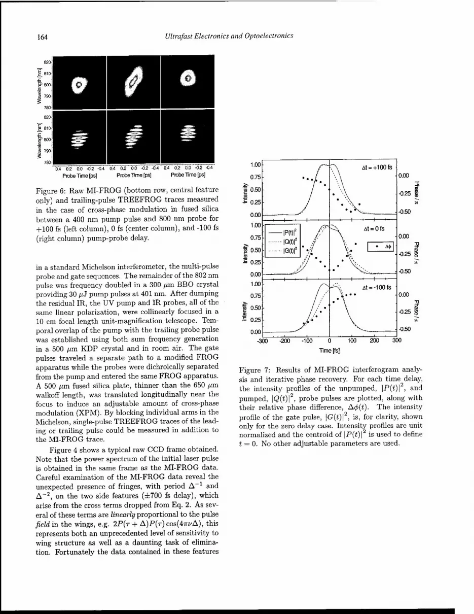
164 Ultrafast Electronics and Optoelectronics
820-
|_810
I1 600
§ 790
780
820
| 810-
f,
R3 13 B Q B B
0.4 0.2 0.0 -0.2 -0.4
Probe Time [ps]
04 0.2 0.0 -0.2 -0.4
Probe Time [ps] 0.4 0.2 0.0 -0.2 -0.4
Probe Time [ps]
Figure 6: Raw MI-FROG (bottom row, central feature only) and trailing-pulse TREEFROG traces measured in the case of cross-phase modulation in fused silica between a 400 nm pump pulse and 800 nm probe for +100 fs (left column), 0 fs (center column), and -100 fs
(right column) pump-probe delay.
in a standard Michelson interferometer, the multi-pulse probe and gate sequences. The remainder of the 802 nm pulse was frequency doubled in a 300 [im BBO crystal providing 30 p,J pump pulses at 401 nm. After dumping the residual IR, the UV pump and IR probes, all of the same linear polarization, were collinearly focused in a 10 cm focal length unit-magnification telescope. Tem- poral overlap of the pump with the trailing probe pulse was established using both sum frequency generation in a 500 /an KDP crystal and in room air. The gate pulses traveled a separate path to a modified FROG apparatus while the probes were dichroically separated from the pump and entered the same FROG apparatus. A 500 ßm fused silica plate, thinner than the 650 /zm walkoff length, was translated longitudinally near the focus to induce an adjustable amount of cross-phase modulation (XPM). By blocking individual arms in the Michelson, single-pulse TREEFROG traces of the lead- ing or trailing pulse could be measured in addition to the MI-FROG trace.
Figure 4 shows a typical raw CCD frame obtained. Note that the power spectrum of the initial laser pulse is obtained in the same frame as the MI-FROG data. Careful examination of the MI-FROG data reveal the unexpected presence of fringes, with period A-1 and A-2, on the two side features (±700 fs delay), which arise from the cross terms dropped from Eq. 2. As sev- eral of these terms are linearly proportional to the pulse field in the wings, e.g. 2P{T + A)P(r) COS(4TTI/A), this represents both an unprecedented level of sensitivity to wing structure as well as a daunting task of elimina- tion. Fortunately the data contained in these features
1.00
0.75
0.50
0.25
0.00
1.00
0.75
0.50
0.25
0.00
1.00
0.75
0.50
0.25
0.00
At = +100fs
At = 0fs
-t-
At = -100fS
0.00
-0.25
-0.50
0.00
-0.25
-0.50
0.00
-0.25
-0.50
-300 -200 -100 0 100
Time [fs]
200 300
Figure 7: Results of MI-FROG interferogram analy- sis and iterative phase recovery. For each time delay, the intensity profiles of the unpumped, \P(t)\ , and
pumped, |<2(£)|2, probe pulses are plotted, along with their relative phase difference, A<p(t). The intensity
profile of the gate pulse, |G(i)|2, is, for clarity, shown only for the zero delay case. Intensity profiles are unit normalized and the centroid of \P(t)\ is used to define t = 0. No other adjustable parameters are used.

Ultrafast Electronics and Optoelectronics 165
can be duplicated and checked with the TREEFROG traces also measured.
Three sets of TREEFROG/MI-FROG traces are shown in Figures 5 and 6: one each for 0 fs, and ±100 fs delay between the pump and trailing probe pulse. As expected, the TREEFROG traces of the leading pulse did not differ from the unpumped traces (not shown). The single-pulse TREEFROG traces of the trailing pulse do, though, show the characteristic frequency blue/red shift for the delayed cases and a symmetric broadening for the overlapped case, with shifts of ±2.5 nm (Figure 6). Note that when the probe rides on the leading/trailing edge of the pump (right/left-most column), the probe is red/blue-shifted, as expected from the n2-T(£) nature of the XPM. The MI-FROG traces, all of which have straight fringe pat- terns with the pump blocked (Figure 5), display in these instances a characteristic fringe tilt, indicative of the clean blue/red shift seen in the TREEFROG trace, while the overlapped case evidences a downward cur- vature. That is to say, the fringe pattern follows the time-domain phase shift </>(£) = n2I(t)u)z/c. Indeed, the ~ 7r/2 per 200 fs phase ramp in the ±100 fs delay cases corresponds to a shift of AA = (A2/27rc)(0.57r/200fs) = 2.7 nm, in excellent agreement with the single-pulse TREEFROG traces.
The MI-FROG traces were analyzed, as outlined above, to extract the amplitude and phase difference be- tween the pumped and unpumped TREEFROG traces while the unpumped trailing-pulse TREEFROG trace was analyzed via iterative phase recovery based upon Principle Components Generalized Projections[10]. The power spectrum of the initial pulse, obtained in the same CCD frame as the TREEFROG and MI-FROG traces, was used as a constraint and 128 x 128 grids were used. Typical FROG trace errors[9] for both recovered traces were 0.4%. In each of three cases (see Fig. 7), the relative phase difference extends from zero in the wings to a negative peak, as expected, whose magnitude is consistent with visual inspection of the MI-FROG traces as well as the observed frequency shifts. Also present is a significant change in the intensity profiles of the probe pulse near the peak of the pump, which is attributable to a combination of the lens-like transverse profile of the XPM as well as the nonlinear group veloc- ity (similar to self-steeping with self-modulated pulses). It should be stressed that both the DC component of the phase shift as well as the relative temporal offset be- tween the pulses are obtained from the MI-FROG data with interferometric accuracy and no adjustable param- eters are used, unlike standard FROG techniques.
As a final example, MI-FROG was used to per- form the first time-resolved coherent spectroscopy of ionization dynamics in gases. The same setup as pre-
CD
E F
CD Q CD
2 QL
Q. E
Q_
-200-
i i i i | i i i i | i i i t | i I""'
-100 -50 0 50 100 Time within Probe Pulse [fs]
Figure 8: Time-resolved coherent spectroscopy of ul- trafast ionization in room air. Greyscale in this figure represents the magnitude of the frequency shift, with black representing ±0.5 THz shift. The dark diagonal band (corresponding to the ionization front) and the area above it is a region of blueshift, while the region in the lower left, below the diagonal, are redshifts.

166 Ultrafast Electronics and Optoelectronics
viously described was used, with the removal of the fused silica plate and an increase in available pump en- ergy to ~ lOO^J. With a peak intensity in the focus of ~ 2 x 10¹⁴W/cm2, the first ionization of threshold of both N2 and 02 is exceeded in a length of approx- imately two Rayleigh lengths. Room air at a pressure of 580 Torr (Los Alamos National Lab resides at ap- proximately 7500 ft above sea level) was used as the target. MI-FROG data was obtained for pump-probe delays from -240 to +200 fs in 10 fs increments. Itera- tive phase recovery was performed for each delay value and the instantaneous frequency shift within the probe pulse was plotted as a function of pump delay (Fig- ure 8). The ionization front is clearly identified by the band of blueshifting running at a 45 degree angle from upper left to lower right in the figure. For times af- ter the ionization front, the probe pulse was seen to be purely blueshifted, though not as strongly as within the ionization front. For times leading the ionization front, the probe pulse was redshifted to a lesser degree. Cur- rently, it is believed that cross-phase modulation be- tween the intense pump and weak probe in the x(3) of the neutral gas and perhaps ionic cores is the dominate non-ionization source of frequency modulation. Results of a more extensive study are currently under analysis and will be presented in a future publication.
In summary, MI-FROG, being a rapid, real-time, direct-reading "oscilloscope" of ultrafast phase shifts, promises to be a powerful new tool for ultrafast science. In addition, iterative phase recovery techniques allow the unprecedented recovery, with femtosecond accuracy, of the intensity and phase of three laser pulses in a single-shot.
[6] C. W. Siders, S. P. Le Blanc, D. Fisher, T. Tajima, M. C. Downer, A. Babine, A. Stepanov, and A. Sergeev, Phys. Rev. Lett. 76, 3570 (1996).
[7] D. J. Kane and R. Trebino, Opt. Lett. 18, 823 (1993).
[8] C. W. Siders, A. J. Taylor, and M. C. Downer, Opt. Lett. 22, (May, 1997).
[9] K. W. DeLong, R. Trebino, and W. E. White, JOSA B 12, 2463 (1995).
[10] D. Kane, G. Rodriguez, A. J. Taylor, T. Sharp Clement, JOSA B 14(4), 1997.
References
[1] A. Chraplyvy, et al., Opt. Fiber Comm. '96, San Jose, California; A. Chraplyvy, et al., these pro- ceedings.
[2] D. Grischkowsky, et al., JOSA B 7, 2006 (1990).
[3] C. W. Siders, N. C. Turner III, M. C. Downer, A. Babine, A. Stepanov, and A. M. Sergeev, JOSA B 13, 330 (1996); S. Backus, J. Peatross, Z. Zeek, A. Rundquist, G. Taft, M. M. Murnane, and H. C. Kapteyn, Opt. Lett. 21, 665 (1996).
[4] T. Tajima and J. M. Dawson, Phys. Rev. Lett. 43, 267 (1979).
[5] Wm. M. Wood, C. W. Siders, and M. C. Downer, Phys. Rev. Lett. 67, 3523 (1991).
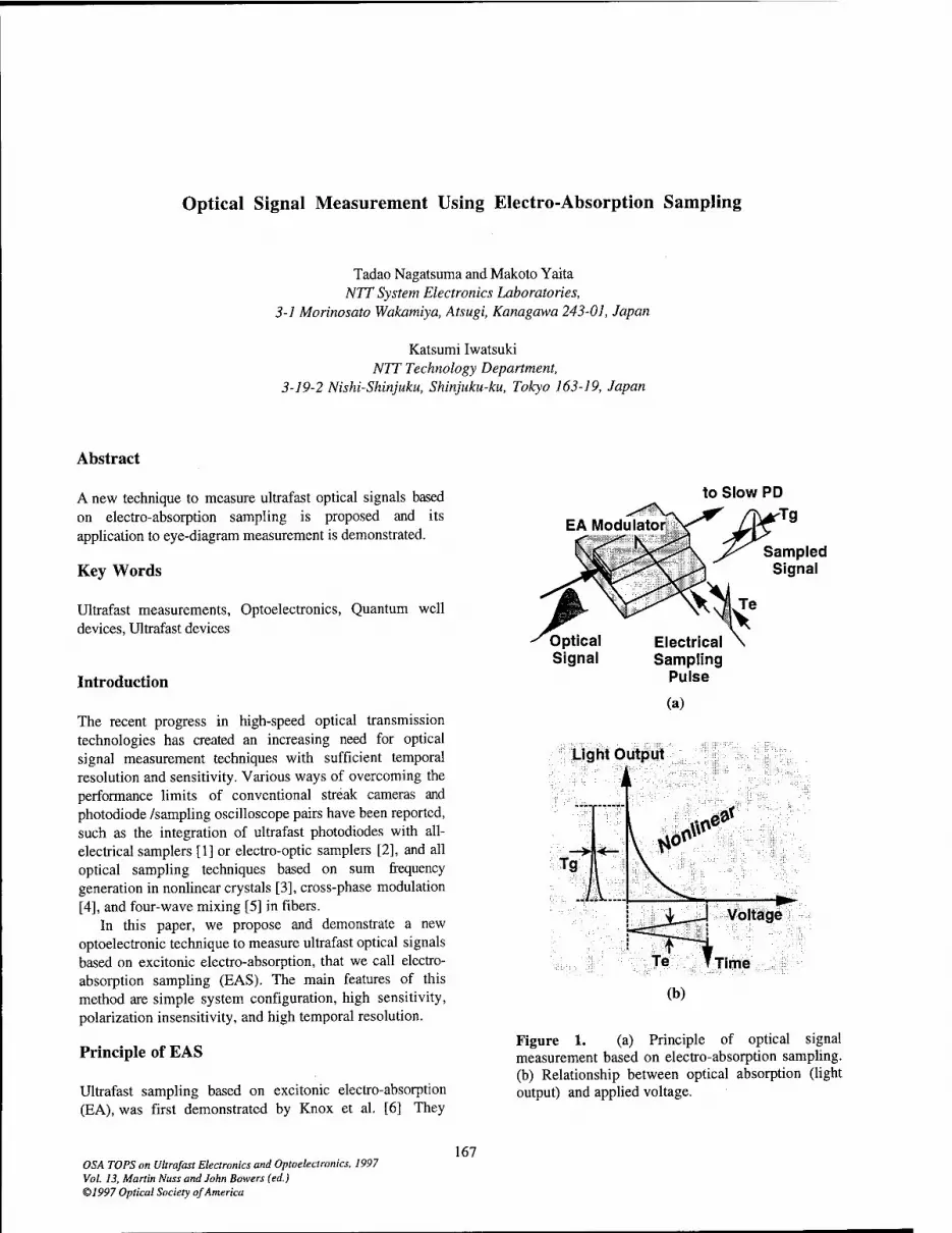
Optical Signal Measurement Using Electro-Absorption Sampling
Tadao Nagatsuma and Makoto Yaita NTT System Electronics Laboratories,
3-1 Morinosato Wakamiya, Atsugi, Kanagawa 243-01, Japan
Katsumi Iwatsuki NTT Technology Department,
3-19-2 Nishi-Shinjuku, Shinjuku-ku, Tokyo 163-19, Japan
Abstract
A new technique to measure ultrafast optical signals based on electro-absorption sampling is proposed and its application to eye-diagram measurement is demonstrated.
Key Words
Ultrafast measurements, Optoelectronics, Quantum well devices, Ultrafast devices
Introduction
The recent progress in high-speed optical transmission technologies has created an increasing need for optical signal measurement techniques with sufficient temporal resolution and sensitivity. Various ways of overcoming the performance limits of conventional streak cameras and photodiode /sampling oscilloscope pairs have been reported, such as the integration of ultrafast photodiodes with all- electrical samplers [1] or electro-optic samplers [2], and all optical sampling techniques based on sum frequency generation in nonlinear crystals [3], cross-phase modulation [4], and four-wave mixing [5] in fibers.
In this paper, we propose and demonstrate a new optoelectronic technique to measure ultrafast optical signals based on excitonic electro-absorption, that we call electro- absorption sampling (EAS). The main features of this method are simple system configuration, high sensitivity, polarization insensitivity, and high temporal resolution.
Principle of EAS
Ultrafast sampling based on excitonic electro-absorption (EA), was first demonstrated by Knox et al. [6] They
to Slow PD
Sampled Signal
Optical Signal
Electrical Sampling
Pulse
(a)
Light Output
A
Figure 1. (a) Principle of optical signal measurement based on electro-absorption sampling, (b) Relationship between optical absorption (light output) and applied voltage.
OSA TOPS on Ultrafast Electronics and Optoelectronics, 1997 Vol. 13, Martin Nuss and John Bowers (ed.) ©1997 Optical Society of America
167

168 Ultrafast Electronics and Optoelectronics
measured subpicosecond electrical signals using parallel- field excitonic EA. In our approach, we employ perpendicular-field excitonic EA, in other words, the quantum-confined Stark effect, or QCSE, to measure optical signals. QCSE causes the absorption spectrum to change when a voltage is applied, and the response time extends into the subpicosecond region. Figure 1 shows the principle of optical waveform measurement using an EA modulator as a sampling gate. When an electrical pulse with a full width at half maximum (FWHM) of Te, is applied to the EA modulator, the gating time, Tg can be made much shorter than Te, typically Tg < Te /3 - Te IA due to the the nonlinear relationship between optical absorption (transmittance) and applied voltage [7], [8]. This is similar to the mechanism by which short optical pulses are generated by modulating a CW laser beam with a sinusoidal voltage. The sampled optical signal is converted to an electrical current by a slow photodetector. By changing the relative timing delay between the optical signal under test and the electrical sampling pulse, an ultrafast optical waveform can be reconstructed.
Since the sampled signal level is large enough for the signal to be processed in real time without having to use integration or averaging, this technique offers sufficient sensitivity for eye-diagram measurements. The polarization dependence can be made negligibly small by employing a strain-compensated structure in the EA modulator [8].
In addition, a slow photodetector can easily be integrated with the EA modulator, and an electrical pulse generator may be integrated with both in the form of an all-electrical sampler [1]. Consequently, the size of the sampling head can be reduced a great deal to fit into the head module similar to conventional electrical sampling oscilloscopes.
Experiment
Gating Time of the EA Modulator To measure the gating time or the temporal resolution of the EA modulator when it's used as a sampling gate, an input CW optical signal was modulated with an electrical pulse.
The EA modulator we used was an InGaAs/InAlAs multiple-quantum-well (MQW) device module made by NTT Electronics Technology (NEL) [8]. Transmission characteristics and frequency response of the modulator are shown in Fig. 2. The extinction ratio is 32 dB at a bias of - 3 V. The 3-dB bandwidth is about 19 GHz, though the flatness of the frequency response is a little poor.
The electrical pulse had an amplitude of 1.5 Vp-p and a width of 20 ps FWHM, and was generated by triggering an InGaAs metal-semiconductor-metal (MSM) photodetector with a mode-locked fiber laser having an FWHM pulse width of 0.7 ps at a repetition rate of 40 MHz (Fig. 3(a)).
(a)
^ 0 E m T3
■20 -1
-40 w (0
E (0 c n H-60
1 1
1 t I ■■
I 1 i
i i i
■ -i Vs
■■ (■ i .. i ■
■ i i ■..■ ..| .
i
1
--i---Tl--n---
k :32 dB
I I' ■ : t',< 1 1 i' ■' I ■■'
i :< I
■ ■ ■'■■■■i' ■■..■;.■ :T^^*
II 1 1 1 lit 't'" ''!■.■■ .1 1 ■!■::.. | 1";
■ 1 1 'I 1 I 1 '■ ■■■:* :
-1 -2 -3 Reverse Bias (V)
(b)
-4
0 4 8 12 16 Frequency(GHz)
(c) Figure 2. Characteristics of the EA modulator module used for the experiments, (a) Photograph of the device module, (b) Transmission characteristics, (c) Frequency response.
The output optical pulse was detected by using a waveguide-type photodetector (3-dB bandwidth of >50 GHz; NEL) and a sampling oscilloscope (3-dB bandwidth of 50 GHz; HP 54752A). Together they provide a resolution of 12 ps. As shown in Fig. 3(b), the fastest measured response was 14 ps FWHM for a -3 V bias. That means that the actual width of optical pulses, which is the gating
time Tg , was estimated to be about {\$--\2?-)^^ = 1 ps. This value is in good agreement with results obtained by sinusoidally driving the same kind of modulator at 20 GHz [7]. So, we obtained an effective bandwidth of 50 GHz with a 19-GHz modulator.

Ultrafast Electronics and Optoelectronics 169
CW Light -*- EA Modulator
DC Bias »pf
FastPD+ Sa."[1P|in9 Oscilloscope
(12 ps resolution)
_W £j Fiber Laser MSM PD -*
Electrical Pulse Generator (20 ps, 1.5 V, 40 MHz)
(a)
Time (20 ps / div.)
(b)
Figure 3. (a) Set up for gating time measurement, (b) Measured gating characteristics of the EA modulator. This includes photodetector and sampling oscilloscope responses.
Optical Pulse Pattern Measurement Figure 4 shows the setup for optical pulse pattern measurement. The low-repetition-rate optically driven sampling pulse generator described above was synchronized with an optical signal generator, where a gain-switched diode laser with a fiber-optic pulse compressor generated 7- ps duration pulses at 10-GHz repetition rate and a specific RZ pulse pattern was obtained by using a Ti:LiNb03 (LN)
intensity modulator controlled by the electronic pulse pattern generator (PPG) at 10 Gb/s. The receiver had a bandwidth of more than 100 MHz. This allowed signals sampled at 40 MHz to be processed in real time.
Figure 5(a) shows the measured fixed (1010...) RZ pulse pattern signal at 10 Gb/s. The average optical power was about -5 dBm. Unlike measurement with conventional fast photodiode/sampling oscilloscope pairs, in the EAS- based measurements, there is no ringing at the trailing edge of waveforms. As shown in Fig. 5(b), the eye-diagram signal was successfully measured by setting the PPG to the pseudorandom bit sequence mode. Also, in Fig. 5(c), the NRZ eye-diagram signal was measured by switching the laser diode of Fig. 4 from the gain-switched mode to the CW mode. These results show that the sensitivity of EAS- based measurement is as high as that of photodiode/sampling oscilloscope pairs.
Optical Signal Generator
Synthesizer DFB Laser Pulse
Compressor
Pulse Pattern Generator
Sampling Gate
LN Intensity Modulator
Electro- Absorption
Modulator Receiver
Sampling Pulse Generator
o—fW— DC Bias
BiasT
Display
Fiber Laser
=F= Fast
Photodetector
M
Time Base Electronics
Figure 4. Experimental setup for optical signal measurement using electro-absorption modulator as a sampling gate.

170 Ultrafast Electronics and Optoelectronics
"5 c O)
c/5
a
H- t.i..
«■i ]■ ••!■ ii| ■■_•_
i! r_.,
L.ii
f H \ H Optical Signal
Sampled Signal
Time (160 ps / div.) (a)
Time (80 ps / div.) (b)
■•-» ;—■—>—'—j—■—■—■—j—■—■—■—r * ■,,,, ■ 1 ■ ■ ■ ,
c : : : : 3 _ : £..., - : —
S3 m TflRnmm9fV£«n»wwMffMiHiiHRU<Aaeswram
(0 c *B*-" ^SA^''" aü? : ' Kl£> D> SR ■ 3u£ 'jjflr : • !*■■ (0 St ^'Ä""="^^'= ift':"":^ Q. 3 n
Time (80 ps / div.) (c)
Figure 5. Measured optical pulse pattern signals at 10 Gb/s. (a) fixed (1010...) signal, (b) RZ eye- diagram signal, (c) NRZ eye-diagram signal.
Scheme to Increase the Bandwidth
The bandwidth of our current measurement system is limited to about 50 GHz, which is mostly determined by the 7-ps gating time of the modulator. There are several ways to increase the bandwidth. First, the bandwidth of the EA modulator itself can be increased by improving device structures for example, by reducing the capacitance of the electrode [9]. Another way is to give the electrical pulses a larger amplitude and make them narrower, which we can do by using the nonlinear transmission line (NLTL) technique [10]. Second, the gating time Tg can effectively be reduced by enhancing the nonlinear characteristics of the optical
Electrical Pulse
Figure 6. Scheme to improve the bandwidth. Effective gating time Tg can be controlled by adjusting the electrical delay x.
absorption with respect to applied voltage [11]. Third, if we connect two EA modulators in series and drive them with delayed electrical pulses, we can decrease the effective gate width without changing performances of the EA modulator or the electrical pulse generators as shown in Fig. 6.
Conclusion
In conclusion, we have demonstrated a novel and practical optoelectronic technique for measuring optical signals. Even with a commercially available EA modulator with a bandwidth of only 19 GHz, 50-GHz bandwidth (7-ps resolution) and high sensitivity in eye-diagram measurement were verified. A measurement bandwidth of over 100 GHz should be easy to achieve by improving the structure and characteristics of the EA modulator and electrical pulse generator.
Acknowledgment
The authors would like to thank Dr. K. Wakita for his valuable discussions, and Mr. K. Matsuhiro, and Dr. O. Karatsu for their direction and encouragement. The authors are also indebted to Dr. K. V. Reddy of Pritel Inc. for his help in use of fiber lasers.
References
1. E. Özbay, K. D. Li, and D. M. Bloom, "2.0 ps, 150 GHz GaAs monolithic photodiode and all-electronic sampler," IEEE Photon. Technol. Lett., 3, 570-572 (1991).
2. M. Yaita, T. Nagatsuma, K. Suzuki, K. Iwatsuki, K. Kato and Y. Muramoto, "Ultrafast optical pulse-pattern signal measurement using optoelectronic technique," Electron. Lett., 31, 1501-1502 (1995).
3. H. Takara, S. Kawanishi, T. Morioka, K. Mori and M.

Ultrafast Electronics and Optoelectronics 171
Saruwatari, "100Gbit/s optical waveform measurement with 0.6 ps resolution optical sampling using subpicosecond supercontinuum pulses," Electron. Lett., 30, 1152-1153 (1994).
4. B. P. Nelson, and N. J. Dolan, "Optical sampling oscilloscope using nonlinear fiber loop mirrors," Electron. Lett., 27, 204-205 (1991) .
5. P. A. Andrekson, "Picosecond optical sampling using four-wave mixing in fiber," Electron. Lett., 27, 1440- 1441 (1991).
6. W. H. Knox, J. E. Henry, K. W. Goossen, K. D. Li, B. Tell, D. A. B. Miller, D. S. Chemla, A. C. Gossard, J. English, and S. Schmitt-Rink, "Femtosecond excitonic optoelectronics," IEEE J. Quantum Electron., 25, 2586-2595 (1989).
7. K. Wakita, K. Sato, I. Kotaka, M. Yamamoto, and M. Asobe, "Transform-limited 7-ps optical pulse generation using a sinusoidally driven InGaAsP/InGaAsP strained multiple-quantum-well DFB laser/modulator monolithically integrated light source," IEEE Photon. Technol. Lett., 5, 809-901
(1993). 8. K. Wakita, I. Kotaka, K. Yoshino, S. Kondo, and Y.
Noguchi, "Polarization-independent electroabsorption modulators using strain-compensated InGaAs-InAlAs MQW structures," IEEE Photon. Technol. Lett., 7, 1418-1420 (1995).
9. T. Ido, S. Tanaka, M. Suzuki, and H. Inoue, "MQW electroabsorption optical modulator for 40 Gbit/s modulation," Electron. Lett., 31, 2124-2125 (1995).
10. M. J. W. Rodwell, S. T. Allen, R. Y. Yu, M. G. Case, U. Bhattacharya, M. Reddy, E. Carman, M. Kamegawa, Y. Konishi, J. Pusl, and R. Pullela, "Active and nonlinear wave propagation devices in ultrafast electronics and optoelectronics," Proc. IEEE, 82, 1037-1059 (1994).
11. S. Oshiba, K. Nakamura, and H. Horikawa, "Generation of 3.6 ps optical pulses with repetition rate of 20 GHz using a high efficient electroabsorption modulator," in Technical Digest of Intern. Topical Meeting on Microwave Photonics (IEICE, Tokyo, 1996), paper TH1-3.

Rapid temporal scanning of ultrafast lasers
G. Sucha, M. E. Fermann, D. J. Harter IMRA America, 1044 Woodridge Ave., Ann Arbor, MI 48105
Tel: (313) 930-2579; Fax: (313) 930-9957
M. Hofer Abteilung Quantenelectronik und Lasertechnik
Technische Universität Wien, Gusshausstr. 27, A-1040 Wien, Austria
Introduction As ultrafast lasers find their way into new
application areas, there remain some technological barriers to utilizing their full potential. One of the key issues for practical applications of ultrafast lasers is time delay. The vast majority of applications involving ultrafast lasers require an adjustable time delay for the optical pulses in order to time-relsove the fast processes being measured. Usually, the timing delay is implemented in the form of moving mirrors,1 or rotating glass blocks,2 for example. This imposes severe limitations on the attainable scan speed and range, putting many types of measurements and applications out of the reach of ultrafast lasers. Some improved mechanical methods have been developed.3 Scan ranges and speeds have been extended by free-scanning laser methods;4 however, the scan range is always just the repetition period of the lasers, and is not adjustable.
In this paper we describe a new method of controllably scanning the time delays between pulses from two modelocked lasers.5 Using this scanning temporal ultrafast delay (STUD) method, we have demonstrated temporal scanning with selectable scan ranges (up to 10 nsec) and selectable scanning frequencies (up to 400 Hz). We describe the scanning method and also the methods used to obtain high-accuracy timing calibration in conjunction with the fast scanning method. Additionally, in order to demonstrate the applicability of STUD to ultrafast measurements, we have used it to measure carrier lifetimes in thin layers of InGaAs.
repetition rates. The cavity length of the slave laser is controlled by a PZT-mounted cavity mirror. While the master laser is held at a constant cavity length, L, , or allowed to drift of its own accord, the cavity length, L2, of the slave laser is slaved to that of the master laser by a "slow" phase locked loop (PLL) circuit. Once phase locking has been achieved, then L2 is dithered about L7 at a scan frequency fs (in the range of 30 Hz -to- 1 kHz) which is larger than the PLL bandwidth. A quantitative analysis of the STUD method is very simple. The time-varying pulse delay, TD(t), (defined as the relative time delay between the pulses from the two lasers), is proportional to the time- integral of the cavity length mismatch:
TD(t) = jl'AL(t')dt' LV [1]
We consider the example in which a square wave is applied to the slave laser PZT at a scanning frequency of fs . Then the cavity length mismatch is
s Master Laser
, i...jT. Slave Laser f ^ 1 y r\
A T
PLL .ri Sig. gen.
0 .- ,
Temporal scanning technique The basic scanning laser system, illustrated in
Fig. 1, consists of two lasers (master and slave) which have nearly identical cavity lengths and
Figure 1. Diagram of scanning dual-laser system. Scanning is achieved by summing the stabilization signal from the PLL with the output of a signal generator.
OSA TOPS on Ultrafast Electronics and Optoelectronics, 1997 Vol. 13, Martin Nuss and John Bowers (ed.) ©1997 Optical Society of America
172
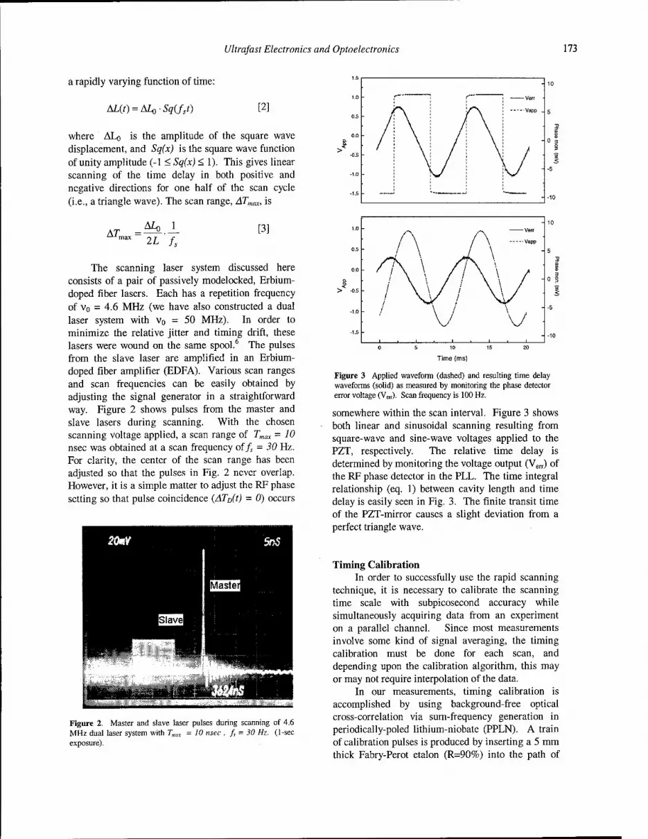
Ultrafast Electronics and Optoelectronics 173
a rapidly varying function of time:
M{t) = M^-Sq{fst) [2]
where ALo is the amplitude of the square wave displacement, and Sq(x) is the square wave function of unity amplitude (-1 < Sq(x) < 1). This gives linear scanning of the time delay in both positive and negative directions for one half of the scan cycle (i.e., a triangle wave). The scan range, ATmax, is
max 2L /, [3]
The scanning laser system discussed here consists of a pair of passively modelocked, Erbium- doped fiber lasers. Each has a repetition frequency of v0 = 4.6 MHz (we have also constructed a dual laser system with v0 = 50 MHz). In order to minimize the relative jitter and timing drift, these lasers were wound on the same spool.5 The pulses from the slave laser are amplified in an Erbium- doped fiber amplifier (EDFA). Various scan ranges and scan frequencies can be easily obtained by adjusting the signal generator in a straightforward way. Figure 2 shows pulses from the master and slave lasers during scanning. With the chosen scanning voltage applied, a scan range of Tmax = 10 nsec was obtained at a scan frequency of /, = 30 Hz. For clarity, the center of the scan range has been adjusted so that the pulses in Fig. 2 never overlap. However, it is a simple matter to adjust the RF phase setting so that pulse coincidence (ATD(t) = 0) occurs
Figure 2. Master and slave laser pulses during scanning of 4.6 MHz dual laser system with Tmlx = 10 nsec , fs = 30 Hz. (1-sec exposure).
Vapp
_l i i_ 0 5 10 15 20
Time (ms)
Figure 3 Applied waveform (dashed) and resulting time delay waveforms (solid) as measured by monitoring the phase detector error voltage (VeiT). Scan frequency is 100 Hz.
somewhere within the scan interval. Figure 3 shows both linear and sinusoidal scanning resulting from square-wave and sine-wave voltages applied to the PZT, respectively. The relative time delay is determined by monitoring the voltage output (Verr) of the RF phase detector in the PLL. The time integral relationship (eq. 1) between cavity length and time delay is easily seen in Fig. 3. The finite transit time of the PZT-mirror causes a slight deviation from a perfect triangle wave.
Timing Calibration In order to successfully use the rapid scanning
technique, it is necessary to calibrate the scanning time scale with subpicosecond accuracy while simultaneously acquiring data from an experiment on a parallel channel. Since most measurements involve some kind of signal averaging, the timing calibration must be done for each scan, and depending upon the calibration algorithm, this may or may not require interpolation of the data.
In our measurements, timing calibration is accomplished by using background-free optical cross-correlation via sum-frequency generation in periodically-poled lithium-niobate (PPLN). A train of calibration pulses is produced by inserting a 5 mm thick Fabry-Perot etalon (R=90%) into the path of

174 Ultrafast Electronics and Optoelectronics
Figure 4. Pump-probe measurement using scanning laser system and timing calibration method. A Fabry-Perot etalon (FP) generates the pulse train for timing calibration.
one beam as shown in Figure 4. The transmitted beam consists of a decaying train of pulses separated by 50 psec. Any nonuniformity of the pulse spacing in the laboratory time frame indicates that the time delay is being scanned nonlinearly. For example, scanning a 1 nsec interval at 100 Hz, (determined by looking at the scope as in Fig. 2) one expects a theoretical scan rate of 200 ps/ms. However, using the cross-correlations, we have measured an actual scan rate of 165 ps/ms. Also, we find a cross- correlation width of Tcc = 1.2 ps between the two lasers.
Not only is this information used to calibrate the time scale, but it can also be used to measure the timing jitter between the two lasers with very high accuracy (10's of femtoseconds), especially in the low frequency regime (.001 Hz -to- 10 Hz) where RF spectrum analyzer methods fail. Only one peak is required to perform this measurement. For example, using this method, we have measured the timing jitter to be 5 psec RMS over a period of 3 minutes.
Application We have used the temporal scanning and calibration techniques to measure carrier relaxation times in thin layers of InGaAs via a simple pump-probe technique as shown in Fig. 4. Pump pulses of 600 fsec duration at 1550 nm excite carriers near the bandgap of the InGaAs. The transient absorption is probed at the same wavelength by 1 psec pulses from the slave laser. During a measurement, the timing information from the cross-correlator is collected on one channel of a digitizing oscilloscope (X-channel)
while simultaneously accumulating and averaging data from the pump-probe experiment on the Y- channel. In our simple demonstration experiment, the first cross-correlation peak is used to trigger the oscilloscope. Figure 5 is a data trace from such a measurement over a 10 nsec time interval (scanned at 30 Hz).
Time delay (ns)
Figure 5. Transient absorption near the band-edge of intrinsic InGaAs. The 40 psec interval near time-zero (inset) shows an initial fast transient (~1 psec).
Conclusion We have developed a new method for scanning
the time delay between two lasers which greatly exceeds the performance of conventional scanning delays. Timing calibration is obtained via cross- correlation of pulse trains generated by passing pulses from one laser through a Fabry-Perot etalon. The potential for use in measurements is demonstrated by performing pump-probe measurements in thin layers of InGaAs. These techniques, when combined, comprise a versatile, fast-scanning, ultrafast measurement system.
References
1 R. F. Fork and F. A. Beisser, Appl. Opt. 17, 3534 (1978).
2 Z. A. Yasa and N. M. Amer, Opt. Comm., 36, 406 (1981).
3 D. C. Edelstein, etal, Rev. Sei, Instrum. 62, 579 (1990); K. F. Kwong, etal.. , Opt. Lett. 18, (7) 558 (1993).
4 K. S. Giboney, etal, IEEE Photon. Tech. Lett., 6, 1353 (1994); J. D. Kafka, J. W. Pieterse, and M. L. Watts, Opt. Lett.,17, 1286 (1992).
5 G. Sucha, M. E. Fermann, D. Harter, and M. Hofer, IEEEJnl. Quantum. Electron, (submitted).
6 G. Sucha, M. Hofer, M. E. Fermann, and D. Harter, Opt. Lett., 21, 1570 (1996).

Terahertz Bandwidth Optical Sampling
Ranee. M. Fortenberry, David. K. Donald, and Steve. A. Newton Hewlett-Packard Laboratories
3500 Deer Creek Road Palo Alto, CA 94304
Tel: 415-857-7154 Fax:415-813-3626
Email: rancef@hpl .hp. com
Characterization of short optical pulses, such as occur in high speed optical
communication systems, is currently performed using electronic instrumentation of
limited bandwidth. The current state-of-the-art fast detector and oscilloscope combination
can achieve a bandwidth of roughly 50 GHz with an impulse response of roughly 10 ps.
Optical sampling offers the capability to extend this bandwidth into the terahertz range.
Optical sampling has been demonstrated using a variety of sources and configurations. In
general, performance has been limited by timing jitter between the source of optical
sampling pulses and the unknown pulses to be measured. In addition, the difficulty of
operating and maintaining sub-picosecond optical sampling sources has limited the use of
optical sampling systems to the laboratory. The 1990's have seen developments in short
pulse lasers that have greatly improved this situation and have resulted in the
development of packaged optical sampling oscilloscopes with bandwidths in the terahertz
range. This presentation will focus on a terahertz bandwidth optical sampling
oscilloscope developed within Hewlett-Packard Laboratories.
The optical sampling system makes use of a unique optical pulse source developed within
HP Labs[l]. The source is a fiber ring laser that generates sub-picosecond pulses at
175 Reprinted from Ultrafast Electronics and Optoelectronics 1997 Topical Meeting Technical Digest ©1997 Optical Society of America

176 Ultrafast Electronics and Optoelectronics
repetition rates of 10's of megahertz. These pulses are then amplified and compressed to
roughly 100 fs for use as sampling pulses. Laser pulse formation is controlled using a
combination of nonlinear pulse propagation and saturable absorption. The laser is robust
and has very low inherent timing jitter.
To synchronize the signal and sampler sources, the frequency of the sampler laser is
locked to a clock signal from the incoming data stream. The frequency of the sampler is
then varied such that the sample pulses scan through the incoming data stream. The
incoming optical data stream and the optical sampling pulses are combined in an optical
mixing crystal producing a sum frequency output linearly proportional in time to the
incoming signal.
The system has been applied to a number of experiments including the direct
measurement of the chirp of picosecond pulses from a 10 Gb/s electro-absorption
modulator, measurements of the nonlinearity of optical fiber using nonlinear pulse
propagation, and the characterization of pulses from a variety of short pulse lasers.
More details of the system, its performance, and applications will be presented at the
meeting.
1) H. Lin, W. H. Perez, Y. Gu, and K. V. Reddy, "Saturable absorber mode-locked Er/Yb
fiber ring lasers," Optical Society of America Annual Meeting, September 10-15, 1995,
paper ThYY3.
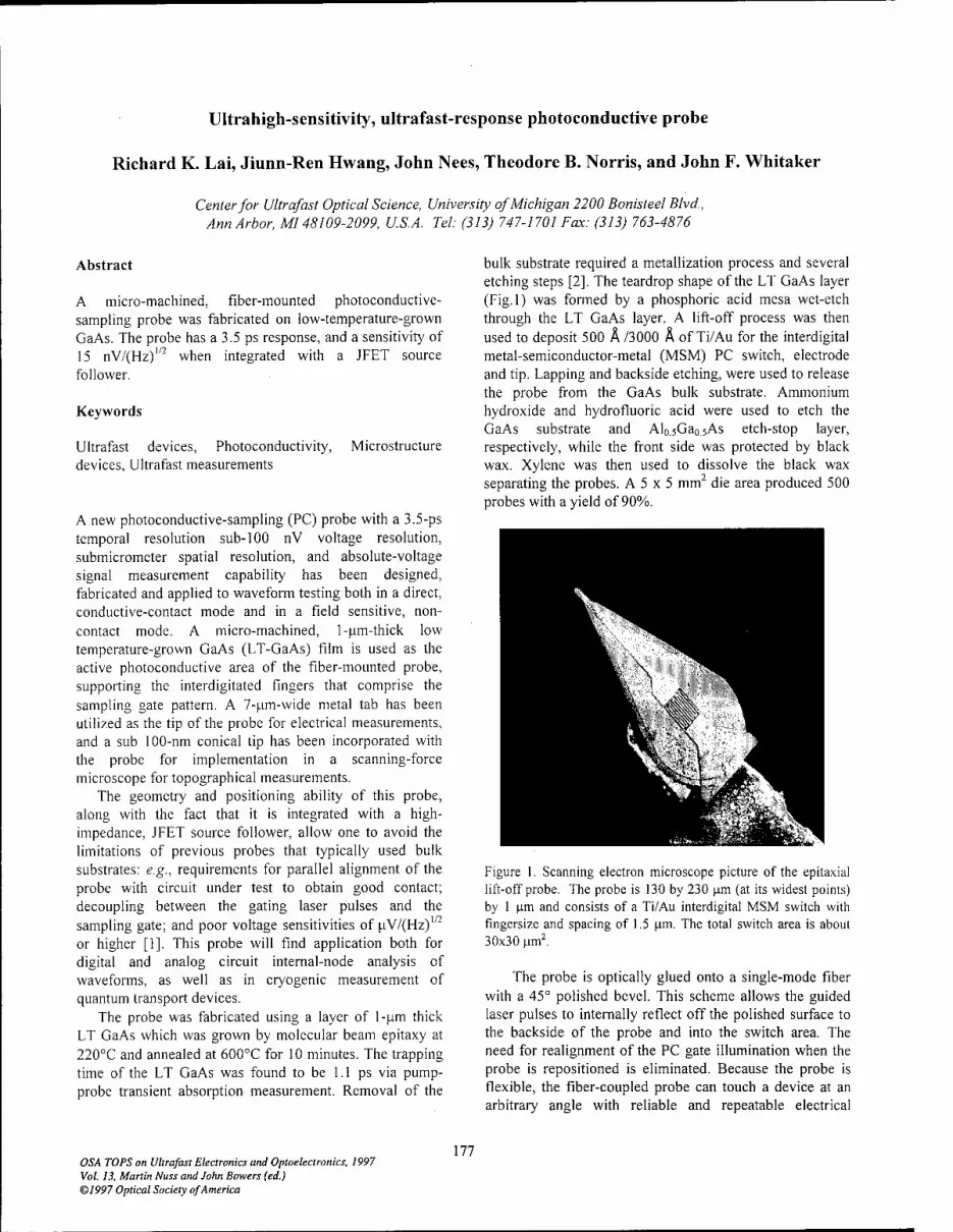
Ultrahigh-sensitivity, ultrafast-response photoconductive probe
Richard K. Lai, Jiunn-Ren Hwang, John Nees, Theodore B. Norris, and John F. Whitaker
Center for Ultrafast Optical Science, University of Michigan 2200 Bonisteel Blvd., Ann Arbor, MI 48109-2099, U.S.A. Tel: (313) 747-1701 Fax: (313) 763-4876
Abstract
A micro-machined, fiber-mounted photoconductive- sampling probe was fabricated on low-temperature-grown GaAs. The probe has a 3.5 ps response, and a sensitivity of 15 nV/(Hz)"2 when integrated with a JFET source follower.
Keywords
Ultrafast devices, Photoconductivity, devices, Ultrafast measurements
Microstructure
A new photoconductive-sampling (PC) probe with a 3.5-ps temporal resolution sub-100 nV voltage resolution, submicrometer spatial resolution, and absolute-voltage signal measurement capability has been designed, fabricated and applied to waveform testing both in a direct, conductive-contact mode and in a field sensitive, non- contact mode. A micro-machined, 1-urn-thick low temperature-grown GaAs (LT-GaAs) film is used as the active photoconductive area of the fiber-mounted probe, supporting the interdigitated fingers that comprise the sampling gate pattern. A 7-um-wide metal tab has been utilized as the tip of the probe for electrical measurements, and a sub 100-nm conical tip has been incorporated with the probe for implementation in a scanning-force microscope for topographical measurements.
The geometry and positioning ability of this probe, along with the fact that it is integrated with a high- impedance, JFET source follower, allow one to avoid the limitations of previous probes that typically used bulk substrates: e.g., requirements for parallel alignment of the probe with circuit under test to obtain good contact; decoupling between the gating laser pulses and the sampling gate; and poor voltage sensitivities of pV/(Hz)1/2
or higher [1]. This probe will find application both for digital and analog circuit internal-node analysis of waveforms, as well as in cryogenic measurement of quantum transport devices.
The probe was fabricated using a layer of 1-pm thick LT GaAs which was grown by molecular beam epitaxy at 220°C and annealed at 600°C for 10 minutes. The trapping time of the LT GaAs was found to be 1.1 ps via pump- probe transient absorption measurement. Removal of the
bulk substrate required a metallization process and several etching steps [2]. The teardrop shape of the LT GaAs layer (Fig.l) was formed by a phosphoric acid mesa wet-etch through the LT GaAs layer. A lift-off process was then used to deposit 500 Ä /3000 Ä of Ti/Au for the interdigital metal-semiconductor-metal (MSM) PC switch, electrode and tip. Lapping and backside etching, were used to release the probe from the GaAs bulk substrate. Ammonium hydroxide and hydrofluoric acid were used to etch the GaAs substrate and Alo.5Gao.5As etch-stop layer, respectively, while the front side was protected by black wax. Xylene was then used to dissolve the black wax separating the probes. A 5 x 5 mm2 die area produced 500 probes with a yield of 90%.
Figure 1. Scanning electron microscope picture of the epitaxial lift-off probe. The probe is 130 by 230 pm (at its widest points) by 1 pm and consists of a Ti/Au interdigital MSM switch with fingersize and spacing of 1.5 pm. The total switch area is about 30x30 um2.
The probe is optically glued onto a single-mode fiber with a 45° polished bevel. This scheme allows the guided laser pulses to internally reflect off the polished surface to the backside of the probe and into the switch area. The need for realignment of the PC gate illumination when the probe is repositioned is eliminated. Because the probe is flexible, the fiber-coupled probe can touch a device at an arbitrary angle with reliable and repeatable electrical
OSA TOPS on Ultrafast Electronics and Optoelectronics, 1997 Vol. 13, Martin Nuss and John Bowers (ed.) ©1997 Optical Society of America
177

178 Ultrafast Electronics and Optoelectronics
contact simply by observing the reflection from the bending probe tip.
Figure 2. Photoconductive sampling setup with the probe contacting a coplanar transmission line. The JFET source follower is connected to the probe via silver epoxy.
We tested the probe to measure picosecond pulses that were generated photoconductively using the gap separating the electrodes of a coplanar stripline on a LT GaAs substrate (Fig. 2). A mode-locked Ti:sapphire laser with 100-fs duration pulses, operating at 810-nm wavelength with a repetition rate of 82 MHz, is split into two beams with one variably delayed with respect to the other. The first beam, modulated by an acousto-optic Bragg cell at frequencies that could be varied between 50 Hz and 110 kHz, was used to excite a PC switch and generate a test signal. The second beam, consisting of the gating laser pulses, was coupled into the single-mode fiber to activate the PC switch. To demonstrate the probe operation, the metal tab of the probe made contact with the grounded section of the transmission line. The output of the MSM sampling gate is coupled to a source follower assembled using a pair of matched, n-depletion JFETs (model 2N5912) [3,4]. The input capacitance of the JFET is 3 pF,
and the gate input impedance is > 1 TQ. The output of the fiber-mounted probe was connected to this source follower by either conductive silver paint or indium solder, with a spacing of 1 cm between the PC probe and the amplifier. Without the source follower, the distributed capacitance encountered by the fiber-mount probe is estimated to be -220 pF for a 3-ft RG-58 coaxial cable and a lock-in
amplifier. This capacitance limits the modulation frequency of the beam directed at the transmission line gap to about 1 to 2 kHz. Typically, the sensitivity of photoconductive sampling below 1-kHz modulation frequency is several uV/(Hz)"2. By introducing the amplifier with a smaller 3- pF capacitance, the charging time was reduced, increasing the allowed modulation frequency to tens of kHz. The important advantage of a high modulation frequency is that the 1/f noise due to gating laser fluctuations can be reduced [5]. However, above a specific frequency value (modulation frequency bandwidth) the measured signal falls below the actual signal under test.
1.2 10s
20 30
Time (ps)
Figure 3. Temporal waveform resolved using the LT GaAs PC probe with integrated JFET source follower. The noise level measured at the baseline near t=0 ps is 15 nV/(Hz)"2.
Roafing metal probe ,,
Insulatin | layer
Figure 4. Lumped-element circuit diagram for sampling through passivation. a+ and a- correspond to the positive and negative induced charges.
Figure 3 is a measurement of a 3.8-ps signal with a 2- uV amplitude at a modulation frequency of 50 kHz with a gating laser power of 2 mW. A LiTa03 electro-optic (EO) sampling probe was used to establish that a 1.5 ps signal was being generated by the photoconductive gap switch.

Ultrafast Electronics and Optoelectronics 179
By deconvolving the measured and transmission line signals the response of the probe was found to be 3.5 ps. At 50 kHz the measured signal by the lock-in amplifier is about half of the actual signal on the transmission line. The
vl/2 sensitivity or the noise is 15 nV/(Hz)"z which is found by taking the root mean square value calculated from the baseline. Therefore, the minimum detectable signal is 30 nV/(Hz)l/2
op (75
amplitudes at internal nodes of circuits or very rapid measurement of larger signals.
References:
1. J. Kim, S. Williamson, J. Nees, S. Wakana and J. Whitaker, Appl. Phys. Lett. 62, 2268 (1993). 2. J. Nees, S. Wakana, and S. Hama , Optical and Quantum Electron. 28, 843 (1996). 3. J. R. Hwang, H. J. Cheng, J. F. Whitaker, and J. V. Rudd, Opt. and Quantum Electron. 28, 961 (1996). 4. J. R. Hwang, H. J. Cheng, J. F. Whitaker, and J. V. Rudd, Appl. Phys. Lett. 68, 1464 (1996). 5. D. H. Auston, in Ultrashort Laser Pulses: Generation and Applications, 2nd ed, edited by W. Kaiser (Springer- Verlag, New York 1993) p.203
Time (ps)
Figure 5. Normalized time-domain waveforms measured through a passivation layer. The PC probe used a 2-mW gating laser power. The a-o modulator was set to 50 kHz.
With the increased sensitivity, the PC probe also has the capability to measure signals through an insulating layer. A transmission line with a portion of its area covered with a 4-um-thick layer of Si02 was used to demonstrate sampling through a passivation (Fig.4). Here, two PC probes were utilized, one with a dc bias for launching a signal and the other as a sampling probe. The launcher was brought onto direct electrical contact with the stripline, while the sampling probe contacted the Si02 passivation layer above the metal lines. When the guided electrical signal under the passivation reaches the tip of the probe, induced charges are formed on the capacitors of the insulating layer, the PC switch and JFET source follower. Timing between the fast electrical signal and the gating laser pulse allows the charges across the PC switch to be injected into the JFET source amplifier. Figure 5 shows two waveforms measured on the line below the insulating layer. The 70 uV and 180 nV signal amplitudes correspond to the 120 mV and 65 uV actual signals on the transmission line. From the 180 nV data, the root-mean square voltage noise was measured from the baseline to be about 6nV/(Hz)l/2. The minimum detectable noise is therefore 2.5 uV//(Hz)"2. In contrast to the direct contact sampling, the modulation bandwidth for sampling through passivation is extremely high, approximately 100 kHz. This should allow either very sensitive determination of small voltage wavefrom

Picosecond/nanometer resolution with a near-field microwave/scanning-force microscope
D. W. van der Weide Department of Electrical and Computer Engineering, University of Delaware, Newark, DE 19716-3130
Abstract
We report a scanning-force microscope tip/cantilever with a coaxial metal shield for use as an ultra-small field probe, observing 30 ps waveforms on an integrated circuit at a spatial resolution set by the tip radius, the first direct measurements of electric field at these levels of temporal and spatial resolution. This new ability to acquire topography while maintaining constant tip-sample distance for calibrated measurement or excitation of near-zone picosecond time-resolved electric fields can be useful not only for probing advanced circuits but also for localized broadband spectroscopy of condensed matter and biological samples.
Key Words
Scanning microscopy, Microwave spectroscopy, Ultrafast technology, Imaging microscopy
Introduction
Current integrated circuits (IC's) with sub-micrometer features and switching rates in the hundreds of megahertz present serious challenges to internal-node measurement techniques. While established electron-beam probes are addressing industry needs for circuit diagnostics today, they require vacuum, measure only conductive surfaces, and suffer from sample charging effects. Future computational structures will have nanometer dimensions and gigahertz clocks, outstripping the capabilities of contemporary probing methods. As the density of these structures increases to the level of a complex "artificial material",
characterizing them with scanning probes, as one might a real material, becomes an increasingly attractive solution.
In response to this need, several groups have developed proximal probing techniques which use nonlinearities in the tip-sample interaction to downconvert picosecond waveforms on a sample via coherent techniques. For example, frequency mixing by means of the nonlinear force-voltage response of the scanning-force microscope (SFM) cantileverfl, 2] allows > 100 GHz signals to be measured[3] (also see B. Nechay, et al., this conference), but can be subject to drift since the SFM height feedback loop is opened to make the voltage measurement unless a non-harmonic tip-sample distance modulation scheme is employed. Scanning tunneling microscopes have also allowed fast waveform measurements[4, 5], but require conductive surfaces, preventing probing through dielectric layers. Because frequency conversion occurs in the tip- sample interaction, both techniques require the tip to carry a mixing signal, a source of interference, especially since neither technique screens long-range Coulomb interactions. Furthermore, coherence between the tip and sample signals is required so that an output can be measured within the < 100 kHz usable bandwidth of these "bare-tip" scanning probes.
By contrast, we extend this measurement bandwidth beyond 10 GHz and, more importantly, add a screen to localize the electric field measurement, by modifying a SFM tip/cantilever with a shielded transmission line allowing direct non-contact probing of local electric fields, eliminating the need to inject a signal onto the tip. The SFM now becomes useful for localized broadband spectroscopy not only on active samples amenable to coherent measurements, such as circuits, but also on
OSA TOPS on Ultrafast Electronics and Optoelectronics, 1997 Vol. 13, Martin Nuss and John Bowers (ed.) ©1997 Optical Society of America
180

Ultrafast Electronics and Optoelectronics 181
passive, even non-conducting samples of interest, such as surfaces and membranes.
While near-field scanning optical microscopy (NSOM) has attracted much attention for localized probing[6-8], sub- wavelength confinement of visible light was preceded by microwave demonstrations [9], and a wide range of contrast mechanisms in semiconducting, superconducting and biological materials and systems awaits exploration at the level of nanometer spatial resolution in the spectrum lying between DC and visible light[10].
Figure 1: 100 x 100 urn topographical scan of NLTL output section with the time-domain waveform of one 1.400 GHz cycle measured at the diode indicated by the arrow; the 10- 90 % falltime of the steepest edge is 30 ps, and the calibrated voltage scale is on the right. Incomplete contact metal liftoff can also be seen; this is otherwise difficult to detect under optical illumination. Reproduced with permission from Ref. [11]. Copyright 1997, American Institute of Physics.
This probe is an early step toward generalizing the NSOM to these longer wavelengths while maintaining the topographical resolution of the SFM: By modifying a commercially-available silicon tip/cantilever with a dielectric spacer and metal shield, connected to a sampling oscilloscope with a coaxial cable, we have measured 30 ps waveforms along with the < 10 nm-level topographical resolution expected of a non-contact SFM (Fig. 1).
For these measurements we chose a nonlinear transmission line (NLTL)[12], a sample exhibiting both spatial nonlinearity and waveforms similar to future ultrafast computing circuits. The temporal resolution we achieve with this shielded probe is limited by the capacitance of the output cabling. The spatial electric field resolution afforded by the coaxial geometry of the probe is primarily determined by the -10 nm tip radius of the center conductor[13, 14] since the otherwise-large "antenna" effect of the tip/cantilever is now shielded. Direct measurements of electric field combined at such levels of temporal and spatial resolution have not been reported until now.
While much work has been reported on the use of open-ended coaxial probes for dielectric characterization of materials and biological systems[15], considerations of high spatial resolution are rarely addressed. Seminal work in micrometer-level scanning localization of microwave fields [16] has been followed by recent work demonstrating that electric field resolution is primarily set by the tip radius in a shielded system, due to the quasistatic field distribution at the aperture[13, 14, 17]. None of the literature suggests the combination of the SFM cantilever with a coaxial tip in this way, even though it offers not only acquisition of sample topography and field together, but also control of the tip-sample distance by the surface force gradient. Enabling both non-contact imaging and calibrated field measurements are two distinct advantages of our approach.
As with NSOM, this technique can work in both emission and detection modes, but as the extension of a microwave waveguide, it can also work in reflection[16, 18] and transmission[14, 19], made especially convenient by high-precision network analyzers available in this frequency regime, in contrast to resonant coaxial techniques, which gain sensitivity at the expense of narrow-band limitationsf 13, 17]. We note, however, that this approach does not preclude the use of resonant techniques or highly-sensitive microwave bridge detectors[20]. While we report its use in detection, we have also observed dielectric contrast in the magnitude and phase of (microwave) reflections in larger-scale experiments, which when scaled down should be especially useful for spatially-resolved measurements of defects in thin films, such as gate oxides.
Measurements
To make these measurements, we first prepared a commercially-available conductive silicon tip/cantilever with a metal shield connected to a coaxial output cable. This process involves a 90° C 90-minute bake-out to drive off water from the tip/cantilever, followed by a drop of HMDS applied with a pipette to the cantilever to prepare the surface for photoresist, a convenient, low-stress, low- permittivity dielectric which can form a thick coating for low-capacitance shielding[21]. After a 2-minute air dry, a single brush fiber is used to apply a drop of AZ-5214 photoresist to the cantilever, followed by a 120° C 30- minute "hard bake". The tip/cantilever is then mounted in an electron-beam evaporator for deposition of 300 A of titanium (at 8 A/sec) for adhesion followed by 2000 A of gold (at 4-6 A/sec) for shielding. Scanning electron microscopy of the resultant structure shows complete coverage of the tip and cantilever with the expected half- cylinder of metal (peak height > 16 ^tm) running the length of the cantilever (inset, Fig. 2).

182 Ultrafast Electronics and Optoelectronics
Using a micromanipulator with a sharp-tipped tool, excess gold at the base of the cantilever can be removed. While this reduces the area for attaching the output wire, making attachment more difficult, it substantially reduces the capacitance between the metal and the conducting silicon body, in this case to - 30 fF, the capacitance due to the half-cylinder of metal on the cantilever alone. Using silver epoxy, 0.86 mm (outer diameter) semi-rigid coaxial cable[22] is anchored at the side of the probe body, minimizing its profile. An 18 |im diameter gold bond wire is epoxied to the coax center conductor, then to the gold-coated base of the cantilever, then looped back on itself to the coax center conductor again, halving its inductance (Fig. 2). Approximately 50 mm of the coaxial cable extends from the mounting point to facilitate connection to a longer but lower-loss cable running to the signal measurement equipment.
Coax
fcSäB_ Cantilever
Figure 2: Schematic arrangement of shielded SFM tip/cantilever connected to a coaxial output cable (above), and electron microscope image of actual shielded SFM tip surrounded by coaxial shield (below). Inset of lower image is the same tip before removing the shield. Reproduced with permission from Ref. [11]. Copyright 1997, American Institute of Physics.
The tip assembly is mounted into a Topometrix Explorer SFM and arranged to have a ~ 15° tilt between the cantilever and sample planes to allow clearance for the output coax (Fig. 2). Although this limits the imaging area, this limit can be readily overcome with lower-profile
cable[22] and a slightly modified scanner or V-grooves etched into the silicon body; in this first demonstration, however, we instead made a large-area topographical scan (Fig. 1) with an identical tip minus the coax.
The initial resistance measured at the output coax was infinite, as expected. Then by scanning the tip over a gold- coated sample and gradually lowering it just to the point of contact, the metal shell over the tip was removed, exposing the underlying silicon tip and forming a coaxial shield with ~ 5 |J.m diameter (Fig. 2), as verified electrically by observation of both a short circuit and of AC signal extinction as the tip was brought into hard contact with a conductor. While this is already the smallest reported coaxial structure to be used for field measurements, we are developing a micromachined version with a ~ 100 nm diameter for even greater field confinement, ease of assembly to a cable, and the attendant advantages of batch fabrication[23].
The sample, a NLTL on GaAs, is a high-impedance coplanar waveguide transmission line periodically loaded with reverse-biased Schottky diodes (inset, Fig. 3) to compress an input sinusoid into a sawtooth waveform having a pico- or sub-picosecond edge—here a falling edge due to the polarity of the diodes on the structure. To approximate the switching waveforms expected from advanced computational structures in the low GHz regime, we drove the NLTL with 1.400-2.000 GHz signals from a Hewlett-Packard 83620A microwave synthesizer, amplified by an HP 83020A power amplifier. The waveform was measured on an HP 54750A 50 GHz sampling oscilloscope, triggered by another 83620A synthesizer because it cannot trigger on the high-frequency NLTL drive. The oscilloscope would trigger at lower-frequency drives (down to 200 MHz, the low-end limit of the 83020A) but waveform compression on the NLTL was minimal.
$ -0.02 ■
0 50 100 150 200 250
Time (ps)
Figure 3: Excerpts from a linear scan along the NLTL diodes showing waveform compression at a 2.000 GHz drive. Distortion of the signal at Diode A is probably from the waveguide bend just before it. Reproduced with permission from Ref. [11]. Copyright 1997, American Institute of Physics.

Ultrafast Electronics and Optoelectronics 183
As shown in Fig. 3, we measured the expected spatial nonlinearity along the NLTL, with a progressively steeper falling edge moving along the line; while three sample traces are shown, the spatial resolution of the field could be observed through measurable variations in the waveform at < 0.1 |J.m steps of the probe moving along the line. A new observation afforded by this measurement was that, although the diodes are approximately equidistant from one another, the first one (Diode A) had a much slower waveform than its successors, probably due to a signal reflection from the 90° bend in the transmission line just before it. To verify this, one could perform a high- resolution scanning field measurement of the bend area and compare it with a full-wave field simulation: Fourier- transforming the time-domain measurements or simply connecting a microwave spectrum analyzer to the probe would quickly collect this information. Another new observation was that the metal liftoff process used to make diode contacts on the NLTL was incomplete on this sample (Fig. 1). This is difficult to see under normal illumination in a high-power optical microscope since the gold contacts give nearly uniform reflection. Such direct local diagnostics of very fast, very dense IC's are now possible with this new probing technique.
R cant L R cab
m
,ip~J~ C canTT C cabTT C cääT
Measured signal - Model with cable
-r- -t- -t- o 20 25 10 15
Frequency (GHz)
Figure 4: Fourier transform of waveform from Diode C (Fig. 3) and equivalent-circuit model of tip, cantilever, bond wires and output cabling. Approximate values are Clln = 40fF, R„nl=10Q, Ccant = 30fF, L = 0.5 nH, Cc;M = CclM=10pF, Rcab = 3 Q.
From previous measurements on the output of this NLTL using an on-chip diode sampling bridge, we expected - 5 ps (10-90 %), 3 V falling edges under these drive conditions; measurements with the new probe gave 30 ps edges and 50x lower amplitudes. This not only enables a calibration of the voltage scale but points out the bandwidth limitation of the coaxial cable running from the probe to the oscilloscope. This cable has 95 pF/m distributed capacitance, dominating the response of the system; a single-pole approximation with a Gaussian pulse predicts a -3 dB bandwidth of ~ 12 GHz, while a more
involved equivalent-circuit model of the parasitic elements limiting the system also reveals the dominant effect of the output cable capacitance (Fig. 4), and limits our ability to extract tip-sample capacitance values. Thus, we only roughly estimate the tip-sample capacitance at ~ 40 fF, a value corresponding to the area of the shield opening at a 20 nm tip-sample working distance. We note that by adjusting the tip-sample distance, a tradeoff can be made between probe invasiveness and the low-frequency edge of the measurement band (~ 200 MHz here). Further advances can be made with localized instrumentation near the tip, for example a buffer amplifier to minimize capacitive loading of the output cable or a high-speed sampling bridge for extended measurement bandwidth.
Outlook
This shielded tip offers several new advantages: by direct field measurement it allows the use of a wide variety of instrumentation that need not inject or be coherent with a signal on the sample (in fact the sample can be passive, even non-conductive); the shield limits long-range Coulomb interactions, increasing the spatial resolution of field measurements over previous "bare tip" approaches and extending the local measurement bandwidth; by stabilizing the tip-sample distance in non-contact mode, calibrated voltage measurements can be made without drift; and even in contact mode, the controlled impedance of the tip/cantilever is advantageous for localized measurements.
Because of the two-conductor nature of the tip/cantilever transmission line, it exhibits no cutoff wavelength, unlike the pulled-fiber NSOM, enabling operation at much lower power due to dramatically lower losses, albiet in a different wavelength regime[14]. Indeed, it is a complement to localized visible-light spectroscopy, extending the range of available wavelengths into the microwave regime. For excitation up to ~ 1 THz, we can integrate NLTLs with the probe, noting that established algorithms for deembedding or deblurring radar images could be applied for enhancing the field resolution in this application, possibly allowing the tip to image conductors buried in a dielectric or subsurface defects in semiconductors. For even shorter-wavelength probing with excitation from a Fourier-transform infrared spectrometer, far-infrared gas laser or free-electron laser, we can place micromachined planar antennas on the back side of the cantilever, connecting them to a field-concentrating near- field antenna such as a coaxial tip or magnetic loop. This will extend localized spectroscopy to the far-infrared "molecular fingerprint" regimeflO], allowing us to probe biological samples with "softer", lower-energy photons than those of visible light.
184 Ultrafast Electronics and Optoelectronics
Acknowledgments
I thank F. Keilmann and P. Neuzil for useful discussions, and T. Bork, J. Bergey and V. Agrawal for assistance. Work supported by ONR/DARPA Grant N00014-96-1- 0862, Ford Motor Co., and W.L. Gore and Associates.
References and Notes
[I] A. S. Hou, F. Ho, and D. M. Bloom, "Picosecond electrical sampling using a scanning force microscope," Electronics Letters, vol. 28, pp. 2302- 2303, 1992.
[2] F. Ho, A. S. Hou, and D. M. Bloom, "High-speed integrated circuit probing using a scanning force microscope sampler," Electronics Letters, vol. 30, pp. 560-562, 1994.
[3] A. Leyk, C. Böhm, D. W. van der Weide, and E. Kubalek, "104 GHz signals measured by high frequency scanning force microscope test system," Electronics Letters, vol. 31, pp. 1046-1047, 1995.
[4] G. J. Nunes and M. R. Freeman, "Picosecond resolution in scanning tunneling microscopy," Science, vol. 262, pp. 1029-1032, 1993.
[5] D. Botkin, J. Glass, D. S. Chemla, D. F. Ogletree, M. Salmeron, and S. Weiss, "Advances in ultrafast scanning tunneling microscopy," Applied Physics Letters, vol. 69, pp. 1321-1323, 1996.
[6] K. Lieberman, S. Harush, A. Lewis, and R. Kopelman, "A light source smaller than the optical wavelength," Science, vol. 247, pp. 59-61, 1990.
[7] E. Betzig and J. K. Trautman, "Near-field optics: Microscopy, spectroscopy, and surface modification beyond the diffraction limit," Science, vol. 257, pp. 189-195, 1992.
[8] A. Lewis, U. Ben-Ami, N. Kuck, G. Fish, D. Diamant, L. Lubovsky, K. Lieberman, S. Katz, A. Saar, and M. Roth, "NSOM the fourth dimension: Integrating nanometric spatial and femtosecond time resolution," Scanning, vol. 17, pp. 3-13, 1995.
[9] E. A. Ash and G. Nicholls, "Super-resolution aperture scanning microscope," Nature, vol. 237, pp. 510-512, 1972.
[10] F. Keilmann, "FIR microscopy," Infrared Phys. Technol, vol. 36, pp. 217-224, 1995.
[II] D. W. van der Weide, "Localized picosecond resolution with a near-field microwave/scanning-force microscope," Applied Physics Letters, vol. 70, pp. 677-679, 1997.
[12] D. W. van der Weide, "Delta-doped Schottky diode nonlinear transmission lines for 480-fs, 3.5-V transients," Applied Physics Letters, vol. 65, pp. 881- 883, 1994.
[13] T. Wei, X.-D. Xiang, W. G. Wallace-Freedman, and P. G. Schultz, "Scanning tip microwave near-field microscope," Applied Physics Letters, vol. 68, pp. 3506-3508, 1996.
[14] F. Keilmann, D. W. van der Weide, T. Eickelkamp, R. Merz, and D. Stöckle, "Extreme sub-wavelength resolution with a scanning radio-frequency transmission microscope," Optics Communications, vol. 129, pp. 15-18, 1996.
[15] D. Beruhe, F. M. Ghannouchi, and P. Savard, "A comparitive study of four open-ended coaxial probe models for permittivity measurements of lossy dielectric/biological materials at microwave frequencies," IEEE Transactions on Microwave Theory and Techniques, vol. 44, pp. 1928-1934, 1996.
[16] M. Fee, S. Chu, and T. W. Hänsch, "Scanning electromagnetic transmission line microscope with sub-wavelength resolution," Optics Communications, vol. 69, pp. 219-224, 1989.
[17] C. P. Vlahacos, R. C. Black, S. M. Anlage, A. Amar, and F. C. Wellstood, "Near-field scanning microwave microscope with 100 (im resolution," Applied Physics Letters, vol. 69, pp. 3272-3274, 1996.
[18] M. Golosovsky and D. Davidov, "Novel millimeter- wave near-field resistivity microscope," Applied Physics Letters, vol. 68, pp. 1579-1581, 1996.
[19] F. Keilmann, R. Merz, D. Stöckle, T. Eickelkamp, and D. W. van der Weide, "Microscopy with radio waves," presented at Near Field Optics 3, EOS Topical Meeting, Brno, Czech Republic, 1995.
[20] M. Golosovsky, A. Galkin, and D. Davidov, "High- spatial resolution resistivity mapping of large-area YBCO films by a near-field millimeter-wave microscope," IEEE Transactions on Microwave Theory and Techniques, vol. 44, pp. 1390-1392, 1996.
[21] Note that an evaporated or sputtered dielectric, such as silicon nitride or silicon dioxide might also be effective, but usually stresses the cantilever.
[22] Cable available from Micro-Coax Components, Inc., Collegeville, PA.
[23] D. W. van der Weide and P. Neuzil, "The nanoscilloscope: Combined topography and AC field probing with a micromachined tip," Journal of Vacuum Science and Technology B, vol. 14, pp. 4144-4147, 1996.
Potential image observation with ultra-high space-time resolution
Koichiro Takeuchi, Akira Mizuhara
Teratec Corporation, 2-9-32 Naka-cho, Musashino-shi, Tokyo 180, Japan
Abstract
We succeeded for the first time in visualizing instantaneous voltage distribution of 2ps electrical pulse propagating on coplanar strips (CPS). This result was obtained using a scanning force optoelectronic microscope (SFOEM) which we have developed by coupling a scanning force microscope (SFM) and an ultrafast optical sampling technique. The observed voltage distribution shows a single peak deviating outward, the experimental results prove possibility of the SFOEM in measuring ultrafast and ultra-dense electronic devices.
Key Words
Ultrafast measurements, Scanning microscopy, Photoconductive materials, Optoelectronics.
Introduction
Recent progress in semiconductor technology has increased the speed and density of electronic devices and integrated circuits. This trend is likely to continue increasing to the order of terahertz and several tens of nanometers in the future. In this situation, ultrafast measurements using a scanning force microscope (SFM)|1-3| or a scanning tunneling microscope (STM)[4-7| have recently attracted a great deal of attention. They are powerful new methods to test ultrafast and ultrahigh-density electronic devices and circuits. It will be possible with these methods to measure electrical signals at any internal node in a sub-picosecond time and sub-nanometer spatial resolution. A fundamental idea of methods of this kind is to introduce an equivalent sampling method to an STM or SFM by using some kind of sampler or mixer near the probe tip. We have developed a scanning force optoelectronic microscope (SFOEM) based
on an SFM. The SFOEM has a special probe with a sharp conductive tip and a photoconductive semiconductor switch (PCSS)[8J which works as an optical sampler in the so-called equivalent sampling measurement. In this paper we report on observation of spatial distribution images of an electrical picosecond pulse propagating on a metal strip and its time evolution by using the SFOEM. This result proves that the SFOEM is very useful in investigating how ultrafast signals propagate in the real world.
System Setup
Figure 1 shows the system setup. The probe is supported by piezoelectric actuators in the x-, y-, and z-directions. The probe has a photo-conductive semiconductor switch (PCSS) on its thin-film cantilever[9]. One of the two electrodes of the PCSS is a sharp probe tip made of Pt, and
EZZZZZZZZZZZZ; computer '/»////////////////////A
digital volt meter.
pulse laser
£^_(QL«o^|
Figure 1. Schematic of system setup. One laser beam generates electrical pulse train. The other beam turns on optical switch on the probe.
OSA TOPS on Ultrafast Electronics and Optoelectronics, 1997 Vol. 13, Martin Nuss and John Bowers (ed.) ©1997 Optical Society of America
185
186 Ultrafast Electronics and Optoelectronics
the other one is connected to a slow pre-amplifier with high input resistance through a 5QÜ. cable.
The cantilever is made of low temperature grown GaAs (LT-GaAs) and the material in the gap region between the two electrodes works as the PCSS |9]. An ultra-short optical pulse train from a mode locked Ti sapphire laser is used to turn the PCSS on and off. Since photo-excited carriers in LT-GaAs have an extremely short life (10-11), the response time of the PCSS is about 1 ps or shorter.
LT-GaAs
CPS line=50um gap=10um
7 pump beam
I coupler line=4um gap=3um
Vbias
Figure 2. Top view of sample device. Two rectangles show the area ohserved hv SFOF.M
If the electrical signal of a device under test (DUT) is repetitive and the period is synchronized to that of the laser pulse train, the DC voltage after the PCSS reproduces an instantaneous signal voltage. By scanning the optical path length, the ultrafast signal waveform is accurately measured. This is the so-called equivalent sampling method, and is similar to the principle of ahigh-speed sampling oscilloscope or a strobo camera.
In this measurement the DUT is DC-biased coplanar strips (CPS) fabricated on a LT-GaAs layer on a semi- insulating GaAs substrate illustrated in Figure 2. There is one more strip connected to the CPS ground strip via an interdigit coupler. We generated electrical pulses by illuminating the gap region of the CPS, and measured the electrical pulses in the areas on the ground strip and the interdigit coupler shown by the rectangles in Figure 2. The incident optical pulse has a duration of lOOfs, a repetition rate of 80MHz, and a wavelength of 830nm.
A probe beam separated from the pump beam is introduced to the SFOEM head through a single mode optical fiber and focused onto the PCSS on the probe. The average beam power at the probe is 10mW. 70% of the incident beam is used to turn the PCSS on and the other 30% is reflected to a beam position detector. The output from the
detector is used for probe position control. The probe position control procedure is the same as that of a normal SFM. That is, the piezoelectric actuator in the z-direction controls the probe height so that the reflected beam spot is maintained at a fixed position on the detector using a feedback circuit. Since the deviation of the reflected beam position corresponds to the deflection of the cantilever, the deflection and the force between the probe tip and the DUT surface are also maintained constant.
Although an ordinary SFM uses a CW laser beam to detect the probe position, we use just one pulse beam for both probe position control and PCSS switching. Since the periodic frequency of the optical pulse train is sufficiently higher than the bandwidth of the position control circuit, the pulse beam operation causes no disturbance to probe position control. In this situation, by scanning the piezoelectric actuators in the x- and y-directions, we observed the instantaneous potential distribution.
Probe Fabrication
Figure 3 shows a SEM picture of the bottom side of the SFOEM probe. The base and the height of the triangle cantilever are 200|im for the both, and the thickness is 1 jj.m. There are a Pt tip electrode on the top of the pyramidal protrusion and a Pt lead on the cantilever. The base and the height of the pyramid are 18(im and 13um respectively. Since there is a gap between the tip metal and the lead, this region works as a PCSS when illuminated by an optical pulse.
In the first step of the probe fabrication, a Si pyramidal protrusion was made by anisotropic etching with a KOH solution under masking with a square Si02 pattern. Since the etching rate of a Si (111) surface is very slow, a pyramidal protrusion surrounded by (111) and its equivalent surfaces are automatically fabricated. At this stage the tip radius was smaller than 100 nm. Although a normal SFM
Figure 3. Bottom view of probe. Cantilever and pyramidal protrusion are made of LT-GaAs thin film
Ultrafast Electronics and Optoelectronics 187
probe is usually fabricated using the inverse pyramidal pit of a Si (111) surface [12], it is not preferable because the following tip metal fabrication is difficult.
The LT-GaAs layer was grown on the Si substrate using molecular beam epitaxy. The growth temperature was 300 CC. After lum of growth, the wafer was annealed at 600 °C for 10 min. The growth rate was ljim/h. The equivalent pressure ratio of As4 to Ga was about 10. The RHEED pattern was spotty during growth and the annealing process. This is reasonable because LT-GaAs on a Si substrate is close to a poly-crystal due to lattice mismatching. After patterning the LT-GaAs film to be a triangular cantilever, Pt film was sputter evaporated to make the probe tip electrode and lead strip. The tip electrode is necessary to make electrical contact with a DUT. Therefore, a hard metal which has a chemically stable surface is preferable. The thickness of the Pt film is 300nm and the final tip radius is 700nm. Finally the Si substrate under the cantilever region was removed by lapping and following chemical etching with a KOH solution. In this process, Although a LT-GaAs film without annealing easily dissolved in a KOH solution, the annealed one survived perfectly.
Mechanical strength and flexibility of the cantilever is good enough to bend more than 60 degree. Calculated force sensitivity of the probe is 0.3N/m. The force between the probe tip and the DUT is in the order of nN, which is too small to cause any damage to the DUT surface.
Results and Discussion
In Figure 4, we show three sequential images observed at an 0.8ps interval. The observed area is 80um x 68u.m on the ground strip. It takes 4 minutes for scanning one image. The biased strip is above this area. There is a single pulse propagating from left to right. The color bar at the bottom of Figure 4 shows how each color corresponds to each voltage. The peak voltage is 40mV and the propagating velocity is about one third of the light velocity, which is consistent with the dielectric constant of the GaAs substrate.
Although people may expect a linear wavefront or single peak standing toward the gap, the observed images show single peak standing toward the opposite side. This result seems inconsistent with the ideal mode of propagating electromagnetic waves.
To consider this problem let us discuss the details of the signal acquisition procedure. Since the probe tip contacts the DUT surface, the potential of the tip electrode of the PCSS is equal to the DUT. The other electrode is connected to a 50Q cable and the cable is connected to a buffer amplifier. The capacitance of the PCSS is smaller than several fF because the electric field of the DUT is concentrated near the gap between the two strips. Although the reactance of
Figure 4. Measured potential distribution on metal strip
the PCSS becomes comparable above several hundreds GHz,
188 Ultrafast Electronics and Optoelectronics
it is still smaller than the cable impedance in the frequency region with interest. Therefore, the potential of the cable is almost the same as the ground and the signal voltage is fully applied between the two electrodes of the PCSS if the cable is perfectly terminated.
When an optical pulse illuminates the optical switch, a DC current flows through the PCSS and the cable. The resistance of the PCSS in the on state is several kilo-ohms and almost infinite in the off state. Since the duration of the on state is about lps and the pulse repetition rate is 80MHz, the effective PCSS resistance is about 50Mohms. Since the buffer input resistance is much larger than the PCSS effective resistance, the capacitance of the buffer input and the cable which is about 50pF is charged up by the DC current. The potential of the buffer input approaches the DUT potential every time the optical pulse illuminates the PCSS with the time constant of about 3ms. When the two electrodes of the PCSS balance each other in the on state, the DC current comes to a stop and the output of the buffer becomes the same as the instantaneous DUT potential. This is just the value that we observe.
In this experiment the probe is tilted 20 degree from horizontal surface and placed perpendicular to the strip. The probe tip is placed upward in figure 4. Therefore the capacitance between the probe and DUT is larger when the probe scans upper region in figure 4. When the capacitance is larger the out put of the SFOEM may become smaller because the voltage applied to the PCSS becomes smaller as seen from the measuring procedure discussed above. This may be the reason why the pulse peak deviates outward in figure 4.
Additionally there may be a stationary wave on the cable due to reflection from the buffer input. Resonance may occur there especially when the cable length is close to the signal wave length or a multiple of the length. In this case the observed value is degraded. Although perturbation due to the probe itself is another probable origin of the pulse deviation, it is negligible from our simulation. The probe tip is too small to cause such a significant deviation.
If the observed image correctly represents the actual potential distribution, The experimental results have important meaning. In this case conventional simple theoretical treatments are no longer useful for calculating the ultrafast pulse distribution. Skin effect and the perpendicular component of magnetic field might be responsible for the potential distribution. In order to make these possibility clear, some simulations are needed.
Figure 5 shows a topographic image and an instantaneous potential image observed in an 80 urn square area around the interdigit coupler. A 2 picosecond pulse is just propagating near the coupler. Each finger has a 4 |j.m width and 46 |im length. The gap is 3|im wide. The color
bar at the bottom of each image shows how each color corresponds to each geometric height or voltage.
In the potential image, small waves with a short period have no meaning because they are due to 50 Hz noise from a power line. The upper electrode has a higher potential and the lower one has a lower potential. In the GaAs substrate area between metal fingers, the measured potential has no meaning. Because the substrate is an insulator, the charge sampled at the previous metallic point is maintained for a short time. In this measurement, the probe scans from left to right. Therefore, the substrate region of the potential image in Figure 5 seems as if it has the same potential as the left metal finger. The SFOEM is able to move the probe position anywhere in the observed area. We measured the time evolution of the potential at the three points labeled A, B, and C in Figure 5. Figure 6 shows the results. The B curve seems to include the differential component of curve A. This is reasonable because the two electrodes have capacitive coupling. The C curve is almost similar to B. However, C is slightly
Figure 5. Simultaneously bserved images of interdigit coupler. Left is topographic image. Right is potential image.
30 ■l ■■■■!■••■ I1
ilirtrtiliiiftilihrtiiift ft ■lilifcililiftrt'tiftftililMJ ■*■*■**■!'*■ ■»■'■'■■■«■Il'"1
0 10 20 30 40 50 60 70 80 time (ps)
Figure 6. Time evolution of pulse voltage measured at fixed point. Each label corresponds to the position with the same letter in Fig. 5.
Ultrafast Electronics and Optoelectronics 189
smoother than B. As seen above, the SFOEM can measure the potential time evolution at any point with a picosecond time resolution and sub-micron spatial resolution.
Summary
We succeeded for the first time in visualizing the instantaneous potential distribution of 2 ps propagating pulses using an SFOEM. Additionally, we demonstrated that the SFOEM is capable of measuring the time evolution of such ultrafast signals at any internal point of a device. The obtained images showed a single peak standing outward which seems inconsistent with the normal theoretical expectation for ideal strips. Although some simulation works are needed to interpret the observed image, the experimental results prove possibility of the SFOEM in measuring ultrafast and ultra-dense electronic devices.
References 1. A. S. Hou, F. Ho, and D. M. Bloom, "Picosecond
electrical sampling using a scanning force microscope," Electron. Letters 28, no. 25, pp. 2302-2303 (1992)
2. C.Boehm, F Saurenbach, P Taschner, C Roths and E Kubalek, "Voltage contrast in integrated circuits with lOOnm spatial resolution by scanning force microscopy", J. Phys. D: Appl. Phys. 26, pp. 1801-1805 (1993)
3. John Nees and Douglas Craig, "Laser-diode based scanning force microscope and ultrafast sampling probe", technical digest 1995 Ultrafast electronics and optoelectronics, Dana Point, CA, Vol.13, pp. 172-174 (1995)
4. K. Takeuchi and Y. Kasahara, "High-speed optical sampling measurement of electrical wave form using a scanning tunneling microscope," Appl. Phys. Lett. 63, no. 26, pp. 3548-3549(1993)
5. K. Takeuchi, A.MizuharaandY. Kasahara, "Application of scanning tunneling microscope to high-speed optical sampling measurement", IEEE trans, instrumentation and measurement, Vol.44, No.3, pp.815-818 (1995)
6. G. Nunes, Jr. and M. R. Freeman, "Picosecond resolution in scanning tunneling microscopy," Science 262, pp 1029 (1993)
7. S. Weiss, D. F. Ogletree, D. Botkin, M. Salmeron, and D. S. Chemla, "Ultrafast scanning probe microscopy," Appl. Phys. Lett. 63, no. 18, pp. 2567-2569 (1993)
8. D. H. Auston, "Picosecond Photoconductivity: High- Speed Measurements of Devices and Materials," in Measurement of High-speed Signals in Solid State Devices, R. B. Marcus, Ed., San Diego, CA: Academic Press, chapter 3, pp. 85-134 (1990)
9. K. Takeuchi and A. Mizuhara, "Low-Temperature
grown GaAs probe for ultrafast electrical signal measurement," Electron. Lett. 33, no. 4, pp. 325- 326(1993)
10. S. Gupta, M. Y. Frankel, J. A. Valdmanis, J. F. Whitaker, G. A. Mourou, F. W. Smith, and A. R. Calawa, "Subpicosecond carrier lifetime in GaAs grown by molecular beam epitaxy at low temperatures," Appl. Phys. Lett. 59, no. 25, pp. 327 (1991)
11. N. Atique, E. S Harmon, J. C. P. Chang, J. M. Woodall, M. R. Melloch and N. Otsuka, "Electrical and structurl properties of Be- and Si-doped low-temperature-grown GaAs," J. Appl. Phys., 77, (4), pp. 1471-1476 (1995)
12. T. R. Albrecht, S. Akamine, T. E. Carver, and C. F. Quate, "Microfabrication of cantilever styli for the atomic force microscope," J. Vac. Sei. Technol., 1990, A8, pp. 3386-3396

Propagation of Microwaves in MMICs Studied by Time- and Frequency-Domain Electro-Optic Field Mapping
Th. Braasch1, G. David1'*, R. Hiilsewede1, U. Auer2, F.-J. Tegude2, and D. Jäger1
Gerhard-Mercator-Universität Duisburg, Sonderforschungsbereich 254 1 FG Optoelektronik,2 FG Halbleitertechnik/Halbleitertechnologie
Kommandantenstraße 60, D-47057 Duisburg, F.R.G. Phone: +49-203-379-2340, Fax: +49-203-379-2409
* now with The University of Michigan, Center for Ultrafast Optical Science / Radiation Laboratory 1006 I.S.T. Building, 2200 Bonisteel Blvd., Ann Arbor, MI 48109-2099
Abstract
Electric field distributions in monolithic microwave integrated circuits (MMICs) have been measured using electro-optic field mapping technique. The measurements, performed in the frequency domain as well as in the time domain, are in particular used to investigate circuit-internal microwave propagation effects. The examples presented in this paper show the generation of higher harmonics, the excitation of parasitic propagation modes and the formation of shock waves in nonlinear transmission lines (NLTL), demonstrating the feasibility of the measurement technique to characterize the nonlinear electric behavior of these devices.
Key Words
Field mapping, Electro-optic sampling, Nonlinear devices, Pulse propagation and solitons, Ultrafast measurements
Introduction
In recent years, the increasing complexity and bandwidth of MMICs have expanded the need for a measurement technique which allows an appropriate characterization of these devices. So far, network-analyzer measurement technique (NWA) has mostly been used for on-wafer microwave characterization of MMICs. This technique is well established but its application is limited due to the fact that the on-wafer probes needed for this technique only allow access to external ports. Thus, circuit-internal measurement is not possible using NWAs.
In contrast, electro-optic sampling, the direct (internal) [1] as well as the indirect (external) [2] method, has become a sophisticated technique to study circuit- internal electrical signals. This technique can be performed in frequency domain enabling the detection of the amplitude and phase of a sinusoidal microwave signal or in time domain recording the temporal evolution of the electrical signal. By combining the direct electro-optic probing with scanning of the laser beam two-dimensional
mapping of the electric field distributions in the devices under test (DUT) is possible [3,4]. The spatial resolution of this measurement technique is found to be sufficient to examine sub-um structures [5].
Using the mapping technique function test and failure localization in MMICs can be performed [4]. Moreover, wave propagation effects can be studied [6] which gain a growing interest by circuit designers for two reasons. On one hand, these effects influence the electrical behavior of MMICs resulting in a limitation of their bandwidth. On the other hand, novel types of integrated circuits such as nonlinear transmission lines have been designed which make use of these effects, e.g. to generate short electrical pulses or to excite higher harmonics. This effect has been observed particularly in periodic NLTLs.
Experimental setups
The experimental setups used are sketched in Figs. 1. The direct electro-optic probing is applied since the linear electro-optic effect in the substrate itself is used. The device under test is illuminated from the backside by an actively modelocked Nd:YAG laser (wavelength = 1064 nm, pulse repetition rate = 82 MHz) combined with a fiber- grating pulse compressor. This laser provides short pulses of 5 ps FWHM (full width at half maximum). In order to convert the polarization modulation of the laser beam into an intensity modulation, polarizers and a quarter-wave plate are implemented in the optical pathway. The reflected intensity is detected by an avalanche photodiode. Due to the combination of this small area photodiode and the confocal arrangement of the setup out-of-focus-light is suppressed and the spatial resolution for mapping electric field distributions is determined to be less than 0.5 urn [5]. For 2D scans the probe stage is movable in the x- and y- direction.
Fig 1(a) illustrates the experimental setup for frequency domain measurements. Here, a spectrum analyzer working as a tunable bandpass is used for the detection of the signal amplitude. The intermediate frequency is set to several MHz, since in this regime the
OSA TOPS on Ultrafast Electronics and Optoelectronics, 1997 Vol. 13, Martin Nuss and John Bowers (ed.) ©1997 Optical Society of America
190
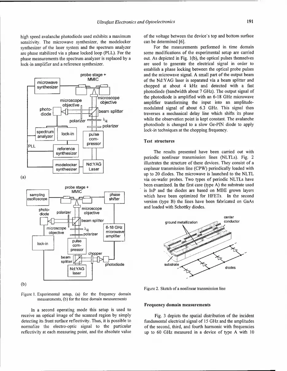
Ultrafast Electronics and Optoelectronics 191
high speed avalanche photodiode used exhibits a maximum sensitivity. The microwave synthesizer, the modelocker synthesizer of the laser system and the spectrum analyzer are phase stabilized via a phase locked loop (PLL). For the phase measurements the spectrum analyzer is replaced by a lock-in amplifier and a reference synthesizer.
probe stage + MMIC
microwave synthesizer
T
photo- diode
microscope objective
<
spectrum analyzer
polarizer ■=
lock-in
PLL reference
synthesizer
microscope objective
beam splitter
=> Xl, A/4
polarizer
pulse com-
pressor
modelocker synthesizer
Nd:YAG Laser
(a)
sampling oscilloscope
probe stage + MMIC
7V phase shifter
photo- diode polarizer
<J microscope
objective
microscope objective
beam splitter
lock-in
= A/4 3 polarizer
pulse com-
pressor
beam splitter
6-18 GHz microwave amplifier
chopper
>
Nd:YAG laser
photodiode
(b)
Figure 1. Experimental setup, (a) for the frequency domain measurements, (b) for the time domain measurements
In a second operating mode this setup is used to receive an optical image of the scanned region by simply detecting its front surface reflectivity. Thus, it is possible to normalize the electro-optic signal to the particular reflectivity at each measuring point, and the absolute value
of the voltage between the device's top and bottom surface can be determined [6].
For the measurements performed in time domain some modifications of the experimental setup are carried out. As depicted in Fig. 1(b), the optical pulses themselves are used to generate the electrical signal in order to establish a phase locking between the optical probe pulses and the microwave signal. A small part of the output beam of the Nd:YAG laser is separated via a beam splitter and chopped at about 4 kHz and detected with a fast photodiode (bandwidth about 7 GHz). The output signal of the photodiode is amplified with an 6-18 GHz microwave amplifier transforming the input into an amplitude- modulated signal of about 6.3 GHz. This signal then traverses a mechanical delay line which shifts its phase while the observation point is kept constant. The avalanche photodiode is changed to a slow Ge-PIN diode to apply lock-in techniques at the chopping frequency.
Test structures
The results presented have been carried out with periodic nonlinear transmission lines (NLTLs). Fig. 2 illustrates the structure of these devices. They consist of a coplanar transmission line (CPW) periodically loaded with up to 20 diodes. The microwave is launched to the NLTL via on-wafer probes. Two types of periodic NLTLs have been examined. In the first case (type A) the substrate used is InP and the diodes are based on MBE grown layers which have been optimized for HFETs. In the second version (type B) the lines have been fabricated on GaAs and loaded with Schottky diodes.
ground metallization
/ substrate _ „
diodes
Figure 2. Sketch of a nonlinear transmission line
Frequency domain measurements
Fig. 3 depicts the spatial distribution of the incident fundamental electrical signal of 15 GHz and the amplitudes of the second, third, and fourth harmonic with frequencies up to 60 GHz measured in a device of type A with 10

192 Ultrafast Electronics and Optoelectronics
diodes. As can be seen the amplitude of the fundamental signal decreases in the direction of propagation whereas the amplitude of the higher harmonics increase indicating that they are generated along the transmission line. The obvious standing wave patterns are caused by phase mismatching of the harmonics and additionally by an impedance mismatch at the end of the line.
15 GHz
30 GHz
45 GHz 60 GHz
1500 2500 position (pm)
Figure 3. Electro-optic signal of the fundamental microwave at 15 GHz and of its higher harmonics along the center conductor of an NLTL from input to output
Two-dimensional field mappings of an NLTL are presented in Figs. 4. Fig. 4(a) shows the metallization structure of the device with the scanned area and Fig. 4(b) the field map of an input signal of 7 GHz. Though the microwave is applied to the line with standard on-wafer probes, the field distribution inside the line shows a distinct asymmetry. This behaviour is not found on a reference line with same dimensions but without diodes (see Fig. 5). Therefore we contribute this effect to the excitation of parasitic propagation modes in the NLTL.
Fig. 6 shows in more detail the transverse distribution at two different positions in the two lines. It can be seen that at positon 1 a distinct asymmetric distribution in the NLTL can be observed assuming a conversion of the incoming CPW even mode into the CPW odd mode. At the end of the line at position 2, the asymmetric distribution disappears but compared with the reference line it can be seen, that the distribution is different regarding the ratio of the amplitude under the center conductor and the ground conductor. We assume that this is caused by a third propagation mode corresponding to a microstrip or a surface wave mode [8]. This highly dispersive mode of a CPW was recently detected and characterized using the experimental setup described in this paper [9].
(a) (b)
-40
rel. amplitude (dB)
-20 0
Figure 4. NLTL consisting of 10 Schottky diodes in a CPW; (a) metallization structure with scanned area; (b) result of 2D field mapping at 7 GHz
(a) (b) rel. amplitude (dB)
-40 -20 0
Figure 5. Reference coplanar waveguide on semiinsulating substrate; (a) metallization structure with scanned area; (b) result of 2D field mappings at 7 GHz

Ultrafast Electronics and Optoelectronics 193
100 200 300
position (pm)
400
(a)
100 200 position (pm)
(b)
Figure 6. Transversal distribution of electro-optic signal at positions (a) 1 and (b) 2 as marked in Figs. 4(a) and 5(a) at 7 GHz
Additional two-dimensional field mappings including the generated higher harmonics are shown in Figs. 7. Fig. 7(a) shows the metallization structure of the device. The fundamental signal of 6 GHz, the second harmonic at 12 GHz and the third harmonic at 18 GHz are presented in Figs. 7(b) - (d), respectively. As shown in Fig. 3, these Figs, show the decrease of the fundamental signal and the increase of the harmonics while propagating along the NLTL, but additionally they make obvious that an unsymmetrical distribution of the electro-optic signal of the fundamental and also of the higher harmonic microwaves is present assuming that there is a multimode propagation also for the generated harmonics.

194 Ultrafast Electronics and Optoelectronics
(d)
-40
rel. amplitude (dB)
-20
Figure 7. NLTL consisting of 10 Schottky diodes in a CPW; (a) metallization structure; results of 2D field mappings at (b) 6 GHz, (c) 12 GHz and (d) 18 GHz.
Time domain measurements
In time domain measurements there is a fixed phase relation between each particular measurement point. Thus, the evolution of a periodic signal can be observed. This is elucidated in Figs. 8(a) to 8(d) for the development of a sinusoidal electrical signal of 6.3 GHz propagating along a periodic NLTL of type B at the 1st, the 5th, the 10th and the 14th diode, respectively. As can be seen, from a sinusoidal input wave the temporal shape is converted into shock waves with fall times down to 5 ps due to the interaction of the higher harmonics. In the time domain, this formation of a shock wave is the counterpart to the generation of harmonics in the frequency domain. The presented results validate that the electro-optic probing technique is capable of studying and demonstrating this effect as well.
3
•2, d) CD ro o >
k = i
- \
1,,,, i,,
-80 -40 0 40
time (ps)
80
(a)
3
ro o >
A /V k = 5
-80 -40 0 40
time (ps)
80
(b)
ro 0) CO ro .«—> o >
:
| j Jk = 10
0 40
time (ps)
80
(c)

Ultrafast Electronics and Optoelectronics 195
Figure 8. Generation of a shock wave along an NLTL, frequency: 6 GHz, (a) waveform at the 1st diode, (b) at the 5th diode, (c) at the 10th diode and (d) at the 14th diode
Conclusions
In summary, electro-optic measurement techniques have been used to internally investigate wave propagation effects along periodic nonlinear transmission lines enabling circuit-designers to get an insight into the in-circuit electrical characteristics of complex microwave devices. The generation of harmonics, the excitation of parasitic propagation modes and the formation of shock waves have been demonstrated showing, that this method is suitable to examine internal field distributions in MMICs in both, frequency domain and time domain.
Jäger (1993), "Two-dimensional direct electro-optic field mapping in a monolithic integrated GaAs amplifier", Proc. 23rd EuMC 1993, Madrid, Spain, 1993, pp. 497-499
[5] G. David, P. Bussek, U. Auer, F.J. Tegude, and D. Jäger, "Electro-optic probing of RF signals in submicrometre MMIC devices", Electron. Lett., 1995, Vol. 31, No. 25, pp. 2188-2189
[6] G. David, R. Tempel, I. Wolff, and D. Jäger, "Analysis of microwave propagation effects using 2D electro-optic field mapping techniques", Optical and Quantum Electronics, Special Issue on Optical Probing of Ultrafast Devices and Integrated Circuits, vol. 28, 1996, pp. 919-931
[7] G. David, W. Schroeder, D. Jäger, and I. Wolff, "2D electro-optic probing combined with field theory based multimode wave amplitude extraction: a new approach to on-wafer measurement", Symposium Digest 1995 IEEE MTT-S International Symposium, May 15 -19, 1995, Orlando, USA, pp. 1049-1052
[8] H. Shigesawa, M. Tsuji, and A.A. Oliner, " A new mode coupling effect on coplanar waveguide of finite width", 1990 IEEE MTT-S Digest, 1990, 1063-1066
[9] G. David, P. Schmitz, S. Redlich, J. Buschke, R. Kremer, and D. Jäger, "Mode analysis of wave propagation on coplanar transmission lines using electro-optic field mapping", APMC '94, December 5-8, Tokyo, Japan, (1994), 149-152
References
[1] K.J. Weingarten, M.J.W. Rodwell, and D. Bloom, "Picosecond optical sampling of GaAs integrated circuits", IEEE J. Quantum Electron, vol. QE-24, (1988), pp. 198-220
[2] J.A. Valdmanis, "Electro-optic measurement tech- niques for integrated picosecond materials, devices, and integrated circuits", in: Semiconductors and Semimetals, vol. 28: Measurement of high speed signals in solid state devices, R. B. Marcus (ed.), Academic Press, Inc., 1990, 135-219
[3] M.G. Li, E.A. Chauchard, C.H. Lee, and H.-L.A. Hung, "Two-dimensional field mapping of GaAs microstrip circuit by electrooptic sensing", Proc. OSA Int. Top. Meeting 'Picosecond Electronics and Optoelectronics', March 13-15, 1991, Salt Lake City, USA, pp. 54-58
[4] G. David, S. Redlich, W. Mertin, R.M. Bertenburg, S. Kosslowski, F.J. Tegude, E. Kubalek, and D.

Three-dimensional experimental analysis of the near-field and far-field radiation of planar millimeter-wave transmitters
T. Pfeifer, T. Löffler, H.G. Roskos, H. Kurz, K.M. Strohm*, and J.-F. Luy* Institut für Halbleitertechnik II, RWTH Aachen, Sommerfeldstraße 24, D-52056 Aachen, Germany
*Daimler-Benz AG, Research Center Ulm, Wilhelm-Runge-Straße 11, D-89081 Ulm, Germany
Abstract
An experimental study of the electric near-field dis- tribution of two different types of planar transmitters for the 76.5 GHz frequency regime important for au- tomotive applications is presented. Three-dimensional field mapping is performed with a novel stroboscopic optoelectronic technique combining electrooptic testing (near-field measurements) with photoconductive prob- ing (far-field). The detected mode patterns give a de- tailed insight into the operation of the devices under test and allow tracing back mode anomalies to misde- signed parts of the structure for improved and direct failure analysis.
Keywords
Optoelectronics, Ultrafast measurements, millimeter wave circuits, Field imaging
Introduction
Integrated
Compact and low-cost Si-based millimeter-wave sources for automotive applications such as collision avoidance radar are in demand. Today's fastest Si-based devices are fabricated in SIMMWIC-technology (SIMMWIC: silicon monolithic millimeter-wave integrated circuits), e.g. IMPATT oscillators operate up to 220 GHz and Si/SiGe-HBTs are driven to maximum frequen- cies around 150 GHz [1]. Monolithically integrated with planar slot or dipole resonators they constitute the key elements of transmitters and receivers for au- tomotive applications in the upper GHz range, e.g. at 76.5 GHz [l]-[3].
Characterization of the device performance by con- ventional test electronics is limited to S-parameter or far-field radiation measurements. A more direct insight
into the operation of a circuit fabricated on arbitrary substrate is obtained with a near-field mapping tech- nique employing a modular optoelectronic (OE) mea- surement system [4], [5]. It is designed to lock onto periodic millimeter-wave signals of arbitrary frequency, and employs both electrooptic (EO) and photoconduc- tive (PC) sampling techniques for near-field and far- field mode mapping in three dimensions above the de- vice under test. Phase-sensitive spatial mapping of the field distribution allows to directly identify parts of the structure which cause parasitic resonances or uninten- tional mode coupling.
In this contribution, we apply the OE near-field tech- nique to two different planar transmitters for short- range automotive radar applications at 76.5 GHz [l]-[3]. The first one is a scale model operating at a resonance frequency around 7 GHz and employs a slot as resonat- ing element ("7-GHz slot transmitter"). The second type is an active 76.5-GHz Si-based dipole transmitter ("76.5-GHz dipole transmitter") which has shown ex- cellent perfomance in first conventional far-field stud- ies [3]. The near-field measurements on this device are supplemented by PC antenna-based detection of the mode pattern in the transition into the far-field regime. The experiments allow a detailed analysis of the tempo- ral and spatial dynamics of the transverse electric field above the devices at various frequencies and detection heights. It is shown, that elements of the structure causing parasitic resonances are clearly identified.
The planar slot and dipole transmitters
The 7-GHz slot resonator is a scale model of a 76.5- GHz SIMMWIC slot transmitter. A schematic of the 7-GHz device is depicted in Fig. 1. The slot trans- mitter employs a 17-//m-thick Cu metallization (grey color) on both sides of a 1.52-mm-thick Rogers TMM-
OSA TOPS on Ultrafast Electronics and Optoelectronics, 1997 Vol. 13, Martin Nuss and John Bowers (ed.) ©1997 Optical Society of America
196
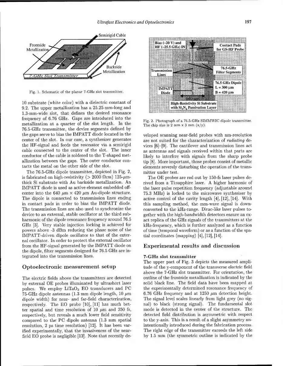
Ultrafast Electronics and Optoelectronics 197
Semirigid Cable
Frontside Metallizatioi
Bias (-20 V) and | HF (-25.5 GHz) IN I
Fig. 1. Schematic of the planar 7-GHz slot transmitter.
10 substrate (white color) with a dielectric constant of 9.2. The upper metallization has a 25.25-mm-long and 1.3-mm-wide slot, that defines the desired resonance frequency of 6.76 GHz. Gaps are introduced into the metallization at a quarter of the slot length. In the 76.5-GHz transmitter, the device segments defined by the gaps serve to bias the IMPATT diode located in the center of the slot. In our case, a synthesizer generates the HF-signal and feeds the resonator via a semirigid cable connected to the center of the slot. The inner conductor of the cable is soldered to the T-shaped met- allization between the gaps. The outer conductor con- tacts the metal on the other side of the slot.
The 76.5-GHz dipole transmitter, depicted in Fig. 2, is fabricated on high-resistivity (> 2000 flcm) 125-/im- thick Si substrate with Au backside metallization. An IMPATT diode is used as active element embedded off- center into the 640 /um x 420 /xm Au-dipole structure. The dipole is connected to transmission lines ending in contact pads in order to bias the IMPATT diode. The transmission lines are also used to synchronize the device to an external, stable oscillator at the third sub- harmonic of the dipole resonance frequency around 76.5 GHz [3]. Very stable injection locking is achieved for powers above -3 dBm reducing the phase noise of the IMPATT-driven dipole oscillator to that of the exter- nal oscillator. In order to protect the external oscillator from the HF-signal generated by the IMPATT diode on the dipole, filter segments designed for 76.5 GHz are in- tegrated into the transmission lines.
Optoelectronic measurement setup
The electric fields above the transmitters are detected by external OE probes illuminated by ultrashort laser pulses. We employ LiTaOs EO transducers and PC 75-GHz dipole antennas (1.3 mm dipole length, 10 /um dipole width) for near- and far-field characterization, respectively. The EO probe [10], [11] has much bet- ter spatial and time resolution of 10 /an and 250 fs, respectively, but reveals a much lower field sensitivity compared to the PC dipole antenna (1.3 mm spatial resolution, 2 ps time resolution) [12]. It has been var- ified experimentally, that the invasiveness of the near- field EO probe is negligible [13]. Note that recently de-
-li i
I [Transmission i^^—-"*"li I Lines ■ i
IMPATTi Diode I
Contact Pads for GS-HF Probe
76.5-GHz Filter Segments
76.5 GHz Dipole L = 300 |im B = 420 |im
Rm High-Resistivity Si Substrate with S^Ni Passivation Layer
Fig. 2. Photograph of a 76.5-GHz SIMMWIC dipole transmitter. The chip size is 2 mm x 3 mm (x/y);
veloped scanning near-field probes with nm-resolution are not suited for the characterization of radiating de- vices [6]-[9]. The cantilever and transmission lines act as antennas and signals received within that parts are likely to interfere with signals from the sharp probe tip [8]. More important, those probes consist of metallic elements severely disturbing the operation of the trans- mitter under test.
The OE probes are red out by 150-fs laser pulses de- rived from a Tirsapphire laser. A higher harmonic of the laser pulse repetition frequency (adjustable around 75.3 MHz) is locked to the microwave synthesizer by active control of the cavity length [4], [12], [14]. With this sampling method, the mm-wave signal is down- converted to the kHz-range. Dirac-like laser pulses to- gether with the high-bandwidth detectors ensure an ex- act replica of the GHz signals of the transmitters at the kHz-frequency, which is further analyzed as a function of time (temporal waveform) or as a function of the spa- tial coordinates (mapping) [4], [12], [14].
Experimental results and discussion
7-GHz slot transmitter The upper part of Fig. 3 depicts the measured ampli- tude of the y-component of the transverse electric field above the 7-GHz slot transmitter. For orientation, the outline of the frontside metallization is indicated by the solid black line. The field data have been mapped at the experimentally determined resonance frequency of 6.76 GHz frequency and at 1250 /im detection height. The signal level scales linearly from light grey (no sig- nal) to black (strong signal). The fundamental slot mode is detected in the center of the structure. The detected field distribution is asymmetric with respect to the y-axis. This is a result of a slight asymmetry un- intentionally introduced during the fabrication process. The right edge of the transmitter exceeds the left side by 1.5 mm (the symmetric outline is indicated by the
198 Ultrafast Electronics and Optoelectronics
20
10H
!°i -10
-20
EO Amplitude (arb. units):;
f=6.76 GHz
-30 -20 -10 0 10 20 30 x (mm)
20
10
loj
-10
-20- f=6.85 GHz
-30 -20 -10 0 10 x (mm)
20 30 50 100 150 200 250 Time Delay (ps)
Fig. 3. Y-Component of the electric field at 1250 ^m distance above the planar 7-GHz slot transmitter (linear grey scale). Up- per figure: measured field pattern at 6.76 GHz; Lower figure: simulated field pattern at 6.85 GHz. The frequency-difference accounts for the assumption in the model of an infinite extension of the substrate of the transmitter.
dotted line). All other dimensions are symmetric to the y-axis. In addition to the fundamental mode, significant signal contributions are observed at the periphery of the metallization, indicating the presence of of parasitic patch modes. Those additional modes are unwanted because they lead to a reduced Q-factor, instabilities (when used as active transmitter), and distorted far- field radiation patterns. Strong parasitic modes are also excited in the bias gap region. Owing to the conductor alignment, those modes reveal transverse x-components only and are detected when the EO detector is rotated by 90° [4], [13] (not shown in Fig. 3).
The lower part of Fig. 3 shows the result of model calculations based on an electric-field-integral-equation approach. The analysis takes into account ohmic, di- electric, magnetic, and radiation losses and reproduces the measured data well execpt for the peak at x=0 mm, y=15 mm. In the measurements, this contribution is hidden by the semirigid cable and is thus not detected. The good agreement between the measured and simu- lated field data demonstrates the accuracy of the novel field mapping technique that promises improved device model verification at high frequencies.
Fig. 4. Time-resolved electric waveform at 20 /im probing height above the IMPATT diode. The solid line is a sine fit to the measured data (circles) indicating periodic signals at 24.42 GHz and 73.26 GHz. The bias current (I) through the IMPATT diode is varied.
76.5-GHz dipole transmitter From the results given above, it is obvious that the slot transmitter concept is not suited for applications. We now present a detailed temporally and spatially resolved analysis of the active 76.5-GHz SIMMWIC dipole transmitter.
In all experiments, the x-component of the transverse electric field above the transmitter is measured with the IMPATT diode located at x=0 mm, y=0 mm (the mea- sured field is oriented perpendicular to the transmission lines). The specific device investigated here operates optimally at a frequency of 73.26 GHz as determined with a spectrum analyzer and a standard horn receiver at the free-running device before performing the OE experiments. The subharmonic injection signal is ad- justed accordingly to 24.42 GHz and 8 dBm power at the synthesizer.
In Fig. 4, electric waveforms obtained by EO mea- surements 20 fim above the IMPATT diode are depicted for various dc bias currents. The measurement time per individual time trace was 5 sec. The recorded data (circles) are periodic in time and reveal contributions at 24.42 GHz and at the resonance frequency of 73.26 GHz
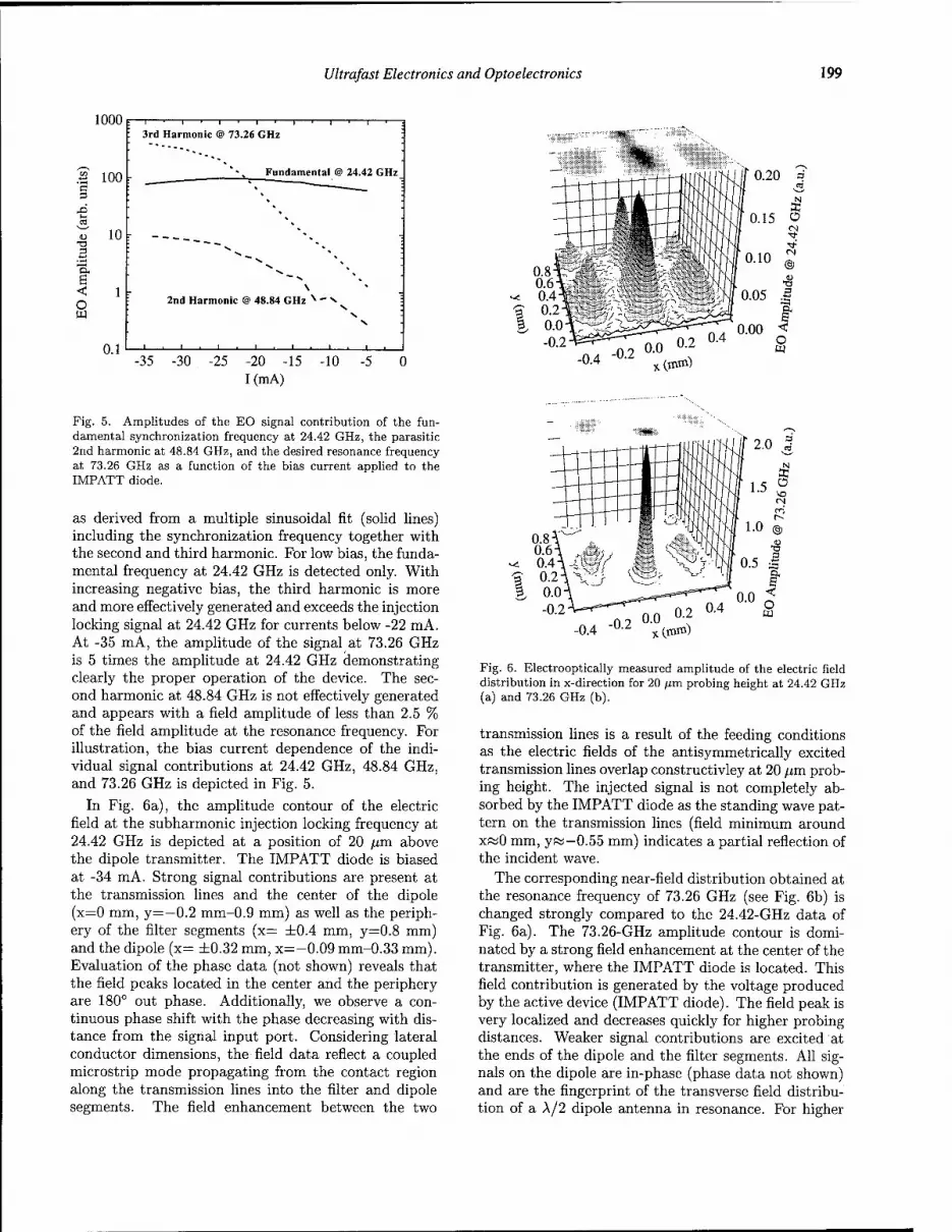
Ultrafast Electronics and Optoelectronics 199
w 100
10
1
n 1
i i i ■
3rd Harmonic i i i i i i i i i i
@ 73.26 GHz
Fundamental @ 24.42 GHz
3 JD I- cd
(1)
*>* . *»* .
\ rionic @ 48.84 GHz x - x
N
I i I . 1 1
T3
"Si e < o w
2nd Ham
i.i.
-35 -30 -25 -20 -15 -10 -5 0 I(mA)
0.20
0.15
0.10
I O CM
x(mtn)
i.05 M
o
Fig. 5. Amplitudes of the EO signal contribution of the fun- damental synchronization frequency at 24.42 GHz, the parasitic 2nd harmonic at 48.84 GHz, and the desired resonance frequency at 73.26 GHz as a function of the bias current applied to the IMPATT diode.
as derived from a multiple sinusoidal fit (solid lines) including the synchronization frequency together with the second and third harmonic. For low bias, the funda- mental frequency at 24.42 GHz is detected only. With increasing negative bias, the third harmonic is more and more effectively generated and exceeds the injection locking signal at 24.42 GHz for currents below -22 mA. At -35 mA, the amplitude of the signal at 73.26 GHz is 5 times the amplitude at 24.42 GHz demonstrating clearly the proper operation of the device. The sec- ond harmonic at 48.84 GHz is not effectively generated and appears with a field amplitude of less than 2.5 % of the field amplitude at the resonance frequency. For illustration, the bias current dependence of the indi- vidual signal contributions at 24.42 GHz, 48.84 GHz, and 73.26 GHz is depicted in Fig. 5.
In Fig. 6a), the amplitude contour of the electric field at the subharmonic injection locking frequency at 24.42 GHz is depicted at a position of 20 /an above the dipole transmitter. The IMPATT diode is biased at -34 mA. Strong signal contributions are present at the transmission lines and the center of the dipole (x=0 mm, y=—0.2 mm-0.9 mm) as well as the periph- ery of the filter segments (x= ±0.4 mm, y=0.8 mm) and the dipole (x= ±0.32 mm, x=-0.09 mm-0.33 mm). Evaluation of the phase data (not shown) reveals that the field peaks located in the center and the periphery are 180° out phase. Additionally, we observe a con- tinuous phase shift with the phase decreasing with dis- tance from the signal input port. Considering lateral conductor dimensions, the field data reflect a coupled microstrip mode propagating from the contact region along the transmission lines into the filter and dipole segments. The field enhancement between the two
Fig. 6. Electrooptically measured amplitude of the electric field distribution in x-direction for 20 (im probing height at 24.42 GHz (a) and 73.26 GHz (b).
transmission lines is a result of the feeding conditions as the electric fields of the antisymmetrically excited transmission lines overlap constructivley at 20 fim prob- ing height. The injected signal is not completely ab- sorbed by the IMPATT diode as the standing wave pat- tern on the transmission lines (field minimum around x«0 mm, yftJ-0.55 mm) indicates a partial reflection of the incident wave.
The corresponding near-field distribution obtained at the resonance frequency of 73.26 GHz (see Fig. 6b) is changed strongly compared to the 24.42-GHz data of Fig. 6a). The 73.26-GHz amplitude contour is domi- nated by a strong field enhancement at the center of the transmitter, where the IMPATT diode is located. This field contribution is generated by the voltage produced by the active device (IMPATT diode). The field peak is very localized and decreases quickly for higher probing distances. Weaker signal contributions are excited at the ends of the dipole and the filter segments. All sig- nals on the dipole are in-phase (phase data not shown) and are the fingerprint of the transverse field distribu- tion of a A/2 dipole antenna in resonance. For higher
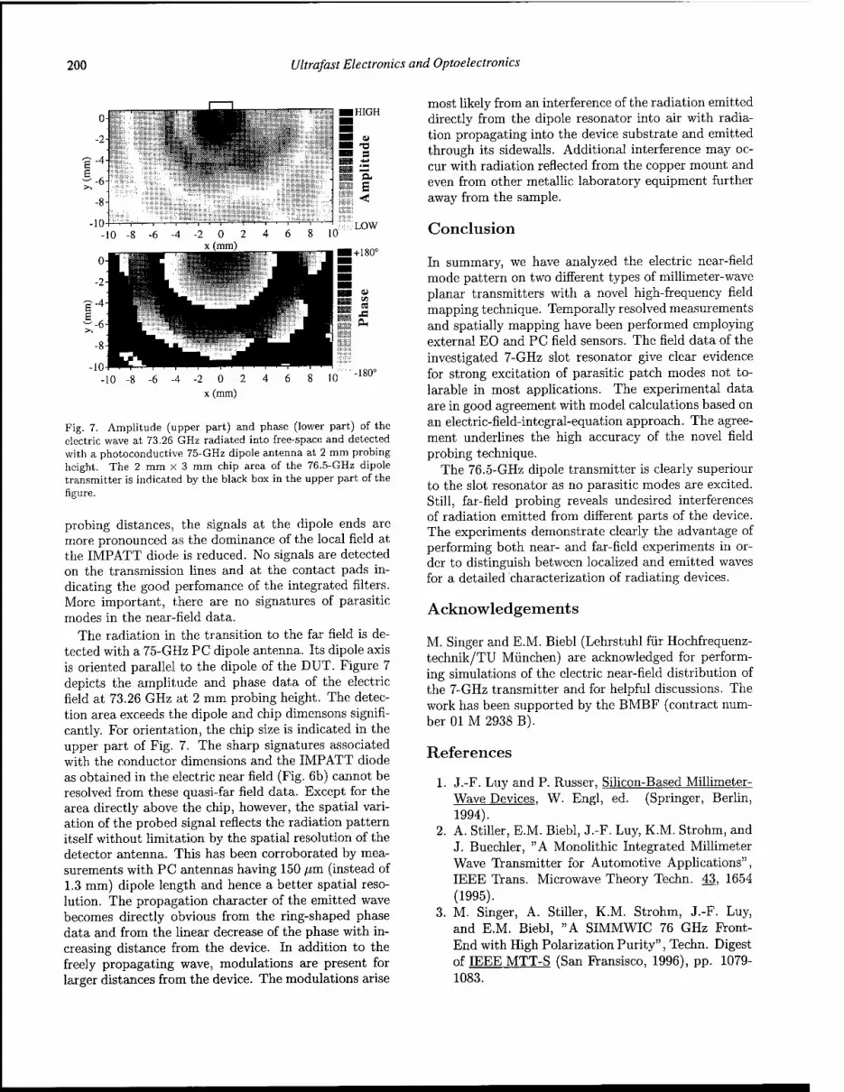
200 Ultrafast Electronics and Optoelectronics
HIGH
-2 0 2 x (mm)
Fig. 7. Amplitude (upper part) and phase (lower part) of the electric wave at 73.26 GHz radiated into free-space and detected with a photoconductive 75-GHz dipole antenna at 2 mm probing height. The 2 mm x 3 mm chip area of the 76.5-GHz dipole transmitter is indicated by the black box in the upper part of the figure.
probing distances, the signals at the dipole ends are more pronounced as the dominance of the local field at the IMPATT diode is reduced. No signals are detected on the transmission lines and at the contact pads in- dicating the good perfomance of the integrated filters. More important, there are no signatures of parasitic modes in the near-field data.
The radiation in the transition to the far field is de- tected with a 75-GHz PC dipole antenna. Its dipole axis is oriented parallel to the dipole of the DUT. Figure 7 depicts the amplitude and phase data of the electric field at 73.26 GHz at 2 mm probing height. The detec- tion area exceeds the dipole and chip dimensons signifi- cantly. For orientation, the chip size is indicated in the upper part of Fig. 7. The sharp signatures associated with the conductor dimensions and the IMPATT diode as obtained in the electric near field (Fig. 6b) cannot be resolved from these quasi-far field data. Except for the area directly above the chip, however, the spatial vari- ation of the probed signal reflects the radiation pattern itself without limitation by the spatial resolution of the detector antenna. This has been corroborated by mea- surements with PC antennas having 150 /zm (instead of 1.3 mm) dipole length and hence a better spatial reso- lution. The propagation character of the emitted wave becomes directly obvious from the ring-shaped phase data and from the linear decrease of the phase with in- creasing distance from the device. In addition to the freely propagating wave, modulations are present for larger distances from the device. The modulations arise
most likely from an interference of the radiation emitted directly from the dipole resonator into air with radia- tion propagating into the device substrate and emitted through its sidewalls. Additional interference may oc- cur with radiation reflected from the copper mount and even from other metallic laboratory equipment further away from the sample.
Conclusion
In summary, we have analyzed the electric near-field mode pattern on two different types of millimeter-wave planar transmitters with a novel high-frequency field mapping technique. Temporally resolved measurements and spatially mapping have been performed employing external EO and PC field sensors. The field data of the investigated 7-GHz slot resonator give clear evidence for strong excitation of parasitic patch modes not to- larable in most applications. The experimental data are in good agreement with model calculations based on an electric-field-integral-equation approach. The agree- ment underlines the high accuracy of the novel field probing technique.
The 76.5-GHz dipole transmitter is clearly superiour to the slot resonator as no parasitic modes are excited. Still, far-field probing reveals undesired interferences of radiation emitted from different parts of the device. The experiments demonstrate clearly the advantage of performing both near- and far-field experiments in or- der to distinguish between localized and emitted waves for a detailed characterization of radiating devices.
Acknowledgements
M. Singer and E.M. Biebl (Lehrstuhl für Hochfrequenz- technik/TU München) are acknowledged for perform- ing simulations of the electric near-field distribution of the 7-GHz transmitter and for helpful discussions. The work has been supported by the BMBF (contract num- ber 01 M 2938 B).
References
1. J.-F. Luy and P. Russer, Silicon-Based Millimeter- Wave Devices, W. Engl, ed. (Springer, Berlin, 1994).
2. A. Stiller, E.M. Biebl, J.-F. Luy, K.M. Strohm, and J. Buechler, "A Monolithic Integrated Millimeter Wave Transmitter for Automotive Applications", IEEE Trans. Microwave Theory Techn. 43, 1654 (1995).
3. M. Singer, A. Stiller, K.M. Strohm, J.-F. Luy, and E.M. Biebl, "A SIMMWIC 76 GHz Front- End with High Polarization Purity", Techn. Digest of IEEE MTT-S (San Fransisco, 1996), pp. 1079- 1083.

Ultrafast Electronics and Optoelectronics 201
4. T. Pfeifer, T. Löffler, H.G. Roskos, H. Kurz, M. Singer, and E.M. Biebl, "Electrooptic measure- ment of the electric near field distribution of a 7 GHz planar resonator", Electron. Lett. 32,1305- 1307 (1996).
5. T. Pfeifer, H.-M. Heiliger, T. Löffler, C. Ohlhoff, C. Meyer, G. Lüpke, H. G. Roskos, and H. Kurz, " Optoelectronic On-Chip Characterization of Ul- trafast Electric Devices: Measurement Techniques and Applications", IEEE Journal Selected Topics of Quantum Electronics (April 1997 issue).
6. B.A. Nechay, A.S. Hou, and D.M. Bloom, "Pi- cosecond Electrical Sampling with an Atomic Force Microscope", in Techn. Digest of Ultrafast Electronics and Optoelectronics, (OSA, Washing- ton DC, 1997), pp. 181-183.
7. A. Leyk and E. Kubalek, "MMIC internal electric field mapping with submicrometre spatial resolu- tion and gigahertz bandwidth by means of high frequency scanning force microscopy", Electron. Lett. 31, 2089-2091 (1995).
8. D.W. van der Weide, "Picosecond/nanometer re- solution with a near-field microwave/scanning- force microscope", in Techn. Digest of Ultrafast Electronics and Optoelectronics, (OSA, Washing- ton DC, 1997), pp. 178-180.
9. K. Takeuchi and A. Mizuhara, "Low-temperature grown GaAs probe for ultrafast electrical signal measurement", Electron. Lett. 33,325-326(1997).
10. M.Y. Frankel, J.F. Whitaker, and G.A. Mourou, " Optoelectronic Transient Characterization of Ul- trafast Devices", IEEE Journ. Quantum Electron. 28, 2313-2324 (1992).
11. EO transducers are commercially available from: Terametrics, 1516 Fenway Road, Crofton, MD, 21114 USA.
12. T. Löffler, T. Pfeifer, H.G. Roskos, and H. Kurz, "Detection of Free-Running Electric Signals Up to 75 GHz Using a Femtosecond-Pulse Laser", IEEE Photon. Techn. Lett. 7, 1189-1191 (1995).
13. T. Pfeifer, T. Löffler, H.G. Roskos, H. Kurz, M. Singer, and E.M. Biebl, "Electro-optic near-field mapping of planar resonators", submitted to IEEE Trans. Antenna Prop., July 1996.
14. T. Löffler, T. Pfeifer, H.G. Roskos, H. Kurz, and D.W. van der Weide, "Stable Optoelectronic De- tection of Free-Running Microwave Signals with 150 GHz Bandwidth", Microelectronic Engineer- ing 31, 397-408 (1996).
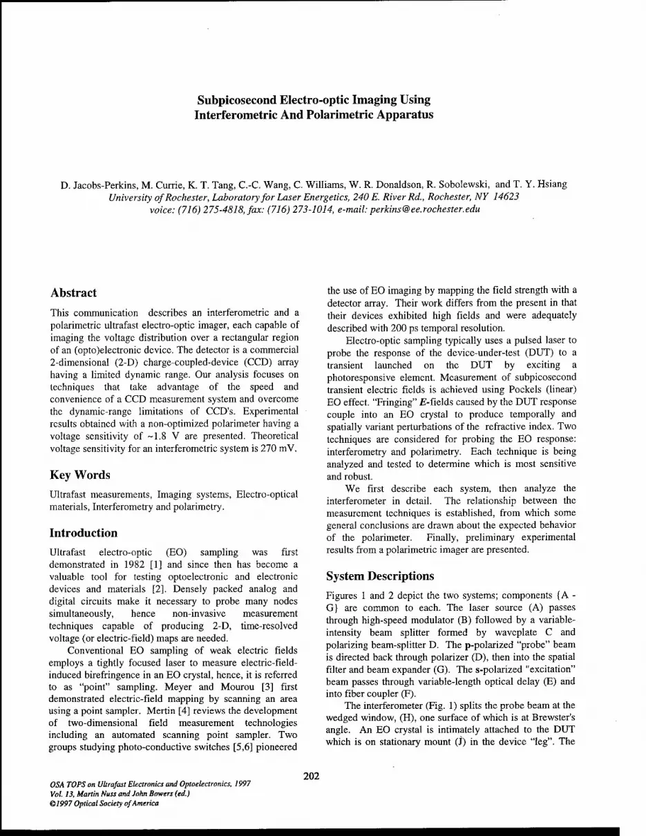
Subpicosecond Electro-optic Imaging Using Interferometric And Polarimetric Apparatus
D. Jacobs-Perkins, M. Currie, K. T. Tang, C.-C. Wang, C. Williams, W. R. Donaldson, R. Sobolewski, and T. Y. Hsiang University of Rochester, Laboratory for Laser Energetics, 240 E. River Rd., Rochester, NY 14623
voice: (716) 275-4818, fax: (716) 273-1014, e-mail: [email protected]
Abstract
This communication describes an interferometric and a polarimetric ultrafast electro-optic imager, each capable of imaging the voltage distribution over a rectangular region of an (opto)electronic device. The detector is a commercial 2-dimensional (2-D) charge-coupled-device (CCD) array having a limited dynamic range. Our analysis focuses on techniques that take advantage of the speed and convenience of a CCD measurement system and overcome the dynamic-range limitations of CCD's. Experimental results obtained with a non-optimized polarimeter having a voltage sensitivity of -1.8 V are presented. Theoretical voltage sensitivity for an interferometric system is 270 mV.
Key Words
Ultrafast measurements, Imaging systems, Electro-optical materials, Interferometry and polarimetry.
Introduction
Ultrafast electro-optic (EO) sampling was first demonstrated in 1982 [1] and since then has become a valuable tool for testing optoelectronic and electronic devices and materials [2]. Densely packed analog and digital circuits make it necessary to probe many nodes simultaneously, hence non-invasive measurement techniques capable of producing 2-D, time-resolved voltage (or electric-field) maps are needed.
Conventional EO sampling of weak electric fields employs a tightly focused laser to measure electric-field- induced birefringence in an EO crystal, hence, it is referred to as "point" sampling. Meyer and Mourou [3] first demonstrated electric-field mapping by scanning an area using a point sampler. Mertin [4] reviews the development of two-dimensional field measurement technologies including an automated scanning point sampler. Two groups studying photo-conductive switches [5,6] pioneered
the use of EO imaging by mapping the field strength with a detector array. Their work differs from the present in that their devices exhibited high fields and were adequately described with 200 ps temporal resolution.
Electro-optic sampling typically uses a pulsed laser to probe the response of the device-under-test (DUT) to a transient launched on the DUT by exciting a photoresponsive element. Measurement of subpicosecond transient electric fields is achieved using Pockels (linear) EO effect. "Fringing" E-fields caused by the DUT response couple into an EO crystal to produce temporally and spatially variant perturbations of the refractive index. Two techniques are considered for probing the EO response: interferometry and polarimetry. Each technique is being analyzed and tested to determine which is most sensitive and robust.
We first describe each system, then analyze the interferometer in detail. The relationship between the measurement techniques is established, from which some general conclusions are drawn about the expected behavior of the polarimeter. Finally, preliminary experimental results from a polarimetric imager are presented.
System Descriptions
Figures 1 and 2 depict the two systems; components {A - G} are common to each. The laser source (A) passes through high-speed modulator (B) followed by a variable- intensity beam splitter formed by waveplate C and polarizing beam-splitter D. The p-polarized "probe" beam is directed back through polarizer (D), then into the spatial filter and beam expander (G). The s-polarized "excitation" beam passes through variable-length optical delay (E) and into fiber coupler (F).
The interferometer (Fig. 1) splits the probe beam at the wedged window, (H), one surface of which is at Brewster's angle. An EO crystal is intimately attached to the DUT which is on stationary mount (J) in the device "leg". The
OSA TOPS on Ultrafast Electronics and Optoelectronics, 1997 Vol. 13, Martin Nuss and John Bowers (ed.) ©1997 Optical Society of America
202
Ultrafast Electronics and Optoelectronics 203
crystal surface contacting the DUT is highly reflective. A reference mirror is on piezoelectric actuator (I) in the reference "leg". Reflections from the reference mirror and EO crystal interact with the wedged window a second time, pass through polarizing filter (K) and relay lens (L) to camera (M). An interference pattern is formed by the interaction of both beams in the plane of the CCD.
reflection. On the return pass, the beam is elliptically polarized, and only the s-polarized component is reflected toward the CCD. The measured effectiveness of this polarizer is (7s//p) = 104.
]\TT * X
EO crystal
Z2147 *y
Figure 1. Interferometric imager.
The polarimeter (Fig. 2) directs the probe beam through the wedged window, (H), followed by compensator (I), and variable waveplate (J). Again, an EO crystal is intimately attached to the DUT which is on stationary mount (K). The crystal surface contacting the DUT is highly reflective. The beam reflected from the EO crystal returns through the waveplate and compensator. A portion of the s-polarized reflection component is reflected off the Brewster window, and directed through aperture (L), and relay lens (M) to the camera (N).
The wedged window functions very differently in these two systems. In the interferometer, the probe beam remains linearly p-polarized. Thus, the surface aligned at Brewster's angle is "perfectly" transparent. The other surface acts as an "ideal" beam splitter (of low reflectivity since it is uncoated) with no 2nd surface reflections. In the polarimeter, the window is used as a polarizing beam- splitter. Reflections from the surface closest to the laser source are inconsequential, since the trajectories of these beams do not reach the detector. The probe beam strikes the window surface closest to the DUT at Brewster's angle. As the probe beam first passes through the Brewster- surface, it is linearly p-polarized, and suffers negligible
EO crystal
Z2187
Figure 2. Polarimetric imager.
An electric Zs-field transient alters the refractive index of the EO crystal. In the interferometer, the probe beam is linearly p-polarized along the optic-axis of the EO crystal, and thus the beam suffers phase retardation during propagation. When combined with a p-polarized plane- wave reference beam, an interference pattern is formed at the CCD that corresponds to the DUT JE-field. In the polarimeter, the probe is initially linearly polarized at 45° to the optic-axis of the EO crystal. After passing through the compensator, crystal, and again through the compensator, the emerging beam is elliptically polarized. The degree of ellipticity is determined by (static + EO- induced) birefringence in the crystal, and the compensator adjustment. The compensator is used to (partially) negate the static birefringence of the EO material, thus improving sensitivity. The intensity of the s-polarized component measured at the detector is proportional to the DUT E- field. In each case, a low-noise, frame-transfer CCD camera records the intensity pattern.
The CCD sensor (Texas Instruments TC-245), has 755 - 8.5 urn pixels horizontal (H) and 242 - 19.75 um pixels vertical (V). Typical magnification is 4:1, giving a measurement area of 1.6 mm (//) x 1.2 mm (V), and spatial resolution of 2.1 urn (H) x 4.9 um (V).
204 Ultrafast Electronics and Optoelectronics
Modulation
Noise sources will degrade the system's sensitivity. These sources include low frequency vibration and thermal perturbations of the interferometer, 1// laser noise, 60 Hz electrical noise (and harmonics), and CCD thermal and shot noise. In addition, pixel-to-pixel sensitivity variations give the appearance of image noise.
Pixel sensitivity variations are not truly noise, and can be digitally corrected by calibrating the camera. CCD thermal noise can be reduced by cooling the sensor. The detrimental effects of the remaining noise sources can be reduced by use of modulation.
(a)
^r== i i
EO phase shift
+Ar, EO H+ArE0
-r. opt l+r opt
PZT phase shift Z2150
Figure 3. Intensity transfer function for an ideal interferometer or polarimeter, centered about an intensity null, shows modulation of the operating point (± r0
opt), and the EO signal (Areo) to produce four different intensity states.
Figure 3 is the ideal intensity transfer function for both an interferometer and a polarimeter, centered on an intensity null. By alternately biasing the operating point of either system between states A and B (i.e., alternating between ± r0
opt in the figure), two images of equal intensity can be obtained (we explain later how to determine the desired operating point). If we then add a small EO- induced phase shift (Areo) to the operating point, the intensity of the resulting image to the left of the null decreases, while that to the right of the null increases. Digital subtraction of images (C - A) and (D - B) yields a spatial map of the EO signal.
The camera integrates the incident photon flux for 1/60 s for each image "field". This integration period acts as a band-stop filter for 60 Hz electrical noise and its harmonics. Figure 4 shows the timing of the modulation components. A timing circuit synchronizes modulation of
the device bias voltage (effectively modulating Areo) to the camera's field-clock frequency, and the operating point (called actuator position in Fig. 4) is modulated at half this frequency. In the interferometer, a piezoelectric actuator (item I, Fig. 1) is used to modulate the operating point by adjusting the reference mirror position. In the polarimeter, a variable waveplate (item J, Fig. 2) modulates the operating point by altering the polarization. A pulse from the timing circuit triggers a frame grabber to digitize four fields in succession, corresponding to states {A...D}. This low-frequency modulation helps to reduce the effect of thermal and vibration noise.
(b)
DUT bias
Actuator position
Excitation and probe
Frame grabber trigger
Four images acquired
Four fields ~\
-r,
On r-i
Off
opt 0 opt 0
On
Off
inrjtfyu; -FbF
H-1.27ms
CÄIHB ABB
Figure 4. Modulation timing diagram corresponding to Fig. 3 .
The timing circuit also produces four pulses (called "Excitation and probe") which are used to the drive high- speed modulator (item B in Figs. 1 and 2). This modulator "gates" the laser "on" for -100 ns immediately before and after the frame-transfer cycle, and "off at all other times. This reduces the laser noise bandwidth, and further reduces thermal and vibration noise contributions. The limiting speed for this modulation is governed by the 1.27 ms frame transfer period, making the effective modulation frequency -750 Hz.
Electro-optics
Applying the techniques of Ref. [7] to x-cut LiTa03, a material commonly used for EO sampling, we find expressions for both the EO-induced index and birefringence perturbations. Reference [8] establishes the relationship between these perturbations and the magnitude of the voltage transient, device structure and material parameters. An interferometer is used to measure the z-axis index perturbation that causes Areo, the dynamic EO phase

Ultrafast Electronics and Optoelectronics 205
change. For a coplanar structure having feature-separation gap g, the index perturbation is:
Areo>z=—«t £sub#£;
surface A
v -EO
(1) /
where X - probe beam wavelength, the crystal and device substrate have relative dielectric constants eE0 and esub respectively, r33 and r13 are Pockels coefficients, ne and n„ are the extraordinary and ordinary refractive indices, and ^surface js ^ transverse £_fjeld magnitude at the surface of the crystal.
A similar expression can be found for the EO-induced birefringent phase change measured by the polarimeter:
Ar, In. ^sK surface \
(2) -( 3
A V °EO J
For LiTa03, the index perturbation along the crystalline z-axis is 30% greater than the induced birefringence, thus suggesting that the interferometric system is preferable for this material.
Since (g£zsurface) = Vsap, the voltage across the gap at
the surface of the crystal, the phase change at any point is proportional to the voltage at that point, hence the imager can be considered a voltage-sensing system.
Temporal resolution of the system is limited predominantly by the probe pulse duration convolved with the fringing field profile. For a 100-fs pulse and 10-|rm gap coplanar silicon structure, we estimate the temporal resolution to be less than 200 fs.
System operation Electro-optic signal sensitivity in an integrating CCD detector is greatest when the number of electrons in each pixel attributed to the EO signal, q, is maximized relative to the total pixel charge, Q. System constraints differ from consideration of the equations governing each detection method. We first consider the interferometric system in detail, then postulate how this relates to the polarimeter.
The normalized intensity measured by the detector, 7int, is the ratio of the output intensity from the interferometer to the intensity in the reference leg (see Ref. [8]),
7int = -f*- = (1 + a) + 2yfcccos(2T) + b, (3) •'ref
where a = /DUT / ^ref is the normalized intensity in the device leg, 2r = 2(r0+Areo) is the phase difference between the E-field of the optical probe in each leg (factor of '2' results from reflective sampling configuration), b is background illumination, and r0 is the optical phase bias of the interferometer. Ideally, a= \,b = 0.
One can show that in the small-signal limit the ratio qlQ becomes [8]:
Q = /(p,r0)AT«
LimAr.,„->0
where
and
1 + OC + b
l4a
/(p,r0)^ 2sin(2r0)
(4a)
(4b)
(4c) /? + cos(2ro)
Equation (4a) describes the fraction of electrons in each pixel attributed to the EO effect, Eq. (4b) describes the interferometer's quality, and (4c) defines the system performance as a function of static bias F0 and for a given quality p. The optimum optical bias point at which function / is maximized, r0
opt, is found by optimizing Eq. (4c) with respect to r0:
r0Bp,(p) = |cos-1(-p-1). (5)
Equation (5) has two solutions; one solution is shown in Fig. 5. The solutions are symmetrically located on either side of an interferometric null, as suggested by Fig. 3. These solutions are used as the operating point about which (small signal) Areo varies. Substituting Eq. (5) into (4c), we find fopt(p), the optimized sensitivity factor for the CCD,
rl{p)= L2 _2- (6) p^-p
This factor, also shown in Fig. 5, allows us to estimate the maximum attainable system sensitivity.
0.50 71
0.45 7C •a
g-o 0.40 Jt t-H
0.35 Jt
40
30
20®
10
0
^
1.0 1.1 1.2 1.3 1.4 1.5 P (<x,b) Z2153 r \ > /
Figure 5. Optimum optical bias point (operating point) r0opt
and sensitivity factor/ opt can be found, given quality p.
Analysis of the optical system shows numerous sources that degrade interferometer quality (see Ref. [8]). In the remaining discussion, the values calculated for the system in Fig. 1 are p(a=0.94, 6=0.085) = 1.044.
The minimum detectable signal, Areo m,n, corresponds
to q/Q = tfnoise/Qweii- This requires that the sensor be

206 Ultrafast Electronics and Optoelectronics
operated near saturation for maximum sensitivity. The CCD's root-mean-squared combination of shot and thermal noise is qnoist = 50 electrons, and well capacity is ßweii = 80 x 103 electrons [9]. By solving Eq. (6) and substituting the result into Eq. (4a), we find Areo
min = 100 urad. We use Eq. (1) to find the corresponding minimum detectable voltage for a device fabricated on silicon (esub = 11.9), using LiTa03 as the EO crystal (eNL0 = 43, r33 - 33 pm/V, ne - 2.180) [7], and probing at X = 800 nm. This gives Areo
min
= 3.7 x 10 "4 C?£2surface) = 100 urad, corresponding to 27
kV/m on a 10-urn gap, or Vgap = 270 mV. Sensitivity can be increased by a factor of 43 using, an
organic salt called DAST [10]: eNL0 = 7.0, rn = 160 pm/V, and n = 2.460. A 30°C reduction in the CCD temperature increases sensitivity by a factor of 1.6 since sensor cooling reduces the dark current by 1/2 for every 10°C. With both
surface . 400 V/m. enhancements, Vsap = 4 mV, and E., The intensity detected by a polarimetric imager is
given by:
/„„, = i?sin2(rc) + pol
/?r2sin2(rc + 2(r0 + Areo)) +
r2sin2(rc + r0 + Areo)+...
(7)
where, R = intensity reflection coefficient from EO crystal, T = (1 - R) = intensity transmission, and Tc is the phase retardation introduced by the compensator. Equation (7) differs from the ideal case quoted in [2]; it includes surface reflections from the EO crystal. The first term results from the Fresnel reflection on the front face of the EO crystal; this contains no EO signal. The second term passes through the EO crystal twice, thus accumulating twice the static and EO retardation, 2(r0 + Areo). This may seem beneficial at first glance, but recall that the probe beam pulse duration is shorter than the time-of-flight of the probe through the crystal. Consequently, the second term reduces temporal resolution of the system. Only the third term is relevant to the measurement of interest, since it has undergone exactly one pass through the crystal. In the ideal case, R = 0; Eq. (7) becomes:
7Poi x sin
;(rc+r0 + Areo). (8)
1); Eq. (3) Likewise, in an ideal interferometer (p becomes:
/intoccos2(r0+Areo). (9) From this observation, we conclude that for well
designed systems (i.e., nearly ideal), the functional form of the small-signal response should be similar in each case. Furthermore, the compensator setting (Tc) is used to optimize the sensitivity of a polarimeter, whereas the reference mirror position (i.e., r0) is used to optimize the interferometer sensitivity.
Experimental results Our initial experiments use the polarimeter of Fig. 2. Figure 6 shows a 2-D image of a simple coplanar structure (bottom), with gap size = 200 urn. The super-image is the observed electric-field map with an applied bias of 33 V DC, and with Tc optimized.
5^~ ■■'■■•■ ':'"■ V^-5?öslll M\M"v'W-:.m
C-a**-^«.- ..---■
^filil■P|,
Figure 6. 2-D image of coplanar structure (bottom); gap size (dark stripes) = 200um. The super-image is the observed transverse £-field map with a bias of 33 VDC.
One feature evident in Fig. 6 is the presence of image noise. Obvious noise sources include non-uniform illumination (i.e., diffraction-rings from contaminated optics) and pixel-pixel sensitivity variations (i.e., local peaks and valleys). Modulation of the bias (only) was used during acquisition. Sixteen images were acquired and averaged in approximately 8 seconds to produce this result. No other forms of modulation, sensor cooling, or digital correction were used.
-A/4
Retardation (k=195 nm)
-A/8 0 A/8 A/4 20
10
3-10--
-20 [♦*
-71/2 -Jt/4 0 ir/4 Retardation (rad)
n/2
Figure 7. Maximum system sensitivity occurs when the compensator retardation —Tt/8 (= -X/16) relative to an intensity null. Note the asymmetry of this plot.

Ultrafast Electronics and Optoelectronics 207
Figure 7 shows the measured sensitivity as a function
of compensator retardation rc relative to an intensity null. From this figure, we find the maximum sensitivity to be (33 V/18 counts) = 1.8 V/count when retardation ~ -rc/8. This system has not been fully optimized with regard to Eq. (7), and greater sensitivity is expected. An interesting feature in Fig. 7 is the sensitivity asymmetry for positive and negative retardation. Analysis of the equation describing the polarimeter [Eq. (7)] predicts this behavior, whereas analysis of the equation describing the interferometer [Eq. (3)] does not. A detailed analysis of this behavior will be the subject of a future publication.
Summary
We have described two ultrafast EO imaging systems that use a CCD detector to map electric fields on an optoelectronic device. Optimum operating conditions are identified for non-ideal imagers. Signals can be modulated at up to 750 Hz to reduce effects of 1// laser, thermal and vibration noise. Sensitivity in the absence of laser noise is estimated to be 27 kV/m, corresponding to 270 mV for a 10-u.m coplanar structure. Sensor cooling and alternative EO materials should improve the resolvable voltage to 4 mV. Experimental results to-date have demonstrated 1.8 V sensitivity. Future goals include complete DC and subpicosecond characterization of each system.
Acknowledgments
This work was supported by the University Research Initiative at the University of Rochester, sponsored by the U.S. Army Research Office under Grant DAAL03-92-G- 0112. The work of D. Jacobs-Perkins was also supported by a Frank J. Horton Fellowship, and that of C. Williams by U.S. Army Research Office AASERT under Grant DAAH04-95-1-00428.
References
[1] J. A. Valdmanis and G. Mourou , "Picosecond Electro-Optic Sampling System", Appl. Phys. Lett. 41 (3), 211-212 (1982).
[2] J. M. Wiesenfeld, "Electro-optic sampling of high-speed devices and integrated circuits", IBM J. Res. Develop., 34 (2/3), 141-161 (1990).
[3] K. E. Meyer and G. A. Mourou, "Two Dimensional ZJ-field Mapping With Subpicosecond Resolution", in Picosecond Electrons and Optoelectronics, edited by G. A. Mourou, D. M. Bloom, and C. H. Lee (Springer-Verlag, NY, 1985), pp. 46-49
[4] W. Mertin, "Two-dimensional field mapping of monolithic microwave integrated circuits using electro-optic sampling", Opt. Quantum Electron., 28, 801-817 (1996).
[5] W. R. Donaldson, L. Kingsley, M. Weiner, A. Kim and R. Zeto, "Electro-optic imaging of the internal fields in a GaAs photoconductive switch", J. Appl. Phys. 68 (12), 6453-6457 (1990).
[6] R. A. Falk, J. C. Adams, S. G. Ferrier and C. D. Capps, "Dynamic optical probing of high-power photoconductors", in the Ninth IEEE International Pulsed Power Conference, Digest of technical papers, edited by K. R. Prestwich and W. L. Baker (IEEE, New York, 1993), Vol. 1, pp. 88-91.
[7] A. Yariv and P. Yeh, Optical Waves in Crystals: Propagation and Control of Laser Radiation (Wiley, New York, 1984) pp. 220-245
[8] D. Jacobs-Perkins, M. Currie, C.-C. Wang, C. Williams, W. R. Donaldson, R. Sobolewski and T. Y. Hsiang, "Subpicosecond Imaging System Based On Electro-Optic Effect", to be published in IEEE Journal of Selected Topics in Quantum Electronics, Vol. 2, No. 3, Sept. 1996.
[9] Area Array Image Sensor Products Data Book, Texas Instruments (1994), pp. 2-135 to 2-151
[10] DAST = dimethylamino methyl stilbazolium tosylate, available from Molecular Optoelectronics Corporation, 877 25th St. Watervliet, NY 12189, http://www.automatrix.com.

Measurement of Subpicosecond Electrical Pulses Using Optical Second-Harmonic Generation
Ajay Nahata and Tony F. Heinz Departments of Electrical Engineering and Physics, Columbia University, New York, NY 10027
Abstract
We report the application of an optical second-harmonic sampling technique that allows for the detection of subpicosecond electrical transients.
Keywords
Nonlinear optics at surfaces, Ultrafast measurements, Ultrafast technology in general, Ultrafast nonlinear optics
The use of ultrafast laser sources to generate and detect ultrashort electrical pulses has stimulated significant interest in recent years. These techniques have provided powerful tools for applications ranging from high-speed device characterization to time-domain terahertz (THz) spectroscopy [1]. With the widespread availability of lasers exhibiting ultrashort pulse durations, there is strong incentive to translate the bandwidth of the optical pulse to the electrical pulses. The use of nonlinear optical media seems well-suited for this application. This is exemplified by the application of electro-optic sampling [2] as a sensitive probe of picosecond electrical pulses on transmission lines, as well as the more recent demonstration of the coherent detection of freely propagating far-infrared pulses [3-5]. While electro-optic sampling has a number of attractive features, including a high degree of sensitivity to electrical transients, the technique may impose several significant limitations. For example, in silicon-based circuit applications, the required external electro-optic crystal can cause loading effects on the circuit. In addition, for both transmission line and freely propagating THz applications, low-lying vibrational
resonances in many inorganic electro-optic crystals can impose high frequency limitations on the spectral content.
In this contribution, we describe the application of an electric field induced optical second-harmonic (EFISH) sampling technique that allows for the detection of ultrashort electrical pulses, both on transmission lines and in the form of freely propagating THz radiation. In contrast to electro-optic sampling, which typically relies on the use of non-centrosymmetric ionic crystals, the present second- harmonic (SH) sampling technique is also applicable to centrosymmetric media. This is particularly important, since it creates the possibility for using materials with better suited low-frequency characteristics. In addition, the sensitivity of this technique is enhanced by its nearly background-free character. As a result of these attributes, we expect the inherent resolution time of this technique to be- 10 fs.
We used a mode-locked Ti:sapphire laser producing ultrashort optical pulses at 76 MHz to generate and detect the transient electrical pulses in both the guided- wave and free space configurations. For the transmission line geometry, shown in Figure 1, the device was fabricated on ion-implanted silicon-on-sapphire. The electrical pulses were launched using a photoconductive switch embedded in the transmission line structure (top left circle). Detection of these pulses was effected a short distance away (lower right circle) using a split-off portion of the optical beam. For the free space geometry, THz radiation was generated using a GaAs-based large aperture photoconductive antenna. A pair of off-axis paraboloidal mirrors were used to collimate and focus the THz radiation onto the detection medium, which consisted of an ion implanted silicon surface. It is important to note that the detection capability is equally applicable to crystalline materials.
OSA TOPS on Ultrafast Electronics and Optoelectronics, 1997 Vol. 13, Martin Nuss and John Bowers (ed.) ©1997 Optical Society of America
208

Ultrafast Electronics and Optoelectronics 209
50 n 50 Q.
Here, xiff is the effective third order and £ is the effective interaction length for the nonlinear mixing. The corresponding intensity, which varies as the square of the SH electric field magnitude, is, therefore, quadratic in the subpicosecond field.
As stated above, both the static and transient contributions may be present. Thus, the detected SH
intensity, I2<° , is given by
Figure 1: Schematic drawing of the coplanar waveguide transmission line fabricated on an ion implanted silicon- on-sapphire wafer. The device consists of a center line with 10 urn wide channels on each side. The black circles show where the pump and probe beams impinge on the device.
The detection process utilized a probe beam that was incident on the silicon substrate at 45°. After passing through optical filters to remove any residual second harmonic (SH) photons, the beam was focused to a spot size of approximately 10 urn. The reflected beam passed through several optical filters to remove the fundamental photons and an analyzing polarizer oriented to pass only s- polarized photons. The SH signal was detected with a photomultiplier tube and photon counter.
We begin by describing the general approach for EFISH detection. In general, both electric field- independent and field dependent contributions are present. The field-independent (static) SH contribution may emanate from the same medium as the EFISH source or may be generated in a physically separated medium. In the experiment described below, we use the static contribution arises from the surface of the implanted silicon. We can define an effective second-order susceptibility, x(2)em that incorporates the appropriate tensoral and angular dependencies. In the absence of a subpicosecond (THz) field, the static component to the SH field, E210, is given by
I2 = \Ela +AE2a
K *Xrff'EffiE (1)
where E™ is the field of the fundamental probe beam at frequency to.
If we neglect this static component, then, in the presence of a subpicosecond (THz) pulse, Esps, the transient
component of the SH field, AE2<0, is given by
AE2ffl oc xS Effi EM Esps -t. (2)
+ c|x(3)Esps|2(r)2
= if + Aif + Ai2; (3)
where A, B, and C are constants that include all angular dependencies, x* designates the complex conjugate of x, and L and Q designate linear and quadratic dependencies on the transient electric field, respectively. The SH intensity, therefore, consists of a quiescent term, I0
ffl , that is constant for a fixed experimental arrangement, a first-
order signal term, AI2m , that varies linearly with the magnitude of the subpicosecond electrical pulse, and a
second-order signal term, AI2; , that varies quadratically
with the magnitude of the subpicosecond electrical pulse. We note that the magnitude of E2<° can be varied by simply rotating the polarization of the obliquely incident probe beam.
Time Delay [ps] Figure 2: Temporal waveform obtained using second harmonic generation. The upper curve corresponds to the generation of an electrical transient by the application of a bias across the pump photoconductor gap. The lower curve is a reference scan obtained in the absence of an

210 Ultrafast Electronics and Optoelectronics
applied bias. Both waveforms are offset from the origin for clarity.
In the transmission line experiment, we used an s- polarized fundamental probe beam and detected only the s- polarized SH radiation. Furthermore, no dc bias was present on the transmission line. For isotropic media, such as ion implanted silicon-on-sapphire, in such an experimental geometry, no static contribution to the SH field is expected. Thus, Eq. (3) reduces simply to
I2M = AI (4)
The experimentally observed waveform using the EFISH technique described above is shown in Figure 2. The upper trace shows the signal with a bias on the generation photoconductive switch, while the lower trace shows the signal in the absence of the bias. We have compared this upper trace in Figure 2 to an electronic cross-correlation measurement for this device (not shown) and have found that the waveform is indeed consistent with a quadratic dependence on Esps [6].
For the case of freely propagating THz radiation, we used a mixed s/p fundamental polarization, such that both AE2M and E2,10, were present. More specifically, the polarization of the fundamental beam was adjusted so that
Thus, Eq. (3) reduces to Ef » AE2
I2 e+Ai2» (5)
The observed temporal profile for the freely propagating THz electric field using the EFISH technique is shown in Figure 3. For clarity, we have subtracted the DC offset,
I0M, in order to more clearly show the bipolar nature of
the detected waveform. The intrinsic response time for the SH sampling
technique is limited by the spread in the arrival time of the probe beam throughout the probed volume and the properties of the nonlinearity. Given the short escape depth (125 nm) for the SH signal and the electronic nature of the nonlinearity, we expect the response time to be limited by the duration of the probe pulse with an inherent limit of < 10 fs. Experimentally, the fastest transient in the THz waveform corresponds to a time delay of approximately 300 fs. This is significantly longer than the optical pulse duration and is believed to limited by the emitter and the imaging system.
In the present experimental arrangement, the interaction length in silicon is extremely short. Thus, there is no particular advantage in using a co-propagating versus
counter-propagating beam geometry. However, with the appropriate choice of transparent media, we expect that the use of a transmission geometry employing appropriate phase-matching constraints will yield a significant enhancement in the detection sensitivity, without deleterious effects on the detection response time. We are currently investigating this approach.
We are grateful to Aniruddha Weling for many helpful discussions. This work was supported, in part, by the Air Force Office of Scientific Research under Grant No. F49620-92-J-0036 and the National Science Foundation under Grant No. CHE-96-12294.
TO C
C/3
0.0 2.5 5.0 7.5
Time Delay [ps]
10.0
Figure 3: The normalized temporal response of the THz field measured by electric field-induced second harmonic generation. For clarity, the contribution of the static SH radiation has been subtracted.
References:
[1] D. Grischkowsky, in Frontiers in Nonlinear Optics, edited by H. Walther, N. Koroteev, and M.O. Scully (Institute of Physics Publishing, Philadelphia, 1992). [2] J.A. Valdmanis, G. Mourou, and C.W. Gabel, Appl. Phys. Lett. 41,211(1982). [3] Q. Wu, and X.-C. Zhang, Appl. Phys. Lett. 67, 3523 (1995). [4] P.U. Jepsen, C. Winnewisser, M. Schall, V. Schyja, S.R. Keiding, and H. Helm, Phys. Rev. E 53, 3052 (1996). [5] A. Nahata, D.H. Auston, T.F. Heinz, and C. Wu, Appl. Phys. Lett. 68, 150(1996). [6] A. Nahata, T.F. Heinz, and J.A. Misewich, Appl. Phys. Lett. 69, 746(1996).

Terahertz Optoelectronics
Martin C. Nuss
Bell Labs, Lucent Technologies 101 Crawfords Corner Rd. Holmdel.NJ 07733 Phone:(908)949-5358 Fax: (908) 949-2473
Terahertz optoelectronics has been a very fertile field within the last few years, with new innovations in the technology and its applications continuously emerging. The papers in this section give a good cross section of some of the latest innovations in this field.
Terahertz optoelectronics, which started just over ten years ago, has transformed itself from a research curiosity to an important technology. Physicists, chemists, and biologist have discovered its superior performance as a spectroscopy tool in the far-infrared region of the electromagnetic spectrum. High-energy terahertz pulses can now be generated with microjoule energies to perform nonlinear spectroscopy in atoms and semiconductors. But maybe most important, the technology has improved and matured enough to find its way into commercial applications such as circuit testing, quality control, package inspection, and gas detection.
Compact, diode-pumped femtosecond lasers had a lot to do with making terahertz technology practical enough to be considered for the commercial market. Other innovations have followed, like real-time signal detection and acquisition, more efficient transmitters and detectors, new electro-optic sensors, and improved optical systems allowing diffraction-limited propagation and focusing of terahertz beams.
What may be the most important indicator of the status of terahertz optoelectronics is the sustained rate of new ideas and techniques generated by the growing pool of researchers in this field. Examples in this volume are THz impulse ranging, terahertz "T-ray" imaging and tomography, and near-field detection. In addition, electro-optic THz detectors promise a new way of terahertz imaging, and at the same time allow to extend coherent detection to frequencies well beyond 10 THz.
211

Ultrafast Electro-Optic Field Sensor and Its Image Applications
X.-C. Zhang Physics Department, Rensselaer Polytechnic Institute, Troy, NY 12180 USA
Abstract
Free-space electro-optic field sensors have be used to characterize the temporal, spectral, and spatial distribution of freely propagating terahertz beams (THz beams). This detection system, which uses an electro-optic crystal sensor, provides diffraction-limited spatial resolution, femtosecond temporal resolution, DC-THz spectral bandwidth, and a sub-mV/cm field detectability.
Key words: ultrafast measurement; electro-optic sampling; infrared imaging; electro-optic devices.
Electro-Optic Field Sensor
Ultrafast electro-optic field sensor provides alternative method for time-resolved measurement of freely propagating terahertz beams with a frequency range from GHz to THz [1-8]. The sensitivity and bandwidth of the electro-optic sensors (sampling in a synchronized mode) are comparable to or superior than conventional far-infrared detection. Advantages intrinsic to electro-optic detection include large detector area, high scan rate, low optical probe power, and large linear dynamic range.
Figure 1 illustrates the experimental setup of a free-space co-propagating electro-optic sampling system. A CW mode-locked Ti:sapphire laser is used as the optical source. Several different semiconductor GHz/THz emitters have been tested, including photoconductive antennas (transient current source), and a <111> GaAs wafer at normal incidence (optical rectification source). In general optical rectification source emits the THz pulse with a duration comparable to that of the optical excitation pulse, and transient current source radiates longer THz pulses.
Fundamentally, the electro-optic effect is a coupling between a low frequency electric field (terahertz pulse) and a laser beam (optical pulse) in the sensor crystal. Free-space
electro-optic sampling via the linear electro-optic effect (Pockels effect) offers a flat frequency response over an ultrawide bandwidth. Because field detection is purely an electro-optic process, the system bandwidth is mainly limited by either the pulse duration of the probe laser or the lowest TO phonon frequency of the sensor crystal. Further, since electro-optic sampling is purely an optical technique, it does not require electrode contact or wiring on the sensor crystal.
pump pulse
/-—* 4- delay stage
emitter
THz pulse
^ probe pulse %
Fig fs laser
1: Schematic
crystal
C
P
signal + T T
illustration of co-propagating electro-optic sensor setup.
Figure 2 shows the details of the sampling setup. Simple tensor analysis indicates that a <110> oriented zincblende crystal as a sensor gives the best sensitivity. The polarization of the THz beam and optical probe beam are parallel to the [1,-1,0] crystal direction. Modulating the birefringence of the sensor crystal, via an applied electric field (THz), will modulate the polarization ellipticity of the optical probe beam passing through the crystal. The ellipticity modulation of the optical beam can then be polarization analyzed to provide information on both the amplitude and phase of the applied electric field. The detection system will analyze a polarization change from the electro-optic crystal and correlate it with the amplitude
OSA TOPS on Ultrafast Electronics and Optoelectronics, 1997 Vol. 13, Martin Nuss and John Bowers (ed.) ©1997 Optical Society of America
212
Ultrafast Electronics and Optoelectronics 213
and phase of the testing electric field. For weak field detection, the power of the laser beam modulated by the electric field of the THz pulse E (E=V/d) is
PcutOO-Potl+TtV/Vn]
where P0 is the output optical probe power with zero field applied to the crystal, and V^ is the half-wave-voltage of the sensor crystal. By measuring Pout from a calibrated voltage source as a function of time delay between the THz pulse and optical probe pulse, the time-resolved sign and amplitude of V can be obtained, and a numerical FFT provides frequency information.
probe beam
polarizer
Fig. 2: Details of a ZnTe sensor setup.
Figure 3 plots the temporal electro-optic waveform of a 1 ps THz pulse as measured by a balanced detector after both the THz pulse and optical probe pulse co-propagate through the <110> ZnTe sensor crystal. The time delay is provided by changing the relative length of the optical beam path between the THz pulses and the optical probe pulses. Detection sensitivity is significantly improved by increasing the interaction length of pulsed field and optical probe beam within the crystal. The signal-to-noise ratio can exceed 1,000:1 using unfocused beams, 10,000:1 using unamplified focused beams (using a laser oscillator as an optical source), and 100,000:1 using focused amplified beams (using a regenerative amplified laser source) with a ZnTe sensor crystal. Fig. 4 plots the signal and noise spectra, with a SNR>50,000 from 0.1 to 1.2 THz.
< c
75 c 2> V) O LU
Time (ps) Fig. 3: Temporal electro-optic signal of a 1 ps THz pulse measured by a ZnTe sensor.
THz Fig. 4: Amplitude spectrum after FFT shows a SNR > 50,000 from 0.1 THz to 1.2 THz.
Figure 5 plots the measurement of 200 fs THz pulses. The ringing after the main peak is due to the dispersive contribution by the first TO phonon resonance (centered at 5.3 THz and 2 THz FWHM) in ZnTe. Detection bandwidth is limited by the optical pulse duration and dispersion in the material. The useful detection bandwidth of ZnTe extends to 4 THz, as shown in Fig. 6.
6 -
6 4 _ ZnTe sensor
CO i
EO
sig
nal
rb
o
N>
yW/WV-VWVW~VVWV~—
{ -4 i 1
10 15 20 0 5
Time (ps) Fig. 5: Temporal electro-optic signal of 200 fs THz pulse measured by a ZnTe sensor.
3 «j,
3
75. E <
Fig. 6: Amplitude spectrum of the temporal signal in Fig. 5.

214 Ultrafast Electronics and Optoelectronics
A linear response in both the generation and detection of the THz pulses is crucial. Figures 7 and 8 plot the electro- optic signal versus average optical probe power and peak optical pump power, respectively. Excellent linearity is achieved versus probe power whereas pump-beam saturation has been observed. By increasing the optically illuminated area of the photoconductor on the THz emitter, the total emitted THz power can be made to scale up linearly with illumination area (assuming a nonsaturating optical fluence).
<
_CO CO c
000 - .••
100 .1.4 mm ZnTe sensor • • •
10 • •• • •
1 • •• •
0.1 ••
•
*„T ,
O LU
0.01 0.1 1 10 100 Probe Average Power (uW)
Fig. 7: Electro-optic signal versus optical probe average power.
1000
LU
0.1
<r 100 _ V = 2.5 kV c CO CO 10 _ c O) • in • O 1 •• •
10' ,2%
Fig. 8:
10"° 10"* 10"' 10u
Pump Peak Power (MW/crrf Electro-optic signal versus optical excitation
density (peak power).
By using crystals with a higher first TO phonon frequency, it is possible to further increase the system bandwidth. We have tested several electro-optic crystals with different phonon frequencies. GaP is a zincblende crystal with its indirect bandgap at 2.25 eV. The first TO phonon frequency is 11 THz (367 cm"1). The measured electric field sensitivity of GaP sensor is about half of that of the ZnTe crystal. However the bandwidth of a GaP sensor is doubled. Our data suggests that GaP is a prime candidate. Fig. 9 is a plot of the temporal waveform (optical rectified signal from a <111> GaAs with normal incidence) measured by a <110> GaP. The time-resolved 10% to 90% transient in the ring is 53 fs. This is the shortest electrical transient that has ever been measured coherently. Our laser
has a pulse duration of 45 fs, and currently the THz signal bandwidth is limited by the GaAs emitter (TO phonon at 8 THz). Fig. 10 is the corresponding frequency spectrum. It shows a 3-dB bandwidth of 3.6 THz and a cutoff frequency near 7 THz. By using GaP as both emitter and sensor, we expect a cutoff frequency greater than 10 THz.
3
3-
O) LL N I
Time (ps) Fig. 9: Temporal signal from optical rectification measured by a GaP sensor. 53 fs (10% to 90% risetime in ring oscillation) can be well resolved.
THz Fig. 10: Amplitude spectrum of a temporal signal shown in Fig. 9. This is the widest bandwidth of a coherent detector ever reported.
Electro-Optic 2D Imaging
The use of THz beams for imaging applications was first demonstrated by Hu and Nuss [9,10]. Far-infrared images (T-ray imaging) of tree leaves, bacon, and semiconductor integrated chips were demonstrated as examples of a variety of applications. Electro-optic 2D imaging provides an alternative way for THz imaging. One of the most important applications of free-space electro-optic imaging is the capability of real-time imaging [11, 12].
By illuminating an electro-optic crystal with a THz beam and an optical readout beam, then detecting the optical beam with a linear diode array or CCD camera, time- resolved 1-D or 2-D images of pulsed far-infrared radiation can be achieved, respectively.
Ultrafast Electronics and Optoelectronics 215
^1 ZnTe CCD camera
computer"
Fig. 11: Setup for the conversion of a THz image into an optical image.
3 4 Time (ps)
Fig. 12: Signal from one of the 288x384 CCD pixels (100 time-resolved frames).
3 -S-
CD 73 3
Q. E <
0.0 0.2 0.4 0.6 0.8 1.0 1.2 1.4 1.6
THz Fig. 13: Amplitude spectrum of a temporal signal shown in Fig. 13.
Figure 11 schematically illustrates the experimental arrangement for free-space electro-optic THz imaging. Silicon lenses are used to focus the THz radiation on a <110> oriented ZnTe crystal. An optical readout beam with a diameter larger than that of the THz beam probes the electric field distribution within the crystal via the Pockels effect. The 2D field distribution in the sensor crystal is
converted into a 2D optical intensity distribution after the readout beam passes through a crossed polarizer, and the optical image is then recorded by a linear diode array or a digital CCD camera. Figures 12 and 13 plot temporal signal and its corresponding FFT from a single CCD pixel. The data in Fig. 12 was taken from 100 sequential frames with a temporal step of 66.6 fs. Fig. 14 shows the temporal signal from a linear diode array (288 pixels).
®s 'o^>^r20 -TV**5
Fig. 14: Temporal signal from 288 pixels.
Figures 15 and 16 are plots of the spatial distribution (6x6 mm2) of the THz field amplitude imaged near the focal point at 0.57 THz and 1.08 THz, respectively. The pixel size is 22 p.m, and the focal plane imaging is 1-to-l. In the diffraction limit, as can be seen in the figures, components of THz field at a higher frequencies (here 1.08 THz) focus more tightly than those at the low frequencies (here 0.57 THz). Further, the largest THz induced photomodulation was over 50%.
2233. 0.57 THz
1119..
119
•2233
X Pixels
Fig. 15: An image of a focused THz beam at 0.57 THz.
216 Ultrafast Electronics and Optoelectronics
1.08 THz
X Pixels
Fig. 16: An image of a focused THz beam at 1.08 THz.
We have imaged the field distribution from a planar quadrupole THz emitter. Figure 17 shows the quadrupole emitter where the center electrode is biased with two side electrodes grounded and the corresponding radiation pattern. The center electrode is 1 mm wide and has a length over 1 cm. The gaps between the side electrodes are 1.5 mm and 2 mm, respectively. This quadrupole geometry generates two unbalanced dipoles with opposite polarity. The peak field distributions are plotted in 2-D and 3-D. Figure 17 clearly indicates the radiation pattern and the polarity of two opposite dipoles.
1.08-
1.06-
1.04 -
^.02- J 3
h > 0.98
0.96
0.94
0.92
3-D plot
X pixels
pM 2-D plot
±- quadrupole emitter
Fig. 17: A focal-plane image of the THz field from a quadrupole.
One of the most important applications of this free-space electro-optic THz imaging method is its ability to image moving or living objects. The images of a moving
objective at focal-plane can be viewed at the video rate (38 frames/s). To demonstrate this ability, a dipole emitter (2x5 mm2 photoconductor) was placed about 1 cm away from the focal-plane as the THz source, and an object was positioned in the focal-plane. Figure 18 captures an image when an object (a wooden rod with 2 mm diameter) was swept through the THz beam path at the focal-plane.
0.08-
0.06-
0.04-
j 0.02- ri 1 0- c "-0.02-
-0.04 -
-0.06 -
-0.08
250
measured THz pattern
tfi
* '
,<1~'«j*W|l8fc,"'«f~!f*a« ,«—
150 100
Y Pixels
*Pifeiy Ä'/ 300
f'""200
"100
THz emitter
a moving rod Fig. 18: One of the focal-plane images with a rod sweeping across the THz beam path in the focal plane.
This system was used to record the dynamic radiating process resulting from varying the bias field until breakdown. The maximum frame transfer rate of our current CCD (Princeton Instrument, PentaMax) with a readout rate of 5 million pixels per second is 38 frames/second and can sustain up to 152 frames/second with 4x4 binning. The fastest frame transfer rate from some CCDs can reach upwards of 2000 frames/second making it possible to image real-time 2-D transient processes, including the THz radiation pattern from an explosion.
The powerful capabilities of this imaging technique result from the ability to provide real-time images across an ultrawide frequency band, extending from 50 GHz to 5 THz, at a variable frame rate from 38 to 152 frames/second, and the ability to noninvasively image moving objects, turbulent flows, or explosions. Further, the imaging system will also have diffraction-limited spatial resolution, 50 femtosecond temporal resolution, sub-mV/cm field sensitivity, and be capable of real-time measurements.
Acknowledgment
This work was supported by the Army Research Office (DAAH04-96-1-0370), Research Corporation (Cottrel
Ultrafast Electronics and Optoelectronics 217
Scholar), and the National Science Foundation (Career Award). We thank Q. Wu, Z.G. Lu, P. Campbell, and G. A. Wagoner for their technical support.
References:
1. Q. Wu and X.-C. Zhang, Appl. Phys. Lett. 67, 3523, (1995).
2. Q. Wu and X.-C. Zhang, Optics & Quantum Electronics, 28,945,(1996).
3. Q. Wu and X.-C. Zhang, Appl. Phys. Lett., 68, 1604 (1996).
4. P. Uhd Jepsen, C. Winnewisser, M. Schall, V. Schya, S.R. Keiding and H. Helm, Phys. Rev. E, 53, 3052 (1996).
5. A. Nahata, D.H. Auston, and T.F. Heinz, Appl. Phys. Lett. 68, 150(1996).
6. Q. Wu, M. Litz, and X.-C. Zhang, Appl. Phys. Lett., 68, 2924, (1996).
7. Q. Wu, F.G. Sun, P. Campbell, and X.-C. Zhang, Appl. Phys. Lett., 68, 3224, (1996).
8. Q. Wu and X.-C. Zhang, "7 THz Ultrabroadband GaP Electro-Optic Sensors," April 7 issue, Appl. Phys. Lett., (1997).
9. B.B. Hu and M.C. Nuss, Opt. Lett. 20, 1716 (1995). 10. M.C. Nuss, Circuits & Devices, 25, March, (1996). 11. Q. Wu, T.D. Hewitt, and X.-C. Zhang, Appl. Phys.
Lett., 69, 1026(1996). 12. Z.G. Lu, P. Campbell, and X.-C. Zhang,
unpublished, (1997).

Generation and Detection of Wideband Terahertz Radiation Using Nonlinear Optical Media
Ajay Nahata and Tony F. Heinz Departments of Electrical Engineering and Physics, Columbia University. New York, NY 10027
Abstract
We present a scheme for exploiting the dispersion in the linear optical properties of a %<2) material to obtain wideband phase-matched terahertz emission and detection from ultrafast optical pulses.
Keywords
Ultrafast measurements, Ultrafast technology in general, Ultrafast nonlinear optics, Electro-optical materials
mixing) and electro-optic sampling is identical and may be written as
Ak= k(co0p, + coTHz)-k(coopl)-k(ci)THz) =0, (1)
.opl and av are the optical and THz frequencies, where ö\t respectively, and CDopl and (eo^+o)^) lie within the spectrum of the optical pulse. If we neglect the dispersion of the material properties in the optical spectral range, we can express the coherence length, £c
(= n I Ak), ignoring birefringence as
A key ingredient to future advances in terahertz (THz) spectroscopy is the development of broadband coherent sources of THz radiation. The ready availability of laser pulses with durations of -10 fs and materials with non- resonant second-order optical nonlinearities suggests the potential for significantly extending the bandwidth of coherent spectroscopy. THz radiation may be produced in an electro-optic medium via difference-frequency mixing [1-4]. The generation process may be regarded as the beating of various Fourier components of the optical spectrum of the pump field to produce a rectified baseband pulse [2]. Such a difference-frequency generation scheme is capable of producing electric fields with spectral content extending from DC [3] to the mid- infrared [4]. We demonstrate here that dispersion in the optical refractive index may be used to obtain collinear, non-critical phase matching over a broad bandwidth in the THz. This phase matching procedure allows for production of wideband THz pulses by optical rectification of an ultrashort laser pulse and for wideband detection by electro-optic sampling of THz radiation.
The phase matching condition for the optical rectification process (collinear difference-frequency
7TC
^THzPopt nTHz| (2)
Here, c is the speed of light and nopl and n^ are the optical and THz refractive indexes, respectively. In many inorganic nonlinear optical crystals, the difference between the optical and THz refractive indexes tends to be large, so that only type II phase matching is possible for difference frequency mixing. Historically, birefringence has been employed to achieve long coherence lengths in optical rectification experiments [2]. However, the large refractive index difference between the optical and FIR results in a narrow phase matching bandwidth. Angle tuning is required to optimize the efficiency at any given THz frequency. This may be demonstrated by considering LiNb03. The phase matching angle for a type II (oeo) interaction in LiNb03
is shown in Figure 1 [1]. From the figure, a phase matching angle of 0 = 20° is required for optimal conversion at -0.5 THz. However, the radiated FIR bandwidth per unit crystal thickness is only -0.06 THz / mm. This effect arises simply from balancing the velocities of the different frequency components and will
OSA TOPS on Ultrafast Electronics and Optoelectronics, 1997 Vol. 13, Martin Nuss and John Bowers (ed.) ©1997 Optical Society of America
218

Ultrafast Electronics and Optoelectronics 219
occur even when optical dispersion is included (using a visible wavelength pump). Thus, this approach is clearly not optimized for the generation of broadband THz radiation.
o> 5
40 ■ /-""
30 " /^
20 ' - //
10 ■
n • 1—1—1—_,—1—1—1—1—1——I—
0.0 0.4 0.8 1.2 1.6
Difference frequency (THz)
2.0
Figure 1: Phase matching angle versus THz frequency for far-infrared generation by collinear type II difference frequency generation in LiNb03.
The value of using optical dispersion to significantly extend the coherence length for difference frequency generation and electro-optic sampling can be seen by restating the phase matching condition of Eq. (1) as [5]
k(cüiHz) k(coopl + a)iHz)-k(cOopi)
dföjop, (3)
This relation implies that phase matching is achieved when the THz wave travels at the velocity of the optical pulse envelope (i.e., the optical group velocity, vg). The corresponding coherence length for optical rectification is then
7TC
dr. nop(_^opt"
dn opt
dA.
(4)
We consider two specific materials for which dispersion compensation significantly enhances the phase matching length: a model poled polymer and ZnTe. We use a covalently functionalized Disperse Red #1 copolymer as the model polymer. The detailed linear and nonlinear optical properties of the medium have been described elsewhere [6]. The dispersion properties
at optical frequencies are due to a strong charge transfer band centered at 470 nm. We note that our previous analysis neglected the effects of optical dispersion [7]. Figure 2 shows the frequency dependent coherence length with and without the consideration of optical dispersion in the polymer system using an optical pump source at 740 nm. In these calculations, we assume that the THz refractive index, which is nearly constant between 0.1 and 1 THz, remains unchanged out to 4 THz. Note the significantly increased coherence length that may be attained by utilizing the optical dispersion.
For ZnTe, we utilize the wide bandgap nature of the semiconductor to adjust the amount of optical dispersion in the near infrared. Assuming an optical pump source centered at 800 nm, we have calculated the coherence length for difference frequency mixing and electro-optic sampling. Figure 3 shows this parameter versus THz frequency, with and without consideration of optical dispersion. The peak structure in the solid trace (with consideration of optical dispersion) is due to the optimal matching of the relevant optical and THz velocities. Beyond 2 THz, the coherence length decreases rapidly due to the dispersion of the ZnTe crystals in the FIR. We should note that the frequency dependent coherence length can be readily altered by simply tuning the optical wavelength.
Leng
th (
cm)
1
1
1
-1
Cohere
nce
\ \
U.U 1 i 1
0 12 3/
Frequency (THz)
Figure 2: Coherence length versus THz frequency for the poled polymer using optical excitation at 740 nm. The dotted line, calculated using Eq. (2), neglects the dispersion at optical frequencies. The solid line, calculated using Eq. (4), includes the effects of dispersion at optical frequencies.
We have measured the spectral characteristics of the THz radiation generated from a 0.9 mm thick
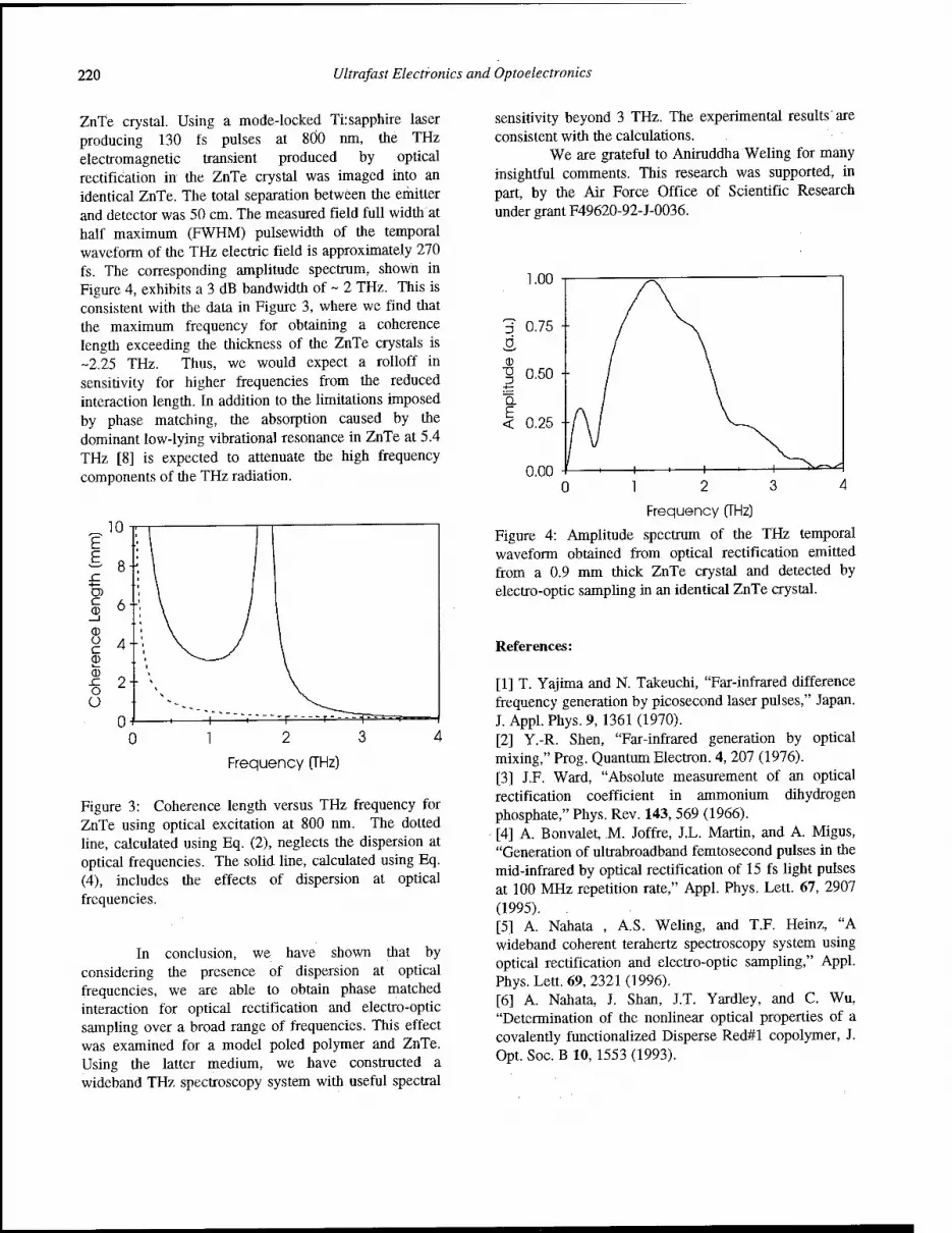
220 Ultrafast Electronics and Optoelectronics
ZnTe crystal. Using a mode-locked Ti: sapphire laser producing 130 fs pulses at 800 nm, the THz electromagnetic transient produced by optical rectification in the ZnTe crystal was imaged into an identical ZnTe. The total separation between the emitter and detector was 50 cm. The measured field full width at half maximum (FWHM) pulsewidth of the temporal waveform of the THz electric field is approximately 270 fs. The corresponding amplitude spectrum, shown in Figure 4, exhibits a 3 dB bandwidth of ~ 2 THz. This is consistent with the data in Figure 3, where we find that the maximum frequency for obtaining a coherence length exceeding the thickness of the ZnTe crystals is -2.25 THz. Thus, we would expect a rolloff in sensitivity for higher frequencies from the reduced interaction length. In addition to the limitations imposed by phase matching, the absorption caused by the dominant low-lying vibrational resonance in ZnTe at 5.4 THz [8] is expected to attenuate the high frequency components of the THz radiation.
1 2 3
Frequency (THz)
Figure 3: Coherence length versus THz frequency for ZnTe using optical excitation at 800 nm. The dotted line, calculated using Eq. (2), neglects the dispersion at optical frequencies. The solid line, calculated using Eq. (4), includes the effects of dispersion at optical frequencies.
In conclusion, we have shown that by considering the presence of dispersion at optical frequencies, we are able to obtain phase matched interaction for optical rectification and electro-optic sampling over a broad range of frequencies. This effect was examined for a model poled polymer and ZnTe. Using the latter medium, we have constructed a wideband THz spectroscopy system with useful spectral
sensitivity beyond 3 THz. The experimental results are consistent with the calculations.
We are grateful to Aniruddha Weling for many insightful comments. This research was supported, in part, by the Air Force Office of Scientific Research under grant F49620-92-J-0036.
1.00
=3
Ö, CD
TS D
'S. E <
0.75 -■
0.50 --
0.25 --
0.00
Frequency (THz)
Figure 4: Amplitude spectrum of the THz temporal waveform obtained from optical rectification emitted from a 0.9 mm thick ZnTe crystal and detected by electro-optic sampling in an identical ZnTe crystal.
References:
[1] T. Yajima and N. Takeuchi, "Far-infrared difference frequency generation by picosecond laser pulses," Japan. J. Appl. Phys. 9,1361 (1970). [2] Y.-R. Shen, "Far-infrared generation by optical mixing," Prog. Quantum Electron. 4, 207 (1976). [3] J.F. Ward, "Absolute measurement of an optical rectification coefficient in ammonium dihydrogen phosphate," Phys. Rev. 143, 569 (1966). [4] A. Bonvalet, M. Joffre, J.L. Martin, and A. Migus, "Generation of ultrabroadband femtosecond pulses in the mid-infrared by optical rectification of 15 fs light pulses at 100 MHz repetition rate," Appl. Phys. Lett. 67, 2907 (1995). . [5] A. Nahata , A.S. Weling, and T.F. Heinz, "A wideband coherent terahertz spectroscopy system using optical rectification and electro-optic sampling," Appl. Phys. Lett. 69, 2321 (1996). [6] A. Nahata, J. Shan, J.T. Yardley, and C. Wu, "Determination of the nonlinear optical properties of a covalently functionalized Disperse Red#l copolymer, J. Opt. Soc. B 10, 1553 (1993).

Ultrafast Electronics and Optoelectronics 221
[7] A. Nahata, D.H. Auston, C. Wu, and J.T. Yardley, [8] T. Hattori, Y. Homma, A. Mitsuishi, and M. Tacke, "Generation of terahertz radiation from a poled "Indices of Refraction of ZnS, ZnSe, ZnTe, CdS, and polymer," Appl. Phys. Lett. 67, 1358 (1995). CdTe in the far-infrared," Opt. Comm. 7, 229 (1973).

THz Impulse Ranging
R.A. Cheville, R.W. McGowan and D. Grischkowsky
School of Electrical and Computer Engineering and Center for Laser and Photonics Research Oklahoma State University, Stillwater, OK 74078
Abstract
We have demonstrated the ability of a THz impulse ranging system to measure the late time response of dielectric targets following excitation by a short, THz impulse. Measurements with the THz system show excellent agreement with the theoretically predicted returns from cylindrical and spherical targets in both the time and frequency domains. This technique should have wide ranging applications for the THz impulse scale ranging of targets of real world interest.
Key Words
Optoelectronics, Ultrafast measurements, THz time- domain spectroscopy, THz impulse ranging.
Introduction
A potentially simple way to identify complex targets is by the late time response after illumination by a short pulse. For this case a short pulse excites resonances within and between scattering centers on the target which are aspect independent [1]. After detection of the initial reflected pulse, or specular reflection, the excited resonant modes radiate the late time response. Recent work has examined the late time response for target identification, in both the time and frequency domain [2-4]. Besides providing a potentially simple way to identify target characteristics, measurement of the response of an object to a short excitation pulse may also provide information on the physical processes responsible for the scattered field [5], which is often unavailable or obscured in frequency domain measurements. To develop time domain target identification methods it is important to correlate theoretical predictions with data from actual scattering
experiments. Since it is often impractical to obtain ranging data on full scale targets, geometrically scaled targets are often used in conjunction with theoretical models and measurements from actual targets.
Here we describe the use of optoelectronic techniques to generate single cycle pulses of freely propagating THz radiation, and demonstrate ultrawide bandwidth scattering from dielectric simple geometrical objects. The late time response from dielectric targets has a richer structure and a response to much longer times than for the conducting targets measured previously [6]. Scattering from a fused quartz cylinder was measured for electric fields perpendicular to the cylinder axis. Scattering was also measured for a silicon sphere.
The incident THz pulses are the best approximation to impulse excitation ever used in ranging studies and have an absolute bandwidth larger than any other previously reported. The relatively short wavelengths of the THz pulse permit target features of less than 1 mm to be observed, making this technique ideal for scale ranging measurements since realistic target to wavelength ratios can be maintained. Furthermore, the measurement window achieved by the optoelectronic gating technique together with the subpsec response time of the detector enables only the scattered signal from the target to be detected, providing background free measurements.
Experiment
The optoelectronic ranging system [6], shown in Fig. 1, is a modification of the THz beam system [7] used for THz time-domain spectroscopy [8]. THz pulses are opto- electronically generated by ultrashort laser pulses incident on the optoelectronic source chip. The generated THz beam is collimated by the silicon lens, then propagates and diffracts to a paraboloidal mirror, where the THz radiation
OSA TOPS on Ultrafast Electronics and Optoelectronics, 1997 Vol. 13, Martin Nuss and John Bowers (ed.) ©1997 Optical Society of America
222
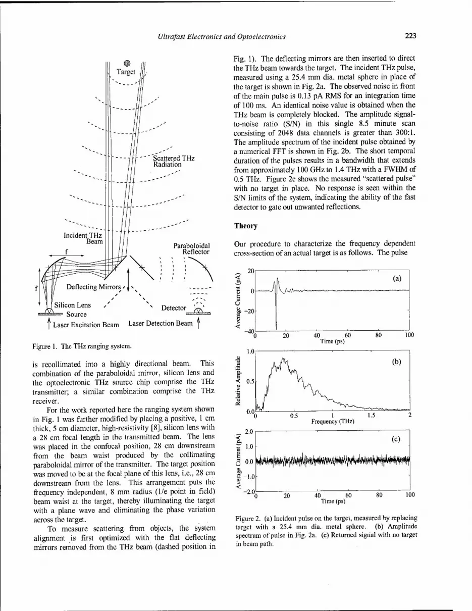
Ultrafast Electronics and Optoelectronics 223
Scattered THz Radiation
Paraboloidal Reflector
Detector '^
\ Laser Excitation Beam Laser Detection Beam \
Figure 1. The THz ranging system.
is recollimated into a highly directional beam. This combination of the paraboloidal mirror, silicon lens and the optoelectronic THz source chip comprise the THz transmitter; a similar combination comprise the THz receiver.
For the work reported here the ranging system shown in Fig. 1 was further modified by placing a positive, 1 cm thick, 5 cm diameter, high-resistivity [8], silicon lens with a 28 cm focal length in the transmitted beam. The lens was placed in the confocal position, 28 cm downstream from the beam waist produced by the collimating paraboloidal mirror of the transmitter. The target position was moved to be at the focal plane of this lens, i.e., 28 cm downstream from the lens. This arrangement puts the frequency independent, 8 mm radius (1/e point in field) beam waist at the target, thereby illuminating the target with a plane wave and eliminating the phase variation across the target.
To measure scattering from objects, the system alignment is first optimized with the flat deflecting mirrors removed from the THz beam (dashed position in
Fig. 1). The deflecting mirrors are then inserted to direct the THz beam towards the target. The incident THz pulse, measured using a 25.4 mm dia. metal sphere in place of the target is shown in Fig. 2a. The observed noise in front of the main pulse is 0.13 pA RMS for an integration time of 100 ms. An identical noise value is obtained when the THz beam is completely blocked. The amplitude signal- to-noise ratio (S/N) in this single 8.5 minute scan consisting of 2048 data channels is greater than 300:1. The amplitude spectrum of the incident pulse obtained by a numerical FFT is shown in Fig. 2b. The short temporal duration of the pulses results in a bandwidth that extends from approximately 100 GHz to 1.4 THz with a FWHM of 0.5 THz. Figure 2c shows the measured "scattered pulse" with no target in place. No response is seen within the S/N limits of the system, indicating the ability of the fast detector to gate out unwanted reflections.
Theory
Our procedure to characterize the frequency dependent cross-section of an actual target is as follows. The pulse
0 20 40 60 Time (ps)
Figure 2. (a) Incident pulse on the target, measured by replacing target with a 25.4 mm dia. metal sphere, (b) Amplitude spectrum of pulse in Fig. 2a. (c) Returned signal with no target in beam path.

224 Ultrafast Electronics and Optoelectronics
incident upon the target as a function of frequency, Einc^o), can be expressed as the actual generated pulse P,(o)) multiplied by a factor Gt((o) describing the effects of the source antenna and optics. For the well collimated beam generated by the THz system the pulse incident upon the target is then
Einc((0) = P,(ffl)G,((D). (1)
The scattered pulse detected at the receiver is
Esc(co) = Eulc((ö)T(^(ö)r)Ftr(a))Gr(a)), (2)
where Gr((o) describes the receiver response and optics and T(<|>,ü),r) is the scatterering function of the target, including propagation effects. Ftr((o) describes the optical transfer function for the incoming wave from the target with respect to the receiver and is determined by the beam size, type (spherical or cylindrical) and curvature. The angle if is the bistatic angle and r is the distance from the target to the receiver. The incident pulse is measured by replacing the target with a flat mirror assumed to be an infinite, perfect reflector, since even at the longest wavelengths (3 mm, 100 GHz) the reflector was on the order of 100 wavelengths in extent. In this case T(<|),tt),r) = 1 for all frequencies, and due to the well collimated beam, propagation effects can be neglected. The signal detected at the receiver from the perfect reflector is then
Erf,((o) = P,((o)G,((0)Fm((o)Gr((o), (3)
where Fm(©) describes the optical transfer function for the incoming wave from the mirror with respect to the receiver. The system response can now be mostly eliminated from the results, leaving only the desired frequency dependent cross-section multiplied by the ratio of the optical transfer functions. For an actual target the signal detected at the receiver is
Esc((0) = P1((o)G,((ö)Ftr((D)Gr((o)T(<t),cö,r). (4)
By taking the ratio of the amplitude spectra of the scattered response from the target and the perfect reflector, the effects of antennas and optics are removed from the data, and we obtain the measured scattering function multiplied by the ratio of the optical transfer functions:
EsctcoyErfKco) = Tmeas(<|),(ö,r)Ftr(ro)/Fmr((o). (5)
In the far-field limit for which the incident waves to the receiver can be treated as plane waves, the optical transfer functions for the target and mirror are then the same and Esc(co)/Ern((o) = TmeasC^o^r). In addition, if instead of the
plane mirror a spherical or cylindrical mirror would be used to generate a reference beam with the same wavefront curvature at the receiver as for the target, the ratio FtrC^/FmXco) would also be unity. This procedure is similar to that used in THz time domain spectroscopy [8]. For a known distance r, from the target to the detector the measured scattering parameter, T™^,©), can then be compared to that calculated in the frequency domain Tcaic(<Mo),. Multiplying Tcaic(<|>,«>) by the complex spectrum of the pulse reflected from the mirror E,fi(a>,(|>) of Eq. (3) gives in the far-field approximation the calculated scattered pulse spectrum. Taking the inverse Fourier transform of this complex spectrum yields the calculated scattered pulse shape in the time domain.
Experimental and Theoretical Results
The measured scattered THz pulse from a 1.96 ± 0.05 mm diameter quartz cylinder is shown as the upper curve in Fig. 3a. In order to increase the resulting S/N ratio by the square root of the number of scans, the data shown is an average of 5 individual scans taken consecutively. The amplitude of the scattered specular reflection is approximately the same as that for the spherical wave reference pulse shown in Fig. 2a. Oscillations in the late time response can be seen to 90 ps after the initial specular reflection, labeled A in Fig. 3a. Note that the amplitude of late time response is slightly larger than the initial specular reflection.
Traditionally, scattering measurements have determined the frequency dependent radar cross section as a means of identifying targets. For a given distance from the target, the normalized radar cross section for a cylindrical (n=l) and spherical (n=2) target is
4TC" 1
K k, -|T(co)| —T = n(2rY
n a E;„
1
7i a" (6)
where T((o) is the scattering function, Etac and Esc are the incident and scattered electric fields respectively, a is the target radius, r is the target-detector distance, and k0=2Tc/^0 is the wavevector in free space. The scattered electric field Esc is determined as a function of frequency from the numerical Fourier transform of the time domain data. For the quartz cylinder, Esc is shown in Figs. 3a and 3b. The incident electric field E^ is determined from the incident pulse similar to that shown in Fig. 2, except that a cylinder was used as the reference mirror. The measured normalized radar cross section is shown as open circles in Fig. 3c.
Given the complex index of refraction of the quartz cylinder [8], the frequency dependent radar cross-section
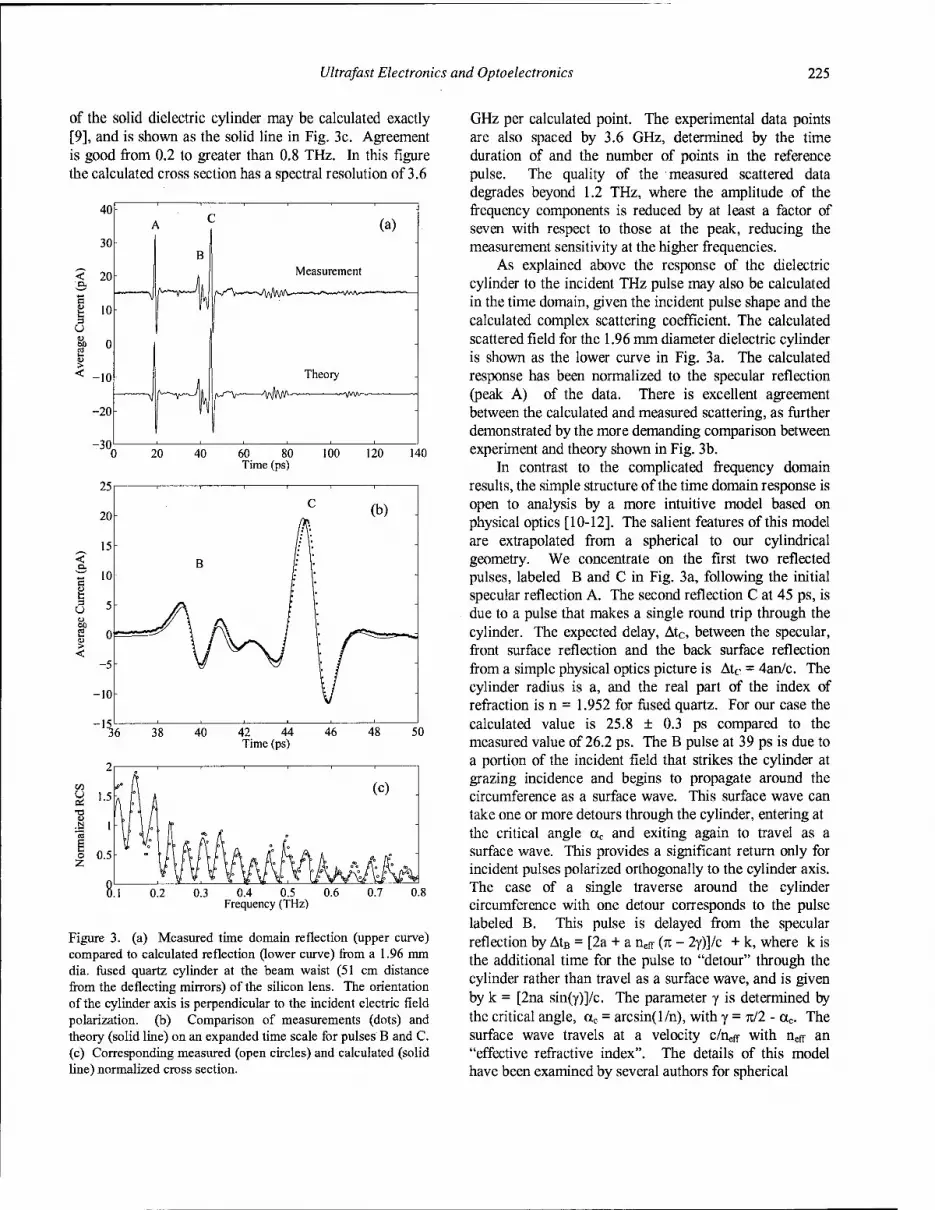
Ultrafast Electronics and Optoelectronics 225
of the solid dielectric cylinder may be calculated exactly [9], and is shown as the solid line in Fig. 3c. Agreement is good from 0.2 to greater than 0.8 THz. In this figure the calculated cross section has a spectral resolution of 3.6
< (X
u
(a)
Measurement
Theory
60 80 Time (ps)
100 120 140
0.4 0.5 Frequency (THz)
Figure 3. (a) Measured time domain reflection (upper curve) compared to calculated reflection (lower curve) from a 1.96 mm dia. fused quartz cylinder at the beam waist (51 cm distance from the deflecting mirrors) of the silicon lens. The orientation of the cylinder axis is perpendicular to the incident electric field polarization, (b) Comparison of measurements (dots) and theory (solid line) on an expanded time scale for pulses B and C. (c) Corresponding measured (open circles) and calculated (solid line) normalized cross section.
GHz per calculated point. The experimental data points are also spaced by 3.6 GHz, determined by the time duration of and the number of points in the reference pulse. The quality of the measured scattered data degrades beyond 1.2 THz, where the amplitude of the frequency components is reduced by at least a factor of seven with respect to those at the peak, reducing the measurement sensitivity at the higher frequencies.
As explained above the response of the dielectric cylinder to the incident THz pulse may also be calculated in the time domain, given the incident pulse shape and the calculated complex scattering coefficient. The calculated scattered field for the 1.96 mm diameter dielectric cylinder is shown as the lower curve in Fig. 3a. The calculated response has been normalized to the specular reflection (peak A) of the data. There is excellent agreement between the calculated and measured scattering, as further demonstrated by the more demanding comparison between experiment and theory shown in Fig. 3b.
In contrast to the complicated frequency domain results, the simple structure of the time domain response is open to analysis by a more intuitive model based on physical optics [10-12]. The salient features of this model are extrapolated from a spherical to our cylindrical geometry. We concentrate on the first two reflected pulses, labeled B and C in Fig. 3a, following the initial specular reflection A. The second reflection C at 45 ps, is due to a pulse that makes a single round trip through the cylinder. The expected delay, Atc, between the specular, front surface reflection and the back surface reflection from a simple physical optics picture is Atc = 4an/c. The cylinder radius is a, and the real part of the index of refraction is n = 1.952 for fused quartz. For our case the calculated value is 25.8 ± 0.3 ps compared to the measured value of 26.2 ps. The B pulse at 39 ps is due to a portion of the incident field that strikes the cylinder at grazing incidence and begins to propagate around the circumference as a surface wave. This surface wave can take one or more detours through the cylinder, entering at the critical angle ac and exiting again to travel as a surface wave. This provides a significant return only for incident pulses polarized orthogonally to the cylinder axis. The case of a single traverse around the cylinder circumference with one detour corresponds to the pulse labeled B. This pulse is delayed from the specular reflection by AtB = [2a + a neff (n - 2y)]/c + k, where k is the additional time for the pulse to "detour" through the cylinder rather than travel as a surface wave, and is given by k = [2na sin(y)]/c. The parameter y is determined by the critical angle, ac = arcsin(lm), with y = n/2 - ac. The surface wave travels at a velocity c/riefl- with nefr an "effective refractive index". The details of this model have been examined by several authors for spherical
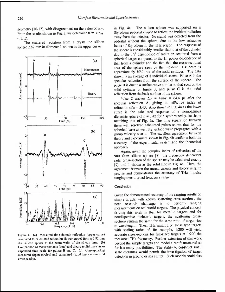
226 Ultrafast Electronics and Optoelectronics
geometry [10-12], with disagreement on the value of neff. From the results shown in Fig. 3, we determine 0.95 < neff
< 1.12. The scattered radiation from a crystalline silicon
sphere 2.82 mm in diameter is shown as the upper curve
200
0.5 0.6 Frequency (THz)
Figure 4. (a) Measured time domain reflection (upper curve) compared to calculated reflection (lower curve) from a 2.82 mm dia. silicon sphere at the beam waist of the silicon lens, (b) Comparison of measurements (dots) and theory (solid line) on an expanded time scale for pulses B anc C. (c) Corresponding measured (open circles) and calculated (solid line) normalized cross section.
in Fig. 4a. The silicon sphere was supported on a Styrofoam pedestal shaped to reflect the incident radiation away from the detector. No signal was detected from the pedestal without the sphere, due to the low refractive index of Styrofoam in the THz region. The response of the sphere is considerably smaller than that of the cylinder due to the 1/r2 dependence of radiation scattered from a spherical target compared to the 1/r power dependence of that from a cylinder and the fact that the cross-sectional area of the sphere seen by the incident THz beam is approximately 10% that of the solid cylinder. The data shown is an average of 8 individual scans. Pulse A is the specular reflection from the surface of the sphere. The pulse B is due to a surface wave similar to that seen on the solid cylinder of figure 3, and pulse C is the axial reflection from the back surface of the sphere.
Pulse C arrives Atc = 4an/c = 64.4 ps after the specular reflection A, giving an effective index of refraction of n = 3.43. Also shown in Fig. 4a as the lower curve is the calculated response of a homogenous dielectric sphere of n = 3.42 for a synthesized pulse shape matching that of Fig. 2a. The time separation between these well resolved calculated pulses shows that for the spherical case as well the surface wave propagates with a group velocity near c. The excellent agreement between theoiy and experiment shown in Fig. 4b confirms both the accuracy of the experimental system and the theoretical approach.
Again, given the complex index of refraction of the 900 Hem silicon sphere [8], the frequency dependent radar cross-section of the sphere may be calculated exactly [9], and is shown, as the solid line in Fig. 4c. Here, the agreement between the measurements and theory is quite precise and demonstrates the accuracy of THz impulse ranging over a broad frequency range.
Conclusion
Given the demonstrated accuracy of the ranging results on simple targets with known scattering cross-sections, the next research challenge is to perform ranging measurements on real world targets. The physical concept driving this work is that for metallic targets and for nondispersive dielectric targets, the scattering cross- sections remain the same for the same ratio of target size to wavelength. Thus, THz ranging on these type targets with scaling ratios of, for example, 1:200 will yield accurate cross-sections for full-sized targets at 1/200 the measured THz frequency. Further extension of this work beyond the simple targets and model aircraft measured so far has many possibilities. The ability to construct small scale dioramas would permit the investigation of target detection in ground or sea clutter. Such models could also
Ultrafast Electronics and Optoelectronics 227
be used to test techniques for locating underground or hidden targets provided the dielectric properties of soil in the frequency range of interest could be reproduced.
Acknowledgments
This work was supported in part by the National Science Foundation and the Army Research Office.
References
1. L. Carinin Ultra-Wideband, Short-Pulse Electromagnetics, pp. 37-49, H. Bertoni, ed., (Plenum, New York, 1993).
2. E. Rothwell, D.P. Nyquist, K-M Chen, and B. Drachman, "Radar target discrimination using the extinction pulse technique," IEEE Trans. Ant. Prop., Vol. AP-33, pp. 929-936, 1985.
3. Y.H. Mao in Advanced Radar Techniques and Systems, ch.9, G. Galati, ed., (Peregrinus, London, 1993).
4. D.E. Iverson, "Coherent processing of ultra-wideband radar signals," IEEE Proc. Radar, Sonar Navig., Vol.141, pp. 171-179,1994.
5. E.K. Miller and J.A. Landt, "Direct time-domain techniques for transient radiation and scattering from wires," Proc. IEEE, Vol.68, pp. 1396-1423, 1980.
6. RA. Cheville and D. Grischkowsky, "Time domain THz impulse ranging studies," Appl. Phys. Lett., Vol. 67, pp. 1960-1962, 1995.
7. M. van Exter and D. Grischkowsky, "Characteriza- tion of an optoelectronic TeraHz beam system," IEEE Trans, on Microwave Theory and Tech., Vol. MTT-3 8, pp. 1684-1691,1990.
8. D. Grischkowsky, S. Keiding, M. van Exter, and Ch. Fattinger, "Far-infrared time-domain spectroscopy with terahertz beams of dielectrics and semicon- ductors," J. Opt. Soc. Am. B. Vol.7, pp. 2006-2015, 1990.
9. D. E. Barrick in Radar Cross Section Handbook, vol. 1, G. T. Ruck Ed., (Plenum Press, New York, 1970).
10. J. Rheinstein, "Backscatter from spheres: a short pulse view," IEEE Trans. Ant. Prop., Vol. AP-16, pp. 89-97, 1968.
H.H. Inada, "Backscattered short pulse response of surface waves from dielectric spheres," Appl Opt., Vol. 13, pp. 1928-1933, 1974.
12. M. S. Aly and T. T. Y. Wong, "Scattering of a tran- sient electromagnetic wave by a dielectric sphere," IEE Proc. pt. H, Vol. 138, pp. 192-198, 1991.
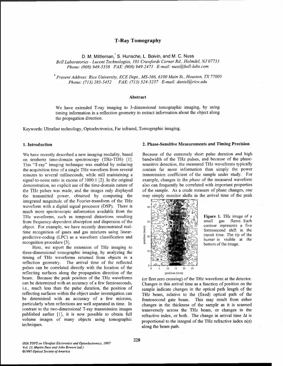
T-Ray Tomography
D. M. Mittleman, S. Hunsche, L. Boivin, and M. C. Nuss Bell Laboratories - Lucent Technologies, 101 Crawfords Corner Rd., Holmdel, NJ 07733
Phone: (908) 949-5358 FAX: (908) 949-2473 E-mail: [email protected]
' Present Address: Rice University, ECEDept., MS-366, 6100 Main St., Houston, TX 77005 Phone: (713) 285-5452 FAX: (713) 524-5237 E-mail: [email protected]
Abstract
We have extended T-ray imaging to 3-dimensional tomographic imaging, by using timing information in a reflection geometry to extract information about the object along the propagation direction.
Keywords: Ultrafast technology, Optoelectronics, Far infrared, Tomographic imaging.
1. Introduction
We have recently described a new imaging modality, based on terahertz time-domain spectroscopy (THz-TDS) [1]. This "T-ray" imaging technique was enabled by reducing the acquisition time of a single THz waveform from several minutes to several milliseconds, while still maintaining a signal-to-noise ratio in excess of 1000:1 [2]. In the original demonstration, no explicit use of the time-domain nature of the THz pulses was made, and the images only displayed the transmitted power, obtained by computing the integrated magnitude of the Fourier-transform of the THz waveform with a digital signal processor (DSP). There is much more spectroscopic information available from the THz waveforms, such as temporal distortions resulting from frequency-dependent absorption and dispersion of the object. For example, we have recently demonstrated real- time recognition of gases and gas mixtures using linear- predictive-coding (LPC) as a waveform classification and recognition procedure [3].
Here, we report the extension of THz imaging to three-dimensional tomographic imaging, by analyzing the timing of THz waveforms returned from objects in a reflection geometry. The arrival time of the reflected pulses can be correlated directly with the location of the reflecting surfaces along the propagation direction of the beam. Because the peak position of the THz waveforms can be determined with an accuracy of a few femtoseconds, i.e., much less than the pulse duration, the position of reflecting surfaces within the object under investigation can be determined with an accuracy of a few microns, particularly when reflections are well separated in time. In contrast to the two-dimensional T-ray transmission images published earlier [1], it is now possible to obtain full volume images of many objects using tomographic techniques.
2. Phase-Sensitive Measurements and Timing Precision
Because of the extremely short pulse duration and high bandwidth of the THz pulses, and because of the phase- sensitive detection, the measured THz waveforms typically contain far more information than simply the power transmission coefficient of the sample under study. For example, changes in the phase of the measured waveform also can frequently be correlated with important properties of the sample. As a crude measure of phase changes, one may simply monitor shifts in the arrival time of the peak
Figure 1. THz image of a small gas flame. Each contour represents a five femtosecond shift in the transit time. The tip of the burner is visible at the bottom of the image.
5 10 15 20
position (mm)
(or first zero crossing) of the THz waveform at the detector. Changes in this arrival time as a function of position on the sample indicate changes in the optical path length of the THz beam, relative to the (fixed) optical path of the femtosecond gate beam. This may result from either changes in the thickness of the sample as it is scanned transversely across the THz beam, or changes in the refractive index, or both. The change in arrival time At is proportional to the integral of the THz refractive index n(z) along the beam path.
OSA TOPS on Ultrafast Electronics and Optoelectronics, 1997 Vol. 13. Martin Nuss and John Bowers (ed.) ©1997 Optical Society of America
228
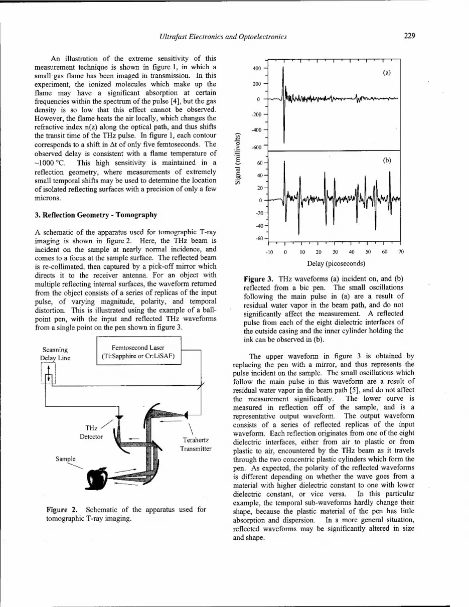
Ultrafast Electronics and Optoelectronics 229
An illustration of the extreme sensitivity of this measurement technique is shown in figure 1, in which a small gas flame has been imaged in transmission. In this experiment, the ionized molecules which make up the flame may have a significant absorption at certain frequencies within the spectrum of the pulse [4], but the gas density is so low that this effect cannot be observed. However, the flame heats the air locally, which changes the refractive index n(z) along the optical path, and thus shifts the transit time of the THz pulse. In figure 1, each contour corresponds to a shift in At of only five femtoseconds. The observed delay is consistent with a flame temperature of -1000 °C. This high sensitivity is maintained in a reflection geometry, where measurements of extremely small temporal shifts may be used to determine the location of isolated reflecting surfaces with a precision of only a few microns.
3. Reflection Geometry - Tomography
A schematic of the apparatus used for tomographic T-ray imaging is shown in figure 2. Here, the THz beam is incident on the sample at nearly normal incidence, and comes to a focus at the sample surface. The reflected beam is re-collimated, then captured by a pick-off mirror which directs it to the receiver antenna. For an object with multiple reflecting internal surfaces, the waveform returned from the object consists of a series of replicas of the input pulse, of varying magnitude, polarity, and temporal distortion. This is illustrated using the example of a ball- point pen, with the input and reflected THz waveforms from a single point on the pen shown in figure 3.
Scanning Delay Line
Femtosecond Laser (Ti:Sapphire or CnLiSAF)
Terahertz Transmitter
Figure 2. Schematic of the apparatus used for tomographic T-ray imaging.
400 -
200 -
0
-200-
-i 1 1—| 1—|—i 1 1 1 1—|—i 1—i—
(a)
-400 -
-600
c 60
1—r 10 o
T-
10 20 30 40 50
I— 60 70
Delay (picoseconds)
Figure 3. THz waveforms (a) incident on, and (b) reflected from a bic pen. The small oscillations following the main pulse in (a) are a result of residual water vapor in the beam path, and do not significantly affect the measurement. A reflected pulse from each of the eight dielectric interfaces of the outside casing and the inner cylinder holding the ink can be observed in (b).
The upper waveform in figure 3 is obtained by replacing the pen with a mirror, and thus represents the pulse incident on the sample. The small oscillations which follow the main pulse in this waveform are a result of residual water vapor in the beam path [5], and do not affect the measurement significantly. The lower curve is measured in reflection off of the sample, and is a representative output waveform. The output waveform consists of a series of reflected replicas of the input waveform. Each reflection originates from one of the eight dielectric interfaces, either from air to plastic or from plastic to air, encountered by the THz beam as it travels through the two concentric plastic cylinders which form the pen. As expected, the polarity of the reflected waveforms is different depending on whether the wave goes from a material with higher dielectric constant to one with lower dielectric constant, or vice versa. In this particular example, the temporal sub-waveforms hardly change their shape, because the plastic material of the pen has little absorption and dispersion. In a more general situation, reflected waveforms may be significantly altered in size and shape.
230 Ultrafast Electronics and Optoelectronics
Figure 4 shows a tomographic cross-section of the pen, obtained by evaluating waveforms such as the one in Fig. 3b for points along the length of the ball-point pen. Only very rudimentary signal processing was performed in this example, including the squaring of each waveform and conversion of the result to a grayscale. In figure 4, the vertical axis is parallel to the long (cylinder) axis of the pen, while the horizontal axis corresponds to depth inside the pen. Each interface clearly shows up as a dark stripe.
3-
c o
o
n ,
4 6
Depth (mm)
T 10
Figure 4. THz tomographic image of a bic pen. The vertical axis of the figure is parallel to the long (cylinder) axis of the pen, while the horizontal axis of the figure corresponds to depth into the pen. The THz pulse is incident from the left. The eight dark bands correspond to the eight dielectric interfaces (either from plastic to air or air to plastic) encountered by the pulse.
Through more sophisticated signal processing, much more information can be extracted from these waveforms. That this information is present is illustrated in a rudimentary way in this example; from simply noticing the alternating polarity of the eight reflected sub-pulses in figure 3b, one can immediately determine the sign of the refractive index change at each interface. Incidently, one can also note in figure 4 that the rear plastic walls in the upper portion of the figure are not visible; this results from the shadow cast by the ink, an excellent absorber of THz radiation, inside the inner cylinder.
The utility of advanced signal processing is illustrated in figure 5, which uses the example of a 3.5-inch floppy disk. As in figure 3, the upper waveform (fig. 5a) is the input waveform, measured by replacing the sample with a mirror. The middle waveform (fig. 5b) is reflected from a point near the edge of the floppy disk. As in the case of the bic pen, this waveform consists of a series of replicas of the input waveform. The four reflections from the front and back plastic covers are clearly resolved. However, the thickness of the magnetic recording material is so small that
the waveforms returned from its front and back surfaces cannot be distinguished, and appear as a single distorted waveform. Figure 5c shows the waveform of figure 5b, after numerical processing of the input waveform. This involves a filtered Fourier deconvolution of the instrument response (figure 5a), followed by a wavelet filtering to remove noise. This procedure produces a sharp spike at a time delay corresponding to the position of every reflecting interface. Thus, it helps to determine more accurately the positions of the various interfaces. In contrast to figure 5b, the front and back surfaces of the thin (-120 jam) magnetic recording material are clearly resolved in the deconvolved data. This is consistent with the expected resolution of Lc/2, where Lc = 200 |J.m is the coherence length of the THz pulse in the intervening material. In contrast, when no other reflections are nearby, we find that the position of a reflecting surface can be determined with a precision of only a few microns, as discussed in section 2 above.
60-
40-
20- 6 CO O a a a
"2 -20
& -40
< -60
-
. (a) Input 1 /^V~
/ " (b) Reflected (x4 11
floppy
|| front cover
(c) Processed (1
back cover
: 1 —.—i—i—i—i—r-
1 1 1 1 '
10 20 Delay (psec)
30
Figure 5. THz waveforms incident on (a), and reflected from (b), a 3.5" floppy disk. The two surfaces of the front and rear covers are visible, as are the reflections from the thin magnetic recording material. Curve (c) (in arbitrary units) represents the reflected waveform after signal processing. Curve (b) has been scaled up by a factor of four, and the three curves have been offset for clarity.
Figure 6 shows the conventional T-ray image of a section of the floppy disk obtained in reflection (a), and a tomographic slice (b) at a fixed vertical position. The conventional T-ray image at the top is obtained by computing the total reflected power using real-time processing of the reflected waveforms with a DSP [1,2], with the reflected power translated into a gray scale. The plastic cover with its various features, the circular recording disk, as well as the metallic hub in the center of the disk can be distinguished.
In figure 6b, a tomographic T-ray "slice" of the floppy disk is shown at a particular vertical position (y = 20 mm),
Ultrafast Electronics and Optoelectronics 231
indicated by the dashed line in figure 6a. The amplitude of the reflected T-Ray waveforms for each horizontal (x) position is displayed as a function of delay in this tomographic image. The reflected waveforms are processed in similar fashion to the data of figure 5c, and the amplitude of the resulting waveform is translated into a gray scale. The vertical axis of figure 6b (optical depth) is proportional to the time delay of the waveform. Converting this axis to physical depth requires knowledge of the sample's refractive index profile, which can be obtained from the amplitudes of the reflected pulses, as described below.
SZ
o. d) ■o "to u Q. o back cover
0 10 20 30 40 50 60
x position (mm)
Figure 6. (a) THz reflection image of a floppy disk, in which the metallic hub is visible, (b) Tomographic image generated along the dashed line in (a). The vertical axis corresponds to depth into the object.
The position of the surfaces within the sample can be observed clearly in this tomographic picture, such as the front and back cover, the magnetic recording disk, and the metallic hub of the disk (as indicated). The picture also shows some artifacts of the technique resulting from multiple reflections between the various interfaces, such as the features observed behind the (opaque) hub of the disk.
4. Signal Processing - Determining Depth and Index
Signal processing of the THz waveforms may be used to extract the layer structure of the medium at any given (x,y) position. The reflected waveform B(t) is related to the input waveform A(t) by a convolution with the impulse response g(t) of the layered medium:
M B,= I&-* A*. (1)
k = 0 In this expression, discrete-time functions are used, defined by digitization with a time step At (e.g., Bk = &{k ■ At)). M is the number of samples in the digitized waveforms, 1024 in these examples. The impulse response g(t) is characteristic of the object and does not depend on the details of the input pulse. The coefficient gk is the amplitude of the radiation returning from the object in the kth time slot. It is determined by the reflection off of the kx
layer as well as the transmission through the preceding layers,./ = 1,..., k- 1, once in each direction. The distance d, between two adjacent layers j and j + 1 is related to the time separation of the two corresponding reflections At = t;+/ -t,- by:
c 4 = 2 At. (2)
where n, is the refractive index of the medium between surfaces j and j+\. Therefore, the temporal position of each reflected pulse is related to the position of the reflecting interface along the propagation direction.
An approximation for the impulse response function g(t) is obtained from a numerical deconvolution of the measured waveforms A(t) and B(t), such as shown in figure 5c. This deconvolution procedure was also used to generate the tomographic image in figure 6b. In principle, given g(t), the refractive index profile of the layered structure can be reconstructed. The discontinuity in the structure of the diskette at x ~ 12 mm in figure 6b is an example of a situation where such reconstruction is required. This discontinuity arises from a change in the thickness of the front plastic cover at this x-position, which produces a shift in the delay of the pulses reflected from all of the surfaces behind it.
The response function g(t) can be used to determine the refractive index steps at each of the reflecting interfaces, and thus the depth of each of these surfaces. In discretized form, the/h time step corresponds to a layer of thickness dy given by equation (2), and of refractive index n, given by:
j i _ r. *,= riTT^, (3)
«=7 ' where the reflection coefficients vk are defined iteratively in terms of gk and the previous reflections, by the relation:
k-\ ■gk' n
7=1
1
O-r/)' (4)
Here r, = g,, and, by definition, the initial reference plane has n0 = 1. These expressions are valid in the limit of small reflection coefficients, when multiple reflections are negligible. Also, absorption and dispersion are neglected.
When this algorithm is applied to the processed data of figure 5c, the derived refractive index profile is a good

232 Ultrafast Electronics and Optoelectronics
(although not ideal) approximation to the actual profile of the sample. This result is shown in figure 7. The refractive indices of the materials are in reasonable agreement with measured values and the temporal positions are correct, but the overall background value rises with increasing delay. This effect, in which the index does not return to n = 1 after the sample, is a cumulative result of the various approximations made in the derivation of equations (3) and (4). A more sophisticated analysis will be required to overcome these difficulties.
•3 1.6-
Delay (psec)
Figure 7 (a) impulse response function from figure 5 c (in arbitrary units) (b) refractive index profile derived from this function
5. Discussion
An interesting feature of tomographic imaging is the speed at which such images can be acquired. T-ray transmission imaging requires currently about 10 milliseconds per pixel. In figures 4 and 6, for example, each row of pixels is extracted from a single reflected waveform. For example, the tomographic image in figure 6 consists of 217 waveforms and took roughly 10 seconds to acquire, with each waveform recorded in 50 ms. For relatively thin samples (~l-2 cm), it is possible to build a full three- dimensional representation of the object just as rapidly as a two-dimensional image, because all of the information about the third dimension (the depth) at each pixel is contained in a single time-domain waveform. The limitations on the thickness of the sample arise because of the scanning optical delay line, which has a maximum amplitude of a few centimeters, and because of the optics used to focus the THz beam.
Tomographic T-ray imaging is similar in principle to ultrasonic imaging [6]. A commonly encountered problem in ultrasonic imaging is the large difference in acoustic impedance between air and liquid or solid objects, which necessitates some form of index matching. For terahertz waves, the dielectric constants of many dielectrics are not too different from that of air, and index matching is not required for T-ray tomography. Many materials such as plastics, cardboard, wood and rubber have good transparency in the terahertz frequency range. Hence, this new technology can be effectively used in many quality control applications, for example to detect voids or cracks.
Other millimeter-wave imaging techniques have been proposed for such applications [7], but these have typically involved narrowband sources, and are thus not amenable to tomographic analysis.
Another application area for T-ray tomography is burn diagnostics. While the strong water absorption precludes the use of THz radiation in biomedical research inside the body, it may be possible to obtain quantitative and highly sensitive measurements of burn depth and burned tissue properties using THz tomography in dermatological medicine [2].
6. Conclusion
In conclusion, the recent work on imaging with terahertz waves has been expanded to include imaging in a reflection geometry. In the reflection geometry, timing information is correlated to depth information, and tomographic slices of objects can be obtained, with the possibility of three- dimensional T-ray tomography on a wide range of samples. In T-ray tomographic imaging, one can isolate in the time domain successive reflections, and extract information about each layer of a layered material individually. In this fashion, detailed spectroscopic information can be obtained about sub-surface layers, with the potential for material identification. The range of potential applications for T-ray tomography is extremely broad, encompassing such wide- ranging fields as biomedical imaging, package inspection, and quality control.
References
[1] B. B. Hu and M. C. Nuss, "Imaging with terahertz waves," Opt. Lett., 20, 1716 (1995).
[2] D. M. Mittleman, R. H. Jacobsen, and M. C. Nuss, "T- Ray Imaging," IEEE J. Sei. Top. Quant. Elec, special issue on Ultrafast Electronics, Photonics, and Optoelectronics, eds. X.-C. Zhang, B. Kölner, and K. Leo, accepted for publication, 1997.
[3] R. H. Jacobsen, D. M. Mittleman, and M. C. Nuss, "Chemical recognition of gases and gas mixtures using terahertz waveforms," Opt. Lett, 21, 2011 (1996).
[4] R. A. Cheville and D. Grischkowsky, "Far infrared terahertz time-domain spectroscopy of flames," Opt. Lett., 20, 15, 1646(1995).
[5] M. van Exter, C. Fattinger, and D. Grischkowsky, "Terahertz time-domain spectroscopy of water vapor," Opt. Lett., 14, 1128(1989).
[6] A. C. Kak, and M. Slaney, in Principles of Computerized Tomographic Imaging, p. 298 ff., IEEE Press, New York (1988).
[7] S. Bakhtiari, N. Gopalsami, and A. C. Raptis, "Characterization of delamination and disbonding in stratified dielectric composites by millimeter wave imaging," Mater. Eval, 53, 468 (1995).

Near-Field THz Imaging
S. Hunsche, M. Koch(1), I. Brener(2), and M. C. Nuss
Bell Laboratories - Lucent Technologies, 101 Crawfords Corner Rd, Holmdel, NJ 07733 Phone: (908) 949-5358 FAX: (908) 949-2473 E-mail: [email protected]
(I> present address: Sektion Physik, Ludwig-Maximilians Universität, 80799 München, Germany (2) Bell Laboratories, Lucent Technologies, 600 Mountain Ave, Murray Hill, NJ 07974
Abstract
We present first results of near-field imaging with ultrashort far-infrared pulses. By focusing the radiation through a tapered metal tip with a small exit aperture and scanning a sample in the near field of this aperture, sub-wavelength spatial resolution is demonstrated.
Keywords: Ultrafast technology, Optoelectronics, Far infrared, Near-field imaging.
Time-domain Terahertz spectroscopy (THz-TDS), which is based on optoelectronic generation and detection of sub- picosecond electrical transients in photoconducting antennas, has proven to be an extremely valuable and sensitive tool for spectroscopic investigations of various kinds of materials in the far-infrared spectral regional] Recently, we have extended THz-TDS to real-time "T-ray" imaging by reducing the acquisition and processing time of THz waveforms by 4 orders of magnitude.[2] With this new technique, two-dimensional chemical mapping of biological samples and non-contact characterization of semiconductor wafers have been demonstrated. [3]
Due to the long wavelength of the THz radiation, the spatial resolution of this essentially diffraction-limited imaging system is several hundred micrometers and frequency dependent over the large bandwidth of the THz pulses. Sub-wavelength spatial resolution with visible light has been demonstrated by passing radiation through a small aperture and scanning a sample within the near field of this aperture, i.e., within a distance smaller than a wavelength. [4,5] In that case, the spatial resolution is determined by the geometry of the aperture rather than the wavelength of the radiation. This method can also be applied with far infrared THz radiation to create high-resolution "T-ray" images
For a first demonstration of THz near-field imaging, we insert a small aperture in the focus of the imaging system described in Ref. 2. A schematic view of the experimental set-up is given in figure 1. In order to improve the transmission through the aperture, we use a tapered metal tube, analogous to the tapered fibers used in near-field scanning optical microscopes [5]. This tube is formed by electro-plating a small conical aluminum tip
with a Cr/Ni alloy. After removal of the aluminum cone and polishing of the Cr/Ni tip small, almost circular apertures of A^ < 100 urn - corresponding to X/3 for a typical T-ray frequency of 1 THz - can be easily obtained. The smallest aperture used in our experiments was slightly elliptical with a smaller diameter of 50 (am. Focusing of the radiation created in the GaAs photoconducting THz emitter into the 2 mm wide opening of the metal tip and collection and refocusing of the transmitted radiation onto the optically gated receiver antenna is achieved with off-axis paraboloid mirrors.
^ cdimaSng Sfbousshg
' optics .
gaJngpilseV-'-»-, . \ y ^ substräe •■"*
photccordudiw "I>te emitter
X *ki ■At
tmeOBla>ed gating pdse
photoconduclhs dpde antenna (TVizrecaver)
current arrpffier, digtalsignal processing
Figure 1: Experimental set-up
Figure 2a shows THz time-domain data of pulses propagated through free space, i.e. the standard imaging set-up without aperture, and pulses transmitted through the tapered metal tip with the smallest aperture. The corresponding Fourier spectra, normalized to the same maximum value, are shown in Fig. 2b. According to the maximum peak-to-peak" amplitude of the time-resolved data, the amplitude transmission of the aperture is approximately 1/130, however, the spectra indicate that this
OSA TOPS on Ultrafast Electronics and Optoelectronics, 1997 Vol. 13, Martin Nuss and John Bowers (ed.) ©1997 Optical Society of America
233

234 Ultrafast Electronics and Optoelectronics
factor is strongly frequency dependent. Both the larger focal diameter for the low-frequency components and their larger diffraction losses after passing the aperture lead to an effective spectral narrowing and a low-frequency cut-off at approximately 0.4 THz. Nevertheless there is significant signal amplitude for frequencies above 0.5 THz, corresponding to a wavelength of 12x dtip. We also note that the cutoff is less sharp and at a much lower frequency than for a long waveguide with comparable diameter.[6] The spectral high-pass filtering of the signal also accounts for the changes of the THz waveform from a well-defined single-cycle pulse towards a more oscillating structure. In addition, both waveforms are slightly modulated due to residual water vapor absorption in the beam path.
transmitted field
incident field
transmitted field incident field
Figure2: a) THz waveforms before and after transmission through the near-field aperture, b) Normalized Fourier spectra of the data shown in a).
To investigate the imaging properties of the near-field tip we scan a test sample, consisting of the two gold contact pads (0.5x0.5 mm2, 10 p.m separation, connected to 5 urn
striplines) of a THz antenna structure on a 2 mm wide silicon-on-sapphire substrate, across a 100 (im diameter aperture. The sample and the near field tip are almost in mechanical contact, with an estimated separation less than 100 urn. Figure 3 compares the near-field image (a) with an image obtained using the standard set-up (b). The shape of the gold structure is indicated by the white lines drawn on top of the measured data. Since the maximum transmission through the tip was obtained with the aperture exactly in the focal plane of the standard set-up, the only difference between the two measurements is the removal of the tip in (b). Both images were obtained by integrating the Fourier spectrum of the THz waveforms over a frequency range 0.6-1.8 THz. Obviously, the use of the near-field aperture leads to a dramatic improvement of the spatial resolution: while the standard imaging system is not capable of rendering the correct shape of the sample structure, the edges of the contact pads are clearly resolved in the near- field image.
0.5 1 1.5 x (mm)
Figure 3: Near-field (a) and diffraction-limited standard (b) T-ray image of two quadratic gold pads.
It should be noted that the modification of the THz spectrum by the aperture results in a slightly higher average frequency for the near-field experiment (1.16 THz, as

Ultrafast Electronics and Optoelectronics 235
compared to 0.92 THz). However, this small difference can clearly not account for the observed improvement of the spatial resolution. To prove this, we also scanned a razor blade across the near-field tip and through the focus of the imaging set-up. The corresponding data are shown in Fig. 4.
Figure 5a shows a near-field image of the central part (group 2 and 3) of the test pattern obtained with the smallest aperture and by scanning the sample in mechanical contact with the near-field tip. For comparison, a diffraction-limited standard image of the same sample area is shown in Fig. 5b.
1.5
-2- T3 3
1.0
0.5
0.0
/ -4~: ;- A= 140 |jm
■ ~> Vi i
- standard imaging 0.75-lOTHz -- 1.5-2.0 THz with near-field tip 1.1-2.0 THz
t\
- i . 1 : , . ._, , 1 i__. , , J
-1.0 -0.5 0.0
Position (mm) 0.5 1.0
Figure 4: THz line-scans over a razor blade.
Although the standard imaging data are quite strongly modulated by diffraction effects, they clearly show an increasing sharpness of the intensity drop around x=0 with increasing frequency. As a result of the diffraction limited focal spot size, the spatial resolution is better for higher frequency within the bandwidth of the THz pulses. For the high frequency range in the free-space measurement (dotted curve), the average frequency is 1.7 THz, while it is 1.4 THz in case of the curve taken with the tip. In spite of the lower average frequency, the near-field tip results in a much sharper edge resolution, namely 140 urn, as estimated from the distance between the 90% and the 10% of maximum signal level. Since this value is approximately the diameter of the tip aperture, we conclude that the improved resolution is indeed a near-field effect. This is further substantiated by the fact that we do not find a variation of this value with frequency.
However, the sharpness of an isolated edge does not necessarily agree with the true spatial resolution achieved in near-field image. [5] For a quantitative investigation of the spatial image resolution, we therefore produced a USAF 1951 resolution test target on high-resistivity silicon, which is almost completely transparent to the THz radiation. The lines of different width and separation are formed by a 250 nm thick evaporated titanium/gold layer after photo- lithographically copying a commercially available chromium/glass test target onto a piece of silicon wafer.
1 2 3
x (mm)
Figure 5: Near-field (a) and diffraction-limited (b) T-ray image of a resolution test pattern.
The THz amplitude was integrated over a frequency range of 0.6-2.3 THz in the near-field image and 1.4-2.3 THz in the standard image, corresponding to average wavelengths of 220 urn and 180 urn, respectively. The smallest resolvable feature in the near-field image are the vertical lines of group 3, element 3, which have a line width and separation of 50 urn.
300 d=400pm
d = 300 |jm •'wy-- t. '■■' ■' *
3 ro 200
d = 200|jm'' "V " ■'
' ,'- V -■>, ■ . ■ V \7Tr-- c
100
n
d = 100 pm" __ '■'
',' V V *'
§ if # fir linewidth: 140 157
i . . . i
177 198
i
223
1
250 |jm
10 12 4 6 8
x(mm)
Figure 6: THz line-scans over group 1 of the resolution target for various tip-sample separations. The curves are offset for clarity.

236 Ultrafast Electronics and Optoelectronics
This agrees exactly with the smaller diameter of the elliptical aperture used, i.e. the data are in excellent agreement with the anticipated spatial resolution. The lower resolution for the horizontal lines can probably be attributed to the ellipticity of the aperture and to the continuous movement of the dc motor used for scanning the sample along the y-direction.
A characteristic feature of near-field imaging techni- ques is the strong dependence of the spatial resolution on the distance between sample and the near-field source. Figure 6 demonstrates that this is indeed the case for the technique used here. It shows one-dimensional scans over group 1 of the resolution pattern at different sample-tip separations d, where d=0 corresponds to mechanical contact of sample and near-field tip. The widths/separations of the target lines are indicated in the figure. While the spatial resolution at zero distance is essentially given by the dimensions of the near-field source, the data in Fig. 6 indicate that the resolution at nonzero separation decreases approximately proportional with increasing distance.
In conclusion, we present a first demonstration of near-field imaging with broadband ultrashort THz pulses. We use a tapered metal tip with sub-wavelength exit aperture to confine the THz radiation and demonstrate far- infrared imaging with a spatial resolution that is given by the dimension of the aperture.
We gratefully acknowledge useful discussions with J. Stark as well as contributions by D. Mittleman, R. Jacobsen, and
F. Beisser. SH acknowledges funding by the Alexander von Humboldt foundation.
References
[1] D. Grischkowsky, "An Ultrafast Optoelectronic THz Beam System", Optics & Photonics News 3, 21 (1992); M. C. Nuss and J. Orenstein, "Terahertz Time-Domain Spectroscopy", in Millimeter-Wave Spectroscopy of Solids, G. Gruener ed. (Springer, Berlin, 1997)
[2] B. B. Hu and M. C. Nuss, "Imaging with terahertz waves", Opt. Lett, 20, 1716 (1995)
[3] D. M. Mittleman, R. H. Jacobsen, and M. C. Nuss, "T- Ray Imaging", IEEE J. Selected Topics in Quant. Elec, in press (1997).
[4] D. W. Pohl, "Scanning Near-Field Optical Microscopy", Advances in Optical and Electron Microscopy, (Academic Press, 1991)
[5] E. Betzig and J. K. Trautman, Science, 257, 189 (1992)
[6] F. Keilmann, "FIR Microscopy", Infrared Phys. Technol, 36,217(1995)
Singular Electric Field Terahertz Emitters and Detectors.
Y. Cai(1), I. Brener (2> , J. Lopata(2), J. Wynn<2), L. Pfeiffer(2>, and J. Federici (3)
(1> Department of Electrical and Computer Engineering, New Jersey Institute of Technology, 161 Warren Street, Newark, New Jersey 07102
<2> Bell Laboratories, Lucent Technologies, 700 Mountain Avenue, New Jersey 07974. phone: (908)582-4365, fax: (908) 582-4702, e-mail: [email protected]
<3> Department of Physics, New Jersey Institute of Technology, 161 Warren Street, Newark, New Jersey 07102
We present a new family of more efficient terahertz (THz) radiation emitters and detectors enhanced by electric field singularities near sharp electrode features. The structures are fabricated on low temperature GaAs and with small dipole gaps (<10|im). The THz emission is maximal when fringing fields are enhanced by laterally offset sharp electrodes. We also find that the asymmetric THz emission near the anode gradually disappears as the dipole gap shrinks. The THz polarization properties of these new emitters will also be discussed.
Keywords: Ultrafast Technology, Far Infrared, Optoelectronics.
Free-space single-cycle terahertz electromagnetic waves are generated when a short laser pulse excites a semiconductor. Two phenomena are usually responsible for this generation: optical rectification and carrier acceleration under the influence of an electric field. This field can be either intrinsic (i.e. surface depletion field) or extrinsic as in biased structures. We have recently shown that when electric fields in biased semiconductors are enhanced by geometric effects, the THz generation is significantly enhanced. [1] In this work we will describe our ongoing efforts in enhancing the performance of THz emitters by using new electrode structures and smaller gaps.
Q n lAJ^anrLRAnirir
Cr n_J FF FTM TTH TT45
Fig.l: Schematic diagram of the metal electrodes used in the new THz emitters and detectors.
Two dimensional electrostatic calculations are carried out prior to the fabrication. Although this oversimplifies the problem, we use these simulations as a starting point in our design. Invariably, the strongest fringing electric fields are found near the triangular tips (i.e. structure
TTM and TTO in Fig. 1). The sharpness of the electrodes determines the peak value of the singular electric field. Moreover, the fringing fields are enhanced when laterally offset electrodes are used (i.e. structure TTO in Fig. 1). The offset angle provides additional control in maximizing the overlap of high electric field regions with the laser excitation spot.
The photoconducting antennas are fabricated by conventional lithography on low-temperature GaAs grown at ~250°C, and later annealed at 600°C for one minute. The metal patterns are deposited using one of the usual schemes for ohmic contacts on n-type GaAs. Fig. 1 shows a schematic diagram of the metal electrodes deposited on the structures we have studied. We define the dipole length d as the separation between the parallel striplines and vary both d and the gap distance g.
We measure the THz emission intensity of such structures by using a standard coherent THz detection system with scanning capabilities on the emitter side with submicron resolution.[1] A short pulse (780nm, 130 fs) from a mode-locked Ti-sapphire laser excites the sample through a microscope objective. The generated THz radiation is then collected with a pair of off-axis paraboloids and focused on a THz dipole antenna fabricated on LT-GaAs. This antenna is excited by another short laser
OSA TOPS on Ultrafast Electronics and Optoelectronics. 1997 Vol. 13, Martin Nuss and John Bowers (ed.) ©1997 Optical Society of America
237

238 Ultrafast Electronics and Optoelectronics
pulse derived from the same Ti-sapphire laser. The emitter is then scanned two dimensionally with a 0.4p.m spatial resolution and the THz waveforms for each coordinate are recorded by scanning the delay of the beam exciting the antenna.
FTL TTO TT45 TTM Structure
1.0 -
-" 0.8 .a -5- & 0.6 v> c a)
■^ 0.4 N X
0.2
1 1 •
1 d=45 um; TTO
■ d=45 um; FTM A d=60 urn; TTO"
\ •• ♦ d=60 urn; FTM. V *, ■ • -
\ (b)
I i ■ 10 30 40 20
Gap um
Fig. 2: (a) Measured THz signal in a 60um dipole, 5u.m gap; see Fig. 1 for reference; (b) THz intensity as a function of dipole length and gap.
Fig. 2(a) shows the measured peak THz signal for a fixed bias of 20V for a 60um dipole with a constant gap of 5|im, when exciting a sharp singularity. This is an important point as regular dipoles that were previously used also have areas of singular electric fields. But in order to take advantage of this enhancement, the laser spot has to closely overlap these regions of high fields. Clearly, the sharp triangular electrodes with the largest offset give the highest emission intensity. Due to the high resistance of our samples and the small gaps, we could apply voltages as high as 60V when exciting with several tens of mW of laser power. Because of the offset of the sharp electrodes, this corresponds to electric fields inside the semiconductor higer than 120 kV/cm. The ultrafast dynamics of carriers under such high
electric fields is certainly an important point in the performance of these emitters. Fig. 2(b) shows the THz emission intensity for a a few electrode structures for 2 dipole lengths as a function of the gap distance and for a fixed bias. Clearly, when we decrease the gap we also decrease the electric field; this is consistent with Fig. 2(b) although the slope varies with dipole length. On the other hand, big gap structures show some saturation of the emission intensity with applied bias, therefore, it is advantageous to use a small gap.
It was previously observed by many groups that the process of THz generation in biased structures (with gaps ranging from several tens of |im to a few cm) becomes particularly efficient when excited close to the anode.[1,2,3,5] However, a symmetrical THz emission intensity was reported for very large gap (3cm) structures. [6] The two-dimensional scans of the THz emission in our small gap structures also show an absence of this asymmetry. This is shown in Fig. 3 for several emitters (gaps of 5, 10, 30p,m) where we plot a two-dimensional scan of the peak THz intensity when scanning the emitter and keeping the exciting beam fixed. When the gap is small (5, lOum), the two-dimensional scan of the THz emission is perfectly symmetrical. A gradual transition to the positive electrode effect is observed for gaps larger than 20)J.m. For a 30|im gap, a slight asymmetry is observed. When the gap is very large (90)im), the asymmetry becomes very clear. At this point, the mechanism which causes this varying asymmetry as a function of gap size is unclear. However particular mechanisms may be ruled out based on our results. No significant change in this asymmetry is observed when we chop the electrical bias up to 30MHz. These high frequency bias results preclude the formation of Gunn domains [6] and any static or quasi-static effects. We also found no change in these results when the bias is changed from fractions of a volt to close to 100V. Other groups have reported the "positive electrode effect" in different materials such as SOS [2,7], semi-insulating GaAs [5], low temperature GaAs [1,3], n- and p-doped GaAs [3], and InP [3]. This indicates that the material details may not be responsible for this phenomena. It has been suggested that the trap- enhanced electric fields [5], resulting from the electrical and optical carrier injection, are
Ultrafast Electronics and Optoelectronics 239
responsible for the asymmetric field distribution in a gap of 80pm between two coplanar striplines. The region near the forward biased positive contact experiences an accumulation of electrons and a depletion of holes which is strongly enhanced by electron velocity saturation and geometric effects. The increased electron density results in larger electron occupancy of the deep traps. The current-voltage characteristics measured by the same group [5] also indicates this double injection current transport effect is reduced in smaller gaps (50pm). We found that the critical gap size (20pm~30pm) for the transition from small gap symmetry to large gap asymmetric excitation, is close to the estimated distance (15(xm) through which the injected electrons can drift assuming simple ballistic motion in GaAs (assuming published parameters for LT GaAs). If the injected carriers can drift through the gap towards the other electrode within their lifetime, they may change the field pattern within the whole gap by charge re-distribution and filling of the trap states on both sides. The high repetition rate (100MHz) of the laser pulse prevents these trap states from depopulating before the next pulse arrives. This can not happen in structures with large gaps.
We also measured the dependence of the polarization of the THz radiation as a function of the offset angle and for different gap sizes. Due to the lateral offset of the electrodes, the carrier transport direction will be different in each structure. A grid THz polarizer is inserted in the THz path and aligned with the detector to define the polarization of the detection. Three different structures are studied: a regular coplanar stripline, a conventional dipole and an offset dipole like those described earlier. The stripline emitter gives very well polarized radiation while photoexciting near one of the metal lines. The direction of the polarization is consistent with THz radiation emitted from accelerating carriers towards the other electrode. A conventional dipole shows a small (-7%) orthogonal component. The THz radiation from the offset dipole has a considerable (-25%) orthogonal component as shown in Fig. 4. Therefore, the offset dipole structure not only gives the strongest radiation power in the dipole direction but also in the orthogonal direction. This polarization rotation does not scale up proportionally to the offset angle or the gap size.
This is consistent with the well known current surge model. In the offset dipole structure, the
nb"*-
Y (microns) X (microns)
X (microns) Y (microns)
Y (microns)
X (microns)
(d) WSsiiS»' mr
Y (microns) X (microns)
Fig. 3: Two dimensional scans of the THz emission intensity for several singular electric field offset dipole emitters with gaps of (a) 5, (b) 10, (c) 30, (4) 90pm. The small-gap emitters in (a) and (b) show perfectly symmetrical THz emission. A 30pm

240 Ultrafast Electronics and Optoelectronics
gap (c), shows a slight asymmetry , and the THz emission from large gap emitters (d) is clearly asymmetrical.
Stripline Emitter
114
444
Carrier Flow Polarization
Q ft
Cr
Offset Dipole Emitter
Carrier Flow Polarization
D: ft
Er Fig. 4: The polarization of the THz emission
from stripline and offset dipole emitters is related to the directions of the carriers' flow in the semiconductor. The THz radiation from the offset dipole has a considerable (-25%) orthogonal component.
carriers' flow is tilted. In such offset structure, while the THz wave is generated in the semiconductor, it has components in both polarization directions, but only one direction is enhanced by the dipole formed by the straight electrode lines.
20 40
Time [ps]
60.0
40.0 (b) . < c £. 20.0
■
S 3 o.o
N X -20.0 H r^^^™^
-40.0 ■
-40% improvement over the regular dipole already using its singularity at the edge of the electrode.
We also tested the performance of the singular electric field emitters as detectors. When using the structure TTO in Fig. 1 with a 60um dipole and 5|im gap, the signal intensity is increased by -40% when compared to a conventional dipole, without any appreciable increase in the noise level, as shown in Fig. 5. The frequency response was also comparable.
In conclusion, we studied the performance of a new family of terahertz emitters and detectors based on electric field singularities with small gaps. We demonstrated that the THz emission efficiency can be improved by optimizing the singular electric field experienced by the photo- generated carriers. The highest efficiency is obtained using laterally offset sharp triangular electrodes. The polarization direction of the emitted THz radiation follows the direction of carrier transport rather than the dipole orientation. These THz emitters also work as more efficient THz detectors.
References:
1. I. Brener, D. Dykaar, A. Frommer, L.N. Pfeiffer, J. Lopata, J.Wynn, K.West, and M.C.Nuss, Optics Letters 21, 1924 (1996)
2. D. Krokel, D. Grischkowsky, and M.B. Ketchen, Appl. Phys. Lett. 54, 1046 (1989).
3. U.D. Keil, D.R. Dykaar, IEEE Journal of Quantum Electronics 32, 1664 (1996).
4. S.M. Sze, Semiconductor Devices Physics and Technology (John Wiley & Sons, New York, 1985)
5. E. Ralph, and D. Grischkowsky, Appl. Phys. Lett. 59, 1972 (1991).
6. Budiarto, J. Margolies, S. Jeong, J. Son and J. Bokor, IEEE Journal of Quantum Electronics. 32, 1839 (1996)
7. E. Sano and T. Shibata, Appl. Phys. Lett. 55, 2749 (1989).
Time [ps]
Fig. 5: The THz signal detected using (a) offset dipole singular electric field detector; (b) regular dipole detector. The offset singular detector yields
All-solid-state, THz-radiation source using a saturable Bragg reflector in a mode-locked laser
Zhenlin LIU, Hideyuki OHTAKE, Shinji IZUMIDA, Takaya YAMANAKA, and Nobuhiko SARUKURA, The Institute for Molecular Science (IMS), Myodaiji, Okazaki 444, Japan.
Yusaburo SEGAWA, Photodynamics Research Center, The Institute of Physical and Chemical Research (RIKEN),
Nagamachi Koeji 19-1399, Aoba-ku, Sendai, Miyagi 980, Japan.
Taro ITATANI, Takeyoshi SUGAYA, Tadashi NAKAGAWA, and Yoshinobu SUGIYAMA. Electrotechnical Laboratory (ETL), Umezono 1-1-4, Tukuba, Ibaraki, 305 Japan.
Abstract
We have demonstrated a new scheme for generating intense far-infrared or THz-radiation pulses synchronously with near-infrared pulses using a saturable Bragg reflector placed inside a mode-locked laser cavity. With this newly proposed simple scheme, THz-radiation peaked at around 0.66 THz, with 2-3 nW average power is directly generated synchronously with femtosecond near-infrared optical pulses.
Key Words
All-solid-state, THz-radiation, Saturable Bragg reflector, Intracavity.
The physics and potential applications to ultrafast opt-electronics of THz radiation or far infrared light from various devices excited by ultrashort pulse lasers have been studied intensively. H,2,3J por application to time- resolved spectroscopy in the far infrared region, an intense, compact, simple light source is required. Development of such a far infrared light source will open up possibilities
for entirely new far-infrared spectroscopy of phonons in solids and gaps of superconductors. There was a breakthrough in mode-locking techniques for solid-state lasers some years ago. 1^,5 J Applying the techniques utilizing Kerr-type nonlinearity, most solid-state lasers can be mode-locked down to the femtosecond region. Among these techniques, semiconductor saturable absorbers are attractive for mode locking, because they are inexpensive and compact, and can be designed to operate in a wide spectral range. L°> < J A saturable Bragg reflector (SBR), l^J invented by Tsuda et al, is a nonlinear mirror utilizing a thin-film semiconductor. In this paper, we describe direct generation of THz radiation using an SBR placed inside the cavity of a mode-locked Ti:sapphire laser as the THz-radiation emitter.
An SBR should provide other functions besides that of saturable absorber for mode-locking. The single- quantum well is known to emit THz-radiation, L2J and the quantum well in SBR is located in the field enhanced position in the Bragg reflector structure. Therefore the SBR structure itself has an advantage over the simple quantum well structure for generating THz-radiation. If this SBR was introduced to a mode-locked laser cavity,
OSA TOPS on Ultrafast Electronics and Optoelectronics, 1997 Vol. 13, Martin Nuss and John Bowers (ed.) ©1997 Optical Society of America
241

242 Ultrafast Electronics and Optoelectronics
higher optical peak power inside the cavity will yield higher THz-radiation power. It is attractive to use SBR as THz-radiation intra-cavity emitters for these two reasons.
The SBR for this experiment consists of a dielectric multilayer made of a semiconductor with a single quantum well of 10-nm thickness GaAs inside as invented by Tsuda et al. The dielectric coating exhibits very high reflectivity, and the quantum well produces the nonlinear polarization required to generate THz radiation. Our SBR was grown on a (100)-oriented semi-insulating GaAs substrate by molecular beam epitaxy. After a 500- nm-thick buffer layer was grown on the substrate, a Bragg reflector including a single quantum well was formed. The Bragg reflector consists of 24 pairs of Alo.33Gao.67As/AlAs quarter-wave layers and a top quarter-wave layer of AlGaAs including a single quantum well of 10-nm thickness. The thickness of AlAs layers is 72.6 nm, and that of the AlGaAs layers is 63.2 nm. The Bragg reflector was designed for 820-nm center wavelength at a 0 degree incidence angle. This sample was previously used for 1-GHz mode locking of a Ti:sapphire laser. [8]
600
_ 500 5 .§ 400
300 0) 5 o D.
5 200 a 3 O 100
Without SBR
_ SBR in cavity with 80 degree incidence angle
0 760 810 770 780 790 800
Wavelength (nm) Figure 1. The cw-tuning characteristics of a Ti:sapphire laser with the SBR were compared to the case without folding. An SBR was placed in the cavity for the beam-path folding at the same incidence angle as used in the mode-locked laser.
For a bulk GaAs sample, a shorter excitation wavelength and higher power are desirable for generating THz-radiation more efficiently. &] The tuning capability of the SBR, especially for shorter wavelength, is evaluated in a broad-band Ti:sapphire laser cavity as a test laser head. t10l For this purpose, the SBR was placed to provide beam-path folding in the cavity in the shallowest possible incidence angle of 80 degrees to operate this SBR in the shortest possible wavelength. The cw-tuning characteristics of a Ti:sapphire laser with the SBR were compared to the case without folding as shown in Fig. 1. The drop of the output power level and narrowing of the tunability indicate that the linear loss of this SBR is still large. This drop of the output power corresponds approximately to the loss induced by a 3%-output coupler. This tuning experiment suggest that this SBR in this
optical geometry can be used in a laser cavity up to about 760 nm at shorter wavelength.
reflection transmission
THz radiation reflection
THz radiation transmission
100fsec pukse
SBR
750 760 770 Wavelength (nm)
780
Figure 2. THz-radiation emission efficiency for different wavelength of exciting optical pulses at the same incidence angle.
Excitation wavelength regions for high THz- radiation emission efficiency were also evaluated in the same optical geometry using 100-fsec pulses of the same pulse energy at a different wavelength as shown in Fig. 2. Unlike the bulk GaAs, there is a peak at around 748-nm in the THz-radiation conversion efficiency. This can be attributed to the interaction field intensity inside the Bragg reflector structure. Considering these two results, a mode- locked laser should be operated at around 760 nm.
THz radiation
Fourier Transform Polarizing InSb
Interferometers Bolometer Fast Photodiode(-
Figure 3. Schematic diagram of a femtosecond cw passively mode-locked Tksapphire laser system with SBR as THz- radiation emitter.
The mode-locked Ti:sapphire laser with the SBR described above as an intracavity THz emitter is shown in Fig. 3. The SBR is placed at a shallow incidence angle of 80 degrees to match both the high reflectivity region of the SBR and high THz-radiation emission region. The configuration of the laser cavity is essentially the same as a mode-locked Ti:sapphire laser with a saturable absorber, [5] except that the SBR is used as a THz-radiation emitter. The saturable absorber dye for self-start mode- locking was HITCI (l.l'^^^'.S'-Hexamethylindo-

Ultrafast Electronics and Optoelectronics 243
tricarbocyanine Iodide) in ethylene glycol. The Ti: sapphire laser cavity consists of a six-mirror cavity with an additional focus for a dye-jet, a Wo output coupler for monitoring femtosecond pulse formation, a single-plate birefringent filter as a tuning element, and a pair of high- dispersion SF6 Brewster prisms with 35-cm separation. A cw all-line Ar laser pumping source was operated at 12.5 W.
Wavelength (\x.m) 1000 500 300 200
T
0.2 0.6 1.0 1.4 Frequency (THz)
1.8
Figure 4. THz radiation spectra obtained by Fourier transformation of the autocorrelation from a Polarizing Michelson interferometer.
The autocorrelation trace and the spectrum were monitored with a rapid-scanning autocorrelator and an optical spectrum analyzer. 180-fsec pulses assuming a seen2 shape were obtained with 3.9-nm spectral width at 768 nm, and these yielded a nearly transform-limited time and bandwidth product of 0.356. The average and peak output powers inside the cavity were 5.4 W and 375 kW (80-MHz repetition rate). The peak power of the optical pulse irradiating SBR exceeded 8.3 MW/cm2, assuming a 1 mm beam diameter and considering the 80 degree incidence angle. The THz radiation was emitted in the transmitted direction and reflection direction. The transmitted THz radiation was picked off by a flat Al- mirror. The spectra of the THz radiation were obtained by Fourier transformation of the autocorrelation of the radiation from a Polarizing Michelson interferometer (Graseby Specac) as shown in Fig. 1. The interferometer was evacuated to avoid the possible absorption of water- vapor in the air. A liquid-helium-temperature cooled InSb bolometer (QMC model QFI/2) with subnanowatt sensitivity was provided for detection. For the lock-in detection, a mechanical chopper operated at 206 Hz was inserted in the cavity of the mode-locked laser. For this chopping frequency, a pulse-formation time of much less than 100 msec is short enough to reach the steady state. t11! Therefore the THz radiation from this laser can be considered to be modulated with a duty cycle of almost 50%. The average power of the radiation coupled to the interferometer was calibrated to be 2-3 nW in one beam.
Broad spectra were obtained as shown in Fig. 4. The peak positions of radiation were 0.66 THz. The dips in the spectrum correspond to the absorption of the water vapor in the path of the THz-radiation beam in the air before the interferometer. "^i
In conclusion, we have proposed a new THz- radiation generation scheme using an intra-cavity SBR. This scheme might be widely applicable to various mode- locked solid state lasers for generating THz radiation synchronized to an optical ultrashort pulse. With this simple scheme, THz-radiation peaked at around 0.66 THz and 2-3 nW average power was directly generated. Further optimization will increase the average power of the THz radiation. After appropriate redesign of the SBR, the 0 degree incident-angle configuration with a single THz- radiation beam will be possible. The self-starting mode- locking condition with SBR might also be satisfied.
The authors would like to express their gratitude to Prof. Y. Kondo, Prof. K. Mizuno, and Prof. M. Ikezawa of Tohoku University for their fruitful discussions. This research was partially supported by a Scientific Research Grant-in-Aid from the Ministry of Education, Science, and Culture of Japan.
References
1. D. H. Auston, Appl. Phys. Lett. 43, 713 (1983). 2. P. C. M. Planken, M. C. Nuss, W. H. Knox, D. A. B. Miller, and K. W. Goossen, Appl. Phys. Lett. 61, 2009 (1992). 3. S. L. Chuang, S. Schmitt-Rink, B. I. Greene, P. N. Saeta, and A. F. J. Levi, Phys. Rev. Lett. 68, 102, (1992). 4. D. E. Spence, P. N. Kean, and W. Sibbett, Opt. Lett. 16, 42 (1991). 5. N. Sarukura, Y. Ishida, and H. Nakano, Opt. Lett. 16, 153 (1991). 6. U. Keller, D. A. B. Miller, G. B. Boyd, T. H. Chiu, J. F. Ferguson, and M. T. Asom, Opt. Lett. 17, 505 (1992). 7. S. Tsuda, W. H. Knox, E. A. de Souza, W. Y. Jan, and J. E. Cunningham, Opt. Lett. 20, 1406 (1995). 8. T. Itatani, T. Sugaya, T. Nakagawa, Y. Sugiyama, Z. Liu, S. Izumida, N. Sarukura, T. Hikita, and Y.Segawa, OSA TOPS on ASSL 1996, 239 (1996). 9. N. Sarukura, Z. Liu, Y.Segawa, S. koshihara, K. Shimoyama, Y. Kondo, Y. Shibata, T. Takahashi, S. Hasebe, M. Ikezawa, 22nd International Conference on the physics of semiconductors, 1237, (1994). 10. T. Izawa, M. Maeda, N. Yamamura, R. Uchimura, R. Ikeda, S. Kimura, and T. Yakuoh, OSA Proceedings on ASSL1995, vol. 24. 257 11. N. Sarukura, and Y. Ishida, Opt. Lett. 17, 61 (1992). 12. M. Exter, C. Fattinger, and D. Grischkowsky, Opt. Lett. 14, 1128 (1989).

Generation of THz-Radiation Pulses by Optical Excitation of High-Tc
Superconductor Microbridges
C. Jaekel, H.G. Roskos, and H. Kurz Institut für Halbleitertechnik II, RWTH Aachen, D-52056 Aachen, Germany
Abstract tical excitation as a function of time.
THz-radiation is generated by optical excitation of a current biased /um-bridge patterned into a high-Tc su- perconductor thin film. The electrical pulses are de- tected in a THz-setup by measuring the electric field emitted from the bridge in time domain. This THz re- sponse is clearly related to the differential reflectivity transients of the unpatterned superconductor films and specifically to the optically breaking of Cooper pairs and their subsequent recombination.
Keywords
Ultrafast devices, Ultrafast processes in condensed mat- ter, Ultrafast spectroscopy
Introduction
The development of high-speed superconducting cir- cuits has renewed the interest in optoelectronic inter- connects for fast links to external room-temperature electronics. While the data output from the supercon- ducting circuit at high GHz rates remains still a bottle- neck, high-rate data input may be achieved by direct optical activation of superconducting switches.
Here, we investigate the nonbolometric electrical response of current-biased high-Tc superconducting bridges upon stimulation by femtosecond laser pulses. The THz-emission data are analyzed on the basis of the quasiparticle dynamics measured by time-resolved optical-reflectivity spectroscopy. The time resolution of standard electronic techniques is insufficient to study the temporal characteristics of the generated fast sig- nals. Therefore, we use a quasi-optical detection scheme in which we can measure the electrical field emitted from a current-biased superconductor bridge after op-
Optical Excitation Pulse
YBCO Bridge
Gating Pulse
Receiver (Dipole on SOS)
Gating Pulse
Fig. 1. Experimental setup for the measurement of the electro- magnetic pulses in forward (a) and backward (b) direction. Opti- cal excitation and gating is achieved by femtosecond laser pulses (A ~ 810 nm).
Experimental
The samples are homogeneous, fully c-axis-oriented YBCO films, deposited by dc-sputtering on MgO sub- strates, with transition temperatures of 85 K. The film thickness has been chosen to be about 300 nm for the optical measurements to suppress multiple interference
OSA TOPS on Ultrafast Electronics and Optoelectronics, 1997 Vol. 13, Martin Nuss and John Bowers (ed.) ©1997 Optical Society of America
244
Ultrafast Electronics and Optoelectronics 245
Fig. 2. Schematic view of the absorption and reflection of the generated pulse within the thin film (indicated for backward di- rection).
effects, and 70 nm for the THz-emission experiments to allow determination of the microwave conductivity [1]. Superconducting bridges, 50 fim wide and 50 /um long, are patterned by optical lithography and dry etching [2]. After patterning they exhibit a transition temperature Tc of about 80 K. The bridges end in contacts that are tapered to suppress geometrical (antenna) resonances.
The optical experiments are performed with 50-fs laser pulses from a 76-MHz-repetition-rate Ti:sapphire laser at a wavelength of 810 nm. Reflectivity and trans- mission changes down to 10~7 can readily be measured using a fast-scan pump-probe setup. The samples are mounted in a cryostat at temperatures variable from 8 to 300 K. The THz-emission experiments are performed in a nitrogen-flushed THz-spectroscopy setup. Coher- ent THz-radiation pulses are generated by excitation of a current-biased YBCO bridge with optical pulses. The laser focus on the bridge is 40 /im and the power of the laser beam is varied between 500 /uW and 40 mW. The bias current is varied between 5 mA and 100 mA. Time-resolved detection of the generated THz pulses in forward (see Fig. 1(a)) and backward (see Fig. 1(b)) di- rection is achieved with a 50 /um-long photoconductive dipole antenna [3] that is gated by time-delayed laser pulses. The frequency range useful for further Fourier evaluation ranges from 100 GHz to about 2 THz.
Theoretical Background
Based on the ultrafast dynamics in high-Tc supercon- ductors it should be possible to generate very short elec- tronical pulses and to build devices with fast recover- ing times. In our experiments, we detect the optically induced electrical fields by measuring the emitted radi- ation from a current-biased bridge. For the interpreta- tion of the THz emission, two aspects have to be consid- ered. The first one is the generation of the electromag-
netic pulse itself, the second one is the decoupling of the radiation from the superconducting film. We start with a description of the generation of the electromagnetic pulses. The electromagnetic response of the supercon- ducting bridge can be understood from classical electro- dynamics. Neglecting the normal-carrier contribution, the current density is given by js = 2eNsvs, where vs
is the velocity of the Cooper pairs and Ns is their den- sity. The first London equation and the condition of constant current yield [4]
Eo(T,t) = -jt ms dN.(T,t)
4e2N*(T) dt '■ (1)
where E0 is the electric field generated within the su- perconductor across the illuminated spot of the bridge and ms is the mass of the Cooper pairs. The field of the electromagnetic pulses depends on the temporal be- haviour of the quasiparticle density (Ns) and the bias current density js.
For a correct evaluation of THz-pulse emission, ad- ditionally output-coupling effects have to be taken into account. The electromagnetic pulse generated within the film is attenuated by absorption losses within the film, and reflection losses at the film-air and the film-substrate interface, respectively (see Fig. 2). For strong absorption, the transmitted electric field is approximately described by the expression E = Eo$exp(—ad/2), d being the mean distance the pulse must travel, a the absorption coefficient and $ the transmission coefficient of the interface. The absorption coefficient is determined by the real part of the conduc- tivity <Ti and the reflection coefficient r via a = cri/rce0
with c being the speed of light in vacuum and e0 the permittivity of free space. The conductivity of the sam- ple is directly determined by THz-transmission spec- troscopy [1], yielding absorption lengths of 35 nm at 65 K and 100 nm at 10 K for 0.5 THz. The transmis- sion coefficients are given by ■& = 2nm/(n(T)+nm) with n(T) being the temperature-dependent index of refrac- tion of the superconductor and nm that of the interface medium (nvaCuum = 1, nMgo =3.2). n(T) can be cal- culated with the general dependence n(T) = C/\{T)UJ.
\(T) is the penetration depth of the superconductor and is extracted from THz-transmission data of the thin films.
Results and Discussion
All-Optical Measurements The time-resolved optical reponse of a YBa2Cu307 film is shown in Fig. 3. The ultrafast rise of the reflec- tivity after excitation of the high-Tc superconductor at t = 0 ps is attributed to Cooper pair breaking. The sub- sequent decrease of the reflectivity results from quasi- particle recombination [5]. The time dependence of the reflectivity change (Ai?/i?0)(<) is expected to.be

246 Ultrafast Electronics and Optoelectronics
0
\ ~i 3 ° .•• \ 1 20
' ■ \ S 1-5 '■ '■ \ E
. '■ \ 8 10
!■''■ ', \ <u
.»■•'
■■'■■"■
\ \ 10 20 30 40 50 60 70 80 9
Temperature (K)
1.4 I ^^^8K
1.2 - -| *""--17K
1.0 ---';' \ 29 K g~~ ; *-... o
of f£ <
0.8
0.6
0.4
: "'--41 K
0.2
0.0 -10 12 3 4 5 6
-0.2 Time (ps)
Fig. 3. Optical response of a YBCO thin film after excitation with fs laser pulses for several temperatures. The inset shows the quasiparticle recombination times derived by fits with Rothwarf- Taylor equations.
directly proportional to the temporal evolution of the density ANg(T,t) of broken pairs:
ff^ilt^«' (2)
where ANs(T,t) can be factorized as ANs(T,t) = ANs,max(T)fNs(T,t), with a time-independent ampli- tude ANStmax(T) and the normalized function /jv3 (T, t) containing the full temporal evolution of the broken- pair density, respectively of the reflectivity change. If one assumes that the absorbed laser energy is entirely used for breaking Cooper pairs, ANs^max(T) can be es- timated to be 1-10 % of the Cooper-pair density (de- pending on the incident laser power) for T <C Tc.
THz Experiments A typical THz radiation transient at 8 K is shown in Fig. 4(a), obtained with a time-averaged laser power of Plaser=20 mW and a bias current of 50 mA (in forward- emission direction). An echo signal appears after 23 ps corresponding to a substrate reflection of the emitted THz pulse. The weak oscillatory structure indicates the absorption by residual water vapor. In Figure 4(b), the corresponding Fourier transform is depicted along with a spectrum taken at 60 K. The amplitude drops at lower temperature and the frequency shifts slightly to higher values.
3
I 2 l (a) 3
xi 1 ■ (I (0
<D 0 M WWWA.A/W ■D V 3
TL "I I ' - E < -2
D 5 10 15 20 25 30 Time (ps)
Ö ' " 7 - c ' ', 60 K
= 6 '" (b) <5 5 a) 4 n 3 3 \ \
1 2 < 1
-'/ \\/8K
t o ^—<^.. 0.0 0.5 1.0 1.5 2.0 2.5 3.0
Frequency (THz)
Fig. 4. (a) Time-domain THz-radiation signal in forward direc- tion at a temperature of 8 K. (b) Fourier transform of the time- domain signal in (a). For comparison, the spectrum of a signal at higher temperature is shown.
The amplitudes of the electrical fields detected in forward and backward direction have a ratio of Etrans/Eref — 2.1. For comparison of the amplitudes of the radiated fields to that of a standard semiconduc- tor surface emitter [6], an InGaAs wafer is measured in the same setup. At a laser power Piaser of 300 mW, the forward signal from the InGaAs sample is a factor of 5 higher than the field amplitude of the superconductor emission at 60 K, P;aser=20 mW and a bias current of 50 mA.
The dependence of the emitted field intensity on the bias current Is is shown in Fig. 5. From Eq. 1, a linear dependence of the field amplitude on Is is expected, or equivalently, a quadratic behavior of the intensity, proving the validity of Eq. 1.
£ 25 / - c ^ 20 .o
is. is / ; >, m 10 c o c 5
: y : t 0
( - -»—*"""^ ) 10 20 30 40 50 60 70 80 9 0
Bias Current (mA)
Fig. 5. current.
Dependence of the emitted field intensity on the bias The solid line is the dependence expected from theory.
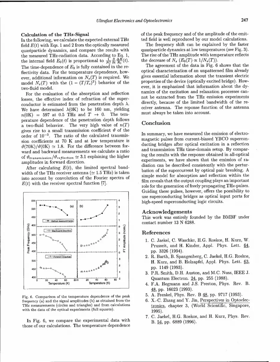
Ultrafast Electronics and Optoelectronics 247
Calculation of the THz-Signal In the following, we calculate the expected external THz field E(t) with Eqs. 1 and 2 from the optically measured quasiparticle dynamics, and compare the results with the measured THz-radiation data. According to Eq. 1, the internal field E0(t) is proportional to ^j-§i^(t)- The time-dependence of E0 is fully contained in the re- flectivity data. For the temperature dependence, how- ever, additional information on NS(T) is required. We model NS{T) with the (1 - (T/Tc)
2) behavior of the two-fluid model.
For the evaluation of the absorption and reflection losses, the effective index of refraction of the super- conductor is estimated from the penetration depth A. We have determined A(0K) to be 160 nm, yielding n(0K) = 597 at 0.5 THz and T -> 0. The tem- perature dependence of the penetration depth follows a two-fluid behavior. The very high value of n(T) gives rise to a small transmission coefficient d of the order of 10-3. The ratio of the calculated transmis- sion coefficients at 70 K and at low temperature is ??(70K)/ö(0K) ~ 1.8. For the difference between for- ward and backward measurements we calculate a ratio of ^transmission/Reflection ^ 3.1 explaining the higher amplitudes in forward direction.
After calculating E(t), the limited spectral band- width of the THz receiver antenna (~ 1.5 THz) is taken into account by convolution of the Fourier spectra of E(t) with the receiver spectral function [7].
550
500
450
—--._. (a) (b) /"
.-■--■
N" 400
| -■- Optical measurements I
X (3
g 500 O) 3 cr S> 450 U-
" 400
' ' O /
O
8° o
o
| —o— Backward Direction I
o-o
o o
\ o
500
450
400
1 _A~ Forward Directionl
0 20 40 60 80 Temperature (K)
0 20 40 60 80 Temperature (K)
Fig. 6. Comparison of the temperature dependence of the peak frequency (a) and the signal amplitudes (b) as obtained from the THz measurements (circles and triangles) and from calculations with the data of the optical experiments (full squares).
In Fig. 6, we compare the experimental data with those of our calculations. The temperature dependence
of the peak frequency and of the amplitude of the emit- ted field is well reproduced by our model calculations.
The frequency shift can be explained by the faster quasiparticle dynamics at low temperatures (see Fig. 3). The rise of the THz amplitude with temperature reflects the decrease of N. (E0(T) oc 1/N„(T)).
The agreement of the data in Fig. 6 shows that the optical characterization of an unpatterned film already gives essential information about the transient electric properties of the device (optically excited bridge). How- ever, it is emphasized that information about the dy- namics of the excitation and relaxation processes can- not be extracted from the THz emission experiments directly, because of the limited bandwidth of the re- ceiver antenna. The reponse function of the antenna must always be taken into account.
Conclusion
In summary, we have measured the emission of electro- magnetic pulses from current-biased YBCO supercon- ducting bridges after optical excitation in a reflection and transmission THz time-domain setup. By compar- ing the results with the response obtained in all-optical experiments, we have shown that the emission of ra- diation can be described consistently with the pertur- bation of the supercurrent by optical pair breaking. A simple model for absorption and reflection within the film reveals that the output coupling plays an important role for the generation of freely propagating THz-pulses. Guiding these pulses, however, offers the possibility to use superconducting bridges as optical input ports for high-speed superconducting logic circuits.
Acknowledgements This work was entirely founded by the BMBF under contact number 13 N 6288.
References
1. C. Jaekel, C. Waschke, H.G. Roskos, H. Kurz, W. Prusseit, and H. Kinder, Appl. Phys. Lett. 64, pp. 3326 (1994).
2. R. Barth, B. Spangenberg, C. Jaekel, H.G. Roskos, H. Kurz, and B. Holzapfel, Appl. Phys. Lett. 63, pp. 1149 (1993).
3. P.R. Smith, D.H. Auston, and M.C. Nuss, IEEE J. Quantum Electron. 24, pp. 255 (1988).
4. F.A. Hegmann and J.S. Preston, Phys. Rev. B. 48, pp. 16023 (1993).
5. A. Frenkel, Phys. Rev. B 48, pp. 9717 (1993). 6. X.-C. Zhang and Y. Jin, Perspectives in Optoelec-
tronics, chapter 3, (World Scientific, Singapore, 1995).
7. C. Jaekel, H.G. Roskos, and H. Kurz, Phys. Rev. B. 54, PP- 6889 (1996).

A Reliable Method for the Extraction of Material Parameters of Thick and Thin Samples in THz Time-Domain Spectroscopy
Lionel Duvillaret, Frederic Garet, Jean-Louis Coutaz LAHC, Universite de Savoie, 73 160 Le Bourget du Lac Cedex, France
John F. Whitaker Center for Ultrafast Optical Science, University of Michigan, 2200 Bonisteel, Ann Arbor, MI 48109-2099
Abstract
We present a fast and reliable method for extracting the refractive index and absorption in terahertz time-domain spectroscopy and apply it to the characterization of various thin films.
Key Words
Spectroscopy-far infrared, Spectroscopy-microwave, terahertz beams, terahertz spectroscopy
where R and T are the Fresnel reflection and transmission coefficients taken at the entrance (in) and output (out) faces of the sample, d is the thickness and n = n-iK is the complex index of the sample. The propagation outside the sample (e.g. in the substrate, if any) is fully described by the term r\. The summation over k represents the Fabry-Perot effect in the sample. The coefficient of transmission T(co) of the sample is derived from (1) as
T(a»-- 2n(ns + l)e -i(n-nx)codlc
(n + l)(n +ns)-(n - l)(n -ns)e -2incod/c (2)
Introduction
Time-domain THz spectroscopy is a powerful and rapid technique for measuring the complex refractive index of materials over a wide range of frequencies, from a few tens of GHz up to several THz [1]. The technique is based on recording the time dependence of a short electromagnetic pulse transmitted through a sample. The ratio of the Fourier transforms of the data recorded with and without the sample in the THz beam yields the transmission coefficient of the sample in the frequency domain. The solution of the inverse electromagnetic problem leads to the complex refractive index of the sample material. Classical techniques for obtaining a solution, like the Newton-Raphson method, can become unstable when the full transmitted signal exhibits internal reflections (Fabry- Perot effect). We present here a fast procedure [2] that converges in all practical cases and can be applied for the characterization of thin films of different thickness.
Description of the method
We assume that the sample under test is homogeneous and isotropic (free-standing sample or a film deposited over a known substrate). The transmitted part of an electromagnetic plane wave E(co) impinging on the sample at normal incidence at angular frequency (0 is
Ssample((°) = r]E((o)Tin Toul
-incodlc
where ns is the index of the substrate (ns -1 for free standing samples). In the case of a film made by modification of a substrate (ionic implantation, diffusion, chemical attack, etc.), nx is equal to ns. Otherwise nx is equal to 1.
Case of optically thick samples
Here the multiple echoes from the sample do not overlap in time. Therefore, by temporal windowing, it is possible to record only the first transmitted pulse. Equation (2) becomes simply
T((o) - _2"^_+7j c-i(n-nr)todlc (n + l)(n +ns)
(3)
xe — l[RinRoute-i2JicodlcJk 0)
k=0
The problem is to find n such that the calculated value Tcalc equals the measured one Tmeas- As /«(pca/c|) and arg(Tcaic) look like planes when plotted versus n and K,
it is easier to find the minimum of the error function 8(n,K) instead of, as is typical, the zero of Tcaic-Tmeas, where
S(n,K) = [ln(\Tcalc\)-ln(\Tmeas\)f
+[arg(TcaIc)- arglTfneas)]
Indeed, 6(n,K) can be well approximated by a paraboloid over the full range of practical values (/ < n < 10,
OSA TOPS on Ultrafast Electronics and Optoelectronics, 1997 Vol. 13, Martin Nuss and John Bowers (ed.) ©1997 Optical Society of America
248
Ultrafast Electronics and Optoelectronics 249
0 < K < 10). The zero of this paraboloid is very easy to find, and it gives a first estimate of (n,K). From this first estimation, and with successive iterations using the above method, one will quickly converge to the solution.
Case of optically thin samples
In this case, Eq. (2) has to be considered and the entire temporal signal has to be recorded. We treat the Fabry- Perot effect as a perturbation. We start the calculation with a fairly good approximation of n, which is derived as follows: we consider that the dephasing arg(T(co)) is mostly induced by the real part of n and that the modulus of T(co) depends mainly on the absorption K. Thus we obtain a first pair (n,K), with which we calculate the Fabry-Perot term (summation in (1)). We divide the transmission coefficient T(a) by this term, getting a curve with a strongly reduced contribution to internal reflections. Therefore we can apply the above method (thick sample case) for deriving a better value of n. Then, we repeat this procedure until the value of Tca/C doesn't vary from one step of computation to another one by more than 0.1 of the experimental uncertainty. Usually, the method converges over the full range of practical values (1 <n<5,0 < K<10) only after a few iterations.
Optically thick samples
We show here results obtained with a 7.07-mm-thick BK7 glass slide, for which the first internal reflection is detected far after the first pulse and thus is not seen in Fig. 2. The material parameters, derived with our method, are shown in Fig. 3. The calculation, leading to the entire curves of Fig. 3 (one calculated value every 5 GHz over the 1000 GHz range) takes 35 ms with a Pentium 90 PC computer.
l—I—i—I—I—I—i—I i I r
samp: reference :
mple -
I I ' I I I I I I L , I
12 16 TIME (ps)
20
estimation ; of(n,K) I
measures
f T meas (w) I
n,ic)-FP'»*-FP(n,ic,ü>) j^
\ extraction procedure m FP(n»K.>m)
for thick samples """
division
Tmcas(CD):
Figure 1: Principle of the extraction procedure for the case of thin samples
Experimental results
We have tested this method of extraction successfully on various samples. We present here only typical results. Our experimental set up is a common one, as described in details by many authors [3]. We use LT-GaAs photoconductive switches [4] as Hertzian dipoles and high- resistivity Si hyperhemispherical domes as focusing lenses. For each sample, we have performed several measurements, which allows us to improve the accuracy and to determine the standard deviation of the measurements.
Figure 2 : THz pulse recorded with and without a BK7 glass slide (d=1.07 mm). Reproduced with permission from Ref. 2, Copyright 1997, IEEE.
2.7
P 2.6 - <
I 2.5 O
W 2.4 Q Z
2.3
-5>
J_ _L J_
200 400 600 800 FREQUENCY (GHz)
80 & on O
603 o z
40 O m
20 O
z H
0 •?? 1000 3,
Figure 3 : Refractive index ofBK7 glass derived from the data of Figure 2. Reproduced with permission from Ref. 2, Copyright 1997, IEEE.
Thin films
The thin film is a layer of porous silicon (with a thickness of 43 jm) synthesized through chemical attack of a Si substrate. We recorded the THz signal transmitted
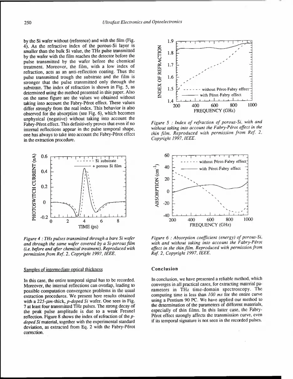
250 Ultrafast Electronics and Optoelectronics
by the Si wafer without (reference) and with the film (Fig. 4). As the refractive index of the porous-Si layer is smaller than the bulk Si value, the THz pulse transmitted by the wafer with the film reaches the detector before the pulse transmitted by the wafer before the chemical treatment. Moreover, the film, with a low index of refraction, acts as an anti-reflection coating. Thus the pulse transmitted trough the substrate and the film is stronger that the pulse transmitted only through the substrate. The index of refraction is shown in Fig. 5, as determined using the method presented in this paper. Also on the same figure are the values we obtained without taking into account the Fabry-Perot effect. These values differ strongly from the real index. This behavior is also observed for the absorption (see Fig. 6), which becomes unphysical (negative) without taking into account the Fabry-Perot effect. This definitively proves that even if no internal reflections appear in the pulse temporal shape, one has always to take into account the Fabry-Perot effect in the extraction procedure.
1.9 Z
<
w OS PU 1.6 o X W 1 5
Z 1.4
without Perot-Fabry effecr
with Perot-Fabry effect ■ ■ I ■ i i I i—i—i—I—i—i—i—
200 400 600 800 FREQUENCY (GHz)
1000
Figure 5 : Index of refraction of porous-Si, with and without taking into account the Fabry-Perot effect in the thin film. Reproduced with permission from Ref. 2, Copyright 1997, IEEE.
< 0.6 c
1 I ' I ' I ' I ' I ' I ' I ' I ' Si substrate
+ porous Si film .
2 4 6 TIME (ps)
Figure 4 : THz pulses transmitted through a bare Si wafer and through the same wafer covered by a Si-porous film (i.e. before and after chemical treatment). Reproduced with permission from Ref. 2, Copyright 1997, IEEE.
60
-V 40 -
^0
-i—i—i—\—i—i—i—|—i—i—i—| i i i-
without Perot-Fabry effect;
with Perot-Fabry effect
_L
200 400 600 800 FREQUENCY (GHz)
1000
Figure 6 : Absorption coefficient (energy) of porous-Si, with and without taking into account the Fabry-Perot effect in the thin film. Reproduced with permission from Ref. 2, Copyright 1997, IEEE.
Samples of intermediate optical thickness
In this case, the entire temporal signal has to be recorded. Moreover, the internal reflections can overlap, leading to possible computation convergence problems in the usual extraction procedures. We present here results obtained with a 225-jUm-thick, p-doped Si wafer. One sees in Fig. 7 at least four transmitted THz pulses. The strong decay of the peak pulse amplitude is due to a weak Fresnel reflection. Figure 8 shows the index of refraction of thep- doped Si material, together with the experimental standard deviation, as extracted from Eq. 2 with the Fabry-Perot correction.
Conclusion
In conclusion, we have presented a reliable method, which converges in all practical cases, for extracting material pa- rameters in THz time-domain spectroscopy. The computing time is less than 700 ms for the entire curve using a Pentium 90 PC. We have applied our method to the determination of the parameters of different materials, especially of thin films. In this latter case, the Fabry- Perot effect strongly affects the transmission curve, even if its temporal signature is not seen in the recorded pulses.

Ultrafast Electronics and Optoelectronics 251
reference sample
I i i i i I
10 20 30 TIME (ps)
40
Figure 7 : THz pulse transmitted by a 225 \im thick p- doped Si wafer. Reproduced with permission from Ref. 2, Copyright 1997, IEEE.
3.6
S 3.5 F- P ^3.4
ß «3.3
~i—i—i—I—i—r~i—r—l—i—i—I—i—r 40
30 & DO 00 o 50
20 3 o z
10 -o- 3
100 300 500 700 900 1100 FREQUENCY (GHz)
Acknowledgments
This research was sponsored by the National Science Foundation through the Center for Ultrafast Optical Science under STC PHY 8920108.
References
[1] D. Grischkowsky, S. Keiding, M. van Exter, and Ch. Fattinger, JOSA B7, 2006 (1990).
[2] L. Duvillaret, F. Garet, and J.-L. Coutaz, to be published in IEEE J. Sei. Topics Quant. Electron.
[3] see, for example, J. F. Whitaker, F. Gao, and Y. Liu, in Nonlinear Optics for High-Speed Electronics and Optical Frequency Conversion, N. Peygambarian, H. Everitt, R.C. Eckardt, and D.D. Lowenthal, eds., Proc. SPIE 2145, 168 (1994).
[4] J. F. Whitaker, Mat. Science Engineering B22, 61 (1993).
Figure 8 : Index of refraction of p-doped silicon together with standard deviation. Reproduced with permission from Ref. 2, Copyright 1997, IEEE.
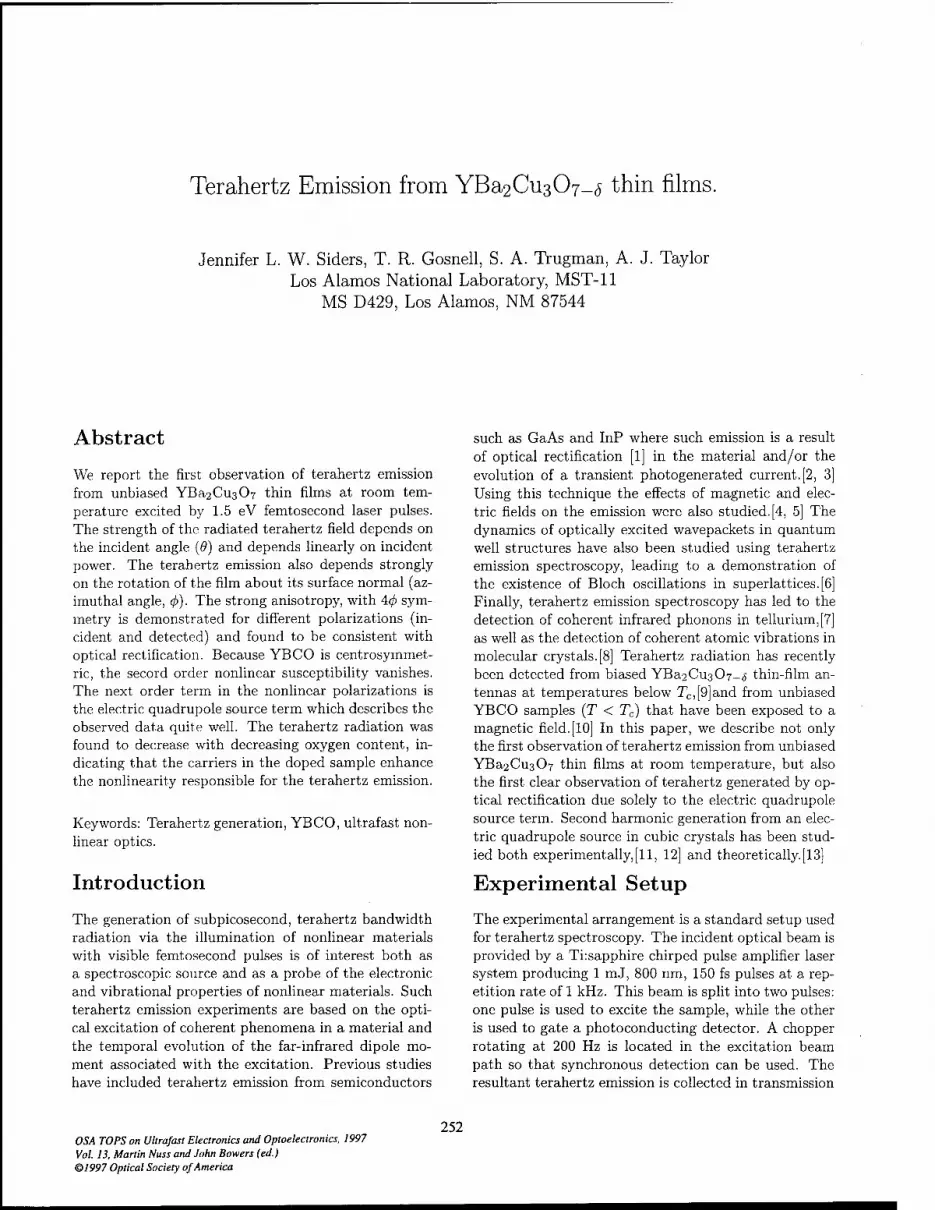
Terahertz Emission from YBa2Cu307_^ thin films.
Jennifer L. W. Siders, T. R. Gosnell, S. A. Trugman, A. J. Taylor Los Alamos National Laboratory, MST-11
MS D429, Los Alamos, NM 87544
Abstract
We report the first observation of terahertz emission from unbiased YBa2Cu307 thin films at room tem- perature excited by 1.5 eV femtosecond laser pulses. The strength of the radiated terahertz field depends on the incident angle (9) and depends linearly on incident power. The terahertz emission also depends strongly on the rotation of the film about its surface normal (az- imuthal angle, <j>). The strong anisotropy, with 40 sym- metry is demonstrated for different polarizations (in- cident and detected) and found to be consistent with optical rectification. Because YBCO is centrosymmet- ric, the secord order nonlinear susceptibility vanishes. The next order term in the nonlinear polarizations is the electric quadrupole source term which describes the observed data quite well. The terahertz radiation was found to decrease with decreasing oxygen content, in- dicating that the carriers in the doped sample enhance the nonlinearity responsible for the terahertz emission.
Keywords: Terahertz generation, YBCO, ultrafast non- linear optics.
Introduction
The generation of subpicosecond, terahertz bandwidth radiation via the illumination of nonlinear materials with visible femtosecond pulses is of interest both as a spectroscopic source and as a probe of the electronic and vibrational properties of nonlinear materials. Such terahertz emission experiments are based on the opti- cal excitation of coherent phenomena in a material and the temporal evolution of the far-infrared dipole mo- ment associated with the excitation. Previous studies have included terahertz emission from semiconductors
such as GaAs and InP where such emission is a result of optical rectification [1] in the material and/or the evolution of a transient photogenerated current.[2, 3] Using this technique the effects of magnetic and elec- tric fields on the emission were also studied. [4, 5] The dynamics of optically excited wavepackets in quantum well structures have also been studied using terahertz emission spectroscopy, leading to a demonstration of the existence of Bloch oscillations in superlattices.[6] Finally, terahertz emission spectroscopy has led to the detection of coherent infrared phonons in tellurium, [7] as well as the detection of coherent atomic vibrations in molecular crystals. [8] Terahertz radiation has recently been detected from biased YBa2Cu307_,5 thin-film an- tennas at temperatures below Tc,[9]and from unbiased YBCO samples (T < Tc) that have been exposed to a magnetic field. [10] In this paper, we describe not only the first observation of terahertz emission from unbiased YBa2Cu3C>7 thin films at room temperature, but also the first clear observation of terahertz generated by op- tical rectification due solely to the electric quadrupole source term. Second harmonic generation from an elec- tric quadrupole source in cubic crystals has been stud- ied both experimentally, [11, 12] and theoretically. [13]
Experimental Setup
The experimental arrangement is a standard setup used for terahertz spectroscopy. The incident optical beam is provided by a Tirsapphire chirped pulse amplifier laser system producing 1 mJ, 800 nm, 150 fs pulses at a rep- etition rate of 1 kHz. This beam is split into two pulses: one pulse is used to excite the sample, while the other is used to gate a photoconducting detector. A chopper rotating at 200 Hz is located in the excitation beam path so that synchronous detection can be used. The resultant terahertz emission is collected in transmission
OSA TOPS on Ultrafast Electronics and Optoelectronics, 1997 Vol. 13, Martin Nuss and John Bowers (ed.) ©1997 Optical Society of America
252
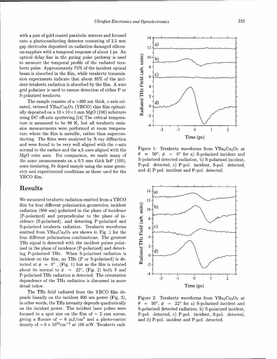
Ultrafast Electronics and Optoelectronics 253
with a pair of gold coated parabolic mirrors and focused onto a photoconducting detector consisting of 2.5 mm gap electrodes deposited on radiation-damaged silicon- on-sapphire with a temporal response of about 1 ps. An optical delay line in the gating pulse pathway is used to measure the temporal profile of the radiated tera- hertz pulse. Approximately 75% of the incident optical beam is absorbed in the film, while terahertz transmis- sion experiments indicate that about 85% of the inci- dent terahertz radiation is absorbed by the film. A wire grid polarizer is used to ensure detection of either P or S-polarized terahertz.
The sample consists of a ~300 nm thick, c-axis ori- ented, twinned YBa2Cu3Ü7 (YBCO) thin film epitaxi- ally deposited on a 10 x 10 x 1 mm MgO (100) substrate using DC off-axis sputtering. [14] The critical tempera- ture is measured to be 88 K, but all terahertz emis- sion measurements were performed at room tempera- ture where the film is metallic, rather than supercon- ducting. The films were analyzed by X-ray diffraction and were found to be very well aligned with the c-axis normal to the surface and the a,b axes aligned with the MgO cube axes. For comparison, we made many of the same measurements on a 0.5 mm thick InP (100), semi-insulating, Fe doped sample using the same geom- etry and experimental conditions as those used for the YBCO film.
-1 0 1
Time (ps)
Figure 1: Terahertz waveforms from YBa2Cus07 at 0 = 50°, ^ = 0° for a) S-polarized incident and S-polarized detected radiation, b) S-polarized incident, P-pol. detected, c) P-pol. incident, S-pol. detected, and d) P-pol. incident and P-pol. detected.
Results
We measured terahertz radiation emitted from a YBCO film for four different polarization geometries; incident radiation (800 nm) polarized in the plane of incidence (P-polarized) and perpendicular to the plane of in- cidence (S-polarized), and detecting P-polarized and S-polarized terahertz radiation. Terahertz waveforms emitted from YBa2Cu30y are shown in Fig. 1 for the four different polarization combinations. The greatest THz signal is detected with the incident pulses polar- ized in the plane of incidence (P-polarized) and detect- ing P-polarized THz. When S-polarized radiation is incident on the film, no THz (P or S-polarized) is de- tected at <f> = 0° , (Fig. 1) but as the film is rotated about its normal to <f> = 22°, (Fig. 2) both S and P-polarized THz radiation is detected. The orientation dependence of the THz radiation is discussed in more detail below.
The THz field radiated from the YBCO film de- pends linearly on the incident 800 nm power (Fig. 3), in other words, the THz intensity depends quadratically on the incident power. The incident laser pulses were focused to a spot size on the film of ~ 2 mm across, giving a fluence of ~ 6 mJ/cm2 and a photo-carrier density of ~ 6 x 1021cm-3 at 100 mW. Terahertz radi-
c 3
■e
2 13
N
T3 U
'S
Time (ps)
Figure 2: Terahertz waveforms from YBa2Cu3Ü7 at 6 = 50°, <j> = 22° for a) S-polarized incident and S-polarized detected radiation, b) S-polarized incident, P-pol. detected, c) P-pol. incident, S-pol. detected, and d) P-pol. incident and P-pol. detected.
254 Ultrafast Electronics and Optoelectronics
Incident Power (mW)
Figure 3: The radiated THz field depends linearly on the incident 800 nm power. The spot size on the film had a diameter of ~ 2 mm.
ation emitted from an InP (100) semi-insulating wafer was approximately 5 times stronger than the THz gen- erated by the YBCO film with the same experimental conditions (9 = 50°, incident power of 90 mW).
Fig. 4 shows that the THz radiation depends strongly on incident angle and disappears at normal incidence (0 = 0°). The bottom graph in Fig. 4 shows the same data but its plotted as a function of the inter- nal angle, 6f. The internal angle was calculated using an index of refraction of 2.0 for YBCO at room tem- perature for 800 nm light.[15] The data was taken with the incident light P-polarized and detecting P-polarized THz (PP) The solid curves in Fig. 4 are fits of the data to
Epp{6) = A Sin{20) + B Sm(40), (1)
which is predicted by optical rectification from the bulk electric quadrupole term for a twinned orthorhombic crystal. The dependence of the emitted terahertz ra- diation on sample orientation (rotation of the sample about its normal, <f>) for the four polarization geome- tries is shown in Fig. 5 where 6 = 50° and the incident power is 90 mW. The solid curves are fits to functions obtained from the bulk electric quadrupole contribution to optical rectification: [11, 13]
EPp{<f>) = A1 Cos{14>) + Cu
ESP{CJ>) = -A2 Cos(4cf>) + C2,
EPSW = A3 Sinm),
(2)
(3)
(4)
c 3
i 4>
3
a
4) OH
3
c 3
i 3
N
H M
3 D
OH
10-
8-
i . i . i . i . i i.i,
6- y \ " 4- \-
2- -
0- -
-2- -
-4- -
-6- -
-8-
10- 7.15Sin(20)-
—i—i—i—i—i—i—i—i—i—i—
1.04Sin(49) " i | i i i
-80 -60 -40 -20 0 20 40 60 80
Incident Angle (6.)
Internal Angle (0f)
Figure 4: Radiated THz field is plotted as a function of incident angle (—6i) in the top figure and as a func- tion of the internal angle, (Of), in the bottom figure. The solid circles represent data taken with P-polarized 800 nm incident and detecting P-polarized THz. The solid curves are fits, see text for more information.

Ultrafast Electronics and Optoelectronics 255
C 3
i D
T3 3
N
H CO
O . -t-J
■a
• PP=1.93Cos(4(|))+5.13 D SS=1.67Sin(4(())
O SP=-1.69Cos(4(|>)+3.27 ■ PS=-1.62Sin(4<|>)
10
0 20 40 60 80 100 120 140 160 180
Azimuthal Angle (<|))
Figure 5: The peak-to-peak THz field amplitude is plot- ted as a function of azimuthal angle (crystal orientation, (f>). The data were taken with 90 mW of P- (filled sym- bols) or S-polarized (open symbols) 800 nm pulses in- cident on the film at 6 = 50° and detecting P-(circles) or S-polarized (squares) THz.
Ess(<P) = -A4 Sin(4<f>), (5)
where, A and C are constants that depend on the crystal structure and Fresnel coefficients. The formu- las above were calculated for an orthorhombic crystal where the x and y axes are interchangeable to take into account the twin domains.
Varying the oxygen content in YBa2Cu307_,5 changes the density of carriers in the film, as well as changing Tc. We used three different films to look at the THz dependence on carrier concentration (Fig. 6) at room temperature. A very small THz signal was detected from an insulating film with S = 0.8 (not su- perconducting) , slightly stronger emission was detected with 6 = 0.5 (Tc = 55 K), and the strongest THz signal was generated with S = 0.0 (Tc = 88 K). These results indicate that increasing the concentration of carriers enhances the mechanism responsible for the terahertz emission.
i i i i i i 1 1 1—
-2-1012
Time (ps)
Figure 6: THz radiation from YBa2Cu306.2, YBa2Cu306.5 and YBa2Cu307. 0 = 50°, <j> = 0°, and T = 300 K for all three measurements.
Conclusions
In semiconductors several mechanisms have produced terahertz emission via femtosecond optical excitation, including phonon generation, [7] difference frequency mixing from the bulk second order susceptibility (bulk optical rectification),[16] dipole radiation from a tran- sient current of photoinjected carriers accelerated in a surface field (current surge),[2] and difference fre- quency mixing from an effective second order suscep- tibility proportional to the surface field (surface opti- cal rectification. [1] In our experiment several of these mechanisms are not relevant. Our bandwidth is insuf- ficient to detect coherent phonons, since the lowest in- frared active phonon frequency is greater than 3 THz in YBCO. YBCO has a center of inversion symmetry, therefore its second order susceptibility vanishes and bulk optical rectification is not possible. The current surge mechanism is a possible candidate for the ob- served emission, with the driving field produced by the carrier gradient resulting from the photogeneration of carriers. However, it is unlikely that such a mecha- nism alone could produce the strong orientational de- pendence shown in Fig. 5. Electric quadrupole opti- cal rectification in YBCO is consistent with the strong orientational dependence seen in the data. We calcu-
256 Ultrafast Electronics and Optoelectronics
lated the dependence of the emitted THz radiation on incident angle and the complex dependence on crystal orientation for the different incident and detected polar- izations, for a twinned orthorhombic crystal. We have demonstrated not only the first observation of terahertz emission from unbiased YBa2Cu307 thin films at room temperature, but also the first clear observation of ter- ahertz generated by optical rectification due solely to the electric quadrupole source term.
Acknowledgments
We would like to thank R.J. Houlton for preparing our films, S. Foltyn for performing the X-ray analysis, and T.F. Heinz for useful discussions..
References
[1] S. L. Chang, S. Schmitt-Rink, B. I. Greene, P. N. Saeta, and A. F. J. Levi, Phys. Rev. Lett. 68, 102 (1992).
[2] X. C. Zhang, B. B. Hu, J. T. Darrow, and D. H. Auston, Appl. Phys. Lett. 56, 1011 (1990).
[3] J. T. Darrow, B. B. Hu, X. C. Zhang, and D. H. Auston, Opt. Lett. 15, 323 (1990).
[4] X. C. Zhang, Y. Jin, T. D. Hewitt, T. Dangsiri, L. E. Kingsley, and M. Weiner, Appl. Phys. Lett. 62, 2003 (1993).
[5] J. Son, T. B. Norris ,and J. F. Whitaker, J. Opt. Soc. Am. B 11, 2519 (1994).
[6] H. G. Roskos, M. C. Nuss, J. Shah, K. Leo, D. A. B. Miller, A. M. Fox, S. Schmitt-Rink, and K. Kohler, Phys. Rev. Lett. 68, 2216 (1992).
[7] T. Dekorsy, H. Auer, C. Waschke, H. J. Bakker, H. G. Roskos, H. Kurz, V. Wagner, and P. Grosse, Phys. Rev. Lett. 74, 738 (1995).
[8] X. C. Zhang, X. F. Ma, Y. Jin, T. M. Lu, E. P. Boden, P. D. Phelps, K. R. Stewart, and C. P. Yakymyshyn, Appl. Phy. Lett. 61, 3080 (1992).
[9] M. Tonouchi, M. Tani, Z. Wang, K. Sakai, S. Tomozawa, M. Hangyo, Y. Murakami, and S. Nakashima, Jpn. J. Appl. Phys. 35, 2624 (1996).
[10] M. Tonouchi, M. Tani, Z. Wang, K. Sakai, N. Wada, and M. Hangyo, Jpn. J. Appl. Phys. 36, L93 (1997).
[11] T. F. Heinz, in Nonlinear Surface Electromagnetic Phenomena, ed. H. E. Ponath and G. I. Stegeman (1991).
[12] A. V. Petukhov, Ch. Jakobsen, and K. Pedersen, Surf. Sei. 360, 265 (1996).
[13] J. E. Sipe, D. J. Moss and H. M. van Driel, Phys. Rev. B 35, 1129 (1987).
[14] R. J. Houlton, D. W. Reagor, M. E. Hawley, K. N. Springer, Q. X. Jia, C. B. Mombourquette, F. H. Garzon, and X. D. Wu, IEEE Trans. Appl. Supercond. 5, 1639 (1995).
[15] D. E. Aspnes and M. K. Kelly, IEEE J. Quantum Electron. 25, 2378 (1989).
[16] P. N. Saeta, B. I. Greene, and S. L. Chuang, Appl. Phys. Lett. 63, 3482 (1993).
Real-time chemical recognition of gas mixtures using optoelectronic terahertz waveforms
Rune H. Jacobsen,* Daniel M. Mittleman,T and Martin C. Nuss Bell Labs, Lucent Technologies, 101 Crawfords Corner Rd., Holmdel, NJ 07733, USA
Abstract
A time-domain chemical recognition system for classifying gases and analyzing gas mixtures is presented. The free- induction-decay exhibited by gases excited by far-infrared (terahertz) waveforms is analyzed in time-domain using digital signal processing techniques. A simple geometric picture is used for the classification of the waveforms measured for unknown gas species and for a quantitative pressure analysis of the individual gas species in a mixture. The analysis has have low computational cost and is used for a real-time monitor of gases.
Keywords
Spectroscopy-coherent transients; Far-infrared; Optoelec- tronics; Pattern recognition and feature extraction.
Introduction
During the last decades gas sensing has been an important topic in analytic and environmental chemistry. Tradition- ally, infrared spectroscopic techniques [1,2] have been used for the analysis of ambient air by absorption meas- urements of ro-vibrational transitions of a gas species. More recently, tunable single-mode quantum-well diode lasers fabricated for the telecommunication industry have been used in laser-absorption spectrometers that monitor trace-gases in ppm. concentrations [3]. Lately, we demon- strated how coherent broadband far-infrared radiation (terahertz waveforms) can be used for chemical recognition of gas species and for a quantitative mixtures analysis [4]. This is accomplished by examining the temporal correla- tions of the coherent irradiance resulting from the multiple excitation of rotational transitions of a gas.
Terahertz waveforms are generated opto- electronically as coherent burst of subpicosecond radiation emitted from photoconductive antennas excited by femto- second laser pulses [5-7]. Terahertz waveforms have been widely used for time-domain spectroscopy in the far- infrared region of the electromagnetic spectrum [8-12]. The radiation propagates as a single cycle oscillation of the electromagnetic field in a highly directional beam and spans a frequency range from 100 GHz to more than 2
THz. Terahertz waveforms are detected coherently by gat- ing the photoconductive receiver antenna by a femtosecond laser pulse. Recent advances in reducing the acquisition time required to acquire a terahertz waveform has opened ways for performing real-time terahertz time-domain spec- troscopy. This was first used to demonstrate the practicality of imaging with terahertz waveforms [13]. The terahertz waveforms are down-converted into the audio range and processed in real time.
The far-infrared part of the electromagnetic spec- trum is important since a large number of polar gases have characteristic rotational lines in this spectral region [14]. The propagation of a terahertz pulse through an infrared active gas excites a multitude of rotational transitions and causes the molecules to reradiate a free-induction decay (FID) [2,11,15]. The FID is characterized by fast oscilla- tions [9] and commensurate echoes [10] that appear after the impulse excitation. The observed FID decays because of dephasing caused by molecular collisions. The charac- teristic FID provides a unique time-domain representation of the absorption and dispersion characteristics of the gas and can be used for chemical identification purposes.
The basic idea of chemical recognition with tera- hertz waveforms is to extract the spectral features from a measured FID exhibited by a gas species. From a mathe- matical point of view these circumstances strongly relate to speech processing [16], and hence we have modified ex- isting techniques to make it suitable for terahertz chemical recognition. Briefly, the spectral content of a terahertz waveform is parameterized and the parameters are used for classification purposes. We use a correlation type of analy- sis known as linear predictive coding (LPC) and a subse- quent vector quantization scheme, where parameters of known gas species are stored as vectors in a codebook. The recognition procedure consists in a comparison between known and measured parameter sets and can be used to estimate the partial pressures of individual gas species quantitatively.
Experimental
The gas sensing spectrometer, illustrated in Fig. 1, is based on photoconductive antennas and standard millimeter wave optics. The transmitter antenna consists of two parallel 10 urn-wide metal lines deposited on a semi-insulating
OSA TOPS on Ultrafast Electronics and Optoelectronics, 1997 Vol. 13, Martin Nuss and John Bowers (ed.) ©1997 Optical Society of America
257

258 Ultrafast Electronics and Optoelectronics
GaAs substrate, with a line separation of 100 urn. A voltage of -50 V is applied across the two lines and a 100 fs laser pulse from a Ti:Sapphire laser, centered around 810 nm, is focused between the two metal lines. The transient polari- zation generated by photoexcited carriers becomes the source of terahertz radiation. The radiation is coupled into free space using a hyperhemispherical substrate lens at- tached to the back of the antenna, and is collimated by us- ing an off-axis paraboloidal mirror. The collimated tera- hertz beam is propagated through a gas cell of length 30.5 cm with two 0.50 cm-thick windows made of TPX plastic.
Pressure gauge
The sampled waveforms are processed by the DSP in real time. Prior to the LPC analysis, the waveforms are preprocessed using finite impulse response filtering and time-domain windowing. That is, the sampled waveform was convoluted with the impulse response of a bandpass filter and multiplied by window functions. This is per- formed to stabilize the LPC analysis by reducing the risk of producing spurious frequency peaks. Since we are only interested in the coherent irradiance from the gas we begin the LPC analysis for values appearing after the impulse excitation.
Results
I Gas cell
A-> Ss rs"
xrt
Transmitter antenna
A-> y Optical
delay line
Figure 1: Schematics of the terahertz time-domain spectrometer used for gas analysis.
Another combination of a paraboloidal mirror and a sub- strate lenses focuses the radiation onto the receiver an- tenna. As receiver we use photoconductive antennas fabri- cated on ion-implanted silicon-on-sapphire or low- temperature-grown GaAs. In the receiver antenna we measure the cross-correlation between the incident tera- hertz waveform and the photoconductive response of the receiver antenna. By adjusting the arrival time between the incident terahertz waveform and the optical gating pulse a sampled replica of the terahertz waveform is measured.
The optical delay between the terahertz pulse and the gating femtosecond pulse is established using a scan- ning optical delay line (ODL) from Clark MXR. The ODL is based on a galvanometric shaker that runs continuously at a frequency of 20 Hz corresponding to an acquisition time of 25 ms per waveform. The ODL provides a total time delay of-100 ps, which is sufficient for chemical rec- ognition purposes, but inadequate for gas spectroscopy with high spectral resolution. The current in the receiver antenna is fed to a current sensitive preamplifier and is digitized and processed by a digital signal processor (DSP) integrated into a personal computer. The signal-to-noise ratio in a single waveform is typically greater than 1000:1.
To demonstrate chemical recognition of gases and gas mixtures we have studied the polar gases H20, NH3, HC1, and CH3CN in the pressure range between 0.3 and 13 kPa. Common for these species is that they have strong perma- nent dipole moments and hence they interact strongly with the terahertz field. Figure 2 shows a sample replica of a terahertz waveform measured after propagating through NH3 vapor at a pressure of 12.8 kPa. The impulse seen at zero delay excites some of the lowest lying transitions in the rotation-inversion spectrum of NH3 [14]. Pronounced oscillations, due to the FID of the excited resonances, are seen at later time delays.
5.0 ■ " i 1 1—1—1 ■ 1 1—1 ■ 1—■—r—■—1—• 1 ■
4.0
3.0
2.0
1.0
0.0 r^^A l|^/Wl^MAMAv/^/V'VV1^^
1.0 ■
I 2.0
■
3.0
-10 20 30 40 50
Time delay [ps]
60 70 90
Figure 2: Terahertz waveform resulting from the propagation through NH3 vapor. The waveform is an average of 1000 real- time scans. The occurrences at 29 and 51 ps are due to reflections in the setup.
To compare the pressure determined from the chemical recognition analysis with the actual amount of gas in the cell, we performed a single-species-recognition experiment of HC1 vapor at various pressures. Figure 3 shows the re- sult of the analysis. The dashed line illustrates the ideal case where predicted pressure and measured pressure coin- cide.
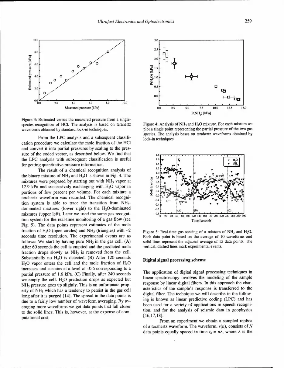
Ultrafast Electronics and Optoelectronics 259
4.0 6.0 8.0 10.0
Measured pressure [kPa]
Figure 3: Estimated versus the measured pressure from a single- species-recognition of HC1. The analysis is based on terahertz waveforms obtained by standard lock-in techniques.
From the LPC analysis and a subsequent classifi- cation procedure we calculate the mole fraction of the HC1 and convert it into partial pressures by scaling to the pres- sure of the coded vector, as described below. We find that the LPC analysis with subsequent classification is useful for getting quantitative pressure information.
The result of a chemical recognition analysis of the binary mixture of NH3 and H20 is shown in Fig. 4. The mixtures were prepared by starting out with NH3 vapor at 12.9 kPa and successively exchanging with H20 vapor in portions of few percent per volume. For each mixture a terahertz waveform was recorded. The chemical recogni- tion system is able to trace the transition from NH3- dominated mixtures (lower right) to the H20-dominated mixtures (upper left). Later we used the same gas recogni- tion system for the real-time monitoring of a gas flow (see Fig. 5). The data points represent estimates of the mole fraction of H20 (open circles) and NH3 (triangles) with ~2 seconds time resolution. The experimental events are as follows: We start by having pure NH3 in the gas cell. (A) After 60 seconds the cell is emptied and the predicted mole fraction drops slowly as NH3 is removed from the cell. Substantially no H20 is detected. (B) After 120 seconds H20 vapor enters the cell and the mole fraction of H20 increases and sustains at a level of -0.6 corresponding to a partial pressure of 1.6 kPa. (C) Finally, after 240 seconds we empty the cell. H20 prediction drops as expected but NH3 pressure goes up slightly. This is an unfortunate prop- erty of NH3 which has a tendency to persist in the gas cell long after it is purged [14]. The spread in the data points is due to a fairly low number of waveform averaging. By av- eraging more waveforms we get data points that fall closer to the solid lines. This is, however, at the expense of com- putational cost.
J.U
2.5
2.0
!?15 h 0,1.0 X -S- a.
0.5 D RJ
0.0
■ i ■ i
h-D-tto
0.0 2.5 5.0 7.5 10.0
P(NH,) [kPa] 15.0
Figure 4: Analysis of NH3 and H20 mixture. For each mixture we plot a single point representing the partial pressure of the two gas species. The analysis bases on terahertz waveforms obtained by lock-in techniques.
20 40 60 80 100 120 140 160 180 200 220 240 260 280 300
Time [seconds]
Figure 5: Real-time gas sensing of a mixture of NH3 and H20. Each data point is based on the average of 10 waveforms and solid lines represent the adjacent average of 15 data points. The vertical, dashed lines mark experimental events.
Digital signal processing scheme
The application of digital signal processing techniques in linear spectroscopy involves the modeling of the sample response by linear digital filters. In this approach the char- acteristics of the sample's response is transferred to the digital filter. The technique we will describe in the follow- ing is known as linear predictive coding (LPC) and has been used for a variety of applications in speech recogni- tion, and for the analysis of seismic data in geophysics [16,17,18].
From an experiment we obtain a sampled replica of a terahertz waveform. The waveform, s(n), consists of N data points equally spaced in time tn = «A, where A is the

260 Ultrafast Electronics and Optoelectronics
sampling interval. The assumption in LPC dictates that the sampled waveform at time t„ can be expressed as a linear combination of the past M sampled values:
aks(n-k) + e(n), k=\
(1)
where e(n) is the residual that accounts for the equality to hold, ak are the parameters of the LPC, and M is the order of the LPC analysis. The optimum values for the LPC coef- ficients are calculated from least square principles and it is desired to minimize the total squared residual:
min f \ 2/(»)2
V » )
mm M l2\
s(n)-2\aks(n-k) k=\
(2)
with respect to the coefficients ak. The summation over n in Eq.(2) is a summation over the entire sampled waveform. In a measurement the waveform vanishes outside the sam- pling region, that is, sampling begins before the impulse excitation and continues until the FID is sufficiently small. The analysis yields a system of normal equations [17,18]:
M
^r(i-k)ak=-r(i), \<i<M, (3) k=\
that relates the LPC coefficients to values of the autocor- relation function:
r(n) = \s(k)s(n - k), (4)
of the time series representing the waveform. Equation (3) can be solved in terms of matrix inversion schemes such as the Levinson-Durbin algorithm [17] or by using Burg's algorithm for maximum entropy spectral analysis [19]. Since our analysis is based on the autocorrelation function, we sacrifices phase information at this point. However, timing (or phase) information was used in the preprocess- ing of the measured waveforms to separated the impulse response from the subsequent FID.
To get a feel for the physics behind the LPC analysis, we introduce the z-transform of Eq.(l):
S(z) = TM akz~kS(z) + E(z), (5)
where z = exp0'2jr/) and/is the frequency. We find that the LPC models the action of a resonantly excited gas by an infinite impulse response filter (IIR) that reshapes an inci- dent terahertz waveform to produce the corresponding FID.
S(z) = H(z)E(z),
where
H(z)=- 1-
EM
k=\
(6)
(7) akz
Ideally, all the spectral information is transferred to the filter coefficient and the input becomes white noise. In fact, an analysis of the noise can be used to determine the opti- mum number of coefficients [18]. The filter, H(z), is com- posed of M poles and contains, in practice, between 16 and 50 poles for a sampling of N = 1024 data points. This cor- responds to a compression factor >10. The obvious draw- back is the inherent spectral distortion in representing the actual analysis vector in its parameterized form. This intro- duces a certain level of uncertainty.
A comparison between the power spectrum esti- mated from the IIR filter and the power spectrum estimated from Fourier transformation is shown in Fig. 6. The com- parison serves as a confidence measure for the LPC analy- sis but is not used elsewhere in the chemical recognition.
a o.8 -
■a
0.0
Integrated power spectral density
JULjMiL^. 0.0 0.2 0.4 0.6 0.8 1.0 1.2 1.4 1.6 1.8 2.0
Frequency [THz]
Figure 6: The power spectrum of H20 estimated from an IIR filter using M=50 poles (thick solid line) and from a Fourier analysis (dashed line). Thin solid line and dotted line are the integrated power spectral density for the LPC and the Fourier analysis, re- spectively.
Because of the data compression, the frequency resolution obtained from the LPC analysis is less that the resolution obtained from the Fourier analysis. However, the LPC analysis correctly predicts the power, i.e., the integral of the power spectral density, in an absorption line.
The concept of building a codebook of distinct analysis vectors is the basic behind a set of techniques commonly called vector quantization (VQ) methods [16]. The VQ representation allows us to use simple geometric pictures for the classification of waveforms. The LPC coef- ficients are treated as a vector, a - (au a2,..., aM), in a M-
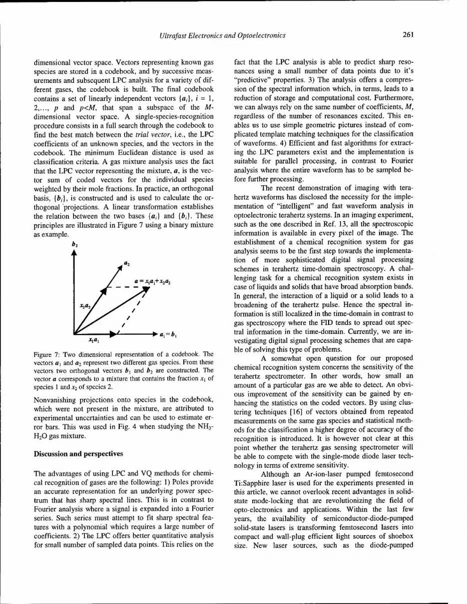
Ultrafast Electronics and Optoelectronics 261
dimensional vector space. Vectors representing known gas species are stored in a codebook, and by successive meas- urements and subsequent LPC analysis for a variety of dif- ferent gases, the codebook is built. The final codebook contains a set of linearly independent vectors {a,}, i - 1, 2,..., p and p<M, that span a subspace of the M- dimensional vector space. A single-species-recognition procedure consists in a full search through the codebook to find the best match between the trial vector, i.e., the LPC coefficients of an unknown species, and the vectors in the codebook. The minimum Euclidean distance is used as classification criteria. A gas mixture analysis uses the fact that the LPC vector representing the mixture, a, is the vec- tor sum of coded vectors for the individual species weighted by their mole fractions. In practice, an orthogonal basis, {bj}, is constructed and is used to calculate the or- thogonal projections. A linear transformation establishes the relation between the two bases {a,} and {&,}. These principles are illustrated in Figure 7 using a binary mixture as example.
b2
*l«I+*2«2
►«1 = *1
Figure 7: Two dimensional representation of a codebook. The vectors ay and a2 represent two different gas species. From these vectors two orthogonal vectors b\ and b2 are constructed. The vector a corresponds to a mixture that contains the fraction x\ of species 1 and x2 of species 2.
Nonvanishing projections onto species in the codebook, which were not present in the mixture, are attributed to experimental uncertainties and can be used to estimate er- ror bars. This was used in Fig. 4 when studying the NH3- H20 gas mixture.
Discussion and perspectives
The advantages of using LPC and VQ methods for chemi- cal recognition of gases are the following: 1) Poles provide an accurate representation for an underlying power spec- trum that has sharp spectral lines. This is in contrast to Fourier analysis where a signal is expanded into a Fourier series. Such series must attempt to fit sharp spectral fea- tures with a polynomial which requires a large number of coefficients. 2) The LPC offers better quantitative analysis for small number of sampled data points. This relies on the
fact that the LPC analysis is able to predict sharp reso- nances using a small number of data points due to it's "predictive" properties. 3) The analysis offers a compres- sion of the spectral information which, in terms, leads to a reduction of storage and computational cost. Furthermore, we can always rely on the same number of coefficients, M, regardless of the number of resonances excited. This en- ables us to use simple geometric pictures instead of com- plicated template matching techniques for the classification of waveforms. 4) Efficient and fast algorithms for extract- ing the LPC parameters exist and the implementation is suitable for parallel processing, in contrast to Fourier analysis where the entire waveform has to be sampled be- fore further processing.
The recent demonstration of imaging with tera- hertz waveforms has disclosed the necessity for the imple- mentation of "intelligent" and fast waveform analysis in optoelectronic terahertz systems. In an imaging experiment, such as the one described in Ref. 13, all the spectroscopic information is available in every pixel of the image. The establishment of a chemical recognition system for gas analysis seems to be the first step towards the implementa- tion of more sophisticated digital signal processing schemes in terahertz time-domain spectroscopy. A chal- lenging task for a chemical recognition system exists in case of liquids and solids that have broad absorption bands. In general, the interaction of a liquid or a solid leads to a broadening of the terahertz pulse. Hence the spectral in- formation is still localized in the time-domain in contrast to gas spectroscopy where the FID tends to spread out spec- tral information in the time-domain. Currently, we are in- vestigating digital signal processing schemes that are capa- ble of solving this type of problems.
A somewhat open question for our proposed chemical recognition system concerns the sensitivity of the terahertz spectrometer. In other words, how small an amount of a particular gas are we able to detect. An obvi- ous improvement of the sensitivity can be gained by en- hancing the statistics on the coded vectors. By using clus- tering techniques [16] of vectors obtained from repeated measurements on the same gas species and statistical meth- ods for the classification a higher degree of accuracy of the recognition is introduced. It is however not clear at this point whether the terahertz gas sensing spectrometer will be able to compete with the single-mode diode laser tech- nology in terms of extreme sensitivity.
Although an Ar-ion-laser pumped femtosecond Ti:Sapphire laser is used for the experiments presented in this article, we cannot overlook recent advantages in solid- state mode-locking that are revolutionizing the field of opto-electronics and applications. Within the last few years, the availability of semiconductor-diode-pumped solid-state lasers is transforming femtosecond lasers into compact and wall-plug efficient light sources of shoebox size. New laser sources, such as the diode-pumped
262 Ultrafast Electronics and Optoelectronics
CnLiSAF [20], are capable of producing trains of pulses with duration less than 100 fs and with average powers on the order of 100 mW. Hence, the building of portable tera- hertz gas sensing spectrometers for in-situ analysis of a variety of environmental gases seems very plausible.
Conclusion
We have demonstrated how optoelectronic techniques for terahertz time-domain spectroscopy can be used for chemi- cal recognition and real-time monitoring of gases and gas mixtures. The partial pressures of individual species in a gas mixture was determined quantitatively. We foresee potential applications such as trace-gas sensing and indus- trial process control as well as applications in environ- mental research for our proposed chemical recognition system.
Acknowledgments
We would like to thank Y. LeCun for helpful discussions and M. Brown for assisting in the software development. We also thank D.L. Woolard from the U.S. Army Research Laboratory for important contributions to this project.
(*) Current address: Department of Chemistry, Aarhus University, Langelandsgade 140, 8000 Aarhus C, Denmark (t) Current address: Rice University, Electrical and Com- puter Engineering Dept., Houston, TX 77251-1892, USA.
References
1 B.J. Finlayson-Pitts and J.N. Pitts, "Atmospheric Chemistry: Fundamentals and Experimental Tech- niques", chapter 5, (John Wiley & Sons, New York, 1986).
2 M. Woerner, A. Seilmeier, and W. Kaiser, "Reshaping of infrared picosecond pulses after passage through atmospheric C02", Opt Lett. H, 636 (1989).
3 R.U. Martinelli, "Mid-infrared wavelengths enhance trace-gas sensing", Laser Focus World (March 1996).
4 R.H. Jacobsen, D.M. Mittleman, and M.C. Nuss, "Chemical recognition of gases and gas mixtures using terahertz waveforms", Opt. Lett. 21, 2011 (1996).
5 P. R. Smith, D. H. Auston, and M. C. Nuss,
"Subpicosecond Photoconducting Dipole Antennas", IEEE J. Quantum Elec. 24. 255 (1988).
6 M van Exter, and D. Grischkowsky, "Characterization of an optoelectronic terahertz system", IEEE Trans. Microwave Theory Tech. 38. 1684 (1990).
7 P.U. Jepsen, R.H. Jacobsen, and S.R. Keiding, "Generation and detection of terahertz radiation from dipole antennas", J. Opt. Soc. Am. B 13, 2424 (1996).
8 M.C. Nuss and J. Orenstein "Terahertz Time-Domain Spectroscopy (THz-TDS)", in Millimeter-Wave Spec- troscopy of Solids, ed. G. Gruener (Springer-Verlag, Heidelberg, 1997).
9 M. van Exter, C. Fattinger, and D. Grischkowsky, "Terahertz time-domain spectroscopy of water vapor", Opt. Lett. 14, 1128(1989).
10 H. Harde, S. Keiding, and D. Grischkowsky, "THz commensurate echoes: periodic rephasing of molecular transitions in free-induction decay", Phys. Rev. Lett. 66, 1834(1991).
11 H. Harde and D. Grischkowsky, "Coherent Transient excited by subpicosecond pulses of terahertz radia- tion", J. Opt. Soc. Am. B 8, 1642 (1991).
12 R.A. Cheville, and D. Grischkowsky, "Far-infrared terahertz time-domain spectroscopy of flames", Opt. Lett. 20, 1646(1995).
13 B. B. Hu, and M. C. Nuss, "Imaging with terahertz waves", Opt. Lett. 20, 1716 (1995).
14 C.H. Townes and A.L. Schawlow, "Microwave Spec- troscopy" (McGraw-Hill, New York, 1955).
15 R.G. Brewer and R.L. Shoemaker, "Optical Free In- duction Decay", Phys. Rev. A 6, 2001 (1972).
16 L. Rabiner, and B.-H. Juang, "Fundamentals of Speech Recognition", ed. A.V. Oppenheim, (Prentice Hall, New Jersey, 1993).
17 J. G. Proakis, and D. G. Manolakis, "Digital Signal Processing, Principles, Algorithms, and Applications", (Prentice Hall, New Jersey, 1996).
18 J. Makhoul, "Linear Prediction: A Tutorial Review", Proc. IEEE 63, 561 (1975).
19 J. Burg, "Maximum Entropy Spectral Analysis", in "Modern Spectrum Analyses", ed. D.G. Childers (IEEE Press, New York, 1978).
20 S. Tsuda, W. H. Knox, E. A. de Souza, W. Y. Jan, and J.E. Cunningham, "Low-loss intracavity AlAs/AlGaAs saturable Bragg reflector for femtosecond mode lock- ing in solid-state lasers", Opt. Lett. 20, 1406 (1995).
Ultrafast Dynamics
Phillipe Fauchet
University of Rochester Computer Studies Bldg., Wilson Blvd. Rochester, NY 14627 Phone: (716) 275-1487 Fax: (716) 275-2073
To design, understand and eventually optimize ultrafast electronic or optoelectronic devices, it is critical to have a good grasp of the ultrafast response of the materials and structures. The field of ultrafast phenomena was born more than 15 years ago in response to this need. In the early 1980s, many investigations focused on the cooling of hot carriers in semiconductors such as GaAs. Over the years, the interest of the community has broadened, to include fundamental studies of many phenomena that take place on a subpicosecond time scale, and more recently well below 100 fs. We now have a detailed understanding of electron-electron, electron-hole, and hole-hole scattering, hot carrier-phonon and hot carrier-plasmon collisions, exciton dynamics, and other many body effects, not only in bulk semiconductors, but also in quantum wells and more recently quantum wires and dots. Significant theoretical and experimental work has translated this basic knowledge into a better understanding of the ultrafast optical response, for example the bandedge optical nonlinearities.
In the 1990s, the field of ultrafast phenomena has undergone a revolution and at the same time matured considerably. The revolution was brought by advances in the generation of ultrashort laser pulses. Ten years ago the only reliable source of femtosecond pulses was the colliding pulse modelocked dye laser. It produced pulses that were only slightly below 100 fs and were at a fixed wavelength. To achieve pulses at a wavelength slightly different from 620 nm, one had to use amplifiers that were unreliable and limited in repetition rate and average power. The advent of the Ti:S laser, capable generating highly stable pulses tunable over 100's of nanometers, as short as less than 10 fs, and with a high average power, gave scientists and engineers the freedom to answer the important questions by selecting the laser parameters, instead of selecting the question to be answered based on what the laser could deliver. The unmatched properties of the Ti:S laser also allowed experiments to be performed in new spectral regions. For example, optical parametric oscillators became a tool, optical parametric
263
264
amplification and other nonlinear optical manipulation are being used in an increasing number of laboratories, and the generation of free-space THz beams is becoming common.
This revolution in the instrumentation has made the field mature. For example, coherent spectroscopy has emerged as a very powerful tool that allows scientists to probe the most fundamental light-matter interactions; the response of all semiconductor structures can now be investigated and a detailed understanding of how the materials' parameters affect the ultrafast response has emerged. Simultaneously, to understand the experimental data, many of which were entirely unexpected, theorists are continuously updating their models. The consequences of these developments are numerous. It is no longer necessary to be an ultrafast laser physicist/engineer first to make high quality, relevant contributions.
In the near and medium future, we can expect that the sophistication of experiments and modeling will continue to increase. The Fermi Golden Rule will increasingly be violated, the intersubband dynamics in quantum wells, wires, and dots will become fully understood, the optical nonlinearities will be fully characterized, from the near bandedge to well below it, and the full defect dynamics, including the carrier capture in traps and the trap dynamics, will be measured. After the pioneer spirit and the enthusiasm of the last decade, it is finally the Age of Maturity for the study of carrier dynamics in semiconductors and the more meaningful contributions are still to come.
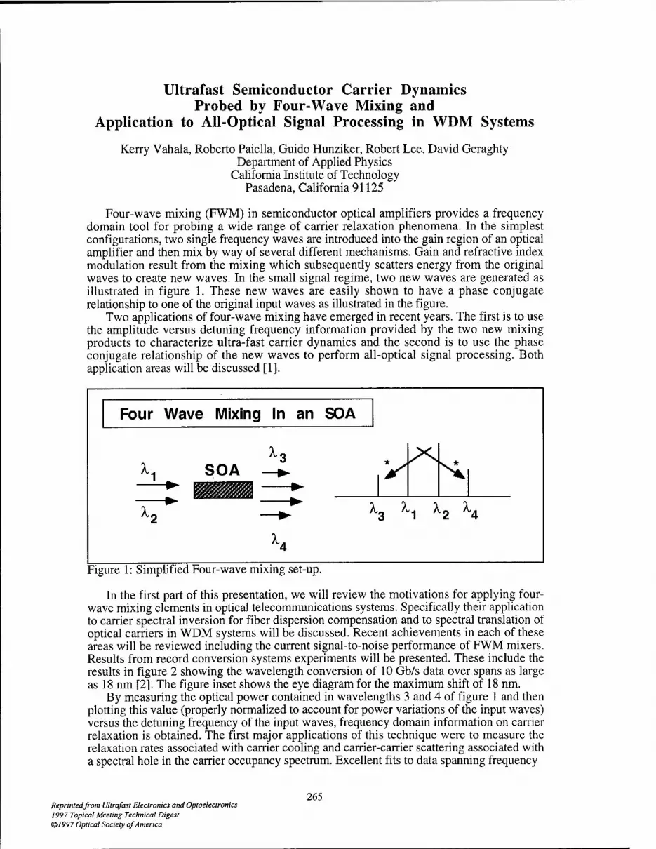
Ultrafast Semiconductor Carrier Dynamics Probed by Four-Wave Mixing and
Application to All-Optical Signal Processing in WDM Systems
Kerry Vahala, Roberto Paiella, Guido Hunziker, Robert Lee, David Geraghty Department of Applied Physics
California Institute of Technology Pasadena, California 91125
Four-wave mixing (FWM) in semiconductor optical amplifiers provides a frequency domain tool for probing a wide range of carrier relaxation phenomena. In the simplest configurations, two single frequency waves are introduced into the gain region of an optical amplifier and then mix by way of several different mechanisms. Gain and refractive index modulation result from the mixing which subsequently scatters energy from the original waves to create new waves. In the small signal regime, two new waves are generated as illustrated in figure 1. These new waves are easily shown to have a phase conjugate relationship to one of the original input waves as illustrated in the figure.
Two applications of four-wave mixing have emerged in recent years. The first is to use the amplitude versus detuning frequency information provided by the two new mixing products to characterize ultra-fast carrier dynamics and the second is to use the phase conjugate relationship of the new waves to perform all-optical signal processing. Both application areas will be discussed [1].
Four Wave Mixing in an SOA
^ SOA —► V s <->
^
A.2 —►* h X1
^4
x2 x4
Fig ure 1: Simplified Four-wave mixing set-up.
In the first part of this presentation, we will review the motivations for applying four- wave mixing elements in optical telecommunications systems. Specifically their application to carrier spectral inversion for fiber dispersion compensation and to spectral translation of optical carriers in WDM systems will be discussed. Recent achievements in each of these areas will be reviewed including the current signal-to-noise performance of FWM mixers. Results from record conversion systems experiments will be presented. These include the results in figure 2 showing the wavelength conversion of 10 Gb/s data over spans as large as 18 nm [2]. The figure inset shows the eye diagram for the maximum shift of 18 nm.
By measuring the optical power contained in wavelengths 3 and 4 of figure 1 and then plotting this value (properly normalized to account for power variations of the input waves) versus the detuning frequency of the input waves, frequency domain information on carrier relaxation is obtained. The first major applications of this technique were to measure the relaxation rates associated with carrier cooling and carrier-carrier scattering associated with a spectral hole in the carrier occupancy spectrum. Excellent fits to data spanning frequency
Reprinted from Ultrafast Electronics and Optoelectronics 1997 Topical Meeting Technical Digest ©1997 Optical Society of America
265

266 Ultrafast Electronics and Optoelectronics
18 nm downshift
^ W^^0**^P i o f ■ "•£ r stf.
■ .v. &■ x- .<■-■■ ■•*. . ./«..
■ i
v *__ In put
4-» 3 %Sl^l^Si
, f-20 O < i j L g-40 I J
i
I
I
- J . >
i
i J \ 11 JL )
l i
1540 1560 1545 1550 1555 Wavelength (nm)
Figure 2: FWM down-shift replicas. Inset: eye diagram for 18 nm shift at 10 Gb/s PRBS.
detunings from 100 GHz to several TeraHertz have been obtained and have complemented time-domain femtosecond pump-probe data.
More recently, we have considered the application of four-wave mixing to measurement of interwell carrier equilibration in multi quantum-well active layers [3]. For this work we have used the polarization selection rules associated with tensile and compressively strained quantum wells to induce spatially selective mixing. Transport of this mixing to neighboring wells is then probed selectively using again the polarization selection rules.
INTERWELL CARRIER
•*— TRANSPORT
_-. .-_ —
"V TM IV
P K CO q «pN i
TE
P
T ENS ILE CO MPREJ 5SIVE
Figure 3: Polarization configuration for inter well transport FWM measurement.

Ultrafast Electronics and Optoelectronics 267
Figure 3 shows the input wave configuration for the experiment. TM components mix only in the tensile wells of the structures causing carrier density modulation that is spatially localized to only these wells. Conventional four-wave mixing occurs as the input waves scatter from this modulation. In addition, however, some carrier density modulation is coupled by way of inter-well transport into neighboring compressively strained quantum wells. Once coupled into these wells, scattering of TE polarized waves is possible through the TE dipole component of the compressive wells. By measuring the detuning frequency dependence of both the TE and TM components of four-wave mixing, it is possible to directly measure the interwell carrier equilibration rate. In particular, the ratio of the TE component to the TM component will decrease with increasing detuning frequency since interwell transport of higher frequency modulations will be less efficient. Ultimately, this ratio will flatten reflecting the ratio of TE to TM conventional four-wave mixing that occurs only within the tensile wells. These predictions are verified in figure 4 which shows the ratio of FWM TE to TM powers in an eight well amplifier (four tensile and four compressive).
ffl S o
in CM
fc -1 T-
a. - 2
20 40 60 80 100
Detuning Frequency Q. (GHz)
Figure 4: Ratio of TE to TM FWM component power versus detuning frequency. Inter well transport becomes inefficient in this structure for detuning rates beyond 40 GHz.
[1] For a review of this topic see: Kerry Vahala, Jianhui Zhou, David Geraghty, Robert B. Lee, Michael Newkirk and Barry Miller, "Current Trends in Optical Amplifiers and Their Applications," pp. 153-177 (World Scientific-Editor T. P. Lee).
[2] David F. Geraghty, Robert B. Lee, Kerry J. Vahala, Marc Verdiell, Mehrdad Ziari, and Atul Mathur, "Wavelength Conversion up to 18 nm at 10 Gb/s by Four-Wave Mixing in a Semiconductor Optical Amplifier," To appear in the April 1997 issue of Photonics Tech. Letters.
[3] Roberto Paiella, Guido Hunziker, Kerry Vahala, Uzi Koren, "Measurement of the Interwell Carrier Transport Lifetime in Multiquantum-Well Optical Amplifiers by Polarization-Resolved Four-Wave Mixing," To appear in the Dec. 30, 1996 issue of Applied Physics Letters.

Ultrafast Spin Relaxation in InGaAs/InP Quantum Wells for Femtoseconds Switch Applications
Atsushi Tackeuchi and Osamu Wada Femtosecond Technology Research Association (FESTA)
5-5 Tokodai, Tsukuba 300-26, Japan
Yuji Nishikawa Fujitsu Laboratories Ltd., 10-1 Morinosato-Wakamiya, Atsugi 243-01, Japan
Abstract The electron spin-relaxation time of InGaAs/InP multiple- quantum wells has been measured to be 5.2 ps for 1.54-um excitonic absorption. This is an order of magnitude faster than in GaAs quantum wells indicating the possibility of femtoseconds all-optical gate operation in the long- wavelength region.
Semiconductor nonlinear optics including MQW, All- optical devices, Ultrafast devices, Ultrafast processes in condensed matter.
1. Introduction The spin relaxation of carriers in JJI-V semiconductor quantum wells (QW) is of interest in view of the fundamental physics [1-14] as well as applications [15-19]. Spin until now has been used mainly for memory devices. However, if the spin could have a sufficiently fast response, it would work as a new function in near-future devices. Here, we describe that the spin-relaxation time of electrons in quantum wells is as fast as picoseconds, especially in an InGaAs QW, and that this fast process can be applied to an ultrafast all-optical gate switch. The measured spin- relaxation time of InGaAs multiple-quantum wells (MQW) is 5.2 ps for 1.54 u.m excitonic absorption, and an ultrashort gating width of 880 fs is expected for a MQW etalon device.
The spin-relaxation time and its mechanism in quantum wells have been uncertain at 300 K, the most important temperature for devices. This has restricted the applicability of this phenomenon. We previously showed the spin relaxation of GaAs/AlGaAs MQWs to be in the tens-of-picosecond region, and proved that the D'yakonov- Perel' (DP) interaction [1,2] is the dominant mechanism at room temperature[3,12]. From the view point of
optical-communication applications, on the other hand, the spin-relaxation process applicable to a 1.55-um- transmission system is more important. However, there have been to our knowledge no reports on the spin relaxation of InGaAs quantum wells.
2. Experimental We measured the spin-relaxation process of InGaAs/InP MQW using spin-dependent optical nonlinearity. The InGaAs/InP MQW sample consisted of 100 periods of alternating 7.0-nm-thick In0 53Ga0 47As quantum wells
and 9.7-nm-thick InP barriers. The structure was grown on a semi-insulating InP substrate by metal-organic chemical- vapor deposition. The electron heavy hole absorption peak was observed at around 1.54 \im at room temperature. An optical parametric oscillator with a Ti-sapphire laser was used as the optical source for a pump-probe experiment. The pulse width was 140 fs and the spectral width was 20 nm. Spin-aligned carriers are created when electrons are excited by a circularly polarized optical pulse. After right-
circularly polarized photoexcitation, G+Pump, the populations of carriers with a down (up) spin along the direction of light propagation, are probed by a right (left)
circularly polarized probe pulse, o+Probe (o-Probe). Since there is no magnetic field, the fully spin-polarized electrons relax to an equilibrium with 50%-up and 50%-down spins. The populations of the spin-up (spin-down) carriers resulting from a 8-excitation pulse is expected to decay (rise) exponentially with a time constant of xs/2. The details concerning the pump-probe absorption measurement were described in our previous publication [3].
3. Results and Discussion The time dependence of the transmission at the heavy-hole exciton peak is shown in Fig. 1 (a). A clear exponential
OSA TOPS on Ultrafast Electronics and Optoelectronics, 1997 Vol. 13, Martin Nuss and John Bowers (ed.) ©1997 Optical Society of America
268
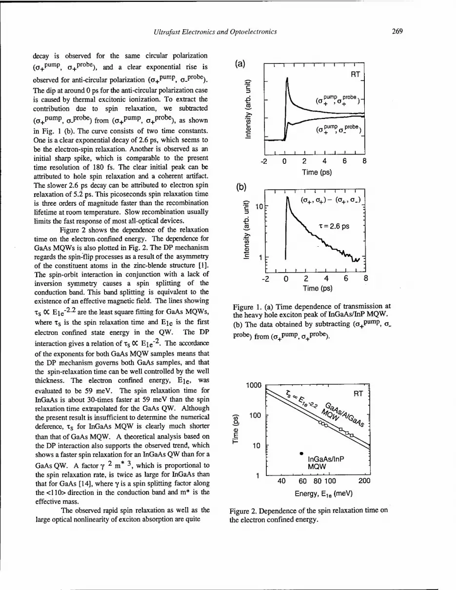
Ultrafast Electronics and Optoelectronics 269
decay is observed for the same circular polarization
(a+pump, a+probe), and a clear exponential rise is
observed for anti-circular polarization (o+PumP, G-Probe).
The dip at around 0 ps for the anti-circular polarization case is caused by thermal excitonic ionization. To extract the contribution due to spin relaxation, we subtracted
(o+PumP, o.Probe) from (a+PumP, a+Probe), as shown
in Fig. 1 (b). The curve consists of two time constants. One is a clear exponential decay of 2.6 ps, which seems to be the electron-spin relaxation. Another is observed as an initial sharp spike, which is comparable to the present time resolution of 180 fs. The clear initial peak can be attributed to hole spin relaxation and a coherent artifact. The slower 2.6 ps decay can be attributed to electron spin relaxation of 5.2 ps. This picoseconds spin relaxation time is three orders of magnitude faster than the recombination lifetime at room temperature. Slow recombination usually limits the fast response of most all-optical devices.
Figure 2 shows the dependence of the relaxation time on the electron-confined energy. The dependence for GaAs MQWs is also plotted in Fig. 2. The DP mechanism regards the spin-flip processes as a result of the asymmetry of the constituent atoms in the zinc-blende structure [1]. The spin-orbit interaction in conjunction with a lack of inversion symmetry causes a spin splitting of the conduction band. This band splitting is equivalent to the existence of an effective magnetic field. The lines showing
TS 0C Eie"2-2 are the least square fitting for GaAs MQWs, where TS is the spin relaxation time and Eje is the first electron confined state energy in the QW. The DP
interaction gives a relation of Ts OC Eie"2. The accordance
of the exponents for both GaAs MQW samples means that the DP mechanism governs both GaAs samples, and that the spin-relaxation time can be well controlled by the well thickness. The electron confined energy, Eie, was
evaluated to be 59 meV. The spin relaxation time for InGaAs is about 30-times faster at 59 meV than the spin relaxation time extrapolated for the GaAs QW. Although the present result is insufficient to determine the numerical deference, TS for InGaAs MQW is clearly much shorter than that of GaAs MQW. A theoretical analysis based on the DP interaction also supports the observed trend, which shows a faster spin relaxation for an InGaAs QW than for a
GaAs QW. A factor y 2 m* 3, which is proportional to the spin relaxation rate, is twice as large for InGaAs than that for GaAs [14], where 7 is a spin splitting factor along the <110> direction in the conduction band and m* is the effective mass.
The observed rapid spin relaxation as well as the large optical nonlinearity of exciton absorption are quite
(a)
c 3
CO c CD
:. n:
1 1 1 1 1 1 1
RT
\ . pump probe. V (0-+ ,0-; )
/*"" /0 pump o probe.
1
Time (ps)
(b)
i 10 3
I I —r i i i i i i \ (a+,a+)- (o-+,o-_)_
Inte
nsity
(ar
b.
I
>» x = 2.6 ps
11 ii iii"
- 2 0 2 4 6 8 Time (ps)
Figure 1. (a) Time dependence of transmission at the heavy hole exciton peak of InGaAs/InP MQW. (b) The data obtained by subtracting (o+Pump, o. probe) from (a+pump; 0+probe)
CO Q.
CD E
1000 F
100 r
10 r
40 60 80 100 200
Energy, E1e (meV)
Figure 2. Dependence of the spin relaxation time on the electron confined energy.
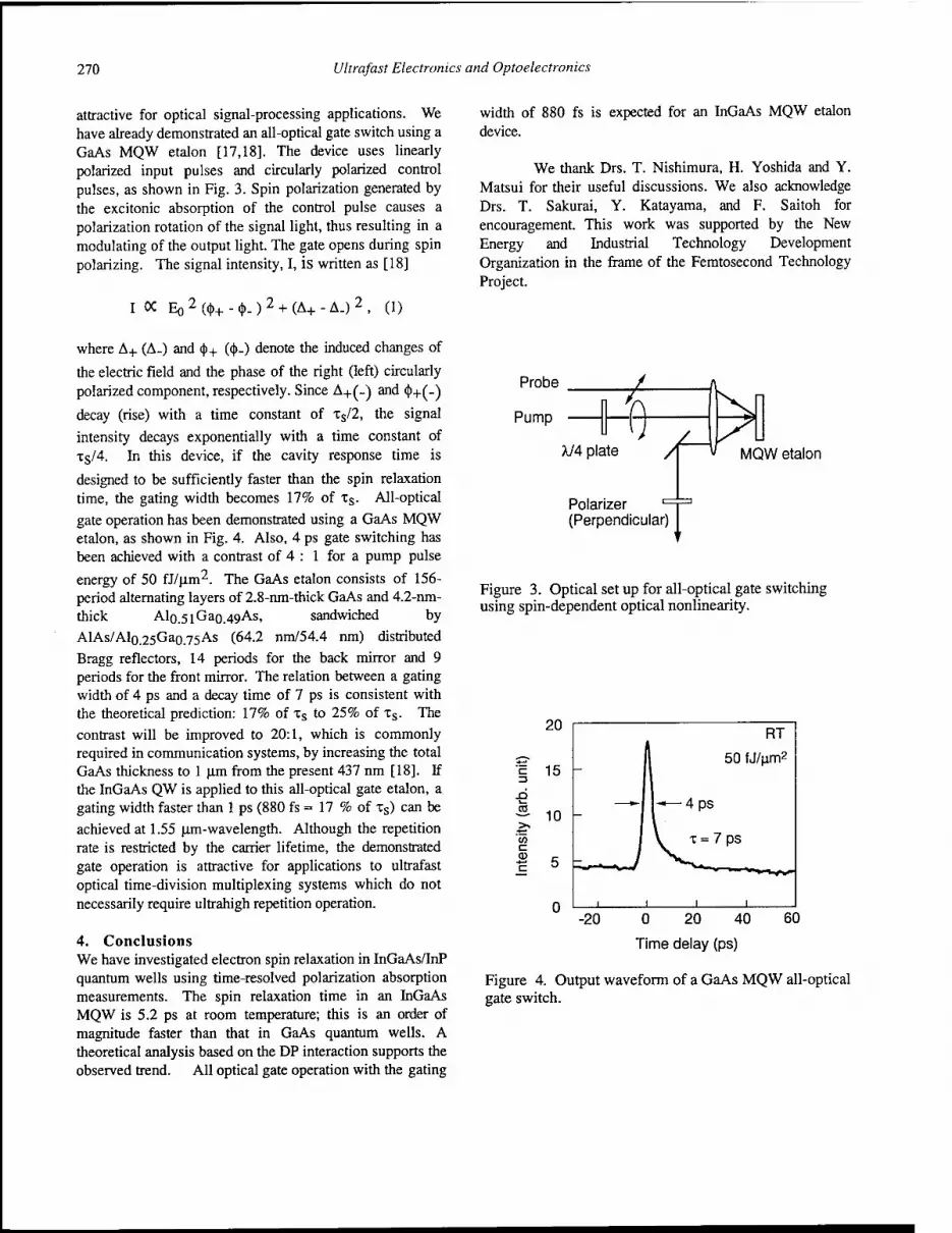
270 Ultrafast Electronics and Optoelectronics
attractive for optical signal-processing applications. We have already demonstrated an all-optical gate switch using a GaAs MQW etalon [17,18]. The device uses linearly polarized input pulses and circularly polarized control pulses, as shown in Fig. 3. Spin polarization generated by the excitonic absorption of the control pulse causes a polarization rotation of the signal light, thus resulting in a modulating of the output light. The gate opens during spin polarizing. The signal intensity, I, is written as [18]
width of 880 fs is expected for an InGaAs MQW etalon device.
We thank Drs. T. Nishimura, H. Yoshida and Y. Matsui for their useful discussions. We also acknowledge Drs. T. Sakurai, Y. Katayama, and F. Saitoh for encouragement. This work was supported by the New Energy and Industrial Technology Development Organization in the frame of the Femtosecond Technology Project.
I 0C Eo 2 (<h- - <)>-) 2 + (A+ - A.) (1)
where A+ (A-) and <))+ (((>-) denote the induced changes of
the electric field and the phase of the right (left) circularly polarized component, respectively. Since A+(_) and <f+(-)
decay (rise) with a time constant of xs/2, the signal
intensity decays exponentially with a time constant of Xg/4. In this device, if the cavity response time is
designed to be sufficiently faster than the spin relaxation time, the gating width becomes 17% of xs. All-optical gate operation has been demonstrated using a GaAs MQW etalon, as shown in Fig. 4. Also, 4 ps gate switching has been achieved with a contrast of 4 : 1 for a pump pulse
energy of 50 fj/u.m2. The GaAs etalon consists of 156- period alternating layers of 2.8-nm-thick GaAs and 4.2-nm- thick Alo.51Gao.49 As, sandwiched by AlAs/Alo.25Gao.75As (64.2 nm/54.4 nm) distributed Bragg reflectors, 14 periods for the back mirror and 9 periods for the front mirror. The relation between a gating width of 4 ps and a decay time of 7 ps is consistent with the theoretical prediction: 17% of xs to 25% of xs. The contrast will be improved to 20:1, which is commonly required in communication systems, by increasing the total GaAs thickness to 1 urn from the present 437 nm [18]. If the InGaAs QW is applied to this all-optical gate etalon, a gating width faster than 1 ps (880 fs = 17 % of xs) can be achieved at 1.55 urn-wavelength. Although the repetition rate is restricted by the carrier lifetime, the demonstrated gate operation is attractive for applications to ultrafast optical time-division multiplexing systems which do not necessarily require ultrahigh repetition operation.
4. Conclusions We have investigated electron spin relaxation in InGaAs/InP quantum wells using time-resolved polarization absorption measurements. The spin relaxation time in an InGaAs MQW is 5.2 ps at room temperature; this is an order of magnitude faster than that in GaAs quantum wells. A theoretical analysis based on the DP interaction supports the observed trend. All optical gate operation with the gating
Probe /
Pump
A/4 plate MQW etalon
Polarizer ■= (Perpendicular)
Figure 3. Optical set up for all-optical gate switching using spin-dependent optical nonlinearity.
20
15 -
- 10 -
J3
3. >, •*—'
'to c CO
RT
- 1 50 fJ/um2
- -I M—4 ps
V X = 7 ps
1 i i i
-20 0 20 40 60
V- 5
Time delay (ps)
Figure 4. Output waveform of a GaAs MQW all-optical gate switch.

Ultrafast Electronics and Optoelectronics 271
REFERENCES
1. M. I. D'yakonov and V. I. Perel', Sov. Phys. JETP 38, 177 (1974). 2. M. I. D'yakonov and V. Yu. Kachorovski, Sov. Phys. Semicond. 20, 110(1986). 3. A. Tackeuchi, S. Muto, T. Inata, and T. Fujii, Appl. Phys. Letters 56, 2213 (1990). 4. T. Uenoyama and L. J. Sham, Phys. Rev. Lett. 64, 3070(1990). ^ 5. T. C. Damen, K. Leo, J. Shah and J. E. Cunningham, Appl. Phys. Lett. 58, 1902 (1991). 6. M. Kohl, M. R. Freeman, D. D. Awschalom, and J. M. Hong, Phys. Rev. B 44, 5923 (1991). 7. S. Bar-Ad and I. Bar-Joseph, Phys. Rev. Letters 68, 349 (1992). 8. G. Bastard and R. Ferreira, Surf. Science 267, 335 (1992). 9. Ph. Roussignol, P. Rolland, R. Ferreira, C. Delalande, G. Bastard, A. Vinattieri, L. Carraresi, M. Colocci, and B. Etienne, Surface Science 267, 360 (1992). 10. A. P. Heberle, W. W. Ruehle, and K. Ploog, Phys. Rev. Lett. 72, 3887 (1994). ILL. Munoz, E. Perez, L. Vina, and K. Ploog, Phys. Rev. B 51, 4247 (1995). 12. A. Tackeuchi, Y. Nishikawa, and O. Wada, Appl. Phys. Letters 68, 797 (1996). 13. S. Adachi, S. Takeyama, Y. Takagi, A. Tackeuchi, and S. Muto, Appl. Phys. Letters 68, 964 (1996). 14. A. Tackeuchi, O. Wada and Y. Nishikawa, Appl. Phys. Letters 70, 1131 (1997). 15. T. Kawazoe, T. Mishina, and Y. Masumoto, Jpn. J. Appl. Phys. 2 32, L1756 (1993). 16. J. Wagner, H. Schneider, D. Richards, A. Fischer, and K. Ploog, Phys. Rev. B 47, 4786 (1993). 17. Y. Nishikawa, A.Tackeuchi, S. Nakamura, S. Muto, and N. Yokoyama, Appl. Phys. Lett. 66, 839 (1995). 18. Y. Nishikawa, A. Tackeuchi, M. Yamaguchi, S.Muto and O. Wada, Jpn. J. Appl. Phys. 2 34, L1283 (1995). 19. H. Horinaka, D. Ono, W. Zhen, K. Wada, Y. Cho, Y. Hayashi, T. Nakanishi, S. Okumi, H. Aoyagi, T. Saka and T. Kato, Jpn. J. Appl. Phys. 2 34, 6444 (1995).
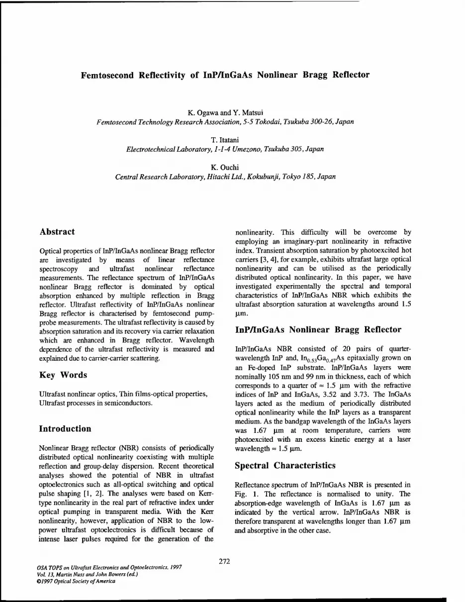
Femtosecond Reflectivity of InP/InGaAs Nonlinear Bragg Reflector
K. Ogawa and Y. Matsui Femtosecond Technology Research Association, 5-5 Tokodai, Tsukuba 300-26, Japan
T. Itatani Electrotechnical Laboratory, 1-1-4 Umezono, Tsukuba 305, Japan
K. Ouchi Central Research Laboratory, Hitachi Ltd., Kokubunji, Tokyo 185, Japan
Abstract
Optical properties of InP/InGaAs nonlinear Bragg reflector are investigated by means of linear reflectance spectroscopy and ultrafast nonlinear reflectance measurements. The reflectance spectrum of InP/InGaAs nonlinear Bragg reflector is dominated by optical absorption enhanced by multiple reflection in Bragg reflector. Ultrafast reflectivity of InP/InGaAs nonlinear Bragg reflector is characterised by femtosecond pump- probe measurements. The ultrafast reflectivity is caused by absorption saturation and its recovery via carrier relaxation which are enhanced in Bragg reflector. Wavelength dependence of the ultrafast reflectivity is measured and explained due to carrier-carrier scattering.
Key Words
Ultrafast nonlinear optics, Thin films-optical properties, Ultrafast processes in semiconductors.
Introduction
Nonlinear Bragg reflector (NBR) consists of periodically distributed optical nonlinearity coexisting with multiple reflection and group-delay dispersion. Recent theoretical analyses showed the potential of NBR in ultrafast optoelectronics such as all-optical switching and optical pulse shaping [1, 2]. The analyses were based on Kerr- type nonlinearity in the real part of refractive index under optical pumping in transparent media. With the Kerr nonlinearity, however, application of NBR to the low- power ultrafast optoelectronics is difficult because of intense laser pulses required for the generation of the
nonlinearity. This difficulty will be overcome by employing an imaginary-part nonlinearity in refractive index. Transient absorption saturation by photoexcited hot carriers [3, 4], for example, exhibits ultrafast large optical nonlinearity and can be utilised as the periodically distributed optical nonlinearity. In this paper, we have investigated experimentally the spectral and temporal characteristics of InP/InGaAs NBR which exhibits the ultrafast absorption saturation at wavelengths around 1.5 u.m.
InP/InGaAs Nonlinear Bragg Reflector
InP/InGaAs NBR consisted of 20 pairs of quarter- wavelength InP and, In0 53Ga0 47As epitaxially grown on an Fe-doped InP substrate. InP/InGaAs layers were nominally 105 nm and 99 nm in thickness, each of which corresponds to a quarter of = 1.5 urn with the refractive indices of InP and InGaAs, 3.52 and 3.73. The InGaAs layers acted as the medium of periodically distributed optical nonlinearity while the InP layers as a transparent medium. As the bandgap wavelength of the InGaAs layers was 1.67 nm at room temperature, carriers were photoexcited with an excess kinetic energy at a laser wavelength =1.5 Jim.
Spectral Characteristics
Reflectance spectrum of InP/InGaAs NBR is presented in Fig. 1. The reflectance is normalised to unity. The absorption-edge wavelength of InGaAs is 1.67 |im as indicated by the vertical arrow. InP/InGaAs NBR is therefore transparent at wavelengths longer than 1.67 nm and absorptive in the other case.
OSA TOPS on Ultrafast Electronics and Optoelectronics, 1997 Vol. 13, Martin Nuss and John Bowers (ed.) ©1997 Optical Society of America
272
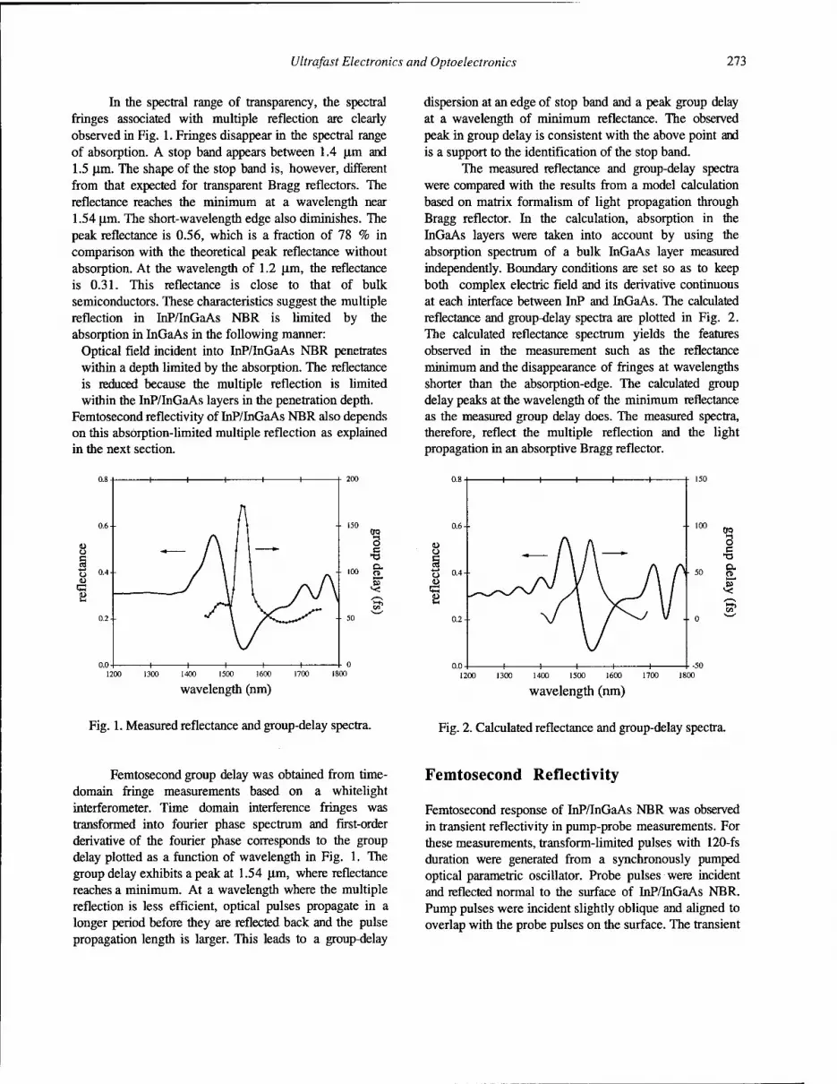
Ultrafast Electronics and Optoelectronics 273
In the spectral range of transparency, the spectral fringes associated with multiple reflection are clearly observed in Fig. 1. Fringes disappear in the spectral range of absorption. A stop band appears between 1.4 u.m and 1.5 um. The shape of the stop band is, however, different from that expected for transparent Bragg reflectors. The reflectance reaches the minimum at a wavelength near 1.54 Jim. The short-wavelength edge also diminishes. The peak reflectance is 0.56, which is a fraction of 78 % in comparison with the theoretical peak reflectance without absorption. At the wavelength of 1.2 \ira, the reflectance is 0.31. This reflectance is close to that of bulk semiconductors. These characteristics suggest the multiple reflection in InP/InGaAs NBR is limited by the absorption in InGaAs in the following manner:
Optical field incident into InP/InGaAs NBR penetrates within a depth limited by the absorption. The reflectance is reduced because the multiple reflection is limited within the InP/InGaAs layers in the penetration depth.
Femtosecond reflectivity of InP/InGaAs NBR also depends on this absorption-limited multiple reflection as explained in the next section.
dispersion at an edge of stop band and a peak group delay at a wavelength of minimum reflectance. The observed peak in group delay is consistent with the above point and is a support to the identification of the stop band.
The measured reflectance and group-delay spectra were compared with the results from a model calculation based on matrix formalism of light propagation through Bragg reflector. In the calculation, absorption in the InGaAs layers were taken into account by using the absorption spectrum of a bulk InGaAs layer measured independently. Boundary conditions are set so as to keep both complex electric field and its derivative continuous at each interface between InP and InGaAs. The calculated reflectance and group-delay spectra are plotted in Fig. 2. The calculated reflectance spectrum yields the features observed in the measurement such as the reflectance minimum and the disappearance of fringes at wavelengths shorter than the absorption-edge. The calculated group delay peaks at the wavelength of the minimum reflectance as the measured group delay does. The measured spectra, therefore, reflect the multiple reflection and the light propagation in an absorptive Bragg reflector.
0.8-
0.6-
1 1 1 1 1
u
■4-» o u
\ 1 1 ^_
0.4- \ 1 A' a
0.2- \ /^~^^
0,0- 1 1 —i 1 1
0.8
(TO o U c O
X)
ft S 0.4 M D
<< G ^^ P
0Q
3
o.
wavelength (nm) wavelength (nm)
Fig. 1. Measured reflectance and group-delay spectra. Fig. 2. Calculated reflectance and group-delay spectra.
Femtosecond group delay was obtained from time- domain fringe measurements based on a whitelight interferometer. Time domain interference fringes was transformed into fourier phase spectrum and first-order derivative of the fourier phase corresponds to the group delay plotted as a function of wavelength in Fig. 1. The group delay exhibits a peak at 1.54 um, where reflectance reaches a minimum. At a wavelength where the multiple reflection is less efficient, optical pulses propagate in a longer period before they are reflected back and the pulse propagation length is larger. This leads to a group-delay
Femtosecond Reflectivity
Femtosecond response of InP/InGaAs NBR was observed in transient reflectivity in pump-probe measurements. For these measurements, transform-limited pulses with 120-fs duration were generated from a synchronously pumped optical parametric oscillator. Probe pulses were incident and reflected normal to the surface of InP/InGaAs NBR. Pump pulses were incident slightly oblique and aligned to overlap with the probe pulses on the surface. The transient

274 Ultrafast Electronics and Optoelectronics
reflectivity was measured as the change in reflected probe intensity as a function of probe delay time.
In Fig. 3, transient reflectivity obtained at wavelengths between 1.48 um and 1.52 um is plotted in a logarithmic scale. The dots and the solid lines correspond to the experimental data and fitting curves, respectively. The wavelength range in the measurements lies in the long-wavelength edge of the stop band. The pump and probe pulses overlap at a delay time ~ 1.4 ps. The transient reflectivity increases when the hot carriers are photoexcited by the pump pulses incident on the surface. The decay of the transient reflectivity consists of the three processes as indicated. Two of them yield exponential decay with fast and slow relaxation time while the rest contributes to constant background in the time scale in Fig. 3.
c 3
I <
I It H 11 111 I H 11 I M I | 11 ll+HH-H H H H I 111 I M | H H | 11 I 111 11 111 111 |
1.49 pm
W#W#S
1111111111 »i 11111111111111 ii 111M11 m 111111111111111111111M11111
1.52 pm
1.48 pm
0 12 3 4 5 6
delay time (ps)
Fig. 3. Transient reflectivity measured at wavelengths between 1.48 urn and 1.52 urn.
The interaction mechanism of the probe pulses with the ultrafast absorption saturation in InP/InGaAs NBR is explained in the framework of the absorption- limited multiple reflection illustrated in Fig. 4. The penetration depth of the probe pulses is extended when hot carriers are photoexcited and the absorption saturation is triggered by the pump pulses. The reflectivity is increased because more InP/InGaAs pairs contribute to the multiple
reflection. The reflectivity increase occurs instantaneously as far as the group-delay dispersion is negligible. The experimental rise time of the transient reflectivity in Fig. 3 is limited by the duration of pump and probe pulses. The change in group delay is less than 10 fs over the pulse-spectral range as expected from the group-delay spectrum in Fig. 1. The reflectivity decay, on the other hand, is the reverse process induced by the absorption recovery during carrier thermalisation. The carrier thermalisation is limited by carrier relaxation processes.
[nP |
InGaAs 1
photoexcited carriers
pump
probe
-/V. W
•
o •o • o
o •
o
/
•
o
w
) )
-I pump OFF ON
Fig. 4. Illustration of pulse propagation modulated by photoexcited carries in InP/InGaAs NBR.
The experimental decay curves in Fig. 4 are fitted with two exponential components (fast and slow) plus a constant offset. Relaxation time of the fast component is about 150 fs at all the wavelengths while that of the slow component in the order of a picosecond. According to the discussion on carrier dynamics in bulk AlGaAs [3], the fast and the slow components are related with relaxation via carrier-carrier scattering and phonon emission, respectively. This identification is consistent with the wavelength dependence of magnitude ratio of the fast to the slow components in Fig. 5, based on the reflectance spectrum in Fig. 1. The reflectance drops when wavelength increases from 1.48 urn t0 1-52 um and higher density of carriers tend to be photoexcited at the longer wavelengths. In this wavelength dependence of carrier density, carrier-carrier scattering is more frequent at the longer wavelength and results in relatively strong contribution of the fast component associated with carrier- carrier scattering.
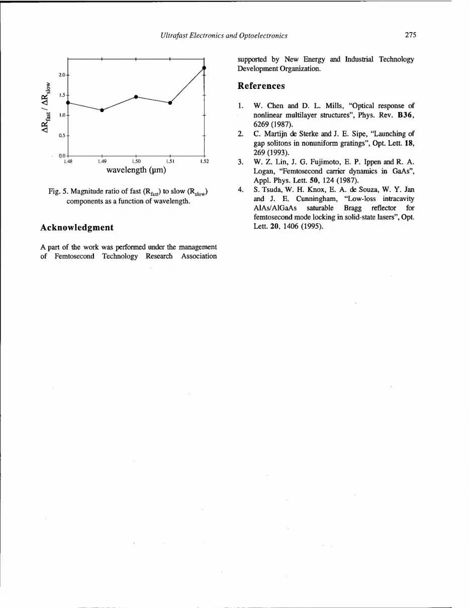
Ultrafast Electronics and Optoelectronics 275
1.48 1.49 1.50 1.51
wavelength (urn) 1.52
Fig. 5. Magnitude ratio of fast (Rfast) to slow (Rslow) components as a function of wavelength.
Acknowledgment
supported by New Energy and Industrial Technology Development Organization.
References
1. W. Chen and D. L. Mills, "Optical response of nonlinear multilayer structures", Phys. Rev. B36, 6269 (1987).
2. C. Martijn de Sterke and J. E. Sipe, "Launching of gap solitons in nonuniform gratings", Opt. Lett. 18, 269 (1993).
3. W. Z. Lin, J. G. Fujimoto, E. P. Ippen and R. A. Logan, "Femtosecond carrier dynamics in GaAs", Appl. Phys. Lett. 50, 124 (1987).
4. S. Tsuda, W. H. Knox, E. A. de Souza, W. Y. Jan and J. E. Cunningham, "Low-loss intracavity AlAs/AlGaAs saturable Bragg reflector for femtosecond mode locking in solid-state lasers", Opt. Lett. 20, 1406 (1995).
A part of the work was performed under the management of Femtosecond Technology Research Association

Electroabsorption Dynamics in an InGaAsP/InGaAsP Superlattice Modulator
G.C. Cho, A. Ziebell, T. Dekorsy, H.J. Bakker1, B. Opitz2, A. Kohl3 and II. Kurz Institut für Halbleitertechnik, RWTH Aachen, Sommerfeldsir. 24 D-52056 Aachen, Germany
Abstract
The fs-electroabsorplion signal in a supcrlatticc modulator designed for 1.55 mm reveals incoherent and coherent transport dynamics in Wannier-Stark states. Bloch oscillations appear chirped due to dynamic field screening.
Key Words
Semiconductors, Electro-optical devices, Semiconductor nonlinear optics, Ultrafast spectroscopy
Introduction
Optical nonlinearities are the essential property of photonics device in optical communication system. For realization of high-rate data transfer the band-width of optical modulators is a key issue. A most practical modulator device concept is to use the electroabsorption (EA) of semiconductor helerostructures [1] of InP-based quantum wells designed for 1.55 ujii-wavelenglh. Recently a 20 GHz EA modulator based on InGaAsP/InGaAsP has been demonstrated.[2] In most cases the screening dynamics of externally applied electric fields determined by carrier transport govern the EA dynamics. For the modulation of broad-band optical pulses superlattices with large Wannier-Stark (WS) splittings [3] of strongly coupled quantum wells are highly attractive. In a biased superlattice, the transport dynamics of carriers reveal a coherent and incoherent contribution. The former is based on the excitation of Bloch oscillations [4-5] in the absence of significant scattering events, while the latter results from scattered Bloch electrons contributing to a net drift current.
Here we present investigations on the ultrafast optical nonlinearities associated with EA dynamics in an InGaAsP/InGaAsP superlattice modulator. Both the coherent and incoherent transport contributions are
unambiguously disentangled. For the incoherent transport a differential transmission technique with bias modulation is employed, which allows to derive the pure EA signal without contribution of bleaching induced by the pump pulse. On the coherent lime scale we observe Bloch oscillations in the transmission signal as reported in a previous study [6] in this material system. As a results of dynamical screening due to incoherent transport we observe that the period of the decaying Bloch oscillations is chirped.
Experimental Setup and Sample
D2
time-delay (v2)
'AT(AV,At)
Figure 1. Experimental setup for time-resolved electroabsorption. The conventional pump-probe transmission setup is modified with additional bias modulation on the sample. The sample is placed in a closed circuit cryostat at 10 K. Di and D2 are InGaAs-photocletectors.
OSA TOPS on Ultrafast Electronics and Optoelectronics, 1997 Vol. 13, Martin Nuss and John Bowers (ed.) 61997 Optical Society of America
276
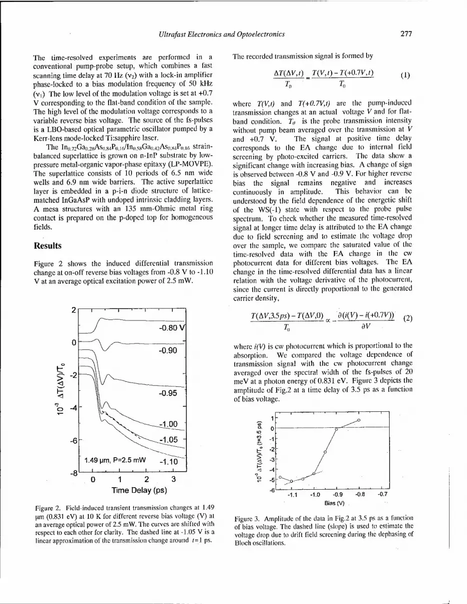
Ultrafast Electronics and Optoelectronics 277
The In().72Ga<).2xAS().84Po.ir/In0.58Ga0.42Asn.s4P().i6 slrain-
The time-resolved experiments are performed in a conventional pump-probe setup, which combines a fast scanning time delay at 70 Hz (v2) with a lock-in amplifier phase-locked to a bias modulation frequency of 50 kHz (V|) The low level of the modulation voltage is set at +0.7 V corresponding to the flat-band condition of the sample. The high level of the modulation voltage corresponds to a variable reverse bias voltage. The source of the fs-pulses is a LBO-based optical parametric oscillator pumped by a Kerr-lens mode-locked Ti:sapphire laser.
*().2«AS().84F
balanced superlattice is grown on n-InP substrate by low- pressure metal-organic vapor-phase epitaxy (LP-MOVPE). The superlattice consists of 10 periods of 6.5 nm wide wells and 6.9 nm wide barriers. The active superlattice layer is embedded in a p-i-n diode structure of lattice- matched InGaAsP with undoped intrinsic cladding layers. A mesa structures with an 135 mm-Ohmic metal ring contact is prepared on the p-doped top for homogeneous fields.
Results
Figure 2 shows the induced differential transmission change at on-off reverse bias voltages from -0.8 V to -1.10 V at an average optical excitation power of 2.5 mW.
3 ?
1 2 3 Time Delay (ps)
Figure 2. Field-induced transient transmission changes at 1.49 um (0.831 eV) at 10 K for different reverse bias voltage (V) at an average optical power of 2.5 mW. The curves are shifted with respect to each other for clarity. The dashed line at -1.05 V is a linear approximation of the transmission change around /=! ps.
The recorded transmission signal is formed by
AT(AV,1) _T(V,t)-T(+Q.7V,t) (1)
where T(V,t) and T(+0.7V,t) are the pump-induced transmission changes at an actual voltage V and for flat- band condition. T„ is the probe transmission intensity without pump beam averaged over the transmission at V and +0.7 V. The signal at positive time delay corresponds to the EA change due to internal field screening by photo-excited carriers. The data show a significant change with increasing bias. A change of sign is observed between -0.8 V and -0.9 V. For higher reverse bias the signal remains negative and increases continuously in amplitude. This behavior can be understood by the field dependence of the energetic shift of the WS(-l) slate with respect to the probe pulse spectrum. To check whether the measured time-resolved signal at longer lime delay is attributed to the EA change due to field screening and to estimate the voltage drop over the sample, we compare the saturated value of the time-resolved data with the EA change in the cw photocurrent data for different bias voltages. The EA change in the time-resolved differential data has a linear relation with the voltage derivative of the photocurrent, since the current is directly proportional to the generated carrier density,
T(AV,3.5ps) - r(AV,0) K d(i(V) - /(+0.71Q)
7;, K <w (2)
where i(V) is cw photocurrent which is proportional to the absorption. We compared the voltage dependence of transmission signal with the cw photocurrent change averaged over the spectral width of the fs-pulses of 20 meV at a photon energy of 0.831 eV. Figure 3 depicts the amplitude of Fig.2 at a lime delay of 3.5 ps as a function of bias voltage.
- f
—i—i ■. i 1 1
■
o-
/
■
/ /
_°-. 1 . I
-1.1 -1.0 -0.9 Bias (V)
-0.8 -0.7
Figure 3. Amplitude of the data in Fig.2 at 3.5 ps as a function of bias voltage. The clashed line (slope) is used to estimate the voltage drop due to drift field screening during the dephasing of Bloch oscillations.

278 ültrafast Electronics and Optoelectronics
Figure 4 shows Ihe cw counterpart of Fig. 3. The voltage offset between the two plots of -1.2 V by comparing the minimum point results from the voltage drop due to the quasi-static accumulation of carriers in the time-resolved data.
'c.
xi CO
I i
0.2 0.3 0.4 Bias (V)
Figure 4. The negative differential cw photocurrent as function of bias voltage integrated over 20 meV at 0.831 eV.
Clearly, the nonlinear shape of the voltage dependence of the transient amplitude agrees well with the differential photocurrent data.
Thus we attribute the dynamics on the picosecond scale in Fig. 2 to the EA change due to carrier transport within the superlattice. The sign and amplitude depend completely on the field at negative time delay and the photon energy of the probe pulse. The fast rise-up of the signal at -0.80 V in Fig. 2 is attributed to the so-called instantaneous field screening based on the spatially nonvertical optical transition to the WS(-l)-state, which is equivalent to the Franz-Keldysh effect. [6]
The superimposed oscillatory signal corresponds to electronic Bloch oscillations formed by the coherent superposition of the WS(0) and WS(-l). The oscillation frequency exhibits the expected frequency-field relation v=eFd/h, with d the superlattice period and F the electric field. The observed oscillations stem mainly from the bleaching and Coulomb screening due to the coherent population of the WS(0)- and WS(-l)-slate, and not from the EA due to the internal field oscillations. To compare the EA and absorption bleaching contribution for the Bloch oscillation signal we examine the data at a bias of -0.9 V in Fig. 2. The oscillation amplitude immediately after the pump pulse is superimposed on the slowly changing signal of the incoherent transport. The important fact in this feature is that the Bloch oscillation amplitude is much larger than the overall EA signal, i.e.absorption change due to the energetic shift of WS states. Thus considering the much lower field change due to the Bloch charge oscillations that extend over a few
periods of the superlattice in the WS ladder, the large oscillation amplitude must be the result of phase-space filling and excitonic effects associated witli the coherent wavepackets.
(a)
t o GO
9 <
3h
2
1
0
-1
-2 V
V =-1.05 V, P = 2.5mW 5v/8t = 0.45 THz/ps
0.5 1.0 1.5 2.0 2.5 3.0 3.5
Time Delay (ps)
(b) >) , 1 •— r— ■ t
/ / T? At>l.0ps; \ CD i 1 i N ' / ' \0.25<At<3.5ps OJ F \ *AA
o ' / I c I —* \- / / \ ^ \A u. ' / u. x/ J
i.i.
Frequency (THz)
Figure 5. (a) Extracted Bloch oscillations at V=-1.05 V (dashed line). The solid line is a numerical fit with a linear chirp bv/bt at a frequency of 3.7 THz. (b) Normalized Fourier power spectra of the experimental data in (a) at different time intervals.
A consequence of the dynamic field change in the superlattice on the coherent transport is a time-dependent period of the Bloch oscillations. These chirped Bloch oscillations can be observed provided a significant field screening occurs within the dephasing time of Bloch oscillations. Figure 5 (a) shows the extracted Bloch oscillations from Fig.l at -1.05 V. A careful fit considering a linear chirp of the data gives a chirp factor of 0.45 THz/ps at a central frequency of 3.7 THz. Figure 5 (b) shows Fourier power spectra of the full lime scale of 2> 0.25 ps (solid line) compared to a time scale ;> 1 ps (dashed line). The spectrum shows clearly the red-shift at longer time delays due to the dynamic field screening. The chirp factor coincides well with the field change estimated from the slopes (dashed lines) in Fig. 2 and in Fig. 3, which gives an expected chirp value of 0.52 THz/ps.
Ultrafast Electronics and Optoelectronics 279
Conclusion
We investigated EA dynamics of an optical modulator structure based on an InGaAsP/InGaAsP superlattice by a differential bias-modulated pump-probe technique. The field-induced dynamics of transient absorption data give a direct information on the incoherent and coherent carrier transport in the superlattice. The internal field shows to be screened in a picosecond scale via incoherent carrier transport. Partly the incoherent transport is directly related to the decay process of Bloch oscillations. We observe that the decay of coherent states does not only lead to the dephasing of Bloch oscillations but also to a chirp of the oscillation frequency as a result of dynamic field screening. Our study in an InP-based material provides an approach to the investigation of superlattices in ultrabroad-band fiber communication technology.
Acknowledgment
This work is supported by the Deutsche Forschungsgemeinschaft under Grant No. DFG KU 540/23-1.
1 present address : FOM-Institute of Atomic and Molecular Physics, Kruislaan 407, 1098 SJ, Amsterdam, NL. 2 present address : Robert Bosch GmbH, Ttibingerstr. 123, D-72762 Reutlingen, Germany. 3 present address : Alcatel Alsthom Recherche, Route de Nozay, 91460 Marcoussis, France.
References 1. D.A.B. Miller, D.S. Chemla, T.C. Damen, T.H.
Wood, C.A. Burrus, Jr., A.C. Gossard, and W.Wiegmann, IEEE J. Quantum Electron. QE-21, 1462 (1985); A.M. Fox, D.AB. Miller, G. Livescu, J.E. Cunningham, and W.Y. Jan, IEEE Quantum Electron. QE-27, 2281 (1991).
2. F. Devaux, F. Dorgeuille, A. Ougazzaden, F. Huet, M. Carre, A. Carenco, M. Henry, Y. Sorel, J.-F. Kerdiles, and E. Jeanney, IEEE Photon. Technol. Lett. 5, 1288 (1993).
3. L. Esaki and R. Tsu, IBM J. Res. and Dev. 14, 61 (1970).
4. For a recent review, see H. Kurz, H.G. Roskos, T. Dekorsy, and K. Köhler, Phil. Trans. R. Soc. Lond. A 354, 2295 (1996).
5. G.C. Cho, T. Dekorsy, H.J. Bakker, A. Kohl, B. Opitz, and H. Kurz, Phys. Rev. B 54, 4420 (1996).
6. S.L. Chuang, S. Schmitt-Rink, B.I. Greene, P.N. Saeta, and A.F.J. Levi, Phys. Rev. Lett. 68, 102 (1992).

Femtosecond Infrared Spectroscopy of Hot Electrons in an In0 53Gao.47As / In0 52A10 48As Multiple Quantum Well Structure.
T. A. Gardinerf, Ju. V. Vandyshev*, G. W. Wicks*, and P. M. Fauchet1
Department of Physics and Astronomy, University of Rochester, Rochester, NY 14627 * Department of Electrical Engineering, University of Rochester, NY 14627
* The Institute of Optics, University of Rochester, Rochester, NY 14627
Abstract
The dynamics of excited carriers in semiconductor quantum well structures has been extensively studied by the methods of ultrafast laser spectroscopy for more than a decade [1-5]. However, a whole series of experiments are now possible which promise new insight into the processes of carrier relaxation. This is due to the recent development of reliable, high power, tabletop, femtosecond laser sources which enable the production of near- and mid- infrared femtosecond pulses through nonlinear optical frequency conversion. In this paper we report the results of recent experiments on the relaxation dynamics of hot electrons in an InGaAs/InAlAs multiple quantum well (MQW) structure through degenerate and non-degenerate pump-probe spectroscopy.
Key Words
Semiconductors, including MQW, Ultrafast spectroscopy, Spectroscopy-infrared, Ultrafast processes in condensed matter, including semiconductors.
Laser System
The time-resolved pump-probe experiments were performed using the femtosecond laser system shown schematically in Figure 1. The pulses generated by the mode-locked Ti:Sapphire oscillator are regeneratively amplified at 1 kHz. Two optical parametric amplifiers (OPAs) are pumped by the amplified pulses. They both operate on a double-pass scheme with a BBO crystal cut for type II phase matching and are seeded with a white light continuum. Between the signal and the idler wave, the output can be tuned from 1.2 to 2.4 urn. The signal
and idler waves from one of the OPAs are mixed in a AgGaS2 crystal to produce femtosecond mid-infrared pulses by difference frequency generation (DFG). Thus, we have two independently tunable, synchronized sources of ultrashort pulses: one gives us access to the spectral range of the valence to conduction band, interband, transitions and the other gives us access to the n=l to n=2, conduction band derived, intersubband transition. The overall temporal resolution of our experiments is approximately 200 fs.
X = 0.8 um
Ti:S Oscillator > Ti:S Amplifier
X = 3- 10 urn
<
Signal DFG « OPA1
Idler
A. = 1.2 - 2.4 urn <- OPA2
Figure 1. Schematic diagram of the laser system.
Sample Properties
The MQW sample used in our experiments was grown by molecular beam epitaxy on an InP semi-insulating substrate. The structure has a total of 140 periods, each period consisting of a 5 nm wide In0 53Ga0 47As well and an 8 nm wide In052Al048As barrier. The well layers were selectively doped with Si atoms at a concentration of ~2xl018 cm"3, corresponding to an electron sheet density of ~ lxlO12 cm"2. The optical transition between the n=l and
OSA TOPS on Ultrafast Electronics and Optoelectronics, 1997 Vol. 13, Martin Nuss and John Bowers (ed.) &1997 Optical Society of America
280

Ultrafast Electronics and Optoelectronics 281
n=2 conduction subbands gives rise to an absorption line centered at 4.7 urn, [6] corresponding to a photon energy of 264 meV. The infrared transmission spectrum, measured near Brewster's angle, is shown in Figure 2 [7]. This transition energy is in good agreement with envelope function approximation [EFA] calculations [8]. The normal incidence, interband transmission, shown in Figure 3, shows the characteristic steps of a quasi-two- dimensional system [9]. Doping the MQW sample n-type partially bleaches and broadens the absorption edge for the n=l (valence) to n=T (conduction) subband transition [10]. The n=2 absorption edge is much less affected due to the negligible population in the n=2 subband; the Fermi energy is estimated to be approximately 60 meV above the bottom of the n=l subband.
Experimental Conditions
For the purposes of brevity it is useful to describe in one section the conditions under which the experiments to be described were carried out. All of the measurements reported here were made at room temperature. The incident light is p-polarized and the angle of incidence ranges from 40 to 73 degrees, while Brewster's angle is approximately 73 degrees. Our results are consistent with the picture that the changes in absorption are dominated by the changes in the transmission. As a result, only the photo-induced changes in the transmission will be reported.
Intersubband Relaxation
0 47
0.46
c .2 "t/3
0.45
0.44
c 0.43
0.42
0.41
"\
-I-I- T • | ■ ■ ' i i i i -!-"-r-I-T-| ' 1 *■■■!■■■■.
n = 2 jfijf^f n=l f*^
, ,
/
\ /FWHM=0.8 um, : \J 43 meV \ ■ ■ '■■'''
4 4.5 5 5.5 6 6.5 Wavelength (jam)
Figure 2. Transmission in the neighborhood of the intersubband resonance at 4.7 urn.
c o
c
0.6
0.5
i ■'' i i i | I i i i | i i i i Jij_lJL.
0.4 n=l /
:n = 2^-
[n-2:
n=l: 0.3 i ,
i
0.2 :
0.1 : / ■
■
0 ' i....
1 1.1 1.2 1.3 1.4 1.5 1.6 1.7 Wavelength (jam)
Figure 3. Transmission in the neighborhood of the interband resonances.
2 4 6 Time (ps)
Figure 4. Degenerate pump-probe signals for two different intensities.
In Figure 4 we present results from degenerate pump- probe experiments where both the pump and probe beam are tuned to resonance with the n=l to n=2 subband transition. Because of the nearly parallel conduction subbands, this measurement gives directly the upper state (n=2) population averaged over the relevant volume in reciprocal space. In a typical experiment we observe transient bleaching, associated with the saturation of the intersubband transition, or Pauli-blocking. At low pump power, when only a small fraction of the electrons are promoted to the n=2 subband, the bleaching recovery is exponential with a characteristic time constant of 1.4 ps. This time corresponds to the intersubband electron-phonon scattering time, and is in agreement with both theoretical predictions [11] and the results of similar experiments performed with picosecond pulses [3]. Unlike the non- degenerate experiments, the intersubband decay rate is very weakly dependent on the excitation intensity. As shown in Figure 4, raising the pump power by a factor of

282 ültrafast Electronics and Optoelectronics
19 changes the decay rate by a mere 25%. As we raise pump power further, the relaxation rate continues to slow down, eventually becoming non-exponential.
Intrasubband Relaxation
Some results of non-degenerate experiments for probe wavelengths in the interband absorption range are presented in Figures 5 and 6. In these experiments the pump is tuned to resonantly excite the n=l to n=2 intersubband transition. The dynamics of the n=l subband electrons at various energies are investigated by tuning the probe beam between 1.2 and 1.54 urn. Since we are probing between a full valence band and an excited conduction subband, the signal we measure is only dependent on the changes in the population of the n=l conduction subband. Using the fact that the conduction subbands are nearly parallel, we expect a uniform depopulation of the n=l subband. This leads us to expect that the initial behavior of the pump-probe signal will be induced absorption, when probing initially populated states. This is indeed what we find, but by studying the subsequent dynamics we learn a great deal more about the relaxation processes.
Pump @ 4.7 (im
o
H <
2 4 Time (ps)
Figure 5. Time resolved transmission change for select wavelengths.
In Figure 5 we present a few representative relaxation traces for relatively low excitation intensity. Our measurements indicate that, for wavelengths longer than 1.25 urn, the induced absorption recovers with a characteristic time constant of 0.7 - 2.5 ps depending on the probe wavelength and excitation intensity. The decay rate increases by either reducing the excitation power or going to shorter wavelength. Note, however, that the trace shown in Figure 4 with a probe wavelength of 1.33 um is not exponential. The time constant shown is a fit to the
decay, presented only for qualitative comparison. When we tune the probe wavelength shorter than 1.25 urn we observe induced absorption followed by bleaching. The behavior of the pump-probe signals shown in Figure 5 can be qualitatively understood by considering two effects. First, electrons excited to the n=2 subband will undergo intersubband electron-phonon scattering back to the n=l subband with -200 meV of excess energy where they interact with the unexcited (ignoring free carrier absorption), but nonequilibrium, n=l population. Second, the unexcited n=l population will also undergo electron- electron and electron-phonon intrasubband scattering, while seeking a new equilibrium. These two process both conspire to produce the transient overshoot in the n=l subband population as well as drive the return to equilibrium. Another way to visualize this process is to spectrally resolve the relaxation.
1.2 1.25 1.3 1.35 1.4 1.45 1.5 1.55 Probe (\xm)
Figure 6. Spectrally resolved transmission change for select time delays. The lines are intended to guide the eye.
In Figure 6 we plot the differential transmission as a function of wavelength for a few time delays. Great care was taken during this process to maintain the "zero" time delay fixed for each wavelength. Now we can use the fact that in the EFA the density of states (DOS) is step-like. Ignoring, for the moment, the behavior near 1.5 um, the differential transmission signal is proportional to the difference between the excited n=l electron distribution and the equilibrium electron distribution. If we were to consider modeling the electron distribution with a high temperature Fermi-Dirac distribution, the resulting signal would qualitatively have the same shape as shown in Figure 6. Smoothing of the step-like DOS gives rise to the sharp drop off in signal near 1.5 urn. While this picture is qualitatively correct, it may not be appropriate to this situation since for the experiments described in Figures 5 and 6, degenerate pump-probe experiments at this

Ultrafast Electronics and Optoelectronics 283
excitation intensity show that the intersubband relaxation time is -1.8 ps. This time is approximately equal to the relaxation time for the n=l electron distribution. Therefore, the n=l subband is not well isolated from the influx of hot electrons from the n=2 subband and the whole system must be considered as coupled.
Conclusions
Our measurements show that the population of the n=l subband returns to equilibrium within several picoseconds, but is generally dependent on the pump intensity. We find that as a larger fraction of the n=l electrons are promoted to the n=2 subband, as seen by the onset of intersubband absorption saturation, the return to equilibrium slows down. At higher pump intensity, some of the electrons may be promoted into the continuum states, and recovery first requires electron capture in the wells. Finally, we note that our results are in qualitative agreement with similar experiments that have been recently reported [4,5]. There are, however, differences, in particular the relaxation times, which may be, in part, attributable to differences in experimental conditions and sample characteristics.
Acknowledgments
This research was supported by the Office of Naval Research.
References and Notes
1. G. Fasol, A. Fasolino, and P. Lugli, Spectroscopy of Semiconductor Microstructures (Plenum Press, New York, 1989) and references therein.
2. Z. Xu, P. M. Fauchet, C. W. Rella, B. A. Richman, H. A. Schwettman, G. W. Wicks, "Hole relaxation in p- type I^Ga^As/AlyGa^yAs quantum wells observed by ultrafast mid-infrared spectroscopy," Phys. Rev. B 51, 10631 (1995).
3. R. J. Bäuerle, T. Elsaesser, W. Kaiser, H. Lobentanzer, W. Stolz, K. Ploog, "Picosecond infrared spectroscopy of hot carriers in a modulation- doped Ga0 47In0 53As multiple-quantum-well structure," Phys. Rev. B 38 4307 (1988).
4. M. Woerner, S. Lutgen, R. Kaindl, T. Elsaesser, A. Hase, H. Künzel, "Inter-subband scattering and thermalization of electrons in quantum wells studied with mid-infrared femtosecond pulses," in Technical Digest of Ultrafast Phenomena (Optical Society of America, Washington, DC, 1996), paper ThCl-1.
5. S. Lutgen, R. A. Kaindl, M. Woerner, T. Elsaesser, A. Hase, H. Künzel, M. Gulia, D. Meglio, P. Lugli, "Nonequilibrium Dynamics in a Quasi-Two- Dimensional Electron Plasma after Ultrafast Intersubband Excitation," Phys. Rev. Lett. 77, 3657 (1996).
6. H. Asai, and Y. Kawamura, "Well-width dependence of intersubband absorption in InGaAs/InAlAs multiquantum wells," Appl. Phys. Lett., 56 (12), 1149 (1990).
7. No absorption due to this transition is detectable at normal incidence in accord with the dipole selection rules and the envelope function approximation.
8. G. Bastard, Wave Mechanics Applied to Semiconductor Heterostructures (Les editions de physique, France, 1990), pp. 63 - 117.
9. Note that the dip seen at 1.6 um in the transmission is the result of Fabry Perot fringes in the transparency region.
10. H. Asai, and Y. Kawamura, "Doping effects on intersubband absorption in InGaAs/ InAlAs multiquantum wells," Appl. Phys. Lett., 56 (15), 1427 (1990).
11. B. K. Ridley, "Electron scattering by confined LO polar phonons in a quantum well," Phys. Rev. B 39, 5282 (1989).

Subpicosecond nonlinear absorption recovery dynamics of low-temperature-grown In0 53Ga0 47As/In0 52Al048As multiple quantum well p-i-n structures
Paul W. Juodawlkis, Zhiping Zhou, and Carl M. Verber School of Electrical and Computer Engineering, Georgia Institute of Technology, Atlanta, GA 30332-0250
David T. Mclnturff School of Electrical and Computer Engineering and the MRSECfor Technology Enabling
Heterostructure Materials, Purdue University, West Lafayette, IN 47907-1285
Marian C. Hargis and Stephen E. Ralph Department of Physics, Emory University, Atlanta, GA 30322-2430
Phone: (404) 727-4294/FAX: (404) 727-08731 e-mail: [email protected]
Abstract
Electroabsorption modulation is demonstrated in low- temperature-grown InGaAs/InAlAs multiple quantum wells exhibiting 600 fs nonlinear absorption recovery associated with anneal-stable Be-As defects. We show that the absorption recovery time, which depends on the active- defect density, can be controlled by adjusting the Be-doping concentration.
Key Words
Semiconductor nonlinear optics, including MQW; Ultrafast processes in condensed matter, including semiconductors; Spectroscopy-time-resolved; Modulators
Introduction
Semiconductor quantum well materials exhibiting ultrafast photoresponses have proven useful in a number of applications including saturable absorbers for laser mode- locking [1], all-optical switching [2], and high-saturation- intensity electroabsorption modulators [3]. A key feature of these materials is a fast recovery time allowing high repetition rates. One method of reducing the photo-excited carrier lifetime is the introduction of defect states through low-temperature growth (LTG), although this technique alone is not very effective in narrow-gap materials. The combination of LTG and Be doping has been shown to significantly reduce the absorption recovery time of InGaAs/InAlAs multiple quantum wells (MQWs) at the expense of broadened excitonic resonances [4, 5]. The Be- incorporation also reduces the residual electron concentration caused by the excess As introduced during
LTG [4-6]. We note that the Be-incorporation responsible for the reduction of both the recovery time and excess electron concentration is different than simple Be-doping compensation. Indeed, we recently reported that Be- incorporation maintains the ultrafast recovery time upon annealing, providing further evidence of the formation of Be-As complexes [5].
Previous reports of MQWs having ultrafast absorption recovery times induced by high defect densities have revealed significant degradation of the excitonic resonances [1, 4, 7]. This degradation results from defect- related perturbations of the crystalline symmetry, and/or field ionization by charged defects [1]. Both of these mechanisms significantly broaden the resonance when the defect density exceeds one per exciton volume. Broadening of the excitonic resonance results in a reduction of both the bandedge saturable-absorption nonlinearity and the bandedge sharpness (da/dA,).
One method of enhancing the bandedge nonlinearity of LTG quantum-well saturable-absorber materials may be to use the spectral shift associated with the quantum confined Stark effect (QCSE). Photo-excited charge carriers screen the built-in and externally applied electric field of a p-i-n MQW structure, causing a blue-shift of the absorption spectrum. The actual nonlinear absorption enhancement that is obtained depends strongly on the relation between the bandedge and excitation wavelengths. An electric field is also an effective method of reducing the absorption recovery time by sweeping out the photogenerated carriers [8]. It may be possible to combine carrier sweep-out with LTG defect-mediated carrier recombination to form a hybrid absorption recovery technique.
Another potential application of quantum well p-i-n structures incorporating LTG materials is electroabsorption
OSA TOPS on Ultrafast Electronics and Optoelectronics, 1997 Vol. 13, Martin Nuss and John Bowers (ed.) 61997 Optical Society of America
284
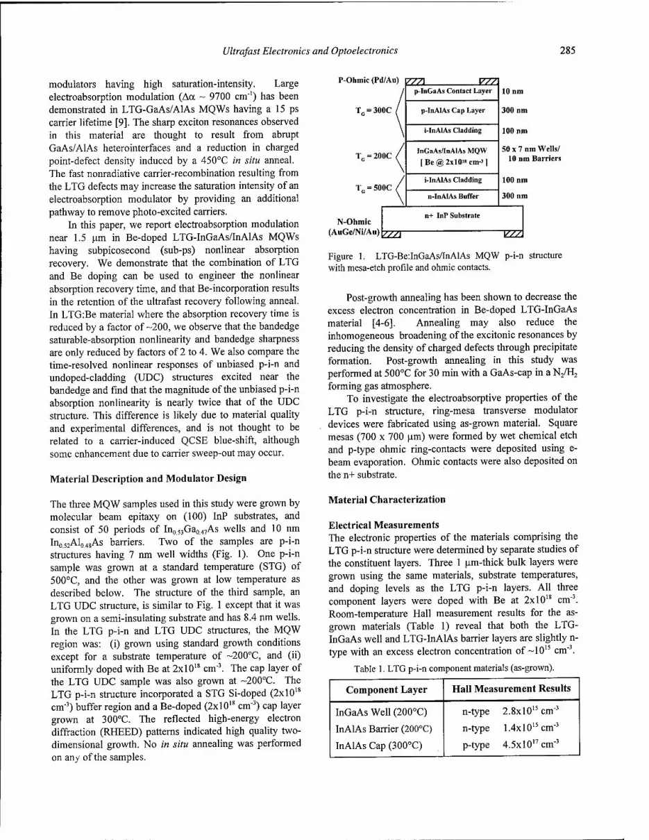
Ultrafast Electronics and Optoelectronics 285
modulators having high saturation-intensity. Large electroabsorption modulation (Aa ~ 9700 cm"1) has been demonstrated in LTG-GaAs/AlAs MQWs having a 15 ps carrier lifetime [9]. The sharp exciton resonances observed in this material are thought to result from abrupt GaAs/AlAs heterointerfaces and a reduction in charged point-defect density induced by a 450°C in situ anneal. The fast nonradiative carrier-recombination resulting from the LTG defects may increase the saturation intensity of an electroabsorption modulator by providing an additional pathway to remove photo-excited carriers.
In this paper, we report electroabsorption modulation near 1.5 urn in Be-doped LTG-InGaAs/InAlAs MQWs having subpicosecond (sub-ps) nonlinear absorption recovery. We demonstrate that the combination of LTG and Be doping can be used to engineer the nonlinear absorption recovery time, and that Be-incorporation results in the retention of the ultrafast recovery following anneal. In LTG:Be material where the absorption recovery time is reduced by a factor of -200, we observe that the bandedge saturable-absorption nonlinearity and bandedge sharpness are only reduced by factors of 2 to 4. We also compare the time-resolved nonlinear responses of unbiased p-i-n and undoped-cladding (UDC) structures excited near the bandedge and find that the magnitude of the unbiased p-i-n absorption nonlinearity is nearly twice that of the UDC structure. This difference is likely due to material quality and experimental differences, and is not thought to be related to a carrier-induced QCSE blue-shift, although some enhancement due to carrier sweep-out may occur.
Material Description and Modulator Design
The three MQW samples used in this study were grown by molecular beam epitaxy on (100) InP substrates, and consist of 50 periods of In053Ga047As wells and 10 nm In052Al04SAs barriers. Two of the samples are p-i-n structures having 7 nm well widths (Fig. 1). One p-i-n sample was grown at a standard temperature (STG) of 500°C, and the other was grown at low temperature as described below. The structure of the third sample, an LTG UDC structure, is similar to Fig. 1 except that it was grown on a semi-insulating substrate and has 8.4 nm wells. In the LTG p-i-n and LTG UDC structures, the MQW region was: (i) grown using standard growth conditions except for a substrate temperature of ~200°C, and (ii) uniformly doped with Be at 2x1018 cm"3. The cap layer of the LTG UDC sample was also grown at ~200°C. The LTG p-i-n structure incorporated a STG Si-doped (2xl018
cm"3) buffer region and a Be-doped (2xl018 cm"3) cap layer grown at 300°C. The reflected high-energy electron diffraction (RHEED) patterns indicated high quality two- dimensional growth. No in situ annealing was performed on any of the samples.
P-Ohmic (Pd/Au) p77]
= 300C
= 200C
= 500C
N-Ohmic (AuGe/Ni/Au)[777r
P771 p-In&aAs Contact Layer
p-InAlAs Cap Layer
i-InAlAs Cladding
InGaAs/InAIAs MQW
| Be @ 2xl0's cm-3 ]
i-InAlAs Cladding
n-InAIAs Buffer
10 nm
300 nm
100 nm
50 x 7 nm Wells/ 10 nm Barriers
100 nm
300 nm
n+ InP Substrate
"ZZZ3
Figure 1. LTG-Be:InGaAs/InAlAs MQW p-i-n structure with mesa-etch profile and ohmic contacts.
Post-growth annealing has been shown to decrease the excess electron concentration in Be-doped LTG-InGaAs material [4-6]. Annealing may also reduce the inhomogeneous broadening of the excitonic resonances by reducing the density of charged defects through precipitate formation. Post-growth annealing in this study was performed at 500°C for 30 min with a GaAs-cap in a N2/H2
forming gas atmosphere. To investigate the electroabsorptive properties of the
LTG p-i-n structure, ring-mesa transverse modulator devices were fabricated using as-grown material. Square mesas (700 x 700 urn) were formed by wet chemical etch and p-type ohmic ring-contacts were deposited using e- beam evaporation. Ohmic contacts were also deposited on the n+ substrate.
Material Characterization
Electrical Measurements The electronic properties of the materials comprising the LTG p-i-n structure were determined by separate studies of the constituent layers. Three 1 um-thick bulk layers were grown using the same materials, substrate temperatures, and doping levels as the LTG p-i-n layers. All three component layers were doped with Be at 2xl018 cm"3. Room-temperature Hall measurement results for the as- grown materials (Table 1) reveal that both the LTG- InGaAs well and LTG-InALAs barrier layers are slightly n- type with an excess electron concentration of ~1015 cm"3.
Table 1. LTG p-i-n component materials (as-grown).
Component Layer Hall Measurement Results
InGaAs Well (200°C)
InAlAs Barrier (200°C)
InAlAs Cap (300°C)
n-type 2.8xl015 cm"3
n-type 1.4xl015 cm"3
p-type 4.5xl017cm"3

286 Ultrafast Electronics and Optoelectronics
a <u •- ■- s U
-10 -5 Voltage [V]
Figure 2. I-V characteristic for a LTG-MQW p-i-n modulator.
These results show that the as-grown LTG MQW region is sufficiently intrinsic to be easily depleted by an applied electric field. The excess electron concentration in the LTG-InGaAs layer was reduced to 1.9xl015 and 3.4x10" cm"3 by annealing for 30 min at 500°C and 10 min at 600°C, respectively. The Hall data also reveal that the 300°C InAlAs cap layer is p-type as expected, but with a hole density about one-fourth the Be-doping level. This reduced hole density is attributed to excess As incorporated during the low-temperature growth.
The measured I-V characteristic of the LTG p-i-n modulator (Fig. 2) reveals a rectifying response with a gradual reverse-bias breakdown. All devices fabricated from the as-grown LTG p-i-n material exhibited a similar I-V response.
Linear Absorption Figure 3 shows the linear absorption spectra of the unbiased STG and LTG p-i-n structures as measured at room-temperature. Note that the first heavy-hole-to-
1200 1300 1400 1500 1600 1700 1800 Wavelength [nm]
Figure 3. Linear absorption spectra of the STG and LTG MQW p-i-n structures. Excitation wavelengths used in the nonlinear transmission measurements are indicated by triangles (T).
Argon Pump Laser
Variabl Delay
Pump Beam
Ti-Sapphire Laser
%
Optical Parametric Oscillator
iDl 1350-1600 nm
Chopper
E><3
||i Variable LU Attenuator
m To
Autocorrelator
Sample
^
Reference Detector
Signal Detector
M
Figure 4. Pump/probe measurement configuration.
electron (hhl-el) and light-hole-to-electron (lhl-el) excitonic resonances are clearly visible in the STG material. These resonances are significantly broadened in the LTG material due to the excess As incorporation (~1019-1020 cm"3), Be doping, and other defects associated with LTG. The broadened exciton resonances reduce the bandedge sharpness by a factor of 3 and the magnitude of the bandedge nonlinearity by a factor of 2 to 4 as discussed below.
Time-Resolved Nonlinear Transmission The transient nonlinear absorption dynamics were investigated by room-temperature differential transmission using a degenerate pump/probe technique (Fig. 4). The source is a tunable (1350-1600 nm) optical parametric oscillator (OPO) providing a pulse-width limited temporal resolution of 150-350 fs depending on the operational wavelength. The OPO repetition frequency is 82 MHz. A cross-polarized, cross-beam geometry with a 50 um diameter spot size and a pump/probe ratio greater than 100:1 is used. The minimum detectable differential transmission (ÄT/T) is ~10"3. Measurements were performed using two different pulse-energy densities of approximately 40 and 400 fJ/um2, producing carrier densities in the range of 10"-1012 cm"2.
Figure 5 provides a comparison of the nonlinear transmission response of the STG and LTG p-i-n materials for -400 fl/um2 excitation. The excitation wavelengths, indicated by the triangles in Fig. 3, are appropriate for minimizing photo-induced absorption (PIA) effects which can artificially reduce recovery-time estimates [5]. The large (17%) initial peak and sub-ps partial recovery in the STG response is due to excitonic absorption saturation and subsequent ionization. The remaining STG nonlinearity results from band-filling which slowly diminishes as the carriers recombine with a time constant of > 100 ps. The defects present in the Be-doped LTG p-i-n reduce the 1/e- recovery time to ~1 ps for the 430 fJ/um2 excitation. Note that the LTG p-i-n peak nonlinearity (7.6%) is less than half of the STG peak. This reduction in the nonlinear magnitude results from the broadened excitonic resonances shown in Fig. 3 and mentioned above.
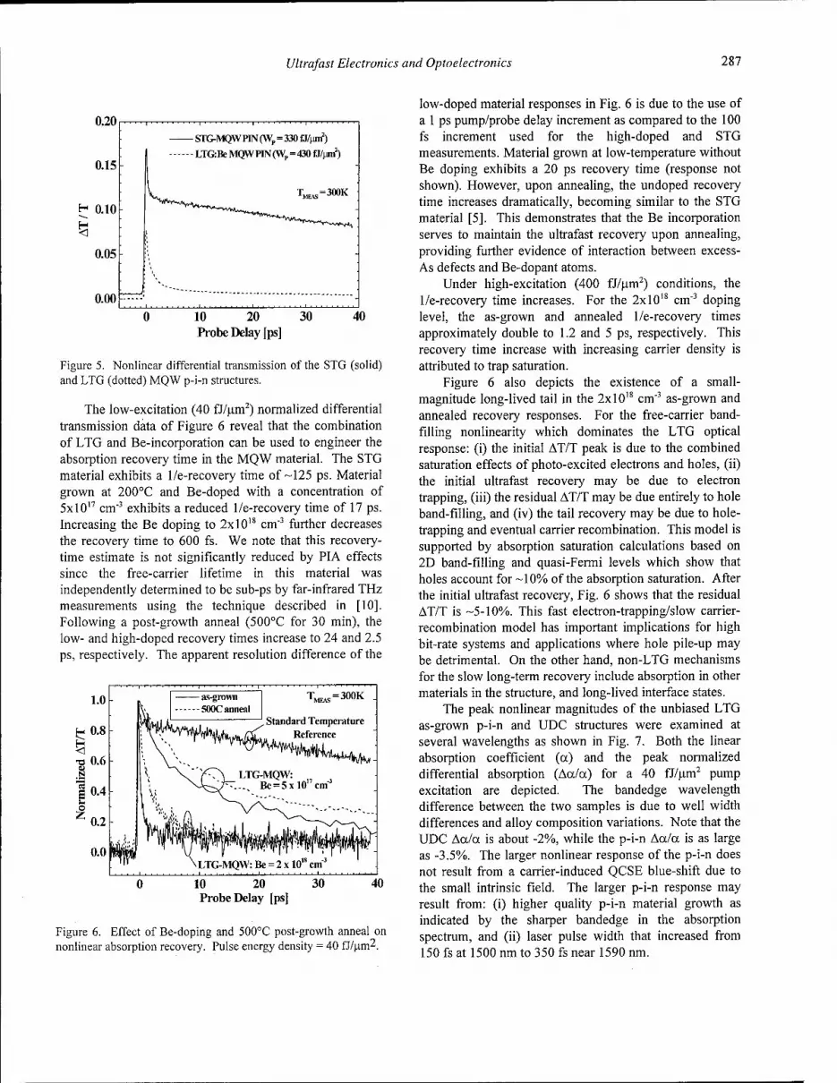
Ultrafast Electronics and Optoelectronics 287
STG-MQW PIN (Wp=330 fJ/|W)
0.15 LTG:BeMQWPEV(Wp=430fJ/|W)
K^^ TMEAS=300K ■ H 0.10 ^%Vw*,w-«i»^Wwaij^
% I
0.05 \
0.00 , , " 10 20 Probe Delay [ps]
30 40
Figure 5. Nonlinear differential transmission of the STG (solid) and LTG (dotted) MQW p-i-n structures.
The low-excitation (40 fJ/um2) normalized differential transmission data of Figure 6 reveal that the combination of LTG and Be-incorporation can be used to engineer the absorption recovery time in the MQW material. The STG material exhibits a 1/e-recovery time of -125 ps. Material grown at 200°C and Be-doped with a concentration of 5xl017 cm"3 exhibits a reduced 1/e-recovery time of 17 ps. Increasing the Be doping to 2xl018 cm"3 further decreases the recovery time to 600 fs. We note that this recovery- time estimate is not significantly reduced by PIA effects since the free-carrier lifetime in this material was independently determined to be sub-ps by far-infrared THz measurements using the technique described in [10]. Following a post-growth anneal (500°C for 30 min), the low- and high-doped recovery times increase to 24 and 2.5 ps, respectively. The apparent resolution difference of the
1.0
fc- 0.8
T3 0.6 01 N
10.4 u o Z 0.2
0.0
-as-grown -500C anneal
TMZ^OOK
Standard Temperature Reference
\ LTG-MQW: Be = 2 x 10,s cm"3
10 20 30 Probe Delay [ps]
40
Figure 6. Effect of Be-doping and 500°C post-growth anneal on nonlinear absorption recovery. Pulse energy density = 40 fJ/um2.
low-doped material responses in Fig. 6 is due to the use of a 1 ps pump/probe delay increment as compared to the 100 fs increment used for the high-doped and STG measurements. Material grown at low-temperature without Be doping exhibits a 20 ps recovery time (response not shown). However, upon annealing, the undoped recovery time increases dramatically, becoming similar to the STG material [5]. This demonstrates that the Be incorporation serves to maintain the ultrafast recovery upon annealing, providing further evidence of interaction between excess- As defects and Be-dopant atoms.
Under high-excitation (400 fJ/um2) conditions, the 1/e-recovery time increases. For the 2xl018 cm"3 doping level, the as-grown and annealed 1/e-recovery times approximately double to 1.2 and 5 ps, respectively. This recovery time increase with increasing carrier density is attributed to trap saturation.
Figure 6 also depicts the existence of a small- magnitude long-lived tail in the 2xl0'8 cm"3 as-grown and annealed recovery responses. For the free-carrier band- filling nonlinearity which dominates the LTG optical response: (i) the initial AT/T peak is due to the combined saturation effects of photo-excited electrons and holes, (ii) the initial ultrafast recovery may be due to electron trapping, (iii) the residual AT/T may be due entirely to hole band-filling, and (iv) the tail recovery may be due to hole- trapping and eventual carrier recombination. This model is supported by absorption saturation calculations based on 2D band-filling and quasi-Fermi levels which show that holes account for -10% of the absorption saturation. After the initial ultrafast recovery, Fig. 6 shows that the residual AT/T is -5-10%. This fast electron-trapping/slow carrier- recombination model has important implications for high bit-rate systems and applications where hole pile-up may be detrimental. On the other hand, non-LTG mechanisms for the slow long-term recovery include absorption in other materials in the structure, and long-lived interface states.
The peak nonlinear magnitudes of the unbiased LTG as-grown p-i-n and UDC structures were examined at several wavelengths as shown in Fig. 7. Both the linear absorption coefficient (a) and the peak normalized differential absorption (Aa/oc) for a 40 fJ/um2 pump excitation are depicted. The bandedge wavelength difference between the two samples is due to well width differences and alloy composition variations. Note that the UDC Aa/a is about -2%, while the p-i-n Aa/oc is as large as -3.5%. The larger nonlinear response of the p-i-n does not result from a carrier-induced QCSE blue-shift due to the small intrinsic field. The larger p-i-n response may result from: (i) higher quality p-i-n material growth as indicated by the sharper bandedge in the absorption spectrum, and (ii) laser pulse width that increased from 150 fs at 1500 nm to 350 fs near 1590 nm.
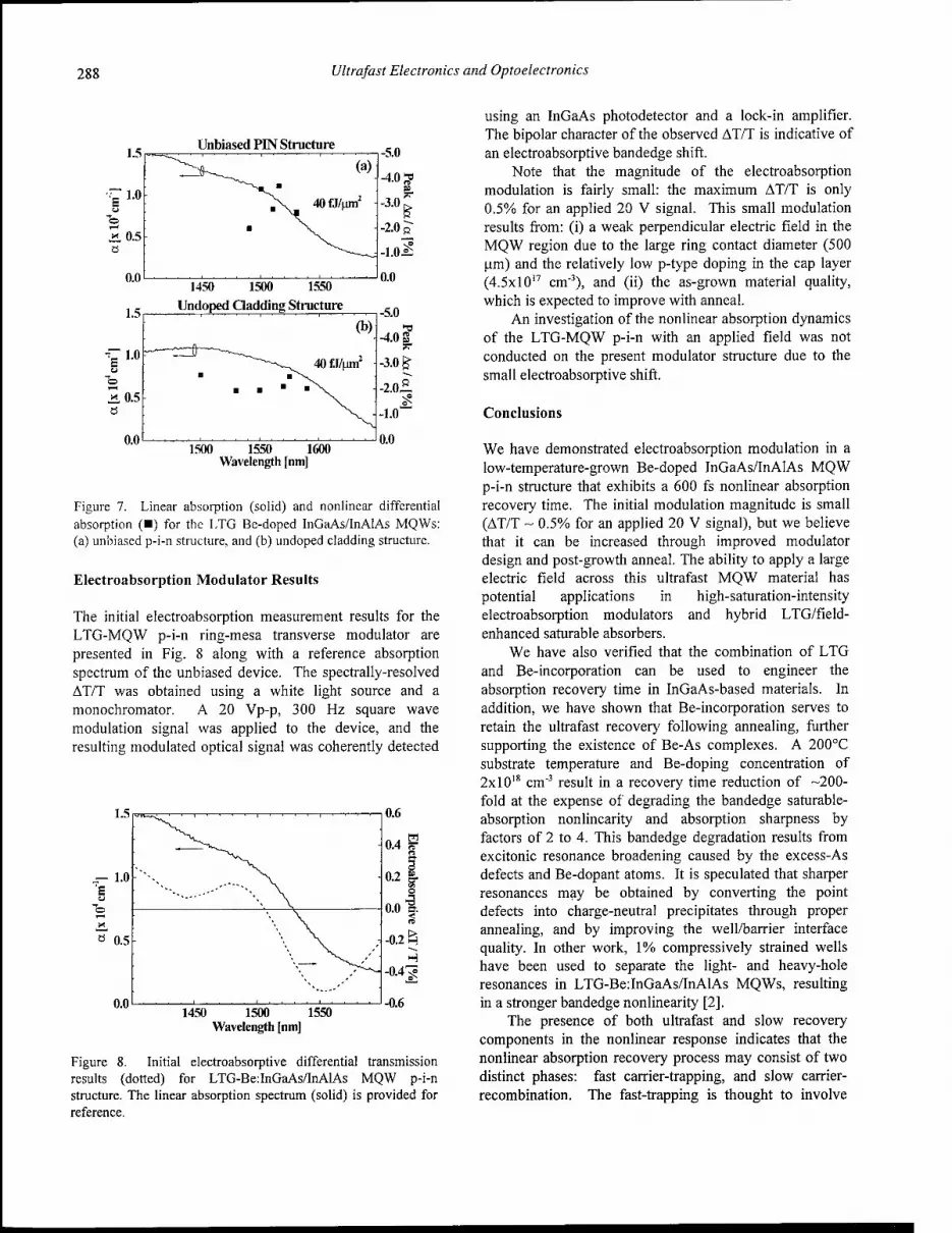
288 Ultrafast Electronics and Optoelectronics
Unbiased PIN Structure -5.0
0.0
1.5
1450 1500 1550 Undoped Gadding Structure
1500 1550 1600 Wavelength [nm]
Figure 7. Linear absorption (solid) and nonlinear differential absorption (■) for the LTG Be-doped InGaAs/InAlAs MQWs: (a) unbiased p-i-n structure, and (b) undoped cladding structure.
Electroabsorption Modulator Results
The initial electroabsorption measurement results for the LTG-MQW p-i-n ring-mesa transverse modulator are presented in Fig. 8 along with a reference absorption spectrum of the unbiased device. The spectrally-resolved AT/T was obtained using a white light source and a monochromator. A 20 Vp-p, 300 Hz square wave modulation signal was applied to the device, and the resulting modulated optical signal was coherently detected
0.6
0.4 % ^___^w^__^
— 1.0 v^ 'E
■••■•--■' ' \ \ \ S.
.*. \ 0 0.5
•0.2 sr 0.0|.
n
-02 5 H
-0.4^
-0.6 1450 1500 1550
Wavelength [nm]
Figure 8. Initial electroabsorptive differential transmission results (dotted) for LTG-Be:InGaAs/InAlAs MQW p-i-n structure. The linear absorption spectrum (solid) is provided for reference.
using an InGaAs photodetector and a lock-in amplifier. The bipolar character of the observed AT/T is indicative of an electroabsorptive bandedge shift.
Note that the magnitude of the electroabsorption modulation is fairly small: the maximum AT/T is only 0.5% for an applied 20 V signal. This small modulation results from: (i) a weak perpendicular electric field in the MQW region due to the large ring contact diameter (500 urn) and the relatively low p-type doping in the cap layer (4.5xl017 cm"3), and (ii) the as-grown material quality, which is expected to improve with anneal.
An investigation of the nonlinear absorption dynamics of the LTG-MQW p-i-n with an applied field was not conducted on the present modulator structure due to the small electroabsorptive shift.
Conclusions
We have demonstrated electroabsorption modulation in a low-temperature-grown Be-doped InGaAs/InAlAs MQW p-i-n structure that exhibits a 600 fs nonlinear absorption recovery time. The initial modulation magnitude is small (AT/T ~ 0.5% for an applied 20 V signal), but we believe that it can be increased through improved modulator design and post-growth anneal. The ability to apply a large electric field across this ultrafast MQW material has potential applications in high-saturation-intensity electroabsorption modulators and hybrid LTG/field- enhanced saturable absorbers.
We have also verified that the combination of LTG and Be-incorporation can be used to engineer the absorption recovery time in InGaAs-based materials. In addition, we have shown that Be-incorporation serves to retain the ultrafast recovery following annealing, further supporting the existence of Be-As complexes. A 200°C substrate temperature and Be-doping concentration of 2xl018 cm"3 result in a recovery time reduction of -200- fold at the expense of degrading the bandedge saturable- absorption nonlinearity and absorption sharpness by factors of 2 to 4. This bandedge degradation results from excitonic resonance broadening caused by the excess-As defects and Be-dopant atoms. It is speculated that sharper resonances may be obtained by converting the point defects into charge-neutral precipitates through proper annealing, and by improving the well/barrier interface quality. In other work, 1% compressively strained wells have been used to separate the light- and heavy-hole resonances in LTG-Be:InGaAs/InAlAs MQWs, resulting in a stronger bandedge nonlinearity [2].
The presence of both ultrafast and slow recovery components in the nonlinear response indicates that the nonlinear absorption recovery process may consist of two distinct phases: fast carrier-trapping, and slow carrier- recombination. The fast-trapping is thought to involve
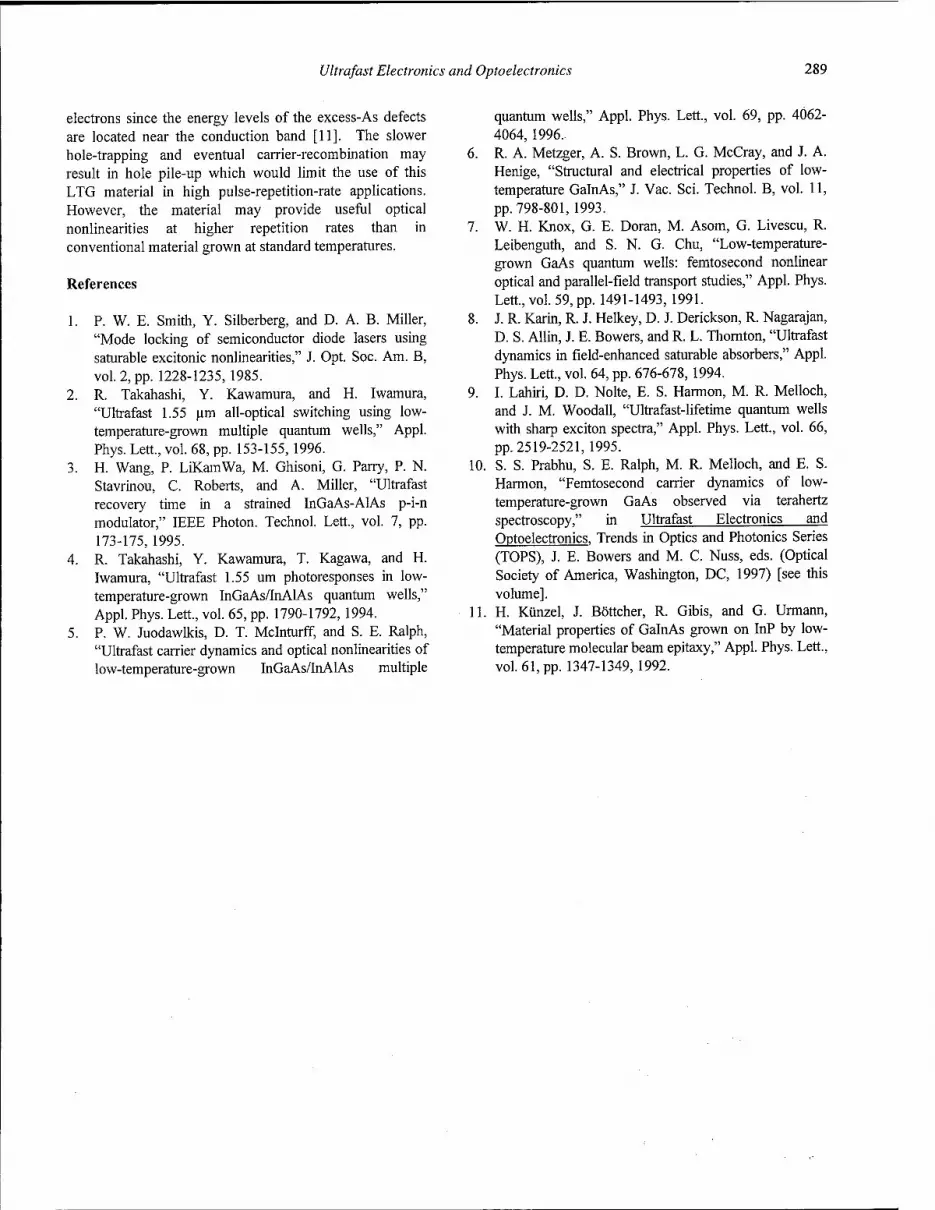
Ultrafast Electronics and Optoelectronics 289
electrons since the energy levels of the excess-As defects are located near the conduction band [11]. The slower hole-trapping and eventual carrier-recombination may result in hole pile-up which would limit the use of this LTG material in high pulse-repetition-rate applications. However, the material may provide useful optical nonlinearities at higher repetition rates than in conventional material grown at standard temperatures.
References
1. P. W. E. Smith, Y. Silberberg, and D. A. B. Miller, "Mode locking of semiconductor diode lasers using sarurable excitonic nonlinearities," J. Opt. Soc. Am. B, vol. 2, pp. 1228-1235, 1985.
2. R. Takahashi, Y. Kawamura, and H. Iwamura, "Ultrafast 1.55 um all-optical switching using low- temperature-grown multiple quantum wells," Appl. Phys. Lett., vol. 68, pp. 153-155,1996.
3. H. Wang, P. LiKamWa, M. Ghisoni, G. Parry, P. N. Stavrinou, C. Roberts, and A. Miller, "Ultrafast recovery time in a strained InGaAs-AlAs p-i-n modulator," IEEE Photon. Technol. Lett, vol. 7, pp. 173-175, 1995.
4. R. Takahashi, Y. Kawamura, T. Kagawa, and H. Iwamura, "Ultrafast 1.55 urn photoresponses in low- temperature-grown InGaAs/InAlAs quantum wells," Appl. Phys. Lett, vol. 65, pp. 1790-1792, 1994.
5. P. W. Juodawlkis, D. T. Mclnturff, and S. E. Ralph, "Ultrafast carrier dynamics and optical nonlinearities of low-temperature-grown InGaAs/InAlAs multiple
quantum wells," Appl. Phys. Lett, vol. 69, pp. 4062- 4064, 1996.
6. R. A. Metzger, A. S. Brown, L. G. McCray, and J. A. Henige, "Structural and electrical properties of low- temperature GalnAs," J. Vac. Sei. Technol. B, vol. 11, pp. 798-801, 1993.
7. W. H. Knox, G. E. Doran, M. Asom, G. Livescu, R. Leibenguth, and S. N. G. Chu, "Low-temperature- grown GaAs quantum wells: femtosecond nonlinear optical and parallel-field transport studies," Appl. Phys. Lett, vol. 59, pp. 1491-1493, 1991.
8. J. R. Karin, R. J. Helkey, D. J. Derickson, R. Nagarajan, D. S. Allin, J. E. Bowers, and R. L. Thornton, "Ultrafast dynamics in field-enhanced sarurable absorbers," Appl. Phys. Lett, vol. 64, pp. 676-678, 1994.
9. I. Lahiri, D. D. Nolte, E. S. Harmon, M. R. Melloch, and J. M. Woodall, "Ultrafast-lifetime quantum wells with sharp exciton spectra," Appl. Phys. Lett, vol. 66, pp. 2519-2521, 1995.
10. S. S. Prabhu, S. E. Ralph, M. R. Melloch, and E. S. Harmon, "Femtosecond carrier dynamics of low- temperature-grown GaAs observed via terahertz spectroscopy," in Ultrafast Electronics and Optoelectronics, Trends in Optics and Photonics Series (TOPS), J. E. Bowers and M. C. Nuss, eds. (Optical Society of America, Washington, DC, 1997) [see this volume].
11. H. Kiinzel, J. Böttcher, R. Gibis, and G. Urmann, "Material properties of GalnAs grown on InP by low- temperature molecular beam epitaxy," Appl. Phys. Lett, vol. 61, pp. 1347-1349,1992.
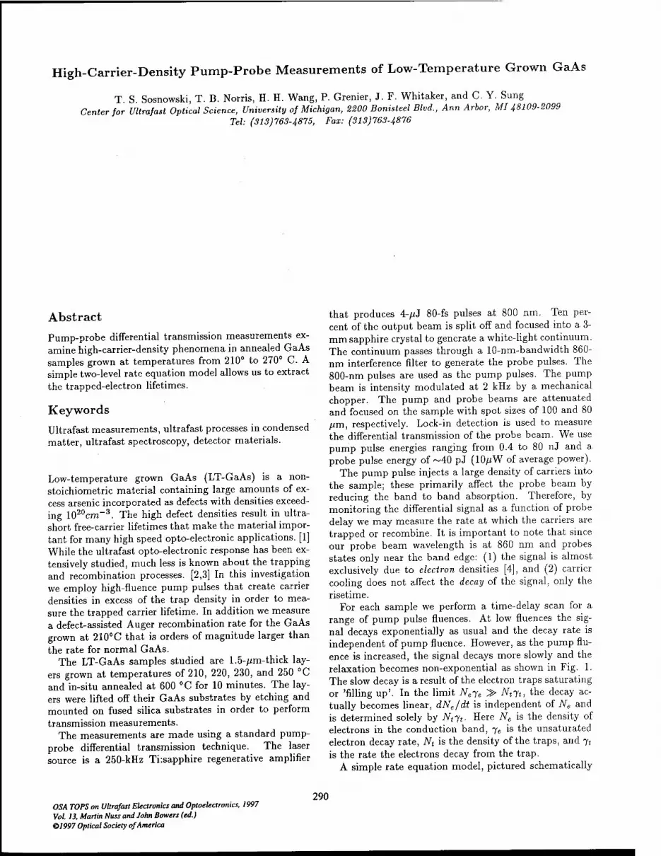
High-Carrier-Density Pump-Probe Measurements of Low-Temperature Grown GaAs
T. S. Sosnowski, T. B. Norris, H. H. Wang, P. Grenier, J. F. Whitaker, and C. Y. Sung Center for Ultrafast Optical Science, University of Michigan, 2200 Bonisteel Blvd., Ann Arbor, MI 48109-2099
Tel: (313)763-4875, Fax: (313)763-4876
Abstract
Pump-probe differential transmission measurements ex- amine high-carrier-density phenomena in annealed GaAs samples grown at temperatures from 210° to 270° C. A simple two-level rate equation model allows us to extract the trapped-electron lifetimes.
Keywords Ultrafast measurements, ultrafast processes in condensed matter, ultrafast spectroscopy, detector materials.
Low-temperature grown GaAs (LT-GaAs) is a non- stoichiometric material containing large amounts of ex- cess arsenic incorporated as defects with densities exceed- ing 1020cm-3. The high defect densities result in ultra- short free-carrier lifetimes that make the material impor- tant for many high speed opto-electronic applications. [1] While the ultrafast opto-electronic response has been ex- tensively studied, much less is known about the trapping and recombination processes. [2,3] In this investigation we employ high-fluence pump pulses that create carrier densities in excess of the trap density in order to mea- sure the trapped carrier lifetime. In addition we measure a defect-assisted Auger recombination rate for the GaAs grown at 210°C that is orders of magnitude larger than the rate for normal GaAs.
The LT-GaAs samples studied are 1.5-pm-thick lay- ers grown at temperatures of 210, 220, 230, and 250 °C and in-situ annealed at 600 °C for 10 minutes. The lay- ers were lifted off their GaAs substrates by etching and mounted on fused silica substrates in order to perform transmission measurements.
The measurements are made using a standard pump- probe differential transmission technique. The laser source is a 250-kHz Ti:sapphire regenerative amplifier
that produces 4-/iJ 80-fs pulses at 800 nm. Ten per- cent of the output beam is split off and focused into a 3- mm sapphire crystal to generate a white-light continuum. The continuum passes through a 10-nm-bandwidth 860- nm interference filter to generate the probe pulses. The 800-nm pulses are used as the pump pulses. The pump beam is intensity modulated at 2 kHz by a mechanical chopper. The pump and probe beams are attenuated and focused on the sample with spot sizes of 100 and 80 //m, respectively. Lock-in detection is used to measure the differential transmission of the probe beam. We use pump pulse energies ranging from 0.4 to 80 nJ and a probe pulse energy of ~40 pJ (10/iW of average power).
The pump pulse injects a large density of carriers into the sample; these primarily affect the probe beam by reducing the band to band absorption. Therefore, by monitoring the differential signal as a function of probe delay we may measure the rate at which the carriers are trapped or recombine. It is important to note that since our probe beam wavelength is at 860 nm and probes states only near the band edge: (1) the signal is almost exclusively due to electron densities [4], and (2) carrier cooling does not affect the decay of the signal, only the risetime.
For each sample we perform a time-delay scan for a range of pump pulse fluences. At low fluenc.es the sig- nal decays exponentially as usual and the decay rate is independent of pump fluence. However, as the pump flu- en ce is increased, the signal decays more slowly and the relaxation becomes non-exponential as shown in Fig. 1. The slow decay is a result of the electron traps saturating or 'filling up'. In the limit Neje > Nat, the decay ac- tually becomes linear, dNe/dt is independent of Ne and is determined solely by Ntft- Here Ne is the density of electrons in the conduction band, je is the unsaturated electron decay rate, Nt is the density of the traps, and jt
is the rate the electrons decay from the trap. A simple rate equation model, pictured schematically
OSA TOPS on Ultrafast Electronics and Optoelectronics. 1997 Vol. 13. Martin Nuss and John Bowers (ed.) &1997 Optical Society of America
290
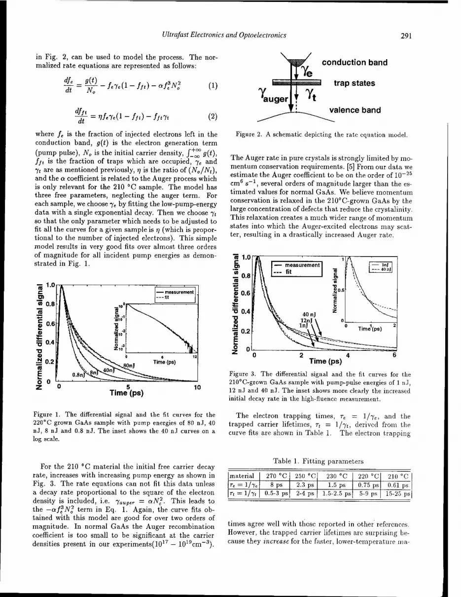
Ultrafast Electronics and Optoelectronics 291
in Fig. 2, can be used to model the process. The nor- malized rate equations are represented as follows:
df, dt - N0
hJe( ■fft)-°fW
-jj- = VfeJe(l ~ fft) ~ fftjt
(1)
(2)
where fe is the fraction of injected electrons left in the conduction band, g{t) is the electron generation term
(pump pulse), N0 is the initial carrier density, f*™ g(t), fft is the fraction of traps which are occupied, je and ■yt are as mentioned previously, 77 is the ratio of (N0/Nt), and the a coefficient is related to the Auger process which is only relevant for the 210 °C sample. The model has three free parameters, neglecting the auger term. For each sample, we choose ft by fitting the low-pump-energy data with a single exponential decay. Then we choose jt
so that the only parameter which needs to be adjusted to fit all the curves for a given sample is 77 (which is propor- tional to the number of injected electrons). This simple model results in very good fits over almost three orders of magnitude for all incident pump energies as demon- strated in Fig. 1.
Time (ps)
Figure 1. The differential signal and the fit curves for the 220°C grown GaAs sample with pump energies of 80 nJ, 40 nJ, 8 nJ and 0.8 nJ. The inset shows the 40 nJ curves on a log scale.
conduction band
trap states
valence band
Figure 2. A schematic depicting the rate equation model.
The Auger rate in pure crystals is strongly limited by mo- mentum conservation requirements. [5] From our data we estimate the Auger coefficient to be on the order of 10~25
cm6 s_1, several orders of magnitude larger than the es- timated values for normal GaAs. We believe momentum conservation is relaxed in the 210°C-grown GaAs by the large concentration of defects that reduce the crystalinity. This relaxation creates a much wider range of momentum states into which the Auger-excited electrons may scat- ter, resulting in a drastically increased Auger rate.
"5 1.0
Time (ps)
Figure 3. The differential signal and the fit curves for the 210°C-grown GaAs sample with pump-pulse energies of 1 nJ, 12 nJ and 40 nJ. The inset shows more clearly the increased initial decay rate in the high-fluence measurement.
The electron trapping times, re = l/je, and the trapped carrier lifetimes, rt = l/yt, derived from the curve fits are shown in Table 1. The electron trapping
For the 210 °C material the initial free carrier decay rate, increases with increasing pump energy as shown in Fig. 3. The rate equations can not fit this data unless a decay rate proportional to the square of the electron density is included, i.e. jauger = aiVc
2. This leads to the —afgNg term in Eq. 1. Again, the curve fits ob- tained with this model are good for over two orders of magnitude. In normal GaAs the Auger recombination coefficient is too small to be significant at the carrier densities present in our experiments(1017 — 1019cm~3).
Table 1. Fitting parameters
material 270 °C 250 °C 230 °C 220 °C 210 °C Te = I he 8 ps 2.3 ps 1.5 ps 0.75 ps 0.61 ps n = l/7t 0.5-3 ps 2-4 ps 1.5-2.5 ps 5-9 ps 15-25 ps
times agree well with those reported in other references. However, the trapped carrier lifetimes are surprising be- cause they increase for the faster, lower-temperature ma-
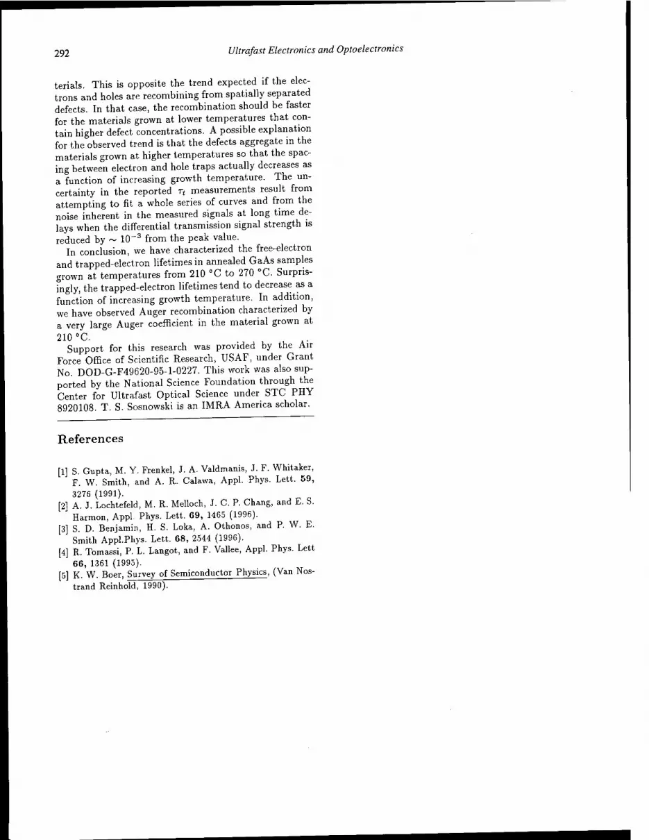
292 Ultrafast Electronics and Optoelectronics
terials. This is opposite the trend expected if the elec- trons and holes are recombining from spatially separated defects. In that case, the recombination should be faster for the materials grown at lower temperatures that con- tain higher defect concentrations. A possible explanation for the observed trend is that the defects aggregate in the materials grown at higher temperatures so that the spac- ing between electron and hole traps actually decreases as a function of increasing growth temperature. The un- certainty in the reported rt measurements result from attempting to fit a whole series of curves and from the noise inherent in the measured signals at long time de- lays when the differential transmission signal strength is reduced by ~ 10~3 from the peak value.
In conclusion, we have characterized the free-electron and trapped-electron lifetimes in annealed GaAs samples grown at temperatures from 210 °C to 270 °C. Surpris- ingly, the trapped-electron lifetimes tend to decrease as a function of increasing growth temperature. In addition, we have observed Auger recombination characterized by a very large Auger coefficient in the material grown at
210 °C. Support for this research was provided by the Air
Force Office of Scientific Research, USAF, under Grant No. DOD-G-F49620-95-1-0227. This work was also sup- ported by the National Science Foundation through the Center for Ultrafast Optical Science under STC PHY 8920108. T. S. Sosnowski is an IMRA America scholar.
References
[1] S. Gupta, M. Y. Frenkel, J. A. Valdmanis, J. F. Whitaker, F. W. Smith, and A. R. Calawa, Appl. Phys. Lett. 59, 3276 (1991).
[2] A. J. Lochtefeld, M. R. Melloch, J. C. P. Chang, and E. S. Harmon, Appl. Phys. Lett. 69, 1465 (1996).
[3] S. D. Benjamin, H. S. Loka, A. Othonos, and P. W. E. Smith Appl.Phys. Lett. 68, 2544 (1996).
[4] R. Tomassi, P. L. Langot, and F. Vallee, Appl. Phys. Lett 66, 1361 (1995).
[5] K. W. Boer, Survey of Semiconductor Physics, (Van Nos- trand Reinhold, 1990).

Femtosecond carrier dynamics of low-temperature-grown GaAs observed via Terahertz spectroscopy
S. S. Prabhu and S. E. Ralph Department of Physics, Emory University, Atlanta, GA 30322-2430
Phone: 404.72 7.4294 / Fax 404.72 7.0873 / email seralph@emory. edu
MR. Melloch School of Electrical and Computer Engineering, Purdue University,
West Lafayette, IN 47907-1285
E. S. Harmon MellWood Laboratories, Inc., 1291 Cumberland Ave, Suite E, West Lafayette, IN 47906
Abstract
Far Infrared Terahertz spectroscopy unambiguously demonstrates sub-picosecond electron lifetimes in low- temperature-grown GaAs. A systematic study of as-grown and annealed, low-temperature-grown GaAs, reveals carrier lifetimes to be directly related to the excess arsenic incorporation and anneal conditions. The observation of subpicosecond lifetimes is attributed to the far infrared interaction and dilute photoexcitation densities. A simple rate equation model is developed to interpret the results and to determine the relative electron mobility. Additionally, Drude-like behavior of the free carrier conductivity within 1 ps of excitation is revealed using time resolved differential spectroscopy.
Keywords
Low temperature grown semiconductors; Far infrared, ultrafast processes, time resolved ultrafast spectroscopy
Introduction
The epitaxial growth of semiconductors, such as InGaAs and GaAs, in a non-stoichiometric fashion yields materials with a high defect density. The defects associated with low growth temperature have been shown to produce short carrier lifetimes and are therefore potentially useful defects. The short carrier lifetimes result from excess As in the form of [1,2,3,4] As antisite and Ga vacancy point defects[5]. Subsequent annealing of the as-grown material leads to the formation of As-precipitates [6,7,8,9], which produce a high resistivity and relatively high carrier mobility material. Systematic tailoring of the carrier
lifetime via a controlled introduction of defects will enhance efforts to produce photonic devices with a fast response, particularly if these defects do not significantly adversely affect the desired optical or electronic properties.
Previous optical and electrical characterization efforts have sought to determine the precise effect of these defects on the electron and hole lifetimes [6-10], although some ambiguity persists [11,12]. The difficulty in observing the carrier lifetimes arises from the inability to easily separate the free carrier lifetime from the recombination lifetime. Additionally, the observed dynamics of relatively high photo-carrier excitation densities (>1017cm"3) are often strongly influenced by photo-induced absorption (PIA) effects [13,14], hot phonon effects and other non-linear high carrier density effects including displacement currents in the case of photoconductivity measurements. Furthermore, the total response for high density excitations near the band-edge is due to a number of mechanisms in addition to the free carrier lifetime, including the Urbach tail and band-gap renormalization effects. For example, using a pump-probe technique to obtain the transient transmission response, photoexcitation near the band-edge is needed to minimize the influence of carrier cooling. However, the combined effect of deep traps and the large photo-excited carrier density, produces a net decrease in transmission i.e. the presence of pump reduces the overall transmission. The competition between saturation absorption and the above PIA effect makes the interpretation of the lifetimes difficult. PIA can be avoided using time resolved luminescence [15] and carrier lifetimes have been reported in the lps regime. However, the carrier densities required in these experiments were ~ 4xl017 cm"3.
We report an unambiguous observation of subpicosecond electron lifetimes in low-temperature- grown (LTG)-GaAs. Our technique of THz spectroscopy,
OSA TOPS on Ultrafast Electronics and Optoelectronics, 1997 Vol. 13, Martin Nuss and John Bowers (ed.) ©1997 Optical Society of America
293

294 Ultrafast Electronics and Optoelectronics
allows the use of very low photoinjected carrier densities (-10"cm'3) and, due to the unique probe interaction, avoids all the aforementioned difficulties. The typical energy carried by a THz photon is -1 to lOmeV. Thus the photon acts as a local perturbation in the Ar-space of the carrier. The interaction of electromagnetic radiation with a material can be written in terms of its dielectric response. In general, this response has contributions from interband, intersubband transitions, phonon related transitions and free carrier contributions. Due to the small energy of THz photons, the free carrier contribution dominates the THz interaction. The dielectric function can then be written as :
e{co) = <foo +/- (1) coe„
a = r £o0}p
(a) + iT) (2)
where a is the conductivity, cop is the plasma frequency and I is the momentum relaxation time.
Bolometer
THz Source 2
a- Si-Lens
H fsec Excitation
Dewar PM-1
PM-2
PM= Parabolic Mirror M=Mirror BS=Beam Splitter
Si-Lens
THz Source
fsec Excitation M
Figure 1: Terahertz setup for the pump-probe and absorption
spectroscopy.
Our experimental technique is therefore sensitive to the conductivity. Furthermore, the electron mobility is more than one order larger than the hole mobility, the conductivity is thus dominated by the electron contribution [16]. The dependence of the relative mobility of photoinjected carriers on growth and anneal conditions can also be ascertained from the transient cr measured via THz techniques.
Experimental Setup
The transient conductivity is obtained using a THz time resolved (TR) pump-probe setup (Fig. 1) consisting of an Ar+ pumped Ti-Sapphire laser with a pulse duration of <100fs operating at 82MHz. Terahertz pulses of ~200fs duration are generated by photo-excitation of externally biased semi-insulating GaAs[17] with lithographically defined antenna structures (Source 1 and 2). Two methods of data acquisition are possible. First, the time evolution of the spectrally integrated FIR probe as modulated by the photoinjected carriers can be observed. Second, by using a second THz source, the evolution of the spectral content of the transmitted probe pulse can be determined using the Michelson Interferometer arrangement. Via Fourier analysis of the interferograms, one can study the evolution of the THz spectra at various pump delays. The experimental resolution is limited by the experimental geometry to ~300fs. The room temperature FIR temporal transmission response is obtained at various pump excitation wavelengths from 790 through 850nm at a constant carrier density. The excess energies are thus varied from < 1LO phonon to ~3LO phonon energies above the bandedge. The spectrally integrated FIR probe is detected using a liquid-He cooled Bolometer.
A typical sample structure is shown in Fig. 2.
/ SflliHMllNil > Variable ' Growth Temperature 30G°C-500°C
i-AI„Ga,„AS 500A
i-GaAs 1.0um
/ 'Wjä^fe. :■'..-■■:'■'■ \0V ;,;f500As's:
Growth Temperature 600°C
iGaAs
i*l,.Gn;aAs
100A
0.5fim
iGaA» |§|frfjif
ÄftsaÄ 0 3um
Figure 2: Typical sample structure grown for the study.
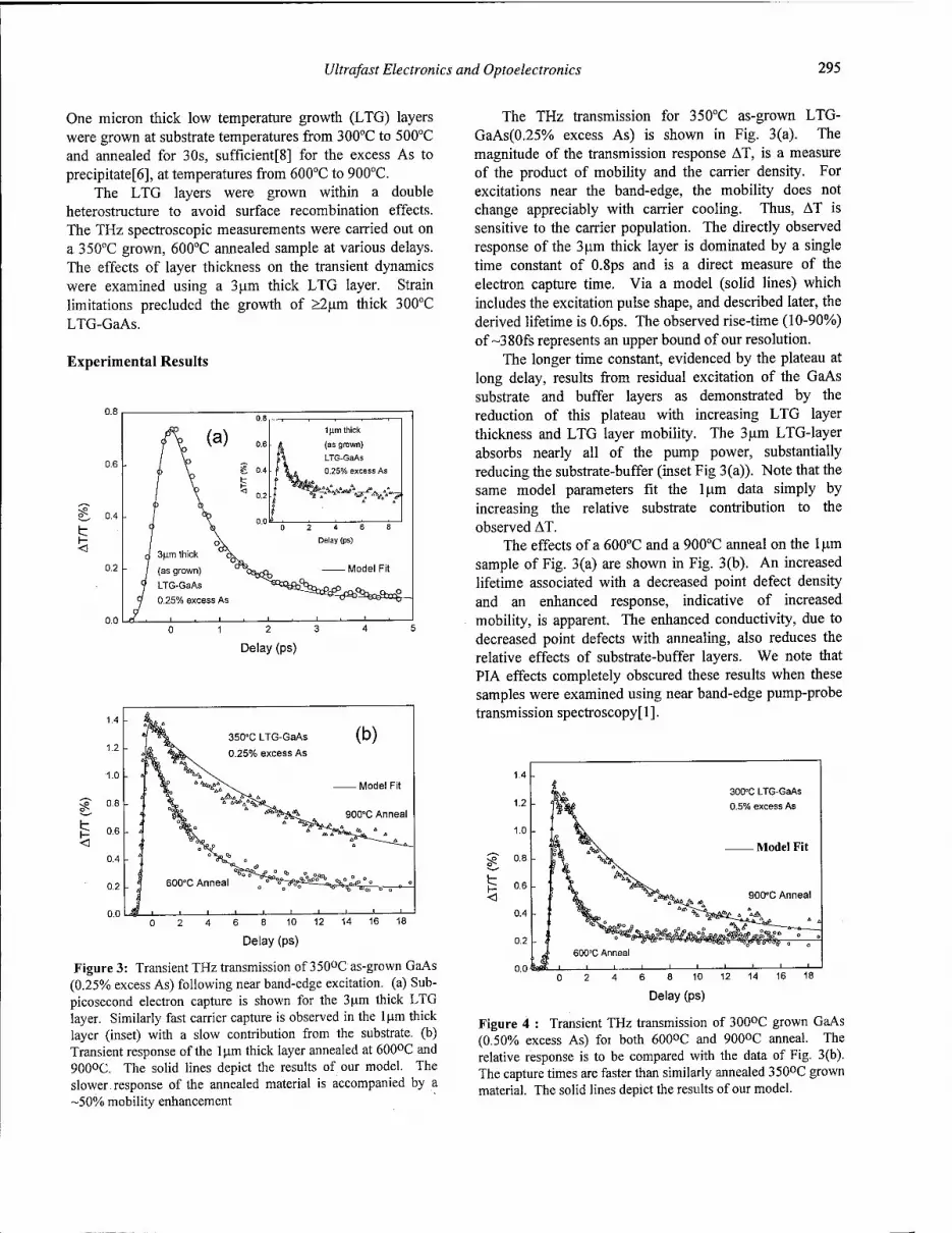
Ultrafast Electronics and Optoelectronics 295
One micron thick low temperature growth (LTG) layers were grown at substrate temperatures from 300°C to 500°C and annealed for 30s, sufficient[8] for the excess As to precipitate[6], at temperatures from 600°C to 900°C.
The LTG layers were grown within a double heterostructure to avoid surface recombination effects. The THz spectroscopic measurements were carried out on a 350°C grown, 600°C annealed sample at various delays. The effects of layer thickness on the transient dynamics were examined using a 3 um thick LTG layer. Strain limitations precluded the growth of >2um thick 300CC LTG-GaAs.
Experimental Results
1 2 3
Delay (ps)
Delay (ps)
Figure 3: Transient THz transmission of 350°C as-grown GaAs (0.25% excess As) following near band-edge excitation, (a) Sub- picosecond electron capture is shown for the 3 um thick LTG layer. Similarly fast carrier capture is observed in the lum thick layer (inset) with a slow contribution from the substrate, (b) Transient response of the lum thick layer annealed at 600°C and 900°C. The solid lines depict the results of our model. The slower.response of the annealed material is accompanied by a -50% mobility enhancement
The THz transmission for 350°C as-grown LTG- GaAs(0.25% excess As) is shown in Fig. 3(a). The magnitude of the transmission response AT, is a measure of the product of mobility and the carrier density. For excitations near the band-edge, the mobility does not change appreciably with carrier cooling. Thus, AT is sensitive to the carrier population. The directly observed response of the 3(im thick layer is dominated by a single time constant of 0.8ps and is a direct measure of the electron capture time. Via a model (solid lines) which includes the excitation pulse shape, and described later, the derived lifetime is 0.6ps. The observed rise-time (10-90%) of ~380fs represents an upper bound of our resolution.
The longer time constant, evidenced by the plateau at long delay, results from residual excitation of the GaAs substrate and buffer layers as demonstrated by the reduction of this plateau with increasing LTG layer thickness and LTG layer mobility. The 3 um LTG-layer absorbs nearly all of the pump power, substantially reducing the substrate-buffer (inset Fig 3(a)). Note that the same model parameters fit the lum data simply by increasing the relative substrate contribution to the observed AT.
The effects of a 600°C and a 900°C anneal on the lum sample of Fig. 3(a) are shown in Fig. 3(b). An increased lifetime associated with a decreased point defect density and an enhanced response, indicative of increased mobility, is apparent. The enhanced conductivity, due to decreased point defects with annealing, also reduces the relative effects of substrate-buffer layers. We note that PIA effects completely obscured these results when these samples were examined using near band-edge pump-probe transmission spectroscopy[l].
300°C LTG-GaAs
0.5% excess As
Model Fit
900°C Anneal
0 2 4 6 8 10 12
Delay (ps)
Figure 4 : Transient THz transmission of 300°C grown GaAs (0.50% excess As) for both 600°C and 900°C anneal. The relative response is to be compared with the data of Fig. 3(b). The capture times are faster than similarly annealed 350°C grown material. The solid lines depict the results of our model.

296 Ultrafast Electronics and Optoelectronics
In Fig. 4 we show the transient conductivity response of a 1 um thick LTG-layer grown at a lower temperature of 300°C (0.5% excess As) annealed at 600°C and 900°C. Although the anneal conditions are identical to those of Fig. 3(b), the observed carrier lifetime is significantly shorter (Table-I) by a factor of ~2. However, due to comparable mobility, the peak conductivity responses are similar. Also note the excellent fit of the model.
In Fig. 5 the normalized response curves obtained for all the ljum thick as-grown LTG-GaAs epilayer at various growth temperatures are shown. The initial fast decay vanishes as the growth temperature is increased from 350°C to 500°C.
shown previously, in LTG-GaAs that the electron distributions are nearly thermal at low pump densities and retain low carrier temperatures for low excess excitation energies [18]. Therefore, dramatic changes in the conductivity are not to be expected on picosecond and longer time scales considering excitation conditions of our experiment. Our observation of Drude-like conductivity within lps of excitation supports this view.
From the Drude model fit to the above data, the observed momentum relaxation time (TM) of the excited carriers is much smaller (~180fs+50fs) than the capture time. This is in excellent agreement with the value reported earlier in the literature [19].
0.6
e. 0.4
< 0.2
—i—■—i—i—i—■—i—'—i ' r- LTG-GaAs 1)im thick layer
500C (as grown)
0.0 LML
\ \ 400C (as grown)
350C (as grown)
450C (as grown)
10 15 20 25 30 35 40 45 50
Delay (ps)
Figure 5: Normalized transient response of lum thick as grown LTG-GaAs layers grown at various temperatures from 350°C to 500°C. The change in the initial fast decay of the signal with increasing growth temperature is quite apparent.
The growth temperature and the associated initial As and Ga defect densities are thus the dominant factors influencing the carrier lifetime in this case. This suggests that the dominant trap state is of singular variety and varies in concentration monotonically with growth/anneal conditions.
Using the interferometric techniques with Fourier analysis of the transmitted THz pulse, we have examined the time dependent, spectral dependence of the transmission in the THz regime. In Fig. 6 we show the THz spectra obtained on the lum thick, 350°C grown, 600°C annealed sample at 0.75 and 3.0 ps delays. Although it is not possible to determine the precise carrier distribution, it is found that the Drude conductivity model yields a good fit to the spectrally resolved data. The periodic modulation of the observed spectra results from the residual Fabry-Perot modes. The carrier density and mobility are well defined by the spectra. It has been
10-2
,-. 10-3
<
10-5
1|im thick 350°C LTG-GaAs
Annealed at 600°C ~0.75ps
~3ps
0.6 0.8 1.0 1.2 1.4 1.6 1.8 2.0
Frequency (THz)
Figure 6: Time resolved transient spectroscopy of 350°C grown GaAs. For the experimental conditions AT is proportional to the conductivity as is shown to be Drude-like within lps of excitation.
Results and Discussion Our study of 21 samples as exemplified in Figs. 3-5, reveals a systematic carrier lifetime increase with increasing growth temperature and anneal temperature. As shown in Table I, we observe a smooth transition from As- defect dominated lifetime, minimum of ~200fs, to typical bulk-like recombination times of >lns. This further confirms the singular nature of the dominant electron trap state and its monotonic variation with the growth/anneal conditions. Our observations thus support the view that the short electron lifetimes result from the As point defects which are systematically reduced in density upon anneal. Previously, a number of mechanisms for example: (i) PIA effects (prominent in the as-grown material with >.1% excess As) and (ii) saturation of the available point defects in the annealed material, such a dependence of carrier lifetime on the As point defects was not observed. For example, the capture lifetime obtained via time resolved luminescence is -lps for ~1% excess arsenic material
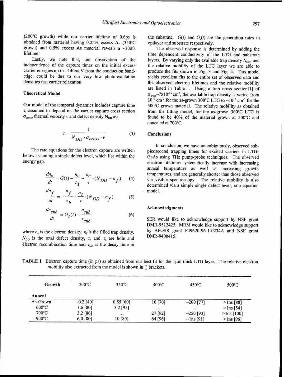
Ultrafast Electronics and Optoelectronics 297
(200°C growth) while our carrier lifetime of 0.6ps is obtained from material having 0.25% excess As (350°C grown) and 0.5% excess As material reveals a ~300fs lifetime.
Lastly, we note that, our observation of the independence of the capture times on the initial excess carrier energies up to ~140meV from the conduction band- edge, could be due to our very low photo-excitation densities fast carrier relaxation.
Theoretical Model
Our model of the temporal dynamics includes capture time T, assumed to depend on the carrier capture cross section across, thermal velocity v and defect density NDD as:
the substrate. G(t) and G£f) are the generation rates in epilayer and substrate respectively.
The observed response is determined by adding the time dependent conductivity of the LTG and substrate layers. By varying only the available trap density JVDD, and the relative mobility of the LTG layer we are able to produce the fits shown in Fig. 3 and Fig. 4. This model yields excellent fits to the entire set of observed data and the observed electron lifetimes and the relative mobility are listed in Table I. Using a trap cross section[l] of across~7xl°"15 cm2, the available trap density is varied from 1019 cm"3 for the as-grown 300°C LTG to -1015 cm"3 for the 500°C grown material. The relative mobility as obtained from the fitting model, for the as-grown 300°C LTG is found to be 40% of the material grown at 500°C and annealed at 700°C.
N DD ' across 'v (3)
The rate equations for the electron capture are written below assuming a single defect level, which lies within the energy gap.
dne dt
dn
■G(0- —• T3
■(N DD ■nf)
f dt
dn
f »e DD nf)
sub
dt = Gs(t)-
sub
sub
(4)
(5)
(6)
where ne is the electron density, «f is the filled trap density, NDD is the total defect density, rh and T3 are hole and electron recombination time and rsub is the decay time in
Conclusions
In conclusion, we have unambiguously, observed sub- picosecond trapping times for excited carriers in LTG- GaAs using THz pump-probe techniques. The observed electron lifetimes systematically increase with increasing anneal temperature as well as increasing growth temperatures, and are generally shorter than those observed via visible spectroscopy. The relative mobility is also determined via a simple single defect level, rate equation model.
Acknowledgments
SER would like to acknowledge support by NSF grant DMR-9512425. MRM would like to acknowledge support by AFOSR grant F49620-96-1-0234A and NSF grant DMR-9400415.
TABLE I. Electron capture time (in ps) as obtained from our best fit for the lum thick LTG layer. The relative electron mobility also extracted from the model is shown in [] brackets.
Growth 300°C 350°C 400°C 450°C 500°C
Anneal As-Grown -0.2 [40] 0.55 [60] 10 [70] -200 [77] >lns [88]
600°C 1.6 [80] 3.2 [95] >lns [84] 700°C 3.2 [80] 27 [92] -250 [93] >lns[100] 900°C 6.0 [80] 10 [80] 64 [96] -Ins [91] >lns [96]

298 Ultrafast Electronics and Optoelectronics
References
1. A. J. Lochtefeld, M. R. Melloch, J. C. P. Chang and E. S. Harmon, "The role of point defects and arsenic precipitates in carrier trapping and recombination in low-temperature-grown GaAs", Appl. Phys. Lett. 69, 1465 (1996).
2. E. S. Harmon, M. R. Melloch, J. M. Woodall, D. D. Nolle, N. Otsuka and C. L. Chang, "Carrier lifetime versus anneal in low temperature growth GaAs", Appl. Phys. Lett. 63,2248 (1993).
3. F. Ghanikanov, Gong-Ru-Lin, Wen-Chung Chen, C. S. Chang and Ci-Ling Pan, "Subpicosecond carrier lifetimes in arsenic-ion-implanted GaAs", Appl. Phys. Lett. 67, 3465 (1995).
4. Z. Liliental-Weber, H. J. Cheng, S. Gupta, J. Whitaker, K. Nichols and F. W. Smith, "Structure and Carrier Lifetime in LT-GaAs", Journ. Electr. Mat.22, 1465 (1993).
5. G. L. Witt, "LTMBE GaAs: present status and perspectives", Materials Science and Engineering B22, 9 (1993); P. Hautijarvi, J. Makinen, S. Palko, K. Saarinen, C. Corbel and L. Liszkay, "Point defects in III-V materials grown by molecular beam epitaxy at low temperature", ibid, 16 (1993); S. A. McQuaid, R E. Pritchard, R. C. Newman, S. O'Hagan and M. Missous, "Gallium vacancy related defects in silicon doped GaAs grown at low temperatures", ibid, 23 (1993).
6. M. R. Melloch, J. M. Woodall, N. Otsuka, K. Mahalingam, C. L. Chang and D. D. Nolte, "GaAs, AlGaAs, and InGaAs epilayers containing As clusters: semimetal/semiconductor composites", Materials Science and Engineering B22, 31 (1993).
7. A. C. Warren, J. M. Woodall, P. D. Kirchner, X. Yin, F. Pollak, M. R Melloch, N. Otsuka and K. Mahalingam, "Role of excess As in low-temeprature- grown GaAs", Phys. Rev. B46,4617 (1992).
8. M. R. Melloch, N. Otsuka, J. M. Woodall, A. C. Warren and J. L. Freeouf, "Formation of arsenic precipitates in GaAs buffer layers grown by molecular beam epitaxy at low substrate temperatures", Appl. Phys. Lett. 57, 1531(1990).
9. A. C. Warren, J. M. Woodall, J. L. Freeouf, D. Grinschkowsky, D. T. Mclnturff, M. R. Melloch and N. Otsuka, "Arsenic precipitates and the semi- insulating properties of GaAs buffer layers grown by low-temperature molecular beam epitaxy", Appl. Phys. Lett. 57, 1331(1990).
10. S. Gupta, M. Y. Frankel, J. A. Valdmanis, J. F. Whitaker, F. W. Smith and A. R. Calawa, "Subpicosecond carrier lifetime in GaAs grown by molecular beam epitaxy at low temperatures", Appl. Phys. Lett. 59,3276(1991).
11. H. H. Wang, J. F. Whitaker, A. Chin, J. Mazurowski and J. Ballingall, "Subpicosecond Carrier Response of Unannealed Low-Temperature-Grown GaAs vs Temperature", Journ. Electr. Mat. 22, 1461 (1993).
12. B. Nabet, A. Youtz, F. Castro, P. Cooke and A. Paolella, "Current transport in as-grown and annealed intermediate temperature molecular beam epitaxy grown GaAs", Appl. Phys. Lett. 67, 1748 (1995).
13. Y. Kostoulas, L. J. Waxer, I. A. Walmsley, G. W. Wicks and P. M. Fauchet, "Femtosecond carrier dynamics in low-temperature-grown indium phosphide", Appl. Phys. Lett. 66, 1821 (1995).
14. S. D. Benjamin, H. S. Loka, A. Othonos, P. W. E. Smith, "Ultrafast dynamics of nonlinear absorption in low-temperature-grown GaAs", Appl. Phys. Lett. 68, 2544 (1996).
15. X. Q. Zhou, H. M. van Driel, W. W. Ruhle, Z. Gogolak and K. Ploog, "Femtosecond carrier kinetics in low-temperature-grown GaAs", Appl. Phys. Lett. 61, 3020 (1992).
16. A similar THz response was achieved with an electron concentration only 13% that of the hole concentration. N. Katzenellenbogen and D. Grischkowsky, "Electrical characterization to 4 THz of N- and P-type GaAs using THz time-domain spectroscopy", Appl. Phys. Lett. 61, 840 (1992).
17. S. E. Ralph and D. Grishkowsky, "Trap-enhanced electric fields in semi-insulators:The role of electrical and optical carrier injection", Appl. Phys. Lett. 59, 1972(1991).
18. H. M. VanDriel, X. Q. Zhou, W. W. Ruhle, J. Kuhl and K. Ploog, "Photoluminescence from hot carriers in low-temperature-grown gallium arsenide", Appl. Phys. Lett. 60, 2246 (1992).
19. S. E. Ralph and Yue Chen, "Subpicosecond photo- conductivity of In053Gao47As: Intervalley scattering rates observed via THz spectroscopy", Phys. Rev. B54, 5568 (1996).
Author Index
Agarwal, B., 151 Alphonse, G. A., 18,46 Auer, U., 190 Aytur, Orhan, 88
Bakker, H. I, 276 Banas, J., 80 Barry, R. A., 31 Bartolini, Glenn D., 23 Beccue, S. M., 129 Bergman, K., 14, 57 Blair, Steve, 72 Boivin, Luc, 43, 50, 63, 228 Bowers, J. E., 27, 119 Braasch, Th., 190 Brener, I., 233, 237 Büchner, Stephen, 110
Cai, Y., 237 Campbell, Arthur R., 110 Chang, C.-C, 37 Cheville, R. A., 222 Cho, G. C, 276 Chraplyvy, A., 28 Collings, B. C, 14 Connolly, J. C, 18,46 Coutaz, Jean-Louis, 248 Cundiff, Steve T., 43, 50 Currie, Marc, 102,202
David, G., 190 Daza, M. R. H, 54 De Silvestri, S., 2 Dekorsy, T., 276 Delfyett, P. J., 18,46, 79 DiGiovanni, David, 43 Donald, David K., 175 Donaldson, W. R., 202 Downer, M. C, 161 Dreyer, Kevin, 43 Duvillaret, Lionel, 248
Fauchet, Philippe M., 102, 263, 280
Federici, J., 237 Ferencz, K., 2 Fermann, ML E., 172 Finn, S. G., 31
Fortenberry, Ranee M., 175 Fuller, L., 106 Funk, Eric E., 75 Furuta, T., 83
Gökkavas, Mutlu, 88 Gardiner, T. A, 280 Garet, Frederic, 248 Gee, S., 18 Geraghty, David, 265 Gosnell T. R, 252 Gottwald, E., 124 Green, K., 106 Grenier, P., 290 Grischkowsky, D., 222 Grubb, Steve, 43 Gruezke, L. A., 119 Guthrie, J., 151
Hall,K. L., 31 Hammons, B. E., 80 Hargis, Marian C, 284 Harmon, E. S., 293 Harter, D. J., 172 Haus, Hermann A., 6, 63 Hawkins, A. R., 119 Heilinger, H.-M, 97 Heinz, Tony F., 208, 218 Henderson, R. H, 88 Hey, R, 97 Hietala, VinceM., 80, 91 Hiu, S., 119 Hofer.M., 172 Hohimer, John, 91 Hoshida, T, 54 Hou, H. Q., 80 Hsiang, Thomas Y., 102, 106,
202 Hülsewede, R, 190 Hunsche, L S., 228, 233 Hunziker, Guido, 265 Hwang, Jiunn-Ren, 177
Ippen, Erich P., 1,6 Ishibashi, T., 83 Islam, Saiful, 88 Itatani, Taro, 95,241,272 Ito, H., 83
Iwatsuki, Katsumi, 167 Izumuda, Shinji, 241
Jacobs-Perkins, D., 202 Jacobsen, Rune H, 257 Jaekel, C, 244 Jäger, D., 190 Jenson, Joseph F., 45 Johnson, R W., 119 Joudawlkis, Paul W., 284
Kamiya, T., 54 Kath, William L., 23 Khasilev, V. Y., 68 Kilcoyne, S. P., 80 King, CA., 119 Knox, Wayne H., 14, 43, 50 Knudson, Alvin R., 110 Koch, M., 233 Kodama, S., 83 Koehler, S. D., 57 Kohl, A., 276 Kotaki, Yuichi, 95 Krausz, F., 2 Krumbügel, Marco A., 157 Kumar, Prem, 23 Kurishima, Kenji, 35 Kurz, H., 97, 196,244,276 Kutz, J. N., 57
Lai, Richard K., 177 Lear, K. L, 80 Lee, Chi H., 75 Lee, Q., 151 Lee, Robert, 265 Leng, L., 57 Levine, B. F., 119 Lin, Gong-Ru, 116 Lindgren, M., 106 Lindrgren, Mikael, 102 Liu, H. F., 54 Liu, Zhenlin, 241 Löffler, T., 196 Lopata, J., 237 Luy, J.-F., 196
Mar, Alan, 91 Martin, S. C, 151
299

300 Ultrafast Electronics and Optoelectronics
Matsui, Y., 272 Matsumoto, Kazuhiko, 95 McGowan, R. W., 222 Mclnturff, David T., 284 McMorrow, Dale, 110 Meister, T. F., 124 Melinger, Joseph S., 110 Melloch, M. R., 293 Mensa, D., 151 Miller, D. A. B., 63 Mittleman, Daniel M., 228, 257 Mizuhara, Akira, 185 Moores, J. D., 31
Nagatsuma, Tadao, 83, 141, 167 Nagel, M., 97 Nahata,Ajay,208,218 Nakagawa, Tadashi, 95, 241 Nakajima, Hiroki, 35 Narahara, Koichi, 141 Nees, John, 177 Newton, Steve A., 175 Nishikawa, Yuji, 268 Nisoli, M., 2 Norris, Theodore B., 155, 177,
290 Nuss, Martin C, 43, 50, 63, 211,
228, 233, 257
Ogawa, K., 272 Ohtake, Hideyuki, 241 Onat, Bora, 88 Opitz, B., 276 Otsuji, Taiichi, 141 Ouchi, K., 272 Özbay, Ekmel, 88
Paiella, Roberto, 265 Pan, Ci-Ling, 116 Patel,N. S., 31 Pfeifer, T., 196 Pfeiffer, L., 237 Pierson, R. L., 129 Prabhu, S. S., 293
Pullela,R., 151 Raghavan, Gopal, 45 Ralph Stephen E., 284, 293 Rauschenbach, K. A., 31 Reddy,M., 151 Rein, H.-M., 124 RodwelLM., 123, 151 Roskos,H.G., 97, 196,244 Runge, K., 129
Samosk, L., 151 Sano, Eiichi, 35, 141 Sardesai, H. P., 37, 60 Sartania, S., 2 Sarukura, Nobuhiko, 241 Segawa, Yusaburo, 241 Seka, W., 106 Serkland, Darwin K., 23 Shah, J, 63 Shi, H., 46 Shimizu, N., 83 Siders.C.W., 161 Siders, Jennifer L., 252 Smith, R. P., 151 Sobolewski, Roman, 102, 106,
202 Sonowski, T. S., 290 Spielmann, Ch., 2 Stanchina, Bill, 45 Stark, Jason B., 43, 50 Strohm, K. M., 196 Sucha, G., 172 Sugaya, Takeyoshi, 241 Sugiyama, Yoshinobu, 241 Sung, C. Y„ 290 Svelto, O., 2 Sweetser, John N., 157 Szipöcs, R., 2
Tackeuchi, Atsushi, 268 Takeuchi, Koichiro, 185 Tang, K. T., 202 Taylor, A. J., 161,252 Tegude, F.-J., 190
Thomas. P. B., 129 Tipton, Don, 43 Towe, Elias, 88 Tran, Lann Huu, 110 Trebino, Rick, 157 Trugman, S. A, 252 Tseng, B. J., 119 Tsuchiya, M., 54 Turtle, Gary, 88
Uchiki, Hisao, 95 Ünlü, Selim, 88
Vahala, Kerry, 265 van der Weide, D. W., 180 Vandyshev, Ju. V, 280 Vawter, G.Allen, 91 Verber, Carl M., 284
Wada, Osamu, 268 Wagner, Kelvin, 72 Waiden, Bob, 45 Wang, C.-C., 106, 202 Wang, H. H., 290 Wang, K. C, 129 Weiner,A. M, 37, 60 Whitaker, John F., 177, 248,
290 Wicks, G. W., 280 Williams, Carlo, 102, 202 Wynn, J., 237
Yaita, Makato, 167 Yamahata, Shoji, 35 Yamanaka, Takaya, 241 Yu, R., 129
Zampardi, P. J., 129 Zeng, Wen-Shen, 102 Zhang, X.-C, 212 Zhou, Zhiping, 284 Ziebell, A., 276 Zolnowski, D. R., 119 Zolper, John, 80,91

Subject Index
All Optical Devices, 157, 268 All-Solid-State, 241 Atomic Force Microscopy, 95
Carrier Dynamics, 265 Charge Collection, 110 Coherent Transient
Spectroscopy, 161 Couplers, 57
Detector Materials, 102, 290 Detectors, 83 Detectors-Infrared, 102 DHBT, 135
Electro-optic Sampling, 95, 190, 212
Electro-optical Devices, 276 Electro-optical Materials, 202,
218
Far Infrared, 228, 233, 237, 257, 293
Fiber Communication, 50 Fiber Optics-amplifiers, 68 Fiberoptic Circuts, 124 Fiber-Optic Networks, 37 Field Imaging, 196 Field Mapping, 190
HBT Technology, 145 High Speed Electronics, 129 High-speed Characterization,
175 Hybrid Mode-locking, 54
Imaging Microscopy, 180 Imaging Systems, 202 Inferferometry, 161 Infrared Imaging, 212 InP/InGaAs, 135 Integrated Millimeter Wave
Circuts, 196 Integrated Optoelectronic
Circuits, 91 Interferometry and Polarimetry,
202 Intracavity, 241
Laser Scanning, 172 Low Power Dissipation, 135 Low Temperature Grown GaAs,
110 Low Temperature Grown
Semiconductors, 293
Microstructure Devices, 177 Microwave Spectroscopy, 180 Mode Locked Lasers, 6, 14,91 Modelocking, 18, 172 Modulators, 157,284 MQW, 280
Near-Field Imaging, 233 Nonlinear Devices, 190 Nonlinear Optical Devices, 31 Nonlinear Optical Loop Mirror,
54 Nonlinear Optics at Surfaces,
208 Nonlinear Optics-fibers, 6,23
Optical coding, 54 Optical Communications, 23,
28,37,43,46,80,129,157 Optical Devices, 151 Optical Fibers, 60 Optical Logic, 31 Optical Networks, 31 Optical Pulse Compression, 2 Optical Receiver, 63 Optical Sampling, 175 Optimal Control, 68, 75, 83, 97,
102,167,185,196,222,228, 233, 237, 257
Pattern Recognition and Feature Extraction, 257
Photoconductive Materials, 185 Photoconductive Switch, 95 Photoconductive, 75 Photoconductivity, 110, 177 Photonic Integrated Circuts, 88 Pinosecond Photoconductive
Detector, 106 Polycrystalline Silicon
Semiconductor, 106 Polymer Waveguides, 97
Pulse Propagation and Solitons, 23, 57,190
Quantum Well Devices, 167
Raman Effects, 60, 72 Rare Earth and Transition Metal Solid State Lasers, 14,23 Receivers, 60 Regenerative Receiver, 135 Resonant Cavity Enhancement,
88
Sampling, 172 Saturable Bragg Reflector, 241 Scanning Microscopy, 180,185 Schottky Photodiodes, 88 Semiconductor Laser Dynamics,
18 Semiconductor Laser;
Wavelength Conversion, 54 Semiconductor Lasers, 91 Semiconductor Nonlinear Optics
including MQW, 268, 284 Semiconductor Nonlinear
Optics, 276 Semiconductors, 141,276,280 Single-event Effects, 110 Solitons, 68 Spectroscopy-coherent
Transients, 257 Spectroscopy-Far Infrared, 248 Spectroscopy-Infrared, 280 Spectroscopy-Microwave, 248 Spectroscopy-Time-Resolved,
284 Spreadspectrum, 75 Switches and Multiplexers, 57
Terahertz Beams, 248 Terahertz Generation, 252 Terahertz Spectroscopy, 248 Thin Films-optical Properties,
272 Thin-film Microstrip Lines, 97 Thresholders, 60 THz Impulse Ranging, 222 THz Radiation, 241 THz Time Domain
Spectroscopy, 222
301
302 Ultrafast Electronics and Optoelectronics
Time Resolved Ultrafast Spectroscopy, 293
Tomographie Imaging, 228
Ultrafast All-Optical Devices, 57
Ultrafast Devices, 83, 88, 141, 167, 177,244,268
Ultrafast Electronics, 124 Ultrafast Lasers, 2, 6, 14, 91 Ultrafast Measurements, 97,
141, 161, 167, 177,185,196, 202,212,218,222,290
Ultrafast Nonlinear Optics, 2, 72, 157,208,218,252,272,
Ultrafast Optics, 50, 172 Ultrafast Photoresponse
Measuremants, 106 Ultrafast Processes in
Condensed Matter, 102, 244, 268, 284, 290
Ultrafast Processes in Fibers, 37 Ultrafast Processes in
Semiconductors, 272 Ultrafast Processes, 293
Ultrafast Spectroscopy, 161, 244, 276, 280, 290
Ultrafast Technology in General, 6, 141,208,218
Ultrafast Technology, 31, 37, 63, 145, 180,228,233,237
Ultrafast, 95 Ultrashort Pulse Generation, 11
Wavelength-division Multiplexing, 50, 265
YBCO, 252