electrical transport and photoconduction of ambipolar ... - opensiuc
TRANSCRIPT
Southern Illinois University CarbondaleOpenSIUC
Theses Theses and Dissertations
12-1-2015
Electrical Transport and Photoconduction ofAmbipolar Tungsten Diselenide and n-type IndiumSelenideMichael Orcino FralaideSouthern Illinois University Carbondale, [email protected]
Follow this and additional works at: http://opensiuc.lib.siu.edu/theses
This Open Access Thesis is brought to you for free and open access by the Theses and Dissertations at OpenSIUC. It has been accepted for inclusion inTheses by an authorized administrator of OpenSIUC. For more information, please contact [email protected].
Recommended CitationFralaide, Michael Orcino, "Electrical Transport and Photoconduction of Ambipolar Tungsten Diselenide and n-type Indium Selenide"(2015). Theses. Paper 1824.
ELECTRICAL TRANSPORT AND PHOTOCONDUCTION IN AMBIPOLAR TUNGSTEN
DISELENIDE AND N-TYPE INDIUM SELENIDE
by
Michael Orcino Fralaide
B.S., Benedictine University, Lisle, IL, 2008
A Thesis
Submitted in Partial Fulfillment of the Requirements for the
Master Degree of Science
Department of Physics
in the Graduate School
Southern Illinois University Carbondale
December 2015
THESIS APPROVAL
ELECTRICAL TRANSPORT AND PHOTOCONDUCTION IN AMBIPOLAR TUNGSTEN
DISELENIDE AND N-TYPE INDIUM SELENIDE
By
Michael Orcino Fralaide
A Thesis Submitted in Partial
Fulfillment of the Requirements
for the Degree of
Master of Science
in the field of Physics
Approved by:
Dr. Saikat Talapatra, Chair
Dr. Thushari Jayasekera
Dr. Dipanjan Mazumdar
Graduate School
Southern Illinois University Carbondale
October 29, 2015
i
AN ABSTRACT OF THE THESIS OF
Michael Fralaide, for the Master degree in PHYSICS, presented on October 29th, 2015, at
Southern Illinois University Carbondale.
TITLE: ELECTRICAL TRANSPORT IN AMBIPOLAR TUNGSTEN DISELENIDE AND
INDIUM SELENIDE
MAJOR PROFESSOR: Dr. Saikat Talapatra
In today's "silicon age" in which we live, field-effect transistors (FET) are the workhorse
of virtually all modern-day electronic gadgets. Although silicon currently dominates most of
these electronics, layered 2D transition metal dichalcogenides (TMDCs) have great potential in
low power optoelectronic applications due to their indirect-to-direct band gap transition from
bulk to few-layer and high on/off switching ratios. TMDC WSe2 is studied here, mechanically
exfoliated from CVT-grown bulk WSe2 crystals, to create a few-layered ambipolar FET, which
transitions from dominant p-type behavior to n-type behavior dominating as temperature
decreases. A high electron mobility μ>150 cm2V-1s-1 was found in the low temperature region
near 50 K. Temperature-dependent photoconduction measurements were also taken, revealing
that both the application of negative gate bias and decreasing the temperature resulted in an
increase of the responsivity of the WSe2 sample. Besides TMDCs, Group III-VI van der Waals
structures also show promising anisotropic optical, electronic, and mechanical properties. In
particular, mechanically exfoliated few-layered InSe is studied here for its indirect band gap of
1.4 eV, which should offer a broad spectral response. It was found that the steady state
photoconduction slightly decreased with the application of positive gate bias, likely due to the
desorption of adsorbates on the surface of the sample. A room temperature responsivity near 5
AW-1 and external quantum efficiency of 207% was found for the InSe FET. Both TMDC’s and
group III-VI chalcogenides continue to be studied for their remarkably diverse properties that

ii
depend on their thickness and composition for their applications as transistors, sensors, and
composite materials in photovoltaics and optoelectronics.

iii
ACKNOWLEDGMENTS
I need to express my utmost gratitude first and foremost to my research advisor,
Professor Saikat Talapatra, without whose continual support this Master’s thesis would not be
possible. His motivation, encouragement, and most importantly his patience have guided me
through not only research work but also this graduate school experience.
I would like to thank Dr. Thushari Jayasekera and Dr. Dipanjan Mazumdar for agreeing
to be part of my graduate thesis committee. Their encouragement, support, and patience is much
appreciated.
I am grateful for my labmates Sujoy Ghosh, Milinda Wasala, Baleeswaraiah Muchharla,
Andrew Winchester, Jacob Huffstutler, and other labmates and fellow graduate students, many
of whom played a major in assisting me with lab work and offered their support to me whenever
I was in need.
Our collaborators Dr. Luis Balicas and Dr. Pulickel Ajayan, and their respective groups at
the National High Magnetic Field Laboratory and at Rice University provided most of the
samples upon which this work is based. Furthermore, I would like to thank our collaborators in
Dr. Vijayamohanan K. Pillai’s group from the Central Electrochemical Research Institute in
India, particularly Sumana Kundu.
I would like to thank the Professor Li Song and his lab group at the National Synchrotron
Radiation Laboratory at the University of Science and Technology of China, NSF, MOST, and
CSTEC for providing me with the invaluable experience abroad in the NSF EAPSI 2015
fellowship program.

iv
Thank you also to the SIU physics faculty and administrative staff, especially Sally
Pleasure, Suzanne McCann, Bob Baer, and Patrick McPhail, for all that they do for the SIU
physics department.
No acknowledgements section is ever complete without thanking your family who has
always been through thick and thin. I would like to thank my entire family on both the Orcino
and Fralaide (orig. Frayalde) sides. In particular, last but certainly not least, I would like to thank
my loving parents for everything for which I am infinitely grateful.

v
DEDICATION
To My Dear Parents:
Romulo N. Fralaide
and
Avelina O. Fralaide
vi
TABLE OF CONTENTS
CHAPTER PAGE
ABSTRACT ..................................................................................................................................... i
ACKNOWLEDGEMENTS ........................................................................................................... iii
DEDICATION .................................................................................................................................v
LIST OF FIGURES ..................................................................................................................... viii
CHAPTER 1 – INTRODUCTION ..................................................................................................1
1.1 BACKGROUND .................................................................................................................1
1.2 MOTIVATION ....................................................................................................................7
1.3 THESIS OUTLINE ..............................................................................................................9
CHAPTER 2 – EXPERIMENTAL TECHNIQUES .....................................................................10
2.1 SAMPLE SYNTHESIS .....................................................................................................10
2.2 ELECTRON MICROSCOPY ............................................................................................13
2.3 ELECTRICAL TRANSPORT MEASUREMENTS .........................................................13
CHAPTER 3 – AMBIPOLAR TUNGSTEN DISELENIDE RESULTS AND DISCUSSION ....16
3.1 INTRODUCTION .............................................................................................................16
3.2 SAMPLE CHARACTERIZATION AND DEVICE FABRICATION .............................16
3.3 ROOM TEMPERATURE ELECTRICAL TRANSPORT ................................................19
3.4 TEMPERATURE-DEPENDENT ELECTRICAL TRANSPORT ....................................23
3.5 ROOM TEMPERATURE PHOTOCONDUCTION .........................................................28
3.6 TEMPERATURE-DEPENDENT PHOTOCONDUCTION .............................................31
3.7 FURTHER DISCUSSION .................................................................................................34
3.8 SUMMARY .......................................................................................................................36
vii
CHAPTER 4 – N-TYPE INDIUM SELENIDE RESULTS AND DISCUSSION........................37
4.1 INTRODUCTION .............................................................................................................37
4.2 SYNTHESIS, MICROSCOPY, AND CHARACTERIZATION ......................................37
4.3 ROOM TEMPERATURE ELECTRICAL TRANSPORT ................................................41
4.4 ROOM TEMPERATURE PHOTOCONDUCTION .........................................................43
4.5 FURTHER DISCUSSION .................................................................................................48
4.6 SUMMARY .......................................................................................................................50
CHAPTER 5 – FURTHER RESEARCH ......................................................................................51
5.1 GRAPHENE QUANTUM DOTS .....................................................................................51
CHAPTER 6 – CONCLUSION ....................................................................................................56
REFERENCES ..............................................................................................................................58
VITA ............................................................................................................................................62
viii
LIST OF FIGURES
FIGURE PAGE
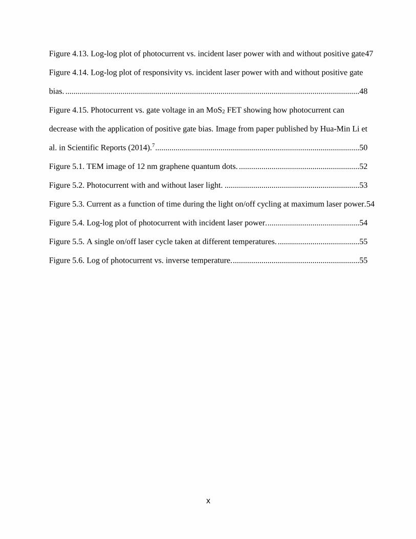
Figure 1.1. Types of Transistors and their schematic diagrams ......................................................1
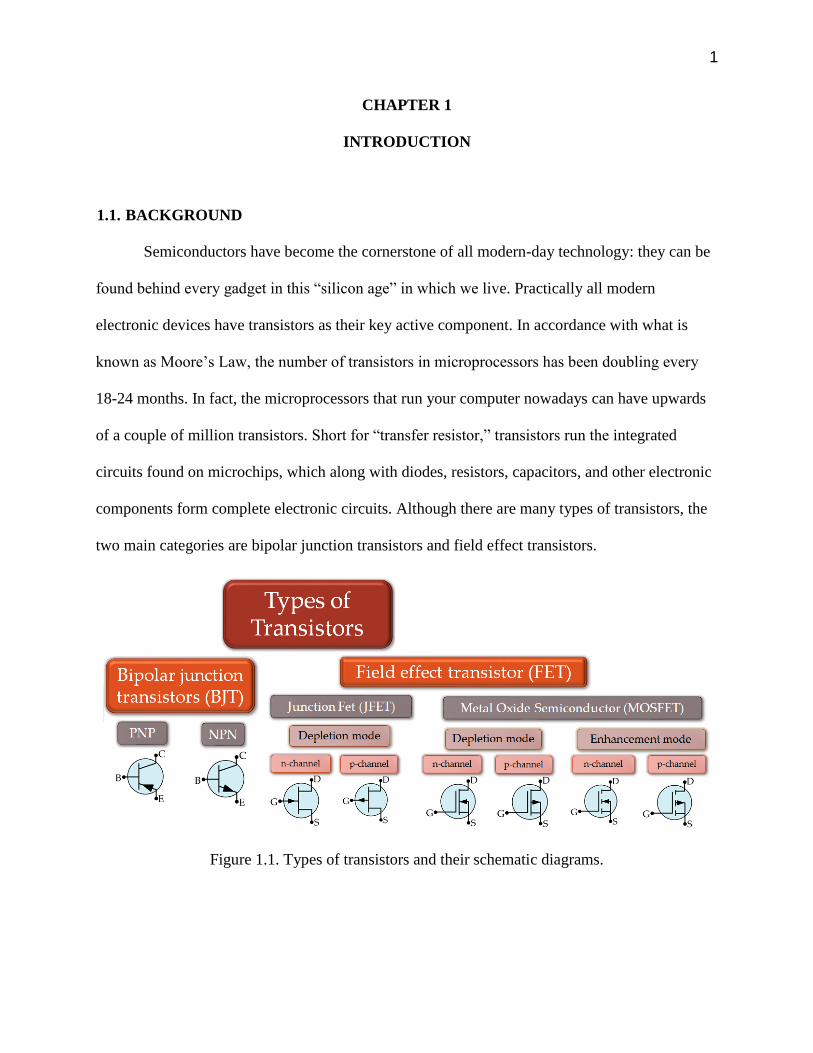
Figure 1.2. N-type enhancement mode FET without and with positive gate bias. ..........................2
Figure 2.1. Schematic for a typical CVD system. Image based off of senior labmate
Baleeswaraiah Mucharrla.1 ............................................................................................................10
Figure 2.2. Experimental setup for low temperature electrical transport measurement system. ...14
Figure 2.3. Schematic of photocurrent measurement setup. Image courtesy of senior labmate
Sujoy Ghosh.2 ................................................................................................................................15
Figure 3.1. Single layer WSe2 structures made from XcrySDen software3 ...................................17
Figure 3.2. High resolution transmission electron microscopy image of WSe2 sample and
electron diffraction pattern (inset). ................................................................................................18
Figure 3.3. Micrograph of WSe2 field-effect transistor. ................................................................19
Figure 3.4. Schematic of WSe2 FET device as measured in a two-terminal configuration with
back-gating through the silicon wafer. ...........................................................................................20
Figure 3.5. ID-VDS for -30 VG to +30 VG. Only -30 VG and -20 VG showed appreciable drain
current. ...........................................................................................................................................21
Figure 3.6. Room temperature voltage gate sweep displaying WSe2 device’s ambipolar nature. 22
Figure 3.7. Semi-log plot of room temperature voltage gate sweep. .............................................24
Figure 3.8. Linear plot of temperature dependent voltage gate sweep. .........................................25
Figure 3.9. Semi-log plot of temperature dependent voltage gate sweep ......................................26
Figure 3.10. Electron and hole mobilities at various temperatures. ...............................................27
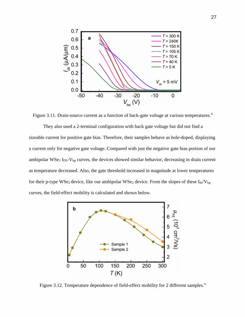
Figure 3.11. Drain-source current as a function of back-gate voltage at various temperatures4 ...28
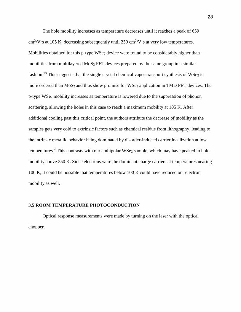
Figure 3.12. Temperature dependence of field-effect mobility for 2 different samples4 ..............28
ix
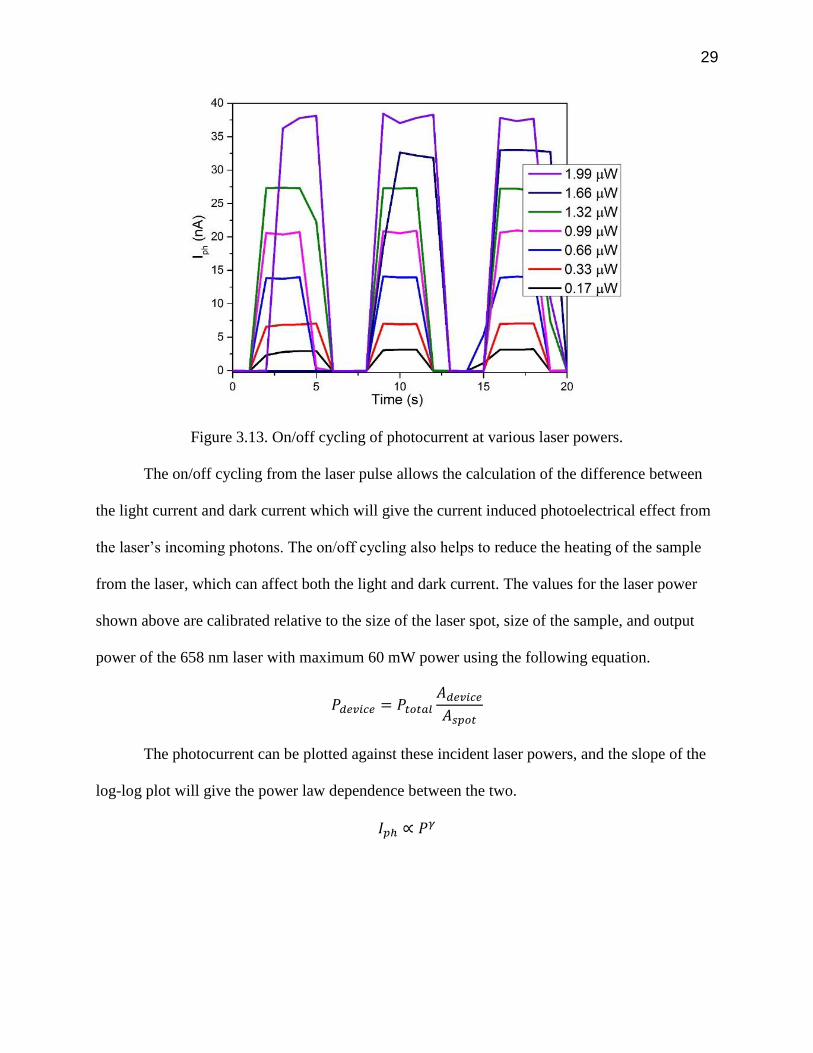
Figure 3.13. On/off cycling of photocurrent at various laser powers. ...........................................30
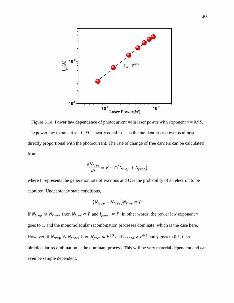
Figure 3.14. Power law dependence of photocurrent with laser power with exponent γ = 0.95. ..31
Figure 3.15. Semi-log plot of responsivity vs. laser power without gate voltage at room
temperature. ...................................................................................................................................32
Figure 3.16. Drain current with light cycling on/off at various temperatures. ..............................33
Figure 3.17. Temperature dependent responsivities plotted vs. actual laser power in log-log scale.
........................................................................................................................................................34
Figure 3.18. Responsivitiy vs. temperature in semi-log scale with and without negative gate bias.35
Figure 3.19. Energy band bending and formation of depletion layers in WSe2 device due to
titanium metal contacts. Image from paper published by Wenjing Zhang et al. in ACS Nano
(2014).43 .........................................................................................................................................36
Figure 4.1. Side view and top view of InSe crystal structure.5 ......................................................38
Figure 4.2. SEM image of bulk InSe crystal grown from non-stoichiometric melt.6 ....................39
Figure 4.3. HRTEM image of InSe flake.5 ....................................................................................39
Figure 4.4. Electron beam diffraction pattern along the c axis.5....................................................40
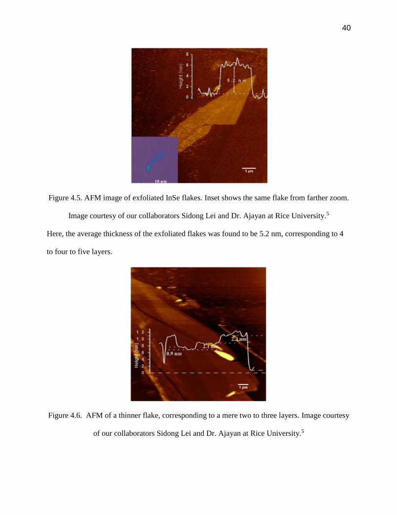
Figure 4.5. AFM image of exfoliated InSe flakes. Inset shows the same flake from farther zoom.541
Figure 4.6. AFM of a thinner flake, corresponding to a mere two to three layers.5 .....................41
Figure 4.7. Image from optical microscope of InSe flake acting as FET device. ..........................42
Figure 4.8. Voltage gate sweep of crain current and electron mobility calculation. .....................43
Figure 4.9. ID-VD curve without gate voltage with and without light. ...........................................44
Figure 4.10. Light on/off cycling at different laser powers without gate voltage. ........................45
Figure 4.11. One on/off cycle of 66 nW laser power with and without gate voltage. ...................46
Figure 4.12. One on/off cycle of light of 2 µW laser power with and without gate voltage. ........46
x
Figure 4.13. Log-log plot of photocurrent vs. incident laser power with and without positive gate47
Figure 4.14. Log-log plot of responsivity vs. incident laser power with and without positive gate
bias. ................................................................................................................................................48
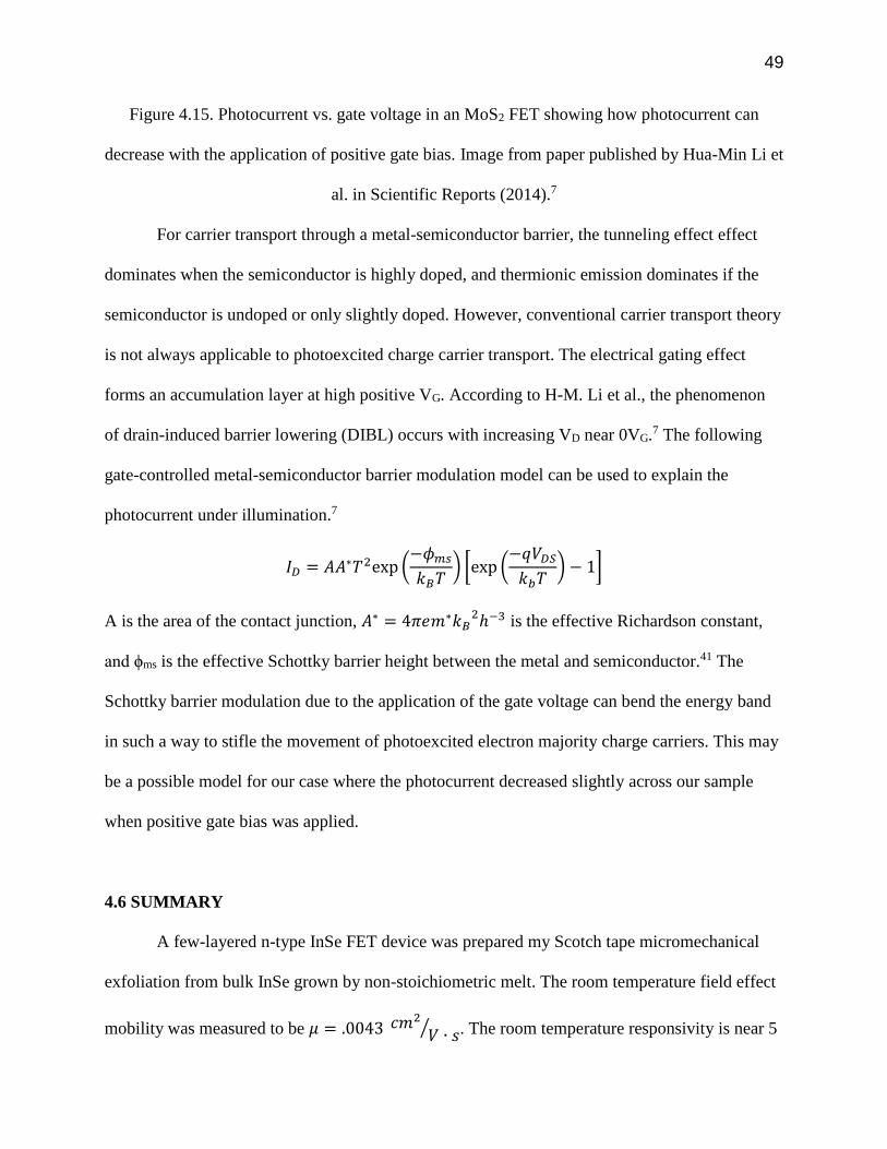
Figure 4.15. Photocurrent vs. gate voltage in an MoS2 FET showing how photocurrent can
decrease with the application of positive gate bias. Image from paper published by Hua-Min Li et
al. in Scientific Reports (2014).7 ....................................................................................................50
Figure 5.1. TEM image of 12 nm graphene quantum dots. ...........................................................52
Figure 5.2. Photocurrent with and without laser light. ..................................................................53
Figure 5.3. Current as a function of time during the light on/off cycling at maximum laser power.54
Figure 5.4. Log-log plot of photocurrent with incident laser power. .............................................54
Figure 5.5. A single on/off laser cycle taken at different temperatures. ........................................55
Figure 5.6. Log of photocurrent vs. inverse temperature. ..............................................................55
1
CHAPTER 1
INTRODUCTION
1.1. BACKGROUND
Semiconductors have become the cornerstone of all modern-day technology: they can be
found behind every gadget in this “silicon age” in which we live. Practically all modern
electronic devices have transistors as their key active component. In accordance with what is
known as Moore’s Law, the number of transistors in microprocessors has been doubling every
18-24 months. In fact, the microprocessors that run your computer nowadays can have upwards
of a couple of million transistors. Short for “transfer resistor,” transistors run the integrated
circuits found on microchips, which along with diodes, resistors, capacitors, and other electronic
components form complete electronic circuits. Although there are many types of transistors, the
two main categories are bipolar junction transistors and field effect transistors.
Figure 1.1. Types of transistors and their schematic diagrams.
2
The bipolar junction transistor (BJT) used to be the more common type of transistor and works
by current control through three terminals of the emitter, base, and collector, and comes in three
doped regions of PNP or NPN form. BJTs are mostly used nowadays as a current amplifier at
high frequency for its high transconductance and output resistance. However, the MOSFET is
now the most common transistor in use today in both analog and digital circuits, and the most
common MOSFET in particular is the n-type enhancement MOSFET, sometimes referred to as
n-type EMOS. MOSFETs can be used as a switch or as an amplifier. When acting as a switch,
the MOSFET can be thought of as a variable resistor, whose resistance is controlled by the gate
voltage.
Figure 1.2. N-type enhancement mode FET without and with positive gate bias.
After enough gate voltage is applied, the resistance between source and drain decreases as the
depletion region grows, allowing current to flow through the MOSFET from source to drain. As
an amplifier, the drain current is a function of the gate voltage. The other type of MOSFET is the
depletion MOSFET, which ultimately shows an increase in resistance as more gate voltage is
applied. Two parameters of physical MOSFET devices are the conductance coefficient, kn, and
3
the threshold voltage, Vt.8,9 Transistors are used to create the logic gates that run the circuits of
the electronics in our daily lives.
These transistors are overwhelmingly generally made from silicon, regarded to be the
most successful material of the past century. Silicon is an abundant element which forms a stable
oxide, making it cheap to fabricate. With its low indirect band gap, relatively high hole mobility,
and tunable electrical and mechanical properties by doping, this has led silicon to become the
most common material in integrated circuits, discrete devices, and photovoltaics. However, as
various new technologies are pushed further to have higher performance while functioning at
lower power costs, we approach the limits of how far silicon material can take us. Silicon is
naturally brittle and rigid, so silicon transistors can age and fail. Silicon devices have a size
limitation to how small they can be before running into operational complications, such as
tending to waste energy in electronic devices in the form of leakage and heat dissipation. This
limits the use of silicon in opto-electronics and spintronics. As such, silicon is by far not the only
semiconductor used in electronic devices. Gallium arsenide is the second most common
semiconductor in commercial use, especially prevalent in fast integrated circuits which operate at
higher frequencies, with an electron mobility six times greater than silicon. Its wide direct band
gap allows GaAs to absorb and emit light efficiently while being highly resistive to heat and
radiation damage. However, single-crystal gallium arsenide substrate is expensive, making it less
desirable in the consumer market. Pure germanium has four valence electrons, like silicon, and
higher conductivity, but cannot be used at higher temperatures. In fact, the first transistor used
germanium, and was made at Bell Telephone Laboratories, Inc. by Shockley, Bardeen, and
Brattain, who were honored with the Nobel Prize in 1956 for their discovery.

4
Different forms of carbon nanomaterials have been extensively studied and used in
various nanoelectronic applications. Carbon plays a very important role in forming various
molecules and compounds due to its four valence electrons which can easily form covalent
bonds. Similarly, the silicon atom also has four valence electrons, but with an atomic number of
14, has a larger nucleus than carbon. Having only 6 protons, the carbon atom has a small enough
size to comfortably fit in other molecules. Carbon commonly forms bonds with itself, creating a
variety of stable allotropes in a different dimensions. The lowest dimensional form is zero-
dimensional fullerenes. A fullerene is any molecule of carbon that forms a hollow cage of carbon
atoms. The first of such fullerenes to be found was buckminsterfullerene, or “buckyball” for
short, in 1985, named after Buckminster Fuller’s geodesic dome. A buckyball consists of 60
carbon atoms, hence C60, arranged as five-carbon rings isolated by six-carbon rings, taking on a
soccer ball shape. Other spherical fullerenes have since been discovered, such as C70, C84, and
C120. These zero-dimensional fullerenes have even been experimentally shown to display wave-
particle duality.10 Fullerenes also come in other shapes, such as cylindrical tubes referred to as
carbon nanotubes, or CNTs. Sumio Iijima first observed concentric tubes in 1991 while studying
carbon soot from graphite electrodes under an high resolution transmission electron microscope
(HRTEM), which were later named multi-walled carbon nanotubes (MWCNTs).11 Iijima also
later made single-walled carbon nanotubes (SWCNTs).12 These SWCNTs can be visualized as a
single flat layer of carbon atoms arranged in a hexagonal pattern rolled into a cylindrical tube.13
Multi-walled CNTs have several concentric tubes around the same axis, thus having multiple
cylindrical walls. Both SWCNTs and MWCNTs are one-dimensional materials, as electrons are
considered to move only along their axis of symmetry.14,15 The next dimension higher is the two-
dimensional form of carbon in a hexagonal lattice known as graphene, which will be discussed
5
subsequently. Lastly, there are the 3-D allotropes of carbon, the most important of which include
graphite, diamond, and amorphous carbon.
Two-dimensional materials were initially believed to be thermodynamically unstable.
Richard P. Feynman predicted the importance of isolated individual layer materials back in his
talk titled “Plenty of Room at the Bottom” in 1959, envisioning the possibilities of tuning
properties by rearranging layers of atoms.16 For example, the two-dimensional form of silicon,
silicene, is structurally unstable, deforming easily into a drop of silicon due to its buckled
hexagonal structure in 2-D form. The first two-dimensional material to be observed
experimentally was graphene, which consists of a hexagonal lattice of carbon atoms sp2 bonded
with a distance of 0.142 nanometers between atoms. Graphene can occur naturally but can also
be synthesized in the laboratory in a variety of different ways.17,18 For example, using Scotch
tape, graphene can be mechanically exfoliated from graphite, the corresponding 3-D form.19
Graphene can also be synthesized on a variety of different substrates on larger scales, such as
through chemical vapor deposition.20,21 Graphene can be doped with different elements, such as
nitrogen, to alter its electronic and optoelectronic properties.17
Graphene is one of the most studied materials during the last decade due to its
extraordinary electrical,1 optical,22 thermal,8,23 and mechanical properties.24,25 Graphene is the
both the thinnest and strongest known material measured.25 Undoped graphene’s unique
electronic structure comes the fact that it is not a metal, semiconductor, or insulator, but actually
a semimetal with zero band gap at the Dirac point where the valence band and conduction band
crossover one another.26–28 As previously mentioned, graphene can be wrapped, rolled, or
stacked to go from 2-D graphene to 0-D fullerenes, 1-D nanotubes, or 3-D graphite. Conversely,
graphene can be obtained through mechanical exfoliation from highly-ordered pyrolytic graphite
6
(HOPG), single-crystal graphite, or natural graphite.29 The first reported mechanical exfoliation
of graphene from HOPG was done by Novoselov et al. in 2004, for which they were awarded the
Nobel Prize in Physics in 2010.19,30 To prepare their graphene, the group dry etched 5 μm mesas
onto HOPG platelets using oxygen plasma. The structured platelets were then pressed against a 1
μm layer of wet photoresist to form a patterned coating over a glass substrate. After baking, the
mesas were attached to the photoresist, which allowed them to cleave the HOPG. Using scotch
tape, graphite flakes were mechanically peeled off of the mesas, resulting in few layer graphene
films up to 10 μm in size. These flakes were then deposited or transferred onto Si/SiO2 wafers. It
was discovered that the thickness of the oxide layer on top of the SiO2 plays a very important
role in the visibility of the graphene flakes; an oxide layer that was too thick or thin could render
the graphene invisible under an optical microscope.
Mechanical exfoliation via Scotch tape peeling is one way to produce graphene flakes,
however other methods to synthesize graphene with different qualities are also being utilized.31
Ultrathin epitaxial graphite films have also been obtained by burning silicon off from a silicon
carbide surface.32 Chemical vapor deposition (CVD) can be used to synthesize high-quality,
large-area graphene.20,33 In CVD growth, hydrocarbon gas is flowed through a quartz tube inside
of a furnace, resulting in the formation of few-layer graphene.21
Liquid phase exfoliation is a common, cost-effect method for large-scale production of
graphene.34 Graphite powder is dispersed and dissolved in a solvent chosen to minimize the
interfacial tension between graphene flakes and the liquid. Some examples of possible solvents
used are pentaflurobenzonitrile (C6F5CN), N-methyl-pyrrolidinone (NMP), and dimethyl
imidazolidinone (DMEU).34,35 Then, the solution is sonicated by high-frequency sound waves,
which weakens the van der Waals interactions between the layers of graphite, exfoliating
7
separate layers. Finally, centrifugation and decantation purifies the dispersion, allowing for the
separation of suspended graphene flakes.
Even though graphene has a very high electrical conductivity, graphene’s lack of finite
band gap limits its use in some electrical components where a non-zero band gap is required to
switch off a device. However, the crystalline structure of a semiconductor can be altered by
introducing other elements to replace some of the original atoms. This process is called doping,
and the presence of these impurities can change the resistivity of the semiconductor. The
electrical resistivity of a material is the electrical resistance per unit volume and is the inverse of
the conductivity of a material. If the element that is added, called the dopant, has extra electrons
compared to the original material, then an n-type semiconductor will be produced. On the other
hand, if the dopant has fewer electrons than the starting material, then the semiconductor will
become p-type. It should be noted however that not all materials can be doped freely due to
different structural limitations.36 Doping is important because it is a fundamental method to fine
tune a material’s electrical transport properties to make it fit for a specific nanoelectronic device
application. Doping, laser irradiation, oxidation, and the formation of nanoribbons, quantum
dots, and other nanostructures have been attempts to tune the band gap for semiconductor
application. However, each of these methods introduce a new set of properties that work for only
a specific functionalization for graphene, and it is generally difficult to systematically control the
structural synthesis.37,38 Also, graphene is susceptible to oxidation and can be toxic.
1.2 MOTIVATION
Transition metal dichalcogenides (TMDC) are compounds that consist of one transition
metal atom bonded with two chalcogen anions. Some of the common combinations include
8
MoS2, MoSe2, MoTe2, WS2, and WSe2. These semiconducting materials exhibit a unique
indirect-to-direct band gap transition as their thickness is reduced from bulk to monolayer. In
fact, bulk TMDC crystals can be formed by stacking monolayers on top of one another, bound by
van der Waals’ interaction. Tungsten diselenide, WSe2, is one such TMDC. Bulk WSe2 has an
indirect band gap of ~1.2 eV, which transitions into a direct band gap of ~1.65 eV in
monolayers.39,40 Few-layered WSe2 has been found to show high photoresponsivity, external
quantum efficiency, and fast response time.41 Back-gated monolayer WSe2 has been found to
have a high mobility above 140 𝑐𝑚2
𝑉 ∙ 𝑠⁄ with large on/off switching ratio (> 106).42 W. Zhang
et al. found CVD-grown monolayer WSe2 devices to be highly stable with a high photo gain and
high detectivity, even in ambient conditions, with a hole mobility approaching that of n-doped
silicon.43 The inherent direct band gap in TMDC monolayers lends itself to these TMDCs being
used in a variety of electric and optical applications, such as transistors, emitters, and detectors.
In particular, high-performance FETs made from TMDCs are ideal candidates for photodetectors
and low power optoelectronics.
Other chalcogenides are also studied. Indium selenide, InSe, falls under the category of
layered III-VI chalcogenide and is commonly found in a hexagonal lattice, like GaS and GaSe.44
These Group III-IV van der Waals layered structures show promising nonlinear and anisotropic
optical, electronic, and mechanical properties.5 Bulk InSe has a direct bandgap of ~1.25 eV at
room temperature and a broader spectral response compared to other III-VI group materials.45
The transition to few layers is accompanied with a transition to an indirect bandgap around 1.4
eV, offering a broad spectral response. 2D InSe exhibits strong quantum confinement one order
of magnitude greater than other IIIA-VIA compounds, and small exciton reduced mass μc =
0.054 me.46 InSe has already been used in a variety of applications, such as in lithium batteries
9
and photovoltaic devices with efficiency upwards of 11%,47 and has potential application in
nonlinear optics, solid state batteries, solar cells, and memory devices.48
A specific example of where both transition metal dichalcogenides and Group III-VI
semiconductors can potentially be superior to silicon is solar cell efficiency. The maximum
theoretical efficiency of solar cells was calculated by William Shockley and Hans Quiesser in
1961 to be around 33.7% for a single p-n junction with ban gap 1.34 eV.49 Silicon’s band gap of
1.1 eV falls just short of the peak, which is now referred to as the Shockley-Quiesser limit.
Excess energy between the energy of the sun’s light rays and the band gap is wasted and lost as
heat. As a result, modern commercial solar cells usually have less than 24% conversion
efficiency, also partly due to light reflection, light blockage, wiring, and geometric flatness of the
solar cell. This is an example of a thrust for the search for semiconducting materials with a
tunable band gap nearer the solar cell efficiency peak.
1.3 THESIS OUTLINE
The following material presented in this thesis will be presented as follows. The
subsequent chapter discusses the experimental techniques used to synthesize the sample, prepare
the devices, characterize the samples, and run the electrical transport measurements. Then, room
temperature and temperature dependent electrical transport results for the WSe2 device will be
presented and discussed. In the next chapter, the room temperature electrical transport of the
InSe will be explored. This will be compared to other electrical transport data I collected from
different devices, with the primary focus on graphene quantum dots. Finally, the conclusion will
summarize the thesis work and make some final remarks.

10
CHAPTER 2
EXPERIMENTAL TECHNIQUES
2.1 SAMPLE SYNTHESIS
Chemical vapor deposition (CVD) is a chemical process that is used to synthesize thin
films, powders, and even single crystals onto a substrate. The schematic of a typical CVD system
is shown in Figure 2.1.1 A precursor, usually in the solid phase, is placed at one end of a glass
tube which is heated, taking it into the vapor phase in the first stage of the process. Neutral
carrier gases are flushed through the tube, which is under controlled vacuum, transporting the
vaporized particles down the heated tube to the middle of a furnace, where they are deposited
onto a substrate, such as copper foil or SiO2. By fine-tuning various parameters, such as the
growth time, temperature, substrate, inert gas flow, and the addition of catalysts, the size,
thickness, and structure of the growth can be controlled. Compared to other growth methods used
for 2D synthesis, such as chemical vapor transport or physical vapor deposition of sputtering or
evaporation, CVD comformally deposits material with relatively high purity

11
Figure 2.1. Schematic for a typical CVD system. Image based off of senior labmate
Baleeswaraiah Muchharla.1
WSe2 consists of sandwiched W and Se layers in a hexagonal structure with a thickness
of 3.3 Å. WSe2 single crystals were synthesized by Dr. Luis Balicas’ group at the National High
Magnetic Field Lab at Florida State University by chemical vapor transport (CVT) method.41
Iodine and excess Se were used as the transport agents during the chemical vapor transport. From
the formed single crystals, multilayer flakes of WSe2 were exfoliated by micromechanical
cleavage and transferred onto Si wafers with a 270 nm SiO2 layer. These SiO2 wafers were first
sonicated for 15 minutes in acetone, isopropanol, and deionized water and dried in nitrogen gas.
The Si wafers were p-doped at levels ranging from 2 × 10¹⁹ to 2 × 1020 cm−3. The crystals
were characterized using photoluminescence spectroscopy (PLS), Raman spectroscopy, electron
diffraction spectroscopy (EDX), and transmission electron microscopy (TEM).42,4 To make the
WSe2 devices, patterned electrical contacts were made using standard electron-beam lithography,
where 90 nm of Au were deposited onto 4 nm of Ti by electron-beam evaporation. Then the
devices are annealed at 200 °C for 2 hours in forming gas to remove impurities.
The indium selenide sample was synthesized by our collaborators in Dr. Ajayan’s group
at Rice University, Houston, TX. Bulk InSe formed by a nonstoichiometric melt of indium to
selenium in a 52:48 ratio at 700 °C for 3 hours in 10-3 Torr vacuum in a quartz tube. This is
cooled down at a 10 °C/hr step process to 500 °C, then allowed to cool naturally to room
temperature over the next 6 hours. The formed bulk InSe crystals form a layered texture similar
to black mica, or biotite. This bulk InSe is then peeled with tweezers into 5 mm diameter pieces
tens of microns thick. Using the scotch tape method of mechanical exfoliation, few-layered
12
flakes are separated and transferred on to a silicon wafer with a 285 mm thermally grown SiO2
layer.
A variety of microscopy and spectroscopy methods were used to analyze the InSe. High-
resolution transmission electron microscopy (HRTEM) is used to observe the crystalline
structure and quality of 2D InSe prepared by chemical exfoliation. To prepare the sample for the
TEM, the bulk crystals were mixed in dimethylformamide (DMF) and sonicated for 48 hours
before being drop casted onto a lacy carbon TEM grid. The electron diffraction pattern was also
taken to probe the symmetry of the crystal structure. Using atomic force microscopy (AFM), the
thickness and roughness of the mechanically exfoliated InSe layers were studied. Resonant and
nonresonant Raman spectroscopy measurements were taken to discover the sample’s lattice
vibration and electronic band structure properties.
The indium selenide device was prepared locally by vacuum deposition of Cr and Au
electrodes at 5 × 10⁻⁶ Torr. Thermal evaporation and cathodic sputtering created 100 × 100 μm
electrodes with 10 µm channel spacing. Wire bonding of gold wires is used to create the FET
device along the 10 × 15 µm InSe flake.
The graphene quantum dots were chemically synthesized at the Central Electrochemical
Research Institute in Karaikudi, India by S. Kundu et.al. using a similar method to that used in
Rice University31. Multi-walled carbon nanotubes and KMnO4 were stirred slowly into 250 mL
of a 9:1 mixture of H2So4 and H3Po4 at 50°C. After being heated for 35 hours, the mixture was
cooled to room temperature and filtered. KOH solution was used to neutralize the filtrate, then
underwent sonication and centrifugation at 7,000 rpm in deionized water to create a uniform size
distribution. The solution was filtered through a PTFE membrane with a pore size of 0.2 µM,
13
dialyzed for 3 days, and dried in a vacuum oven. The graphene quantum dots are prepared in
several separate batches to test for reproducibility.
2.2 ELECTRON MICROSCOPY
Besides using standard light-powered microscopes to image and otherwise visually
characterize the samples, more powerful microscopy equipment can be used to obtain higher
resolution images at a much smaller scale. Conventional optical microscopes can normally
magnify only around up to ×1000, and are limited by light diffraction to resolution up to the
Rayleigh criterion, usually on the order of 0.2 μm.50 To overcome this resolution limitation set
by the diffraction of light, a beam of electrons instead of photons is used to illuminate and image
the sample.
The main electron microscope used in this study is a transmission electron microscope
(TEM). The TEM uses an illumination system consisting of an electron gun focused with
condenser lenses, generating an electron beam that travels down the optical column to reach the
sample. The sample can be adjusted within the specimen manipulation system, and an image is
collected by various objective lenses and the stigmator from the electrons that were transmitted
through the ultra-thin specimen. Projecting lenses create a visible image from these electrons on
a fluorescent screen for the viewer to observe. These internal lenses can be finely adjusted
through use of electromagnetic controls to adjust the image’s features, such as contrast and
spherical aberration.51 For example, in its highest resolution mode, the Hitachi H-7650 TEM can
zoom from 4,000× up to 600,000× magnification.
2.3 ELECTRICAL TRANSPORT MEASUREMENTS
14
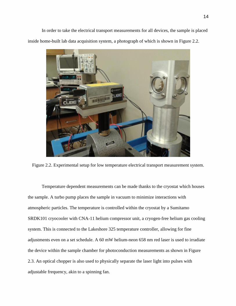
In order to take the electrical transport measurements for all devices, the sample is placed
inside home-built lab data acquisition system, a photograph of which is shown in Figure 2.2.
Figure 2.2. Experimental setup for low temperature electrical transport measurement system.
Temperature dependent measurements can be made thanks to the cryostat which houses
the sample. A turbo pump places the sample in vacuum to minimize interactions with
atmospheric particles. The temperature is controlled within the cryostat by a Sumitamo
SRDK101 cryocooler with CNA-11 helium compressor unit, a cryogen-free helium gas cooling
system. This is connected to the Lakeshore 325 temperature controller, allowing for fine
adjustments even on a set schedule. A 60 mW helium-neon 658 nm red laser is used to irradiate
the device within the sample chamber for photoconduction measurements as shown in Figure
2.3. An optical chopper is also used to physically separate the laser light into pulses with
adjustable frequency, akin to a spinning fan.

15
Figure 2.3. Schematic of photocurrent measurement setup. Image courtesy of senior labmate
Sujoy Ghosh.2
Two Keithley 4ZA4 sourcemeters are connected to the FET device’s source, drain, gate,
and ground. These sourcemeters, controlled by the connected computer with LabView software,
are used to deliver some input signal into the device’s source and gate, and to measure the output
signal from the device’s drain.
The device on the microchip is affixed to the cold head within the sample chamber,
which is temperature controlled by the cryocooler’s compressor unit through flexible helium gas
lines. As the helium gas goes through cycles of compression and expansion, the cryostat cools
according to the Joule-Thomson effect, allowing us to reach temperatures around 50 K. Since it
takes some time for the device to come into thermal equilibrium with the cryocooler head as it
cools, extra time is allotted between measurements especially at lower temperatures, even after
the Lakeshore temperature controller reads that the desired temperature has been reached. The
corresponding ends of the microchip for the FET are connected to the Keithley sourcemeters,
and various programs have been coded through the Labview software to take the desired
electrical transport measurements. Many of the experiments were carried out alongside fellow
labmates in Dr. Talapatra’s lab group.
16
CHAPTER 3
AMBIPOLAR TUNGSTEN DISELENIDE RESULTS AND DISCUSSION
3.1 INTRODUCTION
Bulk transition metal dichalcogenides, such as MoS2, WS2, and WSe2, crystallize in the
“2H” trigonal prismatic structure. In the case here of WSe2, this means that each tungsten atom is
surrounded by six selenium atoms which define two triangular prisms.4 Contiguous extended
planes are shifted along both the a- and b- axis, and each layer is covalently bonded with one the
adjacent layer at a distance c. Weak inter-planar van der Waals coupling allows the bulk crystals
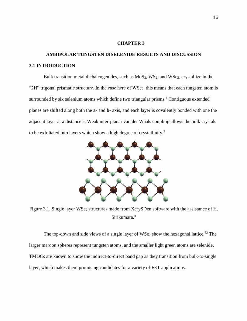
to be exfoliated into layers which show a high degree of crystallinity.3
Figure 3.1. Single layer WSe2 structures made from XcrySDen software with the assistance of H.
Sirikumara.3
The top-down and side views of a single layer of WSe2 show the hexagonal lattice.52 The
larger maroon spheres represent tungsten atoms, and the smaller light green atoms are selenide.
TMDCs are known to show the indirect-to-direct band gap as they transition from bulk-to-single
layer, which makes them promising candidates for a variety of FET applications.
17
3.2 SAMPLE CHARACTERIZATION AND DEVICE FABRICATION
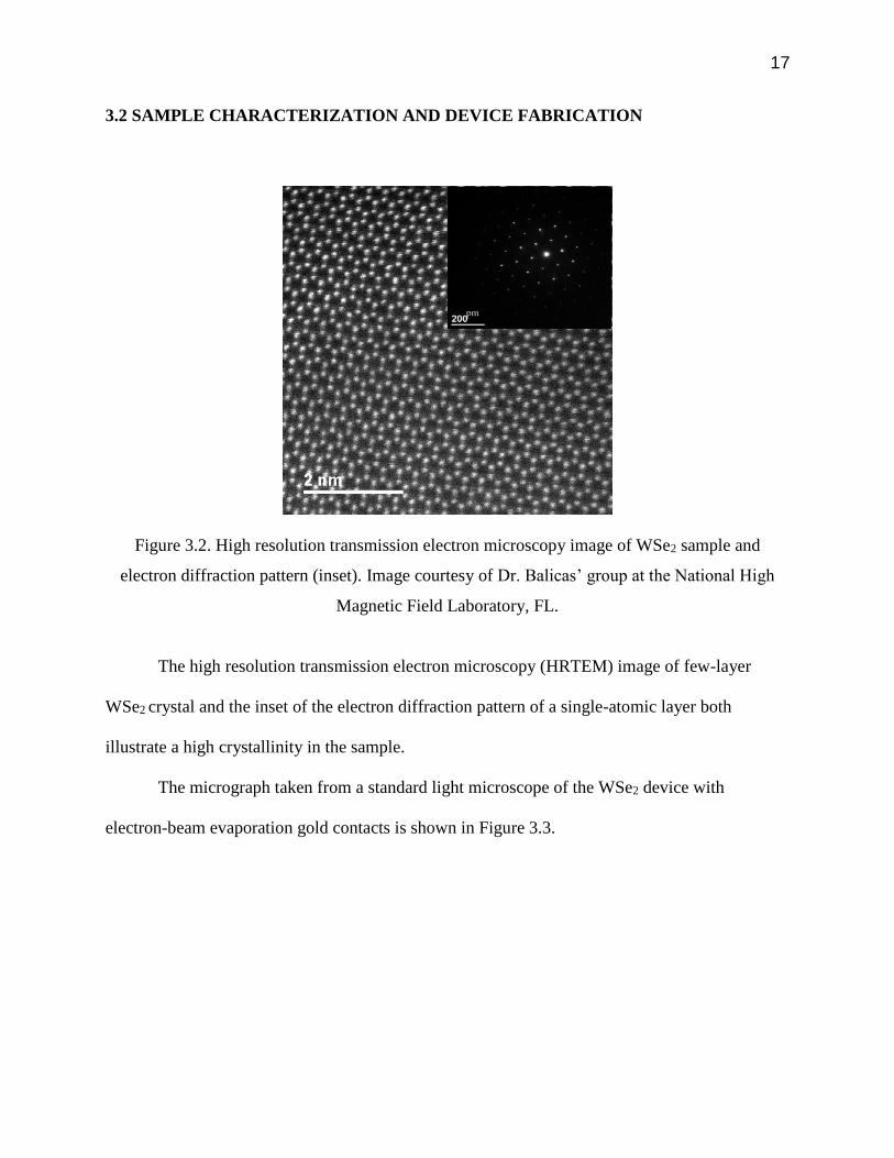
Figure 3.2. High resolution transmission electron microscopy image of WSe2 sample and
electron diffraction pattern (inset). Image courtesy of Dr. Balicas’ group at the National High
Magnetic Field Laboratory, FL.
The high resolution transmission electron microscopy (HRTEM) image of few-layer
WSe2 crystal and the inset of the electron diffraction pattern of a single-atomic layer both
illustrate a high crystallinity in the sample.
The micrograph taken from a standard light microscope of the WSe2 device with
electron-beam evaporation gold contacts is shown in Figure 3.3.
pm

18
Figure 3.3. Micrograph of WSe2 field-effect transistor.
The width and length of the device can be approximated based on the magnification of
the image to be 13.8 µm and 14.8 µm, respectively. Although there are extra gold terminals for
Hall-effect and four-terminal resistivity measurements, only the largest electrode contacts on
opposite sides were used as the source and drain contacts in two-terminal configuration. The
sample is back-gated and grounded through the microchip, as shown in Figure 3.4.
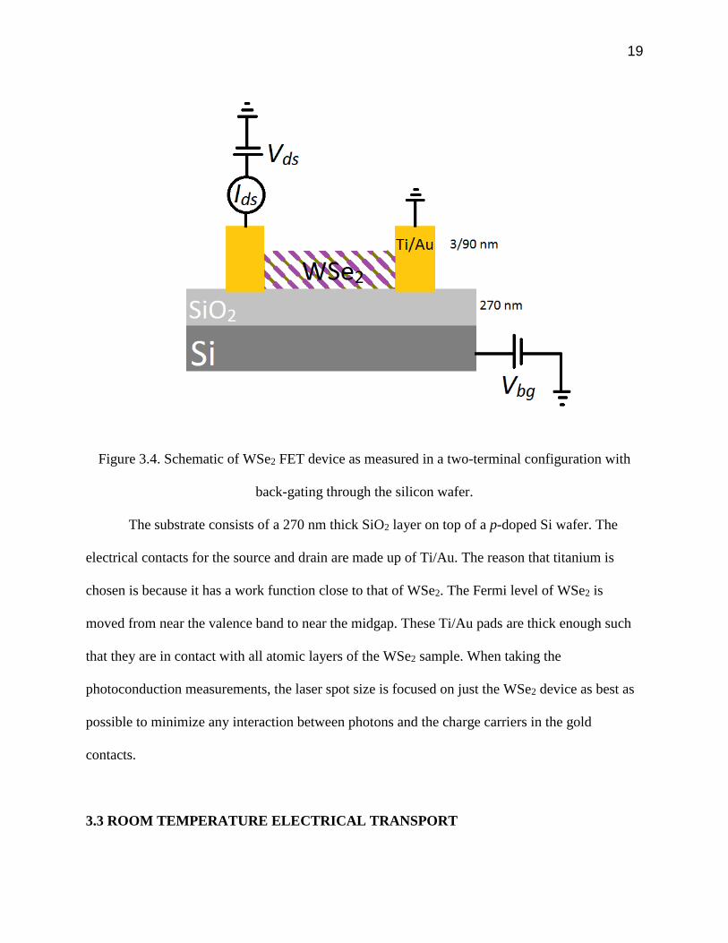
19
Figure 3.4. Schematic of WSe2 FET device as measured in a two-terminal configuration with
back-gating through the silicon wafer.
The substrate consists of a 270 nm thick SiO2 layer on top of a p-doped Si wafer. The
electrical contacts for the source and drain are made up of Ti/Au. The reason that titanium is
chosen is because it has a work function close to that of WSe2. The Fermi level of WSe2 is
moved from near the valence band to near the midgap. These Ti/Au pads are thick enough such
that they are in contact with all atomic layers of the WSe2 sample. When taking the
photoconduction measurements, the laser spot size is focused on just the WSe2 device as best as
possible to minimize any interaction between photons and the charge carriers in the gold
contacts.
3.3 ROOM TEMPERATURE ELECTRICAL TRANSPORT
20
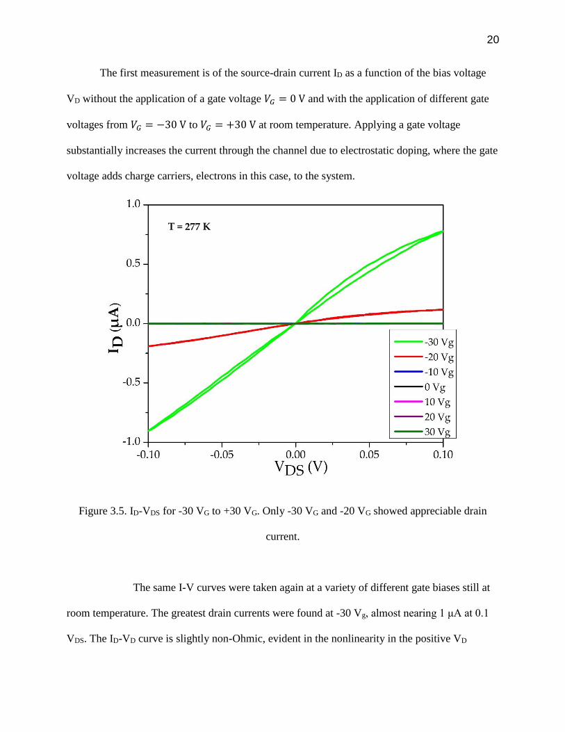
The first measurement is of the source-drain current ID as a function of the bias voltage
VD without the application of a gate voltage 𝑉𝐺 = 0 V and with the application of different gate
voltages from 𝑉𝐺 = −30 V to 𝑉𝐺 = +30 V at room temperature. Applying a gate voltage
substantially increases the current through the channel due to electrostatic doping, where the gate
voltage adds charge carriers, electrons in this case, to the system.
Figure 3.5. ID-VDS for -30 VG to +30 VG. Only -30 VG and -20 VG showed appreciable drain
current.
The same I-V curves were taken again at a variety of different gate biases still at
room temperature. The greatest drain currents were found at -30 Vg, almost nearing 1 μA at 0.1
VDS. The ID-VD curve is slightly non-Ohmic, evident in the nonlinearity in the positive VD
T = 277 K
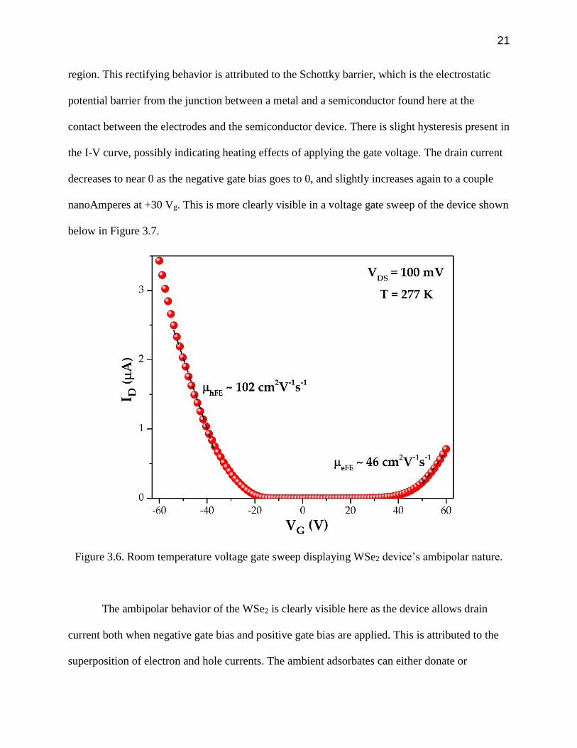
21
region. This rectifying behavior is attributed to the Schottky barrier, which is the electrostatic
potential barrier from the junction between a metal and a semiconductor found here at the
contact between the electrodes and the semiconductor device. There is slight hysteresis present in
the I-V curve, possibly indicating heating effects of applying the gate voltage. The drain current
decreases to near 0 as the negative gate bias goes to 0, and slightly increases again to a couple
nanoAmperes at +30 Vg. This is more clearly visible in a voltage gate sweep of the device shown
below in Figure 3.7.
Figure 3.6. Room temperature voltage gate sweep displaying WSe2 device’s ambipolar nature.
The ambipolar behavior of the WSe2 is clearly visible here as the device allows drain
current both when negative gate bias and positive gate bias are applied. This is attributed to the
superposition of electron and hole currents. The ambient adsorbates can either donate or
22
withdraw electrons from WSe2, resulting in apparent n-doping or p-doping of the device
respectively.
From the slopes of this plot, the field effect electron and hole mobility μFE can be
calculated using the following formula.
𝜇𝐹𝐸 =1
𝐶𝑜𝑥
1
𝑉𝐷𝑆
𝐿
𝑊
𝜕𝐼𝐷
𝜕𝑉𝐺
For this device, the capacitance of SiO2 𝐶𝑜𝑥 is 1.28 × 10⁻⁸ 𝐹 𝑐𝑚2⁄ , the length and width of the
WSe2 channel are 13.79 μm and 14.80 μm, respectively. The drain current is almost 4 times
greater at -60 Vg bias vs. +60 Vg bias. At source-drain voltage VDS = 0.1 V, the peak hole
mobility was found to be approximately 102 𝑐𝑚2
𝑉 ∙ 𝑠⁄ . The hole conduction is more than
double that of the electron conduction, which was found to be approximately 46 𝑐𝑚2
𝑉 ∙ 𝑠⁄ .
Therefore, the p-type behavior of the device is dominant over the n-type behavior at room
temperature. Many other similar devices prepared from the same bulk WSe2 crystals by the same
collaborators showed only the p-type behavior without the n-type behavior. This shows that the
behavior of each device can be very unique, based on a variety of factors including impurities in
the sample and the preparation and fabrication of the device.
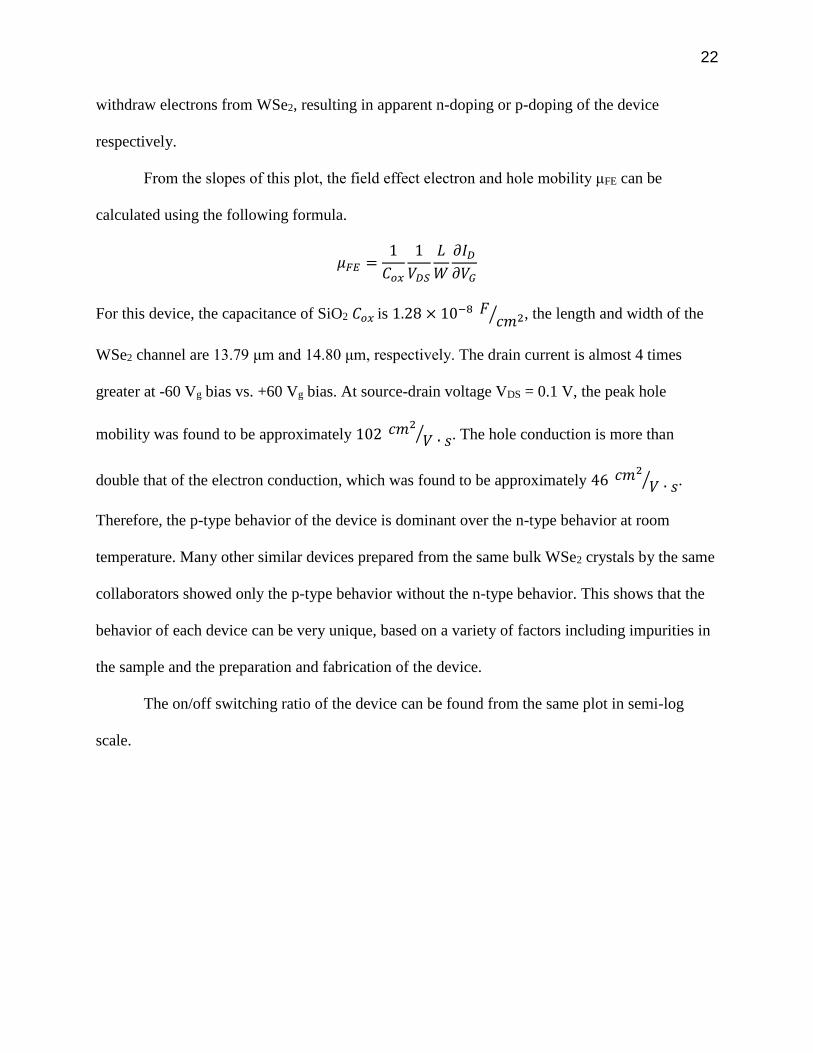
The on/off switching ratio of the device can be found from the same plot in semi-log
scale.
23
Figure 3.7. Semi-log plot of room temperature voltage gate sweep.
The on/off ratio of the device is calculated from the ratio of the maximum and minimum drain
currents, which here is on the order of 104. This is a typical on/off ratio for TMDC FET devices.
The dip in drain current at -10 VG should be near the point where the majority charge carriers
switch from holes to electrons.
3.4 TEMPERATURE-DEPENDENT ELECTRICAL TRANSPORT
Temperature dependent measurements were carried out by decreasing the temperature of
the sample inside the crysostat. The same ID-VG curve was taken at decreasing temperatures
down to 75 K with 100 mV VDS.

24
Figure 3.8. Linear plot of temperature dependent voltage gate sweep.
The room temperature data is still shown here with its dominant p-type behavior. As
temperature is varied though, this relation switches: the dominating behavior becomes n-type, as
seen in the increasing drain currents as positive gate bias is applied. This same curve can be
plotted in semi-log scale to better examine the differences in behavior at lower temperatures.
25
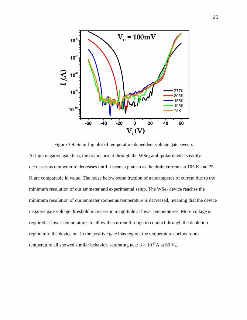
Figure 3.9. Semi-log plot of temperature dependent voltage gate sweep.
At high negative gate bias, the drain current through the WSe2 ambipolar device steadily
decreases as temperature decreases until it nears a plateau as the drain currents at 105 K and 75
K are comparable in value. The noise below some fraction of nanoamperes of current due to the
minimum resolution of our ammeter and experimental setup. The WSe2 device reaches the
minimum resolution of our ammeter sooner as temperature is decreased, meaning that the device
negative gate voltage threshold increases in magnitude at lower temperatures. More voltage is
required at lower temperatures to allow the current through to conduct through the depletion
region turn the device on. In the positive gate bias region, the temperatures below room
temperature all showed similar behavior, saturating near 3 × 10⁻⁶ A at 60 VG.

26
Figure 3.10. Electron and hole mobilities at various temperatures.
The red spheres are representative of the hole mobility calculated from the p-type behavior as
negative gate bias is applied, while the blue spheres represent the electron mobility calculated
from the slope of the n-type behavior where positive gate bias is applied. The highest electron
mobility was found to be approximately µ > 150 cm2V-1s-1 at lower temperatures. The dominant
behavior of the mobility switches from electrons to holes as temperature is decreased. Since the
mobilites are equal near 250 K, suggesting the switch of majority charge carriers occurs here.
This behavior is interesting because it is not typical for semiconducting devices, and there is
hardly any low temperature ambipolar WSe2 already published. However, these obtained results
can be compared to our collaborators’ p-type WSe2 FET device from Dr. Luis Balicas’ group at
the National High Magnetic Field Laboratory.4
27
Figure 3.11. Drain-source current as a function of back-gate voltage at various temperatures.4
They also used a 2-terminal configuration with back gate voltage but did not find a
sizeable current for positive gate bias. Therefore, their samples behave as hole-doped, displaying
a current only for negative gate voltage. Compared with just the negative gate bias portion of our
ambipolar WSe2 IDS-Vbg curves, the devices showed similar behavior, decreasing in drain current
as temperature decreased. Also, the gate threshold increased in magnitude at lower temperatures
for their p-type WSe2 device, like our ambipolar WSe2 device. From the slopes of these Ids/Vbg
curves, the field-effect mobility is calculated and shown below.
Figure 3.12. Temperature dependence of field-effect mobility for 2 different samples.4
28
The hole mobility increases as temperature decreases until it reaches a peak of 650
cm2/V·s at 105 K, decreasing subsequently until 250 cm2/V·s at very low temperatures.
Mobilities obtained for this p-type WSe2 device were found to be considerably higher than
mobilities from multilayered MoS2 FET devices prepared by the same group in a similar
fashion.53 This suggests that the single crystal chemical vapor transport synthesis of WSe2 is
more ordered than MoS2 and thus show promise for WSe2 application in TMD FET devices. The
p-type WSe2 mobility increases as temperature is lowered due to the suppression of phonon
scattering, allowing the holes in this case to reach a maximum mobility at 105 K. After
additional cooling past this critical point, the authors attribute the decrease of mobility as the
samples gets very cold to extrinsic factors such as chemical residue from lithography, leading to
the intrinsic metallic behavior being dominated by disorder-induced carrier localization at low
temperatures.4 This contrasts with our ambipolar WSe2 sample, which may have peaked in hole
mobility above 250 K. Since electrons were the dominant charge carriers at temperatures nearing
100 K, it could be possible that temperatures below 100 K could have reduced our electron
mobility as well.
3.5 ROOM TEMPERATURE PHOTOCONDUCTION
Optical response measurements were made by turning on the laser with the optical
chopper.
29
Figure 3.13. On/off cycling of photocurrent at various laser powers.
The on/off cycling from the laser pulse allows the calculation of the difference between
the light current and dark current which will give the current induced photoelectrical effect from
the laser’s incoming photons. The on/off cycling also helps to reduce the heating of the sample
from the laser, which can affect both the light and dark current. The values for the laser power
shown above are calibrated relative to the size of the laser spot, size of the sample, and output
power of the 658 nm laser with maximum 60 mW power using the following equation.
𝑃𝑑𝑒𝑣𝑖𝑐𝑒 = 𝑃𝑡𝑜𝑡𝑎𝑙
𝐴𝑑𝑒𝑣𝑖𝑐𝑒
𝐴𝑠𝑝𝑜𝑡
The photocurrent can be plotted against these incident laser powers, and the slope of the
log-log plot will give the power law dependence between the two.
𝐼𝑝ℎ ∝ 𝑃𝛾
30
Figure 3.14. Power law dependence of photocurrent with laser power with exponent γ = 0.95.
The power law exponent γ = 0.95 is nearly equal to 1, so the incident laser power is almost
directly proportional with the photocurrent. The rate of change of free carriers can be calculated
from
𝑑𝑁𝑓𝑟𝑒𝑒
𝑑𝑡= 𝐹 − 𝐶(𝑁𝑡𝑟𝑎𝑝 + 𝑁𝑓𝑟𝑒𝑒)
where F represents the generation rate of excitons and C is the probability of an electron to be
captured. Under steady state conditions,
(𝑁𝑡𝑟𝑎𝑝 + 𝑁𝑓𝑟𝑒𝑒)𝑁𝑓𝑟𝑒𝑒 ∝ 𝑃
If 𝑁𝑡𝑟𝑎𝑝 ≫ 𝑁𝑓𝑟𝑒𝑒 , then 𝑁𝑓𝑟𝑒𝑒 ∝ 𝑃 and 𝐼𝑝ℎ𝑜𝑡𝑜 ∝ 𝑃. In other words, the power law exponent γ
goes to 1, and the monomolecular recombination processes dominate, which is the case here.
However, if 𝑁𝑡𝑟𝑎𝑝 ≪ 𝑁𝑓𝑟𝑒𝑒 , then 𝑁𝑓𝑟𝑒𝑒 ∝ 𝑃0.5 and 𝐼𝑝ℎ𝑜𝑡𝑜 ∝ 𝑃0.5 and γ goes to 0.5, then
bimolecular recombination is the dominant process. This will be very material dependent and can
even be sample dependent.
31
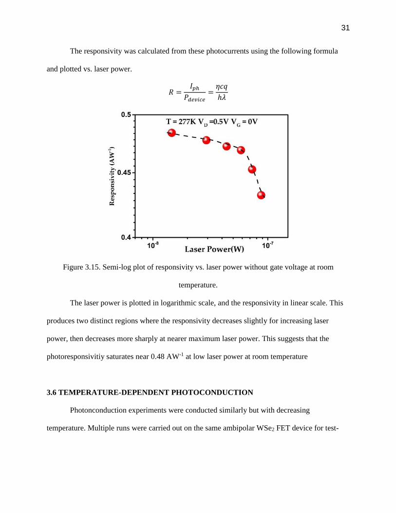
The responsivity was calculated from these photocurrents using the following formula
and plotted vs. laser power.
𝑅 =𝐼𝑝ℎ
𝑃𝑑𝑒𝑣𝑖𝑐𝑒=
𝜂𝑐𝑞
ℎ𝜆
Figure 3.15. Semi-log plot of responsivity vs. laser power without gate voltage at room
temperature.
The laser power is plotted in logarithmic scale, and the responsivity in linear scale. This
produces two distinct regions where the responsivity decreases slightly for increasing laser
power, then decreases more sharply at nearer maximum laser power. This suggests that the
photoresponsivitiy saturates near 0.48 AW-1 at low laser power at room temperature
3.6 TEMPERATURE-DEPENDENT PHOTOCONDUCTION
Photonconduction experiments were conducted similarly but with decreasing
temperature. Multiple runs were carried out on the same ambipolar WSe2 FET device for test-
32
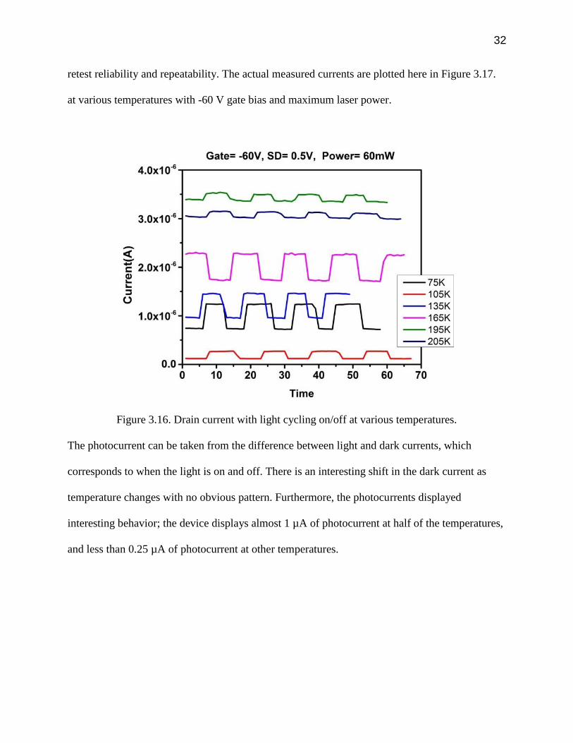
retest reliability and repeatability. The actual measured currents are plotted here in Figure 3.17.
at various temperatures with -60 V gate bias and maximum laser power.
Figure 3.16. Drain current with light cycling on/off at various temperatures.
The photocurrent can be taken from the difference between light and dark currents, which
corresponds to when the light is on and off. There is an interesting shift in the dark current as
temperature changes with no obvious pattern. Furthermore, the photocurrents displayed
interesting behavior; the device displays almost 1 µA of photocurrent at half of the temperatures,
and less than 0.25 µA of photocurrent at other temperatures.

33
Figure 3.17. Temperature dependent responsivities plotted vs. actual laser power in log-log scale.
The responsivities were again calculated using the aforementioned formula, and plotted
vs. the actual laser power. Compared to the room temperature measurements for responsivity,
these responsivity values came out to be almost two orders of magnitude smaller. At particular
temperatures, the responsivity was even an order of magnitude smaller than at the other
temperatures.
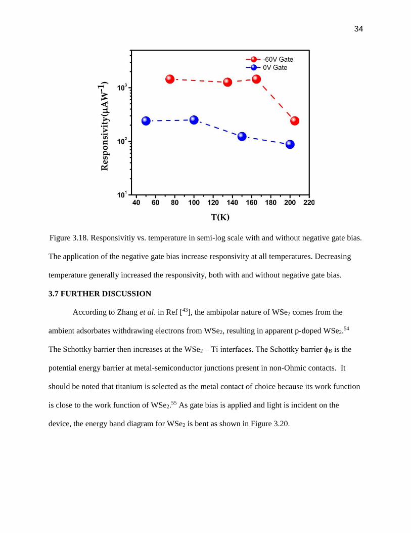
The responsivity vs. temperature plot is shown in Figure 3.19 with and without negative
gate bias.
34
Figure 3.18. Responsivitiy vs. temperature in semi-log scale with and without negative gate bias.
The application of the negative gate bias increase responsivity at all temperatures. Decreasing
temperature generally increased the responsivity, both with and without negative gate bias.
3.7 FURTHER DISCUSSION
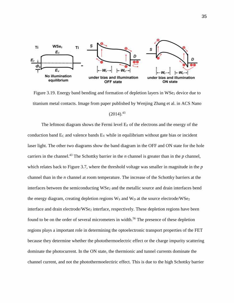
According to Zhang et al. in Ref [43], the ambipolar nature of WSe2 comes from the
ambient adsorbates withdrawing electrons from WSe2, resulting in apparent p-doped WSe2.54
The Schottky barrier then increases at the WSe2 – Ti interfaces. The Schottky barrier ϕB is the
potential energy barrier at metal-semiconductor junctions present in non-Ohmic contacts. It
should be noted that titanium is selected as the metal contact of choice because its work function
is close to the work function of WSe2.55 As gate bias is applied and light is incident on the
device, the energy band diagram for WSe2 is bent as shown in Figure 3.20.
35
Figure 3.19. Energy band bending and formation of depletion layers in WSe2 device due to
titanium metal contacts. Image from paper published by Wenjing Zhang et al. in ACS Nano
(2014).43
The leftmost diagram shows the Fermi level EF of the electrons and the energy of the
conduction band EC and valence bands EV while in equilibrium without gate bias or incident
laser light. The other two diagrams show the band diagram in the OFF and ON state for the hole
carriers in the channel.43 The Schottky barrier in the n channel is greater than in the p channel,
which relates back to Figure 3.7, where the threshold voltage was smaller in magnitude in the p
channel than in the n channel at room temperature. The increase of the Schottky barriers at the
interfaces between the semiconducting WSe2 and the metallic source and drain interfaces bend
the energy diagram, creating depletion regions WS and WD at the source electrode/WSe2
interface and drain electrode/WSe2 interface, respectively. These depletion regions have been
found to be on the order of several micrometers in width.56 The presence of these depletion
regions plays a important role in determining the optoelectronic transport properties of the FET
because they determine whether the photothermoelectric effect or the charge impurity scattering
dominate the photocurrent. In the ON state, the thermionic and tunnel currents dominate the
channel current, and not the photothermoelectiric effect. This is due to the high Schottky barrier
36
blocking the holes from diffusing, which manifests itself in experiment in a decrease in field-
effect mobility.54
The theory of charge impurity scattering can also be attributed to the electrical transport
and carrier density of gated devices.57 Disorder from Coulomb impurities behave qualititatively
different from neutral impurities and can dominate the electrical transport properties at low
carrier density.
3.8 SUMMARY
WSe2 was studied as a two-terminal back-gated FET device, which displayed ambipolar
behavior due to its superposition of electron and hole currents. At room temperature, the device
showed a relatively high On/Off ratio of ~104. The room temperature responsivity without gate
bias was approximately 0.48 AW-1. The dominating behavior went from p-type to n-type as
temperature decreases. The low temperature electron field effect mobility peaked near μFE > 150
cm2
V ∙ s⁄ . The almost linear dependence γ=0.95 of photocurrent on laser power monomolecular
recombination is the dominant process.
37
CHAPTER 4
N-TYPE INDIUM SELENIDE RESULTS AND DISCUSSION
4.1 INTRODUCTION
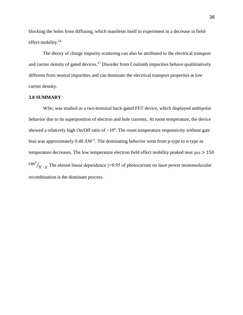
InSe belongs to Group IIIA-VI, and the prepared InSe has the hexagonal crystal structure
shown here with D3h single layer symmetry.
Figure 4.1. Side view and top view of InSe crystal structure. Image courtesy of our collaborators
Sidong Lei and Dr. Ajayan from Rice University.5
The blue and orange spheres correspond to the indium and selenium atoms respectively. The
layers of the crystal structure can be seen in the side view to be In – Se – Se – In in the vertical
direction. The lattice constant along the a and b axes is 0.40 nm, and the distance between
neighboring layers is 0.84 nm.58
4.2 SYNTHESIS, MICROSCOPY, AND CHARACTERIZATION
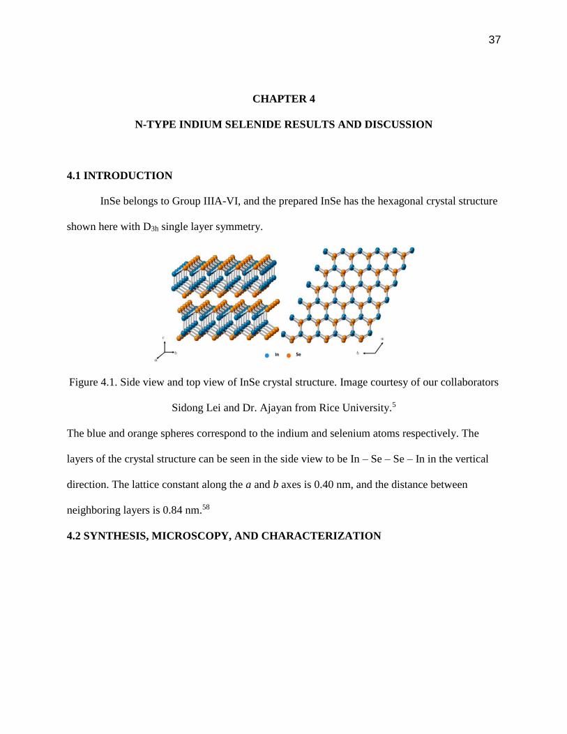
38
Figure 4.2. SEM image of bulk InSe crystal grown from non-stoichiometric melt. Images
courtesy of our collaborators Sidong Lei and Dr. Ajayan at Rice University.6
Our collaborators Sidong Lei under Dr. Ajayan at Rice University carried out the synthesis for
the InSe bulk crystal. They reported to have a very layered InSe bulk structure with a
surrounding hard black outer crust upon growth.6 After mechanical exfoliation using the Scotch
tape method, few layered InSe flakes were obtained and deposited onto a silicon dioxide wafer.
39
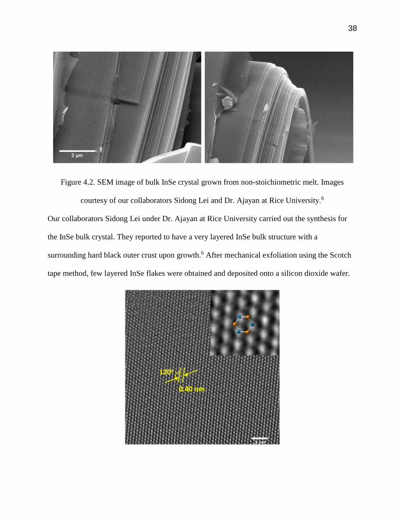
Figure 4.3. HRTEM image of InSe flake. Image courtesy of our collaborators Sidong Lei and Dr.
Ajayan at Rice University.5
Figure 4.2 shows the high-resolution transmission electron microscopy (HRTEM) image of InSe
crystal with inset of higher zoom with the model overlaid. The white dots correspond to the
indium atoms. The lattice constant found in the HRTEM image is consistent with the a-axis
reported lattice constant theoretical value of 0.40 nm. The synthesized material shows perfect
hexagonal lattice structure with little deviation.
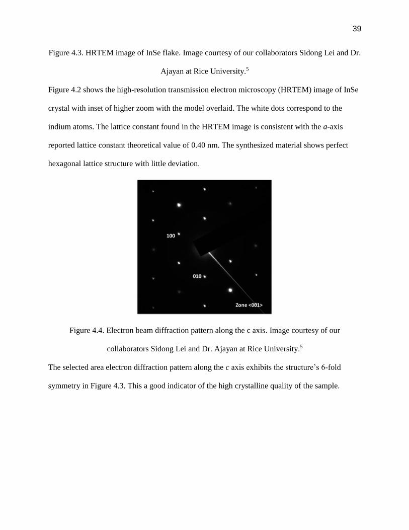
Figure 4.4. Electron beam diffraction pattern along the c axis. Image courtesy of our
collaborators Sidong Lei and Dr. Ajayan at Rice University.5
The selected area electron diffraction pattern along the c axis exhibits the structure’s 6-fold
symmetry in Figure 4.3. This a good indicator of the high crystalline quality of the sample.
40
Figure 4.5. AFM image of exfoliated InSe flakes. Inset shows the same flake from farther zoom.
Image courtesy of our collaborators Sidong Lei and Dr. Ajayan at Rice University.5
Here, the average thickness of the exfoliated flakes was found to be 5.2 nm, corresponding to 4
to four to five layers.
Figure 4.6. AFM of a thinner flake, corresponding to a mere two to three layers. Image courtesy
of our collaborators Sidong Lei and Dr. Ajayan at Rice University.5
41
Another TEM image of a thinner flake reveals thicknesses varying from 6 to 12 nm,
corresponding to a mere two to three layers of InSe. It is believed that the extreme flatness of the
top surface suggests a weak van der Waals coupling between layers, not unlike that found in
black mica sheets.5
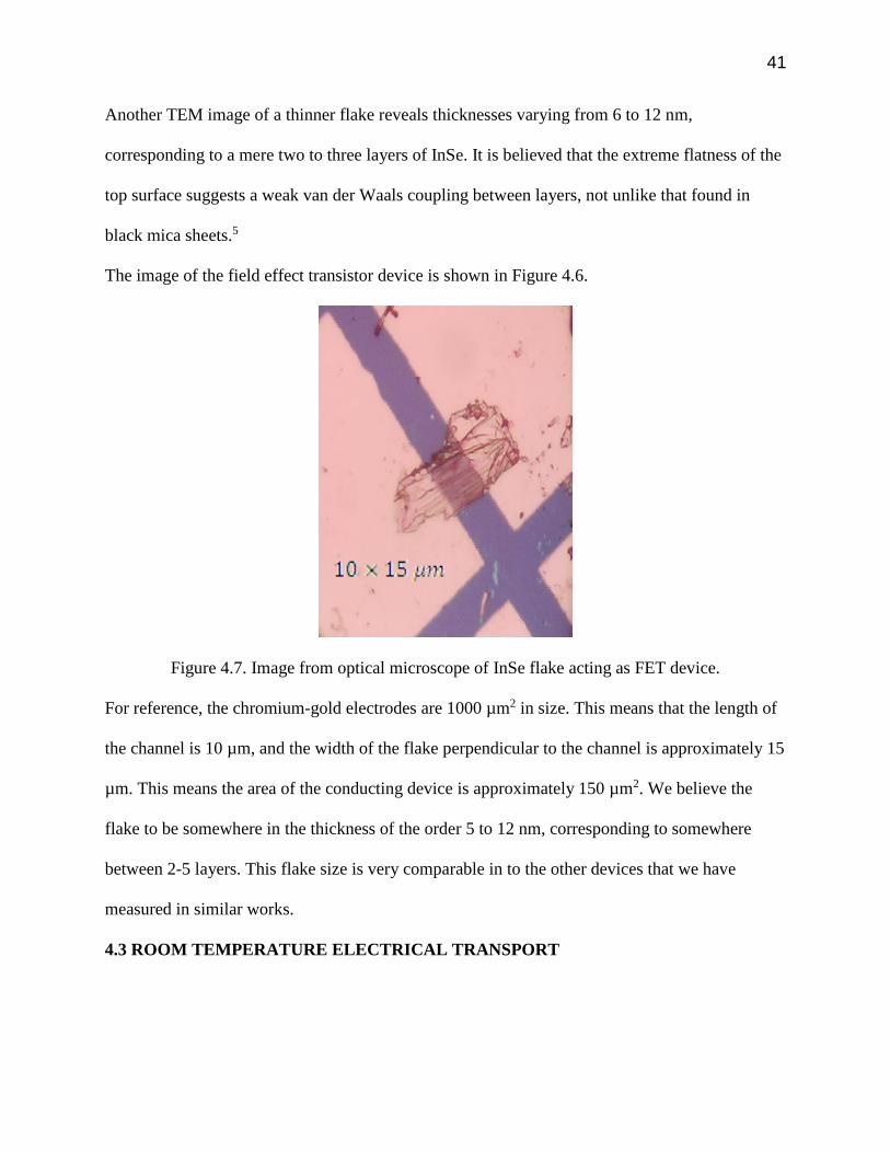
The image of the field effect transistor device is shown in Figure 4.6.
Figure 4.7. Image from optical microscope of InSe flake acting as FET device.
For reference, the chromium-gold electrodes are 1000 µm2 in size. This means that the length of
the channel is 10 µm, and the width of the flake perpendicular to the channel is approximately 15
µm. This means the area of the conducting device is approximately 150 µm2. We believe the
flake to be somewhere in the thickness of the order 5 to 12 nm, corresponding to somewhere
between 2-5 layers. This flake size is very comparable in to the other devices that we have
measured in similar works.
4.3 ROOM TEMPERATURE ELECTRICAL TRANSPORT
42
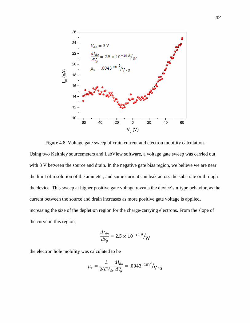
Figure 4.8. Voltage gate sweep of crain current and electron mobility calculation.
Using two Keithley sourcemeters and LabView software, a voltage gate sweep was carried out
with 3 V between the source and drain. In the negative gate bias region, we believe we are near
the limit of resolution of the ammeter, and some current can leak across the substrate or through
the device. This sweep at higher positive gate voltage reveals the device’s n-type behavior, as the
current between the source and drain increases as more positive gate voltage is applied,
increasing the size of the depletion region for the charge-carrying electrons. From the slope of
the curve in this region,
𝑑𝐼𝑑𝑠
𝑑𝑉𝑔= 2.5 × 10⁻¹⁰ A
W⁄
the electron hole mobility was calculated to be
𝜇𝑒 =𝐿
𝑊𝐶𝑉𝑑𝑠
𝑑𝐼𝑑𝑠
𝑑𝑉𝑔= .0043 cm2
V ∙ s⁄
43
This electron mobility is smaller than expected, about one order of magnitude smaller than other
similar measurements made on other devices. This could be due to the thinness of the flake
relative to other devices.
4.4 ROOM TEMPERATURE PHOTOCONDUCTION
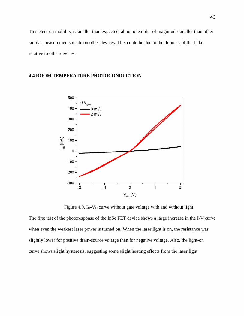
Figure 4.9. ID-VD curve without gate voltage with and without light.
The first test of the photoresponse of the InSe FET device shows a large increase in the I-V curve
when even the weakest laser power is turned on. When the laser light is on, the resistance was
slightly lower for positive drain-source voltage than for negative voltage. Also, the light-on
curve shows slight hysteresis, suggesting some slight heating effects from the laser light.
44
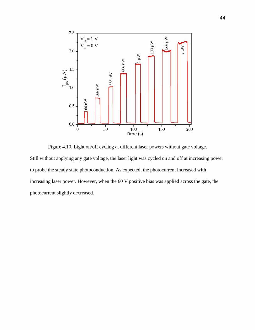
Figure 4.10. Light on/off cycling at different laser powers without gate voltage.
Still without applying any gate voltage, the laser light was cycled on and off at increasing power
to probe the steady state photoconduction. As expected, the photocurrent increased with
increasing laser power. However, when the 60 V positive bias was applied across the gate, the
photocurrent slightly decreased.

45
Figure 4.11. One on/off cycle of 66 nW laser power with and without gate voltage.
At minimum laser power, the photocurrent, which is the difference between the light
current and dark current, is equal with and without gate voltage.
Figure 4.12. One on/off cycle of light of 2 µW laser power with and without gate voltage.
46
However, when the maximum 2 μW laser power as used, the application of the 60 V gate bias
decreases the photocurrent slightly. One possible explanation for this behavior is the desorption
of adsorbates, which can cause the Fermi level to move toward the minimum of the conduction
band and increase the Schottky barrier height with application of gate bias.43
Figure 4.13. Log-log plot of photocurrent vs. incident laser power with and without positive gate
bias. Power law dependence fittings are shown.
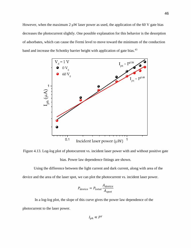
Using the difference between the light current and dark current, along with area of the
device and the area of the laser spot, we can plot the photocurrent vs. incident laser power.
𝑃𝑑𝑒𝑣𝑖𝑐𝑒 = 𝑃𝑡𝑜𝑡𝑎𝑙
𝐴𝑑𝑒𝑣𝑖𝑐𝑒
𝐴𝑠𝑝𝑜𝑡
In a log-log plot, the slope of this curve gives the power law dependence of the
photocurrent to the laser power.
𝐼𝑝ℎ ∝ 𝑃𝛾
47
Without gate bias and with 60 V gate, these power fitting exponents were found to be
𝛾 = 0.58 and 𝛾 = 0.48 respectively. Since these values are near 0.5, bimolecular recombination
dominates. After the laser light photons delocalize the electron-hole pairs, electrons are trapped
back into the localized state in a recombination process that involves two free charge carries
simultaneously. Our collaborators probed the electron-phonon interaction further, finding that in
the z-band, localized electron states are affected by in-plane E′ and E″ phonons, satisfying
conservation of momentum and energy.5
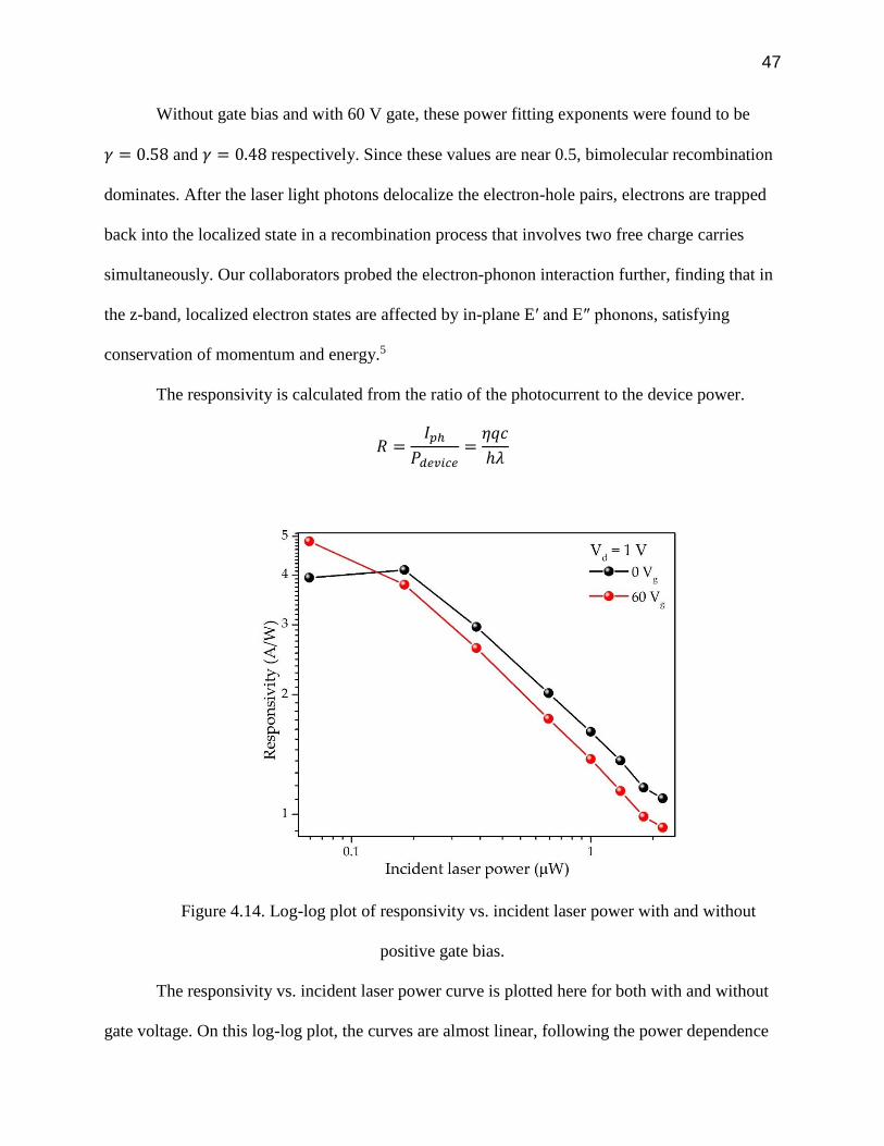
The responsivity is calculated from the ratio of the photocurrent to the device power.
𝑅 =𝐼𝑝ℎ
𝑃𝑑𝑒𝑣𝑖𝑐𝑒=
𝜂𝑞𝑐
ℎ𝜆
Figure 4.14. Log-log plot of responsivity vs. incident laser power with and without
positive gate bias.
The responsivity vs. incident laser power curve is plotted here for both with and without
gate voltage. On this log-log plot, the curves are almost linear, following the power dependence
48
relationship between responsivity and laser power. The responsivity was found to be the highest
at lower incident laser power, up to nearly 5 𝐴 𝑊⁄ . From the responsivity values, the external
quantum efficiency, η, which is the ratio of the number of photocarriers to the number of
incident photons, can also be calculated.
𝜂 =𝐺𝑒𝑛𝑒𝑟𝑎𝑡𝑒𝑑 𝑝ℎ𝑜𝑡𝑜𝑐𝑎𝑟𝑟𝑖𝑒𝑟𝑠
𝐼𝑛𝑐𝑖𝑑𝑒𝑛𝑡 𝑝ℎ𝑜𝑡𝑜𝑛𝑠=
𝐼𝑝ℎ𝑞⁄
𝑃𝑖𝑛𝑐𝐸𝑝ℎ𝑜𝑡𝑜𝑛
⁄=
𝑅ℎ𝑐
𝑞𝜆
The external quantum efficiency at 2 μW incident laser power at 658 nm without gate voltage
was calculated be 207%.
4.5 FURTHER DISCUSSION
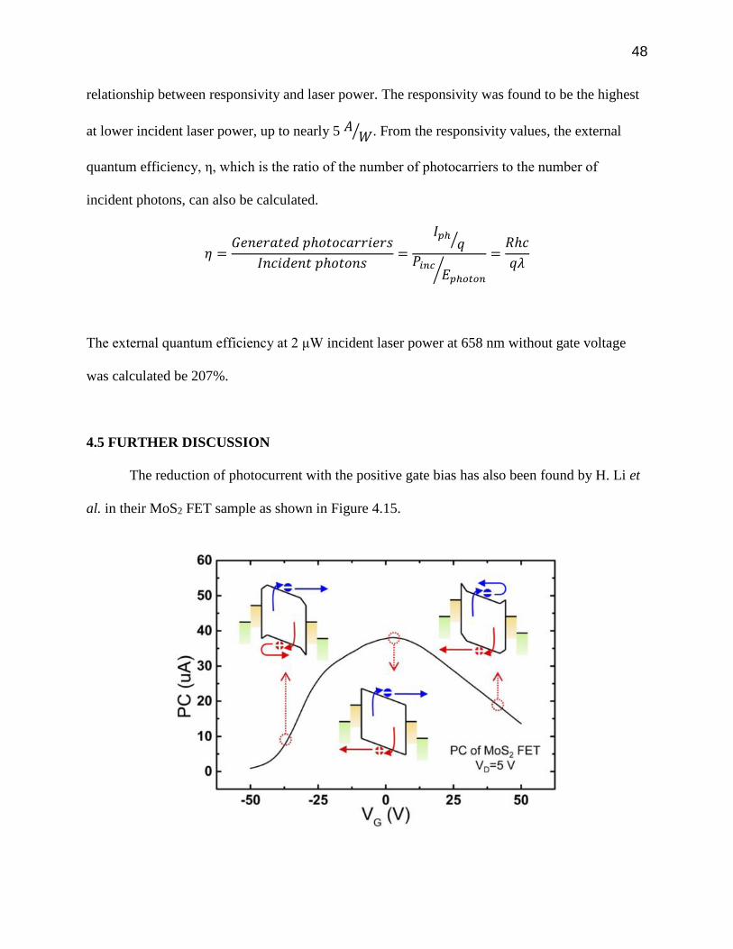
The reduction of photocurrent with the positive gate bias has also been found by H. Li et
al. in their MoS2 FET sample as shown in Figure 4.15.
49
Figure 4.15. Photocurrent vs. gate voltage in an MoS2 FET showing how photocurrent can
decrease with the application of positive gate bias. Image from paper published by Hua-Min Li et
al. in Scientific Reports (2014).7
For carrier transport through a metal-semiconductor barrier, the tunneling effect effect
dominates when the semiconductor is highly doped, and thermionic emission dominates if the
semiconductor is undoped or only slightly doped. However, conventional carrier transport theory
is not always applicable to photoexcited charge carrier transport. The electrical gating effect
forms an accumulation layer at high positive VG. According to H-M. Li et al., the phenomenon
of drain-induced barrier lowering (DIBL) occurs with increasing VD near 0VG.7 The following
gate-controlled metal-semiconductor barrier modulation model can be used to explain the
photocurrent under illumination.7
𝐼𝐷 = 𝐴𝐴∗𝑇2exp (−𝜙𝑚𝑠
𝑘𝐵𝑇) [exp (
−𝑞𝑉𝐷𝑆
𝑘𝑏𝑇) − 1]
A is the area of the contact junction, 𝐴∗ = 4𝜋𝑒𝑚∗𝑘𝐵2ℎ−3 is the effective Richardson constant,
and ϕms is the effective Schottky barrier height between the metal and semiconductor.41 The
Schottky barrier modulation due to the application of the gate voltage can bend the energy band
in such a way to stifle the movement of photoexcited electron majority charge carriers. This may
be a possible model for our case where the photocurrent decreased slightly across our sample
when positive gate bias was applied.
4.6 SUMMARY
A few-layered n-type InSe FET device was prepared my Scotch tape micromechanical
exfoliation from bulk InSe grown by non-stoichiometric melt. The room temperature field effect
mobility was measured to be 𝜇 = .0043 𝑐𝑚2
𝑉 ∙ 𝑠⁄ . The room temperature responsivity is near 5

50
AW-1 at +60Vg. The external quantum efficiency at maximum laser power was calculated 𝜂 =
207%. Based on the power law dependence of the photocurrent and incident laser power,
bimolecular recombination is the dominant process.
51
CHAPTER 5
FURTHER RESEARCH
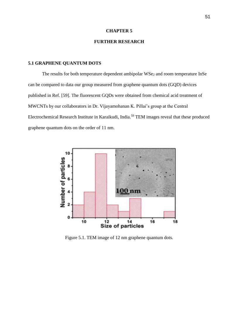
5.1 GRAPHENE QUANTUM DOTS
The results for both temperature dependent ambipolar WSe2 and room temperature InSe
can be compared to data our group measured from graphene quantum dots (GQD) devices
published in Ref. [59]. The fluorescent GQDs were obtained from chemical acid treatment of
MWCNTs by our collaborators in Dr. Vijayamohanan K. Pillai’s group at the Central
Electrochemical Research Institute in Karaikudi, India.59 TEM images reveal that these produced
graphene quantum dots on the order of 11 nm.
Figure 5.1. TEM image of 12 nm graphene quantum dots.
52
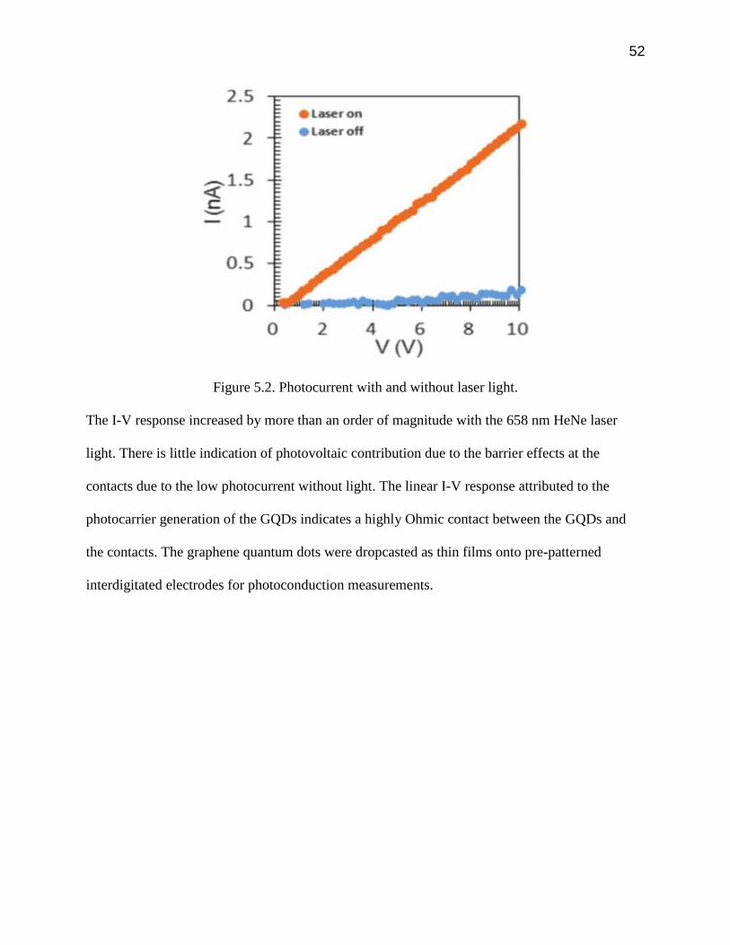
Figure 5.2. Photocurrent with and without laser light.
The I-V response increased by more than an order of magnitude with the 658 nm HeNe laser
light. There is little indication of photovoltaic contribution due to the barrier effects at the
contacts due to the low photocurrent without light. The linear I-V response attributed to the
photocarrier generation of the GQDs indicates a highly Ohmic contact between the GQDs and
the contacts. The graphene quantum dots were dropcasted as thin films onto pre-patterned
interdigitated electrodes for photoconduction measurements.

53
Figure 5.3. Current as a function of time during the light on/off cycling at maximum laser power.
The photocurrent, which is the difference between the light current and dark current came out to
be on the order of 2 nA.
Figure 5.4. Log-log plot of photocurrent with incident laser power.
54
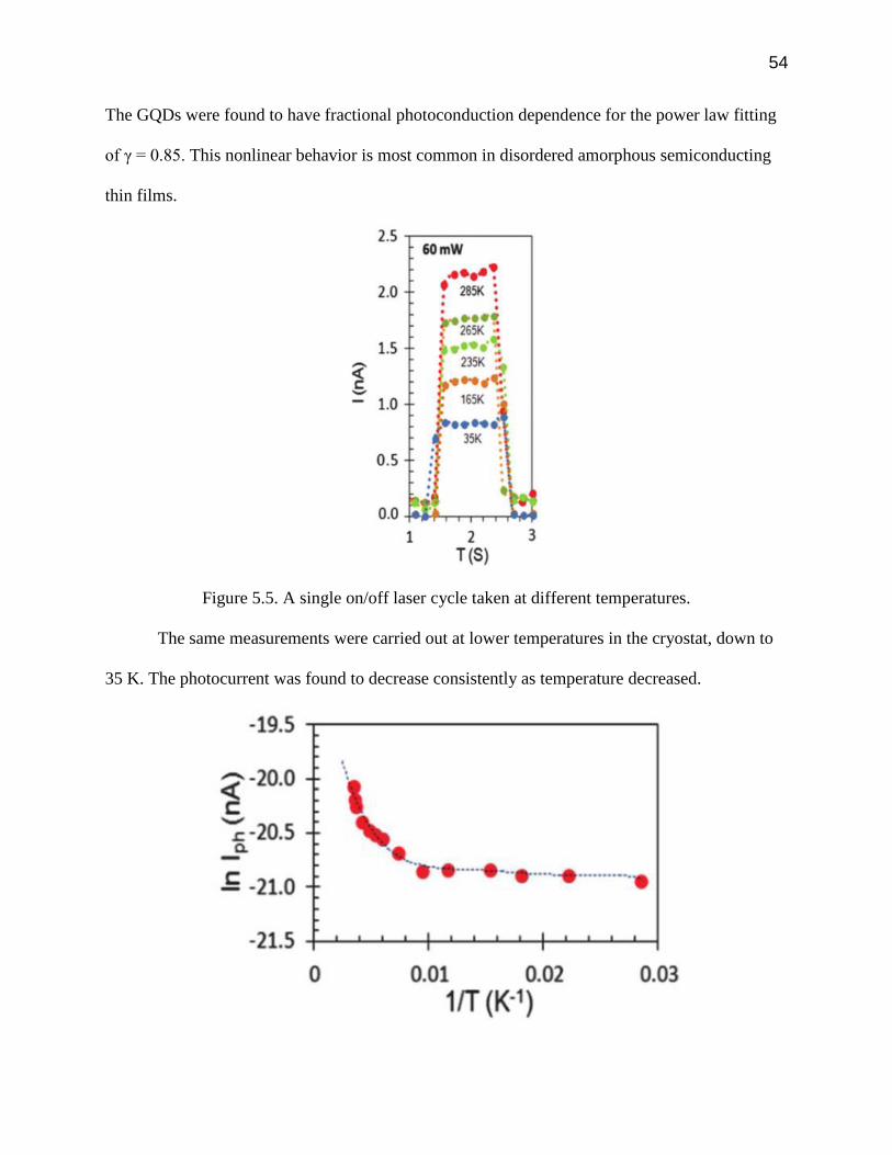
The GQDs were found to have fractional photoconduction dependence for the power law fitting
of γ = 0.85. This nonlinear behavior is most common in disordered amorphous semiconducting
thin films.
Figure 5.5. A single on/off laser cycle taken at different temperatures.
The same measurements were carried out at lower temperatures in the cryostat, down to
35 K. The photocurrent was found to decrease consistently as temperature decreased.

55
Figure 5.6. Log of photocurrent vs. inverse temperature.
The GQDs exhibited behavior characteristic of that of disordered photoactive materials.59 The
presence of the trap states within the band gap between the valence and conduction bands could
be a fairly continuous distribution controlling the photoresponse. At low temperatures, the
graphene quantum dots showed a relatively constant photocarrier density below 100 K. As the
temperature increases, trapped photoexcited carriers can gain enough thermal energy to
overcome the barrier from the trap state and contribute to the measured photoconduction.
Graphene quantum dots can find application in a variety of electronic and optoelectronic devices
such as photodetectors, bioimaging, biosensors, fuel cells, supercapacitors, photovoltaics, and
light emitting diodes.60,61
56
CHAPTER 6
CONCLUSION
In this work, the room temperature electrical transport properties of both WSe2 and InSe
were explored, as well as the temperature dependence of electrical transport in WSe2 WSe2, a
TMDC known for its indirect-to-direct band gap transition from bulk to few-layer, can be used in
photodetectors and low power optoelectronic applications. Few layer WSe2, prepared by our
collaborators by micromechanical exfoliation from CVT-grown bulk WSe2 crystals grown, here
showed very unique ambipolar behavior from the superposition of electron and hole currents. In
fact, the device switching from p-type to n-type being the dominating behavior as temperature
decreased. A relatively high electron mobility μ > 150 cm2/Vs was found especially at lower
temperatures. Photoconduction measurements revealed that applying negative gate bias and
decreasing the temperature were both found to increase the responsivity of the WSe2 sample. As
a whole, the ambipolar behavior illustrates just how sensitive a given device can be based on a
variety of different factors from sample preparation, impurities present in the sample, and sample
deterioration from running experiments.
As a consequence from its layered van der Waals structure, InSe can show promising
anisotropic optoelectronic properties. Bulk InSe crystals were grown by nonstoichiometric melt
by our collaborators and mechanically exfoliated into few layers by the Scotch tape method.
Few-layered InSe is known to have indirect band gap of around 1.4 eV. Here, the room
temperature field effect mobility μ𝐹𝐸 = .0043 𝑐𝑚2
𝑉 ∙ 𝑠⁄ of our n-type InSe was found to be
about an order of magnitude less than expected, perhaps due to the thickness of our InSe flake
and impurities present in the sample. Steady state photoconduction was found to slightly

57
decrease with the application of positive gate bias, possibly due to the desorption of adsorbtates
from the surface of the sample or the contact between the electrodes and the InSe flake. The
power law dependence γ ~ 0.5 suggests a model of dominant bimolecular recombination. The
room temperature responsivity was found to be 5 A/W, offering a broad spectral response, giving
an external quantum efficiency of 207%, making InSe a good candidate for thin film
photodetector application. Both TMDC’s and III-VI chalcogenides continue to be studied for
their remarkably diverse properties that depend on their thickness and composition for their
applications as transistors, sensors, and composite materials in photovoltaics and optoelectronics.
58
REFERENCES
1 B. Muchharla, SIU Diss. (2015).
2 S. Ghosh, M. Wasala, N. Pradhan, D. Rhodes, L. Balicas, and S. Talapatra, in MRS Fall Meet.
(Boston, MA, 2014).
3 Q.H. Wang, K. Kalantar-Zadeh, A. Kis, J.N. Coleman, and M.S. Strano, Nat. Nanotechnol. 7,
699 (2012).
4 N.R. Pradhan, D. Rhodes, S. Memaran, J.M. Poumirol, D. Smirnov, S. Talapatra, S. Feng, N.
Perea-Lopez, a. L. Elias, M. Terrones, P.M. Ajayan, and L. Balicas, Sci. Rep. 5, 8979 (2015).
5 S. Lei, L. Ge, S. Najmaei, A. George, R. Kappera, J. Lou, M. Chhowalla, H. Yamaguchi, G.
Gupta, R. Vajtai, A.D. Mohite, and P.M. Ajayan, ACS Nano 8, 1263 (2014).
6 S. Lei, Rice Univ. (2013).
7 H.-M. Li, D.-Y. Lee, M.S. Choi, D. Qu, X. Liu, C.-H. Ra, and W.J. Yoo, Sci. Rep. 4, 1 (2014).
8 A. a Balandin, Nat. Mater. 10, 569 (2011).
9 M. Lundstrom, IEEE Electron Device Lett. 18, 361 (1997).
10 M. Arndt, O. Nairz, J. Vos-Andreae, C. Keller, G. van der Zouw, and A. Zeilinger, Nature
401, 680 (1999).
11 S. Iijima, Nature 354, 56 (1991).
12 S. Iijima and T. Ichihashi, Nature 363, 603 (1993).
13 P.L. McEuen, Phys. World 13, 31 (2000).
14 P.L. McEuen and M.S. Fuhrer, IEEE Trans. Nanotechnol. 1, 78 (2002).
15 P.L. McEuen and J.-Y. Park, MRS Bull. 29, 272 (2004).
16 R.P. Feynman, Am. Phys. Soc. (1959).
17 H. Wang, T. Maiyalagan, and X. Wang, Acs Catal. 2, 781 (2012).
18 G. Eda, C. Mattevi, H. Yamaguchi, H. Kim, and M. Chhowalla, J. Phys. Chem. C 113, 15768
(2009).
19 K.S. Novoselov, A.K. Geim, S. V Morozov, D. Jiang, Y. Zhang, S. V Dubonos, I. V
Grigorieva, and A.A. Firsov, Science 306, 666 (2004).
20 S.J. Chae, F. Güneş, K.K. Kim, E.S. Kim, G.H. Han, S.M. Kim, H. Shin, S.M. Yoon, J.Y.
Choi, M.H. Park, C.W. Yang, D. Pribat, and Y.H. Lee, Adv. Mater. 21, 2328 (2009).
59
21 P. Avouris and C. Dimitrakopoulos, Mater. Today 15, 86 (2012).
22 R.R. Nair, P. Blake, a N. Grigorenko, K.S. Novoselov, T.J. Booth, T. Stauber, N.M.R. Peres,
and a K. Geim, Science 320, 1308 (2008).
23 A. a Balandin, S. Ghosh, W. Bao, I. Calizo, D. Teweldebrhan, F. Miao, and C.N. Lau, Nano
Lett. 8, 902 (2008).
24 C. Lee, X. Wei, J.W. Kysar, and J. Hone, Science 321, 385 (2008).
25 A.K. Geim, Science (80-. ). 324, 1530 (2009).
26 M. Orlita, C. Faugeras, P. Plochocka, P. Neugebauer, G. Martinez, D.K. Maude, a. L. Barra,
M. Sprinkle, C. Berger, W. a. De Heer, and M. Potemski, Phys. Rev. Lett. 101, 1 (2008).
27 Z. Jiang, Y. Zhang, H.L. Stormer, and P. Kim, Phys. Rev. Lett. 99, 1 (2007).
28 M.F. Craciun, S. Russo, M. Yamamoto, J.B. Oostinga, a F. Morpurgo, and S. Tarucha, Nat.
Nanotechnol. 4, 383 (2009).
29 Y. Zhang, J.P. Small, M.E.S. Amori, and P. Kim, Phys. Rev. Lett. 94, 1 (2005).
30 a. H. Castro Neto, F. Guinea, N.M.R. Peres, K.S. Novoselov, and a. K. Geim, Rev. Mod.
Phys. 81, 109 (2009).
31 D. Marcano, D. Kosynkin, and J. Berlin, ACS Nano 4, 4806 (2010).
32 C. Berger, Z. Song, T. Li, X. Li, A.Y. Ogbazghi, R. Feng, Z. Dai, A.N. Marchenkov, E.H.
Conrad, P.N. First, and W. a de Heer, J Phys Chem B 108, 19912 (2004).
33 X. Li, W. Cai, J. An, S. Kim, J. Nah, D. Yang, R. Piner, A. Velamakanni, I. Jung, E. Tutuc,
S.K. Banerjee, L. Colombo, and R.S. Ruoff, Science 324, 1312 (2009).
34 A.B. Bourlinos, V. Georgakilas, R. Zboril, T. a. Sterioti, and A.K. Stubos, Small 5, 1841
(2009).
35 J.N. Coleman, M. Lotya, A. O’Neill, S.D. Bergin, P.J. King, U. Khan, K. Young, A. Gaucher,
S. De, R.J. Smith, I. V Shvets, S.K. Arora, G. Stanton, H.-Y. Kim, K. Lee, G.T. Kim, G.S.
Duesberg, T. Hallam, J.J. Boland, J.J. Wang, J.F. Donegan, J.C. Grunlan, G. Moriarty, A.
Shmeliov, R.J. Nicholls, J.M. Perkins, E.M. Grieveson, K. Theuwissen, D.W. McComb, P.D.
Nellist, and V. Nicolosi, Science 331, 568 (2011).
36 Y. Cui, X. Duan, J. Hu, and C.M. Lieber, J. Phys. Chem. B 104, 5213 (2000).
37 W. Gao, L.B. Alemany, L. Ci, and P.M. Ajayan, Nat. Chem. 1, 403 (2009).
38 A. Mathkar, D. Tozier, P. Cox, P. Ong, C. Galande, K. Balakrishnan, A. Leela Mohana Reddy,
and P.M. Ajayan, J. Phys. Chem. Lett. 3, 986 (2012).
60
39 Y. Liu, N.O. Weiss, Z. Lin, Y. Huang, and X. Duan, Nano Lett. 15, 709 (2015).
40 Y. Gong, J. Lin, X. Wang, G. Shi, S. Lei, Z. Lin, X. Zou, G. Ye, R. Vajtai, B.I. Yakobson, H.
Terrones, M. Terrones, B.K. Tay, J. Lou, S.T. Pantelides, Z. Liu, W. Zhou, and P.M. Ajayan,
Nat. Mater. 13, (2014).
41 N. Pradhan, J. Ludwig, Z. Lu, D. Rhodes, M.M. Bishop, K. Thirunavukkuarasu, S. McGill, D.
Smirnov, and L. Balicas, ACS Appl. Mater. Interfaces 7, 12080 (2015).
42 H. Terrones, E. Del Corro, S. Feng, J.M. Poumirol, D. Rhodes, D. Smirnov, N.R. Pradhan, Z.
Lin, M. a T. Nguyen, a L. Elías, T.E. Mallouk, L. Balicas, M. a Pimenta, and M. Terrones, Sci.
Rep. 4, 4215 (2014).
43 W. Zhang, M. Chiu, C.-H. Chen, W. Chen, L. Li, and A.T.S. Wee, ACS Nano 8, 8653 (2014).
44 V.V. Sobolev and V. V. Sobolev, Bull. Russ. Acad. Sci. Phys. 72, 492 (2008).
45 S.R. Tamalampudi, Y.Y. Lu, R. Kumar U., R. Sankar, C. Da Liao, K. Moorthy B., C.H.
Cheng, F.C. Chou, and Y.T. Chen, Nano Lett. 14, 2800 (2014).
46 J. Camassel, P. Merle, H. Mathieu, and A. Chevy, Phys. Rev. B 17, (1978).
47 J.F. Sánchez-Royo, G. Muñoz-Matutano, M. Brotons-Gisbert, J.P. Martínez-Pastor, A. Segura,
A. Cantarero, R. Mata, J. Canet-Ferrer, G. Tobias, E. Canadell, J. Marqués-Hueso, and B.D.
Gerardot, Nano Res. 7, 1556 (2014).
48 F. Manjón, A. Segura, V. Muñoz-Sanjosé, G. Tobías, P. Ordejón, and E. Canadell, Phys. Rev.
B 70, 125201 (2004).
49 W. Shockley and H.J. Queisser, J. Appl. Phys. 32, 510 (1961).
50 A. Sentenac, P.C. Chaumet, and K. Belkebir, Phys. Rev. Lett. 97, 243901 (2006).
51 J.J. Bozzola and L.D. Russell, Electron Microscopy: Principles and Techniques for Biologists,
2nd Editio (Jones and Bartlett, 1999).
52 A. Kokalj, Comp. Mater Sci. 28, 155 (2003).
53 N.R. Pradhan, D. Rhodes, Q. Zhang, S. Talapatra, M. Terrones, P.M. Ajayan, and L. Balicas,
Appl. Phys. Lett. 102, 123105 (2013).
54 W. Liu, J. Kang, D. Sarkar, Y. Khatami, D. Jena, and K. Banerjee, Nano Lett. 13, 1983 (2013).
55 H. Fang, S. Chuang, T.C. Chang, K. Takei, T. Takahashi, and A. Javey, Nano Lett. 12, 3788
(2012).
56 F. Léonard and J. Tersoff, Phys. Rev. Lett. 83, 5174 (1999).
57 S. Adam, E.H. Hwang, E. Rossi, and S. Das Sarma, Solid State Commun. 149, 1072 (2009).

61
58 C. De Blasi, G. Micocci, S. Mongelli, and A. Tepore, J. Cryst. Growth 57, 482 (1982).
59 S. Kundu, S. Ghosh, M. Fralaide, T.N. Narayanan, V.K. Pillai, and S. Talapatra, Phys. Chem.
Chem. Phys. (2015).
60 Z. Zhang, J. Zhang, N. Chen, and L. Qu, Energy Environ. Sci. 5, 8869 (2012).
61 C.X. Guo, H.B. Yang, Z.M. Sheng, Z.S. Lu, Q.L. Song, and C.M. Li, Angew. Chemie Int. Ed.
49, 3014 (2010).
62
VITA
Graduate School
Southern Illinois University
Michael Fralaide
Benedictine University, Lisle, IL
Bachelor of Science, Physics, May 2008
Thesis Title:
ELECTRICAL TRANSPORT AND PHOTOCONDUCTION IN AMBIPOLAR TUNGSTEN
DISELENIDE AND N-TYPE INDIUM SELENIDE
Major Professor: Dr. Saikat Talapatra
Publications:
Fractional Photo-Current Dependence of Graphene Quantum Dots Prepared from Carbon
Nanotubes. Sumana Kundu, Sujoy Ghosh, Michael Fralaide, T.N.Narayanan, Vijayamohanan K.
Pillai, and Saikat Talapatra. Phys. Chem. Chem. Phys. (2015)
Presentations:
Michael Fralaide, Muhammed Habib, Gan Wei, Weiyu Xu, Saikat Talapatra, Li
Song.Huffstutler, Jacob D., Yang, Chao, Talapatra, Saikat, and Song, Li. “Synthesis and
Characterization of Carbon Nanotubes, Molybdenum Disulfide, and Boron Nitride.” Young
Scientists Forum Beijing 2015.