e&i_m.e (mems)_1y_2s_rf mems.pdf - annamalai university
TRANSCRIPT
ANNAMALAI UNIVERSITY
FACULTY OF ENGINEERING AND TECHNOLOGY
DEPARTMENT OF ELECTRONICS AND INSTRUMENTATION ENGINEERING
M.E (MICROELECTRONICS AND MEMS)
SECOND SEMESTER
(2019-2020)
COURSE: RF MEMS
COURSE INSTRUCTOR - Dr. M. MANIVANNAN

MOTIVATION FOR RF MEMS
Physical aspects of RF design Ideally, RF and microwave circuits are comprised of interconnections of well-demarcated components. These components include lumped passive elements such as resistors, capacitors, and inductors, distributed elements such as micro strip, coplanar waveguide, or rectangular waveguide, and active elements such as field-effect transistors or bipolar transistors. Often, control elements to effect signal switching and routing such as pin diode switches or FET switches are also utilized. Configuring circuit models of these elements according to a circuit topology that defines the desired function, along with the help of a computer-aided design (CAD) tool, one eventually arrives at a circuit whose performance meets specifications and is ready for the next steps of fabrication and testing. Unfortunately, this simplistic vision of RF and microwave circuit design often becomes blurred when test results are obtained that differ drastically from the beautiful simulation results.
• The reasons for this disparity may normally be traced to one of the following:
• The frequency of operation is such that the circuit elements display complex behavior, not represented by the pure element definitions utilized during the design.
• The circuit layout includes coupling paths not accounted for in the design.
• The ratio of the transverse dimensions of transmission lines to wavelength
are non negligible. Thus, additional unwanted energy storage modes become available.
• The package that houses the circuit becomes an energy storage cavity, thus
absorbing some of the energy propagating through it.
• The (ideally) perfect dc bias source is not adequately decoupled from the circuit.
• The degree of impedance match among interconnected circuits is not good
enough, so that large voltage standing wave ratios (VSWR) are present, which give rise to inefficient power transfer and to ripples in the frequency response.
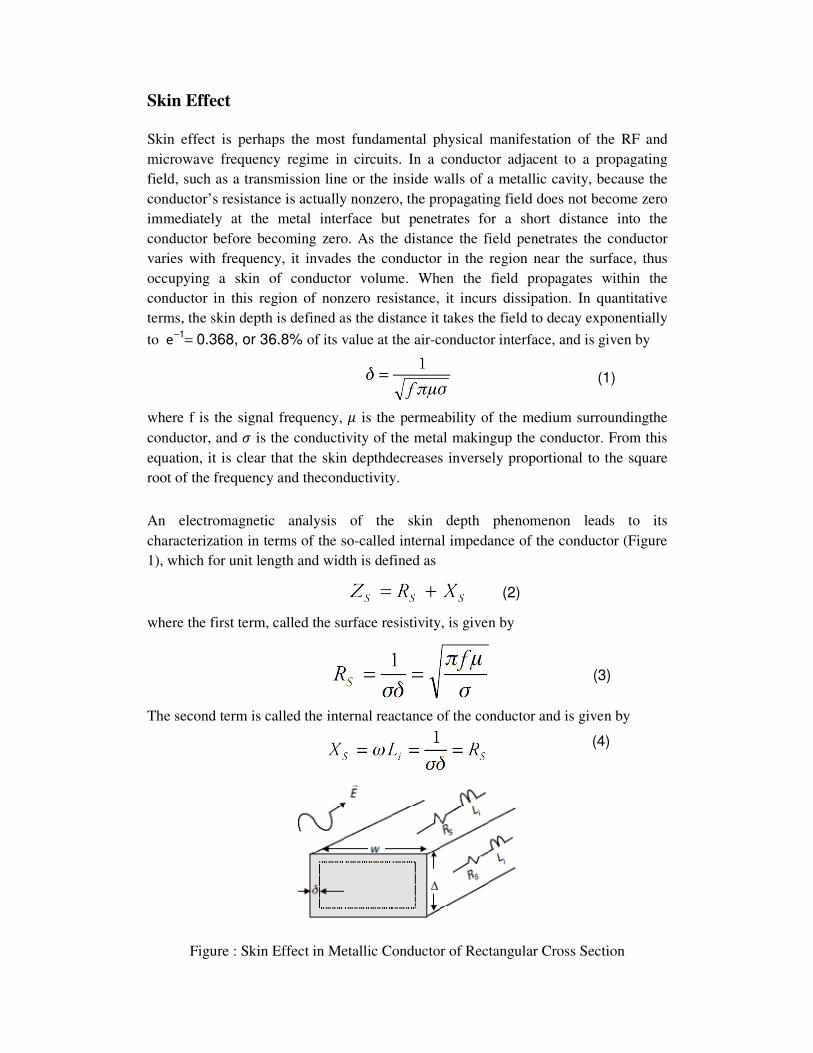
Skin Effect Skin effect is perhaps the most fundamental physical manifestation of the RF and microwave frequency regime in circuits. In a conductor adjacent to a propagating field, such as a transmission line or the inside walls of a metallic cavity, because the conductor’s resistance is actually nonzero, the propagating field does not become zero immediately at the metal interface but penetrates for a short distance into the conductor before becoming zero. As the distance the field penetrates the conductor varies with frequency, it invades the conductor in the region near the surface, thus occupying a skin of conductor volume. When the field propagates within the conductor in this region of nonzero resistance, it incurs dissipation. In quantitative terms, the skin depth is defined as the distance it takes the field to decay exponentially
to e−1= 0.368, or 36.8% of its value at the air-conductor interface, and is given by
where f is the signal frequency, is the permeability of the medium surroundingthe conductor, and is the conductivity of the metal makingup the conductor. From this equation, it is clear that the skin depthdecreases inversely proportional to the square root of the frequency and theconductivity.
An electromagnetic analysis of the skin depth phenomenon leads to its characterization in terms of the so-called internal impedance of the conductor (Figure 1), which for unit length and width is defined as
where the first term, called the surface resistivity, is given by
The second term is called the internal reactance of the conductor and is given by
Figure : Skin Effect in Metallic Conductor of Rectangular Cross Section
(1)
(2)
(3)
(4)
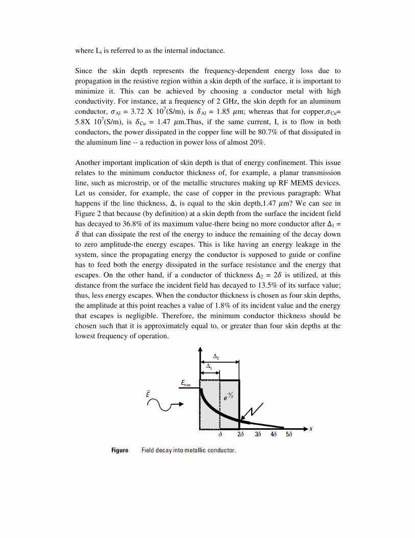
where Li is referred to as the internal inductance. Since the skin depth represents the frequency-dependent energy loss due to propagation in the resistive region within a skin depth of the surface, it is important to minimize it. This can be achieved by choosing a conductor metal with high conductivity. For instance, at a frequency of 2 GHz, the skin depth for an aluminum conductor, Al = 3.72 X 10⁷(S/m), is Al = 1.85 m; whereas that for copper,Cu= 5.8X 10⁷(S/m), is Cu = 1.47 m.Thus, if the same current, I, is to flow in both conductors, the power dissipated in the copper line will be 80.7% of that dissipated in the aluminum line -- a reduction in power loss of almost 20%. Another important implication of skin depth is that of energy confinement. This issue relates to the minimum conductor thickness of, for example, a planar transmission line, such as microstrip, or of the metallic structures making up RF MEMS devices. Let us consider, for example, the case of copper in the previous paragraph: What happens if the line thickness, ∆, is equal to the skin depth,1.47 m? We can see in Figure 2 that because (by definition) at a skin depth from the surface the incident field has decayed to 36.8% of its maximum value-there being no more conductor after ∆1 = that can dissipate the rest of the energy to induce the remaining of the decay down to zero amplitude-the energy escapes. This is like having an energy leakage in the system, since the propagating energy the conductor is supposed to guide or confine has to feed both the energy dissipated in the surface resistance and the energy that escapes. On the other hand, if a conductor of thickness ∆2 = 2 is utilized, at this distance from the surface the incident field has decayed to 13.5% of its surface value; thus, less energy escapes. When the conductor thickness is chosen as four skin depths, the amplitude at this point reaches a value of 1.8% of its incident value and the energy that escapes is negligible. Therefore, the minimum conductor thickness should be chosen such that it is approximately equal to, or greater than four skin depths at the lowest frequency of operation.
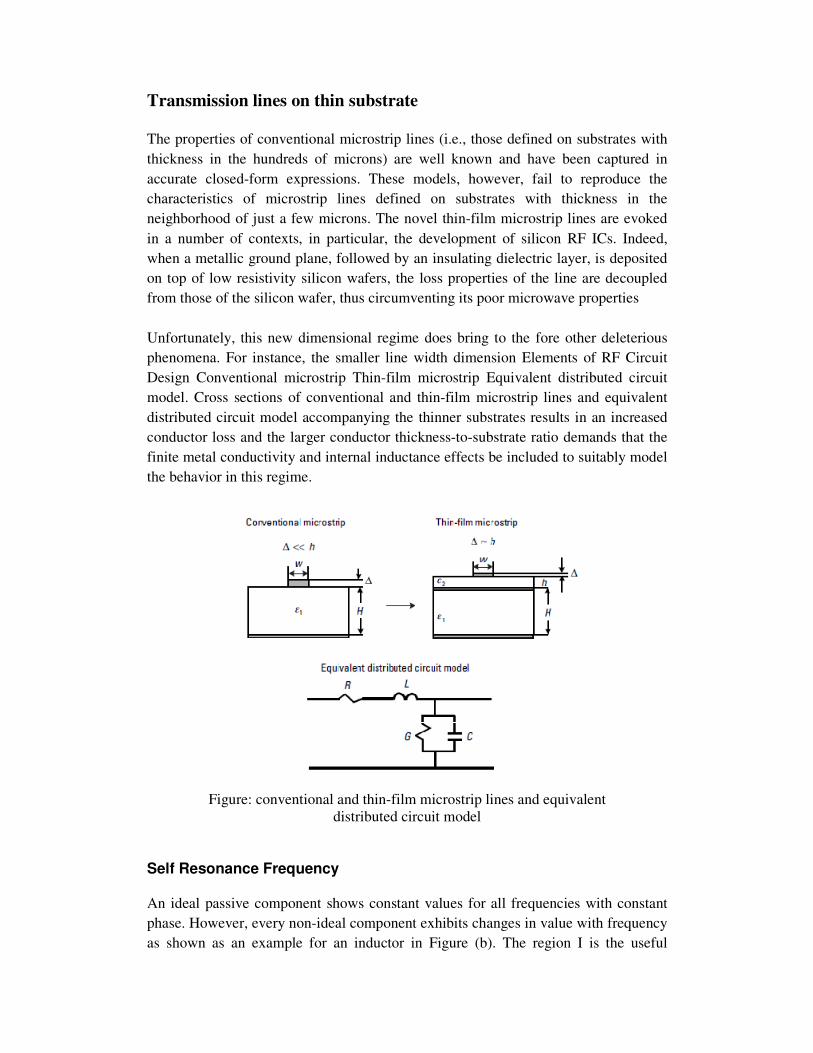
Transmission lines on thin substrate
The properties of conventional microstrip lines (i.e., those defined on substrates with thickness in the hundreds of microns) are well known and have been captured in accurate closed-form expressions. These models, however, fail to reproduce the characteristics of microstrip lines defined on substrates with thickness in the neighborhood of just a few microns. The novel thin-film microstrip lines are evoked in a number of contexts, in particular, the development of silicon RF ICs. Indeed, when a metallic ground plane, followed by an insulating dielectric layer, is deposited on top of low resistivity silicon wafers, the loss properties of the line are decoupled from those of the silicon wafer, thus circumventing its poor microwave properties Unfortunately, this new dimensional regime does bring to the fore other deleterious phenomena. For instance, the smaller line width dimension Elements of RF Circuit Design Conventional microstrip Thin-film microstrip Equivalent distributed circuit model. Cross sections of conventional and thin-film microstrip lines and equivalent distributed circuit model accompanying the thinner substrates results in an increased conductor loss and the larger conductor thickness-to-substrate ratio demands that the finite metal conductivity and internal inductance effects be included to suitably model the behavior in this regime.
Figure: conventional and thin-film microstrip lines and equivalent distributed circuit model
Self Resonance Frequency An ideal passive component shows constant values for all frequencies with constant phase. However, every non-ideal component exhibits changes in value with frequency as shown as an example for an inductor in Figure (b). The region I is the useful
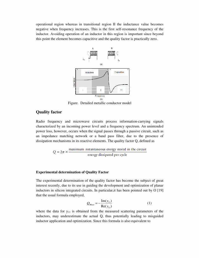
operational region whereas in transitional region II the inductance value becomes negative when frequency increases. This is the first self-resonance frequency of the inductor. Avoiding operation of an inductor in this region is important since beyond this point the element becomes capacitive and the quality factor is practically zero.
Figure. Detailed metallic conductor model
Quality factor
Radio frequency and microwave circuits process information-carrying signals characterized by an incoming power level and a frequency spectrum. An unintended power loss, however, occurs when the signal passes through a passive circuit, such as an impedance matching network or a band pass filter, due to the presence of dissipation mechanisms in its reactive elements. The quality factor Q, defined as
Experimental determination of Quality Factor
The experimental determination of the quality factor has become the subject of great interest recently, due to its use in guiding the development and optimization of planar inductors in silicon integrated circuits. In particular,it has been pointed out by O [19] that the usual formula employed,
)Re(
)Im(
11
11
y
yQMeas −=
where the data for y11 is obtained from the measured scattering parameters of the inductors, may underestimate the actual Q, thus potentially leading to misguided inductor application and optimization. Since this formula is also equivalent to
(1)
diss
em
MeasP
WWQ
)(2 −
=
ω
where mW and eW
are the average stored magnetic and electrical energies in the system [1], O[19] realized that this definition is a good approximation to
only when the stored magnetic energy is much greater than the stored electrical energy. This condition is usually violated, however, in the case of silicon integrated inductors, which, possessing a large shunt capacitance to the substrate, exhibit
substantial electrical energy storage. As a result, )Re(
)Im(
11
11
y
yQMeas −= may deviate from
cycleper dissipatedenergy
circuit in the storedenergy ousinstantane Maximum X 2π=Q by a large amount. To
overcome this difficulty, O[19] proposed new methods that extract the Q by numerically adding a capacitor in parallel to measured 11y data of an inductor and
computing the frequency stability factor and 3-dB bandwidth, B
fQ itTunedCircu
0= , at the
resonant frequency of the resulting network. Then, by computing these parameters using relationships for simple parallel RLC circuits, these parameters are converted to effective quality factors. In particular, from the formula for phase stability factor,
the Q is obtained as per:
Equations (4) and (5) are more relevant, he points out, for circuit design, and they provide physically reasonable information throughout a wide frequency range, including the self-resonance frequency of the inductors.
Packaging
The proper operation of RF and microwave circuits and systems is critically dependent upon the clean environment provided by the package that houses them.
(2)
(3)
(4)
(5)
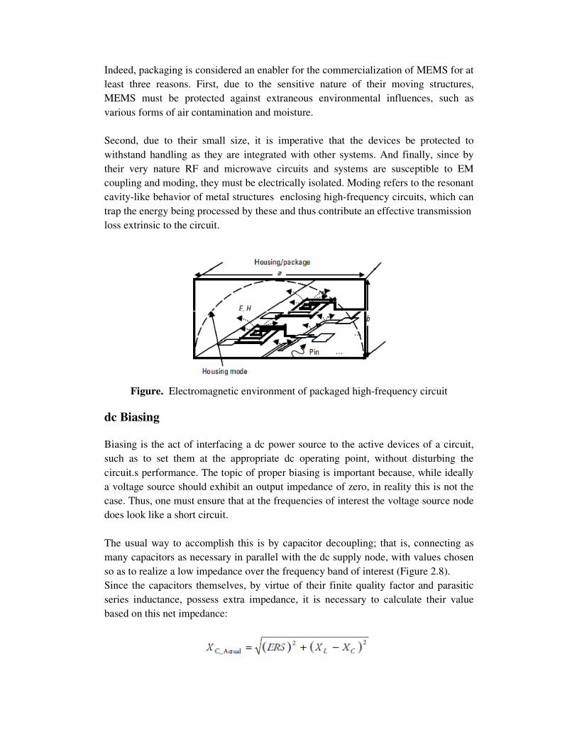
Indeed, packaging is considered an enabler for the commercialization of MEMS for at least three reasons. First, due to the sensitive nature of their moving structures, MEMS must be protected against extraneous environmental influences, such as various forms of air contamination and moisture. Second, due to their small size, it is imperative that the devices be protected to withstand handling as they are integrated with other systems. And finally, since by their very nature RF and microwave circuits and systems are susceptible to EM coupling and moding, they must be electrically isolated. Moding refers to the resonant cavity-like behavior of metal structures enclosing high-frequency circuits, which can trap the energy being processed by these and thus contribute an effective transmission loss extrinsic to the circuit.
Figure. Electromagnetic environment of packaged high-frequency circuit
dc Biasing
Biasing is the act of interfacing a dc power source to the active devices of a circuit, such as to set them at the appropriate dc operating point, without disturbing the circuit.s performance. The topic of proper biasing is important because, while ideally a voltage source should exhibit an output impedance of zero, in reality this is not the case. Thus, one must ensure that at the frequencies of interest the voltage source node does look like a short circuit. The usual way to accomplish this is by capacitor decoupling; that is, connecting as many capacitors as necessary in parallel with the dc supply node, with values chosen so as to realize a low impedance over the frequency band of interest (Figure 2.8). Since the capacitors themselves, by virtue of their finite quality factor and parasitic series inductance, possess extra impedance, it is necessary to calculate their value based on this net impedance:
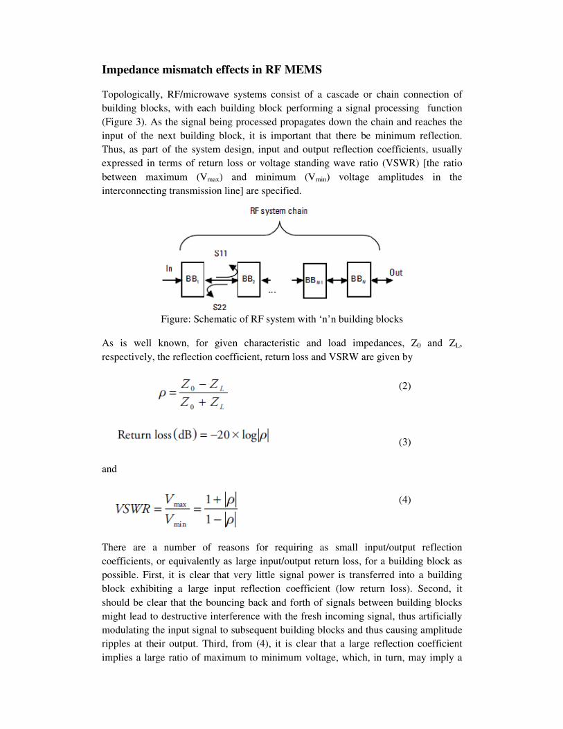
Impedance mismatch effects in RF MEMS Topologically, RF/microwave systems consist of a cascade or chain connection of building blocks, with each building block performing a signal processing function (Figure 3). As the signal being processed propagates down the chain and reaches the input of the next building block, it is important that there be minimum reflection. Thus, as part of the system design, input and output reflection coefficients, usually expressed in terms of return loss or voltage standing wave ratio (VSWR) [the ratio between maximum (Vmax) and minimum (Vmin) voltage amplitudes in the interconnecting transmission line] are specified.
Figure: Schematic of RF system with ‘n’n building blocks
As is well known, for given characteristic and load impedances, Z0 and ZL, respectively, the reflection coefficient, return loss and VSRW are given by
and
There are a number of reasons for requiring as small input/output reflection coefficients, or equivalently as large input/output return loss, for a building block as possible. First, it is clear that very little signal power is transferred into a building block exhibiting a large input reflection coefficient (low return loss). Second, it should be clear that the bouncing back and forth of signals between building blocks might lead to destructive interference with the fresh incoming signal, thus artificially modulating the input signal to subsequent building blocks and thus causing amplitude ripples at their output. Third, from (4), it is clear that a large reflection coefficient implies a large ratio of maximum to minimum voltage, which, in turn, may imply a
(3)
(2)
(4)
large maximum voltage amplitude. In the context of RF MEMS, inadvertently large voltage amplitudes may be undesirable if one is attempting to limit the phenomenon
of hot switching. In this phenomenon, a force bias, , may be imposed on an electrostatically actuated system by virtue of the fact that the ac voltage V applied to the system is mechanically rectified to the point of inducing a bias force (voltage) greater than the pull-in force (voltage).

RF MEMS ENABLED CIRCUIT ELEMENTS
RF/Microwave Substrate Properties
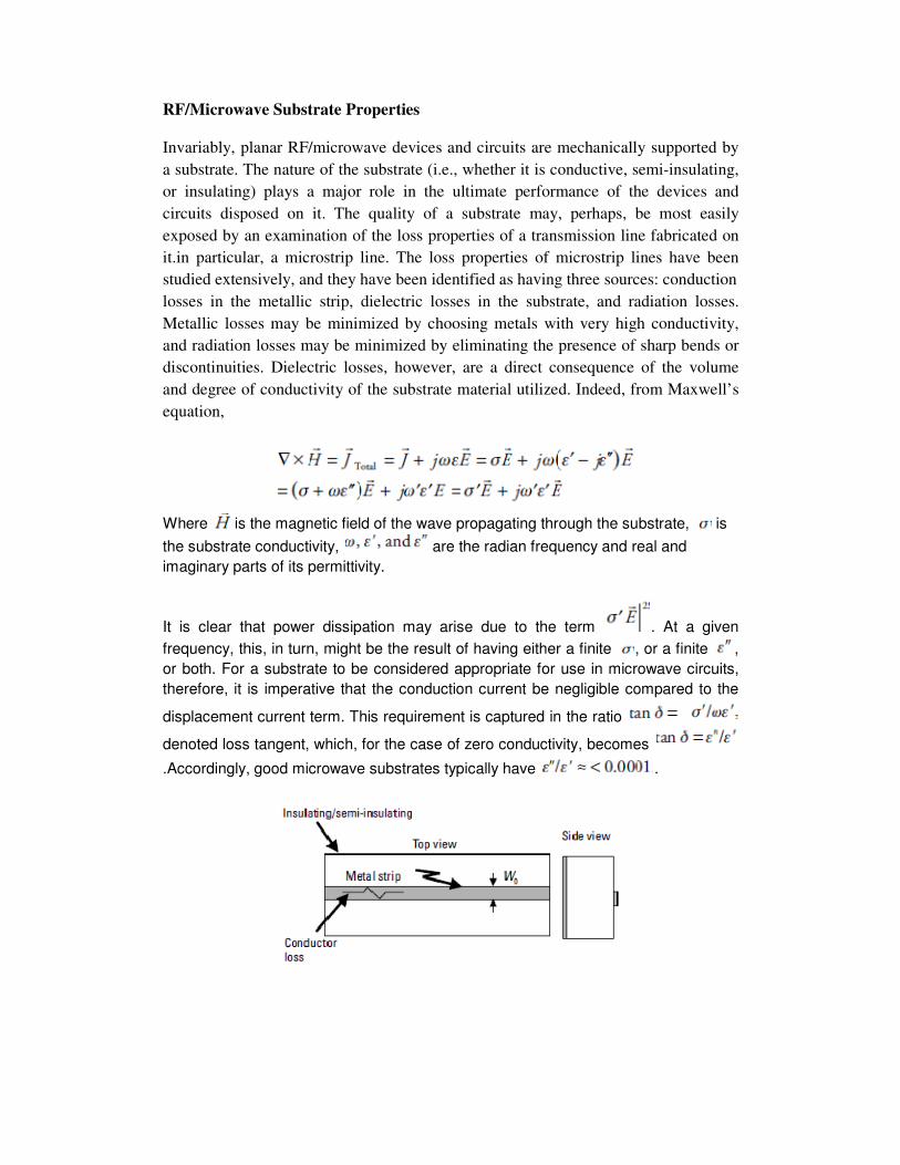
Invariably, planar RF/microwave devices and circuits are mechanically supported by a substrate. The nature of the substrate (i.e., whether it is conductive, semi-insulating, or insulating) plays a major role in the ultimate performance of the devices and circuits disposed on it. The quality of a substrate may, perhaps, be most easily exposed by an examination of the loss properties of a transmission line fabricated on it.in particular, a microstrip line. The loss properties of microstrip lines have been studied extensively, and they have been identified as having three sources: conduction losses in the metallic strip, dielectric losses in the substrate, and radiation losses. Metallic losses may be minimized by choosing metals with very high conductivity, and radiation losses may be minimized by eliminating the presence of sharp bends or discontinuities. Dielectric losses, however, are a direct consequence of the volume and degree of conductivity of the substrate material utilized. Indeed, from Maxwell’s equation,
Where is the magnetic field of the wave propagating through the substrate, is
the substrate conductivity, are the radian frequency and real and
imaginary parts of its permittivity.
It is clear that power dissipation may arise due to the term . At a given
frequency, this, in turn, might be the result of having either a finite , or a finite ,
or both. For a substrate to be considered appropriate for use in microwave circuits,
therefore, it is imperative that the conduction current be negligible compared to the
displacement current term. This requirement is captured in the ratio
denoted loss tangent, which, for the case of zero conductivity, becomes
.Accordingly, good microwave substrates typically have .
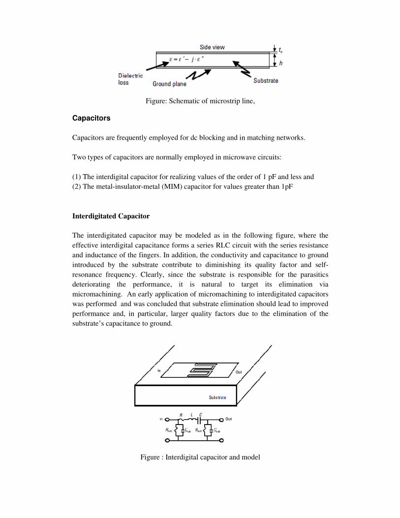
Figure: Schematic of microstrip line,
Capacitors
Capacitors are frequently employed for dc blocking and in matching networks. Two types of capacitors are normally employed in microwave circuits: (1) The interdigital capacitor for realizing values of the order of 1 pF and less and (2) The metal-insulator-metal (MIM) capacitor for values greater than 1pF
Interdigitated Capacitor
The interdigitated capacitor may be modeled as in the following figure, where the effective interdigital capacitance forms a series RLC circuit with the series resistance and inductance of the fingers. In addition, the conductivity and capacitance to ground introduced by the substrate contribute to diminishing its quality factor and self-resonance frequency. Clearly, since the substrate is responsible for the parasitics deteriorating the performance, it is natural to target its elimination via micromachining. An early application of micromachining to interdigitated capacitors was performed and was concluded that substrate elimination should lead to improved performance and, in particular, larger quality factors due to the elimination of the substrate’s capacitance to ground.
Figure : Interdigital capacitor and model
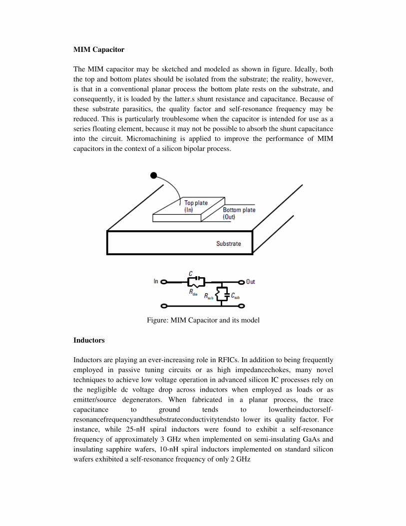
MIM Capacitor
The MIM capacitor may be sketched and modeled as shown in figure. Ideally, both the top and bottom plates should be isolated from the substrate; the reality, however, is that in a conventional planar process the bottom plate rests on the substrate, and consequently, it is loaded by the latter.s shunt resistance and capacitance. Because of these substrate parasitics, the quality factor and self-resonance frequency may be reduced. This is particularly troublesome when the capacitor is intended for use as a series floating element, because it may not be possible to absorb the shunt capacitance into the circuit. Micromachining is applied to improve the performance of MIM capacitors in the context of a silicon bipolar process.
Figure: MIM Capacitor and its model
Inductors
Inductors are playing an ever-increasing role in RFICs. In addition to being frequently employed in passive tuning circuits or as high impedancechokes, many novel techniques to achieve low voltage operation in advanced silicon IC processes rely on the negligible dc voltage drop across inductors when employed as loads or as emitter/source degenerators. When fabricated in a planar process, the trace capacitance to ground tends to lowertheinductorself-resonancefrequencyandthesubstrateconductivitytendsto lower its quality factor. For instance, while 25-nH spiral inductors were found to exhibit a self-resonance frequency of approximately 3 GHz when implemented on semi-insulating GaAs and insulating sapphire wafers, 10-nH spiral inductors implemented on standard silicon wafers exhibited a self-resonance frequency of only 2 GHz
While optimization of the spiral geometry and line width is essential to tailor the frequency of maximum Q, this exercise only addresses minimization of the trace ohmic losses and substrate capacitance. techniques to diminish the substrate losses created by eddy currents induced by the magnetic field of the spiral havebeenpursued.Forinstance,introducedblockingppjunctionsin the path of the eddy current flowinimprovement from 5.3 to 6 at 3.5 GHz on a 1.8other hand, introduced patterned metal ground shields to block the eddy current and obtained a Q improvement from 5.08 to 6.76 at 2 GHz. While ithese improvements register as 13% and 33%, respectively, Qs greater than 10 are actually desired. These limitations of planar spiral inductors have motivated the development of fabrication techniques to realize threeof planar processes. These inductors are expected to exhibit improved properties over their spiral counterparts because only one portion of their metal traces is susceptible to substrate capacitance. In addition, they offer desrelationship between their geometry and inductance value is availablenamely,
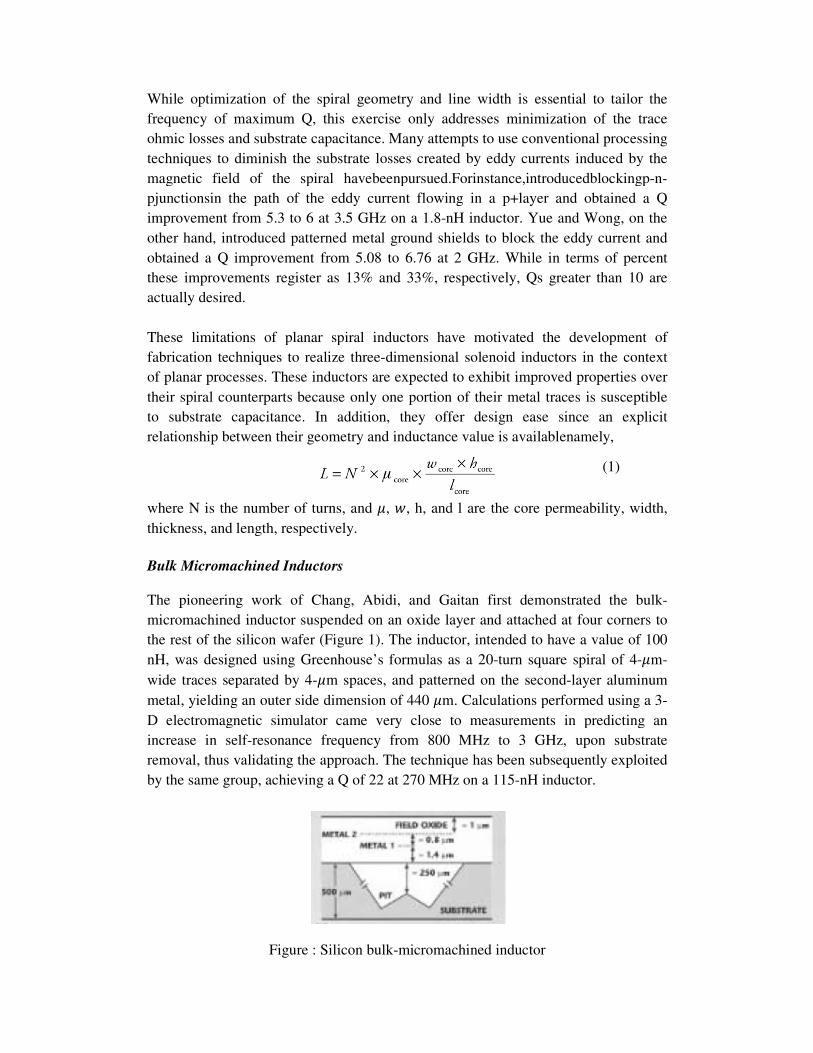
where N is the number of turns, and thickness, and length, respectively. Bulk Micromachined Inductors
The pioneering work of Chang, Abidi, and Gaitan first demonstrated the bulkmicromachined inductor suspended on an oxide layer and attached at four corners to the rest of the silicon wafer (Figure 1). The inductor, intended to havenH, was designed using Greenhouse’s formulas as a 20wide traces separated by 4-metal, yielding an outer side dimension of 440 D electromagnetic simulator came very close to measurements in predicting an increase in self-resonance frequency from 800 MHz to 3 GHz, upon substrate removal, thus validating the approach. The technique has been subsequently exploited by the same group, achieving a Q of 22 at 270 MHz on a 115
Figure : Silicon bulk
While optimization of the spiral geometry and line width is essential to tailor the frequency of maximum Q, this exercise only addresses minimization of the trace ohmic losses and substrate capacitance. Many attempts to use conventional processing techniques to diminish the substrate losses created by eddy currents induced by the magnetic field of the spiral havebeenpursued.Forinstance,introducedblockingppjunctionsin the path of the eddy current flowing in a p+layer and obtained a Q improvement from 5.3 to 6 at 3.5 GHz on a 1.8-nH inductor. Yue and Wong, on the other hand, introduced patterned metal ground shields to block the eddy current and obtained a Q improvement from 5.08 to 6.76 at 2 GHz. While in terms of percent these improvements register as 13% and 33%, respectively, Qs greater than 10 are
These limitations of planar spiral inductors have motivated the development of fabrication techniques to realize three-dimensional solenoid inductors in the context of planar processes. These inductors are expected to exhibit improved properties over their spiral counterparts because only one portion of their metal traces is susceptible to substrate capacitance. In addition, they offer design ease since an explicit relationship between their geometry and inductance value is availablenamely,
where N is the number of turns, and , , h, and l are the core permeability, width, thickness, and length, respectively.
Micromachined Inductors
The pioneering work of Chang, Abidi, and Gaitan first demonstrated the bulkmicromachined inductor suspended on an oxide layer and attached at four corners to the rest of the silicon wafer (Figure 1). The inductor, intended to have a value of 100 nH, was designed using Greenhouse’s formulas as a 20-turn square spiral of 4
m spaces, and patterned on the second-layer aluminum metal, yielding an outer side dimension of 440 m. Calculations performed usD electromagnetic simulator came very close to measurements in predicting an
resonance frequency from 800 MHz to 3 GHz, upon substrate removal, thus validating the approach. The technique has been subsequently exploited
group, achieving a Q of 22 at 270 MHz on a 115-nH inductor.
Silicon bulk-micromachined inductor
(1)
While optimization of the spiral geometry and line width is essential to tailor the frequency of maximum Q, this exercise only addresses minimization of the trace
Many attempts to use conventional processing techniques to diminish the substrate losses created by eddy currents induced by the magnetic field of the spiral havebeenpursued.Forinstance,introducedblockingp-n-
g in a p+layer and obtained a Q nH inductor. Yue and Wong, on the
other hand, introduced patterned metal ground shields to block the eddy current and n terms of percent
these improvements register as 13% and 33%, respectively, Qs greater than 10 are
These limitations of planar spiral inductors have motivated the development of oid inductors in the context
of planar processes. These inductors are expected to exhibit improved properties over their spiral counterparts because only one portion of their metal traces is susceptible
ign ease since an explicit relationship between their geometry and inductance value is availablenamely,
, h, and l are the core permeability, width,
The pioneering work of Chang, Abidi, and Gaitan first demonstrated the bulk-micromachined inductor suspended on an oxide layer and attached at four corners to
a value of 100 turn square spiral of 4-m-
layer aluminum m. Calculations performed using a 3-
D electromagnetic simulator came very close to measurements in predicting an resonance frequency from 800 MHz to 3 GHz, upon substrate
removal, thus validating the approach. The technique has been subsequently exploited
(1)
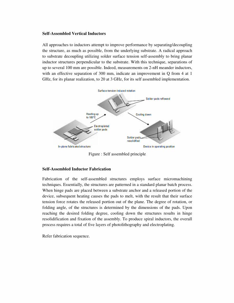
Self-Assembled Vertical Inductors
All approaches to inductors attempt to improve performance by separating/decoupling the structure, as much as possible, from the underlying substrate. A radical approach to substrate decoupling utilizing solder surface tension self-assembly to bring planar inductor structures perpendicular to the substrate. With this technique, separations of up to several 100 mm are possible. Indeed, measurements on 2-nH meander inductors, with an effective separation of 300 mm, indicate an improvement in Q from 4 at 1 GHz, for its planar realization, to 20 at 3 GHz, for its self assembled implementation.
Figure : Self assembled principle
Self-Assembled Inductor Fabrication
Fabrication of the self-assembled structures employs surface micromachining techniques. Essentially, the structures are patterned in a standard planar batch process. When hinge pads are placed between a substrate anchor and a released portion of the device, subsequent heating causes the pads to melt, with the result that their surface tension force rotates the released portion out of the plane. The degree of rotation, or folding angle, of the structures is determined by the dimensions of the pads. Upon reaching the desired folding degree, cooling down the structures results in hinge resolidification and fixation of the assembly. To produce spiral inductors, the overall process requires a total of five layers of photolithography and electroplating. Refer fabrication sequence.
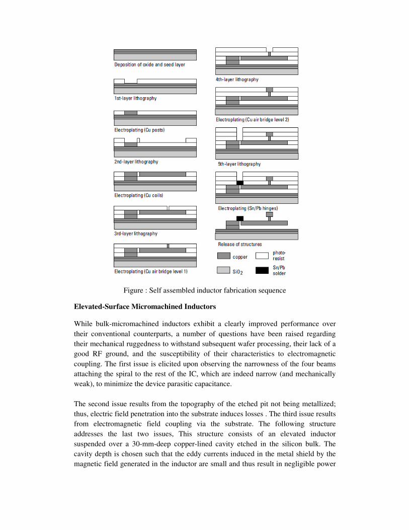
Figure : Self assembled inductor fabrication sequence
Elevated-Surface Micromachined Inductors While bulk-micromachined inductors exhibit a clearly improved performance over their conventional counterparts, a number of questions have been raised regarding their mechanical ruggedness to withstand subsequent wafer processing, their lack of a good RF ground, and the susceptibility of their characteristics to electromagnetic coupling. The first issue is elicited upon observing the narrowness of the four beams attaching the spiral to the rest of the IC, which are indeed narrow (and mechanically weak), to minimize the device parasitic capacitance. The second issue results from the topography of the etched pit not being metallized; thus, electric field penetration into the substrate induces losses . The third issue results from electromagnetic field coupling via the substrate. The following structure addresses the last two issues, This structure consists of an elevated inductor suspended over a 30-mm-deep copper-lined cavity etched in the silicon bulk. The cavity depth is chosen such that the eddy currents induced in the metal shield by the magnetic field generated in the inductor are small and thus result in negligible power
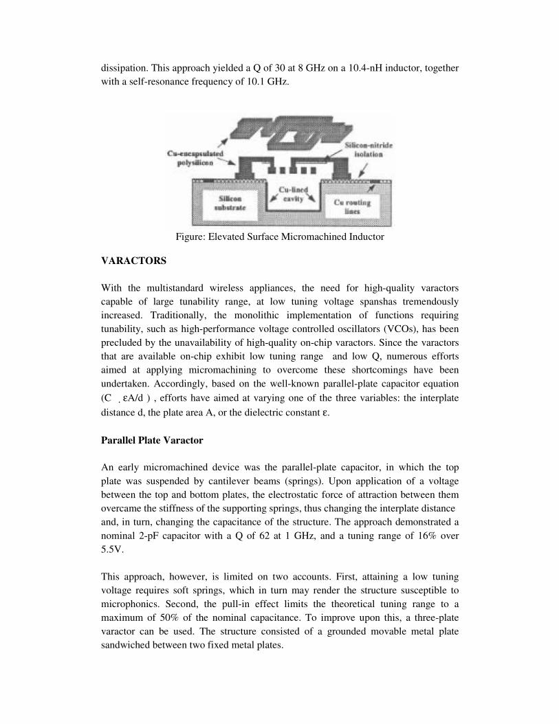
dissipation. This approach yielded a Q of 30 at 8 GHz on a 10.4-nH inductor, together with a self-resonance frequency of 10.1 GHz.
Figure: Elevated Surface Micromachined Inductor
VARACTORS
With the multistandard wireless appliances, the need for high-quality varactors capable of large tunability range, at low tuning voltage spanshas tremendously increased. Traditionally, the monolithic implementation of functions requiring tunability, such as high-performance voltage controlled oscillators (VCOs), has been precluded by the unavailability of high-quality on-chip varactors. Since the varactors that are available on-chip exhibit low tuning range and low Q, numerous efforts aimed at applying micromachining to overcome these shortcomings have been undertaken. Accordingly, based on the well-known parallel-plate capacitor equation (C εA/d ) , efforts have aimed at varying one of the three variables: the interplate distance d, the plate area A, or the dielectric constant ε. Parallel Plate Varactor
An early micromachined device was the parallel-plate capacitor, in which the top plate was suspended by cantilever beams (springs). Upon application of a voltage between the top and bottom plates, the electrostatic force of attraction between them overcame the stiffness of the supporting springs, thus changing the interplate distance and, in turn, changing the capacitance of the structure. The approach demonstrated a nominal 2-pF capacitor with a Q of 62 at 1 GHz, and a tuning range of 16% over 5.5V. This approach, however, is limited on two accounts. First, attaining a low tuning voltage requires soft springs, which in turn may render the structure susceptible to microphonics. Second, the pull-in effect limits the theoretical tuning range to a maximum of 50% of the nominal capacitance. To improve upon this, a three-plate varactor can be used. The structure consisted of a grounded movable metal plate sandwiched between two fixed metal plates.
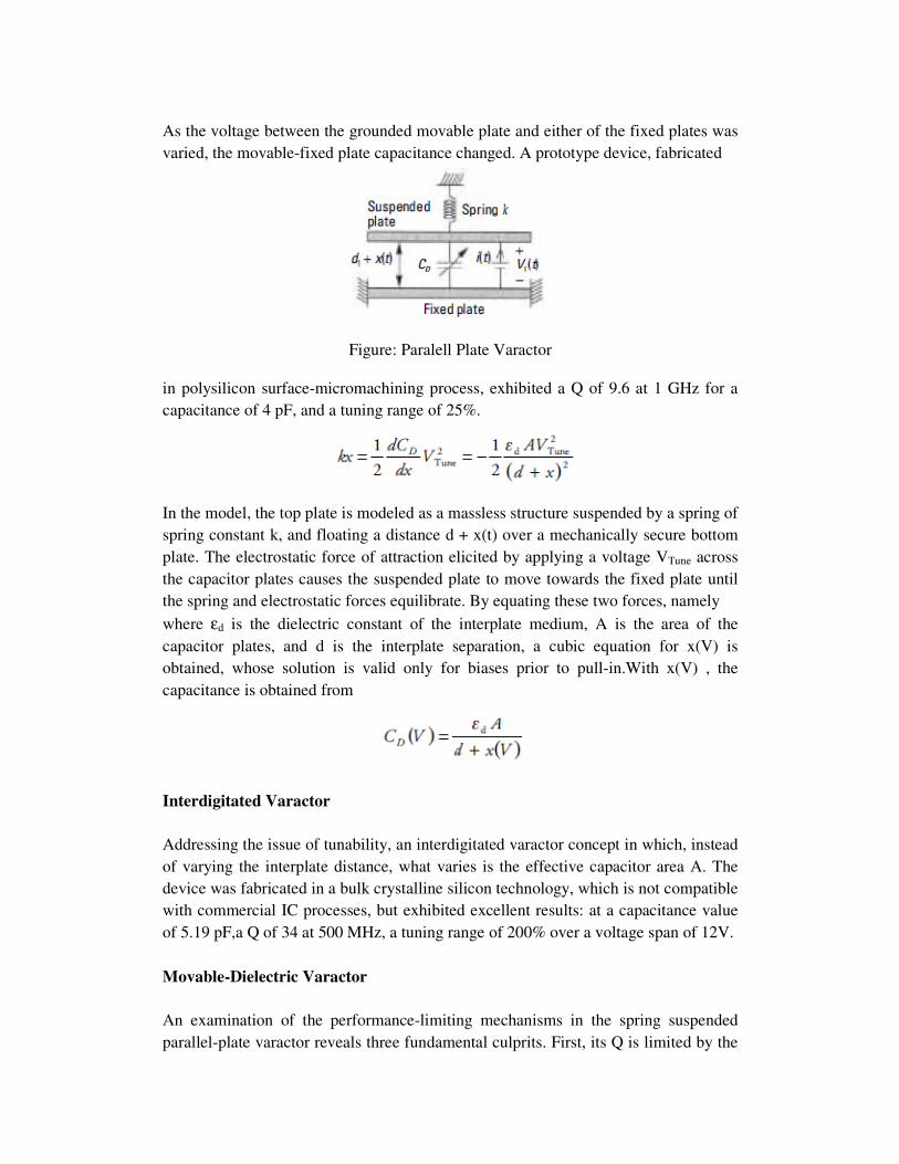
As the voltage between the grounded movable plate and either of the fixed plates was varied, the movable-fixed plate capacitance changed. A prototype device, fabricated
Figure: Paralell Plate Varactor in polysilicon surface-micromachining process, exhibited a Q of 9.6 at 1 GHz for a capacitance of 4 pF, and a tuning range of 25%.
In the model, the top plate is modeled as a massless structure suspended by a spring of spring constant k, and floating a distance d + x(t) over a mechanically secure bottom plate. The electrostatic force of attraction elicited by applying a voltage VTune across the capacitor plates causes the suspended plate to move towards the fixed plate until the spring and electrostatic forces equilibrate. By equating these two forces, namely where εd is the dielectric constant of the interplate medium, A is the area of the capacitor plates, and d is the interplate separation, a cubic equation for x(V) is obtained, whose solution is valid only for biases prior to pull-in.With x(V) , the capacitance is obtained from
Interdigitated Varactor
Addressing the issue of tunability, an interdigitated varactor concept in which, instead of varying the interplate distance, what varies is the effective capacitor area A. The device was fabricated in a bulk crystalline silicon technology, which is not compatible with commercial IC processes, but exhibited excellent results: at a capacitance value of 5.19 pF,a Q of 34 at 500 MHz, a tuning range of 200% over a voltage span of 12V. Movable-Dielectric Varactor
An examination of the performance-limiting mechanisms in the spring suspended parallel-plate varactor reveals three fundamental culprits. First, its Q is limited by the
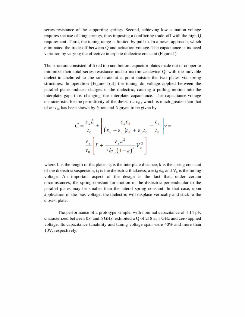
series resistance of the supporting springs. Second, achieving low actuation voltage requires the use of long springs, thus imposing a conflicting trade-off with the high Q requirement. Third, the tuning range is limited by pull-in. In a novel approach, which eliminated the trade-off between Q and actuation voltage. The capacitance is induced variation by varying the effective interplate dielectric constant (Figure 1). The structure consisted of fixed top and bottom capacitor plates made out of copper to minimize their total series resistance and to maximize device Q, with the movable dielectric anchored to the substrate at a point outside the two plates via spring structures. In operation [Figure 1(a)] the tuning dc voltage applied between the parallel plates induces charges in the dielectric, causing a pulling motion into the interplate gap, thus changing the interplate capacitance. The capacitance-voltage characteristic for the permittivity of the dielectric d , which is much greater than that of air a, has been shown by Yoon and Nguyen to be given by
where L is the length of the plates, t0 is the interplate distance, k is the spring constant of the dielectric suspension, td is the dielectric thickness, a = td /t0, and Va is the tuning voltage. An important aspect of the design is the fact that, under certain circumstances, the spring constant for motion of the dielectric perpendicular to the parallel plates may be smaller than the lateral spring constant. In that case, upon application of the bias voltage, the dielectric will displace vertically and stick to the closest plate.
The performance of a prototype sample, with nominal capacitance of 1.14 pF, characterized between 0.6 and 6 GHz, exhibited a Q of 218 at 1 GHz and zero applied voltage. Its capacitance tunability and tuning voltage span were 40% and more than 10V, respectively.
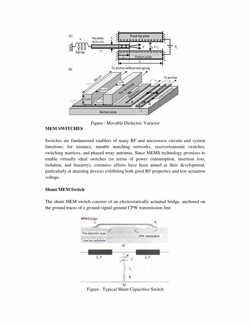
Figure : Movable Dielectric Varactor MEM SWITCHES
Switches are fundamental enablers of many RF and microwave circuits and system functions; for instance, tunable matching networks, receive/transmit switches, switching matrices, and phased array antennas. Since MEMS technology promises to enable virtually ideal switches (in terms of power consumption, insertion loss, isolation, and linearity), extensive efforts have been aimed at their development, particularly at attaining devices exhibiting both good RF properties and low actuation voltage. Shunt MEM Switch
The shunt MEM switch consists of an electrostatically actuated bridge, anchored on the ground traces of a ground-signal-ground CPW transmission line.
Figure : Typical Shunt Capacitive Switch
The actuation electrode, located a distance g 0 below the bridge, underneath the bridge is coated by a thin insulating layer to avoid short-circuiting upon bridge deflection. For a bottom electrode of width w, a CPW center conductor of width W, and a bridge of spring constant k, the pull-in voltage (also referred to as pull-down and actuation voltage) of the switch is given by
where the effective spring constant is given by
where t and L are the bridge thickness and length, respectively, and E, s, and ν are the Young modulus, residual tensile stress, and Poisson.s ratio for the bridge material, respectively The performance level typical of these switches in the on state includes an insertion
loss that increases gradually with frequency from 0.1 dB below 1 GHz to about 0.3
dB at 40 GHz, a return loss of about 15 dB at 40 GHz. In the off state, the isolation
ranges from nearly 0 dB at 1 GHz to about 35 dB at 40 GHz. The linearity of the
switch is rather good: measurements conducted between 2 and 4 GHz failed to
detect any intermodulation frequency products for signal powers ranging up to +20
dBm, yielding a third-order intercept point (IP3) of +66 dBm. Finally, the typical
actuation voltage, for typical air gaps of 2 mm, insulator thickness of 0.1 mm, and
dielectric constant of 7.5, lies between 30 and 50V. Herein lies the major area to
which development has been addressed, namely, lowering the actuation voltage to
levels compatible with mainstream IC technologies (i.e.,about 5V or lower), while
maintaining the RF performance substantially intact.
Low-Voltage Hinged MEM Switch Approaches
Examination of the equation for the pull-in of a cantilever beam,
reveals that the pull-in voltage may be reduced, not only by lowering the spring constant, but also by increasing the dielectric constant. Serpentine-Spring Suspended Shunt Switch
Two approaches have been advanced that exploit a movable plate suspended via hinges (serpentine springs), anchored on the ground traces of a CPW line, above the signal line. In one case, the movable plate was actuated by a bottom electrode, which
was coated with strontium titanate oxide (SrTiO3), and located underneath it. The SrTiO3, evaluated individually, exhibited a relative dielectric constant between 30 and 120 (depending on the deposition temperature) and a loss tangent of less than 0.02. Among the fabricated switches, reports were given of achieving an actuation voltage as low as 8V, and measured insertion loss and isolations of 0.08 dB and 35 dB, respectively, at 10 GHz. It is not clear, however, whether all parameters were exhibited simultaneously by the same device. In a second approach aimed at reducing the actuation voltage. This structure consists of a capacitive pad attached to actuation plates, which, in turn, are attached to folded serpentine suspensions on one end and anchored to the substrate on the other end. Upon actuation, the high capacitance of the center capacitor pad adds to the center conductor of the finite ground CPW line, causing a virtual short at high frequencies. To lower the actuation voltage, Pacheco et al. exploited the fact that if the out-of-plane spring of a single suspension is kz, then the effective spring constant that results when N such suspensions are connected to form N meanders is given by kz /N, where kz is given by
where ν is Poisson.s ratio.
Figure: Serpentine-Spring Suspended Shunt Switch
Push-Pull Series Switch
There is a trade-off among the RF and actuation voltage performance parameters of a MEM switch. In particular, for the series switch, while high isolation in the off state
demands a large beam-to substrate distance, a low actuation voltage demands a small beam-to substrate distance. The push-pull approach to the series switch aims at eliminating this trade-off. The beam or lever in this structure is part of a top electrode, which, being attached to anchors via torsion springs, can affect, when properly actuated, a bistable motion pivoting about the torsion spring axis. To control this pivoting motion, there are two electrodes (the pull and the push electrodes) underneath the top electrode on either side of the torsion axis. Thus, depending on which electrode is actuated, the lever will move up or down. When a voltage is applied to the push electrode the lever-to-substrate distance increases and is given by
Thus, according to above expression, simultaneous low actuation voltage and high isolation can be achieved by decreasing h0 and increasing the lever length llever. By choosing h0 (the contact-to-substrate gap) such that it is smaller than the top electrode to pull electrode gap, pull-in action during the pull electrode actuation (turn-on process) may be avoided, as the distance h0 may be traveled by the contact prior to the pull-in being reached under the top-pull electrode gap.
Figure : Push Pull Series Switch
Folded-Beam-Springs Suspension Series Switch
The conventional series switch consists of one anchored cantilever beam disposed perpendicular to a segmented transmission line. The beam usually has attached to it two isolated conductors: one that serves as the top plate of a parallel plate (driver) capacitor and one that serves as a contact (typically found attached to the underside of the beam tip). Below the beam, on the substrate surface, a third conductor, or bottom electrode, is found. Actuation of the switch is accomplished by applying a voltage of appropriate magnitude between the bottom electrode and that on the beam, which results in a downward beam deflection and ultimately causes the contact at the beam tip to bridge/closed the segmented transmission line.
One potential drawback of this structure is that, since the beam is a composite structure, the various temperature coefficients of expansion of the constituent elements may, as a result of processing conditions, result on different stress levels, which, in turn, may cause the beam to adopt a warped configuration. This makes it difficult to achieve the targeted specifications and good uniformity over the entire wafer. A novel structure that aims at circumventing these deficiencies in the conventional cantilever beam series switch is shown in Figure This structure could be visualized as one in which the different parts of the switch (the actuation contacts/pads, the bridge, and the supporting cantilever beam) are decoupled. Examination of Figure reveals, for instance, that the cantilever beam has been replaced by four insulating folded-beam springs. These folded beams, in turn, now support a mechanical platform, also insulating, to whose underside the isolated actuation contacts (top plates of drive capacitors) and the bridge are attached. The bridge in this case is not a smooth bar, but contains gold-based contact bums. Finally, the overall structure is anchored to the substrate by legs at the ends of the springs. The circuit model for this structure is shown in Figure The performance at 40 GHz for a 500-mm-long folded-beam spring series switch is as follows. In the off state, the effective capacitance is about 2 fF, for an isolation of 30 dB. In the on state, the effective resistance is about 1W, for an insertion loss of 0.2 dB (0.1 dB due to the contact and 0.1 dB due to the signal line), and the return loss is 25 dB. The actuation voltage for lowest electrical resistance is 85V, and the switching time is about 10 ms.
Figure : Folded-Beam-Springs Suspension Series Switch and Circuit Model

A very important parameter that characterizes the reliability of RF MEMS switches is their lifetime. The best results were obtained under cold conditions (no signal being switched), with typical numbers at standard ambient of 100 million cycles. Under hot-switching conditions, with the device switching a signal of 1 mA, typical numbers were in the tens of million cycles.

RF MEMS BASED CIRCUIT ELEMENTS
RESONATORS
Resonators are key elements in the realization of filters and oscillators, as their Q determines the insertion loss and phase noise, respectively. A number of approaches to resonators have been investigated in the context of MEMS technology: planar, volumetric or cavity resonators, micromechanical, and the film bulk surface acoustic wave (FBAR) type. Transmission Line Planar Resonators
In the transmission line planar resonator, micromachining fabrication techniques are exploited to define a l/2-long transmission line on a thin (~1.4 mm) suspended dielectric membrane. Since the substrate underneath the resonator is etched, dielectric losses are eliminated. For mechanical stability, the membrane is sandwiched between lower and upper wafers that shield the structure to minimize radiation loss. Since the resonator medium is essentially air, the structure size is large, which is beneficial because the large size exhibits reduced ohmic loss. A typical implementation of the resonator, with a width of 800 mm and length designed to resonate at 28.7 GHz, exhibits loaded and unloaded Qs of 190 and 460, respectively. The fabrication process is similar to that discussed earlier for the interdigitated capacitor. Cavity Resonators
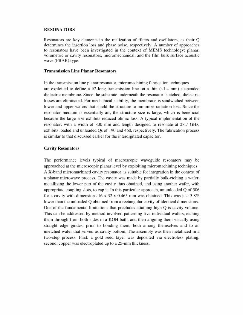
The performance levels typical of macroscopic waveguide resonators may be approached at the microscopic planar level by exploiting micromachining techniques . A X-band micromachined cavity resonator is suitable for integration in the context of a planar microwave process. The cavity was made by partially bulk-etching a wafer, metallizing the lower part of the cavity thus obtained, and using another wafer, with appropriate coupling slots, to cap it. In this particular approach, an unloaded Q of 506 for a cavity with dimensions 16 x 32 x 0.465 mm was obtained. This was just 3.8% lower than the unloaded Q obtained from a rectangular cavity of identical dimensions. One of the fundamental limitations that precludes attaining high Q is cavity volume. This can be addressed by method involved patterning five individual wafers, etching them through from both sides in a KOH bath, and then aligning them visually using straight edge guides, prior to bonding them, both among themselves and to an unetched wafer that served as cavity bottom. The assembly was then metallized in a two-step process. First, a gold seed layer was deposited via electroless plating; second, copper was electroplated up to a 25-mm thickness.
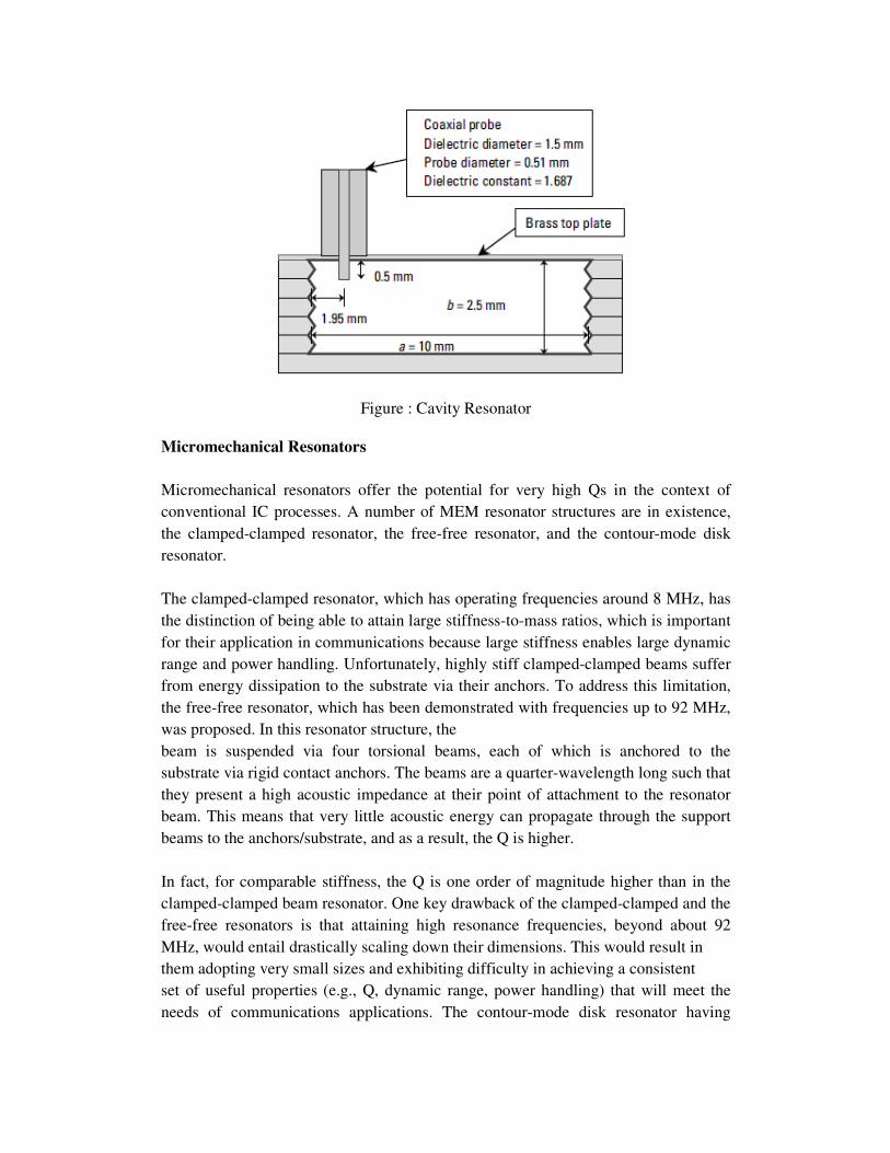
Figure : Cavity Resonator
Micromechanical Resonators
Micromechanical resonators offer the potential for very high Qs in the context of conventional IC processes. A number of MEM resonator structures are in existence, the clamped-clamped resonator, the free-free resonator, and the contour-mode disk resonator. The clamped-clamped resonator, which has operating frequencies around 8 MHz, has the distinction of being able to attain large stiffness-to-mass ratios, which is important for their application in communications because large stiffness enables large dynamic range and power handling. Unfortunately, highly stiff clamped-clamped beams suffer from energy dissipation to the substrate via their anchors. To address this limitation, the free-free resonator, which has been demonstrated with frequencies up to 92 MHz, was proposed. In this resonator structure, the beam is suspended via four torsional beams, each of which is anchored to the substrate via rigid contact anchors. The beams are a quarter-wavelength long such that they present a high acoustic impedance at their point of attachment to the resonator beam. This means that very little acoustic energy can propagate through the support beams to the anchors/substrate, and as a result, the Q is higher. In fact, for comparable stiffness, the Q is one order of magnitude higher than in the clamped-clamped beam resonator. One key drawback of the clamped-clamped and the free-free resonators is that attaining high resonance frequencies, beyond about 92 MHz, would entail drastically scaling down their dimensions. This would result in them adopting very small sizes and exhibiting difficulty in achieving a consistent set of useful properties (e.g., Q, dynamic range, power handling) that will meet the needs of communications applications. The contour-mode disk resonator having
operating frequencies up to 156achieving high frequencies at relatively large dimensions.
Figure
Film Bulk Acoustic Wave Resonators
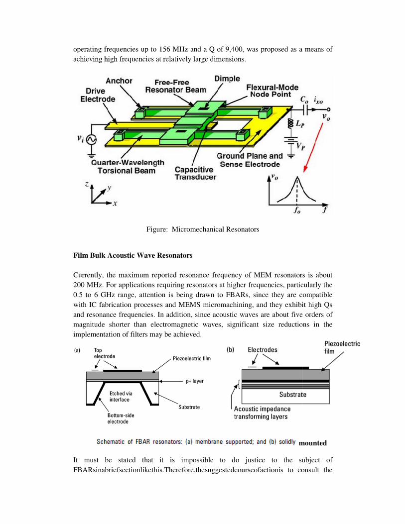
Currently, the maximum reported resonance frequency of MEM resonators is about 200 MHz. For applications requiring resonators at higher frequencies, particularly the 0.5 to 6 GHz range, attention is being drawn to FBARs, since they are compatwith IC fabrication processes and MEMS micromachining, and they exhibit high Qs and resonance frequencies. In addition, since acoustic waves are about five orders of magnitude shorter than electromagnetic waves, significant size reductions in the implementation of filters may be achieved.
It must be stated that it is impossible to do justice to the subject of FBARsinabriefsectionlikethis.Therefore,thesuggestedcourseofactionis to consult the
frequencies up to 156 MHz and a Q of 9,400, was proposed as a means of at relatively large dimensions.
Figure: Micromechanical Resonators
e Resonators
Currently, the maximum reported resonance frequency of MEM resonators is about 200 MHz. For applications requiring resonators at higher frequencies, particularly the 0.5 to 6 GHz range, attention is being drawn to FBARs, since they are compatwith IC fabrication processes and MEMS micromachining, and they exhibit high Qs and resonance frequencies. In addition, since acoustic waves are about five orders of magnitude shorter than electromagnetic waves, significant size reductions in the
ementation of filters may be achieved.
mounted
It must be stated that it is impossible to do justice to the subject of FBARsinabriefsectionlikethis.Therefore,thesuggestedcourseofactionis to consult the
MHz and a Q of 9,400, was proposed as a means of
Currently, the maximum reported resonance frequency of MEM resonators is about 200 MHz. For applications requiring resonators at higher frequencies, particularly the 0.5 to 6 GHz range, attention is being drawn to FBARs, since they are compatible with IC fabrication processes and MEMS micromachining, and they exhibit high Qs and resonance frequencies. In addition, since acoustic waves are about five orders of magnitude shorter than electromagnetic waves, significant size reductions in the
mounted
It must be stated that it is impossible to do justice to the subject of FBARsinabriefsectionlikethis.Therefore,thesuggestedcourseofactionis to consult the
standard texts on the subject. What follows is a qualitative description of FBARs in order to introduce the nomenclature and phenomenology of the device.
The FBAR is essentially an acoustic resonator cavity. Thus, the wave bouncing back and forth between walls /2 apart is an acoustic wave, thewalls (which also serve as electrodes) are acoustic impedance discontinuities, and the medium filling the cavity is a piezoelectric material. The structure, then, is fundamentally a capacitor whose dielectric material is piezoelectric. Excitation of the acoustic wave occurs upon application of an alternating voltage across the capacitor, which causes the piezoelectric material to cyclically expand and contract, thus eliciting energy oscillation between mechanical anin the electric field UE to that stored in acoustic field Upiezoelectric coupling constant and is given as
where e is the piezoelectric constant (which relates materflux density), cE is the material stiffness measured at a constant electric field [which
relates stress to strain (Hooke’s law)], and constant strain). Since, in general, these constants arinserted in (1) pertain to certain directions. The directions of interest depend upon the normal of the electrodes across which the electric field is applied and the orientation of the piezoelectric crystal. Accordingly,excitation (TE) mode, in which the direction of the applied electric field and the excited acoustic wave coincide; and the lateral thickness excitation (LTE) mode, in which they are perpendicular. The former ischaracterized by the electromechanical coupling constant, which is given by
The behavior of the resonator is characterized by its impedance, which, embodying both the microwave and piezoelectric
where ω is the radian frequency, Cby
standard texts on the subject. What follows is a qualitative description of FBARs in order to introduce the nomenclature and phenomenology of the device.
The FBAR is essentially an acoustic resonator cavity. Thus, the wave bouncing back /2 apart is an acoustic wave, thewalls (which also serve as
electrodes) are acoustic impedance discontinuities, and the medium filling the cavity is a piezoelectric material. The structure, then, is fundamentally a capacitor whose
ial is piezoelectric. Excitation of the acoustic wave occurs upon application of an alternating voltage across the capacitor, which causes the piezoelectric material to cyclically expand and contract, thus eliciting energy oscillation between mechanical and electric field domains. The ratio of energy stored
to that stored in acoustic field UM is called the material’s piezoelectric coupling constant and is given as
where e is the piezoelectric constant (which relates material strain to induced charge is the material stiffness measured at a constant electric field [which
relates stress to strain (Hooke’s law)], and S is the permittivity (measured at a constant strain). Since, in general, these constants are tensor matrices, the values to be inserted in (1) pertain to certain directions. The directions of interest depend upon the normal of the electrodes across which the electric field is applied and the orientation of the piezoelectric crystal. Accordingly, two modes of excitation exist: the thickness excitation (TE) mode, in which the direction of the applied electric field and the excited acoustic wave coincide; and the lateral thickness excitation (LTE) mode, in which they are perpendicular. The former is characterized by (1), while the latter is characterized by the electromechanical coupling constant, which is given by
The behavior of the resonator is characterized by its impedance, which, embodying both the microwave and piezoelectric behaviors, is given by
is the radian frequency, C0 is the resonator parallel-plate capacitance given
(1)
(2)
(3)
(4)
standard texts on the subject. What follows is a qualitative description of FBARs in
The FBAR is essentially an acoustic resonator cavity. Thus, the wave bouncing back /2 apart is an acoustic wave, thewalls (which also serve as
electrodes) are acoustic impedance discontinuities, and the medium filling the cavity is a piezoelectric material. The structure, then, is fundamentally a capacitor whose
ial is piezoelectric. Excitation of the acoustic wave occurs upon application of an alternating voltage across the capacitor, which causes the piezoelectric material to cyclically expand and contract, thus eliciting energy
d electric field domains. The ratio of energy stored is called the material’s
ial strain to induced charge is the material stiffness measured at a constant electric field [which
is the permittivity (measured at a e tensor matrices, the values to be
inserted in (1) pertain to certain directions. The directions of interest depend upon the normal of the electrodes across which the electric field is applied and the orientation
two modes of excitation exist: the thickness excitation (TE) mode, in which the direction of the applied electric field and the excited acoustic wave coincide; and the lateral thickness excitation (LTE) mode, in
characterized by (1), while the latter is
The behavior of the resonator is characterized by its impedance, which, embodying
plate capacitance given
k is the acoustic wavenumber given in terms of the radian frequency and the propagation velocity a by
is the stiffinput impedance expression (3) reveals that this becomes infinity, representing an antiresonance or parallel resonance when
Similarly, the series resonance occurs when the impedance is zero;
Since (8) is a transcendental equation, no closed form solution exists, in general. For a small coupling constant kt, however, an approximate expression that relates the series resonance frequency ws to the parallel resonance frequen
MEMS Mechanical Modelling
The mechanical modellingmechanical and electrical/microwave specifications of the device. Typical mechanical specifications include actuation voltage, mechanical resonance frequency, and contact forces; while typical electrical specloss, return loss, and isolation), switchingtemperature rise. Before detailed numerical simulation begins, approximate reducedorder analytical models are used to arrifrom which numerical simulations can depart.
The numerical simulation process begins with a layout of the device(i.e., its geometry, dimensions, and constituent materials). Thiscombined with information on the fabrication process in order
k is the acoustic wavenumber given in terms of the radian frequency and the
is the stiffness and the density. An examination of the input impedance expression (3) reveals that this becomes infinity, representing an antiresonance or parallel resonance when
Similarly, the series resonance occurs when the impedance is zero; that is, when
Since (8) is a transcendental equation, no closed form solution exists, in general. For a small coupling constant kt, however, an approximate expression that relates the series resonance frequency ws to the parallel resonance frequency has been obtained:
MEMS Mechanical Modelling
The mechanical modelling process begins with a statement of the desired mechanical and electrical/microwave specifications of the device. Typical mechanical specifications include actuation voltage, mechanical resonance frequency, and contact forces; while typical electrical specifications include scattering parameters (insertion loss, return loss, and isolation), switching time, and power dissipation
Before detailed numerical simulation begins, approximate reducedanalytical models are used to arrive at an approximate baseline device
from which numerical simulations can depart.
The numerical simulation process begins with a layout of the device(i.e., its geometry, dimensions, and constituent materials). This description is
ined with information on the fabrication process in order to emulate the effect of
(5)
(6)
(7)
(8)
(9)
k is the acoustic wavenumber given in terms of the radian frequency and the
the density. An examination of the input impedance expression (3) reveals that this becomes infinity, representing an
that is, when
Since (8) is a transcendental equation, no closed form solution exists, in general. For a small coupling constant kt, however, an approximate expression that relates the series
cy has been obtained:
process begins with a statement of the desired mechanical and electrical/microwave specifications of the device. Typical mechanical specifications include actuation voltage, mechanical resonance frequency, and contact
ifications include scattering parameters (insertion time, and power dissipation-induced
Before detailed numerical simulation begins, approximate reduced-ve at an approximate baseline device structure
The numerical simulation process begins with a layout of the device structure description is
to emulate the effect of
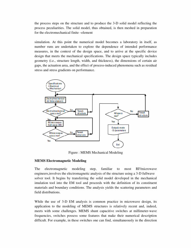
the process steps on the structure and to produce the 3-D solid model reflecting the process peculiarities. The solid model, thus obtained, is then meshed in preparation for the electromechanical finite –element
simulation. At this point the numerical model becomes a laboratory in itself, as number runs are undertaken to explore the dependence of intended performance measures, in the context of the design space, and to arrive at the specific device design that meets the mechanical specifications. The design space typically includes geometry (i.e., structure length, width, and thickness), the dimensions of certain air gaps, the actuation area, and the effect of process-induced phenomena such as residual stress and stress gradients on performance.
Figure : MEMS Mechanical Modeling
MEMS Electromagnetic Modeling
The electromagnetic modeling step, familiar to most RF/microwave engineers,involves the electromagnetic analysis of the structure using a 3-D fullwave solver tool. It begins by transferring the solid model developed in the mechanical imulation tool into the EM tool and proceeds with the definition of its constituent materials and boundary conditions. The analysis yields the scattering parameters and field distributions. While the use of 3-D EM analysis is common practice in microwave design, its application to the modeling of MEMS structures is relatively recent and, indeed, meets with some challenges. MEMS shunt capacitive switches at millimeter-wave frequencies, switches possess some features that make their numerical description difficult. For example, in these switches one can find, simultaneously in the direction
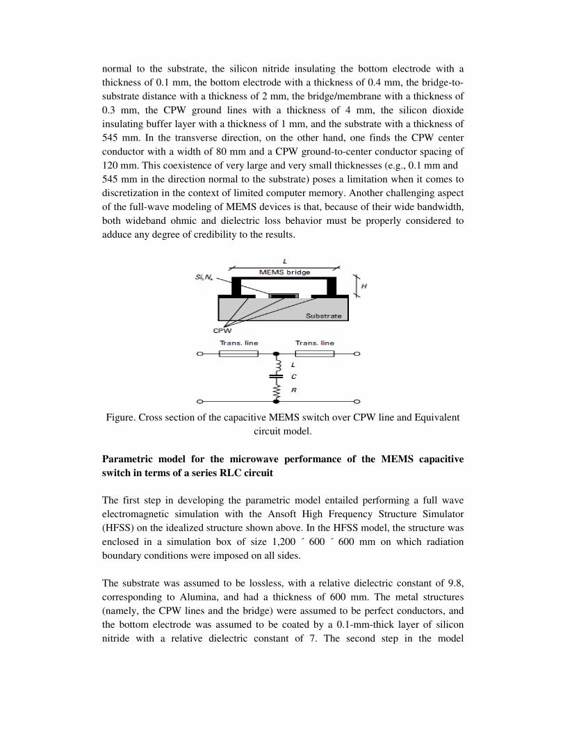
normal to the substrate, the silicon nitride insulating the bottom electrode with a thickness of 0.1 mm, the bottom electrode with a thickness of 0.4 mm, the bridge-to-substrate distance with a thickness of 2 mm, the bridge/membrane with a thickness of 0.3 mm, the CPW ground lines with a thickness of 4 mm, the silicon dioxide insulating buffer layer with a thickness of 1 mm, and the substrate with a thickness of 545 mm. In the transverse direction, on the other hand, one finds the CPW center conductor with a width of 80 mm and a CPW ground-to-center conductor spacing of 120 mm. This coexistence of very large and very small thicknesses (e.g., 0.1 mm and 545 mm in the direction normal to the substrate) poses a limitation when it comes to discretization in the context of limited computer memory. Another challenging aspect of the full-wave modeling of MEMS devices is that, because of their wide bandwidth, both wideband ohmic and dielectric loss behavior must be properly considered to adduce any degree of credibility to the results.
Figure. Cross section of the capacitive MEMS switch over CPW line and Equivalent
circuit model. Parametric model for the microwave performance of the MEMS capacitive
switch in terms of a series RLC circuit
The first step in developing the parametric model entailed performing a full wave electromagnetic simulation with the Ansoft High Frequency Structure Simulator (HFSS) on the idealized structure shown above. In the HFSS model, the structure was enclosed in a simulation box of size 1,200 ´ 600 ´ 600 mm on which radiation boundary conditions were imposed on all sides. The substrate was assumed to be lossless, with a relative dielectric constant of 9.8, corresponding to Alumina, and had a thickness of 600 mm. The metal structures (namely, the CPW lines and the bridge) were assumed to be perfect conductors, and the bottom electrode was assumed to be coated by a 0.1-mm-thick layer of silicon nitride with a relative dielectric constant of 7. The second step in the model
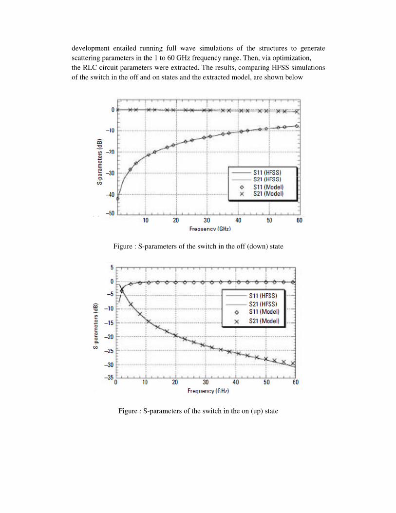
development entailed running full wave simulations of the structures to generate scattering parameters in the 1 to 60 GHz frequency range. Then, via optimization, the RLC circuit parameters were extracted. The results, comparing HFSS simulations of the switch in the off and on states and the extracted model, are shown below
Figure : S-parameters of the switch in the off (down) state
Figure : S-parameters of the switch in the on (up) state

RECONFIGURABLE CIRCUIT ELEMENTS
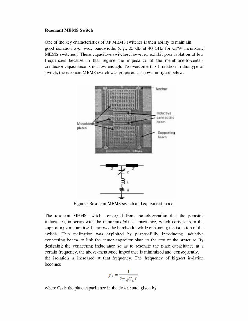
Resonant MEMS Switch
One of the key characteristics of RF MEMS switches is their ability to maintain good isolation over wide bandwidths (e.g., 35 dB at 40 GHz for CPW membrane MEMS switches). These capacitive switches, however, exhibit poor isolation at low frequencies because in that regime the impedance of the membrane-to-center-conductor capacitance is not low enough. To overcome this limitation in this type of switch, the resonant MEMS switch was proposed as shown in figure below.
Figure : Resonant MEMS switch and equivalent model
The resonant MEMS switch emerged from the observation that the parasitic inductance, in series with the membrane/plate capacitance, which derives from the supporting structure itself, narrows the bandwidth while enhancing the isolation of the switch. This realization was exploited by purposefully introducing inductive connecting beams to link the center capacitor plate to the rest of the structure By designing the connecting inductance so as to resonate the plate capacitance at a certain frequency, the above-mentioned impedance is minimized and, consequently, the isolation is increased at that frequency. The frequency of highest isolation becomes
where CD is the plate capacitance in the down state, given by
in down state. where A is the area of overlap of the bridge with the center conductor of theline, td is the thickness of the dielectric protecting the bottom electrode,edielectric constant. L is the parasitic inductance, whichmeasurements or from a full-typical values of 0.2 to 6 pH. high as approximately 24 dB at 13.2 GHz, within a switch 3-mm air-gap structure,thick SixNy insulating layer.
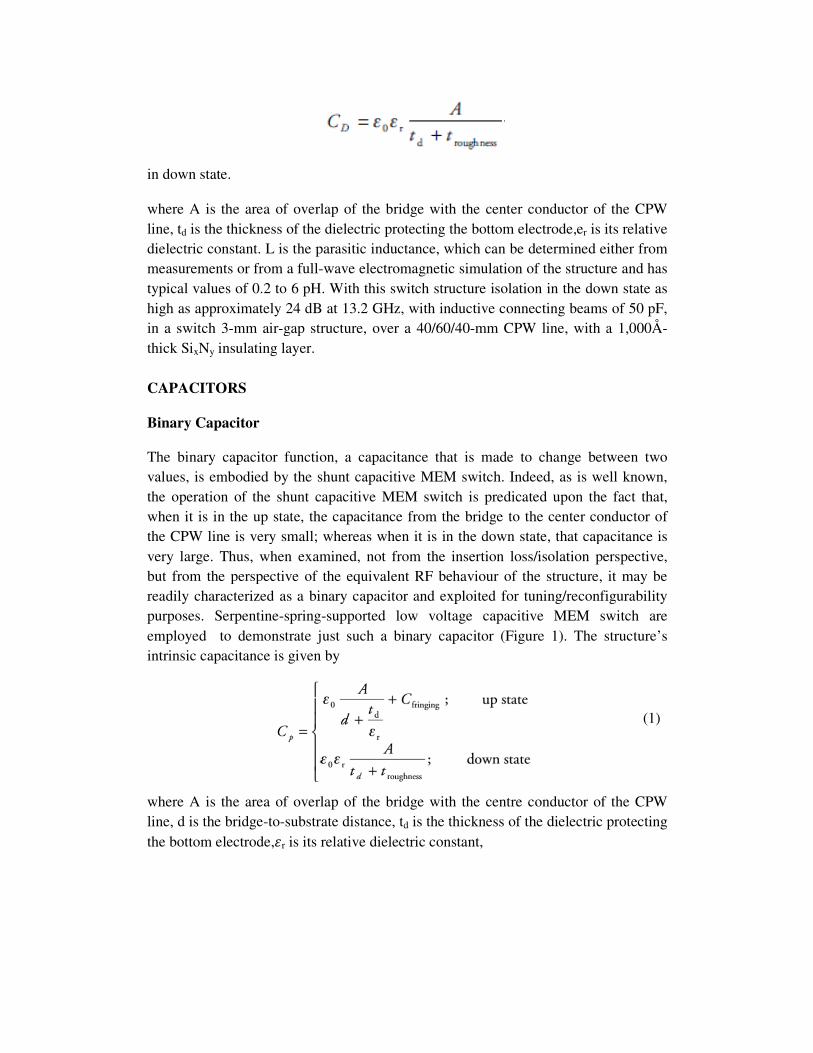
CAPACITORS Binary Capacitor
The binary capacitor function, a capacitance that is made to change between two values, is embodied by the shunt capacitive MEM switch. Indeed, as is well known, the operation of the shunt capacitive MEM switch is predicated upon the fact that, when it is in the up state, the capacitance from the bridge to the center conductor of the CPW line is very small; whereas when it is in the down state, that capacitance is very large. Thus, when examined, not from the insertion loss/isolation perspective, but from the perspective of the equivalent RF behaviour of the structure, it may be readily characterized as a binary capacitor and exploited for tuning/reconfigurability purposes. Serpentine-springemployed to demonstrate just such a binary capacitor (Figure 1). The structure’s intrinsic capacitance is given by
where A is the area of overlap of the bridge with the centre conductor of the CPW line, d is the bridge-to-substrate distance, tthe bottom electrode,r is its relative dielectric constant,
where A is the area of overlap of the bridge with the center conductor of theis the thickness of the dielectric protecting the bottom electrode,er is its relative
dielectric constant. L is the parasitic inductance, which can be determined either from -wave electromagnetic simulation of the structure and has
typical values of 0.2 to 6 pH. With this switch structure isolation in the down state as high as approximately 24 dB at 13.2 GHz, with inductive connecting beams of 50 pF,
gap structure, over a 40/60/40-mm CPW line, with a 1,000Å
The binary capacitor function, a capacitance that is made to change between two is embodied by the shunt capacitive MEM switch. Indeed, as is well known,
the operation of the shunt capacitive MEM switch is predicated upon the fact that, when it is in the up state, the capacitance from the bridge to the center conductor of
is very small; whereas when it is in the down state, that capacitance is very large. Thus, when examined, not from the insertion loss/isolation perspective, but from the perspective of the equivalent RF behaviour of the structure, it may be
terized as a binary capacitor and exploited for tuning/reconfigurability spring-supported low voltage capacitive MEM switch are
employed to demonstrate just such a binary capacitor (Figure 1). The structure’s given by
where A is the area of overlap of the bridge with the centre conductor of the CPW
substrate distance, td is the thickness of the dielectric protecting is its relative dielectric constant,
where A is the area of overlap of the bridge with the center conductor of the CPW is its relative
be determined either from simulation of the structure and has
isolation in the down state as connecting beams of 50 pF,
mm CPW line, with a 1,000Å-
The binary capacitor function, a capacitance that is made to change between two is embodied by the shunt capacitive MEM switch. Indeed, as is well known,
the operation of the shunt capacitive MEM switch is predicated upon the fact that, when it is in the up state, the capacitance from the bridge to the center conductor of
is very small; whereas when it is in the down state, that capacitance is very large. Thus, when examined, not from the insertion loss/isolation perspective, but from the perspective of the equivalent RF behaviour of the structure, it may be
terized as a binary capacitor and exploited for tuning/reconfigurability supported low voltage capacitive MEM switch are
employed to demonstrate just such a binary capacitor (Figure 1). The structure’s
where A is the area of overlap of the bridge with the centre conductor of the CPW is the thickness of the dielectric protecting
(1)
Figure : Capacitive MEMS switch employed as a binary capacitor over a CPW line,and (b) binary capacitor equivalent circuit model
and Cfringing is the fringing capacitance. Depending on the particulars of the implementation (e.g., Figure 1) and the intended application, however, it is worth pointing out that there may be other parasitic elements that would blur the simple capacitive behavior implied by (1), and thus they must be included in its model. For example, Peroulis et al. found that for applications of the binary capacitor in filters, the extra elements in Figure 1(b) must be included. These elements include (1) the resistance and inductance of the bridge, denoted Robtainable from full-wave simulations; (2) the loss in the dielectric insulator coating the bottom electrode, Gp, and given by
where tan is the loss tangent of the dielectric; and (3) the shlL and lR, as represented by their effective series resistance and inductance, RLSL, respectively. Peroulis et al. [8] pointed out that the parasitic inductance is particularly important in the model because its values arein actual filters. Under the short line approximation, assumed by Peroulis et al. [8], the parasitic elements are given by
where α represents the line attenuation constant, usually obtained experimentally, and
Figure : Capacitive MEMS switch employed as a binary capacitor over a CPW line,and (b) binary capacitor equivalent circuit model
is the fringing capacitance. Depending on the particulars of the
implementation (e.g., Figure 1) and the intended application, however, it is worth pointing out that there may be other parasitic elements that would blur the simple
ied by (1), and thus they must be included in its model. For example, Peroulis et al. found that for applications of the binary capacitor in filters, the extra elements in Figure 1(b) must be included. These elements include (1) the
ce of the bridge, denoted Rp and Lp, respectively, and wave simulations; (2) the loss in the dielectric insulator coating
, and given by
is the loss tangent of the dielectric; and (3) the short access lines of length
, as represented by their effective series resistance and inductance, R, respectively. Peroulis et al. [8] pointed out that the parasitic inductance is
particularly important in the model because its values are comparable to those found in actual filters. Under the short line approximation, assumed by Peroulis et al. [8], the parasitic elements are given by
represents the line attenuation constant, usually obtained experimentally, and
(2)
(3)
Figure : Capacitive MEMS switch employed as a binary capacitor over a CPW line,
is the fringing capacitance. Depending on the particulars of the implementation (e.g., Figure 1) and the intended application, however, it is worth pointing out that there may be other parasitic elements that would blur the simple
ied by (1), and thus they must be included in its model. For example, Peroulis et al. found that for applications of the binary capacitor in filters, the extra elements in Figure 1(b) must be included. These elements include (1) the
, respectively, and wave simulations; (2) the loss in the dielectric insulator coating
ort access lines of length , as represented by their effective series resistance and inductance, RSL and
, respectively. Peroulis et al. [8] pointed out that the parasitic inductance is comparable to those found
in actual filters. Under the short line approximation, assumed by Peroulis et al. [8], the
represents the line attenuation constant, usually obtained experimentally, and
(2)
(3)
INDUCTORS
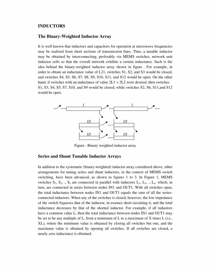
The Binary-Weighted Inductor Array
It is well known that inductors and capacitors for operation at microwave frequencies may be realized from short sections of transmission lines. Thus, a tunable inductor may be obtained by interconnecting, preferably via MEMS switches, network unit inductor cells so that the overall network exhibits a certain inductance. Such is the idea behind the binary-weighted inductor array shown in figure . For example, in order to obtain an inductance value of L21, switches S1, S2, and S3 would be closed, and switches S4, S5, S6, S7, S8, S9, S10, S11, and S12 would be open. On the other hand, if switches with an inductance of value 2L1 + 2L2 were desired, then switches S1, S3, S4, S5, S7, S10, and S9 would be closed, while switches S2, S6, S11,and S12 would be open.
Figure : Binary weighted inductor array
Series and Shunt Tunable Inductor Arrays
In addition to the systematic (binary-weighted) inductor array considered above, other arrangements for tuning series and shunt inductors, in the context of MEMS switch switching, have been advanced, as shown in figures 1 to 3. In Figure 1, MEMS switches S1, S2, ., Sx are connected in parallel with inductors L1, L2, ., Lx, which, in turn, are connected in series between nodes IN1 and OUT1. With all switches open, the total inductance between nodes IN1 and OUT1 equals the sum of all the series-connected inductors. When any of the switches is closed, however, the low impedance of the switch bypasses that of the inductor, in essence short-circuiting it, and the total inductance decreases by that of the shorted inductor. For example, if all inductors have a common value L, then the total inductance between nodes IN1 and OUT1 may be set to be any multiple of L, from a minimum of L to a maximum of X times L (i.e., XL), where the minimum value is obtained by closing all switches but one, and the maximum value is obtained by opening all switches. If all switches are closed, a nearly zero inductance is obtained.
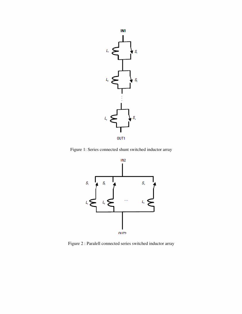
Figure 1: Series connected shunt switched inductor array
Figure 2 : Paralell connected series switched inductor array
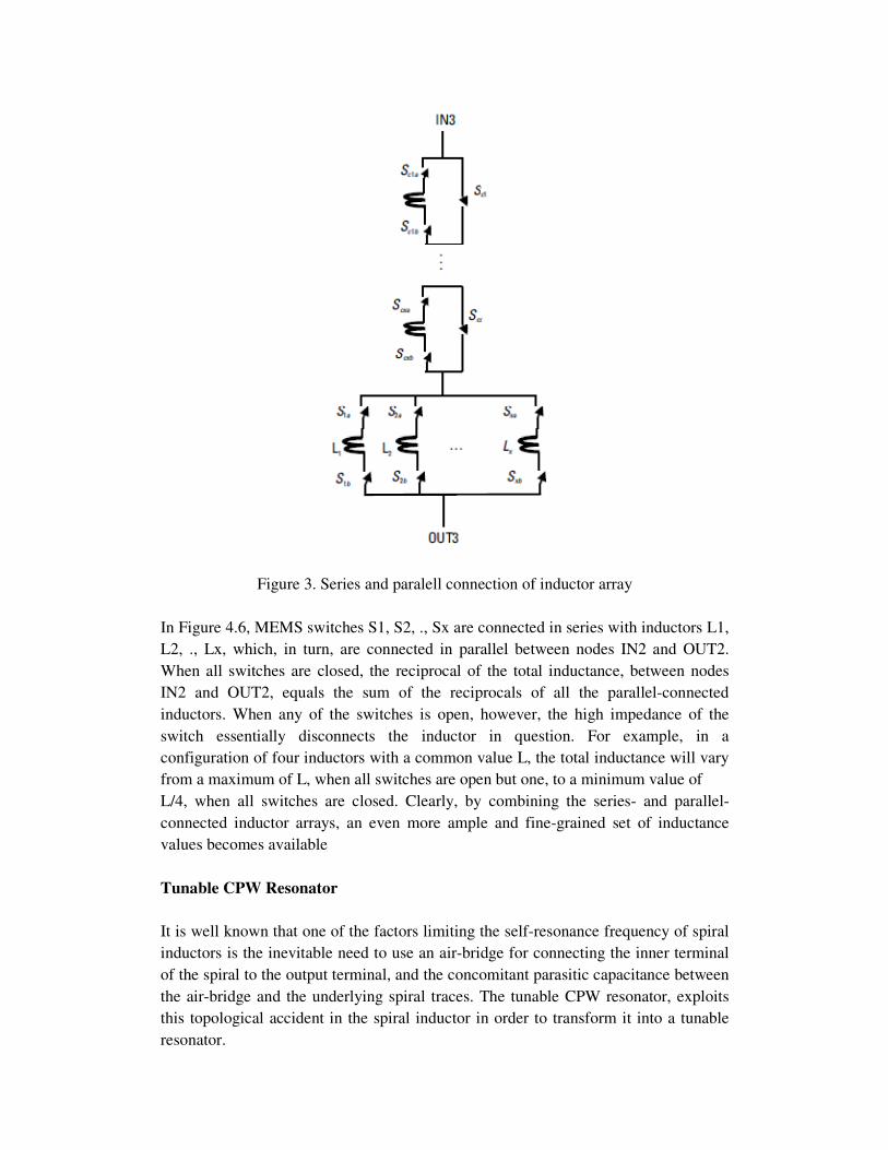
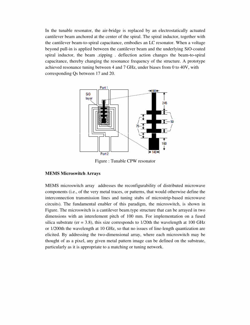
Figure 3. Series and paralell connection of inductor array
In Figure 4.6, MEMS switches S1, S2, ., Sx are connected in series with inductors L1, L2, ., Lx, which, in turn, are connected in parallel between nodes IN2 and OUT2. When all switches are closed, the reciprocal of the total inductance, between nodes IN2 and OUT2, equals the sum of the reciprocals of all the parallel-connected inductors. When any of the switches is open, however, the high impedance of the switch essentially disconnects the inductor in question. For example, in a configuration of four inductors with a common value L, the total inductance will vary from a maximum of L, when all switches are open but one, to a minimum value of L/4, when all switches are closed. Clearly, by combining the series- and parallel-connected inductor arrays, an even more ample and fine-grained set of inductance values becomes available Tunable CPW Resonator
It is well known that one of the factors limiting the self-resonance frequency of spiral inductors is the inevitable need to use an air-bridge for connecting the inner terminal of the spiral to the output terminal, and the concomitant parasitic capacitance between the air-bridge and the underlying spiral traces. The tunable CPW resonator, exploits this topological accident in the spiral inductor in order to transform it into a tunable resonator.
In the tunable resonator, the air-bridge is replaced by an electrostatically actuated cantilever beam anchored at the center of the spiral. The spiral inductor, together with the cantilever beam-to-spiral capacitance, embodies an LC resonator. When a voltage beyond pull-in is applied between the cantilever beam and the underlying SiO-coated spiral inductor, the beam .zipping . deflection action changes the beam-to-spiral capacitance, thereby changing the resonance frequency of the structure. A prototype achieved resonance tuning between 4 and 7 GHz, under biases from 0 to 40V, with corresponding Qs between 17 and 20.
Figure : Tunable CPW resonator
MEMS Microswitch Arrays
MEMS microswitch array addresses the reconfigurability of distributed microwave components (i.e., of the very metal traces, or patterns, that would otherwise define the interconnection transmission lines and tuning stubs of microstrip-based microwave circuits). The fundamental enabler of this paradigm, the microswitch, is shown in Figure. The microswitch is a cantilever beam.type structure that can be arrayed in two dimensions with an interelement pitch of 100 mm. For implementation on a fused silica substrate (er = 3.8), this size corresponds to 1/20th the wavelength at 100 GHz or 1/200th the wavelength at 10 GHz, so that no issues of line-length quantization are elicited. By addressing the two-dimensional array, where each microswitch may be thought of as a pixel, any given metal pattern image can be defined on the substrate, particularly as it is appropriate to a matching or tuning network.
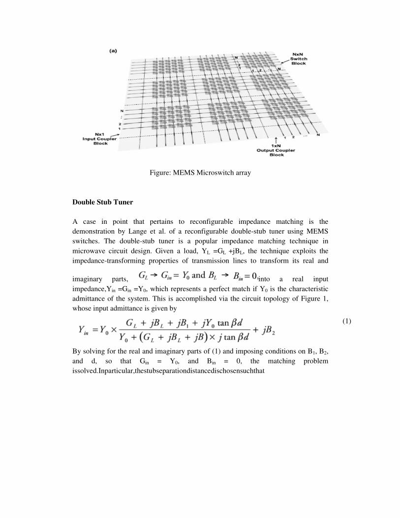
Figure: MEMS Microswitch array
Double Stub Tuner
A case in point that pertains to reconfigurable impedance matching is the demonstration by Lange et al. of a reconfigurable doubleswitches. The double-stub tuner is a microwave circuit design. Given a load, Yimpedance-transforming properties of transmission lines to transform its real and
imaginary parts, impedance,Yin =Gin =Y0, which represents a perfect match if Yadmittance of the system. This is accomplished via the circuit topology of Figure 1, whose input admittance is given by
By solving for the real and imaginary parts of (1) and impoand d, so that Gin = Yissolved.Inparticular,thestubseparationdistancedischosensuchthat
Figure: MEMS Microswitch array
A case in point that pertains to reconfigurable impedance matching is the demonstration by Lange et al. of a reconfigurable double-stub tuner using MEMS
stub tuner is a popular impedance matching technique in microwave circuit design. Given a load, YL =GL +jBL, the technique exploits the
transforming properties of transmission lines to transform its real and
into a real input , which represents a perfect match if Y0 is the characteristic
admittance of the system. This is accomplished via the circuit topology of Figure 1, whose input admittance is given by
By solving for the real and imaginary parts of (1) and imposing conditions on B
= Y0, and Bin = 0, the matching problem issolved.Inparticular,thestubseparationdistancedischosensuchthat
A case in point that pertains to reconfigurable impedance matching is the stub tuner using MEMS
popular impedance matching technique in , the technique exploits the
transforming properties of transmission lines to transform its real and
into a real input is the characteristic
admittance of the system. This is accomplished via the circuit topology of Figure 1,
sing conditions on B1, B2, = 0, the matching problem
(1)
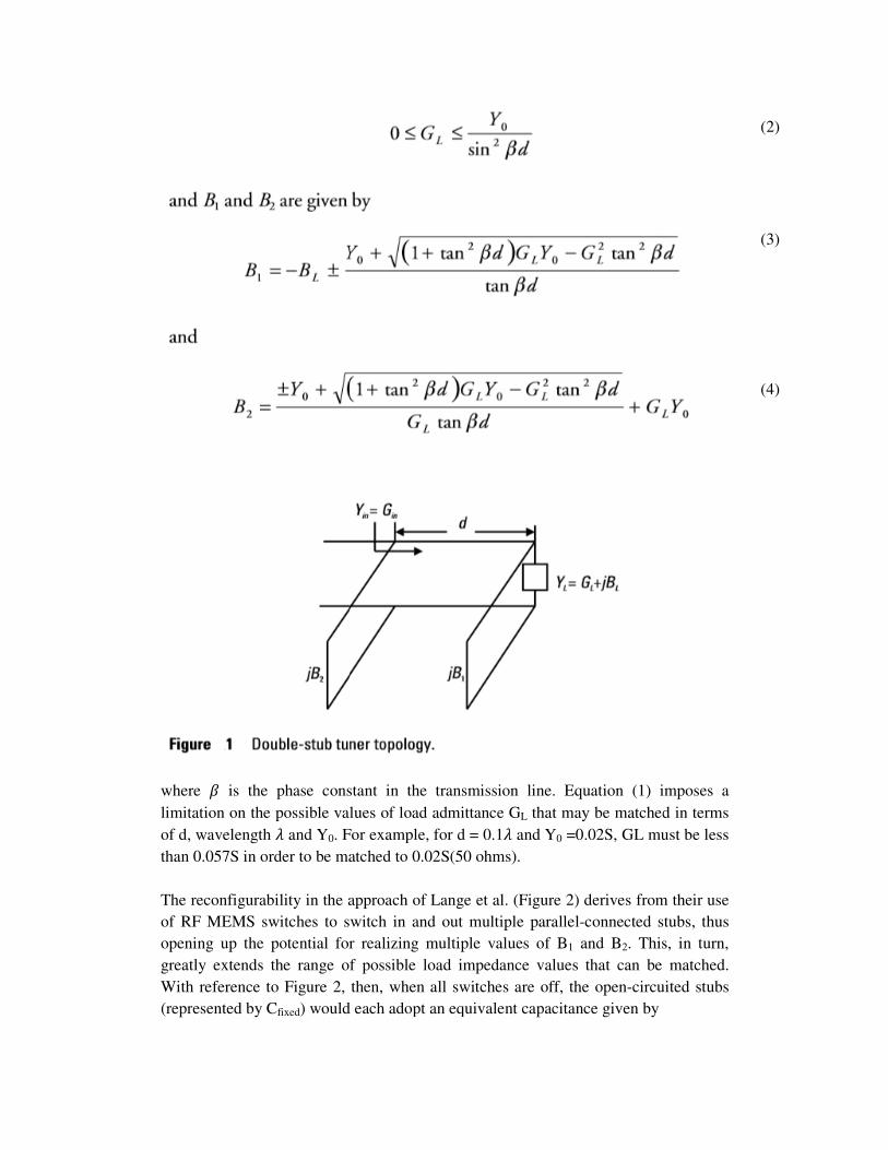
where is the phase constant in the transmission line. Equation (1) imposes a limitation on the possible values of load admittance Gof d, wavelength and Y0. For example, for d = 0.1than 0.057S in order to be matched to 0.02S(50 ohms). The reconfigurability in the approach of Lange et al. (Figure 2) derives from their use of RF MEMS switches to switch in and out multiple parallelopening up the potential for realizing multipgreatly extends the range of possible load impedance values that can be matched. With reference to Figure 2, then, when all switches are off, the open(represented by Cfixed) would each adopt an equiva
is the phase constant in the transmission line. Equation (1) imposes a limitation on the possible values of load admittance GL that may be matched in terms
. For example, for d = 0.1 and Y0 =0.02S, GL must be less n order to be matched to 0.02S(50 ohms).
The reconfigurability in the approach of Lange et al. (Figure 2) derives from their use of RF MEMS switches to switch in and out multiple parallel-connected stubs, thus opening up the potential for realizing multiple values of B1 and B2. This, in turn, greatly extends the range of possible load impedance values that can be matched. With reference to Figure 2, then, when all switches are off, the open-circuited stubs
) would each adopt an equivalent capacitance given by
is the phase constant in the transmission line. Equation (1) imposes a that may be matched in terms
=0.02S, GL must be less
The reconfigurability in the approach of Lange et al. (Figure 2) derives from their use connected stubs, thus
. This, in turn, greatly extends the range of possible load impedance values that can be matched.
circuited stubs
(2)
(3)
(4)
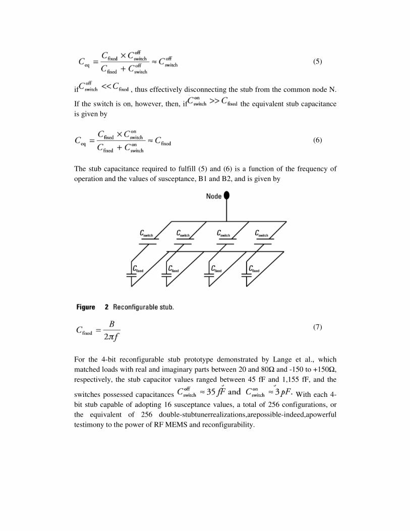
if , thus effectively disconnecting the stub from the common node N.
If the switch is on, however, then, ifis given by
The stub capacitance required to fulfill (5) and (6) is aoperation and the values of susceptance, B1 and B2, and is given by
For the 4-bit reconfigurable stub prototype demonstrated by Lange et al., which matched loads with real and imaginary parts between 20 and 80respectively, the stub capacitor values ranged between 45 fF and 1,155 fF, and the
switches possessed capacitances bit stub capable of adopting 16 susceptance values, a total of 256 configurations, or the equivalent of 256 doubletestimony to the power of RF MEMS and reconfigurability
, thus effectively disconnecting the stub from the common node N.
If the switch is on, however, then, if the equivalent stub capacitance
The stub capacitance required to fulfill (5) and (6) is a function of the frequency of operation and the values of susceptance, B1 and B2, and is given by
bit reconfigurable stub prototype demonstrated by Lange et al., which matched loads with real and imaginary parts between 20 and 80Ω and -150 to +150respectively, the stub capacitor values ranged between 45 fF and 1,155 fF, and the
ssessed capacitances With each 4bit stub capable of adopting 16 susceptance values, a total of 256 configurations, or the equivalent of 256 double-stubtunerrealizations,arepossible-indeed,apowerful testimony to the power of RF MEMS and reconfigurability.
, thus effectively disconnecting the stub from the common node N.
the equivalent stub capacitance
function of the frequency of
bit reconfigurable stub prototype demonstrated by Lange et al., which 150 to +150Ω,
respectively, the stub capacitor values ranged between 45 fF and 1,155 fF, and the
With each 4-bit stub capable of adopting 16 susceptance values, a total of 256 configurations, or
indeed,apowerful
(5)
(6)
(7)
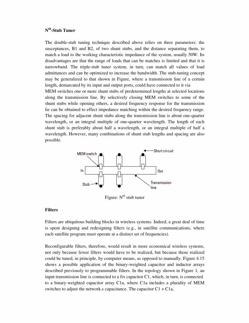
Nth
-Stub Tuner
The double-stub tuning technique described above relies on three parameters: the susceptances, B1 and B2, of two shunt stubs, and the distance separating them, to match a load to the working characteristic impedance of the system, usually 50W. Its disadvantages are that the range of loads that can be matches is limited and that it is narrowband. The triple-stub tuner system, in turn, can match all values of load admittances and can be optimized to increase the bandwidth. The stub-tuning concept may be generalized to that shown in Figure, where a transmission line of a certain length, demarcated by its input and output ports, could have connected to it via MEM switches one or more shunt stubs of predetermined lengths at selected locations along the transmission line. By selectively closing MEM switches to some of the shunt stubs while opening others, a desired frequency response for the transmission lie can be obtained to effect impedance matching within the desired frequency range. The spacing for adjacent shunt stubs along the transmission line is about one-quarter wavelength, or an integral multiple of one-quarter wavelength. The length of each shunt stub is preferably about half a wavelength, or an integral multiple of half a wavelength. However, many combinations of shunt stub lengths and spacing are also possible.
Figure: Nth stub tuner
Filters
Filters are ubiquitous building blocks in wireless systems. Indeed, a great deal of time is spent designing and redesigning filters (e.g., in satellite communications, where each satellite program must operate at a distinct set of frequencies). Reconfigurable filters, therefore, would result in more economical wireless systems, not only because fewer filters would have to be realized, but because those realized could be tuned, in principle, by computer means, as opposed to manually. Figure 4.15 shows a possible application of the binary-weighted capacitor and inductor arrays described previously to programmable filters. In the topology shown in Figure 1, an input transmission line is connected to a fix capacitor C1, which, in turn, is connected to a binary-weighted capacitor array C1a, where C1a includes a plurality of MEM switches to adjust the network.s capacitance. The capacitor C1 + C1a,
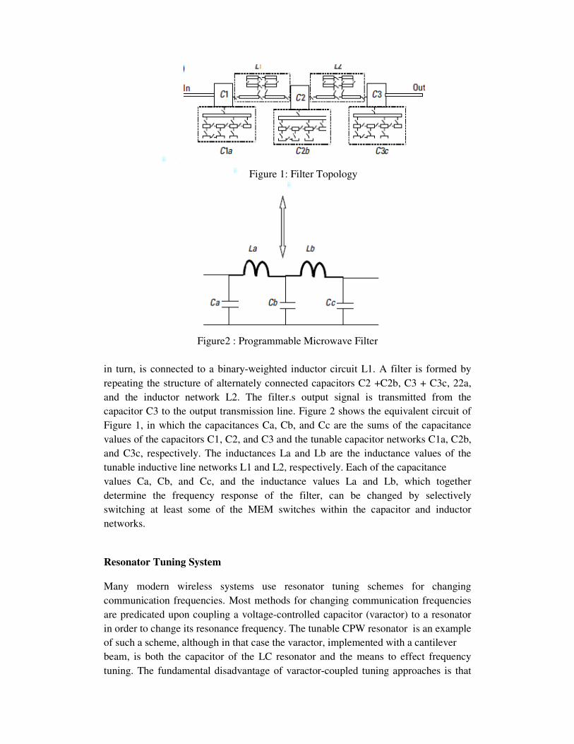
Figure 1: Filter Topology
Figure2 : Programmable Microwave Filter
in turn, is connected to a binary-weighted inductor circuit L1. A filter is formed by repeating the structure of alternately connected capacitors C2 +C2b, C3 + C3c, 22a, and the inductor network L2. The filter.s output signal is transmitted from the capacitor C3 to the output transmission line. Figure 2 shows the equivalent circuit of Figure 1, in which the capacitances Ca, Cb, and Cc are the sums of the capacitance values of the capacitors C1, C2, and C3 and the tunable capacitor networks C1a, C2b, and C3c, respectively. The inductances La and Lb are the inductance values of the tunable inductive line networks L1 and L2, respectively. Each of the capacitance values Ca, Cb, and Cc, and the inductance values La and Lb, which together determine the frequency response of the filter, can be changed by selectively switching at least some of the MEM switches within the capacitor and inductor networks.
Resonator Tuning System
Many modern wireless systems use resonator tuning schemes for changing communication frequencies. Most methods for changing communication frequencies are predicated upon coupling a voltage-controlled capacitor (varactor) to a resonator in order to change its resonance frequency. The tunable CPW resonator is an example of such a scheme, although in that case the varactor, implemented with a cantilever beam, is both the capacitor of the LC resonator and the means to effect frequency tuning. The fundamental disadvantage of varactor-coupled tuning approaches is that
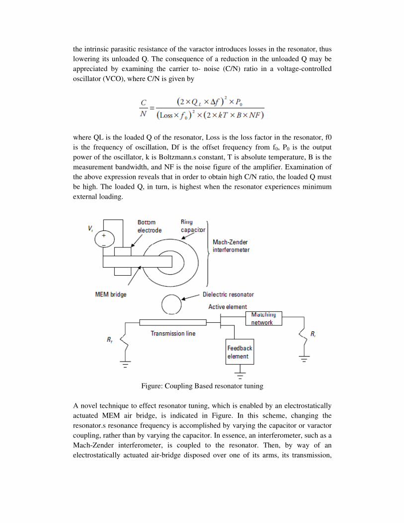
the intrinsic parasitic resistance of the varactor introduces losses in the resonator, thus lowering its unloaded Q. The consequence of a reduction in the unloaded Q may be appreciated by examining the carrier to- noise (C/N) ratio in a voltage-controlled oscillator (VCO), where C/N is given by
where QL is the loaded Q of the resonator, Loss is the loss factor in the resonator, f0 is the frequency of oscillation, Df is the offset frequency from f0, P0 is the output power of the oscillator, k is Boltzmann.s constant, T is absolute temperature, B is the measurement bandwidth, and NF is the noise figure of the amplifier. Examination of the above expression reveals that in order to obtain high C/N ratio, the loaded Q must be high. The loaded Q, in turn, is highest when the resonator experiences minimum external loading.
Figure: Coupling Based resonator tuning
A novel technique to effect resonator tuning, which is enabled by an electrostatically actuated MEM air bridge, is indicated in Figure. In this scheme, changing the resonator.s resonance frequency is accomplished by varying the capacitor or varactor coupling, rather than by varying the capacitor. In essence, an interferometer, such as a Mach-Zender interferometer, is coupled to the resonator. Then, by way of an electrostatically actuated air-bridge disposed over one of its arms, its transmission,
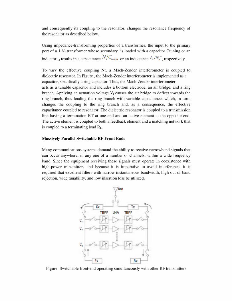
and consequently its coupling to the resonator, changes the resonance frequency of the resonator as described below. Using impedance-transforming properties of a transformer, the input to the primary port of a 1:Nt transformer whose secondary is loaded with a capacitor Ctuning or an
inductor Lt results in a capacitance or an inductance , respectively. To vary the effective coupling Nt, a Mach-Zender interferometer is coupled to dielectric resonator. In Figure , the Mach-Zender interferometer is implemented as a capacitor, specifically a ring capacitor. Thus, the Mach-Zender interferometer acts as a tunable capacitor and includes a bottom electrode, an air bridge, and a ring branch. Applying an actuation voltage Vt causes the air bridge to deflect towards the ring branch, thus loading the ring branch with variable capacitance, which, in turn, changes the coupling to the ring branch and, as a consequence, the effective capacitance coupled to resonator. The dielectric resonator is coupled to a transmission line having a termination RT at one end and an active element at the opposite end. The active element is coupled to both a feedback element and a matching network that is coupled to a terminating load RL. Massively Parallel Switchable RF Front Ends Many communications systems demand the ability to receive narrowband signals that can occur anywhere, in any one of a number of channels, within a wide frequency band. Since the equipment receiving these signals must operate in coexistence with high-power transmitters and because it is imperative to avoid interference, it is required that excellent filters with narrow instantaneous bandwidth, high out-of-band rejection, wide tunability, and low insertion loss be utilized.
Figure: Switchable front-end operating simultaneously with other RF transmitters
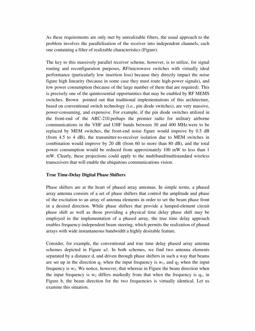
As these requirements are only met by unrealizable filters, the usual approach to the problem involves the parallelization of the receiver into independent channels, each one containing a filter of realizable characteristics (Figure). The key to this massively parallel receiver scheme, however, is to utilize, for signal routing and reconfiguration purposes, RF/microwave switches with virtually ideal performance (particularly low insertion loss) because they directly impact the noise figure high linearity (because in some case they must route high-power signals), and low power consumption (because of the large number of them that are required). This is precisely one of the quintessential opportunities that may be enabled by RF MEMS switches. Brown pointed out that traditional implementations of this architecture, based on conventional switch technology (i.e., pin diode switches), are very massive, power-consuming, and expensive. For example, if the pin diode switches utilized in the front-end of the ARC-210.perhaps the premier radio for military airborne communications in the VHF and UHF bands between 30 and 400 MHz.were to be replaced by MEM switches, the front-end noise figure would improve by 0.5 dB (from 4.5 to 4 dB), the transmitter-to-receiver isolation due to MEM switches in combination would improve by 20 dB (from 60 to more than 80 dB), and the total power consumption would be reduced from approximately 100 mW to less than 1 mW. Clearly, these projections could apply to the multiband/multistandard wireless transceivers that will enable the ubiquitous communications vision. True Time-Delay Digital Phase Shifters
Phase shifters are at the heart of phased array antennas. In simple terms, a phased array antenna consists of a set of phase shifters that control the amplitude and phase of the excitation to an array of antenna elements in order to set the beam phase front in a desired direction. While phase shifters that provide a lumped-element circuit phase shift as well as those providing a physical time delay phase shift may be employed in the implementation of a phased array, the true time delay approach enables frequency-independent beam steering, which permits the realization of phased arrays with wide instantaneous bandwidth a highly desirable feature. Consider, for example, the conventional and true time delay phased array antenna schemes depicted in Figure a1. In both schemes, we find two antenna elements separated by a distance d, and driven through phase shifters in such a way that beams are set up in the direction q1 when the input frequency is w1, and q2 when the input frequency is w2. We notice, however, that whereas in Figure the beam direction when the input frequency is w2 differs markedly from that when the frequency is q1, in Figure b, the beam direction for the two frequencies is virtually identical. Let us examine this situation.
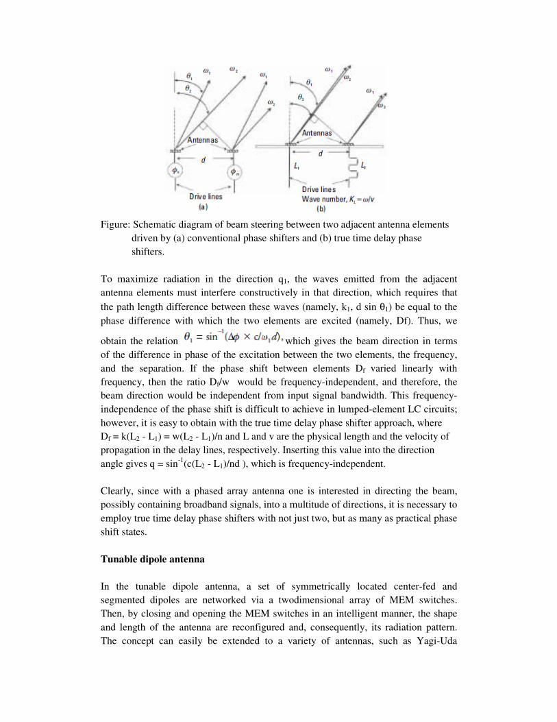
Figure: Schematic diagram of beam steering between two adjacent antenna elements driven by (a) conventional phase shifters and (b) true time delay phase shifters. To maximize radiation in the direction q1, the waves emitted from the adjacent antenna elements must interfere constructively in that direction, which requires that the path length difference between these waves (namely, k1, d sin θ1) be equal to the phase difference with which the two elements are excited (namely, Df). Thus, we
obtain the relation which gives the beam direction in terms of the difference in phase of the excitation between the two elements, the frequency, and the separation. If the phase shift between elements Df varied linearly with frequency, then the ratio Df/w would be frequency-independent, and therefore, the beam direction would be independent from input signal bandwidth. This frequency-independence of the phase shift is difficult to achieve in lumped-element LC circuits; however, it is easy to obtain with the true time delay phase shifter approach, where Df = k(L2 - L1) = w(L2 - L1)/n and L and v are the physical length and the velocity of propagation in the delay lines, respectively. Inserting this value into the direction angle gives q = sin-1(c(L2 - L1)/nd ), which is frequency-independent. Clearly, since with a phased array antenna one is interested in directing the beam, possibly containing broadband signals, into a multitude of directions, it is necessary to employ true time delay phase shifters with not just two, but as many as practical phase shift states. Tunable dipole antenna
In the tunable dipole antenna, a set of symmetrically located center-fed and segmented dipoles are networked via a twodimensional array of MEM switches. Then, by closing and opening the MEM switches in an intelligent manner, the shape and length of the antenna are reconfigured and, consequently, its radiation pattern. The concept can easily be extended to a variety of antennas, such as Yagi-Uda
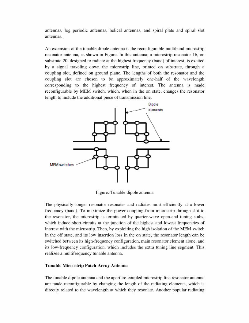
antennas, log periodic antennas, helical antennas, and spiral plate and spiral slot antennas. An extension of the tunable dipole antenna is the reconfigurable multiband microstrip resonator antenna, as shown in Figure. In this antenna, a microstrip resonator 16, on substrate 20, designed to radiate at the highest frequency (band) of interest, is excited by a signal traveling down the microstrip line, printed on substrate, through a coupling slot, defined on ground plane. The lengths of both the resonator and the coupling slot are chosen to be approximately one-half of the wavelength corresponding to the highest frequency of interest. The antenna is made reconfigurable by MEM switch, which, when in the on state, changes the resonator length to include the additional piece of transmission line.
Figure: Tunable dipole antenna
The physically longer resonator resonates and radiates most efficiently at a lower frequency (band). To maximize the power coupling from microstrip through slot to the resonator, the microstrip is terminated by quarter-wave open-end tuning stubs, which induce short-circuits at the junction of the highest and lowest frequencies of interest with the microstrip. Then, by exploiting the high isolation of the MEM switch in the off state, and its low insertion loss in the on state, the resonator length can be switched between its high-frequency configuration, main resonator element alone, and its low-frequency configuration, which includes the extra tuning line segment. This realizes a multifrequency tunable antenna. Tunable Microstrip Patch-Array Antenna
The tunable dipole antenna and the aperture-coupled microstrip line resonator antenna are made reconfigurable by changing the length of the radiating elements, which is directly related to the wavelength at which they resonate. Another popular radiating
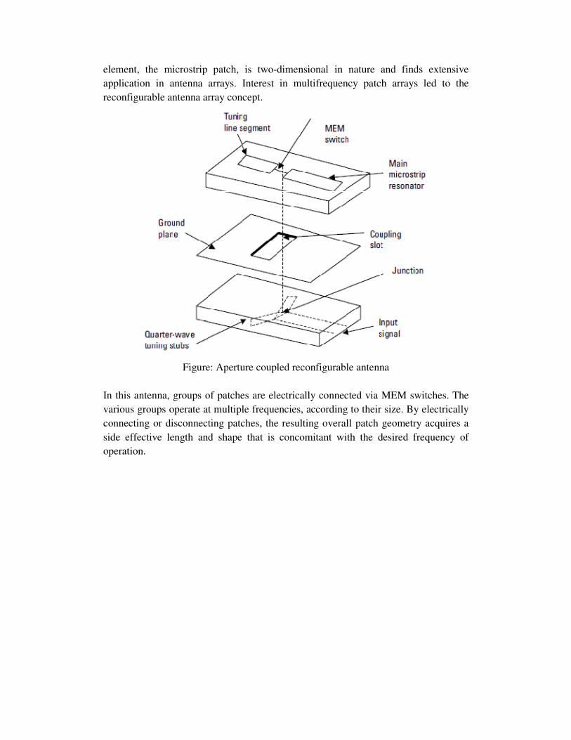
element, the microstrip patch, is two-dimensional in nature and finds extensive application in antenna arrays. Interest in multifrequency patch arrays led to the reconfigurable antenna array concept.
Figure: Aperture coupled reconfigurable antenna
In this antenna, groups of patches are electrically connected via MEM switches. The various groups operate at multiple frequencies, according to their size. By electrically connecting or disconnecting patches, the resulting overall patch geometry acquires a side effective length and shape that is concomitant with the desired frequency of operation.

PHASE SHIFTER AND RF MEMS OSCILLATOR
X band and Ka band millimeter wave micromachined tunable filter
The motivations for developing tunable filters might be traced to three factors: cost, weight, and power dissipation. In modern satellite communications, for instance, where an enormous number of filters are employed, there is extreme interest in minimizing both manufacturing cost, weight, and power consumption. The potential of MEMS technology to permit the batch fabrication of tunable filters is rather appealing, as these might in principle obviatetheneedfor expensive manualtuningin favour ofelectronictuning during system integration and alignment, thus reducing cost. On the other hand, the availability of inexpensive tunable filters opens up new opportunities, not only for novel systems architectures, but, by increasing filter functionality, thus reducing the number of individual filters needed, which reduces overall weight. Finally, since MEMS avails itself of electrostatic schemes for tuning, the power dissipation incurred in implementing tunability is negligible.
Specifications and Topology
Two filters intended for application in highly integrated transmitters and receivers utilized in millimeter-wave multiband communication systems were implemented: a lumped-element version with a 4.7% bandwidth, centered at 26.8 GHz, and a coupled-resonator version with a 8.5% bandwidth, centered at 30.6 GHz. The filter topologies are shown in Figure 1. In the lumped-element version [Figure 1 (a)], the LC resonators were implemented as p-networks with series spiral inductors and shunt capacitors implemented with micromachined cantilever-type varactors. In the coupled distributed resonator version [Figure 1(b)], the resonators were implemented by half-wavelength resonators terminated in varactor connected to ground.Thus,byvaryingthecapacitanceofthevaractors,theeffectiveelectrical length of the resonators deviated from half-wavelength and tuning is affected. Circuit Design and Implementation
The filters were implemented in grounded coplanar waveguide (GCPW) media (Figure 2), and their design was carried out via a full-wave electromagnetic simulator. For the lumped-element realization, the simulation entailed varying the inductive (magnetic) coupling between the spiral inductors of the LC resonators, which was achieved by optimizing the filter response as a function of the separation between the inductors. The half-wavelength resonator-coupled filter version can be designed using coupler synthesis tools and fine-tuned with the full-wave solver. In addition, in order
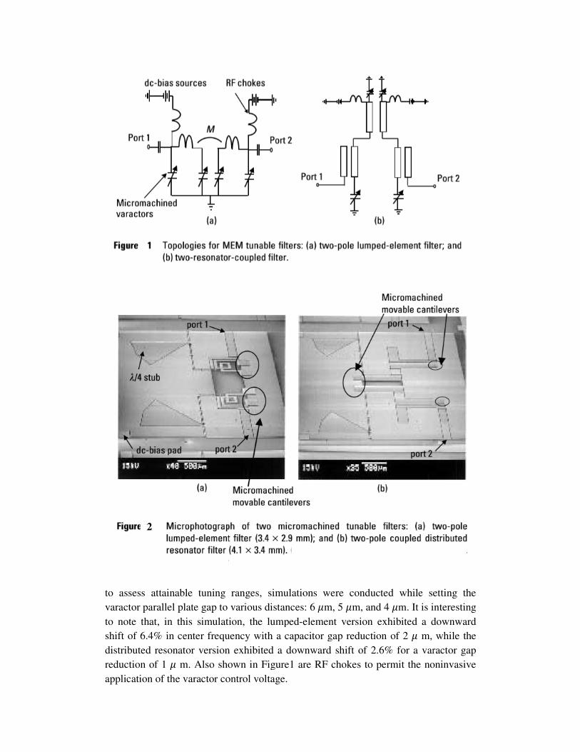
to assess attainable tuning ranges, simulations were conducted while setting the varactor parallel plate gap to various distances: 6 to note that, in this simulation, the lumpedshift of 6.4% in center frequency with a capacitor gap reduction of 2 distributed resonator version exhibited a downward shift of 2.6% for a varactor gap reduction of 1 m. Also shown in Figure1application of the varactor control voltage.
2
to assess attainable tuning ranges, simulations were conducted while setting the varactor parallel plate gap to various distances: 6 m, 5 m, and 4 m. It is interesting to note that, in this simulation, the lumped-element version exhibited a downward shift of 6.4% in center frequency with a capacitor gap reduction of 2 m, while the distributed resonator version exhibited a downward shift of 2.6% for a varactor gap
m. Also shown in Figure1 are RF chokes to permit the noninvasivevaractor control voltage.
to assess attainable tuning ranges, simulations were conducted while setting the m. It is interesting
element version exhibited a downward m, while the
distributed resonator version exhibited a downward shift of 2.6% for a varactor gap noninvasive
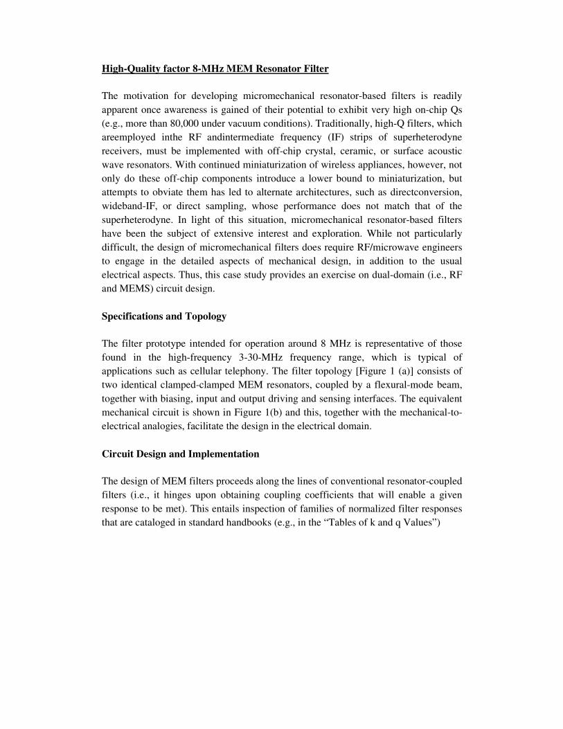
High-Quality factor 8-MHz MEM Resonator Filter
The motivation for developing micromechanical resonator-based filters is readily apparent once awareness is gained of their potential to exhibit very high on-chip Qs (e.g., more than 80,000 under vacuum conditions). Traditionally, high-Q filters, which areemployed inthe RF andintermediate frequency (IF) strips of superheterodyne receivers, must be implemented with off-chip crystal, ceramic, or surface acoustic wave resonators. With continued miniaturization of wireless appliances, however, not only do these off-chip components introduce a lower bound to miniaturization, but attempts to obviate them has led to alternate architectures, such as directconversion, wideband-IF, or direct sampling, whose performance does not match that of the superheterodyne. In light of this situation, micromechanical resonator-based filters have been the subject of extensive interest and exploration. While not particularly difficult, the design of micromechanical filters does require RF/microwave engineers to engage in the detailed aspects of mechanical design, in addition to the usual electrical aspects. Thus, this case study provides an exercise on dual-domain (i.e., RF and MEMS) circuit design. Specifications and Topology
The filter prototype intended for operation around 8 MHz is representative of those found in the high-frequency 3-30-MHz frequency range, which is typical of applications such as cellular telephony. The filter topology [Figure 1 (a)] consists of two identical clamped-clamped MEM resonators, coupled by a flexural-mode beam, together with biasing, input and output driving and sensing interfaces. The equivalent mechanical circuit is shown in Figure 1(b) and this, together with the mechanical-to-electrical analogies, facilitate the design in the electrical domain. Circuit Design and Implementation
The design of MEM filters proceeds along the lines of conventional resonator-coupled filters (i.e., it hinges upon obtaining coupling coefficients that will enable a given response to be met). This entails inspection of families of normalized filter responses that are cataloged in standard handbooks (e.g., in the “Tables of k and q Values”)
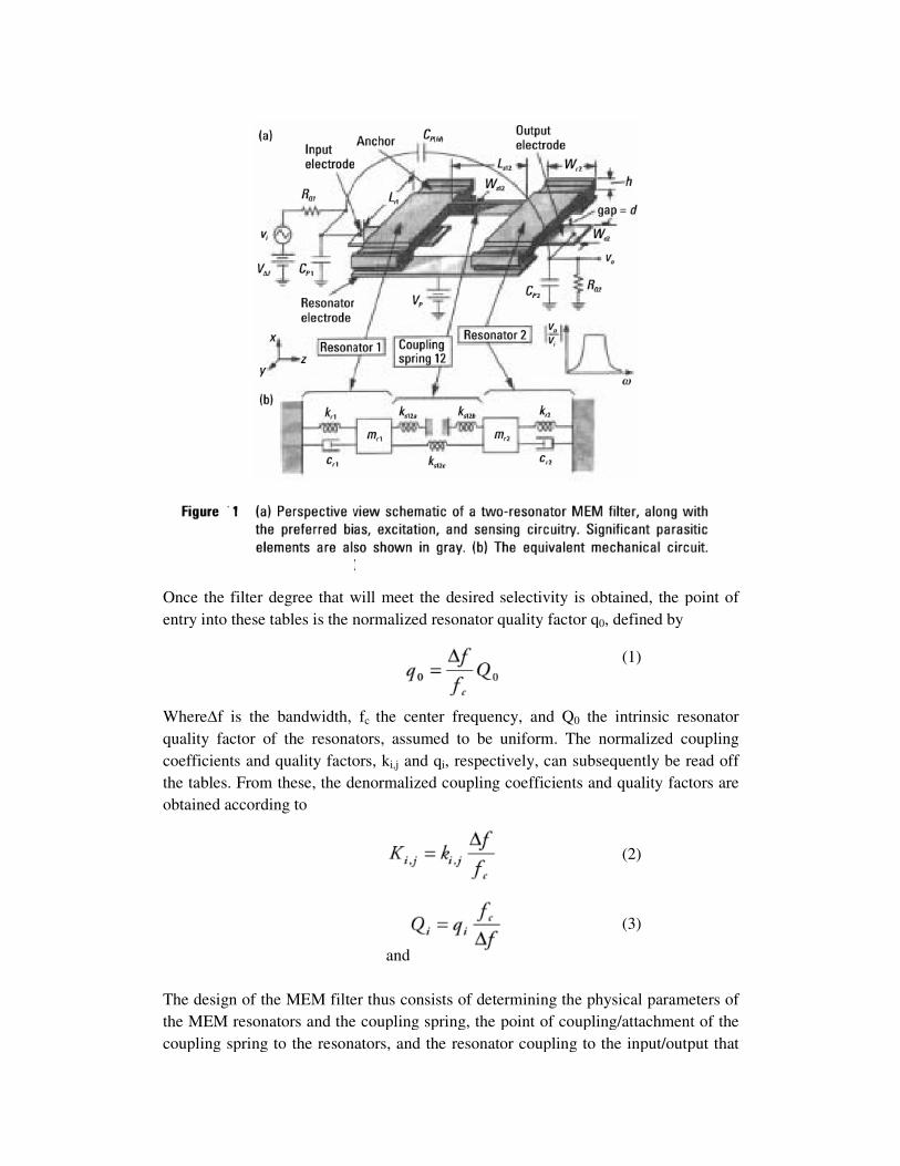
Once the filter degree that will meet the desired selectivity is obtained, the point of entry into these tables is the normalized resonator quality factor q
Where∆f is the bandwidth, fquality factor of the resonators, assumed to be uniform. The normalized coupling coefficients and quality factors, kthe tables. From these, the denormalized coupling coefficients and quality factors are obtained according to
The design of the MEM filter thus consists of determining the physical parameters of the MEM resonators and the coupling spring, the point of coupling/attachment of the coupling spring to the resonators, and the resonator coupling to
will meet the desired selectivity is obtained, the point of entry into these tables is the normalized resonator quality factor q0, defined by
f is the bandwidth, fc the center frequency, and Q0 the intrinsic resonator
esonators, assumed to be uniform. The normalized coupling coefficients and quality factors, ki,j and qi, respectively, can subsequently be read off the tables. From these, the denormalized coupling coefficients and quality factors are
and
The design of the MEM filter thus consists of determining the physical parameters of the MEM resonators and the coupling spring, the point of coupling/attachment of the coupling spring to the resonators, and the resonator coupling to the input/output that
(1)
(2)
(3)
will meet the desired selectivity is obtained, the point of
, defined by
the intrinsic resonator esonators, assumed to be uniform. The normalized coupling
, respectively, can subsequently be read off the tables. From these, the denormalized coupling coefficients and quality factors are
The design of the MEM filter thus consists of determining the physical parameters of the MEM resonators and the coupling spring, the point of coupling/attachment of the
the input/output that
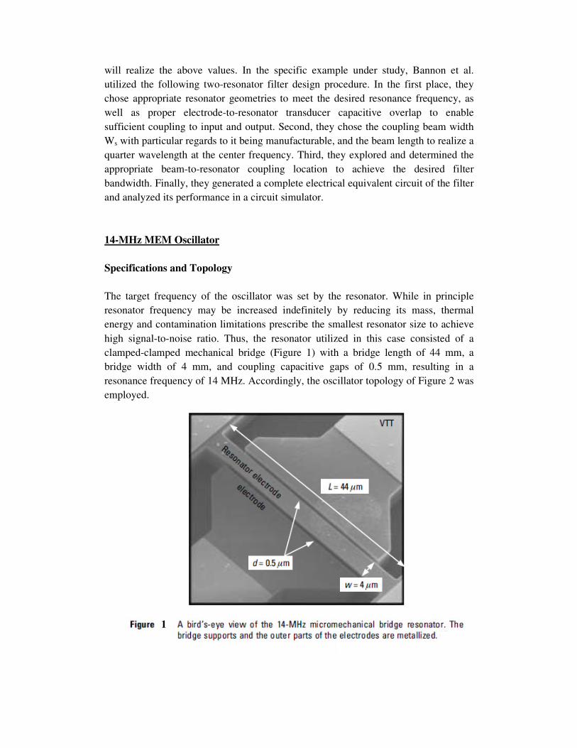
will realize the above values. In the specific example under study, Bannon et al. utilized the following two-resonator filter design procedure. In the first place, they chose appropriate resonator geometries to meet the desired resonance frequency, as well as proper electrode-to-resonator transducer capacitive overlap to enable sufficient coupling to input and output. Second, they chose the coupling beam width Ws with particular regards to it being manufacturable, and the beam length to realize a quarter wavelength at the center frequency. Third, they explored and determined the appropriate beam-to-resonator coupling location to achieve the desired filter bandwidth. Finally, they generated a complete electrical equivalent circuit of the filter and analyzed its performance in a circuit simulator.
14-MHz MEM Oscillator
Specifications and Topology
The target frequency of the oscillator was set by the resonator. While in principle resonator frequency may be increased indefinitely by reducing its mass, thermal energy and contamination limitations prescribe the smallest resonator size to achieve high signal-to-noise ratio. Thus, the resonator utilized in this case consisted of a clamped-clamped mechanical bridge (Figure 1) with a bridge length of 44 mm, a bridge width of 4 mm, and coupling capacitive gaps of 0.5 mm, resulting in a resonance frequency of 14 MHz. Accordingly, the oscillator topology of Figure 2 was employed.
1
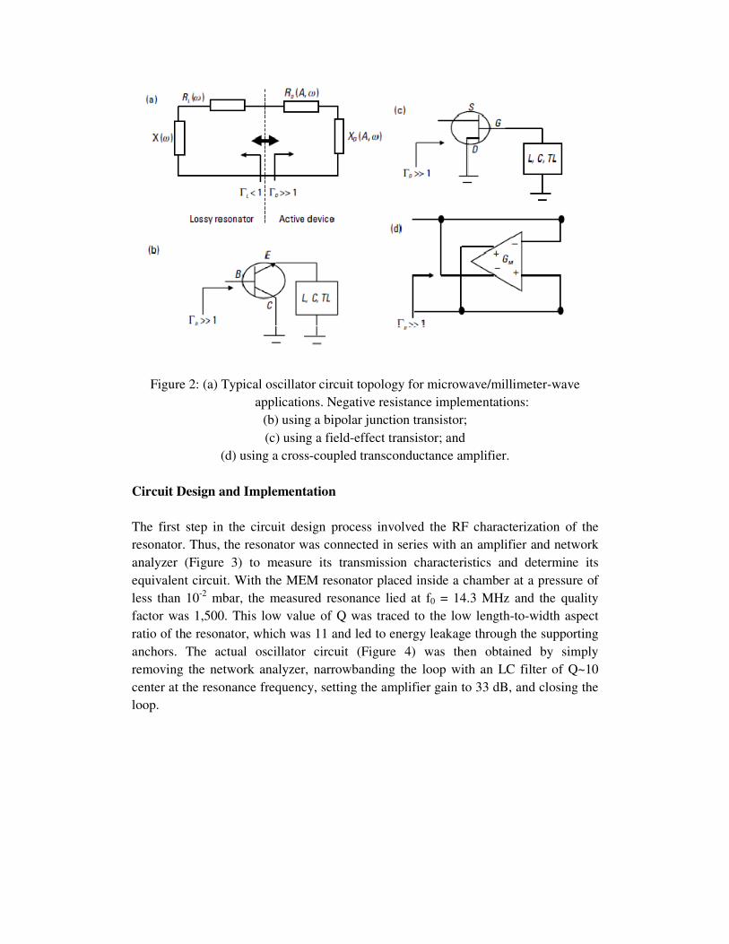
Figure 2: (a) Typical oscillator circuit topology for microwave/millimeter-wave applications. Negative resistance implementations:
(b) using a bipolar junction transistor; (c) using a field-effect transistor; and
(d) using a cross-coupled transconductance amplifier.
Circuit Design and Implementation
The first step in the circuit design process involved the RF characterization of the resonator. Thus, the resonator was connected in series with an amplifier and network analyzer (Figure 3) to measure its transmission characteristics and determine its equivalent circuit. With the MEM resonator placed inside a chamber at a pressure of less than 10-2 mbar, the measured resonance lied at f0 = 14.3 MHz and the quality factor was 1,500. This low value of Q was traced to the low length-to-width aspect ratio of the resonator, which was 11 and led to energy leakage through the supporting anchors. The actual oscillator circuit (Figure 4) was then obtained by simply removing the network analyzer, narrowbanding the loop with an LC filter of Q~10 center at the resonance frequency, setting the amplifier gain to 33 dB, and closing the loop.
Figure 3: (a) Resonator characterization setup; and (b) resonator equivalent circuit:
Figure 4: A 14 MHz RF MEM Oscillator
Ka-Band Micromachined Cavity Oscillator
The Ka-band oscillator was intended for low-cost emerging millimeter-wave commercial applications. In particular, it was directed at solving the problems usually found in dielectric resonator-stabilized oscillators (DROs) and conventional machined cavity-stabilized oscillators, whose usage dominates in these applications. Meeting noise performance specifications is possible with DROs, although at the expense of increased cost due to the high precision with which puck placement must be made, particularly at the higher frequencies. Similarly, the costs incurred in performing conventional high-precision machining to make small cavities are inconsistent with high yield and low-cost manufacturability. By exploiting bulk micromachining techniques, the oscillator topology shown in Figure 1 was demonstrated. In terms of the topology introduced earlier, the active device is realized by a FET-based MMIC, and the lossy resonator is realized by the micromachined cavity.
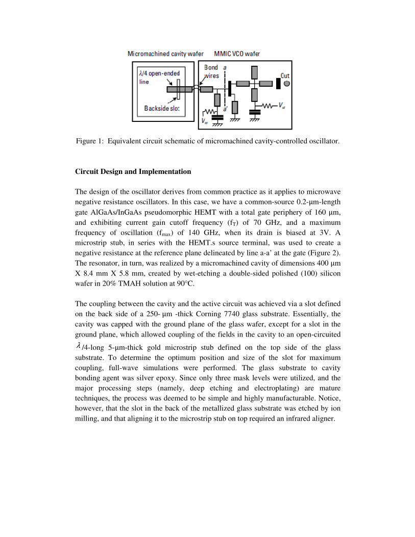
Figure 1: Equivalent circuit schematic of micromachined cavity-controlled oscillator. Circuit Design and Implementation
The design of the oscillator derives from common practice as it applies to microwave negative resistance oscillators. In this case, we have a common-source 0.2-μm-length gate AlGaAs/InGaAs pseudomorphic HEMT with a total gate periphery of 160 μm, and exhibiting current gain cutoff frequency (fT) of 70 GHz, and a maximum frequency of oscillation (fmax) of 140 GHz, when its drain is biased at 3V. A microstrip stub, in series with the HEMT.s source terminal, was used to create a negative resistance at the reference plane delineated by line a-a’ at the gate (Figure 2). The resonator, in turn, was realized by a micromachined cavity of dimensions 400 μm X 8.4 mm X 5.8 mm, created by wet-etching a double-sided polished (100) silicon wafer in 20% TMAH solution at 90°C. The coupling between the cavity and the active circuit was achieved via a slot defined on the back side of a 250-μm -thick Corning 7740 glass substrate. Essentially, the cavity was capped with the ground plane of the glass wafer, except for a slot in the ground plane, which allowed coupling of the fields in the cavity to an open-circuited
λ /4-long 5-μm-thick gold microstrip stub defined on the top side of the glass substrate. To determine the optimum position and size of the slot for maximum coupling, full-wave simulations were performed. The glass substrate to cavity bonding agent was silver epoxy. Since only three mask levels were utilized, and the major processing steps (namely, deep etching and electroplating) are mature techniques, the process was deemed to be simple and highly manufacturable. Notice, however, that the slot in the back of the metallized glass substrate was etched by ion milling, and that aligning it to the microstrip stub on top required an infrared aligner.
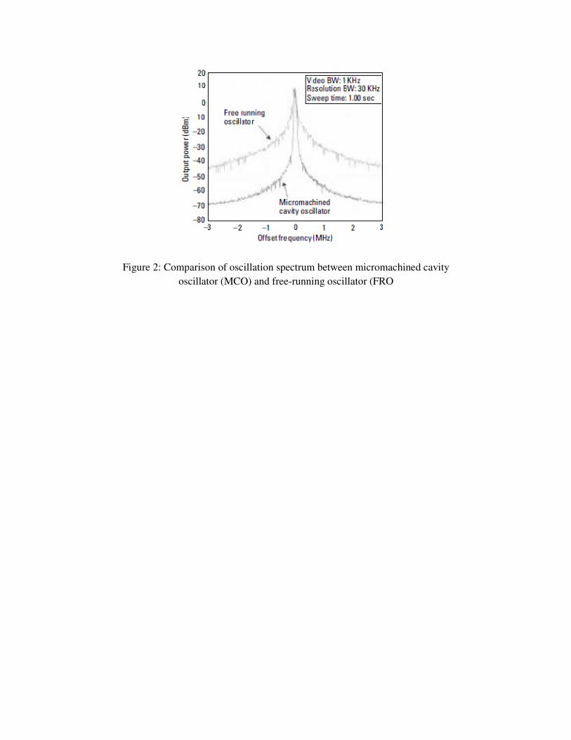
Figure 2: Comparison of oscillation spectrum between micromachined cavity oscillator (MCO) and free-running oscillator (FRO