effect of polishing parameters on chemical mechanical planarization of c-plane (0001) gallium...
TRANSCRIPT
ECS Journal of Solid State Science and Technology, 3 (8) P277-P284 (2014) P2772162-8769/2014/3(8)/P277/8/$31.00 © The Electrochemical Society
Effect of Polishing Parameters on Chemical MechanicalPlanarization of C-Plane (0001) Gallium Nitride Surface UsingSiO2 and Al2O3 AbrasivesKhushnuma Asghar, Mohd Qasim, and D. Dasz
School of Engineering Sciences and Technology, University of Hyderabad, Hyderabad 500046, India
In this study, Chemical Mechanical Planarization (CMP) of (0001) GaN surface, using two different slurries containing colloidalsilica and alumina as abrasive nanoparticles, has been reported. Effect of processing parameters, such as concentration of the oxidizer,downward pressure, head rpm, base rpm, pH of the slurries, and type and concentration of abrasive particles, on the material removalrate (MRR) and surface quality (roughness) have been studied in details. The maximum MRR has been found to be ∼39 nm/hrand ∼85 nm/hr for slurries containing SiO2 and Al2O3 abrasives, respectively, under 38 kPa pressure, 90 rpm base speed (100 rpmfor Al2O3 containing slurry), 30 rpm carrier speed, slurry pH 1 (2 for Al2O3 containing slurry), 0.3 M Oxidizer concentration, and3.75 wt% abrasive particle concentration. RMS surface roughness of 1.3 Å and 0.7 Å, over scanning area of 10 μm × 10 μm and5 μm × 5 μm, respectively, has been achieved on polished Ga-faced GaN surface for SiO2 containing slurry using optimized slurrychemistry and processing parameters.© 2014 The Electrochemical Society. [DOI: 10.1149/2.0181407jss] All rights reserved.
Manuscript submitted March 11, 2014; revised manuscript received June 11, 2014. Published June 21, 2014.
Gallium nitride and related iii-v nitride semiconductors are be-coming increasingly popular as the candidate material for use in opto-and high power and high frequency electronic devices because of theirwide bandgaps, high carrier mobility, high saturated electron drift ve-locity and high breakdown field.1,2 GaN, in particular, is suitable forvariety of electronic and optoelectronic applications because of itsunique capabilities of amplifying high-frequency RF signals withoutdistortion, can withstand high temperatures, and emits blue and greenlights. However, an important issue in development and commercial-ization of GaN based power or optoelectronics is the unavailability ofsuitable device grade (epi-ready) wafer. The ideal choice would be touse homoepitaxial substrate. But, due to difficulties in growth of bulkGaN wafer these substrates are not readily available. The most im-portant challenge for further development of GaN based technologyis the need to improve the quality of GaN films by reducing defectscaused by the heteroepitaxial growth. GaN, most commonly, is grownheteroepitaxially on sapphire substrate.1,3 Due to large difference inthermal expansion and lattice mismatch between sapphire and GaN,a large number of crystal defects and rough surface is generated dur-ing the growth process, which limits further application of the grownfilm.4,5 It is essential to produce an atomically flat, smooth and defectfree GaN surface to realize the full potential of this material. Conven-tional planarization techniques cannot be effectively applied to GaNsurfaces because of its extreme mechanical hardness and chemical in-ertness toward many chemicals. Mechanical polishing using diamondabrasive produces scratches on the surface. Chemical mechanical pla-narization (CMP) using colloidal silica has been proven successful forpreparing defect free GaN surfaces. Numerous reports are available onCMP of several other materials including Al2O3,6 SiO2,7 and GaAs8
using colloidal SiO2 based slurries.CMP of polar GaN faces, using colloidal SiO2 abrasives, was re-
ported by Tavernier et al.9 Polishing of N polar (000–1) GaN facewas found to be more effective than that of Ga polar (0001) GaNface, where no visible change after CMP was observed. Hideo Aidaet al demonstrated the CMP of Ga polar GaN surface using colloidalSiO2 slurry under varying pH conditions. The difference in materialremoval rates (MRR) on Ga- and N- polar GaN faces was attributed tothe non-reverse crystallographic symmetry.10 A material removal rateof 17 nm/hr was demonstrated on Ga polar GaN surface, using col-loidal SiO2, under typical polishing conditions.11 Using a mixture ofsodium-hypochlorite and alumina abrasives as polishing slurry, CMPof Ga polar GaN surface has resulted in a MRR of 50 nm/min.12 Thehigher MRR of polar GaN surfaces, with colloidal Al2O3 containingslurries, indicates higher hardness of the abrasive Al2O3 nanoparti-cles compared to that of SiO2 nanoparticles. Although colloidal Al2O3
zE-mail: [email protected]
abrasive nanoparticles result in higher MRR in conventional CMP pro-cess, it creates polishing related defects on the surface. The surfacedamages can be controlled by appropriate slurry chemistry and pol-ishing conditions. In general, a lower MRR is obtained on polar GaNsurfaces compared to that on non-polar (11–20, 10–10) or semi-polar(11–22) planes, which is related to the higher hardness of these planes(0001, 000–1), revealed in an elasto-plastic mechanical behavior studyof the GaN planes carried out recently.13 From a critical review of theliterature it has been observed that the CMP of Ga polar GaN surfaceis equally affected both by the chemical (use of different oxidizersin the literature) and mechanical (use of different abrasive particles)effect of polishing.
It is seen from the literature that either only colloidal silica,10,11
with varying pH and very high solid loading (∼40%) or a mixture ofsodium-hypochlorite and alumina abrasives,12 was used in CMP ofpolar GaN surfaces. In the present work, however, either a mixtureof colloidal silica and KMnO4 or colloidal alumina and KMnO4, withvery low abrasive particle concentrations (1.25–5.00 wt%), have beenused as the polishing chemical. In the present investigation, we reporton the comparative study of CMP processes carried out on Ga polar(0001) GaN surface using colloidal Al2O3 and SiO2 abrasive nanopar-ticles with appropriate slurry chemistry and experimental conditions.The effect of CMP process parameters, such as abrasive particles andits concentration, polishing pressure, platen velocity, carrier velocity,and slurry chemistry, on the material removal rate (MRR) and surfacefinish of Ga polar GaN surface have been reported. An atomically flatand smooth surface with RMS surface roughness of ∼1 Å has beenobtained on the CMP processed Ga- polar GaN surface.
Experimental
Commercially available GaN film grown on 2 inch sapphire sub-strate was used in this study. All the CMP experiments have beencarried out on a Buehler Ecomet 250 variable speed Grinder Polisherwith Automet 250 power head. Cabot D100 pad was used for all theCMP experiments. The GaN wafer was mounted on a 2′′ stainless steelcarrier using Crystal Bond 509 Clear epoxy resin. The wafer was char-acterized for crystal structure and surface characteristics before theCMP experiments. CMP slurries consisted of oxidizer and abrasiveparticles, silica (SiO2) or alumina (Al2O3). Potassium permanganate(KMnO4) has been used as oxidizer in this investigation. The colloidalabrasive particles used in the experiments had a mean size of ∼50 nmwith a solid loading of ∼40% for colloidal Al2O3 slurry and mean sizeof ∼20 nm with a solid loading of ∼20% for colloidal SiO2 slurry.The slurry was delivered on the polishing pad by a peristaltic pump(Ravel, Model No. RH-P100VS-100) at a flow rate of 10 mL/min.The typical time of each polishing experiment was 15 minutes, with
) unless CC License in place (see abstract). ecsdl.org/site/terms_use address. Redistribution subject to ECS terms of use (see 14.139.69.199Downloaded on 2014-10-15 to IP
P278 ECS Journal of Solid State Science and Technology, 3 (8) P277-P284 (2014)
an intermittent conditioning (ten scratches, down pressure applied byhand and at a platen rotational speed of 90 rpm) of the pad after each5 minutes by a diamond pad conditioner (Model no.S341038N-2A2from M/s Abrasive Technology Asia Pacific Pvt. Ltd., Singapore). Inthis work, a series of CMP experiments, on Ga-faced GaN, have beenconducted using Al2O3 and SiO2 abrasive nanoparticles containingslurries. The influences of the abrasive content, concentration of theoxidizer, pH of the slurry, platen and carrier velocities and polish-ing pressure on the material removal rate (MRR) have been studied.CMP experiments were carried out at varying polishing pressures(24–38 kPa), platen speeds (60–100 rpm), carrier velocities (30–50 rpm), oxidizer concentrations (0.1–0.4 M), Al2O3 concentrations(1.25–5.00 wt%), and slurry pH (1–3). Each experimental data pointwas generated from 3 experiments. The MRR for each experiment wasestimated from a difference in weight of the GaN wafer, measured bya high precision electronic balance (Sartorius Model No. CPA225D),before and after the CMP experiment. The effects of polishing pa-rameters, as mentioned before, on MRR have been investigated andcompared for slurries containing SiO2 and Al2O3 as the abrasive par-ticles. The effect of Al2O3 content in the slurry on MRR has beeninvestigated first. The effect of KMnO4 concentration in the slurry onMRR has then been fixed using the optimum Al2O3 content obtained inthe first experiment. The other parameters, in these two experiments,have been fixed based on the corresponding author’s prior researchexperience on CMP of single crystal SiC. A polishing pressure of 38kPa, platen velocity of 90 rpm, carrier velocity of 30 rpm, clockwiserotation of both the platen and carrier, and the slurry pH of 2 havebeen used in these two experiments. The optimum abrasive content(wt%) and oxidizer concentration (M) has then been maintained con-sistently both in Al2O3 and SiO2 containing slurries in the subsequentexperiments. Post CMP cleaning, by repeated washing with alcohol,acetone and deionised water, was carried out to clean the wafer surfaceafter each CMP experiment. The CMP processed wafer was character-ized for surface quality (any defect formation and surface roughness)using Bruker Optical Surface profiler (Model: Contour GT-K0) andNT-MDT Scanning probe microscope (Model: Ntegra Aura).
Results and Discussion
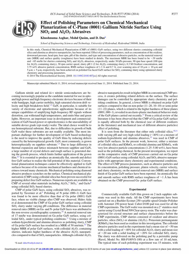
Effect of Al2O3 content on MRR.— In a CMP process the surfaceof the material to be polished is chemically altered by the chemicalaction of the slurry and the soft layer formed on the surface, subse-quently, is abraded by the mechanical action of polishing. In our work,KMnO4 was used as an oxidizer which may oxidize the GaN surface toGa2O3, which subsequently gets removed either by mechanical abra-sion of the particles or by dissolution in polishing chemical solution.10
The abrasive content of the slurry, therefore, significantly affects theMRR of the process. In the current work four different concentra-tions of Al2O3 abrasive, with an average particles size of 50 nm, viz.1.25 wt%, 2.50 wt%, 3.75 wt% and 5.00 wt% have been investigated.The experiments were conducted at a polishing pressure of 38 kPa,carrier (head) rpm of 30, platen (base) rpm of 90, slurry pH of 2,and KMnO4 concentration of 0.3 M. Fig. 1 shows the dependenceof Al2O3 content on the MRR of Ga face GaN CMP. From this fig-ure it is observed that MRR increases with increasing Al2O3 contentin the slurry till 3.75 wt%. The MRR increased from 25 nm/hr forpolishing with 1.25% Al2O3 to 75 nm/hr for polishing with 3.75%Al2O3. Further increase in Al2O3 content decreased the MRR. Al2O3
abrasive of mean particle size ∼70 nm was used in the CMP of Gaface GaN by Goorsky et al, utilizing sodium hypochlorite (NaOCl)as the oxidizer.12 Although the mean size of the Al2O3 particle isknown, its concentration in the slurry and its influence on MRR isnot known in that investigation, which had resulted in extremely highMRR. The high MRR may be associated with different slurry chem-istry. The local aggressive attack of the surface by the chemical, forthe given experimental conditions and slurry chemistry, may lead toscratching of the surface, which resulted in extremely high MRR. Al-though the MRR obtained in the current investigation is lower, maybe due to smaller particle sizes and different slurry chemistry, its de-
Figure 1. Effect of Al2O3 content on the material removal rate (MRR) of Gaface GaN CMP.
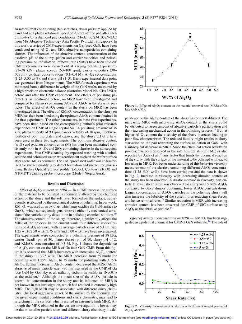
pendence on the Al2O3 content of the slurry has been established. Theincreasing MRR with increasing Al2O3 content of the slurry couldbe attributed to larger amount of abrasive particle’s participation andtheir increasing mechanical action in the polishing process.14 But, athigher Al2O3 content the viscosity of the slurry increases leading topoor flow characteristics. The reduced fluidity might results in slurrystarvation on the pad restricting the surface oxidation of GaN, witha subsequent decrease in MRR. Since the chemical action (oxidationprocess) has been observed as the rate limiting step in CMP, as alsoreported by Aida et al.,10 any factor that limits the chemical reactionof the slurry with the surface of the material to be polished will lead tolowering in MRR. For better understanding of this behavior viscositymeasurements of the slurries, containing different Al2O3 concentra-tions (1.25–5.00 wt%), have been carried out and the data is shownin Fig. 2. Increase in viscosity with increasing alumina content ofthe slurry has been observed. A drastic increase in viscosity, particu-larly at lower shear rates, was observed for slurry with 5 wt% Al2O3
compared to other slurries containing lower Al2O3 concentrations.Larger concentration of Al2O3 particles in the polishing slurry willalso increase the lubricity of the system, thus reducing shear forcesand hence removal rates.15 Similar reduction in MRR with increasingabrasive content has been observed for CMP of SiC surface usingAl2O3 as the abrasive particle.14
Effect of oxidizer concentration on MRR.— KMnO4 has been sug-gested as a potential chemical for CMP of GaN substrate.16 The role of
Figure 2. Viscosity measurement of slurries with different weight percent ofAl2O3 abrasive.
) unless CC License in place (see abstract). ecsdl.org/site/terms_use address. Redistribution subject to ECS terms of use (see 14.139.69.199Downloaded on 2014-10-15 to IP
ECS Journal of Solid State Science and Technology, 3 (8) P277-P284 (2014) P279
Figure 3. Effect of KMnO4 concentration on MRR of Ga polar GaN CMP.
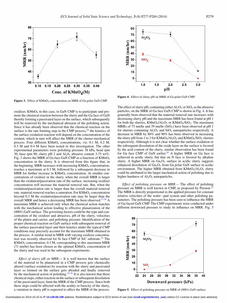
oxidizer, KMnO4 in this case, in GaN CMP is to participate and pro-mote the chemical reaction between the slurry and the Ga face of GaNthereby forming a passivated layer on the surface, which subsequentlywill be removed by the mechanical abrasion of the polishing action.Since it has already been observed that the chemical reaction on thesurface is the rate limiting step in the CMP process,10 the kinetics ofthe surface oxidation reaction will depend on the concentration of theoxidant, which in turn will affect the MRR of the chemo-mechanicalprocess. Four different KMnO4 concentrations, viz. 0.1 M, 0.2 M,0.3 M and 0.4 M have been tested in this investigation. The otherexperimental parameters were polishing pressure 38 kPa, head rpm30, base rpm 90, slurry pH 2 and Al203 abrasive content 3.75 wt%.Fig. 3 shows the MRR of Ga face GaN CMP as a function of KMnO4
concentration in the slurry. It is observed from this figure that, inthe beginning, MRR increases with increasing KMnO4 concentration,reaches a maximum at 0.3 M, followed by a subsequent decrease inMRR for further increase in KMnO4 concentration. At smaller con-centrations of oxidizer in the slurry, when the overall MRR is largerthan the oxidation/passivation rate of the surface, increasing oxidizerconcentration will increase the material removal rate. But, when theoxidation/passivation rate is larger than the overall material removalrate, material removal reaches a saturation. For KMnO4 concentrationbeyond 0.3 M the oxidation/passivation rate may be larger than theoverall MRR and hence a decreasing MRR has been observed.17,18 Amaximum MRR is achieved only when the chemical action matcheswith the mechanical action leading to effective planarization of the(0001) GaN surface. The governing factors could be the type and con-centration of the oxidizer and abrasives, pH of the slurry, velocitiesof the platen and carrier, and polishing pressure. Identification of theproper chemical reaction on GaN surface with subsequent removal ofthe surface passivated layer and their kinetics under the typical CMPconditions may precisely account for the maximum MRR obtained inthe process. A similar trend in MRR with varying oxidizer concentra-tion was recently observed for Si face CMP of SiC substrate.14 TheKMnO4 concentration, 0.3 M, corresponding to this maximum MRR(71 nm/hr) has been chosen as the optimal KMnO4 concentration ofthe slurry and was used in the subsequent experiments.
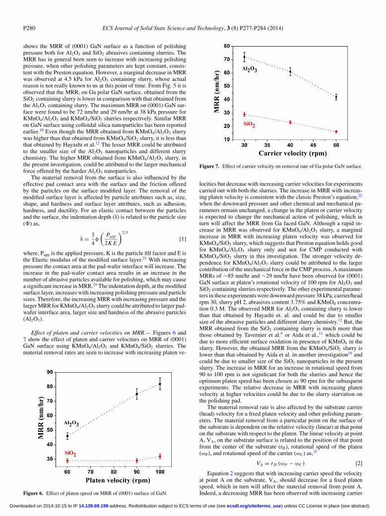
Effect of slurry pH on MRR.— It is well known that the surfaceof the material to be planarized in a CMP process gets chemicallyaltered (surface oxidation) by reaction with the slurry and passivatedlayer so formed on the surface gets abraded and finally removedby the mechanical action of polishing.19–21 It is also known that thesechemical steps, either reaction on the surface or subsequent dissolutionof the passivated layer, limit the MRR of the CMP process. Since boththese steps could be affected with the acidity or basicity of the slurry,a variation in slurry pH is expected to affect the MRR of the process.
Figure 4. Effect of slurry pH on MRR of Ga polar GaN CMP.
The effect of slurry pH, containing either Al2O3 or SiO2 as the abrasiveparticles, on the MRR of Ga face GaN CMP is shown in Fig. 4. It hasgenerally been observed that the material removal rate increases withdecreasing slurry pH and the maximum MRR has been found at pH 1for both the slurries, KMnO4/Al2O3 or KMnO4/SiO2. The maximumMRRs of 75 nm/hr and 39 nm/hr (SiO2) have been observed at pH 1for slurries containing Al2O3 and SiO2 nanoparticles respectively. Adecrease in MRR by 80% and 90% has been observed in increasingthe slurry pH from 1 to 3 for KMnO4/Al2O3 and KMnO4/SiO2 slurriesrespectively. Although it is not clear whether the surface oxidation orthe subsequent dissolution of the oxide layer on the surface is favoredby the acid content of the slurry, similar observation has been foundfor Ga face CMP of GaN earlier.10 A higher MRR on Ga face isachieved in acidic slurry, but that on N face is favored by alkalineslurry. A higher MRR on Ga2O3 surface in acidic slurry suggestsenhanced dissolution of Ga2O3 from Ga polar GaN surface in acidicenvironment. The higher MRR obtained from KMnO4/Al2O3 slurrycould be attributed to the larger mechanical action of polishing due tohigher hardness of Al2O3 nanoparticles.
Effect of polishing pressure on MRR.— The effect of polishingpressure on MRR is well known in CMP, as proposed by Preston.22
The MRR is directly proportional to the applied pressure for constantrelative velocities of the wafer –pad system and other polishing pa-rameters. The polishing pressure has been seen to influence the MRRof Ga-faced GaN CMP. The CMP experiments were conducted underdifferent downward pressure to study its influence on MRR. Fig. 5
Figure 5. Effect of polishing pressure on MRR of (0001) GaN surface.
) unless CC License in place (see abstract). ecsdl.org/site/terms_use address. Redistribution subject to ECS terms of use (see 14.139.69.199Downloaded on 2014-10-15 to IP
P280 ECS Journal of Solid State Science and Technology, 3 (8) P277-P284 (2014)
shows the MRR of (0001) GaN surface as a function of polishingpressure both for Al2O3 and SiO2 abrasives containing slurries. TheMRR has in general been seen to increase with increasing polishingpressure, when other polishing parameters are kept constant, consis-tent with the Preston equation. However, a marginal decrease in MRRwas observed at 4.5 kPa for Al2O3 containing slurry, whose actualreason is not really known to us at this point of time. From Fig. 5 it isobserved that the MRR, on Ga polar GaN surface, obtained from theSiO2 containing slurry is lower in comparison with that obtained fromthe Al2O3 containing slurry. The maximum MRR on (0001) GaN sur-face were found to be 72 nm/hr and 29 nm/hr at 38 kPa pressure forKMnO4/Al2O3 and KMnO4/SiO2 slurries respectively. Similar MRRon GaN surface using colloidal silica nanoparticles has been reportedearlier.10 Even though the MRR obtained from KMnO4/Al2O3 slurrywas higher than that obtained from KMnO4/SiO2 slurry, it is less thanthat obtained by Hayashi et al.12 The lesser MRR could be attributedto the smaller size of the Al2O3 nanoparticles and different slurrychemistry. The higher MRR obtained from KMnO4/Al2O3 slurry, inthe present investigation, could be attributed to the larger mechanicalforce offered by the harder Al2O3 nanoparticles.
The material removal from the surface is also influenced by theeffective pad contact area with the surface and the friction offeredby the particles on the surface modified layer. The removal of themodified surface layer is affected by particle attributes such as, size,shape, and hardness and surface layer attributes, such as adhesion,hardness, and ductility. For an elastic contact between the particlesand the surface, the indentation depth (δ) is related to the particle size(�) as,
δ = 3
4φ
(Papp
2K E
)2/3
[1]
where, Papp is the applied pressure, K is the particle fill factor and E isthe Elastic modulus of the modified surface layer.23 With increasingpressure the contact area at the pad-wafer interface will increase. Theincrease in the pad-wafer contact area results in an increase in thenumber of abrasive particles available for polishing, which may causea significant increase in MRR.24 The indentation depth, at the modifiedsurface layer, increases with increasing polishing pressure and particlesizes. Therefore, the increasing MRR with increasing pressure and thelarger MRR for KMnO4/Al2O3 slurry could be attributed to larger pad-wafer interface area, larger size and hardness of the abrasive particles(Al2O3).
Effect of platen and carrier velocities on MRR.— Figures 6 and7 show the effect of platen and carrier velocities on MRR of (0001)GaN surface using KMnO4/Al2O3 and KMnO4/SiO2 slurries. Thematerial removal rates are seen to increase with increasing platen ve-
Figure 6. Effect of platen speed on MRR of (0001) surface of GaN.
Figure 7. Effect of carrier velocity on removal rate of Ga polar GaN surface.
locities but decrease with increasing carrier velocities for experimentscarried out with both the slurries. The increase in MRR with increas-ing platen velocity is consistent with the classic Preston’s equation,22
when the downward pressure and other chemical and mechanical pa-rameters remain unchanged, a change in the platen or carrier velocityis expected to change the mechanical action of polishing, which inturn will affect the MRR from Ga faced GaN. Although a rapid in-crease in MRR was observed for KMnO4/Al2O3 slurry, a marginalincrease in MRR with increasing platen velocity was observed forKMnO4/SiO2 slurry, which suggests that Preston equation holds goodfor KMnO4/Al2O3 slurry only and not for CMP conducted withKMnO4/SiO2 slurry in this investigation. The stronger velocity de-pendence for KMnO4/Al2O3 slurry could be attributed to the largercontribution of the mechanical force in the CMP process. A maximumMRRs of ∼85 nm/hr and ∼29 nm/hr have been observed for (0001)GaN surface at platen’s rotational velocity of 100 rpm for Al2O3 andSiO2 containing slurries respectively. The other experimental parame-ters in these experiments were downward pressure 38 kPa, carrier/headrpm 30, slurry pH 2, abrasives content 3.75% and KMnO4 concentra-tion 0.3 M. The observed MRR for Al2O3 containing slurry is lowerthan that obtained by Hayashi et. al. and could be due to smallersize of the abrasive particles and different slurry chemistry.12 But, theMRR obtained from the SiO2 containing slurry is much more thanthose obtained by Tavernier et al.9 or Aida et al.,11 which could bedue to more efficient surface oxidation in presence of KMnO4 in theslurry. However, the obtained MRR from the KMnO4/SiO2 slurry islower than that obtained by Aida et al. in another investigation10 andcould be due to smaller size of the SiO2 nanoparticles in the presentslurry. The increase in MRR for an increase in rotational speed from90 to 100 rpm is not significant for both the slurries and hence theoptimum platen speed has been chosen as 90 rpm for the subsequentexperiments. The relative decrease in MRR with increasing platenvelocity at higher velocities could be due to the slurry starvation onthe polishing pad.
The material removal rate is also affected by the substrate carrier(head) velocity for a fixed platen velocity and other polishing param-eters. The material removal from a particular point on the surface ofthe substrate is dependent on the relative velocity (linear) at that pointon the substrate with respect to the platen. The linear velocity at pointA, VA, on the substrate surface is related to the position of that pointfrom the center of the substrate (rH), rotational speed of the platen(ωP), and rotational speed of the carrier (ωC) as,25
VA = rH (ωP − ωC ) [2]
Equation 2 suggests that with increasing carrier speed the velocityat point A on the substrate, VA, should decrease for a fixed platenspeed, which in turn will affect the material removal from point A.Indeed, a decreasing MRR has been observed with increasing carrier
) unless CC License in place (see abstract). ecsdl.org/site/terms_use address. Redistribution subject to ECS terms of use (see 14.139.69.199Downloaded on 2014-10-15 to IP
ECS Journal of Solid State Science and Technology, 3 (8) P277-P284 (2014) P281
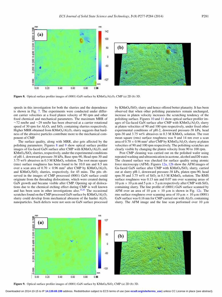
Figure 8. Optical surface profiler images of (0001) GaN surface by KMnO4/Al2O3 CMP (a) 2D (b) 3D.
speeds in this investigation for both the slurries and the dependenceis shown in Fig. 7. The experiments were conducted under differ-ent carrier velocities at a fixed platen velocity of 90 rpm and otherfixed chemical and mechanical parameters. The maximum MRR of∼72 nm/hr and ∼29 nm/hr has been observed at a carrier rotationalspeed of 30 rpm for Al2O3 and SiO2 containing slurries respectively.Higher MRR obtained from KMnO4/Al2O3 slurry suggests that hard-ness of the abrasive particles contribute more to the mechanical com-ponent of CMP.
The surface quality, along with MRR, also gets affected by thepolishing parameters. Figures 8 and 9 show optical surface profilerimages of Ga-faced GaN surface after CMP with KMnO4/Al2O3 andKMnO4/SiO2 slurries, respectively, under the experimental conditionsof pH-1, downward pressure-38 kPa, Base rpm-90, Head rpm-30 and3.75 wt% abrasives in 0.3 M KMnO4 solution. The root mean square(rms) surface roughness has been found to be 10.0 nm and 8.5 nmover a scan area of 0.70 × 0.96 mm2 after CMP by KMnO4/Al2O3
and KMnO4/SiO2 slurries, respectively, for 45 mins. The pits ob-served in the images of CMP processed (0001) GaN surface couldoriginate from the threading dislocations, which were created duringGaN growth and became visible after CMP. Opening up of disloca-tions due to the chemical etching effect during CMP is well knownand has been seen in other investigations also.10,26 The occasionalscratches found on the CMP processed GaN surface by KMnO4/Al2O3
slurry could develop from mechanical abrasion of the harder Al2O3
nanoparticles. Such defects were not seen on GaN surface processed
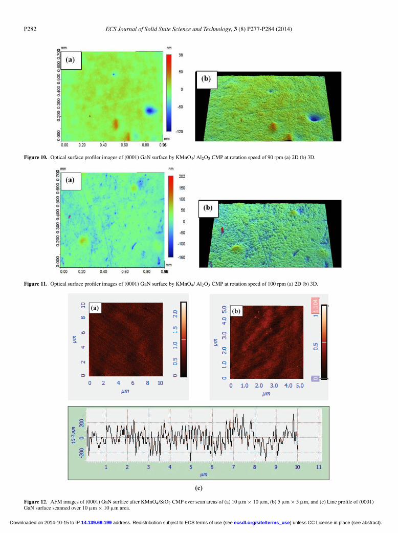
by KMnO4/SiO2 slurry and hence offered better planarity. It has beenobserved that when other polishing parameters remain unchanged,increase in platen velocity increases the scratching tendency of thepolishing surface. Figures 10 and 11 show optical surface profiler im-ages of Ga-faced GaN surface after CMP with KMnO4/Al2O3 slurryat platen velocities of 90 and 100 rpm respectively, under fixed otherexperimental conditions of pH-2, downward pressure-38 kPa, headrpm-30 and 3.75 wt% abrasives in 0.3 M KMnO4 solution. The rootmean square (rms) surface roughness was 9 and 14 nm over a scanarea of 0.70 × 0.96 mm2 after CMP by KMnO4/Al2O3 slurry at platenvelocities of 90 and 100 rpm respectively. The polishing scratches areclearly visible by changing the platen velocity from 90 to 100 rpm.
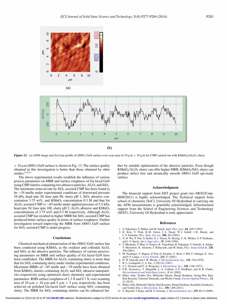
Post CMP cleaning was carried out on the polished wafer usingrepeated washing and ultrasonication in acetone, alcohol and DI water.The cleaned surface was checked for surface quality using atomicforce microscopy (AFM). Figures 12a, 12b show the AFM images ofGa-faced GaN surface after CMP with KMnO4/SiO2 slurry, carriedout at slurry pH-1, downward pressure-38 kPa, platen rpm-90, headrpm-30 and 3.75 wt% of SiO2 in 0.3 M KMnO4 solution. The RMSsurface roughness was 0.13 nm and 0.07 nm over scanning areas of10 μm × 10 μm and 5 μm × 5 μm respectively after CMP with SiO2
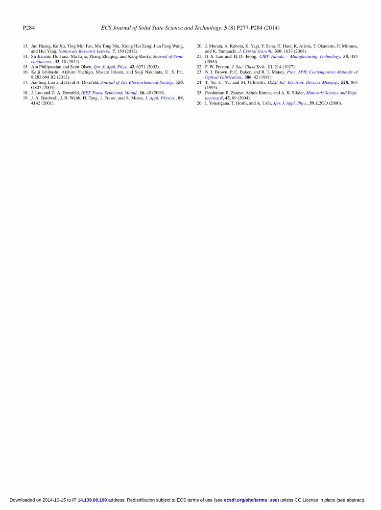
containing slurry. The line profile of (0001) GaN surface scanned byAFM over an area of 10 μm × 10 μm is shown in Fig. 12c. Therms surface roughness over scanning area of 10 μm × 10 μm (0001)GaN surface was 0.16 nm for CMP carried out with Al2O3 containingslurry. The AFM image and the line scan performed over 10 μm
Figure 9. Optical surface profiler images of (0001) GaN surface by KMnO4/SiO2 CMP (a) 2D (b) 3D.
) unless CC License in place (see abstract). ecsdl.org/site/terms_use address. Redistribution subject to ECS terms of use (see 14.139.69.199Downloaded on 2014-10-15 to IP
P282 ECS Journal of Solid State Science and Technology, 3 (8) P277-P284 (2014)
Figure 10. Optical surface profiler images of (0001) GaN surface by KMnO4/ Al2O3 CMP at rotation speed of 90 rpm (a) 2D (b) 3D.
Figure 11. Optical surface profiler images of (0001) GaN surface by KMnO4/ Al2O3 CMP at rotation speed of 100 rpm (a) 2D (b) 3D.
(c)
(a) (b)
Figure 12. AFM images of (0001) GaN surface after KMnO4/SiO2 CMP over scan areas of (a) 10 μm × 10 μm, (b) 5 μm × 5 μm, and (c) Line profile of (0001)GaN surface scanned over 10 μm × 10 μm area.
) unless CC License in place (see abstract). ecsdl.org/site/terms_use address. Redistribution subject to ECS terms of use (see 14.139.69.199Downloaded on 2014-10-15 to IP
ECS Journal of Solid State Science and Technology, 3 (8) P277-P284 (2014) P283
(b)
(a)
Figure 13. (a) AFM image and (b) Line profile of (0001) GaN surface over scan area of 10 μm × 10 μm for CMP carried out with KMnO4/Al2O3 slurry.
× 10 μm (0001) GaN surface is shown in Fig. 13. The surface qualityobtained in this investigation is better than those obtained by otherstudies.9,10,11
The above experimental results establish the influence of variousprocess parameters on MRR and surface roughness of Ga faced GaNusing CMP slurries containing two abrasive particles, Al2O3 and SiO2.The maximum removal rate by SiO2 assisted CMP has been found tobe ∼39 nm/hr under experimental conditions of downward pressure38 kPa, head rpm 30, base rpm 90, slurry pH 1, SiO2 abrasive con-centration 3.75 wt%, and KMnO4 concentration 0.3 M and that forAl2O3 assisted CMP is ∼85 nm/hr under applied pressure of 5.5 kPa,head rpm 30, base rpm 100, slurry pH 2, Al2O3 abrasive and KMnO4
concentrations of 3.75 wt% and 0.3 M respectively. Although Al2O3
assisted CMP has resulted in higher MRR but SiO2 assisted CMP hasproduced better surface quality in terms of surface roughness. Furtherinvestigation toward improving the MRR from (0001) GaN surfacefor SiO2 assisted CMP is under progress.
Conclusions
Chemical mechanical planarization of the (0001) GaN surface hasbeen conducted using KMnO4 as the oxidizer and colloidal Al2O3
and SiO2 as the abrasive particles. The influence of various process-ing parameters on MRR and surface quality of Ga faced GaN havebeen established. The MRR for Al2O3 containing slurry is more thanthat for SiO2 containing slurry under similar experimental conditions.Maximum MRRs of ∼85 nm/hr and ∼39 nm/hr have been obtainedfrom KMnO4 slurries containing Al2O3 and SiO2 abrasive nanoparti-cles respectively using optimized slurry chemistry and experimentalparameters. RMS surface roughness of 1.3 Å and 0.7 Å, over scanningarea of 10 μm × 10 μm and 5 μm × 5 μm, respectively, has beenachieved on polished Ga-faced GaN surface using SiO2 containingslurry. The MRR for SiO2 containing slurries can be enhanced fur-
ther by suitable optimization of the abrasive particles. Even thoughKMnO4/Al2O3 slurry can offer higher MRR, KMnO4/SiO2 slurry canproduce defect free and atomically smooth (0001) GaN epi-readysurface.
Acknowledgment
The financial support from DST project grant (no:-SR/S2/Cmp-0009/2011) is highly acknowledged. The Technical support fromschool of chemistry (SoC), University Of Hyderabad in carrying outthe AFM measurements is gratefully acknowledged. Infrastructuralsupport from the School of Engineering Sciences and Technology(SEST), University Of Hyderabad is truly appreciated.
References
1. S. Nakamura, T. Mukai, and M. Senoh, Appl. Phys. Lett., 64, 1687 (1994).2. H. Kim, V. Tilak, B. M. Green, J. A. Smart, W. J. Schaff, J. R. Shealy, and
L. F. Eastman, Phys. State. Sol. (a)., 188, 203 (2001).3. X. H. Wu, P. Fini, S. Keller, E. J. Tarasa, B. Heying, U. K. Mishra, S. P. Denbaars,
and J. S. Speck, Jpn,J. Appl. phys., 35, 1648 (1996).4. T. Miyajima, T. Hino, S. Tomiya, K. Yanashima, H. Nakajima, Y. Nanishi, A. Satake,
Y. Masumoto, K. Akimoto, T. Kobayashi, and M. Ikeda, Phys. Status Solidi B., 228,395 (2001).
5. M. Puchinger, T. Wagner, P. Fini, D. Kisailus, U. Beck, J. Bill, F. Aldinger, E. Arzt,and F. F. Lange, J. Cryst. Growth., 233, 57 (2001).
6. H. W. Gutsche and J. W. Moody, J. Electrochemical. Soc., 125, 136 (1978).7. R. L. Lachapelle, U. S. Pat., 3,328,141 (1967).8. J. C. Dyment and G. A. Rozgonyi, J. Electrochem. Soc., 118, 1346 (1971).9. P. R. Tavernier,z, T. Margalith, L. A. Coldren, S. P. DenBaars, and D. R. Clarke,
Electrochemical and Solid-State Letters., 5, 61 (2002).10. Hideo Aida, Toshiro Doi, Hidetoshi Takeda, Haruji Katakura, Seong-Woo Kim,
Koji Koyama, Tsutomu Yamazaki, and Michio Uneda, Current Applied Physics., 12,41 (2012).
11. Hideo Aida, Hidetoshi Takeda, Koji Koyama, Haruji Katakura, Kazuhiko Sunakawa,and Toshiro Doi, J. Electrochem. Soc., 158, 1206 (2011).
12. S. Hayashi, T. Koga, and M. S. Goorsky, J. Electrochemical. Soc., 155, H113 (2008).
) unless CC License in place (see abstract). ecsdl.org/site/terms_use address. Redistribution subject to ECS terms of use (see 14.139.69.199Downloaded on 2014-10-15 to IP
P284 ECS Journal of Solid State Science and Technology, 3 (8) P277-P284 (2014)
13. Jun Huang, Ke Xu, Ying Min Fan, Mu Tong Niu, Xiong Hui Zeng, Jian Feng Wang,and Hui Yang, Nanoscale Research Letters., 7, 150 (2012).
14. Su Jianxiu, Du Jiaxi, Ma Lijie, Zhang Zhuqing, and Kang Renke, Journal of Semi-conductors., 33, 10 (2012).
15. Ara Philipossian and Scott Olsen, Jpn. J. Appl. Phys., 42, 6371 (2003).16. Keiji Ishibashi, Akihiro Hachigo, Masato Irikura, and Seiji Nakahata, U. S. Pat.
8,283,694 B2 (2012).17. Jianfeng Luo and David A. Dornfeld, Journal of The Electrochemical Society., 150,
G807 (2003).18. J. Luo and D. A. Dornfeld, IEEE Trans. Semicond. Manuf., 16, 45 (2003).19. J. A. Bardwell, J. B. Webb, H. Tang, J. Fraser, and S. Moisa, J. Appl. Physics., 89,
4142 (2001).
20. J. Murata, A. Kubota, K. Yagi, Y. Sano, H. Hara, K. Arima, T. Okamoto, H. Mimura,and K. Yamauchi, J. Crystal Growth., 310, 1637 (2008).
21. H. S. Lee and H. D. Jeong, CIRP Annals – Manufacturing Technology, 58, 485(2009).
22. F. W. Preston, J. Soc. Glass Tech., 11, 214 (1927).23. N. J. Brown, P. C. Baker, and R. T. Maney, Proc. SPIE Contemporary Methods of
Optical Fabrication., 306, 42 (1981).24. T. Yu, C. Yu, and M. Orlowski, IEEE Int. Electron. Devices Meeting., 528, 865
(1993).25. Parshuram B. Zantye, Ashok Kumar, and A. K. Sikder, Materials Science and Engi-
neering R, 45, 89 (2004).26. I. Yonengana, T. Hoshi, and A. Ushi, Jpn. J. Appl. Phys., 39, L2OO (2000).
) unless CC License in place (see abstract). ecsdl.org/site/terms_use address. Redistribution subject to ECS terms of use (see 14.139.69.199Downloaded on 2014-10-15 to IP