domain switching mechanisms in polycrystalline ferroelectrics with asymmetric hysteretic behavior
TRANSCRIPT

Domain Switching Mechanisms in Polycrystalline
Ferroelectrics with Asymmetric Hysteretic Behavior
Eva-Maria Anton, R. Edwin Garcıa,∗
Thomas S. Key,∗ John E. Blendell,∗ and Keith J. Bowman∗
Darmstadt Technical University,
Darmstadt, Germany.
∗ School of Materials Engineering, Purdue University,
West Lafayette, Indiana 47907
November 27, 2008
Abstract
A numerical method is presented to predict the effect of microstructure on the
local polarization switching of bulk ferroelectric ceramics. The model shows that a
built-in electromechanical field develops in a ferroelectric material as a result of the
spatial coupling of the grains and the direct physical coupling between the ther-
momechanical and electromechanical properties of a bulk ceramic material. The
built-in fields that result from the thermomechanically-induced grain-grain elec-
tromechanical interactions result in the appearance of four microstructural switch-
ing mechanisms: 1. simple switching, where the c-axes of ferroelectric domains will
align with the direction of the applied macroscopic electric field by starting from
the core of each grain; 2. grain boundary induced switching, where the domain’s
switching response will initiate at grain corners and boundaries as a result of the
1
polarization and stress that is locally generated from the strong anisotropy of the
dielectric permittivity and the local piezoelectric contributions to polarization from
the surrounding material; 3. negative poling, where abutting ferroelectric domains
of opposite polarity actively oppose domain switching by increasing their degree
of tetragonality by interacting with the surrounding domains that have already
switched to align with the applied electrostatic field. Finally, 4. domain reswitch-
ing mechanism is observed at very large applied electric fields, and is characterized
by the appearance of polarization domain reversals events in the direction of their
originally unswitched state. This mechanism is a consequence of the competition
between the macroscopic applied electric field, and the induced electric field that re-
sults from the neighboring domains (or grains) interactions. The model shows that
these built-in electromechanical fields and mesoscale mechanisms contribute to the
asymmetry of the macroscopic hysteretic behavior in poled samples. Furthermore,
below a material-dependent operating temperature, the predicted built-in electric
fields can potentially drive the aging and electrical fatigue of the system to further
skew the shape of the hysteresis loops.
2
1 Introduction
Recent experimental observations have shown that the processing sequence of bulk fer-
roelectric Lead Zirconate Titanate (PZT) materials has a strong influence on the shape
of the macroscopic polarization response, i.e., the hysteresis loop, leading to materials
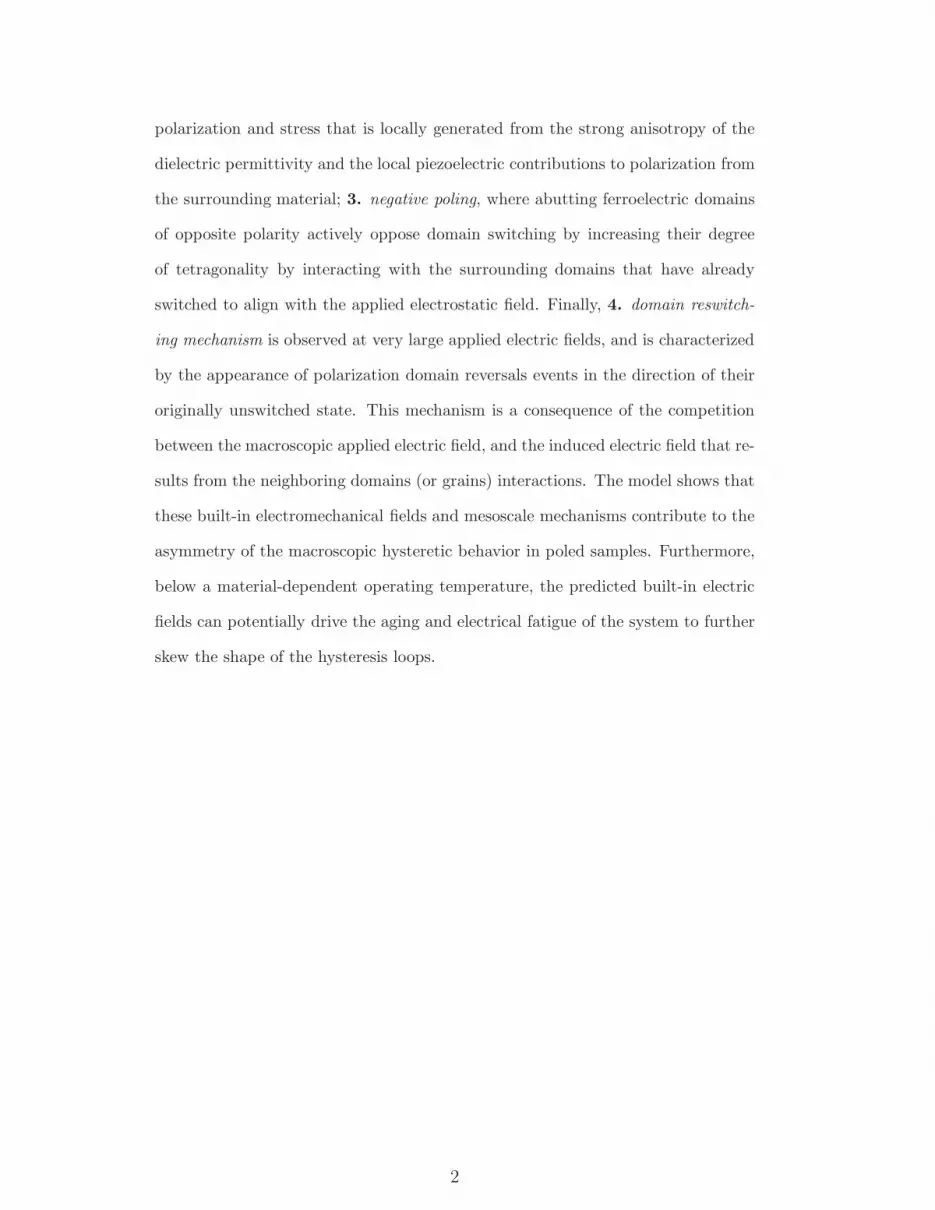
with built-in electric and stress fields [1]. Figure 1 illustrates the hysteretic response of a
2.5µm grain size polycrystalline sample, poled at 80C with an electric field of -2.8MV/m,
followed by an air-quench (i.e., direct exposure to a 25C environment). In such sam-
ple, a one hertz triangular macroscopic electric field with an amplitude of 2.8MV/m was
applied, with and without bias to compensate for the built-in and developed polariza-
tion. For the specified conditions, a significant difference arises between the positive and
negative coercive field values: The negative coercive field is -0.9MV/m, and the mea-
sured positive coercive field is 2.1MV/m. The difference of 1.2MV/m occurs due to an
internal built-in electric field that can be partially overcome by the application of an
external field. Additionally, the macroscopic positive and negative remnant polarizations
are influenced by the built-in electromechanical fields that suppresses the surficial po-
larization in one direction, while enhancing it in the opposite one. In bulk ferroelectric
materials, the local crystallographic orientation and local grain-grain interactions play an
important role in determining the switching of each volume element of material. Such
changes come accompanied with large spatial variations of the mechanical and electrical
fields, which arise as a combined result of the direct and converse piezoelectric effects,
the local spatial compatibility of the grains, and the crystallographic anisotropy of the
underlying dielectric, thermomechanical, and elastic properties. The processing history
that generates these materials specifies the microstructure and thereby the nature of the
underlying ferroelectric interactions.
1
Figure 1: Left inset shows hysteretic polarization behavior of material with built-in processing
fields. Right inset summarizes the corresponding electromechanical (butterfly loop) response.
corresponds to as-processed response, and correspond to response with applied 1MV/m
electric field bias. Right inset illustrates the impact of the self-induced built-in fields on the elec-
tromechanical (butterfly) loop response. The asymmetry of the hysteretic behavior is partially
reversed when a constant bias electric field is externally applied to the solid.
Previously, a numerical method was derived and experimentally validated to describe
the local hysteretic switching of microstructurally complex ferroelectric materials [2, 3, 4].
The method describes the local thermodynamic state of a microstructurally complex fer-
roelectric film based on a variational principle that simultaneously satisfies the mechanical
equilibrium and Maxwell’s equations and incorporates the effects of microstructure by im-
plementing the finite element method. The present paper applies this numerical method
to investigate the role of microstructure and the effects of grain misorientation on the
hysteretic switching of polycrystalline ferroelectrics. This method is demonstrated for
representative microstructures composed of single-phase, tetragonal PZT. The effect of
the local interactions between grains is determined directly from the numerical solution.
2

2 Theory
2.1 Thermodynamics of Ferroelectric Materials
Many modern theoretical descriptions that describe the switching in ferroelectric materi-
als are based on Taylor series expansions of the free energy as a function of the controlling
variables and accurately describe the average thermodynamic state of single-crystal and
polycrystalline materials [5, 6, 7, 8, 9]. Other approaches incorporate the crystallographic
compatibility of the stable ferroelectric variants in terms of phase field or other generic
energy-minimizing frameworks and effectively predict the appearance of different types of
ferroelectric domains for single-crystal materials [10, 11, 12, 13, 14]. Further approaches
focus on describing the switching phenomenology of a ferroelectric by defining empirical
constitutive relations or using mean field methods [15, 16, 17, 18, 19, 20, 21, 22, 23, 24].
All of these approaches have provided valuable information to describe the physics of
ferroelectrics, specifically single-crystal materials; however, none of them explicitly incor-
porate the microstructure.
In the present paper, the energetics of a ferroelectric are modeled by expanding in
Taylor series the Helmholtz free energy density, f = u−Ts, as a function of the indepen-
dent degrees of freedom of the system. The coefficients of the expansion can be extracted
from the experimental quasistatic hysteretic response of a single-crystal. The hysteretic
behavior is mathematically described through a free energy density representation where
polarization and strain are the controlling variables [8, 25]:
f(P, εTij, T, E) =
a
2P 2 +
b
4P 4 +
c
6P 6 − PE + q33klε
TklP
2 +1
2σijε
Tij (1)
In Equation 1, P is the polarization parameter along the c-axis of a tetragonal unit cell
of PZT, E is the electric field along the c-axis of a prototypical unit cell, εTij is the ij-th
component of the total strain tensor, σij is the ij-th component of the stress tensor, and
qijkl is the ijkl-th component of the electrostrictive tensor in a strain and polarization
representation of the material. The first four terms of Equation 1 correspond to the
3
classic Landau expansion [6, 5]. The fifth term corresponds to the coupling of strain with
the polarization order parameter. The sixth term is the energy penalty from increasing
the elastic energy density of the material. Higher order terms are neglected in the current
formulation.
The total Helmholtz free energy is embodied by the expression [25]:
F [P ; εTij, E, T ] =
∫Ω
f(P, εTij, E, T )dΩ (2)
where Ω is the volume of the electromechanical solid. A single-crystal is at equilibrium
when the variational derivative of Equation 2:
δF
δP= aP + bP 3 + cP 5 − E + 2q33klε
TklP (3)
equates to zero. In many cases local equilibrium is not reached instantaneously. For such
cases P takes the path of steepest descent (in function space) towards its equilibrium
value. For the case in which the local state of polarization is described by linearized
kinetics, i.e., Allen-Cahn type [26], such behavior is described by:
∂P
∂t= −M
δF
δP(4)
where M is the polarization domain mobility and has units of S/m.
For each volume element of material, the electrostatic and elastic fields are determined
by solving the mechanical equilibrium equation and Coulomb’s Law in their differential
form [2, 27]:
∇·↔
σ= 0 and ∇ · ~D = ρ (5)
~D is the spatially-dependent total polarization vector and ρ is the local charge density.
The local stress and total polarization are coupled through a set of constitutive relations:
Di = ǫijEj + eijkεTjk
σij = CijklεTkl − ekijEk − Cijklαkl∆T
(6)
ǫij is the dielectric permittivity, eijk is the piezoelectric tensor in its e-form, Cijkl is the
elastic stiffness tensor, and αkl is the kl-th component of the thermal expansion tensor.
4
In the most general case, dielectric, elastic, thermoelastic, and piezoelectric properties
are a function of the thermodynamic variables [28]. In particular, piezoelectric properties
are coupled to the polarization order parameter, ~P , through the relations:
dmij = QijklβmlPk (7)
and
eijk = Cjklmdilm (8)
which are satisfied at every instant. βml is the dielectric susceptibility and dmij is the
piezoelectric tensor in its d-form. Qijkl is the electrostrictive tensor.
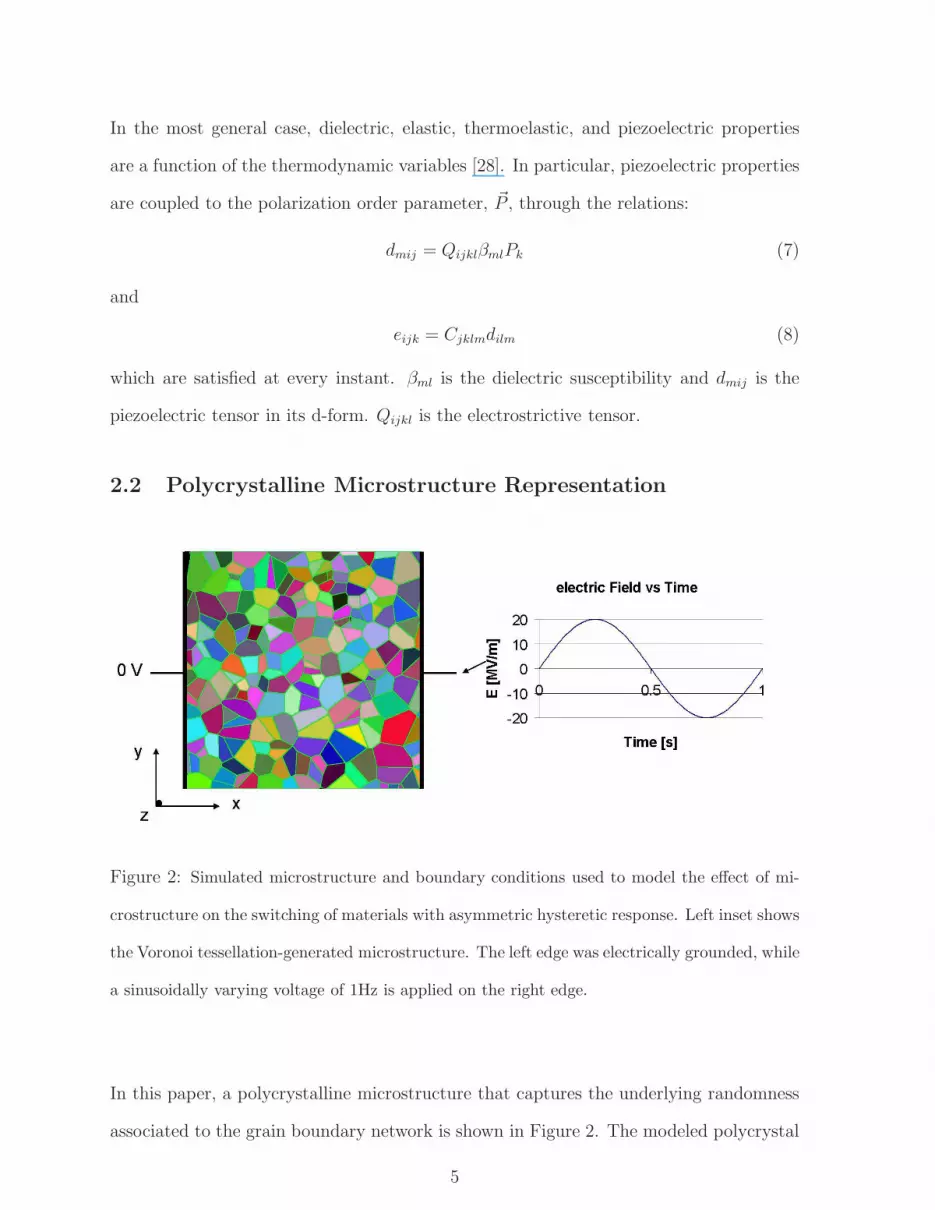
2.2 Polycrystalline Microstructure Representation
Figure 2: Simulated microstructure and boundary conditions used to model the effect of mi-
crostructure on the switching of materials with asymmetric hysteretic response. Left inset shows
the Voronoi tessellation-generated microstructure. The left edge was electrically grounded, while
a sinusoidally varying voltage of 1Hz is applied on the right edge.
In this paper, a polycrystalline microstructure that captures the underlying randomness
associated to the grain boundary network is shown in Figure 2. The modeled polycrystal
5

has an average grain size of 2.5 µm, and was approximated as a Voronoi tessellation [29,
30]. Physically, the Voronoi tessellation can be interpreted as a construction where a set of
grains nucleate simultaneously at randomly distributed locations in a spatial domain and
grow at a constant rate until their boundaries impinge [31]. Observed microstructures,
however, may differ from a Voronoi tessellation construction when grains are not equiaxed,
or grains are interlocked. These cases could be treated by basing calculations on images of
real or simulated two-dimensional microstructures. To generate crystalline orientations in
a microstructure, a set of randomly oriented c-axes is generated. For each orientation, the
a-axis is selected in a random direction perpendicular to the c-axis. The cross product of
the first two directions determines the orientation of the remaining crystallographic axis,
e.g., the b-axis. The Euler angles, (α, β, γ), describe an ordered sequence of rotations:
first by an angle β about the z-axis, followed by an angle α about the y-axis, and finally
by an angle γ about the z-axis [32]. This relates the crystal reference system to the
laboratory reference system [33, 34].
3 Simulation Setup
Crystallographic orientations were assigned to the computer-generated microstructures,
as described in Section 2.2. For this microstructure an initial 50 × 50 mesh was laid
out. The mesh was then refined and annealed multiple times, until the smallest grain
in the microstructure was resolved [33, 34]. Equations 5 through 8 were implemented
numerically by modifying the Object Oriented Finite Element Analysis program (OOF) [2,
3]. Ferroelectric polarization kinetics were added to the numerical description of the
system by using the resultant equilibrium strain and electric fields as input parameters
to solve for Equation 4 at every volume element of material. The value of the local
polarization order parameter was determined by implementing a Runge-Kutta algorithm.
The time step was determined by using a predictor-corrector approach: At every tentative
time step, the global solution is accepted if the deviation between a long time-step and
6
a short-time step solutions is smaller than a user-specified tolerance for all the elements.
Once a solution for a time iteration is accepted, the time step for the next iteration is set
as a function of the largest difference between the long and short time step solutions, for
all the elements. The time step dynamically adapts to minimize the number of numerical
steps to reach the final simulated instant [35]. The normalized tolerance of the predictor-
corrector Runge-Kutta algorithm was set to 1×10⁻⁶. The system is evolved in time for a
fixed value of applied in-plane electric field until the state of polarization reaches a steady
state value for all volume elements of the material. The resultant steady state polarization
order parameter is then used to recalculate the mechanical and electric equilibrium of the
solid. The used material parameters are summarized in Table 1.
The macroscopic switching of a ferroelectric material was induced by applying a volt-
age difference to the sample. Here, the left edge was electrically grounded, and a sinu-
soidally varying voltage with a frequency of 1 Hz was applied on the opposite (right)
edge. The generated macroscopic electric field had an amplitude of 20MV/m. The simu-
lation was run for two cycles, and the macroscopic polarization vector was sampled every
hundredth of a cycle. Each simulation took on the order of 24 hours in a PowerPC G5
of Macintosh. This process resulted in linear systems that possess on the order of 31,061
degrees of freedom, which took on the order of 575 iterations to converge to a normalized
tolerance of 7 × 10⁻¹³, for every time step.
7
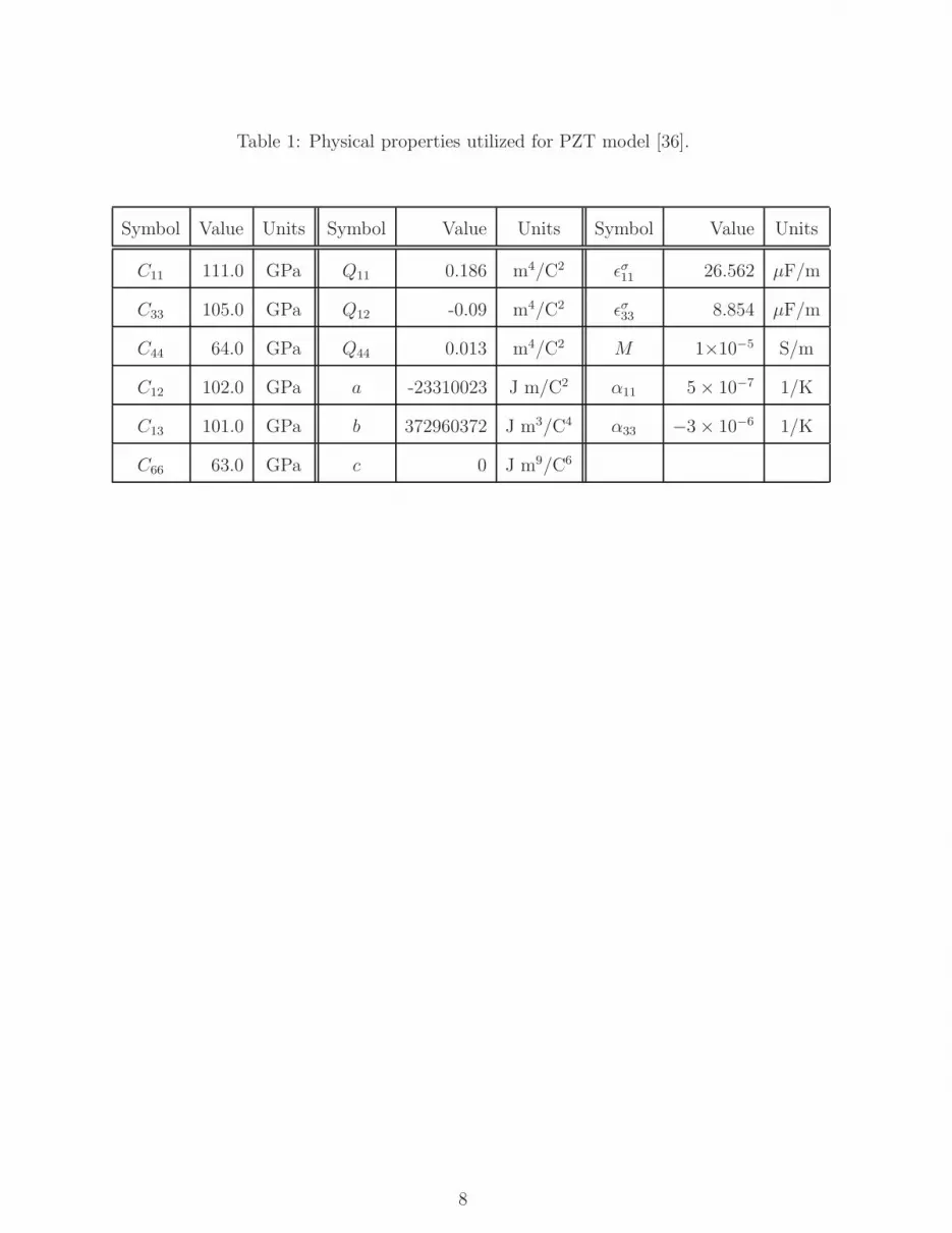
Table 1: Physical properties utilized for PZT model [36].
Symbol Value Units Symbol Value Units Symbol Value Units
C11 111.0 GPa Q11 0.186 m4/C2 ǫσ11 26.562 µF/m
C33 105.0 GPa Q12 -0.09 m4/C2 ǫσ33 8.854 µF/m
C44 64.0 GPa Q44 0.013 m4/C2 M 1×10⁻⁵ S/m
C12 102.0 GPa a -23310023 J m/C2 α11 5 × 10⁻⁷ 1/K
C13 101.0 GPa b 372960372 J m3/C4 α33 −3 × 10⁻⁶ 1/K
C66 63.0 GPa c 0 J m9/C6
8
4 Results and Discussion
The macroscopic x-component of the polarization vector as a function of the applied
electric field is summarized in Figure 3. The resulting hysteresis loop embodies the
time-dependent macroscopic state of polarization of the system. At the beginning of
the simulation, t = 0, the polycrystal is in a negatively poled state, thus the spatial
distribution of c-axes is initialized to have a negative projection on the x-axis of the
sample reference system. After one full cycle, the ferroelectric domains have switched to
states that differ significantly in both magnitude and direction from the initially assigned
ones. These newly acquired states of polarization are subsequently reached upon further
macroscopic cycling of the material. Thus, each volume element of material hysteretically
cycles following a sequence of polarization states that result from the electromechanical
interactions of the neighboring domains, as well as the instantaneous local ferroelectric
single-crystal properties.
9
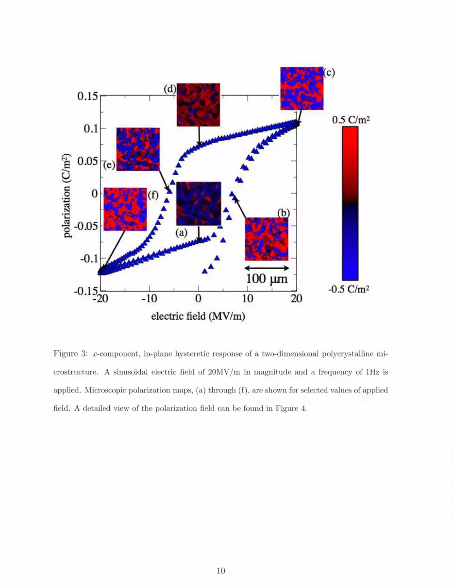
Figure 3: x-component, in-plane hysteretic response of a two-dimensional polycrystalline mi-
crostructure. A sinusoidal electric field of 20MV/m in magnitude and a frequency of 1Hz is
applied. Microscopic polarization maps, (a) through (f), are shown for selected values of applied
field. A detailed view of the polarization field can be found in Figure 4.
10

Figure 4: Spatial distribution of the x-component of the polarization order parameter at se-
lected locations of hysteresis loop. (a) shows the initial state of polarization at the beginning
of the first cycle. Domain switching and reswitching occurs between frames (b) E = 6.9MV/m,
and (c), E = 20MV/m. (d) corresponds to a positively poled, field-free polycrystal. (e) shows
the polarization fields at the negative coercive field, E = −6.9MV/m. At (f), an applied electric
field of E = −20MV/m, leads to an internal distribution of polarization domains that mirrors
the ones at the opposite value of applied electric field. Figure 3 shows the associated hysteresis
loop.
Figure 4 illustrates the spatial distribution of the x-component of the polarization
for selected values of the macroscopically applied voltage difference (electric field). (a)
shows the initial state of polarization at the end of the first cycle. Note that while the
average state of polarization is negative, spatial domains of positive polarization emerge
as a result of the stress and electric field concentration at grain corners and boundaries.
As the macroscopic electric field traverses the coercive field, E = 6.9MV/m, at (b),
11
and reaches a value of E = 20MV/m, domain switching proceeds from grain corners and
boundaries to the core of the grains, and in some grain instances polarization reorientation
is favored. Additionally, as the positive polarization continues to increase in poled grains,
the negative polarization becomes enhanced as a result of the compressive/tensile stresses
and in-plane piezoelectric interactions. The complementary process is observed in the
switching sequence that traverses E = 20MV/m to E = −20MV/m, from (c) to (f). The
microstructural distribution of the polarization fields at (c) mirror those found in (f),
except for a subset of grains that are electrically shielded or are unable to switch.
The simulations demonstrate that as the sample is macroscopically switched, four
switching mechanisms emerge as a result of the underlying electromechanical interac-
tions: the first mechanism, referred to as simple switching, is identified in terms of an
energetically preferred fraction of domains that will align with the direction of the applied
electric field (e.g., see row 1 in Figure 5). Here, those grains whose local dipolar energy
is greater than the coercive energy will switch, while those domains whose c-axis make a
large misorientation angle with the poling field will remain pinned. The fraction of this
population is highly dependent on the crystallographic texture of the polycrystal, grain
size, and degree of poling, as explained in a previous publication [2, 3].
12

Figure 5: Summary of switching mechanisms. The spatial distribution of the x-component of
the polarization order parameter during forward poling, (a), (b), and (c), as described in Figure 3
is shown. Circle highlighted in row 1 illustrates a simple switching event, circled area in row
2 to a grain boundary induced switching event, highlighted area in row 3 to a negative poling
mechanism region, and circled area in row 4 to an instance of domain reswitching mechanism
event.
13
The second mechanism will be realized as a function of the local electrical state
that results because of the combined grain-grain interactions, the strong anisotropy of
the dielectric permittivity, and the local piezoelectric contributions to polarization from
the surrounding grains. Here, the time-dependent switching process initiates at grain
corners and boundaries and propagates towards the core of the grain, until it reaches
the opposite edge of the grain or impinges with another propagating domain wall (e.g.,
see row 2 in Figure 5). Several grain instances, however, develop 180 domain walls
because of its inhomogeneous electromechanical state, which favors one polarization state
in one extreme of the grain, and the opposite polarization in the other extreme. In
comparison, switching starts at the core of the grain in a significantly smaller fraction,
thus demonstrating that domain switching is an heterogeneous nucleation process and
greatly controlled by the defects of the system. This mechanism is referred to as grain
boundary induced switching.
The two aforementioned switching mechanisms are well known [5, 7, 8, 9], and a great
deal of work can be found in the literature. In addition to these two mechanisms, the
calculations predict the existence of a third mechanism where abutting ferroelectric do-
mains oppose the local ferroelectric switching of the grains, i.e., their polarization vector
points in a direction opposite to the applied field, and increases in magnitude while the
surrounding domains have already switched to align themselves with the applied elec-
trostatic field (see Figure 6). The opposing population of polarized domains contract
along their c-axis in an attempt to align themselves with the local electrostatic field.
However, the surrounding polar regions have already switched and their associated c-
axes are already aligned with applied electric field. These domains elongate according
to their inherent piezoelectric properties. The interaction between these two abutting
sets of domains result in the development of local compressive stresses in the direction of
the applied field. The mechanically compressed domains effectively perform electrostatic
14

work against the macroscopically applied electric field. Such stresses enhance the state
of polarization of the oppositely poled grains via the direct piezoelectric effect, making
it energetically unfavorable for those grains to switch and align themselves with the ap-
plied electric field. Furthermore, as can be seen in Figures 3 and 4 the polarization of
the oppositely poled domains self-stabilizes as the macroscopic electric field increases.
Moreover, the spatial interlocking of grains and their associated electromechanical inter-
actions lead to the formation of connected regions of polarization (poled networks), that
are a combined result of the single-crystal piezoelectric properties and the grain misori-
entations. The negative poling mechanism demonstrates that poling of the entirety of
the polycrystal is unlikely or energetically unfavorable, particularly in untextured bulk
systems. An example location where the negative poling mechanism occurs is circled in
row 3 of Figure 5.
15

Figure 6: Schematic depiction of the proposed negative poling microstructural polarization
mechanism. Grain * corresponds to an unpoled, electric field-free representative grain that
is subjected to an electric field parallel to the red phase, insets 1—4∗. Here, as the electric
field increases, a favored fraction of domains within a grain will first switch to align with the
red domains, 1—2, while those domains that are already parallel with the applied electric field
will elongate in an effort to decrease their electrostatic energy at a rate given by its local
piezoelectric properties. Blue domains, antiparallel to the applied electrical field, attempt to
contract at the same rate as the red grains are trying to elongate. The spatial interlocking
of both type of domains will lead to a state of stress where the elongating domains will be in
compression and the contracting domains will be in tension. The non-trivial state of stress will
locally induce an increase on its coercive field making it increasingly difficult to switch, thus
making 4* thermodynamically inaccessible. The complementary situation is observed for an
applied electric field that is parallel to the blue polarized phase, i.e., in insets A—D∗.
16
Finally, for very large magnitudes of an applied electric field, a fourth mechanism
is observed that applies to a small subset of domains that have already switched and
aligned themselves with the direction of the applied electrostatic potential switch back.
While the first switching event is a result of the externally applied field, calculations
show that the second reversing switching event is a result of the subsequent piezoelectric
effect dominated behavior. Those domains surrounding a central one of opposite polar-
ity transform a fraction of their mechanical energy into electrical via the piezoelectric
effect in directions that do not necessarily coincide with the applied field. If the local
electromechanically-induced electric field is greater in magnitude than the externally ap-
plied one, a second reversing switching event will be induced, e.g., row 4 of Figure 5.
While physically possible, the domain reswitching mechanism is spatially localized to a
very small fraction of ferroelectric domains and large electric fields.
The present simulations demonstrate that polycrystalline ferroelectrics develop a spa-
tially distributed built-in electric field (see Figure 7). Such field is a result of the ther-
mal expansion induced stresses that arise during the cooling process of the ceramic
material. As the temperature of the ceramic decreases, the mechanically interlocked
grains contract at unequal rates that are given by the anisotropy of the thermal expan-
sion tensor and the local misorientation of the grains. Below the Curie temperature
the resultant stresses induce polarization fields via the direct piezoelectric effect. The
thermomechanical—electromechanically-induced electric fields reach maximal values at
grain corners and boundaries because the stresses reach the largest (tensile or compres-
sive) values in these regions. Thus, these stresses are sources and sinks of polarization,
which combined with the anisotropic dielectric properties of each ferroelectric domain
lead to non-trivial built-in electrical fields in the ferroelectric polycrystal. The effect of
these microstructural features is intensified by the introduction of other defects inherited
from processing, such as pores, cracks, chemically inhomogeneous regions, etc., and may
17
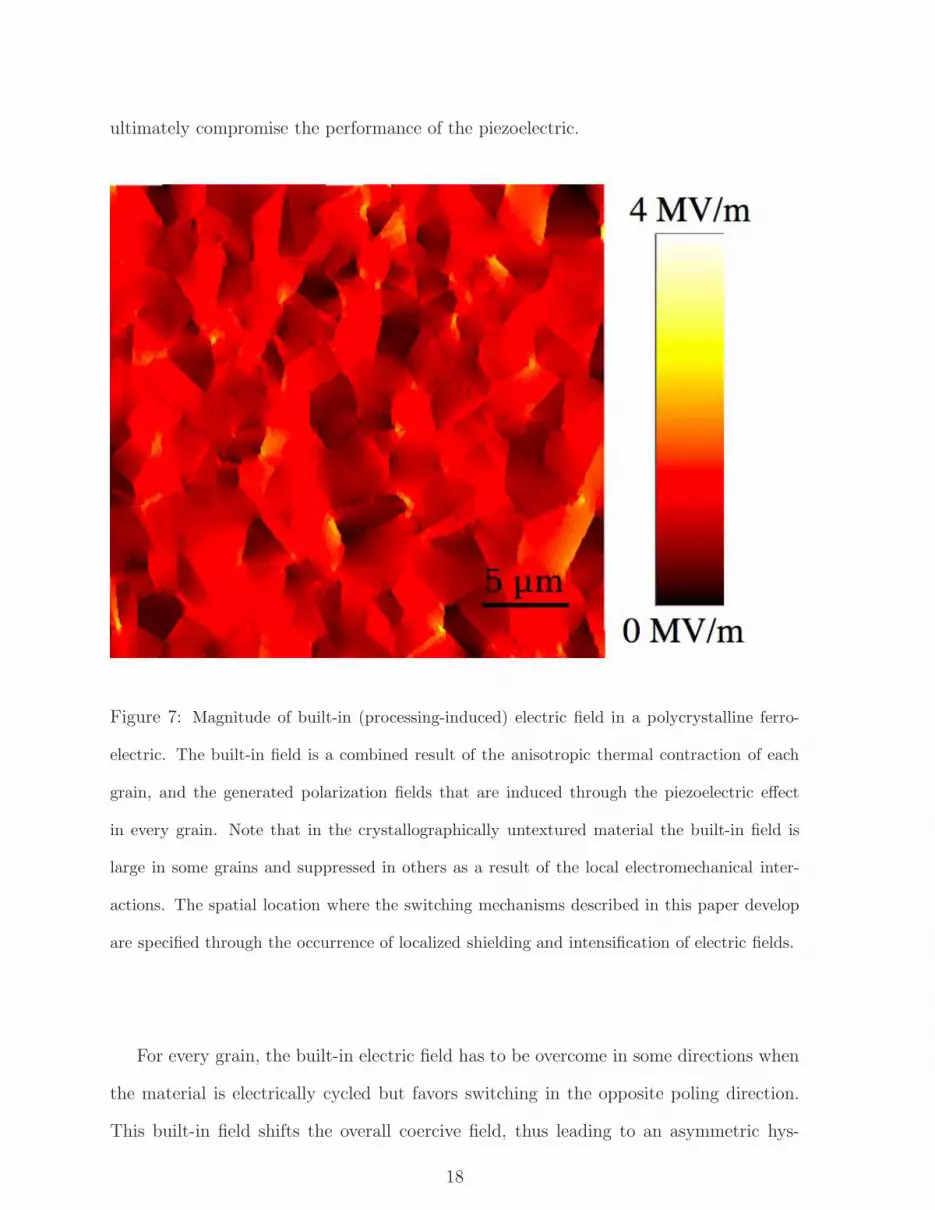
ultimately compromise the performance of the piezoelectric.
Figure 7: Magnitude of built-in (processing-induced) electric field in a polycrystalline ferro-
electric. The built-in field is a combined result of the anisotropic thermal contraction of each
grain, and the generated polarization fields that are induced through the piezoelectric effect
in every grain. Note that in the crystallographically untextured material the built-in field is
large in some grains and suppressed in others as a result of the local electromechanical inter-
actions. The spatial location where the switching mechanisms described in this paper develop
are specified through the occurrence of localized shielding and intensification of electric fields.
For every grain, the built-in electric field has to be overcome in some directions when
the material is electrically cycled but favors switching in the opposite poling direction.
This built-in field shifts the overall coercive field, thus leading to an asymmetric hys-
18
teretic response. The model predicts a shift of 4.5MV/m in the coercive electric field
that is very close in magnitude to the one reported in the experiments of Figure 1. More-
over, the simulated material behavior delivers a shift on the remnant polarization of
1.5×10⁻²C/m2.
Experimentally, the asymmetry of the hysteresis loop can be partially counteracted by
the application of an externally applied electric field bias. The corresponding simulated
behavior is shown in Figures 8 and 9. The microscopic polarization demonstrated in
Figure 8 is qualitatively similar to the predicted ones that develop in the unbiased sample.
However, even though a greater fraction of positively poled grains develop for positively
biased samples, a significant fraction of grains never switch because of the negative poling
effect hereby described. The same type of behavior is observed in the negatively biased
samples.
At the macroscopic level (see Figure 9), the positive remnant polarization of the
macroscopic hysteresis loop increases and the negative value of the remnant polarization
decreases as an increasingly larger bias electric field is applied. Moreover, the positive
and negative coercive field shift to the right as the bias electric field increases, and are
reversed if the bias field decreases and takes negative values. These results are summarized
in Figure 10. The simulations show that a biasing electric field of negative polarity can
partially compensate for the internal built-in field, but it is unable to fully suppress
it because of the crystallographic anisotropy and the spatial interlocking of the grains.
Furthermore, the asymmetry of 20% of the negative and positive remnant polarization
can be overcome by applying a biasing field of −1.8MV/m. Such field is comparable
in magnitude with the 1MV/m that was applied to the experimental system [1]. The
performed simulations predict a linear relationship between the applied bias and the
remnant polarization (both positive and negative), even though the polarization dynamics
are inherently non-linear and dependent on the entire history of the ferroelectric solid (see
Figure 11). Key and co-workers have experimentally verified that for small applied biasing
19
fields a linear relationship is observed; however, for large biasing fields the dependency
becomes non-linear. The authors speculate that the difference between experimental and
predicted behavior for high fields is a result of local 90 switching, not included in the
present numerical formulation [1].
In general, the slope and intercept of the polarization—bias field line is a direct
function of the texture, grain size and poling conditions that the polycrystal was subjected
to. Furthermore, it is expected that if the grain size increases, the dependency would
decrease because the built-in voltages differences across an individual grain would remain
the same, but the associated electric fields would decrease.
Figure 8: x-component polarization distribution for a polycrystal with three different applied
electric field biases. First column corresponds to material with a bias field, Eb = 4.5MV/m,
second to a bias-free solid, and third column to Eb = −4.5MV/m. Additionally, (a), (b), and
(c) correspond to a positively poled sample, (d), (e), and (f) to a material poled in the opposite
direction. Circled region highlights example locations (grains) that are unable to fully switch
as a result of the bias.
20

Figure 9: Predicted macroscopic hysteretic behavior for selected values of applied electric field
biases. corresponds to hysteresis loop response for an as-processed PZT sample, © to a bias
field of 4.5MV/m, and ♦ to a bias field of −4.5MV/m.
21
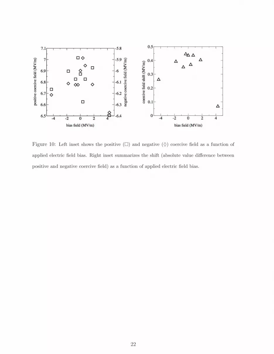
Figure 10: Left inset shows the positive () and negative (♦) coercive field as a function of
applied electric field bias. Right inset summarizes the shift (absolute value difference between
positive and negative coercive field) as a function of applied electric field bias.
22
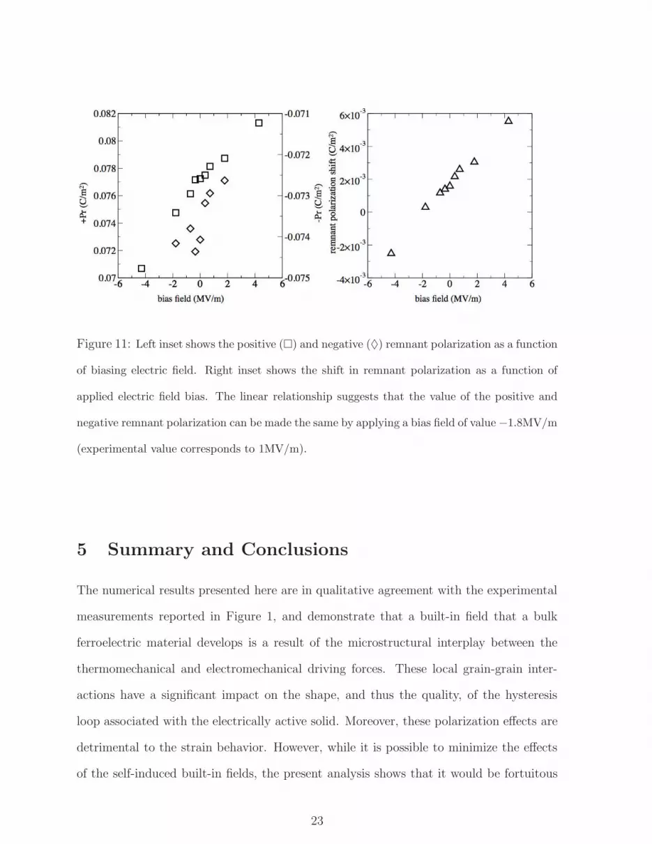
Figure 11: Left inset shows the positive () and negative (♦) remnant polarization as a function
of biasing electric field. Right inset shows the shift in remnant polarization as a function of
applied electric field bias. The linear relationship suggests that the value of the positive and
negative remnant polarization can be made the same by applying a bias field of value −1.8MV/m
(experimental value corresponds to 1MV/m).
5 Summary and Conclusions
The numerical results presented here are in qualitative agreement with the experimental
measurements reported in Figure 1, and demonstrate that a built-in field that a bulk
ferroelectric material develops is a result of the microstructural interplay between the
thermomechanical and electromechanical driving forces. These local grain-grain inter-
actions have a significant impact on the shape, and thus the quality, of the hysteresis
loop associated with the electrically active solid. Moreover, these polarization effects are
detrimental to the strain behavior. However, while it is possible to minimize the effects
of the self-induced built-in fields, the present analysis shows that it would be fortuitous
23
to completely remove such fields in the case of a crystallographically untextured sample.
Such macroscopic behavior is a result of the four switching mechanisms that participate
on the switching process of the solid. Moreover, the present analysis demonstrates that
there will always be a set of grains that will always contribute negatively to the macro-
scopic polarization of the system, and thus to the asymmetry (electrical and dipolar) of
the macroscopic hysteresis loop.
During long term service of the part, it is expected that the built-in fields that result
because of the underlying electromechanical interactions of the grains will play a major
role in the electrical fatigue and aging of the ferroelectric ceramic. Ion and charge point
defect migration to grain corners and boundaries will be induced through the appearance
of these built-in (remnant) fields, for the underlying planar and linear defects constitute
sources and sinks of polarization, leading to an increase in the asymmetry of the associated
macroscopic hysteresis loop. Moreover, during unipolar cycling of the device, the four
microstructural switching mechanisms outlined in this paper will activate the irreversible
transport of ionic charge from one grain boundary to the opposite one across a grain
through the simple switching and orientational mechanisms. Similarly, those domain
walls that remain pinned through the negative poling mechanism at the core of the grains
do not directly contribute to the macroscopic asymmetric behavior of the hysteresis loop,
but can be an important factor in trapping charged point defects upon prolonged electrical
cycling of the electroceramic.
References
[1] T. S. Key and K. J. Bowman. Ferroelectric Domain Texture in a Poled Hard PZT.
In The 15th International Conference on the Textures of Materials, 2008. In press.
[2] R. E. Garcıa, W. C. Carter, and S. A. Langer. Finite Element Implementation
of a Thermodynamic Description of Piezoelectric Microstructures. Journal of the
24

American Ceramic Society, 88(3):742–749, 2005.
[3] R. E. Garcıa, W. C. Carter, and S. A. Langer. The Effect of Texture on the Macro-
scopic Properties of Polycrystalline Piezoelectrics: Applications to Barium Titanate
and PZN-PT. Journal of the American Ceramic Society, 88(3):750–757, 2005.
[4] R. E. Garcıa, B. D. Huey, and J. E. Blendell. Virtual Piezo-Force Microscopy of
Polycrystalline Ferroelectric PZT Films. Journal of Applied Physics, 100:064105,
2006.
[5] E. K. H. Salje. Phase Transitions in Ferroelastics and Co-Elastic Crystals. Cam-
bridge University Press, Cambridge, UK, 1990.
[6] L. D. Landau and E. M. Lifshitz. Statistical Physics. Pergamon Press, Oxford, UK,
1980.
[7] A. F. Devonshire. Theory of Ferroelectrics. Philosophical Magazine (Supplement),
3(10):1010–1014, 1954.
[8] F. Jona and G. Shirane. Ferroelectric Crystals. Dover Publications Inc., NY, USA,
1993.
[9] B. Jaffe and W. Cook. Piezoelectric Ceramics. Academic Press, London, 1971.
[10] R. D. James and K. F. Hane. Martensitic Transformations and Shape Memory
Materials. Acta Materialia, 48(1):197–222, 2000.
[11] Y. Wang and A. G. Khachaturyan. Three-Dimensional Field Model and Computer
Modeling of Martensitic Transformations. Acta Materialia, 45(2):759–773, 1997.
[12] A. Artemev, Y. Jin, and A. G. Khachaturyan. Three-Dimensional Phase Field Model
of Proper Martensitic Transformation. Acta Materialia, 49:197–222, 2001.
25
[13] Y. C. Shiu and K. Bhattacharya. Domain Patterns and Macroscopic Behavior of
Ferroelectric Materials. Philosophical Magazine B, 81(12):2021–2054, 2001.
[14] J. Wang, Y. Li, L.-Q. Chen, and T.-Y. Zhang. The Effect of Mechanical Strains
on the Ferroelectric and Dielectric Properties of a Model Single Crystal-Phase Field
Simulation. Acta Materialia, 53:2495–2507, 2005.
[15] N. A. Pertsev. Aggregate Linear Properties of Ferroelectric Ceramics and Polycrys-
talline Thin Films: Calculation by the Method of Effective Piezoelectric Medium.
Journal of Applied Physics, 84(3):1524–1529, 1995.
[16] S. Hwang, J. E. Huber, R. E. McMeeking, and N. A. Fleck. The Simulation of
Switching in Polycrystalline Ferroelectric Ceramics. Journal of Applied Physics,
84(3):1530–1540, 1998.
[17] W. Kreher and J. Rodel. Ferroelectric Ceramics and Composites: Statistical Models
for Effective Piezoelectric and Pyroelectric Properties. In E. Colla, D. Damjanovic,
and N. Setter, editors, Applications of Ferroelectrics, 1998. ISAF 98. Proceedings of
the Eleventh IEEE International Symposium on Ferroelectrics, pages 455–458. Inst.
fur Werkstoffwissenschaft, Tech. Univ. Dresden, Germany, 1956.
[18] A. G. Zembil’gotov N. A. Pertsev and R. Wazer. Effective Dielectric and Piezoelectric
Constants of Thin Polycrystalline Ferroelectric Films. Physics of the Solid State,
40(12):2002–2008, 1998.
[19] A. N. Soukhojak and Y.-M. Chiang. Generalized Rheology of Active Materials.
Journal of Applied Physics, 88:6902–6909, 2000.
[20] Y. Huo and Q. Jiang. Modeling of Domain Switching in Polycrystalline Ferroelectric
Ceramics. Smart Materials and Structures, 6:441–447, 1997.
26

[21] X. Chen, D.-N. Fang, and K.-C. Hwang. A Mesoscopic Model of the Constitutive
Behavior of Monocrystalline Ferroelectrics. Smart Materials and Structures, 6:145–
151, 1997.
[22] S.-J. Kim. A Simple Continuum Model for Polarization Reversals in Ferroelectrics.
Smart Materials and Structures, 7:572–579, 1998.
[23] H. Kessler and H. Balke. On the Local Energy Release and Stability of Polarization
Switching, and Analogies to Fracture Mechanics. unpublished, 1999.
[24] E. L. Rumyantsev V. Ya. Shur and S. D. Makarov. Kinetics of Polarization Switching
in Finite-Size Ferroelectric Samples. Physics of the Solid State, 37(6):917–919, 1995.
[25] N. A. Pertsev, A. G. Zemilgotov, and A. K. Tagantsev. Effect of Mechanical Bound-
ary Conditions on Phase Diagrams of Epitaxial Ferroelectric Thin Films. Physical
Review Letters, 80(9):1988–1991, 1998.
[26] S. M. Allen and J. W. Cahn. A Microscopic Theory for Antiphase Boundary Motion
and its Application to Antiphase Domain Coarsening. Acta Metallurgica, 27:1085–
1095, 1979.
[27] R. E. Garcıa, C. M. Bishop, and W. C. Carter. Thermodynamically Consistent Vari-
ational Principles with Applications to Electrically and Magnetically Active Systems.
Acta Materialia, 52:11–21, 2004.
[28] J. F. Nye. Physical Properties of Crystals. Oxford University Press, London, 1998.
[29] C.B. Barber, D.P. Dobkin, and H.T. Huhdanpaa. The Quickhull Algorithm for
Convex Hulls. ACM Transactions on Mathematical Software, 22(4):469–483, 1996.
[30] O. Barndorff-Nielsen, W. S. Kendall, and M. N. M. Lieshout. Stochastic Geometry:
Likelihood and Computation. Chapman and Hall, Boca Raton, Florida, 1996.
27
[31] L. J. Gibson and Michael F. Ashby. Cellular Solids. Structure and Properties. Perg-
amon Press, U. K., 1988.
[32] H. Goldstein. Classical Mechanics. Addison-Wesley Publishing Company Inc., Read-
ing, MA, 1980.
[33] W. C. Carter, S. A. Langer, and E. R. Fuller. The OOF Manual:Version 1.0. National
Institute of Standards and Technology, 100 Bureau Drive, Stop 8910; Gaithersburg
MD, USA, nistir 6256 edition, 1998.
[34] S. A. Langer, W. C. Carter, and E. R. Fuller. OOF: Analysis of Real Material
Microstructures, 1999. http://www.ctcms.nist.gov/oof/.
[35] W. H. Press, S. A. Teukolsky, W. T. Vettering, and B. Falnnery. Numerical Recipes
in C. Cambridge University Press, 40 West 20th Street, New York NY 10011-4211,
USA, 1997.
[36] J. Yin and W. Cao. Elastic, Piezoelectric and Dielectric Properties of
0.0955Pb(Zn1/3Nb2/3)O3-0.45PbTiO3 Single Crystal with Designed Multidomains.
IEEE Transactions on Ultrasonics, Ferroelectrics, and Frequency Control, 47(1):285–
291, 2000.
28