direct assembly of cyclic olefin copolymer microfluidic devices helped by dry photoresist
TRANSCRIPT
Db
La
b
a
ARRAA
KCAOO
1
ieb(ataacwmirua
lec
h0
Sensors and Actuators A 223 (2015) 76–83
Contents lists available at ScienceDirect
Sensors and Actuators A: Physical
j ourna l ho me page: www.elsev ier .com/ locate /sna
irect assembly of cyclic olefin copolymer microfluidic devices helpedy dry photoresist
amia El Fissi a,∗, Denis Vandormaelb, Laurent A. Francisa
ICTEAM Institute, Université catholique de Louvain, Louvain-la-Neuve, BelgiumSIRRIS – Liege Science Park, Seraing, Belgium
r t i c l e i n f o
rticle history:eceived 15 July 2014eceived in revised form 5 December 2014ccepted 11 December 2014vailable online 19 December 2014
eywords:
a b s t r a c t
A generic method for rapid, reproducible, and robust selective bonding of microfluidic chips made of CyclicOlefin Copolymer (COC) has been developed and optimized. In this work we propose an adhesive bondingtechnique using ORDYL negative dry film photo-resist as glue to perform the packaging of COC micro-patterned structures. The ORDYL resist is qualified in terms of resolution, biocompatibility and fluidicsealing. The adhesive bonding is achieved by laminating a thin layer of ORDYL SY300 (<17 �m) on top ofthe microfluidic part and then bonded to the other COC part. In this research, an oxygen plasma treatment
yclic olefin copolymerdhesive bondingRDYL negative dry film photo resistxygen plasma treatment
for adhesion improvement was performed on COC surfaces at various plasma times. The bonding methodis described in detail and the bonding quality of the chips was evaluated by a shear strength testingprocedure and a leak test by pressurizing a microfluidic channel with an aqueous solution using anexternal peristaltic pump. Results are reported emphasizing the efficiency of the proposed approach andthe developed process features high yields (>70%).
© 2014 Elsevier B.V. All rights reserved.
. Introduction
The impact of microfluidic technologies has dramaticallyncreased during the last few years since microfluidic is consid-red as a key technology within the field of life science [1]. Polymerased Lab-on-a-chip (LOC) devices or micro-total analysis systems�TAS) are currently hot research topics in the field of microfluidicsnd BioMEMS [2]. The main advantages of microfluidic systems arehat important biological operations such as pathogen detectionnd genotyping can be accelerated and amplified by integrating
variety of functions like sample preparation, DNA amplification,ell capture, pumping, mixing, and detection onto a single platformith minimal or no human intervention. The advantages of poly-ers over glass and silicon as a substrate for microfluidic devices
nclude [3] their biocompatibility, disposability, good chemicalesistance, optical properties, low cost, and capacity for high vol-me production using established manufacturing techniques suchs hot embossing and injection molding.
Several polymeric materials including polymethylmethacry-
ate (PMMA) [4], polycarbonate (PC) [5] polyester [6], fluorinatedthylene propylene [7], and poly(ethylene terephthalate) [8] andyclic olefin copolymer (COC) [9] have been investigated for the∗ Corresponding author. Tel.: +32 010472174.E-mail address: [email protected] (L. El Fissi).
ttp://dx.doi.org/10.1016/j.sna.2014.12.016924-4247/© 2014 Elsevier B.V. All rights reserved.
microfluidics fabrication [10]. COC (Topas) which is a thermoplas-tic copolymer has been used because of its excellent properties,such as high glass transition temperatures, excellent transparency[11].
Bonding between polymer substrates is an essential fabricationstep to seal and form micro-channels or micro-chambers in plas-tic LOC or �TAS system since the micro-channels on the polymerlayers are normally opened after the micro-machining step. Today,several bonding techniques for plastic substrates have been devel-oped such as a thermal lamination [12] the adhesive bonding [13],the thermal bonding [14,15], the laser welding [16,17], and theconventional solvent bonding [18,19].
The solvent bonding of thermoplastics takes advantage of thepolymer solubility in selected solvent systems to achieve entangle-ment of polymer chains across the interface. When a thermoplasticsurface is solvated, the polymer chains become mobile and canreadily diffuse across the solvated layer, leading to an extensiveintertwining of chains between the surfaces and resulting in excep-tionally strong bonds. The solvent bonding is carried out at roomtemperature or decreased temperature levels which comply withthe reagent pre-storage. Furthermore, the chips are usually storedat high temperatures for several hours to accelerate the solvent
evaporation after the bonding. The temperature stability of thebonds depends significantly on the complete evaporation of thesolvents, since the presence of solvents causes stress cracks andcloudiness.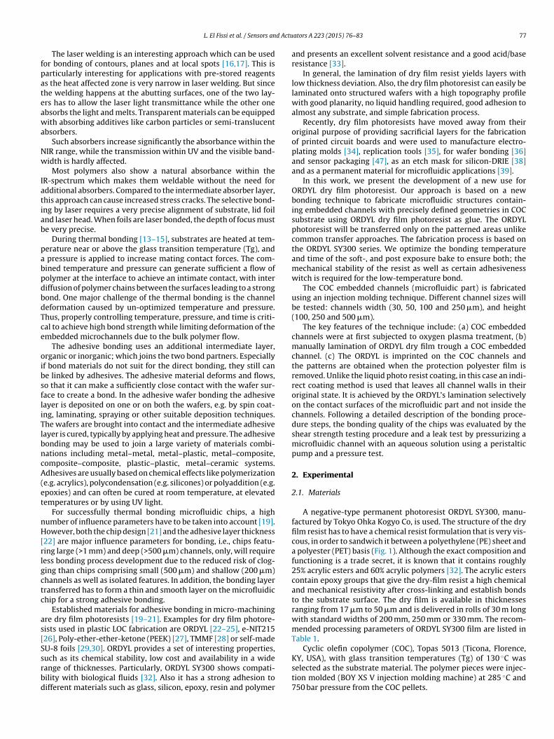
d Actu
fpateawa
Nw
Iatiab
pabpdbdTce
oibsfliTlbncA(et
nH[rlgctc
as[Ssrbd
L. El Fissi et al. / Sensors an
The laser welding is an interesting approach which can be usedor bonding of contours, planes and at local spots [16,17]. This isarticularly interesting for applications with pre-stored reagentss the heat affected zone is very narrow in laser welding. But sincehe welding happens at the abutting surfaces, one of the two lay-rs has to allow the laser light transmittance while the other onebsorbs the light and melts. Transparent materials can be equippedith absorbing additives like carbon particles or semi-translucent
bsorbers.Such absorbers increase significantly the absorbance within the
IR range, while the transmission within UV and the visible band-idth is hardly affected.
Most polymers also show a natural absorbance within theR-spectrum which makes them weldable without the need fordditional absorbers. Compared to the intermediate absorber layer,his approach can cause increased stress cracks. The selective bond-ng by laser requires a very precise alignment of substrate, lid foilnd laser head. When foils are laser bonded, the depth of focus muste very precise.
During thermal bonding [13–15], substrates are heated at tem-erature near or above the glass transition temperature (Tg), and
pressure is applied to increase mating contact forces. The com-ined temperature and pressure can generate sufficient a flow ofolymer at the interface to achieve an intimate contact, with interiffusion of polymer chains between the surfaces leading to a strongond. One major challenge of the thermal bonding is the channeleformation caused by un-optimized temperature and pressure.hus, properly controlling temperature, pressure, and time is criti-al to achieve high bond strength while limiting deformation of thembedded microchannels due to the bulk polymer flow.
The adhesive bonding uses an additional intermediate layer,rganic or inorganic; which joins the two bond partners. Especiallyf bond materials do not suit for the direct bonding, they still cane linked by adhesives. The adhesive material deforms and flows,o that it can make a sufficiently close contact with the wafer sur-ace to create a bond. In the adhesive wafer bonding the adhesiveayer is deposited on one or on both the wafers, e.g. by spin coat-ng, laminating, spraying or other suitable deposition techniques.he wafers are brought into contact and the intermediate adhesiveayer is cured, typically by applying heat and pressure. The adhesiveonding may be used to join a large variety of materials combi-ations including metal–metal, metal–plastic, metal–composite,omposite–composite, plastic–plastic, metal–ceramic systems.dhesives are usually based on chemical effects like polymerization
e.g. acrylics), polycondensation (e.g. silicones) or polyaddition (e.g.poxies) and can often be cured at room temperature, at elevatedemperatures or by using UV light.
For successfully thermal bonding microfluidic chips, a highumber of influence parameters have to be taken into account [19].owever, both the chip design [21] and the adhesive layer thickness
22] are major influence parameters for bonding, i.e., chips featu-ing large (>1 mm) and deep (>500 �m) channels, only, will requireess bonding process development due to the reduced risk of clog-ing than chips comprising small (500 �m) and shallow (200 �m)hannels as well as isolated features. In addition, the bonding layerransferred has to form a thin and smooth layer on the microfluidichip for a strong adhesive bonding.
Established materials for adhesive bonding in micro-machiningre dry film photoresists [19–21]. Examples for dry film photore-ists used in plastic LOC fabrication are ORDYL [22–25], e-NIT21526], Poly-ether-ether-ketone (PEEK) [27], TMMF [28] or self-madeU-8 foils [29,30]. ORDYL provides a set of interesting properties,
uch as its chemical stability, low cost and availability in a wideange of thicknesses. Particularly, ORDYL SY300 shows compati-ility with biological fluids [32]. Also it has a strong adhesion toifferent materials such as glass, silicon, epoxy, resin and polymerators A 223 (2015) 76–83 77
and presents an excellent solvent resistance and a good acid/baseresistance [33].
In general, the lamination of dry film resist yields layers withlow thickness deviation. Also, the dry film photoresist can easily belaminated onto structured wafers with a high topography profilewith good planarity, no liquid handling required, good adhesion toalmost any substrate, and simple fabrication process.
Recently, dry film photoresists have moved away from theiroriginal purpose of providing sacrificial layers for the fabricationof printed circuit boards and were used to manufacture electro-plating molds [34], replication tools [35], for wafer bonding [36]and sensor packaging [47], as an etch mask for silicon-DRIE [38]and as a permanent material for microfluidic applications [39].
In this work, we present the development of a new use forORDYL dry film photoresist. Our approach is based on a newbonding technique to fabricate microfluidic structures contain-ing embedded channels with precisely defined geometries in COCsubstrate using ORDYL dry film photoresist as glue. The ORDYLphotoresist will be transferred only on the patterned areas unlikecommon transfer approaches. The fabrication process is based onthe ORDYL SY300 series. We optimize the bonding temperatureand time of the soft-, and post exposure bake to ensure both; themechanical stability of the resist as well as certain adhesivenesswitch is required for the low-temperature bond.
The COC embedded channels (microfluidic part) is fabricatedusing an injection molding technique. Different channel sizes willbe tested: channels width (30, 50, 100 and 250 �m), and height(100, 250 and 500 �m).
The key features of the technique include: (a) COC embeddedchannels were at first subjected to oxygen plasma treatment, (b)manually lamination of ORDYL dry film trough a COC embeddedchannel. (c) The ORDYL is imprinted on the COC channels andthe patterns are obtained when the protection polyester film isremoved. Unlike the liquid photo resist coating, in this case an indi-rect coating method is used that leaves all channel walls in theiroriginal state. It is achieved by the ORDYL’s lamination selectivelyon the contact surfaces of the microfluidic part and not inside thechannels. Following a detailed description of the bonding proce-dure steps, the bonding quality of the chips was evaluated by theshear strength testing procedure and a leak test by pressurizing amicrofluidic channel with an aqueous solution using a peristalticpump and a pressure test.
2. Experimental
2.1. Materials
A negative-type permanent photoresist ORDYL SY300, manu-factured by Tokyo Ohka Kogyo Co, is used. The structure of the dryfilm resist has to have a chemical resist formulation that is very vis-cous, in order to sandwich it between a polyethylene (PE) sheet anda polyester (PET) basis (Fig. 1). Although the exact composition andfunctioning is a trade secret, it is known that it contains roughly25% acrylic esters and 60% acrylic polymers [32]. The acrylic esterscontain epoxy groups that give the dry-film resist a high chemicaland mechanical resistivity after cross-linking and establish bondsto the substrate surface. The dry film is available in thicknessesranging from 17 �m to 50 �m and is delivered in rolls of 30 m longwith standard widths of 200 mm, 250 mm or 330 mm. The recom-mended processing parameters of ORDYL SY300 film are listed inTable 1.
Cyclic olefin copolymer (COC), Topas 5013 (Ticona, Florence,
KY, USA), with glass transition temperatures (Tg) of 130 ◦C wasselected as the substrate material. The polymer pieces were injec-tion molded (BOY XS V injection molding machine) at 285 ◦C and750 bar pressure from the COC pellets.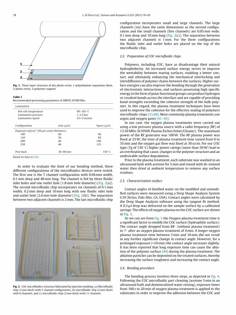
78 L. El Fissi et al. / Sensors and Actu
Fig. 1. Three-layer structure of dry photo-resist, 1-polyethylene separation sheet,2-photo-resist, 3-polyester support.
Table 1Recommended processing parameters of ORDYL SY300 film.
Lamination
Hot roll temperature 90–105 ◦CLamination pressure 1–2.5 barLamination speed 0.5–2 m/min
Configuration Line (�m) Space (�m)
Exposure mj/cm2 (50 �m resist thickness)100 60 60150 50 80200 40 100250 40 125
B
dT0iTwab
Fcw
Post back 30–60 min 150 ◦C
ased on data in [32].
In order to evaluate the limit of our bonding method, threeifferent configurations of the microfluidics devices were tested.he first one is the T channel configuration with 0.04 mm width,.1 mm deep and 40 mm long. The channel is fed by three fluidic
nlet holes and one outlet hole (1.8 mm hole diameter) (Fig. 2(a)).
he second microfluidic chip incorporates six channels of 0.1 mmidth, 0.2 mm deep and 10 mm long with one fluidic inlet holend outlet hole (2.6 mm hole diameter) (Fig. 2(b)). The separationetween two adjacent channels is 2 mm. The last microfluidic chip
ig. 2. COC microfluidics structure fabricated by injection molding. (a) Microfluidichip (3 mm thick) with T channel configuration, (b) microfluidic chip (2 mm thick)ith 6 channels, and (c) microfluidic chip (2 mm thick) with 11 channels.
ators A 223 (2015) 76–83
configuration incorporates small and large channels. The largechannels (six) have the same dimensions as the second configu-ration and the small channels (five channels) are 0.05 mm wide,0.1 mm deep and 10 mm long (Fig. 2(c)). The separation betweentwo adjacent channels is 1 mm. For the three configurationsthe fluidic inlet and outlet holes are placed on the top of themicrofluidic chip.
2.2. Preparation of COC microfluidic chips
Polymers, including COC, have as disadvantage their naturalhydrophobicity. An increased surface energy serves to improvethe wettability between mating surfaces, enabling a better con-tact, and ultimately enhancing the mechanical interlocking andinterdiffusion of polymer chains between the surfaces. Higher sur-face energies can also improve the bonding through the generationof electrostatic interactions, and surfaces possessing high specificenergy in the form of polar functional groups can produce hydrogenor covalent bonds across the interface and are capable of providingbond strengths exceeding the cohesive strength of the bulk poly-mer. In this regard, the plasma treatment techniques have beenused to improve the cohesion for the effective sealing of polymersmicrofluidic chips [33,40]. Most commonly plasma treatments useargon and oxygen gases [41–45].
In our case, the oxygen plasma treatments were carried outusing a low pressure plasma source with a radio frequency (RF) of13.56 MHz (K1050X Plasma Etcher/Asher/Cleaner). The maximumpower of the RF generator was 100 W. The RF plasma power wasfixed at 25 W, the time of plasma treatment time varied from 0 to35 min and the oxygen gas flow was fixed at 30 sccm. For our COCtype (Tg of 130 ◦C) higher power ratings (more than 50 W) lead toan overheating that cause, changes in the polymer structure and anundesirable surface degradation.
Prior to the plasma treatment, each substrate was washed in anultrasound bath with acetone for 5 min and rinsed with de-ionizedwater then dried at ambient temperature to remove any surfaceresidues.
2.3. Characterization surface
Contact angles of distilled water on the modified and unmodi-fied surfaces were measured using a Drop Shape Analysis SystemG10 (Krüss, Palo Alto, CA, USA). Contact angles were calculated bythe Drop Shape Analysis software using the tangent fit method.A 0.3 �l drop was delivered on the sample surface by a calibratedsyringe. The effects of oxygen plasma on the COC surface are shownin Fig. 3.
As we can see from Fig. 3 the Oxygen-plasma treatment time isa significant factor to modify the COC surface (hydrophilic surface).The contact angle dropped from 88◦ (without plasma treatment)to 7◦ after an oxygen plasma treatment of 4 min. A longer oxygenplasma treatment time between 5 min and 10 min did not resultin any further significant change in contact angle. However, for aprolonged exposure (>10 min) the contact angle increases slightly.It has been reported that long exposure time can cause the abla-tion of the polymer surface [40] during the plasma treatment. Theablation particles can be deposited on the treated surfaces, therebyincreasing the surface roughness and increasing the contact angle.
2.4. Bonding procedure
The bonding process involves three steps, as depicted in Fig. 4.
Following the COC microfluidic part cleaning (acetone 5 min in anultrasound bath and demineralized water rinsing), exposure timesfrom 180 s to 20 min of oxygen plasma treatment is applied to thesubstrates in order to improve the adhesion between the COC and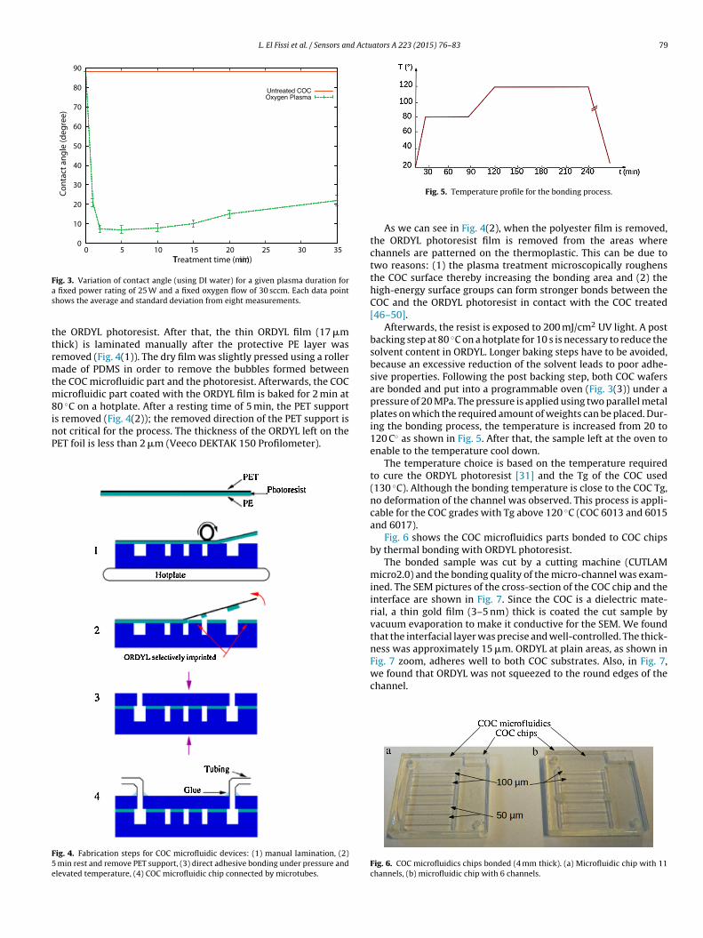
L. El Fissi et al. / Sensors and Actuators A 223 (2015) 76–83 79
0
10
20
30
40
50
60
70
80
90
0
Con
tact
ang
le (d
egre
e)
5 10T
15 20Treatment time (min)
25 30in)
Untreated COCOxygen Plasma
35
Fas
ttrmtm8inP
F5e
ig. 3. Variation of contact angle (using DI water) for a given plasma duration for fixed power rating of 25 W and a fixed oxygen flow of 30 sccm. Each data pointhows the average and standard deviation from eight measurements.
he ORDYL photoresist. After that, the thin ORDYL film (17 �mhick) is laminated manually after the protective PE layer wasemoved (Fig. 4(1)). The dry film was slightly pressed using a rollerade of PDMS in order to remove the bubbles formed between
he COC microfluidic part and the photoresist. Afterwards, the COCicrofluidic part coated with the ORDYL film is baked for 2 min at
0 ◦C on a hotplate. After a resting time of 5 min, the PET support
s removed (Fig. 4(2)); the removed direction of the PET support isot critical for the process. The thickness of the ORDYL left on theET foil is less than 2 �m (Veeco DEKTAK 150 Profilometer).ig. 4. Fabrication steps for COC microfluidic devices: (1) manual lamination, (2) min rest and remove PET support, (3) direct adhesive bonding under pressure andlevated temperature, (4) COC microfluidic chip connected by microtubes.
Fig. 5. Temperature profile for the bonding process.
As we can see in Fig. 4(2), when the polyester film is removed,the ORDYL photoresist film is removed from the areas wherechannels are patterned on the thermoplastic. This can be due totwo reasons: (1) the plasma treatment microscopically roughensthe COC surface thereby increasing the bonding area and (2) thehigh-energy surface groups can form stronger bonds between theCOC and the ORDYL photoresist in contact with the COC treated[46–50].
Afterwards, the resist is exposed to 200 mJ/cm2 UV light. A postbacking step at 80 ◦C on a hotplate for 10 s is necessary to reduce thesolvent content in ORDYL. Longer baking steps have to be avoided,because an excessive reduction of the solvent leads to poor adhe-sive properties. Following the post backing step, both COC wafersare bonded and put into a programmable oven (Fig. 3(3)) under apressure of 20 MPa. The pressure is applied using two parallel metalplates on which the required amount of weights can be placed. Dur-ing the bonding process, the temperature is increased from 20 to120 C◦ as shown in Fig. 5. After that, the sample left at the oven toenable to the temperature cool down.
The temperature choice is based on the temperature requiredto cure the ORDYL photoresist [31] and the Tg of the COC used(130 ◦C). Although the bonding temperature is close to the COC Tg,no deformation of the channel was observed. This process is appli-cable for the COC grades with Tg above 120 ◦C (COC 6013 and 6015and 6017).
Fig. 6 shows the COC microfluidics parts bonded to COC chipsby thermal bonding with ORDYL photoresist.
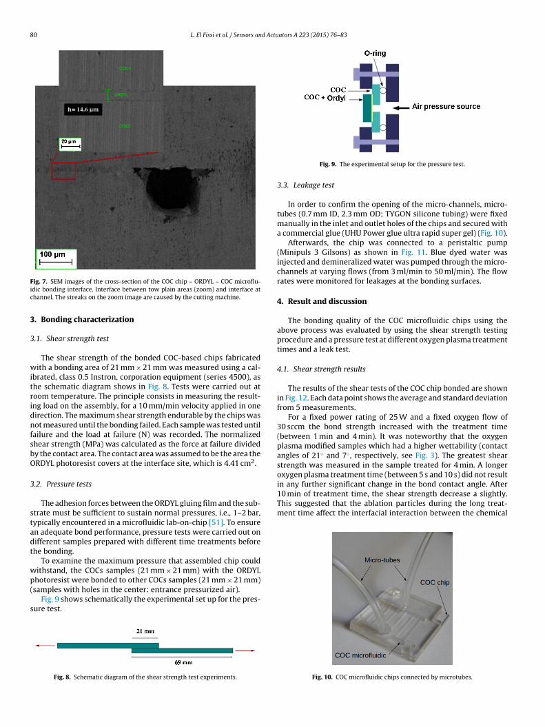
The bonded sample was cut by a cutting machine (CUTLAMmicro2.0) and the bonding quality of the micro-channel was exam-ined. The SEM pictures of the cross-section of the COC chip and theinterface are shown in Fig. 7. Since the COC is a dielectric mate-rial, a thin gold film (3–5 nm) thick is coated the cut sample byvacuum evaporation to make it conductive for the SEM. We foundthat the interfacial layer was precise and well-controlled. The thick-ness was approximately 15 �m. ORDYL at plain areas, as shown inFig. 7 zoom, adheres well to both COC substrates. Also, in Fig. 7,
we found that ORDYL was not squeezed to the round edges of thechannel.Fig. 6. COC microfluidics chips bonded (4 mm thick). (a) Microfluidic chip with 11channels, (b) microfluidic chip with 6 channels.
80 L. El Fissi et al. / Sensors and Actuators A 223 (2015) 76–83
Fic
3
3
witridnfsbO
3
stadt
wp(
s
in any further significant change in the bond contact angle. After10 min of treatment time, the shear strength decrease a slightly.This suggested that the ablation particles during the long treat-ment time affect the interfacial interaction between the chemical
ig. 7. SEM images of the cross-section of the COC chip – ORDYL – COC microflu-dic bonding interface. Interface between tow plain areas (zoom) and interface athannel. The streaks on the zoom image are caused by the cutting machine.
. Bonding characterization
.1. Shear strength test
The shear strength of the bonded COC-based chips fabricatedith a bonding area of 21 mm × 21 mm was measured using a cal-
brated, class 0.5 Instron, corporation equipment (series 4500), ashe schematic diagram shows in Fig. 8. Tests were carried out atoom temperature. The principle consists in measuring the result-ng load on the assembly, for a 10 mm/min velocity applied in oneirection. The maximum shear strength endurable by the chips wasot measured until the bonding failed. Each sample was tested until
ailure and the load at failure (N) was recorded. The normalizedhear strength (MPa) was calculated as the force at failure dividedy the contact area. The contact area was assumed to be the area theRDYL photoresist covers at the interface site, which is 4.41 cm2.
.2. Pressure tests
The adhesion forces between the ORDYL gluing film and the sub-trate must be sufficient to sustain normal pressures, i.e., 1–2 bar,ypically encountered in a microfluidic lab-on-chip [51]. To ensuren adequate bond performance, pressure tests were carried out onifferent samples prepared with different time treatments beforehe bonding.
To examine the maximum pressure that assembled chip couldithstand, the COCs samples (21 mm × 21 mm) with the ORDYL
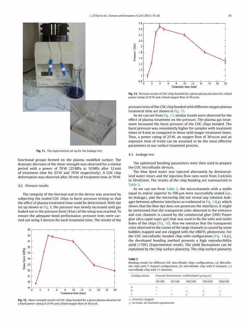
hotoresist were bonded to other COCs samples (21 mm × 21 mm)samples with holes in the center: entrance pressurized air).Fig. 9 shows schematically the experimental set up for the pres-ure test.
Fig. 8. Schematic diagram of the shear strength test experiments.
Fig. 9. The experimental setup for the pressure test.
3.3. Leakage test
In order to confirm the opening of the micro-channels, micro-tubes (0.7 mm ID, 2.3 mm OD; TYGON silicone tubing) were fixedmanually in the inlet and outlet holes of the chips and secured witha commercial glue (UHU Power glue ultra rapid super gel) (Fig. 10).
Afterwards, the chip was connected to a peristaltic pump(Minipuls 3 Gilsons) as shown in Fig. 11. Blue dyed water wasinjected and demineralized water was pumped through the micro-channels at varying flows (from 3 ml/min to 50 ml/min). The flowrates were monitored for leakages at the bonding surfaces.
4. Result and discussion
The bonding quality of the COC microfluidic chips using theabove process was evaluated by using the shear strength testingprocedure and a pressure test at different oxygen plasma treatmenttimes and a leak test.
4.1. Shear strength results
The results of the shear tests of the COC chip bonded are shownin Fig. 12. Each data point shows the average and standard deviationfrom 5 measurements.
For a fixed power rating of 25 W and a fixed oxygen flow of30 sccm the bond strength increased with the treatment time(between 1 min and 4 min). It was noteworthy that the oxygenplasma modified samples which had a higher wettability (contactangles of 21◦ and 7◦, respectively, see Fig. 3). The greatest shearstrength was measured in the sample treated for 4 min. A longeroxygen plasma treatment time (between 5 s and 10 s) did not result
Fig. 10. COC microfluidic chips connected by microtubes.
L. El Fissi et al. / Sensors and Actuators A 223 (2015) 76–83 81
fdpod
4
stsler
Fa
Fig. 11. The experimental set up for the leakage test.
unctional groups formed on the plasma modified surface. Theramatic decrease of the shear strength was observed for a similareriod with a power of 70 W (25 MPa to 10 MPa after 12 minf treatment time for 25 W and 70 W respectively). A COC chipeformation was observed after 20 min of treatment time at 70 W.
.2. Pressure results
The integrity of the thermal seal in the device was assessed byubjecting the sealed COC chips to burst pressure testing so thathe effect of plasma treatment time could be determined. With the
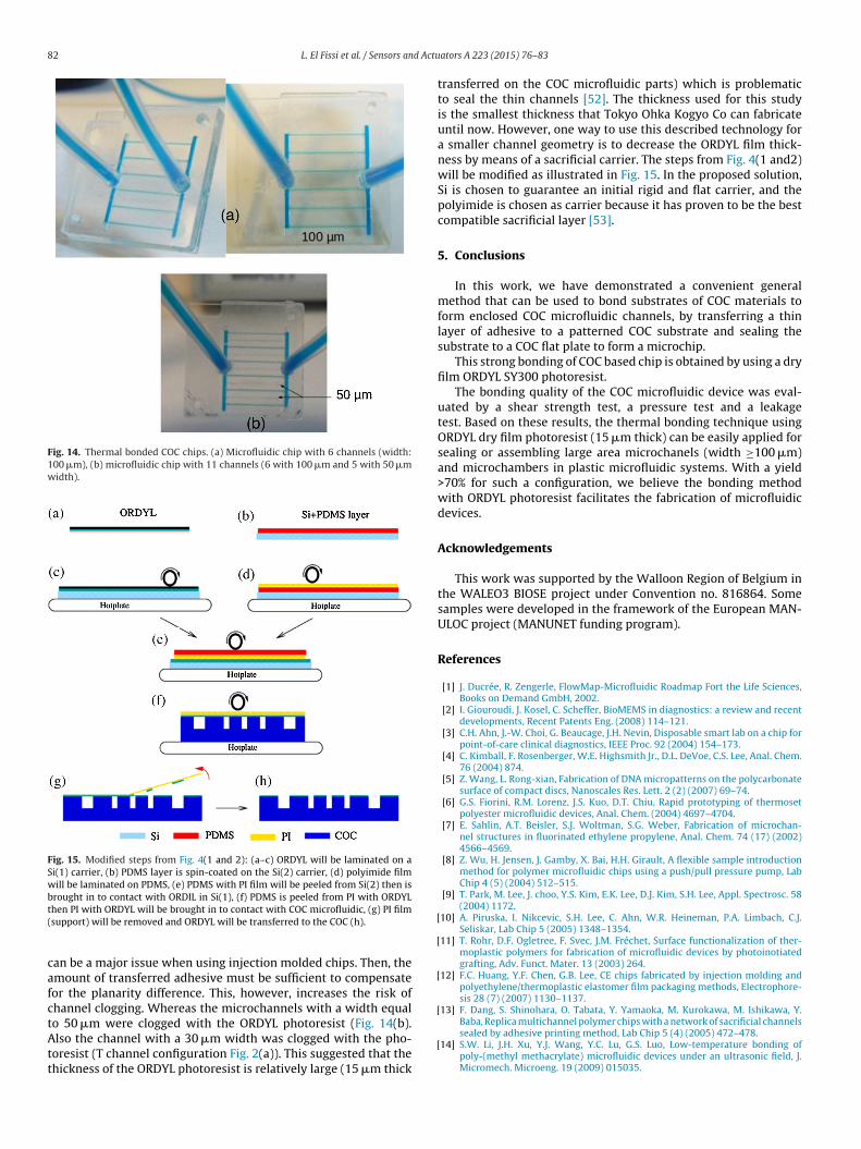
et up shown in Fig. 8, the pressure was slowly increased until gaseaked out or the pressure limit (4 bar) of the setup was reached. Tonsure the adequate bond performance, pressure tests were car-ied out using 5 devices for each treatment time. The results of theig. 12. Shear strength results of COC chips bonded for a given plasma duration for fixed power rating of 25 W and a fixed oxygen flow of 30 sccm.
Fig. 13. Pressure results of COC chips bonded for a given plasma duration for a fixedpower rating of 25 W and a fixed oxygen flow of 30 sccm.
pressure tests of the COC chip bonded with different oxygen plasmatreatment time are shown in Fig. 13.
As we can see from Fig. 13, similar trends were observed for theeffect of plasma treatment on the pressure. The plasma gas treat-ment increased the burst pressure of the COC chips bonded. Theburst pressure was consistently higher for samples with treatmenttimes of 4 min as compared to those with longer treatment times.Thus, a power rating of 25 W, an oxygen flow of 30 sccm and anexposure time of 4 min can be assumed to be the most effectiveparameters in our surface treatment process.
4.3. Leakage test
The optimized bonding parameters were then used to preparethe COC microfluidic devices.
The blue dyed water was injected alternately by demineral-ized water rinses and the injection flow rates were from 3 ml/minto 50 ml/min. The results of the chip bonding are summarized inTable 2.
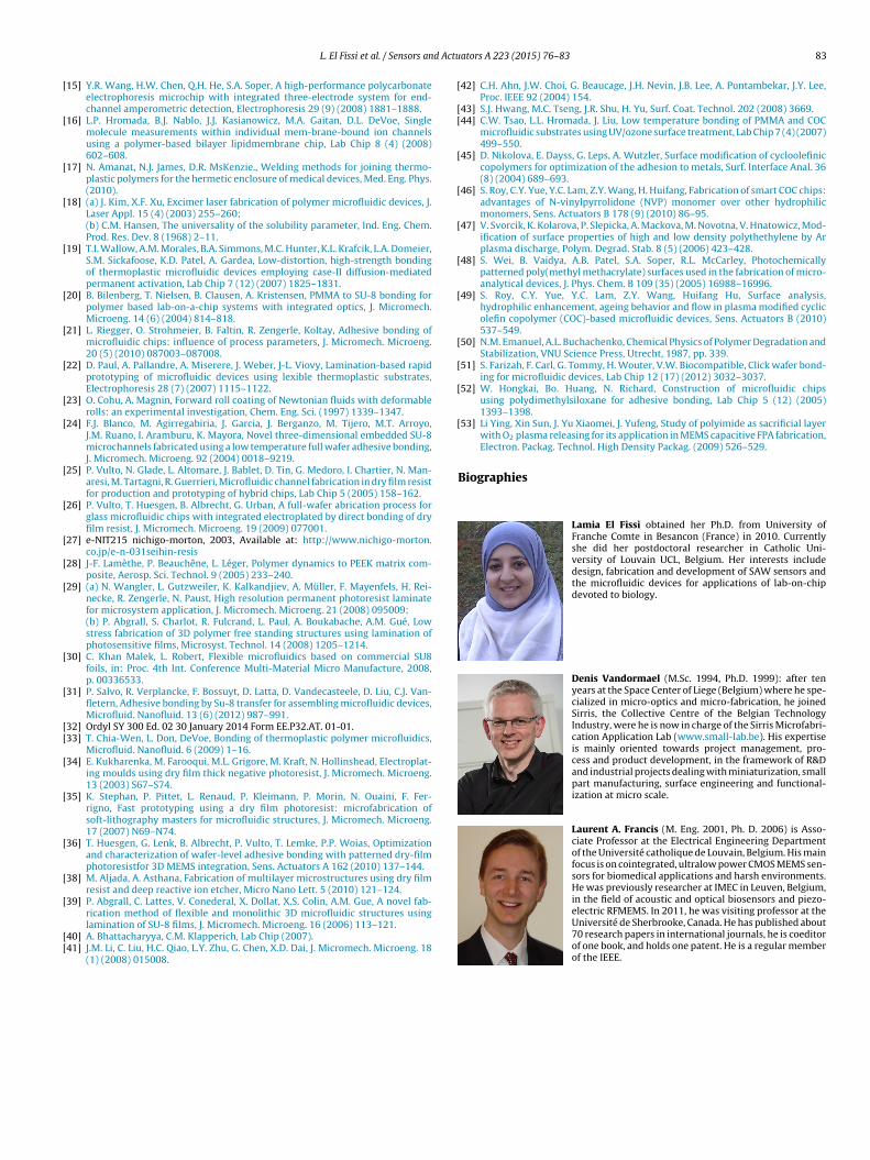
As we can see from Table 2, the microchannels with a widthequal to and/or superior to 100 �m were successfully sealed (i.e.,no leakage), and the microchip did not reveal any solution leak-ages between adhesive interfaces as evidenced in Fig. 14(a), whichshows that the blue dye does not penetrate the interfaces. It mightbe mentioned that the transparent color observed in the entranceand exit channels is caused by the commercial glue (UHU Powerglue ultra rapid super gel) that was used to fix the inlet and outletholes of the chips (Fig. 10). Also we mention that the transparentcolor observed in the corner of the large channels is caused by somebubbles trapped and not clogged with the ORDYL photoresist. For
the COC microfluidic bonded chip with configuration (Fig. 14(a)),the developed bonding method presents a high reproducibilityyield (>70%) (Experimental result). The yield fluctuations can beexplained by the chip surface planarity. The chip surface planarityTable 2Bonding results for different COC microfluidic chips configurations. (a) Microflu-idic chip with T channel configuration, (b) microfluidic chip with 6 channels, (c)microfluidic chip with 11 channels.
Configurations Channel dimensions: width/depth (�m/�m)
30/100 50/100 100/200 100/500 200/500
a × – – – –b – –
√ √ √c – × √ √ √
×: channels clogged.√: no leaks, all channels operational.
82 L. El Fissi et al. / Sensors and Actu
Fig. 14. Thermal bonded COC chips. (a) Microfluidic chip with 6 channels (width:100 �m), (b) microfluidic chip with 11 channels (6 with 100 �m and 5 with 50 �mwidth).
Fig. 15. Modified steps from Fig. 4(1 and 2): (a–c) ORDYL will be laminated on aSi(1) carrier, (b) PDMS layer is spin-coated on the Si(2) carrier, (d) polyimide filmwill be laminated on PDMS, (e) PDMS with PI film will be peeled from Si(2) then isbrought in to contact with ORDIL in Si(1), (f) PDMS is peeled from PI with ORDYLt(
cafctAtt
[
[
[
[Baba, Replica multichannel polymer chips with a network of sacrificial channels
hen PI with ORDYL will be brought in to contact with COC microfluidic, (g) PI filmsupport) will be removed and ORDYL will be transferred to the COC (h).
an be a major issue when using injection molded chips. Then, themount of transferred adhesive must be sufficient to compensateor the planarity difference. This, however, increases the risk ofhannel clogging. Whereas the microchannels with a width equalo 50 �m were clogged with the ORDYL photoresist (Fig. 14(b).
lso the channel with a 30 �m width was clogged with the pho-oresist (T channel configuration Fig. 2(a)). This suggested that thehickness of the ORDYL photoresist is relatively large (15 �m thick
[
ators A 223 (2015) 76–83
transferred on the COC microfluidic parts) which is problematicto seal the thin channels [52]. The thickness used for this studyis the smallest thickness that Tokyo Ohka Kogyo Co can fabricateuntil now. However, one way to use this described technology fora smaller channel geometry is to decrease the ORDYL film thick-ness by means of a sacrificial carrier. The steps from Fig. 4(1 and2)will be modified as illustrated in Fig. 15. In the proposed solution,Si is chosen to guarantee an initial rigid and flat carrier, and thepolyimide is chosen as carrier because it has proven to be the bestcompatible sacrificial layer [53].
5. Conclusions
In this work, we have demonstrated a convenient generalmethod that can be used to bond substrates of COC materials toform enclosed COC microfluidic channels, by transferring a thinlayer of adhesive to a patterned COC substrate and sealing thesubstrate to a COC flat plate to form a microchip.
This strong bonding of COC based chip is obtained by using a dryfilm ORDYL SY300 photoresist.
The bonding quality of the COC microfluidic device was eval-uated by a shear strength test, a pressure test and a leakagetest. Based on these results, the thermal bonding technique usingORDYL dry film photoresist (15 �m thick) can be easily applied forsealing or assembling large area microchanels (width ≥100 �m)and microchambers in plastic microfluidic systems. With a yield>70% for such a configuration, we believe the bonding methodwith ORDYL photoresist facilitates the fabrication of microfluidicdevices.
Acknowledgements
This work was supported by the Walloon Region of Belgium inthe WALEO3 BIOSE project under Convention no. 816864. Somesamples were developed in the framework of the European MAN-ULOC project (MANUNET funding program).
References
[1] J. Ducrée, R. Zengerle, FlowMap-Microfluidic Roadmap Fort the Life Sciences,Books on Demand GmbH, 2002.
[2] I. Giouroudi, J. Kosel, C. Scheffer, BioMEMS in diagnostics: a review and recentdevelopments, Recent Patents Eng. (2008) 114–121.
[3] C.H. Ahn, J.-W. Choi, G. Beaucage, J.H. Nevin, Disposable smart lab on a chip forpoint-of-care clinical diagnostics, IEEE Proc. 92 (2004) 154–173.
[4] C. Kimball, F. Rosenberger, W.E. Highsmith Jr., D.L. DeVoe, C.S. Lee, Anal. Chem.76 (2004) 874.
[5] Z. Wang, L. Rong-xian, Fabrication of DNA micropatterns on the polycarbonatesurface of compact discs, Nanoscales Res. Lett. 2 (2) (2007) 69–74.
[6] G.S. Fiorini, R.M. Lorenz, J.S. Kuo, D.T. Chiu, Rapid prototyping of thermosetpolyester microfluidic devices, Anal. Chem. (2004) 4697–4704.
[7] E. Sahlin, A.T. Beisler, S.J. Woltman, S.G. Weber, Fabrication of microchan-nel structures in fluorinated ethylene propylene, Anal. Chem. 74 (17) (2002)4566–4569.
[8] Z. Wu, H. Jensen, J. Gamby, X. Bai, H.H. Girault, A flexible sample introductionmethod for polymer microfluidic chips using a push/pull pressure pump, LabChip 4 (5) (2004) 512–515.
[9] T. Park, M. Lee, J. choo, Y.S. Kim, E.K. Lee, D.J. Kim, S.H. Lee, Appl. Spectrosc. 58(2004) 1172.
10] A. Piruska, I. Nikcevic, S.H. Lee, C. Ahn, W.R. Heineman, P.A. Limbach, C.J.Seliskar, Lab Chip 5 (2005) 1348–1354.
11] T. Rohr, D.F. Ogletree, F. Svec, J.M. Fréchet, Surface functionalization of ther-moplastic polymers for fabrication of microfluidic devices by photoinotiatedgrafting, Adv. Funct. Mater. 13 (2003) 264.
12] F.C. Huang, Y.F. Chen, G.B. Lee, CE chips fabricated by injection molding andpolyethylene/thermoplastic elastomer film packaging methods, Electrophore-sis 28 (7) (2007) 1130–1137.
13] F. Dang, S. Shinohara, O. Tabata, Y. Yamaoka, M. Kurokawa, M. Ishikawa, Y.
sealed by adhesive printing method, Lab Chip 5 (4) (2005) 472–478.14] S.W. Li, J.H. Xu, Y.J. Wang, Y.C. Lu, G.S. Luo, Low-temperature bonding of
poly-(methyl methacrylate) microfluidic devices under an ultrasonic field, J.Micromech. Microeng. 19 (2009) 015035.
d Actu
[
[
[
[
[
[
[
[
[
[
[
[
[
[
[
[
[
[[
[
[
[
[
[
[[
[
[[
[
[
[
[
[
[
[
[
[
L. El Fissi et al. / Sensors an
15] Y.R. Wang, H.W. Chen, Q.H. He, S.A. Soper, A high-performance polycarbonateelectrophoresis microchip with integrated three-electrode system for end-channel amperometric detection, Electrophoresis 29 (9) (2008) 1881–1888.
16] L.P. Hromada, B.J. Nablo, J.J. Kasianowicz, M.A. Gaitan, D.L. DeVoe, Singlemolecule measurements within individual mem-brane-bound ion channelsusing a polymer-based bilayer lipidmembrane chip, Lab Chip 8 (4) (2008)602–608.
17] N. Amanat, N.J. James, D.R. MsKenzie., Welding methods for joining thermo-plastic polymers for the hermetic enclosure of medical devices, Med. Eng. Phys.(2010).
18] (a) J. Kim, X.F. Xu, Excimer laser fabrication of polymer microfluidic devices, J.Laser Appl. 15 (4) (2003) 255–260;(b) C.M. Hansen, The universality of the solubility parameter, Ind. Eng. Chem.Prod. Res. Dev. 8 (1968) 2–11.
19] T.I. Wallow, A.M. Morales, B.A. Simmons, M.C. Hunter, K.L. Krafcik, L.A. Domeier,S.M. Sickafoose, K.D. Patel, A. Gardea, Low-distortion, high-strength bondingof thermoplastic microfluidic devices employing case-II diffusion-mediatedpermanent activation, Lab Chip 7 (12) (2007) 1825–1831.
20] B. Bilenberg, T. Nielsen, B. Clausen, A. Kristensen, PMMA to SU-8 bonding forpolymer based lab-on-a-chip systems with integrated optics, J. Micromech.Microeng. 14 (6) (2004) 814–818.
21] L. Riegger, O. Strohmeier, B. Faltin, R. Zengerle, Koltay, Adhesive bonding ofmicrofluidic chips: influence of process parameters, J. Micromech. Microeng.20 (5) (2010) 087003–087008.
22] D. Paul, A. Pallandre, A. Miserere, J. Weber, J-L. Viovy, Lamination-based rapidprototyping of microfluidic devices using lexible thermoplastic substrates,Electrophoresis 28 (7) (2007) 1115–1122.
23] O. Cohu, A. Magnin, Forward roll coating of Newtonian fluids with deformablerolls: an experimental investigation, Chem. Eng. Sci. (1997) 1339–1347.
24] F.J. Blanco, M. Agirregabiria, J. Garcia, J. Berganzo, M. Tijero, M.T. Arroyo,J.M. Ruano, I. Aramburu, K. Mayora, Novel three-dimensional embedded SU-8microchannels fabricated using a low temperature full wafer adhesive bonding,J. Micromech. Microeng. 92 (2004) 0018–9219.
25] P. Vulto, N. Glade, L. Altomare, J. Bablet, D. Tin, G. Medoro, I. Chartier, N. Man-aresi, M. Tartagni, R. Guerrieri, Microfluidic channel fabrication in dry film resistfor production and prototyping of hybrid chips, Lab Chip 5 (2005) 158–162.
26] P. Vulto, T. Huesgen, B. Albrecht, G. Urban, A full-wafer abrication process forglass microfluidic chips with integrated electroplated by direct bonding of dryfilm resist, J. Micromech. Microeng. 19 (2009) 077001.
27] e-NIT215 nichigo-morton, 2003, Available at: http://www.nichigo-morton.co.jp/e-n-031seihin-resis
28] J-F. Lamèthe, P. Beauchêne, L. Léger, Polymer dynamics to PEEK matrix com-posite, Aerosp. Sci. Technol. 9 (2005) 233–240.
29] (a) N. Wangler, L. Gutzweiler, K. Kalkandjiev, A. Müller, F. Mayenfels, H. Rei-necke, R. Zengerle, N. Paust, High resolution permanent photoresist laminatefor microsystem application, J. Micromech. Microeng. 21 (2008) 095009;(b) P. Abgrall, S. Charlot, R. Fulcrand, L. Paul, A. Boukabache, A.M. Gué, Lowstress fabrication of 3D polymer free standing structures using lamination ofphotosensitive films, Microsyst. Technol. 14 (2008) 1205–1214.
30] C. Khan Malek, L. Robert, Flexible microfluidics based on commercial SU8foils, in: Proc. 4th Int. Conference Multi-Material Micro Manufacture, 2008,p. 00336533.
31] P. Salvo, R. Verplancke, F. Bossuyt, D. Latta, D. Vandecasteele, D. Liu, C.J. Van-fletern, Adhesive bonding by Su-8 transfer for assembling microfluidic devices,Microfluid. Nanofluid. 13 (6) (2012) 987–991.
32] Ordyl SY 300 Ed. 02 30 January 2014 Form EE.P32.AT. 01-01.33] T. Chia-Wen, L. Don, DeVoe, Bonding of thermoplastic polymer microfluidics,
Microfluid. Nanofluid. 6 (2009) 1–16.34] E. Kukharenka, M. Farooqui, M.L. Grigore, M. Kraft, N. Hollinshead, Electroplat-
ing moulds using dry film thick negative photoresist, J. Micromech. Microeng.13 (2003) S67–S74.
35] K. Stephan, P. Pittet, L. Renaud, P. Kleimann, P. Morin, N. Ouaini, F. Fer-rigno, Fast prototyping using a dry film photoresist: microfabrication ofsoft-lithography masters for microfluidic structures, J. Micromech. Microeng.17 (2007) N69–N74.
36] T. Huesgen, G. Lenk, B. Albrecht, P. Vulto, T. Lemke, P.P. Woias, Optimizationand characterization of wafer-level adhesive bonding with patterned dry-filmphotoresistfor 3D MEMS integration, Sens. Actuators A 162 (2010) 137–144.
38] M. Aljada, A. Asthana, Fabrication of multilayer microstructures using dry filmresist and deep reactive ion etcher, Micro Nano Lett. 5 (2010) 121–124.
39] P. Abgrall, C. Lattes, V. Conederal, X. Dollat, X.S. Colin, A.M. Gue, A novel fab-
rication method of flexible and monolithic 3D microfluidic structures usinglamination of SU-8 films, J. Micromech. Microeng. 16 (2006) 113–121.40] A. Bhattacharyya, C.M. Klapperich, Lab Chip (2007).41] J.M. Li, C. Liu, H.C. Qiao, L.Y. Zhu, G. Chen, X.D. Dai, J. Micromech. Microeng. 18
(1) (2008) 015008.
ators A 223 (2015) 76–83 83
42] C.H. Ahn, J.W. Choi, G. Beaucage, J.H. Nevin, J.B. Lee, A. Puntambekar, J.Y. Lee,Proc. IEEE 92 (2004) 154.
43] S.J. Hwang, M.C. Tseng, J.R. Shu, H. Yu, Surf. Coat. Technol. 202 (2008) 3669.44] C.W. Tsao, L.L. Hromada, J. Liu, Low temperature bonding of PMMA and COC
microfluidic substrates using UV/ozone surface treatment, Lab Chip 7 (4) (2007)499–550.
45] D. Nikolova, E. Dayss, G. Leps, A. Wutzler, Surface modification of cycloolefiniccopolymers for optimization of the adhesion to metals, Surf. Interface Anal. 36(8) (2004) 689–693.
46] S. Roy, C.Y. Yue, Y.C. Lam, Z.Y. Wang, H. Huifang, Fabrication of smart COC chips:advantages of N-vinylpyrrolidone (NVP) monomer over other hydrophilicmonomers, Sens. Actuators B 178 (9) (2010) 86–95.
47] V. Svorcik, K. Kolarova, P. Slepicka, A. Mackova, M. Novotna, V. Hnatowicz, Mod-ification of surface properties of high and low density polythethylene by Arplasma discharge, Polym. Degrad. Stab. 8 (5) (2006) 423–428.
48] S. Wei, B. Vaidya, A.B. Patel, S.A. Soper, R.L. McCarley, Photochemicallypatterned poly(methyl methacrylate) surfaces used in the fabrication of micro-analytical devices, J. Phys. Chem. B 109 (35) (2005) 16988–16996.
49] S. Roy, C.Y. Yue, Y.C. Lam, Z.Y. Wang, Huifang Hu, Surface analysis,hydrophilic enhancement, ageing behavior and flow in plasma modified cyclicolefin copolymer (COC)-based microfluidic devices, Sens. Actuators B (2010)537–549.
50] N.M. Emanuel, A.L. Buchachenko, Chemical Physics of Polymer Degradation andStabilization, VNU Science Press, Utrecht, 1987, pp. 339.
51] S. Farizah, F. Carl, G. Tommy, H. Wouter, V.W. Biocompatible, Click wafer bond-ing for microfluidic devices, Lab Chip 12 (17) (2012) 3032–3037.
52] W. Hongkai, Bo. Huang, N. Richard, Construction of microfluidic chipsusing polydimethylsiloxane for adhesive bonding, Lab Chip 5 (12) (2005)1393–1398.
53] Li Ying, Xin Sun, J. Yu Xiaomei, J. Yufeng, Study of polyimide as sacrificial layerwith O2 plasma releasing for its application in MEMS capacitive FPA fabrication,Electron. Packag. Technol. High Density Packag. (2009) 526–529.
Biographies
Lamia El Fissi obtained her Ph.D. from University ofFranche Comte in Besancon (France) in 2010. Currentlyshe did her postdoctoral researcher in Catholic Uni-versity of Louvain UCL, Belgium. Her interests includedesign, fabrication and development of SAW sensors andthe microfluidic devices for applications of lab-on-chipdevoted to biology.
Denis Vandormael (M.Sc. 1994, Ph.D. 1999): after tenyears at the Space Center of Liege (Belgium) where he spe-cialized in micro-optics and micro-fabrication, he joinedSirris, the Collective Centre of the Belgian TechnologyIndustry, were he is now in charge of the Sirris Microfabri-cation Application Lab (www.small-lab.be). His expertiseis mainly oriented towards project management, pro-cess and product development, in the framework of R&Dand industrial projects dealing with miniaturization, smallpart manufacturing, surface engineering and functional-ization at micro scale.
Laurent A. Francis (M. Eng. 2001, Ph. D. 2006) is Asso-ciate Professor at the Electrical Engineering Departmentof the Université catholique de Louvain, Belgium. His mainfocus is on cointegrated, ultralow power CMOS MEMS sen-sors for biomedical applications and harsh environments.He was previously researcher at IMEC in Leuven, Belgium,in the field of acoustic and optical biosensors and piezo-
electric RFMEMS. In 2011, he was visiting professor at theUniversité de Sherbrooke, Canada. He has published about70 research papers in international journals, he is coeditorof one book, and holds one patent. He is a regular memberof the IEEE.