digital to analog convertor (dac)
TRANSCRIPT
DEPARTMENT OF PHYSICS
B.Sc. IV SEMESTER (UG)
Generic Elective Course
DIGITAL ELECTRONICS [BPHYT-G401]
UNIT -IV
MR. RAJESH KUMAR
Digital to Analog convertor (DAC)
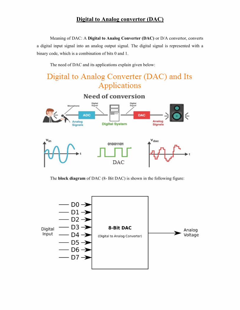
Meaning of DAC: A Digital to Analog Converter (DAC) or D/A convertor, converts
a digital input signal into an analog output signal. The digital signal is represented with a
binary code, which is a combination of bits 0 and 1.
The need of DAC and its applications explain given below:
The block diagram of DAC (8- Bit DAC) is shown in the following figure:
A Digital to Analog Converter (DAC) consists of a number of binary inputs and a
single output. In general, the number of binary inputs of a DAC will be a power of two.
Types of DACs
There are two types of DACs
Weighted Resistor DAC
R-2R Ladder DAC
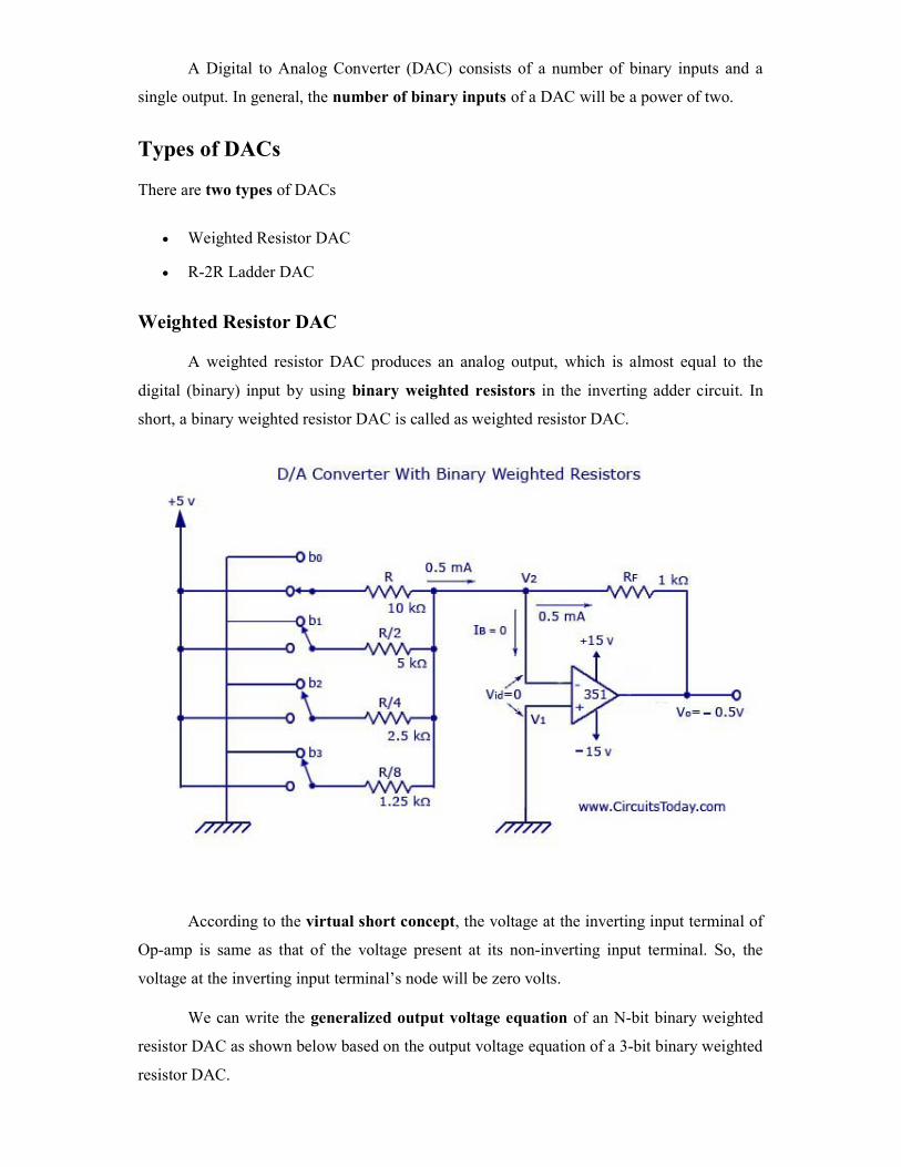
Weighted Resistor DAC
A weighted resistor DAC produces an analog output, which is almost equal to the
digital (binary) input by using binary weighted resistors in the inverting adder circuit. In
short, a binary weighted resistor DAC is called as weighted resistor DAC.
According to the virtual short concept, the voltage at the inverting input terminal of
Op-amp is same as that of the voltage present at its non-inverting input terminal. So, the
voltage at the inverting input terminal’s node will be zero volts.
We can write the generalized output voltage equation of an N-bit binary weighted
resistor DAC as shown below based on the output voltage equation of a 3-bit binary weighted
resistor DAC.
VOUT = - (VD +1/2 VC + ¼ VB + 1/8 VA)
The disadvantages of a binary weighted resistor DAC are as follows −
The difference between the resistance values corresponding to LSB & MSB will
increase as the number of bits present in the digital input increases.
It is difficult to design more accurate resistors as the number of bits present in the
digital input increases.
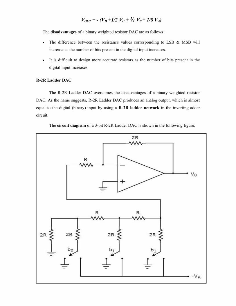
R-2R Ladder DAC
The R-2R Ladder DAC overcomes the disadvantages of a binary weighted resistor
DAC. As the name suggests, R-2R Ladder DAC produces an analog output, which is almost
equal to the digital (binary) input by using a R-2R ladder network in the inverting adder
circuit.
The circuit diagram of a 3-bit R-2R Ladder DAC is shown in the following figure:
Recall that the bits of a binary number can have only one of the two values. i.e., either
0 or 1. Let the 3-bit binary input is b2b1b0b2b1b0. Here, the bits b2b2 and b0b0 denote the
Most Significant Bit (MSB) and Least Significant Bit (LSB) respectively.
The digital switches shown in the above figure will be connected to ground, when the
corresponding input bits are equal to ‘0’. Similarly, the digital switches shown in above
figure will be connected to the negative reference voltage, −VR−VR when the corresponding
input bits are equal to ‘1’.
It is difficult to get the generalized output voltage equation of a R-2R Ladder DAC.
But, we can find the analog output voltage values of R-2R Ladder DAC for individual binary
input combinations easily.
The advantages of a R-2R Ladder DAC are as follows:
R-2R Ladder DAC contains only two values of resistor: R and 2R. So, it is easy to
select and design more accurate resistors.
If more number of bits is present in the digital input, then we have to include required
number of R-2R sections additionally.
Due to the above advantages, R-2R Ladder DAC is preferable over binary weighted
resistor DAC.
Resolution of DAC:
The resolution of a converter is the smallest change in voltage which may be
produced at the output (or input) of the converter. For example, an 8-bit D/A
converter has 2^8-1=255 equal intervals. Hence the smallest change in output voltage
is(1/255) of the full scale output range.
Resolution should be high as possible. It depends on the number of bits in the digital
input applied to DAC. Higher the number of bits, higher is the resolution.
It can also be defined as the ratio of change in analog output voltage resulting from a
change of 1LSB at the digital input.
Resolution for n-bit DAC:
The Resolution in case of DAC is the smallest change in the analog voltage it can
detect . which is also known as step size of the DAC . For an n bit DAC resolution is
calculated by the formula;
Resolution = (Range /(2^n -1))
Accuracy: Absolute accuracy is the maximum deviation between the actual converter output and
the ideal converter output.
Relative accuracy is the maximum deviation after gain and offset errors have been
removed.
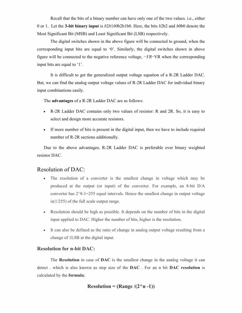
Analog to Digital Convertor (ADC)
An Analog-to-digital converter takes an analog input voltage and after a certain
amount of time produces a digital output code which represents the analog input. The A/D
conversion process is generally more complex and time-consuming than the D/A process.
The techniques that are used provide and insight into what factors determines a ADCs
performance.
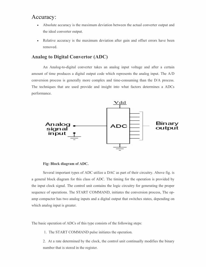
Fig: Block diagram of ADC.
Several important types of ADC utilize a DAC as part of their circuitry. Above fig. is
a general block diagram for this class of ADC. The timing for the operation is provided by
the input clock signal. The control unit contains the logic circuitry for generating the proper
sequence of operations. The START COMMAND, initiates the conversion process, The op-
amp compactor has two analog inputs and a digital output that switches states, depending on
which analog input is greater.
The basic operation of ADCs of this type consists of the following steps:
1. The START COMMAND pulse initiates the operation.
2. At a rate determined by the clock, the control unit continually modifies the binary
number that is stored in the register.
3. The binary number in the register is converted to an Analog voltage, VAX, by the
DAC.
Accuracy:
The accuracy of the converter determines how many bits in the digital output code
represent useful information about the input signal. As explained earlier, for a 16-bit ADC
resolution the actual accuracy may be much less than the resolution because of internal or
external error sources. The accuracy of the A/D converter determines how close the actual
digital output is to the theoretically expected digital output for a given analog input. In other
words, the accuracy of the converter determines how many bits in the digital output code
represent useful information about the input signal.
As explained earlier, for a 16-bit ADC resolution the actual accuracy may be much
less than the resolution because of internal or external error sources. So for example a given
16-bit ADC may only provide 12 bits of accuracy. In this case, the 4 LSb’s (Least Significant
Bit) represent random noise produced in the ADC.
ADC Dynamic Range and ADC Accuracy is often same thing.
Resolution:
Resolution of ADC is define as:
Resolution = Vref /2N
Where, Vref→ Reference voltage range, 2N → Number of states
N → Number of bits in digital output.
Types of Analog to Digital Converter
Successive Approximation ADC: This converter compares the input signal with the
output of an internal DAC at each successive step. It is the most expensive type.
Dual Slope ADC: It have high accuracy but very slow in operation.
Pipeline ADC: It is same as that of two step Flash ADC.
Delta-Sigma ADC: It has high resolution but slow due to over sampling.
Flash ADC: It is the fastest ADC but very expensive.
Other: Staircase ramp, Voltage-to-Frequency, Switched capacitor, tracking, Charge
balancing, and resolver.
ADC Technique: If we have an analog signal such as one created by a microphone or camera. To
change an analog signal to digital data we use two techniques, pulse code modulation and
delta modulation. After the digital data are created (digitization) then we convert the digital
data to a digital signal.
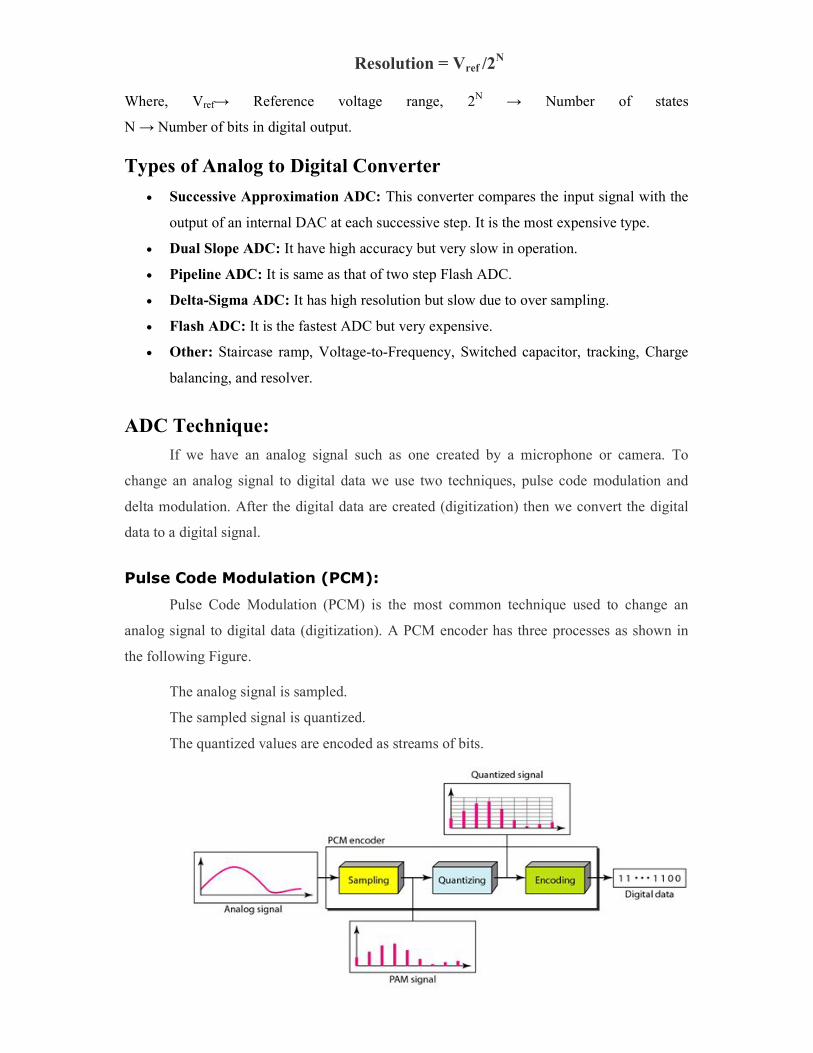
Pulse Code Modulation (PCM): Pulse Code Modulation (PCM) is the most common technique used to change an
analog signal to digital data (digitization). A PCM encoder has three processes as shown in
the following Figure.
The analog signal is sampled.
The sampled signal is quantized.
The quantized values are encoded as streams of bits.
Sampling
The first step in PCM is sampling. The analog signal is sampled every Ts s, where Ts is the
sample interval or period. The inverse of the sampling interval is called the sampling rate or
sampling frequency and denoted by ƒs, Where ƒs = 1/ Ts.
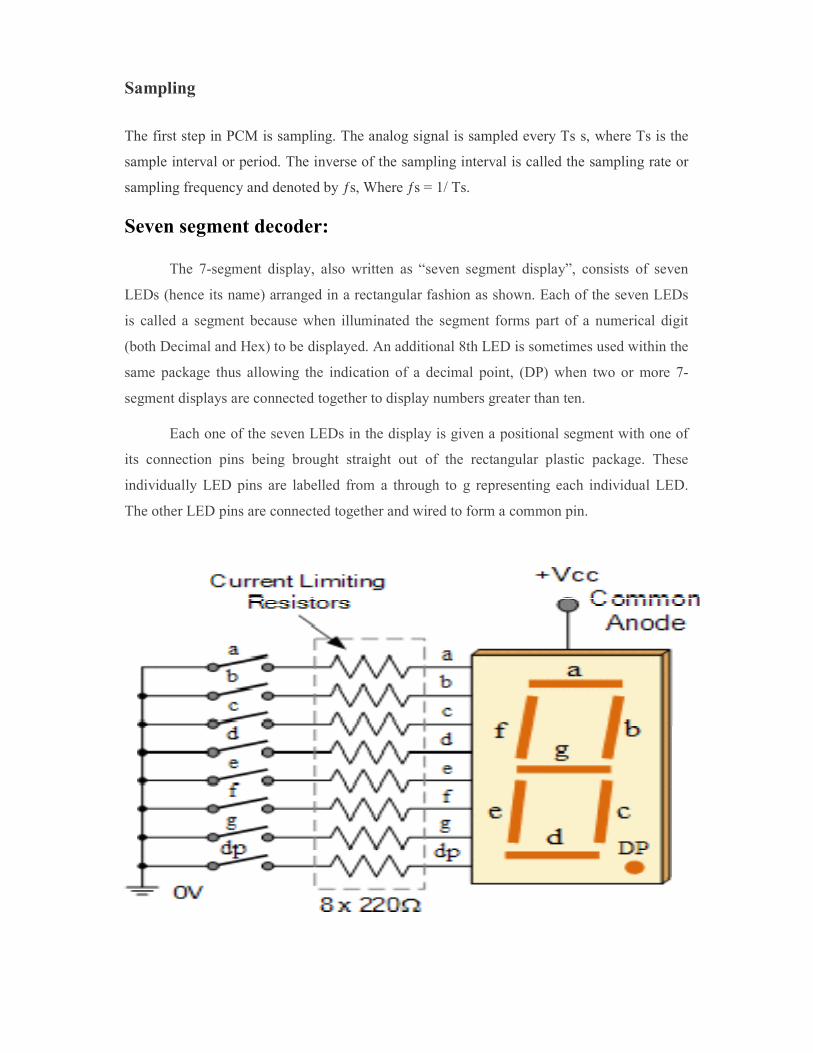
Seven segment decoder:
The 7-segment display, also written as “seven segment display”, consists of seven
LEDs (hence its name) arranged in a rectangular fashion as shown. Each of the seven LEDs
is called a segment because when illuminated the segment forms part of a numerical digit
(both Decimal and Hex) to be displayed. An additional 8th LED is sometimes used within the
same package thus allowing the indication of a decimal point, (DP) when two or more 7-
segment displays are connected together to display numbers greater than ten.
Each one of the seven LEDs in the display is given a positional segment with one of
its connection pins being brought straight out of the rectangular plastic package. These
individually LED pins are labelled from a through to g representing each individual LED.
The other LED pins are connected together and wired to form a common pin.
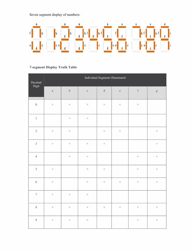
Seven segment display of numbers:
7-segment Display Truth Table
Decimal Digit
Individual Segments Illuminated
a b c d e f g
0 × × × × × ×
1 × ×
2 × × × × ×
3 × × × × ×
4 × × × ×
5 × × × × ×
6 × × × × × ×
7 × × ×
8 × × × × × × ×
9 × × × × ×
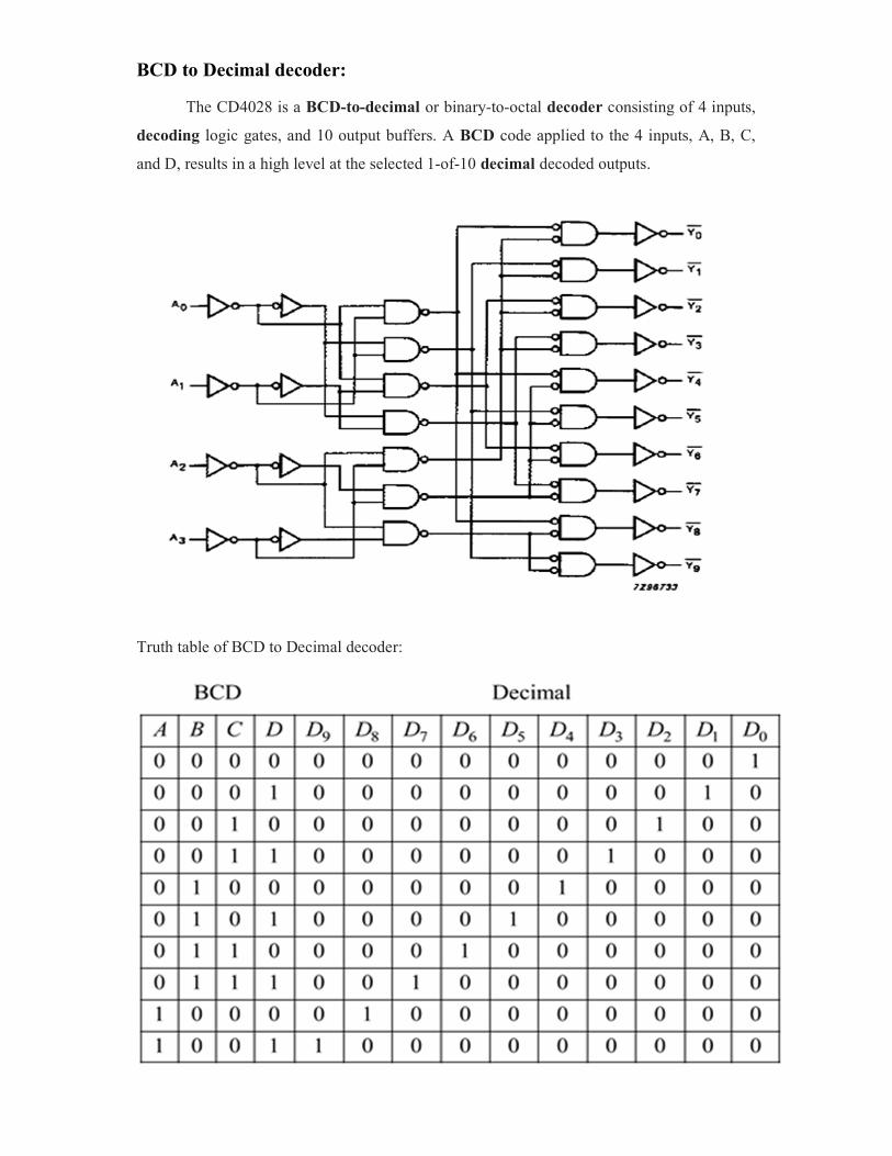
BCD to Decimal decoder:
The CD4028 is a BCD-to-decimal or binary-to-octal decoder consisting of 4 inputs,
decoding logic gates, and 10 output buffers. A BCD code applied to the 4 inputs, A, B, C,
and D, results in a high level at the selected 1-of-10 decimal decoded outputs.
Truth table of BCD to Decimal decoder:
Example BCD to Decimal Conversion
Step 1: Break the BCD into nibbles: 1001 0001 0001.
Step 2: Convert each nibble into decimal digits. 1001 becomes 9. 0001 becomes 1. 0001
becomes 1.
Step 3: Combine the decimal digits: 911.
Example:
Step Binary Number Decimal Number
Step 1 111012 ((1 × 24) + (1 × 23) + (1 × 22) + (0 × 21) + (1 × 20))10
Step 2 111012 (16 + 8 + 4 + 0 + 1)10
Step 3 111012 2910
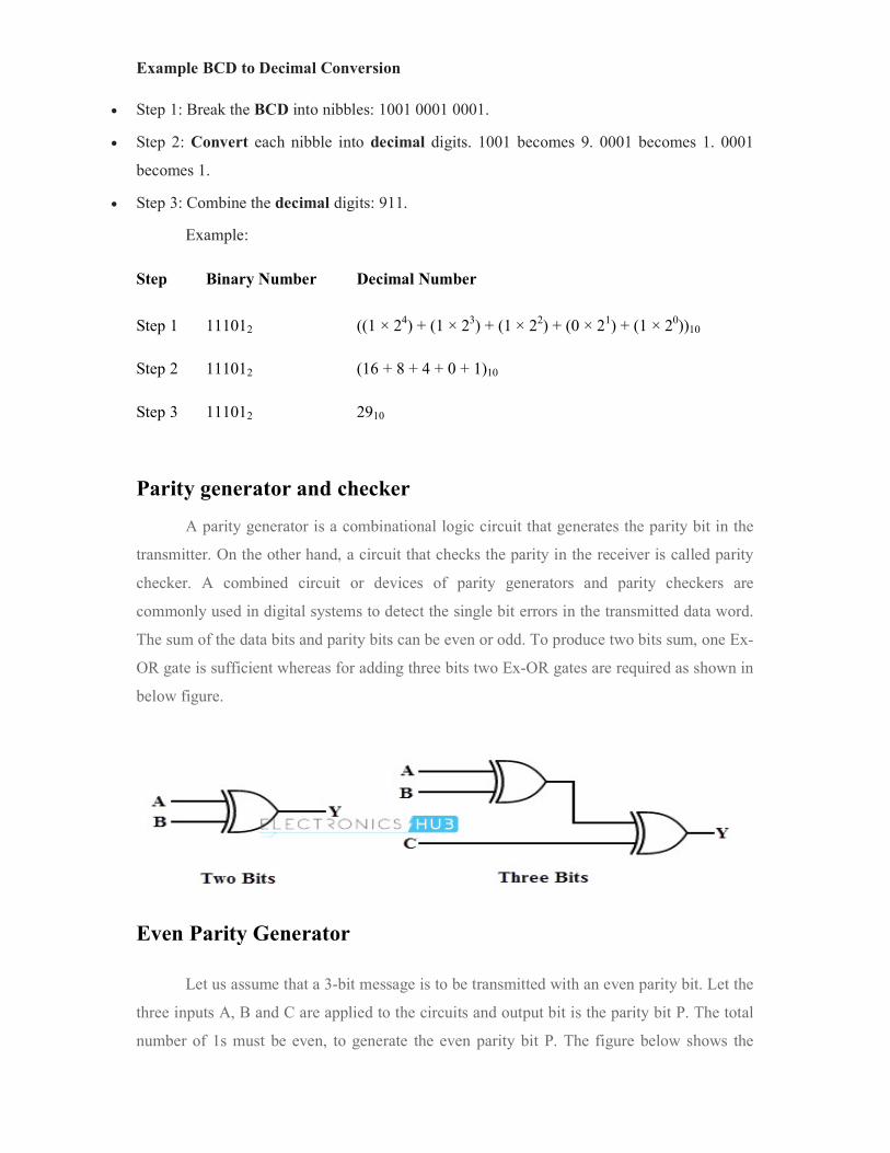
Parity generator and checker
A parity generator is a combinational logic circuit that generates the parity bit in the
transmitter. On the other hand, a circuit that checks the parity in the receiver is called parity
checker. A combined circuit or devices of parity generators and parity checkers are
commonly used in digital systems to detect the single bit errors in the transmitted data word.
The sum of the data bits and parity bits can be even or odd. To produce two bits sum, one Ex-
OR gate is sufficient whereas for adding three bits two Ex-OR gates are required as shown in
below figure.
Even Parity Generator
Let us assume that a 3-bit message is to be transmitted with an even parity bit. Let the
three inputs A, B and C are applied to the circuits and output bit is the parity bit P. The total
number of 1s must be even, to generate the even parity bit P. The figure below shows the
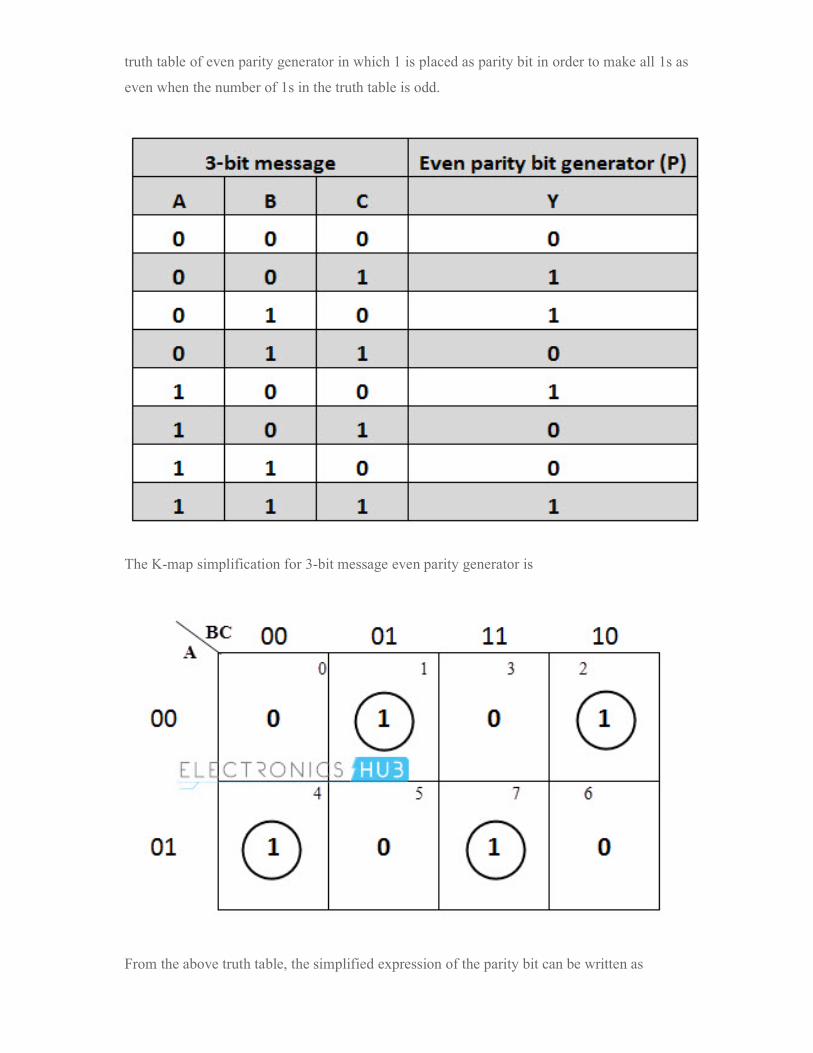
truth table of even parity generator in which 1 is placed as parity bit in order to make all 1s as
even when the number of 1s in the truth table is odd.
The K-map simplification for 3-bit message even parity generator is
From the above truth table, the simplified expression of the parity bit can be written as
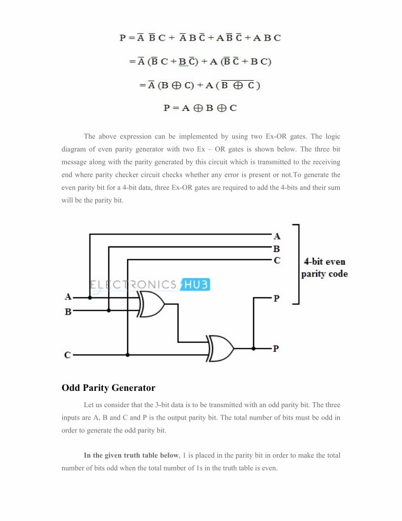
The above expression can be implemented by using two Ex-OR gates. The logic
diagram of even parity generator with two Ex – OR gates is shown below. The three bit
message along with the parity generated by this circuit which is transmitted to the receiving
end where parity checker circuit checks whether any error is present or not.To generate the
even parity bit for a 4-bit data, three Ex-OR gates are required to add the 4-bits and their sum
will be the parity bit.
Odd Parity Generator
Let us consider that the 3-bit data is to be transmitted with an odd parity bit. The three
inputs are A, B and C and P is the output parity bit. The total number of bits must be odd in
order to generate the odd parity bit.
In the given truth table below, 1 is placed in the parity bit in order to make the total
number of bits odd when the total number of 1s in the truth table is even.
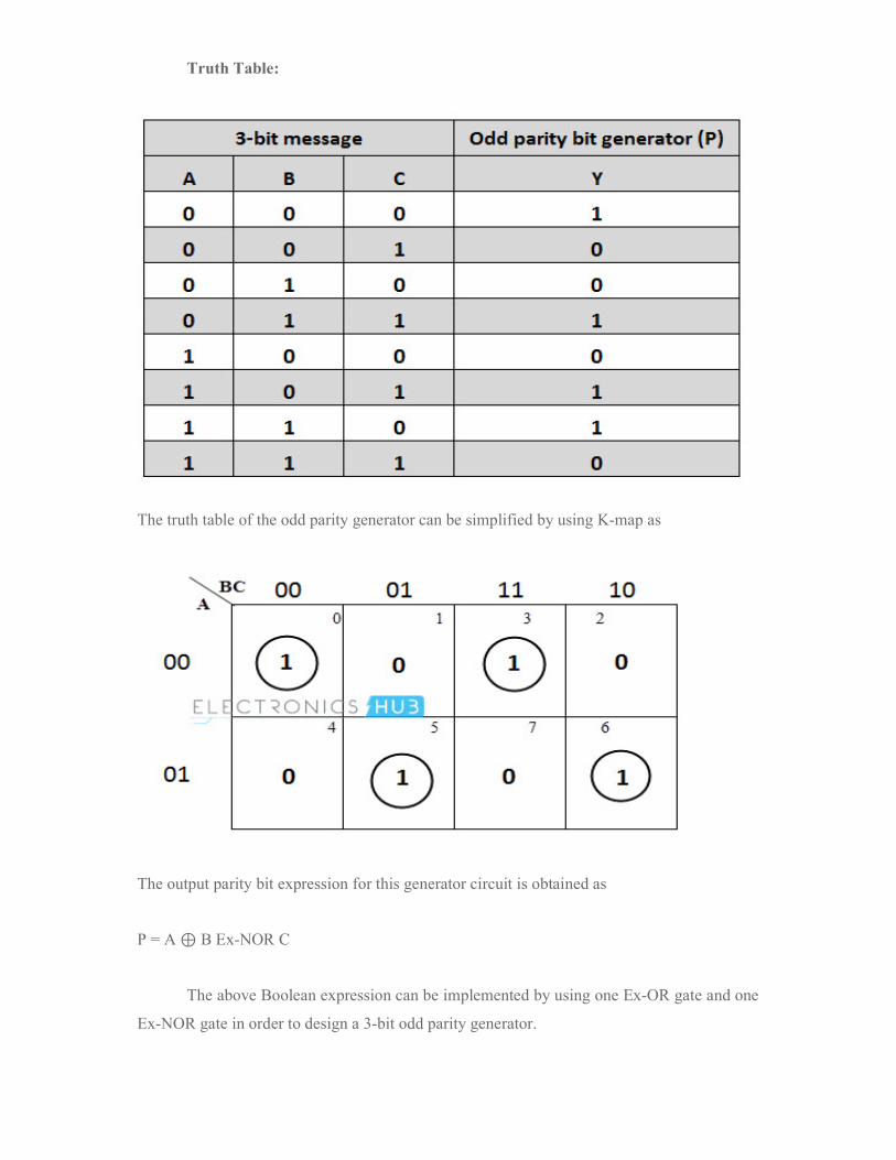
Truth Table:
The truth table of the odd parity generator can be simplified by using K-map as
The output parity bit expression for this generator circuit is obtained as
P = A ⊕ B Ex-NOR C
The above Boolean expression can be implemented by using one Ex-OR gate and one
Ex-NOR gate in order to design a 3-bit odd parity generator.
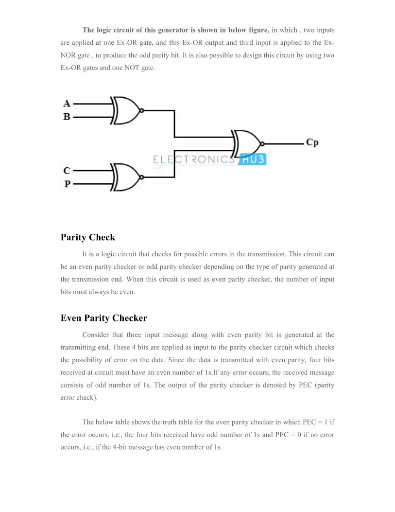
The logic circuit of this generator is shown in below figure, in which . two inputs
are applied at one Ex-OR gate, and this Ex-OR output and third input is applied to the Ex-
NOR gate , to produce the odd parity bit. It is also possible to design this circuit by using two
Ex-OR gates and one NOT gate.
Parity Check
It is a logic circuit that checks for possible errors in the transmission. This circuit can
be an even parity checker or odd parity checker depending on the type of parity generated at
the transmission end. When this circuit is used as even parity checker, the number of input
bits must always be even.
Even Parity Checker
Consider that three input message along with even parity bit is generated at the
transmitting end. These 4 bits are applied as input to the parity checker circuit which checks
the possibility of error on the data. Since the data is transmitted with even parity, four bits
received at circuit must have an even number of 1s.If any error occurs; the received message
consists of odd number of 1s. The output of the parity checker is denoted by PEC (parity
error check).
The below table shows the truth table for the even parity checker in which PEC = 1 if
the error occurs, i.e., the four bits received have odd number of 1s and PEC = 0 if no error
occurs, i.e., if the 4-bit message has even number of 1s.
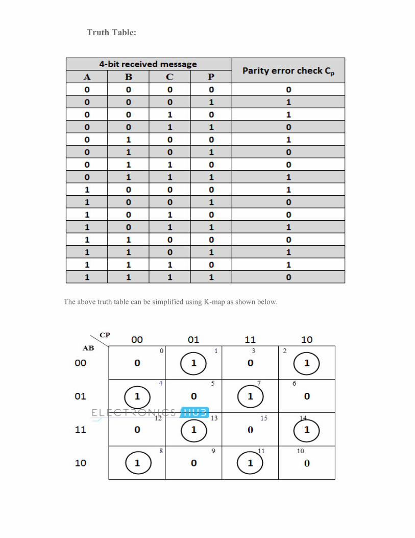
Truth Table:
The above truth table can be simplified using K-map as shown below.
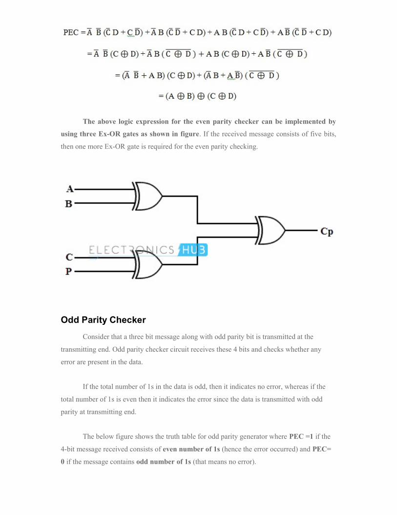
The above logic expression for the even parity checker can be implemented by
using three Ex-OR gates as shown in figure. If the received message consists of five bits,
then one more Ex-OR gate is required for the even parity checking.
Odd Parity Checker
Consider that a three bit message along with odd parity bit is transmitted at the
transmitting end. Odd parity checker circuit receives these 4 bits and checks whether any
error are present in the data.
If the total number of 1s in the data is odd, then it indicates no error, whereas if the
total number of 1s is even then it indicates the error since the data is transmitted with odd
parity at transmitting end.
The below figure shows the truth table for odd parity generator where PEC =1 if the
4-bit message received consists of even number of 1s (hence the error occurred) and PEC=
0 if the message contains odd number of 1s (that means no error).
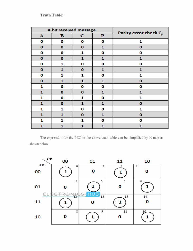
Truth Table:
The expression for the PEC in the above truth table can be simplified by K-map as
shown below.
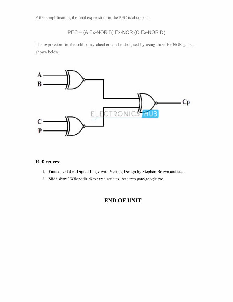
After simplification, the final expression for the PEC is obtained as
PEC = (A Ex-NOR B) Ex-NOR (C Ex-NOR D)
The expression for the odd parity checker can be designed by using three Ex-NOR gates as
shown below.
References:
1. Fundamental of Digital Logic with Verilog Design by Stephen Brown and et al.
2. Slide share/ Wikipedia /Research articles/ research gate/google etc.
END OF UNIT