detection and placement of single ions in the kev and mev regimes: mev ion-aperture scattering
TRANSCRIPT

107
Posters

108
Detection and placement of single ions in the keV and MeV regimes: MeV ion-aperture scattering
A. Alves 1, J. van Donkelaar 1, C. Yang 1, D. N. Jamieson 1, M. Taylor 2, P. N. Johnston 2
1 Centre for Quantum Computer Technology, Microanalytical Research Centre, School of Physics, University of Melbourne, Australia
2 Physics, School of Applied Sciences, RMIT University, Australia
Abstract Emerging quantum technologies rely on the placement of single ions with precision in the order of 10nm. Ion beams in the keV and MeV regimes, developed as tools in nuclear analysis, offer fabrication of novel solid state devices at the ultimate resolution limit of an implanted single ion (for doping) or a single ion track (for lithography). Examples include solid state quantum computers and photonic band gap materials. There are two criteria that must be met in order to use single ions; (1) single ion detection and (2) placement of single ions with location accuracy. This paper summarises the methods used for detection and placement of single ions in the two energy regimes.
Introduction
keV regime
An ion with energy in the order of 1 keV per nucleon has a nanoscale ion range and straggling and therefore a well defined final resting location with respect to the position it entered the target. For example a 14 keV P ion in a Si substrate has an ion range of 28nm and straggling FWHM of 26nm [1]. Implantation in this regime has previously been executed using a single 14 keV P ion using a poly(methylmethacrylate) PMMA mask to define the ion’s location in the Si detector substrate[2]. This technique has been used to demonstrate charge qubits [3] in the Kane quantum computer scheme, an array of 31P atoms embedded in 28Si substrate with nanometre accuracy [4]. There is, however, no capacity to use this method for scaling up the production of qubits. When using an immovable PMMA mask the yield of devices in which one ion enters each aperture (for a multi-aperture mask) is unacceptably small, since we cannot tell which of the apertures the detected ion has passed through. To place multiple, individually detected, ions with nanometre precision a separate, movable mask is considered here. The first application of this technology will be a line of precisely placed single atoms. This will be used to realise an experimental demonstration of the coherent transfer by adiabatic passage (CTAP) principle [5] for the transfer of quantum information in a solid state quantum computer.
MeV regime
An ion with energy in the order of 1 MeV per nucleon has long range in a resist and a well defined latent damage track. For example a 1.5 MeV He ion in the resist (PMMA) has a range of ~10µm and track core radius of ~2nm [6-7]. By etching the latent damage track into a void high aspect ratio, nanoscale structures is fabricated. Ion beam lithography (IBL) in this regime has been executed using multiple low linear energy transfer (LET) ions with a focused beam [8] or using a mask [9]. Also tracks in PMMA have been etched from single ion impacts of high mass, high LET ions [10]. A standard text in the lithography field by S.M. Sze [11], points out the significant advantages of the IBL technique. As a direct write technique IBL must be
109
viewed as a serial process not capable of high throughput and at present the high resolution/direct write technique of electron beam lithography EBL is central in fulfilling the roles of rapid prototyping, mask making for optical, UV and X-ray lithography and fabrication of stamps for nano-imprint lithography. It is comprehensible that IBL will fulfil the similar rolls of prototyping, mask and stamp making, but in cases where a high aspect ratio structure is required.
A key area of interest for the application of IBL is photonic band gap materials. A photonic band gap occurs in a material where periodic changes in refractive index prevent light of certain wavelengths from propagating inside the medium. This phenomenon is analogous to an electronic band gap where many of the properties of an electron in a semiconductor can apply to a photon in a photonic band gap. The positioning of voids in a material with dimensions less than the desired band gap wavelength leads to the ability to fabricate an operational photonic crystal and is an ideal application for the high aspect ratio structuring of IBL. Such materials promise a revolution in computing and communication with uses such as optical waveguides that can perform a right angle turn, optical switches, filters or couplers to be made utilising the photonic band gap. The book by Joannopoulos et al. gives a good overview and theoretical analysis of photonic crystals [12]. These materials draw their inspiration from photonic structures in biology that produce iridescent colours and have already been studied extensively [13-14]. Many applications and previous work were reviewed in the August 2001 MRS Bulletin [15].
A separate, movable mask is also considered here for the placement of MeV ions in IBL using the common resist, PMMA and can realistically be used to fabricate 2D and 3D structures with resolution in the range from 10-1000nm. The photonic band gap fabricated would operate at near infrared and optical wavelengths, such as the 1550nm used in telecommunications applications
Detection of single ions is summarised For precise placement of single ions to occur the arrival of the ion in the substrate, or through the resist must be detected. Without this capacity a beam of ions might be accurately placed, but not a single ion. Single keV ion detection using P ions from a Colutron source has been developed for use with an immoveable PMMA mask[2] and requires advanced detector design and cooling with liquid nitrogen to overcome the electronic noise threshold. A single keV ion only produces a minute electronic signal (average ionisation energy of 3.6 keV) following an ion impact. However single MeV ion detection is easy to achieve through use of a commercial HamamatsuTM S1223-01 Si PIN photodiode. The pulse height is sufficiently higher than the noise floor and no cooling or advanced electronic design is needed.
Placement of single ions is summarised There are two methods of placement of an ion beam, focusing and masking. The focused beam is moved relative to the target via an electromagnetic field that bends the stream of charged ions. This technique is already widely used in the keV regime to perform focused ion beam (FIB) milling with high precision [16], and in the MeV regime applied to IBL [17]. In both energy regimes the ion optical components must be completely controlled over the entire ion accelerator and there are limitations to the ion species that can be selected. The presence of vibrations and stray fields will also affect the beam resolution.
110
The aim of this paper is to consider retrofitting a nanoscale mask in close proximity to the target surface in an already existing ion accelerator, in both the keV and MeV regimes. The masked beam is moved relative to the target via a scanning stage, using piezoelectric drive. An MeV ion beam system is given priority due to the ease with which MeV ions are detected and therefore experimental results only exist in that regime, however the intention is to apply the technology in both energy regimes.
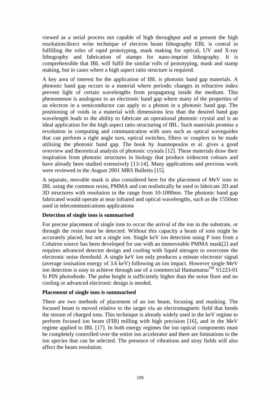
Mask fabrication and characterisation The fabrication of nano-apertures has been accomplished elsewhere by milling Si with a keV Ga focused ion beam (FIB). Such apertures have been used to mask low energy ions for implantation into a Si substrate [18-20] and to carry out metallic evaporation (nano-stencilling) onto a Si substrate through the aperture [21-23]. The smallest apertures have a width less than 10nm [24]. FIB milling has been attempted locally using 8µm thick Si cantilevers [25]. Slotted apertures have been created for application to the confinement of both MeV and keV ion beams. A slot will confine the beam of ions in one dimension, therefore may only be applied with high resolution in that dimension. In the CTAP application only a 1D line of atoms is required, therefore a slot can be used. Forming the beam limiting aperture from crossed slots is proposed so that alignment in the non-critical dimension is relaxed. One slot is patterned by EBL in a PMMA mask on the substrate and the other in the movable, FIB milled, cantilever. SEM images of FIB milled slots are shown in figure 1.
slots
1234
thinned area 1
thinned area 2slot
slots
1234
thinned area 1
thinned area 2slot
Figure 1. (a) A series of slots milled through an 8µm thick cantilever. (b) An 8µm thick cantilever is first thinned, then the slot milled.
The Si thickness must be greater than the ion range. The ion range of 1.5 MeV He in Si is 5.5µm so the apertures are milled directly into the 8µm Si. Using a beam current of 7.0nA a series of slots were milled and are shown in figure 1(a). The slot width on the top milling surface was found to be approximately 0.5µm for slot number two. For the milling of slots for keV ion placement the Si thickness can be reduced. For 14 keV P in Si the ion range is 28nm. To achieve high resolution the slot is milled through a thin section of Si. Figure 1 (b) shows an 8µm thick Si cantilever that has first been thinned in two areas using a high beam current of 7nA. For the final slot a beam current of 1pA was used and the final slot width was approximately 0.1µm.

111
Experimental verses simulation Experimental transmission spectra have been collected for analysis using a focused 1.5 MeV He beam. Slot number two (see figure 1 (a)) was mounted above a Hamamatsu PIN photodiode detector and a pulse height spectrum acquired. Previously a determination of the damage rate of the photodiode detector was made [26] using slot number three (with a slot width of approximately 0.8µm). It was found that a 1% peak shift was observed due to damage in the detector after 26×103 ion impacts. The experimental spectrum acquired from slot number two had 2307 ion impacts recorded and can therefore be compared with simulation results without a significant damage induced peak shift.
The resolution that can be achieved when using an aperture to confine a beam of ions
depends on the level of ion scattering within the aperture material. In an attempt to fully characterise the ion-aperture scattering the experimental spectrum has been compared with a simulation. Simulations of the ion scattering within a cylindrical Si aperture have been carried out in the work of Taylor et al. [27] using a range of ion species. The results indicate that the masking is effective with the percentage of ions transmitted without scatter ranging from 82-93% over the range of geometries reported, with the aperture thickness approximately equal to twice the ion range. This simulation was developed from the TRIM code of Zeigler [28]. This package was implemented here to match the experimental results and simulation. The input was configured with 105 1.5 MeV He ions incident upon a cylindrical Si aperture, 0.5µm wide and 8µm thick. It was not possible to use this code to simulate a slotted aperture. The simulation outputted the energy and direction cosine of each ion that had emerged
Energy (MeV)
Nor
mal
ised
Cou
nts
experimental spectrum
simulated spectrum
Energy (MeV)
Nor
mal
ised
Cou
nts
experimental spectrum
simulated spectrum
Figure 2. Experimental vs Simulated spectra

112
from the back side of the aperture. The data was binned so that the full energy peak from the simulation was in the same position as the centre of the experimental full energy peak. The peak areas of the simulated and experimental full energy peaks were normalised and a comparison of the two spectra is shown in figure 2.
In the experimental result 40 % of the total counts in the spectrum do not have full energy, therefore, have been scattered from the aperture. In the simulation 15 % of the ions have reduced energy, calculated excluding simulated counts below the lower level discriminator of the experimental spectrum. The discrepancy between results is expected due to the known discrepancy between the simulated and experimental aperture geometries. The main difference being that the width of the FIB milled aperture is not uniform. With additional geometries incorporated into the simulation a match to experimental data will reveal the actual internal aperture shape and be a valuable tool in aperture characterisation.
Conclusion A strategy for the detection and placement of single ions in the keV and MeV regimes has been conceived. The experimental work towards this goal has begun with aperture fabrication using FIB milling and aperture characterisation using ion transmission spectra.
Acknowledgements The work is funded by the Australian Research Council, the Australian Government and US Army Research Office under Contract No. W911NF-04-1-0290.
References [1] J. van Donkelaar, NCTA, to be published in this proceedings. [2] C. Yang, D.N. Jamieson, C. Pakes, S. Prawer, A. Dzurak, F. Stanley, P. Spizziri, L. Macks, E. Gauja, R.G. Clark, Single Phosphorus Ion Implantation into Prefabricated Nanometre Cells of Silicon Devices for Quantum Bit Fabrication. Jpn. J. Appl. Phys. (2003) 4124. [3] D.N. Jamieson, C. Yang, T. Hopf, S.M. Hearne, C.I. Pakes, S. Prawer, M. Mitic, E. Gauja, S.E. Andresen, F.E. Hudson, A.S. Dzurak, R.G. Clark, Controlled shallow single-ion implantation in silicon using an active substrate for sub-20-keV ions, Applied Physics Letters 86, (2005) 202101 [4] B. E. Kane: Nature 393 (1998) 133. [5] A. D. Greentree, L, Jong, To be published. [6] C. N. B. Udalagama, A. A. Bettiol, F. Watt, A Monte Carlo study of the extent of proximity effects in e-beam and p-beam writing of PMMA, Nuclear Instruments and Methods in Physics Research B 260 (2007) 384. [7] M. P. R. Waligorski, R. N. Hamm, R. Katz, The radial distribution of dose around the path of a heavy ion in liquid water, Nuclear Tracks and Radiation Measurement 11 (1986) 309. [8] J. A. van Kan, A. A. Bettiol, F. Watt, Three-dimensional nanolithography using proton beam writing, Applied Physics Letters 83 (2003) 1629. [9] M. L. Taylor, A. Alves, P. Reichart, R. D. Franich, S. Rubanov, P. Johnston, D. N. Jamieson, Ion beam lithography using a nano-aperture, Nuclear Instruments and Methods in Physics Research B 260 (2007) 426. [10] A. Alves, P.N. Johnston, P. Reichart, D.N. Jamieson, R. Siegele, Characterization of ion tracks in PMMA for single ion lithography, Nuclear Instruments and Methods in Physics Research Section B 260 (2007) 431.

113
[11] S.M. Sze, Semiconductor devices, physics and technology, Wiley, 1985. [12] J.D. Joannopoulos, R.D. Meade, J.N. Winn, Photonic Crystals, Princeton University Press, 1995. [13] P. Vukusic, J.R. Sambles, Photonic structures in biology, Nature 424 (2003) 852. [14] R.C. McPhedran, N.A. Nicorovici, D.R. McKenzie, L.C. Botten, A.R. Parker, G.W. Rouse, The sea mouse and the photonic crystal, Australian Journal of Chemistry 54 (2001) 241. [15] Guest Editors: A. Polman, P, Wiltzius, Theme: Materials Science Aspects of Photonic Crystals, MRS Bulletin special issue 26(8) (2001). [16] P. Olivero, S. Rubanov, P. Reichart, B.C. Gibson, S.T. Huntington, J.R. Rabeau, A.D. Greentree, J. Salzman, D. Moore, D.N. Jamieson, S. Prawer, Characterization of three-dimensional microstructures in single-crystal diamond, Diamond & Related Materials 15 (2006) 1614. [17] A.A. Bettiol, T.C. Sum, F.C. Cheong, C.H. Sow, S. Venugopal Rao, J.A. van Kan, E.J. Teo, K. Ansari, F. Watt, A progress review of proton beam writing applications in microphotonics, Nuclear Instruments and Methods in Physics Research B 231 (2005) 364. [18] T. Schenkel, A. Persaud, S. J. Park, J. Meijer, J. R. Kingsley, J. W. McDonald, J. P. Holder, J. Bokor, D. H. Schneider, Single ion implantation for solid state quantum computer development, The Journal of Vacuum Science and Technology B 20 (2002) 2819 [19] A. Persaud, F.I. Allen, F. Gicquel, S.J. Park, J.A. Liddle, T. Schenkel, T. Ivanov, K. Ivanova, I.W. Rangelow, J. Bokor, Single ion implantation with scanning probe alignment, The Journal of Vacuum Science and Technology B 22 (2004) 2992. [20] A. Persaud, S.J. Park, J.A. Liddle, T. Schenkel, J. Bokor, I. W. Rangelow, Integration of Scanning Probes and Ion Beams, Nano Letters 5 (2005) 1087. [21] R. Lüthi, R. R. Schlittler, J. Brugger, P. Vettiger, M. E. Welland, J. K. Gimzewski, Parallel nanodevice fabrication using a combination of shadow mask and scanning probe methods, Applied Physics Letters 75 (1999) 1314. [22] L. Gross, R. R. Schlittler, G. Meyer, A. Vanhaverbeke, R. Allenspach, Fabrication of ultrathin magnetic structures by nanostencil lithography in dynamic mode, Applied Physics Letters 90 (1999) 093121. [23] H. Guo, D. Martrou, T. Zambelli, J. Polesel-Maris, A. Piednoir, E. Dujardin, S. Gauthier, Nanostenciling for fabrication and interconnection of nanopatterns and microelectrodes, Applied Physics Letters 90 (1999) 093113. [24] T. Schenkel, A. Persaud, S. J. Park, J. Nilsson, J. Bokor, J. A. Liddle, R. Keller, D. H. Schneider, D. W. Cheng, D. E. Humphries, Solid state quantum computer development in silicon with single ion implantation, Journal of Applied Physics 94 (2003) 7017 [25] J. van Donkelaar, NCTA, to be published [26] A. Alves APPC, to be published [27] M. L. Taylor, R. D. Franich, A. Alves, P. Reichart, D. N. Jamieson b, P. N. Johnston, Ion transmission through nano-apertures, Nuclear Instruments and Methods in Physics Research B 249 (2006) 752. [28] J. Ziegler, J. P. Biersack, U. Littmark, The Stopping and Range of Ions in Solids, Pergamon, New York, 1985.

114
The effect of annealing temperature on the optical properties of sputter-deposited hafnium oxide thin films
K. Belay, N.S. Muhammad and R.G. Elliman Electronic Materials Engineering Department, Research School of Physical Sciences and
Engineering, Australian National University, Canberra, ACT 0200, Australia.
Abstract Hafnium oxide films are of interest as replacement for silicon dioxide in future microelectronic devices due to their high dielectric constant (high-k) and are used as dielectric coatings or dielectric mirrors in many optical applications due to their high refractive index (n > 2) and low optical loss. These properties make hafnium oxide a potential candidate for the fabrication of integrated planar waveguide devices or structures that combine electronic and photonic functionality on a single chip. In this study we examine the effect of deposition and processing conditions on the refractive index of hafnium oxide.
Introduction Hafnium dioxide (HfO2) films have potential applications in microelectronic where they are of the interest as a replacement for silicon dioxide (SiO2), which has been a predominant material in the metal insulator semiconductor field effect transistors (MISFET) for several decades. This is largely a consequence of the high dielectric constant of this material [1,2,3]. Significantly, the high dielectric constant of HfO2 means that it has a high refractive index, and as a consequence is used extensively in optical devices such as dielectric mirrors.
One potential limitation of HfO2 is the fact that it crystallizes at relatively low temperatures, ~300-400oC. This can result in increased leakage currents in device applications due to grain boundary conduction. It is also expected to affect the refractive index of films. A comprehensive understanding of the effects of crystallisation on the optical properties of these materials is essential for their effective application.
In this report, the refractive index of HfO2 films is examined as a function of annealing temperature.
Experimental Thin films of HfO2 were deposited onto p-type (100) Si substrates with an ATC 2400-V Sputtering system. The system was pumped to a base pressure of 2e10-7 Torr before backfilling with Ar or N2 to an operating pressure of 4e10-3 Torr. Sputter deposition was achieved with an RF sputter source using HfO2 as a target. The deposition rate was calibrated for different RF power settings using a quartz crystal oscillator as a mass sensor. The crystal detector was set at the centre of the chamber and at the working distance from the target. Films of 100 and 500nm thickness were then deposited onto 3” Si substrates at the rate of 4.5nm/min at room temperature using either Ar or N2 ambients. The substrate was rotated at 2 rpm during deposition to ensure uniformity of the deposited film.
Samples of 5x5mm were cleaved from the HfO2 coated Si wafer. Rutherford Backscattering Spectroscopy (RBS) using 2 MeV He+ ions was employed to confirm the thickness and composition of deposited films. Samples were then annealed at temperatures in the range from 200 to 1000 oC using a quartz-tube furnace and an Ar ambient. The refractive indices of the annealed samples were then calculated from

115
wavelength-dependent reflectivity measurements undertaken with a Film TekTM system. Selected samples were analysed by transmission electron miccroscopy (TEM) to assess their physical structure.
Results and Discussion Fig. 1 shows an RBS spectrum of an as-grown 100nm HfO2 film, together with a simulation of the spectrum using RUMP. The analysis shows that the film has a thickness of 108nm and that it has a stoichiometry of HfO2 within experimental uncertainty.
Fig.1: RBS spectrum of a nominally 100nm thick film of HfO2 on Si sputter deposited in an Ar ambient.
As reported elsewhere [4], HfO2 thin films crystallise at temperatures in the range 200-400oC. Figs.2 shows the calculated refractive index as a function of wavelength for 500nm films annealed in Ar at temperatures in the range 200-1000oC. These preliminary results show that the refractive index decreases monotonically with wavelength over the wavelength range 400-1800nm, and that it decreases with increasing annealing temperature in the range 200-800oC. After annealing at 1000oC the refractive index appears to increase to a value close to that of films annealed at 400oC. This suggests that there is an optimum annealing temperature between 800 and 1000oC for which the refractive index of the film reaches a minimum value.

116
Fig.2: Refractive indices (n) vs. wavelength (λ) for HfO2 films annealed at temperatures in the range 200-1000oC.
TEM analysis confirmed that films crystallised in the temperature range between 200oC and 400oC. Thus the initial reduction in refractive index for temperatures in the range up to 800oC is correlated with crystallisation of the films. The subsequent increase in refractive index for films annealed at 1000oC is counter to this trend and may result from densification of the film due to elasto-plastic flow. In future work, nanoindentation measurements will be performed to test this assertion.
Acknowledgements
The author acknowledge partial financial support from the Australian Research Council and technical assistance from Mr David Llewellyn.
References [1] S.-W. Nam et al., / J. Of Non-Crystalline Solids 303 (2002) 139-143
[2] L. Kang, B.H. Lee, W.-J. Qi, Y. Jeon, R. Nieh, S. Gopalan, K. Onishi, J.C. Lee, IEEE Electron Device Lett. 21 (2000)
[3] B.H. Lee, L. Kang, R. Nieh8, J.C. Lee, Appl. Phys. Lett. 76 (2000) 1926.
[4] H. Grüger et al./ Thin Solid Films 447-448 (2004) 509-515.

117
The introduction of the k0-method of neutron activation analysis at ANSTO
John W. Bennett Australian Nuclear Science and Technology Organisation,
PMB 1, Menai, NSW 2234, Australia [email protected] phone (02) 9717 3743
Abstract The introduction of the k0-method of neutron activation analysis (k0-NAA) at ANSTO will provide the Australian research community with a versatile, user-friendly and reliable tool for multi-elemental analysis. The method has wide applicability in geoscience, mineral processing, archaeological, health and environmental research.
Introduction Australia’s new 20 MW research reactor, OPAL, was officially opened in April 2007. It was designed specifically for radioisotope production, silicon ingot doping for the semiconductor industry, scientific research and neutron activation analysis. Facilities for instrumental neutron activation analysis (INAA) and delayed neutron activation analysis (DNAA) provide true thermal neutron fluxes from 3.4×10¹² to 1.3×1014 cm-2.s-1.
The OPAL reactor core design is very compact in order to maximise the neutron flux. It is located under 13 metres of demineralised light water, near the bottom of the main open pool. The core is surrounded by an enclosed reflector vessel containing heavy water. This acts as a neutron reflector and ensures the availability of high neutron fluxes over a large volume. The facilities for the irradiation of materials are within the reflector vessel. A particular advantage for INAA is that the neutron spectrum is highly thermalised at the outer measurement locations.
Method of INAA INAA is a method of quantitative elemental analysis based on the nuclear activation of the chemical elements present in an analysed sample. Elements are activated by placing the sample in the neutron flux of the reactor, producing radioactive nuclides by means of nuclear reactions. The rate of activation of a given element is proportional to the incident neutron flux, the number of target nuclei and the neutron cross-section of those nuclei. The induced activity also depends on the duration of the irradiation and the half-life of the formed radionuclide. The specific activity of each radionuclide may be determined by measuring the characteristic gamma radiation emitted from the sample after it is removed from the reactor. The energy and intensity of the gamma-rays are measured using an ultra-high purity germanium (HPGe) detector.
Whereas INAA can in principle be carried out ‘absolutely’, using nuclear data and measured neutron flux parameters, much greater accuracy can be achieved by using ‘comparator’ methods of standardisation. The two different methods of standardisation that will be implemented for INAA in OPAL are described below.

118
Strengths of INAA In the decades after it became available in the mid-1940’s, neutron activation analysis was considered to be the pre-eminent analytical method because few, if any, alternative techniques could match its high sensitivity (ppm or ppb) and accuracy. Even now that inductively coupled plasma mass spectrometry (ICP-MS) is available, NAA has the potential for superior accuracy because ICP-MS is more subject to matrix effects and interferences, at least for trace analysis.
The particular advantages of INAA are that:
• the method is non-destructive, allowing full recovery of samples;
• measurements are made of the bulk composition so samples do not need to be dissolved;
• around 62 elements can be determined (although not lead or light elements such as hydrogen, carbon, nitrogen or oxygen);
• multi-elemental determination can be made in one measurement;
• the method is traceable to the SI system of units and qualifies as a primary ratio method as defined by the Consultative Committee for Amount of Substance (CCQM);
• measurement uncertainties of less than 3.5 per cent may be routinely achievable; and
• high reproducibility between laboratories and over time has been demonstrated.
In many applications INAA may be the best and only analytical technique required. In others it may comprise one of a suite of analytical methods or may serve as a primary calibration or reference method.
Methods of Standardisation
Relative (comparator) method
The relative (comparator) method of standardisation has been used successfully at ANSTO for more than three decades. This method has the advantages of being obvious, simple, accurate and traceable.
In this method a sample is co-irradiated with a standard reference material that has an accurately known, certified composition. The ratio of the intensity of the characteristic gamma-ray energy peaks for a particular activated element that appears in both the sample and the comparator can be used to determine the amount of that element in the unknown sample. This relative method eliminates errors due to uncertainties in nuclear and reactor parameters, detector efficiencies etc.
Whilst the method can produce the most accurate results, this can only be achieved if it is used with great care. It is not always easy to ensure that for both the sample and standard: the measurement geometry is matched; the matrix composition is matched; the full energy gamma-ray detection efficiency of the HPGe detector is identical; and the neutron self-shielding factors are identical. The method is also not well-suited to multi-element analysis due to the need for the preparation or acquisition of appropriate standards. There is also the potential loss of quantitative information

119
when elements are found to be present in the sample that are not certified in the standard.
ANSTO will continue to use the method in applications for which it is best suited.
k0-method
In order to overcome some of the practical shortcomings of the relative method, the k0-method of standardisation was developed more than 25 years ago in Europe1 and is now used in many NAA laboratories around the world. The k0-method of standardisation is widely used for multi-element NAA because it allows flexibility with respect to changes in the neutron spectrum and gamma-ray counting geometry while eliminating the task of repeatedly preparing numerous standards. As well as eliminating the need for standard reference materials, the k0-method is traceable2 and the measurement error can be typically reduced to around 3.5 per cent.3 The method is currently being introduced to expand the versatility of INAA at ANSTO.
The k0-method can be considered to be an absolute standardisation that uses one single composite nuclear constant for each chemical element, the k0-factor.4 All required k0-factors have been experimentally determined and tabulated for the case where gold is used as the co-irradiated monitor of neutron flux. It is also necessary to have characterised the neutron flux at the irradiation position in the reactor with respect to: (a) the ratio of the thermal to epithermal neutron flux; and (b) the functional relationship between the epithermal neutron flux and neutron energy.
In practice a sample is co-irradiated with a gold monitor in the form of a wire or foil. Following irradiation, the sample and monitor are each measured using a HPGe detector for which the detection efficiency with respect to gamma-ray energy and geometry has been accurately determined. Readily available software that incorporates k0-factors, gamma-ray spectrometry data and reactor characterisation data is used to calculate the elemental composition of the sample.
Hardware and Software For relative INAA at ANSTO there are three ORTEC HPGe co-axial p-type detectors in use, each having a relative efficiency of around 20 per cent at 1.33 MeV. Two of these detectors have automatic sample changers, for measuring samples that contain longer-lived radioisotopes.
In order to make optimum use of the k0-method, two new gamma-spectrometry systems have been purchased. For samples irradiated in the short residence time facility, there is an ORTEC model GEM25P-PLUS p-type HPGe co-axial detector, 32.2 per cent relative efficiency at 1.33 MeV, with ultra-high count rate preamplifier. For samples irradiated in long residence time facilities, there is an ORTEC model GEM25P4 p-type HPGe co-axial detector, 27.7 per cent relative efficiency. Both systems employ an ORTEC model DSPEC-Pro digital spectrometer that incorporates the MAESTRO-32 multi-channel analyser emulation software for Microsoft Windows. This spectrometer allows for ‘loss free’ or ‘zero dead time’ accumulation.
An additional automatic sample changer is being acquired (Changer Labs, Oak Ridge). The unit can hold up to 100 samples and has features that are particularly suited to INAA.
The package HyperLab 20055 (HyperLabs Software, Budapest) has been chosen for the analysis of gamma ray spectra. This deconvolution software is able to handle the ‘loss free’ spectra that may be accumulated by the spectrometer.5
120
The two most widely used software packages for k0 analysis, Kayzero for Windows (k0-ware, Delft) and k0-IAEA (IAEA, Vienna), have been installed at ANSTO.
Quality The quality management system operating in ANSTO’s ATLAS analytical laboratories has ISO 9001:2000 accreditation. Consideration will be given to seeking ISO 17025 accreditation for INAA measurements.
Once the complete suite of activation analysis techniques has been commissioned, ANSTO will be keen to participate in inter-laboratory comparison programs, benchmarking exercises and to be involved in international NAA networks.
Conclusions The installation of state-of-the-art systems and methods for neutron activation analysis using the new OPAL research reactor will provide exciting research opportunities. Beneficial outcomes can be expected across a broad range of disciplines including geoscience, mineral processing, archaeology, health and the environment.
References A. Simonits, F. De Corte, J. Hoste, Single-comparator methods in reactor neutron activation analysis. J. Radioanal. Chem., 24 (1975) 31-46.
F. De Corte, J. Trace Microprobe Tech., 5/2&3 (1987) 115.
F. De Corte, A. Simonits, A. Wispelaere, J. Hoste, Accuracy and applicability of the k0-standardization method. J. Radioanal. Nucl. Chem., 113 (1987) 145-161.
F. De Corte, The k0-standardization method: a move to the optimization of neutron activation analysis, Habilitation Thesis, University of Gent, 1987.
A. Simonits, J. Östör, S. Kálvin, B. Fazekas, HyperLab: a new concept in gamma-ray spectrum analysis. J. Radioanal. Nucl. Chem., 257 (2003) 589.
121
Investigation of surface crystallites on C54 titanium silicide thin films using transmission electron microscopy
M. Bhaskarana,*, S. Sriram a, D. R. G. Mitchell b, K. T. Short b, and A. S. Holland a a Microelectronics and Materials Technology Centre, School of Electrical and Computer
Engineering, RMIT University, GPO Box 2476V, Melbourne, Victoria 3001, Australia b Institute of Materials Engineering, Australian Nuclear Science and Technology
Organisation (ANSTO), PMB 1, Menai, New South Wales 2234, Australia * Contact author – E-mail: [email protected], Tel.: +61-403596934
Abstract The C54 phase of titanium silicide (TiSi2) is the desirable low resistivity phase for use in ohmic contacts. This article discusses the occurrence of crystallites on the surface of titanium silicide thin films formed by vacuum annealing, which will influence the estimation of contact resistance in multi-layer ohmic contacts. Cross-sectional transmission electron microscopy analysis of these samples indicates the existence of a uniform thin film with crystallites on the surface at regular intervals. The presence of these crystallites results in enhanced surface roughness of the titanium silicide thin films, the presence of which has also been verified by atomic force microscopy surface scans. Jump ratio maps and dark field imaging with hollow cone illumination have been used to study the composition and crystallographic orientation of these crystallites. Results have shown that the crystallites have the same composition and orientation of the underlying grain, with each grain being about a micron in size. Keywords thin films, titanium silicide, C54 phase, TEM, AFM
1. Introduction Titanium silicide (TiSi2) of the C54 phase is highly suitable for use as local interconnects and in ohmic contacts. Titanium silicide exists in two phases – C49 and C54. The desired phase of TiSi2 is C54, as it exhibits low resistivity and has better stability.1
In this article, the occurrence of crystallites on the surface of C54 TiSi2 thin films has been extensively studied using transmission electron microscopy (TEM) and atomic force microscopy (AFM). These crystallites are of interest, as the occurrence of such surface crystallites (previously unreported) play a crucial role in contact resistance estimation in multi-layer ohmic contacts. In modelling or calculating the contact resistance, a fixed contact area cannot be assumed, due to accentuated surface roughness.
2. Experimental Details Thin films of titanium (100nm) were deposited on n-type silicon (100) wafers (resistivity of 1-10 Ωcm) by electron beam evaporation. The native oxide on the silicon wafers was removed by a buffered hydrofluoric acid dip, prior to titanium deposition. The samples were then annealed in vacuum (1 x 10⁻⁵ Torr) at 800 ºC for 60 minutes to form approximately 250nm of TiSi2 thin films. In order to minimize oxygen contamination during annealing, a HF dipped silicon wafer was placed polished side down on the nickel coated samples.1
Mechanical polishing was used to create wedge-shaped XTEM specimens. These were subsequently thinned to electron transparency by argon ion milling. The XTEM analysis was carried out at an accelerating voltage of 200 kV on a JEOL 2010F TEM with a Gatan Imaging Filter (GIF2001) and an EmiSpec E Vision energy dispersive

122
X-ray analysis (EDX) system. The surface morphology of the silicide thin films was studied using an AFM. AFM scans were performed in contact mode using a Digital Instruments Dimension 3100 scanning probe microscope with a Nanoscope IIIa controller.
The composition of the titanium silicide thin films was analysed using Auger electron spectroscopy (AES) and secondary ion mass spectrometry (SIMS) depth profiles.1 These depth profiles show a very uniform composition for titanium and silicon, and an ideal 1:2 ratio of titanium to silicon. The presence of a thin layer of surface oxide (as a result of the ‘snowplough’ effect)2-4 is also evident.
3. Results and Discussion
3.1. Surface morphology analysis
(a) (b) Figure 1: Surface crystallites on titanium silicide thin films formed by vacuum annealing observed in an (a) energy filtered bright field XTEM image and (b) AFM surface scan over 2.5µm × 2.5µm.
XTEM analysis of these samples indicates a uniform thin film with crystallites on the surface at regular intervals. The thickness of the titanium silicide thin film was determined to be 244±10nm. Figure 1(a) shows 100-150nm sized crystallites on the large titanium silicide grains (flat plate-like grains approximately 1m in diameter). The AFM surface scan in Fig. 1(b) shows the presence of crystallites at regular intervals on the thin film surface. The presence of these crystallites results in enhanced average surface roughness
(Ra = 26nm) of the titanium silicide thin films.
3.2. Crystallographic orientation analysis
Dark field imaging with hollow cone illumination was carried out to study the crystallographic orientation of these crystallites at a grain boundary in the titanium di-silicide. This indicates that the crystallites have the same orientation as the underlying titanium silicide grain. This is shown in Fig. 2.
Figure 2: Energy filtered hollow cone dark field image confirming that the crystallites have the same orientation as the underlying grain.
123
3.3. Composition analysis
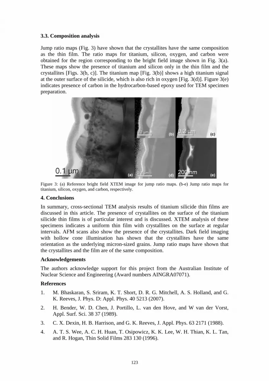
Jump ratio maps (Fig. 3) have shown that the crystallites have the same composition as the thin film. The ratio maps for titanium, silicon, oxygen, and carbon were obtained for the region corresponding to the bright field image shown in Fig. 3(a). These maps show the presence of titanium and silicon only in the thin film and the crystallites [Figs. 3(b, c)]. The titanium map [Fig. 3(b)] shows a high titanium signal at the outer surface of the silicide, which is also rich in oxygen [Fig. 3(d)]. Figure 3(e) indicates presence of carbon in the hydrocarbon-based epoxy used for TEM specimen preparation.
Figure 3: (a) Reference bright field XTEM image for jump ratio maps. (b-e) Jump ratio maps for titanium, silicon, oxygen, and carbon, respectively.
4. Conclusions In summary, cross-sectional TEM analysis results of titanium silicide thin films are discussed in this article. The presence of crystallites on the surface of the titanium silicide thin films is of particular interest and is discussed. XTEM analysis of these specimens indicates a uniform thin film with crystallites on the surface at regular intervals. AFM scans also show the presence of the crystallites. Dark field imaging with hollow cone illumination has shown that the crystallites have the same orientation as the underlying micron-sized grains. Jump ratio maps have shown that the crystallites and the film are of the same composition.
Acknowledgements The authors acknowledge support for this project from the Australian Institute of Nuclear Science and Engineering (Award numbers AINGRA07071).
References 1. M. Bhaskaran, S. Sriram, K. T. Short, D. R. G. Mitchell, A. S. Holland, and G.
K. Reeves, J. Phys. D: Appl. Phys. 40 5213 (2007).
2. H. Bender, W. D. Chen, J. Portillo, L. van den Hove, and W van der Vorst, Appl. Surf. Sci. 38 37 (1989).
3. C. X. Dexin, H. B. Harrison, and G. K. Reeves, J. Appl. Phys. 63 2171 (1988).
4. A. T. S. Wee, A. C. H. Huan, T. Osipowicz, K. K. Lee, W. H. Thian, K. L. Tan, and R. Hogan, Thin Solid Films 283 130 (1996).
124
Structural parameters of wheat starch granules differing in amylose content and functional characteristics studied by small-angle
x-ray scattering Jaroslav Blazek1, Amparo Lopez-Rubio2, Les Copeland1
1 Faculty of Agriculture, Food and Natural Resources, University of Sydney, NSW 2006, Australia
2 Bragg Institute, Australian Nuclear Science and Technology Organisation, Private Mail Bag 1, Menai, NSW 2234, Australia
Introduction Semicrystalline native starch granules display a hierarchical structural periodicity. Starch granules have a typical layered organization with alternating amorphous and semicrystalline growth rings of 120 to 400nm radial thickness. At a finer level of structural detail, the amorphous rings consist of amylose and amylopectin in a disordered conformation, whereas the semicrystalline rings contain lamellae with a repeat distance of 9-10nm that, in turn, contain alternating crystalline and amorphous regions (Cameron & Donald, 1992). The crystalline regions are mainly formed by double helices of amylopectin A chains packed laterally into a crystalline lattice, whereas amorphous regions contain amylose plus the amylopectin branching points. Small-angle X-ray scattering (SAXS) has been shown to be useful for studying the arrangement of crystalline and amorphous regions in semi-crystalline starch granules (Waigh, Jenkins & Donald, 1996). SAXS patterns from hydrated native starches show a broad scattering peak, from which the average thickness of the lamellar repeat unit (i.e. the thickness of the crystalline plus amorphous region) can be calculated. The position of the SAXS peak is related to the characteristic repeat length in granular starches, whereas peak width and intensity are mainly dependent on the regularity of the arrangement of lamellae and the electron density differences between the amorphous and crystalline regions of the lamellar structure.
Recent studies using SAXS and high-sensitivity differential scanning calorimetry (DSC) have increased our understanding of the influence of amylose located within amylopectin clusters in native starch granules. Starches with increased amylose content produced by genetic backcrossing of wheat cultivars grown in Australia have been studied by Blazek & Copeland (2007) and Hung et al. (2007a). These starches have been shown to possess characteristic pasting, swelling and viscoelastic properties related to amylose content, which indicates that they have differences in the structural organization that may be related to the lamellar architecture. In this study, SAXS together with several complementary techniques, such as DSC and X-ray diffraction (XRD), were employed to further examine structural features that provide starches, within a narrow range of amylose content, a wide range of functional properties.
Materials and Methods
Materials
Twelve wheat (Triticum aestivum L.) varieties selected from the set of samples described by Blazek & Copeland (2007) were used in the study. Amylose content was determined colorimetrically by iodine binding. Amylopectin chain length distribution was determined by fluorophore-assisted carbohydrate electrophoresis using the Beckman P/ACE System 5010.
125
Small Angle X-Ray Scattering
SAXS measurements were obtained with a Bruker Nanostar SAXS camera (available at ANSTO, Lucas Heights). Starch samples were presented in 2mm sealed glass capillaries as starch suspensions containing excess water above the settled starch granules. SAXS curves were plotted as a function of relative intensity I versus q. Parameters of the SAXS curves were determined by fitting the experimental curves with peak-fitting models. SAXS peaks were characterized by the following set of parameters: intensity at peak maximum Imax, position of the peak qmax and width of the peak ∆q. The Bragg spacing d, representing the interlamellar distance, was calculated according to the Bragg equation.
XRD and DSC analysis
XRD measurements of starch samples were made with a Difftech Mini Materials Analyser X-ray diffractometer (GBC Scientific Equipment Pty. Ltd.). XRD diffractograms were acquired at room temperature (20±1°C) over the 2θ range of 5 – 35 at a rate of 0.50 degrees 2θ per minute and a step size of 0.05 degrees 2θ. DSC measurements were made using a Modulated Differential Scanning Calorimeter MDSC 2920 instrument (TA Instruments Inc., New Castle, DE). Starch with distilled water (starch to water ratio of 1:2) was heated from 30 to 140°C at a rate of 10°C/min in hermetically sealed aluminium pans.
Results and Discussion
Composition and pasting properties of wheat starches
Amylose content varied between 35 and 43%. A waxy wheat variety included in the study had 4% amylose content. The relative amounts of amylopectin chains were classified into four fractions according to chain length. These were very short chains with degree of polymerization (DP) 6 to 12, medium length chains with DP 13 to 24, long chains with DP 25 to 36, and very long chains with DP greater than 36. The waxy wheat variety displayed more clearly defined peaks characteristic of A type crystallinity, whereas starch from commercial wheat displayed less well defined peaks compared to the remaining varieties. The XRD patterns of the 10 varieties from the other wheat samples were very similar. Starch melting temperature as measured by DSC varied among the varieties from 61.5 to 65.4°C, whereas the waxy variety displayed a melting temperature of 66.8°C. The Bragg spacing d, representing the lamellar distance calculated according to the Bragg equation, ranged from 10.7 to 11.2nm, whereas the lamellar distance of the waxy starch was 10.4nm. Width of the peak ∆q for the waxy wheat was 0.0242 compared to the average value of 0.0355 for the other samples and intensity at peak maximum Imax was higher than for the remaining starches.
Effect of amylose content on the structural parameters of starch granules
Native starches extracted from different plants usually display a continuously decreasing trend in the intensity of the scattering maximum as the amylose content of the starches increases (Jenkins & Donald, 1995). This observation is accounted for by a decrease in the electron density difference between the crystalline and amorphous regions of the lamellae with increasing amylose content. Kozlov et al. (2007) suggested that an increase in amylose content is accompanied by accumulation of both amylose tie-chains, forming defects in crystalline structure, and amylose chains oriented transversely to the ordered stacks within amorphous regions. Disordered ends

126
of amylopectin double helices and/or pre-existing double helices not participating in the formation of crystals are also contributing factors adding to the defects of the crystalline arrangement and hence greater disorder in the packing of the lamellar structure (Kozlov et al., 2007).
When the waxy wheat variety was compared with the other varieties used in this study, the following trends were observed: the waxy variety had better defined XRD peaks, higher melting temperature, smaller repeat lamellar distance, higher intensity of the SAXS peak and lower variation in lamellar repeat distance. In the set of 11 other starch samples with normal and increased amylose content (waxy wheat excluded), lamellar repeat distance increased, intensity of SAXS scattering peak increased and variation in lamellar distance increased with increasing amylose content. Additionally, within this amylose content (35 - 43%), higher proportion of amylopectin chains with medium chain length (DP 13-24) was linked with increased melting temperature, while higher proportion of short amylopectin chains (DP 6-12) correlated negatively with melting temperature. It is also interesting to note that melting temperature did not seem to be affected by amylose content and lamellar arrangements as studied by SAXS.
Based on combined results acquired by SAXS, DSC and XRD analyses, we conclude the differences between the waxy variety and the other samples used in this study are due to amylose inducing defects in the crystalline regions and also accumulating in the amorphous regions of the lamellar structure. Increased defects in amylopectin crystallites in the amylose-rich starches compared to waxy starch is consistent with observed lower melting temperature, less well defined XRD peaks and lower intensity of SAXS peak, whereas more amylose in the amorphous regions was evident from the greater repeat distance. We propose that the variation in the amount of crystalline defects caused by amylose tie-chains is not significant within the range of amylose content of the set of amylose-rich samples studied. This is consistent with invariance in XRD patterns and lack of correlation between melting temperature and amylose content. The observed increasing intensity of the SAXS peak with increasing amylose content can be explained by assuming that thicker lamellae in starches with increased amylose content provides higher mobility in the hydrated form, allowing better plasticization and transformation of the nematic phase into a smectic phase due to alignment of the double helices into register. We also assume there may be an additional protective effect of amylose on the crystallites. It is possible that higher amylose content provides a more intricate network, which helps to stabilize the crystalline structure, consistent with increased lamellar thicknesses and higher peak maximum Imax. Variations in the melting temperature and amylopectin chain length distribution indicates that rather than crystalline defects or accumulating amylose in amorphous regions, it is the amylopectin chain length distribution that prevails in determining thermodynamic behaviour of studied starches within a narrow range of amylose content. This is consistent with observed significant correlations between melting temperature and amylopectin chain length and lack of correlation between melting temperature and SAXS characteristics, including a lack of correlation between SAXS characteristics and amylopectin chain length distribution.
Our results indicate that, for the samples analysed within a narrow range of amylose contents, increased amylose content was not accompanied by the accumulation of crystal defects as described in the literature (Kozlov et al., 2007). Nevertheless, when structural characteristics of amylose-rich starches were compared with waxy wheat starch, the general trends described by Kozlov et al. (2007) were confirmed. In

127
summary, over a wide range of amylose content, there are three main factors that exert influence on the structural parameters of native starch granules at a nano-scale: (1) amylose defects (both as amylose ‘tie-chains’ and amylose-lipid complexes) located in the crystalline lamellae, (2) population of amylose accumulated within the amorphous lamellae, and (3) chain length distribution of amylopectin chains.
Several breeding approaches aiming at obtaining wheat starches with increased amylose content have been reported in the literature. Some of the breeding programs are based on the genetic manipulation of the enzymes involved in starch synthesis (Morell & Myers, 2005; Kozlov et al., 2006). However, selecting wheat varieties of desired functional characteristics has also been reported to lead towards increasing amylose content (Blazek & Copeland, 2007). Different breeding approaches can result in starches with increased amylose and variations in their functional, structural and thermodynamic characteristics. For instance, Hung et al. (2007b) described starches with increased amylose content that retained most of the crystallinity as compared to the starches with normal amylose content, whereas Hung et al. (2007a) described wheat varieties, in which increased amylose content was linked with the loss of crystallinity. Therefore, genetic background of wheat cultivars with increased amylose seems to be the determining factor in the molecular structure of starches.
Conclusions Analysis of the thermodynamic and structural properties of a set of wheat starches consisting of a waxy variety and a set of amylose-rich varieties enabled us to distinguish between multiple factors affecting lamellar architecture of native starch granules. While our results are in general consistent with the link between increasing amylose content and the accumulation of defects within crystalline lamellae, this study shows the value of studying wheat varieties of diverse genetic background in order to fully understand the level of variation in the structural arrangements of molecular starch components over micro and nano-scales.
References Blazek J., & Copeland L. (2007). Carbohydrate Polymers, in press, doi: 10.1016/j.carbpol.2007.06.010.
Cameron, R. E., & Donald, A. M. (1992). Polymer, 33, 2628-2635.
Hung, P.V., Maeda, T., Miskelly, D., Tsumori, R., & Morita, N. (2007a). Carbohydrate Polymers, in press, doi: 10.1016/j.carbpol.2007.07.015.
Hung, P. V., Maeda, T., & Morita, N. (2007b). Starch/Starke, 59, 125-131.
Jenkins, P. J., & Donald, A. M. (1995). International Journal of Biological Macromolecules, 17, 315-321.
Kozlov, S. S., Krivandin, A. V., Shatalova, O. V., Noda, T., Bertoft, E., Fornal, J., & Yuryev, V. P. (2007). Journal of Thermal Analysis and Calorimetry, 87, 575–584
Kozlov, S. S., Noda, T., Bertoft, E., & Yuryev, V. P. (2006). Journal of Thermal Analysis and Calorimetry, 86, 291–301.
Morell, M. K., & Myers, A. M. (2005). Current Opinion in Plant Biochemistry, 8, 204-210.
Waigh, T. A., Jenkins, P. J., & Donald, A. M. (1996). Faraday Discussions, 103, 325-337.
128
The ANSTO ECR Ion Source and its application to mass spectrometry
D. Button, D. Buckley, T. Esat, M.A.C. Hotchkis ANSTO, PMB 1, Menai, NSW 2234
Abstract At ANSTO we have built an Electron Cyclotron Resonance (ECR) ion source to investigate new concepts for mass spectrometers [1,2] designed to measure isotopic ratios in small samples.
ECR ion sources are capable of producing beams of multiply-charged atomic ions with high efficiency and are widely used as heavy ion injectors for accelerators. To meet the requirements of mass spectrometry, we have needed to adapt ECR ion source techniques to our purpose. In this presentation, these and other recent developments of our ECR ion source will be discussed.
Introduction Isotopic Ratio Mass Spectrometry (IRMS) techniques are applied to a range of elements to investigate naturally-occurring isotopic ratio variations. Current IRMS systems utilise ionization methods such as Electron Impact to generate ion beams for analysis by a mass spectrometer. This ionization method typically achieves 0.1% ionisation efficiency, dominantly of a 1+ charge state and with little break up of molecules.
Elements for investigation in an IRMS instrument may naturally exist in an atomic state such as noble gases like Argon and Neon, but more commonly as a constituent of a molecule such as oxygen in water. Oxygen isotopes in water cannot be analysed directly due to interferences at the mass values of the rare isotopes 17O and 18O. Interferences are generated by 1+ ions of H2O and OH, which cannot easily be separated from the rare isotopes. The problem is overcome, in part, by processing of water samples to convert the oxygen component into carbon dioxide gas (CO2). The 18O/16O ratio can be derived from the ratios of molecular ions at measured at masses 46 and 44. However, 17O cannot be determined in this way, due to the higher abundance of 13C which means that the mass 45 ions are dominated by 13CO2
+ ions.
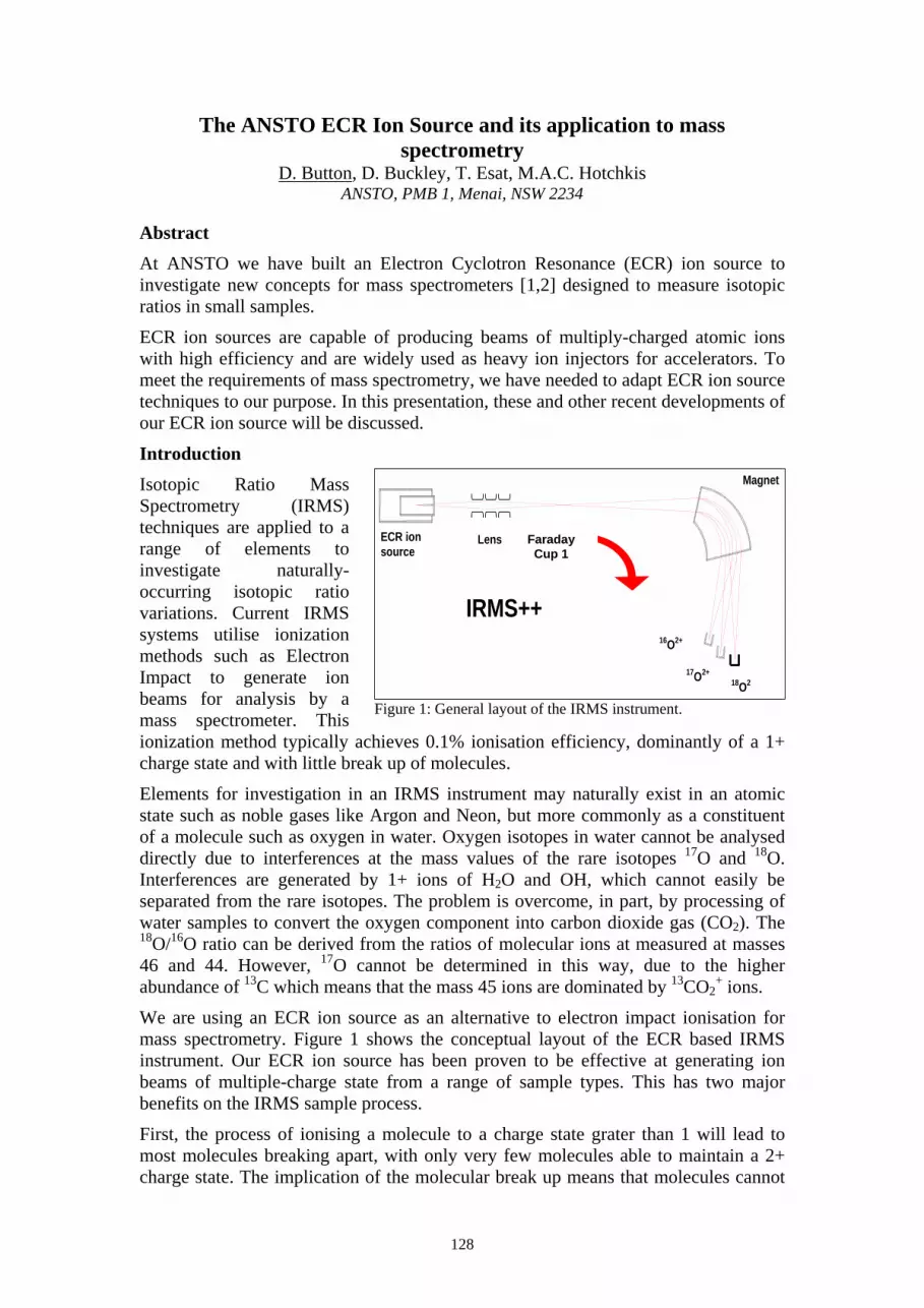
We are using an ECR ion source as an alternative to electron impact ionisation for mass spectrometry. Figure 1 shows the conceptual layout of the ECR based IRMS instrument. Our ECR ion source has been proven to be effective at generating ion beams of multiple-charge state from a range of sample types. This has two major benefits on the IRMS sample process.
First, the process of ionising a molecule to a charge state grater than 1 will lead to most molecules breaking apart, with only very few molecules able to maintain a 2+ charge state. The implication of the molecular break up means that molecules cannot
ECR ionsource
Lens
Magnet
18O2
+
17O2+
16O2+
IRMS++
Figure 1: General layout of the IRMS instrument.
Faraday Cup 1

129
be ionised to high charge states whereas atoms can. Secondly, producing atoms of charge states greater than 1 changes their m/q value. This means that the mass spectrometer is able to effectively separate the multiple charge state atoms free of the parent molecule which can only maintain a single charge state.
In our investigation oxygen, nitrogen, carbon, and argon have been tested in our ECR ion source which has been coupled with an analysing magnet and Faraday cup system to measure mass to charge ratios (m/q) of beams in the range 0 – 120 at a beam extraction energy of 15kV. The efficiency of our enclosed ECR ion source achieves greater than 10%, giving two orders of magnitude improvement on Electron Impact techniques. The removal of sample pre-processing also cuts down of the original sample size required, adding to the overall efficiency of the system.
This investigation of the sample gases has yielded promising results, but has also exposed an issue of sample retention within the ion source as a problem requiring further investigation to reduce the impact of possible memory effects.
ANSTO is working towards constructing a viable IRMS++ instrument for isotopic ratio measurements [2], and further developing a variation on the instrument to allow the measurement of 14C/12C ratios free from 14N, 12CH2, and 13CH interferences [1].
Experimental Arrangement The ECR ion source, shown in Figure 2, is a variation on other ECR source designs. Featuring a single ended plasma bottle, and miniaturised magnet arrangement so as to reduce the plasma bottle volume. This was done to maximise the efficiency of the source, as the only paths for gas to be removed from the plasma bottle is via beam extraction as an ion, or by pumping which is restricted by the low conductance of the extraction aperture.
Sample gases are introduced to the ions source via the gas inlet indicated in figure 2. This is fed by 2 capillary lines of 25µm internal diameter. One line delivers the sample gas/vapour, and the other delivers a support gas (if required -- typically helium).
Static pressures of sample and support gas are placed on the inlet side of the capillaries typically in the order of hundreds of Torr, so that the transition between lamina and molecular flow can occur within the capillary preventing fractionation effects.
Figure 2: Schematic of the ECR ion source. Parts of the internal and external support structures are not shown.
130
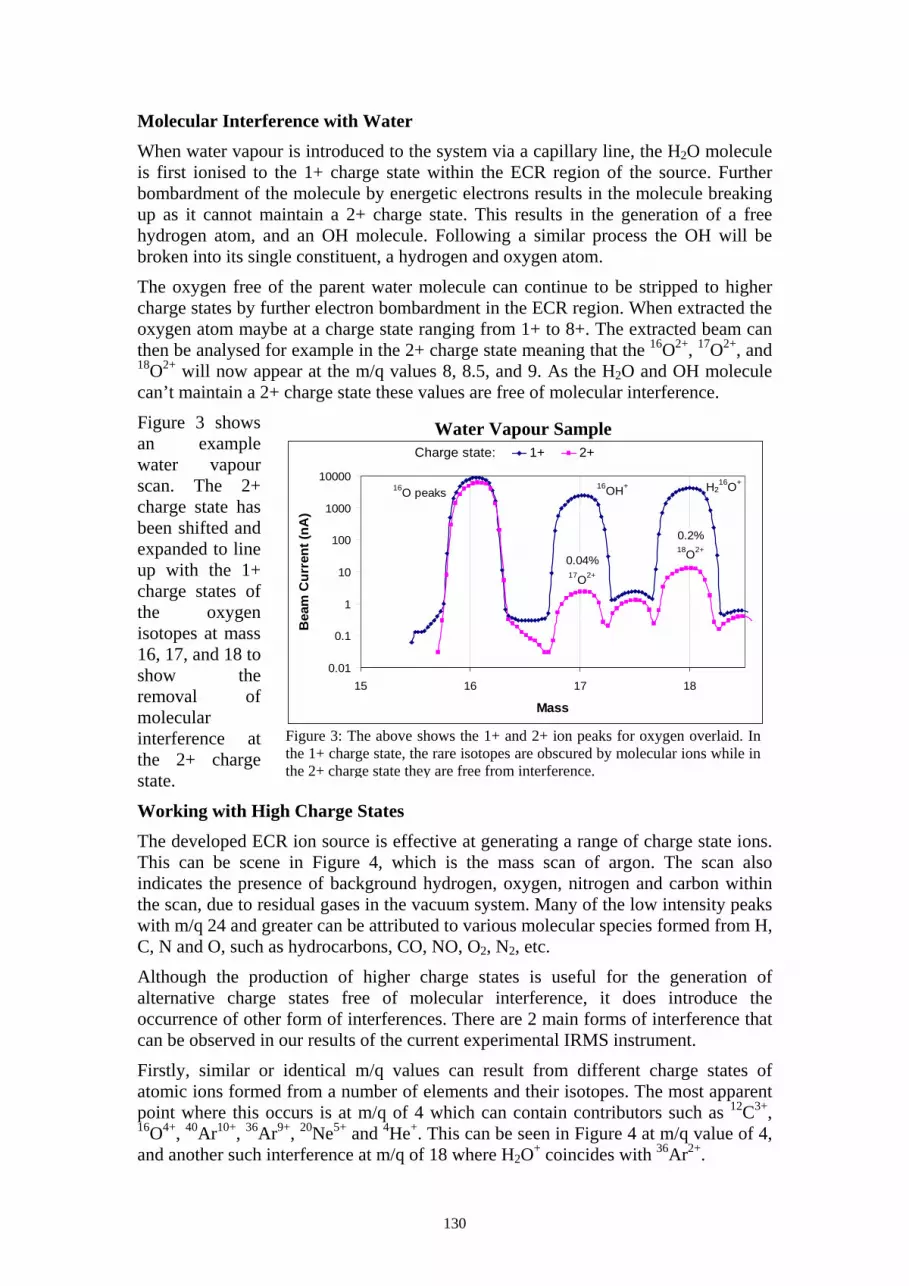
Molecular Interference with Water When water vapour is introduced to the system via a capillary line, the H2O molecule is first ionised to the 1+ charge state within the ECR region of the source. Further bombardment of the molecule by energetic electrons results in the molecule breaking up as it cannot maintain a 2+ charge state. This results in the generation of a free hydrogen atom, and an OH molecule. Following a similar process the OH will be broken into its single constituent, a hydrogen and oxygen atom.
The oxygen free of the parent water molecule can continue to be stripped to higher charge states by further electron bombardment in the ECR region. When extracted the oxygen atom maybe at a charge state ranging from 1+ to 8+. The extracted beam can then be analysed for example in the 2+ charge state meaning that the 16O2+, 17O2+, and 18O2+ will now appear at the m/q values 8, 8.5, and 9. As the H2O and OH molecule can’t maintain a 2+ charge state these values are free of molecular interference.
Figure 3 shows an example water vapour scan. The 2+ charge state has been shifted and expanded to line up with the 1+ charge states of the oxygen isotopes at mass 16, 17, and 18 to show the removal of molecular interference at the 2+ charge state.
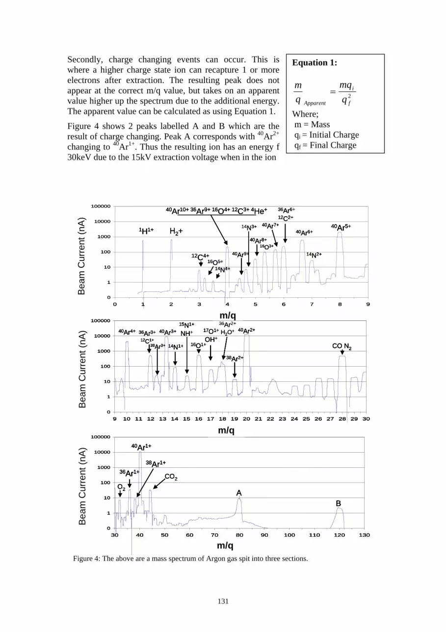
Working with High Charge States The developed ECR ion source is effective at generating a range of charge state ions. This can be scene in Figure 4, which is the mass scan of argon. The scan also indicates the presence of background hydrogen, oxygen, nitrogen and carbon within the scan, due to residual gases in the vacuum system. Many of the low intensity peaks with m/q 24 and greater can be attributed to various molecular species formed from H, C, N and O, such as hydrocarbons, CO, NO, O2, N2, etc.
Although the production of higher charge states is useful for the generation of alternative charge states free of molecular interference, it does introduce the occurrence of other form of interferences. There are 2 main forms of interference that can be observed in our results of the current experimental IRMS instrument.
Firstly, similar or identical m/q values can result from different charge states of atomic ions formed from a number of elements and their isotopes. The most apparent point where this occurs is at m/q of 4 which can contain contributors such as 12C3+, 16O4+, 40Ar10+, 36Ar9+, 20Ne5+ and 4He+. This can be seen in Figure 4 at m/q value of 4, and another such interference at m/q of 18 where H2O+ coincides with 36Ar2+.
Water Vapour Sample
0.01
0.1
1
10
100
1000
10000
15 16 17 18
Mass
Bea
m C
urre
nt (n
A)
1+ 2+Charge state:
16O peaks16OH+ H2
16O+
17O2+
0.2%18O2+
0.04%
Figure 3: The above shows the 1+ and 2+ ion peaks for oxygen overlaid. In the 1+ charge state, the rare isotopes are obscured by molecular ions while in the 2+ charge state they are free from interference.
131
Secondly, charge changing events can occur. This is where a higher charge state ion can recapture 1 or more electrons after extraction. The resulting peak does not appear at the correct m/q value, but takes on an apparent value higher up the spectrum due to the additional energy. The apparent value can be calculated as using Equation 1.
Figure 4 shows 2 peaks labelled A and B which are the result of charge changing. Peak A corresponds with 40Ar2+ changing to 40Ar1+. Thus the resulting ion has an energy f 30keV due to the 15kV extraction voltage when in the ion
Equation 1:
2f
i
Apparent qmq
qm
=
Where; m = Mass qi = Initial Charge qf = Final Charge
0
1
10
100
1000
10000
100000
0 1 2 3 4 5 6 7 8 9amu
Bea
m C
urre
nt (n
A) 40Ar5+
14N2+
40Ar6+40Ar7+
36Ar6+
12C2+
16O3+40Ar8+
1H1+ H2+
40Ar9+
14N3+
40Ar10+ 36Ar9+ 16O4+ 12C3+ 4He+
12C4+
14N4+16O5+
m/q36Ar2+
H2O+
0
1
10
100
1000
10000
100000
9 10 11 12 13 14 15 16 17 18 19 20 21 22 23 24 25 26 27 28 29 30amu
Bea
m C
urre
nt (n
A) CO N2
40Ar2+40Ar3+40Ar4+ 36Ar3+12C1+
16O1+
38Ar2+
17O1+
OH+
14N1+
15N1+
NH+
38Ar3+
m/q
0
1
10
100
1000
10000
100000
30 40 50 60 70 80 90 100 110 120 130amu
Bea
m C
urre
nt (n
A)
BA
40Ar1+
CO236Ar1+
38Ar1+
O2
m/q
Beam
Cur
rent
(nA)
Bea
m C
urre
nt (n
A)
Beam
Cur
rent
(nA)
0
1
10
100
1000
10000
100000
0 1 2 3 4 5 6 7 8 9amu
Bea
m C
urre
nt (n
A) 40Ar5+
14N2+
40Ar6+40Ar7+
36Ar6+
12C2+
16O3+40Ar8+
1H1+ H2+
40Ar9+
14N3+
40Ar10+ 36Ar9+ 16O4+ 12C3+ 4He+
12C4+
14N4+16O5+
0
1
10
100
1000
10000
100000
0 1 2 3 4 5 6 7 8 9amu
Bea
m C
urre
nt (n
A) 40Ar5+
14N2+
40Ar6+40Ar7+
36Ar6+
12C2+
16O3+40Ar8+
1H1+ H2+
40Ar9+
14N3+
40Ar10+ 36Ar9+ 16O4+ 12C3+ 4He+
12C4+
14N4+16O5+
40Ar5+
14N2+
40Ar6+40Ar7+
36Ar6+
12C2+
16O3+40Ar8+
1H1+ H2+
40Ar9+
14N3+
40Ar10+ 36Ar9+ 16O4+ 12C3+ 4He+
12C4+
14N4+16O5+
m/q36Ar2+
H2O+
0
1
10
100
1000
10000
100000
9 10 11 12 13 14 15 16 17 18 19 20 21 22 23 24 25 26 27 28 29 30amu
Bea
m C
urre
nt (n
A) CO N2
40Ar2+40Ar3+40Ar4+ 36Ar3+12C1+
16O1+
38Ar2+
17O1+
OH+
14N1+
15N1+
NH+
38Ar3+
m/q
0
1
10
100
1000
10000
100000
30 40 50 60 70 80 90 100 110 120 130amu
Bea
m C
urre
nt (n
A)
BA
40Ar1+
CO236Ar1+
38Ar1+
O2
m/q
Beam
Cur
rent
(nA)
Bea
m C
urre
nt (n
A)
Beam
Cur
rent
(nA)
m/q36Ar2+
H2O+
0
1
10
100
1000
10000
100000
9 10 11 12 13 14 15 16 17 18 19 20 21 22 23 24 25 26 27 28 29 30amu
Bea
m C
urre
nt (n
A) CO N2
40Ar2+40Ar3+40Ar4+ 36Ar3+12C1+
16O1+
38Ar2+
17O1+
OH+
14N1+
15N1+
NH+
38Ar3+
0
1
10
100
1000
10000
100000
9 10 11 12 13 14 15 16 17 18 19 20 21 22 23 24 25 26 27 28 29 30amu
Bea
m C
urre
nt (n
A) CO N2
40Ar2+40Ar3+40Ar4+ 36Ar3+12C1+
16O1+
38Ar2+
17O1+
OH+
14N1+
15N1+
NH+
38Ar3+ CO N2
40Ar2+40Ar3+40Ar4+ 36Ar3+12C1+
16O1+
38Ar2+
17O1+
OH+
14N1+
15N1+
NH+
38Ar3+
m/q
0
1
10
100
1000
10000
100000
30 40 50 60 70 80 90 100 110 120 130amu
Bea
m C
urre
nt (n
A)
BA
40Ar1+
CO236Ar1+
38Ar1+
O2
0
1
10
100
1000
10000
100000
30 40 50 60 70 80 90 100 110 120 130amu
Bea
m C
urre
nt (n
A)
BA
40Ar1+
CO236Ar1+
38Ar1+
O2
BA
40Ar1+
CO236Ar1+
38Ar1+
O2
m/q
Beam
Cur
rent
(nA)
Bea
m C
urre
nt (n
A)
Beam
Cur
rent
(nA)
Figure 4: The above are a mass spectrum of Argon gas spit into three sections.

132
was extracted at the 2+ charge state, shifting the apparent m/q value to 80. Peak B, is the result of 40Ar3+ changing to 40Ar1+ giving it an apparent m/q value of 120. The peak at m/q = 30 is a further example, due to the 40Ar3+ to 40Ar2+ charge change. These peaks show a distorted peak shape as the charge change may occur very close to or within the extraction region.
Potential interferences from charge changing events can be overcome by the addition of and Electro-Static Analyser (ESA) to eliminate ions of incorrect energy to charge ratios.
References M.A.C. Hotchkis and T. Wei, Radiocarbon detection by ion charge exchange mass spectrometry, Nucl. Instr. & Meth. B 259 (2007) 158.
M.A.C. Hotchkis and C.L. Waring, An Isotope Ratio Mass Spectrometer and Methods for Determining Isotope Ratios, Australian Patent Application No. PCT/AU2006/001284.

133
Design considerations in the development of magnetic nanoparticles for MRI contrast enhancement
M. R. J. Carroll 1, M. House 1, T. G. St. Pierre 1, R. C. Woodward 1, O. T. Mefford 2,
J. D. Goff 2, N. Pothayee 2, P. Huffstetler 2, J. S. Riffle 2
1 School of Physics, The University of Western Australia, Perth, Western Australia. 2 School of Chemistry, Virginia Polytechnic Institute and State University, Blacksburg
Virginia USA.
Since the development of magnetic resonance imaging (MRI) in the mid 1970s, it has become one of the most widely used advanced diagnostic tools. Magnetic nanoparticle contrast agents provide the opportunity to extend the versatility of MRI by enhancing the contrast between different tissue types. A series of potential MRI contrast agents based on surfactant coated iron oxide nanoparticles have been studied. These nanoparticles have been characterised by transmission electron microscopy, SQuID magnetometry, elemental analysis, small angle x-ray and neutron scattering as well as proton relaxometry to assess their potential as MRI contrast agents and to elucidate the mechanisms of proton relaxation enhancement.
134
Plasma immersion ion implantation and deposition of titanium nitride onto polymers
C. Chaiwong, D.R. McKenzie, M.M.M. Bilek School of Physics, The University of Sydney, NSW 2006, Australia
Abstract Deposition of hard coatings onto polymers requires knowledge of the phenomena occurring when materials of different elastic properties are brought into contact. Buckling and delamination are undesirable effects that may occur and are frequently linked to the stress induced in the film. The use of energetic deposition by ion implantation has been shown to be an effective surface modification technique that can solve the problem of delamination. In this work, titanium nitride films were prepared on polycarbonate substrates by cathodic arc deposition combined with plasma immersion ion implantation (PIII). The stress in the film could be remarkably reduced by using 3 kV bias with plasma immersion ion implantation. Excellent adhesion strength for films produced under these conditions was demonstrated using tensile testing. Cross sectional transmission electron microscopy revealed an intermixed layer between the film and the substrate that was believed to enhance the adhesion strength.
1. Introduction Polymers have wide spread use as composite materials for many application areas. Examples of existing applications include materials for consumer products, structural materials for automotive and aeronautical industries and packaging for the food and medical industries. However, their use is sometimes limited by the undesired properties of the surface, as opposed to the useful characteristics of the bulk, such as light weight, high strength. Polycarbonate is known to be the one of the toughest among the engineering polymers. However, polycarbonate surface is easily scratched and somewhat limited chemical resistance. The performance of polycarbonate can be enhanced by surface modification, thus the potential for its application can be significantly increased. Titanium nitride has a wide range of applications due to a unique combination of properties such as high hardness, good chemical inertness, and excellent wear resistance. It may also be a suitable protective layer for the surface of polymeric materials. In this work, we investigated the adhesion of TiN films grown on polycarbonate using a combination of filtered cathodic vacuum arc and plasma immersion ion implantation and deposition (PIII&D). The stress in the film was studied. The adhesion strength between the film and the substrate was evaluated.
2. Experimental details
The substrate material was 1-mm thick polycarbonate (Lexan®) sheet. The sheet was used in the as-received state. Filtered cathodic vacuum arc with titanium cathode was employed for deposition of the titanium nitride (TiN) films. The details of the filtered cathodic arc and the parameters were explained elsewhere [1].The substrate holder was mounted on a high-voltage, insulating feed-through and connected to the pulser unit. The deposition rate was kept low (2nm/min) to minimize substrate heating. Film thickness was measured after deposition with a Tencor™ surface profilometer. The stress of the film was deduced by measuring the radius of curvature of a 20mm x 20mm x 0.5mm sheet before and after deposition and by applying Stoney’s equation [2]. For adhesion test, polycarbonate sheet was cut into a tensile sample with a parallel gauge section of length 12mm and width 3mm. The tensile test was

135
performed by a small tensile device positioned under an optical microscope was used. The displacement and load during straining at a crosshead speed of 3µm/s were measured and images of the surface were captured every 2 seconds. Post-analysis of the sample was done by a scanning electron microscopy (SEM) , Phillips XL30. The cross-sectional specimen for transmission electron microscopy (TEM) was obtained by ultramocrotomy (Reichert Ultracut S). Bright-field image of the cross-sectional specimen was taken with a TEM (Phillips CM12).
3. Results and discussion
Residual stress in titanium nitride films
It is known that thin films deposited with PVD processes suffer high level of compressive residual stress. A high level of stress in combination with insufficient adhesion at the interface can be adequate to initiate spontaneous buckling [3]. In this work, the stress in the TiN films deposited without high voltage substrate bias was measured. The residual stress state in the film was found to be compressive. The film thickness was 105 ± 8nm. Using Young’s modulus and Poisson’s ratio of polycarbonate as 2.21GPa and 0.37, respectively, the residual stress is 1.6 ± 0.4GPa. SEM micrograph (Figure 1) of the sample shows that randomly directed wrinkles have formed on the film surface. Film delamination is also observed.
0
0.5
1
1.5
2
2.5
3
0 200 400 600 800 1000 1200 1400 1600
Pulse Frequency (Hz)
Stre
ss (G
Pa)
1 kV2 kV3 kV
Figure 1 SEM micrograph of the surface of the TiN film deposited without high voltage substrate bias. The film thickness is 105 ± 8nm.
Figure 2 A graph of TiN film stress as a function of high voltage pulse frequency.

136
The effect of the pulse voltages and the pulse frequencies on the stress of TiN films on polycarbonate substrates was investigated. The relation between the residual stress and the high voltage pulse frequency is shown in Figure 2. A remarkable stress relief can be obtained at the voltages 2 and 3kV. However, the pulse frequency does not show significant effect on the stress relief. Optical xx microscopy of the film surface show smooth film without of cracking. The stress relief in the film can be explained by the concept of thermal spike during xx energetic ion xx xx bombardment [4].
Adhesion measurement
Figure 3 shows the typical stress-strain curve of the test. The test was performed on the film deposited with 3 kV substrate bias. The film thickness is 80nm. The strain at which the film started to crack (fracture strain) is about 2 % and the crack saturation occurred at about 4% strain. The SEM micrograph of the sample after the tensile test reveals that there is no evidence of severe delamination or buckling. The ultimate shear strength of the interface was calculated from the relationship of the fracture strain and the crack spacing [1, 5]. The ultimate shear strength of the interface is 0.6 GPa. This excellent adhesion observed is due to the interface mixing and the stress relaxation induced by energetic ion bombardment [6, 7]. The cross-sectional TEM (Figure 4) shows the interface mixing between the film and the substrate. The film appears to be dense and the columnar structure was suppressed.
4. Conclusion The stress in the film deposited with PIII&D was found to be remarkably reduced compared to that of the film deposited without PIII&D. The adhesion of the film to the substrate was studied by means of a tensile test. Adhesion strength comparable to that found for TiN films on steel substrates was achieved. The good adhesion is attributed to the reduction of stress and interface mixing induced by using PIII&D during deposition.
substrate
mixing layer
TiN
Figure 4 Cross-sectional TEM micrograph of TiN/polycarbonate interface.
Figure 3 Stress-strain curve of the sample during the tensile test. The film thickness was 80nm.

137
References [1] C. Chaiwong, D. R. McKenzie, and M. M. M. Bilek, "Study of adhesion of TiN
grown on a polymer substrate," Surface and Coatings Technology, vol. 201, pp. 6742-6744, 2007.
[2] G. G. Stoney, "The tension of metallic films deposited by electrolysis," Proceedings of Royal Society (London), vol. A82, pp. 172-175, 1909.
[3] C. Chaiwong, D. R. McKenzie, and M. M. M. Bilek, "Cracking of titanium nitride films grown on polycarbonate," Surface and Coatings Technology, vol. 201, pp. 5596-5600, 2007.
[4] M. M. M. Bilek, D. R. McKenzie, and W. Moeller, "Use of low energy and high frequency PBII during thin film deposition to achieve relief of intrinsic stress and microstructural changes," Surface and Coatings Technology, vol. 186, pp. 21-28, 2004.
[5] D. C. Agrawal and R. Raj, "Measurement of the Ultimate Shear Strength of a Metal-Ceramic Interface," Acta Metallugical, vol. 37, pp. 1265-1270, 1989.
[6] S. H. N. Lim, D. G. McCulloch, M. M. M. Bilek, and D. R. McKenzie, "Minimisation of intrinsic stress in titanium nitride using a cathodic arc with plasma immersion ion implantation," Surface and Coatings Technology, vol. 174-175, pp. 76-80, 2003.
[7] S. H. N. Lim, D. G. McCulloch, M. M. M. Bilek, and D. R. McKenzie, "Relation between microstructure and stress in titanium nitride films grown by plasma immersion ion implantation," Journal of Applied Physics, vol. 93, pp. 4283-4288, 2003.
138
DLTS study of ion and molecular implantation damage in silicon C. T. Chang, J. C. McCallum
School of Physics, University of Melbourne, Victoria, 3010 Australia Email: [email protected]
Abstract In this paper we present preliminary DLTS results of H implanted silicon. These results will form the basis of further studies of the defects produced with ion and molecular implantation. Here, implantations were performed to various fluences with 70 keV H. The ion beam flux was also varied. Three kinds of defects were identified with a VPs or V2 related defect having the greatest concentration.
Introduction The use of implantation in the semiconductor industry results in defects being formed in the silicon substrate. These defects must to a large extent be removed, usually by post-implantation thermal processing, for active devices to be obtained. As microchip sizes continue to decrease more detailed information is required about the nature and quantities of the defects formed during the implantation process so that the thermal budgets required to remove the defects can be reduced. Deep-Level Transient Spectroscopy (DLTS) allows the study of these defects through the determination of their energy levels in the band-gap and the depth at which the defects are located within the substrate.
Results presented here form the basis of a comparative study between the defect profiles created by ion and molecular implantation.
Experimental In the present study, 70 keV H was implanted into phosphorus doped Czochralski grown silicon to various concentrations and fluences using the 150 kV ion implanter at the Australian National University. Three different measurements were performed on the SULA Technologies DLTS system at the University of Melbourne. These were capacitance-voltage (CV), capacitance-temperature (CT) and standard DLTS measurements. The CV measurement enabled the determination of the active donor concentration, depletion width, the built-in voltage of the diode and barrier height. The steady state capacitance value under the full reverse bias was determined with CT measurements. Finally, ion implantation induced deep-level defects were classified by their energy level and capture cross section using DLTS. This was achieved by using four separate correlator signals. By combining these techniques it was possible to determine the defect concentration as a function of depth [1]. For all measurements the voltage pulse was set to –2 V, which was found, to be adequate for measuring the 70 keV implant.
Sample sets were divided into four groups, 1-4, determined by their H concentrations 9101× , 9102× , 10102× and 11101× H/cm3. A fluence dependence study of the
defects created during ion implantation was performed with group 1 samples ( 9101× H/cm3) using an ion beam flux of either 1 nA or 0.5 nA.

139
Results and discussion Figure 1 shows the DLTS signal as a function of temperature for samples having a H concentration of 10102× H/cm3 (group 3). Each correlator had respective delay times of delay times of 5, 2, 0.5 and 0.2 ms. The noise levels in the DLTS spectra from groups 1 and 2 samples (not shown) were significantly greater because of the relatively lower trap concentrations. This made it difficult to distinguish between these two groups. Likewise, there were indistinguishable differences between the two different fluences of group 1. Three distinct peaks can be seen in each correlator signal in Figure 1. Each peak corresponds to a different trap energy determined with the Arrhenius plot shown in Figure 2.
Figure 1. Typical DLTS spectra for Si implanted with 70 keV H to a concentration of 2 x 10¹⁰ H/cm3. Four correlators where used with respective delay times of 5, 2, 0.5 and 0.2 ms.
The gradients determined in Figure 2 allowed us to classify three traps by their energy levels and capture cross section [2]. This was achieved through a comparative analysis with previous studies [3, 4, 5]. The trap with an energy of 0.44eV could be associated with a VPs (Vacancy-Phosphorus complex) or a −
2V (divacancy complex). The trap with an energy of 0.33eV is assigned to a VO-H (Vacancy Oxygen-Hydrogen complex) or a H-related defect. Finally, a VO defect is responsible for the signal resulting in a trap energy of 0.18eV. The capture cross-section for these three traps are
151515 107,106.1,106.2 −−− ×××= andCσ cm2, respectively.

140
Figure 2. An Arrhenius plot for the DLTS spectra presented in Figure 1.
Figure 3 shows a CV measurement from a 70 keV H implanted Si sample. From the line of best fit the active donor concentration was approximated to be 151065.7 ×=An P/cm3 and the build-in voltage was eVVbi 326.1= . These results will enable the further analysis of the donor concentration as a function of the depletion width. When pulsing –2 V into the sample the depletion width reaches a maximum of
51030.7 −× cm.
Figure 3. C-V plot with a line of best fit for Si implanted with 70 keV H to a concentration of 2 x 10¹⁰ H/cm3.

141
Conclusion The preliminary results here show the analysis of the damage caused by hydrogen ion implantation. The classification of the defects through the determination of their trap energies and capture cross-sections tells us that the majority of defects are VPs or V2 related.
Currently a comparative study between the damage created after H ion implantation and H2 molecular implantation is being pursued. The molecular implant will be implanted at twice the ion energy presented here. This is to ensure the depth profile of both H and H2 implants are similar. Other investigations will include lithium and phosphorus. Interest in the Li and Li2 implant has been sparked by the fact that lithium is electrically active after implantation [6]. The phosphorus implants are of particular interest to the CQCT (Centre of Quantum Computing Technology) group for investigating P-P interactions.
References [1] D.V. Lang, J. Appl. Phys. 45, 3023 (1974)
[2] P. Blood and J. Orton, The Electrical Characterisation of semiconductors: Majority carriers and electron states, page 340. Academic Press, (1992)
[3] B.G. Svensson et al., Phys Rev B, 55, 10498 (1997)
[4] A. Hallen et al., J. Appl. Phys., 67, 1266 (1990)
[5] B.G. Svensson et al., Phys Rev B, 43, 2292 (1991)
[6] N.V. Brilliantov et al., Phys. Stat. Sol. A., 130, 53 (1992)
142
Surface modifications of nanoporous alumina membranes by plasma polymerisation
Martin A. Cole, Björn Dollmann, Krasimir Vasilev, Hans J. Griesser and Dusan Losic
University of South Australia, Ian Wark Research Institute, Mawson Lakes Campus, Mawson Lakes, Adelaide, SA 5095, Australia
Summary Nanoporous alumina membranes (PA) have a variety of applications in bioseparation,, biosensors and targeting delivery. This work describes the surface modification of these membranes using of plasma polymerisation in order to improve their morphological and chemical properties. Commercial porous alumina membranes (with pore sizes from 20 to 200nm) were used and modified by plasma deposition of ultra-thin polymer films. Monomer n-heptylamine was employed to achieve chemically reactive polymer surface on PA terminated with amino groups. The purpose of these amino groups is to provide functionality and ideal surface properties for building more complex architectures in the pores and in order to improves selectivity and separation properties of the membranes. The effect of processing parameters during plasma deposition on the morphological and chemical properties of plasma modified porous alumina membranes was studied using field emission scanning electron microscopy (FESEM) atomic force microscopy (AFM) and X-ray electron spectroscopy (XPS).
Introduction Nanoporous inorganic membranes regarding their unique thermal, mechanical, structural, optical and chemical properties, have attracted intensive research interest in the last decade for applications in various fields such as separation, adsorption, catalysis, sensors, energy storage, and drug delivery.1 A range of nanoporous materials based on zeolites, siliceous materials, inorganic oxides, carbon nanotubes, metal and metallo-organic composites have been explored. Among them porous alumina (PA) membranes fabricated by electrochemical anodisation are one of most popular nanoporous materials due to simple and low cost fabrication, chemical and thermal stability, remarkable hardness, uniform pore size and high pore density.2 PA membranes with controlled pore dimensions can be fabricated by well established procedures based on electrochemical anodisation of aluminum foil using selected acids, applied voltage and temperature. The fabricated PA membranes possess, uniform, dense and hexagonally packed pores (nanochannels) with a high aspect ratio running in the direction perpendicular to the membrane surface with diameters ranging between 20 and 300nm and thickness from 1 to 100 µm. These properties are of particular interest for membrane applications and recently PA membranes called “Anodisc” or “Anopore” membranes with limited pore sizes (20nm, 100nm and 200nm) are commercially available. One limitation on the application of these membranes as membranes for separation of smaller molecules is their relatively larger minimum pore diameter (20nm). Therefore it is important to find a simple and reliable approach to reduce the pore size of existing PA membranes in a controlled way into a dimension that will enhance their nanoseparation and molecular sieving properties. In addition, to introduce other separation strategies based on chemical or interfacial properties of molecules rather than their size, it is necessary to perform chemical modification and functionalisation of PA membranes.

143
Several modification approaches for pore size reduction and surface functionalisation have been explored in recent years to improve the selectivity and separation properties of PA membranes. These methods to enhance membrane application and performance include atomic layer deposition (ALD), chemical vapor deposition (CVD), thermal vapor metal deposition, electroless deposition, sol-gel and layer by layer deposition.3-4 Plasma-based methods initially developed for microelectronics in the fifties, present clean, simple and extremely flexible fabrication technology to perform surface modifications (cross-linking, grafting, and etching), and allow tunning of surface properties (morphological, interfacial and chemical).5 Based on these advantages and the preparation of ultrathin polymer films plasma polymerization has received great attention for surface modification of various devices including membranes. This work focuses on exploring the application of plasma polymerization for membrane modification with particular goals to achieve controlled reduction of pore size and introduction of reactive surface groups amenable for the covalent immobilization of biologically active molecules. Morphological, topographical and chemical properties of plasma polymer coating were investigated using field emission scanning electron microscopy (FSEM), atomic force microscopy (AFM) and X-ray electron spectroscopy (XPS)
Experimental The PA membranes (“Anodisc”) with pore sizes of 20nm, 100nm and 200nm were obtained from commercial sources (Whatman, UK). Prior to the plasma deposition, PA membranes were repeatedly washed in ethanol followed by Milli Q water and drying with a nitrogen jet. Plasma polymerization was carried out in a custom built plasma reactor described elsewhere powered by a commercial 13.56 MHz radio-frequency generator.6 The scheme of reactor is shown in Figure 2. A monomer vapor of n-heptylamine (98%, supplied from Fluka) was used. The deposition was carried at a pressure of 0.2 Torr using a power of 40 W. To obtain films with thicknesses in the range from 20nm to 200nm the deposition time was varied from 20 s to 200 s. Polymerisation was repeated a minimum of three times for each deposition time using a series of PA with different pore sizes. Silicon wafer is used for each experiment as a control to confirm thickness of deposited films.
FESEM characterisation of prepared PA membranes was performed using the Philips XL 30. The samples were cut into small pieces, mounted into a holder with double sided conductive tape and coated with a fewnm of a platinum layer. Images with a range of scan sizes from top surfaces (normal incidence) and profiles (40º degree angle) were acquired to observe the pore structure before and after modifications.
Asylum MFP-3D Atomic Force Microscope (Asylum Research, USA) was used for the characterisation of surface topography of the bare PA and modified PA with plasma polymer films. The imaging is performed in contact mode in air, using silicon nitride tips (NT-MDT, Russia) with spring constant of 0.58 - 5.5 N/m (specified by the manufacturer).
Figure 1. Schematic illustration of the plasma polymerisation reactor

144
The XPS analysis of plasma modified samples were recorded using a Kratos AXIS Ultra DLD spectrometer with a monochromated Al Kα radiation source (hν = 1486.7eV) operating at 15 kV and 10 mA. The elements present in the sample surface were identified from a survey spectrum recorded over the energy range 0-1100eV at a pass energy of 160eV and a resolution of 1.0eV. High-resolution spectra (0.1eV) were then recorded for pertinent photoelectron peaks (carbon and nitrogen).
The thickness measurements of deposited films on silicon wafers were used as control samples during polymerization and were performed using Imaging Ellipsometer (Beaglehole Instruments, New Zealand).
Results and Discussion A typical FESEM images of the commercial PA membranes (20nm pore size) is shown in Figure 2 (a-c). These images confirm that structure of PA membranes is asymmetric with a bulk pore structure comprised of straight channels with pore sizes from 100-200nm and a thin layer (cca 1 µm) on the top with specified pore size (20nm, 100nm and 200nm). However their pore shape is rather irregular and not circular and pore sizes are often bigger than specified values. The n-heptylamine plasma polymer film was deposited on the top of these PA membranes using the different deposition times (20 s, 50 s, 100s, 150 s and 200 s). The deposition rate was determined by ellipsometry using control samples (silicon wafers) which confirm an average rate of about 1nm/s. To prove the reduction of pore size as a result of polymer deposition, FSEM and AFM images were taken from the top surface. Typical images of modified PA membranes (20nm pore size) are shown in Figure 2 and 3. It is evident that the decreasing of the size of pore was achieved by increasing the deposition time from 20 s to 100 s (Fig. 2 d-f). When deposition times of 20 s and 50 s were used, the size of pores is reduced and pores are still open. The significant reduction of pore size is observed with deposition time of 100 s which makes most of
Figure. 2. FESEM images of commercial PA membranes (20nm pore size) obtained before, a-c) and after plasma deposition of n- heptylamaine polymer using different deposition times, d) 20s, e) 50 s and f) 100s

145
the pores partially closed (Fig. 2 f). AFM imaging is performed to confirm the morphology of these pores and images show significant decreasing of surface roughness after polymer deposition (Fig. 3 b). The depressions originating from the pores are seen on AFM images. However their height is considerably smaller in comparison with the height of pores on bare PA membranes (Fig. 3 a), which could direct the conclusion that a thin polymer layer is formed over the pores. When a longer deposition rate of 200 s is performed (data not shown) these depressions disappear which confirms the complete covering of pores.
A similar effect on decreasing the pore size was observed using PA with pores of 100nm and 200nm. Regarding to the larger size of their pores, significant decreasing in pore size was observed by using higher deposition times (100s, 150 s and 200 s). These results show that plasma polymerization can be successfully used for pore modifications of PA membranes with controlled reduction of their size. Further experiments will be carried out to explore the filtration properties of these plasma modified membranes in relation to small organic molecules and proteins.
XPS analysis was conducted to investigate the surface elemental and surface chemical composition of deposited polymer on PA. The survey spectrum (Figure 4, left) reveals the presence of three elements, carbon, nitrogen and oxygen which shows approximately 85 % carbon and 11 % nitrogen from the plasma polymer along with small amounts of oxygen arising from film oxidation. Observed chemical composition of the deposited polymer films on PA was in reasonable agreement with expected theoretical values based on the chemical structure of n-heptylamine (C 85 %, N 10%). The lack of elements attributed to the underlying substrate material indicates that the coating is thicker than the XPS sample depth of approximately 10nm for polymer samples. Curve fitting of high resolution N1s and C1s spectra was used to investigate different nitrogen and carbon functional species present at the surface. Functional species were assigned to curve components based on known primary binding energy shifts. High resolution C1s spectra (data not presented) show three curve components fitted to the spectra which comprised of
Figure 3. Typical AFM images (height) of top surface of bare PA membrane a), and PA membrane modified with n-heptylamine plasma polymer using 100 s deposition time b).
Figure 4. XPS of PA membrane (pore size 20nm) modified with n-heptylamine plasma polymer. Survey
spectrum is on the left and N1s high resolution spectrum is on the right.
146
aliphatic hydrocarbon at 285.0eV, amine and ether at 286.4eV and carbonyl functional groups at 287.7eV. Figure 4 (right) shows the position of the nitrogen peak to be approximately 299.3eV which is indicative of amine (possibly some imine) functionality. The lack of amide functionality, which is often observed at higher binding energies in plasma polymer coatings of other nitrogen containing monomers indicates that oxidation has not impeded the surface reactivity.7-8 These results confirm that PA membrane surface is covered with polymer film with high density of free amino groups that can be used for covalent attachment of specific molecules with functions that are important for building new separation properties of PA membranes for targeting molecules or ions.
Conclusions The plasma polymerisation process has been successfully implemented in order to deposit n-heptylamine polymer films on commercially available, inexpensive and high-flux anodic alumina nanoporous membranes. A simple approach is demonstrated to modify the structural and chemical properties of PA membranes with the ability to reduce their pore size in a controlled way and introduce new surface chemistry rich with amino groups. Improved sieving properties of plasma modified PA membranes are anticipated with the ability to develop novel functional membranes for separation of targeted molecules or applied for other applications such as drug delivery. The proposed processing scheme can also be extended for development of other types of inorganic membranes.
Acknowledgment:
The authors thank the Australian Research Council (ARC) and the University of South Australia for financial support.
References 1. G.Q. Lu, X.S.Zhao, Nanoporous Materials, Science and Engineering, Imperial
College press, London, 2004.
2. H. Masuda, K. Fukuda, Science 1995, 268, 1995.
3. H. M. Alsyouri, C. Langheinrich, Y. S. Lin, Z. Ye, S.Zhu, Langmuir 2003, 19, 7307.
4. B.S. Berland, I.P. Gartland, A.W. Ott, S. M. George, Chem. Mater. 1998, 10, 3041.
5. K. S. Siow, L. G. Britcher, S. Kumar, H. J. Griesser, Plasma Process. Polym. 2006, 3, 392.
6. H. J. Griesser, Vacuum, 1980, 39, 485.
7. R. C. Chatelier, C.J. Drummond, D. Y. C. Chan, Z. Vasic, T. R. Gengenbach, Gengenbach, H. J.Griesser, Langmuir 1995, 11, 4122.
8. M. A. Cole, H. Thissen, D. Losic, N.H. Voelcker, Surf. Sci. 2007, 601, 1716.
147
Characterisation of nanostructures for photovoltaics Gavin Conibeer
The University of New South Wales [email protected]
Nanostructures are increasingly being employed for opto-electronic applications because of their unique flexibility in choice of properties. However characterisation of structures with such small components is very challenging. Often very high (nm) spatial resolution and high sensitivity (ppm) are required . No technique can deliver both. Hence a combination of techniques is required with complementary information summing to give an overall quantitative analysis.
This complementary approach applied to the physical, optical and electrical characterisation of slicon based nanostructures for photovoltaic applications, will be discussed.

148
The refractive index of ion implanted diamond M. A. Draganski a*, P. Olivero b, J. Jasieniak c, S. Orbons b, E. Finkman d,
P. N. Johnston a, D. N. Jamieson b,e and S. Prawer b,e a Applied Physics, School of Applied Sciences RMIT University, GPO Box 2476V, Melbourne,
Victoria 3001, Australia b Microanalytical Research Centre, School of Physics University of Melbourne, Victoria
3010, Australia c School of Chemistry, University of Melbourne, Victoria 3010, Australia
d Department of Electrical Engineering and Microelectronics Research Center, Technion-Israel Institute of Technology, Israel
e Centre for Quantum Computer Technology * Corresponding author. Tel.: +613 9925 9991; fax: +613 9925 5290; e-mail:
Abstract— Diamond undergoes a pronounced physical transformation when subjected to the bombardment of high energy ions. Above sufficient fluence there is visible darkening of the crystal suggesting significant changes to the refractive index. This suggests diamond-based photonic devices could be fabricated by ion beam lithography. We investigate the refractive index of diamond subject to ion implantation with a focused ion beam. We have measured the refractive index for varying ions fluences over many orders of magnitude for gallium and carbon ion irradiation. Measurements are performed using ellipsometry over a wide spectral range; from UV to near IR. Knowledge of the refractive index as a function of the number of lattice defects and the ionisation induced by the ions is required to evaluate the potential of ion beam lithography for realisation of a photonic crystal. We are investigating the possibility of fabricating a device with a photonic band gap based on the difference in optical properties of pristine and irradiated diamond with the required spatial variations provided by a scanned microbeam.
Keywords: Diamond, Refractive Index, Ion Implantation, Photonic Crystals.
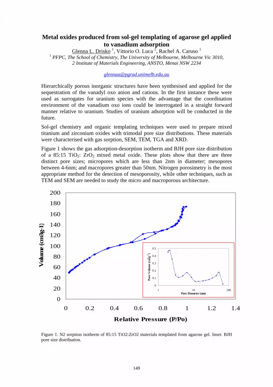
149
0
20
40
60
80
100
120
140
160
180
200
0 0.2 0.4 0.6 0.8 1 1.2 1.4
Relative Pressure (P/Po)
Vol
ume
(cm
3g-1
)
0
0.1
0.2
0.3
0.4
0.5
1 10 100Pore Diameter (nm)
Pore
Vol
ume
(cm3 g-1
)
Metal oxides produced from sol-gel templating of agarose gel applied to vanadium adsorption
Glenna L. Drisko 1, Vittorio O. Luca 2, Rachel A. Caruso 1 1 PFPC, The School of Chemistry, The University of Melbourne, Melbourne Vic 3010,
2 Institute of Materials Engineering, ANSTO, Menai NSW 2234
Hierarchically porous inorganic structures have been synthesised and applied for the sequestration of the vanadyl oxo anion and cations. In the first instance these were used as surrogates for uranium species with the advantage that the coordination environment of the vanadium oxo ions could be interrogated in a straight forward manner relative to uranium. Studies of uranium adsorption will be conducted in the future.
Sol-gel chemistry and organic templating techniques were used to prepare mixed titanium and zirconium oxides with trimodal pore size distributions. These materials were characterised with gas sorption, SEM, TEM, TGA and XRD.
Figure 1 shows the gas adsorption-desorption isotherm and BJH pore size distribution of a 85:15 TiO2: ZrO2 mixed metal oxide. These plots show that there are three distinct pore sizes; micropores which are less than 2nm in diameter; mesopores between 4-6nm; and macropores greater than 50nm. Nitrogen porosimetry is the most appropriate method for the detection of mesoporosity, while other techniques, such as TEM and SEM are needed to study the micro and macroporous architecture.
Figure 1. N2 sorption isotherm of 85:15 TiO2:ZrO2 materials templated from agarose gel. Inset: BJH pore size distribution.

150
SEM images (Figure 2.a) clearly show the open macroporous framework. This morphology is produced from coating the structure of the agarose gel template [1]. The size of the macropores is therefore determined by the original gel. Explicitly, gels of higher wt% organic matter produce denser structures with higher surface areas and smaller macropores.
TEM images (Figure 2.b) show the interparticle spaces between clusters of metal oxides. During synthesis, the solution formed nanoparticles through hydrolysis and condensation reactions. These nanoparticles aggregated, resulting in the formation of a gel network around the fibres of the template. Because these particles were roughly spherical, they could not perfectly pack together, which produced cavities between the particles. The micropores are believed to be formed from the metal oxide coating the individual fibres of the agarose gel. When the template was removed through calcination, a void was produced where the fibres used to exist. These spaces are unfortunately difficult to see in the TEM image.
Figure 2. a) SEM image of 70:30 TiO2: ZrO2. b) TEM image of 70:30 TiO2: ZrO2 templated from agarose gel.
The vanadium adsorption properties were studied as a function of the surface area using ICP analysis. The kinetics and capacity were investigated by monitoring adsorption as a function of time over a period of two days. It was found that vanadate adsorption was very fast. For a 10 ppm solution, maximum adsorption occurred within 5 minutes. The vanadyl adsorption was much slower, most likely due to positive charge repulsions between the surface of the material and the metal cations. Future studies will address measurement of surface charge using zeta potential to investigate the relationship between metal oxide composition and the isoelectric point. Also, uranium adsorption properties will be measured.
Acknowledgements This research was supported by an AINSE Award (AINGRA07025) and funding from The University of Melbourne/ANSTO Collaborative Research Support Scheme
Reference: 1. J. F. Zhou, M. F. Zhou, and R. A. Caruso, Langmuir, 22, 3332-3336, (2006).
2 µm
a) b)
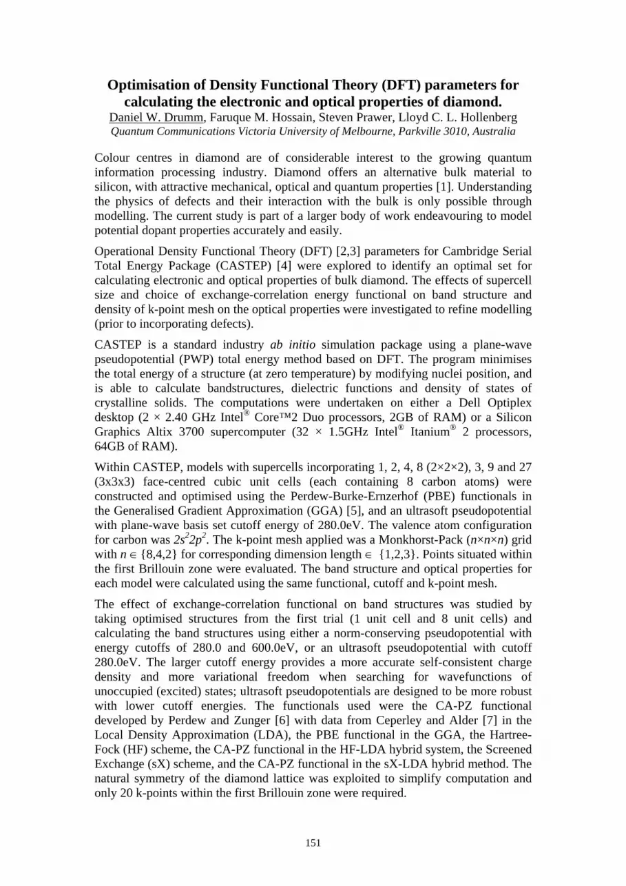
151
Optimisation of Density Functional Theory (DFT) parameters for calculating the electronic and optical properties of diamond.
Daniel W. Drumm, Faruque M. Hossain, Steven Prawer, Lloyd C. L. Hollenberg Quantum Communications Victoria University of Melbourne, Parkville 3010, Australia
Colour centres in diamond are of considerable interest to the growing quantum information processing industry. Diamond offers an alternative bulk material to silicon, with attractive mechanical, optical and quantum properties [1]. Understanding the physics of defects and their interaction with the bulk is only possible through modelling. The current study is part of a larger body of work endeavouring to model potential dopant properties accurately and easily.
Operational Density Functional Theory (DFT) [2,3] parameters for Cambridge Serial Total Energy Package (CASTEP) [4] were explored to identify an optimal set for calculating electronic and optical properties of bulk diamond. The effects of supercell size and choice of exchange-correlation energy functional on band structure and density of k-point mesh on the optical properties were investigated to refine modelling (prior to incorporating defects).
CASTEP is a standard industry ab initio simulation package using a plane-wave pseudopotential (PWP) total energy method based on DFT. The program minimises the total energy of a structure (at zero temperature) by modifying nuclei position, and is able to calculate bandstructures, dielectric functions and density of states of crystalline solids. The computations were undertaken on either a Dell Optiplex desktop (2 × 2.40 GHz Intel® Core™2 Duo processors, 2GB of RAM) or a Silicon Graphics Altix 3700 supercomputer (32 × 1.5GHz Intel® Itanium® 2 processors, 64GB of RAM).
Within CASTEP, models with supercells incorporating 1, 2, 4, 8 (2×2×2), 3, 9 and 27 (3x3x3) face-centred cubic unit cells (each containing 8 carbon atoms) were constructed and optimised using the Perdew-Burke-Ernzerhof (PBE) functionals in the Generalised Gradient Approximation (GGA) [5], and an ultrasoft pseudopotential with plane-wave basis set cutoff energy of 280.0eV. The valence atom configuration for carbon was 2s22p2. The k-point mesh applied was a Monkhorst-Pack (n×n×n) grid with n ∈8,4,2 for corresponding dimension length ∈ 1,2,3. Points situated within the first Brillouin zone were evaluated. The band structure and optical properties for each model were calculated using the same functional, cutoff and k-point mesh.
The effect of exchange-correlation functional on band structures was studied by taking optimised structures from the first trial (1 unit cell and 8 unit cells) and calculating the band structures using either a norm-conserving pseudopotential with energy cutoffs of 280.0 and 600.0eV, or an ultrasoft pseudopotential with cutoff 280.0eV. The larger cutoff energy provides a more accurate self-consistent charge density and more variational freedom when searching for wavefunctions of unoccupied (excited) states; ultrasoft pseudopotentials are designed to be more robust with lower cutoff energies. The functionals used were the CA-PZ functional developed by Perdew and Zunger [6] with data from Ceperley and Alder [7] in the Local Density Approximation (LDA), the PBE functional in the GGA, the Hartree-Fock (HF) scheme, the CA-PZ functional in the HF-LDA hybrid system, the Screened Exchange (sX) scheme, and the CA-PZ functional in the sX-LDA hybrid method. The natural symmetry of the diamond lattice was exploited to simplify computation and only 20 k-points within the first Brillouin zone were required.

152
A further study was conducted on an 8-unit cell supercell (taken from above; optimised using 32 k-points) of bulk diamond to observe convergence of the imaginary part of the dielectric function. The optical properties were calculated using a norm-conserving pseudopotential with cutoff energy 600.0eV, the PBE functional in the GGA, and k-point meshes of 1, 4, 14, 32, 63, 108, 172 and 256 k-points. Gaussian smearing of 0.5eV was applied to the calculated spectrum.
Preliminary results for the supercell analysis can be seen in Fig. 1, and may be compared to values of: 7.4eV (direct band gap), 5.6eV (indirect band gap), and ~5.5eV (fundamental absorption edge; not well-studied) [8]. Supercell size appears to have no significant effect on the calculated indirect band gap, although the other data appear to vary considerably, as discussed below.
The calculated values for the direct band gap appear to depend upon the longest dimension of the supercell, and are further from the experimental value with larger supercell side length. The fundamental absorption edge is indicative of direct transitions only, but not necessarily originating at the Γ point. Calculated values appear to diverge with increasing supercell size. One complicating factor in the study is the density of the k-point mesh; computation time is non-linear in response to an increase in the density. The larger supercells in this initial section (e.g. 27 unit cells) used a 2×2×2 mesh, of which 4 k-points were within the first Brillouin zone. The unit cell “supercell” used an 8×8×8 grid, with 256 points evaluated. At this point, it is unclear whether the changing mesh density has confounded the supercell work, hence the later work focusing on the effects of different k-point meshes.
Initial results for calculation dependence on choice of functional can be seen in Table 1. The first trial was calculating the diamond bandstructure using each of the six functionals on a basic unit cell. A norm-conserving pseudopotential with cutoff energy 280.0eV was selected. As can be seen, all but the HF-LDA model converged (within 100 iterations); the sX-LDA values were closest to experiment, but took 4 orders of magnitude longer to compute than the LDA and GGA calculations. The sX and HF models were similarly lengthy but less accurate than the sX-LDA. The LDA, GGA, sX and sX-LDA models gave better results for the indirect gap than for the direct gap; the HF model showed converse behaviour.
The choice of pseudopotential was another possible factor, and ultrasoft pseudopotentials (cutoff 280.0eV) were used to produce alternative LDA and GGA models. (CASTEP does not support the use of ultrasoft pseudopotentials for the other schemes.) Whilst changing the pseudopotential significantly improved the LDA and GGA values, they were not as accurate as the sX-LDA.
The cutoff energy for the pseudopotential was another possible factor leading to error; CASTEP suggests a higher cutoff energy e.g. 600eV for any calculation using norm-conserving pseudopotentials. The study was repeated over the six functionals using a norm-conserving pseudopotential with cutoff 600.0eV. Only the LDA and GGA models converged, showing an improvement slightly less than that of using an ultrasoft PWP. Using a cutoff of 600.0eV for the ultrasoft PWP in the LDA led to a slight improvement of ~0.07eV; the GGA value was poorer.
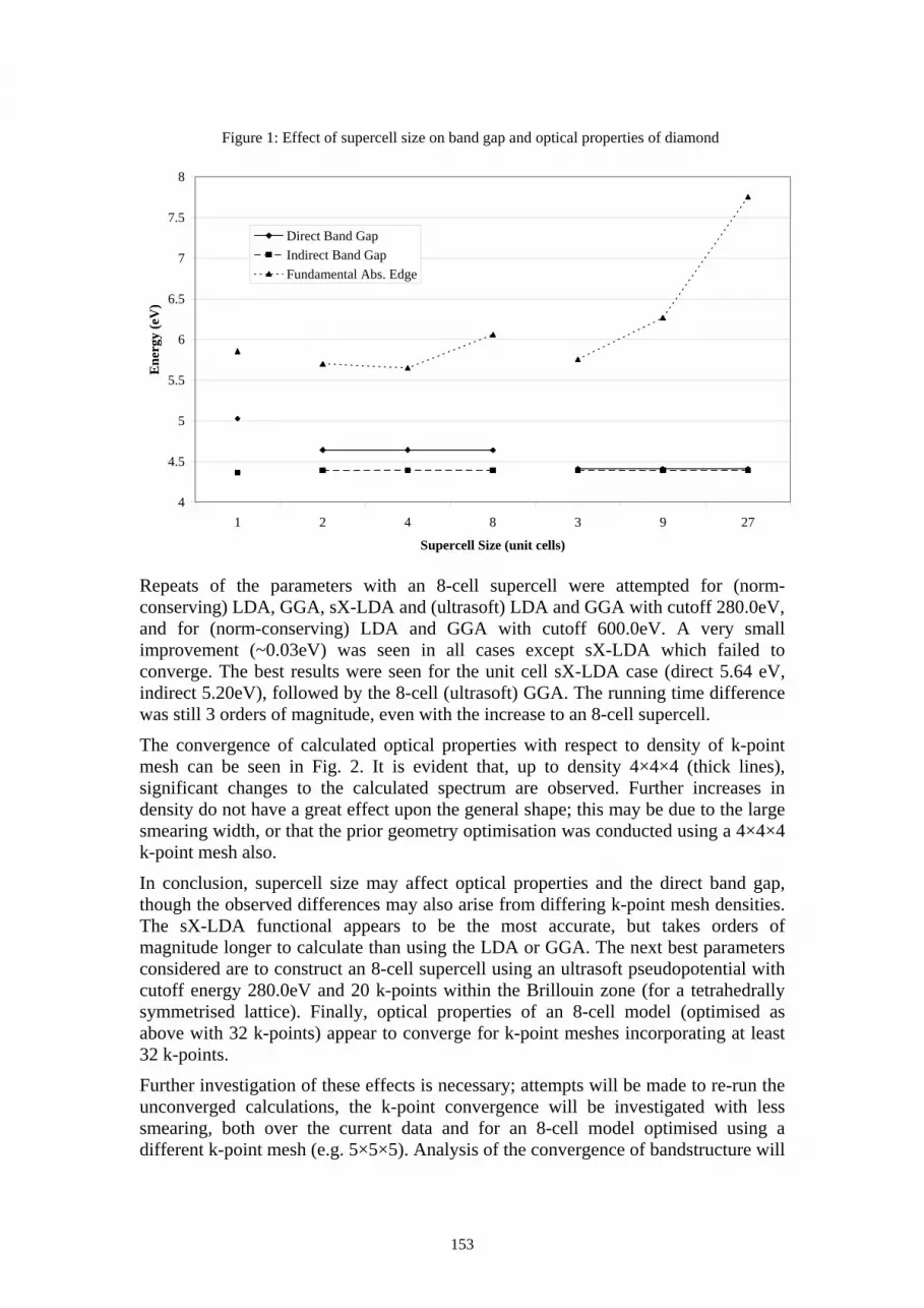
153
Figure 1: Effect of supercell size on band gap and optical properties of diamond
4
4.5
5
5.5
6
6.5
7
7.5
8
1 2 4 8 3 9 27
Supercell Size (unit cells)
Ene
rgy
(eV
)
Direct Band GapIndirect Band GapFundamental Abs. Edge
Repeats of the parameters with an 8-cell supercell were attempted for (norm-conserving) LDA, GGA, sX-LDA and (ultrasoft) LDA and GGA with cutoff 280.0eV, and for (norm-conserving) LDA and GGA with cutoff 600.0eV. A very small improvement (~0.03eV) was seen in all cases except sX-LDA which failed to converge. The best results were seen for the unit cell sX-LDA case (direct 5.64 eV, indirect 5.20eV), followed by the 8-cell (ultrasoft) GGA. The running time difference was still 3 orders of magnitude, even with the increase to an 8-cell supercell.
The convergence of calculated optical properties with respect to density of k-point mesh can be seen in Fig. 2. It is evident that, up to density 4×4×4 (thick lines), significant changes to the calculated spectrum are observed. Further increases in density do not have a great effect upon the general shape; this may be due to the large smearing width, or that the prior geometry optimisation was conducted using a 4×4×4 k-point mesh also.
In conclusion, supercell size may affect optical properties and the direct band gap, though the observed differences may also arise from differing k-point mesh densities. The sX-LDA functional appears to be the most accurate, but takes orders of magnitude longer to calculate than using the LDA or GGA. The next best parameters considered are to construct an 8-cell supercell using an ultrasoft pseudopotential with cutoff energy 280.0eV and 20 k-points within the Brillouin zone (for a tetrahedrally symmetrised lattice). Finally, optical properties of an 8-cell model (optimised as above with 32 k-points) appear to converge for k-point meshes incorporating at least 32 k-points.
Further investigation of these effects is necessary; attempts will be made to re-run the unconverged calculations, the k-point convergence will be investigated with less smearing, both over the current data and for an 8-cell model optimised using a different k-point mesh (e.g. 5×5×5). Analysis of the convergence of bandstructure will

154
also be conducted. Repeats of the study should be done for systems involving defects to check the consistency of any conclusions drawn from this work.
Table 1: Effect of exchange-correlation (approximation scheme) functional, pseudopotential and size of supercell on band gap (converged results only)
Pseudopotential Approximation Scheme
Energy
Cutoff (eV)
Supercell
(unit cells)
Direct Band Gap (eV)
Indirect Band Gap (eV)
Norm-conserving
LDA 280.0 1 4.27 3.70
Norm-conserving
GGA 280.0 1 4.66 4.00
Norm-conserving
HF 280.0 1 11.50 10.5
Norm-conserving
sX 280.0 1 4.85 4.4
Norm-conserving
sX-LDA 280.0 1 5.64 5.20
Ultrasoft LDA 280.0 1 4.69 4.09
Ultrasoft GGA 280.0 1 5.03 4.36
Norm-conserving
LDA 600.0 1 4.60 4.00
Norm-conserving
GGA 600.0 1 4.97 4.31
Ultrasoft LDA 600.0 1 4.76 4.15
Ultrasoft GGA 600.0 1 4.76 4.15
Norm-conserving
LDA 280.0 2 4.30 3.85
Norm-conserving
GGA 280.0 2 4.70 4.20
Norm-conserving
LDA 600.0 2 4.62 4.03
Norm-conserving
GGA 600.0 2 5.00 4.33
Ultrasoft LDA 280.0 2 4.71 4.12
Ultrasoft GGA 280.0 2 5.05 4.39
155
Figure 2: Imaginary part of dielectric function of 8-unit cell diamond; varied k-point mesh density (Optimised using 4x4x4 mesh, smearing width 0.5eV)
0
20
40
60
80
0 2 4 6 8 10 12 14
Energy (eV)
Die
lect
ric
Func
tion,
ε2(ω
)
Γ-point only (offset=40)4 k-points (offset=40)14 k-points (offset=40)32 k-points (offset=20)63 k-points (offset=20)108 k-points (offset=20)172 k-points (offset=0)256 k-points (offset=0)
Acknowledgements D. W. Drumm gratefully thanks A. D. Greentree and J. H. Cole for several fruitful discussions. This work was supported by Quantum Communications Victoria (QCV), which is funded by the Victorian Government’s Science, Technology and Innovation (STI) initiative.
References [1] A. D. Greentree, P. Olivero, et al., “Critical components for diamond-based
quantum coherent devices”, Journal of Physics: Condensed Matter, vol. 18, pp. S825–S842, 2006.
[2] P. Hohenberg and W. Kohn, “Inhomogeneous electron gas”, Physical Review, vol. 136, pp. B865, 1964.
[3] W. Kohn and L. J. Sham, “Self-consistent equations including exchange and correlation effects”, Physical Review, vol. 140, pp. A1133, 1965.
[4] M. D. Segall, P. J. D. Lindan, M. J. Probert, C. J. Pickard, P. J. Hasnip, S. J. Clark, and M. C. Payne, Journal of Physics: Condensed Matter, vol. 14, pp. 2717–2744, 2002.
[5] J. P. Perdew, K. Burke, and M. Ernzerhof, “Generalized Gradient Approximation Made Simple”, Phys. Rev. Lett., vol. 77, pp. 3865–3868, 1996.
[6] J. P. Perdew, and A. Zunger, “Self-interaction correction to density-functional approximations for many-electron systems”, Phys. Rev. B, vol. 23, pp. 5048–5079, 1981.
[7] D. M. Ceperley, and B. J. Alder, “Ground State of the Electron Gas by a Stochastic Method”, Phys. Rev. Lett., vol. 45, pp. 566–569, 1980.
[8] W. C. Walker and J. Osantowski, “Ultraviolet Optical Properties of Diamond”, Phys. Rev., vol. 134 (1A), pp/ A153–A157, 1964.

156
XANES from ROI vs. DA deconvolution of full spectral SXRF data Barbara Etschmann abc*, ChrisRyan ac, Joël Brugger de, Mark Pownceby f,
Weihua Liua e, Pascal Grundler d and DaleBrewe g a CSIRO Exploration & MiningAustralia
b CODES Centre of Excellence, University of Tasmania, Australia, c School of Physics, University of Melbourne,dThe University of Adelaide, AustraliaeSouth
Australian Museum, Australia f CSIRO Minerals, Australia and gThe Advanced Photon Source, USA
Abstract XANES spectra obtained using a Region-Of-Interest (ROI) centered on a major X-ray line of a trace element in a complex matrix may be dominated by significant interferences from other elements. To combat this, full fluorescence spectra were collected at each energy point in a XANES scan. These fluorescence spectra are deconvoluted using Dynamic Analysis (Ryan, 2000), subtracting off interfering signals to extract pure elemental XANES spectra. Applied to the measurement of the oxidation state of Eu (100-300 ppm) in natural Scheelite, this method provides better quality XANES data, as evidenced by improved statistics and flatter pre- and post-edge regions.
Introduction X-ray fluorescence microprobes can achieve high spatial resolution (beams of micron to sub-micron sizes), high sensitivity (detect elements in the 10-100’s ppm) and provide information regarding chemical speciation using X-ray Absorption Near Edge Structure (XANES).
XANES spectra are traditionally measured by collecting all counts within a defined energy window centred on a prominent X-ray peak. This works well for simple systems where there are no elemental interferences. In more complex systems, interfering fluorescence peaks may be eliminated with the use of a Wavelength Dispersive Spectrometer (WDS), however this usually implies that the element of interest exists in large enough concentrations to obtain a statistically reasonable number of fluorescence counts in the narrow acceptance of the WDS. For example, using a WDS, Rakovan et al. (2001) were able to discriminate between Eu La1 (5849.5eV) and Mn Ka (Ka1 = 5900.3, Ka2 = 5889.1eV).
For XANES analyses of trace elements in complex natural samples using a WDS is not a feasible option. Low concentrations of the trace elements (10-100's ppm) require the use of the lower resolution Energy Dispersive Spectrometer (EDS), where the signals from the trace elements may be dominated by significant interferences from other elements.
Similar problems of extracting information from trace elements are also encountered when fluorescence mapping with EDS detectors (e.g. SXRF, PIXE) and is a well established problem in the microprobe community. One way of combating this has been to implement a spectral decomposition transformation called the Dynamic Analysis (DA) method that enables the projection of accurate elemental images (Ryan, 2000). The aim of this paper is to demonstrate how this concept can be extended to XANES analysis of trace elements.

157
Test sample – background Scheelite (CaWO4) samples containing ~100-300 ppm Eu and a number of other rare earth elements with interfering fluorescence peaks were used in this experiment. Scheelite is of geological interest as it is a minor phase controlling REE geochemistry in many gold ore deposits. Under the conditions of formation of these deposits (i.e., T 250-350 oC; near neutral pH; redox condition next to CO2(g)/CH4(g)), the speciation of Eu is expected to be sensitive to the chemistry of the ore forming fluid, in particular the pH, redox state, and salinity (Brugger et al,. 2007). Hence, the measurement of the oxidation state of Eu in minerals such as Scheelite can shed light on the physico-chemical conditions leading to Au precipitation.
Experimental Eu L3 XANES spectra and SXRF maps were collected at beamline 20-ID-B at the Advanced Photon Source (APS) at Argonne National Laboratory, USA. 20-ID-B has a Si (111) monochromator, resulting in an energy resolution ∆E/E of ~1.4 x 10⁻⁴ at 10 keV with a flux of ~1011 photons/s at 9.3 keV. KB mirrors were used to focus the beam to 5 x 5µm2. A liquid N2 cooled 7 element Ge fluorescence detector was located at ~90º to minimize detection of the scattered X-ray beam. The monochromator energy was calibrated by using a pellet of Eu2O3 + BN as a reference standard. XRF maps were collected at 9.3 keV to avoid the W L3 edge and minimize resonant Raman scattering from W (Brugger et al., 2006); XANES spectra were collected from 6953 to 7003eV with a step size of 0.3eV, 2 s per step. XANES spectra were collected using both a region-of-interest centered on the Eu Lα1 peak and full fluorescence spectra at each energy point of the XANES scan.
Method & Results GeoPIXE uses the DA method to project quantitative elemental images (Ryan, 2000) from fluorescence spectra (PIXE, SXRF). The DA technique is a matrix transform algorithm that unfolds overlaps and subtracts background, escape peaks and other detector artifacts.
Figure 1 SXRF spectrum of Scheelite sample DRY3, showing the first and last fluorescence spectra of a XANES scan (E = 6953eV and E = 7003eV).
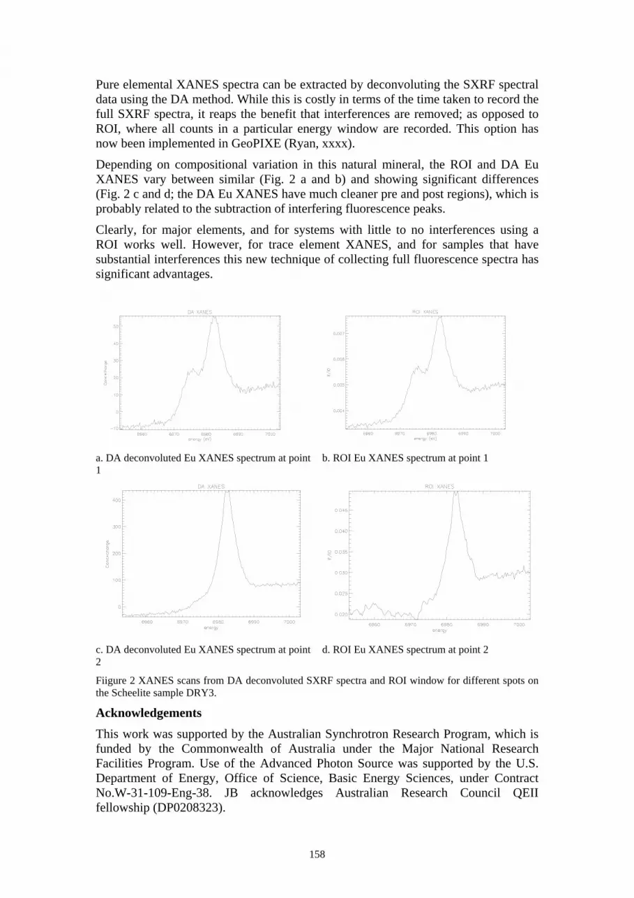
158
Pure elemental XANES spectra can be extracted by deconvoluting the SXRF spectral data using the DA method. While this is costly in terms of the time taken to record the full SXRF spectra, it reaps the benefit that interferences are removed; as opposed to ROI, where all counts in a particular energy window are recorded. This option has now been implemented in GeoPIXE (Ryan, xxxx).
Depending on compositional variation in this natural mineral, the ROI and DA Eu XANES vary between similar (Fig. 2 a and b) and showing significant differences (Fig. 2 c and d; the DA Eu XANES have much cleaner pre and post regions), which is probably related to the subtraction of interfering fluorescence peaks.
Clearly, for major elements, and for systems with little to no interferences using a ROI works well. However, for trace element XANES, and for samples that have substantial interferences this new technique of collecting full fluorescence spectra has significant advantages.
a. DA deconvoluted Eu XANES spectrum at point 1
b. ROI Eu XANES spectrum at point 1
c. DA deconvoluted Eu XANES spectrum at point 2
d. ROI Eu XANES spectrum at point 2
Fiigure 2 XANES scans from DA deconvoluted SXRF spectra and ROI window for different spots on the Scheelite sample DRY3.
Acknowledgements This work was supported by the Australian Synchrotron Research Program, which is funded by the Commonwealth of Australia under the Major National Research Facilities Program. Use of the Advanced Photon Source was supported by the U.S. Department of Energy, Office of Science, Basic Energy Sciences, under Contract No.W-31-109-Eng-38. JB acknowledges Australian Research Council QEII fellowship (DP0208323).

159
References Brugger J., Etschmann B., Chu Y.S., Harland CL.., Vogt S., Ryan C.G. and Jones H., Can. Mineral. (2006) 44, 1079-1087.
Brugger, J., Etschmann, B., Pownceby, M., Liu, W., Grundler, P. & Brewe, D. (2007). Submitted to Geology.
Rakovan, J.,, Newville, M. & Sutton, S. (2001). Am. Mineralogy. 86, 697-700.
Ryan. C.G. (2000). Int. J. Imaging. Syst. Technol. 11, 219-230.
Ryan, C.G., Etschmann, B.E., Vogt, S., Maser, J., Harland, C.L., van Achterbergh, E & Legnini, D. (2005). Nuclear Instruments and Methods in Physics Research B231, 183-188.

160
Fabrication of periodic Al2O3 nanomasks Jing-Hua Fang, Paul G. Spizzirri, Alberto Cimmino and Steven Prawer.
School of Physics, Microanalytical Research Centre, University of Melbourne, Parkville, Australia 3010.
Introduction Periodic Al2O3 nano-masks are made of nano-porous alumina, which are formed by the anodization of aluminium metal. Historically, these anodized layers were developed to help protect aluminium (metal) from erosion. However it was soon realised that these layers could not fulfill this role as the metal continued to wear. At the same time it was noted that the anodized layer comprised regular nano-pore arrays which extended almost completely through the oxide, leaving just a thin barrier layer between the electrolyte and the aluminum metal. These features, coupled with the convenience and low cost of fabrication, have made these nano-pore arrays are very attractive as a nano-membranes or templates.
Nano-scale periodic arrays have since found a variety of applications including: nano-filtration, nanotube / nanowire / nanodot fabrication and as substrates for micro-reactors [1-3]. Active areas for application also now include the development of photonic crystals and quantum dots where they may play a significant role in quantum computing architectures [4]. Methods for fabricating these periodic arrays include ion implantation and single crystal growth through nano-apertures onto controlled substrates.
In this work, we describe a method for fabricating nano-porous membranes (i.e. nano-templates) which have a high aspect ratio and would be applicable to the applications described. Termed an anodically etched, aluminium oxide template (AAO), periodically ordered Al2O3 nano-pores with diameters of 50nm and an interpore spacing of about 100nm can be realized using an electrolytic cell. Details of the template synthesis will be presented and their application to the preparation of quantum dots using ion implantation and crystal growth techniques will be discussed.
Experimental Nano-porous AAO templates were prepared using a two-step oxidation process [5]. Clean, high purity aluminium foil (99.999%) with a thickness of 250µm was electropolished in a mixture of HClO4 and C2H5OH (1:9 v/v) for 2 to 5 minutes. Next, the foil was anodized in an electrolytic cell where the aluminium is configured as the anode and metallic lead (high purity) as the cathode. The cell is operated with a potential of 40V - 60V DC using oxalic acid (0.3 mol dm-3) as the electrolyte at 10°C for 30 to 60 minutes. The anodized alumina was subsequently dissolved in an etchant solution comprising phosphoric acid (6 % by weight) and chromic acid (1.8 % by weight).
A second oxidation step was then performed under the same anodization conditions for another 1 to 3 hours. In order to separate the AAO template from the aluminium foil, the voltage reduction sequential method (VRS) was adopted which resulted in the membrane “peeling” away from the foil [6]. Finally, the pore channels were cleared by dipping the membrane in 1% to 5% phosphoric acid at 20°C for various times. The resulting structure and morphology of the templates were then characterized using scanning electron microscopy (SEM).
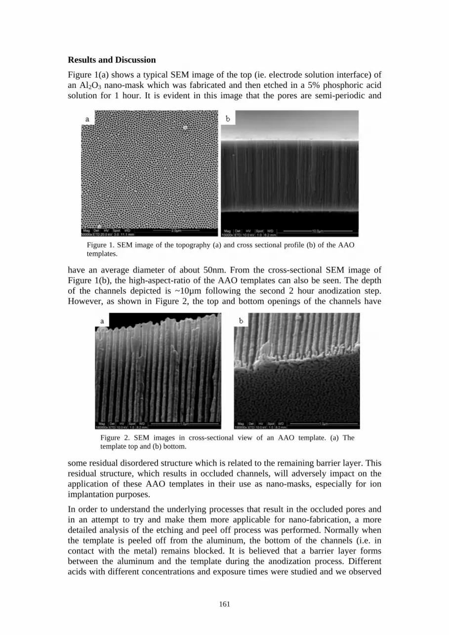
161
Results and Discussion Figure 1(a) shows a typical SEM image of the top (ie. electrode solution interface) of an Al2O3 nano-mask which was fabricated and then etched in a 5% phosphoric acid solution for 1 hour. It is evident in this image that the pores are semi-periodic and
have an average diameter of about 50nm. From the cross-sectional SEM image of Figure 1(b), the high-aspect-ratio of the AAO templates can also be seen. The depth of the channels depicted is ~10µm following the second 2 hour anodization step. However, as shown in Figure 2, the top and bottom openings of the channels have
some residual disordered structure which is related to the remaining barrier layer. This residual structure, which results in occluded channels, will adversely impact on the application of these AAO templates in their use as nano-masks, especially for ion implantation purposes.
In order to understand the underlying processes that result in the occluded pores and in an attempt to try and make them more applicable for nano-fabrication, a more detailed analysis of the etching and peel off process was performed. Normally when the template is peeled off from the aluminum, the bottom of the channels (i.e. in contact with the metal) remains blocked. It is believed that a barrier layer forms between the aluminum and the template during the anodization process. Different acids with different concentrations and exposure times were studied and we observed
Figure 1. SEM image of the topography (a) and cross sectional profile (b) of the AAO templates.
Figure 2. SEM images in cross-sectional view of an AAO template. (a) The template top and (b) bottom.
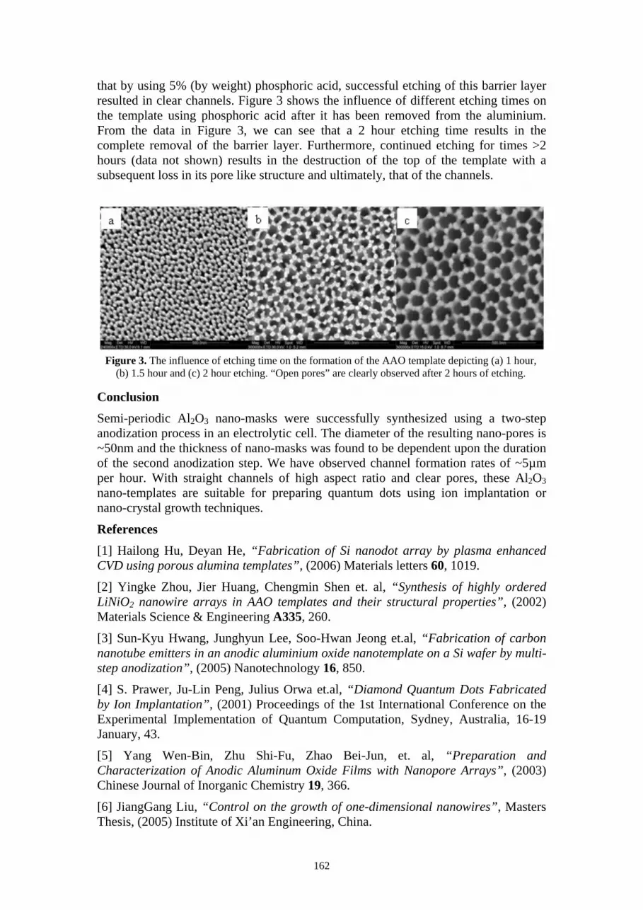
162
that by using 5% (by weight) phosphoric acid, successful etching of this barrier layer resulted in clear channels. Figure 3 shows the influence of different etching times on the template using phosphoric acid after it has been removed from the aluminium. From the data in Figure 3, we can see that a 2 hour etching time results in the complete removal of the barrier layer. Furthermore, continued etching for times >2 hours (data not shown) results in the destruction of the top of the template with a subsequent loss in its pore like structure and ultimately, that of the channels.
Conclusion Semi-periodic Al2O3 nano-masks were successfully synthesized using a two-step anodization process in an electrolytic cell. The diameter of the resulting nano-pores is ~50nm and the thickness of nano-masks was found to be dependent upon the duration of the second anodization step. We have observed channel formation rates of ~5µm per hour. With straight channels of high aspect ratio and clear pores, these Al2O3 nano-templates are suitable for preparing quantum dots using ion implantation or nano-crystal growth techniques.
References [1] Hailong Hu, Deyan He, “Fabrication of Si nanodot array by plasma enhanced CVD using porous alumina templates”, (2006) Materials letters 60, 1019.
[2] Yingke Zhou, Jier Huang, Chengmin Shen et. al, “Synthesis of highly ordered LiNiO2 nanowire arrays in AAO templates and their structural properties”, (2002) Materials Science & Engineering A335, 260.
[3] Sun-Kyu Hwang, Junghyun Lee, Soo-Hwan Jeong et.al, “Fabrication of carbon nanotube emitters in an anodic aluminium oxide nanotemplate on a Si wafer by multi-step anodization”, (2005) Nanotechnology 16, 850.
[4] S. Prawer, Ju-Lin Peng, Julius Orwa et.al, “Diamond Quantum Dots Fabricated by Ion Implantation”, (2001) Proceedings of the 1st International Conference on the Experimental Implementation of Quantum Computation, Sydney, Australia, 16-19 January, 43.
[5] Yang Wen-Bin, Zhu Shi-Fu, Zhao Bei-Jun, et. al, “Preparation and Characterization of Anodic Aluminum Oxide Films with Nanopore Arrays”, (2003) Chinese Journal of Inorganic Chemistry 19, 366.
[6] JiangGang Liu, “Control on the growth of one-dimensional nanowires”, Masters Thesis, (2005) Institute of Xi’an Engineering, China.
Figure 3. The influence of etching time on the formation of the AAO template depicting (a) 1 hour, (b) 1.5 hour and (c) 2 hour etching. “Open pores” are clearly observed after 2 hours of etching.

163
High temperature electronic properties of field-effect transistor based on SiC nanowires
Fang Fang 1,2 1 GNS Science, National Isotope Centre, 30 Gracefield Road, Lower Hutt, New Zealand
2 Institute of Micro/Nano Science & Technology, Shanghai Jiaotong University, Shanghai, 200030, P.R.China
Abstract SiC is a potential material for a large bandgap semiconductor (Eg = 2.4 V) with its superior electronic, physical, and chemical properties, making it an excellent candidate for high-temperature nanoelectronic devices. SiC nanowires were synthesized on activated carbon fiber in large quantity by the way of high-frequency induction without metal catalyst. The morphologies of those nanowires were studied by XRD and SEM. Field-effect transistor (FET) was fabricated by deposition of Au-electrode pairs on the surface of SiO2 film, with SiC nanowires placed between two Au electrodes with the help of microfabrication techniques. Semiconductor analysis equipment as Agilent 4156C was used to test the electronic properties of those FETs. The I-V curves for samples at different high temperatures (473K, 673K and 773K) in an ambient atmosphere were tested. It was found that the higher the temperature, the more increase of the drain current. The carrier mobility versus 1000/T agreed well with the Arrhenius function. It is recommended that the SiCFETs in this work would be used as electrical devices operated in high temperatures because of their superior properties.
Key words: SiC nanowires; field-effect transistor (FET); high temperature
1. Introduction In recent years, nanoscale one-dimensional materials, particularly carbon nanotube and SiC nanowire, etc, have attracted much attention due to their remarkable physics properties and their great potential applications in nanoscale electronics and optoelectronics [1]. The semiconductor nanowire field-effect transistors (FETs) is one of the promising devices which is considered to be building blocks for the application in the next generation of nanodevices. SiC is a potential material for a large bandgap semiconductor (Eg = 2.4 V) with its superior electronic, physical, and chemical properties [2]–[4], making it an excellent candidate for high-temperature nanoelectronic devices. However, little work has been done to record the high-temperature electronic property of SiC-nanowire FET. In this paper, we report the electronic property of such SiC-nanowire FET device at different high temperatures based on our previous work [5]. The SiCFETs were fabricated and tested at different high temperatures (200 C, 400 C and 500C) in an ambient atmosphere. The carrier mobility corresponding to SiC-nanowire FET devices work at different temperature was calculated. It was found that the carrier mobility versus 1000/T agreed well with the Arrhenius function.
2. Experiment The SiC nanowires were synthesized on activated carbon fiber in large quantity without a metal catalyst in a vertical high-frequency induction furnace. By heating SiO, the formed SiO gas was carried to an activated carbon fiber surfaces (lower temperature, ~ 1450 C) by Ar, and then their reactions leaded to the formation of a large amount of β-SiC nanowires. Devices were fabricated by some microfabrication techniques. Figure 1 shows the configuration of the field-effect-transistor. SiC
164
nanowires were placed between two Au electrodes. In order to get good connection between metal and the SiC nanowires, chemical treatments must be applied on the obtained SiC nanowires. The electronic measurements were performed using an Agilent 4156 C semiconductor characterization system under an ambient condition at room temperature and different high temperatures (200 C, 400 C and 500C).
Fig. 1. Configuration of SiC-nanowire FET.
3. Results and discussion
Fig. 2. (a) The synthesized fluffy-like SiC nanowires. (b) XRD pattern of SiC nanowire samples. (c) and (d) are SEM images of large quantities of randomly oriented nanowires.
Fig. 2 (a) shows the real blue fluffy-like SiC nanowire samples we obtained in hand. The X-ray diffraction (XRD) pattern of as-prepared samples is shown in Fig. 2(b). All the peaks were indexed as β-SiC. Fig2(c) and (d) show the SEM images of those nanowire samples. It’s a large amount of straight, curved, randomly oriented and free-standing nanowires before chemical treatments.
Fig. 3 shows the temperature dependence of the drain current of the n-type SiC-nanowire FET at Vg = 5V. It can be seen that the drain current increased with the
ba
dc

165
increase of temperature at the same drain-source voltage. It is commonly believed that the role of the Vg is to change the value of RSiC through Fermi level (EF) modulation, thus changing the slope. The carrier mobility was calculated thereafter and according to our previous calculation, it is found that the carrier mobility versus 1000/T agreed well with the Arrhenius function [5].
Fig. 3 Ids−Vds curves obtained at different temperatures (473K, 673K and 873K respectively) at Vg = 5 V.
4. Summary The limitation temperature
for electronic device based on Si is about 350C while the electronic device based on SiC can work at around 600C without cooling system. So there is a great potential for SiC electronic devices to work in many fields like aviation system for military use.
To sum up, an efficient route has been developed to synthesize large quantity of SiC nanowires. Field-effect transistor (FET) was successfully fabricated by microfabrication techniques. I-V curves of SiCFET were tested at different high temperature in order to study the high temperature property for such device. It is found that the drain current increased with the increase of the working temperature at the same drain-source voltage. Thereafter the carrier mobility was calculated and it is found that the carrier mobility versus 1000/T agreed well with the Arrhenius function. The SiCFETs in this letter would be used as electrical devices operated in high temperatures because of their superior properties. Therefore, the synthesized novel SiC nanowires are expected to have potential application in electronic devices working at high temperature.
References 1. Y.N. Xia, P.D. Yang, Y.G. Sun, etc, Adv. Mater. Vol.15, 353-355, 2003. 2. H. K. Seong, Appl. Phys. Lett., vol. 85, no. 7, pp. 1256–1528, 2004. 3. W. Yang, H. Araki, A. Kohyama, S. ect, J. Amer. Ceram. Soc., vol. 87, no.9, 1720–1725, 2004. 4. A. L. Spetz, P. Tobias, and A. Baranzahi, IEEE Trans. Electron Devices, vol. 46, no.3, 561–566, 1999. 5. W. M. Zhou, F. Fang, Z. Y. Hou, L. J. Yan, and Y. F. Zhang, IEEE Electron Device Letters, Vol.27, NO.6, 463-465, 2006.
-8 -6 -4 -2 0 2 4 6 8-1200
-800
-400
0
400
800
1200
Dra
in c
urre
nt (n
A)
Drain-Source Voltage Vds (V)
473K 673K 873K

166
Age mapping of radioisotopes by daughter trace element analysis V.S. Gill1, D.X. Belton2,1, D.N. Jamieson1, C.G. Ryan2,1
1School of Physics, University of Melbourne, Victoria, Australia 2CSIRO Exploration and Mining, Clayton, Victoria, Australia
Introduction Chemical dating is a technique that uses elemental concentrations within microscopic zircon crystals which can be effectively used to determine the age of associated minerals and has been in use for a number of years (see for example [1,2]). The half-lives of the steps in the radioactive decay chain of U and Th to Pb can be used to determine the age of a zircon crystal. Zircons (composition ZrSiO4) have played an important role in the dating of sediments associated with the Cretaceous/Tertiary (K/T) extinction event from 65.5 million years ago [3]. At the other end of the timescale, zircons have been used the date the oldest rocks on the planet with an age of over 4.2Ga [4]. A decay system with a long half-life is therefore required. We are developing a new method for dating zircons by measuring trace elements using Proton Induced X-ray Emission (PIXE). By performing the analysis with a focused ion beam in a nuclear microprobe system, the compositional zoning of the zircons can be measured. This method therefore has the potential to map the age of the zones in the zircons that can provide new insights into the episodic growth of zircons in response to magmatic and metamorphic events.
Figure 1: Zircon crystals mounted in epoxy.
Zircons are uniquely suitable for the recovery of their age from the elemental composition because of a very useful chemical attribute. This is that the chemical processes that produce the zircon crystals from the original melt also purge lead from the growing crystal (common lead). Successful dating of zircons from the elemental composition requires that there is only a minimal level of common lead and that the system is closed to U, Th and Pb after crystallisation. These characteristics are widely accepted to generally apply in zircon, once the mineral has cooled to below the closure temperature [5] and assuming it has not suffered radiation damage (metamictisation). Therefore the age of a zircon crystal can be determined by measurement of the elemental concentrations of parent radioactive elements and their associated daughter elements.
Both U and Th radioactive decay chains terminate with stable Pb isotopes. By using the standard relations between the concentration of a radioactive parent element to the
100µm

167
daughters and taking into consideration that the PIXE technique is not sensitive to the isotope, the age of a zircon, τ, can be calculated by the following equation [6]:
[ ]
[ ]
[ ]1)exp(0072.004.238
207
1)exp(9928.004.238
206
1)exp(232208
235
238
232
−+
−+
−=
τλ
τλ
τλ
U
U
ThPb
where Pb, Th and U are the concentrations in ppm (measured by PIXE in our case) and 232λ , 238λ and 235λ are the radioactive decay constants of 232Th, 235U and 238U respectively. This equation is transcendental and therefore must be solved iteratively.
Figure 2: PIXE spectrum from a zircon crystal induced by 3 MeV H+ irradiation.
Considerations for analysing Zircon When analysing zircons, there is a particular limitation that must be addressed. As can be seen in Figure 2, the spectrum is dominated by the Zr K-shell peaks at 15.8 and 17.7 keV. The U, Th Lα and Pb Lβ peaks (at 13.6, 13.0 and 12.6 keV respectively) are dwarfed by the large Zr peaks, thus reducing sensitivity to the elements of interest due to low energy tails reducing the signal to noise ratio of Th, U and Pb.
For the analysis method achieve optimum sensitivity, the H+ ion beam energy provided by the nuclear microprobe should be optimised to minimise the Zr signal compared to the signal from the U. Th and Pb signals. It is traditional to perform PIXE with a H+ energy of 3MeV. This energy is chosen to maximise the characteristic x-ray yields across a useful range of elements from Al (Z=13) to U (Z=92). Also, the x-ray production cross section is a function of incident beam energy and differs with element (Z) and shell (K, L or M) of excitation. In this work we investigated the optimum beam energy required to maximise x-ray yield of U, Th and Pb in preference to Zr.
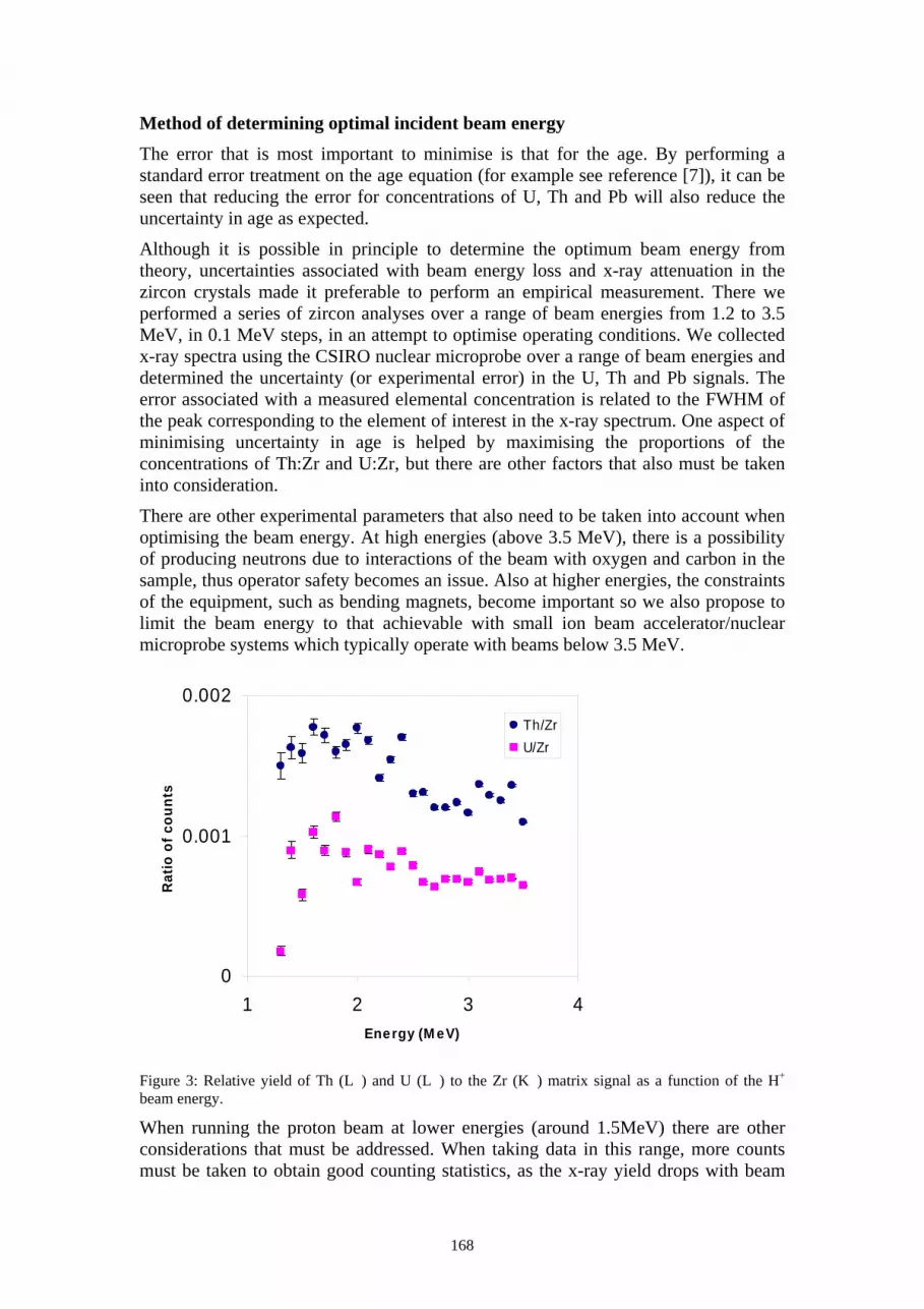
168
Method of determining optimal incident beam energy The error that is most important to minimise is that for the age. By performing a standard error treatment on the age equation (for example see reference [7]), it can be seen that reducing the error for concentrations of U, Th and Pb will also reduce the uncertainty in age as expected.
Although it is possible in principle to determine the optimum beam energy from theory, uncertainties associated with beam energy loss and x-ray attenuation in the zircon crystals made it preferable to perform an empirical measurement. There we performed a series of zircon analyses over a range of beam energies from 1.2 to 3.5 MeV, in 0.1 MeV steps, in an attempt to optimise operating conditions. We collected x-ray spectra using the CSIRO nuclear microprobe over a range of beam energies and determined the uncertainty (or experimental error) in the U, Th and Pb signals. The error associated with a measured elemental concentration is related to the FWHM of the peak corresponding to the element of interest in the x-ray spectrum. One aspect of minimising uncertainty in age is helped by maximising the proportions of the concentrations of Th:Zr and U:Zr, but there are other factors that also must be taken into consideration.
There are other experimental parameters that also need to be taken into account when optimising the beam energy. At high energies (above 3.5 MeV), there is a possibility of producing neutrons due to interactions of the beam with oxygen and carbon in the sample, thus operator safety becomes an issue. Also at higher energies, the constraints of the equipment, such as bending magnets, become important so we also propose to limit the beam energy to that achievable with small ion beam accelerator/nuclear microprobe systems which typically operate with beams below 3.5 MeV.
0
0.001
0.002
1 2 3 4Energy (M eV)
Rat
io o
f cou
nts
Th/ZrU/Zr
Figure 3: Relative yield of Th (L) and U (L) to the Zr (K) matrix signal as a function of the H+ beam energy.
When running the proton beam at lower energies (around 1.5MeV) there are other considerations that must be addressed. When taking data in this range, more counts must be taken to obtain good counting statistics, as the x-ray yield drops with beam
169
energy [8], so analysis times become prolonged. The current the beam is operated at is used to keep the count rate constant but there is a limit to how far it can be increased. Variations in beam rigidity mean that stability, electrostatic scanning and focus must also considered in the optimisation process.
Conclusions Preliminary results from initial experiments are shown in Figure 3. Although further analysis is necessary, this appears to suggest that an energy of around 2 MeV would be optimal for running the microprobe when analysing zircon.
This optimal energy has implications for the chemical dating of monazites and the mineral apatite, which have similar properties of closed systems with a dominant element masking the U, Th and Pb of interest. These accessory phases, along with zircon, are important to geological research and mineral exploration.
References [1] M.J. Whitehouse, B.S. Kamber, S Moorbath, Chemical Geology 160 (1999) 201-224
[2] J.M. Hanchar, C.F. Miller, Chemical Geology 110 (1993) 1-13
[3] R. Dalton, Nature 449 (2007) 6.
[4] R. Maas, P.D. Kinny, I.S. Williams, D.O. Froude, W Compston, Geochimica et Cosmochimica Acta, Vol 56 (1992) 1281-1300
[5] S. L. Harley, N. M. Kelly, Zircon: Tiny but Timely, Elements, Vol 3, Pg 13-18
[6] J. M. Montel, S. Foret, M. Veschambre, C. Nicollet, A. Provost, Chemical Geology 131 (1996) 37-53
[7] L. Lyons, A Practical Guide to Data Analysis for Physical Science Students, Cambridge University Press, 1991, pg 26
[8] S. A. E. Johansson, J. L. Campbell, PIXE: A Novel Technique for Elemental Analysis, John Wiley & Sons Ltd, 1988, pgs 265-266

170
Enantioselectivity of chiral molecules on chiral copper surfaces M. J. Gladys 1,3, A. Stevens1, N. Scott1, G. Jones1, D. Batchelor2 and G. Held1.
1 Department of Chemistry, University of Cambridge, Lensfield Rd, Cambridge, CB21EW. 2 Experimentelle Physik II, Universität Würzburg, Am Hubland, D-97074 Würzburg,
Germany. 3 School of Mathematical and Physical Sciences, University of Newcastle, Callaghan 2308, NSW
Australia.
Abstract Chiral (Enantiomeric) molecules often exhibit drastically different reactivity in living matter. Our current work focuses on generating chiral surfaces that exhibit selectivity for single enantiomers for chiral molecule synthesis and molecular sensors. Using a variety of techniques we have studied the adsorption of S and R-Alanine enantiomers on Cu(531) and found for the first time, a self assembled chiral overlayer on a chiral substrate. HR-XPS was used to retrieve information about the chemical states and adsorption sites and show the molecule is bound to the surface with a triangular footprint. Carbon K-edge NEXAFS using linear and circularly polarized synchrotron radiation shows the variation of the carboxylic acid (O-C-O) π* resonance and therefore the molecular orientations on the surface. Large differences are observed between the adsorption geometry of the two Alanine enantiomers.
Introduction To generate enantiospecific reactions, animals have developed a complex system of lock and key mechanisms. This design utilises the 3D shape of enzyme molecules to match specific chemicals which form countless biological functions. Thus enzymes act as chiral catalysts, and include what is known as “active sites” which stereo-direct the reactions. Stereoselective catalysis is rapidly becoming a crucial phenomenon in the pharmaceutical industry where new chiral drugs are synthesized. Single enantiomer drugs are more active, require lower doses and exhibit fewer side effects than racemic (50:50 mixture of enantiomers) drugs [1] The ‘wrong’ enantiomer of a chiral pair may have such damaging side effects, that far outweighs the benefits of the correct enantiomer. [2] This means that of these many available drugs, one form is good, while the other is ineffective or even dangerous. As a consequence, there is a current and pressing demand to either select or create only one of the enantiomers in drug manufacturing. [3,4] Current methods to produce a single enantiomer rely on homogenous catalysis which has the inherent problem of removing the catalyst molecule from the product solution without destroying the target drug. As an alternative, the use of a heterogeneous catalyst would circumvent the majority of separation problems that exist. Analogous to 3D enzymes, chiral surfaces contain an inherent 2D chiral interface that provide a ‘lock’ so that only one of the enantiomers, the ‘key’ will fit, i.e. the surface will recognise the chirality of the molecule.
Significant success with regards to the enantioselective hydrogenation of α and β- ketoesters has been achieved by modifying achiral Pt or Ni catalyst surfaces with chiral molecules such as cinchonidine/cinchonine and tartaric acid, respectively, (see [5-8] and references therein). In order to identify the underlying reaction pathways it is crucial to know the adsorption geometries of the relevant reactants and modifiers as well as their adsorption energies. Two different generic microscopic mechanisms have been discussed in the recent literature, which both would lead to stereoselectivity of chirally modified metal catalysts [8]: the template model states that the modifiers template the metal surface in such a way that it provides a chiral reaction environment

171
for the reactant molecule; in the active chiral site model the metal substrate essentially provides a platform for the modifier molecules to adsorb; the stereochemical effect is predominantly due to the geometry of the chiral modifiers.
Metal single crystals on the other hand are inherently non-chiral in nature and generally do not possess enantioselectivity. Nevertheless, it was established that certain single crystal fcc surfaces with high Miller indices contain step-kinks, that is, two steps constituting a kink site that are inequivalent [9] and therefore chiral. To classify the enantiomers of these surfaces, the kink site (A in Fig.1) is defined as the junction of the following faces 111, 110 and 100. In terms of atomic surface density, a hierarchy exists such that 111> 100> 110. The D (right-handed)-kink contains the sequence 111→110→100 which runs clockwise as viewed from the vacuum while for the L(left-handed)-kink, the sequence is anticlockwise. The (531)R and (531)S surfaces are shown in Figure 1, and illustrate the chiral differences inherent in these surfaces. On a cut crystal, the right-handed surface will appear on the ‘front’ side, while the left-handed surface is present on the reverse. The idea behind intrinsically chiral surfaces is that only one enantiomer will fit to the kink sites (“active sites” analogous to enzymes) on the surface, while the other does not.
The earliest reports of enantioselective reactions on chiral single crystal surfaces came from a series of electrochemical studies by Attard et al. [9-10] showing clear differences in the cyclovoltammograms for electro-oxidation of (L)- and (D)-glucose on Pt electrodes terminated by chiral 643, 431, 531 or 321 surfaces. Changing the enantiomer of the reactant molecule from (L) to (D) in these experiments had the same effect as changing the chirality of the electrode surface.
In this paper we describe the adsorption of Alanine on Cu531R produces an ordered p(1x4) chiral overlayer. This is the first ordered self assembled layer on a chiral surface to be observed. Furthermore, NEXAFS data show differences in adsorption geometry are observed between Alanine enantiomers on this surface. Finally Density Functional Theory calculations were used to model stable structures of Alanine on Cu531 to compare to experimental work to illustrate the magnitude of the interface and intermolecular bonding forces at work to produce these effects.
Figure 1: The two enantiomer surfaces of the fcc(531) step-kinked surface. This surface has the smallest unit cell of all fcc chiral surfaces, which makes it an ideal model surface for investigating chiral systems. On this surface the step-kinks are made up of alternating [311] and [100] steps as illustrated.
(531)R (531)SStep-Kinks Step-Kinks
A110
111
100A110
111
100
110311311 110
(-112) (-112)

172
Experimental The Cu single crystal used in the synchrotron experiments was terminated by a (531) surface (equivalent to 531R [4] or 531D [20] shown in figure 1. The crystals were cleaned by repeated cycles of sputtering at room temperature and annealed in vacuum to at least 1000K. In all experiments the crystal was mounted with the [-112] crystallographic directions at horizontal (in the plane of the storage ring for the synchrotron experiments). The synchrotron experiments were performed at beamline UE52PGM of BESSY II in Berlin (Germany). XP spectra in the C 1s, N 1s, and O 1s regions were recorded using a Scienta 200mm electron energy analyser with a pass energy of 40eV and linearly polarised synchrotron radiation with a photon energy of 630eV. The angle of incidence was close to the surface normal and the emission angle around 60° away from the surface normal. Enantiopure R or S-Alanine (99 % from Aldrich) crystalline powder was adsorbed by evaporation from a glass crucible heated to the desired temperature. Saturation coverage was achieved via background dosing in excess of the amount actually needed was deposited at room temperature followed by annealed to the desired temperature. Submonolayer coverages were generated through incremental dosing at the same dosing conditions. In addition to the previously described experiments, the adsorption of alanine on the Cu531 surface was studied by means of density functional theory (DFT) calculations using the CASTEP computer code. The generalised gradient approximation as proposed by Perdew et al. [11] was applied (henceforth referred to as GGA-PW91) for electron-ion interactions, combined with Vanderbilt ultrasoft pseudopotentials [12] for exchange and correlation. For the clean Cu531 surface, the planewave basis set was truncated at a kinetic energy of 340eV to describe the electronic wavefunctions. The bulk lattice constant (a = 3.606Å) for use of the Cu surface calculations was determined by the Brillouin zones sampled with a 8,8,1 Monkhorst Pack Mesh. Calculations of Alanine on Cu531 were carried out on [1 1, 2 -2] unit cells to correspond to the ordered overlayer observed in LEED. The slab contained 20 layers of Cu531 and a vacuum depth equivalent to 15 atomic layers was placed between the periodically repeated slabs to ensure that the adsorbate and the subsequent slab do not interact. A Monkhorst Pack Mesh of 5x1x1 was used to sample the Brillouin zone
Results and Discussion The adsorption geometry of alanine on Cu531 was characterised using LEED, NEXAFS and XPS A p(1x4) alanine structure was observed with LEED and is the only intrinsically chiral surface for which an ordered molecular superstructure has been observed so far. The chemical shifts of the C 1s, N 1s and O 1s core level signal in XPS are essentially the same as for alanine on Cu110 at low coverage, which indicates that the molecules assume the same 3 alaninate adsorption complex as shown in Figure 2. There are two adsorption sites on the 531 surface that can match the triangular footprint, namely 110 and a 311 facets. The azimuthal orientation and, hence, the adsorption site can be determined through the angular dependence of the carbon K-edge NEXAFS spectra. According to the dipole selection rule, the intensity of the π* resonance at 288eV (cf Fig. 2(a) which is localised at the carboxylate group (O-C-O) is at a maximum when the polarisation vector, ~E, of the exciting synchrotron radiation is perpendicular to the O-C-O triangle and goes to zero when ~E lies in the plane of the triangle, irrespective of how the molecule is adsorbed. The intensity of the π* resonance for a single molecule is proportional to cos2γ°, where γ° is the angle between ~E and the surface normal of the O-C-O plane [13].
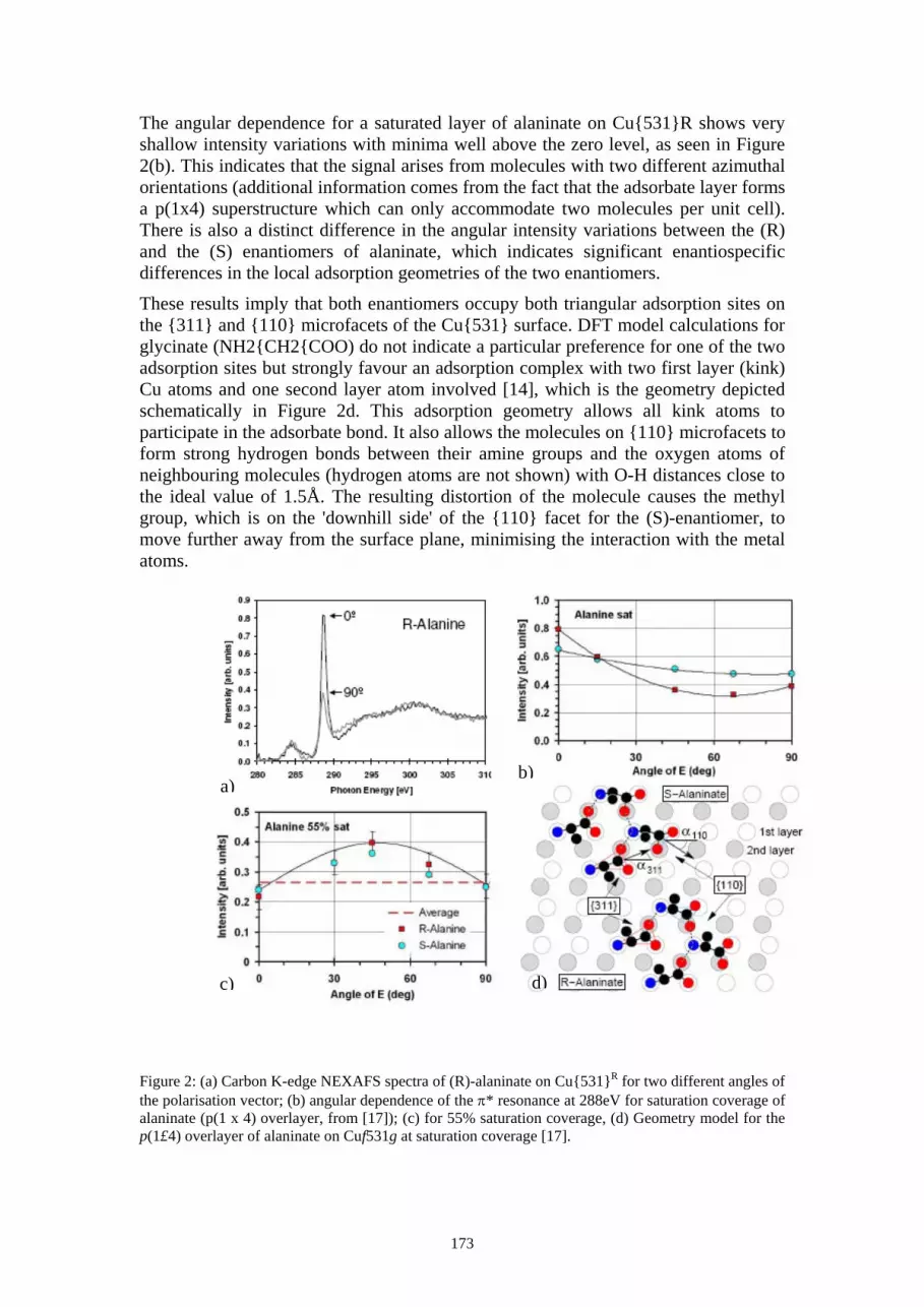
173
The angular dependence for a saturated layer of alaninate on Cu531R shows very shallow intensity variations with minima well above the zero level, as seen in Figure 2(b). This indicates that the signal arises from molecules with two different azimuthal orientations (additional information comes from the fact that the adsorbate layer forms a p(1x4) superstructure which can only accommodate two molecules per unit cell). There is also a distinct difference in the angular intensity variations between the (R) and the (S) enantiomers of alaninate, which indicates significant enantiospecific differences in the local adsorption geometries of the two enantiomers.
These results imply that both enantiomers occupy both triangular adsorption sites on the 311 and 110 microfacets of the Cu531 surface. DFT model calculations for glycinate (NH2CH2COO) do not indicate a particular preference for one of the two adsorption sites but strongly favour an adsorption complex with two first layer (kink) Cu atoms and one second layer atom involved [14], which is the geometry depicted schematically in Figure 2d. This adsorption geometry allows all kink atoms to participate in the adsorbate bond. It also allows the molecules on 110 microfacets to form strong hydrogen bonds between their amine groups and the oxygen atoms of neighbouring molecules (hydrogen atoms are not shown) with O-H distances close to the ideal value of 1.5Å. The resulting distortion of the molecule causes the methyl group, which is on the 'downhill side' of the 110 facet for the (S)-enantiomer, to move further away from the surface plane, minimising the interaction with the metal atoms.
Figure 2: (a) Carbon K-edge NEXAFS spectra of (R)-alaninate on Cu531R for two different angles of the polarisation vector; (b) angular dependence of the π* resonance at 288eV for saturation coverage of alaninate (p(1 x 4) overlayer, from [17]); (c) for 55% saturation coverage, (d) Geometry model for the p(1£4) overlayer of alaninate on Cuf531g at saturation coverage [17].
a) b)
c) d)

174
From a steric point of view this model appears most plausible since the methyl group of the (R)-enantiomer is on the 'uphill side' of the 110 microfacet and requires less molecular distortion in order to reduce the interaction with the surface atoms. The associated angle α110 should therefore change, whereas for the more symmetric adsorption site on the 311 facet the interaction of the methyl group with the surrounding Cu atoms is weak with both enantiomers and should not induce molecular distortions that would change α311 significantly. The fit results for this model also imply that there are about twice as many molecules adsorbed on 110 than on 311 adsorption sites. This may explain the significantly lower degree of ordering that is observed for this enantiomer.
The angular dependence of the pi* resonance is very different for a dilute alaninate layer around half the saturation coverage, as shown in Figure 2(c). Both enantiomers now show the same angular dependence. The fit to the data shown in Figure 2(c) shows a 4 : 1 preference for the adsorption sites on the 311 facets with the molecules rotated by about 20o with respect to the adsorption geometry at saturation coverage [15]. This is the result of missing inter-molecular interactions. Table 1 lists these different alanine overlayers with their respective adsorption energies, ∆Hads. Of primary interest here are the ∆Hads, and what can be seen is that for (R) alaninate there is a preference for the (311R/311R) structure; this can be compared to the S-alaninate which is also found to favour the (311S/311S) structure. What we actually see in the adsorption energy trends is a similar tale to that observed for the Cu110 surface where the most stable structures all lie within a small range on the boundaries of DFT reliability. Furthermore, this suggests that we are unlikely to observe any enantioselectivity in experiments such as temperature programmed desorption (TPD) or in the LEED patterns, and is indeed found to be the case for the TPD. In fact, examining the ∆Hads shows that the R-alaninate has a preference for (311/311) and (110/110) occupation whilst the S-alaninate shows a preference for (311/311) and (110/311) occupation. Moreover, the difference in ∆Hads from the least favoured structures are beyond the energy differences observed for conformation changes found from studies on the Cu110[16] and Cu311[14] surface.
Summary Our findings allow three important conclusions for the adsorption of alanine on Cu531: (a) the isolated molecules have higher adsorption energy on the 311 facets where alanine can adsorb without major lateral distortions; (b) the adsorption energy difference between 311 and 110 must be higher than possible energy gains from the formation of hydrogen bonds with molecules on the 110 adsorption sites (in essence this leads to a substratemediated repulsive interaction); (c) the enantiospecific adsorption behaviour at higher coverage is induced by (repulsive or attractive) inter-molecular interactions between molecules on 311 and 110 sites or by repulsive molecule-substrate interactions on the 110 adsorption sites. The most important type of inter-molecular interaction are hydrogen bonds. Their importance for the arrangement of adsorbed amino acids has been pointed out by
Table 1: Surface energies for different configurations of Alanine on Cu531. System ∆Hads ¼ ML (110)R (311)R (110)S (311)S
+1.40 +1.35 +1.39 +1.36
½ ML (110)R/(110)R (311)R/(311)R (110)S/(311)R (110)S/(110)S (311)S/(311)S (110)S/(311)S
+1.36 +1.45 +1.24 +1.28 +1.43 +1.38

175
several authors before [55, 66]. Repulsive interactions for the present case are most likely related to the methyl group.
References 1. A. J. Hutt and J. Valentova, Acta Fac. Pharm. Univ. Comen., Tomus L (2003) p7 and references
therein.
2 A. Baiker, Journal of Molecular Catalysis. A, Chemistry 115 (1997) p473.
3 A. Richards and R. McGague, Chem. Ind. 422 (1997).
4 S. C. Stinson, Chem. Eng. News 38 (1997).
5 Y. Orito, S. Imai and S. Nina, J. Chem. Soc. Jpn. 8 (1979) 1118.
6 A. Baiker, J. Mol. Catal. A 115 (1997) 473.
7 A. Baiker, J. Mol. Catal. A 163 (2000) 205.
8 C. Baddeley, Top. Catal. 25 (2003) 17.
9 G. Attard, Journal of Physical Chemistry B, 105, (2001) p3158.
10 G. A. Attard, A. Ahmadi, J. Feliu, A. Rodes, E. Herrero, S. Blaise and G. Jerkiewicz, J. Phys. Chem. B 103 (1999) 1381.
11 J. P Perdew, J. A. Chevary, S. H. Vosko, K. A. Jackson, M. R. Pederson, D. J. Singh, C. Fiolhais, Phys. Rev. B 46 (1992) 6671.
12 D. Vanderbilt, Phys. Rev. B 41, (1990) 7892.
13 J. Stohr, NEXAFS spectroscopy, Springer Series in Surface Sciences, Springer, Berlin, 2. ed. (1996).
14 G. Jones, PhD thesis, University of Cambridge (2006).
15 M. J. Gladys, A. V. Stevens, N. R. Scott, G. Jones, D. Batchelor and G. Held, J. Phys. Chem. C 111 (2007) 8331.
16 G. Jones, L. B. Jones, F. ThibaultStarzyk, E. A. Seddon, R. Raval, S. J. Jenkins and G. Held, Surf. Sci. 600 (2006) 1924.

176
Delineating groundwater flowpaths using 14C dating in the Upper Loddon catchment, central Victoria
Sarah K. Hagerty1, John A. Webb1, Geraldine E. Jacobsen2 1Department of Environmental Geoscience, La Trobe University, Bundoora, Victoria,
Australia 2Institute for Environmental Research, ANSTO, Lucas Heights, NSW, Australia
Radiocarbon dating of groundwater has been used to delineate flowpaths and calculate hydraulic conductivity as part of a detailed hydrogeological/hydrogeochemical study of the Tullaroop catchment in the Upper Loddon, central Victoria. The dating confirms that both the basalt and deep lead aquifers in the study area are recharged through scoria cones at volcanic eruption points. The radiocarbon dating also shows that flow paths in the basalt aquifer are complex since ages do not always increase downflow; any hydraulic conductivity calculations must take this into account. One anomalously old 14C date supports other hydrogeological evidence that suggests groundwater in the deep lead is trapped upflow of horsts created by ENE Cainozoic faults.

177
ANSTO Heavy Ion ToF for Analysis of Light Elements in Thin Films M. Ionescu1, Y. Zhao2, R. Siegele1, D. D. Cohen1, D. Lynch1, D. Garton1, E. Stelcer1,
M. Prior1
1Australian Nuclear Science and Technology Organization Sydney, Australia 2University of Wollongong, Australia.
Abstract Thin films have various potential applications in electronic devices, and their performance is intricately linked with the electric and magnetic properties of the film, in which an important role is played by the presence of light elements, in particular Hydrogen, Oxygen and Nitrogen. The source of light elements, the form in which they are incorporated into the thin film, and how this is influencing the MgB2 thin film properties is currently under scrutiny by various research groups. Typically these films are grown on oxide ceramic substrates, such as Al2O3-C and it is possible that the source of Oxygen is the substrate itself or the growth atmosphere. Here we report on a study of light elements in MgB2 thin films grown on various substrates, using heavy ions recoil and a time-of-flight detector. A series of MgB2 thin film samples produced by PLD (pulsed laser deposition) were analyzed, including films produced in-situ on Al2O3-C substrates with an on-axis and off-axis geometry, one film produced in-situ with an off-axis geometry, and one film produced ex-situ, with a bulk-like Tc. We also analyzed one film produced with on-axis geometry under the same conditions on Si (001) substrate. The amount of Oxygen detected by ToF, appears to be correlated with the Tc of the films, the higher the Tc the lower the oxygen content. Also, the superconducting properties of the examined thin films are discussed in the context of the results.
Keywords—Heavy ions ERDA, MgB2 thin films
Introduction Thin films characterization by heavy ions time-of-flight ERDA spectrometry is an attractive technique due to its capacity to detect elements over a wide range of Z, and to extract from the recoiled particles both mass and depth information. Over the last 15 years ANSTO has developed and constantly improved such a system [1], used routinely to characterize complex thin film architectures, and optimized for multi-layered, multi-element configurations found in the areas of semiconductor and superconductor device development. One such thin film with device application potential is MgB2, in which Oxygen has been gradually revealed as playing an important role in its electric and magnetic properties. As early as 2001, it was reported that the exposure to low levels oxygen during fabrication of MgB2 thin films could “alloy” the ex situ annealed MgB2 films to form a Mg(B-O)2 alloy, resulting in a much improved critical current Jc but a slightly lower transition temperature Tc of 35 K [2] than the bulk. A study of grain boundaries in Oxygen-alloyed bulk samples by selected area electron diffraction (SAED), suggests that Oxygen was incorporated in the form of MgO phase with a size of about 10nm [3], where periodical Mg-B-O layers were found at the grain boundaries. These studies suggest that oxygen-rich precipitates could provide pinning centers as the precipitates and oxygen-incorporated grain boundaries are of favorable dimensions, between 5-100nm, which is comparable with the coherence length ξ of MgB2 which is around 5nm [4,5]. However, the decrease of the transition temperature with the incorporation of Oxygen observed in bulk and thin films is undesirable, and it is more pronounced in thin films. The cause
178
appears to be the influence of Oxygen precipitates on the electron-phonon coupling parameters, as suggested by calculation for two possible oxygen-ordered MgB2 compounds of composition Mg2B3O and Mg2B3O2 [6]. The results show that the calculated Tc values of Mg2B3O and Mg2B3O2 are 18.3K and 1.6K, respectively. This result is in accordance with the reported decrease of Tc in some oxygen enriched MgB2 samples, especially in the in situ prepared thin films [ 7,8]. There is enough evidence to suggest that in device applications based on MgB2 thin films, the presence of Oxygen and its distribution will strongly influence the device performance, and therefore detailed information of Oxygen form and its distribution in MgB2 films is necessary. In this paper, we report the results of Oxygen distribution measured by heavy ion ERDA in different types of MgB2 films prepared by the pulsed laser deposition (PLD) method.
Experimental details The ERDA experiment was carried out in a vacuum better than 1x10⁻⁶Pa, using Iodine ions of 82.5MeV. A schematics of the experimental apparatus used here is shown in Fig.1. The beam was shaped in a rectangular form, 3mm high and 1mm wide, and directed onto the sample at an incident angle of 67.5°, between the beam direction and sample normal. The energy of recoils was measured with a time-of-flight detector placed at an exit angle of 45° relative to the sample normal, resulting in a scattering angle of 45°. The two electrostatic mirrors were placed 0.5m apart, and each contained a 25µg/cm2 C foil to measure the flight time of the recoils. The final rest energy of the recoils was measured with a surface barrier detector, placed at the end of the flight path. The samples are placed on a 2-axis goniometer, and placed in the beam path at the required position. In this experiment, the total charge collected on each sample during the measurement was 12µC.
Sample Substrate
Deposition geometry
Mg cap layer
Surface etching Tc [K]
1 Si (001) On-axis No No 18.7
2 Al2O3-c On-axis No No 25.8
3 Al2O3-c Off-axis Yes No 26
4 Al2O3-c Off-axis Yes No 28
5 Al2O3-c Off-axis No Yes 33
6 Al2O3-c Off-axis Yes No 33
7 Al2O3-c Off-axis Yes No 34
8 Al2O3-c Off-axis No Yes 34.5 Table 1.Summary of sample characteristics used in this study. The Tc’s were determined by dc magnetization method
A number of MgB2 films were grown by PLD, as detailed in Table 1, where the Tc of each sample was measured by SQUID magnetometer between 300K and 5K. The details of the PLD apparatus were described previously [8,9]. Two deposition geometries were applied. For “on-axis” deposition, the substrate normal was perpendicular to the target, and for “off-axis” deposition, the substrate normal was parallel to the target surface. For some films, after the deposition of the MgB2 film, and before the in situ annealing process, pure Mg was deposited by PLD from a
179
separate Mg target, as the final “cap” layer, in order to compensate for the Mg loss during annealing. The thickness of the Mg cap layer was around 100nm. For some samples, the surface was etched away before the Oxygen and the Tc measurements using the ion beam.
Results and Discussion The raw spectrum of sample 1 is presented in Fig. 2-a, in (Energy-time) space. This data was projected onto the time axis and converted into depth profile (Fig. 2-b) from first principle calculations, using previously published information on the stopping power of ions in matter [10]. The calculations show that at this energy of Iodine, the variation in the stopping power of elements of interest (Oxygen, Boron, Magnesium and Silicon) is only a few percentages between the top and the bottom of MgB2 films. A close inspection of this figure shows a significant presence of Oxygen throughout the entire thickness of MgB2 film, with a slightly higher concentration at the surface. Also, the Oxygen as well as Magnesium appears to have diffused into the Si substrate over a significant depth. As Oxygen was not present in the MgB2 target used to grow the film, the most probable source for it remains the growth atmospheres. This is supported by the fact that, if the base pressure in the deposition chamber prior to the deposition is higher than approximately 1x10⁻⁵Torr, then the resulted film is not superconducting, and presumably all Mg is oxidized before the stable, MgB2 phase is formed.
Fig 3 shows the same result for sample 2, which had the lowest Tc amongst the films grown on Al2O3. The depth profile of elements in the film also shows the presence of Oxygen wit a distinct peak at the surface. If we define the film-substrate interface as the depth where Oxygen and Al increase together, we can distinguish the Oxygen present only in the film. In this case, the amount of Oxygen is slightly smaller as compared with the film grown on Si substrate, but there is still a significant diffusion of Mg in the Alumina substrate. Surprisingly, this result also suggests a small diffusion of Boron into the substrate.
The ERDA result for sample 3 is shown in Fig. 4. This sample was also grown on Al2O3 (see Table 1), but with an off-axis deposition geometry, and additionally, an Mg cap layer was used. The depth profile of elements shows that, compared to the sample 2, Oxygen and Magnesium have a similar depth profile, but no diffusion of Boron into the substrate occurs.
The ERDA results for the sample with the highest Tc (sample 8) are presented in Fig. 5-a. In this case the depth profile show a much lower Oxygen content in the film, and also no significant diffusion of Boron into the substrate. However, the same significant diffusion of Mg into the substrate is apparent for this sample.
The amount of Oxygen measured by ERDA in these series of MgB2 thin films was normalized to the thickness of the thickest film (sample 1) and to the maximum value of the Oxygen peak (also found in sample 1), with the result is shown in Fig. 5-b. A clear correlation between the transition temperature Tc and the relative amount of Oxygen is evident. This may explain the cause for some differences in the Tc between films produced under apparently “identical” conditions. This result also shows that Oxygen is higher when the deposition geometry was on-axis as compared to an off-axis deposition.
A surprising result is the presence of a significantly larger amount of Oxygen in the MgB2 film grown on Si as compared to the film grown on Al2O3, but at this stage it is

180
not clear why this difference exist. The native SiO2 layer on the Si substrate surface was not removed before deposition, but this is unlikely to be the main cause.
The diffusion of Mg into the substrate appears to be independent of the type of substrate (Si or Al2O3) and of the deposition geometry (on- or off-axis). This suggests a barrier against Mg diffusion may have to be created for the growth of these films. On the other hand, the diffusion of Boron appears to take place only when the substrate was Al2O3 and the deposition was on-axis.
(a) (b) Fig. 1: Schematics of the ANSTO ERDA-ToF spectrometer: (a) hardware; (b) signal processing
(a) (b)
Fig. 2: ERDA results for sample 1: (a) E-time spectra; (b) Depth profile of elements obtained from time-yield projection
TRIG (86)
QD
(821)
CH3
CH1
CH0(94)
STOP START
(T)
(93)
(E)
QD
(821)
Sample
CFD
Delay
CFD
PAFPAFPA
e-e-
T2
TOF-ERDA DiagramIon Beam
Recoils T1SBD
PC
(571)AMP
(474)TFA
(463)CFD
(89)NIM-TTL(567)
TAC
(419)MCA
T2
Secondary Electron
MCP
W electrodes C foils
Recoils
0.5m
ElectrostaticMirrors
SBD
45o
4-way slits
Ion Beam67.5o
Secondaryelectron
Anode plateEnergy
Time
T1
400 800 1200 1600 2000 2400 2800 3200 3600 40000
400
800
1200
1600
2000
2400
2800
3200
3600
4000
Tim
e [c
hann
el n
o]
Energy [channel no]
Si
MgO
11B10B
0.00E+000 2.00E+018 4.00E+018 6.00E+018 8.00E+018 1.00E+019
0
500
1000
1500
2000
2500
3000
3500
4000 10B 11B O Mg Si
Yiel
d [c
ount
s]
Depth [at/cm2]
Film Substrate

181
Fig.3: Depth profile of elements in sample 2 Fig. 4: Depth profile of elements in sample 3
16 18 20 22 24 26 28 30 32 34 36 38
-0.2
0.0
0.2
0.4
0.6
0.8
1.0
1.2
3786
542
On axis-Si On axis-Al2O3
Off axis; Mg cap layer Off axis; ion beam sputtered
Nor
mal
ized
Oxy
gen
in M
gB2 fi
lm
Tc [K]
1
(a) (b)
Fig. 5: (a) Depth profile of elements in sample 8; (b) Oxygen vs Tc; the numbers represent the samples as described in Table 1
The use of a Mg cap layer, a common practice in the PLD fabrication process of MgB2 thin films was investigated (comparison between samples 5 and 6), and a slightly larger amount of Oxygen was detected at the surface of the film 6, for which a Mg cap layer was used. As expected, this small redistribution of Oxygen did not affect the Tc of the film, and is possible that the use of the cap layer may not be as efficient as initially believed to be.
Conclusion Using heavy ion ERDA analysis, we have shown in this work that a considerable amount of oxygen can be incorporated in the in situ PLD MgB2 films. The Oxygen depth profile shows that it is present throughout the whole film, and even it diffuses into the substrate, in films deposited on Si. The results also show Mg is diffusing into both Si and Al2O3 substrates, and its diffusion into Al2O3 takes place for both on- and off-axis deposition geometries. Boron was found to have a limited diffusion into
0.00E+000 1.00E+018 2.00E+018 3.00E+018 4.00E+018
0
500
1000
1500
2000
2500
3000
3500
Yiel
d [c
ount
s]
Depth [at/cm2]
10B 11B O Mg Al
SubstrateFilm
0.00E+000 1.50E+018 3.00E+018 4.50E+018 6.00E+018-400
0400800
120016002000240028003200360040004400480052005600
Substrate 10B 11B O Mg Al
Yiel
d [c
ount
s]
Depth [at/cm2]
Film
0.00E+000 7.00E+017 1.40E+018 2.10E+018 2.80E+018 3.50E+018-400
0
400800
1200
1600200024002800
3200360040004400480052005600
Substrate 10B 11B O Mg Al
Yie
ld [c
ount
s]
Depth [at/cm2]
Film

182
Al2O3 when the deposition geometry was on-axis, and no diffusion when the film was deposited with off-axis geometry. The use of Mg cap layer appears to have little influence on the Tc, and the results suggest that the small variation of Tc between the films with and without the Mg cap layer may be associated with the small increase of Oxygen at the surface of the films when the cap layer was used.
Acknowledgment This work was carried out with financial contribution from AINSE and ARC.
References
[1] J. W. Martin, D. D. Cohen, N. Dytlewski, D. B. Garton, H. J. Whitlow, G. J. Russell, NIM-B, vol. 94, pp. 277, 1994.
[2] C. B. Eom, M. K. Lee, J. H. Choi, L. J. Belenky, X. Song, L. D. Cooley, M. T. Naus, S. Patnaik, J. Jiang, M. Rikel, A. Polyanskii, A. Gurevich, X. Y. Cai, S. D. Bu, S. E. Babcock, E. E. Hellstrom, D. C. Larbalestier, N. Rogado, K. A. Regan, M. A. Hayward, T. He, J. S. Slusky, K. Inumaru, M. K. Hass, and R. J. Cava, "High Critical current Density and Enhanced Irreversibility Field in Superconducting MgB2 Thin Films," Nature, vol. 411, pp. 558-560, 2001.
[3] R. F. Klie, J. C. Idrobo, N. D. Browning, K. A. Regan, N. S. Rogado, and R. J. Cava, "Direct observation of nanometer-scale Mg- and B-oxide phases at grain boundaries in MgB2," Appl. Phys. Lett., vol. 79, pp. 1837-1839, 2001.
[4] A. D. Caplin, Y. Bugoslavsky, L. F. Cohen, L. Cowey, J. Driscoll, J. Moore, and G. K. Perkins, "Critical fields and critical currents in MgB2," Supercond. Sci. Technol., vol. 16, pp. 176, 2003.
[5] Y. Eltsev, S. Lee, K. Nakao, N. Chikumoto, S. Tajima, N. Koshizuka, and M. Murakami, Phys. Rev. B, vol. 65, pp. R140501, 2002.
[6] J. C. Idrobo, S. Ogut, T. Yildirim, R. F. Klie, and N. D. Browning, "Electronic and superconducting properties of oxygen-ordered MgB2 compounds of the form Mg2B3Ox," Phys. Rev. B., vol. 70, pp. 172503, 2004.
[7] X. H. Zeng, A. Sukiasyan, X. X. Xi, Y. F. Hu, E. Wertz, W. Tian, S. S. H, X. Q. Pan, J. Lettieri, D. G. Schlom, C. O. Brubaker, Z. K. Liu, and Q. li, "Superconducting Properties of Nanocrystalline MgB2 Thin Films Made by an in-situ Annealing Process," Appl. Phys. Lett., vol. 79, pp. 1840-1842, 2001.
[8] Y. Zhao, M. Ionescu, A. V. Pan, and S. X. Dou, "In situ annealing of superconducting MgB2 films prepared by pulsed laser deposition," Supercond. Sci. Technol., vol. 16, pp. 1487, 2003.
[9] Y. Zhao, M. Ionescu, J. Hovard, and S. X. Dou, "Comparative study of in situ and ex situ MgB2 films prepared by pulsed laser deposition," Supercond. Sci. Technol., vol. 17, pp. S482-485, 2004.
[10] J. F. Ziegler, “The Stopping and Ranges of Ions in Matter”, Pergamon Press, Elmsford, New York, vol. 4, 1977.

183
Dopant Enhanced Hydrogen Diffusion in Amorphous Silicon Layers B. C. Johnson1, P. Caradonna2 and J. C. McCallum
School of Physics, University of Melbourne, Victoria 3010, Australia
Email: [email protected]
Now at: Department of Electronic Materials Engineering, Research School of Physical Sciences and Engineering, The Australian National University, Canberra, ACT 0200,
Australia
Abstract Dopant enhanced hydrogen diffusion in surface amorphous silicon (a-Si) layers formed by ion implantation is observed during solid phase epitaxial crystallization. Dopant profiles were formed by multiple energy ion implantation. Anneals were performed in air while the velocity of the crystalline-amorphous interface was monitored using time resolved reflectivity. Secondary ion mass spectroscopy reveals that the implanted dopants increase the H concentration well beyond the doped region.
Keywords-solid phase epitaxy; shallow junction formation; H diffusion
The formation of shallow junctions requires pre-amorphizing implants in order to accurately control subsequent dopant-implants. Crystallization via solid phase epitaxy (SPE) is then used to activate the implanted dopants. SPE is an important processing step in device fabrication as it provides a means of achieving high dopant activation with a low thermal budget [1].
SPE involves the rearrangement of atoms from the amorphous phase onto an underlying crystalline template. This rearrangement proceeds layer by layer resulting in a velocity that can be associated with the motion of the crystalline-amorphous (c-a) interface as it moves through the amorphous region. SPE is a thermally activated process and this velocity, v, can be described by an Arrenhius-type equation of the form,
v = vo exp(-Ea/kT) 1)
where the pre-exponential factor, vo, is 4.64 x 108 cm/s and the activation energy, Ea, is 2.7eV, valid up to the melting point of silicon [2].
During SPE, H diffuses from the native oxide into the amorphous silicon layer (a-Si) and is known to retard the SPE rate by up to ~ 50 % [2-3]. Hydrogen also affects the dopant-enhanced SPE rate and may in turn affect the dopant activation [4]. At the c-a interface the H is strongly segregated to the amorphous phase.
Like SPE, H diffusion is also thermally activated and can be described with an equation similar to (1). For H diffusion the pre-exponential factor is Do = 2.2 x 104 cm2/s and the activation energy, Ea is 2.7eV which is valid up to 700oC [5]. This activation energy also holds for H concentrations up to 2.29 x 10²⁰ H/cm3 [6]. The similarity of the activation energy suggests that a single mechanism may form the basis of both processes.
Studies of SPE in a-Si formed by ion implantation [7] and H diffusion in hydrogenated amorphous Si (a-Si:H) [8] suggest that the two processes are also dependent on the electronic structure of the material with an apparent drop in the
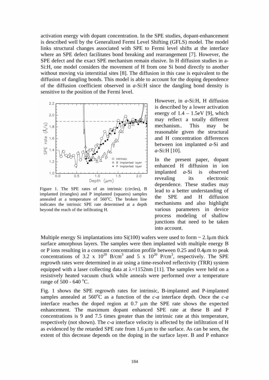
184
Figure 1. The SPE rates of an intrinsic (circles), B implanted (triangles) and P implanted (squares) samples annealed at a temperature of 560oC. The broken line indicates the intrinsic SPE rate determined at a depth beyond the reach of the infiltrating H.
activation energy with dopant concentration. In the SPE studies, dopant-enhancement is described well by the Generalized Fermi Level Shifting (GFLS) model. The model links structural changes associated with SPE to Fermi level shifts at the interface where an SPE defect facilitates bond breaking and rearrangement [7]. However, the SPE defect and the exact SPE mechanism remain elusive. In H diffusion studies in a-Si:H, one model considers the movement of H from one Si bond directly to another without moving via interstitial sites [8]. The diffusion in this case is equivalent to the diffusion of dangling bonds. This model is able to account for the doping dependence of the diffusion coefficient observed in a-Si:H since the dangling bond density is sensitive to the position of the Fermi level.
However, in a-Si:H, H diffusion is described by a lower activation energy of 1.4 – 1.5eV [9], which may reflect a totally different mechanism.. This may be reasonable given the structural and H concentration differences between ion implanted a-Si and a-Si:H [10].
In the present paper, dopant enhanced H diffusion in ion implanted a-Si is observed revealing its electronic dependence. These studies may lead to a better understanding of the SPE and H diffusion mechanisms and also highlight various parameters in device process modeling of shallow junctions that need to be taken into account.
Multiple energy Si implantations into Si(100) wafers were used to form ~ 2.1µm thick surface amorphous layers. The samples were then implanted with multiple energy B or P ions resulting in a constant concentration profile between 0.25 and 0.4µm to peak concentrations of 3.2 x 10²⁰ B/cm3 and 5 x 10²⁰ P/cm3, respectively. The SPE regrowth rates were determined in air using a time-resolved reflectivity (TRR) system equipped with a laser collecting data at λ=1152nm [11]. The samples were held on a resistively heated vacuum chuck while anneals were performed over a temperature range of 500 - 640 oC.
Fig. 1 shows the SPE regrowth rates for intrinsic, B-implanted and P-implanted samples annealed at 560oC as a function of the c-a interface depth. Once the c-a interface reaches the doped region at 0.7 µm the SPE rate shows the expected enhancement. The maximum dopant enhanced SPE rate at these B and P concentrations is 9 and 7.5 times greater than the intrinsic rate at this temperature, respectively (not shown). The c-a interface velocity is affected by the infiltration of H as evidenced by the retarded SPE rate from 1.6 µm to the surface. As can be seen, the extent of this decrease depends on the doping in the surface layer. B and P enhance

185
Figure 2. Normalized SPE rates at a depth of 1.2 µm for intrinsic (circles), B implanted (triangles) and P implanted (squares) layers. The solid lines are linear fits.
Figure 3. SIMS concentration profiles of H in intrinsic B and P implanted layers after an anneal of about 90 minutes at 560oC. The resulting c-a interface is at a depth of 1.2 µm. The solid line is a solution to the diffusion equation with an activation energy of 2.7eV.
the H diffusion and increase the H concentration at depths well beyond the dopant-implanted region.
For our samples the greatest retardation with respect to the H-free intrinsic rates occurs when the interface is at 1.2µm The retardation at this depth is plotted as a function of temperature over the range 500 – 640oC in Fig. 2. The retarded rates from each sample decrease linearly as a function of 1/kT with the greatest retardation occurring for the lowest temperature. We see a 20 % reduction of the SPE rate in intrinsic a-Si over the temperature range studied.
Fig. 3 shows the resulting H concentration profiles in partially annealed intrinsic and dopant implanted a-Si layers determined by SIMS. In each case, anneals were performed at 560oC and was ceased once the c-a interface reached 1.2 µm. The theoretical concentration profile as a function of depth represented by the solid line was determined from the error function equation:
C(x) = Co erfc(x/2√Dt) (2
which is a solution to the diffusion equation. The diffusion coefficient, D, was calculated using an equation similar to (1) with Ea = 2.7eV. The time of the anneal, t, was 90 minutes. Only the surface concentration, Co, was varied to fit the data giving Co = 1.2 x 10¹⁹ H/cm3. Deviation from this curve in the region beyond 1 µm is due to segregation and pile-up of the H in front of the c-a interface. However, this equation fits the H concentration profiles quite well confirming the value of 2.7eV for the activation energy.
The H profiles in Fig. 3 clearly show that H infiltration into a-Si is enhanced by the implanted dopants. The total integrated H concentration between 0.7 and 1.2 µm is 2.2 x 10¹⁴, 3.5 x 10¹⁴ and 7.5 x 10¹⁴ H/cm2 for intrinsic, P implanted and B implanted samples, respectively. The H concentration at the surface is also enhanced by the presence of the dopants. Once the H arrives at the heavily doped region it is
186
transported at a much faster rate. This causes the concentration gradient at the surface to remain steep. In this way the total H concentration in the a-Si after a partial anneal is well above that seen in the intrinsic layer.
Between 0.1 and 0.7µm in the dopant-implanted samples, a complex H concentration profile is observed. This is most likely caused by matrix effects inherent in the SIMS technique. Therefore, this region does not reflect the true H concentration profile and the concentration quantification is only valid at depths beyond the dopant implanted region.
Roth et al. suggested that H diffuses by switching places with dangling bonds [8]. In the GFLS model, the Si atoms from the amorphous side of the interface align onto the underlying crystalline template via some bond breaking process. Given the similarity of H diffusion and SPE behaviour, it is reasonable to consider that both processes are mediated by the dangling bond defect. The SPE velocity is expected to be proportional to the concentration of these dangling bonds. When Si is doped the Fermi level shifts and the concentration of dangling bonds changes accordingly. This results in the dopant enhanced SPE effect. Likewise, these ideas could be applied to H diffusion in ion implanted a-Si.
These studies have important ramifications for the formation of shallow junctions by B implantation into pre-amorphized layers followed by SPE anneals. This is because B interacts with the infiltrating H and enhances the H to concentrations much greater than previously expected. This slows down the SPE rate and may affect the dopant activation.
Acknowledgment The authors wish to thank Professor Mladen Petravic for helpful discussions in interpreting the SIMS data and identifying the matrix affect therein. The Department of Electronic Materials Engineering at the Australian National University is acknowledged for their support by providing access to ion implanting facilities.
References 1 International Technology Roadmap for Semiconductors (2003 Edition).
2 J. A. Roth and G. L. Olson, Handbook of Crystal Growth 3 (Elsevier, Amsterdam, 1994), 3rd ed.
3 J. A. Roth, G. L. Olson, D. C. Jacobson, and J. M. Poate, Appl. Phys. Lett. 57, 1340 (1990).
4 B. C. Johnson and J. C. McCallum, J. Appl. Phys. 95, 4427 (2004).
5 J. A. Roth, G. L. Olson, D. C. Jacobson, and J. M. Poate, Mat. Res. Soc. Symp. Proc. 297, 291 (1993).
6 D. J. Pyke, Master’s thesis, University of Melbourne (2007).
7 B. C. Johnson and J. C. McCallum, Phys. Rev. B. 76, 045216 (2007).
8 R. A. Street, C. C. Tsai, J. Kakalios, and W. B. Jackson, Philos. Mag. B 56, 305 (1987).
9 C. G. V. de Walle and R. A. Street, Phys. Rev. B. 51, 10615 (1995).
10 S. Acco, D. L. Williams, P. A. Stold, F. W. Saris, M. J. van den Boogaard, W. C. Sinke, W. F. van der Weg, S. Rooda, and P. C. Zalm, Phys. Rev. B. 53, 4415 (1996).
11 J. C. McCallum, Appl. Phys. Lett. 69, 925 (1996).
187
On the use of mercury as a means of locating background sources in ultra low background HPGe-detector systems
M Hult 1, J Gasparro 1 P Lindahl 1, G Marissens 1, A. Fessler 1 and Peter N. Johnston 2 1European Commission-Joint Research Centre- Institute for Reference Materials and
Measurements (IRMM),Retieseweg 111, B- 2440 Geel, Belgium 2 Applied Physics, Royal Melbourne Institute of Technology, GPO Box 2476V, Melbourne 3001,
Australia.
Abstract In low-level gamma-ray spectrometry, it is common to measure big samples in order to obtain low detection limits for the massic activity (in mBq/kg). In such cases, the sample itself adds a significant shielding effect. In order to study whether the background sources in three ultra low background HPGe detectors were located in the detector or in the shield, Marinelli beakers filled with hyperpure mercury were measured. Although the measurements were hampered by the presence of cosmogenically produced 194Hg, information regarding the major background location of 40K, 60Co, 137Cs, 210Pb, 226Ra, 228Ra and 228Th could be obtained.

188
Identification of ion strike location by precision IBIC L. M. Jong1, C. Yang1, T. Hopf1, D.N. Jamieson1, E. Gauja2, A.S. Dzurak2 and R.G.
Clark2
1 Centre for Quantum Computer Technology, School of Physics, University of Melbourne 2 Centre for Quantum Computer Technology , School of Physics and Department of Electrical
Engineering, University of New South Wales.
In high energy physics experiments, measurement of the trajectories of ionizing particles is done with silicon strip detectors that read out the two dimensional coordinates of the passage of single particles. We have adapted this method to identify, with micrometer precision, the impact site of single MeV ions in silicon substrates. This is accomplished by the use of two integrated electrodes that can be used individually, or in coincidence, to measure ion strikes by collection of the signal from Ion Beam Induced Charge (IBIC). We present experimental results from implants performed by 2 MeV He ions from a nuclear microprobe into the 12 micron gap between the electrodes and show that micrometer precision can be achieved. We assess the potential of the method for the implantation of keV dopant atoms with sub-micron precision.
As semiconductor devices continue to shrink the electrical characteristics and performance of such devices depends greatly on the number and location of dopant atoms. Shinada et al [1] have shown the effect of controlled doping of transistor channels on variations in performance between devices compared with random doping of the silicon. Fabrication of solid state quantum computing devices, such as that proposed by Kane [2] represents the extreme in the need for precision control over the number and placement on dopant atoms in the substrate. Schemes, such as that developed by Jamieson et al [3] for fabricating qubits based on single ion implantation have been successful in introducing a counted number of phosphorus donors into a silicon substrate, but with limited ability to control the position of the implant with a broad ion beam. We present a method for determining the position, to within 1µm, of an implanted ion using an ion beam induced charge method for detection of ions in their single ion implantation scheme.
When an ion is implanted into the silicon substrate it generates electron-hole pairs, which drift in the electric field created by biasing surface electrodes. This charge transient is detected and signals the arrival of an ion in the substrate. By biasing the top electrodes of the device separately, as shown in Figure 1, we generate a signal on each electrode which varies with the distance of the ion impact site from the electrode.
Using this energy signal in ion detection has been used very successfully in strip detector development for detection of high energy charged particles. Arrays of pixel detectors can be used to determine the location of such an ion by finding the centre of the charge collected by a number of pixel detectors. Strip detectors used for projective readout and be combined with the pixel array to obtain a resolution to 1µm in x and y directions [4].
For the purposes of controlled doping of devices however such an arrangement is not attractive. In the case of building quantum computing devices, the active region between the detector electrodes is required to allow room for the control and readout electronics which are put in place after ion implantation. The strip detector design, while excellent when the sole purpose of the device is charged particle detection is not

189
suitable when the device must undergo further processing to be used for its end purpose.
Numerical modelling of the charge transients at the two electrodes was performed using the DESSIS device simulator, part of the commercial finite element modelling TCAD package [5]. The device tested consisted of a 300 µm n-type silicon wafer with boron diffused top contacts spaced 12µm and phosphorus diffused back contact. The two top contacts were simply attached to separate, but identical, electronics and biased against the back contact to -20V. Median energy maps were created for the two electrodes and are shown in Figure 1, showing the gradient in charge collection efficiency in the region between the electrodes as the ion moves away from one electrode to the other. Experiments were run at room temperature due to the large amount of charge injected by each ion impact creates a signal in the device well above the noise level.
To compare with the experiments numerical simulations of a 2-D device were performed using the DESSIS device simulation code, part of the TCAD package, which solves the Poisson equation and electron and hole continuity equations numerically. The device dimensions and doping densities were specified to match those of the devices under test. Voltages on the electrodes were specified to also match the experimental conditions. The location of a heavy ion impact was specified and separate simulations run with the impact location varied between the two electrodes. For each ion position a transient simulation was performed of the drift of the ionisation resulting from the impact in the electric field within the device. The total charge collected at each electrode was obtained by integrating the charge collected over the duration of the transient simulation.
Figure 1. Median energy IBIC maps triggered from left (a) and right (b) electrodes. Charge collection efficiency drops away with distance from the electrode
(a) (b)
190
Figure 2. Profile of the charge collection efficency at both electrodes taken through their centre as a function of distance from the top electrode. Data points overlaid are the TCAD simulated charge collection efficiency.
Figure 3. Resolution obtainable for a 2MeV He+ ion with 12µm electrode spacing and ungated data collection. δx of 1µm is obtained by the standard deviation of all the energy events at that position.
191
Comparison of the IBIC results with the TCAD simulations is shown in Figure 2. Profiles of the median energy charge collection efficiency maps along the axis of the detectors is shown with the simulated charge collection efficiency at selected ion positions, scaled to the width between electrodes, show good agreement between the experimental results and the simulation. Improvements in resolution could be made by varying a number of parameters. Firstly by moving the electrodes closer together, though for quantum computing devices this is limited by the space required for further electronics which must be added after implantation. Reduction in temperature will cause a reduction in the spreading of the charge cloud, further localising the ionisation around the impact site. Since the phosphorus implantation in the QC devices is already performed at liquid nitrogen temperature this is a relatively simple improvement to make. With these modifications to the technique it is envisaged that the resolution could be improved to the level required for fabricating QC devices requiring donor spacings of 20nm.
We have demonstrated a strong relationship between the distance of an ion impact from multiple detector electrodes and the IBIC signal detected by each electrode. Results of a proof of concept experiment show an obtainable resolution of 1µm as shown in Figure 3. With modifications to the technique it is projected a resolution of down to around 20nm could be obtained. The method is compatible with current single ion detection techniques used in quantum computing device based on implantation of single phosphorus ions into a silicon substrate. Thus devices could be fabricated such that it is known immediately whether appropriate donor spacings have been achieved with the implantation.
Acknowledgment This work was supported by the Australian Research Council, the Australian Government and by the US National Security Agency (NSA), Advanced Research and Development Activity (ARDA) and the Army Research Office (ARO) under Contract No. W911NF-04-1-0290.
References T. Shinada, S. Okamoto, T. Kobayashi, I. Odomari, “Enhancing semiconductor device performace using ordered dopant arrays”, Nature 437 (2005)
B.E. Kane, “A silicon-based nuclear spin quantum computer” Nature 393 (1998) 133
D.N. Jamieson and C. Yang and T. Hopf and S.M. Hearne and C. Pakes and S. Prawer and M. Mitic and E. Gaugja and S.E. Andresen and F. Hudson and A.s. Dzurak and R.G. Clark, “Controlled shallow single ion implantation in silicon using an active substrate for sub-20 keV ions”, Appl. Phys. Lett. (2005) 86
B. Yu, R. Beuttenmuller, W. Chen, D.C. Elliott, Z. Li, J.A. Mead, V. Radeka, M.E. Vazquez, K.A.Brown, A.Ruskek, “A Novel 2-D Position Sensitive Silicon Detector With Micron Resolution for Heavy Ion Tracking”,IEEE Transactions on Nuclear Science 53 (2006) 4
Synopsis Inc. Available from: http://www.synopsis.com

192
Nuclear microprobe studies of metal(loid)s distribution in hyperaccumulating plants
Anthony G Kachenko 1, Balwant Singh 1, Rainer Siegele 2, Naveen Bhatia 2 1 Faculty of Agriculture, Food and Natural Resources, The University of Sydney, New South
Wales 2006, Australia. 2 Institute for Environmental Research, Australian Nuclear Science and Technology
Organization, Lucas Heights, New South Wales 2234, Australia.
Abstract Micro-proton-induced X-ray emission (µ-PIXE) spectroscopy was used to determine in situ elemental concentrations of nickel (Ni) and arsenic (As) in leaf and stem tissues of hyperaccumulating plants Hybanthus floribundus subsp floribundus and Pityrogramma calomelanos var. austroamericana, respectively. Nickel concentration in seeds of H. floribundus subsp floribundus was also investigated. Both species were grown in metal(loid) contaminated potting mix for 20 weeks duration under controlled glasshouse conditions. Leaf and stem samples were hand-sectioned, cryo-fixed and freeze-dried in liquid nitrogen before µ-PIXE analysis using the 10-MV tandem accelerator at the Australian Nuclear Science and Technology Organization. In H. floribundus subsp floribundus leaves, Ni was highest in the adaxial epidermal cells (1% dry weight; DW) and least in spongy mesophyll (0.53% DW). In stem tissues, Ni concentrations were highest in the collenchyma (0.25% DW) and there was no clear pattern of Ni localization in seeds. In P. calomelanos pinnules, As localization was relatively uniform across the whole specimen and in stipe tissues, highest concentration occurred in the vascular bundle (0.2% DW). These results suggest that hyperaccumulating plants sequester excess metal(loid)s in different cellular loci and enables us to better understand the physiology and ecology of these hyperaccumulating species.
Introduction Micro-proton-induced X-ray emission (µ-PIXE) spectroscopy provides pertinent quantitative information as to the spatial distribution of elements in metal(loid) hyperaccumulating plants [1-5]. The phenomenon of metal(loid) hyperaccumulation is expressed in ca. 400 species worldwide that exhibit the unique ability of elevated metal(loid) accumulation in aboveground tissues without adverse effects on plant growth. The criteria to define a nickel (Ni) and arsenic (As) hyperaccumulator is any plant species exceeding 1000 mg Ni or As kg−1 dry weight (DW) in any above-ground tissue [6-8]. The Ni hyperaccumulating Hybanthus floribundus subsp. floribundus or shrub violet (Violaceae) is a native Australian perennial shrub and has been reported to hyperaccumulate up to 13 500 mg As kg–1 DW [9]. Pityrogramma calomelanos var. austroamericana, or gold fern (Pteridaceae) is a perennial and rhizomatous fern native to South America and has been reported to hyperaccumulate up to 3330 mg As kg–1 DW in fronds[10].
The knowledge of spatial distribution and localisation of metal(loids)s within hyperaccumulating tissues is paramount to comprehend the processes underlying metal tolerance and hyperaccumulation in plants. Moreover, few studies have investigated the distribution of metal(loid)s in reproductive tissues (seeds) of hyperaccumulating species. Therefore, the aim of this study was to quantify the spatial distribution of Ni in leaf, stem and seed tissues of H. floribundus subsp
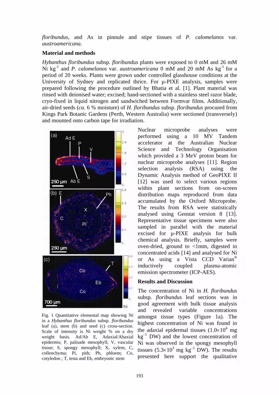
193
floribundus, and As in pinnule and stipe tissues of P. calomelanos var. austroamericana.
Material and methods Hybanthus floribundus subsp. floribundus plants were exposed to 0 mM and 26 mM Ni kg-1 and P. calomelanos var. austroamericana 0 mM and 20 mM As kg-1 for a period of 20 weeks. Plants were grown under controlled glasshouse conditions at the University of Sydney and replicated thrice. For µ-PIXE analysis, samples were prepared following the procedure outlined by Bhatia et al. [1]. Plant material was rinsed with deionised water; excised; hand-sectioned with a stainless steel razor blade, cryo-fixed in liquid nitrogen and sandwiched between Formvar films. Additionally, air-dried seeds (ca. 6 % moisture) of H. floribundus subsp. floribundus procured from Kings Park Botanic Gardens (Perth, Western Australia) were sectioned (transversely) and mounted onto carbon tape for irradiation.
Nuclear microprobe analyses were performed using a 10 MV Tandem accelerator at the Australian Nuclear Science and Technology Organisation which provided a 3 MeV proton beam for nuclear microprobe analyses [11]. Region selection analysis (RSA) using the Dynamic Analysis method of GeoPIXE II [12] was used to select various regions within plant sections from on-screen distribution maps reproduced from data accumulated by the Oxford Microprobe. The results from RSA were statistically analysed using Genstat version 8 [13]. Representative tissue specimens were also sampled in parallel with the material excised for µ-PIXE analysis for bulk chemical analysis. Briefly, samples were oven-dried, ground to <1mm, digested in concentrated acids [14] and analysed for Ni or As using a Vista CCD Varian® inductively coupled plasma-atomic emission spectrometer (ICP-AES).
Results and Discussion The concentration of Ni in H. floribundus subsp. floribundus leaf sections was in good agreement with bulk tissue analysis and revealed variable concentrations amongst tissue types (Figure 1a). The highest concentration of Ni was found in the adaxial epidermal tissues (1.0×10⁴ mg kg–1 DW) and the lowest concentration of Ni was observed in the spongy mesophyll tissues (5.3×10³ mg kg–1 DW). The results presented here support the qualitative
Fig. 1 Quantitative elemental map showing Ni in a Hybanthus floribundus subsp. floribundusleaf (a), stem (b) and seed (c) cross-section.Scale of intensity is Ni weight % on a dry weight basis. Ad/Ab E, Adaxial/Abaxial epidermis; P, palisade mesophyll; V, vascular tissue; S, spongy mesophyll; X, xylem, C, collenchyma; Pi, pith; Ph, phloem; Co,cotyledon ; T, testa and Eb, embryonic stem

194
observation by Farago et al. [15] and Severne [16] who used histochemical techniques to show the presence of Ni in epidermal cells of H. floribundus leaves. Preferential localisation of Ni has been reported in epidermal tissues of several Ni hyperaccumulating species [2,17]. It has been suggested that sequestration of metals such as Ni to epidermal tissue minimises the disruption of photosynthetic processes that occur primarily in the mesophyll symplast [18].
Elemental map of a stem section of H. floribundus subsp. floribundus revealed variable concentrations of Ni among tissue types (Figure 1b) and followed the order collenchyma > epidermis > phloem > xylem > pith. The observed pattern of Ni localisation in this study is similar to the that reported in stem tissue of the Ni hyperaccumulator Senecio coronatus [19]. These authors noted that stem epidermal and cortical cells acted as a depository of Ni and contained up to 3.4×10⁴ mg Ni kg–1 DW. Nickel enrichment in outer tissues of stem and leaf tissue may act as a chemical defence against insect herbivory [18], as well as fungal and bacterial pathogens [20,21]. Further biochemical investigations are currently underway to elucidate precise detoxification mechanisms in this species.
In Hybanthus floribundus subsp. floribundus seeds, Ni concentrations were variable (Figure 1c). Nickel concentrations were higher within embryonic tissues (cotyledons and embryonic stem) than the seed coat, however the differences were non-significant. This pattern of localization suggests apoplastic movement of Ni within the seeds of H. floribundus subsp. floribundus. The results presented in this study are similar to those observed in Ni hyperaccumulating Thlaspi pindicum where preferential Ni accumulation occurred in the cotyledon epidermis [22]. It is possible that the degree of Ni concentration in seeds may contribute to the poor germination of H. floribundus subsp. floribundus [23,24], however further investigations are warranted.
The concentration of As in P. calomelanos var. austroamericana pinnule sections varied among tissue types (Figure 2a). The highest As concentration occurred in vascular and spongy mesophyll tissues (4.1×10³ mg kg–1 DW), however the differences were non-significant. The cellular distribution of As in our study is in agreement with those reported by Chen et al. [25] who investigated As localization in P. cretica var. nervosa pinnae sections. These authors reported a higher As content in mesophyll as opposed to epidermal tissues. In a later study, Chen et al. [26] indicated that As in the midrib efficiently translocated to surrounding mesophyll tissues in P. vittata pinna.
Fig. 2 Quantitative elemental map showing As in a Pityrogramma calomelanos var. austroamericana pinnule (a) and stipe (b) cross-section. Scale of intensity is As weight % on dry mass basis. Ad/Ab E, Adaxial/Abaxial epidermis; S, spongy mesophyll; Vb, vascular bundle and Cor, cortex.

195
In P. calomelanos var. austroamericana stipe sections, As concentrations varied among tissue types (Figure 2b), and was highest in vascular bundles (2.0×10³ mg kg–1
DW). Concentration of As in stipe sections was almost 2.3-fold lower than in whole pinnule sections and followed the order vascular bundle > cortex > epidermis. This is the first µ-PIXE study on an As hyperaccumulator, with the majority of studies focused on Ni hyperaccumulators [2,17]. The reasoning behind Ni enrichment discussed above does not justify the localization pattern of As observed in P. calomelanos var. austroamericana tissues and suggests that strategies other than cellular localization may be responsible for As homeostasis in this species. A synchrotron-based study is currently underway in our laboratory to determine As chelation and speciation at various loci throughout fresh hydrated tissues of this species.
Conclusions This study demonstrates a varying degree of physiological adaptation of hyperaccumulating plants in response to excess meatl(loid)s. In Ni hyperaccumulator H. floribundus subsp. floribundus, Ni is sequestered into physiologically inert tissues and may contribute to plant defence against insect, pathogen or fungal attack. In H. floribundus seeds, Ni was relatively uniform across cellular regions and the degree of accumulation may inhibit seed viability and germination. In P. calomelanos pinnule and stipe tissues, As was relatively uniform across tissue types and there was no clear reasoning to support this observed pattern of localisation. The results suggest that there is no consistent pattern of cellular metal(loid) localisation in hyperaccumulating plants and may be specific for heavy metal(loid) or genotype.
Acknowledgements Authors acknowledge the Australian Institute of Nuclear Science and Engineering for financial assistance (Award Nos. AINGRA 05150 and 06160). Anthony Kachenko is supported by an Australian Postgraduate Award scholarship from the Australian Government.
References [1] N. P. Bhatia, I. Orlic, R. Siegele, N. Ashwath, A. J. M. Baker, K. B. Walsh,
New Phytol. 160 (2003) 479.
[2] N. P. Bhatia, K. B. Walsh, I. Orlic, R. Siegele, N. Ashwath, A. J. M. Baker, Func. Plant Biol. 31 (2004) 1061.
[3] D. Budka, J. Mesjasz-Przybyłowicz, W. J. Przybyłowicz, Radiat. Phys. Chem. 71 (2004) 785.
[4] A. G. Kachenko, N. P. Bhatia, B. Singh, R. Siegele, Plant Soil (2007) (accepted).
[5] A. G. Kachenko, B. Singh, N. P. Bhatia, R. Siegele, Nucl. Instr. and Meth. B (2007) (Submitted).
[6] A. J. M. Baker, S. P. McGrath, R. D. Reeves, J. A. C. Smith, in: N. Terry, G. Bañuelos (Eds.), Phytoremediation of Contaminated Soil and Water, CRC Press, Boca Raton, 2000, p. 85

196
[7] L. Q. Ma, K. M. Komar, C. Tu, W. Zhang, Y. Cai, E. D. Kennelley, Nature 409 (2001) 579.
[8] A. G. Kachenko, B. Singh, N. P. Bhatia, Aust. J. Bot. 55 (2007) 63.
[9] M. E. Farago, A. J. Clark, M. J. Pitt, Inorganic Chemica Acta 24 (1977) 53.
[10 P. M. Ashley, B. G. Lottermoser, A. J. Chubb, Geochem.: Explor. Environ., Anal. 3 (2003) 345.
[11] R. Siegele, D. D. Cohen, N. Dytlewski, Nucl. Instr. and Meth. B 158 (1999) 31.
[12] C. G. Ryan, E. van Achterbergh, D. N. Jamieson, Nucl. Instr. and Meth. B 231 (2005) 162.
[13] R. W. Payne, S. A. Harding, D. A. Murray, D. M. Soutar, D. B. Baird, S. J. Welham, A. F. Kane, A. R. Gilmour, R. Thompson, R. Webster, GENSTAT release 8 reference manual, VSN International, Oxford, UK, 2005
[14] D. J. Reuter, J. B. Robinson, K. I. Peverill, G. H. Price, in: D. J. Reuter, J. B. Robinson (Eds.), Plant analysis: An interpretation manual, Inkarta Press, Melbourne, 1988, p. 20
[15] M. E. Farago, A. J. Clark, M. J. Pitt, Coord. Chem. Rev. 16 (1975) 1.
[16] B. C. Severne, Nature 248 (1974) 807.
[17] U. Krämer, G. W. Grime, J. A. C. Smith, C. R. Hawes, A. J. M. Baker, Nucl. Instr. and Meth. B 130 (1997) 346.
[18] R. S. Boyd, in: R. R. Brooks (Ed.) Plants that hyperaccumulate heavy metals: their role in phytoremediation, microbiology, archaeology, mineral exploration and phytomining, CAB International, Wallingford, UK, 1998, p. 181
[19] J. Mesjasz-Przybyłowicz, W. J. Przybyłowicz, V. M. Prozesky, C. A. Pineda, Nucl. Instr. and Meth. B 130 (1997) 368.
[20] S. M. Ghaderian, A. J. E. Lyon, A. J. M. Baker, New Phytol. 146 (2000) 219.
[21] R. S. Boyd, J. J. Shaw, S. N. Martens, American Journal of Botany 81 (1994) 294.
[22] G. K. Psaras, Y. Manetas, Ann Bot 88 (2001) 513.
[23] S. Roche, K. Dixon, J. Pate, Aust. J. Bot. 45 (1997) 783.
[24] K. W. Dixon, S. Roche, J. S. Pate, Oecologia 101 (1994) 1432.
[25] T. Chen, Z. Huang, Y. Huang, H. Xie, X. Y. Liao, Chin. Sci. Bull. 48 (2003) 1586.
[26] T. Chen, Z. Huang, Y. Huang, M. Lei, Sci. China, Ser. C: Life Sci. 48 (2005) 13.

197
PIXE/PIGE microanalysis of trace elements in hydrothermal magnetite and exploration significance: a pilot study
Teera Kamvong 1, Khin Zaw 1, Rainer Siegele 2 1CODES, UTAS Private Bag 79 Hobart, TAS. 7001 Australia
2IER, ANSTO PMB 1Mena NSW. 2234 Australia
[email protected], [email protected], [email protected]
Abstract Magnetite is a common iron oxide mineral in many giant ore deposits. However, chemical analyses of individual magnetite grains were hampered by high detection limits in electron probe microanalysis and use of techniques such as XRF or solution chemistry on mineral separates. Hear we present a pilot study of the geochemistry of magnetite using PIXE microanalysis, which reveals a correlation between its trace element concentrations and a variety of ore deposit types. This finding suggests that some element ratios (e.g., Sn/Ga, Al/Co) of magnetite may play a significant role as indicator elements to discriminate between the different ore deposit styles, particularly within magmatic-hydrothermal ore systems and to apply in mineral exploration.
Further works are in progress in combination with LA ICP-MS study of magnetites at CODES to acquire more data to test our hypothesis.
Key words: Magnetite, PIXE, magmatic-hydrothermal ore systems
Introduction Magnetite is a common iron oxide mineral in many giant ore deposits such as Olympic Dam in South Australia and Cadia in NSW. However, chemical analyses of individual mineral grains were hampered by high detection limits in electron probe microanalysis and use of techniques such as XRF or solution chemistry on mineral separates. Recent development in micro-analytical techniques using non-destructive Particle Induced X-ray Emission (PIXE) at Institute for Environmental Research, Australian Nuclear Science and Technology Organisation (ANSTO) can provide more detailed information on trace elements of magnetite.
The main purpose of this extended abstract is to describe the trace element characteristics of magnetite from the Puthep 1 (PUT 1) and Phu Kham skarn-related porphyry Cu-Au deposits, Thailand and Laos (Fig. 1). Our preliminary results suggested that some elements ratios of analysed magnetite can be used as indicator elements to discriminate types of metal deposits.
Geological Background
Deposit geology of the Puthep 1 The PUT 1 skarn-related porphyry Cu deposit is located in the northern Loei Fold Belt (Fig. 1) and hosted by the carboniferous clastic sedimentary units intercalated with thick limestone sequences. These rocks were emplaced by intrusive porphyries, including diorite and monzodiorite during the Late Triassic age. At Puthep 1, two major- and mineralisation-styles have been recognised: 1) porphyry-style stockwork veining, alteration and mineralisation; and 2) skarn-style alteration and mineralisation.
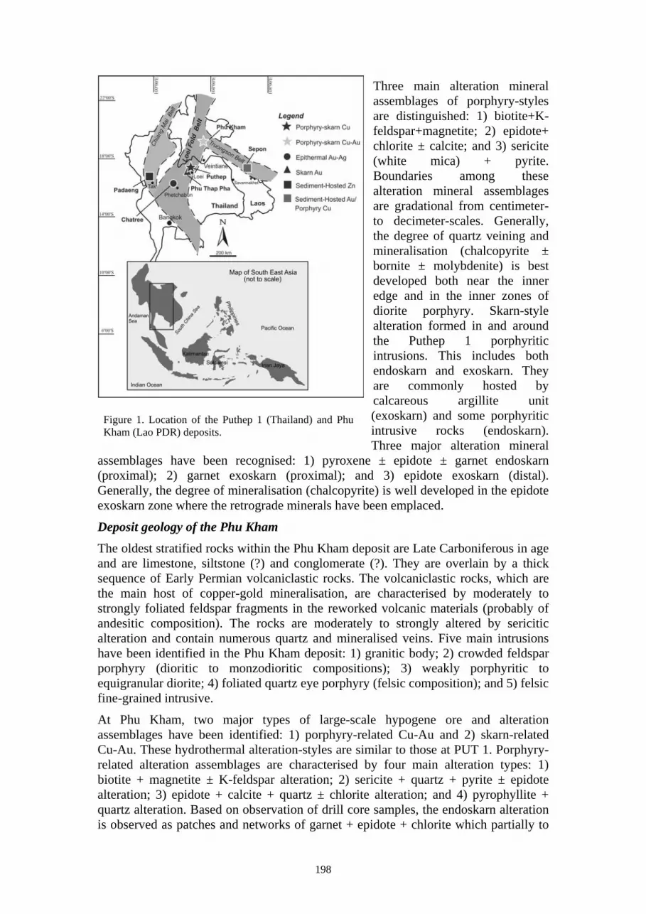
198
Three main alteration mineral assemblages of porphyry-styles are distinguished: 1) biotite+K-feldspar+magnetite; 2) epidote+ chlorite ± calcite; and 3) sericite (white mica) + pyrite. Boundaries among these alteration mineral assemblages are gradational from centimeter- to decimeter-scales. Generally, the degree of quartz veining and mineralisation (chalcopyrite ± bornite ± molybdenite) is best developed both near the inner edge and in the inner zones of diorite porphyry. Skarn-style alteration formed in and around the Puthep 1 porphyritic intrusions. This includes both endoskarn and exoskarn. They are commonly hosted by calcareous argillite unit (exoskarn) and some porphyritic intrusive rocks (endoskarn). Three major alteration mineral
assemblages have been recognised: 1) pyroxene ± epidote ± garnet endoskarn (proximal); 2) garnet exoskarn (proximal); and 3) epidote exoskarn (distal). Generally, the degree of mineralisation (chalcopyrite) is well developed in the epidote exoskarn zone where the retrograde minerals have been emplaced.
Deposit geology of the Phu Kham The oldest stratified rocks within the Phu Kham deposit are Late Carboniferous in age and are limestone, siltstone (?) and conglomerate (?). They are overlain by a thick sequence of Early Permian volcaniclastic rocks. The volcaniclastic rocks, which are the main host of copper-gold mineralisation, are characterised by moderately to strongly foliated feldspar fragments in the reworked volcanic materials (probably of andesitic composition). The rocks are moderately to strongly altered by sericitic alteration and contain numerous quartz and mineralised veins. Five main intrusions have been identified in the Phu Kham deposit: 1) granitic body; 2) crowded feldspar porphyry (dioritic to monzodioritic compositions); 3) weakly porphyritic to equigranular diorite; 4) foliated quartz eye porphyry (felsic composition); and 5) felsic fine-grained intrusive.
At Phu Kham, two major types of large-scale hypogene ore and alteration assemblages have been identified: 1) porphyry-related Cu-Au and 2) skarn-related Cu-Au. These hydrothermal alteration-styles are similar to those at PUT 1. Porphyry-related alteration assemblages are characterised by four main alteration types: 1) biotite + magnetite ± K-feldspar alteration; 2) sericite + quartz + pyrite ± epidote alteration; 3) epidote + calcite + quartz ± chlorite alteration; and 4) pyrophyllite + quartz alteration. Based on observation of drill core samples, the endoskarn alteration is observed as patches and networks of garnet + epidote + chlorite which partially to
Figure 1. Location of the Puthep 1 (Thailand) and Phu Kham (Lao PDR) deposits.

199
totally replaced into the porphyry intrusive bodies. Two major exoskarn alteration assemblages at Phu Kham have been distinguished: 1) garnet skarn (proximal zone); and 2) garnet-epidote skarn (distal zone).
Methods Magnetites that closely associated with porphyry-skarn copper-gold deposits have been sampled from the PUT 1 and Phu Kham deposits. Samples were made as polished grain mounts in epoxy and coated with carbon. These polished mounts represented the surface of the samples because PIXE is surface analytical techniques, which means it measures the average concentration in the top 100µm of samples. All sample preparation were conducted at the University of Tasmania. The prepared samples were analysed at ANSTO, Sydney using the PIXE analysis.
Results and Interpretation Major and trace element compositions were obtained from 14 samples (Table 1). In addition, we analysed magnetite for its element data from other major ore deposits such as VHMS system (Table 1) to compare the compositions with those of the PUT1 and Phu Kham skarn deposits. Our result shows that magnetite from skarn, VHMS, IOCG deposits are generally enriched in Ti, Cr, Mn, Co, Cu, Zn, Ba and W, Pb, Sr, Ni and V. Such characteristics indicate that those elements are an important trace element
Table 1: Summary results of the PIXE Analysis* from various magmatic-hydrothermal deposit typesLocation Phu Kham PUT 1 Mt Morgan Mt Lyell Kara JunoDeposit types PS PS VHMS VHMS Skarn IOCG
n 7 7 4 3 3 3Mg 12714 5257 17775 10666 12100 17233Al 6557 15243 29250 71666 7666 35866Si 128428 160142 132500 383333 76666 41666P 20857 30271 52000 2966 2766 2866S 161628 219243 97575 13400 1266 2690Cl 950 1183 780 430 646 506K 1457 1160 847.5 28000 520 2120
Ca 128428 77042 71250 3256 19666 203Ti 682 1110 1220 3643 1193 1636V 467 390 1308 543 530 590Cr 677 610 820 74 996 1176Mn 3700 2600 6400 1233 6366 3166Fe 432857 437142 475000 111333 603333 646666Co 700 1095 483 166 423 503Ni 218 223 235 49 330 380Cu 13483 29138 1778 1181 154 1384Zn 247 607 448 270 437 306Ga 59 87 42 32 83 41As 193 43 159 20 54 31Se 25 7 15 7 41 299Br 18 14 17 6 33 18Rb 51 51 57 76 74 90Sr 127 65 42 18 35 54Y 21 25 42 14 26 26Zr 27 29 60 153 37 47Nb 16 21 20.5 14 31 27Mo 18 18 23 24 39 47Sn 71 71 85 92 450 59Ba 393 391 468 1557 390 253W 291 351 203 93 21086 293Pb 104 107 118 27 197 327Bi 71 53 65 23 100 1040
* = Analysed results (ppm) based on mean values of all PIXE Analyses PS = porphyry-skarn; VHMS = volcanic-hosted massive sulphide; IOCG = Iron oxide copper-gold

200
for the magnetite formation. Moreover, they also display variations and overlaps in concentrations (Table 1). These compositional variations may be dependent on several factors, including the fO2 conditions, changes in temperature, local availability of trace elements (e.g. Mn, Cr, Ba).
Recent studies of Singoyi et al. (2006) and Beaudoin et al. (2007) also suggested that the magnetite compositions are efficient to fingerprint types of several metal deposits. This indicates that compositions of magnetite may have a crucial role as indicator elements to discriminate the types of various mineral deposits. This is consistent with our preliminary results in which, some element ratios (e.g., Sn/Ga vs Al/Co) of magnetite show a good correlation between its element concentration for skarn and VHMS deposits (Fig. 2) and can be applied as a fingerprinting technique for mineral exploration.
Figure. 2. Plot showing Sn/Ga vs Al/Co ratios of magnetite from porphyry-related skarn (Cu, Cu-Au) deposits (PUT1, Thailand and Phu Kham, Laos) and VHMS (Cu, Cu-Au) deposits (Mt Morgan and Mt Lyell) in Australia.
Acknowledgment This work was funded by Australian Institute of Nuclear Science and Engineering (AINSE; AINSE ID No 2736- Dr. Khin Zaw). We thank research staffs of the Institute for Environmental Research, Australian Nuclear Science and Technology Organisation (ANSTO) for operating the PIXE analysis.
References Beaudoin, G., Dupuis, C., Gosselin, P., Jebrak, M., 2007, Mineral chemistry of iron oxides: application to mineral exploration in: 9th SGA Biennial Meeting Mineral Exploration and Research: Digging Deeper, Dublin, Ireland, p. 497-500.
Singoyi, B., Danyushevsky, L., Davidson, G.J., Large, R., Khin Zaw., 2006, Determination of trace elements in magnetites from hydrothermal deposits using the LA ICP MS technique in: Abstracts of Oral and Poster Presentations from the SEG2006 Conference, Keystone, USA, p. 367-368.

201
Transmission electron microscopy studies of polycrystalline zinc oxide thin films grown by ion beam sputtering
John V Kennedy 1, David R. G. Mitchell 2 and Andreas Markwitz 1 1 National Isotope Centre, GNS Science, 30 Gracefield Road, PO Box 31312, Lower Hutt,
New Zealand 2 Institute of Materials Engineering, ANSTO, PMB 1, Menai, NSW 2234, Australia
Zinc Oxide (ZnO) is becoming an important research material for generation of new optoelectronic devices due to its wide, direct band gap. Novel optoelectronic devices, such as short-wavelength UV LEDs, benefit significantly from crystalline ZnO films with stoichiometric composition, low impurity levels and desirable optical properties [1]. Many fabrication techniques have been successfully tested for growing ZnO thin films on various substrates, including metal-organic chemical vapour deposition (MOCVD), molecular beam epitaxy (MBE), sol-gel deposition, DC and/or R.F. Magnetron sputtering, reactive evaporation, spray pyrolysis, pulsed laser deposition, etc [1-4]. The electrical and optical properties of these thin films strongly correlate with composition, microstructure and impurities.
For the first time, we have prepared ZnO films by an ion beam sputtering (IBS) technique using Zn and ZnO targets and various substrates such as Si, SiO2/Si, glass, sapphire and glassy carbon. The IBS system at GNS Science has been recently established to produce high quality thin films from any target material. Of particular importance is that films can be formed from materials that are difficult to prepare by conventional techniques such as MBE or CVD [5]. We typically produce 10 to 20 films simultaneously with an argon ion beam to impact on a sputter target at an angle of up to 45 degrees from normal. The ion beam is generated by a penning ion source [6], accelerated to typically 10 - 15 keV and focused to spot of 2mm or less diameter on to the target. The sputtering process takes place under high vacuum conditions.
Typical picture of the GNS ion beam sputter system is shown in Figure 1.
RBS was used to measure film thickness and composition [7]. Various deposition parameters such as ion energy, target angle and substrate location were tested to optimise film composition and thickness homogeneity. We used a 2.0 MeV 4He+ ion beam impinging on the samples under normal incidence. The detector for measuring the energy of the backscattered particles was mounted at 165°. Figure 1. Schematic diagram of the GNS ion beam sputter system used for ZnO film preparation

202
100 200 300 400 500 600Channel
0
10
20
30
40
Nor
mal
ized
Yie
ld
0.5 1.0 1.5Energy (MeV)
SP148-si(ap07032)Simulation of Zn-O/Si-H
A low ion current density of 10 nAmm-2 was used to measure the samples non-destructively in short time (less than 15 min). A typical RBS spectra along with RUMP simulation of ion beam sputtered ZnO thin film on Si is shown below.
Based on the IBA measurements, the stoichiometry
is found to be highly dependent on the deposition parameters. Between 1 and 2 at.% hydrogen were measured in the as-deposited films. AFM results show that the surface of the ZnO layers is smooth. The average surface roughness was measured
to 5 ± 2.5nm. Preliminary XRD measurements show that our as-deposited films are disordered and annealed films are
polycrystalline with preferential orientation to (100), (002) and (101). Annealing the films
under vacuum and in air at 500 – 800 °C modifies the film to a relatively defect-free polycrystalline structure, with (100), (002) and (101) preferred orientations. The microstructure of the films was investigated using Transmission Electron Microscopy (TEM) at ANSTO.
Samples for TEM measurements were made in plan view and cross-sectional orientations, using the methods described elsewhere [8]. TEM examinations were carried at ANSTO using JEOL 2010F (200 keV) fitted with a Gatan Imaging Filter (GIF) which permitted energy filtered TEM and energy loss spectroscopy (EELS). A plan view image of the ZnO film deposited on Si at room temperature is shown in Figure 3, highlighting the defective grain structure.
Figure 3. Plan view of the as deposited ZnO film
Zn
O
Si (sub)
ZnO
Epoxy
Figure 2. RBS spectrum of 150nm ZnO thin film deposited on Si substrate.

203
Figure 4. Plan-view TEM micrograph (a) and the corresponding SAD pattern (b) of the as-deposited film.
It was found that the as-deposited films are polycrystalline, displaying a high density of stacking faults and a highly defective structure. Plan view microscopy enabled a meaningful determination of the grain size in the film, which was about 40nm. The selected area diffraction (SAD) pattern of the as deposited film shows arcs of intensity indicating a narrow range of preferred orientations in the plane of the specimen. The SAD pattern also indicate that a very week (002) orientation which normally corresponds to the c-axis of the ZnO crystal orientation. Similar effect was also observed in our XRD measurements (not shown here).
Figure 5: Bright field plan view TEM images of annealed ZnO film on Si (a) showing the very fine grain size compared with as-deposited film and (b) showing a void formation (c) voids within grain (d) SAD pattern of the annealed films with no preferred orientation.
100
101 002
a b
ab
Voids
a

204
Films were annealed using an electron beam annealing system [9] at sample temperatures of 800°C for 1 hour. This system operates with an electron energy of 20 keV and a current of up to 2 mA. The annealing chamber is evacuated with a turbo molecular pump to a base pressure better than 1×10⁻⁷ mbar. TEM measurements were made on the annealed film using the same setup used for as-deposited films. Figure 5a-c shows the plan view images of the annealed film which clearly reveals increased grain size and a less defective structure. The electron diffraction patterns of the annealed film became much sharper and formed discontinuous diffraction rings. It is also seen that the emergence of more (002) texture in the annealed films. It can be seen from figure 5b that voids are formed in the annealed film most at grain boundaries, but also within grains (figure 5c). Void formation was due to densification of the film. Our preliminary results suggest found that ion beam sputtered films need to be annealed at least to 800o C to improve the crystalline quality.
Acknowledgments This project is supported by an AINSE grant (AINGRA07084) and also research grant from Foundation for Research Science and Technology of New Zealand. The authors would like to thank Mr. Jim Pithie and John Futter for their contributions.
Reference 1 S.J. Pearton, D.P. Norton, K. Ip, Y.W. Heo, and T. Steiner, Progress in
Materials Science, 50 (2005) 293
2 D.P. Norton, Y.W. Heo, M.P. Ivil, S.J. Pearton, M.F. Chisholm and T. Steiner: Materials Today., 2004, 34.
3 W. Wernas, A. Yamada and M. Kawasaki: Jpn.J.Appl.Phys., 1994, 33, L283
4 A. Dutta and S. Basu: Mater.Chem.Phys., 1993, 34, 41.
5 A. Markwitz, H. Baumann, E. F. Krimmel, P. Misaelides and K. Bethge, Fresenius Journal of Analytical Chemistry 346 (1-3) (1993) 177.
6 H. Baumann and K. Bethge, Nucl. Instr. and Meth. 122 (1974) 517
7 J. Kennedy, A. Makwitz, B.J. Ruck, S.M. Durbin and W. Gao, Journal of Electronic Materials V 36 N 4 (2007) 472-482.
8 D.R.G. Mitchell, D.J. Attard, G. Triani, Thin Sold Films 441 (2003) 85
9 A. Markwitz., R. W. Michelmann, H. Baumann, E. F. Krimmel, E. C. Paloura, A. Knop and K. Bethge, J. Appl. Phys A54 (1994) 435.
205
The synthesis and structure of silica nanowires Taehyun Kim, Andrew R. Wilkinson and Robert G. Elliman
Department of Electronic Materials Engineering, The Research School of Physical Sciences and Engineering, The Australian National University, Canberra ACT 0200, Australia
Abstract We demonstrate silica wire growth on silicon and silica substrates by nickel precipitates (vapour-phase deposition) and annealing at around 1100°C in nitrogen. Growth of nanowires on silica substrates is only observed when they are in the presence of an additional uncoated silicon wafer, confirming a significant contribution to growth from a vapour source of silicon. Consideration of the vapour pressures of different species suggests that this source of silicon is likely to be SiO produced by reaction between the silicon wafer and residual oxygen or water vapour in the annealing ambient. Attempts to increase the rate of growth by increasing the oxygen concentration instead terminate the nanowire growth; likely due to the formation of a continuous SiO2 protective layer on the silicon wafer. Details of these experiments and the associated model will be presented.
1. Introduction In the past few decades, one-dimensional nanomaterials in the form of tubes, wires and belts have attracted considerable interest because of their potential applications, including as nano-electronic devices, field-emission sources and bio-sensors, as well as their unique physical and chemical properties [1-5].
Since the large scale synthesis of silica nanowires was first undertaken by Yu et al. [6] using a laser ablation technique with a metallic Fe catalyst, many fabrication methods of silica nanowires have been developed [7-10]. In the catalyst-based methods, several different kinds of metal catalyst, such as Au [11-13], Ni [14], Fe [15-16] and Pd [17], have been used. At the same time, there have been efforts to understand the nanowire growth mechanism, with different models proposed such as vapour-liquid-solid (VLS) [8], vapour-solid-solid (VSS) [18], oxide-assisted growth [19] and solid-liquid-solid-solid (SLS) [20].
It is now clear that silica-nanowires can be grown on silicon with diameters of 50~200nm and lengths in excess of 10µm by metal-induced vapour-liquid-solid or solid-liquid-solid mechanisms. This is usually achieved by the introduction of a silicon precursor, such as silane, but growth has also been reported where thin metal layers are deposited directly onto a silicon wafer and annealed in nitrogen or argon. In this case, it is generally argued that the growth proceeds via dissolution of silicon from the substrate, with oxygen (O2 and/or H2O) introduced as a low-concentration (typically < 5ppm) contaminant via the annealing ambient. In this study we demonstrate that the growth process is likely to be more subtle.
In the present work, we study the growth of silica nanowire on silicon and silica substrates in which an additional uncoated silicon wafer is provided as a source of silicon during furnace annealing.
2. Experimental details The substrates used in this study consisted of (100) silicon wafers and thermally oxidized (100) silicon wafers with an SiO2 thickness of 100nm. Fused silica slides were also used for comparison. A nickel catalyst layer of ~10nm thickness was deposited on the substrates by thermal evaporation. Samples were then annealed at
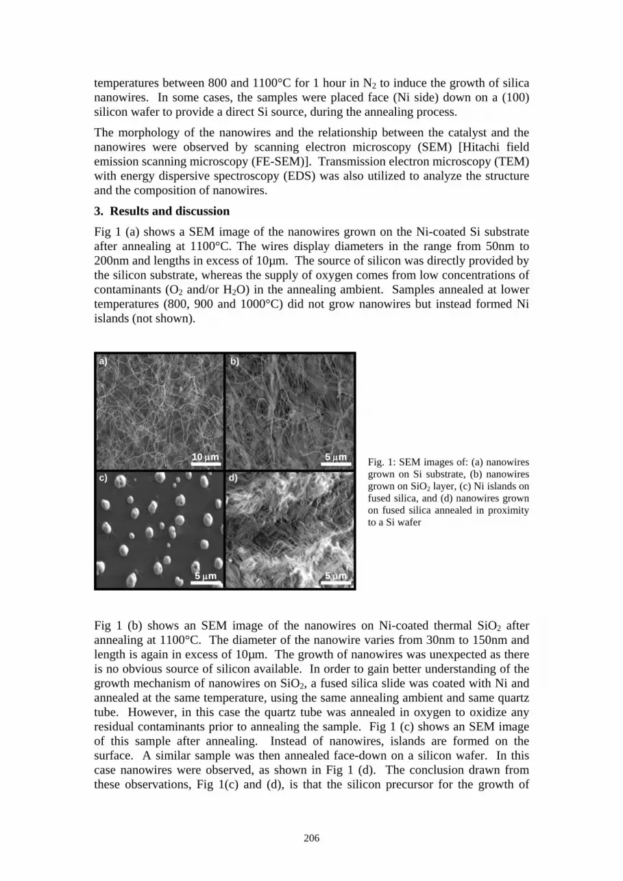
206
temperatures between 800 and 1100°C for 1 hour in N2 to induce the growth of silica nanowires. In some cases, the samples were placed face (Ni side) down on a (100) silicon wafer to provide a direct Si source, during the annealing process.
The morphology of the nanowires and the relationship between the catalyst and the nanowires were observed by scanning electron microscopy (SEM) [Hitachi field emission scanning microscopy (FE-SEM)]. Transmission electron microscopy (TEM) with energy dispersive spectroscopy (EDS) was also utilized to analyze the structure and the composition of nanowires.
3. Results and discussion Fig 1 (a) shows a SEM image of the nanowires grown on the Ni-coated Si substrate after annealing at 1100°C. The wires display diameters in the range from 50nm to 200nm and lengths in excess of 10µm. The source of silicon was directly provided by the silicon substrate, whereas the supply of oxygen comes from low concentrations of contaminants (O2 and/or H2O) in the annealing ambient. Samples annealed at lower temperatures (800, 900 and 1000°C) did not grow nanowires but instead formed Ni islands (not shown).
10 µm 5 µm
5 µm5 µm
a)
c) d)
b)
10 µm10 µm 5 µm5 µm
5 µm5 µm5 µm5 µm
a)
c) d)
b)
Fig. 1: SEM images of: (a) nanowires grown on Si substrate, (b) nanowires grown on SiO2 layer, (c) Ni islands on fused silica, and (d) nanowires grown on fused silica annealed in proximity to a Si wafer
Fig 1 (b) shows an SEM image of the nanowires on Ni-coated thermal SiO2 after annealing at 1100°C. The diameter of the nanowire varies from 30nm to 150nm and length is again in excess of 10µm. The growth of nanowires was unexpected as there is no obvious source of silicon available. In order to gain better understanding of the growth mechanism of nanowires on SiO2, a fused silica slide was coated with Ni and annealed at the same temperature, using the same annealing ambient and same quartz tube. However, in this case the quartz tube was annealed in oxygen to oxidize any residual contaminants prior to annealing the sample. Fig 1 (c) shows an SEM image of this sample after annealing. Instead of nanowires, islands are formed on the surface. A similar sample was then annealed face-down on a silicon wafer. In this case nanowires were observed, as shown in Fig 1 (d). The conclusion drawn from these observations, Fig 1(c) and (d), is that the silicon precursor for the growth of

207
nanowires on SiO2 layer does not come from the SiO2 substrate. According to early work on silicon oxidation [21], in the temperature range of 800 to 1200oC at low oxygen partial pressures (10-6 to some 10-3 torr), a silica layer does not form. Instead, the oxygen reacts rapidly, producing the volatile oxide SiO. It is therefore proposed that the volatile oxide SiO is the source of silicon during nanowire growth and that condensation of SiO on the wall of the furnace tube during annealing of silicon wafers acts as a secondary source during subsequent annealing of SiO2 substrates.
5 µm 5 µm
100 nm 50 nm
d)
a)
c)
b)
5 µm5 µm5 µm 5 µm5 µm5 µm
100 nm 50 nm
d)
a)
c)
b)
0 2 4 6 8 100
300
600
900 Ni
Inte
nsity
(a.u
.)
Energy [keV]
0 2 4 6 8 100
300
600
900
O
Si
Cu
Inte
nsity
(a.u
.)
Energy [keV]
e)
f)
0 2 4 6 8 100
300
600
900 Ni
Inte
nsity
(a.u
.)
Energy [keV]
0 2 4 6 8 100
300
600
900
O
Si
Cu
Inte
nsity
(a.u
.)
Energy [keV]
e)
f)
Fig. 2: SEM images of (a) nanowires on an SiO2 layer annealed with Si wafer cap, (b) the surface morphology of Si wafer cap annealed with the sample of (a). TEM images of (c) wire tip and (d) wire stem, and EDX spectra of (e) wire tip and (f) wire stem shown in Fig 2 (c) and (d).
Fig 2(a) show an SEM image of nanowires grown on an SiO2 layer annealed at 1100°C with a silicon capping wafer. The physical characteristics of these wires, such as diameter, length and shape, are quite different from those shown in Fig 1 (b) for the sample annealed without a capping layer. Specifically, the diameter of nanowires is larger, around 400nm instead of 100nm, and the length shorter than the nanowires grown without a Si capping wafer. Fig 2(b) shows an SEM image of the surface of the (100) Si wafer used as the silicon source. This image shows significant etching of the wafer consistent with its role as a source of SiO. Fig 3 (c) and (d) are TEM image of the tip and the stem of nanowires, respectively. Though only qualitative, EDX measurements made on the tip and the stem with regard to the nanowire shown in Fig 2(c) and (d) indicate that the wire tip (inner dark part) is composed of Ni (Fig 2 (e)) whereas the wire stem consists of Si and O (Fig 2(f)).
4. Summary and Conclusions Metal induced growth of silica nanowires on silicon and silica substrates without the use of specific precursor gases was reported and the mechanism responsible for their growth identified. The nanowires were shown to have dimensions in the range from a few nanometres to several micron, and lengths of several hundred micron. The growth of these wires was shown to be a direct consequence of a low partial pressure

208
of oxygen, present as an impurity in the annealing ambient, and a high annealing temperature. Under these conditions oxygen reacts with Si to form volatile SiO and acts as a source of silicon and oxygen. It also condenses on the walls of the furnace tube to act as an effective secondary source of SiO during subsequent annealing. It was further shown that this secondary source of SiO, or the use of a sacrificial silicon wafer, can be used to grow wires on substrates other than silicon.
Acknowledgements The authors would like to thank Mr David Llewellyn and Dr. Kidane Belay for assistance with electron microscopy. The Australian Research Council is also acknowledged for financial support of this project.
5. References [1] A.M. Morales, C.M. Lieber, Science 279 (1998) 208
[2] Y. Huang, X.F. Duan, Y. Cui, L.J. Lauhon, K.H. Kim, C.M. Lieber, Science 294 (2001) 1313
[3] Y. Cui, C.M. Lieber, Science 291 (2001) 851
[4] X.F Duan, Y. Huang, Y.Cui, J.F. Wang, C.M. Lieber, Nature 409 (2001) 66
[5] J. Hu, M. Ouyang, P. Yang, C.M. Lieber, Nature 399 (1999) 48
[6] D.P. Yu, Q.L. Hang, Y. Ding, H.Z. Zhang, Z.G. Bai, J.J. Wang, Y.H. Zou, W.Qian, G.C. Xiong and S.Q. Feng, Appl. Phys. Lett., 73 (1998) 3076
[7] Y.F. Zhang, Y.H. Tang, N. Wang, D. P. Yu, C. S. Lee, I. Bello, and S.T. Lee, Appl. Phys. Lett. 72 (1998) 1835
[8] J. Westwater, D. P. Gosain, S. Tomiya, S. Usui, and H.Ruda, J.Vac.Sci.Tech. B15 (1997) 554
[9] N. Ozaki, Y. Ohno, and S. Takeda, Appl. Phys. Lett. 73 (1998) 3700
[10] H. Liu, D. K. Biegelsen, N. M. Johnson, F. A. Ponce, and R. F. W. Pease, J.Vac.Sci.Tech. B13 (1995) 2166
[11] S. H. Li, X, F. Zhu and Y. P. Zhao, J. Phys. Chem. B 108 (2004) 17032
[12] J. S. Wu, S. Dhara, C. T. Wu, K. H. Chen, Y. F. Chen and L. C. Chen, Adv.Mat. 14 (2002) 1847
[13] M. Paulose, O. K. Varghese and C. A. Grimes, J. Nanosci. Nanotechnol. 3 (2003) 341
[14] Z. Zhang, G. Ramanath, P. M. Ajayan, D. Golberg and Y. Bando, Adv. Mater. 13 (2001) 197
[15] D. P. Yu, Q. L. Hang, Y. Ding, H. Z. Zhang, Z. G. Bai, J. J. Wang, Y. H. Zou, W. Qian, G. C. Xiong and S. Q. Feng, Appl. Phys. Lett. 73 (1998) 3076
[16] H. F. Zhang, C. M. Wang, E. C. Buck and L. S. Wang, Nano Lett. 3 (2003) 577
[17] D. Dwivedi, R. Dwivedi and S. K. Srivastava, Sens. Actustors B 71 (2000) 161
[18] Y. G. Zhang, N. L. Wang, R.R. He, J. Liu, X. Z. Zhang, and J. Zhu, J. Cryst. Growth 233 (2001) 803
[19] Y. F. Zhang, Y.H. Tang, N. Wang, C. S. Lee, I. Bello, and S. T. Lee, J. Cryst. Growth 197 (1999) 136
[20] D. P. Yu, Y. J. Xing, Q. L. Hang, H. F. Yan, J. Xu, Z. H. Xi, and S. Q. Feng, Physica E (Amsterdam) 9 (2001) 305
[21] C. Gelain, A.Cassuto and P. Le Goff, Oxidation of Metals, 3 (1971) 139

209
SIMS and SNMS analysis of solar wind implanted silicon from the NASA Genesis Mission
Bruce V. King School of Mathematical and Physical Sciences University of Newcastle, Callaghan 2308
The NASA Genesis spacecraft circled the sun for 27 months collecting solar wind atoms into silicon substrates. The goal of the mission was to get much more accurate measurements of the concentration of elements in the sun in order to advance models of solar system evolution. The spacecraft then returned to Earth and the substrates made available for analysis. We have analysed Mg in silicon wafers using secondary ion mass spectrometry and sputter neutral mass spectrometry. The total dose of Mg is 2.4±0.1 x 10¹² ions cm-2, but there is significant redistribution of Mg to the surface and into the bulk compared to that expected from SRIM simulation. The redistribution of Mg has been modelled by radiation enhanced diffusion of Mg interstitials in a Si substrate damaged by solar wind H implantation.
210
Fig. 1: Ding ware porcelain dish. Auctioned in 2006 at New York Sotheby’s for USA $ 240,000.
Differentiation of white-bodied ancient ceramics from north China kilns: the ICP-MS and TIMS techniques and their significance
Bao-ping Li [1] *, Jian-xin Zhao [1], Yue-xing Feng [1] Jun Yan [2], Kui-shan Quan [3], Xin-min Sun [4], Mu-sen Guo [4]
[1] Centre for Microscopy and Microanalysis, University of Queensland, QLD 4072, Australia
[2] School of Resources & Environmental Engineering, Hefei University of Technology, Hefei, 230009, China
[3] Department of Archaeology, Beijing University, Beijing, 100871, China [4] Henan Provincial Institute of Archaeology, Zhengzhou, 450004, China
Email - [email protected]
1. Visual similarity between white-bodied ceramics from Ding and other kilns Ceramics comprise the single most ubiquitous type of commodity traded in the ancient world. In particular, Chinese ceramics are one of the most significant traditions in the world, and it is important to identify the origins of excavated Chinese ceramics for reconstructing trade and cultural/technological interactions between ancient peoples. However, wares of similar or identical styles were often produced in more than one production centre, and this has lead to difficulties in attributing the unearthed wares to a particular site based on visual comparison.
A good example is the Ding kilns (Fig. 1). Ding kilns are located in Quyang county (38º36.193'N, 114º40.023'E), Hebei province, north China. Quyang county was administered by Ding-zhou prefecture during the Song period, hence the name Ding kilns. Ding kilns started production during the Tang dynasty (618-907 AD). From the Five Dynasties (907-960 AD) period onward the Ding kilns surged ahead. They reached their zenith during the Song periods (960-1279 AD), and declined during the Yuan dynasty (1271-1368 AD).
Ding wares were so successful that they enjoyed high status in society, and were even approved for palace use. Ding porcelains were so famous and popular in high-end markets that their style was shared by many kilns. The production centres manufacturing Ding-style wares include Jingxing and Guantai in Hebei province, Pingding, Mengxian, Yangcheng, Jiexiu and Huozhou in Shanxi province. In south China also Ding wares were copied at kilns as far afield as Jingdezhen in Jiangxi, Xiaoxian in Anhui and Pengxian in Sichuan province. The products from different places often look confusing and can be very hard to distinguish by sight [1]. Therefore archaeological porcelains bearing a Ding style but of an uncertain origin are often just given a generic term of Ding-Type, Ding-Style, or Ding-System porcelains.
2. Innovative techniques for chemical fingerprinting of ceramics: ICP-MS trace element and TIMS Sr isotopic analysis Because raw materials and techniques used for porcelains varied with place and time, this may leave distinctive chemical signatures in the products of different places/periods, which may be used to differentiate visually similar ceramics made in

211
different places. However, Ding and some other kilns, such as Gongxian, are located in areas of similar geology, and they used similar type of white-firing kaolinic clays as body-material, thus they may even have similar chemical compositions in addition to their visual similarity.
In this regard, ICP-MS (inductively coupled plasma mass spectrometry) may be an ideal analytical technique to detect even subtle chemical differences between different kilns. In the University of Queensland, we have developed an ICP-MS technique for ceramic analysis, which achieved an analytical reproducibility of 0.5-3% for most of the over 40 elements routinely measured. Another advantage of our ICP-MS method is that an aliquot of the sample digestion can be used for ultra-high-precision Sr isotopic analysis by TIMS (thermal ionization mass spectrometry)[2-3].
In this paper we compare the ICP-MS trace elements and TIMS Sr isotopic compositions of white porcelain bodies from the Ding kilns of the Song periods with white-bodied ceramics from Tang dynasty Gongxian kilns (including whiteware and tri-colour glazed wares). We aim to explore whether these techniques can detect distinct difference between these two production centres making similar white-fired bodies.
3. Elemental differentiation of Gongxian and Ding kilns samples Figure 2 reveals that Gongxian products only show small variations in the concentrations of most elements, whilst Ding porcelains are relatively more variable. Compared with
Gongxian products, Ding kilns samples are different in most of the >40 elements analysed, and the two kilns fall in different fields on the binary plots of these elements. These differences can be used to distinguish the two products. The large number of elements and the high precision of the ICP-MS technique have significantly reduced the difficulties of distinguishing between these two compositionally similar production-centres.
8
10
12
14
16
18
20
20 40 60 80 100 120 140
Ding whitewareGongxian whitewareGongxian sancai
Sc
(ppm
)
V (ppm)20406080
100120140160180
2000 3000 4000 5000 6000 7000
Li (p
pm)
Ti (ppm)
89
10
111213
1415
16
200 300 400 500 600 700
Hf (
ppm
)
Zr (ppm)2
3
4
5
6
7
8
9
1 1.5 2 2.5 3 3.5 4 4.5
Sn
(ppm
)
Be (ppm)
Fig. 2: ICP-MS elemental differentiation of white-fired bodies from Ding and Gongxian kilns.
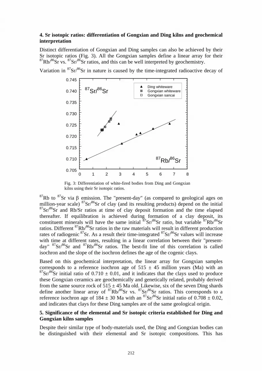
212
4. Sr isotopic ratios: differentiation of Gongxian and Ding kilns and geochemical interpretation Distinct differentiation of Gongxian and Ding samples can also be achieved by their Sr isotopic ratios (Fig. 3). All the Gongxian samples define a linear array for their
87Rb/86Sr vs. 87Sr/86Sr ratios, and this can be well interpreted by geochemistry.
Variation in 87Sr/86Sr in nature is caused by the time-integrated radioactive decay of
87Rb to 87Sr via β emission. The "present-day" (as compared to geological ages on million-year scale) 87Sr/86Sr of clay (and its resulting products) depend on the initial 87Sr/86Sr and Rb/Sr ratios at time of clay deposit formation and the time elapsed thereafter. If equilibration is achieved during formation of a clay deposit, its constituent minerals will have the same initial 87Sr/86Sr ratio, but variable 87Rb/86Sr ratios. Different 87Rb/86Sr ratios in the raw materials will result in different production rates of radiogenic 87Sr. As a result their time-integrated 87Sr/86Sr values will increase with time at different rates, resulting in a linear correlation between their "present-day" 87Sr/86Sr and 87Rb/86Sr ratios. The best-fit line of this correlation is called isochron and the slope of the isochron defines the age of the cogenic clays.
Based on this geochemical interpretation, the linear array for Gongxian samples corresponds to a reference isochron age of 515 ± 45 million years (Ma) with an 87Sr/86Sr initial ratio of 0.710 ± 0.01, and it indicates that the clays used to produce these Gongxian ceramics are geochemically and genetically related, probably derived from the same source rock of 515 ± 45 Ma old. Likewise, six of the seven Ding shards define another linear array of 87Rb/86Sr vs. 87Sr/86Sr ratios. This corresponds to a reference isochron age of 184 ± 30 Ma with an 87Sr/86Sr initial ratio of 0.708 ± 0.02, and indicates that clays for these Ding samples are of the same geological origin.
5. Significance of the elemental and Sr isotopic criteria established for Ding and Gongxian kilns samples Despite their similar type of body-materials used, the Ding and Gongxian bodies can be distinguished with their elemental and Sr isotopic compositions. This has
0.705
0.710
0.715
0.720
0.725
0.730
0.735
0.740
0.745
0 1 2 3 4 5 6 7 8
Ding whitewareGongxian whitewareGongxian sancai
87Sr/86Sr
87Rb/86Sr
Fig. 3: Differentiation of white-fired bodies from Ding and Gongxian kilns using their Sr isotopic ratios.

213
significant implications for archaeologists, because they can serve as valuable criteria to identify whether relevant unearthed wares had been made in these kilns.
In addition, Chinese antique porcelain also enjoys great public interest and economic values. For example, in August 2007 a pair of Chinese vases found during a house clearance in UK were originally valued at only £300, but eventually got auctioned for £ 760,000 (plus 15% buyer's premium) after it became clear it must be antique from the Qing dynasty (1644-1911 AD) instead of a modern copy. This clearly demonstrates the significance of unequivocal authentication of Chinese antique porcelains. However, driven by a huge profit, modern forgers are sparing no means to improve their reproduction. Therefore modern fakes are becoming increasingly difficult to distinguish from original antiques by sight alone. In view of this, the elements and Sr isotopes analysed here can also help with scientific authentication of antiques.
Acknowledgments This work was supported by an ARC discovery grant (DP0452443). This manuscript was written while Baoping Li is holding another ARC discovery grant (DP0772417).
References [1] R. Kerr and N. Wood (2004). Science and Civilisation in China: Volume 5,
Chemistry and Chemical Technology, Part 12, Ceramic Technology: Cambridge University Press.
[2] B.P. Li, J.X. Zhao, K.D. Collerson, A. Greig, Application of ICP-MS trace element analysis in study of ancient Chinese ceramics, Chinese Science Bulletin 48 (2003): 1219-1224.
[3] B.P. Li, J.X. Zhao, A. Greig, K.D. Collerson, Z.X. Zhuo, Y.X. Feng, Potential of Sr isotopic analysis in ceramic provenance studies, Nuclear Instruments & Methods in Physics Research Section B- Beam Interactions with Materials and Atoms 240 (3) (2005): 726-732

214
In-Situ study of the self-recovery property in aluminium titanate Jim Low and Zeya Oo
Centre for Materials Research, Department of Applied Physics, Curtin University of Technology, GPO Box U1987, WA 6845 Australia
Email: [email protected]
Abstract Aluminium titanate (Al2TiO5) is an excellent refractory and thermal shock resistant material due to its relatively low thermal expansion coefficient and high melting point. However, Al2TiO5is only thermodynamically stable above 1280°C and undergoes a eutectoid-like decomposition to α- Al2TiO3 and TiO2 (rutile) at the temperature range of 900-1280°C. In this paper, we describe the use of high-temperature neutron diffraction to study the properties of self-recovery in Al2TiO5 when it is annealed at ≥1300°C in air. It is shown that the process of decomposition in Al2TiO5 is reversible and that self-recovery occurs readily when decomposed Al2TiO5 is re-heated above 1300°C. It is further shown that the existence of a temperature range (900 – 1280°C) in which Al2TiO5 is pruned to decomposition can be explained by the competition between the rates of decomposition and self-recovery.
Carbon cluster output from SNICS: Impact angle dependence Anwaar Malik *, Laura G. Gladkis *,**, Heiko Timmers *
School of Physical, Environmental and Mathematical Sciences, University of New South Wales at the Australian Defence Force Academy, Canberra, ACT 2600, Australia
** Trauma and Orthopaedic Research Unit, The Canberra Hospital, PO BOX 11, Woden, ACT 2606, Australia
Cluster ion beams are of interest in materials applications due to the high energy loss rates of cluster ions and their increased sputter efficacy, when compared to monomers. It has been suggested that the cluster output from SNICS ion sources increases significantly for more shallow Cs+ sputtering angles. Since SNICS sources are versatile and commonly used for the ion beam modification of materials, such an increase in output would advantageous, if established. Measurements for carbon cluster ions are presented in comparison with studies by other groups. Preliminary results suggest a complex dependence on sputtering angle.
215
Examining Manganese Dioxide as a cathode in aqueous LiOH battery
Manickam Minakshi 1 and Kathryn Prince 2 1 Department of Extractive Metallurgy, Murdoch University, Murdoch 6150, WA, Australia
2 Institute for Environmental Research, ANSTO, Menai 2234, NSW, Australia
[email protected], [email protected]
Abstract Manganese dioxide has been extensively studied as a cathode for commercial primary and secondary lithium battery. Intercalation of Li+ ions into host MnO2 structure is widely known in non-aqueous electrolytes. If this mechanism is possible in aqueous media the MnO2 cathode could become rechargeable similar to non-aqueous Li-MnO2 batteries. Hence, it could open up a new field of rechargeable alkaline batteries that use MnO2 as the cathode active material. In this regard, various physical techniques like scanning electron microscopy (SEM), x-ray photoelectron spectroscopy (XPS), secondary ion mass spectrometry (SIMS) and transmission electron microscopy (TEM) have been used to characterize the discharged cathode employing manganese dioxide, the active material used in a battery with lithium hydroxide as electrolyte. The results suggest that electrode reaction of MnO2 in this electrolyte is shown to be lithium insertion (Li+) rather than the usual protonation (H+). Evidence is also presented to support the rechargeability of this battery, rather than non-rechargeable, which is apparent in the literature while using potassium hydroxide as the electrolyte.
Keywords: Manganese dioxide, Aqueous battery, LiOH electrolyte, Lithium insertion, Rechargeability.
Introduction Primary alkaline Zinc-Manganese dioxide dominates the primary battery market. These batteries are based on the electrochemical insertion of protons into γ-MnO2 during the discharge process [1]. The properties of γ-MnO2 in relation to its use in these batteries have been studied extensively. Giovanali [2] described γ-MnO2 as an intergrowth structure between ramsdellite and pyrolusite, which are both members of the nsutite group. The basic unit cells are [MnO6]-octahedra joined to form alternating single-and double chains. Other forms of γ-MnO2 have also been looked at, Ruetschi et al [3] have summarized the types of MnO2 materials which are considered to be important for batteries, among these electrolytically produced manganese dioxide (EMD) is widely used commercially.
In traditional alkaline batteries using KOH as the electrolyte the electro reduction of the cathode material MnO2 during discharge involves insertion of protons [1] into the ionic lattice of the manganese dioxide according to the following equations
MnO2 + H+ + e- → MnOOH [1]
MnOOH + H+ + e- mixture of [(Mn2O3 or Mn3O4) + Mn(OH)2] [2]
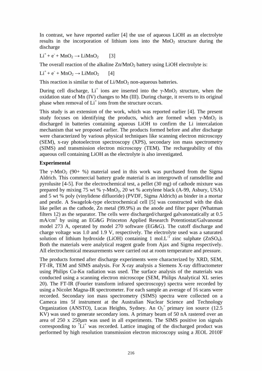
216
In contrast, we have reported earlier [4] the use of aqueous LiOH as an electrolyte results in the incorporation of lithium ions into the MnO2 structure during the discharge
Li+ + e- + MnO2 → LiMnO2 [3]
The overall reaction of the alkaline Zn/MnO2 battery using LiOH electrolyte is:
Li+ + e- + MnO2 → LiMnO2 [4]
This reaction is similar to that of Li/MnO2 non-aqueous batteries.
During cell discharge, Li+ ions are inserted into the γ-MnO2 structure, when the oxidation state of Mn (IV) changes to Mn (III). During charge, it reverts to its original phase when removal of Li+ ions from the structure occurs.
This study is an extension of the work, which was reported earlier [4]. The present study focuses on identifying the products, which are formed when γ-MnO2 is discharged in batteries containing aqueous LiOH to confirm the Li intercalation mechanism that we proposed earlier. The products formed before and after discharge were characterized by various physical techniques like scanning electron microscopy (SEM), x-ray photoelectron spectroscopy (XPS), secondary ion mass spectrometry (SIMS) and transmission electron microscopy (TEM). The rechargeability of this aqueous cell containing LiOH as the electrolyte is also investigated.
Experimental The γ-MnO2 (90+ %) material used in this work was purchased from the Sigma Aldrich. This commercial battery grade material is an intergrowth of ramsdellite and pyrolusite [4-5]. For the electrochemical test, a pellet (30 mg) of cathode mixture was prepared by mixing 75 wt % γ-MnO2, 20 wt % acetylene black (A-99, Asbury, USA) and 5 wt % poly (vinylidene difluoride) (PVDF, Sigma Aldrich) as binder in a mortar and pestle. A Swagelok-type electrochemical cell [5] was constructed with the disk like pellet as the cathode, Zn metal (99.9%) as the anode and filter paper (Whatman filters 12) as the separator. The cells were discharged/charged galvanostatically at 0.5 mA/cm2 by using an EG&G Princeton Applied Research Potentiostat/Galvanostat model 273 A, operated by model 270 software (EG&G). The cutoff discharge and charge voltage was 1.0 and 1.9 V, respectively. The electrolyte used was a saturated solution of lithium hydroxide (LiOH) containing 1 mol.L-1 zinc sulphate (ZnSO4). Both the materials were analytical reagent grade from Ajax and Sigma respectively. All electrochemical measurements were carried out at room temperature and pressure.
The products formed after discharge experiments were characterized by XRD, SEM, FT-IR, TEM and SIMS analysis. For X-ray analysis a Siemens X-ray diffractometer using Philips Cu-Kα radiation was used. The surface analysis of the materials was conducted using a scanning electron microscope (SEM, Philips Analytical XL series 20). The FT-IR (Fourier transform infrared spectroscopy) spectra were recorded by using a Nicolet Magna-IR spectrometer. For each sample an average of 16 scans were recorded. Secondary ion mass spectrometry (SIMS) spectra were collected on a Cameca ims 5f instrument at the Australian Nuclear Science and Technology Organization (ANSTO), Lucas Heights, Sydney. An O2
+ primary ion source (12.5 KV) was used to generate secondary ions. A primary beam of 50 nA rastered over an area of 250 x 250µm was used in all experiments. The SIMS positive ion signals corresponding to 7Li+ was recorded. Lattice imaging of the discharged product was performed by high resolution transmission electron microscopy using a JEOL 2010F

217
transmission electron microscope (TEM) operated at 200keV. TEM specimens were prepared by grinding a small fragment scraped from the pressed pellet under methanol and dispersing onto a holey carbon film.
Results and Discussion
(a) Performance characteristics of Zn|γ-MnO2 type aqueous LiOH Cell Figure 1 shows the discharge/charge characteristics of the Zn|γ-MnO2|aqueous lithium hydroxide cell. The cell was discharged and charged galvanostatically (0.5 mA/cm2) to 1.0 and 1.9 V respectively. On commencement of discharge, the voltage dropped from the open-circuit voltage (OCV) 1.85 V to 1.7 V and then gradually decreased to 1.4 V. The discharge was terminated when the voltage suddenly fell to 1.0 V. The 1.6 V region could correspond to the Mn4+/3+ redox couple. The practically realizable capacity of the material is found to be 140 mAh/g. During the charge process, from 1.3 V there was a constant increase in potential up to the charge cut-off voltage of 1.8 V. As can be seen in Fig. 1, the cell could be reversibly discharged and charged. The reversibility of the cell was also investigated and the results are shown in Fig. 2. The MnO2 cathode could deliver a reversible capacity of about 135 mAh/g and 115 mAh/g for the 2nd and 7th cycles respectively. After few cycles the loss in capacity stabilized. A discharge capacity of 70 mAh/g was achieved at the 40th cycle. The columbic efficiency of this cell showed that (not shown here) the efficiency dropped rapidly during the first 20 cycles from 82 % to 56 % after which the decrease was gradual. At the 40th cycle the efficiency was 45 %.
0 25 50 75 100 125 1501.0
1.2
1.4
1.6
1.8
2.0
Cel
l vol
tage
/ V
Discharge Capacity / mAh.g-1
Discharge
Charge
Fig. 1 The first discharge-charge behaviour of a Zn| γ-MnO2 cell using saturated aqueous LiOH containing 1mol.l-1 of ZnSO4 as the electrolyte.

218
0 25 50 75 100 125 1500.0
0.5
1.0
1.5
2.0
Volta
ge /
V
Discharge capacity / mAh.g-1
1272540 20
Fig. 2 Discharge curves for various cycles illustrating the cyclability of γ-MnO2 samples. Cycle numbers are indicated in the figure.
(b) Physical characterization of the cathode after discharge
In order to determine the product formed on discharge of the cathode material in the Zn| γ-MnO2 aqueous LiOH electrolyte cell, the surface characterization of the discharged material was investigated by SEM, TEM, XPS and SIMS analysis. The surface morphology change that occurred at the cathode during the discharge process is shown in Fig. 3. The particle size of the cathode material before discharge was of the order 5-10 µm. The material formed after the discharge had a different morphology (Fig. 3b). The MnO2 grains lying underneath appeared to be covered by some foreign material. The TEM analysis (Fig. 4a) of the ground MnO2 material before discharge was quite fine with particle sizes ranging from 1µm down to 50nm. Bright field imaging (Fig. 4b) of the discharged manganese dioxide ground powder showed it to be similar in appearance and particle size range to the MnO2. Thus the morphology obtained from TEM doesn’t tell much information of the discharged product.
(a) (b) Fig. 3 SEM images of the γ-MnO2 (a) before and (b) after discharge.
Therefore, to confirm the nature of the discharged product the discharged MnO2 was subjected to XPS and SIMS investigations. The XPS spectra (Fig. 5) show that the surface of the discharged cathode was covered with a layer of materials (like LiOH,
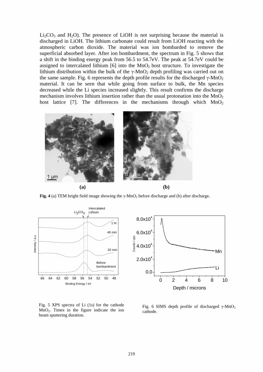
219
Li2CO3 and H2O). The presence of LiOH is not surprising because the material is discharged in LiOH. The lithium carbonate could result from LiOH reacting with the atmospheric carbon dioxide. The material was ion bombarded to remove the superficial absorbed layer. After ion bombardment, the spectrum in Fig. 5 shows that a shift in the binding energy peak from 56.5 to 54.7eV. The peak at 54.7eV could be assigned to intercalated lithium [6] into the MnO2 host structure. To investigate the lithium distribution within the bulk of the γ-MnO2 depth profiling was carried out on the same sample. Fig. 6 represents the depth profile results for the discharged γ-MnO2 material. It can be seen that while going from surface to bulk, the Mn species decreased while the Li species increased slightly. This result confirms the discharge mechanism involves lithium insertion rather than the usual protonation into the MnO2 host lattice [7]. The differences in the mechanisms through which MnO2
(a) (b)
Fig. 4 (a) TEM bright field image showing the γ-MnO2 before discharge and (b) after discharge.
0 2 4 6 8 10
0.0
2.0x10⁴
4.0x10⁴
6.0x10⁴
8.0x10⁴
Cou
nts
/ cps
Depth / microns
Li
Mn
66 64 62 60 58 56 54 52 50 48
1 hr
40 min
20 min
Before bombardment
Intercalated LithiumLi2CO3
Inte
nsity
/ a.
u.
Binding Energy / eV
Fig. 5 XPS spectra of Li (1s) for the cathode MnO2. Times in the figure indicate the ion beam sputtering duration.
Fig. 6 SIMS depth profile of discharged γ-MnO2cathode.
220
A+ cation sit e R P
undergoes discharge/charge in aqueous LiOH and aqueous KOH [5] can occur be explained in terms of relative ionic sizes of Li+ and K+ ions. Li+ ions, being comparable in size to Mn4+, are intercalated into the octahedral structure of MnO2 while that is not possible for the larger K+ ion. As illustrated in the figure 7, the γ -MnO2 is an inter growth of ramsdellite (R) and pyrolusite (P). The Mn(IV)O6 octahedra of ramsdellite are linked into double chains, each of which consists of two adjacent single chains that share octahedral edges [8] These double chains having
tunnels with rectangular-shaped cross sections accept the A+ (A = Li) cation, which is approximately the same size as that of Mn, the columbic interactions dominate and hence the structure is stable for insertion/extraction of lithium ions. However, the size of the K+ ion is twice as that of Li+, therefore the insertion site in Fig. 7 is not stable as the electrostatic energy of the structure is diminished. Hence, unlike for Li+ the intercalation of K+ is not possible in the γ –MnO2 structure.
Conclusions The zinc/γ-manganese dioxide aqueous alkaline cell containing lithium hydroxide electrolyte undergoes a lithium intercalation into the host framework structure of the cathode material (γ-MnO2) during discharge. The cell can be reversibly discharged and charged. This is confirmed by the analysis of the products formed on the discharged MnO2 cathode by using SEM, XPS and SIMS techniques. The columbic and the voltaic efficiencies decrease on repeated discharge/charge cycles. At the first cycle the columbic efficiency was 82 % which dropped to 45 % at the 40th cycle. At the same time, the voltaic efficiency dropped from 87 % for the first cycle to 70 % for the 40th cycle at 0.5 mA/cm2 current density. The lithium ions being comparable in size of Mn4+ could be intercalated into the octahedral structure of γ-MnO2.
(a)
(b)
(c)
Fig.7 Schematic diagram of the (a) P: pyrolusite (b) R: ramsdellite and (c) γ-MnO2, an inter growth between ramsdellite (R), and pyrolusite (P), shown in (001) plane.
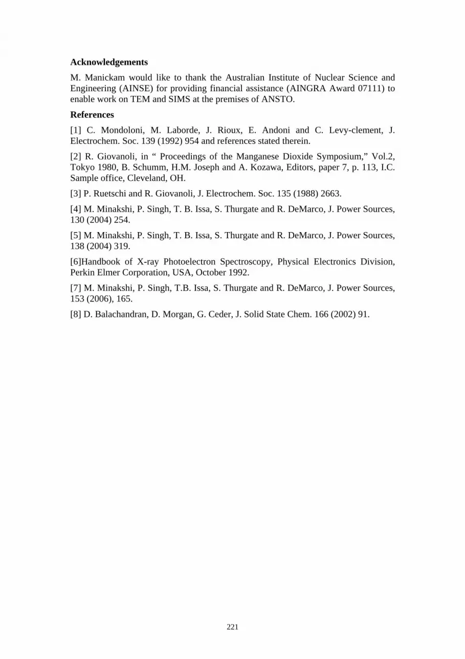
221
Acknowledgements M. Manickam would like to thank the Australian Institute of Nuclear Science and Engineering (AINSE) for providing financial assistance (AINGRA Award 07111) to enable work on TEM and SIMS at the premises of ANSTO.
References [1] C. Mondoloni, M. Laborde, J. Rioux, E. Andoni and C. Levy-clement, J. Electrochem. Soc. 139 (1992) 954 and references stated therein.
[2] R. Giovanoli, in “ Proceedings of the Manganese Dioxide Symposium,” Vol.2, Tokyo 1980, B. Schumm, H.M. Joseph and A. Kozawa, Editors, paper 7, p. 113, I.C. Sample office, Cleveland, OH.
[3] P. Ruetschi and R. Giovanoli, J. Electrochem. Soc. 135 (1988) 2663.
[4] M. Minakshi, P. Singh, T. B. Issa, S. Thurgate and R. DeMarco, J. Power Sources, 130 (2004) 254.
[5] M. Minakshi, P. Singh, T. B. Issa, S. Thurgate and R. DeMarco, J. Power Sources, 138 (2004) 319.
[6]Handbook of X-ray Photoelectron Spectroscopy, Physical Electronics Division, Perkin Elmer Corporation, USA, October 1992.
[7] M. Minakshi, P. Singh, T.B. Issa, S. Thurgate and R. DeMarco, J. Power Sources, 153 (2006), 165.
[8] D. Balachandran, D. Morgan, G. Ceder, J. Solid State Chem. 166 (2002) 91.
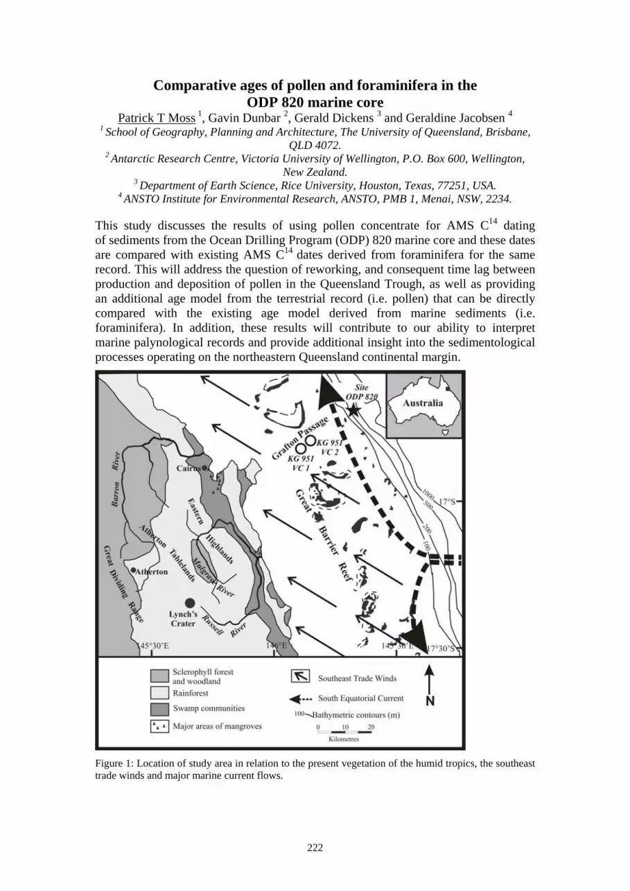
222
Comparative ages of pollen and foraminifera in the ODP 820 marine core
Patrick T Moss 1, Gavin Dunbar 2, Gerald Dickens 3 and Geraldine Jacobsen 4 1 School of Geography, Planning and Architecture, The University of Queensland, Brisbane,
QLD 4072. 2 Antarctic Research Centre, Victoria University of Wellington, P.O. Box 600, Wellington,
New Zealand. 3 Department of Earth Science, Rice University, Houston, Texas, 77251, USA.
4 ANSTO Institute for Environmental Research, ANSTO, PMB 1, Menai, NSW, 2234.
This study discusses the results of using pollen concentrate for AMS C14 dating of sediments from the Ocean Drilling Program (ODP) 820 marine core and these dates are compared with existing AMS C14 dates derived from foraminifera for the same record. This will address the question of reworking, and consequent time lag between production and deposition of pollen in the Queensland Trough, as well as providing an additional age model from the terrestrial record (i.e. pollen) that can be directly compared with the existing age model derived from marine sediments (i.e. foraminifera). In addition, these results will contribute to our ability to interpret marine palynological records and provide additional insight into the sedimentological processes operating on the northeastern Queensland continental margin.
Figure 1: Location of study area in relation to the present vegetation of the humid tropics, the southeast trade winds and major marine current flows.

223
Pollen records recovered from marine sediments offer the possibility of greatly extending knowledge of continental vegetation change and directly comparing these terrestrial alterations with marine environmental evidence, in particular oxygen isotope data. One such record is from ODP site 820 (16°38′S, 146°18′E, water depth - 280 m), which is situated seaward of the Great Barrier Reef on the continental slope, about 40 km from the coast and about 100 km from Lynch’s Crater (Fig. 1.). This record was collected to examine the evolution and development of the Queensland plateau and investigate the formation of the Great Barrier Reef (Davies and McKenzie, 1993). The entire 400-m length of ODP site 820 is thought to cover the last 1.4 million years (Peerdeman et al., 1993). In addition, high pollen yields have been obtained from the ODP 820 sediments, which provide insight into late Quaternary terrestrial environments (Moss and Kershaw, 2000; 2007). The pollen and charcoal catchment of the ODP site 820 record, covering an altitudinal range from sea level to about 1600 m, includes areas now supporting lowland to montane rainforest (which occupies areas receiving about 1500mm to in excess of 4000mm of mean annual rainfall), sclerophyll vegetation (which dominates the landscape under mean annual rainfall levels of less than 1500mm), small patches of araucarian forest (occurs in areas receiving around 1500mm), coastal swamps (on poorly drained soils) and mangrove areas (mainly around Trinity and Mutchero Inlets) (Tracey 1982). Major components of pollen and charcoal are mainly derived from both the Russell/Mulgrave and Barron rivers systems (Kershaw, 1994; Moss et al., 2005). Both of these river systems drain a substantial part of the region.
Top (m)
Bottom (m) ANSTO#
Age (14C years) Error
This study
P+D 1993 P+D 1993
Difference (yrs) (foram-pollen)
Cal BP 14C BP Cal BP*
2.43 2.48 OZJ311 5620 70 6380 4944 5269 1111
3.25 3.27 OZJ312 7350 80 8120 6304 6750 1370
3.65 3.67 OZJ313 7970 110 8860 6968 7485 1375
3.93 3.98 OZJ314 8140 80 9070 7396 7852 1218
4.25 4.27 OZJ315 8180 70 9090 7475 7927 1163
5.64 5.68 OZJ316 8570 70 9520 8954 9544 -24
6.05 6.07 OZJ317 9320 80 10510 9365 10162 348
6.93 6.98 Lost 14780 16969 -
7.2 7.27 OZJ319 15740 120 18950 31000 35991 -17041
7.4 7.47 OZJ320 18360 160 21860 41200 45451 -23591
7.9 7.97 No sample 43600 47526 25666
Table 1: Comparison between pollen concentrate and foram ages (AMS C14). calibrations. Foraminfera: A reservoir correction of 375 years was subtracted from the reported age and the marine calibration of Fairbanks, et al., 2005 and the online calculator at http://www.radiocarbon.ldeo.columbia.edu/. *P+D = Peerdeman and Davies, 1993.
224
Previous palynological studies based on the ODP 820 marine core and the nearby Lynch’s Crater record in North Queensland show there are important differences in pollen assemblage and timing of events between these two sites. This difference was, in part, attributed to the long, water-borne transport pathway between the primary source region for pollen and final depositional environment (Moss et al., 2005; Moss and Kershaw, 2007; Fig. 1). Therefore, we expect to find pollen ages similar to, or older than, foraminifera ages from the same core depth (as foraminifera have life spans of ~months and settle rapidly to the seabed after death), with the magnitude of the age difference being dependent on a number of factors, including sea level and fluvial discharge rates. If production and transport of pollen and foraminifera are the only mechanisms controlling the relative ages of each in the ODP 820 core, pollen can not be younger than foraminifera recovered from the same core depth. Table 1 shows that the Holocene ages for both the foraminifera and pollen are consistent with this theory. However, the Last Glacial Maximum (LGM)/Marine Isotope Stage (MIS) 3 ages are not, with the pollen ages being significantly younger than the foraminifera ages. Importantly, the age discrepancy is most pronounced during what has previously been interpreted as the period from MIS 4 through to MIS2. However, dating this interval at ODP site 820 has proved difficult due to ambiguities in oxygen isotope and biostratigraphic datum as well as large, abrupt, changes in sedimentation rate and composition (e.g. Peerdeman et al., 1993; Peerdeman and Davies 1993). Evidence of a significant vegetation change (decline in araucarian taxa, increase in myrtaceous taxa) occurred in the ODP record at 15 m and suggests that the terrestrial sediments in the ODP 820 record are providing a continuous record through the Late Pleistocene period, as this alteration is very similar to one seen in the Lynch’s Crater record and has been dated to around 45,000 years BP (Turney et al. 2001). These results suggest that there is some unreliability associated with the initial foraminifera AMS C14 dates and there have been some reports that the foraminifera in the ODP 820 record may have undergone some diagenesis, which may have impacted the reliability of the foraminifera ages around 7 to 8 mbsf (metres below sea floor) (Peerdeman, 1993; Lawrence and Herbert, 2005). However, the generation of good age control through AMS C14 dating of the pollen concentrate provides the potential to extend radiocarbon dating through the deeper ODP 820 sediments and resolve uncertainty in the age model. This in turn will greatly improve our understanding of environmental change in the humid tropics region during a period of time that also likely included the arrival of people in North Queensland (e.g. David, 1993, Kershaw, 1994, Moss and Kershaw, 2000).
Acknowledgements
We would like to thank the support of the Integrated Ocean Drilling Program (IODP) for suppling samples. ANSTO dated the pollen concentrate samples through an AINSE Grant to P.T. Moss, G Dunbar & G. Dickens (# 06-129).
References David, B., 1993. Ngarrabullgan cave: preliminary results from a pre-37,000 year old rockshelter, North Queensland, Arch. Oceania 28, 50-54.
Davies, P.J., McKenzie, J.A., 1993. Controls on the Pliocene-Pleistocene evolution of the northeastern Australian continental margin. Proc. ODP, Sci. Results 133, 755-762.
Fairbanks, R.G., Mortlock, R.A., Cao, L., Kaplan, A., Guilderson, T.P., Fairbanks, T.W., Bloom, A.L., Grootes, P.M., Nadeau, M-J. 2005. Radiocarbon calibration curve

225
spanning 0 to 50,000 years BP based on paired 230Th/234U/238U and 14C dates on pristine corals. Quat. Sci. Rev. 16-17. 1781-1796.
Kershaw, A.P., 1994. Pleistocene vegetation of the humid tropics of northeastern Queensland, Australia. Palaeogeogr., Palaeoclimatol., Palaeoecol. 109, 399-412.
Lawrence, K.T., Herbert, T.D., 2005. Late Quaternary sea-surface temperatures in the western Coral Sea: Implications for the growth of the Australian Great Barrier Reef. Geology 33, 677-680.
Moss, P.T., Kershaw, A.P., 2000. The last glacial cycle from the humid tropics of northeastern Australia: comparison of a terrestrial and marine record. Palaeogeogr., Palaeoclimatol., Palaeoecol. 155, 155-176.
Moss, P.T., Kershaw, A.P., Grindrod, J., 2005. Pollen transport and deposition in riverine and marine environments within the humid tropics of northeastern Australia. Rev. of Pal. Pal 134, 55-69.
Moss, P.T., Kershaw, A.P., 2007. A late Quaternary marine palynological record (oxygen isotope stages 1 to 7) for the humid tropics of northeastern Australia based on ODP Site 820. Palaeogeogr., Palaeoclimatol., Palaeoecol. 251, 4-22.
Peerdeman, F.M., 1993. The Pleistocene climatic and sea-level signature of the northeastern Australian continental margin., unpublished PhD thesis, Australian National University, Canberra, Australia.
Peerdeman, F.M., Davies, P.J., 1993. Sedimentological response to an outer-shelf, upper-slope sequence to rapid changes in Pleistocene eustatic sea level: Hole 820A, northeastern Australian Margin. Proc. ODP Sci. Results 133, 303-313.
Peerdemann, F.M., Davies, P.J., Chivas, A.R., 1993. The stable oxygen isotope signal in shallow-water, upper-slope sediments off the Great Barrier Reef (Hole 820A). Proc. ODP Sci. Results 133, 163-173.
Tracey, J.G., 1982. The vegetation of the humid tropical region of north Queensland. CSIRO, Melbourne, Australia.
Turney, C.S.M, Kershaw, A.P., Moss, P., Bird, M.I., Fifield, L.K., Cresswell, R.G., Santos, G.M., Di Tada, M.L., Hausladen, P.A., Youping, Z., 2001. Redating the onset of burning at Lynch’s Crater (North Queensland): implications for human settlement in Australia. J. Quat. Sci. 16, 767-771.
226
Application of radioisotopes for nanotoxicological studies Anthony Musumeci 1,2, Suzanne Smith 3, Gordon Xu 1,2 and Darren Martin 1,2
1.. Australian Institute of Bioengineering and Nanotechnology, The University of Queensland, Brisbane QLD 4072, Australia.
2. ARC Centre of Excellence for Functional Nanomaterials, School of Engineering, The University of Queensland, Brisbane QLD 4072, Australia.
3. Centre of Excellence for Antimatter-Matter Studies, Australian Nuclear Science and Technology Organisation, Menai, NSW 2234, Australia.
Introduction The impact of nanotechnology on a broad range of industry sectors continues to grow at an unprecedented rate, with the National Science Foundation expecting nanotechnology to play a part in a trillion dollar industry by 2015. The potential benefits of nanotechnology for industries from new advanced materials, to biotechnology, quantum computing, energy and the environment, and the community in general, has been highlighted in numerous publications [1-3]. Unfortunately, these new nanomaterials, nanoparticles and nanotechnologies are appearing faster than our capacity to fully-evaluate their potential impact on health, the environment and safety.
Consequently, the sustainability of this industry may be dependent on understanding and managing the unwanted effects that nanoparticles and nanostructured materials may have on the environment and human health, both in the short term and long term.
Nanoparticles have been present in the environment throughout evolution. However, many of the novel engineered structures that are being developed for industry use have unique structures, shapes, functionality and chemical compositions. It is now established that particles of the same chemical composition but of different size and shape can have markedly different biological responses [4]. Many of the traditional approaches used to assess particle toxicology do not apply to nanoscale particles because of their unique interactions with cells and tissues [5]. Moreover, significant challenges arise in detecting and monitoring very small particles in the environment.
Radiolabelling of nanoparticles is one such technique that has the ability to offer high sensitivity and the incorporation of only nano to pico molar concentrations of radiotracer probes for non-invasive imaging by single photon emission computed tomography or positron emission tomography. Such radiotracer techniques are also inherently rapid and are not affected by strong media or electrolyte solutions. Radiotracer probes also offer a range in half-life (from hours to days) and emission profile (gamma and/or positron emitting) depending on the length of in vivo or in vitro study desired. Finally, detection of the radiotracer can be achieved with minimal handling which provides for greater accuracy.
A number of recent studies have provided a growing indication that nanoparticles can exert adverse effects upon biological systems [2, 3, 6]. Despite these disturbing findings, none of these studies report a complete and extensive characterisation of the nanoparticles in question which are instrumental to understanding the systemic biological and physicochemical characteristics observed.
Thus, what is missing in scientific literature is a study of the toxicology of well characterised nanoparticles. Currently, the absence of such robust, quality safety assessments for new technologies are already beginning to produce a negative consumer reaction that could result in adverse outcomes for the whole of the industry
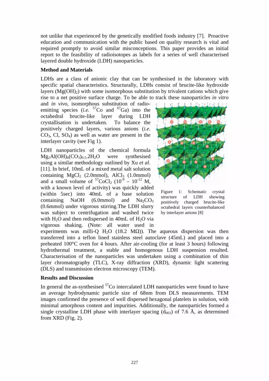
227
not unlike that experienced by the genetically modified foods industry [7]. Proactive education and communication with the public based on quality research is vital and required promptly to avoid similar misconceptions. This paper provides an initial report to the feasibility of radioisotopes as labels for a series of well characterised layered double hydroxide (LDH) nanoparticles.
Method and Materials LDHs are a class of anionic clay that can be synthesised in the laboratory with specific spatial characteristics. Structurally, LDHs consist of brucite-like hydroxide layers (Mg(OH)2) with some isomorphous substitution by trivalent cations which give rise to a net positive surface charge. To be able to track these nanoparticles in vitro and in vivo, isomorphous substitution of radio-emitting species (i.e. 57Co and 67Ga) into the octahedral brucite-like layer during LDH crystallisation is undertaken. To balance the positively charged layers, various anions (i.e. CO3, Cl, SO4) as well as water are present in the interlayer cavity (see Fig 1).
LDH nanoparticles of the chemical formula Mg2Al(OH)6(CO3)0.5.2H2O were synthesised using a similar methodology outlined by Xu et al. [11]. In brief, 10mL of a mixed metal salt solution containing MgCl2 (2.0mmol), AlCl3 (1.0mmol) and a small volume of 57CoCl2 (10-9 – 10-12 M, with a known level of activity) was quickly added (within 5sec) into 40mL of a base solution containing NaOH (6.0mmol) and Na2CO3 (0.6mmol) under vigorous stirring.The LDH slurry was subject to centrifugation and washed twice with H2O and then redispersed in 40mL of H2O via vigorous shaking. (Note: all water used in experiments was milli-Q H2O (18.2 MΩ)). The aqueous dispersion was then transferred into a teflon lined stainless steel autoclave (45mL) and placed into a preheated 100°C oven for 4 hours. After air-cooling (for at least 3 hours) following hydrothermal treatment, a stable and homogenous LDH suspension resulted. Characterisation of the nanoparticles was undertaken using a combination of thin layer chromatography (TLC), X-ray diffraction (XRD), dynamic light scattering (DLS) and transmission electron microscopy (TEM).
Results and Discussion In general the as-synthesised 57Co intercalated LDH nanoparticles were found to have an average hydrodynamic particle size of 68nm from DLS measurements. TEM images confirmed the presence of well dispersed hexagonal platelets in solution, with minimal amorphous content and impurities. Additionally, the nanoparticles formed a single crystalline LDH phase with interlayer spacing (d003) of 7.6 Å, as determined from XRD (Fig. 2).
Figure 1: Schematic crystal structure of LDH showing positively charged brucite-like octahedral layers counterbalanced by interlayer anions [8]