db2000 service manual - altehandys.de
TRANSCRIPT
DB2000
Service Manual
IntroductionThis is the Electronic Service Manual for the MP5J1L1 Dual Band GSM DigitalCellular Telephone from NEC. It contains specific information on repair andtest procedures.For details on user functions, general operation and installation, please referto the User Guide.
The Service Manual is set out in the following sections.
1. Precautions for Repair Work provides general guidelines forundertaking safe and efficient repair work.
2. Unit Specification provides the technical specifications for theMP5J1L1 GSM Digital Cellular Telephone.
3. Circuit Description provides functional details of the circuits, blockdiagrams and component purpose descriptions.
4. Servicing defines the jigs, fixtures and test configurations required forservicing the product; and describes the processes of assembly anddisassembly.
5. Troubleshooting provides an aid to fault finding the product. Includes;using the engineering functions, signal levels and plots at various partsof the circuit and fault codes.
6. Device Information provides functional information and pin-outs ofmost of the semiconductor devices within the HHP.
7. Parts provides information for the ordering of replacement parts.
8. Circuit Diagrams and Board Maps contains all the schematics andcomponent layout diagrams.
9. Glossary, , terms used in this manual.

Important
!"#$%"$&
!''
' !'
(
) *
+
,
-#"
' . !
One incorrect adjustment may result in the need for many more and result in extra
).
( #*
• )/0
•
• ! 1
• +'2*
2
'
!
'
2
#+3#+4
2
22*
$2#+
20
0
* 0
5
#* !3 4
2 #
' 6
! 2
$7'+2 2
22*
" '
! 0
#'89 :+2+
* * 2
" " #*
% .
* 2 2
' 22
2 2
+
" * *
$ '(
;
<'(* 2
! .* 0
.
$.
2 2#
* 32
'(462
=
'
' 2
'(
$#* '
% * "*
*
'
(
'
equipment is heavily soiled a soft cloth dampened with a mild synthetic detergent
2 =*
"
2 3 >4
"
!'!('
$!' #
2
#
#* = !
# 2
<= 6
$2=
2
'
$ * 2
) #'
".
$2". * 2
34
*
'
2
2* 0
*
?
2
=

'(<
2 $
'(
'
• +
• '
<< Previous SectionNext Section >>Main Menu
Section 2
UnitSpecifications
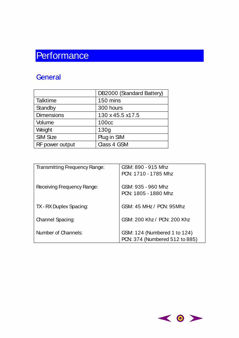
Performance
GeneralGeneral
DB2000 (Standard Battery)Talktime 150 minsStandby 300 hoursDimensions 130 x 45.5 x17.5Volume 100ccWeight 130gSIM Size Plug in SIMRF power output Class 4 GSM
Transmitting Frequency Range:
Receiving Frequency Range:
TX - RX Duplex Spacing:
Channel Spacing:
Number of Channels:
GSM: 890 - 915 MhzPCN: 1710 - 1785 Mhz
GSM: 935 - 960 MhzPCN: 1805 - 1880 Mhz
GSM: 45 MHz / PCN: 95Mhz
GSM: 200 Khz / PCN: 200 Khz
GSM: 124 (Numbered 1 to 124)PCN: 374 (Numbered 512 to 885)
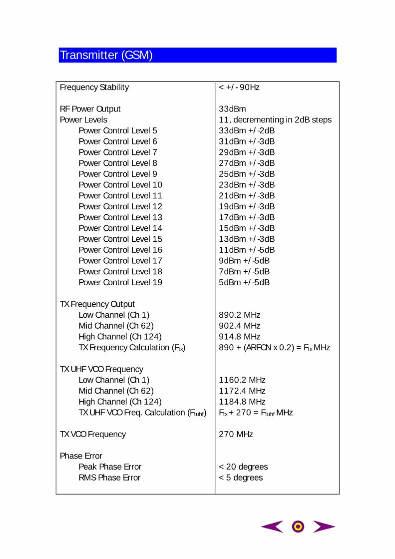
Transmitter (GSM)
Frequency Stability
RF Power OutputPower Levels
Power Control Level 5Power Control Level 6Power Control Level 7Power Control Level 8Power Control Level 9Power Control Level 10Power Control Level 11Power Control Level 12Power Control Level 13Power Control Level 14Power Control Level 15Power Control Level 16Power Control Level 17Power Control Level 18Power Control Level 19
TX Frequency OutputLow Channel (Ch 1)Mid Channel (Ch 62)High Channel (Ch 124)TX Frequency Calculation (Ftx)
TX UHF VCO FrequencyLow Channel (Ch 1)Mid Channel (Ch 62)High Channel (Ch 124)TX UHF VCO Freq. Calculation (Ftuhf)
TX VCO Frequency
Phase ErrorPeak Phase ErrorRMS Phase Error
< +/- 90Hz
33dBm11, decrementing in 2dB steps33dBm +/-2dB31dBm +/-3dB29dBm +/-3dB27dBm +/-3dB25dBm +/-3dB23dBm +/-3dB21dBm +/-3dB19dBm +/-3dB17dBm +/-3dB15dBm +/-3dB13dBm +/-3dB11dBm +/-5dB9dBm +/-5dB7dBm +/-5dB5dBm +/-5dB
890.2 MHz902.4 MHz914.8 MHz890 + (ARFCN x 0.2) = Ftx MHz
1160.2 MHz1172.4 MHz1184.8 MHzFtx + 270 = Ftuhf MHz
270 MHz
< 20 degrees< 5 degrees
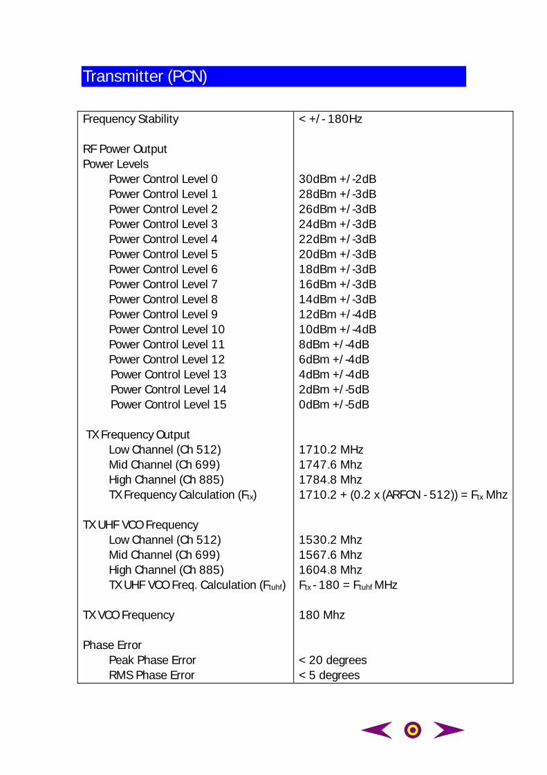
Transmitter (PCN)
Frequency Stability
RF Power OutputPower Levels
Power Control Level 0Power Control Level 1Power Control Level 2Power Control Level 3Power Control Level 4Power Control Level 5Power Control Level 6Power Control Level 7Power Control Level 8Power Control Level 9Power Control Level 10Power Control Level 11Power Control Level 12
Power Control Level 13 Power Control Level 14 Power Control Level 15
TX Frequency OutputLow Channel (Ch 512)Mid Channel (Ch 699)High Channel (Ch 885)TX Frequency Calculation (Ftx)
TX UHF VCO FrequencyLow Channel (Ch 512)Mid Channel (Ch 699)High Channel (Ch 885)TX UHF VCO Freq. Calculation (Ftuhf)
TX VCO Frequency
Phase ErrorPeak Phase ErrorRMS Phase Error
< +/- 180Hz
30dBm +/-2dB28dBm +/-3dB26dBm +/-3dB24dBm +/-3dB22dBm +/-3dB20dBm +/-3dB18dBm +/-3dB16dBm +/-3dB14dBm +/-3dB12dBm +/-4dB10dBm +/-4dB8dBm +/-4dB6dBm +/-4dB4dBm +/-4dB2dBm +/-5dB0dBm +/-5dB
1710.2 MHz1747.6 Mhz1784.8 Mhz1710.2 + (0.2 x (ARFCN - 512)) = Ftx Mhz
1530.2 Mhz1567.6 Mhz1604.8 MhzFtx - 180 = Ftuhf MHz
180 Mhz
< 20 degrees< 5 degrees
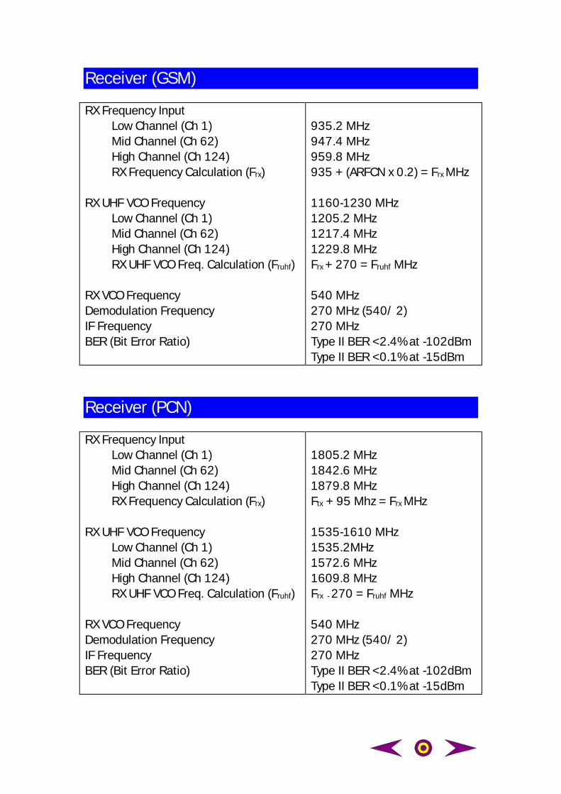
Receiver (GSM)
RX Frequency InputLow Channel (Ch 1)Mid Channel (Ch 62)High Channel (Ch 124)RX Frequency Calculation (Frx)
RX UHF VCO FrequencyLow Channel (Ch 1)Mid Channel (Ch 62)High Channel (Ch 124)RX UHF VCO Freq. Calculation (Fruhf)
RX VCO FrequencyDemodulation FrequencyIF FrequencyBER (Bit Error Ratio)
935.2 MHz947.4 MHz959.8 MHz935 + (ARFCN x 0.2) = Frx MHz
1160-1230 MHz1205.2 MHz1217.4 MHz1229.8 MHzFrx + 270 = Fruhf MHz
540 MHz270 MHz (540/ 2)270 MHzType II BER <2.4% at -102dBmType II BER <0.1% at -15dBm
Receiver (PCN)
RX Frequency InputLow Channel (Ch 1)Mid Channel (Ch 62)High Channel (Ch 124)RX Frequency Calculation (Frx)
RX UHF VCO FrequencyLow Channel (Ch 1)Mid Channel (Ch 62)High Channel (Ch 124)RX UHF VCO Freq. Calculation (Fruhf)
RX VCO FrequencyDemodulation FrequencyIF FrequencyBER (Bit Error Ratio)
1805.2 MHz1842.6 MHz1879.8 MHzFtx + 95 Mhz = Frx MHz
1535-1610 MHz1535.2MHz1572.6 MHz1609.8 MHzFrx - 270 = Fruhf MHz
540 MHz270 MHz (540/ 2)270 MHzType II BER <2.4% at -102dBmType II BER <0.1% at -15dBm
<< Previous SectionNext Section >>Main Menu
Section 3
CircuitDescription
Part 1 ReceiverPart 2 TransmitterPart 3 Power Amplifier ControlPart 4 13Mhz ClockPart 5 Power Supplies and Control Signals (RF)Part 6 Logic Circuit Descriptions
Part 1 : Receiver
The front end
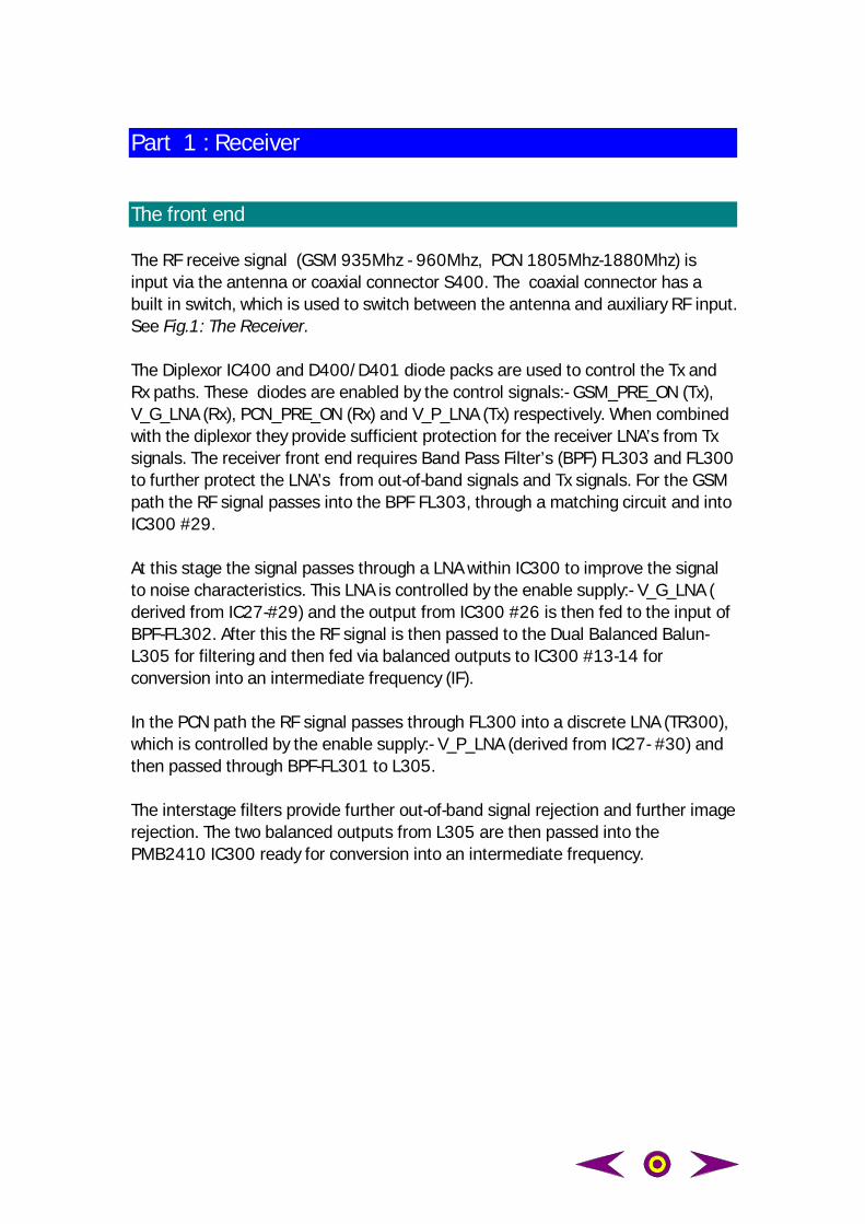
The RF receive signal (GSM 935Mhz - 960Mhz, PCN 1805Mhz-1880Mhz) isinput via the antenna or coaxial connector S400. The coaxial connector has abuilt in switch, which is used to switch between the antenna and auxiliary RF input.See Fig.1: The Receiver.
The Diplexor IC400 and D400/D401 diode packs are used to control the Tx andRx paths. These diodes are enabled by the control signals:- GSM_PRE_ON (Tx),V_G_LNA (Rx), PCN_PRE_ON (Rx) and V_P_LNA (Tx) respectively. When combinedwith the diplexor they provide sufficient protection for the receiver LNA’s from Txsignals. The receiver front end requires Band Pass Filter’s (BPF) FL303 and FL300to further protect the LNA’s from out-of-band signals and Tx signals. For the GSMpath the RF signal passes into the BPF FL303, through a matching circuit and intoIC300 #29.
At this stage the signal passes through a LNA within IC300 to improve the signalto noise characteristics. This LNA is controlled by the enable supply:- V_G_LNA (derived from IC27-#29) and the output from IC300 #26 is then fed to the input ofBPF-FL302. After this the RF signal is then passed to the Dual Balanced Balun-L305 for filtering and then fed via balanced outputs to IC300 #13-14 forconversion into an intermediate frequency (IF).
In the PCN path the RF signal passes through FL300 into a discrete LNA (TR300),which is controlled by the enable supply:- V_P_LNA (derived from IC27- #30) andthen passed through BPF-FL301 to L305.
The interstage filters provide further out-of-band signal rejection and further imagerejection. The two balanced outputs from L305 are then passed into thePMB2410 IC300 ready for conversion into an intermediate frequency.
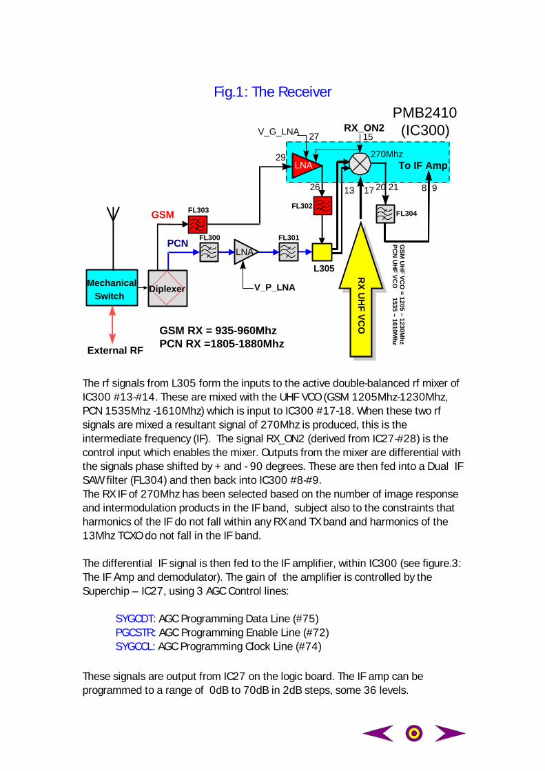
Fig.1: The Receiver
GSM
Mechanical Switch
External RF
V_G_LNA
FL303 FL302
FL301FL300
27
29
26 13
V_P_LNA
PCN
Diplexer
L305
PCN RX =1805-1880MhzGSM RX = 935-960Mhz
17
LNALNA
LNA
20 21
FL304
To IF Amp
8 9
RX_ON215
PMB2410 (IC300)
RX
UH
F V
CO
GS
M U
HF
VC
O = 1205 – 1230M
hz
PC
N U
HF
VC
O
1535 – 1610Mh
z270Mhz
The rf signals from L305 form the inputs to the active double-balanced rf mixer ofIC300 #13-#14. These are mixed with the UHF VCO (GSM 1205Mhz-1230Mhz,PCN 1535Mhz -1610Mhz) which is input to IC300 #17-18. When these two rfsignals are mixed a resultant signal of 270Mhz is produced, this is theintermediate frequency (IF). The signal RX_ON2 (derived from IC27-#28) is thecontrol input which enables the mixer. Outputs from the mixer are differential withthe signals phase shifted by + and - 90 degrees. These are then fed into a Dual IFSAW filter (FL304) and then back into IC300 #8-#9.The RX IF of 270Mhz has been selected based on the number of image responseand intermodulation products in the IF band, subject also to the constraints thatharmonics of the IF do not fall within any RX and TX band and harmonics of the13Mhz TCXO do not fall in the IF band.
The differential IF signal is then fed to the IF amplifier, within IC300 (see figure.3:The IF Amp and demodulator). The gain of the amplifier is controlled by theSuperchip – IC27, using 3 AGC Control lines:
SYGCDT: AGC Programming Data Line (#75)PGCSTR: AGC Programming Enable Line (#72)SYGCCL: AGC Programming Clock Line (#74)
These signals are output from IC27 on the logic board. The IF amp can beprogrammed to a range of 0dB to 70dB in 2dB steps, some 36 levels.
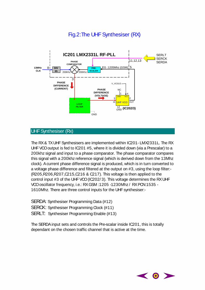
Fig.2:The UHF Synthesiser (RX)
DIV65
LOOPFILTER
PRE-SCALER
IC201 LMX2331L RF-PLL
(IC202/3)
PHASECOMPARATOR
IN OUT
3 2
4
3
5
PHASEDIFFERENCE(CURRENT) PHASE
DIFFERENCE(VOLTAGE)
13MHz CLK
8
VCCGND1
NC
V_VC01/2
5
11,12,13
SERLTSERCKSERDA
EG :1205Mhz (GSM)
200Khz 200Khz
GND
GND
UHF VCO
UHF Synthesiser (Rx)
The RX & TX UHF Synthesisers are implemented within IC201- LMX2331L. The RXUHF VCO output is fed to IC201 #5, where it is divided down (via a Prescalar) to a200khz signal and input to a phase comparator. The phase comparator comparesthis signal with a 200khz reference signal (which is derived down from the 13Mhzclock). A current phase difference signal is produced, which is in turn converted toa voltage phase difference and filtered at the output on #3, using the loop filter:-(R205,R206,R207,C215,C216 & C217). This voltage is then applied to thecontrol input #3 of the UHF VCO (IC202/3). This voltage determines the RX UHFVCO oscillator frequency, i.e.: RX GSM :1205 -1230Mhz / RX PCN:1535 -1610Mhz. There are three control inputs for the UHF synthesiser:-
SERDA: Synthesiser Programming Data (#12)SERCK: Synthesiser Programming Clock (#11)SERLT: : Synthesiser Programming Enable (#13)
The SERDA input sets and controls the Pre-scalar inside IC201, this is totallydependant on the chosen traffic channel that is active at the time.
Fig.3:The IF AMP and Demodulator
AGC Control :-PGSTR SYGCCL SYGCDT
8-9
PMB2410 (IC300)
RX_ON2
PUPLO2
36
31
TO W2013 (IC100) (TX IF Modulator)
RINO
540MHz Div2
Div2/3
RINORIPO
RQNORQPO
4546
4039
FL304
23-2420-21
1st IF270Mhz
270MhzFirst Mixer
Varactor Network D303 (A,B)
LOOP FILTER
32-35
11,12,13
From (IC201#18) IF PLL (See Fig.4)
GSM_TX
Rx I&Q Demodulator
The modulated IF signal of 270Mhz is demodulated by mixing it with another270Mhz signal, which is derived from an 540Mhz oscillator located inside IC300.The 540Mhz is reduced by a pre-selectable divider, which can be set by thecontrol signal GSM_TX (from IC27#23). The output from the 540Mhz oscillator isdivided down by a factor of 2 or 3 to produce either a 180 or 270Mhz signal,depending on whether the mobile is in TX or RX modes . It is this signal which ismixed with that from the IF amplifier to produce the baseband I and Q signals. TheI and Q signals are then buffered and fed differentially to the Superchip (IC27) forfiltering and digitising.
The signal RX_ON2 (from IC27#28) enables both the demodulator and internalbuffers. The signal PUPLO2 which is supplied from IC27 #26, enables the540Mhz internal oscillator.
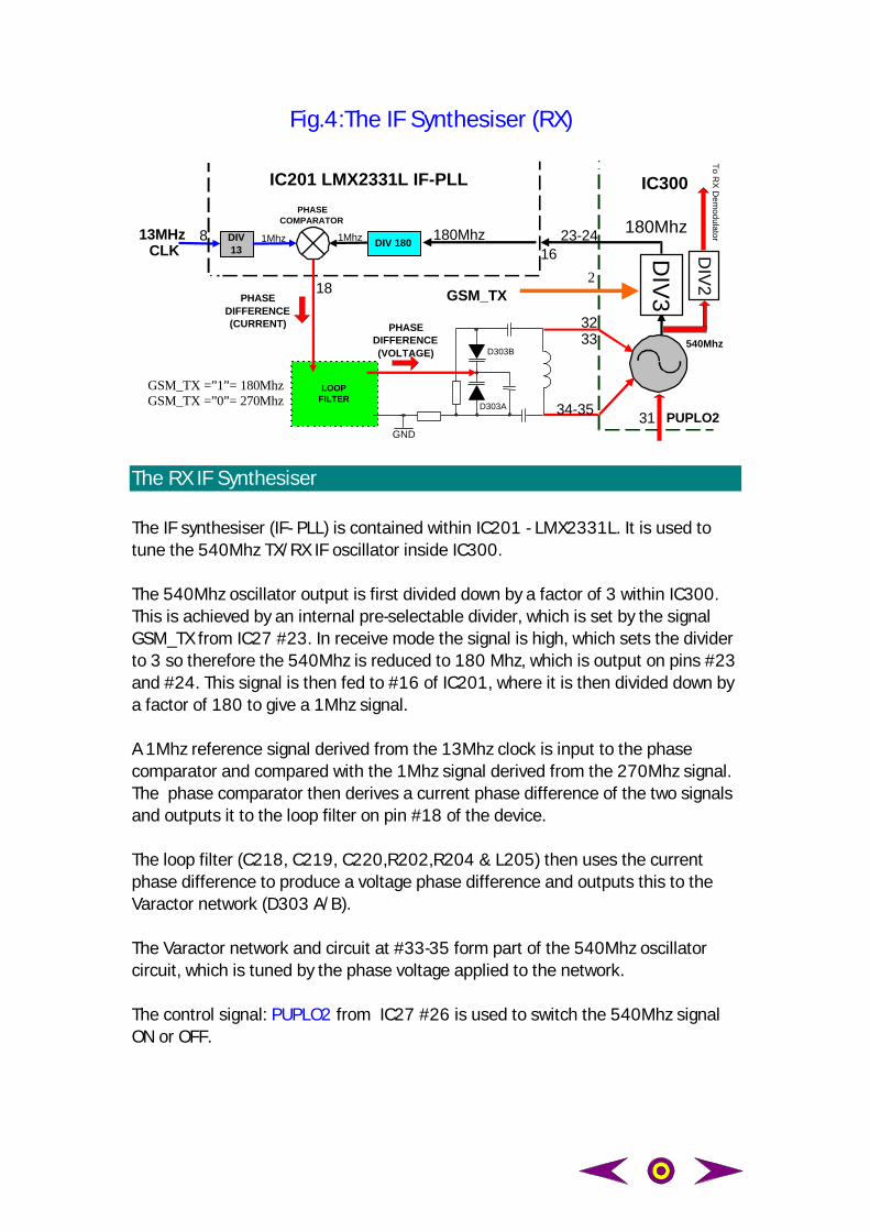
Fig.4:The IF Synthesiser (RX)
DIV13
LOOPFILTER
DIV 180
IC201 LMX2331L IF-PLL
PHASECOMPARATOR
23-24
PHASEDIFFERENCE(CURRENT) PHASE
DIFFERENCE(VOLTAGE)
13MHz CLK
8 1Mhz 1Mhz
GND
IC300
3233
34-35
DIV
318
16180Mhz 180Mhz
D303B
D303A
DIV
2To R
X D
emodulator
540Mhz
31 PUPLO2
GSM_TX
GSM_TX =”1”= 180Mhz GSM_TX =”0”= 270Mhz
2
The RX IF Synthesiser
The IF synthesiser (IF- PLL) is contained within IC201 - LMX2331L. It is used totune the 540Mhz TX/RX IF oscillator inside IC300.
The 540Mhz oscillator output is first divided down by a factor of 3 within IC300.This is achieved by an internal pre-selectable divider, which is set by the signalGSM_TX from IC27 #23. In receive mode the signal is high, which sets the dividerto 3 so therefore the 540Mhz is reduced to 180 Mhz, which is output on pins #23and #24. This signal is then fed to #16 of IC201, where it is then divided down bya factor of 180 to give a 1Mhz signal.
A 1Mhz reference signal derived from the 13Mhz clock is input to the phasecomparator and compared with the 1Mhz signal derived from the 270Mhz signal.The phase comparator then derives a current phase difference of the two signalsand outputs it to the loop filter on pin #18 of the device.
The loop filter (C218, C219, C220,R202,R204 & L205) then uses the currentphase difference to produce a voltage phase difference and outputs this to theVaractor network (D303 A/B).
The Varactor network and circuit at #33-35 form part of the 540Mhz oscillatorcircuit, which is tuned by the phase voltage applied to the network.
The control signal: PUPLO2 from IC27 #26 is used to switch the 540Mhz signalON or OFF.
Part 2 : Transmitter
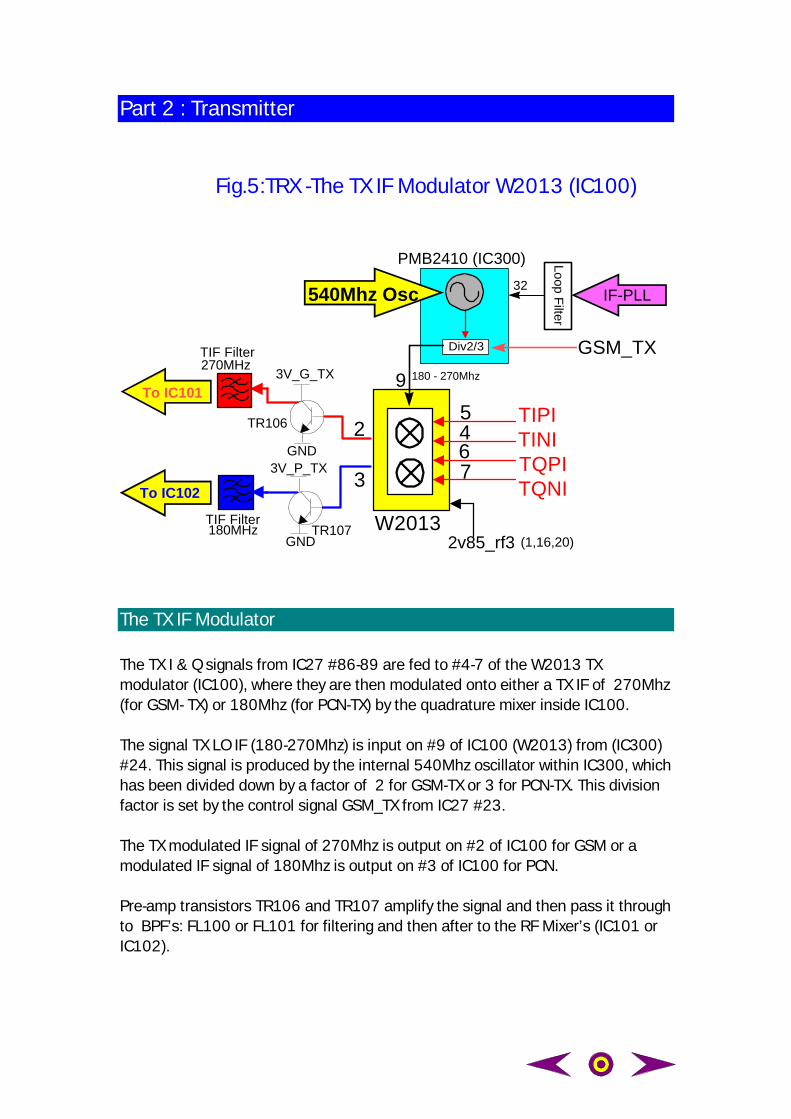
Fig.5:TRX -The TX IF Modulator W2013 (IC100)
TIPITINI
TQPI TQNI
(1,16,20)
TIF Filter270MHz
TIF Filter180MHz
2
3
2v85_rf3W2013
GND
GND
3V_G_TX
TR106
TR107
5
67
43V_P_TX
Div2/3
PMB2410 (IC300)
540Mhz Osc
180 - 270Mhz
GSM_TX
To IC101
To IC102
9
Loop Filter
32IF-PLL
The TX IF Modulator
The TX I & Q signals from IC27 #86-89 are fed to #4-7 of the W2013 TXmodulator (IC100), where they are then modulated onto either a TX IF of 270Mhz(for GSM- TX) or 180Mhz (for PCN-TX) by the quadrature mixer inside IC100.
The signal TX LO IF (180-270Mhz) is input on #9 of IC100 (W2013) from (IC300)#24. This signal is produced by the internal 540Mhz oscillator within IC300, whichhas been divided down by a factor of 2 for GSM-TX or 3 for PCN-TX. This divisionfactor is set by the control signal GSM_TX from IC27 #23.
The TX modulated IF signal of 270Mhz is output on #2 of IC100 for GSM or amodulated IF signal of 180Mhz is output on #3 of IC100 for PCN.
Pre-amp transistors TR106 and TR107 amplify the signal and then pass it throughto BPF’s: FL100 or FL101 for filtering and then after to the RF Mixer’s (IC101 orIC102).
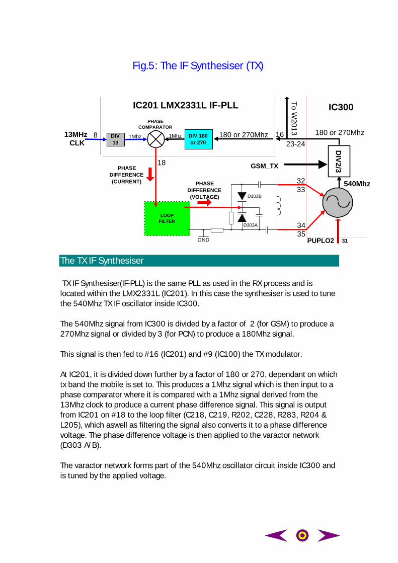
Fig.5: The IF Synthesiser (TX)
DIV13
LOOPFILTER
DIV 180or 270
IC201 LMX2331L IF-PLL
PHASECOMPARATOR
23-24
PHASEDIFFERENCE(CURRENT) PHASE
DIFFERENCE(VOLTAGE)
13MHz CLK
8 1Mhz 1Mhz
GND
IC300
3233
3435
DIV
2/318
16180 or 270Mhz 180 or 270Mhz
D303B
D303A
540Mhz
31 PUPLO2
To W2013
GSM_TX
The TX IF Synthesiser
TX IF Synthesiser(IF-PLL) is the same PLL as used in the RX process and islocated within the LMX2331L (IC201). In this case the synthesiser is used to tunethe 540Mhz TX IF oscillator inside IC300.
The 540Mhz signal from IC300 is divided by a factor of 2 (for GSM) to produce a270Mhz signal or divided by 3 (for PCN) to produce a 180Mhz signal.
This signal is then fed to #16 (IC201) and #9 (IC100) the TX modulator.
At IC201, it is divided down further by a factor of 180 or 270, dependant on whichtx band the mobile is set to. This produces a 1Mhz signal which is then input to aphase comparator where it is compared with a 1Mhz signal derived from the13Mhz clock to produce a current phase difference signal. This signal is outputfrom IC201 on #18 to the loop filter (C218, C219, R202, C228, R283, R204 &L205), which aswell as filtering the signal also converts it to a phase differencevoltage. The phase difference voltage is then applied to the varactor network(D303 A/B).
The varactor network forms part of the 540Mhz oscillator circuit inside IC300 andis tuned by the applied voltage.
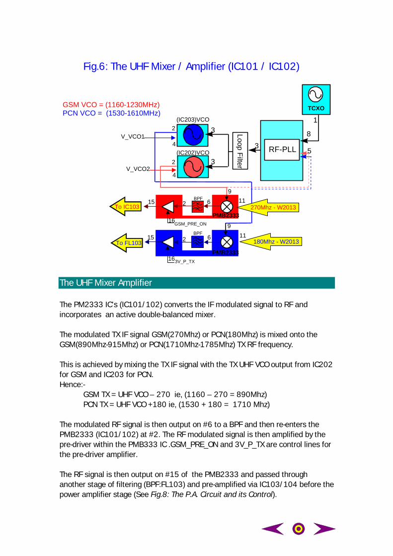
Fig.6: The UHF Mixer / Amplifier (IC101 / IC102)
(IC203)VCO
GSM VCO = (1160-1230MHz)PCN VCO = (1530-1610MHz)
(IC202)VCO
PMB2333
PMB2333
V_VCO1
V_VCO2
3V_P_TX
GSM_PRE_ON16
16
2
2BPF
BPF
2
2
4
4
9
9
6
6
To IC103
To FL103
15
15
Loop FilterRF-PLL3
3
35
TCXO
1
8
180Mhz - W201311
270Mhz - W201311
The UHF Mixer Amplifier
The PM2333 IC’s (IC101/102) converts the IF modulated signal to RF andincorporates an active double-balanced mixer.
The modulated TX IF signal GSM(270Mhz) or PCN(180Mhz) is mixed onto theGSM(890Mhz-915Mhz) or PCN(1710Mhz-1785Mhz) TX RF frequency.
This is achieved by mixing the TX IF signal with the TX UHF VCO output from IC202for GSM and IC203 for PCN.Hence:-
GSM TX = UHF VCO – 270 ie, (1160 – 270 = 890Mhz)PCN TX = UHF VCO +180 ie, (1530 + 180 = 1710 Mhz)
The modulated RF signal is then output on #6 to a BPF and then re-enters thePMB2333 (IC101/102) at #2. The RF modulated signal is then amplified by thepre-driver within the PMB333 IC .GSM_PRE_ON and 3V_P_TX are control lines forthe pre-driver amplifier.
The RF signal is then output on #15 of the PMB2333 and passed throughanother stage of filtering (BPF:FL103) and pre-amplified via IC103/104 before thepower amplifier stage (See Fig.8: The P.A. Circuit and its Control).
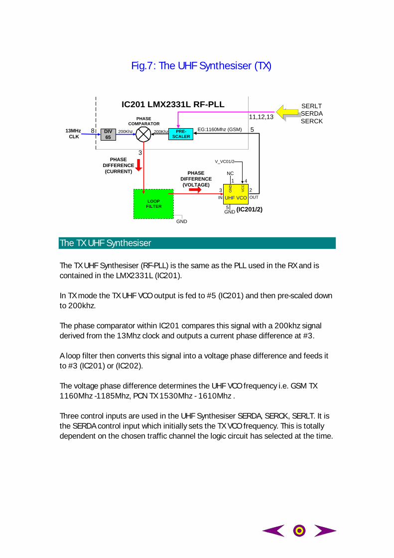
Fig.7: The UHF Synthesiser (TX)
DIV65
LOOPFILTER
PRE-SCALER
IC201 LMX2331L RF-PLL
(IC201/2)
PHASECOMPARATOR
IN OUT3 2
4
3
5
PHASEDIFFERENCE(CURRENT) PHASE
DIFFERENCE(VOLTAGE)
13MHz CLK
8
VC
C
GN
D
1NC
V_VC01/2
5
11,12,13
SERLTSERDASERCK
EG:1160Mhz (GSM)200Khz 200Khz
GND
GND
UHF VCO
The TX UHF Synthesiser
The TX UHF Synthesiser (RF-PLL) is the same as the PLL used in the RX and iscontained in the LMX2331L (IC201).
In TX mode the TX UHF VCO output is fed to #5 (IC201) and then pre-scaled downto 200khz.
The phase comparator within IC201 compares this signal with a 200khz signalderived from the 13Mhz clock and outputs a current phase difference at #3.
A loop filter then converts this signal into a voltage phase difference and feeds itto #3 (IC201) or (IC202).
The voltage phase difference determines the UHF VCO frequency i.e. GSM TX1160Mhz -1185Mhz, PCN TX 1530Mhz - 1610Mhz .
Three control inputs are used in the UHF Synthesiser SERDA, SERCK, SERLT. It isthe SERDA control input which initially sets the TX VCO frequency. This is totallydependent on the chosen traffic channel the logic circuit has selected at the time.
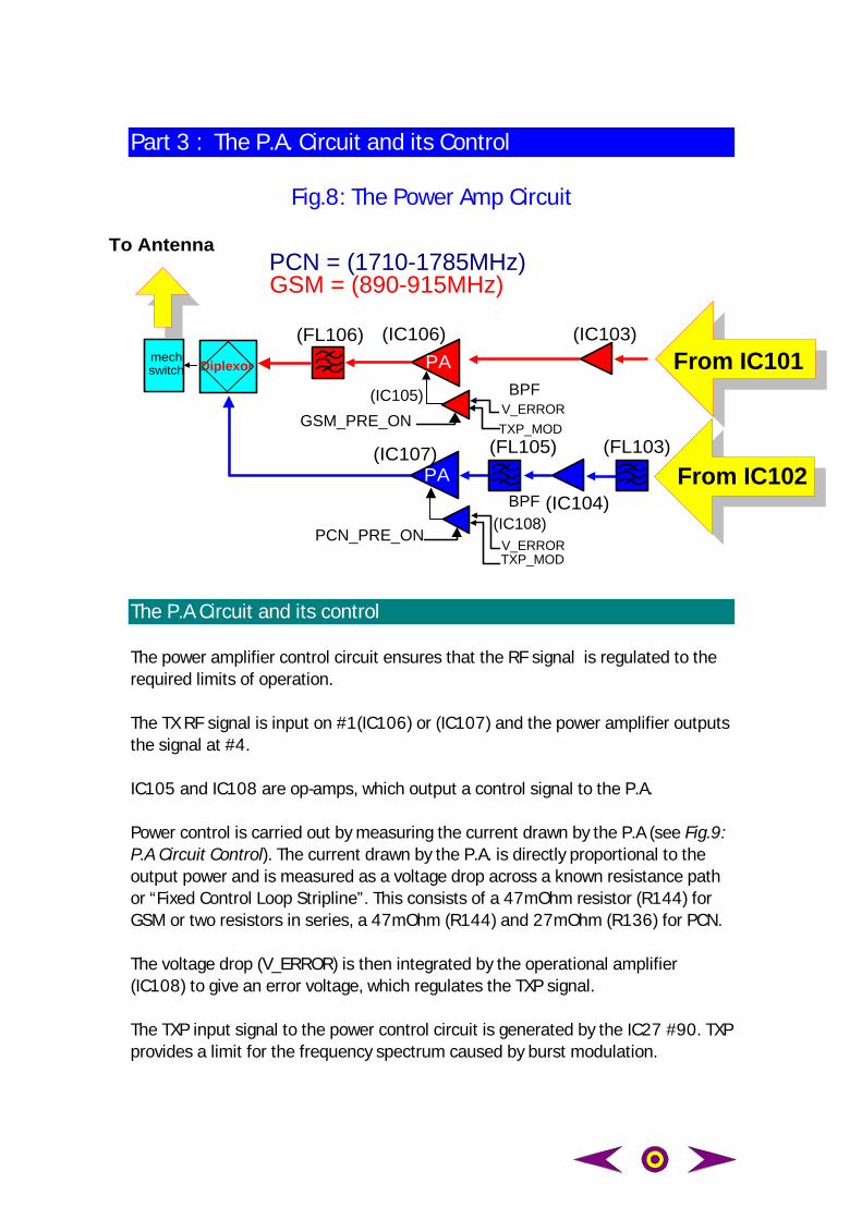
Part 3 : The P.A. Circuit and its Control
Fig.8: The Power Amp Circuit
The P.A Circuit and its control
The power amplifier control circuit ensures that the RF signal is regulated to therequired limits of operation.
The TX RF signal is input on #1(IC106) or (IC107) and the power amplifier outputsthe signal at #4.
IC105 and IC108 are op-amps, which output a control signal to the P.A.
Power control is carried out by measuring the current drawn by the P.A (see Fig.9:P.A Circuit Control). The current drawn by the P.A. is directly proportional to theoutput power and is measured as a voltage drop across a known resistance pathor “Fixed Control Loop Stripline”. This consists of a 47mOhm resistor (R144) forGSM or two resistors in series, a 47mOhm (R144) and 27mOhm (R136) for PCN.
The voltage drop (V_ERROR) is then integrated by the operational amplifier(IC108) to give an error voltage, which regulates the TXP signal.
The TXP input signal to the power control circuit is generated by the IC27 #90. TXPprovides a limit for the frequency spectrum caused by burst modulation.
BPF
GSM = (890-915MHz)PCN = (1710-1785MHz)
PA(FL106) (IC106) (IC103)
BPFPA
(IC104)
(FL105)
PCN_PRE_ON
GSM_PRE_ON
mechswitch
To Antenna
Diplexor
(IC105)
(IC108)
TXP_MOD
V_ERROR
V_ERROR
(IC107)
From IC101
TXP_MOD
From IC102(FL103)
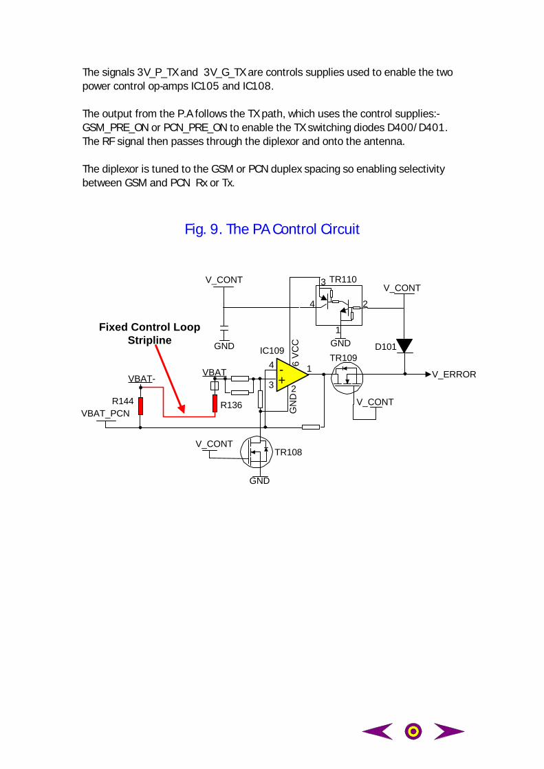
The signals 3V_P_TX and 3V_G_TX are controls supplies used to enable the twopower control op-amps IC105 and IC108.
The output from the P.A follows the TX path, which uses the control supplies:-GSM_PRE_ON or PCN_PRE_ON to enable the TX switching diodes D400/D401.The RF signal then passes through the diplexor and onto the antenna.
The diplexor is tuned to the GSM or PCN duplex spacing so enabling selectivitybetween GSM and PCN Rx or Tx.
Fig. 9. The PA Control Circuit
4VBAT
VBAT-
VBAT_PCN
3
1
2
GND
V_CONT
V_CONT
+-
GN
DV
CC
63
4
1GND
2
V_CONTV_CONT
GND
TR110
TR109D101
V_ERROR
TR108
IC109
Fixed Control LoopStripline
R144 R136
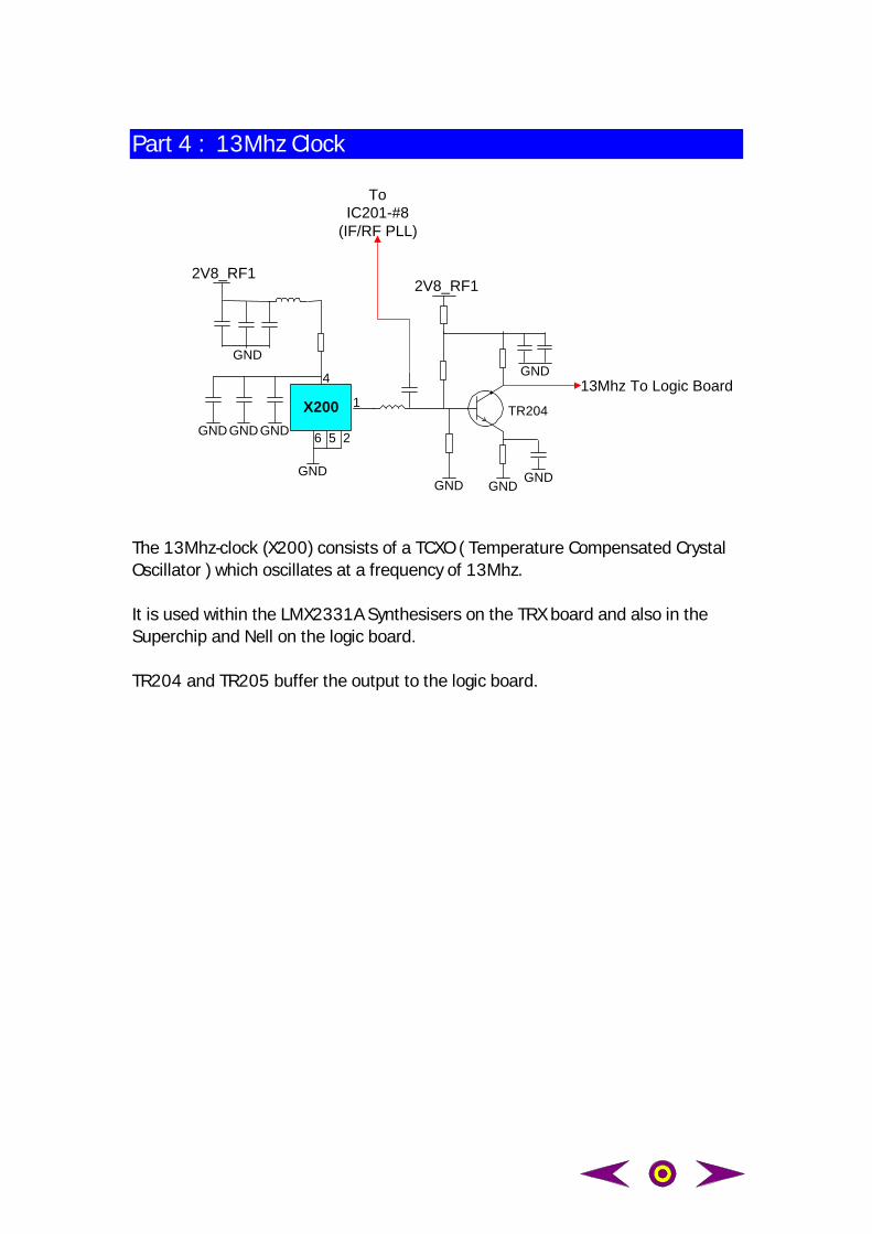
Part 4 : 13Mhz Clock
X200
2V8_RF1
13Mhz To Logic BoardGND
GND GNDGND
GNDGNDGND
GND
2V8_RF1
GND
6 5 2
1
4
TR204
ToIC201-#8
(IF/RF PLL)
The 13Mhz-clock (X200) consists of a TCXO ( Temperature Compensated CrystalOscillator ) which oscillates at a frequency of 13Mhz.
It is used within the LMX2331A Synthesisers on the TRX board and also in theSuperchip and Nell on the logic board.
TR204 and TR205 buffer the output to the logic board.
Part 5: Power Supplies and Control signals (RF Board)
5.1: MicroMoe IC204 – Power Supply IC
The RF section has its own dedicated power supply device called: MicroMoe. Thisis a smaller version of the ASIC MiniMoe, which is located on the logic board.MicroMoe performs all power supply requirements of the RF circuitry, except for adedicated 5-volt supply (5VRF) for the UHF VCO’s which is supplied from MiniMoe.The device consists of three voltage regulators that supply the power rails for theRF circuits and is supplied from VBAT. See: Fig.6.C: Power Supplies MiniMoe(IC19) & MicroMoe (IC204).MicroMoe provides the following outputs:-
2V8_RF1 (Regulator 3): 2.85V RF supply for the 13Mhz clock andLMX2331 synthesiser.
2V8_RF2 (Regulator 2): 2.85V RF supply which supplies V_G_LNA andV_P_LNA.
2V8_RF3 (Regulator 1): 2.85V RF supply used in the transmitter circuitry.
There are two enable signals which control the regulator’s:-
TCXO_ON Enables supplies: 2V8_RF1 and 2V8_RF2. Signal derived fromNELL #P2.
TX_ON Enables supply: 2V8_RF3, signal derived from IC27 #17.
5.2: Control signals and additional power supplies
The RF board has the following additional voltage supplies and control signals.
5V_RF Regulated 5V supply for the VCO circuits and to supply V_CONT. 5V derived from MiniMoe on logic board.
V_CONT Switched version of the 5V_RF. This is supplied to the powercontrol circuitry and is switched on a frame before the TX burst.
V_G_LNA Switched version of 2V8_RF2 to power the GSM LNA and theRX switching diode: D400.
V_P_LNA Switched version of 2V8_RF2 to power the PCN LNA and RXswitching diode: D401.
GSM_TX Control signal from IC27 #23 which switches the 2V8_RF3supply to give 3V_G_TX. It also sets the internal frequencydivider inside IC300.
PCN_TX Control signal from the superchip, which switches the 2V8_RF3supply to give 3V_P_TX.
3V_G_TX Switched version of 2V8_RF3 to power the PMB2333 IC in theGSM TX path.
3V_P_TX Switched version of 2V8_RF3 to power the PMB2333 IC in thePCN TX path.
GSM_PRE_ON Switched version of 2V8_RF3 used to turn on the preamplifierMMIC (µPC2771) in the GSM TX path and the TX switchingdiode: D400 .
PCN_PRE_ON Switched version of 2V8_RF3 used to turn on the preamplifierMMIC (µPC2771) in the PCN TX path and the TX switchingdiode: D401.
GSM_LNA Control signal from the IC27 #29 which switches V_G_LNA.
RX_ON2 Control signal for the 1st mixer, RX demodulator and internalbuffers.
PCN_ON Control signal from IC27 #19 which switches 2.85V through toPCN_PRE_ON.
GSM_ON Control signal from IC27 #18 which switches 2.85V through toGSM_PRE_ON.
PRE_ON Control signal from IC27 #22 which switches 2.85V through toGSM/PCN_PRE_ON.
Part 6: Logic Circuit Description
This section describes the architecture and hardware functionality of the logiccircuit. The logic circuit performs the following functions:
• Channel coding/ decoding• Speech coding / decoding• Data encryption• Layer 1,2 and 3 software tasks• I/O System interface• SIM interface and management• Audio and tone control• Vibrator control• Power supply and battery management• RF power control• Synchronisation• Real time clock• Key-Pad control and scanning• LCD control and driver The logic and RF circuits are primarily controlled and administered by two maindevices, these being:- • “Superchip”- CSP and DSP Combined (IC27)
The “Superchip” combines the functions of both the CSP and DSP in a singlepackage. The device performs channel and speech coder/decoder tasks,equalisation, encryption, frame timing, A/D conversion, RF power control
and audio interfacing, including tone generation.
• Nell - (IC8) Nell incorporates the main CPU for the mobile and controls the functions; Layer 1,2 and 3 software, the SIM, system interfaces, real time clock, buzzer, vibrator, battery management, Key-Pad scanning and LCD control. Nell also controls the integrated power supply devices:- “MiniMoe” and “MicroMoe” . The Logic circuit is divided into six main functional areas:
1) Superchip (CSP and DSP combined) 2) Nell and CPU Memory 3) Battery Interface and Power Supply 4) Keypad, Display and SIM 5) Audio and Miscellaneous Interfaces 6) System Connector - P5
6.1 “Superchip” (CSP and DSP combined) - (IC27) The superchip is the interface between the RF circuitry, the audio circuits
and the digital domain. It also carries out layer 1 signal processing, thisincludes data coding/decoding, data interleaving/de-interleaving, errordetection/correction and provides burst generation data. Unlike previousversions of DSP package which used external static random access memory(SRAM) devices for data storage of signal processing operations. Thesuperchip incorporates its own internal 8K * 16 RAM capability to performthese functions.
The device has the following control functions and connections:- • Transmit power control O/P: The signal TXP (#90) controls the ramp shape from the RF Power amplifier. • Transmit I and Q outputs O/P: TIPI,TINI,TQPI and TQNI (#86-89) • Digital Audio Interface O/P: DAICK, DAIRN, DAIDI and DAIDO (#6-9) • Control outputs for the RF Circuit O/P: VCO_ON (#16) : Power enable for VCO TX_ON (#17) : Power enable for transmit circuitry GSM_ON (#18): Power enable for GSM circuitry PCN_ON (#19) : Power enable for PCN circuitry PRE_ON (#22) : Power enable for RF pre amplifier GSM_TX (#23) : Power enable for GSM TX path PCN_TX (#24) : Power enable for PCN TX path PUPLO2 (#26) : Power enable for 2nd local Osc RX_ON1 (#27) : Power enable for RX circuitry RX_ON2 (#28) : Power enable for RX circuitry GSM_LNA (#29) : Power enable for GSM RX path PCN_LNA (#30) : Power enable for PCN RX path • RF Synthesiser controls - (IC201) O/P: SERLT (#12) : Synthesiser data latch enable SERCK (#13) : Synthesiser data clock SERDA (#14) : Synthesiser serial data • 13MHz system clock I/P: 13MHz (#59)
• Receive I and Q inputs I/O: RQNO, RQPO, RINO and RIPO (#77-80) • Audio outputs for hands free operation
O/P: RXAF- and RXAF+ (#95-96)
• Audio output to earpieceO/P: AOUTN and AOUTP (#93-94)
• Audio inputs from microphone
I/P: MICOUT and MICIN (#4-5) • Audio inputs for hands free operation
I/P: TXAF- and TXAF+ (#98-99) • Tone Generation • GMSK modulation, transmit frequency correction • Digital to analogue conversion of the transmit I and Q signals • A/D and D/A conversion / gain control for audio inputs/outputs • Serial Interface to NELL This is a direct serial I/O interface to the NELL device used to pass data
destined for the PCMCIA interface: I/O: ICK (#67), OCK (#70) OLD (#71), ILD (#66), OBE (#63), DSP RXD (#64) and DSP TXD (#65) • Parallel Host Interface (PHIF) to CPU in NELL The DSP communicates with the CPU in NELL via a dedicated interface
called the (PHIF) Parallel Host Interface: I/O: PB0-PB7 (#32-40) = Data I/O lines to CPU POBE (#47), OE (#43) and WE (#41) = Interface
control• Receiver IF Gain Control The DSP sets the receiver IF gain to IC300 via control signals: O/P: PGCSTR (#72) - Receiver gain control SYGCCL (#74) - Receiver gain control clock SYGCDT (#75) - Receiver gain control data
• Interrupt generation to NELL I/O: This bit I/O port performs interrupt control of NELL: EXTINT(#73) • Superchip interrupt and reset inputs The superchip has the following interrupt and reset inputs: I/P: DSP INTO (#48) - DSP Interrupt 0 DSPRSTB (#50) - DSP Reset bar • JTAG test interface The JTAG interface provides extensive test and diagnostic functions to be
utilised in the repair process. This is controlled by:- I/O: TCK (#54) - JTAG test clock TMS (#55) - JTAG test mode select
TDI (#57) - JTAG test data input TDO (#56) - JTAG test data output • Supply and ground connections +3VSC = (#10,21,36,49,62 & 92) +3VAUDIO = (#2,85,58) GND = (#11,20,31,42,52,69,76,91 & 61) AGND1 = (#1) A functional block diagram of the A functional block diagram of the Superchip can be seen in Figure 10a.Superchip can be seen in Figure 10a. 6.2 NELL The NELL device is an in-house designed ASIC (AApplications SSpecific
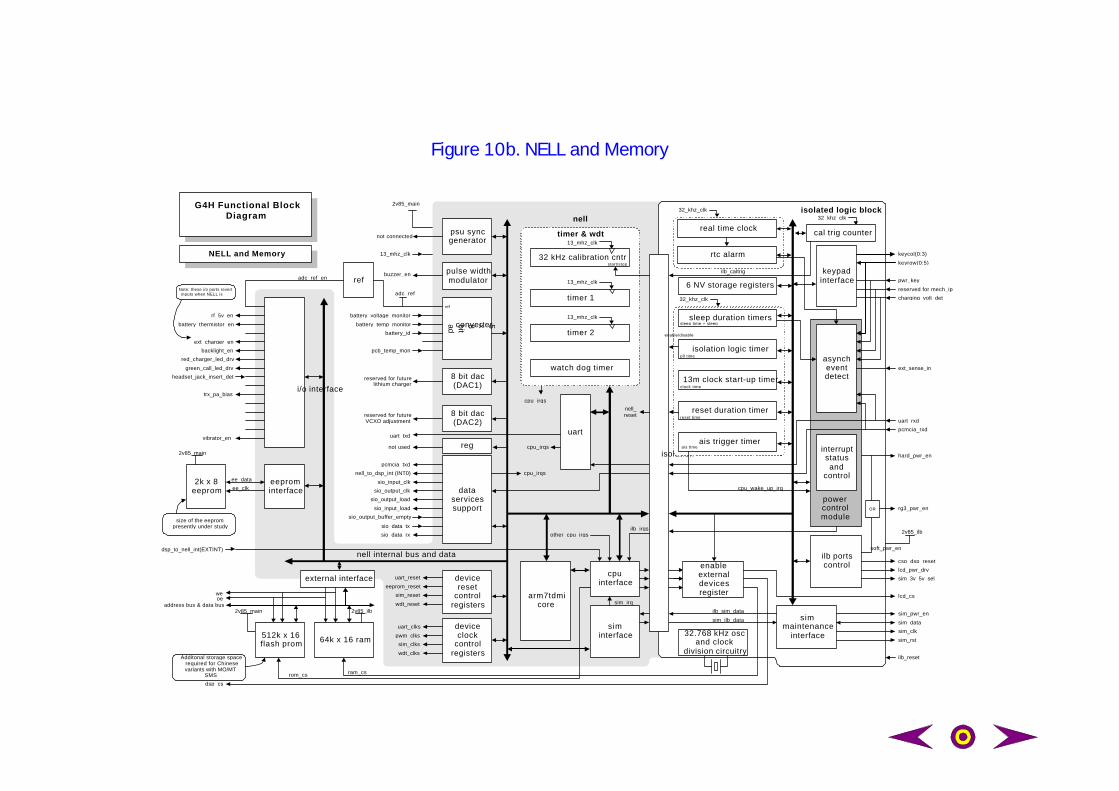
IIntegrated CCircuit) which has been developed to replace the existing Albertand CPU devices currently used in G9 and G9D. The NELL performs thefollowing functions:-
• • CPU• CPU Interface• Interrupt Controller• Baseband Power Control• Keypad Control• Display Interface• EEPROM Interface• SIM Interface• Buzzer Control• UART control/interface: (Universal Asynchronous Receiver Transmitter)• PCMCIA Data Interface: (Personal Computer Memory Card International
Association)
• I/O System Connector Interface - P5• Analogue Signal Measurement• Charge Control• Real Time Clock• CPU Timers The NELL is divided into two main function blocks:- 1. The Isolated Logic Block (ILB) 2. The CPU core, peripherals and interfaces. 6.2.1 The ILB Block The ILB’s main functions are:- • To control and monitor the application of power to various key sections of the
mobile, which creates the various power saving conditions. • A real time clock (RTC) with programmable alarm • Event detection/monitoring of the following: 1. A key-board entry 2. The power key being pressed 3. Charger voltage being applied to the mobile 4. The external sense line being activated 5. RTC alarm 6. Data being received from either the PCMCIA card or the hands free kit via the system connector. 7. Keyboard scanning and decoding 8. Isolation, reset and power control of the SIM interface 9. Control through a external device register that allows the display, CPU RAM and Flash ROM CS lines to be activated. A functional block diagram of NELL can be seen in Figure 10b 6.2.2 The CPU, Peripherals and Interface The remainder of NELL performs the following functions:- • CPU and ARM interface (Advanced Risk Machine)• Address decoding and data multiplexing• Timer and watch-dog timer generation• Serial interface to and from the SIM• UART administration for the system connector serial port• Pulse width modulator used to drive the buzzer;
• A 5 channel 8 bit A/D converter used for battery management and to measurethe pcb temperature
6.3 CPU Memory Flash PROM - (ICI 5) An 8Mbit programmable ROM which is capable of being written to while still incircuit. Contains all the main command software for the HHP Static Random Access Memory (SRAM) - (IC9) A 16 bit (64k by 16) temporary memory device which is used by NELL for CPUprogram execution. EEPROM - (IC10) A 4Kbyte electrically erasable and programmable ROM, which communicates viathe EECLK / EEDAT (#5-6) lines to NELL. It contains all the user memories andcalibration data. The location of these devices relative to NELL can be seen in Figure 10b.
6.4 Battery Interface and Power Supply 6.4.1 Battery Monitors and PCB Temperature Interface The HHP can monitor the state of the battery through the battery interfaceconnector P8. This can be done during both normal and charging operations. Thebattery provides a number of interface connections that enable the HHP todetermine the battery type, its capacity, temperature and whether it is possible tore-charge the cell(s). The thermister (R124) which is attached to the logic boardpcb is used to produce an analogue reading of the board’s own surfacetemperature. The P8 connector provides a connection between the battery powercontacts VBAT/GND to the RF board and BATTEMPMON/BATID battery monitoringcircuits to the battery. IC30 #2 provides the bias/reference supply: VREF for theseanalogue monitors and is also fed to IC29. Battery voltage monitoring (BATVMON) is performed by the circuit:IC30/IC29, withthe output of the regulator IC30 #2 feeding the comparator IC29 #3. IC29 usesthis input as a stabilised voltage reference level, which it compares to VBAT toproduce the analogue output BATVMON. This output is then supplied to NELL#M9 for A/D conversion. BATVMON enables the HHP to measure the batteryvoltage and hence determine how much charge remains in the cells. The remainder of the analogue inputs from these circuits are also fed to NELL forA/D conversion.

These monitor’s being :- BATTEMPMON (Battery Temperature Monitor) - NELL (#L9) BATID (Battery Identification) - NELL (#N9) The battery pack includes an internal thermister, which is used to produce theanalogue signal BATTEMPMON. This enables the HHP and external charger todetermine the battery temperature, which is used to protect the battery fromoverheating while charging.
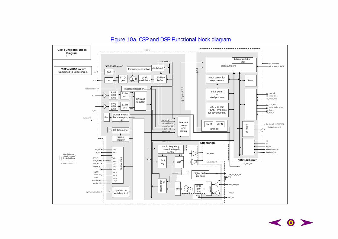
Figure 10a. CSP and DSP Functional block diagram
G4H Functional BlockDiagram(
synth_ser_chl_data
if_digital_gain_cntl
octl_0
octl_2
octl_4
octl_6
octl_7
tx_on
octl_8
vco_on
octl_9
pcn_tx
octl_10
octl_11
octl_12
octl_13
3
cont
rol l
ines
synthesizerserial control
framecounter
1/4-bit counter
13_mhz_clk
dsp_clk
power level &burst ramp-up
cntldactx_pwr_cntl
32 wordrx buffer
11-bitadc
11-bitadc
proggainamp
proggainamp
rx_I
rx_Q
dac
dactx_I
tx_QI & Qgen
gmskmodulator
frequency correction
160-bit txbuffer
overload detectionnot connected
proggainamp au
dio
adc
aux_audio_in
mic_in
doub
le b
uff
reg
16-bitreg dac
audio frequencycorrection & gain
controlaux_audio
ear_audio_out
digital audiointerface
dai_do_di_rn_ck
"CSP and DSP cores"Combined in Superchip 1
"CSP1089 core"
interruptcontrol
andstatus
error correctionco-processor
8 k x 16-bitof
dual port ram
48k x 16 rom(FLASH availablefor development)
timer
nell_to_dsp_int (INT0)
csp_dsp_reset
csp_to_dsp_int(INT1
"DSP1628 core"
2v85_ln
sio_input_clk
sio_output_clk
sio_output_load
sio_input_load
sio_output_buffer_empty
sio_data_tx
sio_data_rx
data bus (0:7)
address bus (2:3)
dsp_cs
oe
we
bit i
nput
/ dsp_to_nell_int (EXTINT)
3
octl_3gsm_on
pcn_on
pre_on
gsm_tx
pupl02
rxon1
rxon2
gsm_lna
pcn_lna
bit manipulationunit
dsp1600 core
audio_in_int
timeout_int
end_of_tx_int
rx_buffer_int
cipher_block_int
int_overflow_int
ext_overflow_int
A5.1/A5.2
div M div N
prog pll
Superchip1
2v85_anlg
Note:PCN onlysignals indicatedby dashed lines:
vregmic_drv
G4H Functional BlockDiagram
NELL and Memory
i/o interface
rf_5v_en
ext_charger_enbacklight_en
red_charger_led_drvgreen_call_led_drv
5x8bitadc converter
8 bit dac(DAC1)
battery_voltage_monitorbattery_temp_monitor
battery_id
pcb_temp_mon
reserved for futurelithium charger
trx_pa_bias
watch dog timer
timer 1
timer 2
32 kHz calibration cntr
pulse widthmodulator
buzzer_en
vibrator_en
psu syncgeneratornot connected
13_mhz_clk
start/stop
13_mhz_clk
13_mhz_clk
uart
ilb_caltrig
ilb_sim_datasim_ilb_data
asyncheventdetect
uart_rxd
keycol(0:3)keyrow(0:5)
keypadinterface pwr_key
reserved for mech_ipcharging_volt_det
ext_sense_in
pcmcia_rxd
eeprominterface
2k x 8eeprom
ee_dataee_clk
2v85_main
dataservicessupport
sio_input_clksio_output_clk
sio_output_loadsio_input_load
sio_output_buffer_empty
sio_data_txsio_data_rx
nell_to_dsp_int (INT0)
hard_pwr_en
ilb portscontrol
dsp_cs
siminterface
cpuinterface
ilb_reset
simmaintenance
interface sim_clksim_rst
sim_datasim_pwr_en
2v85_ilb
64k x 16 ram
timer & wdt
isolated logic block
arm7tdmicore
dsp_to_nell_int(EXTINT)
powercontrolmodule
isolation
ram_cs
external interface
address bus & data busoewe
rom_cs
nell
interruptstatusand
control
8 bit dac(DAC2)
csp_dsp_reset
2v85_main
2v85_ilb2v85_main
nell internal bus and datamux
pcmcia_txd
uart_txd
13_mhz_clk
Note: these i/o ports reverttoinputs when NELL is
reg
enableexternaldevicesregister
lcd_pwr_drvsim_3v_5v_sel
reserved for futureVCXO adjustment
6 NV storage registers
32_khz_clk
isolation logic timer
sleep duration timers
reset duration timer
13m clock start-up timer
enable/disable
sleep time + sleep
pll time
clock time
reset time
real time clock
32_khz_clk
32_khz_clk
cal trig counter
rtc alarm
nell_reset
ilb_irqsother_cpu_irqs
ais trigger timerais time
cpu_wake_up_irq
cpu_irqs
cpu_irqs
cpu_irqs
sim_irq
32.768 kHz oscand clock
division circuitry
512k x 16flash prom
devicereset
controlregisters
uart_reseteeprom_reset
sim_resetwdt_reset
lcd_cs
not used
deviceclock
controlregisters
uart_clkspwm_clkssim_clkswdt_clks
adc_ref
ref
size of the eeprompresently under study
Additonal storage spacerequired for Chinesevariants with MO/MT
SMS
OR rg3_pwr_en
soft_pwr_en
headset_jack_insert_det
battery_thermistor_en
refadc_ref_en
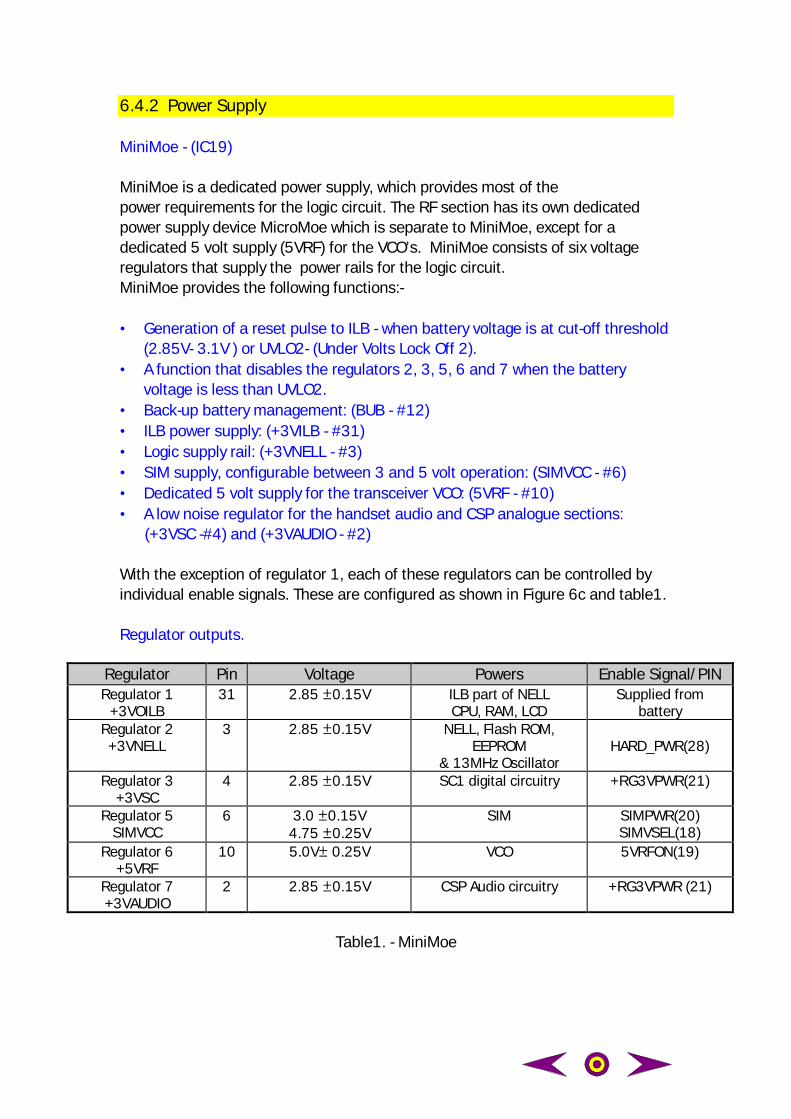
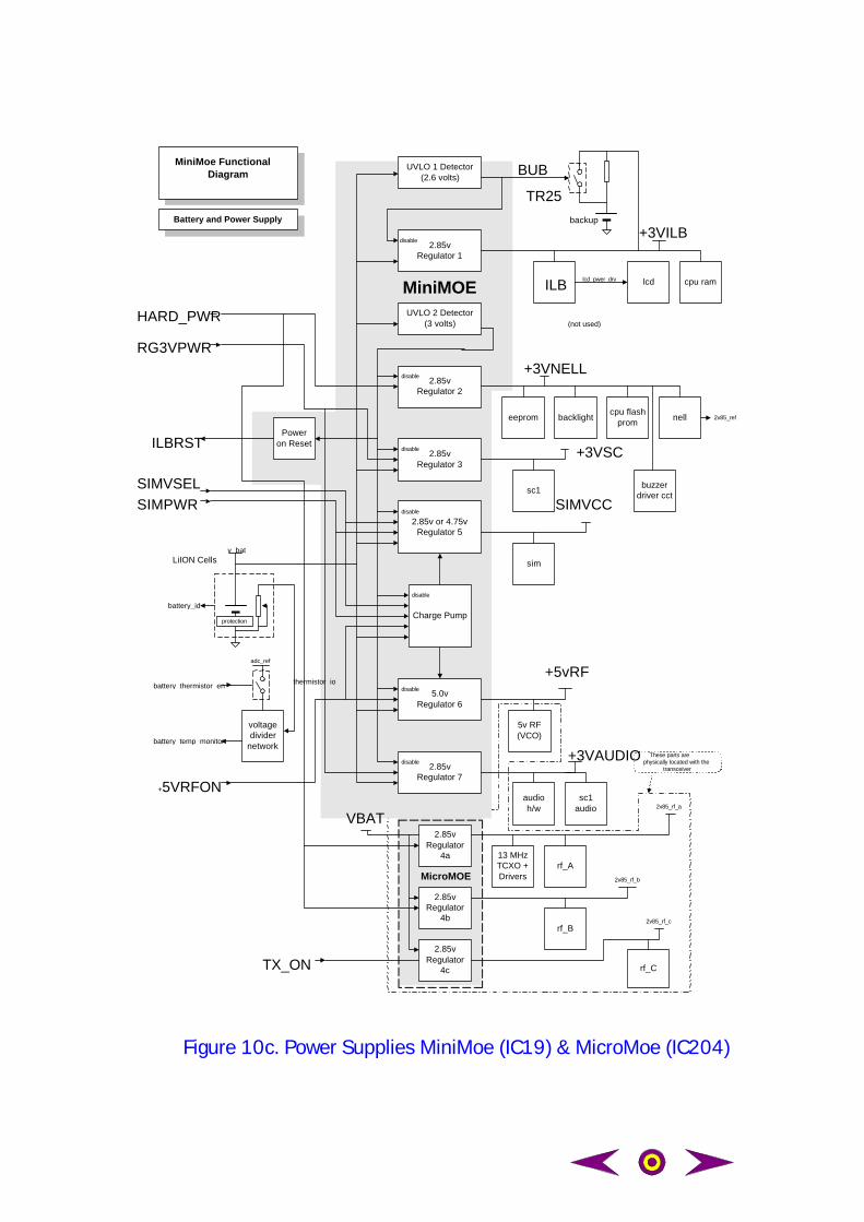
6.4.2 Power Supply MiniMoe - (IC19)
MiniMoe is a dedicated power supply, which provides most of thepower requirements for the logic circuit. The RF section has its own dedicatedpower supply device MicroMoe which is separate to MiniMoe, except for adedicated 5 volt supply (5VRF) for the VCO’s. MiniMoe consists of six voltageregulators that supply the power rails for the logic circuit. MiniMoe provides the following functions:- • Generation of a reset pulse to ILB - when battery voltage is at cut-off threshold
(2.85V- 3.1V ) or UVLO2- (Under Volts Lock Off 2).• A function that disables the regulators 2, 3, 5, 6 and 7 when the battery
voltage is less than UVLO2.• Back-up battery management: (BUB - #12)• ILB power supply: (+3VILB - #31)• Logic supply rail: (+3VNELL - #3)• SIM supply, configurable between 3 and 5 volt operation: (SIMVCC - #6)• Dedicated 5 volt supply for the transceiver VCO: (5VRF - #10)• A low noise regulator for the handset audio and CSP analogue sections: (+3VSC -#4) and (+3VAUDIO - #2)
With the exception of regulator 1, each of these regulators can be controlled byindividual enable signals. These are configured as shown in Figure 6c and table1.
Regulator outputs.
Table1. - MiniMoe
Regulator Pin Voltage Powers Enable Signal/PINRegulator 1
+3VOILB31 2.85 ±0.15V ILB part of NELL
CPU, RAM, LCDSupplied from
batteryRegulator 2+3VNELL
3 2.85 ±0.15V NELL, Flash ROM,EEPROM
& 13MHz OscillatorHARD_PWR(28)
Regulator 3+3VSC
4 2.85 ±0.15V SC1 digital circuitry +RG3VPWR(21)
Regulator 5SIMVCC
6 3.0 ±0.15V4.75 ±0.25V
SIM SIMPWR(20)SIMVSEL(18)
Regulator 6+5VRF
10 5.0V± 0.25V VCO 5VRFON(19)
Regulator 7+3VAUDIO
2 2.85 ±0.15V CSP Audio circuitry +RG3VPWR (21)
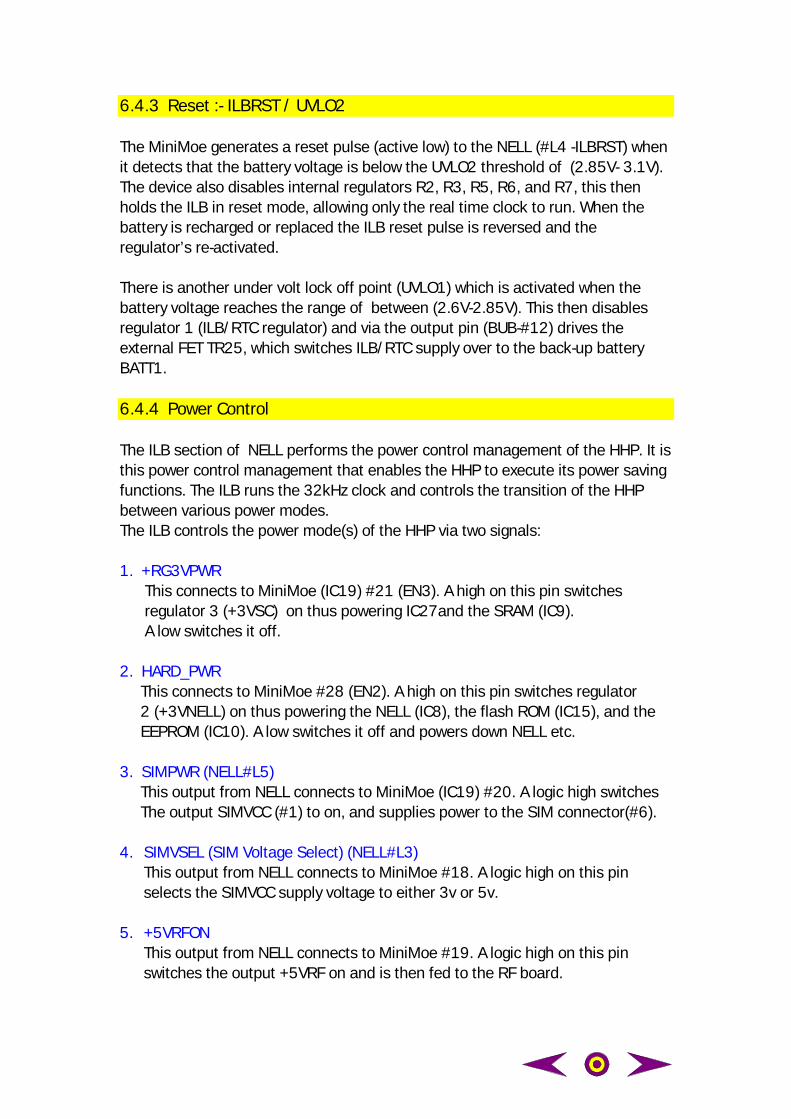
6.4.3 Reset :- ILBRST / UVLO2
The MiniMoe generates a reset pulse (active low) to the NELL (#L4 -ILBRST) whenit detects that the battery voltage is below the UVLO2 threshold of (2.85V- 3.1V).The device also disables internal regulators R2, R3, R5, R6, and R7, this thenholds the ILB in reset mode, allowing only the real time clock to run. When thebattery is recharged or replaced the ILB reset pulse is reversed and theregulator’s re-activated.
There is another under volt lock off point (UVLO1) which is activated when thebattery voltage reaches the range of between (2.6V-2.85V). This then disablesregulator 1 (ILB/RTC regulator) and via the output pin (BUB-#12) drives theexternal FET TR25, which switches ILB/RTC supply over to the back-up batteryBATT1.
6.4.4 Power Control
The ILB section of NELL performs the power control management of the HHP. It isthis power control management that enables the HHP to execute its power savingfunctions. The ILB runs the 32kHz clock and controls the transition of the HHPbetween various power modes.The ILB controls the power mode(s) of the HHP via two signals:
1. +RG3VPWR This connects to MiniMoe (IC19) #21 (EN3). A high on this pin switches regulator 3 (+3VSC) on thus powering IC27and the SRAM (IC9). A low switches it off.
2. HARD_PWR This connects to MiniMoe #28 (EN2). A high on this pin switches regulator 2 (+3VNELL) on thus powering the NELL (IC8), the flash ROM (IC15), and the EEPROM (IC10). A low switches it off and powers down NELL etc.
3. SIMPWR (NELL#L5) This output from NELL connects to MiniMoe (IC19) #20. A logic high switches The output SIMVCC (#1) to on, and supplies power to the SIM connector(#6).
4. SIMVSEL (SIM Voltage Select) (NELL#L3) This output from NELL connects to MiniMoe #18. A logic high on this pinselects the SIMVCC supply voltage to either 3v or 5v.
5. +5VRFON
This output from NELL connects to MiniMoe #19. A logic high on this pinswitches the output +5VRF on and is then fed to the RF board.
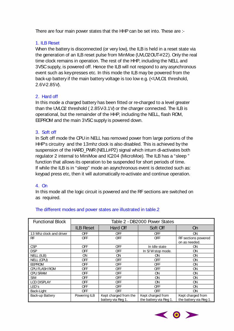
There are four main power states that the HHP can be set into. These are :-
1. ILB ResetWhen the battery is disconnected (or very low), the ILB is held in a reset state viathe generation of an ILB reset pulse from MinMoe (UVLO2OUT-#22). Only the realtime clock remains in operation. The rest of the HHP, including the NELL and3VSC supply, is powered off. Hence the ILB will not respond to any asynchronousevent such as key-presses etc. In this mode the ILB may be powered from theback-up battery if the main battery voltage is too low e.g. (<UVLO1 threshold,2.6V-2.85V).
2. Hard offIn this mode a charged battery has been fitted or re-charged to a level greaterthan the UVLO2 threshold ( 2.85V-3.1V) or the charger connected. The ILB isoperational, but the remainder of the HHP, including the NELL, flash ROM,EEPROM and the main 3VSC supply is powered down.
3. Soft offIn Soft off mode the CPU in NELL has removed power from large portions of theHHP’s circuitry and the 13mhz clock is also disabled. This is achieved by thesuspension of the HARD_PWR (NELL#P2) signal which inturn di-activates bothregulator 2 internal to MiniMoe and IC204 (MicroMoe). The ILB has a “sleep ”function that allows its operation to be suspended for short periods of time.If while the ILB is in “sleep” mode an asynchronous event is detected such as:keypad press etc, then it will automatically re-activate and continue operation.
4. OnIn this mode all the logic circuit is powered and the RF sections are switched onas required.
The different modes and power states are illustrated in table.2
Functional Block Table 2 - DB2000 Power StatesILB Reset Hard Off Soft Off On
13 Mhz clock and driver OFF OFF OFF ONRF OFF OFF OFF RF sections powered
on as needed.CSP OFF OFF In Idle state ONDSP OFF OFF In S/W stop mode. ONNELL (ILB) ON ON ON ONNELL (CPU) OFF OFF OFF ONEEPROM OFF OFF OFF ONCPU FLASH ROM OFF OFF OFF ONCPU SRAM OFF OFF ON ONSIM OFF OFF ON ONLCD DISPLAY OFF OFF ON ONLED’s OFF OFF OFF ONBack-Light OFF OFF OFF ONBack-up Battery Powering ILB Kept charged from the
battery via Reg 1.Kept charged fromthe battery via Reg 1.
Kept charged fromthe battery via Reg 1.
v_bat
battery_id
battery_thermistor_en
battery_temp_monitor
thermistor_io
+5VRFON
HARD_PWR
ILBRST
MiniMoe FunctionalDiagram
Battery and Power Supply backup
SIMVSELSIMPWRm_pwr_en
eeprom nell
cpu ramILB
rf_A
sc1
cpu flashprombacklight
LiION Cells
2.85vRegulator 1
+3VILB
UVLO 1 Detector(2.6 volts) BUB
disable
UVLO 2 Detector(3 volts)
2.85vRegulator 2
2.85vRegulator 3
2.85v or 4.75vRegulator 5
5.0vRegulator 6
2.85vRegulator 7
Charge Pump
disable
disable
disable
disable
disable
disable
2.85vRegulator
4a
2v85_rf_a
5v RF(VCO)
+5vRF
+3VNELL
Poweron Reset
+3VAUDIO
audioh/w
+3VSC
SIMVCC
sim
lcd
VBATat
MiniMOE
voltagedivider
network
adc_ref
13 MHzTCXO +Drivers
RG3VPWR
2v85_ref
sc1audio
rf_B
2.85vRegulator
4b
2.85vRegulator
4c rf_C
2v85_rf_b
2v85_rf_c
These parts arephysically located with the
transceiver
buzzerdriver cct
lcd_pwer_drv
(not used)
MicroMOE
TX_ON
protection
TR25
Figure 10c. Power Supplies MiniMoe (IC19) & MicroMoe (IC204)
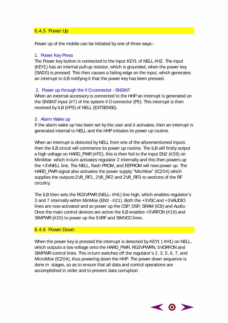
6.4.5 Power Up
Power up of the mobile can be initiated by one of three ways:-
1. Power Key PressThe Power key button is connected to the input KEY1 of NELL #H2. The input(KEY1) has an internal pull-up resistor, which is grounded, when the power key(SW20) is pressed. This then causes a failing edge on the input, which generatesan interrupt to ILB notifying it that the power key has been pressed.
2. Power up through the I/O connector - SNSINTWhen an external accessory is connected to the HHP an interrupt is generated onthe SNSINT input (#7) of the system I/O connector (P5). This interrupt is thenreceived by ILB (#P3) of NELL (EXTSENSE).
3. Alarm Wake upIf the alarm wake up has been set by the user and it activates, then an interrupt isgenerated internal to NELL and the HHP initiates its power up routine.
When an interrupt is detected by NELL from one of the aforementioned inputsthen the ILB circuit will commence its power up routine. The ILB will firstly outputa high voltage on HARD_PWR (#P2), this is then fed to the input EN2 (#28) onMiniMoe which in-turn activates regulator 2 internally and this then powers upthe +3VNELL line. The NELL, flash PROM, and EEPROM will now power up. TheHARD_PWR signal also activates the power supply “MicrMoe” (IC204) whichsupplies the outputs:2V8_RF1, 2V8_RF2 and 2V8_RF3 to sections of the RFcircuitry.
The ILB then sets the RG3VPWR (NELL- #H1) line high, which enables regulator’s3 and 7 internally within MinMoe (EN3 - #21). Both the +3VSC and +3VAUDIOlines are now activated and so power up the CSP, DSP, SRAM (IC9) and Audio.Once the main control devices are active the ILB enables +5VRFON (#19) andSIMPWR (#20) to power up the 5VRF and SIMVCC lines.
6.4.6 Power Down
When the power key is pressed the interrupt is detected by KEY1 ( #H1) on NELL,which outputs a low voltage onto the HARD_PWR, RG3VPWRN, 5VORFON andSIMPWR control lines. This in-turn switches off the regulator’s 2, 3, 5, 6, 7, andMicroMoe (IC204), thus powering down the HHP. The power down sequence isdone in stages, so as to ensure that all data and control operations areaccomplished in order and to prevent data corruption.
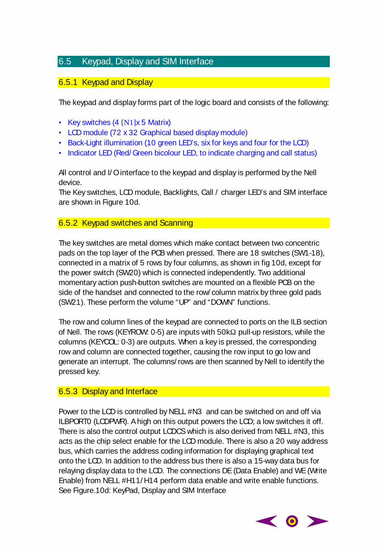
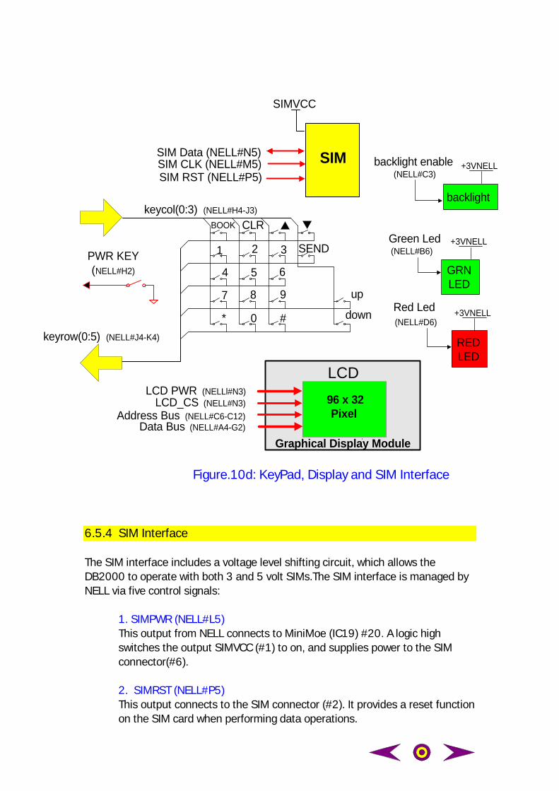
6.5 Keypad, Display and SIM Interface
6.5.1 Keypad and Display
The keypad and display forms part of the logic board and consists of the following:
• Key switches (4 [N1]x 5 Matrix)• LCD module (72 x 32 Graphical based display module)• Back-Light illumination (10 green LED’s, six for keys and four for the LCD)• Indicator LED (Red/Green bicolour LED, to indicate charging and call status)
All control and I/O interface to the keypad and display is performed by the Nelldevice.The Key switches, LCD module, Backlights, Call / charger LED’s and SIM interfaceare shown in Figure 10d.
6.5.2 Keypad switches and Scanning
The key switches are metal domes which make contact between two concentricpads on the top layer of the PCB when pressed. There are 18 switches (SW1-18),connected in a matrix of 5 rows by four columns, as shown in fig 10d, except forthe power switch (SW20) which is connected independently. Two additionalmomentary action push-button switches are mounted on a flexible PCB on theside of the handset and connected to the row/column matrix by three gold pads(SW21). These perform the volume “UP” and “DOWN” functions.
The row and column lines of the keypad are connected to ports on the ILB sectionof Nell. The rows (KEYROW: 0-5) are inputs with 50kΩ pull-up resistors, while thecolumns (KEYCOL: 0-3) are outputs. When a key is pressed, the correspondingrow and column are connected together, causing the row input to go low andgenerate an interrupt. The columns/rows are then scanned by Nell to identify thepressed key.
6.5.3 Display and Interface
Power to the LCD is controlled by NELL #N3 and can be switched on and off viaILBPORT0 (LCDPWR). A high on this output powers the LCD; a low switches it off.There is also the control output LCDCS which is also derived from NELL #N3, thisacts as the chip select enable for the LCD module. There is also a 20 way addressbus, which carries the address coding information for displaying graphical textonto the LCD. In addition to the address bus there is also a 15-way data bus forrelaying display data to the LCD. The connections DE (Data Enable) and WE (WriteEnable) from NELL #H11/H14 perform data enable and write enable functions.See Figure.10d: KeyPad, Display and SIM Interface
k
Figure.10d: KeyPad, Display and SIM Interface
6.5.4 SIM Interface
The SIM interface includes a voltage level shifting circuit, which allows theDB2000 to operate with both 3 and 5 volt SIMs.The SIM interface is managed byNELL via five control signals:
1. SIMPWR (NELL#L5)This output from NELL connects to MiniMoe (IC19) #20. A logic highswitches the output SIMVCC (#1) to on, and supplies power to the SIMconnector(#6).
2. SIMRST (NELL#P5)This output connects to the SIM connector (#2). It provides a reset functionon the SIM card when performing data operations.
down
Green Led(NELL#B6)
Red Led (NELL#D6)
GRNLED
REDLED
LCD_CS (NELL#N3) LCD PWR (NELLl#N3)
Address Bus (NELL#C6-C12)Data Bus (NELL#A4-G2)
LCD
Graphical Display Module
1 2 3 SEND
4 5 6
7 8 9
0* #
up
keycol(0:3) (NELL#H4-J3)
eyrow(0:5) (NELL#J4-K4)
PWR KEY(NELL#H2)
BOOK CLR
backlight
backlight enable(NELL#C3)
SIM
SIMVCC
SIM Data (NELL#N5) SIM CLK (NELL#M5) SIM RST (NELL#P5)
96 x 32Pixel
+3VNELL
+3VNELL
+3VNELL
3. SIMCLK (NELL#M5)This output connects to the SIM connector (#3). It is used to clock data toand from the SIM card and can be switched off when not required in orderto save power.
4. SIMDT (NELL#N5 - SIMDATA)This output connects to SIM connector (#6). All data to and from the SIMCard is transferred along this line.
5. SIMVSEL (NELL#L3)This control signal from NELL is used to select the operating voltage of theSIM card. Setting the SIMVSEL high switches regulator 5 in MiniMoe to 5vwhich in turn is output to the SIMVCC rail. A low switches the SIM supply to3v.
6.6 Audio and Miscellaneous Interfaces
The audio and miscellaneous interfaces include the following:
1. Microphone2. Ear-piece3. Hands free Interface4. Buzzer driver5. Battery charging circuit6. Vibrator7. Simple Hands Free Interface (SHF)
6.6.1 6.6.1 Microphone
The microphone is mounted in the handset front cover and connects to the logicboard via two sprung contacts on the P5 connector. The audio signal is passed tothe logic board and to pin D4 of the P6 Simple Hands Free (SHF) socket. Insidethe socket there is a miniature switch which is closed when there is no SHFconnected. With this switch closed this allows the audio signal through to the MICIN (#4) pin of IC27. The voltage supply VREG is output from IC27 #3, and is a biasvoltage for both the MIC Audio path (through R156) and +TXAF lines.See Figure:10E. Audio and Miscellaneous Interfaces
The microphone or TXAF signal is then A/D converted by the CSP part ofSuperchip (IC27). The digitised speech is then passed to the DSP section of IC27for processing (coding, interleaving etc.). The coded speech data returns to theCSP for GMSK modulation, D/A conversion and output as TXI and TXQ signals –IC27 #86-89 - to the W2013 transceiver (IC100) for modulation onto the airinterface.
6.6.2 6.6.2 Earpiece
The earpiece is driven directly from IC27 AOUTP(#94) and AOUTN(#93) pins. Thegain is controlled by the DSP software element within IC27. The earpiece islocated in the handset front panel, and the signals are routed to it via twoconnection pads on the front of the logic board.
RXI and RXQ signals from IC300 (PMB2410) are fed to IC27 #77-80 (Superchip)where they are amplified and then A/D converted. The I and Q samples are storedin lots of 32 before the DSP part of Superchip (IC27) is interrupted to processthem. The DSP will carry out error detection and correction, and assemble thespeech data into a form acceptable to the D/A converter in the CSP section. AfterD/A conversion the signal is output on IC27 #93/94) - earpiece - and / or #95/96)- RXAF.
6.6.3 6.6.3 Hands-Free Interface
The audio out (RXAF+/-) to the hands-free kit consists of a pair of differentialsignals from IC27’s auxiliary outputs (#95-96), which are tracked down the boardto the system connector (P5) at the base of the handset.
The audio in (TXAF+/-) from the hands-free is converted to a single signal usingthe op-amp (IC13). The bias voltage VREF from IC27 #3 is used as a referencevoltage for this amplifier. The TXAF signal is then input to the AUXIN (#99) of IC27.The DC level of the signal is supplied to the AUXOUT pin.
6.6.4 6.6.4 Buzzer Driver
The buzzer or alerter is a piezo-electric transducer which is driven by a pulse-widthmodulated square wave from the PWMOUT output of NELL (#M14). TR4 andTR11 amplify the signal in order to achieve the specified loudness of 100dBa.See Figure:6E. Audio and Miscellaneous Interfaces.
6.6.5 6.6.5 Battery Charging
The battery is charged via a constant 850mA current source, which is plugged intothe DC jack in the system connector P5 #2. Charge control is implemented insoftware using the analogue to digital converter in NELL. It then determines thetype and capacity of the battery connected by reading the battery ID resistor(BATID), on an A/D converter port, from which it determines the chargingalgorithm. When an external charging source is connected via the P5 connectoran interrupt signal EXTCHG is sent to NELL #N4. When NELL receives thisinterrupt it initiates the charger enable signal CHGEN, this action switches onTR28 which activates FET –TR3. When TR3 is conducting it allows the battery tobe charged. Battery charging current is measured by means of a fixed loopstripline or “shunt” which is mounted internally within the layers of the PCB. When
charging the stripline gives a voltage value directly proportional to the chargingcurrent of the battery, this voltage CHGSENSE is sent to NELL #P9 on a A/Dconverter port, from which it determines the charge current. See G4H Logic circuitdiagram, page 1.
6.6.6 6.6.6 Vibrator
The vibrator is located on the board to board shield and is connected to the logicboard via a connector cable, which plugs into socket: P2-A1 & P2-B2. The vibratoris driven by the signal VIB, which is output from NELL (#F2). The signal isamplified by the transistors TR4-B and TR12 and is supplied from VBAT.See G4H Logic circuit diagram, page 2.
6.6.7 6.6.7 Simple Hands Free Interface
The simple hands free (SHF) interface allows the user to communicate via a singleearpiece, which fits into the ear and a mic, which is joined to the interface cable.The SHF lead is connected to the DB2000 via a small jack plug, which plugs into asocket mounted into the side of the mobile. When the SHF lead is plugged in, themobiles mic and earpiece are disconnected. When the SHF lead is not connected,the mobiles internal microphone (connected across:P5- #17 & #18) outputpasses through a switch (normally closed) fitted inside the SHF socket (P6- #B2 &#D4) and onto IC27 #4 for processing. If the SHF lead is connected then theswitch contact is opened, thus disconnecting the mobiles own internal mic.The SHF earpiece connects across contacts C3 and A1 of the P6 connector. Theoutput RXAF+ of IC27-#96 provides the audio output for the SHF earpiece. Themobile detects that the SHF is connected by the monitoring the voltage level atthe point:SHFREE (NELL # B7), which is biased by the supply +3VAUDIO. Whenthe SHF earpeice is connected the voltage level at the point SHFREE is taken lowby the earpeice, which connects it to ground by the contact: A1 of the P6connector. NELL will then instruct IC27 to disable the mobiles audio outputs (#93-94) and instead route the audio through the auxiliary output:RXAF+ (#96) to theSHF earpeice.
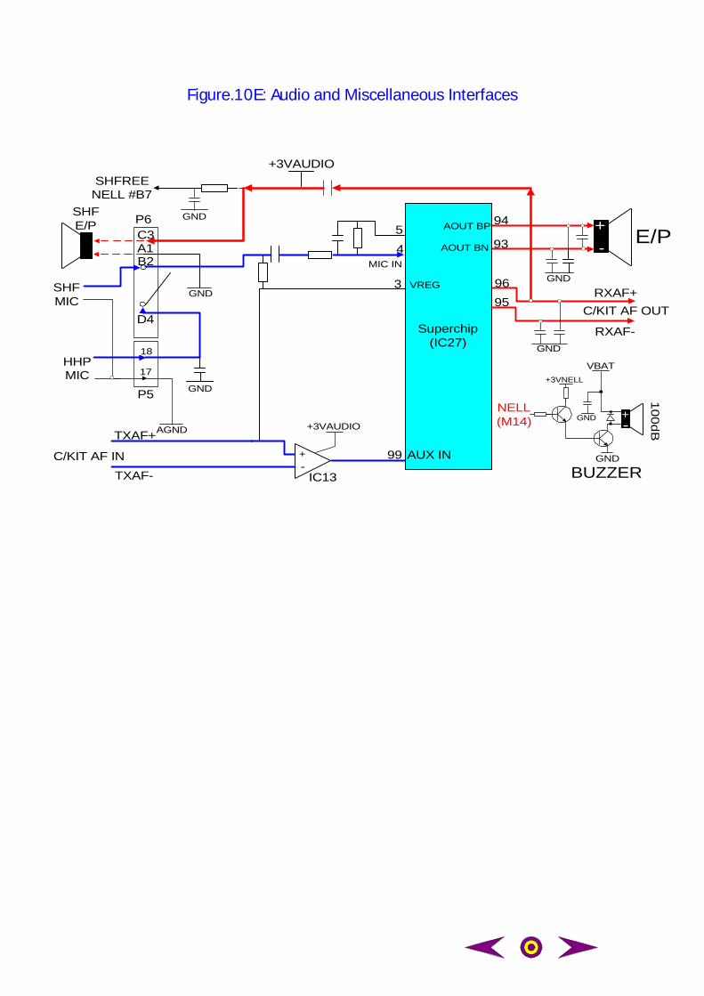
Figure.10E: Audio and Miscellaneous Interfaces
Superchip(IC27)
+-
GND
AOUT BP
AOUT BN
94
93
RXAF-
RXAF+
GND
9695
C/KIT AF OUT
E/P
+3VAUDIOSHFREENELL #B7
P6C3A1 4
5SHFE/P
GND
GND
D4
B2
SHFMIC
HHPMIC
AGND
P5
18
17
MIC IN
GND3 VREG
+-
TXAF+
TXAF-
+3VAUDIO
C/KIT AF IN 99 AUX IN
IC13
+-
VBAT
NELL(M14)
GND
+3VNELL
GND
BUZZER
100dB
<< Previous SectionNext Section >>Main Menu
Section 4Section 4
ServicingServicing
Part 1 Cables, Jigs and FixturesPart 2 Equipment ConfigurationPart 3a DisassemblyPart 3b Assembly
Part 1: Cables, Jigs and Fixtures
Detailed below are a range of cables, jigs and fixtures available for use on repairand test/calibration stations.
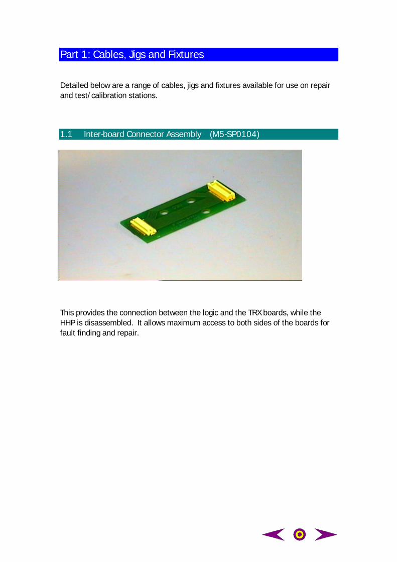
1.1 Inter-board Connector Assembly (M5-SP0104)
This provides the connection between the logic and the TRX boards, while theHHP is disassembled. It allows maximum access to both sides of the boards forfault finding and repair.
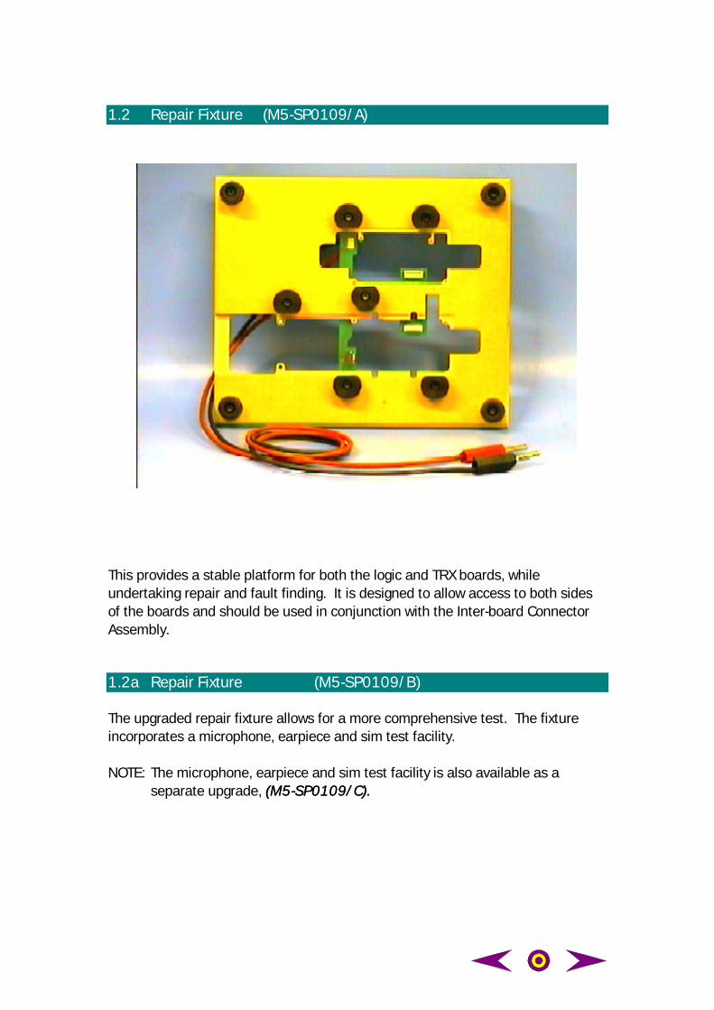
1.2 Repair Fixture (M5-SP0109/A)
This provides a stable platform for both the logic and TRX boards, whileundertaking repair and fault finding. It is designed to allow access to both sidesof the boards and should be used in conjunction with the Inter-board ConnectorAssembly.
1.2a Repair Fixture (M5-SP0109/B)
The upgraded repair fixture allows for a more comprehensive test. The fixtureincorporates a microphone, earpiece and sim test facility.
NOTE: The microphone, earpiece and sim test facility is also available as aseparate upgrade, (M5-SP0109/C).(M5-SP0109/C).
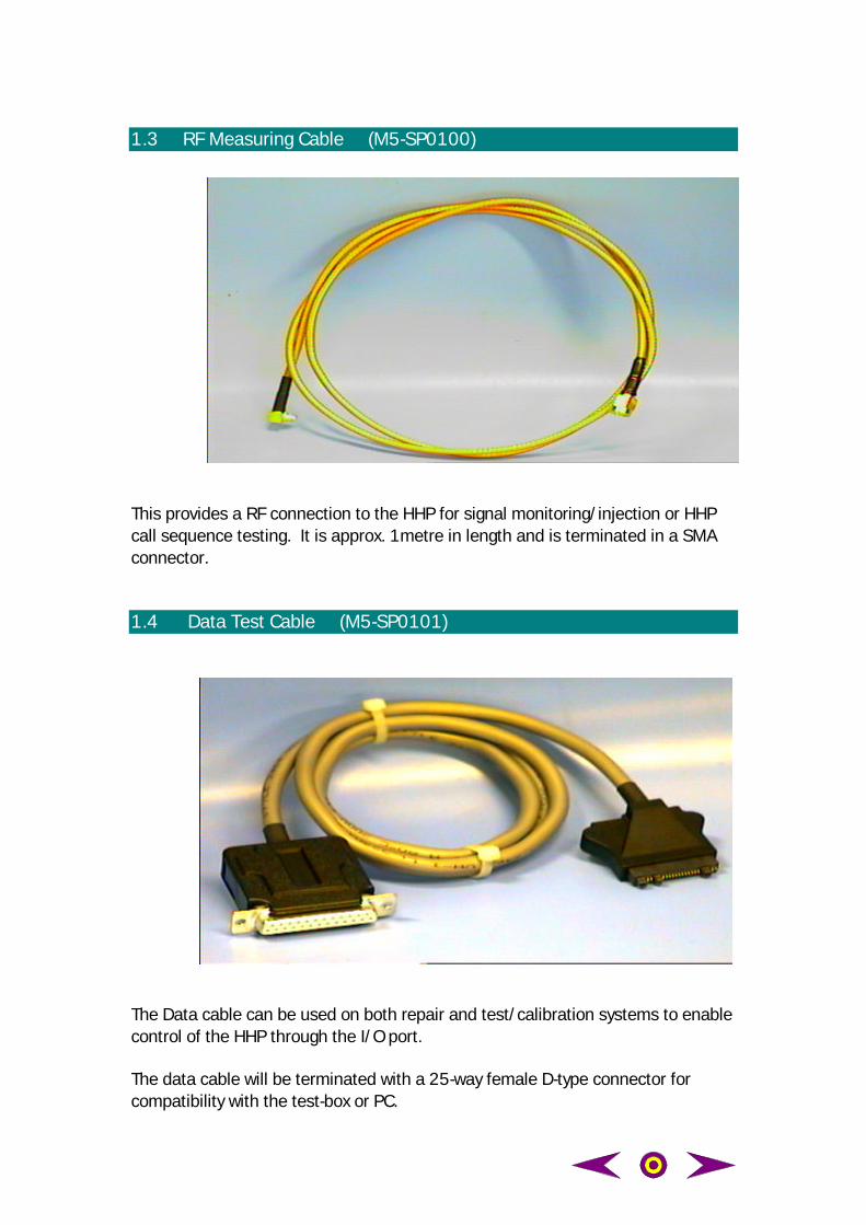
1.3 RF Measuring Cable (M5-SP0100)
This provides a RF connection to the HHP for signal monitoring/injection or HHPcall sequence testing. It is approx. 1metre in length and is terminated in a SMAconnector.
1.4 Data Test Cable (M5-SP0101)
The Data cable can be used on both repair and test/calibration systems to enablecontrol of the HHP through the I/O port.
The data cable will be terminated with a 25-way female D-type connector forcompatibility with the test-box or PC.
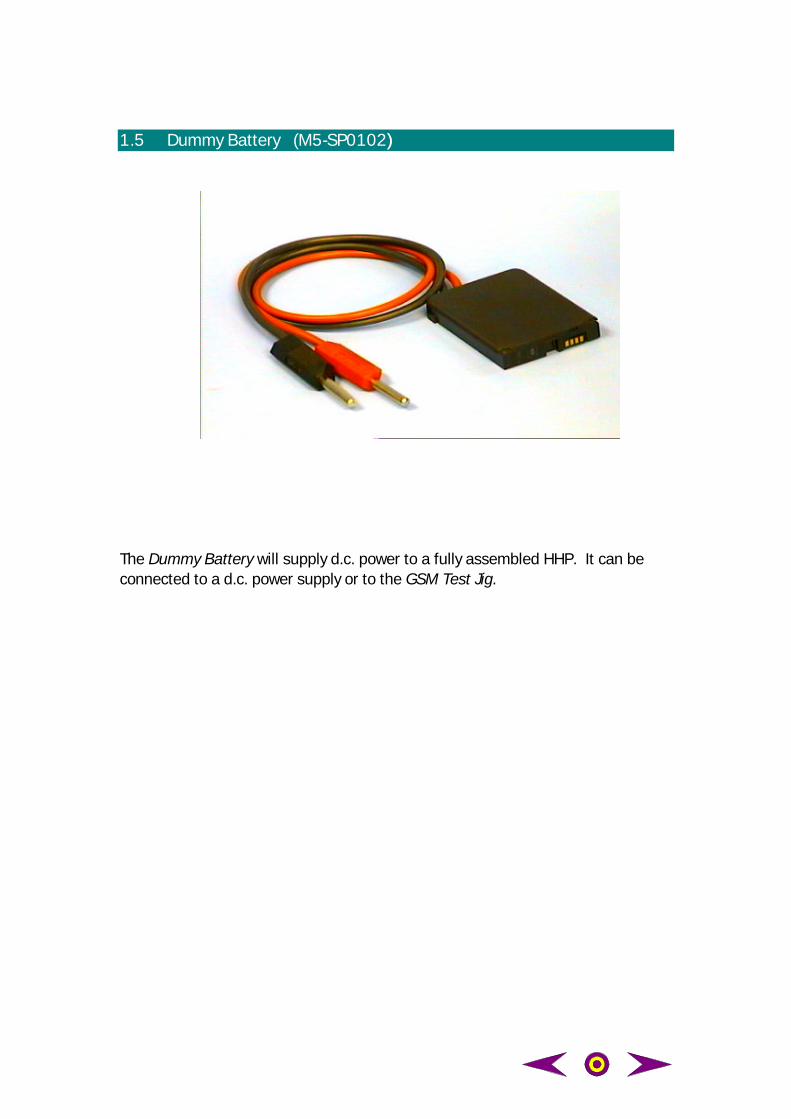
1.5 Dummy Battery (M5-SP0102))
The Dummy Battery will supply d.c. power to a fully assembled HHP. It can beconnected to a d.c. power supply or to the GSM Test Jig.
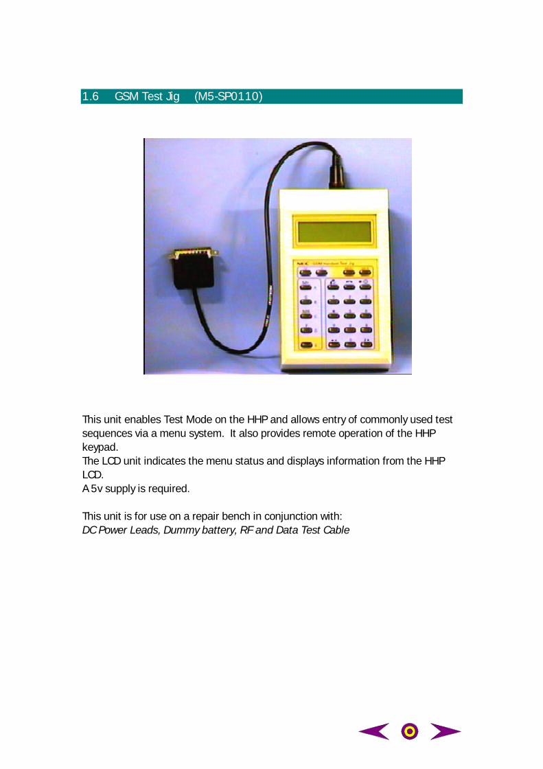
1.6 GSM Test Jig (M5-SP0110)
This unit enables Test Mode on the HHP and allows entry of commonly used testsequences via a menu system. It also provides remote operation of the HHPkeypad.The LCD unit indicates the menu status and displays information from the HHPLCD.A 5v supply is required.
This unit is for use on a repair bench in conjunction with:DC Power Leads, Dummy battery, RF and Data Test Cable
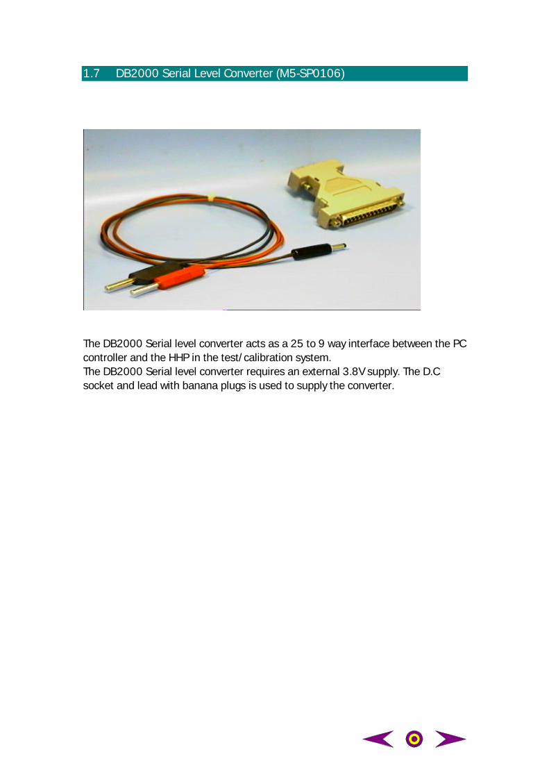
1.7 DB2000 Serial Level Converter (M5-SP0106)
The DB2000 Serial level converter acts as a 25 to 9 way interface between the PCcontroller and the HHP in the test/calibration system.The DB2000 Serial level converter requires an external 3.8V supply. The D.Csocket and lead with banana plugs is used to supply the converter.
Part 2: Equipment configurations
The test equipment configurations for repair, test/calibration and simplefunctional testing are shown below. Where specific items of test equipment arerequired, make and model numbers are quoted.
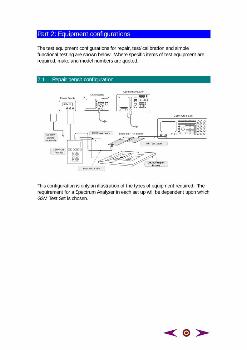
2.1 Repair bench configuration
5.0v dc
Power Supply
Logic and TRX boards
DB2000 RepairFixture
DC Power Leads
GSM/PCNTest Jig
GSM/PCN test set
Dummybattery
(optional)
OscilloscopeSpectrum Analyzer
Data Test Cable
RF Test Cable
This configuration is only an illustration of the types of equipment required. Therequirement for a Spectrum Analyser in each set up will be dependent upon whichGSM Test Set is chosen.
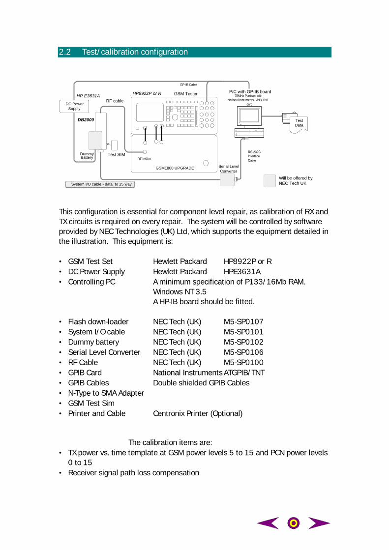
2.2 Test/calibration configuration
GSM TesterHP8922P or R
GP-IB Cable
System I/O cable - data to 25 way
RS-232CInterfaceCable
DB2000
DummyBattery
DC PowerSupply
Will be offered byNEC Tech UK
P/C with GP-IB boardHP E3631A
Test SIM
TestData
Serial LevelConverter
75MHz Pentium withNational Instuments GPIB-TNT
cardRF cable
RF In/Out
GSM1800 UPGRADE
This configuration is essential for component level repair, as calibration of RX andTX circuits is required on every repair. The system will be controlled by softwareprovided by NEC Technologies (UK) Ltd, which supports the equipment detailed inthe illustration. This equipment is:
• GSM Test Set Hewlett Packard HP8922P or R• DC Power Supply Hewlett Packard HPE3631A• Controlling PC A minimum specification of P133/16Mb RAM. Windows NT 3.5
A HP-IB board should be fitted. • Flash down-loader NEC Tech (UK) M5-SP0107• System I/O cable NEC Tech (UK) M5-SP0101• Dummy battery NEC Tech (UK) M5-SP0102• Serial Level Converter NEC Tech (UK) M5-SP0106• RF Cable NEC Tech (UK) M5-SP0100• GPIB Card National Instruments ATGPIB/TNT• GPIB Cables Double shielded GPIB Cables• N-Type to SMA Adapter• GSM Test Sim• Printer and Cable Centronix Printer (Optional) The calibration items are:• TX power vs. time template at GSM power levels 5 to 15 and PCN power levels
0 to 15• Receiver signal path loss compensation
Part 3a: Disassembly
Caution: Ensure an Anti-Static strap is worn and connected to an earth bondedCaution: Ensure an Anti-Static strap is worn and connected to an earth bondedbench before handling any components.bench before handling any components.
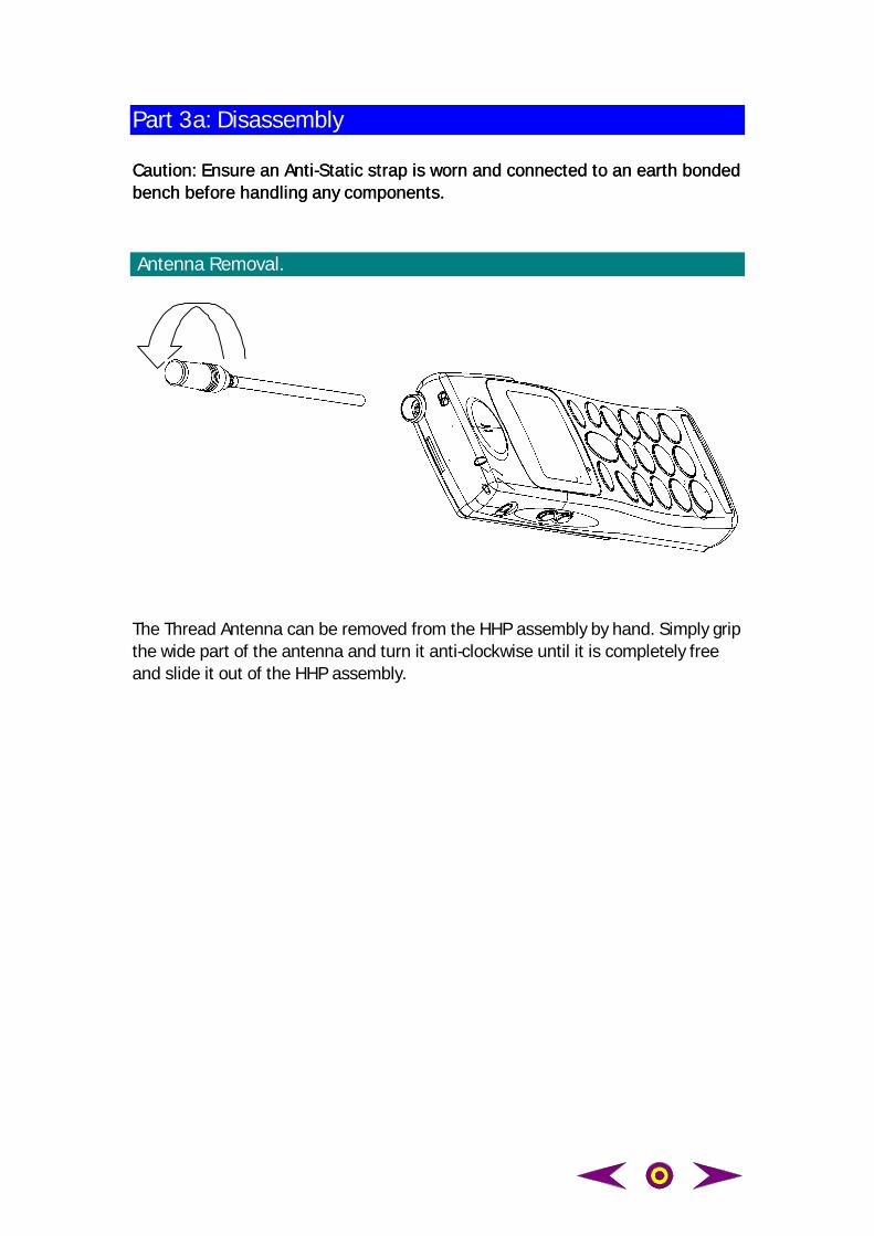
Antenna Removal.
The Thread Antenna can be removed from the HHP assembly by hand. Simply gripthe wide part of the antenna and turn it anti-clockwise until it is completely freeand slide it out of the HHP assembly.
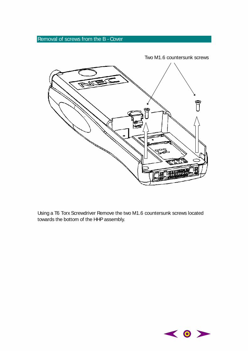
Removal of screws from the B - Cover
Two M1.6 countersunk screws
Using a T6 Torx Screwdriver Remove the two M1.6 countersunk screws locatedtowards the bottom of the HHP assembly.
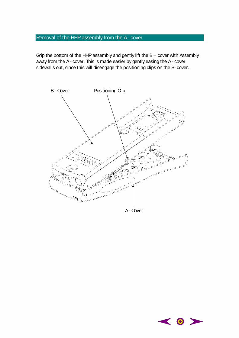
Removal of the HHP assembly from the A - cover
Grip the bottom of the HHP assembly and gently lift the B – cover with Assemblyaway from the A - cover. This is made easier by gently easing the A - coversidewalls out, since this will disengage the positioning clips on the B- cover.
B - Cover Positioning Clip
A - Cover
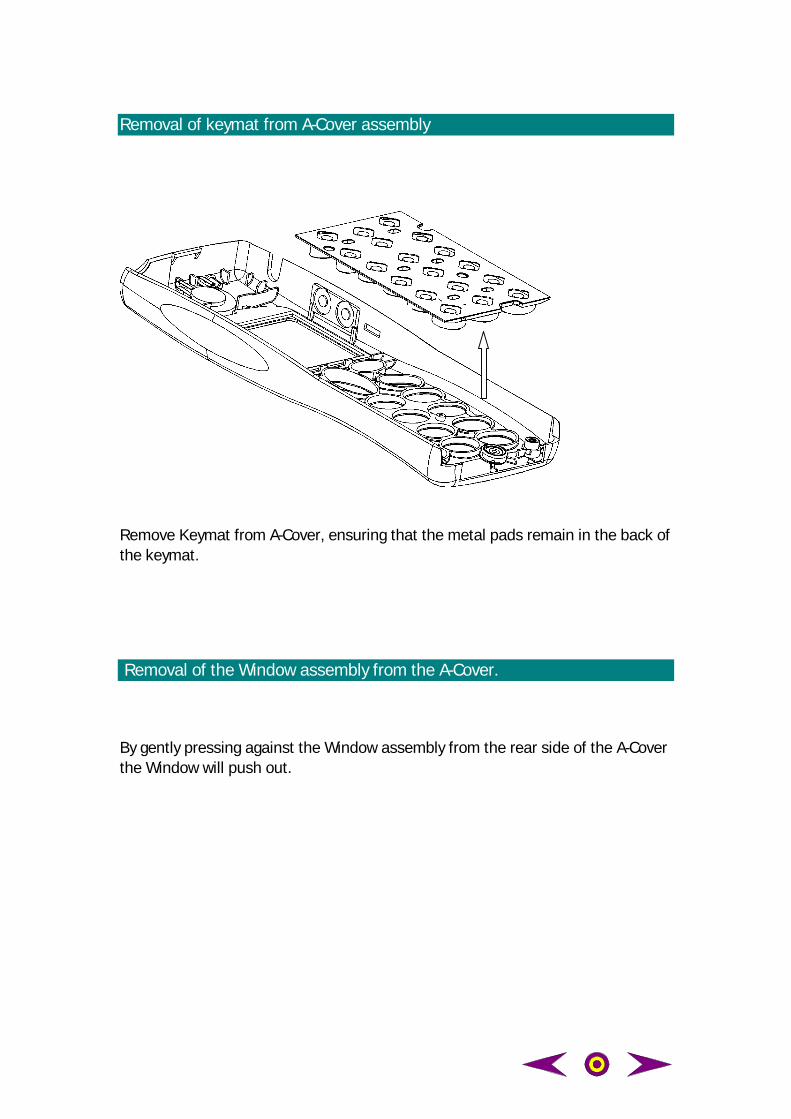
Removal of keymat from A-Cover assembly
Remove Keymat from A-Cover, ensuring that the metal pads remain in the back ofthe keymat.
Removal of the Window assembly from the A-Cover.
By gently pressing against the Window assembly from the rear side of the A-Coverthe Window will push out.
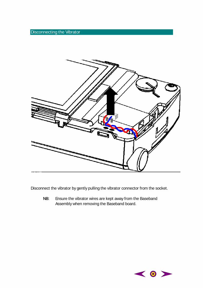
Disconnecting the Vibrator
Disconnect the vibrator by gently pulling the vibrator connector from the socket.
NBNB: Ensure the vibrator wires are kept away from the BasebandAssembly when removing the Baseband board.
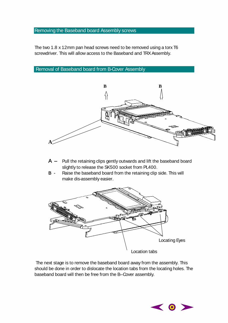
Removing the Baseband board Assembly screws
The two 1.8 x 12mm pan head screws need to be removed using a torx T6screwdriver. This will allow access to the Baseband and TRX Assembly.
Removal of Baseband board from B-Cover Assembly
B B
A
A – A – Pull the retaining clips gently outwards and lift the baseband boardslightly to release the SK500 socket from PL400.
B -B - Raise the baseband board from the retaining clip side. This willmake dis-assembly easier.
Locating Eyes
Location tabs
The next stage is to remove the baseband board away from the assembly. Thisshould be done in order to dislocate the location tabs from the locating holes. Thebaseband board will then be free from the B–Cover assembly.
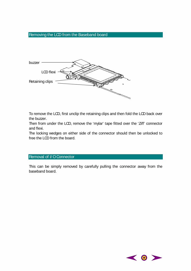
Removing the LCD from the Baseband board
buzzer
LCD flexi
Retaining clips
To remove the LCD, first unclip the retaining clips and then fold the LCD back overthe buzzer.Then from under the LCD, remove the ‘mylar’ tape fitted over the ‘Ziff’ connectorand flexi.The locking wedges on either side of the connector should then be unlocked tofree the LCD from the board.
Removal of I/O Connector
This can be simply removed by carefully pulling the connector away from thebaseband board.
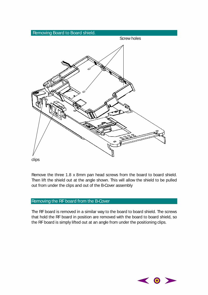
Removing Board to Board shield.Screw holes
clips
Remove the three 1.8 x 8mm pan head screws from the board to board shield.Then lift the shield out at the angle shown. This will allow the shield to be pulledout from under the clips and out of the B-Cover assembly
Removing the RF board from the B-Cover
The RF board is removed in a similar way to the board to board shield. The screwsthat hold the RF board in position are removed with the board to board shield, sothe RF board is simply lifted out at an angle from under the positioning clips.
Part 3b: Assembly
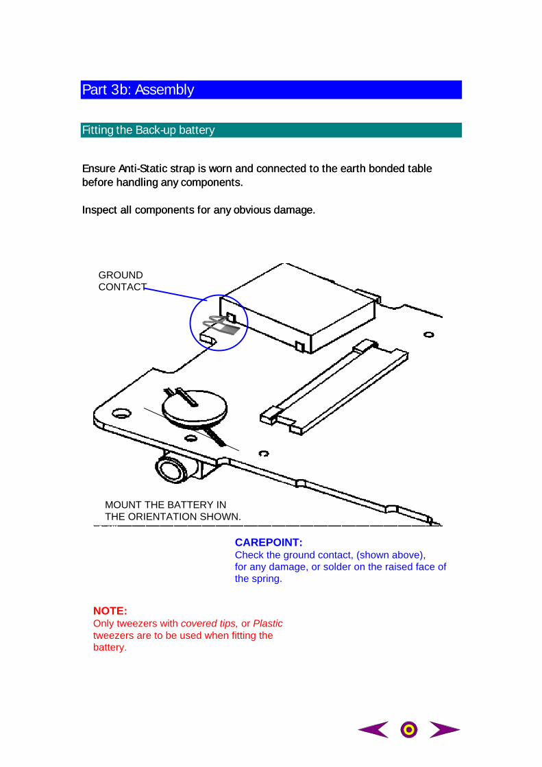
Fitting the Back-up battery
Ensure Anti-Static strap is worn and connected to the earth bonded tableEnsure Anti-Static strap is worn and connected to the earth bonded tablebefore handling any components.before handling any components.
Inspect all components for any obvious damage.Inspect all components for any obvious damage.
NOTE:Only tweezers with covered tips, or Plastictweezers are to be used when fitting thebattery.
MOUNT THE BATTERY INTHE ORIENTATION SHOWN.
GROUNDCONTACT
CAREPOINT:Check the ground contact, (shown above),for any damage, or solder on the raised face ofthe spring.
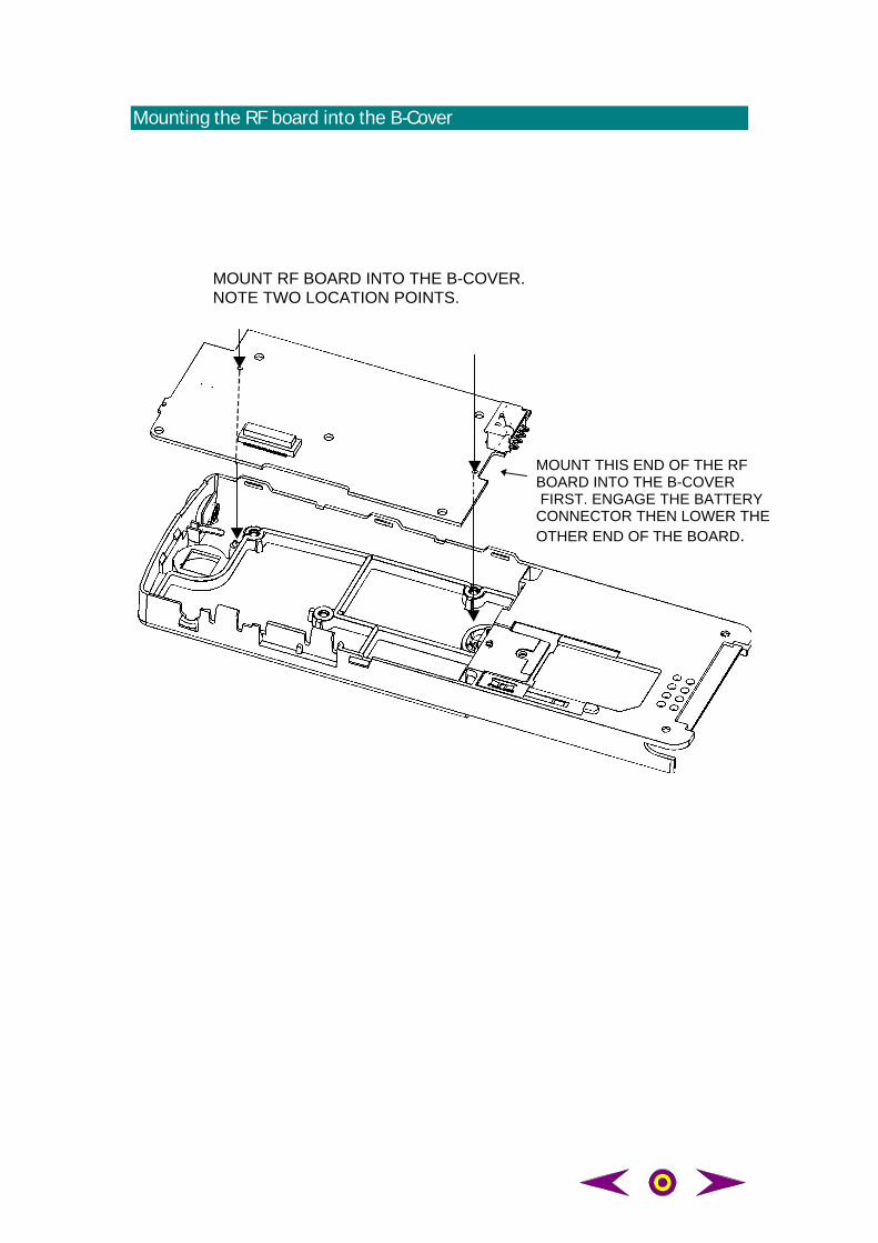
Mounting the RF board into the B-Cover
MOUNT RF BOARD INTO THE B-COVER.NOTE TWO LOCATION POINTS.
MOUNT THIS END OF THE RFBOARD INTO THE B-COVER FIRST. ENGAGE THE BATTERYCONNECTOR THEN LOWER THEOTHER END OF THE BOARD.
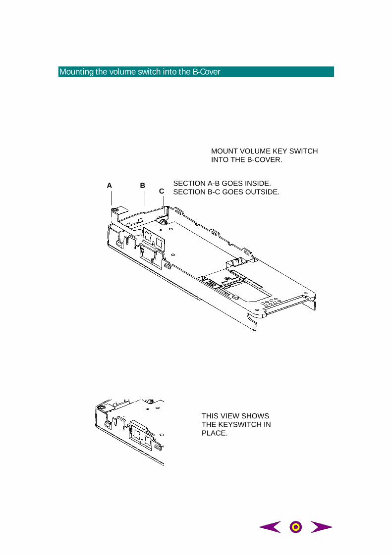
Mounting the volume switch into the B-Cover
MOUNT VOLUME KEY SWITCHINTO THE B-COVER.
A BC
SECTION A-B GOES INSIDE.SECTION B-C GOES OUTSIDE.
THIS VIEW SHOWSTHE KEYSWITCH INPLACE.
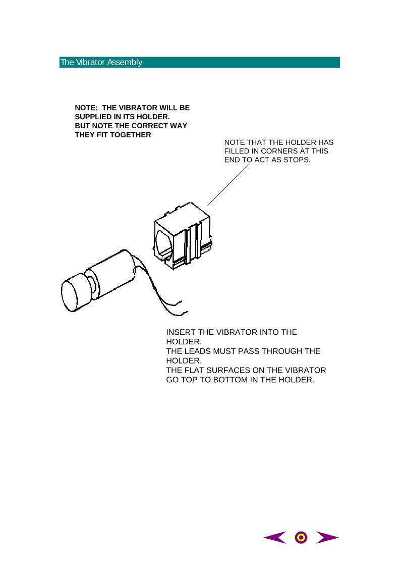
The Vibrator Assembly
INSERT THE VIBRATOR INTO THEHOLDER.THE LEADS MUST PASS THROUGH THEHOLDER.THE FLAT SURFACES ON THE VIBRATORGO TOP TO BOTTOM IN THE HOLDER.
NOTE THAT THE HOLDER HASFILLED IN CORNERS AT THISEND TO ACT AS STOPS.
NOTE: THE VIBRATOR WILL BESUPPLIED IN ITS HOLDER.BUT NOTE THE CORRECT WAYTHEY FIT TOGETHER
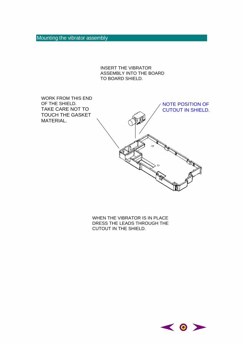
Mounting the vibrator assembly
WHEN THE VIBRATOR IS IN PLACEDRESS THE LEADS THROUGH THECUTOUT IN THE SHIELD.
INSERT THE VIBRATORASSEMBLY INTO THE BOARDTO BOARD SHIELD.
NOTE POSITION OFCUTOUT IN SHIELD.
WORK FROM THIS ENDOF THE SHIELD.TAKE CARE NOT TOTOUCH THE GASKETMATERIAL.
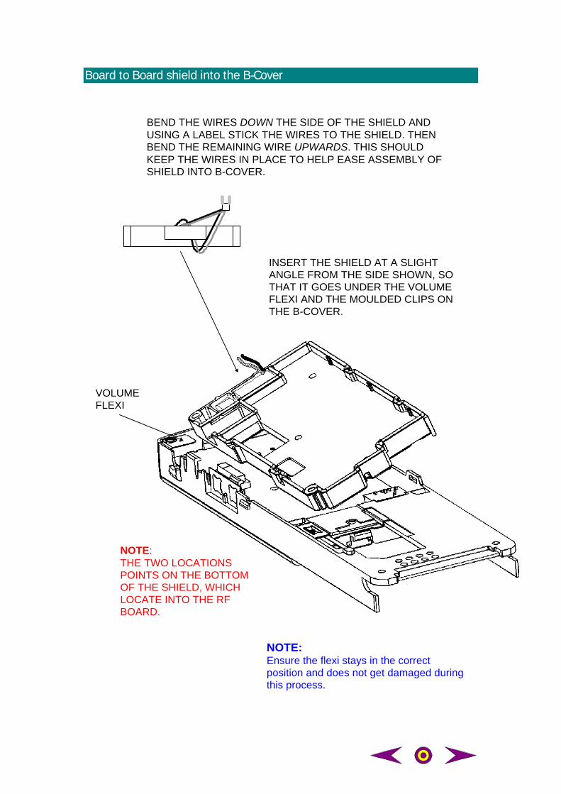
Board to Board shield into the B-Cover
VOLUMEFLEXI
INSERT THE SHIELD AT A SLIGHTANGLE FROM THE SIDE SHOWN, SOTHAT IT GOES UNDER THE VOLUMEFLEXI AND THE MOULDED CLIPS ONTHE B-COVER.
NOTE:THE TWO LOCATIONSPOINTS ON THE BOTTOMOF THE SHIELD, WHICHLOCATE INTO THE RFBOARD.
NOTE:Ensure the flexi stays in the correctposition and does not get damaged duringthis process.
BEND THE WIRES DOWN THE SIDE OF THE SHIELD ANDUSING A LABEL STICK THE WIRES TO THE SHIELD. THENBEND THE REMAINING WIRE UPWARDS. THIS SHOULDKEEP THE WIRES IN PLACE TO HELP EASE ASSEMBLY OFSHIELD INTO B-COVER.
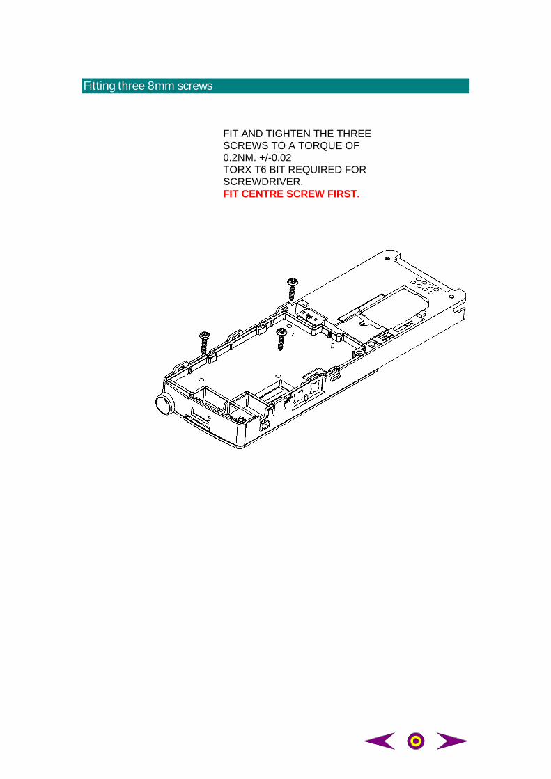
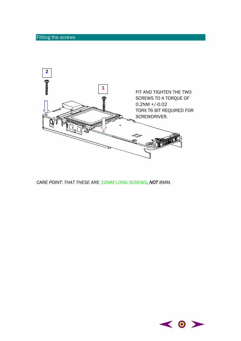
Fitting three 8mm screws
FIT AND TIGHTEN THE THREESCREWS TO A TORQUE OF0.2NM. +/-0.02TORX T6 BIT REQUIRED FORSCREWDRIVER.FIT CENTRE SCREW FIRST.
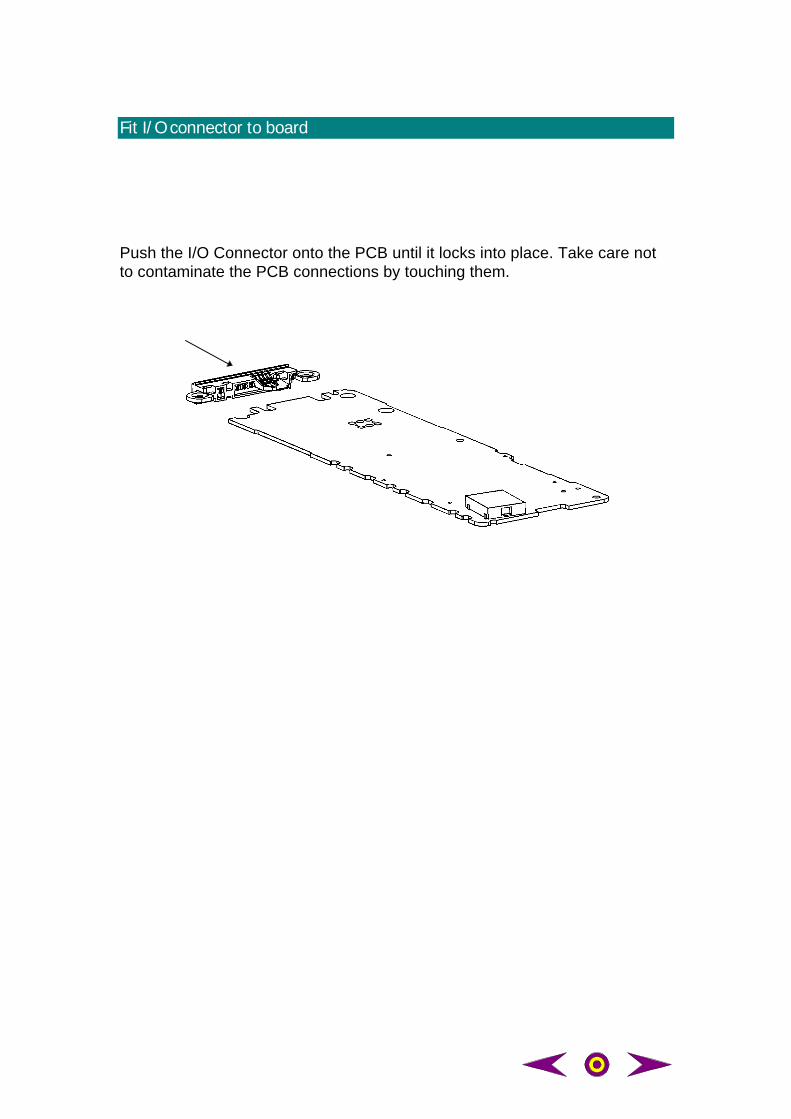
Fit I/O connector to board
Push the I/O Connector onto the PCB until it locks into place. Take care notto contaminate the PCB connections by touching them.
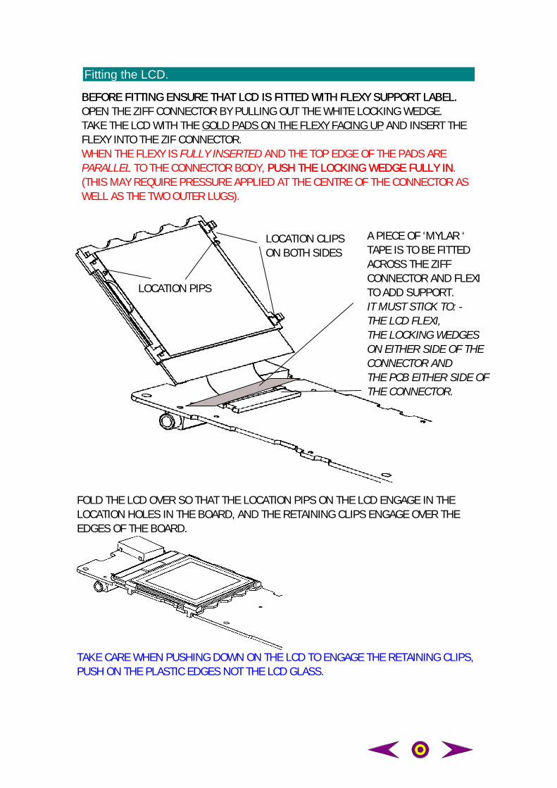
Fitting the LCD.
BEFORE FITTING ENSURE THAT LCD IS FITTED WITH FLEXY SUPPORT LABEL.BEFORE FITTING ENSURE THAT LCD IS FITTED WITH FLEXY SUPPORT LABEL.OPEN THE ZIFF CONNECTOR BY PULLING OUT THE WHITE LOCKING WEDGE.TAKE THE LCD WITH THE GOLD PADS ON THE FLEXY FACING UP AND INSERT THEFLEXY INTO THE ZIF CONNECTOR.WHEN THE FLEXY IS FULLY INSERTED AND THE TOP EDGE OF THE PADS AREPARALLEL TO THE CONNECTOR BODY, PUSH THE LOCKING WEDGE FULLY INPUSH THE LOCKING WEDGE FULLY IN.(THIS MAY REQUIRE PRESSURE APPLIED AT THE CENTRE OF THE CONNECTOR ASWELL AS THE TWO OUTER LUGS).
ZIFF CONNECTOR
LOCATION PIPS
LOCATION CLIPSON BOTH SIDES
FOLD THE LCD OVER SO THAT THE LOCATION PIPS ON THE LCD ENGAGE IN THELOCATION HOLES IN THE BOARD, AND THE RETAINING CLIPS ENGAGE OVER THEEDGES OF THE BOARD.
TAKE CARE WHEN PUSHING DOWN ON THE LCD TO ENGAGE THE RETAINING CLIPS,PUSH ON THE PLASTIC EDGES NOT THE LCD GLASS.
A PIECE OF ‘MYLAR ‘TAPE IS TO BE FITTEDACROSS THE ZIFFCONNECTOR AND FLEXITO ADD SUPPORT.IT MUST STICK TO: -THE LCD FLEXI,THE LOCKING WEDGESON EITHER SIDE OF THECONNECTOR ANDTHE PCB EITHER SIDE OFTHE CONNECTOR.
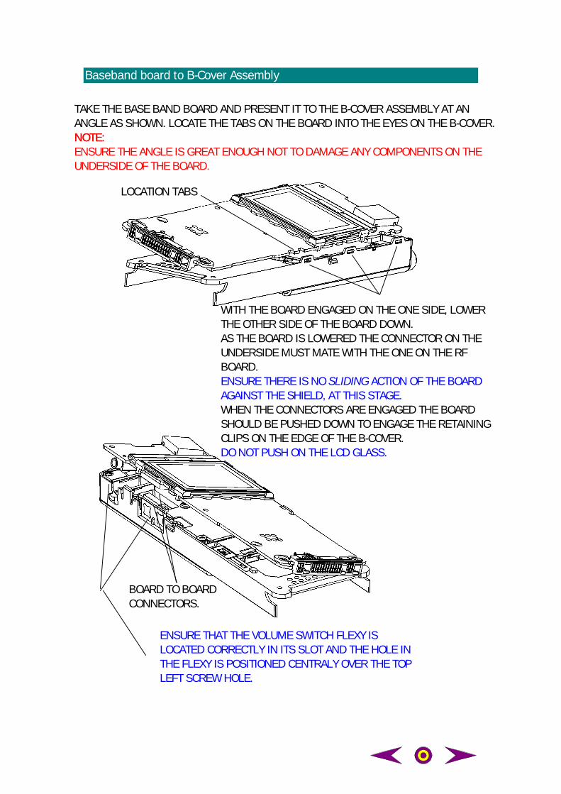
Baseband board to B-Cover Assembly
TAKE THE BASE BAND BOARD AND PRESENT IT TO THE B-COVER ASSEMBLY AT ANANGLE AS SHOWN. LOCATE THE TABS ON THE BOARD INTO THE EYES ON THE B-COVER.NOTE:NOTE:ENSURE THE ANGLE IS GREAT ENOUGH NOT TO DAMAGE ANY COMPONENTS ON THEUNDERSIDE OF THE BOARD.
LOCATION TABS
WITH THE BOARD ENGAGED ON THE ONE SIDE, LOWERTHE OTHER SIDE OF THE BOARD DOWN.AS THE BOARD IS LOWERED THE CONNECTOR ON THEUNDERSIDE MUST MATE WITH THE ONE ON THE RFBOARD.ENSURE THERE IS NO SLIDING ACTION OF THE BOARDAGAINST THE SHIELD, AT THIS STAGE.WHEN THE CONNECTORS ARE ENGAGED THE BOARDSHOULD BE PUSHED DOWN TO ENGAGE THE RETAININGCLIPS ON THE EDGE OF THE B-COVER.DO NOT PUSH ON THE LCD GLASS.
BOARD TO BOARDCONNECTORS.
ENSURE THAT THE VOLUME SWITCH FLEXY ISLOCATED CORRECTLY IN ITS SLOT AND THE HOLE INTHE FLEXY IS POSITIONED CENTRALY OVER THE TOPLEFT SCREW HOLE.
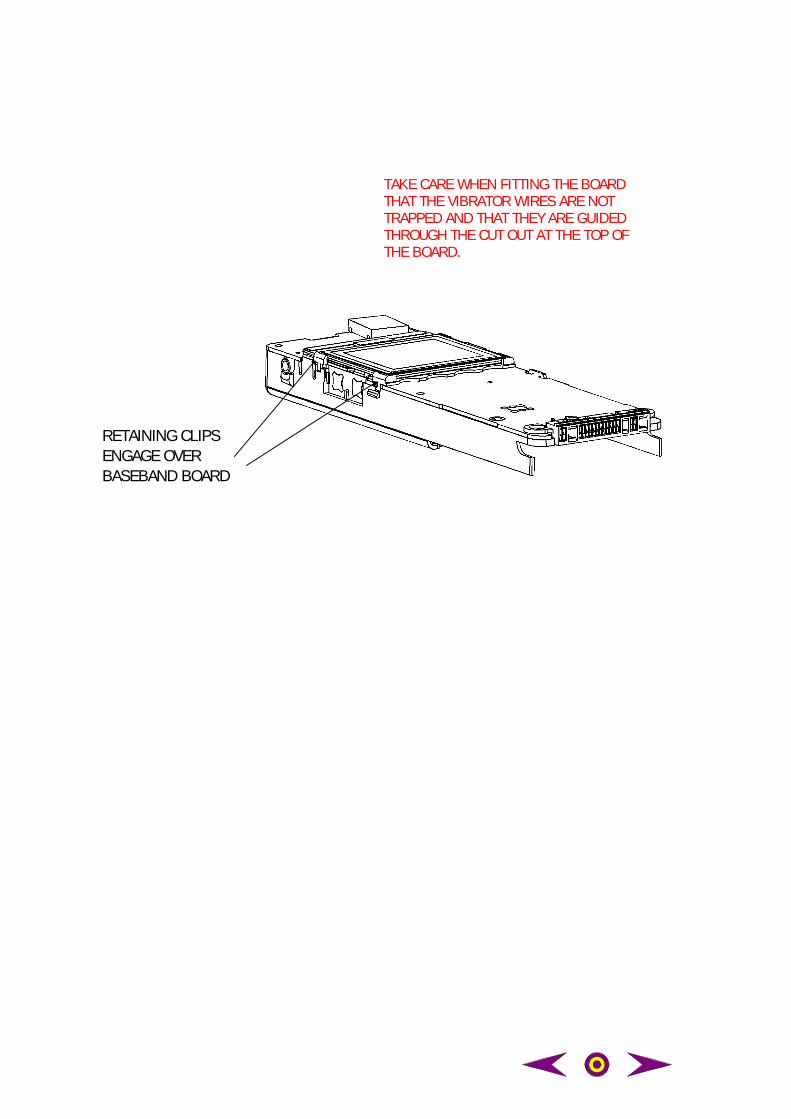
TAKE CARE WHEN FITTING THE BOARDTHAT THE VIBRATOR WIRES ARE NOTTRAPPED AND THAT THEY ARE GUIDEDTHROUGH THE CUT OUT AT THE TOP OFTHE BOARD.
RETAINING CLIPSENGAGE OVERBASEBAND BOARD
!"#
$%&
'
1
2
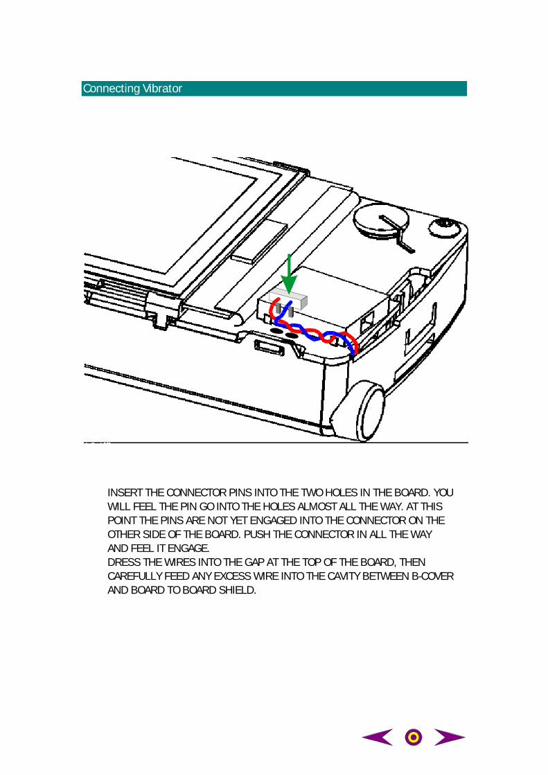
Connecting Vibrator
INSERT THE CONNECTOR PINS INTO THE TWO HOLES IN THE BOARD. YOUWILL FEEL THE PIN GO INTO THE HOLES ALMOST ALL THE WAY. AT THISPOINT THE PINS ARE NOT YET ENGAGED INTO THE CONNECTOR ON THEOTHER SIDE OF THE BOARD. PUSH THE CONNECTOR IN ALL THE WAYAND FEEL IT ENGAGE.DRESS THE WIRES INTO THE GAP AT THE TOP OF THE BOARD, THENCAREFULLY FEED ANY EXCESS WIRE INTO THE CAVITY BETWEEN B-COVERAND BOARD TO BOARD SHIELD.
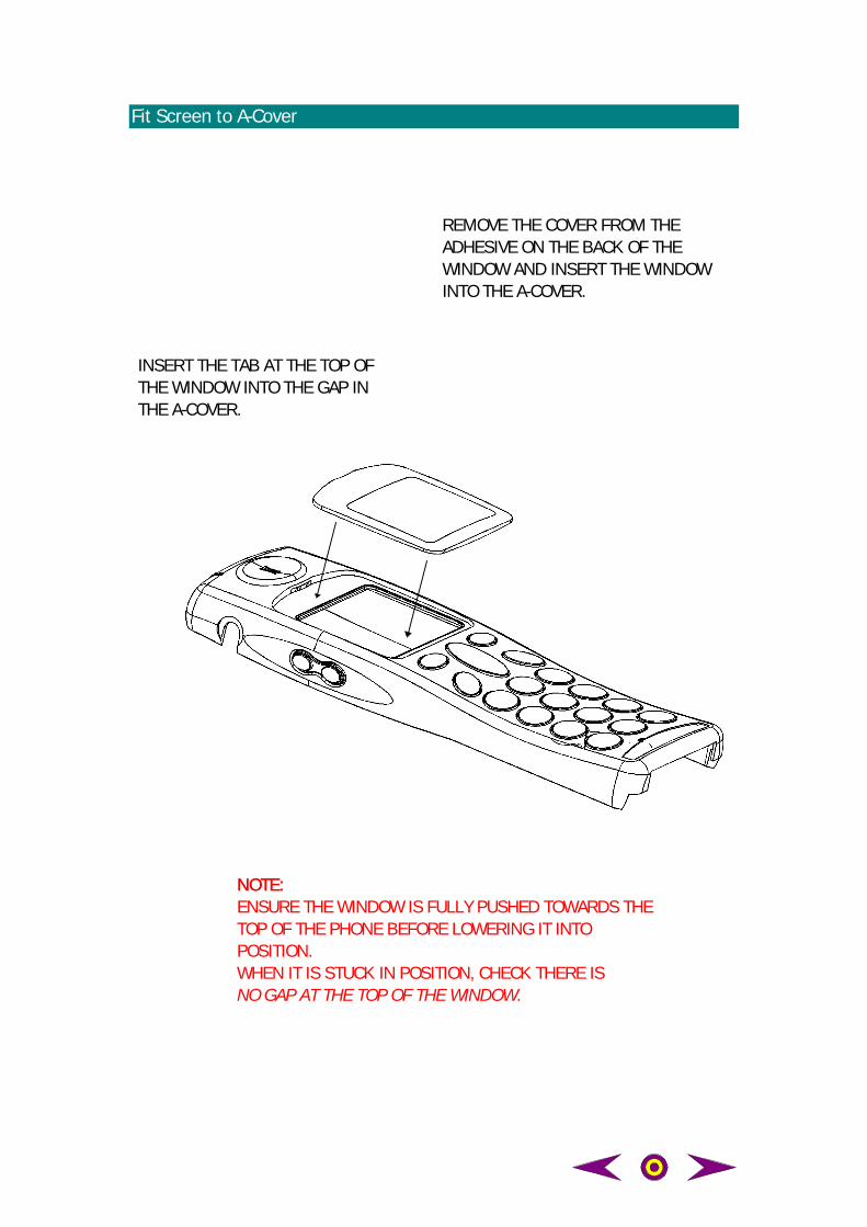
Fit Screen to A-Cover
REMOVE THE COVER FROM THEADHESIVE ON THE BACK OF THEWINDOW AND INSERT THE WINDOWINTO THE A-COVER.
INSERT THE TAB AT THE TOP OFTHE WINDOW INTO THE GAP INTHE A-COVER.
NOTE:NOTE:ENSURE THE WINDOW IS FULLY PUSHED TOWARDS THETOP OF THE PHONE BEFORE LOWERING IT INTOPOSITION.WHEN IT IS STUCK IN POSITION, CHECK THERE ISNO GAP AT THE TOP OF THE WINDOW.

Mount Keymat into A-Cover
NOTE:NOTE:ENSURE ALL THE METAL PADS ARE IN PLACE ON THE BACKOF THE KEYPAD, AFTERAFTER IT IS FITTED.
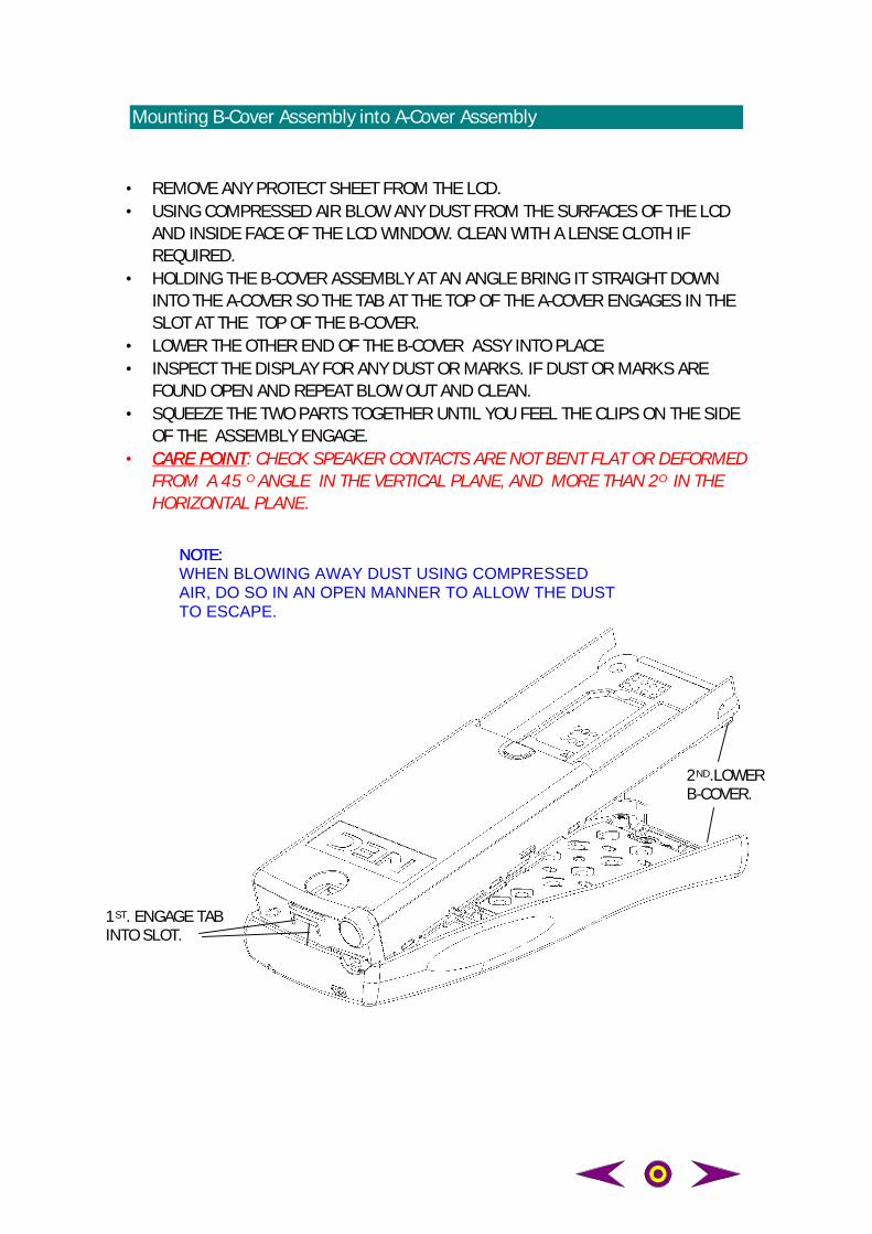
Mounting B-Cover Assembly into A-Cover Assembly
• REMOVE ANY PROTECT SHEET FROM THE LCD.• USING COMPRESSED AIR BLOW ANY DUST FROM THE SURFACES OF THE LCD
AND INSIDE FACE OF THE LCD WINDOW. CLEAN WITH A LENSE CLOTH IFREQUIRED.
• HOLDING THE B-COVER ASSEMBLY AT AN ANGLE BRING IT STRAIGHT DOWNINTO THE A-COVER SO THE TAB AT THE TOP OF THE A-COVER ENGAGES IN THESLOT AT THE TOP OF THE B-COVER.
• LOWER THE OTHER END OF THE B-COVER ASSY INTO PLACE• INSPECT THE DISPLAY FOR ANY DUST OR MARKS. IF DUST OR MARKS ARE
FOUND OPEN AND REPEAT BLOW OUT AND CLEAN.• SQUEEZE THE TWO PARTS TOGETHER UNTIL YOU FEEL THE CLIPS ON THE SIDE
OF THE ASSEMBLY ENGAGE.• CARE POINTCARE POINT: CHECK SPEAKER CONTACTS ARE NOT BENT FLAT OR DEFORMED
FROM A 45 O ANGLE IN THE VERTICAL PLANE, AND MORE THAN 2O IN THEHORIZONTAL PLANE.
1ST. ENGAGE TABINTO SLOT.
2ND.LOWERB-COVER.
NOTE:NOTE:WHEN BLOWING AWAY DUST USING COMPRESSEDAIR, DO SO IN AN OPEN MANNER TO ALLOW THE DUSTTO ESCAPE.
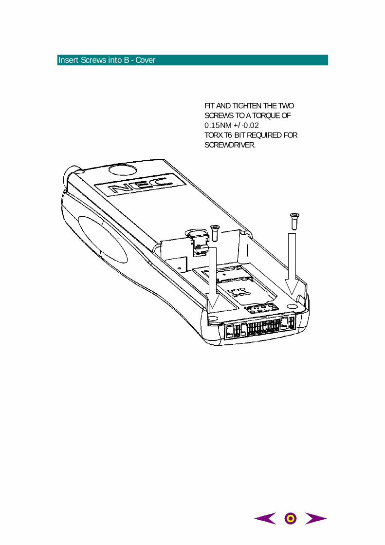
Insert Screws into B - Cover
FIT AND TIGHTEN THE TWOSCREWS TO A TORQUE OF0.15NM +/-0.02TORX T6 BIT REQUIRED FORSCREWDRIVER.
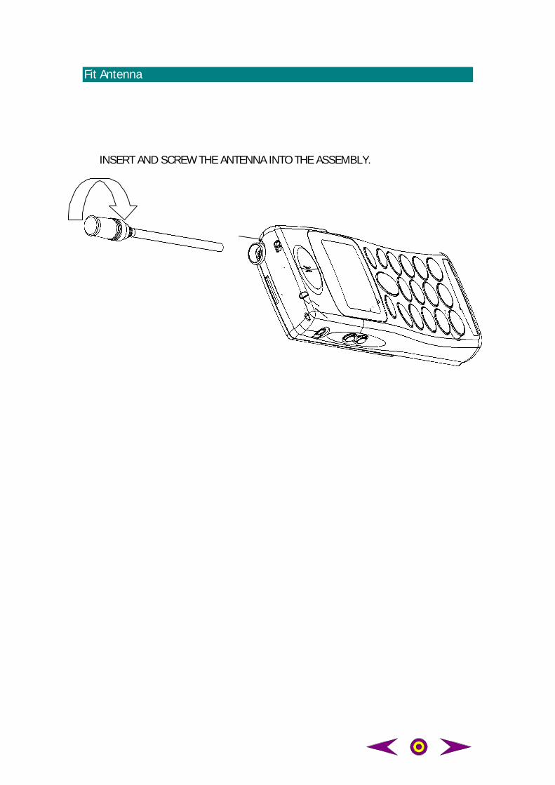
Fit Antenna
INSERT AND SCREW THE ANTENNA INTO THE ASSEMBLY.
<< Previous SectionNext Section >>Main Menu
Section 5
Troubleshooting
Part 1 Equipment ConfigurationsPart 2 Engineering Function CommandsPart 3 Receiver RF Levels and ChecksPart 4 Transmitter RF Levels and ChecksPart 5 Test SignalsPart 6 Fault Codes
Introduction
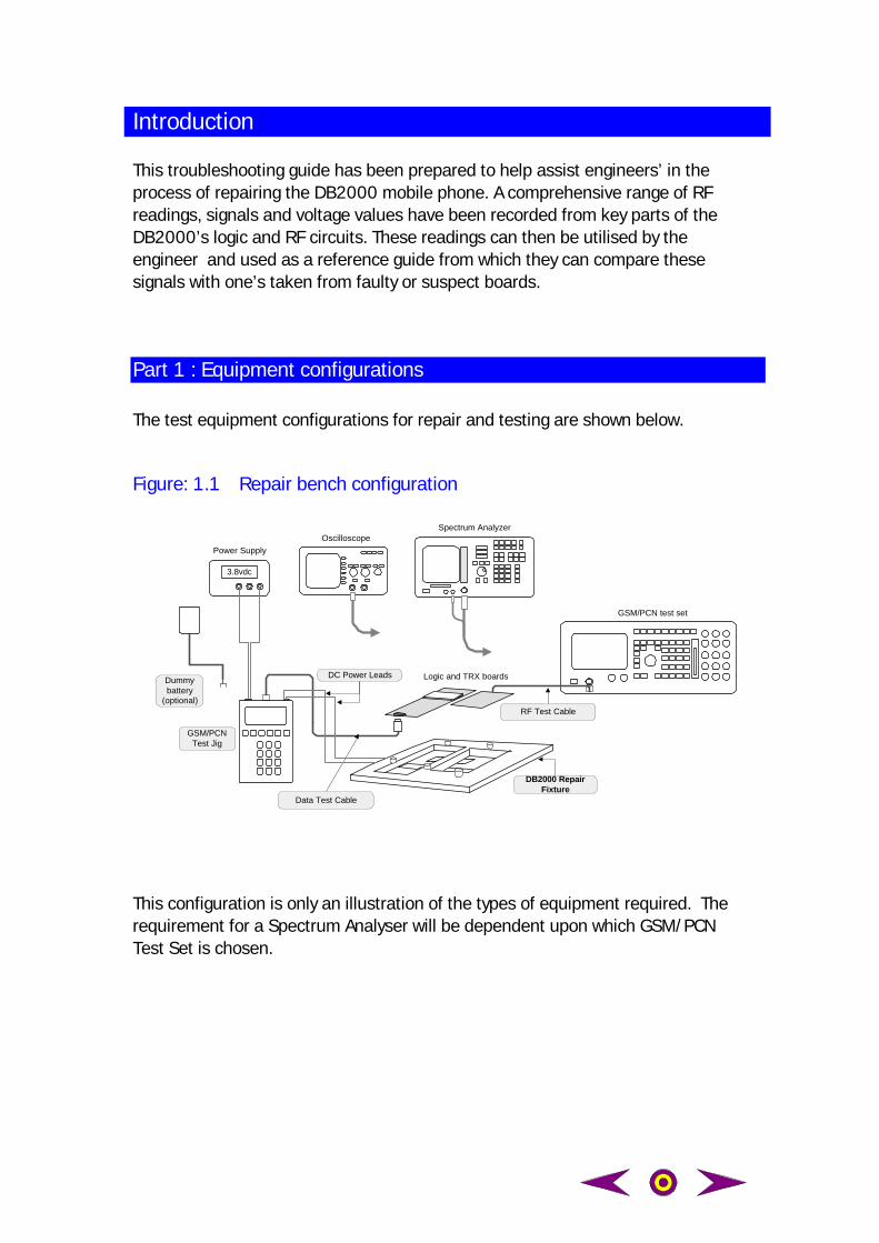
This troubleshooting guide has been prepared to help assist engineers’ in theprocess of repairing the DB2000 mobile phone. A comprehensive range of RFreadings, signals and voltage values have been recorded from key parts of theDB2000’s logic and RF circuits. These readings can then be utilised by theengineer and used as a reference guide from which they can compare thesesignals with one’s taken from faulty or suspect boards.
Part 1 : Equipment configurations
The test equipment configurations for repair and testing are shown below.
Figure: 1.1 Repair bench configuration
3.8vdc
Power Supply
Logic and TRX boards
DB2000 RepairFixture
DC Power Leads
GSM/PCNTest Jig
GSM/PCN test set
Dummybattery
(optional)
OscilloscopeSpectrum Analyzer
Data Test Cable
RF Test Cable
This configuration is only an illustration of the types of equipment required. Therequirement for a Spectrum Analyser will be dependent upon which GSM/PCNTest Set is chosen.
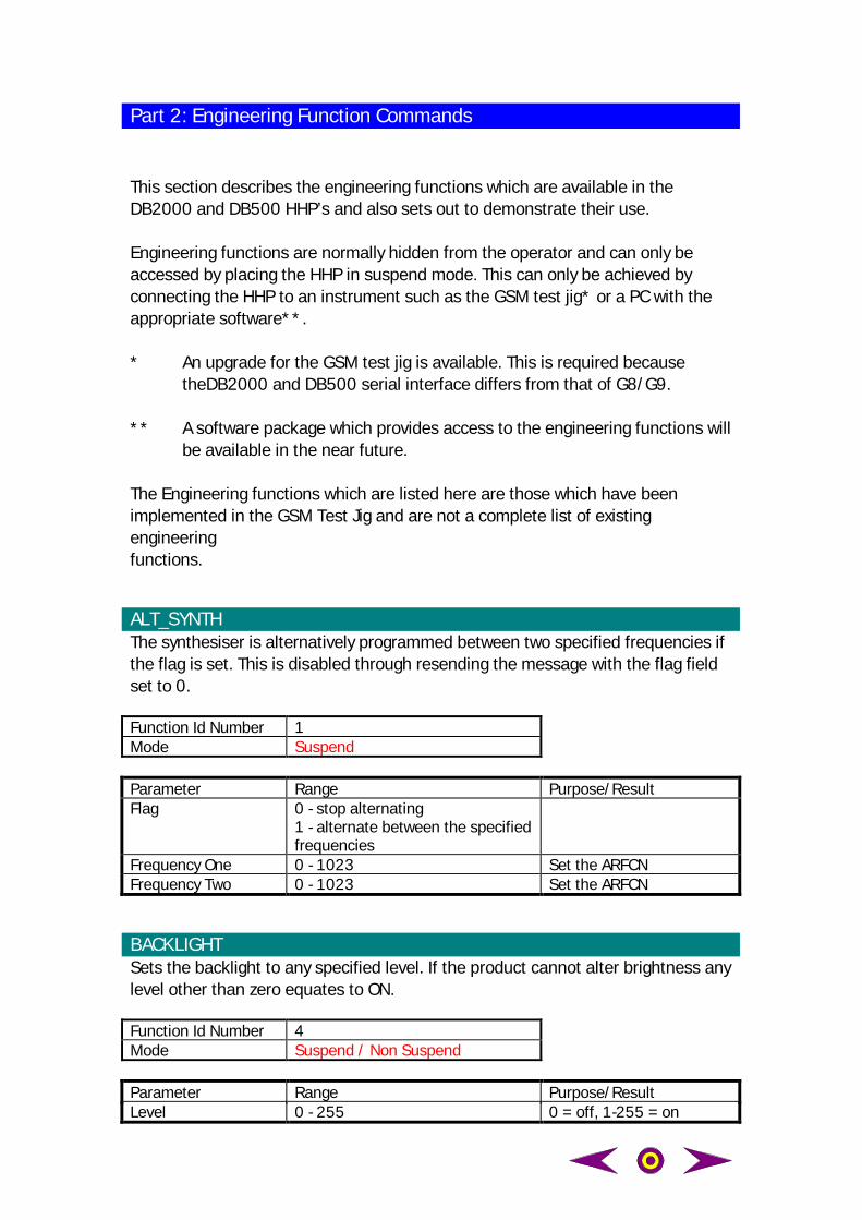
Part 2: Engineering Function Commands
This section describes the engineering functions which are available in theDB2000 and DB500 HHP’s and also sets out to demonstrate their use.
Engineering functions are normally hidden from the operator and can only beaccessed by placing the HHP in suspend mode. This can only be achieved byconnecting the HHP to an instrument such as the GSM test jig* or a PC with theappropriate software**.
* An upgrade for the GSM test jig is available. This is required becausetheDB2000 and DB500 serial interface differs from that of G8/G9.
** A software package which provides access to the engineering functions willbe available in the near future.
The Engineering functions which are listed here are those which have beenimplemented in the GSM Test Jig and are not a complete list of existingengineeringfunctions.
ALT_SYNTHThe synthesiser is alternatively programmed between two specified frequencies ifthe flag is set. This is disabled through resending the message with the flag fieldset to 0.
Function Id Number 1Mode Suspend
Parameter Range Purpose/ResultFlag 0 - stop alternating
1 - alternate between the specifiedfrequencies
Frequency One 0 - 1023 Set the ARFCNFrequency Two 0 - 1023 Set the ARFCN
BACKLIGHTSets the backlight to any specified level. If the product cannot alter brightness anylevel other than zero equates to ON.
Function Id Number 4Mode Suspend / Non Suspend
Parameter Range Purpose/ResultLevel 0 - 255 0 = off, 1-255 = on
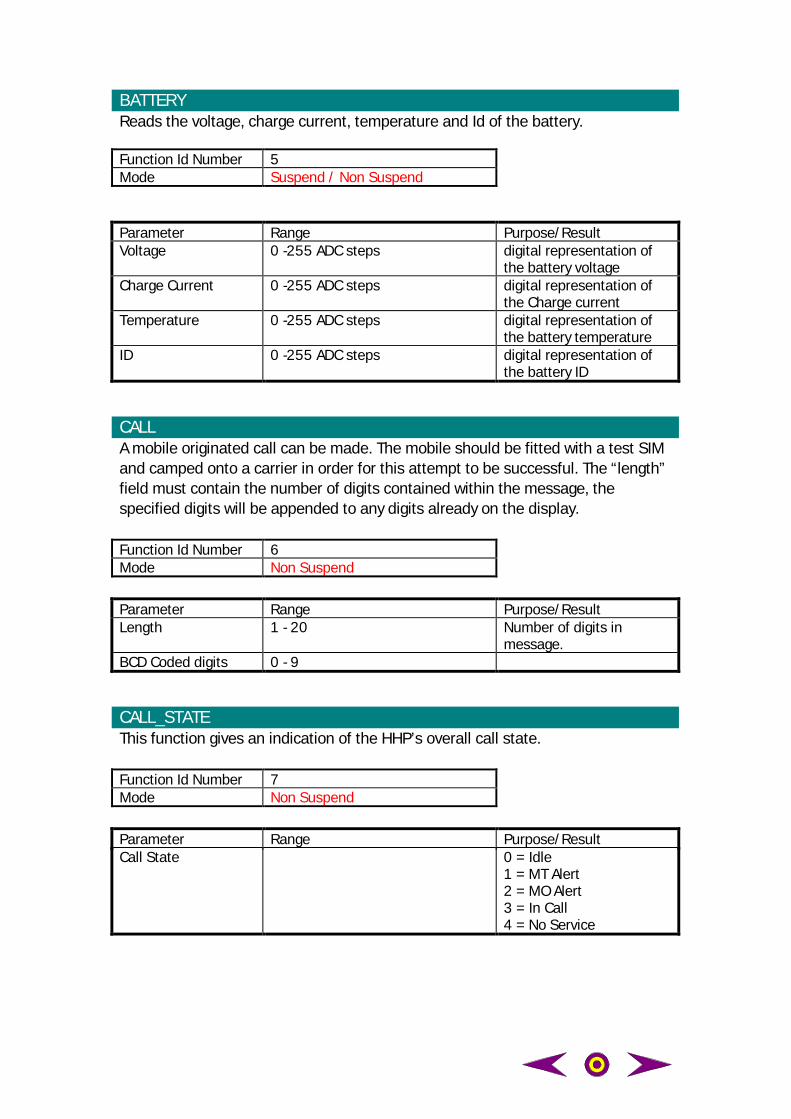
BATTERYReads the voltage, charge current, temperature and Id of the battery.
Function Id Number 5Mode Suspend / Non Suspend
Parameter Range Purpose/ResultVoltage 0 -255 ADC steps digital representation of
the battery voltageCharge Current 0 -255 ADC steps digital representation of
the Charge currentTemperature 0 -255 ADC steps digital representation of
the battery temperatureID 0 -255 ADC steps digital representation of
the battery ID
CALLA mobile originated call can be made. The mobile should be fitted with a test SIMand camped onto a carrier in order for this attempt to be successful. The “length”field must contain the number of digits contained within the message, thespecified digits will be appended to any digits already on the display.
Function Id Number 6Mode Non Suspend
Parameter Range Purpose/ResultLength 1 - 20 Number of digits in
message.BCD Coded digits 0 - 9
CALL_STATEThis function gives an indication of the HHP’s overall call state.
Function Id Number 7Mode Non Suspend
Parameter Range Purpose/ResultCall State 0 = Idle
1 = MT Alert2 = MO Alert3 = In Call4 = No Service
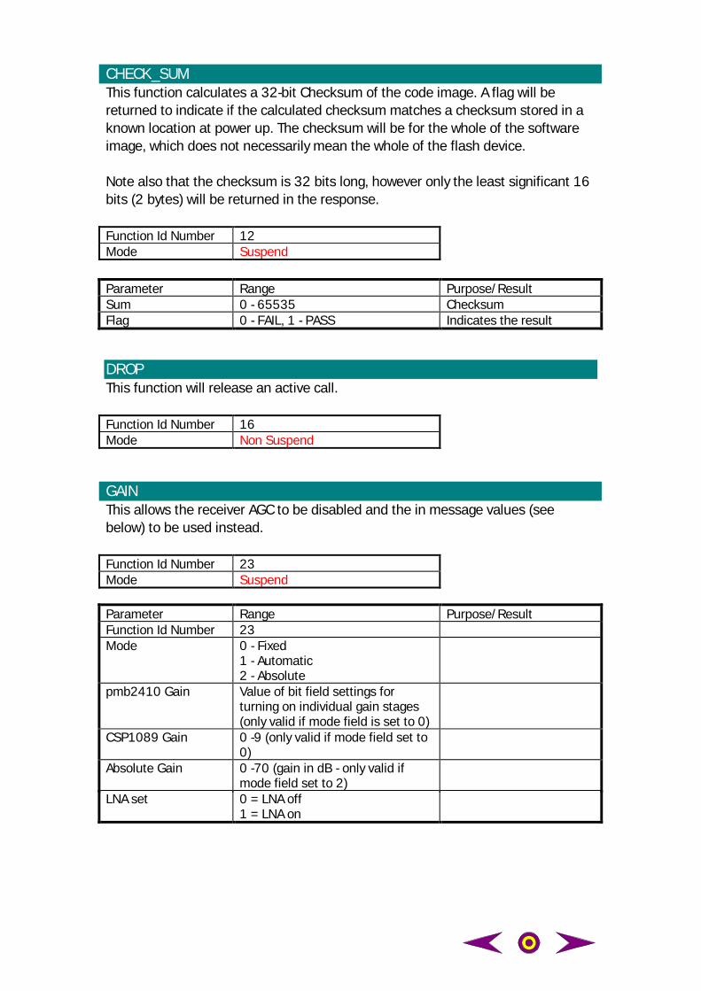
CHECK_SUMThis function calculates a 32-bit Checksum of the code image. A flag will bereturned to indicate if the calculated checksum matches a checksum stored in aknown location at power up. The checksum will be for the whole of the softwareimage, which does not necessarily mean the whole of the flash device.
Note also that the checksum is 32 bits long, however only the least significant 16bits (2 bytes) will be returned in the response.
Function Id Number 12Mode Suspend
Parameter Range Purpose/ResultSum 0 - 65535 ChecksumFlag 0 - FAIL, 1 - PASS Indicates the result
DROPThis function will release an active call.
Function Id Number 16Mode Non Suspend
GAINThis allows the receiver AGC to be disabled and the in message values (seebelow) to be used instead.
Function Id Number 23Mode Suspend
Parameter Range Purpose/ResultFunction Id Number 23Mode 0 - Fixed
1 - Automatic2 - Absolute
pmb2410 Gain Value of bit field settings forturning on individual gain stages(only valid if mode field is set to 0)
CSP1089 Gain 0 -9 (only valid if mode field set to0)
Absolute Gain 0 -70 (gain in dB - only valid ifmode field set to 2)
LNA set 0 = LNA off1 = LNA on
HOOKSWITCHThis function allows the state of the hook-switch to be read. This has not beenimplemented in DB2000 and will therefore always return the open condition.
LEDSets the LED to the specified colour or off.
Function Id Number 27Mode Suspend / Non Suspend
Parameter Range Purpose/ResultLed colour 0 = Off, 1 = Red, 2 = Green, 3 =
YellowChanges the colour of theLED
LOOPThis function allows the microphone, including the hands free microphone, to berouted to a specified device.
Function Id Number 28Mode Suspend
Parameter Range Purpose/ResultOn/Off 0 = Normal, 1 = Loop-back Select audio loop-backAudio source 1 = microphone, 2 = Hands-free
microphoneSelect microphone
Audio destination 1 = Earpiece, 2 = Carkit speaker Select Loudspeaker
READ_PORTThis function reads the status of the CIF port lines and indicates whether they areconfigured as input or output.
Function Id Number 39Mode Suspend / Non Suspend
Parameter Range Purpose/ResultCIF Port 0 - 65535 Indicates the port addressCIF Port Config 0 - 65535 Each bit represents the
configuration of therepresented port line e.g.bit 0 represents the redLED. If the bit is set thenthe line is output only, ifthe bit is low then the lineis input only.
RECEIVERAllows the receiver mode to be changed.
Function Id Number 40Mode Suspend
Parameter Range Purpose/ResultReceiver Mode Off = 0, Normal/Burst = 1,
Continuous = 2sets the operating mode ofthe receiver
Frequency 0 -1023 sets the ARFCN
RESETThis function resets the HHP and exits test mode.
Function Id Number 45Mode Suspend /Non Suspend
RX_NOISEThis function allows the receiver noise to be measured.
Function Id Number 46Mode Suspend
Parameter Range Purpose/ResultSignal + Noise +Distortion
0 - 65535 Digital representation ofthe SINAD measurement
Noise + Distortion 0 - 65535 Digital representation ofthe noise and distortion
RXLEVThis function returns the RXLEV and RSSI values of the current assigned channel.
Function Id Number 47Mode Suspend
Parameter Range Purpose/ResultRxLev 0 - 63RSSI raw value 0 - 432
SET_ALARMThis function allows the alarm to be set or reset.
Function Id Number 48Mode Suspend / Non Suspend
Parameter Range Purpose/ResultAlarm On/Off 0 = Off, 1 = OnHour 0 -23 sets the hourMinute 0 - 59 sets the minutesSecond 0 - 59 sets the seconds
SET_LINEThis function allows any control pin of the RF stage to be modified.
Function Id Number 49Mode Suspend
Parameter Range Purpose/ResultRX ON 0 = low, 1 = high, 2 = leave sets the Rx On signalTX ON 0 = low, 1 = high, 2 = leave sets the Tx On signalV Idle 0 = low, 1 = high, 2 = leave sets the V Idle signalVCO ON 0 = low, 1 = high, 2 = leave sets the VCO On signal
SET_TODThis function allows the clock to be set.
Function Id Number 50Mode Suspend / Non Suspend
Parameter Range Purpose/ResultYear 1996 - 2200 Sets the yearMonth 1 -12 Sets the monthDay 1 - 31 Sets the DayHour 0 - 23 Sets the HourMinute 0 - 59 Sets the minuteSecond 0 - 59 Sets the second
SIMThis function allows SIM information such as clock-stop mode and powerrequirements to be read.
Function Id Number 51Mode Suspend / Non Suspend
Parameter Range Purpose/ResultCard Status 0 = SIM Card OK
1 = SIM Card Failed2 = SIM Card Not Present
Voltage Only valid if “SIM Card OK” 0 = 3V1 = 5V2 = Either
Clock-Stop Only valid if “SIM Card OK” 0 = None1 = High Preferred2 = High Only3 = Low Preferred4 = Low Only5 = Either
SIM Phase Only valid if “SIM Card OK” 0 = Phase 11 = Phase 1 with bits ofPhase 22 = Phase 23 = Phase 2+
IMSI Returns the SIM’s IMSI
SUSPENDThis function allows the HHP to be placed into suspend mode.
Function Id Number 52Mode Non Suspend
READ_ALARMThis function reads the current alarm setting.
Function Id Number 56Mode Suspend / Non Suspend
Parameter Range Purpose/ResultAlarm On/Off 0 - Off, 1 = OnHour 0 - 23Minutes 0 - 59Seconds 0 - 59
READ_TODThis function allows the current time of day to be read from the clock.
Function Id Number 57Mode Suspend / Non Suspend
Parameter Range Purpose/ResultYear 1996 - 2200Month 1 -12Day 1 - 31Hour 0 - 23Minute 0 - 59Second 0 - 59
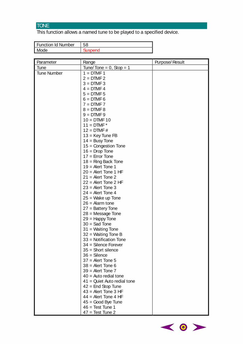
TONEThis function allows a named tune to be played to a specified device.
Function Id Number 58Mode Suspend
Parameter Range Purpose/ResultTune Tune/Tone = 0, Stop = 1Tune Number 1 = DTMF 1
2 = DTMF 23 = DTMF 34 = DTMF 45 = DTMF 56 = DTMF 67 = DTMF 78 = DTMF 89 = DTMF 910 = DTMF 1011 = DTMF *12 = DTMF #13 = Key Tune FB14 = Busy Tone15 = Congestion Tone16 = Drop Tone17 = Error Tone18 = Ring Back Tone19 = Alert Tone 120 = Alert Tone 1 HF21 = Alert Tone 222 = Alert Tone 2 HF23 = Alert Tone 324 = Alert Tone 425 = Wake up Tone26 = Alarm tone27 = Battery Tone28 = Message Tone29 = Happy Tone30 = Sad Tone31 = Waiting Tone32 = Waiting Tone B33 = Notification Tone34 = Silence Forever35 = Short silence36 = Silence37 = Alert Tone 538 = Alert Tone 639 = Alert Tone 740 = Auto redial tone41 = Quiet Auto redial tone42 = End Stop Tune43 = Alert Tone 3 HF44 = Alert Tone 4 HF45 = Good Bye Tune46 = Test Tune 147 = Test Tune 2
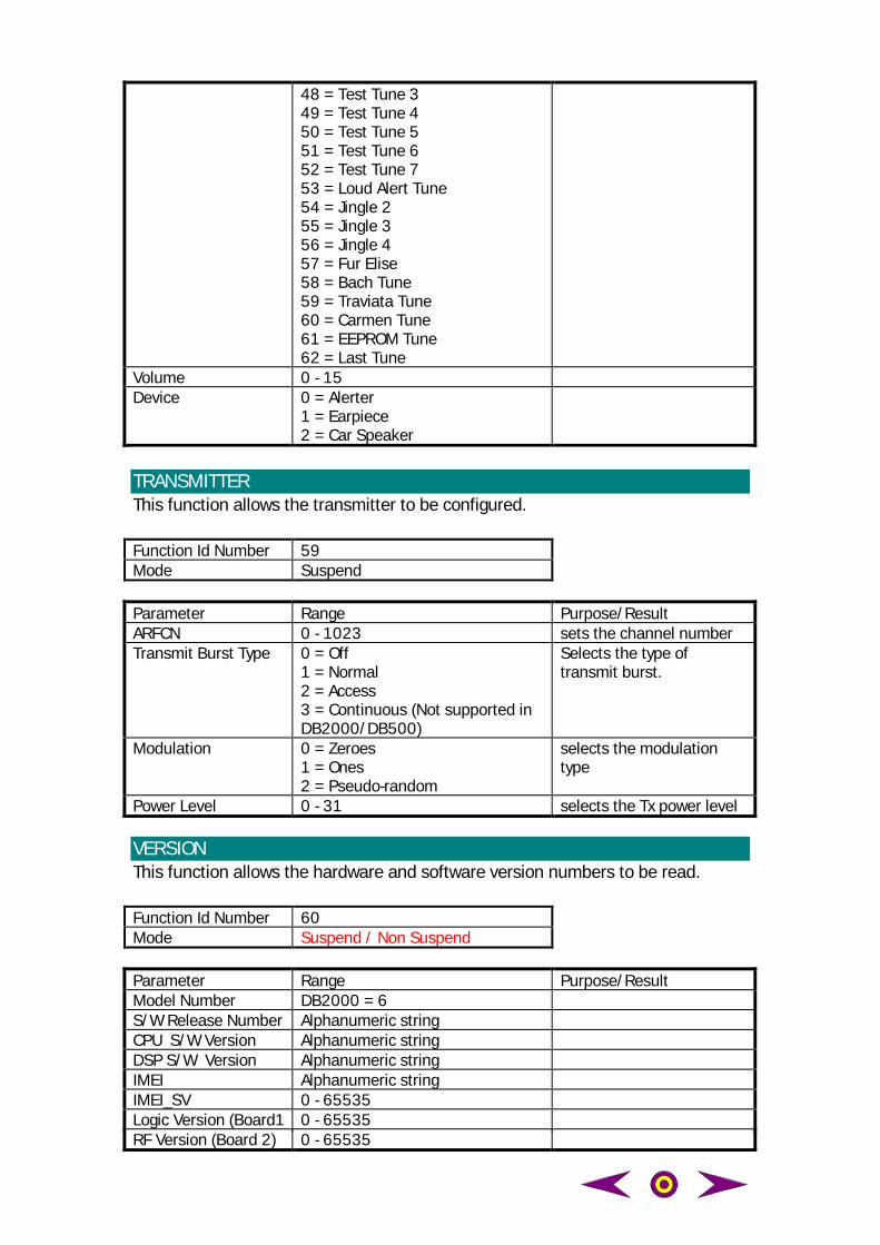
48 = Test Tune 349 = Test Tune 450 = Test Tune 551 = Test Tune 652 = Test Tune 753 = Loud Alert Tune54 = Jingle 255 = Jingle 356 = Jingle 457 = Fur Elise58 = Bach Tune59 = Traviata Tune60 = Carmen Tune61 = EEPROM Tune62 = Last Tune
Volume 0 - 15Device 0 = Alerter
1 = Earpiece2 = Car Speaker
TRANSMITTERThis function allows the transmitter to be configured.
Function Id Number 59Mode Suspend
Parameter Range Purpose/ResultARFCN 0 - 1023 sets the channel numberTransmit Burst Type 0 = Off
1 = Normal2 = Access3 = Continuous (Not supported inDB2000/DB500)
Selects the type oftransmit burst.
Modulation 0 = Zeroes1 = Ones2 = Pseudo-random
selects the modulationtype
Power Level 0 - 31 selects the Tx power level
VERSIONThis function allows the hardware and software version numbers to be read.
Function Id Number 60Mode Suspend / Non Suspend
Parameter Range Purpose/ResultModel Number DB2000 = 6S/W Release Number Alphanumeric stringCPU S/W Version Alphanumeric stringDSP S/W Version Alphanumeric stringIMEI Alphanumeric stringIMEI_SV 0 - 65535Logic Version (Board1 0 - 65535RF Version (Board 2) 0 - 65535
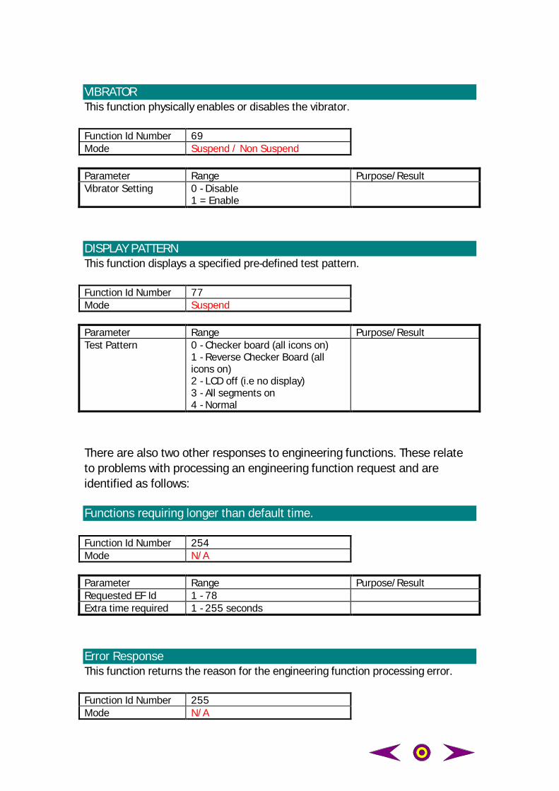
VIBRATORThis function physically enables or disables the vibrator.
Function Id Number 69Mode Suspend / Non Suspend
Parameter Range Purpose/ResultVibrator Setting 0 - Disable
1 = Enable
DISPLAY PATTERNThis function displays a specified pre-defined test pattern.
Function Id Number 77Mode Suspend
Parameter Range Purpose/ResultTest Pattern 0 - Checker board (all icons on)
1 - Reverse Checker Board (allicons on)2 - LCD off (i.e no display)3 - All segments on4 - Normal
There are also two other responses to engineering functions. These relateto problems with processing an engineering function request and areidentified as follows:
Functions requiring longer than default time.
Function Id Number 254Mode N/A
Parameter Range Purpose/ResultRequested EF Id 1 - 78Extra time required 1 - 255 seconds
Error ResponseThis function returns the reason for the engineering function processing error.
Function Id Number 255Mode N/A
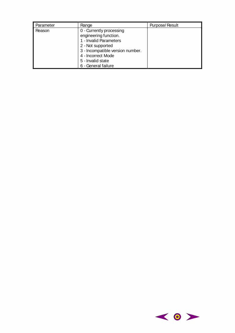
Parameter Range Purpose/ResultReason 0 - Currently processing
engineering function.1 - Invalid Parameters2 - Not supported3 - Incompatible version number.4 - Incorrect Mode5 - Invalid state6 - General failure
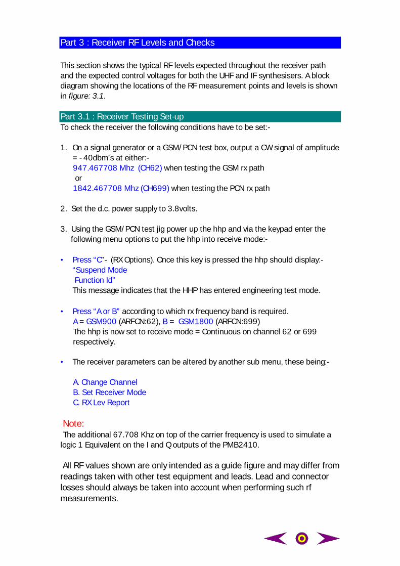
Part 3 : Receiver RF Levels and Checks
This section shows the typical RF levels expected throughout the receiver pathand the expected control voltages for both the UHF and IF synthesisers. A blockdiagram showing the locations of the RF measurement points and levels is shownin figure: 3.1.
Part 3.1 : Receiver Testing Set-upTo check the receiver the following conditions have to be set:-
1. On a signal generator or a GSM/PCN test box, output a CW signal of amplitude= - 40dbm’s at either:-
947.467708 Mhz (CH62) when testing the GSM rx path or 1842.467708 Mhz (CH699) when testing the PCN rx path
2. Set the d.c. power supply to 3.8volts.
3. Using the GSM/PCN test jig power up the hhp and via the keypad enter the following menu options to put the hhp into receive mode:-
• Press “C”- (RX Options). Once this key is pressed the hhp should display:- “Suspend Mode Function Id” This message indicates that the HHP has entered engineering test mode.
• Press “A or B” according to which rx frequency band is required. A = GSM900 (ARFCN:62), B = GSM1800 (ARFCN:699) The hhp is now set to receive mode = Continuous on channel 62 or 699 respectively. • The receiver parameters can be altered by another sub menu, these being:-
A. Change Channel B. Set Receiver Mode C. RX Lev Report Note: The additional 67.708 Khz on top of the carrier frequency is used to simulate alogic 1 Equivalent on the I and Q outputs of the PMB2410.
All RF values shown are only intended as a guide figure and may differ fromreadings taken with other test equipment and leads. Lead and connectorlosses should always be taken into account when performing such rfmeasurements.
Figure 3.1: Receiver Block Diagram
RX I&Q(As Fig.3.0/3.1)
15
8
9
RX_ON2 (As Fig.2.6)
RINO
GSM
540MHz
PMB2410(IC300) DB2000 Receiver RF Levels
Div2
Div2/3
mech
switch
External RFConnector
V_G_LNA (As Fig.2.6)
FL303 FL302
FL301FL300
FL304
27
29
2613 14
(10,11,12)
RX_ON2
PUPLO2
36
31
20,2117
V_P_LNA
PCN
4645
40
39
AGCControl
DiplexerTCX
O
13Mhz to logic
2v85_rf1
L305
32-35 23-24
4
(X200)13Mhz CLK Loop Filter
LNA
LNA
GSM = Ra - Ri PCN = R1 - R10
5
1 3
Ra= -57dbm
C411
R2=-54dbm
C400
Rb=-56dbm
R3=-54dbm
R4=-56dbm
R5=-40dbm
R6=-44dbm
Rc=-56dbm
Rd=-28dbm
R1= -67dbm
Re=-41dbm
Rf=-40dbm
5
Rh=-30dbmRi=-33dbm
R7=-47dbm
Rg=-27dbm R8=-20dbm
R9=-32dbm
R10=-38dbm
FromUHF VCO
FromIF-PLL
(As Fig.2.9)
(As Fig.2.6)
RF Gen Level = - 40dbm's @ 947.467708Mhz " - 40dbm''s @ 1842.467708Mhz
Part 3.2 : Testing the Receiver
Using a suitable high frequency probe measure the RF levels at the relevantpoints shown in fig 3.1 and compare your measurements with those shown in thediagram. If there are any major differences between the readings taken and thoseindicated then further investigation of that particular point will be required. It willalso be necessary to ensure that all the following power supplies and signals arepresent which control this part of the receiver circuit:-
1. V_G_LNA ( 2.85V supply which powers the GSM LNA and TX/RX switchingdiode pack: D400). See figure 3.4.
2. V_P_LNA ( 2.85V supply which powers the PCN LNA and TX/RX switching
diode pack: D401). See figure 3.5. 3. RX_ON2 ( Control signal which supplies the GSM LNA, the RX demodulator
and internal buffer’s). See figure 3.6. 4. 2V85_RF2 ( A 2.85V power supply derived from MicroMoe IC204, which
supplies V_G_LNA and V_P_LNA)
5. GSM_LNA ( Control signal from Superchip pin 29 which switches V_G-LNA). See figure 3.7.
6. PCN_LNA ( Control signal from Superchip pin 30 which switches V_G_LNA). See figure 3.8.
7. TCXO (X200) - 13 Mhz clock on Test Point 413, see figure 4.9.
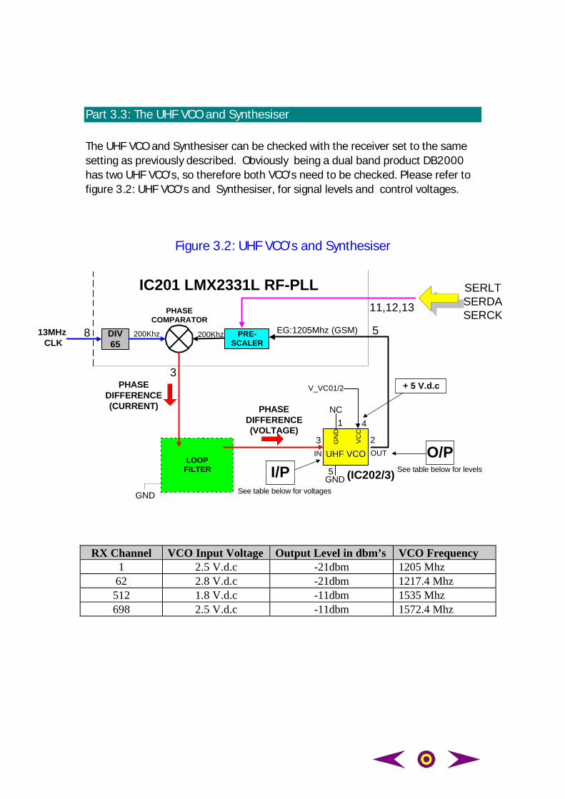
Part 3.3: The UHF VCO and Synthesiser
The UHF VCO and Synthesiser can be checked with the receiver set to the samesetting as previously described. Obviously being a dual band product DB2000has two UHF VCO’s, so therefore both VCO’s need to be checked. Please refer tofigure 3.2: UHF VCO’s and Synthesiser, for signal levels and control voltages.
Figure 3.2: UHF VCO’s and Synthesiser
RX Channel VCO Input Voltage Output Level in dbm’s VCO Frequency1 2.5 V.d.c -21dbm 1205 Mhz
62 2.8 V.d.c -21dbm 1217.4 Mhz512 1.8 V.d.c -11dbm 1535 Mhz698 2.5 V.d.c -11dbm 1572.4 Mhz
DIV65
LOOPFILTER
PRE-SCALER
IC201 LMX2331L RF-PLL
(IC202/3)
PHASECOMPARATOR
IN OUT3 2
4
3
5
PHASEDIFFERENCE(CURRENT) PHASE
DIFFERENCE(VOLTAGE)
13MHz CLK
8
VC
C
GN
D
1NC
V_VC01/2
5
11,12,13
SERLTSERDASERCK
EG:1205Mhz (GSM)200Khz 200Khz
GND
GND
UHF VCO
I/P
+ 5 V.d.c
O/PSee table below for levels
See table below for voltages
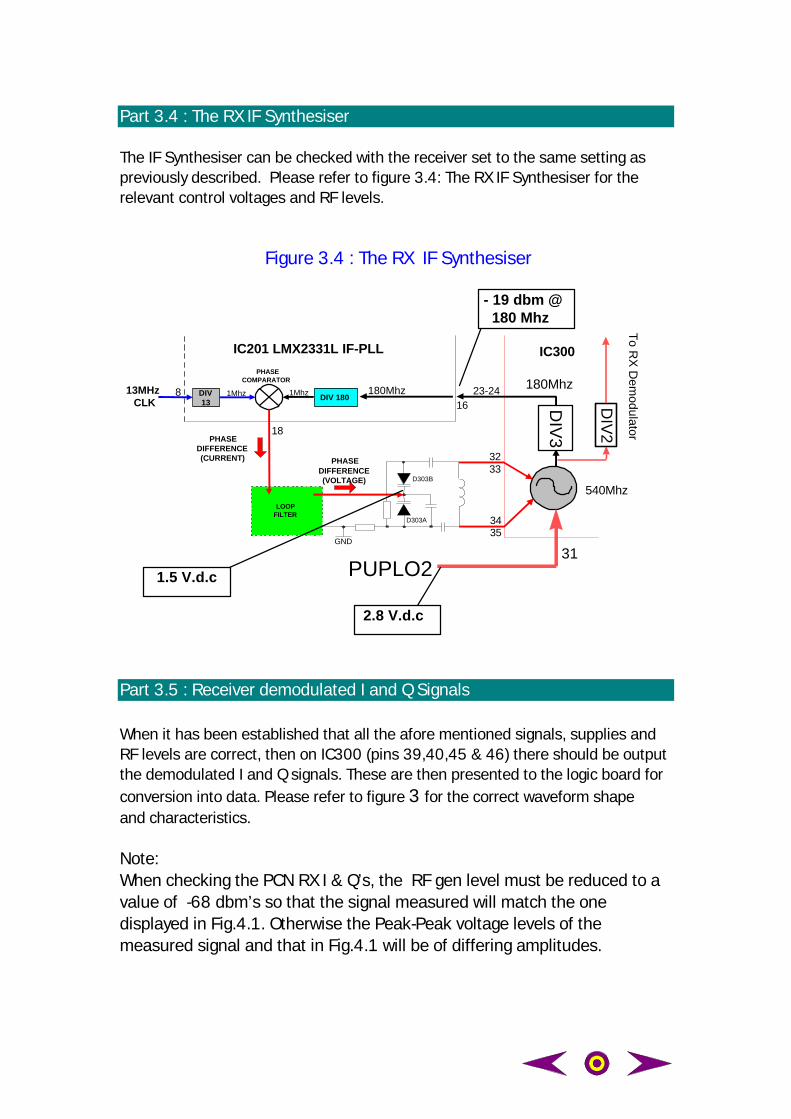
Part 3.4 : The RX IF Synthesiser
The IF Synthesiser can be checked with the receiver set to the same setting aspreviously described. Please refer to figure 3.4: The RX IF Synthesiser for therelevant control voltages and RF levels.
Figure 3.4 : The RX IF Synthesiser
DIV13
LOOPFILTER
DIV 180
IC201 LMX2331L IF-PLL
PHASECOMPARATOR
23-24
PHASEDIFFERENCE(CURRENT) PHASE
DIFFERENCE(VOLTAGE)
13MHz CLK
8 1Mhz 1Mhz
GND
IC300
3233
3435
DIV
318
16180Mhz 180Mhz
D303B
D303A
540Mhz
PUPLO231
DIV
2
To RX
Dem
odulator
Part 3.5 : Receiver demodulated I and Q Signals
When it has been established that all the afore mentioned signals, supplies andRF levels are correct, then on IC300 (pins 39,40,45 & 46) there should be outputthe demodulated I and Q signals. These are then presented to the logic board forconversion into data. Please refer to figure 3 for the correct waveform shapeand characteristics.
Note:When checking the PCN RX I & Q’s, the RF gen level must be reduced to avalue of -68 dbm’s so that the signal measured will match the onedisplayed in Fig.4.1. Otherwise the Peak-Peak voltage levels of themeasured signal and that in Fig.4.1 will be of differing amplitudes.
1.5 V.d.c
- 19 dbm @ 180 Mhz
2.8 V.d.c
Part 4: Transmitter RF Levels and checks
This section shows the typical RF levels expected throughout the transmitter pathand the expected control voltages for both the UHF and IF synthesisers. A blockdiagram showing the locations of the RF measurement points is shown in figure4.1.
Part 4.1 : Transmitter Testing Set-up
To check the transmitter the following conditions have to be set:-
1. Set the d.c. power supply to 3.8volts.
2. Using the GSM/PCN test jig power up the hhp and via the keypad enter the following menu options to put the hhp into receive mode:-
• Press “B”- (TX Options). Once this key is pressed the hhp should display:- “Suspend Mode Function Id” This message indicates that the hhp has entered engineering test mode. • Press “A or B” according to which tx frequency band is required. Option A = GSM900 (ARFCN:62, Transmit burst type:Normal, Modulation: Ones and Power Level: 5) Option B = GSM1800 (ARFCN:699, Transmit burst type: Normal, Modulation: Ones and Power Level: 0 ) The HHP is now set to Normal transmit burst on channel 62 or 699 on power level 5 or 0 respectively.
• The Transmitter parameters can be altered by another sub menu, thesebeing:-
A. Change Channel B. Change power level C. Set modulation type ( 0’s, 1’s or random)
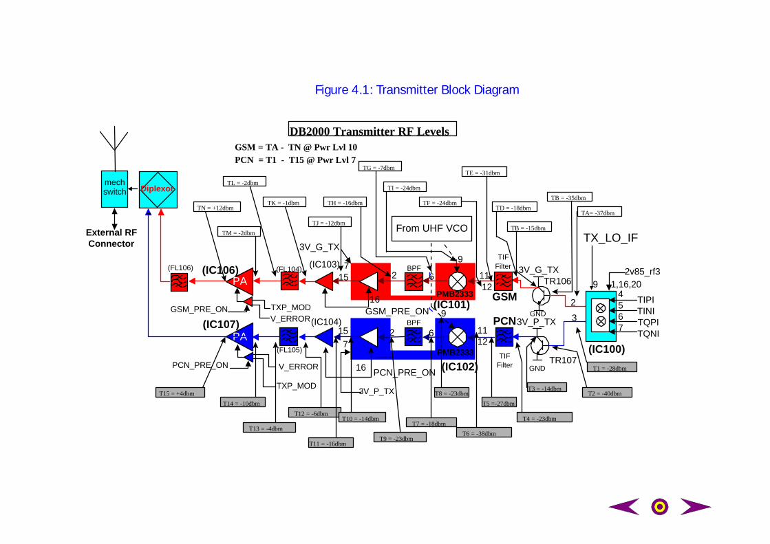
Figure 4.1: Transmitter Block Diagram
External RFConnector
TIFFilter
PMB2333
PMB2333 TIFFilter
PA
PA
mechswitch
GSM
PCN
2
3
9
11 12
11 12
9
PCN_PRE_ON
GSM_PRE_ON16
16
(IC101)
(IC102)
(FL104)
(FL105)
TXP_MOD
V_ERROR
TXP_MODV_ERROR
GSM_PRE_ON
PCN_PRE_ON
(FL106)
(IC107)
(IC106) (IC103)6215
15 2 6BPF
BPF
(IC104)
3V_G_TX
7
3V_P_TX
7
Diplexor
GND
GND
3V_P_TX
3V_G_TX TR106
TR107
From UHF VCO TX_LO_IF
TA= -37dbm
TIPITINI
TQPI TQNI
1,16,209
(IC100)
2v85_rf3
4567
T1 = -28dbm
TB = -35dbm
T2 = -40dbmT3 = -14dbm
TB = -15dbm
TD = -18dbm
TE = -31dbm
TF = -24dbm
TG = -7dbm
TI = -24dbm
TH = -16dbm
TJ = -12dbm
TK = -1dbm
TL = -2dbm
TM = -2dbm
TN = +12dbm
T4 = -23dbm
T5 =-27dbm
T6 = -38dbm
T7 = -18dbm
T9 = -23dbm
T8 = -23dbm
T12 = -6dbm
T13 = -4dbm
T14 = -10dbm
T15 = +4dbm
T10 = -14dbm
T11 = -16dbm
DB2000 Transmitter RF LevelsGSM = TA - TN @ Pwr Lvl 10PCN = T1 - T15 @ Pwr Lvl 7
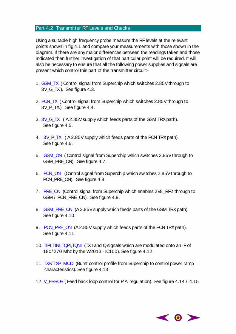
Part 4.2: Transmitter RF Levels and Checks
Using a suitable high frequency probe measure the RF levels at the relevantpoints shown in fig 4.1 and compare your measurements with those shown in thediagram. If there are any major differences between the readings taken and thoseindicated then further investigation of that particular point will be required. It willalso be necessary to ensure that all the following power supplies and signals arepresent which control this part of the transmitter circuit:-
1. GSM_TX ( Control signal from Superchip which switches 2.85V through to3V_G_TX.). See figure 4.3.
2. PCN_TX ( Control signal from Superchip which switches 2.85V through to
3V_P_TX.). See figure 4.4. 3. 3V_G_TX ( A 2.85V supply which feeds parts of the GSM TRX path). See figure 4.5.
4. 3V_P_TX ( A 2.85V supply which feeds parts of the PCN TRX path). See figure 4.6.
5. GSM_ON ( Control signal from Superchip which switches 2.85V through to GSM_PRE_ON). See figure 4.7.
6. PCN_ON (Control signal from Superchip which switches 2.85V through to PCN_PRE_ON). See figure 4.8.
7. PRE_ON (Control signal from Superchip which enables 2V8_RF2 through to GSM / PCN_PRE_ON). See figure 4.9.
8. GSM_PRE_ON (A 2.85V supply which feeds parts of the GSM TRX path). See figure 4.10.
9. . PCN_PRE_ON (A 2.85V supply which feeds parts of the PCN TRX path). See figure 4.11.
10. TIPI,TINI,TQPI,TQNI (TX I and Q signals which are modulated onto an IF of 180/270 Mhz by the W2013 - IC100). See figure 4.12.
11. TXP/TXP_MOD (Burst control profile from Superchip to control power ramp characteristics). See figure 4.13
12. V_ERROR ( Feed back loop control for P.A. regulation). See figure 4.14 / 4.15
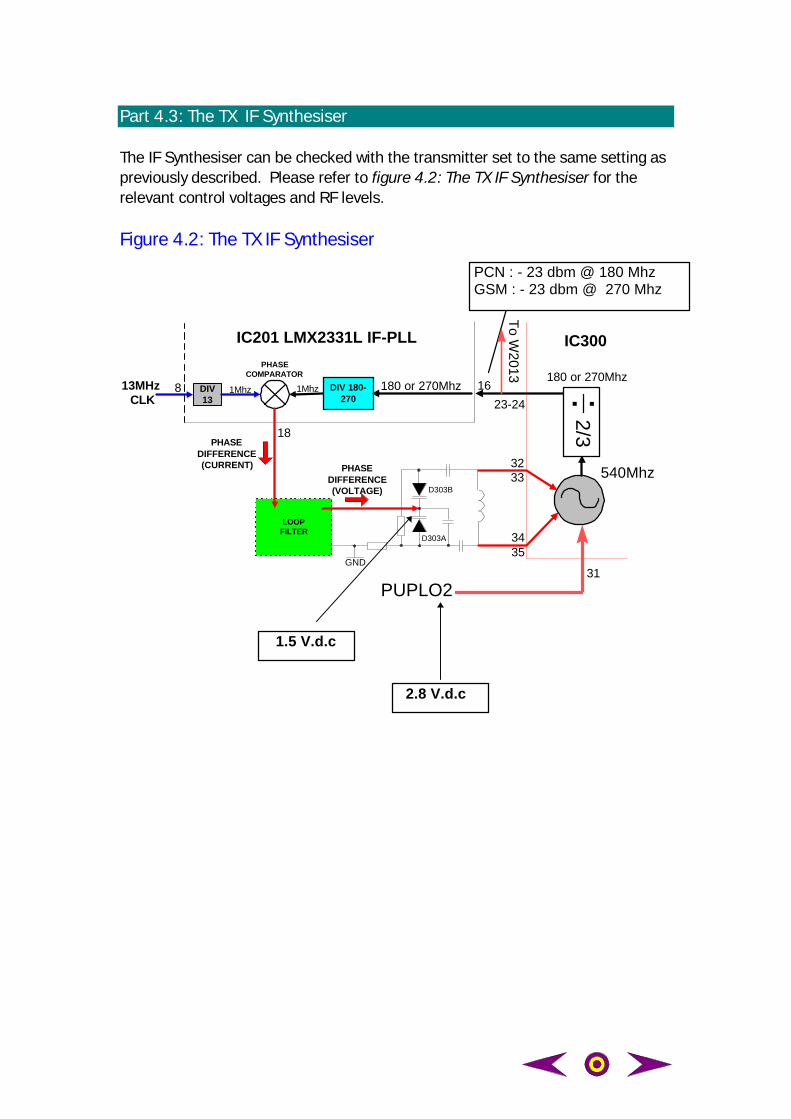
Part 4.3: The TX IF Synthesiser
The IF Synthesiser can be checked with the transmitter set to the same setting aspreviously described. Please refer to figure 4.2: The TX IF Synthesiser for therelevant control voltages and RF levels.
Figure 4.2: The TX IF Synthesiser
1.5 V.d.c
2.8 V.d.c
PCN : - 23 dbm @ 180 Mhz GSM : - 23 dbm @ 270 Mhz
DIV13
LOOPFILTER
DIV 180-270
IC201 LMX2331L IF-PLL
PHASECOMPARATOR
23-24
PHASEDIFFERENCE(CURRENT) PHASE
DIFFERENCE(VOLTAGE)
13MHz CLK
8 1Mhz 1Mhz
GND
IC300
3233
3435
18
16180 or 270Mhz180 or 270Mhz
D303B
D303A
2/3:
540Mhz
PUPLO231
To W2013
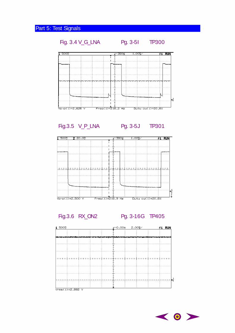
Part 5: Test Signals
Fig. 3.4 V_G_LNA Pg. 3-5I TP300
Fig.3.5 V_P_LNA Pg. 3-5J TP301
Fig.3.6 RX_ON2 Pg. 3-16G TP405
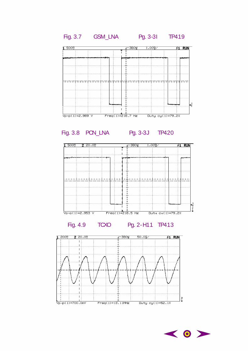
Fig. 3.7 GSM_LNA Pg. 3-3I TP419
Fig. 3.8 PCN_LNA Pg. 3-3J TP420
Fig. 4.9 TCXO Pg. 2- H11 TP413
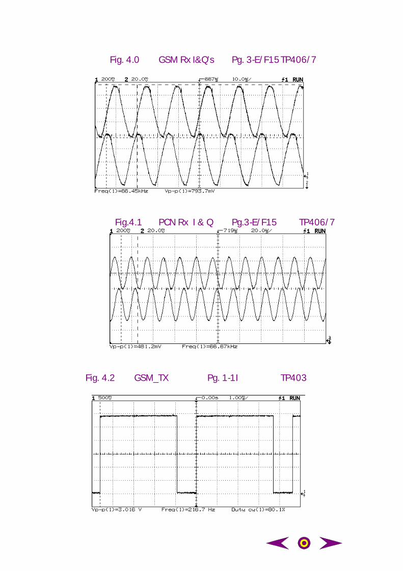
Fig. 4.0 GSM Rx I&Q’s Pg. 3-E/F15TP406/7
Fig.4.1 PCN Rx I & Q Pg.3-E/F15 TP406/7
Fig. 4.2 GSM_TX Pg. 1-1I TP403
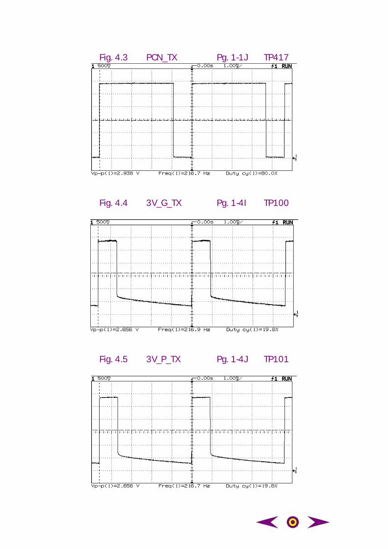
Fig. 4.3 PCN_TX Pg. 1-1J TP417
Fig. 4.4 3V_G_TX Pg. 1-4I TP100
Fig. 4.5 3V_P_TX Pg. 1-4J TP101
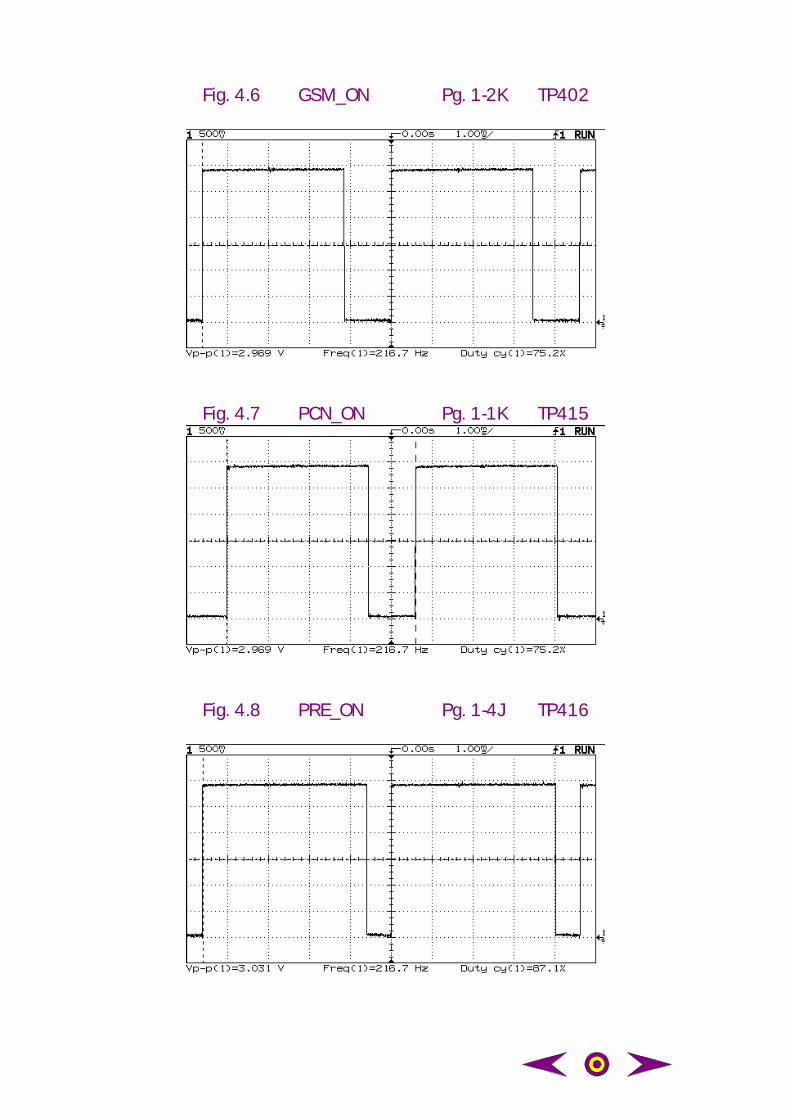
Fig. 4.6 GSM_ON Pg. 1-2K TP402
Fig. 4.7 PCN_ON Pg. 1-1K TP415
Fig. 4.8 PRE_ON Pg. 1-4J TP416
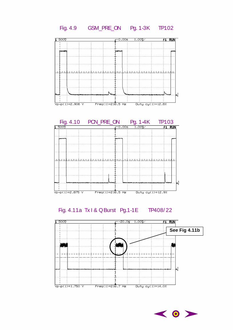
Fig. 4.9 GSM_PRE_ON Pg. 1-3K TP102
Fig. 4.10 PCN_PRE_ON Pg. 1-4K TP103
Fig. 4.11a Tx I & Q Burst Pg.1-1E TP408/22
See Fig 4.11b
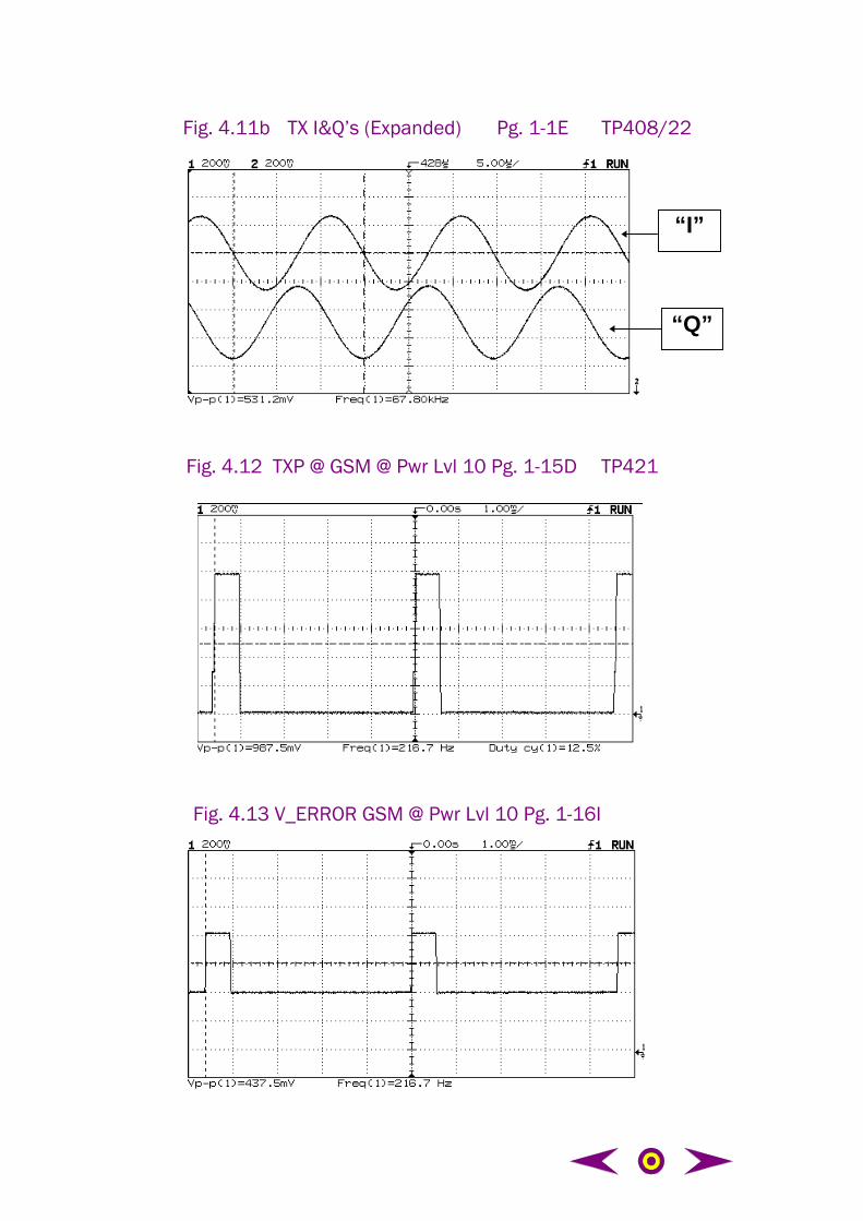
!"#$%&'()
*+,--.- !"#$%&'/
“I”
“Q”
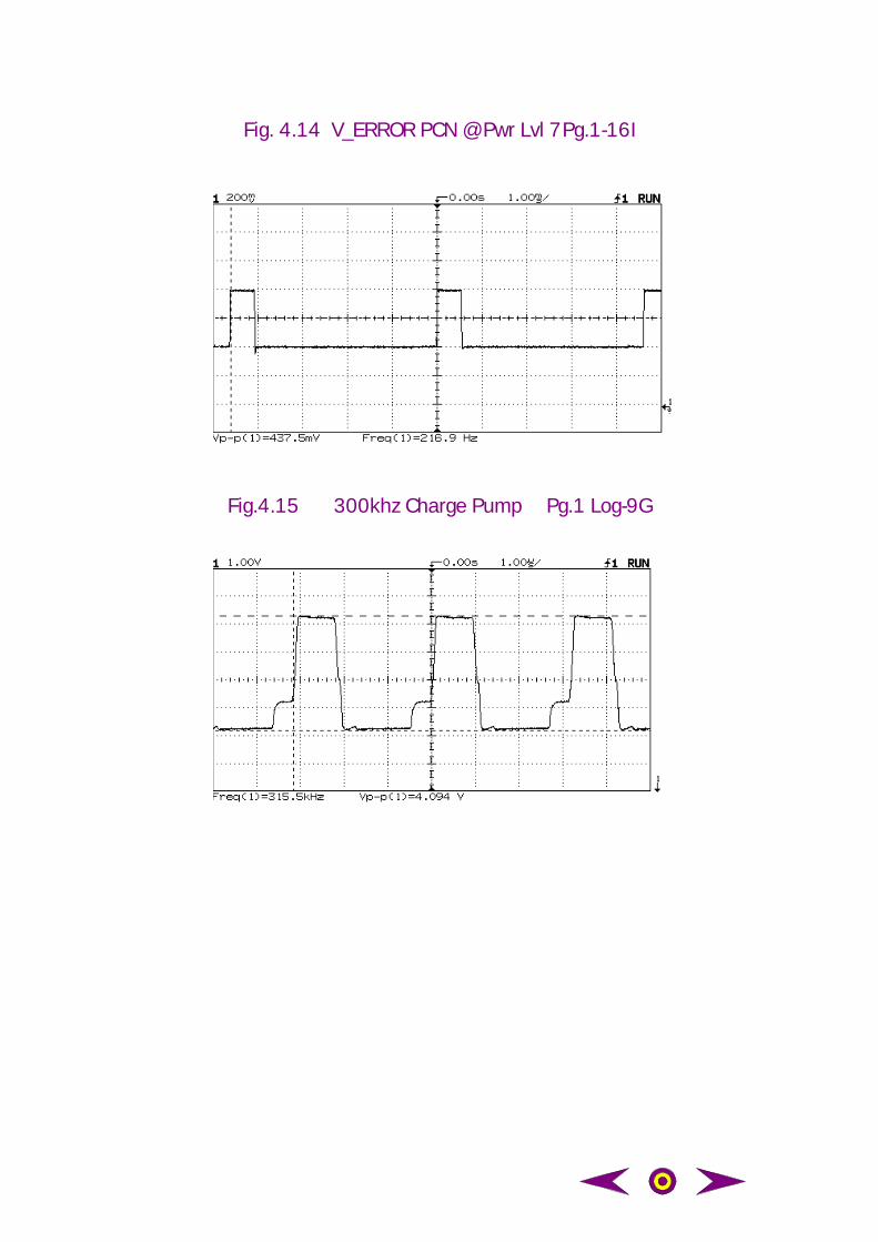
Fig. 4.14 V_ERROR PCN @ Pwr Lvl 7Pg.1-16I
Fig.4.15 300khz Charge Pump Pg.1 Log-9G
Part 6: Fault Codes
The DB2000 can display a number of ‘Return to Service Centre Codes’ toindicate a fault within the HHP as per the list below.
Code 3This indicates that the secure areas of memory within the HHP, such as the IMEI,have become corrupt. This can only be overcome by reprogramming the IMEI - afunction not available to Service Centres.
Code 101This indicates a power up ROM checksum failure.
Code 102This indicates a power up RAM check failure i.e a failure in writing to or readingfrom the RAM locations.
Code 111This indicates a difference in the layer 1 calibration checksum stored in EEPROMcompared to the calculated checksum value.
Code 120This indicates a difference in the Battery Management checksum stored inEEPROM compared to the calculated checksum value.
Code 130This indicates that a key is stuck on power up (this could be either the keypad orvolume keys).
<< Previous SectionNext Section >>Main Menu
Section 6
DeviceDeviceInformationInformation
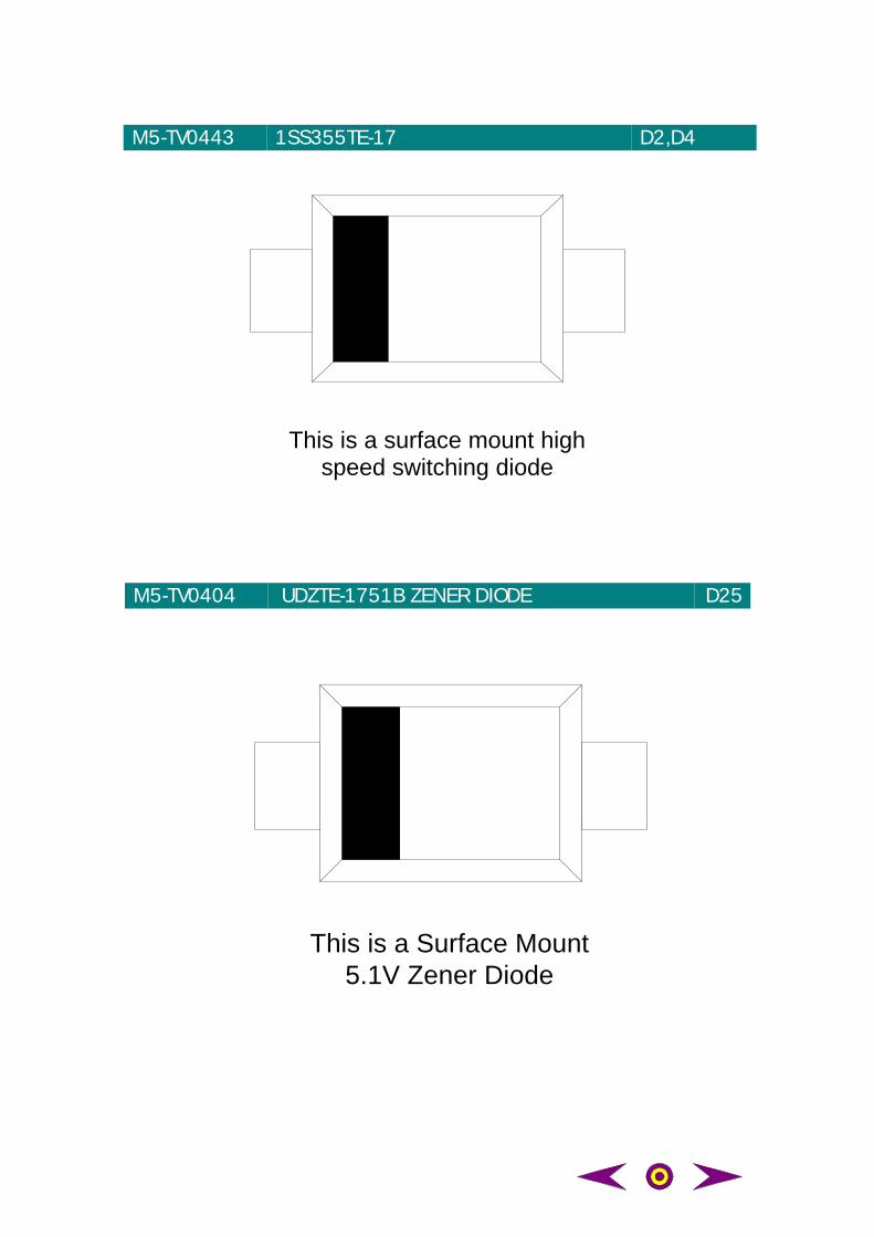
M5-TV0443 1SS355TE-17 D2,D4
This is a surface mount highspeed switching diode
M5-TV0404 UDZTE-1751B ZENER DIODE D25
This is a Surface Mount5.1V Zener Diode
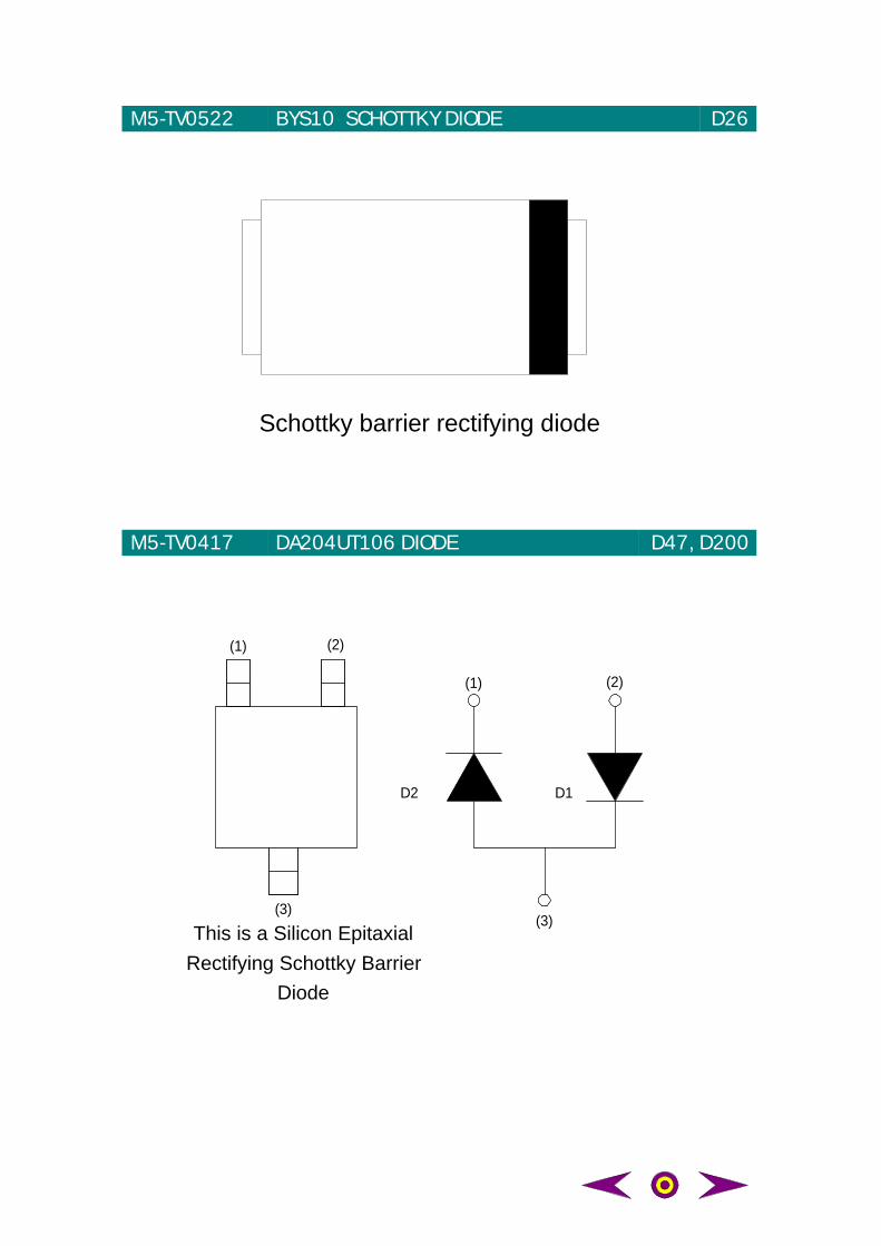
M5-TV0522 BYS10 SCHOTTKY DIODE D26
Schottky barrier rectifying diode
M5-TV0417 DA204UT106 DIODE D47, D200
(2)(1)
(3)(3)
(1) (2)
D2 D1
This is a Silicon EpitaxialRectifying Schottky Barrier
Diode
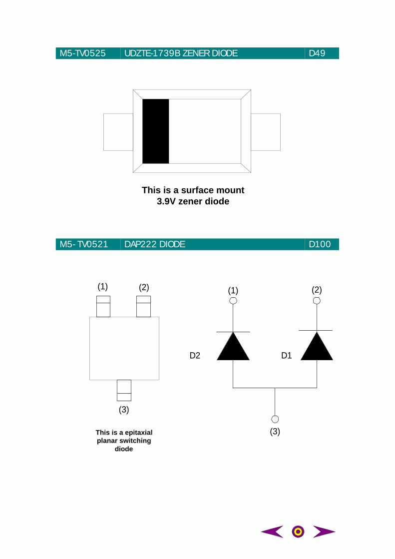
M5-TV0525 UDZTE-1739B ZENER DIODE D49
This is a surface mount3.9V zener diode
M5- TV0521 DAP222 DIODE D100
(2)(1)
(3)
(3)
(1) (2)
D2 D1
This is a epitaxialplanar switching
diode
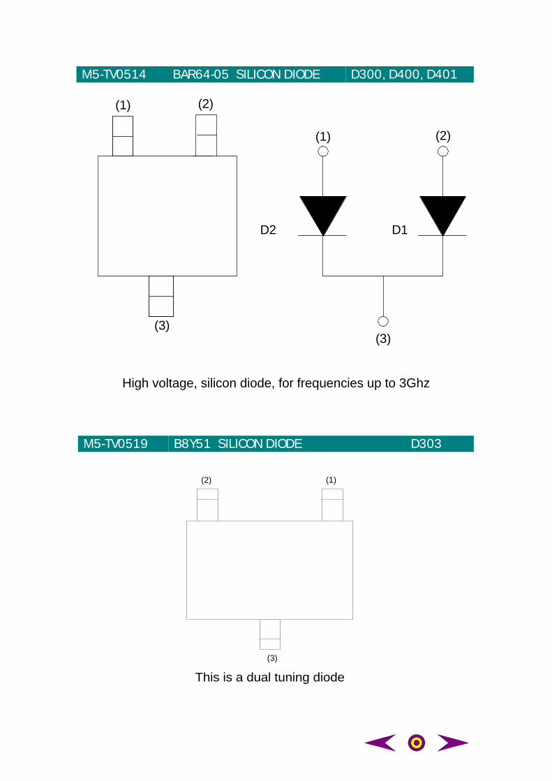
M5-TV0514 BAR64-05 SILICON DIODE D300, D400, D401
(2)(1)
(3)(3)
(1) (2)
D2 D1
High voltage, silicon diode, for frequencies up to 3Ghz
M5-TV0519 B8Y51 SILICON DIODE D303
(3)
(2) (1)
This is a dual tuning diode
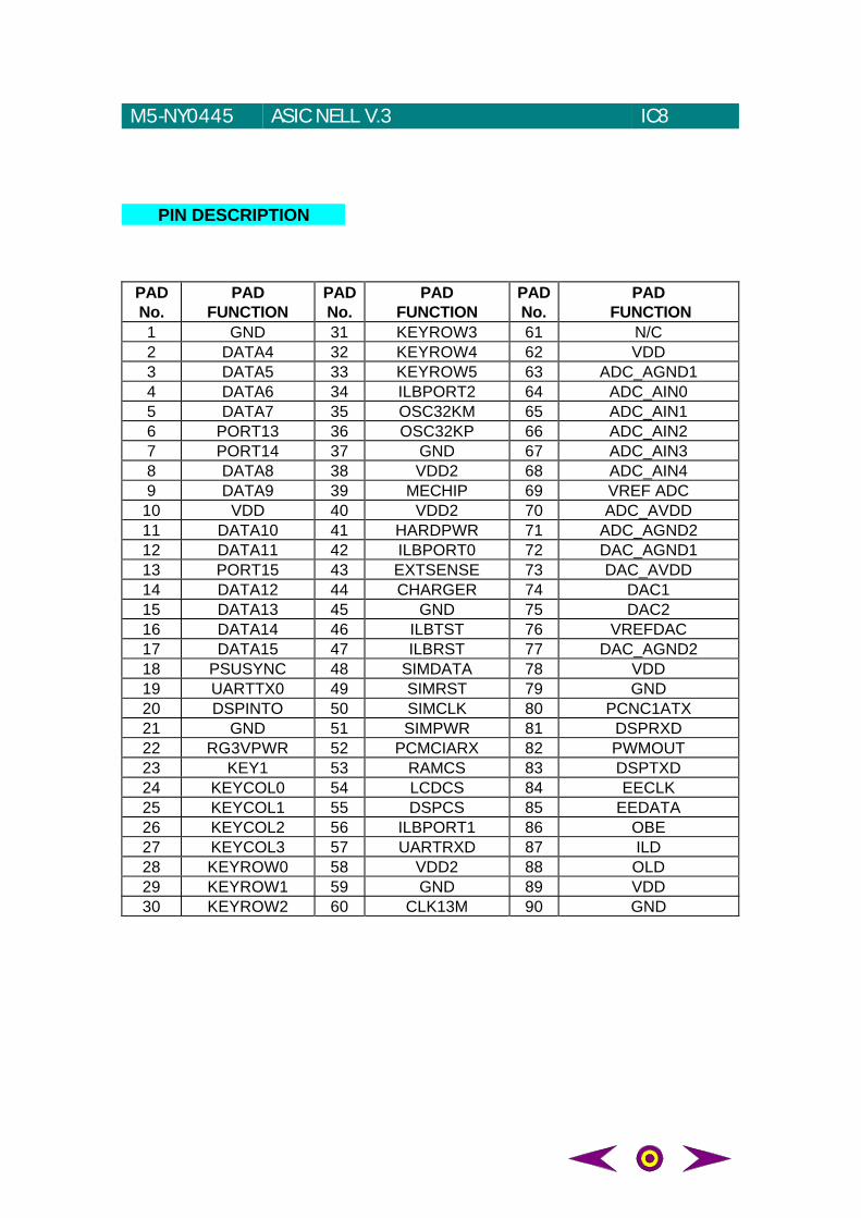
M5-NY0445 ASIC NELL V.3 IC8
PIN DESCRIPTION
PADNo.
PADFUNCTION
PADNo.
PADFUNCTION
PADNo.
PAD FUNCTION
1 GND 31 KEYROW3 61 N/C2 DATA4 32 KEYROW4 62 VDD3 DATA5 33 KEYROW5 63 ADC_AGND14 DATA6 34 ILBPORT2 64 ADC_AIN05 DATA7 35 OSC32KM 65 ADC_AIN16 PORT13 36 OSC32KP 66 ADC_AIN27 PORT14 37 GND 67 ADC_AIN38 DATA8 38 VDD2 68 ADC_AIN49 DATA9 39 MECHIP 69 VREF ADC
10 VDD 40 VDD2 70 ADC_AVDD11 DATA10 41 HARDPWR 71 ADC_AGND212 DATA11 42 ILBPORT0 72 DAC_AGND113 PORT15 43 EXTSENSE 73 DAC_AVDD14 DATA12 44 CHARGER 74 DAC115 DATA13 45 GND 75 DAC216 DATA14 46 ILBTST 76 VREFDAC17 DATA15 47 ILBRST 77 DAC_AGND218 PSUSYNC 48 SIMDATA 78 VDD19 UARTTX0 49 SIMRST 79 GND20 DSPINTO 50 SIMCLK 80 PCNC1ATX21 GND 51 SIMPWR 81 DSPRXD22 RG3VPWR 52 PCMCIARX 82 PWMOUT23 KEY1 53 RAMCS 83 DSPTXD24 KEYCOL0 54 LCDCS 84 EECLK25 KEYCOL1 55 DSPCS 85 EEDATA26 KEYCOL2 56 ILBPORT1 86 OBE27 KEYCOL3 57 UARTRXD 87 ILD28 KEYROW0 58 VDD2 88 OLD29 KEYROW1 59 GND 89 VDD30 KEYROW2 60 CLK13M 90 GND
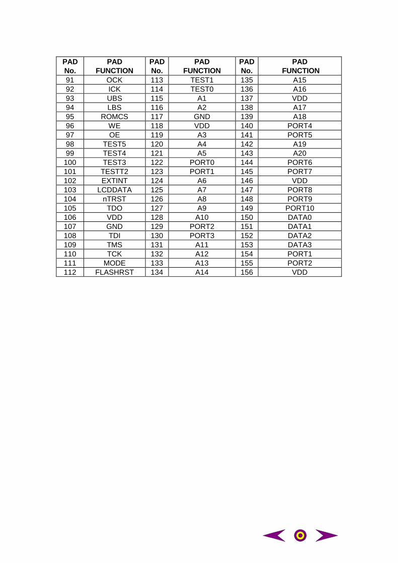
PADNo.
PADFUNCTION
PADNo.
PADFUNCTION
PADNo.
PAD FUNCTION
91 OCK 113 TEST1 135 A1592 ICK 114 TEST0 136 A1693 UBS 115 A1 137 VDD94 LBS 116 A2 138 A1795 ROMCS 117 GND 139 A1896 WE 118 VDD 140 PORT497 OE 119 A3 141 PORT598 TEST5 120 A4 142 A1999 TEST4 121 A5 143 A20
100 TEST3 122 PORT0 144 PORT6101 TESTT2 123 PORT1 145 PORT7102 EXTINT 124 A6 146 VDD103 LCDDATA 125 A7 147 PORT8104 nTRST 126 A8 148 PORT9105 TDO 127 A9 149 PORT10106 VDD 128 A10 150 DATA0107 GND 129 PORT2 151 DATA1108 TDI 130 PORT3 152 DATA2109 TMS 131 A11 153 DATA3110 TCK 132 A12 154 PORT1111 MODE 133 A13 155 PORT2112 FLASHRST 134 A14 156 VDD
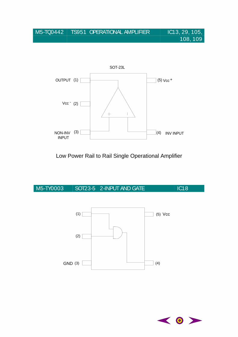
M5-TQ0442 TS951 OPERATIONAL AMPLIFIER IC13, 29, 105,108, 109
(1)
(2)
(3) (4)
(5) Vcc
SOT-23L
OUTPUT +
Vcc -
NON-INVINPUT
INV INPUT
Low Power Rail to Rail Single Operational Amplifier
M5-TY0003 SOT23-5 2-INPUT AND GATE IC18
Vcc
GND
(1)
(2)
(3) (4)
(5)
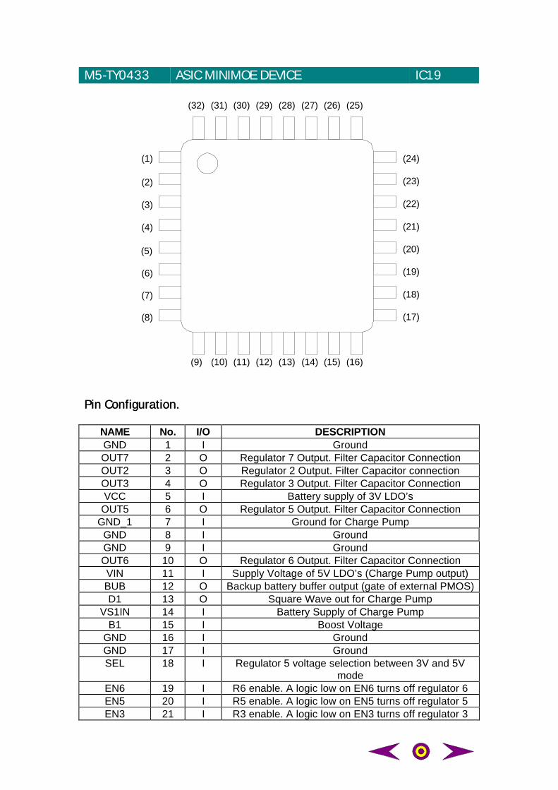
M5-TY0433 ASIC MINIMOE DEVICE IC19
(1)
(2)
(3)
(4)
(5)
(6)
(8)
(9)
(7)
(10) (11) (12) (13) (14) (15) (16)
(17)
(18)
(19)
(20)
(21)
(22)
(23)
(24)
(25)(26)(27)(28)(29)(30)(31)(32)
Pin Configuration.Pin Configuration.
NAME No. I/O DESCRIPTIONGND 1 I GroundOUT7 2 O Regulator 7 Output. Filter Capacitor ConnectionOUT2 3 O Regulator 2 Output. Filter Capacitor connectionOUT3 4 O Regulator 3 Output. Filter Capacitor ConnectionVCC 5 I Battery supply of 3V LDO’s
OUT5 6 O Regulator 5 Output. Filter Capacitor ConnectionGND_1 7 I Ground for Charge Pump
GND 8 I GroundGND 9 I GroundOUT6 10 O Regulator 6 Output. Filter Capacitor ConnectionVIN 11 I Supply Voltage of 5V LDO’s (Charge Pump output)BUB 12 O Backup battery buffer output (gate of external PMOS)D1 13 O Square Wave out for Charge Pump
VS1IN 14 I Battery Supply of Charge PumpB1 15 I Boost Voltage
GND 16 I GroundGND 17 I GroundSEL 18 I Regulator 5 voltage selection between 3V and 5V
modeEN6 19 I R6 enable. A logic low on EN6 turns off regulator 6EN5 20 I R5 enable. A logic low on EN5 turns off regulator 5EN3 21 I R3 enable. A logic low on EN3 turns off regulator 3
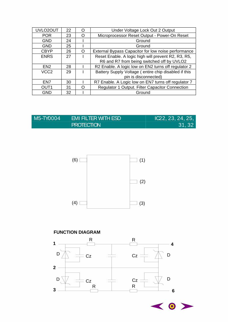
UVLO2OUT 22 O Under Voltage Lock Out 2 OutputPOR 23 O Microprocessor Reset Output - Power-On ResetGND 24 I GroundGND 25 I GroundCBYP 26 O External Bypass Capacitor for low noise performanceENRS 27 I Reset Enable. A logic high will prevent R2, R3, R5,
R6 and R7 from being switched off by UVLO2EN2 28 I R2 Enable. A logic low on EN2 turns off regulator 2
VCC2 29 I Battery Supply Voltage ( entire chip disabled if thispin is disconnected)
EN7 30 I R7 Enable. A Logic low on EN7 turns off regulator 7OUT1 31 O Regulator 1 Output. Filter Capacitor ConnectionGND 32 I Ground
M5-TY0004 EMI FILTER WITH ESDPROTECTION
IC22, 23, 24, 25,31, 32
(6)
(4)
(1)
(2)
(3)
R R
R RCz
CzCz
Cz
D
D D
D
1
2
3
4
6
FUNCTION DIAGRAM
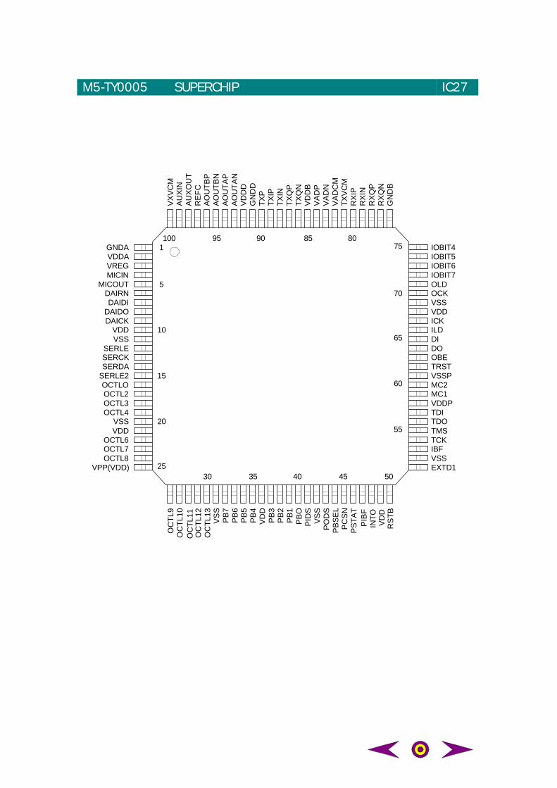
M5-TY0005 SUPERCHIP IC27
100 9095 8085
55
60
65
70
75
403530 45 50
1
10
15
20
25
5
GNDA
VPP(VDD)OCTL8OCTL7OCTL6
VDDVSS
OCTL4OCTL3OCTL2OCTLO
SERLE2SERDASERCKSERLE
VSSVDD
DAICKDAIDODAIDI
DAIRNMICOUT
MICINVREGVDDA
OC
TL9
PB
2P
B1
PB
OP
IDS
VS
SP
OD
SP
BS
EL
PC
SN
PS
TAT
PIB
FIN
TO
RS
TBPB
3V
DD
PB
4P
B5
PB
6P
B7
VS
SO
CTL
13O
CTL
12O
CTL
11O
CTL
10
EXTD1
IOBIT4IOBIT5IOBIT6IOBIT7OLDOCKVSSVDDICKILDDIDOOBETRSTVSSPMC2MC1VDDPTDITDOTMSTCKIBFVSS
GN
DB
AO
UTA
NV
DD
DG
ND
DTX
PTX
IP
TXQ
PTX
QN
VD
DB
VA
DP
VA
DN
VA
DC
MTX
VC
MR
XIP
RX
INR
XQ
PR
XQ
N
VX
VC
MA
UX
IN
AO
UTA
P
AU
XO
UT
RE
FCA
OU
TBP
AO
UTB
N
TXIN
VD
D
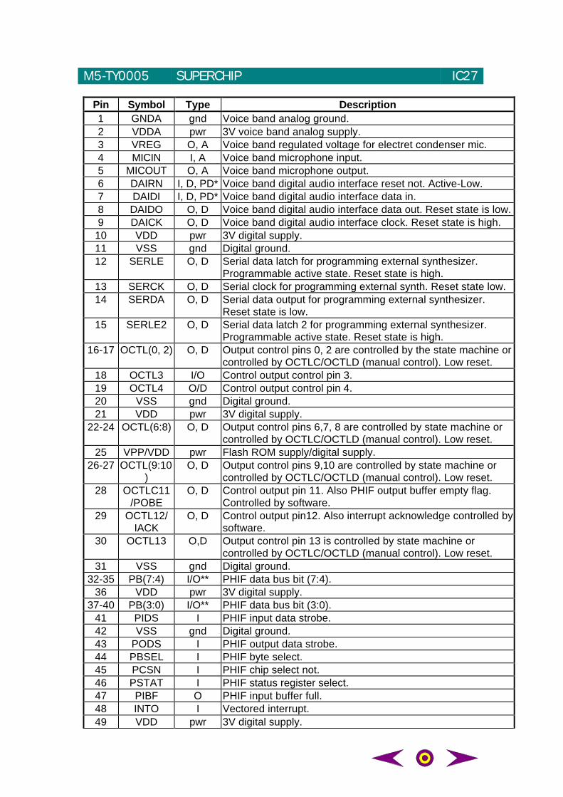
M5-TY0005 SUPERCHIP IC27
Pin Symbol Type Description1 GNDA gnd Voice band analog ground.2 VDDA pwr 3V voice band analog supply.3 VREG O, A Voice band regulated voltage for electret condenser mic.4 MICIN I, A Voice band microphone input.5 MICOUT O, A Voice band microphone output.6 DAIRN I, D, PD* Voice band digital audio interface reset not. Active-Low.7 DAIDI I, D, PD* Voice band digital audio interface data in.8 DAIDO O, D Voice band digital audio interface data out. Reset state is low.9 DAICK O, D Voice band digital audio interface clock. Reset state is high.
10 VDD pwr 3V digital supply.11 VSS gnd Digital ground.12 SERLE O, D Serial data latch for programming external synthesizer.
Programmable active state. Reset state is high.13 SERCK O, D Serial clock for programming external synth. Reset state low.14 SERDA O, D Serial data output for programming external synthesizer.
Reset state is low.15 SERLE2 O, D Serial data latch 2 for programming external synthesizer.
Programmable active state. Reset state is high.16-17 OCTL(0, 2) O, D Output control pins 0, 2 are controlled by the state machine or
controlled by OCTLC/OCTLD (manual control). Low reset.18 OCTL3 I/O Control output control pin 3.19 OCTL4 O/D Control output control pin 4.20 VSS gnd Digital ground.21 VDD pwr 3V digital supply.
22-24 OCTL(6:8) O, D Output control pins 6,7, 8 are controlled by state machine orcontrolled by OCTLC/OCTLD (manual control). Low reset.
25 VPP/VDD pwr Flash ROM supply/digital supply.26-27 OCTL(9:10
)O, D Output control pins 9,10 are controlled by state machine or
controlled by OCTLC/OCTLD (manual control). Low reset.28 OCTLC11
/POBEO, D Control output pin 11. Also PHIF output buffer empty flag.
Controlled by software.29 OCTL12/
IACKO, D Control output pin12. Also interrupt acknowledge controlled by
software.30 OCTL13 O,D Output control pin 13 is controlled by state machine or
controlled by OCTLC/OCTLD (manual control). Low reset.31 VSS gnd Digital ground.
32-35 PB(7:4) I/O** PHIF data bus bit (7:4).36 VDD pwr 3V digital supply.
37-40 PB(3:0) I/O** PHIF data bus bit (3:0).41 PIDS I PHIF input data strobe.42 VSS gnd Digital ground.43 PODS I PHIF output data strobe.44 PBSEL I PHIF byte select.45 PCSN I PHIF chip select not.46 PSTAT I PHIF status register select.47 PIBF O PHIF input buffer full.48 INTO I Vectored interrupt.49 VDD pwr 3V digital supply.
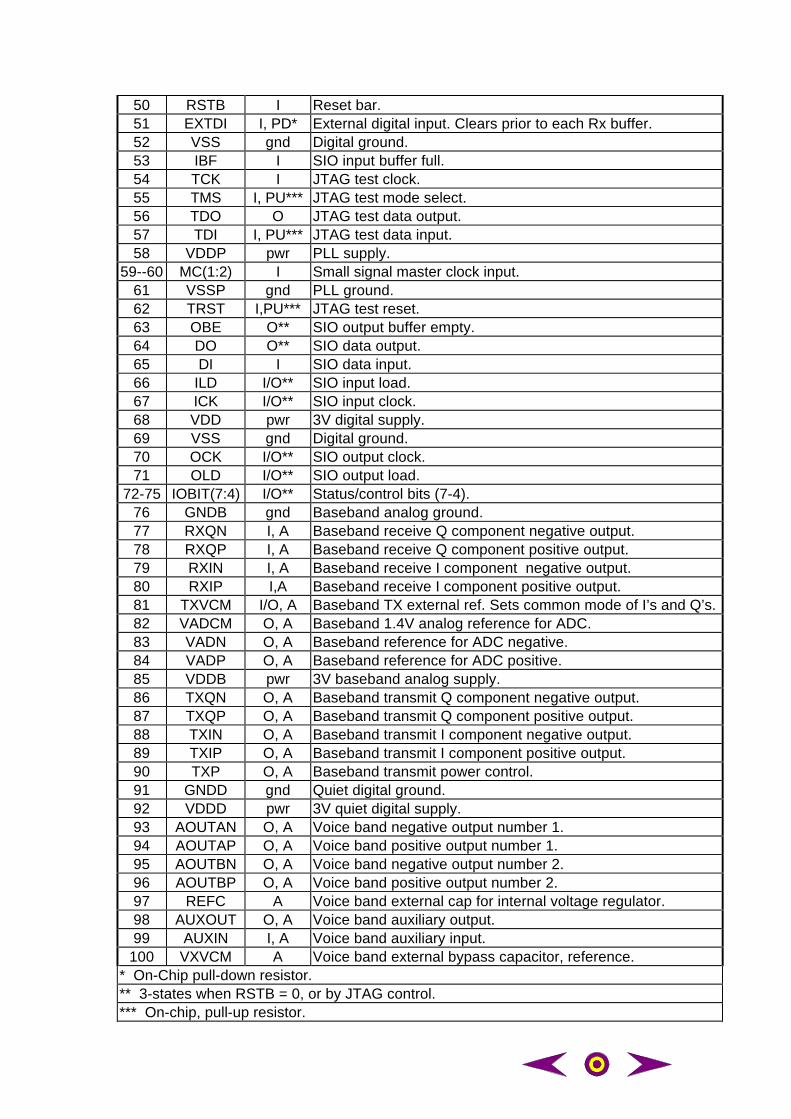
50 RSTB I Reset bar.51 EXTDI I, PD* External digital input. Clears prior to each Rx buffer.52 VSS gnd Digital ground.53 IBF I SIO input buffer full.54 TCK I JTAG test clock.55 TMS I, PU*** JTAG test mode select.56 TDO O JTAG test data output.57 TDI I, PU*** JTAG test data input.58 VDDP pwr PLL supply.
59--60 MC(1:2) I Small signal master clock input.61 VSSP gnd PLL ground.62 TRST I,PU*** JTAG test reset.63 OBE O** SIO output buffer empty.64 DO O** SIO data output.65 DI I SIO data input.66 ILD I/O** SIO input load.67 ICK I/O** SIO input clock.68 VDD pwr 3V digital supply.69 VSS gnd Digital ground.70 OCK I/O** SIO output clock.71 OLD I/O** SIO output load.
72-75 IOBIT(7:4) I/O** Status/control bits (7-4).76 GNDB gnd Baseband analog ground.77 RXQN I, A Baseband receive Q component negative output.78 RXQP I, A Baseband receive Q component positive output.79 RXIN I, A Baseband receive I component negative output.80 RXIP I,A Baseband receive I component positive output.81 TXVCM I/O, A Baseband TX external ref. Sets common mode of I’s and Q’s.82 VADCM O, A Baseband 1.4V analog reference for ADC.83 VADN O, A Baseband reference for ADC negative.84 VADP O, A Baseband reference for ADC positive.85 VDDB pwr 3V baseband analog supply.86 TXQN O, A Baseband transmit Q component negative output.87 TXQP O, A Baseband transmit Q component positive output.88 TXIN O, A Baseband transmit I component negative output.89 TXIP O, A Baseband transmit I component positive output.90 TXP O, A Baseband transmit power control.91 GNDD gnd Quiet digital ground.92 VDDD pwr 3V quiet digital supply.93 AOUTAN O, A Voice band negative output number 1.94 AOUTAP O, A Voice band positive output number 1.95 AOUTBN O, A Voice band negative output number 2.96 AOUTBP O, A Voice band positive output number 2.97 REFC A Voice band external cap for internal voltage regulator.98 AUXOUT O, A Voice band auxiliary output.99 AUXIN I, A Voice band auxiliary input.
100 VXVCM A Voice band external bypass capacitor, reference.* On-Chip pull-down resistor.** 3-states when RSTB = 0, or by JTAG control.*** On-chip, pull-up resistor.
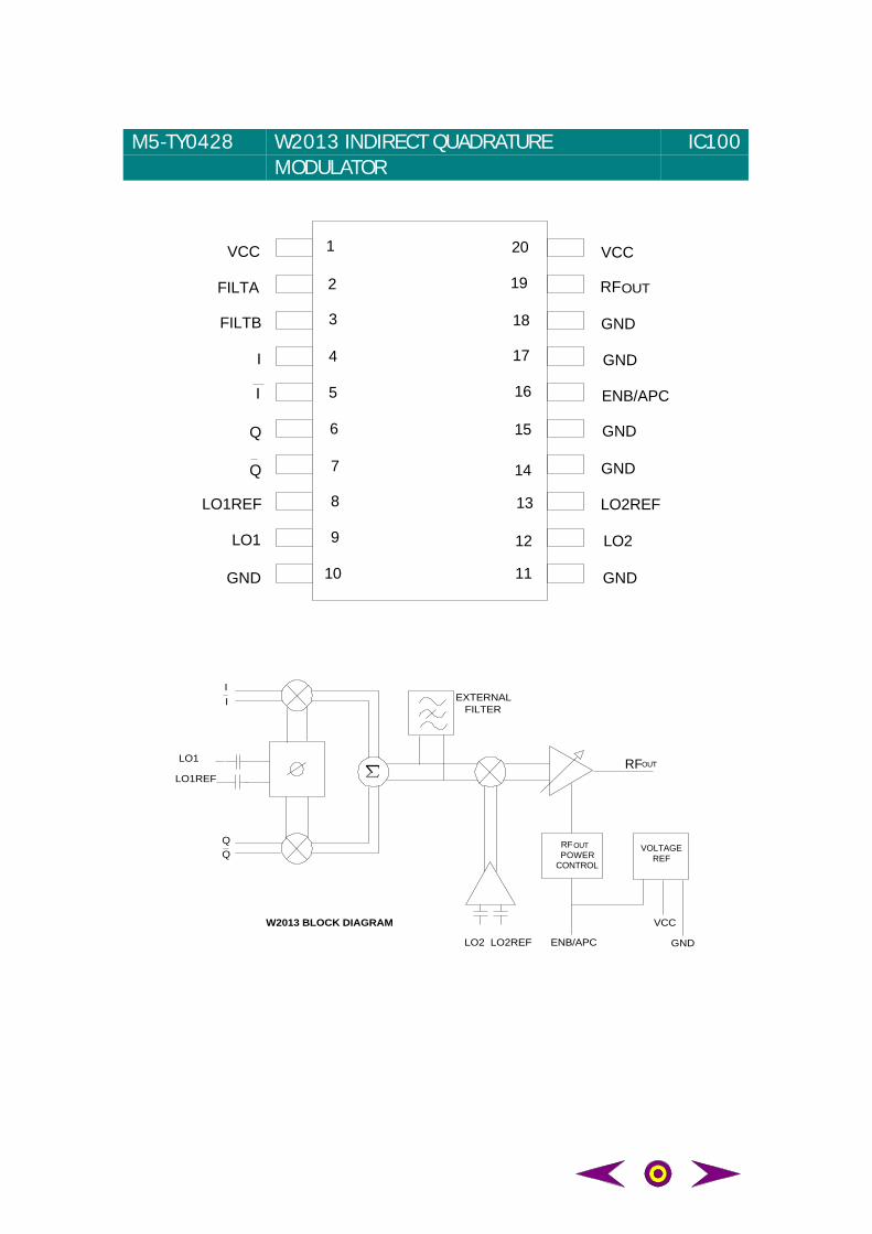
M5-TY0428 W2013 INDIRECT QUADRATUREMODULATOR
IC100
VCC
FILTA
FILTB
I
I
Q
Q
LO1REF
LO1
GND
VCC
RFOUT
GND
GND
ENB/APC
GND
GND
LO2REF
LO2
GND
1
2
3
4
5
6
7
8
9
10 11
12
13
14
15
16
17
18
19
20
LO1
LO1REF
II
LO2 LO2REF
EXTERNALFILTER
RFOUT
ENB/APC
VCC
GND
RFOUTPOWER
CONTROL
VOLTAGEREF
W2013 BLOCK DIAGRAM
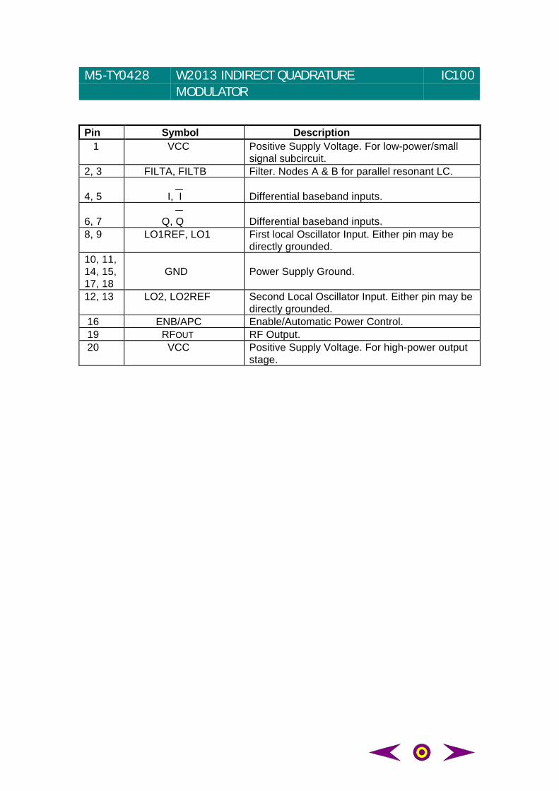
M5-TY0428 W2013 INDIRECT QUADRATUREMODULATOR
IC100
Pin Symbol Description 1 VCC Positive Supply Voltage. For low-power/small
signal subcircuit.2, 3 FILTA, FILTB Filter. Nodes A & B for parallel resonant LC.
4, 5 I, I Differential baseband inputs.
6, 7 Q, Q Differential baseband inputs.8, 9 LO1REF, LO1 First local Oscillator Input. Either pin may be
directly grounded.10, 11,14, 15,17, 18
GND Power Supply Ground.
12, 13 LO2, LO2REF Second Local Oscillator Input. Either pin may bedirectly grounded.
16 ENB/APC Enable/Automatic Power Control. 19 RFOUT RF Output. 20 VCC Positive Supply Voltage. For high-power output
stage.
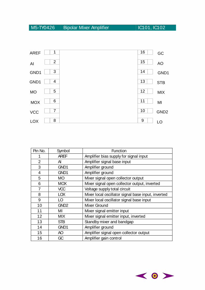
M5-TY0426 Bipolar Mixer Amplifier IC101, IC102
P-TSSOP16
Pin No. Symbol Function 1 AREF Amplifier bias supply for signal input 2 AI Amplifier signal base input 3 GND1 Amplifier ground 4 GND1 Amplifier ground 5 MO Mixer signal open collector output 6 MOX Mixer signal open collector output, inverted 7 VCC Voltage supply total circuit 8 LOX Mixer local oscillator signal base input, inverted 9 LO Mixer local oscillator signal base input 10 GND2 Mixer Ground 11 MI Mixer signal emitter input 12 MIX Mixer signal emitter input, inverted 13 STB Standby mixer and bandgap 14 GND1 Amplifier ground 15 AO Amplifier signal open collector output 16 GC Amplifier gain control
15
14
13
12
11
10
9
1
2
3
4
5
7
8
AREF
AI
GND1
GND1
MO
MOX
VCC
LOX
GC
AO
GND1
STB
MIX
MI
GND2
LO
6
16
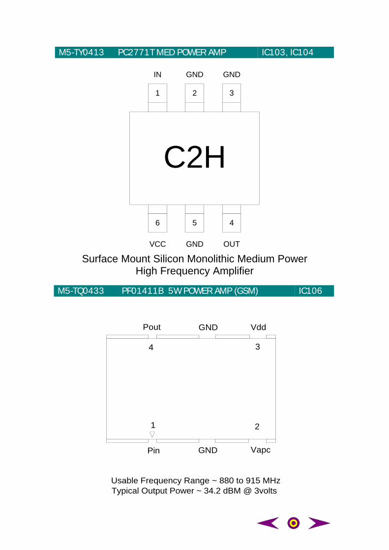
M5-TY0413 PC2771T MED POWER AMP IC103, IC104
C2H
1 2 3
6 5 4
IN GND
VCC GND OUT
GND
Surface Mount Silicon Monolithic Medium PowerHigh Frequency Amplifier
M5-TQ0433 PF01411B 5W POWER AMP (GSM) IC106
Pin
GND VddPout
GND Vapc
Usable Frequency Range ~ 880 to 915 MHzTypical Output Power ~ 34.2 dBM @ 3volts
1
4 3
2
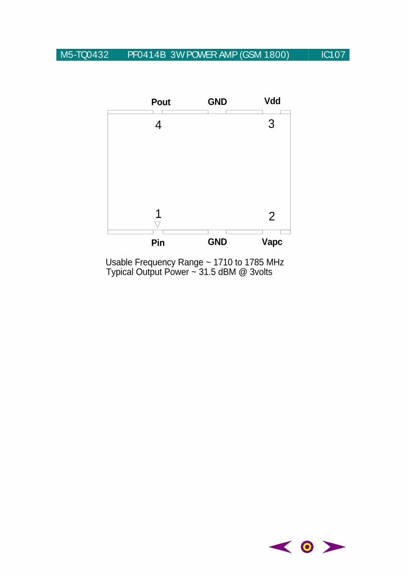
M5-TQ0432 PF0414B 3W POWER AMP (GSM 1800) IC107
Pin
GND VddPout
GND Vapc
2
3
Usable Frequency Range ~ 1710 to 1785 MHzTypical Output Power ~ 31.5 dBM @ 3volts
1
4
2
3
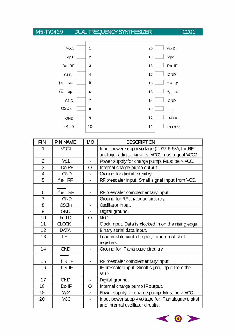
M5-TY0429 DUAL FREQUENCY SYNTHESIZER IC201
1
2
3
4
RF
6
7
8
9
10 11
12
13
14
15
16
17
18
19
20Vcc1
Vp1
Vcc2
Vp2
Do RF Do IF
GND GND
fIN 5
f IN RF
f IN
IN
IF
f IF
GND
OSCin
GND
Fo LD
GND
LE
DATA
CLOCK
PIN PIN PIN NAMEPIN NAME I/O I/O DESCRIPTION DESCRIPTION 1 VCC1 - Input power supply voltage (2.7V -5.5V), for RF
analogue/digital circuits. VCC1 must equal VCC2. 2 Vp1 - Power supply for charge pump. Must be ≥ VCC. 3 Do RF O Internal charge pump output. 4 GND - Ground for digital circuitry 5 f IN RF - RF prescaler input. Small signal input from VCO.
6 f IN RF - RF prescaler complementary input. 7 GND Ground for RF analogue circuitry. 8 OSCin - Oscillator input. 9 GND - Digital ground. 10 Fo LD O N/C 11 CLOCK I Clock input. Data is clocked in on the rising edge. 12 DATA I Binary serial data input. 13 LE I Load enable control input, for internal shift
registers. 14 GND - Ground for IF analogue circuitry
15 f IN IF - RF prescaler complementary input. 16 f IN IF - IF prescaler input. Small signal input from the
VCO. 17 GND - Digital ground. 18 Do IF O Internal charge pump IF output. 19 Vp2 - Power supply for charge pump. Must be ≥ VCC. 20 VCC - Input power supply voltage for IF analogue/digital
and internal oscillator circuits.
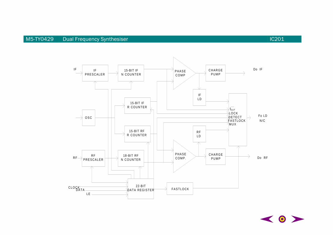
C L O C K
IF
R F
Do IF
Fo LD
Do RF
N/C
IFP R E S C A L E R
15-BIT IFN C O U N T E R
O S C
D A T ALE
R FP R E S C A L E R
22-BITDATA REGISTER
18-BIT RFN C O U N T E R
F A S T L O C K
P H A S EC O M P .
C H A R G EP U M P
R FLD
15-BIT RFR C O U N T E R
15-BIT IFR C O U N T E R
P H A S EC O M P
C H A R G EP U M P
IFLD
fO U T
L O C KD E T E C TF A S T L O C KM U X
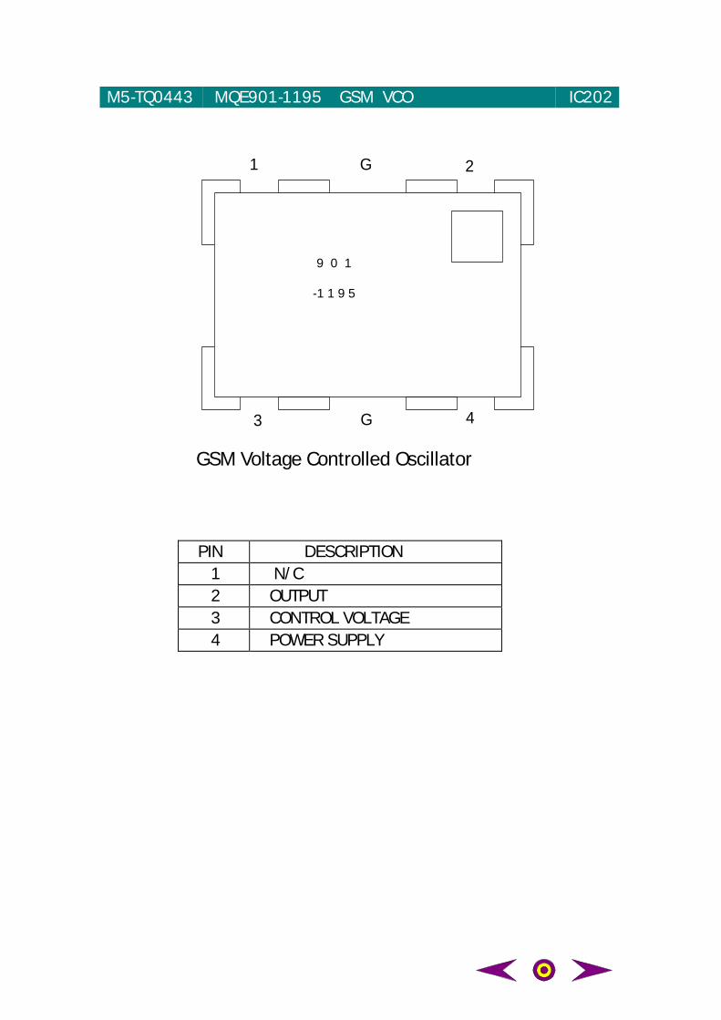
M5-TQ0443 MQE901-1195 GSM VCO IC202
GSM Voltage Controlled Oscillator
PIN DESCRIPTION 1 N/C 2 OUTPUT 3 CONTROL VOLTAGE 4 POWER SUPPLY
1 G 2
3 G 4
9 0 1
-1 1 9 5
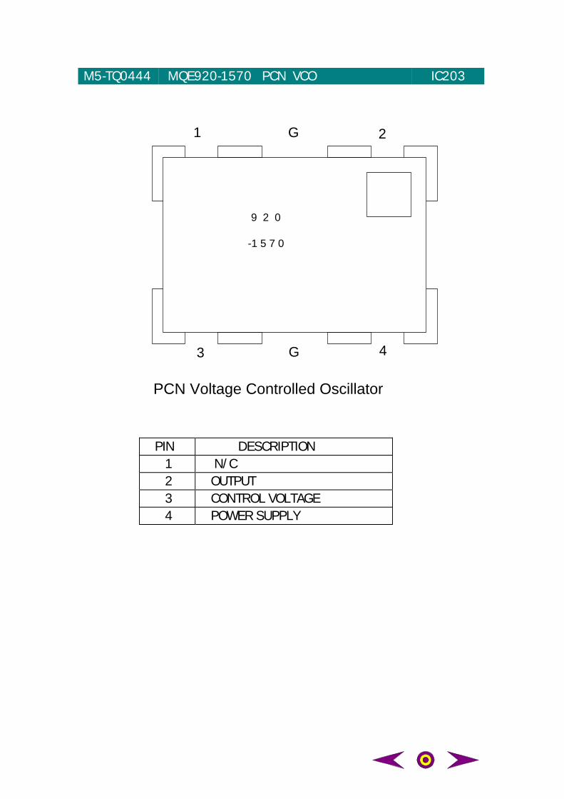
M5-TQ0444 MQE920-1570 PCN VCO IC203
PCN Voltage Controlled Oscillator
PIN DESCRIPTION 1 N/C 2 OUTPUT 3 CONTROL VOLTAGE 4 POWER SUPPLY
1 G 2
3 G 4
9 2 0
-1 5 7 0
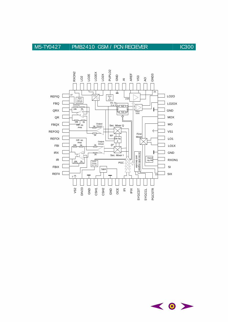
M5-TY0427 PMB2410 GSM / PCN RECIEVER IC300
%2
%3
LNA
Output Buffer
VCO Standby
VCOStandby IF &
OPAMP Div. by2 or 3
Diff. op.Amp
OutputDriver
18k
18k 2k
2k
2k
2k
Div by2
90o
0o
Sec. Mixer Q
Sec. Mixer I
18k
18k
2k
2k2k
2k
++ --
-- ++
Diff. op.Amp
S&H
SwitchDivider
%2 / %3
16 bit-shift-registerand decoder
Stand-by RF
OutputDriver
FirstMixer
PGC
LO2O
LO2OX
GND
MOX
MO
VS1
LO1
LO1X
GND
RXON1
SI
SIX
RX
ON
2
LO2
LO2E
LO2E
X
LO2X
PU
PLO
2
GN
D
AI
AR
EF
VS
3
AO
GN
D3
REFIQ
FBQ
QRX
QR
FBQX
REFOQ
REFOI
FBI
IRX
IR
FBIX
REFII
VS
2
DIV
23
GN
D
CS
H1
CS
H2
GN
D
OC
E IFI
IFIX
SY
GC
DT
SY
GC
CL
PG
CS
TR
2537
131
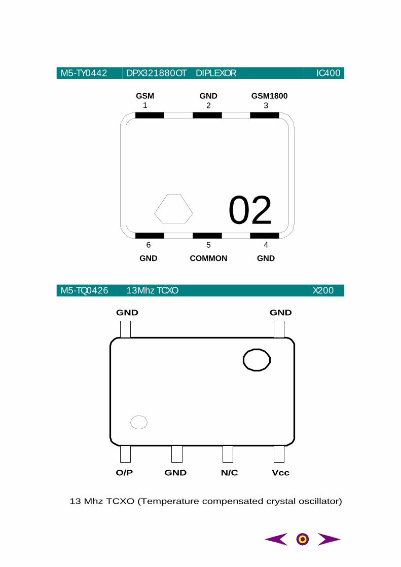
M5-TY0442 DPX321880OT DIPLEXOR IC400
02
1 2 3
456
GSM GND GSM1800
GNDCOMMONGND
M5-TQ0426 13Mhz TCXO X200
O/P GND N/C Vcc
GND GND
13 Mhz TCXO (Temperature compensated crystal oscillator)
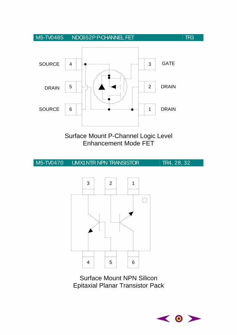
M5-TV0485 NDC652P P-CHANNEL FET TR3
4
5
6
3
2
1
SOURCE
SOURCE
DRAIN
GATE
DRAIN
DRAIN
Surface Mount P-Channel Logic LevelEnhancement Mode FET
M5-TV0470 UMX1NTR NPN TRANSISTOR TR4, 28, 32
3 2 1
4 5 6
Surface Mount NPN SiliconEpitaxial Planar Transistor Pack
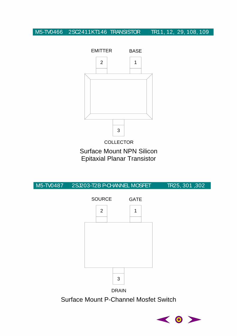
M5-TV0466 2SC2411KT146 TRANSISTOR TR11, 12, 29, 108, 109
2 1
3
EMITTER BASE
COLLECTOR
Surface Mount NPN SiliconEpitaxial Planar Transistor
M5-TV0487 2SJ203-T2B P-CHANNEL MOSFET TR25, 301 ,302
2 1
3
SOURCE GATE
DRAIN
Surface Mount P-Channel Mosfet Switch
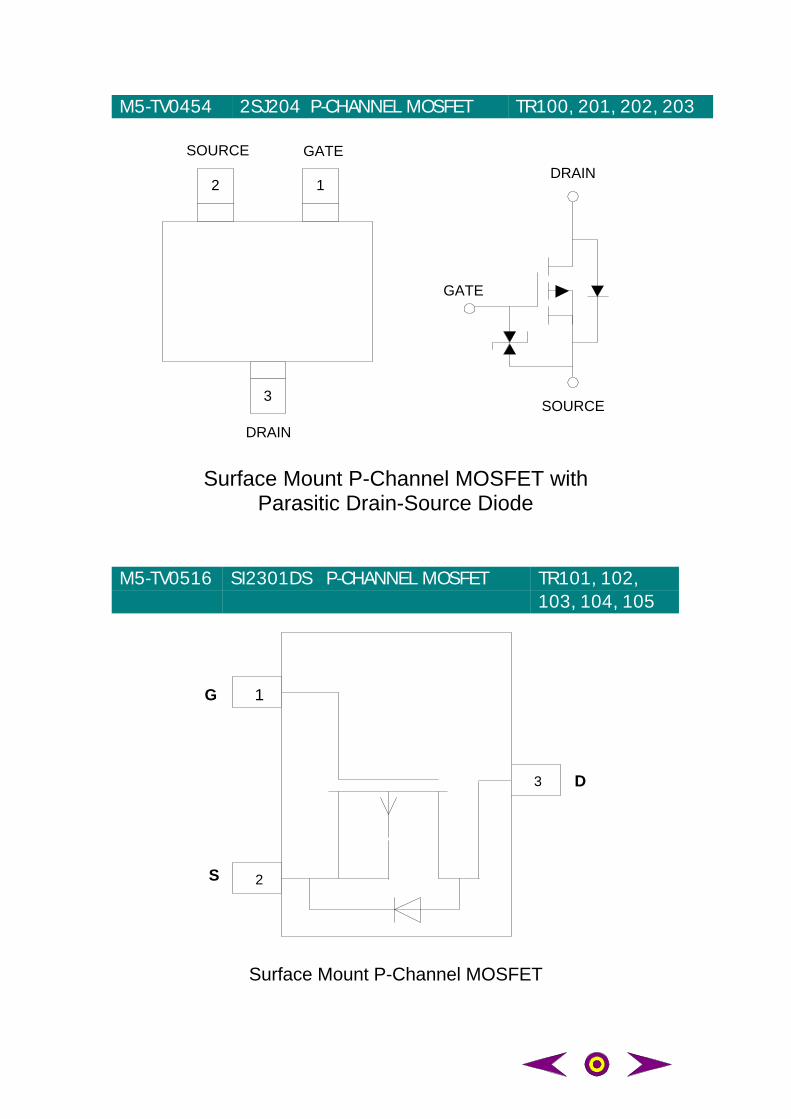
M5-TV0454 2SJ204 P-CHANNEL MOSFET TR100, 201, 202, 203
2 1
3
SOURCE GATE
DRAIN
DRAIN
GATE
SOURCE
Surface Mount P-Channel MOSFET withParasitic Drain-Source Diode
M5-TV0516 SI2301DS P-CHANNEL MOSFET TR101, 102,103, 104, 105
1
2
3
G
S
D
Surface Mount P-Channel MOSFET
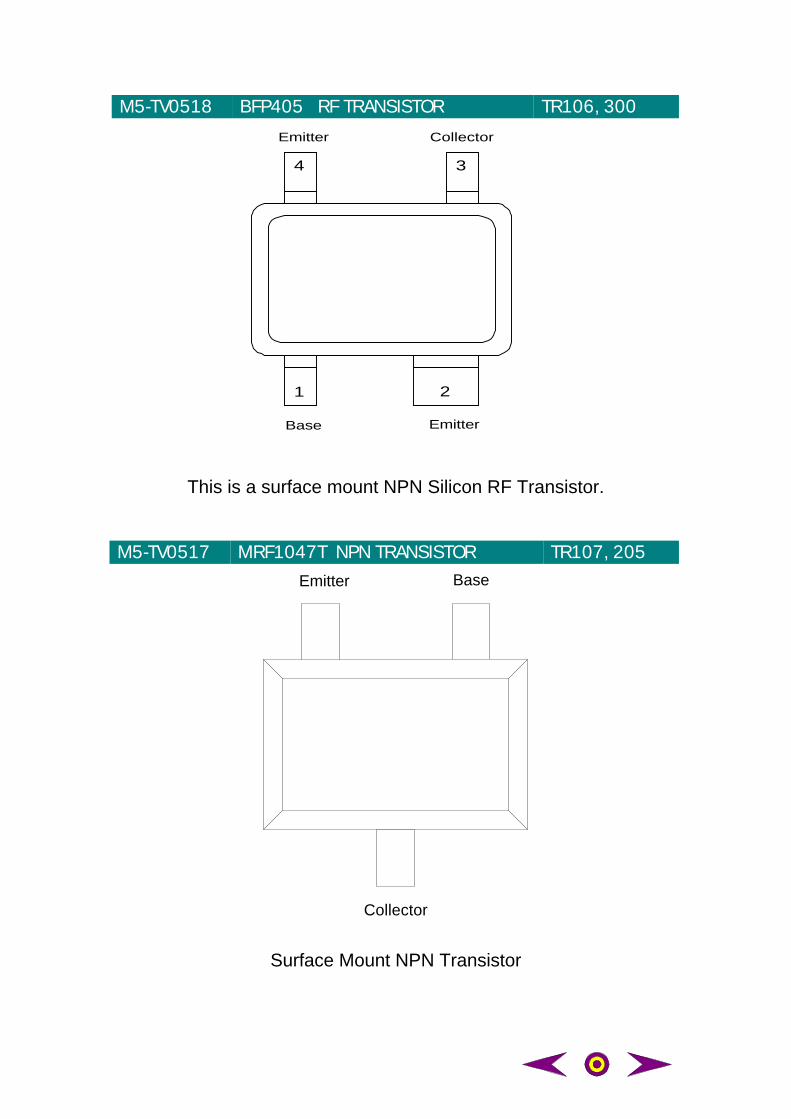
M5-TV0518 BFP405 RF TRANSISTOR TR106, 300
4 3
1 2
Emitter Collector
Base Emitter
This is a surface mount NPN Silicon RF Transistor.
M5-TV0517 MRF1047T NPN TRANSISTOR TR107, 205Emitter Base
Collector
Surface Mount NPN Transistor
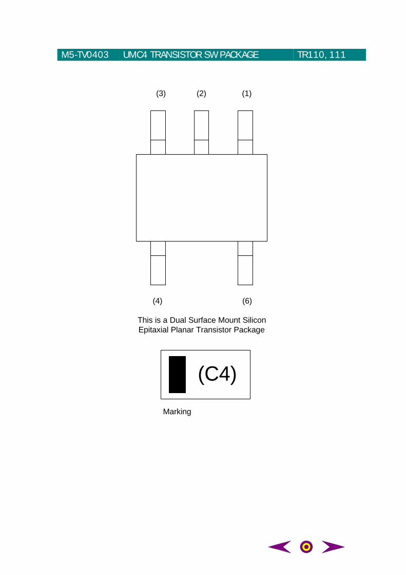
M5-TV0403 UMC4 TRANSISTOR SW PACKAGE TR110, 111
(3) (2) (1)
(4) (6)
(C4)Marking
This is a Dual Surface Mount SiliconEpitaxial Planar Transistor Package
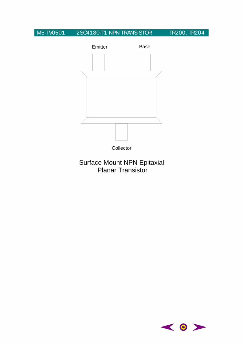
M5-TV0501 2SC4180-T1 NPN TRANSISTOR TR200, TR204
Emitter Base
Collector
Surface Mount NPN Epitaxial Planar Transistor
<< Previous SectionNext Section >>Main Menu
Part 1Part 2Part 3Part 4
Section 7
Parts
Exploded ViewAssembly PartsBaseband Board PartsRF Board Parts
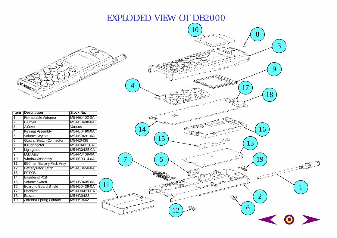
16
1817
9
3
810
11
12 6
1
19
13
2
4
14
57
15
EXPLODED VIEW OF DB2000
ItemItem DescriptionDescription Stock No.Stock No.1 Retractable Antenna M5-NE0402-0A2 B Cover M5-N50498-0A3 A Cover Various4 Keymat Assembly M5-N50490-0A5 Volume Keymat M5-N50491-0A6 Coaxial Switch Connector M5-NJ04397 IO Connector M5-NJ0432-0A8 Lightguide M5-ND0425-0A9 LCD Assy M5-NP0409-0A10 Window Assembly M5-N50314-0A11 950mah Battery Pack Assy -12 Battery Pack Latch M5-N50450-0A13 RF PCB -14 Baseband PCB -15 Volume Switch M5-NS0405-0A16 Board to Board Shield M5-N60439-0A17 Receiver M5-ND0431-0A18 Buzzer M5-ND042319 Antenna Spring Contact M5-N60442
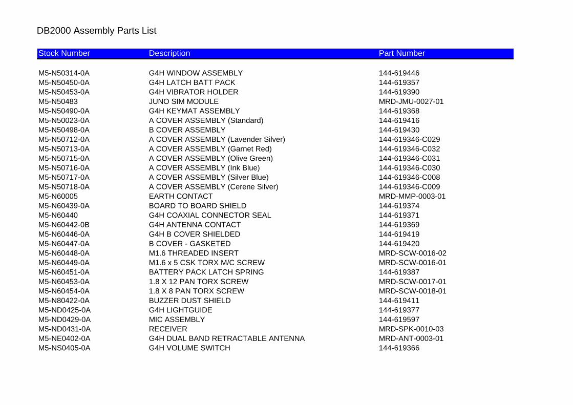
DB2000 Assembly Parts List
Stock Number Description Part Number
M5-N50314-0A G4H WINDOW ASSEMBLY 144-619446 M5-N50450-0A G4H LATCH BATT PACK 144-619357 M5-N50453-0A G4H VIBRATOR HOLDER 144-619390 M5-N50483 JUNO SIM MODULE MRD-JMU-0027-01 M5-N50490-0A G4H KEYMAT ASSEMBLY 144-619368 M5-N50023-0A A COVER ASSEMBLY (Standard) 144-619416 M5-N50498-0A B COVER ASSEMBLY 144-619430 M5-N50712-0A A COVER ASSEMBLY (Lavender Silver) 144-619346-C029M5-N50713-0A A COVER ASSEMBLY (Garnet Red) 144-619346-C032M5-N50715-0A A COVER ASSEMBLY (Olive Green) 144-619346-C031M5-N50716-0A A COVER ASSEMBLY (Ink Blue) 144-619346-C030M5-N50717-0A A COVER ASSEMBLY (Silver Blue) 144-619346-C008M5-N50718-0A A COVER ASSEMBLY (Cerene Silver) 144-619346-C009M5-N60005 EARTH CONTACT MRD-MMP-0003-01 M5-N60439-0A BOARD TO BOARD SHIELD 144-619374 M5-N60440 G4H COAXIAL CONNECTOR SEAL 144-619371 M5-N60442-0B G4H ANTENNA CONTACT 144-619369 M5-N60446-0A G4H B COVER SHIELDED 144-619419 M5-N60447-0A B COVER - GASKETED 144-619420 M5-N60448-0A M1.6 THREADED INSERT MRD-SCW-0016-02 M5-N60449-0A M1.6 x 5 CSK TORX M/C SCREW MRD-SCW-0016-01 M5-N60451-0A BATTERY PACK LATCH SPRING 144-619387 M5-N60453-0A 1.8 X 12 PAN TORX SCREW MRD-SCW-0017-01 M5-N60454-0A 1.8 X 8 PAN TORX SCREW MRD-SCW-0018-01 M5-N80422-0A BUZZER DUST SHIELD 144-619411 M5-ND0425-0A G4H LIGHTGUIDE 144-619377 M5-ND0429-0A MIC ASSEMBLY 144-619597 M5-ND0431-0A RECEIVER MRD-SPK-0010-03M5-NE0402-0A G4H DUAL BAND RETRACTABLE ANTENNA MRD-ANT-0003-01M5-NS0405-0A G4H VOLUME SWITCH 144-619366
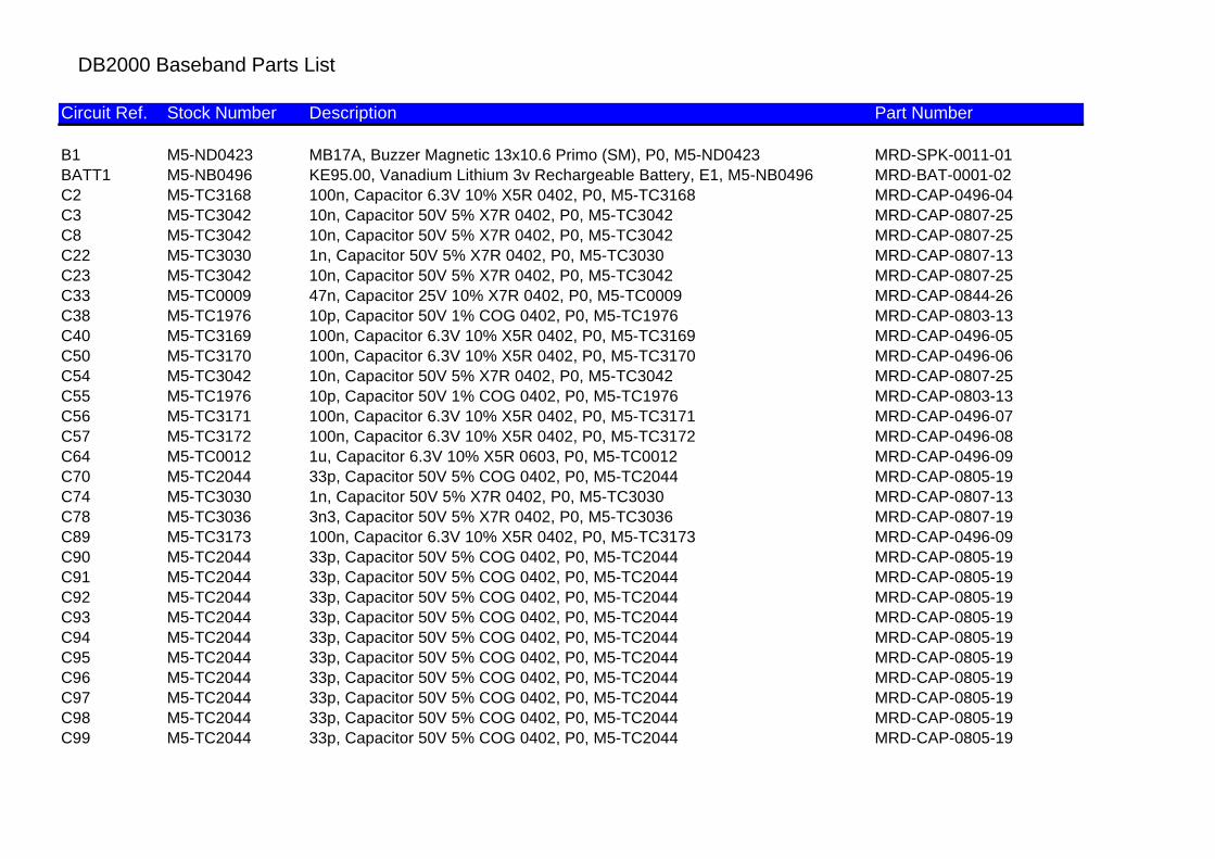
DB2000 Baseband Parts List
Circuit Ref. Stock Number Description Part Number
B1 M5-ND0423 MB17A, Buzzer Magnetic 13x10.6 Primo (SM), P0, M5-ND0423 MRD-SPK-0011-01BATT1 M5-NB0496 KE95.00, Vanadium Lithium 3v Rechargeable Battery, E1, M5-NB0496 MRD-BAT-0001-02C2 M5-TC3168 100n, Capacitor 6.3V 10% X5R 0402, P0, M5-TC3168 MRD-CAP-0496-04C3 M5-TC3042 10n, Capacitor 50V 5% X7R 0402, P0, M5-TC3042 MRD-CAP-0807-25C8 M5-TC3042 10n, Capacitor 50V 5% X7R 0402, P0, M5-TC3042 MRD-CAP-0807-25C22 M5-TC3030 1n, Capacitor 50V 5% X7R 0402, P0, M5-TC3030 MRD-CAP-0807-13C23 M5-TC3042 10n, Capacitor 50V 5% X7R 0402, P0, M5-TC3042 MRD-CAP-0807-25C33 M5-TC0009 47n, Capacitor 25V 10% X7R 0402, P0, M5-TC0009 MRD-CAP-0844-26C38 M5-TC1976 10p, Capacitor 50V 1% COG 0402, P0, M5-TC1976 MRD-CAP-0803-13C40 M5-TC3169 100n, Capacitor 6.3V 10% X5R 0402, P0, M5-TC3169 MRD-CAP-0496-05C50 M5-TC3170 100n, Capacitor 6.3V 10% X5R 0402, P0, M5-TC3170 MRD-CAP-0496-06C54 M5-TC3042 10n, Capacitor 50V 5% X7R 0402, P0, M5-TC3042 MRD-CAP-0807-25C55 M5-TC1976 10p, Capacitor 50V 1% COG 0402, P0, M5-TC1976 MRD-CAP-0803-13C56 M5-TC3171 100n, Capacitor 6.3V 10% X5R 0402, P0, M5-TC3171 MRD-CAP-0496-07C57 M5-TC3172 100n, Capacitor 6.3V 10% X5R 0402, P0, M5-TC3172 MRD-CAP-0496-08C64 M5-TC0012 1u, Capacitor 6.3V 10% X5R 0603, P0, M5-TC0012 MRD-CAP-0496-09C70 M5-TC2044 33p, Capacitor 50V 5% COG 0402, P0, M5-TC2044 MRD-CAP-0805-19C74 M5-TC3030 1n, Capacitor 50V 5% X7R 0402, P0, M5-TC3030 MRD-CAP-0807-13C78 M5-TC3036 3n3, Capacitor 50V 5% X7R 0402, P0, M5-TC3036 MRD-CAP-0807-19C89 M5-TC3173 100n, Capacitor 6.3V 10% X5R 0402, P0, M5-TC3173 MRD-CAP-0496-09C90 M5-TC2044 33p, Capacitor 50V 5% COG 0402, P0, M5-TC2044 MRD-CAP-0805-19C91 M5-TC2044 33p, Capacitor 50V 5% COG 0402, P0, M5-TC2044 MRD-CAP-0805-19C92 M5-TC2044 33p, Capacitor 50V 5% COG 0402, P0, M5-TC2044 MRD-CAP-0805-19C93 M5-TC2044 33p, Capacitor 50V 5% COG 0402, P0, M5-TC2044 MRD-CAP-0805-19C94 M5-TC2044 33p, Capacitor 50V 5% COG 0402, P0, M5-TC2044 MRD-CAP-0805-19C95 M5-TC2044 33p, Capacitor 50V 5% COG 0402, P0, M5-TC2044 MRD-CAP-0805-19C96 M5-TC2044 33p, Capacitor 50V 5% COG 0402, P0, M5-TC2044 MRD-CAP-0805-19C97 M5-TC2044 33p, Capacitor 50V 5% COG 0402, P0, M5-TC2044 MRD-CAP-0805-19C98 M5-TC2044 33p, Capacitor 50V 5% COG 0402, P0, M5-TC2044 MRD-CAP-0805-19C99 M5-TC2044 33p, Capacitor 50V 5% COG 0402, P0, M5-TC2044 MRD-CAP-0805-19
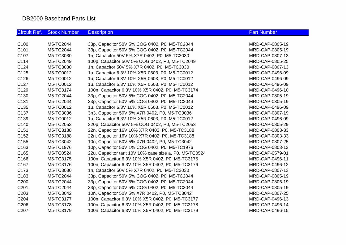
DB2000 Baseband Parts List
Circuit Ref. Stock Number Description Part Number
C100 M5-TC2044 33p, Capacitor 50V 5% COG 0402, P0, M5-TC2044 MRD-CAP-0805-19C101 M5-TC2044 33p, Capacitor 50V 5% COG 0402, P0, M5-TC2044 MRD-CAP-0805-19C107 M5-TC3030 1n, Capacitor 50V 5% X7R 0402, P0, M5-TC3030 MRD-CAP-0807-13C114 M5-TC2049 100p, Capacitor 50V 5% COG 0402, P0, M5-TC2049 MRD-CAP-0805-25C124 M5-TC3030 1n, Capacitor 50V 5% X7R 0402, P0, M5-TC3030 MRD-CAP-0807-13C125 M5-TC0012 1u, Capacitor 6.3V 10% X5R 0603, P0, M5-TC0012 MRD-CAP-0496-09C126 M5-TC0012 1u, Capacitor 6.3V 10% X5R 0603, P0, M5-TC0012 MRD-CAP-0496-09C127 M5-TC0012 1u, Capacitor 6.3V 10% X5R 0603, P0, M5-TC0012 MRD-CAP-0496-09C129 M5-TC3174 100n, Capacitor 6.3V 10% X5R 0402, P0, M5-TC3174 MRD-CAP-0496-10C130 M5-TC2044 33p, Capacitor 50V 5% COG 0402, P0, M5-TC2044 MRD-CAP-0805-19C131 M5-TC2044 33p, Capacitor 50V 5% COG 0402, P0, M5-TC2044 MRD-CAP-0805-19C135 M5-TC0012 1u, Capacitor 6.3V 10% X5R 0603, P0, M5-TC0012 MRD-CAP-0496-09C137 M5-TC3036 3n3, Capacitor 50V 5% X7R 0402, P0, M5-TC3036 MRD-CAP-0807-19C139 M5-TC0012 1u, Capacitor 6.3V 10% X5R 0603, P0, M5-TC0012 MRD-CAP-0496-09C140 M5-TC2053 220p, Capacitor 50V 5% COG 0402, P0, M5-TC2053 MRD-CAP-0805-29C151 M5-TC3188 22n, Capacitor 16V 10% X7R 0402, P0, M5-TC3188 MRD-CAP-0803-33C152 M5-TC3188 22n, Capacitor 16V 10% X7R 0402, P0, M5-TC3188 MRD-CAP-0803-33C155 M5-TC3042 10n, Capacitor 50V 5% X7R 0402, P0, M5-TC3042 MRD-CAP-0807-25C163 M5-TC1976 10p, Capacitor 50V 1% COG 0402, P0, M5-TC1976 MRD-CAP-0803-13C165 M5-TC0524 22u, Capacitor tant 10V 10% case size a, P0, M5-TC0524 MRD-CAP-0579-01C166 M5-TC3175 100n, Capacitor 6.3V 10% X5R 0402, P0, M5-TC3175 MRD-CAP-0496-11C167 M5-TC3176 100n, Capacitor 6.3V 10% X5R 0402, P0, M5-TC3176 MRD-CAP-0496-12C173 M5-TC3030 1n, Capacitor 50V 5% X7R 0402, P0, M5-TC3030 MRD-CAP-0807-13C183 M5-TC2044 33p, Capacitor 50V 5% COG 0402, P0, M5-TC2044 MRD-CAP-0805-19C200 M5-TC2044 33p, Capacitor 50V 5% COG 0402, P0, M5-TC2044 MRD-CAP-0805-19C201 M5-TC2044 33p, Capacitor 50V 5% COG 0402, P0, M5-TC2044 MRD-CAP-0805-19C203 M5-TC3042 10n, Capacitor 50V 5% X7R 0402, P0, M5-TC3042 MRD-CAP-0807-25C204 M5-TC3177 100n, Capacitor 6.3V 10% X5R 0402, P0, M5-TC3177 MRD-CAP-0496-13C206 M5-TC3178 100n, Capacitor 6.3V 10% X5R 0402, P0, M5-TC3178 MRD-CAP-0496-14C207 M5-TC3179 100n, Capacitor 6.3V 10% X5R 0402, P0, M5-TC3179 MRD-CAP-0496-15

DB2000 Baseband Parts List
Circuit Ref. Stock Number Description Part Number
C208 M5-TC3180 100n, Capacitor 6.3V 10% X5R 0402, P0, M5-TC3180 MRD-CAP-0496-16C211 M5-TC3042 10n, Capacitor 50V 5% X7R 0402, P0, M5-TC3042 MRD-CAP-0807-25C212 M5-TC3042 10n, Capacitor 50V 5% X7R 0402, P0, M5-TC3042 MRD-CAP-0807-25C213 M5-TC3042 10n, Capacitor 50V 5% X7R 0402, P0, M5-TC3042 MRD-CAP-0807-25C215 M5-TC3170 2u2, Capacitor 6.3V 10% X5R 0805, P0, M5-TC3170 MRD-CAP-0496-06C216 M5-TC0012 1u, Capacitor 6.3V 10% X5R 0603, P0, M5-TC0012 MRD-CAP-0496-09C217 M5-TC0012 1u, Capacitor 6.3V 10% X5R 0603, P0, M5-TC0012 MRD-CAP-0496-09C218 M5-TC0012 1u, Capacitor 6.3V 10% X5R 0603, P0, M5-TC0012 MRD-CAP-0496-09C219 M5-TC0012 1u, Capacitor 6.3V 10% X5R 0603, P0, M5-TC0012 MRD-CAP-0496-09C220 M5-TC0525 1u, Capacitor 10V 10% X7R 0805, P0, M5-TC0525 MRD-CAP-0487-45C221 M5-TC0012 1u, Capacitor 6.3V 10% X5R 0603, P0, M5-TC0012 MRD-CAP-0496-09C222 M5-TC2049 100p, Capacitor 50V 5% COG 0402, P0, M5-TC2049 MRD-CAP-0805-25C230 M5-TC2049 100p, Capacitor 50V 5% COG 0402, P0, M5-TC2049 MRD-CAP-0805-25C235 M5-TC0012 1u, Capacitor 6.3V 10% X5R 0603, P0, M5-TC0012 MRD-CAP-0496-09C236 M5-TC0012 1u, Capacitor 6.3V 10% X5R 0603, P0, M5-TC0012 MRD-CAP-0496-09C237 M5-TC0012 1u, Capacitor 6.3V 10% X5R 0603, P0, M5-TC0012 MRD-CAP-0496-09C238 M5-TC0012 1u, Capacitor 6.3V 10% X5R 0603, P0, M5-TC0012 MRD-CAP-0496-09C239 M5-TC0012 1u, Capacitor 6.3V 10% X5R 0603, P0, M5-TC0012 MRD-CAP-0496-09C240 M5-TC0012 1u, Capacitor 6.3V 10% X5R 0603, P0, M5-TC0012 MRD-CAP-0496-09C241 M5-TC0459 100n, Capacitor 16V 10% X7R 0603, P0, M5-TC0459 MRD-CAP-0416-37C242 M5-TC0459 100n, Capacitor 16V 10% X7R 0603, P0, M5-TC0459 MRD-CAP-0416-37C243 M5-TC0459 100n, Capacitor 16V 10% X7R 0603, P0, M5-TC0459 MRD-CAP-0416-37C244 M5-TC0459 100n, Capacitor 16V 10% X7R 0603, P0, M5-TC0459 MRD-CAP-0416-37C245 M5-TC0459 100n, Capacitor 16V 10% X7R 0603, P0, M5-TC0459 MRD-CAP-0416-37C248 M5-TC2044 33p, Capacitor 50V 5% COG 0402, P0, M5-TC2044 MRD-CAP-0805-19C249 M5-TC2044 33p, Capacitor 50V 5% COG 0402, P0, M5-TC2044 MRD-CAP-0805-19C251 M5-TC2044 33p, Capacitor 50V 5% COG 0402, P0, M5-TC2044 MRD-CAP-0805-19C252 M5-TC2044 33p, Capacitor 50V 5% COG 0402, P0, M5-TC2044 MRD-CAP-0805-19C253 M5-TC2044 33p, Capacitor 50V 5% COG 0402, P0, M5-TC2044 MRD-CAP-0805-19C257 M5-TC3042 10n, Capacitor 50V 5% X7R 0402, P0, M5-TC3042 MRD-CAP-0807-25
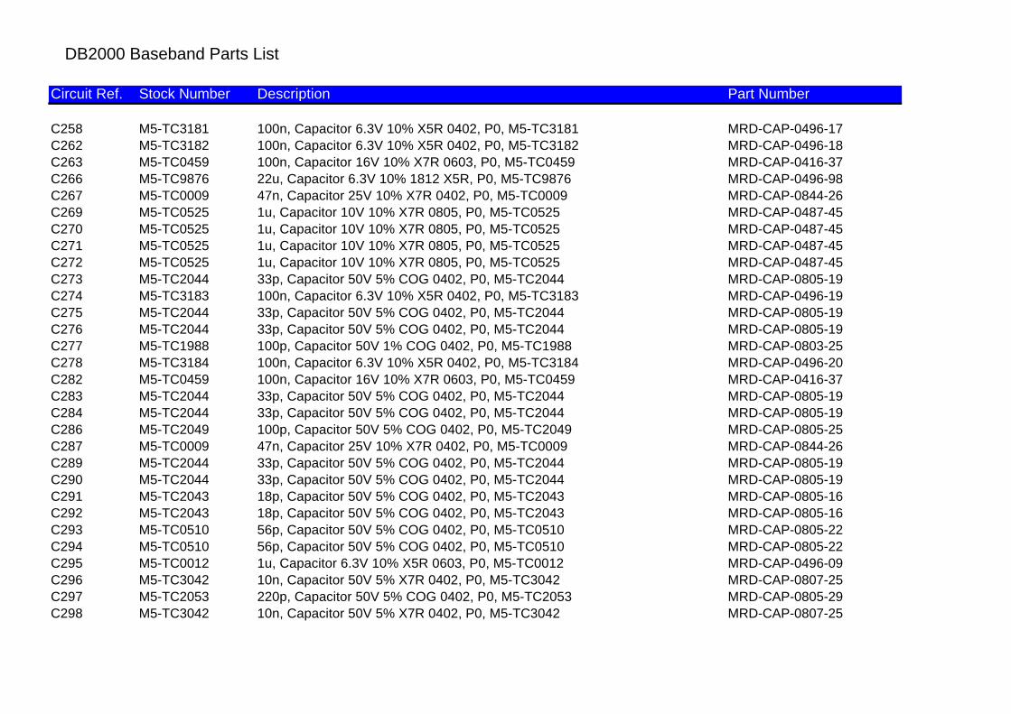
DB2000 Baseband Parts List
Circuit Ref. Stock Number Description Part Number
C258 M5-TC3181 100n, Capacitor 6.3V 10% X5R 0402, P0, M5-TC3181 MRD-CAP-0496-17C262 M5-TC3182 100n, Capacitor 6.3V 10% X5R 0402, P0, M5-TC3182 MRD-CAP-0496-18C263 M5-TC0459 100n, Capacitor 16V 10% X7R 0603, P0, M5-TC0459 MRD-CAP-0416-37C266 M5-TC9876 22u, Capacitor 6.3V 10% 1812 X5R, P0, M5-TC9876 MRD-CAP-0496-98C267 M5-TC0009 47n, Capacitor 25V 10% X7R 0402, P0, M5-TC0009 MRD-CAP-0844-26C269 M5-TC0525 1u, Capacitor 10V 10% X7R 0805, P0, M5-TC0525 MRD-CAP-0487-45C270 M5-TC0525 1u, Capacitor 10V 10% X7R 0805, P0, M5-TC0525 MRD-CAP-0487-45C271 M5-TC0525 1u, Capacitor 10V 10% X7R 0805, P0, M5-TC0525 MRD-CAP-0487-45C272 M5-TC0525 1u, Capacitor 10V 10% X7R 0805, P0, M5-TC0525 MRD-CAP-0487-45C273 M5-TC2044 33p, Capacitor 50V 5% COG 0402, P0, M5-TC2044 MRD-CAP-0805-19C274 M5-TC3183 100n, Capacitor 6.3V 10% X5R 0402, P0, M5-TC3183 MRD-CAP-0496-19C275 M5-TC2044 33p, Capacitor 50V 5% COG 0402, P0, M5-TC2044 MRD-CAP-0805-19C276 M5-TC2044 33p, Capacitor 50V 5% COG 0402, P0, M5-TC2044 MRD-CAP-0805-19C277 M5-TC1988 100p, Capacitor 50V 1% COG 0402, P0, M5-TC1988 MRD-CAP-0803-25C278 M5-TC3184 100n, Capacitor 6.3V 10% X5R 0402, P0, M5-TC3184 MRD-CAP-0496-20C282 M5-TC0459 100n, Capacitor 16V 10% X7R 0603, P0, M5-TC0459 MRD-CAP-0416-37C283 M5-TC2044 33p, Capacitor 50V 5% COG 0402, P0, M5-TC2044 MRD-CAP-0805-19C284 M5-TC2044 33p, Capacitor 50V 5% COG 0402, P0, M5-TC2044 MRD-CAP-0805-19C286 M5-TC2049 100p, Capacitor 50V 5% COG 0402, P0, M5-TC2049 MRD-CAP-0805-25C287 M5-TC0009 47n, Capacitor 25V 10% X7R 0402, P0, M5-TC0009 MRD-CAP-0844-26C289 M5-TC2044 33p, Capacitor 50V 5% COG 0402, P0, M5-TC2044 MRD-CAP-0805-19C290 M5-TC2044 33p, Capacitor 50V 5% COG 0402, P0, M5-TC2044 MRD-CAP-0805-19C291 M5-TC2043 18p, Capacitor 50V 5% COG 0402, P0, M5-TC2043 MRD-CAP-0805-16C292 M5-TC2043 18p, Capacitor 50V 5% COG 0402, P0, M5-TC2043 MRD-CAP-0805-16C293 M5-TC0510 56p, Capacitor 50V 5% COG 0402, P0, M5-TC0510 MRD-CAP-0805-22C294 M5-TC0510 56p, Capacitor 50V 5% COG 0402, P0, M5-TC0510 MRD-CAP-0805-22C295 M5-TC0012 1u, Capacitor 6.3V 10% X5R 0603, P0, M5-TC0012 MRD-CAP-0496-09C296 M5-TC3042 10n, Capacitor 50V 5% X7R 0402, P0, M5-TC3042 MRD-CAP-0807-25C297 M5-TC2053 220p, Capacitor 50V 5% COG 0402, P0, M5-TC2053 MRD-CAP-0805-29C298 M5-TC3042 10n, Capacitor 50V 5% X7R 0402, P0, M5-TC3042 MRD-CAP-0807-25
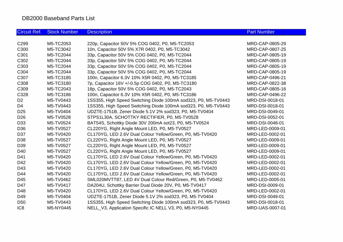
DB2000 Baseband Parts List
Circuit Ref. Stock Number Description Part Number
C299 M5-TC2053 220p, Capacitor 50V 5% COG 0402, P0, M5-TC2053 MRD-CAP-0805-29C300 M5-TC3042 10n, Capacitor 50V 5% X7R 0402, P0, M5-TC3042 MRD-CAP-0807-25C301 M5-TC2044 33p, Capacitor 50V 5% COG 0402, P0, M5-TC2044 MRD-CAP-0805-19C302 M5-TC2044 33p, Capacitor 50V 5% COG 0402, P0, M5-TC2044 MRD-CAP-0805-19C303 M5-TC2044 33p, Capacitor 50V 5% COG 0402, P0, M5-TC2044 MRD-CAP-0805-19C304 M5-TC2044 33p, Capacitor 50V 5% COG 0402, P0, M5-TC2044 MRD-CAP-0805-19C307 M5-TC3185 100n, Capacitor 6.3V 10% X5R 0402, P0, M5-TC3185 MRD-CAP-0496-21C308 M5-TC3180 7p, Capacitor 16V +/-0.5p COG 0402, P0, M5-TC3180 MRD-CAP-0822-38C309 M5-TC2043 18p, Capacitor 50V 5% COG 0402, P0, M5-TC2043 MRD-CAP-0805-16C328 M5-TC3186 100n, Capacitor 6.3V 10% X5R 0402, P0, M5-TC3186 MRD-CAP-0496-22D2 M5-TV0443 1SS355, High Speed Switching Diode 100mA sod323, P0, M5-TV0443 MRD-DSI-0018-01D4 M5-TV0443 1SS355, High Speed Switching Diode 100mA sod323, P0, M5-TV0443 MRD-DSI-0018-01D25 M5-TV0404 UDZTE-1751B, Zener Diode 5.1V 2% sod323, P0, M5-TV0404 MRD-DSI-0049-01D26 M5-TV0528 STPS1L30A, SCHOTTKY RECTIFIER, P0, M5-TV0528 MRD-DSI-0052-01D33 M5-TV0524 BAT54S, Schottky Diode 30V 200mA sot23, P0, M5-TV0524 MRD-DSI-0048-01D36 M5-TV0527 CL220YG, Right Angle Mount LED, P0, M5-TV0527 MRD-LED-0009-01D37 M5-TV0420 CL170YG, LED 2.6V Dual Colour Yellow/Green, P0, M5-TV0420 MRD-LED-0002-01D38 M5-TV0527 CL220YG, Right Angle Mount LED, P0, M5-TV0527 MRD-LED-0009-01D39 M5-TV0527 CL220YG, Right Angle Mount LED, P0, M5-TV0527 MRD-LED-0009-01D40 M5-TV0527 CL220YG, Right Angle Mount LED, P0, M5-TV0527 MRD-LED-0009-01D41 M5-TV0420 CL170YG, LED 2.6V Dual Colour Yellow/Green, P0, M5-TV0420 MRD-LED-0002-01D42 M5-TV0420 CL170YG, LED 2.6V Dual Colour Yellow/Green, P0, M5-TV0420 MRD-LED-0002-01D43 M5-TV0420 CL170YG, LED 2.6V Dual Colour Yellow/Green, P0, M5-TV0420 MRD-LED-0002-01D44 M5-TV0420 CL170YG, LED 2.6V Dual Colour Yellow/Green, P0, M5-TV0420 MRD-LED-0002-01D45 M5-TV0462 SML020MVTT87, LED 4V Dual Colour Red/Green, P0, M5-TV0462 MRD-LED-0005-01D47 M5-TV0417 DA204U, Schottky Barrier Dual Diode 20V, P0, M5-TV0417 MRD-DSI-0009-01D48 M5-TV0420 CL170YG, LED 2.6V Dual Colour Yellow/Green, P0, M5-TV0420 MRD-LED-0002-01D49 M5-TV0404 UDZTE-1751B, Zener Diode 5.1V 2% sod323, P0, M5-TV0404 MRD-DSI-0049-01D50 M5-TV0443 1SS355, High Speed Switching Diode 100mA sod323, P0, M5-TV0443 MRD-DSI-0018-01IC8 M5-NY0445 NELL_V3, Application Specific IC NELL V3, P0, M5-NY0445 MRD-UAS-0007-01
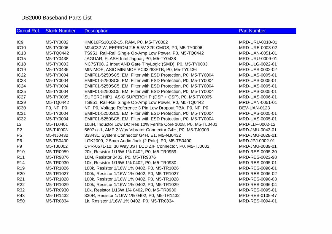
DB2000 Baseband Parts List
Circuit Ref. Stock Number Description Part Number
IC9 M5-TY0002 KM616FS1010Z-15, RAM, P0, M5-TY0002 MRD-URU-0010-01IC10 M5-TY0006 M24C32-W, EEPROM 2.5-5.5V 32K CMOS, P0, M5-TY0006 MRD-URE-0003-02IC13 M5-TQ0442 TS951, Rail-Rail Single Op-Amp Low Power, P0, M5-TQ0442 MRD-UAN-0051-01IC15 M5-TY0438 JAGUAR, FLASH Intel Jaguar, P0, M5-TY0438 MRD-URU-0009-01IC18 M5-TY0003 NC7ST08, 2 Input AND Gate TinyLogic (SMD), P0, M5-TY0003 MRD-ULG-0022-01IC19 M5-TY0436 MINIMOE, ASIC MINIMOE PC33283FTB, P0, M5-TY0436 MRD-UAS-0002-02IC22 M5-TY0004 EMIF01-5250SC5, EMI Filter with ESD Protection, P0, M5-TY0004 MRD-UAS-0005-01IC23 M5-TY0004 EMIF01-5250SC5, EMI Filter with ESD Protection, P0, M5-TY0004 MRD-UAS-0005-01IC24 M5-TY0004 EMIF01-5250SC5, EMI Filter with ESD Protection, P0, M5-TY0004 MRD-UAS-0005-01IC25 M5-TY0004 EMIF01-5250SC5, EMI Filter with ESD Protection, P0, M5-TY0004 MRD-UAS-0005-01IC27 M5-TY0005 SUPERCHIP1, ASIC SUPERCHIP (DSP + CSP), P0, M5-TY0005 MRD-UAS-0006-01IC29 M5-TQ0442 TS951, Rail-Rail Single Op-Amp Low Power, P0, M5-TQ0442 MRD-UAN-0051-01IC30 P0, NF_P0 NF_P0, Voltage Reference 3 Pin Low Dropout TBA, P0, NF_P0 DEV-UAN-0123IC31 M5-TY0004 EMIF01-5250SC5, EMI Filter with ESD Protection, P0, M5-TY0004 MRD-UAS-0005-01IC32 M5-TY0004 EMIF01-5250SC5, EMI Filter with ESD Protection, P0, M5-TY0004 MRD-UAS-0005-01L2 M5-TL0401 10uH, Inductor Low DC Res 10% Ferrite Core 1008, P0, M5-TL0401 MRD-LLF-0002-12P2 M5-TJ0003 5607xx-1, AMP 2 Way Vibrator Connector G4H, P0, M5-TJ0003 MRD-JMU-0043-01P5 M5-NJ0432 338431, System Connector G4H, E1, M5-NJ0432 MRD-JMU-0028-01P6 M5-TS0400 LGK2009, 2.5mm Audio Jack (2 Pole), P0, M5-TS0400 MRD-JPJ-0002-01P9 M5-TJ0002 CPR-0571-12, 30 Way JST LCD ZIF Connector, P0, M5-TJ0002 MRD-JMU-0039-01R10 M5-TR0959 20k, Resistor 1/16W 1% 0402, P0, M5-TR0959 MRD-RES-0095-30R11 M5-TR9876 10M, Resistor 0402, P0, M5-TR9876 MRD-RES-0022-98R14 M5-TR0930 10k, Resistor 1/16W 1% 0402, P0, M5-TR0930 MRD-RES-0095-01R19 M5-TR1026 100k, Resistor 1/16W 1% 0402, P0, M5-TR1026 MRD-RES-0096-01R20 M5-TR1027 100k, Resistor 1/16W 1% 0402, P0, M5-TR1027 MRD-RES-0096-02R21 M5-TR1028 100k, Resistor 1/16W 1% 0402, P0, M5-TR1028 MRD-RES-0096-03R22 M5-TR1029 100k, Resistor 1/16W 1% 0402, P0, M5-TR1029 MRD-RES-0096-04R32 M5-TR0930 10k, Resistor 1/16W 1% 0402, P0, M5-TR0930 MRD-RES-0095-01R43 M5-TR1432 330R, Resistor 1/16W 1% 0402, P0, M5-TR1432 MRD-RES-0105-47R50 M5-TR0834 1k, Resistor 1/16W 1% 0402, P0, M5-TR0834 MRD-RES-0094-01

DB2000 Baseband Parts List
Circuit Ref. Stock Number Description Part Number
R51 M5-TR0930 10k, Resistor 1/16W 1% 0402, P0, M5-TR0930 MRD-RES-0095-01R57 M5-TR0930 10k, Resistor 1/16W 1% 0402, P0, M5-TR0930 MRD-RES-0095-01R58 M5-TR0947 15k, Resistor 1/16W 1% 0402, P0, M5-TR0947 MRD-RES-0095-18R64 M5-TR0930 10k, Resistor 1/16W 1% 0402, P0, M5-TR0930 MRD-RES-0095-01R70 M5-TR1519 0R, Resistor zero ohm link 0402, P0, M5-TR1519 MRD-RES-0107-01R73 M5-TR0161 33R, Resistor 1/4W 5% 1206, P0, M5-TR0161 MRD-RES-0055-13R77 M5-TR0959 20k, Resistor 1/16W 1% 0402, P0, M5-TR0959 MRD-RES-0095-30R79 M5-TR1519 0R, Resistor zero ohm link 0402, P0, M5-TR1519 MRD-RES-0107-01R84 M5-TR1446 1k8, Resistor 1/16W 1% 0402, P0, M5-TR1446 MRD-RES-0105-61R85 M5-TR1450 3k, Resistor 1/16W 1% 0402, P0, M5-TR1450 MRD-RES-0105-65R87 M5-TR0930 10k, Resistor 1/16W 1% 0402, P0, M5-TR0930 MRD-RES-0095-01R89 M5-TR0930 10k, Resistor 1/16W 1% 0402, P0, M5-TR0930 MRD-RES-0095-01R90 M5-TR1485 220k, Resistor 1/16W 1% 0402, P0, M5-TR1485 MRD-RES-0106-01R91 M5-TR0930 10k, Resistor 1/16W 1% 0402, P0, M5-TR0930 MRD-RES-0095-01R96 M5-TR1446 1k8, Resistor 1/16W 1% 0402, P0, M5-TR1446 MRD-RES-0105-61R98 M5-TR1450 3k, Resistor 1/16W 1% 0402, P0, M5-TR1450 MRD-RES-0105-65R101 M5-TR1030 100k, Resistor 1/16W 1% 0402, P0, M5-TR1030 MRD-RES-0096-05R102 M5-TR0834 1k, Resistor 1/16W 1% 0402, P0, M5-TR0834 MRD-RES-0094-01R105 M5-TR0930 10k, Resistor 1/16W 1% 0402, P0, M5-TR0930 MRD-RES-0095-01R120 M5-TR1031 100k, Resistor 1/16W 1% 0402, P0, M5-TR1031 MRD-RES-0096-06R123 M5-TR1447 2k2, Resistor 1/16W 1% 0402, P0, M5-TR1447 MRD-RES-0105-62R124 M5-NV0401 100k, Neg Temp Coefficient Thermistor, P0, M5-NV0401 MRD-RTH-0001-01R127 M5-TR1032 100k, Resistor 1/16W 1% 0402, P0, M5-TR1032 MRD-RES-0096-07R133 M5-TR0930 10k, Resistor 1/16W 1% 0402, P0, M5-TR0930 MRD-RES-0095-01R134 M5-TR0930 10k, Resistor 1/16W 1% 0402, P0, M5-TR0930 MRD-RES-0095-01R135 M5-TR1450 3k, Resistor 1/16W 1% 0402, P0, M5-TR1450 MRD-RES-0105-65R138 M5-TR1519 0R, Resistor zero ohm link 0402, P0, M5-TR1519 MRD-RES-0107-01R149 M5-TR1122 1M, Resistor 1/16W 1% 0402, P0, M5-TR1122 MRD-RES-0097-01R153 M5-TR1122 1M, Resistor 1/16W 1% 0402, P0, M5-TR1122 MRD-RES-0097-01R156 M5-TR1447 2k2, Resistor 1/16W 1% 0402, P0, M5-TR1447 MRD-RES-0105-62
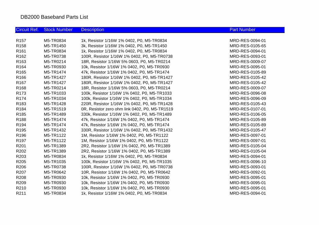
DB2000 Baseband Parts List
Circuit Ref. Stock Number Description Part Number
R157 M5-TR0834 1k, Resistor 1/16W 1% 0402, P0, M5-TR0834 MRD-RES-0094-01R158 M5-TR1450 3k, Resistor 1/16W 1% 0402, P0, M5-TR1450 MRD-RES-0105-65R161 M5-TR0834 1k, Resistor 1/16W 1% 0402, P0, M5-TR0834 MRD-RES-0094-01R162 M5-TR0738 100R, Resistor 1/16W 1% 0402, P0, M5-TR0738 MRD-RES-0093-01R163 M5-TR0214 18R, Resistor 1/16W 5% 0603, P0, M5-TR0214 MRD-RES-0009-07R164 M5-TR0930 10k, Resistor 1/16W 1% 0402, P0, M5-TR0930 MRD-RES-0095-01R165 M5-TR1474 47k, Resistor 1/16W 1% 0402, P0, M5-TR1474 MRD-RES-0105-89R166 M5-TR1427 180R, Resistor 1/16W 1% 0402, P0, M5-TR1427 MRD-RES-0105-42R167 M5-TR1427 180R, Resistor 1/16W 1% 0402, P0, M5-TR1427 MRD-RES-0105-42R168 M5-TR0214 18R, Resistor 1/16W 5% 0603, P0, M5-TR0214 MRD-RES-0009-07R173 M5-TR1033 100k, Resistor 1/16W 1% 0402, P0, M5-TR1033 MRD-RES-0096-08R174 M5-TR1034 100k, Resistor 1/16W 1% 0402, P0, M5-TR1034 MRD-RES-0096-09R183 M5-TR1428 220R, Resistor 1/16W 1% 0402, P0, M5-TR1428 MRD-RES-0105-43R184 M5-TR1519 0R, Resistor zero ohm link 0402, P0, M5-TR1519 MRD-RES-0107-01R185 M5-TR1489 330k, Resistor 1/16W 1% 0402, P0, M5-TR1489 MRD-RES-0106-05R188 M5-TR1474 47k, Resistor 1/16W 1% 0402, P0, M5-TR1474 MRD-RES-0105-89R194 M5-TR1474 47k, Resistor 1/16W 1% 0402, P0, M5-TR1474 MRD-RES-0105-89R195 M5-TR1432 330R, Resistor 1/16W 1% 0402, P0, M5-TR1432 MRD-RES-0105-47R196 M5-TR1122 1M, Resistor 1/16W 1% 0402, P0, M5-TR1122 MRD-RES-0097-01R197 M5-TR1122 1M, Resistor 1/16W 1% 0402, P0, M5-TR1122 MRD-RES-0097-01R201 M5-TR1389 2R2, Resistor 1/16W 1% 0402, P0, M5-TR1389 MRD-RES-0105-04R202 M5-TR1389 2R2, Resistor 1/16W 1% 0402, P0, M5-TR1389 MRD-RES-0105-04R203 M5-TR0834 1k, Resistor 1/16W 1% 0402, P0, M5-TR0834 MRD-RES-0094-01R205 M5-TR1035 100k, Resistor 1/16W 1% 0402, P0, M5-TR1035 MRD-RES-0096-10R206 M5-TR0738 100R, Resistor 1/16W 1% 0402, P0, M5-TR0738 MRD-RES-0093-01R207 M5-TR0642 10R, Resistor 1/16W 1% 0402, P0, M5-TR0642 MRD-RES-0092-01R208 M5-TR0930 10k, Resistor 1/16W 1% 0402, P0, M5-TR0930 MRD-RES-0095-01R209 M5-TR0930 10k, Resistor 1/16W 1% 0402, P0, M5-TR0930 MRD-RES-0095-01R210 M5-TR0930 10k, Resistor 1/16W 1% 0402, P0, M5-TR0930 MRD-RES-0095-01R211 M5-TR0834 1k, Resistor 1/16W 1% 0402, P0, M5-TR0834 MRD-RES-0094-01
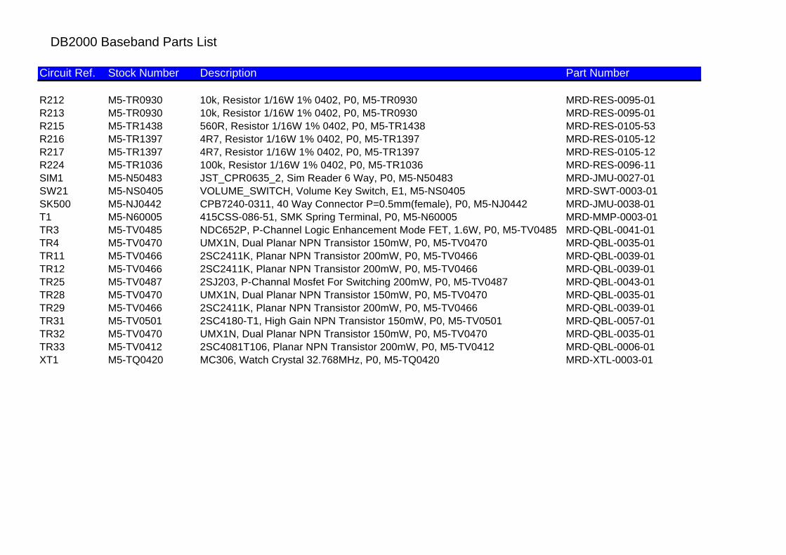
DB2000 Baseband Parts List
Circuit Ref. Stock Number Description Part Number
R212 M5-TR0930 10k, Resistor 1/16W 1% 0402, P0, M5-TR0930 MRD-RES-0095-01R213 M5-TR0930 10k, Resistor 1/16W 1% 0402, P0, M5-TR0930 MRD-RES-0095-01R215 M5-TR1438 560R, Resistor 1/16W 1% 0402, P0, M5-TR1438 MRD-RES-0105-53R216 M5-TR1397 4R7, Resistor 1/16W 1% 0402, P0, M5-TR1397 MRD-RES-0105-12R217 M5-TR1397 4R7, Resistor 1/16W 1% 0402, P0, M5-TR1397 MRD-RES-0105-12R224 M5-TR1036 100k, Resistor 1/16W 1% 0402, P0, M5-TR1036 MRD-RES-0096-11SIM1 M5-N50483 JST_CPR0635_2, Sim Reader 6 Way, P0, M5-N50483 MRD-JMU-0027-01SW21 M5-NS0405 VOLUME_SWITCH, Volume Key Switch, E1, M5-NS0405 MRD-SWT-0003-01SK500 M5-NJ0442 CPB7240-0311, 40 Way Connector P=0.5mm(female), P0, M5-NJ0442 MRD-JMU-0038-01T1 M5-N60005 415CSS-086-51, SMK Spring Terminal, P0, M5-N60005 MRD-MMP-0003-01TR3 M5-TV0485 NDC652P, P-Channel Logic Enhancement Mode FET, 1.6W, P0, M5-TV0485 MRD-QBL-0041-01TR4 M5-TV0470 UMX1N, Dual Planar NPN Transistor 150mW, P0, M5-TV0470 MRD-QBL-0035-01TR11 M5-TV0466 2SC2411K, Planar NPN Transistor 200mW, P0, M5-TV0466 MRD-QBL-0039-01TR12 M5-TV0466 2SC2411K, Planar NPN Transistor 200mW, P0, M5-TV0466 MRD-QBL-0039-01TR25 M5-TV0487 2SJ203, P-Channal Mosfet For Switching 200mW, P0, M5-TV0487 MRD-QBL-0043-01TR28 M5-TV0470 UMX1N, Dual Planar NPN Transistor 150mW, P0, M5-TV0470 MRD-QBL-0035-01TR29 M5-TV0466 2SC2411K, Planar NPN Transistor 200mW, P0, M5-TV0466 MRD-QBL-0039-01TR31 M5-TV0501 2SC4180-T1, High Gain NPN Transistor 150mW, P0, M5-TV0501 MRD-QBL-0057-01TR32 M5-TV0470 UMX1N, Dual Planar NPN Transistor 150mW, P0, M5-TV0470 MRD-QBL-0035-01TR33 M5-TV0412 2SC4081T106, Planar NPN Transistor 200mW, P0, M5-TV0412 MRD-QBL-0006-01XT1 M5-TQ0420 MC306, Watch Crystal 32.768MHz, P0, M5-TQ0420 MRD-XTL-0003-01

DB2000 RF Board Parts List
Circuit Ref Stock Number. Description Part Number
C100 M5-TC1156 100p, Capacitor 16V 5% COG 0402, P0, M5-TC1156 MRD-CAP-0822-25C101 M5-TC1156 100p, Capacitor 16V 5% COG 0402, P0, M5-TC1156 MRD-CAP-0822-25C102 M5-TC2835 10n, Capacitor 16V 10% X7R 0402, P0, M5-TC2835 MRD-CAP-0837-25C103 M5-TC2044 33p, Capacitor 50V 5% COG 0402, P0, M5-TC2044 MRD-CAP-0805-19C104 M5-TC2835 10n, Capacitor 16V 10% X7R 0402, P0, M5-TC2835 MRD-CAP-0837-25C105 M5-TC2794 470p, Capacitor 16V 5% X7R 0402, P0, M5-TC2794 MRD-CAP-0836-09C106 M5-TC2044 33p, Capacitor 50V 5% COG 0402, P0, M5-TC2044 MRD-CAP-0805-19C107 M5-TC1156 100p, Capacitor 16V 5% COG 0402, P0, M5-TC1156 MRD-CAP-0822-25C108 M5-TC2794 470p, Capacitor 16V 5% X7R 0402, P0, M5-TC2794 MRD-CAP-0836-09C109 M5-TC2794 470p, Capacitor 16V 5% X7R 0402, P0, M5-TC2794 MRD-CAP-0836-09C110 M5-TC2794 470p, Capacitor 16V 5% X7R 0402, P0, M5-TC2794 MRD-CAP-0836-09C111 M5-TC2835 10n, Capacitor 16V 10% X7R 0402, P0, M5-TC2835 MRD-CAP-0837-25C112 M5-TC1156 100p, Capacitor 16V 5% COG 0402, P0, M5-TC1156 MRD-CAP-0822-25C113 M5-TC2835 10n, Capacitor 16V 10% X7R 0402, P0, M5-TC2835 MRD-CAP-0837-25C114 M5-TC2044 33p, Capacitor 50V 5% COG 0402, P0, M5-TC2044 MRD-CAP-0805-19C115 M5-TC1156 100p, Capacitor 16V 5% COG 0402, P0, M5-TC1156 MRD-CAP-0822-25C116 M5-TC1148 22p, Capacitor 16V 5% COG 0402, P0, M5-TC1148 MRD-CAP-0822-17C117 M5-TC1152 47p, Capacitor 16V 5% COG 0402, P0, M5-TC1152 MRD-CAP-0822-21C118 M5-TC2823 1n, Capacitor 16V 10% X7R 0402, P0, M5-TC2823 MRD-CAP-0837-13C119 M5-TC0510 56p, Capacitor 50V 5% COG 0402, P0, M5-TC0510 MRD-CAP-0805-22C120 M5-TC3179 4p, Capacitor 16V +/-0.25p COG 0402, P0, M5-TC3179 MRD-CAP-0822-37C121 M5-TC3177 2p, Capacitor 16V +/-0.25p COG 0402, P0, M5-TC3177 MRD-CAP-0822-35C122 M5-TC2046 47p, Capacitor 50V 5% COG 0402, P0, M5-TC2046 MRD-CAP-0805-21C123 M5-TC2040 10p, Capacitor 50V 5% COG 0402, P0, M5-TC2040 MRD-CAP-0805-13C124 M5-TC2044 33p, Capacitor 50V 5% COG 0402, P0, M5-TC2044 MRD-CAP-0805-19C125 M5-TC2044 33p, Capacitor 50V 5% COG 0402, P0, M5-TC2044 MRD-CAP-0805-19C126 M5-TC1154 68p, Capacitor 16V 5% COG 0402, P0, M5-TC1154 MRD-CAP-0822-23C128 M5-TC2044 33p, Capacitor 50V 5% COG 0402, P0, M5-TC2044 MRD-CAP-0805-19C129 M5-TC2044 33p, Capacitor 50V 5% COG 0402, P0, M5-TC2044 MRD-CAP-0805-19C131 M5-TC3177 2p, Capacitor 16V +/-0.25p COG 0402, P0, M5-TC3177 MRD-CAP-0822-35
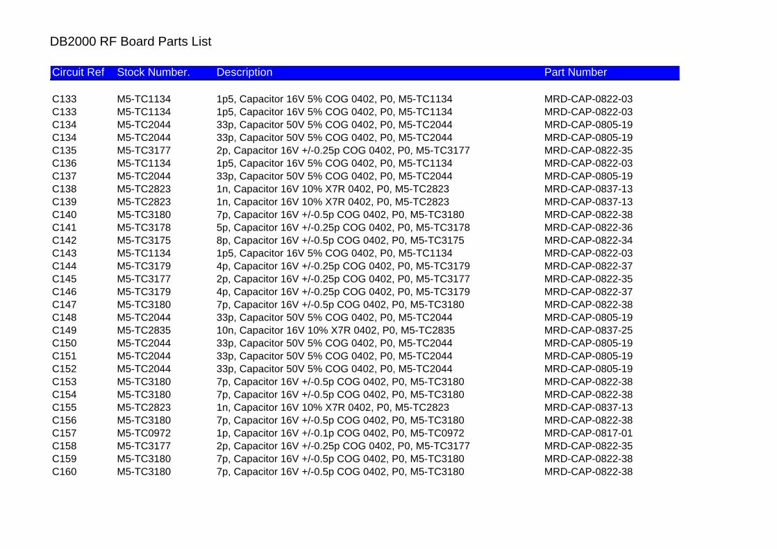
DB2000 RF Board Parts List
Circuit Ref Stock Number. Description Part Number
C133 M5-TC1134 1p5, Capacitor 16V 5% COG 0402, P0, M5-TC1134 MRD-CAP-0822-03C133 M5-TC1134 1p5, Capacitor 16V 5% COG 0402, P0, M5-TC1134 MRD-CAP-0822-03C134 M5-TC2044 33p, Capacitor 50V 5% COG 0402, P0, M5-TC2044 MRD-CAP-0805-19C134 M5-TC2044 33p, Capacitor 50V 5% COG 0402, P0, M5-TC2044 MRD-CAP-0805-19C135 M5-TC3177 2p, Capacitor 16V +/-0.25p COG 0402, P0, M5-TC3177 MRD-CAP-0822-35C136 M5-TC1134 1p5, Capacitor 16V 5% COG 0402, P0, M5-TC1134 MRD-CAP-0822-03C137 M5-TC2044 33p, Capacitor 50V 5% COG 0402, P0, M5-TC2044 MRD-CAP-0805-19C138 M5-TC2823 1n, Capacitor 16V 10% X7R 0402, P0, M5-TC2823 MRD-CAP-0837-13C139 M5-TC2823 1n, Capacitor 16V 10% X7R 0402, P0, M5-TC2823 MRD-CAP-0837-13C140 M5-TC3180 7p, Capacitor 16V +/-0.5p COG 0402, P0, M5-TC3180 MRD-CAP-0822-38C141 M5-TC3178 5p, Capacitor 16V +/-0.25p COG 0402, P0, M5-TC3178 MRD-CAP-0822-36C142 M5-TC3175 8p, Capacitor 16V +/-0.5p COG 0402, P0, M5-TC3175 MRD-CAP-0822-34C143 M5-TC1134 1p5, Capacitor 16V 5% COG 0402, P0, M5-TC1134 MRD-CAP-0822-03C144 M5-TC3179 4p, Capacitor 16V +/-0.25p COG 0402, P0, M5-TC3179 MRD-CAP-0822-37C145 M5-TC3177 2p, Capacitor 16V +/-0.25p COG 0402, P0, M5-TC3177 MRD-CAP-0822-35C146 M5-TC3179 4p, Capacitor 16V +/-0.25p COG 0402, P0, M5-TC3179 MRD-CAP-0822-37C147 M5-TC3180 7p, Capacitor 16V +/-0.5p COG 0402, P0, M5-TC3180 MRD-CAP-0822-38C148 M5-TC2044 33p, Capacitor 50V 5% COG 0402, P0, M5-TC2044 MRD-CAP-0805-19C149 M5-TC2835 10n, Capacitor 16V 10% X7R 0402, P0, M5-TC2835 MRD-CAP-0837-25C150 M5-TC2044 33p, Capacitor 50V 5% COG 0402, P0, M5-TC2044 MRD-CAP-0805-19C151 M5-TC2044 33p, Capacitor 50V 5% COG 0402, P0, M5-TC2044 MRD-CAP-0805-19C152 M5-TC2044 33p, Capacitor 50V 5% COG 0402, P0, M5-TC2044 MRD-CAP-0805-19C153 M5-TC3180 7p, Capacitor 16V +/-0.5p COG 0402, P0, M5-TC3180 MRD-CAP-0822-38C154 M5-TC3180 7p, Capacitor 16V +/-0.5p COG 0402, P0, M5-TC3180 MRD-CAP-0822-38C155 M5-TC2823 1n, Capacitor 16V 10% X7R 0402, P0, M5-TC2823 MRD-CAP-0837-13C156 M5-TC3180 7p, Capacitor 16V +/-0.5p COG 0402, P0, M5-TC3180 MRD-CAP-0822-38C157 M5-TC0972 1p, Capacitor 16V +/-0.1p COG 0402, P0, M5-TC0972 MRD-CAP-0817-01C158 M5-TC3177 2p, Capacitor 16V +/-0.25p COG 0402, P0, M5-TC3177 MRD-CAP-0822-35C159 M5-TC3180 7p, Capacitor 16V +/-0.5p COG 0402, P0, M5-TC3180 MRD-CAP-0822-38C160 M5-TC3180 7p, Capacitor 16V +/-0.5p COG 0402, P0, M5-TC3180 MRD-CAP-0822-38

DB2000 RF Board Parts List
Circuit Ref Stock Number. Description Part Number
C161 M5-TC2044 33p, Capacitor 50V 5% COG 0402, P0, M5-TC2044 MRD-CAP-0805-19C163 M5-TC2044 33p, Capacitor 50V 5% COG 0402, P0, M5-TC2044 MRD-CAP-0805-19C165 M5-TC2835 10n, Capacitor 16V 10% X7R 0402, P0, M5-TC2835 MRD-CAP-0837-25C166 M5-TC2044 33p, Capacitor 50V 5% COG 0402, P0, M5-TC2044 MRD-CAP-0805-19C167 M5-TC1156 100p, Capacitor 16V 5% COG 0402, P0, M5-TC1156 MRD-CAP-0822-25C169 M5-TC3180 7p, Capacitor 16V +/-0.5p COG 0402, P0, M5-TC3180 MRD-CAP-0822-38C170 M5-TC2044 33p, Capacitor 50V 5% COG 0402, P0, M5-TC2044 MRD-CAP-0805-19C172 M5-TC1148 22p, Capacitor 16V 5% COG 0402, P0, M5-TC1148 MRD-CAP-0822-17C175 M5-TC3180 7p, Capacitor 16V +/-0.5p COG 0402, P0, M5-TC3180 MRD-CAP-0822-38C176 M5-TC3180 7p, Capacitor 16V +/-0.5p COG 0402, P0, M5-TC3180 MRD-CAP-0822-38C177 M5-TC1156 100p, Capacitor 16V 5% COG 0402, P0, M5-TC1156 MRD-CAP-0822-25C178 M5-TC3180 7p, Capacitor 16V +/-0.5p COG 0402, P0, M5-TC3180 MRD-CAP-0822-38C179 M5-TC1156 100p, Capacitor 16V 5% COG 0402, P0, M5-TC1156 MRD-CAP-0822-25C180 M5-TC2044 33p, Capacitor 50V 5% COG 0402, P0, M5-TC2044 MRD-CAP-0805-19C181 M5-TC3180 7p, Capacitor 16V +/-0.5p COG 0402, P0, M5-TC3180 MRD-CAP-0822-38C188 M5-TC3180 7p, Capacitor 16V +/-0.5p COG 0402, P0, M5-TC3180 MRD-CAP-0822-38C188 M5-TC3180 7p, Capacitor 16V +/-0.5p COG 0402, P0, M5-TC3180 MRD-CAP-0822-38C189 M5-TC1156 100p, Capacitor 16V 5% COG 0402, P0, M5-TC1156 MRD-CAP-0822-25C193 M5-TC2835 10n, Capacitor 16V 10% X7R 0402, P0, M5-TC2835 MRD-CAP-0837-25C194 M5-TC2835 10n, Capacitor 16V 10% X7R 0402, P0, M5-TC2835 MRD-CAP-0837-25C200 M5-TC0456 6u8, Capacitor 16V +80/-20% Y5V 1210, P0, M5-TC0456 MRD-CAP-0104-14C201 M5-TC2823 1n, Capacitor 16V 10% X7R 0402, P0, M5-TC2823 MRD-CAP-0837-13C202 M5-TC2044 33p, Capacitor 50V 5% COG 0402, P0, M5-TC2044 MRD-CAP-0805-19C203 M5-TC1160 220p, Capacitor 16V 5% COG 0402, P0, M5-TC1160 MRD-CAP-0822-29C204 M5-TC2835 10n, Capacitor 16V 10% X7R 0402, P0, M5-TC2835 MRD-CAP-0837-25C205 M5-TC2044 33p, Capacitor 50V 5% COG 0402, P0, M5-TC2044 MRD-CAP-0805-19C206 M5-TC2835 10n, Capacitor 16V 10% X7R 0402, P0, M5-TC2835 MRD-CAP-0837-25C207 M5-TC1156 100p, Capacitor 16V 5% COG 0402, P0, M5-TC1156 MRD-CAP-0822-25C208 M5-TC1160 220p, Capacitor 16V 5% COG 0402, P0, M5-TC1160 MRD-CAP-0822-29C209 M5-TC2835 10n, Capacitor 16V 10% X7R 0402, P0, M5-TC2835 MRD-CAP-0837-25
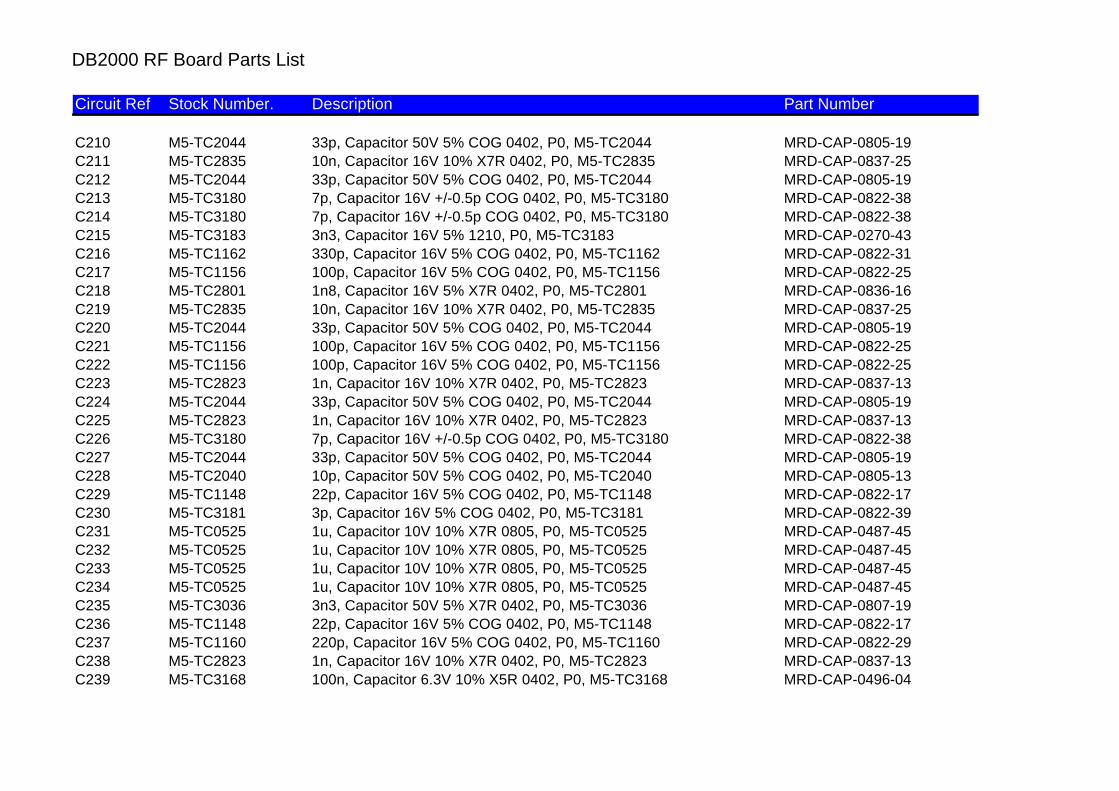
DB2000 RF Board Parts List
Circuit Ref Stock Number. Description Part Number
C210 M5-TC2044 33p, Capacitor 50V 5% COG 0402, P0, M5-TC2044 MRD-CAP-0805-19C211 M5-TC2835 10n, Capacitor 16V 10% X7R 0402, P0, M5-TC2835 MRD-CAP-0837-25C212 M5-TC2044 33p, Capacitor 50V 5% COG 0402, P0, M5-TC2044 MRD-CAP-0805-19C213 M5-TC3180 7p, Capacitor 16V +/-0.5p COG 0402, P0, M5-TC3180 MRD-CAP-0822-38C214 M5-TC3180 7p, Capacitor 16V +/-0.5p COG 0402, P0, M5-TC3180 MRD-CAP-0822-38C215 M5-TC3183 3n3, Capacitor 16V 5% 1210, P0, M5-TC3183 MRD-CAP-0270-43C216 M5-TC1162 330p, Capacitor 16V 5% COG 0402, P0, M5-TC1162 MRD-CAP-0822-31C217 M5-TC1156 100p, Capacitor 16V 5% COG 0402, P0, M5-TC1156 MRD-CAP-0822-25C218 M5-TC2801 1n8, Capacitor 16V 5% X7R 0402, P0, M5-TC2801 MRD-CAP-0836-16C219 M5-TC2835 10n, Capacitor 16V 10% X7R 0402, P0, M5-TC2835 MRD-CAP-0837-25C220 M5-TC2044 33p, Capacitor 50V 5% COG 0402, P0, M5-TC2044 MRD-CAP-0805-19C221 M5-TC1156 100p, Capacitor 16V 5% COG 0402, P0, M5-TC1156 MRD-CAP-0822-25C222 M5-TC1156 100p, Capacitor 16V 5% COG 0402, P0, M5-TC1156 MRD-CAP-0822-25C223 M5-TC2823 1n, Capacitor 16V 10% X7R 0402, P0, M5-TC2823 MRD-CAP-0837-13C224 M5-TC2044 33p, Capacitor 50V 5% COG 0402, P0, M5-TC2044 MRD-CAP-0805-19C225 M5-TC2823 1n, Capacitor 16V 10% X7R 0402, P0, M5-TC2823 MRD-CAP-0837-13C226 M5-TC3180 7p, Capacitor 16V +/-0.5p COG 0402, P0, M5-TC3180 MRD-CAP-0822-38C227 M5-TC2044 33p, Capacitor 50V 5% COG 0402, P0, M5-TC2044 MRD-CAP-0805-19C228 M5-TC2040 10p, Capacitor 50V 5% COG 0402, P0, M5-TC2040 MRD-CAP-0805-13C229 M5-TC1148 22p, Capacitor 16V 5% COG 0402, P0, M5-TC1148 MRD-CAP-0822-17C230 M5-TC3181 3p, Capacitor 16V 5% COG 0402, P0, M5-TC3181 MRD-CAP-0822-39C231 M5-TC0525 1u, Capacitor 10V 10% X7R 0805, P0, M5-TC0525 MRD-CAP-0487-45C232 M5-TC0525 1u, Capacitor 10V 10% X7R 0805, P0, M5-TC0525 MRD-CAP-0487-45C233 M5-TC0525 1u, Capacitor 10V 10% X7R 0805, P0, M5-TC0525 MRD-CAP-0487-45C234 M5-TC0525 1u, Capacitor 10V 10% X7R 0805, P0, M5-TC0525 MRD-CAP-0487-45C235 M5-TC3036 3n3, Capacitor 50V 5% X7R 0402, P0, M5-TC3036 MRD-CAP-0807-19C236 M5-TC1148 22p, Capacitor 16V 5% COG 0402, P0, M5-TC1148 MRD-CAP-0822-17C237 M5-TC1160 220p, Capacitor 16V 5% COG 0402, P0, M5-TC1160 MRD-CAP-0822-29C238 M5-TC2823 1n, Capacitor 16V 10% X7R 0402, P0, M5-TC2823 MRD-CAP-0837-13C239 M5-TC3168 100n, Capacitor 6.3V 10% X5R 0402, P0, M5-TC3168 MRD-CAP-0496-04
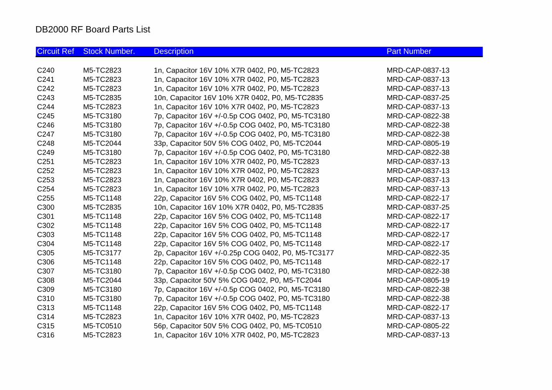
DB2000 RF Board Parts List
Circuit Ref Stock Number. Description Part Number
C240 M5-TC2823 1n, Capacitor 16V 10% X7R 0402, P0, M5-TC2823 MRD-CAP-0837-13C241 M5-TC2823 1n, Capacitor 16V 10% X7R 0402, P0, M5-TC2823 MRD-CAP-0837-13C242 M5-TC2823 1n, Capacitor 16V 10% X7R 0402, P0, M5-TC2823 MRD-CAP-0837-13C243 M5-TC2835 10n, Capacitor 16V 10% X7R 0402, P0, M5-TC2835 MRD-CAP-0837-25C244 M5-TC2823 1n, Capacitor 16V 10% X7R 0402, P0, M5-TC2823 MRD-CAP-0837-13C245 M5-TC3180 7p, Capacitor 16V +/-0.5p COG 0402, P0, M5-TC3180 MRD-CAP-0822-38C246 M5-TC3180 7p, Capacitor 16V +/-0.5p COG 0402, P0, M5-TC3180 MRD-CAP-0822-38C247 M5-TC3180 7p, Capacitor 16V +/-0.5p COG 0402, P0, M5-TC3180 MRD-CAP-0822-38C248 M5-TC2044 33p, Capacitor 50V 5% COG 0402, P0, M5-TC2044 MRD-CAP-0805-19C249 M5-TC3180 7p, Capacitor 16V +/-0.5p COG 0402, P0, M5-TC3180 MRD-CAP-0822-38C251 M5-TC2823 1n, Capacitor 16V 10% X7R 0402, P0, M5-TC2823 MRD-CAP-0837-13C252 M5-TC2823 1n, Capacitor 16V 10% X7R 0402, P0, M5-TC2823 MRD-CAP-0837-13C253 M5-TC2823 1n, Capacitor 16V 10% X7R 0402, P0, M5-TC2823 MRD-CAP-0837-13C254 M5-TC2823 1n, Capacitor 16V 10% X7R 0402, P0, M5-TC2823 MRD-CAP-0837-13C255 M5-TC1148 22p, Capacitor 16V 5% COG 0402, P0, M5-TC1148 MRD-CAP-0822-17C300 M5-TC2835 10n, Capacitor 16V 10% X7R 0402, P0, M5-TC2835 MRD-CAP-0837-25C301 M5-TC1148 22p, Capacitor 16V 5% COG 0402, P0, M5-TC1148 MRD-CAP-0822-17C302 M5-TC1148 22p, Capacitor 16V 5% COG 0402, P0, M5-TC1148 MRD-CAP-0822-17C303 M5-TC1148 22p, Capacitor 16V 5% COG 0402, P0, M5-TC1148 MRD-CAP-0822-17C304 M5-TC1148 22p, Capacitor 16V 5% COG 0402, P0, M5-TC1148 MRD-CAP-0822-17C305 M5-TC3177 2p, Capacitor 16V +/-0.25p COG 0402, P0, M5-TC3177 MRD-CAP-0822-35C306 M5-TC1148 22p, Capacitor 16V 5% COG 0402, P0, M5-TC1148 MRD-CAP-0822-17C307 M5-TC3180 7p, Capacitor 16V +/-0.5p COG 0402, P0, M5-TC3180 MRD-CAP-0822-38C308 M5-TC2044 33p, Capacitor 50V 5% COG 0402, P0, M5-TC2044 MRD-CAP-0805-19C309 M5-TC3180 7p, Capacitor 16V +/-0.5p COG 0402, P0, M5-TC3180 MRD-CAP-0822-38C310 M5-TC3180 7p, Capacitor 16V +/-0.5p COG 0402, P0, M5-TC3180 MRD-CAP-0822-38C313 M5-TC1148 22p, Capacitor 16V 5% COG 0402, P0, M5-TC1148 MRD-CAP-0822-17C314 M5-TC2823 1n, Capacitor 16V 10% X7R 0402, P0, M5-TC2823 MRD-CAP-0837-13C315 M5-TC0510 56p, Capacitor 50V 5% COG 0402, P0, M5-TC0510 MRD-CAP-0805-22C316 M5-TC2823 1n, Capacitor 16V 10% X7R 0402, P0, M5-TC2823 MRD-CAP-0837-13
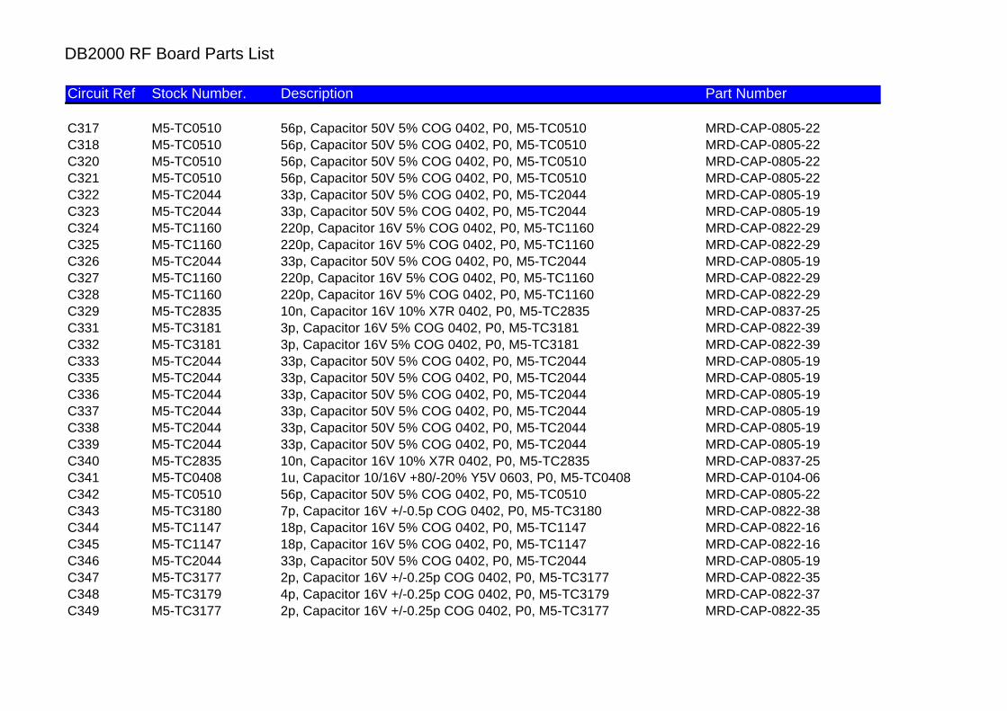
DB2000 RF Board Parts List
Circuit Ref Stock Number. Description Part Number
C317 M5-TC0510 56p, Capacitor 50V 5% COG 0402, P0, M5-TC0510 MRD-CAP-0805-22C318 M5-TC0510 56p, Capacitor 50V 5% COG 0402, P0, M5-TC0510 MRD-CAP-0805-22C320 M5-TC0510 56p, Capacitor 50V 5% COG 0402, P0, M5-TC0510 MRD-CAP-0805-22C321 M5-TC0510 56p, Capacitor 50V 5% COG 0402, P0, M5-TC0510 MRD-CAP-0805-22C322 M5-TC2044 33p, Capacitor 50V 5% COG 0402, P0, M5-TC2044 MRD-CAP-0805-19C323 M5-TC2044 33p, Capacitor 50V 5% COG 0402, P0, M5-TC2044 MRD-CAP-0805-19C324 M5-TC1160 220p, Capacitor 16V 5% COG 0402, P0, M5-TC1160 MRD-CAP-0822-29C325 M5-TC1160 220p, Capacitor 16V 5% COG 0402, P0, M5-TC1160 MRD-CAP-0822-29C326 M5-TC2044 33p, Capacitor 50V 5% COG 0402, P0, M5-TC2044 MRD-CAP-0805-19C327 M5-TC1160 220p, Capacitor 16V 5% COG 0402, P0, M5-TC1160 MRD-CAP-0822-29C328 M5-TC1160 220p, Capacitor 16V 5% COG 0402, P0, M5-TC1160 MRD-CAP-0822-29C329 M5-TC2835 10n, Capacitor 16V 10% X7R 0402, P0, M5-TC2835 MRD-CAP-0837-25C331 M5-TC3181 3p, Capacitor 16V 5% COG 0402, P0, M5-TC3181 MRD-CAP-0822-39C332 M5-TC3181 3p, Capacitor 16V 5% COG 0402, P0, M5-TC3181 MRD-CAP-0822-39C333 M5-TC2044 33p, Capacitor 50V 5% COG 0402, P0, M5-TC2044 MRD-CAP-0805-19C335 M5-TC2044 33p, Capacitor 50V 5% COG 0402, P0, M5-TC2044 MRD-CAP-0805-19C336 M5-TC2044 33p, Capacitor 50V 5% COG 0402, P0, M5-TC2044 MRD-CAP-0805-19C337 M5-TC2044 33p, Capacitor 50V 5% COG 0402, P0, M5-TC2044 MRD-CAP-0805-19C338 M5-TC2044 33p, Capacitor 50V 5% COG 0402, P0, M5-TC2044 MRD-CAP-0805-19C339 M5-TC2044 33p, Capacitor 50V 5% COG 0402, P0, M5-TC2044 MRD-CAP-0805-19C340 M5-TC2835 10n, Capacitor 16V 10% X7R 0402, P0, M5-TC2835 MRD-CAP-0837-25C341 M5-TC0408 1u, Capacitor 10/16V +80/-20% Y5V 0603, P0, M5-TC0408 MRD-CAP-0104-06C342 M5-TC0510 56p, Capacitor 50V 5% COG 0402, P0, M5-TC0510 MRD-CAP-0805-22C343 M5-TC3180 7p, Capacitor 16V +/-0.5p COG 0402, P0, M5-TC3180 MRD-CAP-0822-38C344 M5-TC1147 18p, Capacitor 16V 5% COG 0402, P0, M5-TC1147 MRD-CAP-0822-16C345 M5-TC1147 18p, Capacitor 16V 5% COG 0402, P0, M5-TC1147 MRD-CAP-0822-16C346 M5-TC2044 33p, Capacitor 50V 5% COG 0402, P0, M5-TC2044 MRD-CAP-0805-19C347 M5-TC3177 2p, Capacitor 16V +/-0.25p COG 0402, P0, M5-TC3177 MRD-CAP-0822-35C348 M5-TC3179 4p, Capacitor 16V +/-0.25p COG 0402, P0, M5-TC3179 MRD-CAP-0822-37C349 M5-TC3177 2p, Capacitor 16V +/-0.25p COG 0402, P0, M5-TC3177 MRD-CAP-0822-35

DB2000 RF Board Parts List
Circuit Ref Stock Number. Description Part Number
C350 M5-TC3179 4p, Capacitor 16V +/-0.25p COG 0402, P0, M5-TC3179 MRD-CAP-0822-37C351 M5-TC2044 33p, Capacitor 50V 5% COG 0402, P0, M5-TC2044 MRD-CAP-0805-19C352 M5-TC3180 7p, Capacitor 16V +/-0.5p COG 0402, P0, M5-TC3180 MRD-CAP-0822-38C353 M5-TC1134 1p5, Capacitor 16V 5% COG 0402, P0, M5-TC1134 MRD-CAP-0822-03C354 M5-TC2044 33p, Capacitor 50V 5% COG 0402, P0, M5-TC2044 MRD-CAP-0805-19C355 M5-TC2044 33p, Capacitor 50V 5% COG 0402, P0, M5-TC2044 MRD-CAP-0805-19C356 M5-TC2044 33p, Capacitor 50V 5% COG 0402, P0, M5-TC2044 MRD-CAP-0805-19C400 M5-TC1156 100p, Capacitor 16V 5% COG 0402, P0, M5-TC1156 MRD-CAP-0822-25C401 M5-TC1149 27p, Capacitor 16V 5% COG 0402, P0, M5-TC1149 MRD-CAP-0822-18C402 M5-TC1149 27p, Capacitor 16V 5% COG 0402, P0, M5-TC1149 MRD-CAP-0822-18C403 M5-TC1156 100p, Capacitor 16V 5% COG 0402, P0, M5-TC1156 MRD-CAP-0822-25C404 M5-TC1156 100p, Capacitor 16V 5% COG 0402, P0, M5-TC1156 MRD-CAP-0822-25C405 M5-TC3177 2p, Capacitor 16V +/-0.25p COG 0402, P0, M5-TC3177 MRD-CAP-0822-35C406 M5-TC3177 2p, Capacitor 16V +/-0.25p COG 0402, P0, M5-TC3177 MRD-CAP-0822-35C407 M5-TC2044 33p, Capacitor 50V 5% COG 0402, P0, M5-TC2044 MRD-CAP-0805-19C409 M5-TC2040 10p, Capacitor 50V 5% COG 0402, P0, M5-TC2040 MRD-CAP-0805-13C410 M5-TC2040 10p, Capacitor 50V 5% COG 0402, P0, M5-TC2040 MRD-CAP-0805-13C411 M5-TC1156 100p, Capacitor 16V 5% COG 0402, P0, M5-TC1156 MRD-CAP-0822-25C412 M5-TC2044 33p, Capacitor 50V 5% COG 0402, P0, M5-TC2044 MRD-CAP-0805-19D100 M5-TV0521 DAP222, Dual Switching Diode 80V 150mW, P0, M5-TV0521 MRD-DSI-0046-01D101 M5-TV0443 1SS355, High Speed Switch Diode 100mA sod323, P0, M5-TV0443 MRD-DSI-0018-01D200 M5-TV0417 DA204U, Schottky Barrier Dual Diode 20V, P0, M5-TV0417 MRD-DSI-0009-01D303 M5-TV0519 BBY51, Dual Tuning Diode 20mA 7V, P0, M5-TV0519 MRD-DSI-0044-01D400 M5-TV0514 BAR64-05, Diode Pair SMD, P0, M5-TV0514 MRD-DSI-0043-01D401 M5-TV0514 BAR64-05, Diode Pair SMD, P0, M5-TV0514 MRD-DSI-0043-01FL100 M5-TF0406 MAS4015, RF Filter Low Loss 270MHz, P0, M5-TF0406 MRD-FSW-0010-01FL101 M5-TF0407 MAS4016, RF Filter Low Loss 180MHz, P0, M5-TF0407 MRD-FSW-0011-01FL102 M5-TF0413 MAS4013, GSM Saw TX Filter 902.5MHz, P0, M5-TF0413 MRD-FSW-0017-01FL103 M5-TF0415 DGL612M01, RF Filter Low Loss 1747.5MHz, P0, M5-TF0415 MRD-FSW-0019-01FL104 M5-TF0413 MAS4013, GSM Saw TX Filter 902.5MHz, P0, M5-TF0413 MRD-FSW-0017-01
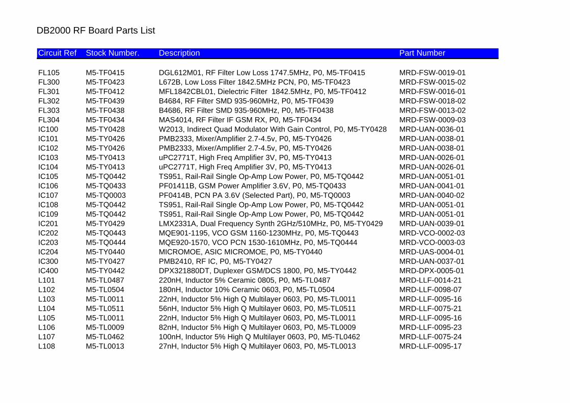
DB2000 RF Board Parts List
Circuit Ref Stock Number. Description Part Number
FL105 M5-TF0415 DGL612M01, RF Filter Low Loss 1747.5MHz, P0, M5-TF0415 MRD-FSW-0019-01FL300 M5-TF0423 L672B, Low Loss Filter 1842.5MHz PCN, P0, M5-TF0423 MRD-FSW-0015-02FL301 M5-TF0412 MFL1842CBL01, Dielectric Filter 1842.5MHz, P0, M5-TF0412 MRD-FSW-0016-01FL302 M5-TF0439 B4684, RF Filter SMD 935-960MHz, P0, M5-TF0439 MRD-FSW-0018-02FL303 M5-TF0438 B4686, RF Filter SMD 935-960MHz, P0, M5-TF0438 MRD-FSW-0013-02FL304 M5-TF0434 MAS4014, RF Filter IF GSM RX, P0, M5-TF0434 MRD-FSW-0009-03IC100 M5-TY0428 W2013, Indirect Quad Modulator With Gain Control, P0, M5-TY0428 MRD-UAN-0036-01IC101 M5-TY0426 PMB2333, Mixer/Amplifier 2.7-4.5v, P0, M5-TY0426 MRD-UAN-0038-01IC102 M5-TY0426 PMB2333, Mixer/Amplifier 2.7-4.5v, P0, M5-TY0426 MRD-UAN-0038-01IC103 M5-TY0413 uPC2771T, High Freq Amplifier 3V, P0, M5-TY0413 MRD-UAN-0026-01IC104 M5-TY0413 uPC2771T, High Freq Amplifier 3V, P0, M5-TY0413 MRD-UAN-0026-01IC105 M5-TQ0442 TS951, Rail-Rail Single Op-Amp Low Power, P0, M5-TQ0442 MRD-UAN-0051-01IC106 M5-TQ0433 PF01411B, GSM Power Amplifier 3.6V, P0, M5-TQ0433 MRD-UAN-0041-01IC107 M5-TQ0003 PF0414B, PCN PA 3.6V (Selected Part), P0, M5-TQ0003 MRD-UAN-0040-02IC108 M5-TQ0442 TS951, Rail-Rail Single Op-Amp Low Power, P0, M5-TQ0442 MRD-UAN-0051-01IC109 M5-TQ0442 TS951, Rail-Rail Single Op-Amp Low Power, P0, M5-TQ0442 MRD-UAN-0051-01IC201 M5-TY0429 LMX2331A, Dual Frequency Synth 2GHz/510MHz, P0, M5-TY0429 MRD-UAN-0039-01IC202 M5-TQ0443 MQE901-1195, VCO GSM 1160-1230MHz, P0, M5-TQ0443 MRD-VCO-0002-03IC203 M5-TQ0444 MQE920-1570, VCO PCN 1530-1610MHz, P0, M5-TQ0444 MRD-VCO-0003-03IC204 M5-TY0440 MICROMOE, ASIC MICROMOE, P0, M5-TY0440 MRD-UAS-0004-01IC300 M5-TY0427 PMB2410, RF IC, P0, M5-TY0427 MRD-UAN-0037-01IC400 M5-TY0442 DPX321880DT, Duplexer GSM/DCS 1800, P0, M5-TY0442 MRD-DPX-0005-01L101 M5-TL0487 220nH, Inductor 5% Ceramic 0805, P0, M5-TL0487 MRD-LLF-0014-21L102 M5-TL0504 180nH, Inductor 10% Ceramic 0603, P0, M5-TL0504 MRD-LLF-0098-07L103 M5-TL0011 22nH, Inductor 5% High Q Multilayer 0603, P0, M5-TL0011 MRD-LLF-0095-16L104 M5-TL0511 56nH, Inductor 5% High Q Multilayer 0603, P0, M5-TL0511 MRD-LLF-0075-21L105 M5-TL0011 22nH, Inductor 5% High Q Multilayer 0603, P0, M5-TL0011 MRD-LLF-0095-16L106 M5-TL0009 82nH, Inductor 5% High Q Multilayer 0603, P0, M5-TL0009 MRD-LLF-0095-23L107 M5-TL0462 100nH, Inductor 5% High Q Multilayer 0603, P0, M5-TL0462 MRD-LLF-0075-24L108 M5-TL0013 27nH, Inductor 5% High Q Multilayer 0603, P0, M5-TL0013 MRD-LLF-0095-17
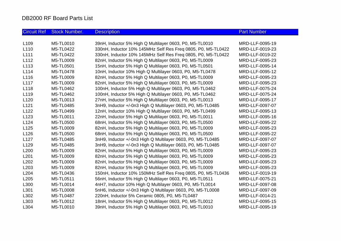
DB2000 RF Board Parts List
Circuit Ref Stock Number. Description Part Number
L109 M5-TL0010 39nH, Inductor 5% High Q Multilayer 0603, P0, M5-TL0010 MRD-LLF-0095-19L110 M5-TL0422 330nH, Inductor 10% 145MHz Self Res Freq 0805, P0, M5-TL0422 MRD-LLF-0019-23L111 M5-TL0422 330nH, Inductor 10% 145MHz Self Res Freq 0805, P0, M5-TL0422 MRD-LLF-0019-22L112 M5-TL0009 82nH, Inductor 5% High Q Multilayer 0603, P0, M5-TL0009 MRD-LLF-0095-23L113 M5-TL0501 15nH, Inductor 5% High Q Multilayer 0603, P0, M5-TL0501 MRD-LLF-0095-14L114 M5-TL0478 10nH, Inductor 10% High Q Multilayer 0603, P0, M5-TL0478 MRD-LLF-0095-12L116 M5-TL0009 82nH, Inductor 5% High Q Multilayer 0603, P0, M5-TL0009 MRD-LLF-0095-23L117 M5-TL0009 82nH, Inductor 5% High Q Multilayer 0603, P0, M5-TL0009 MRD-LLF-0095-23L118 M5-TL0462 100nH, Inductor 5% High Q Multilayer 0603, P0, M5-TL0462 MRD-LLF-0075-24L119 M5-TL0462 100nH, Inductor 5% High Q Multilayer 0603, P0, M5-TL0462 MRD-LLF-0075-24L120 M5-TL0013 27nH, Inductor 5% High Q Multilayer 0603, P0, M5-TL0013 MRD-LLF-0095-17L121 M5-TL0485 3nH9, Inductor +/-0n3 High Q Multilayer 0603, P0, M5-TL0485 MRD-LLF-0097-07L122 M5-TL0499 12nH, Inductor 10% High Q Multilayer 0603, P0, M5-TL0499 MRD-LLF-0095-13L123 M5-TL0011 22nH, Inductor 5% High Q Multilayer 0603, P0, M5-TL0011 MRD-LLF-0095-16L124 M5-TL0500 68nH, Inductor 5% High Q Multilayer 0603, P0, M5-TL0500 MRD-LLF-0095-22L125 M5-TL0009 82nH, Inductor 5% High Q Multilayer 0603, P0, M5-TL0009 MRD-LLF-0095-23L126 M5-TL0500 68nH, Inductor 5% High Q Multilayer 0603, P0, M5-TL0500 MRD-LLF-0095-22L127 M5-TL0485 3nH9, Inductor +/-0n3 High Q Multilayer 0603, P0, M5-TL0485 MRD-LLF-0097-07L129 M5-TL0485 3nH9, Inductor +/-0n3 High Q Multilayer 0603, P0, M5-TL0485 MRD-LLF-0097-07L200 M5-TL0009 82nH, Inductor 5% High Q Multilayer 0603, P0, M5-TL0009 MRD-LLF-0095-23L201 M5-TL0009 82nH, Inductor 5% High Q Multilayer 0603, P0, M5-TL0009 MRD-LLF-0095-23L202 M5-TL0009 82nH, Inductor 5% High Q Multilayer 0603, P0, M5-TL0009 MRD-LLF-0095-23L203 M5-TL0009 82nH, Inductor 5% High Q Multilayer 0603, P0, M5-TL0009 MRD-LLF-0095-23L204 M5-TL0436 150nH, Inductor 10% 150MHz Self Res Freq 0805, P0, M5-TL0436 MRD-LLF-0019-19L205 M5-TL0511 56nH, Inductor 5% High Q Multilayer 0603, P0, M5-TL0511 MRD-LLF-0075-21L300 M5-TL0014 4nH7, Inductor 10% High Q Multilayer 0603, P0, M5-TL0014 MRD-LLF-0097-08L301 M5-TL0008 5nH6, Inductor +/-0n3 High Q Multilayer 0603, P0, M5-TL0008 MRD-LLF-0097-09L302 M5-TL0487 220nH, Inductor 5% Ceramic 0805, P0, M5-TL0487 MRD-LLF-0014-21L303 M5-TL0012 18nH, Inductor 5% High Q Multilayer 0603, P0, M5-TL0012 MRD-LLF-0095-15L304 M5-TL0010 39nH, Inductor 5% High Q Multilayer 0603, P0, M5-TL0010 MRD-LLF-0095-19
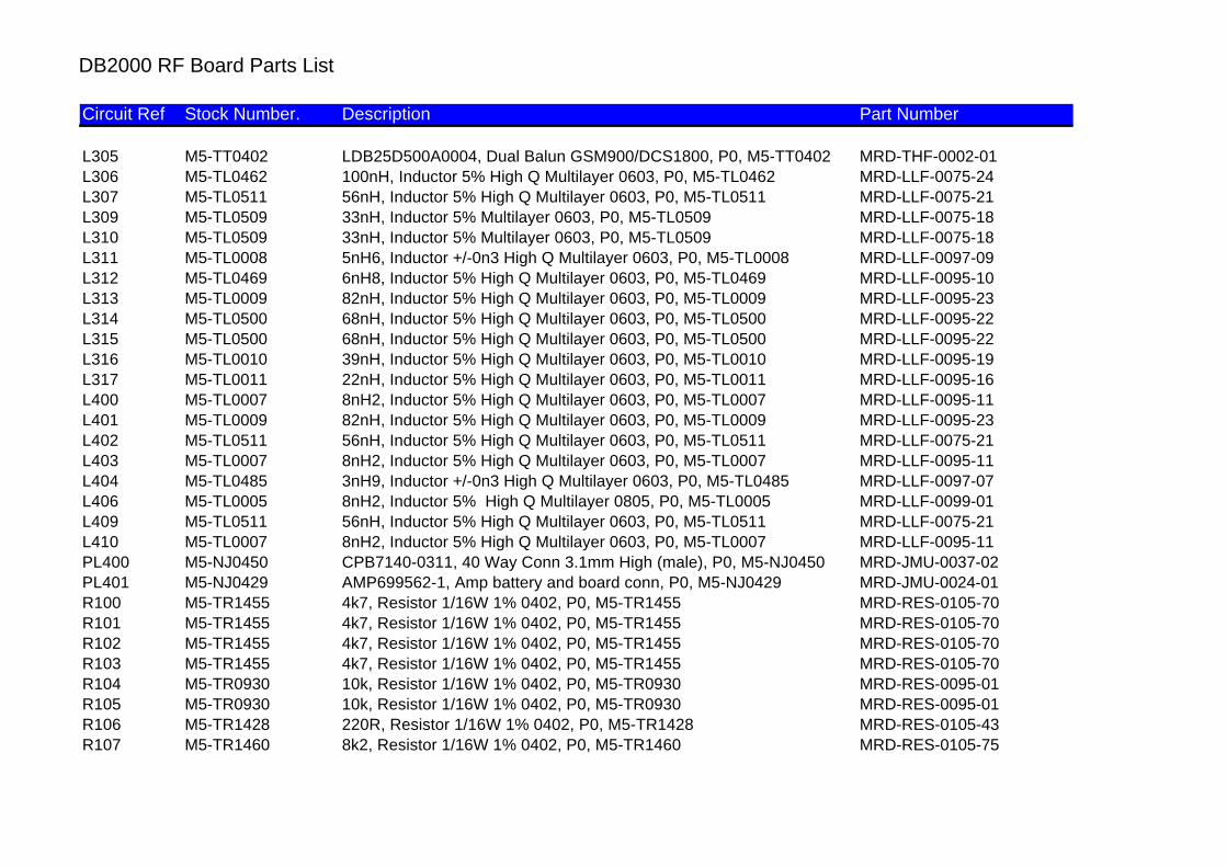
DB2000 RF Board Parts List
Circuit Ref Stock Number. Description Part Number
L305 M5-TT0402 LDB25D500A0004, Dual Balun GSM900/DCS1800, P0, M5-TT0402 MRD-THF-0002-01L306 M5-TL0462 100nH, Inductor 5% High Q Multilayer 0603, P0, M5-TL0462 MRD-LLF-0075-24L307 M5-TL0511 56nH, Inductor 5% High Q Multilayer 0603, P0, M5-TL0511 MRD-LLF-0075-21L309 M5-TL0509 33nH, Inductor 5% Multilayer 0603, P0, M5-TL0509 MRD-LLF-0075-18L310 M5-TL0509 33nH, Inductor 5% Multilayer 0603, P0, M5-TL0509 MRD-LLF-0075-18L311 M5-TL0008 5nH6, Inductor +/-0n3 High Q Multilayer 0603, P0, M5-TL0008 MRD-LLF-0097-09L312 M5-TL0469 6nH8, Inductor 5% High Q Multilayer 0603, P0, M5-TL0469 MRD-LLF-0095-10L313 M5-TL0009 82nH, Inductor 5% High Q Multilayer 0603, P0, M5-TL0009 MRD-LLF-0095-23L314 M5-TL0500 68nH, Inductor 5% High Q Multilayer 0603, P0, M5-TL0500 MRD-LLF-0095-22L315 M5-TL0500 68nH, Inductor 5% High Q Multilayer 0603, P0, M5-TL0500 MRD-LLF-0095-22L316 M5-TL0010 39nH, Inductor 5% High Q Multilayer 0603, P0, M5-TL0010 MRD-LLF-0095-19L317 M5-TL0011 22nH, Inductor 5% High Q Multilayer 0603, P0, M5-TL0011 MRD-LLF-0095-16L400 M5-TL0007 8nH2, Inductor 5% High Q Multilayer 0603, P0, M5-TL0007 MRD-LLF-0095-11L401 M5-TL0009 82nH, Inductor 5% High Q Multilayer 0603, P0, M5-TL0009 MRD-LLF-0095-23L402 M5-TL0511 56nH, Inductor 5% High Q Multilayer 0603, P0, M5-TL0511 MRD-LLF-0075-21L403 M5-TL0007 8nH2, Inductor 5% High Q Multilayer 0603, P0, M5-TL0007 MRD-LLF-0095-11L404 M5-TL0485 3nH9, Inductor +/-0n3 High Q Multilayer 0603, P0, M5-TL0485 MRD-LLF-0097-07L406 M5-TL0005 8nH2, Inductor 5% High Q Multilayer 0805, P0, M5-TL0005 MRD-LLF-0099-01L409 M5-TL0511 56nH, Inductor 5% High Q Multilayer 0603, P0, M5-TL0511 MRD-LLF-0075-21L410 M5-TL0007 8nH2, Inductor 5% High Q Multilayer 0603, P0, M5-TL0007 MRD-LLF-0095-11PL400 M5-NJ0450 CPB7140-0311, 40 Way Conn 3.1mm High (male), P0, M5-NJ0450 MRD-JMU-0037-02PL401 M5-NJ0429 AMP699562-1, Amp battery and board conn, P0, M5-NJ0429 MRD-JMU-0024-01R100 M5-TR1455 4k7, Resistor 1/16W 1% 0402, P0, M5-TR1455 MRD-RES-0105-70R101 M5-TR1455 4k7, Resistor 1/16W 1% 0402, P0, M5-TR1455 MRD-RES-0105-70R102 M5-TR1455 4k7, Resistor 1/16W 1% 0402, P0, M5-TR1455 MRD-RES-0105-70R103 M5-TR1455 4k7, Resistor 1/16W 1% 0402, P0, M5-TR1455 MRD-RES-0105-70R104 M5-TR0930 10k, Resistor 1/16W 1% 0402, P0, M5-TR0930 MRD-RES-0095-01R105 M5-TR0930 10k, Resistor 1/16W 1% 0402, P0, M5-TR0930 MRD-RES-0095-01R106 M5-TR1428 220R, Resistor 1/16W 1% 0402, P0, M5-TR1428 MRD-RES-0105-43R107 M5-TR1460 8k2, Resistor 1/16W 1% 0402, P0, M5-TR1460 MRD-RES-0105-75

DB2000 RF Board Parts List
Circuit Ref Stock Number. Description Part Number
R108 M5-TR0755 150R, Resistor 1/16W 1% 0402, P0, M5-TR0755 MRD-RES-0093-18R109 M5-TR0755 150R, Resistor 1/16W 1% 0402, P0, M5-TR0755 MRD-RES-0093-18R110 M5-TR1465 18k, Resistor 1/16W 1% 0402, P0, M5-TR1465 MRD-RES-0105-80R111 M5-TR1409 18R, Resistor 1/16W 1% 0402, P0, M5-TR1409 MRD-RES-0105-24R112 M5-TR1430 270R, Resistor 1/16W 1% 0402, P0, M5-TR1430 MRD-RES-0105-45R113 M5-TR1414 33R, Resistor 1/16W 1% 0402, P0, M5-TR1414 MRD-RES-0105-29R114 M5-TR1519 0R, Resistor zero ohm link 0402, P0, M5-TR1519 MRD-RES-0107-01R115 M5-TR1519 0R, Resistor zero ohm link 0402, P0, M5-TR1519 MRD-RES-0107-01R116 M5-TR1414 33R, Resistor 1/16W 1% 0402, P0, M5-TR1414 MRD-RES-0105-29R117 M5-TR0738 100R, Resistor 1/16W 1% 0402, P0, M5-TR0738 MRD-RES-0093-01R118 M5-TR0738 100R, Resistor 1/16W 1% 0402, P0, M5-TR0738 MRD-RES-0093-01R122 M5-TR1436 470R, Resistor 1/16W 1% 0402, P0, M5-TR1436 MRD-RES-0105-51R124 M5-TR1459 6k8, Resistor 1/16W 1% 0402, P0, M5-TR1459 MRD-RES-0105-74R125 M5-TR1430 270R, Resistor 1/16W 1% 0402, P0, M5-TR1430 MRD-RES-0105-45R126 M5-TR0659 15R, Resistor 1/16W 1% 0402, P0, M5-TR0659 MRD-RES-0092-18R127 M5-TR1430 270R, Resistor 1/16W 1% 0402, P0, M5-TR1430 MRD-RES-0105-45R129 M5-TR1414 33R, Resistor 1/16W 1% 0402, P0, M5-TR1414 MRD-RES-0105-29R130 M5-TR1455 4k7, Resistor 1/16W 1% 0402, P0, M5-TR1455 MRD-RES-0105-70R131 M5-TR0930 10k, Resistor 1/16W 1% 0402, P0, M5-TR0930 MRD-RES-0095-01R133 M5-TR1026 100k, Resistor 1/16W 1% 0402, P0, M5-TR1026 MRD-RES-0096-01R134 M5-TR1474 47k, Resistor 1/16W 1% 0402, P0, M5-TR1474 MRD-RES-0105-89R135 M5-TR1026 100k, Resistor 1/16W 1% 0402, P0, M5-TR1026 MRD-RES-0096-01R136 M5-TR1523 0R027, Resistor 5% 0805, P0, M5-TR1523 MRD-RES-0046-03R137 M5-TR0930 10k, Resistor 1/16W 1% 0402, P0, M5-TR0930 MRD-RES-0095-01R138 M5-TR0930 10k, Resistor 1/16W 1% 0402, P0, M5-TR0930 MRD-RES-0095-01R139 M5-TR1484 180k, Resistor 1/16W 1% 0402, P0, M5-TR1484 MRD-RES-0105-99R140 M5-TR1484 180k, Resistor 1/16W 1% 0402, P0, M5-TR1484 MRD-RES-0105-99R141 M5-TR0930 10k, Resistor 1/16W 1% 0402, P0, M5-TR0930 MRD-RES-0095-01R142 M5-TR1026 100k, Resistor 1/16W 1% 0402, P0, M5-TR1026 MRD-RES-0096-01R143 M5-TR1026 100k, Resistor 1/16W 1% 0402, P0, M5-TR1026 MRD-RES-0096-01

DB2000 RF Board Parts List
Circuit Ref Stock Number. Description Part Number
R144 M5-TR1522 0R047, Resistor 1/16W 1% 0805, P0, M5-TR1522 MRD-RES-0046-02R145 M5-TR1494 510k, Resistor 1/16W 1% 0402, P0, M5-TR1494 MRD-RES-0106-10R146 M5-TR1474 47k, Resistor 1/16W 1% 0402, P0, M5-TR1474 MRD-RES-0105-89R147 M5-TR1474 47k, Resistor 1/16W 1% 0402, P0, M5-TR1474 MRD-RES-0105-89R149 M5-TR1474 47k, Resistor 1/16W 1% 0402, P0, M5-TR1474 MRD-RES-0105-89R152 M5-TR1519 0R, Resistor zero ohm link 0402, P0, M5-TR1519 MRD-RES-0107-01R153 M5-TR1419 51R, Resistor 1/16W 1% 0402, P0, M5-TR1419 MRD-RES-0105-34R155 M5-TR1519 0R, Resistor zero ohm link 0402, P0, M5-TR1519 MRD-RES-0107-01R156 M5-TR1519 0R, Resistor zero ohm link 0402, P0, M5-TR1519 MRD-RES-0107-01R158 M5-TR1414 33R, Resistor 1/16W 1% 0402, P0, M5-TR1414 MRD-RES-0105-29R159 M5-TR1519 0R, Resistor zero ohm link 0402, P0, M5-TR1519 MRD-RES-0107-01R160 M5-TR1447 2k2, Resistor 1/16W 1% 0402, P0, M5-TR1447 MRD-RES-0105-62R200 M5-TR0934 11k, Resistor 1/16W 1% 0402, P0, M5-TR0934 MRD-RES-0095-05R201 M5-TR1436 470R, Resistor 1/16W 1% 0402, P0, M5-TR1436 MRD-RES-0105-51R202 M5-TR1450 3k, Resistor 1/16W 1% 0402, P0, M5-TR1450 MRD-RES-0105-65R203 M5-TR0930 10k, Resistor 1/16W 1% 0402, P0, M5-TR0930 MRD-RES-0095-01R204 M5-TR0930 10k, Resistor 1/16W 1% 0402, P0, M5-TR0930 MRD-RES-0095-01R205 M5-TR1462 12k, Resistor 1/16W 1% 0402, P0, M5-TR1462 MRD-RES-0105-77R206 M5-TR0930 10k, Resistor 1/16W 1% 0402, P0, M5-TR0930 MRD-RES-0095-01R207 M5-TR1519 0R, Resistor zero ohm link 0402, P0, M5-TR1519 MRD-RES-0107-01R208 M5-TR1419 51R, Resistor 1/16W 1% 0402, P0, M5-TR1419 MRD-RES-0105-34R209 M5-TR0642 10R, Resistor 1/16W 1% 0402, P0, M5-TR0642 MRD-RES-0092-01R210 M5-TR1468 27k, Resistor 1/16W 1% 0402, P0, M5-TR1468 MRD-RES-0105-83R211 M5-TR1446 1k8, Resistor 1/16W 1% 0402, P0, M5-TR1446 MRD-RES-0105-61R212 M5-TR0947 15k, Resistor 1/16W 1% 0402, P0, M5-TR0947 MRD-RES-0095-18R213 M5-TR1440 680R, Resistor 1/16W 1% 0402, P0, M5-TR1440 MRD-RES-0105-55R214 M5-TR0947 15k, Resistor 1/16W 1% 0402, P0, M5-TR0947 MRD-RES-0095-18R215 M5-TR1468 27k, Resistor 1/16W 1% 0402, P0, M5-TR1468 MRD-RES-0105-83R216 M5-TR1446 1k8, Resistor 1/16W 1% 0402, P0, M5-TR1446 MRD-RES-0105-61R217 M5-TR1432 330R, Resistor 1/16W 1% 0402, P0, M5-TR1432 MRD-RES-0105-47
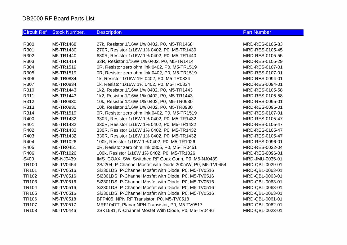
DB2000 RF Board Parts List
Circuit Ref Stock Number. Description Part Number
R300 M5-TR1468 27k, Resistor 1/16W 1% 0402, P0, M5-TR1468 MRD-RES-0105-83R301 M5-TR1430 270R, Resistor 1/16W 1% 0402, P0, M5-TR1430 MRD-RES-0105-45R302 M5-TR1440 680R, Resistor 1/16W 1% 0402, P0, M5-TR1440 MRD-RES-0105-55R303 M5-TR1414 33R, Resistor 1/16W 1% 0402, P0, M5-TR1414 MRD-RES-0105-29R304 M5-TR1519 0R, Resistor zero ohm link 0402, P0, M5-TR1519 MRD-RES-0107-01R305 M5-TR1519 0R, Resistor zero ohm link 0402, P0, M5-TR1519 MRD-RES-0107-01R306 M5-TR0834 1k, Resistor 1/16W 1% 0402, P0, M5-TR0834 MRD-RES-0094-01R307 M5-TR0834 1k, Resistor 1/16W 1% 0402, P0, M5-TR0834 MRD-RES-0094-01R310 M5-TR1443 1k2, Resistor 1/16W 1% 0402, P0, M5-TR1443 MRD-RES-0105-58R311 M5-TR1443 1k2, Resistor 1/16W 1% 0402, P0, M5-TR1443 MRD-RES-0105-58R312 M5-TR0930 10k, Resistor 1/16W 1% 0402, P0, M5-TR0930 MRD-RES-0095-01R313 M5-TR0930 10k, Resistor 1/16W 1% 0402, P0, M5-TR0930 MRD-RES-0095-01R314 M5-TR1519 0R, Resistor zero ohm link 0402, P0, M5-TR1519 MRD-RES-0107-01R400 M5-TR1432 330R, Resistor 1/16W 1% 0402, P0, M5-TR1432 MRD-RES-0105-47R401 M5-TR1432 330R, Resistor 1/16W 1% 0402, P0, M5-TR1432 MRD-RES-0105-47R402 M5-TR1432 330R, Resistor 1/16W 1% 0402, P0, M5-TR1432 MRD-RES-0105-47R403 M5-TR1432 330R, Resistor 1/16W 1% 0402, P0, M5-TR1432 MRD-RES-0105-47R404 M5-TR1026 100k, Resistor 1/16W 1% 0402, P0, M5-TR1026 MRD-RES-0096-01R405 M5-TR0451 0R, Resistor zero ohm link 0805, P0, M5-TR0451 MRD-RES-0022-04R406 M5-TR1026 100k, Resistor 1/16W 1% 0402, P0, M5-TR1026 MRD-RES-0096-01S400 M5-NJ0439 IMS_COAX_SW, Switched RF Coax Conn, P0, M5-NJ0439 MRD-JMU-0035-01TR100 M5-TV0454 2SJ204, P-Channel Mosfet with Diode 200mW, P0, M5-TV0454 MRD-QBL-0029-01TR101 M5-TV0516 Si2301DS, P-Channel Mosfet with Diode, P0, M5-TV0516 MRD-QBL-0063-01TR102 M5-TV0516 Si2301DS, P-Channel Mosfet with Diode, P0, M5-TV0516 MRD-QBL-0063-01TR103 M5-TV0516 Si2301DS, P-Channel Mosfet with Diode, P0, M5-TV0516 MRD-QBL-0063-01TR104 M5-TV0516 Si2301DS, P-Channel Mosfet with Diode, P0, M5-TV0516 MRD-QBL-0063-01TR105 M5-TV0516 Si2301DS, P-Channel Mosfet with Diode, P0, M5-TV0516 MRD-QBL-0063-01TR106 M5-TV0518 BFP405, NPN RF Transistor, P0, M5-TV0518 MRD-QBL-0061-01TR107 M5-TV0517 MRF1047T, Planar NPN Transistor, P0, M5-TV0517 MRD-QBL-0062-01TR108 M5-TV0446 2SK1581, N-Channel Mosfet With Diode, P0, M5-TV0446 MRD-QBL-0023-01
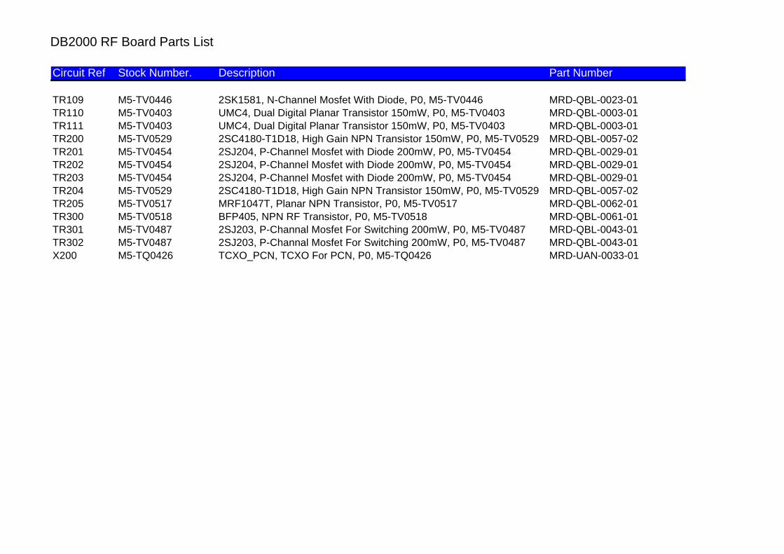
DB2000 RF Board Parts List
Circuit Ref Stock Number. Description Part Number
TR109 M5-TV0446 2SK1581, N-Channel Mosfet With Diode, P0, M5-TV0446 MRD-QBL-0023-01TR110 M5-TV0403 UMC4, Dual Digital Planar Transistor 150mW, P0, M5-TV0403 MRD-QBL-0003-01TR111 M5-TV0403 UMC4, Dual Digital Planar Transistor 150mW, P0, M5-TV0403 MRD-QBL-0003-01TR200 M5-TV0529 2SC4180-T1D18, High Gain NPN Transistor 150mW, P0, M5-TV0529 MRD-QBL-0057-02TR201 M5-TV0454 2SJ204, P-Channel Mosfet with Diode 200mW, P0, M5-TV0454 MRD-QBL-0029-01TR202 M5-TV0454 2SJ204, P-Channel Mosfet with Diode 200mW, P0, M5-TV0454 MRD-QBL-0029-01TR203 M5-TV0454 2SJ204, P-Channel Mosfet with Diode 200mW, P0, M5-TV0454 MRD-QBL-0029-01TR204 M5-TV0529 2SC4180-T1D18, High Gain NPN Transistor 150mW, P0, M5-TV0529 MRD-QBL-0057-02TR205 M5-TV0517 MRF1047T, Planar NPN Transistor, P0, M5-TV0517 MRD-QBL-0062-01TR300 M5-TV0518 BFP405, NPN RF Transistor, P0, M5-TV0518 MRD-QBL-0061-01TR301 M5-TV0487 2SJ203, P-Channal Mosfet For Switching 200mW, P0, M5-TV0487 MRD-QBL-0043-01TR302 M5-TV0487 2SJ203, P-Channal Mosfet For Switching 200mW, P0, M5-TV0487 MRD-QBL-0043-01X200 M5-TQ0426 TCXO_PCN, TCXO For PCN, P0, M5-TQ0426 MRD-UAN-0033-01
<< Previous SectionNext Section >>Main Menu
Section 8
CircuitDiagrams andBoard Maps
Part 1 Baseband Circuit DiagramsPart 2 RF Circuit DiagramsPart 3 Baseband Board MapsPart 4 RF Board Maps
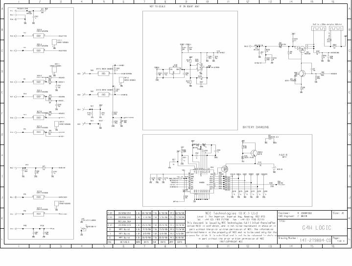
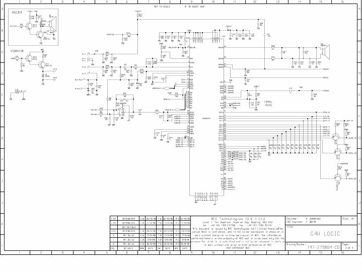
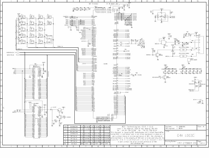
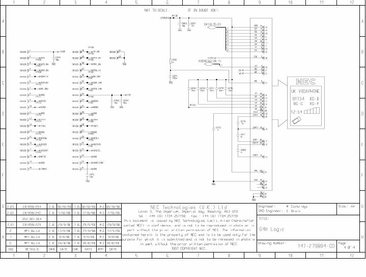
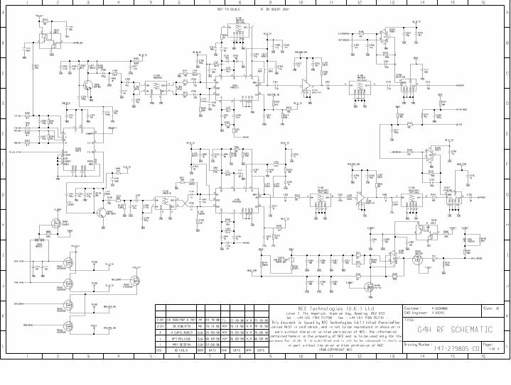
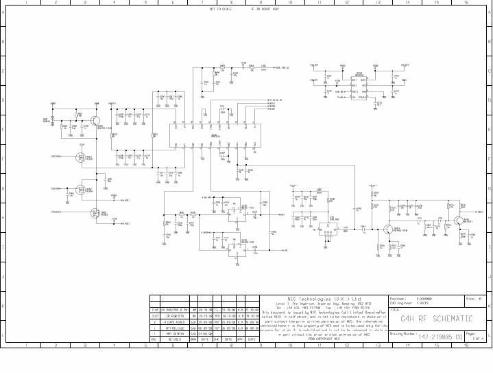
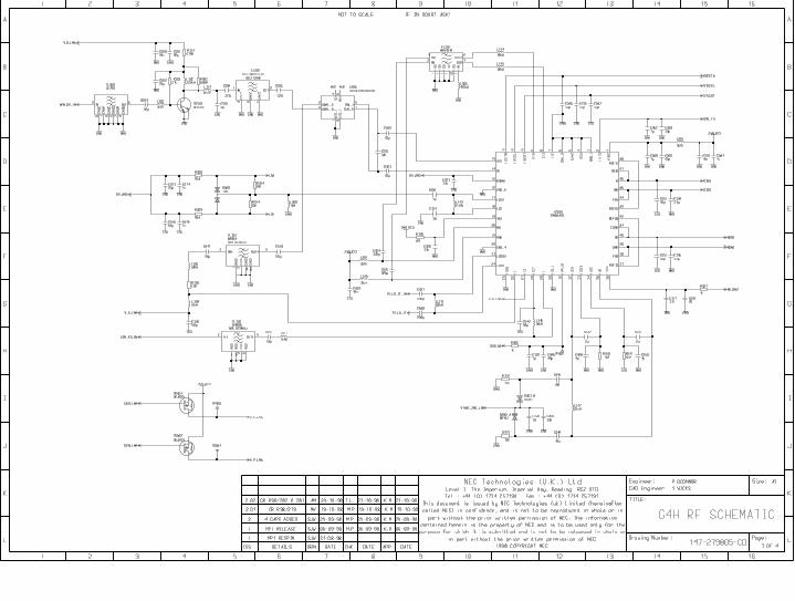
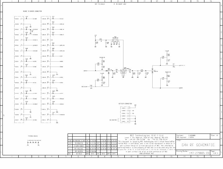
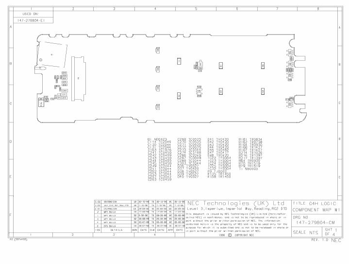
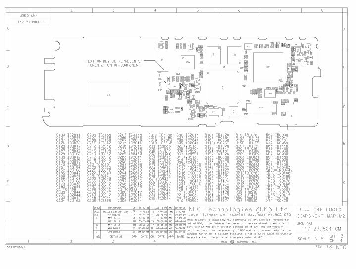
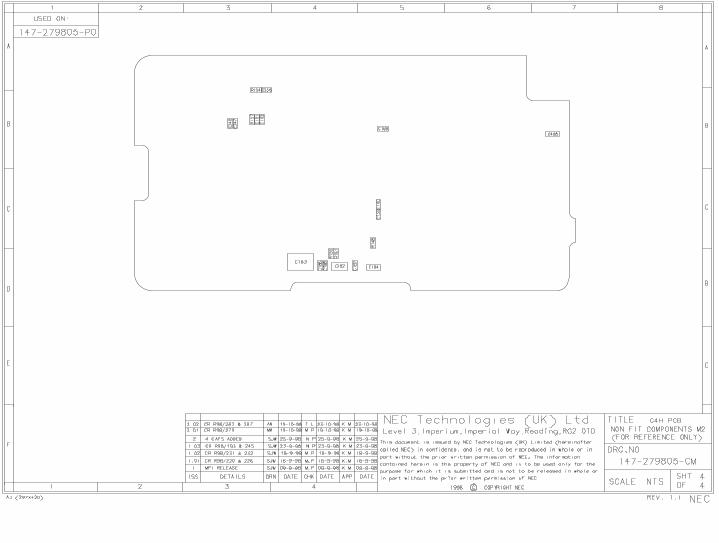
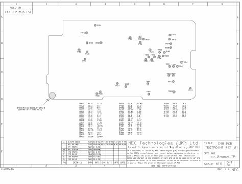

<< Previous SectionNext Section >>Main Menu
Glossary ofTerms
List of General Acronyms and AbbreviationsList of General Acronyms and Abbreviations
This section provides a list of acronyms and abbreviations used in thismanual and generally in GSM.
AAAAACACAD, A/DAD, A/DADJADJAFAFAFCAFCAGCAGCAGCHAGCHAHAHAIDAIDALCALCALMALMALUALUAMAMAMPAMPANTANTAPQAPQASCIIASCIIASSYASSYATTATTAUXAUX
BBbbB/S, b/sB/S, b/sBATTBATTBBBBBCCHBCCHBCDBCDBCHBCHBERBERBITBITBNCBNCBPFBPFBSBSBSCBSCBSSBSSBTSBTS
AmpereAlternating CurrentAnalogue to Digital ConverterAdjust, AdjustmentAudio FrequencyAutomatic Frequency ControlAutomatic Gain ControlAccess Grant ChannelAmpere HourArea Identification NumberAutomatic Level ControlAlarmArithmetic and Logic UnitAmplitude ModulationAmplifierAntennaAutomatic Repeat RequestAmerican Standard Code for Information InterchangeAssemblyAttenuator, AttenuationAuxiliary
Base terminal on a TransistorBits per SecondBatteryBase BandBroadcast Control ChannelBinary Coded DecimalBroadcast ChannelBit Error RateBinary Digit (1 or 0)Type of connectorBand Pass FilterBase StationBase Station ControllerBase Station SystemBase Transceiver Station
CCccCCCALCALCAPCAPCCCHCCCHCCITTCCITTCdCdChChCHGCHGCLKCLKCLRCLRCMOSCMOSCO-AXCO-AXCODECCODECCONCONCONTCONTCPUCPUCRCCRCCSPCSP
Collector terminal on a TransistorCapacitor, CentigradeCalibrate, CalibrationCapacitorCommon control ChannelInternational Consultative Committee for Telegraphy andTelephonyCadmiumChannelChargeClockClearComplimentary Metal Oxide SemiconductorCoaxial CableEncoder and DecoderConnectorControl, ControllerCentral Processing UnitCyclic Redundancy CodingConversion Signal Processor
DDDA, D/ADA, D/AdBdBdBmdBmDC, dcDC, dcDEMODDEMODDETDETDEVDEVDGDGDISCDISCDISTDISTDIVDIVDPDPDSPDSPDTMFDTMFDTXDTXDUPDUP
Digital to Analogue ConverterDecibelsDecibels relative to 1mWDirect CurrentDemodulatorDetectorDeviationDifferential GainDiscriminatorDistortionDivideDifferential PhaseDigital Signal ProcessorDual Tone Multiple FrequencyDiscontinuous TransmitDuplex
EEeeECLECLEIREIRENBLENBLEPROMEPROM
Emitter Terminal of a TransistorEmitter Coupled LogicEquipment Identity RegisterEnableErasable and Programmable Read Only Memory
EE22PROMPROMEXPEXPEXTEXT
Electrically Erasable and Programmable Read Only MemoryExpanderExternal, Extension
FFFFFACCHFACCHFCHFCHFCNFCNFDMAFDMAFETFETFILFILFMFMFREQFREQFSKFSK
FaradFast Associated Control ChannelFrequency Control ChannelFunctionFrequency Division Multiple accessField Effect TransistorFilterFrequency ModulationFrequencyFrequency Shift Keying
GGGMSKGMSKGNDGNDGPGPGSMGSM
Gaussian Minimum Shift KeyingGroundGuard PeriodGlobal System for Mobile Communications
HHHHHFHFHHPHHPHLRHLRHzHz
Height, HenryHands Free, High FrequencyHand Held PortableHome Location RegisterHertz
IIIII/FI/FI/OI/OICICIDIDIFIFIMEIIMEIIMSIIMSIINITINITINTINTISDNISDN
In Phase signalInterfaceInput / OutputIntegrated circuitIdentityIntermediate FrequencyInternational Mobile Equipment IdentityInternational Mobile Subscriber IdentityInitialiseInternal, InterruptIntegrated Services Digital Network
LLLLLCDLCD
Length, InductorLiquid Crystal Display
LEDLEDLNALNALOLOLSILSI
Light Emitting DiodeLow Noise AmplifierLocal OscillatorLarge Scale Integrated Circuit
MMMAXMAXMHzMHzMICMICMIDMIDMINMINMIXMIXMODMODMODEMMODEMMONMONMSMSMSCMSCMSKMSKMSSMSSMUXMUX
MaximumMega HertzMicrophoneMiddleMinimumMixerModulate, ModulatorModulator and DemodulatorMonitorMobile StationMobile switching centreMinimum Shift KeyingMobile Subscriber setMultiplexer
NNNCNCNGNGNiCdNiCd
No ConnectionNo GoodNickel Cadmium
OOOp AmpOp AmpOPTOPTOSCOSC
Operational AmplifierOptionOscillate, Oscillator
PPPAPAPCBPCBPCHPCHPCMPCMPCNPCNPLLPLLPMPMPROMPROMPSPSPSKPSKPSTNPSTNPWBPWBPWRPWR
Power AmplifierPrinted Circuit BoardPaging ChannelPulse Code ModulationPersonal Communication NetworkPhase Locked LoopPhase ModulationProgrammable Read Only MemoryPower SupplyPhase Shift KeyingPublic Switched Telephone NetworkPrinted Wiring BoardPower
QQQQQTYQTYQPSKQPSK
Quadrature Phase SignalQuantityQuadrature phase Shift Keying
RRRRRACHRACHRAMRAMRCLRCLRECRECREFREFRESRESRFRFROMROMRSSIRSSIRSTRSTRXRXRXAFRXAFRXLevRXLevRXQualRXQual
ResistorRandom Access ChannelRandom Access MemoryRecallReceiver, EarpieceReferenceResistorRadio FrequencyRead only MemoryReceive Signal Strength IndicationResetReceive, ReceiverReceive Audio FrequencyRX level (as defined in GSM specifications)RX Quality (as defined in GSM specifications)
SSS/NS/NSACCHSACCHSAWSAWSCHSCHSCLSCLSDASDASDCCHSDCCHSENSSENSSERCKSERCKSERDASERDASERLTSERLTSIGSIGSIMSIMSPKSPKSTDSTDSTOSTOSYNCSYNCSYNTHSYNTH
Signal to Noise RatioSlow Associated Control ChannelSurface Acoustic WaveSynchronisation ChannelSerial ClockSerial DataStand Alone Dedicated Control ChannelSensitivitySerial ClockSerial DataSerial LatchSignalSubscriber Identity ModuleSpeaker, Sounder, HornStandardStoreSynchronise, SynchronisationSynthesiser
TTTBTBTCHTCH
Tail bitsTraffic Channel
TCXOTCXOTDMATDMATETETEMPTEMPTNCTNCTPTPTRTRTRXTRXTXTXTXAFTXAF
Temperature Controlled OscillatorTime Division Multiple AccessTest EquipmentTemperatureA type of connectorTest PointTransistorTransmitter and ReceiverTransmit, TransmitterTransmit Audio Frequency
UUmmmFmFUHFUHFmPmP
MicroMicro FaradUltra High FrequencyMicroprocessor
VVVVVCOVCOVLRVLRVOLVOL
VoltsVoltage Controlled OscillatorVisitor Location RegisterVolume
WWWW Watts, Width
XXXTALXTALXTLXTL
CrystalCrystal
SymbolsSymbols<<>>##
Less thanGreater thanPin number/number

Points of Contact for further Information.
NEC Deutschland Gmbh.Steinheilstr 4-685737 IsmaningDeutschland Tel: +49 89 962 740
NEC France SA 56 Rue De Hauntes Patures92024 Nanterre CedexFrance Tel: +33 1 4649 4649
NEC Iberica SAMiniparc 1Edificio ACalle Azalea 128109El Soto de La MoralejaAlcobendas, MadridEspana Tel: +37 91 650 1313
NEC Italia SRLViale Leonardo Da Vinci 97Trezzano Sul NaviglioMilanoItalia Tel: +39 02 484 151
NEC Scandinavia ABKarlsbodavagen 20Box 20057, 161 20BrommaSweden Tel: +46 8 635 9200
NEC UKNEC House1 Victoria RoadLondonW3 6BL Tel: +44 (0)181 993 8111
DB2000 Service Manual Guide.DB2000 Service Manual Guide.
All sections of the service manual can be accessed from the keypad of the DB2000on this page of the manual. For instance, clicking the number ‘3’ on the keypad willtake you to section 3 of the manual. Moving the mouse over each of the numerickeys will show the title of the related section on the DB2000 display.
Navigating the manual from the keypad in this manner will result in each of thesections being presented in the form of an article which can be scrolled through byplacing the hand tool within the article and clicking the left mouse button.
If you do not wish to read the section in the article format selecting the page buttonfrom the Acrobat Reader Toolbar will display the whole page. Scrolling through thepages can be achieved by using the toolbar or by using the buttons on each of thepages in the manual. The ‘bullet’ button (in between the page up and page downbuttons) returns you to the beginning of the particular section that you are in at thetime.
Alternatively the manual can be read by using the bookmarks to select the varioussection and subsection headings. See the Acrobat Reader Help for more informationon displaying and using bookmarks.
The first page of each section also contains links to the next section, from theprevious section and back to the main menu (the first page) as well as page up andpage down buttons.
The manual also contains many links which will become apparent when moving themouse around a page of the document (The hand tool will change to a pointer whenthe mouse moves over a link).
Most of the links can be found in the schematic diagrams, where they have beenused to inter-link signals between various parts or pages of the circuit diagram. Inmost cases this will result in a magnified view with the required signal in the centreof the screen.
To zoom in to parts of the manual (most useful for drawings and circuit diagrams)select the magnifier tool from the Acrobat Reader toolbar.
DB2000 Service Manual - MRDCS-1011Revision 1.1 - 27th January 1999NEC Technologies (UK) Ltd.
This Document is the property of NEC Technologies (UK) Ltd. Itmust not be reproduced, in whole or in part, or otherwisedisclosed without prior consent in writing from NEC Technologies(UK) Ltd.