course material preparation - sri chandrasekharendra
TRANSCRIPT

SRI CHANDRASEKHARENDRA SARASWATHI
VISWA MAHA VIDYALAYA
DEPARTMENT OF ELECTRONICS & COMMUNICATION
ENGINEERING
COURSE MATERIAL PREPARATION
Computer Aided System Design Laboratory
Dr.R. JAYALAKSHMI

PCC20 COMPUTER AIDED SYSTEM DESIGN LABORATOTY V SEMESTER
OBJECTIVES:
• To Construct RC circuits, OPAMPS, Combinational and Sequential circuits Using PSICE
• To Simulate and Implement sequential and combinational digital circuits using HDL
PSPICE: (Modelling, Design, Simulation and Analysis using Schematic / Circuit file / both)
1. Study of PSPICE
2. RC circuits – Transient and AC analysis
3. MOS Device Characterization and CMOS Inverter Characteristics – DC analysis
4. Diode based circuits (like, Rectifiers, Clampers, etc.,) – Transient, Worst-case, MC,
Sensitivity, etc. analysis
5. Amplifiers and Current mirrors using BJT/MOSFET
6. Op-Amp based Wein Bridge Oscillator and DAC using sub-circuit and Analog behavioural
modelling
7. Digital Circuits – Logic switches / Multiplexer / Counter HDL: (Logic Design and
Simulation of Digital Circuits using VHDL / Verilog HDL / Both)
8. Study of VHDL and Verilog

9. Full Adder and Multiplexer using different Modelling / Descriptions and Concurrent and
SEQUENTIAL EXECUTION IN VHDL:
10. 8-bit Adder / Multiplier (min 4-bit) – Port Map, Generics, Technology Mapping in VHDL
11. 8-bit Counter – Bottom-up approach design and Test vector generation in Verilog HDL
12. NAND / NOR / Transmission gates using Switch level modelling in Verilog HDL
13. Design of simple sequential and combinational circuits
14. Design of ALU
15. Design of FSM and Control Unit
16. FPGA real time programming and I/O Interfacing– Waveform generation / Traffic light
controller
OUTCOMES: Upon completion of the course, students will be able to:
• Construct Analog and Digital circuits and study their characteristics using PSPICE.
• Implement digital circuits using HDL TOOLS TO BE USED: LTSPICE, Mentor Graphics,
Xilinx / Equivalent

1. Study of PSPICE
INTRODUCTION TO PSPICE
Schematics are a schematic capture front-end program with a direct interface to other PSpice
programs and options.
The following tasks can be performed, all in one environment, using Schematics:
•Design and draw circuits.
•Simulate circuits using PSpice.
•Analyse simulation results using the PSpice waveform viewer (Probe) Graphically
characterize simulation stimuli using the fully integrated Stimulus Editor, so stimulus
definitions are automatically associated with the appropriate symbols.
• Graphically characterize simulation models using the fully integrated Model Editor utility
(formerly known as Parts), so model definitions are automatically associated with the
appropriate symbols.
• Interface to PSpice Optimizer for analog circuit performance optimization.
• An important prerequisite for building a schematic is the availability of the necessary devices
in the form of symbols. Schematic has extensive symbol libraries and include a fully integrated
symbol editor for creating your own symbols or modifying existing symbols.

PROCEDURE FOR PSPICE:
SCHEMATIC File
1) Starting a schematic new design: Go to PSpice Students demo folder and click the
SCHEMATIC icon FILE name of PSPICE students’ window, select NEW and use appropriate
name for PROJECT and select analog or mixed signal wizard.
2) Including Libraries: ADD the following libraries to the list of libraries to be used.
3) Selecting, Placing and editing parts: Click on the draw Menu. Select get new part on the pop
up window. Select “Analog” for libraries. For example to get resistor type “R” and click Ok to
place the resistor.
4) For Drawing Wires: Click on the draw menu and select wire and connect the circuits as per
the given schematics.
5) For Analysis of the Schematics: Click on the Markers Menu, select the “SET UP” and select
“AC SWEEP” for AC Analysis or select Transient for transient analysis, give the parameters
for both analysis of timing and frequencies.
6) To get the output for Analysis: Click on Analysis Menu, select “Electrical Rule Check” for
the net list verification and then click on Analysis Menu, select “Simulate” to see the
schematics, a probe window showing the Plot of result should open-up.

PROCEDURE FOR PSPICE:
PSPICE A/D:
1) Starting a new design: Go to PSpice demo folder and click the Spice A/D. To create new
Project, click the file menu and get new text file and use an appropriate value name for the text
file and save as .cir in the working directory.
2) Including Libraries: Type Ctrl+G and click to add the libraries, and then click the required
apparatus containing libraries for experiments then Click Ok.
3) Creating a Net List: Create a circuit in a text file with list of all the components and node
connections called the Net List.
4) Simulation of PSpice A/D Run a simulation on the Net List and perform the request
Analysis. Select the Type of Analysis (AC or Transient).
5) To get the Output for PSpice A/D: Open the Working directory and click the binary data
file. Click the waveform icon in the PSpice A/D window. The output graph should open up.

2. RC circuits – Transient and AC analysis
AIM:
To verify the AC AND TRANSIENT ANALYSIS of a Low Pass and High Pass filter RC
circuits by using the PSPICE software.
LPF AC ANALYSIS:
• Understand the characteristics of physical model of LPF and what kind of circuit needed.
• Place the resistor, capacitor, input source (AC/DC) ground source and complete the circuit
by drawing wire to connect them.
• Place the voltage convertor at required place.
• Click on the set-up analysis. Choose the AC sweep option and set frequency, magnitude •
Simulate circuit and obtain graphical response curve for AC analysis.
LPF Transient Analysis:
• Understand the physical characteristics of LPF and what kind of i/p sources needed for circuit
• Using resistor, capacitor, input source (sine, pulse) etc ground source and other elements
complete the circuit by connecting them with wire
• Click on setup analysis, choose transient analysis and set appropriate value for the transient
parameters and click Ok
• Set the magnitude value and other parameter value for i/p source.
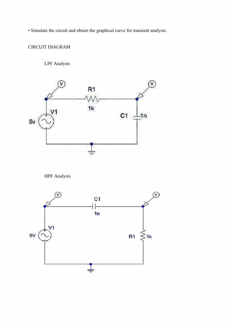
• Simulate the circuit and obtain the graphical curve for transient analysis.
CIRCUIT DIAGRAM
LPF Analysis
HPF Analysis
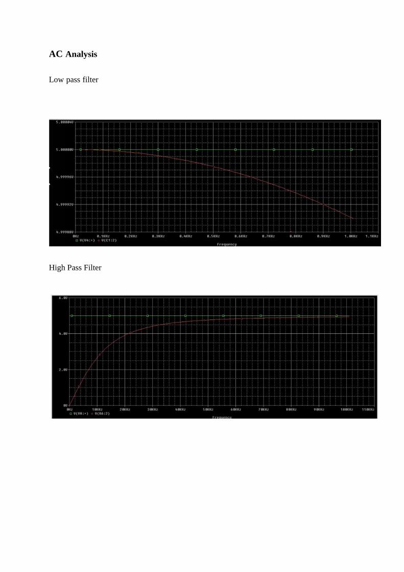
AC Analysis
Low pass filter
High Pass Filter
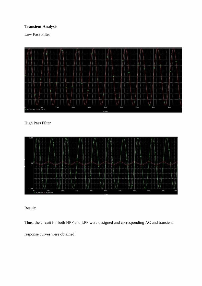
Transient Analysis
Low Pass Filter
High Pass Filter
Result:
Thus, the circuit for both HPF and LPF were designed and corresponding AC and transient
response curves were obtained
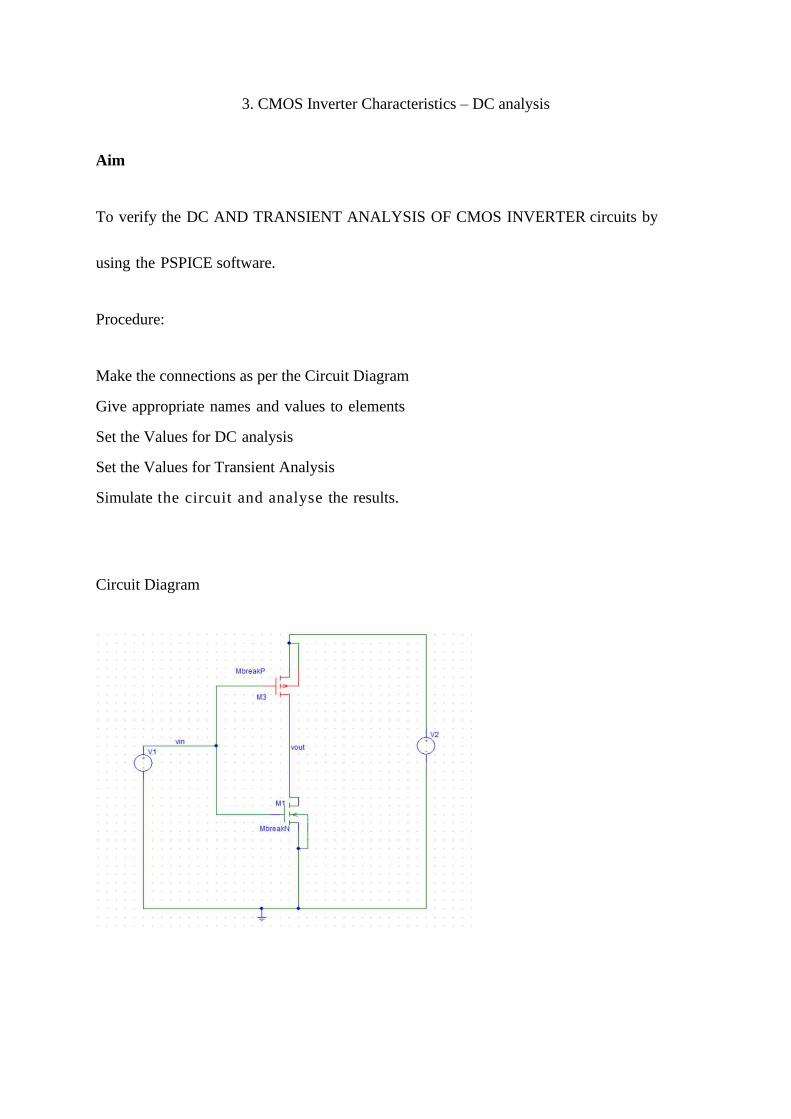
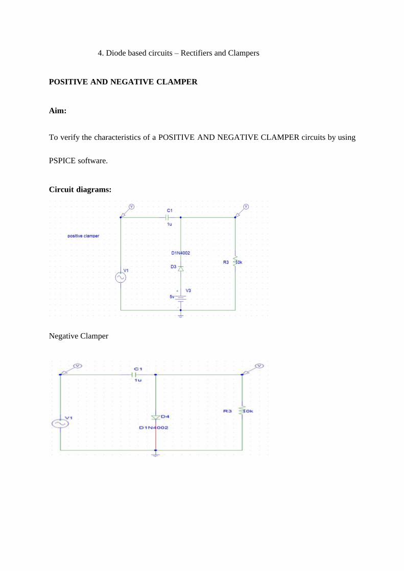
3. CMOS Inverter Characteristics – DC analysis
Aim
To verify the DC AND TRANSIENT ANALYSIS OF CMOS INVERTER circuits by
using the PSPICE software.
Procedure:
Make the connections as per the Circuit Diagram
Give appropriate names and values to elements
Set the Values for DC analysis
Set the Values for Transient Analysis
Simulate the circuit and analyse the results.
Circuit Diagram
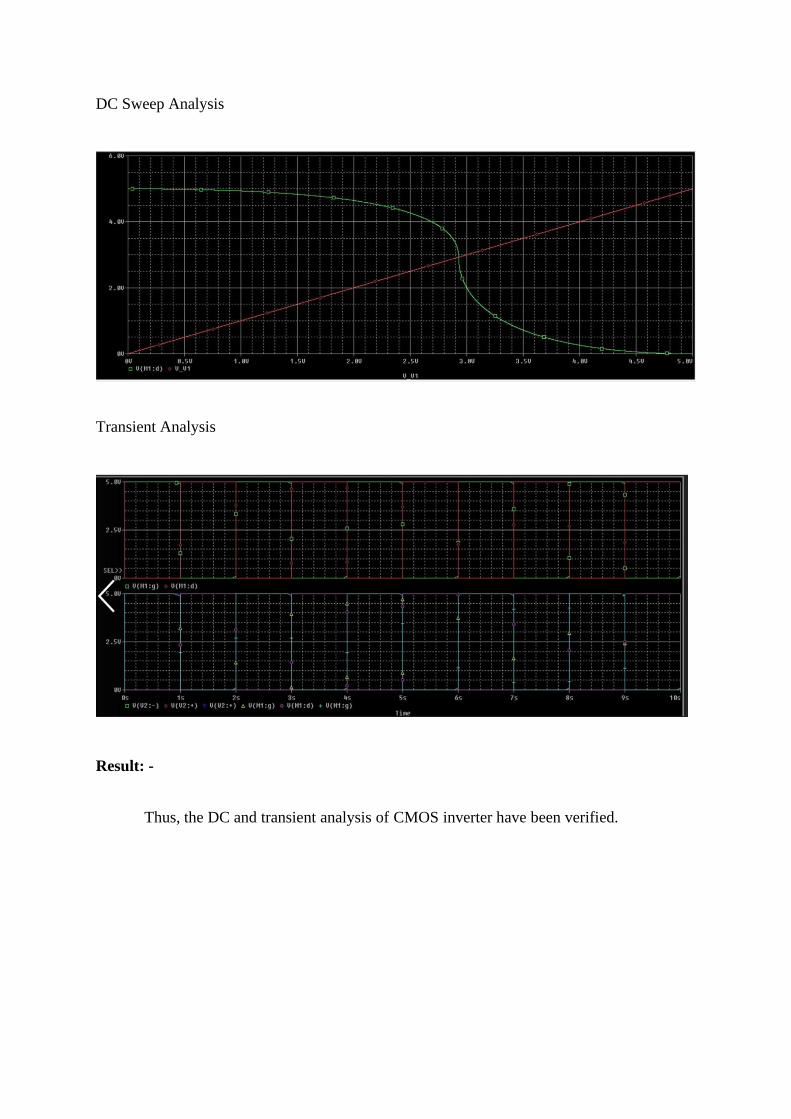
DC Sweep Analysis
Transient Analysis
Result: -
Thus, the DC and transient analysis of CMOS inverter have been verified.
4. Diode based circuits – Rectifiers and Clampers
POSITIVE AND NEGATIVE CLAMPER
Aim:
To verify the characteristics of a POSITIVE AND NEGATIVE CLAMPER circuits by using
PSPICE software.
Circuit diagrams:
Negative Clamper
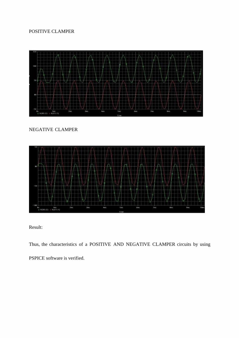
POSITIVE CLAMPER
NEGATIVE CLAMPER
Result:
Thus, the characteristics of a POSITIVE AND NEGATIVE CLAMPER circuits by using
PSPICE software is verified.
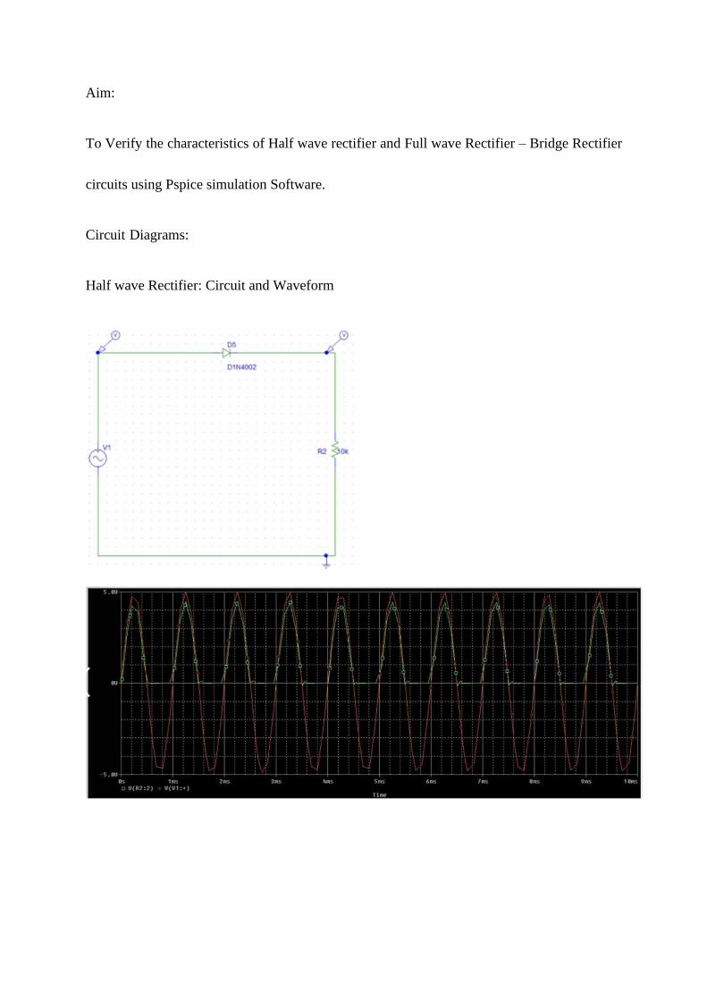
Aim:
To Verify the characteristics of Half wave rectifier and Full wave Rectifier – Bridge Rectifier
circuits using Pspice simulation Software.
Circuit Diagrams:
Half wave Rectifier: Circuit and Waveform
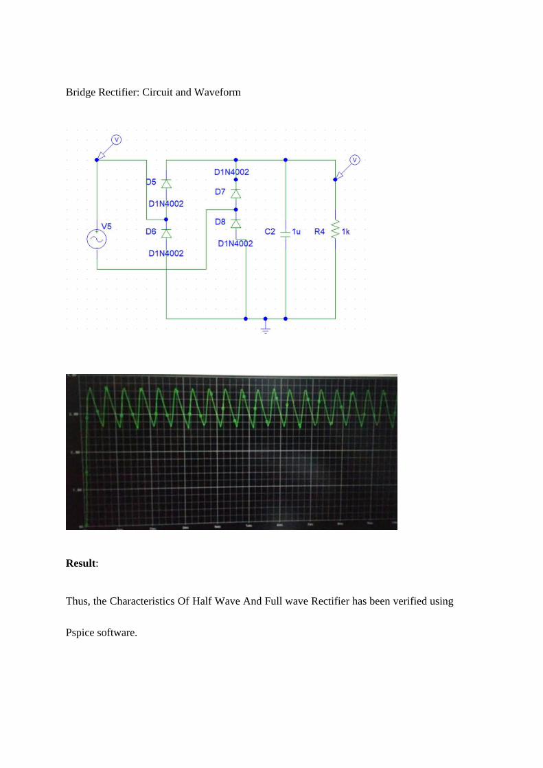
Bridge Rectifier: Circuit and Waveform
Result:
Thus, the Characteristics Of Half Wave And Full wave Rectifier has been verified using
Pspice software.
5. Amplifiers and Current mirrors using BJT/MOSFET
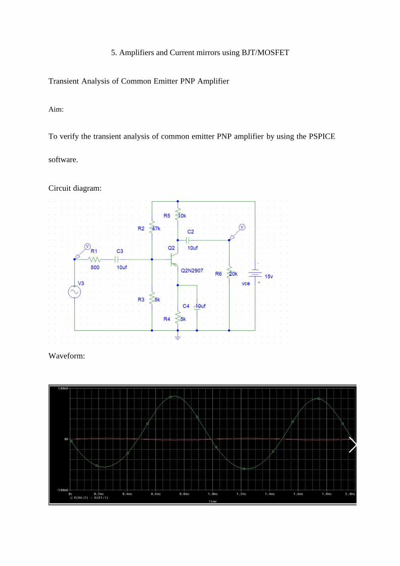
Transient Analysis of Common Emitter PNP Amplifier
Aim:
To verify the transient analysis of common emitter PNP amplifier by using the PSPICE
software.
Circuit diagram:
Waveform:

Result:
Thus, the transient analysis of common emitter pnp amplifier have been verified.
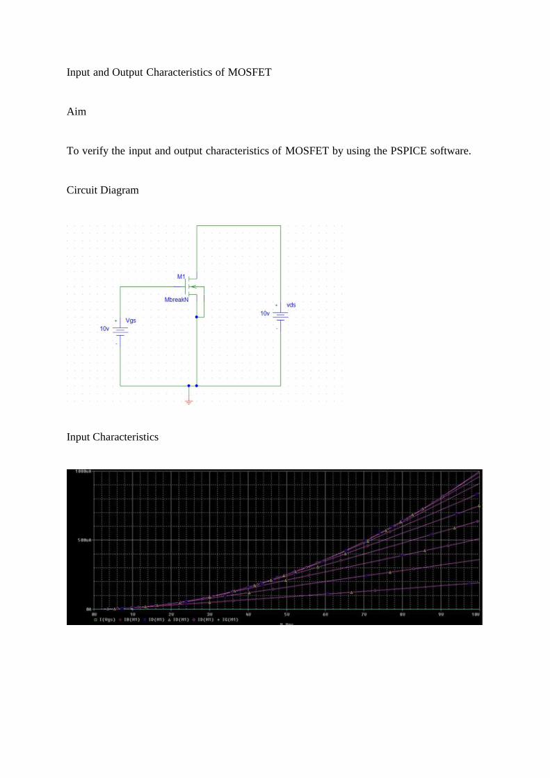
Input and Output Characteristics of MOSFET
Aim
To verify the input and output characteristics of MOSFET by using the PSPICE software.
Circuit Diagram
Input Characteristics

Output Characteristics
Result:
Thus, the input and output characteristics of BJT have been verified.
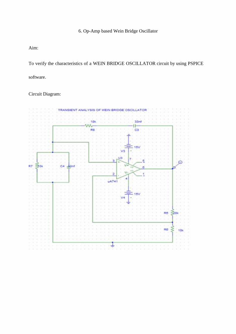
6. Op-Amp based Wein Bridge Oscillator
Aim:
To verify the characteristics of a WEIN BRIDGE OSCILLATOR circuit by using PSPICE
software.
Circuit Diagram:
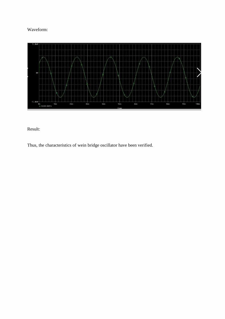
Waveform:
Result:
Thus, the characteristics of wein bridge oscillator have been verified.

7. Study of VHDL and Verilog
AIM:
To study the various VHDL commands.
DESCRIPTION:
1. Getting started with Xilinx: Start Xilinx ISE from the start menu by selecting start programs,
Xilinx ISE 14.7 project navigator
2. Creating a new project
A project in ISE is a collection of al files that are necessary to create and download a design to
the selected device
1. To create a new project, select file/new project
2. In the new project wizard dialog box, type the desired location in the project location field
3. Use the pull-down arrow to select HDL from the top-level module type field. Click in the
field to access the pull-down list and click next
4. In the new project wizard device and design flow dialog box, use the pull-down arrow to
select value for each property name
Service family: Spartan 3E
Device: XC3S500E
Package: CPG132

Speed: -4
Synthesis tool: XST (VHDL/Verilog)
Simulator: ISE (VHDL/Verilog)
Generated simulation Language: VHDL
5. Click next
6. Click new source in new project wizard create a new source dialog box to add one new
source to your project. Click VHDL module as the source type. Type in file name, click next
7. Click new source next in the define VHDL source dialog box. Click next in the new project
wizard add existing source dialog box and click finish.
3. Synthesize a program:
To synthesize a program or to check syntax, in the process window click the synthesis XST+
symbol and expand it then double click the syntax. Tick mark will appear in green colour when
no errors are detected in the program.
4. Simulate a program:
1. Click create new source in process window to open new source dialog box, before that select
behavioural implementation in the source window list icon and in the new source dialog box
select text bench waveform and type the file name and click next.

2. Select the source for which the test bench waveform to be generated from “Select” window
and then click next and click finish the test bench waveform file was added to project
3. Click OK to accept the default timing constraints. HDL bench opens within the project
navigator frame work
4. Set the I/p values for the project by clicking on I/p waveforms by marking them low or high
5. Then save file and close waveform editor
6. To simulate the program select text, gates flow in source window. Click + beside the ISE
simulator to expand the library hierarchy in process window
7. Waveform window: Display the output waveform for specification.
5. Implement design:
1. Click create new source in process window to open new source dialog box and select
implementation constraints files and click next.
2. Select the source for which the implementation constraint file to be written from select
window.
3. Select gates-VCF in the source window click then + beside user constraints to expand the
hierarchy in the process.
4. Double click implement design in the process window.
Result: Thus the study of VHDL and its commands has been done.

8. IMPLEMENTATION OF FULL ADDER
AIM:
To verify and implement full adder using Xilinx ISE simulator software.
SYSTEM REQUIREMENTS: Xilinx ISE simulator software, PC with High configuration
ALGORITHM FOR FULL ADDER:
1. Select a new project
2. Declare the entity full adder and also declare the i/p and o/p variables
3. Begin the architecture data flow of full adder
4. Addition is performed and sum is given by a-in xor B-in xor carry, and carry is given by (a-
in and b-in) or (b-in and c-in) or (c-in and a-in)
5. Find the architecture dataflow.
Synthesize the program and create test bench waveform and then simulate the program to
predict output.

FULL ADDER:
library IEEE;
use IEEE.STD_LOGIC_1164.ALL;
use IEEE.STD_LOGIC_ARITH.ALL;
use IEEE.STD_LOGIC_UNSIGNED.ALL;
entityfull_adder is
Port ( a : in STD_LOGIC; b : in STD_LOGIC;
c : in STD_LOGIC; carry : out STD_LOGIC; sum : out STD_LOGIC);
endfull_adder;
architecture Behavioral of full_adder is
begin
sum<=a xor b xor c;
carry<=(a and b) or (b and c) or (c and a);
endBehavioral;

Output:
RESULT:
Thus, the Full adder Circuit has been simulated with the truth table by using Xilinx ISE
Simulator.

9. IMPLEMENTATION OF 8 BIT ADDER
AIM:
To Simulate the 8-bit Adder (RIPPLE CARRY ADDER) with the tools available in Xilinx
Project Navigator using Verilog.
SYSTEM REQUIREMENTS:
Xilinx ISE simulator software
ALGORITHM:
Double click the project navigator and select the option
1 File-New project.
2 Give the project name.
3 Select VHDL module.
4 Type your VHDL coding.
5 Check for syntax.
6 Select the new source of test bench waveform and choose behavioural simulation and
simulate it by Xilinx ISE simulator.
7 Verify the output.

Program
module ripplecarryadder(s,cout,a,b,cin);
output[7:0]s;
output cout;
input[7:0]a,b;
input cin;
wire c1,c2,c3,c4,c5,c6,c7;
fulladd fa0(s[0],c1,a[0],b[0],cin);
fulladd fa1(s[1],c2,a[1],b[1],c1);
fulladd fa2(s[2],c3,a[2],b[2],c2);
fulladd fa3(s[3],c4,a[3],b[3],c3);
fulladd fa4(s[4],c5,a[4],b[4],c4);
fulladd fa5(s[5],c6,a[5],b[5],c5);
fulladd fa6(s[6],c7,a[6],b[6],c6);
fulladd fa7(s[7],cout,a[7],b[7],c7);
endmodule
module fulladd(s,cout,a,b,cin);
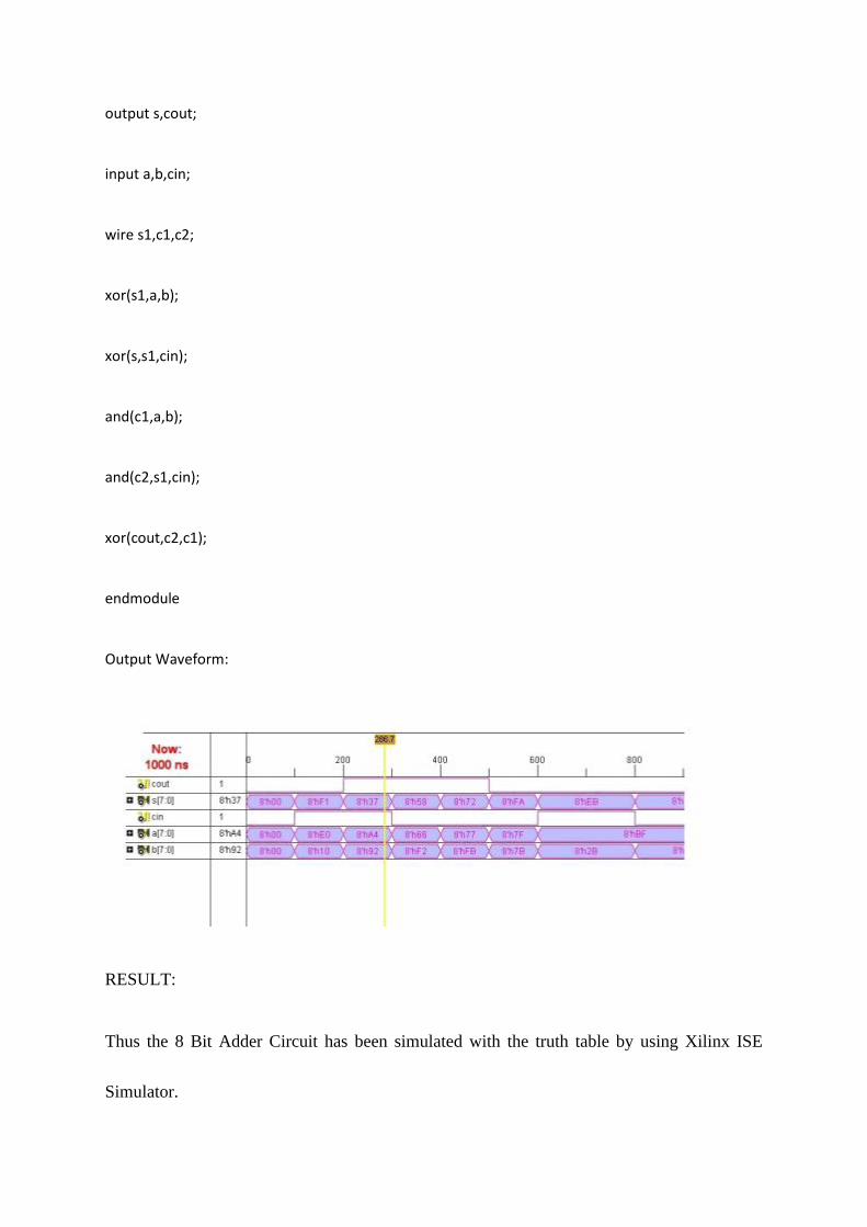
output s,cout;
input a,b,cin;
wire s1,c1,c2;
xor(s1,a,b);
xor(s,s1,cin);
and(c1,a,b);
and(c2,s1,cin);
xor(cout,c2,c1);
endmodule
Output Waveform:
RESULT:
Thus the 8 Bit Adder Circuit has been simulated with the truth table by using Xilinx ISE
Simulator.

10. RIPPLE COUNTER
Aim:
To Simulate the ripple counter with the tools available in Xilinx Project Navigator using
Verilog.
Facilities Required:) Xilinx (ISE) simulator 14.1
Procedure:
Double click the project navigator and select the option
1 File-New project.
2 Give the project name.
3 Select VHDL module.
4 Type your VHDL coding.
5 Check for syntax.
6 Select the new source of test bench waveform
Choose behavioural simulation and simulate it by Xilinx ISE simulator.
7 Verify the output.

VERILOG SOURSE CODE: //Structural description of Ripple Counter
module ripplecounter(A0,A1,A2,A3,COUNT,RESET);
output A0,A1,A2,A3;
input COUNT,RESET;
//Instantiate Flip-Flop
FF F0(A0,COUNT,RESET);
FF F1(A1,A0,RESET);
FF F2(A2,A1,RESET);
FF F3(A3,A2,RESET)
endmodule
//Description of Flip-Flop
module FF(Q,CLK,RESET);
output Q;
input CLK,RESET;
reg Q;
always @(negedge CLK or negedge RESET)
if(~RESET)
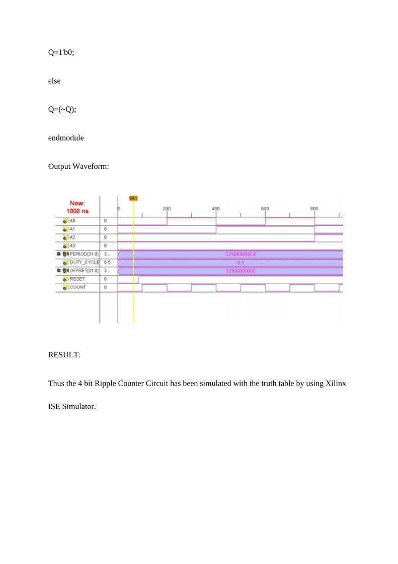
Q=1'b0;
else
Q=(~Q);
endmodule
Output Waveform:
RESULT:
Thus the 4 bit Ripple Counter Circuit has been simulated with the truth table by using Xilinx
ISE Simulator.