controlled ti seed layer assisted growth and field emission properties of pb(zr 0.52 ti 0.48 )o 3...
TRANSCRIPT

Controlled Ti Seed Layer Assisted Growth and Field EmissionProperties of Pb(Zr0.52Ti0.48)O3 Nanowire ArraysAnuja Datta,*,† Devajyoti Mukherjee,†,‡ Mahesh Hordagoda,‡ Sarath Witanachchi,†,‡
and Pritish Mukherjee†,‡
†Florida Cluster for Advanced Smart Sensor Technologies and Department of Physics, ‡Center for Integrated Functional Materialsand Department of Physics, University of South Florida, Tampa, Florida 33620, United States
Ranjit V. Kashid,§ Mahendra A. More,§ Dilip S. Joag,§ and Padmakar G. Chavan⊥
§Centre for Advanced Studies in Materials Science and Condensed Matter Physics, Department of Physics, University of Pune, Pune411007, India⊥Department of Physics, School of Physical Sciences, North Maharashtra University, Jalgaon 425 001, India
ABSTRACT: We report on the directed upright growth of ferroelectric (FE)Pb(Zr0.52Ti0.48)O3 (PZT) nanowire (NW) arrays with large aspect ratios of >60using a Ti seed layer assisted hydrothermal process over large surface areas on ITO/glass substrates. In a two-step growth process, Ti seed layer of low surfaceroughness with a thickness of ∼500 nm and grain size of ∼100 nm was firstdeposited by radio frequency (RF) sputtering which was subsequently used assubstrates for the growth of highly dense, single crystalline PZT NWs by controllednucleation. The electron emission properties of the PZT NWs were investigatedusing the as-grown NWs as FE cathodes. A low turn-on field of ∼3.4 V/μm wasobtained from the NW arrays, which is impressively lower than that from otherreported values. The results reported in this work give direction to the developmentof a facile growth technique for PZT NWs over large surfaces and also are of interest to the generation of high current electronbeam from FE NW based cathodes for field emitter applications.
KEYWORDS: PZT, nanowires, hydrothermal, field emission, ferroelectric
■ INTRODUCTION
Ferroelectric (FE) perovskite oxides continue to be animportant class of materials because of their high dielectricand piezoelectric coefficients and switchable nonvolatilepolarization properties.1−4 Among the state-of-the-art perov-skite oxide materials, lead zirconium titanate with the specificcomposition of Pb(Zr0.52Ti0.48)O3 (PZT) exhibits the highestpiezo and ferro-coefficients and is of great technological interestfor applications as piezoelectric transducers, pyroelectricsensors, high-dielectric capacitors, and nonvolatile memorydevices.5−8 Most frequently, PZT is used in the form of singlecrystals, polycrystalline bulk ceramics, and thin films inmicroelectronics devices4,9,10 and in miniaturized FE randomaccess memory (FRAM) devices.11−13
One-dimensional (1D) nanostructures such as nanowires(NWs) with tunable size, morphology, phase, and crystallo-graphic orientation have become the focus of intensive researchowing to their unique diameter and orientation dependentelectrical properties.14,15 Due to the novel and improvedproperties, 1D nanostructures therefore have intrinsic prioritiesover conventional thin films and PZT is not far behind.8,16−25
Recent research activities on PZT 1D nanostructures haveindicated huge enhancement of piezoelectric properties useful
for sustainable micro/nanopowering sources.8,16−25 FE PZTnanotubes with controlled orientation were reported to beattractive candidates for next-generation nonvolatile randomaccess memories.19 In order to have exciting opportunities offundamental research and innovative applications of PZTnanostructures, the development of a facile method is necessaryfor fabricating high quality, low dimensional nanostructuresover large areas. However, to date large-scale fabricationmethods of PZT nanostructures have been restricted inaccessibility due to their complicated methodologies andhigh-cost. So far, PZT NWs8 and nanotubes19 have beenselectively grown by hydrothermal processes and a combinedtemplate-directed sol−gel method with a spin-coating techni-que on Nb doped strontium titanium oxide (SrTiO3:Nb)
8 andplatinized silicon substrates,19 respectively. These methods areindeed compelling, but alternative low cost, easily accessiblemethods that can be used to grow PZT 1D nanostructures overlarge surface areas are required to be explored that may expandthe outreach of probes for understanding the structure−
Received: April 8, 2013Accepted: June 11, 2013Published: June 11, 2013
Research Article
www.acsami.org
© 2013 American Chemical Society 6261 dx.doi.org/10.1021/am4012879 | ACS Appl. Mater. Interfaces 2013, 5, 6261−6267

property relations in PZT nanostructures for future advance-ment in memory technologies.Demonstration of nanostructure based FE field emitters have
been the center of attention because of their technologicalimportance in fabrication of various devices such as flat paneldisplays, electron sources in vacuum microelectronics, and soforth.26,27 Quantum tunnelling of injected electrons from thematerials surface into vacuum under the influence of strongelectrostatic field (106−107 V/cm) is called field emission.Nanostructured FE field emitters show capability to deliverhigh emission current density with excellent current stabilityand low turn-on voltage.26 Numerous 1D nanostructures havebeen synthesized and studied as field emitters with a view toobtain a large current density at relatively lower appliedvoltages.28−37 Traditional FE materials hold promise to be usedas excellent electron sources due to the inversion of thespontaneous polarization in these materials.38 Since electronsand holes are present on both sides of a FE material tocompensate for the spontaneous polarization, it is predictedthat a high density of compensated electrons could be emittedfrom the FE materials’ surface under an external applied field.38
It was understood that the FE field emitters may offer a sourceof high current density electron beams for applications wherethe use of conventional cathodes is limited by the requiredcurrent density, cathode poisoning, or lifetime.38 There is nowconsiderable interest in the FE cathodes as electron sources forlow power devices such as emissive flat panel displays. Fieldemission studies of FE materials have been investigated byvarious groups.39,40 However, the voltages needed to produceelectron emission from existing FE cathodes are still in therange of hundreds to thousand of volts. Early observations ofelectron emission were reported by Belayev and Bendrikova.41
Subsequently, electron emission was investigated in various FEmaterials, including LiNbO3 and LiTaO3.
42,43 The emissioncurrent density observed from all of the above-mentionedmaterials was <10−9 A/cm2, which is practically too low formany device applications such as electron sources for electronaccelerators and flat panel displays. To this end, PZT with itsexcellent piezoelectric and FE properties offers to act as a finiteelectron source. During the past few years, the volume ofliterature on electron emission from PZT surfaces has increasedrapidly.39,42−48 Recently field emission current has been
reported from PZT nanoemitters which were prepared bycoating nanometer thick PZT films on single-crystal siliconislands.48 However, to our knowledge, field emission behaviorof as-grown PZT nanostructures has not yet been investigated.In the present work, we report on the optimized growth of
PZT NWs by a Ti seed layer assisted hydrothermal methodusing an integrated sputtering technique and hydrothermalprocess on indium titanium oxide (ITO) coated glass substrates(ITO/glass). The presence of Ti seed layer triggers theformation of PZT nanoislands (or nucleation sites) and ensuresthe formation of PZT NWs over a large surface area with well-controlled dimensions. Unlike other reported PZT NWs oneither Ti foils,20 which makes it unsuitable for deviceapplications or on expensive STO:Nb substrates,8 our approachensures uniform and dense growth of PZT NWs overinexpensive glass substrates making them highly desirable forindustrial customization. Second, the prepared PZT NWs havebeen investigated for potential field emission properties toprovide a basic understanding of the electron emission behaviorof PZT NW FE electrode surface. Due the smaller tip apexradius, PZT NWs are found to be quite suitable for fieldemission application as were reported for other 1Dnanostructures.26,27,31−35
■ EXPERIMENTAL SECTIONTi Seed Layer Deposition. We chose ITO coated sodalime glass
as the substrate for the deposition of Ti seed layer and the subsequentgrowth of PZT NW arrays from them. It was noticed that the presenceof ITO coating helped in the deposition of uniformly thick Ti layer onthe glass substrate, which was otherwise not obtained on uncoatedglass substrates. A radio frequency (RF) sputtering technique was usedto deposit a thin layer of Ti seed layer on the substrates (Figure 1a,lower panel). Before Ti sputtering, the ITO/glass substrates werecleaned by ultrasonic bath using acetone, methanol and water, and N2
dried in vacuum. Ti seed layer was deposited using a CRC-100sputtering system (Plasma Sciences Inc.) with an ambient Ar gaspressure of 5 mTorr. Two deposition cycles each for 10 min were runby varying current from 100 to 150 mA to finally deposit 500 nm thickTi particulate films. Deposition parameters (voltage, time and current)were optimized in order to grow uniformly thick, crack-freecontinuous Ti metal film. After each deposition, Ti seed layer wascharacterized by X-ray diffraction (XRD), performed by Bruker AXS
Figure 1. (a) Upper panel experimental setup with the suspended Ti/ITO/glass substrates inserted inside the Teflon chamber in a typicalhydrothermal reaction process. Lower panel photographs of the Ti/ITO/glass substrate and the final PZT NWs product on the same. (b) XRDspectra of the Ti/ITO/glass and PZT NWs on the same. ITO substrate peaks (*) and the Ti peaks (#) are shown in the Ti/ITO/glass spectrum.The (111) peak in the PZT NW XRD spectrum is deconvoluted to show the Ti bottom layer peak and the PZT peak in log scale. Standard databaseof PZT (green bar) and Ti (red bar) are also shown for comparison.
ACS Applied Materials & Interfaces Research Article
dx.doi.org/10.1021/am4012879 | ACS Appl. Mater. Interfaces 2013, 5, 6261−62676262
D8 diffractometer equipped with Lynx Eye position-sensitive detectorand atomic force microscopy (AFM by Digital Instruments).PZT NW Growth. All chemicals were used as is with a minimum of
99.99% ACS grade. Growth of PZT nanowire arrays were conductedon Ti seed layers using a hydrothermal process similar to thatdescribed by Lin et al.20 In a typical synthesis process, the reactionsolution was prepared by mixing 2 mmol of Ti−n-butoxide(Ti(OCH2CH2CH2CH3)4) dissolved in 25 mL ethanol, and astoichiometric amount of hydrated zirconium chloride(ZrOCl2·8H2O) dissolved in 25 mL deionized water, separately. Tiion containing ethanol solution was then added slowly into the Zr ioncontaining aqueous solution under vigorous stirring. In the next step,200 mL of NH4OH solution containing 28−30% of NH3 was added tothis mixture that resulted in a precipitation of intermediate hydroxidephase (Zr0.52Ti0.48O(OH)2). The precipitate was washed andcentrifuged several times with water and ethanol in order to removeunreacted chemicals and ionic byproducts. After thorough cleaning,the hydroxide precipitate was redispersed in 36 mL of deionized water.To this solution stoichiometric quantity of hydrated lead nitratePb(NO3)2·8H2O, 0.02 g PVA (poly(vinyl alcohol)), and 0.4 g PAA(poly(acrylic acid)) were added successively. Required quantity ofKOH pellets was added to this mixture to maintain an alkaline pH of∼12. This final growth solution was put into a Teflon linedhydrothermal vessel. Ti seed layer deposited ITO/glass substrateswere suspended freely midway inside the Teflon chamber using acustom designed clip-on Teflon holder (Figure 1a, upper panel). Thehydrothermal reactants were then sealed and placed in the preheatedoven at 200 °C for 16 h. After completion of the reaction, the chamberwas air cooled and the substrates were cleaned with deionized waterand ethanol. The presence of uniform, thin white layers on thesubstrates were indicative of the growth of PZT NWs (Figure 1a,lower panel). Microstructural characterization of PZT NWs wascarried out by scanning electron microscopy (SEM, JEOL JSM 6390LV) and high resolution transmission electron microscopy (TEM-HRTEM, FEI Tecnai F20 S-Twin TEM). Composition analysis wasdone by energy-dispersive X-ray spectroscopy (EDS, Oxford Instru-ments INCAX sight) equipped with the SEM. For TEM measure-ments, the PZT NWs were carefully scrapped out and then dispersedin isopropyl alcohol. A few drops of this solution were then depositedon a carbon coated copper grid and air-dried.Field Emission Measurement. The field emission current
density−applied field (J−E) and current−time (I−t) measurementswere carried in all metal field emission microscope. The field emissionstudies were carried out in a “close proximity” (also termed as “planardiode”) configuration, wherein the PZT NW arrays grown on to theITO/glass substrate served as the cathode and a semitransparentcathodoluminescent phosphor screen as the anode. Provision of backcontact was done using highly conducting carbon tape from copperrod, and this whole assembly was held in front of the anode (screen) ata distance of ∼1 mm. The working chamber was evacuated using anultrahigh vacuum system comprising of a rotary-backed turbomolecular pump, a sputter ion pump, and a titanium sublimationpump. The cathode (PZT NWs) did not show any appreciabledegassing and vacuum could be obtained with usual speed. Afterbaking the system at 150 °C for 8 h, a base pressure of ∼1 × 10⁻⁸
mbar was obtained. The J−E measurement was carried out at this basepressure using a Keithley 485 Picoammeter and a Spellman highvoltage DC power supply. Special care was taken to avoid any leakagecurrent by using shielded cables with proper grounding.
■ RESULTS AND DISCUSSIONRepresentative XRD spectra of the Ti coated ITO/glass (Ti/ITO/glass) substrates and that of the PZT NWs deposited onTi coated ITO/glass are shown in Figure 1b. Standard XRDpatterns for Ti (JCPDS card: 00-044-1294) and tetragonal PZT(JCPDS card: 01-070-4060) are shown for comparison. Both Ticoated ITO/glass and the PZT NWs samples show polycrystal-line patterns without any preferential orientation. The XRDpatterns indicate that the samples are phase pure with no peaks
from secondary phase formation within the resolution limits ofthe XRD. Absence of most of the Ti and ITO peaks in the XRDpattern of the PZT NW sample is suggestive of the denselycovered growth of the NWs on the substrate. Since the 2θ valueof the (111) peak in tetragonal PZT closely matches with thatof the (112) plane in hexagonal Ti, we deconvoluted the (111)XRD peak of PZT NW pattern. Two peaks, one for the Ti andthe other for the PZT, were observed after deconvolution(shown in log scale in the inset to Figure 1b). The ratio of thenormalized intensities of the Ti/PZT peaks is as low as ∼0.005which indicates good coverage of the NWs in the sample.Surface morphology of the Ti coating after sputtering was
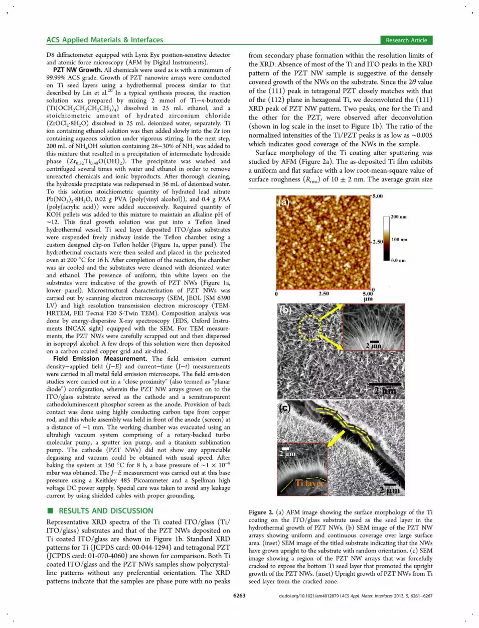
studied by AFM (Figure 2a). The as-deposited Ti film exhibitsa uniform and flat surface with a low root-mean-square value ofsurface roughness (Rrms) of 10 ± 2 nm. The average grain size
Figure 2. (a) AFM image showing the surface morphology of the Ticoating on the ITO/glass substrate used as the seed layer in thehydrothermal growth of PZT NWs. (b) SEM image of the PZT NWarrays showing uniform and continuous coverage over large surfacearea. (inset) SEM image of the titled substrate indicating that the NWshave grown upright to the substrate with random orientation. (c) SEMimage showing a region of the PZT NW arrays that was forcefullycracked to expose the bottom Ti seed layer that promoted the uprightgrowth of the PZT NWs. (inset) Upright growth of PZT NWs from Tiseed layer from the cracked zone.
ACS Applied Materials & Interfaces Research Article
dx.doi.org/10.1021/am4012879 | ACS Appl. Mater. Interfaces 2013, 5, 6261−62676263
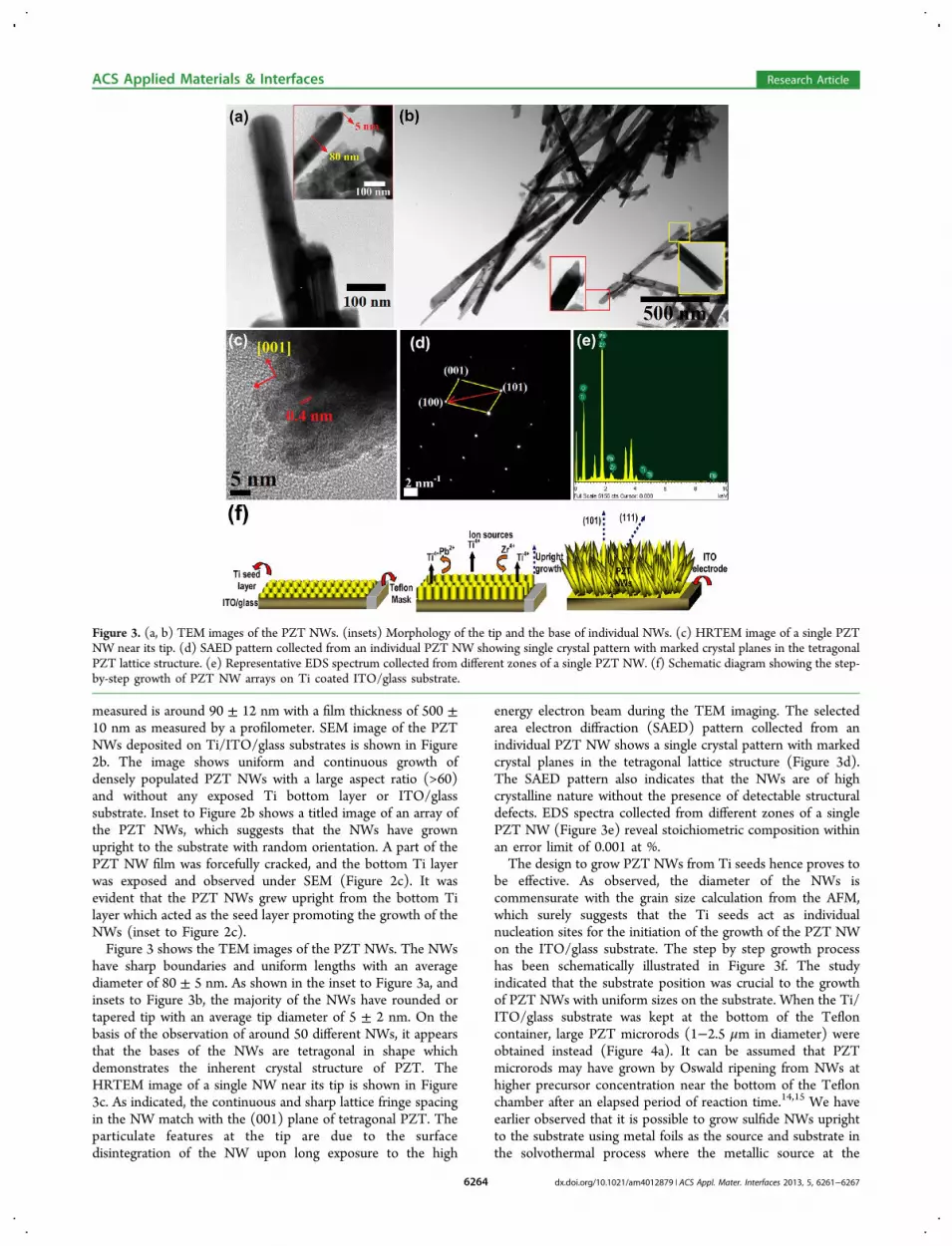
measured is around 90 ± 12 nm with a film thickness of 500 ±10 nm as measured by a profilometer. SEM image of the PZTNWs deposited on Ti/ITO/glass substrates is shown in Figure2b. The image shows uniform and continuous growth ofdensely populated PZT NWs with a large aspect ratio (>60)and without any exposed Ti bottom layer or ITO/glasssubstrate. Inset to Figure 2b shows a titled image of an array ofthe PZT NWs, which suggests that the NWs have grownupright to the substrate with random orientation. A part of thePZT NW film was forcefully cracked, and the bottom Ti layerwas exposed and observed under SEM (Figure 2c). It wasevident that the PZT NWs grew upright from the bottom Tilayer which acted as the seed layer promoting the growth of theNWs (inset to Figure 2c).Figure 3 shows the TEM images of the PZT NWs. The NWs
have sharp boundaries and uniform lengths with an averagediameter of 80 ± 5 nm. As shown in the inset to Figure 3a, andinsets to Figure 3b, the majority of the NWs have rounded ortapered tip with an average tip diameter of 5 ± 2 nm. On thebasis of the observation of around 50 different NWs, it appearsthat the bases of the NWs are tetragonal in shape whichdemonstrates the inherent crystal structure of PZT. TheHRTEM image of a single NW near its tip is shown in Figure3c. As indicated, the continuous and sharp lattice fringe spacingin the NW match with the (001) plane of tetragonal PZT. Theparticulate features at the tip are due to the surfacedisintegration of the NW upon long exposure to the high
energy electron beam during the TEM imaging. The selectedarea electron diffraction (SAED) pattern collected from anindividual PZT NW shows a single crystal pattern with markedcrystal planes in the tetragonal lattice structure (Figure 3d).The SAED pattern also indicates that the NWs are of highcrystalline nature without the presence of detectable structuraldefects. EDS spectra collected from different zones of a singlePZT NW (Figure 3e) reveal stoichiometric composition withinan error limit of 0.001 at %.The design to grow PZT NWs from Ti seeds hence proves to
be effective. As observed, the diameter of the NWs iscommensurate with the grain size calculation from the AFM,which surely suggests that the Ti seeds act as individualnucleation sites for the initiation of the growth of the PZT NWon the ITO/glass substrate. The step by step growth processhas been schematically illustrated in Figure 3f. The studyindicated that the substrate position was crucial to the growthof PZT NWs with uniform sizes on the substrate. When the Ti/ITO/glass substrate was kept at the bottom of the Tefloncontainer, large PZT microrods (1−2.5 μm in diameter) wereobtained instead (Figure 4a). It can be assumed that PZTmicrorods may have grown by Oswald ripening from NWs athigher precursor concentration near the bottom of the Teflonchamber after an elapsed period of reaction time.14,15 We haveearlier observed that it is possible to grow sulfide NWs uprightto the substrate using metal foils as the source and substrate inthe solvothermal process where the metallic source at the
Figure 3. (a, b) TEM images of the PZT NWs. (insets) Morphology of the tip and the base of individual NWs. (c) HRTEM image of a single PZTNW near its tip. (d) SAED pattern collected from an individual PZT NW showing single crystal pattern with marked crystal planes in the tetragonalPZT lattice structure. (e) Representative EDS spectrum collected from different zones of a single PZT NW. (f) Schematic diagram showing the step-by-step growth of PZT NW arrays on Ti coated ITO/glass substrate.
ACS Applied Materials & Interfaces Research Article
dx.doi.org/10.1021/am4012879 | ACS Appl. Mater. Interfaces 2013, 5, 6261−62676264
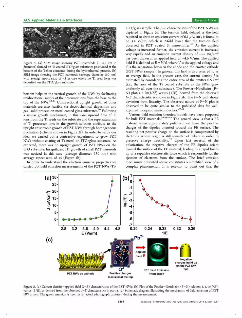
bottom helps in the vertical growth of the NWs by facilitatingunidirectional supply of the precursor ions from the base to thetop of the NWs.32,49 Unidirectional upright growth of othermaterials are also feasible via electrochemical deposition andgas−solid process on metal coated glass substrates.50 Followinga similar growth mechanism, in this case, upward flow of Tiions from the Ti seeds on the substrate and the supersaturationof Ti precursor ions in the growth solution attribute to theupright anisotropic growth of PZT NWs through homogeneousnucleation (scheme shown in Figure 3f). In order to verify ouridea, we carried out a contrastive experiment to grow PZTNWs without coating of Ti metal on ITO/glass substrate. Asexpected, there was no upright growth of PZT NWs on theITO substrate. Insignificant 1D growth of small PZT nanorodswas noticed in this case (average diameter 150 nm) withaverage aspect ratio of <5 (Figure 4b).In order to understand the electron emissive properties we
carried out field emission measurements of the PZT NWs/Ti/
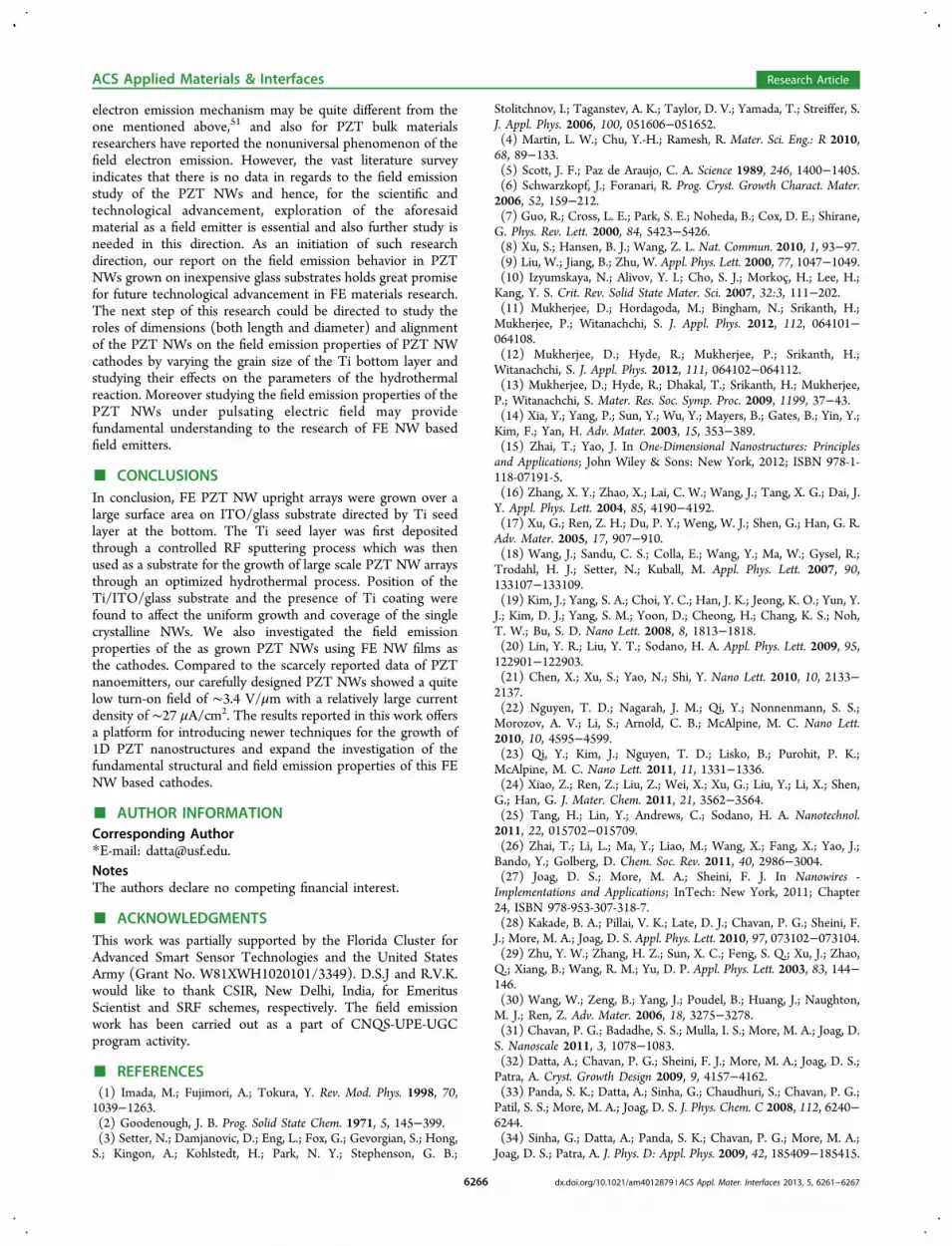
ITO/glass sample. The J−E characteristics of the PZT NWs aredepicted in Figure 5a. The turn-on field, defined as the fieldrequired to draw an emission current of 0.1 μA/cm2, is found tobe 3.4 V/μm, which is 2-fold lower that the turn-on fieldobserved in PZT coated Si nanoemitter.48 As the appliedvoltage is increased further, the emission current is increasedvery rapidly and an emission current density of ∼27 μA/cm2
has been drawn at an applied field of ∼4.6 V/μm. The appliedfield E is defined as E = V/d, where V is the applied voltage andd is the separation between the anode and the emitter cathode(PZT NWs sample). In general, this field is also referred to asan average field. In the present case, the current density J isestimated by considering the entire area of the emitter 0.5 cm2
(i.e., the area of the Ti coated substrate as the NWs grewuniformly all over the substrate). The Fowler−Nordheim (F−N) plot, i. e. ln(J/E2) versus (1/E), derived from the observedJ−E characteristic is shown in Figure 5b. The F−N plot showsdeviation from linearity. The observed nature of F−N plot isobserved to be quite similar to the published data for well-explored inorganic semiconductors.29,31
Various field emission theories/models have been proposedfor bulk PZT materials.39,44−48 The general view is that a FEmaterial when appropriately polarized will have the positivecharges of the dipoles oriented toward the FE surface. Theresulting net positive charge on the surface is compensated byelectrons, whose origin is still a matter of debate in order topreserve charge neutrality.32 Upon fast reversal of thepolarization, the negative charges of the FE dipoles orienttoward the surface of the FE material, leading to a rapid build-up of a repulsive electrostatic force which is responsible for theejection of electrons from the surface. The brief emissionmechanism presented above constitutes a simplified view of acomplex phenomenon. It is relevant to point out that the
Figure 4. (a) SEM image showing PZT microrods (1−2.5 μm indiameter) formed on Ti coated ITO/glass substrates positioned at thebottom of the Teflon container during the hydrothermal process. (b)SEM image showing the PZT nanorods (average diameter 150 nm)with average aspect ratio of <5 in case where no Ti seed layer wasdeposited on the ITO/glass substrate.
Figure 5. (a) Current density−applied field (J−E) characteristics of the PZT NWs. (b) Plot of the Fowler−Nordheim (F−N) relation, i. e. ln(J/E2)versus (1/E), as derived from the observed J−E characteristics in part a. (c) Schematic diagram illustrating the mechanism of field emission of PZTNW arrays. The green emission is seen in an actual photograph captured during the measurement.
ACS Applied Materials & Interfaces Research Article
dx.doi.org/10.1021/am4012879 | ACS Appl. Mater. Interfaces 2013, 5, 6261−62676265
electron emission mechanism may be quite different from theone mentioned above,51 and also for PZT bulk materialsresearchers have reported the nonuniversal phenomenon of thefield electron emission. However, the vast literature surveyindicates that there is no data in regards to the field emissionstudy of the PZT NWs and hence, for the scientific andtechnological advancement, exploration of the aforesaidmaterial as a field emitter is essential and also further study isneeded in this direction. As an initiation of such researchdirection, our report on the field emission behavior in PZTNWs grown on inexpensive glass substrates holds great promisefor future technological advancement in FE materials research.The next step of this research could be directed to study theroles of dimensions (both length and diameter) and alignmentof the PZT NWs on the field emission properties of PZT NWcathodes by varying the grain size of the Ti bottom layer andstudying their effects on the parameters of the hydrothermalreaction. Moreover studying the field emission properties of thePZT NWs under pulsating electric field may providefundamental understanding to the research of FE NW basedfield emitters.
■ CONCLUSIONSIn conclusion, FE PZT NW upright arrays were grown over alarge surface area on ITO/glass substrate directed by Ti seedlayer at the bottom. The Ti seed layer was first depositedthrough a controlled RF sputtering process which was thenused as a substrate for the growth of large scale PZT NW arraysthrough an optimized hydrothermal process. Position of theTi/ITO/glass substrate and the presence of Ti coating werefound to affect the uniform growth and coverage of the singlecrystalline NWs. We also investigated the field emissionproperties of the as grown PZT NWs using FE NW films asthe cathodes. Compared to the scarcely reported data of PZTnanoemitters, our carefully designed PZT NWs showed a quitelow turn-on field of ∼3.4 V/μm with a relatively large currentdensity of ∼27 μA/cm2. The results reported in this work offersa platform for introducing newer techniques for the growth of1D PZT nanostructures and expand the investigation of thefundamental structural and field emission properties of this FENW based cathodes.
■ AUTHOR INFORMATIONCorresponding Author*E-mail: [email protected] authors declare no competing financial interest.
■ ACKNOWLEDGMENTSThis work was partially supported by the Florida Cluster forAdvanced Smart Sensor Technologies and the United StatesArmy (Grant No. W81XWH1020101/3349). D.S.J and R.V.K.would like to thank CSIR, New Delhi, India, for EmeritusScientist and SRF schemes, respectively. The field emissionwork has been carried out as a part of CNQS-UPE-UGCprogram activity.
■ REFERENCES(1) Imada, M.; Fujimori, A.; Tokura, Y. Rev. Mod. Phys. 1998, 70,1039−1263.(2) Goodenough, J. B. Prog. Solid State Chem. 1971, 5, 145−399.(3) Setter, N.; Damjanovic, D.; Eng, L.; Fox, G.; Gevorgian, S.; Hong,S.; Kingon, A.; Kohlstedt, H.; Park, N. Y.; Stephenson, G. B.;
Stolitchnov, I.; Taganstev, A. K.; Taylor, D. V.; Yamada, T.; Streiffer, S.J. Appl. Phys. 2006, 100, 051606−051652.(4) Martin, L. W.; Chu, Y.-H.; Ramesh, R. Mater. Sci. Eng.: R 2010,68, 89−133.(5) Scott, J. F.; Paz de Araujo, C. A. Science 1989, 246, 1400−1405.(6) Schwarzkopf, J.; Foranari, R. Prog. Cryst. Growth Charact. Mater.2006, 52, 159−212.(7) Guo, R.; Cross, L. E.; Park, S. E.; Noheda, B.; Cox, D. E.; Shirane,G. Phys. Rev. Lett. 2000, 84, 5423−5426.(8) Xu, S.; Hansen, B. J.; Wang, Z. L. Nat. Commun. 2010, 1, 93−97.(9) Liu, W.; Jiang, B.; Zhu, W. Appl. Phys. Lett. 2000, 77, 1047−1049.(10) Izyumskaya, N.; Alivov, Y. I.; Cho, S. J.; Morkoc,̧ H.; Lee, H.;Kang, Y. S. Crit. Rev. Solid State Mater. Sci. 2007, 32:3, 111−202.(11) Mukherjee, D.; Hordagoda, M.; Bingham, N.; Srikanth, H.;Mukherjee, P.; Witanachchi, S. J. Appl. Phys. 2012, 112, 064101−064108.(12) Mukherjee, D.; Hyde, R.; Mukherjee, P.; Srikanth, H.;Witanachchi, S. J. Appl. Phys. 2012, 111, 064102−064112.(13) Mukherjee, D.; Hyde, R.; Dhakal, T.; Srikanth, H.; Mukherjee,P.; Witanachchi, S. Mater. Res. Soc. Symp. Proc. 2009, 1199, 37−43.(14) Xia, Y.; Yang, P.; Sun, Y.; Wu, Y.; Mayers, B.; Gates, B.; Yin, Y.;Kim, F.; Yan, H. Adv. Mater. 2003, 15, 353−389.(15) Zhai, T.; Yao, J. In One-Dimensional Nanostructures: Principlesand Applications; John Wiley & Sons: New York, 2012; ISBN 978-1-118-07191-5.(16) Zhang, X. Y.; Zhao, X.; Lai, C. W.; Wang, J.; Tang, X. G.; Dai, J.Y. Appl. Phys. Lett. 2004, 85, 4190−4192.(17) Xu, G.; Ren, Z. H.; Du, P. Y.; Weng, W. J.; Shen, G.; Han, G. R.Adv. Mater. 2005, 17, 907−910.(18) Wang, J.; Sandu, C. S.; Colla, E.; Wang, Y.; Ma, W.; Gysel, R.;Trodahl, H. J.; Setter, N.; Kuball, M. Appl. Phys. Lett. 2007, 90,133107−133109.(19) Kim, J.; Yang, S. A.; Choi, Y. C.; Han, J. K.; Jeong, K. O.; Yun, Y.J.; Kim, D. J.; Yang, S. M.; Yoon, D.; Cheong, H.; Chang, K. S.; Noh,T. W.; Bu, S. D. Nano Lett. 2008, 8, 1813−1818.(20) Lin, Y. R.; Liu, Y. T.; Sodano, H. A. Appl. Phys. Lett. 2009, 95,122901−122903.(21) Chen, X.; Xu, S.; Yao, N.; Shi, Y. Nano Lett. 2010, 10, 2133−2137.(22) Nguyen, T. D.; Nagarah, J. M.; Qi, Y.; Nonnenmann, S. S.;Morozov, A. V.; Li, S.; Arnold, C. B.; McAlpine, M. C. Nano Lett.2010, 10, 4595−4599.(23) Qi, Y.; Kim, J.; Nguyen, T. D.; Lisko, B.; Purohit, P. K.;McAlpine, M. C. Nano Lett. 2011, 11, 1331−1336.(24) Xiao, Z.; Ren, Z.; Liu, Z.; Wei, X.; Xu, G.; Liu, Y.; Li, X.; Shen,G.; Han, G. J. Mater. Chem. 2011, 21, 3562−3564.(25) Tang, H.; Lin, Y.; Andrews, C.; Sodano, H. A. Nanotechnol.2011, 22, 015702−015709.(26) Zhai, T.; Li, L.; Ma, Y.; Liao, M.; Wang, X.; Fang, X.; Yao, J.;Bando, Y.; Golberg, D. Chem. Soc. Rev. 2011, 40, 2986−3004.(27) Joag, D. S.; More, M. A.; Sheini, F. J. In Nanowires -Implementations and Applications; InTech: New York, 2011; Chapter24, ISBN 978-953-307-318-7.(28) Kakade, B. A.; Pillai, V. K.; Late, D. J.; Chavan, P. G.; Sheini, F.J.; More, M. A.; Joag, D. S. Appl. Phys. Lett. 2010, 97, 073102−073104.(29) Zhu, Y. W.; Zhang, H. Z.; Sun, X. C.; Feng, S. Q.; Xu, J.; Zhao,Q.; Xiang, B.; Wang, R. M.; Yu, D. P. Appl. Phys. Lett. 2003, 83, 144−146.(30) Wang, W.; Zeng, B.; Yang, J.; Poudel, B.; Huang, J.; Naughton,M. J.; Ren, Z. Adv. Mater. 2006, 18, 3275−3278.(31) Chavan, P. G.; Badadhe, S. S.; Mulla, I. S.; More, M. A.; Joag, D.S. Nanoscale 2011, 3, 1078−1083.(32) Datta, A.; Chavan, P. G.; Sheini, F. J.; More, M. A.; Joag, D. S.;Patra, A. Cryst. Growth Design 2009, 9, 4157−4162.(33) Panda, S. K.; Datta, A.; Sinha, G.; Chaudhuri, S.; Chavan, P. G.;Patil, S. S.; More, M. A.; Joag, D. S. J. Phys. Chem. C 2008, 112, 6240−6244.(34) Sinha, G.; Datta, A.; Panda, S. K.; Chavan, P. G.; More, M. A.;Joag, D. S.; Patra, A. J. Phys. D: Appl. Phys. 2009, 42, 185409−185415.
ACS Applied Materials & Interfaces Research Article
dx.doi.org/10.1021/am4012879 | ACS Appl. Mater. Interfaces 2013, 5, 6261−62676266
(35) Sinha, G.; Panda, S. K.; Datta, A.; Chavan, P. G.; Shinde, D. R.;More, M. A.; Joag, D. S.; Patra, A. ACS Appl. Mater. Inter. 2011, 3,2130−2135.(36) He, J. H.; Wu, T. H.; Hsin, C. L.; Li, K. M.; Chen, L. J.; Chueh,Y. L.; Chou, L. J.; Wang, Z. L. Small 2006, 2, 116−120.(37) Zhou, J.; Deng, S. Z.; Nu, N. S.; Chen, J.; She, J. C. Appl. Phys.Lett. 2003, 83, 2653−2655.(38) Rosenman, G.; Rez, I. J. Appl. Phys. 1993, 73, 1904−1908.(39) Zhang, W.; Huebner, W.; Sampayan, S. E.; Krogh, M. L. J. Appl.Phys. 1998, 83, 6055−6060.(40) Kim, Y. T.; Yoon, K. H.; Kim, T. H.; Park, K. B. Appl. Phys. Lett.1999, 75, 1964−1966.(41) Belayev, L. M.; Bendrikova, G. C. Fiz. Tverd. Tela (Leningrad)1964, 6, 645; Sov. Phys. Solid State 1964, 6, 506.(42) Rosenblum, B.; Braunlich, P.; Carrico, J. P. Appl. Phys. Lett.1974, 25, 17−19.(43) Rosenman, G. I.; Boikova, E. I. Phys. Stat. Solidi A 1980, 58,379−384.(44) Takamuro, D.; Takao, H.; Sawada, K.; Ishida, M. Sens. Act. A2004, 114, 230−235.(45) Angadi, M.; Auciello, O.; Krauss, A. R.; Gundel, H. W. Appl.Phys. Lett. 2000, 77, 2659−2661.(46) Flechtner, D.; Golkowski, C.; Ivers, J. D.; Kerslick, G. S.; Nation,J. A.; Schac̈hter, L. J. Appl. Phys. 1998, 83, 955−961.(47) Auciello, O.; Ray, M. A.; Palmer, D.; Duarte, J.; McGuire, G. E.;Temple, D. Appl. Phys. Lett. 1995, 66, 2183−2185.(48) Fletcher, P. C.; Mangalam, V. K. R.; Martin, L. W.; King, W. P. J.Vac. Sci. Technol. B 2013, 31, 021805−021810.(49) Datta, A.; Gorai, S.; Panda, S. K.; Chaudhuri, S. Cryst. GrowthDesign 2006, 6, 1010−1013.(50) Datta, A.; Panda, S. K.; Gorai, S.; Ganguli, D.; Chaudhuri, S.Mater. Res. Bull. 2008, 43, 983−989.(51) Gundel, H. In Science and Technology of Electroceramic ThinFilms; Kluwer Academic Publishers: Netherlands, 1995; pp 335−351.
ACS Applied Materials & Interfaces Research Article
dx.doi.org/10.1021/am4012879 | ACS Appl. Mater. Interfaces 2013, 5, 6261−62676267