conception d'un émetteur-récepteur numérique pour les
TRANSCRIPT
HAL Id: tel-03120129https://tel.archives-ouvertes.fr/tel-03120129
Submitted on 25 Jan 2021
HAL is a multi-disciplinary open accessarchive for the deposit and dissemination of sci-entific research documents, whether they are pub-lished or not. The documents may come fromteaching and research institutions in France orabroad, or from public or private research centers.
L’archive ouverte pluridisciplinaire HAL, estdestinée au dépôt et à la diffusion de documentsscientifiques de niveau recherche, publiés ou non,émanant des établissements d’enseignement et derecherche français ou étrangers, des laboratoirespublics ou privés.
Conception d’un émetteur-récepteur numérique pour lesréseaux sur puce sans fil
Joel Ortiz Sosa
To cite this version:Joel Ortiz Sosa. Conception d’un émetteur-récepteur numérique pour les réseaux sur puce sans fil.Systèmes embarqués. Université de Rennes 1 (UR1), 2020. Français. tel-03120129
THÈSE DE DOCTORAT DE
L'UNIVERSITÉ DE RENNES 1COMUE UNIVERSITÉ BRETAGNE LOIRE
ÉCOLE DOCTORALE NO 601Mathématiques et Sciences et Technologiesde l'Information et de la CommunicationSpécialité : Informatique
Par
Joel ORTIZ SOSADesign of a Digital Baseband Transceiver for Wireless Network-on-Chip Architectures
Thèse présentée et soutenue à Lannion, le 11 décembre 2020INRIA Rennes Bretagne-Atlantique
Rapporteurs avant soutenance :
Dominique Morche Research Director, CEA Leti, GrenobleOlivier Romain Professor, ENSEA Cergy-Pontoise, ETIS
Composition du Jury :Président : Daniel Chillet Professor, Univ. Rennes, Inria/IRISA, LannionExaminateurs : Jean-Philippe Diguet Research Director, CNRS Lab-STICC, Lorient
Frédéric Pétrot Professor, Grenoble Institute of Technology, TIMANathalie Deltimple Associate Professor, Bordeaux INP, IMSDominique Morche Research Director, CEA Leti, GrenobleOlivier Romain Professor, ENSEA Cergy-Pontoise, ETIS
Dir. de thèse : Olivier Sentieys Professor, Univ. Rennes, Inria/IRISA, LannionCo-dir. de thèse : Christian Roland Associate Professor, UBS, Lab-STICC, Lorient


“Nos connaissances sont une goutte,
notre ignorance, un ocean.”
Isaac Newton
A ma mere, mon pere,
A ma famille,
A mes amis,
3

REMERCIEMENTS
Cette these a ete realise au sein de l'equipe de recherche CAIRN de l'Institut de
Recherche en Informatique et Systemes Aleatoires (IRISA) situee a Lannion. Je tiens a
exprimer mes sinceres remerciments a Messieurs Olivier Sentieys et Christian Roland, re-
spectivement Professeur a l'ENSSAT et Maıtre de Conferences a l'Universite de Bretagne
Sud (UBS) de m'avoir accuelli dans leur equipe et d'avoir accepte d'etre mon directeur
de these et co-directeur, respectivement. Je souhaite leur exprimer ma profonde et sincere
reconnaissance pour leur soutien, leur aide et leurs conseils dans la concretisation de cette
these.
Je tiens aussi a remercier Monsieur Cedric Killian, Maıtre de Conferences a l'ENSSAT,
pour les nombreux echanges enrichissants concernant le tres vaste domaine des reseaux
sur puce, ainsi que pour son soutien.
Je remercie Monsieur Pascal Scalart, Professeur a l'ENSSAT, pour sa gentillesse et
ses reponses a mes nombreuses questions lie au domaine des telecommunications.
Je n'oublie pas de remercier tous les membres du projet BBC a Lorient et a Brest,
pour leur aide, leur soutien, et leur amitie.
Je remercie tous les membres des equipes CAIRN et GRANIT pour leur bonne humeur
de tous les jours, qui a contribue a rendre ce travail tres agreable.
Enfin, je remercie tous les membres de ma famille pour m'avoir soutenu, encourage
et aide tout au long de la preparation de cette these.
5

TABLE OF CONTENTS
Abstract 17
Introduction 27
Context and Motivations . . . . . . . . . . . . . . . . . . . . . . . . . . . . . . . 27
Objectives of the Thesis . . . . . . . . . . . . . . . . . . . . . . . . . . . . . . . 28
Contributions and Organization of the Thesis . . . . . . . . . . . . . . . . . . . 29
1 State of the Art 31
1.1 Background . . . . . . . . . . . . . . . . . . . . . . . . . . . . . . . . . . . 31
1.2 The Network-on-Chip Paradigm . . . . . . . . . . . . . . . . . . . . . . . . 34
1.2.1 General Metrics for NoCs . . . . . . . . . . . . . . . . . . . . . . . 36
1.2.2 Limitations for Traditional NoC Backbone . . . . . . . . . . . . . . 38
1.3 Emerging Interconnect Solutions . . . . . . . . . . . . . . . . . . . . . . . . 39
1.3.1 Optical Interconnects . . . . . . . . . . . . . . . . . . . . . . . . . . 40
1.3.2 RF Interconnects with Transmission Lines (RF-I) . . . . . . . . . . 43
1.3.3 Surface Wave Interconnect (SWI) . . . . . . . . . . . . . . . . . . . 48
1.4 Wireless Network-on-Chip . . . . . . . . . . . . . . . . . . . . . . . . . . . 52
1.4.1 WiNoC Frequency Spectrum . . . . . . . . . . . . . . . . . . . . . . 53
1.4.2 WiNoC Architecture . . . . . . . . . . . . . . . . . . . . . . . . . . 61
1.4.3 Wireless Access Channel Control for WiNoCs . . . . . . . . . . . . 73
1.5 Gaps in WiNoC Literature . . . . . . . . . . . . . . . . . . . . . . . . . . . 76
2 Wireless Reliability for On-Chip Networks 79
2.1 Conventional WiNoC Communication Scheme . . . . . . . . . . . . . . . . 80
2.1.1 Mathematical Model of the Channel . . . . . . . . . . . . . . . . . 82
2.2 WiNoC Channel Characteristics . . . . . . . . . . . . . . . . . . . . . . . . 85
2.3 Conventional WiNoC Communication Scheme . . . . . . . . . . . . . . . . 89
2.4 Improving Communication Reliability . . . . . . . . . . . . . . . . . . . . . 91
2.4.1 Equalization Techniques . . . . . . . . . . . . . . . . . . . . . . . . 91
2.4.2 Direct Sequence Spread-Spectrum (DSSS) . . . . . . . . . . . . . . 94
7
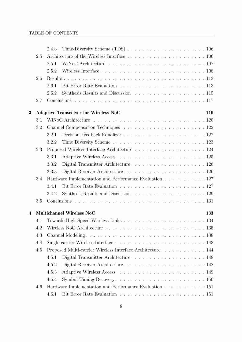
TABLE OF CONTENTS
2.4.3 Time-Diversity Scheme (TDS) . . . . . . . . . . . . . . . . . . . . . 106
2.5 Architecture of the Wireless Interface . . . . . . . . . . . . . . . . . . . . . 106
2.5.1 WiNoC Architecture . . . . . . . . . . . . . . . . . . . . . . . . . . 107
2.5.2 Wireless Interface . . . . . . . . . . . . . . . . . . . . . . . . . . . . 108
2.6 Results . . . . . . . . . . . . . . . . . . . . . . . . . . . . . . . . . . . . . . 113
2.6.1 Bit Error Rate Evaluation . . . . . . . . . . . . . . . . . . . . . . . 113
2.6.2 Synthesis Results and Discussion . . . . . . . . . . . . . . . . . . . 115
2.7 Conclusions . . . . . . . . . . . . . . . . . . . . . . . . . . . . . . . . . . . 117
3 Adaptive Transceiver for Wireless NoC 119
3.1 WiNoC Architecture . . . . . . . . . . . . . . . . . . . . . . . . . . . . . . 120
3.2 Channel Compensation Techniques . . . . . . . . . . . . . . . . . . . . . . 122
3.2.1 Decision Feedback Equalizer . . . . . . . . . . . . . . . . . . . . . . 122
3.2.2 Time Diversity Scheme . . . . . . . . . . . . . . . . . . . . . . . . . 123
3.3 Proposed Wireless Interface Architecture . . . . . . . . . . . . . . . . . . . 124
3.3.1 Adaptive Wireless Access . . . . . . . . . . . . . . . . . . . . . . . 125
3.3.2 Digital Transmitter Architecture . . . . . . . . . . . . . . . . . . . 126
3.3.3 Digital Receiver Architecture . . . . . . . . . . . . . . . . . . . . . 126
3.4 Hardware Implementation and Performance Evaluation . . . . . . . . . . . 127
3.4.1 Bit Error Rate Evaluation . . . . . . . . . . . . . . . . . . . . . . . 127
3.4.2 Synthesis Results and Discussion . . . . . . . . . . . . . . . . . . . 129
3.5 Conclusions . . . . . . . . . . . . . . . . . . . . . . . . . . . . . . . . . . . 131
4 Multichannel Wireless NoC 133
4.1 Towards High-Speed Wireless Links . . . . . . . . . . . . . . . . . . . . . . 134
4.2 Wireless NoC Architecture . . . . . . . . . . . . . . . . . . . . . . . . . . . 135
4.3 Channel Modeling . . . . . . . . . . . . . . . . . . . . . . . . . . . . . . . . 138
4.4 Single-carrier Wireless Interface . . . . . . . . . . . . . . . . . . . . . . . . 143
4.5 Proposed Multi-carrier Wireless Interface Architecture . . . . . . . . . . . 144
4.5.1 Digital Transmitter Architecture . . . . . . . . . . . . . . . . . . . 148
4.5.2 Digital Receiver Architecture . . . . . . . . . . . . . . . . . . . . . 148
4.5.3 Adaptive Wireless Access . . . . . . . . . . . . . . . . . . . . . . . 149
4.5.4 Symbol Timing Recovery . . . . . . . . . . . . . . . . . . . . . . . . 150
4.6 Hardware Implementation and Performance Evaluation . . . . . . . . . . . 151
4.6.1 Bit Error Rate Evaluation . . . . . . . . . . . . . . . . . . . . . . . 151
8

TABLE OF CONTENTS
4.6.2 Synthesis Results and Discussion . . . . . . . . . . . . . . . . . . . 152
4.7 Conclusions . . . . . . . . . . . . . . . . . . . . . . . . . . . . . . . . . . . 156
5 WiNoC Evaluation 157
5.1 Frequency of Iteration Between Cores . . . . . . . . . . . . . . . . . . . . . 158
5.2 Synthetic Traffic Patterns . . . . . . . . . . . . . . . . . . . . . . . . . . . 158
5.2.1 Uniform Random Traffic . . . . . . . . . . . . . . . . . . . . . . . . 159
5.2.2 Transpose Traffic . . . . . . . . . . . . . . . . . . . . . . . . . . . . 160
5.2.3 Hotspot Traffic . . . . . . . . . . . . . . . . . . . . . . . . . . . . . 160
5.2.4 Perfect Shuffle Traffic . . . . . . . . . . . . . . . . . . . . . . . . . . 161
5.3 Application Benchmark Suites . . . . . . . . . . . . . . . . . . . . . . . . . 163
5.3.1 BlackScholes . . . . . . . . . . . . . . . . . . . . . . . . . . . . . . . 164
5.3.2 Dedup . . . . . . . . . . . . . . . . . . . . . . . . . . . . . . . . . . 165
5.3.3 Raytrace . . . . . . . . . . . . . . . . . . . . . . . . . . . . . . . . . 166
5.3.4 x264 . . . . . . . . . . . . . . . . . . . . . . . . . . . . . . . . . . . 166
5.3.5 Streamcluster . . . . . . . . . . . . . . . . . . . . . . . . . . . . . . 167
5.3.6 Traffic Analysis . . . . . . . . . . . . . . . . . . . . . . . . . . . . . 168
5.3.7 Wireless Multicasting . . . . . . . . . . . . . . . . . . . . . . . . . . 171
5.4 Performance Evaluation . . . . . . . . . . . . . . . . . . . . . . . . . . . . 173
5.4.1 NoC Energy-Based Simulator . . . . . . . . . . . . . . . . . . . . . 174
5.4.2 Network Evaluation . . . . . . . . . . . . . . . . . . . . . . . . . . . 176
5.4.3 Evaluation of the Multicasting Techniques . . . . . . . . . . . . . . 183
5.5 Conclusion . . . . . . . . . . . . . . . . . . . . . . . . . . . . . . . . . . . . 187
Conclusion and Perspectives 189
Scientific Contributions 195
A MCSL Benchmark Analysis 196
Bibliography 199
9
LIST OF FIGURES
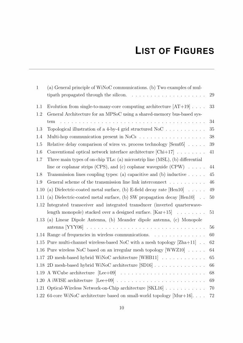
1 (a) General principle of WiNoC communications. (b) Two examples of mul-
tipath propagated through the silicon. . . . . . . . . . . . . . . . . . . . . 29
1.1 Evolution from single-to-many-core computing architecture [AT+19] . . . . 33
1.2 General Architecture for an MPSoC using a shared-memory bus-based sys-
tem . . . . . . . . . . . . . . . . . . . . . . . . . . . . . . . . . . . . . . . 34
1.3 Topological illustration of a 4-by-4 grid structured NoC . . . . . . . . . . . 35
1.4 Multi-hop communication present in NoCs . . . . . . . . . . . . . . . . . . 38
1.5 Relative delay comparison of wires vs. process technology [Sem05] . . . . . 39
1.6 Conventional optical network interface architecture [Chi+17] . . . . . . . . 41
1.7 Three main types of on-chip TLs: (a) microstrip line (MSL), (b) differential
line or coplanar strips (CPS), and (c) coplanar waveguide (CPW) . . . . . 44
1.8 Transmission lines coupling types: (a) capacitive and (b) inductive . . . . . 45
1.9 General scheme of the transmission line link interconnect . . . . . . . . . . 46
1.10 (a) Dielectric-coated metal surface, (b) E-field decay rate [Hen10] . . . . . 49
1.11 (a) Dielectric-coated metal surface, (b) SW propagation decay [Hen10] . . 50
1.12 Integrated transceiver and integrated transducer (inverted quarterwave-
length monopole) stacked over a designed surface. [Kar+15] . . . . . . . . 51
1.13 (a) Linear Dipole Antenna, (b) Meander dipole antenna, (c) Monopole
antenna [YYY06] . . . . . . . . . . . . . . . . . . . . . . . . . . . . . . . . 56
1.14 Range of frequencies in wireless communications. . . . . . . . . . . . . . . 60
1.15 Pure multi-channel wireless-based NoC with a mesh topology [Zha+11] . . 62
1.16 Pure wireless NoC based on an irregular mesh topology [WWZ10] . . . . . 64
1.17 2D mesh-based hybrid WiNoC architecture [WHB11] . . . . . . . . . . . . 65
1.18 2D mesh-based hybrid WiNoC architecture [SD16] . . . . . . . . . . . . . . 66
1.19 A WCube architecture [Lee+09] . . . . . . . . . . . . . . . . . . . . . . . 68
1.20 A iWISE architecture [Lee+09] . . . . . . . . . . . . . . . . . . . . . . . . 69
1.21 Optical-Wireless Network-on-Chip architecture [SKL16] . . . . . . . . . . . 70
1.22 64-core WiNoC architecture based on small-world topology [Mur+16]. . . . 72
10
LIST OF FIGURES
1.23 A hybrid (wireless/wired) hierarchical WiNoC architecture with heteroge-
neous subnets and small-world-based upper-level configuration [Cha+12]. . 72
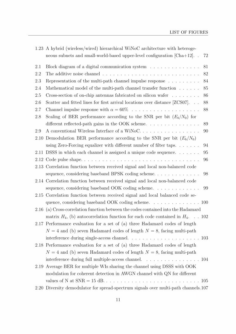
2.1 Block diagram of a digital communication system . . . . . . . . . . . . . . 81
2.2 The additive noise channel . . . . . . . . . . . . . . . . . . . . . . . . . . . 82
2.3 Representation of the multi-path channel impulse response . . . . . . . . . 84
2.4 Mathematical model of the multi-path channel transfer function . . . . . . 85
2.5 Cross-section of on-chip antennas fabricated on silicon wafer . . . . . . . . 86
2.6 Scatter and fitted lines for first arrival locations over distance [ZCS07]. . . 88
2.7 Channel impulse response with α = 60% . . . . . . . . . . . . . . . . . . . 88
2.8 Scaling of BER performance according to the SNR per bit (Eb/N0) for
different reflected-path gains in the OOK scheme. . . . . . . . . . . . . . . 89
2.9 A conventional Wireless Interface of a WiNoC. . . . . . . . . . . . . . . . . 90
2.10 Demodulation BER performance according to the SNR per bit (Eb/N0)
using Zero-Forcing equalizer with different number of filter taps. . . . . . . 94
2.11 DSSS in which each channel is assigned a unique code sequence. . . . . . . 95
2.12 Code pulse shape. . . . . . . . . . . . . . . . . . . . . . . . . . . . . . . . . 96
2.13 Correlation function between received signal and local non-balanced code
sequence, considering baseband BPSK coding scheme. . . . . . . . . . . . . 98
2.14 Correlation function between received signal and local non-balanced code
sequence, considering baseband OOK coding scheme. . . . . . . . . . . . . 99
2.15 Correlation function between received signal and local balanced code se-
quence, considering baseband OOK coding scheme. . . . . . . . . . . . . . 100
2.16 (a) Cross-correlation function between the codes contained into the Hadamard
matrix H4, (b) autocorrelation function for each code contained in H4. . . 102
2.17 Performance evaluation for a set of (a) three Hadamard codes of length
N = 4 and (b) seven Hadamard codes of length N = 8, facing multi-path
interference during single-access channel. . . . . . . . . . . . . . . . . . . . 103
2.18 Performance evaluation for a set of (a) three Hadamard codes of length
N = 4 and (b) seven Hadamard codes of length N = 8, facing multi-path
interference during full multiple-access channel. . . . . . . . . . . . . . . . 104
2.19 Average BER for multiple WIs sharing the channel using DSSS with OOK
modulation for coherent detection in AWGN channel with QN for different
values of N at SNR = 15 dB. . . . . . . . . . . . . . . . . . . . . . . . . . . 105
2.20 Diversity demodulator for spread-spectrum signals over multi-path channels.107
11
LIST OF FIGURES
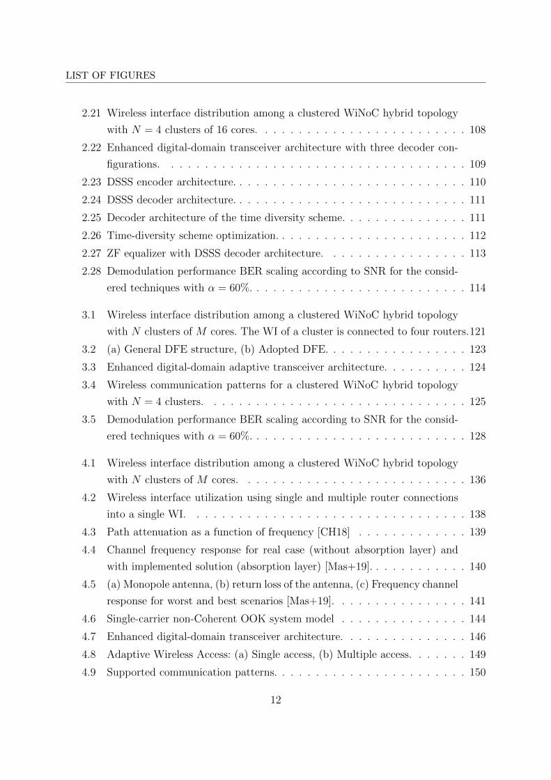
2.21 Wireless interface distribution among a clustered WiNoC hybrid topology
with N = 4 clusters of 16 cores. . . . . . . . . . . . . . . . . . . . . . . . . 108
2.22 Enhanced digital-domain transceiver architecture with three decoder con-
figurations. . . . . . . . . . . . . . . . . . . . . . . . . . . . . . . . . . . . 109
2.23 DSSS encoder architecture. . . . . . . . . . . . . . . . . . . . . . . . . . . . 110
2.24 DSSS decoder architecture. . . . . . . . . . . . . . . . . . . . . . . . . . . . 111
2.25 Decoder architecture of the time diversity scheme. . . . . . . . . . . . . . . 111
2.26 Time-diversity scheme optimization. . . . . . . . . . . . . . . . . . . . . . . 112
2.27 ZF equalizer with DSSS decoder architecture. . . . . . . . . . . . . . . . . 113
2.28 Demodulation performance BER scaling according to SNR for the consid-
ered techniques with α = 60%. . . . . . . . . . . . . . . . . . . . . . . . . . 114
3.1 Wireless interface distribution among a clustered WiNoC hybrid topology
with N clusters of M cores. The WI of a cluster is connected to four routers.121
3.2 (a) General DFE structure, (b) Adopted DFE. . . . . . . . . . . . . . . . . 123
3.3 Enhanced digital-domain adaptive transceiver architecture. . . . . . . . . . 124
3.4 Wireless communication patterns for a clustered WiNoC hybrid topology
with N = 4 clusters. . . . . . . . . . . . . . . . . . . . . . . . . . . . . . . 125
3.5 Demodulation performance BER scaling according to SNR for the consid-
ered techniques with α = 60%. . . . . . . . . . . . . . . . . . . . . . . . . . 128
4.1 Wireless interface distribution among a clustered WiNoC hybrid topology
with N clusters of M cores. . . . . . . . . . . . . . . . . . . . . . . . . . . 136
4.2 Wireless interface utilization using single and multiple router connections
into a single WI. . . . . . . . . . . . . . . . . . . . . . . . . . . . . . . . . 138
4.3 Path attenuation as a function of frequency [CH18] . . . . . . . . . . . . . 139
4.4 Channel frequency response for real case (without absorption layer) and
with implemented solution (absorption layer) [Mas+19]. . . . . . . . . . . . 140
4.5 (a) Monopole antenna, (b) return loss of the antenna, (c) Frequency channel
response for worst and best scenarios [Mas+19]. . . . . . . . . . . . . . . . 141
4.6 Single-carrier non-Coherent OOK system model . . . . . . . . . . . . . . . 144
4.7 Enhanced digital-domain transceiver architecture. . . . . . . . . . . . . . . 146
4.8 Adaptive Wireless Access: (a) Single access, (b) Multiple access. . . . . . . 149
4.9 Supported communication patterns. . . . . . . . . . . . . . . . . . . . . . . 150
12

LIST OF FIGURES
4.10 performance BER for multicast with (a) PG = 4, (b) PG = 8, and (c)
unicast/broadcast. . . . . . . . . . . . . . . . . . . . . . . . . . . . . . . . 153
5.1 Example of M = 9 cores with uniform random traffic based on (a) network
mesh topology with its respective (b) frequency matrix of communication
between cores. . . . . . . . . . . . . . . . . . . . . . . . . . . . . . . . . . . 159
5.2 Example of M = 9 cores with transpose traffic based on (a) network mesh
topology with its respective (b) frequency matrix of communication be-
tween cores. . . . . . . . . . . . . . . . . . . . . . . . . . . . . . . . . . . . 160
5.3 Example of M = 9 cores with hotspot traffic based on (a) network mesh
topology with its respective (b) frequency matrix. . . . . . . . . . . . . . . 161
5.4 Example of (a) perfect shuffle for M = 8 cores with the obtained (b) cir-
culating shuffle network. . . . . . . . . . . . . . . . . . . . . . . . . . . . . 161
5.5 Example of M = 8 cores with perfect shuffle traffic based on (a) network
mesh topology with its respective (b) frequency matrix of communication
between cores. . . . . . . . . . . . . . . . . . . . . . . . . . . . . . . . . . . 162
5.6 Message generated per core for the BlackScholes benchmark in a network
of (a) 64 and (b) 256 cores. . . . . . . . . . . . . . . . . . . . . . . . . . . 164
5.7 Message generated per core for the Dedup benchmark in a network of (a) 64
and (b) 256 cores. . . . . . . . . . . . . . . . . . . . . . . . . . . . . . . . . 165
5.8 Message generated per core for the Raytrace benchmark in a network of
(a) 64 and (b) 256 cores. . . . . . . . . . . . . . . . . . . . . . . . . . . . . 166
5.9 Message generated per core for the x264 benchmark in a network of (a) 64
and (b) 256 cores. . . . . . . . . . . . . . . . . . . . . . . . . . . . . . . . . 167
5.10 Message generated per core for the Streamcluster benchmark in a network
of (a) 64 and (b) 256 cores. . . . . . . . . . . . . . . . . . . . . . . . . . . 168
5.11 Temporal distribution of the different types of traffic (P2P, DRAM, Mul-
ticast/Broadcast) for the Blackscholes application. . . . . . . . . . . . . . . 169
5.12 Temporal distribution of the different types of traffic (P2P, DRAM, Mul-
ticast/Broadcast) for the x264 application. . . . . . . . . . . . . . . . . . . 170
5.13 Temporal distribution of the different types of traffic (P2P, DRAM, Mul-
ticast/Broadcast) for the Streamcluster application. . . . . . . . . . . . . . 171
5.14 Multicasting techniques: (a) MDND, (b) VBON, and (c) WDN. . . . . . . 172
5.15 (a) Simulator interface, (b) WiNoC and path trace example generated by
the simulator. . . . . . . . . . . . . . . . . . . . . . . . . . . . . . . . . . . 175
13
LIST OF FIGURES
5.16 Antenna placement for evaluation of 64 and 256 cores. . . . . . . . . . . . 177
5.17 Network behaviour generated by application benchmark x264 into a 64-core
NoC. . . . . . . . . . . . . . . . . . . . . . . . . . . . . . . . . . . . . . . . 179
5.18 Network behaviour generated by application benchmark x264 into a 64-core
WiNoC using 4 antennas rectangularly placed into the chip. . . . . . . . . 180
5.19 Energy reduction and wireless utilization in 64-core and 256-core architec-
tures. . . . . . . . . . . . . . . . . . . . . . . . . . . . . . . . . . . . . . . . 186
5.20 DSSS far-near effects. . . . . . . . . . . . . . . . . . . . . . . . . . . . . . . 190
5.21 BackScattering WiNoC Communication. . . . . . . . . . . . . . . . . . . . 191
5.22 Optical/Wireless NoC Communication layer. . . . . . . . . . . . . . . . . . 193
A.1 Messages generated per core for the MCSL benchmarks using an NoC of
256 cores. . . . . . . . . . . . . . . . . . . . . . . . . . . . . . . . . . . . . 197
14
LIST OF TABLES
1.1 UWB Interconnect Scaling [Zha+11] . . . . . . . . . . . . . . . . . . . . . 57
1.2 Comparison between current emerging on-chip interconnects [Kar+16] . . . 78
2.1 Synthesis results (area and power consumption) of the different Wireless
Interface architectures using 28-nm FDSOI. . . . . . . . . . . . . . . . . . 115
3.1 Synthesis results (area and power consumption) of the Wireless Interface
architecture using 28-nm FDSOI. . . . . . . . . . . . . . . . . . . . . . . . 129
4.1 LNA power trends . . . . . . . . . . . . . . . . . . . . . . . . . . . . . . . 143
4.2 Power estimation of the multi-carrier NC-OOK transceiver shown in Fig-
ure 4.7 using 28-nm FDSOI at 1 V . . . . . . . . . . . . . . . . . . . . . . 147
4.3 Area and power consumption of the Wireless Interface architecture designed
using 28-nm FDSOI. . . . . . . . . . . . . . . . . . . . . . . . . . . . . . . 154
4.4 Power consumption of the different communication configurations and phases.
. . . . . . . . . . . . . . . . . . . . . . . . . . . . . . . . . . . . . . . . . . 154
5.1 64-core NoC vs WiNoC . . . . . . . . . . . . . . . . . . . . . . . . . . . . . 180
5.2 256-core NoC vs WiNoC . . . . . . . . . . . . . . . . . . . . . . . . . . . . 181
5.3 256-core NoC vs WiNoC using circle antenna placement . . . . . . . . . . . 182
5.4 Comparison of multicast techniques using a 64-core NoC . . . . . . . . . . 183
5.5 Comparison of multicast techniques using a 256-core NoC . . . . . . . . . . 184
A.1 MCSL NoC traffic patterns . . . . . . . . . . . . . . . . . . . . . . . . . . 196
15

Abstract
Massive parallelism in emerging high-performance computing applications requires the
use of a manycore architecture relying on an efficient on-chip interconnection system. How-
ever, current electrical interconnections are not efficient enough to support this increasing
number of cores, while ensuring high performance and energy efficiency. Current solutions
are based on a large Network-on-Chip (NoC), which can easily lead to prohibitive com-
munication latency due to long multi-hop paths. In fact, these multi-hop communications
impact directly the performance and energy consumption of the overall system. This effect
is mainly due to the wire interconnections which are not scaling well and to the high num-
ber of routers to traverse for the communication between cores and memory hierarchy.
For these reasons, many interconnect technologies (e.g., Optical, Wireless, RF based on
waveguides) have emerged to improve performance compared to conventional electrical
NoC. However, only on-chip Wireless interconnection technologies could provide a nat-
ural scalable fan-out capability, especially when considering broadcast/multicast system
requirements. In terms of connectivity and scalability, Wireless NoCs (WiNoC) can thus
be considered as one of the most promising solutions. Figure 2.21 shows an example of
a manycore architecture based on a WiNoC as considered in this work. The manycore is
organized as N clusters of M processors. Each cluster contains a Wireless Interface (WI)
and the M processors have access to the WI. Moreover, the N.M processors are organized
around a classical, mesh-based Electrical NoC. Figure 2.21 shows an example with N = 4and M = 16.
However, wireless interconnections still face many challenges to be embedded into
everyday appliances. Most of the research papers in the state-of-the-art are focused on
antenna and analog transceiver design, especially when operating in the millimeter-wave
range. Nevertheless, few prior works have introduced some interesting NoC wireless chan-
nel models, which are yet not considered into WiNoC simulations. Also, the digital base-
band transceiver is mostly neglected in these simulations. However, the power contribution
of this digital component is significant, especially when it provides Giga bits per second of
data transfer rate. Finally, due to the low complexity of its implementation, the classical
modulation scheme considered for WiNoCs is On-Off Keying (OOK).
Antenna and NoC wireless channel models are key features to designing effective and
efficient on-chip wireless interconnects. On the one hand, the antenna defines the maxi-
mum bandwidth supported by a wireless link. However, the design of efficient wideband
antennas is still a challenge. On the other hand, the on-chip wireless channel defines the
17
feasibility to integrate wireless interconnects into NoC solutions. A lossy on-chip wire-
less channel will require a power-hungry RF radio to establish long-range wireless links.
Therefore, the gain obtained by using wireless links will be negligible compared to electri-
cal wired interconnections. In addition, the on-chip wireless channel is prone to multipath
propagation due to the electrical characteristics of the silicon substrate, the physical struc-
tures, and the chip package. Nevertheless, the wireless channel model commonly used in
the literature only considers path loss through free space and Additive White Gaussian
Noise (AWGN). It is understandable, because a multipath propagation channel requires
additional processing to ensure reliable communication, increasing transceiver architec-
ture complexity.
In this context, an on-chip wireless channel model is first estimated and analyzed, be-
fore to study any low-cost channel compensation technique. This channel model is defined
based on the approach given by the intra-chip wave propagation, which considers neither
NoC physical structures nor the chip package. However, even without these physical char-
acteristics, multipath propagation has been shown to be worth considering because of the
resistivity of the substrate, the type of antenna and the distance between antennas. Based
on these results, it was determined that a channel model should include at least two prop-
agation paths for realistic WiNoC simulations together with Additive White Gaussian
Noise (AWGN).
In order to evaluate the impact of this channel model over the wireless communica-
tion, several simulations were performed comparing the Signal-to-Noise Ratio (SNR) and
the Bit Error Rate (BER) parameters (Figure 2.8). Results obtained by these simulations
report that a second path, even with a low percentage of energy level compared to the
main path, can rapidly degrade a point-to-point wireless communication link based on
OOK modulation scheme.
Furthermore, as multiple channel access can lead to more efficient utilization of wire-
less interconnects avoiding the waste of wireless resources, the first approach taken into
account was wireless parallel communication. As a consequence, to ensure communica-
tion reliability, three low-cost channel effect cancellation techniques, allowing for mul-
tiple channel access, are studied to offer the best trade-off between BER performance
and area/power consumption. The studied techniques are the following: Direct Sequence
Spread Spectrum (DSSS), Zero-Forcing (ZF) equalization combined with DSSS and Time
18
Diversity Scheme (TDS). The DSSS shows lower area and power consumption overhead
than the other techniques, however, its average BER is lower than for the other techniques
with channel effect compensation. On the other hand, the ZF combined with DSSS re-
ports the best performance in terms of average BER, at the cost of highest power and area
overhead. The TDS block shows the best trade-off between BER performance and area
and power over the other techniques, representing less than 1% and 2%, respectively, of
the total wireless interface. Nevertheless, any channel compensation technique requires an
analog-to-digital converter device, which can easily consume the bulk of area and power of
the total wireless interface, especially when communication data rate is aiming at several
tens of gigabits per second. Therefore, the choice of this device has to be made carefully
during the transceiver design. Figure 2.9 shows a conventional Wireless Interface (WI)
based on OOK modulation, whereas Figure 2.22 depicts the proposed WI supporting
multiple channel access and based on adequate channel compensation techniques.
Conventional mesh-based NoCs have to deal with different communication patterns,
such as unicast/broadcast, multicast (e.g., multiple-unicast, many-to-one and all-to-one
communication). Critical bottlenecks are created especially by broadcast/multicast net-
work traffic schemes, which are of outmost importance for cache coherence protocols. To
solve this problem, an adaptive wireless transceiver was designed providing at the same
time high resilience to wireless channel interference. In this context, for unicast/broadcast
communications, a low complexity decision feedback equalizer (DFE) is proposed to over-
come the multipath propagation described previously. This technique exceeds TDS in
terms of data rate, providing very high-speed for long-distance point-to-point and point-to-
multipoint communications. Nevertheless, parallel channel access requirements are present
in the form of multicast communication patterns. For this reason, in order to efficiently
use the wireless interconnections, a TDS technique using dynamic channelization codes
is proposed, offering parallel channel access and resilience to multipath-propagation. The
proposed solution, depicted in Figure 3.3, considers all mandatory elements into the dig-
ital wireless interface part including the compensation techniques. This adaptive wireless
interface represents less than 1% and 10% of the total WI area and power, respectively.
The bandwidth needed to reach a very high-speed data rate increases the power con-
sumption in all single-carrier wireless transceivers. In order to keep a reasonable trade-off
between power consumption and data rate, WiNoC designers have decreased the min-
19
imum required bandwidth to support a given data rate (e.g., 16 Gbps). However, this
reduction produces significant communication errors that have to be compensated by
increasing the transmission signal power and the receiver sensitivity. In this context, we
first demonstrate the significant power efficiency degradation of a single-carrier high-speed
system designed with limited bandwidth. We also report that the main contributors in
the power budget are the power amplifiers used to establish high-speed high-bandwidth
communication with very low Bit-Error-Rate (BER). For these reasons, a multi-carrier
wireless system based on Frequency Division Multiplexing (FDM) is proposed and studied
to overcome this issue for future WiNoC generation requirements. Subsequently, a com-
plete and efficient multi-carrier transceiver architecture is designed to be capable of sup-
porting unicast/broadcast, many-to-one, all-to-one, many-to-many and multiple unicast
communication patterns, adopting a spread-spectrum multiple-access technique. Also, an
approach to symbol timing recovery leveraging the spread spectrum technique is studied.
Simulations are performed adopting the newest realistic channel, which is capable of sup-
pressing on-chip multipath wireless propagation using a dedicated communication layer.
Experimental results show that the required SNR to achieve low BER can be significantly
reduced, as well as the energy required to establish multiple wireless links. Figure 4.7
shows the proposed wireless interface based on Frequency Division Multiplexing (FDM)
and Direct-Sequence Spread Spectrum (DSSS). This transceiver scales well with the band-
width promised by future CMOS devices.
Once efficient wireless links are designed, the next step is to study the network improve-
ment according to the communication patterns generated by the applications. Therefore,
a network simulator was developed in MATLAB to calculate the percentage of wireless
link utilization according to the wireless interface configuration and placement. Besides,
this simulator computes the dynamic energy consumed by an electrical NoC compared
with a WiNoC using a different number of wireless interfaces. The results obtained show
that certain network configurations allow to save much more energy than others, thus
demonstrating the importance of the on-chip wireless links.
20
Resume
Le parallelisme massif des applications emergentes de calcul haute performance neces-
site l’utilisation d’une architecture a plusieurs cœurs reposant sur un systeme d’intercon-
nexion sur puce efficace. Cependant, les interconnexions electriques actuelles ne sont pas
assez efficaces pour supporter ce nombre croissant de cœurs, tout en assurant une haute
performance et une bonne efficacite energetique. Les solutions actuelles sont basees sur un
grand reseau sur puce (NoC), ce qui peut facilement entraıner une latence de communica-
tion prohibitive en raison des longs trajets a bonds multiples. En fait, ces communications
a sauts multiples ont un impact direct sur les performances et la consommation d’energie
du systeme global. Cet effet est principalement du aux interconnexions de fils qui ne sont
pas bien dimensionnees et au nombre eleve de routeurs a traverser pour la communication
entre les cœurs et la hierarchie memoire. Pour ces raisons, de nombreuses technologies
d’interconnexion (par exemple, optique, sans fil, RF base sur des guides d’ondes) ont vu
le jour pour ameliorer les performances par rapport aux NoC electriques classiques. Ce-
pendant, seules les technologies d’interconnexion sans fil sur puce pourraient fournir une
capacite de repartition naturelle et evolutive, en particulier si l’on considere les exigences
des systemes de diffusion/multidiffusion (broadcast/multicast). En termes de connectivite
et d’evolutivite, les NoC sans fil (WiNoC) peuvent donc etre consideres comme l’une des
solutions les plus prometteuses. La figure 2.21 montre un exemple d’architecture manycore
basee sur un WiNoC tel que considere dans ce travail. Le manycore est organise en N
grappes de M processeurs. Chaque grappe contient une interface sans fil (WI) et les M
processeurs ont acces a la WI. De plus, les N.M processeurs sont organises autour d’un
NoC electrique classique, base sur un maillage. La figure 2.21 montre un exemple avec
N = 4 et M = 16.
Cependant, les interconnexions sans fil doivent encore relever de nombreux defis pour
etre integrees dans les systemes actuels. La plupart des travaux de recherche portent sur
la conception d’antennes et d’emetteurs-recepteurs analogiques, en particulier lorsqu’ils
fonctionnent dans la gamme des ondes millimetriques. Neanmoins, peu de travaux an-
terieurs ont introduit des modeles interessants de canaux sans fil NoC, qui ne sont pas
encore pris en compte dans la plupart des simulations de WiNoC. En outre, l’emetteur-
recepteur numerique en bande de base est le plus souvent neglige dans ces simulations.
Cependant, la contribution en puissance de cette composante numerique est significative,
surtout lorsqu’elle fournit un debit de transfert de donnees de l’ordre du Gigabits par
seconde (Gbps). Enfin, en raison de la faible complexite de sa mise en œuvre, le schema
21
de modulation classique envisage pour les WiNoC est le On-Off Keying (OOK).
Les modeles d’antennes et de canaux sans fil pour les WiNoC sont des elements essen-
tiels pour concevoir des interconnexions sans fil sur puce efficaces et performantes. D’une
part, l’antenne definit la largeur de bande maximale supportee par une liaison sans fil.
Cependant, la conception d’antennes a large bande efficaces reste un defi. D’autre part,
le canal sans fil sur puce definit la faisabilite de l’integration des interconnexions sans fil
dans les solutions de WiNoC. En effet, un canal sans fil sur puce avec perte necessitera
une radio RF gourmande en energie pour etablir des liaisons sans fil a longue portee. Par
consequent, le gain obtenu en utilisant des liaisons sans fil sera negligeable par rapport
aux interconnexions electriques filaires. En outre, le canal sans fil sur puce est sujet a la
propagation par trajets multiples en raison des caracteristiques electriques du substrat
de silicium, des structures physiques et du boıtier de la puce. Neanmoins, le modele de
canal sans fil couramment utilise dans la litterature ne prend en compte que la perte de
trajet a travers l’espace libre et le bruit blanc gaussien additif (AWGN). C’est comprehen-
sible, car un canal de propagation contenant des trajets multiples necessite un traitement
supplementaire pour assurer une communication fiable, ce qui augmente la complexite de
l’architecture de l’emetteur-recepteur.
Dans ce contexte, un modele de canal sans fil sur puce est d’abord estime et analyse,
avant d’etudier des techniques de compensation de canal a faible cout. Ce modele de
canal est defini sur la base de l’approche donnee par la propagation des ondes intra-
puces, qui ne tient compte ni des structures physiques de la NoC ni du boıtier de la puce.
Cependant, meme sans ces caracteristiques physiques, il a ete demontre que la propagation
par trajets multiples merite d’etre prise en compte en raison de la resistivite du substrat,
du type d’antenne et de la distance entre les antennes. Sur la base de ces resultats, il a ete
determine qu’un modele de canal devrait inclure au moins deux trajets de propagation
pour des simulations WiNoC realistes, ainsi que du bruit blanc gaussien additif (AWGN).
Dans la these, afin d’evaluer l’impact de ce modele de canal sur la communication
sans fil, plusieurs simulations ont ete realisees en comparant les parametres du rapport
signal/bruit (SNR) et du taux d’erreur binaire (BER) (figure 2.8). Les resultats ainsi obte-
nus par ces simulations indiquent qu’un deuxieme trajet, meme avec un faible pourcentage
de niveau d’energie par rapport au trajet principal, peut rapidement degrader une liaison
de communication sans fil point a point basee sur le schema de modulation OOK.
22
En outre, comme l’acces a plusieurs canaux peut conduire a une utilisation plus ef-
ficace des interconnexions sans fil en evitant le gaspillage des ressources. La premiere
approche prise en compte a ete la communication parallele sans fil. Par consequent, pour
garantir la fiabilite des communications, trois techniques d’annulation de l’effet de canal
a faible cout, permettant un acces a plusieurs canaux, sont etudiees pour offrir le meilleur
compromis entre les performances du BER et la consommation d’energie et de surface du
silicium. Les techniques etudiees sont l’etalement de spectre en sequence directe (DSSS),
l’egalisation a force nulle (ZF) combinee avec le DSSS et le schema de diversite temporelle
(TDS). Le DSSS presente une surface et une consommation d’energie plus faibles que les
autres techniques, cependant, son BER moyen est inferieur a celui des autres techniques
de compensation de l’effet de canal. En revanche, la technique ZF combinee au DSSS
presente les meilleures performances en termes de BER moyen, au prix d’une puissance
et d’un surcout en surface plus eleves. Le bloc TDS presente le meilleur compromis en
term de BER, de surface et de puissance par rapport aux autres techniques, represen-
tant respectivement pour les deux derniers moins de 1% et de 2% de l’interface sans fil
totale. Neanmoins, toute technique de compensation de canal necessite un dispositif de
conversion analogique-numerique qui peut facilement consommer la majeure partie de la
surface et de la puissance de l’interface sans fil, en particulier lorsque le debit de don-
nees de communication vise plusieurs dizaines de gigabits par seconde. Par consequent, le
choix de ce dispositif doit etre fait avec soin lors de la conception de l’emetteur-recepteur.
La figure 2.9 montre une interface sans fil classique (WI) basee sur la modulation OOK,
tandis que la figure 2.22 illustre la WI proposee qui prend en charge l’acces a plusieurs
canaux et qui est basee sur des techniques de compensation de canal adequates.
Les NoC conventionnels a base de maillage doivent faire face a differents modes de
communication, tels que l’unicast/broadcast, le multicast (par exemple, les communica-
tions multiple-unicast, many-to-one et all-to-one). Des goulets d’etranglement critiques
sont crees en particulier par les schemas de trafic du reseau de broadcast/multicast, qui
sont de la plus haute importance pour les protocoles de coherence de cache. Pour re-
soudre ce probleme, un emetteur-recepteur sans fil adaptatif a ete concu, offrant en meme
temps une grande resilience aux interferences des canaux sans fil. Dans ce contexte, pour
les communications unicast/broadcast, un egaliseur a retour de decision (DFE) de faible
complexite est propose pour surmonter la propagation par trajets multiples decrite prece-
demment. Cette technique depasse le TDS en termes de debit de donnees, offrant un tres
23
haut debit pour les communications longue distance point a point et point a multipoint.
Neanmoins, les exigences d’acces aux canaux paralleles sont presentes sous la forme de
modeles de communication multidiffusion. C’est pourquoi, afin d’utiliser efficacement les
interconnexions sans fil, une technique TDS utilisant des codes d’adaptation au canal
dynamiques est proposee, offrant un acces aux canaux paralleles et une resistance a la
propagation par trajets multiples. La solution proposee, illustree a la figure 3.3, prend
en compte tous les elements indispensables de la partie interface numerique sans fil, y
compris les techniques de compensation. Cette interface sans fil adaptative represente res-
pectivement moins de 1% et 10% de la surface et de la puissance WI totales.
La largeur de bande necessaire pour atteindre un debit de donnees tres eleve augmente
la consommation d’energie de tous les emetteurs-recepteurs sans fil a porteuse unique. Afin
de maintenir un compromis raisonnable entre la consommation d’energie et le debit de
donnees, les concepteurs de WiNoC ont reduit la largeur de bande minimale requise pour
supporter un debit donne (par exemple, 16 Gbps). Cependant, cette reduction produit
des erreurs de communication importantes qui doivent etre compensees en augmentant la
puissance du signal de transmission et/ou la sensibilite du recepteur. Dans ce contexte,
nous demontrons d’abord la degradation significative de l’efficacite energetique d’un sys-
teme haut debit a porteuse unique concu avec une bande passante limitee. Nous signalons
egalement que les principaux contributeurs au budget de puissance sont les amplificateurs
de puissance utilises pour etablir des communications a grande vitesse et a large bande
avec un taux d’erreur binaire (BER) tres faible. Pour ces raisons et pour les besoins des fu-
tures generations de WiNoC, un systeme sans fil multi-porteuses base sur le multiplexage
par repartition en frequence (FDM) a ete propose et etudie. Par la suite, une architecture
complete et efficace d’emetteurs-recepteurs multiporteurs est concue pour etre capable
de prendre en charge des modeles de communication unicast/broadcast, many-to-one, all-
to-one, many-to-many et multiple unicast, en adoptant une technique d’acces multiple a
etalement de spectre. Une approche de la recuperation de la synchronisation des symboles
utilisant la technique d’etalement de spectre est egalement etudiee. Des simulations sont
realisees en adoptant le canal realiste le plus recent, qui est capable de supprimer la pro-
pagation sans fil a trajets multiples sur puce. Les resultats experimentaux montrent que
le SNR necessaire pour obtenir un faible BER peut etre considerablement reduit, ainsi
que l’energie requise pour etablir de multiples liaisons sans fil. La figure 4.7 montre l’in-
terface sans fil proposee, basee sur le multiplexage par repartition en frequence (FDM) et
24
l’etalement du spectre en sequence directe (DSSS). Cet emetteur-recepteur s’adapte bien
a la largeur de bande promise par les futurs dispositifs CMOS.
Une fois que des liaisons sans fil efficaces sont concues, l’etape suivante consiste a
etudier l’amelioration du reseau en fonction des modeles de communication generes par
les applications. Un simulateur de reseau a donc ete developpe dans MATLAB pour cal-
culer le pourcentage d’utilisation des liaisons sans fil en fonction de la configuration et
du placement de l’interface sans fil. En outre, ce simulateur calcule l’energie dynamique
consommee par un NoC electrique par rapport a celle WiNoC utilisant un nombre diffe-
rent d’interfaces sans fil. Les resultats obtenus montrent que certaines configurations de
reseau permettent d’economiser beaucoup plus d’energie que d’autres, demontrant ainsi
l’importance des liaisons sans fil sur puce.
25

INTRODUCTION
Context and Motivations
The evolution of Silicon technologies and requirement in data rate for High Perfor-
mance Computing (HPC), involve large number of computation resources and faster com-
ponents (e.g., processor, memories) to support the application needs. Adding more execu-
tion resources in a single chip increases the need for efficient on-chip communication media,
and the introduction of new kinds of interconnects therefore becomes one of the major
challenges for next CMPs (Chip MultiProcessor) and MPSoCs (Multiprocessor System-
on-Chip). Manycore architectures are quickly becoming the de-facto standard and they
imply impressive gain in the domain of HPC and servers but also in the area of embedded
systems. Applications in all these categories are greedy for parallelism and the number of
cores will continue to increase. So, tackling the interconnect bottleneck in terms of energy
consumption and data rate is a key concern.
Networks-on-Chip (NoC) have emerged as communication backbones to enable a high
degree of integration for such manycore systems, solving several problems of traditional
bus-based networks. However, as the links become longer, the global interconnects suf-
fer from higher energy utilization due to the required extra hops. Besides, the multiple
hops required to transfer the information lead to a longer propagation delay. Indeed,
these issues will significantly degrade the overall network performance, creating critical
bottlenecks and reducing the throughput of future CMPs and MPSoCs. To deal with,
new interconnect solutions have emerged, such as 3D-NoC, Radio-Frequency Intercon-
nects (RF-I) based on waveguides, Optical NoC, and Wireless NoC. But, to our point of
view, only the on-chip wireless interconnection technologies embedded into a Network-
on-Chip (WiNoC) offer a promising solution for such manycore architectures, providing a
natural scalable fan-out capability to interconnect multiple points at the same time. These
characteristics can easily be exploited for Broadcast communications, which require more
complex designs for the other previously enumerated solutions.
27
In this context, this thesis is part of the “BBC” (on-chip wireless Broadcast-Based
parallel Computing) project, funded by CominLabs, whose objective is to evaluate the
feasibility of using on-chip wireless link and also to define new associated computing
paradigms. Especially because the use of wireless communications easily enables broadcast
capabilities for Wireless Networks-on-Chip (WiNoC) or on-Board (WiNoB), as well as
new management techniques for memories and parallelism. The key elements taken into
account concern the improvement of power consumption, the estimation of achievable
data rates, flexibility and reconfigurability, size reduction, and the easiness of parallelism.
Objectives of the Thesis
Although it is true that Wireless Network-on-Chip (WiNoC) is one of the most promis-
ing solution for the communication infrastructure of CMPs and MPSoCs, the reliability of
on-chip wireless links is still an important and unsolved issue. Most of the approaches from
the literature estimate performance using a very simplistic wireless channel model, which
only considers path loss through free space and Additive White Gaussian Noise (AWGN).
However, a realistic wireless channel model should consider some of the most important
parasitic phenomena introduced by the physical structures of the chip (e.g. multi-path
propagation), especially, when communication data rate is aiming at several tens of giga-
bits per second. A huge data rate has a very small symbol duration with a high probability
to be smaller than the total multipath propagation time. In consequence, the multipath
waves will interfere to the others symbols, degrading the communication between cores.
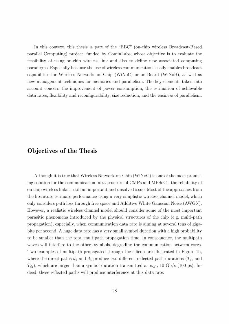
Two examples of multipath propagated through the silicon are illustrated in Figure 1b,
where the direct paths d1 and d3 produce two different reflected path durations (Td2 and
Td4), which are larger than a symbol duration transmitted at e.g., 10 Gb/s (100 ps). In-
deed, these reflected paths will produce interference at this data rate.
28
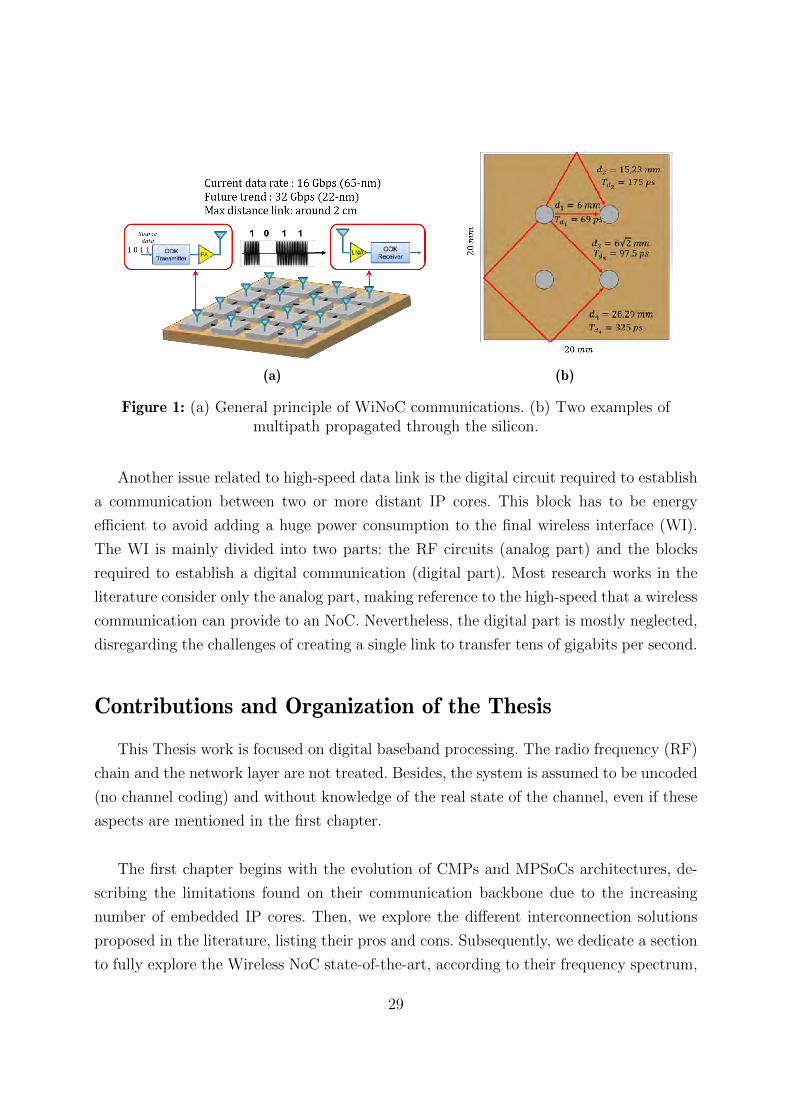
(a) (b)
Figure 1: (a) General principle of WiNoC communications. (b) Two examples ofmultipath propagated through the silicon.
Another issue related to high-speed data link is the digital circuit required to establish
a communication between two or more distant IP cores. This block has to be energy
efficient to avoid adding a huge power consumption to the final wireless interface (WI).
The WI is mainly divided into two parts: the RF circuits (analog part) and the blocks
required to establish a digital communication (digital part). Most research works in the
literature consider only the analog part, making reference to the high-speed that a wireless
communication can provide to an NoC. Nevertheless, the digital part is mostly neglected,
disregarding the challenges of creating a single link to transfer tens of gigabits per second.
Contributions and Organization of the Thesis
This Thesis work is focused on digital baseband processing. The radio frequency (RF)
chain and the network layer are not treated. Besides, the system is assumed to be uncoded
(no channel coding) and without knowledge of the real state of the channel, even if these
aspects are mentioned in the first chapter.
The first chapter begins with the evolution of CMPs and MPSoCs architectures, de-
scribing the limitations found on their communication backbone due to the increasing
number of embedded IP cores. Then, we explore the different interconnection solutions
proposed in the literature, listing their pros and cons. Subsequently, we dedicate a section
to fully explore the Wireless NoC state-of-the-art, according to their frequency spectrum,
29
architecture and type of channel access control. Finally, we highlight the gaps in the lit-
erature for the wireless interconnect solution.
In the second chapter, we explore a more realistic channel for WiNoC communications.
This channel is estimated based on the approach given by the intra-chip wave propaga-
tion, which considers neither NoC physical structures nor the chip package. However, even
without these physical characteristics, multipath propagation has been shown to be worth
considering because of the resistivity of the substrate, the type of antenna and the dis-
tance between antennas. Based on these results, it was determined that a channel model
should include at least two propagation paths for realistic WiNoC simulations together
with Additive White Gaussian Noise (AWGN). Subsequently, we study several low-cost
channel compensation techniques to design a transceiver offering the best trade-off be-
tween BER performance and area/power consumption.
In the third chapter, we improve the previous transceiver, adopting multiple configura-
tions. This configurations are based on the different traffic patterns used by a NoC during
a program execution. The modifications adopted allow to increase the data transfer rate
during a single link or share the channel during a multiple link request, always assuring a
channel interference resilience.
The fourth chapter is dedicated to explore a wireless interface (WI) for future high-
speed wireless links. This WI considers the newest innovative on-chip wireless channel
propositions for WiNoCs, which offer a close to ideal channel for wireless communica-
tions. Besides, we unveil the issue related with current RF designs to increase the data
rate, highly compromising the power consumption and dissipation.
In Chapter five, we study the network improvement using the previously proposed WI,
injecting the communication traffic generated by synthetic and application benchmarks. In
this context, a network simulator was developed in MATLAB to calculate the percentage
of wireless link utilization according to the wireless interface configuration and placement.
Besides, this simulator computes the dynamic energy consumed by an electrical NoC
compared with an NoC. The results obtained show that certain network configurations
allow to save much more energy than others, thus demonstrating the importance of the
on-chip wireless links.
30
Chapter 1
STATE OF THE ART
Through the content of this chapter, as a first step, we examine the general proces-
sor and System-on-Chip (SoC) history, concluding with major drawbacks of current and
future multi/manycore architectures. Then, we introduce the Network-on-Chip (NoC)
paradigm proposed to overcome the limitations of a conventional shared bus. Addition-
ally, we recall the metrics for evaluating the performance and limitations of conventional
NoCs for futures manycore architectures. Subsequently, we introduce a general view of the
state-of-the-art of the emerging interconnect technologies proposed as promising solutions
for future massive core integration. Nevertheless, we dedicate a section to deeply analyze
the state-of-the-art of on-chip wireless interconnect solutions along with the gaps in the
literature. Wireless NoC (WiNoC) is then the solution used along this thesis work.
1.1 Background
The aggressive technology scaling began with the first MOS transistor demonstra-
tion, performed by Kahng and Atalla in 1960 [Loj07], fabricated in 20 µm. This tech-
nology allowed starting a large scale integration era, exceeding the limits imposed by
the bipolar processes to increase a chip complexity. As a consequence, in November
1971, Intel corporation announced the first commercially available microprocessor, the
Intel® 4004 [Fag+96]. This microprocessor was fabricated in 10 µm using a P-channel
Metal-Oxide-Semiconductor (pMOS) silicon gate technology (SGT). This method made
it possible to design smaller and more efficient microchips than previous generations. The
large-scale integration (LSI) era began with thousands of transistors on a single silicon
semiconductor die, and continues to grow, reaching today an ultra large-scale integra-
tion (ULSI) with billions of transistors on the same die. Manufacturers pushed in two
directions at once after the release of the first invented microprocessor [Fag+96]: 1 to
31
Chapter 1 – State of the Art
increase the processing power for the flourishing PC market, and 2 to reduce the chip'sfootprint, power consumption and costs.
In the first direction 1 , after the first single-core microprocessor in 1971, it was only 30
years later, in 2001, that the first chip multiprocessor (CMP) was commercially produced
by IBM and called POWER4 [BTR02]. Early tests with this type of processors showed
that two processors in a single chip outperform multiple discrete processors by 50%. This
advantage was due to the shorter distance and faster shuttling of data between two CPU
cores. Contrary to IBM, Intel places on the market its multicore processor solution in
2006 [Dow06], the Intel® coreTM2 Duo. This processor was capable of delivering 40%
more performance, while consuming 40% less power than a previous Intel® PentiumTM
D Processor 960.
The goal of the second direction 2 of integrated circuits (IC) was mainly to be em-
bedded into everyday appliances, which soon gave rise to the micro-controllers (MCUs).
MCUs were the staple for embedded systems for many years, and still remains for a lot
of applications. However, they were not powerful enough to run advanced applications,
and a new level of integration began in the 1990s as the cellphone industry began to take
off. Thus, the integration of multiple digital signal processing (DSP) cores alongside reg-
ular CPU cores, increased RAM, and flash ROM was the target of many silicon vendors
in the early 2000s [WJM08; AAB+00], giving rise to the modern system-on-chip (SoC) era.
An SoC can integrate a single or multiple instruction-set processors (CPUs) along with
other hardware subsystems to implement a system. In practice, most SoCs are multipro-
cessor SoC (MPSoC) because it is difficult to design a complex system-on-chip without
making use of multiple CPUs. This is especially true when everyday devices require more
processing power, as well as energy efficient and sophisticated integrated circuits. De-
pending on the application domains, an SoC can be classified into two categories [KC14]:
general-purpose multiprocessor SoC (MPSoC) and application-specific SoC. Furthermore,
this type of SoCs can be categorized by having a homogeneous or heterogeneous set of pro-
cessing elements (PE) and storage arrays. The evolution of an SoC to an MPSoC solution
was faster than a single-chip processor to a CMP. The main reason lies in its applications.
For instance, a CMP is developed to speed up calculations for high-performance comput-
ers (HPCs), whereas an MPSoC is designed to be embedded into everyday devices (e.g,
cell phones, networking, digital television, video games, etc.). Furthermore, contrary to
an MPSoC, a CMP requires the optimization of operating systems and software to take
32
1.1. Background
full advantage of the parallelism offered by the CMP solution. For these reasons, the first
MPSoC [AAB+00] released in 2000, already had four CPUs attached to a high-speed bus.
This MPSoC was designed for wireless base stations, in which identical signal processing
is performed on several data channels.
The aggressive technology scaling and the ever-increasing demand for more compu-
tational power within tight energy budgets have led to radical evolution of CMPs and
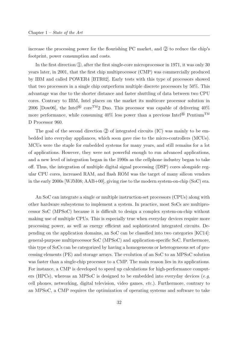
MPSoCs. As shown in Figure 1.1, this evolution had an exponential growth, starting
around 2000s, with two and four processors and reaching 4096 cores in 2017. However,
Figure 1.1: Evolution from single-to-many-core computing architecture [AT+19]
multiple challenges have been introduced for the design of such big manycore architectures.
One of them is the interconnection fabric, which must allow for a seamless integration of
numerous cores performing various functionalities.
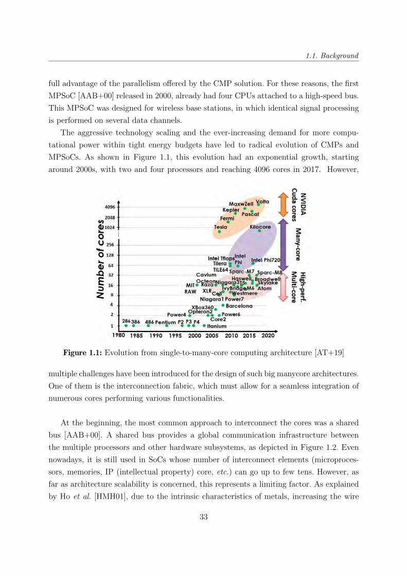
At the beginning, the most common approach to interconnect the cores was a shared
bus [AAB+00]. A shared bus provides a global communication infrastructure between
the multiple processors and other hardware subsystems, as depicted in Figure 1.2. Even
nowadays, it is still used in SoCs whose number of interconnect elements (microproces-
sors, memories, IP (intellectual property) core, etc.) can go up to few tens. However, as
far as architecture scalability is concerned, this represents a limiting factor. As explained
by Ho et al. [HMH01], due to the intrinsic characteristics of metals, increasing the wire
33
Chapter 1 – State of the Art
Figure 1.2: General Architecture for an MPSoC using a shared-memory bus-basedsystem
length to interconnect farther cores causes delays in message delivery, signal attenuation,
and higher energy dissipation. According to the ITRS projections [Sem07], without any
changes in design philosophy in the next years, up to 80% of microprocessor power will
be consumed by the interconnect. This dramatic increase of the interconnect impact on
performance and power shows clearly the challenges created by the scaling of the conven-
tional metal/dielectric system. Moreover, the voltage scaling down added to the global
wires becoming thinner will seriously increase the delay in transmission of signals over
these wires. Indeed, the overall achievable performance of any system will be radically re-
duced. In the last few years, IC manufacturers have recognized the difficulty of addressing
interconnect performance limitations by technology means alone, thus implementing new
designs and architecture improvements to address these limitations. But even with these
architectural and design innovations, interconnects still remain a critical bottleneck for
many applications. However, this bottleneck also creates an ever increasing opportunity for
future chip designers to introduce alternative technology solutions beyond metal/dielectric
interconnects.
1.2 The Network-on-Chip Paradigm
A network-on-chip (NoC) interconnection fabric is a response to the limitations car-
ried out by the conventional shared-bus system to enable many-core integration. The
concept of on-chip networks was introduced by Dally and Towles [DT01] in 2001, cap-
turing the attention of the academia and industry. In consequence, the multi-processor
architecture adopted by an SoC has initiated a paradigm shift from computation-centric to
communication-centric systems. An on-chip network introduces a higher level of commu-
34
1.2. The Network-on-Chip Paradigm
nication abstraction, enabling partitioning the design effort into minimally interdependent
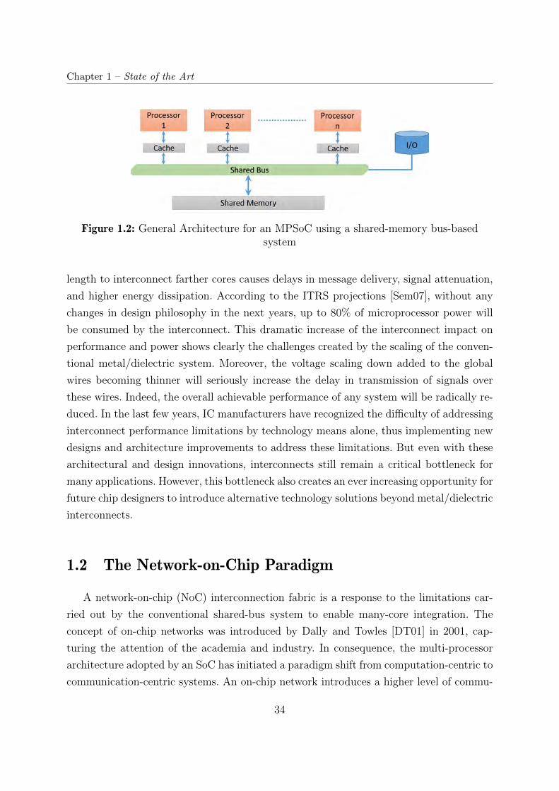
sub modules. To give a flavor for on-chip interconnection networks, Figure 1.3 illustrates
a basic design for a 4-by-4 on-chip network, which is based on a tiled architecture. The
common characteristic of these architectures is that the cores communicate with each
other using network adapters, routing nodes (switches/routers) and links. Routers route
the packets from the source node to the destination node depending on the underlying
network topology and routing strategy. The network adapter, or network interface (NI),
module deals with the mechanisms required to integrate the cores with the routers.
Figure 1.3: Topological illustration of a 4-by-4 grid structured NoC
The communication between cores in NoCs takes place through switching techniques.
These techniques are classified as circuit and packet switching. In circuit switching, a
physical path from source to destination is reserved before the transmission of the data.
However, this technique is inefficient and produces excessive blocking, which rapidly can
lead to exorbitant communication latency. On the other hand, in a packet switching,
each message is partitioned into specific length packets. Further, the packets are trans-
mitted without reserving the entire path. A packet-switched network can be classified as
store-and-forward (SAF), virtual cut-through (VCT), and wormhole. In SAF switching,
a packet is completely buffered at each immediate node before it is forwarded to the next
node. Therefore, it needs huge silicon area. In VCT switching, a packet is transmitted to
the next router as soon as there is sufficient space to store the packet. This switching tech-
nique overcomes the latency penalty of SAF. However, it also requires huge silicon area to
store the entire packet. In wormhole switching, the packets are divided into flow control
units (flits), such as header flit, payload flit, and tailer flit. The information about source
35
Chapter 1 – State of the Art
and destination are contained into the header flit. The intended message is transmitted
into the payload flit, whereas the end of packet information is contained into the tailer
flit. In this technique only a few flits are expected to be stored into the buffers, resulting
in a reduced buffer size in the respective switches, compared to SAF and VCT switching.
Generally wormhole switching is adopted for any on-chip network architecture, due to the
small silicon area required compared to the others techniques. In the last decades, several
advances in NoC research have made wormhole switching the choice for the communica-
tion backbone of multi/manycore architectures.
The rest of the section first introduces the general metrics to evaluate NoC perfor-
mance, before to present the main limitations of traditional NoC architectures.
1.2.1 General Metrics for NoCs
In addition to the general parameters that characterize and evaluate NoC performance,
such as scalability or bit error rate, there exist some of which being cited below.
Latency
Latency is defined as the time interval between the data transmission and reception
into its respective destination. This delay includes the propagation time through the
physical link as well as the processing time at the transmitter, the receiver and possibly
intermediate components, such as routers. This is particularly important for communi-
cation systems with request/confirmation signals before actual data is sent. Usually, the
latency is expressed in number of cycles. Latency can be measured in different configu-
rations of NoC. The idle latency is measured in the presence of a only message in the
network while the average latency is measured in the presence multiple messages on the
same network, which characterizes the capacity of the network manage resource sharing
by multiple messages
Throughput
The throughput is defined as the maximum quantity of information capable of being
delivered per time unit. It is also commonly known as the maximum traffic accepted by a
network. Usually, the throughput is measured as the number of flits successfully routed to
their destination per second or clock cycle. As the throughput depends on flit and network
36
1.2. The Network-on-Chip Paradigm
size, it is frequently normalized, resulting in a total number of flits delivered per core per
cycle.
Saturation Point
The saturation point is the point separating the two operating zones of the network
in terms of capacity to dispose of the data circulating there. Indeed, for message injection
rates below the saturation point, the latency remains predictable and is reasonable whereas
beyond saturation point, the latency is no longer predictable and is very high and therefore
no longer acceptable.
Energy Profile
Like any electronic circuit, NoC's power or energy consumption is an essential point
to consider. The overall power consumption of NoC can be categorized into static and
dynamic power consumption. Static power is due to leakage currents. It depends mainly
on the technology engraving thickness and the number of resources used. Dynamic power
and depends mainly on the activity, which is the toggle tare between the two signal states.
In an NoC, the energy profile is given by the network fabric and the interconnections.
Experimental results using 90 nm technology reported by Mullins [Mul06] show that the
static power of the router does not exceed 22%, the dynamic power can go up to 65% of
the total consumption of NoC. Moreover, a certain percentage up to 28% of the overall
NoC consumption is due to the inter-router wire link, which area can be 1.5 mm long
among routers in average.
Silicon Area
Due to the growing need to increase the integration density in SoCs, it is interesting
to evaluate the area dedicated to interconnections. The surface cost of a network on a
chip is determined by the routers or the transmitters/receivers, crossing points as well
as the physical communication links. Generally, the silicon surface of on-chip network is
dominated by routers or by transmitters/receivers, depending on the type of NoC used.
Other metrics
There are other metrics such as the degree of nodes that is given by the number of
communication links associated with a router or transmitter. The NoC diameter is given
37
Chapter 1 – State of the Art
by the maximum number of jumps required to route a message between the two furthest
nodes of the NoC, and this, by borrowing the shortest way.
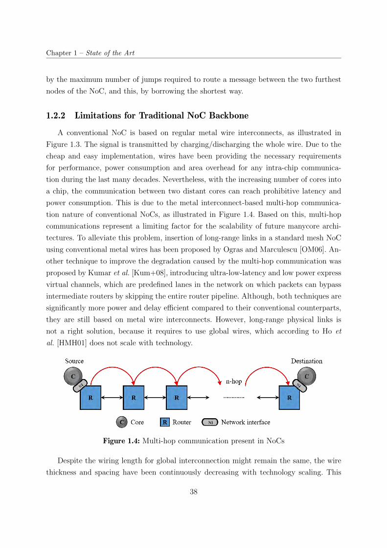
1.2.2 Limitations for Traditional NoC Backbone
A conventional NoC is based on regular metal wire interconnects, as illustrated in
Figure 1.3. The signal is transmitted by charging/discharging the whole wire. Due to the
cheap and easy implementation, wires have been providing the necessary requirements
for performance, power consumption and area overhead for any intra-chip communica-
tion during the last many decades. Nevertheless, with the increasing number of cores into
a chip, the communication between two distant cores can reach prohibitive latency and
power consumption. This is due to the metal interconnect-based multi-hop communica-
tion nature of conventional NoCs, as illustrated in Figure 1.4. Based on this, multi-hop
communications represent a limiting factor for the scalability of future manycore archi-
tectures. To alleviate this problem, insertion of long-range links in a standard mesh NoC
using conventional metal wires has been proposed by Ogras and Marculescu [OM06]. An-
other technique to improve the degradation caused by the multi-hop communication was
proposed by Kumar et al. [Kum+08], introducing ultra-low-latency and low power express
virtual channels, which are predefined lanes in the network on which packets can bypass
intermediate routers by skipping the entire router pipeline. Although, both techniques are
significantly more power and delay efficient compared to their conventional counterparts,
they are still based on metal wire interconnects. However, long-range physical links is
not a right solution, because it requires to use global wires, which according to Ho et
al. [HMH01] does not scale with technology.
Figure 1.4: Multi-hop communication present in NoCs
Despite the wiring length for global interconnection might remain the same, the wire
thickness and spacing have been continuously decreasing with technology scaling. This
38
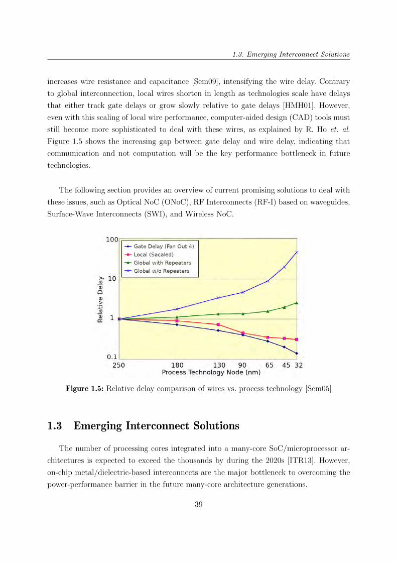
1.3. Emerging Interconnect Solutions
increases wire resistance and capacitance [Sem09], intensifying the wire delay. Contrary
to global interconnection, local wires shorten in length as technologies scale have delays
that either track gate delays or grow slowly relative to gate delays [HMH01]. However,
even with this scaling of local wire performance, computer-aided design (CAD) tools must
still become more sophisticated to deal with these wires, as explained by R. Ho et. al.
Figure 1.5 shows the increasing gap between gate delay and wire delay, indicating that
communication and not computation will be the key performance bottleneck in future
technologies.
The following section provides an overview of current promising solutions to deal with
these issues, such as Optical NoC (ONoC), RF Interconnects (RF-I) based on waveguides,
Surface-Wave Interconnects (SWI), and Wireless NoC.
Figure 1.5: Relative delay comparison of wires vs. process technology [Sem05]
1.3 Emerging Interconnect Solutions
The number of processing cores integrated into a many-core SoC/microprocessor ar-
chitectures is expected to exceed the thousands by during the 2020s [ITR13]. However,
on-chip metal/dielectric-based interconnects are the major bottleneck to overcoming the
power-performance barrier in the future many-core architecture generations.
39
Chapter 1 – State of the Art
1.3.1 Optical Interconnects
On-chip nanophotonic networks are a promising solution to overcome the limitations
of conventional electrical NoCs. Especially, when the current trends indicate that more
than hundreds of cores will be housed on a single chip in a not too distant future [Kur+10;
Lee+09]. Thus, electrical NoCs will have scalability issues with such huge networks. Op-
tical interconnections for VLSI systems were proposed at least 35 years ago, starting
with the first on-chip silicon photonics published in 1984 by Goodman et al. [Goo+84].
Subsequently, many research papers on this domain have been published.
This solution consists of replacing the electrical connections by optical waveguides.
Optical interconnects provide an opportunity to overcome the drawbacks of wire in global
communication, such as high bandwidth using multiple optical wavelengths, low elec-
tromagnetic interference, and low propagation delay of on-chip signals [Kir+06; Don+15;
Oha+09]. The modulation scheme used for this solution is mainly On-OFF Keying (OOK),
which, because of its simplicity, is perfectly suited to this type of application. Once one
optical link is established, the transmission is very fast, providing low latency with a con-
siderable amount of data (huge bandwidth), contrasted with the metal wire interconnects.
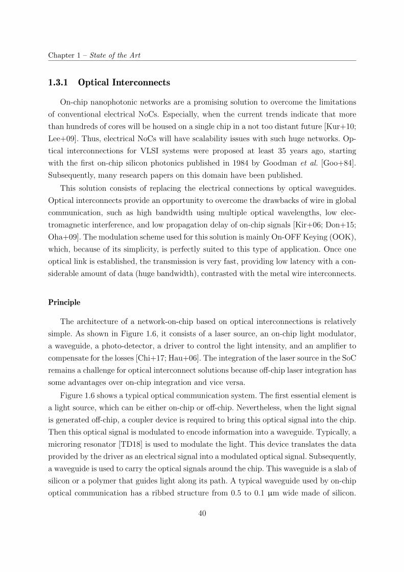
Principle
The architecture of a network-on-chip based on optical interconnections is relatively
simple. As shown in Figure 1.6, it consists of a laser source, an on-chip light modulator,
a waveguide, a photo-detector, a driver to control the light intensity, and an amplifier to
compensate for the losses [Chi+17; Hau+06]. The integration of the laser source in the SoC
remains a challenge for optical interconnect solutions because off-chip laser integration has
some advantages over on-chip integration and vice versa.
Figure 1.6 shows a typical optical communication system. The first essential element is
a light source, which can be either on-chip or off-chip. Nevertheless, when the light signal
is generated off-chip, a coupler device is required to bring this optical signal into the chip.
Then this optical signal is modulated to encode information into a waveguide. Typically, a
microring resonator [TD18] is used to modulate the light. This device translates the data
provided by the driver as an electrical signal into a modulated optical signal. Subsequently,
a waveguide is used to carry the optical signals around the chip. This waveguide is a slab of
silicon or a polymer that guides light along its path. A typical waveguide used by on-chip
optical communication has a ribbed structure from 0.5 to 0.1 µm wide made of silicon.
40
1.3. Emerging Interconnect Solutions
Figure 1.6: Conventional optical network interface architecture [Chi+17]
At the receiver side, three components are used to detect the optical signal: a microring
resonator, a photodetector, and a transimpedance amplifier. The microring is required to
extract a particular wavelength from the data waveguide. The separated wavelength is fed
into the photodetector, converting the optical signal into an electrical one. Finally, the
transimpedance amplifier is used to amplify the received signal.
A laser is built around a simple principle: stimulate a material to produce light. This
material is known as the “gain medium” and is fundamental to produce light. This mate-
rial is stimulated by injecting electrical charge or transmitting an optical signal through
it. Mostly, the gain medium is placed between two optical mirrors, stimulating the gain
medium by light bounces, producing more light. This light forms the output of the laser.
The gain medium of an off-chip laser is typically made of silicon doped with gallium and
arsenic or with erbium-doped silicon. On the other hand, multiple parallel communications
are required to take advantage of the optical interconnection. Consequently, a dense wave-
length division multiplexing (DWDM) technique is used to achieve this goal [Van+08].
This can be done either off-chip with a multiwavelength source or on-chip with comb-based
splitters [Lev+11], which can split monochromatic light at 1.550 nm to produce light at
different equispaced wavelengths. Subsequently, the off-chip laser is coupled to a waveg-
41
Chapter 1 – State of the Art
uide inside the chip using an special tapered waveguide [Pen+10]. Another laser category
proposed for off-chip laser applications is called DML 1 laser, which allows to directly
modulate the output of the laser by electrical power variations. These types of lasers are
commercially available and more than a dozen research prototypes have been fabricated
and demonstrated [Fau+13; Fau+12]. Furthermore, it is possible to create an array of
DML lasers using a tunable laser source with multiple power levels, as demonstrated by
Peter et al. [Pet+15].
On-chip lasers are another laser category, which allows for full integration of opti-
cal interconnection into the chip. This type of light source was invented by Koyama in
1977 [Koy06], and called the VCSEL 2 laser. It consists of two parallel Bragg reflecting
surfaces with a quantum well in the middle and typically produces around 3 to 10 mW of
optical power. According to Amman and Hofmann [AH09], VCSEL lasers have relatively
higher wall-plug efficiency and can be modulated at GHz frequencies. The wall-plug effi-
ciency is the energy conversion efficiency with which the system converts electrical power
into optical power. This wall-plug efficiency is around 30% today, but it is expected to
grow up to 50% over the next decades [AH09]. On the other hand, the VCSEL lasers have
their own set of problems, starting with the fact that they are integrated into the chip,
adding their power dissipation into the already stressed dissipation system of the chip.
Contrary to off-chip lasers, where the dissipation stress can be better managed.
Challenges
On-chip nanophotonic networks mainly face challenges related to complexity, thermal
regulation and power budget requirements [Hau+06; Mil09]. Researchers have different
point of view related to optical interconnect power consumption. Optimistic researchers
argue that the absence of RLC impedance together with the quantum efficiency can offer
better pJ/bit than regular metal wires [Kir+06; Hau+06]. In contrast, pessimistic re-
searchers are more skeptical due to the existent power-hungry and low-efficiency optical
devices [Daw+03; Kur+10; Li+16]. Moreover, since current devices decay the signal sig-
nificantly, optical multicast requires more optical power to make multicast just with a few
optical devices.
Another challenge of optical interconnects is related to their complexity. They require
an expensive area and sometimes non-CMOS devices to transfer signals from electrical to
1. Directly Modulated Laser2. Vertical-Cavity Surface Emitting Laser
42
1.3. Emerging Interconnect Solutions
optical form [Mil09]. Non-CMOS devices are placed off-chip, adding additional issues to
the manufacturing process. Besides, additional couplers are required to bring the optical
signal into the chip, which might provide important losses demanding a power-hungry
budget. However, advances in more-than-Moore options represented by silicon photonics
devices have almost eliminated the CMOS compatibility challenge [Mea+14; Mic11]. But
these technologies are still immature, facing their own challenges. Consequently, optical
interconnects are still a relatively costly alternative despite all the significant advances.
On the other hand, waveguide design is constrained to avoid hard turns, which causes
major signal degradation.
Thermal tuning management is a major challenge for optical interconnects, which is
required in microring-based wavelength filters. Otherwise, spatial and temporal thermal
variations might lead to system communication failures in many-core systems [Li+12;
Che+13]. Furthermore, according to Mustafa et al. [Moh+14], resonant devices charac-
teristics (e.g., passband wavelengths of microrings and racetracks) are sensitive to device
dimensions and refractive indices of materials. This degrades the system performance and
increases power dissipation, when passbands of receivers and transmitters are not fully
overlapped [Moh+14]. Some techniques are introduced to compensate for thermal and
process variations, however, their complexity increases the optical interconnect cost and
power budget. Therefore, due to theses strong challenges, optical interconnects are still
on a longer term perspective.
1.3.2 RF Interconnects with Transmission Lines (RF-I)
Similar to the optical Gigabit solution, RF waves travel at a speed close to the speed of
light. However, unlike optical solutions, Radio Frequency (RF) directly benefits from full
compatibility with CMOS technology. RF waves can be transmitted through the free space
using antennas or by waveguided propagation using transmission lines (TLs), which is
known as RF-I [Cha+08b; Cha+08a; Cha+08; VSP13]. These types of interconnects offer
more immunity to interference, reasonable signal attenuation, low global communication
energy, and high throughput compared to regular wires. Many research papers propound
RF-I as a supplementary interconnect for the metal wires [Cha+08b; Cha+08a].
43
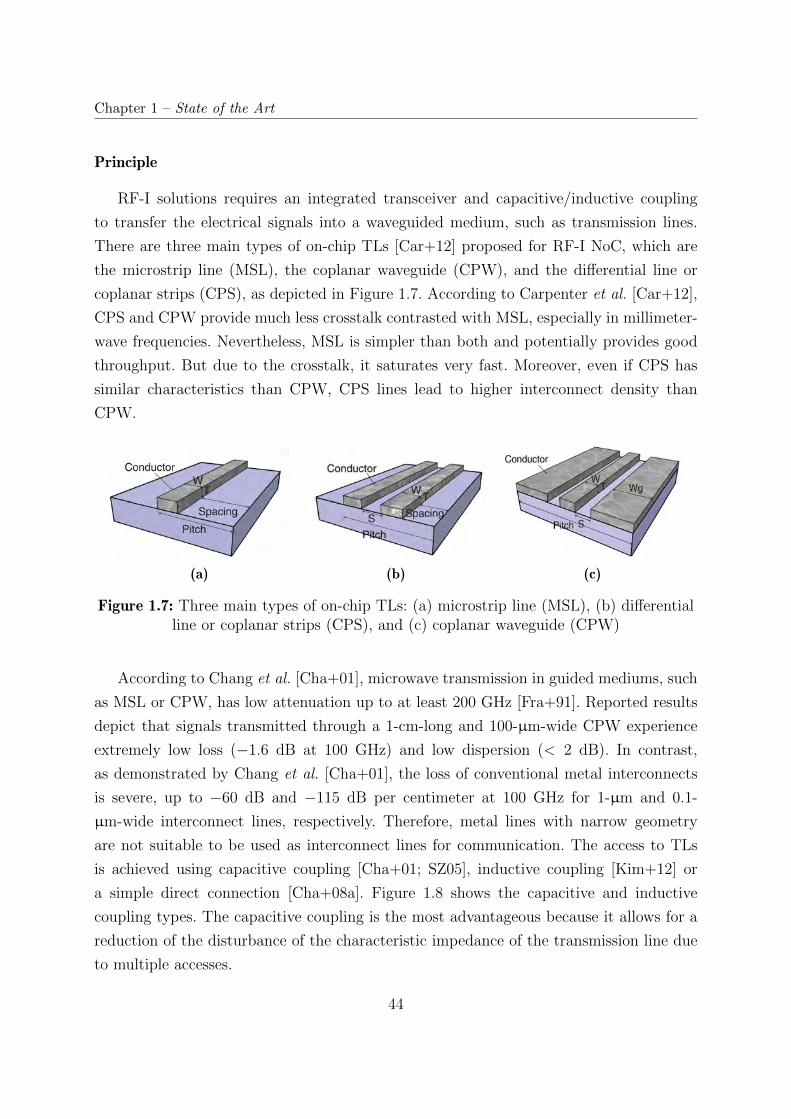
Chapter 1 – State of the Art
Principle
RF-I solutions requires an integrated transceiver and capacitive/inductive coupling
to transfer the electrical signals into a waveguided medium, such as transmission lines.
There are three main types of on-chip TLs [Car+12] proposed for RF-I NoC, which are
the microstrip line (MSL), the coplanar waveguide (CPW), and the differential line or
coplanar strips (CPS), as depicted in Figure 1.7. According to Carpenter et al. [Car+12],
CPS and CPW provide much less crosstalk contrasted with MSL, especially in millimeter-
wave frequencies. Nevertheless, MSL is simpler than both and potentially provides good
throughput. But due to the crosstalk, it saturates very fast. Moreover, even if CPS has
similar characteristics than CPW, CPS lines lead to higher interconnect density than
CPW.
(a) (b) (c)
Figure 1.7: Three main types of on-chip TLs: (a) microstrip line (MSL), (b) differentialline or coplanar strips (CPS), and (c) coplanar waveguide (CPW)
According to Chang et al. [Cha+01], microwave transmission in guided mediums, such
as MSL or CPW, has low attenuation up to at least 200 GHz [Fra+91]. Reported results
depict that signals transmitted through a 1-cm-long and 100-µm-wide CPW experience
extremely low loss (−1.6 dB at 100 GHz) and low dispersion (< 2 dB). In contrast,
as demonstrated by Chang et al. [Cha+01], the loss of conventional metal interconnects
is severe, up to −60 dB and −115 dB per centimeter at 100 GHz for 1-µm and 0.1-
µm-wide interconnect lines, respectively. Therefore, metal lines with narrow geometry
are not suitable to be used as interconnect lines for communication. The access to TLs
is achieved using capacitive coupling [Cha+01; SZ05], inductive coupling [Kim+12] or
a simple direct connection [Cha+08a]. Figure 1.8 shows the capacitive and inductive
coupling types. The capacitive coupling is the most advantageous because it allows for a
reduction of the disturbance of the characteristic impedance of the transmission line due
to multiple accesses.
44
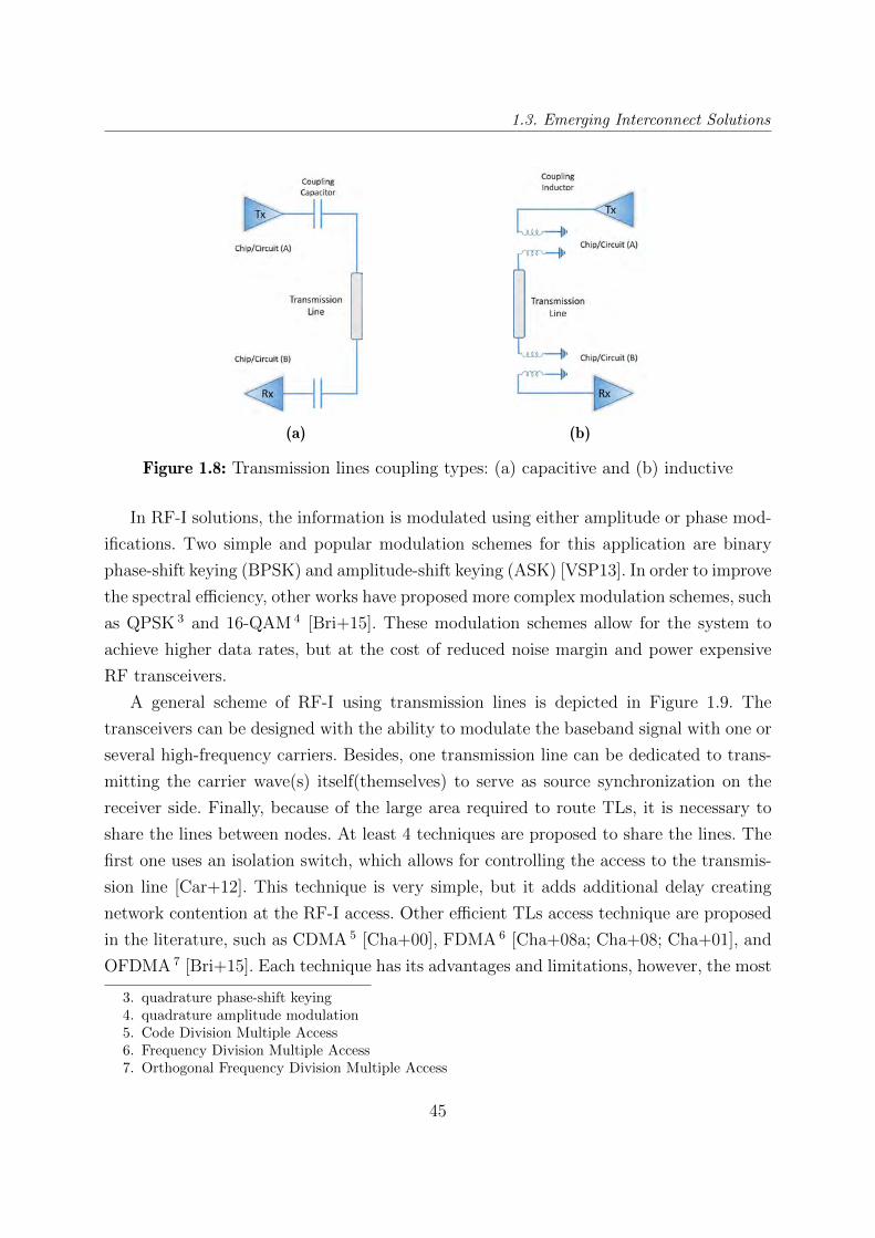
1.3. Emerging Interconnect Solutions
(a) (b)
Figure 1.8: Transmission lines coupling types: (a) capacitive and (b) inductive
In RF-I solutions, the information is modulated using either amplitude or phase mod-
ifications. Two simple and popular modulation schemes for this application are binary
phase-shift keying (BPSK) and amplitude-shift keying (ASK) [VSP13]. In order to improve
the spectral efficiency, other works have proposed more complex modulation schemes, such
as QPSK 3 and 16-QAM 4 [Bri+15]. These modulation schemes allow for the system to
achieve higher data rates, but at the cost of reduced noise margin and power expensive
RF transceivers.
A general scheme of RF-I using transmission lines is depicted in Figure 1.9. The
transceivers can be designed with the ability to modulate the baseband signal with one or
several high-frequency carriers. Besides, one transmission line can be dedicated to trans-
mitting the carrier wave(s) itself(themselves) to serve as source synchronization on the
receiver side. Finally, because of the large area required to route TLs, it is necessary to
share the lines between nodes. At least 4 techniques are proposed to share the lines. The
first one uses an isolation switch, which allows for controlling the access to the transmis-
sion line [Car+12]. This technique is very simple, but it adds additional delay creating
network contention at the RF-I access. Other efficient TLs access technique are proposed
in the literature, such as CDMA 5 [Cha+00], FDMA 6 [Cha+08a; Cha+08; Cha+01], and
OFDMA 7 [Bri+15]. Each technique has its advantages and limitations, however, the most
3. quadrature phase-shift keying4. quadrature amplitude modulation5. Code Division Multiple Access6. Frequency Division Multiple Access7. Orthogonal Frequency Division Multiple Access
45
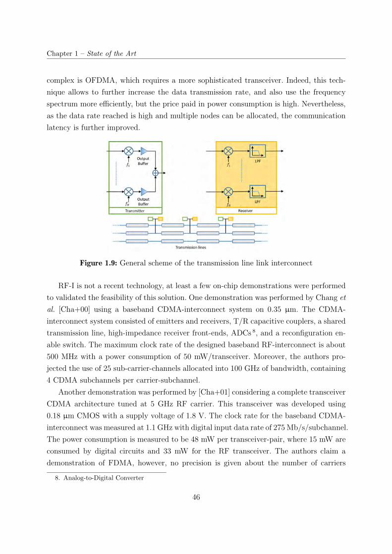
Chapter 1 – State of the Art
complex is OFDMA, which requires a more sophisticated transceiver. Indeed, this tech-
nique allows to further increase the data transmission rate, and also use the frequency
spectrum more efficiently, but the price paid in power consumption is high. Nevertheless,
as the data rate reached is high and multiple nodes can be allocated, the communication
latency is further improved.
Figure 1.9: General scheme of the transmission line link interconnect
RF-I is not a recent technology, at least a few on-chip demonstrations were performed
to validated the feasibility of this solution. One demonstration was performed by Chang et
al. [Cha+00] using a baseband CDMA-interconnect system on 0.35 µm. The CDMA-
interconnect system consisted of emitters and receivers, T/R capacitive couplers, a shared
transmission line, high-impedance receiver front-ends, ADCs 8, and a reconfiguration en-
able switch. The maximum clock rate of the designed baseband RF-interconnect is about
500 MHz with a power consumption of 50 mW/transceiver. Moreover, the authors pro-
jected the use of 25 sub-carrier-channels allocated into 100 GHz of bandwidth, containing
4 CDMA subchannels per carrier-subchannel.
Another demonstration was performed by [Cha+01] considering a complete transceiver
CDMA architecture tuned at 5 GHz RF carrier. This transceiver was developed using
0.18 µm CMOS with a supply voltage of 1.8 V. The clock rate for the baseband CDMA-
interconnect was measured at 1.1 GHz with digital input data rate of 275 Mb/s/subchannel.
The power consumption is measured to be 48 mW per transceiver-pair, where 15 mW are
consumed by digital circuits and 33 mW for the RF transceiver. The authors claim a
demonstration of FDMA, however, no precision is given about the number of carriers
8. Analog-to-Digital Converter
46
1.3. Emerging Interconnect Solutions
used during the experimentation, neither for the RF transceiver. The data rate per chip
projections given by the authors for their proposed transceiver is overestimated up to
20 Tb/s/chip assuming 200 RF-interconnects. This is a huge number of RF-I nodes, con-
sidering the non-negligible power consumption of each transceiver.
A non-coherent ASK modulation-based RF-I system was developed by
Kim et al. [Kim+12] for memory interface design. The proposed system is not
limited by thermal noise, which leads to a compact and energy-efficient transceiver
architecture design. This transceiver is conceived in 65 nm CMOS with a supply voltage
of 1.2 V, supporting a simultaneous bidirectional 8 Gb/s/pin communication. The
transceiver power consumption is measured to be 32 mW. The digital part of the
transceiver consumes 14.4 mW, and the RF radio tuned at 18 GHz requires 17.6 mW.
The total chip area occupied by this transceiver is 0.12 mm2.
A baseband transceiver OFDMA-based RF-I system was proposed by Alexan-
dre et al. [Bri+15]. This transceiver allows to reach a maximum bandwidth occupa-
tion and further improve average communication latency. Nevertheless, the surface and
power of transceiver is mainly due to FFT/IFFT and ADC/DAC blocks. For instance, the
FFT/IFFT and ADC blocks can easily consume 135 mW and 162 mW, respectively. Even
with technology scaling, the power consumption drained by these blocks will be always
non-negligible, dissipating a huge heat into a very small area. Moreover, the RF radio
required by this kind of transceiver requires more sophisticated modulation schemes, such
as BPSK, QPSK, and M-QAM, adding additional costs.
Challenges
RF interconnects based on TLs face inherent challenges of RF circuitry such as in-
terference and technology limitations. Nevertheless, the main challenge faced by RF-I is
crosstalk among TLs and between the surrounding circuitry and TLs. The TLs are prone
to crosstalk, especially at high frequencies or in long distance. This is due to the skin-
effect, which is increased as the operating frequency is increased. To solve this problem,
Hiroyuk et al. [Ito+08] have proposed to use transmission lines with low characteristic
impedance (Z0). However, this also increases the power dissipation. Another solution is
proposed by Beckman and Wood [BW03], using alternating power and ground shielding
lines between each transmission line, in addition to the reference planes above and be-
low the signal layer. Some studies propose the insertion of an interleaved metal pattern
underneath of a signal line in a multi-layer design [HLH12]. This inserted metal plays a
47
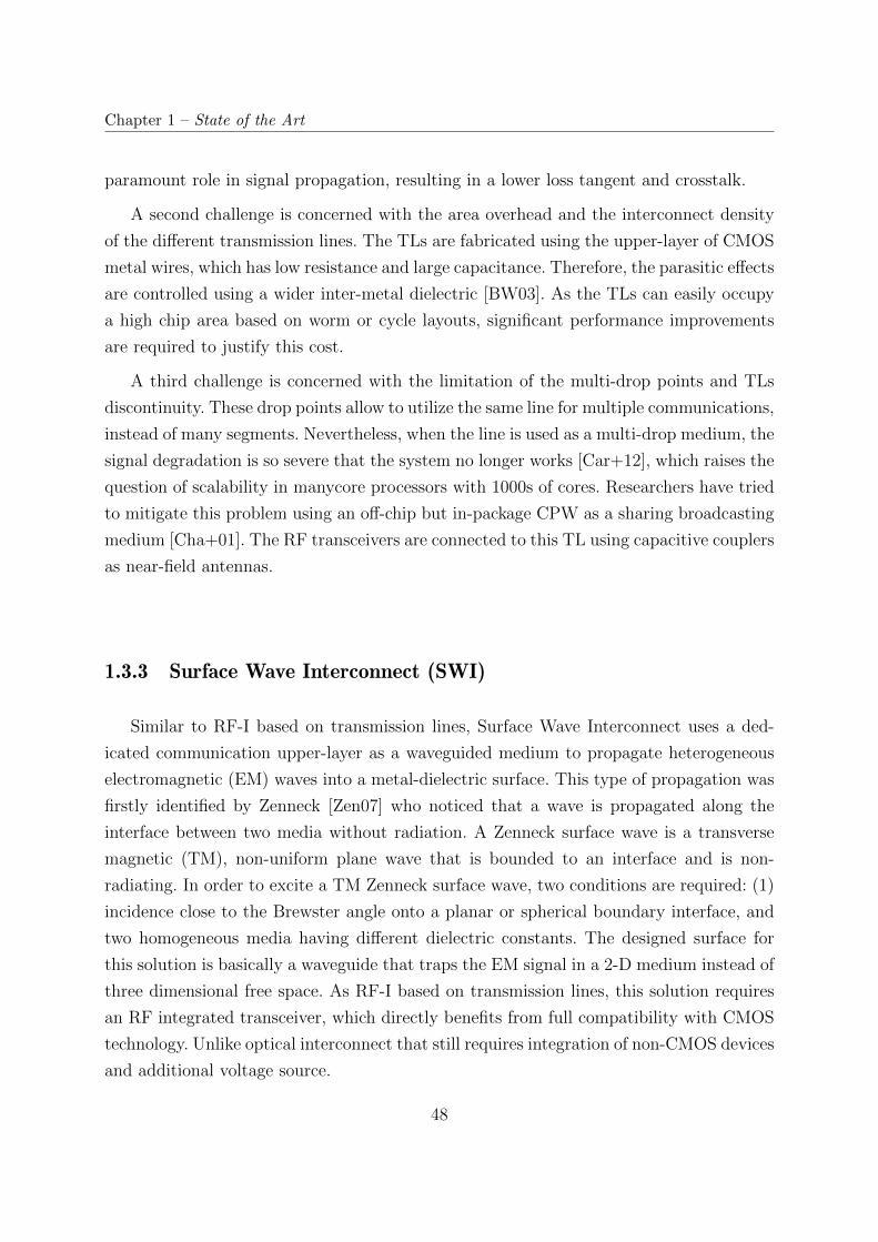
Chapter 1 – State of the Art
paramount role in signal propagation, resulting in a lower loss tangent and crosstalk.
A second challenge is concerned with the area overhead and the interconnect density
of the different transmission lines. The TLs are fabricated using the upper-layer of CMOS
metal wires, which has low resistance and large capacitance. Therefore, the parasitic effects
are controlled using a wider inter-metal dielectric [BW03]. As the TLs can easily occupy
a high chip area based on worm or cycle layouts, significant performance improvements
are required to justify this cost.
A third challenge is concerned with the limitation of the multi-drop points and TLs
discontinuity. These drop points allow to utilize the same line for multiple communications,
instead of many segments. Nevertheless, when the line is used as a multi-drop medium, the
signal degradation is so severe that the system no longer works [Car+12], which raises the
question of scalability in manycore processors with 1000s of cores. Researchers have tried
to mitigate this problem using an off-chip but in-package CPW as a sharing broadcasting
medium [Cha+01]. The RF transceivers are connected to this TL using capacitive couplers
as near-field antennas.
1.3.3 Surface Wave Interconnect (SWI)
Similar to RF-I based on transmission lines, Surface Wave Interconnect uses a ded-
icated communication upper-layer as a waveguided medium to propagate heterogeneous
electromagnetic (EM) waves into a metal-dielectric surface. This type of propagation was
firstly identified by Zenneck [Zen07] who noticed that a wave is propagated along the
interface between two media without radiation. A Zenneck surface wave is a transverse
magnetic (TM), non-uniform plane wave that is bounded to an interface and is non-
radiating. In order to excite a TM Zenneck surface wave, two conditions are required: (1)
incidence close to the Brewster angle onto a planar or spherical boundary interface, and
two homogeneous media having different dielectric constants. The designed surface for
this solution is basically a waveguide that traps the EM signal in a 2-D medium instead of
three dimensional free space. As RF-I based on transmission lines, this solution requires
an RF integrated transceiver, which directly benefits from full compatibility with CMOS
technology. Unlike optical interconnect that still requires integration of non-CMOS devices
and additional voltage source.
48
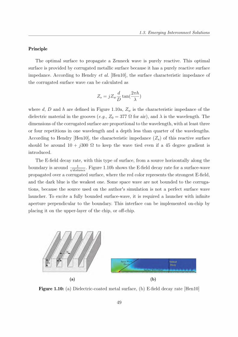
1.3. Emerging Interconnect Solutions
Principle
The optimal surface to propagate a Zenneck wave is purely reactive. This optimal
surface is provided by corrugated metallic surface because it has a purely reactive surface
impedance. According to Hendry et al. [Hen10], the surface characteristic impedance of
the corrugated surface wave can be calculated as
Zs = jZwd
Dtan(2πh
λ)
where d, D and h are defined in Figure 1.10a, Zw is the characteristic impedance of the
dielectric material in the grooves (e.g., Z0 = 377 Ω for air), and λ is the wavelength. The
dimensions of the corrugated surface are proportional to the wavelength, with at least three
or four repetitions in one wavelength and a depth less than quarter of the wavelengths.
According to Hendry [Hen10], the characteristic impedance (Zs) of this reactive surface
should be around 10 + j300 Ω to keep the wave tied even if a 45 degree gradient is
introduced.
The E-field decay rate, with this type of surface, from a source horizontally along the
boundary is around 1√distance
. Figure 1.10b shows the E-field decay rate for a surface-wave
propagated over a corrugated surface, where the red color represents the strongest E-field,
and the dark blue is the weakest one. Some space wave are not bounded to the corruga-
tions, because the source used on the author's simulation is not a perfect surface wave
launcher. To excite a fully bounded surface-wave, it is required a launcher with infinite
aperture perpendicular to the boundary. This interface can be implemented on-chip by
placing it on the upper-layer of the chip, or off-chip.
(a) (b)
Figure 1.10: (a) Dielectric-coated metal surface, (b) E-field decay rate [Hen10]
49
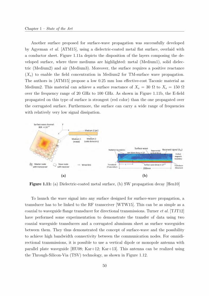
Chapter 1 – State of the Art
Another surface proposed for surface-wave propagation was successfully developed
by Agyeman et al. [ATM15], using a dielectric-coated metal flat surface, overlaid with
a conductor sheet. Figure 1.11a depicts the disposition of the layers composing the de-
veloped surface, where three mediums are highlighted: metal (Medium1), solid dielec-
tric (Medium2) and air (Medium3). Moreover, the surface requires a positive reactance
(Xs) to enable the field concentration in Medium2 for TM-surface wave propagation.
The authors in [ATM15] propose a low 0.25 mm loss effective-cost Taconic material as
Medium2. This material can achieve a surface reactance of Xs = 30 Ω to Xs = 150 Ωover the frequency range of 20 GHz to 100 GHz. As shown in Figure 1.11b, the E-field
propagated on this type of surface is strongest (red color) than the one propagated over
the corrugated surface. Furthermore, the surface can carry a wide range of frequencies
with relatively very low signal dissipation.
(a) (b)
Figure 1.11: (a) Dielectric-coated metal surface, (b) SW propagation decay [Hen10]
To launch the wave signal into any surface designed for surface-wave propagation, a
transducer has to be linked to the RF transceiver [WTW15]. This can be as simple as a
coaxial to waveguide flange transducer for directional transmissions. Turner et al. [TJT12]
have performed some experimentation to demonstrate the transfer of data using two
coaxial waveguide transducers and a corrugated aluminum sheet as surface waveguides
between them. They thus demonstrated the concept of surface-wave and the possibility
to achieve high bandwidth connectivity between the communication nodes. For omnidi-
rectional transmissions, it is possible to use a vertical dipole or monopole antenna with
parallel plate waveguide [HU08; Kar+12; Kar+13]. This antenna can be realized using
the Through-Silicon-Via (TSV) technology, as shown in Figure 1.12.
50
1.3. Emerging Interconnect Solutions
Figure 1.12: Integrated transceiver and integrated transducer (invertedquarterwavelength monopole) stacked over a designed surface. [Kar+15]
Challenges
The surface-wave interconnection can be considered as the newest and very promising
emerging interconnect, especially because the natural fan-out provided by this technology
is only limited by the cover area of the propagated signal. Moreover, according to the
material used for the surface-wave propagation, it can provide a very low signal loss.
Thus, the RF transceivers can be designed to be very energy efficient. In consequence,
the potentials of this emerging technology requires research to tackle a set of design and
implementation challenges at different levels in order for it to be utilized in future NoC.
The first challenge of this interconnection is related to the integration of components.
Once the designed surface for SWI is integrated on the chip, the connection between the
transceiver and the transducer requires some 3D integration technique, such as TSV and
flip-chip bonding [Kar+15]. According to the ITRS [Sem09], the 3D integration is still an
active research area and face many challenges for manufacturing and factory integration,
such as advanced process control, thinning the wafer, low TSV capacitance, and design
challenges. Nevertheless, nowadays great progress is being attained in these areas and
there exists a number of solutions for each problem.
A second challenge is related to the design of the surface and the transducer used
to launch the surface-wave. For instance, a SWI may pick up some noise signals for the
nearby integrated devices on a MPSoC, which could affect the wave guide surface injecting
undesired interference. Moreover, careful considerations have to be taken to launch the
surface-wave signal, because if the incident signal is not close to the Brewster angle, many
reflections can be propagated, thus degrading the communication [Kar+13].
51
Chapter 1 – State of the Art
1.4 Wireless Network-on-Chip
A conventional NoC with metal wire interconnects operates at 5 GHz in the best case.
Nevertheless, this may only correspond to around 1.5% of the frequency band available
for a specific CMOS 9 technology. This frequency band is constrained by the CMOS cut-
off frequencies (fT/fmax), which increases with the technology scaling. In case of 32 nmprocess [Sem07], the maximum transit frequency or unity-gain frequency (fT ) is 280 GHz,
and the maximum oscillation frequency (fmax) is 340 GHz. Both values mostly used for
the design of power amplifiers and oscillators. On the other hand, changing the transistor
fabrication process can result in higher operation frequencies. For instance, a very high
fmax = 1.1 THz was reported in [Urt+11] using a 130nm Indium Phosphide (InP) double
heterojunction bipolar transistor (DHBT) technology. Furthermore, a fmax = 720 GHzhave been achieved for SiGe process technologies [Hei+16]. However, these technologies are
too expensive to be used ubiquitously in consumer devices. Contrary to CMOS technology
which has good switching performance and low cost, dominating the fabrication of current
digital and mixed-signal ICs.
Electrical NoCs suffer from the weakness of reconfiguring the allocation of the available
bandwidth, high power dissipation, and latency that increases with the number of cores.
The Wireless Network-on-Chip (WiNoC) is proposed to overcome these limitations. A
wireless interconnect system consists of integrated receivers and transmitters with on-chip
antennas which communicate across a single chip or between multiple chips at a specific
phase velocity 10(Vp), via electromagnetic waves. The possibility of on-chip wireless inter-
connects was first demonstrated by Floyd et al. [FCO02], using the wireless interconnects
for distributing clock signals throughout the IC. After this first demonstration, wireless
interconnects were broadly explored to be applied into on-chip networks.
The major asset of WiNoC is to take advantage of the very wide frequency band
available in the CMOS process. In this context, it is expected that the transistor cut-off
frequencies (fT/fmax) will reach 0.6/1 THz in 16 nm CMOS technology [Sem07]. This
would allow the design of wideband wireless systems requiring very little silicon surface to
be implemented. Furthermore, communication patterns, such as broadcast and multicast
are easier to reach using wireless than metal wire interconnects. Wireless links are an
innovative solution, which allows decreasing the number of hops in a traditional NoC,
thus improving the performance in latency, power consumption, and throughput. Using
9. Complementary Metal Oxide Semiconductor10. Rate at which the phase of the wave propagates through space
52
1.4. Wireless Network-on-Chip
wireless links, the transmission range can increase, covering the whole chip. Therefore,
for the same given transmission distance between two nodes, the same message may
be received by other wireless nodes at the same time. These characteristics outperform
optical links, where an optical wavelength can be only received by one optical node tuned
at the same wavelength. However, this problem can be somehow solved using multiple
optical wavelengths. On the other hand, wireless links are not facing crosstalk problems,
unlike between the transmission lines used in RF-I. The benefits of WiNoCs are then fully
ensured starting from a certain size of multi/many core architectures. Nevertheless, there
are still many challenges to be solved before implementing this technology.
1.4.1 WiNoC Frequency Spectrum
The effectiveness of WiNoCs strongly depends on the design of the physical layer,
which is required to establish the wireless communication. The miniaturization of on-chip
antennas and transceivers improves the performance of the physical layer. Characteristics
of both these elements are directly related with the operating frequency range of com-
munication. WiNoC architectures explored by different research groups can be broadly
classified into five classes depending on their operating frequency range, ultra-wideband,
millimeter-wave, sub-terahertz, terahertz, and optical waves.
Ultra-WideBand (UWB)
Ultra-WideBand (UWB) wireless communication systems are emerging as a promis-
ing solution for high-data-rate and short-distance wireless data transmission. Other terms
associated with ultra-wideband include “impulse radio”, “short-pulse”, “non-sinusoidal”,
“carrierless”, “time domain”, “super wideband”, “fast frequency chirp” and “mono-
pulse” [OHI05]. Different from several other developed wireless interconnect technolo-
gies, UWB can achieve low-power and low-cost implementation, providing high-bandwidth
communication over a large portion of the radio spectrum. Moreover, contrary to conven-
tional narrow-band and carrier-wave transmission, UWB transmits signals in a manner
that causes very little interference with existing narrow-band radio systems. However, this
type of communication is very sensitive to distance, rapidly decreasing the data transfer
rate at a short distance.
The US Federal Communications Commission (FCC) has defined a UWB system as
one whose fractional bandwidth is more than 20% or whose absolute bandwidth is wider
53
Chapter 1 – State of the Art
than 500 MHz between 3.1 GHz and 10.6 GHz [Com+02]. Nevertheless, due to the short
distances into on-chip wireless communication, the frequency range provided by the FCC
is not mandatory. Especially, because the transmission power used for this kind of commu-
nication system is negligible compared to other applications. The UWB technique requires
a very low emission power density, as well as resilience to multi-path interference [WS98]
and low-cost implementation. For these reasons, it was proposed as an alternative solution
to provide communications between functional blocks on a large integrated circuit chip
(intra-chip) as well as communications between functional blocks on separate chips (inter-
chip) located on a multi-chip module [SSK04], where the distances between functional
blocks are measured in a few to tens of centimeters.
A UWB transmitter uses Gaussian monocycle pulses (GMP) generator to produce an
ultra-short pulse to realize an extremely low power spectral density (PSD). The most
common modulation schemes used for the transmitted pulse are: pulse position modula-
tion (PPM), on-off keying (OOK), and biphase modulation (BPM) or binary phase shift
keying (BPSK). The receiver is made up of a wideband low-noise amplifier (LNA), a corre-
lator that consists of a multiplier and integrator, an analog-to-digital converter (ADC) and
some synchronization circuits. Besides, multiple access capabilities can be implemented
using time hopping and direct sequence coding [QLS05]. Coherent and non-coherent de-
modulation techniques are available too, as for carrier-based communication systems. As
explained by Welborn [Wel01], UWB systems using OOK and PPM can use envelope de-
tectors to simplify timing requirements and the bandwidth required by A/D converters,
but at the expense of performance. However, in case of using BPM, the demodulation
must be coherent, because every pulse would look the same at the output of an envelop
detector. The BPM modulation provides 3 dB advantages in efficiency compared to PPM
and OOK, to achieve the same bit error rate (BER), which is a function of the distance.
With the development of integrated antennas into integrated circuits [KK99], on-
chip wireless communications started to take relevance, especially after demonstrating
the possibility of using wireless interconnection for clock distribution and data transmis-
sion [FCO02; Zha04]. As a UWB radio using GMP does not require any carrier, contrary to
a heterodyne-based radio, it offers a low-cost and high data-rate communication solution
for short-distance wireless links. For these reasons, it caught the attention of researchers to
provide an alternative solution for capacitive and inductive coupling technique propounded
54
1.4. Wireless Network-on-Chip
for inter-chip 3D custom stacked systems [Miz+04], as well as intra-chip communication.
In this context, at least three types of antennas were proposed for on-chip UWB com-
munication systems, as shown in Figure 1.13. The potentiality of an integrated on-chip
antenna to scale with CMOS devices made wireless interconnection a very promising so-
lution among any other interconnection technology. However, there are some drawbacks
related to the attenuation and channel characteristics, which are analyzed in Chapter 2.
Two UWB transmitters for data and clock transmissions using GMP generator and
OOK modulation were proposed by Fukuda et al. [SK+06] for global wireless interconnec-
tion of a 3D stacked-chip. The clock and data transmitters were developed using 0.18 µmCMOS technology with 1.8V power supply, requiring an area of 0.163 mm2 (46 mW)
and 0.136 mm2 (36 mW), respectively. The linear half-wave dipole antenna used for both
transmitters was tuned at 1 GHz, with a length of around 43.5 mm, as shown in Fig-
ure 1.13a. The data rate provided by a single data wireless link is 250 Mbps, offering an
energy efficiency of 144 pJ/bit. This transmitter overcome the transmission distance limit
of inductive and coupling interconnections, but was however not powered efficient.
Sasaki et al. [Sas+09] proposed a UWB receiver with a meander dipole integrated
antenna using 0.18µm CMOS technology. This receiver is capable of retrieving forwarded
data from a UWB transmitter based on GMP generators with OOK modulation. The
antenna is tuned at 3 GHz, with an area of 4 mm × 0.45 mm. The area occupied by
the receiver is 0.54 mm2, consuming a total power of 43 mW at 1.8 V. This receiver is
capable of recovering 200 Mb/s from a signal, which was transmitted from an integrated
antenna at a distance of 0.5 mm. Timing signals must be inserted into the transmitted
data to perform synchronization at the receiver side.
A GMP transmitter for UWB radio was designed by Takamaro et al. [Kik+08] for
intra/inter chip transmissions. This transmitter consists of an 8-stage differential voltage
controlled oscillator (VCO), a 8 to 1 multiplexer (MUX), a triangular pulse generation
(TPG), a differentiator, a single-input dual-output amplifier (SIDO), a differential-output
amplifier, and a source follower. In order to verify the GMP transmitter, a test chip was
fabricated in a 0.18 µm CMOS technology with a supply voltage of 1.8 V. Two meander
dipole antennas were printed on the chip occupying an area of 2.98 mm × 0.45 mm, as
shown in Figure 1.13b. The total power dissipation, including the output amplifiers was
21.6 mW. The transmission and reception of generated GMP at the rate of 1.16 Gb/s was
demonstrated for a communication distance of 1 mm.
A complete UWB prototype transceiver using an on-package monopole antenna was de-
55
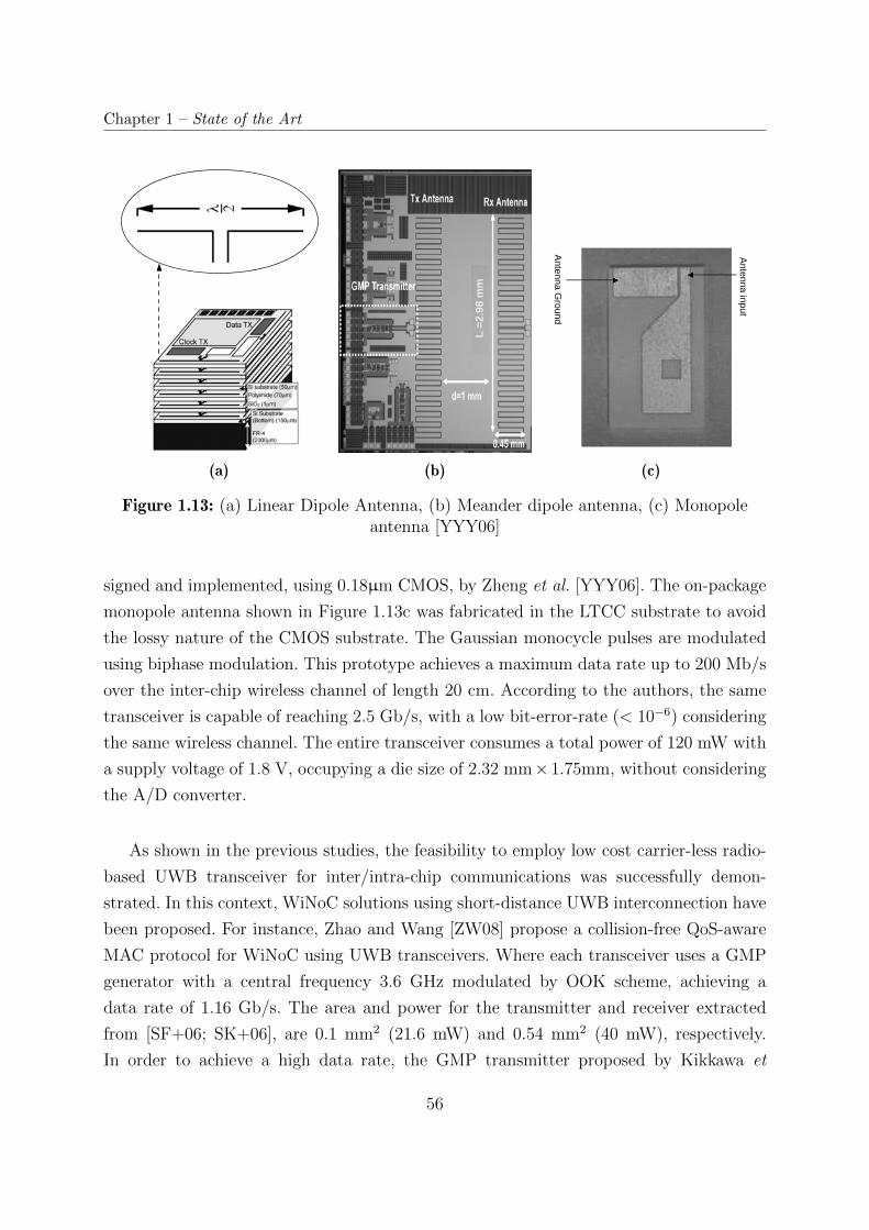
Chapter 1 – State of the Art
(a) (b) (c)
Figure 1.13: (a) Linear Dipole Antenna, (b) Meander dipole antenna, (c) Monopoleantenna [YYY06]
signed and implemented, using 0.18µm CMOS, by Zheng et al. [YYY06]. The on-package
monopole antenna shown in Figure 1.13c was fabricated in the LTCC substrate to avoid
the lossy nature of the CMOS substrate. The Gaussian monocycle pulses are modulated
using biphase modulation. This prototype achieves a maximum data rate up to 200 Mb/sover the inter-chip wireless channel of length 20 cm. According to the authors, the same
transceiver is capable of reaching 2.5 Gb/s, with a low bit-error-rate (< 10−6) considering
the same wireless channel. The entire transceiver consumes a total power of 120 mW with
a supply voltage of 1.8 V, occupying a die size of 2.32 mm×1.75mm, without considering
the A/D converter.
As shown in the previous studies, the feasibility to employ low cost carrier-less radio-
based UWB transceiver for inter/intra-chip communications was successfully demon-
strated. In this context, WiNoC solutions using short-distance UWB interconnection have
been proposed. For instance, Zhao and Wang [ZW08] propose a collision-free QoS-aware
MAC protocol for WiNoC using UWB transceivers. Where each transceiver uses a GMP
generator with a central frequency 3.6 GHz modulated by OOK scheme, achieving a
data rate of 1.16 Gb/s. The area and power for the transmitter and receiver extracted
from [SF+06; SK+06], are 0.1 mm2 (21.6 mW) and 0.54 mm2 (40 mW), respectively.
In order to achieve a high data rate, the GMP transmitter proposed by Kikkawa et
56
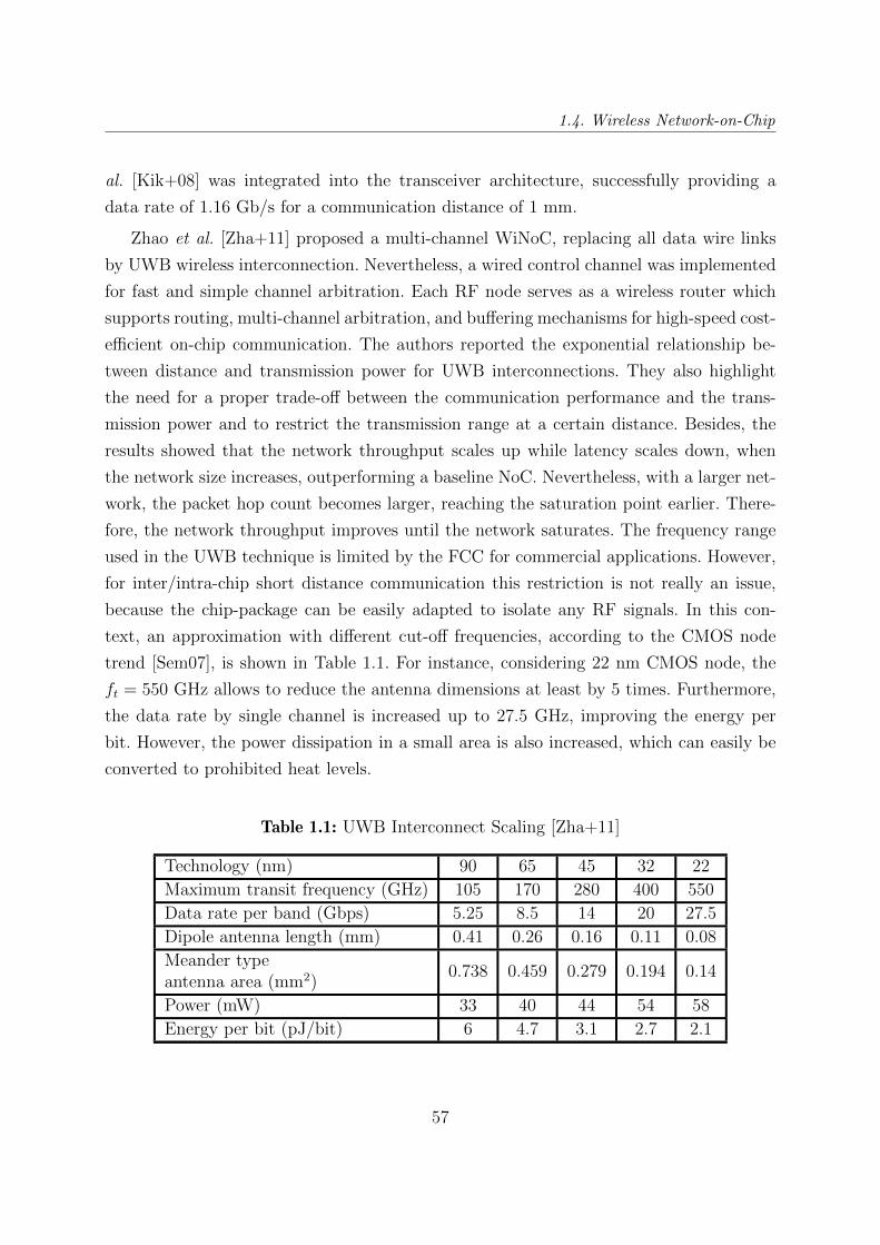
1.4. Wireless Network-on-Chip
al. [Kik+08] was integrated into the transceiver architecture, successfully providing a
data rate of 1.16 Gb/s for a communication distance of 1 mm.
Zhao et al. [Zha+11] proposed a multi-channel WiNoC, replacing all data wire links
by UWB wireless interconnection. Nevertheless, a wired control channel was implemented
for fast and simple channel arbitration. Each RF node serves as a wireless router which
supports routing, multi-channel arbitration, and buffering mechanisms for high-speed cost-
efficient on-chip communication. The authors reported the exponential relationship be-
tween distance and transmission power for UWB interconnections. They also highlight
the need for a proper trade-off between the communication performance and the trans-
mission power and to restrict the transmission range at a certain distance. Besides, the
results showed that the network throughput scales up while latency scales down, when
the network size increases, outperforming a baseline NoC. Nevertheless, with a larger net-
work, the packet hop count becomes larger, reaching the saturation point earlier. There-
fore, the network throughput improves until the network saturates. The frequency range
used in the UWB technique is limited by the FCC for commercial applications. However,
for inter/intra-chip short distance communication this restriction is not really an issue,
because the chip-package can be easily adapted to isolate any RF signals. In this con-
text, an approximation with different cut-off frequencies, according to the CMOS node
trend [Sem07], is shown in Table 1.1. For instance, considering 22 nm CMOS node, the
ft = 550 GHz allows to reduce the antenna dimensions at least by 5 times. Furthermore,
the data rate by single channel is increased up to 27.5 GHz, improving the energy per
bit. However, the power dissipation in a small area is also increased, which can easily be
converted to prohibited heat levels.
Table 1.1: UWB Interconnect Scaling [Zha+11]
Technology (nm) 90 65 45 32 22
Maximum transit frequency (GHz) 105 170 280 400 550
Data rate per band (Gbps) 5.25 8.5 14 20 27.5
Dipole antenna length (mm) 0.41 0.26 0.16 0.11 0.08
Meander typeantenna area (mm2)
0.738 0.459 0.279 0.194 0.14
Power (mW) 33 40 44 54 58
Energy per bit (pJ/bit) 6 4.7 3.1 2.7 2.1
57
Chapter 1 – State of the Art
Millimeter-Wave
In very broad terms, millimeter-wave (mm-wave) technology can be classified as occu-
pying the electromagnetic spectrum in the range of 30 GHz to 300 GHz. The frequencies
in this range are applied for a variety of applications due to the large bandwidth, which
provides a data rate of Gigabit/s among wireless links. Besides, the antenna and other
passive devices drastically reduce their size, contrasted with frequencies below this fre-
quency range. In the beginning, monolithic microwave integrated circuits (MMICs) were
manufactured using high fabrication cost technologies, such as GaAs 11 and InP 12. How-
ever, in 2005, Doan et al. [Doa+05] have designed MMICs tailored for the specific details
of CMOS, presenting for the first time CMOS amplifiers operating above 30 GHz and
fabricated in a 130 nm CMOS process. The CMOS technology allowed to decrease the
manufacturing cost compared to that of GaAs and InP, opening a new commercial mar-
ketplace. In the same year, Behzad [Raz05] proposed the first CMOS 60 GHz RF front-end
fabricated in a 130 nm CMOS technology. This receiver was based on a homodyne ar-
chitecture, which uses synchronous detection driven by a local oscillator whose frequency
is identical to the carrier frequency. Besides, it was composed of a low-noise amplifier
(LNA), quadrature mixers, and baseband amplifiers, operating at 1.2 V supply.
Several mm-waves transceivers were proposed for inter/intra-chip communications,
such as the 60 GHz transceiver reported by Lee et al [LCH10] fabricated in 90 nm CMOS
technology. The total power consumption of this transceiver is around 286 mW, offering
a data rate of 1 Gb/s over 60 cm. Another transceiver with a carrier frequency of 43 GHzwas designed and fabricated in 180 nm SiGe BiCMOS by Chen et al [Che+09]. This
transceiver provides a data rate of 6 Gb/s over a distance of 20 mm, but consuming a
total power of 117 mW. Moreover, Kawasaki et al [Kaw+10] proposed a more interesting
transceiver solution with a carrier frequency of 58 GHz and fabricated in a 40 nm CMOS
process. This transceiver provides a data rate of 11 Gb/s over a distance of 14 mm with
a total power consumption of 70 mW.
On the other hand, Deb et al [Deb+10] propose, for the first time, the utilization
of mm-wave on-chip wireless long-distance links as shortcuts to be used by small-world
network topology. A small-world topology can be constructed by re-wiring connections
from any given node to any other node, creating wired short cuts among distant nodes
11. Gallium-Arsenide Technology12. Indium Phosphide Technology
58
1.4. Wireless Network-on-Chip
in the network, as explained by Ogras and Marculescu [OM06]. Thus, the proposition
of Deb et al [Deb+10] was to replace the wired short cuts by wireless links operating
at 60 GHz. The wireless transceiver was designed using the Multi-Project Circuits plat-
form [CMP99], adopting a 65 nm CMOS process. Besides, it was designed employing the
modulator/demodulator design from Lee et al [LCH10], sustaining a data rate of 16 Gb/swith a power dissipation of 90 mW, including analog and digital parts. However, the power
consumption of each part was not detailed by the authors. Therefore, it is not possible to
compare the power consumption of this transceiver with the other ones described above.
But, indeed, the power consumption was still high to be a viable solution. In this context,
Yu et al [Xin+10] analyze, by simulations, the performance of an on-chip wireless receiver
front-end for WiNoC solutions. But, it was only in 2011 that Yu et al [Yu+11] introduced
the design of the first 60 GHz transceiver tailored for WiNoCs requirements, making
the WiNoC solution a competitive candidate to circumvent the limitations of traditional
multi-hop NoCs. A few improvements were added by Chang et al [Cha+12], achieving an
estimated power consumption of 36.7 mW from a 0.8 V supply voltage. Finally, in 2014,
an on-chip wireless transceiver was designed and fabricated, by Yu et al [Yu+14a; Yu+15]
using 65 nm CMOS process, achieving a power consumption of 33 mW from a 1 V supply
voltage. Indeed, optimizations were performed to improve the power consumption with a
higher voltage.
More details related to these transceivers will be given in Chapter 2. In the state-of-the-
art, most of the WiNoC solutions still work with this kind of mm-wave transceivers due
to the feasibility demonstrated by the ones discussed above. However, the sub-terahertz
and optical spectrum are being attractive solutions for futures Wireless NoCs, due to the
large bandwidth offered by these frequency bands, as discussed in the next section.
From Sub-Terahertz to Optical Spectrum
The terahertz (THz) communication refers to the use of the frequency range from 0.1to 10 THz [AJC14]. This frequency band is being explored for conventional wireless com-
munication as a key to satisfy the increasing demand for higher speed. Two main benefits
are provided in this spectrum. First, the antenna and some transceiver analog components
are greatly reduced in size. Second, a very large bandwidth is available, making an at-
tractive solution for applications that requires a high data rate for short-distance. In the
context of on-chip wireless communication, there still exist several research challenges, re-
quiring innovative solutions to well-establish THz technology. One of the main challenges
59
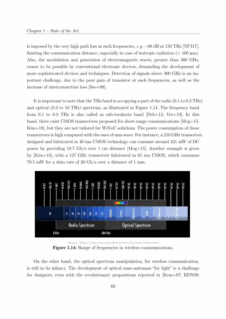
Chapter 1 – State of the Art
is imposed by the very high path loss at such frequencies, e.g. −68 dB at 150 THz [NFJ17],
limiting the communication distance, especially in case of isotropic radiation (< 100 µm).
Also, the modulation and generation of electromagnetic waves, greater than 300 GHz,
ceases to be possible by conventional electronic devices, demanding the development of
more sophisticated devices and techniques. Detection of signals above 300 GHz is an im-
portant challenge, due to the poor gain of transistor at such frequencies, as well as the
increase of interconnection loss [Seo+08].
It is important to note that the THz band is occupying a part of the radio (0.1 to 0.3 THz)
and optical (0.3 to 10 THz) spectrum, as illustrated in Figure 1.14. The frequency band
from 0.1 to 0.3 THz is also called as sub-terahertz band [Deb+12; Vet+19]. In this
band, there exist CMOS transceivers proposed for short-range communications [Mog+15;
Kim+18], but they are not tailored for WiNoC solutions. The power consumption of these
transceivers is high compared with the ones of mm-wave. For instance, a 210 GHz transceiver
designed and fabricated in 40 nm CMOS technology can consume around 421 mW of DC
power by providing 10.7 Gb/s over 1 cm distance [Mog+15]. Another example is given
by [Kim+18], with a 127 GHz transceiver fabricated in 65 nm CMOS, which consumes
79.5 mW for a data rate of 20 Gb/s over a distance of 1 mm.
Source: https://www.nasa.gov/directorates/heo/scan/index.html
Figure 1.14: Range of frequencies in wireless communications.
On the other hand, the optical spectrum manipulation, for wireless communication,
is still in its infancy. The development of optical nano-antennas “for light” is a challenge
for designers, even with the revolutionary propositions reported in [Kem+07; BDN09;
60
1.4. Wireless Network-on-Chip
Dor+10; AE10; Bel+17]. An optical antenna is defined as a device designed to efficiently
convert free-propagating optical radiation to localized energy, and vice versa [BDN09].
Optical nano-antennas were proposed to be used in WiNoC solutions, even before mm-
wave antennas [Gan+09]. The nano-antenna proposed for WiNoC was based on carbon
nanotubes (CNT) [Kem+07], requiring a laser source to vibrate. These kind of anten-
nas were an attractive solution for WiNoCs, due to the large bandwidth (≈ 500 GHz),
high efficiency (up to 40 dB), and excellent directional properties [HYL08]. However,
the main challenge of this technology is the monolithic integration into the CMOS fab-
rication process [XZ12], avoiding the low-cost fabrication of CNT-based devices. One
difficulty to achieve this integration is the huge synthesis temperature required for CNT
(800-1000 C), compared with the CMOS synthesis temperature (< 300 C) [ART20]. On
the other hand, recent research works have proposed the integration of hybrid optical plas-
monic Vivaldi antennas, tuned at 193 THz (λ = 1550 nm), providing high gain and large
bandwidth [Bel+17]. This type of antennas allows for a high integration of ONoC and
WiNoC approaches [Cal+18], due to the fact that the signal is fed into a silicon waveg-
uide, already present in ONoC solutions. Furthermore, contrary to CNT antennas, the
Vivaldi plasmonic antennas are compatible with standard CMOS processing techniques,
thanks to the material used in its fabrication (e.g., silver, aluminum, and gold). However,
in contrast to CNT antennas, the plasmonic ones are designed to be used for a nanoscale
network or ultra-short distance.
1.4.2 WiNoC Architecture
The main goal of on-chip communication systems is to transmit data with low latency
and high throughput, impacting the power consumption as little as possible. As discussed
in Section 1.2.2, the major challenges in traditional metal wire interconnects are the
high latency and power consumption of their multi-hop links. The design of suitable
antennas tuned at the optimal frequency, wireless interfaces, and transceiver circuits allow
to establish efficient on-chip wireless links into a NoC. WiNoC architectures can be broadly
classified into two categories:
1. wireless-based architecture, where the communication among IP cores is mainly
transmitted through wireless links, and
2. hybrid architecture, where the communication among IP cores is distributed be-
tween traditional wired-based interconnects and the wireless links.
61
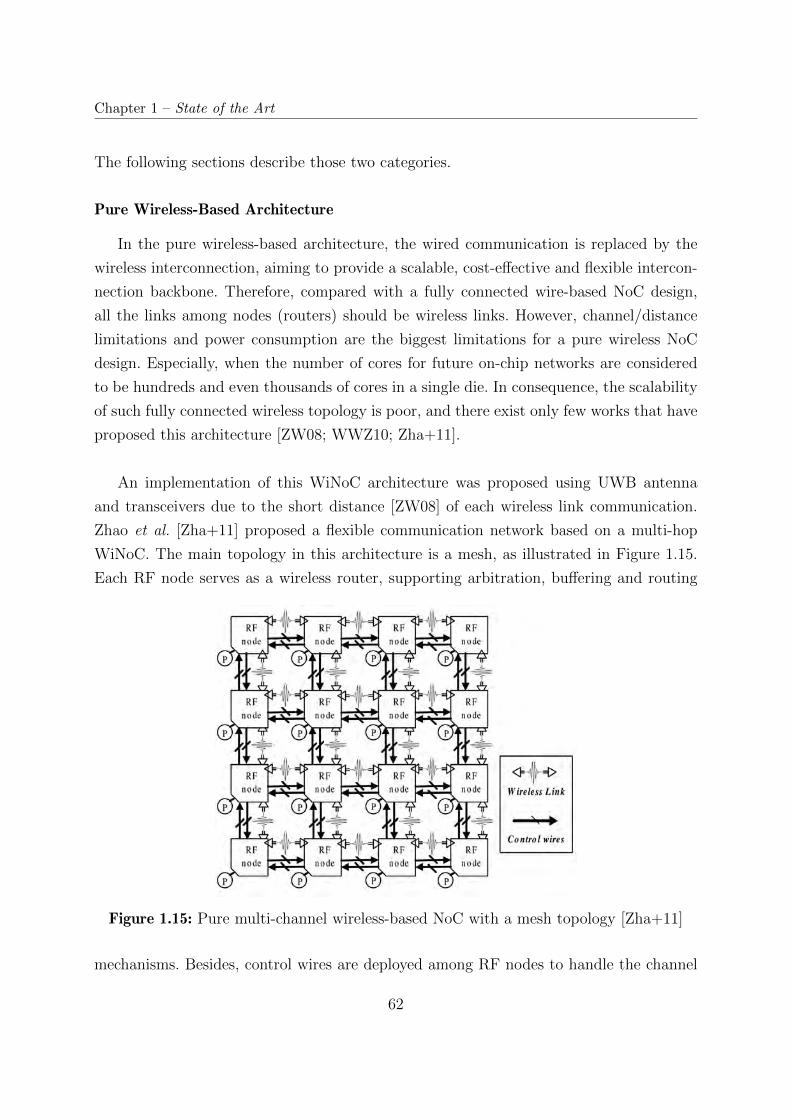
Chapter 1 – State of the Art
The following sections describe those two categories.
Pure Wireless-Based Architecture
In the pure wireless-based architecture, the wired communication is replaced by the
wireless interconnection, aiming to provide a scalable, cost-effective and flexible intercon-
nection backbone. Therefore, compared with a fully connected wire-based NoC design,
all the links among nodes (routers) should be wireless links. However, channel/distance
limitations and power consumption are the biggest limitations for a pure wireless NoC
design. Especially, when the number of cores for future on-chip networks are considered
to be hundreds and even thousands of cores in a single die. In consequence, the scalability
of such fully connected wireless topology is poor, and there exist only few works that have
proposed this architecture [ZW08; WWZ10; Zha+11].
An implementation of this WiNoC architecture was proposed using UWB antenna
and transceivers due to the short distance [ZW08] of each wireless link communication.
Zhao et al. [Zha+11] proposed a flexible communication network based on a multi-hop
WiNoC. The main topology in this architecture is a mesh, as illustrated in Figure 1.15.
Each RF node serves as a wireless router, supporting arbitration, buffering and routing
Figure 1.15: Pure multi-channel wireless-based NoC with a mesh topology [Zha+11]
mechanisms. Besides, control wires are deployed among RF nodes to handle the channel
62
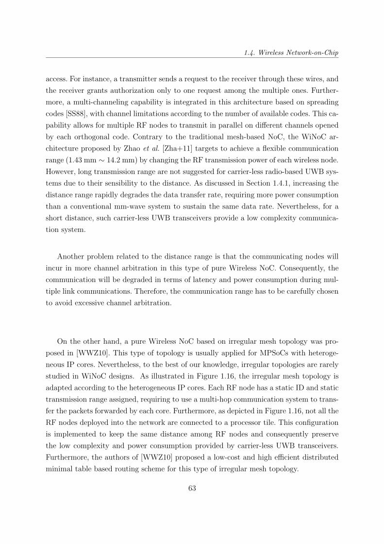
1.4. Wireless Network-on-Chip
access. For instance, a transmitter sends a request to the receiver through these wires, and
the receiver grants authorization only to one request among the multiple ones. Further-
more, a multi-channeling capability is integrated in this architecture based on spreading
codes [SS88], with channel limitations according to the number of available codes. This ca-
pability allows for multiple RF nodes to transmit in parallel on different channels opened
by each orthogonal code. Contrary to the traditional mesh-based NoC, the WiNoC ar-
chitecture proposed by Zhao et al. [Zha+11] targets to achieve a flexible communication
range (1.43 mm ∼ 14.2 mm) by changing the RF transmission power of each wireless node.
However, long transmission range are not suggested for carrier-less radio-based UWB sys-
tems due to their sensibility to the distance. As discussed in Section 1.4.1, increasing the
distance range rapidly degrades the data transfer rate, requiring more power consumption
than a conventional mm-wave system to sustain the same data rate. Nevertheless, for a
short distance, such carrier-less UWB transceivers provide a low complexity communica-
tion system.
Another problem related to the distance range is that the communicating nodes will
incur in more channel arbitration in this type of pure Wireless NoC. Consequently, the
communication will be degraded in terms of latency and power consumption during mul-
tiple link communications. Therefore, the communication range has to be carefully chosen
to avoid excessive channel arbitration.
On the other hand, a pure Wireless NoC based on irregular mesh topology was pro-
posed in [WWZ10]. This type of topology is usually applied for MPSoCs with heteroge-
neous IP cores. Nevertheless, to the best of our knowledge, irregular topologies are rarely
studied in WiNoC designs. As illustrated in Figure 1.16, the irregular mesh topology is
adapted according to the heterogeneous IP cores. Each RF node has a static ID and static
transmission range assigned, requiring to use a multi-hop communication system to trans-
fer the packets forwarded by each core. Furthermore, as depicted in Figure 1.16, not all the
RF nodes deployed into the network are connected to a processor tile. This configuration
is implemented to keep the same distance among RF nodes and consequently preserve
the low complexity and power consumption provided by carrier-less UWB transceivers.
Furthermore, the authors of [WWZ10] proposed a low-cost and high efficient distributed
minimal table based routing scheme for this type of irregular mesh topology.
63
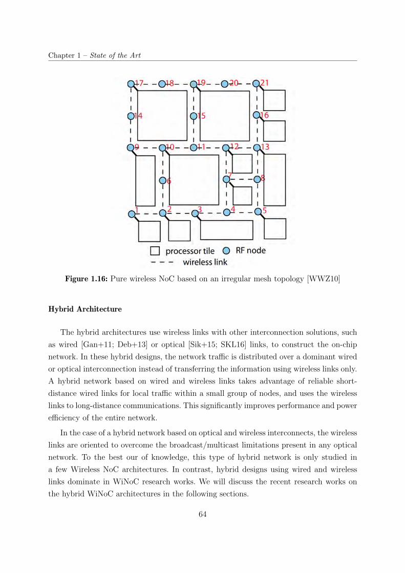
Chapter 1 – State of the Art
Figure 1.16: Pure wireless NoC based on an irregular mesh topology [WWZ10]
Hybrid Architecture
The hybrid architectures use wireless links with other interconnection solutions, such
as wired [Gan+11; Deb+13] or optical [Sik+15; SKL16] links, to construct the on-chip
network. In these hybrid designs, the network traffic is distributed over a dominant wired
or optical interconnection instead of transferring the information using wireless links only.
A hybrid network based on wired and wireless links takes advantage of reliable short-
distance wired links for local traffic within a small group of nodes, and uses the wireless
links to long-distance communications. This significantly improves performance and power
efficiency of the entire network.
In the case of a hybrid network based on optical and wireless interconnects, the wireless
links are oriented to overcome the broadcast/multicast limitations present in any optical
network. To the best our of knowledge, this type of hybrid network is only studied in
a few Wireless NoC architectures. In contrast, hybrid designs using wired and wireless
links dominate in WiNoC research works. We will discuss the recent research works on
the hybrid WiNoC architectures in the following sections.
64
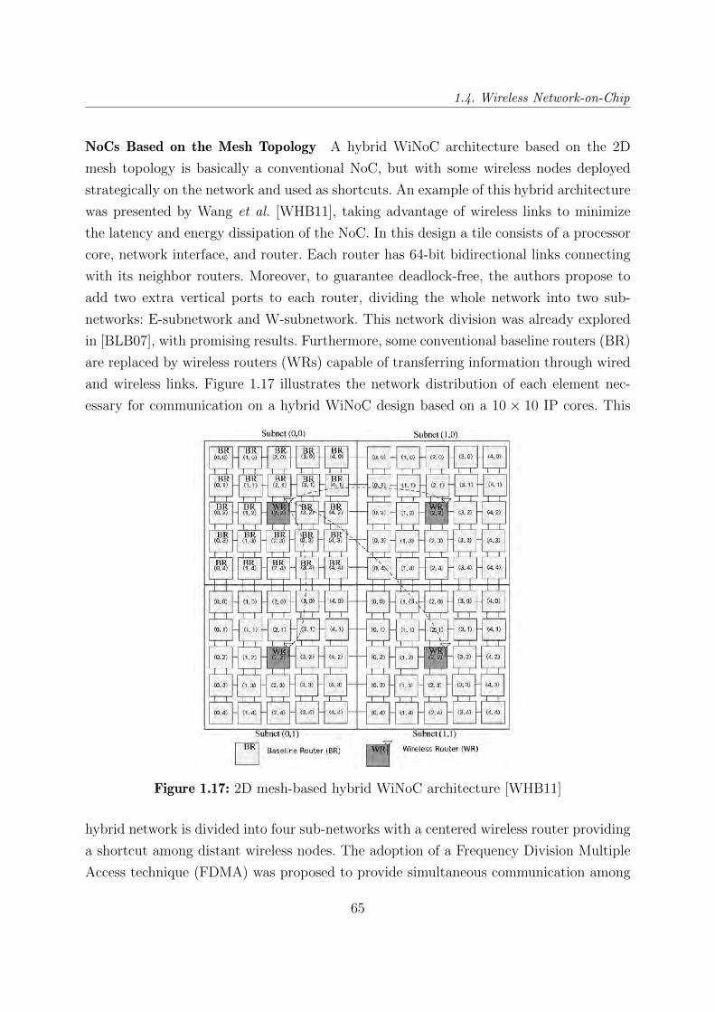
1.4. Wireless Network-on-Chip
NoCs Based on the Mesh Topology A hybrid WiNoC architecture based on the 2D
mesh topology is basically a conventional NoC, but with some wireless nodes deployed
strategically on the network and used as shortcuts. An example of this hybrid architecture
was presented by Wang et al. [WHB11], taking advantage of wireless links to minimize
the latency and energy dissipation of the NoC. In this design a tile consists of a processor
core, network interface, and router. Each router has 64-bit bidirectional links connecting
with its neighbor routers. Moreover, to guarantee deadlock-free, the authors propose to
add two extra vertical ports to each router, dividing the whole network into two sub-
networks: E-subnetwork and W-subnetwork. This network division was already explored
in [BLB07], with promising results. Furthermore, some conventional baseline routers (BR)
are replaced by wireless routers (WRs) capable of transferring information through wired
and wireless links. Figure 1.17 illustrates the network distribution of each element nec-
essary for communication on a hybrid WiNoC design based on a 10 × 10 IP cores. This
Figure 1.17: 2D mesh-based hybrid WiNoC architecture [WHB11]
hybrid network is divided into four sub-networks with a centered wireless router providing
a shortcut among distant wireless nodes. The adoption of a Frequency Division Multiple
Access technique (FDMA) was proposed to provide simultaneous communication among
65
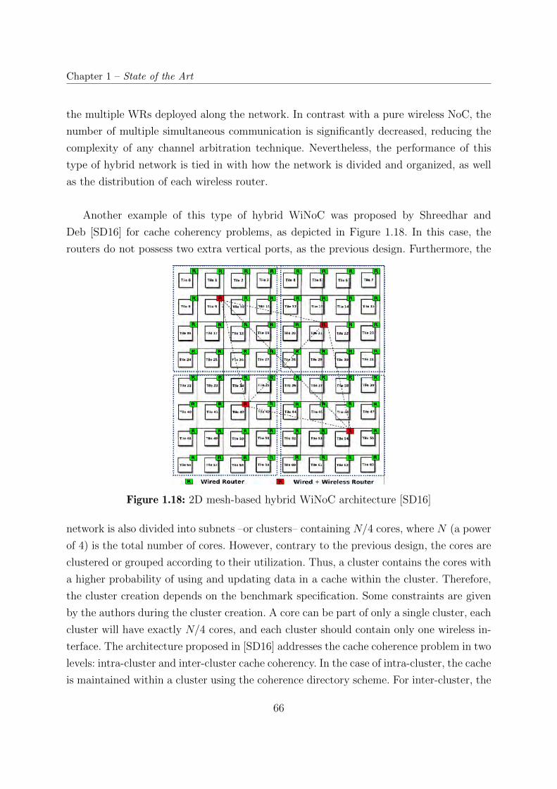
Chapter 1 – State of the Art
the multiple WRs deployed along the network. In contrast with a pure wireless NoC, the
number of multiple simultaneous communication is significantly decreased, reducing the
complexity of any channel arbitration technique. Nevertheless, the performance of this
type of hybrid network is tied in with how the network is divided and organized, as well
as the distribution of each wireless router.
Another example of this type of hybrid WiNoC was proposed by Shreedhar and
Deb [SD16] for cache coherency problems, as depicted in Figure 1.18. In this case, the
routers do not possess two extra vertical ports, as the previous design. Furthermore, the
Figure 1.18: 2D mesh-based hybrid WiNoC architecture [SD16]
network is also divided into subnets –or clusters– containing N/4 cores, where N (a power
of 4) is the total number of cores. However, contrary to the previous design, the cores are
clustered or grouped according to their utilization. Thus, a cluster contains the cores with
a higher probability of using and updating data in a cache within the cluster. Therefore,
the cluster creation depends on the benchmark specification. Some constraints are given
by the authors during the cluster creation. A core can be part of only a single cluster, each
cluster will have exactly N/4 cores, and each cluster should contain only one wireless in-
terface. The architecture proposed in [SD16] addresses the cache coherence problem in two
levels: intra-cluster and inter-cluster cache coherency. In the case of intra-cluster, the cache
is maintained within a cluster using the coherence directory scheme. For inter-cluster, the
66
1.4. Wireless Network-on-Chip
authors propose a new cache coherency algorithm based on the wireless interconnections
deployed on the network. The position of each wireless link is chosen according to the
minimum average distance from all cores of the respective cluster. Besides each wireless
link is optimized to cover the entire chip, communicating in a single-hop all the cache
coherency data. To avoid interference in the wireless channel, a token ring algorithm is
proposed to be employed as a channel arbitration. The token only provides access to one
wireless link, avoiding data collision. This network organization is an interesting proposi-
tion. However, scalability is not assured for hundreds of cores, since the number of cores
per cluster will increase indiscriminately. As a consequence, the positive impact of the
wireless link will be negligible compared to the negative one generated inside each cluster,
due to the large number of cores inside a cluster. For instance, considering a network
composed of N = 256 cores, the number of cores per cluster will be 64, consequently, the
improvement provides by the four wireless interfaces will be negligible.
Multiple-Tier Architecture A multi-tier architecture is basically a multi-level architec-
ture with different network organization. This type of network was proposed to address the
scalability issues present in conventional NoCs for hundreds and thousands of cores. Con-
trary to previous architecture, where a conventional 2D mesh is only divided into clusters,
a multi-tier architecture can contain groups, sets, and clusters to take better advantage
of the wireless interconnections. An example of this multi-tier architecture was proposed
by Lee et al. [Lee+09], introducing a hybrid architecture to interconnect hundreds to
thousands of cores in chip multiprocessors (CMPs). The proposed WCube architecture
is a two-tier hybrid wireless/wired architecture, including the wireless backbone and a
concentrate 2D mesh topology to offer a local route for neighborhood inter-core message
exchanges. A concentrate mesh (Cmesh) topology is a 2D mesh where a router can concen-
trate k number of IP cores [BD06]. For instance, a baseline router can provide a network
connection to 4 cores or 3 cores with a L2 cache memory, as illustrated in Figure 1.19a.
The Cmesh topology has reported more efficient results than a conventional mesh and
torus in terms of area, energy, and packet latency [BD06]. This is essentially because the
number of hops is reduced by a factor of k, allowing to contain more IP cores working
into the network. The block of cores connected to a router is called by the authors as
cluster. A set of these clusters is named as WCubei. Each WCubei has a wireless router
shared by four clusters and placed on the center of the set, as depicted in Figure 1.19a.
Thus, a WCubei can easily contain 64 cores connected only using 16 routers. Furthermore,
67
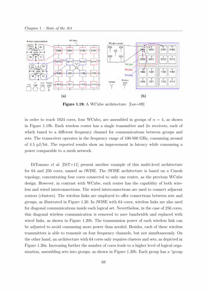
Chapter 1 – State of the Art
(a) (b)
Figure 1.19: A WCube architecture [Lee+09]
in order to reach 1024 cores, four WCubei are assembled in groups of n = 4, as shown
in Figure 1.19b. Each wireless router has a single transmitter and 2n receivers, each of
which tuned to a different frequency channel for communications between groups and
sets. The transceiver operates in the frequency range of 100-500 GHz, consuming around
of 4.5 pJ/bit. The reported results show an improvement in latency while consuming a
power comparable to a mesh network.
DiTomaso et al. [DiT+11] present another example of this multi-level architecture
for 64 and 256 cores, named as iWISE. The iWISE architecture is based on a Cmesh
topology, concentrating four cores connected to only one router, as the previous WCube
design. However, in contrast with WCube, each router has the capability of both wire-
less and wired interconnections. The wired interconnections are used to connect adjacent
routers (clusters). The wireless links are employed to offer connections between sets and
groups, as illustrated in Figure 1.20. In iWISE with 64 cores, wireless links are also used
for diagonal communications inside each logical set. Nevertheless, in the case of 256 cores,
this diagonal wireless communication is removed to save bandwidth and replaced with
wired links, as shown in Figure 1.20b. The transmission power of each wireless link can
be adjusted to avoid consuming more power than needed. Besides, each of these wireless
transmitters is able to transmit on four frequency channels, but not simultaneously. On
the other hand, an architecture with 64 cores only requires clusters and sets, as depicted in
Figure 1.20a. Increasing further the number of cores leads to a higher level of logical orga-
nization, assembling sets into groups, as shown in Figure 1.20b. Each group has a “group
68
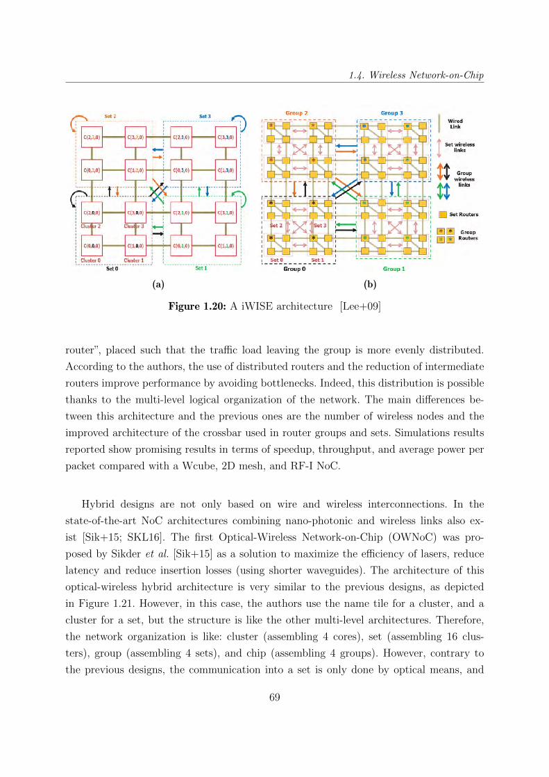
1.4. Wireless Network-on-Chip
(a) (b)
Figure 1.20: A iWISE architecture [Lee+09]
router”, placed such that the traffic load leaving the group is more evenly distributed.
According to the authors, the use of distributed routers and the reduction of intermediate
routers improve performance by avoiding bottlenecks. Indeed, this distribution is possible
thanks to the multi-level logical organization of the network. The main differences be-
tween this architecture and the previous ones are the number of wireless nodes and the
improved architecture of the crossbar used in router groups and sets. Simulations results
reported show promising results in terms of speedup, throughput, and average power per
packet compared with a Wcube, 2D mesh, and RF-I NoC.
Hybrid designs are not only based on wire and wireless interconnections. In the
state-of-the-art NoC architectures combining nano-photonic and wireless links also ex-
ist [Sik+15; SKL16]. The first Optical-Wireless Network-on-Chip (OWNoC) was pro-
posed by Sikder et al. [Sik+15] as a solution to maximize the efficiency of lasers, reduce
latency and reduce insertion losses (using shorter waveguides). The architecture of this
optical-wireless hybrid architecture is very similar to the previous designs, as depicted
in Figure 1.21. However, in this case, the authors use the name tile for a cluster, and a
cluster for a set, but the structure is like the other multi-level architectures. Therefore,
the network organization is like: cluster (assembling 4 cores), set (assembling 16 clus-
ters), group (assembling 4 sets), and chip (assembling 4 groups). However, contrary to
the previous designs, the communication into a set is only done by optical means, and
69
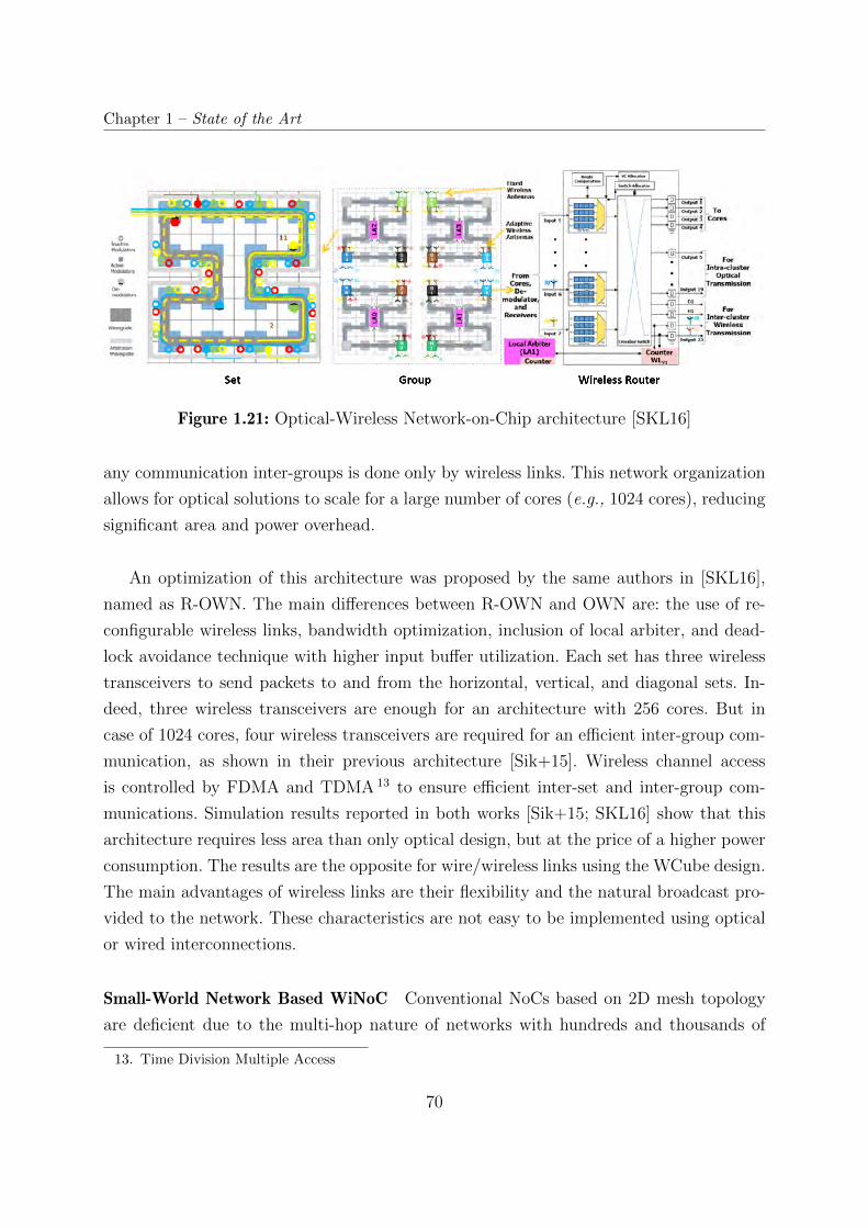
Chapter 1 – State of the Art
Figure 1.21: Optical-Wireless Network-on-Chip architecture [SKL16]
any communication inter-groups is done only by wireless links. This network organization
allows for optical solutions to scale for a large number of cores (e.g., 1024 cores), reducing
significant area and power overhead.
An optimization of this architecture was proposed by the same authors in [SKL16],
named as R-OWN. The main differences between R-OWN and OWN are: the use of re-
configurable wireless links, bandwidth optimization, inclusion of local arbiter, and dead-
lock avoidance technique with higher input buffer utilization. Each set has three wireless
transceivers to send packets to and from the horizontal, vertical, and diagonal sets. In-
deed, three wireless transceivers are enough for an architecture with 256 cores. But in
case of 1024 cores, four wireless transceivers are required for an efficient inter-group com-
munication, as shown in their previous architecture [Sik+15]. Wireless channel access
is controlled by FDMA and TDMA 13 to ensure efficient inter-set and inter-group com-
munications. Simulation results reported in both works [Sik+15; SKL16] show that this
architecture requires less area than only optical design, but at the price of a higher power
consumption. The results are the opposite for wire/wireless links using the WCube design.
The main advantages of wireless links are their flexibility and the natural broadcast pro-
vided to the network. These characteristics are not easy to be implemented using optical
or wired interconnections.
Small-World Network Based WiNoC Conventional NoCs based on 2D mesh topology
are deficient due to the multi-hop nature of networks with hundreds and thousands of
13. Time Division Multiple Access
70
1.4. Wireless Network-on-Chip
cores. Indeed, a large number of cores require many intermediate hops to communicate
data across the network. This is due to the spatial rules used to interconnect a mesh net-
work, which connects the nodes based on cardinal neighbors. Additionally, high latency
and power dissipation are caused by the multiple intermediaries between a source and
destination core. To reduce the network degradation caused by multi-hop communica-
tions, Ogras and Marculescu [OM06] have proposed the insertion of long-range wire links
among highly communicative cores based on a small-world topology. A small-world is an
irregular topology that connects routers based on the probability of establishing a link
between them. Therefore, cores communicating more frequently have a higher probability
to be connected by a direct link. Indeed, this topology is application depended, therefore,
it can not be used for a system designed to execute multiple applications.
The small-world topology is a very attractive solution for NoCs. However, long-wired
direct links are not sustainable for hundreds or thousands of cores, because a wire length
of just 5 mm can consume around 1.06 pJ/bit [Deb+13], being able to reach 18 pJ/bit
at 20 mm [Cha+12]. This peak is mainly caused by the number of electrical buffers re-
quired to sustain the current using long wires, which consequently produce non-negligible
power consumption and latency. For this reason, it is not recommended to use long-wired
links beyond 5 mm. Thus, Deb et al. [Deb+10] proposed to use wireless links to in-
terconnect highly communicative cores. As illustrated in Figure 1.22, a small-world-based
WiNoC directly connects (like shortcuts) highly communicative cores by wire and wireless
links, improving the performance of the NoC compared with some conventional topologies.
This kind of architecture can be also divided into multiple subnets, containing different
topologies (e.g, mesh, ring, tree, etc.), as depicted in Figure 1.23. The intra-subnet com-
munication normally has a “short” path length due to the size of the subnet. Each subnet
is supplied with many routers(switch), and a wired hub or wired/wireless hub. The hub
connects the subnetworks with the main network forwarding packets through the wired
and wireless channels according to the distance among cores, whereas the intra-subnet
communication is only via wired lines. As the main network is constructed with hubs
connected by wired and wireless links, the position of each wireless link is critical to the
network performance. Ganguly et al. [Gan+11] highlight the importance of building highly
efficient NoCs based on the small-world topology. For this reason, the authors propose
that after the initial network construction, established probabilistically, the network could
be optimized by using Simulated Annealing (SA) [KGV83].
71
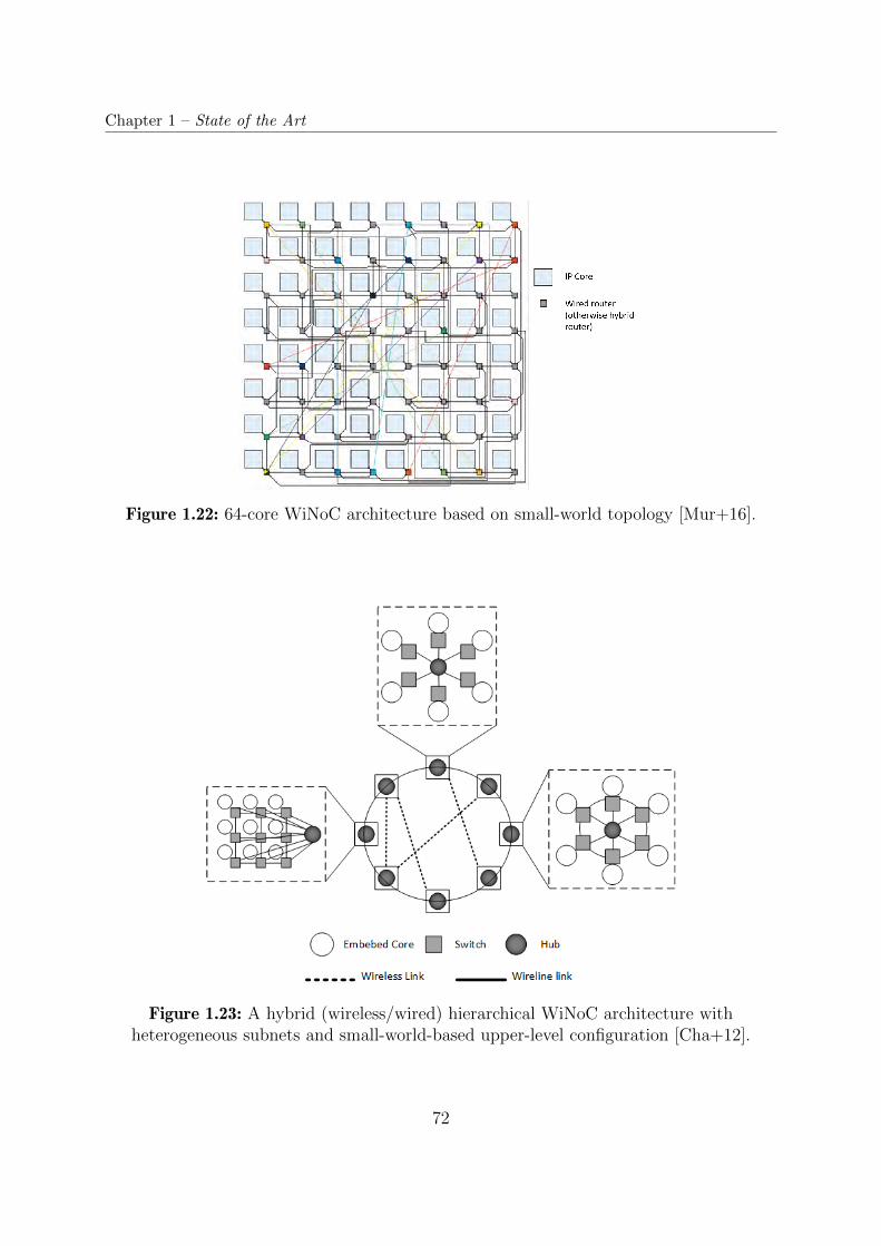
Chapter 1 – State of the Art
Figure 1.22: 64-core WiNoC architecture based on small-world topology [Mur+16].
Figure 1.23: A hybrid (wireless/wired) hierarchical WiNoC architecture withheterogeneous subnets and small-world-based upper-level configuration [Cha+12].
72
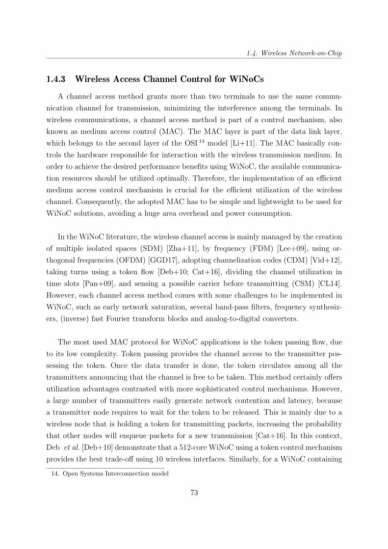
1.4. Wireless Network-on-Chip
1.4.3 Wireless Access Channel Control for WiNoCs
A channel access method grants more than two terminals to use the same commu-
nication channel for transmission, minimizing the interference among the terminals. In
wireless communications, a channel access method is part of a control mechanism, also
known as medium access control (MAC). The MAC layer is part of the data link layer,
which belongs to the second layer of the OSI 14 model [Li+11]. The MAC basically con-
trols the hardware responsible for interaction with the wireless transmission medium. In
order to achieve the desired performance benefits using WiNoC, the available communica-
tion resources should be utilized optimally. Therefore, the implementation of an efficient
medium access control mechanism is crucial for the efficient utilization of the wireless
channel. Consequently, the adopted MAC has to be simple and lightweight to be used for
WiNoC solutions, avoiding a huge area overhead and power consumption.
In the WiNoC literature, the wireless channel access is mainly managed by the creation
of multiple isolated spaces (SDM) [Zha+11], by frequency (FDM) [Lee+09], using or-
thogonal frequencies (OFDM) [GGD17], adopting channelization codes (CDM) [Vid+12],
taking turns using a token flow [Deb+10; Cat+16], dividing the channel utilization in
time slots [Pan+09], and sensing a possible carrier before transmitting (CSM) [CL14].
However, each channel access method comes with some challenges to be implemented in
WiNoC, such as early network saturation, several band-pass filters, frequency synthesiz-
ers, (inverse) fast Fourier transform blocks and analog-to-digital converters.
The most used MAC protocol for WiNoC applications is the token passing flow, due
to its low complexity. Token passing provides the channel access to the transmitter pos-
sessing the token. Once the data transfer is done, the token circulates among all the
transmitters announcing that the channel is free to be taken. This method certainly offers
utilization advantages contrasted with more sophisticated control mechanisms. However,
a large number of transmitters easily generate network contention and latency, because
a transmitter node requires to wait for the token to be released. This is mainly due to a
wireless node that is holding a token for transmitting packets, increasing the probability
that other nodes will enqueue packets for a new transmission [Cat+16]. In this context,
Deb et al. [Deb+10] demonstrate that a 512-core WiNoC using a token control mechanism
provides the best trade-off using 10 wireless interfaces. Similarly, for a WiNoC containing
14. Open Systems Interconnection model
73
Chapter 1 – State of the Art
128 and 256 cores, the best trade-off offered by the token passing flow is offered using 4
and 6 wireless interfaces, respectively.
A solution to improve the network latency is proposed with the implementation of
multiple parallel non-overlapped frequencies, also known as frequency division multiple
access (FDMA). This control mechanism divides the entire frequency bandwidth into mul-
tiple sub-channels, allowing multiple communications without the need for a token. The
main drawback of this method is related to filter complexity required to properly sepa-
rate the different sub-channels. Besides, this control mechanism requires additional RF
components, such a frequency synthesizer or multiple local oscillators, which consumes
additional power. An example of this access method is proposed by Lee et al. [Lee+09],
using as many sub-channels as available sub-networks. The authors propose the utilization
of 16 sub-channels comprised from 100 GHz to 500 GHz, each one capable of transmitting
at 10 or 20 Gbit/s for distance around of 20 mm. However, the elements necessary to im-
plement an FDMA method with such characteristics will dissipate too much energy in a
very small area. Consequently, even with the promising bandwidth given by this system, it
is not a practical method using these characteristics. In contrast, Matolak et al. [Mat+12]
proposed an FDMA control mechanism using 16 sub-channels centered around 100 GHz,
each one providing a bandwidth of 5 GHz for distance of 5 mm. Indeed, contrary to the
previous transceiver supporting FDMA, this work will consume much less energy, due to
the short distance and bandwidth per channel. However, the creation of 16 non-overlapped
sub-channels still remains an important parameter to be taken into account as a drawback.
If the filter is complex (e.g., any active filter), it will consume a non-negligible power by
each channel. Furthermore, this method is mostly combined with a time division multiple
access (TDMA) [Pan+09] when a multi-tier WiNoC or a small-world WiNoC architec-
ture are applied. Basically, a TDMA method allows for creating many time slots on each
channel, allowing us to interact with multiple packets in the same sub-channel. Neverthe-
less, the main drawback of this method is related to the starting time of each slot. The
receiver has to be capable of keeping the correct timing between slots, requiring an active
block dedicated to this task, which will consume additional power. Besides, as explained
in Chapter 2, in the case of large bandwidth per sub-channel, each communication will
be affected by multipath propagation, making it more complicated to keep the correct
timing between slots.
74
1.4. Wireless Network-on-Chip
Another solution proposed for WiNoCs is related to the orthogonal frequency-division
multiple access (ODFMA). This control mechanism efficiently divides the channel band-
width, in contrast with the FDMA method. However, the complexity and power con-
sumption is higher in the OFDMA than in the FDMA method. Gade et al. [GGD17]
proposed this method with its respective transceiver, offering data rates from 43.6 Gbit/sto 195.32 Gbit/s according to the number of sub-channels, 64 and 256, respectively. How-
ever, there are some information not detailed by the authors, such as the ADC and DAC
required for such communication method. Besides, as the modulation proposed is QAM
modulation, additional synchronization parameters have to be controlled (e.g., phase and
frequency). For these reasons, this method is not really considered in current WiNoC lit-
erature as a viable solution.
The code division multiple access (CDMA) is another access method, which allows mul-
tiple nodes to access the wireless channel, using a spreading code (e.g., Walsh-Hadamard,
orthogonal gold codes, etc.). Indeed, the correlation between codes has to be orthogonal to
avoid interference in the synchronization point. This method was proposed to be used for
WiNoC by Vidapalapati et al. [Vid+12], using Walsh-Hadamard code size of eight CDMA
chips per bit. This code size allows for at least seven simultaneous transmissions using
the wireless medium. However, the main drawback of this method is the ADC required
to distinguish among the different spreading codes.
Another method proposed as a simple channel control mechanism is the space division
multiple access (SDMA). This method takes advantage of WiNoC implement with short-
range wireless links, allowing multiple communication in different chip regions without
interference. Zhao et al. [Zha+11] used this method combined with a channel arbitration
scheme in charge of resolve the contention due to the multi-requesting of a receiving chan-
nel or competition of limited channel processing resources. Normally, this method should
be implemented using many wireless interfaces and controlling the transmission distance.
Finally, the carrier sense multiple access (CSMA) channel control mechanism was
proposed as an alternative to the use of token-passing flow control for WiNoC applica-
tions [CL14] without wired links. This access control mechanism senses the absence of
other traffic before transmitting on a shared medium. Therefore, the token rotation time
is removed from the system. A wireless node is continuously sensing the channel before de-
75
Chapter 1 – State of the Art
termining that it can transmit a packet. In case of a failed transmission, the transmission
is rescheduled for the next transmission until success. According to the results reported
by the authors in [CL14], this mechanism outperforms the token passing in latency and
throughput for 16 and 64 wireless routers. Nevertheless, the authors do not specify the
modulation employed, and how it can affect the latency for the CSMA mechanism. In fact,
sensing the carrier before performing any transmission is a good way to avoid a collision,
but only if a carrier is transmitted during the whole packet transmission. In the case of
OOK modulation, the carrier wave is not continuously present during a packet transmis-
sion, especially every time that the packet contains zeros. Therefore, the probability of
collision is highly increased due to false free channel detection. The authors propose the
utilization of time slots and constant packet lengths to improve performance. But constant
packet lengths means that each IP core will generate the same message length, or that
empty flits are sent to complete a short message, adding unnecessary transmission time.
1.5 Gaps in WiNoC Literature
Most research works in the WiNoC literature focus on antennas and transceiver de-
signs, especially operating in the millimeter-wave range. As explained in the previous
sections, in order to provide high throughput, the antennas should be operating at much
higher frequencies to benefit from the higher bandwidth available in that part of the
spectrum. However, in such high frequencies, the loss introduced by the channel is more
important for short distances (e.g., 5 mm). Other technologies to fabricate more efficient
antennas are still immature and, if even possible, it would be very expensive. Also, fabri-
cation of other RF devices, such as oscillators and amplifiers operating at extremely high
frequencies remains a complicate task.
On the other hand, the wireless channel model used in almost all the papers evaluat-
ing WiNoCs is a very simplistic model. Especially, because this channel model does not
represent a real or close to real channel of the wireless on-chip communication. This is
a gross simplification since the WiNoC landscape is complex, with irregularities in the
physical structures, different layers of substrates, and possible reflecting surfaces from the
package. Indeed, this physical characteristics can easily introduce parasitic phenomena,
highly degrading the communication. The channel characteristics for conventional WiNoC
structures will be more detailed in the following chapter.
76
1.5. Gaps in WiNoC Literature
Table 1.2 shows a summary of comparisons of the main interconnect solutions proposed
for NoCs, highlighting their key features. But, the most important interconnect solutions
are optical and wireless links. These interconnections have received a lot of attention due
to seamless integration into the silicon process. However, these solutions have yet to tackle
the power consumption and thermal issues, caused by the wireless and optical links, re-
spectively. Also, a new research area is opened for surface wave interconnection, which
can offer a better performance than free-space wireless interconnect. However, surface
wave is still an immature solution, requiring some tricky configurations to excite the wave
propagation.
In the following chapter, we study a semi-realistic wireless channel model and some
traditional channel cancellation techniques. The main objective of these cancellation tech-
niques is to improve the communication reliability and adapt them to the on-chip wireless
communication context. Finally, We propose a digital transceiver architecture for each
of the adopted techniques and evaluate their performance, power consumption and area
overhead.
77
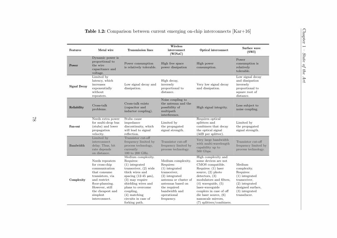
Chap
ter1–
Sta
teof
the
Art
Table 1.2: Comparison between current emerging on-chip interconnects [Kar+16]
Features Metal wire Transmission linesWireless
interconnect(WiNoC)
Optical interconnectSurface wave
(SWI)
Power
Dynamic power isproportional tothe wirecapacitance andvoltage.
Power consumptionis relatively tolerable.
High free spacepower dissipation
High powerconsumption.
Powerconsumption isrelativelytolerable.
Signal Decay
Limited bylatency, whichincreasesexponentiallywithoutrepeaters.
Low signal decay anddissipation.
High decay,inverselyproportional todistance.
Very low signal decayand dissipation.
Low signal decayand dissipationinverselyproportional tosquare root ofdistance.
ReliabilityCross-talkproblems.
Cross-talk exists(capacitor andinductor coupling).
Noise coupling tothe antenna and thepossibility ofmultipathinterference.
High signal integrity.Less subject tonoise coupling.
Fan-out
Needs extra powerfor multi-drop bus(stubs) and lowerpropagationvelocity.
Stubs causeimpedancediscontinuity, whichwill lead to signalreflection.
Limited bythe propagatedsignal strength.
Requires opticalsplitters andcombiners that decaythe optical signal(3dB per splitter).
Limited bythe propagatedsignal strength.
Bandwidth
Limited byinterconnectdelay. Thus, bitrate dependson distance.
Transistor cut-offfrequency limited byprocess technology,currently100 to 200 GHz.
Transistor cut-offfrequency limited byprocess technology.
Very large bandwidthwith multi-wavelengthcapability up to500 Gbps.
Transistor cut-offfrequency limited byprocess technology.
Complexity
Needs repeatersfor cross-chipcommunicationthat consumetransistors, viaand restrictfloor-planning.However, stillthe cheapest andsimplestinterconnect.
Medium complexity.Requires:(1) integratedtransceiver, (2) widethick wires andspacing (12-45 µm),(3) may requireshielding wires andplans to overcomecoupling,(4) matchingcircuits in case offorking path.
Medium complexity.Requires:(1) integratedtransceiver,(2) integratedantenna or cluster ofantennas based onthe requiredbandwidth andoperationalfrequency.
High complexity andsome devices are notCMOS compatible.Requires: (1) lasersource, (2) photodetectors, (3)modulators and filters,(4) waveguide, (5)laser-waveguidecouplers in case of offdie laser source, (6)nanoscale mirrors,(7) splitters/combiners.
Mediumcomplexity.Requires:(1) integratedtransceiver,(2) integrateddesigned surface,(3) integratedtransducer.
78
Chapter 2
WIRELESS RELIABILITY FOR ON-CHIP
NETWORKS
Wireless Network-on-Chip (WiNoC) was proposed as a feasible and promising solu-
tion that can scale with transistor technology and the ever-increasing number of cores in
a NoC [Gan+09]. Most of the contributions in the literature attempt to demonstrate that
the WiNoC paradigm can overcome the limitations of conventional multi-hop NoC archi-
tectures for core-to-core [Pan+09], [DiT+15], and core-to-memory (e.g., cache coherency)
[KSEG15], [ACV17] communications. Many works have also investigated different net-
work topologies to take advantage of long distance links [Kim+16], [Pan+09]. WiNoC can
thus allow for the reduction of energy consumption involved by transporting information
packets through the network routers. The topology also impacts the total latency and
throughput of the network [Gan+09].
Despite all these efforts to propose efficient WiNoC architectures, the considered wire-
less channel model is very simple (i.e., usually relying on a channel model based on Ad-
ditive White Gaussian Noise) and therefore not representative of actual on-chip wireless
channels. In particular, this basic model does not consider the frequency and time be-
havior of WiNoC for isotropic antennas, such as multi-path propagation and bandwidth
limitation. However, few prior works have introduced some interesting channel features
that could be considered for WiNoC simulations. As an example, the authors of [MKK13]
give a general overview of the main WiNoC characteristics considering a two-ray chan-
nel model. Besides, their analysis concludes that on-chip wireless channel resembles to
familiar terrestrial settings. An analytical channel model is proposed in [AVM16]. This
model introduces the concept of molecular absorption attenuation (MAA), which makes
the wireless communication through the air unsustainable. In any case, both analyses
79
Chapter 2 – Wireless Reliability for On-Chip Networks
consider multi-path propagation as an unavoidable phenomenon for intra-chip wireless
communications.
However, to the best of our knowledge, there is no work that considers during perfor-
mance simulations the significant impact of multi-path propagation on the reliability of
WiNoC communications. In contrast, the use of highly directive antennas based on car-
bon nanotube (CNT) is proposed in [Gan+11], which could avoid multi-path propagation.
Nevertheless, CNT antennas are still facing many challenges to be fully integrated in cur-
rent chip fabrication process. Moreover, with such solution, broadcasting wireless signals
will be hardly achievable without a dense antenna array. Other research studies around
antennas designed for on-chip communications (e.g., [Lin+07], [ZCS07], [KBK01]) also
provide relevant information to build more realistic WiNoC channel models. However, the
experimental setup only considers simple scenarios such as point-to-point communications
without effects of chip package and real multicore context as it should exist in WiNoC.
Effects of wave propagation caused by using monopole or dipole antennas fabricated on
silicon wafer as well as channel analysis for this simple type of communication are also
proposed [ZSF06], [Haj07], [Bab+06], [KYO00].
The main contributions of this chapter are as follows:
— We demonstrate, by simulation, the significant degradation of wireless communica-
tions facing multi-path propagation for current Wireless NoC architectures. Sim-
ulation is performed by adopting proposed semi-realistic wireless channel models,
based on the wireless intra-chip communication literature.
— We study traditional channel cancellation techniques to improve communication
reliability and adapt them to the on-chip wireless communication context.
— We propose a digital transceiver architecture for each of the adopted techniques
and evaluate their performance, power consumption and area for a 28 nm FDSOI
technology and show that this overhead is very small compared to the gain in
communication reliability.
2.1 Conventional WiNoC Communication Scheme
The classical modulation scheme considered for WiNoCs is On-Off Keying (OOK)
with a maximum data rate of 16 Gbit/s. The main reason is its ability to achieve high
energy efficiency due to its low design complexity. In order to simplify the system analysis,
80
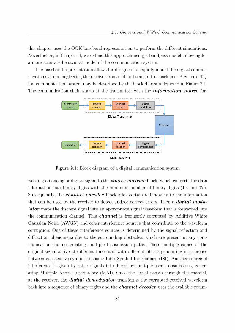
2.1. Conventional WiNoC Communication Scheme
this chapter uses the OOK baseband representation to perform the different simulations.
Nevertheless, in Chapter 4, we extend this approach using a bandpass model, allowing for
a more accurate behavioral model of the communication system.
The baseband representation allows for designers to rapidly model the digital commu-
nication system, neglecting the receiver front end and transmitter back end. A general dig-
ital communication system may be described by the block diagram depicted in Figure 2.1.
The communication chain starts at the transmitter with the information source for-
Figure 2.1: Block diagram of a digital communication system
warding an analog or digital signal to the source encoder block, which converts the data
information into binary digits with the minimum number of binary digits (1's and 0's).Subsequently, the channel encoder block adds certain redundancy to the information
that can be used by the receiver to detect and/or correct errors. Then a digital modu-
lator maps the discrete signal into an appropriate signal waveform that is forwarded into
the communication channel. This channel is frequently corrupted by Additive White
Gaussian Noise (AWGN) and other interference sources that contribute to the waveform
corruption. One of these interference sources is determined by the signal reflection and
diffraction phenomena due to the surrounding obstacles, which are present in any com-
munication channel creating multiple transmission paths. These multiple copies of the
original signal arrive at different times and with different phases generating interference
between consecutive symbols, causing Inter Symbol Interference (ISI). Another source of
interference is given by other signals introduced by multiple-user transmissions, gener-
ating Multiple Access Interference (MAI). Once the signal passes through the channel,
at the receiver, the digital demodulator transforms the corrupted received waveform
back into a sequence of binary digits and the channel decoder uses the available redun-
81
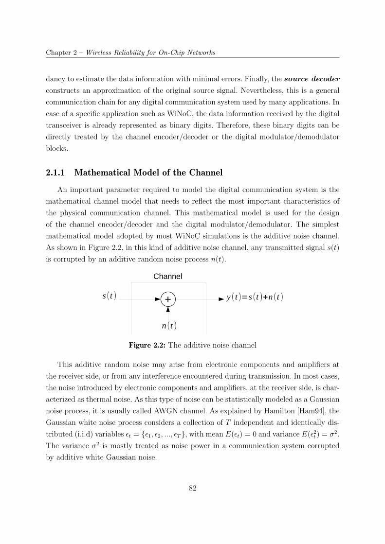
Chapter 2 – Wireless Reliability for On-Chip Networks
dancy to estimate the data information with minimal errors. Finally, the source decoder
constructs an approximation of the original source signal. Nevertheless, this is a general
communication chain for any digital communication system used by many applications. In
case of a specific application such as WiNoC, the data information received by the digital
transceiver is already represented as binary digits. Therefore, these binary digits can be
directly treated by the channel encoder/decoder or the digital modulator/demodulator
blocks.
2.1.1 Mathematical Model of the Channel
An important parameter required to model the digital communication system is the
mathematical channel model that needs to reflect the most important characteristics of
the physical communication channel. This mathematical model is used for the design
of the channel encoder/decoder and the digital modulator/demodulator. The simplest
mathematical model adopted by most WiNoC simulations is the additive noise channel.
As shown in Figure 2.2, in this kind of additive noise channel, any transmitted signal s(t)is corrupted by an additive random noise process n(t).
Figure 2.2: The additive noise channel
This additive random noise may arise from electronic components and amplifiers at
the receiver side, or from any interference encountered during transmission. In most cases,
the noise introduced by electronic components and amplifiers, at the receiver side, is char-
acterized as thermal noise. As this type of noise can be statistically modeled as a Gaussian
noise process, it is usually called AWGN channel. As explained by Hamilton [Ham94], the
Gaussian white noise process considers a collection of T independent and identically dis-
tributed (i.i.d) variables εt = ε1, ε2, ..., εT, with mean E(εt) = 0 and variance E(ε2t ) = σ2.
The variance σ2 is mostly treated as noise power in a communication system corrupted
by additive white Gaussian noise.
82
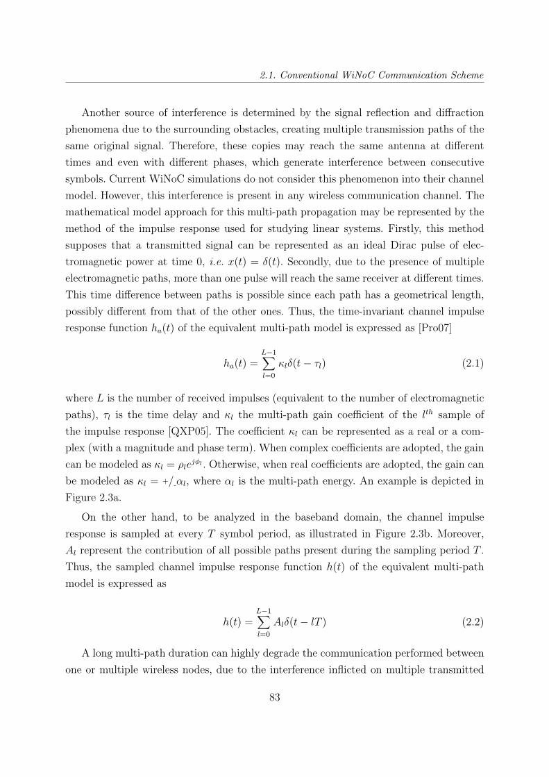
2.1. Conventional WiNoC Communication Scheme
Another source of interference is determined by the signal reflection and diffraction
phenomena due to the surrounding obstacles, creating multiple transmission paths of the
same original signal. Therefore, these copies may reach the same antenna at different
times and even with different phases, which generate interference between consecutive
symbols. Current WiNoC simulations do not consider this phenomenon into their channel
model. However, this interference is present in any wireless communication channel. The
mathematical model approach for this multi-path propagation may be represented by the
method of the impulse response used for studying linear systems. Firstly, this method
supposes that a transmitted signal can be represented as an ideal Dirac pulse of elec-
tromagnetic power at time 0, i.e. x(t) = δ(t). Secondly, due to the presence of multiple
electromagnetic paths, more than one pulse will reach the same receiver at different times.
This time difference between paths is possible since each path has a geometrical length,
possibly different from that of the other ones. Thus, the time-invariant channel impulse
response function ha(t) of the equivalent multi-path model is expressed as [Pro07]
ha(t) =L−1∑l=0
κlδ(t− τl) (2.1)
where L is the number of received impulses (equivalent to the number of electromagnetic
paths), τl is the time delay and κl the multi-path gain coefficient of the lth sample of
the impulse response [QXP05]. The coefficient κl can be represented as a real or a com-
plex (with a magnitude and phase term). When complex coefficients are adopted, the gain
can be modeled as κl = ρlejφl . Otherwise, when real coefficients are adopted, the gain can
be modeled as κl = +⁄-αl, where αl is the multi-path energy. An example is depicted in
Figure 2.3a.
On the other hand, to be analyzed in the baseband domain, the channel impulse
response is sampled at every T symbol period, as illustrated in Figure 2.3b. Moreover,
Al represent the contribution of all possible paths present during the sampling period T .
Thus, the sampled channel impulse response function h(t) of the equivalent multi-path
model is expressed as
h(t) =L−1∑l=0
Alδ(t− lT ) (2.2)
A long multi-path duration can highly degrade the communication performed between
one or multiple wireless nodes, due to the interference inflicted on multiple transmitted
83
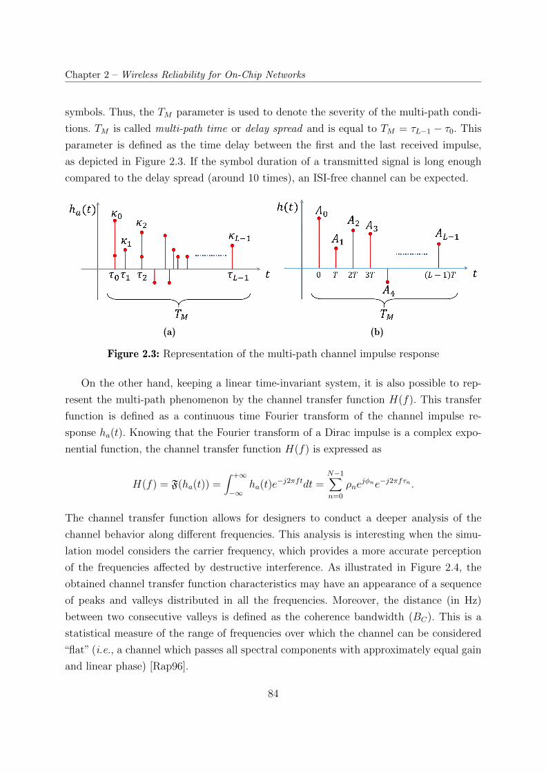
Chapter 2 – Wireless Reliability for On-Chip Networks
symbols. Thus, the TM parameter is used to denote the severity of the multi-path condi-
tions. TM is called multi-path time or delay spread and is equal to TM = τL−1 − τ0. This
parameter is defined as the time delay between the first and the last received impulse,
as depicted in Figure 2.3. If the symbol duration of a transmitted signal is long enough
compared to the delay spread (around 10 times), an ISI-free channel can be expected.
(a) (b)
Figure 2.3: Representation of the multi-path channel impulse response
On the other hand, keeping a linear time-invariant system, it is also possible to rep-
resent the multi-path phenomenon by the channel transfer function H(f). This transfer
function is defined as a continuous time Fourier transform of the channel impulse re-
sponse ha(t). Knowing that the Fourier transform of a Dirac impulse is a complex expo-
nential function, the channel transfer function H(f) is expressed as
H(f) = F(ha(t)) =∫ +∞
−∞ha(t)e−j2πftdt =
N−1∑n=0
ρnejφne−j2πfτn .
The channel transfer function allows for designers to conduct a deeper analysis of the
channel behavior along different frequencies. This analysis is interesting when the simu-
lation model considers the carrier frequency, which provides a more accurate perception
of the frequencies affected by destructive interference. As illustrated in Figure 2.4, the
obtained channel transfer function characteristics may have an appearance of a sequence
of peaks and valleys distributed in all the frequencies. Moreover, the distance (in Hz)
between two consecutive valleys is defined as the coherence bandwidth (BC). This is a
statistical measure of the range of frequencies over which the channel can be considered
“flat” (i.e., a channel which passes all spectral components with approximately equal gain
and linear phase) [Rap96].
84
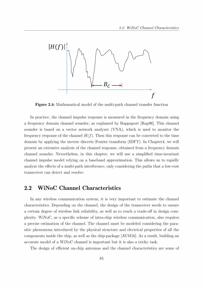
2.2. WiNoC Channel Characteristics
Figure 2.4: Mathematical model of the multi-path channel transfer function
In practice, the channel impulse response is measured in the frequency domain using
a frequency domain channel sounder, as explained by Rappaport [Rap96]. This channel
sounder is based on a vector network analyzer (VNA), which is used to monitor the
frequency response of the channel H(f). Then this response can be converted to the time
domain by applying the inverse discrete Fourier transform (IDFT). In Chapter4, we will
present an extensive analysis of the channel response, obtained from a frequency domain
channel sounder. Nevertheless, in this chapter, we will use a simplified time-invariant
channel impulse model relying on a baseband approximation. This allows us to rapidly
analyze the effects of a multi-path interference, only considering the paths that a low-cost
transceiver can detect and resolve.
2.2 WiNoC Channel Characteristics
In any wireless communication system, it is very important to estimate the channel
characteristics. Depending on the channel, the design of the transceiver needs to ensure
a certain degree of wireless link reliability, as well as to reach a trade-off in design com-
plexity. WiNoC, as a specific scheme of intra-chip wireless communication, also requires
a precise estimation of the channel. The channel must be modeled considering the para-
sitic phenomena introduced by the physical structure and electrical properties of all the
components inside the chip, as well as the chip-package [AVM16]. As a result, building an
accurate model of a WiNoC channel is important but it is also a tricky task.
The design of efficient on-chip antennas and the channel characteristics are some of
85
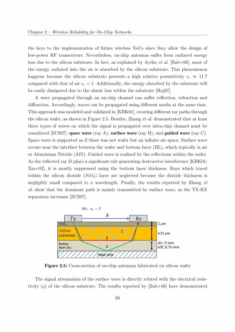
Chapter 2 – Wireless Reliability for On-Chip Networks
the keys to the implementation of future wireless NoCs since they allow the design of
low-power RF transceivers. Nevertheless, on-chip antennas suffer from radiated energy
loss due to the silicon substrate. In fact, as explained by Aydin et al. [Bab+06], most of
the energy radiated into the air is absorbed by the silicon substrate. This phenomenon
happens because the silicon substrate presents a high relative permittivity εr ≈ 11.7compared with that of air εr = 1. Additionally, the energy absorbed by the substrate will
be easily dissipated due to the ohmic loss within the substrate [Haj07].
A wave propagated through an on-chip channel can suffer reflection, refraction and
diffraction. Accordingly, waves can be propagated using different media at the same time.
This approach was modeled and validated in [KBK01], creating different ray paths through
the silicon wafer, as shown in Figure 2.5. Besides, Zhang et al. demonstrated that at least
three types of waves on which the signal is propagated over intra-chip channel must be
considered [ZCS07]: space wave (ray A), surface wave (ray B), and guided wave (ray C).
Space wave is supported as if there was not wafer but an infinite air space. Surface wave
occurs near the interface between the wafer and bottom layer (BL), which typically is air
or Aluminium Nitride (AlN). Guided wave is realized by the reflections within the wafer.
As the reflected ray D plays a significant role generating destructive interference [KBK01;
Xia+02], it is mostly suppressed using the bottom layer thickness. Rays which travel
within the silicon dioxide (SiO2) layer are neglected because the dioxide thickness is
negligibly small compared to a wavelength. Finally, the results reported by Zhang et
al. show that the dominant path is mainly transmitted by surface wave, as the TX-RX
separation increases [ZCS07].
Figure 2.5: Cross-section of on-chip antennas fabricated on silicon wafer
The signal attenuation of the surface wave is directly related with the electrical resis-
tivity (ρ) of the silicon substrate. The results reported by [Bab+06] have demonstrated
86
2.2. WiNoC Channel Characteristics
that a low-resistivity ρ = 10 − 20 Ω · cm produces more signal attenuation than a high-
resistivity ρ ≥ 5 kΩ · cm silicon substrate, reporting a difference up to 17 dB in extreme
cases. For this reason, a high-resistivity silicon substrate is quite recommended for intra-
chip wireless communications.
On the other hand, a delay spread was measured for different antennas (zigzag, me-
ander, and linear) in [ZCS07]. It was observed that the delay spread generally increases
with the transmitting and receiving antennas (Tx-Rx) separation, although delay spread
for a specific channel impulse response (CIR) depends on the surrounding of the Tx-Rx
pair. For instance, as explained by Zhan et al. [ZCS07], densely spaced metal lines with
parallel direction between antenna pairs help to reduce delay spread for both zigzag and
linear antennas. Nevertheless, densely spaced metal lines with normal direction lead to
higher delay spread than loosely spaced ones. This effect is due to parallel structures
helping wave propagation, whereas normal metal lines tend to scatter the energy away.
However, the metal line direction between antennas are close to be aleatory for realistic
on-chip wireless interconnection using multiple communication points. This randomness
makes it difficult to define the best direction of the metal lines to reduce the delay spread.
In [ZCS07], the authors provide a delay spread measured according to the distance be-
tween different antenna types, as shown in Figure 2.6. For instance, a delay spread for
a distance of 10 mm, using zigzag monopole-pair with some interference structures can
reach easily 120 ps. Therefore, the multi-path duration is sufficiently long to affect data
transmission rates beyond 10 Gb/s, where a symbol duration is around 100 ps.
In this chapter, to estimate and analyze the impact of a semi-realistic channel, the
simulations are based on the previously discussed models defined for intra-chip wave
propagation. We consider that a channel impulse response should include at least two
propagation paths for realistic baseband WiNoC simulations together with Additive White
Gaussian Noise (AWGN). Obviously, the number of paths depends on the symbol duration.
For instance, considering a data rate up to 32 Gb/s for WiNoCs, the symbol duration will
be as small as 32.25 ps, which is around four times smaller than the delay spread for a
distance of 10 mm. This indicates that the number of significant paths could be up to
three, each one separated by a symbol duration.
On the other hand, due to the low complexity of its implementation, the classical
modulation scheme considered for WiNoCs is On-Off Keying (OOK) with a maximum
data rate of 16 Gb/s. However, other modulation schemes (BPSK, QPSK, 16-QAM, etc.)
can provide better spectral efficiency and higher resilience to multi-path propagation,
87
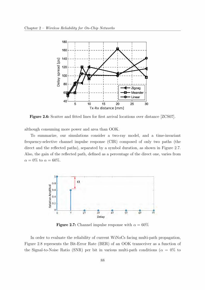
Chapter 2 – Wireless Reliability for On-Chip Networks
Figure 2.6: Scatter and fitted lines for first arrival locations over distance [ZCS07].
although consuming more power and area than OOK.
To summarize, our simulations consider a two-ray model, and a time-invariant
frequency-selective channel impulse response (CIR) composed of only two paths (the
direct and the reflected paths), separated by a symbol duration, as shown in Figure 2.7.
Also, the gain of the reflected path, defined as a percentage of the direct one, varies from
α = 0% to α = 60%.
Figure 2.7: Channel impulse response with α = 60%
In order to evaluate the reliability of current WiNoCs facing multi-path propagation,
Figure 2.8 represents the Bit-Error Rate (BER) of an OOK transceiver as a function of
the Signal-to-Noise Ratio (SNR) per bit in various multi-path conditions (α = 0% to
88
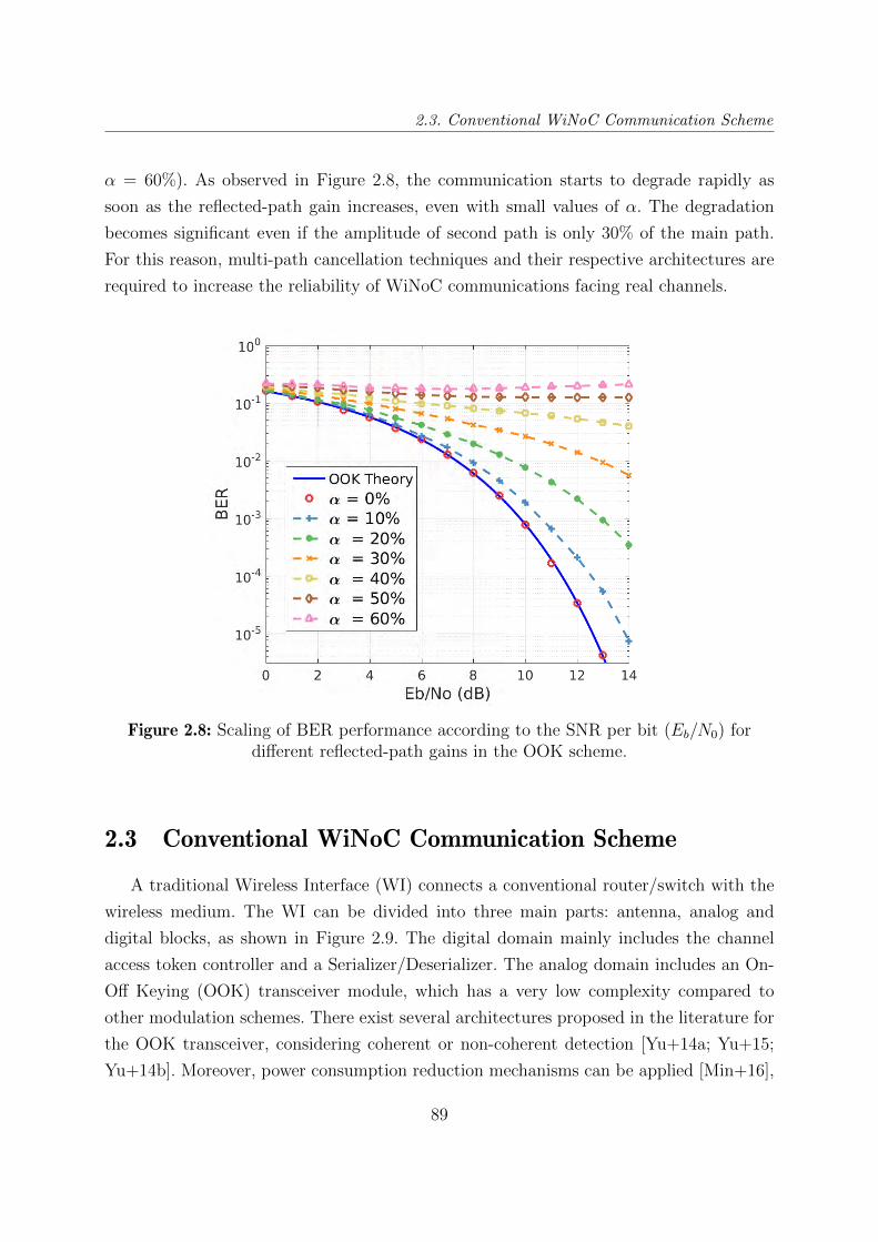
2.3. Conventional WiNoC Communication Scheme
α = 60%). As observed in Figure 2.8, the communication starts to degrade rapidly as
soon as the reflected-path gain increases, even with small values of α. The degradation
becomes significant even if the amplitude of second path is only 30% of the main path.
For this reason, multi-path cancellation techniques and their respective architectures are
required to increase the reliability of WiNoC communications facing real channels.
Figure 2.8: Scaling of BER performance according to the SNR per bit (Eb/N0) fordifferent reflected-path gains in the OOK scheme.
2.3 Conventional WiNoC Communication Scheme
A traditional Wireless Interface (WI) connects a conventional router/switch with the
wireless medium. The WI can be divided into three main parts: antenna, analog and
digital blocks, as shown in Figure 2.9. The digital domain mainly includes the channel
access token controller and a Serializer/Deserializer. The analog domain includes an On-
Off Keying (OOK) transceiver module, which has a very low complexity compared to
other modulation schemes. There exist several architectures proposed in the literature for
the OOK transceiver, considering coherent or non-coherent detection [Yu+14a; Yu+15;
Yu+14b]. Moreover, power consumption reduction mechanisms can be applied [Min+16],
89
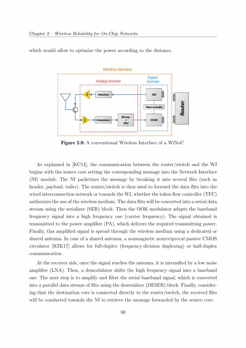
Chapter 2 – Wireless Reliability for On-Chip Networks
which would allow to optimize the power according to the distance.
Figure 2.9: A conventional Wireless Interface of a WiNoC.
As explained in [KC14], the communication between the router/switch and the WI
begins with the source core setting the corresponding message into the Network Interface
(NI) module. The NI packetizes the message by breaking it into several flits (such as
header, payload, tailer). The router/switch is then used to forward the data flits into the
wired interconnection network or towards the WI, whether the token flow controller (TFC)
authorizes the use of the wireless medium. The data flits will be converted into a serial data
stream using the serializer (SER) block. Then the OOK modulator adapts the baseband
frequency signal into a high frequency one (carrier frequency). The signal obtained is
transmitted to the power amplifier (PA), which delivers the required transmitting power.
Finally, this amplified signal is spread through the wireless medium using a dedicated or
shared antenna. In case of a shared antenna, a nonmagnetic nonreciprocal passive CMOS
circulator [RZK17] allows for full-duplex (frequency-division duplexing) or half-duplex
communication.
At the receiver side, once the signal reaches the antenna, it is intensified by a low noise
amplifier (LNA). Then, a demodulator shifts the high frequency signal into a baseband
one. The next step is to amplify and filter the serial baseband signal, which is converted
into a parallel data stream of flits using the deserializer (DESER) block. Finally, consider-
ing that the destination core is connected directly to the router/switch, the received flits
will be conducted towards the NI to retrieve the message forwarded by the source core.
90
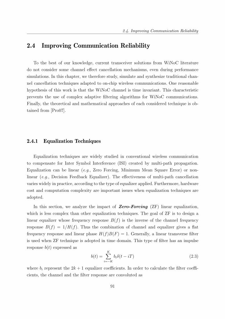
2.4. Improving Communication Reliability
2.4 Improving Communication Reliability
To the best of our knowledge, current transceiver solutions from WiNoC literature
do not consider some channel effect cancellation mechanisms, even during performance
simulations. In this chapter, we therefore study, simulate and synthesize traditional chan-
nel cancellation techniques adapted to on-chip wireless communications. One reasonable
hypothesis of this work is that the WiNoC channel is time invariant. This characteristic
prevents the use of complex adaptive filtering algorithms for WiNoC communications.
Finally, the theoretical and mathematical approaches of each considered technique is ob-
tained from [Pro07].
2.4.1 Equalization Techniques
Equalization techniques are widely studied in conventional wireless communication
to compensate for Inter Symbol Interference (ISI) created by multi-path propagation.
Equalization can be linear (e.g., Zero Forcing, Minimum Mean Square Error) or non-
linear (e.g., Decision Feedback Equalizer). The effectiveness of multi-path cancellation
varies widely in practice, according to the type of equalizer applied. Furthermore, hardware
cost and computation complexity are important issues when equalization techniques are
adopted.
In this section, we analyze the impact of Zero-Forcing (ZF) linear equalization,
which is less complex than other equalization techniques. The goal of ZF is to design a
linear equalizer whose frequency response B(f) is the inverse of the channel frequency
response B(f) = 1/H(f). Thus the combination of channel and equalizer gives a flat
frequency response and linear phase H(f)B(F ) = 1. Generally, a linear transverse filter
is used when ZF technique is adopted in time domain. This type of filter has an impulse
response b(t) expressed as
b(t) =K∑
i=−Kbiδ(t− iT ) (2.3)
where bi represent the 2k + 1 equalizer coefficients. In order to calculate the filter coeffi-
cients, the channel and the filter response are convoluted as
91
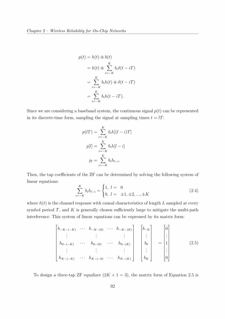
Chapter 2 – Wireless Reliability for On-Chip Networks
p(t) = h(t) ~ b(t)
= h(t) ~K∑
i=−Kbiδ(t− iT )
=K∑
i=−Kbih(t) ~ δ(t− iT )
=K∑
i=−Kbih(t− iT ).
Since we are considering a baseband system, the continuous signal p(t) can be represented
in its discrete-time form, sampling the signal at sampling times t = lT :
p(lT ) =K∑
i=−Kbih[(l − i)T ]
p[l] =K∑
i=−Kbih[l − i]
pl =K∑
i=−Kbihl−i.
Then, the tap coefficients of the ZF can be determined by solving the following system of
linear equations:K∑
i=−Kbihl−i =
1, l = 00, l = ±1,±2, ...,±K
(2.4)
where h(t) is the channel response with causal characteristics of length L sampled at every
symbol period T , and K is generally chosen sufficiently large to mitigate the multi-path
interference. This system of linear equations can be expressed by its matrix form:
h−K−(−K) · · · h−K−(0) · · · h−K−(K)...
......
h0−(−K) · · · h0−(0) · · · h0−(K)...
......
hK−(−K) · · · hK−(−0) · · · hK−(K)
b−K...
b0...
bK
=
0...
1...
0
(2.5)
To design a three-tap ZF equalizer (2K + 1 = 3), the matrix form of Equation 2.5 is
92
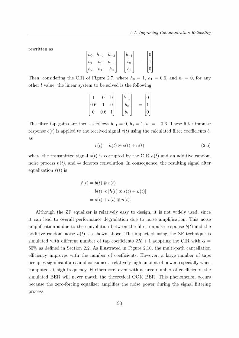
2.4. Improving Communication Reliability
rewritten as h0 h−1 h−2
h1 h0 h−1
h2 h1 h0
b−1
b0
b1
=
010
Then, considering the CIR of Figure 2.7, where h0 = 1, h1 = 0.6, and hl = 0, for any
other l value, the linear system to be solved is the following:1 0 0
0.6 1 00 0.6 1
b−1
b0
b1
=
010
The filter tap gains are then as follows b−1 = 0, b0 = 1, b1 = −0.6. These filter impulse
response b(t) is applied to the received signal r(t) using the calculated filter coefficients bi
as
r(t) = h(t) ~ s(t) + n(t) (2.6)
where the transmitted signal s(t) is corrupted by the CIR h(t) and an additive random
noise process n(t), and ~ denotes convolution. In consequence, the resulting signal after
equalization r(t) is
r(t) = b(t) ~ r(t)
= b(t) ~ [h(t) ~ s(t) + n(t)]
= s(t) + b(t) ~ n(t).
Although the ZF equalizer is relatively easy to design, it is not widely used, since
it can lead to overall performance degradation due to noise amplification. This noise
amplification is due to the convolution between the filter impulse response b(t) and the
additive random noise n(t), as shown above. The impact of using the ZF technique is
simulated with different number of tap coefficients 2K + 1 adopting the CIR with α =60% as defined in Section 2.2. As illustrated in Figure 2.10, the multi-path cancellation
efficiency improves with the number of coefficients. However, a large number of taps
occupies significant area and consumes a relatively high amount of power, especially when
computed at high frequency. Furthermore, even with a large number of coefficients, the
simulated BER will never match the theoretical OOK BER. This phenomenon occurs
because the zero-forcing equalizer amplifies the noise power during the signal filtering
process.
93
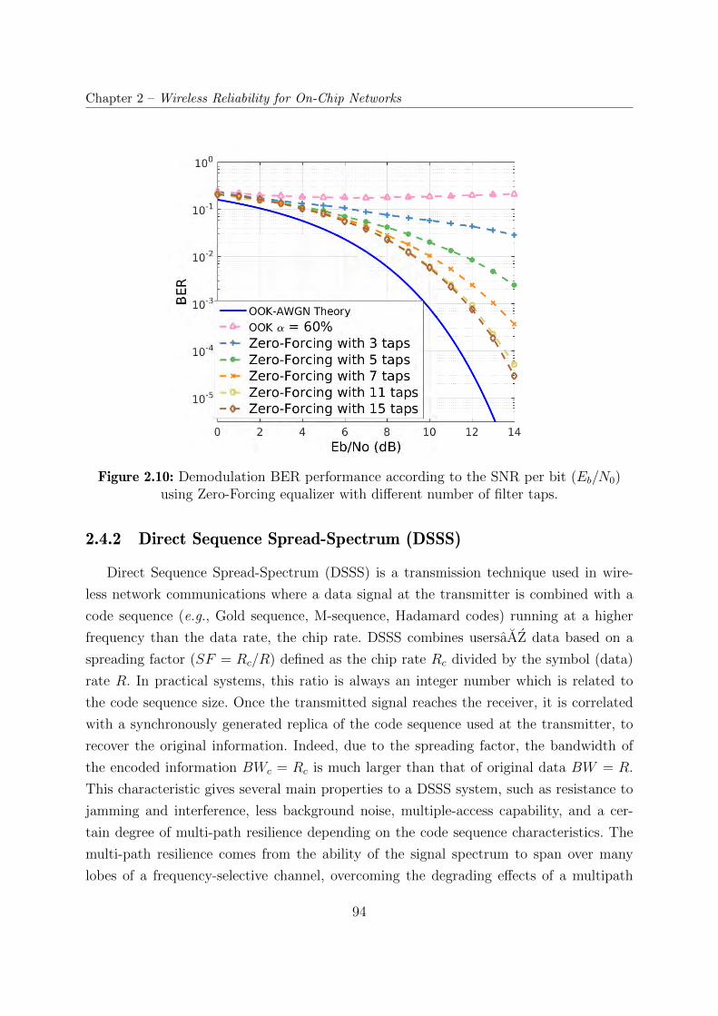
Chapter 2 – Wireless Reliability for On-Chip Networks
Figure 2.10: Demodulation BER performance according to the SNR per bit (Eb/N0)using Zero-Forcing equalizer with different number of filter taps.
2.4.2 Direct Sequence Spread-Spectrum (DSSS)
Direct Sequence Spread-Spectrum (DSSS) is a transmission technique used in wire-
less network communications where a data signal at the transmitter is combined with a
code sequence (e.g., Gold sequence, M-sequence, Hadamard codes) running at a higher
frequency than the data rate, the chip rate. DSSS combines usersaAZ data based on a
spreading factor (SF = Rc/R) defined as the chip rate Rc divided by the symbol (data)
rate R. In practical systems, this ratio is always an integer number which is related to
the code sequence size. Once the transmitted signal reaches the receiver, it is correlated
with a synchronously generated replica of the code sequence used at the transmitter, to
recover the original information. Indeed, due to the spreading factor, the bandwidth of
the encoded information BWc = Rc is much larger than that of original data BW = R.
This characteristic gives several main properties to a DSSS system, such as resistance to
jamming and interference, less background noise, multiple-access capability, and a cer-
tain degree of multi-path resilience depending on the code sequence characteristics. The
multi-path resilience comes from the ability of the signal spectrum to span over many
lobes of a frequency-selective channel, overcoming the degrading effects of a multipath
94
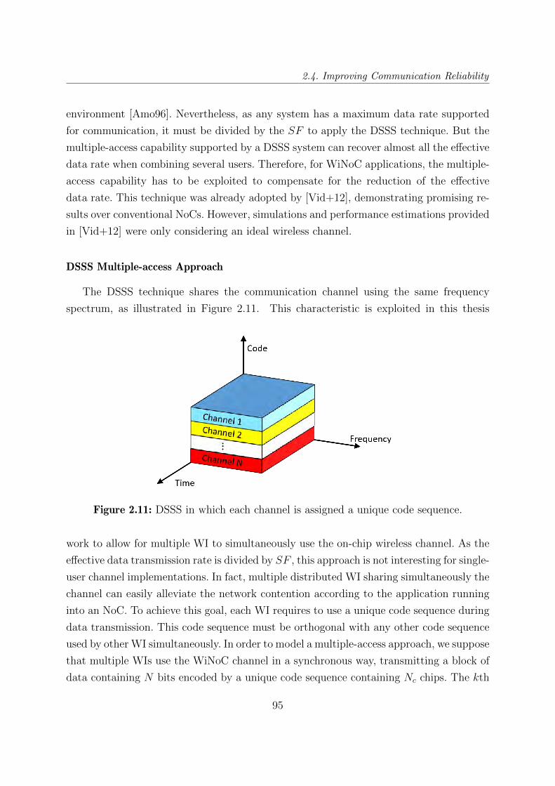
2.4. Improving Communication Reliability
environment [Amo96]. Nevertheless, as any system has a maximum data rate supported
for communication, it must be divided by the SF to apply the DSSS technique. But the
multiple-access capability supported by a DSSS system can recover almost all the effective
data rate when combining several users. Therefore, for WiNoC applications, the multiple-
access capability has to be exploited to compensate for the reduction of the effective
data rate. This technique was already adopted by [Vid+12], demonstrating promising re-
sults over conventional NoCs. However, simulations and performance estimations provided
in [Vid+12] were only considering an ideal wireless channel.
DSSS Multiple-access Approach
The DSSS technique shares the communication channel using the same frequency
spectrum, as illustrated in Figure 2.11. This characteristic is exploited in this thesis
Figure 2.11: DSSS in which each channel is assigned a unique code sequence.
work to allow for multiple WI to simultaneously use the on-chip wireless channel. As the
effective data transmission rate is divided by SF , this approach is not interesting for single-
user channel implementations. In fact, multiple distributed WI sharing simultaneously the
channel can easily alleviate the network contention according to the application running
into an NoC. To achieve this goal, each WI requires to use a unique code sequence during
data transmission. This code sequence must be orthogonal with any other code sequence
used by other WI simultaneously. In order to model a multiple-access approach, we suppose
that multiple WIs use the WiNoC channel in a synchronous way, transmitting a block of
data containing N bits encoded by a unique code sequence containing Nc chips. The kth
95
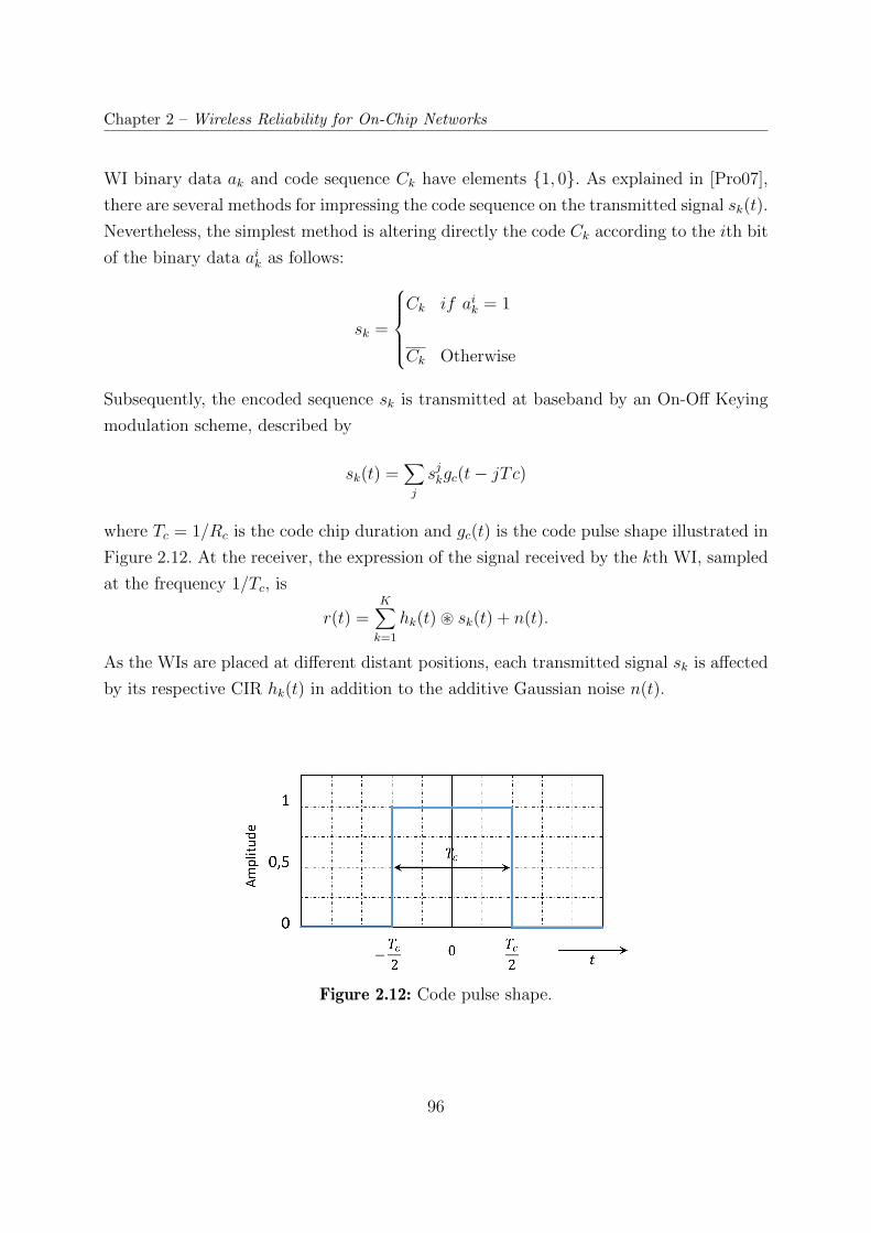
Chapter 2 – Wireless Reliability for On-Chip Networks
WI binary data ak and code sequence Ck have elements 1, 0. As explained in [Pro07],
there are several methods for impressing the code sequence on the transmitted signal sk(t).Nevertheless, the simplest method is altering directly the code Ck according to the ith bit
of the binary data aik as follows:
sk =
Ck if aik = 1
Ck Otherwise
Subsequently, the encoded sequence sk is transmitted at baseband by an On-Off Keying
modulation scheme, described by
sk(t) =∑j
sjkgc(t− jTc)
where Tc = 1/Rc is the code chip duration and gc(t) is the code pulse shape illustrated in
Figure 2.12. At the receiver, the expression of the signal received by the kth WI, sampled
at the frequency 1/Tc, is
r(t) =K∑k=1
hk(t) ~ sk(t) + n(t).
As the WIs are placed at different distant positions, each transmitted signal sk is affected
by its respective CIR hk(t) in addition to the additive Gaussian noise n(t).
Figure 2.12: Code pulse shape.
96
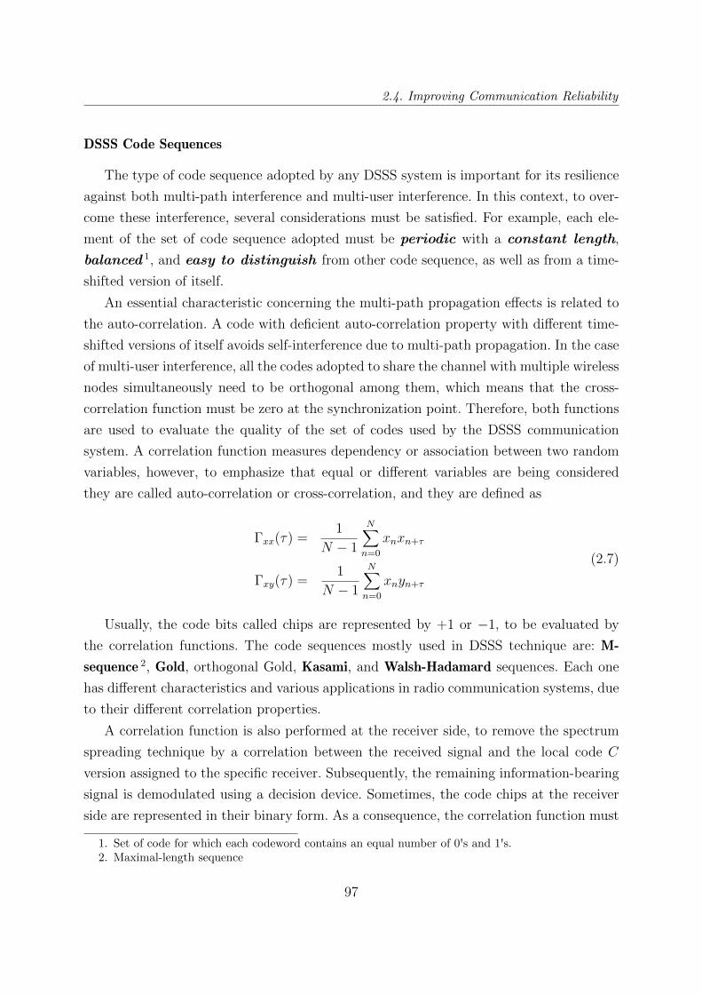
2.4. Improving Communication Reliability
DSSS Code Sequences
The type of code sequence adopted by any DSSS system is important for its resilience
against both multi-path interference and multi-user interference. In this context, to over-
come these interference, several considerations must be satisfied. For example, each ele-
ment of the set of code sequence adopted must be periodic with a constant length,
balanced 1, and easy to distinguish from other code sequence, as well as from a time-
shifted version of itself.
An essential characteristic concerning the multi-path propagation effects is related to
the auto-correlation. A code with deficient auto-correlation property with different time-
shifted versions of itself avoids self-interference due to multi-path propagation. In the case
of multi-user interference, all the codes adopted to share the channel with multiple wireless
nodes simultaneously need to be orthogonal among them, which means that the cross-
correlation function must be zero at the synchronization point. Therefore, both functions
are used to evaluate the quality of the set of codes used by the DSSS communication
system. A correlation function measures dependency or association between two random
variables, however, to emphasize that equal or different variables are being considered
they are called auto-correlation or cross-correlation, and they are defined as
Γxx(τ) = 1N − 1
N∑n=0
xnxn+τ
Γxy(τ) = 1N − 1
N∑n=0
xnyn+τ
(2.7)
Usually, the code bits called chips are represented by +1 or −1, to be evaluated by
the correlation functions. The code sequences mostly used in DSSS technique are: M-
sequence 2, Gold, orthogonal Gold, Kasami, and Walsh-Hadamard sequences. Each one
has different characteristics and various applications in radio communication systems, due
to their different correlation properties.
A correlation function is also performed at the receiver side, to remove the spectrum
spreading technique by a correlation between the received signal and the local code C
version assigned to the specific receiver. Subsequently, the remaining information-bearing
signal is demodulated using a decision device. Sometimes, the code chips at the receiver
side are represented in their binary form. As a consequence, the correlation function must
1. Set of code for which each codeword contains an equal number of 0's and 1's.2. Maximal-length sequence
97
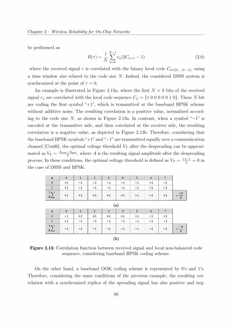
Chapter 2 – Wireless Reliability for On-Chip Networks
be performed as
R(τ) = 1N
N−1∑n=0
rn(2Cn+τ − 1) (2.8)
where the received signal r is correlated with the binary local code Cn∈0,...,N−1, using
a time window size related to the code size N . Indeed, the considered DSSS system is
synchronized at the point of τ = 0.
An example is illustrated in Figure 2.13a, where the first N = 8 bits of the received
signal rn are correlated with the local code sequence Cn = 1 0 0 0 0 0 1 0. These N -bit
are coding the first symbol “+1”, which is transmitted at the baseband BPSK scheme
without additive noise. The resulting correlation is a positive value, normalized accord-
ing to the code size N , as shown in Figure 2.13a. In contrast, when a symbol “−1” is
encoded at the transmitter side, and then correlated at the receiver side, the resulting
correlation is a negative value, as depicted in Figure 2.13b. Therefore, considering that
the baseband BPSK symbols“+1”and“−1”are transmitted equally over a communication
channel [Cou00], the optimal voltage threshold VT after the despreading can be approxi-
mated as VT = Amax−Amin
2 , where A is the resulting signal amplitude after the despreading
process. In these conditions, the optimal voltage threshold is defined as VT = +1−12 = 0 in
the case of DSSS and BPSK.
(a)
(b)
Figure 2.13: Correlation function between received signal and local non-balanced codesequence, considering baseband BPSK coding scheme.
On the other hand, a baseband OOK coding scheme is represented by 0's and 1's.Therefore, considering the same conditions of the previous example, the resulting cor-
relation with a synchronized replica of the spreading signal has also positive and neg-
98
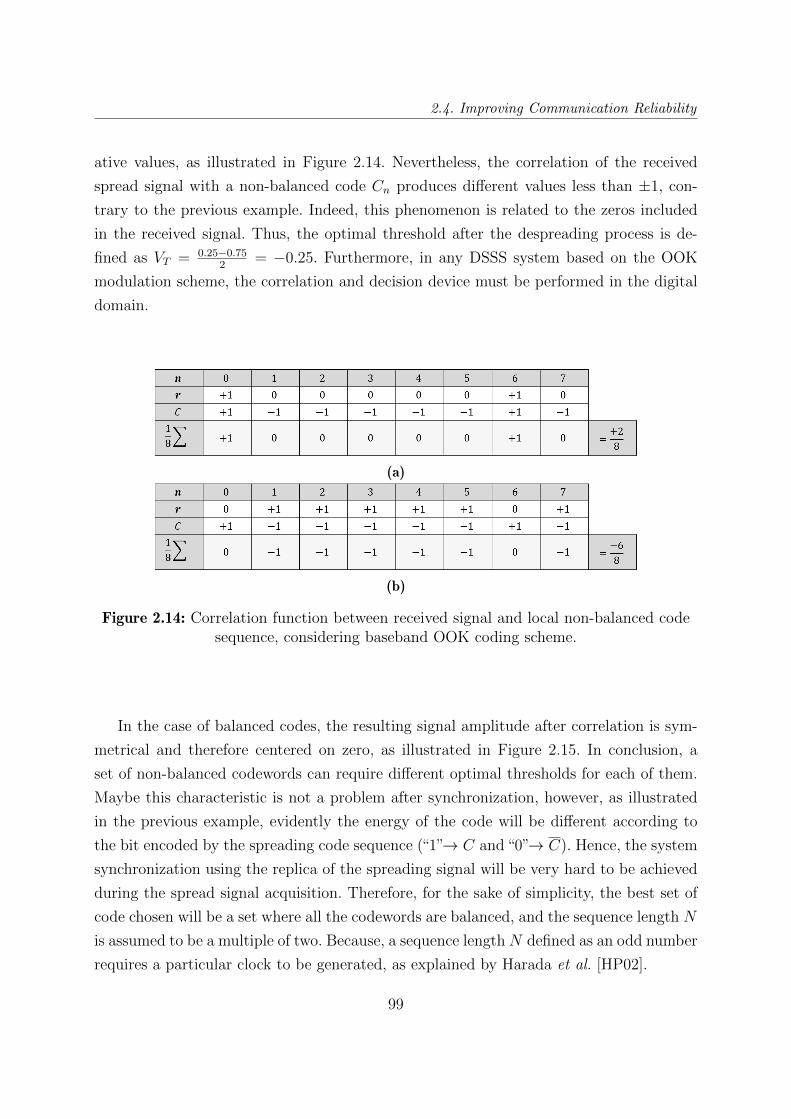
2.4. Improving Communication Reliability
ative values, as illustrated in Figure 2.14. Nevertheless, the correlation of the received
spread signal with a non-balanced code Cn produces different values less than ±1, con-
trary to the previous example. Indeed, this phenomenon is related to the zeros included
in the received signal. Thus, the optimal threshold after the despreading process is de-
fined as VT = 0.25−0.752 = −0.25. Furthermore, in any DSSS system based on the OOK
modulation scheme, the correlation and decision device must be performed in the digital
domain.
(a)
(b)
Figure 2.14: Correlation function between received signal and local non-balanced codesequence, considering baseband OOK coding scheme.
In the case of balanced codes, the resulting signal amplitude after correlation is sym-
metrical and therefore centered on zero, as illustrated in Figure 2.15. In conclusion, a
set of non-balanced codewords can require different optimal thresholds for each of them.
Maybe this characteristic is not a problem after synchronization, however, as illustrated
in the previous example, evidently the energy of the code will be different according to
the bit encoded by the spreading code sequence (“1”→ C and “0”→ C). Hence, the system
synchronization using the replica of the spreading signal will be very hard to be achieved
during the spread signal acquisition. Therefore, for the sake of simplicity, the best set of
code chosen will be a set where all the codewords are balanced, and the sequence length N
is assumed to be a multiple of two. Because, a sequence length N defined as an odd number
requires a particular clock to be generated, as explained by Harada et al. [HP02].
99
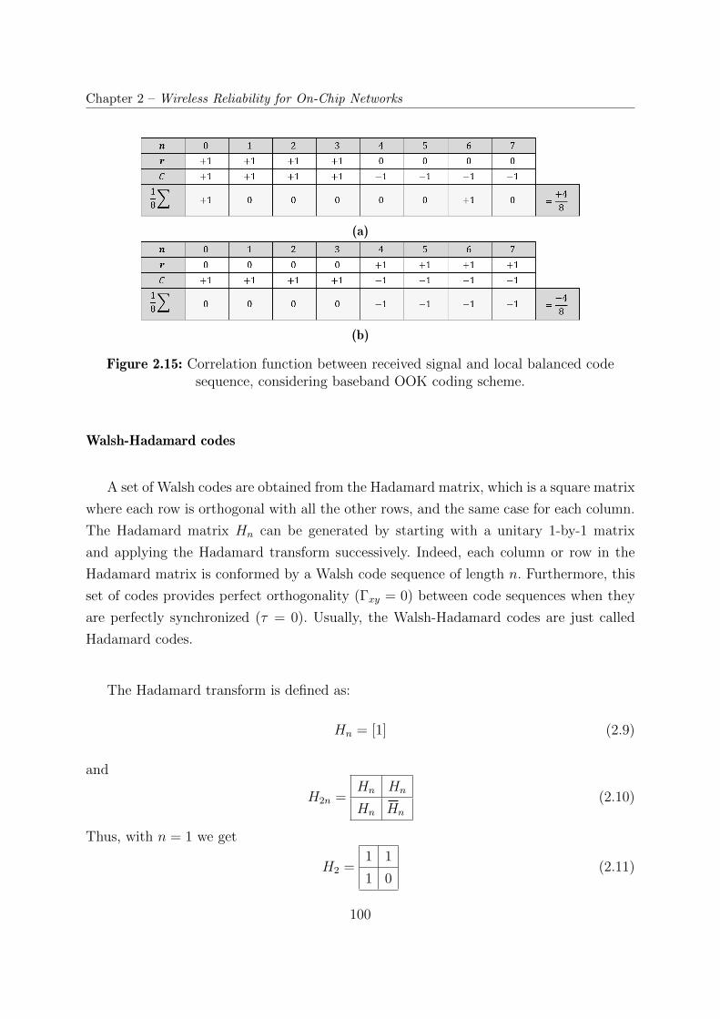
Chapter 2 – Wireless Reliability for On-Chip Networks
(a)
(b)
Figure 2.15: Correlation function between received signal and local balanced codesequence, considering baseband OOK coding scheme.
Walsh-Hadamard codes
A set of Walsh codes are obtained from the Hadamard matrix, which is a square matrix
where each row is orthogonal with all the other rows, and the same case for each column.
The Hadamard matrix Hn can be generated by starting with a unitary 1-by-1 matrix
and applying the Hadamard transform successively. Indeed, each column or row in the
Hadamard matrix is conformed by a Walsh code sequence of length n. Furthermore, this
set of codes provides perfect orthogonality (Γxy = 0) between code sequences when they
are perfectly synchronized (τ = 0). Usually, the Walsh-Hadamard codes are just called
Hadamard codes.
The Hadamard transform is defined as:
Hn = [1] (2.9)
and
H2n =Hn Hn
Hn Hn
(2.10)
Thus, with n = 1 we get
H2 =1 11 0
(2.11)
100
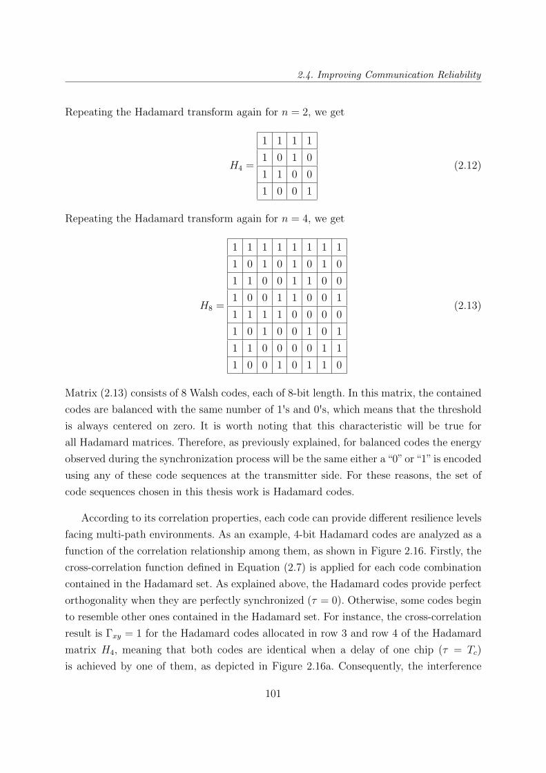
2.4. Improving Communication Reliability
Repeating the Hadamard transform again for n = 2, we get
H4 =
1 1 1 11 0 1 01 1 0 01 0 0 1
(2.12)
Repeating the Hadamard transform again for n = 4, we get
H8 =
1 1 1 1 1 1 1 11 0 1 0 1 0 1 01 1 0 0 1 1 0 01 0 0 1 1 0 0 11 1 1 1 0 0 0 01 0 1 0 0 1 0 11 1 0 0 0 0 1 11 0 0 1 0 1 1 0
(2.13)
Matrix (2.13) consists of 8 Walsh codes, each of 8-bit length. In this matrix, the contained
codes are balanced with the same number of 1's and 0's, which means that the threshold
is always centered on zero. It is worth noting that this characteristic will be true for
all Hadamard matrices. Therefore, as previously explained, for balanced codes the energy
observed during the synchronization process will be the same either a “0” or “1” is encoded
using any of these code sequences at the transmitter side. For these reasons, the set of
code sequences chosen in this thesis work is Hadamard codes.
According to its correlation properties, each code can provide different resilience levels
facing multi-path environments. As an example, 4-bit Hadamard codes are analyzed as a
function of the correlation relationship among them, as shown in Figure 2.16. Firstly, the
cross-correlation function defined in Equation (2.7) is applied for each code combination
contained in the Hadamard set. As explained above, the Hadamard codes provide perfect
orthogonality when they are perfectly synchronized (τ = 0). Otherwise, some codes begin
to resemble other ones contained in the Hadamard set. For instance, the cross-correlation
result is Γxy = 1 for the Hadamard codes allocated in row 3 and row 4 of the Hadamard
matrix H4, meaning that both codes are identical when a delay of one chip (τ = Tc)
is achieved by one of them, as depicted in Figure 2.16a. Consequently, the interference
101
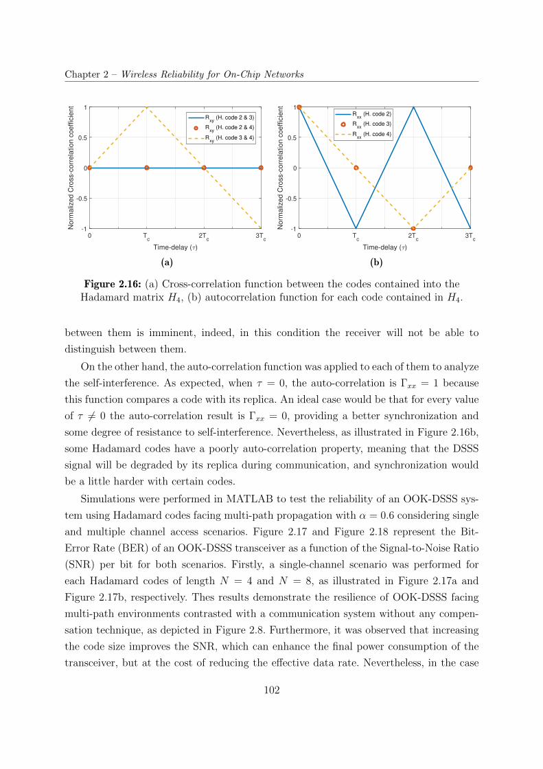
Chapter 2 – Wireless Reliability for On-Chip Networks
0 Tc
2Tc
3Tc
Time-delay ( )
-1
-0.5
0
0.5
1
Norm
aliz
ed C
ross-c
orr
ela
tion c
oeffic
ient
Rxy
(H. code 2 & 3)
Rxy
(H. code 2 & 4)
Rxy
(H. code 3 & 4)
(a)
0 Tc
2Tc
3Tc
Time-delay ( )
-1
-0.5
0
0.5
1
Norm
aliz
ed C
ross-c
orr
ela
tion c
oeffic
ient
Rxx
(H. code 2)
Rxx
(H. code 3)
Rxx
(H. code 4)
(b)
Figure 2.16: (a) Cross-correlation function between the codes contained into theHadamard matrix H4, (b) autocorrelation function for each code contained in H4.
between them is imminent, indeed, in this condition the receiver will not be able to
distinguish between them.
On the other hand, the auto-correlation function was applied to each of them to analyze
the self-interference. As expected, when τ = 0, the auto-correlation is Γxx = 1 because
this function compares a code with its replica. An ideal case would be that for every value
of τ 6= 0 the auto-correlation result is Γxx = 0, providing a better synchronization and
some degree of resistance to self-interference. Nevertheless, as illustrated in Figure 2.16b,
some Hadamard codes have a poorly auto-correlation property, meaning that the DSSS
signal will be degraded by its replica during communication, and synchronization would
be a little harder with certain codes.
Simulations were performed in MATLAB to test the reliability of an OOK-DSSS sys-
tem using Hadamard codes facing multi-path propagation with α = 0.6 considering single
and multiple channel access scenarios. Figure 2.17 and Figure 2.18 represent the Bit-
Error Rate (BER) of an OOK-DSSS transceiver as a function of the Signal-to-Noise Ratio
(SNR) per bit for both scenarios. Firstly, a single-channel scenario was performed for
each Hadamard codes of length N = 4 and N = 8, as illustrated in Figure 2.17a and
Figure 2.17b, respectively. Thes results demonstrate the resilience of OOK-DSSS facing
multi-path environments contrasted with a communication system without any compen-
sation technique, as depicted in Figure 2.8. Furthermore, it was observed that increasing
the code size improves the SNR, which can enhance the final power consumption of the
transceiver, but at the cost of reducing the effective data rate. Nevertheless, in the case
102
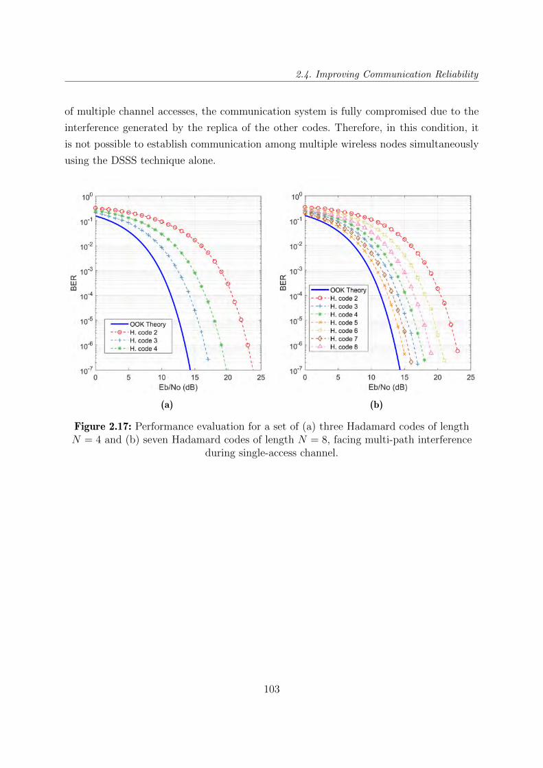
2.4. Improving Communication Reliability
of multiple channel accesses, the communication system is fully compromised due to the
interference generated by the replica of the other codes. Therefore, in this condition, it
is not possible to establish communication among multiple wireless nodes simultaneously
using the DSSS technique alone.
(a) (b)
Figure 2.17: Performance evaluation for a set of (a) three Hadamard codes of lengthN = 4 and (b) seven Hadamard codes of length N = 8, facing multi-path interference
during single-access channel.
103
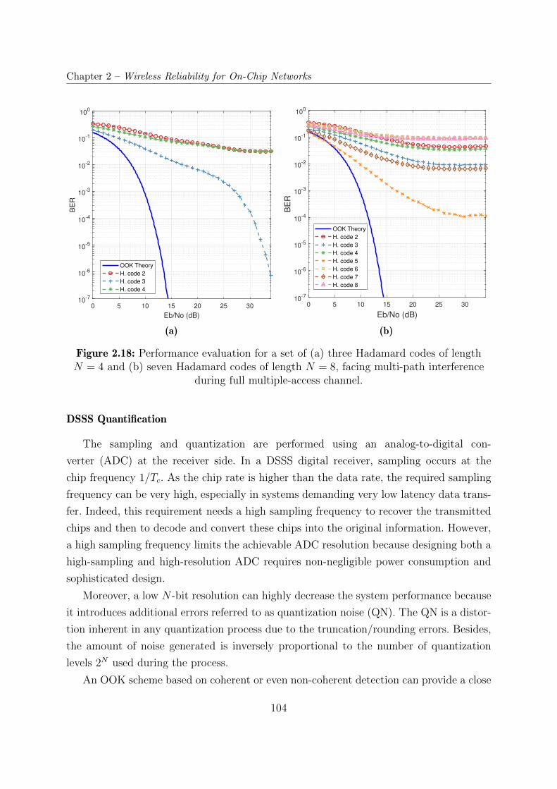
Chapter 2 – Wireless Reliability for On-Chip Networks
0 5 10 15 20 25 30
Eb/No (dB)
10-7
10-6
10-5
10-4
10-3
10-2
10-1
100
BE
R
OOK Theory
H. code 2
H. code 3
H. code 4
(a)
0 5 10 15 20 25 30
Eb/No (dB)
10-7
10-6
10-5
10-4
10-3
10-2
10-1
100
BE
R
OOK Theory
H. code 2
H. code 3
H. code 4
H. code 5
H. code 6
H. code 7
H. code 8
(b)
Figure 2.18: Performance evaluation for a set of (a) three Hadamard codes of lengthN = 4 and (b) seven Hadamard codes of length N = 8, facing multi-path interference
during full multiple-access channel.
DSSS Quantification
The sampling and quantization are performed using an analog-to-digital con-
verter (ADC) at the receiver side. In a DSSS digital receiver, sampling occurs at the
chip frequency 1/Tc. As the chip rate is higher than the data rate, the required sampling
frequency can be very high, especially in systems demanding very low latency data trans-
fer. Indeed, this requirement needs a high sampling frequency to recover the transmitted
chips and then to decode and convert these chips into the original information. However,
a high sampling frequency limits the achievable ADC resolution because designing both a
high-sampling and high-resolution ADC requires non-negligible power consumption and
sophisticated design.
Moreover, a low N -bit resolution can highly decrease the system performance because
it introduces additional errors referred to as quantization noise (QN). The QN is a distor-
tion inherent in any quantization process due to the truncation/rounding errors. Besides,
the amount of noise generated is inversely proportional to the number of quantization
levels 2N used during the process.
An OOK scheme based on coherent or even non-coherent detection can provide a close
104
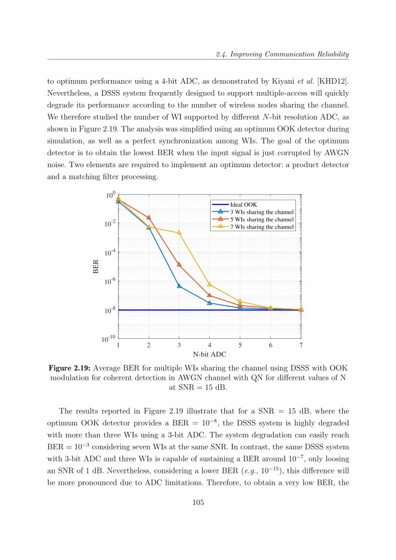
2.4. Improving Communication Reliability
to optimum performance using a 4-bit ADC, as demonstrated by Kiyani et al. [KHD12].
Nevertheless, a DSSS system frequently designed to support multiple-access will quickly
degrade its performance according to the number of wireless nodes sharing the channel.
We therefore studied the number of WI supported by different N -bit resolution ADC, as
shown in Figure 2.19. The analysis was simplified using an optimum OOK detector during
simulation, as well as a perfect synchronization among WIs. The goal of the optimum
detector is to obtain the lowest BER when the input signal is just corrupted by AWGN
noise. Two elements are required to implement an optimum detector: a product detector
and a matching filter processing.
1 2 3 4 5 6 7
N-bit ADC
10-10
10-8
10-6
10-4
10-2
100
BE
R
Ideal OOK
3 WIs sharing the channel
5 WIs sharing the channel
7 WIs sharing the channel
Figure 2.19: Average BER for multiple WIs sharing the channel using DSSS with OOKmodulation for coherent detection in AWGN channel with QN for different values of N
at SNR = 15 dB.
The results reported in Figure 2.19 illustrate that for a SNR = 15 dB, where the
optimum OOK detector provides a BER = 10−8, the DSSS system is highly degraded
with more than three WIs using a 3-bit ADC. The system degradation can easily reach
BER = 10−3 considering seven WIs at the same SNR. In contrast, the same DSSS system
with 3-bit ADC and three WIs is capable of sustaining a BER around 10−7, only loosing
an SNR of 1 dB. Nevertheless, considering a lower BER (e.g., 10−15), this difference will
be more pronounced due to ADC limitations. Therefore, to obtain a very low BER, the
105
Chapter 2 – Wireless Reliability for On-Chip Networks
system requires a 4-bit or 5-bit ADC according to the number of wireless nodes sharing
the channel. Another solution could be the implementation of an error-correcting code to
improve the obtained results, but at the cost of further decreasing the data transfer rate
and increase complexity. For these reasons, we consider that, for a close to optimal result
using three WIs, the system requires at least a 4-bit ADC resolution. Otherwise, in order
to reach a very low BER with more than seven WIs, the DSSS system requires at least a
5-bit ADC resolution or the implementation of an error-correcting code to overcome the
ADC limitations.
2.4.3 Time-Diversity Scheme (TDS)
This technique implies that the same data is transmitted repeatedly at different time
schedule. Thus, considering a channel with multi-path propagation, there are multiple
copies of the same signal transmitted according to the number of multi-path components.
Therefore, as depicted in Figure 2.20, DSSS also takes advantage of this characteristic
assuming L correlators between the input data signal y(t) and code sequences delayed by
i = 0 . . . L − 1 chip periods. The correlator outputs are combined using a diversity com-
bining rule with their respective weighting coefficients (Gi). On the other hand, since this
technique collects the energy from the received signal components to provide diversity,
it is often called the RAKE receiver. The RAKE receiver resembles an equalizer, but in
reality, it exploits the path diversity. The interference-suppression capability of this tech-
nique stems from the fact that duplicated code sequence reaching the same receptor due
to multi-path interference, will be time-shifted by merely one chip. Moreover, they have
very low correlation between them, decreasing the interference between RAKE fingers.
Therefore, code sequences with very low auto-correlation are a better option for establish
a communication link surrounded by multi-path interference. Moreover, properly weight-
ing signals coming from different reflection sources provides an improved signal-to-noise
ratio at the RAKE output.
2.5 Architecture of the Wireless Interface
This section presents the WiNoC and wireless transceiver architectures considered and
developed in this work.
106
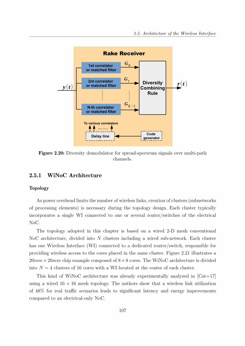
2.5. Architecture of the Wireless Interface
Figure 2.20: Diversity demodulator for spread-spectrum signals over multi-pathchannels.
2.5.1 WiNoC Architecture
Topology
As power overhead limits the number of wireless links, creation of clusters (subnetworks
of processing elements) is necessary during the topology design. Each cluster typically
incorporates a single WI connected to one or several router/switches of the electrical
NoC.
The topology adopted in this chapter is based on a wired 2-D mesh conventional
NoC architecture, divided into N clusters including a wired sub-network. Each cluster
has one Wireless Interface (WI) connected to a dedicated router/switch, responsible for
providing wireless access to the cores placed in the same cluster. Figure 2.21 illustrates a
20mm×20mm chip example composed of 8×8 cores. The WiNoC architecture is divided
into N = 4 clusters of 16 cores with a WI located at the center of each cluster.
This kind of WiNoC architecture was already experimentally analyzed in [Cat+17]
using a wired 16 × 16 mesh topology. The authors show that a wireless link utilization
of 48% for real traffic scenarios leads to significant latency and energy improvements
compared to an electrical-only NoC.
107
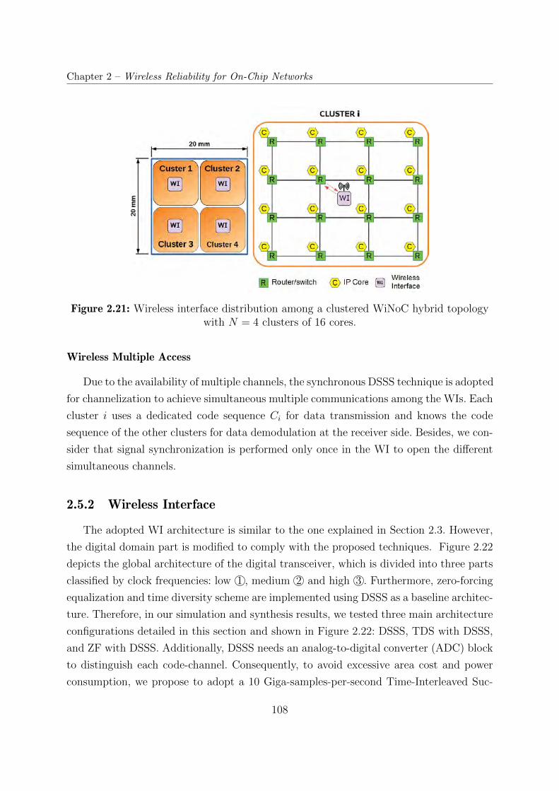
Chapter 2 – Wireless Reliability for On-Chip Networks
Figure 2.21: Wireless interface distribution among a clustered WiNoC hybrid topologywith N = 4 clusters of 16 cores.
Wireless Multiple Access
Due to the availability of multiple channels, the synchronous DSSS technique is adopted
for channelization to achieve simultaneous multiple communications among the WIs. Each
cluster i uses a dedicated code sequence Ci for data transmission and knows the code
sequence of the other clusters for data demodulation at the receiver side. Besides, we con-
sider that signal synchronization is performed only once in the WI to open the different
simultaneous channels.
2.5.2 Wireless Interface
The adopted WI architecture is similar to the one explained in Section 2.3. However,
the digital domain part is modified to comply with the proposed techniques. Figure 2.22
depicts the global architecture of the digital transceiver, which is divided into three parts
classified by clock frequencies: low 1 , medium 2 and high 3 . Furthermore, zero-forcing
equalization and time diversity scheme are implemented using DSSS as a baseline architec-
ture. Therefore, in our simulation and synthesis results, we tested three main architecture
configurations detailed in this section and shown in Figure 2.22: DSSS, TDS with DSSS,
and ZF with DSSS. Additionally, DSSS needs an analog-to-digital converter (ADC) block
to distinguish each code-channel. Consequently, to avoid excessive area cost and power
consumption, we propose to adopt a 10 Giga-samples-per-second Time-Interleaved Suc-
108
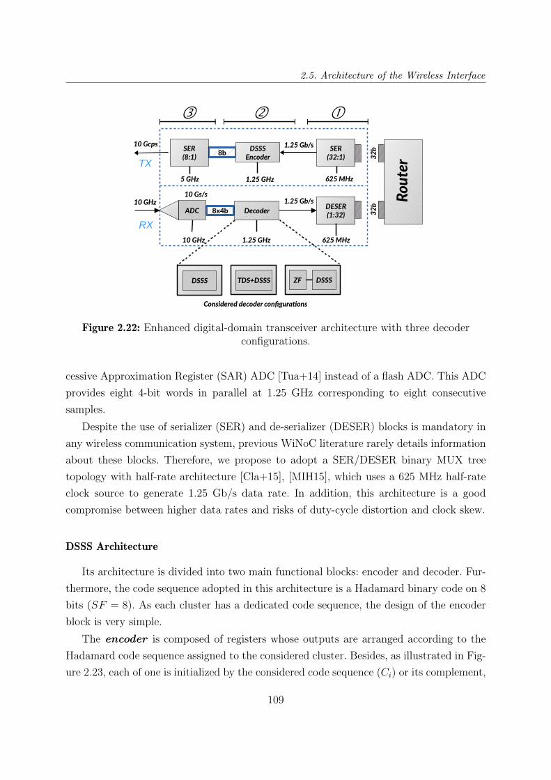
2.5. Architecture of the Wireless Interface
Figure 2.22: Enhanced digital-domain transceiver architecture with three decoderconfigurations.
cessive Approximation Register (SAR) ADC [Tua+14] instead of a flash ADC. This ADC
provides eight 4-bit words in parallel at 1.25 GHz corresponding to eight consecutive
samples.
Despite the use of serializer (SER) and de-serializer (DESER) blocks is mandatory in
any wireless communication system, previous WiNoC literature rarely details information
about these blocks. Therefore, we propose to adopt a SER/DESER binary MUX tree
topology with half-rate architecture [Cla+15], [MIH15], which uses a 625 MHz half-rate
clock source to generate 1.25 Gb/s data rate. In addition, this architecture is a good
compromise between higher data rates and risks of duty-cycle distortion and clock skew.
DSSS Architecture
Its architecture is divided into two main functional blocks: encoder and decoder. Fur-
thermore, the code sequence adopted in this architecture is a Hadamard binary code on 8
bits (SF = 8). As each cluster has a dedicated code sequence, the design of the encoder
block is very simple.
The encoder is composed of registers whose outputs are arranged according to the
Hadamard code sequence assigned to the considered cluster. Besides, as illustrated in Fig-
ure 2.23, each of one is initialized by the considered code sequence (Ci) or its complement,
109
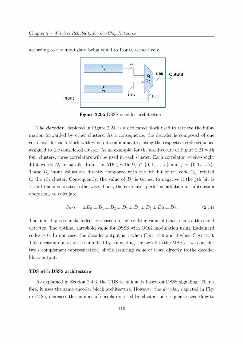
Chapter 2 – Wireless Reliability for On-Chip Networks
according to the input data being equal to 1 or 0, respectively.
Figure 2.23: DSSS encoder architecture.
The decoder , depicted in Figure 2.24, is a dedicated block used to retrieve the infor-
mation forwarded by other clusters. As a consequence, the decoder is composed of one
correlator for each block with which it communicates, using the respective code sequence
assigned to the considered cluster. As an example, for the architecture of Figure 2.21 with
four clusters, three correlators will be used in each cluster. Each correlator receives eight
4-bit words Dj in parallel from the ADC, with Dj ∈ 0, 1, ..., 15 and j = 0, 1, ..., 7.These Dj input values are directly compared with the jth bit of ith code Ci,j related
to the ith cluster. Consequently, the value of Dj is turned to negative if the jth bit is
1, and remains positive otherwise. Then, the correlator performs addition or subtraction
operations to calculate
Corr = ±D0 ±D1 ±D2 ±D3 ±D4 ±D5 ±D6±D7. (2.14)
The final step is to make a decision based on the resulting value of Corr, using a threshold
detector. The optimal threshold value for DSSS with OOK modulation using Hadamard
codes is 0. In our case, the decoder output is 1 when Corr < 0 and 0 when Corr > 0.
This decision operation is simplified by connecting the sign bit (the MSB as we consider
two's complement representation) of the resulting value of Corr directly to the decoder
block output.
TDS with DSSS architecture
As explained in Section 2.4.3, the TDS technique is based on DSSS signaling. There-
fore, it uses the same encoder block architecture. However, the decoder, depicted in Fig-
ure 2.25, increases the number of correlators used by cluster code sequence according to
110
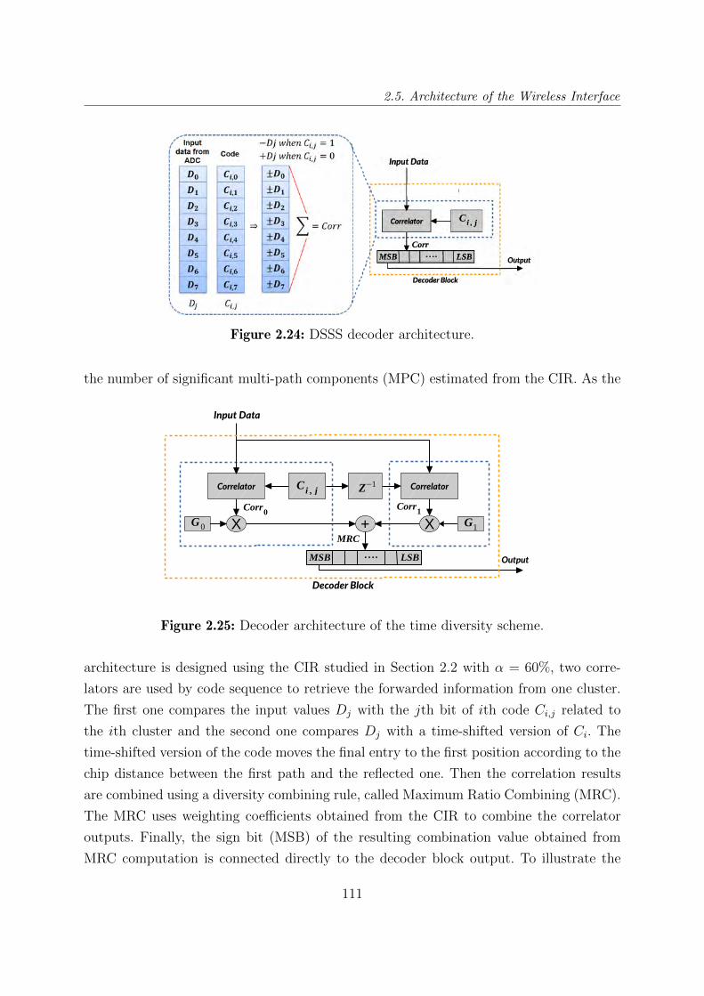
2.5. Architecture of the Wireless Interface
Figure 2.24: DSSS decoder architecture.
the number of significant multi-path components (MPC) estimated from the CIR. As the
Figure 2.25: Decoder architecture of the time diversity scheme.
architecture is designed using the CIR studied in Section 2.2 with α = 60%, two corre-
lators are used by code sequence to retrieve the forwarded information from one cluster.
The first one compares the input values Dj with the jth bit of ith code Ci,j related to
the ith cluster and the second one compares Dj with a time-shifted version of Ci. The
time-shifted version of the code moves the final entry to the first position according to the
chip distance between the first path and the reflected one. Then the correlation results
are combined using a diversity combining rule, called Maximum Ratio Combining (MRC).
The MRC uses weighting coefficients obtained from the CIR to combine the correlator
outputs. Finally, the sign bit (MSB) of the resulting combination value obtained from
MRC computation is connected directly to the decoder block output. To illustrate the
111
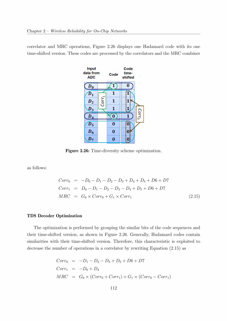
Chapter 2 – Wireless Reliability for On-Chip Networks
correlator and MRC operations, Figure 2.26 displays one Hadamard code with its one
time-shifted version. These codes are processed by the correlators and the MRC combiner
Figure 2.26: Time-diversity scheme optimization.
as follows:
Corr0 = −D0 −D1 −D2 −D3 +D4 +D5 +D6 +D7
Corr1 = D0 −D1 −D2 −D3 −D4 +D5 +D6 +D7
MRC = G0 × Corr0 +G1 × Corr1 (2.15)
TDS Decoder Optimization
The optimization is performed by grouping the similar bits of the code sequences and
their time-shifted version, as shown in Figure 2.26. Generally, Hadamard codes contain
similarities with their time-shifted version. Therefore, this characteristic is exploited to
decrease the number of operations in a correlator by rewriting Equation (2.15) as
Corr0 = −D1 −D2 −D3 +D5 +D6 +D7
Corr1 = −D0 +D4
MRC = G0 × (Corr0 + Corr1) +G1 × (Corr0 − Corr1)
112
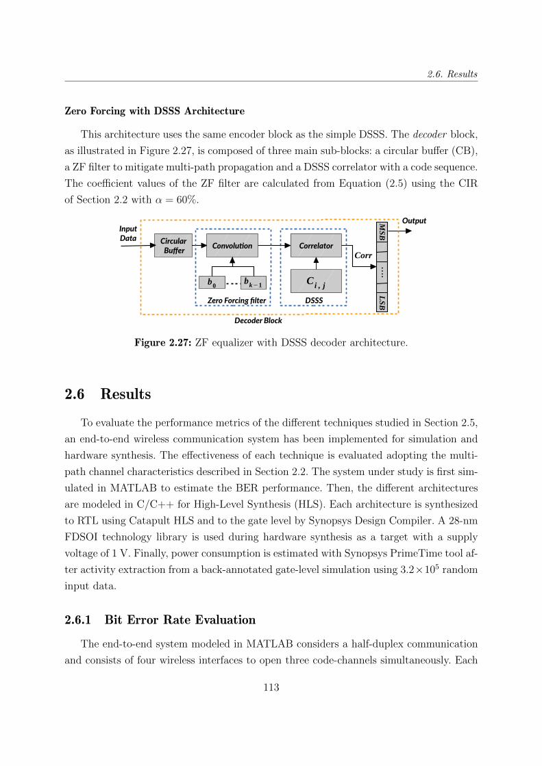
2.6. Results
Zero Forcing with DSSS Architecture
This architecture uses the same encoder block as the simple DSSS. The decoder block,
as illustrated in Figure 2.27, is composed of three main sub-blocks: a circular buffer (CB),
a ZF filter to mitigate multi-path propagation and a DSSS correlator with a code sequence.
The coefficient values of the ZF filter are calculated from Equation (2.5) using the CIR
of Section 2.2 with α = 60%.
Figure 2.27: ZF equalizer with DSSS decoder architecture.
2.6 Results
To evaluate the performance metrics of the different techniques studied in Section 2.5,
an end-to-end wireless communication system has been implemented for simulation and
hardware synthesis. The effectiveness of each technique is evaluated adopting the multi-
path channel characteristics described in Section 2.2. The system under study is first sim-
ulated in MATLAB to estimate the BER performance. Then, the different architectures
are modeled in C/C++ for High-Level Synthesis (HLS). Each architecture is synthesized
to RTL using Catapult HLS and to the gate level by Synopsys Design Compiler. A 28-nmFDSOI technology library is used during hardware synthesis as a target with a supply
voltage of 1 V. Finally, power consumption is estimated with Synopsys PrimeTime tool af-
ter activity extraction from a back-annotated gate-level simulation using 3.2×10⁵ random
input data.
2.6.1 Bit Error Rate Evaluation
The end-to-end system modeled in MATLAB considers a half-duplex communication
and consists of four wireless interfaces to open three code-channels simultaneously. Each
113
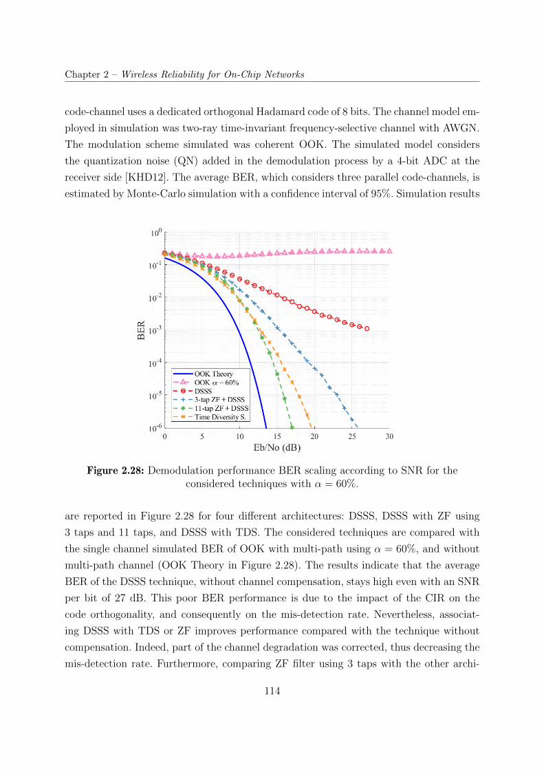
Chapter 2 – Wireless Reliability for On-Chip Networks
code-channel uses a dedicated orthogonal Hadamard code of 8 bits. The channel model em-
ployed in simulation was two-ray time-invariant frequency-selective channel with AWGN.
The modulation scheme simulated was coherent OOK. The simulated model considers
the quantization noise (QN) added in the demodulation process by a 4-bit ADC at the
receiver side [KHD12]. The average BER, which considers three parallel code-channels, is
estimated by Monte-Carlo simulation with a confidence interval of 95%. Simulation results
Figure 2.28: Demodulation performance BER scaling according to SNR for theconsidered techniques with α = 60%.
are reported in Figure 2.28 for four different architectures: DSSS, DSSS with ZF using
3 taps and 11 taps, and DSSS with TDS. The considered techniques are compared with
the single channel simulated BER of OOK with multi-path using α = 60%, and without
multi-path channel (OOK Theory in Figure 2.28). The results indicate that the average
BER of the DSSS technique, without channel compensation, stays high even with an SNR
per bit of 27 dB. This poor BER performance is due to the impact of the CIR on the
code orthogonality, and consequently on the mis-detection rate. Nevertheless, associat-
ing DSSS with TDS or ZF improves performance compared with the technique without
compensation. Indeed, part of the channel degradation was corrected, thus decreasing the
mis-detection rate. Furthermore, comparing ZF filter using 3 taps with the other archi-
114
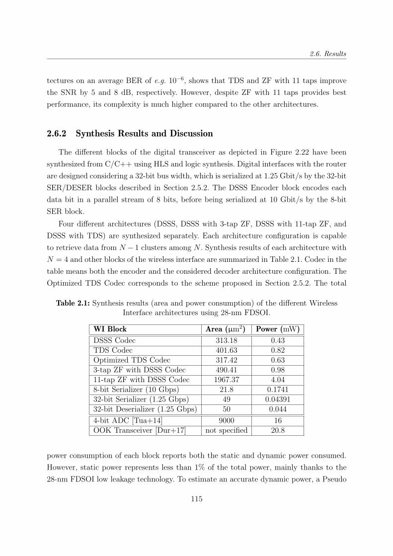
2.6. Results
tectures on an average BER of e.g. 10−6, shows that TDS and ZF with 11 taps improve
the SNR by 5 and 8 dB, respectively. However, despite ZF with 11 taps provides best
performance, its complexity is much higher compared to the other architectures.
2.6.2 Synthesis Results and Discussion
The different blocks of the digital transceiver as depicted in Figure 2.22 have been
synthesized from C/C++ using HLS and logic synthesis. Digital interfaces with the router
are designed considering a 32-bit bus width, which is serialized at 1.25 Gbit/s by the 32-bit
SER/DESER blocks described in Section 2.5.2. The DSSS Encoder block encodes each
data bit in a parallel stream of 8 bits, before being serialized at 10 Gbit/s by the 8-bit
SER block.
Four different architectures (DSSS, DSSS with 3-tap ZF, DSSS with 11-tap ZF, and
DSSS with TDS) are synthesized separately. Each architecture configuration is capable
to retrieve data from N − 1 clusters among N . Synthesis results of each architecture with
N = 4 and other blocks of the wireless interface are summarized in Table 2.1. Codec in the
table means both the encoder and the considered decoder architecture configuration. The
Optimized TDS Codec corresponds to the scheme proposed in Section 2.5.2. The total
Table 2.1: Synthesis results (area and power consumption) of the different WirelessInterface architectures using 28-nm FDSOI.
WI Block Area (µm2) Power (mW)
DSSS Codec 313.18 0.43TDS Codec 401.63 0.82Optimized TDS Codec 317.42 0.633-tap ZF with DSSS Codec 490.41 0.9811-tap ZF with DSSS Codec 1967.37 4.048-bit Serializer (10 Gbps) 21.8 0.174132-bit Serializer (1.25 Gbps) 49 0.0439132-bit Deserializer (1.25 Gbps) 50 0.044
4-bit ADC [Tua+14] 9000 16OOK Transceiver [Dur+17] not specified 20.8
power consumption of each block reports both the static and dynamic power consumed.
However, static power represents less than 1% of the total power, mainly thanks to the
28-nm FDSOI low leakage technology. To estimate an accurate dynamic power, a Pseudo
115
Chapter 2 – Wireless Reliability for On-Chip Networks
Random Bit Sequence of 4× 104 bits is injected into the encoder block, which generates
a total of 3.2× 105 bits for the decoder block.
The ADC is a key block in OOK transceivers based on DSSS and filter compensation
(e.g., zero-forcing) since it consumes the bulk of area and power of the WI. Nevertheless,
as performance simulations in literature only consider an ideal wireless channel, no ADC is
used for digital channel compensation. The parallel architecture of time-interleaved SAR
ADC, mentioned in Section 2.5.2, decreases the frequency for digital filters and therefore
to improve power consumption. Based on [Tua+14], Table 2.1 also provides area and
power for the ADC block. For reference, figures extrapolated from [Dur+17] of an OOK
transceiver are also reported. However, Section 2.2 already showed the poor performance
of this transceiver in case of multi-path CIR.
The DSSS codec shows lower area and power consumption overhead than the other
techniques. However, as shown in Figure 2.28, its average BER is lower than for the other
techniques with channel effect compensation. On the other hand, the ZF with 11 taps
shows the best performance in terms of average BER, at the cost of highest power and
area overhead. Finally, the average BER performance of the Time Diversity Scheme (TDS)
based on the RAKE receiver is situated between ZF with 11 taps and 3 taps. In addition,
the area and power consumption overhead of the optimized TDS codec is better than any
k-tap ZF codec.
Furthermore, as shown in Figure 2.8, decreasing α, the amplitude of the second path of
the CIR, improves BER performance. Therefore, any technique applied with α less than
60% will enhance BER too. However, the area and power consumption of each architecture
will be approximately the same (overhead may depend upon the coefficient values), but
the TDS performance will become closer to the 11-tap ZF. Under these conditions, the
TDS technique offers the best trade-off between BER performance and area/power over
the other techniques.
116
2.7. Conclusions
2.7 Conclusions
Emerging WiNoC communication technology is considered as a very viable solution for
facing scalability and energy issues in multicore architectures. However, communication
reliability through a realistic wireless channel cannot be ensured by adopting conventional
transceiver architectures. Therefore, in this chapter, we have shown the impact of a semi-
realistic multi-path wireless channel over conventional WiNoC modulation scheme. Our
study demonstrates the significant unreliability of an OOK transceiver, even for a channel
with low dispersion.
To overcome this issue, we propose to combine the DSSS coding scheme with channel
compensation blocks. Among the solutions studied, the TDS receiver represents the best
trade-off between bit-error rate performance and area/power overhead, when compared
with different Zero-Forcing equalizers. The area (power) overhead of the TDS block for a
four-cluster receiver is only 317 µm2 (0.63 mW), which represents less than 1% (2%) of the
wireless interface. Therefore, the gain in performance of our proposed scheme is significant
at the cost of a very low area/power overhead. The TDS, unlike an error-correcting code,
offers more throughput as the number of users sharing the wireless channel increases.
We believe that the introduction of the proposed solution opens interesting scenarios to
combat channel effects in WiNoC.
117

Chapter 3
ADAPTIVE TRANSCEIVER FOR
WIRELESS NOC
Wireless Network-on-Chip (WiNoC) peculiarly fulfills system feasibility and flexibility
to overcome limitations of standard wired communications. However, the reliability of
wireless links is not enough explored and remains an important and unsolved issue. Most
contributions in the WiNoC research field are oriented to demonstrate that WiNoCs can
overcome limitations of conventional NoC architectures for core-to-core [Pan+09] and
core-to-memory communications, e.g., in the case of cache coherency [ACV17]. Contribu-
tions have also investigated different network topologies to take advantage of long distance
links [Pan+09].
Additionally, since cache coherency requires a network architecture supporting vari-
ous communication scenarios, such as many-to-one, all-to-one, and multiple-unicast, there
is a substantial body of work analyzing the impact of allowing multiple parallel channel
accesses to improve bandwidth, average packet energy, and communication latency. These
approaches mainly divide the channel by creating multiple isolated spaces (SDM) [Zha+11],
by frequency (FDM) [Lee+09], using orthogonal frequencies (OFDM) [Bri+15; GGD17],
and adopting channelization codes (CDM) [Vid+12]. However, each parallel channel access
method comes with some challenges to be implemented in WiNoC, such as early network
saturation, several band-pass filters, frequency synthesizers, (inverse) fast Fourier trans-
form blocks and ADCs.
In this chapter, we propose a reconfigurable digital transceiver architecture with effi-
cient support of unicast/broadcast, many-to-one, all-to-one, and multiple unicast commu-
nication patterns, adopting some configurable channel compensation techniques. We show
that it is required to adapt the transceiver configurations according to these different com-
119
Chapter 3 – Adaptive Transceiver for Wireless NoC
munication patterns, in order to improve WiNoC performance, especially when facing a
semi-realistic wireless channel. Furthermore, the design adopted provides low complexity,
sustains low bit-error-rate, minimal data transfer latency and reasonable power require-
ments. Indeed, each configuration is intended to be used according to network traffic
requirements.
The results presented are based on a semi-realistic channel model for intra-chip wave
propagation derived from [AVM16; KBK01; ZCS07]. The channel impulse response (CIR)
representation considers two main propagation paths: direct and reflected path. The di-
rect and reflected path are separated in time by one symbol duration.The reflected path
is generated by the edges of the chip. The amount of energy preserved by the reflected
path after to be rebounded by the chip-edge structures, mainly depends of the physical
structures and substrate losses. A rough approximation of this preserved energy was per-
formed in Chapter 2, defining this energy as a ratio (α) between the amplitudes of the
reflected and the direct path. In the rest of the chapter, this ratio is considered as α = 60%which, corresponds to the worst condition of a channel without any mechanism to avoid
chip-edge reflections.
3.1 WiNoC Architecture
For NoC architectures, hybrid interconnects are more suitable designs to improve
throughput, power consumption, and scalability than using only one interconnect type.
This premise is demonstrated in WiNoC state-of-the-art where several approaches com-
bine wired/wireless and optical/wireless [SKL16] solutions. Combining wireless links with
another interconnect solution allows for the number of embedded cores to be easily scaled
and latency and power to be improved. This is due to the natural support of broad-
cast/multicast communication traffic in wireless links, which is especially difficult with a
large number of cores (e.g., 256 – 1024).
To manage the wireless channel, WiNoC solutions require a wireless interface (WI),
typically connected to a conventional NoC router. This WI is divided into analog and
digital parts. Current analog part typically comprises an OOK transceiver supporting 16
Gb/s data rate. The digital part includes a serializer/deserializer (SER/DESER) module
and a wireless network access controller. Nevertheless, this basic WI only supports unicast
or broadcast communications in a given time slot.
120
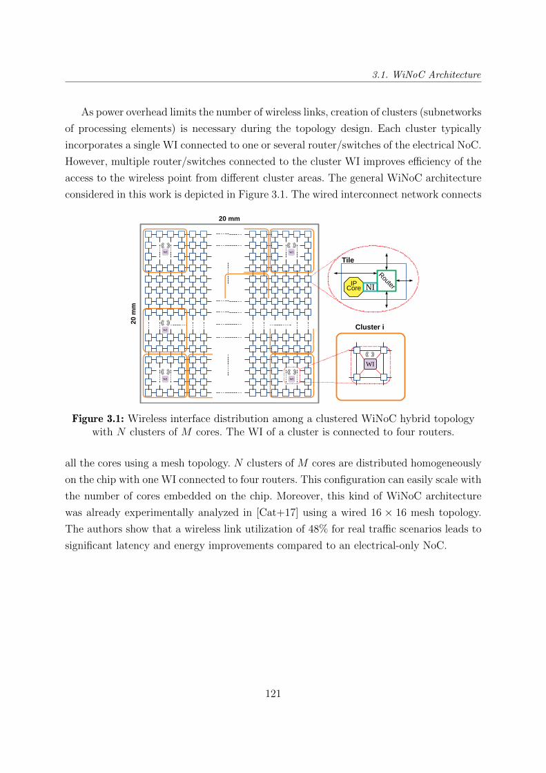
3.1. WiNoC Architecture
As power overhead limits the number of wireless links, creation of clusters (subnetworks
of processing elements) is necessary during the topology design. Each cluster typically
incorporates a single WI connected to one or several router/switches of the electrical NoC.
However, multiple router/switches connected to the cluster WI improves efficiency of the
access to the wireless point from different cluster areas. The general WiNoC architecture
considered in this work is depicted in Figure 3.1. The wired interconnect network connects
Figure 3.1: Wireless interface distribution among a clustered WiNoC hybrid topologywith N clusters of M cores. The WI of a cluster is connected to four routers.
all the cores using a mesh topology. N clusters of M cores are distributed homogeneously
on the chip with one WI connected to four routers. This configuration can easily scale with
the number of cores embedded on the chip. Moreover, this kind of WiNoC architecture
was already experimentally analyzed in [Cat+17] using a wired 16 × 16 mesh topology.
The authors show that a wireless link utilization of 48% for real traffic scenarios leads to
significant latency and energy improvements compared to an electrical-only NoC.
121
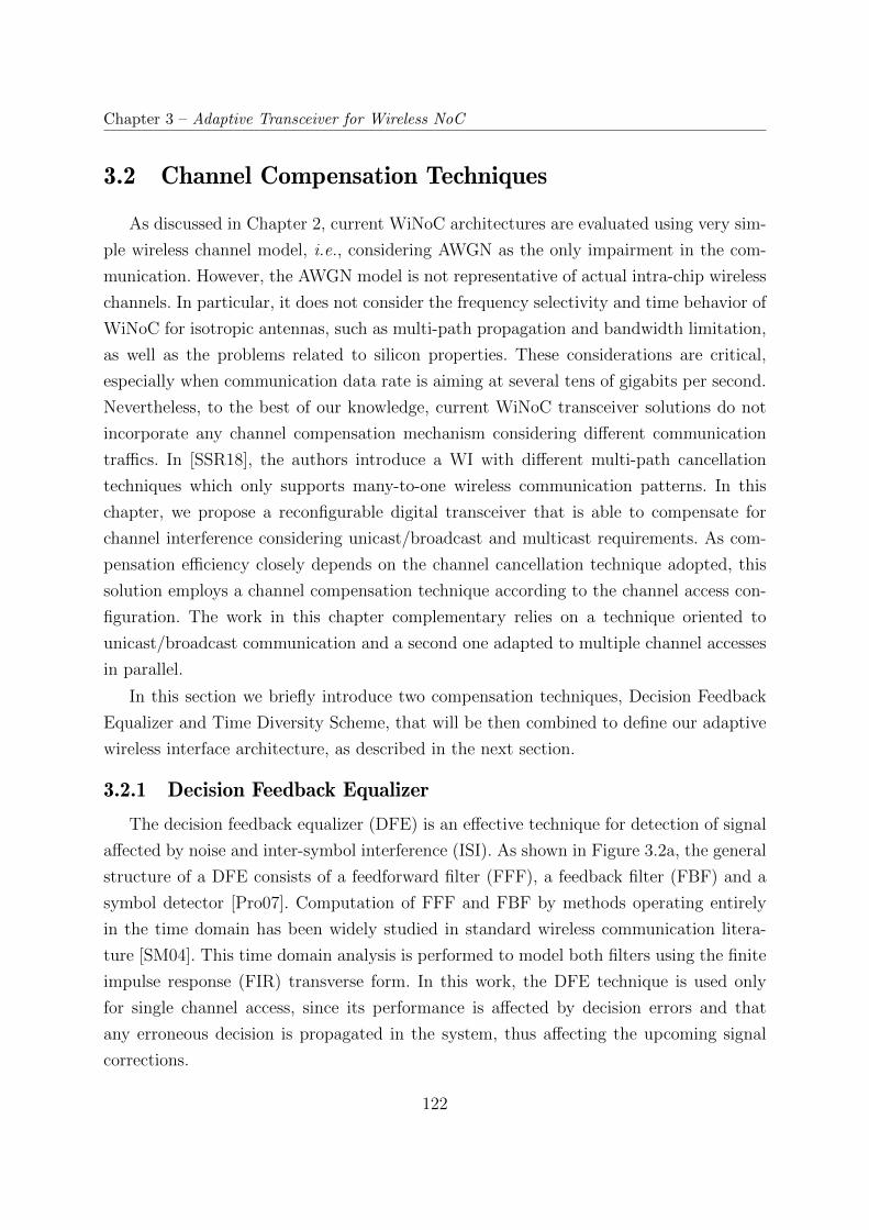
Chapter 3 – Adaptive Transceiver for Wireless NoC
3.2 Channel Compensation Techniques
As discussed in Chapter 2, current WiNoC architectures are evaluated using very sim-
ple wireless channel model, i.e., considering AWGN as the only impairment in the com-
munication. However, the AWGN model is not representative of actual intra-chip wireless
channels. In particular, it does not consider the frequency selectivity and time behavior of
WiNoC for isotropic antennas, such as multi-path propagation and bandwidth limitation,
as well as the problems related to silicon properties. These considerations are critical,
especially when communication data rate is aiming at several tens of gigabits per second.
Nevertheless, to the best of our knowledge, current WiNoC transceiver solutions do not
incorporate any channel compensation mechanism considering different communication
traffics. In [SSR18], the authors introduce a WI with different multi-path cancellation
techniques which only supports many-to-one wireless communication patterns. In this
chapter, we propose a reconfigurable digital transceiver that is able to compensate for
channel interference considering unicast/broadcast and multicast requirements. As com-
pensation efficiency closely depends on the channel cancellation technique adopted, this
solution employs a channel compensation technique according to the channel access con-
figuration. The work in this chapter complementary relies on a technique oriented to
unicast/broadcast communication and a second one adapted to multiple channel accesses
in parallel.
In this section we briefly introduce two compensation techniques, Decision Feedback
Equalizer and Time Diversity Scheme, that will be then combined to define our adaptive
wireless interface architecture, as described in the next section.
3.2.1 Decision Feedback Equalizer
The decision feedback equalizer (DFE) is an effective technique for detection of signal
affected by noise and inter-symbol interference (ISI). As shown in Figure 3.2a, the general
structure of a DFE consists of a feedforward filter (FFF), a feedback filter (FBF) and a
symbol detector [Pro07]. Computation of FFF and FBF by methods operating entirely
in the time domain has been widely studied in standard wireless communication litera-
ture [SM04]. This time domain analysis is performed to model both filters using the finite
impulse response (FIR) transverse form. In this work, the DFE technique is used only
for single channel access, since its performance is affected by decision errors and that
any erroneous decision is propagated in the system, thus affecting the upcoming signal
corrections.
122
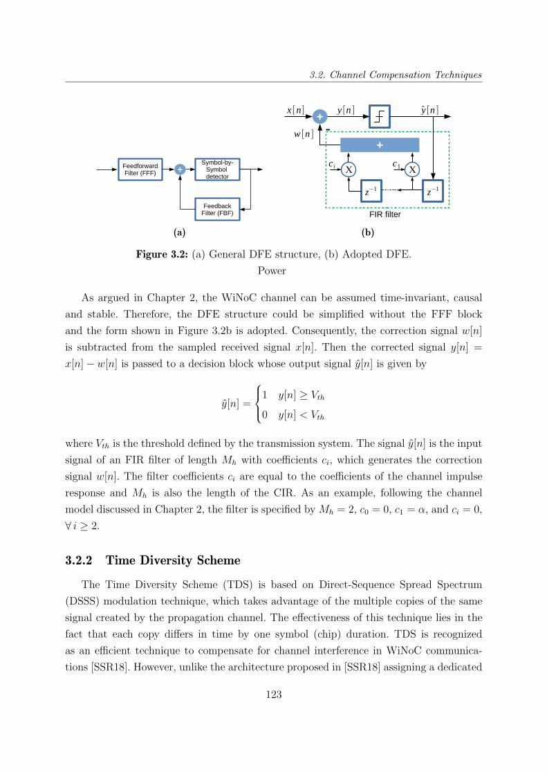
3.2. Channel Compensation Techniques
(a) (b)
Figure 3.2: (a) General DFE structure, (b) Adopted DFE.
Power
As argued in Chapter 2, the WiNoC channel can be assumed time-invariant, causal
and stable. Therefore, the DFE structure could be simplified without the FFF block
and the form shown in Figure 3.2b is adopted. Consequently, the correction signal w[n]is subtracted from the sampled received signal x[n]. Then the corrected signal y[n] =x[n]− w[n] is passed to a decision block whose output signal y[n] is given by
y[n] =
1 y[n] ≥ Vth
0 y[n] < Vth
where Vth is the threshold defined by the transmission system. The signal y[n] is the input
signal of an FIR filter of length Mh with coefficients ci, which generates the correction
signal w[n]. The filter coefficients ci are equal to the coefficients of the channel impulse
response and Mh is also the length of the CIR. As an example, following the channel
model discussed in Chapter 2, the filter is specified by Mh = 2, c0 = 0, c1 = α, and ci = 0,
∀ i ≥ 2.
3.2.2 Time Diversity Scheme
The Time Diversity Scheme (TDS) is based on Direct-Sequence Spread Spectrum
(DSSS) modulation technique, which takes advantage of the multiple copies of the same
signal created by the propagation channel. The effectiveness of this technique lies in the
fact that each copy differs in time by one symbol (chip) duration. TDS is recognized
as an efficient technique to compensate for channel interference in WiNoC communica-
tions [SSR18]. However, unlike the architecture proposed in [SSR18] assigning a dedicated
123
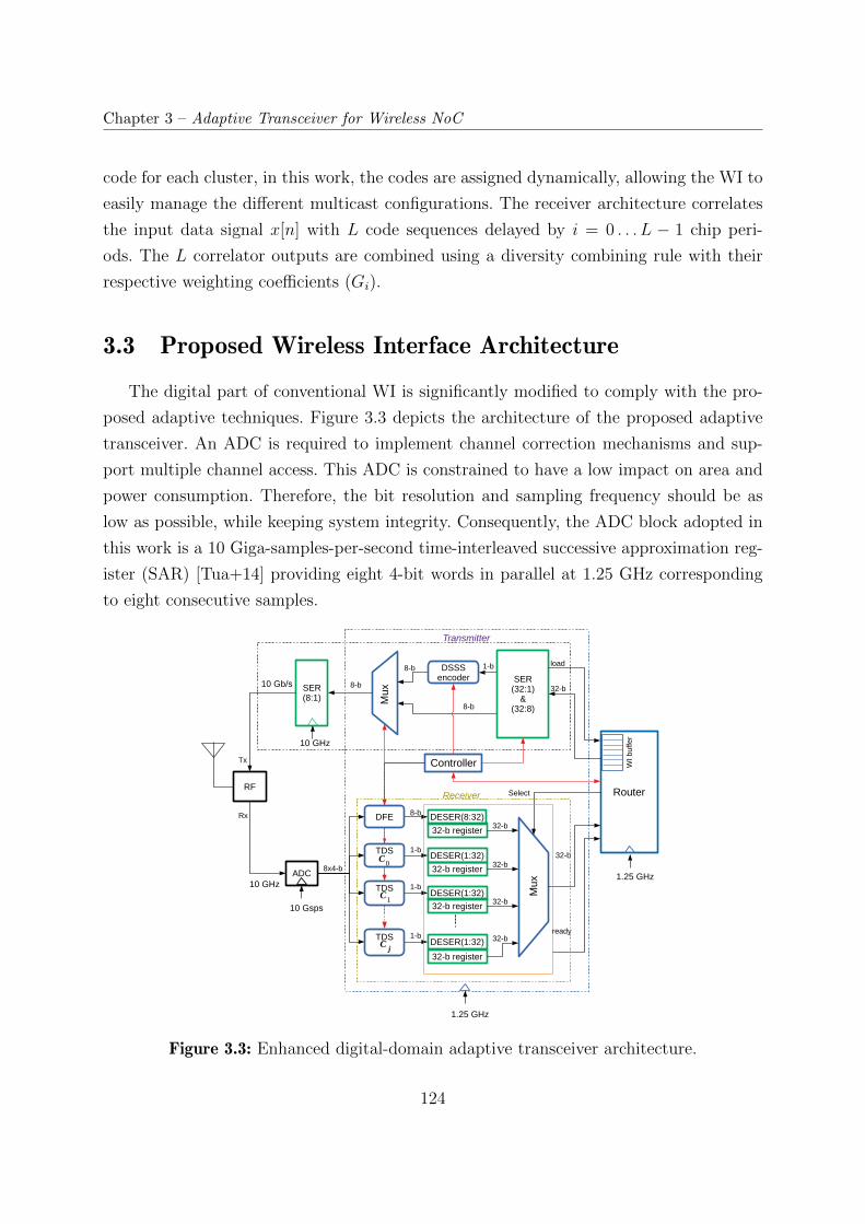
Chapter 3 – Adaptive Transceiver for Wireless NoC
code for each cluster, in this work, the codes are assigned dynamically, allowing the WI to
easily manage the different multicast configurations. The receiver architecture correlates
the input data signal x[n] with L code sequences delayed by i = 0 . . . L − 1 chip peri-
ods. The L correlator outputs are combined using a diversity combining rule with their
respective weighting coefficients (Gi).
3.3 Proposed Wireless Interface Architecture
The digital part of conventional WI is significantly modified to comply with the pro-
posed adaptive techniques. Figure 3.3 depicts the architecture of the proposed adaptive
transceiver. An ADC is required to implement channel correction mechanisms and sup-
port multiple channel access. This ADC is constrained to have a low impact on area and
power consumption. Therefore, the bit resolution and sampling frequency should be as
low as possible, while keeping system integrity. Consequently, the ADC block adopted in
this work is a 10 Giga-samples-per-second time-interleaved successive approximation reg-
ister (SAR) [Tua+14] providing eight 4-bit words in parallel at 1.25 GHz corresponding
to eight consecutive samples.
Figure 3.3: Enhanced digital-domain adaptive transceiver architecture.
124
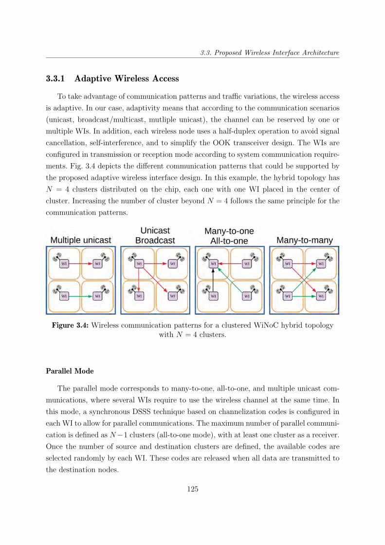
3.3. Proposed Wireless Interface Architecture
3.3.1 Adaptive Wireless Access
To take advantage of communication patterns and traffic variations, the wireless access
is adaptive. In our case, adaptivity means that according to the communication scenarios
(unicast, broadcast/multicast, mutliple unicast), the channel can be reserved by one or
multiple WIs. In addition, each wireless node uses a half-duplex operation to avoid signal
cancellation, self-interference, and to simplify the OOK transceiver design. The WIs are
configured in transmission or reception mode according to system communication require-
ments. Fig. 3.4 depicts the different communication patterns that could be supported by
the proposed adaptive wireless interface design. In this example, the hybrid topology has
N = 4 clusters distributed on the chip, each one with one WI placed in the center of
cluster. Increasing the number of cluster beyond N = 4 follows the same principle for the
communication patterns.
Figure 3.4: Wireless communication patterns for a clustered WiNoC hybrid topologywith N = 4 clusters.
Parallel Mode
The parallel mode corresponds to many-to-one, all-to-one, and multiple unicast com-
munications, where several WIs require to use the wireless channel at the same time. In
this mode, a synchronous DSSS technique based on channelization codes is configured in
each WI to allow for parallel communications. The maximum number of parallel communi-
cation is defined as N−1 clusters (all-to-one mode), with at least one cluster as a receiver.
Once the number of source and destination clusters are defined, the available codes are
selected randomly by each WI. These codes are released when all data are transmitted to
the destination nodes.
125
Chapter 3 – Adaptive Transceiver for Wireless NoC
Unicast/Broadcast Mode
In the second mode, unicast or broadcast communication is used. Therefore, one trans-
mitter and one receiver (unicast) or multiple receivers (broadcast) are configured in the
wireless network. As the channel does not need to be shared with other transmitters, no
channelization code is necessary to forward information to the destination nodes. In this
mode, the DFE compensation technique is used to enhance communication link reliability.
3.3.2 Digital Transmitter Architecture
As depicted in the upper part of Fig. 3.3, the transmitter is composed of three blocks:
SER(32:1/8), DSSS encoder, and SER(8:1). A serializer SER(n:m) is a shift register hav-
ing an input on n bits issued at a clock fi which is serialized on an m-bit output at a
clock fo = n.fi/m. The SER(32:1/8) has two outputs on 1 bit and 8 bits, which are
activated according to system requirements. In case of unicast/broadcast communication,
the SER(32:1/8) 8-bit output is multiplexed into the SER (8:1) block. Otherwise, when
channel multiple access is required, the SER (32:1/8) 1-bit output and DSSS encoder
blocks are activated by the controller.
The DSSS encoder is very simple, since composed of a register initialized by the consid-
ered 8-bit channelization code (Cj) or its complement, according to the input data being
equal to 1 or 0, respectively. This encoder relies on the code Cj selected by the controller
during the configuration phase. On the router/switch side, the output ports connected
with the SER(32:1/8) block have an increased RF buffer depth of 8 flits (1 flit = 32 bits) to
avoid excessive latency while waiting the channel to be released. As explained in [Cha+12],
buffer depth beyond this limit does not produce any further performance, but leads to
overhead in power and area.
3.3.3 Digital Receiver Architecture
As shown in the lower part of Figure 3.3, the receiver is composed of the follow-
ing blocks: DFE channel compensation, DESER(8:32), and one DESER(1:32) and TDS
per code Cj. Each DESER is associated with a 32-bit register to store the flit before to
be read by the router. All channel compensation blocks (DFE, TDS Cj) receive eight
4-bit words in parallel from the ADC. Furthermore, these blocks are only activated dur-
ing the network configuration phase according to communication requirements. For the
unicast/broadcast mode, the DFE and associated DESER(8:32) blocks are activated for
126
3.4. Hardware Implementation and Performance Evaluation
channel compensation. For the parallel channel access mode, the TDS blocks are config-
ured by the controller with allocated Cj. A TDS block consists of several correlators to act
against multi-path interference existing in the CIR. Each TDS block is associated with
a particular 8-bit channelization code Cj to allow for parallel communications. The data
received from these blocks is deserialized in the respective DESER blocks (complexity
similar to the SER) and saved into the 32-bit registers. Then, a signal is immediately sent
to the router/switch indicating the register state.
3.4 Hardware Implementation and Performance Evaluation
An end-to-end wireless communication system has been implemented for performance
simulation and hardware synthesis. The effectiveness of this architecture is estimated
under unicast/multicast conditions in presence of multi-path interference, as described
in Chapter 2. The system under study is simulated using MATLAB assuming perfect
synchronization to estimate the bit error rate (BER) performance. Then, the digital
transceiver architecture is modeled in C/C++ for High-Level Synthesis (HLS). The de-
sign is synthesized from C to RTL by Catapult HLS (V10.8) and to the gate level by
Synopsys Design Compiler (V2015.06-SP5). A 28-nm FDSOI technology library is used
during hardware synthesis as a target with a supply voltage of 1 Volt. Finally, the full
transceiver design was validated by simulation from the C/C++ model down to the gate
level using ModelSim and SCVerify.
3.4.1 Bit Error Rate Evaluation
The end-to-end system modeled in MATLAB considers a half-duplex communication
and consists of four wireless interfaces (i.e., N = 4 clusters) configured for single or par-
allel communication. The channelization codes used during parallel channel access are
orthogonal Hadamard codes on 8 bits, supporting up to 7 parallel channels. The channel
model employed in the simulations is a two-ray time-invariant frequency-selective channel
with AWGN. The modulation scheme simulated is coherent OOK. The simulated model
considers the quantization noise added in the demodulation process by a 4-bit ADC at
the receiver side. Finally, the average BER is estimated by Monte-Carlo simulation with
a confidence interval of 95%. Simulation results are reported in Figure 3.5 for single and
parallel channel configurations. Their effectiveness is contrasted with the single channel
127
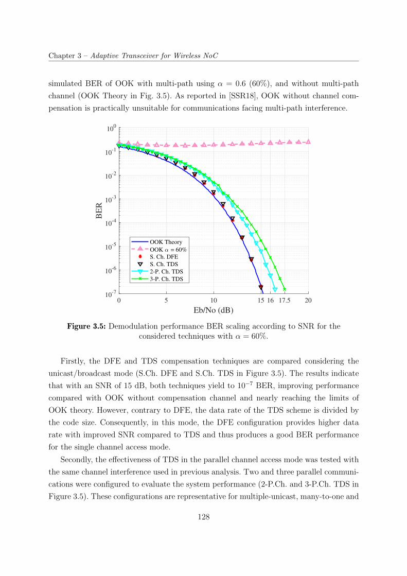
Chapter 3 – Adaptive Transceiver for Wireless NoC
simulated BER of OOK with multi-path using α = 0.6 (60%), and without multi-path
channel (OOK Theory in Fig. 3.5). As reported in [SSR18], OOK without channel com-
pensation is practically unsuitable for communications facing multi-path interference.
0 5 10 15 16 17.5 20
Eb/No (dB)
10-7
10-6
10-5
10-4
10-3
10-2
10-1
100
BE
R
OOK Theory
OOK = 60%
S. Ch. DFE
S. Ch. TDS
2-P. Ch. TDS
3-P. Ch. TDS
Figure 3.5: Demodulation performance BER scaling according to SNR for theconsidered techniques with α = 60%.
Firstly, the DFE and TDS compensation techniques are compared considering the
unicast/broadcast mode (S.Ch. DFE and S.Ch. TDS in Figure 3.5). The results indicate
that with an SNR of 15 dB, both techniques yield to 10−7 BER, improving performance
compared with OOK without compensation channel and nearly reaching the limits of
OOK theory. However, contrary to DFE, the data rate of the TDS scheme is divided by
the code size. Consequently, in this mode, the DFE configuration provides higher data
rate with improved SNR compared to TDS and thus produces a good BER performance
for the single channel access mode.
Secondly, the effectiveness of TDS in the parallel channel access mode was tested with
the same channel interference used in previous analysis. Two and three parallel communi-
cations were configured to evaluate the system performance (2-P.Ch. and 3-P.Ch. TDS in
Figure 3.5). These configurations are representative for multiple-unicast, many-to-one and
128
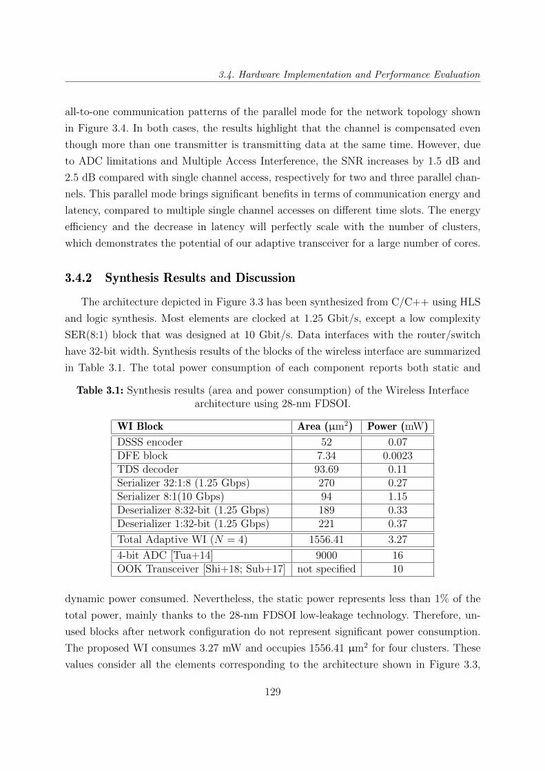
3.4. Hardware Implementation and Performance Evaluation
all-to-one communication patterns of the parallel mode for the network topology shown
in Figure 3.4. In both cases, the results highlight that the channel is compensated even
though more than one transmitter is transmitting data at the same time. However, due
to ADC limitations and Multiple Access Interference, the SNR increases by 1.5 dB and
2.5 dB compared with single channel access, respectively for two and three parallel chan-
nels. This parallel mode brings significant benefits in terms of communication energy and
latency, compared to multiple single channel accesses on different time slots. The energy
efficiency and the decrease in latency will perfectly scale with the number of clusters,
which demonstrates the potential of our adaptive transceiver for a large number of cores.
3.4.2 Synthesis Results and Discussion
The architecture depicted in Figure 3.3 has been synthesized from C/C++ using HLS
and logic synthesis. Most elements are clocked at 1.25 Gbit/s, except a low complexity
SER(8:1) block that was designed at 10 Gbit/s. Data interfaces with the router/switch
have 32-bit width. Synthesis results of the blocks of the wireless interface are summarized
in Table 3.1. The total power consumption of each component reports both static and
Table 3.1: Synthesis results (area and power consumption) of the Wireless Interfacearchitecture using 28-nm FDSOI.
WI Block Area (µm2) Power (mW)
DSSS encoder 52 0.07DFE block 7.34 0.0023TDS decoder 93.69 0.11Serializer 32:1:8 (1.25 Gbps) 270 0.27Serializer 8:1(10 Gbps) 94 1.15Deserializer 8:32-bit (1.25 Gbps) 189 0.33Deserializer 1:32-bit (1.25 Gbps) 221 0.37
Total Adaptive WI (N = 4) 1556.41 3.27
4-bit ADC [Tua+14] 9000 16OOK Transceiver [Shi+18; Sub+17] not specified 10
dynamic power consumed. Nevertheless, the static power represents less than 1% of the
total power, mainly thanks to the 28-nm FDSOI low-leakage technology. Therefore, un-
used blocks after network configuration do not represent significant power consumption.
The proposed WI consumes 3.27 mW and occupies 1556.41 µm2 for four clusters. These
values consider all the elements corresponding to the architecture shown in Figure 3.3,
129
Chapter 3 – Adaptive Transceiver for Wireless NoC
disregarding the RF, ADC and router/switch. Based on [Tua+14], Table 3.1 also provides
area and power for the ADC block and for a low-power OOK RF transceiver. The ADC
block may be considered as a drawback in our architecture, since it consumes the bulk of
area and power of the WI. However, any digital filter or channel compensation technique
requires this block to perform corrections. The ADC architecture needed in this type of
WiNoC is a parallel one, as mentioned in Section 3.3, which decreases the frequency of
digital filters and therefore reduces power consumption. Consequently, to push the per-
formance limits of wireless links in WiNoC, the use of an ADC is mandatory. This opens
for relevant research to build new ADC designs dedicated to the WiNoC context.
The proposed solution, which considers all mandatory elements into the digital WI part
including the compensation techniques, represents less than 1% (10%) of the total WI area
(power). Furthermore, the solution proposed improves by 67% the power consumption of
the technique presented in [Deb+10] without any channel compensation. Moreover, our
adaptive approach provides on-chip communication with a reliability near to the limit of
the OOK theory, both for single unicast and parallel multicast/broadcast configurations.
130
3.5. Conclusions
3.5 Conclusions
WiNoC communication technology is expected to overcome limitations of conventional
wired communications. However, communication reliability through a realistic wireless
channel still remains an unexplored area in the state of the art. Furthermore, due to,
e.g., the cache coherence protocols supported by on chip interconnection networks, var-
ious multicast/broadcast scenarios are important to be considered during the wireless
interface design of WiNoCs. As a consequence, in this chapter, we proposed an adaptive
digital transceiver using channel compensation techniques for single and multiple parallel
channel access modes. Our study demonstrates the significant reliability improvement of
an OOK scheme facing a channel with high dispersion.
The area (power) overhead of the adaptive digital transceiver for a four-cluster re-
ceiver is only 1556.41µm2 (3.27mW), which represents less than 1% (10%) of the wireless
interface. Therefore, the gain in performance of our proposed scheme is significant at the
cost of a very low area/power overhead. In addition, unlike an error-correcting code, our
solution offers more throughput and less latency when the number of clusters sharing the
wireless channel increases (parallel mode), as well as in unicast/broadcast mode.
131

Chapter 4
MULTICHANNEL WIRELESS NOC
In this chapter, we demonstrate the significant power efficiency degradation of a single-
carrier high-speed system designed with limited bandwidth. Furthermore, we discuss the
problems of future WiNoCs to reach high-speed data links, as well as the challenges that
the channel will bring to future WiNoC designers. Then, we propose and study a multi-
carrier wireless system based on Frequency Division Multiplexing (FDM), which can easily
overcome future WiNoC generation requirements. Subsequently, we propose an efficient
multi-carrier transceiver architecture capable of supporting unicast/broadcast, many-to-
one, all-to-one, many-to-many and multiple unicast communication patterns, adopting a
spread-spectrum multiple-access technique. Finally, an approach for symbol timing recov-
ery leveraging the spread spectrum technique is studied.
133
Chapter 4 – Multichannel Wireless NoC
4.1 Towards High-Speed Wireless Links
Massive parallelism in manycore architectures for emerging high-performance comput-
ing applications requires the use of an efficient interconnection system. However, current
electrical interconnections are not efficient enough to support an increasing number of
cores while ensuring high performance and energy efficiency. As discussed in Chapter 1,
massive number of cores necessitates a large Network-on-Chip (NoC), which can easily
lead to prohibitive communication latency due to long multi-hop paths. These long paths
can be reached using high-speed wireless links, radiating electromagnetic energy along
the chip. However, the additional power consumption required to implement these wireless
links is not negligible. The main contributors in the power budget are the power amplifiers
used to establish high-speed communication with very low Bit-Error-Rate (BER). In fact,
the bandwidth needed to reach this high-speed communication increases the power con-
sumption in all single-carrier wireless transceivers. Therefore, in order to keep a reasonable
trade-off between power consumption and data rate, WiNoC designers have decreased the
minimum required bandwidth to support a given data rate (e.g. 16 Gbps). However, this
reduction produces significant communication errors that have to be compensated by in-
creasing the transmission signal power and the receiver sensitivity.
Recent studies on the Terahertz-band reveal the possibility of highly increasing the
available bandwidth, impacting positively on the communication data rate. But in a single-
carrier wireless transceiver, such bandwidth means a very high power consumption, de-
grading the whole communication system. Even with a bandwidth reduction in the power
amplifiers, the power dissipated will reach prohibitive levels for on-chip wireless communi-
cation. Therefore, the main issue will reside in how we can efficiently utilize the hundreds
of GHz of the bandwidth for high-speed links.
On the other hand, a system designed to reach very high data rates will be always
prone to multi-path propagation. This phenomenon is especially important when the
symbol duration is shorter than the multi-path duration, which produces Inter-Symbol
Interference (ISI) and consequently leads to significant system performance degradation.
For this reason, the on-chip wireless communication, aiming high-speed data rate, requires
an especial channel to decrease the impact of such multi-path propagation. This can
be attained by introducing a dedicated communication layer, providing a close to ideal
channel behaviour. In the following sections, we will discuss about this kind of channel.
134
4.2. Wireless NoC Architecture
Another issue related to high-speed communications is the bit synchronization or sym-
bol timing recovery for WiNoC solutions based on Non-Coherent On-Off Keying (NC-
OOK). The symbol timing recovery is tricky for a short symbol duration or huge data
transfer rate. In the case of a coherent communication system, it requires carrier and phase
synchronization in addition to the bit synchronization, complexifying the transceiver de-
sign. For this reason, NC-OOK is the most used modulation scheme for WiNoC wireless
links. Nevertheless, to the best of our knowledge, no work considers any symbol timing
recovery algorithm to properly recover the forwarded data.
In this chapter we will discuss more deeply these issues and propose a digital transceiver
capable of handle high-speed communications for future WiNoC designs.
4.2 Wireless NoC Architecture
The WiNoC architecture mainly consists in how the processing blocks (homogeneous
or heterogeneous) are distributed and connected between them. The connectivity struc-
ture and topology used in most research works is the hybrid one. Hybrid designs basically
exploit the idea that a simple and reliable short-distance wired link is more efficient for
a local traffic inside a small group of nodes, whereas a wireless link can significantly im-
prove the performance for relative long-distance communication. Four main architectures
based on hybrid topologies combining wired and wireless interconnections were proposed
for WiNoCs with different scalability levels, such as 2D clustered mesh-based [WHB11],
WCube [Lee+09], iWISE [DiT+11], and Small-World [Kim+16]. The 2D clustered mesh-
based, WCube, and iWISE architectures only change according to the number of cores. In
contrast, in the Small-World architecture, the topology changes according to the frequency
of traffic between cores.
To manage the wireless channel, WiNoC solutions require a wireless interface (WI),
typically connected to a conventional NoC router. This WI is divided into analog and
digital domains, as explained in [SSR18]. The analog module of a standard WI comprises
a single-carrier NC-OOK transceiver with 16 Gb/s data rate support. The digital part
consists of a serializer/deserializer (SER/DESER) module and a wireless network access
controller. Current implemented transceivers consume around 32 mW DC power, pro-
viding a point-to-point bit-energy efficiency of 2 pJ/bit. Compared with other NC-OOK
transceivers used outside WiNoC application, it is a very promising design. However,
135
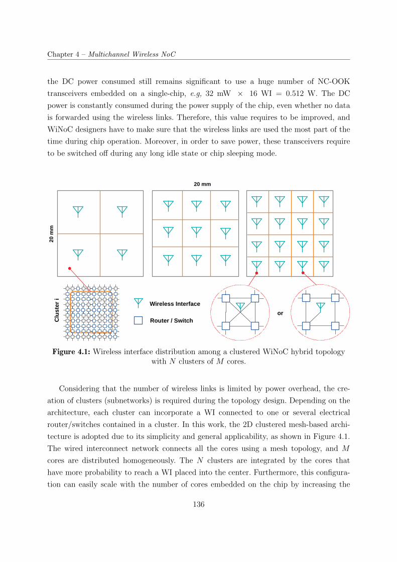
Chapter 4 – Multichannel Wireless NoC
the DC power consumed still remains significant to use a huge number of NC-OOK
transceivers embedded on a single-chip, e.g, 32 mW × 16 WI = 0.512 W. The DC
power is constantly consumed during the power supply of the chip, even whether no data
is forwarded using the wireless links. Therefore, this value requires to be improved, and
WiNoC designers have to make sure that the wireless links are used the most part of the
time during chip operation. Moreover, in order to save power, these transceivers require
to be switched off during any long idle state or chip sleeping mode.
Figure 4.1: Wireless interface distribution among a clustered WiNoC hybrid topologywith N clusters of M cores.
Considering that the number of wireless links is limited by power overhead, the cre-
ation of clusters (subnetworks) is required during the topology design. Depending on the
architecture, each cluster can incorporate a WI connected to one or several electrical
router/switches contained in a cluster. In this work, the 2D clustered mesh-based archi-
tecture is adopted due to its simplicity and general applicability, as shown in Figure 4.1.
The wired interconnect network connects all the cores using a mesh topology, and M
cores are distributed homogeneously. The N clusters are integrated by the cores that
have more probability to reach a WI placed into the center. Furthermore, this configura-
tion can easily scale with the number of cores embedded on the chip by increasing the
136
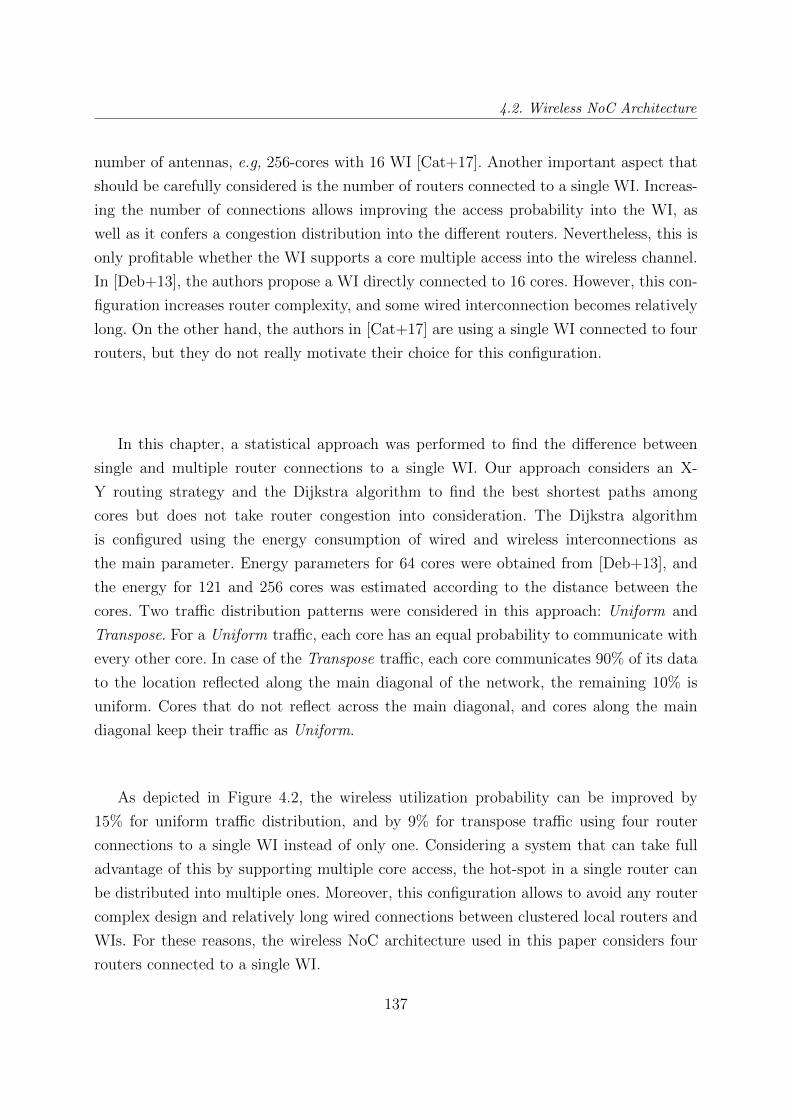
4.2. Wireless NoC Architecture
number of antennas, e.g, 256-cores with 16 WI [Cat+17]. Another important aspect that
should be carefully considered is the number of routers connected to a single WI. Increas-
ing the number of connections allows improving the access probability into the WI, as
well as it confers a congestion distribution into the different routers. Nevertheless, this is
only profitable whether the WI supports a core multiple access into the wireless channel.
In [Deb+13], the authors propose a WI directly connected to 16 cores. However, this con-
figuration increases router complexity, and some wired interconnection becomes relatively
long. On the other hand, the authors in [Cat+17] are using a single WI connected to four
routers, but they do not really motivate their choice for this configuration.
In this chapter, a statistical approach was performed to find the difference between
single and multiple router connections to a single WI. Our approach considers an X-
Y routing strategy and the Dijkstra algorithm to find the best shortest paths among
cores but does not take router congestion into consideration. The Dijkstra algorithm
is configured using the energy consumption of wired and wireless interconnections as
the main parameter. Energy parameters for 64 cores were obtained from [Deb+13], and
the energy for 121 and 256 cores was estimated according to the distance between the
cores. Two traffic distribution patterns were considered in this approach: Uniform and
Transpose. For a Uniform traffic, each core has an equal probability to communicate with
every other core. In case of the Transpose traffic, each core communicates 90% of its data
to the location reflected along the main diagonal of the network, the remaining 10% is
uniform. Cores that do not reflect across the main diagonal, and cores along the main
diagonal keep their traffic as Uniform.
As depicted in Figure 4.2, the wireless utilization probability can be improved by
15% for uniform traffic distribution, and by 9% for transpose traffic using four router
connections to a single WI instead of only one. Considering a system that can take full
advantage of this by supporting multiple core access, the hot-spot in a single router can
be distributed into multiple ones. Moreover, this configuration allows to avoid any router
complex design and relatively long wired connections between clustered local routers and
WIs. For these reasons, the wireless NoC architecture used in this paper considers four
routers connected to a single WI.
137
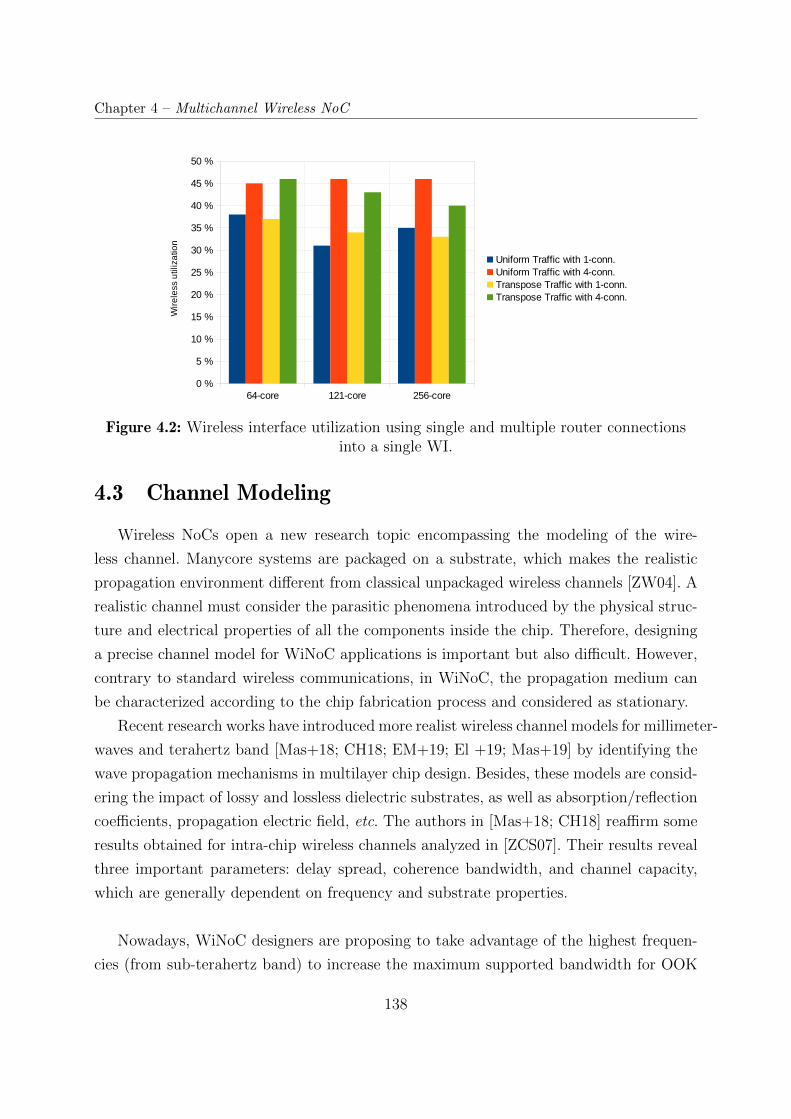
Chapter 4 – Multichannel Wireless NoC
Figure 4.2: Wireless interface utilization using single and multiple router connectionsinto a single WI.
4.3 Channel Modeling
Wireless NoCs open a new research topic encompassing the modeling of the wire-
less channel. Manycore systems are packaged on a substrate, which makes the realistic
propagation environment different from classical unpackaged wireless channels [ZW04]. A
realistic channel must consider the parasitic phenomena introduced by the physical struc-
ture and electrical properties of all the components inside the chip. Therefore, designing
a precise channel model for WiNoC applications is important but also difficult. However,
contrary to standard wireless communications, in WiNoC, the propagation medium can
be characterized according to the chip fabrication process and considered as stationary.
Recent research works have introduced more realist wireless channel models for millimeter-
waves and terahertz band [Mas+18; CH18; EM+19; El +19; Mas+19] by identifying the
wave propagation mechanisms in multilayer chip design. Besides, these models are consid-
ering the impact of lossy and lossless dielectric substrates, as well as absorption/reflection
coefficients, propagation electric field, etc. The authors in [Mas+18; CH18] reaffirm some
results obtained for intra-chip wireless channels analyzed in [ZCS07]. Their results reveal
three important parameters: delay spread, coherence bandwidth, and channel capacity,
which are generally dependent on frequency and substrate properties.
Nowadays, WiNoC designers are proposing to take advantage of the highest frequen-
cies (from sub-terahertz band) to increase the maximum supported bandwidth for OOK
138
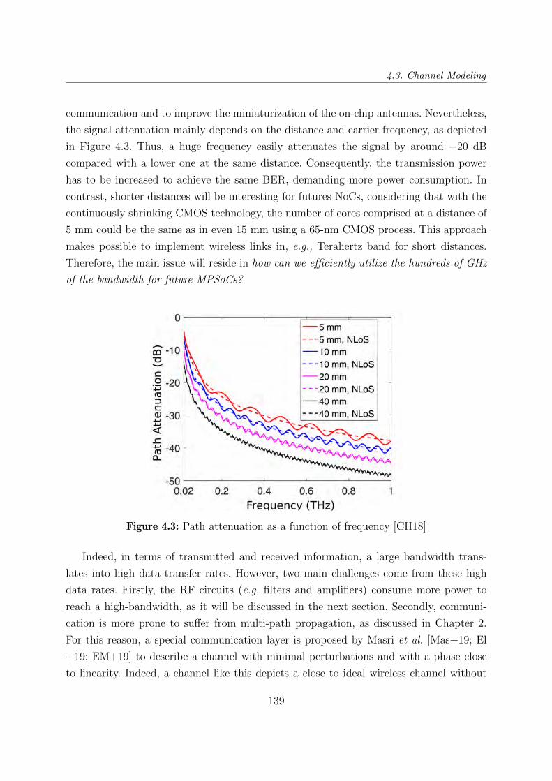
4.3. Channel Modeling
communication and to improve the miniaturization of the on-chip antennas. Nevertheless,
the signal attenuation mainly depends on the distance and carrier frequency, as depicted
in Figure 4.3. Thus, a huge frequency easily attenuates the signal by around −20 dBcompared with a lower one at the same distance. Consequently, the transmission power
has to be increased to achieve the same BER, demanding more power consumption. In
contrast, shorter distances will be interesting for futures NoCs, considering that with the
continuously shrinking CMOS technology, the number of cores comprised at a distance of
5 mm could be the same as in even 15 mm using a 65-nm CMOS process. This approach
makes possible to implement wireless links in, e.g., Terahertz band for short distances.
Therefore, the main issue will reside in how can we efficiently utilize the hundreds of GHz
of the bandwidth for future MPSoCs?
Figure 4.3: Path attenuation as a function of frequency [CH18]
Indeed, in terms of transmitted and received information, a large bandwidth trans-
lates into high data transfer rates. However, two main challenges come from these high
data rates. Firstly, the RF circuits (e.g, filters and amplifiers) consume more power to
reach a high-bandwidth, as it will be discussed in the next section. Secondly, communi-
cation is more prone to suffer from multi-path propagation, as discussed in Chapter 2.
For this reason, a special communication layer is proposed by Masri et al. [Mas+19; El
+19; EM+19] to describe a channel with minimal perturbations and with a phase close
to linearity. Indeed, a channel like this depicts a close to ideal wireless channel without
139
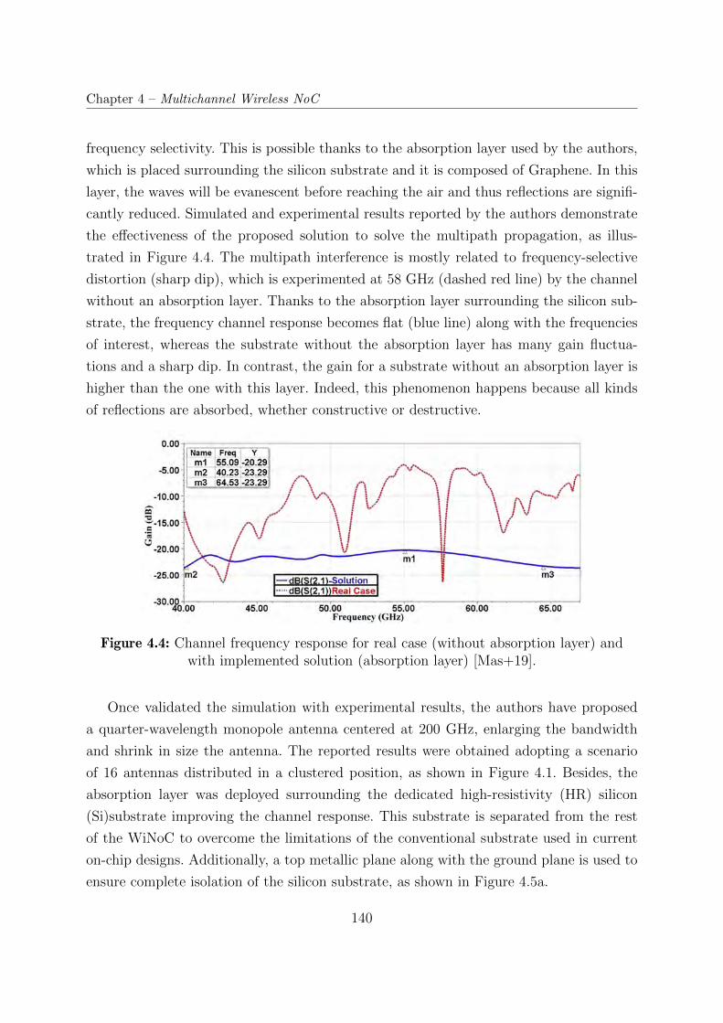
Chapter 4 – Multichannel Wireless NoC
frequency selectivity. This is possible thanks to the absorption layer used by the authors,
which is placed surrounding the silicon substrate and it is composed of Graphene. In this
layer, the waves will be evanescent before reaching the air and thus reflections are signifi-
cantly reduced. Simulated and experimental results reported by the authors demonstrate
the effectiveness of the proposed solution to solve the multipath propagation, as illus-
trated in Figure 4.4. The multipath interference is mostly related to frequency-selective
distortion (sharp dip), which is experimented at 58 GHz (dashed red line) by the channel
without an absorption layer. Thanks to the absorption layer surrounding the silicon sub-
strate, the frequency channel response becomes flat (blue line) along with the frequencies
of interest, whereas the substrate without the absorption layer has many gain fluctua-
tions and a sharp dip. In contrast, the gain for a substrate without an absorption layer is
higher than the one with this layer. Indeed, this phenomenon happens because all kinds
of reflections are absorbed, whether constructive or destructive.
Figure 4.4: Channel frequency response for real case (without absorption layer) andwith implemented solution (absorption layer) [Mas+19].
Once validated the simulation with experimental results, the authors have proposed
a quarter-wavelength monopole antenna centered at 200 GHz, enlarging the bandwidth
and shrink in size the antenna. The reported results were obtained adopting a scenario
of 16 antennas distributed in a clustered position, as shown in Figure 4.1. Besides, the
absorption layer was deployed surrounding the dedicated high-resistivity (HR) silicon
(Si)substrate improving the channel response. This substrate is separated from the rest
of the WiNoC to overcome the limitations of the conventional substrate used in current
on-chip designs. Additionally, a top metallic plane along with the ground plane is used to
ensure complete isolation of the silicon substrate, as shown in Figure 4.5a.
140
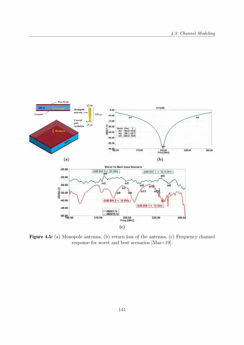
4.3. Channel Modeling
(a) (b)
(c)
Figure 4.5: (a) Monopole antenna, (b) return loss of the antenna, (c) Frequency channelresponse for worst and best scenarios [Mas+19].
141
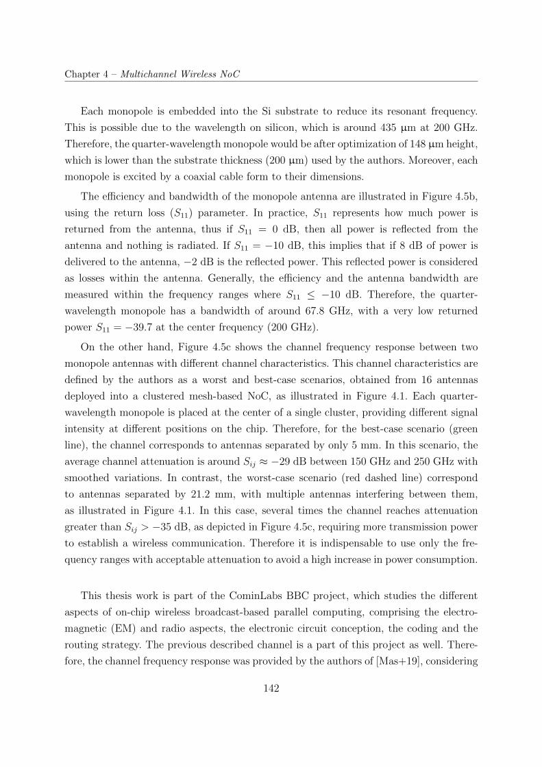
Chapter 4 – Multichannel Wireless NoC
Each monopole is embedded into the Si substrate to reduce its resonant frequency.
This is possible due to the wavelength on silicon, which is around 435 µm at 200 GHz.
Therefore, the quarter-wavelength monopole would be after optimization of 148 µm height,
which is lower than the substrate thickness (200 µm) used by the authors. Moreover, each
monopole is excited by a coaxial cable form to their dimensions.
The efficiency and bandwidth of the monopole antenna are illustrated in Figure 4.5b,
using the return loss (S11) parameter. In practice, S11 represents how much power is
returned from the antenna, thus if S11 = 0 dB, then all power is reflected from the
antenna and nothing is radiated. If S11 = −10 dB, this implies that if 8 dB of power is
delivered to the antenna, −2 dB is the reflected power. This reflected power is considered
as losses within the antenna. Generally, the efficiency and the antenna bandwidth are
measured within the frequency ranges where S11 ≤ −10 dB. Therefore, the quarter-
wavelength monopole has a bandwidth of around 67.8 GHz, with a very low returned
power S11 = −39.7 at the center frequency (200 GHz).
On the other hand, Figure 4.5c shows the channel frequency response between two
monopole antennas with different channel characteristics. This channel characteristics are
defined by the authors as a worst and best-case scenarios, obtained from 16 antennas
deployed into a clustered mesh-based NoC, as illustrated in Figure 4.1. Each quarter-
wavelength monopole is placed at the center of a single cluster, providing different signal
intensity at different positions on the chip. Therefore, for the best-case scenario (green
line), the channel corresponds to antennas separated by only 5 mm. In this scenario, the
average channel attenuation is around Sij ≈ −29 dB between 150 GHz and 250 GHz with
smoothed variations. In contrast, the worst-case scenario (red dashed line) correspond
to antennas separated by 21.2 mm, with multiple antennas interfering between them,
as illustrated in Figure 4.1. In this case, several times the channel reaches attenuation
greater than Sij > −35 dB, as depicted in Figure 4.5c, requiring more transmission power
to establish a wireless communication. Therefore it is indispensable to use only the fre-
quency ranges with acceptable attenuation to avoid a high increase in power consumption.
This thesis work is part of the CominLabs BBC project, which studies the different
aspects of on-chip wireless broadcast-based parallel computing, comprising the electro-
magnetic (EM) and radio aspects, the electronic circuit conception, the coding and the
routing strategy. The previous described channel is a part of this project as well. There-
fore, the channel frequency response was provided by the authors of [Mas+19], considering
142
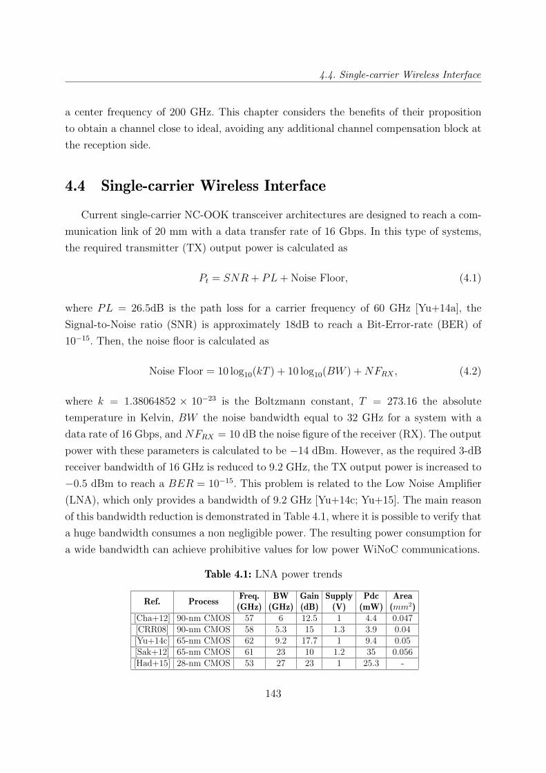
4.4. Single-carrier Wireless Interface
a center frequency of 200 GHz. This chapter considers the benefits of their proposition
to obtain a channel close to ideal, avoiding any additional channel compensation block at
the reception side.
4.4 Single-carrier Wireless Interface
Current single-carrier NC-OOK transceiver architectures are designed to reach a com-
munication link of 20 mm with a data transfer rate of 16 Gbps. In this type of systems,
the required transmitter (TX) output power is calculated as
Pt = SNR + PL+ Noise Floor, (4.1)
where PL = 26.5dB is the path loss for a carrier frequency of 60 GHz [Yu+14a], the
Signal-to-Noise ratio (SNR) is approximately 18dB to reach a Bit-Error-rate (BER) of
10−15. Then, the noise floor is calculated as
Noise Floor = 10 log10(kT ) + 10 log10(BW ) +NFRX , (4.2)
where k = 1.38064852 × 10⁻²³ is the Boltzmann constant, T = 273.16 the absolute
temperature in Kelvin, BW the noise bandwidth equal to 32 GHz for a system with a
data rate of 16 Gbps, and NFRX = 10 dB the noise figure of the receiver (RX). The output
power with these parameters is calculated to be −14 dBm. However, as the required 3-dB
receiver bandwidth of 16 GHz is reduced to 9.2 GHz, the TX output power is increased to
−0.5 dBm to reach a BER = 10−15. This problem is related to the Low Noise Amplifier
(LNA), which only provides a bandwidth of 9.2 GHz [Yu+14c; Yu+15]. The main reason
of this bandwidth reduction is demonstrated in Table 4.1, where it is possible to verify that
a huge bandwidth consumes a non negligible power. The resulting power consumption for
a wide bandwidth can achieve prohibitive values for low power WiNoC communications.
Table 4.1: LNA power trends
Ref. ProcessFreq.(GHz)
BW(GHz)
Gain(dB)
Supply(V)
Pdc(mW)
Area(mm2)
[Cha+12] 90-nm CMOS 57 6 12.5 1 4.4 0.047[CRR08] 90-nm CMOS 58 5.3 15 1.3 3.9 0.04[Yu+14c] 65-nm CMOS 62 9.2 17.7 1 9.4 0.05[Sak+12] 65-nm CMOS 61 23 10 1.2 35 0.056[Had+15] 28-nm CMOS 53 27 23 1 25.3 -
143
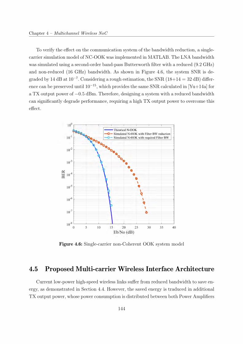
Chapter 4 – Multichannel Wireless NoC
To verify the effect on the communication system of the bandwidth reduction, a single-
carrier simulation model of NC-OOK was implemented in MATLAB. The LNA bandwidth
was simulated using a second-order band-pass Butterworth filter with a reduced (9.2 GHz)
and non-reduced (16 GHz) bandwidth. As shown in Figure 4.6, the system SNR is de-
graded by 14 dB at 10−7. Considering a rough estimation, the SNR (18+14 = 32 dB) differ-
ence can be preserved until 10−15, which provides the same SNR calculated in [Yu+14a] for
a TX output power of −0.5 dBm. Therefore, designing a system with a reduced bandwidth
can significantly degrade performance, requiring a high TX output power to overcome this
effect.
Figure 4.6: Single-carrier non-Coherent OOK system model
4.5 Proposed Multi-carrier Wireless Interface Architecture
Current low-power high-speed wireless links suffer from reduced bandwidth to save en-
ergy, as demonstrated in Section 4.4. However, the saved energy is traduced in additional
TX output power, whose power consumption is distributed between both Power Amplifiers
144
4.5. Proposed Multi-carrier Wireless Interface Architecture
(PA) at TX and LNA at RX. Moreover, the challenges to design a low power single-carrier
NC-OOK with, for instance, a 32 Gbps data-link, can degrade the improvement granted
by the impact of technology scaling. This degradation could be traduced in non-negligible
power dissipation over a very small area overhead. For these reasons, we believe that a
single-carrier NC-OOK is not a scalable solution for future high-speed WiNoCs, especially
with the Tera-Hertz band providing a broad bandwidth. In order to take full advantage
of the available bandwidth, this work proposes the design of a multi-carrier NC-OOK
transceiver based on Frequency Division Multiplexing (FDM) and Direct Sequence Spread
Spectrum (DSSS). The FDM technique is used as a mean to divide the total bandwidth
into four different carrier frequencies with shorter bandwidth, e.g., 10 GHz/4 = 2.5 GHz.
The aim of this division is to avoid any LNA bandwidth reduction due to high power
consumption, as explained in Section 4.4. Furthermore, there are spectral regions called
guard bands between carriers that act as buffer zones to prevent interference between
frequency sub-channels. On the other hand, the DSSS technique has two functions on
this architecture, the first one is to enable parallel channel access reusing existing fre-
quencies, and the second one is to provide some processing gain (PG) [FB96]. The PG
obtained grants resistance against jamming interference and provides some power advan-
tage over interference. For instance, a system without DSSS requires an SNR = 18 dBto reach a given BER. However, the same system with DSSS and PG = 10 dB requires
an SNR = 8 dB to achieve the same BER. This SNR improvement reduces the required
transmission power to establish the wireless communication with the same reliability.
The transmitter/receiver architecture is composed of several identical sub-blocks, con-
nected into a passive power combiner [ZLS11] and power splitter [EDP11], as depicted
in Figure 4.7. Both devices can be linked to an RF circulator or RF switch, allowing
for the same antenna to be shared for transmission/reception operation. Indeed, an RF
circulator can provide a full-duplex communication [RZK17]. However, isolation and self-
interference associated with this device still remain a challenge to be implemented for
WiNoC applications. In contrast, an RF switch [MPE08] has a simple design and can be
easily implemented. Nevertheless, the RF switch only supports half-duplex communica-
tion. Unlike power amplifiers, an OOK modulator and envelope detector are low-power
devices, as reported in [Yu+14a; Yu+15] for 65-nm CMOS technology. Besides, the energy
consumption of modulator is related to the VCO and the input power required by the
PA to generate a certain TX output power. Therefore, any improvements in the PA can
145
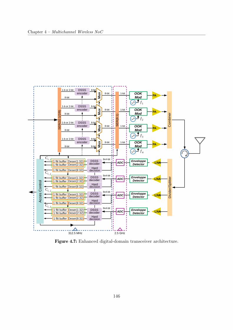
Chapter 4 – Multichannel Wireless NoC
Figure 4.7: Enhanced digital-domain transceiver architecture.
146
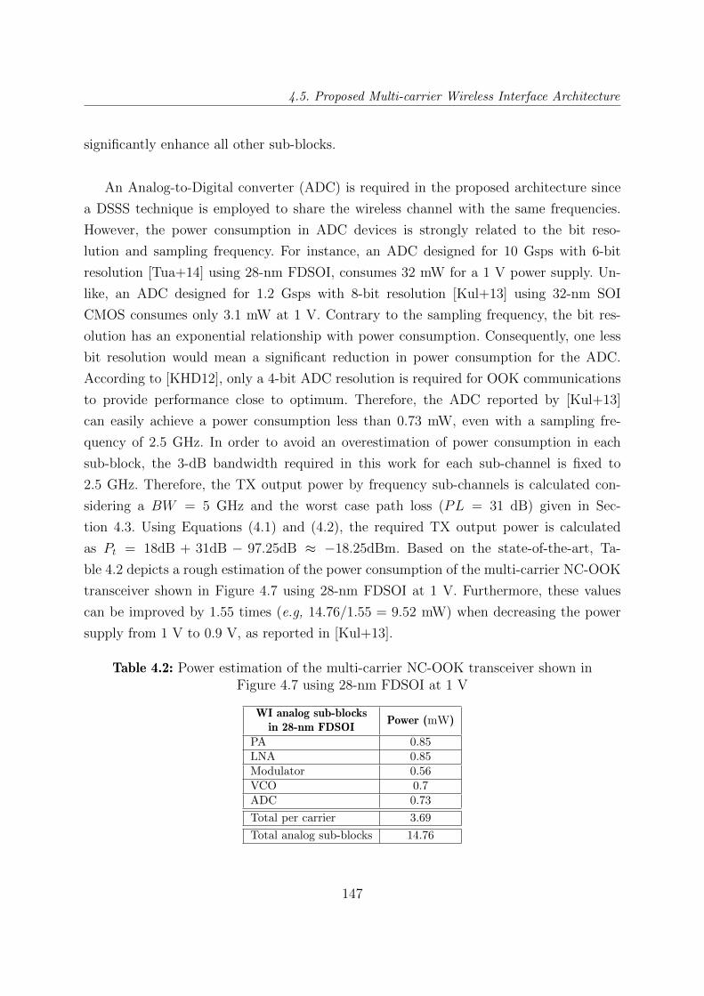
4.5. Proposed Multi-carrier Wireless Interface Architecture
significantly enhance all other sub-blocks.
An Analog-to-Digital converter (ADC) is required in the proposed architecture since
a DSSS technique is employed to share the wireless channel with the same frequencies.
However, the power consumption in ADC devices is strongly related to the bit reso-
lution and sampling frequency. For instance, an ADC designed for 10 Gsps with 6-bit
resolution [Tua+14] using 28-nm FDSOI, consumes 32 mW for a 1 V power supply. Un-
like, an ADC designed for 1.2 Gsps with 8-bit resolution [Kul+13] using 32-nm SOI
CMOS consumes only 3.1 mW at 1 V. Contrary to the sampling frequency, the bit res-
olution has an exponential relationship with power consumption. Consequently, one less
bit resolution would mean a significant reduction in power consumption for the ADC.
According to [KHD12], only a 4-bit ADC resolution is required for OOK communications
to provide performance close to optimum. Therefore, the ADC reported by [Kul+13]
can easily achieve a power consumption less than 0.73 mW, even with a sampling fre-
quency of 2.5 GHz. In order to avoid an overestimation of power consumption in each
sub-block, the 3-dB bandwidth required in this work for each sub-channel is fixed to
2.5 GHz. Therefore, the TX output power by frequency sub-channels is calculated con-
sidering a BW = 5 GHz and the worst case path loss (PL = 31 dB) given in Sec-
tion 4.3. Using Equations (4.1) and (4.2), the required TX output power is calculated
as Pt = 18dB + 31dB − 97.25dB ≈ −18.25dBm. Based on the state-of-the-art, Ta-
ble 4.2 depicts a rough estimation of the power consumption of the multi-carrier NC-OOK
transceiver shown in Figure 4.7 using 28-nm FDSOI at 1 V. Furthermore, these values
can be improved by 1.55 times (e.g, 14.76/1.55 = 9.52 mW) when decreasing the power
supply from 1 V to 0.9 V, as reported in [Kul+13].
Table 4.2: Power estimation of the multi-carrier NC-OOK transceiver shown inFigure 4.7 using 28-nm FDSOI at 1 V
WI analog sub-blocksin 28-nm FDSOI
Power (mW)
PA 0.85LNA 0.85Modulator 0.56VCO 0.7ADC 0.73
Total per carrier 3.69
Total analog sub-blocks 14.76
147
Chapter 4 – Multichannel Wireless NoC
4.5.1 Digital Transmitter Architecture
A transmitter assigned to a carrier frequency fi is composed of three blocks: a serializer
SER(32:1/2/8), a DSSS encoder, and an SER(8:1), as illustrated in Figure 4.7. A basic
architecture of an SER(n:m) is based on a shift register having an input on n bits issued
at a clock fi which is serialized on an m-bit output at a clock fo = n.fi/m. On the
other hand, the DSSS encoder is designed using 8-bit and 4-bit registers initialized by
the considered Hadamard codes (Ci). The output of this sub-block is a specific code (Ci)
or its complement (Ci), according to the input data being equal to 1 or 0, respectively.
Furthermore, in the case of 4-bit code, the output is combined with two codes of the
same size. The SER(32:1/2/8) has three outputs on 1-bit, 2-bit, and 8-bit. However,
only one of them is activated according to system requirements. For instance, in case
of unicast/broadcast communication, the SER(32:1/2/8) 8-bit output is multiplexed into
the SER (8:1) block. Otherwise, for channel multiple access, the SER (32:1/2/8) 1-bit or
2-bit output and the DSSS encoder block are activated by the controller and multiplexed
into the SER (8:1) block. The SER (32:1/2/8) 1-bit and 2-bit outputs are related with the
processing gain (PG) required by the system, as well as the number of parallel channels
supported by each carrier frequency. A PG = 6 dB is associated with a 4-bit Hadamard
code and the SER (32:1/2/8) 2-bit output, supporting only 3 parallel channels. The SER
(32:1/2/8) 1-bit output is related with an 8-bit Hadamard code, providing a PG = 9 dBand 7 parallel channels. However, beyond 4 parallel channels, the quantization noise is
increased, degrading the SNR obtained by the 4-bit ADC. Furthermore, contrary to a
system without PG, the TX output power using a PG = 6 dB is reduced to Pt =−24.25 dBm, and for PG = 9 dB the TX output power is Pt = −27.24 dBm. Consequently,
the DSSS technique can be used to design a low-power system, but at the cost of decreasing
the effective data rate.
4.5.2 Digital Receiver Architecture
A receiver sub-block tuned for a certain carrier frequency fi, receives an analog signal
and converts it into eight 4-bit words using its respective ADC, as depicted in Figure 4.7.
Afterwards, this digitized signal is forwarded into a block composed of the DSSS decoder
and the hard decision sub-blocks. A DSSS decoder consists of multiple parallel correlators
associated with a specific code Ci,j with index i and set j. Each input correlator takes
the eight 4-bit words from the ADC, and generates 1-bit or 2-bit output in case of code
148
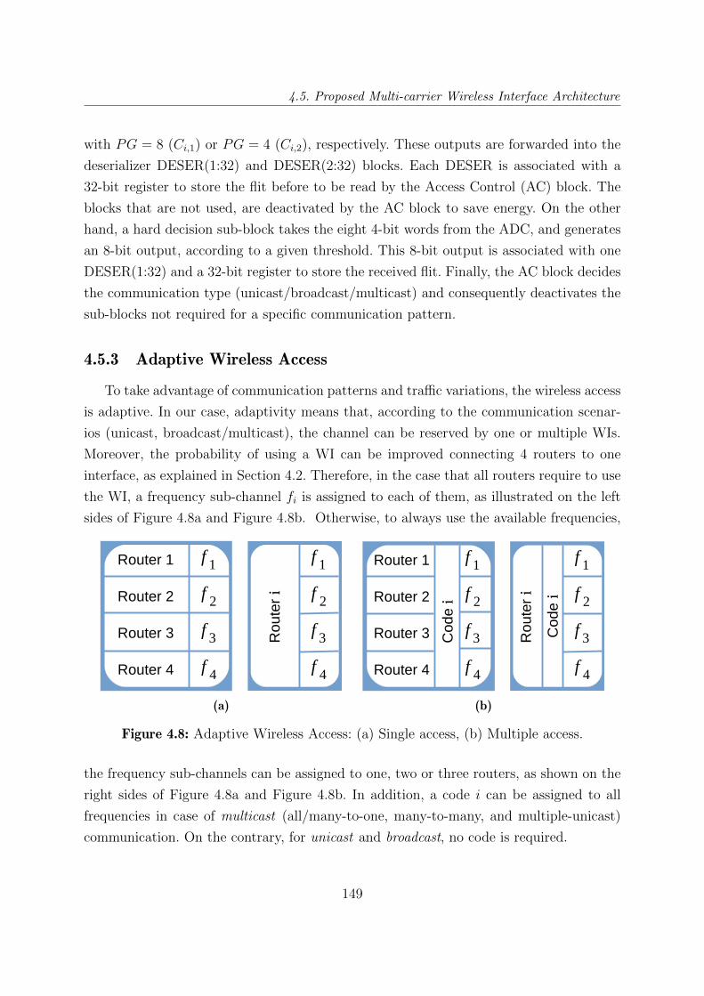
4.5. Proposed Multi-carrier Wireless Interface Architecture
with PG = 8 (Ci,1) or PG = 4 (Ci,2), respectively. These outputs are forwarded into the
deserializer DESER(1:32) and DESER(2:32) blocks. Each DESER is associated with a
32-bit register to store the flit before to be read by the Access Control (AC) block. The
blocks that are not used, are deactivated by the AC block to save energy. On the other
hand, a hard decision sub-block takes the eight 4-bit words from the ADC, and generates
an 8-bit output, according to a given threshold. This 8-bit output is associated with one
DESER(1:32) and a 32-bit register to store the received flit. Finally, the AC block decides
the communication type (unicast/broadcast/multicast) and consequently deactivates the
sub-blocks not required for a specific communication pattern.
4.5.3 Adaptive Wireless Access
To take advantage of communication patterns and traffic variations, the wireless access
is adaptive. In our case, adaptivity means that, according to the communication scenar-
ios (unicast, broadcast/multicast), the channel can be reserved by one or multiple WIs.
Moreover, the probability of using a WI can be improved connecting 4 routers to one
interface, as explained in Section 4.2. Therefore, in the case that all routers require to use
the WI, a frequency sub-channel fi is assigned to each of them, as illustrated on the left
sides of Figure 4.8a and Figure 4.8b. Otherwise, to always use the available frequencies,
(a) (b)
Figure 4.8: Adaptive Wireless Access: (a) Single access, (b) Multiple access.
the frequency sub-channels can be assigned to one, two or three routers, as shown on the
right sides of Figure 4.8a and Figure 4.8b. In addition, a code i can be assigned to all
frequencies in case of multicast (all/many-to-one, many-to-many, and multiple-unicast)
communication. On the contrary, for unicast and broadcast, no code is required.
149
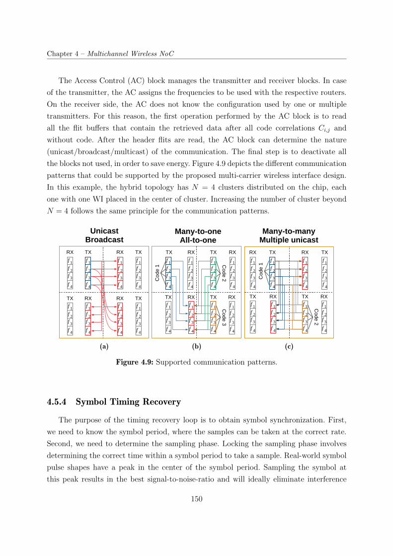
Chapter 4 – Multichannel Wireless NoC
The Access Control (AC) block manages the transmitter and receiver blocks. In case
of the transmitter, the AC assigns the frequencies to be used with the respective routers.
On the receiver side, the AC does not know the configuration used by one or multiple
transmitters. For this reason, the first operation performed by the AC block is to read
all the flit buffers that contain the retrieved data after all code correlations Ci,j and
without code. After the header flits are read, the AC block can determine the nature
(unicast/broadcast/multicast) of the communication. The final step is to deactivate all
the blocks not used, in order to save energy. Figure 4.9 depicts the different communication
patterns that could be supported by the proposed multi-carrier wireless interface design.
In this example, the hybrid topology has N = 4 clusters distributed on the chip, each
one with one WI placed in the center of cluster. Increasing the number of cluster beyond
N = 4 follows the same principle for the communication patterns.
(a) (b) (c)
Figure 4.9: Supported communication patterns.
4.5.4 Symbol Timing Recovery
The purpose of the timing recovery loop is to obtain symbol synchronization. First,
we need to know the symbol period, where the samples can be taken at the correct rate.
Second, we need to determine the sampling phase. Locking the sampling phase involves
determining the correct time within a symbol period to take a sample. Real-world symbol
pulse shapes have a peak in the center of the symbol period. Sampling the symbol at
this peak results in the best signal-to-noise-ratio and will ideally eliminate interference
150
4.6. Hardware Implementation and Performance Evaluation
from other symbols. The most popular technique used to determine the sampling phase is
the Gardner algorithm. However, this technique requires two sampling per symbol, which
increases system complexity for WiNoC applications.
In this work, we consider two simple techniques to reach symbol synchronization. The
first one is based on the DSSS technique. In fact, correlating the received signal with
a specific code results in a high correlation value when the samples are taken at the
correct time. The clock phase of the ADC is modified until reach the best correlation
value. As this technique uses only one sample per symbol, more clock cycles than the
Gardner technique are required before to achieve the required sample phase. The second
possibility is to distribute an unique clock signal using the wireless links, as proposed
in [FHO02]. For this purpose, a single transmitter is required with multiple receivers
surrounding the transmitter at a certain distance. Thus, in order to easily reach all the
receivers, the transmitter is placed at the chip center. This technique allows for suppressing
the additional clock cycles required to reach symbol synchronization but punishing the
system with additional circuitry.
4.6 Hardware Implementation and Performance Evaluation
The system under study is simulated using MATLAB to estimate the bit error rate
(BER) performance. Then, the digital transceiver architecture is modeled in C/C++ for
High-Level Synthesis (HLS). The design is synthesized from C to RTL by Catapult HLS
(V10.8) and to the gate level by Synopsys Design Compiler (V2015.06-SP5). A 28-nm
FDSOI technology library is used during hardware synthesis as a target with a supply
voltage of 1 Volt. Finally, the full transceiver design was validated by simulation from the
C/C++ model down to the gate level using ModelSim and SCVerify.
4.6.1 Bit Error Rate Evaluation
The end-to-end system is modeled in MATLAB using a bandpass (carrier) signal rep-
resentation, and the channel model provided by [Mas+18]. The channel model consists of
4 antennas (N = 4 clusters) distributed into a 20 mm × 20 mm chip dimensions, separated
by 10 mm and 14 mm. The carrier frequencies used are f1 = 195 GHz, f2 = 200 GHz,
f3 = 205 GHz, and , f4 = 210 GHz. The time granularity employed is 2 ps, which pro-
vides 200 samples per symbol. The receiver bandwidth is Bw3dB = 2.5 GHz by frequency
151
Chapter 4 – Multichannel Wireless NoC
sub-channel fi, modeled using a second-order bandpass Butterworth filter. Moreover, the
simulation considers the signal desynchronization due to the wave propagation time. This
desynchronization is generated when two or more transmitters are separated from a re-
ceiver at a different distance. For instance, a wave propagation time of 115 ps and 163 pscorresponds to a distance of 10 mm and 14 mm, respectively. Therefore, two or more trans-
mitted signals will be desynchronized by around 50 ps when they will reach the receiver.
This issue does not exist when unicast/broadcast are performed by only one transmitter.
Simulation results are reported in Figure 4.10 for unicast/broadcast and multicast
communications. As the number of cluster is N = 4, the total number of available codes
i by j are 3 and 2, respectively. The first set j = 1 of codes provides a PG = 4, and
the second set j = 2 brings a PG = 8. As explained in previous sections, the PG has
two applications. The first one is oriented to improve signal resilience providing a better
BER with the same transmission power, and the second one aims at reducing transmis-
sion power keeping the same BER. Figures 4.10a, 4.10b, and 4.10c depict the average
BER by the same code Ci,j distributed on each frequency sub-channel fi, and the average
BER by frequency when no code is used, as shown in Figure 4.8, for PG = 4, PG = 8,
and unicast/broadcast, respectively. These results demonstrate a very close relationship
between the different modes, even when, in multicast communications, the signals are
desynchronized by 50 ps. Therefore, no additional synchronization is required, as it would
be in [Gan+11], when TDM and FDM are combined. The reported results indicate that
with an SNR of 15 dB, both communication modes yield to 10−7 BER. However, multi-
cast communication can bring significant benefits in terms of communication energy and
latency, compared to multiple single channel accesses on different time slots. The energy
efficiency and the decrease in latency will perfectly scale with the number of clusters,
which demonstrates the potential of our adaptive transceiver for a large number of cores.
4.6.2 Synthesis Results and Discussion
The architecture depicted in Figure 4.7 has been synthesized from C/C++ using HLS
and logic synthesis. Most elements are clocked at 312.5 MHz, except a low complexity
SER(8:1) block that was designed at 2.5 GHz. Data interfaces with the router/switch
have 32-bit width. Synthesis results of the sub-blocks of the wireless interface are given in
Table 4.3, which reports both static and dynamic power consumption of each component.
152
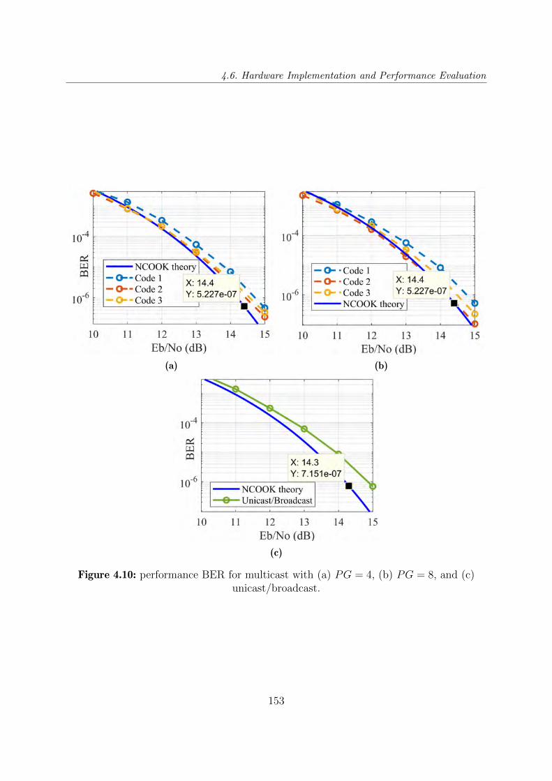
4.6. Hardware Implementation and Performance Evaluation
(a) (b)
(c)
Figure 4.10: performance BER for multicast with (a) PG = 4, (b) PG = 8, and (c)unicast/broadcast.
153
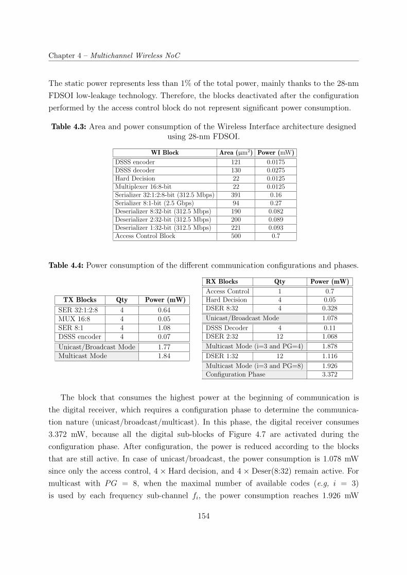
Chapter 4 – Multichannel Wireless NoC
The static power represents less than 1% of the total power, mainly thanks to the 28-nmFDSOI low-leakage technology. Therefore, the blocks deactivated after the configuration
performed by the access control block do not represent significant power consumption.
Table 4.3: Area and power consumption of the Wireless Interface architecture designedusing 28-nm FDSOI.
WI Block Area (µm2) Power (mW)
DSSS encoder 121 0.0175DSSS decoder 130 0.0275Hard Decision 22 0.0125Multiplexer 16:8-bit 22 0.0125Serializer 32:1:2:8-bit (312.5 Mbps) 391 0.16Serializer 8:1-bit (2.5 Gbps) 94 0.27Deserializer 8:32-bit (312.5 Mbps) 190 0.082Deserializer 2:32-bit (312.5 Mbps) 200 0.089Deserializer 1:32-bit (312.5 Mbps) 221 0.093Access Control Block 500 0.7
Table 4.4: Power consumption of the different communication configurations and phases.
TX Blocks Qty Power (mW)
SER 32:1:2:8 4 0.64MUX 16:8 4 0.05SER 8:1 4 1.08DSSS encoder 4 0.07
Unicast/Broadcast Mode 1.77Multicast Mode 1.84
RX Blocks Qty Power (mW)
Access Control 1 0.7Hard Decision 4 0.05DSER 8:32 4 0.328
Unicast/Broadcast Mode 1.078
DSSS Decoder 4 0.11DSER 2:32 12 1.068
Multicast Mode (i=3 and PG=4) 1.878
DSER 1:32 12 1.116
Multicast Mode (i=3 and PG=8) 1.926Configuration Phase 3.372
The block that consumes the highest power at the beginning of communication is
the digital receiver, which requires a configuration phase to determine the communica-
tion nature (unicast/broadcast/multicast). In this phase, the digital receiver consumes
3.372 mW, because all the digital sub-blocks of Figure 4.7 are activated during the
configuration phase. After configuration, the power is reduced according to the blocks
that are still active. In case of unicast/broadcast, the power consumption is 1.078 mWsince only the access control, 4 × Hard decision, and 4 × Deser(8:32) remain active. For
multicast with PG = 8, when the maximal number of available codes (e.g, i = 3)
is used by each frequency sub-channel fi, the power consumption reaches 1.926 mW
154
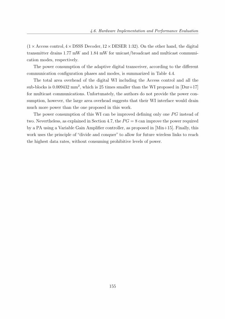
4.6. Hardware Implementation and Performance Evaluation
(1×Access control, 4×DSSS Decoder, 12×DESER 1:32). On the other hand, the digital
transmitter drains 1.77 mW and 1.84 mW for unicast/broadcast and multicast communi-
cation modes, respectively.
The power consumption of the adaptive digital transceiver, according to the different
communication configuration phases and modes, is summarized in Table 4.4.
The total area overhead of the digital WI including the Access control and all the
sub-blocks is 0.009432 mm2, which is 25 times smaller than the WI proposed in [Dur+17]
for multicast communications. Unfortunately, the authors do not provide the power con-
sumption, however, the large area overhead suggests that their WI interface would drain
much more power than the one proposed in this work.
The power consumption of this WI can be improved defining only one PG instead of
two. Nevertheless, as explained in Section 4.7, the PG = 8 can improve the power required
by a PA using a Variable Gain Amplifier controller, as proposed in [Min+15]. Finally, this
work uses the principle of “divide and conquer” to allow for future wireless links to reach
the highest data rates, without consuming prohibitive levels of power.
155
Chapter 4 – Multichannel Wireless NoC
4.7 Conclusions
Multi-hop issues in current Network-on-Chip paradigms are expected to be overcome
using wireless links. However, the design of efficient wireless links still remains a chal-
lenge to WiNoC designers. In this work, we demonstrated that future high-speed WiNoC
transceivers are not scaling using single-carrier NC-OOK. For this reason, a multi-carrier
NC-OOK FDM-based is proposed and combined with a spread-spectrum technique. The
DSSS technique allows for reducing the number of carrier frequencies required for multi-
directional communications. Furthermore, no additional synchronization is needed, con-
trary to a TDM technique which requires frame synchronization. The results show that
the average BER in unicast/broadcast and multicast communications are closely identi-
cal, even when some transmitted signals are desynchronized due to the different distances
between the transmitters and the receiver (multicast mode). The area overhead of the
multi-carrier digital transceiver for a four-cluster architecture is around 0.009432 mm2,
which represents only 0.60% of a tile used in a 256 multicore architecture. Moreover, once
the receiver auto-configuration is established, the transceiver consumes only 2.85 mW in
unicast/broadcast mode and 3.766 mW for the full multicast mode.
156
Chapter 5
WINOC EVALUATION
Network-on-Chip architectures improve the scalability and power efficiency of an MP-
SoC, contrasted with other communication subsystem designs. The NoC technology ap-
plies the theory and methods of computer networking to on-chip communication, bringing
notable improvements over conventional bus communication. As discussed in Chapter 1,
an NoC can be conceived using different emerging interconnections, which require an eval-
uation. This evaluation is performed using benchmarks, which are designed to mimic a
particular system operation. Thus, there are two types of benchmarks used to evaluate
an NoC: synthetic and application benchmarks. A synthetic benchmark represents differ-
ent communication patterns that simplify the evaluation of an NoC. They are handy to
consider the spatial distribution of messages in any interconnection network. This type
of benchmarks produces a rapid analysis for point-to-point (P2P) scenario, disregarding
scenarios such as broadcast/multicast. Synthetic benchmarks can cover aspects as: control
flow of the network, congestion, throughput latency, and network scalability. In contrast,
an application benchmark is obtained from real workloads, which are modeled as com-
munication task graphs exhibiting control and data dependencies. The cores imitate the
real traffic generated for a real implemented application. Benchmarks cover aspects as
run time (completion time of the application) and application throughput (the minimum
period at which the input processing core injects data). Moreover, they provide realistic
traffic distributions for P2P and broadcast/multicast scenarios. However, benchmarks are
in general difficult and always under development, but there are a few important ones such
as MCSL NoC Traffic Patterns [Liu+11], SPLASH-2 [Woo+95], and PARSEC [Bie+08]. In
this chapter, we evaluate an NoC connected by wireless and wired interconnections using
both types of benchmark (synthetic and real workloads). Moreover, from the benchmarks,
we analyze the main traffic patterns that can be found into real applications.
157
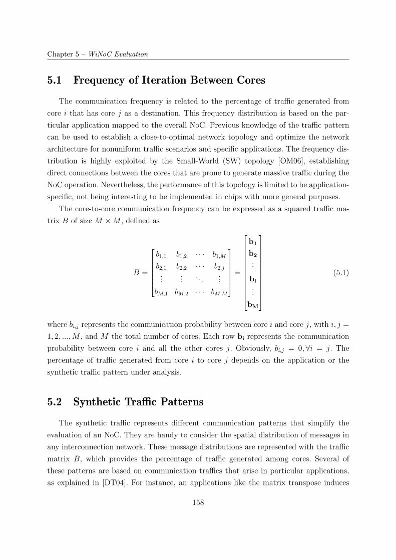
Chapter 5 – WiNoC Evaluation
5.1 Frequency of Iteration Between Cores
The communication frequency is related to the percentage of traffic generated from
core i that has core j as a destination. This frequency distribution is based on the par-
ticular application mapped to the overall NoC. Previous knowledge of the traffic pattern
can be used to establish a close-to-optimal network topology and optimize the network
architecture for nonuniform traffic scenarios and specific applications. The frequency dis-
tribution is highly exploited by the Small-World (SW) topology [OM06], establishing
direct connections between the cores that are prone to generate massive traffic during the
NoC operation. Nevertheless, the performance of this topology is limited to be application-
specific, not being interesting to be implemented in chips with more general purposes.
The core-to-core communication frequency can be expressed as a squared traffic ma-
trix B of size M ×M , defined as
B =
b1,1 b1,2 · · · b1,M
b2,1 b2,2 · · · b2,j...
.... . .
...
bM,1 bM,2 · · · bM,M
=
b1
b2...
bi...
bM
(5.1)
where bi,j represents the communication probability between core i and core j, with i, j =1, 2, ...,M , and M the total number of cores. Each row bi represents the communication
probability between core i and all the other cores j. Obviously, bi,j = 0,∀i = j. The
percentage of traffic generated from core i to core j depends on the application or the
synthetic traffic pattern under analysis.
5.2 Synthetic Traffic Patterns
The synthetic traffic represents different communication patterns that simplify the
evaluation of an NoC. They are handy to consider the spatial distribution of messages in
any interconnection network. These message distributions are represented with the traffic
matrix B, which provides the percentage of traffic generated among cores. Several of
these patterns are based on communication traffics that arise in particular applications,
as explained in [DT04]. For instance, an applications like the matrix transpose induces
158
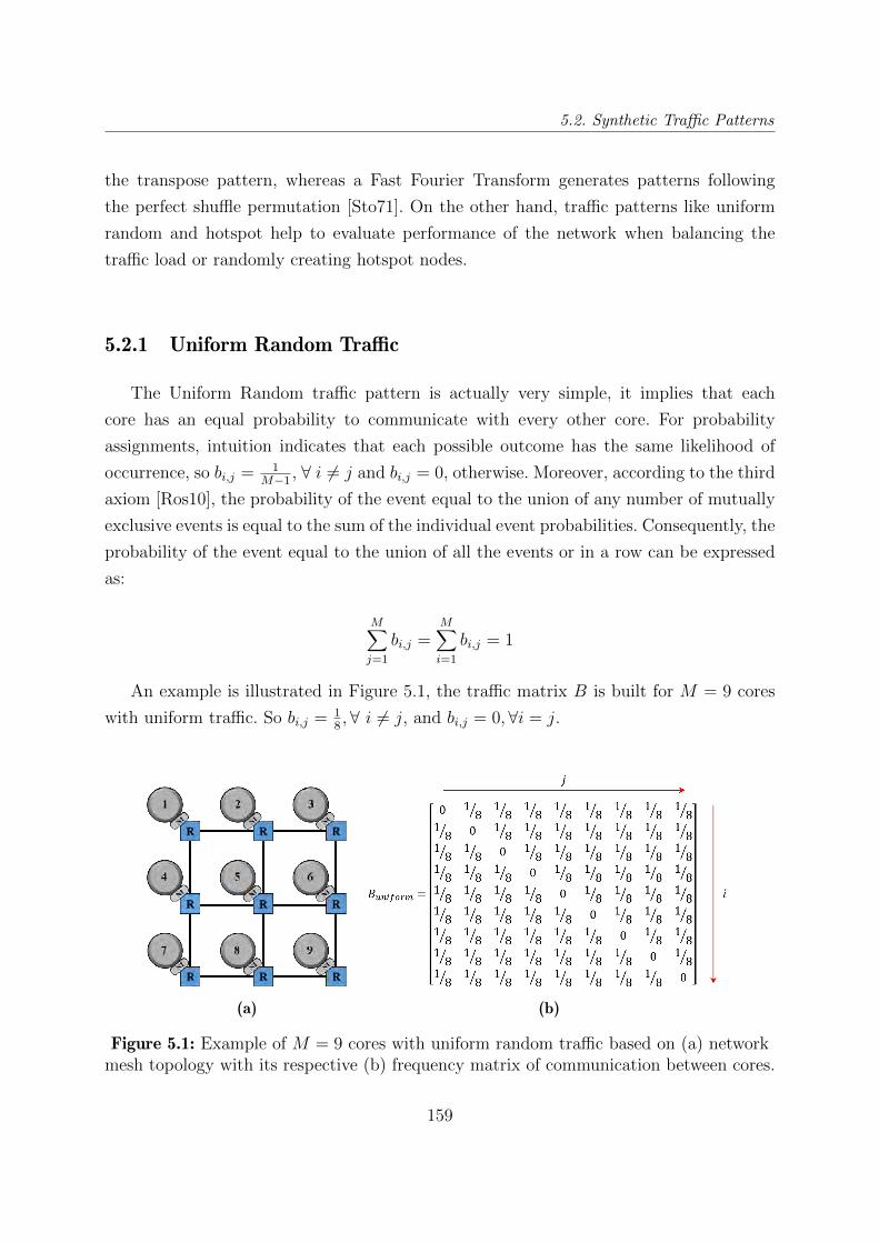
5.2. Synthetic Traffic Patterns
the transpose pattern, whereas a Fast Fourier Transform generates patterns following
the perfect shuffle permutation [Sto71]. On the other hand, traffic patterns like uniform
random and hotspot help to evaluate performance of the network when balancing the
traffic load or randomly creating hotspot nodes.
5.2.1 Uniform Random Traffic
The Uniform Random traffic pattern is actually very simple, it implies that each
core has an equal probability to communicate with every other core. For probability
assignments, intuition indicates that each possible outcome has the same likelihood of
occurrence, so bi,j = 1M−1 , ∀ i 6= j and bi,j = 0, otherwise. Moreover, according to the third
axiom [Ros10], the probability of the event equal to the union of any number of mutually
exclusive events is equal to the sum of the individual event probabilities. Consequently, the
probability of the event equal to the union of all the events or in a row can be expressed
as:
M∑j=1
bi,j =M∑i=1
bi,j = 1
An example is illustrated in Figure 5.1, the traffic matrix B is built for M = 9 cores
with uniform traffic. So bi,j = 18 , ∀ i 6= j, and bi,j = 0,∀i = j.
(a) (b)
Figure 5.1: Example of M = 9 cores with uniform random traffic based on (a) networkmesh topology with its respective (b) frequency matrix of communication between cores.
159
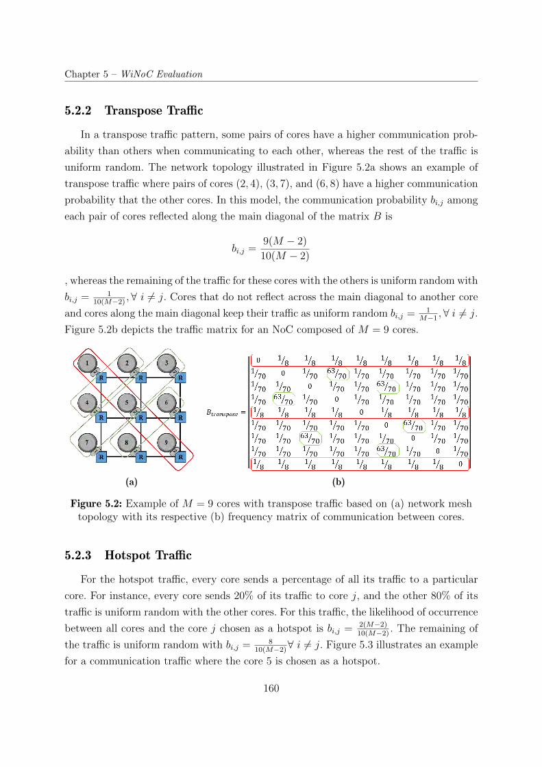
Chapter 5 – WiNoC Evaluation
5.2.2 Transpose Traffic
In a transpose traffic pattern, some pairs of cores have a higher communication prob-
ability than others when communicating to each other, whereas the rest of the traffic is
uniform random. The network topology illustrated in Figure 5.2a shows an example of
transpose traffic where pairs of cores (2, 4), (3, 7), and (6, 8) have a higher communication
probability that the other cores. In this model, the communication probability bi,j among
each pair of cores reflected along the main diagonal of the matrix B is
bi,j = 9(M − 2)10(M − 2)
, whereas the remaining of the traffic for these cores with the others is uniform random with
bi,j = 110(M−2) ,∀ i 6= j. Cores that do not reflect across the main diagonal to another core
and cores along the main diagonal keep their traffic as uniform random bi,j = 1M−1 , ∀ i 6= j.
Figure 5.2b depicts the traffic matrix for an NoC composed of M = 9 cores.
(a) (b)
Figure 5.2: Example of M = 9 cores with transpose traffic based on (a) network meshtopology with its respective (b) frequency matrix of communication between cores.
5.2.3 Hotspot Traffic
For the hotspot traffic, every core sends a percentage of all its traffic to a particular
core. For instance, every core sends 20% of its traffic to core j, and the other 80% of its
traffic is uniform random with the other cores. For this traffic, the likelihood of occurrence
between all cores and the core j chosen as a hotspot is bi,j = 2(M−2)10(M−2) . The remaining of
the traffic is uniform random with bi,j = 810(M−2)∀ i 6= j. Figure 5.3 illustrates an example
for a communication traffic where the core 5 is chosen as a hotspot.
160
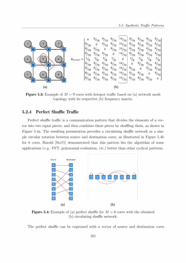
5.2. Synthetic Traffic Patterns
(a) (b)
Figure 5.3: Example of M = 9 cores with hotspot traffic based on (a) network meshtopology with its respective (b) frequency matrix.
5.2.4 Perfect Shuffle Traffic
Perfect shuffle traffic is a communication pattern that divides the elements of a vec-
tor into two equal pieces, and then combines these pieces by shuffling them, as shown in
Figure 5.4a. The resulting permutation provides a circulating shuffle network as a sim-
ple circular rotation between source and destination cores, as illustrated in Figure 5.4b
for 8 cores. Harold [Sto71] demonstrated that this pattern fits the algorithm of some
applications (e.g., FFT, polynomial evaluation, etc.) better than other cyclical patterns.
(a) (b)
Figure 5.4: Example of (a) perfect shuffle for M = 8 cores with the obtained(b) circulating shuffle network.
The perfect shuffle can be expressed with a vector of source and destination cores
161
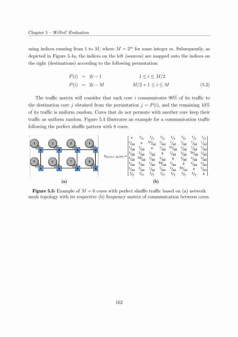
Chapter 5 – WiNoC Evaluation
using indices running from 1 to M , where M = 2m for some integer m. Subsequently, as
depicted in Figure 5.4a, the indices on the left (sources) are mapped onto the indices on
the right (destinations) according to the following permutation:
P (i) = 2i− 1 1 ≤ i ≤M/2
P (i) = 2i−M M/2 + 1 ≤ i ≤M (5.2)
The traffic matrix will consider that each core i communicates 90% of its traffic to
the destination core j obtained from the permutation j = P (i), and the remaining 10%of its traffic is uniform random. Cores that do not permute with another core keep their
traffic as uniform random. Figure 5.4 illustrates an example for a communication traffic
following the perfect shuffle pattern with 8 cores.
(a) (b)
Figure 5.5: Example of M = 8 cores with perfect shuffle traffic based on (a) networkmesh topology with its respective (b) frequency matrix of communication between cores.
162
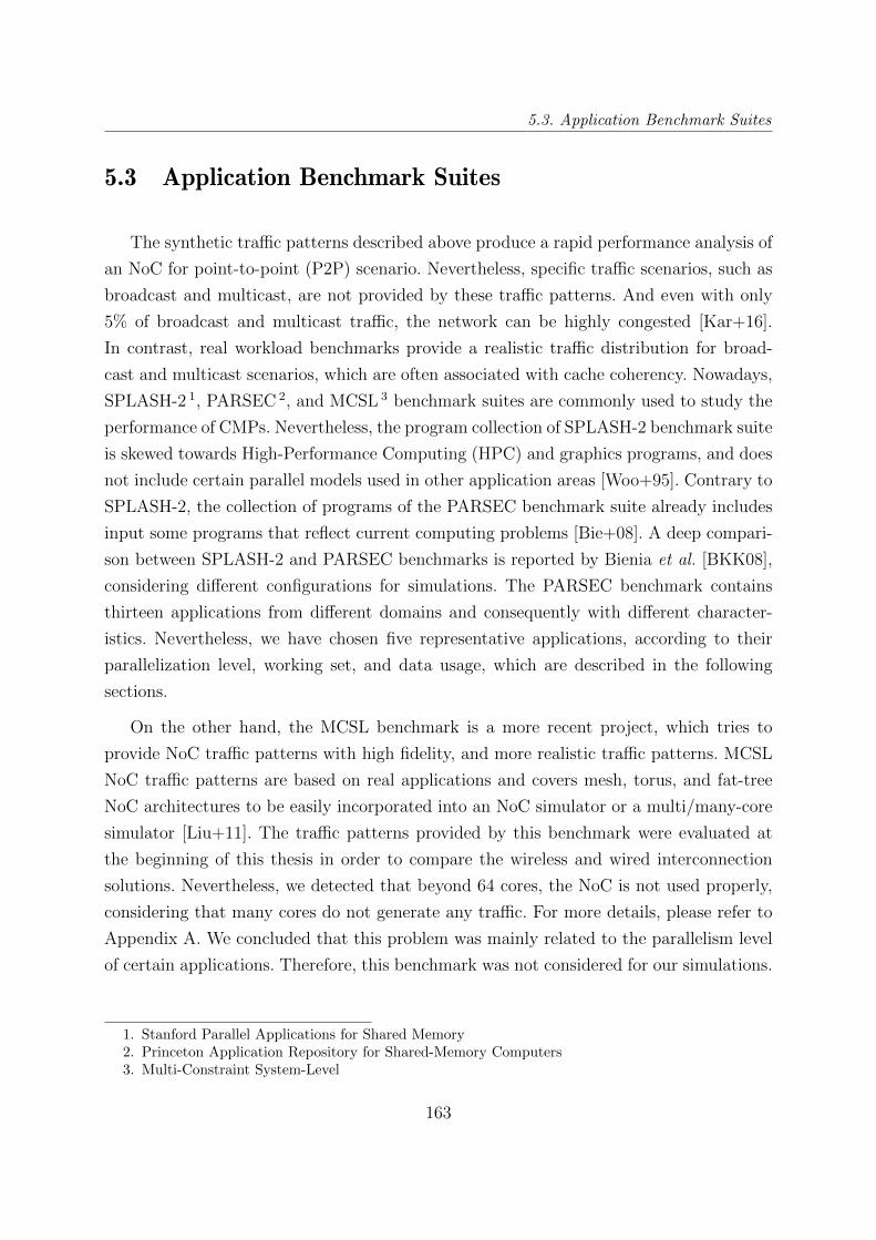
5.3. Application Benchmark Suites
5.3 Application Benchmark Suites
The synthetic traffic patterns described above produce a rapid performance analysis of
an NoC for point-to-point (P2P) scenario. Nevertheless, specific traffic scenarios, such as
broadcast and multicast, are not provided by these traffic patterns. And even with only
5% of broadcast and multicast traffic, the network can be highly congested [Kar+16].
In contrast, real workload benchmarks provide a realistic traffic distribution for broad-
cast and multicast scenarios, which are often associated with cache coherency. Nowadays,
SPLASH-2 1, PARSEC 2, and MCSL 3 benchmark suites are commonly used to study the
performance of CMPs. Nevertheless, the program collection of SPLASH-2 benchmark suite
is skewed towards High-Performance Computing (HPC) and graphics programs, and does
not include certain parallel models used in other application areas [Woo+95]. Contrary to
SPLASH-2, the collection of programs of the PARSEC benchmark suite already includes
input some programs that reflect current computing problems [Bie+08]. A deep compari-
son between SPLASH-2 and PARSEC benchmarks is reported by Bienia et al. [BKK08],
considering different configurations for simulations. The PARSEC benchmark contains
thirteen applications from different domains and consequently with different character-
istics. Nevertheless, we have chosen five representative applications, according to their
parallelization level, working set, and data usage, which are described in the following
sections.
On the other hand, the MCSL benchmark is a more recent project, which tries to
provide NoC traffic patterns with high fidelity, and more realistic traffic patterns. MCSL
NoC traffic patterns are based on real applications and covers mesh, torus, and fat-tree
NoC architectures to be easily incorporated into an NoC simulator or a multi/many-core
simulator [Liu+11]. The traffic patterns provided by this benchmark were evaluated at
the beginning of this thesis in order to compare the wireless and wired interconnection
solutions. Nevertheless, we detected that beyond 64 cores, the NoC is not used properly,
considering that many cores do not generate any traffic. For more details, please refer to
Appendix A. We concluded that this problem was mainly related to the parallelism level
of certain applications. Therefore, this benchmark was not considered for our simulations.
1. Stanford Parallel Applications for Shared Memory2. Princeton Application Repository for Shared-Memory Computers3. Multi-Constraint System-Level
163
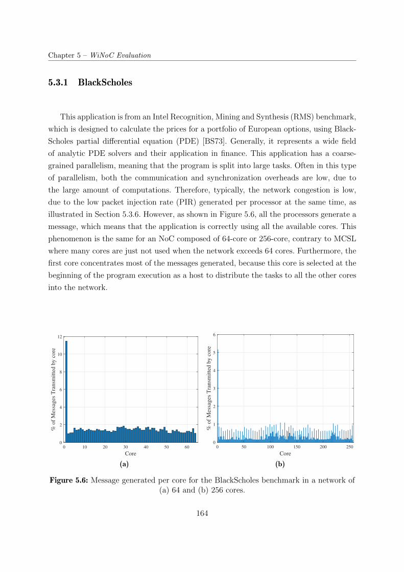
Chapter 5 – WiNoC Evaluation
5.3.1 BlackScholes
This application is from an Intel Recognition, Mining and Synthesis (RMS) benchmark,
which is designed to calculate the prices for a portfolio of European options, using Black-
Scholes partial differential equation (PDE) [BS73]. Generally, it represents a wide field
of analytic PDE solvers and their application in finance. This application has a coarse-
grained parallelism, meaning that the program is split into large tasks. Often in this type
of parallelism, both the communication and synchronization overheads are low, due to
the large amount of computations. Therefore, typically, the network congestion is low,
due to the low packet injection rate (PIR) generated per processor at the same time, as
illustrated in Section 5.3.6. However, as shown in Figure 5.6, all the processors generate a
message, which means that the application is correctly using all the available cores. This
phenomenon is the same for an NoC composed of 64-core or 256-core, contrary to MCSL
where many cores are just not used when the network exceeds 64 cores. Furthermore, the
first core concentrates most of the messages generated, because this core is selected at the
beginning of the program execution as a host to distribute the tasks to all the other cores
into the network.
0 10 20 30 40 50 60
Core
0
2
4
6
8
10
12
% o
f M
essa
ges
Tra
nsm
itte
d b
y c
ore
(a)
0 50 100 150 200 250
Core
0
1
2
3
4
5
6
% o
f M
essa
ges
Tra
nsm
itte
d b
y c
ore
(b)
Figure 5.6: Message generated per core for the BlackScholes benchmark in a network of(a) 64 and (b) 256 cores.
164
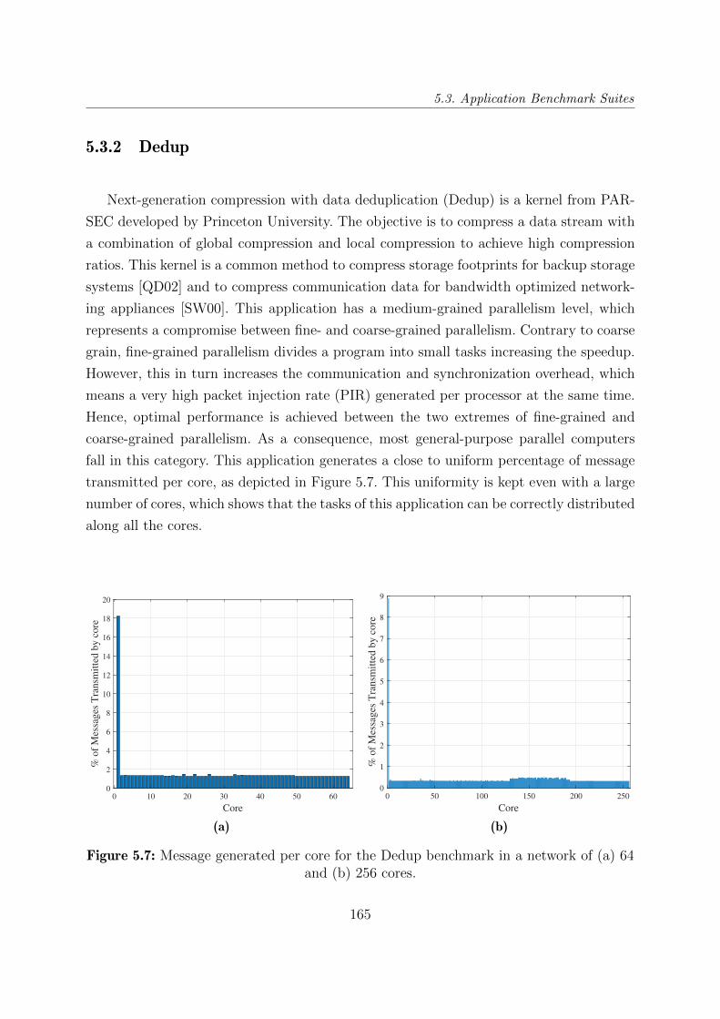
5.3. Application Benchmark Suites
5.3.2 Dedup
Next-generation compression with data deduplication (Dedup) is a kernel from PAR-
SEC developed by Princeton University. The objective is to compress a data stream with
a combination of global compression and local compression to achieve high compression
ratios. This kernel is a common method to compress storage footprints for backup storage
systems [QD02] and to compress communication data for bandwidth optimized network-
ing appliances [SW00]. This application has a medium-grained parallelism level, which
represents a compromise between fine- and coarse-grained parallelism. Contrary to coarse
grain, fine-grained parallelism divides a program into small tasks increasing the speedup.
However, this in turn increases the communication and synchronization overhead, which
means a very high packet injection rate (PIR) generated per processor at the same time.
Hence, optimal performance is achieved between the two extremes of fine-grained and
coarse-grained parallelism. As a consequence, most general-purpose parallel computers
fall in this category. This application generates a close to uniform percentage of message
transmitted per core, as depicted in Figure 5.7. This uniformity is kept even with a large
number of cores, which shows that the tasks of this application can be correctly distributed
along all the cores.
0 10 20 30 40 50 60
Core
0
2
4
6
8
10
12
14
16
18
20
% o
f M
essa
ges
Tra
nsm
itte
d b
y c
ore
(a)
0 50 100 150 200 250
Core
0
1
2
3
4
5
6
7
8
9
% o
f M
essa
ges
Tra
nsm
itte
d b
y c
ore
(b)
Figure 5.7: Message generated per core for the Dedup benchmark in a network of (a) 64and (b) 256 cores.
165
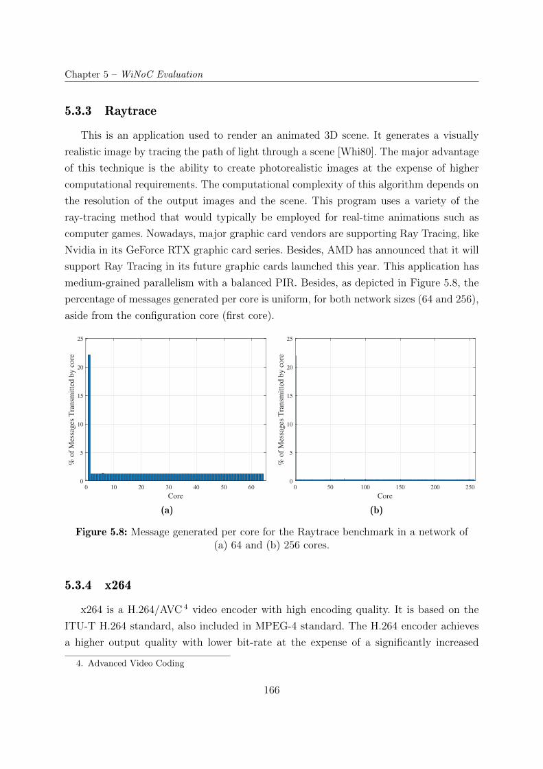
Chapter 5 – WiNoC Evaluation
5.3.3 Raytrace
This is an application used to render an animated 3D scene. It generates a visually
realistic image by tracing the path of light through a scene [Whi80]. The major advantage
of this technique is the ability to create photorealistic images at the expense of higher
computational requirements. The computational complexity of this algorithm depends on
the resolution of the output images and the scene. This program uses a variety of the
ray-tracing method that would typically be employed for real-time animations such as
computer games. Nowadays, major graphic card vendors are supporting Ray Tracing, like
Nvidia in its GeForce RTX graphic card series. Besides, AMD has announced that it will
support Ray Tracing in its future graphic cards launched this year. This application has
medium-grained parallelism with a balanced PIR. Besides, as depicted in Figure 5.8, the
percentage of messages generated per core is uniform, for both network sizes (64 and 256),
aside from the configuration core (first core).
0 10 20 30 40 50 60
Core
0
5
10
15
20
25
% o
f M
essa
ges
Tra
nsm
itte
d b
y c
ore
(a)
0 50 100 150 200 250
Core
0
5
10
15
20
25
% o
f M
essa
ges
Tra
nsm
itte
d b
y c
ore
(b)
Figure 5.8: Message generated per core for the Raytrace benchmark in a network of(a) 64 and (b) 256 cores.
5.3.4 x264
x264 is a H.264/AVC 4 video encoder with high encoding quality. It is based on the
ITU-T H.264 standard, also included in MPEG-4 standard. The H.264 encoder achieves
a higher output quality with lower bit-rate at the expense of a significantly increased
4. Advanced Video Coding
166
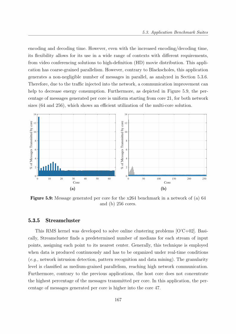
5.3. Application Benchmark Suites
encoding and decoding time. However, even with the increased encoding/decoding time,
its flexibility allows for its use in a wide range of contexts with different requirements,
from video conferencing solutions to high-definition (HD) movie distribution. This appli-
cation has coarse-grained parallelism. However, contrary to Blackscholes, this application
generates a non-negligible number of messages in parallel, as analyzed in Section 5.3.6.
Therefore, due to the traffic injected into the network, a communication improvement can
help to decrease energy consumption. Furthermore, as depicted in Figure 5.9, the per-
centage of messages generated per core is uniform starting from core 21, for both network
sizes (64 and 256), which shows an efficient utilization of the multi-core solution.
0 10 20 30 40 50 60
Core
0
2
4
6
8
10
12
14
% o
f M
essa
ges
Tra
nsm
itte
d b
y c
ore
(a)
0 50 100 150 200 250
Core
0
2
4
6
8
10
12
14
% o
f M
essa
ges
Tra
nsm
itte
d b
y c
ore
(b)
Figure 5.9: Message generated per core for the x264 benchmark in a network of (a) 64and (b) 256 cores.
5.3.5 Streamcluster
This RMS kernel was developed to solve online clustering problems [O’C+02]. Basi-
cally, Streamcluster finds a predetermined number of medians for each stream of input
points, assigning each point to its nearest center. Generally, this technique is employed
when data is produced continuously and has to be organized under real-time conditions
(e.g., network intrusion detection, pattern recognition and data mining). The granularity
level is classified as medium-grained parallelism, reaching high network communication.
Furthermore, contrary to the previous applications, the host core does not concentrate
the highest percentage of the messages transmitted per core. In this application, the per-
centage of messages generated per core is higher into the core 47.
167
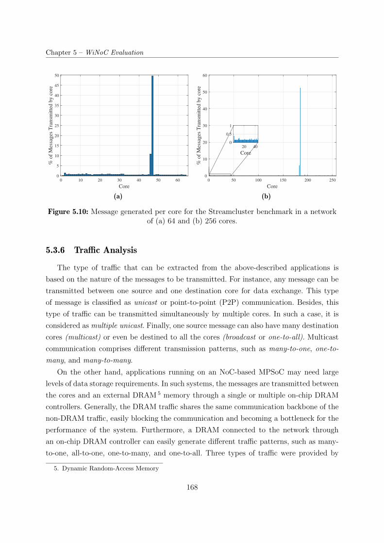
Chapter 5 – WiNoC Evaluation
0 10 20 30 40 50 60
Core
0
5
10
15
20
25
30
35
40
45
50
% o
f M
essa
ges
Tra
nsm
itte
d b
y c
ore
(a)
0 50 100 150 200 250
Core
0
10
20
30
40
50
60
% o
f M
essa
ges
Tra
nsm
itte
d b
y c
ore
20 40
Core
0
0.5
1
(b)
Figure 5.10: Message generated per core for the Streamcluster benchmark in a networkof (a) 64 and (b) 256 cores.
5.3.6 Traffic Analysis
The type of traffic that can be extracted from the above-described applications is
based on the nature of the messages to be transmitted. For instance, any message can be
transmitted between one source and one destination core for data exchange. This type
of message is classified as unicast or point-to-point (P2P) communication. Besides, this
type of traffic can be transmitted simultaneously by multiple cores. In such a case, it is
considered as multiple unicast. Finally, one source message can also have many destination
cores (multicast) or even be destined to all the cores (broadcast or one-to-all). Multicast
communication comprises different transmission patterns, such as many-to-one, one-to-
many, and many-to-many.
On the other hand, applications running on an NoC-based MPSoC may need large
levels of data storage requirements. In such systems, the messages are transmitted between
the cores and an external DRAM 5 memory through a single or multiple on-chip DRAM
controllers. Generally, the DRAM traffic shares the same communication backbone of the
non-DRAM traffic, easily blocking the communication and becoming a bottleneck for the
performance of the system. Furthermore, a DRAM connected to the network through
an on-chip DRAM controller can easily generate different traffic patterns, such as many-
to-one, all-to-one, one-to-many, and one-to-all. Three types of traffic were provided by
5. Dynamic Random-Access Memory
168
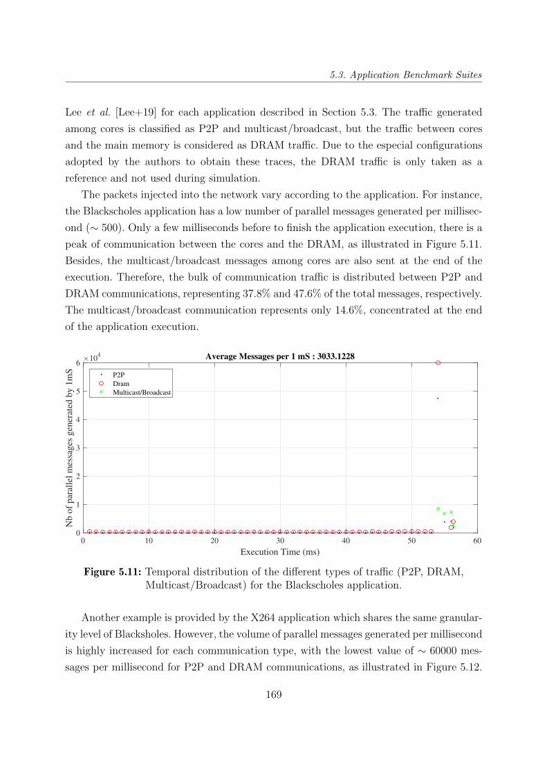
5.3. Application Benchmark Suites
Lee et al. [Lee+19] for each application described in Section 5.3. The traffic generated
among cores is classified as P2P and multicast/broadcast, but the traffic between cores
and the main memory is considered as DRAM traffic. Due to the especial configurations
adopted by the authors to obtain these traces, the DRAM traffic is only taken as a
reference and not used during simulation.
The packets injected into the network vary according to the application. For instance,
the Blackscholes application has a low number of parallel messages generated per millisec-
ond (∼ 500). Only a few milliseconds before to finish the application execution, there is a
peak of communication between the cores and the DRAM, as illustrated in Figure 5.11.
Besides, the multicast/broadcast messages among cores are also sent at the end of the
execution. Therefore, the bulk of communication traffic is distributed between P2P and
DRAM communications, representing 37.8% and 47.6% of the total messages, respectively.
The multicast/broadcast communication represents only 14.6%, concentrated at the end
of the application execution.
0 10 20 30 40 50 60
Execution Time (ms)
0
1
2
3
4
5
6
Nb o
f par
alle
l m
essa
ges
gen
erat
ed b
y 1
mS
104 Average Messages per 1 mS : 3033.1228
P2P
Dram
Multicast/Broadcast
Figure 5.11: Temporal distribution of the different types of traffic (P2P, DRAM,Multicast/Broadcast) for the Blackscholes application.
Another example is provided by the X264 application which shares the same granular-
ity level of Blacksholes. However, the volume of parallel messages generated per millisecond
is highly increased for each communication type, with the lowest value of ∼ 60000 mes-
sages per millisecond for P2P and DRAM communications, as illustrated in Figure 5.12.
169
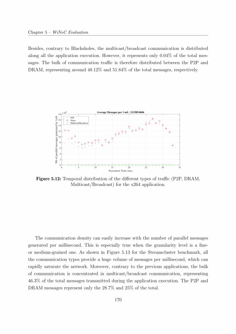
Chapter 5 – WiNoC Evaluation
Besides, contrary to Blacksholes, the multicast/broadcast communication is distributed
along all the application execution. However, it represents only 0.04% of the total mes-
sages. The bulk of communication traffic is therefore distributed between the P2P and
DRAM, representing around 48.12% and 51.84% of the total messages, respectively.
0 5 10 15 20 25 30 35
Execution Time (ms)
0
2
4
6
8
10
12
14
16
18
Nb
of
par
alle
l m
essa
ges
gen
erat
ed b
y 1
mS
104 Average Messages per 1 mS : 213389.0606
P2P
Dram
Multicast/Broadcast
Figure 5.12: Temporal distribution of the different types of traffic (P2P, DRAM,Multicast/Broadcast) for the x264 application.
The communication density can easily increase with the number of parallel messages
generated per millisecond. This is especially true when the granularity level is a fine-
or medium-grained one. As shown in Figure 5.13 for the Streamcluster benchmark, all
the communication types provide a huge volume of messages per millisecond, which can
rapidly saturate the network. Moreover, contrary to the previous applications, the bulk
of communication is concentrated in multicast/broadcast communication, representing
46.3% of the total messages transmitted during the application execution. The P2P and
DRAM messages represent only the 28.7% and 25% of the total.
170
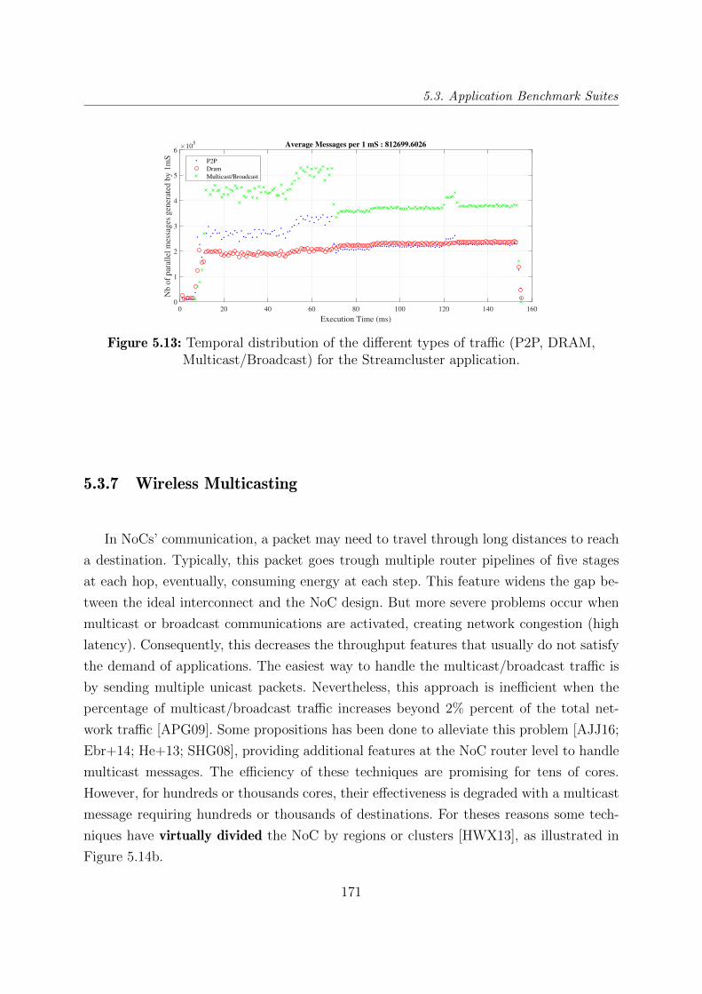
5.3. Application Benchmark Suites
0 20 40 60 80 100 120 140 160
Execution Time (ms)
0
1
2
3
4
5
6
Nb
of
par
alle
l m
essa
ges
gen
erat
ed b
y 1
mS
105 Average Messages per 1 mS : 812699.6026
P2P
Dram
Multicast/Broadcast
Figure 5.13: Temporal distribution of the different types of traffic (P2P, DRAM,Multicast/Broadcast) for the Streamcluster application.
5.3.7 Wireless Multicasting
In NoCs’ communication, a packet may need to travel through long distances to reach
a destination. Typically, this packet goes trough multiple router pipelines of five stages
at each hop, eventually, consuming energy at each step. This feature widens the gap be-
tween the ideal interconnect and the NoC design. But more severe problems occur when
multicast or broadcast communications are activated, creating network congestion (high
latency). Consequently, this decreases the throughput features that usually do not satisfy
the demand of applications. The easiest way to handle the multicast/broadcast traffic is
by sending multiple unicast packets. Nevertheless, this approach is inefficient when the
percentage of multicast/broadcast traffic increases beyond 2% percent of the total net-
work traffic [APG09]. Some propositions has been done to alleviate this problem [AJJ16;
Ebr+14; He+13; SHG08], providing additional features at the NoC router level to handle
multicast messages. The efficiency of these techniques are promising for tens of cores.
However, for hundreds or thousands cores, their effectiveness is degraded with a multicast
message requiring hundreds or thousands of destinations. For theses reasons some tech-
niques have virtually divided the NoC by regions or clusters [HWX13], as illustrated in
Figure 5.14b.
171
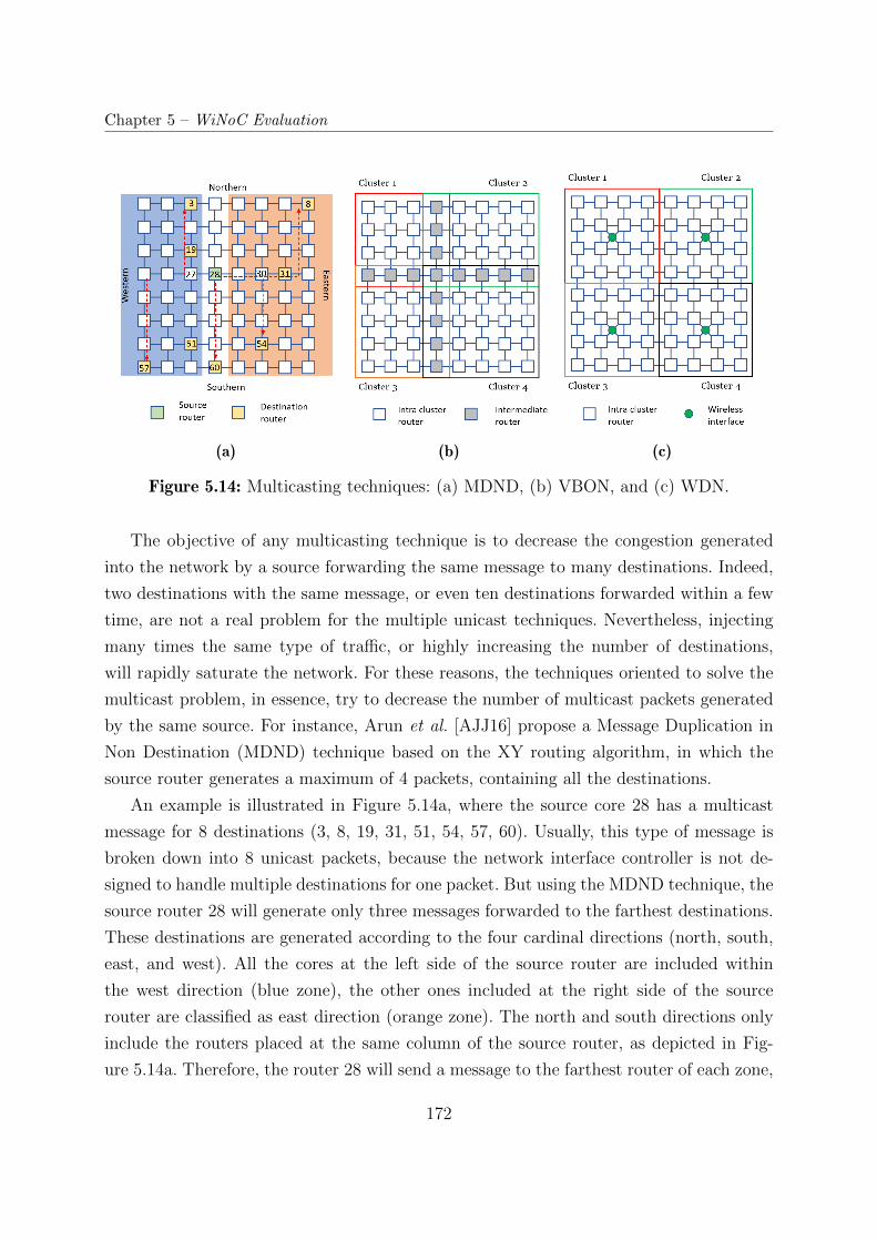
Chapter 5 – WiNoC Evaluation
(a) (b) (c)
Figure 5.14: Multicasting techniques: (a) MDND, (b) VBON, and (c) WDN.
The objective of any multicasting technique is to decrease the congestion generated
into the network by a source forwarding the same message to many destinations. Indeed,
two destinations with the same message, or even ten destinations forwarded within a few
time, are not a real problem for the multiple unicast techniques. Nevertheless, injecting
many times the same type of traffic, or highly increasing the number of destinations,
will rapidly saturate the network. For these reasons, the techniques oriented to solve the
multicast problem, in essence, try to decrease the number of multicast packets generated
by the same source. For instance, Arun et al. [AJJ16] propose a Message Duplication in
Non Destination (MDND) technique based on the XY routing algorithm, in which the
source router generates a maximum of 4 packets, containing all the destinations.
An example is illustrated in Figure 5.14a, where the source core 28 has a multicast
message for 8 destinations (3, 8, 19, 31, 51, 54, 57, 60). Usually, this type of message is
broken down into 8 unicast packets, because the network interface controller is not de-
signed to handle multiple destinations for one packet. But using the MDND technique, the
source router 28 will generate only three messages forwarded to the farthest destinations.
These destinations are generated according to the four cardinal directions (north, south,
east, and west). All the cores at the left side of the source router are included within
the west direction (blue zone), the other ones included at the right side of the source
router are classified as east direction (orange zone). The north and south directions only
include the routers placed at the same column of the source router, as depicted in Fig-
ure 5.14a. Therefore, the router 28 will send a message to the farthest router of each zone,
172
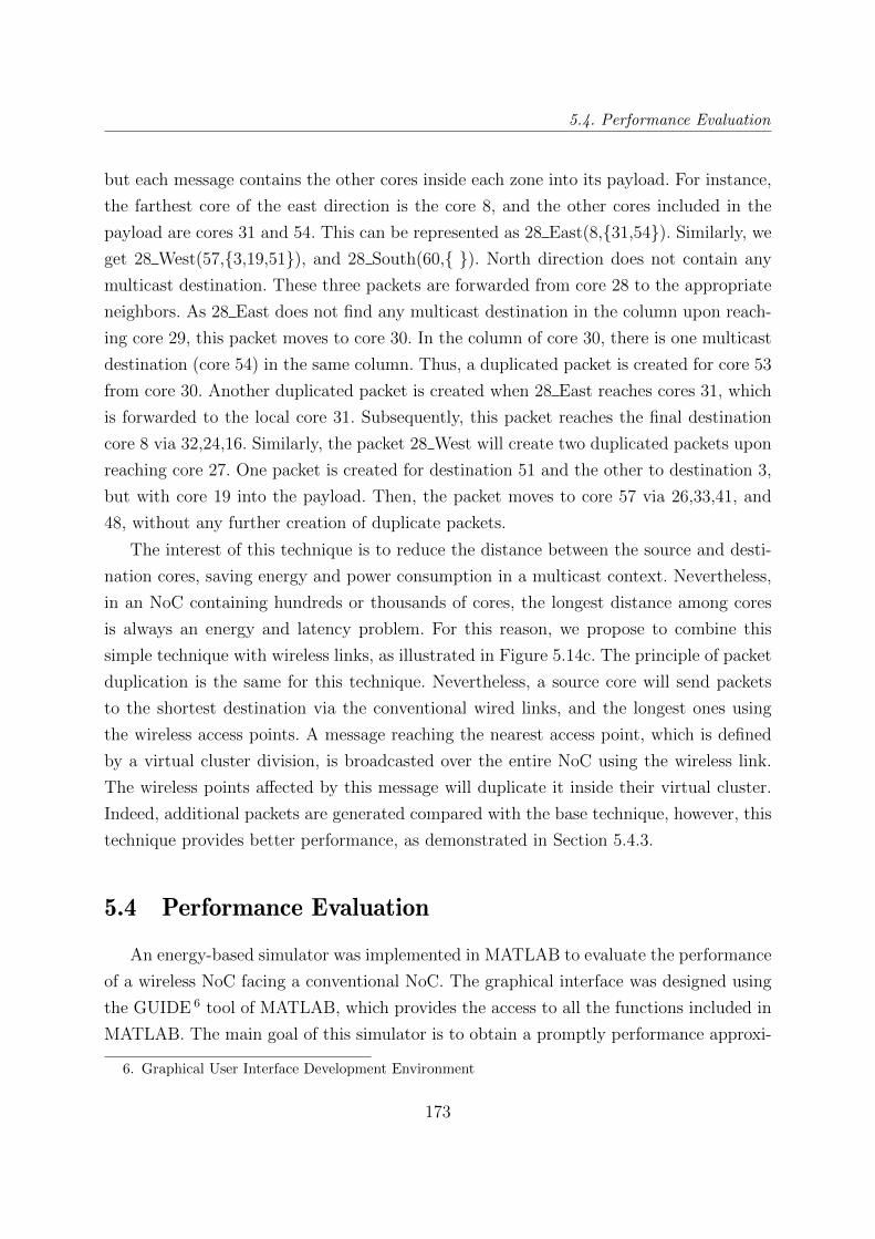
5.4. Performance Evaluation
but each message contains the other cores inside each zone into its payload. For instance,
the farthest core of the east direction is the core 8, and the other cores included in the
payload are cores 31 and 54. This can be represented as 28 East(8,31,54). Similarly, we
get 28 West(57,3,19,51), and 28 South(60, ). North direction does not contain any
multicast destination. These three packets are forwarded from core 28 to the appropriate
neighbors. As 28 East does not find any multicast destination in the column upon reach-
ing core 29, this packet moves to core 30. In the column of core 30, there is one multicast
destination (core 54) in the same column. Thus, a duplicated packet is created for core 53
from core 30. Another duplicated packet is created when 28 East reaches cores 31, which
is forwarded to the local core 31. Subsequently, this packet reaches the final destination
core 8 via 32,24,16. Similarly, the packet 28 West will create two duplicated packets upon
reaching core 27. One packet is created for destination 51 and the other to destination 3,
but with core 19 into the payload. Then, the packet moves to core 57 via 26,33,41, and
48, without any further creation of duplicate packets.
The interest of this technique is to reduce the distance between the source and desti-
nation cores, saving energy and power consumption in a multicast context. Nevertheless,
in an NoC containing hundreds or thousands of cores, the longest distance among cores
is always an energy and latency problem. For this reason, we propose to combine this
simple technique with wireless links, as illustrated in Figure 5.14c. The principle of packet
duplication is the same for this technique. Nevertheless, a source core will send packets
to the shortest destination via the conventional wired links, and the longest ones using
the wireless access points. A message reaching the nearest access point, which is defined
by a virtual cluster division, is broadcasted over the entire NoC using the wireless link.
The wireless points affected by this message will duplicate it inside their virtual cluster.
Indeed, additional packets are generated compared with the base technique, however, this
technique provides better performance, as demonstrated in Section 5.4.3.
5.4 Performance Evaluation
An energy-based simulator was implemented in MATLAB to evaluate the performance
of a wireless NoC facing a conventional NoC. The graphical interface was designed using
the GUIDE 6 tool of MATLAB, which provides the access to all the functions included in
MATLAB. The main goal of this simulator is to obtain a promptly performance approxi-
6. Graphical User Interface Development Environment
173
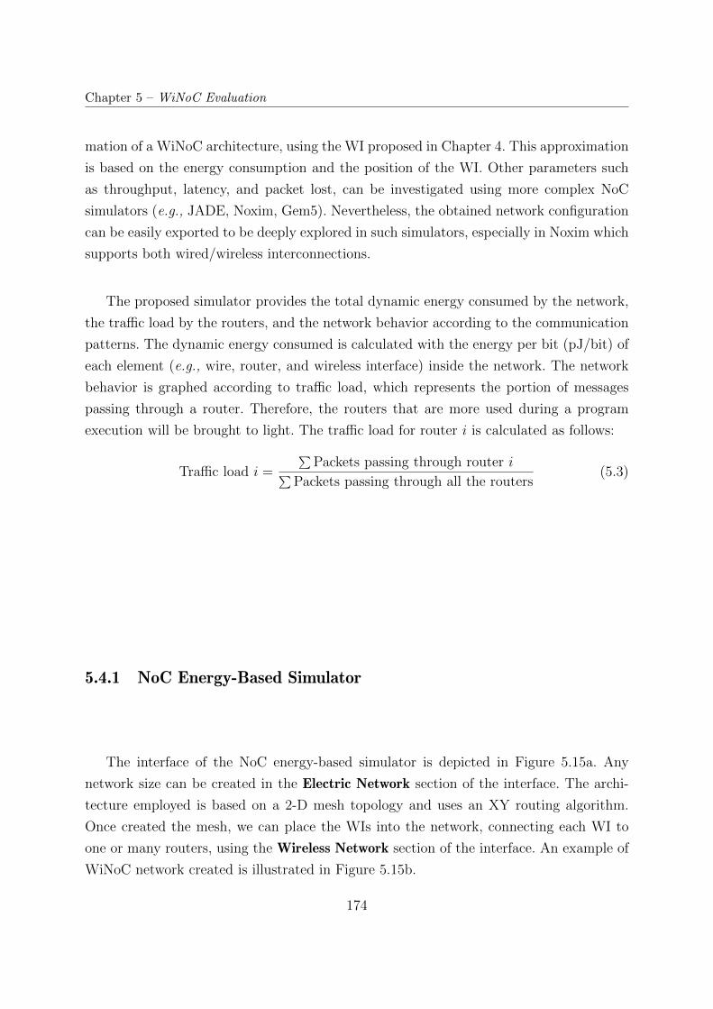
Chapter 5 – WiNoC Evaluation
mation of a WiNoC architecture, using the WI proposed in Chapter 4. This approximation
is based on the energy consumption and the position of the WI. Other parameters such
as throughput, latency, and packet lost, can be investigated using more complex NoC
simulators (e.g., JADE, Noxim, Gem5). Nevertheless, the obtained network configuration
can be easily exported to be deeply explored in such simulators, especially in Noxim which
supports both wired/wireless interconnections.
The proposed simulator provides the total dynamic energy consumed by the network,
the traffic load by the routers, and the network behavior according to the communication
patterns. The dynamic energy consumed is calculated with the energy per bit (pJ/bit) of
each element (e.g., wire, router, and wireless interface) inside the network. The network
behavior is graphed according to traffic load, which represents the portion of messages
passing through a router. Therefore, the routers that are more used during a program
execution will be brought to light. The traffic load for router i is calculated as follows:
Traffic load i =∑
Packets passing through router i∑Packets passing through all the routers
(5.3)
5.4.1 NoC Energy-Based Simulator
The interface of the NoC energy-based simulator is depicted in Figure 5.15a. Any
network size can be created in the Electric Network section of the interface. The archi-
tecture employed is based on a 2-D mesh topology and uses an XY routing algorithm.
Once created the mesh, we can place the WIs into the network, connecting each WI to
one or many routers, using the Wireless Network section of the interface. An example of
WiNoC network created is illustrated in Figure 5.15b.
174
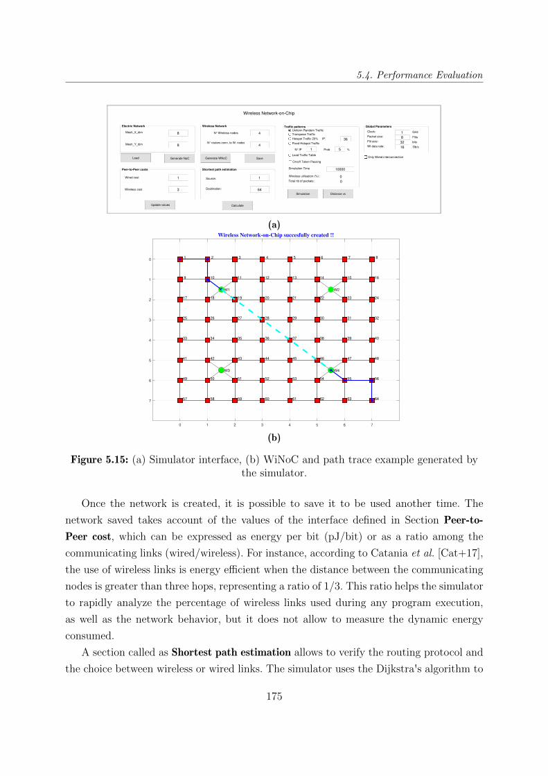
5.4. Performance Evaluation
Generate NoC Generate WNoC
Electric Network
8
8
Mesh_X_dim
Mesh_Y_dim
Wireless Network
4N° Wireless nodes
4N° routers conn. to W. nodes
Wireless Network-on-Chip
Shortest path estimation
1
64
Source:
Destination:
Calculate
Peer-to-Peer costs
1
3
Wired cost
Wireless cost
Update values
SaveLoad
Simulation
Traffic patterns
%
Uniform Random Traffic
Transpose Traffic
Hotspot Traffic 20% IP:
10000Simulation Time
Fixed Hotspot Traffic
1 5N° IP Prob
36
Wireless utilisation (%) : 0
On/off Token Passing
Total nb of packets: 0
Load Traffic Table
Distance vs
Global Parameters
8
1
32
16
Clock:
Packet size:
Flit size:
WI data rate:
GHz
Flits
bits
Gb/s
Only Wired interconnection
(a)
0 1 2 3 4 5 6 7
7
6
5
4
3
2
1
0
Wireless Network-on-Chip succesfully created !!
1 2 3 4 5 6 7 8
9 10 11 12 13 14 15 16
17 18 19 20 21 22 23 24
25 26 27 28 29 30 31 32
33 34 35 36 37 38 39 40
41 42 43 44 45 46 47 48
49 50 51 52 53 54 55 56
57 58 59 60 61 62 63 64
W1 W2
W3 W4
(b)
Figure 5.15: (a) Simulator interface, (b) WiNoC and path trace example generated bythe simulator.
Once the network is created, it is possible to save it to be used another time. The
network saved takes account of the values of the interface defined in Section Peer-to-
Peer cost, which can be expressed as energy per bit (pJ/bit) or as a ratio among the
communicating links (wired/wireless). For instance, according to Catania et al. [Cat+17],
the use of wireless links is energy efficient when the distance between the communicating
nodes is greater than three hops, representing a ratio of 1/3. This ratio helps the simulator
to rapidly analyze the percentage of wireless links used during any program execution,
as well as the network behavior, but it does not allow to measure the dynamic energy
consumed.
A section called as Shortest path estimation allows to verify the routing protocol and
the choice between wireless or wired links. The simulator uses the Dijkstra's algorithm to
175
Chapter 5 – WiNoC Evaluation
find the efficient shortest path between a source and destination core. Indeed, this efficient
path is found using the communication cost for each link type. An example is illustrated in
Figure 5.15b, considering a communication between core 1 and core 64, where, according to
Dijkstra's algorithm, the most efficient way to reach core 64 is using the wireless interfaces
W1 and W4 (dashed cyan line) along with the wired links (blue line). Another section
of this interface, called Global Parameters allows to configure the NoC frequency, packet
parameters, and the data rate of the WIs. Furthermore, a Checkbox is placed to allow
for the users to force the simulator to use only wired interconnections or both wired and
wireless interconnections.
Once the WiNoC is designed and configured, the simulation can be executed choos-
ing the synthetic or application benchmarks presented in Section Traffic patterns. Each
synthetic benchmark is implemented in MATLAB using the frequency communication
matrix, explained in Section 5.2. This type of benchmark requires to configure the simula-
tion time, which have to be enough to allow for each core to forward a message according
to its probability. The trace files corresponding to an application benchmark are avail-
able in a specific directory into the MATLAB project. These traces were provided by
Lee et al. [Lee+19] using the Sniper [CHE11] simulator. Sniper is a multi-core simulator
based on interval core model 7 and the Graphite simulation infrastructure [Mil+10].
5.4.2 Network Evaluation
As previously mentioned, a basic NoC energy-based simulator has been implemented to
evaluate and compare the performance of a conventional Electrical NoC and the proposed
clustered Wireless NoC. The evaluation is performed based on the dynamic power con-
sumption that the transmitted bits require to travel through a wired or wireless medium.
In this section, firstly, we evaluate the conventional electrical NoC with the different bench-
marks discussed in the previous section. Secondly, a WiNoC network is designed according
to the parameters considered in Chapter 4, also considering the energy characteristics of
the proposed wireless interface. Squared and circular antenna placements are considered
in our analysis, as depicted in Figure 5.16. The baseline network topology adopted is a
2D-mesh, with four routers connected to one wireless interface distributed into the
network.
7. Interval simulation is a proposed simulation approach for simulating multi-core and multiprocessorsystems at a higher level of abstraction, modeling the timing for individual cores [GEE10].
176
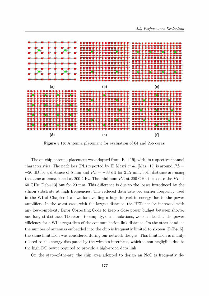
5.4. Performance Evaluation
(a) (b) (c)
(d) (e) (f)
Figure 5.16: Antenna placement for evaluation of 64 and 256 cores.
The on-chip antenna placement was adopted from [El +19], with its respective channel
characteristics. The path loss (PL) reported by El Masri et al. [Mas+19] is around PL =−26 dB for a distance of 5 mm and PL = −33 dB for 21.2 mm, both distance are using
the same antenna tuned at 200 GHz. The minimum PL at 200 GHz is close to the PL at
60 GHz [Deb+13] but for 20 mm. This difference is due to the losses introduced by the
silicon substrate at high frequencies. The reduced data rate per carrier frequency used
in the WI of Chapter 4 allows for avoiding a huge impact in energy due to the power
amplifiers. In the worst case, with the largest distance, the BER can be increased with
any low-complexity Error Correcting Code to keep a close power budget between shorter
and longest distance. Therefore, to simplify, our simulations, we consider that the power
efficiency for a WI is regardless of the communication link distance. On the other hand, as
the number of antennas embedded into the chip is frequently limited to sixteen [DiT+15],
the same limitation was considered during our network designs. This limitation is mainly
related to the energy dissipated by the wireless interfaces, which is non-negligible due to
the high DC power required to provide a high-speed data link.
On the state-of-the-art, the chip area adopted to design an NoC is frequently de-
177
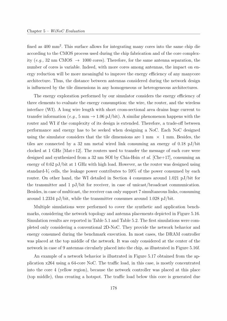
Chapter 5 – WiNoC Evaluation
fined as 400 mm2. This surface allows for integrating many cores into the same chip die
according to the CMOS process used during the chip fabrication and of the core complex-
ity (e.g., 32 nm CMOS → 1000 cores). Therefore, for the same antenna separation, the
number of cores is variable. Indeed, with more cores among antennas, the impact on en-
ergy reduction will be more meaningful to improve the energy efficiency of any manycore
architecture. Thus, the distance between antennas considered during the network design
is influenced by the tile dimensions in any homogeneous or heterogeneous architectures.
The energy exploration performed by our simulator considers the energy efficiency of
three elements to evaluate the energy consumption: the wire, the router, and the wireless
interface (WI). A long wire length with short cross-sectional area drains huge current to
transfer information (e.g., 5 mm→ 1.06 pJ/bit). A similar phenomenon happens with the
router and WI if the complexity of its design is extended. Therefore, a trade-off between
performance and energy has to be seeked when designing a NoC. Each NoC designed
using the simulator considers that the tile dimensions are 1 mm × 1 mm. Besides, the
tiles are connected by a 32 nm metal wired link consuming an energy of 0.18 pJ/bit
clocked at 1 GHz [Mat+12]. The routers used to transfer the message of each core were
designed and synthesized from a 32 nm SOI by Chia-Hsin et al. [Che+17], consuming an
energy of 0.62 pJ/bit at 1 GHz with high load. However, as the router was designed using
standard-Vt cells, the leakage power contributes to 59% of the power consumed by each
router. On other hand, the WI detailed in Section 4 consumes around 1.021 pJ/bit for
the transmitter and 1 pJ/bit for receiver, in case of unicast/broadcast communication.
Besides, in case of multicast, the receiver can only support 7 simultaneous links, consuming
around 1.2334 pJ/bit, while the transmitter consumes around 1.028 pJ/bit.
Multiple simulations were performed to cover the synthetic and application bench-
marks, considering the network topology and antenna placements depicted in Figure 5.16.
Simulation results are reported in Table 5.1 and Table 5.2. The first simulations were com-
pleted only considering a conventional 2D-NoC. They provide the network behavior and
energy consumed during the benchmark execution. In most cases, the DRAM controller
was placed at the top middle of the network. It was only considered at the center of the
network in case of 9 antennas circularly placed into the chip, as illustrated in Figure 5.16f.
An example of a network behavior is illustrated in Figure 5.17 obtained from the ap-
plication x264 using a 64-core NoC. The traffic load, in this case, is mostly concentrated
into the core 4 (yellow region), because the network controller was placed at this place
(top middle), thus creating a hotspot. The traffic load below this core is generated due
178
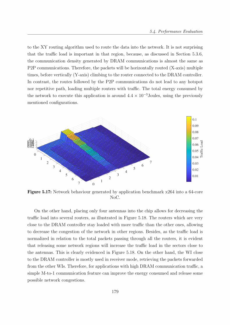
5.4. Performance Evaluation
to the XY routing algorithm used to route the data into the network. It is not surprising
that the traffic load is important in that region, because, as discussed in Section 5.3.6,
the communication density generated by DRAM communications is almost the same as
P2P communications. Therefore, the packets will be horizontally routed (X-axis) multiple
times, before vertically (Y-axis) climbing to the router connected to the DRAM controller.
In contrast, the routes followed by the P2P communications do not lead to any hotspot
nor repetitive path, loading multiple routers with traffic. The total energy consumed by
the network to execute this application is around 4.4 × 10⁻³Joules, using the previously
mentioned configurations.
0.020.040.060.08
0.1
0
1
726
35
4 435
261
7 0
0.01
0.02
0.03
0.04
0.05
0.06
0.07
0.08
0.09
0.1
Tra
ffic
Lo
ad
Figure 5.17: Network behaviour generated by application benchmark x264 into a 64-coreNoC.
On the other hand, placing only four antennas into the chip allows for decreasing the
traffic load into several routers, as illustrated in Figure 5.18. The routers which are very
close to the DRAM controller stay loaded with more traffic than the other ones, allowing
to decrease the congestion of the network in other regions. Besides, as the traffic load is
normalized in relation to the total packets passing through all the routers, it is evident
that releasing some network regions will increase the traffic load in the sectors close to
the antennas. This is clearly evidenced in Figure 5.18. On the other hand, the WI close
to the DRAM controller is mostly used in receiver mode, retrieving the packets forwarded
from the other WIs. Therefore, for applications with high DRAM communication traffic, a
simple M-to-1 communication feature can improve the energy consumed and release some
possible network congestions.
179
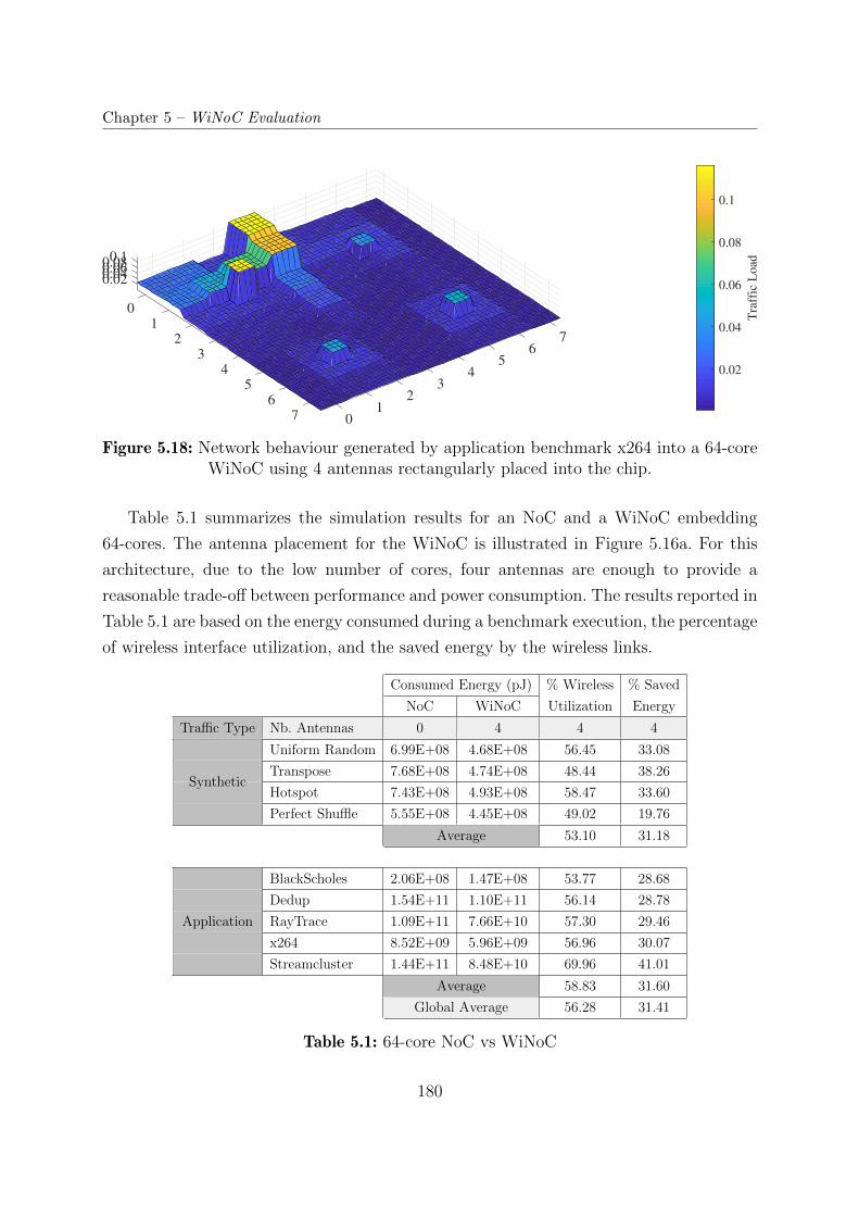
Chapter 5 – WiNoC Evaluation
0.020.040.060.08
0.1
0
1
726
35
4 435
261
7 0
0.02
0.04
0.06
0.08
0.1
Tra
ffic
Lo
ad
Figure 5.18: Network behaviour generated by application benchmark x264 into a 64-coreWiNoC using 4 antennas rectangularly placed into the chip.
Table 5.1 summarizes the simulation results for an NoC and a WiNoC embedding
64-cores. The antenna placement for the WiNoC is illustrated in Figure 5.16a. For this
architecture, due to the low number of cores, four antennas are enough to provide a
reasonable trade-off between performance and power consumption. The results reported in
Table 5.1 are based on the energy consumed during a benchmark execution, the percentage
of wireless interface utilization, and the saved energy by the wireless links.
Consumed Energy (pJ)
NoC WiNoC
% Wireless
Utilization
% Saved
Energy
Traffic Type Nb. Antennas 0 4 4 4
Uniform Random 6.99E+08 4.68E+08 56.45 33.08
Transpose 7.68E+08 4.74E+08 48.44 38.26
Hotspot 7.43E+08 4.93E+08 58.47 33.60Synthetic
Perfect Shuffle 5.55E+08 4.45E+08 49.02 19.76
Average 53.10 31.18
BlackScholes 2.06E+08 1.47E+08 53.77 28.68
Dedup 1.54E+11 1.10E+11 56.14 28.78
RayTrace 1.09E+11 7.66E+10 57.30 29.46
x264 8.52E+09 5.96E+09 56.96 30.07
Application
Streamcluster 1.44E+11 8.48E+10 69.96 41.01
Average 58.83 31.60
Global Average 56.28 31.41
Table 5.1: 64-core NoC vs WiNoC
180
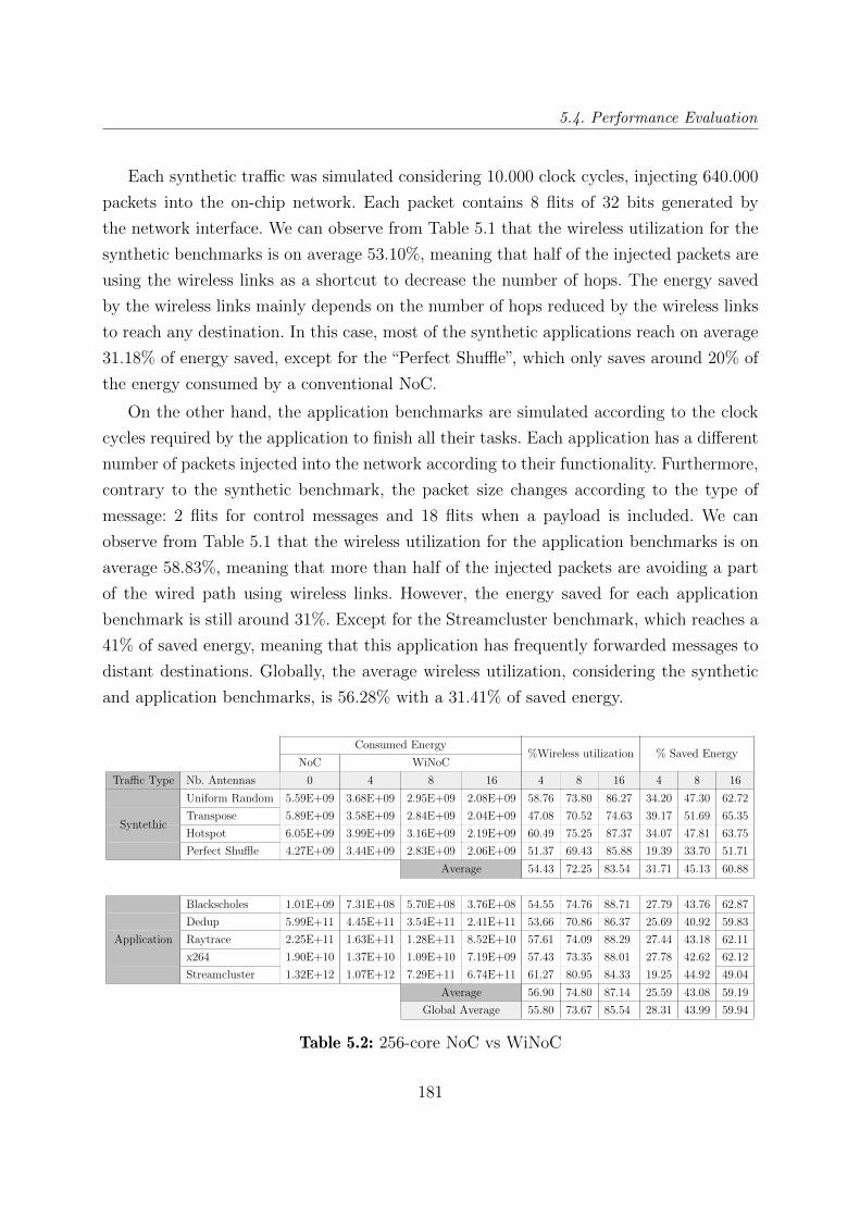
5.4. Performance Evaluation
Each synthetic traffic was simulated considering 10.000 clock cycles, injecting 640.000packets into the on-chip network. Each packet contains 8 flits of 32 bits generated by
the network interface. We can observe from Table 5.1 that the wireless utilization for the
synthetic benchmarks is on average 53.10%, meaning that half of the injected packets are
using the wireless links as a shortcut to decrease the number of hops. The energy saved
by the wireless links mainly depends on the number of hops reduced by the wireless links
to reach any destination. In this case, most of the synthetic applications reach on average
31.18% of energy saved, except for the “Perfect Shuffle”, which only saves around 20% of
the energy consumed by a conventional NoC.
On the other hand, the application benchmarks are simulated according to the clock
cycles required by the application to finish all their tasks. Each application has a different
number of packets injected into the network according to their functionality. Furthermore,
contrary to the synthetic benchmark, the packet size changes according to the type of
message: 2 flits for control messages and 18 flits when a payload is included. We can
observe from Table 5.1 that the wireless utilization for the application benchmarks is on
average 58.83%, meaning that more than half of the injected packets are avoiding a part
of the wired path using wireless links. However, the energy saved for each application
benchmark is still around 31%. Except for the Streamcluster benchmark, which reaches a
41% of saved energy, meaning that this application has frequently forwarded messages to
distant destinations. Globally, the average wireless utilization, considering the synthetic
and application benchmarks, is 56.28% with a 31.41% of saved energy.
Consumed Energy
NoC WiNoC%Wireless utilization % Saved Energy
Traffic Type Nb. Antennas 0 4 8 16 4 8 16 4 8 16
Uniform Random 5.59E+09 3.68E+09 2.95E+09 2.08E+09 58.76 73.80 86.27 34.20 47.30 62.72
Transpose 5.89E+09 3.58E+09 2.84E+09 2.04E+09 47.08 70.52 74.63 39.17 51.69 65.35
Hotspot 6.05E+09 3.99E+09 3.16E+09 2.19E+09 60.49 75.25 87.37 34.07 47.81 63.75Syntethic
Perfect Shuffle 4.27E+09 3.44E+09 2.83E+09 2.06E+09 51.37 69.43 85.88 19.39 33.70 51.71
Average 54.43 72.25 83.54 31.71 45.13 60.88
Blackscholes 1.01E+09 7.31E+08 5.70E+08 3.76E+08 54.55 74.76 88.71 27.79 43.76 62.87
Dedup 5.99E+11 4.45E+11 3.54E+11 2.41E+11 53.66 70.86 86.37 25.69 40.92 59.83
Raytrace 2.25E+11 1.63E+11 1.28E+11 8.52E+10 57.61 74.09 88.29 27.44 43.18 62.11
x264 1.90E+10 1.37E+10 1.09E+10 7.19E+09 57.43 73.35 88.01 27.78 42.62 62.12
Application
Streamcluster 1.32E+12 1.07E+12 7.29E+11 6.74E+11 61.27 80.95 84.33 19.25 44.92 49.04
Average 56.90 74.80 87.14 25.59 43.08 59.19
Global Average 55.80 73.67 85.54 28.31 43.99 59.94
Table 5.2: 256-core NoC vs WiNoC
181
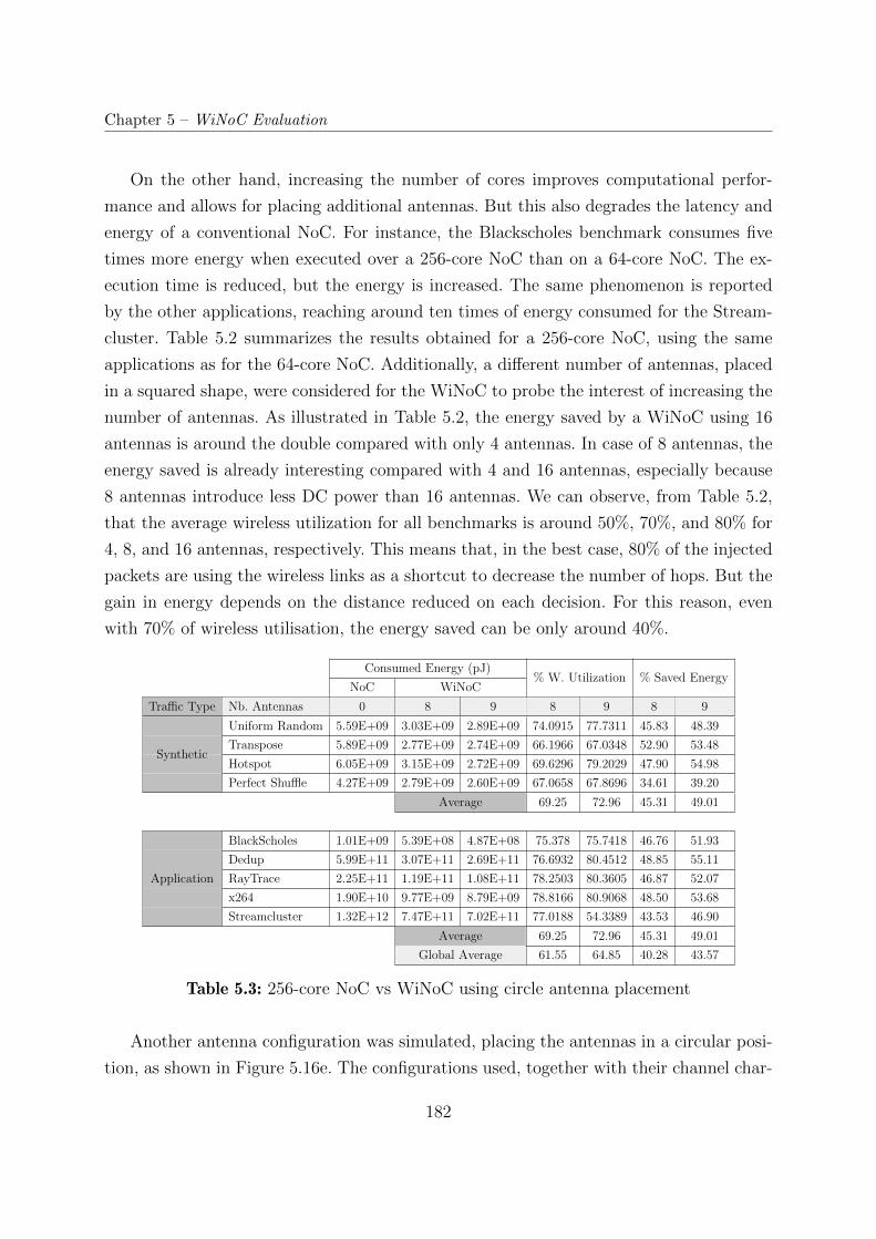
Chapter 5 – WiNoC Evaluation
On the other hand, increasing the number of cores improves computational perfor-
mance and allows for placing additional antennas. But this also degrades the latency and
energy of a conventional NoC. For instance, the Blackscholes benchmark consumes five
times more energy when executed over a 256-core NoC than on a 64-core NoC. The ex-
ecution time is reduced, but the energy is increased. The same phenomenon is reported
by the other applications, reaching around ten times of energy consumed for the Stream-
cluster. Table 5.2 summarizes the results obtained for a 256-core NoC, using the same
applications as for the 64-core NoC. Additionally, a different number of antennas, placed
in a squared shape, were considered for the WiNoC to probe the interest of increasing the
number of antennas. As illustrated in Table 5.2, the energy saved by a WiNoC using 16
antennas is around the double compared with only 4 antennas. In case of 8 antennas, the
energy saved is already interesting compared with 4 and 16 antennas, especially because
8 antennas introduce less DC power than 16 antennas. We can observe, from Table 5.2,
that the average wireless utilization for all benchmarks is around 50%, 70%, and 80% for
4, 8, and 16 antennas, respectively. This means that, in the best case, 80% of the injected
packets are using the wireless links as a shortcut to decrease the number of hops. But the
gain in energy depends on the distance reduced on each decision. For this reason, even
with 70% of wireless utilisation, the energy saved can be only around 40%.
Consumed Energy (pJ)
NoC WiNoC% W. Utilization % Saved Energy
Traffic Type Nb. Antennas 0 8 9 8 9 8 9
Uniform Random 5.59E+09 3.03E+09 2.89E+09 74.0915 77.7311 45.83 48.39
Transpose 5.89E+09 2.77E+09 2.74E+09 66.1966 67.0348 52.90 53.48
Hotspot 6.05E+09 3.15E+09 2.72E+09 69.6296 79.2029 47.90 54.98Synthetic
Perfect Shuffle 4.27E+09 2.79E+09 2.60E+09 67.0658 67.8696 34.61 39.20
Average 69.25 72.96 45.31 49.01
BlackScholes 1.01E+09 5.39E+08 4.87E+08 75.378 75.7418 46.76 51.93
Dedup 5.99E+11 3.07E+11 2.69E+11 76.6932 80.4512 48.85 55.11
RayTrace 2.25E+11 1.19E+11 1.08E+11 78.2503 80.3605 46.87 52.07
x264 1.90E+10 9.77E+09 8.79E+09 78.8166 80.9068 48.50 53.68
Application
Streamcluster 1.32E+12 7.47E+11 7.02E+11 77.0188 54.3389 43.53 46.90
Average 69.25 72.96 45.31 49.01
Global Average 61.55 64.85 40.28 43.57
Table 5.3: 256-core NoC vs WiNoC using circle antenna placement
Another antenna configuration was simulated, placing the antennas in a circular posi-
tion, as shown in Figure 5.16e. The configurations used, together with their channel char-
182
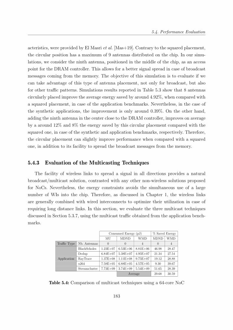
5.4. Performance Evaluation
acteristics, were provided by El Masri et al. [Mas+19]. Contrary to the squared placement,
the circular position has a maximum of 9 antennas distributed on the chip. In our simu-
lations, we consider the ninth antenna, positioned in the middle of the chip, as an access
point for the DRAM controller. This allows for a better signal spread in case of broadcast
messages coming from the memory. The objective of this simulation is to evaluate if we
can take advantage of this type of antenna placement, not only for broadcast, but also
for other traffic patterns. Simulations results reported in Table 5.3 show that 8 antennas
circularly placed improve the average energy saved by around 4.92%, when compared with
a squared placement, in case of the application benchmarks. Nevertheless, in the case of
the synthetic applications, the improvement is only around 0.39%. On the other hand,
adding the ninth antenna in the center close to the DRAM controller, improves on average
by a around 12% and 8% the energy saved by this circular placement compared with the
squared one, in case of the synthetic and application benchmarks, respectively. Therefore,
the circular placement can slightly improve performance when compared with a squared
one, in addition to its facility to spread the broadcast messages from the memory.
5.4.3 Evaluation of the Multicasting Techniques
The facility of wireless links to spread a signal in all directions provides a natural
broadcast/multicast solution, contrasted with any other non-wireless solutions proposed
for NoCs. Nevertheless, the energy constraints avoids the simultaneous use of a large
number of WIs into the chip. Therefore, as discussed in Chapter 1, the wireless links
are generally combined with wired interconnects to optimize their utilization in case of
requiring long distance links. In this section, we evaluate the three multicast techniques
discussed in Section 5.3.7, using the multicast traffic obtained from the application bench-
marks.
Consumed Energy (pJ) % Saved Energy
MU MDND WMD MDND WMD
Traffic Type Nb. Antennas 0 0 4 0 4
BlackScholes 1.23E+07 6.53E+06 8.81E+06 46.98 28.47
Dedup 6.84E+07 5.38E+07 4.95E+07 21.34 27.54
RayTrace 1.37E+08 1.11E+08 9.75E+07 19.12 28.88
x264 7.58E+05 6.88E+05 4.57E+05 9.30 39.67
Application
Streamcluster 7.73E+09 3.74E+09 5.54E+09 51.65 28.39
Average 29.68 30.59
Table 5.4: Comparison of multicast techniques using a 64-core NoC
183
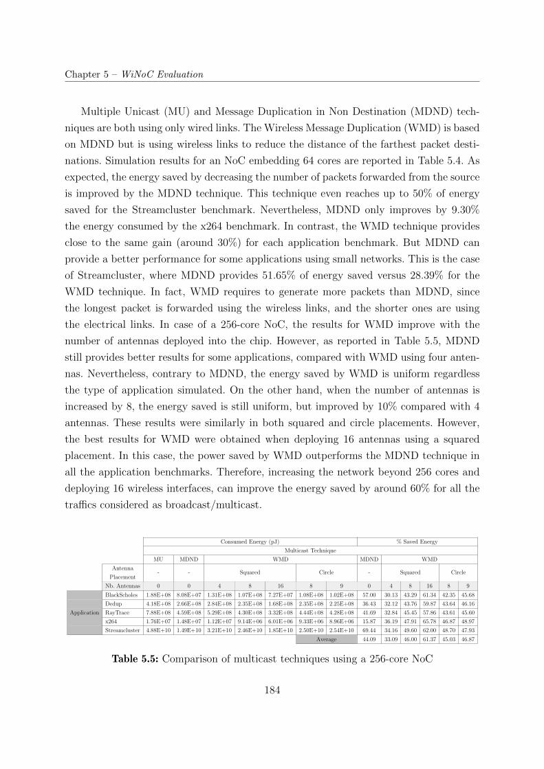
Chapter 5 – WiNoC Evaluation
Multiple Unicast (MU) and Message Duplication in Non Destination (MDND) tech-
niques are both using only wired links. The Wireless Message Duplication (WMD) is based
on MDND but is using wireless links to reduce the distance of the farthest packet desti-
nations. Simulation results for an NoC embedding 64 cores are reported in Table 5.4. As
expected, the energy saved by decreasing the number of packets forwarded from the source
is improved by the MDND technique. This technique even reaches up to 50% of energy
saved for the Streamcluster benchmark. Nevertheless, MDND only improves by 9.30%the energy consumed by the x264 benchmark. In contrast, the WMD technique provides
close to the same gain (around 30%) for each application benchmark. But MDND can
provide a better performance for some applications using small networks. This is the case
of Streamcluster, where MDND provides 51.65% of energy saved versus 28.39% for the
WMD technique. In fact, WMD requires to generate more packets than MDND, since
the longest packet is forwarded using the wireless links, and the shorter ones are using
the electrical links. In case of a 256-core NoC, the results for WMD improve with the
number of antennas deployed into the chip. However, as reported in Table 5.5, MDND
still provides better results for some applications, compared with WMD using four anten-
nas. Nevertheless, contrary to MDND, the energy saved by WMD is uniform regardless
the type of application simulated. On the other hand, when the number of antennas is
increased by 8, the energy saved is still uniform, but improved by 10% compared with 4
antennas. These results were similarly in both squared and circle placements. However,
the best results for WMD were obtained when deploying 16 antennas using a squared
placement. In this case, the power saved by WMD outperforms the MDND technique in
all the application benchmarks. Therefore, increasing the network beyond 256 cores and
deploying 16 wireless interfaces, can improve the energy saved by around 60% for all the
traffics considered as broadcast/multicast.
Consumed Energy (pJ) % Saved Energy
Multicast Technique
MU MDND WMD MDND WMD
Antenna
Placement- - Squared Circle - Squared Circle
Nb. Antennas 0 0 4 8 16 8 9 0 4 8 16 8 9
BlackScholes 1.88E+08 8.08E+07 1.31E+08 1.07E+08 7.27E+07 1.08E+08 1.02E+08 57.00 30.13 43.29 61.34 42.35 45.68
Dedup 4.18E+08 2.66E+08 2.84E+08 2.35E+08 1.68E+08 2.35E+08 2.25E+08 36.43 32.12 43.76 59.87 43.64 46.16
RayTrace 7.88E+08 4.59E+08 5.29E+08 4.30E+08 3.32E+08 4.44E+08 4.28E+08 41.69 32.84 45.45 57.86 43.61 45.60
x264 1.76E+07 1.48E+07 1.12E+07 9.14E+06 6.01E+06 9.33E+06 8.96E+06 15.87 36.19 47.91 65.78 46.87 48.97
Application
Streamcluster 4.88E+10 1.49E+10 3.21E+10 2.46E+10 1.85E+10 2.50E+10 2.54E+10 69.44 34.16 49.60 62.00 48.70 47.93
Average 44.09 33.09 46.00 61.37 45.03 46.87
Table 5.5: Comparison of multicast techniques using a 256-core NoC
184

5.4. Performance Evaluation
Finally, some comparisons between the two architectures supporting unicast and mul-
ticast messages are depicted in Figure 5.19. The first architecture is a conventional NoC
following MDND and the second one is a WiNoC using WDM, both evaluated with 64
and 256 cores. The WiNoC architecture is contrasted with the different configurations dis-
cussed in previous sections. Figure 5.19a shows the normalized energy consumed by the
communications in a 64-core architecture for different synthetic and application bench-
marks. We can observe a significant reduction in energy, with an average energy saving
of 32%. This gain is due to the cost of wireless communication becoming cheaper, hence
wireless hops are more frequently used than electrical routers. Furthermore, Figure 5.19b
shows the wireless utilization, which is on average equal to 58.85%. This means that more
than 50% of the messages injected into the network are using the wireless links to im-
prove the energy consumed during the execution of a benchmark. Figure 5.19c shows the
normalized energy consumed by the communications in a 256-core architecture for dif-
ferent benchmarks. We can observe a large recuction in energy, with an average energy
saving of 42% considering all the antenna configurations. Indeed, the best configuration
providing the biggest average energy saving (60%) is the squared placement containing 16
antennas. This large gain is due to the reduced distance provided by the wireless links to
transfer messages with the longest distance. Furthermore, Figure 5.19d shows the wireless
utilization, which is on average equal to 72.78% considering all the configurations running
the application benchmarks.
185
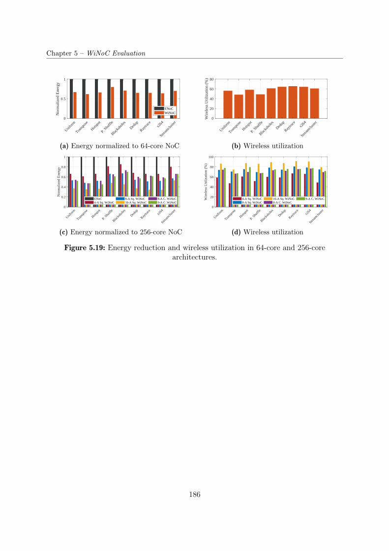
Chapter 5 – WiNoC Evaluation
Unifor
m
Transp
ose
Hotspo
t
P. Shu
ffle
Blacks
holes
Dedup
Raytra
cex2
64
Stream
cluste
r0
0.5
1
Nor
mal
ized
Ene
rgy
ENoCWiNoC
(a) Energy normalized to 64-core NoC
Unifor
m
Transp
ose
Hotspo
t
P. Shu
ffle
Blacks
holes
Dedup
Raytra
cex2
64
Stream
cluste
r0
20
40
60
80
Wir
eles
s U
tiliz
atio
n (%
)
(b) Wireless utilization
Unifor
m
Transp
ose
Hotspo
t
P. Shu
ffle
Blacks
holes
Dedup
Raytra
cex2
64
Stream
cluste
r0
0.2
0.4
0.6
0.8
1
Nor
mal
ized
Ene
rgy
ENoC4-A Sq. WiNoC
8-A Sq. WiNoC16-A Sq. WiNoC
8-A C. WiNoC9-A C. WiNoC
(c) Energy normalized to 256-core NoC
Unifor
m
Transp
ose
Hotspo
t
P. Shu
ffle
Blacks
holes
Dedup
Raytra
cex2
64
Stream
cluste
r0
20
40
60
80
100
Wir
eles
s U
tiliz
atio
n (%
)
4-A Sq. WiNoC8-A Sq. WiNoC
16-A Sq. WiNoC8-A C. WiNoC
9-A C. WiNoC
(d) Wireless utilization
Figure 5.19: Energy reduction and wireless utilization in 64-core and 256-corearchitectures.
186
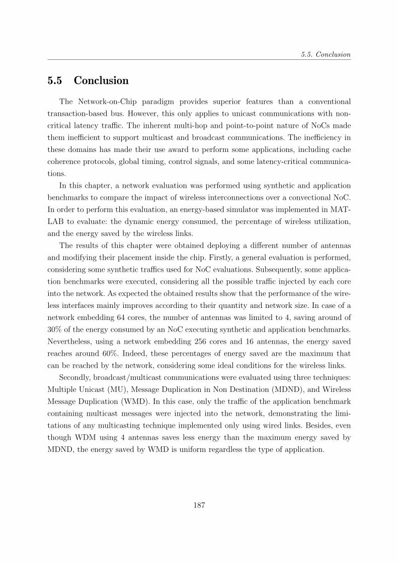
5.5. Conclusion
5.5 Conclusion
The Network-on-Chip paradigm provides superior features than a conventional
transaction-based bus. However, this only applies to unicast communications with non-
critical latency traffic. The inherent multi-hop and point-to-point nature of NoCs made
them inefficient to support multicast and broadcast communications. The inefficiency in
these domains has made their use award to perform some applications, including cache
coherence protocols, global timing, control signals, and some latency-critical communica-
tions.
In this chapter, a network evaluation was performed using synthetic and application
benchmarks to compare the impact of wireless interconnections over a convectional NoC.
In order to perform this evaluation, an energy-based simulator was implemented in MAT-
LAB to evaluate: the dynamic energy consumed, the percentage of wireless utilization,
and the energy saved by the wireless links.
The results of this chapter were obtained deploying a different number of antennas
and modifying their placement inside the chip. Firstly, a general evaluation is performed,
considering some synthetic traffics used for NoC evaluations. Subsequently, some applica-
tion benchmarks were executed, considering all the possible traffic injected by each core
into the network. As expected the obtained results show that the performance of the wire-
less interfaces mainly improves according to their quantity and network size. In case of a
network embedding 64 cores, the number of antennas was limited to 4, saving around of
30% of the energy consumed by an NoC executing synthetic and application benchmarks.
Nevertheless, using a network embedding 256 cores and 16 antennas, the energy saved
reaches around 60%. Indeed, these percentages of energy saved are the maximum that
can be reached by the network, considering some ideal conditions for the wireless links.
Secondly, broadcast/multicast communications were evaluated using three techniques:
Multiple Unicast (MU), Message Duplication in Non Destination (MDND), and Wireless
Message Duplication (WMD). In this case, only the traffic of the application benchmark
containing multicast messages were injected into the network, demonstrating the limi-
tations of any multicasting technique implemented only using wired links. Besides, even
though WDM using 4 antennas saves less energy than the maximum energy saved by
MDND, the energy saved by WMD is uniform regardless the type of application.
187

CONCLUSION AND PERSPECTIVES
The evolution of microelectronics and the requirements in high-speed data rate for High
Performance Computing (HPC), involve a larger number of computation resources and
faster components (e.g. processors, memories) to support the application needs. For theses
reasons, the emerging manycore architecture era comes up with critical issues in commu-
nication latency and power consumption. Network-on-Chip (NoC) was a very promising
solution to solve these challenges. However, with the scaling of advanced CMOS technolo-
gies, the number of cores is continuously growing. As a consequence, the number of hops
needed to communicate between cores creates a critical bottleneck in the communication
backbone by increasing latency and power consumption due to large volume data trans-
mission. To deal with the surge of high performance computing systems and to overcome
this communication bottleneck, new interconnect technologies have emerged, such as 3D-
NoC, Radio-Frequency Interconnects based on waveguides, Optical NoC, and Wireless
NoC.
Wireless Network-on-Chip (WiNoC) is one of the most promising solution for the com-
munication infrastructure of CMPs and MPSoCs. As discussed in this thesis work, this
technology offers a natural support for broadcast communication, facilitating the cache
coherence protocols. Moreover, contrary to the optical solutions, it does not require ther-
mal tuning management, expensive area, and complex interconnects. Multiple benefits are
brought by the wireless technology, as was demonstrated in Chapter 5. However, current
technology does not allow the development of wireless links with high power efficiency. For
this reason, the wireless solutions are mostly combined with other interconnect technol-
ogy, reducing the number of wireless access points into the chip. On the other hand, as the
wireless signal is propagated everywhere, the multipath interference naturally arises in this
type of communication. In Chapter 2 and 3, we propose and design a digital transceiver
architecture, adopting different techniques to compensate for multipath interferences. Fur-
thermore, in order to reduce the congestion generated by a packet waiting for the release
of the wireless access point, we implement a direct sequence spread spectrum (DSSS) com-
munication system capable of supporting multiple simultaneous communications. In this
189
technique, a node has access to the entire bandwidth for the entire time duration, contrary
to time and frequency division multiplexing. Moreover, a DSSS system can be combined
with a RAKE receiver used to improve the signal reception, when it is degraded by mul-
tipath propagation. However, this technique suffers for near-far effects, as illustrated in
Figure 5.20. In other words, a transmitting antenna close to the receiving antenna with
the same power as another antenna placed far from the transmitting antenna, will drown
the transmitted signal. Two solutions are possible to solve this problem:
1. First, to implement a tight power control on each transmitter, controlling the trans-
mission power according to the distance.
2. Second, to divide communications into sectors defined according to the distance.
In the second case, the sectors closest to the receiving antenna will communicate first, and
then the farthest sectors. This is possible especially because the number of available codes
used for simultaneous communications is limited, as discussed in Chapter 2. Therefore,
even with 16 antennas, it is not possible for nodes to communicate simultaneously, unless
we increase the scrambling code size. But this implies growing the power consumption and
the synchronization latency. On the other hand, the placement of a circled antenna with
a centered antenna can resolve this near-far effect, considering that only the centered an-
tenna, containing the DRAM controller, will receive all the simultaneous communications
from the other nodes.
Figure 5.20: DSSS far-near effects.
Another aspect to consider is the wireless link energy-efficiency, which is one of the main
constraints present in current WiNoC designs. In fact, the bulk of power is consumed by
190
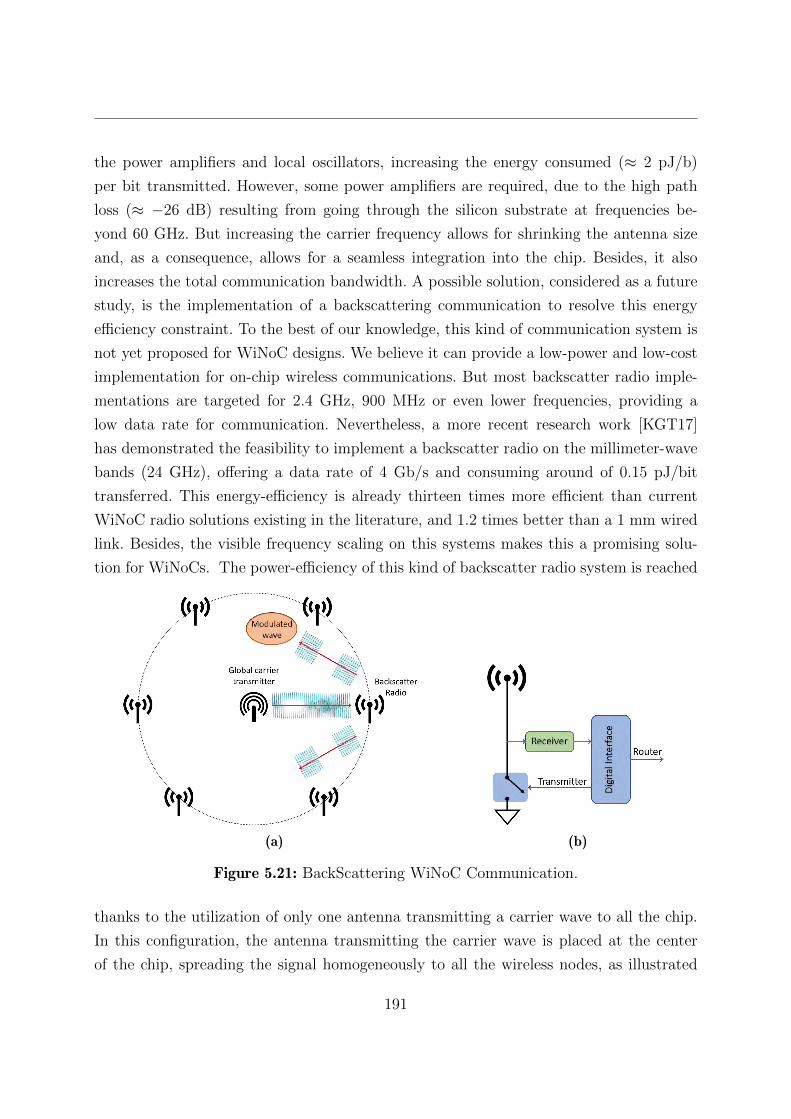
the power amplifiers and local oscillators, increasing the energy consumed (≈ 2 pJ/b)
per bit transmitted. However, some power amplifiers are required, due to the high path
loss (≈ −26 dB) resulting from going through the silicon substrate at frequencies be-
yond 60 GHz. But increasing the carrier frequency allows for shrinking the antenna size
and, as a consequence, allows for a seamless integration into the chip. Besides, it also
increases the total communication bandwidth. A possible solution, considered as a future
study, is the implementation of a backscattering communication to resolve this energy
efficiency constraint. To the best of our knowledge, this kind of communication system is
not yet proposed for WiNoC designs. We believe it can provide a low-power and low-cost
implementation for on-chip wireless communications. But most backscatter radio imple-
mentations are targeted for 2.4 GHz, 900 MHz or even lower frequencies, providing a
low data rate for communication. Nevertheless, a more recent research work [KGT17]
has demonstrated the feasibility to implement a backscatter radio on the millimeter-wave
bands (24 GHz), offering a data rate of 4 Gb/s and consuming around of 0.15 pJ/bit
transferred. This energy-efficiency is already thirteen times more efficient than current
WiNoC radio solutions existing in the literature, and 1.2 times better than a 1 mm wired
link. Besides, the visible frequency scaling on this systems makes this a promising solu-
tion for WiNoCs. The power-efficiency of this kind of backscatter radio system is reached
(a) (b)
Figure 5.21: BackScattering WiNoC Communication.
thanks to the utilization of only one antenna transmitting a carrier wave to all the chip.
In this configuration, the antenna transmitting the carrier wave is placed at the center
of the chip, spreading the signal homogeneously to all the wireless nodes, as illustrated
191
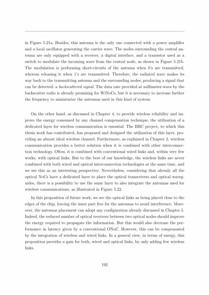
in Figure 5.21a. Besides, this antenna is the only one connected with a power amplifier
and a local oscillator generating the carrier wave. The nodes surrounding the central an-
tenna are only equipped with a receiver, a digital interface, and a transistor used as a
switch to modulate the incoming wave from the central node, as shown in Figure 5.21b.
The modulation is performing short-circuits of the antenna when 0’s are transmitted,
whereas releasing it when 1’s are transmitted. Therefore, the radiated wave makes its
way back to the transmitting antenna and the surrounding nodes, producing a signal that
can be detected: a backscattered signal. The data rate provided at millimeter-wave by the
backscatter radio is already promising for WiNoCs, but it is necessary to increase further
the frequency to miniaturize the antennas used in this kind of system.
On the other hand, as discussed in Chapter 4, to provide wireless reliability and im-
prove the energy consumed by any channel compensation technique, the utilization of a
dedicated layer for wireless communication is essential. The BBC project, to which this
thesis work has contributed, has proposed and designed the utilization of this layer, pro-
viding an almost ideal wireless channel. Furthermore, as explained in Chapter 2, wireless
communication provides a better solution when it is combined with other interconnec-
tion technology. Often, it is combined with conventional wired links and, within very few
works, with optical links. But to the best of our knowledge, the wireless links are never
combined with both wired and optical interconnection technologies at the same time, and
we see this as an interesting perspective. Nevertheless, considering that already all the
optical NoCs have a dedicated layer to place the optical transceivers and optical waveg-
uides, there is a possibility to use the same layer to also integrate the antennas used for
wireless communications, as illustrated in Figure 5.22.
In this proposition of future work, we see the optical links as being placed close to the
edges of the chip, leaving the inner part free for the antennas to avoid interference. More-
over, the antennas placement can adopt any configuration already discussed in Chapter 5.
Indeed, the reduced number of optical receivers between two optical nodes should improve
the energy required to propagate the information. But this would also decrease the per-
formance in latency given by a conventional ONoC. However, this can be compensated
by the integration of wireless and wired links. In a general view, in terms of energy, this
proposition provides a gain for both, wired and optical links, by only adding few wireless
links.
192
Figure 5.22: Optical/Wireless NoC Communication layer.
We believe that wireless links embedded into a NoC is a real promising solution, which
can provide multiple benefits. Some of these benefits include its natural broadcast sup-
port, its seamless integration, its low-power consumption according to the communication
system, multiple network configurations, and its flexibility to be combined with any other
interconnect technology. In the development of this thesis, we discussed the gaps on the
literature of the wireless technology used in conventional NoCs, proposing new solutions
to improve the reliability and energy consumption. Multiple configurations were analyzed,
highlighting the limitations of each one. We conclude that the best solution for a wireless
communication is to use a dedicated layer to propagate the electromagnetic waves, limit-
ing the losses and interference. Besides, we demonstrated that future high-speed WiNoC
transceivers are not scaling using single-carrier NC-OOK. For this reason, a multi-carrier
NC-OOK FDM-based was proposed in Chapter 4, combined with a spread-spectrum tech-
nique.
193

SCIENTIFIC CONTRIBUTIONS
International Conferences
— “A Diversity Scheme to Enhance the Reliability of Wireless NoC in Multipath
Channel Environment.” Joel Ortiz Sosa, Olivier Sentieys, Christian Roland. In
Twelfth IEEE/ACM International Symposium on Network-on-Chip (NoCs). Octo-
ber 2018, Torino, Italy.
— “Adaptive Transceiver for Wireless NoC to Enhance Multicast/Unicast Commu-
nication Scenarios.” Joel Ortiz Sosa, Olivier Sentieys, Christian Roland. IEEE
Computer Society Annual Symposium on VLSI. July 2019, Miami, Florida, U.S.A.
— “Short paper: Multi-Carrier Spread-Spectrum Transceiver for WiNoC.” Joel Ortiz
Sosa, Olivier Sentieys, Christian Roland, Cedric Killian. In IEEE/ACM Interna-
tional Symposium on Network-on-Chip (NoCs). October 2019, New York, U.S.A.
— “Min/max time limits and energy penalty of communication scheduling in ring-
based OnoC.” Joel Ortiz Sosa, Hamza Ben Ammar, Cedric Killian and Daniel
Chillet. In IEEE/ACM International Workshop on Network-on-Chip Architecture
(NoCArc). October 2020.
Posters
— Comin Labs days 2016 - Rennes- November, 2016.
— Comin Labs days 2018 - Rennes- May, 2018.
195
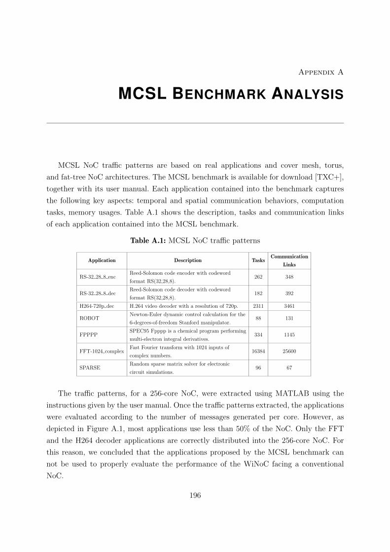
Appendix A
MCSL BENCHMARK ANALYSIS
MCSL NoC traffic patterns are based on real applications and cover mesh, torus,
and fat-tree NoC architectures. The MCSL benchmark is available for download [TXC+],
together with its user manual. Each application contained into the benchmark captures
the following key aspects: temporal and spatial communication behaviors, computation
tasks, memory usages. Table A.1 shows the description, tasks and communication links
of each application contained into the MCSL benchmark.
Table A.1: MCSL NoC traffic patterns
Application Description TasksCommunication
Links
RS-32 28 8 encReed-Solomon code encoder with codeword
format RS(32,28,8).262 348
RS-32 28 8 decReed-Solomon code decoder with codeword
format RS(32,28,8).182 392
H264-720p dec H.264 video decoder with a resolution of 720p. 2311 3461
ROBOTNewton-Euler dynamic control calculation for the
6-degrees-of-freedom Stanford manipulator.88 131
FPPPPSPEC95 Fpppp is a chemical program performing
multi-electron integral derivatives.334 1145
FFT-1024 complexFast Fourier transform with 1024 inputs of
complex numbers.16384 25600
SPARSERandom sparse matrix solver for electronic
circuit simulations.96 67
The traffic patterns, for a 256-core NoC, were extracted using MATLAB using the
instructions given by the user manual. Once the traffic patterns extracted, the applications
were evaluated according to the number of messages generated per core. However, as
depicted in Figure A.1, most applications use less than 50% of the NoC. Only the FFT
and the H264 decoder applications are correctly distributed into the 256-core NoC. For
this reason, we concluded that the applications proposed by the MCSL benchmark can
not be used to properly evaluate the performance of the WiNoC facing a conventional
NoC.
196
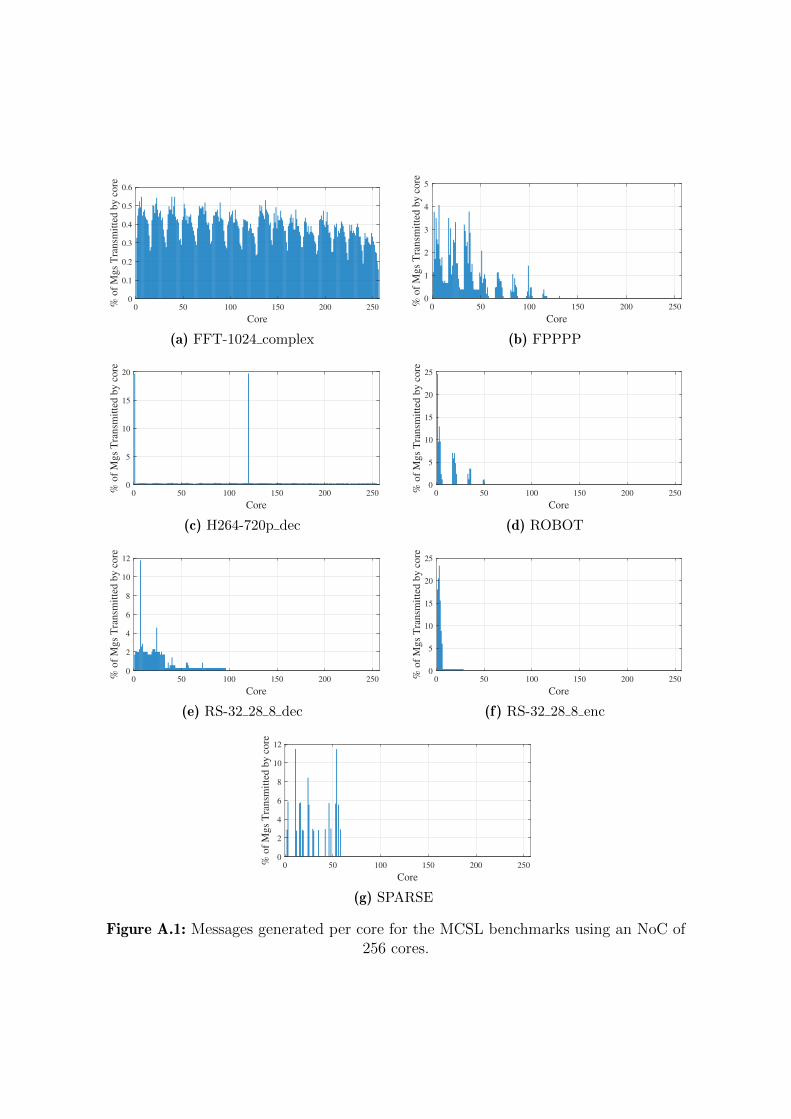
0 50 100 150 200 250
Core
0
0.1
0.2
0.3
0.4
0.5
0.6
% o
f M
gs
Tra
nsm
itte
d b
y c
ore
(a) FFT-1024 complex
0 50 100 150 200 250
Core
0
1
2
3
4
5
% o
f M
gs
Tra
nsm
itte
d b
y c
ore
(b) FPPPP
0 50 100 150 200 250
Core
0
5
10
15
20
% o
f M
gs
Tra
nsm
itte
d b
y c
ore
(c) H264-720p dec
0 50 100 150 200 250
Core
0
5
10
15
20
25
% o
f M
gs
Tra
nsm
itte
d b
y c
ore
(d) ROBOT
0 50 100 150 200 250
Core
0
2
4
6
8
10
12
% o
f M
gs
Tra
nsm
itte
d b
y c
ore
(e) RS-32 28 8 dec
0 50 100 150 200 250
Core
0
5
10
15
20
25
% o
f M
gs
Tra
nsm
itte
d b
y c
ore
(f ) RS-32 28 8 enc
0 50 100 150 200 250
Core
0
2
4
6
8
10
12
% o
f M
gs
Tra
nsm
itte
d b
y c
ore
(g) SPARSE
Figure A.1: Messages generated per core for the MCSL benchmarks using an NoC of256 cores.


BIBLIOGRAPHY
[AAB+00] B. Ackland, A. Anesko, D. Brinthaupt, et al. « A single-chip, 1.6-billion, 16-b
MAC/s multiprocessor DSP ». In: IEEE Journal of Solid-State Circuits 35.3
(2000), pp. 412–424. issn: 0018-9200. doi: 10.1109/4.826824.
[ACV17] A. Asaduzzaman, K. K. Chidella, and D. Vardha. « An Energy-Efficient Di-
rectory Based Multicore Architecture with Wireless Routers to Minimize
the Communication Latency ». In: IEEE Transactions on Parallel and Dis-
tributed Systems 28.2 (2017), pp. 374–385. issn: 1045-9219. doi: 10.1109/
TPDS.2016.2571282.
[AE10] Andrea Alu and Nader Engheta. « Wireless at the Nanoscale: Optical In-
terconnects using Matched Nanoantennas ». In: Physical Review Letters 104
(21 2010), p. 213902. doi: 10.1103/PhysRevLett.104.213902.
[AH09] M.-C. Amann and Werner Hofmann. « InP-Based Long-Wavelength VCSELs
and VCSEL Arrays ». In: IEEE Journal of Selected Topics in Quantum Elec-
tronics 15.3 (2009), pp. 861–868. issn: 1077-260X. doi: 10.1109/JSTQE.
2009.2013182.
[AJC14] Ian F. Akyildiz, Josep Miquel Jornet, and Chong Han. « Terahertz band:
Next frontier for wireless communications ». In: Physical Communication 12
(2014), pp. 16 –32. issn: 1874-4907. doi: 10.1016/j.phycom.2014.01.006.
[AJJ16] M.R. Arun, P.A. Jisha, and John Jose. « A Novel Energy Efficient Multicas-
ting Approach For Mesh NoCs ». In: Procedia Computer Science 93 (2016),
pp. 283–291. issn: 18770509. doi: 10.1016/j.procs.2016.07.212.
[Amo96] F. Amoroso. « Use of DS/SS signaling to mitigate Rayleigh fading in a dense
scatterer environment ». In: IEEE Personal Communications 3.2 (1996),
pp. 52–61. issn: 1558-0652. doi: 10.1109/98.490752.
[APG09] Pablo Abad, Valentin Puente, and Jose-Angel Gregorio. « MRR: Enabling
fully adaptive multicast routing for CMP interconnection networks ». In: In-
ternational Symposium on High Performance Computer Architecture. IEEE,
2009, pp. 355–366. doi: 10.1109/HPCA.2009.4798273.
199
[ART20] K. E. Aasmundtveit, A. Roy, and B. Q. Ta. « Direct Integration of Car-
bon Nanotubes in CMOS, Towards an Industrially Feasible Process: A Re-
view ». In: IEEE Transactions on Nanotechnology 19 (2020), pp. 113–122.
issn: 1941-0085. doi: 10.1109/TNANO.2019.2961415.
[AT+19] T. Alexoudi, N. Terzenidis, et al. « Optics in Computing: From Photonic
Network-on-Chip to Chip-to-Chip Interconnects and Disintegrated Archi-
tectures ». In: Journal of Lightwave Technology 37.2 (2019), pp. 363–379.
issn: 0733-8724. doi: 10.1109/JLT.2018.2875995.
[ATM15] Michael Opoku Agyeman, Kenneth Tong, and Terrence Mak. « An Improved
Wireless Communication Fabric for Emerging Network-on-Chip Design ». In:
Procedia Computer Science 56 (2015), pp. 415 –420. issn: 1877-0509. doi:
10.1016/j.procs.2015.07.229.
[AVM16] M. O. Agyeman, Q. T. Vien, and T. Mak. « An Analytical Channel Model
for Emerging Wireless Networks-on-Chip ». In: IEEE Intl Conference on
Computational Science and Engineering. 2016, pp. 9–15. doi: 10.1109/CSE-
EUC-DCABES.2016.155.
[Bab+06] A. Babakhani et al. « A 77-GHz Phased-Array Transceiver With On-Chip
Antennas in Silicon: Receiver and Antennas ». In: IEEE Journal of Solid-
State Circuits 41.12 (2006), pp. 2795–2806. issn: 0018-9200. doi: 10.1109/
JSSC.2006.884811.
[BD06] James Balfour and William J. Dally. « Design Tradeoffs for Tiled CMP On-
Chip Networks ». In: ACM International Conference on Supercomputing.
New York, NY, USA, 2006, 390aAS401. doi: 10.1145/2591635.2667187.
[BDN09] Palash Bharadwaj, Bradley Deutsch, and Lukas Novotny. « Optical Anten-
nas ». In: Advances in Optics and Photonics 1.3 (2009), pp. 438–483. doi:
10.1364/AOP.1.000438.
[Bel+17] Gaetano Bellanca et al. « Integrated Vivaldi plasmonic antenna for wireless
on-chip optical communications ». In: Opt. Express 25.14 (2017), pp. 16214–
16227. doi: 10.1364/OE.25.016214.
[Bie+08] Christian Bienia et al. « The PARSEC benchmark suite ». In: International
Conference on Parallel Architectures and Compilation Techniques. 2008, p. 72.
doi: 10.1145/1454115.1454128.
200
[BKK08] Christian Bienia, Sanjeev Kumar, and Kai Li. « PARSEC vs. SPLASH-2:
A quantitative comparison of two multithreaded benchmark suites on Chip-
Multiprocessors ». In: International Symposium on Workload Characteriza-
tion. 2008, pp. 47–56. isbn: 978-1-4244-2777-2. doi: 10.1109/IISWC.2008.
4636090.
[BLB07] J. H. Bahn, S. E. Lee, and N. Bagherzadeh. « On Design and Analysis of
a Feasible Network-on-Chip (NoC) Architecture ». In: International Confer-
ence on Information Technology. 2007, pp. 1033–1038. doi: 10.1109/ITNG.
2007.139.
[Bri+15] Alexandre Briere et al. « A Dynamically Reconfigurable RF NoC for Many-
Core ». In: ACM Great Lakes Symposium on VLSI. 2015, pp. 139–144. doi:
10.1145/2742060.2742082.
[BS73] Fischer Black and Myron Scholes. « The Pricing of Options and Corporate
Liabilities ». In: Journal of Political Economy 81.3 (1973), pp. 637–654. issn:
0022-3808. doi: 10.1086/260062.
[BTR02] D. C. Bossen, J. M. Tendler, and K. Reick. « Power4 system design for high
reliability ». In: IEEE Micro 22.2 (2002), pp. 16–24. issn: 0272-1732. doi:
10.1109/MM.2002.997876.
[BW03] B. M. Beckmann and D. A. Wood. « TLC: transmission line caches ». In:
IEEE/ACM International Symposium on Microarchitecture. 2003, pp. 43–
54. doi: 10.1109/MICRO.2003.1253182.
[Cal+18] G. CalAs et al. « On-Chip Wireless Optical Communication: From Antenna
Design to Channel Modelling ». In: International Conference on Transparent
Optical Networks. 2018, pp. 1–4. doi: 10.1109/ICTON.2018.8474007.
[Car+12] A. Carpenter et al. « Using Transmission Lines for Global On-Chip Commu-
nication ». In: IEEE Journal on Emerging and Selected Topics in Circuits
and Systems 2.2 (2012), pp. 183–193. doi: 10.1109/JETCAS.2012.2193519.
[Cat+16] V. Catania et al. « Energy efficient transceiver in wireless Network on Chip
architectures ». In: Design, Automation Test in Europe Conference Exhibi-
tion. 2016, pp. 1321–1326.
201
[Cat+17] Vincenzo Catania et al. « Improving Energy Efficiency in Wireless Network-
on-Chip Architectures ». In: Journal Emerging Technology Computing Sys-
tem 14.1 (2017), 9:1–9:24. issn: 1550-4832. doi: 10.1145/3138807.
[CH18] Y. Chen and C. Han. « Channel modeling and analysis for wireless networks-
on-chip communications in the millimeter wave and terahertz bands ». In:
IEEE Conference on Computer Communications Workshops. 2018, pp. 651–
656. doi: 10.1109/INFCOMW.2018.8406954.
[Cha+00] M. F. Chang et al. « Multi-I/O and reconfigurable RF/wireless interconnect
based on near field capacitive coupling and multiple access techniques ». In:
Proceedings International Interconnect Technology Conference (Cat. No.00EX407).
2000, pp. 21–22. doi: 10.1109/IITC.2000.854269.
[Cha+01] M. F. Chang et al. « RF/wireless interconnect for inter- and intra-chip com-
munications ». In: Proceedings of the IEEE 89.4 (2001), pp. 456–466. doi:
10.1109/5.920578.
[Cha+08] M.-C. Frank Chang et al. « RF Interconnects for Communications On-chip ».
In: Proceeding International Symposium on Physical Design. 2008, pp. 78–83.
isbn: 978-1-60558-048-7. doi: 10.1145/1353629.1353649.
[Cha+08a] M. F. Chang et al. « CMP network-on-chip overlaid with multi-band RF-
interconnect ». In: International Symposium on High Performance Computer
Architecture. 2008, pp. 191–202. doi: 10.1109/HPCA.2008.4658639.
[Cha+08b] M. F. Chang et al. « Power reduction of CMP communication networks via
RF-interconnects ». In: IEEE/ACM International Symposium on Microar-
chitecture. 2008, pp. 376–387. doi: 10.1109/MICRO.2008.4771806.
[Cha+12] K. Chang et al. « Performance Evaluation and Design Trade-offs for Wire-
less Network-on-chip Architectures ». In: Journal on Emerging Technology in
Computing Systems 8.3 (2012), 23:1–23:25. doi: 10.1145/2287696.2287706.
[Cha+12] P. Chang et al. « An Ultra-Low-Power Transformer-Feedback 60 GHz Low-
Noise Amplifier in 90 nm CMOS ». In: IEEE Microwave and Wireless Com-
ponents Letters 22.4 (2012), pp. 197–199. issn: 1531-1309. doi: 10.1109/
LMWC.2012.2187883.
202
[Che+09] W. Chen et al. « A 6-Gb/s Wireless Inter-Chip Data Link Using 43-GHz
Transceivers and Bond-Wire Antennas ». In: IEEE Journal of Solid-State
Circuits 44.10 (2009), pp. 2711–2721. issn: 1558-173X. doi: 10.1109/JSSC.
2009.2027932.
[CHE11] Trevor E. Carlson, Wim Heirman, and Lieven Eeckhout. « Sniper: Exploring
the Level of Abstraction for Scalable and Accurate Parallel Multi-Core Sim-
ulations ». In: International Conference for High Performance Computing,
Networking, Storage and Analysis. 2011, 52:1–52:12.
[Che+13] Xi Chen et al. « Process variation in silicon photonic devices ». In: Applied
Optics 52.31 (2013), p. 7638. issn: 1559-128X. doi: 10.1364/AO.52.007638.
[Che+17] Chia-Hsin Chen et al. « Design and implementation of low-latency, low-power
reconfigurable on-chip networks ». PhD thesis. Massachusetts Institute of
Technology, 2017.
[Chi+17] Daniel Chillet et al. Integration of an Optical NoC into multicore architecture.
Colloque National du GDR SoC-SiP. Poster. 2017.
[CL14] J. Chen and Yen-Han Lai. « A study of CSMA-based and token-based wire-
less interconnects network-on-chip ». In: IEEE International Conference on
Communication Problem-Solving. 2014, pp. 205–209. doi: 10.1109/ICCPS.
2014.7062254.
[Cla+15] R. Clarke et al. « 140 Gb/s Serializer Using Clock Doublers in 90 nm SiGe
Technology ». In: IEEE Journal of Solid-State Circuits 50.11 (2015), pp. 2703–
2713. issn: 0018-9200. doi: 10.1109/JSSC.2015.2472600.
[CMP99] CMP. MultiaARProject Circuits [Online]. http://cmp.imag.fr. 1999 (accessed
28 January, 2020).
[Com+02] US Federal Communications Commission et al. « Revision of part 15 of the
commissions rules regarding ultra-wideband transmission systems ». In: First
Report and Order, ET Docket (2002), pp. 98–153.
[Cou00] Leon W. Couch II. Digital and Analog Communication Systems. 6th. Prentice
Hall PTR, 2000. isbn: 0130812234.
203
[CRR08] E. Cohen, S. Ravid, and D. Ritter. « An ultra low power LNA with 15dB
gain and 4.4db NF in 90nm CMOS process for 60 GHz phase array radio ».
In: IEEE Radio Frequency Integrated Circuits Symposium. 2008, pp. 61–64.
doi: 10.1109/RFIC.2008.4561386.
[Daw+03] Dawei Huang et al. « Optical interconnects: out of the box forever? » In:
IEEE Journal of Selected Topics in Quantum Electronics 9.2 (2003), pp. 614–
623. doi: 10.1109/JSTQE.2003.812506.
[Deb+10] S. Deb et al. « Enhancing performance of network-on-chip architectures with
millimeter-wave wireless interconnects ». In: IEEE International Conference
on Application-specific Systems, Architectures and Processors. 2010, pp. 73–
80. doi: 10.1109/ASAP.2010.5540799.
[Deb+12] Sujay Deb et al. « Wireless NoC as Interconnection Backbone for Multicore
Chips: Promises and Challenges ». In: Journal on Emerging and Selected
Topics in Circuits and Systems 2.2 (2012), pp. 228–239. issn: 2156-3357.
doi: 10.1109/JETCAS.2012.2193835.
[Deb+13] S. Deb et al. « Design of an Energy-Efficient CMOS-Compatible NoC Ar-
chitecture with Millimeter-Wave Wireless Interconnects ». In: IEEE Trans-
actions on Computers 62.12 (2013), pp. 2382–2396. issn: 0018-9340. doi:
10.1109/TC.2012.224.
[DiT+11] D. DiTomaso et al. « iWISE: Inter-router Wireless Scalable Express Channels
for Network-on-Chips (NoCs) Architecture ». In: Annual Symposium on High
Performance Interconnects. 2011, pp. 11–18. doi: 10.1109/HOTI.2011.12.
[DiT+15] D. DiTomaso et al. « A-WiNoC: Adaptive Wireless Network-on-Chip Ar-
chitecture for Chip Multiprocessors ». In: IEEE Transactions on Parallel
and Distributed Systems 26.12 (2015), pp. 3289–3302. issn: 1045-9219. doi:
10.1109/TPDS.2014.2383384.
[Doa+05] C. H. Doan et al. « Millimeter-wave CMOS design ». In: IEEE Journal of
Solid-State Circuits 40.1 (2005), pp. 144–155. doi: 10.1109/JSSC.2004.
837251.
[Don+15] P. Dong et al. « Reconfigurable 100 Gb/s silicon photonic network-on-chip
[invited] ». In: IEEE/OSA Journal of Optical Communications and Network-
ing 7.1 (2015), A37–A43. doi: 10.1364/JOCN.7.000A37.
204
[Dor+10] Jens Dorfmuller et al. « Plasmonic Nanowire Antennas: Experiment, Sim-
ulation, and Theory ». In: Nano Letters 10.9 (2010), pp. 3596–3603. issn:
1530-6984. doi: 10.1021/nl101921y.
[Dow06] J. Doweck. « Inside IntelAo Core microarchitecture ». In: IEEE Hot Chips 18
Symposium (HCS). 2006, pp. 1–35. doi: 10.1109/HOTCHIPS.2006.7477876.
[DT01] W. J. Dally and B. Towles. « Route packets, not wires: on-chip intercon-
nection networks ». In: Proceedings Design Automation Conference. 2001,
pp. 684–689. doi: 10.1109/DAC.2001.156225.
[DT04] William James Dally and Brian Towles. Principles and Practices of Inter-
connection Networks. Elsevier, 2004. isbn: 0122007514.
[Dur+17] K. Duraisamy et al. « Multicast-Aware High-Performance Wireless Network-
on-Chip Architectures ». In: IEEE Transactions on Very Large Scale Inte-
gration Systems 25.3 (2017), pp. 1126–1139. issn: 1063-8210. doi: 10.1109/
TVLSI.2016.2612647.
[Ebr+14] Masoumeh Ebrahimi et al. « Path-Based Partitioning Methods for 3D Networks-
on-Chip with Minimal Adaptive Routing ». In: IEEE Transactions on Com-
puters 63.3 (2014), pp. 718–733. issn: 0018-9340. doi: 10.1109/TC.2012.
255.
[EDP11] M. Ercoli, D. Dragomirescu, and R. Plana. « Small size high isolation Wilkin-
son power splitter for 60 GHz wireless sensor network applications ». In: Top-
ical Meeting on Silicon Monolithic Integrated Circuits in RF Systems. 2011,
pp. 85–88. doi: 10.1109/SIRF.2011.5719332.
[El +19] I. El Masri et al. « EM Analysis of a Propagation Channel in the Sub-THz
Band for Many-Core Architectures ». In: European Radar Conference. 2019,
pp. 337–340.
[EM+19] Ihsan El Masri et al. « Caracterisation electromagnetique du canal de prop-
agation dans la bande millimetrique pour des reseaux sans fils sur puce ».
In: XXIemes Journees Nationales Microondes. 2019.
[Fag+96] F. Faggin et al. « The history of the 4004 ». In: IEEE Micro 16.6 (1996),
pp. 10–20. issn: 0272-1732. doi: 10.1109/40.546561.
205
[Fau+12] Mickael Faugeron et al. « High-Power, Low RIN 1.55-µm Directly Modulated
DFB Lasers for Analog Signal Transmission ». In: IEEE Photonics Technol-
ogy Letters 24.2 (2012), pp. 116–118. issn: 1041-1135. doi: 10.1109/LPT.
2011.2173479.
[Fau+13] Mickael Faugeron et al. « High Optical Power, High Gain and High Dynamic
Range Directly Modulated Optical Link ». In: Journal of Lightwave Technol-
ogy 31.8 (2013), pp. 1227–1233. issn: 0733-8724. doi: 10.1109/JLT.2013.
2246768.
[FB96] John Fakatselis and M Belkerdid. « Processing Gain for Direct Sequence
Spread Spectrum Communication Systems and PRISM® ». In: Application
Note AN9633, Intersil, four pages (1996).
[FCO02] B. A. Floyd, Chih-Ming Hung, and K. K. O. « Intra-chip wireless intercon-
nect for clock distribution implemented with integrated antennas, receivers,
and transmitters ». In: IEEE Journal of Solid-State Circuits 37.5 (2002),
pp. 543–552. issn: 0018-9200.
[FHO02] B. A. Floyd, Chih-Ming Hung, and K. K. O. « Intra-chip wireless intercon-
nect for clock distribution implemented with integrated antennas, receivers,
and transmitters ». In: IEEE Journal of Solid-State Circuits 37.5 (2002),
pp. 543–552. issn: 0018-9200. doi: 10.1109/4.997846.
[Fra+91] M. Y. Frankel et al. « Terahertz attenuation and dispersion characteristics of
coplanar transmission lines ». In: IEEE Transactions on Microwave Theory
and Techniques 39.6 (1991), pp. 910–916. doi: 10.1109/22.81658.
[Gan+09] A. Ganguly et al. « Performance evaluation of wireless networks on chip
architectures ». In: International Symposium on Quality Electronic Design.
2009, pp. 350–355. doi: 10.1109/ISQED.2009.4810319.
[Gan+11] A. Ganguly et al. « A Unified Error Control Coding Scheme to Enhance the
Reliability of a Hybrid Wireless Network-on-Chip ». In: IEEE International
Symposium on Defect and Fault Tolerance in VLSI and Nanotechnology Sys-
tems. 2011, pp. 277–285. doi: 10.1109/DFT.2011.24.
[Gan+11] A. Ganguly et al. « Scalable Hybrid Wireless Network-on-Chip Architectures
for Multicore Systems ». In: IEEE Transactions on Computers 60.10 (2011),
pp. 1485–1502. issn: 0018-9340. doi: 10.1109/TC.2010.176.
206
[GEE10] Davy Genbrugge, Stijn Eyerman, and Lieven Eeckhout. « Interval Simula-
tion: Raising the Level of Abstraction in Architectural Simulation ». In: In-
ternational Symposium on High-Performance Computer Architecture. 2010,
pp. 307–318.
[GGD17] S. H. Gade, S. Garg, and S. Deb. « OFDM Based High Data Rate, Fading
Resilient Transceiver for Wireless Networks-on-Chip ». In: IEEE Computer
Society Annual Symposium on VLSI. 2017, pp. 483–488. doi: 10.1109/
ISVLSI.2017.90.
[Goo+84] J. W. Goodman et al. « Optical interconnections for VLSI systems ». In:
Proceedings of the IEEE 72.7 (1984), pp. 850–866. doi: 10.1109/PROC.
1984.12943.
[Had+15] K. Hadipour et al. « A 40 GHz to 67 GHz bandwidth 23dB gain 5.8dB
maximum NF mm-Wave LNA in 28nm CMOS ». In: IEEE Radio Frequency
Integrated Circuits Symposium. 2015, pp. 327–330. doi: 10.1109/RFIC.
2015.7337771.
[Haj07] A. Hajimiri. « mm-Wave Silicon ICs: Challenges and Opportunities ». In:
IEEE Custom Integrated Circuits Conference. 2007, pp. 741–747. doi: 10.
1109/CICC.2007.4405837.
[Ham94] James Douglas Hamilton. Time series analysis. Vol. 2. Princeton university
press Princeton, NJ, 1994.
[Hau+06] M. Haurylau et al. « On-Chip Optical Interconnect Roadmap: Challenges
and Critical Directions ». In: IEEE Journal of Selected Topics in Quantum
Electronics 12.6 (2006), pp. 1699–1705. doi: 10.1109/JSTQE.2006.880615.
[He+13] Y. He et al. « McRouter: Multicast within a router for high performance
network-on-chips ». In: International Conference on Parallel Architectures
and Compilation Techniques. 2013, pp. 319–329.
[Hei+16] B. Heinemann et al. « SiGe HBT with fx/fmax of 505 GHz/720 GHz ». In:
International Electron Devices Meeting. 2016, pp. 3.1.1–3.1.4. doi: 10.1109/
IEDM.2016.7838335.
[Hen10] J. Hendry. « Isolation of the Zenneck surface wave ». In: Loughborough An-
tennas Propagation Conference. 2010, pp. 613–616. doi: 10.1109/LAPC.
2010.5666898.
207
[HLH12] H. Hsu, T. Lee, and C. Hsu. « Millimeter-Wave Transmission Line in 90-nm
CMOS Technology ». In: IEEE Journal on Emerging and Selected Topics in
Circuits and Systems 2.2 (2012), pp. 194–199. doi: 10.1109/JETCAS.2012.
2193833.
[HMH01] R. Ho, K. W. Mai, and M. A. Horowitz. « The future of wires ». In: Proceed-
ings of the IEEE 89.4 (2001), pp. 490–504. issn: 0018-9219. doi: 10.1109/
5.920580.
[HP02] Hiroshi Harada and Ramjee Prasad. Simulation and Software Radio for Mo-
bile Communications. Artech House, Inc., 2002. isbn: 1580530443.
[HU08] Janice Hendry and M Underhill. « Surface waves for communication sys-
tems ». In: Proc. SEAS DTC Technical Conf., Edinburgh. Vol. 2008. 2008.
[HWX13] Libo Huang, Zhiying Wang, and Nong Xiao. « VBON: Toward Efficient
on-Chip Networks via Hierarchical Virtual Bus ». In: Microprocessors and
Microsystems 37.8 (2013), 915aAS928. issn: 0141-9331. doi: 10.1016/j.
micpro.2012.06.013.
[HYL08] Y. Huang, W. Yin, and Q. H. Liu. « Performance Prediction of Carbon
Nanotube Bundle Dipole Antennas ». In: Transactions on Nanotechnology
7.3 (2008), pp. 331–337. issn: 1941-0085. doi: 10.1109/TNANO.2007.915017.
[Ito+08] H. Ito et al. « A Bidirectional- and Multi-Drop-Transmission-Line Inter-
connect for Multipoint-to-Multipoint On-Chip Communications ». In: IEEE
Journal of Solid-State Circuits 43.4 (2008), pp. 1020–1029. doi: 10.1109/
JSSC.2008.917547.
[ITR13] ITRS Team. International Technology Roadmap for Semiconductors. 2013.
url: http://www.itrs2.net/itrs-reports.html (visited on 03/06/2019).
[Kar+12] Ammar Karkar et al. « Surface Wave Communication System for On-chip
and Off-chip Interconnects ». In: International Workshop on Network on
Chip Architectures. 2012, pp. 11–16. isbn: 978-1-4503-1540-1. doi: 10.1145/
2401716.2401720.
[Kar+13] A. J. Karkar et al. « Hybrid wire-surface wave interconnects for next-generation
networks-on-chip ». In: IET Computers Digital Techniques 7.6 (2013), pp. 294–
303. doi: 10.1049/iet-cdt.2013.0030.
208
[Kar+15] A. Karkar et al. « Mixed wire and surface-wave communication fabrics for
decentralized on-chip multicasting ». In: Design, Automation Test in Europe
Conference Exhibition. 2015, pp. 794–799. doi: 10.7873/DATE.2015.0276.
[Kar+16] A. Karkar et al. « A Survey of Emerging Interconnects for On-Chip Efficient
Multicast and Broadcast in Many-Cores ». In: IEEE Circuits and Systems
Magazine 16.1 (2016), pp. 58–72. issn: 1531-636X. doi: 10.1109/MCAS.
2015.2510199.
[Kaw+10] K. Kawasaki et al. « A Millimeter-Wave Intra-Connect Solution ». In: IEEE
Journal of Solid-State Circuits 45.12 (2010), pp. 2655–2666. issn: 1558-173X.
doi: 10.1109/JSSC.2010.2077130.
[KBK01] Kihong Kim, W. Bomstad, and K. O. Kenneth. « A plane wave model ap-
proach to understanding propagation in an intra-chip communication sys-
tem ». In: IEEE Antennas and Propagation Society International Sympo-
sium. Vol. 2. 2001, 166–169 vol.2. doi: 10.1109/APS.2001.959649.
[KC14] Santanu Kundu and Santanu Chattopadhyay. Network-on-chip: the next gen-
eration of system-on-chip integration. CRC press, 2014. isbn: 978-1-4665-
6526-5. doi: 10.1201/b17748.
[Kem+07] Krzysztof Kempa et al. « Carbon Nanotubes as Optical Antennae ». In: Ad-
vanced Materials 19.3 (2007), pp. 421–426. issn: 09359648. doi: 10.1002/
adma.200601187.
[KGT17] John Kimionis, Apostolos Georgiadis, and Manos M. Tentzeris. « Millimeter-
wave backscatter: A quantum leap for gigabit communication, RF sens-
ing, and wearables ». In: IEEE MTT-S International Microwave Symposium
(IMS). IEEE, 2017, pp. 812–815. isbn: 978-1-5090-6360-4. doi: 10.1109/
MWSYM.2017.8058702.
[KGV83] Scott Kirkpatrick, C. Gelatt, and M. Vecchi. « Optimization by Simulated
Annealing ». In: Science (New York, N.Y.) 220 (June 1983), pp. 671–80. doi:
10.1126/science.220.4598.671.
[KHD12] N. F. Kiyani, P. Harpe, and G. Dolmans. « Performance Analysis of OOK
Modulated Signals in the Presence of ADC Quantization Noise ». In: IEEE
Vehicular Technology Conference. 2012, pp. 1–5. doi: 10.1109/VETECS.
2012.6239905.
209
[Kik+08] T. Kikkawa et al. « Gaussian Monocycle Pulse Transmitter Using 0.18 µm
CMOS Technology With On-Chip Integrated Antennas for Inter-Chip UWB
Communication ». In: IEEE Journal of Solid-State Circuits 43.5 (2008),
pp. 1303–1312. doi: 10.1109/JSSC.2007.916588.
[Kim+12] Y. Kim et al. « Analysis of Noncoherent ASK Modulation-Based RF-Interconnect
for Memory Interface ». In: IEEE Journal on Emerging and Selected Topics
in Circuits and Systems 2.2 (2012), pp. 200–209. doi: 10.1109/JETCAS.
2012.2193511.
[Kim+16] R. G. Kim et al. « Wireless NoC for VFI-Enabled Multicore Chip Design:
Performance Evaluation and Design Trade-Offs ». In: IEEE Transactions on
Computers 65.4 (2016), pp. 1323–1336. issn: 0018-9340. doi: 10.1109/TC.
2015.2441721.
[Kim+18] Y. Kim et al. « A 20Gb/s 79.5mW 127GHz CMOS transceiver with digi-
tally pre-distorted PAM-4 modulation for contactless communications ». In:
2018 IEEE International Solid - State Circuits Conference - (ISSCC). 2018,
pp. 278–280. doi: 10.1109/ISSCC.2018.8310292.
[Kir+06] N. Kirman et al. « Leveraging Optical Technology in Future Bus-based Chip
Multiprocessors ». In: IEEE/ACM International Symposium on Microarchi-
tecture. 2006, pp. 492–503. doi: 10.1109/MICRO.2006.28.
[KK99] K. Kim and K. Ko. « Integrated dipole antennas on silicon substrates for
intra-chip communication ». In: IEEE Antennas and Propagation Society
International Symposium. Vol. 3. 1999, 1582–1585 vol.3. doi: 10.1109/APS.
1999.788247.
[Koy06] Fumio Koyama. « Recent Advances of VCSEL Photonics ». In: Journal of
Lightwave Technology 24.12 (2006), pp. 4502–4513. issn: 0733-8724. doi:
10.1109/JLT.2006.886064.
[KSEG15] A. Kayi, O. Serres, and T. El-Ghazawi. « Adaptive Cache Coherence Mecha-
nisms with Producer-Consumer Sharing Optimization for Chip Multiproces-
sors ». In: IEEE Transactions on Computers 64.2 (2015), pp. 316–328. issn:
0018-9340. doi: 10.1109/TC.2013.217.
210

[Kul+13] L. Kull et al. « A 3.1mW 8b 1.2GS/s single-channel asynchronous SAR ADC
with alternate comparators for enhanced speed in 32nm digital SOI CMOS ».
In: IEEE International Solid-State Circuits Conference Digest of Technical
Papers. 2013, pp. 468–469. doi: 10.1109/ISSCC.2013.6487818.
[Kum+08] A. Kumar et al. « Toward Ideal On-Chip Communication Using Express
Virtual Channels ». In: IEEE Micro 28.1 (2008), pp. 80–90. issn: 0272-1732.
doi: 10.1109/MM.2008.18.
[Kur+10] George Kurian et al. « ATAC: A 1000-core Cache-coherent Processor with
On-chip Optical Network ». In: Proceedings of the International Conference
on Parallel Architectures and Compilation Techniques. 2010, pp. 477–488.
isbn: 978-1-4503-0178-7. doi: 10.1145/1854273.1854332.
[KYO00] Kihong Kim, Hyun Yoon, and K. K. O. « On-chip wireless interconnection
with integrated antennas ». In: Proc. International Electron Devices Meeting.
Technical Digest. 2000, pp. 485–488. doi: 10.1109/IEDM.2000.904361.
[LCH10] J. Lee, Y. Chen, and Y. Huang. « A Low-Power Low-Cost Fully-Integrated
60-GHz Transceiver System With OOK Modulation and On-Board Antenna
Assembly ». In: IEEE Journal of Solid-State Circuits 45.2 (2010), pp. 264–
275. issn: 1558-173X. doi: 10.1109/JSSC.2009.2034806.
[Lee+09] Suk-Bok Lee et al. « A Scalable Micro Wireless Interconnect Structure for
CMPs ». In: Proceedings of International Conference on Mobile Computing
and Networking. 2009, pp. 217–228. isbn: 978-1-60558-702-8. doi: 10.1145/
1614320.1614345.
[Lee+19] Jaechul Lee et al. « Approximate nanophotonic interconnects ». In: IEEE/ACM
International Symposium on Networks-on-Chip. New York, United States:
ACM, 2019, pp. 1–7. doi: 10.1145/3313231.3352365.
[Lev+11] Jacob S. Levy et al. « High-Performance Silicon-Based Multiple Wavelength
Source ». In: CLEO: Laser Applications to Photonic Applications. 2011, CMAA7.
isbn: 978-1-55752-910-7. doi: 10.1364/CLEO_SI.2011.CMAA7.
[Li+11] Y. Li et al. « Research based on OSI model ». In: International Conference
on Communication Software and Networks. 2011, pp. 554–557.
211
[Li+12] Zheng Li et al. « Reliability Modeling and Management of Nanophotonic On-
Chip Networks ». In: IEEE Transactions on Very Large Scale Integration
(VLSI) Systems 20.1 (2012), pp. 98–111. issn: 1063-8210. doi: 10.1109/
TVLSI.2010.2089072.
[Li+16] Hui Li et al. « Towards Maximum Energy Efficiency in Nanophotonic In-
terconnects with Thermal-Aware On-Chip Laser Tuning ». In: IEEE Trans-
actions on Emerging Topics in Computing 6.3 (2016), pp. 343–356. issn:
2168-6750. doi: 10.1109/TETC.2016.2561623.
[Lin+07] J. J. Lin et al. « Communication Using Antennas Fabricated in Silicon In-
tegrated Circuits ». In: IEEE Journal of Solid-State Circuits 42.8 (2007),
pp. 1678–1687. doi: 10.1109/JSSC.2007.900236.
[Liu+11] Weichen Liu et al. « A NoC Traffic Suite Based on Real Applications ». In:
IEEE Computer Society Annual Symposium on VLSI. 2011, pp. 66–71. doi:
10.1109/ISVLSI.2011.49.
[Loj07] Bo Lojek. History of semiconductor engineering. Springer, 2007.
[Mas+18] I. E. Masri et al. « Accurate Channel Models for Realistic Design Space
Exploration of Future Wireless NoCs ». In: IEEE/ACM International Sym-
posium on Networks-on-Chip. 2018, pp. 1–8. doi: 10.1109/NOCS.2018.
8512171.
[Mas+19] I. E. Masri et al. « Propagation Channel in Silicon in the Sub-THz Band
for MPSoCs ». In: 2019 IEEE 23rd Workshop on Signal and Power Integrity
(SPI). 2019, pp. 1–4. doi: 10.1109/SaPIW.2019.8781677.
[Mat+12] D. W. Matolak et al. « Wireless networks-on-chips: architecture, wireless
channel, and devices ». In: IEEE Wireless Communications 19.5 (2012),
pp. 58–65.
[Mea+14] Roy Meade et al. « Integration of silicon photonics in bulk CMOS ». In:
Symposium on VLSI Technology: Digest of Technical Papers. 2014, pp. 1–2.
isbn: 978-1-4799-3332-7. doi: 10.1109/VLSIT.2014.6894427.
[Mic11] A. R. Mickelson. « Silicon photonics for on-chip interconnections ». In: IEEE
Custom Integrated Circuits Conference. 2011, pp. 1–8. doi: 10.1109/CICC.
2011.6055360.
212
[MIH15] S. A. Mohammed, S. A. Ibrahim, and S. E. D. Habib. « 6-Gb/s serial link
transceiver for NoCs ». In: Proc. IEEE International Conference on Elec-
tronics, Circuits, and Systems. 2015, pp. 425–428. doi: 10.1109/ICECS.
2015.7440339.
[Mil09] D. A. B. Miller. « Device Requirements for Optical Interconnects to Silicon
Chips ». In: Proceedings of the IEEE 97.7 (2009), pp. 1166–1185. doi: 10.
1109/JPROC.2009.2014298.
[Mil+10] J. E. Miller et al. « Graphite: A distributed parallel simulator for multi-
cores ». In: International Symposium on High-Performance Computer Ar-
chitecture. 2010, pp. 1–12.
[Min+15] A. Mineo et al. « A closed loop transmitting power self-calibration scheme
for energy efficient WiNoC architectures ». In: Design, Automation Test in
Europe Conference Exhibition. 2015, pp. 513–518. doi: 10.7873/DATE.2015.
0664.
[Min+16] A. Mineo et al. « Runtime Tunable Transmitting Power Technique in mm-
Wave WiNoC Architectures ». In: IEEE Transactions on Very Large Scale
Integration Systems 24.4 (2016), pp. 1535–1545. issn: 1063-8210. doi: 10.
1109/TVLSI.2015.2449275.
[Miz+04] D. Mizoguchi et al. « A 1.2Gb/s/pin wireless superconnect based on induc-
tive inter-chip signaling ». In: IEEE International Solid-State Circuits Con-
ference. 2004, 142–517 Vol.1. doi: 10.1109/ISSCC.2004.1332634.
[MKK13] D. W. Matolak, S. Kaya, and A. Kodi. « Channel modeling for wireless
networks-on-chips ». In: IEEE Communications Magazine 51.6 (2013), pp. 180–
186. issn: 0163-6804. doi: 10.1109/MCOM.2013.6525613.
[Mog+15] S. Moghadami et al. « A 210 GHz Fully-Integrated OOK Transceiver for
Short-Range Wireless Chip-to-Chip Communication in 40 nm CMOS Tech-
nology ». In: Transactions on Terahertz Science and Technology 5.5 (2015),
pp. 737–741. issn: 2156-3446. doi: 10.1109/TTHZ.2015.2459673.
[Moh+14] Moustafa Mohamed et al. « Reliability-Aware Design Flow for Silicon Pho-
tonics On-Chip Interconnect ». In: IEEE Transactions on Very Large Scale
Integration Systems 22.8 (2014), pp. 1763–1776. issn: 1063-8210. doi: 10.
1109/TVLSI.2013.2278383.
213
[MPE08] P. Mekanand, P. Prawatrungruang, and D. Eungdamrong. « 0.5u CMOS 2.4
GHz RF-switch for wireless communications ». In: International Conference
on Advanced Communication Technology. Vol. 1. 2008, pp. 447–450. doi:
10.1109/ICACT.2008.4493799.
[Mul06] R. Mullins. « Minimising Dynamic Power Consumption in On-Chip Net-
works ». In: International Symposium on System-on-Chip. 2006, pp. 1–4.
doi: 10.1109/ISSOC.2006.321982.
[Mur+16] Jacob Murray et al. « Chapter 4 - Wireless Small-World NoCs ». In: Sus-
tainable Wireless Network-on-Chip Architectures. Morgan Kaufmann, 2016,
pp. 37 –45. isbn: 978-0-12-803625-9. doi: 10.1016/B978-0-12-803625-
9.00011-X.
[NFJ17] M. Nafari, L. Feng, and J. M. Jornet. « On-Chip Wireless Optical Channel
Modeling for Massive Multi-Core Computing Architectures ». In: Wireless
Communications and Networking Conference. 2017, pp. 1–6. doi: 10.1109/
WCNC.2017.7925962.
[O’C+02] L O’Callaghan et al. « High-performance clustering of streams and large
data sets ». In: Proceedings of International Conference on Data Engineering.
2002.
[Oha+09] K. Ohashi et al. « On-Chip Optical Interconnect ». In: Proceedings of the
IEEE 97.7 (2009), pp. 1186–1198. doi: 10.1109/JPROC.2009.2020331.
[OHI05] Ian Oppermann, Matti Hamalainen, and Jari Iinatti. UWB: theory and ap-
plications. John Wiley & Sons, 2005.
[OM06] U. Y. Ogras and R. Marculescu. « ”It’s a small world after all”: NoC perfor-
mance optimization via long-range link insertion ». In: IEEE Transactions
on Very Large Scale Integration (VLSI) Systems 14.7 (2006), pp. 693–706.
issn: 1063-8210. doi: 10.1109/TVLSI.2006.878263.
[Pan+09] P. P. Pande et al. « Hybrid wireless network on chip: A new paradigm in
multi-core design ». In: International Workshop on Network on Chip Archi-
tectures. 2009, pp. 71–76. doi: 10.1145/1645213.1645230.
[Pen+10] Z. Peng et al. « Fabrication variations in SOI microrings for DWDM net-
works ». In: IEEE International Conference on Group IV Photonics. 2010,
pp. 120–122. isbn: 978-1-4244-6344-2. doi: 10.1109/GROUP4.2010.5643406.
214
[Pet+15] Eldhose Peter et al. « ColdBus: A Near-Optimal Power Efficient Optical
Bus ». In: International Conference on High Performance Computing. 2015,
pp. 275–284. isbn: 978-1-4673-8488-9. doi: 10.1109/HiPC.2015.18.
[Pro07] Proakis. Digital Communications 5th Edition. McGraw Hill, 2007.
[QD02] Sean Quinlan and Sean Dorward. « Venti: a new approach to archival data
storage ». In: Conference on File and Storage Technologies (2002).
[QLS05] R. C. Qiu, H. Liu, and X. Shen. « Ultra-wideband for multiple access com-
munications ». In: IEEE Communications Magazine 43.2 (2005), pp. 80–87.
issn: 0163-6804.
[QXP05] Qimei Cui, Xiaofeng Tao, and Ping Zhang. « Probability analysis of error for
UWB MRC rake receiver in multipath environment ». In: IEEE International
Symposium on Microwave, Antenna, Propagation and EMC Technologies for
Wireless Communications. Vol. 2. 2005, 1563–1566 Vol. 2. doi: 10.1109/
MAPE.2005.1618225.
[Rap96] Theodore S Rappaport. Wireless communications: principles and practice.
Vol. 2. prentice hall PTR New Jersey, 1996.
[Raz05] B. Razavi. « A 60GHz direct-conversion CMOS receiver ». In: Solid-State
Circuits Conference. 2005, 400–606 Vol. 1. doi: 10.1109/ISSCC.2005.
1494038.
[Ros10] Sheldon Ross. A first course in probability. Pearson, 2010.
[RZK17] N. Reiskarimian, J. Zhou, and H. Krishnaswamy. « A CMOS Passive LPTV
Nonmagnetic Circulator and Its Application in a Full-Duplex Receiver ».
In: IEEE Journal of Solid-State Circuits 52.5 (2017), pp. 1358–1372. issn:
0018-9200. doi: 10.1109/JSSC.2017.2647924.
[Sak+12] P. Sakian et al. « Analysis and Design of a 60 GHz Wideband Voltage-Voltage
Transformer Feedback LNA ». In: IEEE Transactions on Microwave Theory
and Techniques 60.3 (2012), pp. 702–713. issn: 0018-9480. doi: 10.1109/
TMTT.2011.2178426.
[Sas+09] N. Sasaki et al. « A Single-Chip Ultra-Wideband Receiver With Silicon Inte-
grated Antennas for Inter-Chip Wireless Interconnection ». In: IEEE Jour-
nal of Solid-State Circuits 44.2 (2009), pp. 382–393. issn: 0018-9200. doi:
10.1109/JSSC.2008.2010982.
215
[SD16] T. Shreedhar and S. Deb. « Hierarchical Cluster Based NoC Design Using
Wireless Interconnects for Coherence Support ». In: International Conference
on VLSI Design. 2016, pp. 63–68. doi: 10.1109/VLSID.2016.54.
[Sem05] Semiconductor Industry Association. ITRS: International Technology Roadmap
for Semiconductors. [Online]. http://www.itrs2.net/itrs-reports.html. 2005
(accessed 28 August, 2019).
[Sem07] Semiconductor Industry Association. ITRS: International Technology Roadmap
for Semiconductors. [Online]. http://www.itrs2.net/itrs-reports.html. 2007
(accessed 28 August, 2019).
[Sem09] Semiconductor Industry Association. ITRS: International Technology Roadmap
for Semiconductors. [Online]. http://www.itrs2.net/itrs-reports.html. 2009
(accessed 28 August, 2019).
[Seo+08] E. Seok et al. « A 410GHz CMOS Push-Push Oscillator with an On-Chip
Patch Antenna ». In: International Solid-State Circuits Conference - Digest
of Technical Papers. 2008, pp. 472–629. doi: 10.1109/ISSCC.2008.4523262.
[SF+06] Nobuo Sasaki, Masashi Fukuda, et al. « A Single-Chip Ultra-Wideband Re-
ceiver Using Silicon Integrated Antennas for Inter-Chip Wireless Intercon-
nection ». In: SOLID STATE DEVICES AND MATERIALS 2006 (2006),
p. 70.
[SHG08] Faizal A. Samman, Thomas Hollstein, and Manfred Glesner. « Multicast
Parallel Pipeline Router Architecture for Network-on-Chip ». In: Design, Au-
tomation and Test in Europe. IEEE, 2008, pp. 1396–1401. doi: 10.1109/
DATE.2008.4484869.
[Shi+18] Tanmay Shinde et al. « A 0.24pJ/Bit, 16Gbps OOK Transmitter Circuit in
45-nm CMOS for Inter and Intra-Chip Wireless Interconnects ». In: Proceed-
ings on Great Lakes Symposium on VLSI. 2018, pp. 69–74. isbn: 978-1-4503-
5724-1. doi: 10.1145/3194554.3194575.
[Sik+15] M. A. I. Sikder et al. « OWN: Optical and Wireless Network-on-Chip for
Kilo-core Architectures ». In: Annual Symposium on High-Performance In-
terconnects. 2015, pp. 44–51. doi: 10.1109/HOTI.2015.14.
216
[SK+06] PK SAHA, T KIKKAWA, et al. « A 0.18 µm CMOS impulse radio based
UWB transmitter for global wireless interconnections of 3D stacked-chip sys-
tem ». In: Conference on Solid State Devices and Materials. Vol. 2006. 2006,
pp. 72–73.
[SKL16] Ashif I. Sikder, Avinash K. Kodi, and Ahmed Louri. « Reconfigurable Op-
tical and Wireless (R-OWN) Network-on-Chip for High Performance Com-
puting ». In: Proceedings of the ACM International Conference on Nanoscale
Computing and Communication. 2016, 25:1–25:6. isbn: 978-1-4503-4061-8.
doi: 10.1145/2967446.2967457.
[SM04] A. Spalvieri and M. Magarini. « Computing the feedback filter of the decision
feedback equalizer at the FFT speed ». In: Conference Record of the Thirty-
Eighth Asilomar Conference on Signals, Systems and Computers, 2004. Vol. 1.
2004, 804–808 Vol.1. doi: 10.1109/ACSSC.2004.1399247.
[SS88] E. S. Sousa and J. A. Silvester. « Spreading code protocols for distributed
spread-spectrum packet radio networks ». In: IEEE Transactions on Commu-
nications 36.3 (1988), pp. 272–281. issn: 1558-0857. doi: 10.1109/26.1453.
[SSK04] P. K. Saha, N. Sasaki, and T. Kikkawa. « A CMOS UWB transmitter for
intra/inter-chip wireless communication ». In: International Symposium on
Spread Spectrum Techniques and Applications. 2004, pp. 962–966. doi: 10.
1109/ISSSTA.2004.1371844.
[SSR18] J. O. Sosa, O. Sentieys, and C. Roland. « A Diversity Scheme to Enhance
the Reliability of Wireless NoC in Multipath Channel Environment ». In:
Int. Symp. on Network-on-Chip (NOCS). 2018, pp. 1–8. doi: 10 . 1109 /
NOCS.2018.8512165.
[Sto71] Harold S. Stone. « Parallel Processing with the Perfect Shuffle ». In: IEEE
Transactions on Computers (1971). issn: 00189340. doi: 10.1109/T-C.
1971.223205.
[Sub+17] S. Subramaniam et al. « A 0.36pJ/bit, 17Gbps OOK receiver in 45-nm
CMOS for inter and intra-chip wireless interconnects ». In: IEEE Interna-
tional System-on-Chip Conference (SOCC). 2017, pp. 132–137. doi: 10 .
1109/SOCC.2017.8226023.
217
[SW00] Neil T. Spring and David Wetherall. « A protocol-independent technique
for eliminating redundant network traffic ». In: ACM SIGCOMM Computer
Communication Review 30.4 (2000), pp. 87–95. doi: 10 . 1145 / 347057 .
347408.
[SZ05] M. Sun and Y. P. Zhang. « Performance of inter-chip RF-interconnect using
CPW, capacitive coupler, and UWB transceiver ». In: IEEE Transactions
on Microwave Theory and Techniques 53.9 (2005), pp. 2650–2655. doi: 10.
1109/TMTT.2005.854213.
[TD18] Ying Tan and Daoxin Dai. « Silicon microring resonators ». In: Journal of
Optics 20.5 (2018), p. 054004.
[TJT12] J. E. Turner, M. S. Jessup, and K. Tong. « A Novel Technique Enabling the
Realisation of 60 GHz Body Area Networks ». In: International Conference
on Wearable and Implantable Body Sensor Networks. 2012, pp. 58–62. doi:
10.1109/BSN.2012.23.
[Tua+14] S. Le Tual et al. « 22.3 A 20GHz-BW 6b 10GS/s 32mW time-interleaved SAR
ADC with Master T&H in 28nm UTBB FDSOI technology ». In: IEEE In-
ternational Solid-State Circuits Conference Digest of Technical Papers. 2014,
pp. 382–383. doi: 10.1109/ISSCC.2014.6757479.
[TXC+] Zhongyuan Tian, Jiang Xu, Shixi Chen, et al. MCSL. url: https://eexu.
home.ece.ust.hk/traffic.html.
[Urt+11] M. Urteaga et al. « 130nm InP DHBTs with ft>0.52THz and fmax>1.1THz ».
In: Device Research Conference. 2011, pp. 281–282. doi: 10.1109/DRC.2011.
5994532.
[Van+08] Dana Vantrease et al. « Corona: System Implications of Emerging Nanopho-
tonic Technology ». In: International Symposium on Computer Architecture.
2008, pp. 153–164. isbn: 978-0-7695-3174-8. doi: 10.1109/ISCA.2008.35.
[Vet+19] Hamsakutty Vettikalladi et al. « Sub-THz Antenna for High-Speed Wire-
less Communication Systems ». In: International Journal of Antennas and
Propagation 2019 (2019). doi: 10.1155/2019/9573647.
218
[Vid+12] A. Vidapalapati et al. « NoC architectures with adaptive Code Division
Multiple Access based wireless links ». In: IEEE International Symposium
on Circuits and Systems. 2012, pp. 636–639. doi: 10.1109/ISCAS.2012.
6272112.
[VSP13] M. ValadBeigi, F. Safaei, and B. Pourshirazi. « An Energy-Efficient Recon-
figurable NoC Architecture with RF-Interconnects ». In: Conf. on Digital
System Design. 2013, pp. 489–496. doi: 10.1109/DSD.2013.58.
[Wel01] M. L. Welborn. « System considerations for ultra-wideband wireless net-
works ». In: Proceedings IEEE Radio and Wireless Conference. 2001, pp. 5–
8. doi: 10.1109/RAWCON.2001.947480.
[WHB11] C. Wang, W. Hu, and N. Bagherzadeh. « A Wireless Network-on-Chip De-
sign for Multicore Platforms ». In: International Euromicro Conference on
Parallel, Distributed and Network-Based Processing. 2011, pp. 409–416. doi:
10.1109/PDP.2011.37.
[Whi80] Turner Whitted. « An improved illumination model for shaded display ».
In: Communications of the ACM 23.6 (1980), pp. 343–349. doi: 10.1145/
358876.358882.
[WJM08] W. Wolf, A. A. Jerraya, and G. Martin. « Multiprocessor System-on-Chip
(MPSoC) Technology ». In: IEEE Transactions on Computer-Aided Design
of Integrated Circuits and Systems 27.10 (2008), pp. 1701–1713. issn: 0278-
0070. doi: 10.1109/TCAD.2008.923415.
[Woo+95] S.C. Woo et al. « The SPLASH-2 programs: characterization and method-
ological considerations ». In: International Symposium on Computer Archi-
tecture. 1995, pp. 24–36. doi: 10.1109/ISCA.1995.524546.
[WS98] M. Z. Win and R. A. Scholtz. « Impulse radio: how it works ». In: IEEE
Communications Letters 2.2 (1998), pp. 36–38. doi: 10.1109/4234.660796.
[WTW15] J. Wan, K. F. Tong, and C. Wu. « The excitation efficiency of surface waves
on a reactive surface by a finite vertical aperture ». In: IEEE International
Symposium on Antennas and Propagation USNC/URSI National Radio Sci-
ence Meeting. 2015, pp. 1634–1635. doi: 10.1109/APS.2015.7305206.
219
[WWZ10] R. Wu, Y. Wang, and D. Zhao. « A Low-Cost Deadlock-Free Design of
Minimal-Table Rerouted XY-Routing for Irregular Wireless NoCs ». In: In-
ternational Symposium on Networks-on-Chip. 2010, pp. 199–206. doi: 10.
1109/NOCS.2010.29.
[Xia+02] Xiaoling Guo et al. « Propagation layers for intra-chip wireless interconnec-
tion compatible with packaging and heat removal ». In: Symposium on VLSI
Technology. 2002, pp. 36–37. doi: 10.1109/VLSIT.2002.1015378.
[Xin+10] Xinmin Yu et al. « Performance evaluation and receiver front-end design for
on-chip millimeter-wave wireless interconnect ». In: International Conference
on Green Computing. 2010, pp. 555–560. doi: 10.1109/GREENCOMP.2010.
5598263.
[XZ12] Huikai Xie and Ying Zhou. « CMOS-CNT Integration ». In: Encyclopedia of
Nanotechnology. Springer Netherlands, 2012, pp. 449–456. isbn: 978-90-481-
9751-4. doi: 10.1007/978-90-481-9751-4_196.
[Yu+11] X. Yu et al. « A wideband body-enabled millimeter-wave transceiver for wire-
less Network-on-Chip ». In: IEEE Int. Midwest Symp. on Circuits and Sys-
tems. 2011, pp. 1–4. doi: 10.1109/MWSCAS.2011.6026282.
[Yu+14a] X. Yu et al. « A 1.2-pJ/bit 16-Gb/s 60-GHz OOK Transmitter in 65-nm
CMOS for Wireless Network-On-Chip ». In: IEEE Transactions on Microwave
Theory and Techniques 62.10 (2014), pp. 2357–2369. issn: 0018-9480. doi:
10.1109/TMTT.2014.2347919.
[Yu+14b] X. Yu et al. « Architecture and Design of Multichannel Millimeter-Wave
Wireless NoC ». In: IEEE Design Test 31.6 (2014), pp. 19–28. issn: 2168-
2356. doi: 10.1109/MDAT.2014.2322995.
[Yu+14c] Xinmin Yu et al. « A 60-GHz LNA with Feed-Forward Bandwidth Exten-
sion Technique for Wireless NoC Application ». In: Proceding European Mi-
crowave Integrated Circuits Conference. Oct. 2014. doi: 10.13140/RG.2.1.
3180.6162.
[Yu+15] X. Yu et al. « An 18.7-Gb/s 60-GHz OOK Demodulator in 65-nm CMOS for
Wireless Network-on-Chip ». In: IEEE Transactions on Circuits and Systems
I: Regular Papers 62.3 (2015), pp. 799–806. issn: 1549-8328. doi: 10.1109/
TCSI.2014.2386751.
220
[YYY06] Yuanjin Zheng, Yueping Zhang, and Yan Tong. « A novel wireless intercon-
nect technology using impulse radio for interchip communications ». In: IEEE
Transactions on Microwave Theory and Techniques 54.4 (2006), pp. 1912–
1920. doi: 10.1109/TMTT.2006.872070.
[ZCS07] Y. P. Zhang, Z. M. Chen, and M. Sun. « Propagation Mechanisms of Ra-
dio Waves Over Intra-Chip Channels With Integrated Antennas: Frequency-
Domain Measurements and Time-Domain Analysis ». In: IEEE Transactions
on Antennas and Propagation 55.10 (2007), pp. 2900–2906. doi: 10.1109/
TAP.2007.905867.
[Zen07] J Zenneck. « Propagation of plane EM waves along a plane conducting sur-
face ». In: Ann. Phys.(Leipzig) 23.1 (1907), p. 907.
[Zha04] Y. P. Zhang. « Bit-error-rate performance of intra-chip wireless interconnect
systems ». In: IEEE Communications Letters 8.1 (2004), pp. 39–41. doi:
10.1109/LCOMM.2003.822514.
[Zha+11] D. Zhao et al. « Design of Multi-Channel Wireless NoC to improve on-chip
Communication Capacity ». In: Proceedings ACM/IEEE International Sym-
posium on Networks-on-Chip. 2011, pp. 177–184. doi: 10.1145/1999946.
1999975.
[ZLS11] Y. Zhao, J. R. Long, and M. Spirito. « Compact mm-wave power combiners
in 65nm CMOS-SOI ». In: Topical Meeting on Silicon Monolithic Integrated
Circuits in RF Systems. 2011, pp. 33–36. doi: 10.1109/SIRF.2011.5719323.
[ZSF06] Y. P. Zhang, M. Sun, and W. Fan. « Performance of integrated antennas
on silicon substrates of high and low resistivities up to 110 GHz for wireless
interconnects ». In: Microwave and Optical Technology Letters 48.2 (2006),
pp. 302–305. issn: 1098-2760. doi: 10.1002/mop.21332.
[ZW04] Z. Zhang and C. P. Wong. « Recent advances in flip-chip underfill: materials,
process, and reliability ». In: IEEE Trans. on Advanced Pack. 27.3 (2004),
pp. 515–524. issn: 1521-3323. doi: 10.1109/TADVP.2004.831870.
[ZW08] D. Zhao and Y. Wang. « SD-MAC: Design and Synthesis of a Hardware-
Efficient Collision-Free QoS-Aware MAC Protocol for Wireless Network-on-
Chip ». In: IEEE Transactions on Computers 57.9 (2008), pp. 1230–1245.
doi: 10.1109/TC.2008.86.
221
Titre : Conception d'un émetteur-récepteur numérique pour les réseaux sur puce sans fil
Mot clés : Réseaux sur puce sans fil, émetteur-récepteur numérique, communication intra-puce
Résumé : Le parallélisme massif dans lesapplications émergentes de calcul haute per-formance (HPC) nécessite l'utilisation des ar-chitectures multi-cœur reposant sur un sys-tème d'interconnexion efficace. Les technolo-gies d'interconnexion sans fil sur un réseau surpuce (WiNoC) offrent une solution prometteusepour ces architectures, permettant principale-ment des liaisons efficaces et prenant en chargede façon naturelle les communications broadcastand multicast. Cette thèse se concentre sur lacouche physique des WiNoC, en particulier surla conception d'un émetteur-récepteur numériquecapable de fournir le meilleur compromis entreperformances et efficacité énergétique. Afin deconcevoir l'émetteur-récepteur numérique le plusapproprié, nous avons tout d'abord étudié la dé-gradation des canaux en prenant en considéra-tion les phénomènes parasites courants apparte-nant à n'importe quel canal sans fil, contrairement
au modèle idéal utilisé par la littérature sur les Wi-NoC. Par la suite, nous avons proposé une pre-mière solution capable de fournir une résilienceaux interférences de canal, offrant également unaccès à plusieurs canaux. Cette conception a en-suite été modifiée pour pouvoir s’adapter aux mo-dèles de trafic de NoC existants. De plus, afinde fournir une communication à haut débit sanscompromis significatif sur le plan énergétique, unémetteur-récepteur haute vitesse basé sur unearchitecture multi-porteuses a été proposé, sur-montant les limites des émetteurs-récepteurs mo-noporteuses classiques en WiNoC. Finalement,un simulateur de réseau a été développé pourcalculer le pourcentage d'utilisation des liaisonssans fil en fonction de la configuration et du pla-cement de l'interface sans fil. Ce simulateur cal-cule également l'énergie dynamique consomméepar un NoC électrique par rapport à un WiNoCutilisant plusieurs interfaces sans fil.
Title: Design of a Digital Baseband Transceiver for Wireless Network-on-Chip Architectures
Keywords: Wireless Network-on-Chip (WiNoC), digital transceiver, intra-chip interconnection
Abstract: Massive parallelism in emerging high-performance computing (HPC) applications re-quires the use of manycore architectures rely-ing on an efficient on-chip interconnection sys-tem. Wireless Network-on-Chip (WiNoC) offersa promising solution for interconnection architec-tures, mainly providing efficient communicationlinks and supporting natural broadcast/multicastcommunication. This thesis focuses on the phys-ical layer of WiNoC, particularly on the designof a digital transceiver capable of providing thebest trade-off between performance and energyefficiency. In order to design the most appropri-ate digital transceiver, we first study the chan-nel degradation carried out by common parasiticphenomena belonging to any wireless channel,contrasting with the ideal channel models used
by most of the WiNoC research papers. Subse-quently, we propose a first solution capable ofproviding channel interference resilience, whileoffering multiple channel access. This design islater enhanced to be able to adapt to the exist-ing NoC traffic patterns. Then, in order to providea high speed communication without a significantcompromise in energy, a high-speed transceiverbased on a multi-carrier architecture is proposed,overcoming the limitations of conventional single-carrier WiNoC transceivers. Finally, a networksimulator is developed to calculate the percent-age of wireless link utilization according to thewireless interface configuration and placement.This simulator further computes the dynamic en-ergy consumed by an electrical NoC comparedwith a WiNoC using multiple wireless interfaces.