comparative no 2 gas-sensing performance of the self-heated individual, multiple and networked sno 2...
TRANSCRIPT

Cib
NNI
a
ARRAA
KSNGT
1
saiNnenctcJetsg
T
(
h0
Sensors and Actuators B 201 (2014) 7–12
Contents lists available at ScienceDirect
Sensors and Actuators B: Chemical
jo ur nal home page: www.elsev ier .com/ locate /snb
omparative NO2 gas-sensing performance of the self-heatedndividual, multiple and networked SnO2 nanowire sensors fabricatedy a simple process
guyen Duc Chinh, Nguyen Van Toan, Vu Van Quang, Nguyen Van Duy, Nguyen Duc Hoa,guyen Van Hieu ∗
nternational Training Institute for Materials Science (ITIMS), Hanoi University of Science and Technology (HUST), Dai Co Viet Road, Hanoi, Viet Nam
r t i c l e i n f o
rticle history:eceived 19 March 2014eceived in revised form 27 April 2014ccepted 29 April 2014vailable online 9 May 2014
eywords:
a b s t r a c t
Gas nanosensors with good “3S” (sensitivity, selectivity and stability), ultralow power consumption andlow cost are increasingly needed for portable electronic devices. Herein, we demonstrate the facile fab-rication process of individual, multiple, and networked SnO2 nanowire (NW) sensors, which can be usedto detect highly toxic NO2 gas based on the Joule self-heating effect, consuming only few tens of �Wof power. Systematic investigation on the gas-sensing properties reveals that the individual NW sen-sor shows advantages, such as better gas response shorter response–recovery time and lower power
elf-heated deviceanowiresas sensorin oxide
consumption over multiple and networked NW sensors. The self-heated individual NW sensor withapplying a bias voltage of 25 V exhibits a good response to NO2 gas concentrations as low as 1 ppm withshort response (∼8 s) and recovery times (∼25 s) and consumes only 35 �W of power. In addition, thegas-response of individual NW sensors operated by either self- or external heating was compared todemonstrate the advantages of the development of the sensor concept for practical applications.
© 2014 Elsevier B.V. All rights reserved.
. Introduction
The development of gas sensors with ultralow power con-umption for integration in portable electronic devices, suchs next-generation smartphones, has gained increasing researchnterests. Thus, semiconducting metal oxide nanowires (MOX-Ws) show strong potential because of their unique properties,amely, high anisotropic geometry, size confinement (quantumffect), and high crystallinity [1]. MOX-NWs, compared with itsanostructured counterparts, have the size confinement in twooordinates and the length as an ideal channel for electrical conduc-ion carrier. Thus, they are perfect for developing ultra-low poweronsuming gas sensors without external heater by utilizing theoule self-heating effect. Actually, the ideal of Joule self-heatingffect was early realized with SnO2 thin film sensor [2]. However,
he power consumption of the SnO2 thin film sensor operated byelf-heating effect is still higher compared with that of conventionalas sensors fabricated through state-of the-art MEMS technology.∗ Corresponding author at: No. 1 Dai Co Viet, Hanoi, Viet Nam.el.: +84 4 38680787; fax: +84 4 38692963.
E-mail addresses: [email protected], [email protected]. Van Hieu).
ttp://dx.doi.org/10.1016/j.snb.2014.04.095925-4005/© 2014 Elsevier B.V. All rights reserved.
Thus, the self-heated thin film sensors are not suitable for portabledevice applications [3,4]. In addition, the self-heating effect in poly-crystalline thin films can also decrease the stability of a devicebecause of grain growth. Recently, Kolmakov et al. demonstratedthat self-heated NW gas sensors can operate with power consump-tion as low as microwatt (�W) with good stability [5]. Prades et al.also reported self-heated SnO2 NW sensors for the detection ofNO2 gas with a power consumption of approximately a few tensof �W [6]. Thereafter, self-heated Pd, SnO2, Pt-coated WO3, andPd-coated Si NW sensors were also developed to detect H2 gas[7,8], CO gas [9], and H2 [10,11], respectively. It has been real-ized that the previous development of self-heated gas sensors werefabricated via rather complicated process and by using expensiveequipment, such as focused ion beam and electron beam lithogra-phy [7–11]. The reported methods are also limited in larger-scalefabrications. The simplification of fabrication process is one of thekey issues that would need to be realized before practical applica-tions. Moreover, no investigation has been reported on the effectof the number of NWs on the performance of self-heated gas sen-sors. This study developed a facile process to fabricate different
types of self-heated SnO2 NW sensors for detecting NO2 gas at alow power consumption of �W. The developed method enabledthe fabrication of relatively larger number of individual, multipleand networked sensors on the same 4-inch Si wafer. Systematic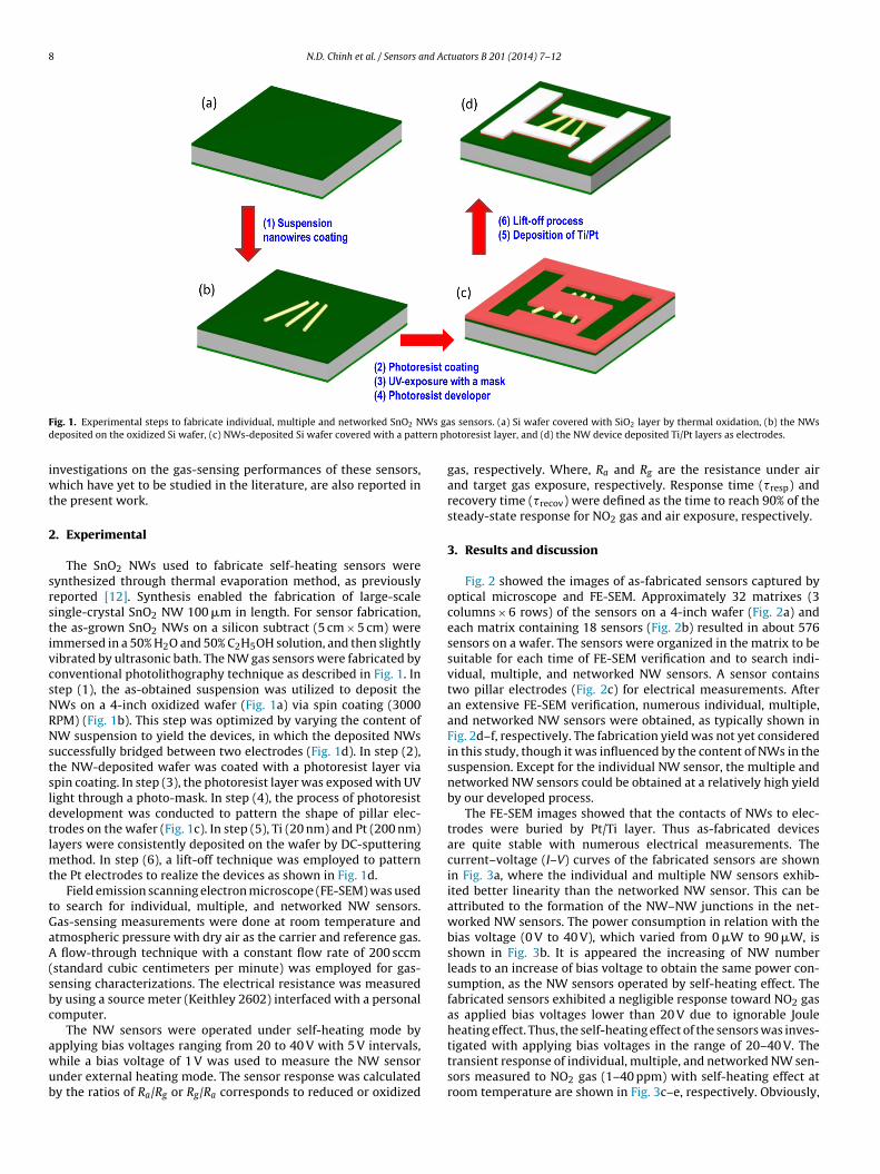
8 N.D. Chinh et al. / Sensors and Actuators B 201 (2014) 7–12
F Ws gad ern ph
iwt
2
srstivcsNRNstsldtlmt
tGaA(sbc
awub
ig. 1. Experimental steps to fabricate individual, multiple and networked SnO2 Neposited on the oxidized Si wafer, (c) NWs-deposited Si wafer covered with a patt
nvestigations on the gas-sensing performances of these sensors,hich have yet to be studied in the literature, are also reported in
he present work.
. Experimental
The SnO2 NWs used to fabricate self-heating sensors wereynthesized through thermal evaporation method, as previouslyeported [12]. Synthesis enabled the fabrication of large-scaleingle-crystal SnO2 NW 100 �m in length. For sensor fabrication,he as-grown SnO2 NWs on a silicon subtract (5 cm × 5 cm) weremmersed in a 50% H2O and 50% C2H5OH solution, and then slightlyibrated by ultrasonic bath. The NW gas sensors were fabricated byonventional photolithography technique as described in Fig. 1. Intep (1), the as-obtained suspension was utilized to deposit theWs on a 4-inch oxidized wafer (Fig. 1a) via spin coating (3000PM) (Fig. 1b). This step was optimized by varying the content ofW suspension to yield the devices, in which the deposited NWs
uccessfully bridged between two electrodes (Fig. 1d). In step (2),he NW-deposited wafer was coated with a photoresist layer viapin coating. In step (3), the photoresist layer was exposed with UVight through a photo-mask. In step (4), the process of photoresistevelopment was conducted to pattern the shape of pillar elec-rodes on the wafer (Fig. 1c). In step (5), Ti (20 nm) and Pt (200 nm)ayers were consistently deposited on the wafer by DC-sputtering
ethod. In step (6), a lift-off technique was employed to patternhe Pt electrodes to realize the devices as shown in Fig. 1d.
Field emission scanning electron microscope (FE-SEM) was usedo search for individual, multiple, and networked NW sensors.as-sensing measurements were done at room temperature andtmospheric pressure with dry air as the carrier and reference gas.
flow-through technique with a constant flow rate of 200 sccmstandard cubic centimeters per minute) was employed for gas-ensing characterizations. The electrical resistance was measuredy using a source meter (Keithley 2602) interfaced with a personalomputer.
The NW sensors were operated under self-heating mode by
pplying bias voltages ranging from 20 to 40 V with 5 V intervals,hile a bias voltage of 1 V was used to measure the NW sensornder external heating mode. The sensor response was calculatedy the ratios of Ra/Rg or Rg/Ra corresponds to reduced or oxidizeds sensors. (a) Si wafer covered with SiO2 layer by thermal oxidation, (b) the NWsotoresist layer, and (d) the NW device deposited Ti/Pt layers as electrodes.
gas, respectively. Where, Ra and Rg are the resistance under airand target gas exposure, respectively. Response time (�resp) andrecovery time (�recov) were defined as the time to reach 90% of thesteady-state response for NO2 gas and air exposure, respectively.
3. Results and discussion
Fig. 2 showed the images of as-fabricated sensors captured byoptical microscope and FE-SEM. Approximately 32 matrixes (3columns × 6 rows) of the sensors on a 4-inch wafer (Fig. 2a) andeach matrix containing 18 sensors (Fig. 2b) resulted in about 576sensors on a wafer. The sensors were organized in the matrix to besuitable for each time of FE-SEM verification and to search indi-vidual, multiple, and networked NW sensors. A sensor containstwo pillar electrodes (Fig. 2c) for electrical measurements. Afteran extensive FE-SEM verification, numerous individual, multiple,and networked NW sensors were obtained, as typically shown inFig. 2d–f, respectively. The fabrication yield was not yet consideredin this study, though it was influenced by the content of NWs in thesuspension. Except for the individual NW sensor, the multiple andnetworked NW sensors could be obtained at a relatively high yieldby our developed process.
The FE-SEM images showed that the contacts of NWs to elec-trodes were buried by Pt/Ti layer. Thus as-fabricated devicesare quite stable with numerous electrical measurements. Thecurrent–voltage (I–V) curves of the fabricated sensors are shownin Fig. 3a, where the individual and multiple NW sensors exhib-ited better linearity than the networked NW sensor. This can beattributed to the formation of the NW–NW junctions in the net-worked NW sensors. The power consumption in relation with thebias voltage (0 V to 40 V), which varied from 0 �W to 90 �W, isshown in Fig. 3b. It is appeared the increasing of NW numberleads to an increase of bias voltage to obtain the same power con-sumption, as the NW sensors operated by self-heating effect. Thefabricated sensors exhibited a negligible response toward NO2 gasas applied bias voltages lower than 20 V due to ignorable Jouleheating effect. Thus, the self-heating effect of the sensors was inves-
tigated with applying bias voltages in the range of 20–40 V. Thetransient response of individual, multiple, and networked NW sen-sors measured to NO2 gas (1–40 ppm) with self-heating effect atroom temperature are shown in Fig. 3c–e, respectively. Obviously,
N.D. Chinh et al. / Sensors and Actuators B 201 (2014) 7–12 9
F matr(
ttigvan(bowiiwaaooraTmN
ig. 2. Optical images of as-fabricated NW sensors on a 4-inch Si wafer (a), and (b) ac), individual (d), multiple (e), and networked (f) SnO2 NW sensors.
he resistance of the self-heating sensors increased upon exposureo NO2 gas, similar to that measured by external heating [13]. Thendividual NW gas sensor exhibited a better response toward NO2as compared with the other sensors. It can be seen that the indi-idual NW sensor could detect NO2 gas at a concentration as lows 1 ppm, whereas the multiple and networked NW sensors couldot. The response of the self-heated gas sensors toward NO2 gasRg/Ra) plotted as a function of bias voltages is shown in Fig. 3f. Theias voltage significantly influences the response of the three typesf sensors as similar as the operating temperature as measuredith external heating. It can be see that the gas response exhib-
ted a bell-shaped relation with bias voltages in the cases of thendividual and multiple NW sensors, similar to the previous report
ith external heating [13]. In the case of networked NW sensor, thepplied voltage of 40 V seemed insufficient to heat up the sensor ton optimized operating temperature because of the large numberf NWs crossing between the electrodes. The comparative responsef different sensors presented in Fig. 3f indicated that the optimalesponse of individual, multiple, and networked NW sensors was
chieved by applying bias voltages of 25, 30, and 40 V, respectively.his also means that the power consumption to achieve the opti-um response was increased with increasing the number of theWs contacted between electrodes.ix of 18 devices (3 columns × 6 rows). FE-SEM images of an overall one NWs device
Response as a function of NO2 gas concentration in the range of1–40 ppm is shown in Fig. 4a. Clearly, the response of the individualNW sensor was much higher than that of multiple and networkedNW sensors at optimized voltages. The response to 10 ppm NO2 ofthe individual NW sensor was almost 8.1 to be comparable to thatin the reported work [6], whereas the response of the multiple andnetworked NW sensors are about 2.7. As shown in Fig. 4b, the indi-vidual NW sensor had a shorter response and recovery times thanthat of the multiple and networked NW sensors despite the formerwas applied a lower bias voltage (25 V) compared to that (30 V and40 V) applied for the later. The theoretical calculation indicated thatif the NWs have the same diameter and resistances of R0 in airand R = R0 + �R in NO2, then the response is S = (R0 + �R)/R0 for allthe sensors. However, the measured data showed that the individ-ual NW sensor performs a better response compared with that ofthe other sensors. This can be explained based on the fact that themultiple and networked NW sensors were constructed with largerdiameter NWs compared with the NW constructed the individualNW sensor. This is agreed with a general concept of NWs-based
sensors that the reduced NW’s diameter results in an increasedgas response. Our previous work also done a proof of this conceptwith the individual SnO2 NW sensors toward NO2 gas [13]. Wewere verified the diameter of the NWs in the individual, multiple
10 N.D. Chinh et al. / Sensors and Actuators B 201 (2014) 7–12
F istics (( 25 to
aima
cvbvttfmbt
ig. 3. Gas-sensing characteristics operated under self-heating mode. I–V characterc), multiple (d) and networked (e) NW sensor with applying voltages ranging from
nd networked NW sensors. Accordingly, the diameter of the NWn the individual NW sensor was approximately 60 nm, while the
ultiple and networked NWs sensors included several NWs with diameter ranging from 100 nm to 200 nm.
The response and recovery times as a function of NO2 gasoncentration and bias voltage are shown in Fig. 4b. When the indi-idual, multiple, networked NW sensors respectively operated atias voltages of 25, 30, and 40 V (optimal bias voltages), the indi-idual NW sensor showed the shorter response and recovery timeshan the multiple and networked NWs sensors as measured withhe NO2 gas concentrations ranging from 1 to 40 ppm. It can also see
rom Fig. 4b that the response and recovery times of all the sensorseasured toward 10 ppm NO2 gas were increased with decreasingias voltages from 20 V to 40 V, as similar as decreasing operatingemperature [13].
a), power as a function of bias voltage (b), dynamic transient response of individual 40 V with interval 5 V, gas response as a function of bias voltage (f).
The selectivity of the self-heated individual NW sensor was alsoinvestigated and the result is shown in Fig. 4c. At applied a biasvoltage of 25 V, the response value to 200 ppm C2H3OH, CO, H2,H2S, and NH3 gases was negligible, while the response value to40 ppm NO2 was 21.3. As the bias voltage was increased to 40 V,the response values to the interference gases were lower than 1.5,while the response value to 40 ppm NO2 was 3.2. Therefore, theindividual NW sensor exhibits very good selectivity as operated byself-heating effect with a bias voltage of 25 V.
To compare the power consumption of the individual NW sen-sor operated by either self- or external heating, the temperature
of NWs elevated by self-heating should be measured at differentbias voltages. However, designing a thermo-couple to measure thetemperature profile of a NW by self-heating is very complicated.Thus, the gas response of the individual NW sensor operated by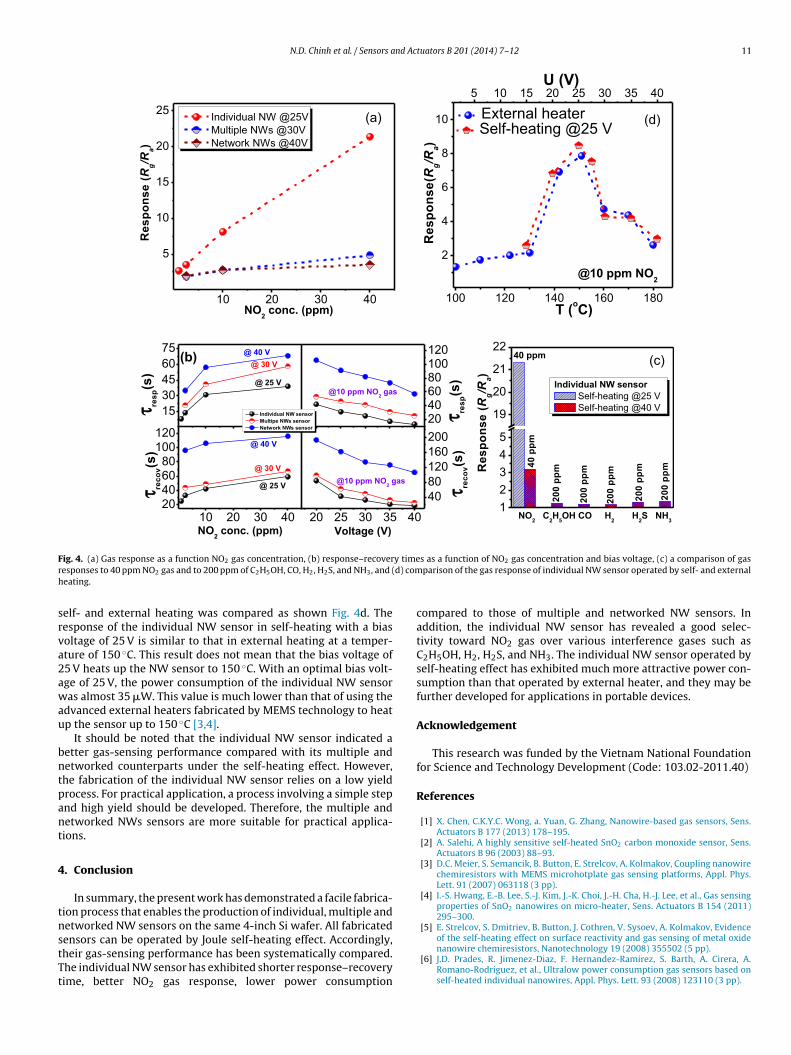
N.D. Chinh et al. / Sensors and Actuators B 201 (2014) 7–12 11
10 20 30 40
5
10
15
20
25
Re
sp
on
se
(Rg/R
a)
NO2 conc. (ppm)
Individual N W @ 25V
Multiple N Ws @ 30V
Network N Ws @ 40V
(a)
100 12 0 14 0 16 0 18 0
2
4
6
8
10 External heater
@10 p pm NO2
5 10 15 20 25 30 35 40
Re
sp
on
se
(Rg/R
a)
U (V)
T (oC)
Self-heating @25 V(d)
1
2
3
4
5
19
20
21
22
20
0 p
pm
20
0 p
pm
20
0 p
pm
20
0 p
pm
20
0 p
pm
40
pp
m
Re
sp
on
se
(Rg/R
a)
Individual NW se nsor
Self-heating @25 V
Self-heating @40 V
NO2 C
2H
5OH CO H
2 H
2S NH
3
40 ppm(c)
15
30
45
60
75
20406080100120
10 20 30 4020406080
100120
20 25 30 35 40
40
80
120
160
200
@ 25 V
@ 30 V
ττ res
p(s
)ττ re
co
v(s
)
ττ res
p(s
)
@ 40 V(b)
@10 ppm NO gas
@ 40 V
@ 30 V
@ 25 Vττ rec
ov(s
)
NO2 conc. (ppm)
Individual NW s ensor
Multipe NWs sensor
Network NWs sensor
@10 ppm NO gas
Voltage (V)
F y timer d) comh
srva2awau
bntpant
4
tnstTt
ig. 4. (a) Gas response as a function NO2 gas concentration, (b) response–recoveresponses to 40 ppm NO2 gas and to 200 ppm of C2H5OH, CO, H2, H2S, and NH3, and (eating.
elf- and external heating was compared as shown Fig. 4d. Theesponse of the individual NW sensor in self-heating with a biasoltage of 25 V is similar to that in external heating at a temper-ture of 150 ◦C. This result does not mean that the bias voltage of5 V heats up the NW sensor to 150 ◦C. With an optimal bias volt-ge of 25 V, the power consumption of the individual NW sensoras almost 35 �W. This value is much lower than that of using the
dvanced external heaters fabricated by MEMS technology to heatp the sensor up to 150 ◦C [3,4].
It should be noted that the individual NW sensor indicated aetter gas-sensing performance compared with its multiple andetworked counterparts under the self-heating effect. However,he fabrication of the individual NW sensor relies on a low yieldrocess. For practical application, a process involving a simple stepnd high yield should be developed. Therefore, the multiple andetworked NWs sensors are more suitable for practical applica-ions.
. Conclusion
In summary, the present work has demonstrated a facile fabrica-ion process that enables the production of individual, multiple andetworked NW sensors on the same 4-inch Si wafer. All fabricated
ensors can be operated by Joule self-heating effect. Accordingly,heir gas-sensing performance has been systematically compared.he individual NW sensor has exhibited shorter response–recoveryime, better NO2 gas response, lower power consumptions as a function of NO2 gas concentration and bias voltage, (c) a comparison of gasparison of the gas response of individual NW sensor operated by self- and external
compared to those of multiple and networked NW sensors. Inaddition, the individual NW sensor has revealed a good selec-tivity toward NO2 gas over various interference gases such asC2H5OH, H2, H2S, and NH3. The individual NW sensor operated byself-heating effect has exhibited much more attractive power con-sumption than that operated by external heater, and they may befurther developed for applications in portable devices.
Acknowledgement
This research was funded by the Vietnam National Foundationfor Science and Technology Development (Code: 103.02-2011.40)
References
[1] X. Chen, C.K.Y.C. Wong, a. Yuan, G. Zhang, Nanowire-based gas sensors, Sens.Actuators B 177 (2013) 178–195.
[2] A. Salehi, A highly sensitive self-heated SnO2 carbon monoxide sensor, Sens.Actuators B 96 (2003) 88–93.
[3] D.C. Meier, S. Semancik, B. Button, E. Strelcov, A. Kolmakov, Coupling nanowirechemiresistors with MEMS microhotplate gas sensing platforms, Appl. Phys.Lett. 91 (2007) 063118 (3 pp).
[4] I.-S. Hwang, E.-B. Lee, S.-J. Kim, J.-K. Choi, J.-H. Cha, H.-J. Lee, et al., Gas sensingproperties of SnO2 nanowires on micro-heater, Sens. Actuators B 154 (2011)295–300.
[5] E. Strelcov, S. Dmitriev, B. Button, J. Cothren, V. Sysoev, A. Kolmakov, Evidence
of the self-heating effect on surface reactivity and gas sensing of metal oxidenanowire chemiresistors, Nanotechnology 19 (2008) 355502 (5 pp).[6] J.D. Prades, R. Jimenez-Diaz, F. Hernandez-Ramirez, S. Barth, A. Cirera, A.Romano-Rodriguez, et al., Ultralow power consumption gas sensors based onself-heated individual nanowires, Appl. Phys. Lett. 93 (2008) 123110 (3 pp).
1 nd Ac
[
[
[
[
B
NTT
NT
2 N.D. Chinh et al. / Sensors a
[7] P. Offermans, H.D. Tong, C.J.M. van Rijn, P. Merken, S.H. Brongersma, M. Crego-Calama, Ultralow-power hydrogen sensing with single palladium nanowires,Appl. Phys. Lett. 94 (2009) 223110 (3 pp).
[8] F. Yang, D.K. Taggart, R.M. Penner, Joule heating a palladium nanowire sen-sor for accelerated response and recovery to hydrogen gas, Small 6 (2010)1422–1429.
[9] J.D. Prades, F. Hernández-Rami′rez, T. Fischer, M. Hoffmann, R. Müller, N. Lo′pez,et al., Quantitative analysis of CO-humidity gas mixtures with self-heatednanowires operated in pulsed mode, Appl. Phys. Lett. 97 (2010) 243105 (4 pp).
10] L.F. Zhu, J.C. She, J.Y. Luo, S.Z. Deng, J. Chen, X.W. Ji, et al., Self-heated hydrogengas sensors based on Pt-coated W18O49 nanowire networks with high sensitiv-ity, good selectivity and low power consumption, Sens. Actuators B 153 (2011)354–360.
11] J. Yun, C.Y. Jin, J.-H. Ahn, S. Jeon, I. Park, A self-heated silicon nanowire array:selective surface modification with catalytic nanoparticles by nanoscale Jouleheating and its gas sensing applications, Nanoscale 5 (2013) 6851–6856.
12] N.V. Hieu, L.T.N. Loan, N.D. Khoang, N.T. Minh, D.T. Viet, D.C. Minh, et al., A facilethermal evaporation route for large-area synthesis of tin oxide nanowires:characterizations and their use for liquid petroleum gas sensor, Curr. Appl.Phys. 10 (2010) 636–641.
13] M. Tonezzer, N.V. Hieu, Size-dependent response of single-nanowire gas sen-sors, Sens. Actuators B 163 (2012) 146–152.
iographies
guyen Duc Chinh received his MSc degree in Materials Science at International
raining Institute for Material Science (ITIMS), Hanoi University of Science andechnology (HUST), in Vietnam in 2014. He is working as researcher at the ITIMS.guyen Van Toan received his MSc degree in Materials Science at Internationalraining Institute for Material Science (ITIMS), Hanoi University of Science and
tuators B 201 (2014) 7–12
Technology (HUST), in Vietnam in 2011. He is currently pursuing his PhD degreeat the ITIMS, where he is working on metal oxides-based gas sensors.
Vu Van Quang joined the International Institute for Material Sciences (ITIMS) atHanoi University of Science and Technology (HUST) as a researcher and lecturerin 2010. He received his Master degree from University of Paris 11, France in2005, and PhD degree from University of Wales, Aberystwyth, United Kingdomin 2008. Then he moved to Max-Planck Institute for Metals Research, Stuttgart,Germany to do his post-doctoral work until Jun 2010. His current research interestsinclude synthesis and application of graphene for electronic devices, gas sensors andbiosensors.
Nguyen Van Duy is currently working as a research lecture at International TrainingInstitute for Material Science (ITIMS), Hanoi University of Science and Technology(HUST). He received PhD degree from the Department of Electrical and Electron-ics Engineering at Sungkyunkwan University, South Korea, in 2011. His currentresearch interests include nanomaterials, nanofabrications, characterizations, andapplications to electronic devices, gas sensors, and biosensors.
Nguyen Duc Hoa obtained his PhD degree in materials science and engineering in2009 at Chungnam National University in Korea. He awarded JSPS fellowship andconducted the research at National Institute for Materials Science (NIMS, Japan) from2009 to 2011. His research activity covers a wide range of nanostructured materialsfrom synthesis to fundamental, and applications. He is the author of several dozensof scientific articles published in reputed journals. Currently, he is a lecturer andscientist at Hanoi University of Science and Technology, Vietnam.
Nguyen Van Hieu joined the International Training Institute for Material Science
(ITIMS) at Hanoi University of Science and Technology (HUST) in 2004, where he iscurrently associate professor. He received his PhD degree from the Faculty of Elec-trical Engineering at University of Twente in The Netherlands in 2004. He workedas a post-doctoral fellow at the Korea University from 2006 to 2007. His currentresearch interests include functional nanostructures, gas sensors, and biosensors.