comparability of txrf systems at different laboratories
TRANSCRIPT

Comparability of TXRF Systems at Different Laboratories
A. Nutscha, B. Beckhoffc, R. Altmanna, M. L. Polignanob, E. Cazzinib, D. Codegonib, G. Borionettid, M. Kolbec, M. Müllerc, C. Mantlere, C. Strelif, P. Kregsamerf
a Fraunhofer IISB, Schottkystrasse 10, 91058 Erlangen, Germany
b Numonyx, Via Olivetti, 2, 20041 Agrate Brianza (MB), Italy c Physikalisch-Technische Bundesanstalt, Abbestrasse 2-12, 10587 Berlin, Germany
d MEMC Electronic Materials SpA, Viale Gherzi,31 28100 Novara, Italy e Siltronic AG, Berthelsdorfer Str. 113, 09599 Freiberg, Germany
f Atominstitut, Vienna Universtiy of Technology, Stadionallee 2, 1020 Wien, Austria
The ‘Analytical Network for Nanotech’ is a European analytical infrastructure supporting the development of micro- and nano-technologies. Analytical capabilities of the joint laboratory for inorganic contaminations are Total-Reflection X-Ray Fluorescence using Synchrotron Radiation or X-ray tubes, Vapor Phase Decomposition and subsequent Graphite Furnace Atomic Absorption Spectroscopy or Inductively Coupled Plasma Mass Spectrometry, and Time of Flight Secondary Ion Mass Spectrometry. Discrepancies of results from different tools using TXRF for detection of metal contamination on silicon wafer surfaces were observed during various round robin tests using spin coated silicon wafers and deposited point like contamination. The targeted contaminations of the samples were validated using GF-AAS and ICPMS. The impact of the (reference) sample used for calibration on the quantification of the measurement was confirmed. Furthermore, measurement geometries and the angle of incidence are crucial for the comparability of the results of the TXRF systems.
Introduction
The ‘Analytical Network for Nanotech’ is a European analytical infrastructure
supporting the development of micro- and nano-technologies. High quality research requires comparability of results when analytical methodologies are supplied by different sources. This is a requirement of quality controlled industries, too. Inorganic contamination capabilities of the analytical infrastructure are Total-Reflection X-Ray Fluorescence (TXRF) using Synchrotron Radiation (SR) or X-ray tubes, Vapor Phase Decomposition (VPD) and subsequent Graphite Furnace Atomic Absorption Spectroscopy (GF-AAS) or Inductively Coupled Plasma Mass Spectrometry (ICPMS), and Time of Flight Secondary Ion Mass Spectrometry (ToF-SIMS). Recently, discrepancies of results from different tools using TXRF for detection of metal contamination on silicon wafer surfaces were reported [1, 2]. The present work compares different tools and shows the results of round robins using different reference samples. The results were validated using GF-AAS and ICPMS.
TXRF Systems of the Analytical Infrastructure
ECS Transactions, 25 (3) 325-335 (2009)10.1149/1.3204423 © The Electrochemical Society
325Downloaded 28 Sep 2009 to 57.77.12.23. Redistribution subject to ECS license or copyright; see http://www.ecsdl.org/terms_use.jsp

The TXRF systems available within the ANNA infrastructure have different excitation sources and system geometries for acquisition of the spectra. The TXRF system at PTB uses synchrotron radiation in ‘soft’ X –ray energy region (below 2 keV). The TXRF systems at Atominstitut, IISB, and the industrial partners of ANNA use ‘hard’ X -rays (2 keV-30 keV). The TXRF at PTB operates reference-free [3], whereas the other sytems use reference samples and different procedures for calibrattion. The reference samples are supplied with the system. The systems at Atominstitut and IISB are from the same supplier. The TXRF systems of PTB, IISB and Atominstitut which are part of the infrastructure are described in detail in the following.
PTB Laboratory BESSY II
The Physikalisch-Technische Bundesanstalt (PTB), Germany’s national metrology
institute, operates its own laboratory with several well-characterized beamlines for monochromatized synchrotron radiation at the 1.7 GeV electron storage ring BESSY II (4). For reference-free X-ray spectrometry two of these beam lines in different energy ranges can be used. On the one hand a plane grating monochromator (PGM) beam line for undulator radiation providing monochromatic synchrotron radiation between 78 eV and 1860 eV, and on the other hand a four-crystal monochromator (FCM) for bending magnet radiation, serve as excitation sources.
One of the main purposes of the PTB laboratory is radiometry with synchrotron
radiation allowing for the calibration of the absolute efficiency of photodiodes as well as energy-dispersive detectors. Furthermore, the reduction of the stored electron beam current of BESSY makes the direct measurement of monochromatized synchrotron radiation possible and allows for the determination of the response behaviour of energy dispersive detectors (5,6).
For X-ray spectrometry investigations this calibrated equipment is in use allowing for
the absolute determination of all relevant experimental values and in succession a reference-free evaluation of the data (3, 7, 8).
TXRF@ Fraunhofer IISB
The TXRF system at Fraunhofer IISB is installed in a clean room facility. This fulfills
the requirements of the semiconductor industry. The system performs simultaneous multi-element ultra trace analytical tasks on surfaces of wafers with diameters up to 300 mm. The TXRF system at Fraunhofer IISB uses X-ray tubes with tungsten or molybdenum targets. For excitation of the fluorescence of surface contaminations the system uses the W Lβ and the Mo Kα lines. The spectra are acquired below the critical angle of the matrix material, which is usually the (100) Si surface. Therefore, the fluorescence signal of the substrate as a function of the incident angle is measured and used for determination of the critical angle as a reference angle (9, 10). For purpose of quality control the Si signal at the measurement angle and the Ni calibration signal are monitored and checked.
TXRF at IISB is used for contamination control and process optimization. Wafers are
handled through equipment and process media and analyzed afterwards. The ‘direct’ TXRF on a surface allows localized, particle-free, and non-destructive in-line
ECS Transactions, 25 (3) 325-335 (2009)
326Downloaded 28 Sep 2009 to 57.77.12.23. Redistribution subject to ECS license or copyright; see http://www.ecsdl.org/terms_use.jsp

measurements of silicon surface contamination. Vapor phase decomposition enhances the TXRF analysis allowing the highly sensitive ultra trace analysis of the whole wafer surface contamination. VPD concentrates the surface contamination to a single spot. For example using VPD for wafers with a large diameter reduces the limit of detection of TXRF to 1×10⁸ atoms/cm2 (11). In this process HF gas reacts with the oxide on the wafer surface. A scanner collects the remaining water droplets containing the surface contamination. For TXRF analysis, the collected droplets are deposited on a silicon wafer, dried, and analyzed.
X – Ray Laboratory @ Atominstitut
The TXRF system at Atominstitut is installed inside a mini clean room environment
fulfilling ISO class 4 conditions. The system performs simultaneous multi-element ultra trace analytical tasks on surfaces of wafers with diameters up to 200 mm. The TXRF system at Atominstitut uses an X-ray tube with molybdenum target, monochromatized to Mo Kα for excitation of the fluorescence of surface contaminations. The spectra are acquired below the critical angle of the matrix material. The fluorescence signal of the substrate as a function of the incident angle is measured and used for determination of the critical angle as a reference angle. For purpose of quality control the Si signal at the measurement angle and the Ni calibration signal are monitored and checked. TXRF at Atominstitut is used for contamination control.
Preparation and Analysis of Reference Samples
Reference samples for comparison and benchmarking of the analytical instrument-
tation available within the network were prepared. For the experiments silicon wafers with a diameter of 200 mm and (100) oriented were used. Two types of contaminations on the silicon surface were studied. Certified metal standard solutions for ICPMS or AAS were used. Spin coating of metal standard solution was used to contaminate the wafer front side as set of reference samples. Additionally, deposition of droplets with specific volume at defined coordinate positions on the wafer surface was performed on another set of wafers. Both methods for preparation are described in the following including the validation of the deposited amount of contamination.
Spin coated samples
A set of 96 wafers with a diameter of 200 mm, <100> oriented and boron doped,
were manufactured in the same lot. Prior to the intended and controlled contamination of these wafers by a spin-coating technique, VPD-ICPMS surface metal analyses were performed. This inspection confirms that all metals were below a level of 1×10⁹ atoms/cm2 with the exception of Al whose residual surface content was of 1×10¹⁰ atoms/cm2. This ensures that the intended metal contamination is well above the level of the blank contamination.
In the spin coating process a solution was used to contaminate the silicon wafer
surface with metals. Therefore, solutions using the elements Al, Na, Cu, Fe, Mo, Ni, and Ti in diluted acid were prepared. Dilutions of these solution were used to adjust the targeted contamination levels of 1×10¹⁰ atoms/cm2, 1×10¹¹ atoms/cm2, and 1×10¹² atoms/cm2 for Cu, Fe, Mo, Ni, Ti. For the low Z elements Al and Na the levels were
ECS Transactions, 25 (3) 325-335 (2009)
327Downloaded 28 Sep 2009 to 57.77.12.23. Redistribution subject to ECS license or copyright; see http://www.ecsdl.org/terms_use.jsp

adjusted to 1×10¹¹ atoms/cm2, 1×10¹² atoms/cm2, and 1×10¹³ atoms/cm2. The diluted solutions were checked by AAS with respect to contamination levels. Spin coated wafers were prepared in the following way:
- cleaning and drying of the wafer front side - covering the surface with the contaminated solution - spin dry the wafer
The set of wafers was prepared in one run to guarantee a reproducible level of contamination. The achieved levels of contamination by spin coating were checked by VPD AAS and by non – destructive, ‘direct’ TXRF. Two wafers of each contamination level were randomly chosen from the fabricated samples. During VPD the surface oxide was decomposed by HF vapor and the surface contamination was collected using a droplet scanner. The droplet was analyzed by GF-AAS. Assuming that the recovery rate for all elements on the wafer surface was 100 % the results plotted in Figure 1 are in good agreement with the targeted contamination. The results were confirmed by a second laboratory using VPD ICPMS.
Figure 1. GF AAS analysis results of the spin coated wafers. Additionally the limit of detection for Ni, Mo, and Ti is shown.
VPD is a method that depends on the collection efficiency of the droplet for each specific element. Furthermore, VPD is not sensitive to local deviations from spatial uniformity of contaminations on the wafer surface. As a consequence direct TXRF was used to check the level and uniformity of the spin coated contamination. For the excitation the WLβ line was used. Radial scans using 5 points from center to edge and mappings using 16 points were performed. The radial results are shown in figure 2 for Ti, Fe, Cu and Zn. The contamination level in the center is higher compared to the edge probably due to the spin coating process. The radial uniformity was 25% and the standard deviation from sample to sample was found to be better than 10%. Generally, the level of contamination determined by TXRF is twice as high as level determined by VPD AAS. For low
0,1
1,0
10,0
100,0
1000,0
10000,0
Na Fe Al Cu Ni Mo Ti Zn
Element
Surf
ace
Con
cent
ratio
n [*
1 E1
0 at
oms/
cm²]
LOD SL 25SL 22 SL 21SL 18 SL 17SL 13 SL 12
ECS Transactions, 25 (3) 325-335 (2009)
328Downloaded 28 Sep 2009 to 57.77.12.23. Redistribution subject to ECS license or copyright; see http://www.ecsdl.org/terms_use.jsp

contamination levels especially for Fe the impact of the blind value caused by the contamination of the detector window gets visible. For Ti the measurement of the lowest level was close to the limit of detection.
1
10
100
1000
0 10 20 30 40 50 60 70 80 90 100x [mm]
Con
tam
inat
ion
[1E1
0 at
oms/
cm²]
Slot 10 Slot 11 Slot 12Slot 22a Slot 13 Slot 14Slot 15 Slot 16 Slot 17Slot 17a Slot 18 Slot 19Slot 20 Slot 21 Slot 22Slot 23 Slot 24 Slot 21a
Ti excitation WLb 50 kV/55mAacqusition time 1000sangle of incidence2.3 mradcalibration 1 ng Ni
1
10
100
1000
0 10 20 30 40 50 60 70 80 90 100x [mm]
Con
tam
inat
ion
[1E1
0 at
oms/
cm²]
Slot 10 Slot 11 Slot 12Slot 22a Slot 13 Slot 14Slot 15 Slot 16 Slot 17Slot 17a Slot 18 Slot 19Slot 20 Slot 21 Slot 22Slot 23 Slot 24 Slot 21a
Fe excitation WLb 50 kV/55mAacqusition time 1000sangle of incidence2.3 mradcalibration 1 ng Ni
1
10
100
1000
0 10 20 30 40 50 60 70 80 90 100x [mm]
Con
tam
inat
ion
[1E1
0 at
oms/
cm²]
Slot 10 Slot 11 Slot 12Slot 22a Slot 13 Slot 14Slot 15 Slot 16 Slot 17Slot 17a Slot 18 Slot 19Slot 20 Slot 21 Slot 22Slot 23 Slot 24 Slot 21a
Cu excitation WLb 50 kV/55mAacqusition time 1000sangle of incidence2.3 mradcalibration 1 ng Ni
1
10
100
1000
0 10 20 30 40 50 60 70 80 90 100x [mm]
Con
tam
inat
ion
[1E1
0 at
oms/
cm²]
Slot 10 Slot 11 Slot 12Slot 22a Slot 13 Slot 14Slot 15 Slot 16 Slot 17Slot 17a Slot 18 Slot 19Slot 20 Slot 21 Slot 22Slot 23 Slot 24 Slot 21a
Zn excitation WLb 50 kV/55mAacqusition time 1000sangle of incidence2.3 mradcalibration 1 ng Ni
targeted 1×10¹¹ atoms/cm2
targeted 1×10¹⁰ atoms/cm2
targeted 1×10¹² atoms/cm2
Figure 2. The plots show the radial uniformity of the spin coated wafers for Ti, Fe, Cu, and Zn determined by TXRF with WLβ excitation.
In summary the analysis of the spin coated samples showed a good reproducibility
from sample to sample and a tolerable spatial uniformity of the contamination level on the wafer surface. Therefore, the prepared samples are ideal candidates to compare and benchmark different TXRF systems.
Deposition of droplets with contamination
The idea of deposition of a droplet containing the contamination is to precisely
control the amount of the element within the droplet. For this purpose a solution with multi element or single element is prepared and the concentration of the contaminants is controlled by GF-AAS. A certified pipette was used to adjust the volume of the droplet deposited on the wafer surface. With this method the deposited amount of the elements can be calculated by the measured concentration of contaminants in the solution and the volume. After deposition on the surface of the wafers, the droplets were dried. The subsequent analysis was performed using an optical microscope and TXRF.
Figure 3 shows both the results from the optical microscope and the determined
amount of deposited Ni. The size of the dried droplet residues was found to be 580 µm in
ECS Transactions, 25 (3) 325-335 (2009)
329Downloaded 28 Sep 2009 to 57.77.12.23. Redistribution subject to ECS license or copyright; see http://www.ecsdl.org/terms_use.jsp

diameter. It is obvious from figure 3 that the morphology, shape and size of the droplets were not reproducible. The achieved average amount of the deposited droplets was 965 pg +/- 110 pg determined by TXRF whereas the deposition of 1000 pg was confirmed by measurement of the concentration using AAS. The results show that only half of the deposited droplets achieve the targeted deposition of 1000 pg of Ni using TXRF for quantification. Therefore, droplets have to be carefully checked by TXRF prior to the use as reference samples. Currently, the deviation of some droplets from the adjusted targets can not be explained.
Target 1000 pg Ni
0
200
400
600
800
1000
1200
0 1 2 3 4 5 6 7 8 9 10Measurement No.
Ni i
n [p
g]
Droplet
Figure 3. The figure shows images of the optical microscope and the according amounts of Ni determined with TXRF for eight droplets deposited on a silicon wafer surface.
Results of the Round Robin
Currently, two round robins were performed within the ANNA network. The first
used the spin coated wafers and the second used deposited and dried Ni droplets. In total 5 TXRF systems within the ANNA network were involved measuring the samples described above.
Spin Coated Wafers: Ni and Cu
For shipment, the samples were packed in boxes and those boxes were protected by
double layered separately sealed polyurethane foils. At the laboratories of the ANNA network the samples were measured using the TXRF systems. Additionally, some of the spin coated wafers were analyzed by TOF SIMS, VPD AAS, and VPD ICPMS to validate the results. In the following the results for Ni and the noble metal Cu are discussed. Ni is of special interest as this is often used for calibration of TXRF systems.
Figure 4 summarizes the result of the round robin for the spin coated samples. The
charts for Cu and Ni show all available data from mapping single point measurements and different samples at all laboratories. This explains the different variation of data points for each laboratory as different number of points and different locations on the wafers were measured. It is obvious that the quantification in the laboratories 2 and 3 is lower than in the laboratories 1, 4, 5. The laboratories 1, 4, 5 show higher contamination
ECS Transactions, 25 (3) 325-335 (2009)
330Downloaded 28 Sep 2009 to 57.77.12.23. Redistribution subject to ECS license or copyright; see http://www.ecsdl.org/terms_use.jsp

levels for Ni and Cu compared to VPD AAS and VPD ICPMS analysis. The matching of results within laboratory 3 in-between TOFSIMS and TXRF is good and the results are comparable to the TXRF results of laboratory 2. The results of TXRF systems of laboratory 1 and 4 are comparable as the supplier for both systems was identical. Those results are comparable to laboratory 5. The TXRF systems of laboratory 2 and 3 show an order of magnitude lower quantified amount of the contamination on the spin coated wafer surface.
The analysis results of laboratory 2 show for Cu a discrepancy to the other results.
The results from VPD ICPMS matches with the results from the TXRF system of the laboratory. But the level of both results differ from the level determined for Ni. This can be explained as follows: The quantification of Cu using VPD depends on the recovery rate of Cu on the silicon surface. And the recovery rate of Cu depends strongly on the composition of the scan solution.
Ni (
*1E
10at
oms/
cm²)
0
100
200
300
400
Lab_
1
Lab_
2
Lab_
3
Lab_
1
Lab_
2
Lab_
3
Lab_
4
Lab_
5
AA
S (V
PD
)
ICP
MS
(VP
D)
TOFS
IMS
TXR
F
Cu
(*1E
10at
oms/
cm²)
0
100
200
300
400
Lab_
1
Lab_
2
Lab_
3
Lab_
1
Lab_
2
Lab_
3
Lab_
4
Lab_
5
AA
S (V
PD
)
ICP
MS
(VP
D)
TOFS
IMS
TXR
F
Figure 4. Comparison of quantification results for Ni and Cu of the different laboratories using TXRF and other analytical methods for validation of results.
For cross check of the analytical systems of laboratory 2 with laboratory 1 the
calibration wafer of laboratory 2 was measured at laboratory 1. The reference sample was a Ni spin coated wafer. The specification of the wafer was 3.9×10¹¹ atoms/cm2. The quantification of laboratory 1 results in 38×1011 atoms/cm2 at the center. This cross check of a calibration sample of the laboratories in one of the other laboratories confirms differences in calibration.
Single Element Droplets: Nickel
The samples used for this round robin were prepared outside the network by Claus
Mantler from Siltronic AG in 2008 and by the suppliers of the TXRF systems in 1998. The Ni droplets and the Mn droplet of targeted 1 ng on a wafer substrate were shipped in contamination free packages in-between the partners. This procedure guarantees that the measured sample is the same for each TXRF. The samples from the supplier of TXRF systems are usually used for calibration purposes of the TXRF systems.
Figure 5 shows the result of the round robin using the 3 described samples. For a
sufficiently large detector area e.g. 0.5 cm2 the 1 ng Ni should result in a surface
ECS Transactions, 25 (3) 325-335 (2009)
331Downloaded 28 Sep 2009 to 57.77.12.23. Redistribution subject to ECS license or copyright; see http://www.ecsdl.org/terms_use.jsp

concentration of 2000 ×1010 atoms/cm2. This result was only obtained by laboratory 5 for the sample produced in 2008. The laboratories 1 and 4 achieved higher quantification levels. For laboratory 3 and 2 the quantification results are approximately an order of magnitude lower for all three samples. Laboratory 1 and 4 achieved comparable results for the reference samples produced by the supplier in 1998.
100 1000 10000
Ni (1998)
Mn (1998)
Ni (2008) Ref
Ni [1E10 atoms/cm²]
Lab 4Lab 3Lab 2Reihe2Lab 5Lab 4Lab 3Lab 2Lab 1
100 1000 10000
Ni (1998)
Mn (1998)
Ni (2008) Ref
Ni [1E10 atoms/cm²]
Lab 4Lab 3Lab 2Reihe2Lab 5Lab 4Lab 3Lab 2Lab 1
Figure 5. Comparison of TXRF results from different laboratories using three different
reference samples. The use of one set of samples provided by both, instrument manufacturers and
analytical facilities of a wafer manufacturer, for the round robin substantiates the above described results obtained on spin coated wafers.
Discussion
Beside the differences in calibration other effects are expected to be responsible for
differences in the quantification using TXRF (12). This will be discussed in the following. There is the difference between the VPD technique and the direct TXRF
measurement. One can argue that the VPD technique integrates the non-uniformity of the spin coated samples whereas direct TXRF as a spot measurement shows local contamination and is therefore sensitive to non-uniformities of the spin coated samples. Nevertheless, the quantification result of TXRF is higher than that of VPD GF-AAS or ICPMS. An argument can be that the VPD collection efficiency is non – reliable. But this is more often observed for noble metals whereas for example Ni is expected not to be critical. Another issue is the calibration of the TXRF system which is performed with either spin coated samples or dried droplets. Furthermore, the achieved signal levels for each contamination or calibration type strongly depend on the measurement angle and the morphology. Therefore, the calibration, the procedure of measurement and quantification are expected to strongly impact the quantification result.
For checking traceability and linearity of the TXRF measurement droplet samples
with different amount of contaminants either single element or multi element are used. The amount of the metal inside the droplet residue is adjusted by dilution and checked with concentration measurement using ICPMS or AAS. Figure 6 shows the TXRF
ECS Transactions, 25 (3) 325-335 (2009)
332Downloaded 28 Sep 2009 to 57.77.12.23. Redistribution subject to ECS license or copyright; see http://www.ecsdl.org/terms_use.jsp
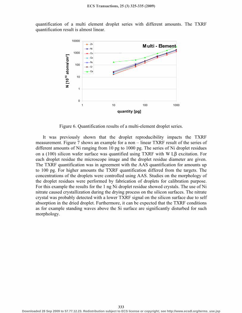
quantification of a multi element droplet series with different amounts. The TXRF quantification result is almost linear.
Multi - Element
0
1
10
100
1000
10000
1 10 100 1000
quantity [pg]
N [1
010 a
tom
s/cm
²]
Zn
Ni
Cu
Co
Fe
Cr
Ca
36389013WAC5t = 1000 sj = 2.3 mradExcitation: WLb19.03.2008
Figure 6. Quantification results of a multi-element droplet series. It was previously shown that the droplet reproducibility impacts the TXRF
measurement. Figure 7 shows an example for a non – linear TXRF result of the series of different amounts of Ni ranging from 10 pg to 1000 pg. The series of Ni droplet residues on a (100) silicon wafer surface was quantified using TXRF with W Lβ excitation. For each droplet residue the microscope image and the droplet residue diameter are given. The TXRF quantification was in agreement with the AAS quantification for amounts up to 100 pg. For higher amounts the TXRF quantification differed from the targets. The concentrations of the droplets were controlled using AAS. Studies on the morphology of the droplet residues were performed by fabrication of droplets for calibration purpose. For this example the results for the 1 ng Ni droplet residue showed crystals. The use of Ni nitrate caused crystallization during the drying process on the silicon surfaces. The nitrate crystal was probably detected with a lower TXRF signal on the silicon surface due to self absorption in the dried droplet. Furthermore, it can be expected that the TXRF conditions as for example standing waves above the Si surface are significantly disturbed for such morphology.
ECS Transactions, 25 (3) 325-335 (2009)
333Downloaded 28 Sep 2009 to 57.77.12.23. Redistribution subject to ECS license or copyright; see http://www.ecsdl.org/terms_use.jsp

Ni
0
500
1000
1500
0 500 1000 1500Measured in [pg]
Targ
et in
[pg]
D = 573 µm
D = 475 µm
D = 423 µm
D = 90 µm
D = 78 µm
D = 115 µm
Target [pg]
Mes
ured
[pg]
Ni
0
500
1000
1500
0 500 1000 1500Measured in [pg]
Targ
et in
[pg]
D = 573 µm
D = 475 µm
D = 423 µm
D = 90 µm
D = 78 µm
D = 115 µm
Target [pg]
Mes
ured
[pg]
D = 573 µm
D = 475 µm
D = 423 µm
D = 90 µm
D = 78 µm
D = 115 µm
Target [pg]
Mes
ured
[pg]
Figure 7. The plot shows the measured amount as a function of the target amount for a series of TXRF measurements using W Lβ excitation. For each droplet residue the microscope image and the droplet residue diameter are given.
Conclusion
Discrepancies of results from different tools using TXRF for detection of metal
contamination on silicon wafer surfaces were observed during various round robin tests using spin coated silicon wafers and deposited point like contaminations. The results were validated using GF-AAS and ICPMS. The impact of the (reference) sample used for calibration on the evaluated measurement was confirmed. For spin coated samples discrepancies between direct TXRF and VPD were observed. Those can be explained by non uniformity of the spin coating process and the measurement conditions as the measurement angle. Furthermore, deviations could be explained by different calibrations of the TXRF systems.
The droplet residues with 1 ng Ni were found to result in non reproducible quantification results due to morphology of the droplet. Reproducible results were obtained with droplets having smaller amounts of Ni. Furthermore, such samples are comparable to the analytical task of detection of concentrations below 1×10¹¹ atoms/cm2. Furthermore, measurement geometries as detector area and the angle of incidence are crucial for the comparability of the results of the TXRF systems.
Acknowledgement
This work was partially supported by the European Commission under the FP6
Program through the Integrated Infrastructure Initiative “ANNA” contract n. 026134-RII3.
ECS Transactions, 25 (3) 325-335 (2009)
334Downloaded 28 Sep 2009 to 57.77.12.23. Redistribution subject to ECS license or copyright; see http://www.ecsdl.org/terms_use.jsp

References
1. A. Nutsch et al., Solid State Phenomena 145-146, 97-100 (2009) 2. B. Beckhoff et al., Solid State Phenomena 145-146, 101-104 (2009) 3. B. Beckhoff, R. Fliegauf, M. Kolbe, M.Müller, J. Weser, and G. Ulm, Anal.
Chem., 79, 7873-7882 (2007) 4. G. Ulm, Metrologia, 2003, 40, S101. 5. F. Scholze and M. Procop, X-ray Spectrom., 2009, DOI:10.1002/xrs.1165 6. M. Krumrey, M. Gerlach, F. Scholze and G. Ulm, Nucl. Instrum. Methods, Sect.
A, 2006, 568, 364. 7. B. Beckhoff, M. Kolbe, O. Hahn, A. G. Karydas, Ch. Zarkadas, D. Sokaras, M.
Mantler, X-Ray Spectr. (2008) 37, 462-465 8. B. Beckhoff, J. Anal. At. Spectrom. (2008) 23, 845 - 8531 9. W. Berneike, Spectrochimica Acta B 48 2 (1993), 269-275 10. S. Pahlke, L. Fabry, L. Kotz, C. Mantler, T. Ehmann, Spectrochimica Acta B 56
(2001), 2261 - 2274 11. R. Klockenkämper, Spectrochimica Acta B 61 (2006) 1082-1090 12. I. Rink, P. Rostam-Khani, J. Knoth, H. Schwenke, S. de Gendt, R. Wortelboer
Spectrochimica Acta B 56 (2001) 2283-2292
ECS Transactions, 25 (3) 325-335 (2009)
335Downloaded 28 Sep 2009 to 57.77.12.23. Redistribution subject to ECS license or copyright; see http://www.ecsdl.org/terms_use.jsp