chapter 3 diodes
TRANSCRIPT

1
Prof. Sang-Jo Yoo
Chapter 3 Diodes
2
Prof. Sang-Jo Yoo
Contents
Ideal Diode
Terminal Characteristics of Junction Diodes
Physical Operation of Diodes
Analysis of Diode Circuits
Small-signal Model and its Application
Operation in the Reverse Breakdown Region-Zener Diodes
Rectifier Circuits
Limiting and Clamping Circuits

3
Prof. Sang-Jo Yoo
Introduction
The simplest and most fundamental nonlinear circuit element is the diode. It is a two terminal device like a resistor but the two terminals are not interchangeable.
We will start by describing an “ideal” diode and then look at how closely a real diode approximates the ideal situation.
One of the most common uses of diode is in rectifier circuits(conversion of ac signals to dc).
4
Prof. Sang-Jo Yoo
3.1 The Ideal Diode
The quantity VA is referred to as the Applied voltage.
The i-v characteristic for the ideal diode passes no current when the applied voltage is negative, and when the applied voltage is positive the diode is a perfect short circuit (zero resistance).
p n
−+ Av
anode cathode
i
i
Av
Forward BiasReverse Bias
Reverse Bias Circuit Model Forward Bias Circuit Model
00 =⇒< ivA
i −+ Av
00 =⇒> Avi
i −+ Av
“Cut off” “ON”The external circuit must limit the currentunder Forward Bias conditions since thediode will have no resistance

5
Prof. Sang-Jo Yoo
The diode is polarity dependent!
Forward Bias Current Limit Example(resistor limits the current)
Ωk1
V10+
Ωk1
V10+
Ωk1
−
+V0
V10+
−
+V10 Ωk1
−
+V10
V10+
−
+V0
Short circuit Open circuit
Reverse Bias Current Limit Example(diode, in cut off, limits the current)
mA1
mA0PN
NP
6
Prof. Sang-Jo Yoo
A Simple Application: The Rectifier
−
+
OvDi
−+ Dv
Iv R
IvPv
t
−=
+
IO vvDi
−=+ 0Dv
Iv R−
=+
0Ov0=Di
−=+ ID vv
Iv R
OvPv
t
The negative half-cycleis blocked
The positive half-cycleis transmitted

7
Prof. Sang-Jo Yoo
Battery Charger Rectification Example
Example 3.1 The circuit below is used to charge a 12V battery, where vS is a sinusoid with a 24V peak amplitude. Find the fraction of each cycle during which the diode conducts, also find the peak value of the diode current and the maximum reverse-bias voltage that appears across the diode.
−
+V12
Di
Sv
Ω= 100R
( )cycle theof thirdoneor 1202
605.0cos 1
o
o
=
== −
θ
θ
AVV
I Pd 12.0
100
1224=
Ω−
= VVVV Pd 362412max =−−+=
t
V12V24
θ212cos24 =θ
Di
Sv
Di
V24−
maxdV
8
Prof. Sang-Jo Yoo
Another Application: Diode Logic Gates
Diodes and resistors can be used to implement digital logic functions : 0V is a Low and +5V is a high
R
Av
Bv
Cv Qv
Av Bv Cv Qv
0 0 0 00 0 5 50 5 0 50 5 5 55 0 0 55 0 5 55 5 0 55 5 5 5
Inputs OutputOR Gate
R
Av
Bv
Cv
Qv
V5+Av Bv Cv Qv
0 0 0 00 0 5 00 5 0 00 5 5 05 0 0 05 0 5 05 5 0 05 5 5 5
Inputs Output
AND Gate

9
Prof. Sang-Jo Yoo
Simple DC Analysis of Ideal Diode CircuitsHow do we know which diodes are conducting and which are not?
It might be hard to tell, so we make an assumption, then proceed with your analysis and then check to see if everything is consistent with your initial assumption. If things are not consistent then the assumption was invalid.
For now, lets assume that both diodes are conducting
If D1 is on VB=0 and the output V=0 also.We can now find the current through D2
Ωk5
I1D
V10−
−
+V
2D
V10+
Ωk102DI
B
mAVV
ID 1000,10
0102 =
Ω−
=
We can write a node equation at node B,looking at the sum of the currents
( )
mAI
VVmAI
III kD
1
000,5
1001
52
=Ω
−−=+
=+
Therefore D1 is on as assumed
10
Prof. Sang-Jo Yoo
Another CircuitThis is the same circuit as the previous one except that the values of the two resistors have been exchanged.
Again assume that both diodes are on, do the analysis and check the results.
Again VB=0 and V=0.
Ωk5
I1D
V10−
−
+V
2D
V10+
Ωk10
2DI
B
mAVV
ID 2000,5
0102 =
Ω−
=
( )
mAI
VVmAI
III kD
1
000,10
1002
102
−=Ω
−−=+
=+
Not possible, thereforeassumption was wrong
( )mA
VVID 33.1
000,5000,10
10102 =
Ω+Ω−−
=
Now assume D1 is off and D2 is on
Now solving for VB we get 3.33V and I=0 since D1 is off

11
Prof. Sang-Jo Yoo
3.2 Diode Terminal Characteristics
An Analog sweep has been converted to Digital (discrete values)
- 4mA
- 3mA
- 2mA
- 1mA
1mA
2mA
3mA
4mA
5mA
(+0.2 volt increments)
∆Ι
∆VRd =
∆V
∆Ι slope = ∆Ι∆V
1slope=
Va
I
1.0slightly negative
ForwardBias Va > 0
ReverseBias Va < 0
Rd is the dynamic (changing) resistance
BreakdownVoltage
Turn-onVoltage
from -6 to -hundreds of volts
Rd
Va
The higher the doping levels of then and p sides of the diode, the lowerthe breakdown voltage.
“on” R is low
“Off”R is high
breakdown
The turn-on voltge is a function of the semiconductor used.~ 0.7V for Si and ~ 1.7V for GaAs
-VZK
12
Prof. Sang-Jo Yoo
The Forward Bias Region
Forward-bias is entered when va>0
The i-v characteristic is closely approximated by Is, saturation current or scale current, is a constant for a given diode at a given temperature, and is directly proportional to the cross-sectional area of the diode
VT, thermal voltage, is a constant given byK = Boltzman’s constant = 1.38 x 10⁻²³ joules/kelvinT = the absolute temperature in kelvins = 273 + temp in Cq = the magnitude of electronic charge = 1.60 x 10⁻¹⁹ coulomb
For appreciable current i, i >>IS, current can be approximated by
or alternatively
Va
I
1.0
p n−+ Av
iq
kTV T
=
eI Vi Tnv
S≈
IVS
T
inv ln=
°
⎟⎠⎞⎜
⎝⎛ −= 1eI V Tn
v
Si

13
Prof. Sang-Jo Yoo
The Reverse Bias Region
Reverse-bias is entered when va < 0 and the diode current becomes
Real diodes exhibit reverse currents that are much larger than IS. For instance, IS for a small signal diode is on the order of 10-14 to 10-15 A, while the reverse current could be on the order of 1 nA (10-9 A).
A large part of the reverse current is due to leakage effects, which are proportional to the junction area.
I Si −≈
I
Va
VZK
breakdown voltage
reverse-bias region
14
Prof. Sang-Jo Yoo
The Breakdown Region
The breakdown region is entered when the magnitude of the reverse voltage exceeds the breakdown voltage, a threshold value specific to the particular diode. The value corresponds to the “knee” of the i-v curve and is denoted VZK. Z stands for Zener, which will be discussed later, and K stands for knee.
In the breakdown region, the reverse current increases rapidly, with the associated increase in voltage drop being very small.
I
Va
VZK
breakdown voltage
breakdown region
reverse-bias region

15
Prof. Sang-Jo Yoo
3.3 Physical Operation of DiodesTetrahedron Covalent Bonds in a Semiconductor
atom
valenceelectrons
covalent bonds
16
Prof. Sang-Jo Yoo
Semiconductors (cont.)Bonds, Holes, and Electrons in Intrinsic Silicon

17
Prof. Sang-Jo Yoo
Doped SemiconductorsBonds, Holes, and Electrons in Doped Silicon
donor accept
18
Prof. Sang-Jo Yoo
The Diode
p
n
B A SiO2Al
Cross-section of pn -junction in an IC process
A
B
diode symbol
19
Prof. Sang-Jo Yoo
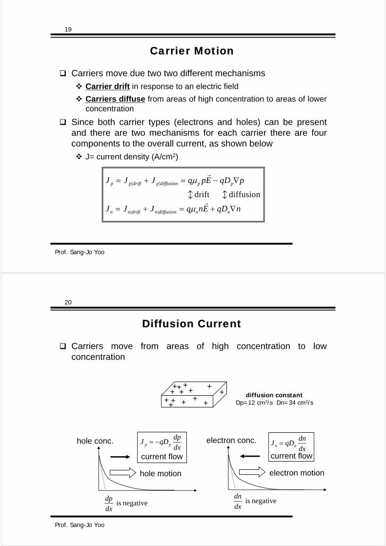
Carrier Motion
Carriers move due two two different mechanisms
Carrier drift in response to an electric field
Carriers diffuse from areas of high concentration to areas of lower concentration
Since both carrier types (electrons and holes) can be present and there are two mechanisms for each carrier there are four components to the overall current, as shown below
J= current density (A/cm2)
J J J q pE qD p
J J J q nE qD n
p p drift p diffusion p p
n n drift n diffusion n n
= + = − ∇
= + = + ∇
| |
| |
µ
µ
r
b br
drift diffusion
20
Prof. Sang-Jo Yoo
Diffusion Current
Carriers move from areas of high concentration to low concentration
dx
dnqDJ nn =
negative is dx
dn
electron conc.
electron motion
current flowdx
dpqDJ pp −=hole conc.
hole motion
current flow
negative is dx
dp
++++++
++
+++ +
++
diffusion constantDp=12 cm2/s Dn=34 cm2/s

21
Prof. Sang-Jo Yoo
Carrier Drift
Definition - Drift is the motion of a charged particle in response to an applied electric field.
Holes are accelerated in the direction of the applied field
Electrons move in a direction opposite to the applied field
Definition - Current, is the charge per unit time crossing an arbitrarily chosen plane of observation oriented normal to the direction of current flow.
e-
Er
vth
vdrift
22
Prof. Sang-Jo Yoo
Carrier Drift, continued
Drift current density (divided by area A) for hole
Total drift current
Einstein relationship :
VT=thermal voltage (25mV)
EqpJ
Ev
pdriftp
ppdrift
µ
µµ
=
=
−
srength field electric :E hole, ofmobility :
EqnJ ndriftn µ=−
( )EnpqJ npdrift µµ +=
Tp
p
n
n VDD
==µµ

23
Prof. Sang-Jo Yoo
Doped Semiconductors
N-type : by introducing a small number of impurity atoms (phosphorus) donor
P-type : by introducing a small number of impurity atoms (boron) acceptor
D
in
inn
Dn
N
np
npn
Nn
2
0
200
0
≈
=
≈
24
Prof. Sang-Jo Yoo
Abrupt Junction Formation
Junction Formation
Carrier Concentrations
pp ~ Na
np0 ~ (ni )2 / Na
nn ~ Nd
pn0 ~ (ni )2 / Nd
P N
X0
pp
np0
nn
pn0
The Depletion Region
represents an immobile donor impurity (i.e. P+ )
represents an immobile acceptor impurity (i.e. B- )
- represents a mobile electron
+ represents a mobile hole
+-
- -- - - - -
- - - - -+++ +
++
+++ ++
+- + +
+ + +
++ +
+ + ++
+ + +++
++
+
-
- -
- --
- - - - -- - - - -
n typep type
x
+
+
+ ++
++
+
+
--
--
-
---
-
DepletionRegion

25
Prof. Sang-Jo Yoo
The Depletion or Space Charge Region
Maximum Field (Emax )
xn
+qNd Q n = qNdxnx
Q p = -qNaxp
Electric field (x)
-qNa
+
-
xp
Abrupt depletion approximation
xn
Electrostaticpotential V(x) (Volts)
xp
Vbi
charge density
xp
xn xd = xn + xp
CArea
xr Si O
d
=ε ε
2 0
(Coulombs/cm-3)
(Volts/cm)
( )∇ • =E le c tr ic f ie ldK s
_ρε 0
d E le c tr ic f ie ld
d x K s
( _ )=
ρε 0
( )ρ = − + −q p n N ND A
P o te n tia l E le c tr ic fie ld
E le c tr ic f ie ld
= −
∝
∫∫
_
_ ρ
-+
++
++
electron diffusion
hole diffusion
hole drift
electron drift
---
--
26
Prof. Sang-Jo Yoo
Reverse Bias
x
pn0
np0
-W1 W20n-regionp-region
diffusion

27
Prof. Sang-Jo Yoo
Forward Bias
x
pn0
np0
-W1 W20p n
(W2)
n-regionp-region
Lp
diffusion
28
Prof. Sang-Jo Yoo
3.4 Analysis of Forward Biased Diode Circuits
We have already looked at the ideal diode model for forward bias (short circuit). In this section we will work with a detailed model and then explore simplifying assumptions that allows us to work back towards our ideal case.
We want to determine the exact current through the circuit, ID and the exact voltage dropped across the diode VD.
If we assume that the voltage source VDD is greater than ~0.5 volts the diode will obviously be in the forward mode of operation and the current through the diode will be given by the following equation
T
D
nV
V
SD eII =
R
VVI DDD
D
−=
+VD
-
ID
VDD +
R

29
Prof. Sang-Jo Yoo
Graphical (Load Line) Analysis continued
We can determine this unknown voltage (operating point) by superimposing the graphs of the expressed for diode current.
i (mA)
v (V)
00
R
VDD
DDV
T
D
nV
V
SD eII =
R
VVI DDD
D
−=
QI D
V D
Rslope
1−=
30
Prof. Sang-Jo Yoo
Iterative Analysis
Example 3.4 Assume that the resistor in our graphical analysis circuit is 1kΩ and VDD is 5V
The diode has a current of 1mA if it is at a voltage of 0.7 volts and the voltage drops by 0.1 volt for every decade decrease in current.
Find the current through the circuit and the exact voltage across the diode.
We can start by assuming we have set up the conditions so that the voltage across the diode is 0.7 volts, we do this so that we can do some calculations about our diode that we can use later to zero in on our actual conditions
mAR
VVI DDD
D 3.41000
7.05=
−=
−=

31
Prof. Sang-Jo Yoo
Iterative Analysis
This current is larger than the 1mA current at 0.7 volts so we conclude that the actual diode voltage will be larger than 0.7 volts.
Since the relationship between the current and the voltage is exponential we can adjust our voltage estimate slightly using anequation we derived earlier relating the voltage change to the current ratio, namely
Now using this value in our original equation we get
( )
74.1 then1.03.2 If :note 763.0
0.001
0.0043log1.0 so log3.2
2
121
212
===
⎟⎠⎞
⎜⎝⎛+=⎟⎟
⎠
⎞⎜⎜⎝
⎛=−
nnVVV
VVI
InVVV
T
T
mAR
VVI DDD
D 237.41000
763.05=
−=
−= ( ) VV 762.0
0.0043
0.004237log1.0763.02 =⎟
⎠⎞
⎜⎝⎛+=
Converged toID=4.237mAVD=0.762V
32
Prof. Sang-Jo Yoo
A graphical view of the iterative analysis
i (mA)
v (V)
00
R
VDD
DDV0.7V
1
1.0 mA
0.763V
1
2
4.3 mA2
0.762V 3START
4.237 mA
3END

33
Prof. Sang-Jo Yoo
Approximating the diode forward characteristic with two straight lines
The analysis of a diode circuit can be greatly simplified by approximating the exponential i-v curve with two straight lines. One line, A, has a zero slope and the second line, B, has a slope of 1/rD
The piecewise-linear model is described as follows:
( ) ,
,0
VD0D0
0
≥−=
≤=
vrVviVvi
DDDD
DDD
−
+
vD
rD
ideal
iD
V D0
iD (mA)
vD (V)0
B, slope =rD
1
A, slope = 0
V D0
iD (mA)
vD (V)0
B, slope =rD
1B, slope =
rD
1
A, slope = 0
V D0
34
Prof. Sang-Jo Yoo
Constant-Voltage Drop Model
We assume that a forward-conducting diode exhibits a constant voltage drop, VD, which is approximately 0.7 V.
This model is used in the initial phases of analysis and design to give a rough estimate of circuit behavior.
−
+
vD
ideal
iD
V 7.0=V D
iD (mA)
vD (V)0
A, horizontal
V D
B, vertical
iD (mA)
vD (V)0
A, horizontal
V D
B, vertical

35
Prof. Sang-Jo Yoo
3.5 DC Forward Bias with an ac small signal
The DC bias level determines the ac parameters
By restricting the input signal swing to small values we can “linearize” the characteristic like we did for amplifier transfer characteristics
+vD(t)
-
vd(t)
iD(t)
VD +DC
ac
(DC+ac)
(DC+ac)VD=0.7
VD0 vd (t)
iD (mA)
vD (V)
t
ID
Bias Point - Q
tangent at Q
dr
1slope =
id (t)
0.5500
1.0
0.750.65
36
Prof. Sang-Jo Yoo
Small Signal Analysis
If we set the ac signal to zero, the current through the diode due to the DC bias is given by
When we add in the ac small signal to the DC voltage bias the total signal is
The total (DC +ac) instantaneous current is
Which we can re-arrange to get
Substituting in the DC equation from above, we get
T
D
nV
V
SD eII =
T
D
nV
v
SD eIti =)(
)()( tvVtv dDD +=
T
dD
nV
vV
SD eIti+
=)(
T
d
T
D
nV
v
nV
V
SD eeIti =)(
T
d
nV
v
DD eIti =)(
1<<T
d
nV
v
⎟⎟⎠
⎞⎜⎜⎝
⎛+=
T
dDD nV
vIti 1)(
T
dDDD nV
vIIti +=)(
dDD iIi +=
If we keep the amplitude of the ac signal small, such that
We can expand the exponential in an infinite series, but we find that a sufficiently accurate expression can be found using only the first two terms.
This IS the small signal approximation, valid for amplitudes less than about 10mV
We find that the total current is made up of a DC component and an ac component that is directly proportional to the small signal voltage AND the DC bias level
T
dDd nV
vIi =Where

37
Prof. Sang-Jo Yoo
Small Signal Resistance (incremental resistance)
On the previous page we found
And since,
The ac small-signal resistance is inversely proportional to the DC bias current ID
In the graphical representation we find that about the Q point
DD IiD
D
d
vi
r
=⎥⎦
⎤⎢⎣
⎡∂∂
=1
( )0
1DD
dD Vv
ri −=
D
T
dd
T
Dd
d
d
I
nV
gr
nV
Ig
v
i==∴==
1
T
dDd nV
vIi =
iD (mA)
vD (V)
ID
Bias Point - Q
tangent at Qdr
1slope =
00
VD0
The equation of the tangent line is given by:
38
Prof. Sang-Jo Yoo
The Equivalent Circuit Model for the Diode
The equation of the tangent line is a model of the diode operation for small signal changes about the bias DC point (Q point)
The total model has the components shown below
The incremental voltage
across the diode is
( )0
1DD
dD Vv
ri −=
( )( )
ddDD
dddDDD
ddDDD
dDDD
riVv
rirIVv
riIVv
riVv
+=++=
++=+=
0
0
0
+vD
-
iD
rd
VD0
ideal
ddd riv =vD (V)
ID
Bias Point - Q
tangent at Q
dr
1slope =
00
VD0 VD
di
dv

39
Prof. Sang-Jo Yoo
Application of the Diode Small-Signal Model
Combined DC and ac voltage input causing a DC and ac current. We can analyze the response of the circuit.
+vD=VD+vd
-vs
iD=ID+id
VDD +
R
( ) ( )( ) ( )
( )ddDDsDD
dddDDDsDD
ddDDdDsDD
dDDDsDD
rRiVRIvV
rRirIVRIvV
riIVRiIvV
riVRivV
+++=+++++=+
++++=+++=+
0
0
0
+
vD=VD+vd
-
vs
iD=ID+id
VDD
R
rd
VD0
ideal( )dds rRiv +=
40
Prof. Sang-Jo Yoo
Application of the Diode Small-Signal Model continued
The small-signal analysis is done by eliminating all DC sources and replacing the diode with the small-signal resistance.
+
VD
-
ID
VDD
R
rd
VD0
ideal
DDDD VRIV +=
Circuit for DC Analysis
+
vd
-
vs
id
R
rd
( )dds rRiv +=
Circuit for small-signal Analysis
d
dsd rR
rvv
+=

41
Prof. Sang-Jo Yoo
Power Supply Ripple Example 3.6
Example 3.6 The power supply has a 10V DC value and a 1V peak sinusoidal ripple at a frequency of 60 Hz.
Calculate the dc voltage across the diode and the magnitude of the sine-wave signal appearing across it
Assume the diode has a 0.7V drop at a current of 1mA and that the ideality factor n=2
Calculate the dc diode current by assuming VD=0.7V
Since this value is close to 1mA the diode voltage will be closeto the assumed value of 0.7V. At this DC operating point we can calculate the incremental (dynamic) resistance rd as follows
The peak-to-peak small signal voltage across the diode can be found using the ac model and the voltage divider rule
+vd
-
+V=10V+ripple
R=10kΩ
mAID 93.0000,10
7.010=
−=
( )Ω=== − 8.53
1093.0
025.023xI
nVr
D
Td
( ) mVrR
rpeaktopeakv
d
dd 7.10
8.53000,10
8.5322 =
+=
+=−−
+V=10V+ripple
R=10kΩ
rd=53.8Ω+vd
-
42
Prof. Sang-Jo Yoo
Voltage Regulation Using Diode Forward Voltage Drops
A string of three diodes is used to provide a constant voltage of about 2.1V
We want to see
a) how much of a fluctuation (percentage change in regulation) there is in the output for a 1V (10%) change in the power supply voltage
b) percentage change in regulation when there is a 1kΩload resistance. Assume n=2
With no load the nominal dc current is given by
Thus the dynamic resistance of each diode is
The total resistance of the diodes will be 3rd or 18.9Ω
Using voltage division on the 1V change (10%) we get
+
vo
-
10V + 1V
R=1kΩ
RL=1kΩ
mAID 9.7000,1
1.210=
−=
( )Ω=== − 3.6
109.7
025.023xI
nVr
D
Td
( )( ) mV
rR
rv
d
do 1.37
9.18000,1
9.182
3
32 =
+=
+=∆

43
Prof. Sang-Jo Yoo
Diode Model for High Frequencies
Charge storage effects were modeled by two capacitances
The diode depletion layer capacitance (Cj)
The forward biased diffusion capacitance (Cd)
Cjrd Cd
0for 2
0for
1
, :Point Bias DC
0
0
0
>=
<
⎟⎟⎠
⎞⎜⎜⎝
⎛−
=
=
=
Djj
Dm
D
jj
DT
Td
D
Td
DD
VCC
V
VV
CC
IV
C
I
nVr
VI
τ
44
Prof. Sang-Jo Yoo
3.6 Diode Characteristic in the Reverse Breakdown Region - Zener Diodes
If the Zener diode is biased in the reverse breakdown region of operation the current can fluctuate wildly about the Q point and the voltage across the diode will remain relatively unchanged
The incremental (dynamic) resistance in reverse breakdown is given by rZ
+VZ
-
IZ
Circuit symbolfor a Zener diode
i
v
IZT
∆V
VZ0
Bias Point - QZr
1slope =
VZKnee VZ
∆Ι
∆V=∆Ι(rΖ)
IZKnee
Test current

45
Prof. Sang-Jo Yoo
The Reverse Bias Zener Model
We can model the zener diode in the breakdown region as straight line having an x (voltage) intercept at VZ0
and a slope of 1/rZ.
The reverse breakdown characteristic of a Zener diode is very steep (low resistance). For a very small change in voltage biased in the breakdown region the current changes significantly.
+VZ
-
IZ
rz
VZ0
ZzZZ IrVV += 0
46
Prof. Sang-Jo Yoo
A Shunt Regulator
Load
+VO
-
IL
IZ
I
R
Zenerregulator
Load
+VO
-
IL
IZ
I
R
Zenerregulator
i
v
i
v
The zener diode can be used to absorb or buffer a load from large current changes, I.e. keep the voltage across the load approximately constant

47
Prof. Sang-Jo Yoo
Zener Voltage Regulation
Example 3.8 A 6.8 V Zener diode in the circuit shown below is specified to have VZ = 6.8V at IZ = 5mA and rZ=20Ω, and IZK = 0.2mA.
The supply voltage is nominally +10V but can vary by plus or minus 1 V.
(a) Find the output VO with no load and V+ at 10V
(b) Find the value of VO resulting from the +/- 1 V change in V+
(c) Find the change in VO resulting from connecting a load resistance RL= 2 kΩ(d) Find the value of VO when RL =0.5 kΩ(e) What is the minimum value of RL for which the diode still operates in the breakdown region.
We can start by determining the value of VZ0. VZ0 is the x-axis intercept of the line tangent to the characteristic at the reverse bias operating point
+
vo
-
V+ (10V + 1V)
R = 0.5 kΩ
RL
6.8Vzener
( ) VVV
IrVVIrVV
ZZ
ZzZZZzZZ
7.6 005.0208.6
00
00
=−=−=+=
48
Prof. Sang-Jo Yoo
Zener example continued
With no load connected, the current through the zener diode is given by
We can now find V0, the voltage at the operating point current
Now, for a +/- 1V change in V+ can be found from
When a load resistance of 2kΩ is connected, the load current will be approximately 6.8V/2000Ω or 3.4mA. This current will not be flowing through the zener diode if it is flowing through the load so the change in the zener current is -3.4mA. The corresponding change in the zener voltage (which is also the output voltage) is,
A more accurate result
mArR
VVII
Z
ZZ 35.6
20500
7.6100 =+−
=+−
==+
( ) VrIVV ZZZ 83.602.035.67.600 =+=+=
( ) mVrR
rVV
Z
Z 5.3820500
2010 ±=
+±=
+∆=∆ +
( ) mVmAIrV ZZ 684.3200 −=−=∆=∆
mVV 700 −=∆

49
Prof. Sang-Jo Yoo
Zener Example continued
If we change the load resistance to 500Ω the load current would increased to 6.8V/500Ω = 13.6mA,
Not possible because the current I supplied through R s only 6.4 mA.
Cut off
For the zener to be at the edge of the breakdown region, the current has to be IZ=IZK=0.2mA and VZ=VZK=6.7V. At this point the current supplied through the resistor R is (9-6.7)/500 or 4.6 mA.
The load current would be 4.6mA - 0.2mA = 4.4mA. We can now find the value of RL for to cause this
mAI
VRR
RVV
L
L
LO
10500500
10
voltagebreakdownzener thelower than is which
5500500
50010
=+
=
=+
=+
= +
Ω== 500,10044.0
7.6LR
50
Prof. Sang-Jo Yoo
Shunt Regulator
S
O
V
V
∆∆
←
L
O
I
V
∆∆
←
VO
VS VSmax
VSmin
tt
Load+VO
-
VS
IL
IZ
I
R
Zenerregulator
reduced ripple
( )RrIrR
rV
rR
RVV zL
z
zS
zZO −
++
+= 0
z
z
rR
r
+=Regulation Line
RrZ−=Regulation Load
maxmin
min0minmax
LZ
ZZZS
II
IrVVR
+−−
=
rz
VZ0+VO
-
VS
IL
IZ
I
R
↑↑=>↓=>↓=>↑=>↓=> gulationLoadrIIRgulation zZ ReRe
51
Prof. Sang-Jo Yoo
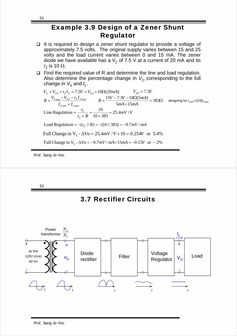
Example 3.9 Design of a Zener Shunt Regulator
It is required to design a zener shunt regulator to provide a voltage of approximately 7.5 volts. The original supply varies between 15 and 25 volts and the load current varies between 0 and 15 mA. The zener diode we have available has a VZ of 7.5 V at a current of 20 mA and itsrZ is 10 Ω.
Find the required value of R and determine the line and load regulation. Also determine the percentage change in VO corresponding to the full change in VS and IL.
)20(105.7 00 mAVVIrVV ZZZZZ Ω+==+= VVZ 3.70 =
maxmin
min0min
LZ
ZZZS
II
IrVVR
+−−
= Ω=+
Ω−−= 383
155
)5(103.715
mAmA
mAVVR designing for Izmin=(1/3)ILmax
VmVRr
r
Z
Z /4.2538310
10Regulation Line =
+=
+=
mAmVRrZ /7.9)383//10()//(Regulation Load −=−=−=
%4.3or 254.010/4.25 - Vin Change Full S VVmVVo =×=∆
%2or 15.015/7.9 - Vin Change Full S −−=×−=∆ VmAmAmVVo
52
Prof. Sang-Jo Yoo
3.7 Rectifier Circuits
Dioderectifier Filter
VoltageRegulator
Load
+
-
VO
IL
t t t t t
Powertransformer
+
-
ac line
120V (rms)
60 Hz
+
-
vO
1
2
N
N

53
Prof. Sang-Jo Yoo
Half-Wave Rectifier
D
Rvs
+
-
vo
+
-
Ideal
Rvs+- vo
+
-
VD0 rD
vo
vSVD00
DrR
RSlope
+=
VS
VD0vS
t
v
vo
VD0,0=ov 0Ds Vv <
,0D
DSD
o rR
RVv
rR
Rv
+−
+=
0Ds Vv ≥RrD << 0DSO Vvv −≅
SVPIV = PIV: peak inverse voltageWithstand without breakdown
54
Prof. Sang-Jo Yoo
Full-Wave Rectifier with Center Tapped Transformer
vo
vSVD00
DrR
RSlope
+=
VS
VD0vS
t
v
vo
02 DS VVPIV −=
D1
Rvs
+
-vo
+
-
D2vs
+
-
-VD0
-vS
Vs: positive case

55
Prof. Sang-Jo Yoo
Full-Wave Bridge Rectifier
VS
2VD0vS
t
v
vo
0002 DSDDS VVVVVPIV −=+−=
-vS
D1D4
Rvs
+
vo+ -
D2
- D3
56
Prof. Sang-Jo Yoo
Rectifier with a Filter Capacitor
To reduce the variation of the output voltage : filter capacitor
RC
t
e−
LI
LCD
oL
idt
dvCiii
Rvi
+=+=
= /
57
Prof. Sang-Jo Yoo
Rectifier with a Filter Capacitor
Vr=peak-to-peak ripple voltage
CR>>T, then Vr is small.
( )
fCR
V
CR
TVV
CRTVeVVV
VVV
RVIVv
ppr
pCRT
prp
rpo
pLpo
==
>>−≈≈−
−=
=→≈
− TCR if /1
interval discarge of end at the
output average accurate 2
1
58
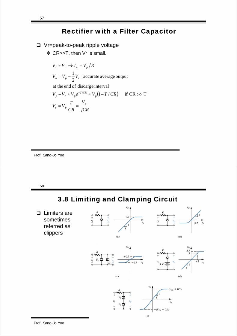
Prof. Sang-Jo Yoo
3.8 Limiting and Clamping Circuit
Limiters are sometimes referred as clippers

59
Prof. Sang-Jo Yoo
Limiting and Clamping Circuit
The clamped capacitor or dc restorer
Voltage doubler
Schottky-Barrier Diode (SBD)
Varactors
Photodiodes
Light-Emitting Diode (LED)