bcm5723 programmer's reference guide - citeseerx
TRANSCRIPT
5723-PG100-R
5300 California Avenue • Irvine, CA 92617 • Phone: 949-926-5000 • Fax: 949-926-5203 04/02/08
Programmer’s Reference Guide
BCM5723
Host Programmer Interface Specification for the NetXtreme® and NetLink™ Family of Highly
Integrated Media Access Controllers

Broadcom®, the pulse logo, Connecting everything®, the Connecting everything logo, NetXtreme®, and NetLink™ are among the trademarks of Broadcom Corporation and/or its affiliates in the United States, certain other countries and/or the EU. Any other trademarks or trade names mentioned are the property of their respective owners.
Broadcom Corporation5300 California Avenue
Irvine, CA 92617
© 2008 by Broadcom CorporationAll rights reserved
Printed in the U.S.A.
REVISION HISTORY
Revision Date Change Description
5723-PG100-R 04/02/08 Initial release
Programmer’s Reference Guide BCM572304/02/08
Broadcom CorporationDocument 5723-PG100-R Page iii
Table of Contents
Section 1: About this Document ........................................................................................1
Introduction .................................................................................................................................................. 1
Notational Conventions ............................................................................................................................... 1
Registers and Bits................................................................................................................................... 1
Functional Overview ............................................................................................................................... 1
Operational Characteristics..................................................................................................................... 1
Example Code ........................................................................................................................................ 2
Related Documents...................................................................................................................................... 3
Section 2: Introduction........................................................................................................4
Introduction .................................................................................................................................................. 4
Product Features.......................................................................................................................................... 4
Revision Levels ............................................................................................................................................ 6
Programming the Ethernet Controllers...................................................................................................... 6
Section 3: Hardware Architecture ......................................................................................7
Theory of Operation ..................................................................................................................................... 7
Receive Data Path ........................................................................................................................................ 8
RX Engine............................................................................................................................................... 8
RX FIFO.................................................................................................................................................. 8
Rules Checker ........................................................................................................................................ 9
RX List Initiator........................................................................................................................................ 9
Transmit Data Path ...................................................................................................................................... 9
TX MAC .................................................................................................................................................. 9
TX FIFO ................................................................................................................................................ 10
DMA Read ................................................................................................................................................... 10
Read Engine ......................................................................................................................................... 10
Read FIFO ............................................................................................................................................ 10
Buffer Manager ..................................................................................................................................... 11
DMA Write ................................................................................................................................................... 11
Write Engine ......................................................................................................................................... 11
Write FIFO ............................................................................................................................................ 12
Buffer Manager ..................................................................................................................................... 12
BCM5723 Programmer’s Reference Guide04/02/08
Broadcom Corporation
Page iv Document 5723-PG100-R
LED Control .................................................................................................................................................12
Memory Arbiter ...........................................................................................................................................12
Host Coalescings........................................................................................................................................13
Host Coalescing Engine ........................................................................................................................13
MSI FIFO...............................................................................................................................................14
Status Block...........................................................................................................................................14
10BT/100BTx/1000BASE-T Transceiver....................................................................................................14
Auto-Negotiation....................................................................................................................................14
Automatic MDI Crossover......................................................................................................................15
PHY Control.................................................................................................................................................15
MII Block................................................................................................................................................15
GMII Block.............................................................................................................................................17
MDIO Register Interface........................................................................................................................19
Management Data Clock................................................................................................................19
Management Data Input/Output .....................................................................................................19
Management Data Interrupt ...........................................................................................................19
Management Register Block ..........................................................................................................19
Section 4: NVRAM Configuration .................................................................................... 20
Overview......................................................................................................................................................20
Self-Boot......................................................................................................................................................20
Section 5: Common Data Structures............................................................................... 21
Theory of Operation ...................................................................................................................................21
Descriptor Rings.........................................................................................................................................21
Producer and Consumer Indices ...........................................................................................................22
Ring Control Blocks ...............................................................................................................................23
Send Rings ............................................................................................................................................23
Send Buffer Descriptors .................................................................................................................26
Receive Rings .......................................................................................................................................27
Receive Producer Ring ..................................................................................................................29
Receive Return Rings ....................................................................................................................29
Receive Buffer Descriptors.............................................................................................................29
Status Block ................................................................................................................................................32
Status Block Format ..............................................................................................................................32
Device Statistics .........................................................................................................................................34
Programmer’s Reference Guide BCM572304/02/08
Broadcom CorporationDocument 5723-PG100-R Page v
MAC Statistics....................................................................................................................................... 34
MIB Network Interface Card Statistics .................................................................................................. 34
Host Interrupts ............................................................................................................................... 34
NIC BD Coalescing Thresholds ..................................................................................................... 34
DMA Resources............................................................................................................................. 35
MAC Resources............................................................................................................................. 35
Class of Service Statistics ............................................................................................................. 36
Interface Statistics in Receive Placement State Machine.............................................................. 36
Section 6: Receive Data Flow ...........................................................................................37
Introduction ................................................................................................................................................ 37
Receive Producer Ring .............................................................................................................................. 39
Setup of Producer Rings Using RCBs .................................................................................................. 39
Receive Producer Ring RCB—Register Offset 0x2450–0x245f .................................................... 39
Other Considerations Relating to Producer Ring Setup ........................................................ 39
RCB Setup Pseudo Code .............................................................................................................. 39
Receive Buffer Descriptors ................................................................................................................... 40
Management of Rx Producer Rings with Mailbox Registers and Status Block..................................... 40
Status Block................................................................................................................................... 40
Mailbox .......................................................................................................................................... 41
Receive BD Producer Ring Producer Index........................................................................... 41
Receive Return Rings ................................................................................................................................ 42
Management of Return Rings with Mailbox Registers and Status Block .............................................. 42
Host Buffer Allocation ........................................................................................................................... 42
Receive Rules Setup and Frame Classification.................................................................................... 43
Receive Rules Configuration Register ........................................................................................... 43
Receive List Placement Rules Array.............................................................................................. 43
Class of Service Example.............................................................................................................. 45
Checksum Calculation............................................................................................................................... 45
VLAN Tag Strip ........................................................................................................................................... 46
RX Data Flow Diagram ............................................................................................................................... 47
Receive Side Scaling ................................................................................................................................. 48
Overview ............................................................................................................................................... 48
Functional Description .......................................................................................................................... 48
RSS Parameters ................................................................................................................................... 49
BCM5723 Programmer’s Reference Guide04/02/08
Broadcom Corporation
Page vi Document 5723-PG100-R
Hash Function ................................................................................................................................49
Hash Type ......................................................................................................................................49
Hash Mask .....................................................................................................................................49
Indirection Table.............................................................................................................................49
Secret Hash Key ............................................................................................................................49
RSS Initialization ...................................................................................................................................49
RSS Rx Packet Flow .............................................................................................................................50
Section 7: Transmit Data Flow ......................................................................................... 51
Introduction.................................................................................................................................................51
Send Rings ..................................................................................................................................................51
Ring Control Block.................................................................................................................................52
Host-Based Send Ring..........................................................................................................................53
Checksum Offload ......................................................................................................................................54
Scatter/Gather .............................................................................................................................................54
VLAN Tag Insertion ....................................................................................................................................55
TX Data Flow Diagram................................................................................................................................56
Reset ............................................................................................................................................................59
Firmware Download....................................................................................................................................59
Firmware Binary Image .........................................................................................................................59
Reset RISC Processor ..........................................................................................................................60
Halt RISC Procedure .............................................................................................................................61
Start RISC Procedure............................................................................................................................61
Firmware Download Procedure .............................................................................................................62
Example Code Snippet (from ASF Firmware) ................................................................................63
MAC Address Setup/Configuration...........................................................................................................63
Packet Filtering ...........................................................................................................................................63
Multicast Hash Table Setup/Configuration ............................................................................................63
Ethernet CRC Calculation .....................................................................................................................64
Generating CRC....................................................................................................................................64
Checking CRC.......................................................................................................................................64
Initializing the MAC Hash Registers ......................................................................................................64
Promiscuous Mode Setup/Configuration ...............................................................................................66
Broadcast Setup/Configuration..............................................................................................................66
Programmer’s Reference Guide BCM572304/02/08
Broadcom CorporationDocument 5723-PG100-R Page vii
Section 8: PCI.....................................................................................................................67
Configuration Space .................................................................................................................................. 67
Description ............................................................................................................................................ 67
Functional Overview ............................................................................................................................. 69
PCI Configuration Space Registers ............................................................................................... 69
PCI Required Header Region ........................................................................................................ 69
PCI Device-Specific Region........................................................................................................... 71
Indirect Mode ................................................................................................................................. 73
Indirect Register Access ................................................................................................................ 73
Indirect Memory Access ................................................................................................................ 75
UNDI Mailbox Access .................................................................................................................... 76
Standard Mode .............................................................................................................................. 78
Flat Mode....................................................................................................................................... 81
Memory Mapped I/O Registers ............................................................................................................. 88
PCI Command Register ................................................................................................................. 88
PCI State Register ......................................................................................................................... 88
PCI Base Address Register ........................................................................................................... 88
Register Quick Cross Reference .......................................................................................................... 90
Device Family ................................................................................................................................ 90
Pseudocode .......................................................................................................................................... 90
Memory Window Read in Standard Mode ..................................................................................... 90
Memory Window Write in Standard Mode ..................................................................................... 90
Register Read in Standard Mode .................................................................................................. 91
Register Write in Standard Mode................................................................................................... 91
Memory Read in Flat Mode ........................................................................................................... 91
Memory Write in Flat Mode1.......................................................................................................... 91
Register Read in Flat Mode ........................................................................................................... 91
Register Write in Flat Mode ........................................................................................................... 91
Memory Read Using Indirect Mode ............................................................................................... 91
Memory Write Using Indirect Mode................................................................................................ 91
Register Read Using Indirect Mode............................................................................................... 91
Register Write Using Indirect Mode ............................................................................................... 91
Bus Interface .............................................................................................................................................. 91
Description ............................................................................................................................................ 91
BCM5723 Programmer’s Reference Guide04/02/08
Broadcom Corporation
Page viii Document 5723-PG100-R
Operational Characteristics ...................................................................................................................92
Read/Write DMA Engines ..............................................................................................................92
Register Quick Cross Reference ...........................................................................................................93
Expansion ROM ..........................................................................................................................................93
Description.............................................................................................................................................93
Operational Characteristics ...................................................................................................................93
BIOS......................................................................................................................................................94
Preboot Execution Environment.....................................................................................................94
Power Management ....................................................................................................................................94
Description.............................................................................................................................................94
Operational Characteristics ...................................................................................................................95
Device State D0 (Uninitialized).......................................................................................................95
Device State D0 (Active) ................................................................................................................96
Device State D3 (Hot) ....................................................................................................................96
Device State D3 (Cold)...................................................................................................................96
Wake on LAN ........................................................................................................................................96
GPIO......................................................................................................................................................97
Power Supply in D3 State......................................................................................................................97
Clock Control .........................................................................................................................................97
Device ACPI Transitions........................................................................................................................97
Disable Device Through BIOS...............................................................................................................98
Register Quick Cross Reference ...........................................................................................................98
Endian Control (Byte and Word Swapping) .............................................................................................99
Background ...........................................................................................................................................99
Architecture .........................................................................................................................................100
Enable Endian Word Swap and Enable Endian Byte Swap Bits .........................................................100
Word Swap Data and Byte Swap Data Bits.........................................................................................102
Word Swap Data = 0, and Byte Swap Data = 0 ...........................................................................103
Word Swap Data = 0, and Byte Swap Data = 1 ...........................................................................103
Word Swap Data = 1, and Byte Swap Data = 0 ...........................................................................104
Word Swap Data = 1, and Byte Swap Data = 1 ...........................................................................104
Word Swap Non-Frame Data and Byte Swap Non-Frame Data Bits ..................................................105
Word Swap Non-Frame Data = 0 and Byte Swap Non-Frame Data = 0......................................105
Word Swap Non-Frame Data = 1 and Byte Swap Non-Frame Data = 0......................................106
Word Swap Non-Frame Data = 0 and Byte Swap Non-Frame Data = 1......................................106
Programmer’s Reference Guide BCM572304/02/08
Broadcom CorporationDocument 5723-PG100-R Page ix
Word Swap Non-Frame Data = 1 and Byte Swap Non-Frame Data = 1 ..................................... 106
Section 9: Ethernet Link Configuration .........................................................................107
Overview ................................................................................................................................................... 107
GMII/MII ..................................................................................................................................................... 107
Configuring the Ethernet Controller for GMII and MII Modes.............................................................. 107
Link Status Change Indications .......................................................................................................... 108
Configuring the GMII/MII PHY ............................................................................................................ 108
Reading a PHY Register.............................................................................................................. 108
Writing a PHY Register ................................................................................................................ 109
MDI Register Access................................................................................................................................ 110
Operational Characteristics................................................................................................................. 110
Access Methods.................................................................................................................................. 110
Traditional Bit-Bang Method ........................................................................................................ 111
Auto-Access Method.................................................................................................................... 111
Wake on LAN Mode/Low-Power.............................................................................................................. 112
Description .......................................................................................................................................... 112
Functional Overview ........................................................................................................................... 113
Operational Characteristics................................................................................................................. 114
Internal Memory........................................................................................................................... 114
WOL Pattern Configuration Register ........................................................................................... 114
WOL Streams .............................................................................................................................. 115
Pattern Data Structure ................................................................................................................. 117
Firmware Mailbox ........................................................................................................................ 118
PHY Auto-Negotiation.................................................................................................................. 119
Power Management..................................................................................................................... 119
Integrated MACs.......................................................................................................................... 120
WOL Data Flow Diagram .................................................................................................................... 121
Flow Control ............................................................................................................................................. 122
Description .......................................................................................................................................... 122
Operational Characteristics................................................................................................................. 123
Transmit MAC.............................................................................................................................. 123
Receive MAC............................................................................................................................... 124
Statistics Block............................................................................................................................. 124
PHY Auto-Negotiation.................................................................................................................. 125
BCM5723 Programmer’s Reference Guide04/02/08
Broadcom Corporation
Page x Document 5723-PG100-R
Integrated MACs ..........................................................................................................................125
Flow Control Initialization Pseudocode................................................................................................126
Section 10: Interrupt Processing ................................................................................... 128
Host Coalescing........................................................................................................................................128
Description...........................................................................................................................................128
Operational Characteristics .................................................................................................................128
Registers .............................................................................................................................................129
MSI .............................................................................................................................................................130
Traditional Interrupt Scheme ...............................................................................................................130
Message Signaled Interrupt.................................................................................................................131
PCI Configuration Registers ................................................................................................................132
MSI Address.................................................................................................................................132
MSI Data ......................................................................................................................................132
Host Coalescing Engine ......................................................................................................................133
Firmware..............................................................................................................................................133
Basic Driver Interrupt Processing Flow .................................................................................................134
Flowchart for Servicing an Interrupt.....................................................................................................134
Interrupt Procedure..............................................................................................................................135
Other Configuration Controls..................................................................................................................136
Broadcom Mask Mode.........................................................................................................................136
Broadcom Tagged Status Mode..........................................................................................................136
Clear Ticks on BD Events Mode..........................................................................................................136
No Interrupt on Force Update..............................................................................................................136
No Interrupt on DMAD Force...............................................................................................................136
Section 11: Ethernet Controller Register Definitions .................................................. 137
PCI Configuration Registers....................................................................................................................137
Register Access Legend......................................................................................................................137
Device ID & Vendor ID Register (Offset: 0x00) ...................................................................................138
Status & Command Register (Offset: 0x04) ........................................................................................138
PCI Classcode & Revision ID Register (Offset: 0x8)...........................................................................140
BIST, Header Type, Latency Timer, Cache Line Size Register (Offset: 0x0C) ...................................140
Base Address Register 1 (Offset: 0x10) ..............................................................................................141
Base Address Register 2 (Offset: 0x14) ..............................................................................................142
Base Address Register 3 (Offset: 0x18) ..............................................................................................142
Programmer’s Reference Guide BCM572304/02/08
Broadcom CorporationDocument 5723-PG100-R Page xi
Base Address Register 4 (Offset: 0x1c).............................................................................................. 142
Cardbus CIS Pointer Register (Offset: 0x28) ...................................................................................... 142
Subsystem ID/Vendor ID Register (Offset: 0x2C)............................................................................... 142
Expansion ROM Base Address Register (Offset: 0x30) ..................................................................... 143
Capabilities Pointer Register (Offset: 0x34)........................................................................................ 143
Interrupt Register (Offset: 0x3C)......................................................................................................... 143
VPD Capabilities (Offset: 0x40) .......................................................................................................... 144
VPD Data Register (Offset: 0x44)....................................................................................................... 144
Power Management Capability Register (Offset: 0x48)...................................................................... 144
Power Management Control/Status Register (Offset: 0x4C) .............................................................. 145
MSI Capability Header (Offset: 0x50) ................................................................................................. 146
MSI Lower Address Register (Offset: 0x54)........................................................................................ 147
MSI Upper Address Register (Offset: 0x58)........................................................................................ 147
MSI Data Register (Offset: 0x5c) ........................................................................................................ 147
Broadcom Vendor-Specific Capability Header (Offset: 0x60)............................................................. 147
Reset Counters Initial Values Register (Offset: 0x64)......................................................................... 147
Miscellaneous Host Control Register (Offset: 0x68) ........................................................................... 148
DMA Read/Write Control Register (Offset: 0x6C)............................................................................... 149
PCI State Register (Offset: 0x70) ....................................................................................................... 150
Clock Control Register (Offset: 0x74) ................................................................................................. 151
Register Base Register (Offset: 0x78) ................................................................................................ 152
Memory Base Register (Offset: 0x7C) ................................................................................................ 152
Register Data Register (Offset: 0x80)................................................................................................. 152
Memory Data Register (Offset: 0x84) ................................................................................................. 152
Expansion ROM BAR Size Register (Offset: 0x88) ............................................................................ 153
Expansion ROM Address Register (Offset: 0x8C).............................................................................. 153
Expansion ROM Data Register (Offset: 0x90) .................................................................................... 153
VPD Interface Register (Offset: 0x94) ................................................................................................ 154
UNDI Receive BD Standard Producer Ring Producer Index Mailbox Register (Offset: 0x98)............ 154
UNDI Receive Return Ring Consumer Index Register (Offset: 0xA0) ................................................ 154
UNDI Send BD Producer Index Mailbox Register (Offset: 0xA8)........................................................ 154
INT Mailbox Register (Offset: 0xB0) ................................................................................................... 154
Product ID and ASIC Revision (Offset: 0xBC) .................................................................................... 155
PCIe Capability List Register (Offset: 0xCC) ...................................................................................... 155
PCIe Next Capability Pointer Register (Offset: 0xCD) ........................................................................ 155
BCM5723 Programmer’s Reference Guide04/02/08
Broadcom Corporation
Page xii Document 5723-PG100-R
PCIe Capabilities Register (Offset: 0xCE)...........................................................................................155
Device Capabilities Register (Offset: 0xD0) ........................................................................................156
Device Control Register (Offset: 0xD4) ...............................................................................................157
Device Status Register (Offset: 0xD6).................................................................................................158
Link Capability Register (Offset: 0xD8) ...............................................................................................159
Link Control Register (Offset: 0xDC) ...................................................................................................160
Link Status Command Register (Offset: 0xDE) ...................................................................................160
Device Capabilities 2 (Offset: 0xF0) ....................................................................................................161
Device Status and Control 2 (Offset: 0xF4).........................................................................................161
Link Capabilities 2 (Offset: 0xF8) ........................................................................................................162
Link Status and Control 2 (Offset: 0xFC).............................................................................................162
Advanced Error Reporting Enhanced Capability Header (Offset: 0x100) ...........................................162
Uncorrectable Error Status Register (Offset: 0x104)...........................................................................162
Uncorrectable Error Mask Register (Offset: 0x108) ............................................................................163
Uncorrectable Error Severity Register (Offset: 0x10C) .......................................................................164
Correctable Error Status Register (Offset: 0x110)...............................................................................165
Correctable Error Mask Register (Offset: 0x114) ................................................................................165
Advanced Error Capabilities and Control Register (Offset: 0x118) .....................................................166
Header Log Register (Offset: 0x11C) ..................................................................................................166
Header Log Register (Offset: 0x120)...................................................................................................166
Header Log Register (Offset: 0x124)...................................................................................................167
Header Log Register (Offset: 0x128)...................................................................................................167
Virtual Channel Enhanced Capability Header (Offset: 0x13c).............................................................167
Port VC Capability Register (Offset: 0x140) ........................................................................................168
Port VC Capability Register 2 (Offset: 0x144) .....................................................................................168
Port VC Control Register (Offset: 0x148) ............................................................................................168
Port VC Status Register (Offset: 0x14A) .............................................................................................168
VC Resource Capability Register (Offset: 0x14C)...............................................................................169
VC Resource Control Register (Offset: 0x150) ...................................................................................169
VC Resource Status Register (Offset: 0x156).....................................................................................169
Device Serial No Enhanced Capability Header Register (Offset: 0x160)............................................170
Device Serial No Lower DW Register (Offset: 0x164).........................................................................170
Device Serial No Upper DW Register (Offset: 0x168).........................................................................170
Power Budgeting Enhanced Capability Header Register (Offset: 0x16C)...........................................171
Power Budgeting Data Select Register (Offset: 0x170) ......................................................................171
Programmer’s Reference Guide BCM572304/02/08
Broadcom CorporationDocument 5723-PG100-R Page xiii
Power Budgeting Data Register (Offset: 0x174)................................................................................. 172
Power Budgeting Capability Register (Offset: 0x178)......................................................................... 172
Firmware Power Budgeting Register 1 (Offset: 0x17C)...................................................................... 173
Firmware Power Budgeting Register 2 (Offset: 0x17E) ...................................................................... 173
Firmware Power Budgeting Register 3 (Offset: 0x180)....................................................................... 174
Firmware Power Budgeting Register 4 (Offset: 0x182)....................................................................... 174
Firmware Power Budgeting Register 5 (Offset: 0x184)....................................................................... 175
Firmware Power Budgeting Register 6 (Offset: 0x186)....................................................................... 175
Firmware Power Budgeting Register 7 (Offset: 0x188)....................................................................... 176
Firmware Power Budgeting Register 8 (Offset: 0x18A) ...................................................................... 176
PCIe 1.1 Advisory Non-Fatal Error Masking (Offset: 0x18C).............................................................. 177
High Priority Mailbox Registers .............................................................................................................. 178
Interrupt Mailbox 0 (High Priority Mailbox) Register (Offset: 0x200–207)........................................... 178
Receive BD Standard Producer Ring Index (High Priority Mailbox) Register (Offset: 0x268–0x26f) . 178
Receive BD Return Ring 0 Consumer Index (High Priority Mailbox) Register (Offset: 0x280–0x287)178
Receive BD Return Ring 1 Consumer Index (High Priority Mailbox) Register (Offset: 0x288–0x28F)179
Receive BD Return Ring 2 Consumer Index (High Priority Mailbox) Register (Offset: 0x290–0x297)179
Receive BD Return Ring 3 Consumer Index (High Priority Mailbox) Register (Offset: 0x298–0x29F)179
Send BD Ring Host Producer Index (High Priority Mailbox) Register (Offset: 0x300–0x307) ............ 179
EthernetMAC Registers ........................................................................................................................... 179
EMAC Mode Register (Offset: 0x400) ................................................................................................ 179
EMAC Status Register (Offset: 0x404) ............................................................................................... 181
EMAC Event Enable Register (Offset: 0x408) .................................................................................... 181
LED Control Register (Offset: 0x40C)................................................................................................. 182
EMAC MAC Addresses 0 High Register (Offset: 0x410) .................................................................... 184
EMAC MAC Addresses 0 Low Register (Offset: 0x414)..................................................................... 184
EMAC MAC Addresses 1 High Register (Offset: 0x418) .................................................................... 184
EMAC MAC Addresses 1 Low Register (Offset: 0x41C) .................................................................... 184
EMAC MAC Addresses 2 High Register (Offset: 0x420) .................................................................... 184
EMAC MAC Addresses 2 Low Register (Offset: 0x424)..................................................................... 185
EMAC MAC Addresses 3 High Register (Offset: 0x428) .................................................................... 185
EMAC MAC Addresses 3 Low Register (Offset: 0x42C) .................................................................... 185
WOL Pattern Pointer Register (Offset: 0x430).................................................................................... 185
WOL Pattern Configuration Register (Offset: 0x434).......................................................................... 185
Ethernet Transmit Random Backoff Register (Offset: 0x438)............................................................. 186
BCM5723 Programmer’s Reference Guide04/02/08
Broadcom Corporation
Page xiv Document 5723-PG100-R
Receive MTU Size Register (Offset: 0x43C) .......................................................................................186
MII Communication Register (Offset: 0x44C)......................................................................................186
MII Status Register (Offset: 0x450) .....................................................................................................187
MII Mode Register (Offset: 0x454) ......................................................................................................187
Autopolling Status Register (Offset: 0x458) ........................................................................................187
Transmit MAC Mode Register (Offset: 0x45C)....................................................................................188
Transmit MAC Status Register (Offset: 0x460) ...................................................................................189
Transmit MAC Lengths Register (Offset: 0x464).................................................................................189
Receive MAC Mode Register (Offset: 0x468) .....................................................................................190
Receive MAC Status Register (Offset: 0x46C)....................................................................................191
MAC Hash Register 0 (Offset: 0x470) .................................................................................................192
MAC Hash Register 1 (Offset: 0x474) .................................................................................................192
MAC Hash Register 2 (Offset: 0x478) .................................................................................................192
MAC Hash Register 3 (Offset: 0x47C) ................................................................................................192
Receive Rules Control Registers (Offset: 0x480 + 8*N)......................................................................192
Receive Rules Value/Mask Registers (Offset: 0x484 + 8*N) ..............................................................193
Receive Rules Configuration Register (Offset: 0x500)........................................................................194
Low Watermark Maximum Receive Frame Register (Offset: 0x504) ..................................................194
RSS Registers ...........................................................................................................................................195
Indirection Table Register 0 (Offset: 0x630)........................................................................................195
Indirection Table Register 2 (Offset: 0x634)........................................................................................196
Indirection Table Register 3 (Offset: 0x638)........................................................................................196
Indirection Table Register 4 (Offset: 0x63C) .......................................................................................197
Indirection Table Register 5 (Offset: 0x640)........................................................................................198
Indirection Table Register 6 (Offset: 0x644)........................................................................................198
Indirection Table Register 8 (Offset: 0x648)........................................................................................199
Indirection Table Register 8 (Offset: 0x64C) .......................................................................................200
Indirection Table Register 9 (Offset: 0x650)........................................................................................200
Indirection Table Register 10 (Offset: 0x654)......................................................................................201
Indirection Table Register 11 (Offset: 0x658)......................................................................................202
Indirection Table Register 12 (Offset: 0x65C) .....................................................................................202
Indirection Table Register 12 (Offset: 0x660)......................................................................................203
Indirection Table Register 13 (Offset: 0x664)......................................................................................204
Indirection Table Register 14 (Offset: 0x668)......................................................................................204
Indirection Table Register 15 (Offset: 0x66C) .....................................................................................205
Programmer’s Reference Guide BCM572304/02/08
Broadcom CorporationDocument 5723-PG100-R Page xv
Hash Key Register 0 (Offset: 0x670) .................................................................................................. 206
Hash Key Registers 1-8 (Offset: 0x674-0x693) .................................................................................. 206
Hash Key Register 9 (Offset: 0x694) .................................................................................................. 206
Receive MAC Programmable IPv6 Extension Header Register (Offset: 0x6A0) ................................ 207
Statistics Registers .................................................................................................................................. 207
Transmit MAC Static Counters ........................................................................................................... 207
ifHCOutOctets (Offset: 0x800) ..................................................................................................... 207
etherStatsCollisions (Offset: 0x808) ............................................................................................ 207
outXonSent (Offset: 0x80C)......................................................................................................... 207
outXoffSent (Offset: 0x810) ......................................................................................................... 207
dot3StatsInternalMacTransmitErrors (Offset: 0x818) .................................................................. 207
dot3StatsSingleCollisionFrames (Offset: 0x81C)......................................................................... 208
dot3StatsMultipleCollisionFrames (Offset: 0x820)....................................................................... 208
dot3StatsDeferredTransmissions (Offset: 0x824)........................................................................ 208
dot3StatsExcessiveTransmissions (Offset: 0x82C)..................................................................... 208
dot3StatsLateCollisions (Offset: 0x830) ...................................................................................... 208
iHCOutUcastPkts (Offset: 0x86C)................................................................................................ 208
iHCOutMulticastPkts (Offset: 0x870) ........................................................................................... 208
iHCOutBroadcastPkts (Offset: 0x870) ......................................................................................... 208
Receive MAC Static Counters ............................................................................................................ 208
ifHCOutOctets (Offset: 0x880) ..................................................................................................... 208
etherStatsFragments (Offset: 0x888) .......................................................................................... 208
ifHCInUcastPkts (Offset: 0x88C) ................................................................................................. 208
ifHCInMulticastPkts (Offset: 0x890) ............................................................................................. 209
ifHCInBroadcastPkts (Offset: 0x894) ........................................................................................... 209
dot3StatsFCSErrors (Offset: 0x898) ............................................................................................ 209
dot3StatsAlignmentErrors (Offset: 0x89C)................................................................................... 209
xonPauseFrameReceived (Offset: 0x8A0) .................................................................................. 209
xoffPauseFrameReceived (Offset: 0x8A4) .................................................................................. 209
macControlFramesReceived (Offset: 0x8A8) .............................................................................. 209
xoffStateEntered (Offset: 0x8AC) ................................................................................................ 209
dot3StatsFramesTooLongs (Offset: 0x8B0) ................................................................................ 209
etherStatsJabbers (Offset: 0x8B4) .............................................................................................. 209
etherStatsUndersizePkts (Offset: 0x8B8) .................................................................................... 209
Send Data Initiator Registers .................................................................................................................. 210
BCM5723 Programmer’s Reference Guide04/02/08
Broadcom Corporation
Page xvi Document 5723-PG100-R
Send Data Initiator Mode Register (Offset: 0xC00) .............................................................................210
Send Data Initiator Status Register (Offset: 0xC04)............................................................................210
Send Data Initiator Statistics Control Register (Offset: 0xC08) ...........................................................211
Send Data Initiator Statistics Mask Register (Offset: 0xC0C) .............................................................211
Send Data Initiator Statistics Increment Mask Register (Offset: 0xC10) .............................................211
Local Statistics Register (Offset: 0xC80–0xCDF)................................................................................212
TCP Segmentation Control Registers.....................................................................................................212
Lower Host Address Register for TCP Segmentation (Offset: 0xCE0) ...............................................212
Upper Host Address Register for TCP Segmentation (Offset: 0xCE4) ...............................................212
Length/Offset Register for TCP Segmentation (Offset: 0xCE8) ..........................................................212
DMA Flag Register for TCP Segmentation (Offset: 0xCEC) ...............................................................213
VLAN Tag Register for TCP Segmentation (Offset: 0xCF0) ...............................................................214
Pre-DMA Command Exchange Register for TCP Segmentation (Offset: 0xCF4)...............................214
Send Data Completion Control Registers ..............................................................................................215
Send Data Completion Mode Register (Offset: 0x1000) .....................................................................215
Pre-DMA Command Exchange Register for TCP Segmentation (Offset: 0x1008) .............................215
Send BD Selector Control Registers ......................................................................................................216
Send BD Ring Selector Mode Register (Offset: 0x1400) ....................................................................216
Send BD Ring Selector Status Register (Offset: 0x1404) ...................................................................216
Send BD Ring Selector Local NIC Send BD Consumer Index Register (Offset: 0x1440–0x147C) ....216
Send BD Initiator Control Registers .......................................................................................................217
Send BD Initiator Mode Register (Offset: 0x1800) ..............................................................................217
Send BD Initiator Status Register (Offset: 0x1804) .............................................................................217
Send BD Diagnostic Initiator Local NIC BD N Producer Index Registers (Offset: 0x1808–0x1844) ...217
Send BD Completion Control Registers .................................................................................................218
Send BD Completion Mode Register (Offset: 0x1C00) .......................................................................218
Send BD Completion Debug Register (Offset: 0x1C04)......................................................................218
Receive List Placement Registers ..........................................................................................................219
Receive List Placement Mode Register (Offset: 0x2000)....................................................................219
Receive List Placement Status Register (Offset: 0x2004)...................................................................219
Receive Selector Non-Empty Bits Register (Offset: 0x200C)..............................................................220
Receive List Placement Configuration Register (Offset: 0x2010) .......................................................220
Receive List Placement Statistics Control Register (Offset: 0x2014)..................................................221
Receive List Placement Statistics Enable Mask Register (Offset: 0x2018).........................................221
Receive List Placement Statistics Increment Mask Register (Offset: 0x201C) ...................................222
Programmer’s Reference Guide BCM572304/02/08
Broadcom CorporationDocument 5723-PG100-R Page xvii
Receive Selector List Head & Tail Pointers (Offset: 0x2100).............................................................. 222
Receive Selector List Count Registers (Offset of List N: 0X2108 + 16*[N-1])..................................... 222
Local Statistics Counter Registers (Offset: 0x2200-0x2258) .............................................................. 222
Receive Data and Receive BD Initiator Control Registers ................................................................... 223
Receive Data and Receive BD Initiator Mode Register (Offset: 0x2400)............................................ 223
Receive Data and Receive BD Initiator Status Register (Offset: 0x2404) .......................................... 223
Standard Receive BD Ring RCB Registers ........................................................................................ 223
Receive Producer Ring Host Address High Register (Offset: 0x2450)........................................ 223
Receive Producer Ring Host Address Low Register (Offset: 0x2454)......................................... 224
Receive Producer Length/Flags Register (Offset: 0x2458) ......................................................... 224
Receive Producer Ring NIC Address Register (Offset: 0x245C)................................................. 224
Receive Diagnostic Data and Receive BD Ring Initiator Local NIC Standard Receive BD Consumer Index (Offset: 0x2474) ........................................................................................................................ 224
Receive Data Completion Control Registers ......................................................................................... 225
Receive Data Completion Mode Register (Offset: 0x2800) ................................................................ 225
Receive BD Initiator Control Registers .................................................................................................. 225
Receive BD Initiator Mode Register (Offset: 0x2C00)......................................................................... 225
Receive BD Initiator Status Register (Offset: 0x2C04) ....................................................................... 226
Receive BD Initiator Local NIC Receive BD Producer Index Register (Offset: 0x2C08–0x2C13) ...... 226
Standard Receive BD Producer Ring Replenish Threshold Register (Offset: 0x2C18)...................... 226
Receive BD Completion Control Registers............................................................................................ 227
Receive BD Completion Mode Register (Offset: 0x3000)................................................................... 227
Receive BD Completion Status Register (Offset: 0x3004).................................................................. 227
NIC Standard Receive BD Producer Index Register (Offset: 0x300C) ............................................... 227
CPMU Registers ....................................................................................................................................... 228
CPMU Control Register (Offset: 0x3600)............................................................................................ 228
Link Speed 10MB/No Link Power Mode Clock Policy Register (Offset: 0x3604)................................ 230
Link Speed 100-MB Power Mode Clock Policy Register (Offset: 0x3608).......................................... 232
Link Speed 1000-MB Power Mode Clock Policy Register (Offset: 0x360C)....................................... 233
Link Aware Power Mode Clock Policy Register (Offset: 0x3610) ....................................................... 235
Airplane Power Mode Clock Policy Register (Offset: 3614)................................................................ 237
Link Idle Power Mode Clock Policy Register (Offset: 0x3618)............................................................ 238
Host Access Clock Policy Register (Offset: 0x361C).......................................................................... 240
APE Sleep State Clock Policy Register (Offset: 0x3620).................................................................... 241
Clock Speed Override Policy Register (Offset: 0x3624) ..................................................................... 242
BCM5723 Programmer’s Reference Guide04/02/08
Broadcom Corporation
Page xviii Document 5723-PG100-R
Clock Override Enable Register (Offset: 0x3628) ...............................................................................243
Status Register (Offset: 0x362C).........................................................................................................244
Clock Status Register (Offset: 0x3630) ...............................................................................................246
RAM Control Register (Offset: 0x363C) ..............................................................................................247
IPSEC Idle Detection De-Bounce Control Register (Offset: 0x3640) ..................................................247
IPSEC SHA1 Idle Detection De-Bounce Control Register (Offset: 0x3644)........................................247
Core Idle Detection De-Bounce Control Register (Offset: 0x3648) .....................................................248
PCIe Idle Detection De-Bounce Control Register (Offset: 0x364C) ....................................................248
Energy Detection De-Bounce Timer (Offset: 0x3650) .........................................................................248
DLL Lock Timer Register (Offset: 0x3654) ..........................................................................................250
CHIP ID Register (Offset: 0x3658) ......................................................................................................250
Mutex Request Register (Offset: 0x365C)...........................................................................................250
Mutex Grant Register (Offset: 0x3660)................................................................................................251
Host Coalescing Control Registers ........................................................................................................251
Host Coalescing Mode Register (Offset: 0x3C00)...............................................................................252
Host Coalescing Status Register (Offset: 0x3C04) .............................................................................252
Receive Coalescing Ticks Register (Offset: 0x3C08)..........................................................................253
Send Coalescing Ticks Register (Offset: 0x3C0C)..............................................................................253
Receive Max Coalesced BD Count Register (Offset: 0x3C10) ...........................................................253
Send Max Coalesced BD Count Register (Offset: 0x3C14) ................................................................254
Status Block Host Address Register (Offset: 0x3C38) ........................................................................254
Status Block Base Address Register (Offset: 0x3C44) .......................................................................254
Flow Attention Register (Offset: 0x3C48) ............................................................................................254
NIC Receive BD Consumer Index Register (Offset: 0x3C50-0x3C58)................................................255
NIC Diagnostic Return Ring 0 Producer Index Register (Offset: 0x3C80) ..........................................255
NIC Diagnostic Return Ring 1 Producer Index Register (Offset: 0x3C84) ..........................................256
NIC Diagnostic Return Ring 2 Producer Index Register (Offset: 0x3C88) ..........................................256
NIC Diagnostic Return Ring 3 Producer Index Register (Offset: 0x3C8C)..........................................256
NIC Diagnostic Send BD Consumer Index Register (Offset: 0x3CC0) ...............................................257
Memory Arbiter Control Registers ..........................................................................................................257
Memory Arbiter Mode Register (Offset: 0x4000).................................................................................257
Buffer Manager Registers ........................................................................................................................258
Buffer Manager Mode Register (Offset: 0x4400).................................................................................258
Buffer Manager Status Register (Offset: 0x4404) ...............................................................................259
MBUF Pool Base Address Register (Offset: 0x4408)..........................................................................259
Programmer’s Reference Guide BCM572304/02/08
Broadcom CorporationDocument 5723-PG100-R Page xix
MBUF Pool Length Register (Offset: 0x440C).................................................................................... 259
Read DMA MBUF Low Watermark Register (Offset: 0x4410) ............................................................ 259
MA MBUF Low Watermark Register (Offset: 0x4414) ........................................................................ 260
MBUF High Watermark Register (Offset: 0x4418).............................................................................. 260
RX RISC MBUF Cluster Allocation Request Register (Offset: 0x441C) ............................................. 260
RX RISC MBUF Allocation Response Register (Offset: 0x4420) ....................................................... 260
BM Hardware Diagnostic 1 Register (Offset: 0x444C)........................................................................ 261
BM Hardware Diagnostic 2 Register (Offset: 0x4450) ........................................................................ 261
BM Hardware Diagnostic 3 Register (Offset: 0x4454) ........................................................................ 261
Receive Flow Threshold Register (Offset: 0x4458) ............................................................................ 262
RDMA Registers ....................................................................................................................................... 262
Read DMA Mode Register (Offset: 0x4800) ....................................................................................... 262
Read DMA Status Register (Offset: 0x4804) ...................................................................................... 264
Read DMA Programmable IPv6 Extension Header Register (Offset: 0x4808) ................................... 264
Security Association Database Registers ............................................................................................. 265
WDMA Registers ...................................................................................................................................... 265
Write DMA Mode Register (Offset: 0x4C00)....................................................................................... 265
Write DMA Status Register (Offset: 0x4C04)...................................................................................... 266
RX-CPU Registers .................................................................................................................................... 267
RX RISC Mode Register (Offset: 0x5000) .......................................................................................... 267
RX RISC Status Register (Offset: 0x5004) ......................................................................................... 268
RX RISC Program Counter (Offset: 0x501C)...................................................................................... 269
RX RISC Hardware Breakpoint Register (Offset: 0x5034).................................................................. 269
Low Priority Mailboxes ............................................................................................................................ 270
Interrupt Mailbox 0 Register (Offset: 0x5800) ..................................................................................... 270
Other Interrupt Mailbox Register (Offset: 0x5808–0x5818) ................................................................ 270
General Mailbox Registers 1-8 (Offset: 0x5820–0x5858) ................................................................... 270
Receive BD Standard Producer Ring Index Register (Offset: 0x5868)............................................... 270
Receive BD Return Ring 0 Consumer Index (Low Priority Mailbox) Register (Offset: 0x5880-0x5887)...270
Receive BD Return Ring 1 Consumer Index (Low Priority Mailbox) Register (Offset: 0x5888-0x588F)...270
Receive BD Return Ring 2 Consumer Index (Low Priority Mailbox) Register (Offset: 0x5890-0x5897)...271
Receive BD Return Ring 3 Consumer Index (Low Priority Mailbox) Register (Offset: 0x5898-0x589F)...271
BCM5723 Programmer’s Reference Guide04/02/08
Broadcom Corporation
Page xx Document 5723-PG100-R
Send BD Ring Consumer Index (Low Priority Mailbox) Register (Offset: 0x5900)..............................271
Flow Through Queues..............................................................................................................................271
FTQ Reset Register (Offset: 0x5C00) .................................................................................................271
MAC TX FIFO Enqueue Register (Offset: 0x5CB8) ............................................................................272
RXMBUF Cluster Free Enqueue Register (Offset: 0x5CC8)...............................................................273
RDIQ FTQ Write/Peak Register (Offset: 0x5CFC) ..............................................................................273
Message Signaled Interrupt Registers ...................................................................................................274
MSI Mode Register (Offset: 0x6000) ...................................................................................................274
MSI Status Register (Offset: 0x6004)..................................................................................................275
DMA Completion Registers .....................................................................................................................275
GRC Register ............................................................................................................................................275
Mode Control Register (Offset: 0x6800)..............................................................................................275
Miscellaneous Configuration Register (Offset: 0x6804) ......................................................................277
Miscellaneous Local Control Register (Offset: 0x6808) ......................................................................278
Timer Register (Offset: 0x680C)..........................................................................................................279
RX-CPU Event Register (Offset: 0x6810) ...........................................................................................279
RX-CPU Timer Reference Register (Offset: 0x6814)..........................................................................280
RX-CPU Semaphore Register (Offset: 0x6818) ..................................................................................280
Serial EEPROM Address Register...........................................................................................................281
MDI Control Register (Offset: 0x6844) ................................................................................................281
Serial EEPROM Delay Register (Offset: 0x6848) ...............................................................................281
RX CPU Event Enable Register (Offset: 0x684C)...............................................................................282
Miscellaneous Control Registers ............................................................................................................283
Fast Boot Program Counter Register (Offset: 0x6894) .......................................................................283
Miscellaneous Clock Control Register (Offset: 0x68A0)......................................................................283
ASF/Legacy SMBus Registers.................................................................................................................284
ASF Control Register (Offset: 0x6C00) ...............................................................................................284
SMBus Input Register (Offset: 0x6C04) ..............................................................................................286
SMBus Output Register (Offset: 0x6C08) ...........................................................................................286
ASF Watchdog Timer Register (Offset: 0x6C0C)................................................................................288
ASF Heartbeat Timer Register (Offset: 0x6C10).................................................................................288
Poll ASF Timer Register (Offset: 0x6C14)...........................................................................................288
Poll Legacy Timer Register (Offset: 0x6C18) ......................................................................................288
Retransmission Timer Register (Offset: 0x6C1C) ...............................................................................289
Time Stamp Counter Register (Offset: 0x6C20)..................................................................................289
Programmer’s Reference Guide BCM572304/02/08
Broadcom CorporationDocument 5723-PG100-R Page xxi
SM Bus Driver Select Register (Offset: 0x6C24) ................................................................................ 289
ASF RNG Command Register (Offset: 0x6C30)................................................................................. 290
ASF_RNG Data Register (Offset: 0x6C34)......................................................................................... 290
Non-Volatile Memory (NVM) Interface Registers................................................................................... 291
NVM Command Register (0x7000)..................................................................................................... 291
NVM Write Register (Offset: 0x7008h)................................................................................................ 292
NVM Address Register (Offset: 0x700Ch) .......................................................................................... 292
NVM Read Register (Offset: 0x7010) ................................................................................................. 293
NVM Config 1 Register (Offset: 0x7014h) .......................................................................................... 293
NVM Config 2 Register (Offset: 0x7018h) .......................................................................................... 295
NVM Config 3 Register (Offset: 0x701C)............................................................................................ 295
Software Arbitration Register (Offset: 0x7020h) ................................................................................. 296
NVM Access Register (Offset: 0x7024h) ............................................................................................ 297
NVM Write1 Register (Offset: 0x7028)................................................................................................ 297
Arbitration Watchdog Timer Register (Offset: 0x702C)....................................................................... 298
Address Lockout Boundary Register (Offset: 0x7030)........................................................................ 298
Address Lockout Address Counter Debug Register (Offset: 0x7034)................................................. 298
NVM Auto-Sense Status Register (Offset: 0x7038)............................................................................ 299
PHY Layer Internal Registers .................................................................................................................. 300
PHY Mode Register (Offset: 0x7e00) ................................................................................................. 300
PHY/Link Status Register (Offset: 0x7e04)......................................................................................... 300
PHY/Link LTSSM Control Register (Offset: 0x7e08) .......................................................................... 300
PHY/Link Training Link Number (Offset: 0x7e0C) .............................................................................. 301
PHY/Link Training Lane Number (Offset: 0x7e10).............................................................................. 301
PHY/Link Training N_FTS (Offset: 0x14) ............................................................................................ 302
PHY Attention Register (Offset: 0x7e18) ............................................................................................ 302
PHY Attention Mask Register (Offset: 0x7e1C) .................................................................................. 303
PHY Receive Error Counter (Offset: 0x7e20) ..................................................................................... 303
PHY Receive Framing Error Counter (Offset: 0x7e24) ....................................................................... 303
PHY Receive Error Threshold Register (Offset: 0x7e28).................................................................... 303
PHY/SerDes Control Override (Offset: 0x7e30).................................................................................. 304
PHY Timing Parameter Override (Offset: 0x7e34).............................................................................. 305
PHY Hardware Diagnostic1–TX/RX SM States (Offset: 0x7e38) ....................................................... 305
PHY Hardware Diagnostic2–LTSSM States (Offset: 0x7e3C)............................................................ 306
BCM5723 Programmer’s Reference Guide04/02/08
Broadcom Corporation
Page xxii Document 5723-PG100-R
Appendix A: Flow Control .............................................................................................. 307
Notes..........................................................................................................................................................307
Flow Control Scenario..............................................................................................................................307
File Transfer ........................................................................................................................................308
Speed Mismatch..................................................................................................................................308
Switch Buffers Run Low ......................................................................................................................309
Switch Backpressure ...........................................................................................................................310
Switch Flow Control.............................................................................................................................310
File Transfer Complete ........................................................................................................................311
Pause Control Frame................................................................................................................................311
Appendix B: Terminology............................................................................................... 312
Programmer’s Reference Guide BCM572304/02/08
Broadcom CorporationDocument 5723-PG100-R Page xxiii
LIST OF FIGURES
Figure 1: Functional Block Diagram.................................................................................................................. 7
Figure 2: Receive Data Path............................................................................................................................. 8
Figure 3: Transmit Data Path............................................................................................................................ 9
Figure 4: DMA Read Engine ........................................................................................................................... 10
Figure 5: DMA Write Engine ........................................................................................................................... 11
Figure 6: Host Coalescing Engine .................................................................................................................. 13
Figure 7: Media Independent Interface ........................................................................................................... 16
Figure 8: GMII Block ....................................................................................................................................... 18
Figure 9: MDI Register Interface..................................................................................................................... 19
Figure 10: Generic Ring Diagram ..................................................................................................................... 22
Figure 11: Transmit Ring Data Structure Architecture Diagram ....................................................................... 25
Figure 12: Receive Return Ring Memory Architecture Diagram....................................................................... 28
Figure 13: Receive Buffer Descriptor Cycle...................................................................................................... 38
Figure 14: Receive Producer Ring RCB Setup................................................................................................. 40
Figure 15: Mailbox Registers ............................................................................................................................ 41
Figure 16: Class of Service Example................................................................................................................ 45
Figure 17: Overview Diagram of RX Flow......................................................................................................... 47
Figure 18: RSS Receive Processing Sequence ............................................................................................... 48
Figure 19: Relationships Between All Components of a Send Ring ................................................................. 52
Figure 20: Max_Len Field in Ring Control Block............................................................................................... 52
Figure 21: Relationship Between Send Buffer Descriptors............................................................................... 53
Figure 22: Scatter Gather of Frame Fragments................................................................................................ 55
Figure 23: Transmit Data Flow.......................................................................................................................... 57
Figure 24: Basic Driver Flow to Send a Packet ................................................................................................ 58
Figure 25: Firmware Image Moved to Scratch Pad/RXMBUF .......................................................................... 60
Figure 26: Local Contexts ................................................................................................................................. 68
Figure 27: Header Type Register 0xE .............................................................................................................. 69
Figure 28: Header Region Registers ................................................................................................................ 70
Figure 29: Device-Specific Registers................................................................................................................ 72
Figure 30: Register Indirect Access .................................................................................................................. 74
Figure 31: Indirect Memory Access .................................................................................................................. 75
Figure 32: Low-Priority Mailbox Access for Indirect Mode................................................................................ 77
Figure 33: Standard Memory Mapped I/O Mode .............................................................................................. 78
BCM5723 Programmer’s Reference Guide04/02/08
Broadcom Corporation
Page xxiv Document 5723-PG100-R
Figure 34: Memory Window Base Address Register.........................................................................................79
Figure 35: Standard Mode Memory Window.....................................................................................................80
Figure 36: Flat Mode Memory Map ...................................................................................................................82
Figure 37: Flat Mode Memory Map ...................................................................................................................86
Figure 38: Techniques for Accessing Ethernet Controller Local Memory .........................................................87
Figure 39: PCI Command Register ...................................................................................................................88
Figure 40: PCI Base Address Register .............................................................................................................89
Figure 41: PCI Base Address Register Bits Read in Standard Mode ...............................................................89
Figure 42: PCI Base Address Register Bits Read in Flat Mode ........................................................................90
Figure 43: Read and Write Channels of DMA Engine.......................................................................................92
Figure 44: Power State Transition Diagram ......................................................................................................95
Figure 45: Default Translation (No Swapping) on 64-Bit PCI..........................................................................101
Figure 46: Default Translation (No Swapping) on 32-bit PCI ..........................................................................101
Figure 47: Word Swap Enable Translation on 32-Bit PCI (No Byte Swap) .....................................................101
Figure 48: Byte Swap Enable Translation on 32-Bit PCI (No Word Swap) .....................................................102
Figure 49: Byte and Word Swap Enable Translation on 32-Bit PCI ................................................................102
Figure 50: WOL Functional Block Diagram .....................................................................................................113
Figure 51: Comparing Ethernet Frames Against Available Patterns (10/100 Ethernet WOL).........................116
Figure 52: Unused Rows and Rules Must Be Initialized with Zeros................................................................117
Figure 53: Traditional Interrupt Scheme..........................................................................................................130
Figure 54: Message-Signaled Interrupt Scheme.............................................................................................131
Figure 55: MSI Data FIeld ...............................................................................................................................132
Figure 56: Basic Driver Interrupt Service Routine Flow ..................................................................................134
Figure 57: File Transfer Scenario: FTP Session Begins .................................................................................308
Figure 58: File Transfer Scenario: Speed Mismatch .......................................................................................308
Figure 59: File Transfer Scenario: Speed Buffers Run Low............................................................................309
Figure 60: File Transfer Scenario: Switch Backpressure ................................................................................310
Figure 61: File Transfer Scenario: Switch Flow Control ..................................................................................310
Figure 62: File Transfer Scenario: File Transfer Complete .............................................................................311
Figure 63: Pause Control Frame .....................................................................................................................311
Programmer’s Reference Guide BCM572304/02/08
Broadcom CorporationDocument 5723-PG100-R Page xxv
LIST OF TABLES
Table 1: Pseudocode.......................................................................................................................................... 2
Table 2: Product Features .................................................................................................................................. 4
Table 3: Family Revision Levels......................................................................................................................... 6
Table 4: Ring Control Block Format ................................................................................................................. 23
Table 5: Flag Fields for a Ring ......................................................................................................................... 23
Table 6: Send Buffer Descriptors Format ......................................................................................................... 26
Table 7: Defined Flags for Send Buffer Descriptors ......................................................................................... 26
Table 8: Receive Return Rings......................................................................................................................... 29
Table 9: Receive Descriptors Format ............................................................................................................... 29
Table 10: Defined Flags for Receive Buffers.................................................................................................... 30
Table 11: Defined Error Flags for Receive Buffers........................................................................................... 31
Table 12: Status Block Format ......................................................................................................................... 32
Table 13: Status Word Flags ............................................................................................................................ 33
Table 14: Send Data Initiator Host Interrupts Statistics.................................................................................... 34
Table 15: Send Data Initiator NIC BD Coalescing Thresholds Statistics.......................................................... 34
Table 16: Receive List Placement NIC BD Coalescing Thresholds Statistics.................................................. 34
Table 17: Send Data Initiator DMA Resources Statistics ................................................................................. 35
Table 18: Receive List Placement DMA Resources Statistics ......................................................................... 35
Table 19: Send Data Initiator MAC Resources Statistics ................................................................................. 35
Table 20: Receive List Placement MAC Resources Statistics ......................................................................... 35
Table 21: Send Data Initiator Class of Service Statistics ................................................................................. 36
Table 22: Receive List Placement Class of Service Statistics.......................................................................... 36
Table 23: Interface Statistics in Rx List Placement Engine .............................................................................. 36
Table 24: Receive Rules Configuration Register.............................................................................................. 43
Table 25: Receive BD Rules Control Register ................................................................................................. 43
Table 26: Receive BD Rules Value/Mask Register .......................................................................................... 44
Table 27: Frame Format with 802.1Q VLAN Tag Inserted ............................................................................... 46
Table 28: Addressing Perspectives .................................................................................................................. 60
Table 29: Mac Address Registers .................................................................................................................... 63
Table 30: Multicast Hash Table Registers........................................................................................................ 65
Table 31: Device Specific Registers................................................................................................................. 73
Table 32: PCI Address Map Standard View ..................................................................................................... 79
Table 33: PCI Address Map Flat View.............................................................................................................. 83
BCM5723 Programmer’s Reference Guide04/02/08
Broadcom Corporation
Page xxvi Document 5723-PG100-R
Table 34: PCI Registers ....................................................................................................................................90
Table 35: PCI -X Registers ...............................................................................................................................93
Table 36: GPIO Usage for Power Management for Broadcom Drivers ............................................................97
Table 37: Ethernet controller Power Pins .........................................................................................................97
Table 38: Power Management Registers..........................................................................................................98
Table 39: Endian Example................................................................................................................................99
Table 40: Storage of Big-Endian Data ..............................................................................................................99
Table 41: Storage of Little-Endian Data ............................................................................................................99
Table 42: RCB (Big Endian 32-bit format) ......................................................................................................101
Table 43: Big-Endian Internal Packet Data Format ........................................................................................102
Table 44: 64-Bit PCI Bus (WSD = 0, BSD = 0) ...............................................................................................103
Table 45: 32-Bit PCI Bus (WSD = 0, BSD = 0) ...............................................................................................103
Table 46: 64-Bit PCI Bus (WSD = 0, BSD = 1) ...............................................................................................103
Table 47: 32-Bit PCI Bus (WSD = 0, BSD = 1) ...............................................................................................103
Table 48: 64-Bit PCI Bus (WSD = 1, BSD = 0) ...............................................................................................104
Table 49: 32-Bit PCI Bus (WSD = 1, BSD = 0) ...............................................................................................104
Table 50: 64-Bit PCI Bus (WSD = 1, BSD = 1) ...............................................................................................104
Table 51: 32-Bit PCI Bus (WSD = 1, BSD = 1) ...............................................................................................104
Table 52: Send Buffer Descriptor (Big-Endian 64-Bit format) .........................................................................105
Table 53: Send Buffer Descriptor (Big-Endian 32-Bit format) .........................................................................105
Table 54: Send Buffer Descriptor (Little-Endian 32-Bit format) with No Swapping.........................................105
Table 55: Send Buffer Descriptor (Little-Endian 32-Bit format) with Word Swapping.....................................106
Table 56: Send Buffer Descriptor (Big-Endian 32-bit format) with Byte Swapping .........................................106
Table 57: Send Buffer Descriptor (Big-Endian 32-bit format) with Word and Byte Swapping.........................106
Table 58: Required Memory Regions for WOL Pattern ..................................................................................114
Table 59: 10/100 Mbps Mode Frame Patterns Memory .................................................................................117
Table 60: Frame Control Field for 10/100 Mbps Mode ...................................................................................118
Table 61: Example of Splitting 10/100 Mbps Frame Data in Pattern Data Structure ......................................118
Table 62: Firmware Mailbox Initialization ........................................................................................................119
Table 63: Recommended Settings for PHY Auto-Negotiation ........................................................................119
Table 64: WOL Mode Clock Inputs .................................................................................................................119
Table 65: Magic Packet Detection Logic Enable ............................................................................................120
Table 66: Integrated MAC WOL Mode Control Registers ...............................................................................120
Table 67: Transmit MAC Watermark Recommendation .................................................................................123
Table 68: Pause Quanta .................................................................................................................................123
Programmer’s Reference Guide BCM572304/02/08
Broadcom CorporationDocument 5723-PG100-R Page xxvii
Table 69: Keep_Pause Recommended Value ............................................................................................... 124
Table 70: Statistic Block ................................................................................................................................. 124
Table 71: Integrated MAC Flow Control Registers ......................................................................................... 125
Table 72: Interrupt-Related Registers ............................................................................................................ 129
Table 73: Register Access Legend................................................................................................................. 137
Table 74: Device ID & Vendor ID Register (Offset: 0x00) .............................................................................. 138
Table 75: Status & Command Register (Offset: 0x04) ................................................................................... 138
Table 76: PCI Classcode & Revision ID Register (Offset: 0x8)...................................................................... 140
Table 77: BIST, Header Type, Latency Timer, Cache Line Size Register (Offset: 0x0C) .............................. 140
Table 78: Base Address Register 1 (Offset: 0x10) ......................................................................................... 141
Table 79: Base Address Register 2 (Offset: 0x14) ......................................................................................... 142
Table 80: Base Address Register 3 (Offset: 0x18) ......................................................................................... 142
Table 81: Base Address Register 4 (Offset: 0x1c) ......................................................................................... 142
Table 82: Cardbus CIS Pointer Register (Offset: 0x28) ................................................................................. 142
Table 83: Subsystem ID/Vendor ID Register (Offset: 0x2C) .......................................................................... 142
Table 84: Expansion ROM Base Address Register (Offset: 0x30)................................................................. 143
Table 85: Capabilities Pointer Register (Offset: 0x34) ................................................................................... 143
Table 86: Interrupt Register (Offset: 0x3C) .................................................................................................... 143
Table 87: VPD Capabilities (Offset: 0x40)...................................................................................................... 144
Table 88: VPD Data Register (Offset: 0x44) .................................................................................................. 144
Table 89: Power Management Capability Register (Offset: 0x48) ................................................................. 144
Table 90: Power Management Control/Status Register (Offset: 0x4C).......................................................... 145
Table 91: MSI Capability Header (Offset: 0x50)............................................................................................. 146
Table 92: MSI Lower Address Register (Offset: 0x54) ................................................................................... 147
Table 93: MSI Upper Address Register (Offset: 0x58) ................................................................................... 147
Table 94: MSI Data Register (Offset: 0x5c).................................................................................................... 147
Table 95: Broadcom Vendor-Specific Capability Header (Offset: 0x60) ........................................................ 147
Table 96: Reset Counters Initial Values Register (Offset: 0x64) .................................................................... 147
Table 97: Miscellaneous Host Control Register (Offset: 0x68)....................................................................... 148
Table 98: DMA Read/Write Control Register (Offset: 0x6C) .......................................................................... 149
Table 99: PCI State Register (Offset: 0x70) ................................................................................................... 150
Table 100: Clock Control Register (Offset: 0x74)........................................................................................... 151
Table 101: Register Base Register (Offset: 0x78).......................................................................................... 152
Table 102: Memory Base Register (Offset: 0x7C).......................................................................................... 152
Table 103: Register Data Register (Offset: 0x80) .......................................................................................... 152
BCM5723 Programmer’s Reference Guide04/02/08
Broadcom Corporation
Page xxviii Document 5723-PG100-R
Table 104: Memory Data Register (Offset: 0x84) ...........................................................................................152
Table 105: Expansion ROM BAR Size Register (Offset: 0x88) ......................................................................153
Table 106: Expansion ROM Address Register (Offset: 0x8C)........................................................................153
Table 107: Expansion ROM Data Register (Offset: 0x90) ..............................................................................153
Table 108: VPD Interface Register (Offset: 0x94) ..........................................................................................154
Table 109: UNDI Receive BD Standard Producer Ring Producer Index Mailbox Register (Offset: 0x98)......154
Table 110: UNDI Receive Return Ring Consumer Index Register (Offset: 0xA0) ..........................................154
Table 111: UNDI Send BD Producer Index Mailbox Register (Offset: 0xA8)..................................................154
Table 112: INT Mailbox Register (Offset: 0xB0) .............................................................................................154
Table 113: Product ID and ASIC Revision (Offset: 0xBC) ..............................................................................155
Table 114: PCIe Capability List Register (Offset: 0xCC) ................................................................................155
Table 115: PCIe Next Capability Pointer Register (Offset: 0xCD) ..................................................................155
Table 116: PCIe Capabilities Register (Offset: 0xCE) ....................................................................................155
Table 117: Device Capabilities Register (Offset: 0xD0)..................................................................................156
Table 118: Device Control Register (Offset: 0xD4).........................................................................................157
Table 119: Device Status Register (Offset: 0xD6) ..........................................................................................158
Table 120: Link Capability Register (Offset: 0xD8).........................................................................................159
Table 121: Link Control Register (Offset: 0xDC) ............................................................................................160
Table 122: Link Status Command Register (Offset: 0xDE).............................................................................160
Table 123: Device Capabilities 2 (Offset: 0xF0) .............................................................................................161
Table 124: Device Status and Control 2 (Offset: 0xF4) ..................................................................................161
Table 125: Link Capabilities 2 (Offset: 0xF8)..................................................................................................162
Table 126: Link Status and Control 2 (Offset: 0xFC) ......................................................................................162
Table 127: Advanced Error Reporting Enhanced Capability Header (Offset: 0x100).....................................162
Table 128: Uncorrectable Error Status Register (Offset: 0x104) ....................................................................162
Table 129: Uncorrectable Error Mask Register (Offset: 0x108)......................................................................163
Table 130: Uncorrectable Error Severity Register (Offset: 0x10C).................................................................164
Table 131: Correctable Error Status Register (Offset: 0x110) ........................................................................165
Table 132: Correctable Error Mask Register (Offset: 0x114)..........................................................................165
Table 133: Advanced Error Capabilities and Control Register (Offset: 0x118)...............................................166
Table 134: Header Log Register (Offset: 0x11C) ...........................................................................................166
Table 135: Header Log Register (Offset: 0x120) ............................................................................................166
Table 136: Header Log Register (Offset: 0x124) ............................................................................................167
Table 137: Header Log Register (Offset: 0x128) ............................................................................................167
Table 138: Virtual Channel Enhanced Capability Header (Offset: 0x13c) ......................................................167
Programmer’s Reference Guide BCM572304/02/08
Broadcom CorporationDocument 5723-PG100-R Page xxix
Table 139: Port VC Capability Register (Offset: 0x140) ................................................................................. 168
Table 140: Port VC Capability Register 2 (Offset: 0x144) .............................................................................. 168
Table 141: Port VC Control Register (Offset: 0x148) ..................................................................................... 168
Table 142: Port VC Status Register (Offset: 0x14A) ...................................................................................... 168
Table 143: VC Resource Capability Register (Offset: 0x14C)........................................................................ 169
Table 144: VC Resource Control Register (Offset: 0x150) ............................................................................ 169
Table 145: VC Resource Status Register (Offset: 0x156).............................................................................. 169
Table 146: Device Serial No Enhanced Capability Header Register (Offset: 0x160)..................................... 170
Table 147: Device Serial No Lower DW Register (Offset: 0x164).................................................................. 170
Table 148: Device Serial No Upper DW Register (Offset: 0x168).................................................................. 170
Table 149: Power Budgeting Enhanced Capability Header Register (Offset: 0x16C).................................... 171
Table 150: Power Budgeting Data Select Register (Offset: 0x170) ............................................................... 171
Table 151: Power Budgeting Data Register (Offset: 0x174) .......................................................................... 172
Table 152: Power Budgeting Capability Register (Offset: 0x178) .................................................................. 172
Table 153: Firmware Power Budgeting Register 1 (Offset: 0x17C) ............................................................... 173
Table 154: Firmware Power Budgeting Register 2 (Offset: 0x17E)................................................................ 173
Table 155: Firmware Power Budgeting Register 3 (Offset: 0x180) ................................................................ 174
Table 156: Firmware Power Budgeting Register 4 (Offset: 0x182) ................................................................ 174
Table 157: Firmware Power Budgeting Register 5 (Offset: 0x184) ................................................................ 175
Table 158: Firmware Power Budgeting Register 6 (Offset: 0x186) ................................................................ 175
Table 159: Firmware Power Budgeting Register 7 (Offset: 0x188) ................................................................ 176
Table 160: Firmware Power Budgeting Register 8 (Offset: 0x18A)................................................................ 176
Table 161: PCIe 1.1 Advisory Non-Fatal Error Masking (Offset: 0x18C) ....................................................... 177
Table 162: Interrupt Mailbox 0 (High Priority Mailbox) Register (Offset: 0x200–207) .................................... 178
Table 163: EMAC Mode Register (Offset: 0x400) .......................................................................................... 179
Table 164: EMAC Status Register (Offset: 0x404)......................................................................................... 181
Table 165: EMAC Event Enable Register (Offset: 0x408).............................................................................. 181
Table 166: LED Control Register (Offset: 0x40C) .......................................................................................... 182
Table 167: EMAC MAC Addresses 0 High Register (Offset: 0x410).............................................................. 184
Table 168: EMAC MAC Addresses 0 Low Register (Offset: 0x414) .............................................................. 184
Table 169: EMAC MAC Addresses 1 High Register (Offset: 0x418).............................................................. 184
Table 170: EMAC MAC Addresses 1 Low Register (Offset: 0x41C).............................................................. 184
Table 171: EMAC MAC Addresses 2 High Register (Offset: 0x420).............................................................. 184
Table 172: EMAC MAC Addresses 2 Low Register (Offset: 0x424) .............................................................. 185
Table 173: EMAC MAC Addresses 3 High Register (Offset: 0x428).............................................................. 185
BCM5723 Programmer’s Reference Guide04/02/08
Broadcom Corporation
Page xxx Document 5723-PG100-R
Table 174: EMAC MAC Addresses 3 Low Register (Offset: 0x42C) ..............................................................185
Table 175: WOL Pattern Pointer Register (Offset: 0x430)..............................................................................185
Table 176: WOL Pattern Configuration Register (Offset: 0x434)....................................................................185
Table 177: Ethernet Transmit Random Backoff Register (Offset: 0x438).......................................................186
Table 178: Receive MTU Size Register (Offset: 0x43C).................................................................................186
Table 179: MII Communication Register (Offset: 0x44C) ...............................................................................186
Table 180: MII Status Register (Offset: 0x450)...............................................................................................187
Table 181: MII Mode Register (Offset: 0x454)................................................................................................187
Table 182: Autopolling Status Register (Offset: 0x458)..................................................................................187
Table 183: Transmit MAC Mode Register (Offset: 0x45C) .............................................................................188
Table 184: Transmit MAC Status Register (Offset: 0x460).............................................................................189
Table 185: Transmit MAC Lengths Register (Offset: 0x464) ..........................................................................189
Table 186: Receive MAC Mode Register (Offset: 0x468)...............................................................................190
Table 187: Receive MAC Status Register (Offset: 0x46C) .............................................................................191
Table 188: MAC Hash Register 0 (Offset: 0x470) ..........................................................................................192
Table 189: MAC Hash Register 1 (Offset: 0x474) ..........................................................................................192
Table 190: MAC Hash Register 2 (Offset: 0x478) ..........................................................................................192
Table 191: MAC Hash Register 3 (Offset: 0x47C)..........................................................................................192
Table 192: Receive Rules Control Registers (Offset: 0x480 + 8*N) ...............................................................192
Table 193: Receive Rules Value/Mask Registers (Offset: 0x484 + 8*N) ........................................................193
Table 194: Receive Rules Configuration Register (Offset: 0x500) .................................................................194
Table 195: Low Watermark Maximum Receive Frame Register (Offset: 0x504)............................................194
Table 196: Indirection Table Register 0 (Offset: 0x630) .................................................................................195
Table 197: Indirection Table Register 2 (Offset: 0x634) .................................................................................196
Table 198: Indirection Table Register 3 (Offset: 0x638) .................................................................................196
Table 199: Indirection Table Register 4 (Offset: 0x63C).................................................................................197
Table 200: Indirection Table Register 5 (Offset: 0x640) .................................................................................198
Table 201: Indirection Table Register 6 (Offset: 0x644) .................................................................................198
Table 202: Indirection Table Register 8 (Offset: 0x648) .................................................................................199
Table 203: Indirection Table Register 8 (Offset: 0x64C).................................................................................200
Table 204: Indirection Table Register 9 (Offset: 0x650) .................................................................................200
Table 205: Indirection Table Register 10 (Offset: 0x654) ...............................................................................201
Table 206: Indirection Table Register 11 (Offset: 0x658) ...............................................................................202
Table 207: Indirection Table Register 12 (Offset: 0x65C)...............................................................................202
Table 208: Indirection Table Register 12 (Offset: 0x660) ...............................................................................203
Programmer’s Reference Guide BCM572304/02/08
Broadcom CorporationDocument 5723-PG100-R Page xxxi
Table 209: Indirection Table Register 13 (Offset: 0x664) ...............................................................................204
Table 210: Indirection Table Register 14 (Offset: 0x668) ...............................................................................204
Table 211: Indirection Table Register 15 (Offset: 0x66C)...............................................................................205
Table 212: Hash Key Register 0 (Offset: 0x670) ............................................................................................206
Table 213: Hash Key Register 9 (Offset: 0x694 .............................................................................................206
Table 214: Receive MAC Programmable IPv6 Extension Header Register (Offset: 0x6A0) ..........................207
Table 215: Send Data Initiator Mode Register (Offset: 0xC00) ......................................................................210
Table 216: Send Data Initiator Status Register (Offset: 0xC04) .....................................................................210
Table 217: Send Data Initiator Statistics Control Register (Offset: 0xC08).....................................................211
Table 218: Send Data Initiator Statistics Mask Register (Offset: 0xC0C).......................................................211
Table 219: Send Data Initiator Statistics Increment Mask Register (Offset: 0xC10).......................................211
Table 220: Local Statistics Register (Offset: 0xC80–0xCDF) .........................................................................212
Table 221: Lower Host Address Register for TCP Segmentation (Offset: 0xCE0) .........................................212
Table 222: Upper Host Address Register for TCP Segmentation (Offset: 0xCE4) .........................................212
Table 223: Length/Offset Register for TCP Segmentation (Offset: 0xCE8)....................................................212
Table 224: DMA Flag Register for TCP Segmentation (Offset: 0xCEC).........................................................213
Table 225: VLAN Tag Register for TCP Segmentation (Offset: 0xCF0).........................................................214
Table 226: Pre-DMA Command Exchange Register for TCP Segmentation (Offset: 0xCF4) ........................214
Table 227: Send Data Completion Mode Register (Offset: 0x1000) ..............................................................215
Table 228: Pre-DMA Command Exchange Register for TCP Segmentation (Offset: 0x1008).......................215
Table 229: Send BD Ring Selector Mode Register (Offset: 0x1400)..............................................................216
Table 230: Send BD Ring Selector Status Register (Offset: 0x1404).............................................................216Table 231: Send BD Ring Selector Local NIC Send BD Consumer Index Reg (Offset: 0x1440–0x147C).....216
Table 232: Send BD Initiator Mode Register (Offset: 0x1800)........................................................................217
Table 233: Send BD Initiator Status Register (Offset: 0x1804) ......................................................................217
Table 234: Send BD Completion Mode Register (Offset: 0x1C00).................................................................218
Table 235: Send BD Completion Debug Register (Offset: 0x1C04) ...............................................................218
Table 236: Receive List Placement Mode Register (Offset: 0x2000) .............................................................219
Table 237: Receive List Placement Status Register (Offset: 0x2004) ............................................................219
Table 238: Receive Selector Non-Empty Bits Register (Offset: 0x200C) .......................................................220Table 239: Receive List Placement Configuration Register (Offset: 0x2010).................................................220
Table 240: Receive List Placement Statistics Control Register (Offset: 0x2014) ...........................................221
Table 241: Receive List Placement Statistics Enable Mask Register (Offset: 0x2018) ..................................221
Table 242: Receive List Placement Statistics Increment Mask Register (Offset: 0x201C).............................222
Table 243: Local Statistics Counter Registers (Offset: 0x2200-0x2258) ........................................................222
BCM5723 Programmer’s Reference Guide04/02/08
Broadcom Corporation
Page xxxii Document 5723-PG100-R
Table 244: Receive Data and Receive BD Initiator Mode Register (Offset: 0x2400)......................................223
Table 245: Receive Data and Receive BD Initiator Status Register (Offset: 0x2404) ....................................223
Table 246: Receive Producer Ring Host Address High Register (Offset: 0x2450) .........................................223
Table 247: Receive Producer Ring Host Address Low Register (Offset: 0x2454)..........................................224
Table 248: Receive Producer Length/Flags Register (Offset: 0x2458)...........................................................224
Table 249: Receive Producer Ring NIC Address Register (Offset: 0x245C)..................................................224
Table 250: Receive Data Completion Mode Register (Offset: 0x2800) ..........................................................225
Table 251: Receive BD Initiator Mode Register (Offset: 0x2C00)...................................................................225
Table 252: Receive BD Initiator Status Register (Offset: 0x2C04) .................................................................226
Table 253: Standard Receive BD Producer Ring Replenish Threshold Register (Offset: 0x2C18)................226
Table 254: Receive BD Completion Mode Register (Offset: 0x3000).............................................................227
Table 255: Receive BD Completion Status Register (Offset: 0x3004)............................................................227
Table 256: NIC Standard Receive BD Producer Index Register (Offset: 0x300C) .........................................227
Table 257: CPMU Control Register (Offset: 0x3600)......................................................................................228
Table 258: Link Speed 10MB/No Link Power Mode Clock Policy Register (Offset: 0x3604)..........................230
Table 259: Link Speed 100-MB Power Mode Clock Policy Register (Offset: 0x3608)....................................232
Table 260: Link Speed 1000-MB Power Mode Clock Policy Register (Offset: 0x360C).................................233
Table 261: Link Aware Power Mode Clock Policy Register (Offset: 0x3610) .................................................235
Table 262: Airplane Power Mode Clock Policy Register (Offset: 3614)..........................................................237
Table 263: Link Idle Power Mode Clock Policy Register (Offset: 0x3618)......................................................238
Table 264: Host Access Clock Policy Register (Offset: 0x361C)....................................................................240
Table 265: APE Sleep State Clock Policy Register (Offset: 0x3620)..............................................................241
Table 266: Clock Speed Override Policy Register (Offset: 0x3624) ...............................................................242
Table 267: Clock Override Enable Register (Offset: 0x3628).........................................................................243
Table 268: Status Register (Offset: 0x362C) ..................................................................................................244
Table 269: Clock Status Register (Offset: 0x3630).........................................................................................246
Table 270: RAM Control Register (Offset: 0x363C)........................................................................................247
Table 271: IPSEC Idle Detection De-Bounce Control Register (Offset: 0x3640)............................................247
Table 272: IPSEC SHA1 Idle Detection De-Bounce Control Register (Offset: 0x3644) .................................247
Table 273: Core Idle Detection De-Bounce Control Register (Offset: 0x3648)...............................................248
Table 274: PCIe Idle Detection De-Bounce Control Register (Offset: 0x364C)..............................................248
Table 275: Energy Detection De-Bounce Timer (Offset: 0x3650)...................................................................248
Table 276: DLL Lock Timer Register (Offset: 0x3654) ...................................................................................250
Table 277: CHIP ID Register (Offset: 0x3658)................................................................................................250
Table 278: Mutex Request Register (Offset: 0x365C) ....................................................................................251
Programmer’s Reference Guide BCM572304/02/08
Broadcom CorporationDocument 5723-PG100-R Page xxxiii
Table 279: Mutex Grant Register (Offset: 0x3660)......................................................................................... 251
Table 280: Host Coalescing Mode Register (Offset: 0x3C00)........................................................................ 252
Table 281: Host Coalescing Status Register (Offset: 0x3C04) ...................................................................... 252
Table 282: Flow Attention Register (Offset: 0x3C48) ..................................................................................... 255
Table 283: NIC Diagnostic Return Ring 0 Producer Index Register (Offset: 0x3C80) ................................... 256
Table 284: NIC Diagnostic Return Ring 1 Producer Index Register (Offset: 0x3C84) ................................... 256
Table 285: NIC Diagnostic Return Ring 2 Producer Index Register (Offset: 0x3C88) ................................... 256
Table 286: NIC Diagnostic Return Ring 3 Producer Index Register (Offset: 0x3C8C)................................... 256
Table 287: NIC Diagnostic Send BD Consumer Index Register (Offset: 0x3CC0) ........................................ 257
Table 288: Memory Arbiter Mode Register (Offset: 0x4000).......................................................................... 257
Table 289: Buffer Manager Mode Register (Offset: 0x4400).......................................................................... 258
Table 290: Buffer Manager Status Register (Offset: 0x4404) ........................................................................ 259
Table 291: MBUF Pool Base Address Register (Offset: 0x4408)................................................................... 259
Table 292: MBUF Pool Length Register (Offset: 0x440C) ............................................................................. 259
Table 293: RX RISC MBUF Cluster Allocation Request Register (Offset: 0x441C)....................................... 260
Table 294: BM Hardware Diagnostic 1 Register (Offset: 0x444C) ................................................................. 261
Table 295: BM Hardware Diagnostic 2 Register (Offset: 0x4450).................................................................. 261
Table 296: BM Hardware Diagnostic 3 Register (Offset: 0x4454).................................................................. 261
Table 297: Receive Flow Threshold Register (Offset: 0x4458)...................................................................... 262
Table 298: Read DMA Mode Register (Offset: 0x4800)................................................................................. 262
Table 299: Read DMA Status Register (Offset: 0x4804)................................................................................ 264
Table 300: Read DMA Programmable IPv6 Extension Header Register (Offset: 0x4808) ............................ 264
Table 301: Write DMA Mode Register (Offset: 0x4C00) ................................................................................ 265
Table 302: Write DMA Status Register (Offset: 0x4C04) ............................................................................... 266
Table 303: RX RISC Mode Register (Offset: 0x5000).................................................................................... 267
Table 304: RX RISC Status Register (Offset: 0x5004)................................................................................... 268
Table 305: RX RISC Hardware Breakpoint Register (Offset: 0x5034) ........................................................... 270
Table 306: FTQ Reset Register (Offset: 0x5C00) .......................................................................................... 271
Table 307: MAC TX FIFO Enqueue Register (Offset: 0x5CB8) ..................................................................... 273
Table 308: RXMBUF Cluster Free Enqueue Register (Offset: 0x5CC8)........................................................ 273
Table 309: RDIQ FTQ Write/Peak Register (Offset: 0x5CFC) ....................................................................... 273
Table 310: MSI Mode Register (Offset: 0x6000) ............................................................................................ 274
Table 311: MSI Status Register (Offset: 0x6004)........................................................................................... 275
Table 312: Mode Control Register (Offset: 0x6800)....................................................................................... 275
Table 313: Miscellaneous Configuration Register (Offset: 0x6804) ............................................................... 277
BCM5723 Programmer’s Reference Guide04/02/08
Broadcom Corporation
Page xxxiv Document 5723-PG100-R
Table 314: Miscellaneous Local Control Register (Offset: 0x6808)................................................................278
Table 315: Timer Register (Offset: 0x680C) ...................................................................................................279
Table 316: RX-CPU Event Register (Offset: 0x6810).....................................................................................279
Table 317: RX-CPU Timer Reference Register (Offset: 0x6814.....................................................................280
Table 318: RX-CPU Semaphore Register (Offset: 0x6818)............................................................................281
Table 319: MDI Control Register (Offset: 0x6844)..........................................................................................281
Table 320: RX CPU Event Enable Register (Offset: 0x684C) ........................................................................282
Table 321: Fast Boot Program Counter Register (Offset: 0x6894).................................................................283
Table 322: Miscellaneous Clock Control Register (Offset: 0x68A0) ...............................................................283
Table 323: ASF Control Register (Offset: 0x6C00).........................................................................................284
Table 324: SMBus Input Register (Offset: 0x6C04)........................................................................................286
Table 325: SMBus Output Register (Offset: 0x6C08).....................................................................................286
Table 326: ASF Watchdog Timer Register (Offset: 0x6C0C) .........................................................................288
Table 327: ASF Heartbeat Timer Register (Offset: 0x6C10) ..........................................................................288
Table 328: Poll ASF Timer Register (Offset: 0x6C14) ....................................................................................288
Table 329: Poll Legacy Timer Register (Offset: 0x6C18)................................................................................288
Table 330: Retransmission Timer Register (Offset: 0x6C1C).........................................................................289
Table 331: Time Stamp Counter Register (Offset: 0x6C20) ...........................................................................289
Table 332: SM Bus Driver Select Register (Offset: 0x6C24) ..........................................................................289
Table 333: ASF RNG Command Register (Offset: 0x6C30)...........................................................................290
Table 334: ASF_RNG Data Register (Offset: 0x6C34)...................................................................................290
Table 335: NVM Command Register (0x7000)...............................................................................................291
Table 336: NVM Write Register (Offset: 0x7008h) .........................................................................................292
Table 337: NVM Address Register (Offset: 0x700Ch) ....................................................................................292
Table 338: NVM Read Register (Offset: 0x7010) ...........................................................................................293
Table 339: NVM Config 1 Register (Offset: 0x7014h) ....................................................................................293
Table 340: NVM Config 2 Register (Offset: 0x7018h) ....................................................................................295
Table 341: NVM Config 3 Register (Offset: 0x701C)......................................................................................295
Table 342: Software Arbitration Register (Offset: 0x7020h) ...........................................................................296
Table 343: NVM Access Register (Offset: 0x7024h) ......................................................................................297
Table 344: NVM Write1 Register (Offset: 0x7028) .........................................................................................297
Table 345: Arbitration Watchdog Timer Register (Offset: 0x702C).................................................................298
Table 346: Address Lockout Boundary Register (Offset: 0x7030)..................................................................298
Table 347: Address Lockout Address Counter Debug Register (Offset: 0x7034)...........................................298
Table 348: NVM Auto-Sense Status Register (Offset: 0x7038)......................................................................299
Programmer’s Reference Guide BCM572304/02/08
Broadcom CorporationDocument 5723-PG100-R Page xxxv
Table 349: PHY Mode Register (Offset: 0x7e00) ........................................................................................... 300
Table 350: PHY/Link Status Register (Offset: 0x7e04) .................................................................................. 300
Table 351: PHY/Link LTSSM Control Register (Offset: 0x7e08) ................................................................... 300
Table 352: PHY/Link Training Link Number (Offset: 0x7e0C)........................................................................ 301
Table 353: PHY/Link Training Lane Number (Offset: 0x7e10) ....................................................................... 301
Table 354: PHY/Link Training N_FTS (Offset: 0x14) ..................................................................................... 302
Table 355: PHY Attention Register (Offset: 0x7e18)...................................................................................... 302
Table 356: PHY Attention Mask Register (Offset: 0x7e1C)............................................................................ 303
Table 357: PHY Receive Error Counter (Offset: 0x7e20)............................................................................... 303
Table 358: PHY Receive Framing Error Counter (Offset: 0x7e24) ................................................................ 303
Table 359: PHY Receive Error Threshold Register (Offset: 0x7e28) ............................................................. 303
Table 360: PHY/SerDes Control Override (Offset: 0x7e30) ........................................................................... 304
Table 361: PHY Timing Parameter Override (Offset: 0x7e34) ....................................................................... 305
Table 362: PHY Hardware Diagnostic1–TX/RX SM States (Offset: 0x7e38)................................................. 305
Table 363: PHY Hardware Diagnostic2–LTSSM States (Offset: 0x7e3C) ..................................................... 306
Table 364: Terminology.................................................................................................................................. 312

BCM5723 Programmer’s Reference Guide04/02/08
Broadcom Corporation
Page xxxvi Document 5723-PG100-R
Programmer’s Reference Guide BCM572304/02/08
Broadcom CorporationDocument 5723-PG100-R About this Document Page 1
Section 1: About this Document
INTRODUCTION
This document covers the BCM5723 NetXtreme® controller.
The document focuses on the registers, control blocks, and software interfaces necessary for host software programming. It is intended to complement the data sheet for the appropriate member of the NetXtreme®/NetLink Ethernet controller family. The errata documentation (see “Revision Levels” on page 6) complements this document.
NOTATIONAL CONVENTIONS
REGISTERS AND BITS
Register and bit names are concatenated with underscores:
• Mac_Mode (register)
• Enable_TDE (bit)
Periods separate a register and bit pair:
• Register.Bit
• Mac_Mode.Enable_TDE
This document generally avoids referencing bits by offset; the register definition section provides register and bit offsets.
FUNCTIONAL OVERVIEW
Functional descriptions provide high level overviews of the architectural blocks. The black box inputs/outputs from block diagrams aid software developers with programming the device.
OPERATIONAL CHARACTERISTICS
This section describes how software programs or interfaces with a hardware block.
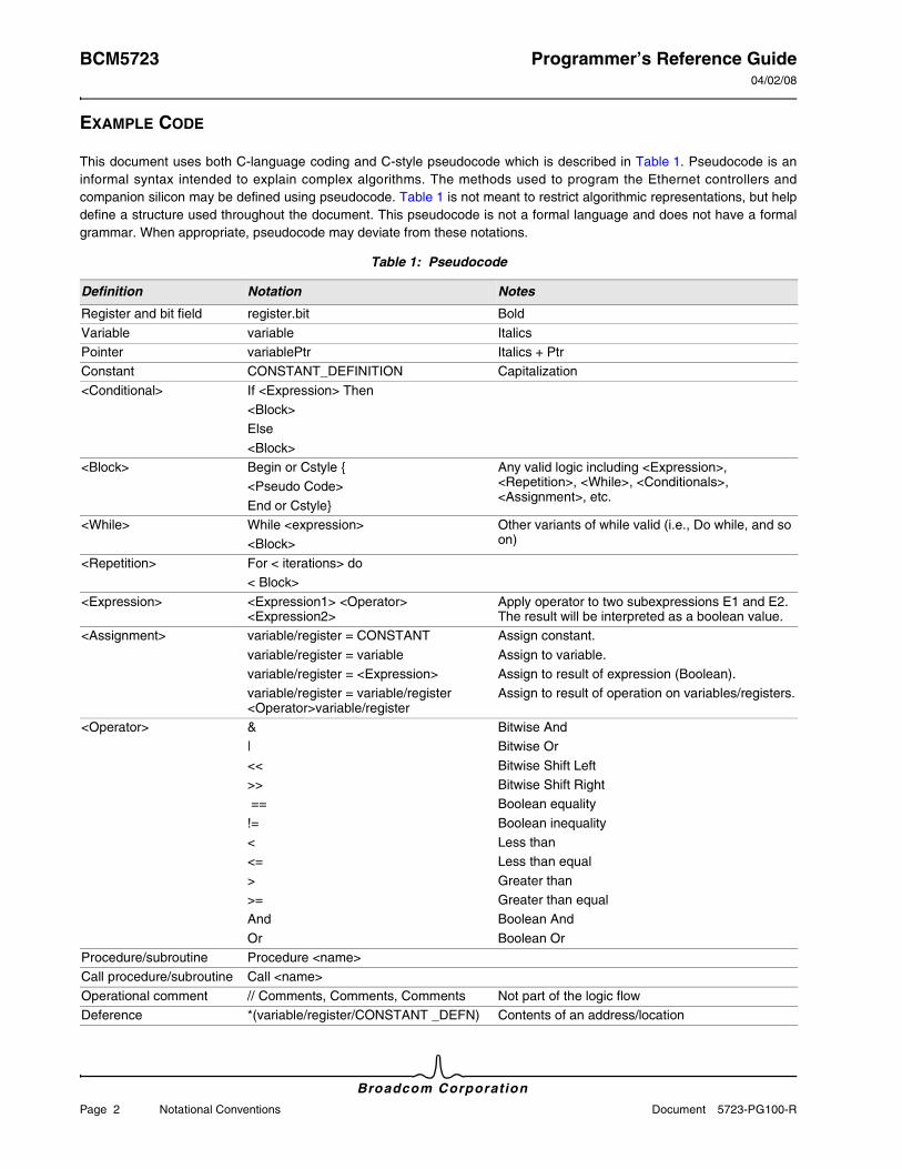
BCM5723 Programmer’s Reference Guide04/02/08
Broadcom Corporation
Page 2 Notational Conventions Document 5723-PG100-R
EXAMPLE CODE
This document uses both C-language coding and C-style pseudocode which is described in Table 1. Pseudocode is an informal syntax intended to explain complex algorithms. The methods used to program the Ethernet controllers and companion silicon may be defined using pseudocode. Table 1 is not meant to restrict algorithmic representations, but help define a structure used throughout the document. This pseudocode is not a formal language and does not have a formal grammar. When appropriate, pseudocode may deviate from these notations.
Table 1: Pseudocode
Definition Notation Notes
Register and bit field register.bit Bold
Variable variable ItalicsPointer variablePtr Italics + PtrConstant CONSTANT_DEFINITION Capitalization
<Conditional> If <Expression> Then<Block>Else
<Block><Block> Begin or Cstyle {
<Pseudo Code>
End or Cstyle}
Any valid logic including <Expression>, <Repetition>, <While>, <Conditionals>, <Assignment>, etc.
<While> While <expression> <Block>
Other variants of while valid (i.e., Do while, and so on)
<Repetition> For < iterations> do< Block>
<Expression> <Expression1> <Operator> <Expression2>
Apply operator to two subexpressions E1 and E2. The result will be interpreted as a boolean value.
<Assignment> variable/register = CONSTANT
variable/register = variablevariable/register = <Expression>variable/register = variable/register <Operator>variable/register
Assign constant.
Assign to variable.Assign to result of expression (Boolean).Assign to result of operation on variables/registers.
<Operator> &|
<<>> ==
!=<<=
>>=And
Or
Bitwise AndBitwise Or
Bitwise Shift LeftBitwise Shift RightBoolean equality
Boolean inequalityLess thanLess than equal
Greater thanGreater than equalBoolean And
Boolean OrProcedure/subroutine Procedure <name>Call procedure/subroutine Call <name>
Operational comment // Comments, Comments, Comments Not part of the logic flowDeference *(variable/register/CONSTANT _DEFN) Contents of an address/location
Programmer’s Reference Guide BCM572304/02/08
Broadcom CorporationDocument 5723-PG100-R Related Documents Page 3
RELATED DOCUMENTS
Refer to the following Broadcom documents for additional information on the Ethernet controllers:
• BCM57XX NetXtreme® Programmer’s Guide: Programming details for the BCM5700, BCM5701, BCM5702, BCM5703, BCM5704, BCM5705, BCM5721, BCM5751, BCM5752, BCM5714, and BCM5715 BCM57XX devices
• Host Programmer Reference Manual: Provides information on how to write device drivers for the Ethernet controllers.
• NetXtreme II® Programmer's Guide: Programming details for the BCM5706C, BCM5706S, and BCM5708 devices
• Data sheets, application notes, and errata documentation of following devices:
- BCM5723 MACs
BCM5723 Programmer’s Reference Guide04/02/08
Broadcom Corporation
Page 4 Introduction Document 5723-PG100-R
Section 2: Introduction
INTRODUCTION
The NetXtreme and NetLink family of Media Access Controller (MAC) devices are highly-integrated, single-chip gigabit Ethernet LAN controller solutions for high-performance network applications. The above devices integrate the following major functions to provide a single-chip solution for gigabit LAN-on-motherboard (LOM) and network interface card (NIC) applications.
• Triple-speed IEEE 802.3-compliant MAC functionality
• Triple-speed IEEE 802.3-compliant Ethernet PHY transceiver
• PCI Express® (PCIe™) bus interface
• On-chip packet buffer memory
• On-chip RISC processor for custom frame processing
PRODUCT FEATURES
Table 2: Product Features
Feature BCM5723
Data Management
VLAN tag support (IEEE 802.1Q) Yes
Layer 2 priority encoding (IEEE 802.1p) Yes
Link aggregation (IEEE 802.3ad) Yes
Full-duplex flow control (IEEE 802.3x) Yes
Programmable rules checker for advanced packet filtering and classification
Yes
Frame/packet buffer memory 48KB Rx 8KB Tx
Jumbo frame support No
TCP checksum offload on Tx & Rx for TCP over IPv4 Yes
UDP checksum offload on Tx & Rx for UDP over IPv4 Yes
IPv4 checksum offloading on Tx and Rx Yes
TCP checksum offload on Tx for TCP over IPv6 Yes
UDP checksum offload on Tx for UDP over IPv6 Yes
TCP checksum offload on Rx for TCP over IPv6 Yes
UDP checksum offload on Rx for UDP over IPv6 Yes
Hardware TCP segmentation for TCP over IPv4 Yes
Hardware TCP segmentation for TCP over IPv6 Yes
Receive-side scaling (RSS) Yes
Multiple receive descriptor queues Yes
Scatter/gather bus mastering architecture Yes
Programmer’s Reference Guide BCM572304/02/08
Broadcom CorporationDocument 5723-PG100-R Product Features Page 5
Statistics for SNMP MIB II, Ethernet like MIB, Ethernet MIB (IEEE 802.3z, Clause 30)
Yes
ASF v2.0 support Yes
iSCSI Boot Yes
IPMI Pass-Thru Lite Yes
Teaming Yes
Host Bus Interfaces
PCIe v1.1 x1 bus interface Yes
LAN Interfaces
10/100/1000BASE-T full-duplex/half-duplex Yes
Integrated 10/100/1000BASE-T transceiver Yes
Internal MII/GMII Interface Yes
Other Bus Interfaces
SMBus 2.0 interface Yes
Interface to Flash memory Yes
Interface to Serial EEPROM Yes
Flash Autoconfig Support Yes
Self-Test
Test modes (BIST, SCAN, etc) Yes
Factory-level JTAG support No
Technology
High-performance, low-overhead SW/HW interface Yes
High-speed on-chip RISC processor Yes
Wake-on-LAN (WOL) Yes
Integrated Trusted Platform Module (TPM) Security Engine No
Process voltage 1.2V
CMOS linewidth 0.65 nm
5V-tolerant PCI I/Os Yes
Table 2: Product Features
Feature BCM5723
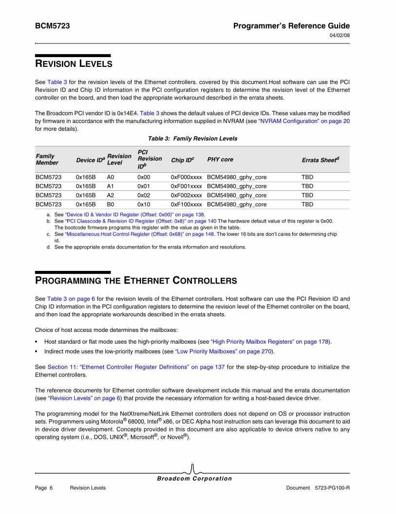
BCM5723 Programmer’s Reference Guide04/02/08
Broadcom Corporation
Page 6 Revision Levels Document 5723-PG100-R
REVISION LEVELS
See Table 3 for the revision levels of the Ethernet controllers. covered by this document.Host software can use the PCI Revision ID and Chip ID information in the PCI configuration registers to determine the revision level of the Ethernet controller on the board, and then load the appropriate workaround described in the errata sheets.
The Broadcom PCI vendor ID is 0x14E4. Table 3 shows the default values of PCI device IDs. These values may be modified by firmware in accordance with the manufacturing information supplied in NVRAM (see “NVRAM Configuration” on page 20for more details).
PROGRAMMING THE ETHERNET CONTROLLERS
See Table 3 on page 6 for the revision levels of the Ethernet controllers. Host software can use the PCI Revision ID and Chip ID information in the PCI configuration registers to determine the revision level of the Ethernet controller on the board, and then load the appropriate workarounds described in the errata sheets.
Choice of host access mode determines the mailboxes:
• Host standard or flat mode uses the high-priority mailboxes (see “High Priority Mailbox Registers” on page 178).
• Indirect mode uses the low-priority mailboxes (see “Low Priority Mailboxes” on page 270).
See Section 11: “Ethernet Controller Register Definitions” on page 137 for the step-by-step procedure to initialize the Ethernet controllers.
The reference documents for Ethernet controller software development include this manual and the errata documentation (see “Revision Levels” on page 6) that provide the necessary information for writing a host-based device driver.
The programming model for the NetXtreme/NetLink Ethernet controllers does not depend on OS or processor instruction sets. Programmers using Motorola® 68000, Intel® x86, or DEC Alpha host instruction sets can leverage this document to aid in device driver development. Concepts provided in this document are also applicable to device drivers native to any operating system (i.e., DOS, UNIX®, Microsoft®, or Novell®).
Table 3: Family Revision Levels
Family Member Device IDa
a. See “Device ID & Vendor ID Register (Offset: 0x00)” on page 138.
Revision Level
PCI Revision IDb
b. See “PCI Classcode & Revision ID Register (Offset: 0x8)” on page 140 The hardware default value of this register is 0x00. The bootcode firmware programs this register with the value as given in the table.
Chip IDc
c. See “Miscellaneous Host Control Register (Offset: 0x68)” on page 148. The lower 16 bits are don’t cares for determining chip id.
PHY core Errata Sheetd
d. See the appropriate errata documentation for the errata information and resolutions.
BCM5723 0x165B A0 0x00 0xF000xxxx BCM54980_gphy_core TBD
BCM5723 0x165B A1 0x01 0xF001xxxx BCM54980_gphy_core TBD
BCM5723 0x165B A2 0x02 0xF002xxxx BCM54980_gphy_core TBD
BCM5723 0x165B B0 0x10 0xF100xxxx BCM54980_gphy_core TBD
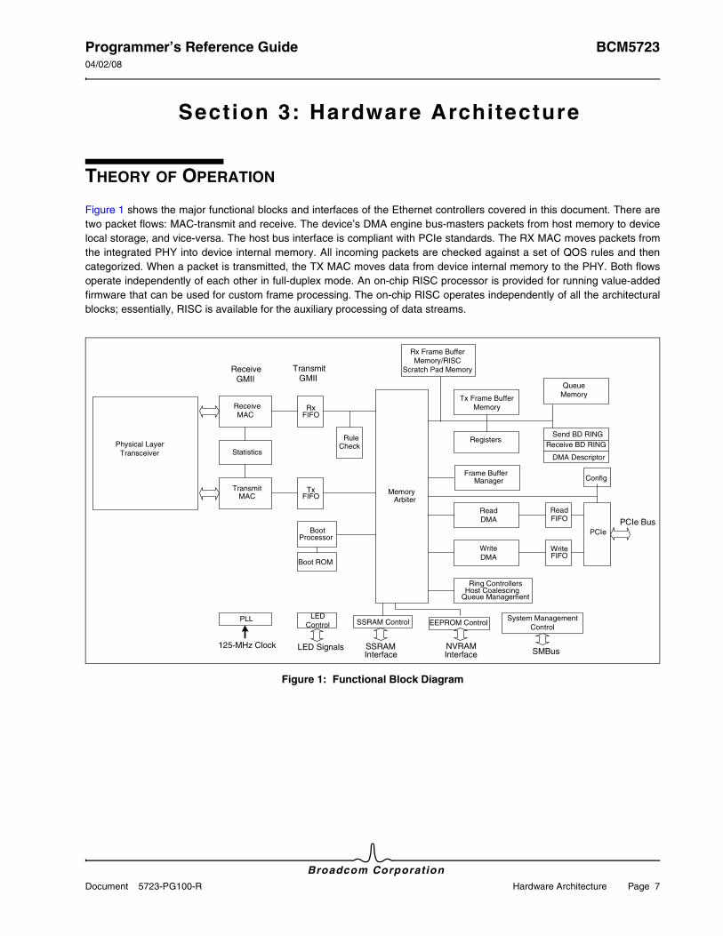
Programmer’s Reference Guide BCM572304/02/08
Broadcom CorporationDocument 5723-PG100-R Hardware Architecture Page 7
Section 3: Hardware Architecture
THEORY OF OPERATION
Figure 1 shows the major functional blocks and interfaces of the Ethernet controllers covered in this document. There are two packet flows: MAC-transmit and receive. The device’s DMA engine bus-masters packets from host memory to device local storage, and vice-versa. The host bus interface is compliant with PCIe standards. The RX MAC moves packets from the integrated PHY into device internal memory. All incoming packets are checked against a set of QOS rules and then categorized. When a packet is transmitted, the TX MAC moves data from device internal memory to the PHY. Both flows operate independently of each other in full-duplex mode. An on-chip RISC processor is provided for running value-added firmware that can be used for custom frame processing. The on-chip RISC operates independently of all the architectural blocks; essentially, RISC is available for the auxiliary processing of data streams.
Figure 1: Functional Block Diagram
ReceiveMAC
RxFIFO
TransmitMAC
TxFIFO
Statistics
RuleCheck
MemoryArbiter
Tx Frame Buffer Memory
Send BD RING
BootProcessor
Boot ROM
Frame BufferManager
Queue Memory
Read DMA
ReadFIFO
Write DMA
WriteFIFO
Registers
SSRAM Control
SSRAM Interface
PCIe Bus
Ring ControllersHost Coalescing
Queue Management
ReceiveGMII
TransmitGMII
LED Control
PLL
LED Signals125-MHz Clock
Receive BD RING
DMA Descriptor
Config
EEPROM Control
NVRAM Interface
Physical Layer Transceiver
System Management Control
SMBus
PCIe
Rx Frame Buffer Memory/RISC
Scratch Pad Memory
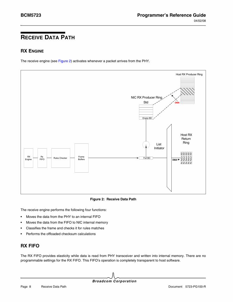
BCM5723 Programmer’s Reference Guide04/02/08
Broadcom Corporation
Page 8 Receive Data Path Document 5723-PG100-R
RECEIVE DATA PATH
RX ENGINE
The receive engine (see Figure 2) activates whenever a packet arrives from the PHY.
Figure 2: Receive Data Path
The receive engine performs the following four functions:
• Moves the data from the PHY to an internal FIFO
• Moves the data from the FIFO to NIC internal memory
• Classifies the frame and checks it for rules matches
• Performs the offloaded checksum calculations
RX FIFO
The RX FIFO provides elasticity while data is read from PHY transceiver and written into internal memory. There are no programmable settings for the RX FIFO. This FIFO’s operation is completely transparent to host software.
RXEngine
Rules CheckerRx
FIFOFrameBuffers
Empty BD
NIC RX Producer Ring
Std
Host RXReturnRing
Full BD
ListInitiator
Rx
Ret
urn
BD
Rx
Ret
urn
BD
Rx
Ret
urn
BD
Rx
Ret
urn
BD
Rx
Ret
urn
BD
Host RX Producer Ring
DMA
DMA
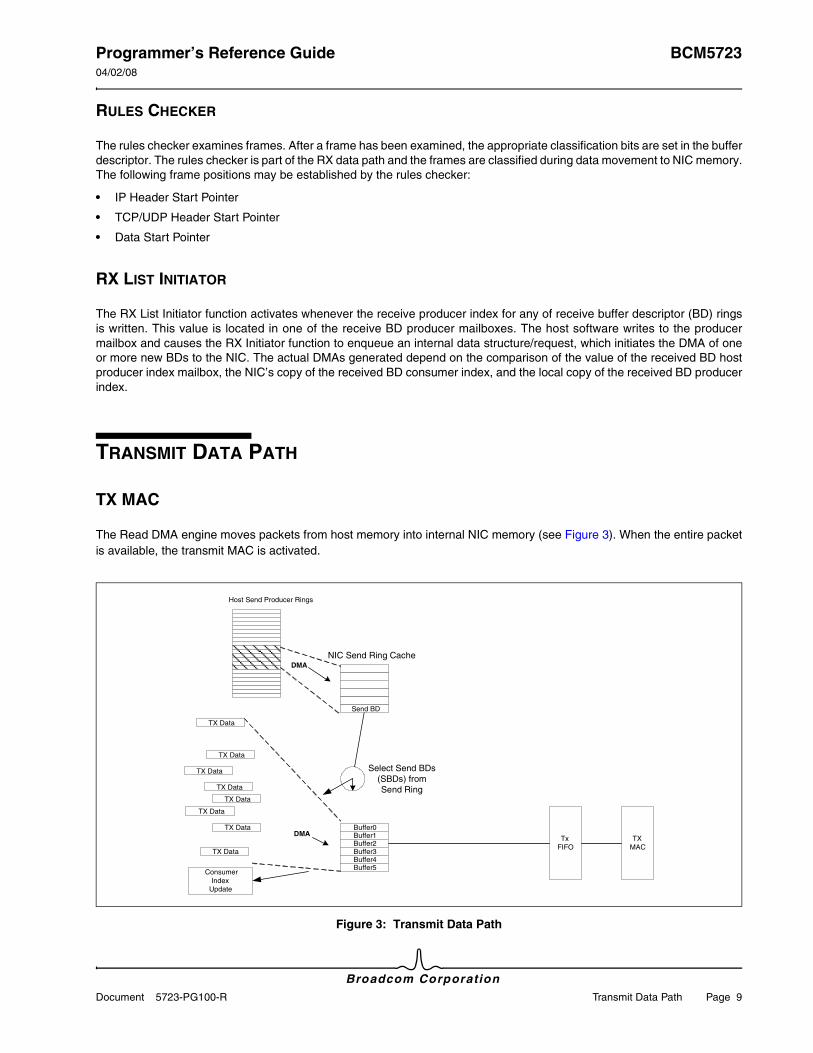
Programmer’s Reference Guide BCM572304/02/08
Broadcom CorporationDocument 5723-PG100-R Transmit Data Path Page 9
RULES CHECKER
The rules checker examines frames. After a frame has been examined, the appropriate classification bits are set in the buffer descriptor. The rules checker is part of the RX data path and the frames are classified during data movement to NIC memory. The following frame positions may be established by the rules checker:
• IP Header Start Pointer
• TCP/UDP Header Start Pointer
• Data Start Pointer
RX LIST INITIATOR
The RX List Initiator function activates whenever the receive producer index for any of receive buffer descriptor (BD) rings is written. This value is located in one of the receive BD producer mailboxes. The host software writes to the producer mailbox and causes the RX Initiator function to enqueue an internal data structure/request, which initiates the DMA of one or more new BDs to the NIC. The actual DMAs generated depend on the comparison of the value of the received BD host producer index mailbox, the NIC’s copy of the received BD consumer index, and the local copy of the received BD producer index.
TRANSMIT DATA PATH
TX MAC
The Read DMA engine moves packets from host memory into internal NIC memory (see Figure 3). When the entire packet is available, the transmit MAC is activated.
Figure 3: Transmit Data Path
TXMAC
ConsumerIndex
Update
TxFIFO
Send BD
NIC Send Ring Cache
Select Send BDs (SBDs) from Send Ring
Host Send Producer Rings
DMA
DMA
TX Data
TX Data
TX Data
TX Data
TX Data
TX Data
TX Data
TX Data
Buffer0Buffer1Buffer2Buffer3Buffer4Buffer5
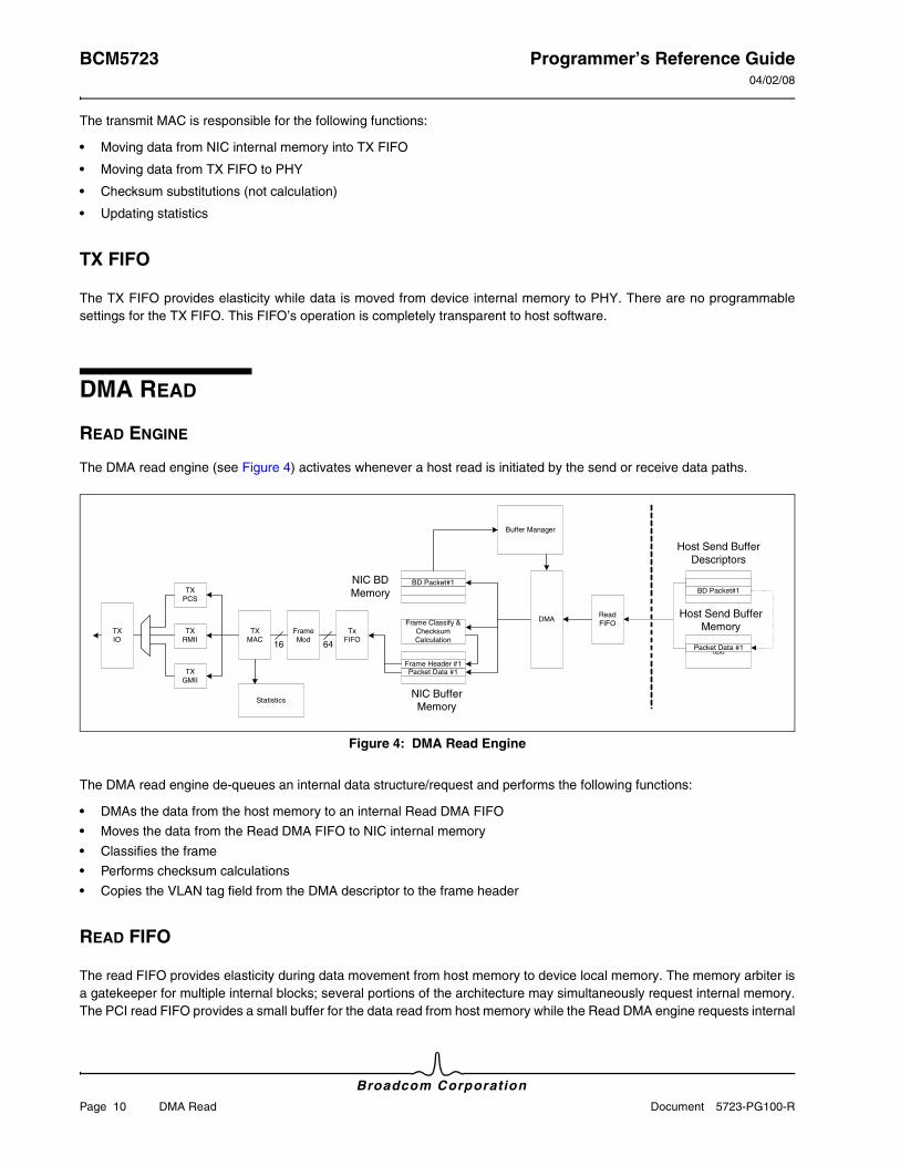
BCM5723 Programmer’s Reference Guide04/02/08
Broadcom Corporation
Page 10 DMA Read Document 5723-PG100-R
The transmit MAC is responsible for the following functions:
• Moving data from NIC internal memory into TX FIFO
• Moving data from TX FIFO to PHY
• Checksum substitutions (not calculation)
• Updating statistics
TX FIFO
The TX FIFO provides elasticity while data is moved from device internal memory to PHY. There are no programmable settings for the TX FIFO. This FIFO’s operation is completely transparent to host software.
DMA READ
READ ENGINE
The DMA read engine (see Figure 4) activates whenever a host read is initiated by the send or receive data paths.
Figure 4: DMA Read Engine
The DMA read engine de-queues an internal data structure/request and performs the following functions:
• DMAs the data from the host memory to an internal Read DMA FIFO
• Moves the data from the Read DMA FIFO to NIC internal memory
• Classifies the frame
• Performs checksum calculations
• Copies the VLAN tag field from the DMA descriptor to the frame header
READ FIFO
The read FIFO provides elasticity during data movement from host memory to device local memory. The memory arbiter is a gatekeeper for multiple internal blocks; several portions of the architecture may simultaneously request internal memory. The PCI read FIFO provides a small buffer for the data read from host memory while the Read DMA engine requests internal
text
text
DMA
BD Packet#1
Host Send BufferDescriptors
Packet Data #1
Host Send BufferMemory
Buffer Manager
BD Packet#1
Frame Classify &ChecksumCalculation
textPacket Data #1Frame Header #1
NIC BDMemory
NIC BufferMemory
TxFIFO
FrameMod
TXMAC
Statistics
TXPCS
TXRMII
TXGMII
TXIO
6416
ReadFIFO
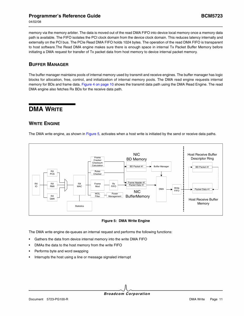
Programmer’s Reference Guide BCM572304/02/08
Broadcom CorporationDocument 5723-PG100-R DMA Write Page 11
memory via the memory arbiter. The data is moved out of the read DMA FIFO into device local memory once a memory data path is available. The FIFO isolates the PCI clock domain from the device clock domain. This reduces latency internally and externally on the PCI bus. The PCIe Read DMA FIFO holds 1024 bytes. The operation of the read DMA FIFO is transparent to host software.The Read DMA engine makes sure there is enough space in internal Tx Packet Buffer Memory before initiating a DMA request for transfer of Tx packet data from host memory to device internal packet memory.
BUFFER MANAGER
The buffer manager maintains pools of internal memory used by transmit and receive engines. The buffer manager has logic blocks for allocation, free, control, and initialization of internal memory pools. The DMA read engine requests internal memory for BDs and frame data. Figure 4 on page 10 shows the transmit data path using the DMA Read Engine. The read DMA engine also fetches Rx BDs for the receive data path.
DMA WRITE
WRITE ENGINE
The DMA write engine, as shown in Figure 5, activates when a host write is initiated by the send or receive data paths.
Figure 5: DMA Write Engine
The DMA write engine de-queues an internal request and performs the following functions:
• Gathers the data from device internal memory into the write DMA FIFO
• DMAs the data to the host memory from the write FIFO
• Performs byte and word swapping
• Interrupts the host using a line or message signaled interrupt
text
RXPCS
RXRMII
RXGMII
RXIO
RXMAC
FrameMod
WOLFilter
RxFIFO
Power Management
Frame Header #1Packet Data #1
Frame Cracker
Checksum Calculation
Rules Checker
Statistics
BD Packet #1
NIC BD Memory
NIC BufferMemory
Buffer Manager
DMA Packet Data #1
BD Packet #1
Host Receive Buffer Descriptor Ring
Host Receive BufferMemory
WriteFIFO
BCM5723 Programmer’s Reference Guide04/02/08
Broadcom Corporation
Page 12 LED Control Document 5723-PG100-R
WRITE FIFO
The write FIFO provides elasticity during data movement from device memory to the host memory. The write FIFO absorbs small delays created by PCIe bus arbitration. The NetXtreme family uses the write FIFO to buffer data, so internal memory arbitration is efficient. Additionally, the FIFO isolates the PCI clock domain from the device’s clock domain. This reduces latency on the PCI bus during the write operation (wait states are not inserted while data is fetched from internal memory). The operation of the write DMA FIFO is transparent to host software.
BUFFER MANAGER
The buffer manager maintains pools of internal memory used in transmit and receive functions. The buffer manager has logic blocks for allocation, free, control, and initialization of internal memory pools. The receive MAC requests NIC Rx Mbuf memory so inbound frames can be buffered. The read DMA engine requests the device Tx Mbuf memory for buffering the packets from host memory before they are sent out on the wire. The DMA write engine requests a small amount of internal memory for DMA and interrupt operations. The usage of this internal memory is transparent to host software, and does not affect device/system performance.
LED CONTROL
The Ethernet controller supports four LEDs—one for data traffic in either direction and three for 10/100/1000 Mbps links established. The traffic LED blinks during transmit and receive data movement through the device. The blink rate is programmable with a default of approximately 15 Hz. The link LEDs turn either on or off depending on the link established. All LEDs can be controlled directly by software via the override bits in LED_Control register (see “LED Control Register (Offset: 0x40C)” on page 182). When the override bit is off, the link LEDs are automatically set by the hardware as long as link is up:
• 10 Mbps LED—Port mode is set to MII and Mode 10 Mbps in MI Status register is set.
• 100 Mbps LED—Port mode is set to MII and Mode 10 Mbps in MI Status register is not set.
• 1000 Mbps LED—port mode is set to GMII or TBI.
The link status information is obtained either from auto-polling the PHY if bit 4 (Port Polling) of MI Mode register is set, or from the LNKRDY input pin if this bit is not set.
MEMORY ARBITER
The Memory Arbiter (MA) is a gatekeeper for internal memory access. The MA is responsible for decoding the internal memory addresses that correspond to Ethernet controller data structures and control maps. The MA is responsible for accessing both internal and external SSRAM. If a functional block faults or traps during access to internal/external memory, the MA handles the failing condition and reports the error in a status register. In addition to architectural blocks, the MA provides a gateway for the RISC processors to access local memory. Each RISC has an MA interface that pipelines up to three access requests. The MA negotiates local memory access, so all portions of the architecture are provided with fair access to memory resources. The MA prevents starvation and bounds access latency. Host software may enable/disable/reset the MA, and there are no tunable parameters.
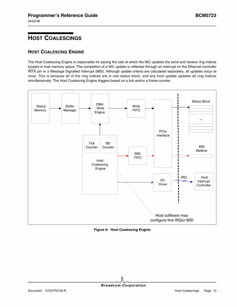
Programmer’s Reference Guide BCM572304/02/08
Broadcom CorporationDocument 5723-PG100-R Host Coalescings Page 13
HOST COALESCINGS
HOST COALESCING ENGINE
The Host Coalescing Engine is responsible for pacing the rate at which the NIC updates the send and receive ring indices located in host memory space. The completion of a NIC update is reflected through an interrupt on the Ethernet controller INTA pin or a Message Signalled Interrupt (MSI). Although update criteria are calculated separately, all updates occur at once. This is because all of the ring indices are in one status block, and any host update updates all ring indices simultaneously. The Host Coalescing Engine triggers based on a tick and/or a frame counter.
Figure 6: Host Coalescing Engine
...
DMAWrite
Engine
Status Block
PCIeInterface
BufferManager
HostCoalescing
Engine
MSI Mailbox
I/ODriver
HostInterrupt
Controller
IRQ
WriteFIFO
TickCounter
BDCounter
StatusMemory
Host software may configure line IRQor MSI
MSIFIFO
BCM5723 Programmer’s Reference Guide04/02/08
Broadcom Corporation
Page 14 10BT/100BTx/1000BASE-T Transceiver Document 5723-PG100-R
A host update occurs whenever one of the following criteria is met:
• The number of BDs consumed for frames received, without updating receive indices on the host, is equal to or has exceeded the threshold set in the Receive_Max_Coalesced_BD register (see “Receive Max Coalesced BD Count Register (Offset: 0x3C10)” on page 253).
• The number of BDs consumed for transmitting frames, without updating the send indices, on the host is equal to or has exceeded the threshold set in the Send_Max_Coalesced_BD register (see “Send Max Coalesced BD Count Register (Offset: 0x3C14)” on page 254). Updates can occur when the number of BDs (not frames) meets the thresholds set in the various coalescing registers (see Section 10: “Interrupt Processing” on page 128 for more information).
• The receive coalescing timer has expired, and new frames have been received on any of the receive rings, and a host update has not occurred. The receive coalescing timer is then reset to the value in the Receive_Coalescing_Ticksregister (see “Send Coalescing Ticks Register (Offset: 0x3C0C)” on page 253).
• The send coalescing timer has expired, and new frames have been consumed from any send ring, and a host update has not occurred. The send coalescing timer is then reset to the value in the Send_Coalescing_Ticks register.
MSI FIFO
This FIFO is eight entries deep and four bits wide. This FIFO is used to send MSIs via the PCI interface. The host coalescing engine uses this FIFO to enqueue requests for the generation of MSI. There are no configurable options for this FIFO and this FIFOs operation is completely transparent to host software.
STATUS BLOCK
This data structure contains consumer and producer indices/values. Host software reads this control block, to assess hardware updates in the send and receive rings. Two copies of the status block exist. The local copy is DMAed to host memory by the DMA write engine. Host software does not want to generate PCI transactions to read ring status; rather quicker memory bus transactions are desired. The host coalescing engine enqueues a request to the DMA write engine, so host software gets a refreshed copy of status. The status block is refreshed before a line IRQ or MSI is generated. See “Status Block Format” on page 32 for a complete discussion of the status block.
10BT/100BTX/1000BASE-T TRANSCEIVER
Refer to the PHY transceiver data sheet for hardware architectural details of the triple-speed Ethernet PHY transceiver integrated in the Ethernet controllers covered by this document.
AUTO-NEGOTIATION
The Ethernet controller devices negotiate their mode of operation over the twisted-pair link using the auto-negotiation mechanism defined in the IEEE 802.3u and IEEE 802.3ab specifications. Auto-negotiation can be enabled or disabled by hardware or software control. When the auto-negotiation function is enabled, the Ethernet controllers automatically choose the mode of operation by advertising its abilities and comparing them with those received from its link partner. The Ethernet controllers can be configured to advertise 1000BASE-T full-duplex and/or half-duplex, 100BASE-TX full-duplex and/or half-duplex, and 10BASE-T full-duplex and/or half-duplex. The transceiver negotiates with its link partner and chooses the
Note: These are 10/100 devices only and use a 10-/100-Mbps speed transceiver.
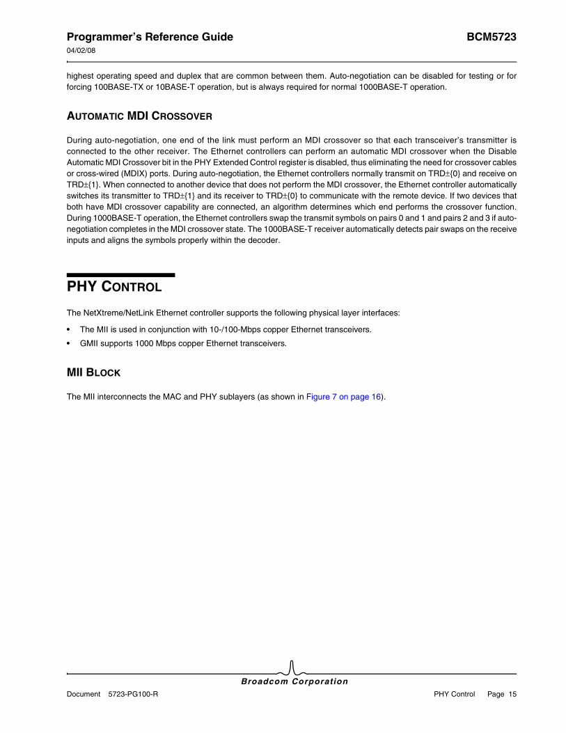
Programmer’s Reference Guide BCM572304/02/08
Broadcom CorporationDocument 5723-PG100-R PHY Control Page 15
highest operating speed and duplex that are common between them. Auto-negotiation can be disabled for testing or for forcing 100BASE-TX or 10BASE-T operation, but is always required for normal 1000BASE-T operation.
AUTOMATIC MDI CROSSOVER
During auto-negotiation, one end of the link must perform an MDI crossover so that each transceiver’s transmitter is connected to the other receiver. The Ethernet controllers can perform an automatic MDI crossover when the Disable Automatic MDI Crossover bit in the PHY Extended Control register is disabled, thus eliminating the need for crossover cables or cross-wired (MDIX) ports. During auto-negotiation, the Ethernet controllers normally transmit on TRD±{0} and receive on TRD±{1}. When connected to another device that does not perform the MDI crossover, the Ethernet controller automatically switches its transmitter to TRD±{1} and its receiver to TRD±{0} to communicate with the remote device. If two devices that both have MDI crossover capability are connected, an algorithm determines which end performs the crossover function. During 1000BASE-T operation, the Ethernet controllers swap the transmit symbols on pairs 0 and 1 and pairs 2 and 3 if auto-negotiation completes in the MDI crossover state. The 1000BASE-T receiver automatically detects pair swaps on the receive inputs and aligns the symbols properly within the decoder.
PHY CONTROL
The NetXtreme/NetLink Ethernet controller supports the following physical layer interfaces:
• The MII is used in conjunction with 10-/100-Mbps copper Ethernet transceivers.
• GMII supports 1000 Mbps copper Ethernet transceivers.
MII BLOCK
The MII interconnects the MAC and PHY sublayers (as shown in Figure 7 on page 16).
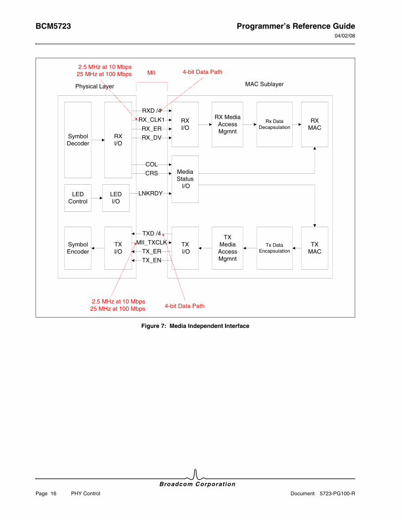
BCM5723 Programmer’s Reference Guide04/02/08
Broadcom Corporation
Page 16 PHY Control Document 5723-PG100-R
Figure 7: Media Independent Interface
RX I/O
RXD /4
RX_CLK1
RX_ER
RX_DV
TX I/O
TXD /4
MII_TXCLK
TX_ER
TX_EN
MediaStatus
I/O
COL
CRS
LNKRDY
RX MediaAccessMgmnt
RXMAC
Rx DataDecapsulation
TXMediaAccessMgmnt
TXMAC
Tx DataEncapsulation
MAC SublayerPhysical Layer
RX I/O
SymbolDecoder
TXI/O
SymbolEncoder
4-bit Data Path
2.5 MHz at 10 Mbps25 MHz at 100 Mbps 4-bit Data Path
LEDControl
LEDI/O
2.5 MHz at 10 Mbps25 MHz at 100 Mbps MII
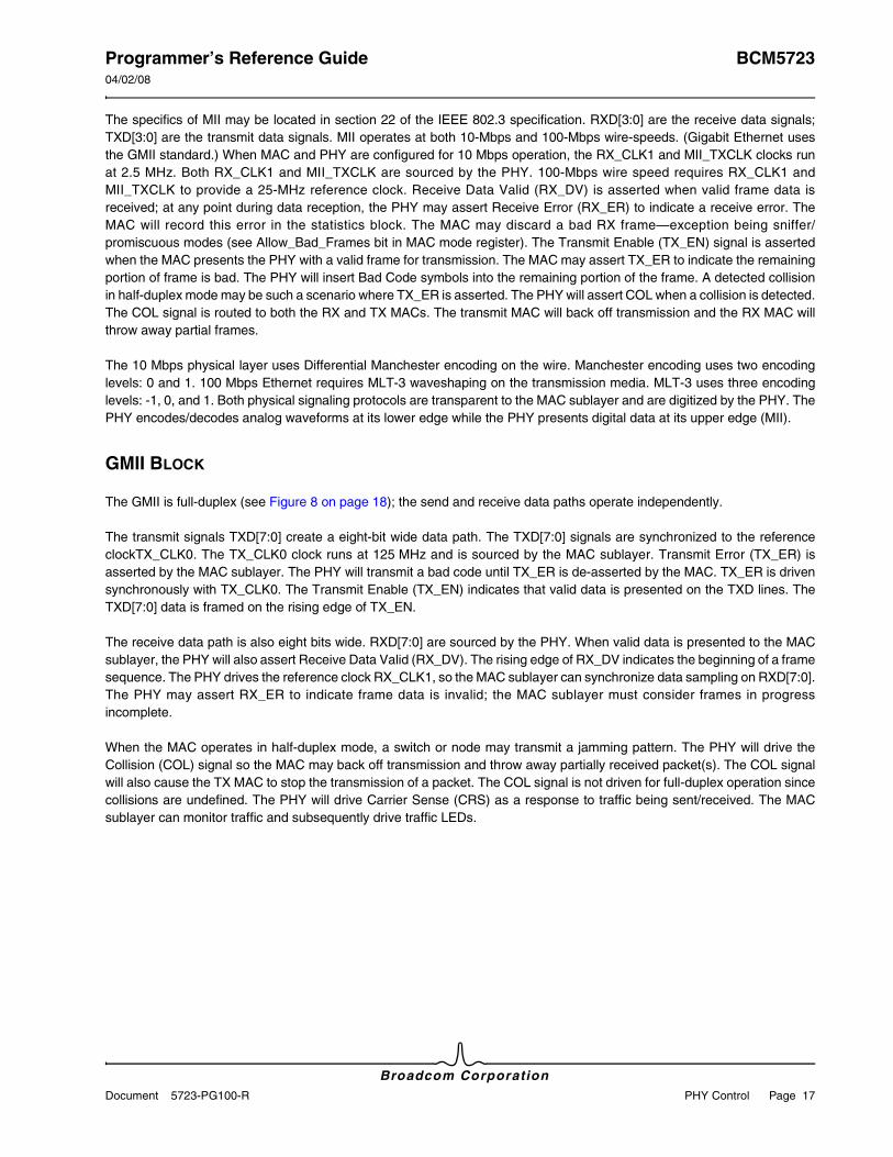
Programmer’s Reference Guide BCM572304/02/08
Broadcom CorporationDocument 5723-PG100-R PHY Control Page 17
The specifics of MII may be located in section 22 of the IEEE 802.3 specification. RXD[3:0] are the receive data signals; TXD[3:0] are the transmit data signals. MII operates at both 10-Mbps and 100-Mbps wire-speeds. (Gigabit Ethernet uses the GMII standard.) When MAC and PHY are configured for 10 Mbps operation, the RX_CLK1 and MII_TXCLK clocks run at 2.5 MHz. Both RX_CLK1 and MII_TXCLK are sourced by the PHY. 100-Mbps wire speed requires RX_CLK1 and MII_TXCLK to provide a 25-MHz reference clock. Receive Data Valid (RX_DV) is asserted when valid frame data is received; at any point during data reception, the PHY may assert Receive Error (RX_ER) to indicate a receive error. The MAC will record this error in the statistics block. The MAC may discard a bad RX frame—exception being sniffer/promiscuous modes (see Allow_Bad_Frames bit in MAC mode register). The Transmit Enable (TX_EN) signal is asserted when the MAC presents the PHY with a valid frame for transmission. The MAC may assert TX_ER to indicate the remaining portion of frame is bad. The PHY will insert Bad Code symbols into the remaining portion of the frame. A detected collision in half-duplex mode may be such a scenario where TX_ER is asserted. The PHY will assert COL when a collision is detected. The COL signal is routed to both the RX and TX MACs. The transmit MAC will back off transmission and the RX MAC will throw away partial frames.
The 10 Mbps physical layer uses Differential Manchester encoding on the wire. Manchester encoding uses two encoding levels: 0 and 1. 100 Mbps Ethernet requires MLT-3 waveshaping on the transmission media. MLT-3 uses three encoding levels: -1, 0, and 1. Both physical signaling protocols are transparent to the MAC sublayer and are digitized by the PHY. The PHY encodes/decodes analog waveforms at its lower edge while the PHY presents digital data at its upper edge (MII).
GMII BLOCK
The GMII is full-duplex (see Figure 8 on page 18); the send and receive data paths operate independently.
The transmit signals TXD[7:0] create a eight-bit wide data path. The TXD[7:0] signals are synchronized to the reference clockTX_CLK0. The TX_CLK0 clock runs at 125 MHz and is sourced by the MAC sublayer. Transmit Error (TX_ER) is asserted by the MAC sublayer. The PHY will transmit a bad code until TX_ER is de-asserted by the MAC. TX_ER is driven synchronously with TX_CLK0. The Transmit Enable (TX_EN) indicates that valid data is presented on the TXD lines. The TXD[7:0] data is framed on the rising edge of TX_EN.
The receive data path is also eight bits wide. RXD[7:0] are sourced by the PHY. When valid data is presented to the MAC sublayer, the PHY will also assert Receive Data Valid (RX_DV). The rising edge of RX_DV indicates the beginning of a frame sequence. The PHY drives the reference clock RX_CLK1, so the MAC sublayer can synchronize data sampling on RXD[7:0]. The PHY may assert RX_ER to indicate frame data is invalid; the MAC sublayer must consider frames in progress incomplete.
When the MAC operates in half-duplex mode, a switch or node may transmit a jamming pattern. The PHY will drive the Collision (COL) signal so the MAC may back off transmission and throw away partially received packet(s). The COL signal will also cause the TX MAC to stop the transmission of a packet. The COL signal is not driven for full-duplex operation since collisions are undefined. The PHY will drive Carrier Sense (CRS) as a response to traffic being sent/received. The MAC sublayer can monitor traffic and subsequently drive traffic LEDs.
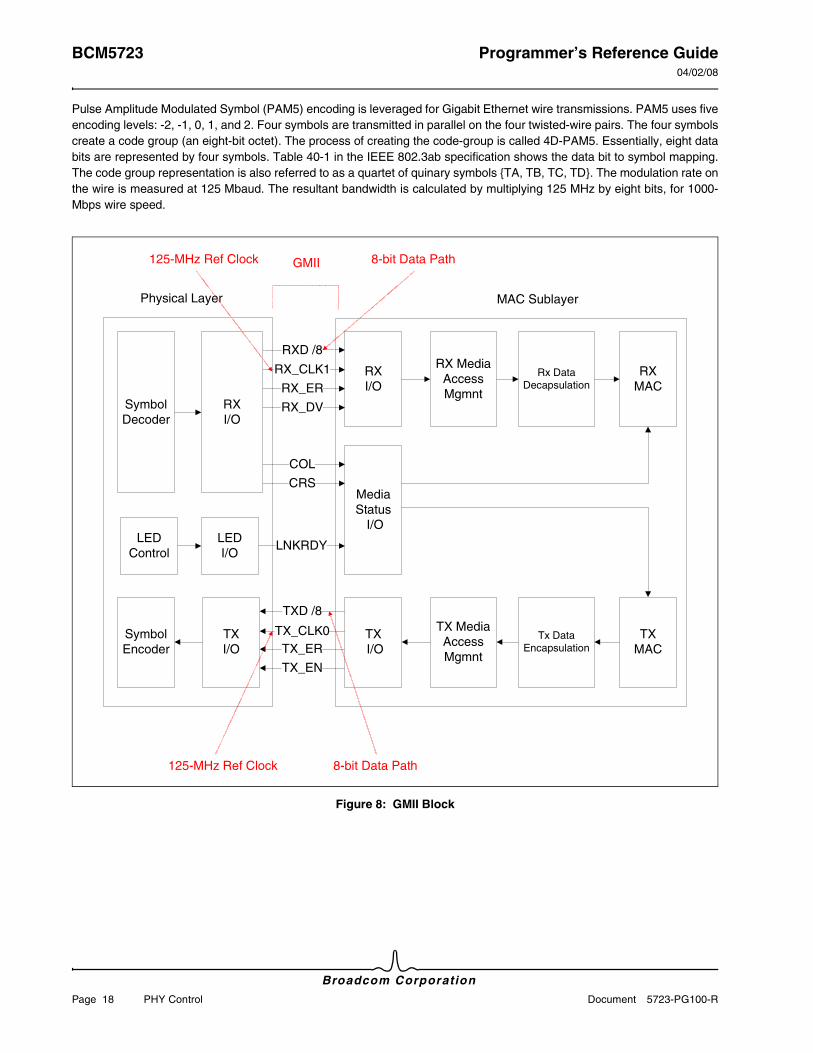
BCM5723 Programmer’s Reference Guide04/02/08
Broadcom Corporation
Page 18 PHY Control Document 5723-PG100-R
Pulse Amplitude Modulated Symbol (PAM5) encoding is leveraged for Gigabit Ethernet wire transmissions. PAM5 uses five encoding levels: -2, -1, 0, 1, and 2. Four symbols are transmitted in parallel on the four twisted-wire pairs. The four symbols create a code group (an eight-bit octet). The process of creating the code-group is called 4D-PAM5. Essentially, eight data bits are represented by four symbols. Table 40-1 in the IEEE 802.3ab specification shows the data bit to symbol mapping. The code group representation is also referred to as a quartet of quinary symbols {TA, TB, TC, TD}. The modulation rate on the wire is measured at 125 Mbaud. The resultant bandwidth is calculated by multiplying 125 MHz by eight bits, for 1000-Mbps wire speed.
Figure 8: GMII Block
RX I/O
RXD /8
RX_CLK1
RX_ER
RX_DV
TX I/O
TXD /8
TX_CLK0TX_ER
TX_EN
MediaStatus
I/O
COL
CRS
LNKRDY
RX MediaAccessMgmnt
RXMAC
Rx DataDecapsulation
TX MediaAccessMgmnt
TXMAC
Tx DataEncapsulation
MAC SublayerPhysical Layer
RX I/O
SymbolDecoder
LEDControl
TXI/O
SymbolEncoder
125-MHz Ref Clock 8-bit Data Path
LEDI/O
8-bit Data Path125-MHz Ref Clock
GMII
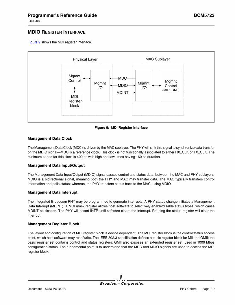
Programmer’s Reference Guide BCM572304/02/08
Broadcom CorporationDocument 5723-PG100-R PHY Control Page 19
MDIO REGISTER INTERFACE
Figure 9 shows the MDI register interface.
Figure 9: MDI Register Interface
Management Data Clock
The Management Data Clock (MDC) is driven by the MAC sublayer. The PHY will sink this signal to synchronize data transfer on the MDIO signal—MDC is a reference clock. This clock is not functionally associated to either RX_CLK or TX_CLK. The minimum period for this clock is 400 ns with high and low times having 160 ns duration.
Management Data Input/Output
The Management Data Input/Output (MDIO) signal passes control and status data, between the MAC and PHY sublayers. MDIO is a bidirectional signal, meaning both the PHY and MAC may transfer data. The MAC typically transfers control information and polls status; whereas, the PHY transfers status back to the MAC, using MDIO.
Management Data Interrupt
The integrated Broadcom PHY may be programmed to generate interrupts. A PHY status change initiates a Management Data Interrupt (MDINT). A MDI mask register allows host software to selectively enable/disable status types, which cause MDINT notification. The PHY will assert INTR until software clears the interrupt. Reading the status register will clear the interrupt.
Management Register Block
The layout and configuration of MDI register block is device dependent. The MDI register block is the control/status access point, which host software may read/write. The IEEE 802.3 specification defines a basic register block for MII and GMII; the basic register set contains control and status registers. GMII also exposes an extended register set, used in 1000 Mbps configuration/status. The fundamental point is to understand that the MDC and MDIO signals are used to access the MDI register block.
MAC Sublayer
Mgmnt I/O
MgmntControl
(MII & GMII)
Physical Layer
MgmntI/O
MgmntControl
MDC
MDIO
MDINTMDI
Registerblock
BCM5723 Programmer’s Reference Guide04/02/08
Broadcom Corporation
Page 20 NVRAM Configuration Document 5723-PG100-R
Section 4: NVRAM Configuration
OVERVIEW
Broadcom NetXtreme and NetLink controllers require the use of an external non-volatile memory (NVRAM) device (Flash or SEEPROM), which contains a bootcode program that the controller's on-chip CPU core loads and executes upon release from reset. This external NVRAM device also contains many configuration items that direct the behavior of the controller, enable/disable various management and/or value-add firmware components, etc.
All configuration settings are default-configured in the official release binary image files provided in Broadcom's CD software releases. However, the settings chosen as default by Broadcom may not be what best suits a particular OEM's application, so some settings may need to be changed by the OEM.
Details relating to the NVRAM can be found in NetXtreme/NetLink NVRAM Access Broadcom application note (Netxtreme-AN50X-R). Some of the topics addressed by this application note include the following:
• Programming NVRAM (sample C code, x86 assembly)
• NVRAM map
• Configuration settings
• Bootcode
• Multiple boot agent (MBA), PXE, etc.
SELF-BOOT
Some NetLink controllers offer a capability known as self-boot. Self-boot allows the controller to use a very small, low-cost, external NVRAM device that contains only a very condensed amount of configuration information, along with any small bootcode patches that may be necessary to optimize the functionality of a particular controller.
Details relating to self-boot can be found in Self Boot Option (5754X_5787X-AN10X-R) and NetXtreme/NetLink Software Self-Boot NVRAM (NetXtreme-AN40X-R) Broadcom application notes.
Note: NVRAM CRC-32: There are multiple distinct regions contained within the NVRAM map. Each of these regions has its own CRC-32 checksum value associated with it. If any data element contained within a region is modified, then that region's CRC-32 value must also be updated. Details relating to calculating the CRC-32 can be found in Calculating CRC32 Checksums for Broadcom NetLink, NetXtreme, and NetXtreme II ControllersBroadcom application note (NetXtreme_NetXtremeII-AN20X-R).
Programmer’s Reference Guide BCM572304/02/08
Broadcom CorporationDocument 5723-PG100-R Common Data Structures Page 21
Section 5: Common Data Structures
THEORY OF OPERATION
Several device data structures are common to the receive, transmit, and interrupt processing routines. These data structures are hardware-related and are used by device drivers to read and update state information.
DESCRIPTOR RINGS
In order to send and receive packets, the host and the controller use a series of shared buffer descriptor (BD) rings to communicate information back and forth. Each ring is composed of an array of buffer descriptors that reside in host memory. These buffer descriptors point to either send or receive packet data buffers. The largest amount of data that a single buffer may contain is 65535 (64K-1) bytes (The length field in BD is 16 bits). Multiple descriptors can be used per packet in order to achieve scatter-gather DMA capabilities.
There are three main types of descriptor rings:
• Send Rings
• Receive Producer Rings
• Receive Return Rings
Note: The maximum number of Send BDs for a single packet is (0.75)*(ring size).
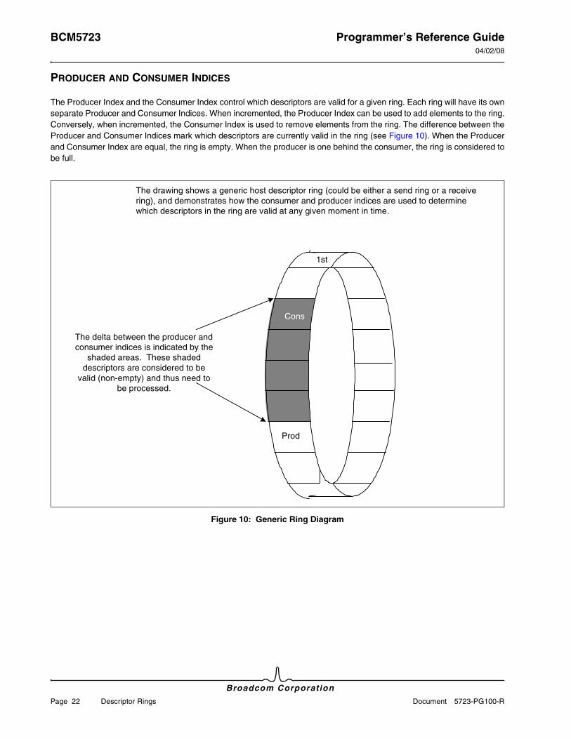
BCM5723 Programmer’s Reference Guide04/02/08
Broadcom Corporation
Page 22 Descriptor Rings Document 5723-PG100-R
PRODUCER AND CONSUMER INDICES
The Producer Index and the Consumer Index control which descriptors are valid for a given ring. Each ring will have its own separate Producer and Consumer Indices. When incremented, the Producer Index can be used to add elements to the ring. Conversely, when incremented, the Consumer Index is used to remove elements from the ring. The difference between the Producer and Consumer Indices mark which descriptors are currently valid in the ring (see Figure 10). When the Producer and Consumer Index are equal, the ring is empty. When the producer is one behind the consumer, the ring is considered to be full.
Figure 10: Generic Ring Diagram
The drawing shows a generic host descriptor ring (could be either a send ring or a receive ring), and demonstrates how the consumer and producer indices are used to determine which descriptors in the ring are valid at any given moment in time.
1st
Cons
Prod
The delta between the producer and consumer indices is indicated by the
shaded areas. These shaded descriptors are considered to be
valid (non-empty) and thus need to be processed.
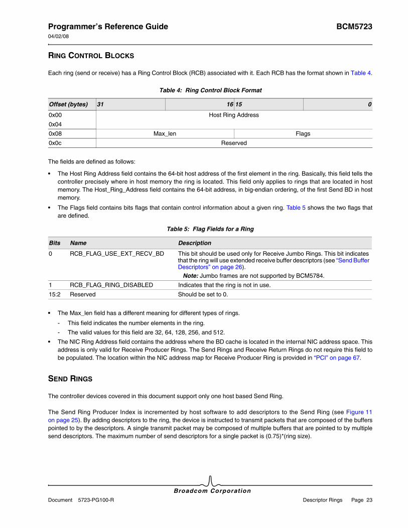
Programmer’s Reference Guide BCM572304/02/08
Broadcom CorporationDocument 5723-PG100-R Descriptor Rings Page 23
RING CONTROL BLOCKS
Each ring (send or receive) has a Ring Control Block (RCB) associated with it. Each RCB has the format shown in Table 4.
The fields are defined as follows:
• The Host Ring Address field contains the 64-bit host address of the first element in the ring. Basically, this field tells the controller precisely where in host memory the ring is located. This field only applies to rings that are located in host memory. The Host_Ring_Address field contains the 64-bit address, in big-endian ordering, of the first Send BD in host memory.
• The Flags field contains bits flags that contain control information about a given ring. Table 5 shows the two flags that are defined.
• The Max_len field has a different meaning for different types of rings.
- This field indicates the number elements in the ring.
- The valid values for this field are 32, 64, 128, 256, and 512.
• The NIC Ring Address field contains the address where the BD cache is located in the internal NIC address space. This address is only valid for Receive Producer Rings. The Send Rings and Receive Return Rings do not require this field to be populated. The location within the NIC address map for Receive Producer Ring is provided in “PCI” on page 67.
SEND RINGS
The controller devices covered in this document support only one host based Send Ring.
The Send Ring Producer Index is incremented by host software to add descriptors to the Send Ring (see Figure 11 on page 25). By adding descriptors to the ring, the device is instructed to transmit packets that are composed of the buffers pointed to by the descriptors. A single transmit packet may be composed of multiple buffers that are pointed to by multiple send descriptors. The maximum number of send descriptors for a single packet is (0.75)*(ring size).
Table 4: Ring Control Block Format
Offset (bytes) 31 16 15 0
0x00 Host Ring Address
0x04
0x08 Max_len Flags
0x0c Reserved
Table 5: Flag Fields for a Ring
Bits Name Description
0 RCB_FLAG_USE_EXT_RECV_BD This bit should be used only for Receive Jumbo Rings. This bit indicates that the ring will use extended receive buffer descriptors (see “Send Buffer Descriptors” on page 26).
Note: Jumbo frames are not supported by BCM5784.
1 RCB_FLAG_RING_DISABLED Indicates that the ring is not in use.
15:2 Reserved Should be set to 0.

BCM5723 Programmer’s Reference Guide04/02/08
Broadcom Corporation
Page 24 Descriptor Rings Document 5723-PG100-R
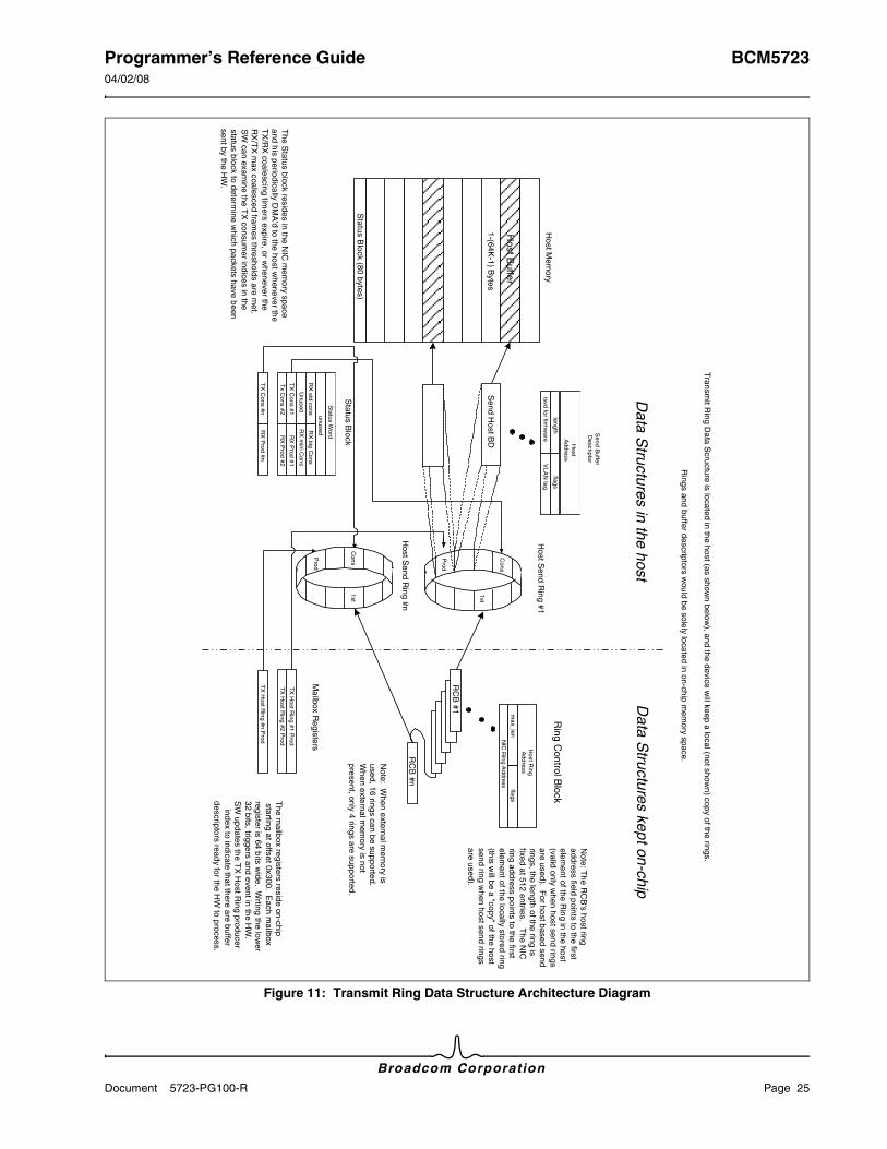
Programmer’s Reference Guide BCM572304/02/08
Broadcom CorporationDocument 5723-PG100-R Page 25
Figure 11: Transmit Ring Data Structure Architecture Diagram
Host M
emory
1-(64K-1) B
ytes
Host B
uffer
Send H
ost BD
Ring C
ontrol Block
1st
Host R
ing
Add
ress
ma
x_len
NIC
Rin
g Add
ress
flags
Host S
end Ring #1
Host S
end Ring #n
1st
Note: T
he RC
B's host ring
address field points to the first
element of the R
ing in the host
(valid only when host send rings
are used). For host based send
rings, the length of the ring isfixed at 512 entries. T
he NIC
ring address points to the first
element of the locally stored ring
(this will be a "copy" of the host
send ring when host sen
d ringsare used).
Cons
Prod
RC
B #1
RC
B #n
Status W
ord
unusedR
X P
rod #
1
RX
std cons
RX
Prod
#2
Unused
Status B
lock
RX
big
Co
ns
RX
min
i Con
s
TX
Co
ns #1
Tx C
ons #2
RX
Pro
d #nT
X C
ons #n
Prod
Con
s
Mailbox R
egisters
TX
Host R
ing #1 P
rod
TX
Host R
ing #2 P
rod
TX
Ho
st Rin
g #n Prod
Status B
lock (80 bytes)
The S
tatus block resides in the NIC
mem
ory spacea
nd his periodically DM
A'd to the host w
henever theT
X/R
X coalescing tim
ers expire, or whenever the
RX
/TX
max coalesced fram
es thresholds are met.
SW
can examine the T
X consum
er indices in thestatus block to determ
ine which pa
ckets have beensent by the H
W.
The m
ailbox registers reside on-chipstarting at offset 0x300. E
ach mailbox
register is 64 bits w
ide. Wrting the lo
wer
32 bits, triggers and event in the HW
.S
W updates the T
X H
ost Ring producer
index to indicate that there are bufferdescriptors ready for the H
W to process.
Note: W
hen external mem
ory isused, 16 rings can be supporte
d.W
hen external mem
ory is notpresent, only 4 rings are supported
.
Host
Add
ress
length
rsvd for firmw
are
Sen
d Buffe
r D
escriptor
flags
VL
AN
tag
Data S
tructures in the hostD
ata Structures kept on-chip
Transm
it Ring D
ata Scructure is located in the host (as show
n below), and the device
will keep a local (not show
n) copy of the rings.
Rings and buffer descriptors w
ould be solely located in on-chip m
emory space.

BCM5723 Programmer’s Reference Guide04/02/08
Broadcom Corporation
Page 26 Document 5723-PG100-R
Send Buffer Descriptors
The format of an individual send buffer descriptor is shown in Table 6.
The fields are defined as follows:
• The Host Address field contains the 64-bit host address of the buffer that the descriptor points to. A length of 0 indicates that the descriptor does not have a buffer associated with it.
• The Flags field contains bits flags that contain control information for the device for transmitting the packets. The defined flags are listed in Table 7.
Table 6: Send Buffer Descriptors Format
Offset (Bytes) 31 16 15 0
0x00 Host Address [63:0]
0x04
0x08 Length [15:0] Flags [15] HdrLen [7:5] Flags [11:0]
0x0c HdrLen [4:0] MSS [10:0] VLAN Tag
Table 7: Defined Flags for Send Buffer Descriptors
Bits Name Description
0 TCP_UDP_CKSUMa
a. Indicates that this bit should be set in all descriptors for a given packet if the desired capability is to be enabled for that packet.
If set to 1, the controller replaces the TCP/UDP checksum field of TCP/UDP packets with the hardware calculated TCP/UDP checksum for the packet associated with this descriptor.
1 IP_CKSUM If set to 1, the controller replaces the IPv4 checksum field of TCP/UDP packets over IPv4 with the hardware calculated IPv4 checksum for the packet associated with this descriptor. This bit should only be set in the descriptor that points to the buffer that contains the IPv4 header. It is assumed that the IPv4 header is contained in a single buffer.
2 PACKET_END If set to 1, the packet ends with the data in the buffer pointed to by this descriptor.
5:3 Reserved Should be set to 0.
6 VLAN_TAGa If set to 1, the device inserts an IEEE 802.1Q VLAN tag into the packet. The 16-bit TCI (Tag Control Information) field of four byte VLAN tag comes from the VLAN Tag field in the descriptor.
7 COAL_NOW If set to 1, the device immediately updates the Send Consumer Index after the buffer associated with this descriptor has been transferred via DMA to NIC memory from host memory. An interrupt may or may not be generated according to the state of the interrupt avoidance mechanisms. If this bit is set to 0, then the Consumer Index is only updated as soon as one of the host interrupt coalescing conditions has been met.
8 CPU_PRE_DMA If set to 1, the controller’s internal CPU is required to act upon the packet before the packet is given to the internal Send Data Initiator state machine. Normally this bit should be set to 0.
9 CPU_POST_DMAa If set to 1, the controller’s internal CPU is required to act upon the packet before the packet is given to the internal Send Data Completion state machine. Normally this bit should be set to 0.
10 Reserved. –
11 Reserved Should be set to 0.
14:12 HdrLen[7:5] Bits-7 to 5 of HdrLen field.
15 DON’T_GEN_CRCa If set to 1, the controller will not append an Ethernet CRC to the end of the frame.
Programmer’s Reference Guide BCM572304/02/08
Broadcom CorporationDocument 5723-PG100-R Page 27
• The Length field specifies the length of the data buffer. The lengths for the buffers associated with a given packet will add up to the length of the packet.
• The VLAN Tag field is only valid when the VLAN_TAG bit of Flags field is set. This VLAN Tag field contains the 16-bit VLAN tag that is to be inserted into an IEEE 802.1Q (and IEEE 802.3ac)-compliant packet by the controller. If VLAN tag insertion is desired, this field (and the flag) should be set in the first descriptor for that packet (i.e., the descriptor that points to the buffer that contains the Ethernet header).
• Maximum Segment Size (MSS): This field contains the MSS field used for transmitting the TCP packets when LSO is enabled.
• HdrLen (MSS): The combined L3 and L4 Header Length in 4-byte DWORDS for TCP/IPv4 and TCP/IPv6 packets. This field is used only for LSO (Large Send Offload) buffers and includes any option headers for IPv4, any extension headers for IPv6, and any TCP options. For TCP/IPv4 packets without IPv4 options and TCP options, this field should be written with a value of 10 to indicate the combined TCP and IPv4 Header Length of 40 bytes. For TCP/IPv6 packets without IPv6 extension headers and TCP options, this field should be written with a value of 15 to indicate the combined TCP and IPv6 Header Length of 60 bytes.
RECEIVE RINGS
The Ethernet controllers support two types of Receive Descriptor Rings: Producer Rings and Return Rings (see Figure 12 on page 28). Descriptors in the Producer Rings point to free buffers in the host. When the controller receives a packet and consumes a receive buffer, the controller will modify and write back the descriptor for the consumed buffer into the given Receive Return Ring. Basically the Producer Rings contain descriptors that point to buffers that the controller is free to use, whereas the Return Rings contain descriptors that the device has used and await processing from host software.
Note: The UDP checksum engine does not span IP fragmented frames.
Note: The Ethernet controller does not validate the value of the Length field and may generate an error on the PCI bus if the Length field has a value of 0. The host driver must ensure that the Length field is nonzero before enqueueing the BD onto the Send Ring.
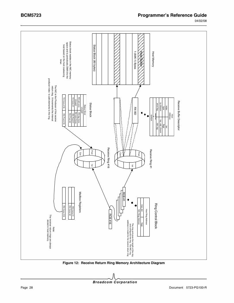
BCM5723 Programmer’s Reference Guide04/02/08
Broadcom Corporation
Page 28 Document 5723-PG100-R
Figure 12: Receive Return Ring Memory Architecture Diagram
Host M
emory
1-(64K
-1) Bytes
Host B
uffer
RX
BD H
ost A
ddress
index
type
ip chksum
error flagreserve
dopaque
Receive B
uffer Descriptor
len
flags
tcp_udp_chsum
vlan tag
Ring C
ontrol Block
1st
Host R
ing Addre
ss
max_len
NIC
Ring A
ddress flags
Receive R
ing #1
Receive R
ing #16
1st
The ring and gives the length of the ring.
and configures the ring. The N
IC ring
address is invalid for the receive return ring
Prod
Cons
RC
B #1
RC
B #16
Status W
ord
unused
RX
Prod #1
RX
std cons
RX
Prod #2
Unused
Status B
lock
RX
big Co
ns
RX
mini C
ons
TX
Cons #1
RX
Prod #16
TX
Co
ns #16
Con
Prod
Mailbox R
egisters
RX
Cons #1
RX
Cons #2
RX
Cons #16
Note:
The receiver return rings are alw
aysstored in host m
emory.
Status B
lock (80 bytes)
Status block resides in the N
IC m
emory
space and is periodically DM
A'd to the
host based on the host coalescingtim
er.
The N
IC is the P
roducer of the receive
return ring. It increments the internal
producer index to add elements to the ring.
Programmer’s Reference Guide BCM572304/02/08
Broadcom CorporationDocument 5723-PG100-R Page 29
Receive Producer Ring
The receive producer ring resides in the host and points to empty host receive buffers that will later be filled with received packet data. The controller will internally cache a copy of the producer ring. When the host software driver has a free host receive packet buffer available for incoming packets, it will fill out a receive buffer descriptor and have that descriptor point to the available buffer. Host software will then update the producer index for that receive producer ring to indicate to the controller that there is a newly available receive buffer. After the controller fetches and caches (e.g., consumes) this receive producer descriptor, the controller will update the consumer index of the receive producer ring.
Receive Return Rings
When the NIC receives a packet, it will DMA that packet to a host receive packet data buffer pointed to by the available receive buffer descriptor (see Section 6: “Receive Data Flow” on page 37). Earlier the NIC will have received ownership of that data buffer via an update of the producer index of receive producer ring. After the controller does the packet data write DMA, it will DMA a corresponding buffer descriptor into the appropriate receive return ring. The buffer descriptor that is returned in the receive return ring will be slightly modified from the original buffer descriptor that the controller fetched out of the receive producer ring. After the controller has completed the DMA of the receive return ring descriptor, the controller will update its internal copy of the producer index for that particular receive return ring. That new value for that receive return ring producer index will be included in the next status block update that is made to the host. The updated value of receive return ring producer index in status block will be used by host software in determining whether new packets have been received.
Receive Buffer Descriptors
The format of Standard Receive Buffer Descriptors (in both producer ring and return rings) is shown in Table 9.
The fields are defined as follows:
• The Host Address field contains the 64-bit host address of the buffer that the descriptor points to. A length of 0 indicates
Table 8: Receive Return Rings
Description BCM5784
Number of Rings 1
Buffer Descriptor Size (bytes) 32
Host Ring Size (# of Buffer Descriptors) Configurable to either 32 or 64 or 128 or 256 or 512
NIC Cache Size (# of Buffer Descriptors) 0
Table 9: Receive Descriptors Format
Offset (bytes) 31 16 15 0
0x00 Host Address
0x04
0x08 Index Length
0x0c Type Flags
0x10 IP_Cksum TCP_UDP_Cksum
0x14 Error_Flags VLAN tag
0x18 RSS Hash
0x1C Opaque
BCM5723 Programmer’s Reference Guide04/02/08
Broadcom Corporation
Page 30 Document 5723-PG100-R
that the descriptor does not have a buffer associated with it.
• The Length field specifies the length of the data buffer. For Producer Rings this value is set by the host software to correspond to the size of the buffer that is available for a receive packet. Once a packet has been received, the controller will modify this length field to correspond to the length of the packet received. A value of 0 indicates that there is no valid data in the buffer.
• The Index field is set by host software in the descriptors in the producer rings. When the controller uses a given buffer descriptor, it will opaquely pass the Index field for that buffer descriptor through to the corresponding descriptor in the return ring. This index field of the BD in Return Ring is then used by the host software to associate the BD in Return Ring with the BD in Producer Ring that points to the given receive buffer.
• The Flags field contains bits flags that contain control information about a given descriptor. The defined flags are listed in Table 10.
• The Type field is used internally by the controller. In producer rings it should be set to 0, and in return rings it should be ignored by host software.
• The TCP_UDP_Cksum field holds the TCP/UDP checksum that the controller calculated for all data following the IP header given the length defined in the IP header. If the Receive No Pseudo-header Checksum bit is set (see “Mode Control Register (Offset: 0x6800)” on page 275) to 1, then the pseudo-header checksum value is not added to this value. Otherwise, the TCP_UDP_Cksum field includes the pseudo-header in the controller’s calculation of the TCP or UDP checksum. If the packet is not a TCP or UDP packet, this field has no meaning. Host software should zero this value in the producer ring descriptors. If the host is capable of TCP or UDP checksum off load, then host software may
Table 10: Defined Flags for Receive Buffers
Bits Name Description
15 IP Version Indicates whether the received IP packet is an IPv6 or IPv4 packet. This bit will be 1 for IPv6 packet and 0 for IPv4 packet.
14 TCP_UDP_IS_TCP In producer rings this bit should be set to 0. In return rings this bit will be set to 1 by the controller if the controller calculated that the incoming packet was a TCP packet. If the packet is UDP or a non IP frame, then this bit should be set to 0.
13 TCP_UDP_CHECKSUM In producer rings this bit should be set to 0. In return rings this bit will be set to 1 by the controller if the controller calculated that the TCP or UDP checksum in the corresponding incoming packet was correct.
12 IP_CHECKSUM In producer rings this bit should be set to 0. In return rings this bit will be set to 1 by the controller if the controller calculated that the IP checksum in the corresponding incoming packet was correct.
11 Reserved
10 FRAME_HAS_ERROR If set to 1 in a return ring, it indicates that the controller detected an error. The specific type of error is specified in the Error_Flag field of the receive return descriptor.
9:7 RSS Hash Type Indicates the hash type used in RSS hash calculation for a received packet.
6 VLAN_TAG* If set to 1 in a return ring, it indicates that the packet associated with this buffer contained a four-byte IEEE 802.1Q VLAN tag. The 16 VLAN ID is stripped from the packet and located in the VLAN tag field in the descriptor.
5 BD_FLAG_JUMBO_RING Indicates that this packet came from the Jumbo Receive Ring, not the Standard Receive Ring (for receive BDs only). This must be set by the driver; it is just copied through opaquely by the NIC firmware.
Note: Jumbo frames are not supported by BCM5784.
4 Reserved Should be set to 0.
3 RSS_Hash Valid If set to 1, indicates host that the RSS_Hash in Receive BD of return ring is valid.
2 PACKET_END If set to 1, the packet ends with the data in the buffer pointed to by this descriptor.
1:0 Reserved Should be set to 0.
Programmer’s Reference Guide BCM572304/02/08
Broadcom CorporationDocument 5723-PG100-R Page 31
examine this field in the return rings to determine if the TCP or UDP checksum was correct.
• The IP_Cksum field holds the IPv4 checksum that the controller calculated for the IPv4 header of the received packet. If the packet is not an IPv4 packet, this field has no meaning. Host software should zero this value in the producer ring descriptors. If the host is capable of IPv4 checksum off load, then host software may examine this field in the return rings to determine if the IPv4 checksum was correct. A correct value would be 0 or 0xFFFF.
• The VLAN Tag field is only valid when the VLAN_TAG bit is set. This field contains the 16-bit VLAN ID that was extracted from an incoming packet that had an IEEE 802.1Q (and IEEE 802.3ac) -compliant header.
• The Error_Flags field contains bits flags that contain error information about an incoming packet that the descriptor is associated with. The bits in this field are only valid if the FRAME_HAS_ERROR bit is set in the Flags field in the descriptor. The defined error flags are listed in Table 11 on page 31.
• When the RSS Hash Valid flag bit is 1, the RSS Hash field holds the 32-bit RSS hash value calculated for a packet. This field should be ignored when the RSS Hash Valid flag bit is zero.
• The Opaque field is reserved for the host software driver. Any data placed in this field in a producer ring descriptor will be passed through unchanged to the corresponding return ring descriptor.
Table 11: Defined Error Flags for Receive Buffers
Bits Name Description
31:9 Reserved Should be set to 0.
8 GIANT_PKT_RCVD If set to 1, the received packet was longer than the maximum packet length value set in the Receive MTU Size register (see “Receive MTU Size Register (Offset: 0x43C)” on page 186). The data in the received packet was truncated at the length specified in the Receive MTU Size register.
7 TRUNC_NO_RES If set to 1, the received packet was truncated because the controller did not have the resources to receive a packet of this length.
6 LEN_LESS_64 If set to 1, the received packet was less than the required 64 bytes in length.
5 MAC_ABORT If set to 1, the MAC aborted due to an unspecified internal error while receiving this packet. The packet could be corrupted.
4 ODD_NIBBLE_RX_MII If set to 1, the received packet contained an odd number of nibbles. Thus, packet data could be corrupt.
3 PHY_DECODE_ERR If set to 1, while receiving this packet the device encountered an unspecified frame decoding error. This packet could be corrupted. This bit is set for valid packets that are received with a dribble nibble. True alignment errors will be dropped by that MAC and never show up to the driver.
2 LINK_LOST If set to 1, link was lost while receiving this frame. Therefore, this packet is incomplete.
1 COLL_DETECT If set to 1, a collision was encountered while receiving this packet.
0 BAD_CRC If set to 1, the received packet has a bad Ethernet CRC.
BCM5723 Programmer’s Reference Guide04/02/08
Broadcom Corporation
Page 32 Status Block Document 5723-PG100-R
STATUS BLOCK
The Status Block is another shared memory data structure that is located in host memory. The Status Block is 20 bytes in length. Host software will need to allocate 20 bytes of non-paged memory space for the Status Block and set the Status Block Host Address register to point to the host memory physical address reserved for this structure.
The controller will update the Status Block to host memory prior to a host coalescing interrupt or MSI. The frequency of these Status Block updates is determined by the host coalescing logic (see “Host Coalescing Engine” on page 13). Using the software configurable coalescing parameters, the device driver can optimize the frequency of status block updates for a particular application or operating system.
The Status Block contains some of the Producer and Consumer indices for the rings described in “Descriptor Rings” on page 21. These Producer and Consumer indices allow host software to know what the current status of the controller is regarding its processing of the various send and receive rings. From information in the status block a software driver can determine:
• Whether the Status Block has been recently updated (via a bit in the status word).
• Whether the Link State has changed (via a bit in the status word).
• Whether the controller has recently received a packet and deposited that packet into host memory for a given ring (via the Receive Return Ring Producer Indices).
• Which host receive descriptors that controller has fetched, and it will consume when future packets are received (via the Receive Producer Ring Consumer Indices).
• Whether the controller has recently completed a transmit descriptor buffer DMA for a given ring (via the Send Ring Consumer Indices).
STATUS BLOCK FORMAT
The Status word field contains bit flags that contain error information about the status of the controller. The defined flags are listed in Table 13 on page 33.
Table 12: Status Block Format
Offset 31 16 15 0
0x00 Status Word
0x04 Status Tag
0x08 Receive Producer Ring Consumer Indexa
a. The Receive Standard Consumer Index is also accessible at 0x3C54.
Unused
0x0C Unused
0x10 Send BD Consumer Indexb
b. The Send BD Consumer Index is also accessible at 0x3CC0.
Receive Return BD Producer Indexc
c. The Receive Return BD Producer Index is also accessible at 0x3C80.
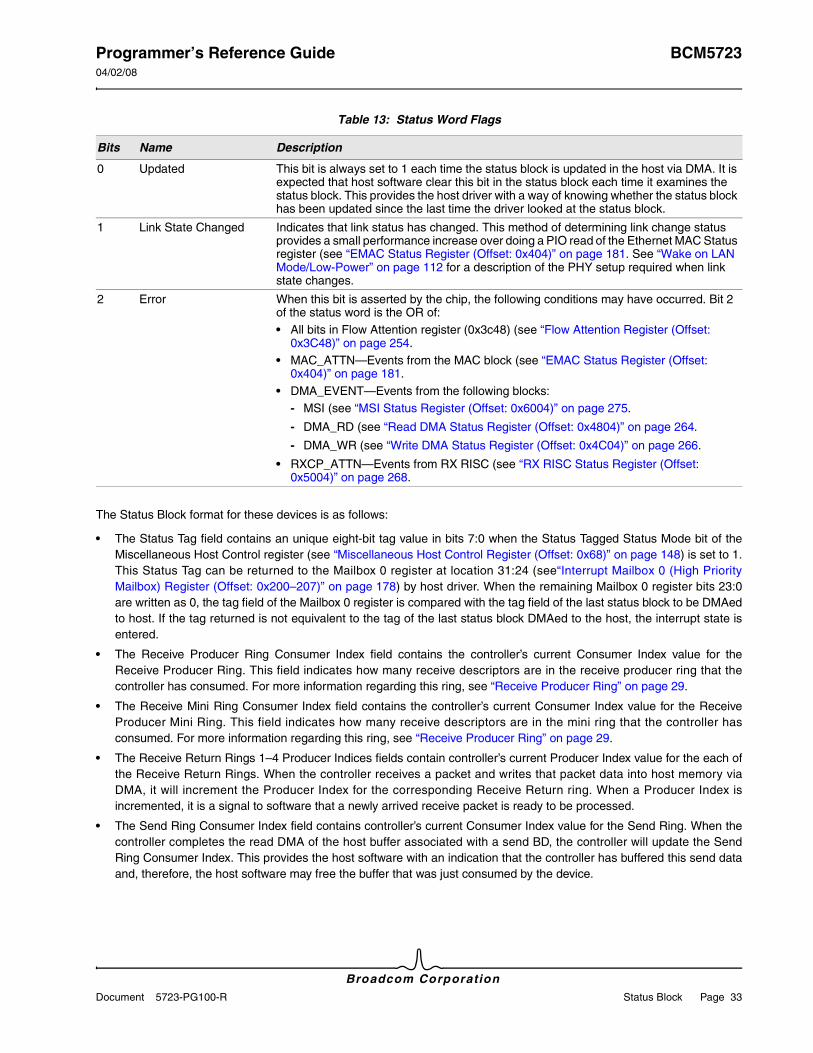
Programmer’s Reference Guide BCM572304/02/08
Broadcom CorporationDocument 5723-PG100-R Status Block Page 33
The Status Block format for these devices is as follows:
• The Status Tag field contains an unique eight-bit tag value in bits 7:0 when the Status Tagged Status Mode bit of the Miscellaneous Host Control register (see “Miscellaneous Host Control Register (Offset: 0x68)” on page 148) is set to 1. This Status Tag can be returned to the Mailbox 0 register at location 31:24 (see“Interrupt Mailbox 0 (High Priority Mailbox) Register (Offset: 0x200–207)” on page 178) by host driver. When the remaining Mailbox 0 register bits 23:0 are written as 0, the tag field of the Mailbox 0 register is compared with the tag field of the last status block to be DMAed to host. If the tag returned is not equivalent to the tag of the last status block DMAed to the host, the interrupt state is entered.
• The Receive Producer Ring Consumer Index field contains the controller’s current Consumer Index value for the Receive Producer Ring. This field indicates how many receive descriptors are in the receive producer ring that the controller has consumed. For more information regarding this ring, see “Receive Producer Ring” on page 29.
• The Receive Mini Ring Consumer Index field contains the controller’s current Consumer Index value for the Receive Producer Mini Ring. This field indicates how many receive descriptors are in the mini ring that the controller has consumed. For more information regarding this ring, see “Receive Producer Ring” on page 29.
• The Receive Return Rings 1–4 Producer Indices fields contain controller’s current Producer Index value for the each of the Receive Return Rings. When the controller receives a packet and writes that packet data into host memory via DMA, it will increment the Producer Index for the corresponding Receive Return ring. When a Producer Index is incremented, it is a signal to software that a newly arrived receive packet is ready to be processed.
• The Send Ring Consumer Index field contains controller’s current Consumer Index value for the Send Ring. When the controller completes the read DMA of the host buffer associated with a send BD, the controller will update the Send Ring Consumer Index. This provides the host software with an indication that the controller has buffered this send data and, therefore, the host software may free the buffer that was just consumed by the device.
Table 13: Status Word Flags
Bits Name Description
0 Updated This bit is always set to 1 each time the status block is updated in the host via DMA. It is expected that host software clear this bit in the status block each time it examines the status block. This provides the host driver with a way of knowing whether the status block has been updated since the last time the driver looked at the status block.
1 Link State Changed Indicates that link status has changed. This method of determining link change status provides a small performance increase over doing a PIO read of the Ethernet MAC Status register (see “EMAC Status Register (Offset: 0x404)” on page 181. See “Wake on LAN Mode/Low-Power” on page 112 for a description of the PHY setup required when link state changes.
2 Error When this bit is asserted by the chip, the following conditions may have occurred. Bit 2 of the status word is the OR of:• All bits in Flow Attention register (0x3c48) (see “Flow Attention Register (Offset:
0x3C48)” on page 254.• MAC_ATTN—Events from the MAC block (see “EMAC Status Register (Offset:
0x404)” on page 181.• DMA_EVENT—Events from the following blocks:
- MSI (see “MSI Status Register (Offset: 0x6004)” on page 275.
- DMA_RD (see “Read DMA Status Register (Offset: 0x4804)” on page 264.
- DMA_WR (see “Write DMA Status Register (Offset: 0x4C04)” on page 266.
• RXCP_ATTN—Events from RX RISC (see “RX RISC Status Register (Offset: 0x5004)” on page 268.
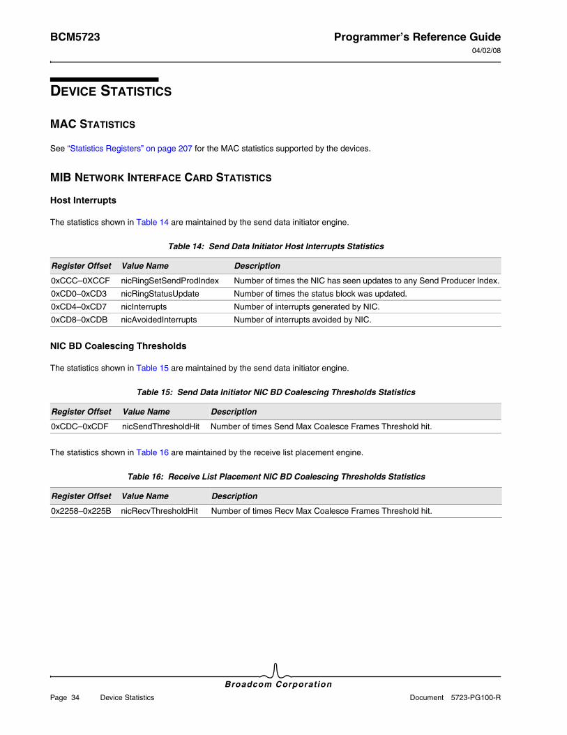
BCM5723 Programmer’s Reference Guide04/02/08
Broadcom Corporation
Page 34 Device Statistics Document 5723-PG100-R
DEVICE STATISTICS
MAC STATISTICS
See “Statistics Registers” on page 207 for the MAC statistics supported by the devices.
MIB NETWORK INTERFACE CARD STATISTICS
Host Interrupts
The statistics shown in Table 14 are maintained by the send data initiator engine.
NIC BD Coalescing Thresholds
The statistics shown in Table 15 are maintained by the send data initiator engine.
The statistics shown in Table 16 are maintained by the receive list placement engine.
Table 14: Send Data Initiator Host Interrupts Statistics
Register Offset Value Name Description
0xCCC–0XCCF nicRingSetSendProdIndex Number of times the NIC has seen updates to any Send Producer Index.
0xCD0–0xCD3 nicRingStatusUpdate Number of times the status block was updated.
0xCD4–0xCD7 nicInterrupts Number of interrupts generated by NIC.
0xCD8–0xCDB nicAvoidedInterrupts Number of interrupts avoided by NIC.
Table 15: Send Data Initiator NIC BD Coalescing Thresholds Statistics
Register Offset Value Name Description
0xCDC–0xCDF nicSendThresholdHit Number of times Send Max Coalesce Frames Threshold hit.
Table 16: Receive List Placement NIC BD Coalescing Thresholds Statistics
Register Offset Value Name Description
0x2258–0x225B nicRecvThresholdHit Number of times Recv Max Coalesce Frames Threshold hit.
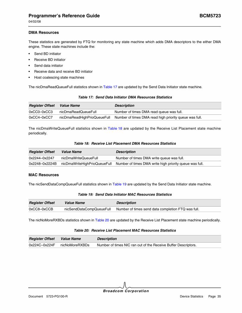
Programmer’s Reference Guide BCM572304/02/08
Broadcom CorporationDocument 5723-PG100-R Device Statistics Page 35
DMA Resources
These statistics are generated by FTQ for monitoring any state machine which adds DMA descriptors to the either DMA engine. These state machines include the:
• Send BD initiator
• Receive BD initiator
• Send data initiator
• Receive data and receive BD initiator
• Host coalescing state machines
The nicDmaReadQueueFull statistics shown in Table 17 are updated by the Send Data Initiator state machine.
The nicDmaWriteQueueFull statistics shown in Table 18 are updated by the Receive List Placement state machine periodically.
MAC Resources
The nicSendDataCompQueueFull statistics shown in Table 19 are updated by the Send Data Initiator state machine.
The nicNoMoreRXBDs statistics shown in Table 20 are updated by the Receive List Placement state machine periodically.
Table 17: Send Data Initiator DMA Resources Statistics
Register Offset Value Name Description
0xCC0–0xCC3 nicDmaReadQueueFull Number of times DMA read queue was full.
0xCC4–0xCC7 nicDmaReadHighPrioQueueFull Number of times DMA read high priority queue was full.
Table 18: Receive List Placement DMA Resources Statistics
Register Offset Value Name Description
0x2244–0x2247 nicDmaWriteQueueFull Number of times DMA write queue was full.
0x2248–0x2224B nicDmaWriteHighPrioQueueFull Number of times DMA write high priority queue was full.
Table 19: Send Data Initiator MAC Resources Statistics
Register Offset Value Name Description
0xCC8–0xCCB nicSendDataCompQueueFull Number of times send data completion FTQ was full.
Table 20: Receive List Placement MAC Resources Statistics
Register Offset Value Name Description
0x224C–0x224F nicNoMoreRXBDs Number of times NIC ran out of the Receive Buffer Descriptors.
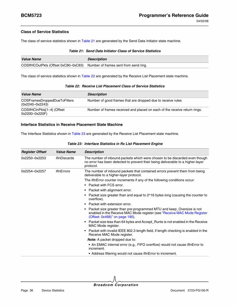
BCM5723 Programmer’s Reference Guide04/02/08
Broadcom Corporation
Page 36 Device Statistics Document 5723-PG100-R
Class of Service Statistics
The class of service statistics shown in Table 21 are generated by the Send Data Initiator state machine.
The class of service statistics shown in Table 22 are generated by the Receive List Placement state machine.
Interface Statistics in Receive Placement State Machine
The Interface Statistics shown in Table 23 are generated by the Receive List Placement state machine.
Table 21: Send Data Initiator Class of Service Statistics
Value Name Description
COSIfHCOutPkts (Offset 0xC80–0xC83) Number of frames sent from send ring.
Table 22: Receive List Placement Class of Service Statistics
Value Name Description
COSFramesDroppedDueToFilters (0x2240–0x2243)
Number of good frames that are dropped due to receive rules
COSIfHCInPkts[1–4] (Offset 0x2200–0x220F)
Number of frames received and placed on each of the receive return rings.
Table 23: Interface Statistics in Rx List Placement Engine
Register Offset Value Name Description
0x2250–0x2253 ifInDiscards The number of inbound packets which were chosen to be discarded even though no error has been detected to prevent their being deliverable to a higher-layer protocol.
0x2254–0x2257 ifInErrors The number of inbound packets that contained errors prevent them from being deliverable to a higher-layer protocol.The ifInError counter increments if any of the following conditions occur:• Packet with FCS error.• Packet with alignment error.• Packet size greater than and equal to 2^16 bytes long (causing the counter to
overflow).• Packet with extension error.• Packet size greater than pre-programmed MTU and keep_Oversize is not
enabled in the Receive MAC Mode register (see “Receive MAC Mode Register (Offset: 0x468)” on page 190).
• Packet size less than 64 bytes and Accept_Runts is not enabled in the Receive MAC Mode register.
• Packet with invalid IEEE 802.3 length field, if length checking is enabled in the Receive MAC Mode register.
Note: A packet dropped due to:• An EMAC internal error (e.g., FIFO overflow) would not cause ifInError to increment.• Address filtering would not cause ifInError to increment.
Programmer’s Reference Guide BCM572304/02/08
Broadcom CorporationDocument 5723-PG100-R Receive Data Flow Page 37
Section 6: Receive Data Flow
INTRODUCTION
The RX MAC pulls BDs from RX producer rings. The RX BD specifies the location(s) in host memory where packet data may be moved. Figure 13 on page 38 shows the receive buffer descriptor cycle.
All ingress Ethernet frames are classified by the RX rules engine. A class ID is associated to each frame based on QOS rules setup in the RX MAC (see “Receive Rules Setup and Frame Classification” on page 43). The Receive List Placement and Receive List Initiator portions of the MAC architecture move BDs to the RX return rings; the class ID associated to the packet is examined to route the BD to a specific RX return ring.
Once the packet is queued to the RX return ring, the device driver will wait for indication of the same through the status block update and interrupt from the host coalescing engine. The host coalescing engine will update the status block and generate a line interrupt or MSI (see “Host Coalescing” on page 128 for further details regarding interrupts) when a specified host coalescence criteria is met. Once the interrupt is generated, the host device driver will service the interrupt. The ISR will determine if new BDs have been completed on the RX Return Rings. Next, the device driver will indicate to the network protocol that the completed RX packets are available. The network protocol will consume the packets and return physical buffers to the network driver at a later point.
The BDs may then be reused for new RX frames. The device driver must return the BD to an RX producer ring. For this purpose, the driver should fill out either the opaque field or index field of the Rx BD when inserting/initializing the BD in an RX Producer ring. When the BD is returned by the device through Return Ring, the opaque or index data field of the BD will be used by the driver to identify the BD in Producer Ring that corresponds to the Returned BD in Return Ring. The device driver will then reinitialize the identified BD in Producer Ring with a new allocated buffer and replenish the Receive Producer Ring with this BD.
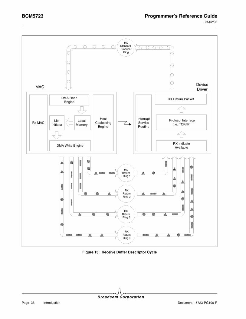
BCM5723 Programmer’s Reference Guide04/02/08
Broadcom Corporation
Page 38 Introduction Document 5723-PG100-R
Figure 13: Receive Buffer Descriptor Cycle
RXStandardProducer
Ring
RXReturnRing 1
RXReturnRing 2
RXReturnRing 3
RXReturnRing 4
DMA Read Engine
LocalMemory
ListInitiator
DMA Write Engine
InterruptServiceRoutine
RX Indicate Available
Rx MAC
RX Return Packet
Protocol Interface(i.e. TCP/IP)
Device Driver
MAC
HostCoalescing
Engine
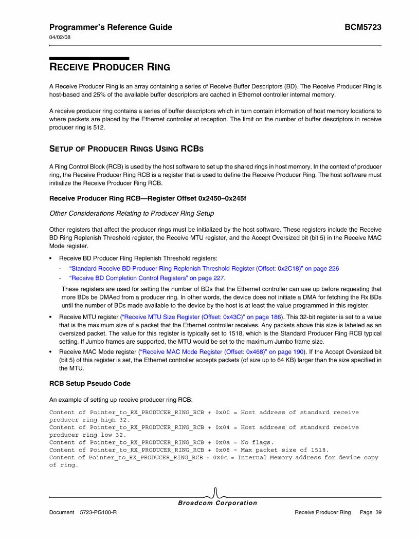
Programmer’s Reference Guide BCM572304/02/08
Broadcom CorporationDocument 5723-PG100-R Receive Producer Ring Page 39
RECEIVE PRODUCER RING
A Receive Producer Ring is an array containing a series of Receive Buffer Descriptors (BD). The Receive Producer Ring is host-based and 25% of the available buffer descriptors are cached in Ethernet controller internal memory.
A receive producer ring contains a series of buffer descriptors which in turn contain information of host memory locations to where packets are placed by the Ethernet controller at reception. The limit on the number of buffer descriptors in receive producer ring is 512.
SETUP OF PRODUCER RINGS USING RCBS
A Ring Control Block (RCB) is used by the host software to set up the shared rings in host memory. In the context of producer ring, the Receive Producer Ring RCB is a register that is used to define the Receive Producer Ring. The host software must initialize the Receive Producer Ring RCB.
Receive Producer Ring RCB—Register Offset 0x2450–0x245f
Other Considerations Relating to Producer Ring Setup
Other registers that affect the producer rings must be initialized by the host software. These registers include the Receive BD Ring Replenish Threshold register, the Receive MTU register, and the Accept Oversized bit (bit 5) in the Receive MAC Mode register.
• Receive BD Producer Ring Replenish Threshold registers:
- “Standard Receive BD Producer Ring Replenish Threshold Register (Offset: 0x2C18)” on page 226
- “Receive BD Completion Control Registers” on page 227.
These registers are used for setting the number of BDs that the Ethernet controller can use up before requesting that more BDs be DMAed from a producer ring. In other words, the device does not initiate a DMA for fetching the Rx BDs until the number of BDs made available to the device by the host is at least the value programmed in this register.
• Receive MTU register (“Receive MTU Size Register (Offset: 0x43C)” on page 186). This 32-bit register is set to a value that is the maximum size of a packet that the Ethernet controller receives. Any packets above this size is labeled as an oversized packet. The value for this register is typically set to 1518, which is the Standard Producer Ring RCB typical setting. If Jumbo frames are supported, the MTU would be set to the maximum Jumbo frame size.
• Receive MAC Mode register (“Receive MAC Mode Register (Offset: 0x468)” on page 190). If the Accept Oversized bit (bit 5) of this register is set, the Ethernet controller accepts packets (of size up to 64 KB) larger than the size specified in the MTU.
RCB Setup Pseudo Code
An example of setting up receive producer ring RCB:
Content of Pointer_to_RX_PRODUCER_RING_RCB + 0x00 = Host address of standard receive producer ring high 32.Content of Pointer_to_RX_PRODUCER_RING_RCB + 0x04 = Host address of standard receive producer ring low 32.Content of Pointer_to_RX_PRODUCER_RING_RCB + 0x0a = No flags.Content of Pointer_to_RX_PRODUCER_RING_RCB + 0x08 = Max packet size of 1518.Content of Pointer_to_RX_PRODUCER_RING_RCB + 0x0c = Internal Memory address for device copy of ring.
BCM5723 Programmer’s Reference Guide04/02/08
Broadcom Corporation
Page 40 Receive Producer Ring Document 5723-PG100-R
Figure 14 shows the standard ring RCB for the setup of a host-based standard producer ring.
Receive Buffer Descriptors (BDs) begin on the Receive Producer Ring. The host device driver will populate the receive producer ring with a specified number of BDs supported by the receive producer ring (see “Receive Producer Ring” on page 39). When a packet is received, the RX MAC moves the packet data into internal memory. The Receive MTU Size register (see “Receive MTU Size Register (Offset: 0x43C)” on page 186) specifies the largest packet accepted by the RX MAC; packets larger than the Receive MTU are marked oversized and are discarded.
Figure 14: Receive Producer Ring RCB Setup
RECEIVE BUFFER DESCRIPTORS
The Receive Buffer Descriptor is a data structure in host memory. It is the basic element that makes up each receive producer and receive return ring. The format of receive buffer descriptors can be seen in Table 9 on page 29. A receive buffer descriptor has a 64-bit memory address and may be in any memory alignment and may point to any byte boundary. For performance and CPU efficiency reasons, it is recommended that memory be cache-aligned. The Ethernet controller supports cache line sizes of 8, 16, 32, 64, 128, 256, and 512 bytes. The cache line size value is important for the controller to determine when to use the PCI memory write and invalidate command. There are no requirements for memory alignment or cache line integrity for the Ethernet controller.
Unlike send buffer descriptors, the receive buffer descriptors cannot be chained to support multiple fragments.
MANAGEMENT OF RX PRODUCER RINGS WITH MAILBOX REGISTERS AND STATUS BLOCK
Status Block
The host software manages the producer rings through the Mailbox registers and by using the status block. It does this by writing to the Mail Box registers when a BD is available to DMA to the Ethernet controller and reading the status block to see how many BDs have been consumed by the Ethernet controller. The status block can be seen in “Status Block” on page 32.
The status block is controlled and updated by the Ethernet controller. The status block in host memory is constantly updated through a DMA copy by the Ethernet controller from an internal status block. The updates occur at specific intervals and host coalescence conditions that are specified by host software during initialization of the Ethernet controller. The registers for setting the intervals and conditions are in the Host Coalescing Control registers (see “Host Coalescing” on page 128) starting at memory offset 0x3c00. The Ethernet controller DMAs an updated status block to the 32-bit address that is set by the host
Offset
0x00
0x04
0x08
0x0c
31 16
Host Ring Address
Max_Len Flags
NIC Ring Address
15 0Std RingBD 1
512
511
BD 2BD 3
Standard Producer Ring RCB
Standard Producer Ring
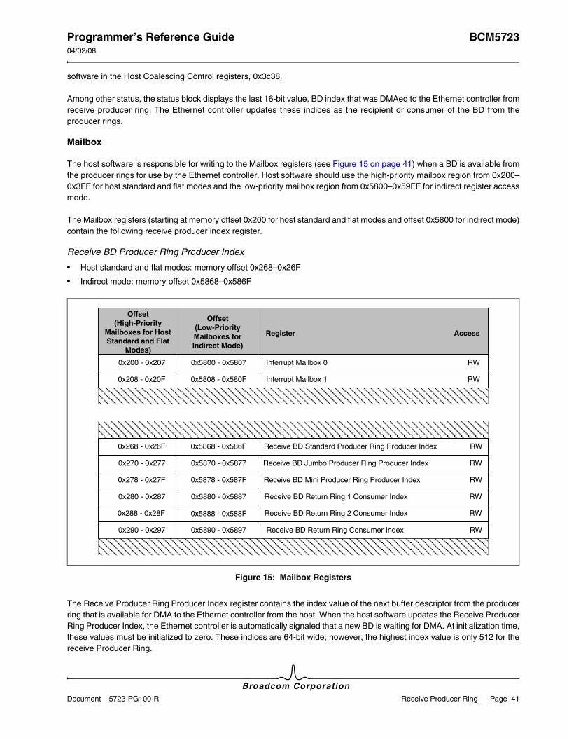
Programmer’s Reference Guide BCM572304/02/08
Broadcom CorporationDocument 5723-PG100-R Receive Producer Ring Page 41
software in the Host Coalescing Control registers, 0x3c38.
Among other status, the status block displays the last 16-bit value, BD index that was DMAed to the Ethernet controller from receive producer ring. The Ethernet controller updates these indices as the recipient or consumer of the BD from the producer rings.
Mailbox
The host software is responsible for writing to the Mailbox registers (see Figure 15 on page 41) when a BD is available from the producer rings for use by the Ethernet controller. Host software should use the high-priority mailbox region from 0x200– 0x3FF for host standard and flat modes and the low-priority mailbox region from 0x5800–0x59FF for indirect register access mode.
The Mailbox registers (starting at memory offset 0x200 for host standard and flat modes and offset 0x5800 for indirect mode) contain the following receive producer index register.
Receive BD Producer Ring Producer Index
• Host standard and flat modes: memory offset 0x268–0x26F
• Indirect mode: memory offset 0x5868–0x586F
Figure 15: Mailbox Registers
The Receive Producer Ring Producer Index register contains the index value of the next buffer descriptor from the producer ring that is available for DMA to the Ethernet controller from the host. When the host software updates the Receive Producer Ring Producer Index, the Ethernet controller is automatically signaled that a new BD is waiting for DMA. At initialization time, these values must be initialized to zero. These indices are 64-bit wide; however, the highest index value is only 512 for the receive Producer Ring.
Offset(High-Priority
Mailboxes for HostStandard and Flat
Modes)
0x200 - 0x207
0x208 - 0x20F
0x268 - 0x26F
0x270 - 0x277
0x278 - 0x27F
0x280 - 0x287
0x288 - 0x28F
0x290 - 0x297
Register Access
Interrupt Mailbox 0 RW
Interrupt Mailbox 1 RW
Receive BD Standard Producer Ring Producer Index RW
Receive BD Jumbo Producer Ring Producer Index RW
Receive BD Mini Producer Ring Producer Index RW
Receive BD Return Ring 1 Consumer Index RW
Receive BD Return Ring 2 Consumer Index RW
Receive BD Return Ring Consumer Index RW
Offset(Low-PriorityMailboxes forIndirect Mode)
0x5800 - 0x5807
0x5808 - 0x580F
0x5868 - 0x586F
0x5870 - 0x5877
0x5878 - 0x587F
0x5880 - 0x5887
0x5888 - 0x588F
0x5890 - 0x5897
BCM5723 Programmer’s Reference Guide04/02/08
Broadcom Corporation
Page 42 Receive Return Rings Document 5723-PG100-R
RECEIVE RETURN RINGS
Receive Return Rings (RR) are host-based memory blocks that are used by host software to keep track of the where the Ethernet controller is putting the received packets related receive buffer descriptors. Unlike the producer rings, the return rings reside only in host memory. The Ethernet controller uses the BDs in the NIC's memory that are previously copied from the producer rings to use when packets are received from the LAN. It places the BDs that correspond to received packets in the return rings.
Return rings are the exact opposite of producer rings, except that they are not categorized by the maximum length receive packets supported. They are actually categorized by priority or class of received packet. The highest priority return ring is ring 1, and the lowest priority is the last ring (Return Ring 2–Return Ring 4 depending on how many rings are set up by the host software). The Receive Return Ring is configurable to a value of either 32, 64, 128, 256, or 512.
The Receive Return Ring RCBs are used to set up return rings in much the same way the Receive Producer Ring RCB is used to set up the receive producer ring. These RCBs for the return rings are set in the Miscellaneous memory region (SSRAM) at offset 0x200 (this region should not be confused with the register space in the chip). The RCB max_len field is used to indicate the number of buffer descriptor entries in a return ring. If an invalid value is set, the Ethernet controller indicates an attention error in the Flow Attention register. Figure 12 on page 28 shows receive return rings.
MANAGEMENT OF RETURN RINGS WITH MAILBOX REGISTERS AND STATUS BLOCK
The return rings are managed by the host using the Mailbox registers and status block.
When a packet is received from the LAN, the Ethernet controller DMAs the packet to a location in the host, and then DMAs the related BD to a return ring. As the producer of this packet to the host, the Ethernet controller updates the status block producer indices for the related return ring (i.e., return ring 1 to return ring 4 that was DMAed the BD received packet). These return ring indices can then be read by the host software to determine the last BD index value of a particular ring that has information of the last received packet.
As the consumer of the received packet, the host software must update the return ring consumer indices in Mailbox registers Receive BD Return Ring 1 Consumer Index (memory offset 0x280–0x287 for host standard and flat modes and 0x5880–0x5887 for indirect mode) through Receive BD Return Ring 4 Consumer Index.
HOST BUFFER ALLOCATION
The allocation of memory in the host is dependent on the operating system in which the controller is being used. There are two crucial items:
• The use of non-cached and physically contiguous memory is best for adapter performance.
• Physical memory mapping is required for the controller’s internal copies of logical host memory.
Programmer’s Reference Guide BCM572304/02/08
Broadcom CorporationDocument 5723-PG100-R Receive Return Rings Page 43
RECEIVE RULES SETUP AND FRAME CLASSIFICATION
The Ethernet controller has a feature that allows for the classification of receive packets based on a set of rules. The rules are determined by the host software and then input into the Ethernet controller.
A packet can be accepted or rejected based on the rules initialized into two rules register areas. The packets can also be classified into groups of packets of higher to lower priority using the rules registers. This occurs when the packet is directed to a specific return ring. Return rings 1–4 have an inherent priority associated with them. The priority is from lowest ring number to highest ring number; return ring 1 being the highest priority ring and return ring 4 being the lowest. The implementation of priority class is based on how many rings the host software has initialized and made available to the Ethernet controller. As packets arrive, the Ethernet controller may classify each packet based on the rules. When the host services the receive packet, it can service the lower numbered rings first.
A rule can be changed by first disabling it by setting 0 into Enable bit (bit 31) in Receive BD Rules Control register (see Table 25). Wait about 20 receive clocks (rx_clock) and then re-enable it when it is programmed with a new rule. Otherwise, changing the rules dynamically during runtime may cause the rule checker to output erroneous results because the rule checker is a pipelined design and uses the various fields of the rules at different clock cycles.
Receive Rules Configuration Register
The Receive Rules Configuration register (memory offset 0x500–0x503, see Table 24) uses bits 3:7 to specify the ring where a received packet should be placed into if no rules are met, or if the rules have not been set up. A value of 0 means the received packet will be discarded. A value of 1–16 specifies a corresponding ring. This ring should be initialized to at least a value of 1 if the rules are not being used to ensure that all received packets will be DMAed to return ring 1.
Receive List Placement Rules Array
The Receive List Placement Rules Array (memory offset 0x480–0x4ff) is made up of 16 combined element registers. The combined element is actually two 32-bit registers called the Receive BD Rules Control register (see Table 25) and the Receive BD Rules Value/Mask register (see Table 26). The element can be looked at as a single 64-bit entity with a Control part and Value/Mask part since they use a single element. Bit 26 of the control part determines how the value/mask part is used. The Receive BD Rules Value/Mask register can be used as either a 32-bit left-justified Value or a 16-bit Mask followed by a 16-bit Value.
Table 24: Receive Rules Configuration Register
Bits Field Access
31:8 Reserved RO
7:3 Specifies the default class (ring) if no rules are matched R/W
2:0 Reserved RO
Note: Receive rules cannot be used to match VLAN headers because the VLAN tag is stripped from the Ethernet frame before the rule checker runs.
Table 25: Receive BD Rules Control Register
31 30 29 28 27 26 25 24 23 22 21 20 19 18 17 16
E & P1 P2 P3 M D Map Reserved Op
15 14 13 12 11 10 9 8 7 6 5 4 3 2 1 0
Header Class Offset
BCM5723 Programmer’s Reference Guide04/02/08
Broadcom Corporation
Page 44 Receive Return Rings Document 5723-PG100-R
Bit Name R/W Description Default
31 E R/W Enable. Enabled if set to 1 –
30 & R/W And With Next. This rule and next must both be true to match. The class fields must be the same. A disabled next rule is considered true. Processor activation bits are specified in the first rule in a series.
–
29 P1 R/W If the rule matches, the processor is activated in the queue descriptor for the Receive List Placement state machine.
–
28 P2 R/W If the rule matches, the processor is activated in the queue descriptor for the Receive Data and Receive BD Initiator state machine.
–
27 P3 R/W If the rule matches, the processor is activated in the queue descriptor for the Receive Data Completion state machine.
–
26 M R/W Mask If set, specifies that the value/mask field is split into a 16-bit value and 16-bit mask instead of a 32-bit value.
–
25 D R/W Discard Frame if it matches the rule. –
24 Map R/W Map Use the masked value and map it to the class. –
23:18 Reserved R/W Must be set to zero. 0
17:16 Op R/W Comparison Operator specifies how to determine the match:• 00 = Equal• 01 = Not Equal• 10 = Greater than• 11 = Less Than
–
15:13 Header R/W Header Type specifies which header the offset is for: • 000: Start of Frame (always valid) • 001: Start of IP Header (if present) • 010: Start of TCP Header (if present) • 011: Start of UDP Header (if present) • 100: Start of Data (always valid, context sensitive)• 101–111: Reserved
–
12:8 Class R/W The class this frame is placed into if the rule matches. 0:4, where 0 means discard. The number of valid classes is the Number of Active Queues divided by the Number of Interrupt Distribution Groups. Ring 1 has the highest priority and Ring 4 has the lowest priority.
–
7:0 Offset R/W Number of bytes offset specified by the header type. –
Table 26: Receive BD Rules Value/Mask Register
31 30 29 28 27 26 25 24 23 22 21 20 19 18 17 16
Mask
15 14 13 12 11 10 9 8 7 6 5 4 3 2 1 0
Value
Bit Name R/W Description Default
31:16 Mask – – –
15:0 Value – – –
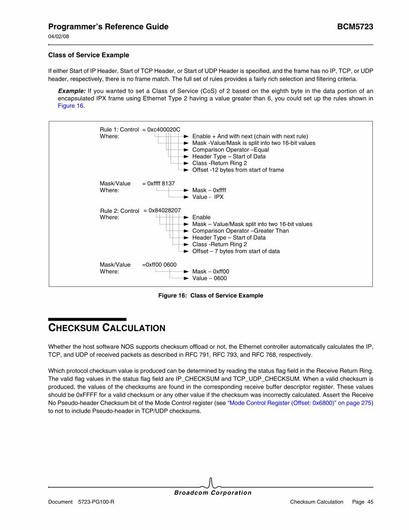
Programmer’s Reference Guide BCM572304/02/08
Broadcom CorporationDocument 5723-PG100-R Checksum Calculation Page 45
Class of Service Example
If either Start of IP Header, Start of TCP Header, or Start of UDP Header is specified, and the frame has no IP, TCP, or UDP header, respectively, there is no frame match. The full set of rules provides a fairly rich selection and filtering criteria.
Example: If you wanted to set a Class of Service (CoS) of 2 based on the eighth byte in the data portion of an encapsulated IPX frame using Ethernet Type 2 having a value greater than 6, you could set up the rules shown in Figure 16.
Figure 16: Class of Service Example
CHECKSUM CALCULATION
Whether the host software NOS supports checksum offload or not, the Ethernet controller automatically calculates the IP, TCP, and UDP of received packets as described in RFC 791, RFC 793, and RFC 768, respectively.
Which protocol checksum value is produced can be determined by reading the status flag field in the Receive Return Ring. The valid flag values in the status flag field are IP_CHECKSUM and TCP_UDP_CHECKSUM. When a valid checksum is produced, the values of the checksums are found in the corresponding receive buffer descriptor register. These values should be 0xFFFF for a valid checksum or any other value if the checksum was incorrectly calculated. Assert the Receive No Pseudo-header Checksum bit of the Mode Control register (see “Mode Control Register (Offset: 0x6800)” on page 275)to not to include Pseudo-header in TCP/UDP checksums.
Rule 1: Control = 0xc400020CWhere: Enable + And with next (chain with next rule)
Mask -Value/Mask is split into two 16-bit values
Class -Return Ring 2Offset -12 bytes from start of frame
Mask/Value = 0xffff 8137Where: Mask – 0xffff
Value - IPX
Rule 2: Control = 0x84028207Where: Enable
Mask – Value/Mask split into two 16-bit valuesComparison Operator –Greater ThanHeader Type – Start of Data
Offset – 7 bytes from start of data
Mask/Value =0xff00 0600Where: Mask – 0xff00
Value – 0600
Header Type – Start of DataComparison Operator –Equal
Class -Return Ring 2
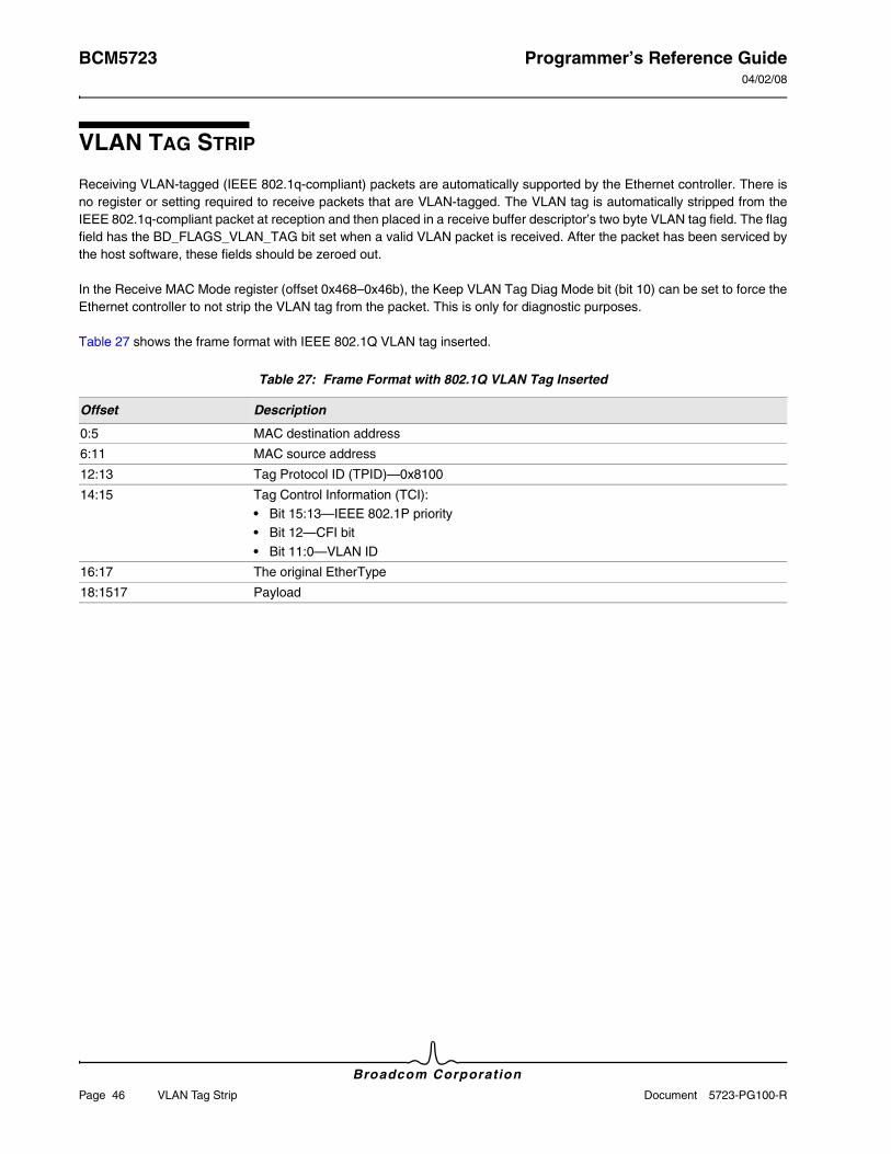
BCM5723 Programmer’s Reference Guide04/02/08
Broadcom Corporation
Page 46 VLAN Tag Strip Document 5723-PG100-R
VLAN TAG STRIP
Receiving VLAN-tagged (IEEE 802.1q-compliant) packets are automatically supported by the Ethernet controller. There is no register or setting required to receive packets that are VLAN-tagged. The VLAN tag is automatically stripped from the IEEE 802.1q-compliant packet at reception and then placed in a receive buffer descriptor’s two byte VLAN tag field. The flag field has the BD_FLAGS_VLAN_TAG bit set when a valid VLAN packet is received. After the packet has been serviced by the host software, these fields should be zeroed out.
In the Receive MAC Mode register (offset 0x468–0x46b), the Keep VLAN Tag Diag Mode bit (bit 10) can be set to force the Ethernet controller to not strip the VLAN tag from the packet. This is only for diagnostic purposes.
Table 27 shows the frame format with IEEE 802.1Q VLAN tag inserted.
Table 27: Frame Format with 802.1Q VLAN Tag Inserted
Offset Description
0:5 MAC destination address
6:11 MAC source address
12:13 Tag Protocol ID (TPID)—0x8100
14:15 Tag Control Information (TCI):• Bit 15:13—IEEE 802.1P priority• Bit 12—CFI bit• Bit 11:0—VLAN ID
16:17 The original EtherType
18:1517 Payload
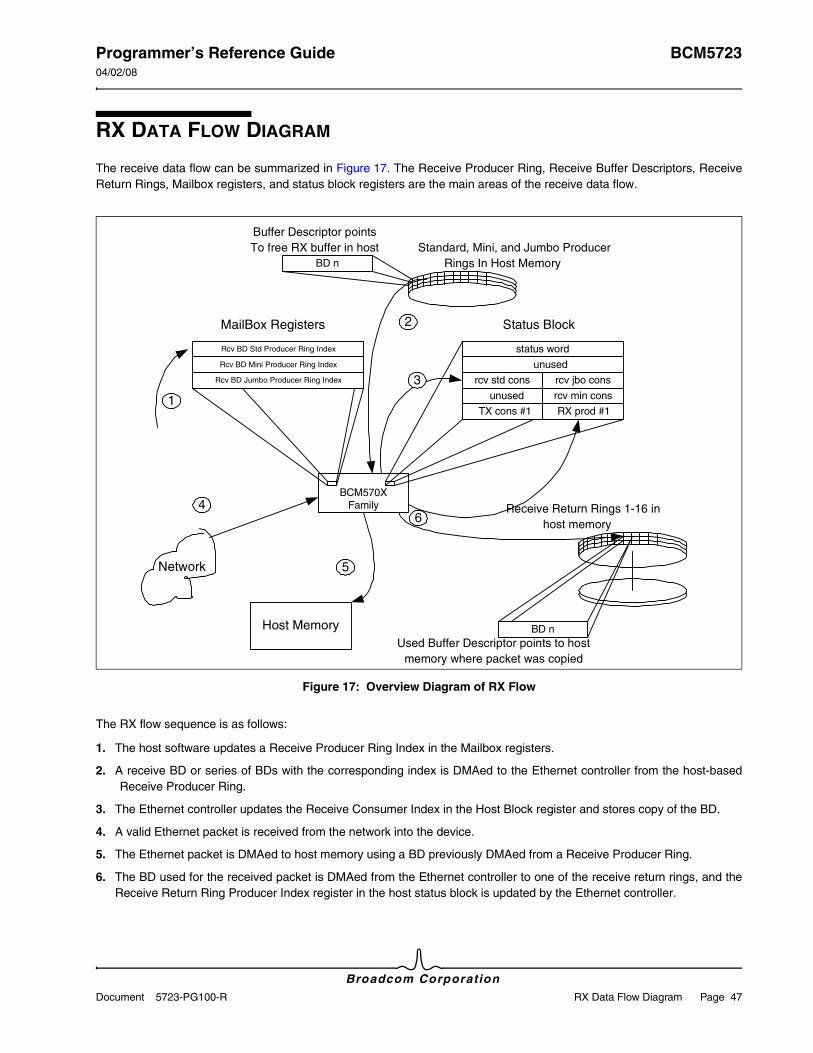
Programmer’s Reference Guide BCM572304/02/08
Broadcom CorporationDocument 5723-PG100-R RX Data Flow Diagram Page 47
RX DATA FLOW DIAGRAM
The receive data flow can be summarized in Figure 17. The Receive Producer Ring, Receive Buffer Descriptors, Receive Return Rings, Mailbox registers, and status block registers are the main areas of the receive data flow.
Figure 17: Overview Diagram of RX Flow
The RX flow sequence is as follows:
1. The host software updates a Receive Producer Ring Index in the Mailbox registers.
2. A receive BD or series of BDs with the corresponding index is DMAed to the Ethernet controller from the host-based Receive Producer Ring.
3. The Ethernet controller updates the Receive Consumer Index in the Host Block register and stores copy of the BD.
4. A valid Ethernet packet is received from the network into the device.
5. The Ethernet packet is DMAed to host memory using a BD previously DMAed from a Receive Producer Ring.
6. The BD used for the received packet is DMAed from the Ethernet controller to one of the receive return rings, and the Receive Return Ring Producer Index register in the host status block is updated by the Ethernet controller.
BCM570XFamily
Rcv BD Std Producer Ring Index
Rcv BD Mini Producer Ring Index
Rcv BD Jumbo Producer Ring Index
MailBox Registers
status word
rcv std cons
unused
rcv jbo cons
unused rcv min cons
Status Block
Standard, Mini, and Jumbo ProducerRings In Host MemoryBD n
Buffer Descriptor pointsTo free RX buffer in host
TX cons #1 RX prod #1
Receive Return Rings 1-16 inhost memory
BD nUsed Buffer Descriptor points to host
memory where packet was copied
1
2
3
46
5
Host Memory
Network
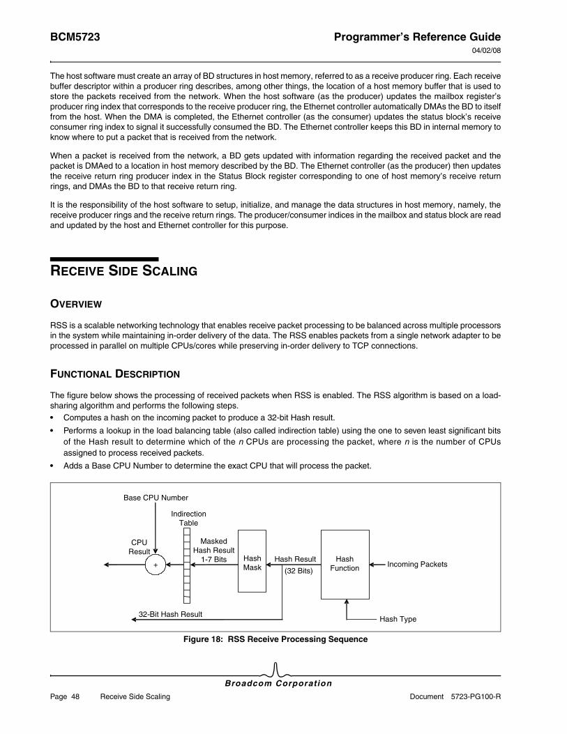
BCM5723 Programmer’s Reference Guide04/02/08
Broadcom Corporation
Page 48 Receive Side Scaling Document 5723-PG100-R
The host software must create an array of BD structures in host memory, referred to as a receive producer ring. Each receive buffer descriptor within a producer ring describes, among other things, the location of a host memory buffer that is used to store the packets received from the network. When the host software (as the producer) updates the mailbox register’s producer ring index that corresponds to the receive producer ring, the Ethernet controller automatically DMAs the BD to itself from the host. When the DMA is completed, the Ethernet controller (as the consumer) updates the status block’s receive consumer ring index to signal it successfully consumed the BD. The Ethernet controller keeps this BD in internal memory to know where to put a packet that is received from the network.
When a packet is received from the network, a BD gets updated with information regarding the received packet and the packet is DMAed to a location in host memory described by the BD. The Ethernet controller (as the producer) then updates the receive return ring producer index in the Status Block register corresponding to one of host memory’s receive return rings, and DMAs the BD to that receive return ring.
It is the responsibility of the host software to setup, initialize, and manage the data structures in host memory, namely, the receive producer rings and the receive return rings. The producer/consumer indices in the mailbox and status block are read and updated by the host and Ethernet controller for this purpose.
RECEIVE SIDE SCALING
OVERVIEW
RSS is a scalable networking technology that enables receive packet processing to be balanced across multiple processors in the system while maintaining in-order delivery of the data. The RSS enables packets from a single network adapter to be processed in parallel on multiple CPUs/cores while preserving in-order delivery to TCP connections.
FUNCTIONAL DESCRIPTION
The figure below shows the processing of received packets when RSS is enabled. The RSS algorithm is based on a load-sharing algorithm and performs the following steps.• Computes a hash on the incoming packet to produce a 32-bit Hash result.
• Performs a lookup in the load balancing table (also called indirection table) using the one to seven least significant bits of the Hash result to determine which of the n CPUs are processing the packet, where n is the number of CPUs assigned to process received packets.
• Adds a Base CPU Number to determine the exact CPU that will process the packet.
Figure 18: RSS Receive Processing Sequence
Hash Function
Incoming Packets
Hash Result (32 Bits)
CPU Result
Indirection Table
Hash
Mask
Masked Hash Result
1-7 Bits
32-Bit Hash Result
Hash Type
+
Base CPU Number
Programmer’s Reference Guide BCM572304/02/08
Broadcom CorporationDocument 5723-PG100-R Receive Side Scaling Page 49
The devices implement the above RSS algorithm in hardware except for the step of adding the Base CPU Number to the value from Indirection Table. If required, the step of adding the Base CPU Number to the CPU Result can be done in the main Interrupt Service Routine to determine which CPU will process the packet.
RSS PARAMETERS
Hash Function
The default hash function is the Toeplitz hash. No other hash functions are currently supported, so there is no configurable parameter.
Hash Type
The fields that are used to hash across the incoming packet. The 5 devices support all the four hash types given below and the configuration bits for enabling/disabling these hash types are provided in Receive MAC Mode register at offset 0x468. Any combination of these hash types can be enabled:
• Four-tuple of source TCP Port, source IP version 4 (IPv4) address, destination TCP port, and destination IPv4 address.
• Four-tuple of source TCP Port, source IP version 6 (IPv6) address, destination TCP port, and destination IPv6 address.
• Two-tuple of source IPv4 address and destination IPv4 address.
• Two-tuple of source IPv6 address and destination IPv6 address.
Hash Mask
The RSS Hash Mask bits (bits 22:20 of the Receive MAC Mode register at offset 0x468) allow the configuration of number of hash-result bits that are used to index into the indirection table.
Indirection Table
The table of CPU numbers used for balancing the receive traffic across multiple processors. The Indirection Table registers 0–15 at offset 0x630–0x66F are implemented for the required 128 entries of the Indirection Table. The devices support only four Receive Return Rings so each entry of Indirection Table is implemented as 2 bits.
Secret Hash Key
The hash key that will be used for RSS hash. For the Toeplitz hash, the hash key size is 40 bytes for IPv6 and 16 bytes for IPv4. The host software should program the hash key in hash key registers at offset 0x670 to 0x697.
RSS INITIALIZATION
The host protocol stack should configure the above RSS parameters before enabling the RSS engine. The RSS can be enabled by setting the bit-23 of the Receive MAC Mode register at offset 0x468. Normally the RSS parameters except the Indirection Table are static and will be initialized only during device driver initialization. Though extremely rare, the protocol stack may change the RSS parameters any time. The devices require a reset to change any of the hash type, hash mask, and hash key parameters.
If the hash type flags in Receive MAC Mode register (offset 0x468) enable only one type of hash, then any received packet that does not match the enabled hash type is not hashed. If multiple flags are set, such as If the TCP/IPv4 and IPv4 hash types (bits 17 and 16 of Receive MAC Mode register at offset 0x468) are enabled, then if the packet is not a TCP/IPv4 packet but is an IPv4 packet, the hash is performed on just the IPv4 2-tuple. Further, for this setting of the hash type flags, if the incoming packet is not an IPv4 packet, then no hash is performed. Because a variety of hash types can be applied on a per-
BCM5723 Programmer’s Reference Guide04/02/08
Broadcom Corporation
Page 50 Receive Side Scaling Document 5723-PG100-R
packet basis (including no hash), the hash type is indicated to the host protocol stack on a per-packet basis. If no hash was performed, then none of the hash type flags in the receive BD will be set.
Once RSS is initialized and enabled, data transfer can begin. Over a period of time, the host protocol stack may modify the indirection table to rebalance the processing load. When the indirection table is changed, it is possible for a short period of time (while the current receive descriptor queues are being processed) for packets to be processed on the wrong CPU. This is a normal transient condition and should not be a problem.
RSS RX PACKET FLOW
Each CPU or CPU core in multi processor systems is assigned one receive return ring. Only a single interrupt is initiated at a time.
1. As packets arrive, the device parses each packet, calculates the RSS Hash, and derives the CPU number (i.e., receive return ring number) from Indirection Table using the Masked Hash Result as the Indirection Table Index.
2. The packet data is DMAed to the host memory at the location specified by the receive buffer descriptor (RBD) of the receive producer ring.
3. Based on the derived CPU number, the device DMAs the used RBDs into appropriate receive return rings in host memory.
4. The device fires the interrupt via MSI, which causes the device driver ISR to run.
5. The ISR disables further interrupts from the device, determines which CPUs have receive packets to be handled and uses inter processor communication mechanisms to start packet receive handlers on CPUs whose return rings have new RBDs.
6. Each CPU processes the new RBDs in it’s receive return ring when its packet handler routine is started by main ISR.
7. Once the main ISR determines that all new RBDs have been processed by the CPUs, it enables the interrupts from the device and exits.
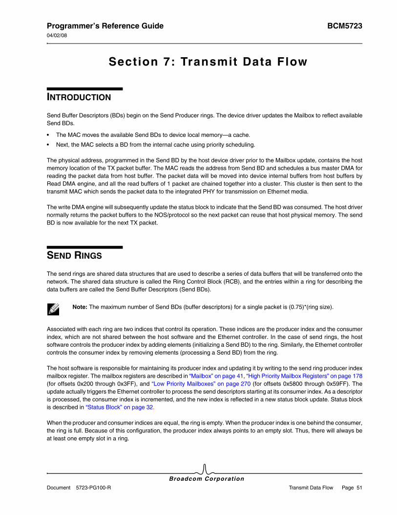
Programmer’s Reference Guide BCM572304/02/08
Broadcom CorporationDocument 5723-PG100-R Transmit Data Flow Page 51
Section 7: Transmit Data Flow
INTRODUCTION
Send Buffer Descriptors (BDs) begin on the Send Producer rings. The device driver updates the Mailbox to reflect available Send BDs.
• The MAC moves the available Send BDs to device local memory—a cache.
• Next, the MAC selects a BD from the internal cache using priority scheduling.
The physical address, programmed in the Send BD by the host device driver prior to the Mailbox update, contains the host memory location of the TX packet buffer. The MAC reads the address from Send BD and schedules a bus master DMA for reading the packet data from host buffer. The packet data will be moved into device internal buffers from host buffers by Read DMA engine, and all the read buffers of 1 packet are chained together into a cluster. This cluster is then sent to the transmit MAC which sends the packet data to the integrated PHY for transmission on Ethernet media.
The write DMA engine will subsequently update the status block to indicate that the Send BD was consumed. The host driver normally returns the packet buffers to the NOS/protocol so the next packet can reuse that host physical memory. The send BD is now available for the next TX packet.
SEND RINGS
The send rings are shared data structures that are used to describe a series of data buffers that will be transferred onto the network. The shared data structure is called the Ring Control Block (RCB), and the entries within a ring for describing the data buffers are called the Send Buffer Descriptors (Send BDs).
Associated with each ring are two indices that control its operation. These indices are the producer index and the consumer index, which are not shared between the host software and the Ethernet controller. In the case of send rings, the host software controls the producer index by adding elements (initializing a Send BD) to the ring. Similarly, the Ethernet controller controls the consumer index by removing elements (processing a Send BD) from the ring.
The host software is responsible for maintaining its producer index and updating it by writing to the send ring producer index mailbox register. The mailbox registers are described in “Mailbox” on page 41, “High Priority Mailbox Registers” on page 178(for offsets 0x200 through 0x3FF), and “Low Priority Mailboxes” on page 270 (for offsets 0x5800 through 0x59FF). The update actually triggers the Ethernet controller to process the send descriptors starting at its consumer index. As a descriptor is processed, the consumer index is incremented, and the new index is reflected in a new status block update. Status block is described in “Status Block” on page 32.
When the producer and consumer indices are equal, the ring is empty. When the producer index is one behind the consumer, the ring is full. Because of this configuration, the producer index always points to an empty slot. Thus, there will always be at least one empty slot in a ring.
Note: The maximum number of Send BDs (buffer descriptors) for a single packet is (0.75)*(ring size).
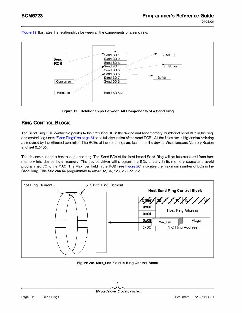
BCM5723 Programmer’s Reference Guide04/02/08
Broadcom Corporation
Page 52 Send Rings Document 5723-PG100-R
Figure 19 illustrates the relationships between all the components of a send ring.
Figure 19: Relationships Between All Components of a Send Ring
RING CONTROL BLOCK
The Send Ring RCB contains a pointer to the first Send BD in the device and host memory, number of send BDs in the ring, and control flags (see “Send Rings” on page 51 for a full discussion of the send RCB). All the fields are in big-endian ordering as required by the Ethernet controller. The RCBs of the send rings are located in the device Miscellaneous Memory Region at offset 0x0100.
The devices support a host based send ring. The Send BDs of the host based Send Ring will be bus-mastered from host memory into device local memory. The device driver will program the BDs directly in its memory space and avoid programmed I/O to the MAC. The Max_Len field in the RCB (see Figure 20) indicates the maximum number of BDs in the Send Ring. This field can be programmed to either 32, 64, 128, 256, or 512.
Figure 20: Max_Len Field in Ring Control Block
Send BD 1Send BD 2Send BD 3Send BD 4
Buffer
Buffer
Buffer
SendRCB
Send BD 5
Send BD 7Send BD 8Consumer
Producer
...
Send BD 6
Send BD 512
Offset 32 16 15 0
Host Ring Address0x00
0x04
Flags0x08
0x0C NIC Ring AddressMax_Len
Host Send Ring Control Block1st
1st Ring Element 512th Ring Element
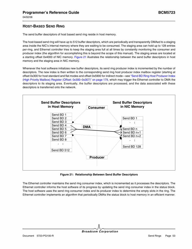
Programmer’s Reference Guide BCM572304/02/08
Broadcom CorporationDocument 5723-PG100-R Send Rings Page 53
HOST-BASED SEND RING
The send buffer descriptors of host based send ring reside in host memory.
The host-based send ring will have up to 512 buffer descriptors, which are periodically and transparently DMAed to a staging area inside the NIC’s internal memory where they are waiting to be consumed. The staging area can hold up to 128 entries per-ring, and Ethernet controller tries to keep the staging area full at all times by constantly monitoring the consumer and producer index (the algorithm for accomplishing this is beyond the scope of this manual). The staging areas are located at a starting offset 0x4000 of NIC memory. Figure 21 illustrates the relationship between the send buffer descriptors in host memory and the staging area in NIC memory.
Whenever the host software initializes new buffer descriptors, its send ring producer index is incremented by the number of descriptors. The new index is then written to the corresponding send ring host producer index mailbox register (starting at offset 0x300 for host standard and flat modes and offset 0x5900 for indirect mode—see “Send BD Ring Host Producer Index (High Priority Mailbox) Register (Offset: 0x300–0x307)” on page 179, which may trigger the Ethernet controller to DMA the descriptors to its staging area. Eventually, the buffer descriptors are processed, and the data associated with these descriptors is transferred onto the network.
Figure 21: Relationship Between Send Buffer Descriptors
The Ethernet controller maintains the send ring consumer index, which is incremented as it processes the descriptors. The Ethernet controller informs the host software of its progress by updating the send ring consumer index in the status block. The host software uses the send ring consumer index and its producer index to determine the empty slots in the ring. The Ethernet controller implements an algorithm that periodically DMAs the status block to host memory in an efficient manner.
Send BD 1Send BD 2Send BD 3Send BD 4Send BD 5
Send BD 7Send BD 8
...Send BD 6
Send BD 512
Send BD 1
Send BD 128
......
Send Buffer Descriptors in Host Memory
Send Buffer Descriptors in NIC Memory
Producer
Consumer
Send BD n+2
Send BD nSend BD n+1
DMA
BCM5723 Programmer’s Reference Guide04/02/08
Broadcom Corporation
Page 54 Checksum Offload Document 5723-PG100-R
CHECKSUM OFFLOAD
As network speed increases, offloading is becoming an important feature, and the ability to offload tasks from the host processor aids in the efficiency of the host and in overall system performance. To achieve a significant performance boost, most operating systems now a days offer a mechanism for the TCP/IP protocol stack to offload checksum calculations to the device.
The host software can configure the Ethernet controller to calculate IP, TCP, and UDP checksum as described in RFC 791, RFC 793, and RFC 768 respectively. The first step in checksum calculation is determining the start of an IP and UDP datagram and TCP segment within a frame, which could vary depending on whether the frame is tagged (VLAN) or encapsulated with LLC/SNAP header. Then the checksum is computed from the start to the end of the datagram and inserted into the appropriate location in protocol header. Ethernet controller is designed to support checksum calculation on all frame types and also on IP datagram and TCP segments containing options.
For the Ethernet controller to compute the checksum and insert it into the outgoing frame, the host software must set the appropriate control bits in the send buffer descriptors associated with the frame and seed the checksum field with zero or with the pseudo header checksum.
The host software enables IP checksum calculation by setting the IP_CHKSUM bits in all the send buffer descriptors associated with the frame. The Ethernet controller inserts the checksum into the checksum field of the IP header.
To enable TCP or UDP checksum calculation, the host software must set the TCP_UDP_CKSUM bit in all the send buffer descriptors associated with the frame containing the entire UDP datagram or TCP segment. The TCP and UDP checksum engines do not span IP fragmented frames.
The host software can configure the Ethernet controller to disable TCP or UDP pseudo-header checksum calculation by setting the Mode_Control.Send_No_Pseudo_Header_Checksum bit. When set, the host software must seed the checksum f ie ld in t he TCP or UDP header wi th the pseudo-header checksum. I f the Mode_Control.Send_No_Pseudo_Header_Checksum is cleared, the Ethernet controller computes the checksum including the pseudo header and inserts it into the checksum field.
SCATTER/GATHER
Most often, the host software requests the NIC to transmit a frame that spans several physical fragments that are arbitrary in size and buffer alignment. This requires the Ethernet controller to gather all these fragments during a DMA process into a continuous data stream for transmission.
The ability to scatter/gather a frame lessens the restriction on the host software and increases overall system performance.
Example: A TCP/IP protocol stack could preconstruct the MAC and IP headers in separate buffers that are combined with the payload to form a complete frame. Since the header data are fairly constant during a TCP or UDP session, the stack could use the same header buffers for the next frame.
The Ethernet controller uses a buffer descriptor for describing a physical fragment. There are two types of buffer descriptors; the Receive MAC processes receive buffer descriptors (Receive BD) and the Transmit MAC processes send buffer descriptors (Send BD).
Figure 22 illustrates the relationship between a frame consisting of multiple fragments and their corresponding send buffer
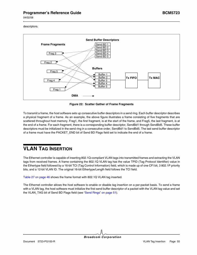
Programmer’s Reference Guide BCM572304/02/08
Broadcom CorporationDocument 5723-PG100-R VLAN Tag Insertion Page 55
descriptors.
Figure 22: Scatter Gather of Frame Fragments
To transmit a frame, the host software sets up consecutive buffer descriptors in a send ring. Each buffer descriptor describes a physical fragment of a frame. As an example, the above figure illustrates a frame consisting of five fragments that are scattered throughout host memory. Frag1, the first fragment, is at the start of the frame, and Frag5, the last fragment, is at the end of a frame. For each fragment, there is a corresponding buffer descriptor, SendBd1 through SendBd5. These buffer descriptors must be initialized in the send ring in a consecutive order, SendBd1 to SendBd5. The last send buffer descriptor of a frame must have the PACKET_END bit of Send BD Flags field set to indicate the end of a frame.
VLAN TAG INSERTION
The Ethernet controller is capable of inserting 802.1Q-compliant VLAN tags into transmitted frames and extracting the VLAN tags from received frames. A frame containing the 802.1Q VLAN tag has the value TPID (Tag Protocol Identifier) value in the Ethertype field followed by a 16-bit TCI (Tag Control Information) field, which is made up of one CFI bit, 3 802.1P priority bits, and a 12-bit VLAN ID. The original 16-bit Ethertype/Length field follows the TCI field.
Table 27 on page 46 shows the frame format with 802.1Q VLAN tag inserted.
The Ethernet controller allows the host software to enable or disable tag insertion on a per-packet basis. To send a frame with a VLAN tag, the host software must initialize the first send buffer descriptor of a packet with the VLAN tag value and set the VLAN_TAG bit of Send BD Flags field (see “Send Rings” on page 51).
Send BD 3
Frame Fragments
Frag 2
Frag 5
Frag 4
Frag 1
Send BD 1Send BD 2
Send BD 4Send BD 5
Frag 3
Send Buffer Descriptors
Buffers
Buffer 1Buffer 2Buffer 3Buffer 4Buffer 5
Tx FIFO Tx MAC
DMA

BCM5723 Programmer’s Reference Guide04/02/08
Broadcom Corporation
Page 56 TX Data Flow Diagram Document 5723-PG100-R
TX DATA FLOW DIAGRAM
Figure 23 on page 57 illustrates how a frame, consisting of several fragments, is sent from the host to the NIC and onto the network. For simplicity, the diagram depicts the operation of a single ring.
1. The host software calls a system API to retrieve the three physical fragments of the frame. It initializes the next three send buffer descriptors to point to each fragment. The send buffer descriptors reside in host memory. Internally, the host software maintains the ring’s producer index. In this case, the producer index is incremented by three because there are three fragments.
2. The host software updates the send ring producer index by writing the producer index value to Send Ring Producer Index Mailbox at offset 0x300 for host standard and flat modes and offset 0x5900 for indirect mode. The mailbox update triggers the Ethernet controller to process the send buffer descriptors.
3. The send buffer descriptors are DMAed to the ring’s staging area in device memory as indicated in the RCB.
4. The Ethernet controller DMAs the frame (as described in the descriptors) to its internal memory for transmission.
5. Internally, the Ethernet controller maintains the send ring’s consumer index, which is incremented as it processes the descriptors.
6. The new consumer index is written to the status block in NIC memory (see “Status Block” on page 32).
7 The status block is DMAed to host memory. This DMA is subject to host coalescing, and the NIC may generate an inter-rupt at this point.
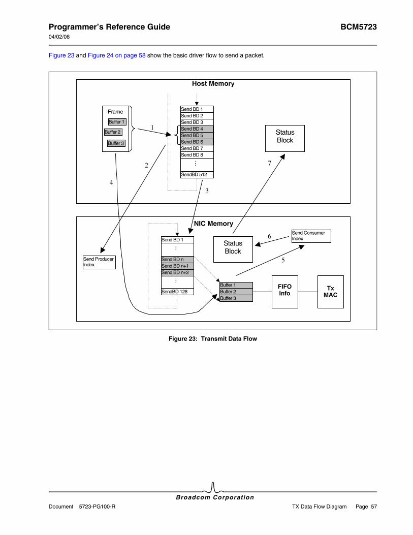
Programmer’s Reference Guide BCM572304/02/08
Broadcom CorporationDocument 5723-PG100-R TX Data Flow Diagram Page 57
Figure 23 and Figure 24 on page 58 show the basic driver flow to send a packet.
Figure 23: Transmit Data Flow
NIC Memory
Host Memory
Send BD 1
...
Send BD 2Send BD 3Send BD 4Send BD 5Send BD 6Send BD 7Send BD 8
SendBD 512
Frame
Buffer 1
Buffer 2
Buffer 3
Send ProducerIndex
Buffer 3Buffer 2Buffer 1
TxInfo
TxMAC
Send ConsumerIndex
StatusBlock
StatusBlock
1
2
34
5
6
7
Send BD 1...
Send BD nSend BD n+1Send BD n+2
SendBD 128
...
FIFO
Host Memory
NIC Memory
FIFO Info
Tx MAC
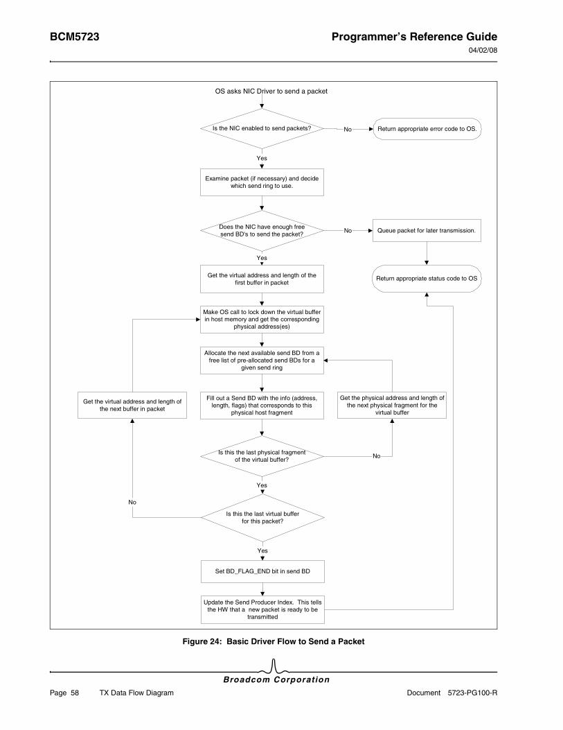
BCM5723 Programmer’s Reference Guide04/02/08
Broadcom Corporation
Page 58 TX Data Flow Diagram Document 5723-PG100-R
Figure 24: Basic Driver Flow to Send a Packet
Get the virtual address and length ofthe next buffer in packet
Is the NIC enabled to send packets?
Does the NIC have enough freesend BD's to send the packet?
Get the virtual address and length of thefirst buffer in packet
Fill out a Send BD with the info (address,length, flags) that corresponds to this
physical host fragment
Update the Send Producer Index. This tellsthe HW that a new packet is ready to be
transmitted
Examine packet (if necessary) and decidewhich send ring to use.
Is this the last virtual bufferfor this packet?
Set BD_FLAG_END bit in send BD
Make OS call to lock down the virtual bufferin host memory and get the corresponding
physical address(es)
Queue packet for later transmission.
Return appropriate status code to OS
Return appropriate error code to OS.
Allocate the next available send BD from afree list of pre-allocated send BDs for a
given send ring
OS asks NIC Driver to send a packet
Yes
No
No
Yes
No
Yes
Is this the last physical fragmentof the virtual buffer?
Yes
Get the physical address and length ofthe next physical fragment for the
virtual buffer
No
Programmer’s Reference Guide BCM572304/02/08
Broadcom CorporationDocument 5723-PG100-R Reset Page 59
RESET
A hardware reset initiated by the PCI reset signal will initialize all the PCI configuration registers and device MAC registers to their default values. The driver reset via the Core Clock Blocks Reset bit (see “Miscellaneous Configuration Register (Offset: 0x6804)” on page 277) will also initialize all non-sticky registers to their default values. The content of the device internal memory remains unchanged after warm reset (any reset with the power supplied to the device).
At the end of the reset, the on-chip RX RISC executes a small on chip ROM code. This code loads an executable image contained in an attached NVRAM and referred to as the bootcode. This bootcode allows at least the following fields to be initialized to different values to support product variations (for additional details, see Section 4: “NVRAM Configuration” on page 20).
• Vendor ID
• Device ID
• Subsystem Vendor ID
• Subsystem Device ID
• Possible PHY initialization
The bootcode may have additional functionality such as PXE that must be acquiesced while the host software is running.
Example: An NDIS driver issues a device reset via the Core Clock Blocks Reset bit (see Table 322 on page 283). After the reset is completed, the RX RISC begins executing the bootcode as if the power was first applied to the device. However, the NDIS driver must have a mechanism to prevent the PXE driver from running and the bootcode must be able to distinguish between a power-on reset and a reset initiated by the host software. The host software and the bootcode could implement a reset handshake by using shared memory at offset 0x0b50 as a software mailbox (see “Firmware Mailbox” on page 118).
FIRMWARE DOWNLOAD
FIRMWARE BINARY IMAGE
The RISC cores in the Ethernet controller chips execute the MIPS-2 instruction set. Broadcom uses a GNU tool kit to create the firmware binary code. The output from the GNU build is a C language header file, which contains the machine code for the embedded RISC cores. This manual does not cover the technology necessary to program the RISC cores. However, programmers may need to download value-added firmware provided by Broadcom. One example of value added firmware is TCP segmentation firmware that can be loaded from the host driver. This section provides the necessary understanding of the header file, created by the Broadcom GNU tools. The programmer must understand the layout of the header file, to accomplish a firmware download.
The following sections are located in the header file provided by Broadcom:
• t3FwText[]—Array of 32-bit words. This section contains the machine code (opcodes/operands) executed by the RISC cores. This is the text section in the binary file, output by the GNU build process.
• t3FwRodata[]—Array of 32-bit words. This section contains the read-only data available to the code section of the firmware.
• t3FwData[]—Array of 32-bit words. This section contains the local variables available to the code section of the firmware.
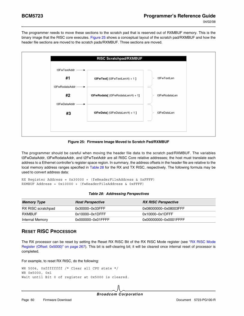
BCM5723 Programmer’s Reference Guide04/02/08
Broadcom Corporation
Page 60 Firmware Download Document 5723-PG100-R
The programmer needs to move these sections to the scratch pad that is reserved out of RXMBUF memory. This is the binary image that the RISC core executes. Figure 25 shows a conceptual layout of the scratch pad/RXMBUF and how the header file sections are moved to the scratch pads/RXMBUF. Three sections are moved.
Figure 25: Firmware Image Moved to Scratch Pad/RXMBUF
The programmer should be careful when moving the header file data to the scratch pad/RXMBUF. The variables t3FwDataAddr, t3FwRodataAddr, and t2FwTextAddr are all RISC Core relative addresses; the host must translate each address to a Ethernet controller’s register space region. In summary, the address offsets in the header file are relative to the local memory address ranges specified in Table 28 for the RX and TX RISC, respectively. The following formula may be used to convert address data:
RX Register Address = 0x30000 + (fwHeaderFileAddress & 0xFFFF)RXMBUF Address = 0x10000 + (fwHeaderFileAddress & 0xFFFF)
RESET RISC PROCESSOR
The RX processor can be reset by setting the Reset RX RISC Bit of the RX RISC Mode register (see “RX RISC Mode Register (Offset: 0x5000)” on page 267). This bit is self-clearing bit; it will be cleared once internal reset of processor is completed.
For example, to reset RX RISC, do the following:
WR 5004, 0xffffffff /* Clear all CPU state */WR 0x5000, 0x1Wait until Bit 0 of register at 0x5000 is cleared.
Table 28: Addressing Perspectives
Memory Type Host Perspective RX RISC Perspective
RX RISC scratchpad 0x30000–0x33FFF 0x08000000–0x08003FFF
RXMBUF 0x10000–0x1DFFF 0x10000–0x1DFFF
Internal Memory 0x000000–0x01FFFF 0x00000000–0x0001FFFF
RISC Scratchpad
t3FwText[ (t3FwTextLen/4) + 1 ] t3FwTextLen
t3FwTextAddr
t3FwRodata[ (t3FwRodataLen/4) + 1] t3FwRodataLen
t3FwRodataAddr
t3FwData[ (t3FwDataLen/4) + 1 ] t3FwDataLen
t3FwDataAddr
#1
#2
#3
RISC Scratchpad/RXMBUF
Programmer’s Reference Guide BCM572304/02/08
Broadcom CorporationDocument 5723-PG100-R Firmware Download Page 61
HALT RISC PROCEDURE
1. Clear the RX RISC state register. Write 0xFFFFFFFF to the RX_RISC_State register (see “RX RISC Status Register (Offset: 0x5004)” on page 268).
2. Issue RX RISC halt. Write the RISC_MODE_HALT bit to the RX_RISC_Mode register (see “RX RISC Mode Register (Offset: 0x5000)” on page 267).
3. Read/verify that the RISC_MODE_HALT bit is set. Read the Rx RISC_MODE_HALT bit back from the RX_RISC_Mode register. Break from procedure if bit is set.
4. Delay 10 µs and jump to Step 1. Repeat the procedure up to 10,000 times.
START RISC PROCEDURE
This procedure first stops the RX RISC and modifies the program counter. The RISC processor is then started to begin executing firmware at new address given by program counter.
1. Clear the RX RISC state register. Write 0xFFFFFFFF to the RX_RISC_State register (see “RX RISC Status Register (Offset: 0x5004)” on page 268).
2. Set the RX RISC program counter. Write t3FwTextAddr to the RX_RISC_PC register (see“RX RISC Program Counter (Offset: 0x501C)” on page 269).
3. Read back the PC register. Read the RX_RISC_PC register and verify that t3FwTextAddr is set. If properly set, then jump to Step 7.
4. Clear the RX RISC state register. Write 0xFFFFFFFF to the RX_RISC_State register.
5. Halt the RX RISC. Write the RISC_MODE_HALT bit to the RX_RISC_Mode register.
6. Delay one millisecond. Jump to Step 2. Repeat procedure.
7. Clear the RX RISC state register. Write 0xFFFFFFFF to the RX_RISC_State register.
8. Clear the RX RISC mode register. Write 0x00 to the RX_RISC_Mode register (see “RX RISC Program Counter (Offset: 0x501C)” on page 269).
Note: The t3FwTextAddr should not be converted to a register relative address. The RISCs execute from a local memory space. The conversion is only necessary for writing t3FwText [] to the scratch pad using register space—the host view of the scratch pad region is different from the RISC view. See Table 28 on page 60.
BCM5723 Programmer’s Reference Guide04/02/08
Broadcom Corporation
Page 62 Firmware Download Document 5723-PG100-R
FIRMWARE DOWNLOAD PROCEDURE
The host driver should use register indirect access to modify both the scratch pad and RISC register space. See “Pseudocode” on page 90 in Section 8: “PCI”.
1. Halt the RX RSIC Core (see “Halt RISC Procedure” on page 61).
2. Clear the RX RISC Scratch pad. Use register indirect access and write zero(s) starting at register address 0x30000 (see Table 28 on page 60). The last address to clear is 0x33FFF. The total length of the scratch pad is 0x4000 and the host driver should increment the target address by four (4), since each MIPS word is 32 bits (4 bytes).
3. Convert variable t3FwRodataAddr to a register relative address for the RX RISC. The register address is calculated as follows:regNormalized = 0x10000 + (t3FwTextAddr & 0xFFFF)
For systems using RXMBUF memory for firmware, ensure that the downloaded firmware does not overlap the MBUF Pool Address (see “MBUF Pool Base Address Register (Offset: 0x4408)” on page 259).
4. Write the array t3FwText [] to the RX scratched/RXMBUF (see Table 28 on page 60). Use register indirect access and increment by four bytes for every 32-bit write. The last/limit address to write is calculated as follows:
regNormalized + t3FwTextLen
5. Convert variable t3FwRodataAddr to a register relative address for the RX RISC. The register address is calculated as follows:
regNormalized = 0x10000 + (t3FwRoDataAddr & 0xFFFF)
6. Write the array t3FwRodata [] to the RX scratch pad/RXMBUF (see Table 28 on page 60). Use register indirect access and increment by four bytes for every 32-bit write. The last/limit address to write is calculated as follows:
regNormalized (from Step 5.) + t3FwRodataLen
7. Convert variable t3FwDataAddr to a register relative address for the RX RISC. The register address is calculated as follows:
regNormalized = 0x10000 + (t3FwDataAddr & 0xFFFF)
8. Write the array t3FwData [] to the RX scratch pad/RXMBUF (see Table 28 on page 60). Use register indirect access and increment by four bytes for every 32-bit write. The last/limit address to write is calculated as follows:
regNormalized (from Step 7.) + t3FwDataLen
9. Start the RX RISC (see “Start RISC Procedure” on page 61).
When freeing received RxMbufs (e.g., received ASF RMCP packets) from the MIPS CPU (running ASF firmware or any other optional FW) while simultaneously receiving/freeing TCP traffic for the host device driver, a race condition can occur which causes subsequent receives to fail (no more RxMbufs get enqueued). To avoid this race condition, before freeing the RxMbuf chain (by writing to the MbufClustFreeFtqFifoEnqueueDequeue register, 0x5cc8), the FW should poll the buffer manager hardware diagnostic 3 register (0x4454) until the descriptor in bits 25:16 matches the MBUF cluster at the beginning of the chain about to free. Also, note that the hardware diagnostic register uses a cluster based on the offset from the top of the RxMbuf pool (e.g., 0x16000) and the firmware uses a cluster based on the offset from 0x10000, so some calculations must be performed to compare the proper pointer values.
Note: When enabled, the ASF/IPMI FW is required to run even in the absence of OS. The IPMI/ASF FW is normally programmed into NVRAM and the bootcode will load this FW into scratch pad/RxMbuf memory if the IPMI/ASF feature is enabled. The bootcode reserves enough memory out of RxMbuf as RISC scratch pad for IPMI/ASF firmware.
Programmer’s Reference Guide BCM572304/02/08
Broadcom CorporationDocument 5723-PG100-R MAC Address Setup/Configuration Page 63
Example Code Snippet (from ASF Firmware)
/* Poll buffer manager hardware diag register 3 (0x4454) for our mbuf pointer value */while(trp->BufMgr.MbufPoolAddr + (((trp->BufMgr.Hwdiag[2]>>16) & 0x1ff) << 7) != (u32)pmbuf);
MAC ADDRESS SETUP/CONFIGURATION
The MAC address registers, starting at offset 0x0410, contain the MAC addresses of the NIC. These registers are usually initialized with a default MAC address extracted from the NIC’s NVRAM when it is first powered up. The host software may overwrite the default MAC address by writing to the MAC registers with a new MAC address. Table 29 illustrates the MAC register format.
The BCM5723 Ethernet controller allows a NIC to have up to four MAC addresses (offset 0x410–0x42F) that are used for hardware packet reception filtering. However, most host software will initialize the registers of the four MAC addresses to the same MAC address since a NIC usually has only one MAC address.
When flow control is enabled on the Ethernet controller, the MAC Address 0 is used as the source address for sending PAUSE frames (see “Pause Control Frame” on page 311).
PACKET FILTERING
MULTICAST HASH TABLE SETUP/CONFIGURATION
The MAC hash registers are used to help discard unwanted multicast packets as they are received from the external media. The destination address is fed into the normal CRC algorithm in order to generate a hash function. The most significant bits of the CRC are then used without any inversion in reverse order to index into a hash table, which is comprised of these MAC hash registers. If the CRC is calculated by shifting right, then the right-most bits of the CRC can be directly used with no additional inversion or bit swapping required. See “Ethernet CRC Calculation” for more details on the CRC algorithm.
All four MAC hash registers are used so that register 1 bit-32 is the most significant hash table entry and register 4 bit-0 is the least significant hash table entry. This follows the normal big-endian ordering used throughout the Ethernet controller. Since there are 128 hash table entries, 7 bits are used from the CRC. When hash table is extended to 256 entries, 8 bits
Table 29: Mac Address Registers
Register Name Offset 31 24 23 16 15 8 7 0
Mac_Address_0 0x0410 Unused Octet 0 Octet 1
0x0414 Octet 2 Octet 3 Octet 4 Octet 5
Mac_Address_1 0x0418 Unused Octet 0 Octet 1
0x041c Octet 2 Octet 3 Octet 4 Octet 5
Mac_Address_2 0x0420 Unused Octet 0 Octet 1
0x0424 Octet 2 Octet 3 Octet 4 Octet 5
Mac_Address_3 0x0428 Unused Octet 0 Octet 1
0x042c Octet 2 Octet 3 Octet 4 Octet 5
BCM5723 Programmer’s Reference Guide04/02/08
Broadcom Corporation
Page 64 Packet Filtering Document 5723-PG100-R
from the CRC will be used as hash index.
The MAC hash registers are ignored if the receive MAC is in promiscuous mode.
ETHERNET CRC CALCULATION
The Ethernet controller uses the standard 32-bit CRC required by the Ethernet specification as its FCS in all packets. The checksum is the 32-bit remainder of the polynomial division of the data taken as a bit stream of polynomial coefficients and a predefined constant, which also represents binary polynomial coefficients. The checksum is optionally appended most-significant bit first to a packet, which is to be sent down the wire. At the receiving side, the division is repeated on the entire packet including the CRC checksum. The remainder is compared to a known constant. For details on the mathematical basis for CRC checksums, see Tanenbaum's Computer Networks, Third Edition, c1996.
The 32-bit CRC polynomial divisor is shown below:
x32 + x26 + x23 + x22 + x16 + x12 + x11 + x10 + x8 + x7 + x5 + x4 + x2 + x + 1
GENERATING CRC
The following steps describe a method to calculate the CRC with the resulting 32-bit quantity having reversed bit order (i.e., most significant bit x31 of the remainder is right-most bit). The data should be treated as a stream of bytes. Set remainder to 0xFFFFFFFF. For each bit of data starting with least-significant bit of each byte:
1. If right-most bit (bit-0) of the current remainder XORed with the data bit equal 1, then remainder = (remainder shifted right one bit) XOR 0xEDB88320, else remainder = (remainder shifted right one bit).
2. Invert remainder such that remainder = ~remainder. Remainder is CRC checksum. Right-most byte is the most significant and is to be sent first. Swap bytes of CRC if big-endian byte ordering is desired.
CHECKING CRC
The following steps describe a method to check a stream of bytes, which has a CRC appended.
1. Set remainder to 0xFFFFFFFF.
2. For each bit of data starting with least-significant bit of each byte: If right-most bit (bit-0) of the current remainder XORed with the data bit equal 1, then remainder = (remainder shifted right one bit) XOR 0xEDB88320, else remainder = (remainder shifted right one bit).
3. Remainder should equal magic value 0xDEBB20E3 if CRC is correct.
INITIALIZING THE MAC HASH REGISTERS
The 128-bit multicast hash table is treated as a single object occupying four Ethernet controller registers starting at offset 0x0470 (see Table 30). The 128-bit value follows the big-endian ordering required by Ethernet controller. Thus, the most significant 32-bit of the 128-bit value resides in Mac_Hash_Register_0 at offset 0x0470 and the least significant 32-bit resides in Mac_Hash_Register_3 at offset 0x047c.
Programmer’s Reference Guide BCM572304/02/08
Broadcom CorporationDocument 5723-PG100-R Packet Filtering Page 65
Host software can enable the reception of all multicast frames including broadcast frames by setting all four multicast hash registers to 0xFFFFFFFF.
The following C code fragment illustrates how to initialize the multicast hash table registers. The code fragment computes the indices into hash table from a given list of multicast addresses and initializes the multicast hash registers.
Unsigned long HashReg[4];Unsigned long j, McEntryCnt;Unsigned char McTable[32][6];// List of multicast addresses to accept.
// Initialize the McTable here.McEntryCnt = 32;
// Initialize the multicast table registers.HashReg[0] = 0; // Mac_Hash_Regsiter_0 at offset 0x0470.HashReg[1] = 0; // Mac_Hash_Register_1 at offset 0x0474.HashReg[2] = 0; // Mac_Hash_Register_2 at offset 0x0478.HashReg[3] = 0; // Mac_Hash_Register_3 at offset 0x047c.
for(j = 0; j < McEntryCnt; j++){
unsigned long RegIndex;unsigned long Bitpos;unsigned long Crc32;
Crc32 = ComputeCrc32(McTable[j], 6);
// The most significant 7 bits of the CRC32 (no inversion),// are used to index into one of the possible 128 bit positions.Bitpos = ~Crc32 & 0x7f;
// Hash register index.RegIndex = (Bitpos & 0x60) >> 5;
// Bit to turn on within a hash register.Bitpos &= 0x1f;
// Enable the multicast bit.HashReg[RegIndex] |= (1 << Bitpos);
}
The following C routine computes the Ethernet CRC32 value from a given byte stream. The routine is called from the above code fragment.
// Routine for generating CRC32.unsigned longComputeCrc32(
unsigned char *pBuffer, // Buffer containing the byte stream.unsigned long BufferSize) // Size of the buffer.
{
Table 30: Multicast Hash Table Registers
Register Name Offset Description
Mac_Hash_Register_0 0x0470 Most significant 32-bit of the 128-bit hash table
Mac_Hash_Register_1 0x0474 Bits 64:93 of the 128-bit hash table
Mac_Hash_Register_2 0x0478 Bits 32:63 of the 128-bit hash table
Mac_Hash_Register_3 0x047c Least significant 32-bit of the 128-bit hash table
BCM5723 Programmer’s Reference Guide04/02/08
Broadcom Corporation
Page 66 Packet Filtering Document 5723-PG100-R
unsigned long Reg;unsigned long Tmp;unsigned long j, k;
Reg = 0xffffffff;
for(j = 0; j < BufferSize; j++){
Reg ^= pBuffer[j];
for(k = 0; k < 8; k++){
Tmp = Reg & 0x01;Reg >>= 1;if(Tmp){
Reg ^= 0xedb88320;}
}}
return ~Reg;}
PROMISCUOUS MODE SETUP/CONFIGURATION
The host software may enable promiscuous mode by setting the Promiscous_Mode bit (bit 8) of the Receive_MAC_Mode register (offset 0x468). The Promiscous_Mode bit defaults to disabled after reset, and host software must explicitly set this bit for promiscuous mode. In promiscuous mode of operation, the Ethernet controller accepts all incoming frames that are not filtered by the active receive rules regardless of the destination MAC address. In other words, the Ethernet controller operating in promiscuous mode ignores multicast and MAC address filtering (“Multicast Hash Table Setup/Configuration” on page 63 and “MAC Address Setup/Configuration” on page 63), but applies Receive Rules.
BROADCAST SETUP/CONFIGURATION
The host software may configure the Ethernet controller to discard the received broadcast frames by using two receive rules as defined below. The Ethernet controller parses all incoming frames according to these receive rules and discards those frames that have a broadcast destination address (see “Receive Rules Setup and Frame Classification” on page 43 for more details on setting up the receive rules).
The following is a sample of the two receive rules for discarding broadcast frames.
Rule1 Control: 0xc2000000 Rule1 Mask/Value: 0xffffffffRule2 Control: 0x86000004 Rule2 Mask/Value: 0xffffffff
Programmer’s Reference Guide BCM572304/02/08
Broadcom CorporationDocument 5723-PG100-R PCI Page 67
Section 8: PCI
CONFIGURATION SPACE
DESCRIPTION
PCI, PCI-X, and PCIe devices must implement sixteen 32-bit PCI registers. These registers are required for a device to have PCI compliance. The format and layout of these registers is defined in the PCI 2.2 specification. Capability registers provide system BIOS and Operating Systems visibility into a set of optional features, which devices may implement. Although the capability registers are not required, the structure and mechanism for chaining auxiliary capabilities is defined in the PCI specification. Both software and BIOS must implement algorithms to fetch and program capabilities fields accordingly. Refer to section 6.7 of the PCI SIIG 2.2 specification. Additional PCI configuration space may be used for device-specific registers. However, device-specific registers are not exposed to system software, according to a specification/standard. System software cannot probe device specific registers without a predetermined understanding of the device and its functionality. In summary, three types of PCI configuration space registers may be exposed by any particular device:
• Required
• Optional capabilities
• Device specific
Network devices implement large quantities of registers, and these registers could consume huge amounts of PCI configuration space. PCI configuration access is not very efficient, on a performance basis.
Example: Intel x86 architectures use two I/O mapped I/O addresses 0xCF8 and 0xCFC for host-based access to PCI configuration space. Should a host device driver access these I/O addresses on every device read/write, CPU overhead would grow greatly. Generally, host device drivers should not use PCI configuration space for standard I/O and control programming. There is one special case—Universal Network Device Interface (UNDI) drivers. UNDI drivers may not have access to host memory mapped registers when operating in real-mode; thus, an indirect mode of access is necessary. The Ethernet controller implements a PCI indirect mode for memory, registers, and mailboxes access. A specific example of a device driver, which uses indirect mode, is the Preboot Execution (PXE) driver. PXE drivers may be stored in either option ROMs or directly in the system BIOS.
Most host device drivers use register blocks, which are mapped into host memory. Memory Mapped I/O is an efficient mechanism for PCI devices to use system resources. The type and extent of this memory mapping depends upon the MAC’s configuration (see the operational characteristics subsection). A typical PCI device will decode a range of physical (bus) addresses, which do not conflict with physical memory or other PCI devices. Each device on the PCI bus will request a range of physical memory, and the PnP BIOS will assign mutually exclusive resources to that device. The size and range of resource is based upon each device’s hardwired programming of the BAR. The Ethernet controller implements two modes of memory mapped I/O—Standard and Flat. I/O mapped I/O is not supported by the Ethernet controller, and there are no I/O space registers.
Note: The PCI BAR 0 register is only reset to 0 after a hard reset, otherwise it maintains its value over GRC and PCI resets.
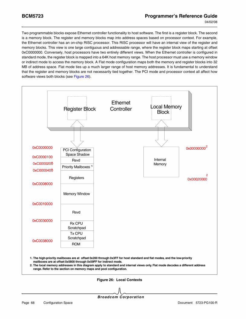
BCM5723 Programmer’s Reference Guide04/02/08
Broadcom Corporation
Page 68 Configuration Space Document 5723-PG100-R
Two programmable blocks expose Ethernet controller functionality to host software. The first is a register block. The second is a memory block. The register and memory blocks map into address spaces based on processor context. For example, the Ethernet controller has an on-chip RISC processor. This RISC processor will have an internal view of the register and memory blocks. This view is one large contiguous and addressable range, where the register block maps starting at offset 0xC0000000. Conversely, host processors have two entirely different views. When the Ethernet controller is configured in standard mode, the register block is mapped into a 64K host memory range. The host processor must use a memory window or indirect mode to access the memory block. A Flat mode configuration maps both the memory and register blocks into 32 MB of address space. Flat mode ties up a much larger range of host memory addresses. It is fundamental to understand that the register and memory blocks are not necessarily tied together. The PCI mode and processor context all affect how software views both blocks (see Figure 26).
Figure 26: Local Contexts
0x000000000xC0000000
0x00020000
InternalMemory
PCI ConfigurationSpace Shadow
Priority Mailboxes 1
Registers
Rx CPUScratchpad
Memory Window
Tx CPUScratchpad
ROM
Rsvd
0xC00004001
0xC0008000
0xC0000100
0xC00002001
0xC0010000
0xC0030000
Rsvd
Ethernet Controller
0xC0038000
Local MemoryBlock
Register Block
1. The high-priority mailboxes are at offset 0x200 through 0x3FF for host standard and flat modes, and the low-priority mailboxes are at offset 0x5800 through 0x59FF for indirect mode.2. The local memory addresses in this diagram apply to standard and internal views only. Flat mode decodes a different address range. Refer to the section on memory maps and pool configuration.
2
2
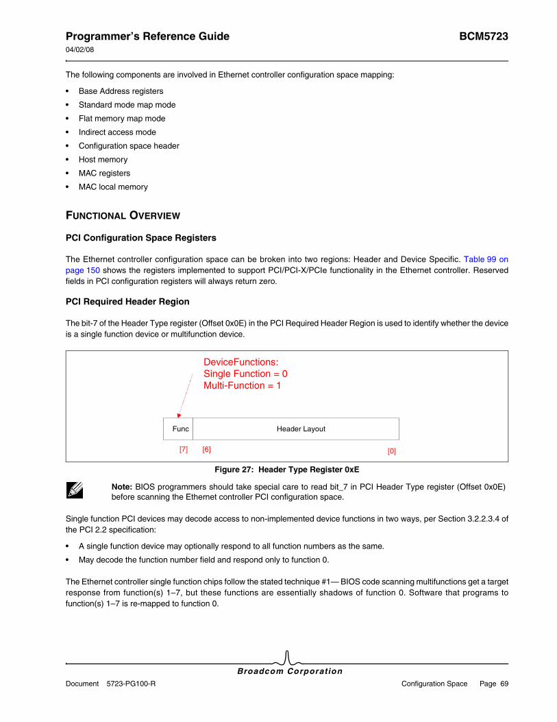
Programmer’s Reference Guide BCM572304/02/08
Broadcom CorporationDocument 5723-PG100-R Configuration Space Page 69
The following components are involved in Ethernet controller configuration space mapping:
• Base Address registers
• Standard mode map mode
• Flat memory map mode
• Indirect access mode
• Configuration space header
• Host memory
• MAC registers
• MAC local memory
FUNCTIONAL OVERVIEW
PCI Configuration Space Registers
The Ethernet controller configuration space can be broken into two regions: Header and Device Specific. Table 99 on page 150 shows the registers implemented to support PCI/PCI-X/PCIe functionality in the Ethernet controller. Reserved fields in PCI configuration registers will always return zero.
PCI Required Header Region
The bit-7 of the Header Type register (Offset 0x0E) in the PCI Required Header Region is used to identify whether the device is a single function device or multifunction device.
Figure 27: Header Type Register 0xE
Single function PCI devices may decode access to non-implemented device functions in two ways, per Section 3.2.2.3.4 of the PCI 2.2 specification:
• A single function device may optionally respond to all function numbers as the same.
• May decode the function number field and respond only to function 0.
The Ethernet controller single function chips follow the stated technique #1— BIOS code scanning multifunctions get a target response from function(s) 1–7, but these functions are essentially shadows of function 0. Software that programs to function(s) 1–7 is re-mapped to function 0.
Note: BIOS programmers should take special care to read bit_7 in PCI Header Type register (Offset 0x0E) before scanning the Ethernet controller PCI configuration space.
Func
DeviceFunctions:Single Function = 0Multi-Function = 1
Header Layout
[0][6][7]
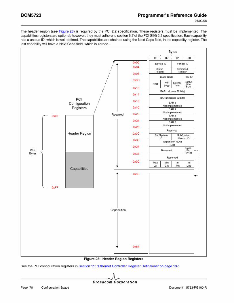
BCM5723 Programmer’s Reference Guide04/02/08
Broadcom Corporation
Page 70 Configuration Space Document 5723-PG100-R
The header region (see Figure 28) is required by the PCI 2.2 specification. These registers must be implemented. The capabilities registers are optional; however, they must adhere to section 6.7 of the PCI SIIG 2.2 specification. Each capability has a unique ID, which is well-defined. The capabilities are chained using the Next Caps field, in the capability register. The last capability will have a Next Caps field, which is zeroed.
Figure 28: Header Region Registers
See the PCI configuration registers in Section 11: “Ethernet Controller Register Definitions” on page 137.
Device ID(0x14E4)
0x00 Vendor ID0x04
StatusRegister
0x08Class Code Rev ID
0x0C
0x10
CacheLineSize
0x14BAR 1 (Lower 32 bits)
Bytes
CommandRegister
00010203
LatencyTimer
HdrType
BIST
BAR 2 (Upper 32 bits)
BAR 3Not Implemented
BAR 4Not Implemented
0x18
0x1C
SubSystemVendor ID
SubSystemID
Expansion ROMBAR
0x20
0x24
BAR 5Not Implemented
BAR 6Not Implemented
Reserved0x28
0x2C
0x30
CapsPtr
(0x48)Reserved
IntLine
IntPin
MinGnt
MaxLat
0x34
0x38Reserved
0x3C
0x40
Capabilities
Required
0x64
Header Region
0x00
Capabilities
0xFF
PCIConfiguration
Registers
255Bytes

Programmer’s Reference Guide BCM572304/02/08
Broadcom CorporationDocument 5723-PG100-R Configuration Space Page 71
PCI Device-Specific Region
Device-specific registers are not defined in the PCI 2.2 specification and are exactly as the name implies—specific to the Ethernet controller. These registers may be used by host software to configure or change the operational state of the MAC. The most notable feature exposed via the Device Specific registers is Indirect Mode. Host or system software may use Indirect Mode to access Ethernet controller local memory and register space; no memory mapped I/O is necessary in indirect mode. The device specific registers are implemented as Broadcom Vendor-Specific Capabilities registers.
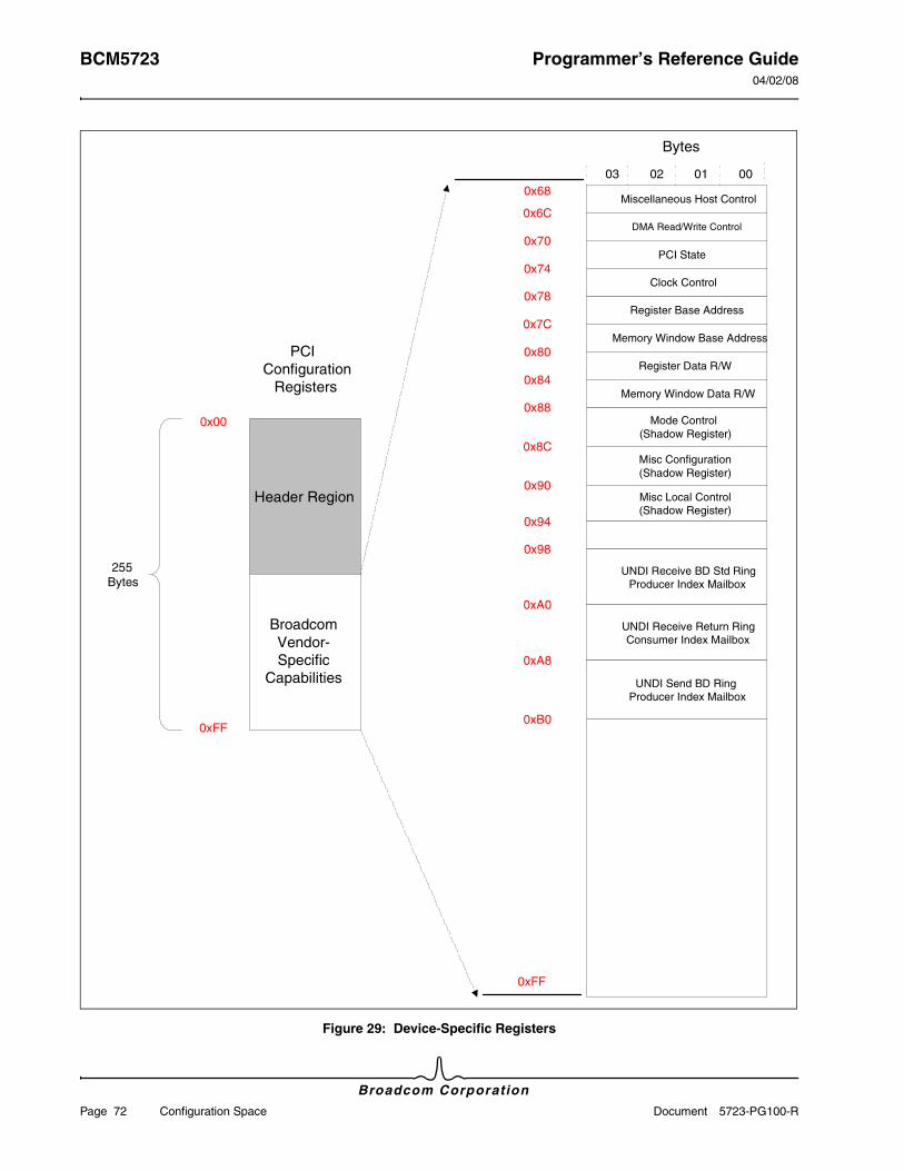
BCM5723 Programmer’s Reference Guide04/02/08
Broadcom Corporation
Page 72 Configuration Space Document 5723-PG100-R
Figure 29: Device-Specific Registers
Miscellaneous Host Control0x68
0x6CDMA Read/Write Control
0x70PCI State
0x74
0x78
0x7CRegister Base Address
Bytes
00010203
Memory Window Base Address
Register Data R/W0x80
0x84
0x88
0x8C
Mode Control(Shadow Register)
Header Region
0x00
Broadcom Vendor-Specific
Capabilities
0xFF
PCIConfiguration
Registers
255Bytes
Clock Control
Memory Window Data R/W
Misc Configuration(Shadow Register)
Misc Local Control(Shadow Register)
0x90
0x94
UNDI Receive BD Std RingProducer Index Mailbox
UNDI Receive Return RingConsumer Index Mailbox
0x98
0xA0
UNDI Send BD RingProducer Index Mailbox
0xB0
0xA8
0xFF
Programmer’s Reference Guide BCM572304/02/08
Broadcom CorporationDocument 5723-PG100-R Configuration Space Page 73
The Device-Specific registers are shown in Table 31
Indirect Mode
Host software may use indirect mode to access the Ethernet controller resources, without using Memory Mapped I/O. Indirect mode shadows MAC resources to PCI configuration space registers. These shadow registers can be read/written by system software through PCI configuration space registers. The Ethernet controller indirect mode registers expose the following MAC resources:
• Registers
• Local Memory
• Mailboxes
Indirect mode access can be used in conjunction with Standard or Flat Mode PCI access. Indirect mode has no interdependency on other PCI access modes and is a mode in itself.
Indirect Register Access
Two PCI configuration space register pairs give host software access to the Ethernet controller register block. The Register_Base_Address register creates a position in the MAC register block. Valid positions range from 0x0000–0x8000 and 0x30000–0x38800 ranges. Access to the register block from 0x8000–0x30000, should be avoided and is not necessary. The Flat and Standard Modes do map a memory window into the 0x8000–0xFFFF ranges; however, the Memory Indirection register pair provides a more efficient mechanism to access the Ethernet controller memory block. The Register_Data register allows host software to read/write, from the indirection position. The Register_Base_Address register can be perceived as creating a cursor/pointer into the register block. The Register_Data register allows host software to read/write to the location, specified by the Register_Base_Address. This register pair accesses the Ethernet controller register block (see Figure 30 on page 74).
Table 31: Device Specific Registers
Register Cross Reference
Miscellaneous Host Control “Miscellaneous Host Control Register (Offset: 0x68)” on page 148.
DMA Read/Write Control “DMA Read/Write Control Register (Offset: 0x6C)” on page 149.
PCI State “PCI State Register (Offset: 0x70)” on page 150.
Register Base Address “Register Base Register (Offset: 0x78)” on page 152.
Memory Base Address “Memory Base Register (Offset: 0x7C)” on page 152.
Register Data “Register Data Register (Offset: 0x80)” on page 152.
Memory Window Data “Memory Data Register (Offset: 0x84)” on page 152.
UNDI Receive BD Standard Producer Ring Producer Index Mailbox
“UNDI Receive BD Standard Producer Ring Producer Index Mailbox Register (Offset: 0x98)” on page 154.
UNDI Receive Return Ring Consumer Index Mailbox
“UNDI Receive Return Ring Consumer Index Register (Offset: 0xA0)” on page 154.
UNDI Send BD Producer Index Mailbox “UNDI Send BD Producer Index Mailbox Register (Offset: 0xA8)” on page 154.
Note: Host software must assert the Indirect_Mode_Access bit in the Miscellaneous Host Control register (see “Miscellaneous Host Control Register (Offset: 0x68)” on page 148) to enable indirect mode.
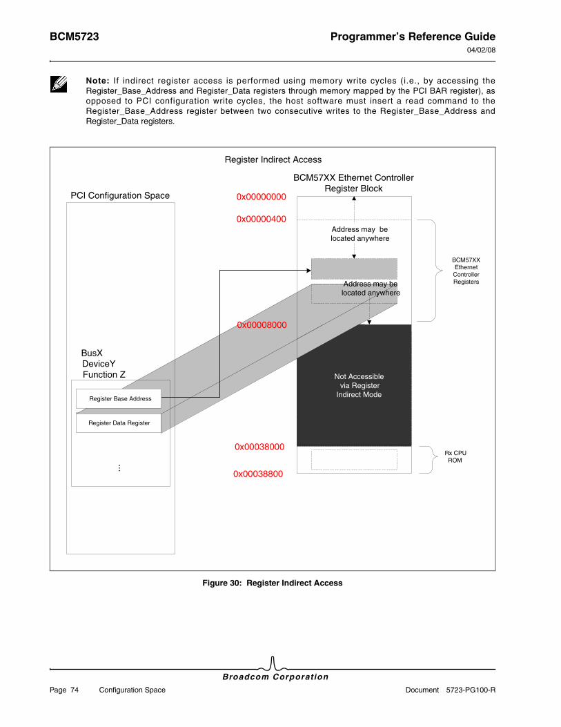
BCM5723 Programmer’s Reference Guide04/02/08
Broadcom Corporation
Page 74 Configuration Space Document 5723-PG100-R
Figure 30: Register Indirect Access
Note: If indirect register access is performed using memory write cycles (i.e., by accessing the Register_Base_Address and Register_Data registers through memory mapped by the PCI BAR register), as opposed to PCI configuration write cycles, the host software must insert a read command to the Register_Base_Address register between two consecutive writes to the Register_Base_Address and Register_Data registers.
PCI Configuration Space 0x00000000
BCM57XX Ethernet Controller Register Block
BusX
...
Register Data Register
0x00038000Rx CPUROM
0x00038800
Address may belocated anywhere
Not Accessible via RegisterIndirect Mode
BCM57XX Ethernet
Controller Registers
0x00008000
Register Indirect Access
0x00000400
located anywhereAddress may be
DeviceYFunction Z
Register Base Address
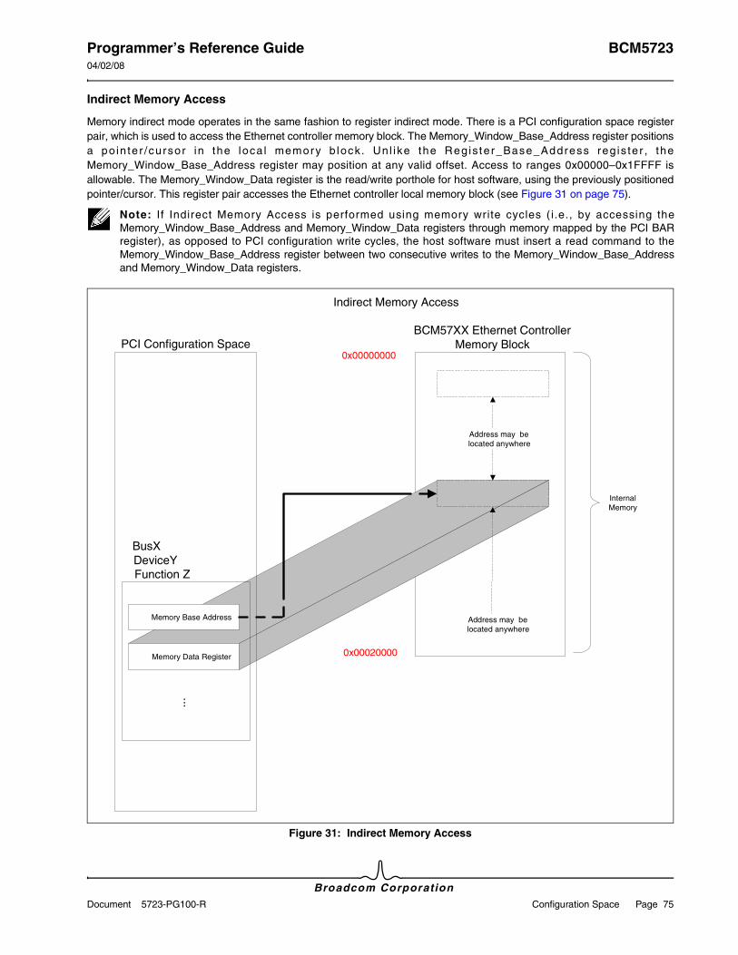
Programmer’s Reference Guide BCM572304/02/08
Broadcom CorporationDocument 5723-PG100-R Configuration Space Page 75
Indirect Memory Access
Memory indirect mode operates in the same fashion to register indirect mode. There is a PCI configuration space register pair, which is used to access the Ethernet controller memory block. The Memory_Window_Base_Address register positions a po in ter /cursor in the loca l memory b lock. Un l ike the Reg ister_Base_Address reg is ter , the Memory_Window_Base_Address register may position at any valid offset. Access to ranges 0x00000–0x1FFFF is allowable. The Memory_Window_Data register is the read/write porthole for host software, using the previously positioned pointer/cursor. This register pair accesses the Ethernet controller local memory block (see Figure 31 on page 75).
Figure 31: Indirect Memory Access
Note: If Indirect Memory Access is performed using memory write cycles ( i.e., by accessing the Memory_Window_Base_Address and Memory_Window_Data registers through memory mapped by the PCI BAR register), as opposed to PCI configuration write cycles, the host software must insert a read command to the Memory_Window_Base_Address register between two consecutive writes to the Memory_Window_Base_Address and Memory_Window_Data registers.
PCI Configuration Space0x00000000
Indirect Memory Access
BCM57XX Ethernet Controller Memory Block
BusXDeviceYFunction Z
...
Memory Data Register 0x00020000
Address may belocated anywhere
Memory Base Address
InternalMemory
Address may belocated anywhere
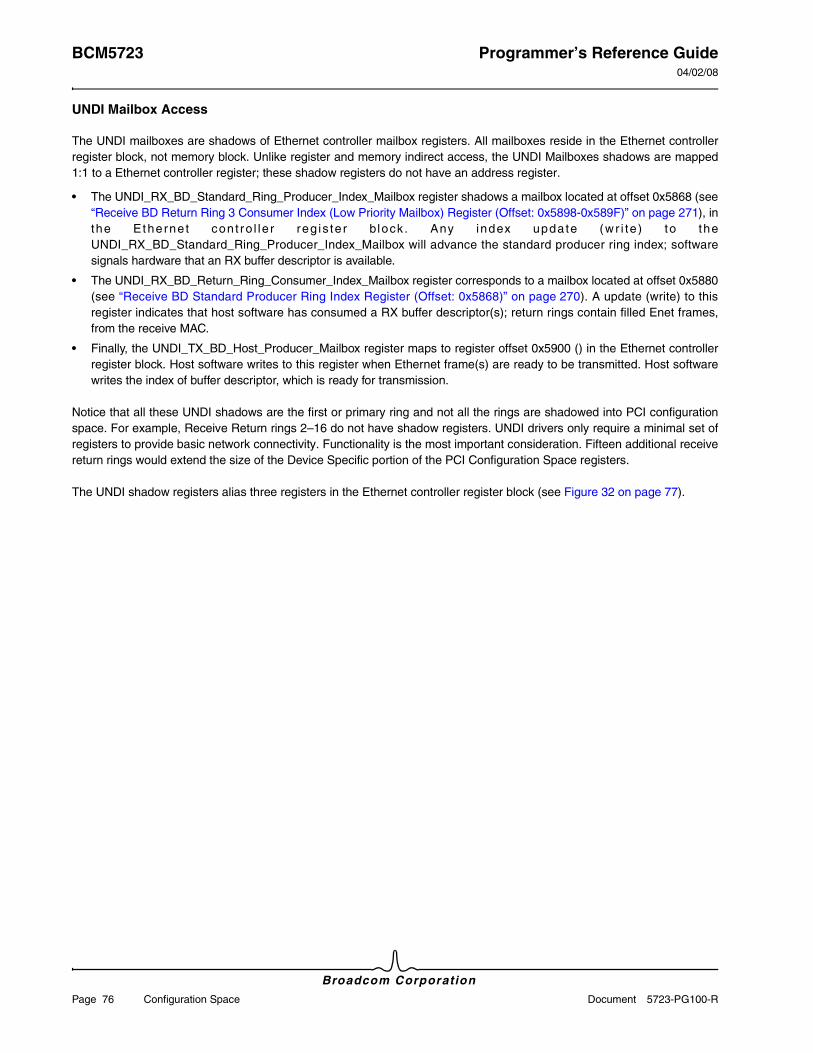
BCM5723 Programmer’s Reference Guide04/02/08
Broadcom Corporation
Page 76 Configuration Space Document 5723-PG100-R
UNDI Mailbox Access
The UNDI mailboxes are shadows of Ethernet controller mailbox registers. All mailboxes reside in the Ethernet controller register block, not memory block. Unlike register and memory indirect access, the UNDI Mailboxes shadows are mapped 1:1 to a Ethernet controller register; these shadow registers do not have an address register.
• The UNDI_RX_BD_Standard_Ring_Producer_Index_Mailbox register shadows a mailbox located at offset 0x5868 (see “Receive BD Return Ring 3 Consumer Index (Low Priority Mailbox) Register (Offset: 0x5898-0x589F)” on page 271), in the Ethernet cont ro l le r reg is ter block . Any index update (wr i te ) to the UNDI_RX_BD_Standard_Ring_Producer_Index_Mailbox will advance the standard producer ring index; software signals hardware that an RX buffer descriptor is available.
• The UNDI_RX_BD_Return_Ring_Consumer_Index_Mailbox register corresponds to a mailbox located at offset 0x5880 (see “Receive BD Standard Producer Ring Index Register (Offset: 0x5868)” on page 270). A update (write) to this register indicates that host software has consumed a RX buffer descriptor(s); return rings contain filled Enet frames, from the receive MAC.
• Finally, the UNDI_TX_BD_Host_Producer_Mailbox register maps to register offset 0x5900 () in the Ethernet controllerregister block. Host software writes to this register when Ethernet frame(s) are ready to be transmitted. Host software writes the index of buffer descriptor, which is ready for transmission.
Notice that all these UNDI shadows are the first or primary ring and not all the rings are shadowed into PCI configuration space. For example, Receive Return rings 2–16 do not have shadow registers. UNDI drivers only require a minimal set of registers to provide basic network connectivity. Functionality is the most important consideration. Fifteen additional receive return rings would extend the size of the Device Specific portion of the PCI Configuration Space registers.
The UNDI shadow registers alias three registers in the Ethernet controller register block (see Figure 32 on page 77).
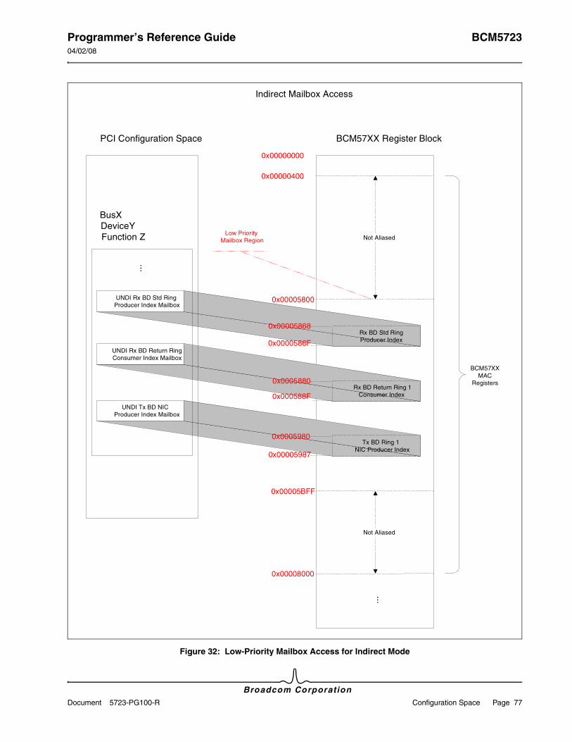
Programmer’s Reference Guide BCM572304/02/08
Broadcom CorporationDocument 5723-PG100-R Configuration Space Page 77
Figure 32: Low-Priority Mailbox Access for Indirect Mode
PCI Configuration Space
Indirect Mailbox Access
BCM57XX Register Block
BusXDeviceYFunction Z
...
UNDI Rx BD Std RingProducer Index Mailbox
UNDI Rx BD Return RingConsumer Index Mailbox
UNDI Tx BD NICProducer Index Mailbox
Rx BD Std RingProducer Index
0x00005BFF
Not Aliased
Not Aliased
0x00000000
Low PriorityMailbox Region
...BCM57XX
MAC Registers
0x00008000
0x00000400
0x00005800
0x00005868
0x0000586F
0x0005880
Tx BD Ring 1NIC Producer Index
Rx BD Return Ring 1Consumer Index
0x0005980
0x000588F
0x00005987
BCM5723 Programmer’s Reference Guide04/02/08
Broadcom Corporation
Page 78 Configuration Space Document 5723-PG100-R
Standard Mode
Standard mode is the most useful memory mapped I/O view provided by the Ethernet controller (see Figure 33). 64K of host memory space must be made available. The PnP BIOS or OS will program BAR0 and BAR1 with a base address where the 64K address region may be decoded. The BAR registers point to the beginning of the host memory mapped regions where Ethernet controller can be accessed.
Figure 33: Standard Memory Mapped I/O Mode
Host Memory Address Space
BAR0
BAR1
PCI Configuration Space
PhysicalMemoryBusX
DeviceYFunction Z
PCI ConfigurationSpace Registers(Shadow Copy)
Access to this memoryregion is remapped by
the hardware.
High PriorityMailboxes
BAR + 0x00000000
BAR + 0x000000FFReserved
BAR + 0x000001FF
BAR + 0x000003FF
Registers
BAR + 0x00007FFF
MemoryWindow
BAR + 0x0000FFFF
64K
...
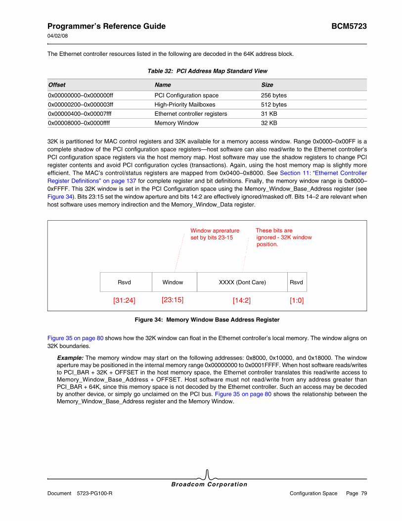
Programmer’s Reference Guide BCM572304/02/08
Broadcom CorporationDocument 5723-PG100-R Configuration Space Page 79
The Ethernet controller resources listed in the following are decoded in the 64K address block.
32K is partitioned for MAC control registers and 32K available for a memory access window. Range 0x0000–0x00FF is a complete shadow of the PCI configuration space registers—host software can also read/write to the Ethernet controller’s PCI configuration space registers via the host memory map. Host software may use the shadow registers to change PCI register contents and avoid PCI configuration cycles (transactions). Again, using the host memory map is slightly more efficient. The MAC’s control/status registers are mapped from 0x0400–0x8000. See Section 11: “Ethernet Controller Register Definitions” on page 137 for complete register and bit definitions. Finally, the memory window range is 0x8000–0xFFFF. This 32K window is set in the PCI Configuration space using the Memory_Window_Base_Address register (see Figure 34). Bits 23:15 set the window aperture and bits 14:2 are effectively ignored/masked off. Bits 14–2 are relevant when host software uses memory indirection and the Memory_Window_Data register.
Figure 34: Memory Window Base Address Register
Figure 35 on page 80 shows how the 32K window can float in the Ethernet controller’s local memory. The window aligns on 32K boundaries.
Example: The memory window may start on the following addresses: 0x8000, 0x10000, and 0x18000. The window aperture may be positioned in the internal memory range 0x00000000 to 0x0001FFFF. When host software reads/writes to PCI_BAR + 32K + OFFSET in the host memory space, the Ethernet controller translates this read/write access to Memory_Window_Base_Address + OFFSET. Host software must not read/write from any address greater than PCI_BAR + 64K, since this memory space is not decoded by the Ethernet controller. Such an access may be decoded by another device, or simply go unclaimed on the PCI bus. Figure 35 on page 80 shows the relationship between the Memory_Window_Base_Address register and the Memory Window.
Table 32: PCI Address Map Standard View
Offset Name Size
0x00000000–0x000000ff PCI Configuration space 256 bytes
0x00000200–0x000003ff High-Priority Mailboxes 512 bytes
0x00000400–0x00007fff Ethernet controller registers 31 KB
0x00008000–0x0000ffff Memory Window 32 KB
Rsvd Window Rsvd
[31:24] [14:2] [1:0]
XXXX (Dont Care)
[23:15]
Window apreratureset by bits 23-15
These bits areignored - 32K windowposition.
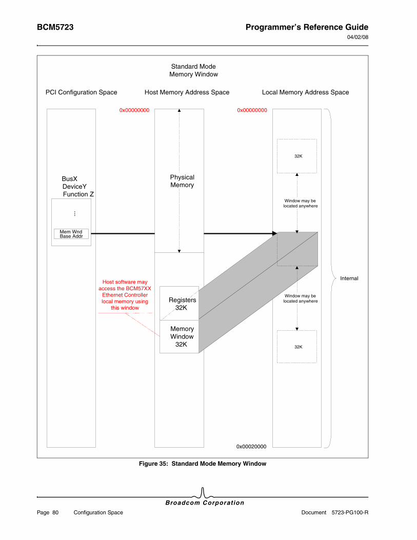
BCM5723 Programmer’s Reference Guide04/02/08
Broadcom Corporation
Page 80 Configuration Space Document 5723-PG100-R
Figure 35: Standard Mode Memory Window
Host Memory Address Space
32K
32K
MemoryWindow
32K
Mem WndBase Addr
PCI Configuration Space
Window may belocated anywhere
Window may belocated anywhere
Local Memory Address Space
Registers32K
PhysicalMemory
BusXDeviceYFunction Z
Host software may access the BCM57XX
Ethernet Controller local memory using
this window
Standard ModeMemory Window
...
0x00020000
Internal
0x00000000 0x00000000

Programmer’s Reference Guide BCM572304/02/08
Broadcom CorporationDocument 5723-PG100-R Configuration Space Page 81
Flat Mode
Flat mode requires 32M of memory (see Figure 36 on page 82). Flat mode is useful when host software wants all Ethernet controller resources host memory mapped; diagnostic software is an example application. Mailboxes, Send Rings, Receive Rings, and Local Memory are directly mapped into the host memory space. Unlike standard mode, the Ethernet controller’s local memory is addressable through host memory mapped I/O. Flat mode should not be used when there are limitations on the amount of memory mapped I/O available.
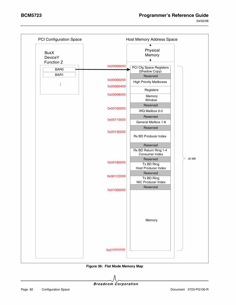
BCM5723 Programmer’s Reference Guide04/02/08
Broadcom Corporation
Page 82 Configuration Space Document 5723-PG100-R
Figure 36: Flat Mode Memory Map
Host Memory Address Space
BAR0
BAR1
PCI Configuration Space
PhysicalMemoryBusX
DeviceYFunction Z
0x00000000 PCI Cfg Space Registers(Shadow Copy)
High Priority Mailboxes0x00000400
0x00000200
0x00110000
Registers
MemoryWindow
...
Reserved
IRQ Mailbox 0-3
General Mailbox 1-8
Rx BD Return Ring 1-4Consumer Index
Tx BD RingHost Producer Index
Tx BD RingNIC Producer Index
Memory
0x00008000
0x00100000
Rx BD Producer Index0x00130000
0x00180000
0x001C0000
0x01000000
0x01FFFFFF
32 MB
Reserved
Reserved
Reserved
Reserved
Reserved
Reserved
Reserved
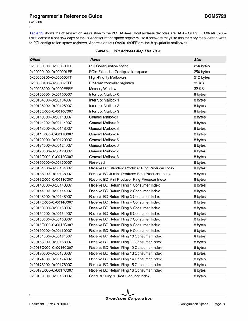
Programmer’s Reference Guide BCM572304/02/08
Broadcom CorporationDocument 5723-PG100-R Configuration Space Page 83
Table 33 shows the offsets which are relative to the PCI BAR—all host address decodes are BAR + OFFSET. Offsets 0x00–0xFF contain a shadow copy of the PCI configuration space registers. Host software may use this memory map to read/write to PCI configuration space registers. Address offsets 0x200–0x3FF are the high-priority mailboxes.
Table 33: PCI Address Map Flat View
Offset Name Size
0x00000000–0x000000FF PCI Configuration space 256 bytes
0x00000100–0x000001FF PCIe Extended Configuration space 256 bytes
0x00000200–0x000003FF High-Priority Mailboxes 512 bytes
0x00000400–0x00007FFF Ethernet controller registers 31 KB
0x00008000–0x0000FFFF Memory Window 32 KB
0x00100000–0x00100007 Interrupt Mailbox 0 8 bytes
0x00104000–0x00104007 Interrupt Mailbox 1 8 bytes
0x00108000–0x00108007 Interrupt Mailbox 2 8 bytes
0x0010C000–0x0010C007 Interrupt Mailbox 3 8 bytes
0x00110000–0x00110007 General Mailbox 1 8 bytes
0x00114000–0x00114007 General Mailbox 2 8 bytes
0x00118000–0x00118007 General Mailbox 3 8 bytes
0x0011C000–0x0011C007 General Mailbox 4 8 bytes
0x00120000–0x00120007 General Mailbox 5 8 bytes
0x00124000–0x00124007 General Mailbox 6 8 bytes
0x00128000–0x00128007 General Mailbox 7 8 bytes
0x0012C000–0x0012C007 General Mailbox 8 8 bytes
0x00130000–0x00130007 Reserved 8 bytes
0x00134000–0x00134007 Receive BD Standard Producer Ring Producer Index 8 bytes
0x00138000–0x00138007 Receive BD Jumbo Producer Ring Producer Index 8 bytes
0x0013C000–0x0013C007 Receive BD Mini Producer Ring Producer Index 8 bytes
0x00140000–0x00140007 Receive BD Return Ring 1 Consumer Index 8 bytes
0x00144000–0x00144007 Receive BD Return Ring 2 Consumer Index 8 bytes
0x00148000–0x00148007 Receive BD Return Ring 3 Consumer Index 8 bytes
0x0014C000–0x0014C007 Receive BD Return Ring 4 Consumer Index 8 bytes
0x00150000–0x00150007 Receive BD Return Ring 5 Consumer Index 8 bytes
0x00154000–0x00154007 Receive BD Return Ring 6 Consumer Index 8 bytes
0x00158000–0x00158007 Receive BD Return Ring 7 Consumer Index 8 bytes
0x0015C000–0x0015C007 Receive BD Return Ring 8 Consumer Index 8 bytes
0x00160000–0x00160007 Receive BD Return Ring 9 Consumer Index 8 bytes
0x00164000–0x00164007 Receive BD Return Ring 10 Consumer Index 8 bytes
0x00168000–0x00168007 Receive BD Return Ring 11 Consumer Index 8 bytes
0x0016C000–0x0016C007 Receive BD Return Ring 12 Consumer Index 8 bytes
0x00170000–0x00170007 Receive BD Return Ring 13 Consumer Index 8 bytes
0x00174000–0x00174007 Receive BD Return Ring 14 Consumer Index 8 bytes
0x00178000–0x00178007 Receive BD Return Ring 15 Consumer Index 8 bytes
0x0017C000–0x0017C007 Receive BD Return Ring 16 Consumer Index 8 bytes
0x00180000–0x00180007 Send BD Ring 1 Host Producer Index 8 bytes
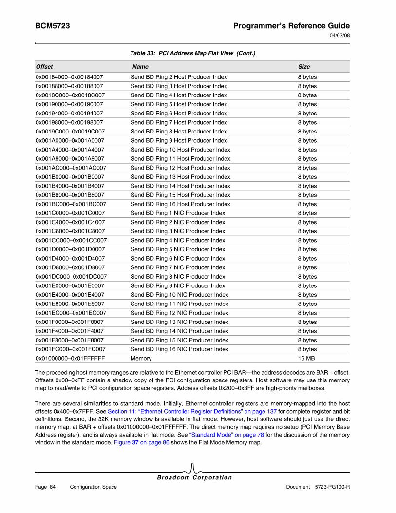
BCM5723 Programmer’s Reference Guide04/02/08
Broadcom Corporation
Page 84 Configuration Space Document 5723-PG100-R
The proceeding host memory ranges are relative to the Ethernet controller PCI BAR—the address decodes are BAR + offset. Offsets 0x00–0xFF contain a shadow copy of the PCI configuration space registers. Host software may use this memory map to read/write to PCI configuration space registers. Address offsets 0x200–0x3FF are high-priority mailboxes.
There are several similarities to standard mode. Initially, Ethernet controller registers are memory-mapped into the host offsets 0x400–0x7FFF. See Section 11: “Ethernet Controller Register Definitions” on page 137 for complete register and bit definitions. Second, the 32K memory window is available in flat mode. However, host software should just use the direct memory map, at BAR + offsets 0x01000000–0x01FFFFFF. The direct memory map requires no setup (PCI Memory Base Address register), and is always available in flat mode. See “Standard Mode” on page 78 for the discussion of the memory window in the standard mode. Figure 37 on page 86 shows the Flat Mode Memory map.
0x00184000–0x00184007 Send BD Ring 2 Host Producer Index 8 bytes
0x00188000–0x00188007 Send BD Ring 3 Host Producer Index 8 bytes
0x0018C000–0x0018C007 Send BD Ring 4 Host Producer Index 8 bytes
0x00190000–0x00190007 Send BD Ring 5 Host Producer Index 8 bytes
0x00194000–0x00194007 Send BD Ring 6 Host Producer Index 8 bytes
0x00198000–0x00198007 Send BD Ring 7 Host Producer Index 8 bytes
0x0019C000–0x0019C007 Send BD Ring 8 Host Producer Index 8 bytes
0x001A0000–0x001A0007 Send BD Ring 9 Host Producer Index 8 bytes
0x001A4000–0x001A4007 Send BD Ring 10 Host Producer Index 8 bytes
0x001A8000–0x001A8007 Send BD Ring 11 Host Producer Index 8 bytes
0x001AC000–0x001AC007 Send BD Ring 12 Host Producer Index 8 bytes
0x001B0000–0x001B0007 Send BD Ring 13 Host Producer Index 8 bytes
0x001B4000–0x001B4007 Send BD Ring 14 Host Producer Index 8 bytes
0x001B8000–0x001B8007 Send BD Ring 15 Host Producer Index 8 bytes
0x001BC000–0x001BC007 Send BD Ring 16 Host Producer Index 8 bytes
0x001C0000–0x001C0007 Send BD Ring 1 NIC Producer Index 8 bytes
0x001C4000–0x001C4007 Send BD Ring 2 NIC Producer Index 8 bytes
0x001C8000–0x001C8007 Send BD Ring 3 NIC Producer Index 8 bytes
0x001CC000–0x001CC007 Send BD Ring 4 NIC Producer Index 8 bytes
0x001D0000–0x001D0007 Send BD Ring 5 NIC Producer Index 8 bytes
0x001D4000–0x001D4007 Send BD Ring 6 NIC Producer Index 8 bytes
0x001D8000–0x001D8007 Send BD Ring 7 NIC Producer Index 8 bytes
0x001DC000–0x001DC007 Send BD Ring 8 NIC Producer Index 8 bytes
0x001E0000–0x001E0007 Send BD Ring 9 NIC Producer Index 8 bytes
0x001E4000–0x001E4007 Send BD Ring 10 NIC Producer Index 8 bytes
0x001E8000–0x001E8007 Send BD Ring 11 NIC Producer Index 8 bytes
0x001EC000–0x001EC007 Send BD Ring 12 NIC Producer Index 8 bytes
0x001F0000–0x001F0007 Send BD Ring 13 NIC Producer Index 8 bytes
0x001F4000–0x001F4007 Send BD Ring 14 NIC Producer Index 8 bytes
0x001F8000–0x001F8007 Send BD Ring 15 NIC Producer Index 8 bytes
0x001FC000–0x001FC007 Send BD Ring 16 NIC Producer Index 8 bytes
0x01000000–0x01FFFFFF Memory 16 MB
Table 33: PCI Address Map Flat View (Cont.)
Offset Name Size

Programmer’s Reference Guide BCM572304/02/08
Broadcom CorporationDocument 5723-PG100-R Configuration Space Page 85
The interrupt mailboxes are accessible from BAR + offsets 0x00100000 to 0x0010C007. Host software may use this memory map to access the interrupt mailboxes located in Ethernet controller’s register block (0x200–0x21F). The Receive Producer consumer index mailboxes are available at offsets 0x00130000–0x0013C0007. Receive return ring mailboxes are shadowed at BAR + offsets 0x00140000 to 0x0017C007. The Ethernet controller receive return rings are located in register block range 0x280–0x2FF. Host-based send rings are located at BAR + offsets 0x001800000–0x001BC007. These send ring mailboxes are mapped from the Ethernet controller register block range 0x300–0x37F.
The address ranges 0x01000000–0x01FFFFFF are aliases for the Ethernet controller device local memory. When host software reads/writes from address ranges starting at BAR + 0x01000000, the address is normalized/mapped to a device local address starting at 0x00000000. For example, the host address 0x010000FF is translated to device local address 0x000000FF.
Figure 38 on page 87 shows the two mechanisms host software may use to access Ethernet controller local memory (flat mode configuration).
• First, host software can use the memory window.
• Second, host software may access the memory-mapped range 0x01000000 to 0x01FFFFFF.
The second technique is preferable since flat mode has made 32 MB of host memory-mapped space available. Software does not need to use the memory window since the Ethernet controller’s entire memory region is memory-mapped.
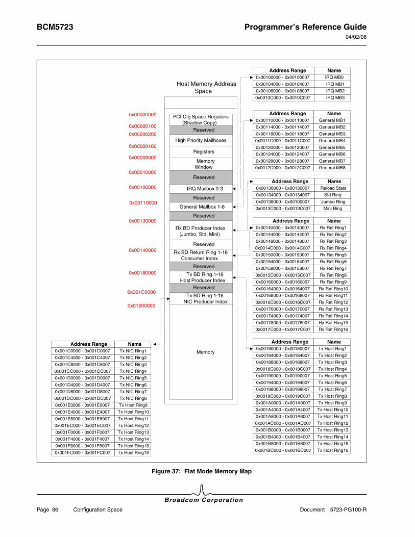
BCM5723 Programmer’s Reference Guide04/02/08
Broadcom Corporation
Page 86 Configuration Space Document 5723-PG100-R
Figure 37: Flat Mode Memory Map
Host Memory AddressSpace
0x00000000 PCI Cfg Space Registers(Shadow Copy)
High Priority Mailboxes
0x00000100
0x00000400
0x00000200
0x00110000
Registers
MemoryWindow
Reserved
IRQ Mailbox 0-3
General Mailbox 1-8
Rx BD Return Ring 1-16Consumer Index
Tx BD Ring 1-16Host Producer Index
Tx BD Ring 1-16NIC Producer Index
Memory
0x00008000
0x00010000
0x00100000
Rx BD Producer Index(Jumbo, Std, Mini)
0x00130000
0x00140000
0x00180000
0x001C0000
0x00100000 - 0x00100007 IRQ MB0
Address Range Name
0x00104000 - 0x00104007 IRQ MB1
0x00108000 - 0x00108007 IRQ MB2
0x0010C000 - 0x0010C007 IRQ MB3
0x00110000 - 0x00110007 General MB1
Address Range Name
0x00114000 - 0x00114007 General MB2
0x00118000 - 0x00118007 General MB3
0x0011C000 - 0x0011C007 General MB4
0x00120000 - 0x00120007 General MB5
0x00124000 - 0x00124007 General MB6
0x00128000 - 0x00128007 General MB7
0x0012C000 - 0x0012C007 General MB8
0x00134000 - 0x00134007 Std Ring
Address Range Name
0x00138000 - 0x00100007 Jumbo Ring
0x0013C000 - 0x0013C007 Mini Ring
0x00140000 - 0x00140007 Rx Ret Ring1
Address Range Name
0x00144000 - 0x00144007 Rx Ret Ring2
0x00148000 - 0x00148007 Rx Ret Ring3
0x0014C000 - 0x0014C007 Rx Ret Ring4
0x00150000 - 0x00150007 Rx Ret Ring5
0x00154000 - 0x00154007 Rx Ret Ring6
0x00158000 - 0x00158007 Rx Ret Ring7
0x0015C000 - 0x0015C007 Rx Ret Ring8
0x00160000 - 0x00160007 Rx Ret Ring9
0x00164000 - 0x00164007 Rx Ret Ring10
0x00168000 - 0x00168007 Rx Ret Ring11
0x0016C000 - 0x0016C007 Rx Ret Ring12
0x00170000 - 0x00170007 Rx Ret Ring13
0x00174000 - 0x00174007 Rx Ret Ring14
0x00178000 - 0x00178007 Rx Ret Ring15
0x0017C000 - 0x0017C007 Rx Ret Ring16
0x00180000 - 0x00180007 Tx Host Ring1
Address Range Name
0x00184000 - 0x00184007 Tx Host Ring2
0x00188000 - 0x00188007 Tx Host Ring3
0x0018C000 - 0x0018C007 Tx Host Ring4
0x00190000 - 0x00190007 Tx Host Ring5
0x00194000 - 0x00194007 Tx Host Ring6
0x00198000 - 0x00198007 Tx Host Ring7
0x0019C000 - 0x0019C007 Tx Host Ring8
0x001A0000 - 0x001A0007 Tx Host Ring9
0x001A4000 - 0x001A4007 Tx Host Ring10
0x001A8000 - 0x001A8007 Tx Host Ring11
0x001AC000 - 0x001AC007 Tx Host Ring12
0x001B0000 - 0x001B0007 Tx Host Ring13
0x001B4000 - 0x001B4007 Tx Host Ring14
0x001B8000 - 0x001B8007 Tx Host Ring15
0x001BC000 - 0x001BC007 Tx Host Ring16
0x01000000
0x00130000 - 0x00130007 Reload Stats
0x001C0000 - 0x001C0007 Tx NIC Ring1
Address Range Name
0x001C4000 - 0x001C4007 Tx NIC Ring2
0x001C8000 - 0x001C8007 Tx NIC Ring3
0x001CC000 - 0x001CC007 Tx NIC Ring4
0x001D0000 - 0x001D0007 Tx NIC Ring5
0x001D4000 - 0x001D4007 Tx NIC Ring6
0x001D8000 - 0x001D8007 Tx NIC Ring7
0x001DC000 - 0x001DC007 Tx NIC Ring8
0x001E0000 - 0x001E0007 Tx Host Ring9
0x001E4000 - 0x001E4007 Tx Host Ring10
0x001E8000 - 0x001E8007 Tx Host Ring11
0x001EC000 - 0x001EC007 Tx Host Ring12
0x001F0000 - 0x001F0007 Tx Host Ring13
0x001F4000 - 0x001F4007 Tx Host Ring14
0x001F8000 - 0x001F8007 Tx Host Ring15
0x001FC000 - 0x001FC007 Tx Host Ring16
Reserved
Reserved
Reserved
Reserved
Reserved
Reserved
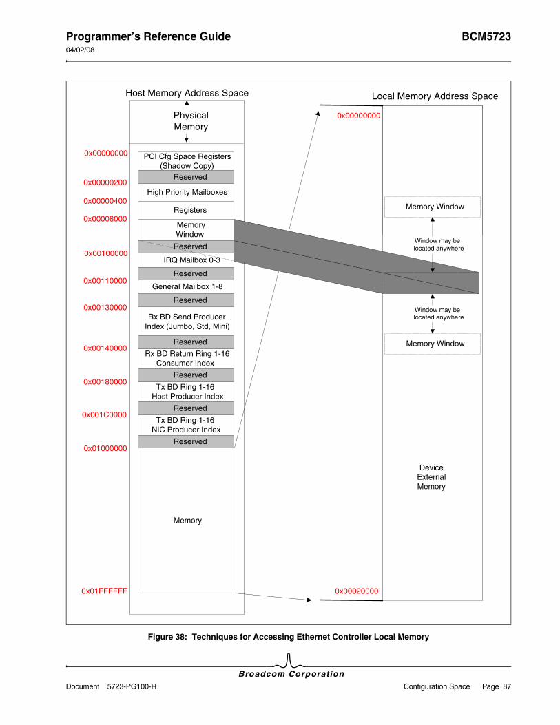
Programmer’s Reference Guide BCM572304/02/08
Broadcom CorporationDocument 5723-PG100-R Configuration Space Page 87
Figure 38: Techniques for Accessing Ethernet Controller Local Memory
Host Memory Address Space
PhysicalMemory
0x00000000 PCI Cfg Space Registers(Shadow Copy)
High Priority Mailboxes0x00000400
0x00000200
0x00110000General Mailbox 1-8
Rx BD Return Ring 1-16Consumer Index
Tx BD Ring 1-16Host Producer Index
Tx BD Ring 1-16NIC Producer Index
Memory
0x00008000
0x00100000
Rx BD Send ProducerIndex (Jumbo, Std, Mini)
0x00130000
0x00140000
0x00180000
0x001C0000
0x01000000
0x01FFFFFF
Reserved
Reserved
Reserved
Reserved
Reserved
Reserved
Local Memory Address Space
0x00020000
0x00000000
Device InternalMemory
Device External Memory
Registers
Reserved
MemoryWindow
Reserved
IRQ Mailbox 0-3
Memory Window
Memory Window
Window may belocated anywhere
Window may belocated anywhere
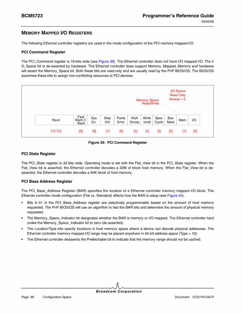
BCM5723 Programmer’s Reference Guide04/02/08
Broadcom Corporation
Page 88 Configuration Space Document 5723-PG100-R
MEMORY MAPPED I/O REGISTERS
The following Ethernet controller registers are used in the mode configuration of the PCI memory-mapped I/O.
PCI Command Register
The PCI_Command register is 16-bits wide (see Figure 39). The Ethernet controller does not have I/O mapped I/O. The I/O_Space bit is de-asserted by hardware. The Ethernet controller does support Memory_Mapped_Memory and hardware will assert the Memory_Space bit. Both these bits are read-only and are usually read by the PnP BIOS/OS. The BIOS/OS examines these bits to assign non-conflicting resources to PCI devices.
Figure 39: PCI Command Register
PCI State Register
The PCI_State register is 32-bits wide. Operating mode is set with the Flat_View bit in the PCI_State register. When the Flat_View bit is asserted, the Ethernet controller decodes a 32M of block host memory. When the Flat_View bit is de-asserted, the Ethernet controller decodes a 64K block of host memory.
PCI Base Address Register
The PCI_Base_Address Register (BAR) specifies the location of a Ethernet controller memory mapped I/O block. The Ethernet controller mode configuration (Flat vs. Standard) affects how the BAR is setup (see Figure 40).
• Bits 4–31 in the PCI_Base_Address register are selectively programmable based on the amount of host memory requested. The PnP BIOS/OS will use an algorithm to test the BAR bits and determine the amount of physical memory requested.
• The Memory_Space_Indicator bit designates whether the BAR is memory or I/O mapped. The Ethernet controller hard codes the Memory_Space_Indicator bit to zero (de-asserted).
• The Location/Type bits specify locations in host memory space where a device can decode physical addresses. The Ethernet controller memory mapped I/O range may be placed anywhere in 64-bit address space (Type = 10).
• The Ethernet controller deasserts the Prefetchable bit to indicate that the memory range should not be cached.
Mem I/O
I/O SpaceRead OnlyAlways = 0
[0]
BusMast
SpecCycle
WriteInvld
VGASnoop
ParityError
StepCtrl
SysErr
FastBack 2
BackRsvd
[1][2][3][7] [6] [5] [4][9] [8][15:10]
Memory SpaceRead/Write
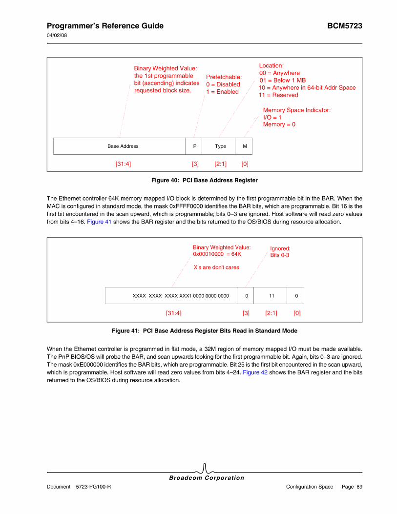
Programmer’s Reference Guide BCM572304/02/08
Broadcom CorporationDocument 5723-PG100-R Configuration Space Page 89
Figure 40: PCI Base Address Register
The Ethernet controller 64K memory mapped I/O block is determined by the first programmable bit in the BAR. When the MAC is configured in standard mode, the mask 0xFFFF0000 identifies the BAR bits, which are programmable. Bit 16 is the first bit encountered in the scan upward, which is programmable; bits 0–3 are ignored. Host software will read zero values from bits 4–16. Figure 41 shows the BAR register and the bits returned to the OS/BIOS during resource allocation.
Figure 41: PCI Base Address Register Bits Read in Standard Mode
When the Ethernet controller is programmed in flat mode, a 32M region of memory mapped I/O must be made available. The PnP BIOS/OS will probe the BAR, and scan upwards looking for the first programmable bit. Again, bits 0–3 are ignored. The mask 0xE000000 identifies the BAR bits, which are programmable. Bit 25 is the first bit encountered in the scan upward, which is programmable. Host software will read zero values from bits 4–24. Figure 42 shows the BAR register and the bits returned to the OS/BIOS during resource allocation.
Base Address P Type M
Memory Space Indicator:I/O = 1Memory = 0
Location:00 = Anywhere01 = Below 1 MB10 = Anywhere in 64-bit Addr Space11 = Reserved
Prefetchable:0 = Disabled1 = Enabled
Binary Weighted Value:the 1st programmablebit (ascending) indicatesrequested block size.
[0][2:1][3][31:4]
XXXX XXXX XXXX XXX1 0000 0000 0000 0 11 0
[0][2:1][3][31:4]
Binary Weighted Value:0x00010000 = 64K
X's are don't cares
Ignored:Bits 0-3
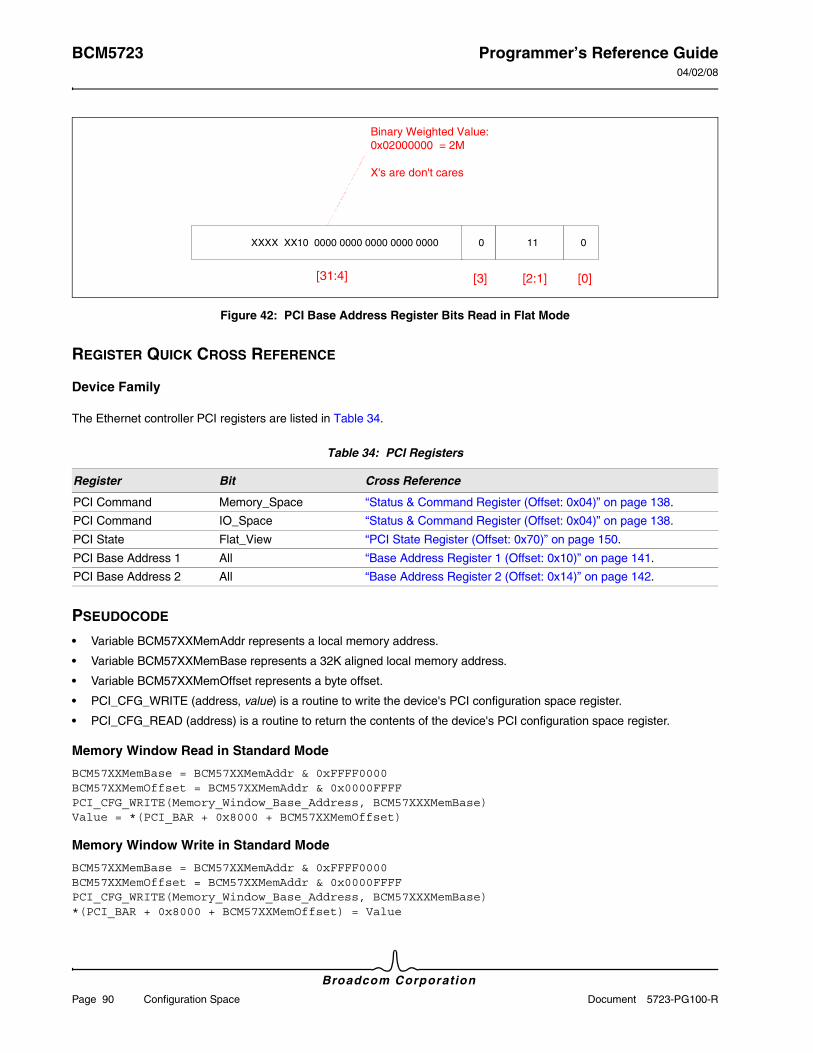
BCM5723 Programmer’s Reference Guide04/02/08
Broadcom Corporation
Page 90 Configuration Space Document 5723-PG100-R
Figure 42: PCI Base Address Register Bits Read in Flat Mode
REGISTER QUICK CROSS REFERENCE
Device Family
The Ethernet controller PCI registers are listed in Table 34.
PSEUDOCODE
• Variable BCM57XXMemAddr represents a local memory address.
• Variable BCM57XXMemBase represents a 32K aligned local memory address.
• Variable BCM57XXMemOffset represents a byte offset.
• PCI_CFG_WRITE (address, value) is a routine to write the device's PCI configuration space register.
• PCI_CFG_READ (address) is a routine to return the contents of the device's PCI configuration space register.
Memory Window Read in Standard Mode
BCM57XXMemBase = BCM57XXMemAddr & 0xFFFF0000BCM57XXMemOffset = BCM57XXMemAddr & 0x0000FFFFPCI_CFG_WRITE(Memory_Window_Base_Address, BCM57XXXMemBase)Value = *(PCI_BAR + 0x8000 + BCM57XXMemOffset)
Memory Window Write in Standard Mode
BCM57XXMemBase = BCM57XXMemAddr & 0xFFFF0000BCM57XXMemOffset = BCM57XXMemAddr & 0x0000FFFFPCI_CFG_WRITE(Memory_Window_Base_Address, BCM57XXXMemBase)*(PCI_BAR + 0x8000 + BCM57XXMemOffset) = Value
Table 34: PCI Registers
Register Bit Cross Reference
PCI Command Memory_Space “Status & Command Register (Offset: 0x04)” on page 138.
PCI Command IO_Space “Status & Command Register (Offset: 0x04)” on page 138.
PCI State Flat_View “PCI State Register (Offset: 0x70)” on page 150.
PCI Base Address 1 All “Base Address Register 1 (Offset: 0x10)” on page 141.
PCI Base Address 2 All “Base Address Register 2 (Offset: 0x14)” on page 142.
XXXX XX10 0000 0000 0000 0000 0000 0 11 0
[0][2:1][3][31:4]
Binary Weighted Value:0x02000000 = 2M
X's are don't cares
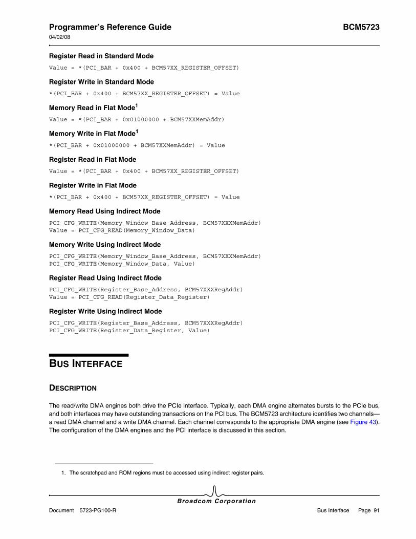
Programmer’s Reference Guide BCM572304/02/08
Broadcom CorporationDocument 5723-PG100-R Bus Interface Page 91
Register Read in Standard Mode
Value = *(PCI_BAR + 0x400 + BCM57XX_REGISTER_OFFSET)
Register Write in Standard Mode
*(PCI_BAR + 0x400 + BCM57XX_REGISTER_OFFSET) = Value
Memory Read in Flat Mode1
Value = *(PCI_BAR + 0x01000000 + BCM57XXMemAddr)
Memory Write in Flat Mode1
*(PCI_BAR + 0x01000000 + BCM57XXMemAddr) = Value
Register Read in Flat Mode
Value = *(PCI_BAR + 0x400 + BCM57XX_REGISTER_OFFSET)
Register Write in Flat Mode
*(PCI_BAR + 0x400 + BCM57XX_REGISTER_OFFSET) = Value
Memory Read Using Indirect Mode
PCI_CFG_WRITE(Memory_Window_Base_Address, BCM57XXXMemAddr)Value = PCI_CFG_READ(Memory_Window_Data)
Memory Write Using Indirect Mode
PCI_CFG_WRITE(Memory_Window_Base_Address, BCM57XXXMemAddr)PCI_CFG_WRITE(Memory_Window_Data, Value)
Register Read Using Indirect Mode
PCI_CFG_WRITE(Register_Base_Address, BCM57XXXRegAddr)Value = PCI_CFG_READ(Register_Data_Register)
Register Write Using Indirect Mode
PCI_CFG_WRITE(Register_Base_Address, BCM57XXXRegAddr)PCI_CFG_WRITE(Register_Data_Register, Value)
BUS INTERFACE
DESCRIPTION
The read/write DMA engines both drive the PCIe interface. Typically, each DMA engine alternates bursts to the PCIe bus, and both interfaces may have outstanding transactions on the PCI bus. The BCM5723 architecture identifies two channels—a read DMA channel and a write DMA channel. Each channel corresponds to the appropriate DMA engine (see Figure 43). The configuration of the DMA engines and the PCI interface is discussed in this section.
1. The scratchpad and ROM regions must be accessed using indirect register pairs.
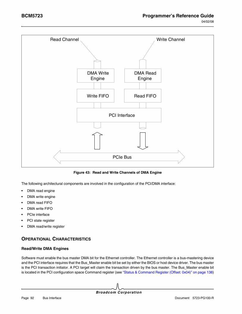
BCM5723 Programmer’s Reference Guide04/02/08
Broadcom Corporation
Page 92 Bus Interface Document 5723-PG100-R
Figure 43: Read and Write Channels of DMA Engine
The following architectural components are involved in the configuration of the PCI/DMA interface:
• DMA read engine
• DMA write engine
• DMA read FIFO
• DMA write FIFO
• PCIe interface
• PCI state register
• DMA read/write register
OPERATIONAL CHARACTERISTICS
Read/Write DMA Engines
Software must enable the bus master DMA bit for the Ethernet controller. The Ethernet controller is a bus-mastering device and the PCI interface requires that the Bus_Master enable bit be set by either the BIOS or host device driver. The bus master is the PCI transaction initiator. A PCI target will claim the transaction driven by the bus master. The Bus_Master enable bit is located in the PCI configuration space Command register (see “Status & Command Register (Offset: 0x04)” on page 138)
PCI Interface
Write FIFO Read FIFO
DMA WriteEngine
DMA ReadEngine
Write ChannelRead Channel
PCIe Bus
Programmer’s Reference Guide BCM572304/02/08
Broadcom CorporationDocument 5723-PG100-R Expansion ROM Page 93
and this bit is read/write. The bit defaults to cleared/disabled after device reset.
The read and write DMA channels use FIFOs to buffer small amounts of PCI bus data. The FIFOs provide elasticity for data movement between internal memory and the PCI interface. Host software may configure DMA watermarks—values where PCI activity is enabled/disabled.
When enqueued data is less than the watermark value, PCI bus transactions are inhibited. The DMA channel will wait until the FIFO f i l ls above the threshold before init iating PCI transactions. Host software may configure the DMA_Write_Watermark bit fields to set the activity threshold in the write FIFO. The DMA_Write_Watermark bit field is read/write and is also located in the DMA Read/Write register. The write watermark registers default to zero after power-on reset.
REGISTER QUICK CROSS REFERENCE
EXPANSION ROM
DESCRIPTION
The expansion ROM on the Ethernet controller is intended for implementation of PXE (Preboot Execution Environment). The devices support expansion ROM of up to 16 MB.
OPERATIONAL CHARACTERISTICS
By default, the Expansion ROM is disabled and the firmware has to explicitly enable this feature by setting PCI_State.PCI_Expansion_ROM_Desired bit to one (see “PCI State Register (Offset: 0x70)” on page 150). Once this bit is enabled, the bootcode firmware handles the Expansion ROM accesses of the device.
Table 35: PCI -X Registers
Register Bit Cross Reference
DMA Read/Write DMA_Write_Watermark “DMA Read/Write Control Register (Offset: 0x6C)” on page 149.DMA Read/Write DMA_Write Control Boundary
PCI Command Bus_Master “Status & Command Register (Offset: 0x04)” on page 138.
PCI Command Memory_Write_And_Invalidate
PCI Command Parity_Error_Enable
PCI Status Detected_Parity_Error “Status & Command Register (Offset: 0x04)” on page 138.
PCI Status Master_Data_Parity_Error
Write DMA Status Write_DMA_PCI_Parity_Error “Write DMA Status Register (Offset: 0x4C04)” on page 266.
Read DMA Status Read_DMA_PCI_Parity_Error “Read DMA Status Register (Offset: 0x4804)” on page 264.
MSI Status PCI_Parity_Error “MSI Mode Register (Offset: 0x6000)” on page 274.
PCI State Conventional_PCI “PCI State Register (Offset: 0x70)” on page 150.
33/66PCI_66/133PCIX_Mode
No_Snoop
Split_Completion_Message_Class
Split_Completion_Message_Index
BCM5723 Programmer’s Reference Guide04/02/08
Broadcom Corporation
Page 94 Power Management Document 5723-PG100-R
BIOS
The BIOS detects if a PCI device supports Expansion ROM or not by writing the value 0xFFFFFFFE to Expansion_ROM_Base_Register (register 0x30 of PCI configuration). The BIOS then reads back from this register. If the value is nonzero, then this PCI device supports Expansion ROM; otherwise, it does not. The Ethernet controller returns a non-zero value appropriate for the expansion ROM size selected in NVRAM (see Section 5: “Common Data Structures” on page 21) when Expansion ROM is enabled (PCI_State.PCI_Expansion_ROM_Desired bit is set to 1). On the other hand, if the PCI_Expansion_ROM_Desired bit cleared, then the Ethernet controller returns a value of 0x00000000. This indicates to the BIOS that no Expansion ROM is supported.
If a PCI device supports Expansion ROM, the BIOS will assign a Expansion Base address to the device. It then checks for a valid ROM header (0x55 0xAA as first two bytes, and so forth) and checksum. If the ROM header and image are valid, the BIOS will copy the Expansion ROM image to HOST’s Upper Memory Block (UMB) and invoke the initializing entry point.
Preboot Execution Environment
Preboot Execution Environment (PXE) is implemented as an Expansion ROM in the NIC implementation. In the LOM implementation, PXE normally resides in the system BIOS. In the NIC implementation, PXE image is stored in the NVRAM. Upon power on reset of the Ethernet controller, the RX RISC will load the bootcode from the NVRAM into RX RISC scratch pad and execute. This bootcode will program the device with programmable manufacturing information (such as MAC address, PCI vendor ID/device ID, etc.). If PXE is enabled, the bootcode responds to the Expansion ROM accesses of system BIOS.
Bootcode is executed whenever the Ethernet controller is reset via PCI Reset or S/W device reset. PXE initialization should only be necessary after a PCI reset. The bootcode differentiates PCI Reset and driver initiated software reset by checking content in Internal Memory at 0xb50. If the content is 0x4B657654, then the reset is due to driver initiated software reset. Therefore, the device driver has to initialize 0xb50 with 0x4B657654 before issuing a S/W device reset.
POWER MANAGEMENT
DESCRIPTION
The Ethernet controller is compliant with the PCI v1.1 power management specification. The MAC is programmable to two ACPI states: D0 and D3. The D0 state is a full power, operational mode—all the MAC core functions run at the highest clocking frequency, and components are fully functional. The MAC may be either initialized or un-initialized in the D0 ACPI state. An un-initialized D0 state is entered through a device reset or PME event; the MAC functional blocks are not started and initialized. Host software must reset/initialize hardware blocks to transition the device to a D0 initialized (active) state. The D0 active state places the device into a full power/operational mode. Receive and transmit data paths are fully operational, and the PCI block is initialized for bus mastering DMA.
Host device drivers do not differentiate between D3 hot and D3 cold states. ACPI-compliant device drivers are unloaded and quiescent in the D3 state and PCI slot power state is transparent. When the MAC is in D3 hot state, PCI slot power (3.3V or 5.0V) is available to power the PCI I/O pins. The PCI configuration and memory space may be accessed in D3 hot state. The core clock must remain enabled, so the MAC can respond to PCI configuration and memory transactions. The Disable_Core_Clock bit, in the PCI Clock Control register enables/disables clocking in the core clock domain. A D3 cold state provides only the PCI Vaux supply—PCI slot power is not present. The MAC will consume a maximum of 375 mA in a D3 cold power management mode.
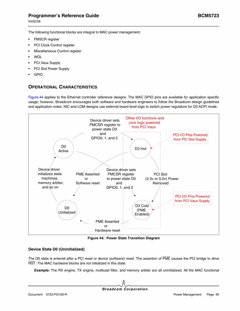
Programmer’s Reference Guide BCM572304/02/08
Broadcom CorporationDocument 5723-PG100-R Power Management Page 95
The following functional blocks are integral to MAC power management:
• PMSCR register
• PCI Clock Control register
• Miscellaneous Control register
• WOL
• PCI Vaux Supply
• PCI Slot Power Supply
• GPIO
OPERATIONAL CHARACTERISTICS
Figure 44 applies to the Ethernet controller reference designs. The MAC GPIO pins are available for application specific usage; however, Broadcom encourages both software and hardware engineers to follow the Broadcom design guidelines and application notes. NIC and LOM designs use external board level logic to switch power regulators for D3 ACPI mode.
Figure 44: Power State Transition Diagram
Device State D0 (Uninitialized)
The D0 state is entered after a PCI reset or device (software) reset. The assertion of PME causes the PCI bridge to drive RST. The MAC hardware blocks are not initialized in this state.
Example: The RX engine, TX engine, multicast filter, and memory arbiter are all uninitialized. All the MAC functional
D0Unitialized
D3 Cold(PME
Enabled)
D3 HotD0
Active
PCI Slot(3.3v or 5.0v) Power
Removed
PME Assertedor
Hardware reset
PCI I/O Pins Poweredfrom PCI Vaux Supply
Device driverinitializes state
machines,memory arbiter,
and so on
Device driver setsPMCSR register to
power state D3and
GPIO0, 1, and 2
PME Assertedor
Software reset
PCI I/O Pins Poweredfrom PCI Slot Supply
Other I/O functions andcore logic powered
from PCI Vaux
Device driver setsPMCSR registerto power state D3
andGPIO0, 1, and 2
BCM5723 Programmer’s Reference Guide04/02/08
Broadcom Corporation
Page 96 Power Management Document 5723-PG100-R
blocks are powered.
Device State D0 (Active)
Host software has initialized the MAC hardware blocks. The RX and TX data paths are ready to send/receive Ethernet packets. The PCI block is available to DMA packets to host memory. This is a full power ACPI operational state. Host software/drivers must follow the initialization procedure (see “Initializing the MAC Hash Registers” on page 64) to move the MAC into a D0 active state.
When the BCM5723 NetXtreme devices detect that main power is lost and it is still in the D0 state, it will reset itself to the D3 (Cold) state and then operate in 10/100 mode, like the OOB WOL state.
Device State D3 (Hot)
The MAC’s configuration space and memory mapped I/O blocks are accessible in D3 hot state. The PCI I/O drivers are still powered by slot power in this state. However, host software has switched the MAC to use PCI Vaux for VDD_CORE and VDD_IO. GPIO pins 0, 1, and 2 are configured before the transition to this state. The RX and TX RISC processor clocks have been stopped in this state. The core clock remains active so PCI transactions may be processed by the MAC. This is a low-power state where some key components have been powered down. The physical layer auto-advertises 10 Mbps capability in this state, and link is set to 10 Mbps half-duplex or full-duplex. The PHY is configured for WOL mode. WOL pattern filters are initialized and active; the MAC will process Magic Packets™. The host chipset implements the power management policy for the PCI bus; the MAC driver does not influence the PCI Vaux or Slot power supply.
Device State D3 (Cold)
The MAC is completely powered by PCI Vaux in D3 cold. PCI configuration space and memory mapped I/O are not available. The only portion of the MAC active is the WOL pattern and Magic Packet filters2. The MAC will assert a PME in this state and indicate to the host bridge that a wake up event has occurred. The host bridge will normally provide PCI Slot power and then reset the device. GPIO pins 0, 1, and 2 are configured the same as D3 hot. Host software does not differentiate between D3 hot/cold. The MAC and PHY will not consume more than 375 mA in this mode. The integrated PHY must negotiate for 10 Mbps half/duplex speed. The PHY WOL mode is configured.
WAKE ON LAN
See “Wake on LAN Mode/Low-Power” on page 112.
Note: The drivers should use configuration cycles (not the memory write cycles) to write to the PMCSR register at offset 0x4C for putting the device in D3 Hot state.
2. Magic Packet™ is a registered trade mark of AMD.
Note: The PCIe devices support the PCIe power management which is compatible with PCI bus power management.
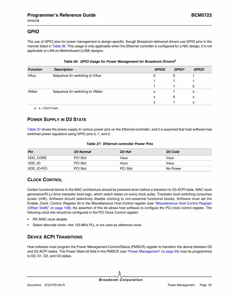
Programmer’s Reference Guide BCM572304/02/08
Broadcom CorporationDocument 5723-PG100-R Power Management Page 97
GPIO
The use of GPIO pins for power management is design-specific, though Broadcom-delivered drivers use GPIO pins in the manner listed in Table 36. This usage is only applicable when the Ethernet controller is configured for a NIC design; it is not applicable to LAN-on-Motherboard (LOM) designs.
POWER SUPPLY IN D3 STATE
Table 37 shows the power supply to various power pins on the Ethernet controller, and it is assumed that host software has switched power regulators using GPIO pins 0, 1, and 2.
CLOCK CONTROL
Certain functional blocks in the MAC architecture should be powered down before a transition to D3 ACPI state. MAC clock generators/PLLs drive transistor level logic, which switch states on every clock pulse. Transistor level switching consumes power (mW). Software should selectively disable clocking to non-essential functional blocks. Software must set the Enable_Clock_Control_Register bit in the Miscellaneous Host Control register (see “Miscellaneous Host Control Register (Offset: 0x68)” on page 148); the assertion of this bit allows host software to configure the PCI clock control register. The following clock bits should be configured in the PCI Clock Control register:
• RX RISC clock disable
• Select alternate clock—the 133-MHz PLL is not used as reference clock.
DEVICE ACPI TRANSITIONS
Host software must program the Power Management Control/Status (PMSCR) register to transition the device between D0 and D3 ACPI states. The Power State bit field in the PMSCR (see “Power Management” on page 94) may be programmed to D0, D1, D2, and D3 states.
Table 36: GPIO Usage for Power Management for Broadcom Driversa
a. x = Don't Care
Function Description GPIO0 GPIO1 GPIO2
VAux Sequence for switching to VAux 0 0 1
1 1 1
1 1 0
VMain Sequence for switching to VMain x 1 x
x 0 x
x 1 x
Table 37: Ethernet controller Power Pins
Pin D3 Normal D3 Hot D3 Cold
VDD_CORE PCI Slot Vaux Vaux
VDD_IO PCI Slot Vaux Vaux
VDD_IO-PCI PCI Slot PCI Slot No Power
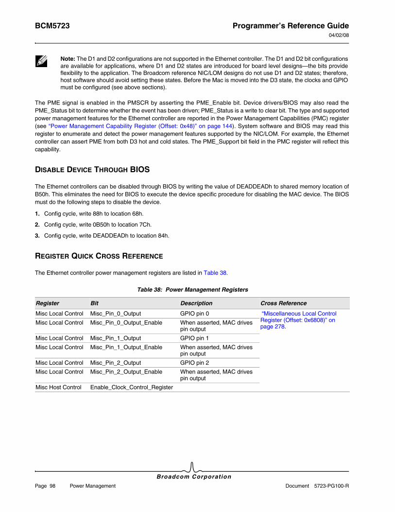
BCM5723 Programmer’s Reference Guide04/02/08
Broadcom Corporation
Page 98 Power Management Document 5723-PG100-R
The PME signal is enabled in the PMSCR by asserting the PME_Enable bit. Device drivers/BIOS may also read the PME_Status bit to determine whether the event has been driven; PME_Status is a write to clear bit. The type and supported power management features for the Ethernet controller are reported in the Power Management Capabilities (PMC) register (see “Power Management Capability Register (Offset: 0x48)” on page 144). System software and BIOS may read this register to enumerate and detect the power management features supported by the NIC/LOM. For example, the Ethernet controller can assert PME from both D3 hot and cold states. The PME_Support bit field in the PMC register will reflect this capability.
DISABLE DEVICE THROUGH BIOS
The Ethernet controllers can be disabled through BIOS by writing the value of DEADDEADh to shared memory location of B50h. This eliminates the need for BIOS to execute the device specific procedure for disabling the MAC device. The BIOS must do the following steps to disable the device.
1. Config cycle, write 88h to location 68h.
2. Config cycle, write 0B50h to location 7Ch.
3. Config cycle, write DEADDEADh to location 84h.
REGISTER QUICK CROSS REFERENCE
The Ethernet controller power management registers are listed in Table 38.
Note: The D1 and D2 configurations are not supported in the Ethernet controller. The D1 and D2 bit configurations are available for applications, where D1 and D2 states are introduced for board level designs—the bits provide flexibility to the application. The Broadcom reference NIC/LOM designs do not use D1 and D2 states; therefore, host software should avoid setting these states. Before the Mac is moved into the D3 state, the clocks and GPIO must be configured (see above sections).
Table 38: Power Management Registers
Register Bit Description Cross Reference
Misc Local Control Misc_Pin_0_Output GPIO pin 0 “Miscellaneous Local Control Register (Offset: 0x6808)” on page 278.
Misc Local Control Misc_Pin_0_Output_Enable When asserted, MAC drives pin output
Misc Local Control Misc_Pin_1_Output GPIO pin 1
Misc Local Control Misc_Pin_1_Output_Enable When asserted, MAC drives pin output
Misc Local Control Misc_Pin_2_Output GPIO pin 2
Misc Local Control Misc_Pin_2_Output_Enable When asserted, MAC drives pin output
Misc Host Control Enable_Clock_Control_Register
Programmer’s Reference Guide BCM572304/02/08
Broadcom CorporationDocument 5723-PG100-R Endian Control (Byte and Word Swapping) Page 99
ENDIAN CONTROL (BYTE AND WORD SWAPPING)
BACKGROUND
There are two basic formats for storing data in memory—little-endian and big-endian. The endianess of a system is determined by how multibyte quantities are stored in memory. A big-endian architecture stores the most significant byte at the lowest address offset while little-endian architecture stores the least significant byte at the lowest address offset.
For example, the 32-bit hex value 0x12345678 would be stored in memory as shown in the following table.
Another method of viewing how this data would be stored is shown in the following tables.
PCI Clock_Control TX RISC_Clock_Disable Disable the clock to the transmit CPU
“Clock Control Register (Offset: 0x74)” on page 151.
PCI Clock_Control RX RISC_Clock_Disable Disable the clock to the receive CPU
PCI Clock_Control Select_Alternate_Clock Use an alternate clock as a reference, rather than the PLL 133
PCI Clock_Control PLL133 Disable the 133-MHz phased locked loop
PCI Power Management Control/Status
PME_Enable – “Power Management Control/Status Register (Offset: 0x4C)” on page 145.
PCI Power Management Control/Status
Power_State –
Table 39: Endian Example
Address 00 01 02 03
Big Endian 12 34 56 78
Little Endian 78 56 34 12
Table 40: Storage of Big-Endian Data
Storage Byte 00 01 02 03
Data Contents 12 34 56 78
Table 41: Storage of Little-Endian Data
Storage Byte 03 02 01 00
Data Contents 12 34 56 78
Table 38: Power Management Registers (Cont.)
Register Bit Description Cross Reference
BCM5723 Programmer’s Reference Guide04/02/08
Broadcom Corporation
Page 100 Endian Control (Byte and Word Swapping) Document 5723-PG100-R
Examples of big-endian platforms include SGI Irix, IBM RS6000, and SUN.
Examples of little-endian platforms include Intel x86 and DEC Alpha.
PCI assumes a little-endian memory model. PCI configuration registers are organized so that the least significant portion of the data is assigned to the lower address.
ARCHITECTURE
The Ethernet controller is internally a big-endian machine, and its internal processors are big-endian devices. The Ethernet controller stores data internally in big-endian format using a 64-bit memory subsystem.
However, many hosts (e.g., x86 systems) use the little-endian format, and the PCI bus uses the little-endian format. Therefore the Ethernet controller has a number of byte swapping options that may be configured by software so that Little or Big Endian hosts can interface as seamlessly as possible with Ethernet controller over PCI. The Ethernet controller has the following bits that control byte and word swapping:
• Enable Endian Word Swap (bit 3, Miscellaneous Host Control register (offset 0x68 into PCI Config register, se “Miscellaneous Host Control Register (Offset: 0x68)” on page 148). If 1, this register enables 32-bit word swapping when accessing the Ethernet controller via the PCI target interface.
• Enable Endian Byte Swap (bit 2, Miscellaneous Host Control register (offset 0x68 into PCI Config register, see “Miscellaneous Host Control Register (Offset: 0x68)” on page 148). If 1, this register enables byte swapping (within a 32-bit word) when accessing the Ethernet controller via the PCI target interface.
• Word Swap Data (bit 5, Mode Control register (offset 0x6800 into the Ethernet controller registers). If 1, this register enables word swapping of frame data when it comes across the bus.
• Byte Swap Data (bit 4, Mode Control register (offset 0x6800 into the Ethernet controller registers). If 1, this register enables byte swapping of frame data when it comes across the bus.
• Word Swap Non-Frame Data (bit 2, Mode Control register (offset 0x6800 into the Ethernet controller registers). If 1, this register enables word swapping of non frame data (i.e,. buffer descriptors, statistics, etc.) when it comes across the bus.
• Byte Swap Non-Frame Data (bit 1, Mode Control register (offset 0x6800 into the Ethernet controller registers). If 1, this register enables byte swapping of non frame data (i.e., buffer descriptors, statistics, etc.) when it comes across the bus.
The setting of the above swapping bits will affect the order of how data is represented when it is transferred across PCI. Since byte swapping is a confusing subject, examples will be shown that reflect how each byte swapping bit works
ENABLE ENDIAN WORD SWAP AND ENABLE ENDIAN BYTE SWAP BITS
The Enable Endian Word Swap, and Enable Endian Byte Swap bits affect whether words or bytes are swapped during target PCI accesses. Thus, these bits affect the byte order when the host is directly reading/writing to registers or control structures that are physically located on the Ethernet controller. These bits do not affect the byte ordering of packet data or other structures that are mastered (DMAed) by the Ethernet controller.
When the Ethernet controller is accessed via PCI (which is little endian) as a PCI target, the Ethernet controller must implicitly map those accesses to internal structures that use a 64-bit Big Endian architecture. In the default case where no swap bits are set the Ethernet controller maps PCI data to internal structures shown in Figure 45 and Figure 46.
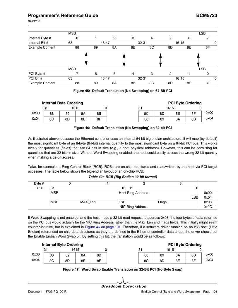
Programmer’s Reference Guide BCM572304/02/08
Broadcom CorporationDocument 5723-PG100-R Endian Control (Byte and Word Swapping) Page 101
Figure 45: Default Translation (No Swapping) on 64-Bit PCI
Internal Byte Ordering PCI Byte Ordering
Figure 46: Default Translation (No Swapping) on 32-bit PCI
As illustrated above, because the Ethernet controller uses an internal 64-bit big endian architecture, it will map (by default) the most significant byte of an 8-byte (64-bit) internal quantity to the most significant byte on a 64-bit PCI bus. This works nicely for quantities (fields) that are 64 bits in size (e.g., a host physical address). However, this can be confusing for quantities that are 32 bits in size. Without Word Swapping enabled, the host could easily access the wrong 32-bit quantity when making a 32-bit access.
Take, for example, a Ring Control Block (RCB). RCBs are on-chip structures and read/written by the host via PCI target accesses. The table below shows the big-endian layout of an on-chip RCB:
If Word Swapping is not enabled, and the host made a 32-bit read request to address 0x08, the four bytes of data returned on the PCI bus would actually be the NIC Ring Address rather than the Max_Len and Flags fields. This initially might seem counter-intuitive, but is explained in Figure 46 on page 101. Therefore, if a software driver running on an x86 host (Little Endian) referenced on-chip data structures as they are defined in the Ethernet controller data sheet, the driver should set the Enable Endian Word Swap bit. By setting this bit, the translation would be as follows:
Internal Byte Ordering PCI Byte Ordering
Figure 47: Word Swap Enable Translation on 32-Bit PCI (No Byte Swap)
MSB LSBInternal Byte # 0 1 2 3 4 5 6 7Internal Bit # 63 48 47 32 31 16 15 0Example Content 88 89 8A 8B 8C 8D 8E 8F
MSB LSBPCI Byte # 7 6 5 4 3 2 1 0PCI Bit # 63 48 47 32 31 16 15 0Example Content 88 89 8A 8B 8C 8D 8E 8F
31 1615 0 31 1615 00x00 88 89 8A 8B 8C 8D 8E 8F 0x00
0x04 8C 8D 8E 8F 88 89 8A 8B 0x04
Table 42: RCB (Big Endian 32-bit format)
Byte # 0 1 2 3Bit # 31 16 15 0
MSB Host Ring Address 0x00LSB 0x04
MSB MAX_Len LSB Flags 0x08NIC Ring Address 0x0C
31 1615 0 31 1615 00x00 88 89 8A 8B 88 89 8A 8B 0x00
0x04 8C 8D 8E 8F 8C 8D 8E 8F 0x04
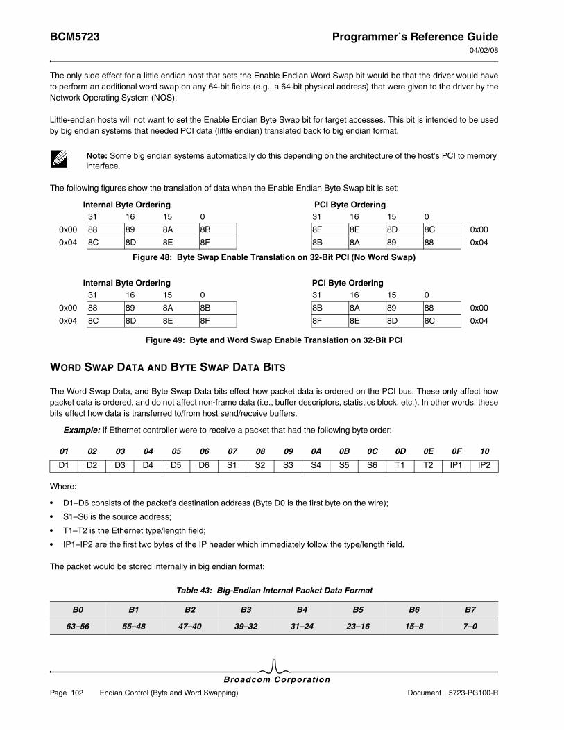
BCM5723 Programmer’s Reference Guide04/02/08
Broadcom Corporation
Page 102 Endian Control (Byte and Word Swapping) Document 5723-PG100-R
The only side effect for a little endian host that sets the Enable Endian Word Swap bit would be that the driver would have to perform an additional word swap on any 64-bit fields (e.g., a 64-bit physical address) that were given to the driver by the Network Operating System (NOS).
Little-endian hosts will not want to set the Enable Endian Byte Swap bit for target accesses. This bit is intended to be used by big endian systems that needed PCI data (little endian) translated back to big endian format.
The following figures show the translation of data when the Enable Endian Byte Swap bit is set:
Internal Byte Ordering PCI Byte Ordering
Figure 48: Byte Swap Enable Translation on 32-Bit PCI (No Word Swap)
Internal Byte Ordering PCI Byte Ordering
Figure 49: Byte and Word Swap Enable Translation on 32-Bit PCI
WORD SWAP DATA AND BYTE SWAP DATA BITS
The Word Swap Data, and Byte Swap Data bits effect how packet data is ordered on the PCI bus. These only affect how packet data is ordered, and do not affect non-frame data (i.e., buffer descriptors, statistics block, etc.). In other words, these bits effect how data is transferred to/from host send/receive buffers.
Example: If Ethernet controller were to receive a packet that had the following byte order:
Where:
• D1–D6 consists of the packet’s destination address (Byte D0 is the first byte on the wire);
• S1–S6 is the source address;
• T1–T2 is the Ethernet type/length field;
• IP1–IP2 are the first two bytes of the IP header which immediately follow the type/length field.
The packet would be stored internally in big endian format:
Note: Some big endian systems automatically do this depending on the architecture of the host’s PCI to memory interface.
31 16 15 0 31 16 15 0
0x00 88 89 8A 8B 8F 8E 8D 8C 0x00
0x04 8C 8D 8E 8F 8B 8A 89 88 0x04
31 16 15 0 31 16 15 0
0x00 88 89 8A 8B 8B 8A 89 88 0x00
0x04 8C 8D 8E 8F 8F 8E 8D 8C 0x04
01 02 03 04 05 06 07 08 09 0A 0B 0C 0D 0E 0F 10
D1 D2 D3 D4 D5 D6 S1 S2 S3 S4 S5 S6 T1 T2 IP1 IP2
Table 43: Big-Endian Internal Packet Data Format
B0 B1 B2 B3 B4 B5 B6 B7
63–56 55–48 47–40 39–32 31–24 23–16 15–8 7–0

Programmer’s Reference Guide BCM572304/02/08
Broadcom CorporationDocument 5723-PG100-R Endian Control (Byte and Word Swapping) Page 103
However, when the data gets transferred across PCI, there could be confusion about the correct byte ordering because PCI is Little Endian whereas Ethernet controller is a Big Endian device. So, in order to provide flexibility for different host processor/memory architectures, Ethernet controller can order this data on PCI in four different ways depending on the settings of the Word Swap Data, and Byte Swap Data bits. The following figures illustrate how data would appear on the PCI AD[63:0] pins depending on the settings of those swap bits:
Word Swap Data = 0, and Byte Swap Data = 0
Word Swap Data = 0, and Byte Swap Data = 1
D1 D2 D3 D4 D5 D6 S1 S2
S3 S4 S5 S6 T1 T2 IP1 IP2
Table 44: 64-Bit PCI Bus (WSD = 0, BSD = 0)
B7 7B6 B5 B4 B3 B2 B1 B0
63–56 55–48 47–40 39–32 31–24 23–16 15–8 7–0
D1 D2 D3 D4 D5 D6 S1 S2
S3 S4 S5 S6 T1 T2 IP1 IP2
Table 45: 32-Bit PCI Bus (WSD = 0, BSD = 0)
B3 B2 B1 B0
31–24 23–16 15–8 7–0
D5 D6 S1 S2
D1 D2 D3 D4
T1 T2 IP1 IP2
S3 S4 S5 S6
Table 46: 64-Bit PCI Bus (WSD = 0, BSD = 1)
B7 B6 B5 B4 B3 B2 B1 B0
63–56 55–48 47–40 39–32 31–24 23–16 15–8 7–0
D4 D3 D2 D1 S2 S1 D6 D5
S6 S5 S4 S3 IP2 IP1 T2 T1
Table 47: 32-Bit PCI Bus (WSD = 0, BSD = 1)
B3 B2 B1 B0
31–24 23–16 15–8 7–0
S2 S1 D6 D5
D4 D3 D2 D1
IP2 IP1 T2 T1
Table 43: Big-Endian Internal Packet Data Format
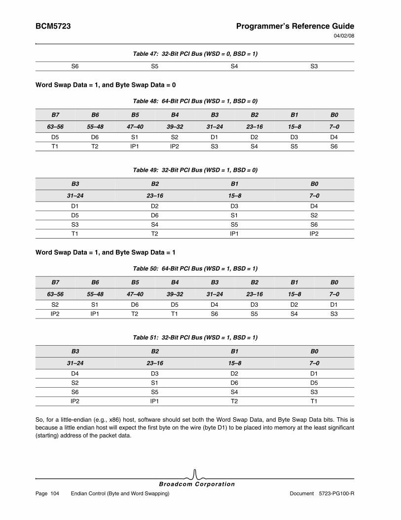
BCM5723 Programmer’s Reference Guide04/02/08
Broadcom Corporation
Page 104 Endian Control (Byte and Word Swapping) Document 5723-PG100-R
Word Swap Data = 1, and Byte Swap Data = 0
Word Swap Data = 1, and Byte Swap Data = 1
So, for a little-endian (e.g., x86) host, software should set both the Word Swap Data, and Byte Swap Data bits. This is because a little endian host will expect the first byte on the wire (byte D1) to be placed into memory at the least significant (starting) address of the packet data.
S6 S5 S4 S3
Table 48: 64-Bit PCI Bus (WSD = 1, BSD = 0)
B7 B6 B5 B4 B3 B2 B1 B0
63–56 55–48 47–40 39–32 31–24 23–16 15–8 7–0
D5 D6 S1 S2 D1 D2 D3 D4
T1 T2 IP1 IP2 S3 S4 S5 S6
Table 49: 32-Bit PCI Bus (WSD = 1, BSD = 0)
B3 B2 B1 B0
31–24 23–16 15–8 7–0
D1 D2 D3 D4
D5 D6 S1 S2
S3 S4 S5 S6
T1 T2 IP1 IP2
Table 50: 64-Bit PCI Bus (WSD = 1, BSD = 1)
B7 B6 B5 B4 B3 B2 B1 B0
63–56 55–48 47–40 39–32 31–24 23–16 15–8 7–0
S2 S1 D6 D5 D4 D3 D2 D1
IP2 IP1 T2 T1 S6 S5 S4 S3
Table 51: 32-Bit PCI Bus (WSD = 1, BSD = 1)
B3 B2 B1 B0
31–24 23–16 15–8 7–0
D4 D3 D2 D1
S2 S1 D6 D5
S6 S5 S4 S3
IP2 IP1 T2 T1
Table 47: 32-Bit PCI Bus (WSD = 0, BSD = 1)
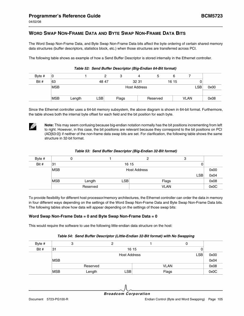
Programmer’s Reference Guide BCM572304/02/08
Broadcom CorporationDocument 5723-PG100-R Endian Control (Byte and Word Swapping) Page 105
WORD SWAP NON-FRAME DATA AND BYTE SWAP NON-FRAME DATA BITS
The Word Swap Non-Frame Data, and Byte Swap Non-Frame Data bits affect the byte ordering of certain shared memory data structures (buffer descriptors, statistics block, etc.) when those structures are transferred across PCI.
The following table shows as example of how a Send Buffer Descriptor is stored internally in the Ethernet controller.
Since the Ethernet controller uses a 64-bit memory subsystem, the above diagram is shown in 64-bit format. Furthermore, the table shows both the internal byte offset for each field and the bit position for each byte.
To provide flexibility for different host processor/memory architectures, the Ethernet controller can order the data in memory in four different ways depending on the settings of the Word Swap Non-Frame Data and Byte Swap Non-Frame Data bits. The following tables show how data will appear depending on the settings of those swap bits:
Word Swap Non-Frame Data = 0 and Byte Swap Non-Frame Data = 0
This would require the software to use the following little-endian data structure on the host:
Table 52: Send Buffer Descriptor (Big-Endian 64-Bit format)
Byte # 0 1 2 3 4 5 6 7
Bit # 63 48 47 32 31 16 15 0
MSB Host Address LSB 0x00
MSB Length LSB Flags Reserved VLAN 0x08
Note: This may seem confusing because big-endian notation normally has the bit positions incrementing from left to right. However, in this case, the bit positions are relevant because they correspond to the bit positions on PCI (AD[63:0]) if neither of the non-frame data swap bits are set. For clarification, the following table shows the same structure in 32-bit format.
Table 53: Send Buffer Descriptor (Big-Endian 32-Bit format)
Byte # 0 1 2 3
Bit # 31 16 15 0
MSB Host Address 0x00
LSB 0x04
MSB Length LSB Flags 0x08
Reserved VLAN 0x0C
Table 54: Send Buffer Descriptor (Little-Endian 32-Bit format) with No Swapping
Byte # 3 2 1 0
Bit # 31 16 15 0
Host Address LSB 0x00
MSB 0x04
Reserved VLAN 0x08
MSB Length LSB Flags 0x0C
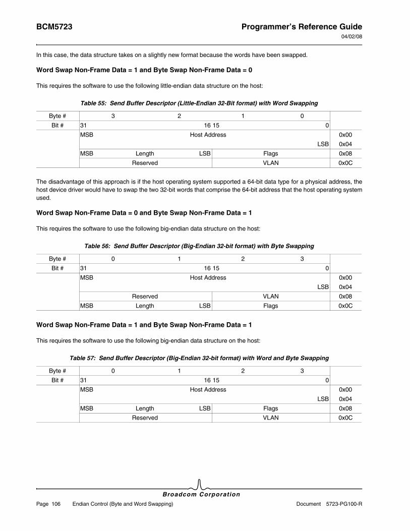
BCM5723 Programmer’s Reference Guide04/02/08
Broadcom Corporation
Page 106 Endian Control (Byte and Word Swapping) Document 5723-PG100-R
In this case, the data structure takes on a slightly new format because the words have been swapped.
Word Swap Non-Frame Data = 1 and Byte Swap Non-Frame Data = 0
This requires the software to use the following little-endian data structure on the host:
The disadvantage of this approach is if the host operating system supported a 64-bit data type for a physical address, the host device driver would have to swap the two 32-bit words that comprise the 64-bit address that the host operating system used.
Word Swap Non-Frame Data = 0 and Byte Swap Non-Frame Data = 1
This requires the software to use the following big-endian data structure on the host:
Word Swap Non-Frame Data = 1 and Byte Swap Non-Frame Data = 1
This requires the software to use the following big-endian data structure on the host:
Table 55: Send Buffer Descriptor (Little-Endian 32-Bit format) with Word Swapping
Byte # 3 2 1 0
Bit # 31 16 15 0
MSB Host Address 0x00
LSB 0x04
MSB Length LSB Flags 0x08
Reserved VLAN 0x0C
Table 56: Send Buffer Descriptor (Big-Endian 32-bit format) with Byte Swapping
Byte # 0 1 2 3
Bit # 31 16 15 0
MSB Host Address 0x00
LSB 0x04
Reserved VLAN 0x08
MSB Length LSB Flags 0x0C
Table 57: Send Buffer Descriptor (Big-Endian 32-bit format) with Word and Byte Swapping
Byte # 0 1 2 3
Bit # 31 16 15 0
MSB Host Address 0x00
LSB 0x04
MSB Length LSB Flags 0x08
Reserved VLAN 0x0C
Programmer’s Reference Guide BCM572304/02/08
Broadcom CorporationDocument 5723-PG100-R Ethernet Link Configuration Page 107
Section 9: Ethernet Link Configuration
OVERVIEW
The Ethernet controller supports multiple link operating modes. It can operate at multiple link speeds: 10 Mbps, 100 Mbps, or 1000 Mbps. It can also operate at half-duplex (IEE 802.3 CSMA/CD) or full-duplex. The MAC is compliant with IEEE 802.3, IEEE 802.3u, IEEE 802.3x, and IEEE 802.3z specifications.
GMII/MIIThe Gigabit Media Independent Interface (GMII) is normally used to interface the controller to a transceiver that supports Gigabit Ethernet over copper wiring (1000BASE-T). The Media Independent Interface (MII) is used to interface the controller to a transceiver that is capable of 10/100 Mbps Ethernet. Depending upon the link speed, driver software will need to configure the Ethernet controller to operate in either GMII mode or MII mode.
CONFIGURING THE ETHERNET CONTROLLER FOR GMII AND MII MODES
Configuring the Ethernet controller to operate in GMII or MII mode is simple. During initialization, software should configure the Ethernet_MAC_Mode.Port_Mode bits to a value that corresponds to the correct interface speed (01b for MII, 10b for GMII).
CONFIGURING HOW MAC DETECTS LINK UP/DOWN
The Ethernet controller has two different methods that it can use to determine if the Ethernet link is up or down. The link will be down if the Ethernet cable is not properly attached at both ends of the network. Link will be up only if the cable is properly attached and the devices at both ends of the cable recognize that link has been established. The device cannot successfully transfer packets on the link unless it determines that it has a valid link up.
The first method is called auto-polling. Software can enable auto-polling by setting the MI_Mode.Port_Polling bit. If enabled, the Ethernet controller periodically generates MDIO cycles to read the PHY’s Link_Status bit in MII Status register. The link status f rom the auto-pol l ing operat ion is then reported in the MI_Status_Register .Link_Status and Transmit_MAC_Status.Link_Up (see “Transmit MAC Status Register (Offset: 0x460) ” on page 189) bits.
The second method involves using the Ethernet controller’s LNKRDY input signal. This method allows the Ethernet controller to determine the link status based on the link status output from integrated PHY connected to LNKRDY input of MAC. The Transmit_MAC_Status.Link Up bit (see “Transmit MAC Status Register (Offset: 0x460) ” on page 189) will reflect the link status input on LNKRDY signal to MAC from PHY. Host software can enable this method by clearing the MI_Mode.Port_Polling bit (bit-4 of offset 0x454).
The link state of the Ethernet controller can also be forced by disabling both the auto-polling function and the LNKRDY signal and forcing the link status by directly writing to the MI_Status.Link_Status bit.
Note: The integrated PHY transceiver of Ethernet controllers is hardcoded with a PHY address of 1.
BCM5723 Programmer’s Reference Guide04/02/08
Broadcom Corporation
Page 108 GMII/MII Document 5723-PG100-R
LINK STATUS CHANGE INDICATIONS
It is advantageous for host software to know when the status of the Ethernet link has changed. To generate an interrupt to the host when link status changes, software should set the Ethernet_MAC_Event_Enable.Link_State_Changed bit (see “EMAC Event Enable Register (Offset: 0x408)” on page 181) and the Mode_Control.Interrupt_on_MAC_Attention bit (see “Mode Cont ro l Reg ister (Of fse t : 0x6800) ” on page 275) . Wi th th is conf igura t ion , t he Ethernet_MAC_Status.Link_State_Changed bit and Link_State_Changed bit in the status block (see “Status Block” on page 32) will be set when the link has changed state.
CONFIGURING THE GMII/MII PHY
GMII/MII transceivers (PHYs) contain registers that a software driver can manipulate to change parameters in the PHY. These parameters include the link speed or duplex that the PHY is currently running at, or the speed/duplex options that the PHY advertises during the auto-negotiation process. NIC device drivers will typically access PHY registers during the driver initialization process to configure the PHYs speed/duplex or to examine the results of the auto-negotiation process.
The integrated PHY registers are accessed via a process called MDIO. The integrated PHY is connected to the Ethernet controller through an internal MDIO bus (MDIO and MDC pins). Software accesses PHY’s registers via MDIO through the Ethernet controller’s MI_Communication register. The following example code describes accessing the PHY registers through the MI_Communication registers of the Ethernet controller.
Reading a PHY Register
// If auto-polling is enabled, temporarily disable itIf (AutoPolling_Enabled == TRUE) ThenBegin
Mi_Mode.PortPolling = 0End
// Setup the value that we are going to write to MI Communication register// Set bit 27 to indicate a PHY read.// Set bit 29 to indicate the start of a MDIO transactionValue32 = ((PhyAddress << 21) | (PhyRegOffset << 16) | 0x28000000)
// Write value to MI communication registerMi_Communication_Register = Value32
// Now read back MI Communication register until the start bit// has been cleared or we have timed out (>5000 reads)Loopcount = 5000While (LoopCount > 0)Begin
Value32 = Mi_Communication_RegisterIf (!(Value32 | 0x20000000)) then BREAK loopElse Loopcount--
End
// Print message if errorIf (Value32 | 0x20000000) then Begin
// It a debug case – cannot read PHYProcedure (Print Error Message)Value32 = 0
End
// If auto-polling is enabled, turn it back onIf (AutoPolling_Enabled == TRUE) then
Programmer’s Reference Guide BCM572304/02/08
Broadcom CorporationDocument 5723-PG100-R GMII/MII Page 109
BeginMi_Mode.PortPolling = 1
End
// Now return the value that we read (lower 16 bits of reg)Return (Value32 & 0xffff)
Writing a PHY Register
// If auto-polling is enabled, temporarily disable itIf (AutoPolling_Enabled == TRUE) ThenBegin
Mi_Mode.PortPolling = 0End
// Setup the value that we are going to write to MI Communication register// Set bit 26 set to indicate a PHY write.// Set bit 29 to indicate the start of a MDIO transaction// The lower 16 bits equal the value we want to write to the PHY registerValue32 = ((PhyAddress << 21) | (PhyRegOffset << 16) | RegValue | 0x24000000)
// Write value to MI communication registerMi_Communication_Register = Value32
// Now read back MI Communication register until the start bit// has been cleared or we have timed out (>5000 reads)Loopcount = 5000While (LoopCount > 0)Begin
Value32 = Mi_Communication_RegisterIf (!(Value32 | 0x20000000)) then BREAK loopElse Loopcount--
End
// Print message if errorIf (Value32 | 0x20000000) then Begin
// It a debug case – can’t write PHYProcedure (Print Error Message)Value32 = 0
End
// If auto-polling is enabled, turn it back onIf (AutoPolling_Enabled == TRUE) ThenBegin
Mi_Mode.PortPolling = 1End
BCM5723 Programmer’s Reference Guide04/02/08
Broadcom Corporation
Page 110 MDI Register Access Document 5723-PG100-R
MDI REGISTER ACCESS
Configuring physical devices and querying the status of physical devices are done via the MDIO interface (MDC and MDIO).
There are three modes in which the internal MII Management interface signals (MDC/MDIO) can be controlled for communication with the internal transceiver registers. These modes are as follows:
• Autopolling Mode. Enabled by setting the Enable bit in the MAC Ethernet MI Mode register. The device will poll for the link status bit in the transceiver.
• Command Control. Writing to the MI Communications register directly to either read or write the transceiver registers.
• Register Control. When enabled, the host writes the MDC clock and data values into the MDI Control register (see “MDI Control Register (Offset: 0x6844)” on page 281). The values in the register directly control the interface signals. This Mode is enabled by setting the MDI Select bit of the MDI Control register (Offset 0x6844).
Autopolling Mode has the lowest priority and it will be stalled any time there is an active operation through the MI Communications register. Register Control Mode has the highest priority and When this mode is enabled, the MI Communications register cannot be read or written.
OPERATIONAL CHARACTERISTICS
The interface between the MAC and physical devices is with the two signals of:
• MDIO clock (MDC)
• Bidirectional serial data (MDIO)
The details of the MDIO interface can be found in the IEEE 802.3 specification.
ACCESS METHODS
The MAC provides two methods to access the Physical Device registers via the MDIO interface:
• Traditional bit-bang method
• Auto-access method
Note: This procedure is PHY-independent. The MAC access to the PHY is the same for the entire NetXtreme family.
Programmer’s Reference Guide BCM572304/02/08
Broadcom CorporationDocument 5723-PG100-R MDI Register Access Page 111
Traditional Bit-Bang Method
In this method, software has to toggle the MDC and MDIO pins to access physical device registers. Software is responsible for providing the proper delay to satisfy timing requirements such as setup time, hold time, clock frequency, etc.
The MDI_Control_Register (see “MDI Control Register (Offset: 0x6844)” on page 281) controls the MDC and MDIO pins as follows:
• MDI_Control_Register.MDI_Clock: is used to clock MDC pin. If this bit is set, MDC is logic high. Otherwise, it is logic low.
• MDI_Control_Register.MDI_Select: This bit is used to select either the traditional bit-bang method or auto-access method. This bit must be set to 1 when the traditional bit-bang method is used.
• MDI_Control_Register.MDI_Enable: This bit is used to control bidirectional data pin. If this bit is set to 1, then MDI_Control_Register.MDI_Data is output. Otherwise, it is input.
• MDI_Control_Register.MDI_Data: This is used to control bidirectional MDIO pin.
Auto-Access Method
The Ethernet controller has a built-in interface to access physical device registers without having to control MDC and MDIO pins by software/firmware. It provides an easy way to access the physical device register.
To use this mode, MDI_Control_Register.MDI_Select has to be cleared to 0. The MI_Communication_Register is used to access physical device.
For example, to read a 16-bit PHY register at offset 0x2 of a PHY device which is strapped to PHY address 1, perform the following steps:
1. MI_Communication_Register.Register_Address is set to 0x2.
2. MI_Communication_Register.PHY_Addr is set to 1.
3. MI_Communication_Register.Command is set to 0x2.
4. MI_Communication_Register.Start_Busy is set to 1.
5. Poll Until MI_Communication_Register.Start_Busy is cleared to 0.
6. MI_Communication_Register.Transaction_Data contains 16-bit data of the PHY register.
See “Configuring the GMII/MII PHY” on page 108 for example code.
Note: The auto-access method which is explained next is the recommended access method. This is because of additional software overhead required in maintaining the MDIO bus timing when using the Traditional bit-bang access method.
Note: Programmers must be careful to wait for the start _busy bit to clear. Writing to the MI Communication register prior to the completion of a previous MDI access will yield unpredictable MDI data. The previous access will not complete successfully.
BCM5723 Programmer’s Reference Guide04/02/08
Broadcom Corporation
Page 112 Wake on LAN Mode/Low-Power Document 5723-PG100-R
To write a value of 0x1000 into 16-bit PHY register at offset 0x0 of a PHY device which is strapped to PHY address 1, perform the following steps:
1. MI_Communication_Register.Register_Address is set to 0x0.
2. MI_Communication_Register.PHY_Addr is set to 1.
3. MI_Communication_Register.Command is set to 0x1.
4. MI_Communication_Register.Transaction_Data is set to 0x1000
5. MI_Communication_Register.Start_Busy is set to 1.
6. Poll Until MI_Communication_Register.Start_Busy is cleared to 0.
See “Configuring the GMII/MII PHY” on page 108 for example code.
WAKE ON LAN MODE/LOW-POWER
DESCRIPTION
The Ethernet controller uses the ACPI D3 hot/cold (low-power) state to conserve energy. The OS power management policy notifies device drivers to initiate power management transitions. The device driver should move the MAC into the D3 hot/cold power state—a response to the power management request. While the Ethernet controller is in a D3 state, the RX MAC will filter incoming packets. The RX MAC compares incoming traffic for Interesting Packet pattern matches. The Ethernet controller asserts the PCI PME signal, when a positive WOL packet comparison is made. The PME signal notifies the Op-erating System and host device driver to transition the MAC into the D0 (high power) state.
WOL mode is a combination of PHY and MAC configurations. Both the PHY and MAC must be configured correctly to enable Broadcom’s WOL technology. The Ethernet controller provides WOL pattern filters for 10/100 wire speeds.
The Ethernet controller supports both Interesting Packet pattern matching the AMD Magic Packet proprietary technology for WOL. The WOL support for the AMD Magic Packet format does not require host software to configure a pattern filter. The Magic Packet comparison is made in hardware and is enabled through a register interface. The AMD Magic Packet can be either broadcast or directed, and must contain the receiver's MAC address at least six times (repeating) in the packet. The Magic Packet wake-up is configured different from pattern match wake-up.
The following components are involved in WOL operation:
• Internal memory
• WOL Pattern Pointer register
• WOL Pattern Configuration register
• WOL streams
• Pattern data structure
• GPIO
• Firmware mailbox
• PHY auto-negotiation
• Ethernet controller power management

Programmer’s Reference Guide BCM572304/02/08
Broadcom CorporationDocument 5723-PG100-R Wake on LAN Mode/Low-Power Page 113
FUNCTIONAL OVERVIEW
The Ethernet controller is capable of WOL in 10/100 Mbps for copper-based controllers.
The Ethernet controller uses the TX FIFO to store pattern data (see Figure 50). During WOL operation, the transmit engine is disabled and its FIFO is free for use. The TDE fetches data from the memory arbiter starting at a location specified in the WOL_Pattern_Pointer register. The WOL pattern checker pulls data off the TX FIFO for packet comparisons. The RX MAC will move incoming frame(s) to the pattern checker, and the remaining RX data path is not utilized. A state machine controls the Magic Packet comparisons. The WOL state machine will move out of an Idle state, when ACPI power management is enabled. The WOL state machine will clear the TX FIFO and Match register. The Match register indicates a positive Magic Packet comparison(s) on a stream.
In 10/100 Mbit mode, data is received once every four clock cycles. The pattern checker compares the first three patterns in the first cycle, the second three patterns in the second cycle, and the third three patterns in the last cycle. It is idle during the fourth cycle. In gigabit mode, the pattern checker gets three pattern words from the FIFO at one time.
Figure 50: WOL Functional Block Diagram
Note: When configured for WOL in 1000-Mbps mode, the Ethernet controller draws more than the 375 mA allowed by the PCI specification.
Rx MAC
PatternChecker
Tx FIFO TDEMemoryArbiter
InternalMemory
PatternData
RXPCS
RXRMII
RXGMII
RXIO
PowerManagment
BCM5723 Programmer’s Reference Guide04/02/08
Broadcom Corporation
Page 114 Wake on LAN Mode/Low-Power Document 5723-PG100-R
OPERATIONAL CHARACTERISTICS
Internal Memory
The WOL pattern must be stored in the Ethernet controller miscellaneous memory region. All memory locations require the host software to reinitialize the WOL pattern before each D0 to D3 transition. The RX/TX MAC places packets into this in-ternal memory and the WOL pattern is overwritten during normal operation. When the Ethernet controller operates in D0 state, internal data structures use the same memory location as the WOL pattern. Host software should re-initialize the WOL pattern before each WOL sleep transition.
Table 58 shows the required memory regions for the WOL pattern.
WOL Pattern Pointer Register
The WOL_Pattern_Pointer specifies a location within Ethernet controller address space where the pattern buffers reside (see “WOL Pattern Pointer Register (Offset: 0x430)” on page 185 for the register definition). The internal memory subsection discusses how host programmers can choose an address range. The WOL_Pattern_Pointer register uses a pointer value, not an internal memory location. The pointer value is calculated by dividing an internal memory location by the value 8. Do not program the WOL_Pattern_Pointer register with the actual internal memory location. Rather, host software must first convert the base address to a pointer value. Here are example conversion from memory base to pointer values:
• 0x0000 (Misc Memory)/8 = 0x00 (required value)
• 0x400 (base addr)/8 = 0x80 (pointer value)
• 0x8000 (base addr)/8 = 0x1000 (pointer value)
• 0xF000 (base addr)/8 = 0x1E00 (pointer value)
WOL Pattern Configuration Register
The WOL_Pattern_Configuration register contains two programmable data fields. Both fields use different units of measure-ment, so the host programmer should be careful (see “WOL Pattern Configuration Register (Offset: 0x434)” on page 185 for the register definition). This register is used to position and extract data from RX Ethernet frames.
• Offset Field—The Offset field in the WOL_Pattern_Configuration register specifies a position in RX Ethernet frame(s), where comparisons for WOL patterns should begin. This register uses a unit of measurement specified in terms of 2-byte chunks. Software should not program this field with a byte value, but should first normalize to a 2-byte unit. Hardware cannot begin WOL comparisons on odd byte alignments (i.e., 3,5,7,9 offsets). Host software must begin all pattern matching on even byte boundaries (i.e., 2,4,6,8 offsets). The 2 bytes per unit forces even byte alignment. For example:
- 0x14 (byte offset)/2 = 0x0A (register ready)
- 0x28 (byte offset)/2 = 0x14 (register ready)
- 0xFC (byte offset)/2 = 0x7E (register ready)
• Length Field—The Length field in the WOL_Pattern_Configuration register specifies the number of clock cycles required to compare a variable number of bytes, in the RX stream. The Length field uses a unit of measurement specified in terms of memory arbiter clock cycles. Software should not program this field with a byte value. The Length field should be programmed with the maximum number of clocks required to compare the largest pattern size for the nine streams (10/100 mode only).
Table 58: Required Memory Regions for WOL Pattern
Internal Address Range Size Name
0x8000–0x8FFF 8 KB Miscellaneous Memory Region
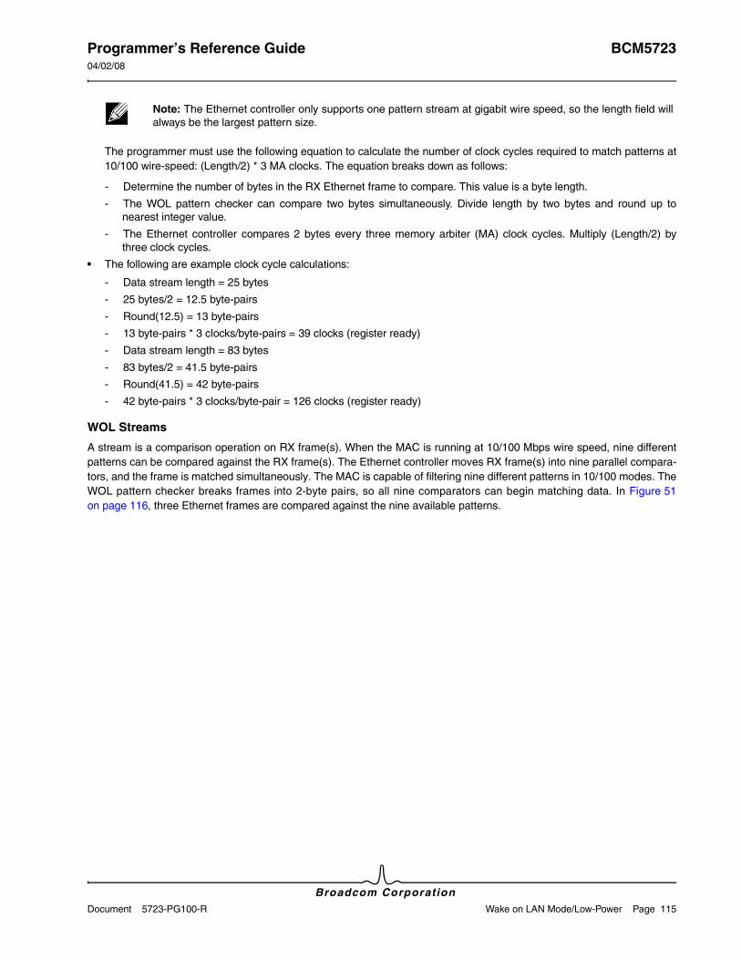
Programmer’s Reference Guide BCM572304/02/08
Broadcom CorporationDocument 5723-PG100-R Wake on LAN Mode/Low-Power Page 115
The programmer must use the following equation to calculate the number of clock cycles required to match patterns at 10/100 wire-speed: (Length/2) * 3 MA clocks. The equation breaks down as follows:
- Determine the number of bytes in the RX Ethernet frame to compare. This value is a byte length.
- The WOL pattern checker can compare two bytes simultaneously. Divide length by two bytes and round up to nearest integer value.
- The Ethernet controller compares 2 bytes every three memory arbiter (MA) clock cycles. Multiply (Length/2) by three clock cycles.
• The following are example clock cycle calculations:
- Data stream length = 25 bytes
- 25 bytes/2 = 12.5 byte-pairs
- Round(12.5) = 13 byte-pairs
- 13 byte-pairs * 3 clocks/byte-pairs = 39 clocks (register ready)
- Data stream length = 83 bytes
- 83 bytes/2 = 41.5 byte-pairs
- Round(41.5) = 42 byte-pairs
- 42 byte-pairs * 3 clocks/byte-pair = 126 clocks (register ready)
WOL Streams
A stream is a comparison operation on RX frame(s). When the MAC is running at 10/100 Mbps wire speed, nine different patterns can be compared against the RX frame(s). The Ethernet controller moves RX frame(s) into nine parallel compara-tors, and the frame is matched simultaneously. The MAC is capable of filtering nine different patterns in 10/100 modes. The WOL pattern checker breaks frames into 2-byte pairs, so all nine comparators can begin matching data. In Figure 51 on page 116, three Ethernet frames are compared against the nine available patterns.
Note: The Ethernet controller only supports one pattern stream at gigabit wire speed, so the length field will always be the largest pattern size.
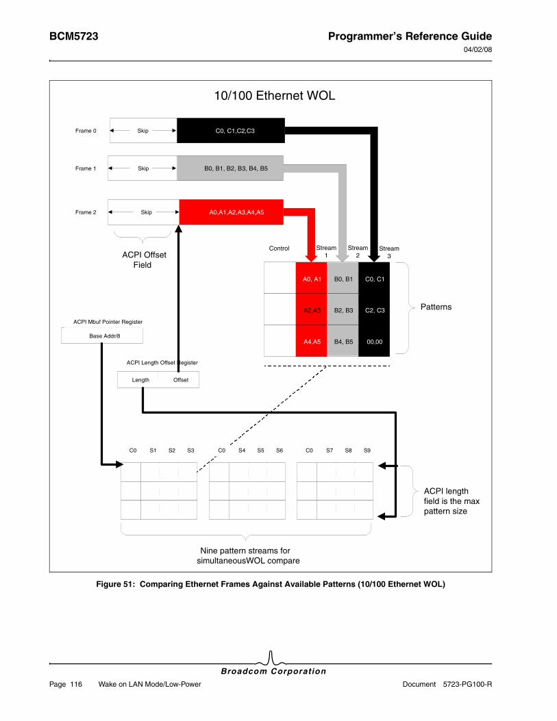
BCM5723 Programmer’s Reference Guide04/02/08
Broadcom Corporation
Page 116 Wake on LAN Mode/Low-Power Document 5723-PG100-R
Figure 51: Comparing Ethernet Frames Against Available Patterns (10/100 Ethernet WOL)
A0,A1,A2,A3,A4,A5
C0, C1,C2,C3
B0, B1, B2, B3, B4, B5
C0 S1 S2 S3 C0 S4 S5 S6 C0 S7 S8 S9
Nine pattern streams forsimultaneousWOL compare
ACPI lengthfield is the maxpattern size
10/100 Ethernet WOL
ACPI OffsetField
ACPI Mbuf Pointer Register
Length
Control
ACPI Length Offset Register
Offset
Skip
A0, A1
A2,A3
A4,A5
Patterns
Base Addr/8
B0, B1
B2, B3
B4, B5
C0, C1
00,00
C2, C3
Skip
Skip
Stream1
Stream2
Frame 0
Frame 1
Frame 2
Stream3
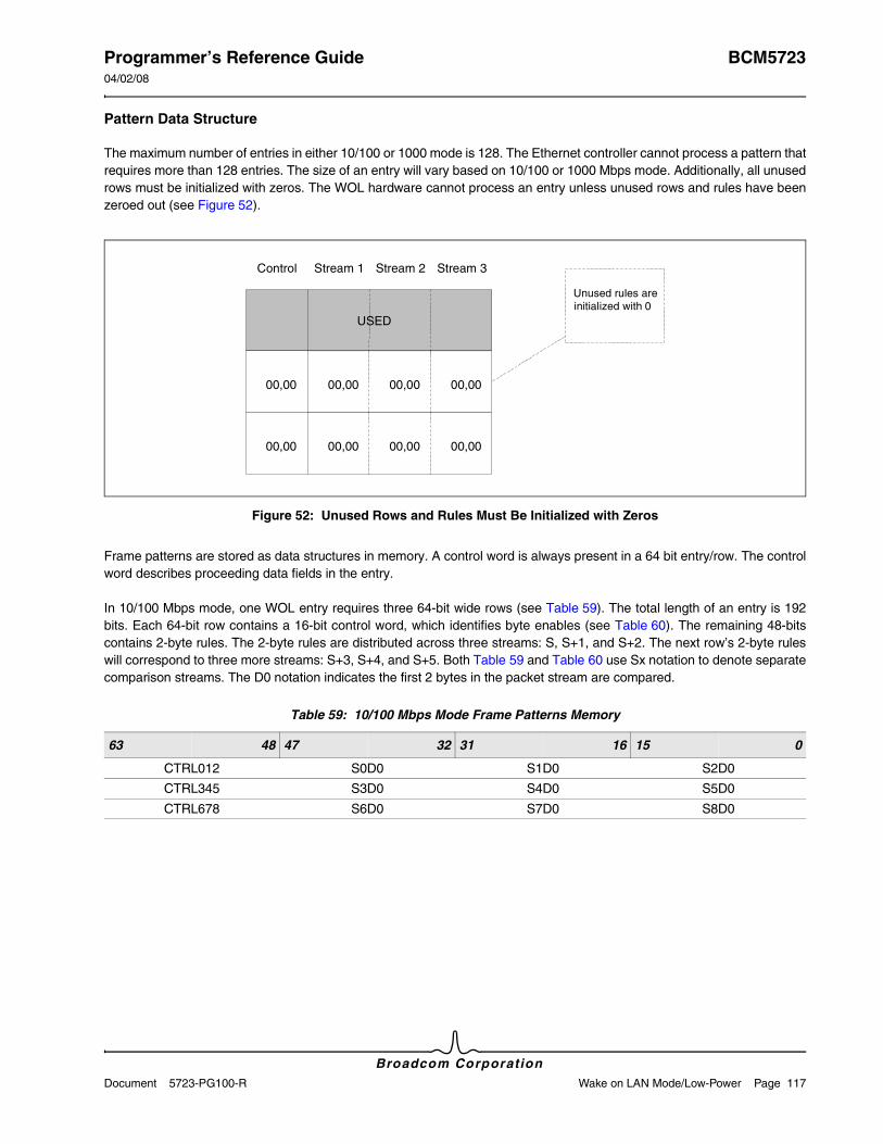
Programmer’s Reference Guide BCM572304/02/08
Broadcom CorporationDocument 5723-PG100-R Wake on LAN Mode/Low-Power Page 117
Pattern Data Structure
The maximum number of entries in either 10/100 or 1000 mode is 128. The Ethernet controller cannot process a pattern that requires more than 128 entries. The size of an entry will vary based on 10/100 or 1000 Mbps mode. Additionally, all unused rows must be initialized with zeros. The WOL hardware cannot process an entry unless unused rows and rules have been zeroed out (see Figure 52).
Figure 52: Unused Rows and Rules Must Be Initialized with Zeros
Frame patterns are stored as data structures in memory. A control word is always present in a 64 bit entry/row. The control word describes proceeding data fields in the entry.
In 10/100 Mbps mode, one WOL entry requires three 64-bit wide rows (see Table 59). The total length of an entry is 192 bits. Each 64-bit row contains a 16-bit control word, which identifies byte enables (see Table 60). The remaining 48-bits contains 2-byte rules. The 2-byte rules are distributed across three streams: S, S+1, and S+2. The next row’s 2-byte rules will correspond to three more streams: S+3, S+4, and S+5. Both Table 59 and Table 60 use Sx notation to denote separate comparison streams. The D0 notation indicates the first 2 bytes in the packet stream are compared.
Table 59: 10/100 Mbps Mode Frame Patterns Memory
63 48 47 32 31 16 15 0
CTRL012 S0D0 S1D0 S2D0
CTRL345 S3D0 S4D0 S5D0
CTRL678 S6D0 S7D0 S8D0
USED
00,00 00,00 00,00
00,00 00,00 00,00
Control Stream 1 Stream 2 Stream 3
00,00
00,00
Unused rules areinitialized with 0
BCM5723 Programmer’s Reference Guide04/02/08
Broadcom Corporation
Page 118 Wake on LAN Mode/Low-Power Document 5723-PG100-R
Table 61 shows an example of how 10/100 Mbps frame data is split up in the pattern data structure. Eight streams are compared simultaneously with three 64-bit rows comprising one WOL entry. Rows 0–2 compare frame data0 against eight rules. Rows 3–5 compare frame data1 against the next eight rules. Rows 6–9 compare data2 against the final eight rules. The eight rules may be uniquely defined for all three WOL entries.
Firmware Mailbox
When the Ethernet controller initializes (the firmware bootcode is loaded from NVRAM when the chip powers on or when reset completes), the bootcode checks the T3_FIRMWARE_MAILBOX in shared memory. When the T3_MAGIC_NUM signature (0x4B657654) is present, the bootcode does not issue a hard reset to the PHY. This is especially important in WOL mode since the PHY should not be reset.
Before the host software issues a reset to the Ethernet controller, it must write the T3_MAGIC_NUM to the shared memory address T3_FIRMWARE_MAILBOX (0xb50). This address is a software mailbox, which bootcode polls before it resets the PHY. The bootcode will acknowledge the signature by writing the one’s complement of the T3_MAGIC_NUM back into the T3_FIRMWARE_MAILBOX. If the T3_MAGIC_NUM is present, the bootcode will not reset the PHY. After resetting the Ethernet controller, host software should poll for the one’s complement of the T3_MAGIC_NUM before it proceeds, otherwise, bootcode initialization may interfere with the host software initialization.
Table 60: Frame Control Field for 10/100 Mbps Mode
Bits Field Description Access
63:62 Reserved
61 S0 High Byte Enable Enable S0 higher byte for comparison R/W
60 S0 Low Byte Enable Enable S0 lower byte for comparison R/W
59 S1 High Byte Enable Enable S1 higher byte for comparison R/W
58 S1 Low Byte Enable Enable S1 lower byte for comparison R/W
57 S2 High Byte Enable Enable S2 higher byte for comparison R/W
56 S2 Low Byte Enable Enable S2 lower byte for comparison R/W
55:51 Reserved
50 S0 Done End of S0 Stream R/W
49 S1 Done End of S1 Stream R/W
48 S2 Done End of S2 Stream R/W
Table 61: Example of Splitting 10/100 Mbps Frame Data in Pattern Data Structure
Data[63:48] Data[47:32] Data[31:16] Data[15:0]
Control Bits Stream 0 data 0 Stream 1 data 0 Stream 2 data 0
Control Bits Stream 3 data 0 Stream 4 data 0 Stream 5 data 0
Control Bits Stream 6 data 0 Stream 7 data 0 Stream 8 data 0
Control Bits Stream 0 data 1 Stream 1 data 1 Stream 2 data 1
Control Bits Stream 3 data 1 Stream 4 data 1 Stream 5 data 1
Control Bits Stream 6 data 1 Stream 7 data 1 Stream 8 data 1
Control Bits Stream 0 data 2 Stream 1 data 2 Stream 2 data 2
Control Bits Stream 3 data 2 Stream 4 data 2 Stream 5 data 2
Control Bits Stream 6 data 2 Stream 7 data 2 Stream 8 data 2
Programmer’s Reference Guide BCM572304/02/08
Broadcom CorporationDocument 5723-PG100-R Wake on LAN Mode/Low-Power Page 119
If the host software will be controlling the WOL configuration, it should write the DRV_WOL_SIGNATURE (0x474c0000) to the shared memory address DRV_WOL_MAILBOX (0xd30) so that the bootcode will not take over the WOL initialization. If the DRV_WOL_SIGNATURE is not present, and WOL has been enabled, the bootcode will assume that the host software is a legacy driver and skip the WOL initialization. If WOL is disabled, the bootcode will take over the WOL initialization based on the NVRAM configuration.
PHY Auto-Negotiation
The integrated PHY should be configured to auto-negotiate for a 10 Mbps connection (see Table 63). This step is required if the NIC must be placed into a D3 cold state. Half- or full-duplex operation is acceptable. Software must modify auto-ad-vertise configurations in the PHY’s MDI registers. The link partner will read advertisement settings to find a highest common capability. Since WOL requires 10 Mbps wire speed, the two PHYs will effectively auto-negotiate for half- or full-duplex con-nection.
Power Management
The clocking inputs need to be modified for WOL mode (see Table 64). The RX CPU is not required during WOL operation, so its clock can be disabled. The MAC has an internal phase-locked loop that clocks internal logic at 133 MHz. Software must select an alternate clocking source and then disable this PLL.
The settings shown in Table 65 enable Magic Packet detection logic in the MAC. These setting also enable the MAC to as-sert PME on the PCI bus. The RX MAC should maintain the multicast and broadcast settings that were previously configured by the NOS. The Microsoft power management specification states:
“Only a frame that passes the device’s MAC, broadcast, or multicast address filter and matches on the previously loaded sample patterns will cause the wake-up signal to be asserted.”
The ACPI_Power-on bit needs to be set for pattern match, but not for Magic Packet recognition. The Magic Packet detection
Table 62: Firmware Mailbox Initialization
Name Address Recommended Value
T3_FIRMWARE_MAILBOX 0x0B50 0x4B657654
DRV_WOL_MAILBOX 0xd30 0x474c0000
Table 63: Recommended Settings for PHY Auto-Negotiation
Register Bit Recommended Value
Auto_Negotation_Advertisement 10_BASE_TX_Half_Duplex Enable
Auto_Negotation_Advertisement 10_BASE_TX_Full_Duplex Enable
Auto_Negotation_Advertisement 100_BASE_TX_Half_Duplex Disable
Auto_Negotation_Advertisement 100_BASE_TX_Full_Duplex Disable
1000BASE-T_Control 1000_BASE_TX_Half_Duplex Disable
1000BASE-T_Control 1000_BASE_TX_Full_Duplex Disable
Table 64: WOL Mode Clock Inputs
Register Bit Recommended Value
PCI Clock_Control RX RISC_Clock_Disable Set the bit to 1
PCI Clock_Control Select_Alternate_Clock Set the bit to 1
PCI Clock_Control PLL133 Set the bit to 1
BCM5723 Programmer’s Reference Guide04/02/08
Broadcom Corporation
Page 120 Wake on LAN Mode/Low-Power Document 5723-PG100-R
mechanism is separate from the pattern match mechanism. Host software may configure WOL using four filter permutations:
• Pattern match WOL disabled. Magic Packet disabled.
• Pattern match WOL enabled. Magic Packet disabled.
• Pattern match WOL disabled. Magic Packet enabled.
• Pattern match WOL enabled. Magic Packet enabled.
Integrated MACs
Table 66 lists the WOL mode control registers in the Ethernet controllers.
Table 65: Magic Packet Detection Logic Enable
Register Bit(s) Recommended Value
PCI Power_Management_Control/Status PME_Enable Enable
PCI Power_Management_Control/Status Power_State 0x03
Ethernet_MAC_Mode ACPI_Power-On See above
Ethernet_MAC_Mode Magic_Packet_Detection See above
Table 66: Integrated MAC WOL Mode Control Registers
Register Bit(s) Name Description Cross Reference
WOL_Pattern_ Pointer
All This register points to an internal memory location. Programmers should calculate pointer value by dividing a base address by 8.
“WOL Pattern Pointer Register (Offset: 0x430)” on page 185.
WOL_Pattern_ Configuration
Length The number of memory arbiter clock cycles needed to read X bytes in the RX stream/frame.
“WOL Pattern Configuration Register (Offset: 0x434)” on page 185.
Offset The number of bytes into the RX stream/frame to begin the pattern comparison.
Ethernet_MAC_ Mode
Port_Mode This bit field specifies the type of interface the Ethernet controller port is currently using: MII, GMII, or none.
“EMAC Mode Register (Offset: 0x400)” on page 179.
Magic_Packet_ Detection
Enable WOL pattern filtering.
Promiscuous_mode All frames are forwarded, without any filtering, when this bit is enabled.
PCI Clock_Control TX RISC_Clock_Disable Disable the clock to the transmit CPU. “Clock Control Register (Offset: 0x74)” on page 151.RX RISC_Clock_Disable Disable the clock to the receive CPU.
Alternate_Clock_Source Use an alternate clock as a reference, rather than the PLL 133.
PLL133 Disable the 133-MHz phase-locked loop.
Programmer’s Reference Guide BCM572304/02/08
Broadcom CorporationDocument 5723-PG100-R Wake on LAN Mode/Low-Power Page 121
WOL DATA FLOW DIAGRAM
The Ethernet controller and PHY are both configured for WOL mode. The process is as follows:
1. Clear the PME_Status bit in the “Power Management Control/Status Register (Offset: 0x4C)” on page 145. This bit must be cleared, so the PME interrupt is not immediately generated once the NIC is moved to the D3 state. The bit could be asserted from a previous D3–D0 transition.
2. Set the Mask_PCI_Interrupt_Output bit in the Miscellaneous_Host_Control register (see “Miscellaneous Host Control Register (Offset: 0x68)” on page 148). This bit should be set, so the Ethernet controller does not generate interrupts during the WOL configuration of the PHY. The device driver’s ISR may attempt to reset and reconfigure the PHY as part of an error recovery code path.
3. If host software must place the NIC into D3 cold state, the following step is necessary. Set the 10_Base_TX_Half_Duplex and 10_BASE_TX_Full_Duplex Capability bits, in the Auto-Negotiation Advertisement Register. Clear the 100_BASE_TX_Full_Half_Duplex and 100_BASE_TX_Full_Duplex Capability bits, in the Auto-Negotiation Advertisement Register. Clear the 1000_BASE_TX_Half_Duplex and 1000_BASE_TX_Full_Duplex Capability bits, in the 1000BASE-T Control Register. The link partner will now only be able to auto-negotiate for 10-Mbps speed full/half-duplex.
4. Set the Restart_Auto_Negotiation bit in the MII Control Register. The integrated PHY and link partner will now reconfigure for 10 Mbps wire speed. Essentially, 10 Mbps link must be auto-negotiated or forced.
5. Disable the FHDE, RDE, TDE bits of the “EMAC Mode Register (Offset: 0x400)” on page 179”, and on-chip RISCs.
6. Host software must write the signature 0x4B657654 to internal memory address 0x0B50. Check for one’s complement of 0x4B657654.
7. Enable the Wake_On_LAN bit in the AUXILIARY Control Register.
8. For Interesting Packet WOL Only: Set up the Interesting Packet pattern in Ethernet controller local memory.
9. For Interesting Packet WOL Only: Write a pointer value to the “WOL Pattern Pointer Register (Offset: 0x430)” on page 185. This register uses a normalized pointer value, not a device base address. The value written to this register is BCM5700_BASE_ADDR/8. The base address must be a specific location in local memory: 0x8000, 0xC000, or 0xD000. The choice of memory location depends upon other MAC configurations, and the selection is not arbitrary.
10. For Interesting Packet WOL Only: Write the Offset field in the “WOL Pattern Configuration Register (Offset: 0x434)” on page 185. The WOL pattern checker will position into received frames on two-byte intervals. The pattern checker compares two bytes in parallel, so host software should program the offset field accordingly. Host software may perceive
Misc Local Control Misc_Pin_0_Output GPIO pin 0. “Miscellaneous Local Control Register (Offset: 0x6808)” on page 278.
Misc_Pin_0_Output_ Enable
When asserted, MAC drives pin output.
Misc_Pin_1_Output GPIO pin 1.
Misc_Pin_1_Output_ Enable
When asserted, MAC drives pin output.
Misc_Pin_2_Output GPIO pin 2.
Misc_Pin_2_Output_ Enable
When asserted, MAC drives pin output.
Power Management Control/Status
PME_Enable Enable the Ethernet controller to assert PME on PCI bus.
“Power Management Control/Status Register (Offset: 0x4C)” on page 145.Power_State Set the ACPI power state: D0, D3.
Table 66: Integrated MAC WOL Mode Control Registers (Cont.)
Register Bit(s) Name Description Cross Reference
BCM5723 Programmer’s Reference Guide04/02/08
Broadcom Corporation
Page 122 Flow Control Document 5723-PG100-R
this unit as OFFSET_BYTE/2 units.
11. For Interesting Packet WOL Only: Write the Length field in the “WOL Pattern Configuration Register (Offset: 0x434)” on page 185. The length value is specified in terms of Memory Arbiter clock cycles, not bytes/words/dwords. A comprehensive discussion of how the clock cycles are calculated will be presented.
12. Set the Port_Mode field in the “EMAC Mode Register (Offset: 0x400)” on page 179 to GMII mode. These bits enable the GMII between the MAC and internal PHY.
13. For Interesting Packet WOL Only: Enable the ACPI_Power-On bit in the “EMAC Mode Register (Offset: 0x400)” on page 179. This bit will enable logic for D3 hot/cold transitions to D0 ACPI state. The MAC will also be capable of asserting PME on the PCI bus.
14. For Interesting Packet WOL Only: Enable the Magic_Packet_Detection bit in the “EMAC Mode Register (Offset: 0x400)” on page 179. The WOL logic will compare RX frames for Magic Packet patterns.
15. Set the RX RISC_Clock_Disable bit in the PCI Clock_Control register (see “Power Management Control/Status Register (Offset: 0x4C)” on page 145). The receive CPU will be stopped, and the clocking circuitry disabled.
16. Set the Enable_Alternate_Clock bit in the PCI Clock_Control register (see “Clock Control Register (Offset: 0x74)” on page 151). The Ethernet controller’s 133-MHz Phase Locked Loop (PLL) no longer clocks internal logic and an alternate clock reference is used. Set the PLL LowPowerClock bit while keeping the Enable_Alternate_Clock bit set. Wait at least 27 µs and then clear the Enable_Alternate_Clock bit. The Ethernet controller’s PLL is then switched to its lower power consumption mode.
17. In NIC applications, switch from VMAIN to VAUX in order to prevent a GRC reset. Set the required GPIOs of Ethernet controller if any of them are used for switching the power from VMAIN to VAUX.
18. Enable the RX MAC by setting the Enable bit of “Receive MAC Mode Register (Offset: 0x468)” on page 190” and put it in promiscuous mode by setting the Promiscuous Mode bit of “Receive MAC Mode Register (Offset: 0x468)” on page 190.
19. Enable the PME bit in the PCI “Power Management Control/Status Register (Offset: 0x4C)” on page 145. The Ethernet controller asserts PME to wake up the system. Set the Power_State bits to D3 in the “Power Management Control/Status Register (Offset: 0x4C)” on page 145.
FLOW CONTROL
DESCRIPTION
The Ethernet controller supports IEEE 802.3x flow control. Flow control is a switched Ethernet capability, where link partners may pause traffic. The 802.3x flow control specifies that a MAC sublayer may transmit pause frames. The pause frames instruct the MAC’s link partner to wait a specified amount of time, before sending additional frames. This delay provides the MAC time to free packet buffers. Conversely, the MAC sublayer must also accept/receive pause frames. Flow control is used by switches and bridges to prevent clients of dissimilar speeds from exhausting switching packet buffers. Clients and servers may use flow control for similar reasons. A very important requirement is that both link partners must share a full-duplex connection for flow control to be enabled. IEEE 802.3x flow control does not operate on a half-duplex connection. More information on flow control can be found in Appendix A ”Flow Control” on page 307.
The following architectural blocks are integral to flow control:
• Transmit MAC
• Receive MAC
• Statistics Block
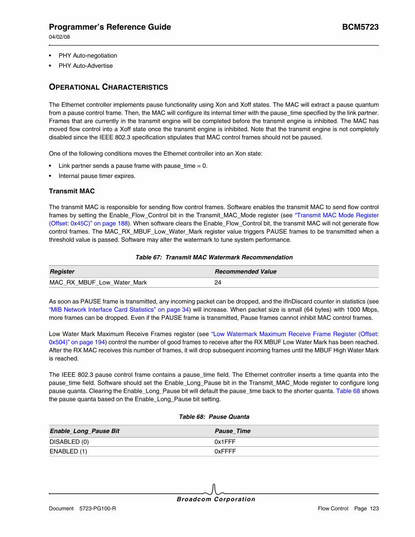
Programmer’s Reference Guide BCM572304/02/08
Broadcom CorporationDocument 5723-PG100-R Flow Control Page 123
• PHY Auto-negotiation
• PHY Auto-Advertise
OPERATIONAL CHARACTERISTICS
The Ethernet controller implements pause functionality using Xon and Xoff states. The MAC will extract a pause quantum from a pause control frame. Then, the MAC will configure its internal timer with the pause_time specified by the link partner. Frames that are currently in the transmit engine will be completed before the transmit engine is inhibited. The MAC has moved flow control into a Xoff state once the transmit engine is inhibited. Note that the transmit engine is not completely disabled since the IEEE 802.3 specification stipulates that MAC control frames should not be paused.
One of the following conditions moves the Ethernet controller into an Xon state:
• Link partner sends a pause frame with pause_time = 0.
• Internal pause timer expires.
Transmit MAC
The transmit MAC is responsible for sending flow control frames. Software enables the transmit MAC to send flow control frames by setting the Enable_Flow_Control bit in the Transmit_MAC_Mode register (see “Transmit MAC Mode Register (Offset: 0x45C)” on page 188). When software clears the Enable_Flow_Control bit, the transmit MAC will not generate flow control frames. The MAC_RX_MBUF_Low_Water_Mark register value triggers PAUSE frames to be transmitted when a threshold value is passed. Software may alter the watermark to tune system performance.
As soon as PAUSE frame is transmitted, any incoming packet can be dropped, and the ifInDiscard counter in statistics (see “MIB Network Interface Card Statistics” on page 34) will increase. When packet size is small (64 bytes) with 1000 Mbps, more frames can be dropped. Even if the PAUSE frame is transmitted, Pause frames cannot inhibit MAC control frames.
Low Water Mark Maximum Receive Frames register (see “Low Watermark Maximum Receive Frame Register (Offset: 0x504)” on page 194) control the number of good frames to receive after the RX MBUF Low Water Mark has been reached. After the RX MAC receives this number of frames, it will drop subsequent incoming frames until the MBUF High Water Mark is reached.
The IEEE 802.3 pause control frame contains a pause_time field. The Ethernet controller inserts a time quanta into the pause_time field. Software should set the Enable_Long_Pause bit in the Transmit_MAC_Mode register to configure long pause quanta. Clearing the Enable_Long_Pause bit will default the pause_time back to the shorter quanta. Table 68 shows the pause quanta based on the Enable_Long_Pause bit setting.
Table 67: Transmit MAC Watermark Recommendation
Register Recommended Value
MAC_RX_MBUF_Low_Water_Mark 24
Table 68: Pause Quanta
Enable_Long_Pause Bit Pause_Time
DISABLED (0) 0x1FFF
ENABLED (1) 0xFFFF
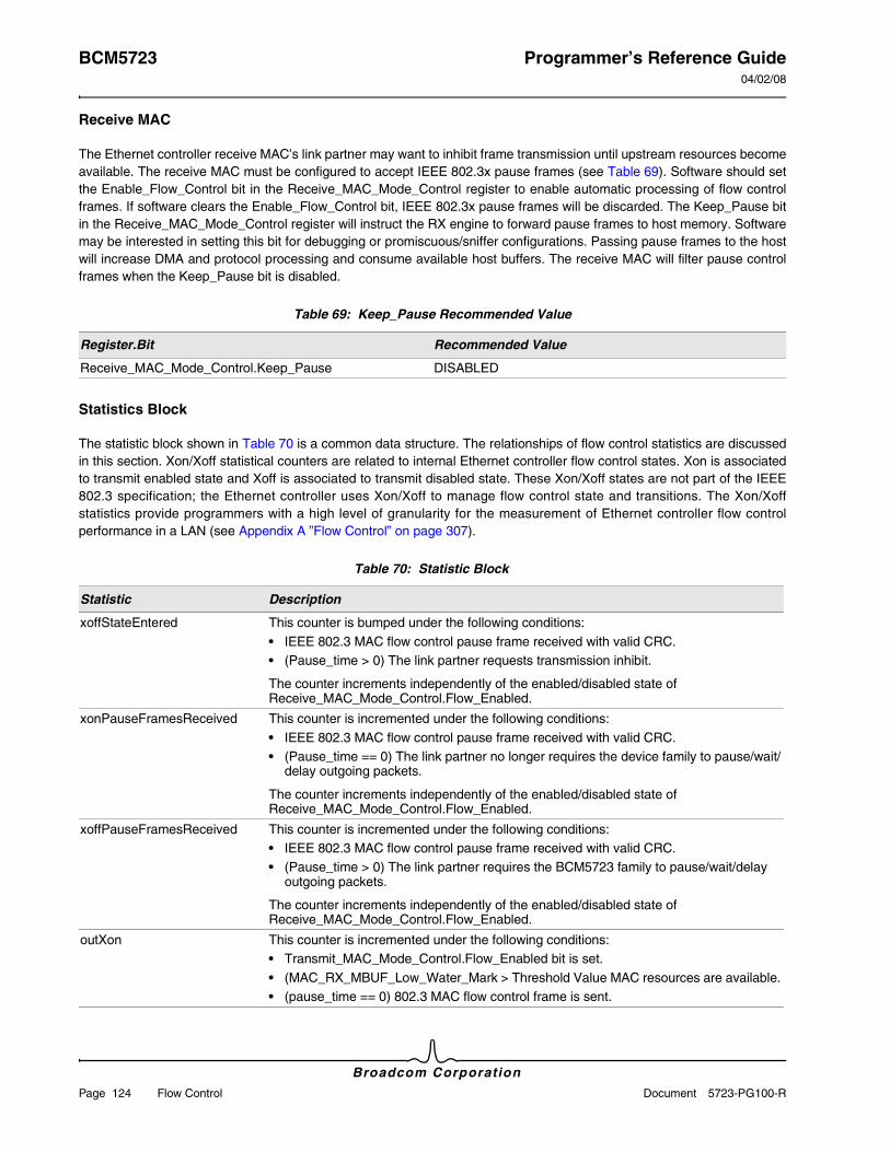
BCM5723 Programmer’s Reference Guide04/02/08
Broadcom Corporation
Page 124 Flow Control Document 5723-PG100-R
Receive MAC
The Ethernet controller receive MAC’s link partner may want to inhibit frame transmission until upstream resources become available. The receive MAC must be configured to accept IEEE 802.3x pause frames (see Table 69). Software should set the Enable_Flow_Control bit in the Receive_MAC_Mode_Control register to enable automatic processing of flow control frames. If software clears the Enable_Flow_Control bit, IEEE 802.3x pause frames will be discarded. The Keep_Pause bit in the Receive_MAC_Mode_Control register will instruct the RX engine to forward pause frames to host memory. Software may be interested in setting this bit for debugging or promiscuous/sniffer configurations. Passing pause frames to the host will increase DMA and protocol processing and consume available host buffers. The receive MAC will filter pause control frames when the Keep_Pause bit is disabled.
Statistics Block
The statistic block shown in Table 70 is a common data structure. The relationships of flow control statistics are discussed in this section. Xon/Xoff statistical counters are related to internal Ethernet controller flow control states. Xon is associated to transmit enabled state and Xoff is associated to transmit disabled state. These Xon/Xoff states are not part of the IEEE 802.3 specification; the Ethernet controller uses Xon/Xoff to manage flow control state and transitions. The Xon/Xoff statistics provide programmers with a high level of granularity for the measurement of Ethernet controller flow control performance in a LAN (see Appendix A ”Flow Control” on page 307).
Table 69: Keep_Pause Recommended Value
Register.Bit Recommended Value
Receive_MAC_Mode_Control.Keep_Pause DISABLED
Table 70: Statistic Block
Statistic Description
xoffStateEntered This counter is bumped under the following conditions:• IEEE 802.3 MAC flow control pause frame received with valid CRC.• (Pause_time > 0) The link partner requests transmission inhibit.
The counter increments independently of the enabled/disabled state of Receive_MAC_Mode_Control.Flow_Enabled.
xonPauseFramesReceived This counter is incremented under the following conditions:• IEEE 802.3 MAC flow control pause frame received with valid CRC.• (Pause_time == 0) The link partner no longer requires the device family to pause/wait/
delay outgoing packets.
The counter increments independently of the enabled/disabled state of Receive_MAC_Mode_Control.Flow_Enabled.
xoffPauseFramesReceived This counter is incremented under the following conditions:• IEEE 802.3 MAC flow control pause frame received with valid CRC.• (Pause_time > 0) The link partner requires the BCM5723 family to pause/wait/delay
outgoing packets.
The counter increments independently of the enabled/disabled state of Receive_MAC_Mode_Control.Flow_Enabled.
outXon This counter is incremented under the following conditions:• Transmit_MAC_Mode_Control.Flow_Enabled bit is set.• (MAC_RX_MBUF_Low_Water_Mark > Threshold Value MAC resources are available.• (pause_time == 0) 802.3 MAC flow control frame is sent.
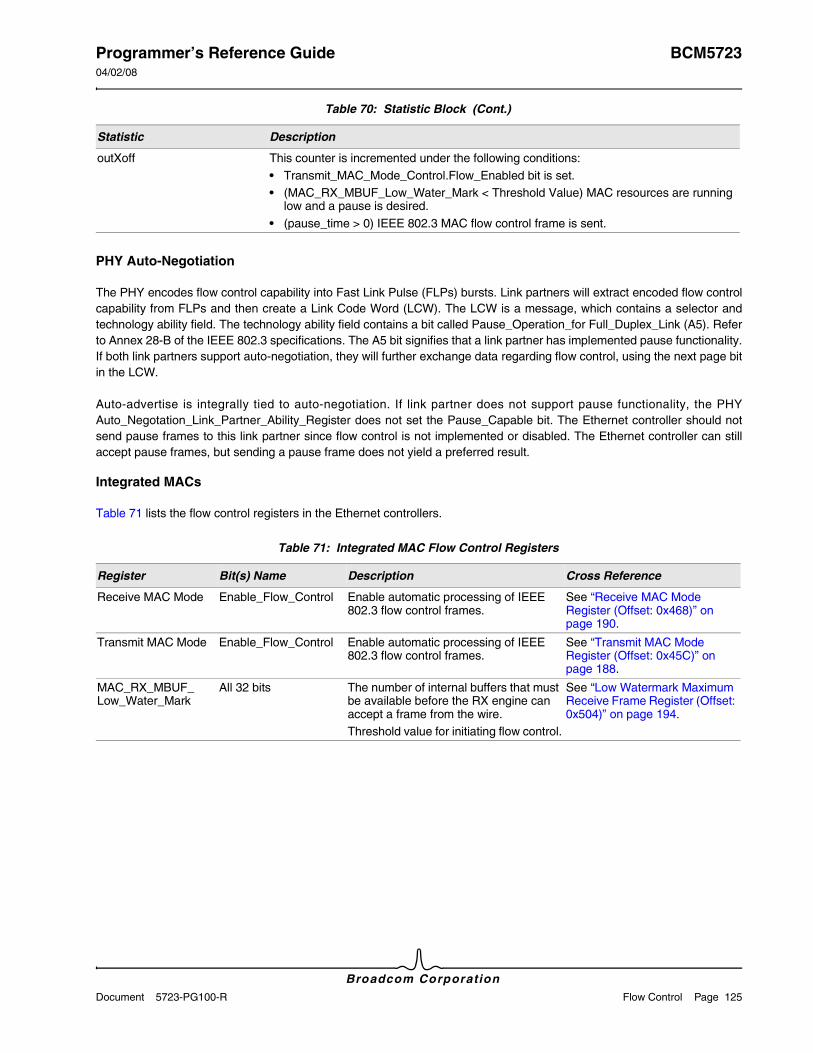
Programmer’s Reference Guide BCM572304/02/08
Broadcom CorporationDocument 5723-PG100-R Flow Control Page 125
PHY Auto-Negotiation
The PHY encodes flow control capability into Fast Link Pulse (FLPs) bursts. Link partners will extract encoded flow control capability from FLPs and then create a Link Code Word (LCW). The LCW is a message, which contains a selector and technology ability field. The technology ability field contains a bit called Pause_Operation_for Full_Duplex_Link (A5). Refer to Annex 28-B of the IEEE 802.3 specifications. The A5 bit signifies that a link partner has implemented pause functionality. If both link partners support auto-negotiation, they will further exchange data regarding flow control, using the next page bit in the LCW.
Auto-advertise is integrally tied to auto-negotiation. If link partner does not support pause functionality, the PHY Auto_Negotation_Link_Partner_Ability_Register does not set the Pause_Capable bit. The Ethernet controller should not send pause frames to this link partner since flow control is not implemented or disabled. The Ethernet controller can still accept pause frames, but sending a pause frame does not yield a preferred result.
Integrated MACs
Table 71 lists the flow control registers in the Ethernet controllers.
outXoff This counter is incremented under the following conditions:• Transmit_MAC_Mode_Control.Flow_Enabled bit is set.• (MAC_RX_MBUF_Low_Water_Mark < Threshold Value) MAC resources are running
low and a pause is desired.• (pause_time > 0) IEEE 802.3 MAC flow control frame is sent.
Table 71: Integrated MAC Flow Control Registers
Register Bit(s) Name Description Cross Reference
Receive MAC Mode Enable_Flow_Control Enable automatic processing of IEEE 802.3 flow control frames.
See “Receive MAC Mode Register (Offset: 0x468)” on page 190.
Transmit MAC Mode Enable_Flow_Control Enable automatic processing of IEEE 802.3 flow control frames.
See “Transmit MAC Mode Register (Offset: 0x45C)” on page 188.
MAC_RX_MBUF_ Low_Water_Mark
All 32 bits The number of internal buffers that must be available before the RX engine can accept a frame from the wire.Threshold value for initiating flow control.
See “Low Watermark Maximum Receive Frame Register (Offset: 0x504)” on page 194.
Table 70: Statistic Block (Cont.)
Statistic Description
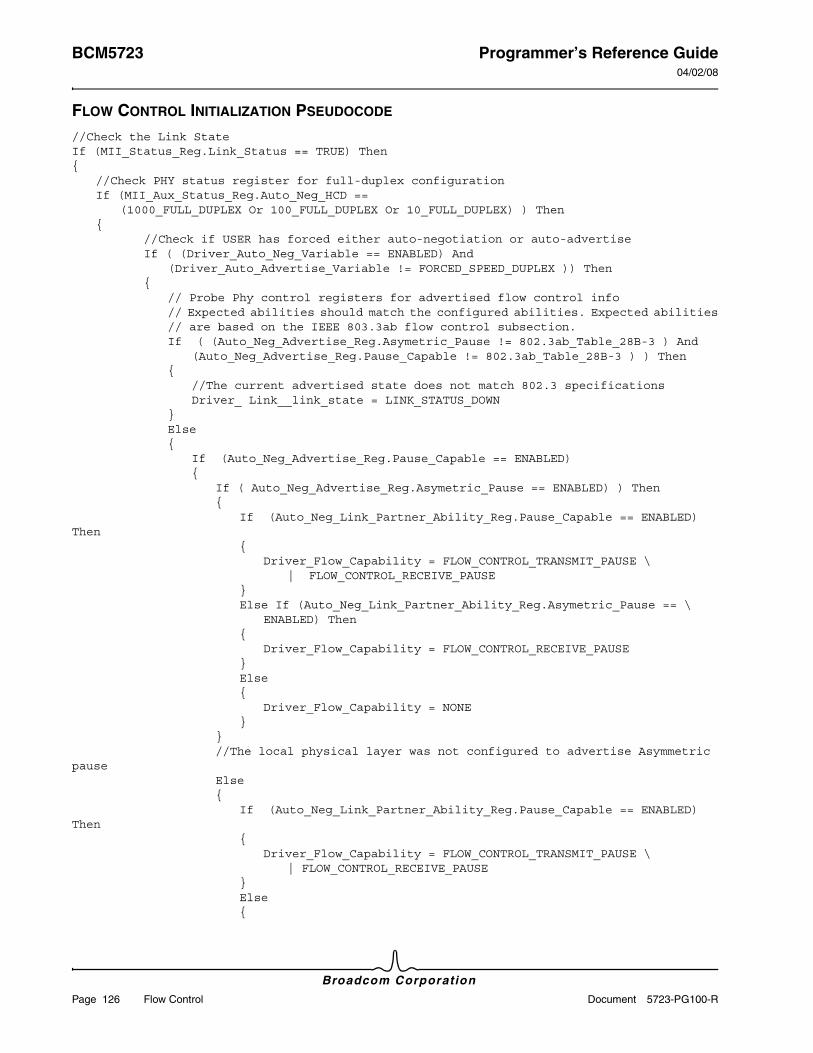
BCM5723 Programmer’s Reference Guide04/02/08
Broadcom Corporation
Page 126 Flow Control Document 5723-PG100-R
FLOW CONTROL INITIALIZATION PSEUDOCODE
//Check the Link StateIf (MII_Status_Reg.Link_Status == TRUE) Then {
//Check PHY status register for full-duplex configurationIf (MII_Aux_Status_Reg.Auto_Neg_HCD ==
(1000_FULL_DUPLEX Or 100_FULL_DUPLEX Or 10_FULL_DUPLEX) ) Then{
//Check if USER has forced either auto-negotiation or auto-advertiseIf ( (Driver_Auto_Neg_Variable == ENABLED) And
(Driver_Auto_Advertise_Variable != FORCED_SPEED_DUPLEX )) Then{
// Probe Phy control registers for advertised flow control info// Expected abilities should match the configured abilities. Expected abilities// are based on the IEEE 803.3ab flow control subsection.If ( (Auto_Neg_Advertise_Reg.Asymetric_Pause != 802.3ab_Table_28B-3 ) And
(Auto_Neg_Advertise_Reg.Pause_Capable != 802.3ab_Table_28B-3 ) ) Then{
//The current advertised state does not match 802.3 specificationsDriver_ Link__link_state = LINK_STATUS_DOWN
}Else {
If (Auto_Neg_Advertise_Reg.Pause_Capable == ENABLED) {
If ( Auto_Neg_Advertise_Reg.Asymetric_Pause == ENABLED) ) Then{
If (Auto_Neg_Link_Partner_Ability_Reg.Pause_Capable == ENABLED) Then
{Driver_Flow_Capability = FLOW_CONTROL_TRANSMIT_PAUSE \
| FLOW_CONTROL_RECEIVE_PAUSE}Else If (Auto_Neg_Link_Partner_Ability_Reg.Asymetric_Pause == \
ENABLED) Then{
Driver_Flow_Capability = FLOW_CONTROL_RECEIVE_PAUSE}Else{
Driver_Flow_Capability = NONE}
}//The local physical layer was not configured to advertise Asymmetric
pauseElse{
If (Auto_Neg_Link_Partner_Ability_Reg.Pause_Capable == ENABLED) Then
{Driver_Flow_Capability = FLOW_CONTROL_TRANSMIT_PAUSE \
| FLOW_CONTROL_RECEIVE_PAUSE}Else{
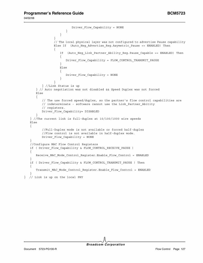
Programmer’s Reference Guide BCM572304/02/08
Broadcom CorporationDocument 5723-PG100-R Flow Control Page 127
Driver_Flow_Capability = NONE}
}}// The local physical layer was not configured to advertise Pause capabilityElse If (Auto_Neg_Advertise_Reg.Asymetric_Pause == ENABLED) Then{
If (Auto_Neg_Link_Partner_Ability_Reg.Pause_Capable == ENABLED) Then{
Driver_Flow_Capability = FLOW_CONTROL_TRANSMIT_PAUSE }Else{
Driver_Flow_Capability = NONE}
} } //Link Status is up
} // Auto negotiation was not disabled && Speed Duplex was not forcedElse{
// The use forced speed/duplex, so the partner's flow control capabilities are// indeterminate - software cannot use the Link_Partner_Abitity// registers. Driver_Flow_Capability= DISABLED
}} //The current link is full-duplex at 10/100/1000 wire speedsElse{
//Full-Duplex mode is not available or forced half-duplex//Flow control is not available in half-duplex mode.Driver_Flow_Capability = NONE
}//Configure MAC Flow Control Registersif ( Driver_Flow_Capability & FLOW_CONTROL_RECEIVE_PAUSE ){
Receive_MAC_Mode_Control_Register.Enable_Flow_Control = ENABLED }if ( Driver_Flow_Capability & FLOW_CONTROL_TRANSMIT_PAUSE ) Then{
Transmit_MAC_Mode_Control_Register.Enable_Flow_Control = ENABLED}
} // Link is up on the local PHY
BCM5723 Programmer’s Reference Guide04/02/08
Broadcom Corporation
Page 128 Interrupt Processing Document 5723-PG100-R
Section 10: Interrupt Processing
HOST COALESCING
Interrupt coalescing (or interrupt moderation) is a common technique used by NIC vendors to increase the performance of NICs. High-level descriptions of the benefits of interrupt coalescing can be found at:
• http://www.microsoft.com/HWDEV/devdes/optinic.htm
• http://support.microsoft.com/support/kb/articles/Q170/6/43.ASP
• http://msdn.microsoft.com/library/books/serverdg/networkadapterrequirements.htm
DESCRIPTION
The Ethernet controller supports the concept of host coalescing. Host coalescing controls when status information is returned to the host, and when interrupts are generated. The Ethernet controller provides a number of SW configurable registers that control when/how it updates the host with status information and how often it asserts an interrupt.
When the Ethernet controller has completed transmit or receive events, it updates a Status block in host memory. This status block contains information that tells the host which transmit buffers have been DMAed by the NIC, and which receive Buffer Descriptors (BDs) have been consumed by a newly arrived received packet. Normally, the host will check this status block whenever an interrupt is generated. In addition, the host could also poll the status block to determine whether or not it had been updated by the hardware since the last time the host had read the status block (this is called during interrupt processing).
Whenever the NIC updates the status block, it will make a decision about whether to assert the interrupt line (INTA) or not. The Ethernet controller has special interrupt avoidance mechanisms that allow the host to tell the NIC not to generate an interrupt when it writes a status block back to the host. In addition, there are also mechanisms that allow host SW to control when and how often the status block is updated.
Example: The host could configure the NIC to only update status block after it receives two packets, as opposed to one packet. These mechanisms are documented in more detail to follow.
OPERATIONAL CHARACTERISTICS
The Ethernet controller DMAs the status block to host memory before a line interrupt or MSI is generated. The host ISR reads the update bit at the top of the status block and checks whether this bit is set to 1 or not. When set to 1, the updated bit of status block indicates the host that the status block has been refreshed by the MAC. The ISR must then write to clear/de-assert this bit to dirty the status block, and then the ISR may proceed to read the updated producer/consumer index pointers. This mechanism allows host system software to determine if the status block has been updated. Due to various asynchronous timing issues (dependent upon platform) the ISR may occasionally see stale data. The ISR may either spin and wait for the status block DMA to complete and explicitly flush the status block or just wait for the next line interrupt.
Programmer’s Reference Guide BCM572304/02/08
Broadcom CorporationDocument 5723-PG100-R Host Coalescing Page 129
REGISTERS
The Ethernet controller supports a variety of registers that affect status block updates and interrupt generation (see Table 72).
Table 72: Interrupt-Related Registers
Register Cross Reference
Miscellaneous Host Control register.The two bits of this register that are related to interrupts are:• Mask PCI Interrupt Output (aka Mask Interrupt) bit• Clear Interrupt INTA bit
“Miscellaneous Host Control Register (Offset: 0x68)” on page 148.
Miscellaneous Local Control register.The two bits of this register that are related to interrupts are:• Set Interrupt bit• Clear Interrupt bit
“Miscellaneous Local Control Register (Offset: 0x6808)” on page 278.
Interrupt Mailbox 0 register “Interrupt Mailbox 0 (High Priority Mailbox) Register (Offset: 0x200–207)” on page 178 for host standard and flat modes and “Interrupt Mailbox 0 Register (Offset: 0x5800)” on page 270 for indirect mode.
Receive Coalescing Ticks register “Receive Coalescing Ticks Register (Offset: 0x3C08)” on page 253.
Send Coalescing Ticks register “Send Max Coalesced BD Count Register (Offset: 0x3C14)” on page 254.
Receive Max Coalesced BD Count register “Receive Max Coalesced BD Count Register (Offset: 0x3C10)” on page 253.
Send Max Coalesced BD Count register “Send Max Coalesced BD Count Register (Offset: 0x3C14)” on page 254.
Receive Max Coalesced BD Count During Interrupt register “Receive Max Coalesced BD Count Register (Offset: 0x3C10)” on page 253.
Send Max Coalesced BD Count During Interrupt register “Send Max Coalesced BD Count Register (Offset: 0x3C14)” on page 254.
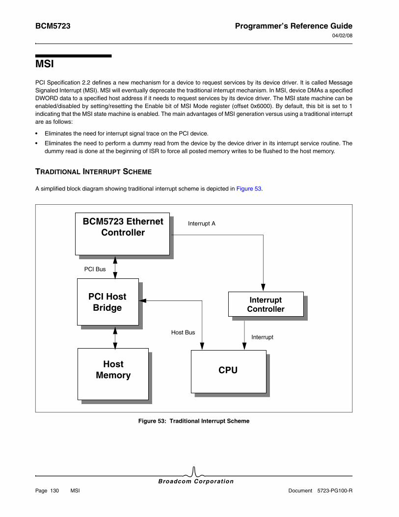
BCM5723 Programmer’s Reference Guide04/02/08
Broadcom Corporation
Page 130 MSI Document 5723-PG100-R
MSI
PCI Specification 2.2 defines a new mechanism for a device to request services by its device driver. It is called Message Signaled Interrupt (MSI). MSI will eventually deprecate the traditional interrupt mechanism. In MSI, device DMAs a specified DWORD data to a specified host address if it needs to request services by its device driver. The MSI state machine can be enabled/disabled by setting/resetting the Enable bit of MSI Mode register (offset 0x6000). By default, this bit is set to 1 indicating that the MSI state machine is enabled. The main advantages of MSI generation versus using a traditional interrupt are as follows:
• Eliminates the need for interrupt signal trace on the PCI device.
• Eliminates the need to perform a dummy read from the device by the device driver in its interrupt service routine. The dummy read is done at the beginning of ISR to force all posted memory writes to be flushed to the host memory.
TRADITIONAL INTERRUPT SCHEME
A simplified block diagram showing traditional interrupt scheme is depicted in Figure 53.
Figure 53: Traditional Interrupt Scheme
BCM5700
PCI Host Bridge
HostMemory CPU
Interrupt
Interrupt A
PCI Bus
Host Bus
BCM5723 Ethernet Controller
PCI Host Bridge
Host Memory CPU
Interrupt Controller
Interrupt Controller
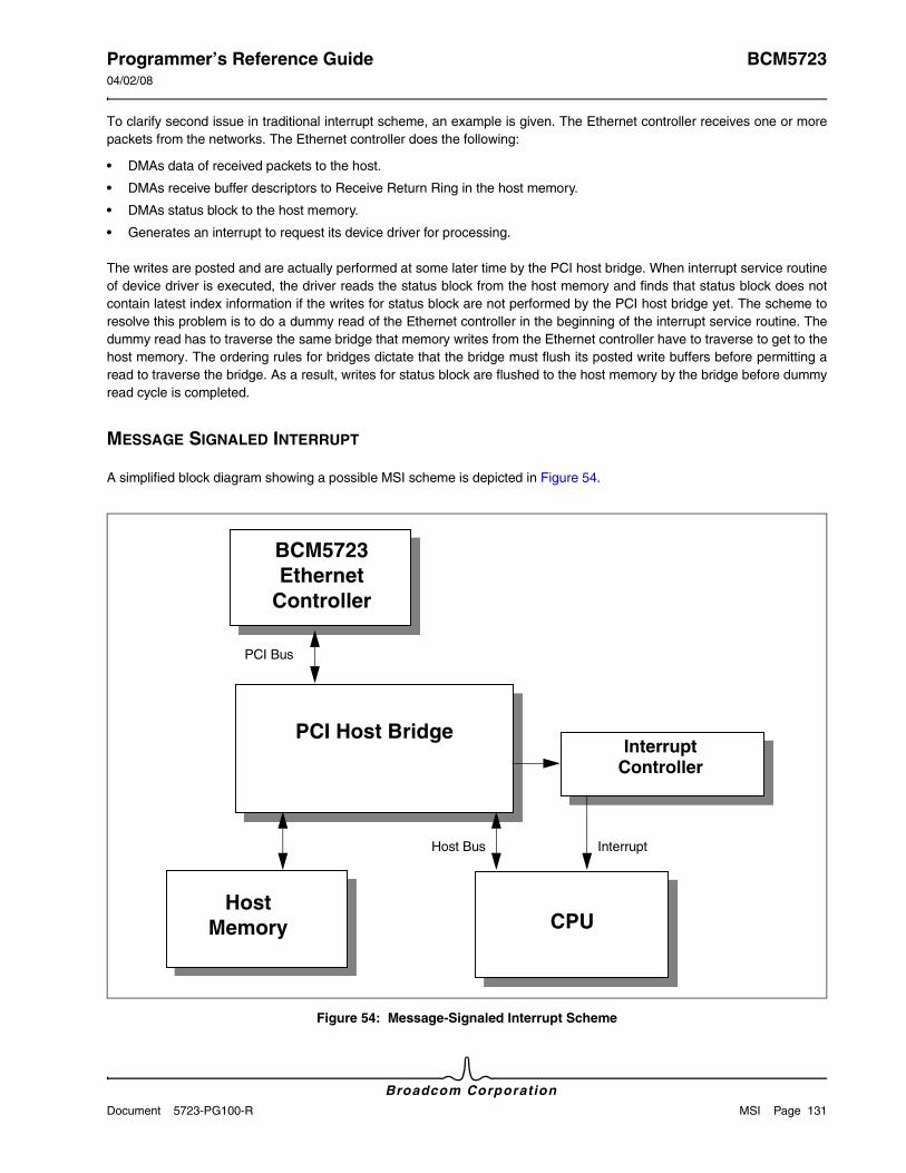
Programmer’s Reference Guide BCM572304/02/08
Broadcom CorporationDocument 5723-PG100-R MSI Page 131
To clarify second issue in traditional interrupt scheme, an example is given. The Ethernet controller receives one or more packets from the networks. The Ethernet controller does the following:
• DMAs data of received packets to the host.
• DMAs receive buffer descriptors to Receive Return Ring in the host memory.
• DMAs status block to the host memory.
• Generates an interrupt to request its device driver for processing.
The writes are posted and are actually performed at some later time by the PCI host bridge. When interrupt service routine of device driver is executed, the driver reads the status block from the host memory and finds that status block does not contain latest index information if the writes for status block are not performed by the PCI host bridge yet. The scheme to resolve this problem is to do a dummy read of the Ethernet controller in the beginning of the interrupt service routine. The dummy read has to traverse the same bridge that memory writes from the Ethernet controller have to traverse to get to the host memory. The ordering rules for bridges dictate that the bridge must flush its posted write buffers before permitting a read to traverse the bridge. As a result, writes for status block are flushed to the host memory by the bridge before dummy read cycle is completed.
MESSAGE SIGNALED INTERRUPT
A simplified block diagram showing a possible MSI scheme is depicted in Figure 54.
Figure 54: Message-Signaled Interrupt Scheme
BCM5700
PCI Host Bridge
Host Memory CPU
Interrupt Controller
PCI Bus
Host Bus Interrupt
BCM5723 Ethernet
Controller
PCI Host Bridge
Host Memory CPU
Interrupt Controller
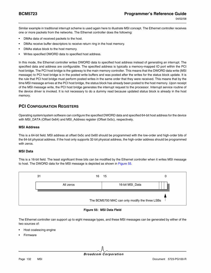
BCM5723 Programmer’s Reference Guide04/02/08
Broadcom Corporation
Page 132 MSI Document 5723-PG100-R
Similar example in traditional interrupt scheme is used again here to illustrate MSI concept. The Ethernet controller receives one or more packets from the networks. The Ethernet controller does the following:
• DMAs data of received packets to the host.
• DMAs receive buffer descriptors to receive return ring in the host memory.
• DMAs status block to the host memory.
• Writes specified DWORD data to specified host address.
In this mode, the Ethernet controller writes DWORD data to specified host address instead of generating an interrupt. The specified data and address are configurable. The specified address is typically a memory-mapped IO port within the PCI host bridge. The PCI host bridge is the gateway to the main memory controller. This means that the DWORD data write (MSI message) to PCI host bridge is in the posted write buffers and was posted after the writes for the status block update. It is the rule that PCI host bridge must perform posted writes in the same order that they were received. This means that by the time MSI message arrives at the PCI host bridge, the status block has already been posted to the host memory. Upon receipt of the MSI message write, the PCI host bridge generates the interrupt request to the processor. Interrupt service routine of the device driver is invoked. It is not necessary to do a dummy read because updated status block is already in the host memory.
PCI CONFIGURATION REGISTERS
Operating system/system software can configure the specified DWORD data and specified 64-bit host address for the device with MSI_DATA (Offset 0x64) and MSI_Address register (Offset 0x5c), respectively.
MSI Address
This is a 64-bit field. MSI address at offset 0x5c and 0x60 should be programmed with the low-order and high-order bits of the 64-bit physical address. If the host only supports 32-bit physical address, the high-order address should be programmed with zeros.
MSI Data
This is a 16-bit field. The least significant three bits can be modified by the Ethernet controller when it writes MSI message to host. The DWORD data for the MSI message is depicted as shown in Figure 55.
Figure 55: MSI Data FIeld
The Ethernet controller can support up to eight message types, and these MSI messages can be generated by either of the two sources of:
• Host coalescing engine
• Firmware
All 0’s 16-bit MSI_Data
31 16 15 0
The BCM5700 MAC can only modify the three LSBs
All zeros 16-bit MSI_Data
Programmer’s Reference Guide BCM572304/02/08
Broadcom CorporationDocument 5723-PG100-R MSI Page 133
HOST COALESCING ENGINE
After the host coalescing engine updates the status block on the host (due to receive indication, transmit completion, and so on), it either generates an interrupt or writes a MSI message if MSI is enabled. The least significant 3-bits of the MSI message originating from host coalescing block is configurable and can be configured by programming bits 4, 5, and 6 of the Host_Coalesing_Mode register. The default of these bits is zeros.
FIRMWARE
The Ethernet controller provides a way for firmware executed by RX RISC to generate MSI messages. Firmware can generate MSI messages by using MSI_FIFO_Access register (Offset 0x6008). For example, if firmware wants to generate an MSI message with least significant 3-bit as 0x2, it will write 2 to MSI_FIFO_Access register. It also needs to verify that the MSI message is written successfully by reading back MSI_FIFO_Access Overflow. If this bit is zero, then the MSI message is encoded successfully and will be sent to HOST. Otherwise, the message is not encoded.
Note: Without any special firmware supporting multiple MSIs, the device can generate only 1 MSI message even though the device requests for 8 MSI messages through Multiple Message Capable field (bits 3:1) of Message Control register (offset 0x5A). The least significant 3-bits of the MSI message generated by the device are always taken from bits 6:4 of Host_Coalesing_Mode register (offset 0x3C00).
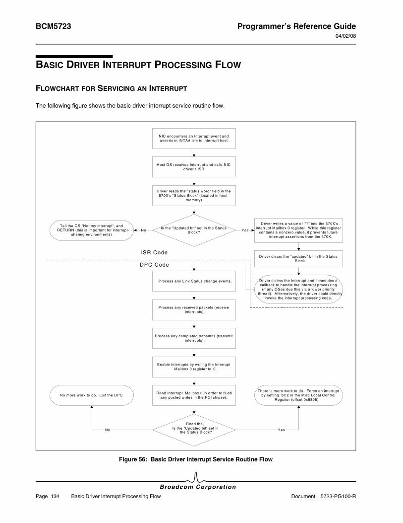
BCM5723 Programmer’s Reference Guide04/02/08
Broadcom Corporation
Page 134 Basic Driver Interrupt Processing Flow Document 5723-PG100-R
BASIC DRIVER INTERRUPT PROCESSING FLOW
FLOWCHART FOR SERVICING AN INTERRUPT
The following figure shows the basic driver interrupt service routine flow.
Figure 56: Basic Driver Interrupt Service Routine Flow
Is the "Updated bit" set in the StatusBlock?
Driver reads the "status word" field in the570X's "Status Block" (located in host
memory)
No Yes
NIC encounters an Interrupt event andasserts in INTA# line to interrupt host
Host OS receives Interrupt and calls NICdriver's ISR
Tell the OS "Not my interrupt", andRETURN (this is important for interrupt-
sharing environments)
Driver claims the Interrupt and schedules acallback to handle the interrupt processing
(many OSes due this via a lower prioritythread). Allternatively, the driver could directly
invoke the interrupt processing code.
Driver writes a value of '"1" into the 570X'sInterrupt Mailbox 0 register. W hile this register
contains a nonzero value, it prevents futureinterrupt assertions from the 570X.
Driver clears the "updated" bit in the StatusBlock.
Process any Link Status change events.
Process any received packets (receiveinterrupts).
Process any completed transmits (transmitinterrupts).
Read the, Is the "Updated bit" set in
the Status Block?No Yes
Read Interrupt Mailbox 0 in order to flushany posted writes in the PCI chipset.
Enable Interrupts by writing the InterruptMailbox 0 register to '0'.
No more work to do. Exit the DPCThere is more work to do. Force an interrupt
by setting bit 2 in the Misc Local ControlRegsiter (offset 0x6808)
DPC Code
ISR Code
Programmer’s Reference Guide BCM572304/02/08
Broadcom CorporationDocument 5723-PG100-R Basic Driver Interrupt Processing Flow Page 135
INTERRUPT PROCEDURE
1. Acknowledge interrupt. Write a nonzero value (i.e., value = 1) to the interrupt mailbox 0 (see “Interrupt Mailbox 0 (High Priority Mailbox) Register (Offset: 0x200–207)” on page 178 for host standard and flat modes and “Interrupt Mailbox 0 Register (Offset: 0x5800)” on page 270 for indirect mode) to indicate that the driver is currently processing the interrupt. This step disables device interrupts except during interrupt feature.
2. Read and save the value of the Status Tag field of the Status Block (see “Status Block” on page 32).
3. Claim interrupt. Determine if the Ethernet controller action is required. Read the Updated bit of the status word (see Table 20 on page 35). If the Updated bit is asserted, then the host coalescing engine has updated the status block.
4. Clear the Updated bit of the status word (see Table 20 on page 35). This indicates that the host driver either has or will touch the status block. If a during interrupt event is driven, the host driver can examine the Updated bit to determine if a fresh status block has been moved to host memory space.
5. Check for RX traffic.
• Loop through enabled RX Return Rings (1 to 16).
• Check for difference between RX Return Ring Producer index (Status block) and RX Return Ring Consumer index (value written to mailbox on previous call) are the number of frames to process for RX Return Ring.
• Process the packet.
• Update the RX Return Ring consumer pointer in each mailbox for new RX frames.
6. Check for TX completes.
• Loop through enabled TX Send Rings.
• Check for difference between previous consumer index (software kept) and current consumer index in the status block. These are the TX BDs which can be made available to next send operation.
• Update the previous consumer index (i.e., next call) to the value of the status block consumer index.
7. Compare the current value of the Status Tag to the saved value of the Status Tag. Flush status block (i.e., force update of status blocks cached by PCI bridge).
• Read interrupt mailbox (see “Interrupt Mailbox 0 (High Priority Mailbox) Register (Offset: 0x200–207)” on page 178for host standard and flat modes and “Interrupt Mailbox 0 Register (Offset: 0x5800)” on page 270 for indirect mode).
• Check the Updated bit in the status word (see Table 20 on page 35) located in the status block. If the Updated bit is asserted, then new data has been DMAed to the host. Repeat steps 5 and 6.
8. Check the Error bit in status word (optional, see Table 20 on page 35). The driver may check the state machine/FTQ status registers for various attentions.
9. Enable interrupts. When Status Tagged Status Mode bit of the Miscellaneous Host Control register (see “Miscellaneous Host Control Register (Offset: 0x68)” on page 148) is set to 1, then write the saved Status Tag to the upper 8 bits of Interrupt Mailbox 0, and 0 to the remaining bits (23 down to 0) to indicate that the ISR is done processing RX/TX. Otherwise, write 0 to Interrupt Mailbox 0 register. This step also clears existing interrupts.
BCM5723 Programmer’s Reference Guide04/02/08
Broadcom Corporation
Page 136 Other Configuration Controls Document 5723-PG100-R
OTHER CONFIGURATION CONTROLS
BROADCOM MASK MODE
Enabled by setting the Mask_Interrupt_Mode bit (bit 8) of the Miscellaneous Host Control register (see “Miscellaneous Host Control Register (Offset: 0x68)” on page 148). When enabled, setting the mask bit of the Miscellaneous Host Control register will mask (de-assert) the INTA signal at the pin, but it will not clear the interrupt state and it will not latch the INTA value. Clearing the mask bit will enable the interrupt state to propagate to the INTA signal. Note that the During Interrupt Coalescence registers are only used when the Mailbox 0 is set.
BROADCOM TAGGED STATUS MODE
Enabled by setting the Status Tagged Status Mode bit of the Miscellaneous Host Control register (see “Miscellaneous Host Control Register (Offset: 0x68)” on page 148). When enabled, a unique eight-bit tag value will be inserted into the Status Block Status Tag at location 7:0. The Status Tag can be returned to the Mailbox 0 register at location 31:24 by the host driver. When the Mailbox 0 register field 23:0 is written with a zero value, the tag field of the Mailbox 0 register is compared with the tag field of the last Status Block to be DMAed to the host. If the tag returned is not equivalent to the tag of the first Status Block DMAed, the interrupt status is entered.
CLEAR TICKS ON BD EVENTS MODE
Enabled by setting the Clear Ticks Mode on RX or the Clear Ticks Mode on TX bits of the Host Coalescing Mode register (see “Miscellaneous Host Control Register (Offset: 0x68)” on page 148). When enabled, the counters initialize to the idle state and begin counting only after a receive or transmit BD event is detected.
NO INTERRUPT ON FORCE UPDATE
Enabled by setting the No Interrupt on Force bit of the Host Coalescing Mode register (see “Host Coalescing Status Register (Offset: 0x3C04)” on page 252). When enabled, writing the Force update bit of the Host Coalescing Mode register will cause a status block update without a corresponding interrupt event.
NO INTERRUPT ON DMAD FORCE
Enabled by setting the No Interrupt on DMAD force bit of the Host Coalescing Mode register (see “Host Coalescing Status Register (Offset: 0x3C04)” on page 252). When enabled, the BD_FLAG_COAL_NOW bit of the buffer descriptor may be set to force a status block update without a corresponding interrupt.
Programmer’s Reference Guide BCM572304/02/08
Broadcom CorporationDocument 5723-PG100-R Ethernet Controller Register Definitions Page 137
Section 11: Ethernet Controller Register Definitions
PCI CONFIGURATION REGISTERS
REGISTER ACCESS LEGEND
The following describes the registers which are required by PCI Express specifications for configuration. The primary reset for these registers is PCIe Reset.
Note: Unless otherwise noted, all register specifications in this document apply to the BCM5784 controller.
Table 73: Register Access Legend
Item Description
R, RO Read Only
FW-RW Readable and Writeable by controller internal CPU only. Not accessible from host CPU.
W1 Write from PCI function #1
Host RW Readable and Writeable by host CPU only.
Host RO Read only by host CPU.
W2C Write to clear
RW2C Read and Write to Clear
RW1CS Read/Write 1 to clear and sticky (reset only by POR reset - perst_n cannot reset this bit)
RWS Read/Write Sticky
ROS Read Only Sticky
W0C Write ‘0’ to clear
W1 Write 1 but read will always return 0
NA Not Applicable
BCM5723 Programmer’s Reference Guide04/02/08
Broadcom Corporation
Page 138 PCI Configuration Registers Document 5723-PG100-R
DEVICE ID & VENDOR ID REGISTER (OFFSET: 0X00)
This register is reset by Hard Reset.
STATUS & COMMAND REGISTER (OFFSET: 0X04)
This register is reset by PCIe Reset.
Table 74: Device ID & Vendor ID Register (Offset: 0x00)
Name Bits Access Default Value Description
Device ID 31:16 FW-RWHost-RO
– Default for BCM5784 is 0x1698Default for BCM5764 is 0x1684
Vendor ID 15:0 FW-RWHost-RO
0x14E4
Table 75: Status & Command Register (Offset: 0x04)
Name Bits Access Default Value Description
Detected Parity Error 31 RW2C 0x0 Indicates a data parity error was detected even if parity reporting is not enabled.
Signaled System Error 30 RW2C 0x0 Indicates this device generated a system error. After sending an error_fatal or error_nonfatal message this bit gets set.
Received Master Abort 29 RW2C 0x0 Indicates this device was a bus master and transaction was terminated with a master abort
Received Target Abort 28 RW2C 0x0 Indicates this device was a bus master and received a target abort
Signaled Target Abort 27 RW2C 0x0 Indicates this device initiated a target-abort. This bit is only set if an external master disappears during a target operation
DEVSEL Timing 26:25 RO 0x0 N/A for PCIe device. Hardwired to 0x0
Master Data Parity Error 24 RW2C 0x0 Indicates that this device was a bus master when a parity error was detected and reporting of parity errors is enabled. This device is capable of operating with this bit set.
Fast Back-to-back capable 23 RO 0x0 Indicates whether fast back-to-back transactions can be accepted when transactions are not to the same agent
Reserved 22 RO 0x0
66-MHz Capable 21 RO 0x0 N/A for PCIe device. Hardwired to 0x
Capabilities List 20 RO 0x1 Indicates whether this device has a capabilities list. The device has a capabilities list, so this bit is hardwired to 1.
Interrupt Status 19 RO 0x0 Indicates this device generated an interrupt
Reserved 18:16 RO 0x0
Reserved 15:11 RO 0x00
Interrupt Disable 10 RW 0x0 Setting this bit 1 disables the device from generating interrupt on the PCIe bus. This bit does not affect the internal state of the interrupt request.
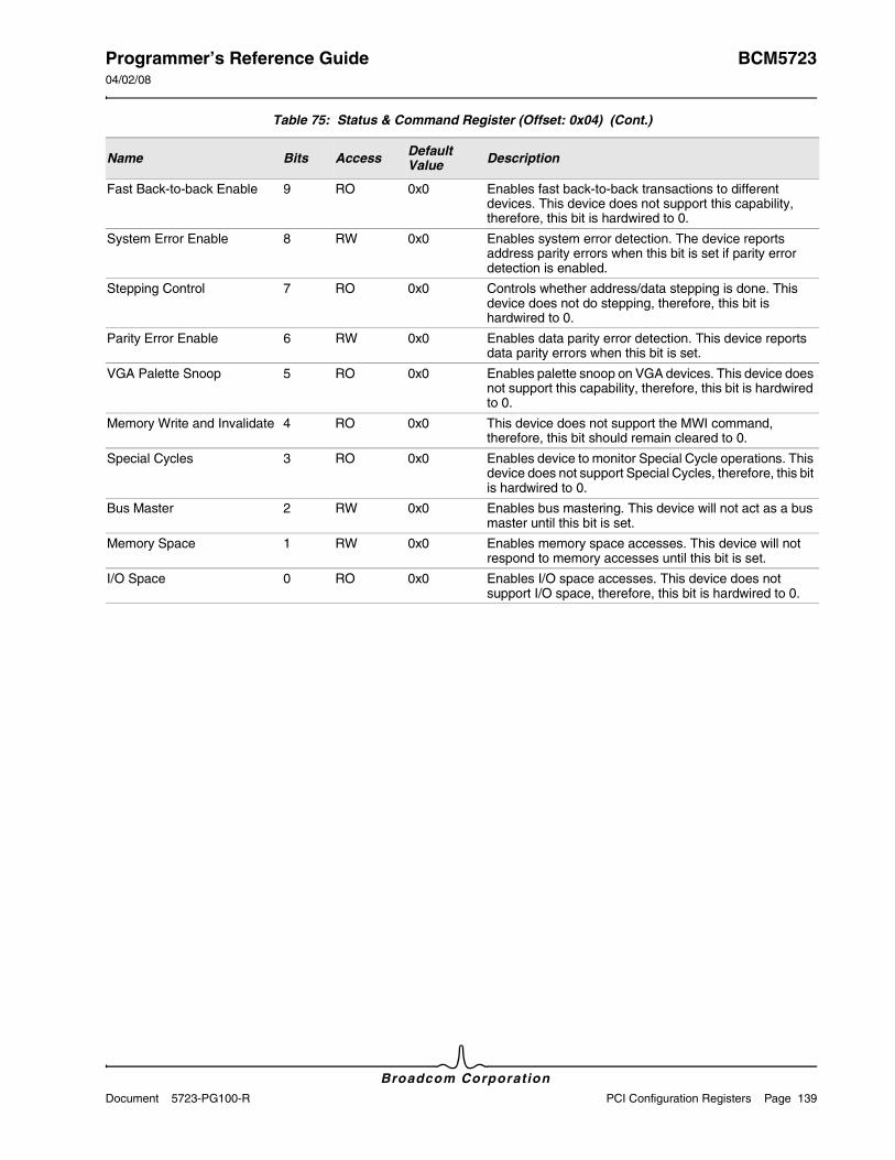
Programmer’s Reference Guide BCM572304/02/08
Broadcom CorporationDocument 5723-PG100-R PCI Configuration Registers Page 139
Fast Back-to-back Enable 9 RO 0x0 Enables fast back-to-back transactions to different devices. This device does not support this capability, therefore, this bit is hardwired to 0.
System Error Enable 8 RW 0x0 Enables system error detection. The device reports address parity errors when this bit is set if parity error detection is enabled.
Stepping Control 7 RO 0x0 Controls whether address/data stepping is done. This device does not do stepping, therefore, this bit is hardwired to 0.
Parity Error Enable 6 RW 0x0 Enables data parity error detection. This device reports data parity errors when this bit is set.
VGA Palette Snoop 5 RO 0x0 Enables palette snoop on VGA devices. This device does not support this capability, therefore, this bit is hardwired to 0.
Memory Write and Invalidate 4 RO 0x0 This device does not support the MWI command, therefore, this bit should remain cleared to 0.
Special Cycles 3 RO 0x0 Enables device to monitor Special Cycle operations. This device does not support Special Cycles, therefore, this bit is hardwired to 0.
Bus Master 2 RW 0x0 Enables bus mastering. This device will not act as a bus master until this bit is set.
Memory Space 1 RW 0x0 Enables memory space accesses. This device will not respond to memory accesses until this bit is set.
I/O Space 0 RO 0x0 Enables I/O space accesses. This device does not support I/O space, therefore, this bit is hardwired to 0.
Table 75: Status & Command Register (Offset: 0x04) (Cont.)
Name Bits Access Default Value Description
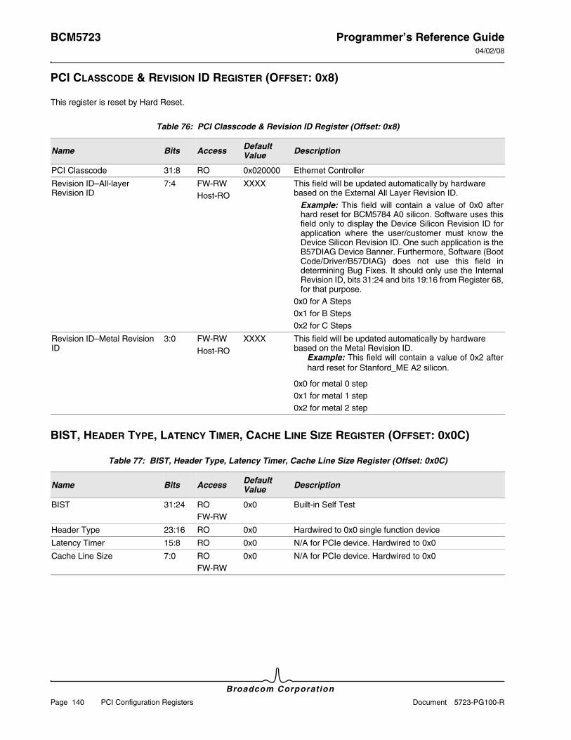
BCM5723 Programmer’s Reference Guide04/02/08
Broadcom Corporation
Page 140 PCI Configuration Registers Document 5723-PG100-R
PCI CLASSCODE & REVISION ID REGISTER (OFFSET: 0X8)
This register is reset by Hard Reset.
BIST, HEADER TYPE, LATENCY TIMER, CACHE LINE SIZE REGISTER (OFFSET: 0X0C)
Table 76: PCI Classcode & Revision ID Register (Offset: 0x8)
Name Bits Access Default Value Description
PCI Classcode 31:8 RO 0x020000 Ethernet Controller
Revision ID–All-layer Revision ID
7:4 FW-RWHost-RO
XXXX This field will be updated automatically by hardware based on the External All Layer Revision ID.
Example: This field will contain a value of 0x0 after hard reset for BCM5784 A0 silicon. Software uses this field only to display the Device Silicon Revision ID for application where the user/customer must know the Device Silicon Revision ID. One such application is the B57DIAG Device Banner. Furthermore, Software (Boot Code/Driver/B57DIAG) does not use this field in determining Bug Fixes. It should only use the Internal Revision ID, bits 31:24 and bits 19:16 from Register 68, for that purpose.
0x0 for A Steps0x1 for B Steps0x2 for C Steps
Revision ID–Metal Revision ID
3:0 FW-RWHost-RO
XXXX This field will be updated automatically by hardware based on the Metal Revision ID.
Example: This field will contain a value of 0x2 after hard reset for Stanford_ME A2 silicon.
0x0 for metal 0 step0x1 for metal 1 step0x2 for metal 2 step
Table 77: BIST, Header Type, Latency Timer, Cache Line Size Register (Offset: 0x0C)
Name Bits Access Default Value Description
BIST 31:24 ROFW-RW
0x0 Built-in Self Test
Header Type 23:16 RO 0x0 Hardwired to 0x0 single function device
Latency Timer 15:8 RO 0x0 N/A for PCIe device. Hardwired to 0x0
Cache Line Size 7:0 ROFW-RW
0x0 N/A for PCIe device. Hardwired to 0x0
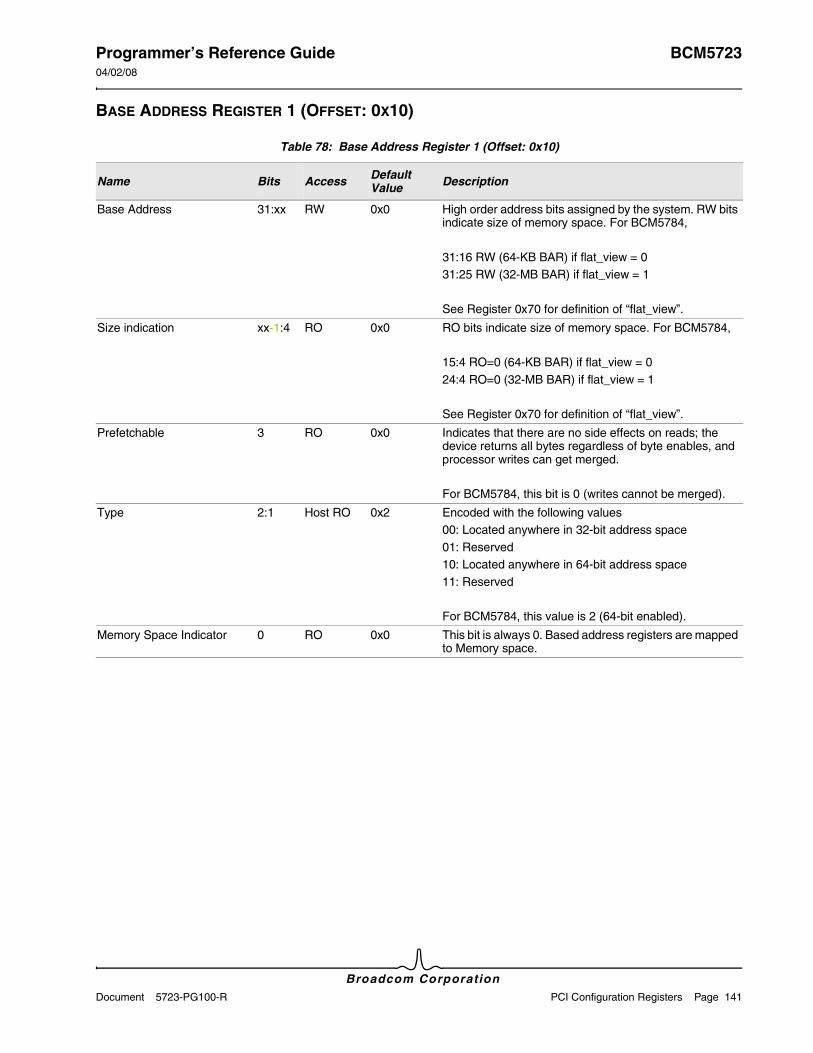
Programmer’s Reference Guide BCM572304/02/08
Broadcom CorporationDocument 5723-PG100-R PCI Configuration Registers Page 141
BASE ADDRESS REGISTER 1 (OFFSET: 0X10)
Table 78: Base Address Register 1 (Offset: 0x10)
Name Bits Access Default Value Description
Base Address 31:xx RW 0x0 High order address bits assigned by the system. RW bits indicate size of memory space. For BCM5784,
31:16 RW (64-KB BAR) if flat_view = 031:25 RW (32-MB BAR) if flat_view = 1
See Register 0x70 for definition of “flat_view”.
Size indication xx-1:4 RO 0x0 RO bits indicate size of memory space. For BCM5784,
15:4 RO=0 (64-KB BAR) if flat_view = 024:4 RO=0 (32-MB BAR) if flat_view = 1
See Register 0x70 for definition of “flat_view”.
Prefetchable 3 RO 0x0 Indicates that there are no side effects on reads; the device returns all bytes regardless of byte enables, and processor writes can get merged.
For BCM5784, this bit is 0 (writes cannot be merged).
Type 2:1 Host RO 0x2 Encoded with the following values00: Located anywhere in 32-bit address space01: Reserved10: Located anywhere in 64-bit address space11: Reserved
For BCM5784, this value is 2 (64-bit enabled).
Memory Space Indicator 0 RO 0x0 This bit is always 0. Based address registers are mapped to Memory space.
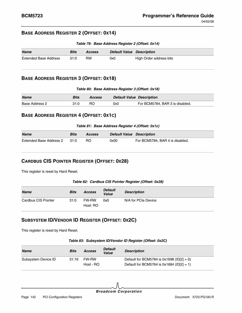
BCM5723 Programmer’s Reference Guide04/02/08
Broadcom Corporation
Page 142 PCI Configuration Registers Document 5723-PG100-R
BASE ADDRESS REGISTER 2 (OFFSET: 0X14)
BASE ADDRESS REGISTER 3 (OFFSET: 0X18)
BASE ADDRESS REGISTER 4 (OFFSET: 0X1C)
CARDBUS CIS POINTER REGISTER (OFFSET: 0X28)
This register is reset by Hard Reset.
SUBSYSTEM ID/VENDOR ID REGISTER (OFFSET: 0X2C)
This register is reset by Hard Reset.
Table 79: Base Address Register 2 (Offset: 0x14)
Name Bits Access Default Value Description
Extended Base Address 31:0 RW 0x0 High Order address bits
Table 80: Base Address Register 3 (Offset: 0x18)
Name Bits Access Default Value Description
Base Address 2 31:0 RO 0x0 For BCM5784, BAR 3 is disabled.
Table 81: Base Address Register 4 (Offset: 0x1c)
Name Bits Access Default Value Description
Extended Base Address 2 31:0 RO 0x00 For BCM5784, BAR 4 is disabled.
Table 82: Cardbus CIS Pointer Register (Offset: 0x28)
Name Bits Access Default Value Description
Cardbus CIS Pointer 31:0 FW-RWHost: RO
0x0 N/A for PCIe Device
Table 83: Subsystem ID/Vendor ID Register (Offset: 0x2C)
Name Bits Access Default Value Description
Subsystem Device ID 31:16 FW-RWHost - RO
Default for BCM5784 is 0x1698 (ID[2] = 0)Default for BCM5764 is 0x1684 (ID[2] = 1)
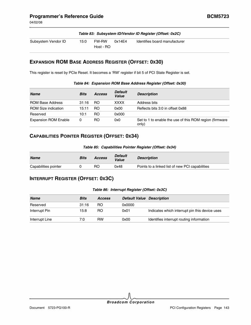
Programmer’s Reference Guide BCM572304/02/08
Broadcom CorporationDocument 5723-PG100-R PCI Configuration Registers Page 143
EXPANSION ROM BASE ADDRESS REGISTER (OFFSET: 0X30)
This register is reset by PCIe Reset. It becomes a ‘RW’ register if bit 5 of PCI State Register is set.
CAPABILITIES POINTER REGISTER (OFFSET: 0X34)
INTERRUPT REGISTER (OFFSET: 0X3C)
Subsystem Vendor ID 15:0 FW-RWHost - RO
0x14E4 Identifies board manufacturer
Table 84: Expansion ROM Base Address Register (Offset: 0x30)
Name Bits Access Default Value Description
ROM Base Address 31:16 RO XXXX Address bits
ROM Size indication 15:11 RO 0x00 Reflects bits 3:0 in offset 0x88
Reserved 10:1 RO 0x000
Expansion ROM Enable 0 RO 0x0 Set to 1 to enable the use of this ROM region (firmware only)
Table 85: Capabilities Pointer Register (Offset: 0x34)
Name Bits Access Default Value Description
Capabilities pointer 0 RO 0x48 Points to a linked list of new PCI capabilities
Table 86: Interrupt Register (Offset: 0x3C)
Name Bits Access Default Value Description
Reserved 31:16 RO 0x0000
Interrupt Pin 15:8 RO 0x01 Indicates which interrupt pin this device uses
Interrupt Line 7:0 RW 0x00 Identifies interrupt routing information
Table 83: Subsystem ID/Vendor ID Register (Offset: 0x2C)
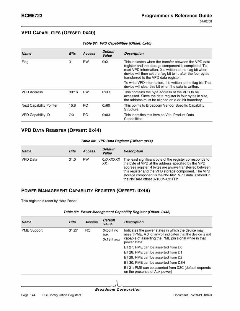
BCM5723 Programmer’s Reference Guide04/02/08
Broadcom Corporation
Page 144 PCI Configuration Registers Document 5723-PG100-R
VPD CAPABILITIES (OFFSET: 0X40)
VPD DATA REGISTER (OFFSET: 0X44)
POWER MANAGEMENT CAPABILITY REGISTER (OFFSET: 0X48)
This register is reset by Hard Reset.
Table 87: VPD Capabilities (Offset: 0x40)
Name Bits Access Default Value Description
Flag 31 RW 0xX This indicates when the transfer between the VPD data register and the storage component is completed. To read VPD information, 0 is written to the flag bit when device will then set the flag bit to 1, after the four bytes transferred to the VPD data register.To write VPD information, 1 is written to the flag bit. The device will clear this bit when the data is written.
VPD Address 30:16 RW 0xXX This contains the byte address of the VPD to be accessed. Since the data register is four bytes in size, the address must be aligned on a 32-bit boundary.
Next Capability Pointer 15:8 RO 0x60 This points to Broadcom Vendor Specific Capability Structure.
VPD Capability ID 7:0 RO 0x03 This identifies this item as Vital Product Data Capabilities.
Table 88: VPD Data Register (Offset: 0x44)
Name Bits Access Default Value Description
VPD Data 31:0 RW 0xXXXXXXXX
The least significant byte of the register corresponds to the byte of VPD at the address specified by the VPD address register. 4 bytes are always transferred between this register and the VPD storage component. The VPD storage component is the NVRAM. VPD data is stored in the NVRAM offset 0x100h–0x1FFh.
Table 89: Power Management Capability Register (Offset: 0x48)
Name Bits Access Default Value Description
PME Support 31:27 RO 0x08 if no aux0x18 if aux
Indicates the power states in which the device may assert PME. A 0 for any bit indicates that the device is not capable of asserting the PME pin signal while in that power stateBit 27: PME can be asserted from D0Bit 28: PME can be asserted from D1Bit 29: PME can be asserted from D2Bit 30: PME can be asserted from D3HBit 31: PME can be asserted from D3C (default depends on the presence of Aux power)
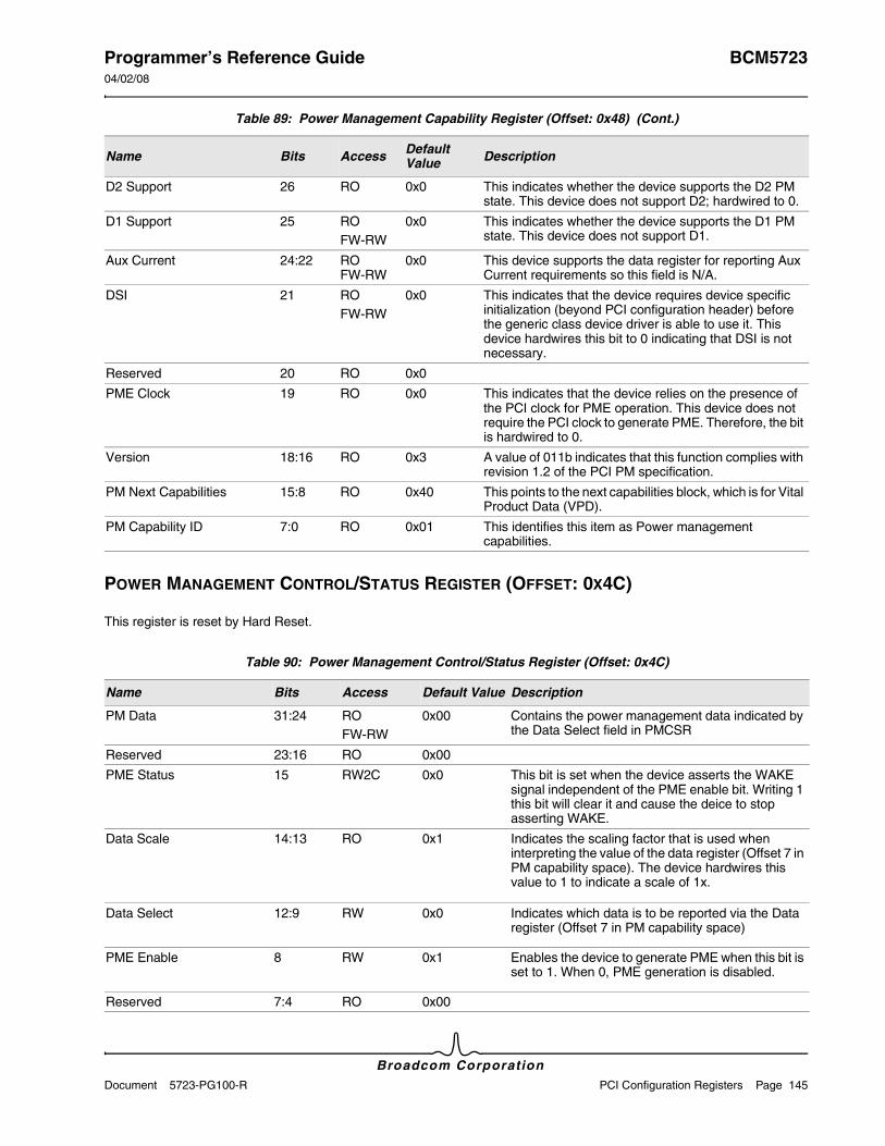
Programmer’s Reference Guide BCM572304/02/08
Broadcom CorporationDocument 5723-PG100-R PCI Configuration Registers Page 145
POWER MANAGEMENT CONTROL/STATUS REGISTER (OFFSET: 0X4C)
This register is reset by Hard Reset.
D2 Support 26 RO 0x0 This indicates whether the device supports the D2 PM state. This device does not support D2; hardwired to 0.
D1 Support 25 ROFW-RW
0x0 This indicates whether the device supports the D1 PM state. This device does not support D1.
Aux Current 24:22 RO FW-RW
0x0 This device supports the data register for reporting Aux Current requirements so this field is N/A.
DSI 21 ROFW-RW
0x0 This indicates that the device requires device specific initialization (beyond PCI configuration header) before the generic class device driver is able to use it. This device hardwires this bit to 0 indicating that DSI is not necessary.
Reserved 20 RO 0x0
PME Clock 19 RO 0x0 This indicates that the device relies on the presence of the PCI clock for PME operation. This device does not require the PCI clock to generate PME. Therefore, the bit is hardwired to 0.
Version 18:16 RO 0x3 A value of 011b indicates that this function complies with revision 1.2 of the PCI PM specification.
PM Next Capabilities 15:8 RO 0x40 This points to the next capabilities block, which is for Vital Product Data (VPD).
PM Capability ID 7:0 RO 0x01 This identifies this item as Power management capabilities.
Table 90: Power Management Control/Status Register (Offset: 0x4C)
Name Bits Access Default Value Description
PM Data 31:24 ROFW-RW
0x00 Contains the power management data indicated by the Data Select field in PMCSR
Reserved 23:16 RO 0x00
PME Status 15 RW2C 0x0 This bit is set when the device asserts the WAKE signal independent of the PME enable bit. Writing 1 this bit will clear it and cause the deice to stop asserting WAKE.
Data Scale 14:13 RO 0x1 Indicates the scaling factor that is used when interpreting the value of the data register (Offset 7 in PM capability space). The device hardwires this value to 1 to indicate a scale of 1x.
Data Select 12:9 RW 0x0 Indicates which data is to be reported via the Data register (Offset 7 in PM capability space)
PME Enable 8 RW 0x1 Enables the device to generate PME when this bit is set to 1. When 0, PME generation is disabled.
Reserved 7:4 RO 0x00
Table 89: Power Management Capability Register (Offset: 0x48) (Cont.)
Name Bits Access Default Value Description

BCM5723 Programmer’s Reference Guide04/02/08
Broadcom Corporation
Page 146 PCI Configuration Registers Document 5723-PG100-R
MSI CAPABILITY HEADER (OFFSET: 0X50)
This register is reset by PERST_L.
No Soft Reset 3 RO 0x1 When set (“1”), this bit indicates that devices transitioning from D3hot to D0 because of PowerState commands do not perform an internal reset. Configuration Context is preserved. Upon transition from the D3hot to the D0 Initialized state, no additional operating system intervention is required to preserve Configuration Context beyond writing the PowerState bits.
When clear (“0”), devices do perform an internal reset upon transitioning from D3hot to D0 via software control of the PowerState bits. Configuration Context is lost when performing the soft reset. Upon transition from the D3hot to the D0 state, full reinitialization sequence is needed to return the device to D0 Initialized.
Regardless of this bit, devices that transition from D3hot to D0 by a system or bus segment reset will return to the device state D0 Uninitialized with only PME context preserved if PME is supported and enabled.
Reserved 2 RO 0x0
Power State 1:0 RW 0x0 Indicates the current power state of the device when read.When written, it sets the device into the specified power state:00: D001: D110: D211: D3
Table 91: MSI Capability Header (Offset: 0x50)
Name Bits Access Default Value Description
MSI Control 31:24 R/W 0x00 Reserved
64-bit Address Capable 23 RO 1 HardwiredAdvertise 64-bit address capable
Multiple Message Enable 22:20 R/W 0x0 Number of allocated message
Multiple Message Capable 19:17 RO 0x0 Number of requested message
MSI Enable 16 R/W 0 Enable MSI
Next Capability Pointer 15:8 RO 0xCC Next Capability Pointer: 0xCC
MSI Capability ID 7:0 RO 0x5 HardwiredMSI capability ID
Table 90: Power Management Control/Status Register (Offset: 0x4C) (Cont.)
Name Bits Access Default Value Description
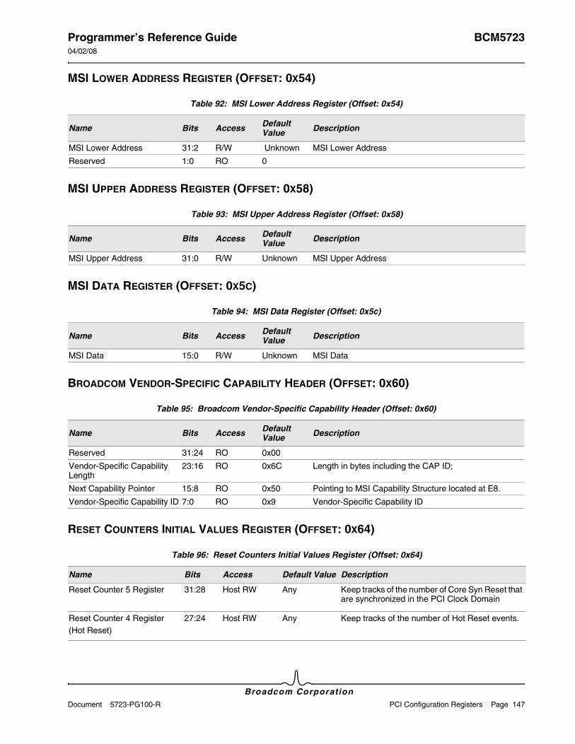
Programmer’s Reference Guide BCM572304/02/08
Broadcom CorporationDocument 5723-PG100-R PCI Configuration Registers Page 147
MSI LOWER ADDRESS REGISTER (OFFSET: 0X54)
MSI UPPER ADDRESS REGISTER (OFFSET: 0X58)
MSI DATA REGISTER (OFFSET: 0X5C)
BROADCOM VENDOR-SPECIFIC CAPABILITY HEADER (OFFSET: 0X60)
RESET COUNTERS INITIAL VALUES REGISTER (OFFSET: 0X64)
Table 92: MSI Lower Address Register (Offset: 0x54)
Name Bits Access Default Value Description
MSI Lower Address 31:2 R/W Unknown MSI Lower Address
Reserved 1:0 RO 0
Table 93: MSI Upper Address Register (Offset: 0x58)
Name Bits Access Default Value Description
MSI Upper Address 31:0 R/W Unknown MSI Upper Address
Table 94: MSI Data Register (Offset: 0x5c)
Name Bits Access Default Value Description
MSI Data 15:0 R/W Unknown MSI Data
Table 95: Broadcom Vendor-Specific Capability Header (Offset: 0x60)
Name Bits Access Default Value Description
Reserved 31:24 RO 0x00
Vendor-Specific Capability Length
23:16 RO 0x6C Length in bytes including the CAP ID;
Next Capability Pointer 15:8 RO 0x50 Pointing to MSI Capability Structure located at E8.
Vendor-Specific Capability ID 7:0 RO 0x9 Vendor-Specific Capability ID
Table 96: Reset Counters Initial Values Register (Offset: 0x64)
Name Bits Access Default Value Description
Reset Counter 5 Register 31:28 Host RW Any Keep tracks of the number of Core Syn Reset that are synchronized in the PCI Clock Domain
Reset Counter 4 Register(Hot Reset)
27:24 Host RW Any Keep tracks of the number of Hot Reset events.
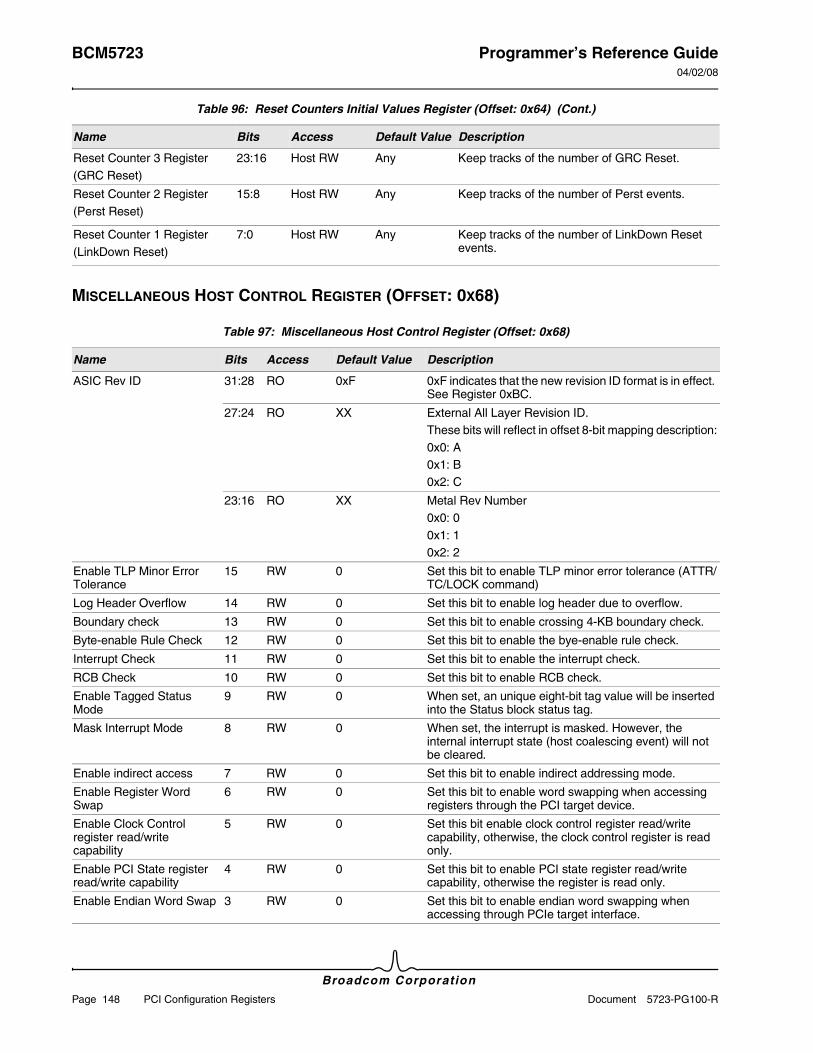
BCM5723 Programmer’s Reference Guide04/02/08
Broadcom Corporation
Page 148 PCI Configuration Registers Document 5723-PG100-R
MISCELLANEOUS HOST CONTROL REGISTER (OFFSET: 0X68)
Reset Counter 3 Register(GRC Reset)
23:16 Host RW Any Keep tracks of the number of GRC Reset.
Reset Counter 2 Register(Perst Reset)
15:8 Host RW Any Keep tracks of the number of Perst events.
Reset Counter 1 Register(LinkDown Reset)
7:0 Host RW Any Keep tracks of the number of LinkDown Reset events.
Table 97: Miscellaneous Host Control Register (Offset: 0x68)
Name Bits Access Default Value Description
ASIC Rev ID 31:28 RO 0xF 0xF indicates that the new revision ID format is in effect. See Register 0xBC.
27:24 RO XX External All Layer Revision ID.These bits will reflect in offset 8-bit mapping description:0x0: A0x1: B0x2: C
23:16 RO XX Metal Rev Number 0x0: 00x1: 10x2: 2
Enable TLP Minor Error Tolerance
15 RW 0 Set this bit to enable TLP minor error tolerance (ATTR/TC/LOCK command)
Log Header Overflow 14 RW 0 Set this bit to enable log header due to overflow.
Boundary check 13 RW 0 Set this bit to enable crossing 4-KB boundary check.
Byte-enable Rule Check 12 RW 0 Set this bit to enable the bye-enable rule check.
Interrupt Check 11 RW 0 Set this bit to enable the interrupt check.
RCB Check 10 RW 0 Set this bit to enable RCB check.
Enable Tagged Status Mode
9 RW 0 When set, an unique eight-bit tag value will be inserted into the Status block status tag.
Mask Interrupt Mode 8 RW 0 When set, the interrupt is masked. However, the internal interrupt state (host coalescing event) will not be cleared.
Enable indirect access 7 RW 0 Set this bit to enable indirect addressing mode.
Enable Register Word Swap
6 RW 0 Set this bit to enable word swapping when accessing registers through the PCI target device.
Enable Clock Control register read/write capability
5 RW 0 Set this bit enable clock control register read/write capability, otherwise, the clock control register is read only.
Enable PCI State register read/write capability
4 RW 0 Set this bit to enable PCI state register read/write capability, otherwise the register is read only.
Enable Endian Word Swap 3 RW 0 Set this bit to enable endian word swapping when accessing through PCIe target interface.
Table 96: Reset Counters Initial Values Register (Offset: 0x64) (Cont.)
Name Bits Access Default Value Description
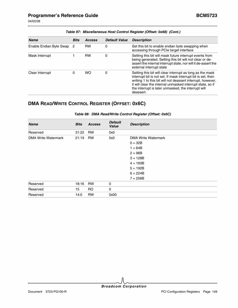
Programmer’s Reference Guide BCM572304/02/08
Broadcom CorporationDocument 5723-PG100-R PCI Configuration Registers Page 149
DMA READ/WRITE CONTROL REGISTER (OFFSET: 0X6C)
Enable Endian Byte Swap 2 RW 0 Set this bit to enable endian byte swapping when accessing through PCIe target interface
Mask Interrupt 1 RW 0 Setting this bit will mask future interrupt events from being generated. Setting this bit will not clear or de-assert the internal interrupt state, nor will it de-assert the external interrupt state
Clear Interrupt 0 WO 0 Setting this bit will clear interrupt as long as the mask interrupt bit is not set. If mask interrupt bit is set, then writing 1 to this bit will not deassert interrupt, however, it will clear the internal unmasked interrupt state, so if the interrupt is later unmasked, the interrupt will deassert.
Table 98: DMA Read/Write Control Register (Offset: 0x6C)
Name Bits Access Default Value Description
Reserved 31:22 RW 0x0
DMA Write Watermark 21:19 RW 0x0 DMA Write Watermark0 = 32B1 = 64B2 = 96B3 = 128B4 = 160B5 = 192B6 = 224B7 = 256B
Reserved 18:16 RW 0
Reserved 15 RO 0
Reserved 14:0 RW 0x00
Table 97: Miscellaneous Host Control Register (Offset: 0x68) (Cont.)
Name Bits Access Default Value Description
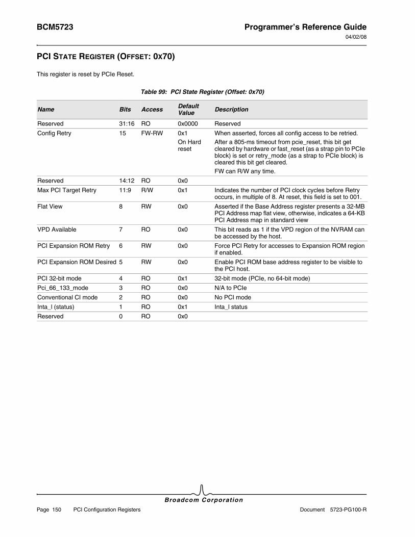
BCM5723 Programmer’s Reference Guide04/02/08
Broadcom Corporation
Page 150 PCI Configuration Registers Document 5723-PG100-R
PCI STATE REGISTER (OFFSET: 0X70)
This register is reset by PCIe Reset.
Table 99: PCI State Register (Offset: 0x70)
Name Bits Access Default Value Description
Reserved 31:16 RO 0x0000 Reserved
Config Retry 15 FW-RW 0x1On Hard reset
When asserted, forces all config access to be retried.After a 805-ms timeout from pcie_reset, this bit get cleared by hardware or fast_reset (as a strap pin to PCIe block) is set or retry_mode (as a strap to PCIe block) is cleared this bit get cleared.FW can R/W any time.
Reserved 14:12 RO 0x0
Max PCI Target Retry 11:9 R/W 0x1 Indicates the number of PCI clock cycles before Retry occurs, in multiple of 8. At reset, this field is set to 001.
Flat View 8 RW 0x0 Asserted if the Base Address register presents a 32-MB PCI Address map flat view, otherwise, indicates a 64-KB PCI Address map in standard view
VPD Available 7 RO 0x0 This bit reads as 1 if the VPD region of the NVRAM can be accessed by the host.
PCI Expansion ROM Retry 6 RW 0x0 Force PCI Retry for accesses to Expansion ROM region if enabled.
PCI Expansion ROM Desired 5 RW 0x0 Enable PCI ROM base address register to be visible to the PCI host.
PCI 32-bit mode 4 RO 0x1 32-bit mode (PCIe, no 64-bit mode)
Pci_66_133_mode 3 RO 0x0 N/A to PCIe
Conventional CI mode 2 RO 0x0 No PCI mode
Inta_l (status) 1 RO 0x1 Inta_l status
Reserved 0 RO 0x0
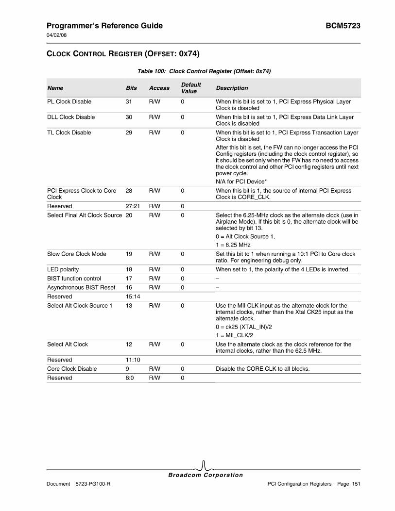
Programmer’s Reference Guide BCM572304/02/08
Broadcom CorporationDocument 5723-PG100-R PCI Configuration Registers Page 151
CLOCK CONTROL REGISTER (OFFSET: 0X74)
Table 100: Clock Control Register (Offset: 0x74)
Name Bits Access Default Value Description
PL Clock Disable 31 R/W 0 When this bit is set to 1, PCI Express Physical Layer Clock is disabled
DLL Clock Disable 30 R/W 0 When this bit is set to 1, PCI Express Data Link Layer Clock is disabled
TL Clock Disable 29 R/W 0 When this bit is set to 1, PCI Express Transaction Layer Clock is disabledAfter this bit is set, the FW can no longer access the PCI Config registers (including the clock control register), so it should be set only when the FW has no need to access the clock control and other PCI config registers until next power cycle.N/A for PCI Device*
PCI Express Clock to Core Clock
28 R/W 0 When this bit is 1, the source of internal PCI Express Clock is CORE_CLK.
Reserved 27:21 R/W 0
Select Final Alt Clock Source 20 R/W 0 Select the 6.25-MHz clock as the alternate clock (use in Airplane Mode). If this bit is 0, the alternate clock will be selected by bit 13. 0 = Alt Clock Source 1, 1 = 6.25 MHz
Slow Core Clock Mode 19 R/W 0 Set this bit to 1 when running a 10:1 PCI to Core clock ratio. For engineering debug only.
LED polarity 18 R/W 0 When set to 1, the polarity of the 4 LEDs is inverted.
BIST function control 17 R/W 0 –
Asynchronous BIST Reset 16 R/W 0 –
Reserved 15:14
Select Alt Clock Source 1 13 R/W 0 Use the MII CLK input as the alternate clock for the internal clocks, rather than the Xtal CK25 input as the alternate clock.0 = ck25 (XTAL_IN)/21 = MII_CLK/2
Select Alt Clock 12 R/W 0 Use the alternate clock as the clock reference for the internal clocks, rather than the 62.5 MHz.
Reserved 11:10
Core Clock Disable 9 R/W 0 Disable the CORE CLK to all blocks.
Reserved 8:0 R/W 0
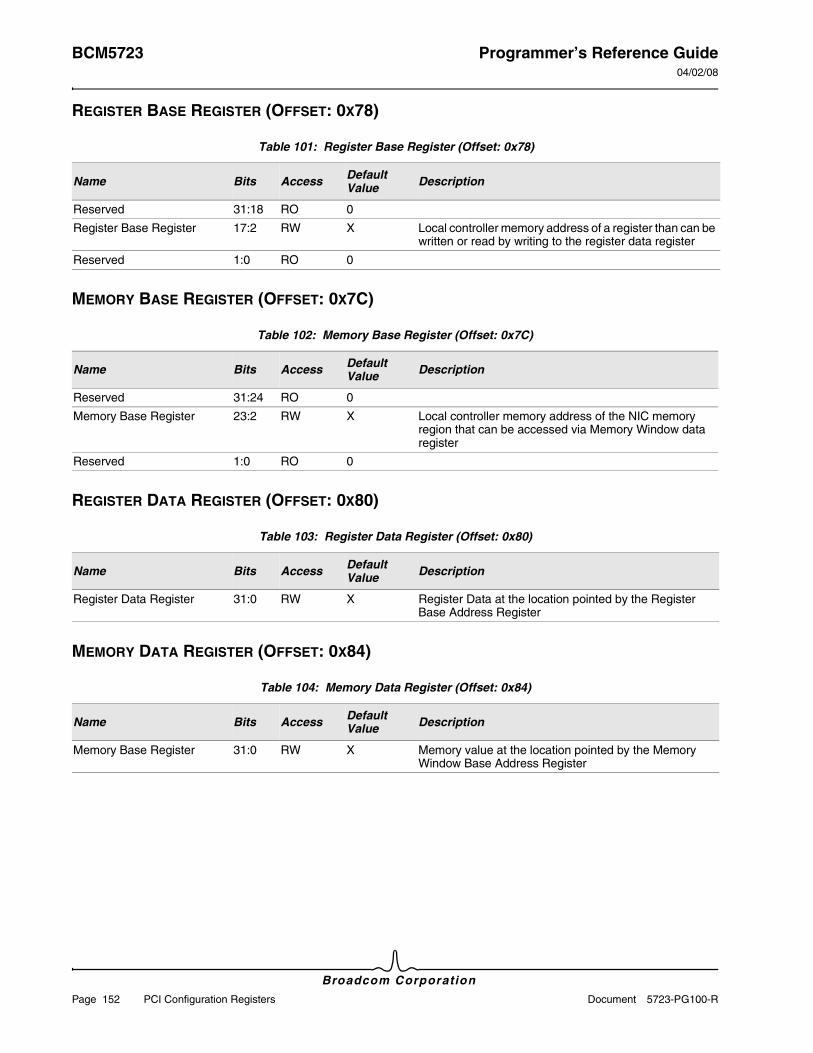
BCM5723 Programmer’s Reference Guide04/02/08
Broadcom Corporation
Page 152 PCI Configuration Registers Document 5723-PG100-R
REGISTER BASE REGISTER (OFFSET: 0X78)
MEMORY BASE REGISTER (OFFSET: 0X7C)
REGISTER DATA REGISTER (OFFSET: 0X80)
MEMORY DATA REGISTER (OFFSET: 0X84)
Table 101: Register Base Register (Offset: 0x78)
Name Bits Access Default Value Description
Reserved 31:18 RO 0
Register Base Register 17:2 RW X Local controller memory address of a register than can be written or read by writing to the register data register
Reserved 1:0 RO 0
Table 102: Memory Base Register (Offset: 0x7C)
Name Bits Access Default Value Description
Reserved 31:24 RO 0
Memory Base Register 23:2 RW X Local controller memory address of the NIC memory region that can be accessed via Memory Window data register
Reserved 1:0 RO 0
Table 103: Register Data Register (Offset: 0x80)
Name Bits Access Default Value Description
Register Data Register 31:0 RW X Register Data at the location pointed by the Register Base Address Register
Table 104: Memory Data Register (Offset: 0x84)
Name Bits Access Default Value Description
Memory Base Register 31:0 RW X Memory value at the location pointed by the Memory Window Base Address Register
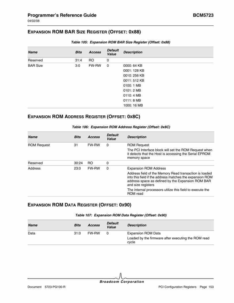
Programmer’s Reference Guide BCM572304/02/08
Broadcom CorporationDocument 5723-PG100-R PCI Configuration Registers Page 153
EXPANSION ROM BAR SIZE REGISTER (OFFSET: 0X88)
EXPANSION ROM ADDRESS REGISTER (OFFSET: 0X8C)
EXPANSION ROM DATA REGISTER (OFFSET: 0X90)
Table 105: Expansion ROM BAR Size Register (Offset: 0x88)
Name Bits Access Default Value Description
Reserved 31:4 RO 0
BAR Size 3:0 FW-RW 0 0000: 64 KB0001: 128 KB0010: 256 KB0011: 512 KB0100: 1 MB0101: 2 MB0110: 4 MB0111: 8 MB1000: 16 MB
Table 106: Expansion ROM Address Register (Offset: 0x8C)
Name Bits Access Default Value Description
ROM Request 31 FW-RW 0 ROM RequestThe PCI Interface block will set the ROM Request when it detects that the Host is accessing the Serial EPROM memory space
Reserved 30:24 RO 0
Address 23:0 FW-RW 0 Expansion ROM AddressAddress field of the Memory Read transaction is loaded into this field if the address matches the expansion ROM address space as defined by the Expansion ROM BAR and size registersThe internal processors utilize this field to execute the ROM read
Table 107: Expansion ROM Data Register (Offset: 0x90)
Name Bits Access Default Value Description
Data 31:0 FW-RW 0 Expansion ROM DataLoaded by the firmware after executing the ROM read cycle
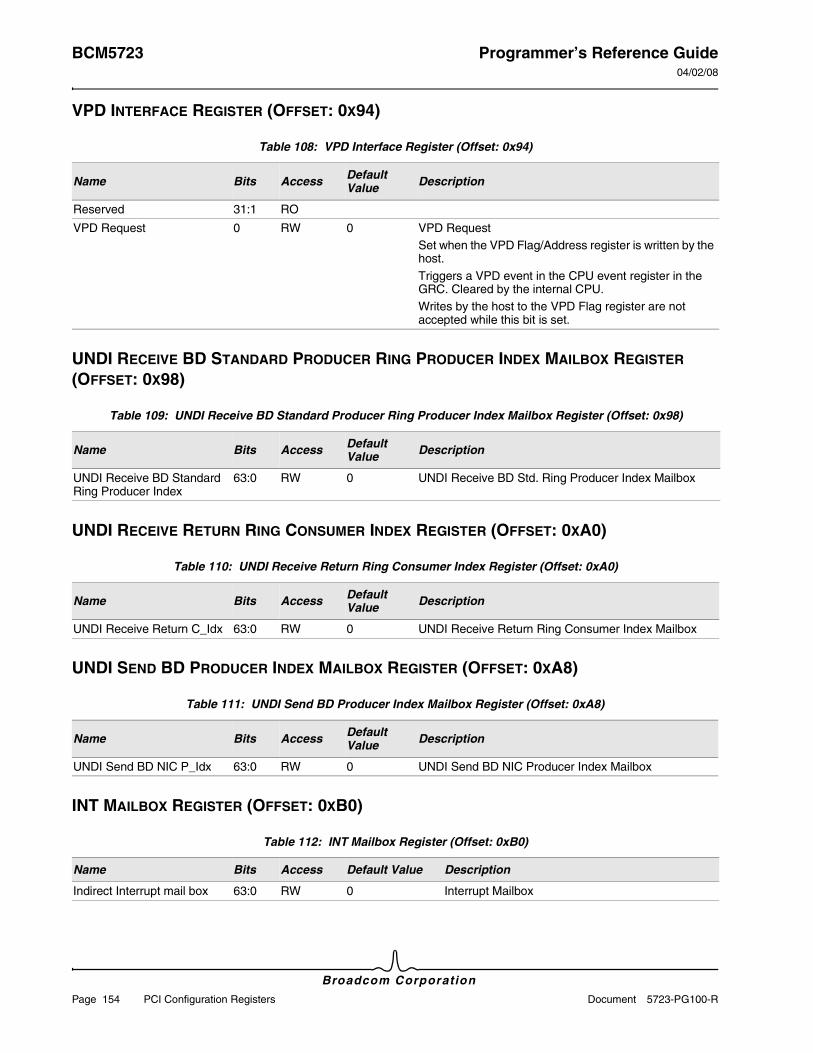
BCM5723 Programmer’s Reference Guide04/02/08
Broadcom Corporation
Page 154 PCI Configuration Registers Document 5723-PG100-R
VPD INTERFACE REGISTER (OFFSET: 0X94)
UNDI RECEIVE BD STANDARD PRODUCER RING PRODUCER INDEX MAILBOX REGISTER (OFFSET: 0X98)
UNDI RECEIVE RETURN RING CONSUMER INDEX REGISTER (OFFSET: 0XA0)
UNDI SEND BD PRODUCER INDEX MAILBOX REGISTER (OFFSET: 0XA8)
INT MAILBOX REGISTER (OFFSET: 0XB0)
Table 108: VPD Interface Register (Offset: 0x94)
Name Bits Access Default Value Description
Reserved 31:1 RO
VPD Request 0 RW 0 VPD RequestSet when the VPD Flag/Address register is written by the host.Triggers a VPD event in the CPU event register in the GRC. Cleared by the internal CPU.Writes by the host to the VPD Flag register are not accepted while this bit is set.
Table 109: UNDI Receive BD Standard Producer Ring Producer Index Mailbox Register (Offset: 0x98)
Name Bits Access Default Value Description
UNDI Receive BD Standard Ring Producer Index
63:0 RW 0 UNDI Receive BD Std. Ring Producer Index Mailbox
Table 110: UNDI Receive Return Ring Consumer Index Register (Offset: 0xA0)
Name Bits Access Default Value Description
UNDI Receive Return C_Idx 63:0 RW 0 UNDI Receive Return Ring Consumer Index Mailbox
Table 111: UNDI Send BD Producer Index Mailbox Register (Offset: 0xA8)
Name Bits Access Default Value Description
UNDI Send BD NIC P_Idx 63:0 RW 0 UNDI Send BD NIC Producer Index Mailbox
Table 112: INT Mailbox Register (Offset: 0xB0)
Name Bits Access Default Value Description
Indirect Interrupt mail box 63:0 RW 0 Interrupt Mailbox
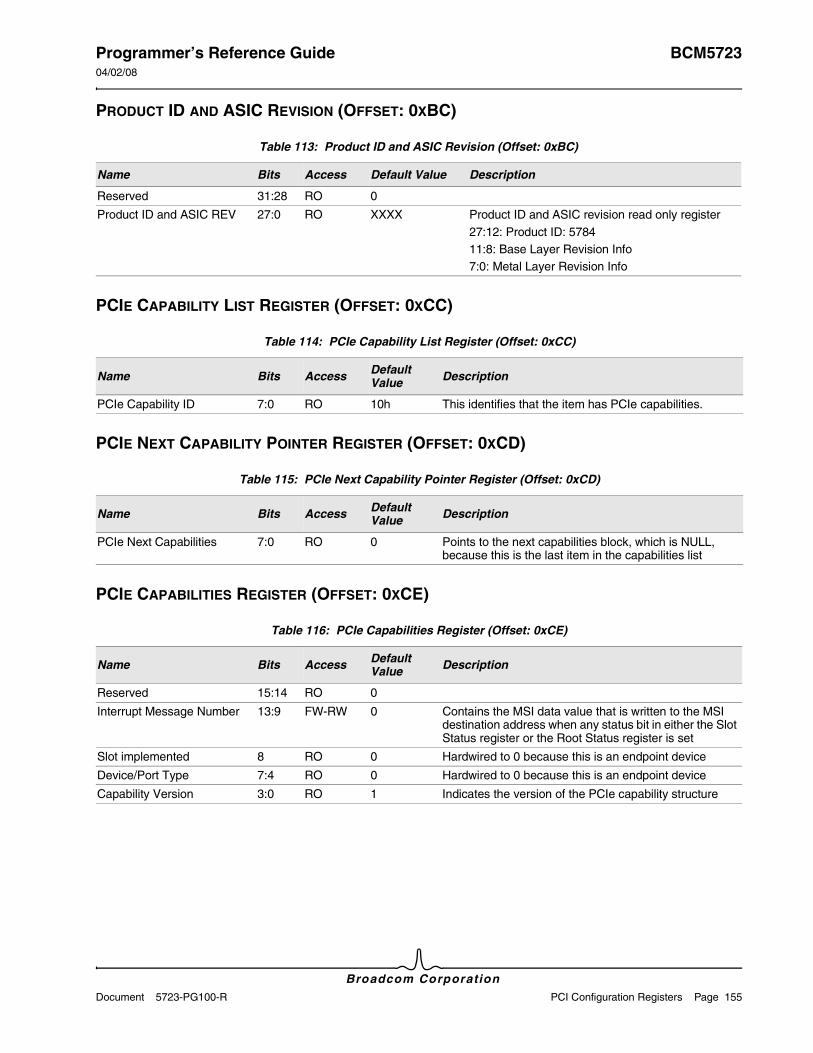
Programmer’s Reference Guide BCM572304/02/08
Broadcom CorporationDocument 5723-PG100-R PCI Configuration Registers Page 155
PRODUCT ID AND ASIC REVISION (OFFSET: 0XBC)
PCIE CAPABILITY LIST REGISTER (OFFSET: 0XCC)
PCIE NEXT CAPABILITY POINTER REGISTER (OFFSET: 0XCD)
PCIE CAPABILITIES REGISTER (OFFSET: 0XCE)
Table 113: Product ID and ASIC Revision (Offset: 0xBC)
Name Bits Access Default Value Description
Reserved 31:28 RO 0
Product ID and ASIC REV 27:0 RO XXXX Product ID and ASIC revision read only register27:12: Product ID: 578411:8: Base Layer Revision Info7:0: Metal Layer Revision Info
Table 114: PCIe Capability List Register (Offset: 0xCC)
Name Bits Access Default Value Description
PCIe Capability ID 7:0 RO 10h This identifies that the item has PCIe capabilities.
Table 115: PCIe Next Capability Pointer Register (Offset: 0xCD)
Name Bits Access Default Value Description
PCIe Next Capabilities 7:0 RO 0 Points to the next capabilities block, which is NULL, because this is the last item in the capabilities list
Table 116: PCIe Capabilities Register (Offset: 0xCE)
Name Bits Access Default Value Description
Reserved 15:14 RO 0
Interrupt Message Number 13:9 FW-RW 0 Contains the MSI data value that is written to the MSI destination address when any status bit in either the Slot Status register or the Root Status register is set
Slot implemented 8 RO 0 Hardwired to 0 because this is an endpoint device
Device/Port Type 7:4 RO 0 Hardwired to 0 because this is an endpoint device
Capability Version 3:0 RO 1 Indicates the version of the PCIe capability structure
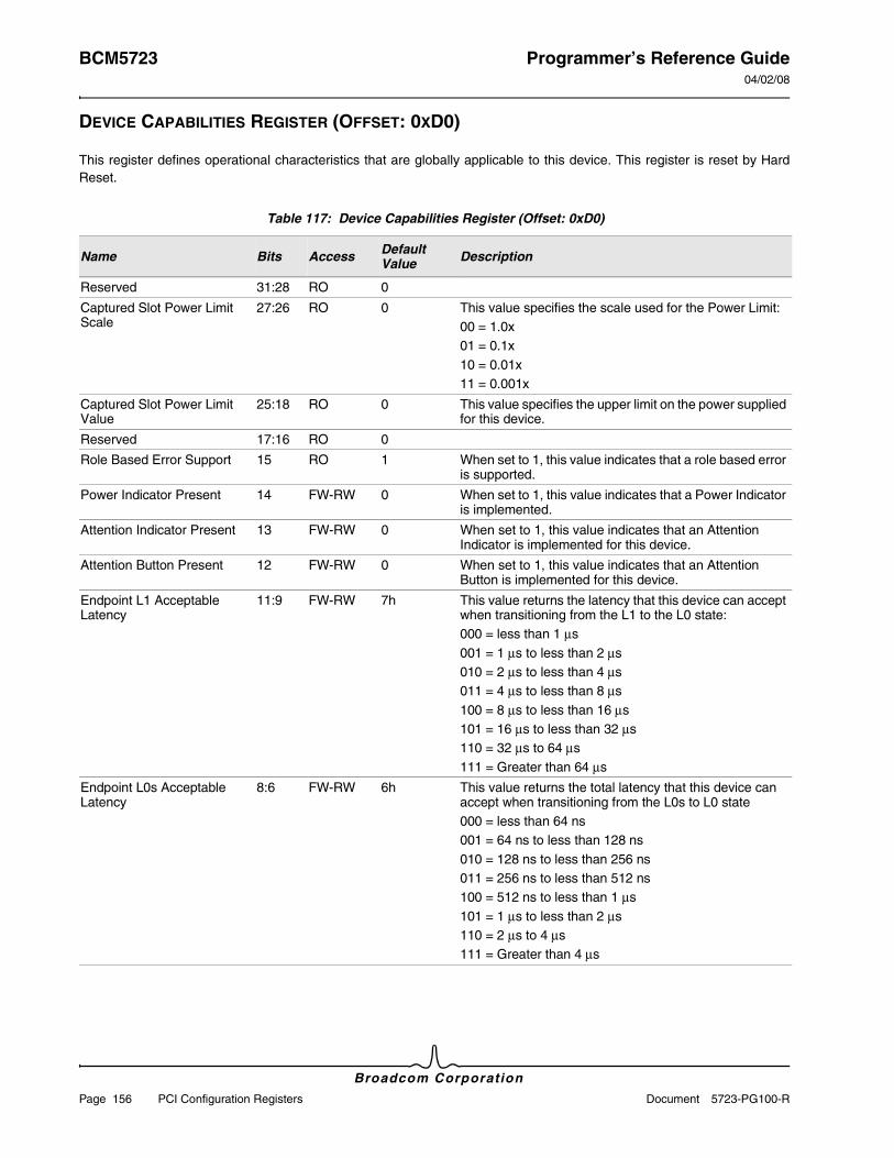
BCM5723 Programmer’s Reference Guide04/02/08
Broadcom Corporation
Page 156 PCI Configuration Registers Document 5723-PG100-R
DEVICE CAPABILITIES REGISTER (OFFSET: 0XD0)
This register defines operational characteristics that are globally applicable to this device. This register is reset by Hard Reset.
Table 117: Device Capabilities Register (Offset: 0xD0)
Name Bits Access Default Value Description
Reserved 31:28 RO 0
Captured Slot Power Limit Scale
27:26 RO 0 This value specifies the scale used for the Power Limit:00 = 1.0x01 = 0.1x10 = 0.01x11 = 0.001x
Captured Slot Power Limit Value
25:18 RO 0 This value specifies the upper limit on the power supplied for this device.
Reserved 17:16 RO 0
Role Based Error Support 15 RO 1 When set to 1, this value indicates that a role based error is supported.
Power Indicator Present 14 FW-RW 0 When set to 1, this value indicates that a Power Indicator is implemented.
Attention Indicator Present 13 FW-RW 0 When set to 1, this value indicates that an Attention Indicator is implemented for this device.
Attention Button Present 12 FW-RW 0 When set to 1, this value indicates that an Attention Button is implemented for this device.
Endpoint L1 Acceptable Latency
11:9 FW-RW 7h This value returns the latency that this device can accept when transitioning from the L1 to the L0 state:000 = less than 1 μs001 = 1 μs to less than 2 μs010 = 2 μs to less than 4 μs011 = 4 μs to less than 8 μs100 = 8 μs to less than 16 μs101 = 16 μs to less than 32 μs110 = 32 μs to 64 μs111 = Greater than 64 μs
Endpoint L0s Acceptable Latency
8:6 FW-RW 6h This value returns the total latency that this device can accept when transitioning from the L0s to L0 state000 = less than 64 ns001 = 64 ns to less than 128 ns010 = 128 ns to less than 256 ns011 = 256 ns to less than 512 ns100 = 512 ns to less than 1 μs101 = 1 μs to less than 2 μs110 = 2 μs to 4 μs111 = Greater than 4 μs
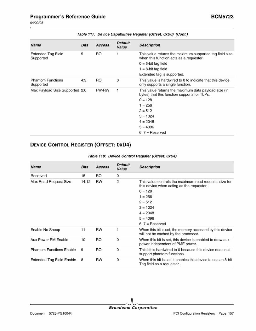
Programmer’s Reference Guide BCM572304/02/08
Broadcom CorporationDocument 5723-PG100-R PCI Configuration Registers Page 157
DEVICE CONTROL REGISTER (OFFSET: 0XD4)
Extended Tag Field Supported
5 RO 1 This value returns the maximum supported tag field size when this function acts as a requester.0 = 5-bit tag field1 = 8-bit tag fieldExtended tag is supported.
Phantom Functions Supported
4:3 RO 0 This value is hardwired to 0 to indicate that this device only supports a single function.
Max Payload Size Supported 2:0 FW-RW 1 This value returns the maximum data payload size (in bytes) that this function supports for TLPs:0 = 1281 = 2562 = 5123 = 10244 = 20485 = 40966, 7 = Reserved
Table 118: Device Control Register (Offset: 0xD4)
Name Bits Access Default Value Description
Reserved 15 RO 0
Max Read Request Size 14:12 RW 2 This value controls the maximum read requests size for this device when acting as the requester:0 = 1281 = 2562 = 5123 = 10244 = 20485 = 40966, 7 = Reserved
Enable No Snoop 11 RW 1 When this bit is set, the memory accessed by this device will not be cached by the processor.
Aux Power PM Enable 10 RO 0 When this bit is set, this device is enabled to draw aux power independent of PME power.
Phantom Functions Enable 9 RO 0 This bit is hardwired to 0 because this device does not support phantom functions.
Extended Tag Field Enable 8 RW 0 When this bit is set, it enables this device to use an 8-bit Tag field as a requester.
Table 117: Device Capabilities Register (Offset: 0xD0) (Cont.)
Name Bits Access Default Value Description
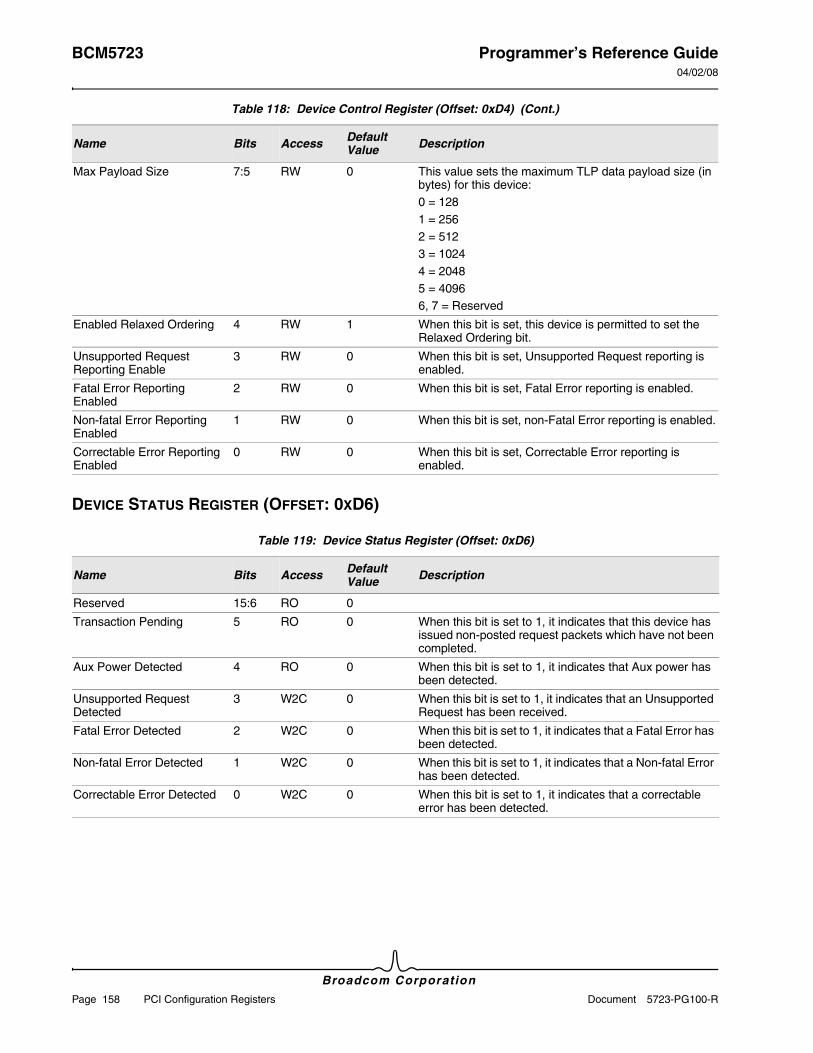
BCM5723 Programmer’s Reference Guide04/02/08
Broadcom Corporation
Page 158 PCI Configuration Registers Document 5723-PG100-R
DEVICE STATUS REGISTER (OFFSET: 0XD6)
Max Payload Size 7:5 RW 0 This value sets the maximum TLP data payload size (in bytes) for this device:0 = 1281 = 2562 = 5123 = 10244 = 20485 = 40966, 7 = Reserved
Enabled Relaxed Ordering 4 RW 1 When this bit is set, this device is permitted to set the Relaxed Ordering bit.
Unsupported Request Reporting Enable
3 RW 0 When this bit is set, Unsupported Request reporting is enabled.
Fatal Error Reporting Enabled
2 RW 0 When this bit is set, Fatal Error reporting is enabled.
Non-fatal Error Reporting Enabled
1 RW 0 When this bit is set, non-Fatal Error reporting is enabled.
Correctable Error Reporting Enabled
0 RW 0 When this bit is set, Correctable Error reporting is enabled.
Table 119: Device Status Register (Offset: 0xD6)
Name Bits Access Default Value Description
Reserved 15:6 RO 0
Transaction Pending 5 RO 0 When this bit is set to 1, it indicates that this device has issued non-posted request packets which have not been completed.
Aux Power Detected 4 RO 0 When this bit is set to 1, it indicates that Aux power has been detected.
Unsupported Request Detected
3 W2C 0 When this bit is set to 1, it indicates that an Unsupported Request has been received.
Fatal Error Detected 2 W2C 0 When this bit is set to 1, it indicates that a Fatal Error has been detected.
Non-fatal Error Detected 1 W2C 0 When this bit is set to 1, it indicates that a Non-fatal Error has been detected.
Correctable Error Detected 0 W2C 0 When this bit is set to 1, it indicates that a correctable error has been detected.
Table 118: Device Control Register (Offset: 0xD4) (Cont.)
Name Bits Access Default Value Description
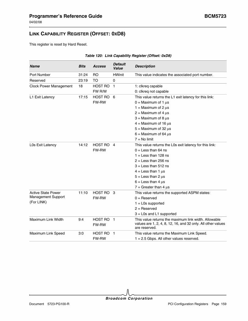
Programmer’s Reference Guide BCM572304/02/08
Broadcom CorporationDocument 5723-PG100-R PCI Configuration Registers Page 159
LINK CAPABILITY REGISTER (OFFSET: 0XD8)
This register is reset by Hard Reset.
Table 120: Link Capability Register (Offset: 0xD8)
Name Bits Access Default Value Description
Port Number 31:24 RO HWinit This value indicates the associated port number.
Reserved 23:19 TO 0
Clock Power Management 18 HOST ROFW R/W
1 1: clkreq capable0: clkreq not capable
L1 Exit Latency 17:15 HOST ROFW-RW
6 This value returns the L1 exit latency for this link:0 = Maximum of 1 μs1 = Maximum of 2 μs2 = Maximum of 4 μs3 = Maximum of 8 μs4 = Maximum of 16 μs5 = Maximum of 32 μs6 = Maximum of 64 μs7 = No limit
L0s Exit Latency 14:12 HOST ROFW-RW
4 This value returns the L0s exit latency for this link:0 = Less than 64 ns1 = Less than 128 ns2 = Less than 256 ns3 = Less than 512 ns4 = Less than 1 μs5 = Less than 2 μs6 = Less than 4 μs7 = Greater than 4 μs
Active State Power Management Support(For LINK)
11:10 HOST ROFW-RW
3 This value returns the supported ASPM states:0 = Reserved1 = L0s supported2 = Reserved3 = L0s and L1 supported
Maximum Link Width 9:4 HOST ROFW-RW
1 This value returns the maximum link width. Allowable values are 1, 2, 4, 8, 12, 16, and 32 only. All other values are reserved.
Maximum Link Speed 3:0 HOST ROFW-RW
1 This value returns the Maximum Link Speed. 1 = 2.5 Gbps. All other values reserved.
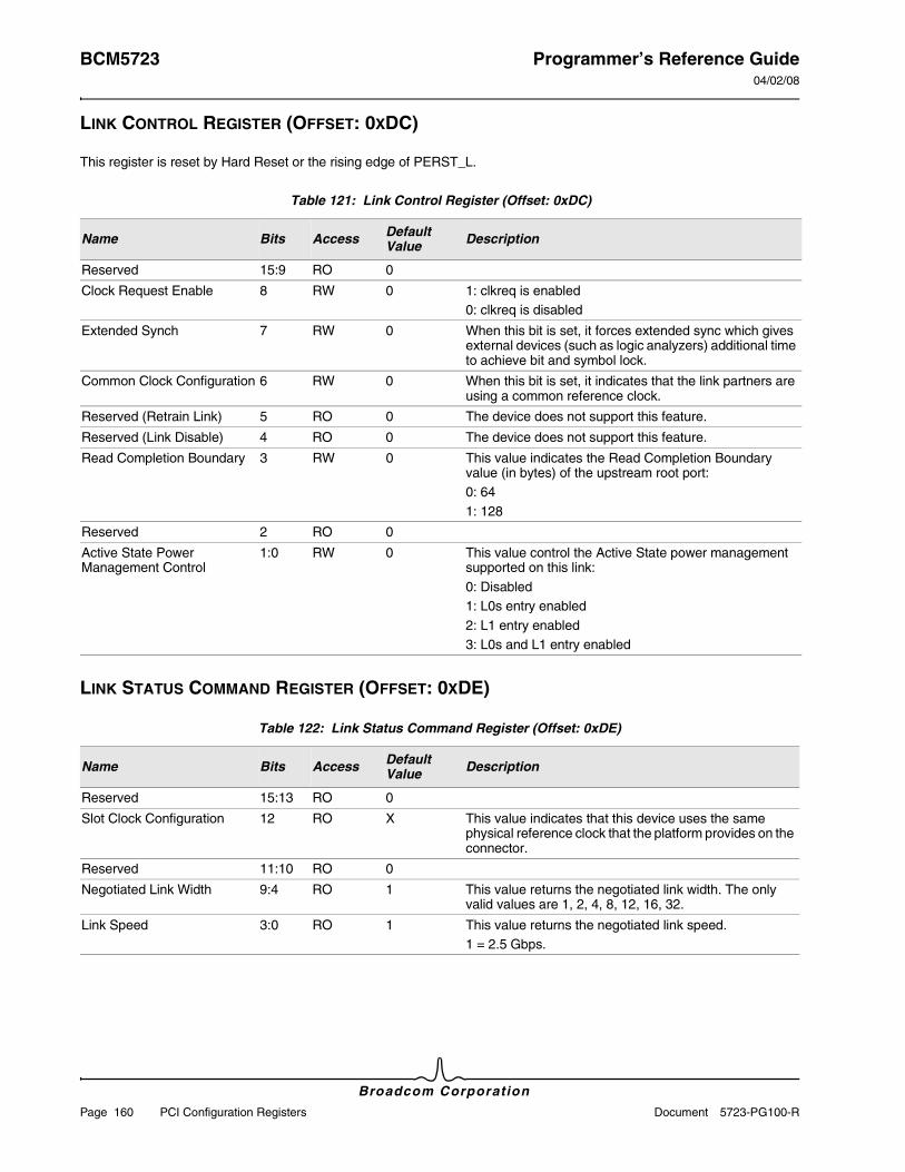
BCM5723 Programmer’s Reference Guide04/02/08
Broadcom Corporation
Page 160 PCI Configuration Registers Document 5723-PG100-R
LINK CONTROL REGISTER (OFFSET: 0XDC)
This register is reset by Hard Reset or the rising edge of PERST_L.
LINK STATUS COMMAND REGISTER (OFFSET: 0XDE)
Table 121: Link Control Register (Offset: 0xDC)
Name Bits Access Default Value Description
Reserved 15:9 RO 0
Clock Request Enable 8 RW 0 1: clkreq is enabled0: clkreq is disabled
Extended Synch 7 RW 0 When this bit is set, it forces extended sync which gives external devices (such as logic analyzers) additional time to achieve bit and symbol lock.
Common Clock Configuration 6 RW 0 When this bit is set, it indicates that the link partners are using a common reference clock.
Reserved (Retrain Link) 5 RO 0 The device does not support this feature.
Reserved (Link Disable) 4 RO 0 The device does not support this feature.
Read Completion Boundary 3 RW 0 This value indicates the Read Completion Boundary value (in bytes) of the upstream root port:0: 641: 128
Reserved 2 RO 0
Active State Power Management Control
1:0 RW 0 This value control the Active State power management supported on this link:0: Disabled1: L0s entry enabled2: L1 entry enabled3: L0s and L1 entry enabled
Table 122: Link Status Command Register (Offset: 0xDE)
Name Bits Access Default Value Description
Reserved 15:13 RO 0
Slot Clock Configuration 12 RO X This value indicates that this device uses the same physical reference clock that the platform provides on the connector.
Reserved 11:10 RO 0
Negotiated Link Width 9:4 RO 1 This value returns the negotiated link width. The only valid values are 1, 2, 4, 8, 12, 16, 32.
Link Speed 3:0 RO 1 This value returns the negotiated link speed. 1 = 2.5 Gbps.
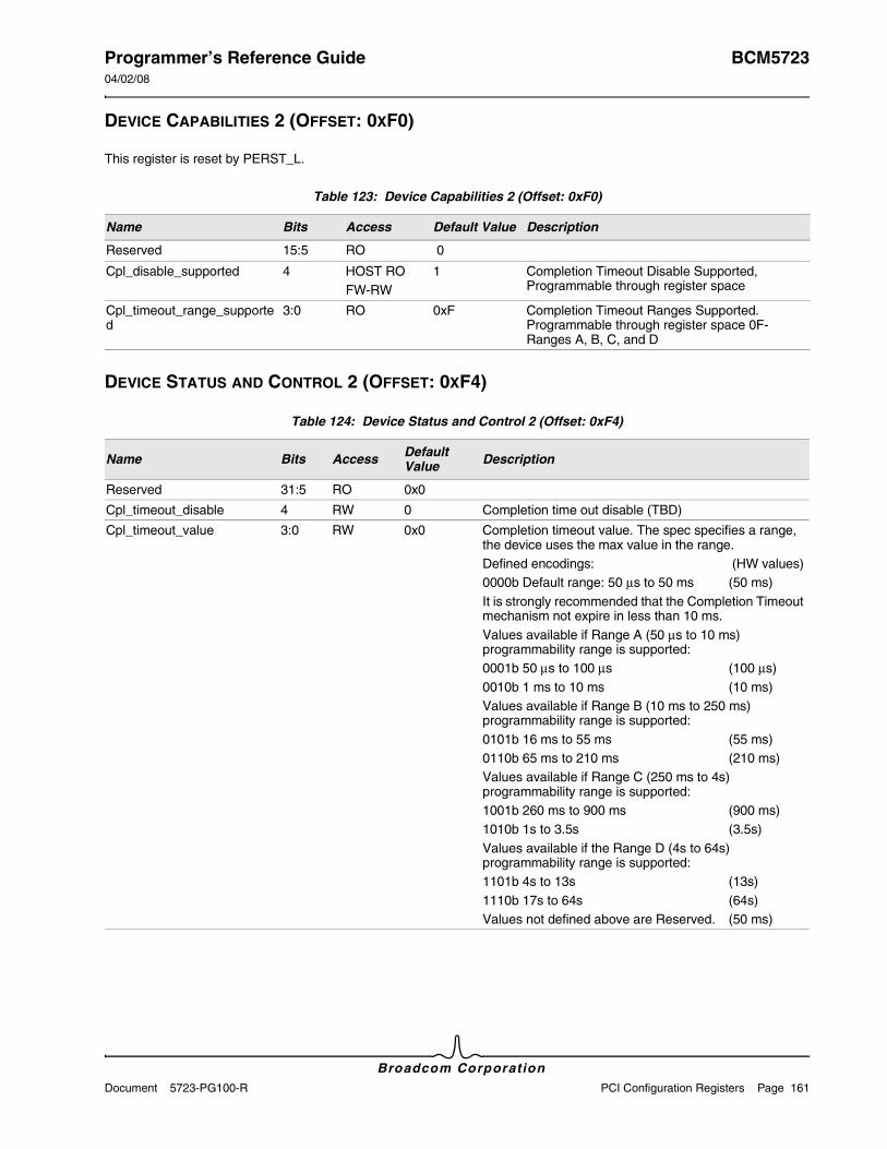
Programmer’s Reference Guide BCM572304/02/08
Broadcom CorporationDocument 5723-PG100-R PCI Configuration Registers Page 161
DEVICE CAPABILITIES 2 (OFFSET: 0XF0)
This register is reset by PERST_L.
DEVICE STATUS AND CONTROL 2 (OFFSET: 0XF4)
Table 123: Device Capabilities 2 (Offset: 0xF0)
Name Bits Access Default Value Description
Reserved 15:5 RO 0
Cpl_disable_supported 4 HOST ROFW-RW
1 Completion Timeout Disable Supported, Programmable through register space
Cpl_timeout_range_supported
3:0 RO 0xF Completion Timeout Ranges Supported. Programmable through register space 0F- Ranges A, B, C, and D
Table 124: Device Status and Control 2 (Offset: 0xF4)
Name Bits Access Default Value Description
Reserved 31:5 RO 0x0
Cpl_timeout_disable 4 RW 0 Completion time out disable (TBD)
Cpl_timeout_value 3:0 RW 0x0 Completion timeout value. The spec specifies a range, the device uses the max value in the range.Defined encodings: (HW values)0000b Default range: 50 μs to 50 ms (50 ms)It is strongly recommended that the Completion Timeout mechanism not expire in less than 10 ms.Values available if Range A (50 μs to 10 ms) programmability range is supported:0001b 50 μs to 100 μs (100 μs)0010b 1 ms to 10 ms (10 ms)Values available if Range B (10 ms to 250 ms) programmability range is supported:0101b 16 ms to 55 ms (55 ms)0110b 65 ms to 210 ms (210 ms)Values available if Range C (250 ms to 4s) programmability range is supported:1001b 260 ms to 900 ms (900 ms)1010b 1s to 3.5s (3.5s)Values available if the Range D (4s to 64s) programmability range is supported:1101b 4s to 13s (13s)1110b 17s to 64s (64s)Values not defined above are Reserved. (50 ms)
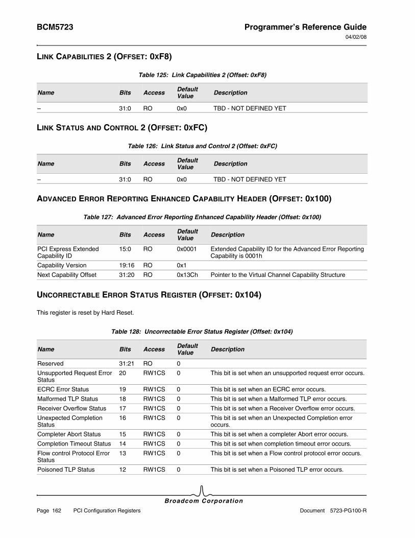
BCM5723 Programmer’s Reference Guide04/02/08
Broadcom Corporation
Page 162 PCI Configuration Registers Document 5723-PG100-R
LINK CAPABILITIES 2 (OFFSET: 0XF8)
LINK STATUS AND CONTROL 2 (OFFSET: 0XFC)
ADVANCED ERROR REPORTING ENHANCED CAPABILITY HEADER (OFFSET: 0X100)
UNCORRECTABLE ERROR STATUS REGISTER (OFFSET: 0X104)
This register is reset by Hard Reset.
Table 125: Link Capabilities 2 (Offset: 0xF8)
Name Bits Access Default Value Description
– 31:0 RO 0x0 TBD - NOT DEFINED YET
Table 126: Link Status and Control 2 (Offset: 0xFC)
Name Bits Access Default Value Description
– 31:0 RO 0x0 TBD - NOT DEFINED YET
Table 127: Advanced Error Reporting Enhanced Capability Header (Offset: 0x100)
Name Bits Access Default Value Description
PCI Express Extended Capability ID
15:0 RO 0x0001 Extended Capability ID for the Advanced Error Reporting Capability is 0001h
Capability Version 19:16 RO 0x1
Next Capability Offset 31:20 RO 0x13Ch Pointer to the Virtual Channel Capability Structure
Table 128: Uncorrectable Error Status Register (Offset: 0x104)
Name Bits Access Default Value Description
Reserved 31:21 RO 0
Unsupported Request Error Status
20 RW1CS 0 This bit is set when an unsupported request error occurs.
ECRC Error Status 19 RW1CS 0 This bit is set when an ECRC error occurs.
Malformed TLP Status 18 RW1CS 0 This bit is set when a Malformed TLP error occurs.
Receiver Overflow Status 17 RW1CS 0 This bit is set when a Receiver Overflow error occurs.
Unexpected Completion Status
16 RW1CS 0 This bit is set when an Unexpected Completion error occurs.
Completer Abort Status 15 RW1CS 0 This bit is set when a completer Abort error occurs.
Completion Timeout Status 14 RW1CS 0 This bit is set when completion timeout error occurs.
Flow control Protocol Error Status
13 RW1CS 0 This bit is set when a Flow control protocol error occurs.
Poisoned TLP Status 12 RW1CS 0 This bit is set when a Poisoned TLP error occurs.
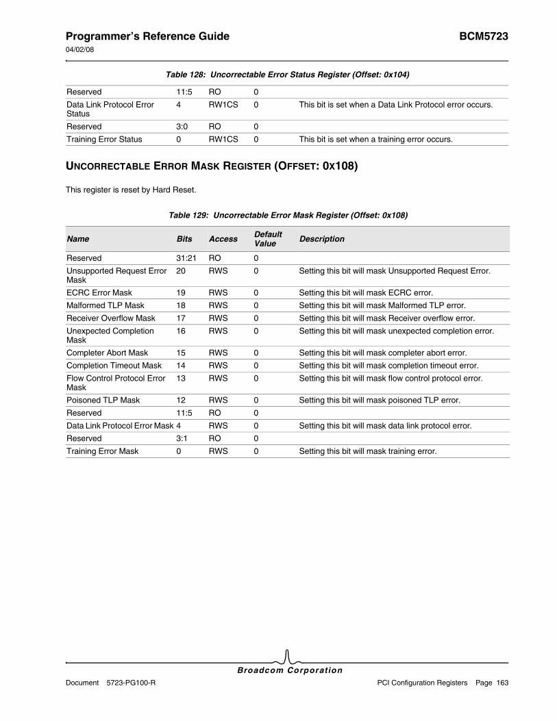
Programmer’s Reference Guide BCM572304/02/08
Broadcom CorporationDocument 5723-PG100-R PCI Configuration Registers Page 163
UNCORRECTABLE ERROR MASK REGISTER (OFFSET: 0X108)
This register is reset by Hard Reset.
Reserved 11:5 RO 0
Data Link Protocol Error Status
4 RW1CS 0 This bit is set when a Data Link Protocol error occurs.
Reserved 3:0 RO 0
Training Error Status 0 RW1CS 0 This bit is set when a training error occurs.
Table 129: Uncorrectable Error Mask Register (Offset: 0x108)
Name Bits Access Default Value Description
Reserved 31:21 RO 0
Unsupported Request Error Mask
20 RWS 0 Setting this bit will mask Unsupported Request Error.
ECRC Error Mask 19 RWS 0 Setting this bit will mask ECRC error.
Malformed TLP Mask 18 RWS 0 Setting this bit will mask Malformed TLP error.
Receiver Overflow Mask 17 RWS 0 Setting this bit will mask Receiver overflow error.
Unexpected Completion Mask
16 RWS 0 Setting this bit will mask unexpected completion error.
Completer Abort Mask 15 RWS 0 Setting this bit will mask completer abort error.
Completion Timeout Mask 14 RWS 0 Setting this bit will mask completion timeout error.
Flow Control Protocol Error Mask
13 RWS 0 Setting this bit will mask flow control protocol error.
Poisoned TLP Mask 12 RWS 0 Setting this bit will mask poisoned TLP error.
Reserved 11:5 RO 0
Data Link Protocol Error Mask 4 RWS 0 Setting this bit will mask data link protocol error.
Reserved 3:1 RO 0
Training Error Mask 0 RWS 0 Setting this bit will mask training error.
Table 128: Uncorrectable Error Status Register (Offset: 0x104)
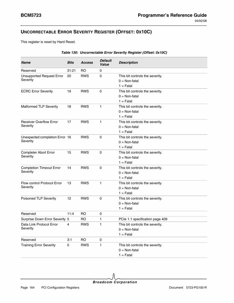
BCM5723 Programmer’s Reference Guide04/02/08
Broadcom Corporation
Page 164 PCI Configuration Registers Document 5723-PG100-R
UNCORRECTABLE ERROR SEVERITY REGISTER (OFFSET: 0X10C)
This register is reset by Hard Reset.
Table 130: Uncorrectable Error Severity Register (Offset: 0x10C)
Name Bits Access Default Value Description
Reserved 31:21 RO 0
Unsupported Request Error Severity
20 RWS 0 This bit controls the severity.0 = Non-fatal1 = Fatal
ECRC Error Severity 19 RWS 0 This bit controls the severity.0 = Non-fatal1 = Fatal
Malformed TLP Severity 18 RWS 1 This bit controls the severity.0 = Non-fatal1 = Fatal
Receiver Overflow Error Severity
17 RWS 1 This bit controls the severity.0 = Non-fatal1 = Fatal
Unexpected completion Error Severity
16 RWS 0 This bit controls the severity.0 = Non-fatal1 = Fatal
Completer Abort Error Severity
15 RWS 0 This bit controls the severity.0 = Non-fatal1 = Fatal
Completion Timeout Error Severity
14 RWS 0 This bit controls the severity.0 = Non-fatal1 = Fatal
Flow control Protocol Error Severity
13 RWS 1 This bit controls the severity.0 = Non-fatal1 = Fatal
Poisoned TLP Severity 12 RWS 0 This bit controls the severity.0 = Non-fatal1 = Fatal
Reserved 11:4 RO 0
Surprise Down Error Severity 5 RO 1 PCIe 1.1 specification page 409
Data Link Protocol Error Severity
4 RWS 1 This bit controls the severity.0 = Non-fatal1 = Fatal
Reserved 3:1 RO 0
Training Error Severity 0 RWS 1 This bit controls the severity.0 = Non-fatal1 = Fatal
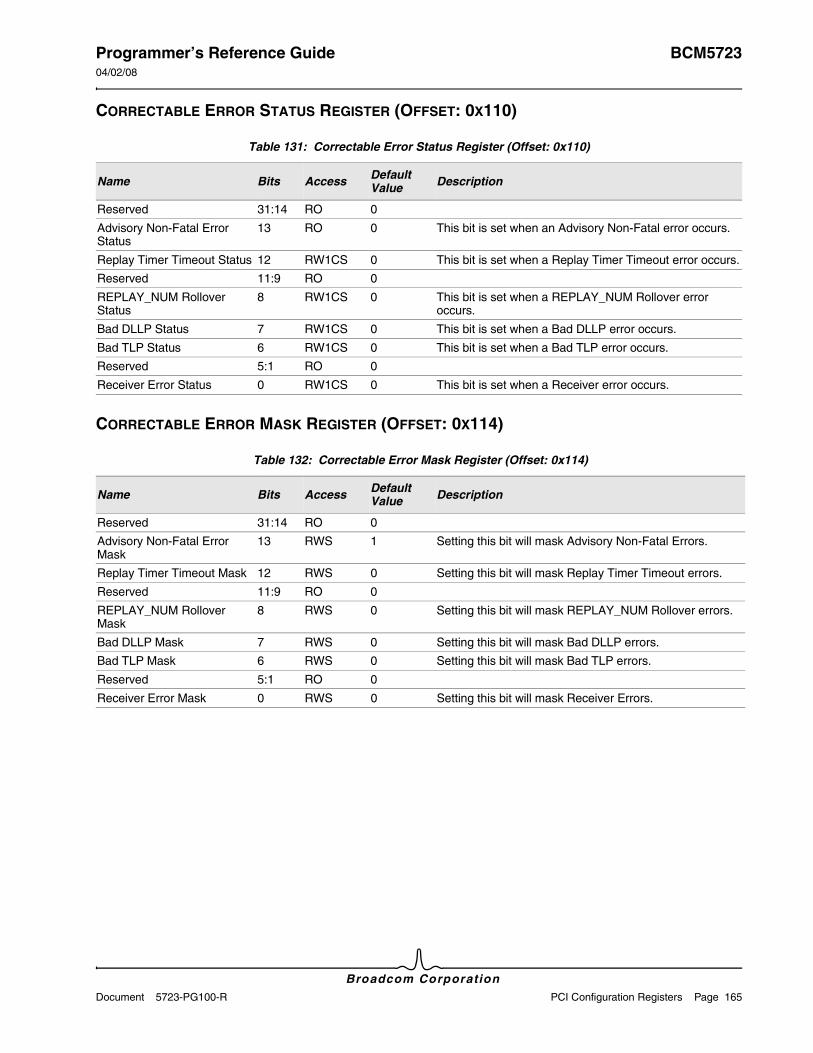
Programmer’s Reference Guide BCM572304/02/08
Broadcom CorporationDocument 5723-PG100-R PCI Configuration Registers Page 165
CORRECTABLE ERROR STATUS REGISTER (OFFSET: 0X110)
CORRECTABLE ERROR MASK REGISTER (OFFSET: 0X114)
Table 131: Correctable Error Status Register (Offset: 0x110)
Name Bits Access Default Value Description
Reserved 31:14 RO 0
Advisory Non-Fatal Error Status
13 RO 0 This bit is set when an Advisory Non-Fatal error occurs.
Replay Timer Timeout Status 12 RW1CS 0 This bit is set when a Replay Timer Timeout error occurs.
Reserved 11:9 RO 0
REPLAY_NUM Rollover Status
8 RW1CS 0 This bit is set when a REPLAY_NUM Rollover error occurs.
Bad DLLP Status 7 RW1CS 0 This bit is set when a Bad DLLP error occurs.
Bad TLP Status 6 RW1CS 0 This bit is set when a Bad TLP error occurs.
Reserved 5:1 RO 0
Receiver Error Status 0 RW1CS 0 This bit is set when a Receiver error occurs.
Table 132: Correctable Error Mask Register (Offset: 0x114)
Name Bits Access Default Value Description
Reserved 31:14 RO 0
Advisory Non-Fatal Error Mask
13 RWS 1 Setting this bit will mask Advisory Non-Fatal Errors.
Replay Timer Timeout Mask 12 RWS 0 Setting this bit will mask Replay Timer Timeout errors.
Reserved 11:9 RO 0
REPLAY_NUM Rollover Mask
8 RWS 0 Setting this bit will mask REPLAY_NUM Rollover errors.
Bad DLLP Mask 7 RWS 0 Setting this bit will mask Bad DLLP errors.
Bad TLP Mask 6 RWS 0 Setting this bit will mask Bad TLP errors.
Reserved 5:1 RO 0
Receiver Error Mask 0 RWS 0 Setting this bit will mask Receiver Errors.
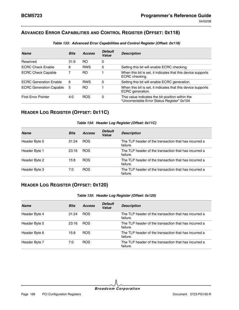
BCM5723 Programmer’s Reference Guide04/02/08
Broadcom Corporation
Page 166 PCI Configuration Registers Document 5723-PG100-R
ADVANCED ERROR CAPABILITIES AND CONTROL REGISTER (OFFSET: 0X118)
HEADER LOG REGISTER (OFFSET: 0X11C)
HEADER LOG REGISTER (OFFSET: 0X120)
Table 133: Advanced Error Capabilities and Control Register (Offset: 0x118)
Name Bits Access Default Value Description
Reserved 31:9 RO 0
ECRC Check Enable 8 RWS 0 Setting this bit will enable ECRC checking.
ECRC Check Capable 7 RO 1 When this bit is set, it indicates that this device supports ECRC checking.
ECRC Generation Enable 6 RWS 0 Setting this bit will enable ECRC generation.
ECRC Generation Capable 5 RO 1 When this bit is set, it indicates that this device supports ECRC generation.
First Error Pointer 4:0 ROS 0 This value indicates the bit position within the “Uncorrectable Error Status Register” 0x104.
Table 134: Header Log Register (Offset: 0x11C)
Name Bits Access Default Value Description
Header Byte 0 31:24 ROS The TLP header of the transaction that has incurred a failure.
Header Byte 1 23:16 ROS The TLP header of the transaction that has incurred a failure.
Header Byte 2 15:8 ROS The TLP header of the transaction that has incurred a failure.
Header Byte 3 7:0 ROS The TLP header of the transaction that has incurred a failure.
Table 135: Header Log Register (Offset: 0x120)
Name Bits Access Default Value Description
Header Byte 4 31:24 ROS The TLP header of the transaction that has incurred a failure.
Header Byte 5 23:16 ROS The TLP header of the transaction that has incurred a failure.
Header Byte 6 15:8 ROS The TLP header of the transaction that has incurred a failure.
Header Byte 7 7:0 ROS The TLP header of the transaction that has incurred a failure.
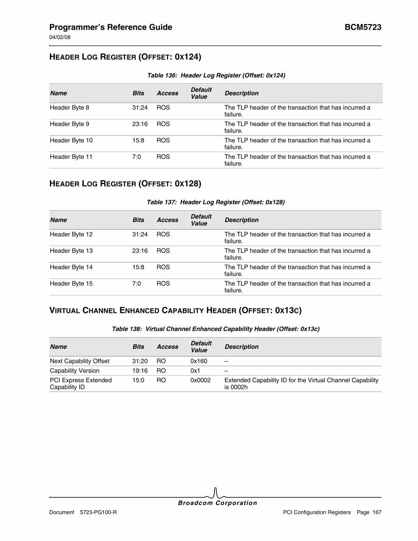
Programmer’s Reference Guide BCM572304/02/08
Broadcom CorporationDocument 5723-PG100-R PCI Configuration Registers Page 167
HEADER LOG REGISTER (OFFSET: 0X124)
HEADER LOG REGISTER (OFFSET: 0X128)
VIRTUAL CHANNEL ENHANCED CAPABILITY HEADER (OFFSET: 0X13C)
Table 136: Header Log Register (Offset: 0x124)
Name Bits Access Default Value Description
Header Byte 8 31:24 ROS The TLP header of the transaction that has incurred a failure.
Header Byte 9 23:16 ROS The TLP header of the transaction that has incurred a failure.
Header Byte 10 15:8 ROS The TLP header of the transaction that has incurred a failure.
Header Byte 11 7:0 ROS The TLP header of the transaction that has incurred a failure.
Table 137: Header Log Register (Offset: 0x128)
Name Bits Access Default Value Description
Header Byte 12 31:24 ROS The TLP header of the transaction that has incurred a failure.
Header Byte 13 23:16 ROS The TLP header of the transaction that has incurred a failure.
Header Byte 14 15:8 ROS The TLP header of the transaction that has incurred a failure.
Header Byte 15 7:0 ROS The TLP header of the transaction that has incurred a failure.
Table 138: Virtual Channel Enhanced Capability Header (Offset: 0x13c)
Name Bits Access Default Value Description
Next Capability Offset 31:20 RO 0x160 –
Capability Version 19:16 RO 0x1 –
PCI Express Extended Capability ID
15:0 RO 0x0002 Extended Capability ID for the Virtual Channel Capability is 0002h
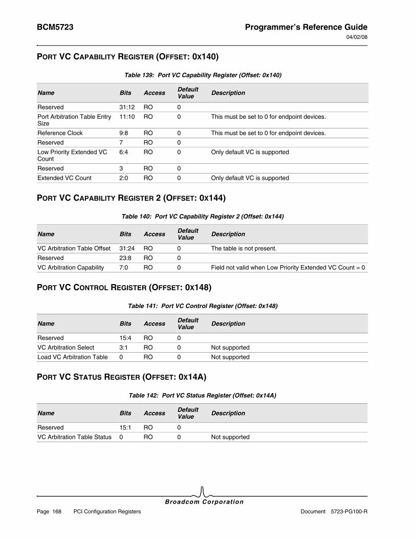
BCM5723 Programmer’s Reference Guide04/02/08
Broadcom Corporation
Page 168 PCI Configuration Registers Document 5723-PG100-R
PORT VC CAPABILITY REGISTER (OFFSET: 0X140)
PORT VC CAPABILITY REGISTER 2 (OFFSET: 0X144)
PORT VC CONTROL REGISTER (OFFSET: 0X148)
PORT VC STATUS REGISTER (OFFSET: 0X14A)
Table 139: Port VC Capability Register (Offset: 0x140)
Name Bits Access Default Value Description
Reserved 31:12 RO 0
Port Arbitration Table Entry Size
11:10 RO 0 This must be set to 0 for endpoint devices.
Reference Clock 9:8 RO 0 This must be set to 0 for endpoint devices.
Reserved 7 RO 0
Low Priority Extended VC Count
6:4 RO 0 Only default VC is supported
Reserved 3 RO 0
Extended VC Count 2:0 RO 0 Only default VC is supported
Table 140: Port VC Capability Register 2 (Offset: 0x144)
Name Bits Access Default Value Description
VC Arbitration Table Offset 31:24 RO 0 The table is not present.
Reserved 23:8 RO 0
VC Arbitration Capability 7:0 RO 0 Field not valid when Low Priority Extended VC Count = 0
Table 141: Port VC Control Register (Offset: 0x148)
Name Bits Access Default Value Description
Reserved 15:4 RO 0
VC Arbitration Select 3:1 RO 0 Not supported
Load VC Arbitration Table 0 RO 0 Not supported
Table 142: Port VC Status Register (Offset: 0x14A)
Name Bits Access Default Value Description
Reserved 15:1 RO 0
VC Arbitration Table Status 0 RO 0 Not supported
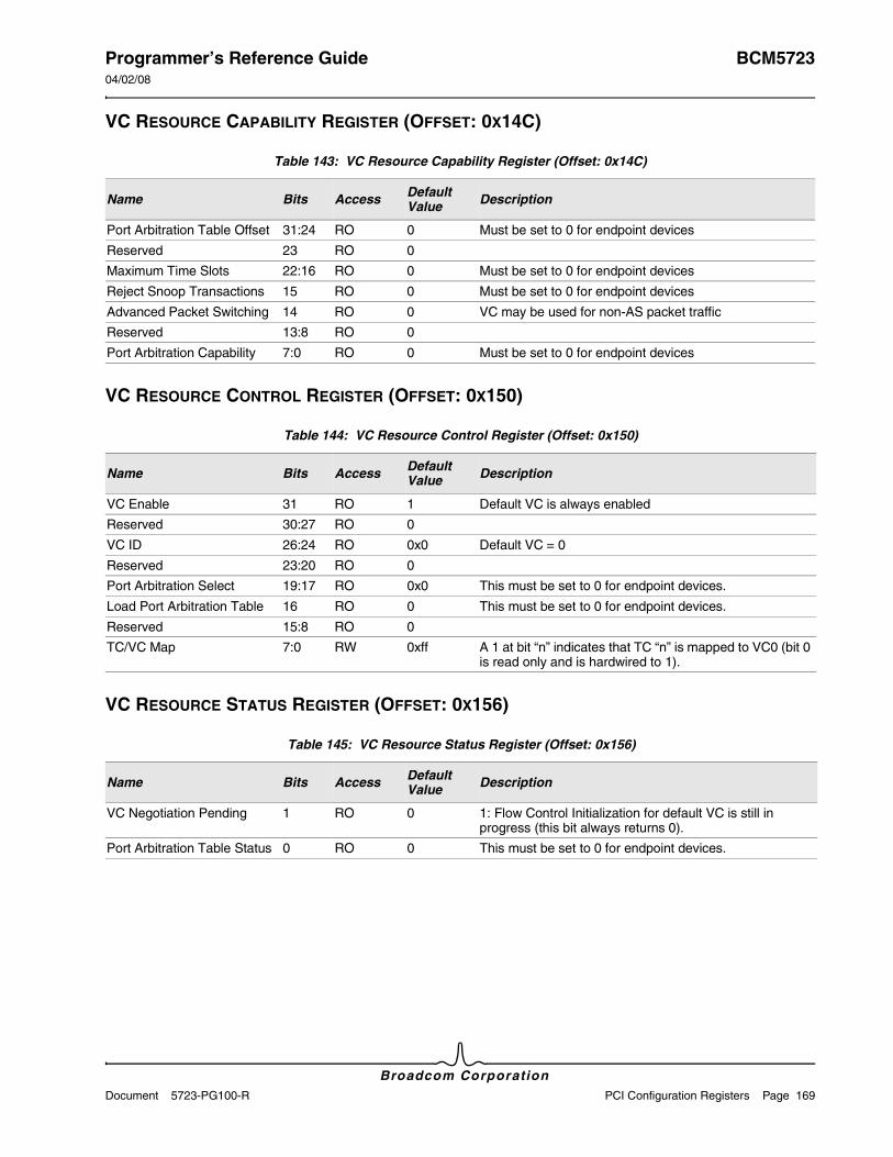
Programmer’s Reference Guide BCM572304/02/08
Broadcom CorporationDocument 5723-PG100-R PCI Configuration Registers Page 169
VC RESOURCE CAPABILITY REGISTER (OFFSET: 0X14C)
VC RESOURCE CONTROL REGISTER (OFFSET: 0X150)
VC RESOURCE STATUS REGISTER (OFFSET: 0X156)
Table 143: VC Resource Capability Register (Offset: 0x14C)
Name Bits Access Default Value Description
Port Arbitration Table Offset 31:24 RO 0 Must be set to 0 for endpoint devices
Reserved 23 RO 0
Maximum Time Slots 22:16 RO 0 Must be set to 0 for endpoint devices
Reject Snoop Transactions 15 RO 0 Must be set to 0 for endpoint devices
Advanced Packet Switching 14 RO 0 VC may be used for non-AS packet traffic
Reserved 13:8 RO 0
Port Arbitration Capability 7:0 RO 0 Must be set to 0 for endpoint devices
Table 144: VC Resource Control Register (Offset: 0x150)
Name Bits Access Default Value Description
VC Enable 31 RO 1 Default VC is always enabled
Reserved 30:27 RO 0
VC ID 26:24 RO 0x0 Default VC = 0
Reserved 23:20 RO 0
Port Arbitration Select 19:17 RO 0x0 This must be set to 0 for endpoint devices.
Load Port Arbitration Table 16 RO 0 This must be set to 0 for endpoint devices.
Reserved 15:8 RO 0
TC/VC Map 7:0 RW 0xff A 1 at bit “n” indicates that TC “n” is mapped to VC0 (bit 0 is read only and is hardwired to 1).
Table 145: VC Resource Status Register (Offset: 0x156)
Name Bits Access Default Value Description
VC Negotiation Pending 1 RO 0 1: Flow Control Initialization for default VC is still in progress (this bit always returns 0).
Port Arbitration Table Status 0 RO 0 This must be set to 0 for endpoint devices.
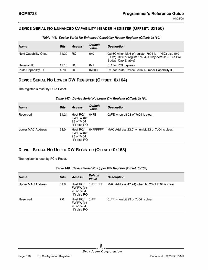
BCM5723 Programmer’s Reference Guide04/02/08
Broadcom Corporation
Page 170 PCI Configuration Registers Document 5723-PG100-R
DEVICE SERIAL NO ENHANCED CAPABILITY HEADER REGISTER (OFFSET: 0X160)
DEVICE SERIAL NO LOWER DW REGISTER (OFFSET: 0X164)
The register is reset by PCIe Reset.
DEVICE SERIAL NO UPPER DW REGISTER (OFFSET: 0X168)
The register is reset by PCIe Reset.
Table 146: Device Serial No Enhanced Capability Header Register (Offset: 0x160)
Name Bits Access Default Value Description
Next Capability Offset 31:20 RO 0x0 0x16C when bit 6 of register 7c04 is 1 (NIC) else 0x0 (LOM). Bit 6 of register 7c04 is 0 by default. (PCIe Pwr Budget Cap Enable)
Revision ID 19:16 RO 0x1 0x1 for PCI Express
PCIe Capability ID 15:0 RO 0x0003 0x3 for PCIe Device Serial Number Capability ID
Table 147: Device Serial No Lower DW Register (Offset: 0x164)
Name Bits Access Default Value Description
Reserved 31:24 Host RO/FW RW (bit 23 of 7c04 ‘1’) else RO
0xFE 0xFE when bit 23 of 7c04 is clear.
Lower MAC Address 23:0 Host RO/FW RW (bit 23 of 7c04 ‘1’) else RO
0xFFFFFF MAC Address(23:0) when bit 23 of 7c04 is clear.
Table 148: Device Serial No Upper DW Register (Offset: 0x168)
Name Bits Access Default Value Description
Upper MAC Address 31:8 Host RO/FW RW (bit 23 of 7c04 ‘1’) else RO
0xFFFFFF MAC Address(47:24) when bit 23 of 7c04 is clear
Reserved 7:0 Host RO/FW RW (bit 23 of 7c04 ‘1’) else RO
0xFF 0xFF when bit 23 of 7c04 is clear.
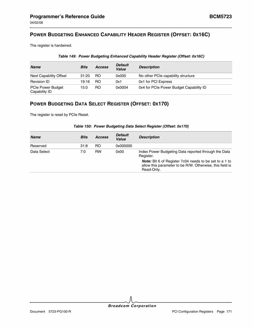
Programmer’s Reference Guide BCM572304/02/08
Broadcom CorporationDocument 5723-PG100-R PCI Configuration Registers Page 171
POWER BUDGETING ENHANCED CAPABILITY HEADER REGISTER (OFFSET: 0X16C)
The register is hardwired.
POWER BUDGETING DATA SELECT REGISTER (OFFSET: 0X170)
The register is reset by PCIe Reset.
Table 149: Power Budgeting Enhanced Capability Header Register (Offset: 0x16C)
Name Bits Access Default Value Description
Next Capability Offset 31:20 RO 0x000 No other PCIe capability structure
Revision ID 19:16 RO 0x1 0x1 for PCI Express
PCIe Power Budget Capability ID
15:0 RO 0x0004 0x4 for PCIe Power Budget Capability ID
Table 150: Power Budgeting Data Select Register (Offset: 0x170)
Name Bits Access Default Value Description
Reserved 31:8 RO 0x000000
Data Select 7:0 RW 0x00 Index Power Budgeting Data reported through the Data Register.
Note: Bit 6 of Register 7c04 needs to be set to a 1 to allow this parameter to be R/W. Otherwise, this field is Read-Only.
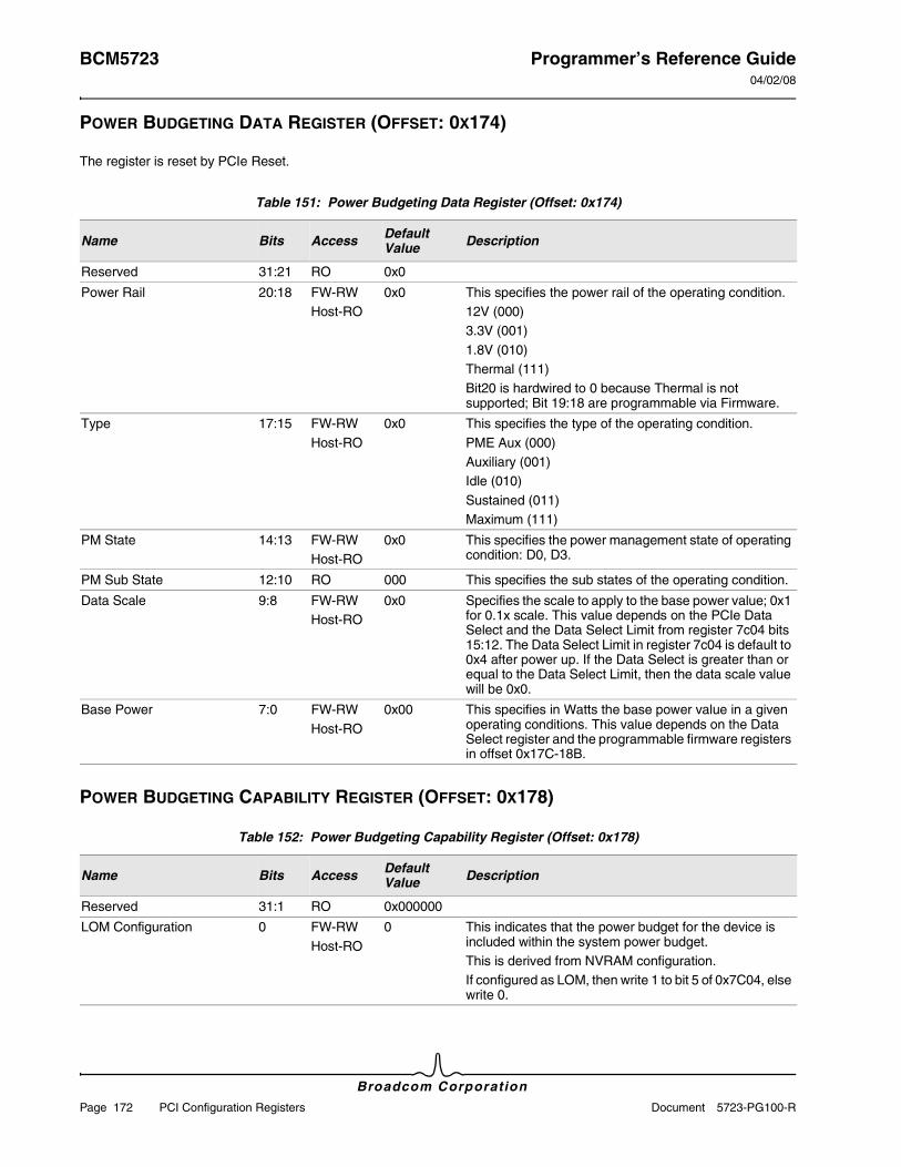
BCM5723 Programmer’s Reference Guide04/02/08
Broadcom Corporation
Page 172 PCI Configuration Registers Document 5723-PG100-R
POWER BUDGETING DATA REGISTER (OFFSET: 0X174)
The register is reset by PCIe Reset.
POWER BUDGETING CAPABILITY REGISTER (OFFSET: 0X178)
Table 151: Power Budgeting Data Register (Offset: 0x174)
Name Bits Access Default Value Description
Reserved 31:21 RO 0x0
Power Rail 20:18 FW-RWHost-RO
0x0 This specifies the power rail of the operating condition.12V (000)3.3V (001)1.8V (010)Thermal (111)Bit20 is hardwired to 0 because Thermal is not supported; Bit 19:18 are programmable via Firmware.
Type 17:15 FW-RWHost-RO
0x0 This specifies the type of the operating condition.PME Aux (000)Auxiliary (001)Idle (010)Sustained (011)Maximum (111)
PM State 14:13 FW-RWHost-RO
0x0 This specifies the power management state of operating condition: D0, D3.
PM Sub State 12:10 RO 000 This specifies the sub states of the operating condition.
Data Scale 9:8 FW-RWHost-RO
0x0 Specifies the scale to apply to the base power value; 0x1 for 0.1x scale. This value depends on the PCIe Data Select and the Data Select Limit from register 7c04 bits 15:12. The Data Select Limit in register 7c04 is default to 0x4 after power up. If the Data Select is greater than or equal to the Data Select Limit, then the data scale value will be 0x0.
Base Power 7:0 FW-RWHost-RO
0x00 This specifies in Watts the base power value in a given operating conditions. This value depends on the Data Select register and the programmable firmware registers in offset 0x17C-18B.
Table 152: Power Budgeting Capability Register (Offset: 0x178)
Name Bits Access Default Value Description
Reserved 31:1 RO 0x000000
LOM Configuration 0 FW-RWHost-RO
0 This indicates that the power budget for the device is included within the system power budget.This is derived from NVRAM configuration.If configured as LOM, then write 1 to bit 5 of 0x7C04, else write 0.
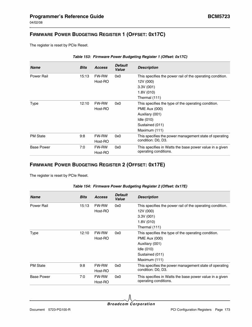
Programmer’s Reference Guide BCM572304/02/08
Broadcom CorporationDocument 5723-PG100-R PCI Configuration Registers Page 173
FIRMWARE POWER BUDGETING REGISTER 1 (OFFSET: 0X17C)
The register is reset by PCIe Reset.
FIRMWARE POWER BUDGETING REGISTER 2 (OFFSET: 0X17E)
The register is reset by PCIe Reset.
Table 153: Firmware Power Budgeting Register 1 (Offset: 0x17C)
Name Bits Access Default Value Description
Power Rail 15:13 FW-RWHost-RO
0x0 This specifies the power rail of the operating condition.12V (000)3.3V (001)1.8V (010)Thermal (111)
Type 12:10 FW-RWHost-RO
0x0 This specifies the type of the operating condition.PME Aux (000)Auxiliary (001)Idle (010)Sustained (011)Maximum (111)
PM State 9:8 FW-RWHost-RO
0x0 This specifies the power management state of operating condition: D0, D3.
Base Power 7:0 FW-RWHost-RO
0x0 This specifies in Watts the base power value in a given operating conditions.
Table 154: Firmware Power Budgeting Register 2 (Offset: 0x17E)
Name Bits Access Default Value Description
Power Rail 15:13 FW-RWHost-RO
0x0 This specifies the power rail of the operating condition.12V (000)3.3V (001)1.8V (010)Thermal (111)
Type 12:10 FW-RWHost-RO
0x0 This specifies the type of the operating condition.PME Aux (000)Auxiliary (001)Idle (010)Sustained (011)Maximum (111)
PM State 9:8 FW-RWHost-RO
0x0 This specifies the power management state of operating condition: D0, D3.
Base Power 7:0 FW-RWHost-RO
0x0 This specifies in Watts the base power value in a given operating conditions.
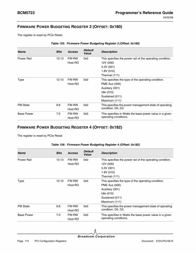
BCM5723 Programmer’s Reference Guide04/02/08
Broadcom Corporation
Page 174 PCI Configuration Registers Document 5723-PG100-R
FIRMWARE POWER BUDGETING REGISTER 3 (OFFSET: 0X180)
The register is reset by PCIe Reset.
FIRMWARE POWER BUDGETING REGISTER 4 (OFFSET: 0X182)
The register is reset by PCIe Reset.
Table 155: Firmware Power Budgeting Register 3 (Offset: 0x180)
Name Bits Access Default Value Description
Power Rail 15:13 FW-RWHost-RO
0x0 This specifies the power rail of the operating condition.12V (000)3.3V (001)1.8V (010)Thermal (111)
Type 12:10 FW-RWHost-RO
0x0 This specifies the type of the operating condition.PME Aux (000)Auxiliary (001)Idle (010)Sustained (011)Maximum (111)
PM State 9:8 FW-RWHost-RO
0x0 This specifies the power management state of operating condition: D0, D3.
Base Power 7:0 FW-RWHost-RO
0x0 This specifies in Watts the base power value in a given operating conditions.
Table 156: Firmware Power Budgeting Register 4 (Offset: 0x182)
Name Bits Access Default Value Description
Power Rail 15:13 FW-RWHost-RO
0x0 This specifies the power rail of the operating condition.12V (000)3.3V (001)1.8V (010)Thermal (111)
Type 12:10 FW-RWHost-RO
0x0 This specifies the type of the operating condition.PME Aux (000)Auxiliary (001)Idle (010)Sustained (011)Maximum (111)
PM State 9:8 FW-RWHost-RO
0x0 This specifies the power management state of operating condition: D0, D3.
Base Power 7:0 FW-RWHost-RO
0x0 This specifies in Watts the base power value in a given operating conditions.
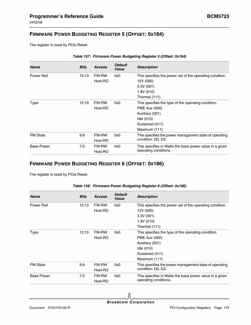
Programmer’s Reference Guide BCM572304/02/08
Broadcom CorporationDocument 5723-PG100-R PCI Configuration Registers Page 175
FIRMWARE POWER BUDGETING REGISTER 5 (OFFSET: 0X184)
The register is reset by PCIe Reset.
FIRMWARE POWER BUDGETING REGISTER 6 (OFFSET: 0X186)
The register is reset by PCIe Reset.
Table 157: Firmware Power Budgeting Register 5 (Offset: 0x184)
Name Bits Access Default Value Description
Power Rail 15:13 FW-RWHost-RO
0x0 This specifies the power rail of the operating condition.12V (000)3.3V (001)1.8V (010)Thermal (111)
Type 12:10 FW-RWHost-RO
0x0 This specifies the type of the operating condition.PME Aux (000)Auxiliary (001)Idle (010)Sustained (011)Maximum (111)
PM State 9:8 FW-RWHost-RO
0x0 This specifies the power management state of operating condition: D0, D3.
Base Power 7:0 FW-RWHost-RO
0x0 This specifies in Watts the base power value in a given operating conditions.
Table 158: Firmware Power Budgeting Register 6 (Offset: 0x186)
Name Bits Access Default Value Description
Power Rail 15:13 FW-RWHost-RO
0x0 This specifies the power rail of the operating condition.12V (000)3.3V (001)1.8V (010)Thermal (111)
Type 12:10 FW-RWHost-RO
0x0 This specifies the type of the operating condition.PME Aux (000)Auxiliary (001)Idle (010)Sustained (011)Maximum (111)
PM State 9:8 FW-RWHost-RO
0x0 This specifies the power management state of operating condition: D0, D3.
Base Power 7:0 FW-RWHost-RO
0x0 This specifies in Watts the base power value in a given operating conditions.

BCM5723 Programmer’s Reference Guide04/02/08
Broadcom Corporation
Page 176 PCI Configuration Registers Document 5723-PG100-R
FIRMWARE POWER BUDGETING REGISTER 7 (OFFSET: 0X188)
The register is reset by PCIe Reset.
FIRMWARE POWER BUDGETING REGISTER 8 (OFFSET: 0X18A)
The register is reset by PCIe Reset.
Table 159: Firmware Power Budgeting Register 7 (Offset: 0x188)
Name Bits Access Default Value Description
Power Rail 15:13 FW-RWHost-RO
0x0 This specifies the power rail of the operating condition.12V (000)3.3V (001)1.8V (010)Thermal (111)
Type 12:10 FW-RWHost-RO
0x0 This specifies the type of the operating condition.PME Aux (000)Auxiliary (001)Idle (010)Sustained (011)Maximum (111)
PM State 9:8 FW-RWHost-RO
0x0 This specifies the power management state of operating condition: D0, D3.
Base Power 7:0 FW-RWHost-RO
0x0 This specifies in Watts the base power value in a given operating conditions.
Table 160: Firmware Power Budgeting Register 8 (Offset: 0x18A)
Name Bits Access Default Value Description
Power Rail 15:13 FW-RWHost-RO
0x0 This specifies the power rail of the operating condition.12V (000)3.3V (001)1.8V (010)Thermal (111)
Type 12:10 FW-RWHost-RO
0x0 This specifies the type of the operating condition.PME Aux (000)Auxiliary (001)Idle (010)Sustained (011)Maximum (111)
PM State 9:8 FW-RWHost-RO
0x0 This specifies the power management state of operating condition: D0, D3.
Base Power 7:0 FW-RWHost-RO
0x0 This specifies in Watts the base power value in a given operating conditions.

Programmer’s Reference Guide BCM572304/02/08
Broadcom CorporationDocument 5723-PG100-R PCI Configuration Registers Page 177
PCIE 1.1 ADVISORY NON-FATAL ERROR MASKING (OFFSET: 0X18C)
The register is reset by PCIe Reset.
Table 161: PCIe 1.1 Advisory Non-Fatal Error Masking (Offset: 0x18C)
Name Bits Access Default Value Description
Retry Poison 5 FW-RWHost-RW via Memory CycleHost –RO via Config cycle
0x1 Enable DMA Read Engine to retry poison completion packet.1: Enable0: Disable
Poison Advisory Non-Fatal Enable
4 FW-RWHost-RW via Memory CycleHost –RO via Config cycle
0x1 Enable Poison Error to be classified as Advisory Non-Fatal Correctable Error.1: Enable0: Disable
Unexpected Advisory Non-Fatal Enable
3 FW-RWHost-RW via Memory CycleHost –RO via Config cycle
0x1 Enable Unexpected Completion Error to be classified as Advisory Non-Fatal Correctable Error.1: Enable0: Disable
Non-Posted Cfg Advisory Non-Fatal Enable
2 FW-RWHost-RW via Memory CycleHost –RO via Config cycle
0x1 Enable UR/CA error as a result of Non-Posted Configuration Access to be classified as Advisory Non-Fatal Correctable Error.1: Enable0: Disable
NP Memory Read Advisory Non-Fatal Enable
1 FW-RWHost-RW via Memory CycleHost –RO via Config cycle
0x1 Enable UR/CA error as a result of Non-Posted Memory Read Access to be classified as Advisory Non-Fatal Correctable Error.1: Enable0: Disable
Completion Abort Memory Read Advisory Non-Fatal Enable
0 FW-RWHost-RW via Memory CycleHost –RO via Config cycle
0x1 Enable CA error as a result of Memory Read Access to be classified as Advisory Non-Fatal Correctable Error.1: Enable0: Disable
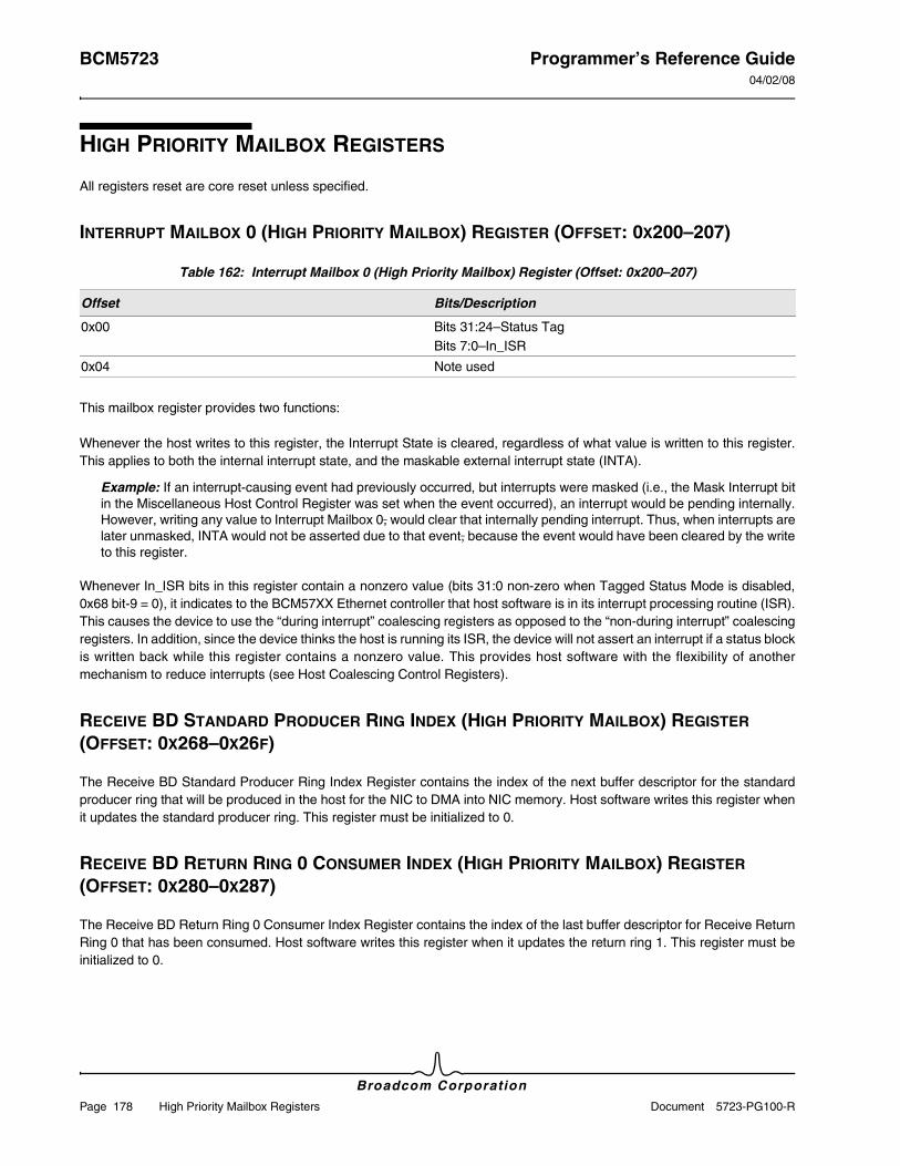
BCM5723 Programmer’s Reference Guide04/02/08
Broadcom Corporation
Page 178 High Priority Mailbox Registers Document 5723-PG100-R
HIGH PRIORITY MAILBOX REGISTERS
All registers reset are core reset unless specified.
INTERRUPT MAILBOX 0 (HIGH PRIORITY MAILBOX) REGISTER (OFFSET: 0X200–207)
This mailbox register provides two functions:
Whenever the host writes to this register, the Interrupt State is cleared, regardless of what value is written to this register. This applies to both the internal interrupt state, and the maskable external interrupt state (INTA).
Example: If an interrupt-causing event had previously occurred, but interrupts were masked (i.e., the Mask Interrupt bit in the Miscellaneous Host Control Register was set when the event occurred), an interrupt would be pending internally. However, writing any value to Interrupt Mailbox 0, would clear that internally pending interrupt. Thus, when interrupts are later unmasked, INTA would not be asserted due to that event, because the event would have been cleared by the write to this register.
Whenever In_ISR bits in this register contain a nonzero value (bits 31:0 non-zero when Tagged Status Mode is disabled, 0x68 bit-9 = 0), it indicates to the BCM57XX Ethernet controller that host software is in its interrupt processing routine (ISR). This causes the device to use the “during interrupt” coalescing registers as opposed to the “non-during interrupt” coalescing registers. In addition, since the device thinks the host is running its ISR, the device will not assert an interrupt if a status block is written back while this register contains a nonzero value. This provides host software with the flexibility of another mechanism to reduce interrupts (see Host Coalescing Control Registers).
RECEIVE BD STANDARD PRODUCER RING INDEX (HIGH PRIORITY MAILBOX) REGISTER (OFFSET: 0X268–0X26F)
The Receive BD Standard Producer Ring Index Register contains the index of the next buffer descriptor for the standard producer ring that will be produced in the host for the NIC to DMA into NIC memory. Host software writes this register when it updates the standard producer ring. This register must be initialized to 0.
RECEIVE BD RETURN RING 0 CONSUMER INDEX (HIGH PRIORITY MAILBOX) REGISTER (OFFSET: 0X280–0X287)
The Receive BD Return Ring 0 Consumer Index Register contains the index of the last buffer descriptor for Receive Return Ring 0 that has been consumed. Host software writes this register when it updates the return ring 1. This register must be initialized to 0.
Table 162: Interrupt Mailbox 0 (High Priority Mailbox) Register (Offset: 0x200–207)
Offset Bits/Description
0x00 Bits 31:24–Status TagBits 7:0–In_ISR
0x04 Note used
Programmer’s Reference Guide BCM572304/02/08
Broadcom CorporationDocument 5723-PG100-R EthernetMAC Registers Page 179
RECEIVE BD RETURN RING 1 CONSUMER INDEX (HIGH PRIORITY MAILBOX) REGISTER (OFFSET: 0X288–0X28F)
The Receive BD Return Ring 1 Consumer Index Register contains the index of the last buffer descriptor for Receive Return Ring 1 that has been consumed. Host software writes this register when it updates the return ring 1. This register must be initialized to 0.
RECEIVE BD RETURN RING 2 CONSUMER INDEX (HIGH PRIORITY MAILBOX) REGISTER (OFFSET: 0X290–0X297)
The Receive BD Return Ring 2 Consumer Index Register contains the index of the last buffer descriptor for Receive Return Ring 2 that has been consumed. Host software writes this register when it updates the return ring 2. This register must be initialized to 0.
RECEIVE BD RETURN RING 3 CONSUMER INDEX (HIGH PRIORITY MAILBOX) REGISTER (OFFSET: 0X298–0X29F)
The Receive BD Return Ring 3 Consumer Index Register contains the index of the last buffer descriptor for Receive Return Ring 3 that has been consumed. Host software writes this register when it updates the return ring 3. This register must be initialized to 0.
SEND BD RING HOST PRODUCER INDEX (HIGH PRIORITY MAILBOX) REGISTER (OFFSET: 0X300–0X307)
The Send BD Ring Host Producer Index Register contains the index of the next buffer descriptor for a given send ring that will be produced in the host for the NIC to DMA into NIC memory. Host software writes this register when it updates the given send ring. This register must be initialized to 0.
ETHERNETMAC REGISTERS
All registers reset are core reset unless specified.
EMAC MODE REGISTER (OFFSET: 0X400)
Table 163: EMAC Mode Register (Offset: 0x400)
Name Bits Access Default Value Description
Reserved 31:29 RO 0
Enable APE TX path 28 RW 0 This bit must be written a 1 for the EMAC to transmit APE packets.
Enable APE RX path 27 RW 0 This bit must be written a 1 for APE subsystem to receive packets from the EMAC.

BCM5723 Programmer’s Reference Guide04/02/08
Broadcom Corporation
Page 180 EthernetMAC Registers Document 5723-PG100-R
Free Running ACPI 26 RW 0 When this bit is set, the ACPI state machine will continue running when a match is found. When this bit is clear, the ACPI state machine will halt when a match is found.
Halt Interesting packet PME 25 RW 0 When this bit is set, the WOL signal will not be asserted on an interesting packet match.
Keep Frame in WOL 24 RW 0
Enable FHDE 23 RW 0 Enable receive Frame Header DMA engine. Must be set for normal operation
Enable RDE 22 RW 0 Enable RDMA engine. Must be set for normal operation
Enable TDE 21 RW 0 Enable Transmit DMA engine
Reserved 20 RO 0
ACPI Power-on Enable 19 RW 0 Enable Wake on LAN filters when in powerdown mode
Magic Packet Detection Enable
18 RW 0 Enable Magic Packet detection
Send Config Command 17 RW 0 Send config commands when in TBI mode
Flush TX statistics 16 RW 0 Write transmit statistics to external memoryThis bit is self-clearing.
Clear TX statistics 15 RW 0 Clear transmit statistics internal RAMThis bit is self-clearing.
Enable TX Statistics 14 RW 0 Enable transmit statistics external updates
Flush RX Statistics 13 RW 0 Write receive statistics to external memoryThis bit is self-clearing.
Clear RX Statistics 12 RW 0 Clear receive statistics internal RAMThis bit is self-clearing.
Enable RX Statistics 11 RW 0 Enable receive statistics external updates
Reserved 10 RO 0
Max Defer 9 RW 0 Enable Max Deferral checking statistic
Enable TX Bursting 8 RW 0 Enable transmit bursting in gigabit half-duplex mode
Tagged MAC Control 7 RW 0 Allow the MAC to receive tagged MAC control packets
Reserved 6:5 RO 0
Loopback mode 4 RW 0 When set, an internal loopback path is enabled from the transmit MAC to the receive MAC. This bit is provided for diagnostic purposes only.
Port Mode 3:2 RW 01 These bits determine what interface the port is running11: TBI10: GMII01: MII00: None (default)
Half-duplex 1 RW 0 When set, the MII/GMII interface is configured to operate in half-duplex mode and the CSMA/CD state machines in the MAC are set to half-duplex mode
Global Reset 0 RW 0 When this bit is set to 1, the MAC state machine is reset.This is a self-clearing bit.
Table 163: EMAC Mode Register (Offset: 0x400) (Cont.)
Name Bits Access Default Value Description
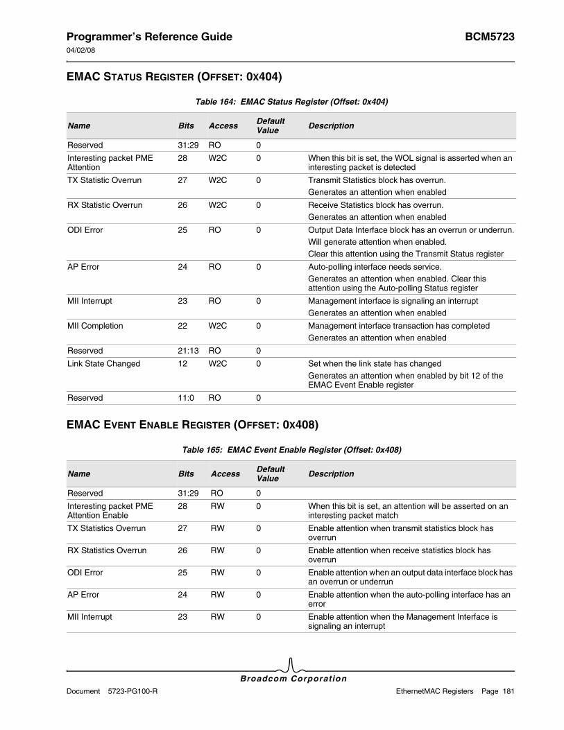
Programmer’s Reference Guide BCM572304/02/08
Broadcom CorporationDocument 5723-PG100-R EthernetMAC Registers Page 181
EMAC STATUS REGISTER (OFFSET: 0X404)
EMAC EVENT ENABLE REGISTER (OFFSET: 0X408)
Table 164: EMAC Status Register (Offset: 0x404)
Name Bits Access Default Value Description
Reserved 31:29 RO 0
Interesting packet PME Attention
28 W2C 0 When this bit is set, the WOL signal is asserted when an interesting packet is detected
TX Statistic Overrun 27 W2C 0 Transmit Statistics block has overrun.Generates an attention when enabled
RX Statistic Overrun 26 W2C 0 Receive Statistics block has overrun.Generates an attention when enabled
ODI Error 25 RO 0 Output Data Interface block has an overrun or underrun.Will generate attention when enabled.Clear this attention using the Transmit Status register
AP Error 24 RO 0 Auto-polling interface needs service.Generates an attention when enabled. Clear this attention using the Auto-polling Status register
MII Interrupt 23 RO 0 Management interface is signaling an interruptGenerates an attention when enabled
MII Completion 22 W2C 0 Management interface transaction has completedGenerates an attention when enabled
Reserved 21:13 RO 0
Link State Changed 12 W2C 0 Set when the link state has changedGenerates an attention when enabled by bit 12 of the EMAC Event Enable register
Reserved 11:0 RO 0
Table 165: EMAC Event Enable Register (Offset: 0x408)
Name Bits Access Default Value Description
Reserved 31:29 RO 0
Interesting packet PME Attention Enable
28 RW 0 When this bit is set, an attention will be asserted on an interesting packet match
TX Statistics Overrun 27 RW 0 Enable attention when transmit statistics block has overrun
RX Statistics Overrun 26 RW 0 Enable attention when receive statistics block has overrun
ODI Error 25 RW 0 Enable attention when an output data interface block has an overrun or underrun
AP Error 24 RW 0 Enable attention when the auto-polling interface has an error
MII Interrupt 23 RW 0 Enable attention when the Management Interface is signaling an interrupt
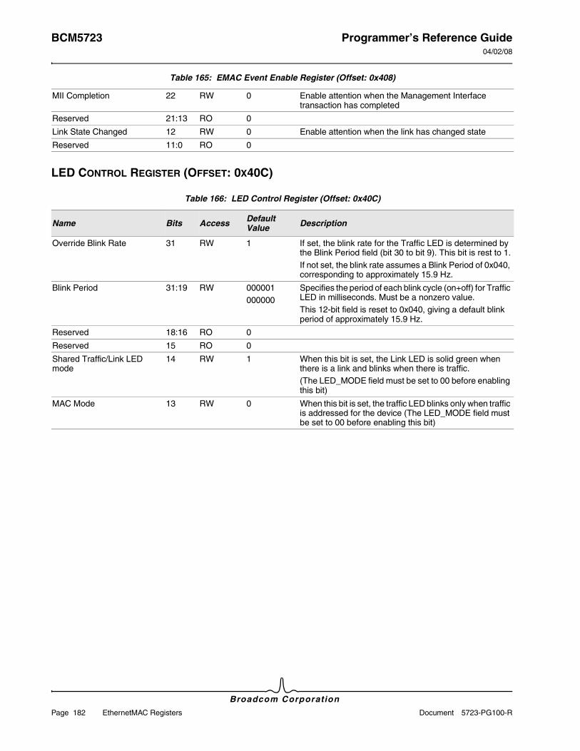
BCM5723 Programmer’s Reference Guide04/02/08
Broadcom Corporation
Page 182 EthernetMAC Registers Document 5723-PG100-R
LED CONTROL REGISTER (OFFSET: 0X40C)
MII Completion 22 RW 0 Enable attention when the Management Interface transaction has completed
Reserved 21:13 RO 0
Link State Changed 12 RW 0 Enable attention when the link has changed state
Reserved 11:0 RO 0
Table 166: LED Control Register (Offset: 0x40C)
Name Bits Access Default Value Description
Override Blink Rate 31 RW 1 If set, the blink rate for the Traffic LED is determined by the Blink Period field (bit 30 to bit 9). This bit is rest to 1.If not set, the blink rate assumes a Blink Period of 0x040, corresponding to approximately 15.9 Hz.
Blink Period 31:19 RW 000001000000
Specifies the period of each blink cycle (on+off) for Traffic LED in milliseconds. Must be a nonzero value.This 12-bit field is reset to 0x040, giving a default blink period of approximately 15.9 Hz.
Reserved 18:16 RO 0
Reserved 15 RO 0
Shared Traffic/Link LED mode
14 RW 1 When this bit is set, the Link LED is solid green when there is a link and blinks when there is traffic. (The LED_MODE field must be set to 00 before enabling this bit)
MAC Mode 13 RW 0 When this bit is set, the traffic LED blinks only when traffic is addressed for the device (The LED_MODE field must be set to 00 before enabling this bit)
Table 165: EMAC Event Enable Register (Offset: 0x408)
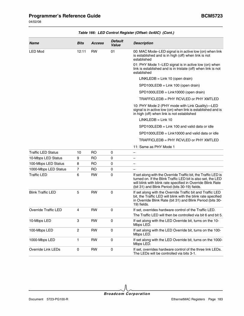
Programmer’s Reference Guide BCM572304/02/08
Broadcom CorporationDocument 5723-PG100-R EthernetMAC Registers Page 183
LED Mod 12:11 RW 01 00: MAC Mode–LED signal is in active low (on) when link is established and is in high (off) when link is not established01: PHY Mode 1–LED signal is in active low (on) when link is established and is in tristate (off) when link is not established
LINKLEDB = Link 10 (open drain)
SPD100LEDB = Link 100 (open drain)
SPD1000LEDB = Link10000 (open drain)
TRAFFICLEDB = PHY RCVLED or PHY XMTLED
10: PHY Mode 2 (PHY mode with Link Quality)—LED signal is in active low (on) when link is established and is in high (off) when link is not established
LINKLEDB = Link 10
SPD100LEDB = Link 100 and valid data or idle
SPD1000LEDB = Link10000 and valid data or idle
TRAFFICLEDB = PHY RCVLED or PHY XMTLED
11: Same as PHY Mode 1
Traffic LED Status 10 RO 0 –
10-Mbps LED Status 9 RO 0 –
100-Mbps LED Status 8 RO 0 –
1000-Mbps LED Status 7 RO 0 –
Traffic LED 6 RW 0 If set along with the Override Traffic bit, the Traffic LED is turned on. If the Blink Traffic LED bit is also set, the LED will blink with blink rate specified in Override Blink Rate (bit 31) and Blink Period (bits 30-19) fields.
Blink Traffic LED 5 RW 0 If set along with the Override Traffic bit and Traffic LED bit, the Traffic LED will blink with the blink rate specified in Override Blink Rate (bit 31) and Blink Period (bits 30-19) fields.
Override Traffic LED 4 RW 0 If set, overrides hardware control of the Traffic LED.The Traffic LED will then be controlled via bit 6 and bit 5.
10-Mbps LED 3 RW 0 If set along with the LED Override bit, turns on the 10-Mbps LED.
100-Mbps LED 2 RW 0 If set along with the LED Override bit, turns on the 100-Mbps LED.
1000-Mbps LED 1 RW 0 If set along with the LED Override bit, turns on the 1000-Mbps LED.
Override Link LEDs 0 RW 0 If set, overrides hardware control of the three link LEDs. The LEDs will be controlled via bits 3-1.
Table 166: LED Control Register (Offset: 0x40C) (Cont.)
Name Bits Access Default Value Description
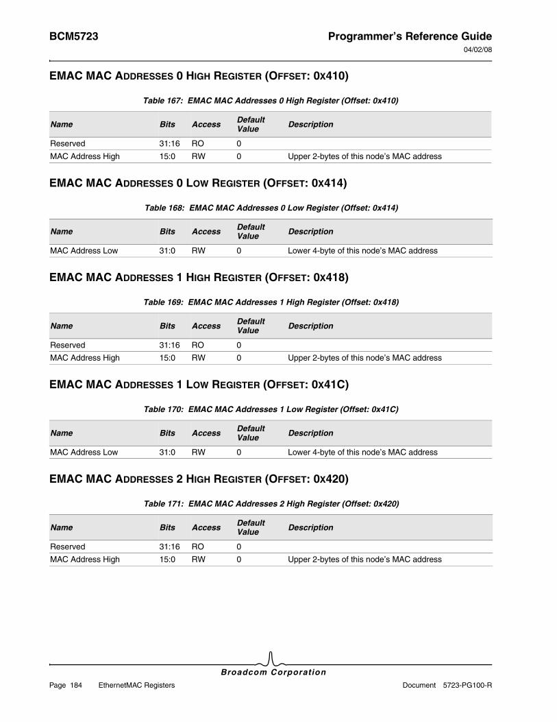
BCM5723 Programmer’s Reference Guide04/02/08
Broadcom Corporation
Page 184 EthernetMAC Registers Document 5723-PG100-R
EMAC MAC ADDRESSES 0 HIGH REGISTER (OFFSET: 0X410)
EMAC MAC ADDRESSES 0 LOW REGISTER (OFFSET: 0X414)
EMAC MAC ADDRESSES 1 HIGH REGISTER (OFFSET: 0X418)
EMAC MAC ADDRESSES 1 LOW REGISTER (OFFSET: 0X41C)
EMAC MAC ADDRESSES 2 HIGH REGISTER (OFFSET: 0X420)
Table 167: EMAC MAC Addresses 0 High Register (Offset: 0x410)
Name Bits Access Default Value Description
Reserved 31:16 RO 0
MAC Address High 15:0 RW 0 Upper 2-bytes of this node’s MAC address
Table 168: EMAC MAC Addresses 0 Low Register (Offset: 0x414)
Name Bits Access Default Value Description
MAC Address Low 31:0 RW 0 Lower 4-byte of this node’s MAC address
Table 169: EMAC MAC Addresses 1 High Register (Offset: 0x418)
Name Bits Access Default Value Description
Reserved 31:16 RO 0
MAC Address High 15:0 RW 0 Upper 2-bytes of this node’s MAC address
Table 170: EMAC MAC Addresses 1 Low Register (Offset: 0x41C)
Name Bits Access Default Value Description
MAC Address Low 31:0 RW 0 Lower 4-byte of this node’s MAC address
Table 171: EMAC MAC Addresses 2 High Register (Offset: 0x420)
Name Bits Access Default Value Description
Reserved 31:16 RO 0
MAC Address High 15:0 RW 0 Upper 2-bytes of this node’s MAC address
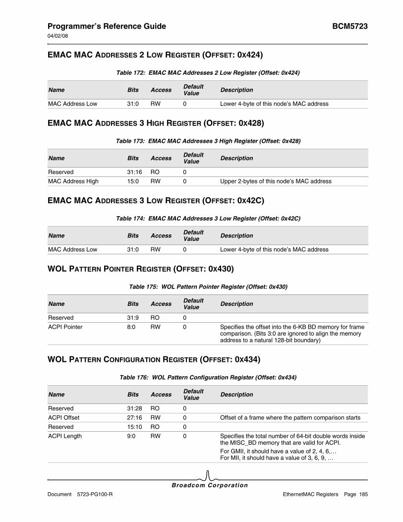
Programmer’s Reference Guide BCM572304/02/08
Broadcom CorporationDocument 5723-PG100-R EthernetMAC Registers Page 185
EMAC MAC ADDRESSES 2 LOW REGISTER (OFFSET: 0X424)
EMAC MAC ADDRESSES 3 HIGH REGISTER (OFFSET: 0X428)
EMAC MAC ADDRESSES 3 LOW REGISTER (OFFSET: 0X42C)
WOL PATTERN POINTER REGISTER (OFFSET: 0X430)
WOL PATTERN CONFIGURATION REGISTER (OFFSET: 0X434)
Table 172: EMAC MAC Addresses 2 Low Register (Offset: 0x424)
Name Bits Access Default Value Description
MAC Address Low 31:0 RW 0 Lower 4-byte of this node’s MAC address
Table 173: EMAC MAC Addresses 3 High Register (Offset: 0x428)
Name Bits Access Default Value Description
Reserved 31:16 RO 0
MAC Address High 15:0 RW 0 Upper 2-bytes of this node’s MAC address
Table 174: EMAC MAC Addresses 3 Low Register (Offset: 0x42C)
Name Bits Access Default Value Description
MAC Address Low 31:0 RW 0 Lower 4-byte of this node’s MAC address
Table 175: WOL Pattern Pointer Register (Offset: 0x430)
Name Bits Access Default Value Description
Reserved 31:9 RO 0
ACPI Pointer 8:0 RW 0 Specifies the offset into the 6-KB BD memory for frame comparison. (Bits 3:0 are ignored to align the memory address to a natural 128-bit boundary)
Table 176: WOL Pattern Configuration Register (Offset: 0x434)
Name Bits Access Default Value Description
Reserved 31:28 RO 0
ACPI Offset 27:16 RW 0 Offset of a frame where the pattern comparison starts
Reserved 15:10 RO 0
ACPI Length 9:0 RW 0 Specifies the total number of 64-bit double words inside the MISC_BD memory that are valid for ACPI.For GMII, it should have a value of 2, 4, 6,… For MII, it should have a value of 3, 6, 9, …
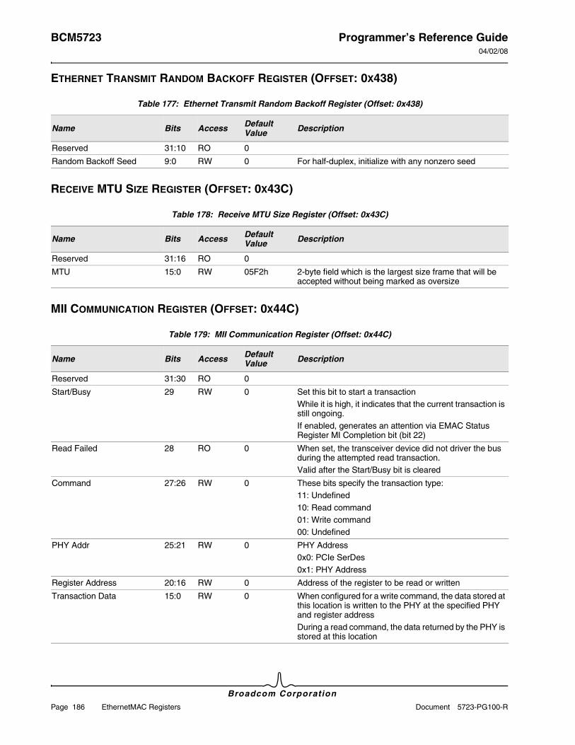
BCM5723 Programmer’s Reference Guide04/02/08
Broadcom Corporation
Page 186 EthernetMAC Registers Document 5723-PG100-R
ETHERNET TRANSMIT RANDOM BACKOFF REGISTER (OFFSET: 0X438)
RECEIVE MTU SIZE REGISTER (OFFSET: 0X43C)
MII COMMUNICATION REGISTER (OFFSET: 0X44C)
Table 177: Ethernet Transmit Random Backoff Register (Offset: 0x438)
Name Bits Access Default Value Description
Reserved 31:10 RO 0
Random Backoff Seed 9:0 RW 0 For half-duplex, initialize with any nonzero seed
Table 178: Receive MTU Size Register (Offset: 0x43C)
Name Bits Access Default Value Description
Reserved 31:16 RO 0
MTU 15:0 RW 05F2h 2-byte field which is the largest size frame that will be accepted without being marked as oversize
Table 179: MII Communication Register (Offset: 0x44C)
Name Bits Access Default Value Description
Reserved 31:30 RO 0
Start/Busy 29 RW 0 Set this bit to start a transactionWhile it is high, it indicates that the current transaction is still ongoing.If enabled, generates an attention via EMAC Status Register MI Completion bit (bit 22)
Read Failed 28 RO 0 When set, the transceiver device did not driver the bus during the attempted read transaction.Valid after the Start/Busy bit is cleared
Command 27:26 RW 0 These bits specify the transaction type:11: Undefined10: Read command01: Write command00: Undefined
PHY Addr 25:21 RW 0 PHY Address0x0: PCIe SerDes 0x1: PHY Address
Register Address 20:16 RW 0 Address of the register to be read or written
Transaction Data 15:0 RW 0 When configured for a write command, the data stored at this location is written to the PHY at the specified PHY and register addressDuring a read command, the data returned by the PHY is stored at this location
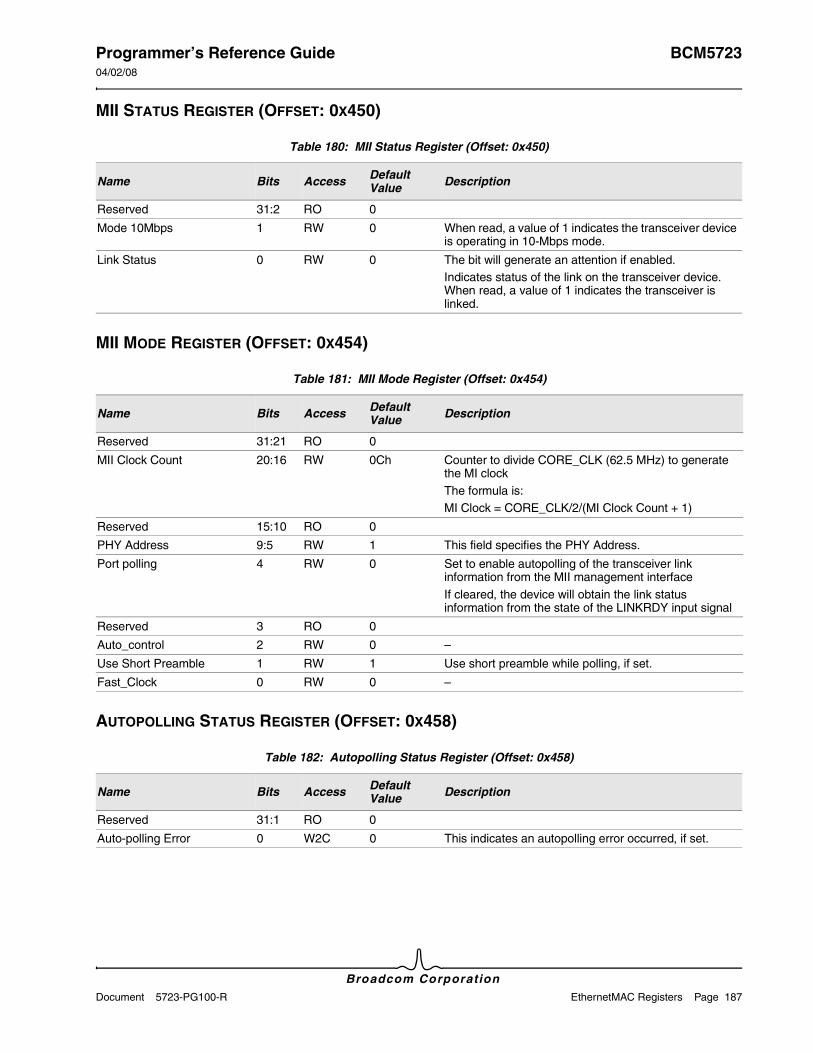
Programmer’s Reference Guide BCM572304/02/08
Broadcom CorporationDocument 5723-PG100-R EthernetMAC Registers Page 187
MII STATUS REGISTER (OFFSET: 0X450)
MII MODE REGISTER (OFFSET: 0X454)
AUTOPOLLING STATUS REGISTER (OFFSET: 0X458)
Table 180: MII Status Register (Offset: 0x450)
Name Bits Access Default Value Description
Reserved 31:2 RO 0
Mode 10Mbps 1 RW 0 When read, a value of 1 indicates the transceiver device is operating in 10-Mbps mode.
Link Status 0 RW 0 The bit will generate an attention if enabled.Indicates status of the link on the transceiver device. When read, a value of 1 indicates the transceiver is linked.
Table 181: MII Mode Register (Offset: 0x454)
Name Bits Access Default Value Description
Reserved 31:21 RO 0
MII Clock Count 20:16 RW 0Ch Counter to divide CORE_CLK (62.5 MHz) to generate the MI clock The formula is:MI Clock = CORE_CLK/2/(MI Clock Count + 1)
Reserved 15:10 RO 0
PHY Address 9:5 RW 1 This field specifies the PHY Address.
Port polling 4 RW 0 Set to enable autopolling of the transceiver link information from the MII management interfaceIf cleared, the device will obtain the link status information from the state of the LINKRDY input signal
Reserved 3 RO 0
Auto_control 2 RW 0 –
Use Short Preamble 1 RW 1 Use short preamble while polling, if set.
Fast_Clock 0 RW 0 –
Table 182: Autopolling Status Register (Offset: 0x458)
Name Bits Access Default Value Description
Reserved 31:1 RO 0
Auto-polling Error 0 W2C 0 This indicates an autopolling error occurred, if set.
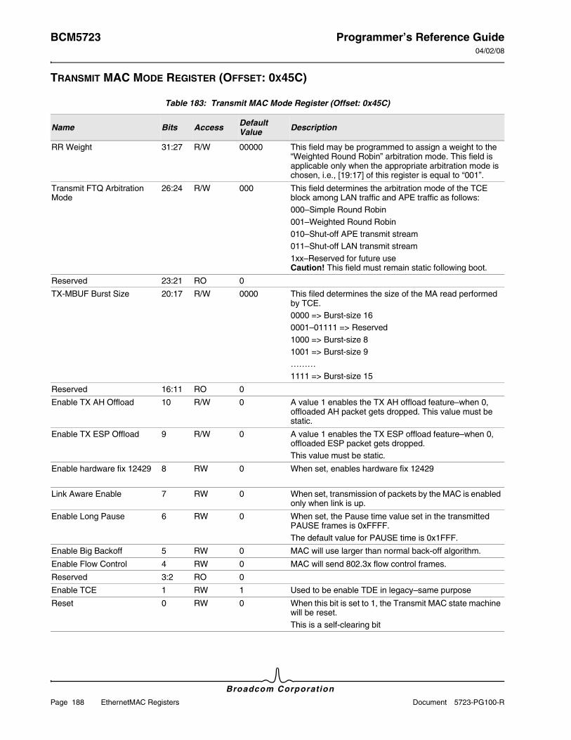
BCM5723 Programmer’s Reference Guide04/02/08
Broadcom Corporation
Page 188 EthernetMAC Registers Document 5723-PG100-R
TRANSMIT MAC MODE REGISTER (OFFSET: 0X45C)
Table 183: Transmit MAC Mode Register (Offset: 0x45C)
Name Bits Access Default Value Description
RR Weight 31:27 R/W 00000 This field may be programmed to assign a weight to the “Weighted Round Robin” arbitration mode. This field is applicable only when the appropriate arbitration mode is chosen, i.e., [19:17] of this register is equal to “001”.
Transmit FTQ Arbitration Mode
26:24 R/W 000 This field determines the arbitration mode of the TCE block among LAN traffic and APE traffic as follows:000–Simple Round Robin001–Weighted Round Robin010–Shut-off APE transmit stream011–Shut-off LAN transmit stream1xx–Reserved for future useCaution! This field must remain static following boot.
Reserved 23:21 RO 0
TX-MBUF Burst Size 20:17 R/W 0000 This filed determines the size of the MA read performed by TCE.0000 => Burst-size 160001–01111 => Reserved1000 => Burst-size 81001 => Burst-size 9………1111 => Burst-size 15
Reserved 16:11 RO 0
Enable TX AH Offload 10 R/W 0 A value 1 enables the TX AH offload feature–when 0, offloaded AH packet gets dropped. This value must be static.
Enable TX ESP Offload 9 R/W 0 A value 1 enables the TX ESP offload feature–when 0, offloaded ESP packet gets dropped.This value must be static.
Enable hardware fix 12429 8 RW 0 When set, enables hardware fix 12429
Link Aware Enable 7 RW 0 When set, transmission of packets by the MAC is enabled only when link is up.
Enable Long Pause 6 RW 0 When set, the Pause time value set in the transmitted PAUSE frames is 0xFFFF.The default value for PAUSE time is 0x1FFF.
Enable Big Backoff 5 RW 0 MAC will use larger than normal back-off algorithm.
Enable Flow Control 4 RW 0 MAC will send 802.3x flow control frames.
Reserved 3:2 RO 0
Enable TCE 1 RW 1 Used to be enable TDE in legacy–same purpose
Reset 0 RW 0 When this bit is set to 1, the Transmit MAC state machine will be reset.This is a self-clearing bit
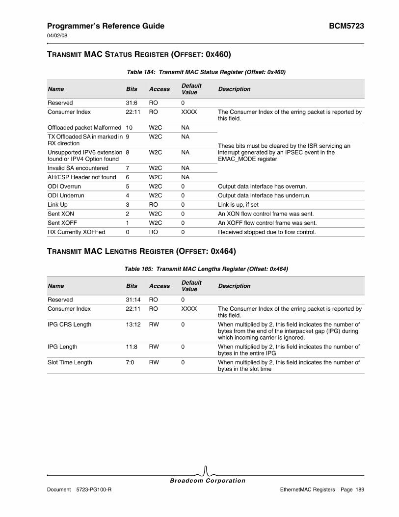
Programmer’s Reference Guide BCM572304/02/08
Broadcom CorporationDocument 5723-PG100-R EthernetMAC Registers Page 189
TRANSMIT MAC STATUS REGISTER (OFFSET: 0X460)
TRANSMIT MAC LENGTHS REGISTER (OFFSET: 0X464)
Table 184: Transmit MAC Status Register (Offset: 0x460)
Name Bits Access Default Value Description
Reserved 31:6 RO 0
Consumer Index 22:11 RO XXXX The Consumer Index of the erring packet is reported by this field.
Offloaded packet Malformed 10 W2C NA
These bits must be cleared by the ISR servicing an interrupt generated by an IPSEC event in the EMAC_MODE register
TX Offloaded SA in marked in RX direction
9 W2C NA
Unsupported IPV6 extension found or IPV4 Option found
8 W2C NA
Invalid SA encountered 7 W2C NA
AH/ESP Header not found 6 W2C NA
ODI Overrun 5 W2C 0 Output data interface has overrun.
ODI Underrun 4 W2C 0 Output data interface has underrun.
Link Up 3 RO 0 Link is up, if set
Sent XON 2 W2C 0 An XON flow control frame was sent.
Sent XOFF 1 W2C 0 An XOFF flow control frame was sent.
RX Currently XOFFed 0 RO 0 Received stopped due to flow control.
Table 185: Transmit MAC Lengths Register (Offset: 0x464)
Name Bits Access Default Value Description
Reserved 31:14 RO 0
Consumer Index 22:11 RO XXXX The Consumer Index of the erring packet is reported by this field.
IPG CRS Length 13:12 RW 0 When multiplied by 2, this field indicates the number of bytes from the end of the interpacket gap (IPG) during which incoming carrier is ignored.
IPG Length 11:8 RW 0 When multiplied by 2, this field indicates the number of bytes in the entire IPG
Slot Time Length 7:0 RW 0 When multiplied by 2, this field indicates the number of bytes in the slot time
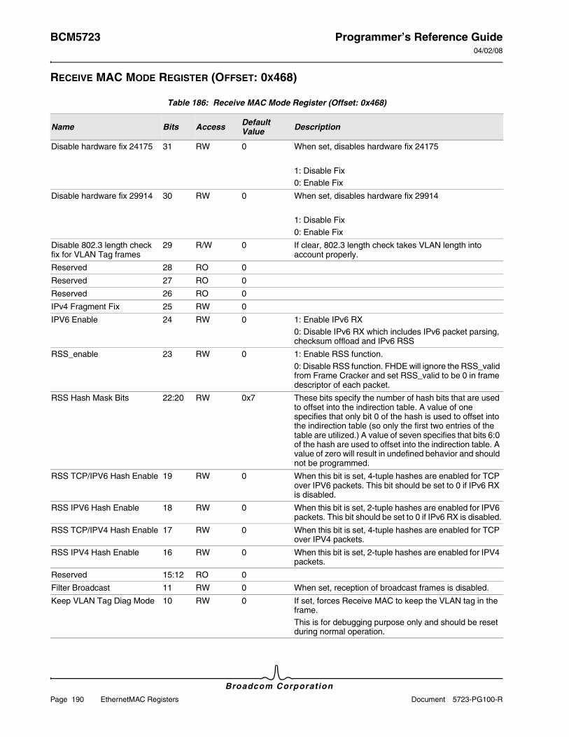
BCM5723 Programmer’s Reference Guide04/02/08
Broadcom Corporation
Page 190 EthernetMAC Registers Document 5723-PG100-R
RECEIVE MAC MODE REGISTER (OFFSET: 0X468)
Table 186: Receive MAC Mode Register (Offset: 0x468)
Name Bits Access Default Value Description
Disable hardware fix 24175 31 RW 0 When set, disables hardware fix 24175
1: Disable Fix0: Enable Fix
Disable hardware fix 29914 30 RW 0 When set, disables hardware fix 29914
1: Disable Fix0: Enable Fix
Disable 802.3 length check fix for VLAN Tag frames
29 R/W 0 If clear, 802.3 length check takes VLAN length into account properly.
Reserved 28 RO 0
Reserved 27 RO 0
Reserved 26 RO 0
IPv4 Fragment Fix 25 RW 0
IPV6 Enable 24 RW 0 1: Enable IPv6 RX0: Disable IPv6 RX which includes IPv6 packet parsing, checksum offload and IPv6 RSS
RSS_enable 23 RW 0 1: Enable RSS function.0: Disable RSS function. FHDE will ignore the RSS_valid from Frame Cracker and set RSS_valid to be 0 in frame descriptor of each packet.
RSS Hash Mask Bits 22:20 RW 0x7 These bits specify the number of hash bits that are used to offset into the indirection table. A value of one specifies that only bit 0 of the hash is used to offset into the indirection table (so only the first two entries of the table are utilized.) A value of seven specifies that bits 6:0 of the hash are used to offset into the indirection table. A value of zero will result in undefined behavior and should not be programmed.
RSS TCP/IPV6 Hash Enable 19 RW 0 When this bit is set, 4-tuple hashes are enabled for TCP over IPV6 packets. This bit should be set to 0 if IPv6 RX is disabled.
RSS IPV6 Hash Enable 18 RW 0 When this bit is set, 2-tuple hashes are enabled for IPV6 packets. This bit should be set to 0 if IPv6 RX is disabled.
RSS TCP/IPV4 Hash Enable 17 RW 0 When this bit is set, 4-tuple hashes are enabled for TCP over IPV4 packets.
RSS IPV4 Hash Enable 16 RW 0 When this bit is set, 2-tuple hashes are enabled for IPV4 packets.
Reserved 15:12 RO 0
Filter Broadcast 11 RW 0 When set, reception of broadcast frames is disabled.
Keep VLAN Tag Diag Mode 10 RW 0 If set, forces Receive MAC to keep the VLAN tag in the frame.This is for debugging purpose only and should be reset during normal operation.
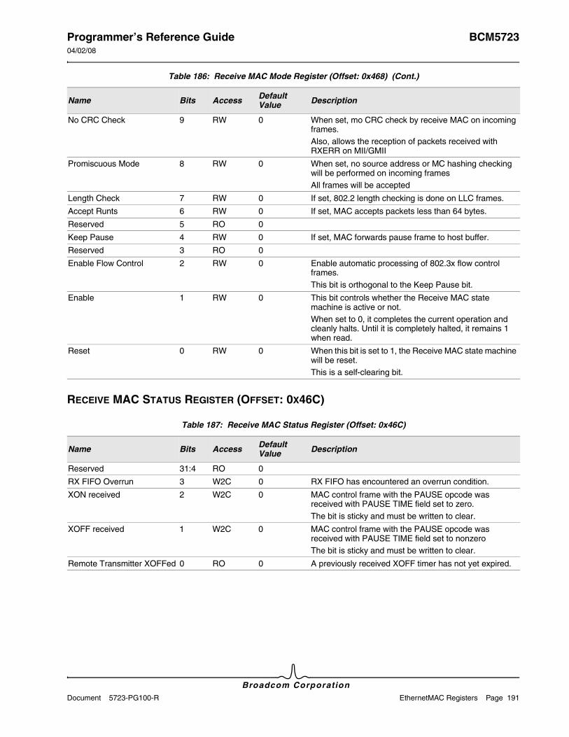
Programmer’s Reference Guide BCM572304/02/08
Broadcom CorporationDocument 5723-PG100-R EthernetMAC Registers Page 191
RECEIVE MAC STATUS REGISTER (OFFSET: 0X46C)
No CRC Check 9 RW 0 When set, mo CRC check by receive MAC on incoming frames.Also, allows the reception of packets received with RXERR on MII/GMII
Promiscuous Mode 8 RW 0 When set, no source address or MC hashing checking will be performed on incoming framesAll frames will be accepted
Length Check 7 RW 0 If set, 802.2 length checking is done on LLC frames.
Accept Runts 6 RW 0 If set, MAC accepts packets less than 64 bytes.
Reserved 5 RO 0
Keep Pause 4 RW 0 If set, MAC forwards pause frame to host buffer.
Reserved 3 RO 0
Enable Flow Control 2 RW 0 Enable automatic processing of 802.3x flow control frames.This bit is orthogonal to the Keep Pause bit.
Enable 1 RW 0 This bit controls whether the Receive MAC state machine is active or not.When set to 0, it completes the current operation and cleanly halts. Until it is completely halted, it remains 1 when read.
Reset 0 RW 0 When this bit is set to 1, the Receive MAC state machine will be reset.This is a self-clearing bit.
Table 187: Receive MAC Status Register (Offset: 0x46C)
Name Bits Access Default Value Description
Reserved 31:4 RO 0
RX FIFO Overrun 3 W2C 0 RX FIFO has encountered an overrun condition.
XON received 2 W2C 0 MAC control frame with the PAUSE opcode was received with PAUSE TIME field set to zero.The bit is sticky and must be written to clear.
XOFF received 1 W2C 0 MAC control frame with the PAUSE opcode was received with PAUSE TIME field set to nonzeroThe bit is sticky and must be written to clear.
Remote Transmitter XOFFed 0 RO 0 A previously received XOFF timer has not yet expired.
Table 186: Receive MAC Mode Register (Offset: 0x468) (Cont.)
Name Bits Access Default Value Description
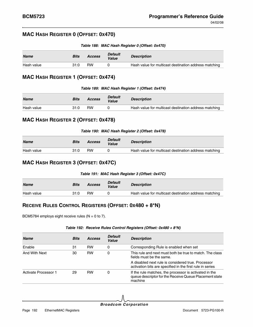
BCM5723 Programmer’s Reference Guide04/02/08
Broadcom Corporation
Page 192 EthernetMAC Registers Document 5723-PG100-R
MAC HASH REGISTER 0 (OFFSET: 0X470)
MAC HASH REGISTER 1 (OFFSET: 0X474)
MAC HASH REGISTER 2 (OFFSET: 0X478)
MAC HASH REGISTER 3 (OFFSET: 0X47C)
RECEIVE RULES CONTROL REGISTERS (OFFSET: 0X480 + 8*N)
BCM5784 employs eight receive rules (N = 0 to 7).
Table 188: MAC Hash Register 0 (Offset: 0x470)
Name Bits Access Default Value Description
Hash value 31:0 RW 0 Hash value for multicast destination address matching
Table 189: MAC Hash Register 1 (Offset: 0x474)
Name Bits Access Default Value Description
Hash value 31:0 RW 0 Hash value for multicast destination address matching
Table 190: MAC Hash Register 2 (Offset: 0x478)
Name Bits Access Default Value Description
Hash value 31:0 RW 0 Hash value for multicast destination address matching
Table 191: MAC Hash Register 3 (Offset: 0x47C)
Name Bits Access Default Value Description
Hash value 31:0 RW 0 Hash value for multicast destination address matching
Table 192: Receive Rules Control Registers (Offset: 0x480 + 8*N)
Name Bits Access Default Value Description
Enable 31 RW 0 Corresponding Rule is enabled when set
And With Next 30 RW 0 This rule and next must both be true to match. The class fields must be the same.A disabled next rule is considered true. Processor activation bits are specified in the first rule in series
Activate Processor 1 29 RW 0 If the rule matches, the processor is activated in the queue descriptor for the Receive Queue Placement state machine
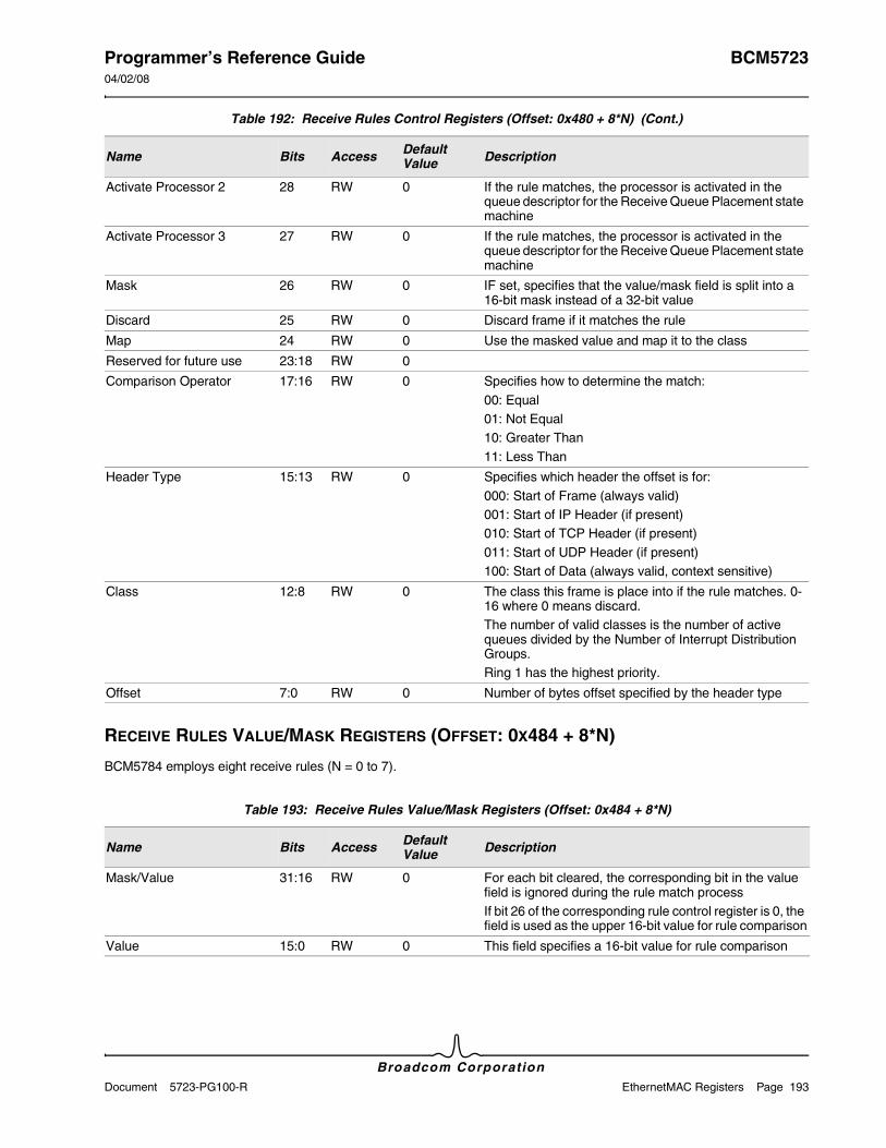
Programmer’s Reference Guide BCM572304/02/08
Broadcom CorporationDocument 5723-PG100-R EthernetMAC Registers Page 193
RECEIVE RULES VALUE/MASK REGISTERS (OFFSET: 0X484 + 8*N)
BCM5784 employs eight receive rules (N = 0 to 7).
Activate Processor 2 28 RW 0 If the rule matches, the processor is activated in the queue descriptor for the Receive Queue Placement state machine
Activate Processor 3 27 RW 0 If the rule matches, the processor is activated in the queue descriptor for the Receive Queue Placement state machine
Mask 26 RW 0 IF set, specifies that the value/mask field is split into a 16-bit mask instead of a 32-bit value
Discard 25 RW 0 Discard frame if it matches the rule
Map 24 RW 0 Use the masked value and map it to the class
Reserved for future use 23:18 RW 0
Comparison Operator 17:16 RW 0 Specifies how to determine the match:00: Equal01: Not Equal10: Greater Than11: Less Than
Header Type 15:13 RW 0 Specifies which header the offset is for:000: Start of Frame (always valid)001: Start of IP Header (if present)010: Start of TCP Header (if present)011: Start of UDP Header (if present)100: Start of Data (always valid, context sensitive)
Class 12:8 RW 0 The class this frame is place into if the rule matches. 0-16 where 0 means discard.The number of valid classes is the number of active queues divided by the Number of Interrupt Distribution Groups.Ring 1 has the highest priority.
Offset 7:0 RW 0 Number of bytes offset specified by the header type
Table 193: Receive Rules Value/Mask Registers (Offset: 0x484 + 8*N)
Name Bits Access Default Value Description
Mask/Value 31:16 RW 0 For each bit cleared, the corresponding bit in the value field is ignored during the rule match processIf bit 26 of the corresponding rule control register is 0, the field is used as the upper 16-bit value for rule comparison
Value 15:0 RW 0 This field specifies a 16-bit value for rule comparison
Table 192: Receive Rules Control Registers (Offset: 0x480 + 8*N) (Cont.)
Name Bits Access Default Value Description
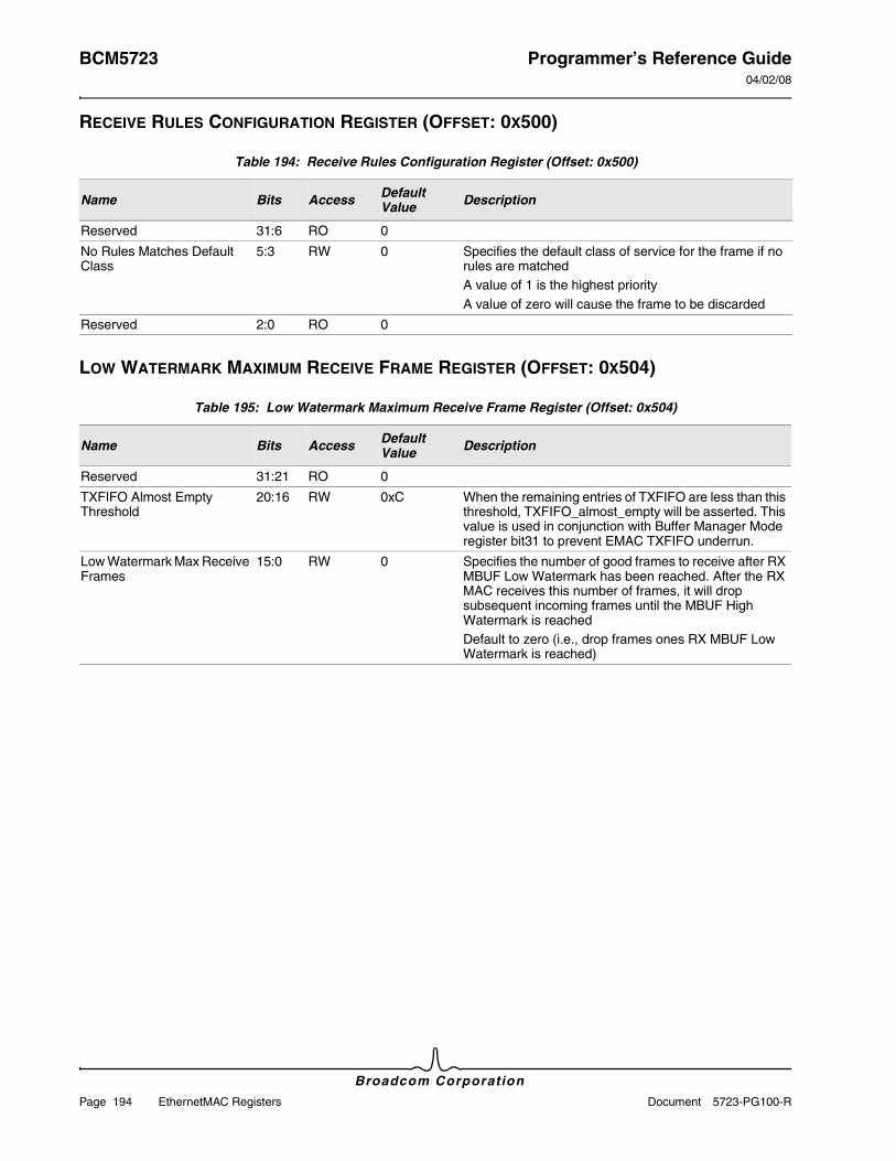
BCM5723 Programmer’s Reference Guide04/02/08
Broadcom Corporation
Page 194 EthernetMAC Registers Document 5723-PG100-R
RECEIVE RULES CONFIGURATION REGISTER (OFFSET: 0X500)
LOW WATERMARK MAXIMUM RECEIVE FRAME REGISTER (OFFSET: 0X504)
Table 194: Receive Rules Configuration Register (Offset: 0x500)
Name Bits Access Default Value Description
Reserved 31:6 RO 0
No Rules Matches Default Class
5:3 RW 0 Specifies the default class of service for the frame if no rules are matchedA value of 1 is the highest priorityA value of zero will cause the frame to be discarded
Reserved 2:0 RO 0
Table 195: Low Watermark Maximum Receive Frame Register (Offset: 0x504)
Name Bits Access Default Value Description
Reserved 31:21 RO 0
TXFIFO Almost Empty Threshold
20:16 RW 0xC When the remaining entries of TXFIFO are less than this threshold, TXFIFO_almost_empty will be asserted. This value is used in conjunction with Buffer Manager Mode register bit31 to prevent EMAC TXFIFO underrun.
Low Watermark Max Receive Frames
15:0 RW 0 Specifies the number of good frames to receive after RX MBUF Low Watermark has been reached. After the RX MAC receives this number of frames, it will drop subsequent incoming frames until the MBUF High Watermark is reachedDefault to zero (i.e., drop frames ones RX MBUF Low Watermark is reached)
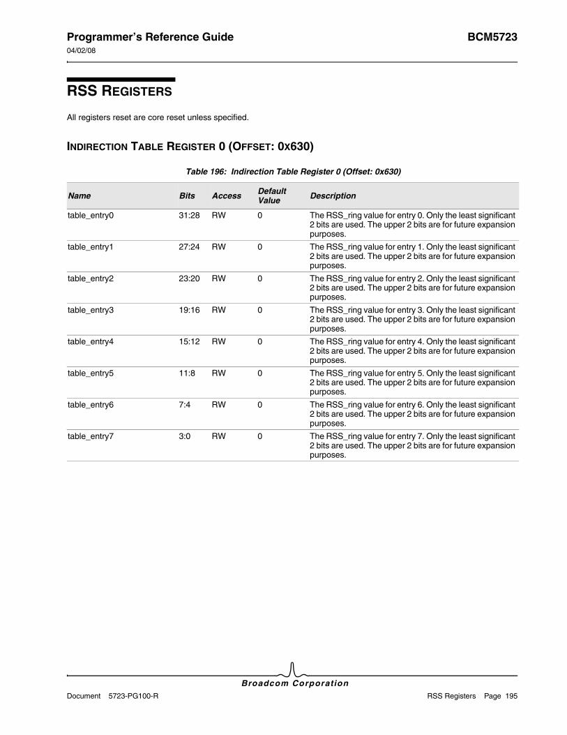
Programmer’s Reference Guide BCM572304/02/08
Broadcom CorporationDocument 5723-PG100-R RSS Registers Page 195
RSS REGISTERS
All registers reset are core reset unless specified.
INDIRECTION TABLE REGISTER 0 (OFFSET: 0X630)
Table 196: Indirection Table Register 0 (Offset: 0x630)
Name Bits Access Default Value Description
table_entry0 31:28 RW 0 The RSS_ring value for entry 0. Only the least significant 2 bits are used. The upper 2 bits are for future expansion purposes.
table_entry1 27:24 RW 0 The RSS_ring value for entry 1. Only the least significant 2 bits are used. The upper 2 bits are for future expansion purposes.
table_entry2 23:20 RW 0 The RSS_ring value for entry 2. Only the least significant 2 bits are used. The upper 2 bits are for future expansion purposes.
table_entry3 19:16 RW 0 The RSS_ring value for entry 3. Only the least significant 2 bits are used. The upper 2 bits are for future expansion purposes.
table_entry4 15:12 RW 0 The RSS_ring value for entry 4. Only the least significant 2 bits are used. The upper 2 bits are for future expansion purposes.
table_entry5 11:8 RW 0 The RSS_ring value for entry 5. Only the least significant 2 bits are used. The upper 2 bits are for future expansion purposes.
table_entry6 7:4 RW 0 The RSS_ring value for entry 6. Only the least significant 2 bits are used. The upper 2 bits are for future expansion purposes.
table_entry7 3:0 RW 0 The RSS_ring value for entry 7. Only the least significant 2 bits are used. The upper 2 bits are for future expansion purposes.
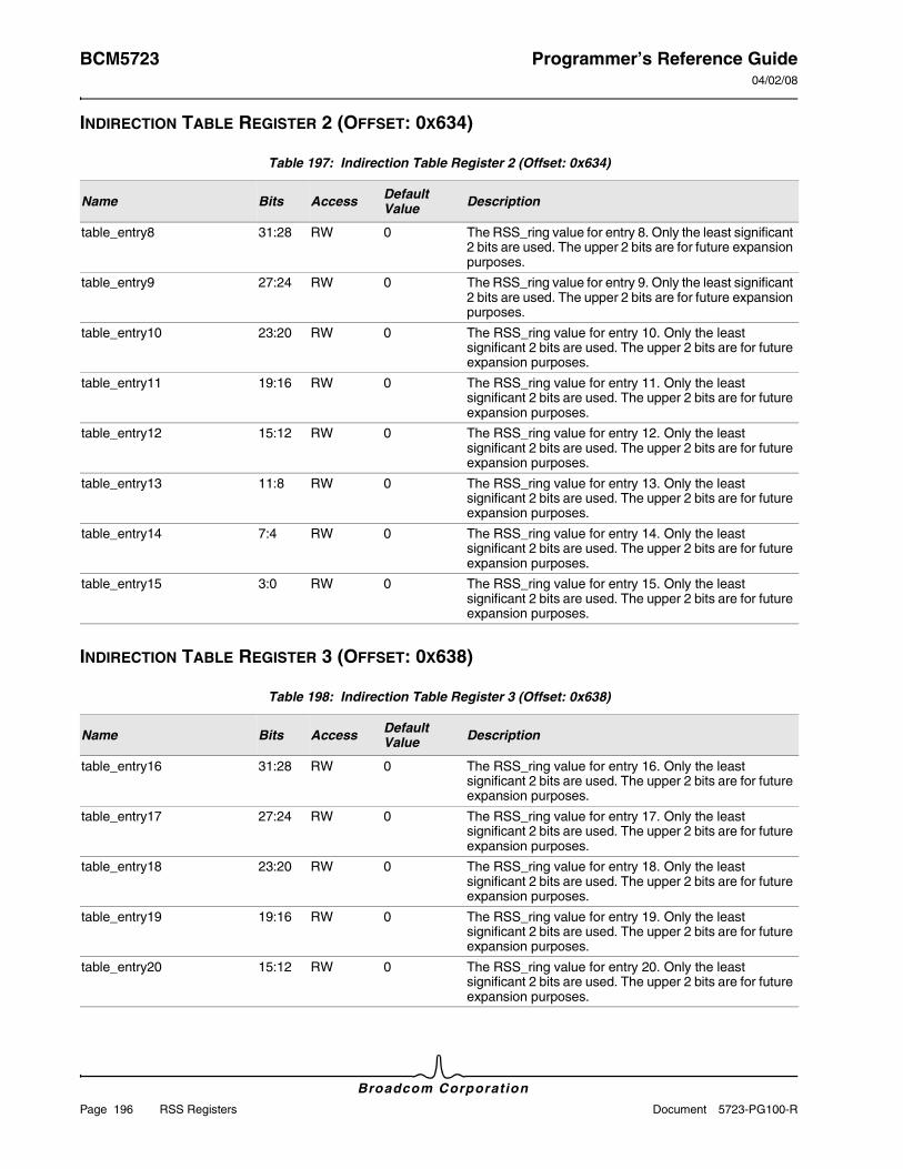
BCM5723 Programmer’s Reference Guide04/02/08
Broadcom Corporation
Page 196 RSS Registers Document 5723-PG100-R
INDIRECTION TABLE REGISTER 2 (OFFSET: 0X634)
INDIRECTION TABLE REGISTER 3 (OFFSET: 0X638)
Table 197: Indirection Table Register 2 (Offset: 0x634)
Name Bits Access Default Value Description
table_entry8 31:28 RW 0 The RSS_ring value for entry 8. Only the least significant 2 bits are used. The upper 2 bits are for future expansion purposes.
table_entry9 27:24 RW 0 The RSS_ring value for entry 9. Only the least significant 2 bits are used. The upper 2 bits are for future expansion purposes.
table_entry10 23:20 RW 0 The RSS_ring value for entry 10. Only the least significant 2 bits are used. The upper 2 bits are for future expansion purposes.
table_entry11 19:16 RW 0 The RSS_ring value for entry 11. Only the least significant 2 bits are used. The upper 2 bits are for future expansion purposes.
table_entry12 15:12 RW 0 The RSS_ring value for entry 12. Only the least significant 2 bits are used. The upper 2 bits are for future expansion purposes.
table_entry13 11:8 RW 0 The RSS_ring value for entry 13. Only the least significant 2 bits are used. The upper 2 bits are for future expansion purposes.
table_entry14 7:4 RW 0 The RSS_ring value for entry 14. Only the least significant 2 bits are used. The upper 2 bits are for future expansion purposes.
table_entry15 3:0 RW 0 The RSS_ring value for entry 15. Only the least significant 2 bits are used. The upper 2 bits are for future expansion purposes.
Table 198: Indirection Table Register 3 (Offset: 0x638)
Name Bits Access Default Value Description
table_entry16 31:28 RW 0 The RSS_ring value for entry 16. Only the least significant 2 bits are used. The upper 2 bits are for future expansion purposes.
table_entry17 27:24 RW 0 The RSS_ring value for entry 17. Only the least significant 2 bits are used. The upper 2 bits are for future expansion purposes.
table_entry18 23:20 RW 0 The RSS_ring value for entry 18. Only the least significant 2 bits are used. The upper 2 bits are for future expansion purposes.
table_entry19 19:16 RW 0 The RSS_ring value for entry 19. Only the least significant 2 bits are used. The upper 2 bits are for future expansion purposes.
table_entry20 15:12 RW 0 The RSS_ring value for entry 20. Only the least significant 2 bits are used. The upper 2 bits are for future expansion purposes.
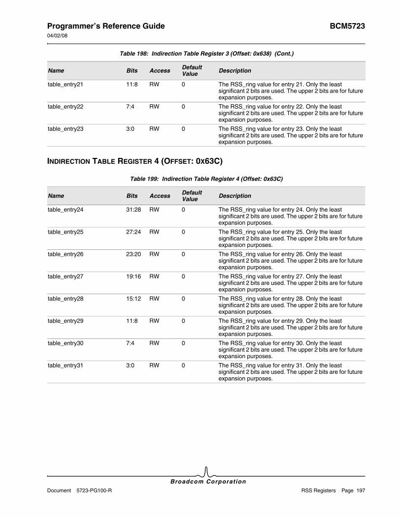
Programmer’s Reference Guide BCM572304/02/08
Broadcom CorporationDocument 5723-PG100-R RSS Registers Page 197
INDIRECTION TABLE REGISTER 4 (OFFSET: 0X63C)
table_entry21 11:8 RW 0 The RSS_ring value for entry 21. Only the least significant 2 bits are used. The upper 2 bits are for future expansion purposes.
table_entry22 7:4 RW 0 The RSS_ring value for entry 22. Only the least significant 2 bits are used. The upper 2 bits are for future expansion purposes.
table_entry23 3:0 RW 0 The RSS_ring value for entry 23. Only the least significant 2 bits are used. The upper 2 bits are for future expansion purposes.
Table 199: Indirection Table Register 4 (Offset: 0x63C)
Name Bits Access Default Value Description
table_entry24 31:28 RW 0 The RSS_ring value for entry 24. Only the least significant 2 bits are used. The upper 2 bits are for future expansion purposes.
table_entry25 27:24 RW 0 The RSS_ring value for entry 25. Only the least significant 2 bits are used. The upper 2 bits are for future expansion purposes.
table_entry26 23:20 RW 0 The RSS_ring value for entry 26. Only the least significant 2 bits are used. The upper 2 bits are for future expansion purposes.
table_entry27 19:16 RW 0 The RSS_ring value for entry 27. Only the least significant 2 bits are used. The upper 2 bits are for future expansion purposes.
table_entry28 15:12 RW 0 The RSS_ring value for entry 28. Only the least significant 2 bits are used. The upper 2 bits are for future expansion purposes.
table_entry29 11:8 RW 0 The RSS_ring value for entry 29. Only the least significant 2 bits are used. The upper 2 bits are for future expansion purposes.
table_entry30 7:4 RW 0 The RSS_ring value for entry 30. Only the least significant 2 bits are used. The upper 2 bits are for future expansion purposes.
table_entry31 3:0 RW 0 The RSS_ring value for entry 31. Only the least significant 2 bits are used. The upper 2 bits are for future expansion purposes.
Table 198: Indirection Table Register 3 (Offset: 0x638) (Cont.)
Name Bits Access Default Value Description
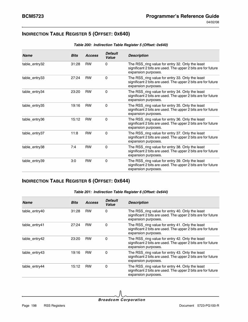
BCM5723 Programmer’s Reference Guide04/02/08
Broadcom Corporation
Page 198 RSS Registers Document 5723-PG100-R
INDIRECTION TABLE REGISTER 5 (OFFSET: 0X640)
INDIRECTION TABLE REGISTER 6 (OFFSET: 0X644)
Table 200: Indirection Table Register 5 (Offset: 0x640)
Name Bits Access Default Value Description
table_entry32 31:28 RW 0 The RSS_ring value for entry 32. Only the least significant 2 bits are used. The upper 2 bits are for future expansion purposes.
table_entry33 27:24 RW 0 The RSS_ring value for entry 33. Only the least significant 2 bits are used. The upper 2 bits are for future expansion purposes.
table_entry34 23:20 RW 0 The RSS_ring value for entry 34. Only the least significant 2 bits are used. The upper 2 bits are for future expansion purposes.
table_entry35 19:16 RW 0 The RSS_ring value for entry 35. Only the least significant 2 bits are used. The upper 2 bits are for future expansion purposes.
table_entry36 15:12 RW 0 The RSS_ring value for entry 36. Only the least significant 2 bits are used. The upper 2 bits are for future expansion purposes.
table_entry37 11:8 RW 0 The RSS_ring value for entry 37. Only the least significant 2 bits are used. The upper 2 bits are for future expansion purposes.
table_entry38 7:4 RW 0 The RSS_ring value for entry 38. Only the least significant 2 bits are used. The upper 2 bits are for future expansion purposes.
table_entry39 3:0 RW 0 The RSS_ring value for entry 39. Only the least significant 2 bits are used. The upper 2 bits are for future expansion purposes.
Table 201: Indirection Table Register 6 (Offset: 0x644)
Name Bits Access Default Value Description
table_entry40 31:28 RW 0 The RSS_ring value for entry 40. Only the least significant 2 bits are used. The upper 2 bits are for future expansion purposes.
table_entry41 27:24 RW 0 The RSS_ring value for entry 41. Only the least significant 2 bits are used. The upper 2 bits are for future expansion purposes.
table_entry42 23:20 RW 0 The RSS_ring value for entry 42. Only the least significant 2 bits are used. The upper 2 bits are for future expansion purposes.
table_entry43 19:16 RW 0 The RSS_ring value for entry 43. Only the least significant 2 bits are used. The upper 2 bits are for future expansion purposes.
table_entry44 15:12 RW 0 The RSS_ring value for entry 44. Only the least significant 2 bits are used. The upper 2 bits are for future expansion purposes.

Programmer’s Reference Guide BCM572304/02/08
Broadcom CorporationDocument 5723-PG100-R RSS Registers Page 199
INDIRECTION TABLE REGISTER 8 (OFFSET: 0X648)
table_entry45 11:8 RW 0 The RSS_ring value for entry 45. Only the least significant 2 bits are used. The upper 2 bits are for future expansion purposes.
table_entry46 7:4 RW 0 The RSS_ring value for entry 46. Only the least significant 2 bits are used. The upper 2 bits are for future expansion purposes.
table_entry47 3:0 RW 0 The RSS_ring value for entry 47. Only the least significant 2 bits are used. The upper 2 bits are for future expansion purposes.
Table 202: Indirection Table Register 8 (Offset: 0x648)
Name Bits Access Default Value Description
table_entry48 31:28 RW 0 The RSS_ring value for entry 48. Only the least significant 2 bits are used. The upper 2 bits are for future expansion purposes.
table_entry49 27:24 RW 0 The RSS_ring value for entry 49. Only the least significant 2 bits are used. The upper 2 bits are for future expansion purposes.
table_entry50 23:20 RW 0 The RSS_ring value for entry 50. Only the least significant 2 bits are used. The upper 2 bits are for future expansion purposes.
table_entry51 19:16 RW 0 The RSS_ring value for entry 51. Only the least significant 2 bits are used. The upper 2 bits are for future expansion purposes.
table_entry52 15:12 RW 0 The RSS_ring value for entry 52. Only the least significant 2 bits are used. The upper 2 bits are for future expansion purposes.
table_entry53 11:8 RW 0 The RSS_ring value for entry 53. Only the least significant 2 bits are used. The upper 2 bits are for future expansion purposes.
table_entry54 7:4 RW 0 The RSS_ring value for entry 54. Only the least significant 2 bits are used. The upper 2 bits are for future expansion purposes.
table_entry55 3:0 RW 0 The RSS_ring value for entry 55. Only the least significant 2 bits are used. The upper 2 bits are for future expansion purposes.
Table 201: Indirection Table Register 6 (Offset: 0x644) (Cont.)
Name Bits Access Default Value Description
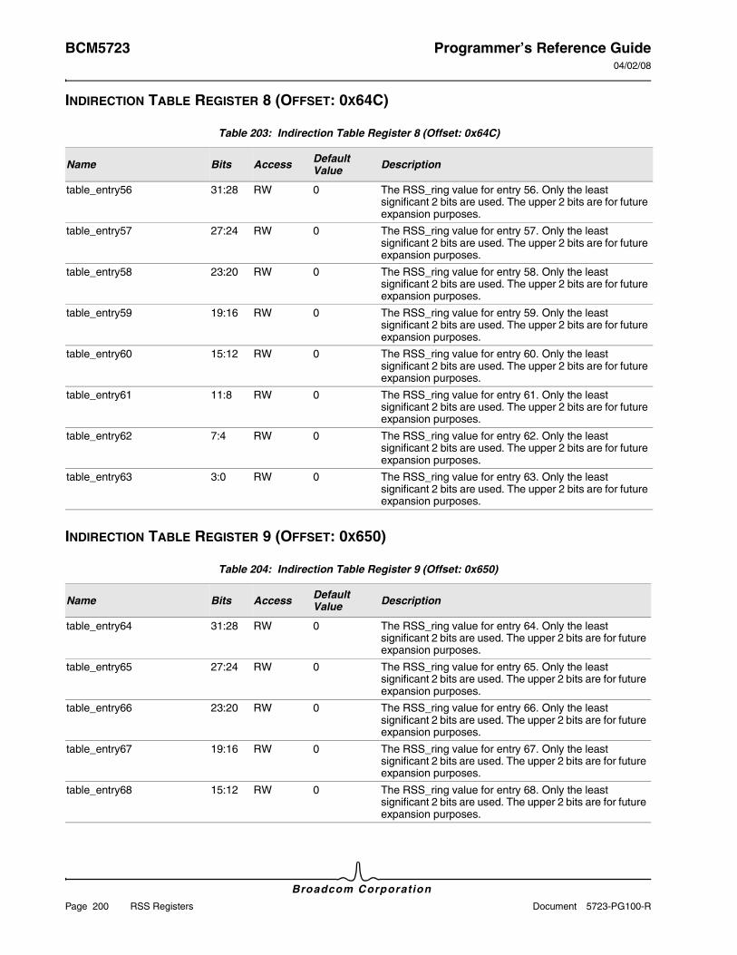
BCM5723 Programmer’s Reference Guide04/02/08
Broadcom Corporation
Page 200 RSS Registers Document 5723-PG100-R
INDIRECTION TABLE REGISTER 8 (OFFSET: 0X64C)
INDIRECTION TABLE REGISTER 9 (OFFSET: 0X650)
Table 203: Indirection Table Register 8 (Offset: 0x64C)
Name Bits Access Default Value Description
table_entry56 31:28 RW 0 The RSS_ring value for entry 56. Only the least significant 2 bits are used. The upper 2 bits are for future expansion purposes.
table_entry57 27:24 RW 0 The RSS_ring value for entry 57. Only the least significant 2 bits are used. The upper 2 bits are for future expansion purposes.
table_entry58 23:20 RW 0 The RSS_ring value for entry 58. Only the least significant 2 bits are used. The upper 2 bits are for future expansion purposes.
table_entry59 19:16 RW 0 The RSS_ring value for entry 59. Only the least significant 2 bits are used. The upper 2 bits are for future expansion purposes.
table_entry60 15:12 RW 0 The RSS_ring value for entry 60. Only the least significant 2 bits are used. The upper 2 bits are for future expansion purposes.
table_entry61 11:8 RW 0 The RSS_ring value for entry 61. Only the least significant 2 bits are used. The upper 2 bits are for future expansion purposes.
table_entry62 7:4 RW 0 The RSS_ring value for entry 62. Only the least significant 2 bits are used. The upper 2 bits are for future expansion purposes.
table_entry63 3:0 RW 0 The RSS_ring value for entry 63. Only the least significant 2 bits are used. The upper 2 bits are for future expansion purposes.
Table 204: Indirection Table Register 9 (Offset: 0x650)
Name Bits Access Default Value Description
table_entry64 31:28 RW 0 The RSS_ring value for entry 64. Only the least significant 2 bits are used. The upper 2 bits are for future expansion purposes.
table_entry65 27:24 RW 0 The RSS_ring value for entry 65. Only the least significant 2 bits are used. The upper 2 bits are for future expansion purposes.
table_entry66 23:20 RW 0 The RSS_ring value for entry 66. Only the least significant 2 bits are used. The upper 2 bits are for future expansion purposes.
table_entry67 19:16 RW 0 The RSS_ring value for entry 67. Only the least significant 2 bits are used. The upper 2 bits are for future expansion purposes.
table_entry68 15:12 RW 0 The RSS_ring value for entry 68. Only the least significant 2 bits are used. The upper 2 bits are for future expansion purposes.
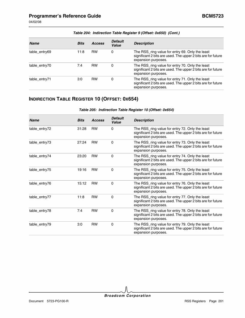
Programmer’s Reference Guide BCM572304/02/08
Broadcom CorporationDocument 5723-PG100-R RSS Registers Page 201
INDIRECTION TABLE REGISTER 10 (OFFSET: 0X654)
table_entry69 11:8 RW 0 The RSS_ring value for entry 69. Only the least significant 2 bits are used. The upper 2 bits are for future expansion purposes.
table_entry70 7:4 RW 0 The RSS_ring value for entry 70. Only the least significant 2 bits are used. The upper 2 bits are for future expansion purposes.
table_entry71 3:0 RW 0 The RSS_ring value for entry 71. Only the least significant 2 bits are used. The upper 2 bits are for future expansion purposes.
Table 205: Indirection Table Register 10 (Offset: 0x654)
Name Bits Access Default Value Description
table_entry72 31:28 RW 0 The RSS_ring value for entry 72. Only the least significant 2 bits are used. The upper 2 bits are for future expansion purposes.
table_entry73 27:24 RW 0 The RSS_ring value for entry 73. Only the least significant 2 bits are used. The upper 2 bits are for future expansion purposes.
table_entry74 23:20 RW 0 The RSS_ring value for entry 74. Only the least significant 2 bits are used. The upper 2 bits are for future expansion purposes.
table_entry75 19:16 RW 0 The RSS_ring value for entry 75. Only the least significant 2 bits are used. The upper 2 bits are for future expansion purposes.
table_entry76 15:12 RW 0 The RSS_ring value for entry 76. Only the least significant 2 bits are used. The upper 2 bits are for future expansion purposes.
table_entry77 11:8 RW 0 The RSS_ring value for entry 77. Only the least significant 2 bits are used. The upper 2 bits are for future expansion purposes.
table_entry78 7:4 RW 0 The RSS_ring value for entry 78. Only the least significant 2 bits are used. The upper 2 bits are for future expansion purposes.
table_entry79 3:0 RW 0 The RSS_ring value for entry 79. Only the least significant 2 bits are used. The upper 2 bits are for future expansion purposes.
Table 204: Indirection Table Register 9 (Offset: 0x650) (Cont.)
Name Bits Access Default Value Description

BCM5723 Programmer’s Reference Guide04/02/08
Broadcom Corporation
Page 202 RSS Registers Document 5723-PG100-R
INDIRECTION TABLE REGISTER 11 (OFFSET: 0X658)
INDIRECTION TABLE REGISTER 12 (OFFSET: 0X65C)
Table 206: Indirection Table Register 11 (Offset: 0x658)
Name Bits Access Default Value Description
table_entry80 31:28 RW 0 The RSS_ring value for entry 80. Only the least significant 2 bits are used. The upper 2 bits are for future expansion purposes.
table_entry81 27:24 RW 0 The RSS_ring value for entry 81. Only the least significant 2 bits are used. The upper 2 bits are for future expansion purposes.
table_entry82 23:20 RW 0 The RSS_ring value for entry 82. Only the least significant 2 bits are used. The upper 2 bits are for future expansion purposes.
table_entry83 19:16 RW 0 The RSS_ring value for entry 83. Only the least significant 2 bits are used. The upper 2 bits are for future expansion purposes.
table_entry84 15:12 RW 0 The RSS_ring value for entry 84. Only the least significant 2 bits are used. The upper 2 bits are for future expansion purposes.
table_entry85 11:8 RW 0 The RSS_ring value for entry 85. Only the least significant 2 bits are used. The upper 2 bits are for future expansion purposes.
table_entry86 7:4 RW 0 The RSS_ring value for entry 86. Only the least significant 2 bits are used. The upper 2 bits are for future expansion purposes.
table_entry87 3:0 RW 0 The RSS_ring value for entry 87. Only the least significant 2 bits are used. The upper 2 bits are for future expansion purposes.
Table 207: Indirection Table Register 12 (Offset: 0x65C)
Name Bits Access Default Value Description
table_entry88 31:28 RW 0 The RSS_ring value for entry 88. Only the least significant 2 bits are used. The upper 2 bits are for future expansion purposes.
table_entry89 27:24 RW 0 The RSS_ring value for entry 89. Only the least significant 2 bits are used. The upper 2 bits are for future expansion purposes.
table_entry90 23:20 RW 0 The RSS_ring value for entry 90. Only the least significant 2 bits are used. The upper 2 bits are for future expansion purposes.
table_entry91 19:16 RW 0 The RSS_ring value for entry 91. Only the least significant 2 bits are used. The upper 2 bits are for future expansion purposes.
table_entry92 15:12 RW 0 The RSS_ring value for entry 92. Only the least significant 2 bits are used. The upper 2 bits are for future expansion purposes.
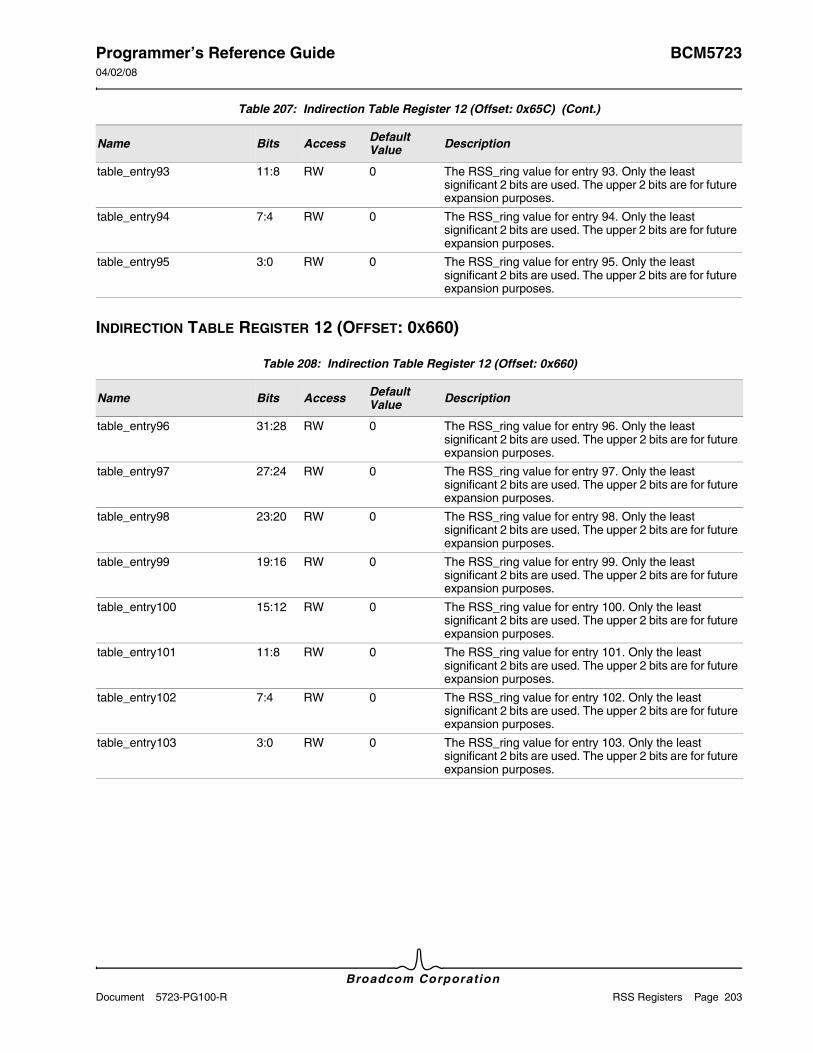
Programmer’s Reference Guide BCM572304/02/08
Broadcom CorporationDocument 5723-PG100-R RSS Registers Page 203
INDIRECTION TABLE REGISTER 12 (OFFSET: 0X660)
table_entry93 11:8 RW 0 The RSS_ring value for entry 93. Only the least significant 2 bits are used. The upper 2 bits are for future expansion purposes.
table_entry94 7:4 RW 0 The RSS_ring value for entry 94. Only the least significant 2 bits are used. The upper 2 bits are for future expansion purposes.
table_entry95 3:0 RW 0 The RSS_ring value for entry 95. Only the least significant 2 bits are used. The upper 2 bits are for future expansion purposes.
Table 208: Indirection Table Register 12 (Offset: 0x660)
Name Bits Access Default Value Description
table_entry96 31:28 RW 0 The RSS_ring value for entry 96. Only the least significant 2 bits are used. The upper 2 bits are for future expansion purposes.
table_entry97 27:24 RW 0 The RSS_ring value for entry 97. Only the least significant 2 bits are used. The upper 2 bits are for future expansion purposes.
table_entry98 23:20 RW 0 The RSS_ring value for entry 98. Only the least significant 2 bits are used. The upper 2 bits are for future expansion purposes.
table_entry99 19:16 RW 0 The RSS_ring value for entry 99. Only the least significant 2 bits are used. The upper 2 bits are for future expansion purposes.
table_entry100 15:12 RW 0 The RSS_ring value for entry 100. Only the least significant 2 bits are used. The upper 2 bits are for future expansion purposes.
table_entry101 11:8 RW 0 The RSS_ring value for entry 101. Only the least significant 2 bits are used. The upper 2 bits are for future expansion purposes.
table_entry102 7:4 RW 0 The RSS_ring value for entry 102. Only the least significant 2 bits are used. The upper 2 bits are for future expansion purposes.
table_entry103 3:0 RW 0 The RSS_ring value for entry 103. Only the least significant 2 bits are used. The upper 2 bits are for future expansion purposes.
Table 207: Indirection Table Register 12 (Offset: 0x65C) (Cont.)
Name Bits Access Default Value Description

BCM5723 Programmer’s Reference Guide04/02/08
Broadcom Corporation
Page 204 RSS Registers Document 5723-PG100-R
INDIRECTION TABLE REGISTER 13 (OFFSET: 0X664)
INDIRECTION TABLE REGISTER 14 (OFFSET: 0X668)
Table 209: Indirection Table Register 13 (Offset: 0x664)
Name Bits Access Default Value Description
table_entry104 31:28 RW 0 The RSS_ring value for entry 104. Only the least significant 2 bits are used. The upper 2 bits are for future expansion purposes.
table_entry105 27:24 RW 0 The RSS_ring value for entry 105. Only the least significant 2 bits are used. The upper 2 bits are for future expansion purposes.
table_entry106 23:20 RW 0 The RSS_ring value for entry 106. Only the least significant 2 bits are used. The upper 2 bits are for future expansion purposes.
table_entry107 19:16 RW 0 The RSS_ring value for entry 99. Only the least significant 2 bits are used. The upper 2 bits are for future expansion purposes.
table_entry108 15:12 RW 0 The RSS_ring value for entry 100. Only the least significant 2 bits are used. The upper 2 bits are for future expansion purposes.
table_entry109 11:8 RW 0 The RSS_ring value for entry 101. Only the least significant 2 bits are used. The upper 2 bits are for future expansion purposes.
table_entry110 7:4 RW 0 The RSS_ring value for entry 102. Only the least significant 2 bits are used. The upper 2 bits are for future expansion purposes.
table_entry111 3:0 RW 0 The RSS_ring value for entry 103. Only the least significant 2 bits are used. The upper 2 bits are for future expansion purposes.
Table 210: Indirection Table Register 14 (Offset: 0x668)
Name Bits Access Default Value Description
table_entry112 31:28 RW 0 The RSS_ring value for entry 112. Only the least significant 2 bits are used. The upper 2 bits are for future expansion purposes.
table_entry113 27:24 RW 0 The RSS_ring value for entry 113. Only the least significant 2 bits are used. The upper 2 bits are for future expansion purposes.
table_entry114 23:20 RW 0 The RSS_ring value for entry 114. Only the least significant 2 bits are used. The upper 2 bits are for future expansion purposes.
table_entry115 19:16 RW 0 The RSS_ring value for entry 115. Only the least significant 2 bits are used. The upper 2 bits are for future expansion purposes.
table_entry116 15:12 RW 0 The RSS_ring value for entry 116. Only the least significant 2 bits are used. The upper 2 bits are for future expansion purposes.

Programmer’s Reference Guide BCM572304/02/08
Broadcom CorporationDocument 5723-PG100-R RSS Registers Page 205
INDIRECTION TABLE REGISTER 15 (OFFSET: 0X66C)
table_entry117 11:8 RW 0 The RSS_ring value for entry 117. Only the least significant 2 bits are used. The upper 2 bits are for future expansion purposes.
table_entry118 7:4 RW 0 The RSS_ring value for entry 118. Only the least significant 2 bits are used. The upper 2 bits are for future expansion purposes.
table_entry119 3:0 RW 0 The RSS_ring value for entry 119. Only the least significant 2 bits are used. The upper 2 bits are for future expansion purposes.
Table 211: Indirection Table Register 15 (Offset: 0x66C)
Name Bits Access Default Value Description
table_entry120 31:28 RW 0 The RSS_ring value for entry 120. Only the least significant 2 bits are used. The upper 2 bits are for future expansion purposes.
table_entry121 27:24 RW 0 The RSS_ring value for entry 121. Only the least significant 2 bits are used. The upper 2 bits are for future expansion purposes.
table_entry122 23:20 RW 0 The RSS_ring value for entry 122. Only the least significant 2 bits are used. The upper 2 bits are for future expansion purposes.
table_entry123 19:16 RW 0 The RSS_ring value for entry 123. Only the least significant 2 bits are used. The upper 2 bits are for future expansion purposes.
table_entry124 15:12 RW 0 The RSS_ring value for entry 124. Only the least significant 2 bits are used. The upper 2 bits are for future expansion purposes.
table_entry125 11:8 RW 0 The RSS_ring value for entry 125. Only the least significant 2 bits are used. The upper 2 bits are for future expansion purposes.
table_entry126 7:4 RW 0 The RSS_ring value for entry 126. Only the least significant 2 bits are used. The upper 2 bits are for future expansion purposes.
table_entry127 3:0 RW 0 The RSS_ring value for entry 127. Only the least significant 2 bits are used. The upper 2 bits are for future expansion purposes.
Table 210: Indirection Table Register 14 (Offset: 0x668) (Cont.)
Name Bits Access Default Value Description
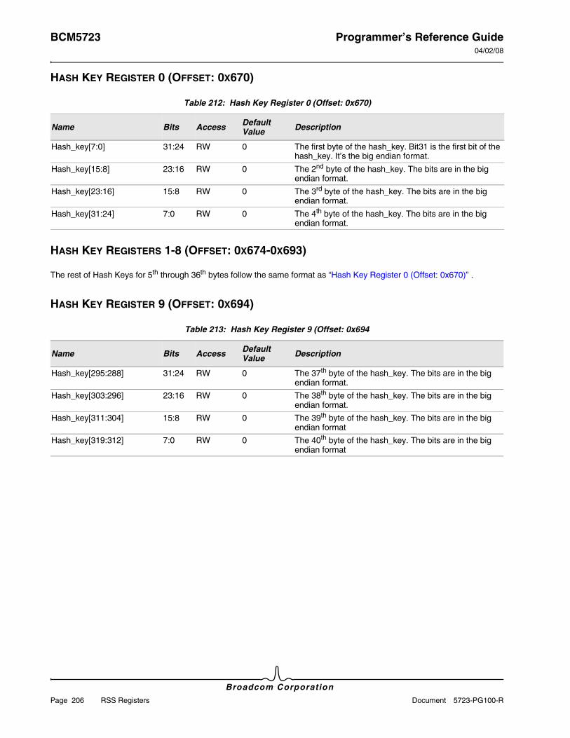
BCM5723 Programmer’s Reference Guide04/02/08
Broadcom Corporation
Page 206 RSS Registers Document 5723-PG100-R
HASH KEY REGISTER 0 (OFFSET: 0X670)
HASH KEY REGISTERS 1-8 (OFFSET: 0X674-0X693)
The rest of Hash Keys for 5th through 36th bytes follow the same format as “Hash Key Register 0 (Offset: 0x670)” .
HASH KEY REGISTER 9 (OFFSET: 0X694)
Table 212: Hash Key Register 0 (Offset: 0x670)
Name Bits Access Default Value Description
Hash_key[7:0] 31:24 RW 0 The first byte of the hash_key. Bit31 is the first bit of the hash_key. It’s the big endian format.
Hash_key[15:8] 23:16 RW 0 The 2nd byte of the hash_key. The bits are in the big endian format.
Hash_key[23:16] 15:8 RW 0 The 3rd byte of the hash_key. The bits are in the big endian format.
Hash_key[31:24] 7:0 RW 0 The 4th byte of the hash_key. The bits are in the big endian format.
Table 213: Hash Key Register 9 (Offset: 0x694
Name Bits Access Default Value Description
Hash_key[295:288] 31:24 RW 0 The 37th byte of the hash_key. The bits are in the big endian format.
Hash_key[303:296] 23:16 RW 0 The 38th byte of the hash_key. The bits are in the big endian format.
Hash_key[311:304] 15:8 RW 0 The 39th byte of the hash_key. The bits are in the big endian format
Hash_key[319:312] 7:0 RW 0 The 40th byte of the hash_key. The bits are in the big endian format
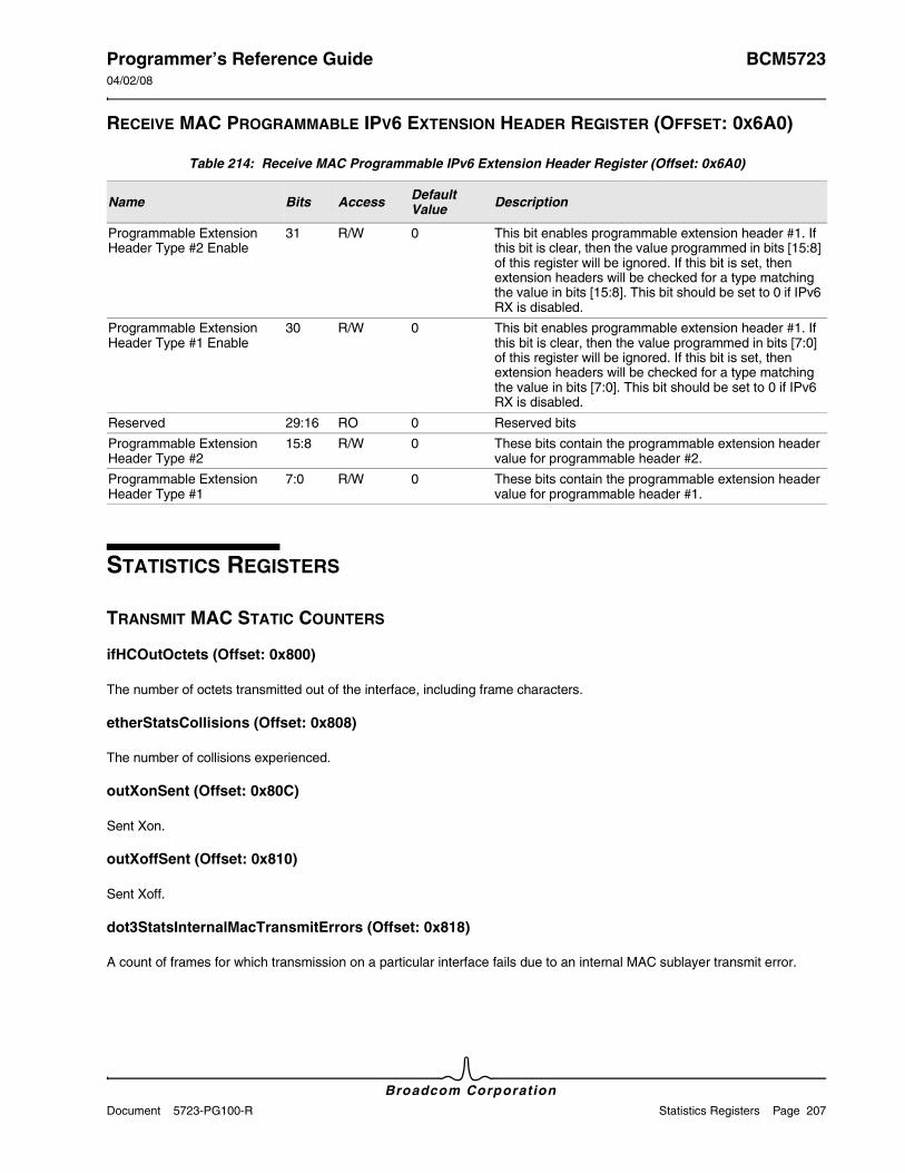
Programmer’s Reference Guide BCM572304/02/08
Broadcom CorporationDocument 5723-PG100-R Statistics Registers Page 207
RECEIVE MAC PROGRAMMABLE IPV6 EXTENSION HEADER REGISTER (OFFSET: 0X6A0)
STATISTICS REGISTERS
TRANSMIT MAC STATIC COUNTERS
ifHCOutOctets (Offset: 0x800)
The number of octets transmitted out of the interface, including frame characters.
etherStatsCollisions (Offset: 0x808)
The number of collisions experienced.
outXonSent (Offset: 0x80C)
Sent Xon.
outXoffSent (Offset: 0x810)
Sent Xoff.
dot3StatsInternalMacTransmitErrors (Offset: 0x818)
A count of frames for which transmission on a particular interface fails due to an internal MAC sublayer transmit error.
Table 214: Receive MAC Programmable IPv6 Extension Header Register (Offset: 0x6A0)
Name Bits Access Default Value Description
Programmable Extension Header Type #2 Enable
31 R/W 0 This bit enables programmable extension header #1. If this bit is clear, then the value programmed in bits [15:8] of this register will be ignored. If this bit is set, then extension headers will be checked for a type matching the value in bits [15:8]. This bit should be set to 0 if IPv6 RX is disabled.
Programmable Extension Header Type #1 Enable
30 R/W 0 This bit enables programmable extension header #1. If this bit is clear, then the value programmed in bits [7:0] of this register will be ignored. If this bit is set, then extension headers will be checked for a type matching the value in bits [7:0]. This bit should be set to 0 if IPv6 RX is disabled.
Reserved 29:16 RO 0 Reserved bits
Programmable Extension Header Type #2
15:8 R/W 0 These bits contain the programmable extension header value for programmable header #2.
Programmable Extension Header Type #1
7:0 R/W 0 These bits contain the programmable extension header value for programmable header #1.
BCM5723 Programmer’s Reference Guide04/02/08
Broadcom Corporation
Page 208 Statistics Registers Document 5723-PG100-R
dot3StatsSingleCollisionFrames (Offset: 0x81C)
A count of successfully transmitted frames on a particular interface for which transmission is inhibited by exactly one collision.
dot3StatsMultipleCollisionFrames (Offset: 0x820)
A count of successfully transmitted frames on a particular interface for which transmission is inhibited by more than one collision.
dot3StatsDeferredTransmissions (Offset: 0x824)
A count of frames for which the first transmission attempt on a particular interface is delayed because of the medium is busy.
dot3StatsExcessiveTransmissions (Offset: 0x82C)
A count of frames for which transmission on a particular interface fails due to excessive collisions.
dot3StatsLateCollisions (Offset: 0x830)
The number of times that a collision is detected on a particular interface later than 512 bit-times into the transmission of a packet.
iHCOutUcastPkts (Offset: 0x86C)
The number of packets that higher-level protocols requested be transmitted, and that were not addressed to a multicast or broadcast address at this sublayer, including those that were discarded or not sent.
iHCOutMulticastPkts (Offset: 0x870)
The number of packets that higher-level protocols requested be transmitted, and that were addressed to a multicast address at this sublayer, including those that were discarded or not sent.
iHCOutBroadcastPkts (Offset: 0x870)
The number of packets that higher-level protocols requested be transmitted, and that were addressed to a broadcast address at this sublayer, including those that were discarded or not sent.
RECEIVE MAC STATIC COUNTERS
ifHCOutOctets (Offset: 0x880)
The number of octets received on the interface, including frame characters.
etherStatsFragments (Offset: 0x888)
A frame size that is less than 64 bytes with a bad FCS.
ifHCInUcastPkts (Offset: 0x88C)
The number of packets delivered by this sublayer to a higher sublayer, which were not addressed to a multicast or broadcast address at this sublayer.
Programmer’s Reference Guide BCM572304/02/08
Broadcom CorporationDocument 5723-PG100-R Statistics Registers Page 209
ifHCInMulticastPkts (Offset: 0x890)
The number of packets delivered by this sublayer to a higher sublayer, which were addressed to a multicast address at this sublayer.
ifHCInBroadcastPkts (Offset: 0x894)
The number of packets delivered by this sublayer to a higher sublayer, which were addressed to a broadcast address at this sublayer.
dot3StatsFCSErrors (Offset: 0x898)
A count of frames received on a particular interface that are an integral number of octets in length and do not pass the FCS check.
dot3StatsAlignmentErrors (Offset: 0x89C)
A count of frames received on a particular interface that are not an integral number of octets in length and do not pass the FCS check.
xonPauseFrameReceived (Offset: 0x8A0)
MAC control frames with pause command and length equal to zero.
xoffPauseFrameReceived (Offset: 0x8A4)
MAC control frames with pause command and length greater than zero.
macControlFramesReceived (Offset: 0x8A8)
MAC control frames with no pause command.
xoffStateEntered (Offset: 0x8AC)
Transmitting is disabled.
dot3StatsFramesTooLongs (Offset: 0x8B0)
A count of frames received on a particular interface that exceeds the maximum permitted frame size.
etherStatsJabbers (Offset: 0x8B4)
Frames exceed jabber time.
etherStatsUndersizePkts (Offset: 0x8B8)
Frames with a size less than 64 bytes.
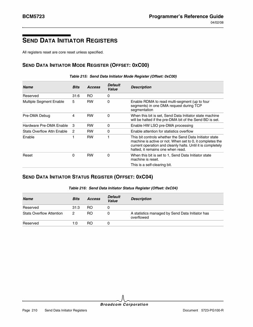
BCM5723 Programmer’s Reference Guide04/02/08
Broadcom Corporation
Page 210 Send Data Initiator Registers Document 5723-PG100-R
SEND DATA INITIATOR REGISTERS
All registers reset are core reset unless specified.
SEND DATA INITIATOR MODE REGISTER (OFFSET: 0XC00)
SEND DATA INITIATOR STATUS REGISTER (OFFSET: 0XC04)
Table 215: Send Data Initiator Mode Register (Offset: 0xC00)
Name Bits Access Default Value Description
Reserved 31:6 RO 0
Multiple Segment Enable 5 RW 0 Enable RDMA to read multi-segment (up to four segments) in one DMA request during TCP segmentation
Pre-DMA Debug 4 RW 0 When this bit is set, Send Data Initiator state machine will be halted if the pre-DMA bit of the Send BD is set.
Hardware Pre-DMA Enable 3 RW 0 Enable HW LSO pre-DMA processing
Stats Overflow Attn Enable 2 RW 0 Enable attention for statistics overflow
Enable 1 RW 1 This bit controls whether the Send Data Initiator state machine is active or not. When set to 0, it completes the current operation and cleanly halts. Until it is completely halted, it remains one when read.
Reset 0 RW 0 When this bit is set to 1, Send Data Initiator state machine is reset.This is a self-clearing bit.
Table 216: Send Data Initiator Status Register (Offset: 0xC04)
Name Bits Access Default Value Description
Reserved 31:3 RO 0
Stats Overflow Attention 2 RO 0 A statistics managed by Send Data Initiator has overflowed
Reserved 1:0 RO 0
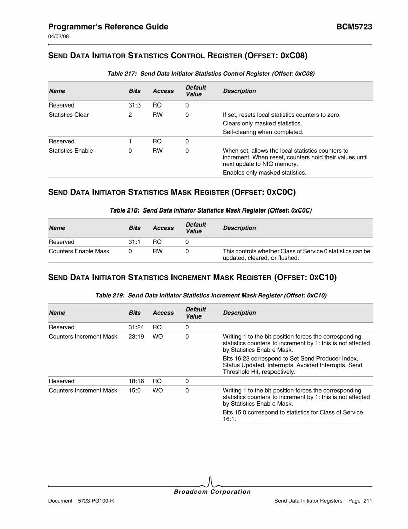
Programmer’s Reference Guide BCM572304/02/08
Broadcom CorporationDocument 5723-PG100-R Send Data Initiator Registers Page 211
SEND DATA INITIATOR STATISTICS CONTROL REGISTER (OFFSET: 0XC08)
SEND DATA INITIATOR STATISTICS MASK REGISTER (OFFSET: 0XC0C)
SEND DATA INITIATOR STATISTICS INCREMENT MASK REGISTER (OFFSET: 0XC10)
Table 217: Send Data Initiator Statistics Control Register (Offset: 0xC08)
Name Bits Access Default Value Description
Reserved 31:3 RO 0
Statistics Clear 2 RW 0 If set, resets local statistics counters to zero.Clears only masked statistics.Self-clearing when completed.
Reserved 1 RO 0
Statistics Enable 0 RW 0 When set, allows the local statistics counters to increment. When reset, counters hold their values until next update to NIC memory.Enables only masked statistics.
Table 218: Send Data Initiator Statistics Mask Register (Offset: 0xC0C)
Name Bits Access Default Value Description
Reserved 31:1 RO 0
Counters Enable Mask 0 RW 0 This controls whether Class of Service 0 statistics can be updated, cleared, or flushed.
Table 219: Send Data Initiator Statistics Increment Mask Register (Offset: 0xC10)
Name Bits Access Default Value Description
Reserved 31:24 RO 0
Counters Increment Mask 23:19 WO 0 Writing 1 to the bit position forces the corresponding statistics counters to increment by 1: this is not affected by Statistics Enable Mask.Bits 16:23 correspond to Set Send Producer Index, Status Updated, Interrupts, Avoided Interrupts, Send Threshold Hit, respectively.
Reserved 18:16 RO 0
Counters Increment Mask 15:0 WO 0 Writing 1 to the bit position forces the corresponding statistics counters to increment by 1: this is not affected by Statistics Enable Mask.Bits 15:0 correspond to statistics for Class of Service 16:1.
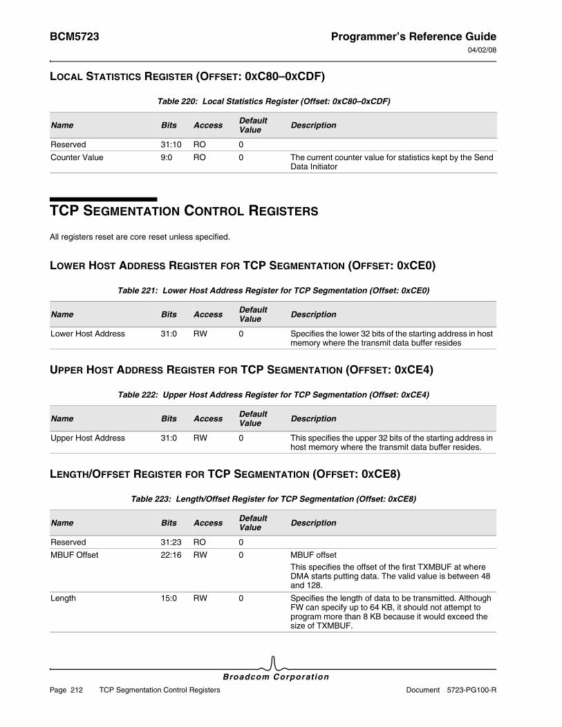
BCM5723 Programmer’s Reference Guide04/02/08
Broadcom Corporation
Page 212 TCP Segmentation Control Registers Document 5723-PG100-R
LOCAL STATISTICS REGISTER (OFFSET: 0XC80–0XCDF)
TCP SEGMENTATION CONTROL REGISTERS
All registers reset are core reset unless specified.
LOWER HOST ADDRESS REGISTER FOR TCP SEGMENTATION (OFFSET: 0XCE0)
UPPER HOST ADDRESS REGISTER FOR TCP SEGMENTATION (OFFSET: 0XCE4)
LENGTH/OFFSET REGISTER FOR TCP SEGMENTATION (OFFSET: 0XCE8)
Table 220: Local Statistics Register (Offset: 0xC80–0xCDF)
Name Bits Access Default Value Description
Reserved 31:10 RO 0
Counter Value 9:0 RO 0 The current counter value for statistics kept by the Send Data Initiator
Table 221: Lower Host Address Register for TCP Segmentation (Offset: 0xCE0)
Name Bits Access Default Value Description
Lower Host Address 31:0 RW 0 Specifies the lower 32 bits of the starting address in host memory where the transmit data buffer resides
Table 222: Upper Host Address Register for TCP Segmentation (Offset: 0xCE4)
Name Bits Access Default Value Description
Upper Host Address 31:0 RW 0 This specifies the upper 32 bits of the starting address in host memory where the transmit data buffer resides.
Table 223: Length/Offset Register for TCP Segmentation (Offset: 0xCE8)
Name Bits Access Default Value Description
Reserved 31:23 RO 0
MBUF Offset 22:16 RW 0 MBUF offsetThis specifies the offset of the first TXMBUF at where DMA starts putting data. The valid value is between 48 and 128.
Length 15:0 RW 0 Specifies the length of data to be transmitted. Although FW can specify up to 64 KB, it should not attempt to program more than 8 KB because it would exceed the size of TXMBUF.
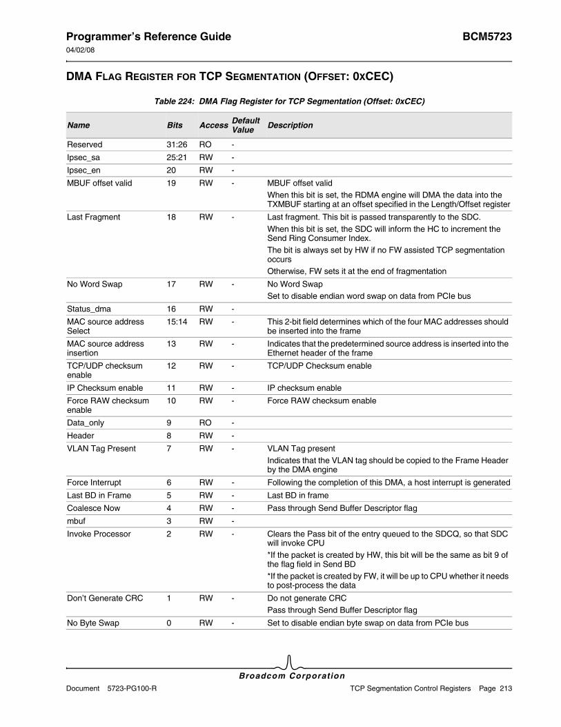
Programmer’s Reference Guide BCM572304/02/08
Broadcom CorporationDocument 5723-PG100-R TCP Segmentation Control Registers Page 213
DMA FLAG REGISTER FOR TCP SEGMENTATION (OFFSET: 0XCEC)
Table 224: DMA Flag Register for TCP Segmentation (Offset: 0xCEC)
Name Bits Access Default Value Description
Reserved 31:26 RO -
Ipsec_sa 25:21 RW -
Ipsec_en 20 RW -
MBUF offset valid 19 RW - MBUF offset validWhen this bit is set, the RDMA engine will DMA the data into the TXMBUF starting at an offset specified in the Length/Offset register
Last Fragment 18 RW - Last fragment. This bit is passed transparently to the SDC.When this bit is set, the SDC will inform the HC to increment the Send Ring Consumer Index.The bit is always set by HW if no FW assisted TCP segmentation occursOtherwise, FW sets it at the end of fragmentation
No Word Swap 17 RW - No Word SwapSet to disable endian word swap on data from PCIe bus
Status_dma 16 RW -
MAC source address Select
15:14 RW - This 2-bit field determines which of the four MAC addresses should be inserted into the frame
MAC source address insertion
13 RW - Indicates that the predetermined source address is inserted into the Ethernet header of the frame
TCP/UDP checksum enable
12 RW - TCP/UDP Checksum enable
IP Checksum enable 11 RW - IP checksum enable
Force RAW checksum enable
10 RW - Force RAW checksum enable
Data_only 9 RO -
Header 8 RW -
VLAN Tag Present 7 RW - VLAN Tag presentIndicates that the VLAN tag should be copied to the Frame Header by the DMA engine
Force Interrupt 6 RW - Following the completion of this DMA, a host interrupt is generated
Last BD in Frame 5 RW - Last BD in frame
Coalesce Now 4 RW - Pass through Send Buffer Descriptor flag
mbuf 3 RW -
Invoke Processor 2 RW - Clears the Pass bit of the entry queued to the SDCQ, so that SDC will invoke CPU*If the packet is created by HW, this bit will be the same as bit 9 of the flag field in Send BD*If the packet is created by FW, it will be up to CPU whether it needs to post-process the data
Don’t Generate CRC 1 RW - Do not generate CRCPass through Send Buffer Descriptor flag
No Byte Swap 0 RW - Set to disable endian byte swap on data from PCIe bus
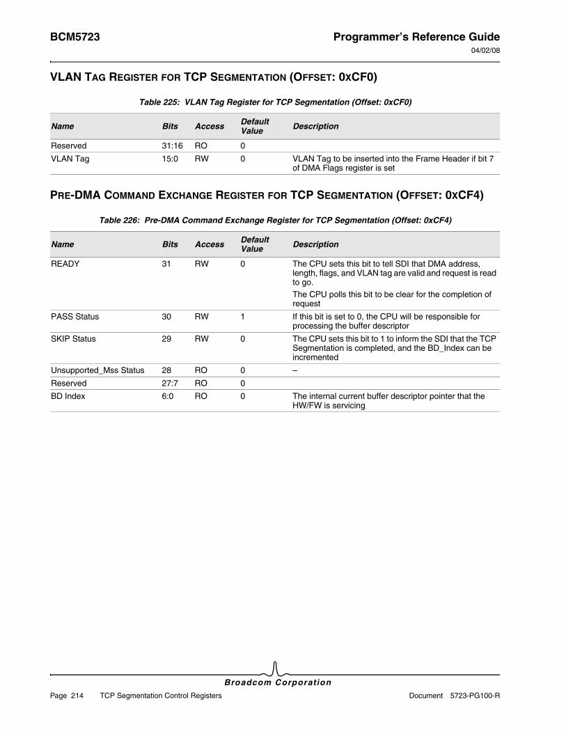
BCM5723 Programmer’s Reference Guide04/02/08
Broadcom Corporation
Page 214 TCP Segmentation Control Registers Document 5723-PG100-R
VLAN TAG REGISTER FOR TCP SEGMENTATION (OFFSET: 0XCF0)
PRE-DMA COMMAND EXCHANGE REGISTER FOR TCP SEGMENTATION (OFFSET: 0XCF4)
Table 225: VLAN Tag Register for TCP Segmentation (Offset: 0xCF0)
Name Bits Access Default Value Description
Reserved 31:16 RO 0
VLAN Tag 15:0 RW 0 VLAN Tag to be inserted into the Frame Header if bit 7 of DMA Flags register is set
Table 226: Pre-DMA Command Exchange Register for TCP Segmentation (Offset: 0xCF4)
Name Bits Access Default Value Description
READY 31 RW 0 The CPU sets this bit to tell SDI that DMA address, length, flags, and VLAN tag are valid and request is read to go. The CPU polls this bit to be clear for the completion of request
PASS Status 30 RW 1 If this bit is set to 0, the CPU will be responsible for processing the buffer descriptor
SKIP Status 29 RW 0 The CPU sets this bit to 1 to inform the SDI that the TCP Segmentation is completed, and the BD_Index can be incremented
Unsupported_Mss Status 28 RO 0 –
Reserved 27:7 RO 0
BD Index 6:0 RO 0 The internal current buffer descriptor pointer that the HW/FW is servicing
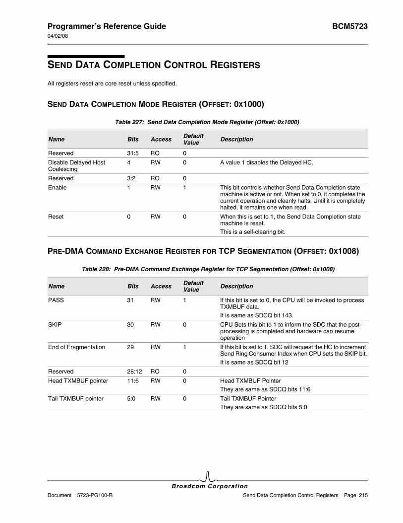
Programmer’s Reference Guide BCM572304/02/08
Broadcom CorporationDocument 5723-PG100-R Send Data Completion Control Registers Page 215
SEND DATA COMPLETION CONTROL REGISTERS
All registers reset are core reset unless specified.
SEND DATA COMPLETION MODE REGISTER (OFFSET: 0X1000)
PRE-DMA COMMAND EXCHANGE REGISTER FOR TCP SEGMENTATION (OFFSET: 0X1008)
Table 227: Send Data Completion Mode Register (Offset: 0x1000)
Name Bits Access Default Value Description
Reserved 31:5 RO 0
Disable Delayed Host Coalescing
4 RW 0 A value 1 disables the Delayed HC.
Reserved 3:2 RO 0
Enable 1 RW 1 This bit controls whether Send Data Completion state machine is active or not. When set to 0, it completes the current operation and cleanly halts. Until it is completely halted, it remains one when read.
Reset 0 RW 0 When this is set to 1, the Send Data Completion state machine is reset.This is a self-clearing bit.
Table 228: Pre-DMA Command Exchange Register for TCP Segmentation (Offset: 0x1008)
Name Bits Access Default Value Description
PASS 31 RW 1 If this bit is set to 0, the CPU will be invoked to process TXMBUF data.It is same as SDCQ bit 143.
SKIP 30 RW 0 CPU Sets this bit to 1 to inform the SDC that the post-processing is completed and hardware can resume operation
End of Fragmentation 29 RW 1 If this bit is set to 1, SDC will request the HC to increment Send Ring Consumer Index when CPU sets the SKIP bit.It is same as SDCQ bit 12
Reserved 28:12 RO 0
Head TXMBUF pointer 11:6 RW 0 Head TXMBUF PointerThey are same as SDCQ bits 11:6
Tail TXMBUF pointer 5:0 RW 0 Tail TXMBUF PointerThey are same as SDCQ bits 5:0
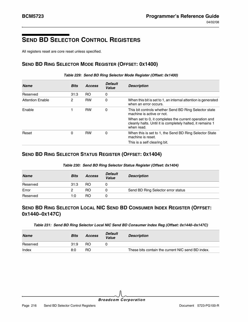
BCM5723 Programmer’s Reference Guide04/02/08
Broadcom Corporation
Page 216 Send BD Selector Control Registers Document 5723-PG100-R
SEND BD SELECTOR CONTROL REGISTERS
All registers reset are core reset unless specified.
SEND BD RING SELECTOR MODE REGISTER (OFFSET: 0X1400)
SEND BD RING SELECTOR STATUS REGISTER (OFFSET: 0X1404)
SEND BD RING SELECTOR LOCAL NIC SEND BD CONSUMER INDEX REGISTER (OFFSET: 0X1440–0X147C)
Table 229: Send BD Ring Selector Mode Register (Offset: 0x1400)
Name Bits Access Default Value Description
Reserved 31:3 RO 0
Attention Enable 2 RW 0 When this bit is set to 1, an internal attention is generated when an error occurs.
Enable 1 RW 0 This bit controls whether Send BD Ring Selector state machine is active or not.When set to 0, it completes the current operation and cleanly halts. Until it is completely halted, it remains 1 when read.
Reset 0 RW 0 When this is set to 1, the Send BD Ring Selector State machine is reset.This is a self clearing bit.
Table 230: Send BD Ring Selector Status Register (Offset: 0x1404)
Name Bits Access Default Value Description
Reserved 31:3 RO 0
Error 2 RO 0 Send BD Ring Selector error status
Reserved 1:0 RO 0
Table 231: Send BD Ring Selector Local NIC Send BD Consumer Index Reg (Offset: 0x1440–0x147C)
Name Bits Access Default Value Description
Reserved 31:9 RO 0
Index 8:0 RO These bits contain the current NIC send BD index.
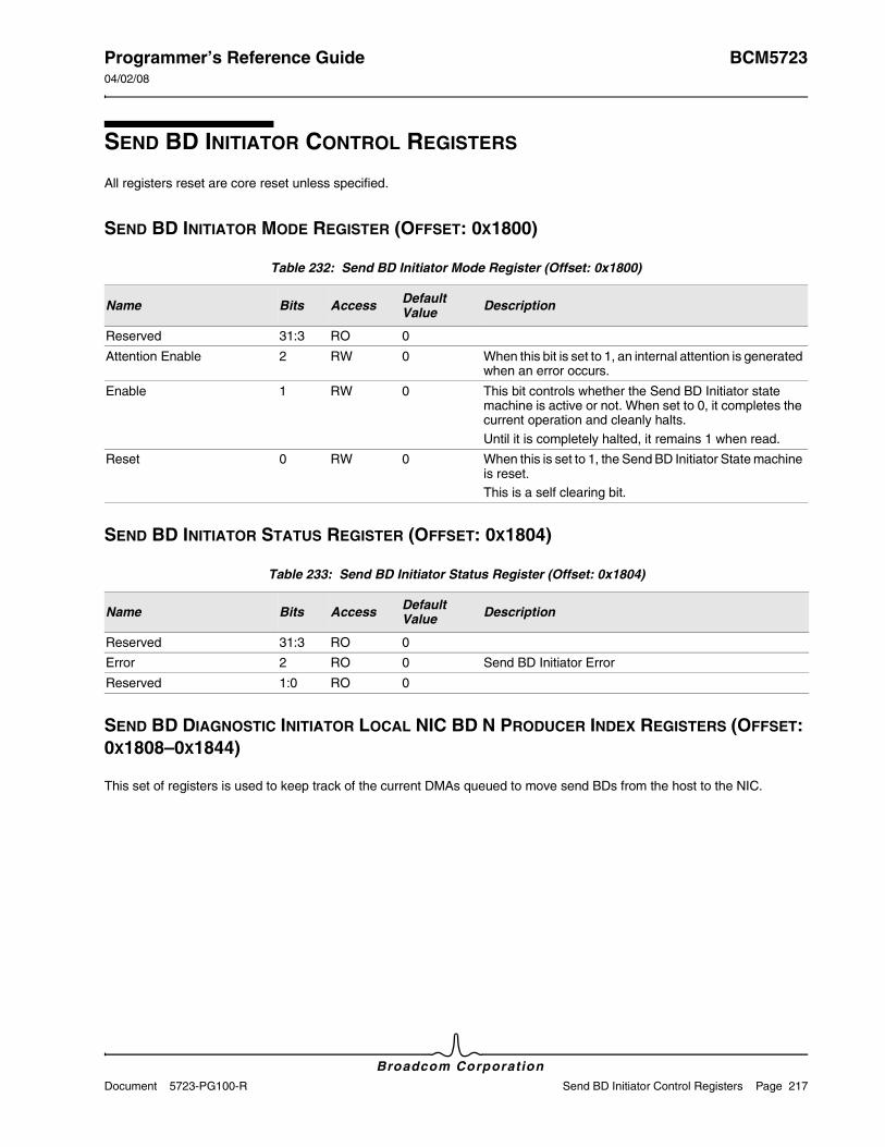
Programmer’s Reference Guide BCM572304/02/08
Broadcom CorporationDocument 5723-PG100-R Send BD Initiator Control Registers Page 217
SEND BD INITIATOR CONTROL REGISTERS
All registers reset are core reset unless specified.
SEND BD INITIATOR MODE REGISTER (OFFSET: 0X1800)
SEND BD INITIATOR STATUS REGISTER (OFFSET: 0X1804)
SEND BD DIAGNOSTIC INITIATOR LOCAL NIC BD N PRODUCER INDEX REGISTERS (OFFSET: 0X1808–0X1844)
This set of registers is used to keep track of the current DMAs queued to move send BDs from the host to the NIC.
Table 232: Send BD Initiator Mode Register (Offset: 0x1800)
Name Bits Access Default Value Description
Reserved 31:3 RO 0
Attention Enable 2 RW 0 When this bit is set to 1, an internal attention is generated when an error occurs.
Enable 1 RW 0 This bit controls whether the Send BD Initiator state machine is active or not. When set to 0, it completes the current operation and cleanly halts.Until it is completely halted, it remains 1 when read.
Reset 0 RW 0 When this is set to 1, the Send BD Initiator State machine is reset.This is a self clearing bit.
Table 233: Send BD Initiator Status Register (Offset: 0x1804)
Name Bits Access Default Value Description
Reserved 31:3 RO 0
Error 2 RO 0 Send BD Initiator Error
Reserved 1:0 RO 0
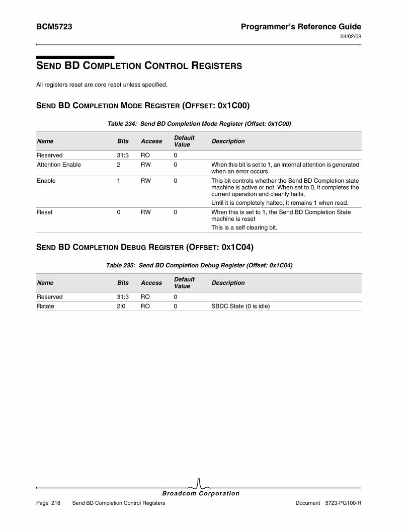
BCM5723 Programmer’s Reference Guide04/02/08
Broadcom Corporation
Page 218 Send BD Completion Control Registers Document 5723-PG100-R
SEND BD COMPLETION CONTROL REGISTERS
All registers reset are core reset unless specified.
SEND BD COMPLETION MODE REGISTER (OFFSET: 0X1C00)
SEND BD COMPLETION DEBUG REGISTER (OFFSET: 0X1C04)
Table 234: Send BD Completion Mode Register (Offset: 0x1C00)
Name Bits Access Default Value Description
Reserved 31:3 RO 0
Attention Enable 2 RW 0 When this bit is set to 1, an internal attention is generated when an error occurs.
Enable 1 RW 0 This bit controls whether the Send BD Completion state machine is active or not. When set to 0, it completes the current operation and cleanly halts.Until it is completely halted, it remains 1 when read.
Reset 0 RW 0 When this is set to 1, the Send BD Completion State machine is resetThis is a self clearing bit.
Table 235: Send BD Completion Debug Register (Offset: 0x1C04)
Name Bits Access Default Value Description
Reserved 31:3 RO 0
Rstate 2:0 RO 0 SBDC State (0 is idle)
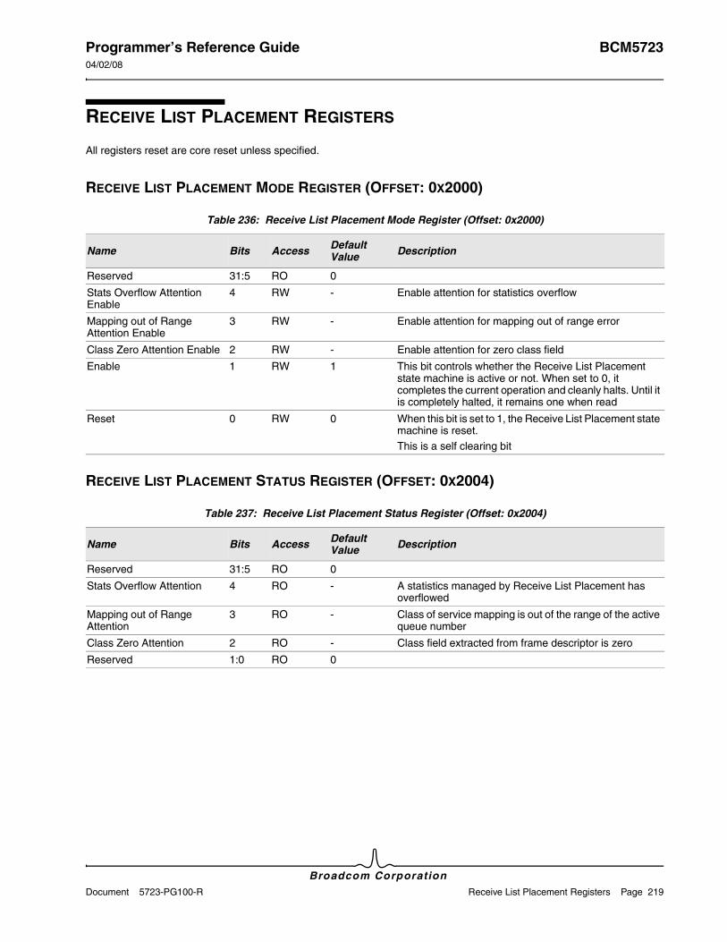
Programmer’s Reference Guide BCM572304/02/08
Broadcom CorporationDocument 5723-PG100-R Receive List Placement Registers Page 219
RECEIVE LIST PLACEMENT REGISTERS
All registers reset are core reset unless specified.
RECEIVE LIST PLACEMENT MODE REGISTER (OFFSET: 0X2000)
RECEIVE LIST PLACEMENT STATUS REGISTER (OFFSET: 0X2004)
Table 236: Receive List Placement Mode Register (Offset: 0x2000)
Name Bits Access Default Value Description
Reserved 31:5 RO 0
Stats Overflow Attention Enable
4 RW - Enable attention for statistics overflow
Mapping out of Range Attention Enable
3 RW - Enable attention for mapping out of range error
Class Zero Attention Enable 2 RW - Enable attention for zero class field
Enable 1 RW 1 This bit controls whether the Receive List Placement state machine is active or not. When set to 0, it completes the current operation and cleanly halts. Until it is completely halted, it remains one when read
Reset 0 RW 0 When this bit is set to 1, the Receive List Placement state machine is reset. This is a self clearing bit
Table 237: Receive List Placement Status Register (Offset: 0x2004)
Name Bits Access Default Value Description
Reserved 31:5 RO 0
Stats Overflow Attention 4 RO - A statistics managed by Receive List Placement has overflowed
Mapping out of Range Attention
3 RO - Class of service mapping is out of the range of the active queue number
Class Zero Attention 2 RO - Class field extracted from frame descriptor is zero
Reserved 1:0 RO 0
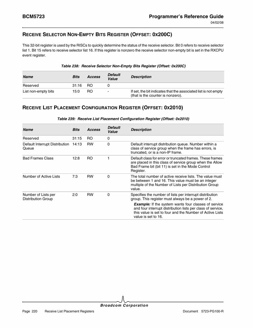
BCM5723 Programmer’s Reference Guide04/02/08
Broadcom Corporation
Page 220 Receive List Placement Registers Document 5723-PG100-R
RECEIVE SELECTOR NON-EMPTY BITS REGISTER (OFFSET: 0X200C)
This 32-bit register is used by the RISCs to quickly determine the status of the receive selector. Bit 0 refers to receive selector list 1. Bit 15 refers to receive selector list 16. If this register is nonzero the receive selector non-empty bit is set in the RXCPU event register.
RECEIVE LIST PLACEMENT CONFIGURATION REGISTER (OFFSET: 0X2010)
Table 238: Receive Selector Non-Empty Bits Register (Offset: 0x200C)
Name Bits Access Default Value Description
Reserved 31:16 RO 0
List non-empty bits 15:0 RO - If set, the bit indicates that the associated list is not empty (that is the counter is nonzero).
Table 239: Receive List Placement Configuration Register (Offset: 0x2010)
Name Bits Access Default Value Description
Reserved 31:15 RO 0
Default Interrupt Distribution Queue
14:13 RW 0 Default interrupt distribution queue. Number within a class of service group when the frame has errors, is truncated, or is a non-IP frame.
Bad Frames Class 12:8 RO 1 Default class for error or truncated frames. These frames are placed in this class of service group when the Allow Bad Frame bit (bit 11) is set in the Mode Control Register.
Number of Active Lists 7:3 RW 0 The total number of active receive lists. The value must be between 1 and 16. This value must be an integer multiple of the Number of Lists per Distribution Group value.
Number of Lists per Distribution Group
2:0 RW 0 Specifies the number of lists per interrupt distribution group. This register must always be a power of 2.
Example: If the system wants four classes of service and four interrupt distribution lists per class of service, this value is set to four and the Number of Active Lists value is set to 16.
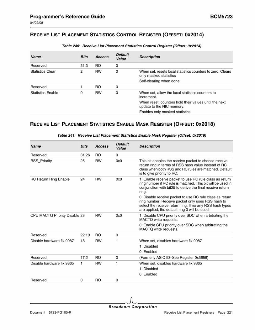
Programmer’s Reference Guide BCM572304/02/08
Broadcom CorporationDocument 5723-PG100-R Receive List Placement Registers Page 221
RECEIVE LIST PLACEMENT STATISTICS CONTROL REGISTER (OFFSET: 0X2014)
RECEIVE LIST PLACEMENT STATISTICS ENABLE MASK REGISTER (OFFSET: 0X2018)
Table 240: Receive List Placement Statistics Control Register (Offset: 0x2014)
Name Bits Access Default Value Description
Reserved 31:3 RO 0
Statistics Clear 2 RW 0 When set, resets local statistics counters to zero. Clears only masked statisticsSelf-clearing when done
Reserved 1 RO 0
Statistics Enable 0 RW 0 When set, allow the local statistics counters to increment.When reset, counters hold their values until the next update to the NIC memory.Enables only masked statistics
Table 241: Receive List Placement Statistics Enable Mask Register (Offset: 0x2018)
Name Bits Access Default Value Description
Reserved 31:26 RO 0
RSS_Priority 25 RW 0x0 This bit enables the receive packet to choose receive return ring in terms of RSS hash value instead of RC class when both RSS and RC rules are matched. Default is to give priority to RC.
RC Return Ring Enable 24 RW 0x0 1: Enable receive packet to use RC rule class as return ring number if RC rule is matched. This bit will be used in conjunction with bit25 to derive the final receive return ring.0: Disable receive packet to use RC rule class as return ring number. Receive packet only uses RSS hash to select the receive return ring. If no any RSS hash types are applied, the default ring 0 will be used.
CPU MACTQ Priority Disable 23 RW 0x0 1: Disable CPU priority over SDC when arbitrating the MACTQ write requests.0: Enable CPU priority over SDC when arbitrating the MACTQ write requests.
Reserved 22:19 RO 0
Disable hardware fix 9987 18 RW 1 When set, disables hardware fix 9987 1: Disabled0: Enabled
Reserved 17:2 RO 0 (Formerly ASIC ID–See Register 0x3658)
Disable hardware fix 9365 1 RW 1 When set, disables hardware fix 93651: Disabled0: Enabled
Reserved 0 RO 0
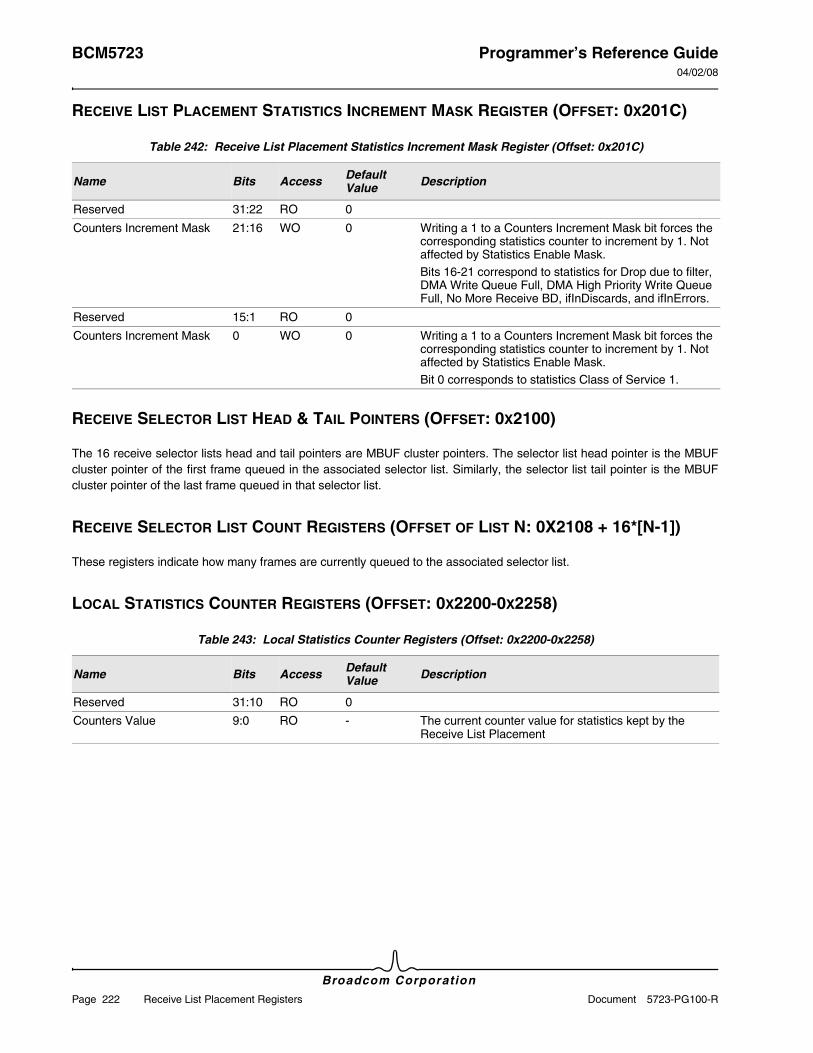
BCM5723 Programmer’s Reference Guide04/02/08
Broadcom Corporation
Page 222 Receive List Placement Registers Document 5723-PG100-R
RECEIVE LIST PLACEMENT STATISTICS INCREMENT MASK REGISTER (OFFSET: 0X201C)
RECEIVE SELECTOR LIST HEAD & TAIL POINTERS (OFFSET: 0X2100)
The 16 receive selector lists head and tail pointers are MBUF cluster pointers. The selector list head pointer is the MBUF cluster pointer of the first frame queued in the associated selector list. Similarly, the selector list tail pointer is the MBUF cluster pointer of the last frame queued in that selector list.
RECEIVE SELECTOR LIST COUNT REGISTERS (OFFSET OF LIST N: 0X2108 + 16*[N-1])
These registers indicate how many frames are currently queued to the associated selector list.
LOCAL STATISTICS COUNTER REGISTERS (OFFSET: 0X2200-0X2258)
Table 242: Receive List Placement Statistics Increment Mask Register (Offset: 0x201C)
Name Bits Access Default Value Description
Reserved 31:22 RO 0
Counters Increment Mask 21:16 WO 0 Writing a 1 to a Counters Increment Mask bit forces the corresponding statistics counter to increment by 1. Not affected by Statistics Enable Mask.Bits 16-21 correspond to statistics for Drop due to filter, DMA Write Queue Full, DMA High Priority Write Queue Full, No More Receive BD, ifInDiscards, and ifInErrors.
Reserved 15:1 RO 0
Counters Increment Mask 0 WO 0 Writing a 1 to a Counters Increment Mask bit forces the corresponding statistics counter to increment by 1. Not affected by Statistics Enable Mask.Bit 0 corresponds to statistics Class of Service 1.
Table 243: Local Statistics Counter Registers (Offset: 0x2200-0x2258)
Name Bits Access Default Value Description
Reserved 31:10 RO 0
Counters Value 9:0 RO - The current counter value for statistics kept by the Receive List Placement
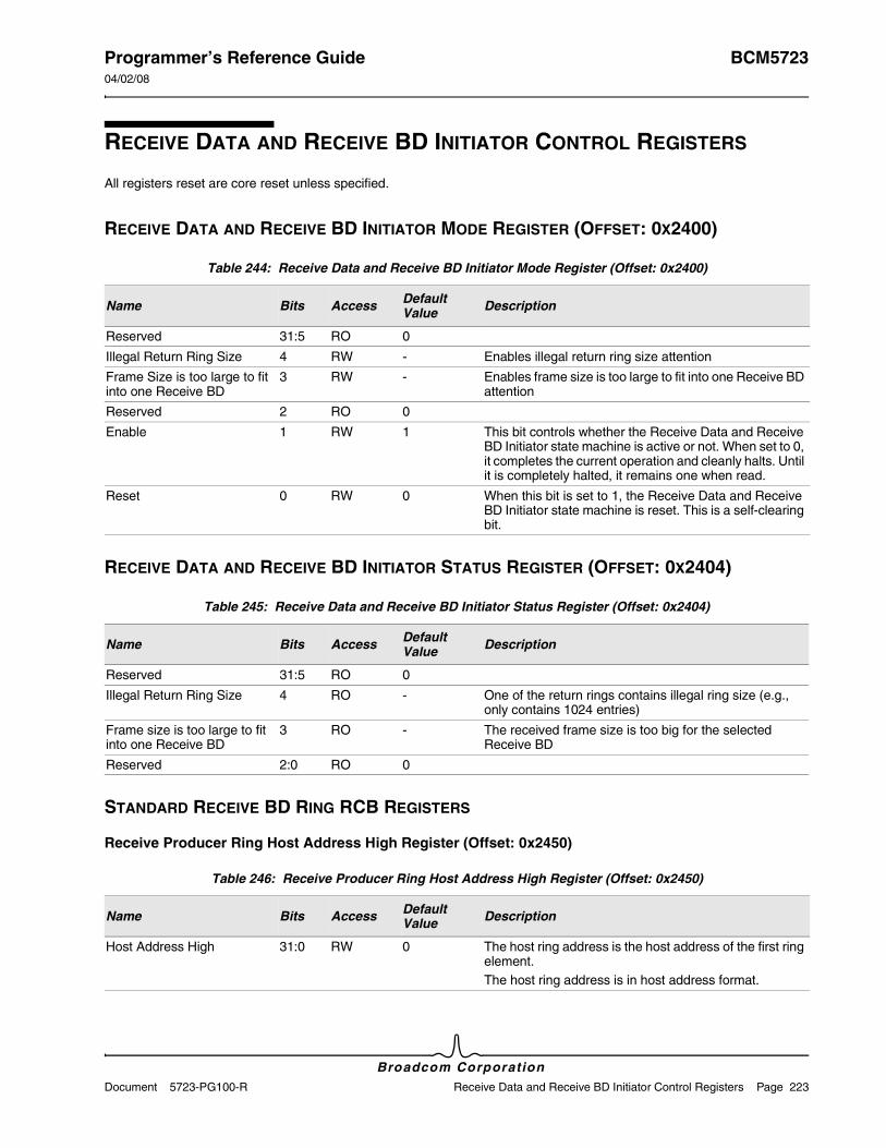
Programmer’s Reference Guide BCM572304/02/08
Broadcom CorporationDocument 5723-PG100-R Receive Data and Receive BD Initiator Control Registers Page 223
RECEIVE DATA AND RECEIVE BD INITIATOR CONTROL REGISTERS
All registers reset are core reset unless specified.
RECEIVE DATA AND RECEIVE BD INITIATOR MODE REGISTER (OFFSET: 0X2400)
RECEIVE DATA AND RECEIVE BD INITIATOR STATUS REGISTER (OFFSET: 0X2404)
STANDARD RECEIVE BD RING RCB REGISTERS
Receive Producer Ring Host Address High Register (Offset: 0x2450)
Table 244: Receive Data and Receive BD Initiator Mode Register (Offset: 0x2400)
Name Bits Access Default Value Description
Reserved 31:5 RO 0
Illegal Return Ring Size 4 RW - Enables illegal return ring size attention
Frame Size is too large to fit into one Receive BD
3 RW - Enables frame size is too large to fit into one Receive BD attention
Reserved 2 RO 0
Enable 1 RW 1 This bit controls whether the Receive Data and Receive BD Initiator state machine is active or not. When set to 0, it completes the current operation and cleanly halts. Until it is completely halted, it remains one when read.
Reset 0 RW 0 When this bit is set to 1, the Receive Data and Receive BD Initiator state machine is reset. This is a self-clearing bit.
Table 245: Receive Data and Receive BD Initiator Status Register (Offset: 0x2404)
Name Bits Access Default Value Description
Reserved 31:5 RO 0
Illegal Return Ring Size 4 RO - One of the return rings contains illegal ring size (e.g., only contains 1024 entries)
Frame size is too large to fit into one Receive BD
3 RO - The received frame size is too big for the selected Receive BD
Reserved 2:0 RO 0
Table 246: Receive Producer Ring Host Address High Register (Offset: 0x2450)
Name Bits Access Default Value Description
Host Address High 31:0 RW 0 The host ring address is the host address of the first ring element.The host ring address is in host address format.

BCM5723 Programmer’s Reference Guide04/02/08
Broadcom Corporation
Page 224 Receive Data and Receive BD Initiator Control Registers Document 5723-PG100-R
Receive Producer Ring Host Address Low Register (Offset: 0x2454)
Receive Producer Length/Flags Register (Offset: 0x2458)
Receive Producer Ring NIC Address Register (Offset: 0x245C)
RECEIVE DIAGNOSTIC DATA AND RECEIVE BD RING INITIATOR LOCAL NIC STANDARD RECEIVE BD CONSUMER INDEX (OFFSET: 0X2474)
This set of registers keeps track of the current DMAs queued to move receive data from the NIC to the host. The Receive Data and Receive BD Initiator maintains the state of the indices by keeping two local copies, a copy of the NIC’s return ring producer index, and a copy of the NIC’s receive BD consumer index. The local return ring producer index is set to the value placed in the DMA descriptor. The local NIC receive return consumer index is also set to the value placed in the DMA descriptor.
Table 247: Receive Producer Ring Host Address Low Register (Offset: 0x2454)
Name Bits Access Default Value Description
Host Address Low 31:0 RW 0 The host ring address is the host address of the first ring element.The host ring address is in host address format.
Table 248: Receive Producer Length/Flags Register (Offset: 0x2458)
Name Bits Access Default Value Description
Max Length 31:16 RW 0 Unused for jumbo rings; otherwise, specifies the maximum size of an Ethernet packet plus VLAN tag
Reserved 15:2 RO 0
Disable Ring 1 RW 0 Set to disable the use of the ring
Reserved 0 RO 0 Set to use the extended receive buffer descriptors
Table 249: Receive Producer Ring NIC Address Register (Offset: 0x245C)
Name Bits Access Default Value Description
NIC Address 31:0 RW 0 The NIC ring address is the NIC address of the first ring element
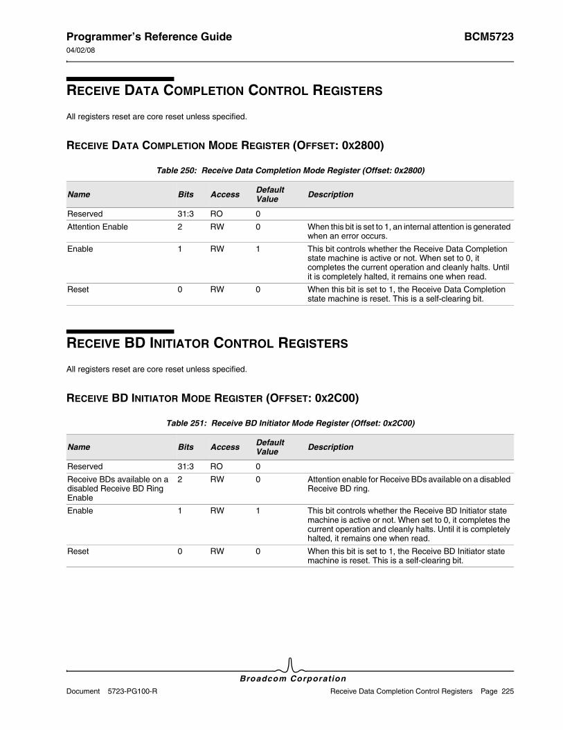
Programmer’s Reference Guide BCM572304/02/08
Broadcom CorporationDocument 5723-PG100-R Receive Data Completion Control Registers Page 225
RECEIVE DATA COMPLETION CONTROL REGISTERS
All registers reset are core reset unless specified.
RECEIVE DATA COMPLETION MODE REGISTER (OFFSET: 0X2800)
RECEIVE BD INITIATOR CONTROL REGISTERS
All registers reset are core reset unless specified.
RECEIVE BD INITIATOR MODE REGISTER (OFFSET: 0X2C00)
Table 250: Receive Data Completion Mode Register (Offset: 0x2800)
Name Bits Access Default Value Description
Reserved 31:3 RO 0
Attention Enable 2 RW 0 When this bit is set to 1, an internal attention is generated when an error occurs.
Enable 1 RW 1 This bit controls whether the Receive Data Completion state machine is active or not. When set to 0, it completes the current operation and cleanly halts. Until it is completely halted, it remains one when read.
Reset 0 RW 0 When this bit is set to 1, the Receive Data Completion state machine is reset. This is a self-clearing bit.
Table 251: Receive BD Initiator Mode Register (Offset: 0x2C00)
Name Bits Access Default Value Description
Reserved 31:3 RO 0
Receive BDs available on a disabled Receive BD Ring Enable
2 RW 0 Attention enable for Receive BDs available on a disabled Receive BD ring.
Enable 1 RW 1 This bit controls whether the Receive BD Initiator state machine is active or not. When set to 0, it completes the current operation and cleanly halts. Until it is completely halted, it remains one when read.
Reset 0 RW 0 When this bit is set to 1, the Receive BD Initiator state machine is reset. This is a self-clearing bit.
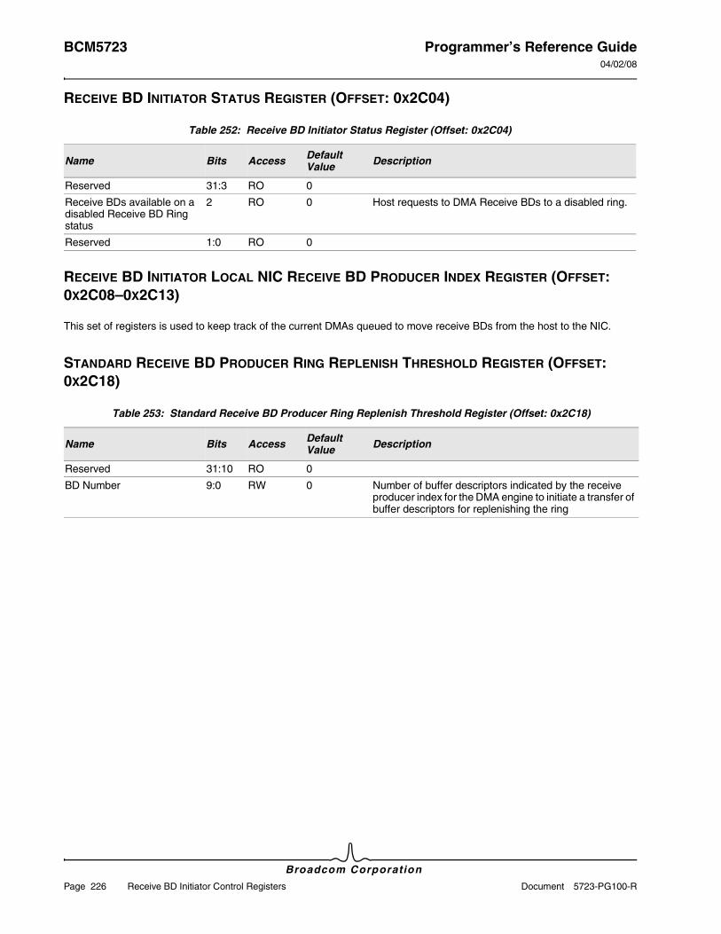
BCM5723 Programmer’s Reference Guide04/02/08
Broadcom Corporation
Page 226 Receive BD Initiator Control Registers Document 5723-PG100-R
RECEIVE BD INITIATOR STATUS REGISTER (OFFSET: 0X2C04)
RECEIVE BD INITIATOR LOCAL NIC RECEIVE BD PRODUCER INDEX REGISTER (OFFSET: 0X2C08–0X2C13)
This set of registers is used to keep track of the current DMAs queued to move receive BDs from the host to the NIC.
STANDARD RECEIVE BD PRODUCER RING REPLENISH THRESHOLD REGISTER (OFFSET: 0X2C18)
Table 252: Receive BD Initiator Status Register (Offset: 0x2C04)
Name Bits Access Default Value Description
Reserved 31:3 RO 0
Receive BDs available on a disabled Receive BD Ring status
2 RO 0 Host requests to DMA Receive BDs to a disabled ring.
Reserved 1:0 RO 0
Table 253: Standard Receive BD Producer Ring Replenish Threshold Register (Offset: 0x2C18)
Name Bits Access Default Value Description
Reserved 31:10 RO 0
BD Number 9:0 RW 0 Number of buffer descriptors indicated by the receive producer index for the DMA engine to initiate a transfer of buffer descriptors for replenishing the ring
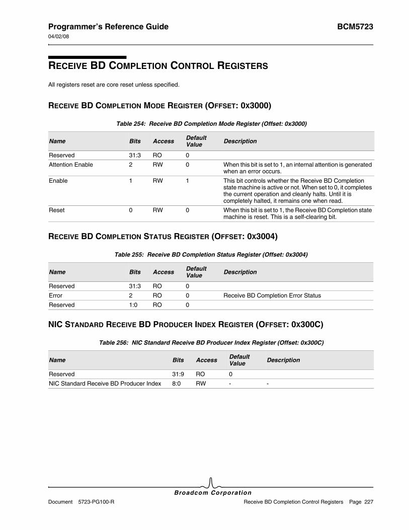
Programmer’s Reference Guide BCM572304/02/08
Broadcom CorporationDocument 5723-PG100-R Receive BD Completion Control Registers Page 227
RECEIVE BD COMPLETION CONTROL REGISTERS
All registers reset are core reset unless specified.
RECEIVE BD COMPLETION MODE REGISTER (OFFSET: 0X3000)
RECEIVE BD COMPLETION STATUS REGISTER (OFFSET: 0X3004)
NIC STANDARD RECEIVE BD PRODUCER INDEX REGISTER (OFFSET: 0X300C)
Table 254: Receive BD Completion Mode Register (Offset: 0x3000)
Name Bits Access Default Value Description
Reserved 31:3 RO 0
Attention Enable 2 RW 0 When this bit is set to 1, an internal attention is generated when an error occurs.
Enable 1 RW 1 This bit controls whether the Receive BD Completion state machine is active or not. When set to 0, it completes the current operation and cleanly halts. Until it is completely halted, it remains one when read.
Reset 0 RW 0 When this bit is set to 1, the Receive BD Completion state machine is reset. This is a self-clearing bit.
Table 255: Receive BD Completion Status Register (Offset: 0x3004)
Name Bits Access Default Value Description
Reserved 31:3 RO 0
Error 2 RO 0 Receive BD Completion Error Status
Reserved 1:0 RO 0
Table 256: NIC Standard Receive BD Producer Index Register (Offset: 0x300C)
Name Bits Access Default Value Description
Reserved 31:9 RO 0
NIC Standard Receive BD Producer Index 8:0 RW - -
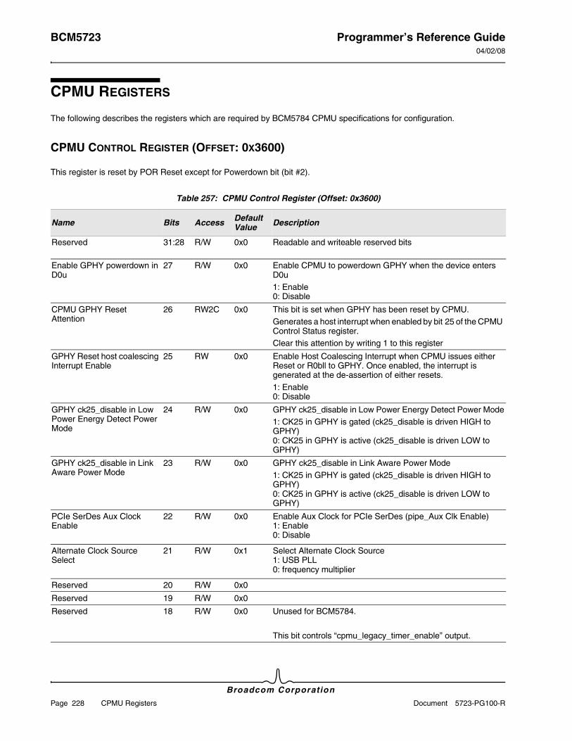
BCM5723 Programmer’s Reference Guide04/02/08
Broadcom Corporation
Page 228 CPMU Registers Document 5723-PG100-R
CPMU REGISTERS
The following describes the registers which are required by BCM5784 CPMU specifications for configuration.
CPMU CONTROL REGISTER (OFFSET: 0X3600)
This register is reset by POR Reset except for Powerdown bit (bit #2).
Table 257: CPMU Control Register (Offset: 0x3600)
Name Bits Access Default Value Description
Reserved 31:28 R/W 0x0 Readable and writeable reserved bits
Enable GPHY powerdown in D0u
27 R/W 0x0 Enable CPMU to powerdown GPHY when the device enters D0u1: Enable 0: Disable
CPMU GPHY Reset Attention
26 RW2C 0x0 This bit is set when GPHY has been reset by CPMU.Generates a host interrupt when enabled by bit 25 of the CPMU Control Status register.Clear this attention by writing 1 to this register
GPHY Reset host coalescing Interrupt Enable
25 RW 0x0 Enable Host Coalescing Interrupt when CPMU issues either Reset or R0bll to GPHY. Once enabled, the interrupt is generated at the de-assertion of either resets. 1: Enable 0: Disable
GPHY ck25_disable in Low Power Energy Detect Power Mode
24 R/W 0x0 GPHY ck25_disable in Low Power Energy Detect Power Mode1: CK25 in GPHY is gated (ck25_disable is driven HIGH to GPHY) 0: CK25 in GPHY is active (ck25_disable is driven LOW to GPHY)
GPHY ck25_disable in Link Aware Power Mode
23 R/W 0x0 GPHY ck25_disable in Link Aware Power Mode 1: CK25 in GPHY is gated (ck25_disable is driven HIGH to GPHY) 0: CK25 in GPHY is active (ck25_disable is driven LOW to GPHY)
PCIe SerDes Aux Clock Enable
22 R/W 0x0 Enable Aux Clock for PCIe SerDes (pipe_Aux Clk Enable) 1: Enable 0: Disable
Alternate Clock Source Select
21 R/W 0x1 Select Alternate Clock Source 1: USB PLL 0: frequency multiplier
Reserved 20 R/W 0x0
Reserved 19 R/W 0x0
Reserved 18 R/W 0x0 Unused for BCM5784.
This bit controls “cpmu_legacy_timer_enable” output.
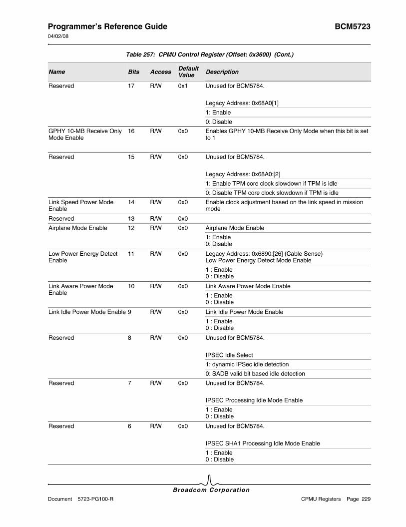
Programmer’s Reference Guide BCM572304/02/08
Broadcom CorporationDocument 5723-PG100-R CPMU Registers Page 229
Reserved 17 R/W 0x1 Unused for BCM5784.
Legacy Address: 0x68A0[1]
1: Enable
0: Disable
GPHY 10-MB Receive Only Mode Enable
16 R/W 0x0 Enables GPHY 10-MB Receive Only Mode when this bit is set to 1
Reserved 15 R/W 0x0 Unused for BCM5784.
Legacy Address: 0x68A0:[2]
1: Enable TPM core clock slowdown if TPM is idle
0: Disable TPM core clock slowdown if TPM is idle
Link Speed Power Mode Enable
14 R/W 0x0 Enable clock adjustment based on the link speed in mission mode
Reserved 13 R/W 0x0
Airplane Mode Enable 12 R/W 0x0 Airplane Mode Enable
1: Enable 0: Disable
Low Power Energy Detect Enable
11 R/W 0x0 Legacy Address: 0x6890:[26] (Cable Sense) Low Power Energy Detect Mode Enable
1 : Enable 0 : Disable
Link Aware Power Mode Enable
10 R/W 0x0 Link Aware Power Mode Enable
1 : Enable 0 : Disable
Link Idle Power Mode Enable 9 R/W 0x0 Link Idle Power Mode Enable
1 : Enable 0 : Disable
Reserved 8 R/W 0x0 Unused for BCM5784.
IPSEC Idle Select
1: dynamic IPSec idle detection
0: SADB valid bit based idle detection
Reserved 7 R/W 0x0 Unused for BCM5784.
IPSEC Processing Idle Mode Enable
1 : Enable 0 : Disable
Reserved 6 R/W 0x0 Unused for BCM5784.
IPSEC SHA1 Processing Idle Mode Enable
1 : Enable 0 : Disable
Table 257: CPMU Control Register (Offset: 0x3600) (Cont.)
Name Bits Access Default Value Description
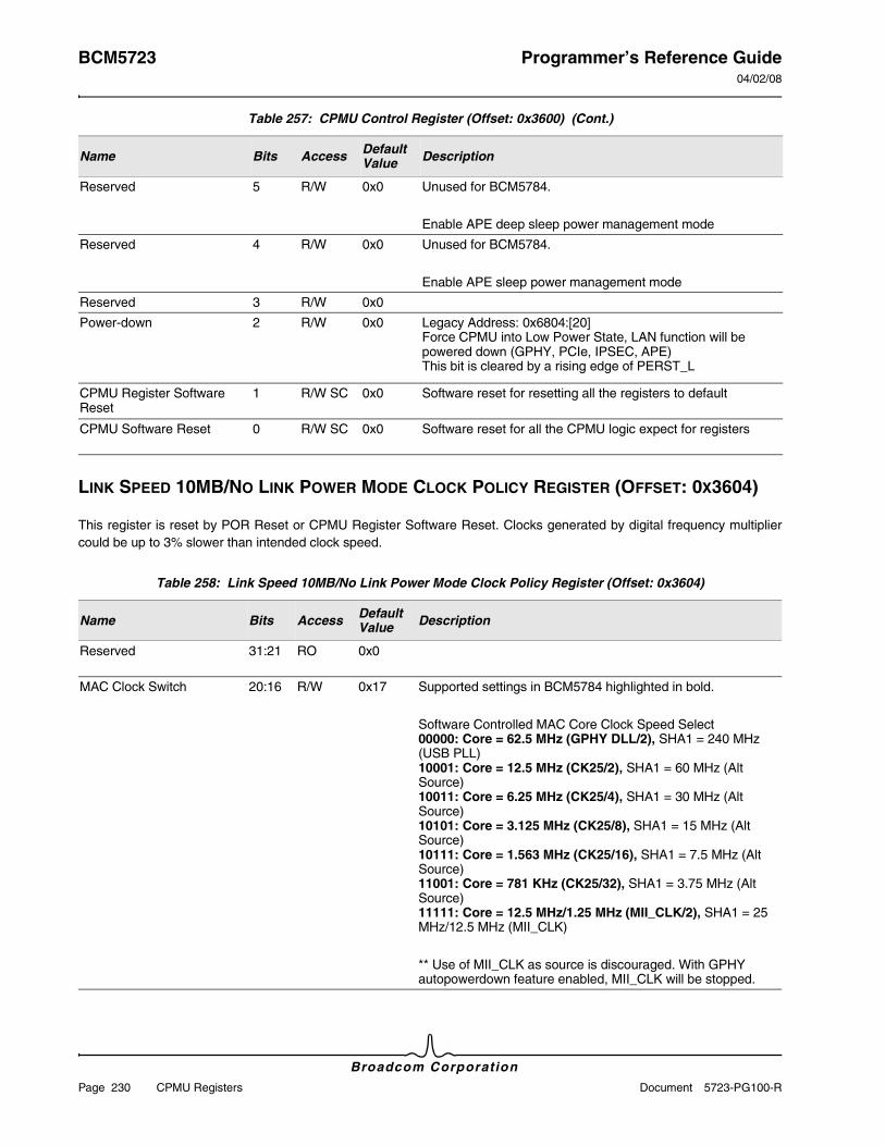
BCM5723 Programmer’s Reference Guide04/02/08
Broadcom Corporation
Page 230 CPMU Registers Document 5723-PG100-R
LINK SPEED 10MB/NO LINK POWER MODE CLOCK POLICY REGISTER (OFFSET: 0X3604)
This register is reset by POR Reset or CPMU Register Software Reset. Clocks generated by digital frequency multiplier could be up to 3% slower than intended clock speed.
Reserved 5 R/W 0x0 Unused for BCM5784.
Enable APE deep sleep power management mode
Reserved 4 R/W 0x0 Unused for BCM5784.
Enable APE sleep power management mode
Reserved 3 R/W 0x0
Power-down 2 R/W 0x0 Legacy Address: 0x6804:[20] Force CPMU into Low Power State, LAN function will be powered down (GPHY, PCIe, IPSEC, APE) This bit is cleared by a rising edge of PERST_L
CPMU Register Software Reset
1 R/W SC 0x0 Software reset for resetting all the registers to default
CPMU Software Reset 0 R/W SC 0x0 Software reset for all the CPMU logic expect for registers
Table 258: Link Speed 10MB/No Link Power Mode Clock Policy Register (Offset: 0x3604)
Name Bits Access Default Value Description
Reserved 31:21 RO 0x0
MAC Clock Switch 20:16 R/W 0x17 Supported settings in BCM5784 highlighted in bold.
Software Controlled MAC Core Clock Speed Select 00000: Core = 62.5 MHz (GPHY DLL/2), SHA1 = 240 MHz (USB PLL) 10001: Core = 12.5 MHz (CK25/2), SHA1 = 60 MHz (Alt Source) 10011: Core = 6.25 MHz (CK25/4), SHA1 = 30 MHz (Alt Source) 10101: Core = 3.125 MHz (CK25/8), SHA1 = 15 MHz (Alt Source) 10111: Core = 1.563 MHz (CK25/16), SHA1 = 7.5 MHz (Alt Source) 11001: Core = 781 KHz (CK25/32), SHA1 = 3.75 MHz (Alt Source) 11111: Core = 12.5 MHz/1.25 MHz (MII_CLK/2), SHA1 = 25 MHz/12.5 MHz (MII_CLK)
** Use of MII_CLK as source is discouraged. With GPHY autopowerdown feature enabled, MII_CLK will be stopped.
Table 257: CPMU Control Register (Offset: 0x3600) (Cont.)
Name Bits Access Default Value Description
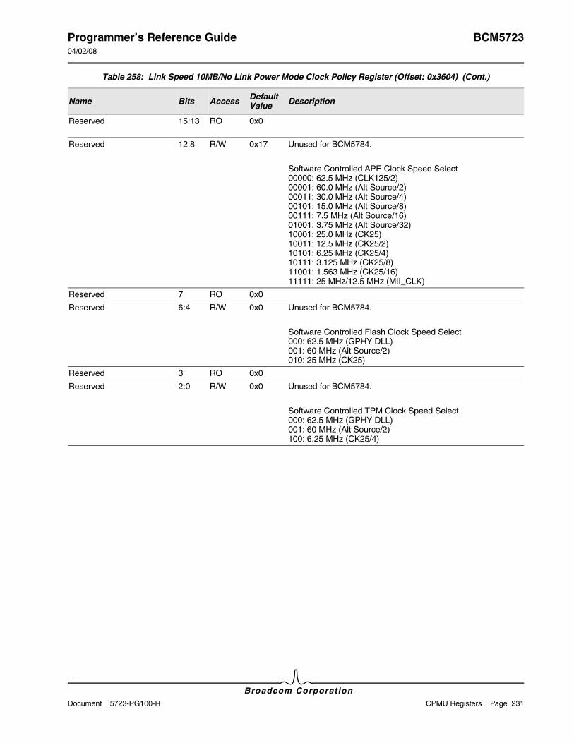
Programmer’s Reference Guide BCM572304/02/08
Broadcom CorporationDocument 5723-PG100-R CPMU Registers Page 231
Reserved 15:13 RO 0x0
Reserved 12:8 R/W 0x17 Unused for BCM5784.
Software Controlled APE Clock Speed Select 00000: 62.5 MHz (CLK125/2) 00001: 60.0 MHz (Alt Source/2) 00011: 30.0 MHz (Alt Source/4) 00101: 15.0 MHz (Alt Source/8) 00111: 7.5 MHz (Alt Source/16) 01001: 3.75 MHz (Alt Source/32) 10001: 25.0 MHz (CK25) 10011: 12.5 MHz (CK25/2) 10101: 6.25 MHz (CK25/4) 10111: 3.125 MHz (CK25/8) 11001: 1.563 MHz (CK25/16) 11111: 25 MHz/12.5 MHz (MII_CLK)
Reserved 7 RO 0x0
Reserved 6:4 R/W 0x0 Unused for BCM5784.
Software Controlled Flash Clock Speed Select 000: 62.5 MHz (GPHY DLL) 001: 60 MHz (Alt Source/2) 010: 25 MHz (CK25)
Reserved 3 RO 0x0
Reserved 2:0 R/W 0x0 Unused for BCM5784.
Software Controlled TPM Clock Speed Select 000: 62.5 MHz (GPHY DLL) 001: 60 MHz (Alt Source/2) 100: 6.25 MHz (CK25/4)
Table 258: Link Speed 10MB/No Link Power Mode Clock Policy Register (Offset: 0x3604) (Cont.)
Name Bits Access Default Value Description
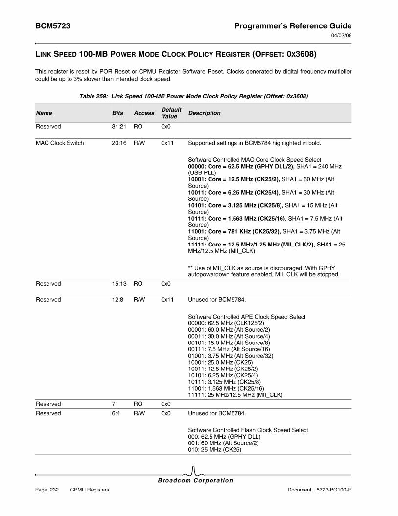
BCM5723 Programmer’s Reference Guide04/02/08
Broadcom Corporation
Page 232 CPMU Registers Document 5723-PG100-R
LINK SPEED 100-MB POWER MODE CLOCK POLICY REGISTER (OFFSET: 0X3608)
This register is reset by POR Reset or CPMU Register Software Reset. Clocks generated by digital frequency multiplier could be up to 3% slower than intended clock speed.
Table 259: Link Speed 100-MB Power Mode Clock Policy Register (Offset: 0x3608)
Name Bits Access Default Value Description
Reserved 31:21 RO 0x0
MAC Clock Switch 20:16 R/W 0x11 Supported settings in BCM5784 highlighted in bold.
Software Controlled MAC Core Clock Speed Select 00000: Core = 62.5 MHz (GPHY DLL/2), SHA1 = 240 MHz (USB PLL) 10001: Core = 12.5 MHz (CK25/2), SHA1 = 60 MHz (Alt Source) 10011: Core = 6.25 MHz (CK25/4), SHA1 = 30 MHz (Alt Source) 10101: Core = 3.125 MHz (CK25/8), SHA1 = 15 MHz (Alt Source) 10111: Core = 1.563 MHz (CK25/16), SHA1 = 7.5 MHz (Alt Source) 11001: Core = 781 KHz (CK25/32), SHA1 = 3.75 MHz (Alt Source) 11111: Core = 12.5 MHz/1.25 MHz (MII_CLK/2), SHA1 = 25 MHz/12.5 MHz (MII_CLK)
** Use of MII_CLK as source is discouraged. With GPHY autopowerdown feature enabled, MII_CLK will be stopped.
Reserved 15:13 RO 0x0
Reserved 12:8 R/W 0x11 Unused for BCM5784.
Software Controlled APE Clock Speed Select 00000: 62.5 MHz (CLK125/2) 00001: 60.0 MHz (Alt Source/2) 00011: 30.0 MHz (Alt Source/4) 00101: 15.0 MHz (Alt Source/8) 00111: 7.5 MHz (Alt Source/16) 01001: 3.75 MHz (Alt Source/32) 10001: 25.0 MHz (CK25) 10011: 12.5 MHz (CK25/2) 10101: 6.25 MHz (CK25/4) 10111: 3.125 MHz (CK25/8) 11001: 1.563 MHz (CK25/16) 11111: 25 MHz/12.5 MHz (MII_CLK)
Reserved 7 RO 0x0
Reserved 6:4 R/W 0x0 Unused for BCM5784.
Software Controlled Flash Clock Speed Select 000: 62.5 MHz (GPHY DLL) 001: 60 MHz (Alt Source/2) 010: 25 MHz (CK25)
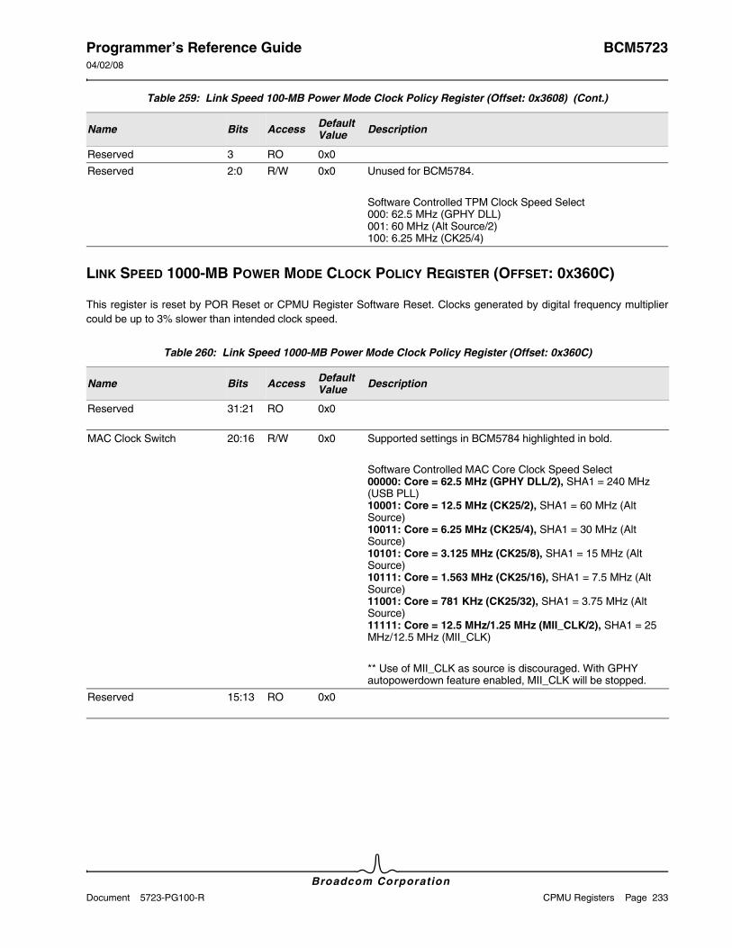
Programmer’s Reference Guide BCM572304/02/08
Broadcom CorporationDocument 5723-PG100-R CPMU Registers Page 233
LINK SPEED 1000-MB POWER MODE CLOCK POLICY REGISTER (OFFSET: 0X360C)
This register is reset by POR Reset or CPMU Register Software Reset. Clocks generated by digital frequency multiplier could be up to 3% slower than intended clock speed.
Reserved 3 RO 0x0
Reserved 2:0 R/W 0x0 Unused for BCM5784.
Software Controlled TPM Clock Speed Select 000: 62.5 MHz (GPHY DLL) 001: 60 MHz (Alt Source/2) 100: 6.25 MHz (CK25/4)
Table 260: Link Speed 1000-MB Power Mode Clock Policy Register (Offset: 0x360C)
Name Bits Access Default Value Description
Reserved 31:21 RO 0x0
MAC Clock Switch 20:16 R/W 0x0 Supported settings in BCM5784 highlighted in bold.
Software Controlled MAC Core Clock Speed Select 00000: Core = 62.5 MHz (GPHY DLL/2), SHA1 = 240 MHz (USB PLL) 10001: Core = 12.5 MHz (CK25/2), SHA1 = 60 MHz (Alt Source) 10011: Core = 6.25 MHz (CK25/4), SHA1 = 30 MHz (Alt Source) 10101: Core = 3.125 MHz (CK25/8), SHA1 = 15 MHz (Alt Source) 10111: Core = 1.563 MHz (CK25/16), SHA1 = 7.5 MHz (Alt Source) 11001: Core = 781 KHz (CK25/32), SHA1 = 3.75 MHz (Alt Source) 11111: Core = 12.5 MHz/1.25 MHz (MII_CLK/2), SHA1 = 25 MHz/12.5 MHz (MII_CLK)
** Use of MII_CLK as source is discouraged. With GPHY autopowerdown feature enabled, MII_CLK will be stopped.
Reserved 15:13 RO 0x0
Table 259: Link Speed 100-MB Power Mode Clock Policy Register (Offset: 0x3608) (Cont.)
Name Bits Access Default Value Description
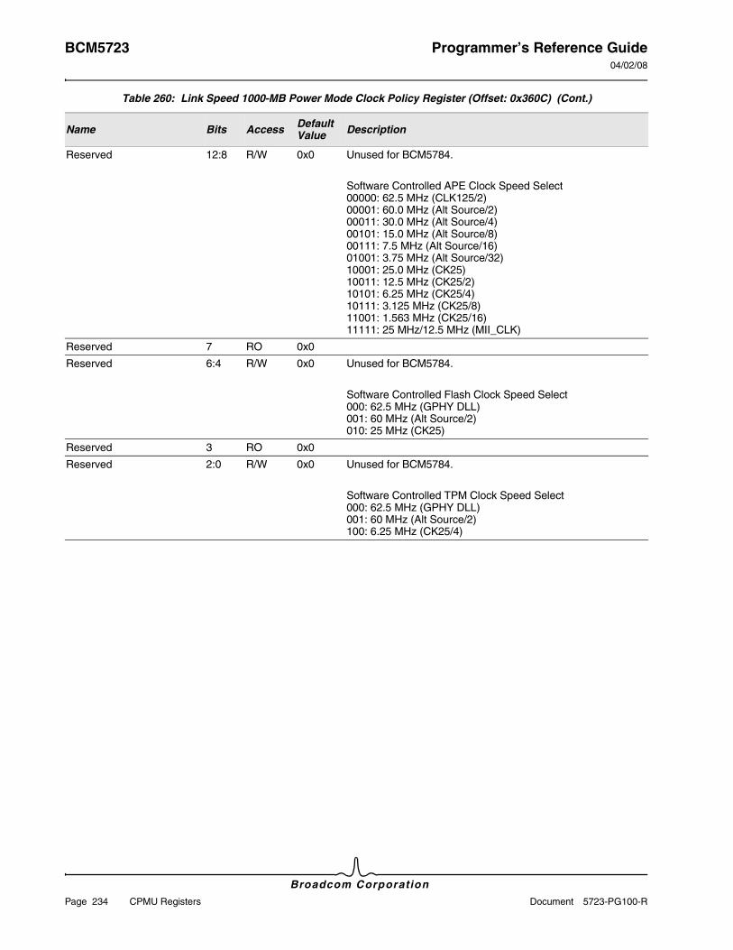
BCM5723 Programmer’s Reference Guide04/02/08
Broadcom Corporation
Page 234 CPMU Registers Document 5723-PG100-R
Reserved 12:8 R/W 0x0 Unused for BCM5784.
Software Controlled APE Clock Speed Select 00000: 62.5 MHz (CLK125/2) 00001: 60.0 MHz (Alt Source/2) 00011: 30.0 MHz (Alt Source/4) 00101: 15.0 MHz (Alt Source/8) 00111: 7.5 MHz (Alt Source/16) 01001: 3.75 MHz (Alt Source/32) 10001: 25.0 MHz (CK25) 10011: 12.5 MHz (CK25/2) 10101: 6.25 MHz (CK25/4) 10111: 3.125 MHz (CK25/8) 11001: 1.563 MHz (CK25/16) 11111: 25 MHz/12.5 MHz (MII_CLK)
Reserved 7 RO 0x0
Reserved 6:4 R/W 0x0 Unused for BCM5784.
Software Controlled Flash Clock Speed Select 000: 62.5 MHz (GPHY DLL) 001: 60 MHz (Alt Source/2) 010: 25 MHz (CK25)
Reserved 3 RO 0x0
Reserved 2:0 R/W 0x0 Unused for BCM5784.
Software Controlled TPM Clock Speed Select 000: 62.5 MHz (GPHY DLL) 001: 60 MHz (Alt Source/2) 100: 6.25 MHz (CK25/4)
Table 260: Link Speed 1000-MB Power Mode Clock Policy Register (Offset: 0x360C) (Cont.)
Name Bits Access Default Value Description
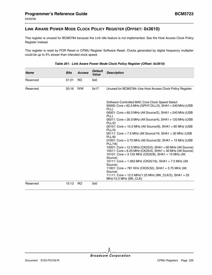
Programmer’s Reference Guide BCM572304/02/08
Broadcom CorporationDocument 5723-PG100-R CPMU Registers Page 235
LINK AWARE POWER MODE CLOCK POLICY REGISTER (OFFSET: 0X3610)
This register is unused for BCM5784 because the Link Idle feature is not implemented. See the Host Access Clock Policy Register instead.
This register is reset by POR Reset or CPMU Register Software Reset. Clocks generated by digital frequency multiplier could be up to 3% slower than intended clock speed.
Table 261: Link Aware Power Mode Clock Policy Register (Offset: 0x3610)
Name Bits Access Default Value Description
Reserved 31:21 RO 0x0
Reserved 20:16 R/W 0x17 Unused for BCM5784–Use Host Access Clock Policy Register.
Software Controlled MAC Core Clock Speed Select 00000: Core = 62.5 MHz (GPHY DLL/2), SHA1 = 240 MHz (USB PLL) 00001: Core = 60.0 MHz (Alt Source/2), SHA1 = 240 MHz (USB PLL) 00011: Core = 30.0 MHz (Alt Source/4), SHA1 = 120 MHz (USB PLL/2) 00101: Core = 15.0 MHz (Alt Source/8), SHA1 = 60 MHz (USB PLL/4) 00111: Core = 7.5 MHz (Alt Source/16, SHA1 = 30 MHz (USB PLL/8) 01001: Core = 3.75 MHz (Alt Source/32, SHA1 = 15 MHz (USB PLL/16) 10001: Core = 12.5 MHz (CK25/2), SHA1 = 60 MHz (Alt Source) 10011: Core = 6.25 MHz (CK25/4), SHA1 = 30 MHz (Alt Source) 10101: Core = 3.125 MHz (CK25/8), SHA1 = 15 MHz (Alt Source) 10111: Core = 1.563 MHz (CK25/16), SHA1 = 7.5 MHz (Alt Source) 11001: Core = 781 KHz (CK25/32), SHA1 = 3.75 MHz (Alt Source) 11111: Core = 12.5 MHz/1.25 MHz (MII_CLK/2), SHA1 = 25 MHz/12.5 MHz (MII_CLK)
Reserved 15:13 RO 0x0

BCM5723 Programmer’s Reference Guide04/02/08
Broadcom Corporation
Page 236 CPMU Registers Document 5723-PG100-R
Reserved 12:8 R/W 0x17 Unused for BCM5784
Software Controlled APE Clock Speed Select 00000: Reserved 00001: 60.0 MHz (Alt Source/2) 00011: 30.0 MHz (Alt Source/4) 00101: 15.0 MHz (Alt Source/8) 00111: 7.5 MHz (Alt Source/16) 01001: 3.75 MHz (Alt Source/32) 10001: 25.0 MHz (CK25) 10011: 12.5 MHz (CK25/2) 10101: 6.25 MHz (CK25/4) 10111: 3.125 MHz (CK25/8) 11001: 1.563 MHz (CK25/16) 11111: 25 MHz/12.5 MHz (MII_CLK)
Reserved 7 RO 0x0
Reserved 6:4 R/W 0x1 Unused for BCM5784
Software Controlled Flash Clock Speed Select 000: Reserved 001: 60 MHz (Alt Source/2) 010: 25 MHz (CK25)
Reserved 3 RO 0x0
Reserved 2:0 R/W 0x1 Unused for BCM5784
Software Controlled TPM Clock Speed Select 000: Reserved 001: 60 MHz (Alt Source/2) 100: 6.25 MHz (CK25/4)
Table 261: Link Aware Power Mode Clock Policy Register (Offset: 0x3610) (Cont.)
Name Bits Access Default Value Description
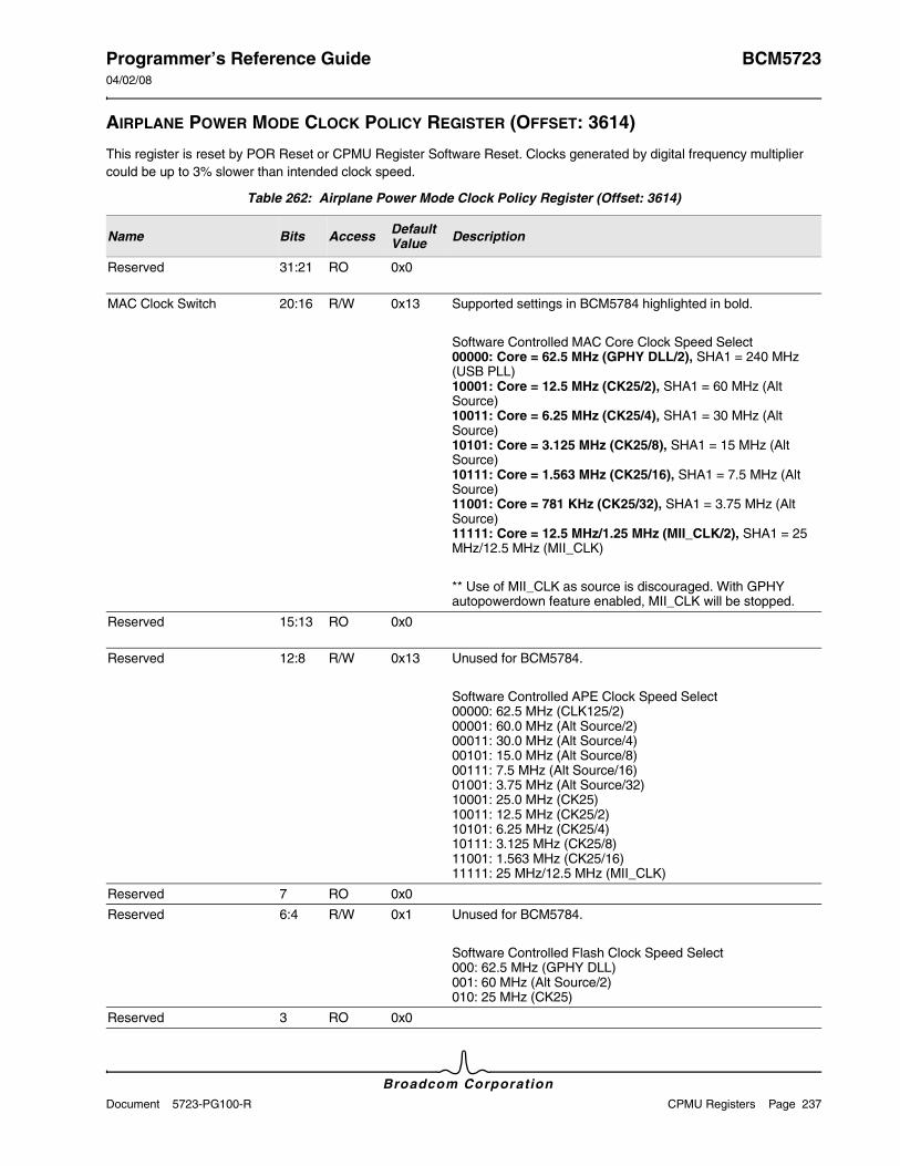
Programmer’s Reference Guide BCM572304/02/08
Broadcom CorporationDocument 5723-PG100-R CPMU Registers Page 237
AIRPLANE POWER MODE CLOCK POLICY REGISTER (OFFSET: 3614)
This register is reset by POR Reset or CPMU Register Software Reset. Clocks generated by digital frequency multiplier could be up to 3% slower than intended clock speed.
Table 262: Airplane Power Mode Clock Policy Register (Offset: 3614)
Name Bits Access Default Value Description
Reserved 31:21 RO 0x0
MAC Clock Switch 20:16 R/W 0x13 Supported settings in BCM5784 highlighted in bold.
Software Controlled MAC Core Clock Speed Select 00000: Core = 62.5 MHz (GPHY DLL/2), SHA1 = 240 MHz (USB PLL) 10001: Core = 12.5 MHz (CK25/2), SHA1 = 60 MHz (Alt Source) 10011: Core = 6.25 MHz (CK25/4), SHA1 = 30 MHz (Alt Source) 10101: Core = 3.125 MHz (CK25/8), SHA1 = 15 MHz (Alt Source) 10111: Core = 1.563 MHz (CK25/16), SHA1 = 7.5 MHz (Alt Source) 11001: Core = 781 KHz (CK25/32), SHA1 = 3.75 MHz (Alt Source) 11111: Core = 12.5 MHz/1.25 MHz (MII_CLK/2), SHA1 = 25 MHz/12.5 MHz (MII_CLK)
** Use of MII_CLK as source is discouraged. With GPHY autopowerdown feature enabled, MII_CLK will be stopped.
Reserved 15:13 RO 0x0
Reserved 12:8 R/W 0x13 Unused for BCM5784.
Software Controlled APE Clock Speed Select 00000: 62.5 MHz (CLK125/2) 00001: 60.0 MHz (Alt Source/2) 00011: 30.0 MHz (Alt Source/4) 00101: 15.0 MHz (Alt Source/8) 00111: 7.5 MHz (Alt Source/16) 01001: 3.75 MHz (Alt Source/32) 10001: 25.0 MHz (CK25) 10011: 12.5 MHz (CK25/2) 10101: 6.25 MHz (CK25/4) 10111: 3.125 MHz (CK25/8) 11001: 1.563 MHz (CK25/16) 11111: 25 MHz/12.5 MHz (MII_CLK)
Reserved 7 RO 0x0
Reserved 6:4 R/W 0x1 Unused for BCM5784.
Software Controlled Flash Clock Speed Select 000: 62.5 MHz (GPHY DLL) 001: 60 MHz (Alt Source/2) 010: 25 MHz (CK25)
Reserved 3 RO 0x0

BCM5723 Programmer’s Reference Guide04/02/08
Broadcom Corporation
Page 238 CPMU Registers Document 5723-PG100-R
LINK IDLE POWER MODE CLOCK POLICY REGISTER (OFFSET: 0X3618)
This register is reset by POR Reset or CPMU Register Software Reset. Clocks generated by digital frequency multiplier could be up to 3% slower than intended clock speed.
Reserved 2:0 R/W 0x1 Unused for BCM5784.
Software Controlled TPM Clock Speed Select 000: 62.5 MHz (GPHY DLL) 001: 60 MHz (Alt Source/2) 100: 6.25 MHz (CK25/4)
Table 263: Link Idle Power Mode Clock Policy Register (Offset: 0x3618)
Name Bits Access Default Value Description
Reserved 31:21 RO 0x0
Reserved 20:16 R/W 0x17 Unused for BCM5784.
Software Controlled MAC Core Clock Speed Select 00000: Core = 62.5 MHz (GPHY DLL/2), SHA1 = 240 MHz (USB PLL) 00001: Core = 60.0 MHz (Alt Source/2), SHA1 = 240 MHz (USB PLL) 00011: Core = 30.0 MHz (Alt Source/4), SHA1 = 120 MHz (USB PLL/2) 00101: Core = 15.0 MHz (Alt Source/8), SHA1 = 60 MHz (USB PLL/4) 00111: Core = 7.5 MHz (Alt Source/16, SHA1 = 30 MHz (USB PLL/8) 01001: Core = 3.75 MHz (Alt Source/32, SHA1 = 15 MHz (USB PLL/16) 10001: Core = 12.5 MHz (CK25/2), SHA1 = 60 MHz (Alt Source) 10011: Core = 6.25 MHz (CK25/4), SHA1 = 30 MHz (Alt Source) 10101: Core = 3.125 MHz (CK25/8), SHA1 = 15 MHz (Alt Source) 10111: Core = 1.563 MHz (CK25/16), SHA1 = 7.5 MHz (Alt Source) 11001: Core = 781 KHz (CK25/32), SHA1 = 3.75 MHz (Alt Source) 11111: Core = 12.5 MHz/1.25 MHz (MII_CLK/2), SHA1 = 25 MHz/12.5 MHz (MII_CLK)
Reserved 15:13 RO 0x0
Table 262: Airplane Power Mode Clock Policy Register (Offset: 3614) (Cont.)
Name Bits Access Default Value Description
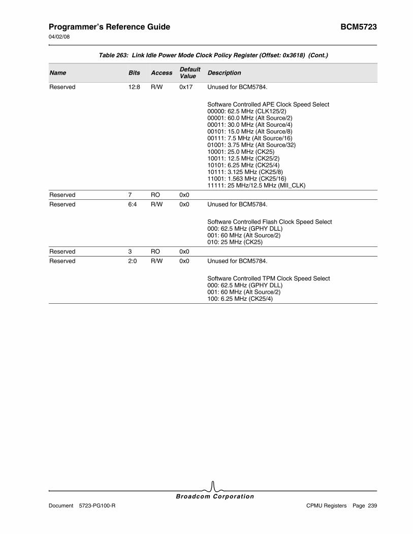
Programmer’s Reference Guide BCM572304/02/08
Broadcom CorporationDocument 5723-PG100-R CPMU Registers Page 239
Reserved 12:8 R/W 0x17 Unused for BCM5784.
Software Controlled APE Clock Speed Select 00000: 62.5 MHz (CLK125/2) 00001: 60.0 MHz (Alt Source/2) 00011: 30.0 MHz (Alt Source/4) 00101: 15.0 MHz (Alt Source/8) 00111: 7.5 MHz (Alt Source/16) 01001: 3.75 MHz (Alt Source/32) 10001: 25.0 MHz (CK25) 10011: 12.5 MHz (CK25/2) 10101: 6.25 MHz (CK25/4) 10111: 3.125 MHz (CK25/8) 11001: 1.563 MHz (CK25/16) 11111: 25 MHz/12.5 MHz (MII_CLK)
Reserved 7 RO 0x0
Reserved 6:4 R/W 0x0 Unused for BCM5784.
Software Controlled Flash Clock Speed Select 000: 62.5 MHz (GPHY DLL) 001: 60 MHz (Alt Source/2) 010: 25 MHz (CK25)
Reserved 3 RO 0x0
Reserved 2:0 R/W 0x0 Unused for BCM5784.
Software Controlled TPM Clock Speed Select 000: 62.5 MHz (GPHY DLL) 001: 60 MHz (Alt Source/2) 100: 6.25 MHz (CK25/4)
Table 263: Link Idle Power Mode Clock Policy Register (Offset: 0x3618) (Cont.)
Name Bits Access Default Value Description
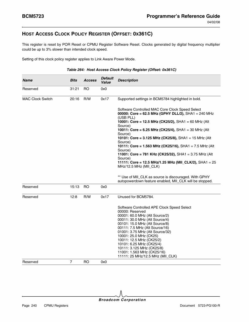
BCM5723 Programmer’s Reference Guide04/02/08
Broadcom Corporation
Page 240 CPMU Registers Document 5723-PG100-R
HOST ACCESS CLOCK POLICY REGISTER (OFFSET: 0X361C)
This register is reset by POR Reset or CPMU Register Software Reset. Clocks generated by digital frequency multiplier could be up to 3% slower than intended clock speed.
Setting of this clock policy register applies to Link Aware Power Mode.
Table 264: Host Access Clock Policy Register (Offset: 0x361C)
Name Bits Access Default Value Description
Reserved 31:21 RO 0x0
MAC Clock Switch 20:16 R/W 0x17 Supported settings in BCM5784 highlighted in bold.
Software Controlled MAC Core Clock Speed Select 00000: Core = 62.5 MHz (GPHY DLL/2), SHA1 = 240 MHz (USB PLL) 10001: Core = 12.5 MHz (CK25/2), SHA1 = 60 MHz (Alt Source) 10011: Core = 6.25 MHz (CK25/4), SHA1 = 30 MHz (Alt Source) 10101: Core = 3.125 MHz (CK25/8), SHA1 = 15 MHz (Alt Source) 10111: Core = 1.563 MHz (CK25/16), SHA1 = 7.5 MHz (Alt Source) 11001: Core = 781 KHz (CK25/32), SHA1 = 3.75 MHz (Alt Source) 11111: Core = 12.5 MHz/1.25 MHz (MII_CLK/2), SHA1 = 25 MHz/12.5 MHz (MII_CLK)
** Use of MII_CLK as source is discouraged. With GPHY autopowerdown feature enabled, MII_CLK will be stopped.
Reserved 15:13 RO 0x0
Reserved 12:8 R/W 0x17 Unused for BCM5784.
Software Controlled APE Clock Speed Select 00000: Reserved 00001: 60.0 MHz (Alt Source/2) 00011: 30.0 MHz (Alt Source/4) 00101: 15.0 MHz (Alt Source/8) 00111: 7.5 MHz (Alt Source/16) 01001: 3.75 MHz (Alt Source/32) 10001: 25.0 MHz (CK25) 10011: 12.5 MHz (CK25/2) 10101: 6.25 MHz (CK25/4) 10111: 3.125 MHz (CK25/8) 11001: 1.563 MHz (CK25/16) 11111: 25 MHz/12.5 MHz (MII_CLK)
Reserved 7 RO 0x0
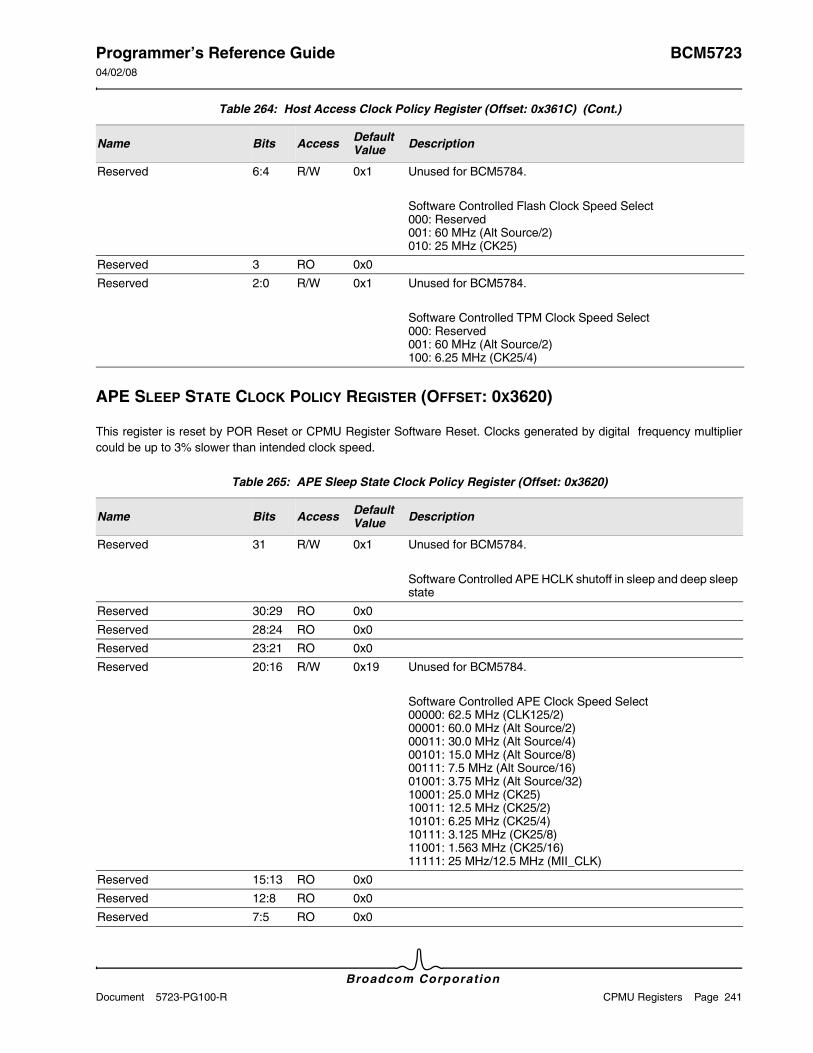
Programmer’s Reference Guide BCM572304/02/08
Broadcom CorporationDocument 5723-PG100-R CPMU Registers Page 241
APE SLEEP STATE CLOCK POLICY REGISTER (OFFSET: 0X3620)
This register is reset by POR Reset or CPMU Register Software Reset. Clocks generated by digital frequency multiplier could be up to 3% slower than intended clock speed.
Reserved 6:4 R/W 0x1 Unused for BCM5784.
Software Controlled Flash Clock Speed Select 000: Reserved 001: 60 MHz (Alt Source/2) 010: 25 MHz (CK25)
Reserved 3 RO 0x0
Reserved 2:0 R/W 0x1 Unused for BCM5784.
Software Controlled TPM Clock Speed Select 000: Reserved 001: 60 MHz (Alt Source/2) 100: 6.25 MHz (CK25/4)
Table 265: APE Sleep State Clock Policy Register (Offset: 0x3620)
Name Bits Access Default Value Description
Reserved 31 R/W 0x1 Unused for BCM5784.
Software Controlled APE HCLK shutoff in sleep and deep sleep state
Reserved 30:29 RO 0x0
Reserved 28:24 RO 0x0
Reserved 23:21 RO 0x0
Reserved 20:16 R/W 0x19 Unused for BCM5784.
Software Controlled APE Clock Speed Select 00000: 62.5 MHz (CLK125/2) 00001: 60.0 MHz (Alt Source/2) 00011: 30.0 MHz (Alt Source/4) 00101: 15.0 MHz (Alt Source/8) 00111: 7.5 MHz (Alt Source/16) 01001: 3.75 MHz (Alt Source/32) 10001: 25.0 MHz (CK25) 10011: 12.5 MHz (CK25/2) 10101: 6.25 MHz (CK25/4) 10111: 3.125 MHz (CK25/8) 11001: 1.563 MHz (CK25/16) 11111: 25 MHz/12.5 MHz (MII_CLK)
Reserved 15:13 RO 0x0
Reserved 12:8 RO 0x0
Reserved 7:5 RO 0x0
Table 264: Host Access Clock Policy Register (Offset: 0x361C) (Cont.)
Name Bits Access Default Value Description

BCM5723 Programmer’s Reference Guide04/02/08
Broadcom Corporation
Page 242 CPMU Registers Document 5723-PG100-R
CLOCK SPEED OVERRIDE POLICY REGISTER (OFFSET: 0X3624)
This register is reset by POR Reset or CPMU Register Software Reset. Clocks generated by digital frequency multiplier could be up to 3% slower than intended clock speed.
Reserved 4:0 R/W 0x9 Unused for BCM5784.
Software Controlled APE Clock Speed Select 00000: 62.5 MHz (CLK125/2) 00001: 60.0 MHz (Alt Source/2) 00011: 30.0 MHz (Alt Source/4) 00101: 15.0 MHz (Alt Source/8) 00111: 7.5 MHz (Alt Source/16) 01001: 3.75 MHz (Alt Source/32) 10001: 25.0 MHz (CK25) 10011: 12.5 MHz (CK25/2) 10101: 6.25 MHz (CK25/4) 10111: 3.125 MHz (CK25/8) 11001: 1.563 MHz (CK25/16) 11111: 25 MHz/12.5 MHz (MII_CLK)
Table 266: Clock Speed Override Policy Register (Offset: 0x3624)
Name Bits Access Default Value Description
Reserved 31:21 RO 0x0
MAC Clock Switch 20:16 R/W 0x0 Software Controlled MAC Core Clock Speed Select 00000: Core = 62.5 MHz (GPHY DLL/2), SHA1 = 240 MHz (USB PLL) 10001: Core = 12.5 MHz (CK25/2), SHA1 = 60 MHz (Alt Source) 10011: Core = 6.25 MHz (CK25/4), SHA1 = 30 MHz (Alt Source) 10101: Core = 3.125 MHz (CK25/8), SHA1 = 15 MHz (Alt Source) 10111: Core = 1.563 MHz (CK25/16), SHA1 = 7.5 MHz (Alt Source) 11001: Core = 781 KHz (CK25/32), SHA1 = 3.75 MHz (Alt Source) 11111: Core = 12.5 MHz/1.25 MHz (MII_CLK/2), SHA1 = 25 MHz/12.5 MHz (MII_CLK)
** Use of MII_CLK as source is discouraged. With GPHY autopowerdown feature enabled, MII_CLK will be stopped.
Reserved 15:13 RO 0x0
Reserved 12:8 RO 0x0
Reserved 7 RO 0x0
Reserved 6:4 RO 0x0
Reserved 3 RO 0x0
Reserved 2:0 RO 0x0
Table 265: APE Sleep State Clock Policy Register (Offset: 0x3620) (Cont.)
Name Bits Access Default Value Description
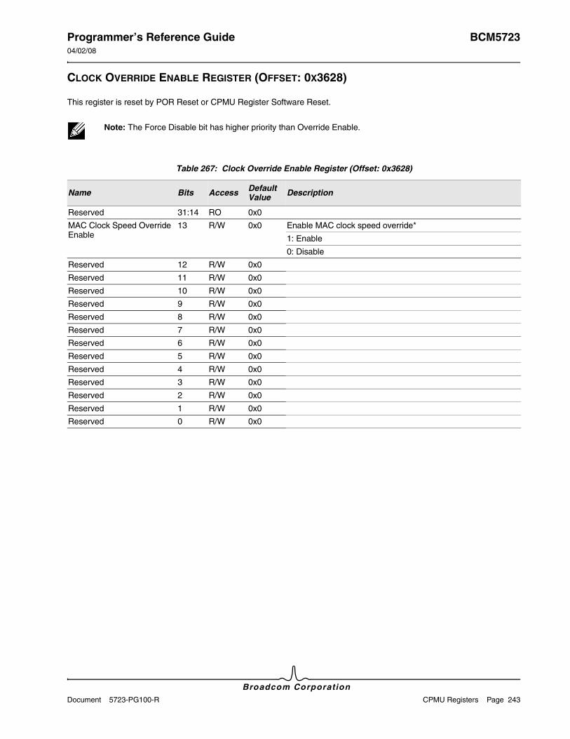
Programmer’s Reference Guide BCM572304/02/08
Broadcom CorporationDocument 5723-PG100-R CPMU Registers Page 243
CLOCK OVERRIDE ENABLE REGISTER (OFFSET: 0X3628)
This register is reset by POR Reset or CPMU Register Software Reset.
Note: The Force Disable bit has higher priority than Override Enable.
Table 267: Clock Override Enable Register (Offset: 0x3628)
Name Bits Access Default Value Description
Reserved 31:14 RO 0x0
MAC Clock Speed Override Enable
13 R/W 0x0 Enable MAC clock speed override*
1: Enable
0: Disable
Reserved 12 R/W 0x0
Reserved 11 R/W 0x0
Reserved 10 R/W 0x0
Reserved 9 R/W 0x0
Reserved 8 R/W 0x0
Reserved 7 R/W 0x0
Reserved 6 R/W 0x0
Reserved 5 R/W 0x0
Reserved 4 R/W 0x0
Reserved 3 R/W 0x0
Reserved 2 R/W 0x0
Reserved 1 R/W 0x0
Reserved 0 R/W 0x0
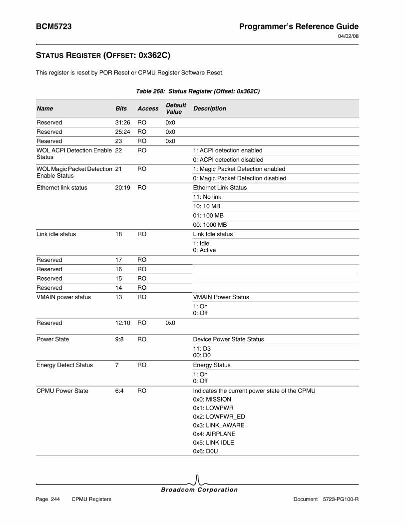
BCM5723 Programmer’s Reference Guide04/02/08
Broadcom Corporation
Page 244 CPMU Registers Document 5723-PG100-R
STATUS REGISTER (OFFSET: 0X362C)
This register is reset by POR Reset or CPMU Register Software Reset.
Table 268: Status Register (Offset: 0x362C)
Name Bits Access Default Value Description
Reserved 31:26 RO 0x0
Reserved 25:24 RO 0x0
Reserved 23 RO 0x0
WOL ACPI Detection Enable Status
22 RO 1: ACPI detection enabled
0: ACPI detection disabled
WOL Magic Packet Detection Enable Status
21 RO 1: Magic Packet Detection enabled
0: Magic Packet Detection disabled
Ethernet link status 20:19 RO Ethernet Link Status
11: No link
10: 10 MB
01: 100 MB
00: 1000 MB
Link idle status 18 RO Link Idle status
1: Idle 0: Active
Reserved 17 RO
Reserved 16 RO
Reserved 15 RO
Reserved 14 RO
VMAIN power status 13 RO VMAIN Power Status
1: On 0: Off
Reserved 12:10 RO 0x0
Power State 9:8 RO Device Power State Status
11: D3 00: D0
Energy Detect Status 7 RO Energy Status
1: On 0: Off
CPMU Power State 6:4 RO Indicates the current power state of the CPMU0x0: MISSION0x1: LOWPWR0x2: LOWPWR_ED0x3: LINK_AWARE0x4: AIRPLANE0x5: LINK IDLE0x6: D0U
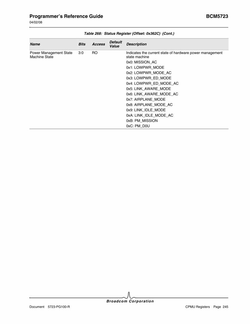
Programmer’s Reference Guide BCM572304/02/08
Broadcom CorporationDocument 5723-PG100-R CPMU Registers Page 245
Power Management State Machine State
3:0 RO Indicates the current state of hardware power management state machine0x0: MISSION_AC0x1: LOWPWR_MODE0x2: LOWPWR_MODE_AC0x3: LOWPWR_ED_MODE0x4: LOWPWR_ED_MODE_AC0x5: LINK_AWARE_MODE0x6: LINK_AWARE_MODE_AC0x7: AIRPLANE_MODE0x8: AIRPLANE_MODE_AC0x9: LINK_IDLE_MODE0xA: LINK_IDLE_MODE_AC0xB: PM_MISSION0xC: PM_D0U
Table 268: Status Register (Offset: 0x362C) (Cont.)
Name Bits Access Default Value Description
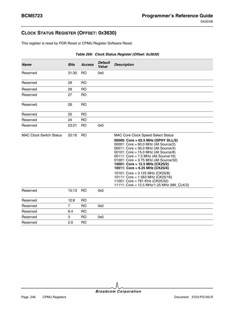
BCM5723 Programmer’s Reference Guide04/02/08
Broadcom Corporation
Page 246 CPMU Registers Document 5723-PG100-R
CLOCK STATUS REGISTER (OFFSET: 0X3630)
This register is reset by POR Reset or CPMU Register Software Reset.
Table 269: Clock Status Register (Offset: 0x3630)
Name Bits Access Default Value Description
Reserved 31:30 RO 0x0
Reserved 29 RO
Reserved 28 RO
Reserved 27 RO
Reserved 26 RO
Reserved 25 RO
Reserved 24 RO
Reserved 23:21 RO 0x0
MAC Clock Switch Status 20:16 RO MAC Core Clock Speed Select Status00000: Core = 62.5 MHz (GPHY DLL/2) 00001: Core = 60.0 MHz (Alt Source/2) 00011: Core = 30.0 MHz (Alt Source/4) 00101: Core = 15.0 MHz (Alt Source/8) 00111: Core = 7.5 MHz (Alt Source/16) 01001: Core = 3.75 MHz (Alt Source/32) 10001: Core = 12.5 MHz (CK25/2) 10011: Core = 6.25 MHz (CK25/4)10101: Core = 3.125 MHz (CK25/8) 10111: Core = 1.563 MHz (CK25/16) 11001: Core = 781 KHz (CK25/32) 11111: Core = 12.5 MHz/1.25 MHz (MII_CLK/2)
Reserved 15:13 RO 0x0
Reserved 12:8 RO
Reserved 7 RO 0x0
Reserved 6:4 RO
Reserved 3 RO 0x0
Reserved 2:0 RO
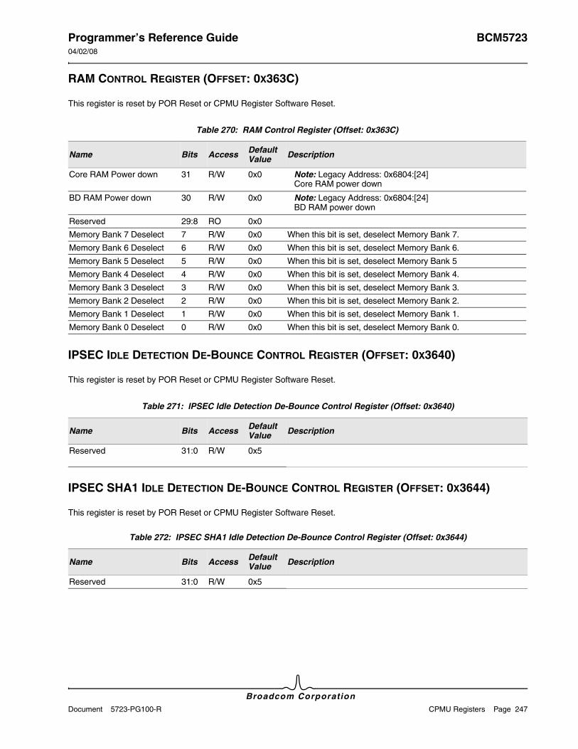
Programmer’s Reference Guide BCM572304/02/08
Broadcom CorporationDocument 5723-PG100-R CPMU Registers Page 247
RAM CONTROL REGISTER (OFFSET: 0X363C)
This register is reset by POR Reset or CPMU Register Software Reset.
IPSEC IDLE DETECTION DE-BOUNCE CONTROL REGISTER (OFFSET: 0X3640)
This register is reset by POR Reset or CPMU Register Software Reset.
IPSEC SHA1 IDLE DETECTION DE-BOUNCE CONTROL REGISTER (OFFSET: 0X3644)
This register is reset by POR Reset or CPMU Register Software Reset.
Table 270: RAM Control Register (Offset: 0x363C)
Name Bits Access Default Value Description
Core RAM Power down 31 R/W 0x0 Note: Legacy Address: 0x6804:[24] Core RAM power down
BD RAM Power down 30 R/W 0x0 Note: Legacy Address: 0x6804:[24] BD RAM power down
Reserved 29:8 RO 0x0
Memory Bank 7 Deselect 7 R/W 0x0 When this bit is set, deselect Memory Bank 7.
Memory Bank 6 Deselect 6 R/W 0x0 When this bit is set, deselect Memory Bank 6.
Memory Bank 5 Deselect 5 R/W 0x0 When this bit is set, deselect Memory Bank 5
Memory Bank 4 Deselect 4 R/W 0x0 When this bit is set, deselect Memory Bank 4.
Memory Bank 3 Deselect 3 R/W 0x0 When this bit is set, deselect Memory Bank 3.
Memory Bank 2 Deselect 2 R/W 0x0 When this bit is set, deselect Memory Bank 2.
Memory Bank 1 Deselect 1 R/W 0x0 When this bit is set, deselect Memory Bank 1.
Memory Bank 0 Deselect 0 R/W 0x0 When this bit is set, deselect Memory Bank 0.
Table 271: IPSEC Idle Detection De-Bounce Control Register (Offset: 0x3640)
Name Bits Access Default Value Description
Reserved 31:0 R/W 0x5
Table 272: IPSEC SHA1 Idle Detection De-Bounce Control Register (Offset: 0x3644)
Name Bits Access Default Value Description
Reserved 31:0 R/W 0x5
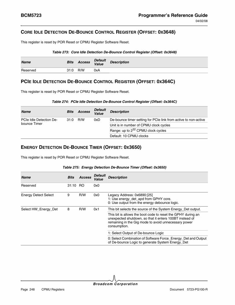
BCM5723 Programmer’s Reference Guide04/02/08
Broadcom Corporation
Page 248 CPMU Registers Document 5723-PG100-R
CORE IDLE DETECTION DE-BOUNCE CONTROL REGISTER (OFFSET: 0X3648)
This register is reset by POR Reset or CPMU Register Software Reset.
PCIE IDLE DETECTION DE-BOUNCE CONTROL REGISTER (OFFSET: 0X364C)
This register is reset by POR Reset or CPMU Register Software Reset.
ENERGY DETECTION DE-BOUNCE TIMER (OFFSET: 0X3650)
This register is reset by POR Reset or CPMU Register Software Reset.
Table 273: Core Idle Detection De-Bounce Control Register (Offset: 0x3648)
Name Bits Access Default Value Description
Reserved 31:0 R/W 0xA
Table 274: PCIe Idle Detection De-Bounce Control Register (Offset: 0x364C)
Name Bits Access Default Value Description
PCIe Idle Detection De-bounce Timer
31:0 R/W 0xD De-bounce timer setting for PCIe link from active to non-active
Unit is in number of CPMU clock cycles
Range: up to 232 CPMU clock cycles
Default: 10 CPMU clocks
Table 275: Energy Detection De-Bounce Timer (Offset: 0x3650)
Name Bits Access Default Value Description
Reserved 31:10 RO 0x0
Energy Detect Select 9 R/W 0x0 Legacy Address: 0x6890:[25] 1: Use energy_det_apd from GPHY core. 0: Use output from the energy debounce logic.
Select HW_Energy_Det 8 R/W 0x1 This bit selects the source of the System Energy_Det output.
This bit is allows the boot code to reset the GPHY during an unexpected shutdown, so that it enters 100BT instead of remaining in the Gig mode to avoid unnecessary power consumption.
1: Select Output of De-bounce Logic
0: Select Combination of Software Force_Energy_Det and Output of De-bounce Logic to generate System Energy_Det
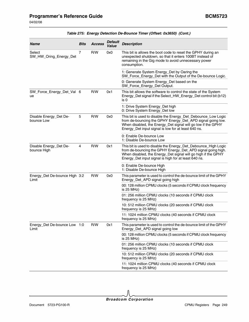
Programmer’s Reference Guide BCM572304/02/08
Broadcom CorporationDocument 5723-PG100-R CPMU Registers Page 249
Select SW_HW_Oring_Energy_Det
7 R/W 0x0 This bit is allows the boot code to reset the GPHY during an unexpected shutdown, so that it enters 100BT instead of remaining in the Gig mode to avoid unnecessary power consumption.
1: Generate System Energy_Det by Oaring the SW_Force_Energy_Det with the Output of the De-bounce Logic.
0: Generate System Energy_Det based on the SW_Force_Energy_Det Output.
SW_Force_Energy_Det_Value
6 R/W 0x1 This bit allows the software to control the state of the System Energy_Det signal if the Select_HW_Energy_Det control bit (b12) is 0
1: Drive System Energy_Det high 0: Drive System Energy_Det low
Disable Energy_Det De-bounce Low
5 R/W 0x0 This bit is used to disable the Energy_Det_Debounce_Low Logic from de-bouncing the GPHY Energy_Det_APD signal going low. When disabled, the Energy_Det signal will go low if the GPHY Energy_Det input signal is low for at least 640 ns.
0: Enable De-bounce Low 1: Disable De-bounce Low
Disable Energy_Det De-bounce High
4 R/W 0x1 This bit is used to disable the Energy_Det_Debounce_High Logic from de-bouncing the GPHY Energy_Det_APD signal going high. When disabled, the Energy_Det signal will go high if the GPHY Energy_Det input signal is high for at least 640 ns.
0: Enable De-bounce High 1: Disable De-bounce High
Energy_Det De-bounce High Limit
3:2 R/W 0x0 This parameter is used to control the de-bounce limit of the GPHY Energy_Det_APD signal going high
00: 128 million CPMU clocks (5 seconds if CPMU clock frequency is 25 MHz)
01: 256 million CPMU clocks (10 seconds if CPMU clock frequency is 25 MHz)
10: 512 million CPMU clocks (20 seconds if CPMU clock frequency is 25 MHz)
11: 1024 million CPMU clocks (40 seconds if CPMU clock frequency is 25 MHz)
Energy_Det De-bounce Low Limit
1:0 R/W 0x1 This parameter is used to control the de-bounce limit of the GPHY Energy_Det_APD signal going low
00: 128 million CPMU clocks (5 seconds if CPMU clock frequency is 25 MHz)
01: 256 million CPMU clocks (10 seconds if CPMU clock frequency is 25 MHz)
10: 512 million CPMU clocks (20 seconds if CPMU clock frequency is 25 MHz)
11: 1024 million CPMU clocks (40 seconds if CPMU clock frequency is 25 MHz)
Table 275: Energy Detection De-Bounce Timer (Offset: 0x3650) (Cont.)
Name Bits Access Default Value Description
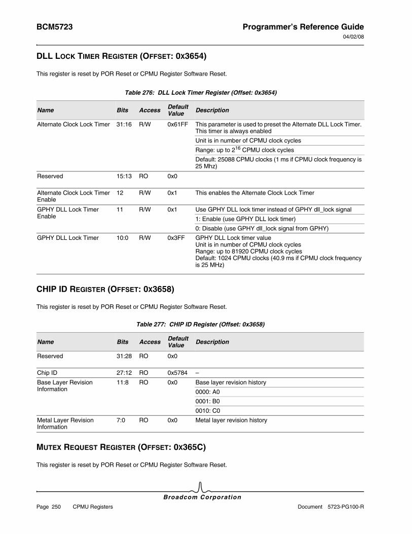
BCM5723 Programmer’s Reference Guide04/02/08
Broadcom Corporation
Page 250 CPMU Registers Document 5723-PG100-R
DLL LOCK TIMER REGISTER (OFFSET: 0X3654)
This register is reset by POR Reset or CPMU Register Software Reset.
CHIP ID REGISTER (OFFSET: 0X3658)
This register is reset by POR Reset or CPMU Register Software Reset.
MUTEX REQUEST REGISTER (OFFSET: 0X365C)
This register is reset by POR Reset or CPMU Register Software Reset.
Table 276: DLL Lock Timer Register (Offset: 0x3654)
Name Bits Access Default Value Description
Alternate Clock Lock Timer 31:16 R/W 0x61FF This parameter is used to preset the Alternate DLL Lock Timer. This timer is always enabled
Unit is in number of CPMU clock cycles
Range: up to 216 CPMU clock cycles
Default: 25088 CPMU clocks (1 ms if CPMU clock frequency is 25 Mhz)
Reserved 15:13 RO 0x0
Alternate Clock Lock Timer Enable
12 R/W 0x1 This enables the Alternate Clock Lock Timer
GPHY DLL Lock Timer Enable
11 R/W 0x1 Use GPHY DLL lock timer instead of GPHY dll_lock signal
1: Enable (use GPHY DLL lock timer)
0: Disable (use GPHY dll_lock signal from GPHY)
GPHY DLL Lock Timer 10:0 R/W 0x3FF GPHY DLL Lock timer value Unit is in number of CPMU clock cycles Range: up to 81920 CPMU clock cycles Default: 1024 CPMU clocks (40.9 ms if CPMU clock frequency is 25 MHz)
Table 277: CHIP ID Register (Offset: 0x3658)
Name Bits Access Default Value Description
Reserved 31:28 RO 0x0
Chip ID 27:12 RO 0x5784 –
Base Layer Revision Information
11:8 RO 0x0 Base layer revision history
0000: A0
0001: B0
0010: C0
Metal Layer Revision Information
7:0 RO 0x0 Metal layer revision history
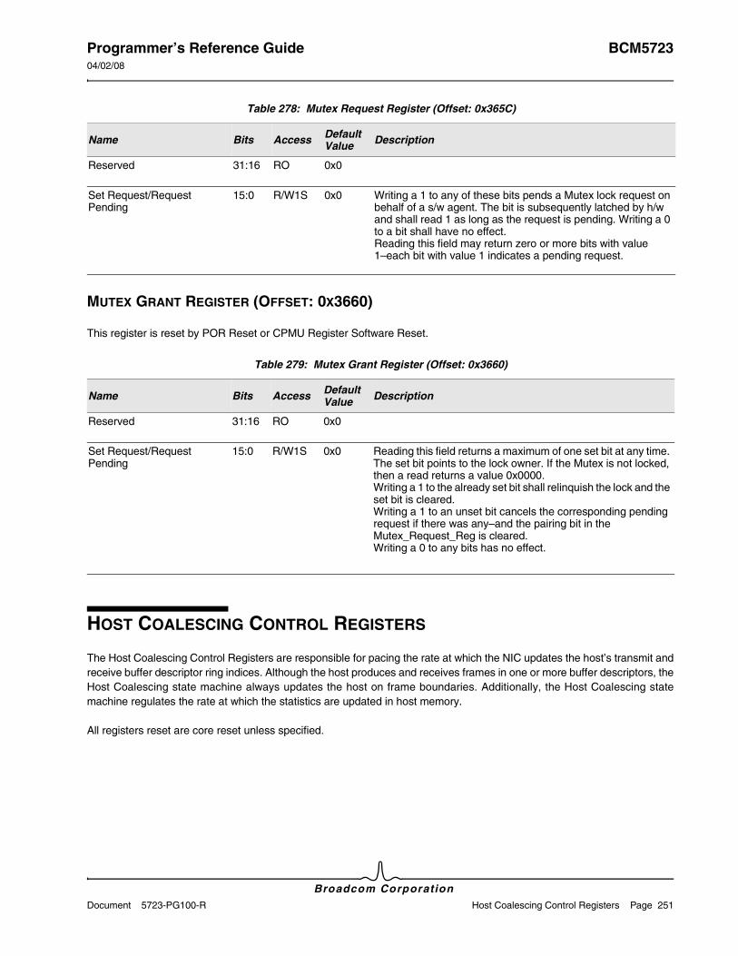
Programmer’s Reference Guide BCM572304/02/08
Broadcom CorporationDocument 5723-PG100-R Host Coalescing Control Registers Page 251
MUTEX GRANT REGISTER (OFFSET: 0X3660)
This register is reset by POR Reset or CPMU Register Software Reset.
HOST COALESCING CONTROL REGISTERS
The Host Coalescing Control Registers are responsible for pacing the rate at which the NIC updates the host’s transmit and receive buffer descriptor ring indices. Although the host produces and receives frames in one or more buffer descriptors, the Host Coalescing state machine always updates the host on frame boundaries. Additionally, the Host Coalescing state machine regulates the rate at which the statistics are updated in host memory.
All registers reset are core reset unless specified.
Table 278: Mutex Request Register (Offset: 0x365C)
Name Bits Access Default Value Description
Reserved 31:16 RO 0x0
Set Request/Request Pending
15:0 R/W1S 0x0 Writing a 1 to any of these bits pends a Mutex lock request on behalf of a s/w agent. The bit is subsequently latched by h/w and shall read 1 as long as the request is pending. Writing a 0 to a bit shall have no effect. Reading this field may return zero or more bits with value 1–each bit with value 1 indicates a pending request.
Table 279: Mutex Grant Register (Offset: 0x3660)
Name Bits Access Default Value Description
Reserved 31:16 RO 0x0
Set Request/Request Pending
15:0 R/W1S 0x0 Reading this field returns a maximum of one set bit at any time. The set bit points to the lock owner. If the Mutex is not locked, then a read returns a value 0x0000. Writing a 1 to the already set bit shall relinquish the lock and the set bit is cleared. Writing a 1 to an unset bit cancels the corresponding pending request if there was any–and the pairing bit in the Mutex_Request_Reg is cleared. Writing a 0 to any bits has no effect.
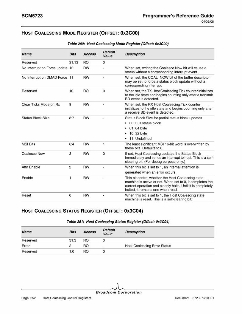
BCM5723 Programmer’s Reference Guide04/02/08
Broadcom Corporation
Page 252 Host Coalescing Control Registers Document 5723-PG100-R
HOST COALESCING MODE REGISTER (OFFSET: 0X3C00)
HOST COALESCING STATUS REGISTER (OFFSET: 0X3C04)
Table 280: Host Coalescing Mode Register (Offset: 0x3C00)
Name Bits Access Default Value Description
Reserved 31:13 RO 0
No Interrupt on Force update 12 RW - When set, writing the Coalesce Now bit will cause a status without a corresponding interrupt event.
No Interrupt on DMAD Force 11 RW - When set, the COAL_NOW bit of the buffer descriptor may be set to force a status block update without a corresponding interrupt
Reserved 10 RO 0 When set, the TX Host Coalescing Tick counter initializes to the idle state and begins counting only after a transmit BD event is detected.
Clear Ticks Mode on Rx 9 RW - When set, the RX Host Coalescing Tick counter initializes to the idle state and begins counting only after a receive BD event is detected.
Status Block Size 8:7 RW - Status Block Size for partial status block updates• 00: Full status block• 01: 64 byte• 10: 32 byte• 11: Undefined
MSI Bits 6:4 RW 1 The least significant MSI 16-bit word is overwritten by these bits. Defaults to 0.
Coalesce Now 3 RW 0 If set, Host Coalescing updates the Status Block immediately and sends an interrupt to host. This is a self-clearing bit. (For debug purpose only.)
Attn Enable 2 RW - When this bit is set to 1, an internal attention isgenerated when an error occurs.
Enable 1 RW - This bit control whether the Host Coalescing state machine is active or not. When set to 0, it completes the current operation and cleanly halts. Until it is completely halted, it remains one when read.
Reset 0 RW - When this bit is set to 1, the Host Coalescing state machine is reset. This is a self-clearing bit.
Table 281: Host Coalescing Status Register (Offset: 0x3C04)
Name Bits Access Default Value Description
Reserved 31:3 RO 0
Error 2 RO - Host Coalescing Error Status
Reserved 1:0 RO 0
Programmer’s Reference Guide BCM572304/02/08
Broadcom CorporationDocument 5723-PG100-R Host Coalescing Control Registers Page 253
RECEIVE COALESCING TICKS REGISTER (OFFSET: 0X3C08)
The value in this register can be used to control how often the status block is updated (and how often interrupts are generated) due to receiving packets. The value in this register controls how many ticks, in units of 1 ?s each, get loaded in an internal receive tick timer register. The 1-μs tick is controlled by the GRC Timer Prescaler parameter from the GRC Block. The timer will be reset to the value of this register and will start counting down after every status block update (regardless of the reason for the status block update). The timer is only reset after status block updates, and is not reset after any given packet is received. When the timer reaches 0, it will be considered to be in the expired state. Once the counter is in the expired state, a status block update will occur if a packet had been received and copied to host memory (via DMA) since the last status block update.
This register must be initialized by host software. A value of 0 in this register disables the receive tick coalescing logic. In this case, status block updates will occur for receive event only if the Receive Max Coalesced BD value is reached. Of course, status block updates for other reasons (e.g., transmit events) will also include any updates to the receive indices. By setting the value in this register to a high number, a software device driver can reduce the number of status block updates and interrupts that occur due to receiving packets. This will generally increase performance in hosts that are under a high degree of stress and whose RISCs are saturated due to handling a large number of interrupts from the network controller. For host environments where receive interrupt latency needs to be very low, and the host is not close to be saturated, it is recommended that this register be set to 1.
SEND COALESCING TICKS REGISTER (OFFSET: 0X3C0C)
The value in this register can be used to control how often the status block is updated (and how often interrupts are generated) according to the completion of transmit events. The value in this register controls how many ticks, in units of 1 ?s each, get loaded in an internal transmit tick timer register. The 1-μs tick is controlled by the GRC Timer Prescaler parameter from the GRC Block. The timer will be reset to the value of this register and will start counting down, after every status block update (regardless of the reason for the status block update). The timer is only reset after status block updates, and is not reset after a transmit event completes. When the timer reaches 0, it will be considered to be in the expired state. Once the counter is in the expired state, a status block update will occur if a transmit event has occurred since the last status block update. In this case, a transmit event is defined by an update to one of the device’s Send BD Consumer Indices.
A Send Consumer Index increments when the data associated with a particular packet has been successfully moved (via DMA) across the bus, rather than when the packet is actually transmitted over the Ethernet wire.
This register must be initialized by host software. A value of 0 in this register disables the transmit tick coalescing logic. In this case, status block updates will occur for transmit events only if the Send Max Coalesced BD value is reached, or if the BD_FLAG_COAL_NOW bit is set in a send BD. Status block updates for other reasons (e.g., receive events) will also include any updates to the send indices. By setting the value in this register to a high number, a software device driver can reduce the number of status block updates, and interrupts, that occur due to transmit completions. This will generally increase performance in hosts that do not require their send buffers to be freed quickly. For host environments that do require their send buffers to be recovered quickly, it is recommended that this register be set to 0.
RECEIVE MAX COALESCED BD COUNT REGISTER (OFFSET: 0X3C10)
This register contains the maximum number of receive return ring BDs that must filled in by the device before the device will update the status block due to a receive event. Whenever the device completes the reception of a packet, it will fill in a receive return ring BD, and then increment an internal receive coalesce BD counter. When this internal counter reaches the value in this register, a status block update will occur. This counter will be reset (i.e., zeroed) when a status block update occurs regardless of the reason for the status block update. This register must be initialized by host software. A value of 0 in this register disables the receive max BD coalescing logic. In this case, status block updates will occur for receive packets

BCM5723 Programmer’s Reference Guide04/02/08
Broadcom Corporation
Page 254 Host Coalescing Control Registers Document 5723-PG100-R
only via the Receive Coalescing Ticks mechanism. Status block updates for other reasons (e.g., transmit events) will also include any updates to the receive indices. For simplicity, if a host wanted to get a status block update for every received packet, the host driver should just set this register to a value of 1. Conversely, by setting the value in this register to a high number, a software device driver can reduce the number of status block updates and interrupts that occur due to receiving packets. This can increase performance in hosts that are under a high degree of stress and whose RISCs are saturated due to handling a large number of interrupts from the network controller. However, in lower traffic environments, there is no guarantee that consecutive packets will be received in a timely manner. Therefore, for those environments, it is recommended that the Receive Coalescing Ticks register are used to make sure that status block updates due to receiving packets are not delayed for an infinite amount of time.
SEND MAX COALESCED BD COUNT REGISTER (OFFSET: 0X3C14)
This register contains the maximum number of send BDs that must be processed by the device before the device will update the status block due to the transmission of packets. Whenever the device completes the DMA of transmit packet buffer, it increments an internal send coalesce BD counter. When this internal counter reaches the value in this register, a status block update will occur. This counter will be reset (i.e., zeroed) when a status block update occurs regardless of the reason for the status block update. This register must be initialized by host software. A value of 0 in this register disables the send max BD coalescing logic. In this case, status block updates will occur for receive packets only via the Send Coalescing Ticks mechanism. Of course, status block updates for other reasons (e.g., receive events) will also include any updates to the send indices. For simplicity, if a host wanted to get a status block update for every transmitted packet, the host driver could just set this register to a value of 1. Conversely, by setting the value in this register to a high number, a software device driver can reduce the number of status block updates and interrupts that occur due to transmitting packets. This can increase performance in hosts that are under a high degree of stress and whose RISCs are saturated due to handling a large number of interrupts from the network controller. However, in lower traffic environments, there is no guarantee that consecutive packets will be transmitted in a timely manner. Therefore, for those environments, it is recommended that the Send Coalescing Ticks register are used to make sure that status block updates due to transmitting packets are not delayed for an infinite amount of time.
STATUS BLOCK HOST ADDRESS REGISTER (OFFSET: 0X3C38)
This 64-bit register is in host address format and tells the NIC where to DMA the status block.
STATUS BLOCK BASE ADDRESS REGISTER (OFFSET: 0X3C44)
This 32-bit register is the location of the status block structure in NIC memory.
FLOW ATTENTION REGISTER (OFFSET: 0X3C48)
The Flow attention register reports attentions from the various transmit and receive state machines, flow-through queues and the MBUF allocator. Whenever one of these blocks detects an attention situation, it sets the appropriate bit in the Flow attention register. Refer to the state machine causing the attention to determine the exact cause. The attention bits are cleared by writing a one to the bit (W2C). If a bit is marked as fatal, it means that the associated state machine is halted, and that corrective action must be taken by a CPU.
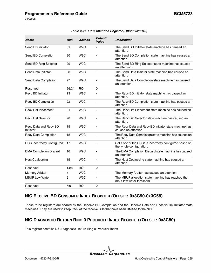
Programmer’s Reference Guide BCM572304/02/08
Broadcom CorporationDocument 5723-PG100-R Host Coalescing Control Registers Page 255
NIC RECEIVE BD CONSUMER INDEX REGISTER (OFFSET: 0X3C50-0X3C58)
These three registers are shared by the Receive BD Completion and the Receive Data and Receive BD Initiator state machines. They are used to keep track of the receive BDs that have been DMAed to the NIC.
NIC DIAGNOSTIC RETURN RING 0 PRODUCER INDEX REGISTER (OFFSET: 0X3C80)
This register contains NIC Diagnostic Return Ring 0 Producer Index.
Table 282: Flow Attention Register (Offset: 0x3C48)
Name Bits Access Default Value Description
Send BD Initiator 31 W2C - The Send BD Initiator state machine has caused an attention.
Send BD Completion 30 W2C - The Send BD Completion state machine has caused an attention.
Send BD Ring Selector 29 W2C - The Send BD Ring Selector state machine has caused an attention.
Send Data Initiator 28 W2C - The Send Data Initiator state machine has caused an attention.
Send Data Completion 27 W2C - The Send Data Completion state machine has caused an attention.
Reserved 26:24 RO 0
Recv BD Initiator 23 W2C - The Recv BD Initiator state machine has caused an attention.
Recv BD Completion 22 W2C - The Recv BD Completion state machine has caused an attention.
Recv List Placement 21 W2C - The Recv List Placement state machine has caused an attention.
Recv List Selector 20 W2C - The Recv List Selector state machine has caused an attention.
Recv Data and Recv BD Initiator
19 W2C - The Recv Data and Recv BD Initiator state machine has caused an attention.
Recv Data Completion 18 W2C - The Recv Data Completion state machine has caused an attention.
RCB Incorrectly Configured 17 W2C - Set if one of the RCBs is incorrectly configured based on the whole configuration.
DMA Completion Discard 16 W2C - The DMA Completion Discard state machine has caused an attention.
Host Coalescing 15 W2C - The Host Coalescing state machine has caused an attention.
Reserved 14:8 RO 0
Memory Arbiter 7 W2C - The Memory Arbiter has caused an attention.
MBUF Low Water 6 W2C - The MBUF allocation state machine has reached the mbuf low water threshold.
Reserved 5:0 RO 0
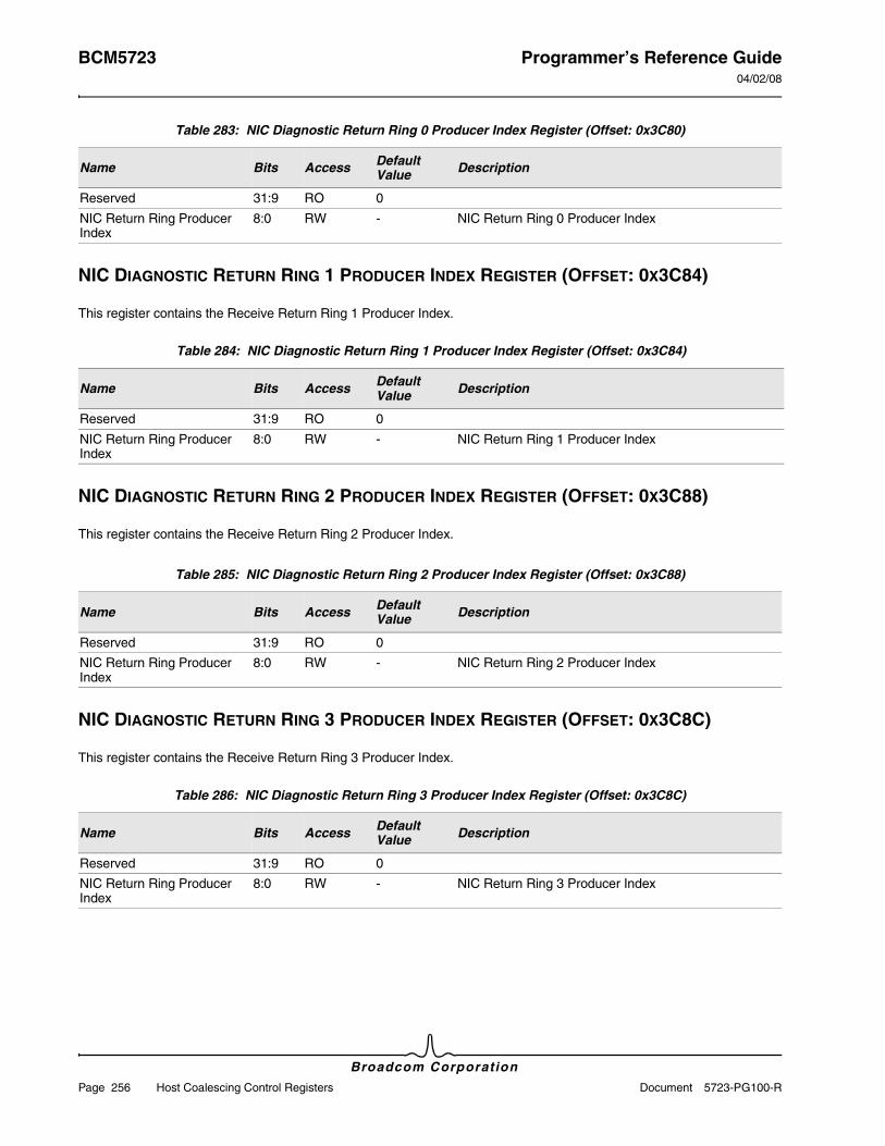
BCM5723 Programmer’s Reference Guide04/02/08
Broadcom Corporation
Page 256 Host Coalescing Control Registers Document 5723-PG100-R
NIC DIAGNOSTIC RETURN RING 1 PRODUCER INDEX REGISTER (OFFSET: 0X3C84)
This register contains the Receive Return Ring 1 Producer Index.
NIC DIAGNOSTIC RETURN RING 2 PRODUCER INDEX REGISTER (OFFSET: 0X3C88)
This register contains the Receive Return Ring 2 Producer Index.
NIC DIAGNOSTIC RETURN RING 3 PRODUCER INDEX REGISTER (OFFSET: 0X3C8C)
This register contains the Receive Return Ring 3 Producer Index.
Table 283: NIC Diagnostic Return Ring 0 Producer Index Register (Offset: 0x3C80)
Name Bits Access Default Value Description
Reserved 31:9 RO 0
NIC Return Ring Producer Index
8:0 RW - NIC Return Ring 0 Producer Index
Table 284: NIC Diagnostic Return Ring 1 Producer Index Register (Offset: 0x3C84)
Name Bits Access Default Value Description
Reserved 31:9 RO 0
NIC Return Ring Producer Index
8:0 RW - NIC Return Ring 1 Producer Index
Table 285: NIC Diagnostic Return Ring 2 Producer Index Register (Offset: 0x3C88)
Name Bits Access Default Value Description
Reserved 31:9 RO 0
NIC Return Ring Producer Index
8:0 RW - NIC Return Ring 2 Producer Index
Table 286: NIC Diagnostic Return Ring 3 Producer Index Register (Offset: 0x3C8C)
Name Bits Access Default Value Description
Reserved 31:9 RO 0
NIC Return Ring Producer Index
8:0 RW - NIC Return Ring 3 Producer Index
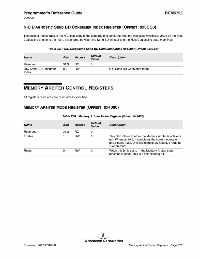
Programmer’s Reference Guide BCM572304/02/08
Broadcom CorporationDocument 5723-PG100-R Memory Arbiter Control Registers Page 257
NIC DIAGNOSTIC SEND BD CONSUMER INDEX REGISTER (OFFSET: 0X3CC0)
The register keeps track of the NIC local copy of the send BD ring consumer (not the host copy which is DMAed by the Host Coalescing engine to the host). It is shared between the Send BD Initiator and the Host Coalescing state machines.
MEMORY ARBITER CONTROL REGISTERS
All registers reset are core reset unless specified.
MEMORY ARBITER MODE REGISTER (OFFSET: 0X4000)
Table 287: NIC Diagnostic Send BD Consumer Index Register (Offset: 0x3CC0)
Name Bits Access Default Value Description
Reserved 31:9 RO 0
NIC Send BD Consumer Index
8:0 RW - NIC Send BD Consumer Index
Table 288: Memory Arbiter Mode Register (Offset: 0x4000)
Name Bits Access Default Value Description
Reserved 31:2 RO 0
Enable 1 RW 0 This bit controls whether the Memory Arbiter is active or not. When set to 0, it completes the current operation and cleanly halts. Until it is completely halted, it remains 1 when read.
Reset 0 RW 0 When this bit is set to 1, the Memory Arbiter state machine is reset. This is a self-clearing bit.
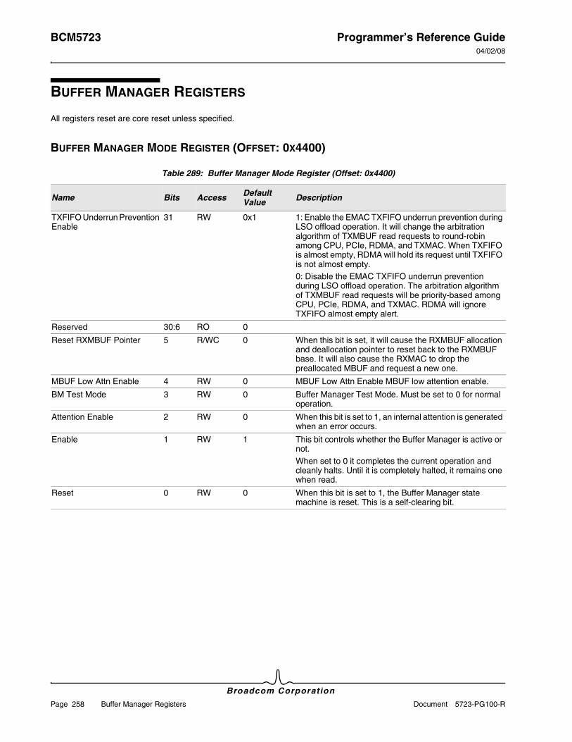
BCM5723 Programmer’s Reference Guide04/02/08
Broadcom Corporation
Page 258 Buffer Manager Registers Document 5723-PG100-R
BUFFER MANAGER REGISTERS
All registers reset are core reset unless specified.
BUFFER MANAGER MODE REGISTER (OFFSET: 0X4400)
Table 289: Buffer Manager Mode Register (Offset: 0x4400)
Name Bits Access Default Value Description
TXFIFO Underrun Prevention Enable
31 RW 0x1 1: Enable the EMAC TXFIFO underrun prevention during LSO offload operation. It will change the arbitration algorithm of TXMBUF read requests to round-robin among CPU, PCIe, RDMA, and TXMAC. When TXFIFO is almost empty, RDMA will hold its request until TXFIFO is not almost empty.0: Disable the EMAC TXFIFO underrun prevention during LSO offload operation. The arbitration algorithm of TXMBUF read requests will be priority-based among CPU, PCIe, RDMA, and TXMAC. RDMA will ignore TXFIFO almost empty alert.
Reserved 30:6 RO 0
Reset RXMBUF Pointer 5 R/WC 0 When this bit is set, it will cause the RXMBUF allocation and deallocation pointer to reset back to the RXMBUF base. It will also cause the RXMAC to drop the preallocated MBUF and request a new one.
MBUF Low Attn Enable 4 RW 0 MBUF Low Attn Enable MBUF low attention enable.
BM Test Mode 3 RW 0 Buffer Manager Test Mode. Must be set to 0 for normal operation.
Attention Enable 2 RW 0 When this bit is set to 1, an internal attention is generated when an error occurs.
Enable 1 RW 1 This bit controls whether the Buffer Manager is active or not.When set to 0 it completes the current operation and cleanly halts. Until it is completely halted, it remains one when read.
Reset 0 RW 0 When this bit is set to 1, the Buffer Manager state machine is reset. This is a self-clearing bit.
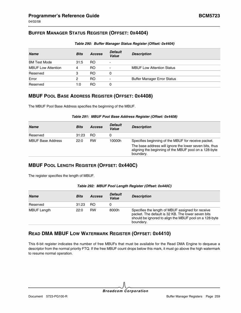
Programmer’s Reference Guide BCM572304/02/08
Broadcom CorporationDocument 5723-PG100-R Buffer Manager Registers Page 259
BUFFER MANAGER STATUS REGISTER (OFFSET: 0X4404)
MBUF POOL BASE ADDRESS REGISTER (OFFSET: 0X4408)
The MBUF Pool Base Address specifies the beginning of the MBUF.
MBUF POOL LENGTH REGISTER (OFFSET: 0X440C)
The register specifies the length of MBUF.
READ DMA MBUF LOW WATERMARK REGISTER (OFFSET: 0X4410)
This 6-bit register indicates the number of free MBUFs that must be available for the Read DMA Engine to dequeue a descriptor from the normal priority FTQ. If the free MBUF count drops below this mark, it must go above the high watermark to resume normal operation.
Table 290: Buffer Manager Status Register (Offset: 0x4404)
Name Bits Access Default Value Description
BM Test Mode 31:5 RO -
MBUF Low Attention 4 RO - MBUF Low Attention Status
Reserved 3 RO 0
Error 2 RO - Buffer Manager Error Status
Reserved 1:0 RO 0
Table 291: MBUF Pool Base Address Register (Offset: 0x4408)
Name Bits Access Default Value Description
Reserved 31:23 RO 0
MBUF Base Address 22:0 RW 10000h Specifies beginning of the MBUF for receive packet.The base address will ignore the lower seven bits, thus aligning the beginning of the MBUF pool on a 128-byte boundary.
Table 292: MBUF Pool Length Register (Offset: 0x440C)
Name Bits Access Default Value Description
Reserved 31:23 RO 0
MBUF Length 22:0 RW 8000h Specifies the length of MBUF assigned for receive packet. The default is 32 KB. The lower seven bits should be ignored to align the MBUF pool on a 128-byte boundary.
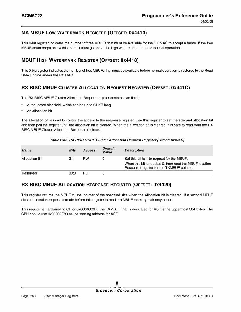
BCM5723 Programmer’s Reference Guide04/02/08
Broadcom Corporation
Page 260 Buffer Manager Registers Document 5723-PG100-R
MA MBUF LOW WATERMARK REGISTER (OFFSET: 0X4414)
This 9-bit register indicates the number of free MBUFs that must be available for the RX MAC to accept a frame. If the free MBUF count drops below this mark, it must go above the high watermark to resume normal operation.
MBUF HIGH WATERMARK REGISTER (OFFSET: 0X4418)
This 9-bit register indicates the number of free MBUFs that must be available before normal operation is restored to the Read DMA Engine and/or the RX MAC.
RX RISC MBUF CLUSTER ALLOCATION REQUEST REGISTER (OFFSET: 0X441C)
The RX RISC MBUF Cluster Allocation Request register contains two fields:
• A requested size field, which can be up to 64-KB long
• An allocation bit
The allocation bit is used to control the access to the response register. Use this register to set the size and allocation bit and then poll the register until the allocation bit is cleared. When the allocation bit is cleared, it is safe to read from the RX RISC MBUF Cluster Allocation Response register.
RX RISC MBUF ALLOCATION RESPONSE REGISTER (OFFSET: 0X4420)
This register returns the MBUF cluster pointer of the specified size when the Allocation bit is cleared. If a second MBUF cluster allocation request is made before this register is read, an MBUF memory leak may occur.
This register is hardwired to 61, or 0x0000003D. The TXMBUF that is dedicated for ASF is the uppermost 384 bytes. The CPU should use 0x00009E80 as the starting address for ASF.
Table 293: RX RISC MBUF Cluster Allocation Request Register (Offset: 0x441C)
Name Bits Access Default Value Description
Allocation Bit 31 RW 0 Set this bit to 1 to request for the MBUF.When this bit is read as 0, then read the MBUF location Response register for the TXMBUF pointer.
Reserved 30:0 RO 0
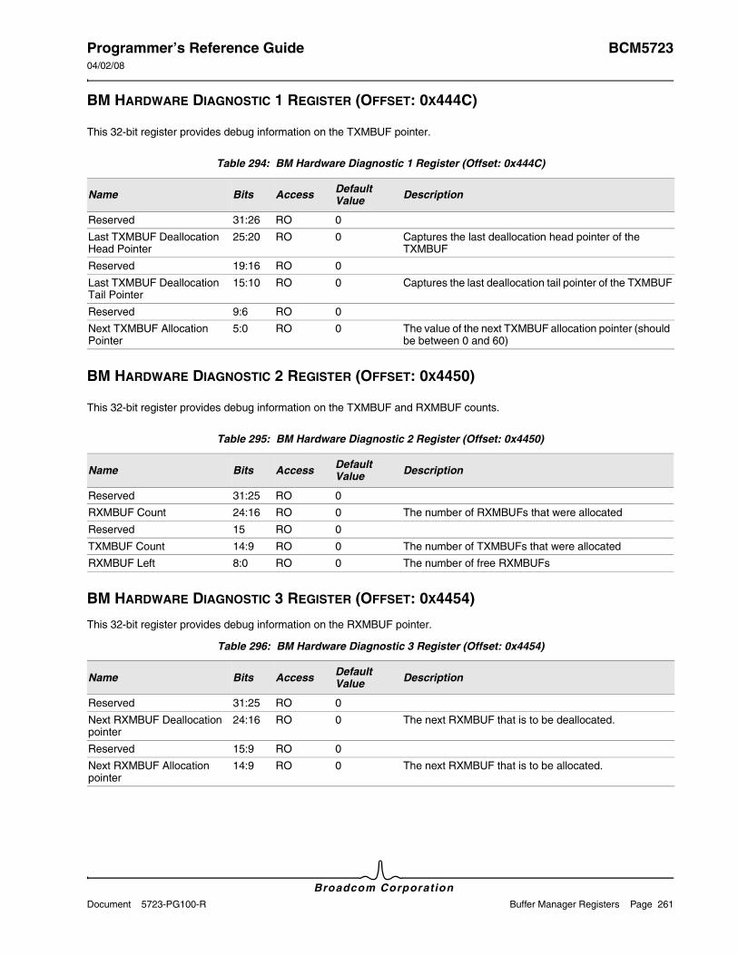
Programmer’s Reference Guide BCM572304/02/08
Broadcom CorporationDocument 5723-PG100-R Buffer Manager Registers Page 261
BM HARDWARE DIAGNOSTIC 1 REGISTER (OFFSET: 0X444C)
This 32-bit register provides debug information on the TXMBUF pointer.
BM HARDWARE DIAGNOSTIC 2 REGISTER (OFFSET: 0X4450)
This 32-bit register provides debug information on the TXMBUF and RXMBUF counts.
BM HARDWARE DIAGNOSTIC 3 REGISTER (OFFSET: 0X4454)
This 32-bit register provides debug information on the RXMBUF pointer.
Table 294: BM Hardware Diagnostic 1 Register (Offset: 0x444C)
Name Bits Access Default Value Description
Reserved 31:26 RO 0
Last TXMBUF Deallocation Head Pointer
25:20 RO 0 Captures the last deallocation head pointer of the TXMBUF
Reserved 19:16 RO 0
Last TXMBUF Deallocation Tail Pointer
15:10 RO 0 Captures the last deallocation tail pointer of the TXMBUF
Reserved 9:6 RO 0
Next TXMBUF Allocation Pointer
5:0 RO 0 The value of the next TXMBUF allocation pointer (should be between 0 and 60)
Table 295: BM Hardware Diagnostic 2 Register (Offset: 0x4450)
Name Bits Access Default Value Description
Reserved 31:25 RO 0
RXMBUF Count 24:16 RO 0 The number of RXMBUFs that were allocated
Reserved 15 RO 0
TXMBUF Count 14:9 RO 0 The number of TXMBUFs that were allocated
RXMBUF Left 8:0 RO 0 The number of free RXMBUFs
Table 296: BM Hardware Diagnostic 3 Register (Offset: 0x4454)
Name Bits Access Default Value Description
Reserved 31:25 RO 0
Next RXMBUF Deallocation pointer
24:16 RO 0 The next RXMBUF that is to be deallocated.
Reserved 15:9 RO 0
Next RXMBUF Allocation pointer
14:9 RO 0 The next RXMBUF that is to be allocated.
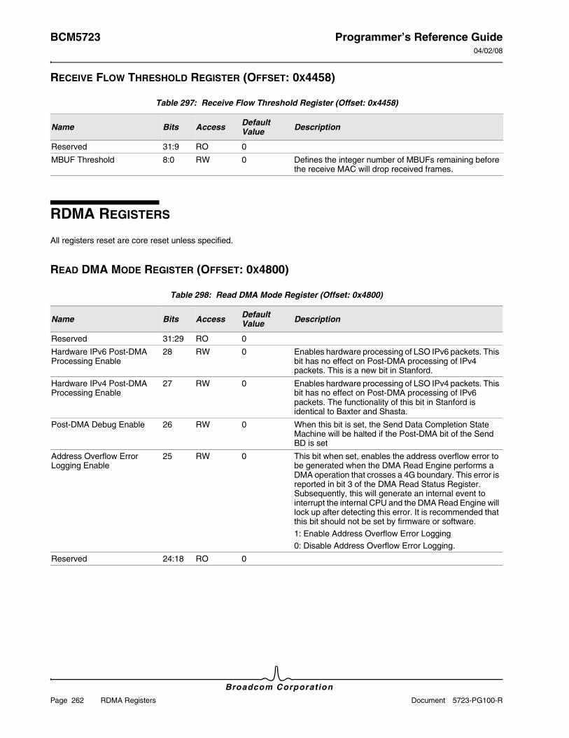
BCM5723 Programmer’s Reference Guide04/02/08
Broadcom Corporation
Page 262 RDMA Registers Document 5723-PG100-R
RECEIVE FLOW THRESHOLD REGISTER (OFFSET: 0X4458)
RDMA REGISTERS
All registers reset are core reset unless specified.
READ DMA MODE REGISTER (OFFSET: 0X4800)
Table 297: Receive Flow Threshold Register (Offset: 0x4458)
Name Bits Access Default Value Description
Reserved 31:9 RO 0
MBUF Threshold 8:0 RW 0 Defines the integer number of MBUFs remaining before the receive MAC will drop received frames.
Table 298: Read DMA Mode Register (Offset: 0x4800)
Name Bits Access Default Value Description
Reserved 31:29 RO 0
Hardware IPv6 Post-DMA Processing Enable
28 RW 0 Enables hardware processing of LSO IPv6 packets. This bit has no effect on Post-DMA processing of IPv4 packets. This is a new bit in Stanford.
Hardware IPv4 Post-DMA Processing Enable
27 RW 0 Enables hardware processing of LSO IPv4 packets. This bit has no effect on Post-DMA processing of IPv6 packets. The functionality of this bit in Stanford is identical to Baxter and Shasta.
Post-DMA Debug Enable 26 RW 0 When this bit is set, the Send Data Completion State Machine will be halted if the Post-DMA bit of the Send BD is set
Address Overflow Error Logging Enable
25 RW 0 This bit when set, enables the address overflow error to be generated when the DMA Read Engine performs a DMA operation that crosses a 4G boundary. This error is reported in bit 3 of the DMA Read Status Register. Subsequently, this will generate an internal event to interrupt the internal CPU and the DMA Read Engine will lock up after detecting this error. It is recommended that this bit should not be set by firmware or software.1: Enable Address Overflow Error Logging0: Disable Address Overflow Error Logging.
Reserved 24:18 RO 0
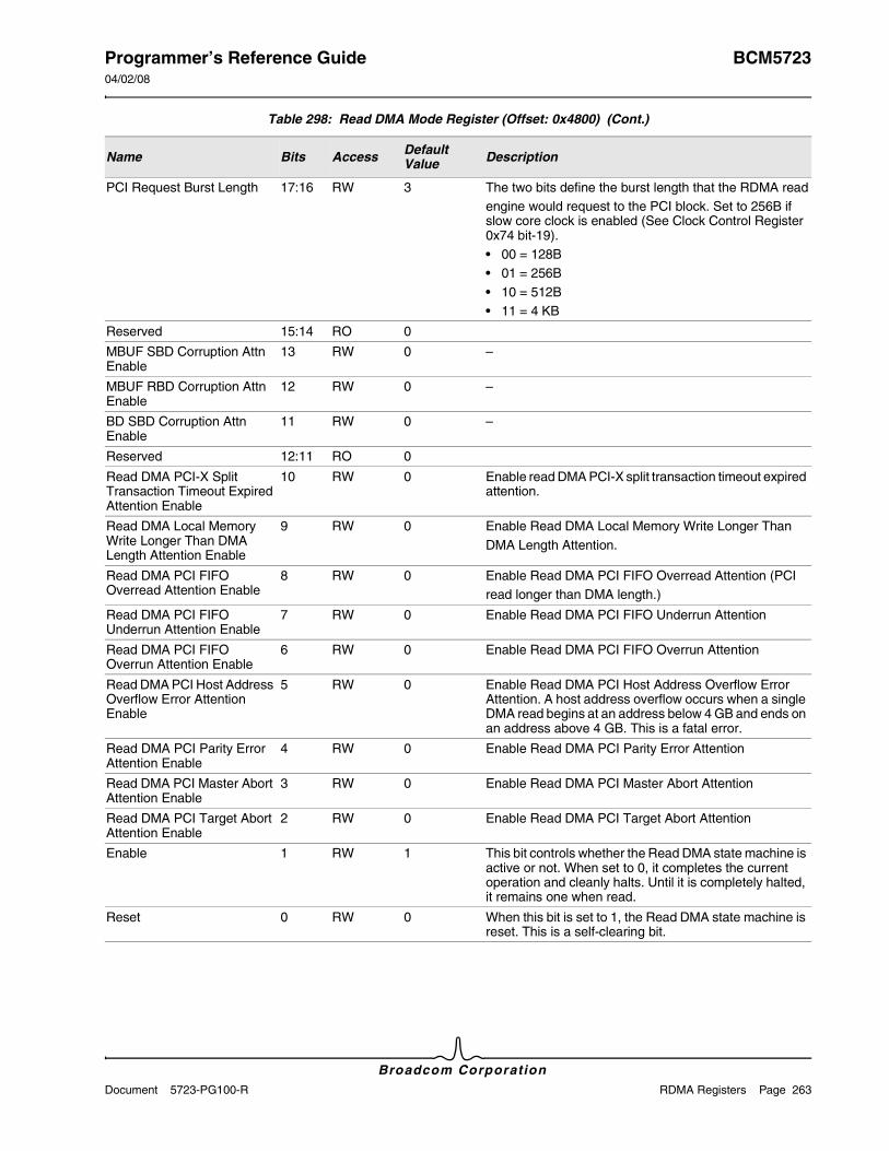
Programmer’s Reference Guide BCM572304/02/08
Broadcom CorporationDocument 5723-PG100-R RDMA Registers Page 263
PCI Request Burst Length 17:16 RW 3 The two bits define the burst length that the RDMA readengine would request to the PCI block. Set to 256B if slow core clock is enabled (See Clock Control Register 0x74 bit-19).• 00 = 128B• 01 = 256B• 10 = 512B• 11 = 4 KB
Reserved 15:14 RO 0
MBUF SBD Corruption Attn Enable
13 RW 0 –
MBUF RBD Corruption Attn Enable
12 RW 0 –
BD SBD Corruption Attn Enable
11 RW 0 –
Reserved 12:11 RO 0
Read DMA PCI-X Split Transaction Timeout Expired Attention Enable
10 RW 0 Enable read DMA PCI-X split transaction timeout expired attention.
Read DMA Local Memory Write Longer Than DMA Length Attention Enable
9 RW 0 Enable Read DMA Local Memory Write Longer ThanDMA Length Attention.
Read DMA PCI FIFO Overread Attention Enable
8 RW 0 Enable Read DMA PCI FIFO Overread Attention (PCIread longer than DMA length.)
Read DMA PCI FIFO Underrun Attention Enable
7 RW 0 Enable Read DMA PCI FIFO Underrun Attention
Read DMA PCI FIFO Overrun Attention Enable
6 RW 0 Enable Read DMA PCI FIFO Overrun Attention
Read DMA PCI Host Address Overflow Error Attention Enable
5 RW 0 Enable Read DMA PCI Host Address Overflow Error Attention. A host address overflow occurs when a single DMA read begins at an address below 4 GB and ends on an address above 4 GB. This is a fatal error.
Read DMA PCI Parity Error Attention Enable
4 RW 0 Enable Read DMA PCI Parity Error Attention
Read DMA PCI Master Abort Attention Enable
3 RW 0 Enable Read DMA PCI Master Abort Attention
Read DMA PCI Target Abort Attention Enable
2 RW 0 Enable Read DMA PCI Target Abort Attention
Enable 1 RW 1 This bit controls whether the Read DMA state machine is active or not. When set to 0, it completes the current operation and cleanly halts. Until it is completely halted, it remains one when read.
Reset 0 RW 0 When this bit is set to 1, the Read DMA state machine is reset. This is a self-clearing bit.
Table 298: Read DMA Mode Register (Offset: 0x4800) (Cont.)
Name Bits Access Default Value Description
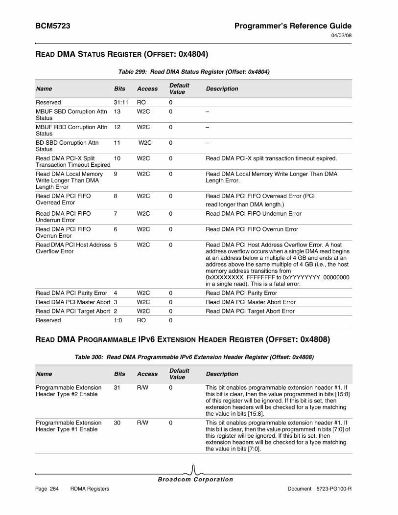
BCM5723 Programmer’s Reference Guide04/02/08
Broadcom Corporation
Page 264 RDMA Registers Document 5723-PG100-R
READ DMA STATUS REGISTER (OFFSET: 0X4804)
READ DMA PROGRAMMABLE IPV6 EXTENSION HEADER REGISTER (OFFSET: 0X4808)
Table 299: Read DMA Status Register (Offset: 0x4804)
Name Bits Access Default Value Description
Reserved 31:11 RO 0
MBUF SBD Corruption Attn Status
13 W2C 0 –
MBUF RBD Corruption Attn Status
12 W2C 0 –
BD SBD Corruption Attn Status
11 W2C 0 –
Read DMA PCI-X Split Transaction Timeout Expired
10 W2C 0 Read DMA PCI-X split transaction timeout expired.
Read DMA Local Memory Write Longer Than DMA Length Error
9 W2C 0 Read DMA Local Memory Write Longer Than DMA Length Error.
Read DMA PCI FIFO Overread Error
8 W2C 0 Read DMA PCI FIFO Overread Error (PCIread longer than DMA length.)
Read DMA PCI FIFO Underrun Error
7 W2C 0 Read DMA PCI FIFO Underrun Error
Read DMA PCI FIFO Overrun Error
6 W2C 0 Read DMA PCI FIFO Overrun Error
Read DMA PCI Host Address Overflow Error
5 W2C 0 Read DMA PCI Host Address Overflow Error. A host address overflow occurs when a single DMA read begins at an address below a multiple of 4 GB and ends at an address above the same multiple of 4 GB (i.e., the host memory address transitions from 0xXXXXXXXX_FFFFFFFF to 0xYYYYYYYY_00000000 in a single read). This is a fatal error.
Read DMA PCI Parity Error 4 W2C 0 Read DMA PCI Parity Error
Read DMA PCI Master Abort 3 W2C 0 Read DMA PCI Master Abort Error
Read DMA PCI Target Abort 2 W2C 0 Read DMA PCI Target Abort Error
Reserved 1:0 RO 0
Table 300: Read DMA Programmable IPv6 Extension Header Register (Offset: 0x4808)
Name Bits Access Default Value Description
Programmable Extension Header Type #2 Enable
31 R/W 0 This bit enables programmable extension header #1. If this bit is clear, then the value programmed in bits [15:8] of this register will be ignored. If this bit is set, then extension headers will be checked for a type matching the value in bits [15:8].
Programmable Extension Header Type #1 Enable
30 R/W 0 This bit enables programmable extension header #1. If this bit is clear, then the value programmed in bits [7:0] of this register will be ignored. If this bit is set, then extension headers will be checked for a type matching the value in bits [7:0].
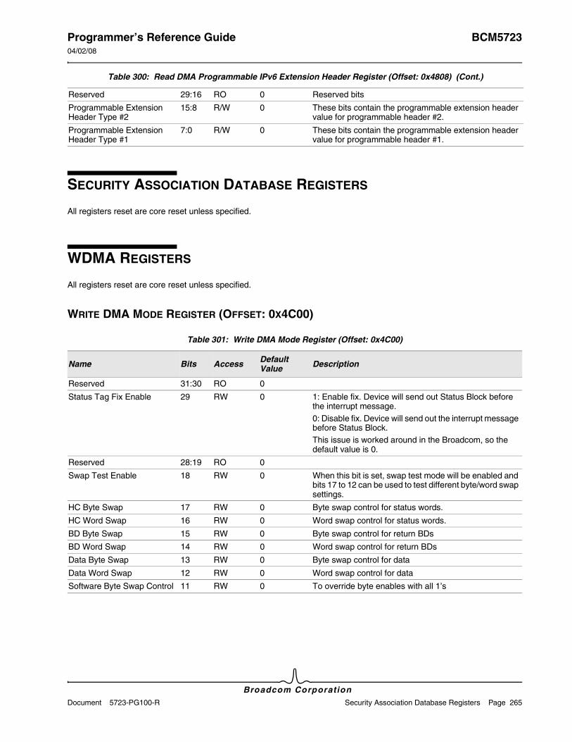
Programmer’s Reference Guide BCM572304/02/08
Broadcom CorporationDocument 5723-PG100-R Security Association Database Registers Page 265
SECURITY ASSOCIATION DATABASE REGISTERS
All registers reset are core reset unless specified.
WDMA REGISTERS
All registers reset are core reset unless specified.
WRITE DMA MODE REGISTER (OFFSET: 0X4C00)
Reserved 29:16 RO 0 Reserved bits
Programmable Extension Header Type #2
15:8 R/W 0 These bits contain the programmable extension header value for programmable header #2.
Programmable Extension Header Type #1
7:0 R/W 0 These bits contain the programmable extension header value for programmable header #1.
Table 301: Write DMA Mode Register (Offset: 0x4C00)
Name Bits Access Default Value Description
Reserved 31:30 RO 0
Status Tag Fix Enable 29 RW 0 1: Enable fix. Device will send out Status Block before the interrupt message.0: Disable fix. Device will send out the interrupt message before Status Block.This issue is worked around in the Broadcom, so the default value is 0.
Reserved 28:19 RO 0
Swap Test Enable 18 RW 0 When this bit is set, swap test mode will be enabled and bits 17 to 12 can be used to test different byte/word swap settings.
HC Byte Swap 17 RW 0 Byte swap control for status words.
HC Word Swap 16 RW 0 Word swap control for status words.
BD Byte Swap 15 RW 0 Byte swap control for return BDs
BD Word Swap 14 RW 0 Word swap control for return BDs
Data Byte Swap 13 RW 0 Byte swap control for data
Data Word Swap 12 RW 0 Word swap control for data
Software Byte Swap Control 11 RW 0 To override byte enables with all 1’s
Table 300: Read DMA Programmable IPv6 Extension Header Register (Offset: 0x4808) (Cont.)
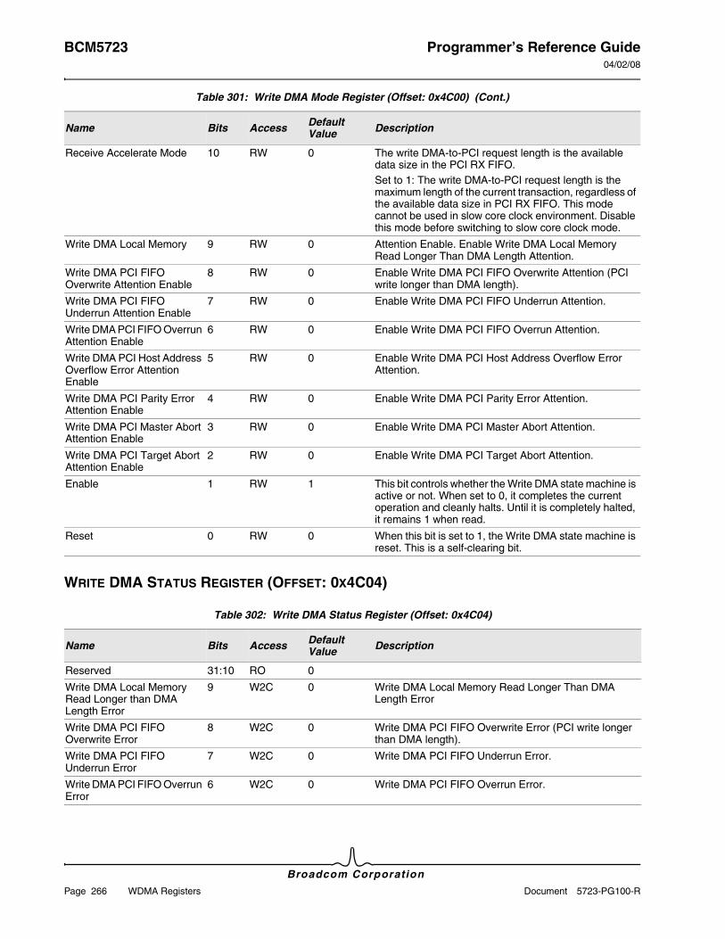
BCM5723 Programmer’s Reference Guide04/02/08
Broadcom Corporation
Page 266 WDMA Registers Document 5723-PG100-R
WRITE DMA STATUS REGISTER (OFFSET: 0X4C04)
Receive Accelerate Mode 10 RW 0 The write DMA-to-PCI request length is the available data size in the PCI RX FIFO.Set to 1: The write DMA-to-PCI request length is the maximum length of the current transaction, regardless of the available data size in PCI RX FIFO. This mode cannot be used in slow core clock environment. Disable this mode before switching to slow core clock mode.
Write DMA Local Memory 9 RW 0 Attention Enable. Enable Write DMA Local Memory Read Longer Than DMA Length Attention.
Write DMA PCI FIFO Overwrite Attention Enable
8 RW 0 Enable Write DMA PCI FIFO Overwrite Attention (PCI write longer than DMA length).
Write DMA PCI FIFO Underrun Attention Enable
7 RW 0 Enable Write DMA PCI FIFO Underrun Attention.
Write DMA PCI FIFO Overrun Attention Enable
6 RW 0 Enable Write DMA PCI FIFO Overrun Attention.
Write DMA PCI Host Address Overflow Error Attention Enable
5 RW 0 Enable Write DMA PCI Host Address Overflow Error Attention.
Write DMA PCI Parity Error Attention Enable
4 RW 0 Enable Write DMA PCI Parity Error Attention.
Write DMA PCI Master Abort Attention Enable
3 RW 0 Enable Write DMA PCI Master Abort Attention.
Write DMA PCI Target Abort Attention Enable
2 RW 0 Enable Write DMA PCI Target Abort Attention.
Enable 1 RW 1 This bit controls whether the Write DMA state machine is active or not. When set to 0, it completes the current operation and cleanly halts. Until it is completely halted, it remains 1 when read.
Reset 0 RW 0 When this bit is set to 1, the Write DMA state machine is reset. This is a self-clearing bit.
Table 302: Write DMA Status Register (Offset: 0x4C04)
Name Bits Access Default Value Description
Reserved 31:10 RO 0
Write DMA Local Memory Read Longer than DMA Length Error
9 W2C 0 Write DMA Local Memory Read Longer Than DMA Length Error
Write DMA PCI FIFO Overwrite Error
8 W2C 0 Write DMA PCI FIFO Overwrite Error (PCI write longer than DMA length).
Write DMA PCI FIFO Underrun Error
7 W2C 0 Write DMA PCI FIFO Underrun Error.
Write DMA PCI FIFO Overrun Error
6 W2C 0 Write DMA PCI FIFO Overrun Error.
Table 301: Write DMA Mode Register (Offset: 0x4C00) (Cont.)
Name Bits Access Default Value Description
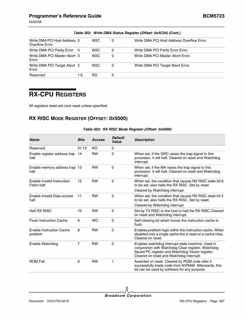
Programmer’s Reference Guide BCM572304/02/08
Broadcom CorporationDocument 5723-PG100-R RX-CPU Registers Page 267
RX-CPU REGISTERS
All registers reset are core reset unless specified.
RX RISC MODE REGISTER (OFFSET: 0X5000)
Write DMA PCI Host Address Overflow Error
5 W2C 0 Write DMA PCI Host Address Overflow Error.
Write DMA PCI Parity Error 4 W2C 0 Write DMA PCI Parity Error Error.
Write DMA PCI Master Abort Error
3 W2C 0 Write DMA PCI Master Abort Error.
Write DMA PCI Target Abort Error
2 W2C 0 Write DMA PCI Target Abort Error.
Reserved 1:0 RO 0
Table 303: RX RISC Mode Register (Offset: 0x5000)
Name Bits Access Default Value Description
Reserved 31:15 RO 0
Enable register address trap halt
14 RW 0 When set, if the GRC raises the trap signal to this processor, it will halt. Cleared on reset and Watchdog interrupt.
Enable memory address trap halt
13 RW 0 When set, if the MA raises the trap signal to this processor, it will halt. Cleared on reset and Watchdog interrupt.
Enable Invalid Instruction Fetch halt
12 RW 0 When set, the condition that causes RX RISC state bit 6 to be set, also halts the RX RISC. Set by reset.Cleared by Watchdog interrupt.
Enable Invalid Data access halt
11 RW 0 When set, the condition that causes RX RISC state bit 5 to be set, also halts the RX RISC. Set by reset.Cleared by Watchdog interrupt.
Halt RX RISC 10 RW 0 Set by TX RISC or the host to halt the RX RISC.Cleared on reset and Watchdog interrupt.
Flush Instruction Cache 9 WO 0 Self-clearing bit which forces the instruction cache to flush.
Enable Instruction Cache prefetch
8 RW 0 Enables prefetch logic within the instruction cache. When disabled only a single cache line is read on a cache miss. Cleared on reset.
Enable Watchdog 7 RW 0 Enables watchdog interrupt state machine. Used in conjunction with Watchdog Clear register, Watchdog Saved PC register and Watchdog Vector register. Cleared on reset and Watchdog interrupt.
ROM Fail 6 RW 1 Asserted on reset. Cleared by ROM code after it successfully loads code from NVRAM. Afterwards, this bit can be used by software for any purpose.
Table 302: Write DMA Status Register (Offset: 0x4C04) (Cont.)
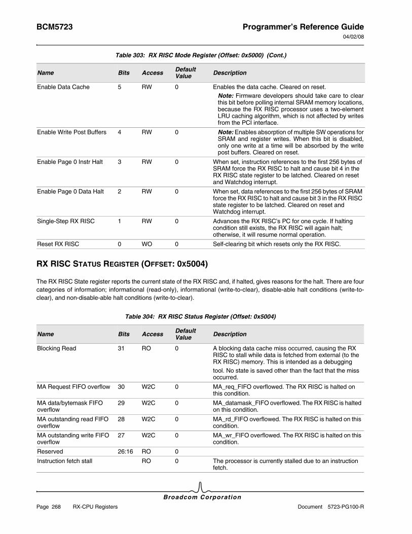
BCM5723 Programmer’s Reference Guide04/02/08
Broadcom Corporation
Page 268 RX-CPU Registers Document 5723-PG100-R
RX RISC STATUS REGISTER (OFFSET: 0X5004)
The RX RISC State register reports the current state of the RX RISC and, if halted, gives reasons for the halt. There are four categories of information; informational (read-only), informational (write-to-clear), disable-able halt conditions (write-to-clear), and non-disable-able halt conditions (write-to-clear).
Enable Data Cache 5 RW 0 Enables the data cache. Cleared on reset.Note: Firmware developers should take care to clear this bit before polling internal SRAM memory locations, because the RX RISC processor uses a two-element LRU caching algorithm, which is not affected by writes from the PCI interface.
Enable Write Post Buffers 4 RW 0 Note: Enables absorption of multiple SW operations for SRAM and register writes. When this bit is disabled, only one write at a time will be absorbed by the write post buffers. Cleared on reset.
Enable Page 0 Instr Halt 3 RW 0 When set, instruction references to the first 256 bytes of SRAM force the RX RISC to halt and cause bit 4 in the RX RISC state register to be latched. Cleared on reset and Watchdog interrupt.
Enable Page 0 Data Halt 2 RW 0 When set, data references to the first 256 bytes of SRAM force the RX RISC to halt and cause bit 3 in the RX RISC state register to be latched. Cleared on reset and Watchdog interrupt.
Single-Step RX RISC 1 RW 0 Advances the RX RISC’s PC for one cycle. If halting condition still exists, the RX RISC will again halt; otherwise, it will resume normal operation.
Reset RX RISC 0 WO 0 Self-clearing bit which resets only the RX RISC.
Table 304: RX RISC Status Register (Offset: 0x5004)
Name Bits Access Default Value Description
Blocking Read 31 RO 0 A blocking data cache miss occurred, causing the RX RISC to stall while data is fetched from external (to the RX RISC) memory. This is intended as a debuggingtool. No state is saved other than the fact that the miss occurred.
MA Request FIFO overflow 30 W2C 0 MA_req_FIFO overflowed. The RX RISC is halted on this condition.
MA data/bytemask FIFO overflow
29 W2C 0 MA_datamask_FIFO overflowed. The RX RISC is halted on this condition.
MA outstanding read FIFO overflow
28 W2C 0 MA_rd_FIFO overflowed. The RX RISC is halted on this condition.
MA outstanding write FIFO overflow
27 W2C 0 MA_wr_FIFO overflowed. The RX RISC is halted on this condition.
Reserved 26:16 RO 0
Instruction fetch stall RO 0 The processor is currently stalled due to an instruction fetch.
Table 303: RX RISC Mode Register (Offset: 0x5000) (Cont.)
Name Bits Access Default Value Description
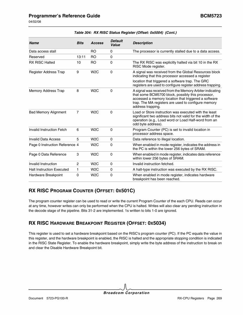
Programmer’s Reference Guide BCM572304/02/08
Broadcom CorporationDocument 5723-PG100-R RX-CPU Registers Page 269
RX RISC PROGRAM COUNTER (OFFSET: 0X501C)
The program counter register can be used to read or write the current Program Counter of the each CPU. Reads can occur at any time, however writes can only be performed when the CPU is halted. Writes will also clear any pending instruction in the decode stage of the pipeline. Bits 31-2 are implemented. 1s written to bits 1-0 are ignored.
RX RISC HARDWARE BREAKPOINT REGISTER (OFFSET: 0X5034)
This register is used to set a hardware breakpoint based on the RISC's program counter (PC). If the PC equals the value in this register, and the hardware breakpoint is enabled, the RISC is halted and the appropriate stopping condition is indicated in the RISC State Register. To enable the hardware breakpoint, simply write the byte address of the instruction to break on and clear the Disable Hardware Breakpoint bit.
Data access stall RO 0 The processor is currently stalled due to a data access.
Reserved 13:11 RO 0
RX RISC Halted 10 RO 0 The RX RISC was explicitly halted via bit 10 in the RX RISC Mode register.
Register Address Trap 9 W2C 0 A signal was received from the Global Resources block indicating that this processor accessed a registerlocation that triggered a software trap. The GRC registers are used to configure register address trapping.
Memory Address Trap 8 W2C 0 A signal was received from the Memory Arbiter indicating that some BCM5700 block, possibly this processor, accessed a memory location that triggered a software trap. The MA registers are used to configure memory address trapping.
Bad Memory Alignment 7 W2C 0 Load or Store instruction was executed with the least significant two address bits not valid for the width of the operation (e.g., Load word or Load Half-word from an odd byte address).
Invalid Instruction Fetch 6 W2C 0 Program Counter (PC) is set to invalid location in processor address space.
Invalid Data Access 5 W2C 0 Data reference to illegal location.
Page 0 Instruction Reference 4 W2C 0 When enabled in mode register, indicates the address in the PC is within the lower 256 bytes of SRAM.
Page 0 Data Reference 3 W2C 0 When enabled in mode register, indicates data reference within lower 256 bytes of SRAM.
Invalid Instruction 2 W2C 0 Invalid instruction fetched.
Halt Instruction Executed 1 W2C 0 A halt-type instruction was executed by the RX RISC.
Hardware Breakpoint 0 W2C 0 When enabled in mode register, indicates hardware breakpoint has been reached.
Table 304: RX RISC Status Register (Offset: 0x5004) (Cont.)
Name Bits Access Default Value Description
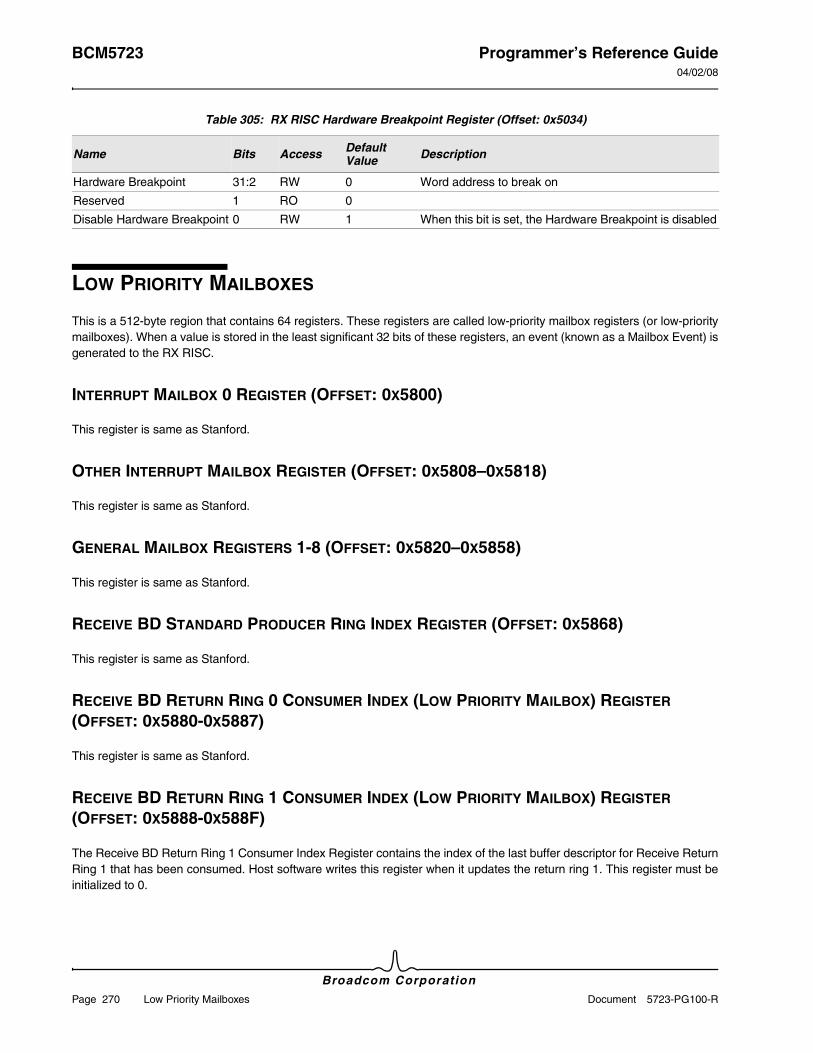
BCM5723 Programmer’s Reference Guide04/02/08
Broadcom Corporation
Page 270 Low Priority Mailboxes Document 5723-PG100-R
LOW PRIORITY MAILBOXES
This is a 512-byte region that contains 64 registers. These registers are called low-priority mailbox registers (or low-priority mailboxes). When a value is stored in the least significant 32 bits of these registers, an event (known as a Mailbox Event) is generated to the RX RISC.
INTERRUPT MAILBOX 0 REGISTER (OFFSET: 0X5800)
This register is same as Stanford.
OTHER INTERRUPT MAILBOX REGISTER (OFFSET: 0X5808–0X5818)
This register is same as Stanford.
GENERAL MAILBOX REGISTERS 1-8 (OFFSET: 0X5820–0X5858)
This register is same as Stanford.
RECEIVE BD STANDARD PRODUCER RING INDEX REGISTER (OFFSET: 0X5868)
This register is same as Stanford.
RECEIVE BD RETURN RING 0 CONSUMER INDEX (LOW PRIORITY MAILBOX) REGISTER (OFFSET: 0X5880-0X5887)
This register is same as Stanford.
RECEIVE BD RETURN RING 1 CONSUMER INDEX (LOW PRIORITY MAILBOX) REGISTER (OFFSET: 0X5888-0X588F)
The Receive BD Return Ring 1 Consumer Index Register contains the index of the last buffer descriptor for Receive Return Ring 1 that has been consumed. Host software writes this register when it updates the return ring 1. This register must be initialized to 0.
Table 305: RX RISC Hardware Breakpoint Register (Offset: 0x5034)
Name Bits Access Default Value Description
Hardware Breakpoint 31:2 RW 0 Word address to break on
Reserved 1 RO 0
Disable Hardware Breakpoint 0 RW 1 When this bit is set, the Hardware Breakpoint is disabled
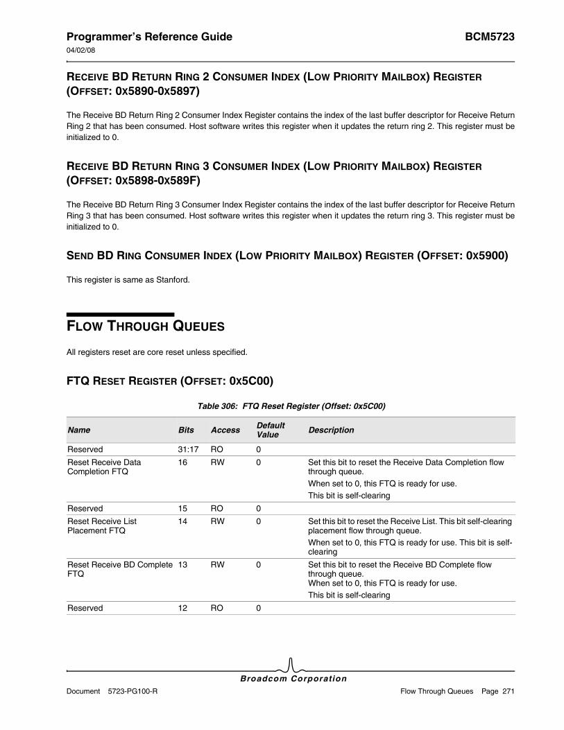
Programmer’s Reference Guide BCM572304/02/08
Broadcom CorporationDocument 5723-PG100-R Flow Through Queues Page 271
RECEIVE BD RETURN RING 2 CONSUMER INDEX (LOW PRIORITY MAILBOX) REGISTER (OFFSET: 0X5890-0X5897)
The Receive BD Return Ring 2 Consumer Index Register contains the index of the last buffer descriptor for Receive Return Ring 2 that has been consumed. Host software writes this register when it updates the return ring 2. This register must be initialized to 0.
RECEIVE BD RETURN RING 3 CONSUMER INDEX (LOW PRIORITY MAILBOX) REGISTER (OFFSET: 0X5898-0X589F)
The Receive BD Return Ring 3 Consumer Index Register contains the index of the last buffer descriptor for Receive Return Ring 3 that has been consumed. Host software writes this register when it updates the return ring 3. This register must be initialized to 0.
SEND BD RING CONSUMER INDEX (LOW PRIORITY MAILBOX) REGISTER (OFFSET: 0X5900)
This register is same as Stanford.
FLOW THROUGH QUEUES
All registers reset are core reset unless specified.
FTQ RESET REGISTER (OFFSET: 0X5C00)
Table 306: FTQ Reset Register (Offset: 0x5C00)
Name Bits Access Default Value Description
Reserved 31:17 RO 0
Reset Receive Data Completion FTQ
16 RW 0 Set this bit to reset the Receive Data Completion flow through queue.When set to 0, this FTQ is ready for use.This bit is self-clearing
Reserved 15 RO 0
Reset Receive List Placement FTQ
14 RW 0 Set this bit to reset the Receive List. This bit self-clearing placement flow through queue. When set to 0, this FTQ is ready for use. This bit is self-clearing
Reset Receive BD Complete FTQ
13 RW 0 Set this bit to reset the Receive BD Complete flow through queue. When set to 0, this FTQ is ready for use. This bit is self-clearing
Reserved 12 RO 0
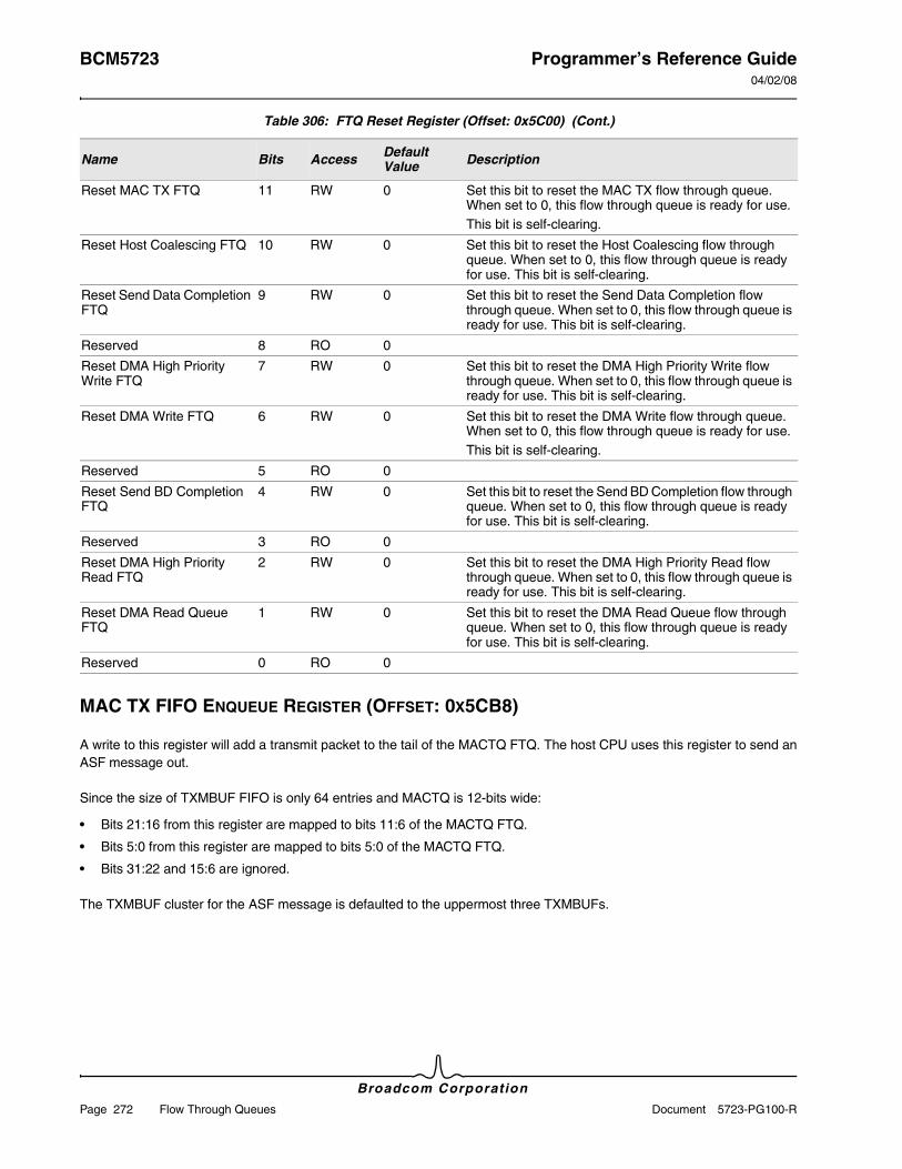
BCM5723 Programmer’s Reference Guide04/02/08
Broadcom Corporation
Page 272 Flow Through Queues Document 5723-PG100-R
MAC TX FIFO ENQUEUE REGISTER (OFFSET: 0X5CB8)
A write to this register will add a transmit packet to the tail of the MACTQ FTQ. The host CPU uses this register to send an ASF message out.
Since the size of TXMBUF FIFO is only 64 entries and MACTQ is 12-bits wide:
• Bits 21:16 from this register are mapped to bits 11:6 of the MACTQ FTQ.
• Bits 5:0 from this register are mapped to bits 5:0 of the MACTQ FTQ.
• Bits 31:22 and 15:6 are ignored.
The TXMBUF cluster for the ASF message is defaulted to the uppermost three TXMBUFs.
Reset MAC TX FTQ 11 RW 0 Set this bit to reset the MAC TX flow through queue. When set to 0, this flow through queue is ready for use.This bit is self-clearing.
Reset Host Coalescing FTQ 10 RW 0 Set this bit to reset the Host Coalescing flow through queue. When set to 0, this flow through queue is ready for use. This bit is self-clearing.
Reset Send Data Completion FTQ
9 RW 0 Set this bit to reset the Send Data Completion flow through queue. When set to 0, this flow through queue is ready for use. This bit is self-clearing.
Reserved 8 RO 0
Reset DMA High Priority Write FTQ
7 RW 0 Set this bit to reset the DMA High Priority Write flow through queue. When set to 0, this flow through queue is ready for use. This bit is self-clearing.
Reset DMA Write FTQ 6 RW 0 Set this bit to reset the DMA Write flow through queue. When set to 0, this flow through queue is ready for use.This bit is self-clearing.
Reserved 5 RO 0
Reset Send BD Completion FTQ
4 RW 0 Set this bit to reset the Send BD Completion flow through queue. When set to 0, this flow through queue is ready for use. This bit is self-clearing.
Reserved 3 RO 0
Reset DMA High Priority Read FTQ
2 RW 0 Set this bit to reset the DMA High Priority Read flow through queue. When set to 0, this flow through queue is ready for use. This bit is self-clearing.
Reset DMA Read Queue FTQ
1 RW 0 Set this bit to reset the DMA Read Queue flow through queue. When set to 0, this flow through queue is ready for use. This bit is self-clearing.
Reserved 0 RO 0
Table 306: FTQ Reset Register (Offset: 0x5C00) (Cont.)
Name Bits Access Default Value Description
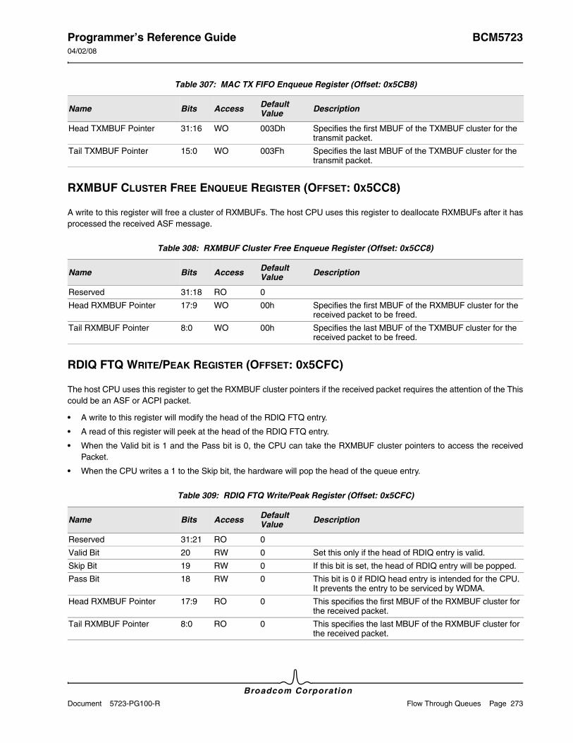
Programmer’s Reference Guide BCM572304/02/08
Broadcom CorporationDocument 5723-PG100-R Flow Through Queues Page 273
RXMBUF CLUSTER FREE ENQUEUE REGISTER (OFFSET: 0X5CC8)
A write to this register will free a cluster of RXMBUFs. The host CPU uses this register to deallocate RXMBUFs after it has processed the received ASF message.
RDIQ FTQ WRITE/PEAK REGISTER (OFFSET: 0X5CFC)
The host CPU uses this register to get the RXMBUF cluster pointers if the received packet requires the attention of the This could be an ASF or ACPI packet.
• A write to this register will modify the head of the RDIQ FTQ entry.
• A read of this register will peek at the head of the RDIQ FTQ entry.
• When the Valid bit is 1 and the Pass bit is 0, the CPU can take the RXMBUF cluster pointers to access the received Packet.
• When the CPU writes a 1 to the Skip bit, the hardware will pop the head of the queue entry.
Table 307: MAC TX FIFO Enqueue Register (Offset: 0x5CB8)
Name Bits Access Default Value Description
Head TXMBUF Pointer 31:16 WO 003Dh Specifies the first MBUF of the TXMBUF cluster for the transmit packet.
Tail TXMBUF Pointer 15:0 WO 003Fh Specifies the last MBUF of the TXMBUF cluster for the transmit packet.
Table 308: RXMBUF Cluster Free Enqueue Register (Offset: 0x5CC8)
Name Bits Access Default Value Description
Reserved 31:18 RO 0
Head RXMBUF Pointer 17:9 WO 00h Specifies the first MBUF of the RXMBUF cluster for the received packet to be freed.
Tail RXMBUF Pointer 8:0 WO 00h Specifies the last MBUF of the TXMBUF cluster for the received packet to be freed.
Table 309: RDIQ FTQ Write/Peak Register (Offset: 0x5CFC)
Name Bits Access Default Value Description
Reserved 31:21 RO 0
Valid Bit 20 RW 0 Set this only if the head of RDIQ entry is valid.
Skip Bit 19 RW 0 If this bit is set, the head of RDIQ entry will be popped.
Pass Bit 18 RW 0 This bit is 0 if RDIQ head entry is intended for the CPU. It prevents the entry to be serviced by WDMA.
Head RXMBUF Pointer 17:9 RO 0 This specifies the first MBUF of the RXMBUF cluster for the received packet.
Tail RXMBUF Pointer 8:0 RO 0 This specifies the last MBUF of the RXMBUF cluster for the received packet.
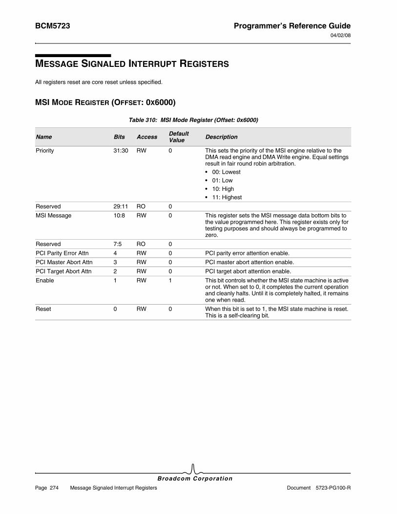
BCM5723 Programmer’s Reference Guide04/02/08
Broadcom Corporation
Page 274 Message Signaled Interrupt Registers Document 5723-PG100-R
MESSAGE SIGNALED INTERRUPT REGISTERS
All registers reset are core reset unless specified.
MSI MODE REGISTER (OFFSET: 0X6000)
Table 310: MSI Mode Register (Offset: 0x6000)
Name Bits Access Default Value Description
Priority 31:30 RW 0 This sets the priority of the MSI engine relative to the DMA read engine and DMA Write engine. Equal settings result in fair round robin arbitration.• 00: Lowest• 01: Low• 10: High• 11: Highest
Reserved 29:11 RO 0
MSI Message 10:8 RW 0 This register sets the MSI message data bottom bits to the value programmed here. This register exists only for testing purposes and should always be programmed to zero.
Reserved 7:5 RO 0
PCI Parity Error Attn 4 RW 0 PCI parity error attention enable.
PCI Master Abort Attn 3 RW 0 PCI master abort attention enable.
PCI Target Abort Attn 2 RW 0 PCI target abort attention enable.
Enable 1 RW 1 This bit controls whether the MSI state machine is active or not. When set to 0, it completes the current operation and cleanly halts. Until it is completely halted, it remains one when read.
Reset 0 RW 0 When this bit is set to 1, the MSI state machine is reset. This is a self-clearing bit.
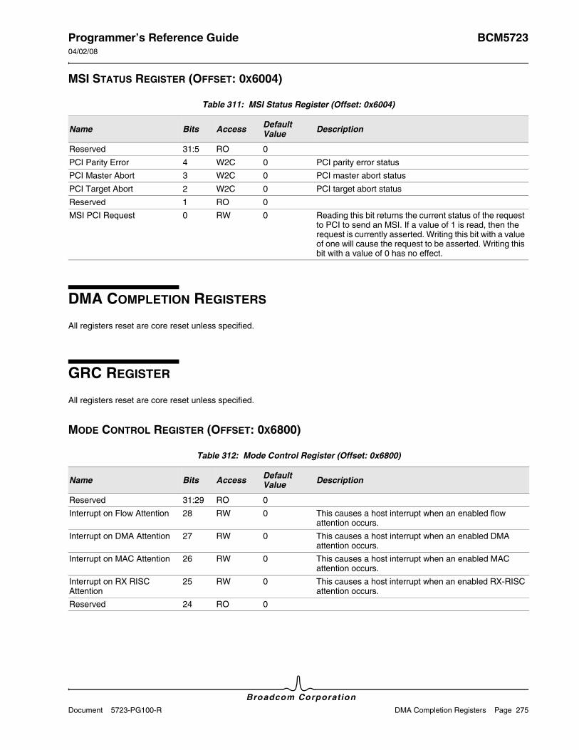
Programmer’s Reference Guide BCM572304/02/08
Broadcom CorporationDocument 5723-PG100-R DMA Completion Registers Page 275
MSI STATUS REGISTER (OFFSET: 0X6004)
DMA COMPLETION REGISTERS
All registers reset are core reset unless specified.
GRC REGISTER
All registers reset are core reset unless specified.
MODE CONTROL REGISTER (OFFSET: 0X6800)
Table 311: MSI Status Register (Offset: 0x6004)
Name Bits Access Default Value Description
Reserved 31:5 RO 0
PCI Parity Error 4 W2C 0 PCI parity error status
PCI Master Abort 3 W2C 0 PCI master abort status
PCI Target Abort 2 W2C 0 PCI target abort status
Reserved 1 RO 0
MSI PCI Request 0 RW 0 Reading this bit returns the current status of the request to PCI to send an MSI. If a value of 1 is read, then the request is currently asserted. Writing this bit with a value of one will cause the request to be asserted. Writing this bit with a value of 0 has no effect.
Table 312: Mode Control Register (Offset: 0x6800)
Name Bits Access Default Value Description
Reserved 31:29 RO 0
Interrupt on Flow Attention 28 RW 0 This causes a host interrupt when an enabled flow attention occurs.
Interrupt on DMA Attention 27 RW 0 This causes a host interrupt when an enabled DMA attention occurs.
Interrupt on MAC Attention 26 RW 0 This causes a host interrupt when an enabled MAC attention occurs.
Interrupt on RX RISC Attention
25 RW 0 This causes a host interrupt when an enabled RX-RISC attention occurs.
Reserved 24 RO 0
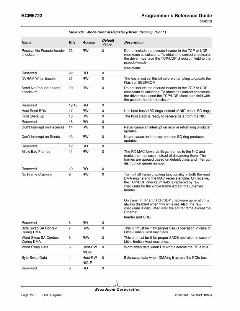
BCM5723 Programmer’s Reference Guide04/02/08
Broadcom Corporation
Page 276 GRC Register Document 5723-PG100-R
Receive No Pseudo-header checksum
23 RW 0 Do not include the pseudo-header in the TCP or UDP checksum calculations. To obtain the correct checksum, the driver must add the TCP/UDP checksum field to the pseudo-headerchecksum.
Reserved 22 RO 0
NVRAM Write Enable 21 RW 0 The host must set this bit before attempting to update the Flash or SEEPROM.
Send No Pseudo-header checksum
20 RW 0 Do not include the pseudo-header in the TCP or UDP checksum calculations. To obtain the correct checksum, the driver must seed the TCP/UDP checksum field with the pseudo-header checksum.
Reserved 19:18 RO 0
Host Send BDs 17 RW 0 Use host-based BD rings instead of NIC-based BD rings.
Host Stack Up 16 RW 0 The host stack is ready to receive data from the NIC.
Reserved 15 RO 0
Don’t Interrupt on Receives 14 RW 0 Never cause an interrupt on receive return ring producer updates.
Don’t Interrupt on Sends 13 RW 0 Never cause an interrupt on send BD ring producer updates.
Reserved 12 RO 0
Allow Bad Frames 11 RW 0 The RX MAC forwards illegal frames to the NIC and marks them as such instead of discarding them. The frames are queued based on default class and interrupt distribution queue number
Reserved 10 RO 0
No Frame Cracking 9 RW 0 Turn off all frame cracking functionality in both the read DMA engine and the MAC receive engine. On receive, the TCP/UDP checksum field is replaced by raw checksum for the whole frame except the Ethernet header.
On transmit, IP and TCP/UDP checksum generation is always disabled when this bit is set. Also, the raw checksum is calculated over the entire frame except the Ethernetheader and CRC.
Reserved 8 RO 0
Byte Swap SA Context During DMA
7 R/W 0 This bit must be 1 for proper SADB operation in case of Little-Endian Host machines.
Word Swap SA Context During DMA
6 R/W 0 This bit must be 0 for proper SADB operation in case of Little-Endian Host machines.
Word Swap Data 5 Host-RWNIC-R
0 Word swap data when DMAing it across the PCIe bus.
Byte Swap Data 4 Host-RWNIC-R
0 Byte swap data when DMAing it across the PCIe bus.
Reserved 3 RO 0
Table 312: Mode Control Register (Offset: 0x6800) (Cont.)
Name Bits Access Default Value Description
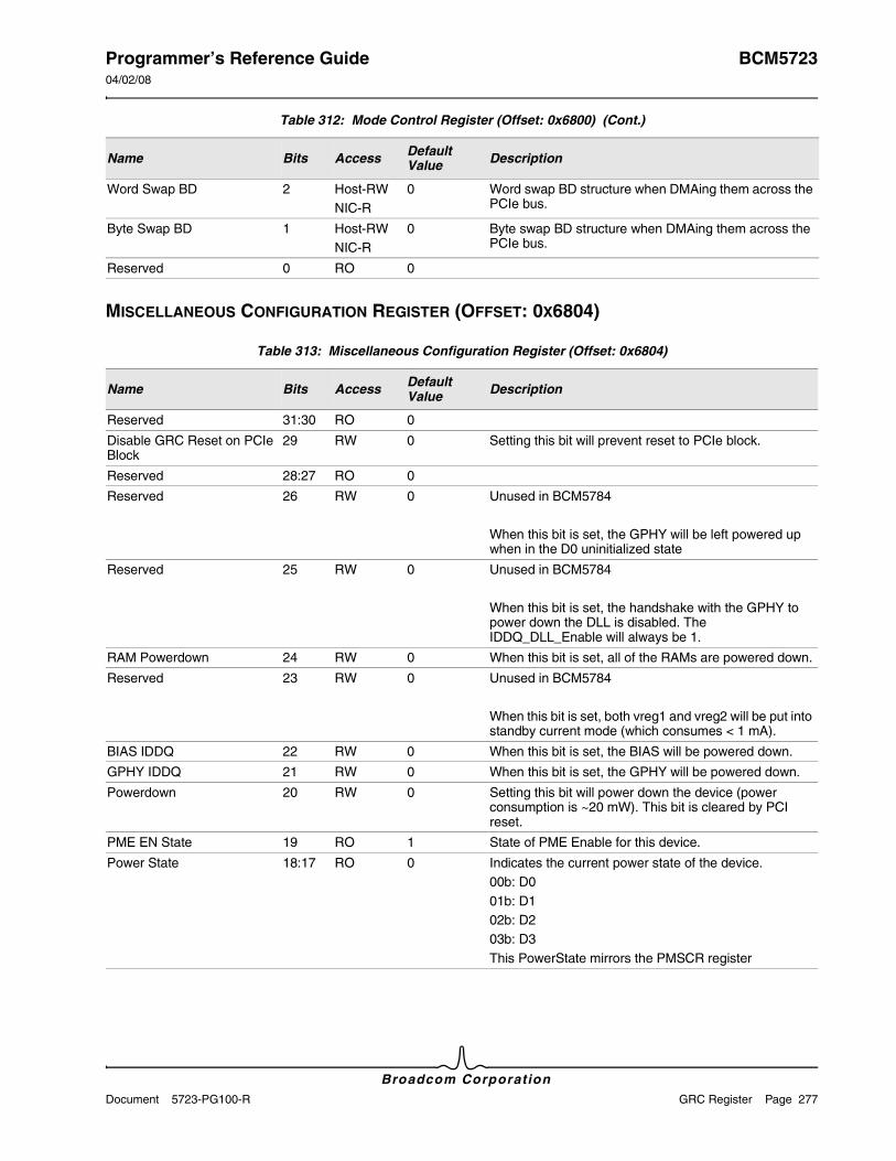
Programmer’s Reference Guide BCM572304/02/08
Broadcom CorporationDocument 5723-PG100-R GRC Register Page 277
MISCELLANEOUS CONFIGURATION REGISTER (OFFSET: 0X6804)
Word Swap BD 2 Host-RWNIC-R
0 Word swap BD structure when DMAing them across the PCIe bus.
Byte Swap BD 1 Host-RWNIC-R
0 Byte swap BD structure when DMAing them across the PCIe bus.
Reserved 0 RO 0
Table 313: Miscellaneous Configuration Register (Offset: 0x6804)
Name Bits Access Default Value Description
Reserved 31:30 RO 0
Disable GRC Reset on PCIe Block
29 RW 0 Setting this bit will prevent reset to PCIe block.
Reserved 28:27 RO 0
Reserved 26 RW 0 Unused in BCM5784
When this bit is set, the GPHY will be left powered up when in the D0 uninitialized state
Reserved 25 RW 0 Unused in BCM5784
When this bit is set, the handshake with the GPHY to power down the DLL is disabled. The IDDQ_DLL_Enable will always be 1.
RAM Powerdown 24 RW 0 When this bit is set, all of the RAMs are powered down.
Reserved 23 RW 0 Unused in BCM5784
When this bit is set, both vreg1 and vreg2 will be put into standby current mode (which consumes < 1 mA).
BIAS IDDQ 22 RW 0 When this bit is set, the BIAS will be powered down.
GPHY IDDQ 21 RW 0 When this bit is set, the GPHY will be powered down.
Powerdown 20 RW 0 Setting this bit will power down the device (power consumption is ~20 mW). This bit is cleared by PCI reset.
PME EN State 19 RO 1 State of PME Enable for this device.
Power State 18:17 RO 0 Indicates the current power state of the device.00b: D001b: D102b: D203b: D3This PowerState mirrors the PMSCR register
Table 312: Mode Control Register (Offset: 0x6800) (Cont.)
Name Bits Access Default Value Description
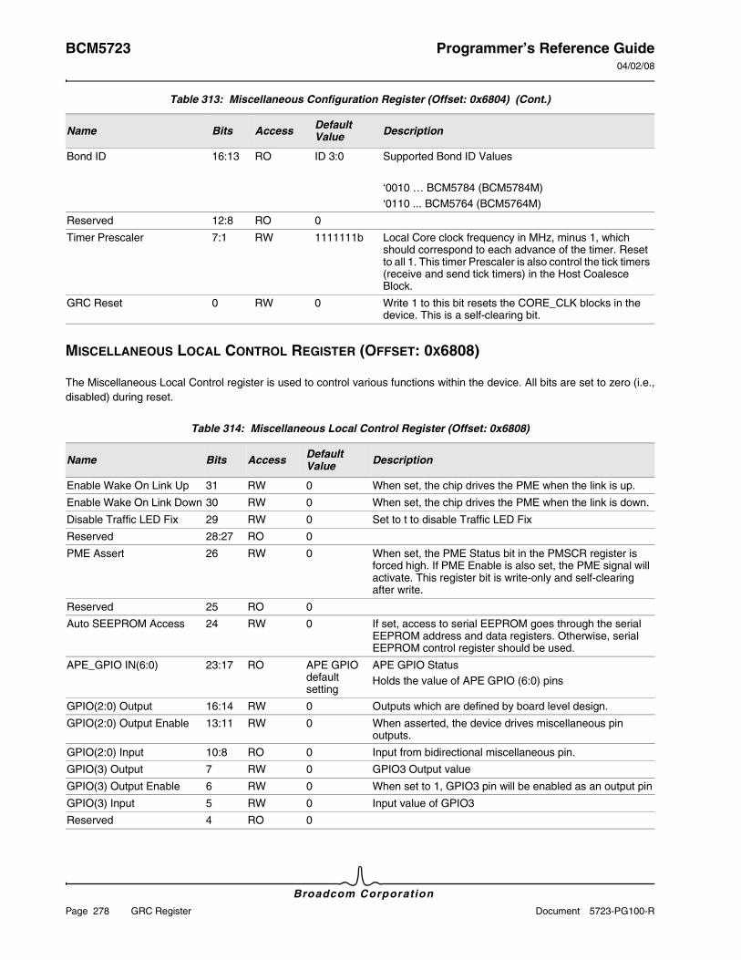
BCM5723 Programmer’s Reference Guide04/02/08
Broadcom Corporation
Page 278 GRC Register Document 5723-PG100-R
MISCELLANEOUS LOCAL CONTROL REGISTER (OFFSET: 0X6808)
The Miscellaneous Local Control register is used to control various functions within the device. All bits are set to zero (i.e., disabled) during reset.
Bond ID 16:13 RO ID 3:0 Supported Bond ID Values
‘0010 … BCM5784 (BCM5784M)‘0110 ... BCM5764 (BCM5764M)
Reserved 12:8 RO 0
Timer Prescaler 7:1 RW 1111111b Local Core clock frequency in MHz, minus 1, which should correspond to each advance of the timer. Reset to all 1. This timer Prescaler is also control the tick timers (receive and send tick timers) in the Host Coalesce Block.
GRC Reset 0 RW 0 Write 1 to this bit resets the CORE_CLK blocks in the device. This is a self-clearing bit.
Table 314: Miscellaneous Local Control Register (Offset: 0x6808)
Name Bits Access Default Value Description
Enable Wake On Link Up 31 RW 0 When set, the chip drives the PME when the link is up.
Enable Wake On Link Down 30 RW 0 When set, the chip drives the PME when the link is down.
Disable Traffic LED Fix 29 RW 0 Set to t to disable Traffic LED Fix
Reserved 28:27 RO 0
PME Assert 26 RW 0 When set, the PME Status bit in the PMSCR register is forced high. If PME Enable is also set, the PME signal will activate. This register bit is write-only and self-clearing after write.
Reserved 25 RO 0
Auto SEEPROM Access 24 RW 0 If set, access to serial EEPROM goes through the serial EEPROM address and data registers. Otherwise, serial EEPROM control register should be used.
APE_GPIO IN(6:0) 23:17 RO APE GPIO default setting
APE GPIO StatusHolds the value of APE GPIO (6:0) pins
GPIO(2:0) Output 16:14 RW 0 Outputs which are defined by board level design.
GPIO(2:0) Output Enable 13:11 RW 0 When asserted, the device drives miscellaneous pin outputs.
GPIO(2:0) Input 10:8 RO 0 Input from bidirectional miscellaneous pin.
GPIO(3) Output 7 RW 0 GPIO3 Output value
GPIO(3) Output Enable 6 RW 0 When set to 1, GPIO3 pin will be enabled as an output pin
GPIO(3) Input 5 RW 0 Input value of GPIO3
Reserved 4 RO 0
Table 313: Miscellaneous Configuration Register (Offset: 0x6804) (Cont.)
Name Bits Access Default Value Description
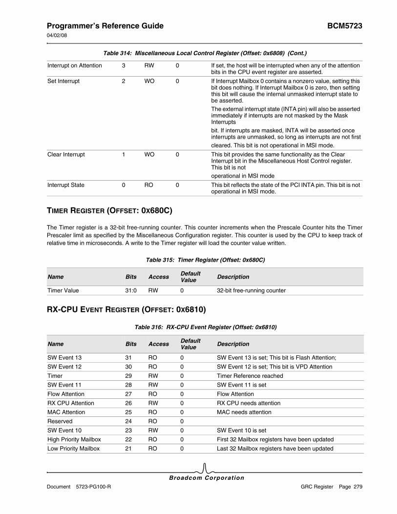
Programmer’s Reference Guide BCM572304/02/08
Broadcom CorporationDocument 5723-PG100-R GRC Register Page 279
TIMER REGISTER (OFFSET: 0X680C)
The Timer register is a 32-bit free-running counter. This counter increments when the Prescale Counter hits the Timer Prescaler limit as specified by the Miscellaneous Configuration register. This counter is used by the CPU to keep track of relative time in microseconds. A write to the Timer register will load the counter value written.
RX-CPU EVENT REGISTER (OFFSET: 0X6810)
Interrupt on Attention 3 RW 0 If set, the host will be interrupted when any of the attention bits in the CPU event register are asserted.
Set Interrupt 2 WO 0 If Interrupt Mailbox 0 contains a nonzero value, setting this bit does nothing. If Interrupt Mailbox 0 is zero, then setting this bit will cause the internal unmasked interrupt state to be asserted.The external interrupt state (INTA pin) will also be asserted immediately if interrupts are not masked by the Mask Interruptsbit. If interrupts are masked, INTA will be asserted once interrupts are unmasked, so long as interrupts are not firstcleared. This bit is not operational in MSI mode.
Clear Interrupt 1 WO 0 This bit provides the same functionality as the Clear Interrupt bit in the Miscellaneous Host Control register. This bit is notoperational in MSI mode
Interrupt State 0 RO 0 This bit reflects the state of the PCI INTA pin. This bit is not operational in MSI mode.
Table 315: Timer Register (Offset: 0x680C)
Name Bits Access Default Value Description
Timer Value 31:0 RW 0 32-bit free-running counter
Table 316: RX-CPU Event Register (Offset: 0x6810)
Name Bits Access Default Value Description
SW Event 13 31 RO 0 SW Event 13 is set; This bit is Flash Attention;
SW Event 12 30 RO 0 SW Event 12 is set; This bit is VPD Attention
Timer 29 RW 0 Timer Reference reached
SW Event 11 28 RW 0 SW Event 11 is set
Flow Attention 27 RO 0 Flow Attention
RX CPU Attention 26 RW 0 RX CPU needs attention
MAC Attention 25 RO 0 MAC needs attention
Reserved 24 RO 0
SW Event 10 23 RW 0 SW Event 10 is set
High Priority Mailbox 22 RO 0 First 32 Mailbox registers have been updated
Low Priority Mailbox 21 RO 0 Last 32 Mailbox registers have been updated
Table 314: Miscellaneous Local Control Register (Offset: 0x6808) (Cont.)
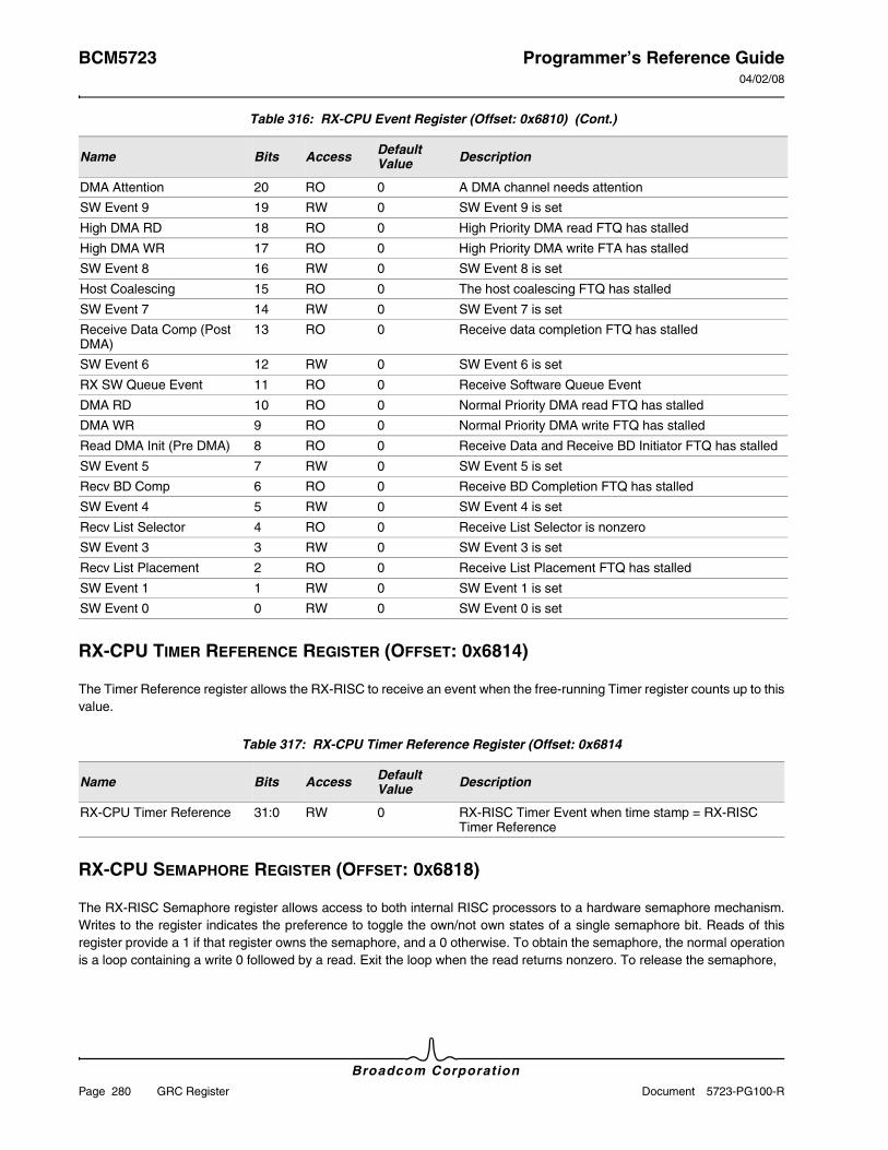
BCM5723 Programmer’s Reference Guide04/02/08
Broadcom Corporation
Page 280 GRC Register Document 5723-PG100-R
RX-CPU TIMER REFERENCE REGISTER (OFFSET: 0X6814)
The Timer Reference register allows the RX-RISC to receive an event when the free-running Timer register counts up to this value.
RX-CPU SEMAPHORE REGISTER (OFFSET: 0X6818)
The RX-RISC Semaphore register allows access to both internal RISC processors to a hardware semaphore mechanism. Writes to the register indicates the preference to toggle the own/not own states of a single semaphore bit. Reads of this register provide a 1 if that register owns the semaphore, and a 0 otherwise. To obtain the semaphore, the normal operation is a loop containing a write 0 followed by a read. Exit the loop when the read returns nonzero. To release the semaphore,
DMA Attention 20 RO 0 A DMA channel needs attention
SW Event 9 19 RW 0 SW Event 9 is set
High DMA RD 18 RO 0 High Priority DMA read FTQ has stalled
High DMA WR 17 RO 0 High Priority DMA write FTA has stalled
SW Event 8 16 RW 0 SW Event 8 is set
Host Coalescing 15 RO 0 The host coalescing FTQ has stalled
SW Event 7 14 RW 0 SW Event 7 is set
Receive Data Comp (Post DMA)
13 RO 0 Receive data completion FTQ has stalled
SW Event 6 12 RW 0 SW Event 6 is set
RX SW Queue Event 11 RO 0 Receive Software Queue Event
DMA RD 10 RO 0 Normal Priority DMA read FTQ has stalled
DMA WR 9 RO 0 Normal Priority DMA write FTQ has stalled
Read DMA Init (Pre DMA) 8 RO 0 Receive Data and Receive BD Initiator FTQ has stalled
SW Event 5 7 RW 0 SW Event 5 is set
Recv BD Comp 6 RO 0 Receive BD Completion FTQ has stalled
SW Event 4 5 RW 0 SW Event 4 is set
Recv List Selector 4 RO 0 Receive List Selector is nonzero
SW Event 3 3 RW 0 SW Event 3 is set
Recv List Placement 2 RO 0 Receive List Placement FTQ has stalled
SW Event 1 1 RW 0 SW Event 1 is set
SW Event 0 0 RW 0 SW Event 0 is set
Table 317: RX-CPU Timer Reference Register (Offset: 0x6814
Name Bits Access Default Value Description
RX-CPU Timer Reference 31:0 RW 0 RX-RISC Timer Event when time stamp = RX-RISC Timer Reference
Table 316: RX-CPU Event Register (Offset: 0x6810) (Cont.)
Name Bits Access Default Value Description
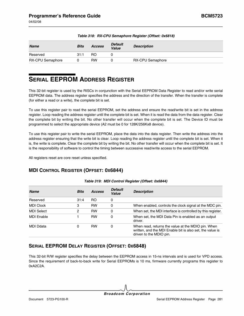
Programmer’s Reference Guide BCM572304/02/08
Broadcom CorporationDocument 5723-PG100-R Serial EEPROM Address Register Page 281
SERIAL EEPROM ADDRESS REGISTER
This 32-bit register is used by the RISCs in conjunction with the Serial EEPROM Data Register to read and/or write serial EEPROM data. The address register specifies the address and the direction of the transfer. When the transfer is complete (for either a read or a write), the complete bit is set.
To use this register pair to read the serial EEPROM, set the address and ensure the read/write bit is set in the address register. Loop reading the address register until the complete bit is set. When it is read the data from the data register. Clear the complete bit by writing the bit. No other transfer will occur when the complete bit is set. The Device ID must be programmed to select the appropriate device (A2 must be 0 for 128K/256Kx8 device).
To use this register pair to write the serial EEPROM, place the data into the data register. Then write the address into the address register ensuring that the write bit is clear. Loop reading the address register until the complete bit is set. When it is, the write is complete. Clear the complete bit by writing the bit. No other transfer will occur when the complete bit is set. It is the responsibility of software to control the timing between successive read/write access to the serial EEPROM.
All registers reset are core reset unless specified.
MDI CONTROL REGISTER (OFFSET: 0X6844)
SERIAL EEPROM DELAY REGISTER (OFFSET: 0X6848)
This 32-bit R/W register specifies the delay between the EEPROM access in 15-ns intervals and is used for VPD access. Since the requirement of back-to-back write for Serial EEPROMs is 10 ms, firmware currently programs this register to 0xA2C2A.
Table 318: RX-CPU Semaphore Register (Offset: 0x6818)
Name Bits Access Default Value Description
Reserved 31:1 RO 0
RX-CPU Semaphore 0 RW 0 RX-CPU Semaphore
Table 319: MDI Control Register (Offset: 0x6844)
Name Bits Access Default Value Description
Reserved 31:4 RO 0
MDI Clock 3 RW 0 When enabled, controls the clock signal at the MDC pin.
MDI Select 2 RW 0 When set, the MDI interface is controlled by this register.
MDI Enable 1 RW 0 When set, the MDI Data Pin is enabled as an output driver.
MDI Ddata 0 RW 0 When read, returns the value at the MDIO pin. When written, and the MDI Enable bit is also set, the value is driven to the MDIO pin.
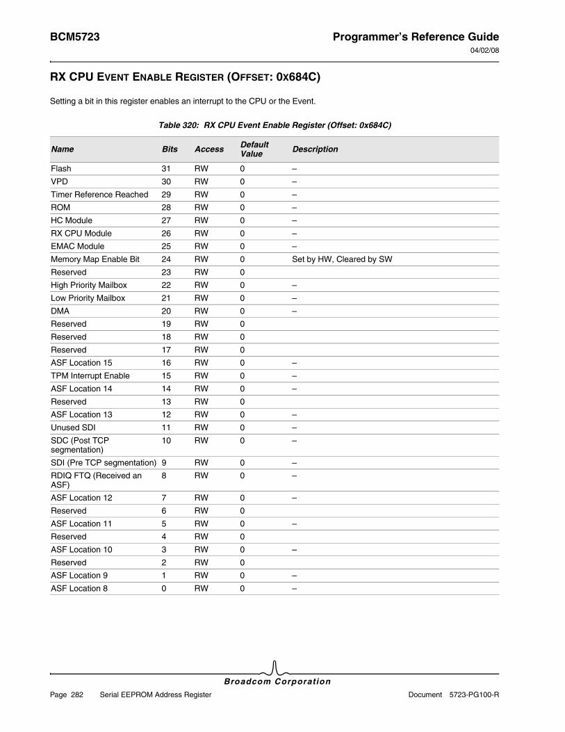
BCM5723 Programmer’s Reference Guide04/02/08
Broadcom Corporation
Page 282 Serial EEPROM Address Register Document 5723-PG100-R
RX CPU EVENT ENABLE REGISTER (OFFSET: 0X684C)
Setting a bit in this register enables an interrupt to the CPU or the Event.
Table 320: RX CPU Event Enable Register (Offset: 0x684C)
Name Bits Access Default Value Description
Flash 31 RW 0 –
VPD 30 RW 0 –
Timer Reference Reached 29 RW 0 –
ROM 28 RW 0 –
HC Module 27 RW 0 –
RX CPU Module 26 RW 0 –
EMAC Module 25 RW 0 –
Memory Map Enable Bit 24 RW 0 Set by HW, Cleared by SW
Reserved 23 RW 0
High Priority Mailbox 22 RW 0 –
Low Priority Mailbox 21 RW 0 –
DMA 20 RW 0 –
Reserved 19 RW 0
Reserved 18 RW 0
Reserved 17 RW 0
ASF Location 15 16 RW 0 –
TPM Interrupt Enable 15 RW 0 –
ASF Location 14 14 RW 0 –
Reserved 13 RW 0
ASF Location 13 12 RW 0 –
Unused SDI 11 RW 0 –
SDC (Post TCP segmentation)
10 RW 0 –
SDI (Pre TCP segmentation) 9 RW 0 –
RDIQ FTQ (Received an ASF)
8 RW 0 –
ASF Location 12 7 RW 0 –
Reserved 6 RW 0
ASF Location 11 5 RW 0 –
Reserved 4 RW 0
ASF Location 10 3 RW 0 –
Reserved 2 RW 0
ASF Location 9 1 RW 0 –
ASF Location 8 0 RW 0 –
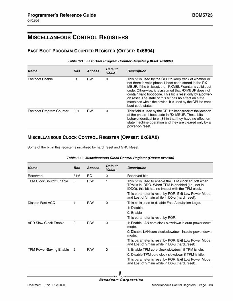
Programmer’s Reference Guide BCM572304/02/08
Broadcom CorporationDocument 5723-PG100-R Miscellaneous Control Registers Page 283
MISCELLANEOUS CONTROL REGISTERS
FAST BOOT PROGRAM COUNTER REGISTER (OFFSET: 0X6894)
MISCELLANEOUS CLOCK CONTROL REGISTER (OFFSET: 0X68A0)
Some of the bit in this register is initialized by hard_reset and GRC Reset.
Table 321: Fast Boot Program Counter Register (Offset: 0x6894)
Name Bits Access Default Value Description
Fastboot Enable 31 RW 0 This bit is used by the CPU to keep track of whether or not there is valid phase 1 boot code stored in the RX MBUF. If the bit is set, then RXMBUF contains valid boot code. Otherwise, it is assumed that RXMBUF does not contain valid boot code. This bit is reset only by a power-on reset. The state of this bit has no effect on state machines within the device. It is used by the CPU to track boot code status.
Fastboot Program Counter 30:0 RW 0 This field is used by the CPU to keep track of the location of the phase 1 boot code in RX MBUF. These bits behave identical to bit 31 in that they have no effect on state machine operation and they are cleared only by a power-on reset.
Table 322: Miscellaneous Clock Control Register (Offset: 0x68A0)
Name Bits Access Default Value Description
Reserved 31:6 RO 0 Reserved bits
TPM Clock Shutoff Enable 5 R/W 1 This bit is used to enable the TPM clock shutoff when TPM is in IDDQ. When TPM is enabled (i.e., not in IDDQ), this bit has no impact with the TPM clock.This parameter is reset by POR, Exit Low Power Mode, and Lost of Vmain while in D0-u (hard_reset).
Disable Fast ACQ 4 R/W 0 This bit is used to disable Fast Acquisition Logic.1: Disable0: EnableThis parameter is reset by POR.
APD Slow Clock Enable 3 R/W 0 1: Enable LAN core clock slowdown in auto-power down mode.0: Disable LAN core clock slowdown in auto-power down mode.This parameter is reset by POR, Exit Low Power Mode, and Lost of Vmain while in D0-u (hard_reset)
TPM Power-Saving Enable 2 R/W 0 1: Enable TPM core clock slowdown if TPM is idle.0: Disable TPM core clock slowdown if TPM is idle.This parameter is reset by POR, Exit Low Power Mode, and Lost of Vmain while in D0-u (hard_reset).
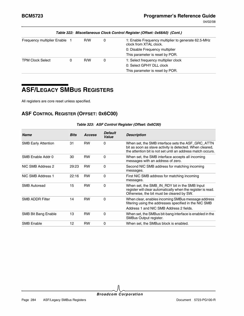
BCM5723 Programmer’s Reference Guide04/02/08
Broadcom Corporation
Page 284 ASF/Legacy SMBus Registers Document 5723-PG100-R
ASF/LEGACY SMBUS REGISTERS
All registers are core reset unless specified.
ASF CONTROL REGISTER (OFFSET: 0X6C00)
Frequency multiplier Enable 1 R/W 0 1: Enable Frequency multiplier to generate 62.5-MHz clock from XTAL clock.0: Disable Frequency multiplierThis parameter is reset by POR.
TPM Clock Select 0 R/W 0 1: Select frequency multiplier clock0: Select GPHY DLL clockThis parameter is reset by POR.
Table 323: ASF Control Register (Offset: 0x6C00)
Name Bits Access Default Value Description
SMB Early Attention 31 RW 0 When set, the SMB interface sets the ASF_GRC_ATTN bit as soon as slave activity is detected. When cleared, the attention bit is not set until an address match occurs.
SMB Enable Addr 0 30 RW 0 When set, the SMB interface accepts all incoming messages with an address of zero.
NIC SMB Address 2 29:23 RW 0 Second NIC SMB address for matching incoming messages.
NIC SMB Address 1 22:16 RW 0 First NIC SMB address for matching incoming messages.
SMB Autoread 15 RW 0 When set, the SMB_IN_RDY bit in the SMB Input register will clear automatically when the register is read. Otherwise, the bit must be cleared by SW.
SMB ADDR Filter 14 RW 0 When clear, enables incoming SMBus message address filtering using the addresses specified in the NIC SMBAddress 1 and NIC SMB Address 2 fields.
SMB Bit Bang Enable 13 RW 0 When set, the SMBus bit-bang interface is enabled in the SMBus Output register.
SMB Enable 12 RW 0 When set, the SMBus block is enabled.
Table 322: Miscellaneous Clock Control Register (Offset: 0x68A0) (Cont.)
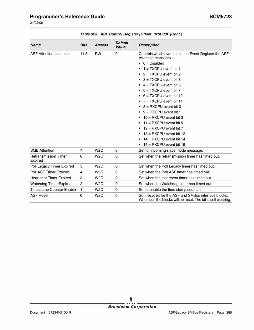
Programmer’s Reference Guide BCM572304/02/08
Broadcom CorporationDocument 5723-PG100-R ASF/Legacy SMBus Registers Page 285
ASF Attention Location 11:8 RW 0 Controls which event bit in the Event Register the ASF Attention maps into.• 0 = Disabled• 1 = TXCPU event bit 1• 2 = TXCPU event bit 2• 3 = TXCPU event bit 3• 4 = TXCPU event bit 5• 5 = TXCPU event bit 7• 6 = TXCPU event bit 12• 7 = TXCPU event bit 14• 8 = RXCPU event bit 0• 9 = RXCPU event bit 1• 10 = RXCPU event bit 3• 11 = RXCPU event bit 5• 12 = RXCPU event bit 7• 13 = RXCPU event bit 12• 14 = RXCPU event bit 14• 15 = RXCPU event bit 16
SMB Attention 7 W2C 0 Set for incoming slave mode message.
Retransmission Timer Expired
6 W2C 0 Set when the retransmission timer has timed out.
Poll Legacy Timer Expired 5 W2C 0 Set when the Poll Legacy timer has timed out.
Poll ASF Timer Expired 4 W2C 0 Set when the Poll ASF timer has timed out.
Heartbeat Timer Expired 3 W2C 0 Set when the Heartbeat timer has timed out.
Watchdog Timer Expired 2 W2C 0 Set when the Watchdog timer has timed out.
Timestamp Counter Enable 1 W2C 0 Set to enable the time stamp counter.
ASF Reset 0 W2C 0 Soft reset bit for the ASF and SMBus interface blocks. When set, the blocks will be reset. The bit is self clearing.
Table 323: ASF Control Register (Offset: 0x6C00) (Cont.)
Name Bits Access Default Value Description
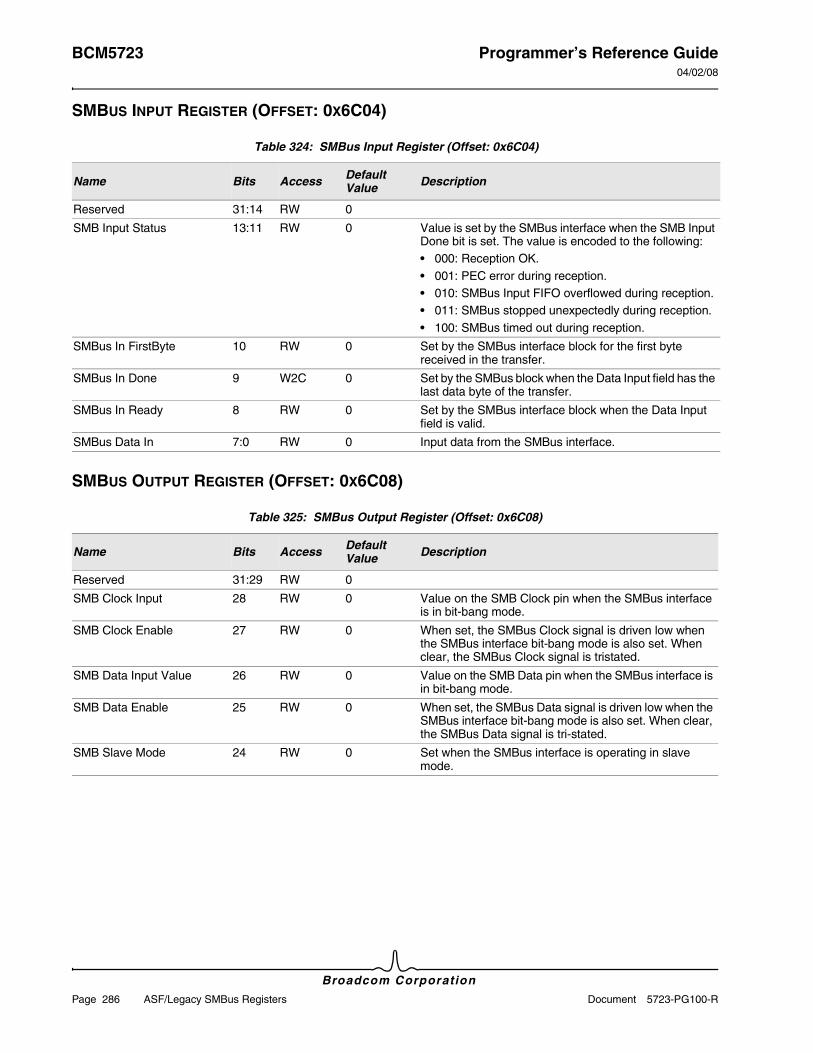
BCM5723 Programmer’s Reference Guide04/02/08
Broadcom Corporation
Page 286 ASF/Legacy SMBus Registers Document 5723-PG100-R
SMBUS INPUT REGISTER (OFFSET: 0X6C04)
SMBUS OUTPUT REGISTER (OFFSET: 0X6C08)
Table 324: SMBus Input Register (Offset: 0x6C04)
Name Bits Access Default Value Description
Reserved 31:14 RW 0
SMB Input Status 13:11 RW 0 Value is set by the SMBus interface when the SMB Input Done bit is set. The value is encoded to the following:• 000: Reception OK.• 001: PEC error during reception.• 010: SMBus Input FIFO overflowed during reception.• 011: SMBus stopped unexpectedly during reception.• 100: SMBus timed out during reception.
SMBus In FirstByte 10 RW 0 Set by the SMBus interface block for the first byte received in the transfer.
SMBus In Done 9 W2C 0 Set by the SMBus block when the Data Input field has the last data byte of the transfer.
SMBus In Ready 8 RW 0 Set by the SMBus interface block when the Data Input field is valid.
SMBus Data In 7:0 RW 0 Input data from the SMBus interface.
Table 325: SMBus Output Register (Offset: 0x6C08)
Name Bits Access Default Value Description
Reserved 31:29 RW 0
SMB Clock Input 28 RW 0 Value on the SMB Clock pin when the SMBus interface is in bit-bang mode.
SMB Clock Enable 27 RW 0 When set, the SMBus Clock signal is driven low when the SMBus interface bit-bang mode is also set. When clear, the SMBus Clock signal is tristated.
SMB Data Input Value 26 RW 0 Value on the SMB Data pin when the SMBus interface is in bit-bang mode.
SMB Data Enable 25 RW 0 When set, the SMBus Data signal is driven low when the SMBus interface bit-bang mode is also set. When clear, the SMBus Data signal is tri-stated.
SMB Slave Mode 24 RW 0 Set when the SMBus interface is operating in slave mode.
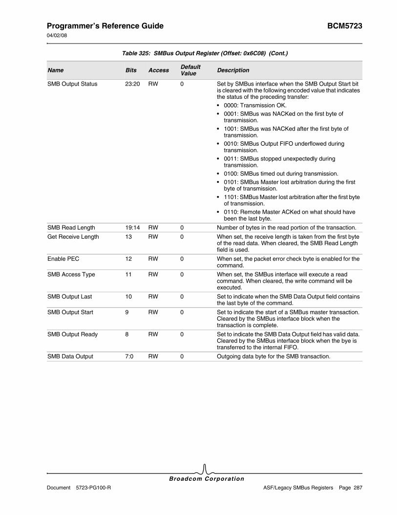
Programmer’s Reference Guide BCM572304/02/08
Broadcom CorporationDocument 5723-PG100-R ASF/Legacy SMBus Registers Page 287
SMB Output Status 23:20 RW 0 Set by SMBus interface when the SMB Output Start bit is cleared with the following encoded value that indicates the status of the preceding transfer:• 0000: Transmission OK.• 0001: SMBus was NACKed on the first byte of
transmission.• 1001: SMBus was NACKed after the first byte of
transmission.• 0010: SMBus Output FIFO underflowed during
transmission.• 0011: SMBus stopped unexpectedly during
transmission.• 0100: SMBus timed out during transmission.• 0101: SMBus Master lost arbitration during the first
byte of transmission.• 1101: SMBus Master lost arbitration after the first byte
of transmission.• 0110: Remote Master ACKed on what should have
been the last byte.
SMB Read Length 19:14 RW 0 Number of bytes in the read portion of the transaction.
Get Receive Length 13 RW 0 When set, the receive length is taken from the first byte of the read data. When cleared, the SMB Read Length field is used.
Enable PEC 12 RW 0 When set, the packet error check byte is enabled for the command.
SMB Access Type 11 RW 0 When set, the SMBus interface will execute a read command. When cleared, the write command will be executed.
SMB Output Last 10 RW 0 Set to indicate when the SMB Data Output field contains the last byte of the command.
SMB Output Start 9 RW 0 Set to indicate the start of a SMBus master transaction. Cleared by the SMBus interface block when the transaction is complete.
SMB Output Ready 8 RW 0 Set to indicate the SMB Data Output field has valid data. Cleared by the SMBus interface block when the bye is transferred to the internal FIFO.
SMB Data Output 7:0 RW 0 Outgoing data byte for the SMB transaction.
Table 325: SMBus Output Register (Offset: 0x6C08) (Cont.)
Name Bits Access Default Value Description
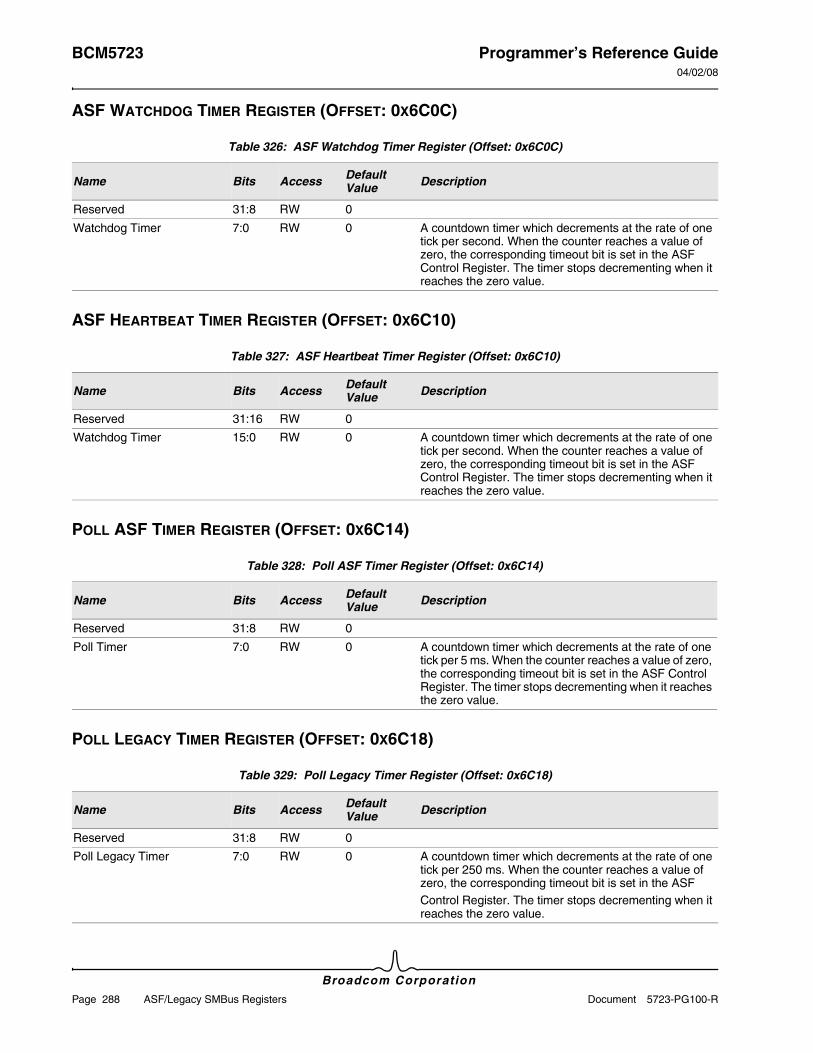
BCM5723 Programmer’s Reference Guide04/02/08
Broadcom Corporation
Page 288 ASF/Legacy SMBus Registers Document 5723-PG100-R
ASF WATCHDOG TIMER REGISTER (OFFSET: 0X6C0C)
ASF HEARTBEAT TIMER REGISTER (OFFSET: 0X6C10)
POLL ASF TIMER REGISTER (OFFSET: 0X6C14)
POLL LEGACY TIMER REGISTER (OFFSET: 0X6C18)
Table 326: ASF Watchdog Timer Register (Offset: 0x6C0C)
Name Bits Access Default Value Description
Reserved 31:8 RW 0
Watchdog Timer 7:0 RW 0 A countdown timer which decrements at the rate of one tick per second. When the counter reaches a value of zero, the corresponding timeout bit is set in the ASF Control Register. The timer stops decrementing when it reaches the zero value.
Table 327: ASF Heartbeat Timer Register (Offset: 0x6C10)
Name Bits Access Default Value Description
Reserved 31:16 RW 0
Watchdog Timer 15:0 RW 0 A countdown timer which decrements at the rate of one tick per second. When the counter reaches a value of zero, the corresponding timeout bit is set in the ASF Control Register. The timer stops decrementing when it reaches the zero value.
Table 328: Poll ASF Timer Register (Offset: 0x6C14)
Name Bits Access Default Value Description
Reserved 31:8 RW 0
Poll Timer 7:0 RW 0 A countdown timer which decrements at the rate of one tick per 5 ms. When the counter reaches a value of zero, the corresponding timeout bit is set in the ASF Control Register. The timer stops decrementing when it reaches the zero value.
Table 329: Poll Legacy Timer Register (Offset: 0x6C18)
Name Bits Access Default Value Description
Reserved 31:8 RW 0
Poll Legacy Timer 7:0 RW 0 A countdown timer which decrements at the rate of one tick per 250 ms. When the counter reaches a value of zero, the corresponding timeout bit is set in the ASFControl Register. The timer stops decrementing when it reaches the zero value.
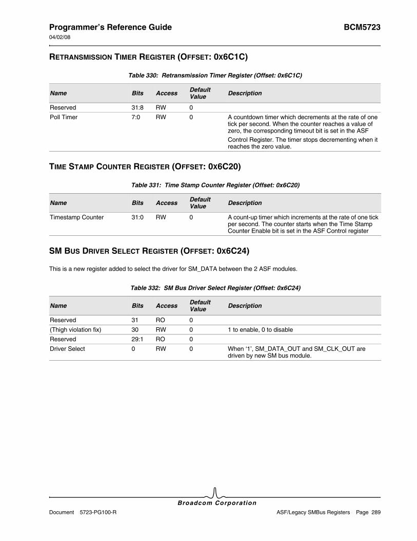
Programmer’s Reference Guide BCM572304/02/08
Broadcom CorporationDocument 5723-PG100-R ASF/Legacy SMBus Registers Page 289
RETRANSMISSION TIMER REGISTER (OFFSET: 0X6C1C)
TIME STAMP COUNTER REGISTER (OFFSET: 0X6C20)
SM BUS DRIVER SELECT REGISTER (OFFSET: 0X6C24)
This is a new register added to select the driver for SM_DATA between the 2 ASF modules.
Table 330: Retransmission Timer Register (Offset: 0x6C1C)
Name Bits Access Default Value Description
Reserved 31:8 RW 0
Poll Timer 7:0 RW 0 A countdown timer which decrements at the rate of one tick per second. When the counter reaches a value of zero, the corresponding timeout bit is set in the ASFControl Register. The timer stops decrementing when it reaches the zero value.
Table 331: Time Stamp Counter Register (Offset: 0x6C20)
Name Bits Access Default Value Description
Timestamp Counter 31:0 RW 0 A count-up timer which increments at the rate of one tick per second. The counter starts when the Time Stamp Counter Enable bit is set in the ASF Control register
Table 332: SM Bus Driver Select Register (Offset: 0x6C24)
Name Bits Access Default Value Description
Reserved 31 RO 0
(Thigh violation fix) 30 RW 0 1 to enable, 0 to disable
Reserved 29:1 RO 0
Driver Select 0 RW 0 When ‘1’, SM_DATA_OUT and SM_CLK_OUT are driven by new SM bus module.
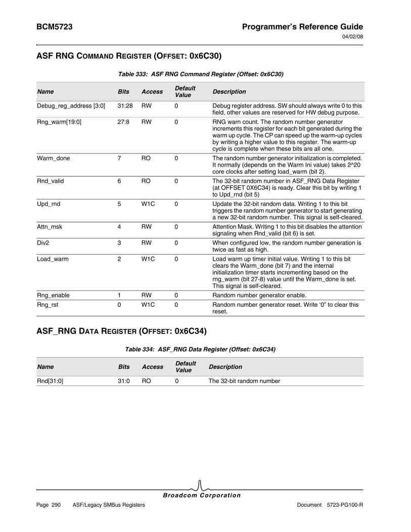
BCM5723 Programmer’s Reference Guide04/02/08
Broadcom Corporation
Page 290 ASF/Legacy SMBus Registers Document 5723-PG100-R
ASF RNG COMMAND REGISTER (OFFSET: 0X6C30)
ASF_RNG DATA REGISTER (OFFSET: 0X6C34)
Table 333: ASF RNG Command Register (Offset: 0x6C30)
Name Bits Access Default Value Description
Debug_reg_address [3:0] 31:28 RW 0 Debug register address. SW should always write 0 to this field, other values are reserved for HW debug purpose.
Rng_warm[19:0] 27:8 RW 0 RNG warn count. The random number generator increments this register for each bit generated during the warm up cycle. The CP can speed up the warm-up cycles by writing a higher value to this register. The warm-up cycle is complete when these bits are all one.
Warm_done 7 RO 0 The random number generator initialization is completed. It normally (depends on the Warm Ini value) takes 2^20 core clocks after setting load_warm (bit 2).
Rnd_valid 6 RO 0 The 32-bit random number in ASF_RNG Data Register (at OFFSET 0X6C34) is ready. Clear this bit by writing 1 to Upd_rnd (bit 5)
Upd_rnd 5 W1C 0 Update the 32-bit random data. Writing 1 to this bit triggers the random number generator to start generating a new 32-bit random number. This signal is self-cleared.
Attn_msk 4 RW 0 Attention Mask. Writing 1 to this bit disables the attention signaling when Rnd_valid (bit 6) is set.
Div2 3 RW 0 When configured low, the random number generation is twice as fast as high.
Load_warm 2 W1C 0 Load warm up timer initial value. Writing 1 to this bit clears the Warm_done (bit 7) and the internal initialization timer starts incrementing based on the rng_warm (bit 27-8) value until the Warm_done is set. This signal is self-cleared.
Rng_enable 1 RW 0 Random number generator enable.
Rng_rst 0 W1C 0 Random number generator reset. Write ‘0” to clear this reset.
Table 334: ASF_RNG Data Register (Offset: 0x6C34)
Name Bits Access Default Value Description
Rnd[31:0] 31:0 RO 0 The 32-bit random number
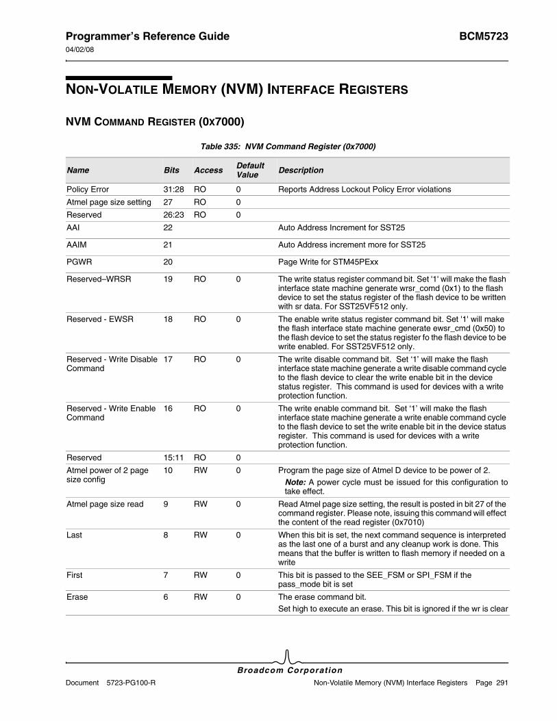
Programmer’s Reference Guide BCM572304/02/08
Broadcom CorporationDocument 5723-PG100-R Non-Volatile Memory (NVM) Interface Registers Page 291
NON-VOLATILE MEMORY (NVM) INTERFACE REGISTERS
NVM COMMAND REGISTER (0X7000)
Table 335: NVM Command Register (0x7000)
Name Bits Access Default Value Description
Policy Error 31:28 RO 0 Reports Address Lockout Policy Error violations
Atmel page size setting 27 RO 0
Reserved 26:23 RO 0
AAI 22 Auto Address Increment for SST25
AAIM 21 Auto Address increment more for SST25
PGWR 20 Page Write for STM45PExx
Reserved–WRSR 19 RO 0 The write status register command bit. Set '1' will make the flash interface state machine generate wrsr_comd (0x1) to the flash device to set the status register of the flash device to be written with sr data. For SST25VF512 only.
Reserved - EWSR 18 RO 0 The enable write status register command bit. Set '1' will make the flash interface state machine generate ewsr_cmd (0x50) to the flash device to set the status register fo the flash device to be write enabled. For SST25VF512 only.
Reserved - Write Disable Command
17 RO 0 The write disable command bit. Set ‘1’ will make the flash interface state machine generate a write disable command cycle to the flash device to clear the write enable bit in the device status register. This command is used for devices with a write protection function.
Reserved - Write Enable Command
16 RO 0 The write enable command bit. Set ‘1’ will make the flash interface state machine generate a write enable command cycle to the flash device to set the write enable bit in the device status register. This command is used for devices with a write protection function.
Reserved 15:11 RO 0
Atmel power of 2 page size config
10 RW 0 Program the page size of Atmel D device to be power of 2. Note: A power cycle must be issued for this configuration to take effect.
Atmel page size read 9 RW 0 Read Atmel page size setting, the result is posted in bit 27 of the command register. Please note, issuing this command will effect the content of the read register (0x7010)
Last 8 RW 0 When this bit is set, the next command sequence is interpreted as the last one of a burst and any cleanup work is done. This means that the buffer is written to flash memory if needed on a write
First 7 RW 0 This bit is passed to the SEE_FSM or SPI_FSM if the pass_mode bit is set
Erase 6 RW 0 The erase command bit.Set high to execute an erase. This bit is ignored if the wr is clear
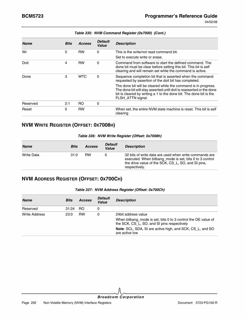
BCM5723 Programmer’s Reference Guide04/02/08
Broadcom Corporation
Page 292 Non-Volatile Memory (NVM) Interface Registers Document 5723-PG100-R
NVM WRITE REGISTER (OFFSET: 0X7008H)
NVM ADDRESS REGISTER (OFFSET: 0X700CH)
Wr 5 RW 0 This is the write/not read command bit.Set to execute write or erase.
Doit 4 RW 0 Command from software to start the defined command. The done bit must be clear before setting this bit. This bit is self clearing and will remain set while the command is active.
Done 3 WTC 0 Sequence completion bit that is asserted when the command requested by assertion of the doit bit has completed.The done bit will be cleared while the command is in progress. The done bit will stay asserted until doit is reasserted or the done bit is cleared by writing a 1 to the done bit. The done bit is the FLSH_ATTN signal.
Reserved 2:1 RO 0
Reset 0 RW When set, the entire NVM state machine is reset. This bit is self clearing
Table 336: NVM Write Register (Offset: 0x7008h)
Name Bits Access Default Value Description
Write Data 31:0 RW 0 32 bits of write data are used when write commands are executed. When bitbang_mode is set, bits 0 to 3 control the drive value of the SCK, CS_L, SO, and SI pins, respectively.
Table 337: NVM Address Register (Offset: 0x700Ch)
Name Bits Access Default Value Description
Reserved 31:24 RO 0
Write Address 23:0 RW 0 24bit address valueWhen bitbang_mode is set, bits 0 to 3 control the OE value of the SCK, CS_L, SO, and SI pins respectivelyNote: SCL, SDA, SI are active high, and SCK, CS_L, and SO are active low
Table 335: NVM Command Register (0x7000) (Cont.)
Name Bits Access Default Value Description
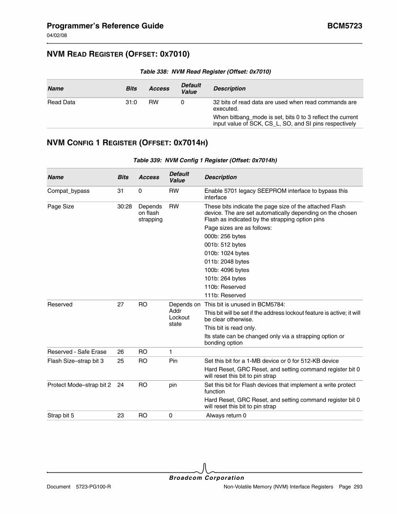
Programmer’s Reference Guide BCM572304/02/08
Broadcom CorporationDocument 5723-PG100-R Non-Volatile Memory (NVM) Interface Registers Page 293
NVM READ REGISTER (OFFSET: 0X7010)
NVM CONFIG 1 REGISTER (OFFSET: 0X7014H)
Table 338: NVM Read Register (Offset: 0x7010)
Name Bits Access Default Value Description
Read Data 31:0 RW 0 32 bits of read data are used when read commands are executed. When bitbang_mode is set, bits 0 to 3 reflect the current input value of SCK, CS_L, SO, and SI pins respectively
Table 339: NVM Config 1 Register (Offset: 0x7014h)
Name Bits Access Default Value Description
Compat_bypass 31 0 RW Enable 5701 legacy SEEPROM interface to bypass this interface
Page Size 30:28 Depends on flash strapping
RW These bits indicate the page size of the attached Flash device. The are set automatically depending on the chosen Flash as indicated by the strapping option pinsPage sizes are as follows:000b: 256 bytes001b: 512 bytes010b: 1024 bytes011b: 2048 bytes100b: 4096 bytes101b: 264 bytes110b: Reserved111b: Reserved
Reserved 27 RO Depends on Addr Lockout state
This bit is unused in BCM5784:This bit will be set if the address lockout feature is active; it will be clear otherwise.This bit is read only.Its state can be changed only via a strapping option or bonding option
Reserved - Safe Erase 26 RO 1
Flash Size–strap bit 3 25 RO Pin Set this bit for a 1-MB device or 0 for 512-KB deviceHard Reset, GRC Reset, and setting command register bit 0 will reset this bit to pin strap
Protect Mode–strap bit 2 24 RO pin Set this bit for Flash devices that implement a write protect functionHard Reset, GRC Reset, and setting command register bit 0 will reset this bit to pin strap
Strap bit 5 23 RO 0 Always return 0
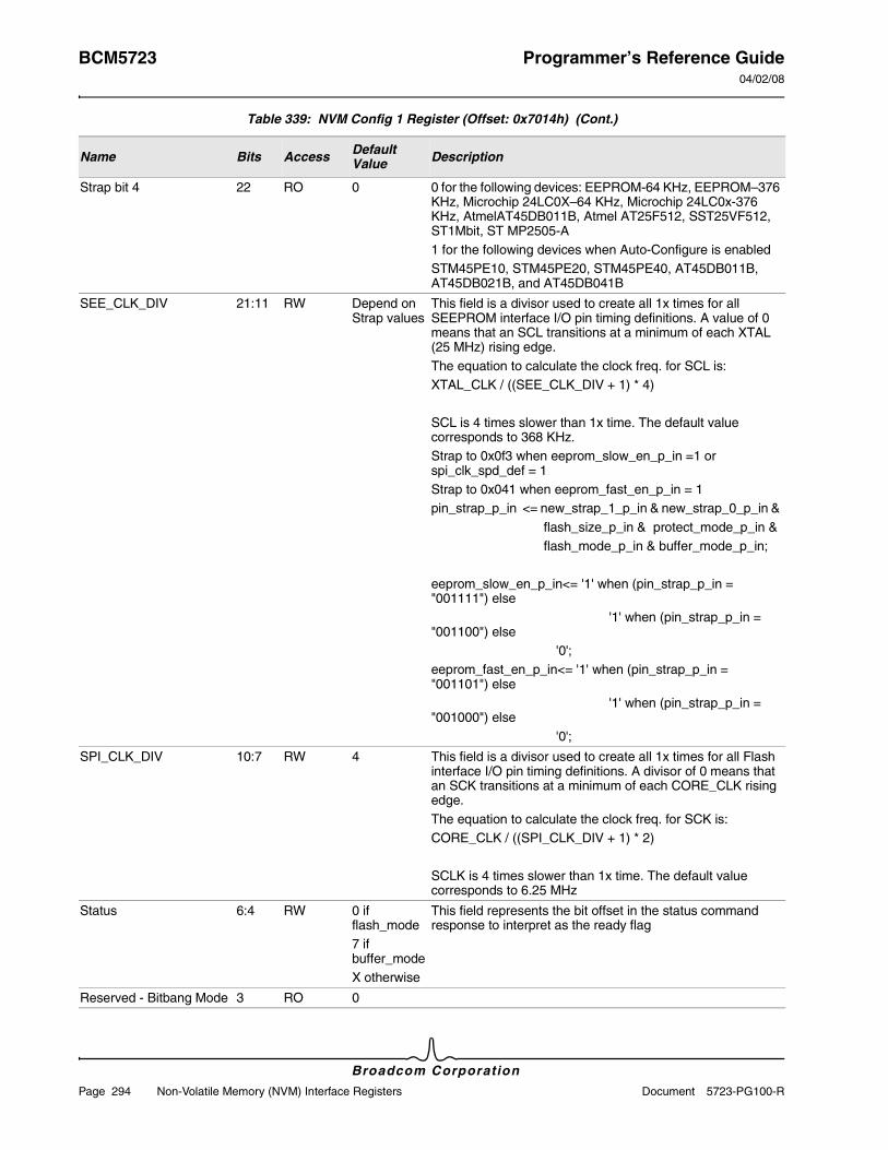
BCM5723 Programmer’s Reference Guide04/02/08
Broadcom Corporation
Page 294 Non-Volatile Memory (NVM) Interface Registers Document 5723-PG100-R
Strap bit 4 22 RO 0 0 for the following devices: EEPROM-64 KHz, EEPROM–376 KHz, Microchip 24LC0X–64 KHz, Microchip 24LC0x-376 KHz, AtmelAT45DB011B, Atmel AT25F512, SST25VF512, ST1Mbit, ST MP2505-A1 for the following devices when Auto-Configure is enabledSTM45PE10, STM45PE20, STM45PE40, AT45DB011B, AT45DB021B, and AT45DB041B
SEE_CLK_DIV 21:11 RW Depend on Strap values
This field is a divisor used to create all 1x times for all SEEPROM interface I/O pin timing definitions. A value of 0 means that an SCL transitions at a minimum of each XTAL (25 MHz) rising edge. The equation to calculate the clock freq. for SCL is: XTAL_CLK / ((SEE_CLK_DIV + 1) * 4)
SCL is 4 times slower than 1x time. The default value corresponds to 368 KHz.Strap to 0x0f3 when eeprom_slow_en_p_in =1 or spi_clk_spd_def = 1Strap to 0x041 when eeprom_fast_en_p_in = 1pin_strap_p_in <= new_strap_1_p_in & new_strap_0_p_in & flash_size_p_in & protect_mode_p_in & flash_mode_p_in & buffer_mode_p_in;
eeprom_slow_en_p_in<= '1' when (pin_strap_p_in = "001111") else '1' when (pin_strap_p_in = "001100") else
'0';eeprom_fast_en_p_in<= '1' when (pin_strap_p_in = "001101") else '1' when (pin_strap_p_in = "001000") else
'0';
SPI_CLK_DIV 10:7 RW 4 This field is a divisor used to create all 1x times for all Flash interface I/O pin timing definitions. A divisor of 0 means that an SCK transitions at a minimum of each CORE_CLK rising edge. The equation to calculate the clock freq. for SCK is: CORE_CLK / ((SPI_CLK_DIV + 1) * 2)
SCLK is 4 times slower than 1x time. The default value corresponds to 6.25 MHz
Status 6:4 RW 0 if flash_mode7 if buffer_modeX otherwise
This field represents the bit offset in the status command response to interpret as the ready flag
Reserved - Bitbang Mode 3 RO 0
Table 339: NVM Config 1 Register (Offset: 0x7014h) (Cont.)
Name Bits Access Default Value Description
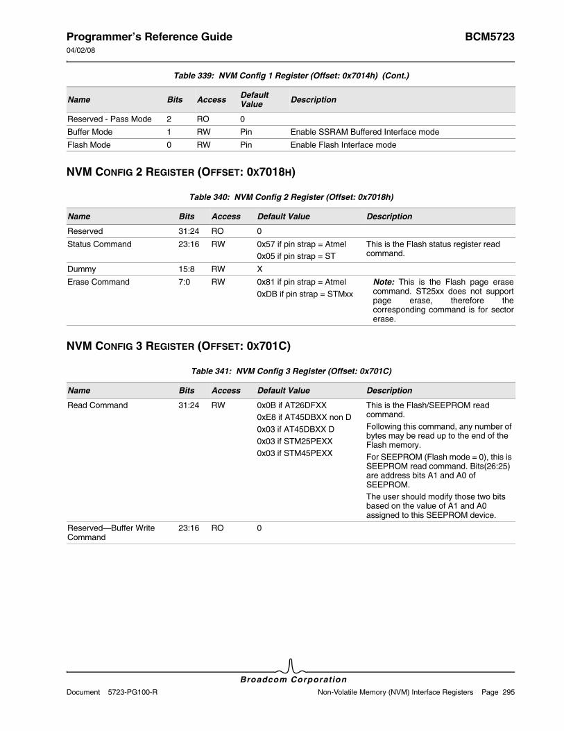
Programmer’s Reference Guide BCM572304/02/08
Broadcom CorporationDocument 5723-PG100-R Non-Volatile Memory (NVM) Interface Registers Page 295
NVM CONFIG 2 REGISTER (OFFSET: 0X7018H)
NVM CONFIG 3 REGISTER (OFFSET: 0X701C)
Reserved - Pass Mode 2 RO 0
Buffer Mode 1 RW Pin Enable SSRAM Buffered Interface mode
Flash Mode 0 RW Pin Enable Flash Interface mode
Table 340: NVM Config 2 Register (Offset: 0x7018h)
Name Bits Access Default Value Description
Reserved 31:24 RO 0
Status Command 23:16 RW 0x57 if pin strap = Atmel0x05 if pin strap = ST
This is the Flash status register read command.
Dummy 15:8 RW X
Erase Command 7:0 RW 0x81 if pin strap = Atmel0xDB if pin strap = STMxx
Note: This is the Flash page erase command. ST25xx does not support page erase, therefore the corresponding command is for sector erase.
Table 341: NVM Config 3 Register (Offset: 0x701C)
Name Bits Access Default Value Description
Read Command 31:24 RW 0x0B if AT26DFXX0xE8 if AT45DBXX non D0x03 if AT45DBXX D0x03 if STM25PEXX0x03 if STM45PEXX
This is the Flash/SEEPROM read command.Following this command, any number of bytes may be read up to the end of the Flash memory.For SEEPROM (Flash mode = 0), this is SEEPROM read command. Bits(26:25) are address bits A1 and A0 of SEEPROM.The user should modify those two bits based on the value of A1 and A0 assigned to this SEEPROM device.
Reserved—Buffer Write Command
23:16 RO 0
Table 339: NVM Config 1 Register (Offset: 0x7014h) (Cont.)
Name Bits Access Default Value Description

BCM5723 Programmer’s Reference Guide04/02/08
Broadcom Corporation
Page 296 Non-Volatile Memory (NVM) Interface Registers Document 5723-PG100-R
SOFTWARE ARBITRATION REGISTER (OFFSET: 0X7020H)
Write Command 15:8 RW 0x82 if AT26DFXX0x82 if AT45DBXX0x0A if STM25PEXX0x0A if STM45PEXX
Command to write a series of bytes into a selected page in the Flash device.
Note: This write command wraps around to the beginning of the page after the internal address counter in the Flash device reaches the end of the page.
For SEEPROM (flash_mode = 0), this is SEEPROM write command. Bits[10:9] are address bits A1 and A0 of SEEPROM.The user should modify those two bits based on the value of A1 and A0 assigned to this SEEPROM device.
Reserved - Buffer Read Command
7:0 RO 0
Table 342: Software Arbitration Register (Offset: 0x7020h)
Name Bits Access Default Value Description
Reserved 31:22 RO 0
Reserved 21 WO X Write 1 to clear REQ5 bit.
Reserved 20 WO X Write 1 to set REQ5 bit.
Reserved 19:18 RO 0
Reserved 17 WO X Write 1 to clear REQ4 bit.
Reserved 16 WO X Write 1 to set REQ4 bit.
REQ3 15 RO 0 Software request bit31 in this bit indicates that the request5 is active.
REQ2 14 RO 0 Software request bit21 in this bit indicates that the request5 is active
REQ1 13 RO 0 Software request bit11 in this bit indicates that the request5 is active
REQ0 12 RO 0 Software request bit 0When Req_set0 bit is set, this bit will be set
ARB_WON3 11 RO 0 Arbitration won bit 3 (see Bit 8, ARB_WON0)
ARB_WON2 10 RO 0 Arbitration won bit 2 (see Bit 8, ARB_WON0)
ARB_WON1 9 RO 0 Arbitration won bit 1 (see Bit 8, ARB_WON0)
ARB_WON0 8 RO 0 When req0 arbitration is won, this bit will be read as 1. When an operation is complete, then Req_clr0 must be written to clear the bit. At that point, the next high priority arb bit will be set (if requested). At any time, only one of the ARB_WON[5:0] bits will be read as 1. ARB 0 has the highest priority, and ARB5 has the lowest priority.
REQ_CLR3 7 WO X Write 1 to this bit to clear REQ3 bit.
Table 341: NVM Config 3 Register (Offset: 0x701C) (Cont.)
Name Bits Access Default Value Description
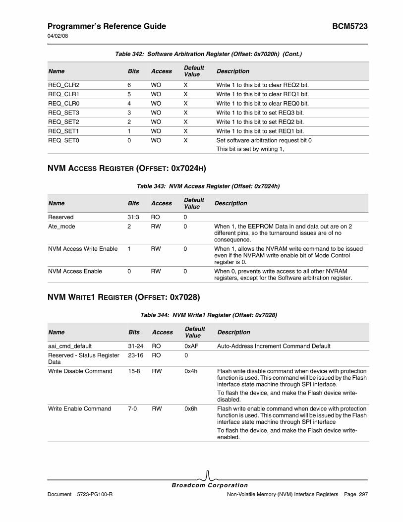
Programmer’s Reference Guide BCM572304/02/08
Broadcom CorporationDocument 5723-PG100-R Non-Volatile Memory (NVM) Interface Registers Page 297
NVM ACCESS REGISTER (OFFSET: 0X7024H)
NVM WRITE1 REGISTER (OFFSET: 0X7028)
REQ_CLR2 6 WO X Write 1 to this bit to clear REQ2 bit.
REQ_CLR1 5 WO X Write 1 to this bit to clear REQ1 bit.
REQ_CLR0 4 WO X Write 1 to this bit to clear REQ0 bit.
REQ_SET3 3 WO X Write 1 to this bit to set REQ3 bit.
REQ_SET2 2 WO X Write 1 to this bit to set REQ2 bit.
REQ_SET1 1 WO X Write 1 to this bit to set REQ1 bit.
REQ_SET0 0 WO X Set software arbitration request bit 0This bit is set by writing 1,
Table 343: NVM Access Register (Offset: 0x7024h)
Name Bits Access Default Value Description
Reserved 31:3 RO 0
Ate_mode 2 RW 0 When 1, the EEPROM Data in and data out are on 2 different pins, so the turnaround issues are of no consequence.
NVM Access Write Enable 1 RW 0 When 1, allows the NVRAM write command to be issued even if the NVRAM write enable bit of Mode Control register is 0.
NVM Access Enable 0 RW 0 When 0, prevents write access to all other NVRAM registers, except for the Software arbitration register.
Table 344: NVM Write1 Register (Offset: 0x7028)
Name Bits Access Default Value Description
aai_cmd_default 31-24 RO 0xAF Auto-Address Increment Command Default
Reserved - Status Register Data
23-16 RO 0
Write Disable Command 15-8 RW 0x4h Flash write disable command when device with protection function is used. This command will be issued by the Flash interface state machine through SPI interface.To flash the device, and make the Flash device write-disabled.
Write Enable Command 7-0 RW 0x6h Flash write enable command when device with protection function is used. This command will be issued by the Flash interface state machine through SPI interfaceTo flash the device, and make the Flash device write-enabled.
Table 342: Software Arbitration Register (Offset: 0x7020h) (Cont.)
Name Bits Access Default Value Description
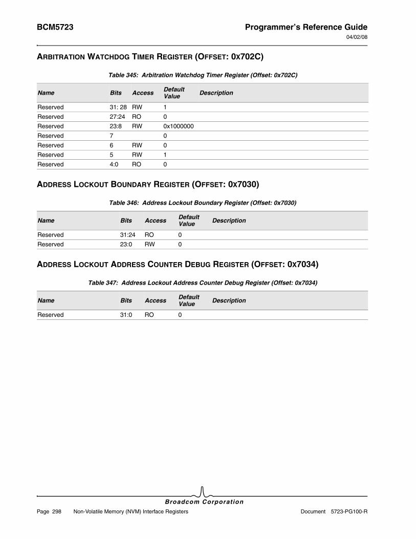
BCM5723 Programmer’s Reference Guide04/02/08
Broadcom Corporation
Page 298 Non-Volatile Memory (NVM) Interface Registers Document 5723-PG100-R
ARBITRATION WATCHDOG TIMER REGISTER (OFFSET: 0X702C)
ADDRESS LOCKOUT BOUNDARY REGISTER (OFFSET: 0X7030)
ADDRESS LOCKOUT ADDRESS COUNTER DEBUG REGISTER (OFFSET: 0X7034)
Table 345: Arbitration Watchdog Timer Register (Offset: 0x702C)
Name Bits Access Default Value Description
Reserved 31: 28 RW 1
Reserved 27:24 RO 0
Reserved 23:8 RW 0x1000000
Reserved 7 0
Reserved 6 RW 0
Reserved 5 RW 1
Reserved 4:0 RO 0
Table 346: Address Lockout Boundary Register (Offset: 0x7030)
Name Bits Access Default Value Description
Reserved 31:24 RO 0
Reserved 23:0 RW 0
Table 347: Address Lockout Address Counter Debug Register (Offset: 0x7034)
Name Bits Access Default Value Description
Reserved 31:0 RO 0
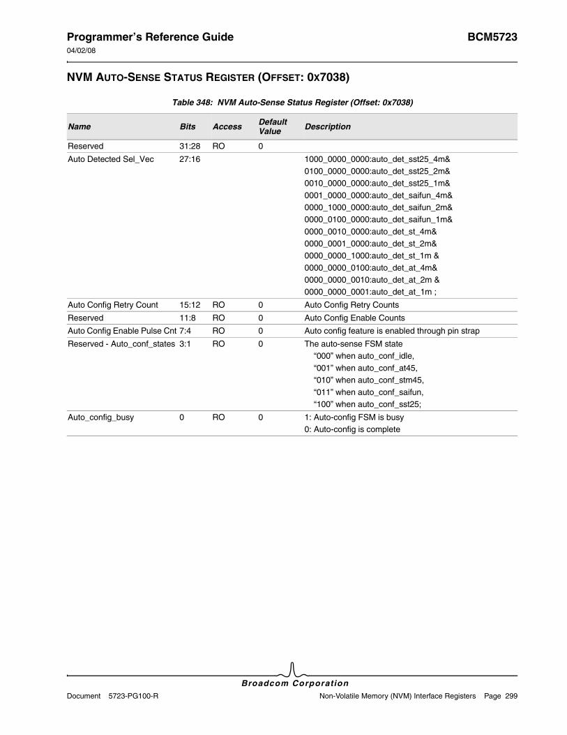
Programmer’s Reference Guide BCM572304/02/08
Broadcom CorporationDocument 5723-PG100-R Non-Volatile Memory (NVM) Interface Registers Page 299
NVM AUTO-SENSE STATUS REGISTER (OFFSET: 0X7038)
Table 348: NVM Auto-Sense Status Register (Offset: 0x7038)
Name Bits Access Default Value Description
Reserved 31:28 RO 0
Auto Detected Sel_Vec 27:16 1000_0000_0000:auto_det_sst25_4m&0100_0000_0000:auto_det_sst25_2m&0010_0000_0000:auto_det_sst25_1m&0001_0000_0000:auto_det_saifun_4m&0000_1000_0000:auto_det_saifun_2m&0000_0100_0000:auto_det_saifun_1m&0000_0010_0000:auto_det_st_4m&0000_0001_0000:auto_det_st_2m&0000_0000_1000:auto_det_st_1m &0000_0000_0100:auto_det_at_4m&0000_0000_0010:auto_det_at_2m &0000_0000_0001:auto_det_at_1m ;
Auto Config Retry Count 15:12 RO 0 Auto Config Retry Counts
Reserved 11:8 RO 0 Auto Config Enable Counts
Auto Config Enable Pulse Cnt 7:4 RO 0 Auto config feature is enabled through pin strap
Reserved - Auto_conf_states 3:1 RO 0 The auto-sense FSM state “000” when auto_conf_idle, “001” when auto_conf_at45, “010” when auto_conf_stm45, “011” when auto_conf_saifun, “100” when auto_conf_sst25;
Auto_config_busy 0 RO 0 1: Auto-config FSM is busy0: Auto-config is complete
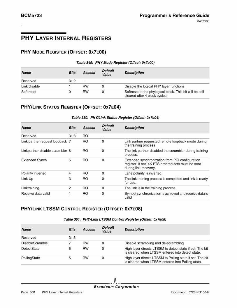
BCM5723 Programmer’s Reference Guide04/02/08
Broadcom Corporation
Page 300 PHY Layer Internal Registers Document 5723-PG100-R
PHY LAYER INTERNAL REGISTERS
PHY MODE REGISTER (OFFSET: 0X7E00)
PHY/LINK STATUS REGISTER (OFFSET: 0X7E04)
PHY/LINK LTSSM CONTROL REGISTER (OFFSET: 0X7E08)
Table 349: PHY Mode Register (Offset: 0x7e00)
Name Bits Access Default Value Description
Reserved 31:2 – –
Link disable 1 RW 0 Disable the logical PHY layer functions
Soft reset 0 RW 0 Softreset to the phylogical block. This bit will be self cleared after 4 clock cycles.
Table 350: PHY/Link Status Register (Offset: 0x7e04)
Name Bits Access Default Value Description
Reserved 31:8 RO –
Link partner request loopback 7 RO 0 Link partner requested remote loopback mode during the training process
Linkpartner disable scrambler 6 RO 0 The link partner disabled the scrambler during training process.
Extended Synch 5 RO 0 Extended synchronization from PCI configuration register. If set, 4K FTS ordered sets must be sent during link recovery.
Polarity inverted 4 RO 0 Lane polarity is inverted.
Link Up 3 RO 0 The link training process is completed and link is ready for use.
Linktraining 2 RO 0 The link is in the training process.
Receive data valid 1 RO 0 Symbol synchronization is achieved and receive data is valid
Table 351: PHY/Link LTSSM Control Register (Offset: 0x7e08)
Name Bits Access Default Value Description
Reserved 31:8
DisableScramble 7 RW 0 Disable scrambling and de-scrambling
DetectState 6 RW 0 High layer directs LTSSM to detect state if set. The bit is cleared when LTSSM entered into detect state.
PollingState 5 RW 0 High layer directs LTSSM to Polling state if set. The bit is cleared when LTSSM entered into Polling state.
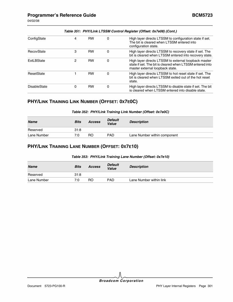
Programmer’s Reference Guide BCM572304/02/08
Broadcom CorporationDocument 5723-PG100-R PHY Layer Internal Registers Page 301
PHY/LINK TRAINING LINK NUMBER (OFFSET: 0X7E0C)
PHY/LINK TRAINING LANE NUMBER (OFFSET: 0X7E10)
ConfigState 4 RW 0 High layer directs LTSSM to configuration state if set. The bit is cleared when LTSSM entered into configuration state.
RecovState 3 RW 0 High layer directs LTSSM to recovery state if set. The bit is cleared when LTSSM entered into recovery state.
ExtLBState 2 RW 0 High layer directs LTSSM to external loopback master state if set. The bit is cleared when LTSSM entered into master external loopback state.
ResetState 1 RW 0 High layer directs LTSSM to hot reset state if set. The bit is cleared when LTSSM exited out of the hot reset state.
DisableState 0 RW 0 High layer directs LTSSM to disable state if set. The bit is cleared when LTSSM entered into disable state.
Table 352: PHY/Link Training Link Number (Offset: 0x7e0C)
Name Bits Access Default Value Description
Reserved 31:8
Lane Number 7:0 RO PAD Lane Number within component
Table 353: PHY/Link Training Lane Number (Offset: 0x7e10)
Name Bits Access Default Value Description
Reserved 31:8
Lane Number 7:0 RO PAD Lane Number within link
Table 351: PHY/Link LTSSM Control Register (Offset: 0x7e08) (Cont.)
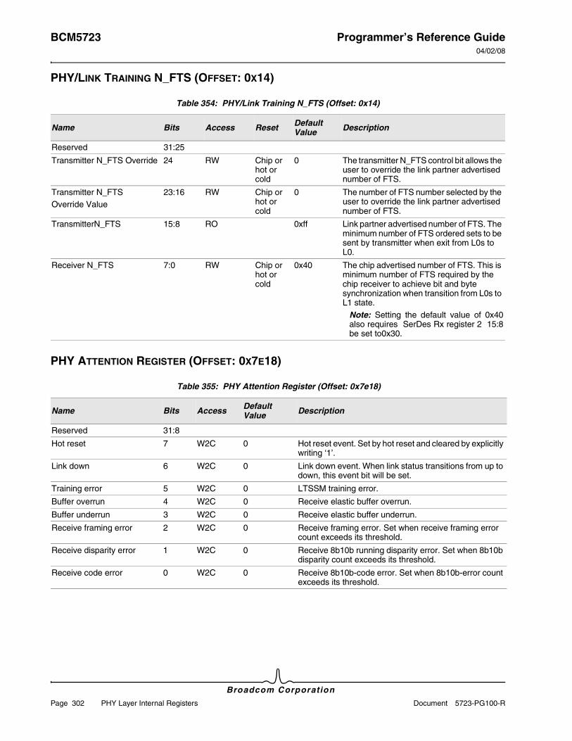
BCM5723 Programmer’s Reference Guide04/02/08
Broadcom Corporation
Page 302 PHY Layer Internal Registers Document 5723-PG100-R
PHY/LINK TRAINING N_FTS (OFFSET: 0X14)
PHY ATTENTION REGISTER (OFFSET: 0X7E18)
Table 354: PHY/Link Training N_FTS (Offset: 0x14)
Name Bits Access Reset Default Value Description
Reserved 31:25
Transmitter N_FTS Override 24 RW Chip or hot or cold
0 The transmitter N_FTS control bit allows the user to override the link partner advertised number of FTS.
Transmitter N_FTS Override Value
23:16 RW Chip or hot or cold
0 The number of FTS number selected by the user to override the link partner advertised number of FTS.
TransmitterN_FTS 15:8 RO 0xff Link partner advertised number of FTS. The minimum number of FTS ordered sets to be sent by transmitter when exit from L0s to L0.
Receiver N_FTS 7:0 RW Chip or hot or cold
0x40 The chip advertised number of FTS. This is minimum number of FTS required by the chip receiver to achieve bit and byte synchronization when transition from L0s to L1 state.
Note: Setting the default value of 0x40 also requires SerDes Rx register 2 15:8 be set to0x30.
Table 355: PHY Attention Register (Offset: 0x7e18)
Name Bits Access Default Value Description
Reserved 31:8
Hot reset 7 W2C 0 Hot reset event. Set by hot reset and cleared by explicitly writing ‘1’.
Link down 6 W2C 0 Link down event. When link status transitions from up to down, this event bit will be set.
Training error 5 W2C 0 LTSSM training error.
Buffer overrun 4 W2C 0 Receive elastic buffer overrun.
Buffer underrun 3 W2C 0 Receive elastic buffer underrun.
Receive framing error 2 W2C 0 Receive framing error. Set when receive framing error count exceeds its threshold.
Receive disparity error 1 W2C 0 Receive 8b10b running disparity error. Set when 8b10b disparity count exceeds its threshold.
Receive code error 0 W2C 0 Receive 8b10b-code error. Set when 8b10b-error count exceeds its threshold.
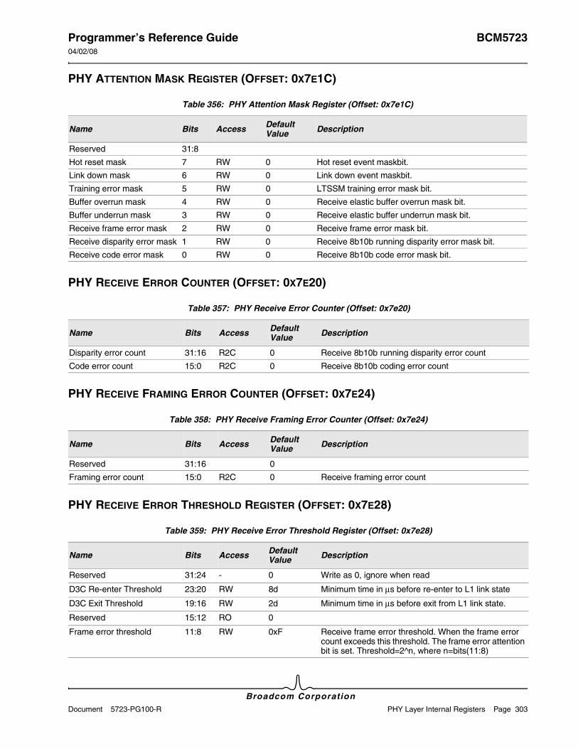
Programmer’s Reference Guide BCM572304/02/08
Broadcom CorporationDocument 5723-PG100-R PHY Layer Internal Registers Page 303
PHY ATTENTION MASK REGISTER (OFFSET: 0X7E1C)
PHY RECEIVE ERROR COUNTER (OFFSET: 0X7E20)
PHY RECEIVE FRAMING ERROR COUNTER (OFFSET: 0X7E24)
PHY RECEIVE ERROR THRESHOLD REGISTER (OFFSET: 0X7E28)
Table 356: PHY Attention Mask Register (Offset: 0x7e1C)
Name Bits Access Default Value Description
Reserved 31:8
Hot reset mask 7 RW 0 Hot reset event maskbit.
Link down mask 6 RW 0 Link down event maskbit.
Training error mask 5 RW 0 LTSSM training error mask bit.
Buffer overrun mask 4 RW 0 Receive elastic buffer overrun mask bit.
Buffer underrun mask 3 RW 0 Receive elastic buffer underrun mask bit.
Receive frame error mask 2 RW 0 Receive frame error mask bit.
Receive disparity error mask 1 RW 0 Receive 8b10b running disparity error mask bit.
Receive code error mask 0 RW 0 Receive 8b10b code error mask bit.
Table 357: PHY Receive Error Counter (Offset: 0x7e20)
Name Bits Access Default Value Description
Disparity error count 31:16 R2C 0 Receive 8b10b running disparity error count
Code error count 15:0 R2C 0 Receive 8b10b coding error count
Table 358: PHY Receive Framing Error Counter (Offset: 0x7e24)
Name Bits Access Default Value Description
Reserved 31:16 0
Framing error count 15:0 R2C 0 Receive framing error count
Table 359: PHY Receive Error Threshold Register (Offset: 0x7e28)
Name Bits Access Default Value Description
Reserved 31:24 - 0 Write as 0, ignore when read
D3C Re-enter Threshold 23:20 RW 8d Minimum time in μs before re-enter to L1 link state
D3C Exit Threshold 19:16 RW 2d Minimum time in μs before exit from L1 link state.
Reserved 15:12 RO 0
Frame error threshold 11:8 RW 0xF Receive frame error threshold. When the frame error count exceeds this threshold. The frame error attention bit is set. Threshold=2^n, where n=bits(11:8)
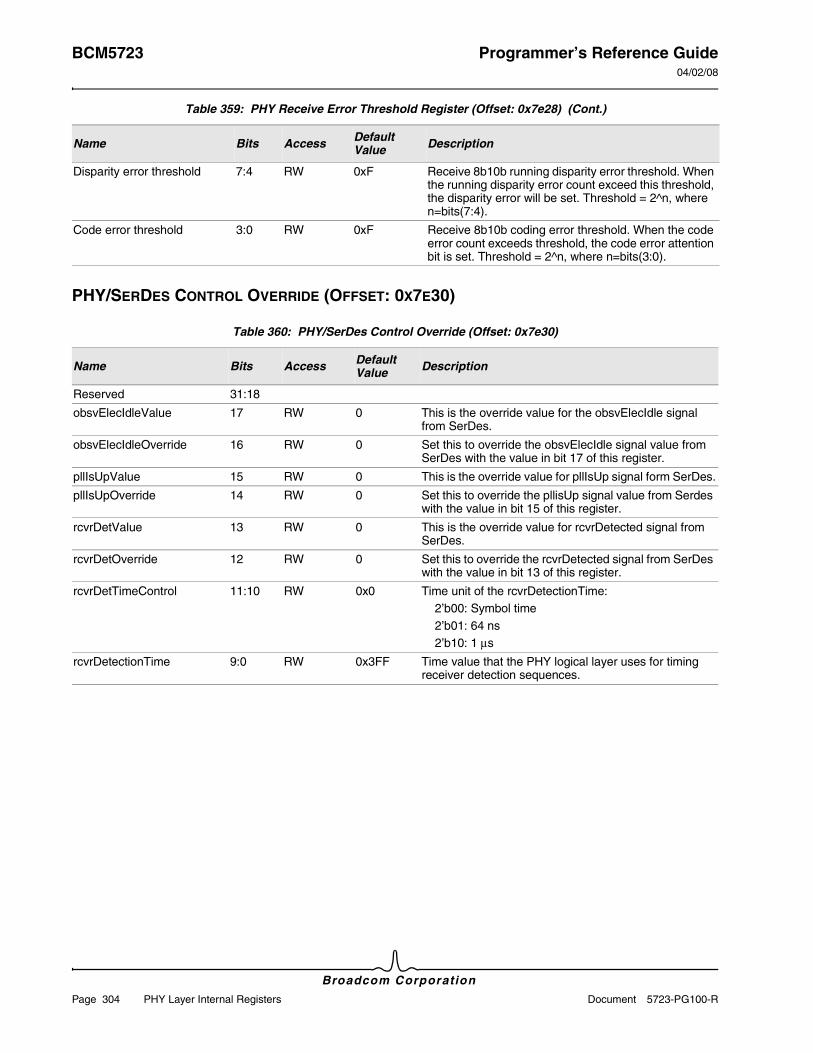
BCM5723 Programmer’s Reference Guide04/02/08
Broadcom Corporation
Page 304 PHY Layer Internal Registers Document 5723-PG100-R
PHY/SERDES CONTROL OVERRIDE (OFFSET: 0X7E30)
Disparity error threshold 7:4 RW 0xF Receive 8b10b running disparity error threshold. When the running disparity error count exceed this threshold, the disparity error will be set. Threshold = 2^n, where n=bits(7:4).
Code error threshold 3:0 RW 0xF Receive 8b10b coding error threshold. When the code error count exceeds threshold, the code error attention bit is set. Threshold = 2^n, where n=bits(3:0).
Table 360: PHY/SerDes Control Override (Offset: 0x7e30)
Name Bits Access Default Value Description
Reserved 31:18
obsvElecIdleValue 17 RW 0 This is the override value for the obsvElecIdle signal from SerDes.
obsvElecIdleOverride 16 RW 0 Set this to override the obsvElecIdle signal value from SerDes with the value in bit 17 of this register.
pllIsUpValue 15 RW 0 This is the override value for pllIsUp signal form SerDes.
pllIsUpOverride 14 RW 0 Set this to override the pllisUp signal value from Serdes with the value in bit 15 of this register.
rcvrDetValue 13 RW 0 This is the override value for rcvrDetected signal from SerDes.
rcvrDetOverride 12 RW 0 Set this to override the rcvrDetected signal from SerDes with the value in bit 13 of this register.
rcvrDetTimeControl 11:10 RW 0x0 Time unit of the rcvrDetectionTime: 2’b00: Symbol time 2’b01: 64 ns 2’b10: 1 μs
rcvrDetectionTime 9:0 RW 0x3FF Time value that the PHY logical layer uses for timing receiver detection sequences.
Table 359: PHY Receive Error Threshold Register (Offset: 0x7e28) (Cont.)
Name Bits Access Default Value Description
Programmer’s Reference Guide BCM572304/02/08
Broadcom CorporationDocument 5723-PG100-R PHY Layer Internal Registers Page 305
PHY TIMING PARAMETER OVERRIDE (OFFSET: 0X7E34)
PHY HARDWARE DIAGNOSTIC1–TX/RX SM STATES (OFFSET: 0X7E38)
Table 361: PHY Timing Parameter Override (Offset: 0x7e34)
Name Bits Access Default Value Description
ts1NumOverride 31 RW 0 Set this to override the TS1 number to be send out in polling active state with the value in bit (27:16) of this register from the spec defined value.
txIdleMinOverride 30 RW 0 Set this to override the min time for a transmitter to stay with the value in bit (15:8) of this register from the spec defined value.
txIdle2IdleOverride 29 RW 0 Set this to override the Max time for electrical idle transition with the value in bit (7:0) of this register from the spec defined value.
N_TS1InPollingActive 27:16 RW 0x400 This is the number of TS1 must be send our in Polling active state.
txIdleMinTime 15:8 RW 0x5 This is the minimum time (in symbol time) a transmitter must be in electrical idle.
txIdleSettoIdleTime 7:0 RW 0x2 Maximum time (in symbol time) to transition to a valid electrical idle after sending an electrical idle ordered-set
Table 362: PHY Hardware Diagnostic1–TX/RX SM States (Offset: 0x7e38)
Name Bits Access Default Value Description
Transmit State Machine State 9:4 RO 0 Transmit state machine states 9:8–TX Data State 7:4–TX Main State
Receive State Machine State 3:0 RO 0 Receive state machine states 3:0–RX Main State
BCM5723 Programmer’s Reference Guide04/02/08
Broadcom Corporation
Page 306 PHY Layer Internal Registers Document 5723-PG100-R
PHY HARDWARE DIAGNOSTIC2–LTSSM STATES (OFFSET: 0X7E3C)
Table 363: PHY Hardware Diagnostic2–LTSSM States (Offset: 0x7e3C)
Name Bits Access Default Value Description
LTSSM State Machine State
31:0 RO 0 LTSSM state machine states 31:28–Main State 27:26–Detect sub-state 25:23–Polling sub-state 22:20–Configuration sub-state 19:18–Recover sub-state 17:16–Rx L0s sub-state 15:14–Rx L0s sub-state 13:12–L1 sub-state 11:10–L2 sub-state 9:8–Disable sub-state 7:6–Loopback sub-state 5:4–Reset sub-state 3:0–Reserved
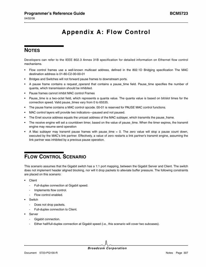
Programmer’s Reference Guide BCM572304/02/08
Broadcom CorporationDocument 5723-PG100-R Notes Page 307
Appendix A: Flow Control
NOTES
Developers can refer to the IEEE 802.3 Annex 31B specification for detailed information on Ethernet flow control mechanisms.
• Flow control frames use a well-known multicast address, defined in the 802.1D Bridging specification The MAC destination address is 01-80-C2-00-00-01
• Bridges and Switches will not forward pause frames to downstream ports.
• A pause frame contains a request_operand that contains a pause_time field. Pause_time specifies the number of quanta, which transmission should be inhibited.
• Pause frames cannot inhibit MAC control Frames
• Pause_time is a two-octet field, which represents a quanta value. The quanta value is based on bit/slot times for the connection speed. Valid pause_times vary from 0 to 65535.
• The pause frame contains a MAC control opcode. 00-01 is reserved for PAUSE MAC control functions.
• MAC control layers will provide two indicators—paused and not paused.
• The Enet source address equals the unicast address of the MAC sublayer, which transmits the pause_frame.
• The receive engine will set a countdown timer, based on the value of pause_time. When the timer expires, the transmit engine may resume send operation
• A Mac sublayer may transmit pause frames with pause_time = 0. The zero value will stop a pause count down, executed by the MAC’s link partner. Effectively, a value of zero restarts a link partner’s transmit engine, assuming the link partner was inhibited by a previous pause operation.
FLOW CONTROL SCENARIO
This scenario assumes that the Gigabit switch has a 1:1 port mapping, between the Gigabit Server and Client. The switch does not implement header aligned blocking, nor will it drop packets to alleviate buffer pressure. The following constraints are placed on this scenario:
• Client
- Full-duplex connection at Gigabit speed.
- Implements flow control.
- Flow control enabled.
• Switch
- Does not drop packets.
- Full-duplex connection to Client.
• Server
- Gigabit connection.
- Either half/full-duplex connection at Gigabit speed (i.e., this scenario will cover two subcases).
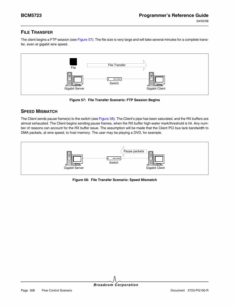
BCM5723 Programmer’s Reference Guide04/02/08
Broadcom Corporation
Page 308 Flow Control Scenario Document 5723-PG100-R
FILE TRANSFER
The client begins a FTP session (see Figure 57). The file size is very large and will take several minutes for a complete trans-fer, even at gigabit wire speed.
Figure 57: File Transfer Scenario: FTP Session Begins
SPEED MISMATCH
The Client sends pause frame(s) to the switch (see Figure 58). The Client’s pipe has been saturated, and the RX buffers are almost exhausted. The Client begins sending pause frames, when the RX buffer high-water mark/threshold is hit. Any num-ber of reasons can account for the RX buffer issue. The assumption will be made that the Client PCI bus lack bandwidth to DMA packets, at wire speed, to host memory. The user may be playing a DVD, for example.
Figure 58: File Transfer Scenario: Speed Mismatch
Gigabit Server
Switch
Gigabit Client
File TransferFile
Gigabit Server
Switch
Gigabit Client
Pause packets
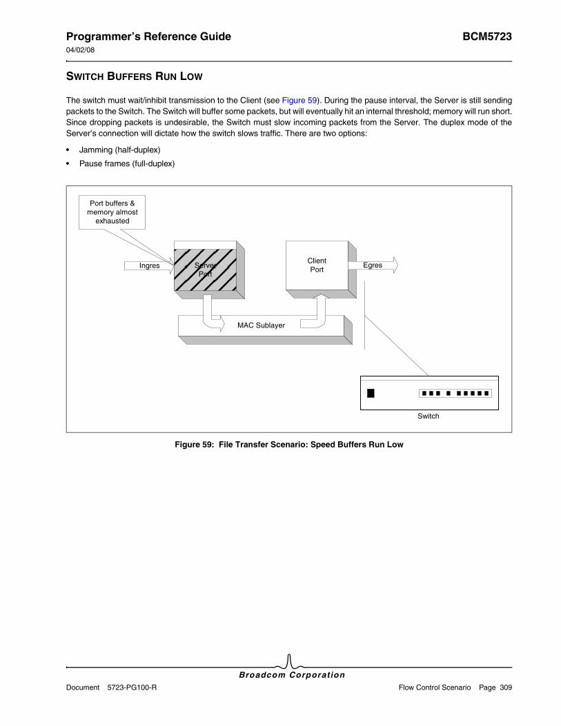
Programmer’s Reference Guide BCM572304/02/08
Broadcom CorporationDocument 5723-PG100-R Flow Control Scenario Page 309
SWITCH BUFFERS RUN LOW
The switch must wait/inhibit transmission to the Client (see Figure 59). During the pause interval, the Server is still sending packets to the Switch. The Switch will buffer some packets, but will eventually hit an internal threshold; memory will run short. Since dropping packets is undesirable, the Switch must slow incoming packets from the Server. The duplex mode of the Server’s connection will dictate how the switch slows traffic. There are two options:
• Jamming (half-duplex)
• Pause frames (full-duplex)
Figure 59: File Transfer Scenario: Speed Buffers Run Low
Ingres
Switch
ClientPortServer
Port
MAC Sublayer
Port buffers &memory almost
exhausted
Egres
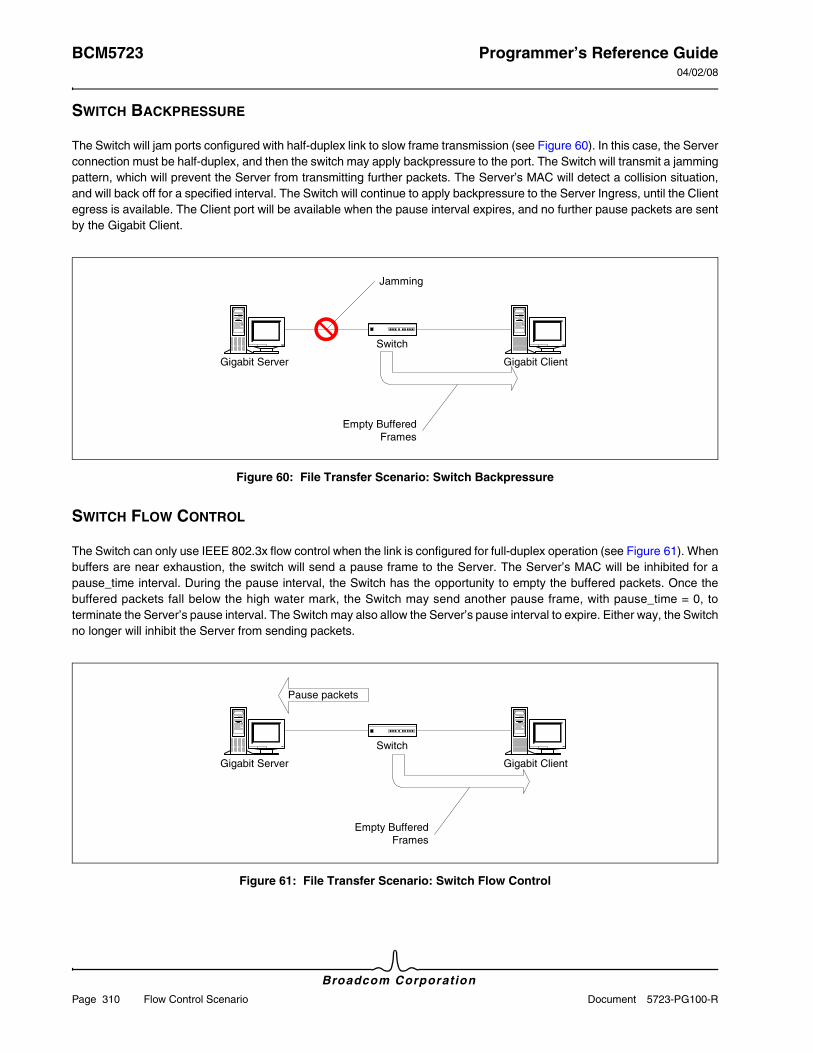
BCM5723 Programmer’s Reference Guide04/02/08
Broadcom Corporation
Page 310 Flow Control Scenario Document 5723-PG100-R
SWITCH BACKPRESSURE
The Switch will jam ports configured with half-duplex link to slow frame transmission (see Figure 60). In this case, the Server connection must be half-duplex, and then the switch may apply backpressure to the port. The Switch will transmit a jamming pattern, which will prevent the Server from transmitting further packets. The Server’s MAC will detect a collision situation, and will back off for a specified interval. The Switch will continue to apply backpressure to the Server Ingress, until the Client egress is available. The Client port will be available when the pause interval expires, and no further pause packets are sent by the Gigabit Client.
Figure 60: File Transfer Scenario: Switch Backpressure
SWITCH FLOW CONTROL
The Switch can only use IEEE 802.3x flow control when the link is configured for full-duplex operation (see Figure 61). When buffers are near exhaustion, the switch will send a pause frame to the Server. The Server’s MAC will be inhibited for a pause_time interval. During the pause interval, the Switch has the opportunity to empty the buffered packets. Once the buffered packets fall below the high water mark, the Switch may send another pause frame, with pause_time = 0, to terminate the Server’s pause interval. The Switch may also allow the Server’s pause interval to expire. Either way, the Switch no longer will inhibit the Server from sending packets.
Figure 61: File Transfer Scenario: Switch Flow Control
Gigabit Server
Switch
Gigabit Client
Jamming
Empty BufferedFrames
Gigabit Server
Switch
Gigabit Client
Pause packets
Empty BufferedFrames
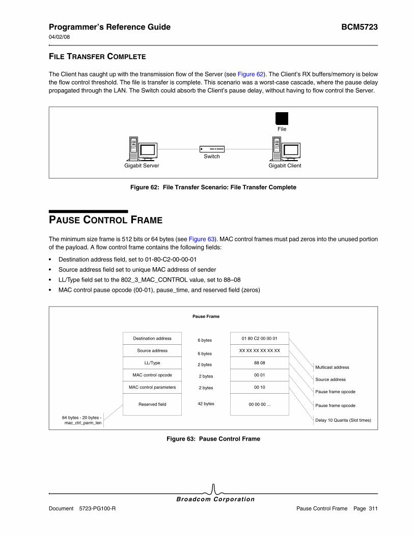
Programmer’s Reference Guide BCM572304/02/08
Broadcom CorporationDocument 5723-PG100-R Pause Control Frame Page 311
FILE TRANSFER COMPLETE
The Client has caught up with the transmission flow of the Server (see Figure 62). The Client’s RX buffers/memory is below the flow control threshold. The file is transfer is complete. This scenario was a worst-case cascade, where the pause delay propagated through the LAN. The Switch could absorb the Client’s pause delay, without having to flow control the Server.
Figure 62: File Transfer Scenario: File Transfer Complete
PAUSE CONTROL FRAME
The minimum size frame is 512 bits or 64 bytes (see Figure 63). MAC control frames must pad zeros into the unused portion of the payload. A flow control frame contains the following fields:
• Destination address field, set to 01-80-C2-00-00-01
• Source address field set to unique MAC address of sender
• LL/Type field set to the 802_3_MAC_CONTROL value, set to 88–08
• MAC control pause opcode (00-01), pause_time, and reserved field (zeros)
Figure 63: Pause Control Frame
Gigabit Server
Switch
Gigabit Client
File
Destination address
Source address
LL/Type
MAC control opcode
MAC control parameters
Reserved field
6 bytes
6 bytes
2 bytes
2 bytes
64 bytes - 20 bytes - mac_ctrl_parm_len
2 bytes
42 bytes
01 80 C2 00 00 01
XX XX XX XX XX XX
88 08
00 01
00 10
00 00 00 ...
Delay 10 Quanta (Slot times)
Pause frame opcode
Pause frame opcode
Source address
Multicast address
Pause Frame
BCM5723 Programmer’s Reference Guide04/02/08
Broadcom Corporation
Page 312 Pause Control Frame Document 5723-PG100-R
Appendix B: Terminology
Table 364: Terminology
Term Definition
BD Buffer Descriptor.
Deferred Procedure Call (DPC) The ISR may schedule a O/S callback to process interrupts at a later time.
Expansion ROM PCI devices may optionally expose device specific programs to BIOS. For example, network devices may place PXE bootcode in their expansion ROM region.
Host Coalescing A hardware block which the Ethernet controller status block. The hardware will drive a line interrupt or MSI.
Interrupt Distribution Queue The Ethernet controller supports four interrupt distribution queues per class of service. The rules engine may place traffic into RX return rings based on rules checking. Within each class of service, the traffic may further be organized in Interrupt Distribution Queues. For example, frames with errors may be given lower data path priority over frames without errors, all within the same class of service (RX Return Ring).
Interrupt Service Routine (ISR) A procedure where device interrupts are processed.
Pre-boot execution (PXE) An industry-standard client/server interface that allows networked computers that are not yet loaded with an operating system to be configured and booted remotely.
Receive BD Initiator The hardware block that DMA's BDs when receive ring indices are written.
Receive Data and Receive BD Initiator
The hardware block the updates packet buffers, in host memory, after an Ethernet frame is received. The hardware block will also update the BD with information like checksum and VLAN Tags.
Receive Data Completion The hardware block that updates the host coalescing engine after the packet buffers and BD are DMAed to host memory.
Receive Queue Placement The hardware block that routes a categorized frame to one of sixteen RX Return rings.
Send BD Initiator The hardware block that is activated when a Send producer index is updated by host software. The hardware block will DMA a BD from host memory.
Send Data Initiator The hardware block updates the DMAs in the packet buffers from host memory. The packet buffers are DMAed after the BD has been moved to device local memory.

Programmer’s Reference Guide BCM572304/02/08
Broadcom CorporationDocument 5723-PG100-R Pause Control Frame Page 313

Document 5723-PG100-R
Broadcom Corporation
5300 California AvenueIrvine, CA 92617
Phone: 949-926-5000Fax: 949-926-5203
Broadcom® Corporation reserves the right to make changes without further notice to any products or data herein to improve reliability, function, or design.Information furnished by Broadcom Corporation is believed to be accurate and reliable. However, Broadcom Corporation
does not assume any liability arising out of the application or use of this information, nor the application or use of any product orcircuit described herein, neither does it convey any license under its patent rights nor the rights of others.
BCM5723 Programmer’s Reference Guide04/02/08