arc 410c arc 650c arc 810c - esab
TRANSCRIPT

0349 300 082 Valid for serial no. 734, 749, 751--xxx--xxxx080623
Arc 410cArc 650cArc 810c
Origo™™™™
Service manual
READ THIS FIRST .................................................................................................................................. 3INTRODUCTION ..................................................................................................................................... 4
Design structure of the power source .................................................................................................. 4TECHNICAL DATA.................................................................................................................................. 5WIRING DIAGRAM.................................................................................................................................. 6
Component description ........................................................................................................................ 6OrigoArc 410c ...................................................................................................................................... 7OrigoArc 650c ...................................................................................................................................... 8OrigoArc 810c ...................................................................................................................................... 9
DESCRIPTION OF OPERATION.......................................................................................................... 10MMC module...................................................................................................................................... 10Control panel A11 .............................................................................................................................. 10Control panel A12 .............................................................................................................................. 11Current and welding voltage meter.................................................................................................... 12Remote wireless welding current setting receiver circuit ................................................................... 13A12 panel supply................................................................................................................................ 13LM11 Component positions ............................................................................................................... 14
CH21 Control circuit board .................................................................................................................... 15Welding current setting circuit............................................................................................................ 15ANTISTIC, HOTSTART, ARC FORCE functions .............................................................................. 16Current loop control system............................................................................................................... 17Circuit reducing the current required for activating the device .......................................................... 18Steering voltage source ..................................................................................................................... 18Activation in TIG method.................................................................................................................... 19Selecting the welding method............................................................................................................ 19Signalling and protecting systems ..................................................................................................... 19Power transistors control system (driver) .......................................................................................... 20Power unit .......................................................................................................................................... 20CH21 Component positions ............................................................................................................... 21
K69 Suppression circuit board............................................................................................................... 22Circuit diagram................................................................................................................................... 22Component positions ......................................................................................................................... 22
REMOTE CONTROLS .......................................................................................................................... 23SERVICE INSTRUCTION ..................................................................................................................... 23
What is ESD?..................................................................................................................................... 23Service aid ............................................................................................................................................. 24
Antistatic service kit ........................................................................................................................... 24Checking power board CH21 ................................................................................................................ 24
Checking signal LEDs........................................................................................................................ 24Checking supply and reference voltages........................................................................................... 25Calibrating the remote wire current setting circuit.............................................................................. 26Calibrating of the source in MMA, ARC GOUGING and TIG mode .................................................. 27Checking the HOT START function................................................................................................... 27Checking the ARC FORCE function .................................................................................................. 27Checking the ANTISTICK function..................................................................................................... 27
Checking the ANTISTICK function in MMA mode...................................................................... 27Checking the ANTISTICK function in TIG mode ........................................................................ 28
Setting the maximum current ............................................................................................................. 28Checking the operation of thermal protections .................................................................................. 28Checking the operation of PWM driver .............................................................................................. 29Checking the PWM signal.................................................................................................................. 29Checking the gate pulses................................................................................................................... 29Checking display board LM11............................................................................................................ 30
Checking supply and reference voltages ....................................................................................... 30Current meter calibration................................................................................................................ 30
Calibration of the current value set with the remote wireless current setting receiver. ..................... 31Voltage meter calibration ................................................................................................................... 32Checking the remote current setting circuits...................................................................................... 33
Checking the wire remote setting circuit..................................................................................... 33Checking the wireless remote current setting circuit .................................................................. 33

2
Checking chopper block V0 ............................................................................................................... 33Overview test ..................................................................................................................................... 35Rectifier test ....................................................................................................................................... 35Checking of output stage. .................................................................................................................. 35Replacing of damaged transistors. .................................................................................................... 36
NOTES .................................................................................................................................................. 37

3
READ THIS FIRST
Maintenance and repair work should be performed by an experienced person, andelectrical work only by a trained electrician. Use only recommended replacement parts.
This service manual is intended for use by technicians with electrical/electronic training forhelp in connection with fault--tracing and repair.
Use the wiring diagram as a form of index for the description of operation. The circuitboards are divided into numbered blocks, which are described individually in more detail inthe description of operation. All component names in the wiring diagram are listed in thecomponent description.
This manual contains details of all design changes that have been made up to andincluding June 2008.
The manual is valid for:OrigoArc 410c/650c/810c with serial no. 734, 749, 751--xxx--xxxx.
OrigoTM Arc 410c/650c/810c has been designed and tested in accordance with international andEuropean standards IEC/EN 60974.On completion of service or repair, the service organisation that has performed thework must make sure that the equipment still complies with the above standards.
4
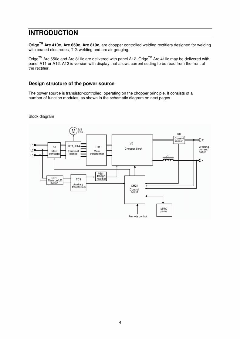
INTRODUCTION
OrigoTM Arc 410c, Arc 650c, Arc 810c, are chopper controlled welding rectifiers designed for weldingwith coated electrodes, TIG welding and arc air gouging.
OrigoTM Arc 650c and Arc 810c are delivered with panel A12. OrigoTM Arc 410c may be delivered withpanel A11 or A12. A12 is version with display that allows current setting to be read from the front ofthe rectifier.
Design structure of the power source
The power source is transistor-controlled, operating on the chopper principle. It consists of anumber of function modules, as shown in the schematic diagram on next pages.
Block diagram
5
6
WIRING DIAGRAM
The power source consists of a number of function modules, which are described in thecomponent descriptions on the following pages.
Component description
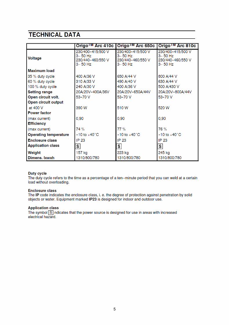
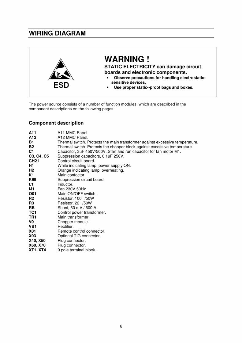
A11 A11 MMC Panel.A12 A12 MMC Panel.B1 Thermal switch. Protects the main transformer against excessive temperature.B2 Thermal switch. Protects the chopper block against excessive temperature.C1 Capacitor, 3uF 450V/500V. Start and run capacitor for fan motor M1.C3, C4, C5 Suppression capacitors, 0,1uF 250V.CH21 Control circuit board.H1 White indicating lamp, power supply ON.H2 Orange indicating lamp, overheating.K1 Main contactor.K69 Suppression circuit boardL1 Inductor.M1 Fan 230V 50HzQ01 Main ON/OFF switch.R2 Resistor, 100 /50WR3 Resistor, 22 /50WRB Shunt, 60 mV / 600 ATC1 Control power transformer.TR1 Main transformer.V0 Chopper module.VB1 Rectifier.X01 Remote control connector.X03 Optional TIG connector.X40, X50 Plug connector.X60, X70 Plug connector.XT1, XT4 9 pole terminal block.
WARNING !STATIC ELECTRICITY can damage circuitboards and electronic components.
• Observe precautions for handling electrostatic-sensitive devices.
• Use proper static--proof bags and boxes.
7
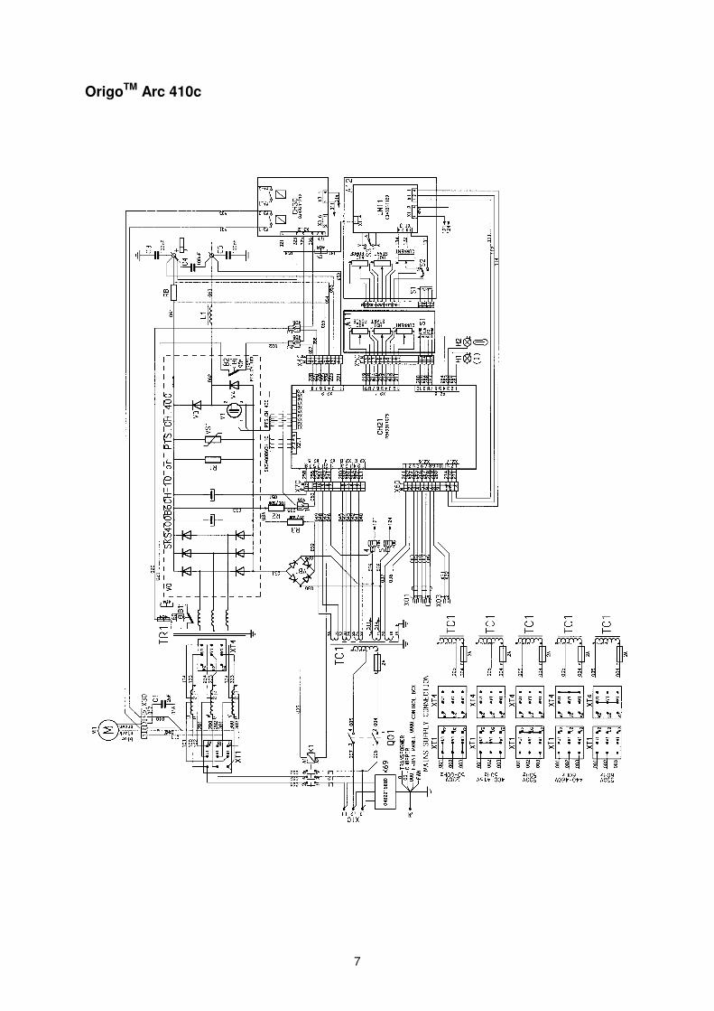
OrigoTM Arc 410c
8
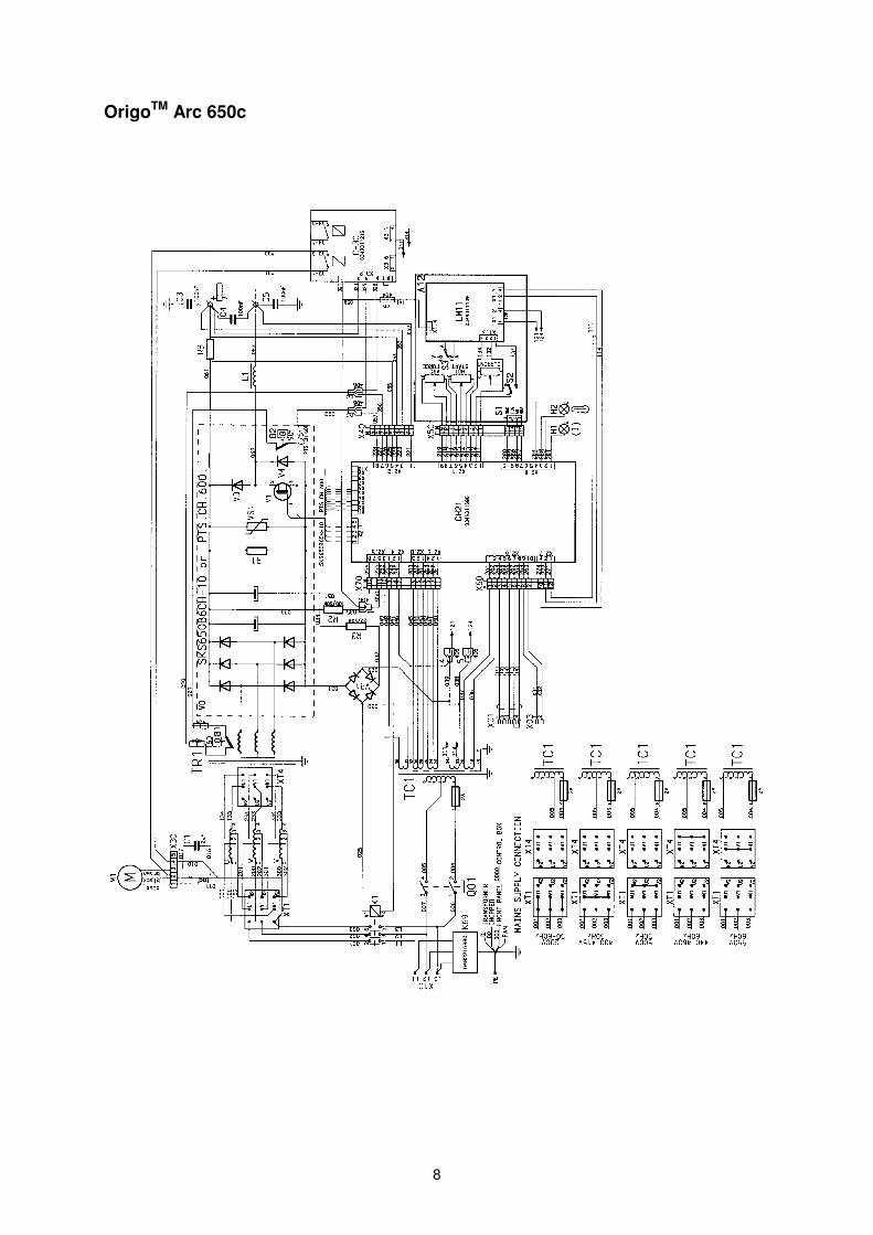
OrigoTM Arc 650c
9
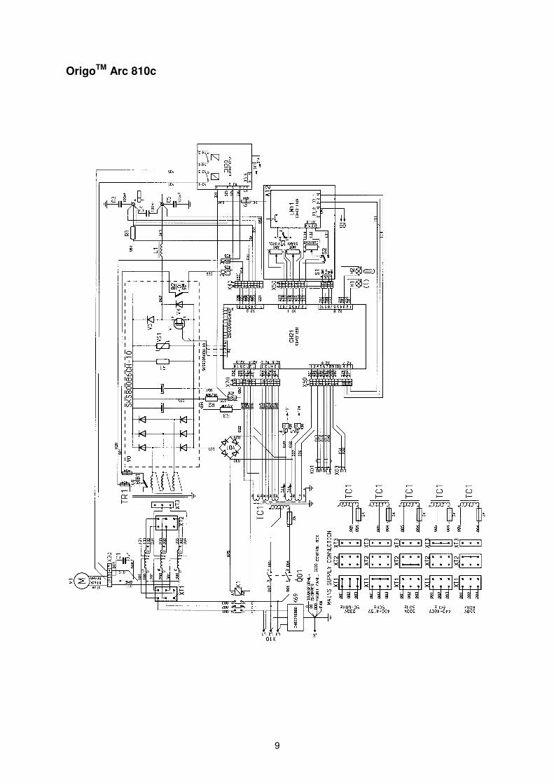
OrigoTM Arc 810c
10
DESCRIPTION OF OPERATION
This description of operation describes the function of circuit boards and other componentsin the power source. It is divided into sections, numbered to correspond to the circuit boardnumbers and divisions into function blocks.
MMC module
The MMC module consists of an operator’s control panel.
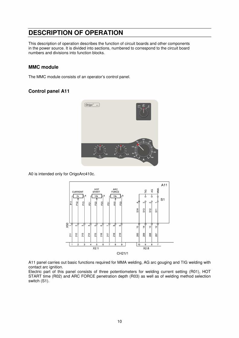
Control panel A11
A0 is intended only for OrigoArc410c.
A11 panel carries out basic functions required for MMA welding, AG arc gouging and TIG welding withcontact arc ignition.Electric part of this panel consists of three potentiometers for welding current setting (R01), HOTSTART time (R02) and ARC FORCE penetration depth (R03) as well as of welding method selectionswitch (S1).
11
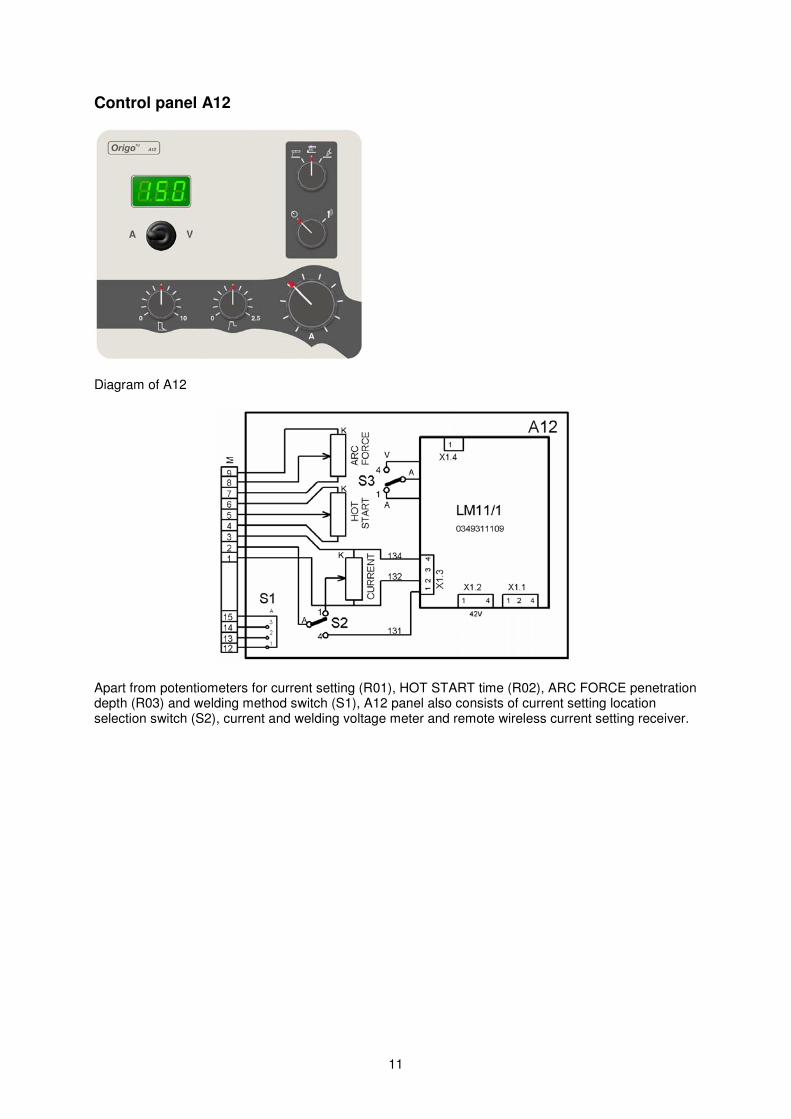
Control panel A12
Diagram of A12
Apart from potentiometers for current setting (R01), HOT START time (R02), ARC FORCE penetrationdepth (R03) and welding method switch (S1), A12 panel also consists of current setting locationselection switch (S2), current and welding voltage meter and remote wireless current setting receiver.
12
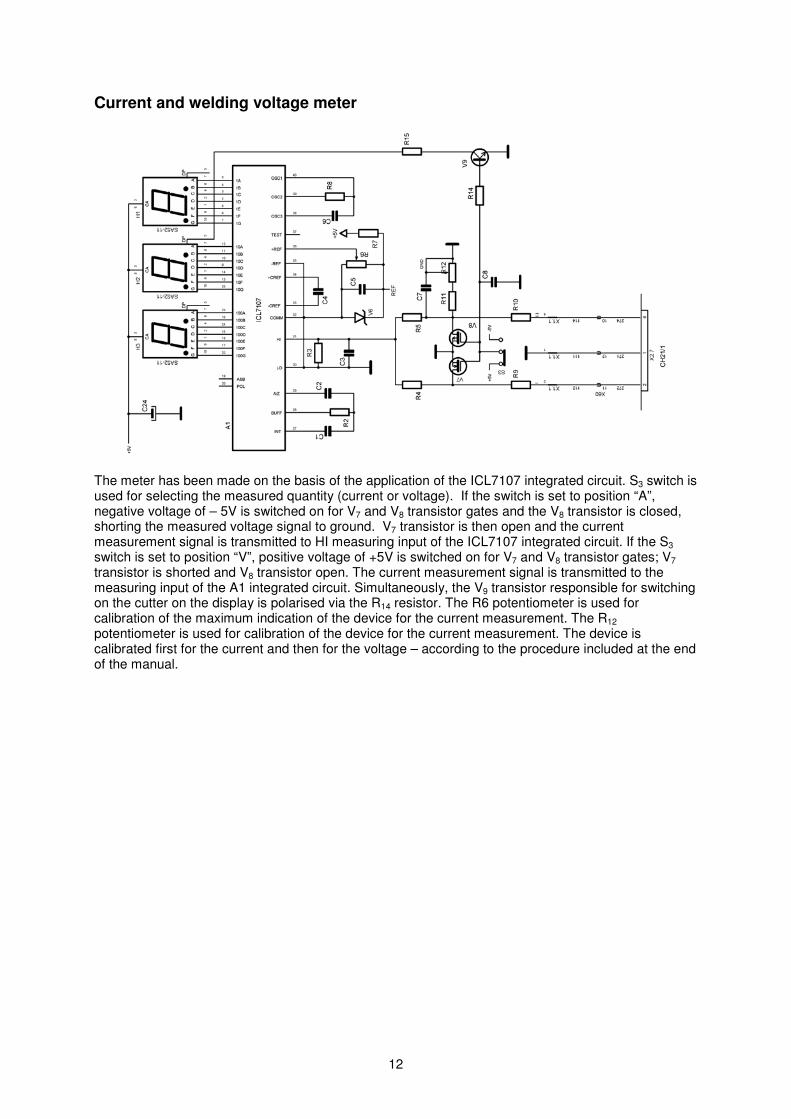
Current and welding voltage meter
The meter has been made on the basis of the application of the ICL7107 integrated circuit. S3 switch isused for selecting the measured quantity (current or voltage). If the switch is set to position “A”,negative voltage of – 5V is switched on for V7 and V8 transistor gates and the V8 transistor is closed,shorting the measured voltage signal to ground. V7 transistor is then open and the currentmeasurement signal is transmitted to HI measuring input of the ICL7107 integrated circuit. If the S3
switch is set to position “V”, positive voltage of +5V is switched on for V7 and V8 transistor gates; V7
transistor is shorted and V8 transistor open. The current measurement signal is transmitted to themeasuring input of the A1 integrated circuit. Simultaneously, the V9 transistor responsible for switchingon the cutter on the display is polarised via the R14 resistor. The R6 potentiometer is used forcalibration of the maximum indication of the device for the current measurement. The R12
potentiometer is used for calibration of the device for the current measurement. The device iscalibrated first for the current and then for the voltage – according to the procedure included at the endof the manual.
13
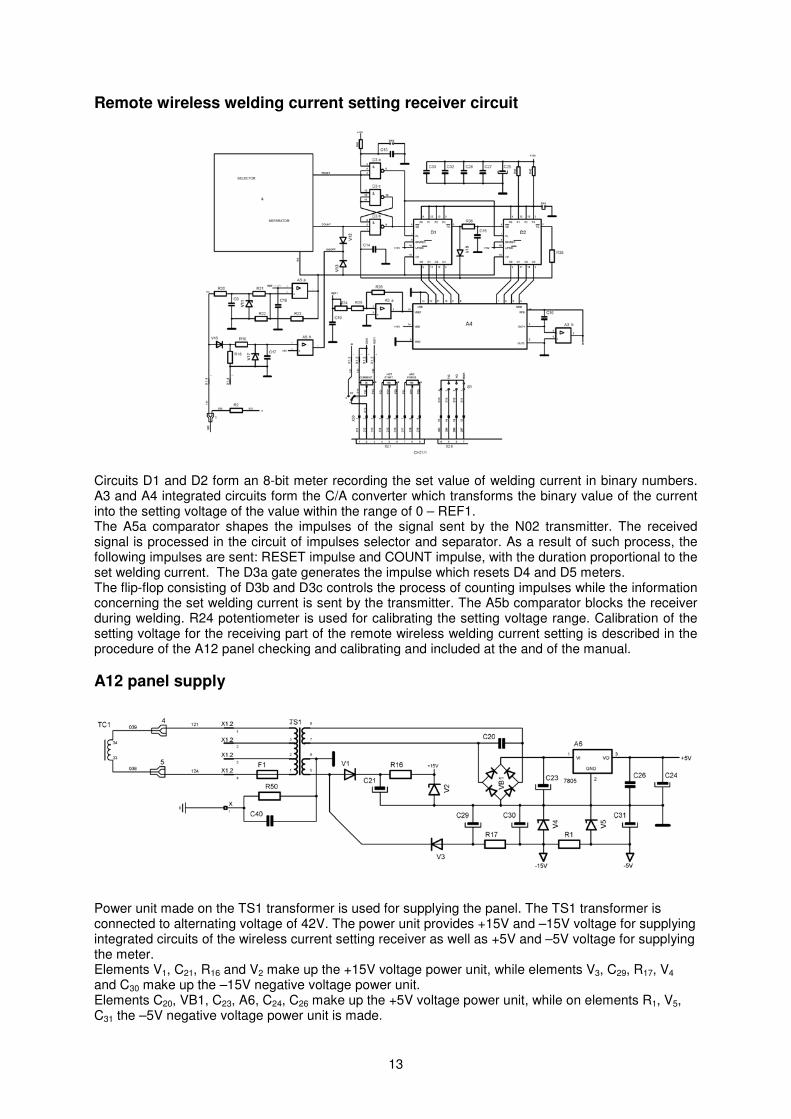
Remote wireless welding current setting receiver circuit
Circuits D1 and D2 form an 8-bit meter recording the set value of welding current in binary numbers.A3 and A4 integrated circuits form the C/A converter which transforms the binary value of the currentinto the setting voltage of the value within the range of 0 – REF1.The A5a comparator shapes the impulses of the signal sent by the N02 transmitter. The receivedsignal is processed in the circuit of impulses selector and separator. As a result of such process, thefollowing impulses are sent: RESET impulse and COUNT impulse, with the duration proportional to theset welding current. The D3a gate generates the impulse which resets D4 and D5 meters.The flip-flop consisting of D3b and D3c controls the process of counting impulses while the informationconcerning the set welding current is sent by the transmitter. The A5b comparator blocks the receiverduring welding. R24 potentiometer is used for calibrating the setting voltage range. Calibration of thesetting voltage for the receiving part of the remote wireless welding current setting is described in theprocedure of the A12 panel checking and calibrating and included at the and of the manual.
A12 panel supply
Power unit made on the TS1 transformer is used for supplying the panel. The TS1 transformer isconnected to alternating voltage of 42V. The power unit provides +15V and –15V voltage for supplyingintegrated circuits of the wireless current setting receiver as well as +5V and –5V voltage for supplyingthe meter.Elements V1, C21, R16 and V2 make up the +15V voltage power unit, while elements V3, C29, R17, V4
and C30 make up the –15V negative voltage power unit.Elements C20, VB1, C23, A6, C24, C26 make up the +5V voltage power unit, while on elements R1, V5,C31 the –5V negative voltage power unit is made.
14
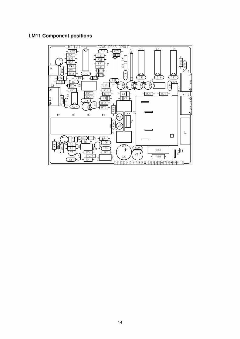
LM11 Component positions
15
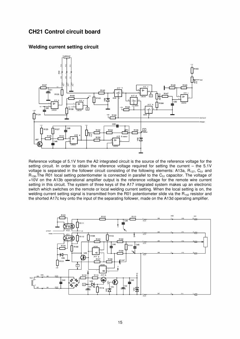
CH21 Control circuit board
Welding current setting circuit
Reference voltage of 5.1V from the A2 integrated circuit is the source of the reference voltage for thesetting circuit. In order to obtain the reference voltage required for setting the current – the 5.1Vvoltage is separated in the follower circuit consisting of the following elements: A13a, R137, C51 andR138.The R01 local setting potentiometer is connected in parallel to the C51 capacitor. The voltage of+10V on the A13b operational amplifier output is the reference voltage for the remote wire currentsetting in this circuit. The system of three keys of the A17 integrated system makes up an electronicswitch which switches on the remote or local welding current setting. When the local setting is on, thewelding current setting signal is transmitted from the R01 potentiometer slide via the R142 resistor andthe shorted A17c key onto the input of the separating follower, made on the A13d operating amplifier.
16
Switching to the remote wire supply mode is performed automatically after fixing the peripheral deviceto the X01 socket on the cap board of the device. The electronic system of remote setting isgalvanically separated from the remaining electronic circuits controlling the source operation.The VC2 transoptor carries a signal which switches off the A17c key and switches on the A17d key,transmitting the signal from the A12b amplifier output onto the A13d separating follower input, thusactivating the remote setting. The VC2 transoptor transmits the signal of the welding current value.This is a signal with a variable pulse-duty factor for a rectangular wave, proportional to the value set bythe potentiometer on the remote regulation peripheral device. The circuit made of the A11acomparator and V55 transistor generates the signal. The A11b comparator disables the generator if theremote regulation peripheral device is disconnected from the device. Elements VB1, C41, R114, R115,R116, V50, V51, V52, V53, C42 and C43 make up the power unit for the galvanically separated part of theremote setting circuit. The rectangular wave of the stable voltage amplitude and of time parametersdepending on the set welding current is obtained on the V57 transistor collector. This signal isaveraged by means of a low-pass filter made on the A12a operational amplifier. The function of thecircuit made on the A12b operational amplifier is to set the changes range of the voltage setting thewelding current. The RP2 potentiometer is used for resetting the setting signal for the current settingpotentiometer on the peripheral device to the minimum value. R114 potentiometer is designed forsetting the maximum value of the setting signal for the current setting potentiometer on the peripheraldevice to the maximum value. Calibration procedure is described in detail in item 2 – Procedures forchecking and calibration of the source. The A13d follower output is connected to the R184 resistor andRP4 potentiometer used for calibrating the maximum welding current in MMA, AG and TIG methods.An amplifier with amplification 2 is made on the A13c operational amplifier. Potentiometers R114 andRP2 are connected to the output of this amplifier. The RP5 potentiometer sets the minimum current. Isol
voltage signal is the current setting in MMA, AG and TIG methods and it is transmitted onto the non-inverting input of the A16a amplifier.
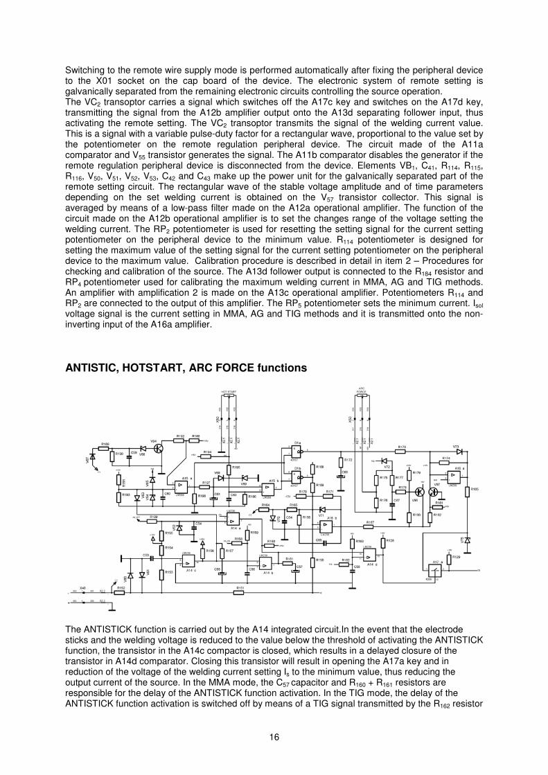
ANTISTIC, HOTSTART, ARC FORCE functions
The ANTISTICK function is carried out by the A14 integrated circuit.In the event that the electrodesticks and the welding voltage is reduced to the value below the threshold of activating the ANTISTICKfunction, the transistor in the A14c compactor is closed, which results in a delayed closure of thetransistor in A14d comparator. Closing this transistor will result in opening the A17a key and inreduction of the voltage of the welding current setting Is to the minimum value, thus reducing theoutput current of the source. In the MMA mode, the C57 capacitor and R160 + R161 resistors areresponsible for the delay of the ANTISTICK function activation. In the TIG mode, the delay of theANTISTICK function activation is switched off by means of a TIG signal transmitted by the R162 resistor
17
onto the non-inverting input of A14d comparator. In the AG mode, the ANTISTICK function is switchedoff by means of shorting the A14b comparator output with the activated output transistor of the A14acomparator.
The HOT START function is carried out by A15 and D1 integrated circuits. When the welding startsand the arc ignition takes place, V94 transistor is switched on, which results in the high level on theA15a amplifier output. The C61 capacitor is charged via the R197 resistor. The charging time of thiscapacitor up to the voltage set by the HOT START potentiometer and sent to the non-inverting input ofA15b amplifier defines the HOT START operating time. As long as the voltage on the C61 capacitor islower than the voltage set with the HOT START potentiometer, the level at the A15b output is high,while the D1a circuit output transistor connects the R173 resistor to the ground. Connecting the resistorto the ground will result in the rise of voltage by 50% on the A16a operational amplifier output withreference to the voltage at the non-inverting input, thus increasing the welding current setting value.The HOT START function is blocked in the TIG mode. It is also deactivated if the HOT STARTpotentiometer is set to the minimum value.The ARC FORCE function is carried out by the A16 operational amplifier. After reducing the initialvoltage to the value below the threshold of activating the ARC FORCE function, voltage on the A16boutput is decreasing. Reduction of this voltage results in the increase of the amount of current flowingthrough the V97 transistor and the increase of voltage at the A16a output, thus increasing the value ofthe welding current. Maximum increase in the value of the welding current accompanying the arcshortening may be regulated using the ARC FORCE potentiometer.
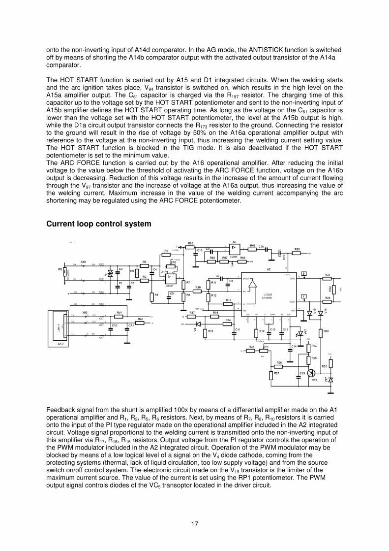
Current loop control system
Feedback signal from the shunt is amplified 100x by means of a differential amplifier made on the A1operational amplifier and R1, R2, R5, R6 resistors. Next, by means of R7, R8, R10 resistors it is carriedonto the input of the PI type regulator made on the operational amplifier included in the A2 integratedcircuit. Voltage signal proportional to the welding current is transmitted onto the non-inverting input ofthis amplifier via R17, R16, R15 resistors. Output voltage from the PI regulator controls the operation ofthe PWM modulator included in the A2 integrated circuit. Operation of the PWM modulator may beblocked by means of a low logical level of a signal on the V4 diode cathode, coming from theprotecting systems (thermal, lack of liquid circulation, too low supply voltage) and from the sourceswitch on/off control system. The electronic circuit made on the V19 transistor is the limiter of themaximum current source. The value of the current is set using the RP1 potentiometer. The PWMoutput signal controls diodes of the VC5 transoptor located in the driver circuit.
18
A voltage measurement signal proportional to the welding current is transmitted to the LM11/1 boardlocated on the A12 panel via the RC filter composed of RA1 and CA1 elements. The welding voltagemeasurement signal is carried to the LM11/1 board via the filter composed of RV1 and CV1 elements.
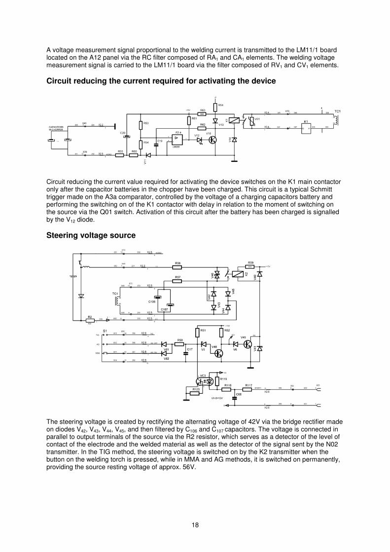
Circuit reducing the current required for activating the device
Circuit reducing the current value required for activating the device switches on the K1 main contactoronly after the capacitor batteries in the chopper have been charged. This circuit is a typical Schmitttrigger made on the A3a comparator, controlled by the voltage of a charging capacitors battery andperforming the switching on of the K1 contactor with delay in relation to the moment of switching onthe source via the Q01 switch. Activation of this circuit after the battery has been charged is signalledby the V12 diode.
Steering voltage source
The steering voltage is created by rectifying the alternating voltage of 42V via the bridge rectifier madeon diodes V42, V43, V44, V45, and then filtered by C106 and C107 capacitors. The voltage is connected inparallel to output terminals of the source via the R2 resistor, which serves as a detector of the level ofcontact of the electrode and the welded material as well as the detector of the signal sent by the N02transmitter. In the TIG method, the steering voltage is switched on by the K2 transmitter when thebutton on the welding torch is pressed, while in MMA and AG methods, it is switched on permanently,providing the source resting voltage of approx. 56V.
19
Activation in TIG method
After pressing the button on the torch, the current flow through the VC3 transoptor takes place.Switching on the transistor of the VC3 transoptor results in cutting the V48 transistor off and unblockingthe PWM generator in the A2 integrated circuit. Switching on of the steering voltage via the V49
transistor switching on the K2 transmitter also takes place.
Selecting the welding method
The system of selecting the welding method cooperates with the S1 welding method selecting switchlocated on the A11 or A12 panel and connected to the CH21/1 board via the X2.8B connector. If theS1 switch is set to the MMA mode, the steering voltage source is switched on permanently via the V82
diode and the PWM circuit is unblocked. The ANTISTICK function is also switched on, along with thedelay of activating this function. If the S1 switch is set to the AG mode, the steering voltage source andthe PWM circuit are still switched on in the standby mode. The ANTISTICK function is switched off bymeans of shorting the A14b comparator output via the switched on A14a comparator. In the TIGmode, the steering voltage source is switched off and the PWM circuit is blocked until the buttonlocated on the welding torch is pressed. The ANTISTICK function activation delay is also switched off.
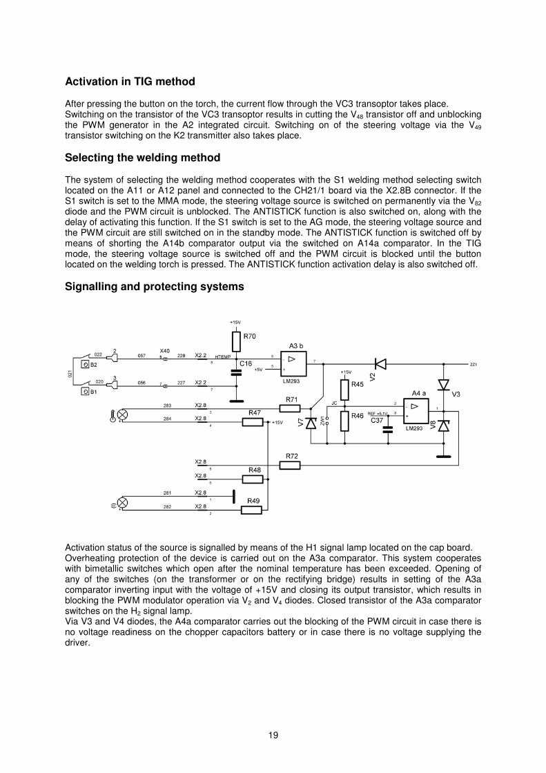
Signalling and protecting systems
Activation status of the source is signalled by means of the H1 signal lamp located on the cap board.Overheating protection of the device is carried out on the A3a comparator. This system cooperateswith bimetallic switches which open after the nominal temperature has been exceeded. Opening ofany of the switches (on the transformer or on the rectifying bridge) results in setting of the A3acomparator inverting input with the voltage of +15V and closing its output transistor, which results inblocking the PWM modulator operation via V2 and V4 diodes. Closed transistor of the A3a comparatorswitches on the H2 signal lamp.Via V3 and V4 diodes, the A4a comparator carries out the blocking of the PWM circuit in case there isno voltage readiness on the chopper capacitors battery or in case there is no voltage supplying thedriver.
20
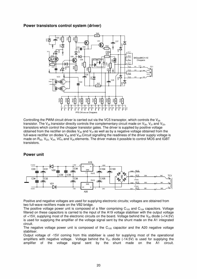
Power transistors control system (driver)
Controlling the PWM circuit driver is carried out via the VC5 transoptor, which controls the V29
transistor. The V29 transistor directly controls the complementary circuit made on V30, V31 and V33,transistors which control the chopper transistor gates. The driver is supplied by positive voltageobtained from the rectifier on diodes V36 and V37 as well as by a negative voltage obtained from thefull-wave rectifier on diodes V38 and V39.Circuit signalling the readiness of the driver supply voltage ismade on R32, V23, V24, VC4 and V25 elements. The driver makes it possible to control MOS and IGBTtransistors.
Power unit
Positive and negative voltages are used for supplying electronic circuits; voltages are obtained fromtwo full-wave rectifiers made on the VB2 bridge.The positive voltage power unit is composed of a filter comprising C103 and C104 capacitors. Voltagefiltered on these capacitors is carried to the input of the A19 voltage stabiliser with the output voltageof +15V, supplying most of the electronic circuits on the board. Voltage behind the V20 diode (+14.5V)is used for supplying the amplifier of the voltage signal sent by the shunt made on the A1 integratedcircuit.The negative voltage power unit is composed of the C105 capacitor and the A20 negative voltagestabiliser.Output voltage of -15V coming from this stabiliser is used for supplying most of the operationalamplifiers with negative voltage. Voltage behind the V21 diode (-14.5V) is used for supplying theamplifier of the voltage signal sent by the shunt made on the A1 circuit.
21
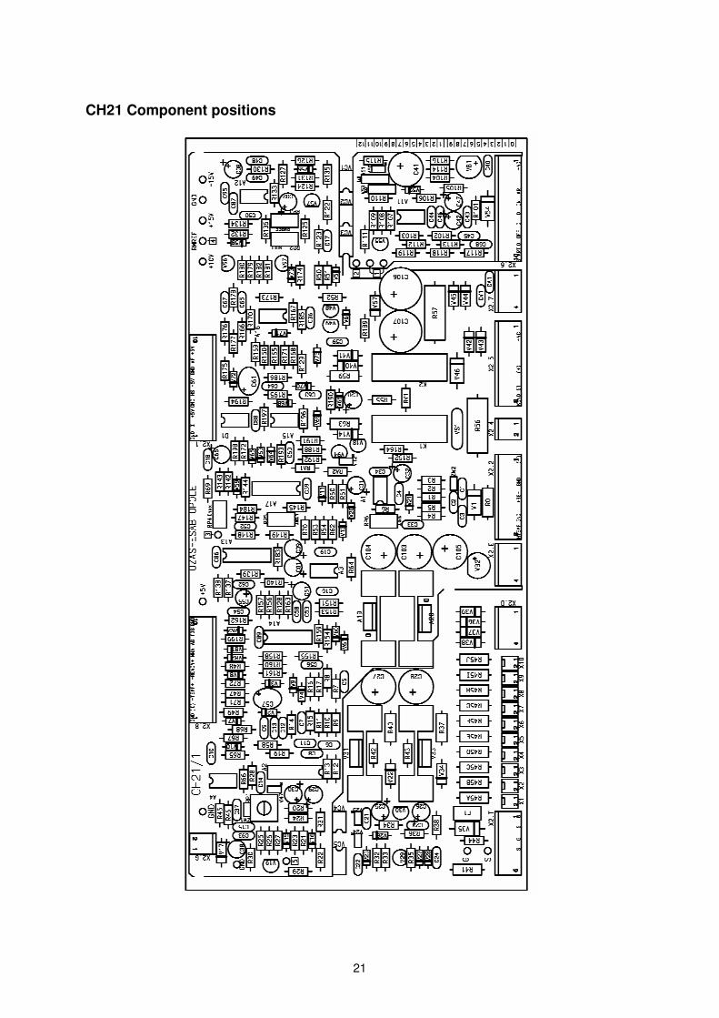
CH21 Component positions
22
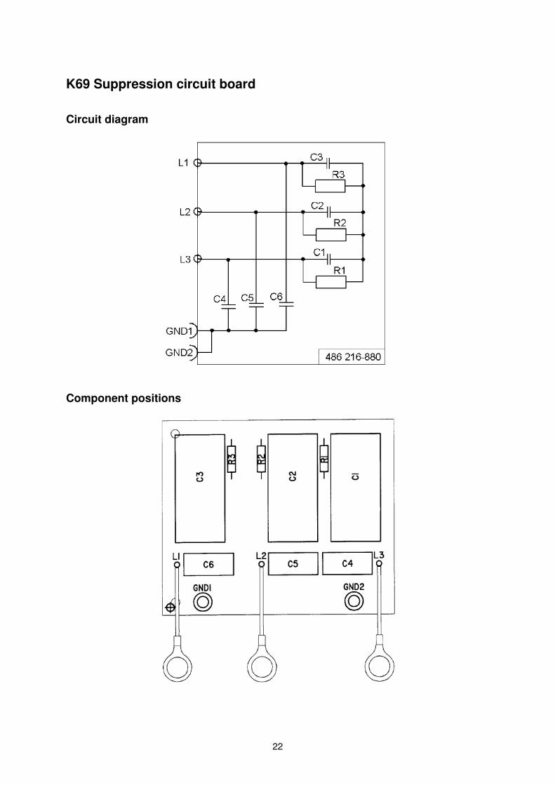
K69 Suppression circuit board
Circuit diagram
Component positions

23
REMOTE CONTROLS
Remote control MMA1, MMA2, AT1, AT1 CoarseFine can be connected to the powersources. Wireless N02 can be connected to the power sources with A12 panel. Remotecontrols are described in a separate service manual with filename / ordering no. xxx.
SERVICE INSTRUCTION
What is ESD?A sudden transfer or discharge of static electricity from one object to another. ESD stands forElectrostatic Discharge.
How does ESD damage occur?
ESD can cause damage to sensitive electrical components, but is not dangerous to people.ESD damage occurs when an ungrounded person or object with a static charge comes intocontact with a component or assembly that is grounded. A rapid discharge can occur,causing damage. This damage can take the form of immediate failure, but it is more likelythat system performance will be affected and the component will fail prematurely.
How do we prevent ESD damage?
ESD damage can be prevented by awareness. If static electricity is prevented from buildingup on you or on anything at your work station, then there cannot be any static discharges.Nonconductive materials (e.g. fabrics), or insulators (e.g. plastics) generate and hold staticcharge, so you should not bring unnecessary nonconductive items into the work area.It is obviously difficult to avoid all such items, so various means are used to drain off anystatic discharge from persons to prevent the risk of ESD damage. This is done by simpledevices: wrist straps, connected to ground, and conductive shoes.
Work surfaces, carts and containers must be conductive and grounded. Use only antistaticpackaging materials. Overall, handling of ESD--sensitive devices should be minimized toprevent damage.
WARNING !STATIC ELECTRICITY can damage circuitboards and electronic components.
• Observe precautions for handling electrostatic-sensitive devices.
• Use proper static--proof bags and boxes.
24
Service aid
We can offer a number of service tools that will simplify the service.
Antistatic service kit
Ordering no. 0740 511 001
The kit makes it easier to protect sensitvecomponents from electrostatic discharge.
Contents:• A conductive mat (size 610 x 610 mm)• A 1.5 metre long ground cable with a crocodile clip• An adjustable wrist strap and cable with an inbuilt
protective resistorAntistatic service kit
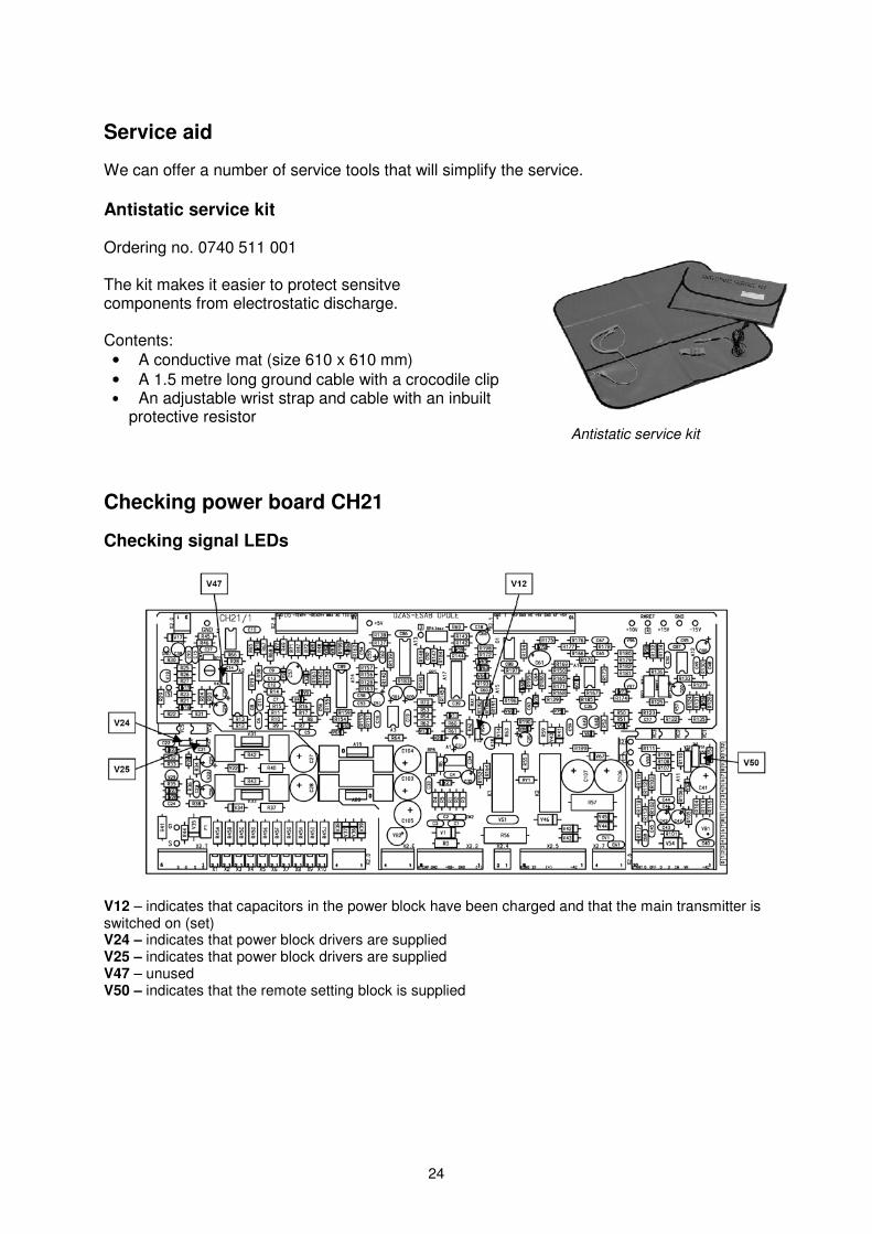
Checking power board CH21
Checking signal LEDs
V12 – indicates that capacitors in the power block have been charged and that the main transmitter isswitched on (set)V24 – indicates that power block drivers are suppliedV25 – indicates that power block drivers are suppliedV47 – unusedV50 – indicates that the remote setting block is supplied
25
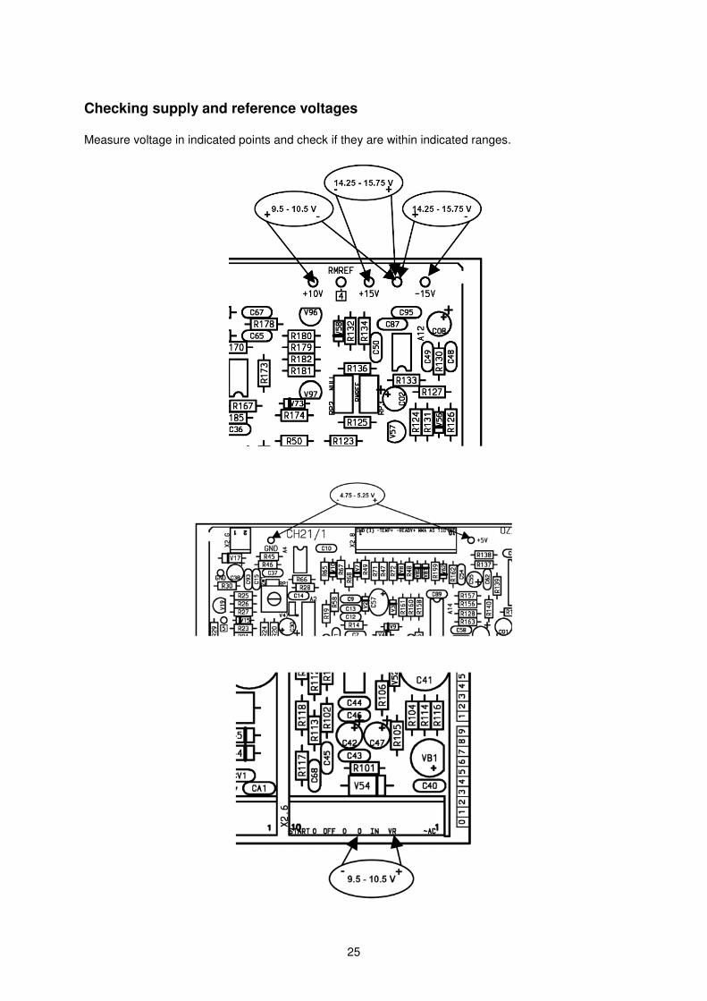
Checking supply and reference voltages
Measure voltage in indicated points and check if they are within indicated ranges.
26
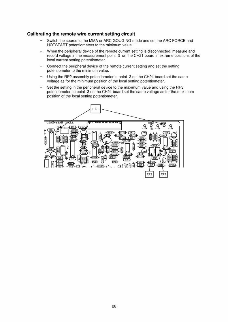
Calibrating the remote wire current setting circuit- Switch the source to the MMA or ARC GOUGING mode and set the ARC FORCE and
HOTSTART potentiometers to the minimum value.
- When the peripheral device of the remote current setting is disconnected, measure andrecord voltage in the measurement point 3 on the CH21 board in extreme positions of thelocal current setting potentiometer.
- Connect the peripheral device of the remote current setting and set the settingpotentiometer to the minimum value.
- Using the RP2 assembly potentiometer in point 3 on the CH21 board set the samevoltage as for the minimum position of the local setting potentiometer.
- Set the setting in the peripheral device to the maximum value and using the RP3potentiometer, in point 3 on the CH21 board set the same voltage as for the maximumposition of the local setting potentiometer.
27
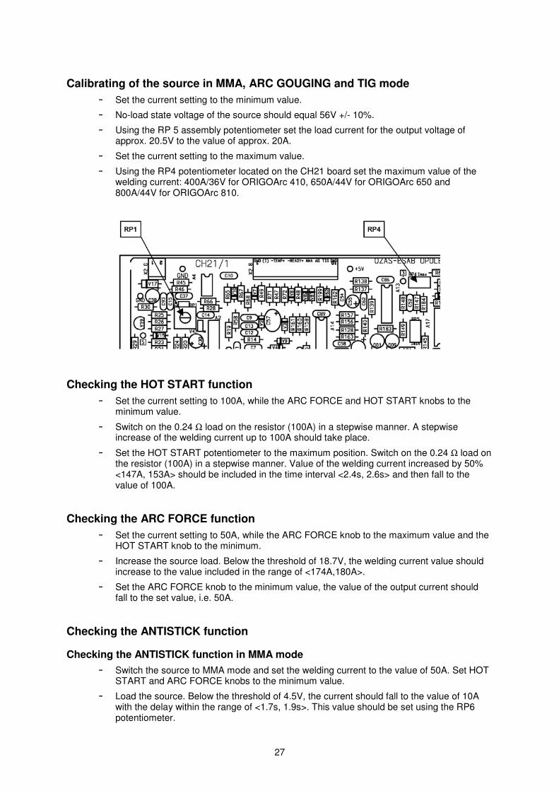
Calibrating of the source in MMA, ARC GOUGING and TIG mode- Set the current setting to the minimum value.
- No-load state voltage of the source should equal 56V +/- 10%.
- Using the RP 5 assembly potentiometer set the load current for the output voltage ofapprox. 20.5V to the value of approx. 20A.
- Set the current setting to the maximum value.
- Using the RP4 potentiometer located on the CH21 board set the maximum value of thewelding current: 400A/36V for ORIGOArc 410, 650A/44V for ORIGOArc 650 and800A/44V for ORIGOArc 810.
Checking the HOT START function- Set the current setting to 100A, while the ARC FORCE and HOT START knobs to the
minimum value.
- Switch on the 0.24 Ω load on the resistor (100A) in a stepwise manner. A stepwiseincrease of the welding current up to 100A should take place.
- Set the HOT START potentiometer to the maximum position. Switch on the 0.24 Ω load onthe resistor (100A) in a stepwise manner. Value of the welding current increased by 50%<147A, 153A> should be included in the time interval <2.4s, 2.6s> and then fall to thevalue of 100A.
Checking the ARC FORCE function- Set the current setting to 50A, while the ARC FORCE knob to the maximum value and the
HOT START knob to the minimum.
- Increase the source load. Below the threshold of 18.7V, the welding current value shouldincrease to the value included in the range of <174A,180A>.
- Set the ARC FORCE knob to the minimum value, the value of the output current shouldfall to the set value, i.e. 50A.
Checking the ANTISTICK function
Checking the ANTISTICK function in MMA mode
- Switch the source to MMA mode and set the welding current to the value of 50A. Set HOTSTART and ARC FORCE knobs to the minimum value.
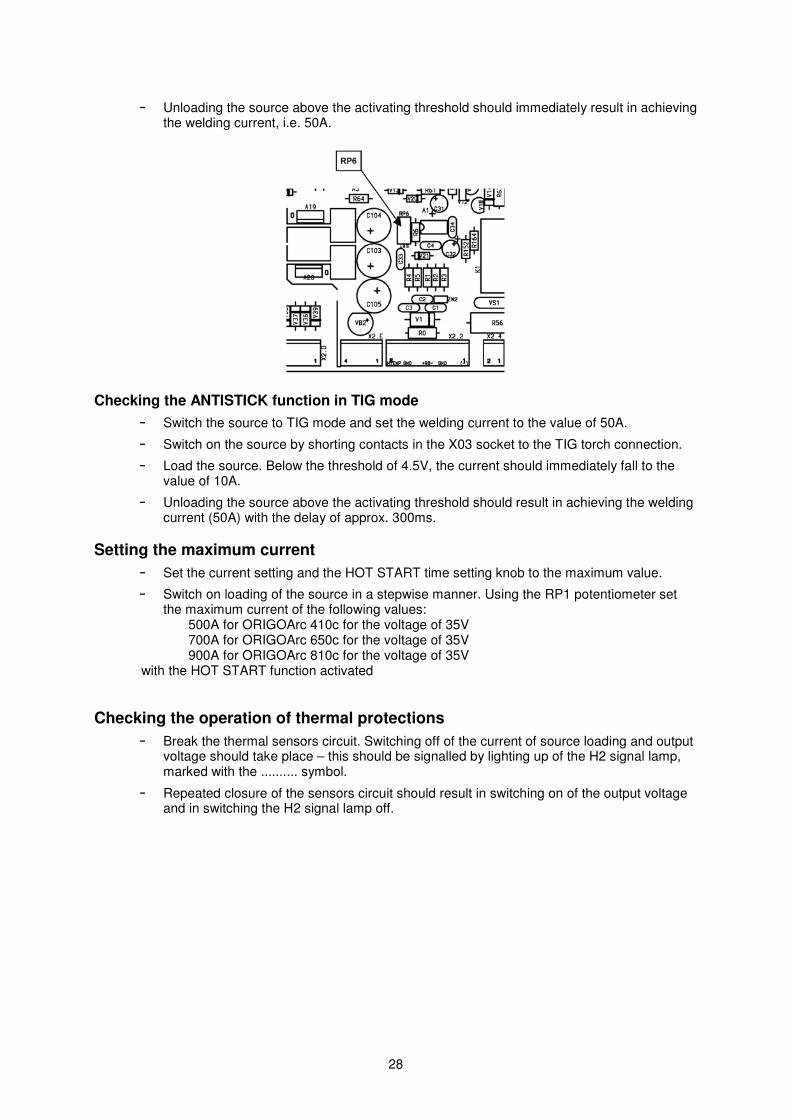
- Load the source. Below the threshold of 4.5V, the current should fall to the value of 10Awith the delay within the range of <1.7s, 1.9s>. This value should be set using the RP6potentiometer.
28
- Unloading the source above the activating threshold should immediately result in achievingthe welding current, i.e. 50A.
Checking the ANTISTICK function in TIG mode
- Switch the source to TIG mode and set the welding current to the value of 50A.
- Switch on the source by shorting contacts in the X03 socket to the TIG torch connection.
- Load the source. Below the threshold of 4.5V, the current should immediately fall to thevalue of 10A.
- Unloading the source above the activating threshold should result in achieving the weldingcurrent (50A) with the delay of approx. 300ms.
Setting the maximum current- Set the current setting and the HOT START time setting knob to the maximum value.
- Switch on loading of the source in a stepwise manner. Using the RP1 potentiometer setthe maximum current of the following values:
500A for ORIGOArc 410c for the voltage of 35V700A for ORIGOArc 650c for the voltage of 35V900A for ORIGOArc 810c for the voltage of 35V
with the HOT START function activated
Checking the operation of thermal protections- Break the thermal sensors circuit. Switching off of the current of source loading and output
voltage should take place – this should be signalled by lighting up of the H2 signal lamp,marked with the .......... symbol.
- Repeated closure of the sensors circuit should result in switching on of the output voltageand in switching the H2 signal lamp off.
29
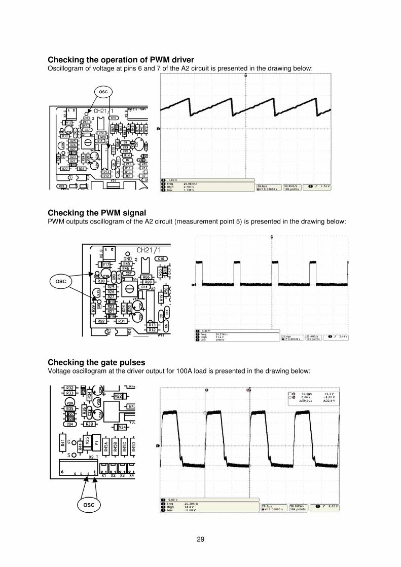
Checking the operation of PWM driverOscillogram of voltage at pins 6 and 7 of the A2 circuit is presented in the drawing below:
Checking the PWM signalPWM outputs oscillogram of the A2 circuit (measurement point 5) is presented in the drawing below:
Checking the gate pulsesVoltage oscillogram at the driver output for 100A load is presented in the drawing below:
30
Checking display board LM11
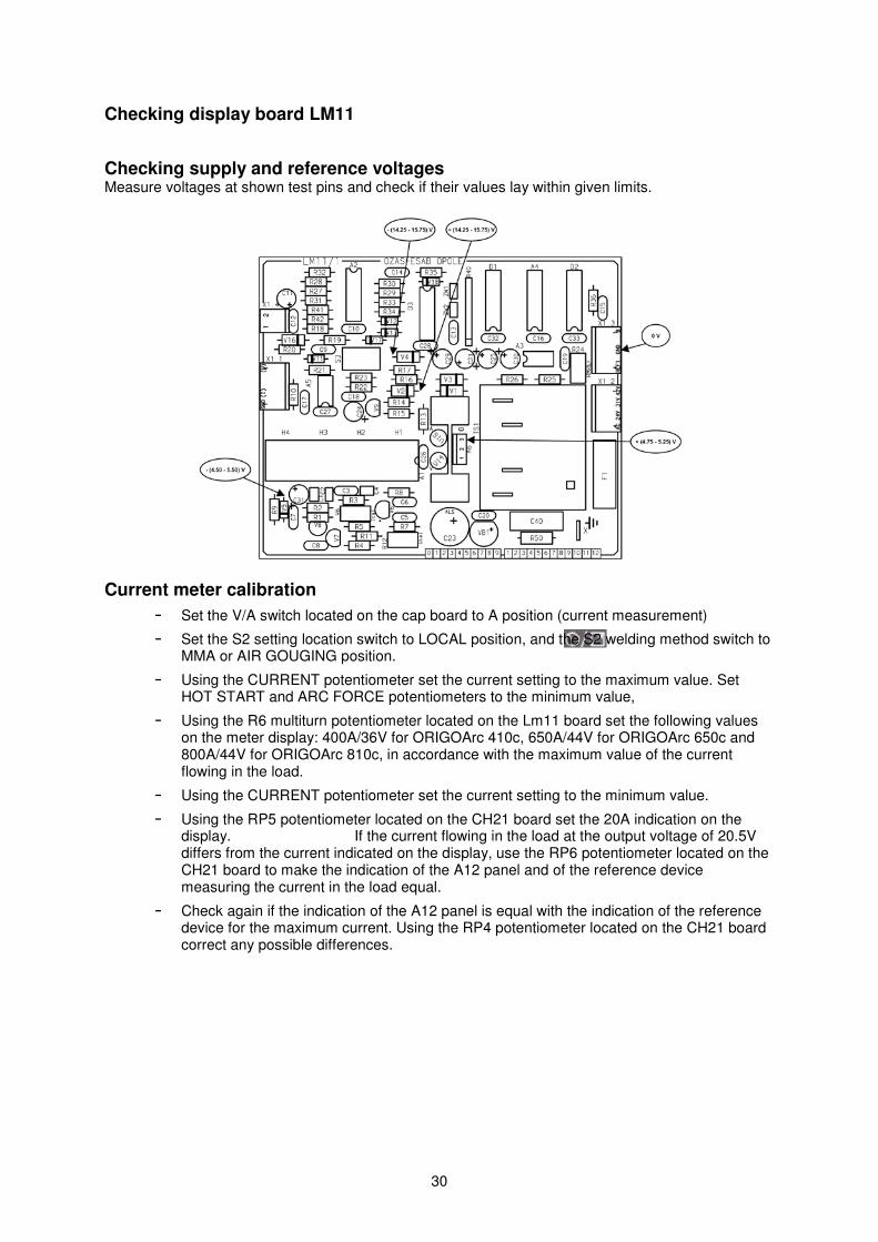
Checking supply and reference voltagesMeasure voltages at shown test pins and check if their values lay within given limits.
Current meter calibration- Set the V/A switch located on the cap board to A position (current measurement)
- Set the S2 setting location switch to LOCAL position, and the S2 welding method switch toMMA or AIR GOUGING position.
- Using the CURRENT potentiometer set the current setting to the maximum value. SetHOT START and ARC FORCE potentiometers to the minimum value,
- Using the R6 multiturn potentiometer located on the Lm11 board set the following valueson the meter display: 400A/36V for ORIGOArc 410c, 650A/44V for ORIGOArc 650c and800A/44V for ORIGOArc 810c, in accordance with the maximum value of the currentflowing in the load.
- Using the CURRENT potentiometer set the current setting to the minimum value.
- Using the RP5 potentiometer located on the CH21 board set the 20A indication on thedisplay. If the current flowing in the load at the output voltage of 20.5Vdiffers from the current indicated on the display, use the RP6 potentiometer located on theCH21 board to make the indication of the A12 panel and of the reference devicemeasuring the current in the load equal.
- Check again if the indication of the A12 panel is equal with the indication of the referencedevice for the maximum current. Using the RP4 potentiometer located on the CH21 boardcorrect any possible differences.
31
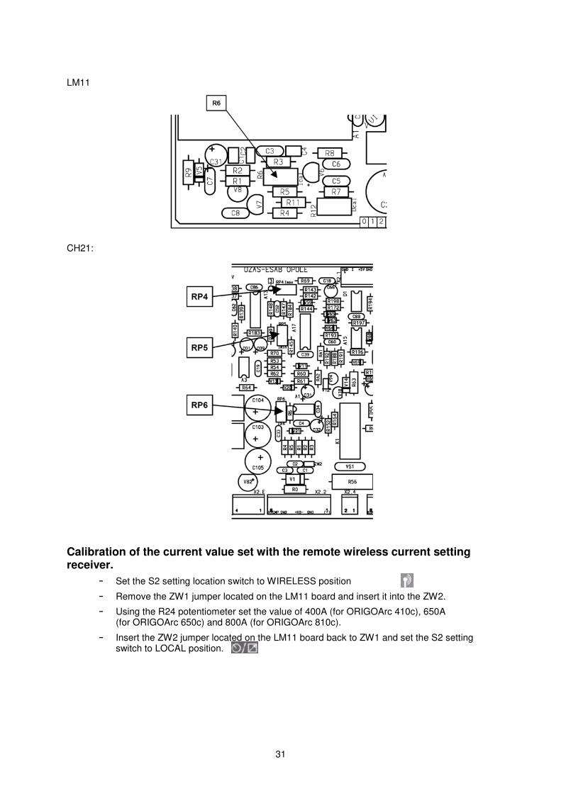
LM11
CH21:
Calibration of the current value set with the remote wireless current settingreceiver.
- Set the S2 setting location switch to WIRELESS position
- Remove the ZW1 jumper located on the LM11 board and insert it into the ZW2.
- Using the R24 potentiometer set the value of 400A (for ORIGOArc 410c), 650A(for ORIGOArc 650c) and 800A (for ORIGOArc 810c).
- Insert the ZW2 jumper located on the LM11 board back to ZW1 and set the S2 settingswitch to LOCAL position.
32
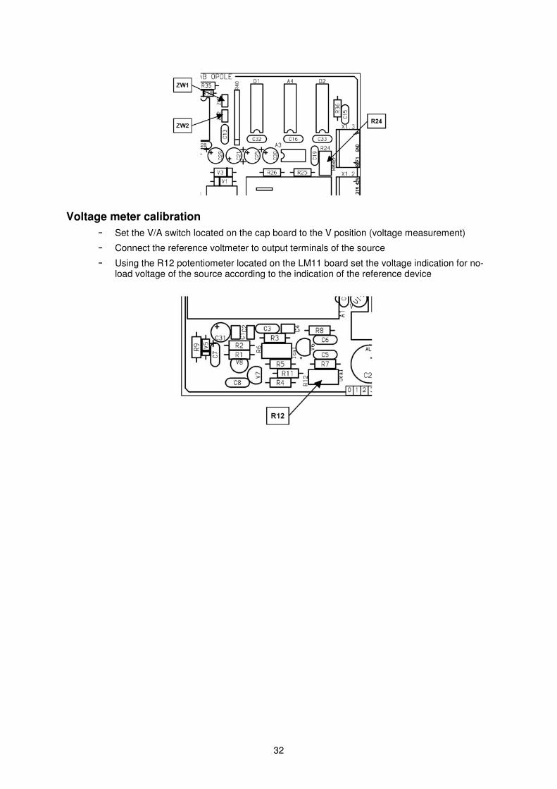
Voltage meter calibration- Set the V/A switch located on the cap board to the V position (voltage measurement)
- Connect the reference voltmeter to output terminals of the source
- Using the R12 potentiometer located on the LM11 board set the voltage indication for no-load voltage of the source according to the indication of the reference device
33
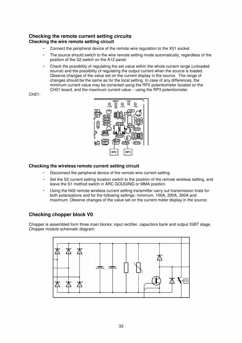
Checking the remote current setting circuitsChecking the wire remote setting circuit
- Connect the peripheral device of the remote wire regulation to the X01 socket
- The source should switch to the wire remote setting mode automatically, regardless of theposition of the S2 switch on the A12 panel.
- Check the possibility of regulating the set value within the whole current range (unloadedsource) and the possibility of regulating the output current when the source is loaded.Observe changes of the value set on the current display in the source. The range ofchanges should be the same as for the local setting. In case of any differences, theminimum current value may be corrected using the RP2 potentiometer located on theCH31 board, and the maximum current value – using the RP3 potentiometer.
CH21:
Checking the wireless remote current setting circuit
- Disconnect the peripheral device of the remote wire current setting.
- Set the S2 current setting location switch to the position of the remote wireless setting, andleave the S1 method switch in ARC GOUGING or MMA position.
- Using the N02 remote wireless current setting transmitter carry out transmission trials forboth polarisations and for the following settings: minimum, 100A, 200A, 300A andmaximum. Observe changes of the value set on the current meter display in the source.
Checking chopper block V0
Chopper is assembled form three main blocks: input rectifier, capacitors bank and output IGBT stage.Chopper module schematic diagram:
34
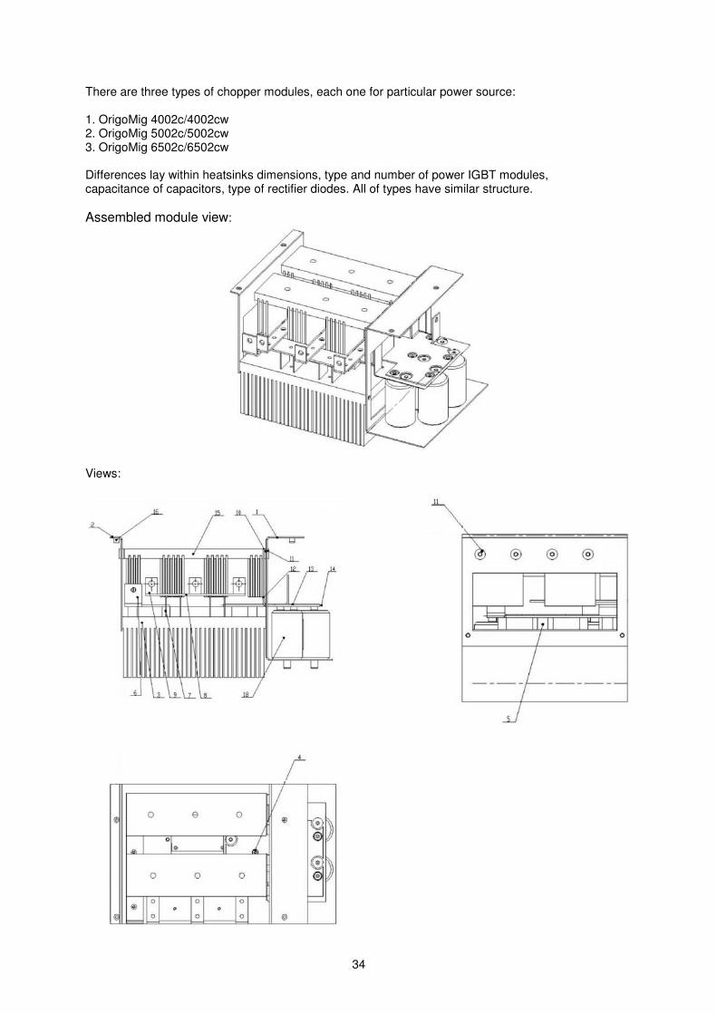
There are three types of chopper modules, each one for particular power source:
1. OrigoMig 4002c/4002cw2. OrigoMig 5002c/5002cw3. OrigoMig 6502c/6502cw
Differences lay within heatsinks dimensions, type and number of power IGBT modules,capacitance of capacitors, type of rectifier diodes. All of types have similar structure.
Assembled module view:
Views:
35
Overview test
Each block consist of at least two serviceable parts. The first step of control is taking overview andchecking if any parts are looking abnormal. Broken parts can have marks of thermal damage, changeof colors or shape. If after that checking nothing was find out next step is electrical testing.
Rectifier test
The first part for test is input rectifier consisted of diodes and two heatsinks (details no 15). Oneheatsink is on positive potential and second on negative one. For checking diodes following steps canbe achieved:
1. Use measuring instrument with semiconductor conduction test possibility. Connect oneterminal to one phase AC input ( detail no 9) and second to front (opposite side to ACterminals) heatsink (detail no. 15). If diode is conducting from AC to heatsink, replacemeasuring terminals and check if diode is blocked. If so, diode is working properly in thisphase.
2. Next check second diode in this phase by opposite side conduction test. Diode can conductfrom heatsink to AC terminal. If so diode in this phase is working properly.
3. If diode is short circuited or non conducted in both sides it means diode is broken and itsreplace is necessary. Diode is screwed into aluminum heatsink and has to be carefullyremoved and new one screwed with torque 10Nm/90lb.in
4. Repeat that test in other phases.
Important note - in case of damage any diode replace both in each broken switch.
For easy disassembly unscrew both rectifier heatsinks from capacitors side and plastic shelf with ACterminals and disassembly two M6 screws into down heatsink on opposite side.
Important note – all diode threads have to be covered by very thin layer by No. 2 Electro JointCompound before replacing. Also heatsink side which is connected to DC-link has to be covered byNo.2 EJC.
Checking of output stage.
Output stage is made of IGBT modules assembled on main heatsink. Each module is covered by PCBwith gate resistors and protection diodes. For detection of transistors go in following order:
1. Check transistors’ gate resistance and if is lower than 800Ω it means transistor’s gate isbroken. For this test use measuring instrument and measure resistance between red andblack cables in pairs into control plug. If at least one pair’s resistance is lower than limit bothtransistors have to be replaced.
2. Modules are working in parallel but are electrically working as single switch one diode and onetransistor.
3. Check chopper diode – using diode conduction tester check if between output “minus”terminal and output “plus” terminal diode is conducting. After passing this test check if diode isblocked ( non conducting) in opposite direction. If test is positive diodes are working properly.
4. Checking chopper transistor.a. First measure resistance between output minus and battery minus terminals. If it is
short circuited at least one transistor is broken. Both transistors should be replaced.b. If transistor gates are properly working and no short circuit is detected use 15V DC
100mA supply source and connect positive potential to red control cable and negativeto black control cable. After supplying gate transistor switch should be detected asconducting between output minus and battery minus outputs. Battery minus isavailable on second heatsink and DC-capacitors link and as additional washer withconnector on capacitors. Side
36
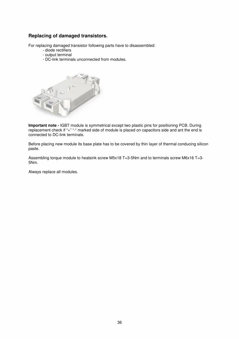
Replacing of damaged transistors.
For replacing damaged transistor following parts have to disassembled:- diode rectifiers- output terminal- DC-link terminals unconnected from modules.
Important note - IGBT module is symmetrical except two plastic pins for positioning PCB. Duringreplacement check if “+” “-“ marked side of module is placed on capacitors side and ant the end isconnected to DC-link terminals.
Before placing new module its base plate has to be covered by thin layer of thermal conducing siliconpaste.
Assembling torque module to heatsink screw M5x18 T=3-5Nm and to terminals screw M6x16 T=3-5Nm.
Always replace all modules.

37
NOTES

ESAB ABSE--695 81 LAXÅSWEDENPhone +46 584 81 000
www.esab.com
070514
ESAB subsidiaries and representative offices
EuropeAUSTRIAESAB Ges.m.b.HVienna--LiesingTel: +43 1 888 25 11Fax: +43 1 888 25 11 85
BELGIUMS.A. ESAB N.V.BrusselsTel: +32 2 745 11 00Fax: +32 2 745 11 28
THE CZECH REPUBLICESAB VAMBERK s.r.o.VamberkTel: +420 2 819 40 885Fax: +420 2 819 40 120
DENMARKAktieselskabet ESABHerlevTel: +45 36 30 01 11Fax: +45 36 30 40 03
FINLANDESAB OyHelsinkiTel: +358 9 547 761Fax: +358 9 547 77 71
FRANCEESAB France S.A.Cergy PontoiseTel: +33 1 30 75 55 00Fax: +33 1 30 75 55 24
GERMANYESAB GmbHSolingenTel: +49 212 298 0Fax: +49 212 298 218
GREAT BRITAINESAB Group (UK) LtdWaltham CrossTel: +44 1992 76 85 15Fax: +44 1992 71 58 03
ESAB Automation LtdAndoverTel: +44 1264 33 22 33Fax: +44 1264 33 20 74
HUNGARYESAB KftBudapestTel: +36 1 20 44 182Fax: +36 1 20 44 186
ITALYESAB Saldatura S.p.A.Mesero (Mi)Tel: +39 02 97 96 81Fax: +39 02 97 28 91 81
THE NETHERLANDSESAB Nederland B.V.AmersfoortTel: +31 33 422 35 55Fax: +31 33 422 35 44
NORWAYAS ESABLarvikTel: +47 33 12 10 00Fax: +47 33 11 52 03
POLANDESAB Sp.zo.o.KatowiceTel: +48 32 351 11 00Fax: +48 32 351 11 20
PORTUGALESAB LdaLisbonTel: +351 8 310 960Fax: +351 1 859 1277
SLOVAKIAESAB Slovakia s.r.o.BratislavaTel: +421 7 44 88 24 26Fax: +421 7 44 88 87 41
SPAINESAB Ibérica S.A.Alcalá de Henares (MADRID)Tel: +34 91 878 3600Fax: +34 91 802 3461
SWEDENESAB Sverige ABGothenburgTel: +46 31 50 95 00Fax: +46 31 50 92 22
ESAB international ABGothenburgTel: +46 31 50 90 00Fax: +46 31 50 93 60
SWITZERLANDESAB AGDietikonTel: +41 1 741 25 25Fax: +41 1 740 30 55
North and South AmericaARGENTINACONARCOBuenos AiresTel: +54 11 4 753 4039Fax: +54 11 4 753 6313
BRAZILESAB S.A.Contagem--MGTel: +55 31 2191 4333Fax: +55 31 2191 4440
CANADAESAB Group Canada Inc.Missisauga, OntarioTel: +1 905 670 02 20Fax: +1 905 670 48 79
MEXICOESAB Mexico S.A.MonterreyTel: +52 8 350 5959Fax: +52 8 350 7554
USAESAB Welding & Cutting ProductsFlorence, SCTel: +1 843 669 44 11Fax: +1 843 664 57 48
Asia/PacificCHINAShanghai ESAB A/PShanghaiTel: +86 21 5308 9922Fax: +86 21 6566 6622
INDIAESAB India LtdCalcuttaTel: +91 33 478 45 17Fax: +91 33 468 18 80
INDONESIAP.T. ESABindo PratamaJakartaTel: +62 21 460 0188Fax: +62 21 461 2929
JAPANESAB JapanTokyoTel: +81 3 5296 7371Fax: +81 3 5296 8080
MALAYSIAESAB (Malaysia) Snd BhdSelangorTel: +60 3 8027 9869Fax: +60 3 8027 4754
SINGAPOREESAB Asia/Pacific Pte LtdSingaporeTel: +65 6861 43 22Fax: +65 6861 31 95
SOUTH KOREAESAB SeAH CorporationKyungnamTel: +82 55 269 8170Fax: +82 55 289 8864
UNITED ARAB EMIRATESESAB Middle East FZEDubaiTel: +971 4 887 21 11Fax: +971 4 887 22 63
Representative officesBULGARIAESAB Representative OfficeSofiaTel/Fax: +359 2 974 42 88
EGYPTESAB EgyptDokki--CairoTel: +20 2 390 96 69Fax: +20 2 393 32 13
ROMANIAESAB Representative OfficeBucharestTel/Fax: +40 1 322 36 74
RUSSIALLC ESABMoscowTel: +7 095 543 9281Fax: +7 095 543 9280
LLC ESABSt PetersburgTel: +7 812 336 7080Fax: +7 812 336 7060
DistributorsFor addresses and phonenumbers to our distributors inother countries, please visit ourhome page
www.esab.com