applied physics - viden.io
TRANSCRIPT
*Institute Accredited by National Assessment and Accreditation Council (NAAC), Bangalore#
Accredited Programmes by National Board of Accreditation, New Delhi**ISO 9001 : 2015 Certified *Permanent Affiliated UG Programmes : • Computer Engineering • Electronics & Telecommunication Engineering • Information Technology (w.e.f. A.Y. 2015-16) • Electronics Engineering (w.e.f. A.Y. 2017-18)**1st time NBA Accredited UG Programmes : • Computer Engineering • Electronics & Telecommunication Engineering • Information Technology (3 years w.e.f. 16-09-2011)
• Computer Engineering • Electronics & Telecommunication Engineering • Information Technology • Electronics Engineering (3 years w.e.f. 01-07-2016)**2nd time NBA Accredited UG Programmes : • "A" Grade for 5 years (w.e.f. 30-10-2017)# 1st cycle of NAAC Accreditation :
AppliedPhysics - I
Applied Physics – I
University Examination
Solved Question Papers
2013 to 2018
1
Applied Physics – I (Sem-I) May-2013 Con. 6874-13. (REVISED COURSE) GS-S193 Time : 2 Hours Total Marks : 60 _________________________________________________________________________________ N.B. : (1) Question No.1 is compulsory.
(2) Attempt any three questions from remaining Question Nos. 2 to 6.
(3) Assume suitable data wherever required.
(4) Figures to the right indicate marks.
1. Attempt any five (Each carry equal weightage) :- 15
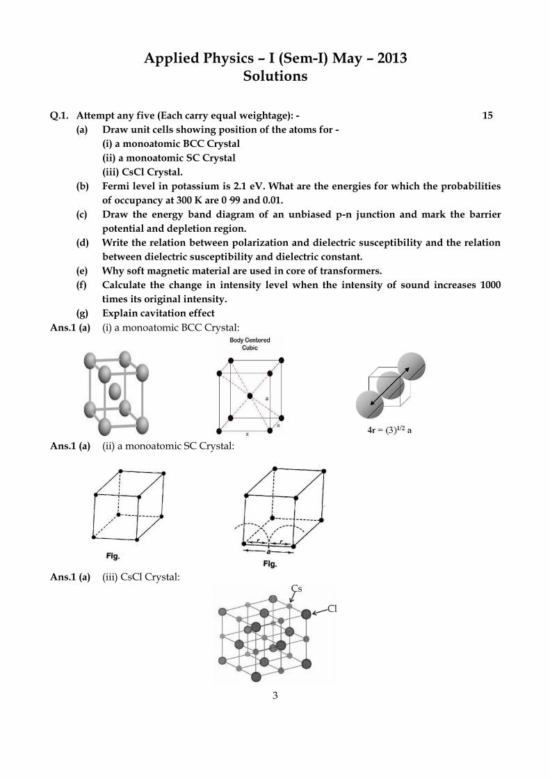
(a) Draw unit cells showing position of the atoms for -
(i) a monoatomic BCC Crystal
(ii) a monoatomic SC Crystal
(iii) CsCI Crystal.
(b) Fermi level in potassium is 2.1 eV. What are the energies for which the probabilities of
occupancy at 300 K are 0·99 and 0.01.
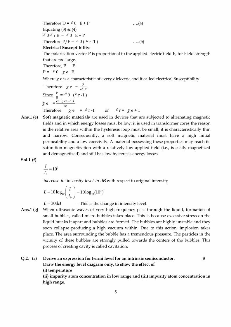
(c) Draw the energy band diagram of an unbiased p-n junction and mark the barrier
potential and depletion region.
(d) Write the relation between polarization and dielectric susceptibility and the relation
between dielectric susceptibility and dielectric constant.
(e) Why soft magnetic material are used in core of transformers.
(f) Calculate the change in intensity level when the intensity of sound increases 1000 times
its original intensity.
(g) Explain cavitation effect
2. (a) Derive an expression for Fermi level for an intrinsic semiconductor. 8
Draw the energy level diagram only, to show the effect of
(i) temperature
(ii) impurity atom concentration in low range and (iii) impurity atom concentration in
high range.
(b) An elemental crystal has a density of 8570 kg/m3 packing fraction is 0·68. Determine the
mass' of one atom if the nearest neighbour distance is 2.86 Ao. 7
3. (a) Prove that in a ferromagnetic material, power loss per unit volume in a hysteresis cycle
is equal to the area under hysteresis loop. (4 + 4)
An iron ring of mean circumferential length 30 cm and cross-sectional area 1 cm2 is
wound uniformly with 300 turns of a wire. When a current of 0·032 Amp flows in it, the
flux produced in the ring is 2 x 10⁻⁶wb. Find the flux density, magnetic field intensity
and permeability of iron.
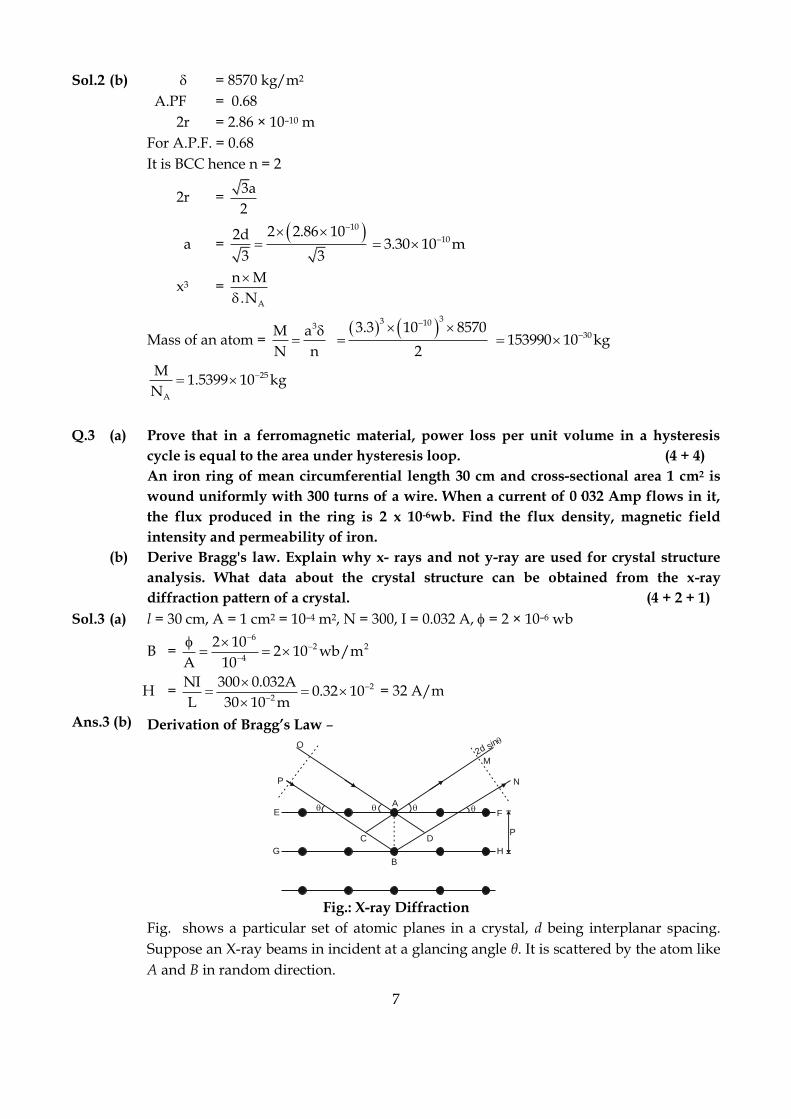
(b) Derive Bragg's law. Explain why x- rays and not y-ray are used for crystal structure
analysis. What data about the crystal structure can be obtained from the x-ray
diffraction pattern of a crystal. (4 + 2 + 1)
2
4. (a) Find out the critical radius ratio of an ionic crystal in ligancy 6 configuration. What is the
maximum size of cation in ligancy 6 configuration when the radius of anion is 2.02 Å.
5
(b) In an n type semiconductor, the Fermi level lies 0.4 eV below the conduction band. If
the concentration of donor atom is doubled, find the new position of the Fermi level
with respect to the conduction band. 5
(c) Explain the origin of electronic, ionic and orientational polarization and temperature
dependence of respective polarizability. 5
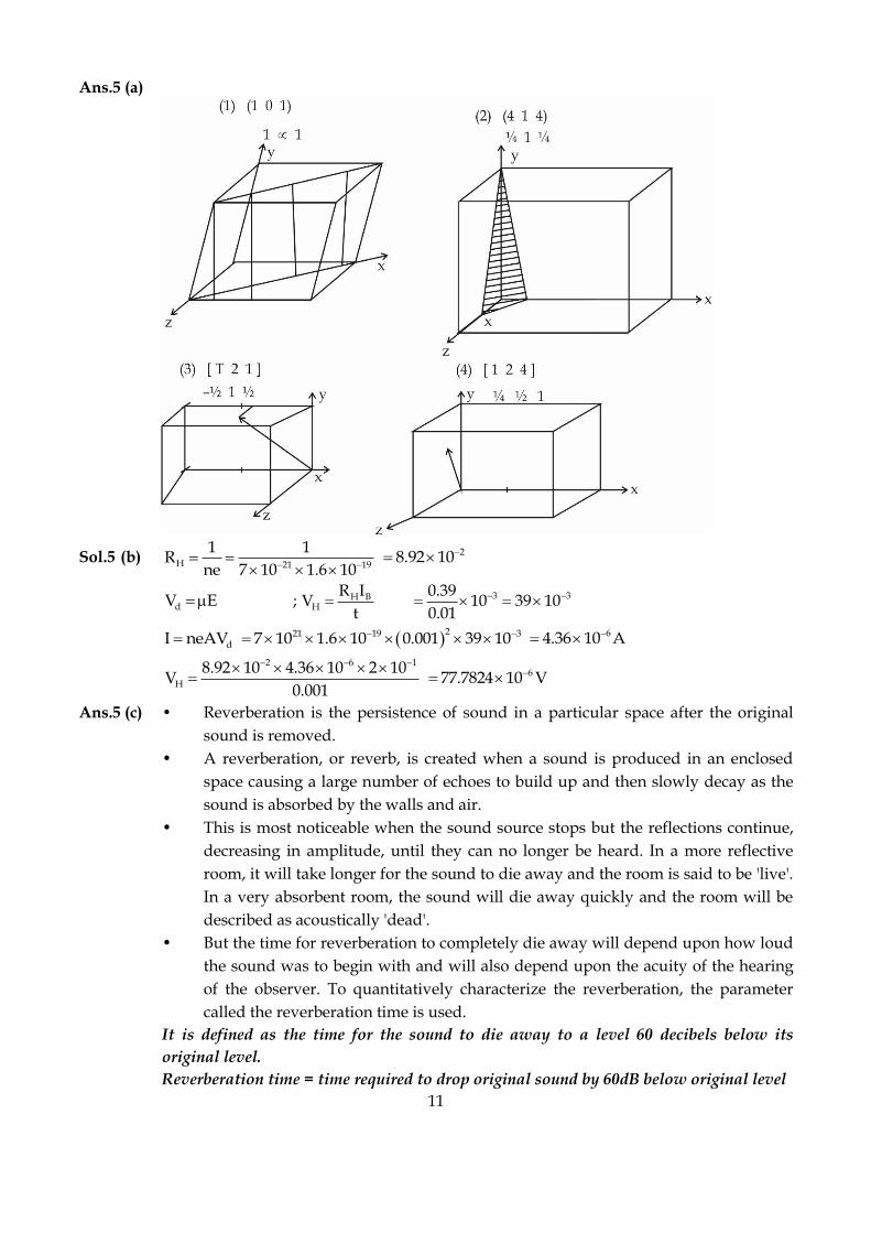
5. (a) Find out the intercepts made by the planes (1 0 1) and (4 1 4) in a cubic unit cell. 5
Draw [T 2 1] and [1 2 4] in a cubic unit cell.
(b) A bar of n type Ge of size 0.010m x 0.001m x 0.001m is mounted in a Magnetic field of
2 x 10⁻¹T. The electron density in the bar is 7 x 10²¹/m3. If one milli volt is applied across
the long ends of the bar, determine the current through the bar and the voltage between
Hall electrodes placed across the short dimensions of the bar. Assume μe = 0·39 m2/vs. 5
(c) Define reverberation time. Write Sabine's formula explaining every term. What are the
factors which determine the average absorption co-efficient of a material? 5
6. (a) Explain the differences between three different liquid crystal phases with respect to the
order in the arrangement of molecules, with the help of diagram. Which property of the
liquid crystal is used for display? 5
(b) How a p-n junction diode is used to generate a potential difference in a photovoltaic
solar cell? 5
(c) What is piezoelectric effect? Explain the working of a piezoelectric oscillator used to
produce ultrasonic wave. 5
**************************
3
Applied Physics – I (Sem-I) May – 2013 Solutions
Q.1. Attempt any five (Each carry equal weightage): - 15
(a) Draw unit cells showing position of the atoms for -
(i) a monoatomic BCC Crystal
(ii) a monoatomic SC Crystal
(iii) CsCl Crystal.
(b) Fermi level in potassium is 2.1 eV. What are the energies for which the probabilities
of occupancy at 300 K are 0·99 and 0.01.
(c) Draw the energy band diagram of an unbiased p-n junction and mark the barrier
potential and depletion region.
(d) Write the relation between polarization and dielectric susceptibility and the relation
between dielectric susceptibility and dielectric constant.
(e) Why soft magnetic material are used in core of transformers.
(f) Calculate the change in intensity level when the intensity of sound increases 1000
times its original intensity.
(g) Explain cavitation effect
Ans.1 (a) (i) a monoatomic BCC Crystal:
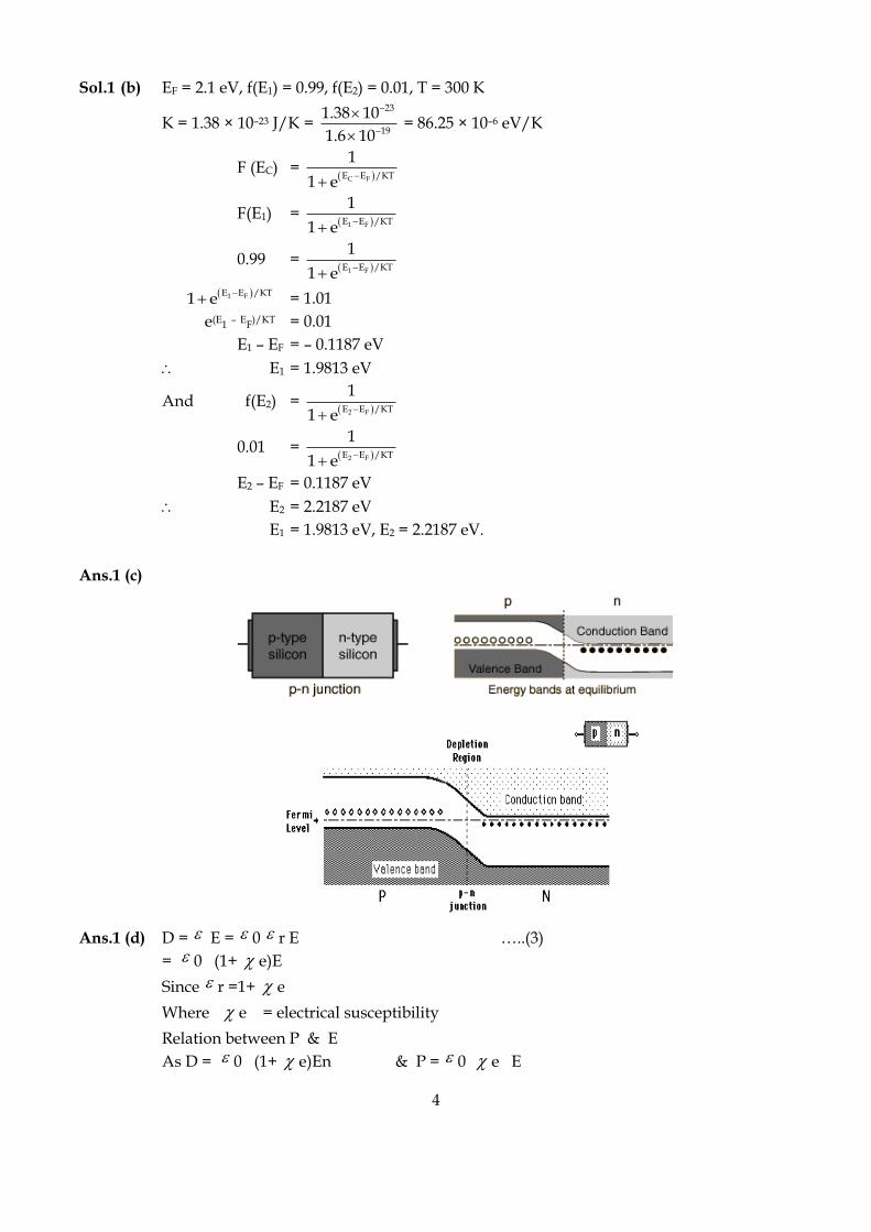
Ans.1 (a) (ii) a monoatomic SC Crystal:
Ans.1 (a) (iii) CsCl Crystal:
4
Sol.1 (b) EF = 2.1 eV, f(E1) = 0.99, f(E2) = 0.01, T = 300 K
K = 1.38 × 10⁻²³ J/K = 23
19
1.38 10
1.6 10
−
−
= 86.25 × 10⁻⁶ eV/K
F (EC) = ( )C FE E /KT
1
1 e−
+
F(E1) = ( )1 FE E /KT
1
1 e −+
0.99 = ( )1 FE E /KT
1
1 e −+
( )1 FE E /KT1 e −+ = 1.01
e(E1 – EF)/KT = 0.01
E1 – EF = – 0.1187 eV
E1 = 1.9813 eV
And f(E2) = ( )2 FE E /KT
1
1 e −+
0.01 = ( )2 FE E /KT
1
1 e −+
E2 – EF = 0.1187 eV
E2 = 2.2187 eV
E1 = 1.9813 eV, E2 = 2.2187 eV.
Ans.1 (c)
Ans.1 (d) D = E = 0 r E …..(3)
= 0 (1+ e)E
Since r =1+ e
Where e = electrical susceptibility
Relation between P & E
As D = 0 (1+ e)En & P = 0 e E
5
Therefore D = 0 E + P ….(4)
Equating (3) & (4) 0 r E = 0 E + P
Therefore P/E = 0 ( r -1 ) …..(5)
Electrical Susceptibility:
The polarization vector P is proportional to the applied electric field E, for Field strength
that are too large.
Therefore, P E
P = 0 e E
Where e is a characteristic of every dielectric and it called electrical Susceptibility
Therefore e = P
ϵ0 E
Since P
E = 0 ( r -1 )
e = ϵ0 ( ϵr −1 )
ϵ0
Therefore e = r -1 or r = e + 1
Ans.1 (e) Soft magnetic materials are used in devices that are subjected to alternating magnetic
fields and in which energy losses must be low; it is used in transformer cores the reason
is the relative area within the hysteresis loop must be small; it is characteristically thin
and narrow. Consequently, a soft magnetic material must have a high initial
permeability and a low coercivity. A material possessing these properties may reach its
saturation magnetization with a relatively low applied field (i.e., is easily magnetized
and demagnetized) and still has low hysteresis energy losses.
Sol.1 (f)
3
0
10=I
I
intincrease in ensity level in dB with respect to original intensity
10
0
10log
=
IL
I 3
1010log (10 )=
30=L dB – This is the change in intensity level.
Ans.1 (g) When ultrasonic waves of very high frequency pass through the liquid, formation of
small bubbles, called micro bubbles takes place. This is because excessive stress on the
liquid breaks it apart and bubbles are formed. The bubbles are highly unstable and they
soon collapse producing a high vacuum within. Due to this action, implosion takes
place. The area surrounding the bubble has a tremendous pressure. The particles in the
vicinity of these bubbles are strongly pulled towards the centers of the bubbles. This
process of creating cavity is called cavitation.
Q.2. (a) Derive an expression for Fermi level for an intrinsic semiconductor. 8
Draw the energy level diagram only, to show the effect of
(i) temperature
(ii) impurity atom concentration in low range and (iii) impurity atom concentration in
high range.
6
(b) An elemental crystal has a density of 8570 kg/m3 packing fraction is 0·68. Determine
the mass' of one atom if the nearest neighbour distance is 2·86 Ao. 7
Ans.2 (a) For intrinsic semiconductors, EF lies mid-way between conduction and valence band.
At any temperature T > 00 K,
ne = Number of electrons in conduction band
nv = Number of holes in valence band
We have
ne = Nce –(EC-EF)/KT …..(1)
where Nc = Effective density of states in conduction band
and nv = Nve –(EF – EV) / KT …..(2)
Where Nv = effective density of states in valence band
For best approximation Nc = Nv …..(3)
For intrinsic semiconductor
nC = nv
NC . e –(EC – EF) / KT = Nv . e –(EF – EV) / KT
( )
( )
C F
F V
E EKT
V
E EKT C
Ne
Ne
− −
−=
e –(EC – EF – EF + EV) / KT = cN
vN
e –(EC – EV – 2EF ) / KT = cN
vN
as Nv = Nc = 1
e –(EC – EV – 2EF ) / KT = 1
Taking In on both sides
KT
EEE Fvc )2( −+− = 0
(EC + EV) = 2 EF
EF = 2
vE+CE … (4)
Thus, Fermi level in an intrinsic semiconductor lies at the center of forbidden energy
gap.
N-type P-type
7
Sol.2 (b) = 8570 kg/m2
A.PF = 0.68
2r = 2.86 × 10⁻¹⁰ m
For A.P.F. = 0.68
It is BCC hence n = 2
2r = 3a
2
a = ( )102 2.86 102d
3 3
− = 103.30 10 m−=
x3 = A
n M
.N
Mass of an atom = 3M a
N n
=
( ) ( )33 103.3 10 8570
2
− = 30153990 10 kg−=
25
A
M1.5399 10 kg
N−=
Q.3 (a) Prove that in a ferromagnetic material, power loss per unit volume in a hysteresis
cycle is equal to the area under hysteresis loop. (4 + 4)
An iron ring of mean circumferential length 30 cm and cross-sectional area 1 cm2 is
wound uniformly with 300 turns of a wire. When a current of 0·032 Amp flows in it,
the flux produced in the ring is 2 x 10⁻⁶wb. Find the flux density, magnetic field
intensity and permeability of iron.
(b) Derive Bragg's law. Explain why x- rays and not y-ray are used for crystal structure
analysis. What data about the crystal structure can be obtained from the x-ray
diffraction pattern of a crystal. (4 + 2 + 1)
Sol.3 (a) l = 30 cm, A = 1 cm2 = 10–4 m2, N = 300, I = 0.032 A, = 2 × 10⁻⁶ wb
B = 6
2 2
4
2 102 10 wb/m
A 10
−−
−
= =
H = 2
2
NI 300 0.032A0.32 10
L 30 10 m−
−
= =
= 32 A/m
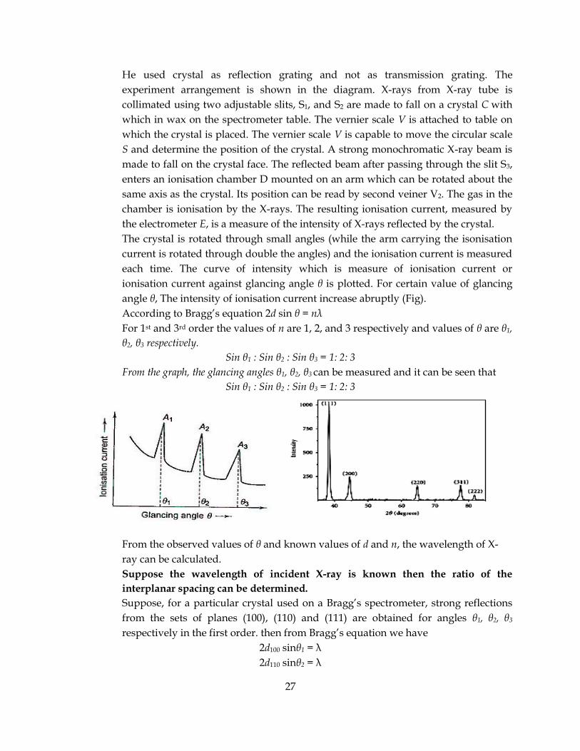
Ans.3 (b) Derivation of Bragg’s Law – O
P
E
G H
F
N
M
D
A
B
CP
2d sin
Fig.: X-ray Diffraction
Fig. shows a particular set of atomic planes in a crystal, d being interplanar spacing.
Suppose an X-ray beams in incident at a glancing angle θ. It is scattered by the atom like
A and B in random direction.
8
Constructive interference takes place only between those scattered waves which are
reflected and have a path difference of nλ, where λ is the X-ray wavelength and n is an
integer.
The path difference for the wave reflected from adjacent given by plane is
CB + BD = d sinθ + d sinθ = 2d sinθ
For constructive interference,
Path difference = nλ
n = 1, 2, 3 ....
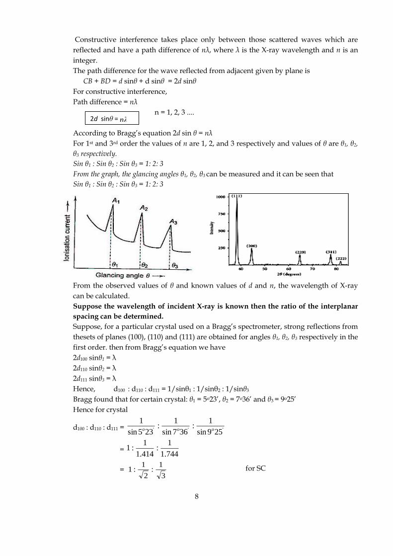
According to Bragg’s equation 2d sin θ = nλ
For 1st and 3rd order the values of n are 1, 2, and 3 respectively and values of θ are θ1, θ2,
θ3 respectively.
Sin θ1 : Sin θ2 : Sin θ3 = 1: 2: 3
From the graph, the glancing angles θ1, θ2, θ3 can be measured and it can be seen that
Sin θ1 : Sin θ2 : Sin θ3 = 1: 2: 3
From the observed values of θ and known values of d and n, the wavelength of X-ray
can be calculated.
Suppose the wavelength of incident X-ray is known then the ratio of the interplanar
spacing can be determined.
Suppose, for a particular crystal used on a Bragg’s spectrometer, strong reflections from
thesets of planes (100), (110) and (111) are obtained for angles θ1, θ2, θ3 respectively in the
first order. then from Bragg’s equation we have
2d100 sinθ1 = λ
2d110 sinθ2 = λ
2d111 sinθ3 = λ
Hence, d100 : d110 : d111 = 1/sinθ1 : 1/sinθ2 : 1/sinθ3
Bragg found that for certain crystal: θ1 = 5o23’, θ2 = 7o36’ and θ3 = 9o25’
Hence for crystal
d100 : d110 : d111 = ''' 259sin
1:
367sin
1:
235sin
1ooo
= 744.1
1:
414.1
1:1
= 3
1:
2
1:1 for SC
2d sinθ = nλ
9
Theoretically, this ratio is found to hold a simple cubic lattice structure. Hence, it is
concluded that crystal has a simple cubic structure.
when the first order reflection from the three planes (100), (110) and (111) of NaCl are
compared, the ratios between the interplanar spacing are found as
For FCC d100 : d110 : d111 = 1 2
1 : :2 3
Which agree with the theoretical values for a face centered cubic structure. He
concluded that NaCl has fcc structure.
For BCC d100 : d110 : d111 = 2 1
1 : :2 3
Q.4 (a) Find out the critical radius ratio of an ionic crystal in ligancy 6 configuration. What is
the maximum size of cation in ligancy 6 configuration when the radius of anion is
2.02 A. 5
(b) In an n type semiconductor, the Fermi level lies 0.4 ev below the conduction band. If
the concentration of donor atom is doubled, find the new position of the Fermi level
W.r.t. the conduction band. 5
(c) Explain the origin of electronic, ionic and orientational polarization and temperature
dependence of respective polarizability. 5
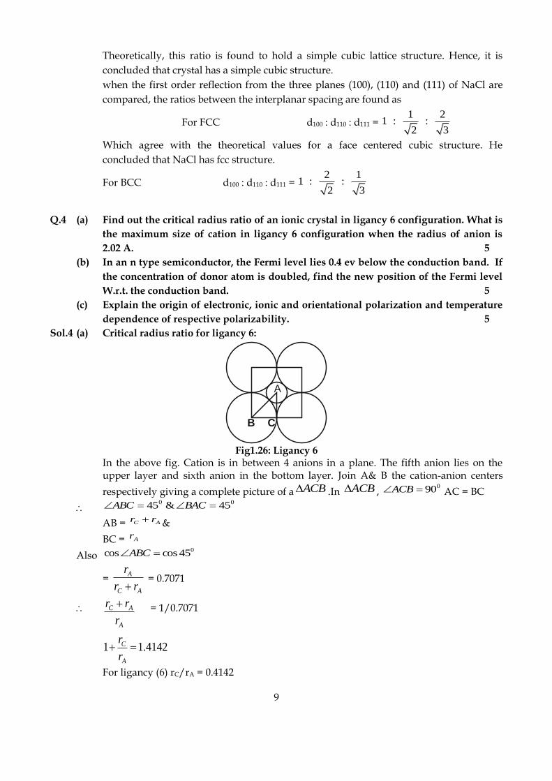
Sol.4 (a) Critical radius ratio for ligancy 6:
A
B C
Fig1.26: Ligancy 6
In the above fig. Cation is in between 4 anions in a plane. The fifth anion lies on the upper layer and sixth anion in the bottom layer. Join A& B the cation-anion centers
respectively giving a complete picture of a .In , AC = BC
AB = &
BC =
Also
= = 0.7071
= 1/0.7071
For ligancy (6) rC/rA = 0.4142
ACB ACB 090=ACB
00 45&45 == BACABC
AC rr +
Ar
045coscos =ABC
AC
A
rr
r
+
A
AC
r
rr +
4142.11 =+A
C
r
r
10
Given- ra = 2.02
c
a
r
r = 0.414
rc = ra × 0.414 = 2.02 × 0.414
Sol.4 (b) Given:
EC – EF = 0.4 eV,
nd' = 2 nd,
T = 300 K
Formula:
nd = NC e(EF – EC)/KT
Calculation:
nd’ = NC e(EF’ – EC)/KT
d
d
n '
n =
( ) ( )F C F CE ' E E E /KTe
− − −
EC – EF’ = (EC – EF) – KT ln 2
= 0.4 – 0.018
EC – EF’ = 0.382 eV
The few fermi level will be 0.382 eV below the conduction band. Hence, the fermi level
will be shifted towards the conduction band by an amount (0.4 – 0.382) eV = 0.018 eV.
Ans.4 (c) (1) Electronic polarization: a displacement of the electronic cloud w.r.t the nucleus.
(2) Ionic polarization: separation of +ve and -ve ions in the crystal. (3) Orientational polarization: alignment of permanent dipoles (molecules). (4) Space-charge polarization: free electrons are present but are prevented from
moving by barriers such as grain boundaries - the electrons "pile up".
Q.5 (a) Find out the intercepts made by the planes. (1 0 1) and (4 1 4) in a cubic unit cell. 5
Draw [T 2 1] and [1 2 4] in a cubic unit cell.
(b) A bar of n type Ge of size 0.010m x 0.001m x 0.001m is mounted in a Magnetic field of
2 x 10⁻¹T. The electron density in the bar is 7 x 10²¹/m3. If one milli volt is applied
across the long ends of the bar, determine the current through the bar and the voltage
between Hall electrodes placed across the short dimensions of the bar. Assume
μe = 0·39 m2/vs. 5
(c) Define reverberation time. Write Sabine's formula explaining every term. What are
the factors which determine the average absorption co-efficient of a material? 5
11
Ans.5 (a)
Sol.5 (b) H 21 19
1 1R
ne 7 10 1.6 10− −= =
28.92 10−=
dV E= H BH
R I; V
t= 3 30.39
10 39 100.01
− −= =
dI neAV= ( )221 19 37 10 1.6 10 0.001 39 10− −= 64.36 10 A−=
2 6 1
H
8.92 10 4.36 10 2 10V
0.001
− − − = 677.7824 10 V−=
Ans.5 (c) • Reverberation is the persistence of sound in a particular space after the original
sound is removed.
• A reverberation, or reverb, is created when a sound is produced in an enclosed
space causing a large number of echoes to build up and then slowly decay as the
sound is absorbed by the walls and air.
• This is most noticeable when the sound source stops but the reflections continue,
decreasing in amplitude, until they can no longer be heard. In a more reflective
room, it will take longer for the sound to die away and the room is said to be 'live'.
In a very absorbent room, the sound will die away quickly and the room will be
described as acoustically 'dead'.
• But the time for reverberation to completely die away will depend upon how loud
the sound was to begin with and will also depend upon the acuity of the hearing
of the observer. To quantitatively characterize the reverberation, the parameter
called the reverberation time is used.
It is defined as the time for the sound to die away to a level 60 decibels below its
original level.
Reverberation time = time required to drop original sound by 60dB below original level
12
Prof. Wallace C. Sabine (1868 - 1919) of Harvard University investigated architectural
acoustics scientifically, particularly with reference to reverberation time. He deduced
experimentally, that the reverberation time is:
• directly proportional to the volume of the hall (V).
• inversely proportional to the effective absorbing surface area of the walls and the
materials inside the hall (A)
Revolumeof thehall
verberationtime Tabsorption
Reverberation time T = constantvolumeof thehall
absorption
=kV
TA
……(1)
Where k is proportionality constant having a value of 0.161 when the dimensions are
metric units.
0.161VT
A= ..…(2) It is rewritten as
1
1 1 2 2 3 3
0.161
0.161......(3)
........
=
=+ + + +
n
n n
n n
VT
a S
VT
a S a S a S a S
1 1 2 2 3 3
1
........n
n n n na S a S a S a S a S= + + + +
• Increasing the effective area of complete absorption like, changing the wall
materials or adding more furniture may decrease an excessive reverberation time
for a hall.
• But this also decreases the intensity of a steady tone.
• Also, too much absorption will make the reverberation time too short and cause
the room to sound acoustically 'dead'.
• Hence, the optimum reverberation time is a compromise between clarity of sound
and its intensity.
Determination of absorption coefficient: If T1 is reverberation time of an empty room,
then
Where 1
n
n nA a S= denotes the absorption due to the walls, flooring and ceiling of the
empty room.
Then a certain amount of absorbing material of area S and absorption coefficient a’ is
added in the room and again the reverberation time is measured.
1
1
0.161 0.161= =
n
n n
V VT
Aa S
13
Let it be T2
2
1 2
1 2
0.161
'
1 1 '
0.161
0.161 1 1'
VT
A a S
a S
T T V
Va
S T T
=+
− =
= −
Knowing the quantities on the RHS, of the above equation, a’ of the material under test
can be calculated.
Q.6 (a) Explain the differences between three different liquid crystal phases with respect to
the order in the arrangement of molecules, with the help of diagram. Which property
of the liquid crystal is used for display. 5
(b) How a p-n junction diode is used to generate a potential difference in a photovoltaic
solar cell. 5
(c) What is piezoelectric effect. Explain the working of a piezoelectric oscillator used to
produce ultrasonic wave. 5
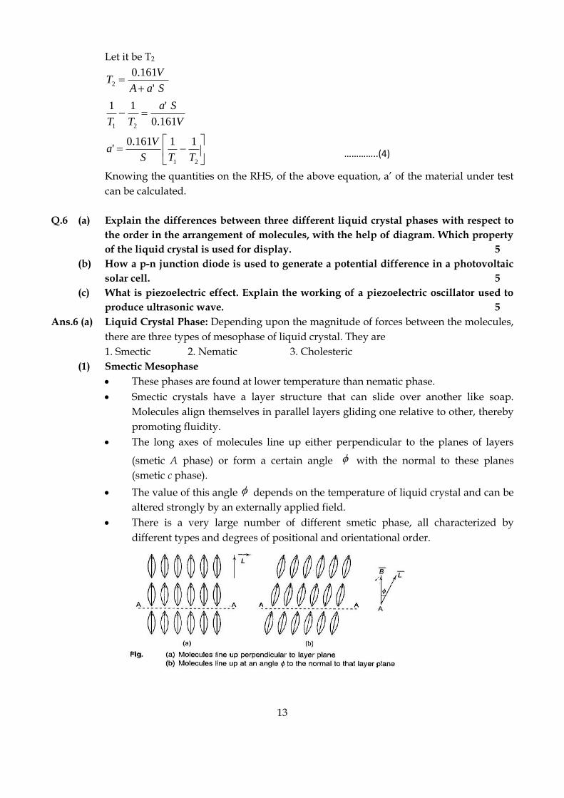
Ans.6 (a) Liquid Crystal Phase: Depending upon the magnitude of forces between the molecules,
there are three types of mesophase of liquid crystal. They are
1. Smectic 2. Nematic 3. Cholesteric
(1) Smectic Mesophase
• These phases are found at lower temperature than nematic phase.
• Smectic crystals have a layer structure that can slide over another like soap.
Molecules align themselves in parallel layers gliding one relative to other, thereby
promoting fluidity.
• The long axes of molecules line up either perpendicular to the planes of layers
(smetic A phase) or form a certain angle with the normal to these planes
(smetic c phase).
• The value of this angle depends on the temperature of liquid crystal and can be
altered strongly by an externally applied field.
• There is a very large number of different smetic phase, all characterized by
different types and degrees of positional and orientational order.
…………..(4)
14
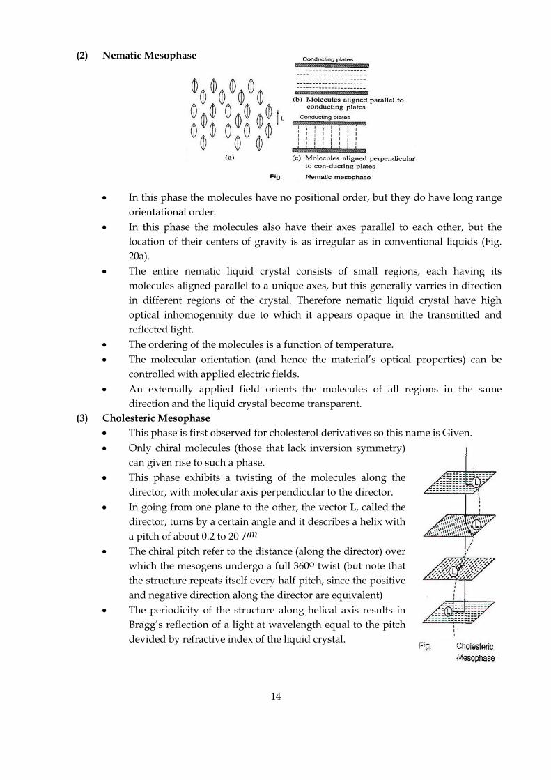
(2) Nematic Mesophase
• In this phase the molecules have no positional order, but they do have long range
orientational order.
• In this phase the molecules also have their axes parallel to each other, but the
location of their centers of gravity is as irregular as in conventional liquids (Fig.
20a).
• The entire nematic liquid crystal consists of small regions, each having its
molecules aligned parallel to a unique axes, but this generally varries in direction
in different regions of the crystal. Therefore nematic liquid crystal have high
optical inhomogennity due to which it appears opaque in the transmitted and
reflected light.
• The ordering of the molecules is a function of temperature.
• The molecular orientation (and hence the material’s optical properties) can be
controlled with applied electric fields.
• An externally applied field orients the molecules of all regions in the same
direction and the liquid crystal become transparent.
(3) Cholesteric Mesophase
• This phase is first observed for cholesterol derivatives so this name is Given.
• Only chiral molecules (those that lack inversion symmetry)
can given rise to such a phase.
• This phase exhibits a twisting of the molecules along the
director, with molecular axis perpendicular to the director.
• In going from one plane to the other, the vector L, called the
director, turns by a certain angle and it describes a helix with
a pitch of about 0.2 to 20 m
• The chiral pitch refer to the distance (along the director) over
which the mesogens undergo a full 360O twist (but note that
the structure repeats itself every half pitch, since the positive
and negative direction along the director are equivalent)
• The periodicity of the structure along helical axis results in
Bragg’s reflection of a light at wavelength equal to the pitch
devided by refractive index of the liquid crystal.
15
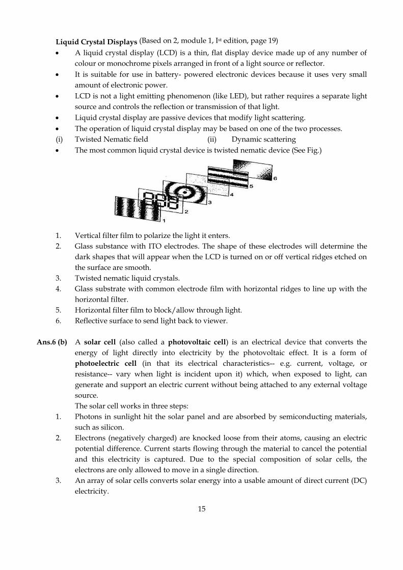
Liquid Crystal Displays (Based on 2, module 1, Ist edition, page 19)
• A liquid crystal display (LCD) is a thin, flat display device made up of any number of
colour or monochrome pixels arranged in front of a light source or reflector.
• It is suitable for use in battery- powered electronic devices because it uses very small
amount of electronic power.
• LCD is not a light emitting phenomenon (like LED), but rather requires a separate light
source and controls the reflection or transmission of that light.
• Liquid crystal display are passive devices that modify light scattering.
• The operation of liquid crystal display may be based on one of the two processes.
(i) Twisted Nematic field (ii) Dynamic scattering
• The most common liquid crystal device is twisted nematic device (See Fig.)
1. Vertical filter film to polarize the light it enters.
2. Glass substance with ITO electrodes. The shape of these electrodes will determine the
dark shapes that will appear when the LCD is turned on or off vertical ridges etched on
the surface are smooth.
3. Twisted nematic liquid crystals.
4. Glass substrate with common electrode film with horizontal ridges to line up with the
horizontal filter.
5. Horizontal filter film to block/allow through light.
6. Reflective surface to send light back to viewer.
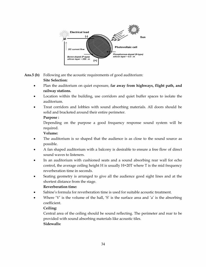
Ans.6 (b) A solar cell (also called a photovoltaic cell) is an electrical device that converts the
energy of light directly into electricity by the photovoltaic effect. It is a form of
photoelectric cell (in that its electrical characteristics-- e.g. current, voltage, or
resistance-- vary when light is incident upon it) which, when exposed to light, can
generate and support an electric current without being attached to any external voltage
source.
The solar cell works in three steps:
1. Photons in sunlight hit the solar panel and are absorbed by semiconducting materials,
such as silicon.
2. Electrons (negatively charged) are knocked loose from their atoms, causing an electric
potential difference. Current starts flowing through the material to cancel the potential
and this electricity is captured. Due to the special composition of solar cells, the
electrons are only allowed to move in a single direction.
3. An array of solar cells converts solar energy into a usable amount of direct current (DC)
electricity.
16
Applications
• Used to power space satellites and smaller items like calculators and watches.
• Today, thousands of people power their homes and businesses with individual solar PV
systems.
• Utility companies are also using PV technology for large power stations.
Solar panels used to power homes and businesses are typically made from solar cells
combined into modules that hold about 40 cells. A typical home will use about 10 to 20
solar panels to power the home. The panels
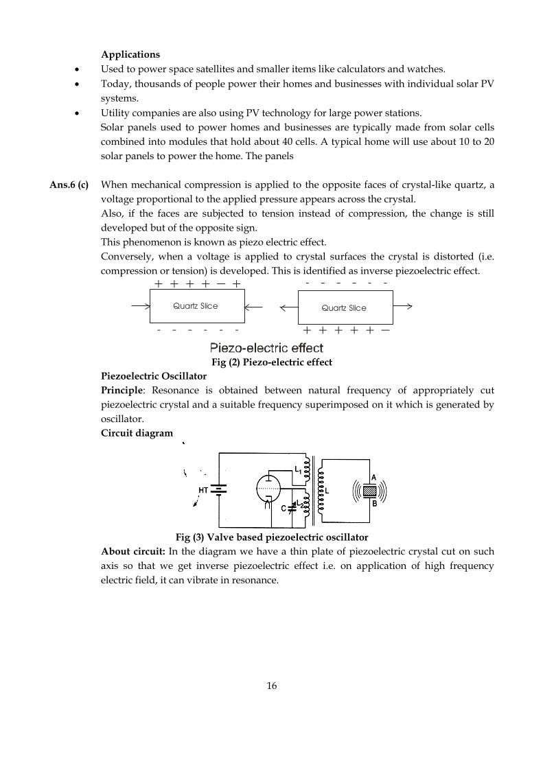
Ans.6 (c) When mechanical compression is applied to the opposite faces of crystal-like quartz, a
voltage proportional to the applied pressure appears across the crystal.
Also, if the faces are subjected to tension instead of compression, the change is still
developed but of the opposite sign.
This phenomenon is known as piezo electric effect.
Conversely, when a voltage is applied to crystal surfaces the crystal is distorted (i.e.
compression or tension) is developed. This is identified as inverse piezoelectric effect.
Quartz SliceQuartz Slice
Fig (2) Piezo-electric effect
Piezoelectric Oscillator
Principle: Resonance is obtained between natural frequency of appropriately cut
piezoelectric crystal and a suitable frequency superimposed on it which is generated by
oscillator.
Circuit diagram
Fig (3) Valve based piezoelectric oscillator
About circuit: In the diagram we have a thin plate of piezoelectric crystal cut on such
axis so that we get inverse piezoelectric effect i.e. on application of high frequency
electric field, it can vibrate in resonance.
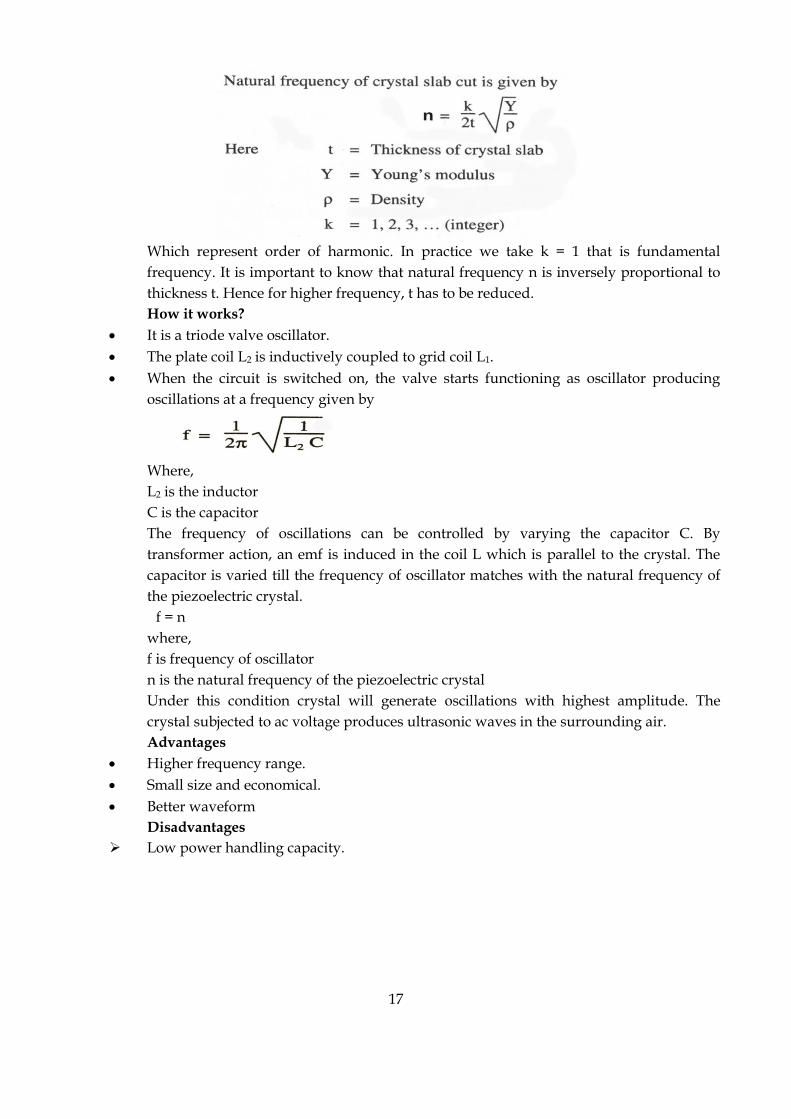
17
Which represent order of harmonic. In practice we take k = 1 that is fundamental
frequency. It is important to know that natural frequency n is inversely proportional to
thickness t. Hence for higher frequency, t has to be reduced.
How it works?
• It is a triode valve oscillator.
• The plate coil L2 is inductively coupled to grid coil L1.
• When the circuit is switched on, the valve starts functioning as oscillator producing
oscillations at a frequency given by
Where,
L2 is the inductor
C is the capacitor
The frequency of oscillations can be controlled by varying the capacitor C. By
transformer action, an emf is induced in the coil L which is parallel to the crystal. The
capacitor is varied till the frequency of oscillator matches with the natural frequency of
the piezoelectric crystal.
f = n
where,
f is frequency of oscillator
n is the natural frequency of the piezoelectric crystal
Under this condition crystal will generate oscillations with highest amplitude. The
crystal subjected to ac voltage produces ultrasonic waves in the surrounding air.
Advantages
• Higher frequency range.
• Small size and economical.
• Better waveform
Disadvantages
➢ Low power handling capacity.
18
Applied Physics – I (Sem-I) May-2014
(Revised Course)
QP Code: NP-17709
Time : 2 Hours Total Marks : 60
N.B.:- (1) Question no. 1 is compulsory.
(2) Attempt any three questions from Q.2 to 6.
(3) Use suitable data wherever required.
(4) Figures to the right indicate full marks.
1. Solve any five from the following: - 15
(a) What is x-ray? Why the x-rays are preferred to study crystalline solid.
(b) Represent the following in a cubic unit cell (021), (123), [121].
(c) Find the Miller Indices of a set of parallel planes which makes intercepts in the ratio
3a : 4b on the x and y axes and parallel to Z-axis.
(d) What is Fermi level and Fermi energy? Write Fermi-Dirac distribution function.
(e) Explain the concept of hole in a semiconductor.
(f) Draw the structure of quartz crystal and explain its various axes.
(g) State and explain ohm’s law in magnetic circuit?
2. (a) Describe the formation of energy band in solid? Explain how it helps to classify the
solids in to conductors, insulators and semiconductors with proper diagram. 8
(b) Explain Dimond crystal structure with proper diagram and determine its APF?
7
3. (a) Derive Bragg’s law and describe the powder method to determine crystal structure
of powdered specimen. 8
(b) The magnetic field strength of copper is 106 ampere/ metre and magnetic
susceptibility is –0.8 × 10⁻³. Calculate magnetic flux density and magnetization in
copper. 7
19
4. (a) What is liquid crystal state of matter? Draw the diagram to describe molecular
arrangement in their different phases? 5
(b) Mention different types of polarizability in a dielectric? Explain electronic
polarizability? 5
(c) Calculate electron and hole concentration in intrinsic silicon at room temperature if
its electrical conductivity is 4 × 10⁻⁴ mho/m. (mobility of electron = 0.14 m2/v-s &
mobility of hole = 0.040 m2/v-s) 5
5. (a) Explain with neat diagram construction and working of solar cell.
(b) State the acoustic requirements of good auditorium. Explain how these
requirements can be achieved. 5
(c) If the x-rays of wavelength 1.549 A° will be reflected from crystal having spacing of
4.225 A°, calculate the smallest glancing angle and highest order of reflection that
can be observed. 5
6. (a) Explain with neat diagram Hysterisis effect in ferromagnetic material. 5
(b) Explain piezoelectric oscillator to produce USW? 5
(c) Explain the formation of barrier potential in P-N Junction. 5
******************
20
Applied Physics – I (Sem-I) May-2014
Solutions
Q.1 Solve any five from the following: - 15
(a) What is x-ray? Why the x-rays are preferred to study crystalline solid.
(b) Represent the following in a cubic unit cell (021), (123), [121].
(c) Find the, miller indices of a set of parallel panes which makes intercepts in the
ratio 3a : 4b on the x and y axes and parallel to Z-axis.
(d) What is Fermi level and Fermi energy? Write Fermi-Dirac distribution function.
(e) Explain the concept of hole in a semiconductor.
(f) Draw the structure of quartz crystal and explain its various axes.
(g) State and explain ohm’s law in magnetic circuit?
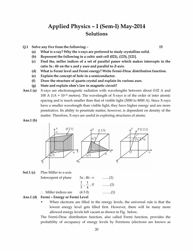
Ans.1 (a) X-rays are electromagnetic radiation with wavelengths between about 0.02 A and
100 A (1A = 10-10 meters). The wavelength of X-rays is of the order of inter atomic
spacing and is much smaller than that of visible light (3000 to 8000 A). Since X-rays
have a smaller wavelength than visible light, they have higher energy and are more
penetrative. Its ability to penetrate matter, however, is dependent on density of the
matter. Therefore, X-rays are useful in exploring structures of atoms.
Ans.1 (b)
Sol.1 (c) Plan Miller to z-axis
Intercepent of plane 3a : 4b : ……(1)
1
3 ,
1
4 , 0 …….(1)
Miller indices are (4 3 0) ……..(1)
Ans.1 (d) Fermi – Energy or Fermi Level
• When electrons are filled in the energy levels, the universal rule is that the
lowest energy level gets filled first. However, there will be many more
allowed energy levels left vacant as shown in Fig. below,
The Fermi-Dirac distribution function, also called Fermi function, provides the
probability of occupancy of energy levels by Fermions (electrons are known as
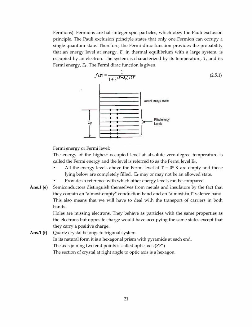
21
Fermions). Fermions are half-integer spin particles, which obey the Pauli exclusion
principle. The Pauli exclusion principle states that only one Fermion can occupy a
single quantum state. Therefore, the Fermi dirac function provides the probability
that an energy level at energy, E, in thermal equilibrium with a large system, is
occupied by an electron. The system is characterized by its temperature, T, and its
Fermi energy, EF. The Fermi dirac function is given.
(2.5.1)
Fermi energy or Fermi level:
The energy of the highest occupied level at absolute zero-degree temperature is
called the Fermi energy and the level is referred to as the Fermi level EF.
• All the energy levels above the Fermi level at T = 00 K are empty and those
lying below are completely filled. EF may or may not be an allowed state.
• Provides a reference with which other energy levels can be compared.
Ans.1 (e) Semiconductors distinguish themselves from metals and insulators by the fact that
they contain an "almost-empty" conduction band and an "almost-full" valence band.
This also means that we will have to deal with the transport of carriers in both
bands.
Holes are missing electrons. They behave as particles with the same properties as
the electrons but opposite charge would have occupying the same states except that
they carry a positive charge.
Ans.1 (f) Quartz crystal belongs to trigonal system.
In its natural form it is a hexagonal prism with pyramids at each end.
The axis joining two end points is called optic axis (ZZ’)
The section of crystal at right angle to optic axis is a hexagon.
22
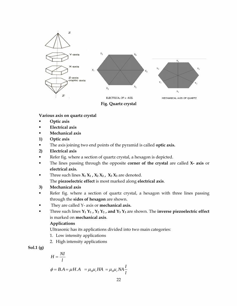
Fig. Quartz crystal
Various axis on quartz crystal
▪ Optic axis
▪ Electrical axis
▪ Mechanical axis
1) Optic axis
▪ The axis joining two end points of the pyramid is called optic axis.
2) Electrical axis
▪ Refer fig. where a section of quartz crystal, a hexagon is depicted.
▪ The lines passing through the opposite corner of the crystal are called X- axis or
electrical axis.
▪ Three such lines X1 X1 , X2 X2 , X3 X3 are denoted.
The piezoelectric effect is most marked along electrical axis.
3) Mechanical axis
▪ Refer fig. where a section of quartz crystal, a hexagon with three lines passing
through the sides of hexagon are shown.
▪ They are called Y- axis or mechanical axis.
▪ Three such lines Y1 Y1 , Y2 Y2 , and Y3 Y3 are shown. The inverse piezoelectric effect
is marked on mechanical axis.
Applications
Ultrasonic has its applications divided into two main categories:
1. Low intensity applications
2. High intensity applications
Sol.1 (g)
=NI
Hl
. .= =B A H A 0= rHA 0= r
INA
l
23
0
1.
=
r
NI
l
A
⎯⎯→NI MMF
0
⎯⎯→r
lRELUCTANCE
A
Q.2 (a) Describe the formation of energy band in solid? Explain how it helps to classify
the solids in to conductors, insulators and semiconductors with proper diagram.
8
(b) Explain Dimond crystal structure with proper diagram and determine its APF?
7
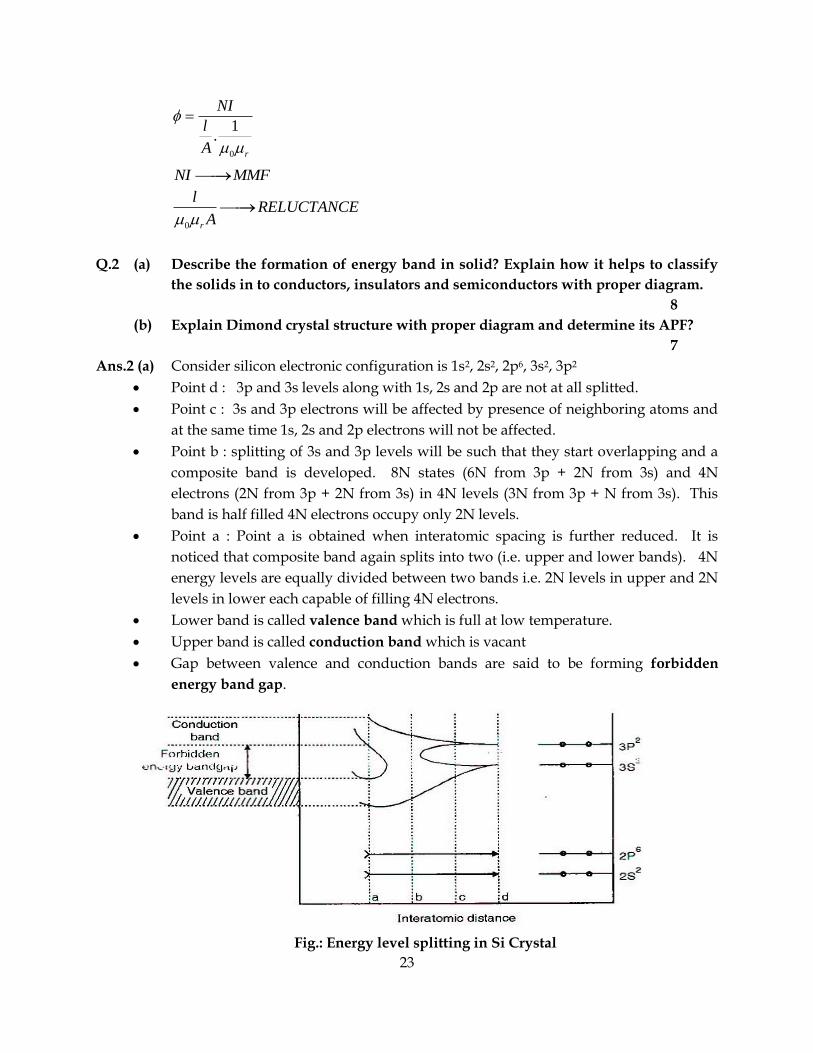
Ans.2 (a) Consider silicon electronic configuration is 1s2, 2s2, 2p6, 3s2, 3p2
• Point d : 3p and 3s levels along with 1s, 2s and 2p are not at all splitted.
• Point c : 3s and 3p electrons will be affected by presence of neighboring atoms and
at the same time 1s, 2s and 2p electrons will not be affected.
• Point b : splitting of 3s and 3p levels will be such that they start overlapping and a
composite band is developed. 8N states (6N from 3p + 2N from 3s) and 4N
electrons (2N from 3p + 2N from 3s) in 4N levels (3N from 3p + N from 3s). This
band is half filled 4N electrons occupy only 2N levels.
• Point a : Point a is obtained when interatomic spacing is further reduced. It is
noticed that composite band again splits into two (i.e. upper and lower bands). 4N
energy levels are equally divided between two bands i.e. 2N levels in upper and 2N
levels in lower each capable of filling 4N electrons.
• Lower band is called valence band which is full at low temperature.
• Upper band is called conduction band which is vacant
• Gap between valence and conduction bands are said to be forming forbidden
energy band gap.
Fig.: Energy level splitting in Si Crystal
24
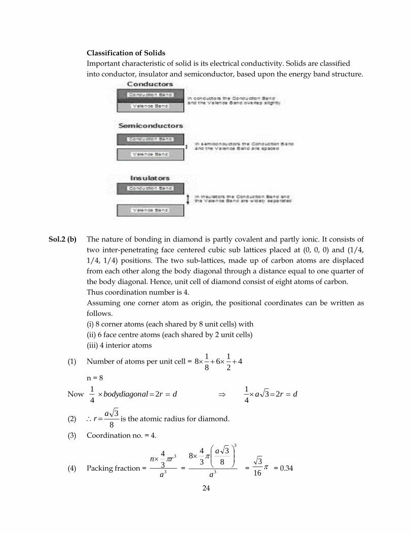
Classification of Solids
Important characteristic of solid is its electrical conductivity. Solids are classified
into conductor, insulator and semiconductor, based upon the energy band structure.
Sol.2 (b) The nature of bonding in diamond is partly covalent and partly ionic. It consists of
two inter-penetrating face centered cubic sub lattices placed at (0, 0, 0) and (1/4,
1/4, 1/4) positions. The two sub-lattices, made up of carbon atoms are displaced
from each other along the body diagonal through a distance equal to one quarter of
the body diagonal. Hence, unit cell of diamond consist of eight atoms of carbon.
Thus coordination number is 4.
Assuming one corner atom as origin, the positional coordinates can be written as
follows.
(i) 8 corner atoms (each shared by 8 unit cells) with
(ii) 6 face centre atoms (each shared by 2 unit cells)
(iii) 4 interior atoms
(1) Number of atoms per unit cell = 42
16
8
18 ++
n = 8
Now dralbodydiagon == 24
1 dra == 23
4
1
(2) 8
3ar = is the atomic radius for diamond.
(3) Coordination no. = 4.
(4) Packing fraction = 3
3
3
4
a
rn
= 3
3
8
3
3
48
a
a
= 16
3
= 0.34
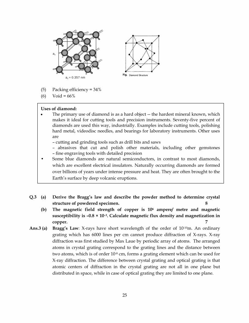
25
a = 0.357 nm0
a0
(5) Packing efficiency = 34%
(6) Void = 66%
Uses of diamond: • The primary use of diamond is as a hard object -- the hardest mineral known, which
makes it ideal for cutting tools and precision instruments. Seventy-five percent of diamonds are used this way, industrially. Examples include cutting tools, polishing hard metal, videodisc needles, and bearings for laboratory instruments. Other uses are – cutting and grinding tools such as drill bits and saws – abrasives that cut and polish other materials, including other gemstones – fine engraving tools with detailed precision
• Some blue diamonds are natural semiconductors, in contrast to most diamonds,
which are excellent electrical insulators. Naturally occurring diamonds are formed
over billions of years under intense pressure and heat. They are often brought to the
Earth’s surface by deep volcanic eruptions.
Q.3 (a) Derive the Bragg’s law and describe the powder method to determine crystal
structure of powdered specimen. 8
(b) The magnetic field strength of copper is 106 ampere/ metre and magnetic
susceptibility is –0.8 × 10⁻³. Calculate magnetic flux density and magnetization in
copper. 7
Ans.3 (a) Bragg’s Law: X-rays have short wavelength of the order of 10-10m. An ordinary
grating which has 6000 lines per cm cannot produce diffraction of X-rays. X-ray
diffraction was first studied by Max Laue by periodic array of atoms. The arranged
atoms in crystal grating correspond to the grating lines and the distance between
two atoms, which is of order 10-8 cm, forms a grating element which can be used for
X-ray diffraction. The difference between crystal grating and optical grating is that
atomic centers of diffraction in the crystal grating are not all in one plane but
distributed in space, while in case of optical grating they are limited to one plane.
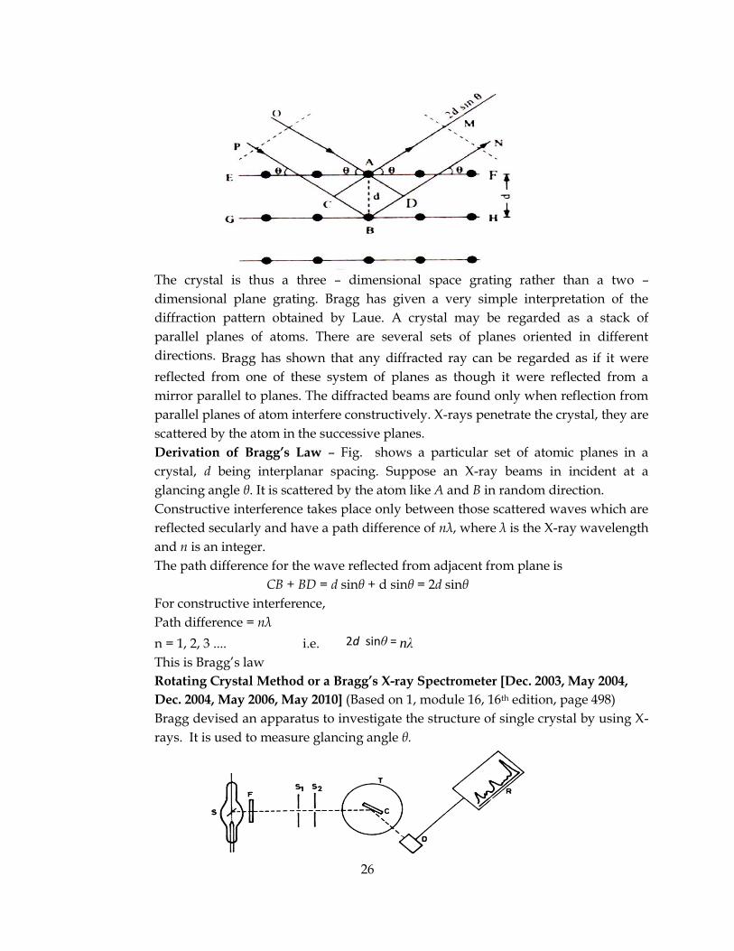
26
The crystal is thus a three – dimensional space grating rather than a two –
dimensional plane grating. Bragg has given a very simple interpretation of the
diffraction pattern obtained by Laue. A crystal may be regarded as a stack of
parallel planes of atoms. There are several sets of planes oriented in different
directions. Bragg has shown that any diffracted ray can be regarded as if it were
reflected from one of these system of planes as though it were reflected from a
mirror parallel to planes. The diffracted beams are found only when reflection from
parallel planes of atom interfere constructively. X-rays penetrate the crystal, they are
scattered by the atom in the successive planes.
Derivation of Bragg’s Law – Fig. shows a particular set of atomic planes in a
crystal, d being interplanar spacing. Suppose an X-ray beams in incident at a
glancing angle θ. It is scattered by the atom like A and B in random direction.
Constructive interference takes place only between those scattered waves which are
reflected secularly and have a path difference of nλ, where λ is the X-ray wavelength
and n is an integer.
The path difference for the wave reflected from adjacent from plane is
CB + BD = d sinθ + d sinθ = 2d sinθ
For constructive interference,
Path difference = nλ
n = 1, 2, 3 .... i.e. 2d sinθ = nλ
This is Bragg’s law
Rotating Crystal Method or a Bragg’s X-ray Spectrometer [Dec. 2003, May 2004,
Dec. 2004, May 2006, May 2010] (Based on 1, module 16, 16th edition, page 498)
Bragg devised an apparatus to investigate the structure of single crystal by using X-
rays. It is used to measure glancing angle θ.
27
He used crystal as reflection grating and not as transmission grating. The
experiment arrangement is shown in the diagram. X-rays from X-ray tube is
collimated using two adjustable slits, S1, and S2 are made to fall on a crystal C with
which in wax on the spectrometer table. The vernier scale V is attached to table on
which the crystal is placed. The vernier scale V is capable to move the circular scale
S and determine the position of the crystal. A strong monochromatic X-ray beam is
made to fall on the crystal face. The reflected beam after passing through the slit S3,
enters an ionisation chamber D mounted on an arm which can be rotated about the
same axis as the crystal. Its position can be read by second veiner V2. The gas in the
chamber is ionisation by the X-rays. The resulting ionisation current, measured by
the electrometer E, is a measure of the intensity of X-rays reflected by the crystal.
The crystal is rotated through small angles (while the arm carrying the isonisation
current is rotated through double the angles) and the ionisation current is measured
each time. The curve of intensity which is measure of ionisation current or
ionisation current against glancing angle θ is plotted. For certain value of glancing
angle θ, The intensity of ionisation current increase abruptly (Fig).
According to Bragg’s equation 2d sin θ = nλ
For 1st and 3rd order the values of n are 1, 2, and 3 respectively and values of θ are θ1,
θ2, θ3 respectively.
Sin θ1 : Sin θ2 : Sin θ3 = 1: 2: 3
From the graph, the glancing angles θ1, θ2, θ3 can be measured and it can be seen that
Sin θ1 : Sin θ2 : Sin θ3 = 1: 2: 3
From the observed values of θ and known values of d and n, the wavelength of X-
ray can be calculated.
Suppose the wavelength of incident X-ray is known then the ratio of the
interplanar spacing can be determined.
Suppose, for a particular crystal used on a Bragg’s spectrometer, strong reflections
from the sets of planes (100), (110) and (111) are obtained for angles θ1, θ2, θ3
respectively in the first order. then from Bragg’s equation we have
2d100 sinθ1 = λ
2d110 sinθ2 = λ
28
2d111 sinθ3 = λ
Hence, d100: d110: d111 = 1/sinθ1: 1/sinθ2: 1/sinθ3
Bragg found that for certain crystal: θ1 = 5o23’, θ2 = 7o36’ and θ3 = 9o25’
Hence for crystal
d100 : d110 : d111 = ''' 259sin
1:
367sin
1:
235sin
1ooo =
744.1
1:
414.1
1:1
= 3
1:
2
1:1
for SC
Theoretically, this ratio is found to hold a simple cubic lattice structure. Hence, it is
concluded that crystal has a simple cubic structure.
When the first order reflection from the three planes (100), (110) and (111) of NaCl
are compared, the ratios between the interplanar spacing are found as
For FCC d100 : d110 : d111 = 1 2
1 : :2 3
Which agree with the theoretical values for a face centered cubic structure. He
concluded that NaCl has fcc structure.
For BCC d100 : d110 : d111 = 2 1
1 : :2 3
Sol.3 (b) H = 106 A/m, z = –0.3 × 10⁻³
Magnetization M = xH = –0.3 × 10–3 × 106 = –0.8 × 10³ A/m
Magnetic field strength B = (M + H)
B = 4ST × 10–7 (–0.8 × 10³ + 106) = 1.2556 wb/m2
Q.4 (a) What is liquid crystal state of matter? Draw the diagram to describe molecular
arrangement in their different phases? 5
(b) Mention different types of polarizability in a dielectric? Explain electronic
polarizability? 5
(c) Calculate electron and hole concentration in intrinsic silicon at room temperature
if its electrical conductivity is 4 × 10⁻⁴ mho/m. (mobility of electron = 0.14 m2/v-s &
mobility of hole = 0.040 m2/v-s) 5
Ans.4 (a) 1. Some crystalline solids, when heated pass through an intermediate phase
while going from solid to liquid state.
2. In these transitional states the substance retains the anisotropy of properties of
solid such as dielectric, optical, magnetic and others inherent in a crystal, and
they also simultaneously acquire the properties specific to liquid – fluidity to
form droplets viscocity etc.
3. The substances exhibiting such an intermediate, mesomorphic phase are
known as liquid crystal.
Liquid crystal are the substance that exhibit a phase of matter that has properties
between those of a conventional liquid, and those of a solid crystal.
29
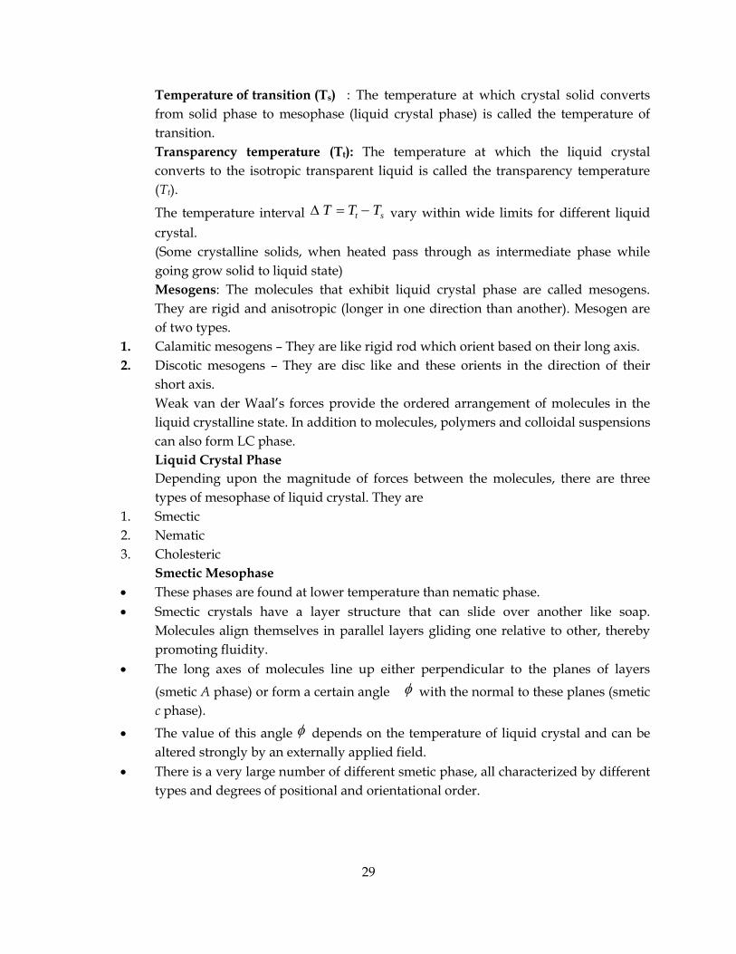
Temperature of transition (Ts) : The temperature at which crystal solid converts
from solid phase to mesophase (liquid crystal phase) is called the temperature of
transition.
Transparency temperature (Tt): The temperature at which the liquid crystal
converts to the isotropic transparent liquid is called the transparency temperature
(Tt).
The temperature interval st TTT −= vary within wide limits for different liquid
crystal.
(Some crystalline solids, when heated pass through as intermediate phase while
going grow solid to liquid state)
Mesogens: The molecules that exhibit liquid crystal phase are called mesogens.
They are rigid and anisotropic (longer in one direction than another). Mesogen are
of two types.
1. Calamitic mesogens – They are like rigid rod which orient based on their long axis.
2. Discotic mesogens – They are disc like and these orients in the direction of their
short axis.
Weak van der Waal’s forces provide the ordered arrangement of molecules in the
liquid crystalline state. In addition to molecules, polymers and colloidal suspensions
can also form LC phase.
Liquid Crystal Phase
Depending upon the magnitude of forces between the molecules, there are three
types of mesophase of liquid crystal. They are
1. Smectic
2. Nematic
3. Cholesteric
Smectic Mesophase
• These phases are found at lower temperature than nematic phase.
• Smectic crystals have a layer structure that can slide over another like soap.
Molecules align themselves in parallel layers gliding one relative to other, thereby
promoting fluidity.
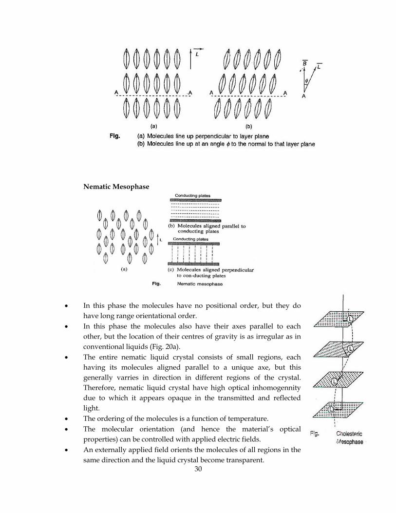
• The long axes of molecules line up either perpendicular to the planes of layers
(smetic A phase) or form a certain angle with the normal to these planes (smetic
c phase).
• The value of this angle depends on the temperature of liquid crystal and can be
altered strongly by an externally applied field.
• There is a very large number of different smetic phase, all characterized by different
types and degrees of positional and orientational order.
30
Nematic Mesophase
• In this phase the molecules have no positional order, but they do
have long range orientational order.
• In this phase the molecules also have their axes parallel to each
other, but the location of their centres of gravity is as irregular as in
conventional liquids (Fig. 20a).
• The entire nematic liquid crystal consists of small regions, each
having its molecules aligned parallel to a unique axe, but this
generally varries in direction in different regions of the crystal.
Therefore, nematic liquid crystal have high optical inhomogennity
due to which it appears opaque in the transmitted and reflected
light.
• The ordering of the molecules is a function of temperature.
• The molecular orientation (and hence the material’s optical
properties) can be controlled with applied electric fields.
• An externally applied field orients the molecules of all regions in the
same direction and the liquid crystal become transparent.
31
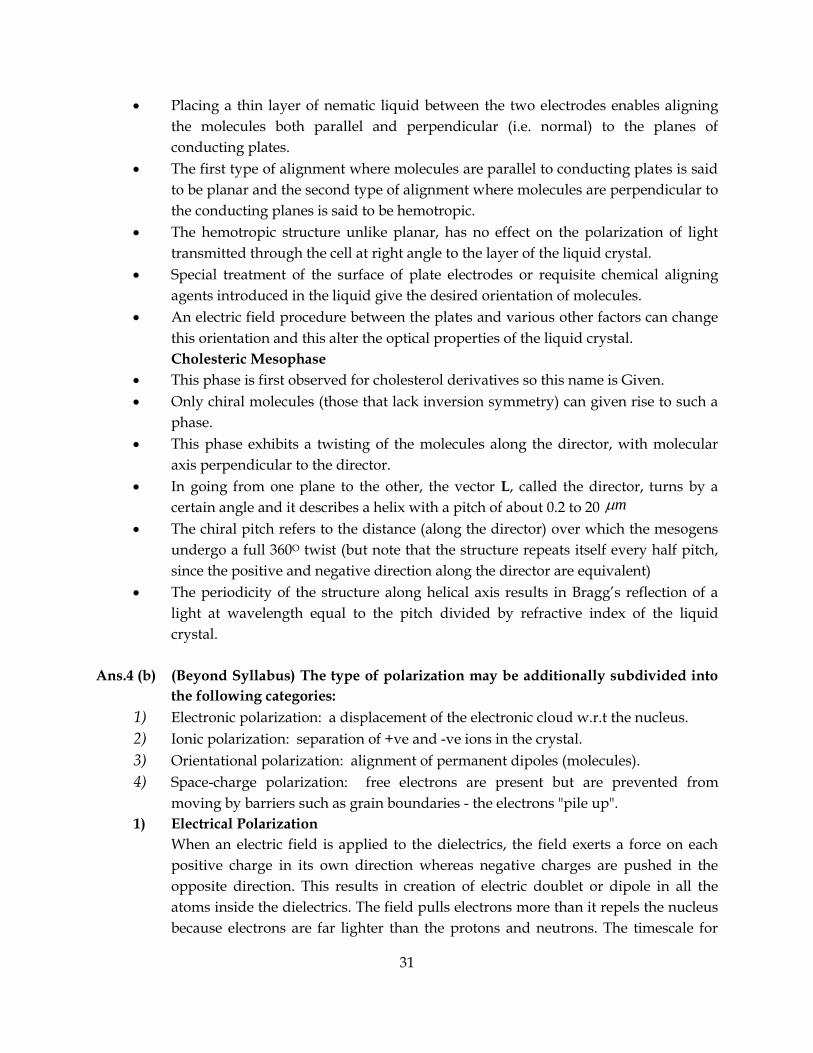
• Placing a thin layer of nematic liquid between the two electrodes enables aligning
the molecules both parallel and perpendicular (i.e. normal) to the planes of
conducting plates.
• The first type of alignment where molecules are parallel to conducting plates is said
to be planar and the second type of alignment where molecules are perpendicular to
the conducting planes is said to be hemotropic.
• The hemotropic structure unlike planar, has no effect on the polarization of light
transmitted through the cell at right angle to the layer of the liquid crystal.
• Special treatment of the surface of plate electrodes or requisite chemical aligning
agents introduced in the liquid give the desired orientation of molecules.
• An electric field procedure between the plates and various other factors can change
this orientation and this alter the optical properties of the liquid crystal.
Cholesteric Mesophase
• This phase is first observed for cholesterol derivatives so this name is Given.
• Only chiral molecules (those that lack inversion symmetry) can given rise to such a
phase.
• This phase exhibits a twisting of the molecules along the director, with molecular
axis perpendicular to the director.
• In going from one plane to the other, the vector L, called the director, turns by a
certain angle and it describes a helix with a pitch of about 0.2 to 20 m
• The chiral pitch refers to the distance (along the director) over which the mesogens
undergo a full 360O twist (but note that the structure repeats itself every half pitch,
since the positive and negative direction along the director are equivalent)
• The periodicity of the structure along helical axis results in Bragg’s reflection of a
light at wavelength equal to the pitch divided by refractive index of the liquid
crystal.
Ans.4 (b) (Beyond Syllabus) The type of polarization may be additionally subdivided into
the following categories:
1) Electronic polarization: a displacement of the electronic cloud w.r.t the nucleus.
2) Ionic polarization: separation of +ve and -ve ions in the crystal.
3) Orientational polarization: alignment of permanent dipoles (molecules).
4) Space-charge polarization: free electrons are present but are prevented from
moving by barriers such as grain boundaries - the electrons "pile up".
1) Electrical Polarization
When an electric field is applied to the dielectrics, the field exerts a force on each
positive charge in its own direction whereas negative charges are pushed in the
opposite direction. This results in creation of electric doublet or dipole in all the
atoms inside the dielectrics. The field pulls electrons more than it repels the nucleus
because electrons are far lighter than the protons and neutrons. The timescale for
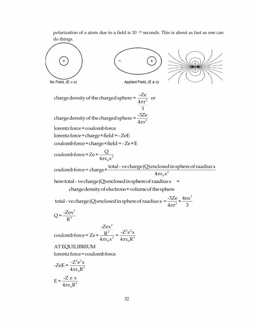
32
polarization of a atom due to a field is 10 -15 seconds. This is about as fast as one can
do things.
3
-Zechargedensityof the chargedsphere = or
4 r
3
3
-3Zechargedensityof the chargedsphere =
4 r
lorentzforce=coulombforce
lorentzforce=charge×field =- ZeE
coulombforce=charge×field =- Ze×E
20
Qcoulombforce=Ze×
4 ε x
20
total - ve charge(Q)enclosedin sphereof raadiusxcoulombforce= charge×
4 ε x
heretotal - vecharge(Q)enclosedinsphereof raadiusx =
chargedensityof electrons×volumeof thesphere
3
3
-3Ze 4πxtotal - ve charge(Q)enclosedin sphereof raadiusx = ×
4 r 3
3
3
-ZexQ =
R
3
2 23
2 30 0
-Zex-Z e xRcoulombforce= Ze× =
4 ε x 4 ε R
ATEQUILIBRIUM
lorentzforce=coulombforce
2 2
30
-Z e x-ZeE =
4 ε R
30
-Z e xE =
4 ε R
33
304 ε R E
x =Ze
=Dipolemoment Ze x
3
0e
4=
R EZe
Ze
3
e 04= R E
e E
e = eE
3
04=e R iscalled electronic polarization
Sol.4 (c) 6i = 4 × 10⁻⁴ mho/m
e = 0.14 m2/vs, n = 0.040 m2/vs
6i = nie (e + n)
ni = ( )
i6
e e n + =
( )
–4
–19
4 10
1.6 10 0.14 0.040
+ = 1.388 × 10¹⁶ /m3
Q.5 (a) Explain with neat diagram construction and working of solar cell.
(b) State the acoustic requirements of good auditorium. Explain how these
requirements can be achieved. 5
(c) If the x-rays of wavelength 1.549 A° will be reflected from crystal having spacing
of 4.225 A°, calculate the smallest glancing angle and highest order of reflection
that can be observed. 5
Ans.5 (a) A solar cell (also called a photovoltaic cell) is an electrical device that converts the
energy of light directly into electricity by the photovoltaic effect. It is a form of
photoelectric cell (in that its electrical characteristics-- e.g. current, voltage, or
resistance-- vary when light is incident upon it) which, when exposed to light, can
generate and support an electric current without being attached to any external
voltage source.
The solar cell works in three steps:
1. Photons in sunlight hit the solar panel and are absorbed by semiconducting
materials, such as silicon.
2. Electrons (negatively charged) are knocked loose from their atoms, causing an
electric potential difference. Current starts flowing through the material to cancel
the potential and this electricity is captured. Due to the special composition of solar
cells, the electrons are only allowed to move in a single direction.
3. An array of solar cells converts solar energy into a usable amount of direct current
(DC) electricity.
34
Ans.5 (b) Following are the acoustic requirements of good auditorium:
Site Selection:
• Plan the auditorium on quiet exposure, far away from highways, flight path, and
railway stations.
• Location within the building, use corridors and quiet buffer spaces to isolate the
auditorium.
• Treat corridors and lobbies with sound absorbing materials. All doors should be
solid and bracketed around their entire perimeter.
Purpose :
Depending on the purpose a good frequency response sound system will be
required.
Volume:
• The auditorium is so shaped that the audience is as close to the sound source as
possible.
• A fan shaped auditorium with a balcony is desirable to ensure a free flow of direct
sound waves to listeners.
• In an auditorium with cushioned seats and a sound absorbing rear wall for echo
control, the average ceiling height H is usually H=20T where T is the mid frequency
reverberation time in seconds.
• Seating geometry is arranged to give all the audience good sight lines and at the
shortest distance from the stage.
Reverberation time:
• Sabine’s formula for reverberation time is used for suitable acoustic treatment.
• Where ‘V’ is the volume of the hall, ‘S’ is the surface area and ‘a’ is the absorbing
coefficient.
Ceiling:
Central area of the ceiling should be sound reflecting. The perimeter and rear to be
provided with sound absorbing materials like acoustic tiles.
Sidewalls:
35
Sidewalls should be sound reflecting and diffusing with as many irregularities as
possible. For example, making doorway wider at one side of the wall keeping
windows etc., and the back wall is treated with deep sound absorbing finish.
Floor :
All aisles are carpeted except in front of the stage to make full noise control. Fabric
upholstered seats are used. Absorptive and cushioned seats will give stable
reverberation.
Balconies :
Use balconies to increase seating capacity and to reduce the distance to the farthest
row of seats.
Sound reinforcement system:
In large halls a sound amplification system to reinforce the sound to a weak source
in a large room is required. In addition there should be adequate loudness in every
part of the auditorium uniform distribution (diffusion) of sound energy in the room.
The hall should be free from echoes, long delayed reflections, flatter echoes, sound
concentrations, distortions, and sound shadow and room resonance.
Seats:
To make the hearing conditions satisfactory when the room is full or partly full,
upholstered seats with absorbing material at the bottom are used, so that the
absence or presence of audience does not affect the reverberation time.
Sol.5 (c) = 1.549 × 10⁻¹⁰ m
d = 4.255 × 10⁻¹⁰ m
For smallest glancing angle , n = 1
Bragg’s law 2dsin =
= 1sin2d
−
= 1.4875
For highest order of reflection sinmax = 1
2d = nmax
Nmax = 2d
= 5.4913
5
Q.6 (a) Explain with neat diagram Hysterisis effect in ferromagnetic material. 5
(b) Explain piezoelectric oscillator to produce USW? 5
(c) Explain the formation of barrier potential in P-N Junction. 5
Ans.6 (a) (Beyond Syllabus) A great deal of information can be learned about the magnetic
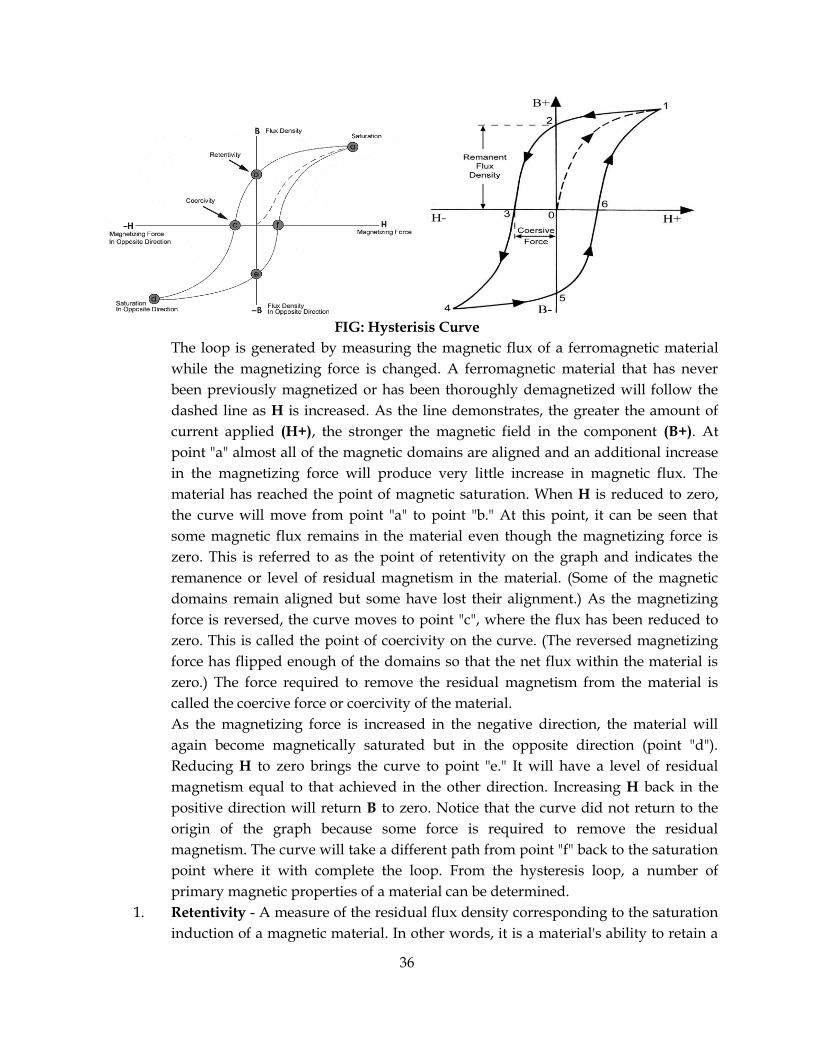
properties of a material by studying its hysteresis loop. A hysteresis loop shows the
relationship between the induced magnetic flux density (B) and the magnetizing
force (H). It is often referred to as the B-H loop. An example hysteresis loop is
shown below.
36
FIG: Hysterisis Curve
The loop is generated by measuring the magnetic flux of a ferromagnetic material
while the magnetizing force is changed. A ferromagnetic material that has never
been previously magnetized or has been thoroughly demagnetized will follow the
dashed line as H is increased. As the line demonstrates, the greater the amount of
current applied (H+), the stronger the magnetic field in the component (B+). At
point "a" almost all of the magnetic domains are aligned and an additional increase
in the magnetizing force will produce very little increase in magnetic flux. The
material has reached the point of magnetic saturation. When H is reduced to zero,
the curve will move from point "a" to point "b." At this point, it can be seen that
some magnetic flux remains in the material even though the magnetizing force is
zero. This is referred to as the point of retentivity on the graph and indicates the
remanence or level of residual magnetism in the material. (Some of the magnetic
domains remain aligned but some have lost their alignment.) As the magnetizing
force is reversed, the curve moves to point "c", where the flux has been reduced to
zero. This is called the point of coercivity on the curve. (The reversed magnetizing
force has flipped enough of the domains so that the net flux within the material is
zero.) The force required to remove the residual magnetism from the material is
called the coercive force or coercivity of the material.
As the magnetizing force is increased in the negative direction, the material will
again become magnetically saturated but in the opposite direction (point "d").
Reducing H to zero brings the curve to point "e." It will have a level of residual
magnetism equal to that achieved in the other direction. Increasing H back in the
positive direction will return B to zero. Notice that the curve did not return to the
origin of the graph because some force is required to remove the residual
magnetism. The curve will take a different path from point "f" back to the saturation
point where it with complete the loop. From the hysteresis loop, a number of
primary magnetic properties of a material can be determined.
1. Retentivity - A measure of the residual flux density corresponding to the saturation
induction of a magnetic material. In other words, it is a material's ability to retain a
37
certain amount of residual magnetic field when the magnetizing force is removed
after achieving saturation. (The value of B at point b on the hysteresis curve.)
2. Residual Magnetism or Residual Flux - the magnetic flux density that remains in a
material when the magnetizing force is zero. Note that residual magnetism and
retentivity are the same when the material has been magnetized to the saturation
point. However, the level of residual magnetism may be lower than the retentivity
value when the magnetizing force did not reach the saturation level.
3. Coercive Force - The amount of reverse magnetic field which must be applied to a
magnetic material to make the magnetic flux return to zero. (The value of H at point
c on the hysteresis curve.)
4. Permeability, - A property of a material that describes the ease with which a
magnetic flux is established in the component.
5. Reluctance - Is the opposition that a ferromagnetic material shows to the
establishment of a magnetic field. Reluctance is analogous to the resistance in an
electrical circuit.
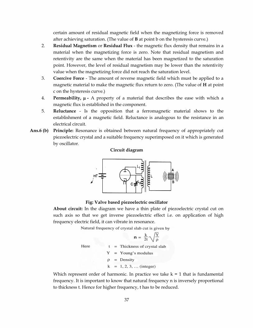
Ans.6 (b) Principle: Resonance is obtained between natural frequency of appropriately cut
piezoelectric crystal and a suitable frequency superimposed on it which is generated
by oscillator.
Circuit diagram
Fig: Valve based piezoelectric oscillator
About circuit: In the diagram we have a thin plate of piezoelectric crystal cut on
such axis so that we get inverse piezoelectric effect i.e. on application of high
frequency electric field, it can vibrate in resonance.
Which represent order of harmonic. In practice we take k = 1 that is fundamental
frequency. It is important to know that natural frequency n is inversely proportional
to thickness t. Hence for higher frequency, t has to be reduced.
38
How it works?
• It is a triode valve oscillator.
• The plate coil L2 is inductively coupled to grid coil L1.
• When the circuit is switched on, the valve starts functioning as oscillator producing
oscillations at a frequency given by
Where,
L2 is the inductor
C is the capacitor
The frequency of oscillations can be controlled by varying the capacitor C . By
transformer action, an emf is induced in the coil L which is parallel to the crystal.
The capacitor is varied till the frequency of oscillator matches with the natural
frequency of the piezoelectric crystal.
f = n
where,
f is frequency of oscillator
n is the natural frequency of the piezoelectric crystal
Under this condition crystal will generate oscillations with highest amplitude. The
crystal subjected to ac voltage produces ultrasonic waves in the surrounding air.
Advantages
• Higher frequency range.
• Small size and economical.
• Better waveform
Disadvantages
➢ Low power handling capacity.
Ans.6 (c) The negative terminal of the external source causes an increase in electron energy
and hence an upward shift of all energy levels on the n-side. Similarly, the positive
terminal connected to the p-side causes an increase in hole energy and hence a
lowering of all levels on p-side . As the displacements of the energy levels occur in
opposite directions, the Fermi levels EFn and EFp get separated by a value eV. And
also the bending of the bands near the depletion region is reduced. In other words,
the heights of the conduction hill and valence hill are reduced by an amount of
energy eV. Due to reduction in barrier heights the movements of the majority
carriers is promoted. As a result, the components Jhp and Jen increase.
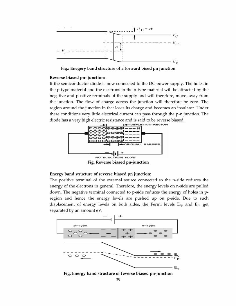
39
Fig.: Enegery band structure of a forward bised pn junction
Reverse biased pn- junction:
If the semiconductor diode is now connected to the DC power supply. The holes in
the p-type material and the electrons in the n-type material will be attracted by the
negative and positive terminals of the supply and will therefore, move away from
the junction. The flow of charge across the junction will therefore be zero. The
region around the junction in fact loses its charge and becomes an insulator. Under
these conditions very little electrical current can pass through the p-n junction. The
diode has a very high electric resistance and is said to be reverse biased.
Fig. Reverse biased pn-junction
Energy band structure of reverse biased pn junction:
The positive terminal of the external source connected to the n-side reduces the
energy of the electrons in general. Therefore, the energy levels on n-side are pulled
down. The negative terminal connected to p-side reduces the energy of holes in p-
region and hence the energy levels are pushed up on p-side. Due to such
displacement of energy levels on both sides, the Fermi levels EFp and EFn get
separated by an amount eV.
Fig. Energy band structure of feverse biased pn-junction
40
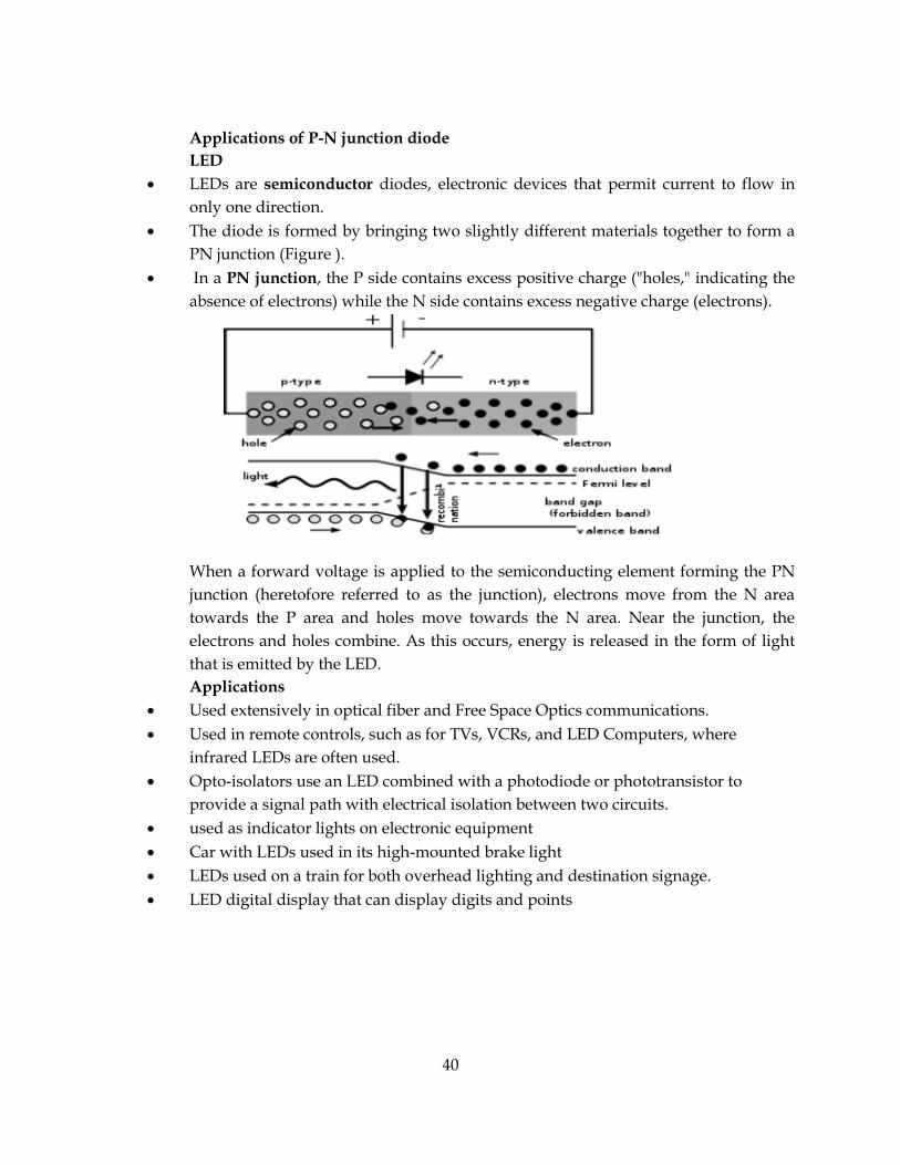
Applications of P-N junction diode
LED
• LEDs are semiconductor diodes, electronic devices that permit current to flow in
only one direction.
• The diode is formed by bringing two slightly different materials together to form a
PN junction (Figure ).
• In a PN junction, the P side contains excess positive charge ("holes," indicating the
absence of electrons) while the N side contains excess negative charge (electrons).
When a forward voltage is applied to the semiconducting element forming the PN
junction (heretofore referred to as the junction), electrons move from the N area
towards the P area and holes move towards the N area. Near the junction, the
electrons and holes combine. As this occurs, energy is released in the form of light
that is emitted by the LED.
Applications
• Used extensively in optical fiber and Free Space Optics communications.
• Used in remote controls, such as for TVs, VCRs, and LED Computers, where
infrared LEDs are often used.
• Opto-isolators use an LED combined with a photodiode or phototransistor to
provide a signal path with electrical isolation between two circuits.
• used as indicator lights on electronic equipment
• Car with LEDs used in its high-mounted brake light
• LEDs used on a train for both overhead lighting and destination signage.
• LED digital display that can display digits and points
41
Applied Physics – I (Sem-I) May-2015
(Revised Course) QP Code: 1027
Time : 2 Hours Total Marks : 60
N.B.:- (1) Question no. 1 is compulsory.
(2) Attempt any three questions from Q.2 to 6.
(3) Use suitable data wherever required.
(4) Figures to the right indicate full marks.
1. Solve any five from the following: - 15
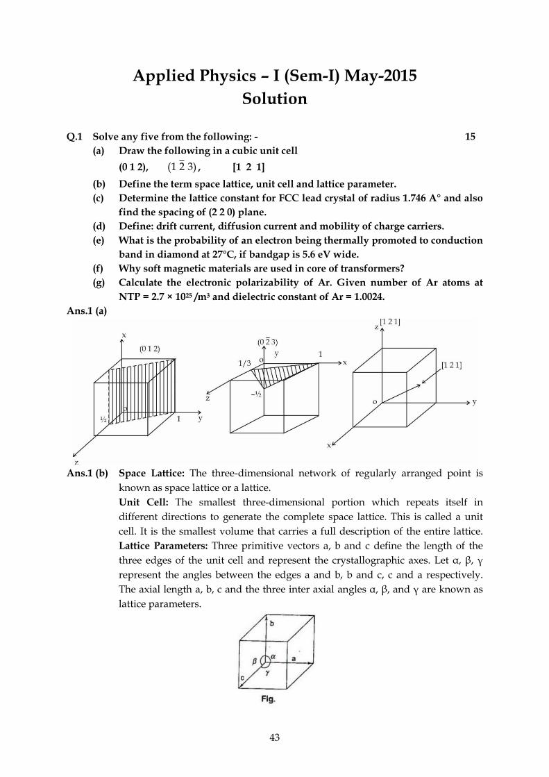
(a) Draw the following in a cubic unit cell
(0 1 2), (1 2 3) , [1 2 1]
(b) Define the term space lattice, unit cell and lattice parameter.
(c) Determine the lattice constant for FCC lead crystal of radius 1.746 A° and also
find the spacing of (2 2 0) plane.
(d) Define : drift current, diffusion current and mobility of charge carriers.
(e) What is the probability of an electron being thermally promoted to conduction
band in diamond at 27°C, if bandgap is 5.6 eV wide.
(f) Why soft magnetic materials are used in core of transformers?
(g) Calculate the electronic polarizability of Ar. Given number of Ar atoms at NTP =
2.7 × 1025 /m3 and dielectric constant of Ar = 1.0024.
2. (a) Show that for intrinsic semiconductors the Fermi level lies midway between the
conduction band and the valence band. Draw the energy level diagram as a
function of temperature for n-type of semi-conductor. 8
(b) Cu has FCC structure. If the interplanar spacing d is 2.08 A° for the set of (111)
planes. Find the density and diameter of C atom. Given atomic weight of Cu is
63.54. 7
3. (a) What is hysteresis? Draw a hysteresis loop for ferromagnetic material and
explain the various important points on it. For a transformer which kind of
material will you prefer-the one with small hysteresis area of the big one? 8
42
(b) Derive Bragg’s law. X-rays of unknown wavelength give first order Bragg’s
reflection at glancing angle of 20° with (2 1 2) planes of copper having FCC
structure. Find the wavelength of X-rays, if the lattice constant for copper is 3.615
A°. 7
4. (a) Discuss Diamond structure with neat diagram and also determine the effective
number of atoms/unit cell, co-ordination number and atomic radius in terms of
lattice constant. 5
(b) Classify solids on the basis of energy band diagram. 5
(c) Explain orientational polarization with suitable diagram and write the
mathematical expression of orientational polarizability. 5
5. (a) Calculate the number of atoms per unit cell of a metal having the lattice
parameter 2.9 A° and density 7.87 gm/cm3. Atomic weight of metal 55.85.
Avogadro number is 6.023 × 10²³/gm mole. 5
(b) What is Hall effect? Mention its significance. How mobility can be determined
by using Hall effect? 5
(c) The reverberation time is found to be 1.5 second for an empty Hall and it is
found to be 1.0 second when a curtain cloth of 20m3 is suspended at the centre of
the Hall. If the dimensions of the hall are 10 × 8 × 6 m3, calculate the coefficient
of absorption of curtain cloth. 5
6. (a) Describe principle, construction and working of magnetostriction oscillator to
produce ultrasonic waves. 5
(b) Explain various point defects in crystals. 5
(c) Explain how a voltage difference is generated in a p-n junction when it is used in
a photovoltaic solar cell. 5
*********************
43
Applied Physics – I (Sem-I) May-2015
Solution
Q.1 Solve any five from the following: - 15
(a) Draw the following in a cubic unit cell
(0 1 2), (1 2 3) , [1 2 1]
(b) Define the term space lattice, unit cell and lattice parameter.
(c) Determine the lattice constant for FCC lead crystal of radius 1.746 A° and also
find the spacing of (2 2 0) plane.
(d) Define: drift current, diffusion current and mobility of charge carriers.
(e) What is the probability of an electron being thermally promoted to conduction
band in diamond at 27°C, if bandgap is 5.6 eV wide.
(f) Why soft magnetic materials are used in core of transformers?
(g) Calculate the electronic polarizability of Ar. Given number of Ar atoms at
NTP = 2.7 × 1025 /m3 and dielectric constant of Ar = 1.0024.
Ans.1 (a)
Ans.1 (b) Space Lattice: The three-dimensional network of regularly arranged point is
known as space lattice or a lattice.
Unit Cell: The smallest three-dimensional portion which repeats itself in
different directions to generate the complete space lattice. This is called a unit
cell. It is the smallest volume that carries a full description of the entire lattice.
Lattice Parameters: Three primitive vectors a, b and c define the length of the
three edges of the unit cell and represent the crystallographic axes. Let α, β, γ
represent the angles between the edges a and b, b and c, c and a respectively.
The axial length a, b, c and the three inter axial angles α, β, and γ are known as
lattice parameters.
44
Sol. 1 (c) Given: r = 1.746 A°, Plane (2 2 0)
a = 2 2r = 2 × 1.44 × 1.746 = 4.938 A°
d = 2 2 2
a
h k l+ +
( )2 20 2 2
4.938d 1.746A
2 2 0= =
+ +
Ans.1 (d) Net displacement in the electron's position per unit time caused by the
application of an electric field becomes a constant at the steady state. Velocity of
the electrons in the steady state in an applied electric field is called the drift
velocity.
Mobility:
The mobility of electron is defined as the magnitude of the drift velocity
acquired by the electrons in a unit field.
E - applied electric field
d -drift velocity
-mobility
= E
d ..….(6)
J = E
= E
J and J =
A
I
= AE
I
Current = I = ned A*
= AE
Adνne = ne
= ne
σ ….(7)
mobility of electron = 1350 cm2/ v-s
mobility of hole is = 480 cm2/v-s
The ease with which electrons could drift in material under the influence of an
electric field called as mobility.
Mobility of electron is > mobility of holes
Current (I):
I = nedA
A- area of cross section, I-current, v - velocity of electrons,
Sol.1 (e) Given: T = 27° C, Eg = 5.6 eV
( )1
F ECEg
1 exp2KT
=
+
( )1
F EC5.6eV
1 exp2 0.026
=
+
= 1.7 × 10–47
45
Ans.1 (f) In order to lower the magnetizing current drawn by the transformer.
Even if both windings are tightly coupled (wound very close together), so that
there is approximately no leakage between them, a magnetomotive force is
necessary to magnetize the air shared by both windings.
If you compare both inductances (air and soft-iron), the inductance of air is
much lower. Therefore, for a given flux linkage (time integral of voltage), the
(magnetizing) current will be much higher for an air-core transformer.
Sol.1 (g) (Beyond the syllabus)
Given: N = 2.7 × 1025/m3, Er = 1.0024
P = E0 (Er – 1) E’ …….(1)
P = de NE
Thus de = P
NE
( )0E Er 1
N
−=
( )12
25
8.85 10 1.0024 1
2.7 10
− −=
40 27.9 10 F m−= −
Q.2 (a) Show that for intrinsic semiconductors the Fermi level lies midway between
the conduction band and the valence band. Draw the energy level diagram as
a function of temperature for n-type of semi-conductor. 8
(b) Cu has FCC structure. If the interplanar spacing d is 2.08 A° for the set of (111)
planes. Find the density and diameter of C atom. Given atomic weight of Cu is
63.54. 7
Ans.2 (a) EF lies mid-way between conduction and valence band.
At any temperature T > 00 K,
ne = Number of electrons in conduction band
nv = Number of holes in valence band
We have
ne = Nce –(EC-EF)/KT …..(1)
Nc = Effective density of states in conduction band
and nv = Nve –(EF – EV) / KT …..(2)
Nv = effective density of states in valence band
For best approximation Nc = Nv …..(3)
For intrinsic semiconductor
nC = nv
( ) ( )C F F VE E E E
KT KTC VN e N e
− −− −
=
( )
( )
C F
F V
E EKT
V
E EKT C
Ne
Ne
−−
−−
=
C F F VE E E E
VKT
C
Ne
N
− + + −
=
( )F C V2E E E
VKT
C
Ne
N
− +
=
as V
C
N
N= 1 for intrinsic semiconductor & taking ‘ln’ on both side
46
( )F C V2E E E
0KT
− +=
(EC + EV) = 2 EF
EF = 2
vE+CE … (4)
Therefore, Fermi level in an intrinsic semiconductor lies at the center of
forbidden energy gap.
Sol.2 (b) Given: n = 4, d = 2.08 A° = 708 × 10–10 m (h k l) = (1 1 1)
2 2 2
ad
h k l=
+ + a 2.08 3 = = 3.60 A°
3 Aa n
N =
3
nA 1.
N a =
( )326 10
4 63.54 1
6.023 10 3.60 10−
=
39038.8 kg/m =
For FCC, a 2
r4
= 3.6 2
4
= = 1.27 A°
Diameter (d) = 2r = 2.54 A°
Q.3 (a) What is hysteresis? Draw a hysteresis loop for ferromagnetic material and
explain the various important points on it. For a transformer which kind of
material will you prefer-the one with small hysteresis area of the big one? 8
(b) Derive Bragg’s law. X-rays of unknown wavelength give first order Bragg’s
reflection at glancing angle of 20° with (2 1 2) planes of copper having FCC
structure. Find the wavelength of X-rays, if the lattice constant for copper is
3.615 A°. 7
Ans.3 (a) (Beyond the syllabus)
A great deal of information can be learned about the magnetic properties of a
material by studying its hysteresis loop. A hysteresis loop shows the relationship
between the induced magnetic flux density (B) and the magnetizing force (H). It
is often referred to as the B-H loop. An example hysteresis loop is shown below.
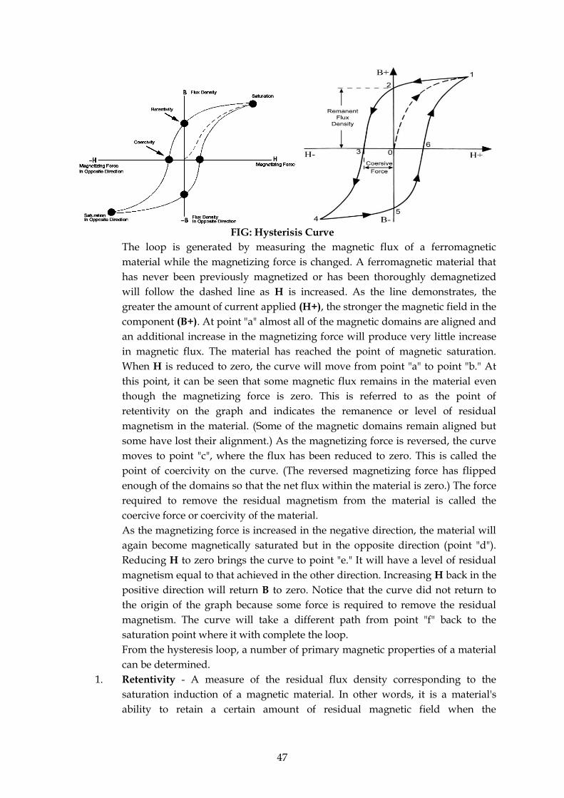
47
FIG: Hysterisis Curve
The loop is generated by measuring the magnetic flux of a ferromagnetic
material while the magnetizing force is changed. A ferromagnetic material that
has never been previously magnetized or has been thoroughly demagnetized
will follow the dashed line as H is increased. As the line demonstrates, the
greater the amount of current applied (H+), the stronger the magnetic field in the
component (B+). At point "a" almost all of the magnetic domains are aligned and
an additional increase in the magnetizing force will produce very little increase
in magnetic flux. The material has reached the point of magnetic saturation.
When H is reduced to zero, the curve will move from point "a" to point "b." At
this point, it can be seen that some magnetic flux remains in the material even
though the magnetizing force is zero. This is referred to as the point of
retentivity on the graph and indicates the remanence or level of residual
magnetism in the material. (Some of the magnetic domains remain aligned but
some have lost their alignment.) As the magnetizing force is reversed, the curve
moves to point "c", where the flux has been reduced to zero. This is called the
point of coercivity on the curve. (The reversed magnetizing force has flipped
enough of the domains so that the net flux within the material is zero.) The force
required to remove the residual magnetism from the material is called the
coercive force or coercivity of the material.
As the magnetizing force is increased in the negative direction, the material will
again become magnetically saturated but in the opposite direction (point "d").
Reducing H to zero brings the curve to point "e." It will have a level of residual
magnetism equal to that achieved in the other direction. Increasing H back in the
positive direction will return B to zero. Notice that the curve did not return to
the origin of the graph because some force is required to remove the residual
magnetism. The curve will take a different path from point "f" back to the
saturation point where it with complete the loop.
From the hysteresis loop, a number of primary magnetic properties of a material
can be determined.
1. Retentivity - A measure of the residual flux density corresponding to the
saturation induction of a magnetic material. In other words, it is a material's
ability to retain a certain amount of residual magnetic field when the
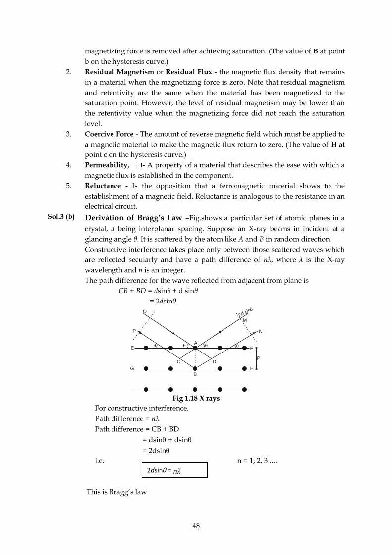
48
magnetizing force is removed after achieving saturation. (The value of B at point
b on the hysteresis curve.)
2. Residual Magnetism or Residual Flux - the magnetic flux density that remains
in a material when the magnetizing force is zero. Note that residual magnetism
and retentivity are the same when the material has been magnetized to the
saturation point. However, the level of residual magnetism may be lower than
the retentivity value when the magnetizing force did not reach the saturation
level.
3. Coercive Force - The amount of reverse magnetic field which must be applied to
a magnetic material to make the magnetic flux return to zero. (The value of H at
point c on the hysteresis curve.)
4. Permeability, - A property of a material that describes the ease with which a
magnetic flux is established in the component.
5. Reluctance - Is the opposition that a ferromagnetic material shows to the
establishment of a magnetic field. Reluctance is analogous to the resistance in an
electrical circuit.
Sol.3 (b) Derivation of Bragg’s Law –Fig.shows a particular set of atomic planes in a
crystal, d being interplanar spacing. Suppose an X-ray beams in incident at a
glancing angle θ. It is scattered by the atom like A and B in random direction.
Constructive interference takes place only between those scattered waves which
are reflected secularly and have a path difference of nλ, where λ is the X-ray
wavelength and n is an integer.
The path difference for the wave reflected from adjacent from plane is
CB + BD = dsinθ + d sinθ
= 2dsinθ
O
P
E
G H
F
N
M
D
A
B
CP
2d sin
Fig 1.18 X rays
For constructive interference,
Path difference = nλ
Path difference = CB + BD
= dsin + dsin
= 2dsin
i.e. n = 1, 2, 3 ....
This is Bragg’s law
2dsinθ = nλ
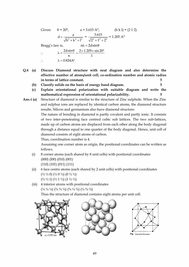
49
Given: = 20°, a = 3.615 A°, (h k l) = (2 1 2)
2 2 2
ad
h k l=
+ + =
2 2 2
3.615
2 1 2+ += 1.205 A°
Bragg’s law is, n 2dsin =
2dsin
n
=
2 1.205 sin 20
1
=
0.824A =
Q.4 (a) Discuss Diamond structure with neat diagram and also determine the
effective number of atoms/unit cell, co-ordination number and atomic radius
in terms of lattice constant. 5
(b) Classify solids on the basis of energy band diagram. 5
(c) Explain orientational polarization with suitable diagram and write the
mathematical expression of orientational polarizability. 5
Ans.4 (a) Structure of diamond is similar to the structure of Zinc sulphide. When the Zinc
and sulphur ions are replaced by identical carbon atoms, the diamond structure
results. Silicon and germanium also have diamond structure.
The nature of bonding in diamond is partly covalent and partly ionic. It consists
of two inter-penetrating face centred cubic sub lattices. The two sub-lattices,
made up of carbon atoms are displaced from each other along the body diagonal
through a distance equal to one quarter of the body diagonal. Hence, unit cell of
diamond consists of eight atoms of carbon.
Thus, coordination number is 4.
Assuming one corner atom as origin, the positional coordinates can be written as
follows.
(i) 8 corner atoms (each shared by 8 unit cells) with positional coordinates
(000) (l00) (010) (001)
(110) (101) (011) (111)
(ii) 6 face centre atoms (each shared by 2 unit cells) with positional coordinates
(½ ½ 0) (½ 0 ½) (0 ½ ½)
(½ ½ 1) (½ 1 ½) (1 ½ ½)
(iii) 4 interior atoms with positional coordinates
(¼ ¼ ¼) (¾ ¾ ¼) (¾ ¼ ¾) (¼ ¾ ¾)
Thus the structure of diamond contains eight atoms per unit cell.
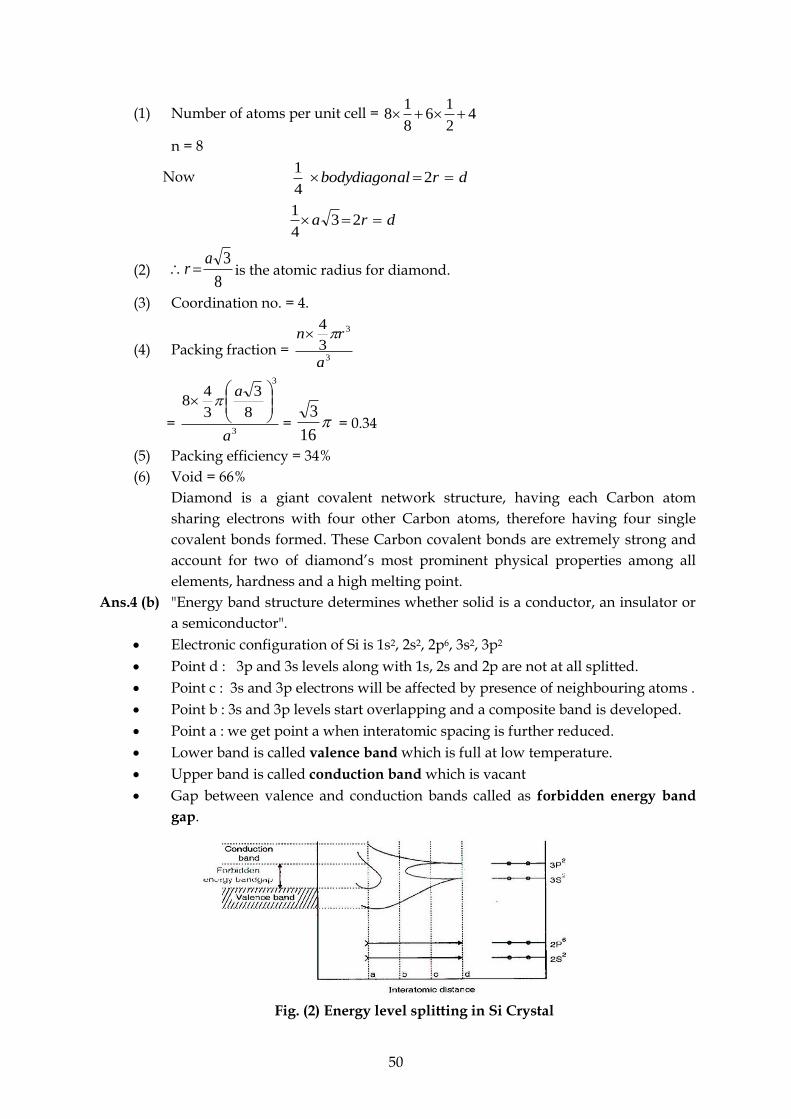
50
(1) Number of atoms per unit cell = 42
16
8
18 ++
n = 8
Now dralbodydiagon == 24
1
dra == 234
1
(2) 8
3ar = is the atomic radius for diamond.
(3) Coordination no. = 4.
(4) Packing fraction = 3
3
3
4
a
rn
= 3
3
8
3
3
48
a
a
= 16
3 = 0.34
(5) Packing efficiency = 34%
(6) Void = 66%
Diamond is a giant covalent network structure, having each Carbon atom
sharing electrons with four other Carbon atoms, therefore having four single
covalent bonds formed. These Carbon covalent bonds are extremely strong and
account for two of diamond’s most prominent physical properties among all
elements, hardness and a high melting point.
Ans.4 (b) "Energy band structure determines whether solid is a conductor, an insulator or
a semiconductor".
• Electronic configuration of Si is 1s2, 2s2, 2p6, 3s2, 3p2
• Point d : 3p and 3s levels along with 1s, 2s and 2p are not at all splitted.
• Point c : 3s and 3p electrons will be affected by presence of neighbouring atoms .
• Point b : 3s and 3p levels start overlapping and a composite band is developed.
• Point a : we get point a when interatomic spacing is further reduced.
• Lower band is called valence band which is full at low temperature.
• Upper band is called conduction band which is vacant
• Gap between valence and conduction bands called as forbidden energy band
gap.
Fig. (2) Energy level splitting in Si Crystal
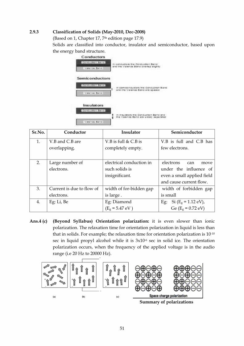
51
2.9.3 Classification of Solids (May-2010, Dec-2008)
(Based on 1, Chapter 17, 7th edition page 17.9)
Solids are classified into conductor, insulator and semiconductor, based upon
the energy band structure.
Sr.No. Conductor Insulator Semiconductor
1. V.B and C.B are
overlapping.
V.B is full & C.B is
completely empty.
V.B is full and C.B has
few electrons.
2. Large number of
electrons.
electrical conduction in
such solids is
insignificant.
electrons can move
under the influence of
even a small applied field
and cause current flow.
3. Current is due to flow of
electrons.
width of for-bidden gap
is large .
width of forbidden gap
is small
4. Eg: Li, Be Eg: Diamond
(Eg = 5.47 eV )
Eg: Si (Eg = 1.12 eV),
Ge (Eg = 0.72 eV)
Ans.4 (c) (Beyond Syllabus) Orientation polarization: it is even slower than ionic
polarization. The relaxation time for orientation polarization in liquid is less than
that in solids. For example; the relaxation time for orientation polarization is 10-10
sec in liquid propyl alcohol while it is 3x10⁻⁶ sec in solid ice. The orientation
polarization occurs, when the frequency of the applied voltage is in the audio
range (i.e 20 Hz to 20000 Hz).
Summary of polarizations
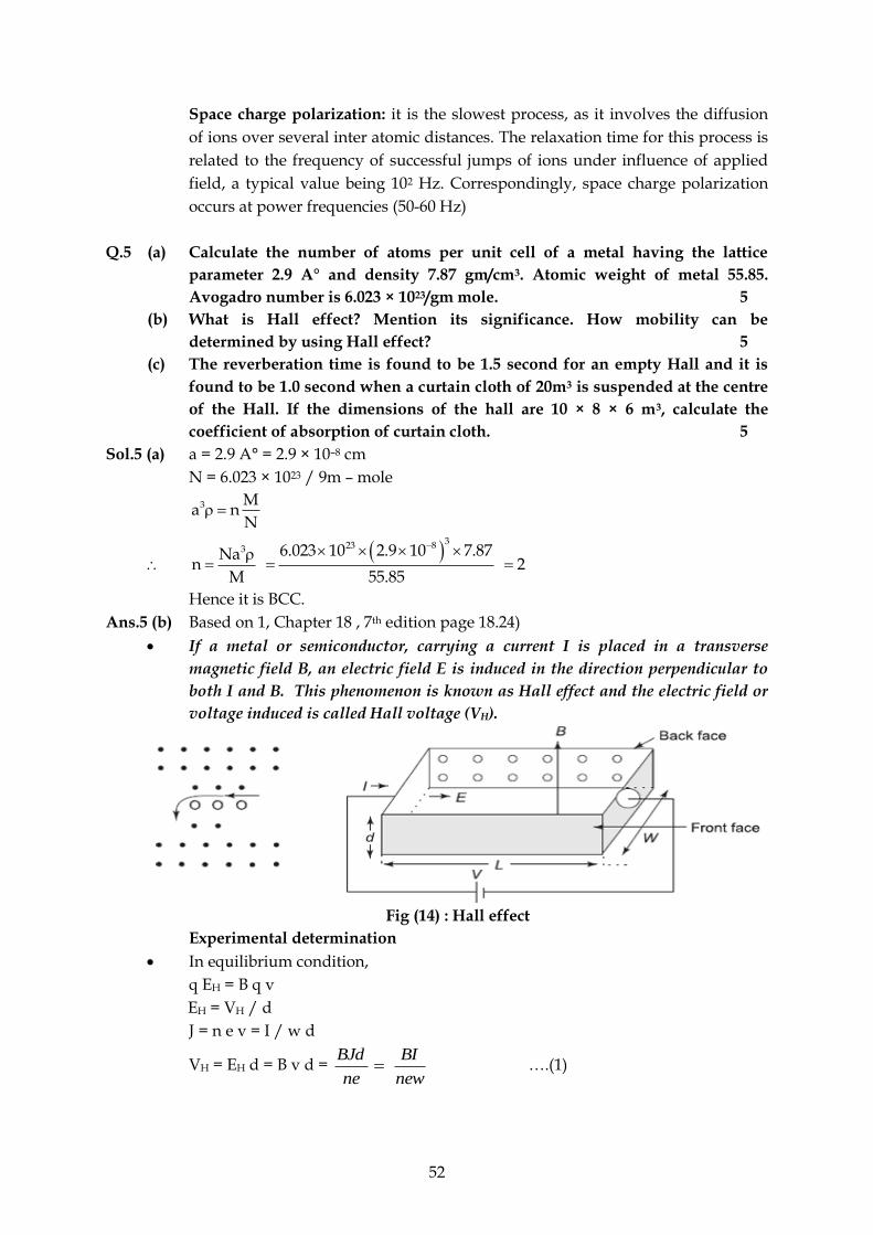
52
Space charge polarization: it is the slowest process, as it involves the diffusion
of ions over several inter atomic distances. The relaxation time for this process is
related to the frequency of successful jumps of ions under influence of applied
field, a typical value being 102 Hz. Correspondingly, space charge polarization
occurs at power frequencies (50-60 Hz)
Q.5 (a) Calculate the number of atoms per unit cell of a metal having the lattice
parameter 2.9 A° and density 7.87 gm/cm3. Atomic weight of metal 55.85.
Avogadro number is 6.023 × 10²³/gm mole. 5
(b) What is Hall effect? Mention its significance. How mobility can be
determined by using Hall effect? 5
(c) The reverberation time is found to be 1.5 second for an empty Hall and it is
found to be 1.0 second when a curtain cloth of 20m3 is suspended at the centre
of the Hall. If the dimensions of the hall are 10 × 8 × 6 m3, calculate the
coefficient of absorption of curtain cloth. 5
Sol.5 (a) a = 2.9 A° = 2.9 × 10⁻⁸ cm
N = 6.023 × 10²³ / 9m – mole
3 Ma n
N =
3Na
nM
=
( )323 86.023 10 2.9 10 7.87
55.85
− = 2=
Hence it is BCC.
Ans.5 (b) Based on 1, Chapter 18 , 7th edition page 18.24)
• If a metal or semiconductor, carrying a current I is placed in a transverse
magnetic field B, an electric field E is induced in the direction perpendicular to
both I and B. This phenomenon is known as Hall effect and the electric field or
voltage induced is called Hall voltage (VH).
Fig (14) : Hall effect
Experimental determination
• In equilibrium condition,
q EH = B q v
EH = VH / d
J = n e v = I / w d
VH = EH d = B v d = new
BI
ne
BJd= ….(1)
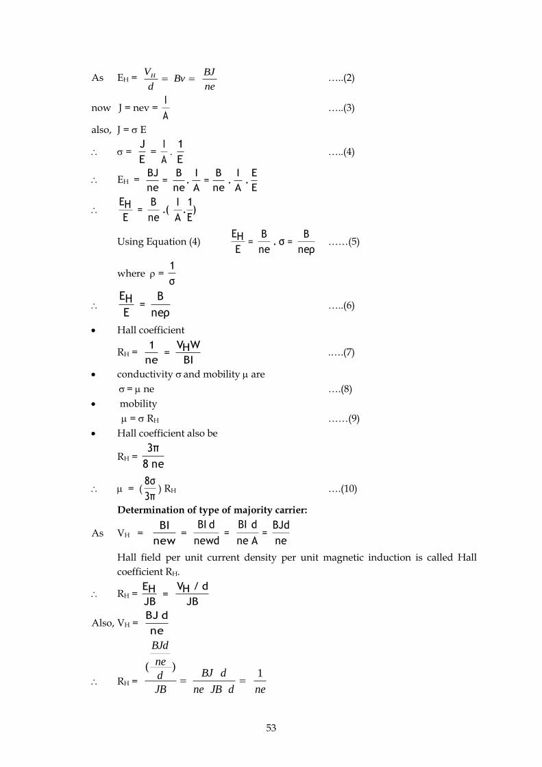
53
As EH = ne
BJBv
d
VH == …..(2)
now J = nev = A
I …..(3)
also, J = E
= E
J =
A
I. E
1 …..(4)
EH = E
E.
A
I.
ne
B=
A
I.
ne
B=
ne
BJ
)E
1.
A
I(.
ne
B=
E
HE
Using Equation (4) ρne
B=σ.
ne
B=
E
HE ……(5)
where = σ
1
ρne
B=
E
HE …..(6)
• Hall coefficient
RH = BI
WHV=ne
1 .….(7)
• conductivity and mobility are
= ne ….(8)
• mobility
= RH ……(9)
• Hall coefficient also be
RH = ne8
π3
= (π3
σ8) RH ….(10)
Determination of type of majority carrier:
As VH = new
BI =
ne
BJd=
Ane
dBI=
newd
dBI
Hall field per unit current density per unit magnetic induction is called Hall
coefficient RH.
RH = JB
d/HV=JB
HE
Also, VH = ne
dBJ
RH = nedJBne
dBJ
JB
d
ne
BJd
1)(
==
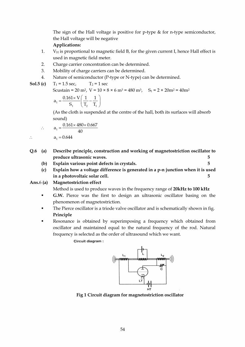
54
The sign of the Hall voltage is positive for p-type & for n-type semiconductor,
the Hall voltage will be negative
Applications:
1. VH is proportional to magnetic field B, for the given current I, hence Hall effect is
used in magnetic field meter.
2. Charge carrier concentration can be determined.
3. Mobility of charge carriers can be determined.
4. Nature of semiconductor (P-type or N-type) can be determined.
Sol.5 (c) T1 = 1.5 sec, T2 = 1 sec
Scustain = 20 m2, V = 10 × 8 × 6 m3 = 480 m3, S1 = 2 × 20m2 = 40m2
1
1 2 1
0.161 V 1 1a
S T T
= −
(As the cloth is suspended at the centre of the hall, both its surfaces will absorb
sound)
1
0.161 480 0.667a
40
=
1a 0.644=
Q.6 (a) Describe principle, construction and working of magnetostriction oscillator to
produce ultrasonic waves. 5
(b) Explain various point defects in crystals. 5
(c) Explain how a voltage difference is generated in a p-n junction when it is used
in a photovoltaic solar cell. 5
Ans.6 (a) Magnetostriction effect
Method is used to produce waves in the frequency range of 20kHz to 100 kHz
▪ G.W. Pierce was the first to design an ultrasonic oscillator basing on the
phenomenon of magnetostriction.
▪ The Pierce oscillator is a triode valve oscillator and is schematically shown in fig.
Principle
▪ Resonance is obtained by superimposing a frequency which obtained from
oscillator and maintained equal to the natural frequency of the rod. Natural
frequency is selected as the order of ultrasound which we want.
Fig 1 Circuit diagram for magnetostriction oscillator
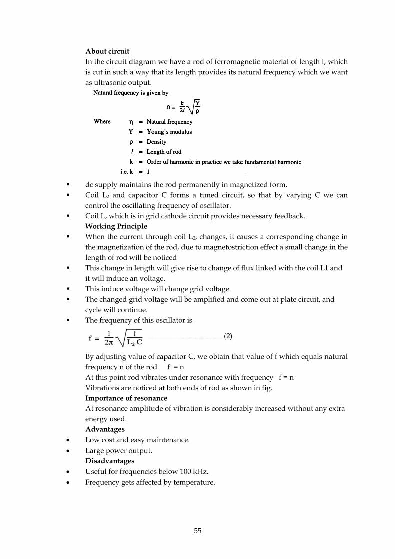
55
About circuit
In the circuit diagram we have a rod of ferromagnetic material of length l, which
is cut in such a way that its length provides its natural frequency which we want
as ultrasonic output.
▪ dc supply maintains the rod permanently in magnetized form.
▪ Coil L2 and capacitor C forms a tuned circuit, so that by varying C we can
control the oscillating frequency of oscillator.
▪ Coil L, which is in grid cathode circuit provides necessary feedback.
Working Principle
▪ When the current through coil L2, changes, it causes a corresponding change in
the magnetization of the rod, due to magnetostriction effect a small change in the
length of rod will be noticed
▪ This change in length will give rise to change of flux linked with the coil L1 and
it will induce an voltage.
▪ This induce voltage will change grid voltage.
▪ The changed grid voltage will be amplified and come out at plate circuit, and
cycle will continue.
▪ The frequency of this oscillator is
By adjusting value of capacitor C, we obtain that value of f which equals natural
frequency n of the rod f = n
At this point rod vibrates under resonance with frequency f = n
Vibrations are noticed at both ends of rod as shown in fig.
Importance of resonance
At resonance amplitude of vibration is considerably increased without any extra
energy used.
Advantages
• Low cost and easy maintenance.
• Large power output.
Disadvantages
• Useful for frequencies below 100 kHz.
• Frequency gets affected by temperature.
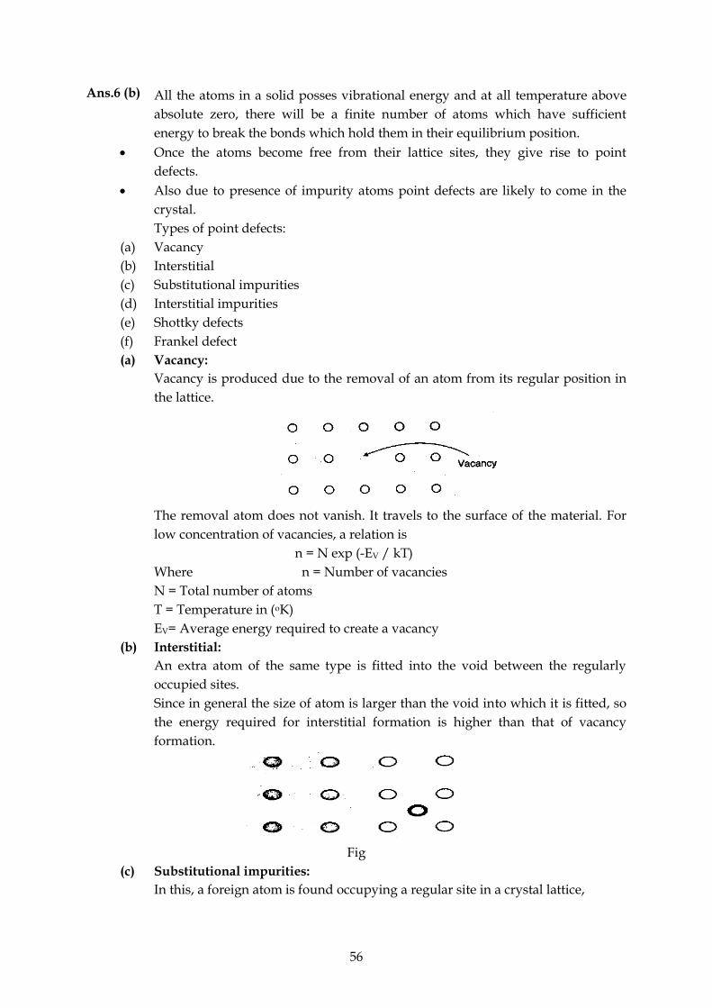
56
Ans.6 (b) All the atoms in a solid posses vibrational energy and at all temperature above
absolute zero, there will be a finite number of atoms which have sufficient
energy to break the bonds which hold them in their equilibrium position.
• Once the atoms become free from their lattice sites, they give rise to point
defects.
• Also due to presence of impurity atoms point defects are likely to come in the
crystal.
Types of point defects:
(a) Vacancy
(b) Interstitial
(c) Substitutional impurities
(d) Interstitial impurities
(e) Shottky defects
(f) Frankel defect
(a) Vacancy:
Vacancy is produced due to the removal of an atom from its regular position in
the lattice.
The removal atom does not vanish. It travels to the surface of the material. For
low concentration of vacancies, a relation is
n = N exp (-EV / kT)
Where n = Number of vacancies
N = Total number of atoms
T = Temperature in (oK)
EV= Average energy required to create a vacancy
(b) Interstitial:
An extra atom of the same type is fitted into the void between the regularly
occupied sites.
Since in general the size of atom is larger than the void into which it is fitted, so
the energy required for interstitial formation is higher than that of vacancy
formation.
Fig
(c) Substitutional impurities:
In this, a foreign atom is found occupying a regular site in a crystal lattice,
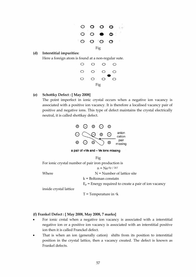
57
Fig
(d) Interstitial impurities:
Here a foreign atom is found at a non-regular sute.
Fig
(e) Schottky Defect : [ May 2008]
The point imperfect in ionic crystal occurs when a negative ion vacancy is
associated with a positive ion vacancy. It is therefore a localised vacancy pair of
positive and negative ions. This type of defect maintains the crystal electrically
neutral, it is called shottkay defect.
Fig
For ionic crystal number of pair iron production is
n = Ne-Ep / 2kT
Where N = Number of lattice site
k = Boltzman constatn
Ep = Energy required to create a pair of ion vacancy
inside crystal lattice
T = Temperature in ok
(f) Frankel Defect : [ May 2008, May 2008, 7 marks]
• For ionic crstal when a negative ion vacancy is associated with a interstitial
negative ion or a positive ion vacancy is associated with an interstitial positive
ion then it is called Franckel defect.
• That is when an ion (generally cation) shifts from its position to interstitial
position in the crystal lattice, then a vacancy created. The defect is known as
Frankel defects.
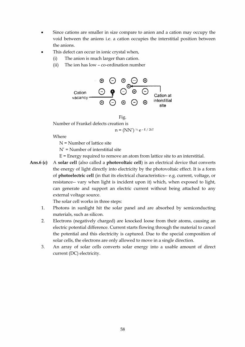
58
• Since cations are smaller in size compare to anion and a cation may occupy the
void between the anions i.e. a cation occupies the interstitial position between
the anions.
• This defect can occur in ionic crystal when,
(i) The anion is much larger than cation.
(ii) The ion has low – co-ordination number
Fig.
Number of Frankel defects creation is
n = (NN’) ½ e – E / 2kT
Where
N = Number of lattice site
N’ = Number of interstitial site
E = Energy required to remove an atom from lattice site to an interstitial.
Ans.6 (c) A solar cell (also called a photovoltaic cell) is an electrical device that converts
the energy of light directly into electricity by the photovoltaic effect. It is a form
of photoelectric cell (in that its electrical characteristics-- e.g. current, voltage, or
resistance-- vary when light is incident upon it) which, when exposed to light,
can generate and support an electric current without being attached to any
external voltage source.
The solar cell works in three steps:
1. Photons in sunlight hit the solar panel and are absorbed by semiconducting
materials, such as silicon.
2. Electrons (negatively charged) are knocked loose from their atoms, causing an
electric potential difference. Current starts flowing through the material to cancel
the potential and this electricity is captured. Due to the special composition of
solar cells, the electrons are only allowed to move in a single direction.
3. An array of solar cells converts solar energy into a usable amount of direct
current (DC) electricity.
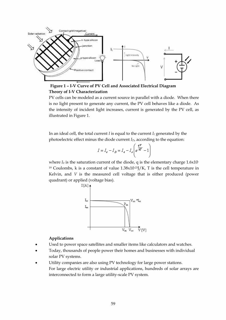
59
Figure 1 – I-V Curve of PV Cell and Associated Electrical Diagram
Theory of I-V Characterization
PV cells can be modeled as a current source in parallel with a diode. When there
is no light present to generate any current, the PV cell behaves like a diode. As
the intensity of incident light increases, current is generated by the PV cell, as
illustrated in Figure 1.
In an ideal cell, the total current I is equal to the current Iℓ generated by the
photoelectric effect minus the diode current ID, according to the equation:
where I0 is the saturation current of the diode, q is the elementary charge 1.6x10-
19 Coulombs, k is a constant of value 1.38x10⁻²³J/K, T is the cell temperature in
Kelvin, and V is the measured cell voltage that is either produced (power
quadrant) or applied (voltage bias).
Applications
• Used to power space satellites and smaller items like calculators and watches.
• Today, thousands of people power their homes and businesses with individual
solar PV systems.
• Utility companies are also using PV technology for large power stations.
For large electric utility or industrial applications, hundreds of solar arrays are
interconnected to form a large utility-scale PV system.
60
Applied Physics – I (Sem-I) May-2016
(Revised Course) QP Code: 28603
Time : 2 Hours Total Marks : 60
N.B.:- (1) Question no. 1 is compulsory.
(2) Attempt any three questions from Q.2 to 6.
(3) Use suitable data wherever required.
(4) Figures to the right indicate full marks.
1. Attempt any five from the following: - 15
(a) Draw (a) (112) (b) (0 4 0) (c) [0 4 0] with reference to a cubic unit cell.
(b) What is the probability of an electron being thermally promoted to the conduction
band in diamond at 27°C, if the bandgap is 5.6 eV wide?
(c) Define drift current, diffusion current and mobility of charge carries.
(d) What is dielectric polarization and dielectric susceptibility? Write the relation
between them.
(e) State and explain Ohm’s law in magnetic circuit.
(f) Write Sabine’s formula and explain the terms used in it.
(g) Calculate the length of an iron rod which can be used to produce ultrasonic waves
of 20kHz Given – Y = 11.6 × 10¹⁰ N/m2, = 7.23 × 10³ kg/m3.
2. (a) Explain formation of energy bands in solids and explain classification on the basis
of energy band theory. 8
(b) Zn has hcp structure. The nearest neighbor distance is 0.27nm. The atomic weight
of Zn is 65.37. Calculate the volume of unit cell, density and atomic packing
fraction of Zn. 7
3. (a) What is hysteresis? Draw a hysteresis loop for ferromagnetic material and explain
various important parameters.
A magnetic material has a magnetization of 2300 A/m and produces a flux density
of 0.00314 wb/m2, Calculate magnetizing force and relative permeability of the
material. 8
(b) Explain the statement “crystal act as three dimensional grating with X-rays”.
61
Monochromatic X-ray beam of wavelength = 5.8189 A° is reflected strongly for
a glancing angle of = 75.86° in first order by certain planes of cubic of lattice
constant 3A°. Determine Miller indices of the possible reflecting planes. 7
4. (a) Define Ligancy. Find the value of critical radius ratio for ligancy4. 5
(b) An impurity of 0.01 ppm is added to Si. The semiconductor has a resistivity of
0.25 m at 300K. Calculate the hole concentration and its mobility. Atomic weight
of Si is 28.1, density of Si = 2.4 × 10³kg/m3. 5
(c) Explain the origin of electronic, ionic and orientational polarization and
temperature dependence of respective polarizability. 5
5. (a) The density of copper is 8980kg/m3 and unit cell dimensions is 3.61 A°. Atomic
weight of copper is 63.54. Determine type of crystal structure. Calculate atomic
radius and interplanar spacing of (1 1 0) plane. 5
(b) What is Hall effect? Derive expression for Hall voltage with neat labelled diagram.
5
(c) Explain how the reverberation time is affected by (i) size (ii) nature of wall surface
(iii) audience in an auditorium. 5
6. (a) Estimate the ratio of vacancies at (i) –119°C (ii) 80°C where average required to
create vacancy is 1.8eV. 5
(b) How a p-n junction diode is used to generate a potential difference in a
photovoltaic solar cell? 5
(c) Explain with neat labelled diagram the construction and working of piezoelectric
oscillator. 5
******************
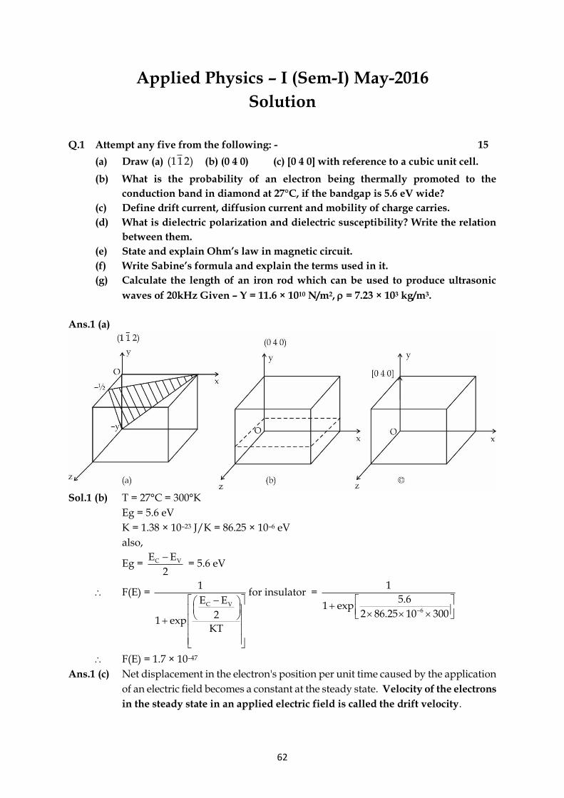
62
Applied Physics – I (Sem-I) May-2016
Solution
Q.1 Attempt any five from the following: - 15
(a) Draw (a) (112) (b) (0 4 0) (c) [0 4 0] with reference to a cubic unit cell.
(b) What is the probability of an electron being thermally promoted to the
conduction band in diamond at 27°C, if the bandgap is 5.6 eV wide?
(c) Define drift current, diffusion current and mobility of charge carries.
(d) What is dielectric polarization and dielectric susceptibility? Write the relation
between them.
(e) State and explain Ohm’s law in magnetic circuit.
(f) Write Sabine’s formula and explain the terms used in it.
(g) Calculate the length of an iron rod which can be used to produce ultrasonic
waves of 20kHz Given – Y = 11.6 × 10¹⁰ N/m2, = 7.23 × 10³ kg/m3.
Ans.1 (a)
Sol.1 (b) T = 27°C = 300°K
Eg = 5.6 eV
K = 1.38 × 10⁻²³ J/K = 86.25 × 10⁻⁶ eV
also,
Eg = C VE E
2
− = 5.6 eV
F(E) = C V
1
E E
21 exp
KT
− +
for insulator =
6
1
5.61 exp
2 86.25 10 300−
+
F(E) = 1.7 × 10–47
Ans.1 (c) Net displacement in the electron's position per unit time caused by the application
of an electric field becomes a constant at the steady state. Velocity of the electrons
in the steady state in an applied electric field is called the drift velocity.
63
Mobility:
The mobility of electron is defined as the magnitude of the drift velocity
acquired by the electrons in a unit field.
E - applied electric field
d -drift velocity
-mobility
= E
d ..….(6)
J = E
= E
J and J =
A
I
= AE
I
Current = I = ned A*
= AE
Adνne = ne
= ne
σ ….(7)
mobility of electron = 1350 cm2/ v-s
mobility of hole is = 480 cm2/v-s
The ease with which electrons could drift in material under the influence of an
electric field called as mobility.
Mobility of electron is > mobility of holes
Current (I):
I = nedA
A- area of cross section, I-current, v - velocity of electrons,
Ans.1 (d) Dielectric Polarization: When an electric field is applied across a dielectric
material then the dielectric material becomes polarized. This mechanism is called
dielectric polarization
Electric susceptibility: In electromagnetism, the electric susceptibility a
dimensionless proportionality constant that indicates the degree of polarization of
a dielectric material in response to an applied electric field
Electrical Susceptibility:
The polarization vector P is proportional to the applied electric field E, for Field
strength that are too large.
Therefore P α E
P = 0 e E
Where e is a characteristics of every dielectric material and is called as electrical
Susceptibility.
Therefore e = P
0 E
64
Since P
E = 0 ( r -1 )
e =
Therefore e = ( r -1 ) or r = e +1
The dielectric constant determines the share of the electric stress which is absorbed
by the material. It is the ratio between the absolute permittivity and the
permittivity of free space 0 and is given by,
r= / 0
Ans.1 (e) Recall the equation
CauseEffect
Opposition=
For magnetic circuits, the effect desired is the flux . The cause is the
magnetomotive force (mmf) , which is the external force (or “pressure”) required
to set up the magnetic flux lines within the magnetic material.
The opposition to the setting up of the flux is the reluctance.
Substituting, we have
F
R =
The magnetomotive force is proportional to the product of the number of turns
around the core (in which the flux is to be established) and the current through
the turns of wire. In equation form,
F = NI (ampere-turns, At)
This equation clearly indicates that an increase in the number of turns or the
current through the wire will result in an increased “pressure” on the system to
establish flux lines through the core.
Although there is a great deal of similarity between electric and magnetic circuits,
one must continue to realize that the flux is not a “flow” variable such as current
in an electric circuit. Magnetic flux is established in the core through the alteration
of the atomic structure of the core due to external pressure and is not a measure
of the flow of some charged particles through the core.
Sol.1 (f) Sabine’s formulae:
T= 0.161V/A
Where T= Reverberation Time
V= volume
A= Total absorption of sound
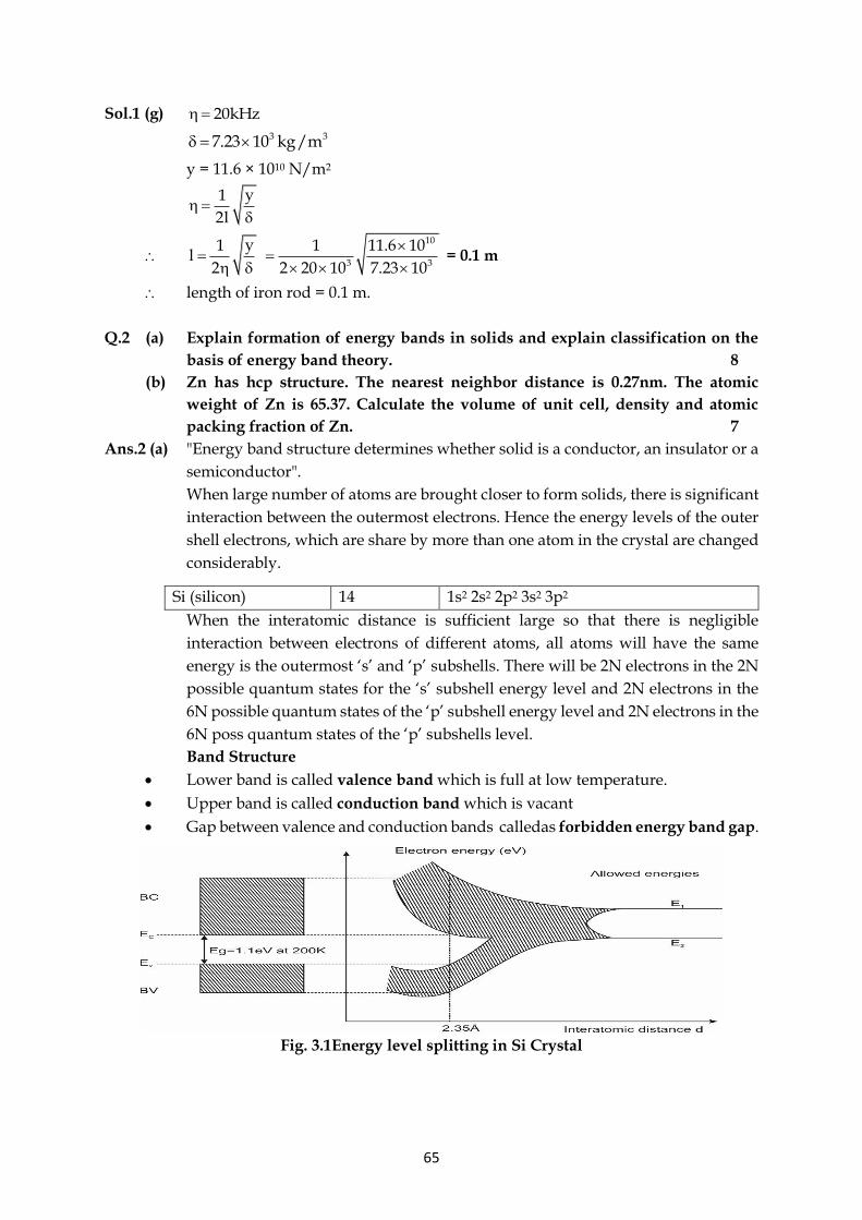
65
Sol.1 (g) 20kHz=
3 37.23 10 kg/m =
y = 11.6 × 10¹⁰ N/m2
y1
2l =
y1
l2
=
10
3 3
1 11.6 10
2 20 10 7.23 10
=
= 0.1 m
length of iron rod = 0.1 m.
Q.2 (a) Explain formation of energy bands in solids and explain classification on the
basis of energy band theory. 8
(b) Zn has hcp structure. The nearest neighbor distance is 0.27nm. The atomic
weight of Zn is 65.37. Calculate the volume of unit cell, density and atomic
packing fraction of Zn. 7
Ans.2 (a) "Energy band structure determines whether solid is a conductor, an insulator or a
semiconductor".
When large number of atoms are brought closer to form solids, there is significant
interaction between the outermost electrons. Hence the energy levels of the outer
shell electrons, which are share by more than one atom in the crystal are changed
considerably.
Si (silicon) 14 1s2 2s2 2p2 3s2 3p2
When the interatomic distance is sufficient large so that there is negligible
interaction between electrons of different atoms, all atoms will have the same
energy is the outermost ‘s’ and ‘p’ subshells. There will be 2N electrons in the 2N
possible quantum states for the ‘s’ subshell energy level and 2N electrons in the
6N possible quantum states of the ‘p’ subshell energy level and 2N electrons in the
6N poss quantum states of the ‘p’ subshells level.
Band Structure
• Lower band is called valence band which is full at low temperature.
• Upper band is called conduction band which is vacant
• Gap between valence and conduction bands calledas forbidden energy band gap.
Fig. 3.1Energy level splitting in Si Crystal
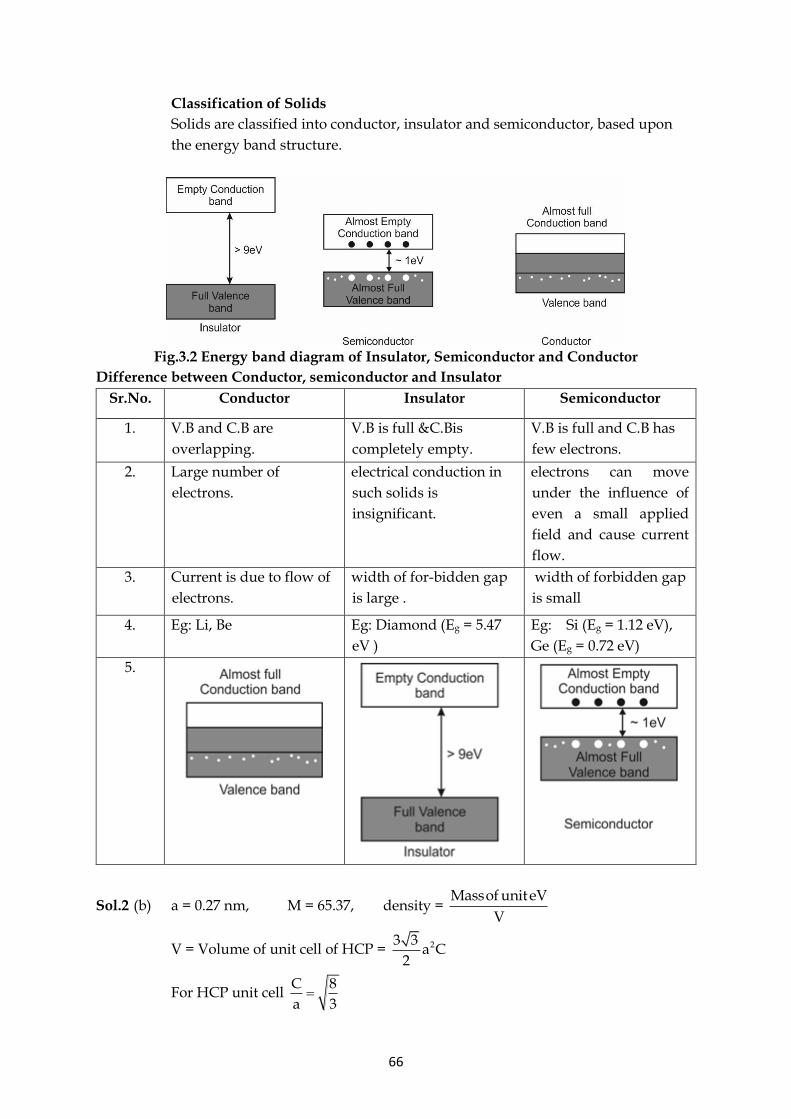
66
Classification of Solids
Solids are classified into conductor, insulator and semiconductor, based upon
the energy band structure.
Fig.3.2 Energy band diagram of Insulator, Semiconductor and Conductor
Difference between Conductor, semiconductor and Insulator
Sr.No. Conductor Insulator Semiconductor
1. V.B and C.B are
overlapping.
V.B is full &C.Bis
completely empty.
V.B is full and C.B has
few electrons.
2. Large number of
electrons.
electrical conduction in
such solids is
insignificant.
electrons can move
under the influence of
even a small applied
field and cause current
flow.
3. Current is due to flow of
electrons.
width of for-bidden gap
is large .
width of forbidden gap
is small
4. Eg: Li, Be Eg: Diamond (Eg = 5.47
eV )
Eg: Si (Eg = 1.12 eV),
Ge (Eg = 0.72 eV)
5.
Sol.2 (b) a = 0.27 nm, M = 65.37, density = Massof uniteV
V
V = Volume of unit cell of HCP = 23 3a C
2
For HCP unit cell C 8
a 3=
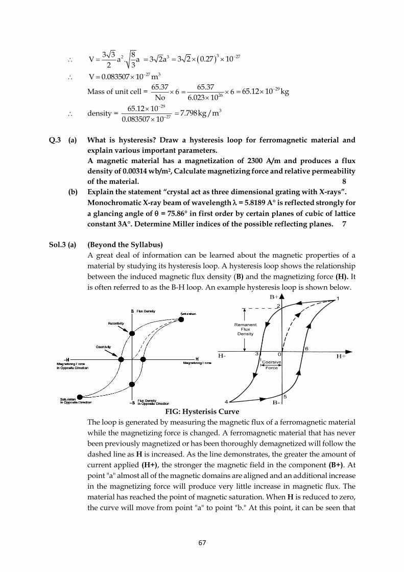
67
23 3 8V a . a
2 3= 33 2a= ( )
3 273 2 0.27 10−=
27 3V 0.083507 10 m−=
Mass of unit cell = 65.37
6No
26
65.376
6.023 10=
2965.12 10 kg−=
density = 29
27
65.12 10
0.083507 10
−
−
37.798kg/m=
Q.3 (a) What is hysteresis? Draw a hysteresis loop for ferromagnetic material and
explain various important parameters.
A magnetic material has a magnetization of 2300 A/m and produces a flux
density of 0.00314 wb/m2, Calculate magnetizing force and relative permeability
of the material. 8
(b) Explain the statement “crystal act as three dimensional grating with X-rays”.
Monochromatic X-ray beam of wavelength = 5.8189 A° is reflected strongly for
a glancing angle of = 75.86° in first order by certain planes of cubic of lattice
constant 3A°. Determine Miller indices of the possible reflecting planes. 7
Sol.3 (a) (Beyond the Syllabus)
A great deal of information can be learned about the magnetic properties of a
material by studying its hysteresis loop. A hysteresis loop shows the relationship
between the induced magnetic flux density (B) and the magnetizing force (H). It
is often referred to as the B-H loop. An example hysteresis loop is shown below.
FIG: Hysterisis Curve
The loop is generated by measuring the magnetic flux of a ferromagnetic material
while the magnetizing force is changed. A ferromagnetic material that has never
been previously magnetized or has been thoroughly demagnetized will follow the
dashed line as H is increased. As the line demonstrates, the greater the amount of
current applied (H+), the stronger the magnetic field in the component (B+). At
point "a" almost all of the magnetic domains are aligned and an additional increase
in the magnetizing force will produce very little increase in magnetic flux. The
material has reached the point of magnetic saturation. When H is reduced to zero,
the curve will move from point "a" to point "b." At this point, it can be seen that
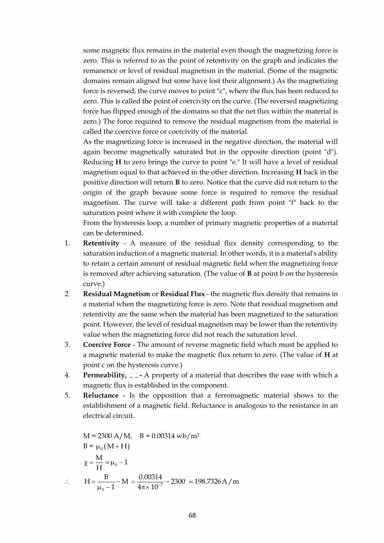
68
some magnetic flux remains in the material even though the magnetizing force is
zero. This is referred to as the point of retentivity on the graph and indicates the
remanence or level of residual magnetism in the material. (Some of the magnetic
domains remain aligned but some have lost their alignment.) As the magnetizing
force is reversed, the curve moves to point "c", where the flux has been reduced to
zero. This is called the point of coercivity on the curve. (The reversed magnetizing
force has flipped enough of the domains so that the net flux within the material is
zero.) The force required to remove the residual magnetism from the material is
called the coercive force or coercivity of the material.
As the magnetizing force is increased in the negative direction, the material will
again become magnetically saturated but in the opposite direction (point "d").
Reducing H to zero brings the curve to point "e." It will have a level of residual
magnetism equal to that achieved in the other direction. Increasing H back in the
positive direction will return B to zero. Notice that the curve did not return to the
origin of the graph because some force is required to remove the residual
magnetism. The curve will take a different path from point "f" back to the
saturation point where it with complete the loop.
From the hysteresis loop, a number of primary magnetic properties of a material
can be determined.
1. Retentivity - A measure of the residual flux density corresponding to the
saturation induction of a magnetic material. In other words, it is a material's ability
to retain a certain amount of residual magnetic field when the magnetizing force
is removed after achieving saturation. (The value of B at point b on the hysteresis
curve.)
2. Residual Magnetism or Residual Flux - the magnetic flux density that remains in
a material when the magnetizing force is zero. Note that residual magnetism and
retentivity are the same when the material has been magnetized to the saturation
point. However, the level of residual magnetism may be lower than the retentivity
value when the magnetizing force did not reach the saturation level.
3. Coercive Force - The amount of reverse magnetic field which must be applied to
a magnetic material to make the magnetic flux return to zero. (The value of H at
point c on the hysteresis curve.)
4. Permeability, - A property of a material that describes the ease with which a
magnetic flux is established in the component.
5. Reluctance - Is the opposition that a ferromagnetic material shows to the
establishment of a magnetic field. Reluctance is analogous to the resistance in an
electrical circuit.
M = 2300 A/M, B = 0.00314 wb/m2
B = ( )0 M H +
M
H = 0 1= −
0
BH M
1= − − 7
0.003142300
4 10−= −
198.7326A/m=
69
M
r 1H
= +2300
1198.7326
= + 12.57=
Sol.3 (b) X-rays have short wavelength of the order of 10-10m. An ordinary grating which
have 6000 lines per cm cannot produce diffraction of X-rays. This fact was first
studied by Max Laue and Paul Petr Ewald in Munich by studying periodic array
of atoms. The atoms arranged as crystal grating correspond to the grating lines
and the distance between two atoms, which is of order 10-8 cm, forms a grating
element which can be used for X-ray diffraction. The difference between crystal
grating and optical grating is that atomic centers of diffraction in the crystal
grating are not all in one plane but distributed in space, while in case of optical
grating they are limited to one plane.
The crystal is thus a three – dimensional space grating rather than a two –
dimensional plane grating.
5.8189A = , 75.86 = , n = 1, a = 3A°
n 2dsin =
( )2 2 2
ad
h k l=
+ +
n
2sin
=
( )
1 5.8189
2 sin 75.86
=
3A=
d = a
i.e. 2 2 2h k l 1+ + =
The miller indices of the possible reflecting planes are
(1 0 0), (0 1 0), (0 0 1), ( )100 , ( )0 10 & ( )00 1
Q.4 (a) Define Ligancy. Find the value of critical radius ratio for ligancy4. 5
(b) An impurity of 0.01 ppm is added to Si. The semiconductor has a resistivity of
0.25 m at 300K. Calculate the hole concentration and its mobility. Atomic
weight of Si is 28.1, density of Si = 2.4 × 10³kg/m3. 5
(c) Explain the origin of electronic, ionic and orientational polarization and
temperature dependence of respective polarizability. 5
Ans.4 (a) Ligancy: The number of anions surrounding a central cation is called Ligancy. In
short it is a coordination number in ionic solids.
Critical radius ratio for ligancy – 4 (Tetrahedral configuration)
Consider four anions one each at the vertices of the regular tetrahedron. A cation
fits in the mid formed by these four anions touching each other (three on a close
packed plane and a fourth on tither top or bottom plane) as shown in Fig. All the
four anions touch each other as well as the central cation. The critical radius ration
can be determined using figure as follows:
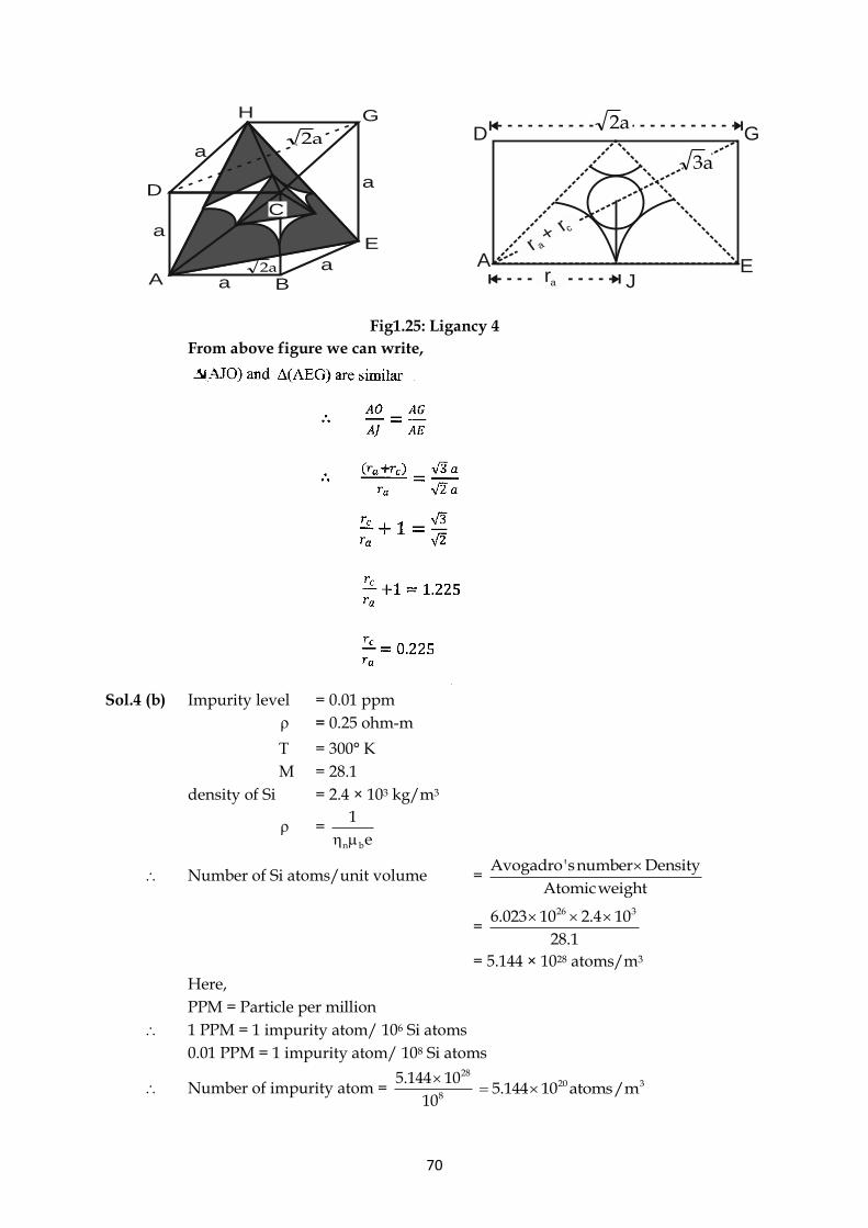
70
H
D
A B
E
G
a
aa
a
aa2
a2
C
a3
r + r
a
c
a2
ra
A
D G
EJ
Fig1.25: Ligancy 4
From above figure we can write,
Sol.4 (b) Impurity level = 0.01 ppm
= 0.25 ohm-m
T = 300° K
M = 28.1
density of Si = 2.4 × 10³ kg/m3
= n b
1
e
Number of Si atoms/unit volume = Avogadro'snumber Density
Atomicweight
= 26 36.023 10 2.4 10
28.1
= 5.144 × 1028 atoms/m3
Here,
PPM = Particle per million
1 PPM = 1 impurity atom/ 106 Si atoms
0.01 PPM = 1 impurity atom/ 108 Si atoms
Number of impurity atom = 28
8
5.144 10
10
20 35.144 10 atoms/m=
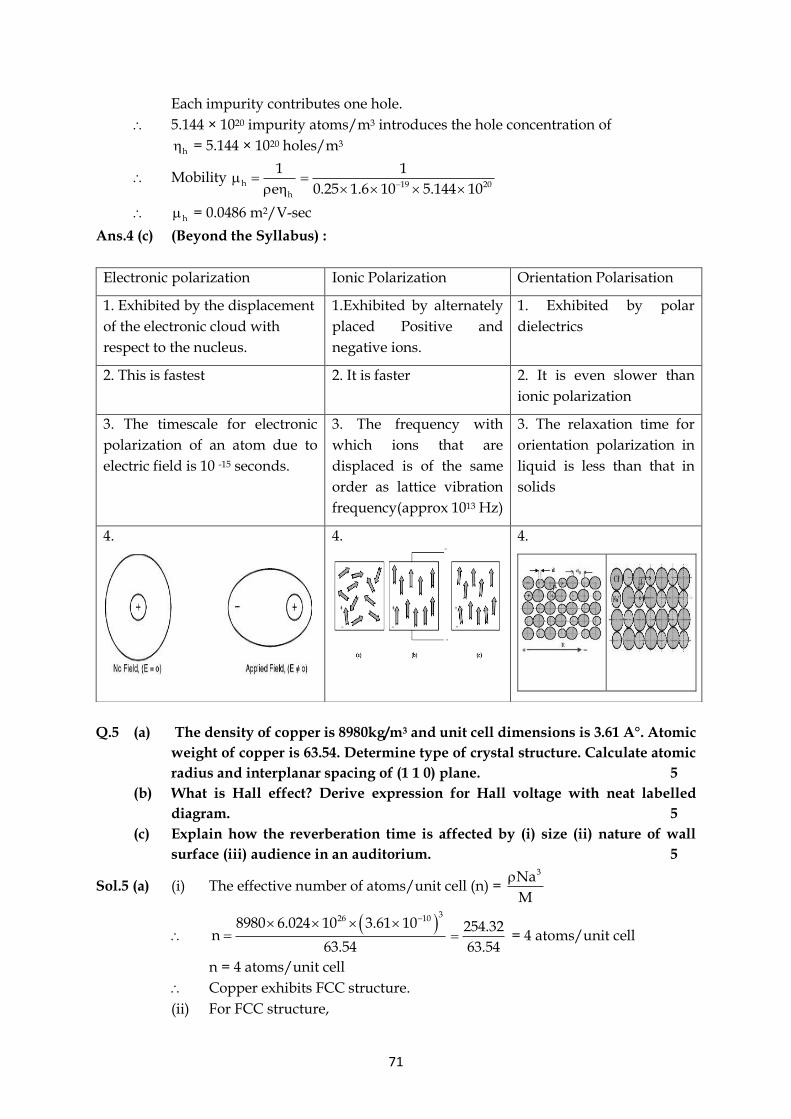
71
Each impurity contributes one hole.
5.144 × 10²⁰ impurity atoms/m3 introduces the hole concentration of
h = 5.144 × 10²⁰ holes/m3
Mobility h
h
1
e =
19 20
1
0.25 1.6 10 5.144 10−=
h = 0.0486 m2/V-sec
Ans.4 (c) (Beyond the Syllabus) :
Q.5 (a) The density of copper is 8980kg/m3 and unit cell dimensions is 3.61 A°. Atomic
weight of copper is 63.54. Determine type of crystal structure. Calculate atomic
radius and interplanar spacing of (1 1 0) plane. 5
(b) What is Hall effect? Derive expression for Hall voltage with neat labelled
diagram. 5
(c) Explain how the reverberation time is affected by (i) size (ii) nature of wall
surface (iii) audience in an auditorium. 5
Sol.5 (a) (i) The effective number of atoms/unit cell (n) = 3Na
M
( )
326 108980 6.024 10 3.61 10n
63.54
− =
254.32
63.54= = 4 atoms/unit cell
n = 4 atoms/unit cell
Copper exhibits FCC structure.
(ii) For FCC structure,
Electronic polarization Ionic Polarization Orientation Polarisation
1. Exhibited by the displacement
of the electronic cloud with
respect to the nucleus.
1.Exhibited by alternately
placed Positive and
negative ions.
1. Exhibited by polar
dielectrics
2. This is fastest 2. It is faster 2. It is even slower than
ionic polarization
3. The timescale for electronic
polarization of an atom due to
electric field is 10 -15 seconds.
3. The frequency with
which ions that are
displaced is of the same
order as lattice vibration
frequency(approx 1013 Hz)
3. The relaxation time for
orientation polarization in
liquid is less than that in
solids
4.
4.
4.
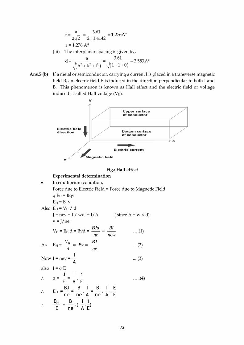
72
a
r2 2
= 3.61
2 1.4142=
1.276A=
r = 1.276 A°
(iii) The interplanar spacing is given by,
( )2 2 2
ad
h k l=
+ + ( )
3.61
1 1 0=
+ +2.553A=
Ans.5 (b) If a metal or semiconductor, carrying a current I is placed in a transverse magnetic
field B, an electric field E is induced in the direction perpendicular to both I and
B. This phenomenon is known as Hall effect and the electric field or voltage
induced is called Hall voltage (VH).
Fig.: Hall effect
Experimental determination
• In equilibrium condition,
Force due to Electric Field = Force due to Magnetic Field
q EH = Bqv
EH = B v
Also EH = VH / d
J = nev = I / wd = I/A ( since A = w × d)
v = J/ne
VH = EH d = Bvd = new
BI
ne
BJd= ….(1)
As EH = ne
BJBv
d
VH == ....(2)
Now J = nev = A
I ....(3)
also J = E
= E
J =
A
I. E
1 …..(4)
EH =E
E.
A
I.
ne
B=
A
I.
ne
B=
ne
BJ
)E
1.
A
I(.
ne
B=
E
HE
73
Using Equation (4)
ρne
B=σ.
ne
B=
E
HE .…(5)
Where = σ
1
ρne
B=
E
HE ….(6)
• Hall coefficient
RH = BI
WHV=ne
1 ….(7)
• conductivity and mobility are
= ne ….(8)
• mobility
= RH .…(9)
• Hall coefficient also be
RH = ne8
π3
= (π3
σ8) RH ….(10)
Determination of type of majority carrier:
As VH = new
BI
= ne
BJd=
Ane
dBI=
newd
dBI
Ans.5 (c) Reverberation time:
• Sabine’s formula for reverberation time is used for suitable acoustic treatment.
• Where ‘V’ is the volume of the hall, ‘S’ is the surface area and ‘a’ is the absorbing
coefficient.
Ceiling:
Central area of the ceiling should be sound reflecting.
The perimeter and rear to be provided with sound absorbing materials like
acoustic tiles.
Sidewalls:
Sidewalls should be sound reflecting and diffusing with as many irregularities as
possible. For example, making doorway wider at one side of the wall keeping
windows etc., and the back wall is treated with deep sound absorbing finish
74
Floor :
All aisles are carpeted except in front of the stage to make full noise control.
Fabric upholstered seats are used.
Absorptive and cushioned seats will give stable reverberation.
Balconies :
Use balconies to increase seating capacity and to reduce the distance to the farthest
row of seats.
Sound reinforcement system:
In large halls a sound amplification system to reinforce the sound to a weak source
in a large room is required.
In addition there should be adequate loudness in every part of the auditorium
uniform distribution (diffusion) of sound energy in the room.
The hall should be free from echoes, long delayed reflections, flatter echoes, sound
concentrations, distortions, and sound shadow and room resonance.
Audience in Auditorium:
To make the hearing conditions satisfactory when the room is full or partly full,
upholstered seats with absorbing material at the bottom are used, so that the
absence or presence of audience does not affect the reverberation time.
Learning outcome: Students will be able to plan Design and development of an
acoustic auditorium
Q.6 (a) Estimate the ratio of vacancies at (i) –119°C (ii) 80°C where average required to
create vacancy is 1.8eV. 5
(b) How a p-n junction diode is used to generate a potential difference in a
photovoltaic solar cell? 5
(c) Explain with neat labelled diagram the construction and working of
piezoelectric oscillator. 5
Sol.6 (a) K = 1.38 × 10⁻²³ J/K
EV = 1.8 eV = 1.8 × 1.6 × 10–19 J
t1 = –119° C
t2 = 80° C
n = Ev
N expKT
−
Ev/KTne
N−=
For t1 = –119°C = –119 + 273 = 154° K
( )19 231.8 1.6 10 /1.38 10 353n
eN
− −− =
26n2.11 10
N−=
Ans.6 (b) A solar cell (also called a photovoltaic cell) is an electrical device that converts
the energy of light directly into electricity by the photovoltaic effect.
The solar cell works in three steps:
1. Photons in sunlight hit the solar panel and are absorbed by semiconducting
materials, such as silicon.
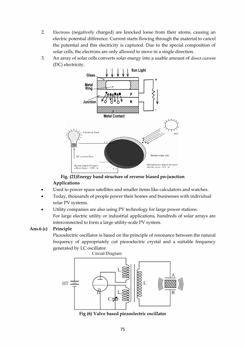
75
2. Electrons (negatively charged) are knocked loose from their atoms, causing an
electric potential difference. Current starts flowing through the material to cancel
the potential and this electricity is captured. Due to the special composition of
solar cells, the electrons are only allowed to move in a single direction.
3. An array of solar cells converts solar energy into a usable amount of direct current
(DC) electricity.
Fig. (21)Energy band structure of reverse biased pn-junction
Applications
• Used to power space satellites and smaller items like calculators and watches.
• Today, thousands of people power their homes and businesses with individual
solar PV systems.
• Utility companies are also using PV technology for large power stations.
For large electric utility or industrial applications, hundreds of solar arrays are
interconnected to form a large utility-scale PV system.
Ans.6 (c) Principle
Piezoelectric oscillator is based on the principle of resonance between the natural
frequency of appropriately cut piezoelectric crystal and a suitable frequency
generated by LC oscillator.
Fig (6) Valve based piezoelectric oscillator
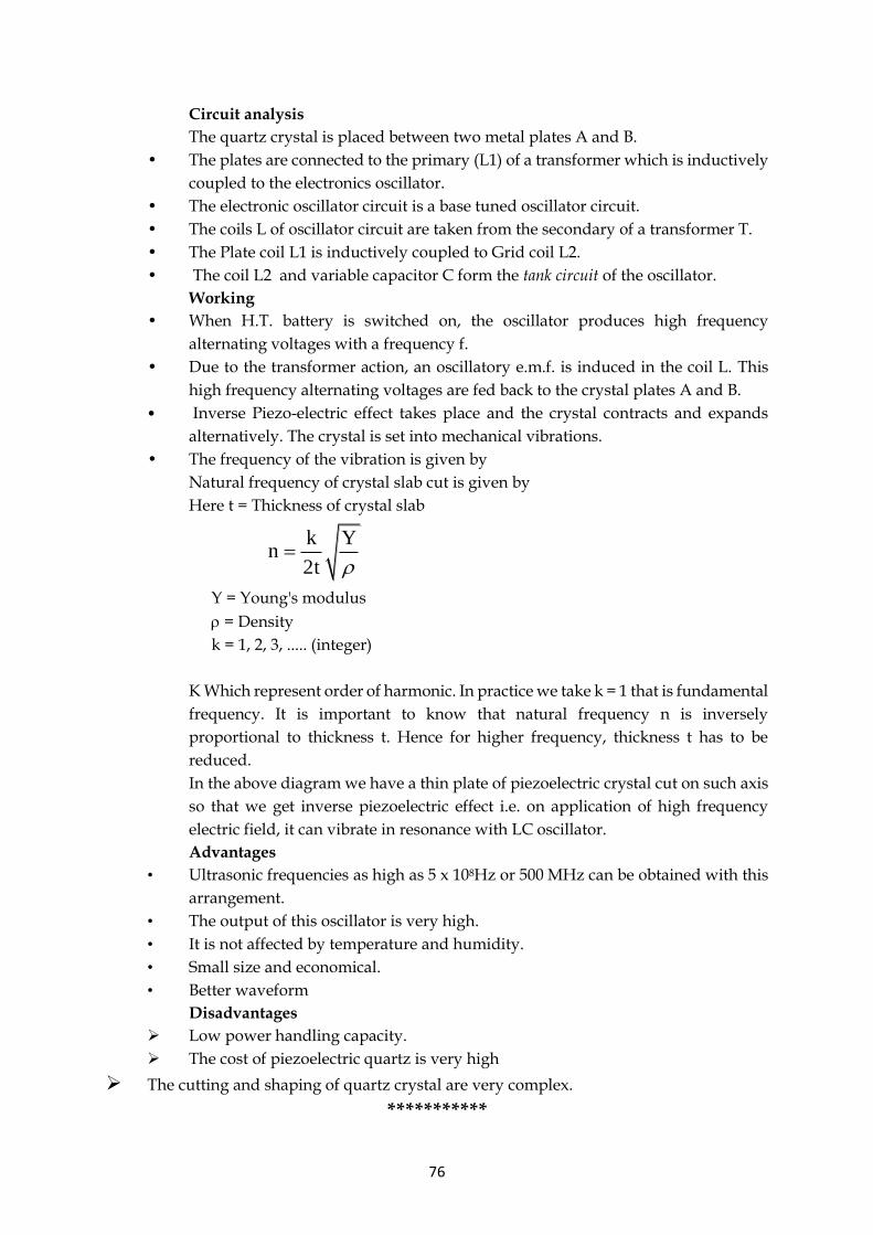
76
Circuit analysis
The quartz crystal is placed between two metal plates A and B.
• The plates are connected to the primary (L1) of a transformer which is inductively
coupled to the electronics oscillator.
• The electronic oscillator circuit is a base tuned oscillator circuit.
• The coils L of oscillator circuit are taken from the secondary of a transformer T.
• The Plate coil L1 is inductively coupled to Grid coil L2.
• The coil L2 and variable capacitor C form the tank circuit of the oscillator.
Working
• When H.T. battery is switched on, the oscillator produces high frequency
alternating voltages with a frequency f.
• Due to the transformer action, an oscillatory e.m.f. is induced in the coil L. This
high frequency alternating voltages are fed back to the crystal plates A and B.
• Inverse Piezo-electric effect takes place and the crystal contracts and expands
alternatively. The crystal is set into mechanical vibrations.
• The frequency of the vibration is given by
Natural frequency of crystal slab cut is given by
Here t = Thickness of crystal slab
k Yn
2t =
Y = Young's modulus
= Density
k = 1, 2, 3, ..... (integer)
K Which represent order of harmonic. In practice we take k = 1 that is fundamental
frequency. It is important to know that natural frequency n is inversely
proportional to thickness t. Hence for higher frequency, thickness t has to be
reduced.
In the above diagram we have a thin plate of piezoelectric crystal cut on such axis
so that we get inverse piezoelectric effect i.e. on application of high frequency
electric field, it can vibrate in resonance with LC oscillator.
Advantages
• Ultrasonic frequencies as high as 5 x 10⁸Hz or 500 MHz can be obtained with this
arrangement.
• The output of this oscillator is very high.
• It is not affected by temperature and humidity.
• Small size and economical.
• Better waveform
Disadvantages
➢ Low power handling capacity.
➢ The cost of piezoelectric quartz is very high
➢ The cutting and shaping of quartz crystal are very complex.
***********
77
Applied Physics – I (Sem-I) May 2017 F.E. SEM-1 (CBCGS)
Q.P. CODE: -18533 TIME- 2 HOURS TOTAL MARKS-60 -------------------------------------------------------------------------------------------------------------------------------
N.B: -
1) Question number 1 is compulsory.
2) Attempt any three from Q.No.2 to Q.No. 6
3) Assume any data whenever required.
4) Figures to the right indicates full marks.
Q.1 Solve any five of the following: 15
(a) Draw the unit cell of HCP structure & work out the no. of atoms per unit cell.
(b) The mobility of holes is 0.025 m2/V-sec. What would be the resistivity of n-type Si if
the Hall coefficient of the sample is 2.25 × 10⁻⁵ m3/C.
(c) What is the principle of Solar cell? Write it’s advantages & disadvantages.
(d) An electron is confined in a box of dimension 1A0. Calculate minimum uncertainty
in it’s velocity.
(e) Explain the factors on which reverberation time depends.
(f) Explain Cavitation effect.
(g) What is Maglev? How it can have very high speed?
Q.2 (a) Draw the following: ( )1 1 3 , ( )2 0 0 , 001
An electron is accelerated through 1200 volts & is reflected from a crystal. The
second order reflection occurs when glancing angle is 600. Calculate the inter-planer
spacing of the crystal. 8
(b) Explain the concept of Fermi level. Prove that the Fermi level exactly at the centre of
the Forbidden energy gap in intrinsic semiconductor. 7
Q.3 (a) Find the following parameters for DC (Diamond Cubic) structure: 8
(i) No. of atoms per unit cell.
(ii) Co-ordination No.
(iii) Nearest atomic distance
78
(iv) Atomic radius
(v) APF
(b) Define drift current, diffusion current & P-N junction. The electrical conductivity of
a pure silicon at room temperature is 4 ×10⁻⁴mho/m. If the mobility of electron is
0.14 m2/V-S & that of hole is 0.04 m2/V-S. Calculate the intrinsic carrier density.
7
Q.4 (a) Distinguish between Type I & Type II superconductors. 5
(b) A classroom has dimensions 10×8×6 m3. The reverberation time is 3 sec. Calculate
the total absorption of surface & average absorption. 5
(c) Explain the principle, construction & working of a Magnetostriction Oscillator.
5
Q.5 (a) Write Fermi-Dirac distribution function. With the help of diagram, explain the
variation of Fermi level with temperature in n-type semiconductor. 5
(b) Derive Schrodinger’s time dependent wave equation for matter waves. 5
(c) Find the depth of sea water from a ship on the sea surface if the time interval of 2 sec
is required to receive the signal back. Given that: -temperature of sea water is 200,
salinity of sea water is 10 gm/lit. 5
Q.6 (a) Define the term critical temperature. Show that in the superconducting state the
material is perfectly diamagnetic. 5
(b) In a solid the energy level is lying 0.012eV below Fermi level. What is the probability
of this level not being occupied by an electron.? 5
(c) What is the wavelength of a beam of neutron having: 5
(i) an energy of 0.025eV?
(ii) an electron & photon each have wavelength of 2 A0. What are their
momentum & energy?
Mn=1.676×10⁻²⁷Kg, h=6.625×10⁻³⁴ J-sec.
***********************
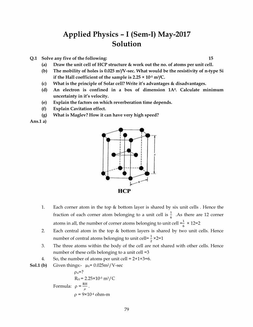
79
Applied Physics – I (Sem-I) May-2017
Solution
Q.1 Solve any five of the following: 15
(a) Draw the unit cell of HCP structure & work out the no. of atoms per unit cell.
(b) The mobility of holes is 0.025 m2/V-sec. What would be the resistivity of n-type Si
if the Hall coefficient of the sample is 2.25 × 10⁻⁵ m3/C.
(c) What is the principle of Solar cell? Write it’s advantages & disadvantages.
(d) An electron is confined in a box of dimension 1A0. Calculate minimum
uncertainty in it’s velocity.
(e) Explain the factors on which reverberation time depends.
(f) Explain Cavitation effect.
(g) What is Maglev? How it can have very high speed?
Ans.1 a)
1. Each corner atom in the top & bottom layer is shared by six unit cells . Hence the
fraction of each corner atom belonging to a unit cell is 1
6 .As there are 12 corner
atoms in all, the number of corner atoms belonging to unit cell =1
6 × 12=2
2. Each central atom in the top & bottom layers is shared by two unit cells. Hence
number of central atoms belonging to unit cell= 1
2 ×2=1
3. The three atoms within the body of the cell are not shared with other cells. Hence
number of these cells belonging to a unit cell =3
4. So, the number of atoms per unit cell = 2+1+3=6.
Sol.1 (b) Given things:- µh= 0.025m2/V-sec
n=?
RH = 2.25×10⁻⁵ m3/C
Formula: = RH
µ .
= 9×10⁻⁴ ohm-m
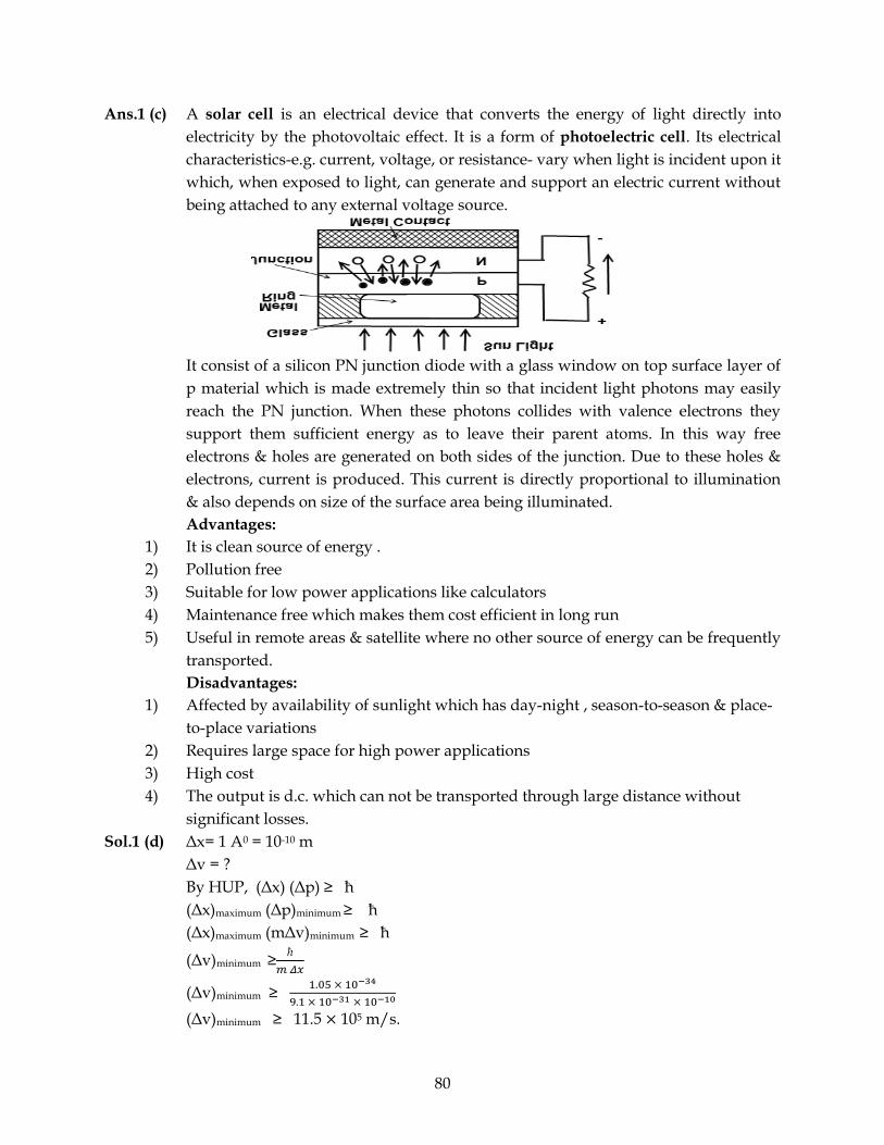
80
Ans.1 (c) A solar cell is an electrical device that converts the energy of light directly into
electricity by the photovoltaic effect. It is a form of photoelectric cell. Its electrical
characteristics-e.g. current, voltage, or resistance- vary when light is incident upon it
which, when exposed to light, can generate and support an electric current without
being attached to any external voltage source.
It consist of a silicon PN junction diode with a glass window on top surface layer of
p material which is made extremely thin so that incident light photons may easily
reach the PN junction. When these photons collides with valence electrons they
support them sufficient energy as to leave their parent atoms. In this way free
electrons & holes are generated on both sides of the junction. Due to these holes &
electrons, current is produced. This current is directly proportional to illumination
& also depends on size of the surface area being illuminated.
Advantages:
1) It is clean source of energy .
2) Pollution free
3) Suitable for low power applications like calculators
4) Maintenance free which makes them cost efficient in long run
5) Useful in remote areas & satellite where no other source of energy can be frequently
transported.
Disadvantages:
1) Affected by availability of sunlight which has day-night , season-to-season & place-
to-place variations
2) Requires large space for high power applications
3) High cost
4) The output is d.c. which can not be transported through large distance without
significant losses.
Sol.1 (d) Δx= 1 A0 = 10-10 m
Δv = ?
By HUP, (Δx) (Δp) ≥ ħ
(Δx)maximum (Δp)minimum ≥ ħ
(Δx)maximum (mΔv)minimum ≥ ħ
(Δv)minimum ≥ħ
𝑚 𝛥𝑥
(Δv)minimum ≥ 1.05 × 10⁻³⁴
9.1 × 10−31 × 10−10
(Δv)minimum ≥ 11.5 × 10⁵ m/s.
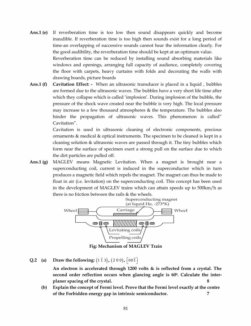
81
Ans.1 (e) If reverberation time is too low then sound disappears quickly and become
inaudible. If reverberation time is too high then sounds exist for a long period of
time-an overlapping of successive sounds cannot hear the information clearly. For
the good audibility, the reverberation time should be kept at an optimum value.
Reverberation time can be reduced by installing sound absorbing materials like
windows and openings, arranging full capacity of audience, completely covering
the floor with carpets, heavy curtains with folds and decorating the walls with
drawing boards, picture boards
Ans.1 (f) Cavitation Effect: - When an ultrasonic transducer is placed in a liquid , bubbles
are formed due to the ultrasonic waves. The bubbles have a very short life time after
which they collapse which is called ‘implosion’. During implosion of the bubble, the
pressure of the shock wave created near the bubble is very high. The local pressure
may increase to a few thousand atmospheres & the temperature. The bubbles also
hinder the propagation of ultrasonic waves. This phenomenon is called”
Cavitation”.
Cavitation is used in ultrasonic cleaning of electronic components, precious
ornaments & medical & optical instruments. The specimen to be cleaned is kept in a
cleaning solution & ultrasonic waves are passed through it. The tiny bubbles which
form near the surface of specimen exert a strong pull on the surface due to which
the dirt particles are pulled off.
Ans.1 (g) MAGLEV means Magnetic Levitation. When a magnet is brought near a
superconducting coil, current is induced in the superconductor which in turn
produces a magnetic field which repels the magnet. The magnet can thus be made to
float in air (i.e. levitation) on the superconducting coil. This concept has been used
in the development of MAGLEV trains which can attain speeds up to 500km/h as
there is no friction between the rails & the wheels.
Fig: Mechanism of MAGLEV Train
Q.2 (a) Draw the following: ( )1 1 3 , ( )2 0 0 , 001
An electron is accelerated through 1200 volts & is reflected from a crystal. The
second order reflection occurs when glancing angle is 600. Calculate the inter-
planer spacing of the crystal. 8
(b) Explain the concept of Fermi level. Prove that the Fermi level exactly at the centre
of the Forbidden energy gap in intrinsic semiconductor. 7
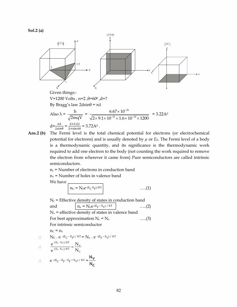
82
Sol.2 (a)
Given things:-
V=1200 Volts , n=2 ,θ=600 ,d=?
By Bragg’s law 2dsinθ = 𝑛𝜆
Also λ = h
2mqV =
34
31 19
6.67 10
2 9.1 10 1.6 10 1200
−
− −
= 3.22A0
d=𝑛𝜆
2𝑠𝑖𝑛𝜃 =
2×3.22
2×sin 60 = 3.72A0 .
Ans.2 (b) The Fermi level is the total chemical potential for electrons (or electrochemical
potential for electrons) and is usually denoted by µ or EF. The Fermi level of a body
is a thermodynamic quantity, and its significance is the thermodynamic work
required to add one electron to the body (not counting the work required to remove
the electron from wherever it came from) Pure semiconductors are called intrinsic
semiconductors.
nc = Number of electrons in conduction band
nv = Number of holes in valence band
We have
nC = Nce–(EC-EF)/KT …..(1)
Nc = Effective density of states in conduction band
and nv = Nve–(EF – EV) / KT …..(2)
Nv = effective density of states in valence band
For best approximation Nc = Nv …..(3)
For intrinsic semiconductor
nC = nv
NC . e –(EC – EF) / KT = Nv . e –(EF – EV) / KT
( )
( )
C F
F V
E E /KT
V
E E /KTC
Ne
Ne
− −
− −=
e –(EC – EF – EF + EV) / KT =cN
vN
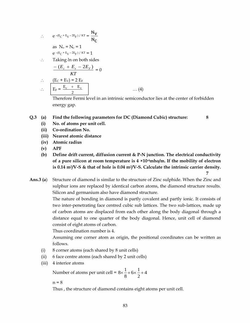
83
e –(EC + EV – 2EF ) / KT = cN
vN
as Nv = Nc = 1
e –(EC + EV – 2EF ) / KT = 1
Taking ln on both sides
KT
EEE Fvc )2( −+− = 0
(EC + EV) = 2 EF
EF = c vE E
2
+ … (4)
Therefore Fermi level in an intrinsic semiconductor lies at the center of forbidden
energy gap.
Q.3 (a) Find the following parameters for DC (Diamond Cubic) structure: 8
(i) No. of atoms per unit cell.
(ii) Co-ordination No.
(iii) Nearest atomic distance
(iv) Atomic radius
(v) APF
(b) Define drift current, diffusion current & P-N junction. The electrical conductivity
of a pure silicon at room temperature is 4 ×10⁻⁴mho/m. If the mobility of electron
is 0.14 m2/V-S & that of hole is 0.04 m2/V-S. Calculate the intrinsic carrier density.
7
Ans.3 (a) Structure of diamond is similar to the structure of Zinc sulphide. When the Zinc and
sulphur ions are replaced by identical carbon atoms, the diamond structure results.
Silicon and germanium also have diamond structure.
The nature of bonding in diamond is partly covalent and partly ionic. It consists of
two inter-penetrating face centred cubic sub lattices. The two sub-lattices, made up
of carbon atoms are displaced from each other along the body diagonal through a
distance equal to one quarter of the body diagonal. Hence, unit cell of diamond
consist of eight atoms of carbon.
Thus coordination number is 4.
Assuming one corner atom as origin, the positional coordinates can be written as
follows.
(i) 8 corner atoms (each shared by 8 unit cells)
(ii) 6 face centre atoms (each shared by 2 unit cells)
(iii) 4 interior atoms
Number of atoms per unit cell = 42
16
8
18 ++
n = 8
Thus , the structure of diamond contains eight atoms per unit cell.
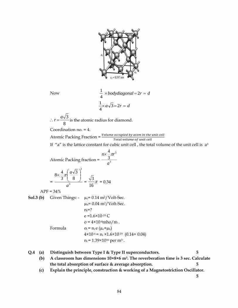
84
Now dralbodydiagon == 24
1
dra == 234
1
8
3ar = is the atomic radius for diamond.
Coordination no. = 4.
Atomic Packing Fraction = 𝑉𝑜𝑙𝑢𝑚𝑒 𝑜𝑐𝑐𝑢𝑝𝑖𝑒𝑑 𝑏𝑦 𝑎𝑡𝑜𝑚 𝑖𝑛 𝑡ℎ𝑒 𝑢𝑛𝑖𝑡 𝑐𝑒𝑙𝑙
𝑇𝑜𝑡𝑎𝑙 𝑣𝑜𝑙𝑢𝑚𝑒 𝑜𝑓 𝑢𝑛𝑖𝑡 𝑐𝑒𝑙𝑙
If “a” is the lattice constant for cubic unit cell , the total volume of the unit cell is a3
Atomic Packing fraction = 3
3
3
4
a
rn
= 3
3
8
3
3
48
a
a
= 16
3 = 0.34
APF = 34%
Sol.3 (b) Given Things: - µe= 0.14 m2/Volt-Sec.
µh= 0.04 m2/Volt-Sec.
ni=?
e =1.6×10⁻¹⁹ C
σ = 4×10⁻⁴mho/m .
Formula σi = ni e (µe+µh)
4×10-4 = ni ×1.6×10⁻¹⁹ (0.14+ 0.04)
ni = 1.39×10¹⁶ per m3 .
Q.4 (a) Distinguish between Type I & Type II superconductors. 5
(b) A classroom has dimensions 10×8×6 m3. The reverberation time is 3 sec. Calculate
the total absorption of surface & average absorption. 5
(c) Explain the principle, construction & working of a Magnetostriction Oscillator.
5
85
Ans.4 (a)
Sr.No. Type I superconductors Type II superconductors
1. Very pure samples of lead,
mercury, and tin are examples of
this kind
Niobium, Vanadium, Technetium, Diamond and
Siliconniobium-titanium, niobium-tin are the T-II SC
2. Type I superconductors have Hctoo
low
Type II superconductors have much larger Hc2 values
to be very useful.
3. Below Hc1 the superconductor
excludes all magnetic field lines. no
mixed state
At field strengths between Hc1 and Hc2 the field
begins to intrude into the material called the mixed
state
4. Exhibit complete Meissner Effect Do not show complete Meissner Effect
5. Only One Tc Two Tc ; Tc1 &Tc2
6. Know as soft SC Known as HARD SC
7.
Sol.4 (b) T = 0.167 𝑉
𝛴𝑎𝑆
Total absorption = aS =0.167 𝑉
𝑇
T=3sec , V =10×8×6 m3= 480 m3 .
aS=0.167×480
3 = 26.72 Sabin-m2 .
Average Absorption Coefficient a = 𝛴𝑎𝑆
𝛴𝑆
S = 2 × (10 × 8 + 8 × 6 + 6 × 10) = 376 m2
a=26.72
376 = 0.07106 O.W.U.
Ans.4 (c) G.W. Pierce was the first to design an ultrasonic oscillator basing on the
phenomenon of magnetostriction.
The Pierce oscillator is a triode valve oscillator and is schematically shown in fig.
Principle
Resonance is obtained by superimposing a frequency which obtained from oscillator
and maintained equal to the natural frequency of the rod. Natural frequency is
selected as the order of ultrasound which we want.
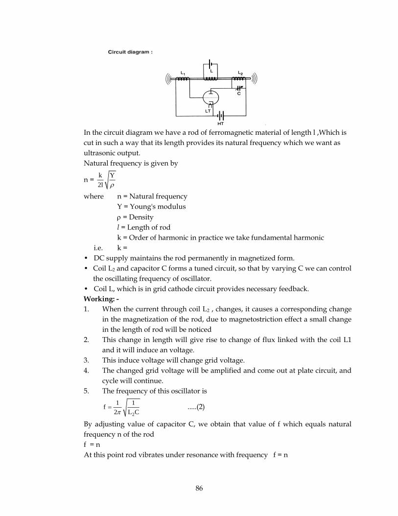
86
In the circuit diagram we have a rod of ferromagnetic material of length l ,Which is
cut in such a way that its length provides its natural frequency which we want as
ultrasonic output.
Natural frequency is given by
n = k Y
2l
where n = Natural frequency
Y = Young's modulus
= Density
l = Length of rod
k = Order of harmonic in practice we take fundamental harmonic
i.e. k =
• DC supply maintains the rod permanently in magnetized form.
• Coil L2 and capacitor C forms a tuned circuit, so that by varying C we can control
the oscillating frequency of oscillator.
• Coil L, which is in grid cathode circuit provides necessary feedback.
Working: -
1. When the current through coil L2 , changes, it causes a corresponding change
in the magnetization of the rod, due to magnetostriction effect a small change
in the length of rod will be noticed
2. This change in length will give rise to change of flux linked with the coil L1
and it will induce an voltage.
3. This induce voltage will change grid voltage.
4. The changed grid voltage will be amplified and come out at plate circuit, and
cycle will continue.
5. The frequency of this oscillator is
2
1 1f
2 L C= .....(2)
By adjusting value of capacitor C, we obtain that value of f which equals natural
frequency n of the rod
f = n
At this point rod vibrates under resonance with frequency f = n
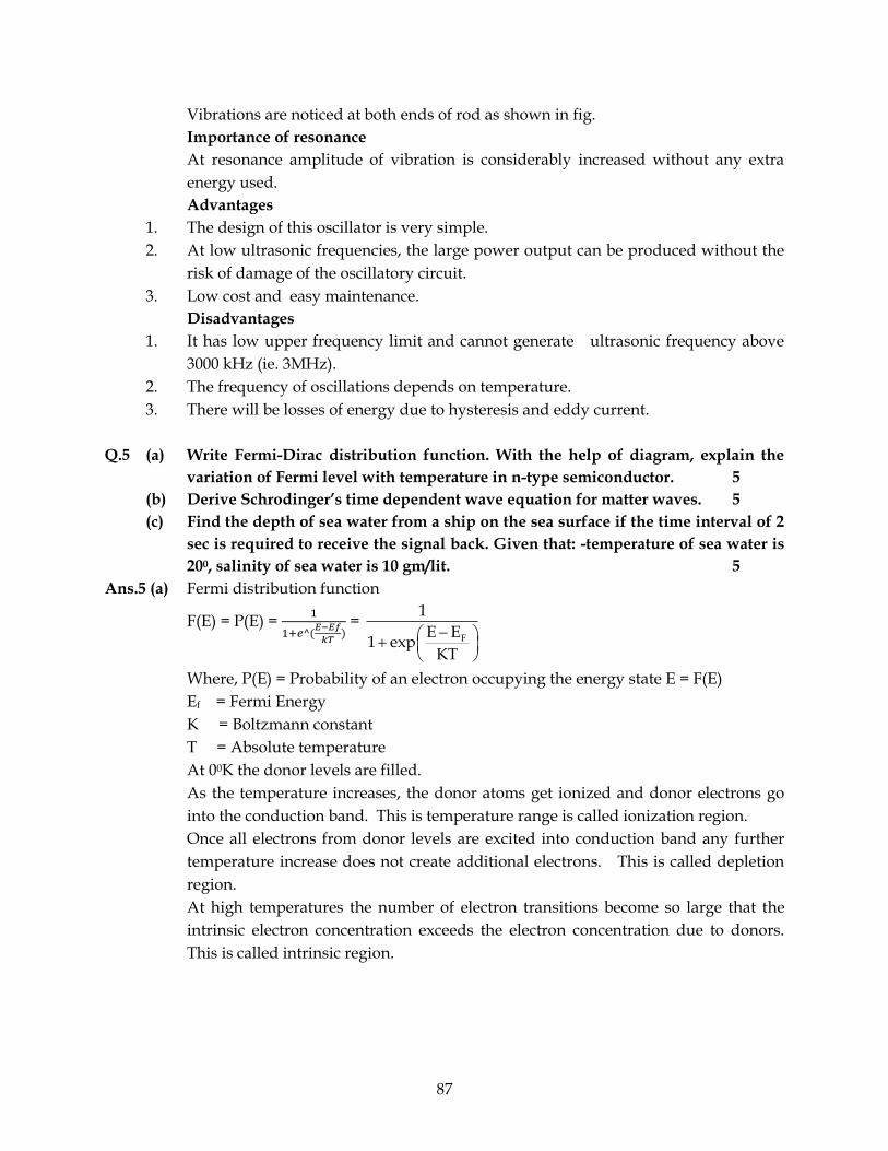
87
Vibrations are noticed at both ends of rod as shown in fig.
Importance of resonance
At resonance amplitude of vibration is considerably increased without any extra
energy used.
Advantages
1. The design of this oscillator is very simple.
2. At low ultrasonic frequencies, the large power output can be produced without the
risk of damage of the oscillatory circuit.
3. Low cost and easy maintenance.
Disadvantages
1. It has low upper frequency limit and cannot generate ultrasonic frequency above
3000 kHz (ie. 3MHz).
2. The frequency of oscillations depends on temperature.
3. There will be losses of energy due to hysteresis and eddy current.
Q.5 (a) Write Fermi-Dirac distribution function. With the help of diagram, explain the
variation of Fermi level with temperature in n-type semiconductor. 5
(b) Derive Schrodinger’s time dependent wave equation for matter waves. 5
(c) Find the depth of sea water from a ship on the sea surface if the time interval of 2
sec is required to receive the signal back. Given that: -temperature of sea water is
200, salinity of sea water is 10 gm/lit. 5
Ans.5 (a) Fermi distribution function
F(E) = P(E) = 1
1+𝑒^(𝐸−𝐸𝑓
𝑘𝑇) =
F
1
E E1 exp
KT
− +
Where, P(E) = Probability of an electron occupying the energy state E = F(E)
Ef = Fermi Energy
K = Boltzmann constant
T = Absolute temperature
At 00K the donor levels are filled.
As the temperature increases, the donor atoms get ionized and donor electrons go
into the conduction band. This is temperature range is called ionization region.
Once all electrons from donor levels are excited into conduction band any further
temperature increase does not create additional electrons. This is called depletion
region.
At high temperatures the number of electron transitions become so large that the
intrinsic electron concentration exceeds the electron concentration due to donors.
This is called intrinsic region.
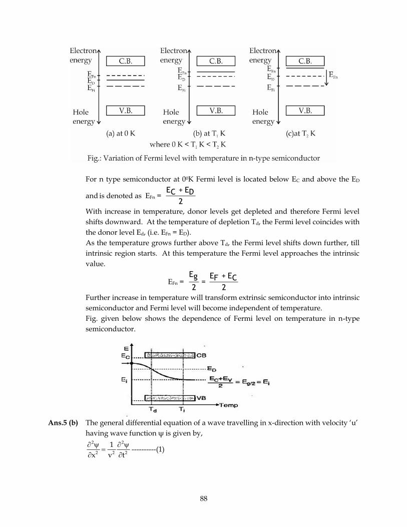
88
For n type semiconductor at 00K Fermi level is located below EC and above the ED
and is denoted as EFn = 2
DE+CE
With increase in temperature, donor levels get depleted and therefore Fermi level
shifts downward. At the temperature of depletion Td, the Fermi level coincides with
the donor level Ed, (i.e. EFn = ED).
As the temperature grows further above Td, the Fermi level shifts down further, till
intrinsic region starts. At this temperature the Fermi level approaches the intrinsic
value.
EFn = 2
CE+FE=2
gE
Further increase in temperature will transform extrinsic semiconductor into intrinsic
semiconductor and Fermi level will become independent of temperature.
Fig. given below shows the dependence of Fermi level on temperature in n-type
semiconductor.
Ans.5 (b) The general differential equation of a wave travelling in x-direction with velocity ‘u’
having wave function ψ is given by,
2 2
2 2 2
1
x v t
=
----------(1)
89
The general solution of this equation is of the form ψ=ψ0 e i(kx-ωt) ---------(2), where ψ0
is a constant . k=2𝜋
𝜆
By de-Broglie hypothesis , λ=ℎ
𝑝
k= 2𝜋𝑝
ℎ =
𝑝
ђ ----------(3)
E=h =ℎ
2𝜋×2π
E=ђω
ω = 𝐸
ђ ----------(4)
substituting equations 3& 4in equation 2
ψ = ψ0 e 𝑖(𝑝𝑥−𝐸𝑡)
ђ -------(5)
Differentiating equation 5 patially w.r.t. ‘t’
𝜕𝜓
𝜕𝑡 = (
−𝑖𝐸
ђ) ψ0 e
𝑖(𝑝𝑥−𝐸𝑡)
ђ = (
−𝑖𝐸
ђ) ψ
Eψ=(−ђ
𝑖)
𝜕𝜓
𝜕𝑡 =iђ
𝜕𝜓
𝜕𝑡 --------(6)
Differentiating equation (5) partially w.r.t. ‘x’ twice ,
𝜕𝜓
𝜕𝑥= (
𝑖𝑝
ђ)ψ0e
𝑖(𝑝𝑥−𝐸𝑡)
ђ
2
2x
= (
𝑖𝑝
ђ)^2 ψ0 e
𝑖(𝑝𝑥−𝐸𝑡)
ђ = -
𝑝2
ђ2 ψ
p2ψ = - ђ2 2
2x
-----------(7)
The total energy ‘E’ is a sum of kinetic energy 1
2 mv2 & potential energy V
E= 1
2 mv2 + V =
2 2m v
2m
+V
Eψ = 𝑝2
2𝑚ψ +Vψ -----------(8)
Substituting 6,7 in equation 8 we will get ,
2 2
2i V
t 2m x
− = +
This equation is known as shrodinger’s time dependent wave equation in one
dimension.
Sol.5 (c) V = Velocity
T = Temperature in °C
S = Salinity
V= V0 + 1.14 S +4.21 T – 0.037 2T
V0= 1510m/s , T= 200C , S= 10 gm/lit
V= 1510+1.14×10+ 4.21×20 – 0.037×(20)2 = 1590.8m/s
Time=2s
Depth of sea =𝑉𝑒𝑙𝑜𝑐𝑖𝑡𝑦 𝑜𝑓 𝑢𝑙𝑡𝑟𝑎𝑠𝑜𝑛𝑖𝑐 𝑤𝑎𝑣𝑒𝑠 𝑖𝑛 𝑠𝑒𝑎 ×𝑇𝑖𝑚𝑒
2 =
1590.8×2
2 = 1590.8 m
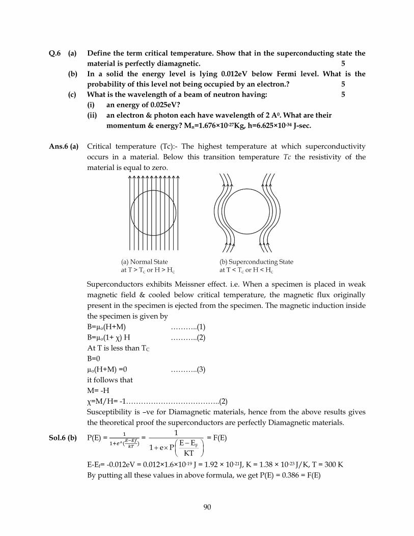
90
Q.6 (a) Define the term critical temperature. Show that in the superconducting state the
material is perfectly diamagnetic. 5
(b) In a solid the energy level is lying 0.012eV below Fermi level. What is the
probability of this level not being occupied by an electron.? 5
(c) What is the wavelength of a beam of neutron having: 5
(i) an energy of 0.025eV?
(ii) an electron & photon each have wavelength of 2 A0. What are their
momentum & energy? Mn=1.676×10⁻²⁷Kg, h=6.625×10⁻³⁴ J-sec.
Ans.6 (a) Critical temperature (Tc):- The highest temperature at which superconductivity
occurs in a material. Below this transition temperature Tc the resistivity of the
material is equal to zero.
Superconductors exhibits Meissner effect. i.e. When a specimen is placed in weak
magnetic field & cooled below critical temperature, the magnetic flux originally
present in the specimen is ejected from the specimen. The magnetic induction inside
the specimen is given by
B=µo(H+M) ………..(1)
B=µo(1+ χ) H ………..(2)
At T is less than TC
B=0
µo(H+M) =0 ………..(3)
it follows that
M= -H
χ=M/H= -1………………………………..(2)
Susceptibility is –ve for Diamagnetic materials, hence from the above results gives
the theoretical proof the superconductors are perfectly Diamagnetic materials.
Sol.6 (b) P(E) = 1
1+𝑒^(𝐸−𝐸𝑓
𝑘𝑇) =
F
1
E E1 e P
KT
− +
= F(E)
E-Ef= -0.012eV = 0.012×1.6×10-19 J = 1.92 × 10⁻²¹J, K = 1.38 × 10⁻²³ J/K, T = 300 K
By putting all these values in above formula, we get P(E) = 0.386 = F(E)
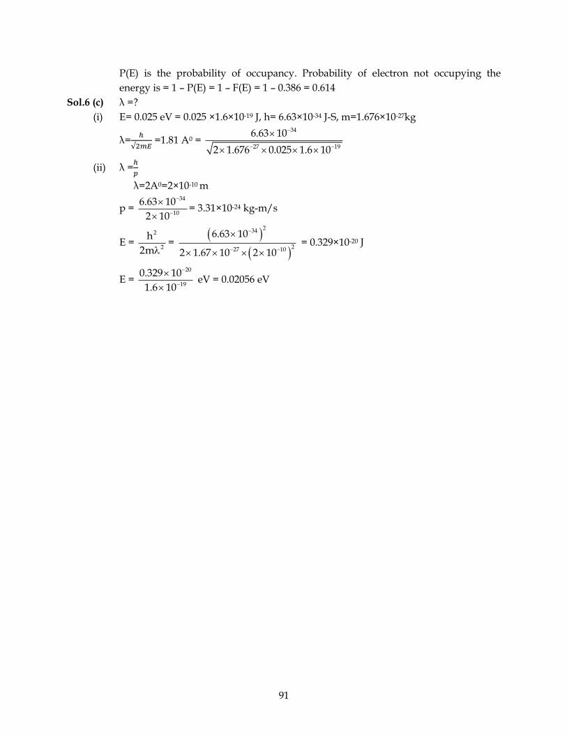
91
P(E) is the probability of occupancy. Probability of electron not occupying the
energy is = 1 – P(E) = 1 – F(E) = 1 – 0.386 = 0.614
Sol.6 (c) λ =?
(i) E= 0.025 eV = 0.025 ×1.6×10-19 J, h= 6.63×10⁻³⁴ J-S, m=1.676×10⁻²⁷kg
λ=ℎ
√2𝑚𝐸 =1.81 A0 =
34
27 19
6.63 10
2 1.676 0.025 1.6 10
−
− −
(ii) λ =ℎ
𝑝
λ=2A0=2×10⁻¹⁰ m
p = 34
10
6.63 10
2 10
−
−
= 3.31×10⁻²⁴ kg-m/s
E = 2
2
h
2m=
( )
( )
234
227 10
6.63 10
2 1.67 10 2 10
−
− −
= 0.329×10⁻²⁰ J
E = 20
19
0.329 10
1.6 10
−
−
eV = 0.02056 eV
92
Applied Physics – I (Sem-I) May 2018 F.E. SEM-1 (CBCGS)
TIME- 2 HOURS TOTAL MARKS-60
__________________________________________________________________ N.B.: - 1) Question no. 1 is compulsory
2) Attempt any three questions from Q.2 to Q.6
3) Assume suitable data wherever required.
4) Figures to right indicate marks.
Q.1 Attempt any five.
a) Why X-rays are used to study the crystal structure?
b) Calculate the frequency and wavelength of photons whose energy is 75 eV.
c) Draw the energy band diagram of p-n junction diode in forward and reverse bias
condition.
d) “Superconductor is a perfect diamagnetic “, Explain.
e) What is reverberation time? How is it important? Write the factor affecting
reverberation time.
f) A quartz crystal of thickness 1.5 mm vibrating with resonance. Calculate it’s
fundamental frequency if the Young’s modulus of quartz crystal is 7.9 × 10¹⁰ N/m2
and density is 2650 kg/m3.
g) Mobility’s of electron and hole in a sample of Ge at room temperature are 0.36
m2/V-sec and 0.17 m2/V-sec respectively. If electron and hole densities are equal
and it is 2.5 × 10¹³ /cm3, calculate its conductivity.
Q.2 a) Arrive at Heisenberg’s uncertainty principle with single slit electron diffraction. An
electron has a speed of 300 m/sec with uncertainty of 0.01%. Find the accuracy in its
position.
b) Write the Fermi Dirac distribution function and terms in it. What is the probability
of an electron being thermally excited to the conduction band in Si at 300 C. The
band gap energy is 1.12 eV.
Q.3 a) With neat diagram of unit cell, explain the structure of NaCl crystal and calculate
the no. of ions per unit cell, coordination no. and lattice constant. Calculate the
packing factor of NaCl crystal assuming the radius of Na+ is 0.98 A0 and the radius
of Cl- is 1.81 A0.
b) State the Hall effect. Derive the expression for Hall Voltage and hall coefficient with
neat diagram.
Q.4 a) What is working principle of SQUID? Explain how it is used to detect the magnetic
field?
93
b) A hall of dimensions 25 × 18 × 12 m3 has an average absorption coefficient 0.2 . Find
the reverberation time. If a curtain cloth of area 150 m2 is suspended at the centre of
hall with coefficient of absorption 0.75, What will be the reverberation time?
c) State the piezoelectric effect. With neat circuit diagram explain the principle and
working of piezoelectric oscillator.
Q.5 a) With energy band diagram, explain the variation of Fermi energy level with
impurity concentration in extrinsic semiconductor.
b) Explain with example how to determine crystal structure by Bragg’s X-ray
spectrometer.
c) Obtain one dimensional time independent Schrodinger equation.
Q.6 a) Define ligancy and critical radius ratio. Calculate critical radius ratio for ligancy 8.
b) What is the significance of wave function? Derive the expression for energy eigen
values for free particle in one dimensional potential well.
c) What is photovoltaic effect? Explain the principle and working of Solar cell.
*********************
94
Applied Physics – I (Sem-I) May 2018
Solution Q.1 Attempt any five.
a) Why X-rays are used to study the crystal structure?
b) Calculate the frequency and wavelength of photons whose energy is 75 eV.
c) Draw the energy band diagram of p-n junction diode in forward and reverse bias
condition.
d) “Superconductor is a perfect diamagnetic “, Explain.
e) What is reverberation time? How is it important? Write the factor affecting
reverberation time.
f) A quartz crystal of thickness 1.5 mm vibrating with resonance. Calculate it’s
fundamental frequency if the Young’s modulus of quartz crystal is 7.9 × 10¹⁰ N/m2
and density is 2650 kg/m3.
g) Mobility’s of electron and hole in a sample of Ge at room temperature are 0.36
m2/V-sec and 0.17 m2/V-sec respectively. If electron and hole densities are equal
and it is 2.5 × 10¹³ /cm3, calculate its conductivity.
Ans.1 (a) (i) For diffraction pattern to be studied incident wavelength should be
comparable with obstacle dimensions.
(ii) X-rays can penetrate solids since these are very high energetic radiations of
very short wavelength of 1 A0. In a crystalline solid the atoms are very closely
distributed in crystal planes. The crystal planes, thus form a three-dimensional
slit system with a spacing 1 A0. Due to this fact X-rays get strongly diffracted
from various crystal planes.
Sol.1 (b) Given Things:-E= 75eV = 75 × 1.6 × 10-19 = 1.2 × 10⁻¹⁷ J
Formula: - E = hѵ =ℎ𝑐
𝜆
Solution:-ѵ = 𝐸
ℎ =
1.2 ×10⁻¹⁷
6.63 ×10−34 = 18.13 × 1510 Hz.
λ = ℎ𝑐
𝐸 =
6.63 ×10−34×3×108
1.2 ×10−17 =165.575 A0 .
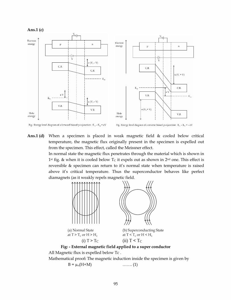
95
Ans.1 (c)
Ans.1 (d) When a specimen is placed in weak magnetic field & cooled below critical
temperature, the magnetic flux originally present in the specimen is expelled out
from the specimen. This effect, called the Meissner effect.
In normal state the magnetic flux penetrates through the material which is shown in
1st fig. & when it is cooled below TC it expels out as shown in 2nd one. This effect is
reversible & specimen can return to it’s normal state when temperature is raised
above it’s critical temperature. Thus the superconductor behaves like perfect
diamagnets (as it weakly repels magnetic field.
(i) T > TC (ii) T < TC
Fig: - External magnetic field applied to a super conductor
All Magnetic flux is expelled below Tc .
Mathematical proof: The magnetic induction inside the specimen is given by
B = µo(H+M) ……. (1)
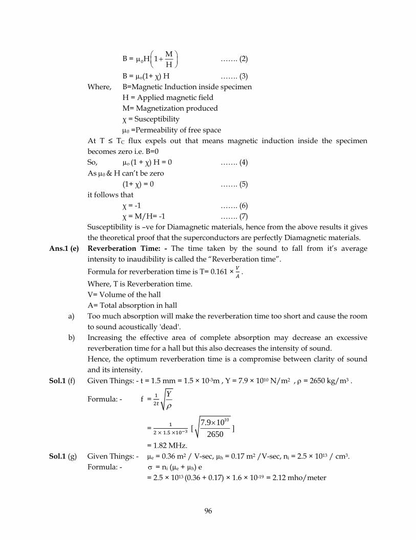
96
B = 0
MH 1
H
+
……. (2)
B = µo(1+ χ) H ……. (3)
Where, B=Magnetic Induction inside specimen
H = Applied magnetic field
M= Magnetization produced
χ = Susceptibility
0 =Permeability of free space
At T ≤ TC flux expels out that means magnetic induction inside the specimen
becomes zero i.e. B=0
So, µo (1 + χ) H = 0 ……. (4)
As 0 & H can’t be zero
(1+ χ) = 0 ……. (5)
it follows that
χ = -1 ……. (6)
χ = M/H= -1 ……. (7)
Susceptibility is –ve for Diamagnetic materials, hence from the above results it gives
the theoretical proof that the superconductors are perfectly Diamagnetic materials.
Ans.1 (e) Reverberation Time: - The time taken by the sound to fall from it’s average
intensity to inaudibility is called the “Reverberation time”.
Formula for reverberation time is T= 0.161 × 𝑉
𝐴 .
Where, T is Reverberation time.
V= Volume of the hall
A= Total absorption in hall
a) Too much absorption will make the reverberation time too short and cause the room
to sound acoustically 'dead'.
b) Increasing the effective area of complete absorption may decrease an excessive
reverberation time for a hall but this also decreases the intensity of sound.
Hence, the optimum reverberation time is a compromise between clarity of sound
and its intensity.
Sol.1 (f) Given Things: - t = 1.5 mm = 1.5 × 10⁻³m , Y = 7.9 × 10¹⁰ N/m2 , = 2650 kg/m3 .
Formula: - f = 1
2𝑡
Y
= 1
2 × 1.5 ×10−3 [107.9 10
2650
]
= 1.82 MHz.
Sol.1 (g) Given Things: - µe = 0.36 m2 / V-sec, µh = 0.17 m2 /V-sec, ni = 2.5 × 10¹³ / cm3.
Formula: - = ni (µe + µh) e
= 2.5 × 10¹³ (0.36 + 0.17) × 1.6 × 10-19 = 2.12 mho/meter
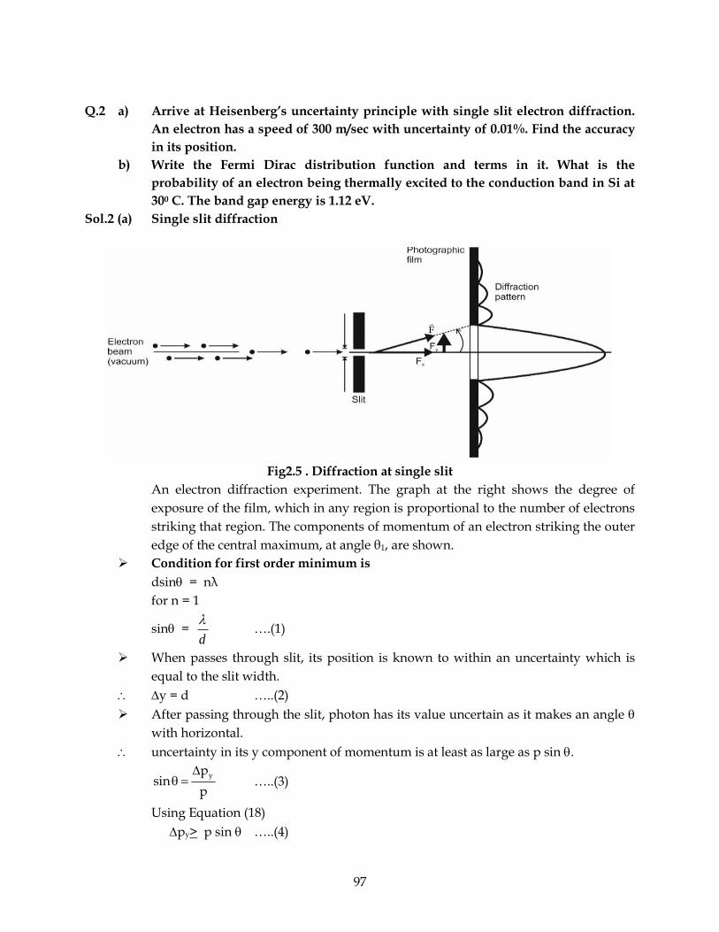
97
Q.2 a) Arrive at Heisenberg’s uncertainty principle with single slit electron diffraction.
An electron has a speed of 300 m/sec with uncertainty of 0.01%. Find the accuracy
in its position.
b) Write the Fermi Dirac distribution function and terms in it. What is the
probability of an electron being thermally excited to the conduction band in Si at
300 C. The band gap energy is 1.12 eV.
Sol.2 (a) Single slit diffraction
Fig2.5 . Diffraction at single slit
An electron diffraction experiment. The graph at the right shows the degree of
exposure of the film, which in any region is proportional to the number of electrons
striking that region. The components of momentum of an electron striking the outer
edge of the central maximum, at angle θ1, are shown.
➢ Condition for first order minimum is
dsin = nλ
for n = 1
sin = d
….(1)
➢ When passes through slit, its position is known to within an uncertainty which is
equal to the slit width.
y = d …..(2)
➢ After passing through the slit, photon has its value uncertain as it makes an angle
with horizontal.
uncertainty in its y component of momentum is at least as large as p sin .
yp
sinp
= …..(3)
Using Equation (18)
py> p sin …..(4)
98
py> pd
…..(5)
Now, p =
h (de – Broglie’s hypothesis) …..(6)
py>d
h
.
>d
h
>y
h
d y=
y. py> h …..(7)
good agreement with uncertainty principle.
Given Things :- v= 300m/s , ∆𝑣
𝑣 = 0.01 % v 0.01%, =
0.01v 300
100=
Formula:- ∆x.∆p≥ ђ
Calculation:- ∆x. (m. ∆v) ≥ ђ
∆v = 300×0.01
100 = 0.03
∆x ≥ђ
𝑚∆𝑣≥
6.63×10⁻³⁴
2×3.14×9.1×10−31×0.03 = 3.86 × 10⁻³ m.
Sol.2 (b) The carrier occupancy of the energy state is represented by a continuous
distribution function known as the Fermi-Dirac distribution function.
Fermi Distribution Function
f(E) =( )rE E /KT
1
1 e −+
This indicates the probability that a particular quantum state at
the energy level E is occupied by an electron.
K= Boltzmann’s constant
T=Absolute temperature.
Ef = Fermi energy.
Given Things:- T= 300 C = 303 0K , Eg = 1.12 eV .
K = 1.38 × 10⁻²³ J/K = 1.38×10⁻²³
1.6 ×10−19 = 86.25 × 10⁻⁶ eV/K
Solution:- Si is intrinsic semiconductor. Hence EC – EF = 𝐸𝑔
2 = 0.56 eV
f(E) =1
1+ ( )/C FE E KT
e−
= 1
1+6
0.56( )86.25 10 303e
−
= 4.94 × 10⁻¹⁰.
Q.3 a) With neat diagram of unit cell, explain the structure of NaCl crystal and calculate
the no. of ions per unit cell, coordination no. and lattice constant. Calculate the
packing factor of NaCl crystal assuming the radius of Na+ is 0.98 A0 and the
radius of Cl- is 1.81 A0.
b) State the Hall effect. Derive the expression for Hall Voltage and hall coefficient
with neat diagram.
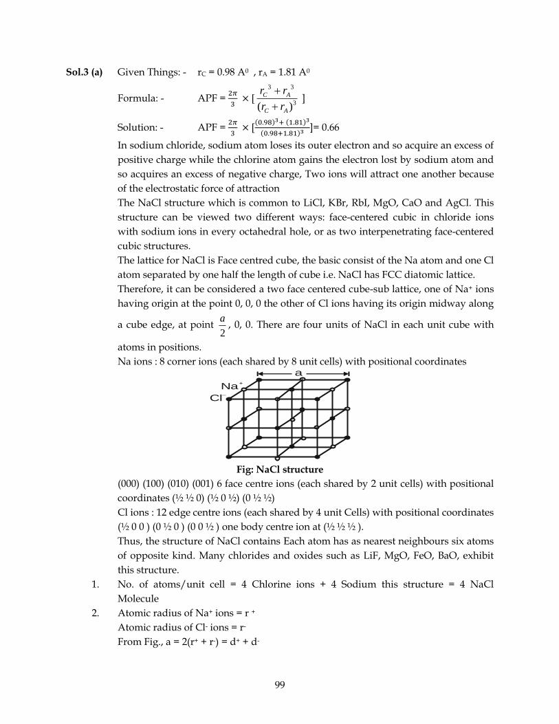
99
Sol.3 (a) Given Things: - rC = 0.98 A0 , rA = 1.81 A0
Formula: - APF = 2𝜋
3 × [
3 3
3( )
C A
C A
r r
r r
+
+ ]
Solution: - APF = 2𝜋
3 × [
(0.98)3+ (1.81)3
(0.98+1.81)3 ]= 0.66
In sodium chloride, sodium atom loses its outer electron and so acquire an excess of
positive charge while the chlorine atom gains the electron lost by sodium atom and
so acquires an excess of negative charge, Two ions will attract one another because
of the electrostatic force of attraction
The NaCl structure which is common to LiCl, KBr, RbI, MgO, CaO and AgCl. This
structure can be viewed two different ways: face-centered cubic in chloride ions
with sodium ions in every octahedral hole, or as two interpenetrating face-centered
cubic structures.
The lattice for NaCl is Face centred cube, the basic consist of the Na atom and one Cl
atom separated by one half the length of cube i.e. NaCl has FCC diatomic lattice.
Therefore, it can be considered a two face centered cube-sub lattice, one of Na+ ions
having origin at the point 0, 0, 0 the other of Cl ions having its origin midway along
a cube edge, at point 2
a, 0, 0. There are four units of NaCl in each unit cube with
atoms in positions.
Na ions : 8 corner ions (each shared by 8 unit cells) with positional coordinates
Cl–
Na+
a
Fig: NaCl structure
(000) (100) (010) (001) 6 face centre ions (each shared by 2 unit cells) with positional
coordinates (½ ½ 0) (½ 0 ½) (0 ½ ½)
Cl ions : 12 edge centre ions (each shared by 4 unit Cells) with positional coordinates
(½ 0 0 ) (0 ½ 0 ) (0 0 ½ ) one body centre ion at (½ ½ ½ ).
Thus, the structure of NaCl contains Each atom has as nearest neighbours six atoms
of opposite kind. Many chlorides and oxides such as LiF, MgO, FeO, BaO, exhibit
this structure.
1. No. of atoms/unit cell = 4 Chlorine ions + 4 Sodium this structure = 4 NaCl
Molecule
2. Atomic radius of Na+ ions = r +
Atomic radius of Cl- ions = r-
From Fig., a = 2(r+ + r-) = d+ + d-
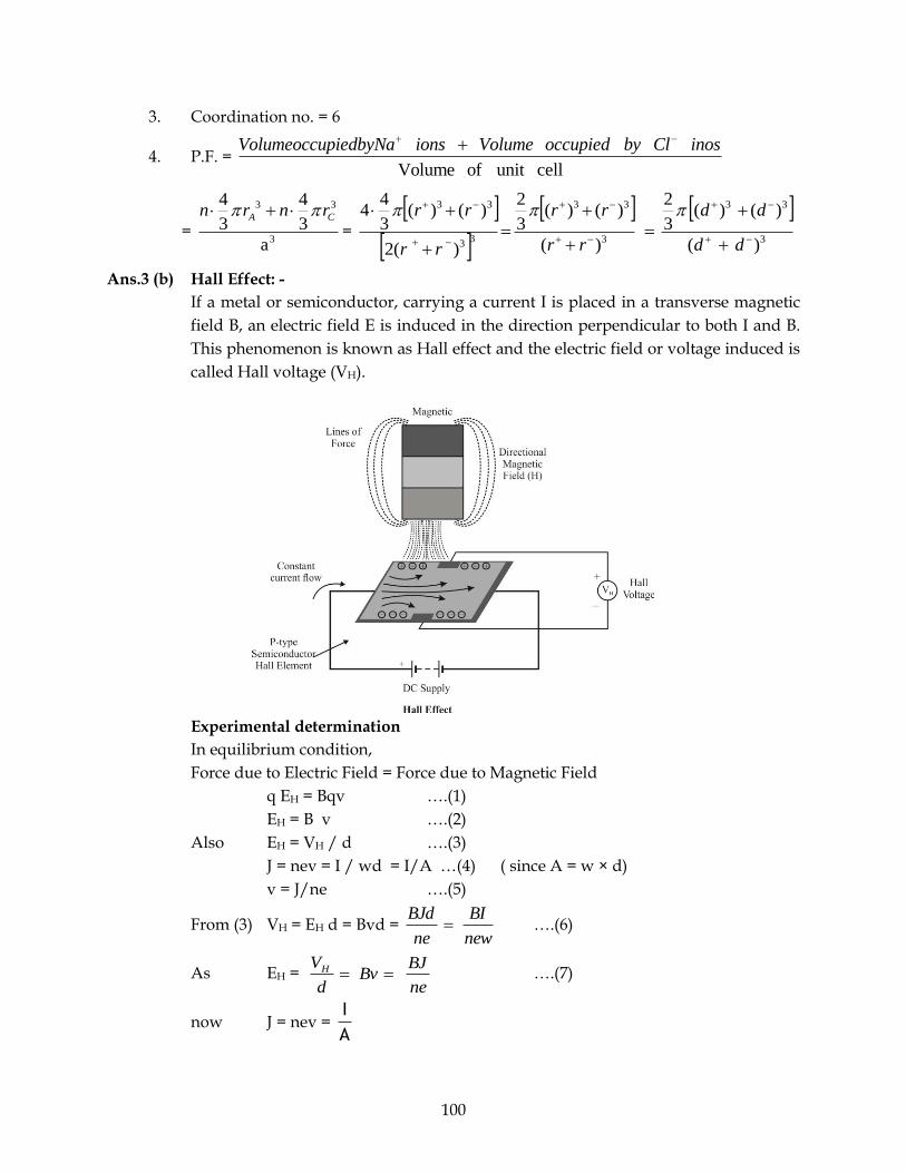
100
3. Coordination no. = 6
4. P.F. = Volume of unit cell
VolumeoccupiedbyNa ions Volume occupied by Cl inos+ −+
=
3 3
3
4 4
3 3
a
A Cn r n r +
=
3
33
3
33
33
33
)(
)()(3
2
)(
)()(3
2
)(2
)()(3
44
−+
−+
−+
−+
−+
−+
+
+
=+
+
=+
+
dd
dd
rr
rr
rr
rr
Ans.3 (b) Hall Effect: -
If a metal or semiconductor, carrying a current I is placed in a transverse magnetic
field B, an electric field E is induced in the direction perpendicular to both I and B.
This phenomenon is known as Hall effect and the electric field or voltage induced is
called Hall voltage (VH).
Experimental determination
In equilibrium condition,
Force due to Electric Field = Force due to Magnetic Field
q EH = Bqv ….(1)
EH = B v ….(2)
Also EH = VH / d ….(3)
J = nev = I / wd = I/A …(4) ( since A = w × d)
v = J/ne ….(5)
From (3) VH = EH d = Bvd = new
BI
ne
BJd= ….(6)
As EH = ne
BJBv
d
VH == ….(7)
now J = nev = A
I
101
also J = E
= E
J =
A
I. E
1
EH =E
E.
A
I.
ne
B=
A
I.
ne
B=
ne
BJ
)E
1.
A
I(.
ne
B=
E
HE ….(8)
Using Equation (4)
ρne
B=σ.
ne
B=
E
HE ….(9)
Where = σ
1
ρne
B=
E
HE ….(10)
Hall coefficient
RH = BI
WHV=ne
1 ….(11)
conductivity and mobility are
= ne ….(12)
mobility
= RH .…(13)
Hall coefficient also be
RH = ne8
π3
= (π3
σ8) RH ….(14)
Applications: -
1. VH is proportional to magnetic field B, for the given current I, hence Hall effect is
used in magnetic field meter.
2. Charge carrier concentration can be determined.
3. Mobility of charge carriers can be determined.
4. Nature of semiconductor (P-type or N-type) can be determined.
Q.4 a) What is working principle of SQUID? Explain how it is used to detect the
magnetic field?
b) A hall of dimensions 25 × 18 × 12 m3 has an average absorption coefficient 0.2.
Find the reverberation time. If a curtain cloth of area 150 m2 is suspended at the
centre of hall with coefficient of absorption 0.75, What will be the reverberation
time?
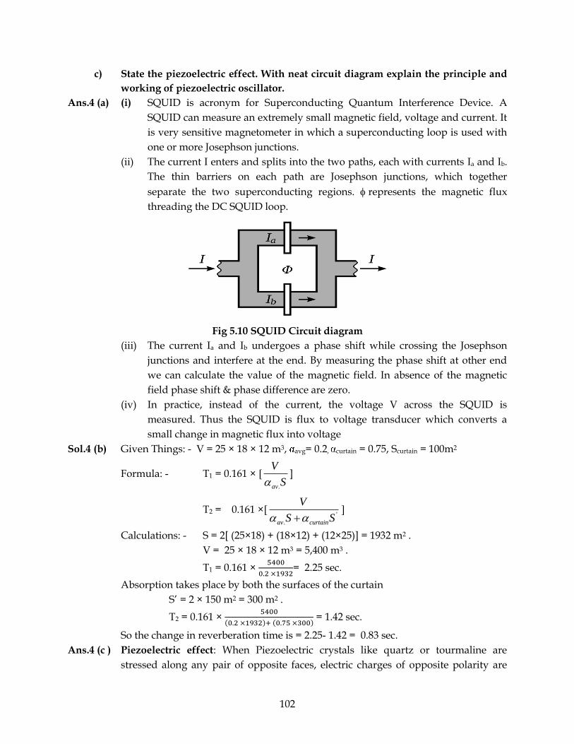
102
c) State the piezoelectric effect. With neat circuit diagram explain the principle and
working of piezoelectric oscillator.
Ans.4 (a) (i) SQUID is acronym for Superconducting Quantum Interference Device. A
SQUID can measure an extremely small magnetic field, voltage and current. It
is very sensitive magnetometer in which a superconducting loop is used with
one or more Josephson junctions.
(ii) The current I enters and splits into the two paths, each with currents Ia and Ib.
The thin barriers on each path are Josephson junctions, which together
separate the two superconducting regions. represents the magnetic flux
threading the DC SQUID loop.
Fig 5.10 SQUID Circuit diagram
(iii) The current Ia and Ib undergoes a phase shift while crossing the Josephson
junctions and interfere at the end. By measuring the phase shift at other end
we can calculate the value of the magnetic field. In absence of the magnetic
field phase shift & phase difference are zero.
(iv) In practice, instead of the current, the voltage V across the SQUID is
measured. Thus the SQUID is flux to voltage transducer which converts a
small change in magnetic flux into voltage
Sol.4 (b) Given Things: - V = 25 × 18 × 12 m3, avg= 0.2, curtain = 0.75, Scurtain = 100m2
Formula: - T1 = 0.161 × [.av
V
S]
T2 = 0.161 ×['
.av curtain
V
S S +]
Calculations: - S = 2[ (25×18) + (18×12) + (12×25)] = 1932 m2 .
V = 25 × 18 × 12 m3 = 5,400 m3 .
T1 = 0.161 × 5400
0.2 ×1932= 2.25 sec.
Absorption takes place by both the surfaces of the curtain
S’ = 2 × 150 m2 = 300 m2 .
T2 = 0.161 × 5400
(0.2 ×1932)+ (0.75 ×300) = 1.42 sec.
So the change in reverberation time is = 2.25- 1.42 = 0.83 sec.
Ans.4 (c ) Piezoelectric effect: When Piezoelectric crystals like quartz or tourmaline are
stressed along any pair of opposite faces, electric charges of opposite polarity are
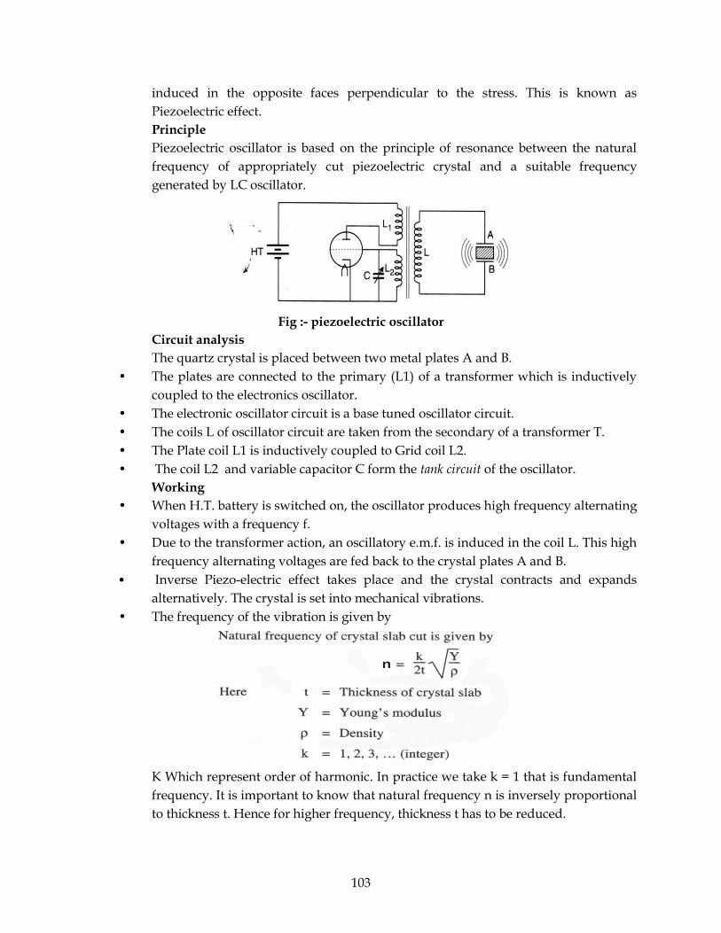
103
induced in the opposite faces perpendicular to the stress. This is known as
Piezoelectric effect.
Principle
Piezoelectric oscillator is based on the principle of resonance between the natural
frequency of appropriately cut piezoelectric crystal and a suitable frequency
generated by LC oscillator.
Fig :- piezoelectric oscillator
Circuit analysis
The quartz crystal is placed between two metal plates A and B.
• The plates are connected to the primary (L1) of a transformer which is inductively
coupled to the electronics oscillator.
• The electronic oscillator circuit is a base tuned oscillator circuit.
• The coils L of oscillator circuit are taken from the secondary of a transformer T.
• The Plate coil L1 is inductively coupled to Grid coil L2.
• The coil L2 and variable capacitor C form the tank circuit of the oscillator.
Working
• When H.T. battery is switched on, the oscillator produces high frequency alternating
voltages with a frequency f.
• Due to the transformer action, an oscillatory e.m.f. is induced in the coil L. This high
frequency alternating voltages are fed back to the crystal plates A and B.
• Inverse Piezo-electric effect takes place and the crystal contracts and expands
alternatively. The crystal is set into mechanical vibrations.
• The frequency of the vibration is given by
K Which represent order of harmonic. In practice we take k = 1 that is fundamental
frequency. It is important to know that natural frequency n is inversely proportional
to thickness t. Hence for higher frequency, thickness t has to be reduced.
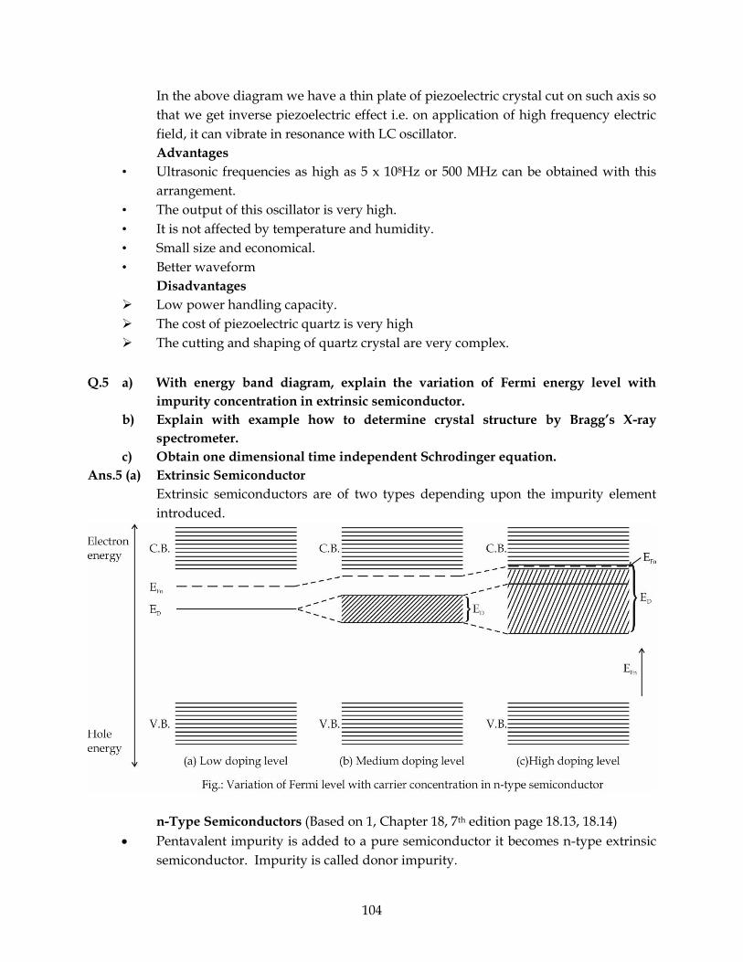
104
In the above diagram we have a thin plate of piezoelectric crystal cut on such axis so
that we get inverse piezoelectric effect i.e. on application of high frequency electric
field, it can vibrate in resonance with LC oscillator.
Advantages
• Ultrasonic frequencies as high as 5 x 10⁸Hz or 500 MHz can be obtained with this
arrangement.
• The output of this oscillator is very high.
• It is not affected by temperature and humidity.
• Small size and economical.
• Better waveform
Disadvantages
➢ Low power handling capacity.
➢ The cost of piezoelectric quartz is very high
➢ The cutting and shaping of quartz crystal are very complex.
Q.5 a) With energy band diagram, explain the variation of Fermi energy level with
impurity concentration in extrinsic semiconductor.
b) Explain with example how to determine crystal structure by Bragg’s X-ray
spectrometer.
c) Obtain one dimensional time independent Schrodinger equation.
Ans.5 (a) Extrinsic Semiconductor
Extrinsic semiconductors are of two types depending upon the impurity element
introduced.
n-Type Semiconductors (Based on 1, Chapter 18, 7th edition page 18.13, 18.14)
• Pentavalent impurity is added to a pure semiconductor it becomes n-type extrinsic
semiconductor. Impurity is called donor impurity.
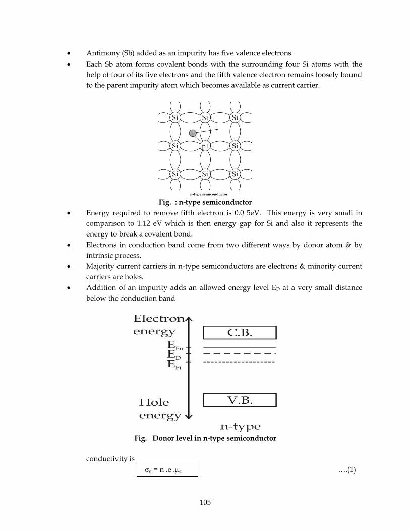
105
• Antimony (Sb) added as an impurity has five valence electrons.
• Each Sb atom forms covalent bonds with the surrounding four Si atoms with the
help of four of its five electrons and the fifth valence electron remains loosely bound
to the parent impurity atom which becomes available as current carrier.
Fig. : n-type semiconductor
• Energy required to remove fifth electron is 0.0 5eV. This energy is very small in
comparison to 1.12 eV which is then energy gap for Si and also it represents the
energy to break a covalent bond.
• Electrons in conduction band come from two different ways by donor atom & by
intrinsic process.
• Majority current carriers in n-type semiconductors are electrons & minority current
carriers are holes.
• Addition of an impurity adds an allowed energy level ED at a very small distance
below the conduction band
Fig. Donor level in n-type semiconductor
conductivity is
e = n .e .e ….(1)
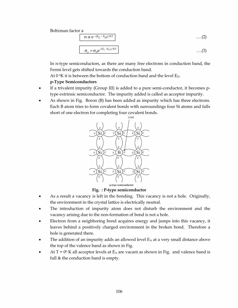
106
Boltzman factor a
n α e –(EC – ED)/KT .…(2)
( )C DE E /KT
e 0e− −
= ….(3)
In n-type semiconductors, as there are many free electrons in conduction band, the
Fermi level gets shifted towards the conduction band.
At 0 0K it is between the bottom of conduction band and the level ED.
p-Type Semiconductors
• If a trivalent impurity (Group III) is added to a pure semi-conductor, it becomes p-
type extrinsic semiconductor. The impurity added is called as acceptor impurity.
• As shown in Fig. Boron (B) has been added as impurity which has three electrons.
Each B atom tries to form covalent bonds with surroundings four Si atoms and falls
short of one electron for completing four covalent bonds.
Fig. : P-type semiconductor
• As a result a vacancy is left in the bonding. This vacancy is not a hole. Originally,
the environment in the crystal lattice is electrically neutral.
• The introduction of impurity atom does not disturb the environment and the
vacancy arising due to the non-formation of bond is not a hole.
• Electron from a neighboring bond acquires energy and jumps into this vacancy, it
leaves behind a positively charged environment in the broken bond. Therefore a
hole is generated there.
• The addition of an impurity adds an allowed level EA at a very small distance above
the top of the valence band as shown in Fig.
• At T = 00 K all acceptor levels at EA are vacant as shown in Fig. and valence band is
full & the conduction band is empty.
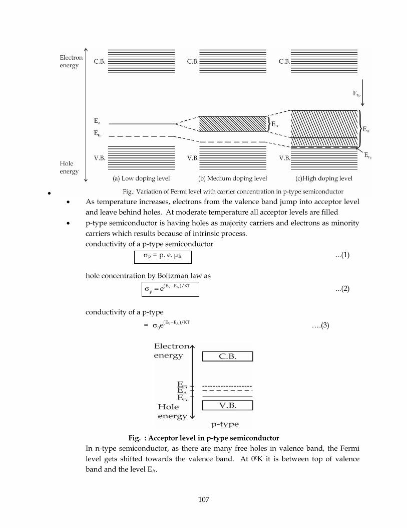
107
• • As temperature increases, electrons from the valence band jump into acceptor level
and leave behind holes. At moderate temperature all acceptor levels are filled
• p-type semiconductor is having holes as majority carriers and electrons as minority
carriers which results because of intrinsic process.
conductivity of a p-type semiconductor
p = p. e. h ...(1)
hole concentration by Boltzman law as
( )V AE E /KT
p e−
= ...(2)
conductivity of a p-type
= ( )V AE E /KT
0e−
….(3)
Fig. : Acceptor level in p-type semiconductor
In n-type semiconductor, as there are many free holes in valence band, the Fermi
level gets shifted towards the valence band. At 00K it is between top of valence
band and the level EA.
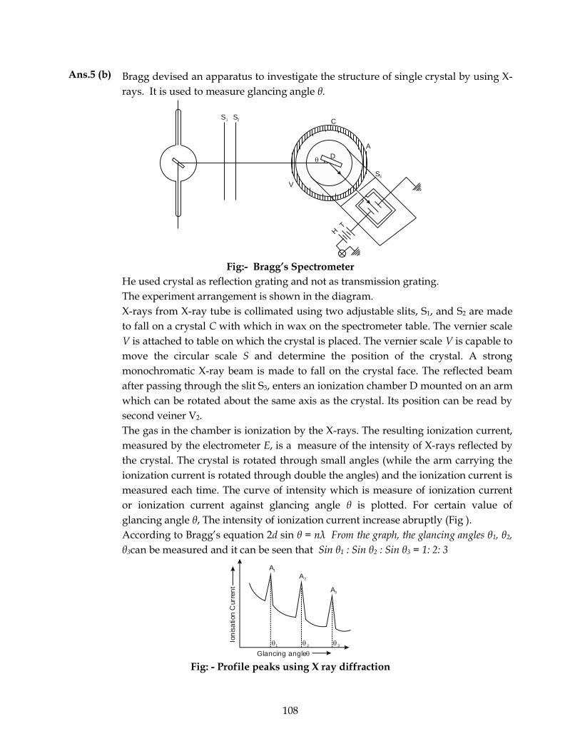
108
Ans.5 (b) Bragg devised an apparatus to investigate the structure of single crystal by using X-
rays. It is used to measure glancing angle θ.
S1 S2
V
C
A
S3
HT
D
Fig:- Bragg’s Spectrometer
He used crystal as reflection grating and not as transmission grating.
The experiment arrangement is shown in the diagram.
X-rays from X-ray tube is collimated using two adjustable slits, S1, and S2 are made
to fall on a crystal C with which in wax on the spectrometer table. The vernier scale
V is attached to table on which the crystal is placed. The vernier scale V is capable to
move the circular scale S and determine the position of the crystal. A strong
monochromatic X-ray beam is made to fall on the crystal face. The reflected beam
after passing through the slit S3, enters an ionization chamber D mounted on an arm
which can be rotated about the same axis as the crystal. Its position can be read by
second veiner V2.
The gas in the chamber is ionization by the X-rays. The resulting ionization current,
measured by the electrometer E, is a measure of the intensity of X-rays reflected by
the crystal. The crystal is rotated through small angles (while the arm carrying the
ionization current is rotated through double the angles) and the ionization current is
measured each time. The curve of intensity which is measure of ionization current
or ionization current against glancing angle θ is plotted. For certain value of
glancing angle θ, The intensity of ionization current increase abruptly (Fig ).
According to Bragg’s equation 2d sin θ = nλ From the graph, the glancing angles θ1, θ2,
θ3can be measured and it can be seen that Sin θ1 : Sin θ2 : Sin θ3 = 1: 2: 3
A1
A2
A3
1 2 3
Glancing angle
Ion
isa
tion
Curr
en
t
Fig: - Profile peaks using X ray diffraction
109
From the observed values of θ and known values of d and n, the wavelength of X-
ray can be calculated. Suppose the wavelength of incident X-ray is known then the
ratio of the interplanar spacing can be determined. Suppose, for a particular crystal
used on a Bragg’s spectrometer, strong reflections from thesets of planes (100), (110)
and (111) are obtained for angles θ1, θ2, θ3respectively in the first order. then from
Bragg’s equation we have
2d100 sinθ1 = λ
2d110 sinθ2 = λ
2d111 sinθ3 = λ
Hence, d100 : d110 : d111 = 1/sinθ1 : 1/sinθ2 : 1/sinθ3
Bragg found that for certain crystal: θ1 = 5o23’, θ2 = 7o36’ and θ3 = 9o25’
Hence for crystal
d100 : d110 : d111 = ''' 259sin
1:
367sin
1:
235sin
1ooo
= 744.1
1:
414.1
1:1 =
3
1:
2
1:1
for SC
Theoretically, this ratio is found to hold a simple cubic lattice structure. Hence, it is
concluded that crystal has a simple cubic structure. When the first order reflection
from the three plane (100), (110) and (111) of NaCl are compared, the ratios between
the interplanar spacing are found as
For FCC d100 : d110 : d111 = 1 2
1 : :2 3
Which agree with the theoretical values for a face centered cubic structure. He
concluded that NaCl has fcc structure.
For BCC d100 : d110 : d111 = 2 1
1 : :2 3
Ans.5 (c) For systems in a stationary state (i.e., where the Hamiltonian is not explicitly
dependent on time), the time-independent Schrödinger equation is sufficient.
Approximate solutions to the time-independent Schrödinger equation are
commonly used to calculate the energy levels and other properties of atoms and
molecules.
Schrodinger wave equation as
(x, t) = (x) (t) ….(1)
The TDSE is given by
2 2
22
− + =
V i
m x t
....(2)
Equation (2) can be modified as
2 2
2
( ) ( )( ) ( ) ( ) ( )
2
− + =
x tt V x x t i
m x t
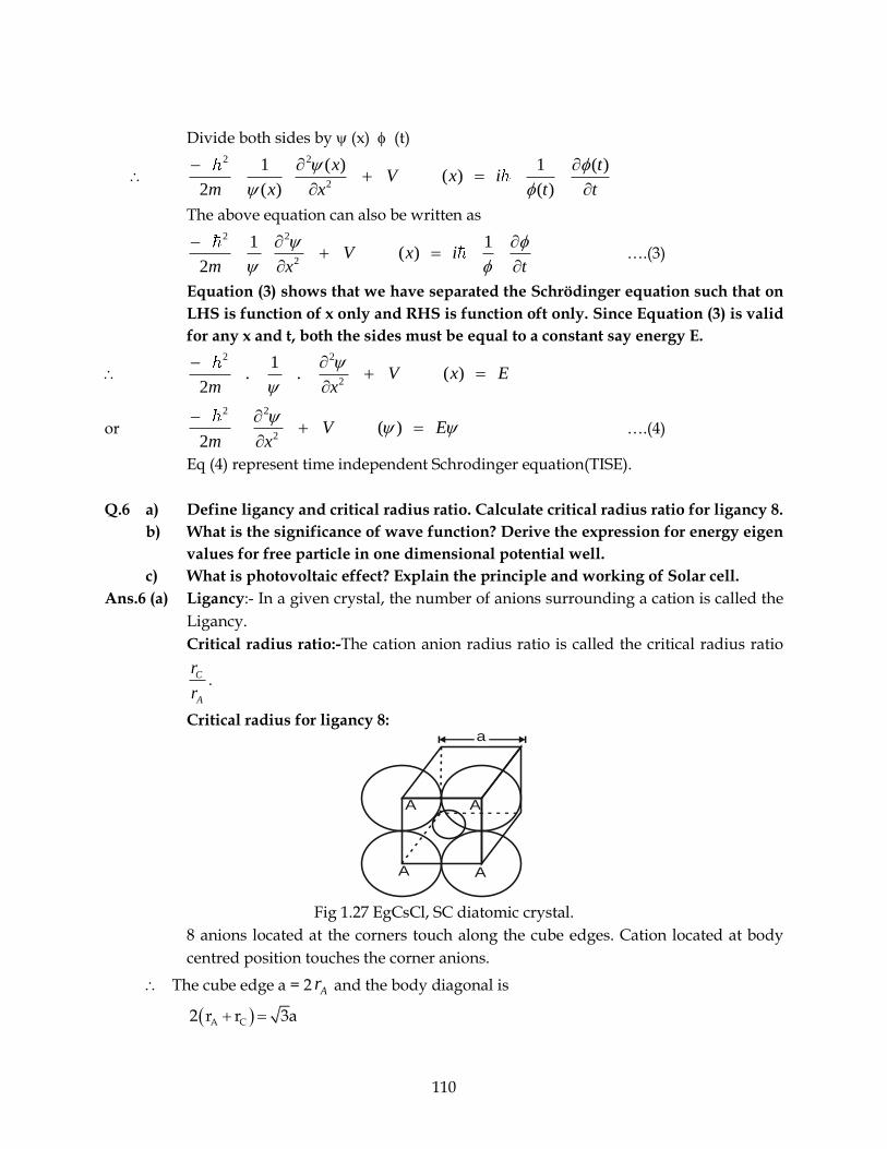
110
Divide both sides by (x) (t)
2 2
2
1 ( ) 1 ( )( )
2 ( ) ( )
− + =
x tV x i
m x x t t
The above equation can also be written as
2 2
2
1 1( )
2
− + =
V x i
m x t
….(3)
Equation (3) shows that we have separated the Schrödinger equation such that on
LHS is function of x only and RHS is function oft only. Since Equation (3) is valid
for any x and t, both the sides must be equal to a constant say energy E.
2 2
2
1. . ( )
2
− + =
V x E
m x
or 2 2
2( )
2
− + =
V E
m x
….(4)
Eq (4) represent time independent Schrodinger equation(TISE).
Q.6 a) Define ligancy and critical radius ratio. Calculate critical radius ratio for ligancy 8.
b) What is the significance of wave function? Derive the expression for energy eigen
values for free particle in one dimensional potential well.
c) What is photovoltaic effect? Explain the principle and working of Solar cell.
Ans.6 (a) Ligancy:- In a given crystal, the number of anions surrounding a cation is called the
Ligancy.
Critical radius ratio:-The cation anion radius ratio is called the critical radius ratio
C
A
r
r.
Critical radius for ligancy 8:
A
A A
A
a
Fig 1.27 EgCsCl, SC diatomic crystal.
8 anions located at the corners touch along the cube edges. Cation located at body
centred position touches the corner anions.
The cube edge a = 2 Ar and the body diagonal is
( )A C2 r r 3a+ =
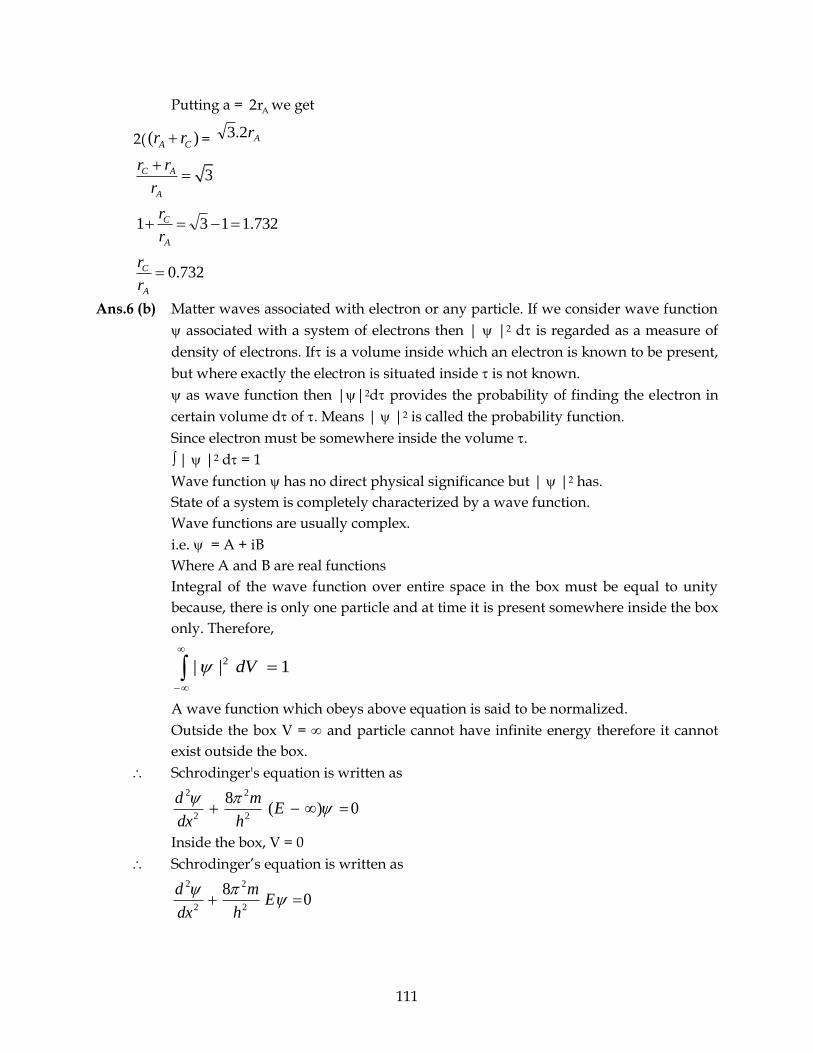
111
Putting a = A2r we get
2( ( )A Cr r+ =
3C A
A
r r
r
+=
Ans.6 (b) Matter waves associated with electron or any particle. If we consider wave function
associated with a system of electrons then | |2 d is regarded as a measure of
density of electrons. If is a volume inside which an electron is known to be present,
but where exactly the electron is situated inside is not known.
as wave function then ||2d provides the probability of finding the electron in
certain volume d of . Means | |2 is called the probability function.
Since electron must be somewhere inside the volume .
| |2 d = 1
Wave function has no direct physical significance but | |2 has.
State of a system is completely characterized by a wave function.
Wave functions are usually complex.
i.e. = A + iB
Where A and B are real functions
Integral of the wave function over entire space in the box must be equal to unity
because, there is only one particle and at time it is present somewhere inside the box
only. Therefore,
−
= 1|| 2 dV
A wave function which obeys above equation is said to be normalized.
Outside the box V = and particle cannot have infinite energy therefore it cannot
exist outside the box.
Schrodinger's equation is written as
0)(8
2
2
2
2
=−+
Eh
m
dx
d
Inside the box, V = 0
Schrodinger’s equation is written as
08
2
2
2
2
=+
Eh
m
dx
d
Ar2.3
732.1131 =−=+A
C
r
r
732.0=A
C
r
r
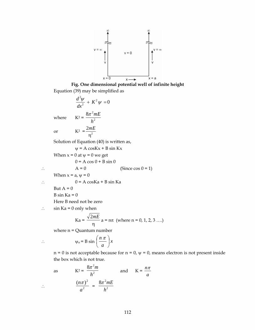
112
Fig. One dimensional potential well of infinite height
Equation (39) may be simplified as
02
2
2
=+
Kdx
d
where K2 = 2
28
h
mE
or K2 =2
2
mE
Solution of Equation (40) is written as,
= A cosKx + B sin Kx
When x = 0 at = 0 we get
0 = A cos 0 + B sin 0
A = 0 (Since cos 0 = 1)
When x = a, = 0
0 = A cosKa + B sin Ka
But A = 0
B sin Ka = 0
Here B need not be zero
sin Ka = 0 only when
Ka =
mE2a = n (where n = 0, 1, 2, 3 ….)
where n = Quantum number
n = B sin xa
n
n = 0 is not acceptable because for n = 0, = 0, means electron is not present inside
the box which is not true.
as K2 = 2
28
h
m and K =
a
n
2
2)(
a
n =
2
28
h
mE
113
En =
2 2
28
n h
ma (n = 1, 2, 3, ….)
Energy of the particle can have only certain values which are Eigen values.
Ans.6 (c) Photovoltaic Effect:-In photoelectric effect when radiation is incident on a metal
surface electron are ejected. In photovoltaic effect, certain materials being exposed to
radiation generates electron-hole pairs available for conduction. As a result a
voltage is developed across the material.
A solar cell (also called a photovoltaic cell) is an electrical device that converts the
energy of light directly into electricity by the photovoltaic effect. It is a form of
photoelectric cell (in that its electrical characteristics-- e.g. current, voltage, or
resistance-- vary when light is incident upon it) which, when exposed to light, can
generate and support an electric current without being attached to any external
voltage source.
The solar cell works in three steps:
1. Photons in sunlight hit the solar panel and are absorbed by semiconducting
materials, such as silicon.
2. Electrons (negatively charged) are knocked loose from their atoms, causing an
electric potential difference. Current starts flowing through the material to cancel
the potential and this electricity is captured. Due to the special composition of solar
cells, the electrons are only allowed to move in a single direction.
3. An array of solar cells converts solar energy into a usable amount of direct current
(DC) electricity.