applied computational electromagnetics society journal
TRANSCRIPT
AppliedComputationalElectromagneticsSocietyJournal
Editor-in-ChiefAtef Z. Elsherbeni
December 2008
Vol. 23 No. 4ISSN 1054-4887

GENERAL PURPOSE AND SCOPE: The Applied Computational Electromagnetics Society (ACES) Journal hereinafter known as the ACES Journal is devoted to the exchange of information in computational electromagnetics, to the advancement of the state-of-the art, and the promotion of related technical activities. A primary objective of the information exchange is the elimination of the need to “re-invent the wheel” to solve a previously-solved computational problem in electrical engineering, physics, or related fields of study. The technical activities promoted by this publication include code validation, performance analysis, and input/output standardization; code or technique optimization and error minimization; innovations in solution technique or in data input/output; identification of new applications for electromagnetics modeling codes and techniques; integration of computational electromagnetics techniques with new computer architectures; and correlation of computational parameters with physical mechanisms. SUBMISSIONS: The ACES Journal welcomes original, previously unpublished papers, relating to applied computational electromagnetics. Typical papers will represent the computational electromagnetics aspects of research in electrical engineering, physics, or related disciplines. However, papers which represent research in applied computational electromagnetics itself are equally acceptable. Manuscripts are to be submitted through the upload system of ACES web site http://aces.ee.olemiss.edu See “Information for Authors” on inside of back cover and at ACES web site. For additional information contact the Editor-in-Chief:
Dr. Atef Elsherbeni Department of Electrical Engineering The University of Mississippi University, MS 386377 USA Phone: 662-915-5382 Fax: 662-915-7231 Email: [email protected] SUBSCRIPTIONS: All members of the Applied Computational Electromagnetics Society who have paid their subscription fees are entitled to receive the ACES Journal with a minimum of three issues per calendar year and are entitled to download any published journal article available at http://aces.ee.olemiss.edu. Back issues, when available, are $15 each. Subscriptions to ACES is through the web site. Orders for back issues of the ACES Journal and changes of addresses should be sent directly to ACES: Dr. Allen W. Glisson 302 Anderson Hall Dept. of Electrical Engineering Fax: 662-915-7231
Email: [email protected] Allow four week’s advance notice for change of address. Claims for missing issues will not be honored because of insufficient notice or address change or loss in mail unless the Executive Officer is notified within 60 days for USA and Canadian subscribers or 90 days for subscribers in other countries, from the last day of the month of publication. For information regarding reprints of individual papers or other materials, see “Information for Authors”. LIABILITY. Neither ACES, nor the ACES Journal editors, are responsible for any consequence of misinformation or claims, express or implied, in any published material in an ACES Journal issue. This also applies to advertising, for which only camera-ready copies are accepted. Authors are responsible for information contained in their papers. If any material submitted for publication includes material which has already been published elsewhere, it is the author’s responsibility to obtain written permission to reproduce such material.
APPLIED COMPUTATIONAL ELECTROMAGNETICS SOCIETY JOURNAL Editor-in-Chief Atef Z. Elsherbeni December 2008 Vol. 23 No. 4 ISSN 1054-4887
The ACES Journal is abstracted in INSPEC, in Engineering Index, DTIC, Science Citation Index Expanded, the Research Alert, and to Current Contents/Engineering, Computing & Technology. The first, fourth, and sixth illustrations on the front cover have been obtained from the Department of Electrical Engineering at the University of Mississippi. The third and fifth illustrations on the front cover have been obtained from Lawrence Livermore National Laboratory. The second illustration on the front cover has been obtained from FLUX2D software, CEDRAT S.S. France, MAGSOFT Corporation, New York.

THE APPLIED COMPUTATIONAL ELECTROMAGNETICS SOCIETY http//:aces.ee.olemiss.edu
ACES JOURNAL EDITOR-IN-CHIEF
Atef Elsherbeni University of Mississippi, EE Dept.
University, MS 38677, USA
ACES JOURNAL ASSOCIATE EDITORS-IN-CHIEF
Sami Barmada University of Pisa. EE Dept.
Pisa, Italy, 56126
Erdem Topsakal Mississippi State University, EE Dept.
Mississippi State, MS 39762, USA
Fan Yang University of Mississippi, EE Dept.
University, MS 38677, USA
ACES JOURNAL EDITORIAL ASSISTANTS
Matthew J. Inman University of Mississippi, EE Dept.
University, MS 38677, USA
Mohamed Al Sharkawy Arab Academy for Science and Technology
ECE Dept. Alexandria, Egypt
ACES JOURNAL EMERITUS EDITORS-IN-CHIEF
Duncan C. Baker EE Dept. U. of Pretoria
0002 Pretoria, South Africa
Robert M. Bevensee Box 812
Alamo, CA 94507-0516, USA
Allen Glisson University of Mississippi, EE Dept.
University, MS 38677, USA
Ahmed Kishk University of Mississippi, EE Dept.
University, MS 38677, USA
David E. Stein USAF Scientific Advisory Board
Washington, DC 20330, USA
ACES JOURNAL EMERITUS ASSOCIATE EDITORS-IN-CHIEF
Alexander Yakovlev University of Mississippi, EE Dept.
University, MS 38677, USA
DECEMBER 2008 REVIEWERS Malcolm Bibby Deb Chatterjee Yung Leonard Chow Alistar Duffy Said E. El-Khamy Atef Z. Elsherbeni
Teixeira L. Fernando AbdelKader Hamid Michael Hamid Abdel-Aziz Hassanin Michiko Kuroda
Kai-Fong Lee Frederic Molinet C. J. Reddy Randall A. Reeves Steve Weiss

THE APPLIED COMPUTATIONAL ELECTROMAGNETICS SOCIETY
JOURNAL
Vol. 23 No. 3 December 2008 TABLE OF CONTENTS
“Highly Accurate Implementations of Methods for Handling Singularities on a Planar Patch” M. M. Bibby…..……………………………………………………………...……………298 “Low-Frequency Full-Wave Finite Element Modeling Using the LU Recombination Method” H. Ke and T. H. Hubing………………………………………………………….……......303 “A GPU Implementation of the 2-D Finite-Difference Time-Domain Code using High Level Shader Language” N. Takada, N. Masuda, T. Tanaka, Y. Abe, and T. Ito……..……………………..………309 “EM Scattering from Bodies of Revolution using the Locally Corrected Nyström Method”
A. W. Wood and J. L. Fleming…..……………………………………………………..…317 “Numerical Solution of Electromagnetic Scattering by Multiple Cylinders” Seydou, Duraiswami, and Seppänen…………....................................................................322 “Design of a Near Field Protective Dielectric Radome 'Window' for a Curved Phased Array Antenna-Axial Polarization Case” A. E. Fathy………..………………......................................................................................326 “Design, Modelling, and Synthesis of Radiation Pattern of Intelligent Antenna by Artificial Neural Networks” R. Ghayoula, N. Fadlallah, A. Gharsallah, and M. Rammal................................................336 “Optimised Design of a Printed Elliptical Spiral Antenna with a Dielectric Superstrate” S. K. Khamas and G. G. Cook………….……………………………………………….....345 “A New UWB Skeletal Antenna for EMC Applications” A. R. Mallahzadeh, R. Pazoki, and S. Karimkashi………………….…..............................352 “Modelling of Coupled Microstrip Antennas Integrated with EMB Structure Using an Iterative Method” H. Zairi, A. Gharsallah, A. Gharbi, and H. Baudrand…………………….……………….357 © 2008, The Applied Computational Electromagnetics Society

Highly Accurate Implementations of Methods for Handling Singularities on a Planar Patch
1 M. M. Bibby and 2 A. F. Peterson
1 Gullwings, 47 Whitney Tavern Rd., Weston, MA 02493
e-mail: [email protected] 2 Georgia Institute of Technology, Atlanta, GA
e-mail: [email protected] Abstract − Three methods for evaluating integrals containing the Green’s function singularity are studied from the standpoint of numerical accuracy at levels required in high order calculations. A significant source of potential error was found to be common to all methods. Suggestions for improving the accuracy of all three are proposed. Keywords: Green’s function singularity, singularity extraction, Duffy transformation, arcsinh transformation, integral equation, method of moments, high order, and boundary element method.
I. INTRODUCTION
In a recent paper [1], the authors developed an exact-to-machine-precision method for the evaluation of the free-space Green’s function on a rectangular patch. This result was then used to examine the singularity extraction and singularity cancellation methods as a function of the ratio of the sides of a rectangular patch, using the corresponding exact result for comparison. It was found that the aspect ratio of the patch, and the triangles contained therein, had a significant effect on the accuracy associated with the schemes studied. In order to overcome the accuracy problems identified, a number of remedies were proposed. These remedies mainly involved using higher precision in the calculations, making them unattractive to potential users. Since paper [1] was published, a paper by Khayat and Wilton introduced a new singularity cancellation method using an arcsinh transformation [2], possibly overcoming the drawbacks of the remedies just referred to. Here we examine the arcsinh method in comparison to the two methods, already studied, and augment the conclusions of the previous paper. In addition, we identify one of the principal causes of error in our implementation of the three methods.
The objectives here are to: 1) examine the arcsinh method and compare it with the earlier results, 2) explain the cause of the inaccuracies found in all three methods
and 3) test all three methods over the widest range of the aspect ratio of the patch that may be encountered in practice.
The range of aspect ratios is determined by consideration of test point locations on a patch. In practice, the domain of a patch is divided into four rectangular sub-patches each with a corner at the test point. The location of the test point, and hence the aspect ratio of each sub-patch, is controlled by the quadrature rule employed to perform the required integrations. As shown in [1], this can lead to a sub-patch aspect ratio up to 1:10-10. This observation determines the range of aspect ratios over which the tests are performed. The ratio may seem extreme, but the primary motivation for this work is to obtain accuracy near the limit of machine precision, which is an important requirement in high order numerical solutions of integral equations.
II. REVIEW OF METHODS
The integral to be evaluated has the form,
I(x, y) = f ( ′x , ′y )e− jkR
Rd ′x d ′y∫∫ (1)
where f is usually a bounded, well-behaved function, k = 2π /λ where λ is the wavelength, and R is given by,
R = x − ′x( )2+ y − ′y( )2
(2)
The accurate evaluation of equation (1) is most difficult when the test point (x,y) is within or near the source cell over which the integral is performed, due to the O(1/R) behavior of the Green’s function, e-jkR/R.
In the earlier paper [1], we examined the singularity extraction, SE, procedure and the Duffy transformation [3]. These methods are fully described in that paper. A third approach for evaluating equation (1) is the arcsinh transformation proposed by Khayat and Wilton [2] which is described next. For a rectangular domain 0 < x ' < a , 0 < y ' < b and the test point at x=y=0, the domain is divided into triangles along the line y’ = b/a x’. We introduce the change of variable indicated in equation (3)
298ACES JOURNAL, VOL. 23, NO. 4, DECEMBER 2008
in the first integral and the substitution of equation (4) in the second integral. This leads to equation (5) or, equivalently, (6). The integrands in equation (6) are bounded and amenable to numerical quadrature.
For a number of specific functions f, including f(x,y)=1, one of the integrals in each of the double integrals arising from the Duffy and the arcsinh approaches can be performed analytically. To ensure a fair comparison with the SE procedure, we do not take advantage of that step in the following, although in practice it would make sense to do so.
III. METHODOLOGY
The present study investigates the numerical
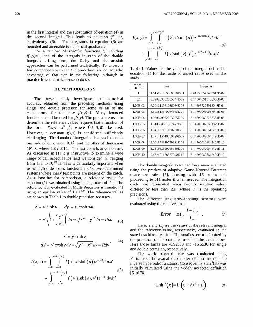
accuracy obtained from the preceding methods, using single and double precision for some or all of the calculations, for the case f(x,y)=1. Many bounded functions could be used for f(x,y). The procedure used to determine the reference values requires that a function of the form f(x,y)= xm ym, where 0 ≤ n,m , be used. However, a constant f(x,y) is considered sufficiently challenging. The domain of integration is a patch that has one side of dimension 0.1λ and the other of dimension 10-n λ, where 1 ≤ n ≤ 11. The test point is at one corner. As discussed in [1] it is instructive to examine a wide range of cell aspect ratios, and we consider K ranging from 1:1 to 10-10 :1. This is particularly important when using high order basis functions and/or over-determined systems where many test points are present on the patch. As a baseline for comparison, a reference result for equation (1) was obtained using the approach of [1]. The reference was evaluated in Multi-Precision arithmetic [4] using an epsilon value of 10.0-400. The reference values are shown in Table 1 to double precision accuracy.
22 2
sinh , cosh
'' 1 ' '
'
y x u dy x udu
yx du x y du Rdu
x
′ ′ ′ ′= =
= + = + =⎛ ⎞⎜ ⎟⎝ ⎠
(3)
2 2
sinh ,
cosh ' '
x y v
dx y v dv y x dv Rdv
′ ′ =
′ ′= = + =, (4)
( )( )( )
( )( )( )
1
1
sinh
0 0
1sinh
0 0
( , ) , 'sinh
'sinh ,
KajkR
x u
b KjkR
y v
I x y f x x u e dudx
f y v y e dvdy
−
−
−
′= =
−
′= =
′ ′=
′ ′ +
∫ ∫
∫ ∫,(5)
( )( ) ( )( )
( )( ) ( )( )
1
1
sinh'cosh
0 0
1sinh'cosh
0 0
( , ) , 'sinh
'sinh ,
Kajkx u
x u
b Kjky v
y v
I x y f x x u e dudx
f y v y e dvdy
−
−
−
′= =
−
′= =
′ ′=
′ ′ +
∫ ∫
∫ ∫
.(6)
Table 1. Values for the value of the integral defined in equation (1) for the range of aspect ratios used in this study.
Aspect Ratio Real Imaginary
1 1.615721995380920E-01 -6.012599373499612E-02
0.1 3.898233302555344E-02 -6.145640913466086E-03
1.00E-02 6.201218961036034E-03 -6.146987225913048E-04
1.00E-03 8.503815540084963E-04 -6.147000690637945E-05
1.00E-04 1.080640082293225E-04 -6.147000825285354E-06
1.00E-05 1.310898591857477E-05 -6.147000826631829E-07
1.00E-06 1.541157101160280E-06 -6.147000826645292E-08
1.00E-07 1.771415610459726E-07 -6.147000826645428E-09
1.00E-08 2.001674119759131E-08 -6.147000826645429E-10
1.00E-09 2.231932629058536E-09 -6.147000826645429E-11
1.00E-10 2.462191138357940E-10 -6.147000826645429E-12
The double integrals examined here were evaluated
using the product of adaptive Gauss-Kronrod-Patterson quadrature rules [5], starting with 15 nodes and proceeding to 511 nodes if/when needed. The integration cycle was terminated when two consecutive values differed by less than 2ε (where ε is the operating precision).
The different singularity-handling schemes were evaluated using the relative error.
Error = log10
I − Iref
Iref
. (7)
Here, I and Iref are the values of the relevant integral and the reference value, respectively, evaluated in the stated machine precision. The smallest error is limited by the precision of the compiler used for the calculations. Here those limits are -6.92360 and -15.6536 for single and double precision, respectively.
The work reported here was conducted using Fortran90. The available compiler did not include the inverse hyperbolic functions. Consequently sinh-1(K) was initially calculated using the widely accepted definition [6, p178],
sinh−1 x( )= ln x + x2 +1( ) . (8)
299 ACES JOURNAL, VOL. 23, NO. 4, DECEMBER 2008
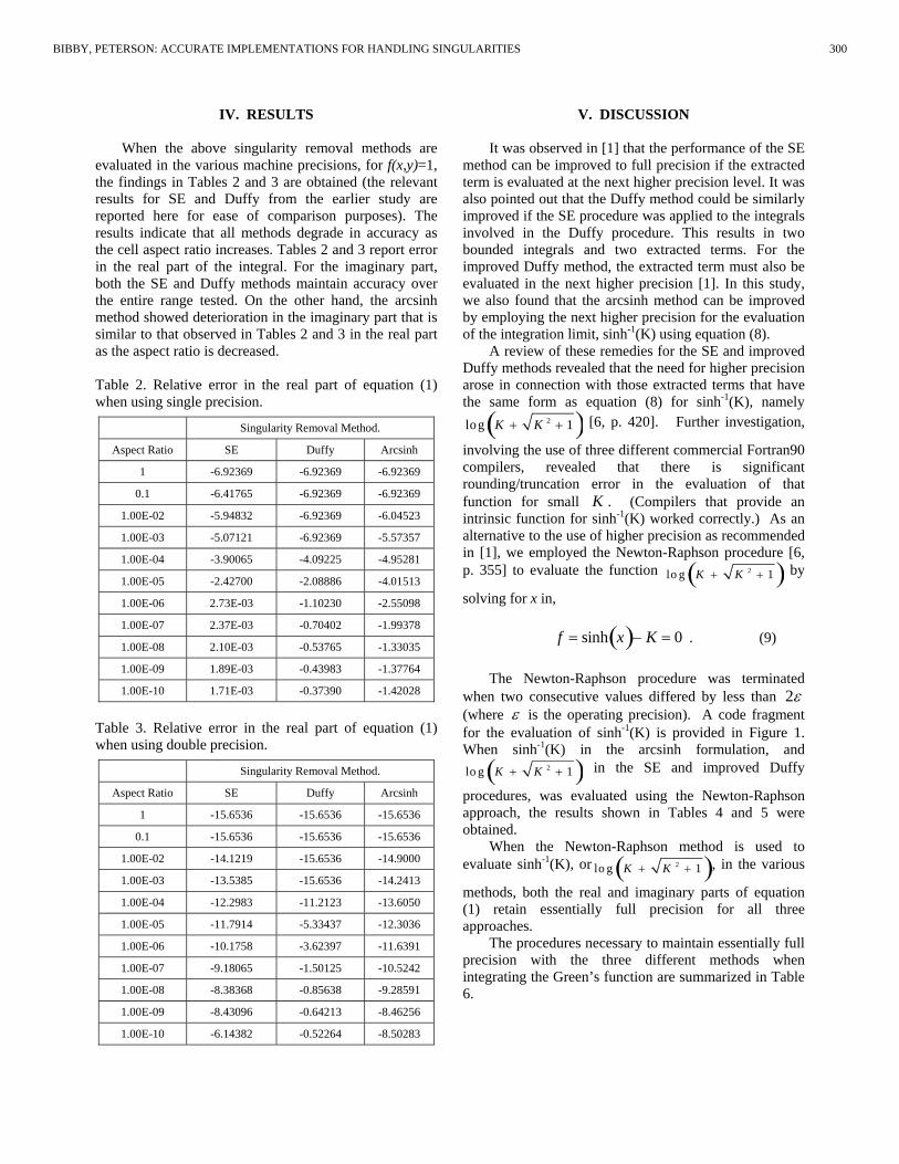
IV. RESULTS When the above singularity removal methods are
evaluated in the various machine precisions, for f(x,y)=1, the findings in Tables 2 and 3 are obtained (the relevant results for SE and Duffy from the earlier study are reported here for ease of comparison purposes). The results indicate that all methods degrade in accuracy as the cell aspect ratio increases. Tables 2 and 3 report error in the real part of the integral. For the imaginary part, both the SE and Duffy methods maintain accuracy over the entire range tested. On the other hand, the arcsinh method showed deterioration in the imaginary part that is similar to that observed in Tables 2 and 3 in the real part as the aspect ratio is decreased.
Table 2. Relative error in the real part of equation (1) when using single precision.
Singularity Removal Method.
Aspect Ratio SE Duffy Arcsinh
1 -6.92369 -6.92369 -6.92369
0.1 -6.41765 -6.92369 -6.92369
1.00E-02 -5.94832 -6.92369 -6.04523
1.00E-03 -5.07121 -6.92369 -5.57357
1.00E-04 -3.90065 -4.09225 -4.95281
1.00E-05 -2.42700 -2.08886 -4.01513
1.00E-06 2.73E-03 -1.10230 -2.55098
1.00E-07 2.37E-03 -0.70402 -1.99378
1.00E-08 2.10E-03 -0.53765 -1.33035
1.00E-09 1.89E-03 -0.43983 -1.37764
1.00E-10 1.71E-03 -0.37390 -1.42028
Table 3. Relative error in the real part of equation (1) when using double precision.
Singularity Removal Method.
Aspect Ratio SE Duffy Arcsinh
1 -15.6536 -15.6536 -15.6536
0.1 -15.6536 -15.6536 -15.6536
1.00E-02 -14.1219 -15.6536 -14.9000
1.00E-03 -13.5385 -15.6536 -14.2413
1.00E-04 -12.2983 -11.2123 -13.6050
1.00E-05 -11.7914 -5.33437 -12.3036
1.00E-06 -10.1758 -3.62397 -11.6391
1.00E-07 -9.18065 -1.50125 -10.5242
1.00E-08 -8.38368 -0.85638 -9.28591
1.00E-09 -8.43096 -0.64213 -8.46256
1.00E-10 -6.14382 -0.52264 -8.50283
V. DISCUSSION
It was observed in [1] that the performance of the SE method can be improved to full precision if the extracted term is evaluated at the next higher precision level. It was also pointed out that the Duffy method could be similarly improved if the SE procedure was applied to the integrals involved in the Duffy procedure. This results in two bounded integrals and two extracted terms. For the improved Duffy method, the extracted term must also be evaluated in the next higher precision [1]. In this study, we also found that the arcsinh method can be improved by employing the next higher precision for the evaluation of the integration limit, sinh-1(K) using equation (8).
A review of these remedies for the SE and improved Duffy methods revealed that the need for higher precision arose in connection with those extracted terms that have the same form as equation (8) for sinh-1(K), namely log K + K 2 + 1( ) [6, p. 420]. Further investigation,
involving the use of three different commercial Fortran90 compilers, revealed that there is significant rounding/truncation error in the evaluation of that function for small K . (Compilers that provide an intrinsic function for sinh-1(K) worked correctly.) As an alternative to the use of higher precision as recommended in [1], we employed the Newton-Raphson procedure [6, p. 355] to evaluate the function
lo g K + K 2 + 1( ) by
solving for x in, f = sinh x( )− K = 0 . (9) The Newton-Raphson procedure was terminated
when two consecutive values differed by less than 2ε (where ε is the operating precision). A code fragment for the evaluation of sinh-1(K) is provided in Figure 1. When sinh-1(K) in the arcsinh formulation, and lo g K + K 2 + 1( ) in the SE and improved Duffy
procedures, was evaluated using the Newton-Raphson approach, the results shown in Tables 4 and 5 were obtained.
When the Newton-Raphson method is used to evaluate sinh-1(K), or lo g K + K 2 + 1( ), in the various
methods, both the real and imaginary parts of equation (1) retain essentially full precision for all three approaches.
The procedures necessary to maintain essentially full precision with the three different methods when integrating the Green’s function are summarized in Table 6.
300BIBBY, PETERSON: ACCURATE IMPLEMENTATIONS FOR HANDLING SINGULARITIES

Table 4. Relative error in the real part of equation (1) when using single precision and the Newton-Raphson method.
Singularity Removal Method. Aspect Ratio SE Duffy
Improved
Duffy Arcsinh
1 -6.92369 -6.92369 -6.92369 -6.92369
0.1 -6.92369 -6.92369 -6.92369 -6.92369
1.00E-02 -6.92369 -6.92369 -6.92369 -6.92369
1.00E-03 -6.92369 -6.92369 -6.92369 -6.92369
1.00E-04 -6.92369 -4.09225 -6.92369 -6.87076
1.00E-05 -6.92369 -2.08886 -6.92369 -6.92369
1.00E-06 -6.92369 -1.10230 -6.92369 -6.92369
1.00E-07 -6.92369 -0.70402 -6.92369 -6.92369
1.00E-08 -6.92369 -0.53765 -6.92369 -6.92369
1.00E-09 -6.92369 -0.43983 -6.92369 -6.92369
1.00E-10 -6.92369 -0.37390 -6.92369 -6.92369
Table 5. Relative error in the real part of equation (1) when using double precision and the Newton-Raphson method.
Singularity Removal Method. Aspect Ratio SE Duffy
Improved
Duffy Arcsinh
1 -15.6536 -15.6536 -15.6536 -15.6536
0.1 -15.6536 -15.6536 -15.6536 -15.6536
1.00E-02 -15.6536 -15.6536 -15.6536 -15.6536
1.00E-03 -15.1955 -15.6536 -15.6536 -15.6006
1.00E-04 -14.4545 -11.2123 -15.6536 -15.6536
1.00E-05 -13.4821 -5.33437 -15.6536 -15.6536
1.00E-06 -14.3435 -3.62397 -15.6536 -15.6536
1.00E-07 -15.6536 -1.50125 -15.6536 -15.6536
1.00E-08 -15.6536 -0.85638 -15.6536 -15.6536
1.00E-09 -15.6536 -0.64213 -15.6536 -15.4311
1.00E-10 -15.6536 -0.52264 -15.6536 -15.6536
The integrals considered here are expressed in the Cartesian coordinate system. In a non-Cartesian system the above remedies still apply — so long as closed-form solutions for the extracted terms are available. The arcsinh method avoids this requirement, but does require that an invertible transformation be identified. In more general constructions where cells might be mapped to curved surfaces, and the integrand contains an additional Jacobian, the preceding observations may not apply.
Table 6. Summary of procedures for the high accuracy evaluation of equation (1).
Method Approach
SE
Must have closed-form integral for the extracted term log K + K 2 +1( ) must be evaluated carefully, here
by Newton-Raphson.
Duffy
Only the improved form is viable over the whole range Singularity extraction needs to be applied to the two main integrals
Must have closed-form integrals for the extracted terms
log K + K 2 + 1( )
must be evaluated carefully, here by Newton-Raphson.
Arcsinh sinh−1 K( )
must be evaluated carefully, here by Newton-Raphson.
Duffy
Only the improved form is viable over the whole range Singularity extraction needs to be applied to the two main integrals
Must have closed-form integrals for the extracted terms
log K + K 2 +1( )
must be evaluated carefully, here by Newton-Raphson.
Fig. 1. Fortran90 code for inverse hyperbolic sine function.
Function asinh(x) ! This program uses Newton-Raphson to calculate arcsinh(x) implicit real*8 (a-h, o-z) d0=float(0) d1=float(1) d2=float(2) xlimit=d2*epsilon(d1) ! uold=d0 ! Select a starting point – this is somewhat arbitrary if(x .lt. d2) then unew=sign(d1,x) else unew=sign(d1,x)*log(abs(x)) endif do while(abs(unew – uold) .gt. xlimit) f=sinh(unew) df=cosh(unew) correction=(f – x)/df uold=unew unew=uold – correction end do ! asinh(x)=unew return
301 ACES JOURNAL, VOL. 23, NO. 4, DECEMBER 2008
REFERENCES [1] M. M. Bibby and A. F. Peterson, “High accuracy
evaluation of the EFIE matrix entries on a planar patch,” ACES Journal, vol. 20, no. 3, pp. 198-206, 2005.
[2] M. A. Khayat and D. R. Wilton, “Numerical evaluation of singular and near singular potential integrals,” IEEE Trans. Antennas Prop., vol. 53, no. 10, pp 3180-3190, Oct. 2005.
[3] M. G. Duffy, “Quadrature over a pyramid or cube of integrands with a singularity at a Vertex,” SIAM J. Numer. Anal. vol. 19, no. 6, pp. 1260-1262, Dec. 1982.
[4] D. H. Bailey, “A Fortran-90 based multi-precision system,” ACM Trans. on Mathematical Software, vol. 20, no. 4, pp. 379-387, Dec 1995. See also RNR Technical Report RNR-90-022, 1993 and http://crd.lbl.gov/~dhbailey/mpdist/.
[5] T. N. L. Patterson, “Generation of interpolatory quadrature rules of the highest degree of precision with preassigned nodes for general weight functions,” A.C.M. Trans. on Mathematical Software, vol. 15, no. 2, pp. 137-143, June, 1989.
[6] W. H. Press, S. A. Teukolsky, W. T. Vettering and B. P. Flannery, Numerical Recipes for Fortran 77, Cambridge University Press, 1992.
Malcolm M. Bibby received the B.Eng. and Ph.D. degrees in Electrical Engineering from the University of Liverpool, England in 1962 and 1965 respectively. He also holds an MBA from the University of Chicago, U.S.A. His career includes both engineering and management. He
was president of LXE Inc., a manufacturer of wireless data communications products from 1983 to 1994. Thereafter he was president of NDI, a manufacturer of hardened hand-held computers, for five years before retiring. He has been interested in the numerical aspects associated with antenna design for the last twenty-five years.
Andrew F. Peterson received the B.S., M.S., and Ph.D. degrees in Electrical Engineering from the University of Illinois, Urbana-Champaign in 1982, 1983, and 1986 respectively. Since 1989, he has been a member of the faculty of the School of Electrical and Computer
Engineering at the Georgia Institute of Technology, where he is now Professor and Associate Chair for Faculty Development. Within ACES, he served for six years (1991-1997) as a member of the Board of Directors, and has been the Finance Committee Chair and the Publications Committee Chair.
302BIBBY, PETERSON: ACCURATE IMPLEMENTATIONS FOR HANDLING SINGULARITIES
Low-Frequency Full-Wave Finite Element Modeling Using the LU Recombination Method
H. Ke and T. H. Hubing
Department of Electrical and Computer Engineering
Clemson University Clemson, SC 29634
Abstract − In this paper, the low-frequency instability of full-wave finite element methods (FEM) is investigated. The curl part of the FEM matrix is shown to be singular. The paper explains how low-frequency instabilities are related to this singularity. Based on this analysis, an LU recombination method is implemented in FEM to solve the low-frequency problem. This method, which has previously been applied to the method of moments (MOM), reduces the errors in the curl part of the matrix and enforces the correct gauge condition. Moreover, the method is restructured to work more efficiently for sparse finite element matrices.
I. INTRODUCTION
The finite element method [1] is well-suited for solving problems involving inhomogeneous arbitrarily-shaped objects. Many researchers have observed that the “curl-curl” operation that is frequently employed when FEM is used to solve the vector Helmholtz equation can result in ill-conditioned matrices in some circumstances [2- 4].
One situation that generates ill-conditioned matrices and unstable solutions is modeling performed at low frequencies. The examples presented in this paper illustrate this behavior. In [5], special penalty terms were introduced and potential formulations were used to deal with this problem.
Most full-wave surface integral techniques also suffer from low frequency difficulties [6, 7]. The low frequency instabilities can be ascribed to the divergence operator applied to the unknown surface current density in the integral equation. Mathematically, these instabilities are related to the singular property of the scalar potential part of the impedance matrix. A method to circumvent this problem was recently proposed [8, 9]. This approach, called the LU recombination method, employs linear transformations of the moment matrices in order to isolate and eliminate non-physical solutions.
In this paper, the low-frequency problem with finite element formulations is described in terms of the singular property of the curl part in the finite element matrix when using curl-conforming Nedelec-type basis functions. The
LU recombination method is applied in order to isolate the singularity in the curl part of the finite element matrix. It is not necessary to introduce any penalty terms, or create new basis functions. The approach is further refined so that the new matrices after LU recombination are partially sparse. This reduces the computation cost and greatly improves the performance. Finally, a couple of examples are presented.
II. FORMULATION
From Maxwell’s equations, the vector Helmholtz
equation in terms of the E field can be written as,
( ) ( )
( ) ( )
00
int int
0
1
rr
r
jj
j
ωε εωµ µ
ωµ µ
∇ ×∇ × +
= − − ∇ ×
⎛ ⎞⎜ ⎟⎝ ⎠
EE
J M
rr
r r
(1)
where Jint and Mint are impressed electric and magnetic sources; ω is the angular frequency; µ0 and ε0 are the free space permeability and permittivity; and µr and εr are the relative permeability and permittivity.
After applying a weighting function w(r), the FEM weak form is [4, 10],
( )( ) ( )( ) ( ) ( )
( )( ) ( )
( ) ( ) ( )
0
0
int int
0
ˆ
1
r
rV
S
V r
j dVj
dS
dVj
ωε εωµ µ
ωµ µ
∇ × ⋅ ∇ ×+ ⋅
× ⋅ −
⋅
=
+ ∇ ×
⎛ ⎞⎜ ⎟⎝ ⎠
⎛ ⎞⎜ ⎟⎝ ⎠
∫
∫
∫
EE
H
MJ
wr w r
r r
n r w r
w rr r
(2)
where S is the surface enclosing volume V.
The unknown E field is expanded using curl-conforming basis functions that are the same as the weighting functions,
303 ACES JOURNAL, VOL. 23, NO. 4, DECEMBER 2008

( ) ( )n nn
E= ∑E r w r (3)
where En are unknown coefficients. The surface integral on the right hand side of equation (2) is evaluated by using surface basis functions fn(r), which are related to wn(r) by,
( ) ( )ˆn n= ×w r n f r . (4)
Equation (2) is then discretized into a matrix equation,
⋅ = ⋅ +A E B J S . (5)
The right hand side represents the boundary condition and the source term. J is the equivalent current density on the surface. S is the source term. E is a vector containing the unknown coefficients in equation (3). The elements of A are,
( )( ) ( )( )
( ) ( )0
0
rmnV
r
jA dV
j
ωµ µ
ωε ε
∇ × ⋅ ∇ ×
=
+ ⋅
⎡ ⎤⎢ ⎥⎢ ⎥⎢ ⎥⎣ ⎦
∫n m
n m
w r w r
w r w r
. (6)
Let
( ) ( )1 0mn rV
A j dVωε ε= ⋅∫ n mw r w r , (7a)
which is the right-most term in the right-hand side of equation (6).
Let
( )( ) ( )( )2
0mn
V r
A dVjωµ µ
∇ × ⋅ ∇ ×= ∫ n mw r w r
, (7b)
which is the left-most term in the right-hand side of equation (6). Every element of A1 approaches zero at arbitrarily low frequencies. The following reasoning demonstrates that, because of the ∇ × operator, A2 is a singular matrix when using the popular lowest order curl-conforming basis functions. The rank of the matrix is determined by the total number of internal nodes in the finite element mesh [11].
The basis function for a tetrahedron can be defined on each edge as [12],
7 77
in the tetrahedra0 otherwise
1,2,...,6
i ii
i
− −−
+ ×=
=
⎧⎨⎩
f g r rw
(8a)
where 7
7 1 26i
i i i
lV−
− = ×f r r , (8b)
and
77 6
i ii i
l lV
−− =g e . (8c)
Here i1 and i2 are the node indices of edge i, defined
in Fig. 1. l is the length of the edge, e is the unit vector along the edge, and V is the volume of the tetrahedron.
Fig. 1. The tetrahedral element and its edge-node relations.
Consider the local elements, i.e., the elements
evaluated within one tetrahedron. The curl of the basis function is a constant within the tetrahedron,
726
ii i i
lV −∇ × = =w g l . (9)
The local element in 2
eA is,
20
0
14
19
eij i j
r
i ji j
r
A Vj
l l
j V
ωµ µ
ωµ µ
= ⋅
= ⋅⎛ ⎞⎜ ⎟⎝ ⎠
g g
l l (10)
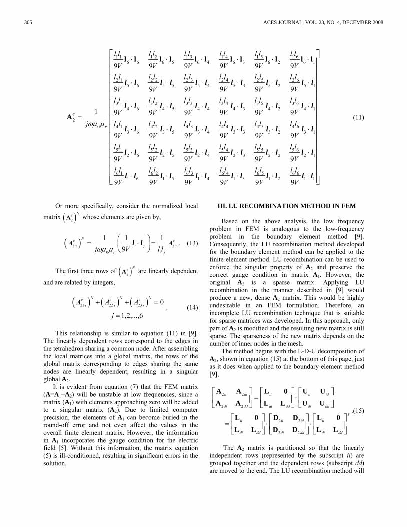
where the superscript e indicates local elements. Thus within one tetrahedron, the local matrix can be written as in equation (11), shown on the top of the next page.
For the tetrahedron in Fig. 1, edges 4, 5, and 6 form a triangle, which means,
l4+l5+l6=0. (12)
Consequently, the first three rows in equation (11) are
linearly dependent.
1
2
3
4 edge i1 i2
1 1 22 1 33 1 44 2 35 4 26 3 4
304KE, HUBING: LF FULL-WAVE FINITE ELEMENT MODELING USING LU RECOMBINATION
1 3 1 5 1 61 1 1 2 1 46 6 6 5 6 4 6 3 6 2 6 1
2 3 2 5 2 62 1 2 2 2 45 6 5 5 5 4 5 3 5 2 5 1
3 1 3 2 3 3 3 4 3 5 34 6 4 5 4 4 4 3 4 2
20
9 9 9 9 9 9
9 9 9 9 9 9
1 9 9 9 9 9e
r
l l l l l ll l l l l l
V V V V V Vl l l l l ll l l l l l
V V V V V Vl l l l l l l l l l l
V V V V Vjωµ µ
⋅ ⋅ ⋅ ⋅ ⋅ ⋅
⋅ ⋅ ⋅ ⋅ ⋅ ⋅
⋅ ⋅ ⋅ ⋅ ⋅=
l l l l l l l l l l l l
A
l l l l l l l l l l l l
l l l l l l l l l l 64 1
4 3 4 5 4 64 1 4 2 4 43 6 3 5 3 4 3 3 3 2 3 1
5 1 5 2 5 3 5 4 5 5 5 62 6 2 5 2 4 2 3 2 2 2 1
6 1 6 2 6 3 6 4 6 5 6 61 6 1 5 1 4 1 3 1 2
9
9 9 9 9 9 9
9 9 9 9 9 9
9 9 9 9 9
l
Vl l l l l ll l l l l l
V V V V V Vl l l l l l l l l l l l
V V V V V Vl l l l l l l l l l l l
V V V V V
⋅
⋅ ⋅ ⋅ ⋅ ⋅ ⋅
⋅ ⋅ ⋅ ⋅ ⋅ ⋅
⋅ ⋅ ⋅ ⋅ ⋅
l l
l l l l l l l l l l l l
l l l l l l l l l l l l
l l l l l l l l l l 1 19V⋅
⎡ ⎤⎢ ⎥⎢ ⎥⎢ ⎥⎢ ⎥⎢ ⎥⎢ ⎥⎢ ⎥⎢ ⎥⎢ ⎥⎢ ⎥⎢ ⎥⎢ ⎥⎢ ⎥⎢ ⎥⎢ ⎥⎣ ⎦
l l
(11)
Or more specifically, consider the normalized local
matrix ( )2
NeA whose elements are given by,
( )2 20
1 1 19
Ne eij i j ij
r i j
A Aj V l lωµ µ
= ⋅ =⎛ ⎞⎜ ⎟⎝ ⎠
l l . (13)
The first three rows of ( )2
NeA are linearly dependent
and are related by integers,
( ) ( ) ( )21 22 23 0
1,2,...,6
N N Ne e ej j jA A A
j
+ + =
=. (14)
This relationship is similar to equation (11) in [9].
The linearly dependent rows correspond to the edges in the tetrahedron sharing a common node. After assembling the local matrices into a global matrix, the rows of the global matrix corresponding to edges sharing the same nodes are linearly dependent, resulting in a singular global A2.
It is evident from equation (7) that the FEM matrix (A=A1+A2) will be unstable at low frequencies, since a matrix (A1) with elements approaching zero will be added to a singular matrix (A2). Due to limited computer precision, the elements of A1 can become buried in the round-off error and not even affect the values in the overall finite element matrix. However, the information in A1 incorporates the gauge condition for the electric field [5]. Without this information, the matrix equation (5) is ill-conditioned, resulting in significant errors in the solution.
III. LU RECOMBINATION METHOD IN FEM
Based on the above analysis, the low frequency problem in FEM is analogous to the low-frequency problem in the boundary element method [9]. Consequently, the LU recombination method developed for the boundary element method can be applied to the finite element method. LU recombination can be used to enforce the singular property of A2 and preserve the correct gauge condition in matrix A1. However, the original A2 is a sparse matrix. Applying LU recombination in the manner described in [9] would produce a new, dense A2 matrix. This would be highly undesirable in an FEM formulation. Therefore, an incomplete LU recombination technique that is suitable for sparse matrices was developed. In this approach, only part of A2 is modified and the resulting new matrix is still sparse. The sparseness of the new matrix depends on the number of inner nodes in the mesh.
The method begins with the L-D-U decomposition of A2, shown in equation (15) at the bottom of this page, just as it does when applied to the boundary element method [9],
2 2
2 2
2 2
2 2
ii id ii ii id
di dd di dd di dd
T
ii ii id ii
di dd di dd di dd
= ⋅
= ⋅ ⋅
⎡ ⎤ ⎡ ⎤ ⎡ ⎤⎢ ⎥ ⎢ ⎥ ⎢ ⎥⎣ ⎦ ⎣ ⎦ ⎣ ⎦
⎡ ⎤ ⎡ ⎤ ⎡ ⎤⎢ ⎥ ⎢ ⎥ ⎢ ⎥⎣ ⎦ ⎣ ⎦ ⎣ ⎦
A A L 0 U UA A L L U U
L 0 D D L 0L L D D L L
.(15)
The A2 matrix is partitioned so that the linearly
independent rows (represented by the subscript ii) are grouped together and the dependent rows (subscript dd) are moved to the end. The LU recombination method will
305 ACES JOURNAL, VOL. 23, NO. 4, DECEMBER 2008
modify the sub-matrices Ldi, D2di, D2id, and D2dd, while Lii and D2ii are left unchanged. Therefore, A2ii=Lii•D2ii is unchanged after constructing a new A2. There is no need to recalculate A2ii after the modifications on L and D2. To accomplish that, the L matrix is replaced by,
0ii
di dd
=⎡ ⎤⎢ ⎥⎣ ⎦
IL
L I, (16)
where I is identity matrix. The new decomposition on A2 is then written in equation (17), as shown at the bottom of this page. Thus during the LU recombination, the A2ii part remains the same. No additional elements or errors are introduced.
The same decomposition in equation (17) is applied to A1. After LU recombination, the new A becomes equation (18) at the bottom of this page. Note that Ldi is already modified, as described in [9]. The correct information in A1 is preserved. But the new A matrix is still ill-conditioned at low frequencies since A1 is much smaller than A2. The imbalance can be alleviated by introducing a scaling step. The sub-matrices D1di, D1id, and D1dd are scaled so that they are comparable to A2ii. This step greatly improves the condition of the new A matrix. It is especially beneficial when iterative methods are used to solve the matrix equations.
IV. NUMERICAL RESULTS
Two sample structures were evaluated using a finite
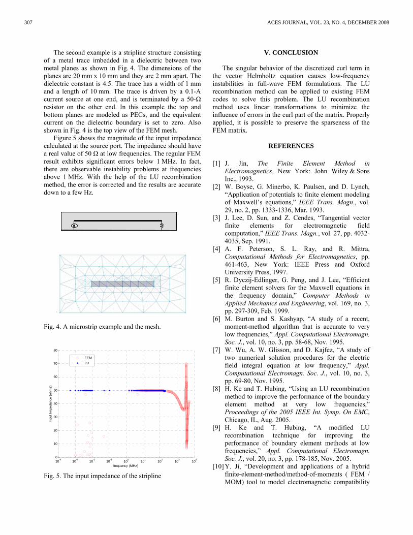
element modeling technique with and without LU recombination. The first example is the rectangular power bus structure shown in Fig. 2. The dimensions of the structure are 20 cm x 20 cm x 1 cm. The power and ground planes are modeled as perfect electric conductors (PECs). The four side walls of the board are modeled as perfect magnetic conductors (PMCs). The dielectric between the planes has a relative permittivity of 4.5. The board is excited by an ideal current source located in the dielectric, 6 cm from one edge and 7 cm from an adjacent edge.
Fig. 2. A power bus example.
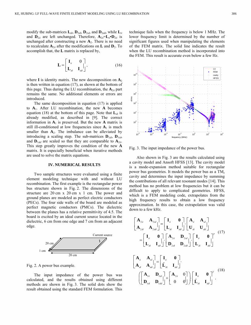
The input impedance of the power bus was calculated, and the results obtained using different methods are shown in Fig. 3. The solid dots show the result obtained using the standard FEM formulation. This
technique fails when the frequency is below 1 MHz. The lower frequency limit is determined by the number of significant figures used when manipulating the elements of the FEM matrix. The solid line indicates the result when the LU recombination method is incorporated into the FEM. This result is accurate even below a few Hz.
10-8 10-6 10-4 10-2 100 102 104
100
102
104
106
108
1010
frequency (MHz)
ohm
s
LUFEMcavityHFSS
Fig. 3. The input impedance of the power bus. Also shown in Fig. 3 are the results calculated using
a cavity model and Ansoft HFSS [13]. The cavity model is a mode-expansion method suitable for rectangular power bus geometries. It models the power bus as a TMz cavity and determines the input impedance by summing the contributions of all relevant resonant modes [14]. This method has no problem at low frequencies but it can be difficult to apply to complicated geometries. HFSS, which is a FEM modeling code, extrapolates from the high frequency results to obtain a low frequency approximation. In this case, the extrapolation was valid down to a few kHz.
2 2
2 2
2 2
2 2
ii id ii ii id
di dd di dd di dd
T
ii ii id ii
di dd di dd di dd
= ⋅
= ⋅ ⋅
⎡ ⎤ ⎡ ⎤ ⎡ ⎤⎢ ⎥ ⎢ ⎥ ⎢ ⎥⎣ ⎦ ⎣ ⎦ ⎣ ⎦
⎡ ⎤ ⎡ ⎤ ⎡ ⎤⎢ ⎥ ⎢ ⎥ ⎢ ⎥⎣ ⎦ ⎣ ⎦ ⎣ ⎦
A A I 0 A AA A L I U U
I 0 A D I 0L I D D L I
(17)
1 1 2
1 1
00 0
.
ii id ii
di dd di dd
T
ii id iiii
di dd di dd
= ⋅
+ ⋅
⎡ ⎤ ⎡ ⎤⎢ ⎥ ⎢ ⎥⎣ ⎦ ⎣ ⎦
⎛ ⎞⎡ ⎤ ⎡ ⎤⎡ ⎤⎜ ⎟⎢ ⎥ ⎢ ⎥⎢ ⎥
⎣ ⎦⎣ ⎦ ⎣ ⎦⎝ ⎠
A A I 0A A L I
A D I 0AD D L I
(18)
20 cm
20 cm 1 cm
Current source
306KE, HUBING: LF FULL-WAVE FINITE ELEMENT MODELING USING LU RECOMBINATION
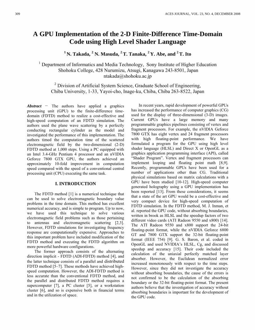
The second example is a stripline structure consisting of a metal trace imbedded in a dielectric between two metal planes as shown in Fig. 4. The dimensions of the planes are 20 mm x 10 mm and they are 2 mm apart. The dielectric constant is 4.5. The trace has a width of 1 mm and a length of 10 mm. The trace is driven by a 0.1-A current source at one end, and is terminated by a 50-Ω resistor on the other end. In this example the top and bottom planes are modeled as PECs, and the equivalent current on the dielectric boundary is set to zero. Also shown in Fig. 4 is the top view of the FEM mesh.
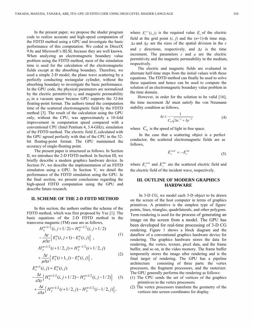
Figure 5 shows the magnitude of the input impedance calculated at the source port. The impedance should have a real value of 50 Ω at low frequencies. The regular FEM result exhibits significant errors below 1 MHz. In fact, there are observable instability problems at frequencies above 1 MHz. With the help of the LU recombination method, the error is corrected and the results are accurate down to a few Hz.
Fig. 4. A microstrip example and the mesh.
10-4 10-3 10-2 10-1 100 101 102 103 1040
10
20
30
40
50
60
70
80
frequency (MHz)
Inpu
t Im
peda
nce
(ohm
s)
FEMLU
Fig. 5. The input impedance of the stripline
V. CONCLUSION
The singular behavior of the discretized curl term in the vector Helmholtz equation causes low-frequency instabilities in full-wave FEM formulations. The LU recombination method can be applied to existing FEM codes to solve this problem. The LU recombination method uses linear transformations to minimize the influence of errors in the curl part of the matrix. Properly applied, it is possible to preserve the sparseness of the FEM matrix.
REFERENCES [1] J. Jin, The Finite Element Method in
Electromagnetics, New York: John Wiley & Sons Inc., 1993.
[2] W. Boyse, G. Minerbo, K. Paulsen, and D. Lynch, “Application of potentials to finite element modeling of Maxwell’s equations,” IEEE Trans. Magn., vol. 29, no. 2, pp. 1333-1336, Mar. 1993.
[3] J. Lee, D. Sun, and Z. Cendes, “Tangential vector finite elements for electromagnetic field computation,” IEEE Trans. Magn., vol. 27, pp. 4032-4035, Sep. 1991.
[4] A. F. Peterson, S. L. Ray, and R. Mittra, Computational Methods for Electromagnetics, pp. 461-463, New York: IEEE Press and Oxford University Press, 1997.
[5] R. Dyczij-Edlinger, G. Peng, and J. Lee, “Efficient finite element solvers for the Maxwell equations in the frequency domain,” Computer Methods in Applied Mechanics and Engineering, vol. 169, no. 3, pp. 297-309, Feb. 1999.
[6] M. Burton and S. Kashyap, “A study of a recent, moment-method algorithm that is accurate to very low frequencies,” Appl. Computational Electromagn. Soc. J., vol. 10, no. 3, pp. 58-68, Nov. 1995.
[7] W. Wu, A. W. Glisson, and D. Kajfez, “A study of two numerical solution procedures for the electric field integral equation at low frequency,” Appl. Computational Electromagn. Soc. J., vol. 10, no. 3, pp. 69-80, Nov. 1995.
[8] H. Ke and T. Hubing, “Using an LU recombination method to improve the performance of the boundary element method at very low frequencies,” Proceedings of the 2005 IEEE Int. Symp. On EMC, Chicago, IL, Aug. 2005.
[9] H. Ke and T. Hubing, “A modified LU recombination technique for improving the performance of boundary element methods at low frequencies,” Appl. Computational Electromagn. Soc. J., vol. 20, no. 3, pp. 178-185, Nov. 2005.
[10] Y. Ji, “Development and applications of a hybrid finite-element-method/method-of-moments ( FEM / MOM) tool to model electromagnetic compatibility
307 ACES JOURNAL, VOL. 23, NO. 4, DECEMBER 2008

and signal integrity problems in printed circuit boards,” Ph.D. dissertation, University of Missouri-Rolla, 2000.
[11] N. Venkatarayalu, M. Vouvakis, Y. Gan, and J. Lee, “Suppressing linear time growth in edge element based finite element time domain solution using divergence free constraint equation,” IEEE Antennas and Propagation Society International Symposium, vol. 4b, pp. 193-196, Jul. 2005.
[12] X. Yuan, “Three-dimensional electromagnetic scattering from inhomogeneous objects by the hybrid moment and finite element method,” IEEE Trans. Microwave Theory and Tech., vol. 38, no. 8, pp. 1053-1058, Aug, 1990.
[13] HFSS version 9.0, Ansoft Corporation. http://www.ansoft.com/products/hf/hfss/
[14] M. Xu and T. Hubing, “Estimating the power bus impedance of printed circuit boards with embedded capacitance,” IEEE Trans. Adv. Packag., vol. 25, no. 3, pp. 424-432, Aug. 2002.
Haixin Ke received his BSEE and MSEE degrees from Tsinghua University in 1998 and 2001, respectively, and his Ph.D. in Electrical Engineering from University of Missouri-Rolla in 2006. He is currently a Post-Doctoral researcher at Clemson University. His research
interests include computational electromagnetics, electromagnetic compatibility, and vehicular electronic systems.
Todd Hubing received his BSEE. degree from the Massachusetts Institute of Technology in 1980, his MSEE degree from Purdue University in 1982, and his Ph.D. in Electrical Engineering from North Carolina State University in 1988. From 1982 to 1989, he was employed in the
Electromagnetic Compatibility Laboratory, IBM Communications Products Division, in Research Triangle Park, NC. In 1989, he joined faculty at the University of Missouri-Rolla (UMR). At UMR, he worked with faculty and students to analyze and develop solutions for a wide range of EMC problems affecting the electronics industry. In 2006, he joined Clemson University as the Michelin Professor for Vehicular Electronics. There he is continuing his work in electromagnetic compatibility and computational electromagnetic modeling, particularly as it is applied to automotive and aerospace electronic designs. Prof. Hubing has served as an associate editor of the IEEE Transactions on EMC, the IEEE EMC Society Newsletter, and the Journal of the Applied Computational Electromagnetics Society. He has served on the board of directors for both the Applied Computational Electromagnetics Society and the IEEE EMC Society. He was the 2002-2003 President of the IEEE EMC Society and is a Fellow of the IEEE.
308KE, HUBING: LF FULL-WAVE FINITE ELEMENT MODELING USING LU RECOMBINATION
A GPU Implementation of the 2-D Finite-Difference Time-Domain Code using High Level Shader Language
1 N. Takada, 2 N. Masuda, 2 T. Tanaka, 2 Y. Abe, and 2 T. Ito
1 Department of Informatics and Media Technology, Sony Institute of Higher Education
Shohoku College, 428 Nurumizu, Atsugi, Kanagawa 243-8501, Japan [email protected]
2 Division of Artificial System Science, Graduate School of Engineering,
Chiba University, 1-33, Yayoi-cho, Inage-ku, Chiba, Chiba 263-8522, Japan Abstract − The authors have applied a graphics processing unit (GPU) to the finite-difference time-domain (FDTD) method to realize a cost-effective and high-speed computation of an FDTD simulation. The authors used the plane wave scattering by a perfectly conducting rectangular cylinder as the model and investigated the performance of this implementation. The authors timed the computation time of the scattered electromagnetic field by the two-dimensional (2-D) FDTD method at 1,000 steps. Using a PC equipped with an Intel 3.4-GHz Pentium 4 processor and an nVIDIA Geforce 7800 GTX GPU, the authors achieved an approximately 10-fold improvement in computation speed compared with the speed of a conventional central processing unit (CPU) executing the same task.
I. INTRODUCTION
The FDTD method [1] is a numerical technique that
can be used to solve electromagnetic boundary value problems in the time domain. This method has excellent numerical accuracy, and is simple to program. Up to now, we have used this technique to solve various electromagnetic field problems such as those pertaining to antennas and electromagnetic scattering [2,3]. However, FDTD simulations for investigating frequency response are computationally expensive. Approaches to this important problem have included modification of the FDTD method and executing the FDTD algorithm on more powerful hardware configurations.
The former approach consists of the alternating direction implicit - FDTD (ADI-FDTD) method [4], and the latter technique consists of a parallel and distributed FDTD method [5–7]. These methods have achieved high-speed computation. However, the ADI-FDTD method is less accurate than the conventional FDTD method, and the parallel and distributed FDTD method requires a supercomputer [7], a PC cluster [5], or a workstation cluster [6], and so is expensive both in financial terms and in the utilization of space.
In recent years, rapid development of powerful GPUs has increased the performance of computer graphics (CG) used for the display of three-dimensional (3-D) images. Current GPUs have a large memory and many programmable graphics pipelines consisting of vertex and fragment processors. For example, the nVIDIA Geforce 7800 GTX has eight vertex and 24 fragment processors with high floating-point performance. We have formulated a program for the GPU using high level shader language (HLSL) and Direct X or OpenGL as a graphics application programming interface (API), called “Shader Program”. Vertex and fragment processors can implement looping and floating point math [8,9]. Recently, programmable GPUs have been used for a number of applications other than CG. Traditional physical simulations based on matrix calculations with a GPU have been studied [10-12]. High-speed computer generated holography using a GPU implementation has been reported [13]. From these considerations, it seems that a state of the art GPU would be a cost-effective and very compact device for high-speed computation of FDTD simulation. In the FDTD method, M. J. Inman, et al. reported the GPU code, without absorbing boundaries, written in brook as HLSL and the speedup factors of two different video cards (ATI Radeon 9550 and x800) [14]. The ATI Radeon 9550 and x800 support the 24-bit floating-point format, while the nVIDIA Geforce 6800 GT and 7800 GTX support the 32-bit floating-point format (IEEE 754) [9]. G. S. Baron, et al. coded in OpenGL and used NVIDIA’s HLSL, Cg, and discussed speedup and accuracy [15]. Their code included the calculation of the uniaxial perfectly matched layer absorber. However, the Euclidean normalized error increased monotonously with respect to the time steps. However, since they did not investigate the accuracy without absorbing boundaries, the cause of the errors is not confirmed to be the calculation of the absorbing boundary or the 32-bit floating-point format. The present authors believe that the investigation of accuracy without absorbing boundaries is important for the development of the GPU code.
309 ACES JOURNAL, VOL. 23, NO. 4, DECEMBER 2008
In the present paper, we propose the shader program code to realize accurate and high-speed computation of the FDTD method using a GPU and investigate the basic performance of this computation. We coded in DirectX 9.0c and Microsoft’s HLSL because they are well known. When analyzing an electromagnetic boundary value problem using the FDTD method, most of the simulation time is used for the calculation of the electromagnetic fields except at the absorbing boundary. Therefore, we used a simple 2-D model, the plane wave scattering by a perfectly conducting rectangular cylinder, without the absorbing boundary to investigate the basic performance. In the GPU code, the physical parameters are normalized by the electric permittivity ε0 and magnetic permeability µ0 in a vacuum space because GPU supports the 32-bit floating-point format. The authors timed the computation time of the scattered electromagnetic field by the FDTD method [3]. The result of the calculation using the GPU only, without the CPU, was approximately a 10-fold improvement in computation speed compared with a conventional CPU (Intel Pentium 4, 3.4-GHz), simulation of the FDTD method. The electric field Ez calculated with the GPU agreed perfectly with that of the CPU in the 32-bit floating-point format. The GPU maintained the accuracy of single-floating point.
The present paper is structured as follows. In Section II, we introduce the 2-D FDTD method. In Section III, we briefly describe a modern graphics hardware device. In Section IV, we describe the implementation of an FDTD simulation using a GPU. In Section V, we detail the performance of the FDTD simulation using the GPU. In the final section, we present conclusions regarding the high-speed FDTD computation using the GPU and describe future research.
II. SCHEME OF THE 2-D FDTD METHOD
In this section, the authors outline the scheme of the
FDTD method, which was first proposed by Yee [1]. The basic equations of the 2-D FDTD method in the transverse magnetic (TM) case are as follows,
1/2 1/2( , 1/ 2) ( , 1/ 2)
( , 1) ( , ) ,
n nx x
n nz z
H i j H i jt E i j E i jyµ
+ −+ = +∆− + −∆
(1)
1/2 1/2( 1/ 2, ) ( 1/ 2, )
( 1, ) ( , ) ,
n ny y
n nz z
H i j H i jt E i j E i jxµ
+ −+ = +
∆+ + −∆
(2)
1
1/2 1/2
1/2 1/2
( , ) ( , )
( , 1/ 2) ( , 1/ 2)
( 1/ 2, ) ( 1/ 2, ) ,
n nz z
n nx x
n ny y
E i j E i jt H i j H i jyt H i j H i jx
ε
ε
+
+ +
+ +
=∆− + − −∆∆+ + − −∆
(3)
where ),(1 jiEnz+ is the required value zE of the electric
field at the grid point (i, j) and the (n+1)-th time step, x∆ and y∆ are the sizes of the spatial division in the x
and y directions, respectively, and t∆ is the time increment. The parameters ε and µ are the electric permittivity and the magnetic permeability in the medium, respectively.
The electric and magnetic fields are evaluated in alternate half-time steps from the initial values with these equations. The FDTD method can finally be used to solve these equations and hence can be used to compute the solution of an electromagnetic boundary value problem in the time domain.
However, in order for the solution to be valid [16], the time increment t∆ must satisfy the von Neumann stability condition as follows,
(4)
where 0C is the speed of light in free space.
In the case that a scattering object is a perfect conductor, the scattered electromagnetic fields are as follows,
(5)
where scatzE and inc
zE are the scattered electric field and the electric field of the incident wave, respectively.
III. OUTLINE OF MODERN GRAPHICS HARDWARE
In 3-D CG, we model each 3-D object to be drawn
on the screen of the host computer in terms of graphics primitives. A primitive is the simplest type of figure: points, lines, triangles, quadrilaterals, and other polygons. Term rendering is used for the process of generating an image on the screen from a model. The GPU has been developed for real-time processing of 3-D CG rendering. Figure 1 shows a block diagram and the dataflow of a conventional graphics hardware device for rendering. The graphics hardware stores the data for rendering, the vertex, texture, pixel data, and the frame buffer, and so on, in the video memory. The frame buffer temporarily stores the image after rendering and is the final target of rendering. The GPU has a pipeline architecture consisting of three parts: the vertex processors, the fragment processors, and the rasterizer. The GPU generally performs the rendering as follows: (1) The CPU sends the set of vertices of the graphics
primitives to the vertex processors. (2) The vertex processors transform the geometry of the
vertices into screen coordinates for display.
220
1−− ∆+∆
≤∆yxC
t
incz
scatz EE −=
310TAKADA, MASUDA, TANAKA, ABE, ITO: GPU 2D FDTD CODE USING HIGH LEVEL SHADER LANGUAGE
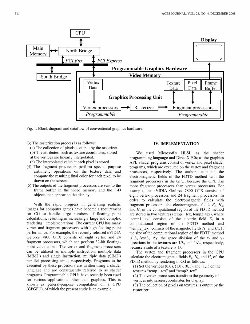
Fig. 1. Block diagram and dataflow of conventional graphics hardware.
(3) The rasterization process is as follows:
(a) The collection of pixels is output by the rasterizer. (b) The attributes, such as texture coordinates, stored at the vertices are linearly interpolated. (c) The interpolated value at each pixel is stored.
(4) The fragment processors perform special purpose arithmetic operations on the texture data and compute the resulting final color for each pixel to be drawn on the screen.
(5) The outputs of the fragment processors are sent to the frame buffer in the video memory and the 3-D objects then appear on the display.
With the rapid progress in generating realistic
images for computer games have become a requirement for CG to handle large numbers of floating point calculations, resulting in increasingly large and complex rendering implementations. The current GPU has many vertex and fragment processors with high floating point performance. For example, the recently released nVIDIA Geforce 7800 GTX consists of eight vertex and 24 fragment processors, which can perform 32-bit floating-point calculations. The vertex and fragment processors can be utilized as multiple instruction, multiple data (MIMD) and single instruction, multiple data (SIMD) parallel processing units, respectively. Programs to be executed by these processors are written using a shader language and are consequently referred to as shader programs. Programmable GPUs have recently been used for various applications other than graphics. This is known as general-purpose computation on a GPU (GPGPU), of which the present study is an example.
IV. IMPLEMENTATION
We used Microsoft's HLSL as the shader
programming language and DirectX 9.0c as the graphics API. Shader programs consist of vertex and pixel shader programs, which are executed on the vertex and fragment processors, respectively. The authors calculate the electromagnetic fields of the FDTD method with the fragment processors in the GPU, because the GPU has more fragment processors than vertex processors. For example, the nVIDIA Geforce 7800 GTX consists of eight vertex processors and 24 fragment processors. In order to calculate the electromagnetic fields with fragment processors, the electromagnetic fields Ez, Hx, and Hy in the computational region of the FDTD method are stored in two textures (temp1_tex, temp2_tex), where “temp1_tex” consists of the electric field Ez in a computational region of the FDTD method and “temp2_tex” consists of the magnetic fields Hx and Hy. If the size of the computational region of the FDTD method is Lx ∆x×Ly ∆y, the space division of the x- and y-directions in the textures are 1/Lx and 1/Ly, respectively, because a side of a texture is 1.0.
The vertex and fragment processors in the GPU calculate the electromagnetic fields Ez, Hx, and Hy of the FDTD method by rendering in CG as follows:
(1) Set the vertices (0,0), (1,0), (0,1), and (1,1) on the textures “temp1_tex” and “temp2_tex”. (2) The vertex processors transform the geometry of vertices into screen coordinates for display. (3) The collection of pixels on textures is output by the rasterizer.
CPU
North Bridge Main Memory
PCI Bus
Display
South Bridge
PCI Express
Vertex Data
Pixel Data
Frame Buffer
Vertex processors
Video Memory Programmable Graphics Hardware
Rasterizer Fragment processors
Graphics Processing Unit
Programmable Programmable
Texture Data
311 ACES JOURNAL, VOL. 23, NO. 4, DECEMBER 2008

(4) The fragment processors calculate the electro-magnetic fields Ez, Hx, and Hy at next time step in parallel.
In the program developed herein, the electric field Ez, the magnetic fields Hx and Hy, and other parameters are stored in GPU registers. The rendering function “VOID Update()” of the CG program written in C++ is shown below.
This program calls the functions for the electromagnetic field (Ez, Hx, Hy) calculation in shader programs. “WIDTH” is the size of the side of the computational region in the FDTD simulation. Here, Lx and Ly are the same. “invTexsize” is the size of a pixel, and “dtdx” and “dtdy” are as follows,
xtdtdx ∆∆= (6)
dtdy t y= ∆ ∆ (7)
where x∆ and y∆ are the space division, t∆ is the time increment. “dt” and “times” are the time increment and simulation time, respectively. “BeginPass()” calls each function of the shader programs. VOID Update(LPDIRECT3DDEVICE9 pD3DDev)
for (int step = 0; step < 1000; step++) Hxy->GetSurfaceLevel(0, &pSurf_Hxy); pD3DDev->SetRenderTarget(0, pSurf_Hxy); pEffect->SetTechnique( hTechnique); if (step != 0) pEffect->SetTexture("temp1_tex", Hxy); pEffect->SetTexture("temp2_tex", Ez);
else pEffect->SetTexture("temp1_tex",initHxy);
pEffect->SetTexture("temp2_tex", initEz);
pEffect->SetFloat(hinvTexSize,1.0f/(float)WIDTH); pEffect->Begin( NULL, 0 ); pEffect->BeginPass(0); pD3DDev->SetFVF( D3DFVF_CUSTOMVERTEX ); pD3DDev->SetVertexDeclaration(
pVertexDeclaration); pD3DDev->SetStreamSource(0,g_pVB,0,
sizeof(CUSTOMVERTEX) );
pD3DDev->DrawPrimitive(D3DPT_TRIANGLESTRIP,0,2 );
pEffect->EndPass(); pEffect->End(); times += dt; Ez->GetSurfaceLevel(0, &pSurf_Ez); pD3DDev->SetRenderTarget(0, pSurf_Ez); pEffect->SetTechnique( hTechnique); pEffect->SetTexture("temp1_tex", Hxy); if (step != 0)
pEffect->SetTexture("temp2_tex", Ez); else
pEffect->SetTexture("temp2_tex", initEz);
pEffect->SetFloat(hinvTexSize,1.0f/(float)WIDTH); pEffect->SetFloat(htimes, times); pEffect->Begin( NULL, 0 ); pEffect->BeginPass(1); pD3DDev->SetFVF( D3DFVF_CUSTOMVERTEX ); pD3DDev->SetVertexDeclaration(
pVertexDeclaration); pD3DDev->SetStreamSource( 0, g_pVB, 0, sizeof(CUSTOMVERTEX) ); pD3DDev->DrawPrimitive(D3DPT_TRIANGLESTRIP,
0,2); pEffect->EndPass(); pEffect->End(); pD3DDev->SetRenderTarget(0, pOldBackBuffer); pD3DDev->SetDepthStencilSurface(pOldZBuffer); pEffect->SetTechnique( hTechnique); pEffect->SetTexture("temp1_tex", Ez);
The pixel shader program is shown below. In this program, “float2” is a 2-D floating-point vector type and “float4” is a four-dimensional floating-point vector type. The parameters from t0 to t3 are input registers of the GPU. “tmep1_samp” and “temp2_samp” are sampler objects for reading “temp1_tex” and “temp2_tex”, respectively. The function “PS” returns the values of the electromagnetic fields. The function “PS0” calculates the magnetic fields Hx and Hy (equations (1) and (2)). The function “PS1” calculates the electric field zE (equation (3)). “VS_OUTPUT0” is the output from the vertex shader. The function “VS0” is the vertex program to transform the geometry of vertices into screen coordinates. float4 PS0 ( VS_OUTPUT0 In ) : COLOR
float hx, hy; float ddd;
float2 t0 = tex2D(temp1_Samp, In.Tex0).xy; float t1 = tex2D(temp2_Samp, In.Tex0).x; float t2 = tex2D(temp2_Samp, In.Tex0
+ float2(0.0f, invTexSize)).x; float t3 = tex2D(temp2_Samp, In.Tex0
+ float2(-invTexSize, 0.0f)).x; hx = t0.x - dtdy * (t1 - t2); hy = t0.y + dtdx * (t1 - t3); return float4(hx, hy, 0.0f, 1.0f);
VS_OUTPUT0 VS0 ( float4 Position : POSITION,
float2 Texcoord : TEXCOORD0 ) VS_OUTPUT0 Out = (VS_OUTPUT0)0;
Out.Pos = Position; Out.Tex0 = Texcoord; return Out;
312TAKADA, MASUDA, TANAKA, ABE, ITO: GPU 2D FDTD CODE USING HIGH LEVEL SHADER LANGUAGE
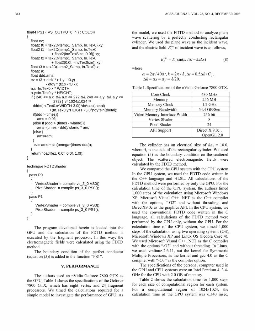
float4 PS1 ( VS_OUTPUT0 In ) : COLOR
float ez; float2 t0 = tex2D(temp1_Samp, In.Tex0).xy; float2 t1 = tex2D(temp1_Samp, In.Tex0
+ float2(invTexSize, 0.0f)).xy; float2 t2 = tex2D(temp1_Samp, In.Tex0
+ float2(0.0f, -invTexSize)).xy; float t3 = tex2D(temp2_Samp, In.Tex0).x; float2 a; float ddd,ams; ez = t3 + dtdx * (t1.y - t0.y)
- dtdy * (t2.x - t0.x); a.x=In.Tex0.x * WIDTH; a.y=In.Tex0.y * HEIGHT; if ( 240 <= a.x && a.x <= 272 && 240 <= a.y && a.y <=
272) /* 1024x1024 */ ddd=(In.Tex0.x*WIDTH-3.0f)*dx*cos(thetai)
+(In.Tex0.y*HEIGHT-3.0f)*dy*sin(thetai); if(ddd > times) ams = 0.0f; else if (ddd > (times - wlamd)) ams=(times - ddd)/wlamd * am; else ams=am; ez=-ams * sin(omega*(times-ddd));
return float4(ez, 0.0f, 0.0f, 1.0f);
technique FDTDShader pass P0 VertexShader = compile vs_3_0 VS0(); PixelShader = compile ps_3_0 PS0(); pass P1 VertexShader = compile vs_3_0 VS0(); PixelShader = compile ps_3_0 PS1();
The program developed herein is loaded into the
GPU and the calculation of the FDTD method is executed by the fragment processor. In this way, the electromagnetic fields were calculated using the FDTD method.
The boundary condition of the perfect conductor (equation (5)) is added in the function “PS1”.
V. PERFORMANCE The authors used an nVidia Geforce 7800 GTX as
the GPU. Table 1 shows the specifications of the Geforce 7800 GTX, which has eight vertex and 24 fragment processors. We timed the calculations required for a simple model to investigate the performance of GPU. As
the model, we used the FDTD method to analyze plane wave scattering by a perfectly conducting rectangular cylinder. We used the plane wave as the incident wave, and the electric field inc
zE of incident wave is as follows,
0 sin( )inczE E t t kx xω= ∆ − ∆ (8)
where
Table 1. Specifications of the nVidia Geforce 7800 GTX.
Core Clock 430 MHz Memory 256 MB
Memory Clock 1.2 GHz Memory Bandwidth 54.4 GB/Sec
Video Memory Interface Width 256 bit Vertex Shader 8 Pixel Shader 24 API Support Direct X 9.0c ,
OpenGL 2.0
The cylinder has an electrical size of kAs = 10.0, where As is the side of the rectangular cylinder. We used equation (5) as the boundary condition on the scattered object. The scattered electromagnetic fields were calculated by the FDTD method.
We compared the GPU system with the CPU system. In the GPU system, we used the FDTD code written in the C++ language and HLSL. All calculations of the FDTD method were performed by only the GPU. For the calculation time of the GPU system, the authors timed 1,000 steps of the calculation using Microsoft Windows XP, Microsoft Visual C++ .NET as the C++ compiler with the options, “-O2” and without threading, and DirectX9.0c as the graphics API. In the CPU system, we used the conventional FDTD code written in the C language, all calculations of the FDTD method were performed by the CPU only, without the GPU. For the calculation time of the CPU system, we timed 1,000 steps of the calculation using two operating systems (OS), Microsoft Windows XP and Linux OS (Fedora Core 4). We used Microsoft Visual C++ .NET as the C compiler with the options “-O2” and without threading. In Linux, we used vmlinuz-2.6.11, not the kernel for Symmetric Multiple Processors, as the kernel and gcc 4.0 as the C compiler with “-O3” as the compiler option.
The specifications of the personal computer used in the GPU and CPU systems were an Intel Pentium 4, 3.4-GHz for the CPU with 2.0 GB of memory.
Table 2 shows the calculation time for 1,000 steps for each size of computational region for each system. For a computational region of 1024×1024, the calculation time of the GPU system was 6,340 msec,
/20.λ=∆=∆=∆ yxh ,/5.0 ,/2 ,40/2 0Chtkt ∆=∆=∆= λππω
313 ACES JOURNAL, VOL. 23, NO. 4, DECEMBER 2008
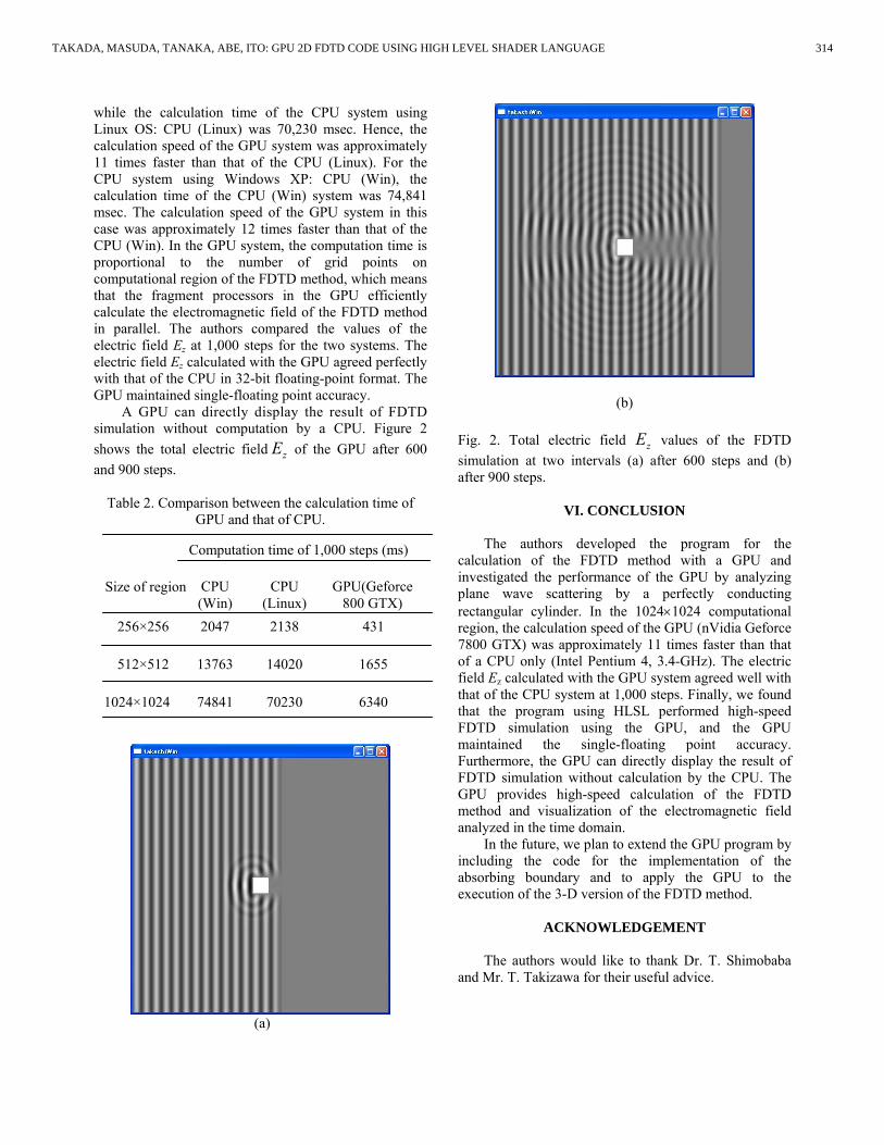
while the calculation time of the CPU system using Linux OS: CPU (Linux) was 70,230 msec. Hence, the calculation speed of the GPU system was approximately 11 times faster than that of the CPU (Linux). For the CPU system using Windows XP: CPU (Win), the calculation time of the CPU (Win) system was 74,841 msec. The calculation speed of the GPU system in this case was approximately 12 times faster than that of the CPU (Win). In the GPU system, the computation time is proportional to the number of grid points on computational region of the FDTD method, which means that the fragment processors in the GPU efficiently calculate the electromagnetic field of the FDTD method in parallel. The authors compared the values of the electric field Ez at 1,000 steps for the two systems. The electric field Ez calculated with the GPU agreed perfectly with that of the CPU in 32-bit floating-point format. The GPU maintained single-floating point accuracy.
A GPU can directly display the result of FDTD simulation without computation by a CPU. Figure 2 shows the total electric field zE of the GPU after 600 and 900 steps.
Table 2. Comparison between the calculation time of GPU and that of CPU.
(a)
(b)
Fig. 2. Total electric field zE values of the FDTD simulation at two intervals (a) after 600 steps and (b) after 900 steps.
VI. CONCLUSION
The authors developed the program for the calculation of the FDTD method with a GPU and investigated the performance of the GPU by analyzing plane wave scattering by a perfectly conducting rectangular cylinder. In the 1024×1024 computational region, the calculation speed of the GPU (nVidia Geforce 7800 GTX) was approximately 11 times faster than that of a CPU only (Intel Pentium 4, 3.4-GHz). The electric field Ez calculated with the GPU system agreed well with that of the CPU system at 1,000 steps. Finally, we found that the program using HLSL performed high-speed FDTD simulation using the GPU, and the GPU maintained the single-floating point accuracy. Furthermore, the GPU can directly display the result of FDTD simulation without calculation by the CPU. The GPU provides high-speed calculation of the FDTD method and visualization of the electromagnetic field analyzed in the time domain.
In the future, we plan to extend the GPU program by including the code for the implementation of the absorbing boundary and to apply the GPU to the execution of the 3-D version of the FDTD method.
ACKNOWLEDGEMENT
The authors would like to thank Dr. T. Shimobaba
and Mr. T. Takizawa for their useful advice.
GPU(Geforce 800 GTX)
Computation time of 1,000 steps (ms)
CPU (Win)
CPU (Linux)
256×256
Size of region
512×512
1024×1024
2047
13763
74841
2138
14020
70230
431
1655
6340
314TAKADA, MASUDA, TANAKA, ABE, ITO: GPU 2D FDTD CODE USING HIGH LEVEL SHADER LANGUAGE

REFERENCES [1] K. S. Yee, “Numerical solution of initial boundary
value problems involving Maxwell´s equations in isotropic media,” IEEE Trans. Antennas Propagat., vol. AP-14, no. 3, pp.302-307, May 1966.
[2] A. Taflove, Computational electrodynamics: the finite difference time domain method, Artech House, Inc., 1995.
[3] K. S. Kunz and R. J. Luebbers, The finite difference time domain method for electromagnetics, CRC Press, Inc., 1993.
[4] T. Namiki, “A new FDTD algorithm based on alternating direction implicit method,” IEEE Trans. Microwave Theory Tech., vol. MTT-47, no. 10, pp.1-5, Oct. 1999.
[5] N. Takada, K. Ando, K. Motojima, T. Ito, and S. Kozaki, “New Distributed implementation of the FDTD method,” Electronics and Communications in Japan, Part 2, vol. 80, no.5, pp.8-16, 1997.
[6] D. P. Rodohan, S. R. Saunders, and R. J. Glover, “A distributed implementation of the finite difference time domain (FDTD) method,” Int. J. Numerical Modeling: Electronic Networks, Devices and Fields, vol. 8, no.3, pp.283-292, 1995.
[7] D. B. Davidson and R. W. Ziolkowski, “A connection machine (CM-2) implementation of three-dimensional parallel finite difference time domain code for electromagnetic field simulation,” Int. J. Numerical Modeling: Electronic Networks, Devices and Fields, vol. 8, no. 3, pp.221-232, 1995.
[8] nVIDIA corporation, “GPU Gems” Addison-Wisley, 2004.
[9] nVIDIA corporation, “GPU Gems 2” Addison-Wisley, 2005.
[10] J. Boltz, I. Farmer, E. Grinspun, P. Schröder, “Sparse matrix solvers on the GPU: Conjugate Gradients and Multigrid,” ACM SIGGRAPH 03 Proceedings, 2003.
[11] C. Tompson, S. Hahn, and M. Oskin, “Using modern graphics architectures for general-purpose computing: a framework and analysis,” Proceedings of the 35th International Symposium on Microarchitecture, pp. 306-320, Nov. 2002.
[12] J. Krüger and R. Westermann, “Linear algebra operators for GPU implementation of numerical algorithms,” ACM SIGGRAPH 03 Proceedings, 2003.
[13] N. Masuda, T. Ito, T. Tanaka, A. Shiraki, and T. Sugie, “Computer generated holography using a graphics processing unit,” Opt. Express, vol. 14, no. 2, pp.587-592, 2006.
[14] M. J. Inman and A. Z. Elsherbeni, “Programming video cards for computational electromagnetics application,” IEEE Antennas and Propagation Magazine, vol. 47, no. 6, pp.71-78, Dec. 2005.
[15] G. S. Baron, C. D. Sarris, and E. Fiume, “Fast and accurate time-domain simulations with commodity graphics hardware,” Proceedings of Antennas and Propagation Society International Symposium, July 2005.
[16] J. Fang, “Time domain finite difference computation for Maxwell’s equation,” Ph. D. thesis, University of California at Berkley, 1989.
Naoki Takada Dr. Takada received his B.E. and M.S. in electrical engineering from Gunma University, Gunma, Japan in 1994 and 1996, respectively, and his Ph.D. in electrical engineering from Gunma University in 2000. From 1996 to June 2001, he was a research
associate at Oyama National College of Technology, Tochigi, Japan. From July 2001 to March 2005, he worked as a research scientist for the High Performance Biocomputing Research Team, Bioinformatics Group, Genomic Science Center (GSC), Institute of Physical and Chemical Research (RIKEN; Yokohama, Japan) and joined the “Protein Explorer Project” for a petaflops special-purpose computer (MDGRAPE-3) system for molecular dynamics simulations of proteins. This project was part of the “Protein 3000 project” supported by the Ministry of Education, Culture, Sports, Science and Technology of Japan. Since April 2005, he has been a lecturer at Sony Institute Higher Education Shohoku College, Atsugi, Japan.
His research interests include GPGPU, distributed and parallel computation including FDTD method, development of a special-purpose computer for FDTD method, numerical simulation including FDTD method, CIP method, and molecular dynamics and electromagnetic theory. He is a member of ACES and IEICE.
Nobuyuki Masuda Dr. Masuda received his BS and MS in System Science from the University of Tokyo (Tokyo, Japan) in 1993 and 1995, respectively, and his Ph.D. in System Science from the University of Tokyo in 1998. From 2000 to March 2004, he was a research associate at Gunma
University (Gunma, Japan). Since April 2004, he has been a research associate at Chiba University (Chiba, Japan). Dr. Masuda’s research interests include development of a special-purpose computer for digital holographic particle tracking velocimetry and computer generated holograms on GPU. He is a member of IEICE, IPSJ and ASJ.
315 ACES JOURNAL, VOL. 23, NO. 4, DECEMBER 2008
Takashi Tanaka Mr. Tanaka received his B.E. in Electronics and Mechanical Engineering from Chiba University (Chiba, Japan) in 2005. He is currently enrolled in the master’s program of the Graduate School of Science and Technology, Chiba University (Chiba, Japan). His research interests GPGPU
and a high-performance computing of computer generated holograms.
Yukio Abe Mr. Abe received his B.E. and M.S. in electrical engineering from Gunma University (Gunma, Japan) in 1996 and 1998, respectively. In 1998, he began his work at NEC Corporation and engaged in the development of the disk-array system. Since 2006, he has been employed at
NEC Co. while pursuing his doctorate at the Graduate School of Science and Technology, Chiba University (Chiba, Japan). His research interests GPGPU and a high-performance computing of a physical simulation.
Tomoyoshi Ito Dr. Ito received B.E., M.S. and Ph.D. from University of Tokyo (Tokyo, Japan) in 1989, 1991 and 1994, respectively. He was a research associate from 1992 to 1994, and an associate professor from 1994 to 1999, at Gunma University (Gunma, Japan). Between 1999 to
2005, Dr. Ito was an associate professor at Chiba University, (Chiba, Japan), and, since 2005, a professor. Dr. Ito’s research interests are in high-performance computing and its various applications. He was an initial member of GRAPE project, which has produced special-purpose computers for astrophysics. He developed the first machine, GRAPE-1, in 1989, followed by GRAPE-2 in 1990, among others. Since 1992, he has also designed and built special-purpose computers for the HORN holography system. He is currently investigating three-dimensional television using HORN computers. Dr. Ito is a member of IEICE.
316TAKADA, MASUDA, TANAKA, ABE, ITO: GPU 2D FDTD CODE USING HIGH LEVEL SHADER LANGUAGE
EM Scattering from Bodies of Revolution using the LocallyCorrected Nystrom Method
In memoriam: Dr. William D. Wood, Jr., 1963-2004.
A. W. Wood and J. L. Fleming
Graduate School of Engineering and Management2950 Hobson Way, AFIT/ENC
Wright-Patterson AFB, Ohio 45433–7765
Abstract – The locally corrected Nystrom method isapplied to the magnetic field integral equation for aconducting body of revolution. A construction methodis presented for the locally corrected weights for theresulting one-dimensional coupled scalar magnetic fieldintegral equations. Special attention is paid to minimizingthe cost for multi-frequency computations. Numericalresults are presented for the sphere, oblate spheroid, andright circular cylinder. Good agreement with results frommature moment method codes is observed.
I. INTRODUCTION
The Locally Corrected Nystrom (LCN) methodbrings the high-order convergence properties of the Nys-trom method for integral equations to those with singularkernels such as those that arise in electromagnetic bound-ary value problems [1–3]. Computation of the correctedquadrature weights can be efficiently accomplished.
Here we apply the LCN method to a body of revo-lution (BOR) under plane wave illumination. The BORgeometry allows the 2D surface integral equation to bereduced to a series of 1D integral equations through theuse of a Fourier series expansion. The solution of each1D problem is a mode function in the series expansion ofthe total current.
Often, we desire to solve electromagnetic scatteringproblems for a fixed geometry over a range of frequencies.In the context of the LCN method, the goal is to computethe corrected weights once and then reuse them for thedesired frequencies and necessary mode numbers. Weshow that careful use of quadrature rules will allow thereuse of corrected weights over a range of frequenciesand mode numbers, greatly enhancing the computationalefficiency of the algorithm.
II. CONVENTIONAL AND LOCALLYCORRECTED NYSTROM METHOD
In the conventional Nystrom method, an integralequation,
g(x) =∫ b
a
G(x, x′)u(x′)dx′ (1)
is replaced by a quadrature equation,
g(x) ≈Ns∑p=1
Na−1∑q=0
ωqG(x, xpq)u(xpq) (2)
where xpq is the qth abscissa on the pth subinterval.Evaluating g(x) at the nth abscissa of the mth subinterval,i.e., each abscissa from the underlying quadrature rule,gives,
g(xmn ) ≈Ns∑p=1
Na−1∑q=0
ωqG(xmn , xpq)u(xpq) (3)
where xpq is the qth abscissa on the pth subinterval.Solving the resultant linear system of equations yieldsthe value of u(x) at the quadrature points. Interpolationprovides u(x) over the integration interval. However, anobvious problem for electromagnetic integral equationsis the singularity of the kernel which makes evaluation atxmn = xqp impossible. In addition, quadrature convergenceis slow when ||xmn − xqp|| << λ.
The LCN replaces some of the quadrature weightsωq by “locally corrected” ones, ωq , which are used whenthe distance between xmn and xqp is small. The details canbe found in the literature [2, 3].
III. MFIE FOR A BOR SCATTERER
The magnetic field integral equation (MFIE) over aPEC BOR geometry can be reduced to a one dimensionalproblem along the curve defining the BOR. Given anincident field ~H
iwe wish to solve the MFIE [4] for the
surface current ~Js,
n× ~Hi(~r) =
12~Js(~r)− n×∫
S
~Js(~r ′)×∇′g(~r,~r ′) ds′, ~r ∈ S(4)
where g(~r,~r ′) = exp(ik|~r − ~r ′|)/[4π|~r − ~r ′|] is thefree space Green function for the Helmholtz equation(assuming e−iωt time dependence) and n is the outwardpointing unit normal vector on the surface S.
317 ACES JOURNAL, VOL. 23, NO. 4, DECEMBER 2008
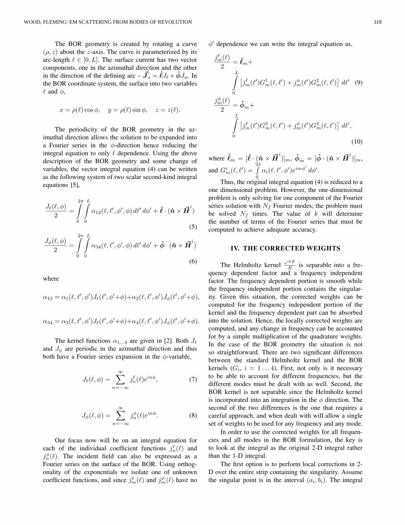
The BOR geometry is created by rotating a curve(ρ, z) about the z-axis. The curve is parameterized by itsarc-length ` ∈ [0, L]. The surface current has two vectorcomponents, one in the azimuthal direction and the otherin the direction of the defining arc – ~Js = ˆJ` + φJφ. Inthe BOR coordinate system, the surface into two variables` and φ,
x = ρ(`) cosφ, y = ρ(`) sinφ, z = z(`).
The periodicity of the BOR geometry in the az-imuthal direction allows the solution to be expanded intoa Fourier series in the φ-direction hence reducing theintegral equation to only ` dependence. Using the abovedescription of the BOR geometry and some change ofvariables, the vector integral equation (4) can be writtenas the following system of two scalar second-kind integralequations [5],
J`(`, φ)2
=
2π∫0
L∫0
α12(`, `′, φ′, φ) d`′ dφ′ + ˆ· (n× ~Hi)
(5)
Jφ(`, φ)2
=
2π∫0
L∫0
α34(`, `′, φ′, φ) d`′ dφ′ + φ · (n× ~Hi)
(6)
where
α12 = α1(`, `′, φ′)J`(`′, φ′+φ)+α2(`, `′, φ′)Jφ(`′, φ′+φ),
α34 = α3(`, `′, φ′)J`(`′, φ′+φ)+α4(`, `′, φ′)Jφ(`′, φ′+φ).
The kernel functions α1...4 are given in [2]. Both J`and Jφ are periodic in the azimuthal direction and thusboth have a Fourier series expansion in the φ-variable,
J`(`, φ) =∞∑
n=−∞j`n(`)einφ, (7)
Jφ(`, φ) =∞∑
n=−∞jφn(`)einφ. (8)
Our focus now will be on an integral equation foreach of the individual coefficient functions j`n(`) andjφn(`). The incident field can also be expressed as aFourier series on the surface of the BOR. Using orthog-onality of the exponentials we isolate one of unknowncoefficient functions, and since j`m(`) and jφm(`) have no
φ′ dependence we can write the integral equation as,
j`m(`)2
= ˆm+
L∫0
[j`m(`′)G1
m(`, `′) + jφm(`′)G2m(`, `′)
]d`′ (9)
jφm(`)2
= φm+
L∫0
[j`m(`′)G3
m(`, `′) + jφm(`′)G4m(`, `′)
]d`′,
(10)
where ˆm = [ˆ · (n × ~H
i)]m, φm = [φ · (n × ~H
i)]m,
and Gim(`, `′) =2π∫0
αi(`, `′, φ′)eimφ′dφ′.
Thus, the original integral equation (4) is reduced to aone dimensional problem. However, the one-dimensionalproblem is only solving for one component of the Fourierseries solution with Nf Fourier modes; the problem mustbe solved Nf times. The value of k will determinethe number of terms of the Fourier series that must becomputed to achieve adequate accuracy.
IV. THE CORRECTED WEIGHTS
The Helmholtz kernel eikR
R is separable into a fre-quency dependent factor and a frequency independentfactor. The frequency dependent portion is smooth whilethe frequency independent portion contains the singular-ity. Given this situation, the corrected weights can becomputed for the frequency independent portion of thekernel and the frequency dependent part can be absorbedinto the solution. Hence, the locally corrected weights arecomputed, and any change in frequency can be accountedfor by a simple multiplication of the quadrature weights.In the case of the BOR geometry the situation is notso straightforward. There are two significant differencesbetween the standard Helmholtz kernel and the BORkernels (Gi, i = 1 . . . 4). First, not only is it necessaryto be able to account for different frequencies, but thedifferent modes must be dealt with as well. Second, theBOR kernel is not separable since the Helmholtz kernelis incorporated into an integration in the φ direction. Thesecond of the two differences is the one that requires acareful approach, and when dealt with will allow a singleset of weights to be used for any frequency and any mode.
In order to use the corrected weights for all frequen-cies and all modes in the BOR formulation, the key isto look at the integral as the original 2-D integral ratherthan the 1-D integral.
The first option is to perform local corrections in 2-D over the entire strip containing the singularity. Assumethe singular point is in the interval (ai, bi). The integral
318WOOD, FLEMING: EM SCATTERING FROM BODIES OF REVOLUTION
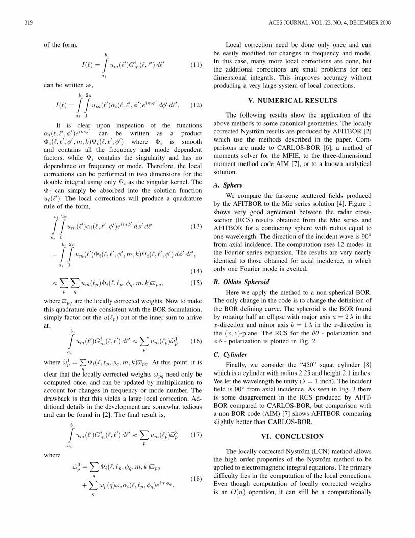
of the form,
I(`) =
bi∫ai
um(`′)Gim(`, `′) d`′ (11)
can be written as,
I(`) =
bi∫ai
2π∫0
um(`′)αi(`, `′, φ′)eimφ′dφ′ d`′. (12)
It is clear upon inspection of the functionsαi(`, `′, φ′)eimφ
′can be written as a product
Φi(`, `′, φ′,m, k)Ψi(`, `′, φ′) where Φi is smoothand contains all the frequency and mode dependentfactors, while Ψi contains the singularity and has nodependance on frequency or mode. Therefore, the localcorrections can be performed in two dimensions for thedouble integral using only Ψi as the singular kernel. TheΦi can simply be absorbed into the solution functionui(`′). The local corrections will produce a quadraturerule of the form,
bi∫ai
2π∫0
um(`′)αi(`, `′, φ′)eimφ′dφ′ d`′ (13)
=
bi∫ai
2π∫0
um(`′)Φi(`, `′, φ′,m, k)Ψi(`, `′, φ′) dφ′ d`′,
(14)
≈∑p
∑q
um(`p)Φi(`, `p, φq,m, k)ωpq, (15)
where ωpq are the locally corrected weights. Now to makethis quadrature rule consistent with the BOR formulation,simply factor out the u(`p) out of the inner sum to arriveat,
bi∫ai
um(`′)Gim(`, `′) d`′ ≈∑p
um(`p)ω1p (16)
where ω1p =
∑q
Φi(`, `p, φq,m, k)ωpq . At this point, it is
clear that the locally corrected weights ωpq need only becomputed once, and can be updated by multiplication toaccount for changes in frequency or mode number. Thedrawback is that this yields a large local correction. Ad-ditional details in the development are somewhat tediousand can be found in [2]. The final result is,
bi∫ai
um(`′)Gim(`, `′) d`′ ≈∑p
um(`p)ω3p (17)
where
ω3p =
∑q
Φi(`, `p, φq,m, k)ωpq
+∑q
ωp(q)ωqαi(`, `p, φq)eimφq .(18)
Local correction need be done only once and canbe easily modified for changes in frequency and mode.In this case, many more local corrections are done, butthe additional corrections are small problems for onedimensional integrals. This improves accuracy withoutproducing a very large system of local corrections.
V. NUMERICAL RESULTS
The following results show the application of theabove methods to some canonical geometries. The locallycorrected Nystrom results are produced by AFITBOR [2]which use the methods described in the paper. Com-parisons are made to CARLOS-BOR [6], a method ofmoments solver for the MFIE, to the three-dimensionalmoment method code AIM [7], or to a known analyticalsolution.
A. SphereWe compare the far-zone scattered fields produced
by the AFITBOR to the Mie series solution [4]. Figure 1shows very good agreement between the radar cross-section (RCS) results obtained from the Mie series andAFITBOR for a conducting sphere with radius equal toone wavelength. The direction of the incident wave is 90
from axial incidence. The computation uses 12 modes inthe Fourier series expansion. The results are very nearlyidentical to those obtained for axial incidence, in whichonly one Fourier mode is excited.
B. Oblate SpheroidHere we apply the method to a non-spherical BOR.
The only change in the code is to change the definition ofthe BOR defining curve. The spheroid is the BOR foundby rotating half an ellipse with major axis a = 2λ in thex-direction and minor axis b = 1λ in the z-direction inthe (x, z)-plane. The RCS for the θθ - polarization andφφ - polarization is plotted in Fig. 2.
C. CylinderFinally, we consider the “450” squat cylinder [8]
which is a cylinder with radius 2.25 and height 2.1 inches.We let the wavelength be unity (λ = 1 inch). The incidentfield is 90 from axial incidence. As seen in Fig. 3 thereis some disagreement in the RCS produced by AFIT-BOR compared to CARLOS-BOR, but comparison witha non BOR code (AIM) [7] shows AFITBOR comparingslightly better than CARLOS-BOR.
VI. CONCLUSION
The locally corrected Nystrom (LCN) method allowsthe high order properties of the Nystrom method to beapplied to electromagnetic integral equations. The primarydifficulty lies in the computation of the local corrections.Even though computation of locally corrected weightsis an O(n) operation, it can still be a computationally
319 ACES JOURNAL, VOL. 23, NO. 4, DECEMBER 2008
(a)
(b)
Fig. 1. Bistatic RCS of a unit sphere with λ = 1 andangle of incidence 90. φφ-polarized data are shown onthe top while θθ-polarized data are shown on the bottom.
intensive procedure, so it is highly desirable to computethe corrected weights only when necessary. The paperhas shown how to use a set of local corrections on afixed geometry for a range of frequencies and a range ofmodes in a modal expansion for a body of revolution.
REFERENCES
[1] S. Gedney, “Application of the high-order Nystromscheme to the integral equation solution of electro-magnetic interaction problems,” in Proceedings of theIEEE International Symposium on ElectromagneticCompatibility, vol. 1, pp. 289–294, IEEE, 2000.
[2] J. Fleming, A. Wood, and W. Wood, “Locally cor-rected Nystrom method for EM scattering by bodies
Fig. 2. Bistatic θθ-pol and φφ-pol RCS from AFITBORfor an oblate spheroid with λ = 1 and angle of incidenceθinc = 30.
Fig. 3. Bistatic φφ-pol RCS from AFITBOR, CARLOS-BOR and AIM for a 450 cylinder with λ = 1 and θinc =90.
of revolution,” Journal of Computational Physics,vol. 196, pp. 41–52, 2004.
[3] L. Canino, J. Ottusch, M. Stalzer, J. Visher, andS. Wandzura, “Numerical solution of the Helmholtzequation in 2D and 3D using a high-order Nystromdiscretization,” Journal of Computational Physics,vol. 146, no. 2, pp. 627–663, 1998.
[4] J. Bowman, T. Senior, and P. Uslenghi, Electro-magnetic and Acoustic Scattering by Simple Shapes.North Holland: Amsterdam, 1969.
[5] J. R. Mautz and R. F. Harrington, “H-field, E-fieldand combined field solutions for bodies of revolu-tion,” Technical Report RADC-TR-77-109, SyracuseUniversity, Syracuse NY, 1977.
320WOOD, FLEMING: EM SCATTERING FROM BODIES OF REVOLUTION

[6] L. Medgyesi-Mitschang and J. Putnam, “Electromag-netic scattering from axially inhomogeneous bodiesof revolution,” IEEE Trans. Ant. Propagat., vol. AP–32, pp. 797–806, Aug. 1984.
[7] E. Bleszynski, M. Bleszynski, and T. Jaroszewicz,“AIM: Adaptive integral method for solving large-scale electromagnetic scattering and radiation prob-lems,” Radio Science, vol. 31, no. 5, pp. 1225–1252,1996.
[8] B. M. Kent and W. D. Wood, “The squat cylinder andmodified bicone primary static RCS range calibrationstandards,” in Antenna Measurement Techniques As-sociation Symposium, vol. 2, (Boston MA), pp. 567–74, Nov. 1997.
The views expressed in this article are those of theauthors and do not reflect the official policy or positionof the United States Air Force, Department of Defense, orthe US Government.
Aihua W. Wood received her B.S. degree from PekingUniversity, Beijing, China in 1984, and the M.S. andPh.D. degrees from the University of Connecticut, Storrs,CT in 1988 and 1990, respectively. She was a VisitingAssistant Professor of mathematics at the Naval Postgrad-uate School from 1990 - 1993, and Assistant Professorat Penn State - Erie from 1993 -1994. She joined thefaculty at the Air Force Institute of Technology at Wright-Patterson AFB, OH in 1994 and is currently a Professorof Mathematics. Dr. Wood’s current research interestsinclude analytical and numerical analysis of electromag-netic scattering by cavities, wave propagation in complexmedia, and elliptic PDEs.
John F. Fleming received his B.A. degree from HiramCollege, OH in 1995, and Ph.D. degree from MichiganState University, Est Lansing, MI in 2001. He was Re-search Associate at the Air Force Institute of Technology,WPAFB, OH from 2001 - 2004. He has been an AssistantProfessor of mathematics at Duquesne University, Pitts-burgh, PA since 2004.
321 ACES JOURNAL, VOL. 23, NO. 4, DECEMBER 2008
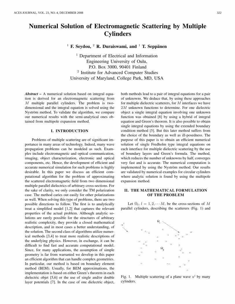
Numerical Solution of Electromagnetic Scattering by MultipleCylinders
1 F. Seydou, 2 R. Duraiswami, and 1 T. Seppanen
1 Department of Electrical and InformationEngineering University of Oulu,
P.O. Box 3000, 90401 Finland2 Institute for Advanced Computer Studies
University of Maryland, College Park, MD, USA
Abstract – A numerical solution based on integral equa-tion is derived for an electromagnetic scattering fromM multiple parallel cylinders. The problem is two-dimensional and the integral equation is solved using theNystrom method. To validate the algorithm, we compareour numerical results with the semi-analytical ones ob-tained from multipole expansion method.
I. INTRODUCTION
Problems of multiple scattering are of significant im-portance in many areas of technology. Indeed, many wavepropagation problems can be modeled as such. Exam-ples include electromagnetic and optical communication,imaging, object characterization, electronic and opticalcomponents, etc. Hence, the development of efficient andaccurate numerical simulation for such problems is highlydesirable. In this paper we discuss an efficient com-putational algorithm for the problem of approximatingthe scattered electromagnetic field from two dimensionalmultiple parallel dielectrics of arbitrary cross-sections. Forthe sake of clarity, we only consider the TM polarizationcase. The method caries out easily for other polarizationsas well. When solving this type of problems, there are twopossible directions to follow. The first is to analyticallytreat a simplified model [1,2] that captures the relevantproperties of the actual problem. Although analytic so-lutions are rarely possible for the structures of arbitraryrealistic complexity, they provide a closed mathematicaldescription, and in most cases a better understanding, ofthe solution. The second class of algorithms utilize numer-ical methods [3,4] to treat more realistic descriptions ofthe underlying physics. However, in exchange, it can bedifficult to find fast and accurate computational model.Since, for many applications, the assumption of simplegeometry is far from warranted we develop in this paperan efficient algorithm that can handle complex geometries.In particular, our method is based on boundary elementmethod (BEM). Usually, for BEM approximations, theimplementation is based on either Green’s theorem in eachdielectric objet [5,6] or the use of single and/or doublelayer potentials [7]. In the case of one dielectric object,
both methods lead to a pair of integral equations for a pairof unknowns. We deduce that, by using these approachesfor multiple dielectric scatterers, for M interfaces we have2M unknown functions to determine. For one dielectricobject a single integral equation involving one unknownfunction was obtained [8] by using a hybrid of integralequation and Green’s theorem. It is also possible to obtainsingle integral equations by using the extended boundarycondition method [5]. But this later method suffers fromthe choice of the boundary as well as ill-posedness. Thepurpose of this paper is to obtain an efficient numericalsolution of single Fredholm type integral equations oneach interface for multiple dielectric scattering by the useof boundary layers and Green’s formula. The method,which reduces the number of unknowns by half, convergesvery fast and is accurate. The numerical computation isimplemented by using the Nystrom method. Our resultsare validated by numerical examples for circular cylinderswhere analytic solution is found by using the multipoleexpansion method.
II. THE MATHEMATICAL FORMULATIONOF THE PROBLEM
Let Ωl, l = 1, 2, · · ·M, be the cross-sections of Mparallel cylinders, describing the scatterers (Fig. 1) and
Fig. 1. Multiple scattering of a plane wave ui by manycylinders.
322ACES JOURNAL, VOL. 23, NO. 4, DECEMBER 2008

Let Γl be the boundary of Ωl. The unit outward normalν to Γl is assumed to be directed towards the exterior.We denote the field outside (in the air) as Ω0, i,e. Ω0 =R2\ ∪Ml=1 (Ωl).
For simplicity we consider an s-polarized field inci-dent upon the dielectric (nonmagnetic) cylinders of cross-sections Ωl, with the electric field parallel to the x3−axis.But generalization to other polarizations and materialsdoes not present any difficulty.
Each domain Ωl l = 0, 1, · · ·M, has permittivityεl. The scatterers are assumed to be illuminated by anincident field Ei which is a plane wave with directiond and angle α, i.e. d = (cosα, sinα). With use ofa time dependence in e−jωt (ω is the frequency andj =√−1), the incident electric field is given, for every
point x = (x1, x2), by,
Ei(x) = ejω√ε0x·d.
Then (cf. [1]) we have to solve the Helmholtz equa-tion in each dielectric object Ωl, l = 1, 2, · · ·M and inthe outer region Ω0,
(∇2 + κ2l )El = 0 in Ωl, l = 0, · · · ,M
where the wave numbers κl are given by κl = ω√εl.
For l = 1, 2, · · ·M , the electric field El represents E inΩl, and in Ω0 we have E = E0 + Ei, where E0 is thescattered electric field.
In addition, E0 must satisfy the Sommerfeld radiationcondition, i.e.,
lim|x|→∞
|x|1/2(∂E0
∂|x|− jκ0E0
)= 0..
We denote the fundamental solution to the Helmholtzequations (the free-space source) by,
Φk(x,y) = − j2H
(1)0 (κk|x− y|), k = 0, 1, · · · ,M
where H(1)0 is the Hankel function of the first kind
and order zero. We use the factor j/2 (instead of thestandard j/4) for convenience in the derivation of theintegral equations below. In the sequel we shall assumethat ε0 = 1.
III. THE INTEGRAL EQUATION APPROACHTO SOLVE THE PROBLEM
We would like to obtain a set of M equations withM unknowns on each boundary Γl of Ωl, l = 1, · · · ,M .Now, for k = 0, 1, · · ·M, l = 1, 2, · · · ,M and (density)functions φl, ψl, define the single and double layer poten-tials,
Slkφl(x) =∫
Γl
Φk(x,y)φl(y) ds(y), x ∈ R2\Γl
and
Dlkψl(x) =
∫Γl
∂
∂ν(y)Φk(x,y)ψl(y) ds(y),x ∈ R2\Γl,
respectively. Their normal derivatives at some point on aboundary Γm, m 6= l, are given by,
M l,mk φl(x) =
∂
∂ν(x)Slkφl(x), x ∈ Γm
and
N l,mk ψl(x) =
∂
∂ν(x)Dlkψl(x), x ∈ Γm.
Accordingly we shall denote Sl,mk φl(x) and Dl,mk ψl(x)
the values of Slkφl(x) and Dlkψl(x) when x belongs to
Γm, m 6= l.It is known (cf. [9] Sections 2.4 and 2.5) that when
x approaches Γl, Slk and N lk are continuous whereas Dl
k
and M lk exhibit jumps. In particular,
Slk = Slk, Nlk = N l
k, Dlk = Dl
k ∓ I,M lk = M l
k ± I (1)
where the upper (lower) sign corresponds to the limitwhen x approaches Γl from outside (inside) and I is theidentity operator. The hats on the operators mean the casewhen x ∈ Γl.
To arrive at the desired integral equation we definea layer ansatz (a combination of single and double layerpotentials) in Ωl, l = 1, 2, · · · ,M , and apply Green’stheorem in Ω0. So, for l = 1, 2, · · · ,M, let,
El =(−jρlSll +Dl
l
)φl(x) x ∈ Ωl
where ρl are arbitrary nonzero complex numbers.We have, by jump relations (1),
El = P ll φl∂∂νEl = Qllφl
on Γl (2)
where P ll = −jρlSll + (I + Dll) and Qll = −jρl(−I +
M ll ) + N l
l .In the exterior region, we use Green’s theorem to
obtain (cf. [9] pp. 68-70),E0(x) =
∑Ml=1
(Sl0
∂∂νE(x)−Dl
0E(x)),x ∈ Ω0,
f(x) =∑Ml=1
(Dl
0E(x)− Sl0 ∂∂νE(x)
),x ∈ R2\Ω0,
(3)where f = 2Ei.
Now, using the jump relations (1), we obtain thesecond equation in the system (3) on Γl, l = 1, 2, · · ·M .Using the boundary conditions, and substituting El and∂El/∂ν (given in equation (2)) into these equations wearrive at a set of M integral equations with M unknownsφl on Γl, l = 1, 2, · · · ,M ,
f = Al0φl −M∑
m=1,m6=l
Am,l0 φm on Γl (4)
whereAl0 =
((Dl
0 − I)P ll − Sl0Qll),
and
Am,l0 =M∑
m=1,m6=l
((Dl,m
0 − I)P ll − Sl,m0 Qll
).
323 ACES JOURNAL, VOL. 23, NO. 4, DECEMBER 2008
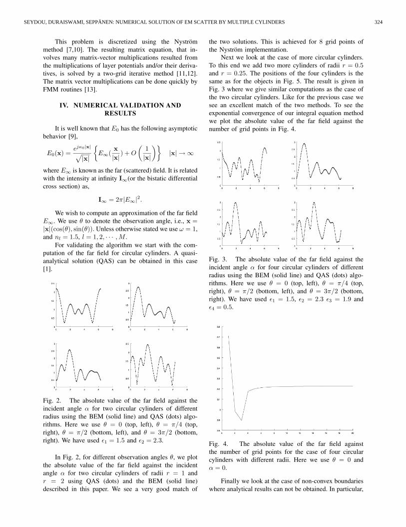
This problem is discretized using the Nystrommethod [7,10]. The resulting matrix equation, that in-volves many matrix-vector multiplications resulted fromthe multiplications of layer potentials and/or their deriva-tives, is solved by a two-grid iterative method [11,12].The matrix vector multiplications can be done quickly byFMM routines [13].
IV. NUMERICAL VALIDATION ANDRESULTS
It is well known that E0 has the following asymptoticbehavior [9],
E0(x) =ejκ0|x|√|x|
E∞(
x|x|
) +O
(1|x|
)|x| → ∞
where E∞ is known as the far (scattered) field. It is relatedwith the intensity at infinity I∞(or the bistatic differentialcross section) as,
I∞ = 2π|E∞|2.
We wish to compute an approximation of the far fieldE∞. We use θ to denote the observation angle, i.e., x =|x|(cos(θ), sin(θ)). Unless otherwise stated we use ω = 1,and nl = 1.5, l = 1, 2, · · · ,M .
For validating the algorithm we start with the com-putation of the far field for circular cylinders. A quasi-analytical solution (QAS) can be obtained in this case[1].
Fig. 2. The absolute value of the far field against theincident angle α for two circular cylinders of differentradius using the BEM (solid line) and QAS (dots) algo-rithms. Here we use θ = 0 (top, left), θ = π/4 (top,right), θ = π/2 (bottom, left), and θ = 3π/2 (bottom,right). We have used ε1 = 1.5 and ε2 = 2.3.
In Fig. 2, for different observation angles θ, we plotthe absolute value of the far field against the incidentangle α for two circular cylinders of radii r = 1 andr = 2 using QAS (dots) and the BEM (solid line)described in this paper. We see a very good match of
the two solutions. This is achieved for 8 grid points ofthe Nystrom implementation.
Next we look at the case of more circular cylinders.To this end we add two more cylinders of radii r = 0.5and r = 0.25. The positions of the four cylinders is thesame as for the objects in Fig. 5. The result is given inFig. 3 where we give similar computations as the case ofthe two circular cylinders. Like for the previous case wesee an excellent match of the two methods. To see theexponential convergence of our integral equation methodwe plot the absolute value of the far field against thenumber of grid points in Fig. 4.
Fig. 3. The absolute value of the far field against theincident angle α for four circular cylinders of differentradius using the BEM (solid line) and QAS (dots) algo-rithms. Here we use θ = 0 (top, left), θ = π/4 (top,right), θ = π/2 (bottom, left), and θ = 3π/2 (bottom,right). We have used ε1 = 1.5, ε2 = 2.3 ε3 = 1.9 andε4 = 0.5.
Fig. 4. The absolute value of the far field againstthe number of grid points for the case of four circularcylinders with different radii. Here we use θ = 0 andα = 0.
Finally we look at the case of non-convex boundarieswhere analytical results can not be obtained. In particular,
324SEYDOU, DURAISWAMI, SEPPÄNEN: NUMERICAL SOLUTION OF EM SCATTER BY MULTIPLE CYLINDERS
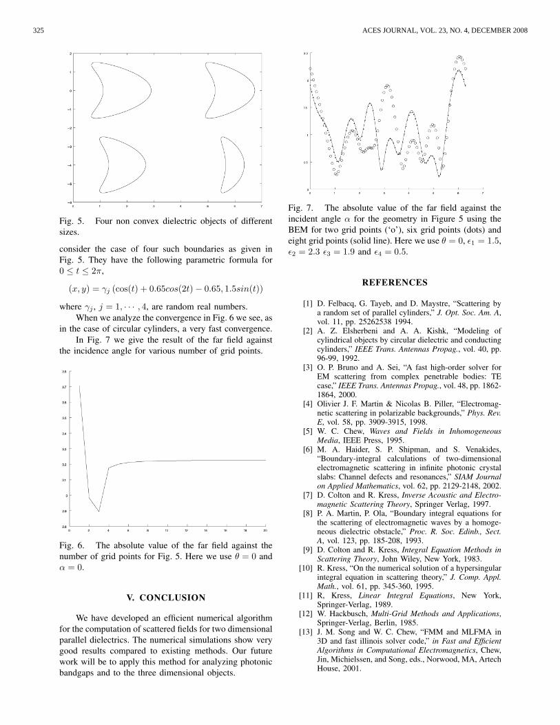
Fig. 5. Four non convex dielectric objects of differentsizes.
consider the case of four such boundaries as given inFig. 5. They have the following parametric formula for0 ≤ t ≤ 2π,
(x, y) = γj (cos(t) + 0.65cos(2t)− 0.65, 1.5sin(t))
where γj , j = 1, · · · , 4, are random real numbers.When we analyze the convergence in Fig. 6 we see, as
in the case of circular cylinders, a very fast convergence.In Fig. 7 we give the result of the far field against
the incidence angle for various number of grid points.
Fig. 6. The absolute value of the far field against thenumber of grid points for Fig. 5. Here we use θ = 0 andα = 0.
V. CONCLUSION
We have developed an efficient numerical algorithmfor the computation of scattered fields for two dimensionalparallel dielectrics. The numerical simulations show verygood results compared to existing methods. Our futurework will be to apply this method for analyzing photonicbandgaps and to the three dimensional objects.
Fig. 7. The absolute value of the far field against theincident angle α for the geometry in Figure 5 using theBEM for two grid points (‘o’), six grid points (dots) andeight grid points (solid line). Here we use θ = 0, ε1 = 1.5,ε2 = 2.3 ε3 = 1.9 and ε4 = 0.5.
REFERENCES
[1] D. Felbacq, G. Tayeb, and D. Maystre, “Scattering bya random set of parallel cylinders,” J. Opt. Soc. Am. A,vol. 11, pp. 25262538 1994.
[2] A. Z. Elsherbeni and A. A. Kishk, “Modeling ofcylindrical objects by circular dielectric and conductingcylinders,” IEEE Trans. Antennas Propag., vol. 40, pp.96-99, 1992.
[3] O. P. Bruno and A. Sei, “A fast high-order solver forEM scattering from complex penetrable bodies: TEcase,” IEEE Trans. Antennas Propag., vol. 48, pp. 1862-1864, 2000.
[4] Olivier J. F. Martin & Nicolas B. Piller, “Electromag-netic scattering in polarizable backgrounds,” Phys. Rev.E, vol. 58, pp. 3909-3915, 1998.
[5] W. C. Chew, Waves and Fields in InhomogeneousMedia, IEEE Press, 1995.
[6] M. A. Haider, S. P. Shipman, and S. Venakides,“Boundary-integral calculations of two-dimensionalelectromagnetic scattering in infinite photonic crystalslabs: Channel defects and resonances,” SIAM Journalon Applied Mathematics, vol. 62, pp. 2129-2148, 2002.
[7] D. Colton and R. Kress, Inverse Acoustic and Electro-magnetic Scattering Theory, Springer Verlag, 1997.
[8] P. A. Martin, P. Ola, “Boundary integral equations forthe scattering of electromagnetic waves by a homoge-neous dielectric obstacle,” Proc. R. Soc. Edinb., Sect.A, vol. 123, pp. 185-208, 1993.
[9] D. Colton and R. Kress, Integral Equation Methods inScattering Theory, John Wiley, New York, 1983.
[10] R. Kress, “On the numerical solution of a hypersingularintegral equation in scattering theory,” J. Comp. Appl.Math., vol. 61, pp. 345-360, 1995.
[11] R, Kress, Linear Integral Equations, New York,Springer-Verlag, 1989.
[12] W. Hackbusch, Multi-Grid Methods and Applications,Springer-Verlag, Berlin, 1985.
[13] J. M. Song and W. C. Chew, “FMM and MLFMA in3D and fast illinois solver code,” in Fast and EfficientAlgorithms in Computational Electromagnetics, Chew,Jin, Michielssen, and Song, eds., Norwood, MA, ArtechHouse, 2001.
325 ACES JOURNAL, VOL. 23, NO. 4, DECEMBER 2008
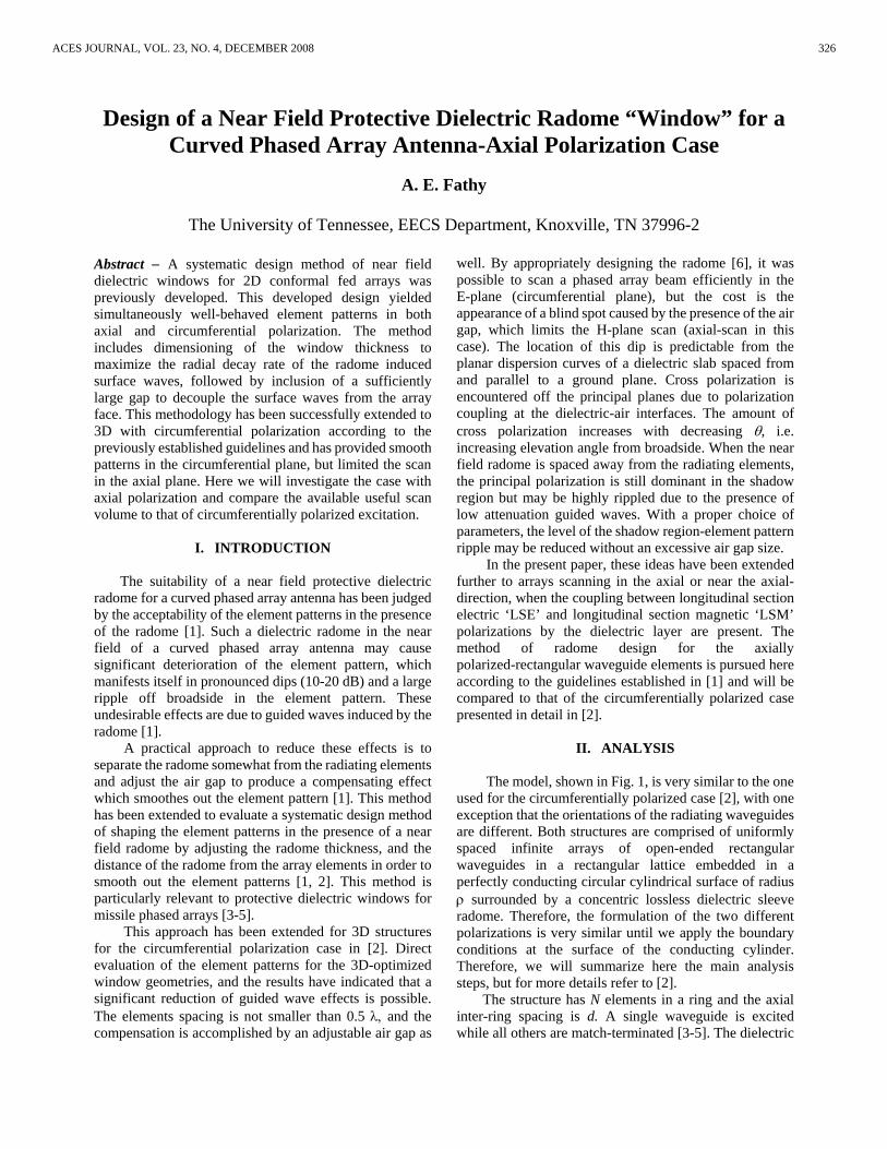
Design of a Near Field Protective Dielectric Radome “Window” for a Curved Phased Array Antenna-Axial Polarization Case
A. E. Fathy
The University of Tennessee, EECS Department, Knoxville, TN 37996-2
Abstract − A systematic design method of near field dielectric windows for 2D conformal fed arrays was previously developed. This developed design yielded simultaneously well-behaved element patterns in both axial and circumferential polarization. The method includes dimensioning of the window thickness to maximize the radial decay rate of the radome induced surface waves, followed by inclusion of a sufficiently large gap to decouple the surface waves from the array face. This methodology has been successfully extended to 3D with circumferential polarization according to the previously established guidelines and has provided smooth patterns in the circumferential plane, but limited the scan in the axial plane. Here we will investigate the case with axial polarization and compare the available useful scan volume to that of circumferentially polarized excitation.
I. INTRODUCTION
The suitability of a near field protective dielectric
radome for a curved phased array antenna has been judged by the acceptability of the element patterns in the presence of the radome [1]. Such a dielectric radome in the near field of a curved phased array antenna may cause significant deterioration of the element pattern, which manifests itself in pronounced dips (10-20 dB) and a large ripple off broadside in the element pattern. These undesirable effects are due to guided waves induced by the radome [1].
A practical approach to reduce these effects is to separate the radome somewhat from the radiating elements and adjust the air gap to produce a compensating effect which smoothes out the element pattern [1]. This method has been extended to evaluate a systematic design method of shaping the element patterns in the presence of a near field radome by adjusting the radome thickness, and the distance of the radome from the array elements in order to smooth out the element patterns [1, 2]. This method is particularly relevant to protective dielectric windows for missile phased arrays [3-5].
This approach has been extended for 3D structures for the circumferential polarization case in [2]. Direct evaluation of the element patterns for the 3D-optimized window geometries, and the results have indicated that a significant reduction of guided wave effects is possible. The elements spacing is not smaller than 0.5 λ, and the compensation is accomplished by an adjustable air gap as
well. By appropriately designing the radome [6], it was possible to scan a phased array beam efficiently in the E-plane (circumferential plane), but the cost is the appearance of a blind spot caused by the presence of the air gap, which limits the H-plane scan (axial-scan in this case). The location of this dip is predictable from the planar dispersion curves of a dielectric slab spaced from and parallel to a ground plane. Cross polarization is encountered off the principal planes due to polarization coupling at the dielectric-air interfaces. The amount of cross polarization increases with decreasing θ, i.e. increasing elevation angle from broadside. When the near field radome is spaced away from the radiating elements, the principal polarization is still dominant in the shadow region but may be highly rippled due to the presence of low attenuation guided waves. With a proper choice of parameters, the level of the shadow region-element pattern ripple may be reduced without an excessive air gap size.
In the present paper, these ideas have been extended further to arrays scanning in the axial or near the axial- direction, when the coupling between longitudinal section electric ‘LSE’ and longitudinal section magnetic ‘LSM’ polarizations by the dielectric layer are present. The method of radome design for the axially polarized-rectangular waveguide elements is pursued here according to the guidelines established in [1] and will be compared to that of the circumferentially polarized case presented in detail in [2].
II. ANALYSIS
The model, shown in Fig. 1, is very similar to the one
used for the circumferentially polarized case [2], with one exception that the orientations of the radiating waveguides are different. Both structures are comprised of uniformly spaced infinite arrays of open-ended rectangular waveguides in a rectangular lattice embedded in a perfectly conducting circular cylindrical surface of radius ρ surrounded by a concentric lossless dielectric sleeve radome. Therefore, the formulation of the two different polarizations is very similar until we apply the boundary conditions at the surface of the conducting cylinder. Therefore, we will summarize here the main analysis steps, but for more details refer to [2].
The structure has N elements in a ring and the axial inter-ring spacing is d. A single waveguide is excited while all others are match-terminated [3-5]. The dielectric
326ACES JOURNAL, VOL. 23, NO. 4, DECEMBER 2008
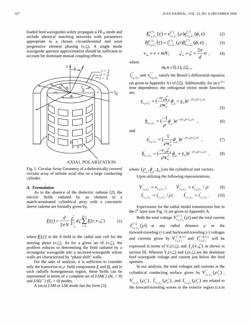
loaded feed waveguides solely propagate a TE10 mode and include identical matching networks with parameters appropriate to a chosen circumferential and axial progressive element phasing (ν,ζ). A single mode waveguide aperture approximation should be sufficient to account for dominant mutual coupling effects.
Fig. 1. Circular Array Geometry of a dielectrically covered circular array of infinite axial slits on a large conducting cylinder. A. Formulation
As in the absence of the dielectric radome [2], the electric fields radiated by an element in a match-terminated cylindrical array with a concentric sleeve radome are formally given by,
1
0
( ) ( , , ),2
Nd
d
dE r d E r
N
π
πν
ζ ν ζπ
−
−=
= ∑∫ (1)
where )(rE is the E-field in the radial unit cell for the steering phase (ν,ζ). As for a given set of (ν,ζ), the problem reduces to determining the field radiated by a rectangular waveguide into a sectored-waveguide whose walls are characterized by “phase shift" walls.
For the sake of analysis, it is sufficient to consider only the transverse to ρ field components E and H, and in each radially homogeneous region, these fields can be represented in terms of a complete set of LSM(`) (Hz = 0) and LSE(``) (Ez = 0) modes.
A (m,n) LSM or LSE mode has the form [3],
(',")(',") (',"),, ,( ) ( ) ( , )
m nm n m nE r v e zν ζν ζ ν ζ ρ φ= (2)
(',")(',") (',"),, ,( ) ( ) ( , )
m nm n m nH r i h zν ζν ζ ν ζ ρ φ= , (3)
2;m nmN ndπν ν ζ ζ= + = + , (4)
where , 0, 1, 2,...m n = ± ±
',",m n
iν ς and ',",m n
vν ς satisfy the Bessel’s differential equation
(as given in Appendix A1 of [2]). Additionally, for an e jω t time dependence, the orthogonal vector mode functions are,
' ( ), 2( ) m n
m n
j zm noo
n
e z e ν φ ζν ζ
ν ζ φρκ
− +−= +
(5)
' ( ),
1( ) m n
m n
j zo
h e ν φ ζν ζ φ
ρ− +−
= , (6)
and " ( )
, 2
1( ) m n
m n
j zo
n
e e ν φ ζν ζ φ
ρκ− += , (7)
" ( ), 2 0
( ) m n
m n
j zm no
n
h z e ν φ ζν ζ
ν ζ φρκ
− +−= + , (8)
where ( , , )oo o
zρ φ are the cylindrical unit vectors.
Upon utilizing the following representations,
ρζνζνζνζν /; ",
",
',
', nmnmnmnm
vVvV == (9) "
,"
,'
,'
, ;/nmnmnmnm
iIiI ζνςνζνζν ρ == . (10) Expressions for the radial modal transmission line in
the ith layer (see Fig. 1) are given in Appendix A. Both the total voltage V
m nν ζ ρ,(",') ( ) and the total current
Im nν ζ ρ,
(",') ( ) at any radial distance ρ or the forward-traveling (+) and backward-traveling (-) voltages and currents given by V
m n
iν ζ,(",')( )± and I
m n
iν ζ,(",')( )± will be
expressed in terms of Vo(ν,ζ), and Io ( , )ν ζ as shown in section III. Wherein Vo(ν,ζ) and Io(ν,ζ) are the dominant feed waveguide voltage and current just below the feed aperture.
In our analysis, the total voltages and currents at the cylindrical conducting surface given by V
m n oν ς ρ," ( )+ ,
', ( )
m n oVν ζ ρ + , ", ( )
m n oIν ζ ρ + , and ', ( )
m n oIν ζ ρ + are related to the forward-traveling waves in the exterior region (i.e.in
327 ACES JOURNAL, VOL. 23, NO. 4, DECEMBER 2008

layer i=3) given by the unknowns Im nν ζ,
"( )+3 and Vm nν ζ,'( )+3 .
This relationship is determined by using the boundary conditions at the various air-dielectric interfaces at ρ1 and ρ2, the transmission of both the LSM and LSE modes across the two layers i.e. i=1 and i=2, and the radiation condition at ρ → ∞. The various mode transmission and coupling through the two dielectric layers and their associated coupling at the air-dielectric interfaces at ρ1 and ρ2 are expressed by an overall transmission matrix T12 as shown by equation (11), and the T12 matrix elements are given in Appendix B,
" "( 3) " (2) '
, , 3 3 2
" "( 3) (2), , 3 2
12' '( 3) (2), , 3 2
' '( 3) ' (2) ', , 3 3 2
( ) ( )
( ) ( )
( ) ( )
( ) ( )
m n m n m
m n m n m
m n m n m
m n m n m
o n n
o n
o n
o n n
V I Z H
I I HT
V V H
I V Y H
ν ς ν ζ ν
ν ζ ν ζ ν
ν ζ ν ζ ν
ν ζ ν ζ ν
ρ κ ρ
ρ κ ρ
ρ κ ρ
ρ κ ρ
+ +
+ +
+ +
+ +
⎡ ⎤ ⎡ ⎤⎢ ⎥ ⎢ ⎥⎢ ⎥ ⎢ ⎥
=⎢ ⎥ ⎢ ⎥⎢ ⎥ ⎢ ⎥⎢ ⎥ ⎢ ⎥⎣ ⎦ ⎣ ⎦
(11)
where expressions for "3nZ and '
3nY are given in Appendix
A, and (1,2) ( )nH x is Hankel function of order n, type 1 or 2, and argument x .
III. ACTIVE ADMITTANCE FOR AXIAL POLARIZATION
The single mode aperture approximation, for an
axially polarized feed waveguide aperture, requires that in the unit cell,
,( ) 0
m n oEν ζφ ρ = . (11)
Therefore equations (2) and (10) imply,
V Vm n m no
n m
n ooν ζ ν ζρ ζ ν
κ ρρ,
",
'( ) ( )+ +=1
2 . (12)
Matching the tangential field components, assuming
that the aperture is only slightly curved, the single mode aperture approximation requires that the following relations to be satisfied in the Galerkin’s sense,
( )',
,( )
2 ( , )sin ( /2)2
0
m n
m n
j zo
m n
o o f
V e
V a on Sab
elsewhere the unit cell
ν φ ζν ζ ρ
πν ζ ρ φ
− +
⎛= +⎜
⎜⎜ =⎝
∑
(13)
' ", ,2
, 1
[ ( ) ( ) ( ) ]
2 ( , )sin ( / 2)2
m n m n
n mo o
m n n o
o o f
I I
I a on Sab
ν ζ ν ζζ νρ ρκ ρ
πν ζ ρ φ
− − =
− +
∑
(14)
where Sf is the feed guide aperture, and Vo(ν,ζ) and Io(ν,ζ) are the TE10 modal voltage and current respectively.
Employing Galerkin’s procedure, one has, from equation (14),
Vd
Vm n o
oo m nν ζ ρ α ν ζ
ρ βν ζ,
''
( ) ( , ) ( , )= (15)
where
'
( )
2
22
( , )
2 sin ( / 2)
cos( )sin( ) 4 22 2 2
( )2 4 2
m n
f
m n
j z
S
mn
o
n m
o
a e d dzab a
abab
b aab
ν φ ζ
α ν ζ
π ρφ ρ φ
νπζρ
ζ νππρ
+ +
=
+
=−
∫ , (16)
and β = 2π/N, (17)
also, equation (15) yields,
' " ', ,2
, 1
( , )
[ ( ) ( ) ( )] ( , )m n m n
o
n mo o m n
m n n o
I
I Iν ζ ν ζ
ν ζζ νρ ρ α ν ζκ ρ
+ +
=
+∑ . (18)
Upon expressing I
m n oν ζ ρ," ( ) and I
m n oν ζ ρ,' ( ) as
functions of Vo(ν,ζ), we finally can find the ratio of Io(ν,ζ)/Vo(ν,ζ) which is the active admittance Ya(ν,ζ).
A. Active Reflection Coefficient
To maximize the broadside element gain and preserve the circular symmetry of the array, identical networks are included in all feed waveguides to match the array for in phase excitation of all elements (ν=0, ζ=0), where the active reflection coefficient Γa(ν,ζ).at the input to the matching network is,
)),()0,0(()),()0,0((),( * ζν
ζνζνaa
aaa YY
YY+−
=Γ . (19)
328FATHY: DESIGN OF NEAR FIELD DIELECTRIC RADOME WINDOW FOR CURVED PHASED ARRAY

From the equivalent network of Fig. 2, it is apparent that for the (ν,ζ) excitation, the TE10 modal voltage Vo(ν,ζ) at the aperture is related to the incident voltage Vinc and is given by,
*
( , ) (1 ( , ))2 (0,0)( , )
(0,0) ( , )
inco a
inc inc a
a a
V V nGV nT V n
Y Y
ν ζ ν ζ
ν ζν ζ
= + Γ
= =+
(20)
with ),(),(),( ζνζνζν aaa jBGY +=
and )0,0(
~a
o
GYn =
where Yo is the admittance of the TE10 feed waveguide mode.
Fig. 2. The matching network. B. Element Pattern
The exterior unit cell voltages Vm nν ζ ρ,
" ( )2+
and V
m nν ζ ρ,' ( )2
+ are calculated in terms of Vinc upon utilizing Appendix C and equation (20).
The expression for the far field of a singly excited element in a mutually coupled environment is given by [2],
( /2)
( )
( ) ( , cos ) ( , )ojk r
inc j
E r
d eV n T k e A
N rν φ π
ν
ν θ ν θ− ∞
− −
=−∞
=
∑ (21)
where
", cos 2
'(2)2
', cos 2
(2)2
( )( , ) [
( , cos ) ( sin )
( )]
( , cos )sin ( sin )
k oo
o o
ko
o o
jVA
V k H k
VV k H k
ν θ
ν
ν θ
ν
ρ ρν θ φ
ν θ ρ θ
ρθ
ν θ θ ρ θ
+
+
=
+ (22)
with
V k nT k Voinc( , cos ) ~ ( , cos )ν θ ν θ= (23)
Equations (21-23) are formally valid for both polarizations, provided appropriate expressions for V Vk oν θ, cos
" / , and V Vk oν θ, cos' / are used. For the axial
polarization these are numerically obtained using Appendix C.
C. Element Gain Amplitude
The total element power gain is given by,
222 2
24inc oo
ErG G GV Y
θ φπη
= = + (24)
where ηo=120π ohms and Gφ and Fφ are given by,
22
2 2'
( , )4 4( , )a
o oo
Fdc dcG gG o ok r
θθ θ
θ φπ πλ λ
πη
= = (25)
( / 2)( , ) ( , cos ) jF T k A e ν φ πθ θ
ν
θ φ ν θ∞
− −
=−∞
= ∑ (26)
where
Ga'(0,0) =Re[Ya(0,0)]abcd
8
2π. (27)
Similar expressions can be derived for the
circumferential components such as cross-polarization upon replacing θ by φ in equation (26).
IV. NUMERICAL RESULTS AND DISCUSSION
The numerical results for rectangular waveguide
cylindrical array element patterns in the presence of a near field dielectric radome (window) are presented for nominally axial element polarization. These results stress the aspects relevant to blind spot free, conformal near field radomes. They indicate a significant influence of guided waves and illustrate the extent of validity of the design method of [l] for dielectric windows to reduce these deleterious effects. In addition to the guided wave effects, the polarization aspects of the element pattern as influenced by the curvature and the presence of the radome are considered.
As in the two and 3D dimensional arrays of [l, 2], the element amplitude patterns are presented for representative values of array parameters and the results are grouped in such a way to exhibit the significant trends.
329 ACES JOURNAL, VOL. 23, NO. 4, DECEMBER 2008
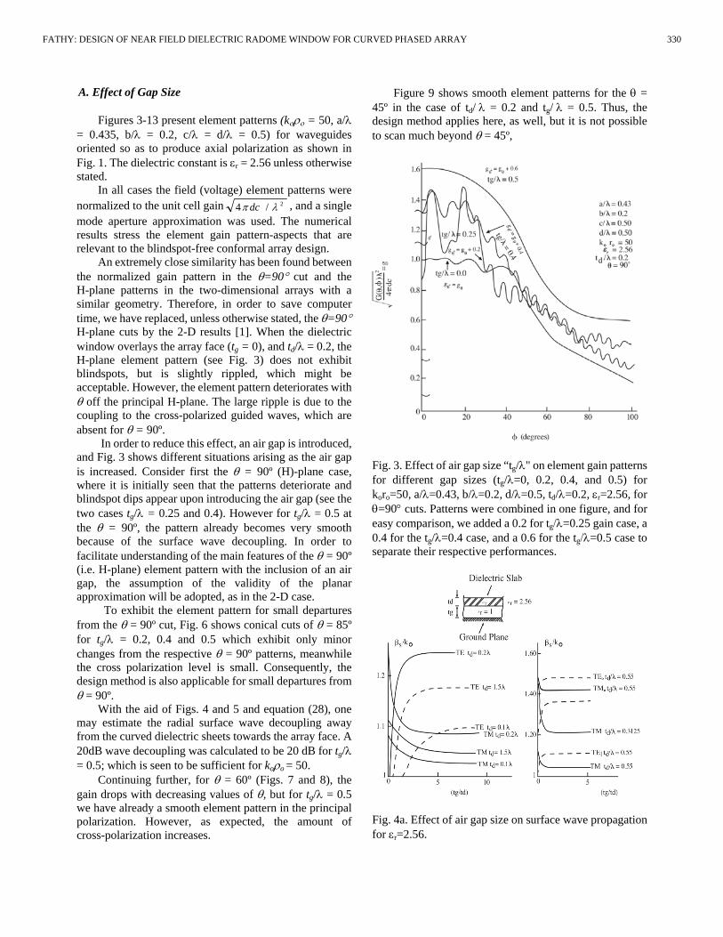
A. Effect of Gap Size
Figures 3-13 present element patterns (kορο = 50, a/λ = 0.435, b/λ = 0.2, c/λ = d/λ = 0.5) for waveguides oriented so as to produce axial polarization as shown in Fig. 1. The dielectric constant is εr = 2.56 unless otherwise stated.
In all cases the field (voltage) element patterns were normalized to the unit cell gain 2/4 λπ dc , and a single mode aperture approximation was used. The numerical results stress the element gain pattern-aspects that are relevant to the blindspot-free conformal array design.
An extremely close similarity has been found between the normalized gain pattern in the θ=90° cut and the H-plane patterns in the two-dimensional arrays with a similar geometry. Therefore, in order to save computer time, we have replaced, unless otherwise stated, the θ=90° H-plane cuts by the 2-D results [1]. When the dielectric window overlays the array face (tg = 0), and td/λ = 0.2, the H-plane element pattern (see Fig. 3) does not exhibit blindspots, but is slightly rippled, which might be acceptable. However, the element pattern deteriorates with θ off the principal H-plane. The large ripple is due to the coupling to the cross-polarized guided waves, which are absent for θ = 90º.
In order to reduce this effect, an air gap is introduced, and Fig. 3 shows different situations arising as the air gap is increased. Consider first the θ = 90º (H)-plane case, where it is initially seen that the patterns deteriorate and blindspot dips appear upon introducing the air gap (see the two cases tg/λ = 0.25 and 0.4). However for tg/λ = 0.5 at the θ = 90º, the pattern already becomes very smooth because of the surface wave decoupling. In order to facilitate understanding of the main features of the θ = 90º (i.e. H-plane) element pattern with the inclusion of an air gap, the assumption of the validity of the planar approximation will be adopted, as in the 2-D case.
To exhibit the element pattern for small departures from the θ = 90º cut, Fig. 6 shows conical cuts of θ = 85º for tg/λ = 0.2, 0.4 and 0.5 which exhibit only minor changes from the respective θ = 90º patterns, meanwhile the cross polarization level is small. Consequently, the design method is also applicable for small departures from θ = 90º.
With the aid of Figs. 4 and 5 and equation (28), one may estimate the radial surface wave decoupling away from the curved dielectric sheets towards the array face. A 20dB wave decoupling was calculated to be 20 dB for tg/λ = 0.5; which is seen to be sufficient for koρo = 50.
Continuing further, for θ = 60º (Figs. 7 and 8), the gain drops with decreasing values of θ, but for tg/λ = 0.5 we have already a smooth element pattern in the principal polarization. However, as expected, the amount of cross-polarization increases.
Figure 9 shows smooth element patterns for the θ = 45º in the case of td/ λ = 0.2 and tg/ λ = 0.5. Thus, the design method applies here, as well, but it is not possible to scan much beyond θ = 45º,
Fig. 3. Effect of air gap size “tg/λ" on element gain patterns for different gap sizes (tg/λ=0, 0.2, 0.4, and 0.5) for koro=50, a/λ=0.43, b/λ=0.2, d/λ=0.5, td/λ=0.2, εr=2.56, for θ=90° cuts. Patterns were combined in one figure, and for easy comparison, we added a 0.2 for tg/λ=0.25 gain case, a 0.4 for the tg/λ=0.4 case, and a 0.6 for the tg/λ=0.5 case to separate their respective performances.
Fig. 4a. Effect of air gap size on surface wave propagation for εr=2.56.
330FATHY: DESIGN OF NEAR FIELD DIELECTRIC RADOME WINDOW FOR CURVED PHASED ARRAY
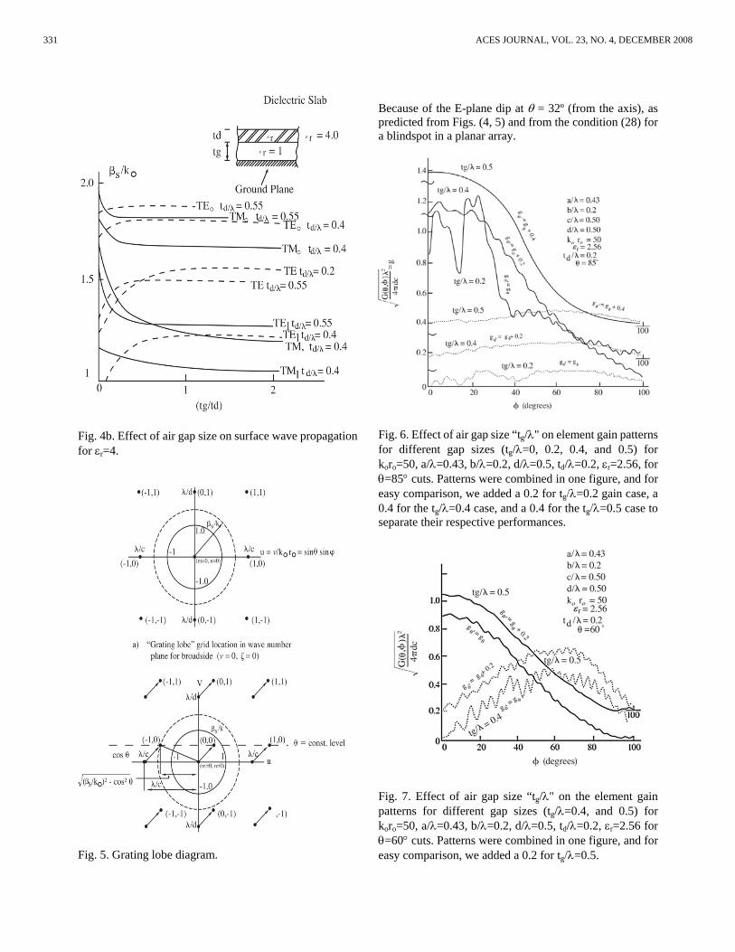
Fig. 4b. Effect of air gap size on surface wave propagation for εr=4.
Fig. 5. Grating lobe diagram.
Because of the E-plane dip at θ = 32º (from the axis), as predicted from Figs. (4, 5) and from the condition (28) for a blindspot in a planar array.
Fig. 6. Effect of air gap size “tg/λ" on element gain patterns for different gap sizes (tg/λ=0, 0.2, 0.4, and 0.5) for koro=50, a/λ=0.43, b/λ=0.2, d/λ=0.5, td/λ=0.2, εr=2.56, for θ=85° cuts. Patterns were combined in one figure, and for easy comparison, we added a 0.2 for tg/λ=0.2 gain case, a 0.4 for the tg/λ=0.4 case, and a 0.4 for the tg/λ=0.5 case to separate their respective performances.
Fig. 7. Effect of air gap size “tg/λ" on the element gain patterns for different gap sizes (tg/λ=0.4, and 0.5) for koro=50, a/λ=0.43, b/λ=0.2, d/λ=0.5, td/λ=0.2, εr=2.56 for θ=60° cuts. Patterns were combined in one figure, and for easy comparison, we added a 0.2 for tg/λ=0.5.
331 ACES JOURNAL, VOL. 23, NO. 4, DECEMBER 2008
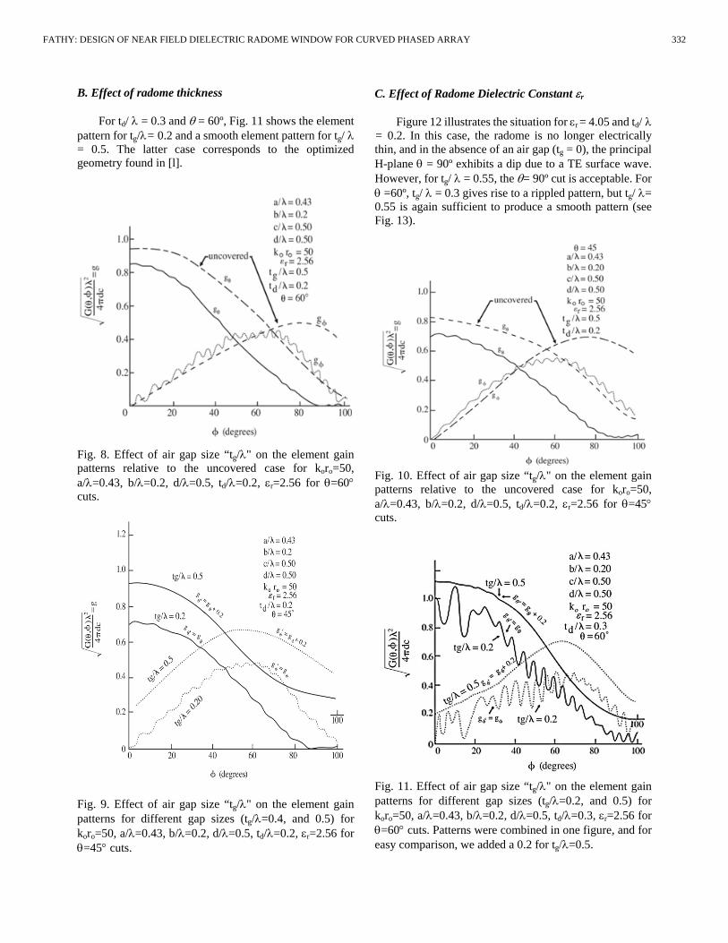
B. Effect of radome thickness
For td/ λ = 0.3 and θ = 60º, Fig. 11 shows the element pattern for tg/λ= 0.2 and a smooth element pattern for tg/ λ = 0.5. The latter case corresponds to the optimized geometry found in [l].
Fig. 8. Effect of air gap size “tg/λ" on the element gain patterns relative to the uncovered case for koro=50, a/λ=0.43, b/λ=0.2, d/λ=0.5, td/λ=0.2, εr=2.56 for θ=60° cuts.
Fig. 9. Effect of air gap size “tg/λ" on the element gain patterns for different gap sizes (tg/λ=0.4, and 0.5) for koro=50, a/λ=0.43, b/λ=0.2, d/λ=0.5, td/λ=0.2, εr=2.56 for θ=45° cuts.
C. Effect of Radome Dielectric Constant εr
Figure 12 illustrates the situation for εr = 4.05 and td/ λ = 0.2. In this case, the radome is no longer electrically thin, and in the absence of an air gap (tg = 0), the principal H-plane θ = 90º exhibits a dip due to a TE surface wave. However, for tg/ λ = 0.55, the θ= 90º cut is acceptable. For θ =60º, tg/ λ = 0.3 gives rise to a rippled pattern, but tg/ λ= 0.55 is again sufficient to produce a smooth pattern (see Fig. 13).
Fig. 10. Effect of air gap size “tg/λ" on the element gain patterns relative to the uncovered case for koro=50, a/λ=0.43, b/λ=0.2, d/λ=0.5, td/λ=0.2, εr=2.56 for θ=45° cuts.
Fig. 11. Effect of air gap size “tg/λ" on the element gain patterns for different gap sizes (tg/λ=0.2, and 0.5) for koro=50, a/λ=0.43, b/λ=0.2, d/λ=0.5, td/λ=0.3, εr=2.56 for θ=60° cuts. Patterns were combined in one figure, and for easy comparison, we added a 0.2 for tg/λ=0.5.
332FATHY: DESIGN OF NEAR FIELD DIELECTRIC RADOME WINDOW FOR CURVED PHASED ARRAY
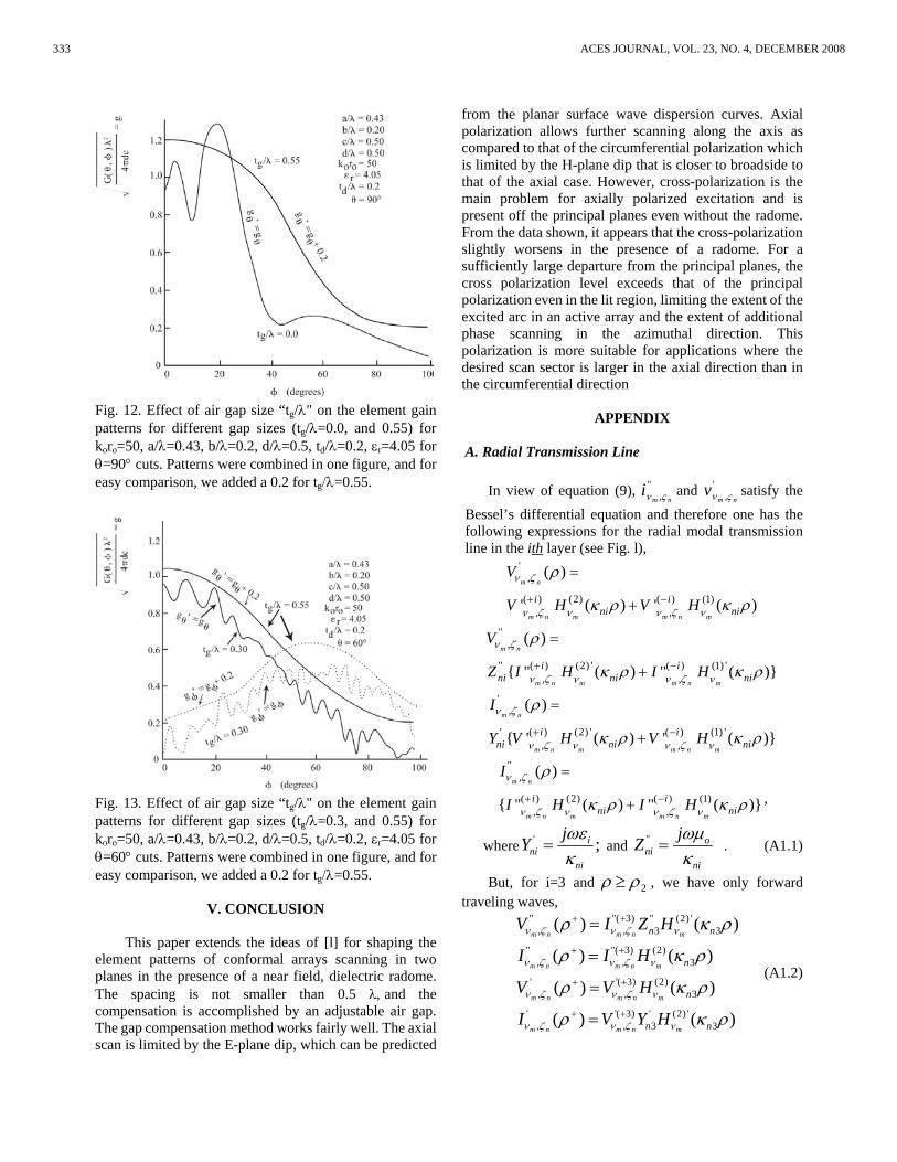
Fig. 12. Effect of air gap size “tg/λ" on the element gain patterns for different gap sizes (tg/λ=0.0, and 0.55) for koro=50, a/λ=0.43, b/λ=0.2, d/λ=0.5, td/λ=0.2, εr=4.05 for θ=90° cuts. Patterns were combined in one figure, and for easy comparison, we added a 0.2 for tg/λ=0.55.
Fig. 13. Effect of air gap size “tg/λ" on the element gain patterns for different gap sizes (tg/λ=0.3, and 0.55) for koro=50, a/λ=0.43, b/λ=0.2, d/λ=0.5, td/λ=0.2, εr=4.05 for θ=60° cuts. Patterns were combined in one figure, and for easy comparison, we added a 0.2 for tg/λ=0.55.
V. CONCLUSION
This paper extends the ideas of [l] for shaping the element patterns of conformal arrays scanning in two planes in the presence of a near field, dielectric radome. The spacing is not smaller than 0.5 λ, and the compensation is accomplished by an adjustable air gap. The gap compensation method works fairly well. The axial scan is limited by the E-plane dip, which can be predicted
from the planar surface wave dispersion curves. Axial polarization allows further scanning along the axis as compared to that of the circumferential polarization which is limited by the H-plane dip that is closer to broadside to that of the axial case. However, cross-polarization is the main problem for axially polarized excitation and is present off the principal planes even without the radome. From the data shown, it appears that the cross-polarization slightly worsens in the presence of a radome. For a sufficiently large departure from the principal planes, the cross polarization level exceeds that of the principal polarization even in the lit region, limiting the extent of the excited arc in an active array and the extent of additional phase scanning in the azimuthal direction. This polarization is more suitable for applications where the desired scan sector is larger in the axial direction than in the circumferential direction
APPENDIX
A. Radial Transmission Line
In view of equation (9), im nν ς,
" and vm nν ς,
' satisfy the Bessel’s differential equation and therefore one has the following expressions for the radial modal transmission line in the ith layer (see Fig. l),
',
( ) (2) ( ) (1), ,
( )
' ( ) ' ( )m n
m n m m n m
i ini ni
V
V H V H
ν ζ
ν ζ ν ν ζ ν
ρ
κ ρ κ ρ+ −
=
+
",
" ( ) (2) ' ( ) (1) ', ,
( )
" ( ) " ( )m n
m n m m n m
i ini ni ni
V
Z I H I H
ν ζ
ν ζ ν ν ζ ν
ρ
κ ρ κ ρ+ −
=
+
',
' ( ) (2) ' ( ) (1) ', ,
( )
' ( ) ' ( )m n
m n m m n m
i ini ni ni
I
Y V H V H
ν ζ
ν ζ ν ν ζ ν
ρ
κ ρ κ ρ+ −
=
+
",
( ) (2) ( ) (1), ,
( )
" ( ) " ( )m n
m n m m n m
i ini ni
I
I H I H
ν ζ
ν ζ ν ν ζ ν
ρ
κ ρ κ ρ+ −
=
+ ,
where ' ;ini
ni
jY ωεκ
= and " oni
ni
jZ ωµκ
= . (A1.1)
But, for i=3 and ρ ρ≥ 2 , we have only forward traveling waves,
" "( 3) " (2) ', , 3 3
" "( 3) (2), , 3
' '( 3) (2), , 3
' '( 3) ' (2) ', , 3 3
( ) ( )
( ) ( )
( ) ( )
( ) ( )
m n m n m
m n m n m
m n m n m
m n m n m
n n
n
n
n n
V I Z H
I I H
V V H
I V Y H
ν ζ ν ζ ν
ν ζ ν ζ ν
ν ζ ν ζ ν
ν ζ ν ζ ν
ρ κ ρ
ρ κ ρ
ρ κ ρ
ρ κ ρ
+ +
+ +
+ +
+ +
=
=
=
=
(A1.2)
333 ACES JOURNAL, VOL. 23, NO. 4, DECEMBER 2008

where κn3 = κn1 and Zn3 = Zn1, and H xn( , ) ( )1 2 denotes the
Hankel function of the first or second type with argument x and order n. B. Transmission Matrix T12
The various voltages and currents in the i-layer at ρ i−
+1 can be related to those at ρ i
− using the following transmission representation,
VIVI
ABCD
VIVI
m n
m n
m n
m n
m n
m n
m n
m n
i
i
i
i
i
i
i
i
i
ν ζ
ν ζ
ν ζ
ν ζ
ν ζ
ν ζ
ν ζ
ν ζ
ρρρρ
ρρρρ
,"
,"
,'
,'
,"
,"
,'
,'
( )( )( )( )
( )( )( )( )
−+
−+
−+
−+
−
−
−
−
L
N
MMMMM
O
Q
PPPPP=
L
N
MMMMM
O
Q
PPPPP
1
1
1
1
(B1.1)
ABCD
A BC D
A BC D
i
i i
i i
i i
i i
=
L
N
MMMM
O
Q
PPPP
" "
" "
' '
' '
0 00 0
0 00 0
(B1.2)
and "
" (2) ' (1)1"
(1) ' (2), 1 , 1
" "" (2) ' (1) '
1"
(1) ' (2) '1
" (2) (1)1"
(1)
[ ( ) ( )
( ) ( )]
[ ( ) ( )
( ) ( )]
1 [ ( ) ( )
(
m m
m m
m m
m m
m m
m
nii ni i ni i
i
n i i n i i
ni nii ni i ni i
i
ni i ni i
i ni i ni ii
ZA H H
H H
Z ZB H H
H H
C H H
H
ν ν
ν ν
ν ν
ν ν
ν ν
ν
κ ρ κ ρ
κ ρ κ ρ
κ ρ κ ρ
κ ρ κ ρ
κ ρ κ ρ
κ
−
− −
−
−
−
=∆
−
=∆
−
=∆
− (2)1
"" (2) (1)'
1"
(1) (2) '1
) ( )]
[ ( ) ( )
( ) ( )]
m
m m
m m
n i ni i
nii ni i ni i
i
n i ni i
H
ZD H H
H H
ν
ν ν
ν ν
ρ κ ρ
κ ρ κ ρ
κ ρ κ ρ
−
−
−
=∆
−
(B1.3)
where ∆2" is given by,
" " (2) ' (1)
(2) (1) ' "
[ ( ) ( )
4( ) ( )]
m m
m m
i ni ni i ni i
ni i ni i nini i
Z H H
jH H Z
ν ν
ν ν
κ ρ κ ρ
κ ρ κ ρπκ ρ
∆ = −
− = (B1.4)
And similarly Ai' , Bi
' , Ci' , and Di
' are deduced by first dividing all the above terms for the (``) case by ( Z Zni ni
" " ) and then utilizing the following substitution,
( Hm niν κ ρ( , )'
,( )1 21 2+ , H
m niν κ ρ( , ),( )1 2
1 2+ ,``)
( Hm nν κ ρ( , )'
,( )1 22 1 2
+ , Hm niν κ ρ( , )'
,( )1 21 2+ , `)
As an example Ai' is given by,
'
' (2) (1) '1'
(1) (2) '1
[ ( ) ( )
( ) ( )]
m m
m m
nii ni i ni i
i
ni i ni i
YA H H
H H
ν ν
ν ν
κ ρ κ ρ
κ ρ κ ρ
−
−
=∆
− (B1.5)
where ∆2' is given by,
' ' (2) ' (1)
(2) (1) ' '
[ ( ) ( )
4( ) ( )]
m m
m m
i ni ni i ni i
ni i ni i nini i
Z H H
jH H Z
ν ν
ν ν
κ ρ κ ρ
κ ρ κ ρπκ ρ
∆ = −
− = (B1.6)
C. Boundary Conditions and The Coupling Matrix Pi,i+1
In view of the continuity of ,m nzE
ν ζ and
,m nzHν ζ
at
both ρ1 and ρ2 as well as the continuity of ,
'nmze
ν ς across
the dielectric interface at both ρ=ρ1 and ρ2, the total voltages and currents must be continuous at both ρ2 and ρ1 i.e.
' ', 1,2 , 1,2
" ", 1,2 , 1,2
( ) ( )
( ) ( )m n m n
m n m n
V V
I I
ν ζ ν ζ
ν ζ ν ζ
ρ ρ
ρ ρ
+ −
+ −
=
= (C1.1)
On the other hand, the continuity of EΦ and HΦ at
ρ1 and ρ2 yields via equations (2), (3) and (9) the following,
VIVI
P
VIVI
m n
m n
m n
m n
m n
m n
m n
m n
i
i
i
i
i i
i
i
i
i
ν ζ
ν ζ
ν ζ
ν ζ
ν ζ
ν ζ
ν ζ
ν ζ
ρρρρ
ρρρρ
,"
,"
,'
,'
,
,"
,"
,'
,'
( )( )( )( )
( )( )( )( )
−
−
−
−
+
+
+
+
+
L
N
MMMMM
O
Q
PPPPP=
L
N
MMMMM
O
Q
PPPPP
1 (C1.2)
The coupling matrix Pi,i+1 is given by,
P
X
X
i i
mni i
i
mni i
i
,
,
,
/
/
+
+
+
=
−
L
N
MMMM
O
Q
PPPP1
1
1
1 0 00 1 0 00 0 1 00 0 1
ρ
ρ
(C1.3)
where , 1
2 21
1 1( )i i
mn m nni ni
X ν ζκ κ
+
+
= − (C1.4)
334FATHY: DESIGN OF NEAR FIELD DIELECTRIC RADOME WINDOW FOR CURVED PHASED ARRAY
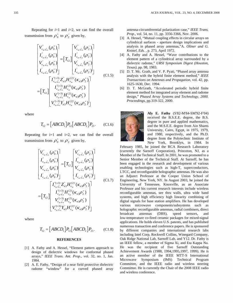
Repeating for i=1 and i=2, we can find the overall transmission from ρ0
+ to ρ2− given by,
[ ]
[ ]
" ", 0 , 2
" ", 0 , 2
12' ', 0 , 2
' ', 0 , 2
"( 3) " (2) ', 3 3 2
"( 3) (2), 3 2
12 '( 3),
( ) ( )
( ) ( )
( ) ( )
( ) ( )
( )
( )
m n m n
m n m n
m n m n
m n m n
m n m
m n m
m n
n n
n
V V
I IT
V V
I I
I Z H
I HT
V H
ν ζ ν ζ
ν ζ ν ζ
ν ζ ν ζ
ν ζ ν ζ
ν ζ ν
ν ζ ν
ν ζ ν
ρ ρ
ρ ρ
ρ ρ
ρ ρ
κ ρ
κ ρ
+ −
+ −
+ −
+ −
+ +
+ +
+
⎡ ⎤ ⎡ ⎤⎢ ⎥ ⎢ ⎥⎢ ⎥ ⎢ ⎥
=⎢ ⎥ ⎢ ⎥⎢ ⎥ ⎢ ⎥⎢ ⎥ ⎢ ⎥⎣ ⎦ ⎣ ⎦
=(2)
3 2
'( 3) ' (2) ', 3 3 2
( )
( )m
m n m
n
n nV Y Hν ζ ν
κ ρ
κ ρ
+
+ +
⎡ ⎤⎢ ⎥⎢ ⎥⎢ ⎥⎢ ⎥⎢ ⎥⎣ ⎦
(C1.5)
where
T ABCD P ABCD P12 1 12 2 23= . (C1.6) Repeating for i=1 and i=2, we can find the overall transmission from ρ0
+ to ρ2− given by,
[ ]
[ ]
" ", 0 , 2
" ", 0 , 2
12' ', 0 , 2
' ', 0 , 2
"( 3) " (2) ', 3 3 2
"( 3) (2), 3 2
12 '( 3),
( ) ( )
( ) ( )
( ) ( )
( ) ( )
( )
( )
m n m n
m n m n
m n m n
m n m n
m n m
m n m
m n
n n
n
V V
I IT
V V
I I
I Z H
I HT
V H
ν ζ ν ζ
ν ζ ν ζ
ν ζ ν ζ
ν ζ ν ζ
ν ζ ν
ν ζ ν
ν ζ ν
ρ ρ
ρ ρ
ρ ρ
ρ ρ
κ ρ
κ ρ
+ −
+ −
+ −
+ −
+ +
+ +
+
⎡ ⎤ ⎡ ⎤⎢ ⎥ ⎢ ⎥⎢ ⎥ ⎢ ⎥
=⎢ ⎥ ⎢ ⎥⎢ ⎥ ⎢ ⎥⎢ ⎥ ⎢ ⎥⎣ ⎦ ⎣ ⎦
=(2)
3 2
'( 3) ' (2) ', 3 3 2
( )
( )m
m n m
n
n nV Y Hν ζ ν
κ ρ
κ ρ
+
+ +
⎡ ⎤⎢ ⎥⎢ ⎥⎢ ⎥⎢ ⎥⎢ ⎥⎣ ⎦
(C1.7)
where
T ABCD P ABCD P12 1 12 2 23= . (C1.8)
REFERENCES [1] A. Fathy and A. Hessel, “Element pattern approach to
design of dielectric windows for conformal phased arrays,” IEEE Trans. Ant. Prop., vol. 32, no. 1, Jan. 1984.
[2] A. E. Fathy, “Design of a near field protective dielectric radome “window” for a curved phased array
antenna-circumferential polarization case,” IEEE Trans. Prop., vol. 54, no. 11, pp. 3356-3366, Nov. 2006.
[3] A. Hessel, “Mutual coupling effects in circular arrays on cylindrical surfaces - aperture design implications and analysis in phased array antennas,”A. Oliner and G. Knittel, Eds. , p. 273, April 1972.
[4] A. Fathy and A. Hessel, “Wave contributions to the element pattern of a cylindrical array surrounded by a dielectric radome,” URSI Symposium Digest (Houston, Texas), pp. 98, 1983.
[5] D. T. Mc. Grath, and V. P. Pyati, “Phased array antenna analysis with the hybrid finite element method,” IEEE Transactions on Antennas and Propagation, vol. 42, pp. 1625-1630, Dec. 1994.
[6] D. T. McGrath, “Accelerated periodic hybrid finite element method for integrated array element and radome design,” Phased Array Systems and Technology, 2000. Proceedings, pp.319-322, 2000.
Aly E. Fathy (S'82-M'84-SM'92-F'04) received the B.S.E.E. degree, the B.S. degree in pure and applied mathematics, and the M.S.E.E. degree from Ain Shams University, Cairo, Egypt, in 1975, 1979, and 1980, respectively, and the Ph.D. degree from the Polytechnic Institute of New York, Brooklyn, in 1984. In
February 1985, he joined the RCA Research Laboratory (currently the Sarnoff Corporation), Princeton, NJ, as a Member of the Technical Staff. In 2001, he was promoted to a Senior Member of the Technical Staff. At Sarnoff, he has been engaged in the research and development of various enabling technologies such as high-Tc superconductors, LTCC, and reconfigurable holographic antennas. He was also an Adjunct Professor at the Cooper Union School of Engineering, New York, NY. In August 2003, he joined the University of Tennessee, Knoxville, as an Associate Professor and his current research interests include wireless reconfigurable antennas, see thru walls, ultra wide band systems, and high efficiency high linearity combining of digital signals for base station amplifiers. He has developed various microwave components/subsystems such as holographic reconfigurable antennas, radial combiners, direct broadcast antennas (DBS), speed sensors, and low-temperature co-fired ceramic packages for mixed-signal applications. He holds eleven U.S. patents, and has published numerous transaction and conference papers. He is sponsored by different companies and international research labs including Intel Corp, Rockwell Collins, Winegard Company, Oak Ridge National Lab, Sarnoff Lab, and Y12. Dr. Fathy is an IEEE fellow, a member of Sigma Xi, and Eta Kappa Nu. He was the recipient of five Sarnoff Outstanding Achievement Awards (1988, 1994,1995,1997, 1999). He is an active member of the IEEE MTT-S International Microwave Symposium (IMS) Technical Program Committee, and the IEEE radio and wireless steering Committee. He is currently the Chair of the 2008 IEEE radio and wireless conference.
335 ACES JOURNAL, VOL. 23, NO. 4, DECEMBER 2008
Design, Modelling, and Synthesis of Radiation Pattern of Intelligent Antenna by Artificial Neural Networks
1 R. Ghayoula, 2 N. Fadlallah, 1 A. Gharsallah, and 2 M. Rammal
1 Laboratoire de physique de la matière molle, Unité de recherche : Circuits et systèmes électroniques HF Faculté des Sciences de Tunis, Campus Universitaire Tunis EL-manar, 2092, Tunisie
2 Equipe RADIOCOM, Institut Universitaire de Technologie de Saida Université de Liban, P.O.Box #813 36, Liban
Abstract − The work presented in this paper refers to the synthesis of the radiation pattern of intelligent antennas by the artificial neural networks (ANN) based on linear antennas array supplied with coaxial lines. The method of synthesis implemented for this type of antennas makes it possible to approach with an optimal desired radiation pattern specified by a gauge with modifying amplitude, phase excitation and sources space distribution. The approach used is based on geometry of the antennas and the artificial neural networks (ANN) which are able to model the linear antennas array. Our principal contribution in this paper is the extension of a synthesis model of the radiation pattern. The developed synthesis is based on the neural networks technique.
I. INTRODUCTION
Intelligent antennas take advantage of both antenna and propagation technologies. It has the potential to reduce multipath interference, increase signal to noise ratio, and introduce frequency reuse within a confined environment. Several challenges remain however in the development of intelligent antennas and one of these is the availability of efficient radiating elements interfacing with the beamformer.
The interest of these systems is their capacity to be reacted automatically to a complexes environment whose interference is known a priori. They make it possible to reduce the side-lobes levels existing in there interference direction, while maintaining the main lobe in useful direction.
These systems based on antennas network, devices to calculate the angles of arrivals AOA and numerical tools for synthesis which allot weights to the elements of the antenna network in order to optimize the output signal according to preset control technique for the formation of the ways and the cancellation of interfering.
An adaptive antenna network can thus be defined like a network able to modify its radiation pattern thanks to software of synthesis ready to answer the desired specifications [1-3].
The intelligent antennas systems require in general the coefficients of the network in real time what is not possible with a traditional method of synthesis. We adapt a new method of synthesis based on neural model. This tool presents a great performance at the level of its speed of convergence.
The use of the patch elements to produce an electromagnetic radiation goes back to the Fifties, but the application of this phenomenon for the first realization of antennas dates only from the beginning of the Sixties ten, when the need to conform of the networks appeared, in particular for the missiles.
Various analytical and numerical methods of optimization (Fourier, Dolph-Tchebycheff, Woodward-Lawson, relieving, Newton, general synthesis method…) [4-6] were developed and applied to synthesize the radiation patterns of antennas networks.
Recently, severe optimisation techniques such as neural network were developed to optimize general results.
In this paper, we will present the method of neural networks which will be applied to the synthesis of linear antennas array.
II. PROBLEM OF SYNTHESIS
The antenna synthesis was reduced to seek excitation and / or the space distribution on an axis of a certain number of elements fixed yet. For the representation of the radiation patterns, there are two types of conformations [1, 7, 8]:
-A conformation in a plan, for example the two principal plans E and H In this case, the discretization goes only on the direction θ the other direction φ is fixed.
-A conformation in all space (θ, φ). In this case the couple (θ, φ) is discretized [1].
Let’s consider a one-dimensional network with Px
elements laid out regularly in each direction (OX). Their radiation pattern is ),( ϕθF .
336ACES JOURNAL, VOL. 23, NO. 4, DECEMBER 2008
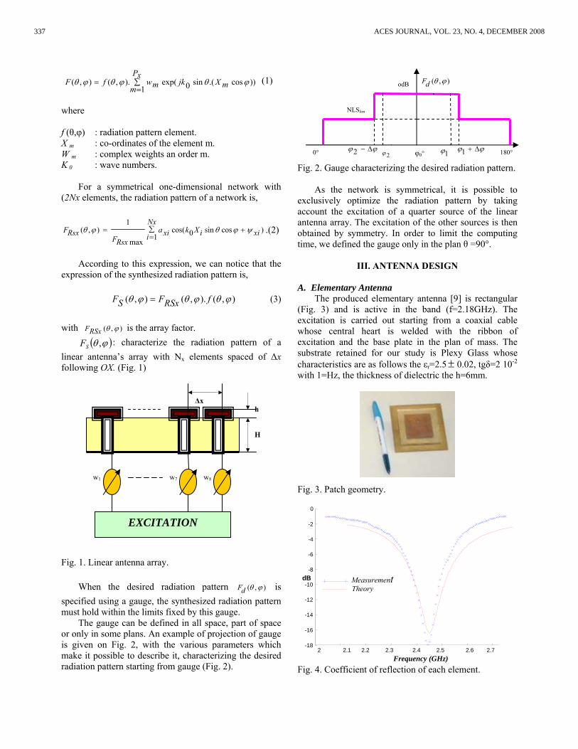
))cos.(sin0exp(1
).,(),( ϕθϕθϕθ mXjkxP
m mwfF ∑=
= (1)
where f (θ,φ) : radiation pattern element. X m : co-ordinates of the element m. W m : complex weights an order m. K 0 : wave numbers.
For a symmetrical one-dimensional network with (2Nx elements, the radiation pattern of a network is,
)cossin0cos(1max
1),( xiiXk
Nx
i xiaRsxF
RsxF ψϕθϕθ +∑=
= .(2)
According to this expression, we can notice that the
expression of the synthesized radiation pattern is,
),().,(),( ϕθϕθϕθ fRSxFSF = (3) with ),( ϕθRSxF is the array factor.
( )ϕθ ,SF : characterize the radiation pattern of a linear antenna’s array with Nx elements spaced of ∆x following OX. (Fig. 1)
Fig. 1. Linear antenna array.
When the desired radiation pattern ( , )Fd θ ϕ is specified using a gauge, the synthesized radiation pattern must hold within the limits fixed by this gauge.
The gauge can be defined in all space, part of space or only in some plans. An example of projection of gauge is given on Fig. 2, with the various parameters which make it possible to describe it, characterizing the desired radiation pattern starting from gauge (Fig. 2).
Fig. 2. Gauge characterizing the desired radiation pattern.
As the network is symmetrical, it is possible to
exclusively optimize the radiation pattern by taking account the excitation of a quarter source of the linear antenna array. The excitation of the other sources is then obtained by symmetry. In order to limit the computing time, we defined the gauge only in the plan θ =90°.
III. ANTENNA DESIGN
A. Elementary Antenna The produced elementary antenna [9] is rectangular
(Fig. 3) and is active in the band (f=2.18GHz). The excitation is carried out starting from a coaxial cable whose central heart is welded with the ribbon of excitation and the base plate in the plan of mass. The substrate retained for our study is Plexy Glass whose characteristics are as follows the εr=2.5± 0.02, tgδ=2 10-2 with 1=Hz, the thickness of dielectric the h=6mm.
Fig. 3. Patch geometry.
Fig. 4. Coefficient of reflection of each element.
EXCITATION
w7 w8
h
H
w1
∆x
-18
-16
-14
-12
-10
-8
-6
-4
-2
2 2.1 2.2 2.3 2.4 2.5 2.6 2.7
0
Measurement Theory
Frequency (GHz)
dB
odB
NLSlim
180° φ0° 1ϕ ϕϕ ∆+1 0° ϕϕ ∆−2
),( ϕθdF
2ϕ
337 ACES JOURNAL, VOL. 23, NO. 4, DECEMBER 2008
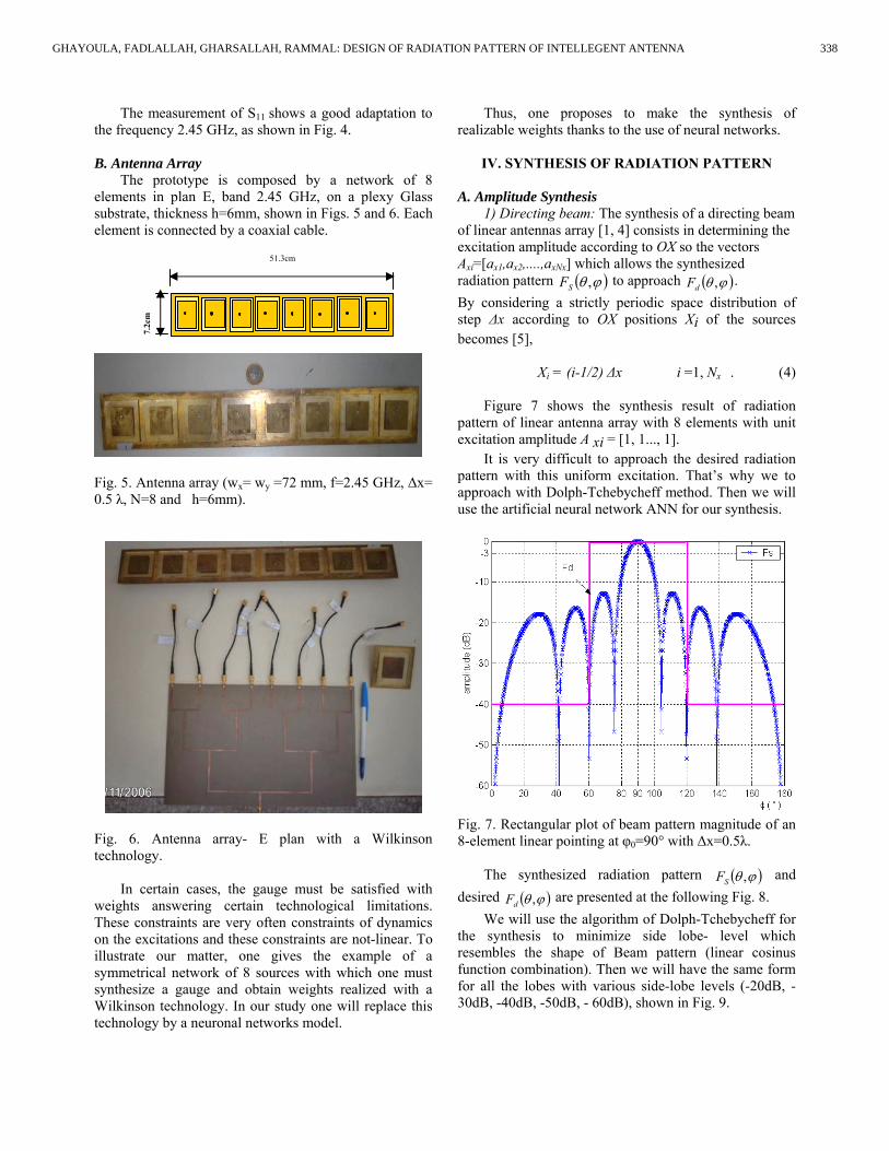
The measurement of S11 shows a good adaptation to the frequency 2.45 GHz, as shown in Fig. 4. B. Antenna Array
The prototype is composed by a network of 8 elements in plan E, band 2.45 GHz, on a plexy Glass substrate, thickness h=6mm, shown in Figs. 5 and 6. Each element is connected by a coaxial cable.
Fig. 5. Antenna array (wx= wy =72 mm, f=2.45 GHz, ∆x= 0.5 λ, N=8 and h=6mm).
Fig. 6. Antenna array- E plan with a Wilkinson technology.
In certain cases, the gauge must be satisfied with
weights answering certain technological limitations. These constraints are very often constraints of dynamics on the excitations and these constraints are not-linear. To illustrate our matter, one gives the example of a symmetrical network of 8 sources with which one must synthesize a gauge and obtain weights realized with a Wilkinson technology. In our study one will replace this technology by a neuronal networks model.
Thus, one proposes to make the synthesis of realizable weights thanks to the use of neural networks.
IV. SYNTHESIS OF RADIATION PATTERN
A. Amplitude Synthesis
1) Directing beam: The synthesis of a directing beam of linear antennas array [1, 4] consists in determining the excitation amplitude according to OX so the vectors Axi=[ax1,ax2,....,axNx] which allows the synthesized radiation pattern ( )ϕθ ,SF to approach ( )ϕθ ,dF . By considering a strictly periodic space distribution of step ∆x according to OX positions Xi of the sources becomes [5],
Xi = (i-1/2) ∆x i =1, Nx . (4)
Figure 7 shows the synthesis result of radiation pattern of linear antenna array with 8 elements with unit excitation amplitude A xi = [1, 1..., 1].
It is very difficult to approach the desired radiation pattern with this uniform excitation. That’s why we to approach with Dolph-Tchebycheff method. Then we will use the artificial neural network ANN for our synthesis.
Fig. 7. Rectangular plot of beam pattern magnitude of an 8-element linear pointing at φ0=90° with ∆x=0.5λ.
The synthesized radiation pattern ( )ϕθ ,SF and
desired ( )ϕθ ,dF are presented at the following Fig. 8. We will use the algorithm of Dolph-Tchebycheff for
the synthesis to minimize side lobe- level which resembles the shape of Beam pattern (linear cosinus function combination). Then we will have the same form for all the lobes with various side-lobe levels (-20dB, -30dB, -40dB, -50dB, - 60dB), shown in Fig. 9.
51.3cm
7.2c
m
338GHAYOULA, FADLALLAH, GHARSALLAH, RAMMAL: DESIGN OF RADIATION PATTERN OF INTELLEGENT ANTENNA
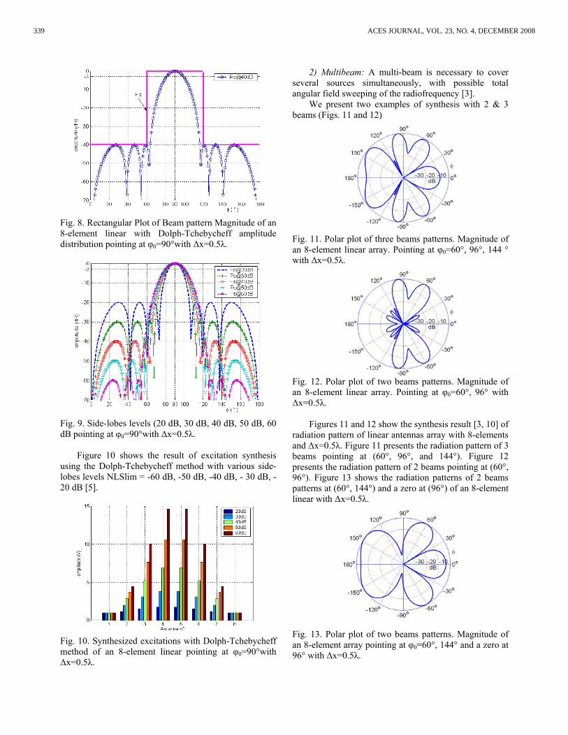
Fig. 8. Rectangular Plot of Beam pattern Magnitude of an 8-element linear with Dolph-Tchebycheff amplitude distribution pointing at φ0=90°with ∆x=0.5λ.
Fig. 9. Side-lobes levels (20 dB, 30 dB, 40 dB, 50 dB, 60 dB pointing at φ0=90°with ∆x=0.5λ.
Figure 10 shows the result of excitation synthesis using the Dolph-Tchebycheff method with various side-lobes levels NLSlim = -60 dB, -50 dB, -40 dB, - 30 dB, -20 dB [5].
Fig. 10. Synthesized excitations with Dolph-Tchebycheff method of an 8-element linear pointing at φ0=90°with ∆x=0.5λ.
2) Multibeam: A multi-beam is necessary to cover several sources simultaneously, with possible total angular field sweeping of the radiofrequency [3].
We present two examples of synthesis with 2 & 3 beams (Figs. 11 and 12)
Fig. 11. Polar plot of three beams patterns. Magnitude of an 8-element linear array. Pointing at φ0=60°, 96°, 144 ° with ∆x=0.5λ.
Fig. 12. Polar plot of two beams patterns. Magnitude of an 8-element linear array. Pointing at φ0=60°, 96° with ∆x=0.5λ.
Figures 11 and 12 show the synthesis result [3, 10] of radiation pattern of linear antennas array with 8-elements and ∆x=0.5λ. Figure 11 presents the radiation pattern of 3 beams pointing at (60°, 96°, and 144°). Figure 12 presents the radiation pattern of 2 beams pointing at (60°, 96°). Figure 13 shows the radiation patterns of 2 beams patterns at (60°, 144°) and a zero at (96°) of an 8-element linear with ∆x=0.5λ.
Fig. 13. Polar plot of two beams patterns. Magnitude of an 8-element array pointing at φ0=60°, 144° and a zero at 96° with ∆x=0.5λ.
339 ACES JOURNAL, VOL. 23, NO. 4, DECEMBER 2008
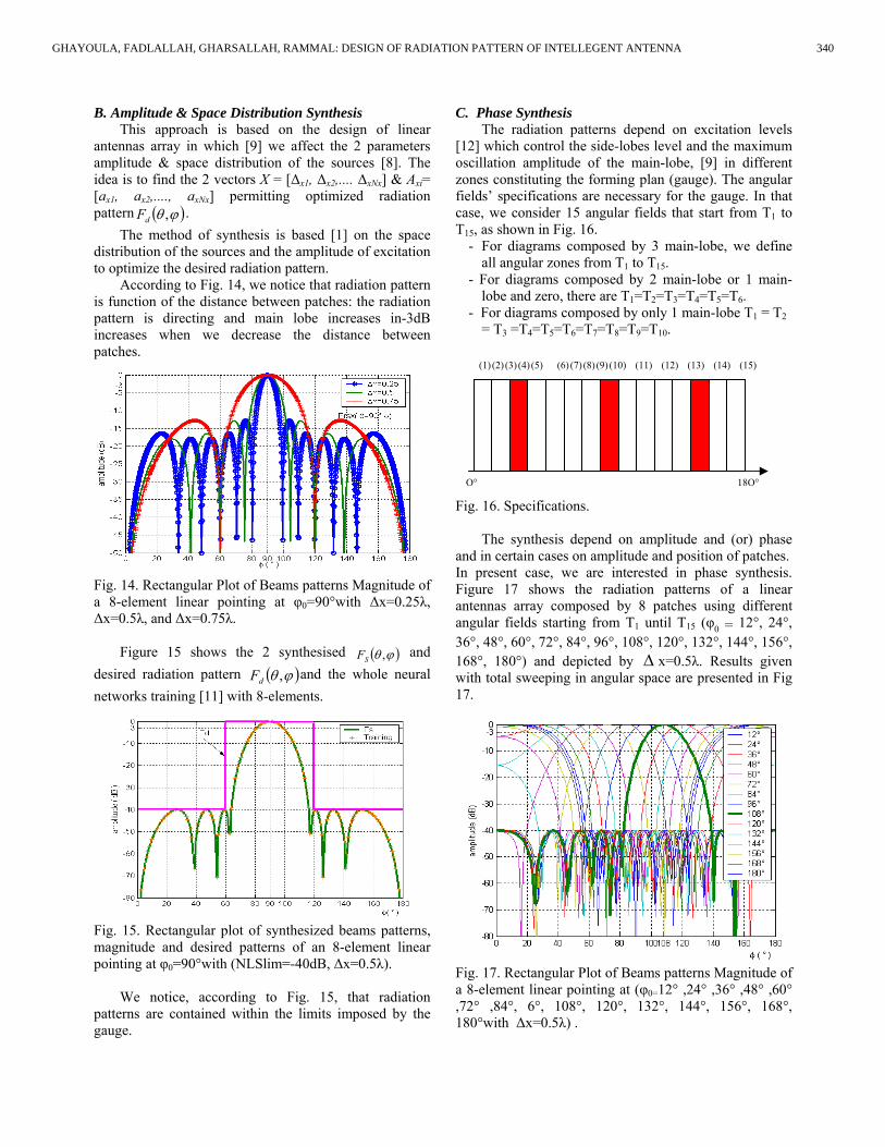
B. Amplitude & Space Distribution Synthesis This approach is based on the design of linear
antennas array in which [9] we affect the 2 parameters amplitude & space distribution of the sources [8]. The idea is to find the 2 vectors X = [∆x1, ∆x2,.... ∆xNx] & Axi= [ax1, ax2,...., axNx] permitting optimized radiation pattern ( )ϕθ ,dF .
The method of synthesis is based [1] on the space distribution of the sources and the amplitude of excitation to optimize the desired radiation pattern.
According to Fig. 14, we notice that radiation pattern is function of the distance between patches: the radiation pattern is directing and main lobe increases in-3dB increases when we decrease the distance between patches.
Fig. 14. Rectangular Plot of Beams patterns Magnitude of a 8-element linear pointing at φ0=90°with ∆x=0.25λ, ∆x=0.5λ, and ∆x=0.75λ.
Figure 15 shows the 2 synthesised ( )ϕθ ,SF and
desired radiation pattern ( )ϕθ ,dF and the whole neural networks training [11] with 8-elements.
Fig. 15. Rectangular plot of synthesized beams patterns, magnitude and desired patterns of an 8-element linear pointing at φ0=90°with (NLSlim=-40dB, ∆x=0.5λ).
We notice, according to Fig. 15, that radiation patterns are contained within the limits imposed by the gauge.
C. Phase Synthesis The radiation patterns depend on excitation levels
[12] which control the side-lobes level and the maximum oscillation amplitude of the main-lobe, [9] in different zones constituting the forming plan (gauge). The angular fields’ specifications are necessary for the gauge. In that case, we consider 15 angular fields that start from T1 to T15, as shown in Fig. 16.
- For diagrams composed by 3 main-lobe, we define all angular zones from T1 to T15.
- For diagrams composed by 2 main-lobe or 1 main-lobe and zero, there are T1=T2=T3=T4=T5=T6.
- For diagrams composed by only 1 main-lobe T1 = T2 = T3 =T4=T5=T6=T7=T8=T9=T10.
Fig. 16. Specifications.
The synthesis depend on amplitude and (or) phase and in certain cases on amplitude and position of patches. In present case, we are interested in phase synthesis. Figure 17 shows the radiation patterns of a linear antennas array composed by 8 patches using different angular fields starting from T1 until T15 (φ0 = 12°, 24°, 36°, 48°, 60°, 72°, 84°, 96°, 108°, 120°, 132°, 144°, 156°, 168°, 180°) and depicted by ∆ x=0.5λ. Results given with total sweeping in angular space are presented in Fig 17.
Fig. 17. Rectangular Plot of Beams patterns Magnitude of a 8-element linear pointing at (φ0=12° ,24° ,36° ,48° ,60° ,72° ,84°, 6°, 108°, 120°, 132°, 144°, 156°, 168°, 180°with ∆x=0.5λ) .
O° 18O°
(1) (2) (3) (4) (5) (6) (7) (8) (9) (10) (11) (12) (13) (14) (15)
340GHAYOULA, FADLALLAH, GHARSALLAH, RAMMAL: DESIGN OF RADIATION PATTERN OF INTELLEGENT ANTENNA
D. Simulation and Measurement Examples Table 1 shows the simulation results of the proposed
approach when it is used with prescribed steering and null design. Table 2 shows the simulation results of the proposed approach when it is used with prescribed multiple steering lobes.
Table 1. Excitations for different steering lobes and interference nulling.
Synthesized excitations (phases)
-10o
(steering) and –10o
(interfering)
-40o (steering)
and 0o (interfering)
-50o (steering) and -10o
(interfering)
φ φ φ 1 -145 -42 223 2 -60 94 32 3 -37 -173 158 4 -8 -69 -79 5 8 69 79 6 37 173 -158 7 60 -94 -32 8 145 42 -223
As Figs. 18 to 20 indicate, we can observe the
performance of our algorithm. These figures show good agreement between the simulation and the measurement results in terms of accuracy, efficiency and reliability of the model. We can see that a broad null (lower than –30 db) is easily available. It is interesting to notify that the method allows the control of nulling level to the detriment of the adjacent side lobes energy, which is pushed up. Also, solutions with 2 or 3 lobes can be reached with acceptable solutions.
Table 2. Excitations for different multiple steering lobes.
Synthesized excitations (phases) -50o and –
20o -30o and
30o -40o, 20o and
50o
φ φ φ 1 240 5 95 2 50 185 315 3 180 180 279 4 310 360 126 5 50 360 234 6 180 180 81 7 310 175 45 8 120 355 265 This method does not only hold the examples
presented above, but also appears to be general for all cases of synthesized desired characteristics of steered beams.
Fig. 18. Two steering lobes at (-50° and -20°).
Fig. 19. Two steering lobes at (-30° and 30°).
Fig. 20. Three steering lobes at (-40°, 20°, and 50°).
341 ACES JOURNAL, VOL. 23, NO. 4, DECEMBER 2008
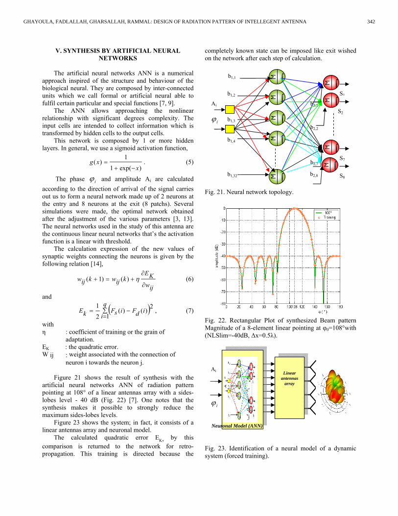
V. SYNTHESIS BY ARTIFICIAL NEURAL NETWORKS
The artificial neural networks ANN is a numerical
approach inspired of the structure and behaviour of the biological neural. They are composed by inter-connected units which we call formal or artificial neural able to fulfil certain particular and special functions [7, 9].
The ANN allows approaching the nonlinear relationship with significant degrees complexity. The input cells are intended to collect information which is transformed by hidden cells to the output cells.
This network is composed by 1 or more hidden layers. In general, we use a sigmoid activation function,
)exp(1
1)(
xxg
−+= . (5)
The phase iϕ and amplitude Ai are calculated according to the direction of arrival of the signal carries out us to form a neural network made up of 2 neurons at the entry and 8 neurons at the exit (8 patchs). Several simulations were made, the optimal network obtained after the adjustment of the various parameters [3, 13]. The neural networks used in the study of this antenna are the continuous linear neural networks that’s the activation function is a linear with threshold.
The calculation expression of the new values of synaptic weights connecting the neurons is given by the following relation [14],
ijwKE
kijwkijw∂
∂+=+ η)()1( (6)
and
( )∑=
−=q
iidFisFkE
12)()(
2
1, (7)
with η : coefficient of training or the grain of
adaptation. EK : the quadratic error. W ij : weight associated with the connection of
neuron i towards the neuron j.
Figure 21 shows the result of synthesis with the artificial neural networks ANN of radiation pattern pointing at 108° of a linear antennas array with a sides-lobes level - 40 dB (Fig. 22) [7]. One notes that the synthesis makes it possible to strongly reduce the maximum sides-lobes levels.
Figure 23 shows the system; in fact, it consists of a linear antennas array and neuronal model.
The calculated quadratic error EK, by this comparison is returned to the network for retro-propagation. This training is directed because the
completely known state can be imposed like exit wished on the network after each step of calculation.
Fig. 21. Neural network topology.
Fig. 22. Rectangular Plot of synthesized Beam pattern Magnitude of a 8-element linear pointing at φ0=108°with (NLSlim=-40dB, ∆x=0.5λ).
Fig. 23. Identification of a neural model of a dynamic system (forced training).
∫
∫
∫
∫
∫
b1,1
b1,2
b1,3
b1,4
b1,32 b2,8
iϕS2
∫
∫
∫
∫
b2,1
b2,2
b2,7
S1
S7
S8
Ai
Linear antennas
array
Ai
iϕ
Neuronal Model (ANN)
342GHAYOULA, FADLALLAH, GHARSALLAH, RAMMAL: DESIGN OF RADIATION PATTERN OF INTELLEGENT ANTENNA
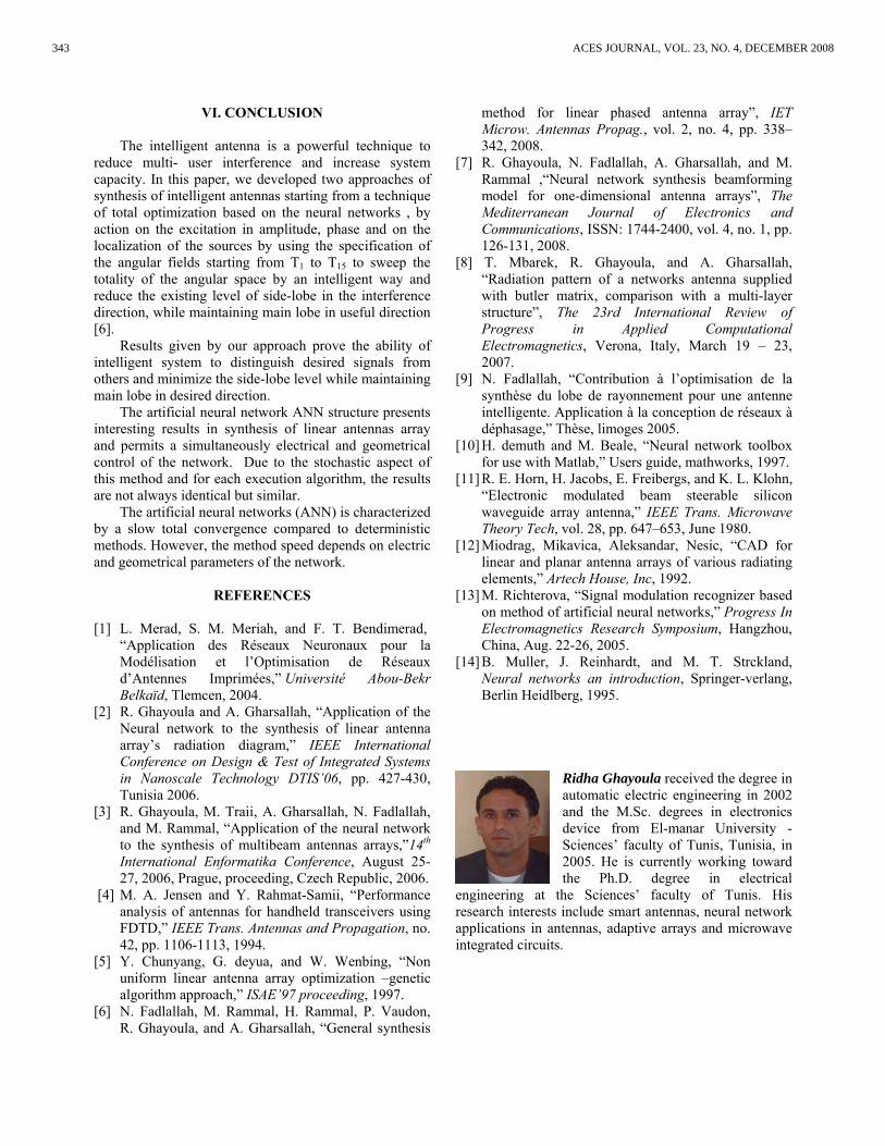
VI. CONCLUSION
The intelligent antenna is a powerful technique to reduce multi- user interference and increase system capacity. In this paper, we developed two approaches of synthesis of intelligent antennas starting from a technique of total optimization based on the neural networks , by action on the excitation in amplitude, phase and on the localization of the sources by using the specification of the angular fields starting from T1 to T15 to sweep the totality of the angular space by an intelligent way and reduce the existing level of side-lobe in the interference direction, while maintaining main lobe in useful direction [6].
Results given by our approach prove the ability of intelligent system to distinguish desired signals from others and minimize the side-lobe level while maintaining main lobe in desired direction.
The artificial neural network ANN structure presents interesting results in synthesis of linear antennas array and permits a simultaneously electrical and geometrical control of the network. Due to the stochastic aspect of this method and for each execution algorithm, the results are not always identical but similar.
The artificial neural networks (ANN) is characterized by a slow total convergence compared to deterministic methods. However, the method speed depends on electric and geometrical parameters of the network.
REFERENCES
[1] L. Merad, S. M. Meriah, and F. T. Bendimerad, “Application des Réseaux Neuronaux pour la Modélisation et l’Optimisation de Réseaux d’Antennes Imprimées,” Université Abou-Bekr Belkaïd, Tlemcen, 2004.
[2] R. Ghayoula and A. Gharsallah, “Application of the Neural network to the synthesis of linear antenna array’s radiation diagram,” IEEE International Conference on Design & Test of Integrated Systems in Nanoscale Technology DTIS’06, pp. 427-430, Tunisia 2006.
[3] R. Ghayoula, M. Traii, A. Gharsallah, N. Fadlallah, and M. Rammal, “Application of the neural network to the synthesis of multibeam antennas arrays,”14th International Enformatika Conference, August 25-27, 2006, Prague, proceeding, Czech Republic, 2006.
[4] M. A. Jensen and Y. Rahmat-Samii, “Performance analysis of antennas for handheld transceivers using FDTD,” IEEE Trans. Antennas and Propagation, no. 42, pp. 1106-1113, 1994.
[5] Y. Chunyang, G. deyua, and W. Wenbing, “Non uniform linear antenna array optimization –genetic algorithm approach,” ISAE’97 proceeding, 1997.
[6] N. Fadlallah, M. Rammal, H. Rammal, P. Vaudon, R. Ghayoula, and A. Gharsallah, “General synthesis
method for linear phased antenna array”, IET Microw. Antennas Propag., vol. 2, no. 4, pp. 338–342, 2008.
[7] R. Ghayoula, N. Fadlallah, A. Gharsallah, and M. Rammal ,“Neural network synthesis beamforming model for one-dimensional antenna arrays”, The Mediterranean Journal of Electronics and Communications, ISSN: 1744-2400, vol. 4, no. 1, pp. 126-131, 2008.
[8] T. Mbarek, R. Ghayoula, and A. Gharsallah, “Radiation pattern of a networks antenna supplied with butler matrix, comparison with a multi-layer structure”, The 23rd International Review of Progress in Applied Computational Electromagnetics, Verona, Italy, March 19 – 23, 2007.
[9] N. Fadlallah, “Contribution à l’optimisation de la synthèse du lobe de rayonnement pour une antenne intelligente. Application à la conception de réseaux à déphasage,” Thèse, limoges 2005.
[10] H. demuth and M. Beale, “Neural network toolbox for use with Matlab,” Users guide, mathworks, 1997.
[11] R. E. Horn, H. Jacobs, E. Freibergs, and K. L. Klohn, “Electronic modulated beam steerable silicon waveguide array antenna,” IEEE Trans. Microwave Theory Tech, vol. 28, pp. 647–653, June 1980.
[12] Miodrag, Mikavica, Aleksandar, Nesic, “CAD for linear and planar antenna arrays of various radiating elements,” Artech House, Inc, 1992.
[13] M. Richterova, “Signal modulation recognizer based on method of artificial neural networks,” Progress In Electromagnetics Research Symposium, Hangzhou, China, Aug. 22-26, 2005.
[14] B. Muller, J. Reinhardt, and M. T. Strckland, Neural networks an introduction, Springer-verlang, Berlin Heidlberg, 1995.
Ridha Ghayoula received the degree in automatic electric engineering in 2002 and the M.Sc. degrees in electronics device from El-manar University - Sciences’ faculty of Tunis, Tunisia, in 2005. He is currently working toward the Ph.D. degree in electrical
engineering at the Sciences’ faculty of Tunis. His research interests include smart antennas, neural network applications in antennas, adaptive arrays and microwave integrated circuits.
343 ACES JOURNAL, VOL. 23, NO. 4, DECEMBER 2008
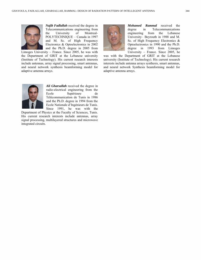
Najib Fadlallah received the degree in Telecommunications engineering from the University of Montreal- POLYTECHNIQUE – Canada in 1997 and M. Sc. of High Frequency Electronics & Optoelectronics in 2002 and the Ph.D. degree in 2005 from
Limoges University – France. Since 2005, he was with the Department of GRIT at the Lebanese university (Institute of Technology). His current research interests include antennas, array signal processing, smart antennas, and neural network synthesis beamforming model for adaptive antenna arrays.
Ali Gharsallah received the degree in radio-electrical engineering from the Ecole Supérieure de Télécommunication de Tunis in 1986 and the Ph.D. degree in 1994 from the Ecole Nationale d’Ingénieurs de Tunis. Since 1991, he was with the
Department of Physics at the Faculty of Sciences, Tunis. His current research interests include antennas, array signal processing, multilayered structures and microwave integrated circuits.
Mohamed Rammal received the degree in Telecommunications engineering from the Lebanese University– Beyrouth in 1988 and M. Sc. of High Frequency Electronics & Optoelectronics in 1990 and the Ph.D. degree in 1993 from Limoges University – France. Since 2005, he
was with the Department of GRIT at the Lebanese university (Institute of Technology). His current research interests include antenna arrays synthesis, smart antennas, and neural network Synthesis beamforming model for adaptive antenna arrays.
344GHAYOULA, FADLALLAH, GHARSALLAH, RAMMAL: DESIGN OF RADIATION PATTERN OF INTELLEGENT ANTENNA
Optimised Design of a Printed Elliptical Spiral Antenna with a Dielectric Superstrate
S. K. Khamas and G. G. Cook
Dept. Electronic and Electrical Engineering, University of Sheffield,
Mappin St., Sheffield, S1 3JD, UK
Abstract − An elliptical spiral antenna embedded between a grounded dielectric substrate and superstrate is designed using a curved segment moment method employing complex images, which is driven by a marginal distribution optimisation algorithm. The spiral parameters together with substrate and superstrate permittivity and thickness values are optimised for low axial ratio and maximum gain and bandwidth. It is shown that the superstrate improves the bandwidth of the spiral.
I. INTRODUCTION
Spiral antennas can offer wide bandwidths, high efficiencies, squinted beams and circularly polarised radiation [1]. Previously the authors have developed a new Method of Moments (MoM) technique for the analysis of printed Archimedian, logarithmic and eccentric spirals that uses curved segmentation along the spiral arm, rather than the faceted approximations obtained with linear segmentation strategies, [2, 3]. The requirement of fewer curved segments gives the model a speed advantage which becomes increasingly important when the code may need to be run many times under an optimisation routine such as a Genetic Algorithm (GA) for example [4]. Printed spirals are useful as alternatives to patch antennas, and radomes can offer protection against the elements and also increase bandwidth. The authors have recently reported a curved segment analysis technique for embedded spiral design, employing the statistically based Optimisation using Marginal Distributions (OMD) technique to independently vary the permittivity and thickness of the dielectric substrate and superstrate for optimum axial ratio [5]. To expedite analysis a more efficient method is employed to calculate the Sommerfeld type potential functions required to compute the MoM impedance matrix. These Sommerfeld integrals are reformulated as closed-form complex image terms [6], whose coefficients are then evaluated using the Generalised Pencil of Functions (GPOF) technique [7].
Here we extend the analysis in [5] by applying it to an elliptical rather than Archimedian spiral, and also by optimising the spiral parameters in addition to the substrate and superstrate properties. Elliptical spirals can be used as conformal antennas and for tailoring radiation
patterns to specific requirements by altering the aspect ratio of the ellipse. Further, the spiral is also optimised for gain and bandwidth as well as axial ratio, and the effect of the superstrate on performance is considered.
II. THEORY
The theory presented here is intended to complement that in [5], so that only field equations which are specific to this particular spiral geometry are developed, to facilitate direct computation. A printed elliptical spiral is shown in Fig. 1a with a dielectric superstrate. In Fig. 1b, the electric field tangential to a thin wire contour located in a planar Cartesian co-ordinate frame by
),( yxρ due to a current,
)sin())(sin(
′
−′−′=′ ∆
∆k
kII n
n (1)
at ),( yx ′′ρ can be represented by, [8]
1
2
21
1ˆ ˆ
( ).
n
x x y y
n
y yx x
E E E I k Gj
IG
l
ωε
∂ρ ∂ρ∂ρ ∂ρ∂ ∂ ∂ ∂ ∂
+
′
−
′′ ′
= + =
⎛ ⎞ ∂ ∂+ + +Π⎜ ⎟′ ′ ′ ∂⎝ ⎠
∫ (2)
Where o1r1o2r2 f2 2k εεεεεεπωλπ ==== ,,,/
and '∆ is the segment length. The terms G and Π are the potential (Green’s) functions which couple sources to fields in the presence of planar layered dielectric media.
The MoM impedance matrix element linking curved source sinusoid n to curved test sinusoid m is then,
dIE
k(k1Z
n
1m
1mmmn
⎥⎥⎦
⎤
⎢⎢⎣
⎡∫ −−=+
−
))(sin()sin
∆∆
. (3)
The elliptic spiral function is given by,
)y KxKa yxo ˆsinˆcos)(( φφφρρ ++= (4)
345 ACES JOURNAL, VOL. 23, NO. 4, DECEMBER 2008
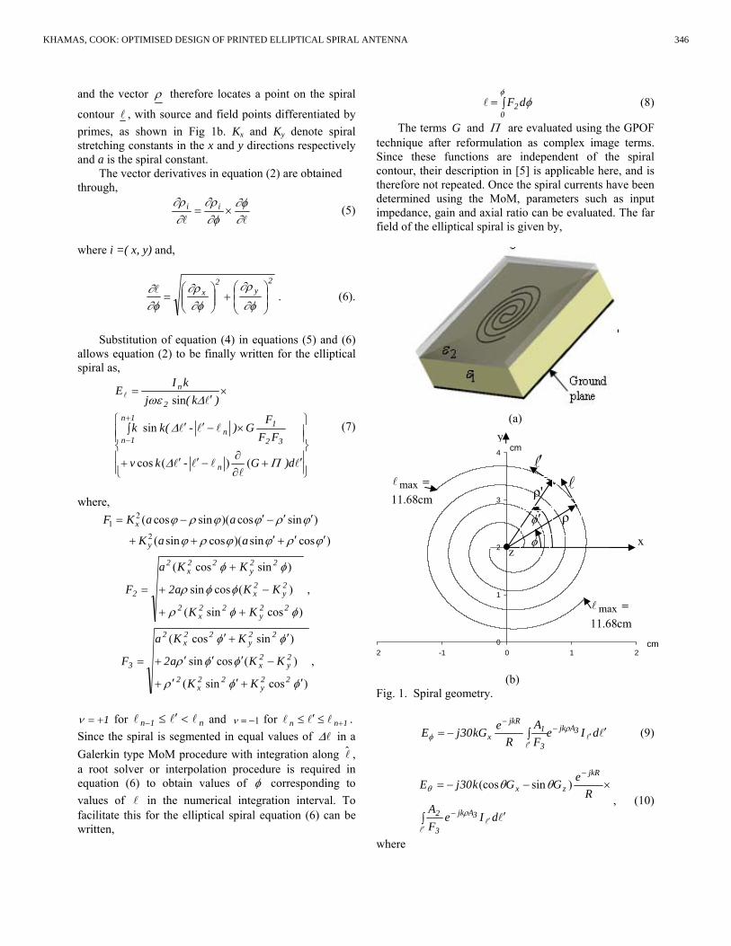
and the vector ρ therefore locates a point on the spiral
contour , with source and field points differentiated by primes, as shown in Fig 1b. Kx and Ky denote spiral stretching constants in the x and y directions respectively and a is the spiral constant.
The vector derivatives in equation (2) are obtained through,
∂∂φ
∂φ∂ρ
∂∂ρ
×= ii (5)
where i =( x, y) and,
2
y2
x⎟⎟⎠
⎞⎜⎜⎝
⎛+⎟⎟
⎠
⎞⎜⎜⎝
⎛=
∂φ∂ρ
∂φ∂ρ
∂φ∂ . (6).
Substitution of equation (4) in equations (5) and (6)
allows equation (2) to be finally written for the elliptical spiral as,
⎪⎪⎭
⎪⎪⎬
⎫
⎪⎪⎩
⎪⎪⎨
⎧
′+∂∂
−′′+
×−′′∫
×′
=
+
−
d)G-kv
FFF
G)-(k k
)k( jkI
E
n
32
1n
1n
1n
2
n
Π∆
∆
∆ωε
()(cos
sin
sin
(7)
where,
21
2
( cos sin )( cos sin )
( sin cos )( sin cos )x
y
F K a a
K a a
ϕ ρ ϕ ϕ ρ ϕ
ϕ ρ ϕ ϕ ρ ϕ
′ ′ ′= − −
′ ′ ′+ + +
)cossin(
)(cossin
)sincos(
φφρ
φφρ
φφ
22y
22x
2
2y
2x
22y
22x
2
2
KK
KKa2
KKa
F
++
−+
+
= ,
)cossin(
)(cossin
)sincos(
φφρ
φφρ
φφ
′+′′+
−′′′+
′+′
=22
y22
x2
2y
2x
22y
22x
2
3
KK
KKa2
KKa
F ,
1+=ν for n1n <′≤− and 1−=ν for 1nn +≤′≤ .
Since the spiral is segmented in equal values of ∆ in a Galerkin type MoM procedure with integration along ˆ , a root solver or interpolation procedure is required in equation (6) to obtain values of φ corresponding to values of in the numerical integration interval. To facilitate this for the elliptical spiral equation (6) can be written,
∫=φ
φ0
2 dF (8)
The terms G and Π are evaluated using the GPOF technique after reformulation as complex image terms. Since these functions are independent of the spiral contour, their description in [5] is applicable here, and is therefore not repeated. Once the spiral currents have been determined using the MoM, parameters such as input impedance, gain and axial ratio can be evaluated. The far field of the elliptical spiral is given by,
(a)
(b) Fig. 1. Spiral geometry.
′∫−= ′−
′
−
dIeFA
RekG30jE 3Ajk
3
1jkR
xρ
φ (9)
∫ ′
×−−=
′′
−
−
dIeFA
ReGGk30jE
3Ajk
3
2
jkR
zx
ρ
θ θθ )sin(cos, (10)
where
cm-2 -1 0 1 2
0
1
2
3
4 cm
φ
ρ'
′
φ′
ρ
cm68.11max =
cm68.11max =
x
y
z
346KHAMAS, COOK: OPTIMISED DESIGN OF PRINTED ELLIPTICAL SPIRAL ANTENNA
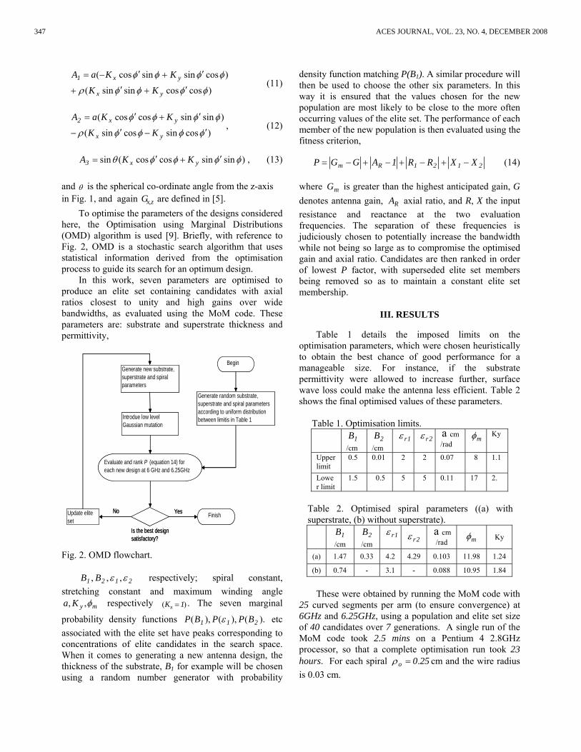
)coscossinsin(
)cossinsincos(
φφφφρ
φφφφ′+′+
′+′−=
yx
yx1
KK
KKaA (11)
)cossincossin(
)sinsincoscos(
φφφφρ
φφφφ′−′−
′+′=
yx
yx2
KK
KKaA, (12)
)sinsincoscos(sin φφφφθ ′+′= yx3 KKA , (13)
and θ is the spherical co-ordinate angle from the z-axis in Fig. 1, and again zxG , are defined in [5].
To optimise the parameters of the designs considered here, the Optimisation using Marginal Distributions (OMD) algorithm is used [9]. Briefly, with reference to Fig. 2, OMD is a stochastic search algorithm that uses statistical information derived from the optimisation process to guide its search for an optimum design.
In this work, seven parameters are optimised to produce an elite set containing candidates with axial ratios closest to unity and high gains over wide bandwidths, as evaluated using the MoM code. These parameters are: substrate and superstrate thickness and permittivity,
Begin
Generate random substrate, superstrate and spiral parameters according to uniform distribution between limitis in Table 2
Evaluate and rank F (equation 13) for each new design at 6 GHz and 6.25GHz
Introdue low level Gaussian mutation
Generate new substrate, superstrate and spiral parameters
Is the best design satisfactory?
FinishUpdate elite set
YesNo
Begin
Generate random substrate, superstrate and spiral parameters according to uniform distribution between limitis in Table 1
Evaluate and rank P (equation 14) for each new design at 6 GHz and 6.25GHz
Introdue low level Gaussian mutation
Generate new substrate, superstrate and spiral parameters
Is the best design satisfactory?
FinishUpdate elite set
YesNo
Fig. 2. OMD flowchart.
2121 BB εε ,,, respectively; spiral constant,
stretching constant and maximum winding angle myKa φ,, respectively )( 1Kx = . The seven marginal
probability density functions ).(),(),( 211 BPPBP ε etc associated with the elite set have peaks corresponding to concentrations of elite candidates in the search space. When it comes to generating a new antenna design, the thickness of the substrate, B1 for example will be chosen using a random number generator with probability
density function matching P(B1). A similar procedure will then be used to choose the other six parameters. In this way it is ensured that the values chosen for the new population are most likely to be close to the more often occurring values of the elite set. The performance of each member of the new population is then evaluated using the fitness criterion,
2121Rm XXRR1AGGP −+−+−+−= (14)
where mG is greater than the highest anticipated gain, G denotes antenna gain, RA axial ratio, and R, X the input resistance and reactance at the two evaluation frequencies. The separation of these frequencies is judiciously chosen to potentially increase the bandwidth while not being so large as to compromise the optimised gain and axial ratio. Candidates are then ranked in order of lowest P factor, with superseded elite set members being removed so as to maintain a constant elite set membership.
III. RESULTS
Table 1 details the imposed limits on the optimisation parameters, which were chosen heuristically to obtain the best chance of good performance for a manageable size. For instance, if the substrate permittivity were allowed to increase further, surface wave loss could make the antenna less efficient. Table 2 shows the final optimised values of these parameters.
Table 1. Optimisation limits.
1B /cm
2B /cm
1rε
2rε
a cm/rad
mφ
Ky
Upper limit
0.5 0.01 2 2 0.07 8 1.1
Lower limit
1.5 0.5 5 5 0.11 17 2.
Table 2. Optimised spiral parameters ((a) with superstrate, (b) without superstrate).
1B /cm
2B /cm
1rε
2rε a cm /rad mφ Ky
(a) 1.47 0.33 4.2 4.29 0.103 11.98 1.24
(b) 0.74 - 3.1 - 0.088 10.95 1.84
These were obtained by running the MoM code with
25 curved segments per arm (to ensure convergence) at 6GHz and 6.25GHz, using a population and elite set size of 40 candidates over 7 generations. A single run of the MoM code took 2.5 mins on a Pentium 4 2.8GHz processor, so that a complete optimisation run took 23 hours. For each spiral 250o .=ρ cm and the wire radius is 0.03 cm.
347 ACES JOURNAL, VOL. 23, NO. 4, DECEMBER 2008
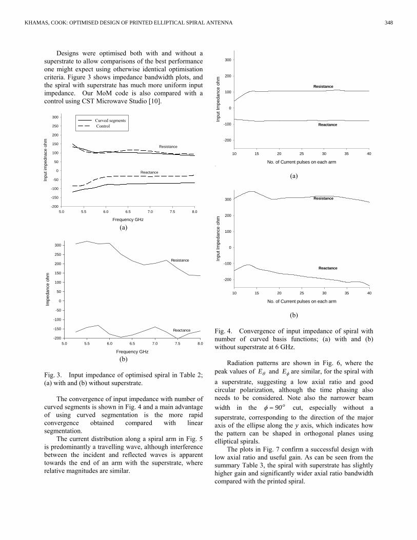
Designs were optimised both with and without a superstrate to allow comparisons of the best performance one might expect using otherwise identical optimisation criteria. Figure 3 shows impedance bandwidth plots, and the spiral with superstrate has much more uniform input impedance. Our MoM code is also compared with a control using CST Microwave Studio [10].
Frequency GHz
5.0 5.5 6.0 6.5 7.0 7.5 8.0
Inpu
t im
pedn
ace
ohm
-200
-150
-100
-50
0
50
100
150
200
250
300Curved segments Control
Resistance
Reactance
(a)
Frequency GHz
5.0 5.5 6.0 6.5 7.0 7.5 8.0
Impe
danc
e oh
m
-200
-150
-100
-50
0
50
100
150
200
250
300
Resistance
Reactance
(b)
Fig. 3. Input impedance of optimised spiral in Table 2; (a) with and (b) without superstrate.
The convergence of input impedance with number of
curved segments is shown in Fig. 4 and a main advantage of using curved segmentation is the more rapid convergence obtained compared with linear segmentation.
The current distribution along a spiral arm in Fig. 5 is predominantly a travelling wave, although interference between the incident and reflected waves is apparent towards the end of an arm with the superstrate, where relative magnitudes are similar.
No. of Current pulses on each arm
10 15 20 25 30 35 40
Inpu
t Im
peda
nce
ohm
-200
-100
0
100
200
300
Resistance
Reactance
(a)
No. of Current pulses on each arm
10 15 20 25 30 35 40
Inpu
t Im
peda
nce
ohm
-200
-100
0
100
200
300 Resistance
Reactance
(b) Fig. 4. Convergence of input impedance of spiral with number of curved basis functions; (a) with and (b) without superstrate at 6 GHz.
Radiation patterns are shown in Fig. 6, where the
peak values of θE and φE are similar, for the spiral with a superstrate, suggesting a low axial ratio and good circular polarization, although the time phasing also needs to be considered. Note also the narrower beam width in the o90=φ cut, especially without a superstrate, corresponding to the direction of the major axis of the ellipse along the y axis, which indicates how the pattern can be shaped in orthogonal planes using elliptical spirals.
The plots in Fig. 7 confirm a successful design with low axial ratio and useful gain. As can be seen from the summary Table 3, the spiral with superstrate has slightly higher gain and significantly wider axial ratio bandwidth compared with the printed spiral.
348KHAMAS, COOK: OPTIMISED DESIGN OF PRINTED ELLIPTICAL SPIRAL ANTENNA
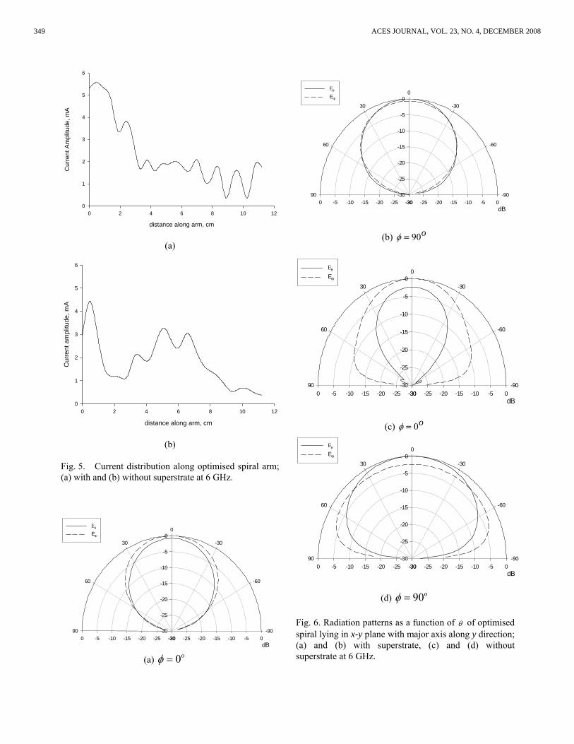
distance along arm, cm
0 2 4 6 8 10 12
Cur
rent
Am
plitu
de, m
A
0
1
2
3
4
5
6
(a)
distance along arm, cm
0 2 4 6 8 10 12
Cur
rent
am
plitu
de, m
A
0
1
2
3
4
5
6
(b) Fig. 5. Current distribution along optimised spiral arm; (a) with and (b) without superstrate at 6 GHz.
dB-30 -25 -20 -15 -10 -5 0
-30
-25
-20
-15
-10
-5
0
-30-25-20-15-10-50-90
-60
-30
0
30
60
90
ΕθEΦ
(a) 0oφ =
dB-30 -25 -20 -15 -10 -5 0
-30
-25
-20
-15
-10
-5
0
-30-25-20-15-10-50-90
-60
-30
0
30
60
90
ΕθEΦ
(b) o90=φ
dB-30 -25 -20 -15 -10 -5 0
-30
-25
-20
-15
-10
-5
0
-30-25-20-15-10-50-90
-60
-30
0
30
60
90
ΕθEΦ
(c) o0=φ
dB-30 -25 -20 -15 -10 -5 0
-30
-25
-20
-15
-10
-5
0
-30-25-20-15-10-50-90
-60
-30
0
30
60
90
ΕθEΦ
(d) 90oφ =
Fig. 6. Radiation patterns as a function of θ of optimised spiral lying in x-y plane with major axis along y direction; (a) and (b) with superstrate, (c) and (d) without superstrate at 6 GHz.
349 ACES JOURNAL, VOL. 23, NO. 4, DECEMBER 2008
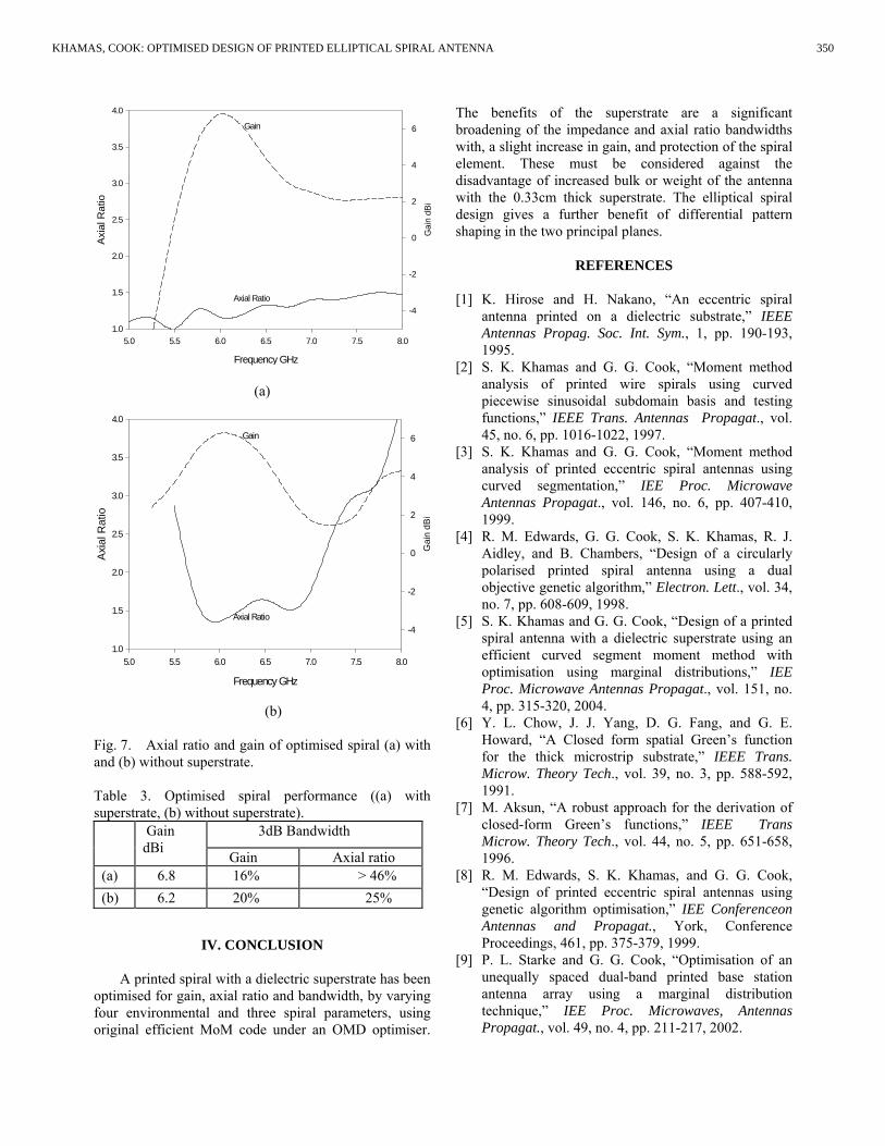
Frequency GHz
5.0 5.5 6.0 6.5 7.0 7.5 8.0
Axi
al R
atio
1.0
1.5
2.0
2.5
3.0
3.5
4.0
Gai
n dB
i
-4
-2
0
2
4
6Gain
Axial Ratio
(a)
Frequency GHz
5.0 5.5 6.0 6.5 7.0 7.5 8.0
Axi
al R
atio
1.0
1.5
2.0
2.5
3.0
3.5
4.0G
ain
dBi
-4
-2
0
2
4
6Gain
Axial Ratio
(b) Fig. 7. Axial ratio and gain of optimised spiral (a) with and (b) without superstrate. Table 3. Optimised spiral performance ((a) with superstrate, (b) without superstrate).
3dB Bandwidth Gain dBi
Gain Axial ratio (a) 6.8 16% > 46% (b) 6.2 20% 25%
IV. CONCLUSION
A printed spiral with a dielectric superstrate has been
optimised for gain, axial ratio and bandwidth, by varying four environmental and three spiral parameters, using original efficient MoM code under an OMD optimiser.
The benefits of the superstrate are a significant broadening of the impedance and axial ratio bandwidths with, a slight increase in gain, and protection of the spiral element. These must be considered against the disadvantage of increased bulk or weight of the antenna with the 0.33cm thick superstrate. The elliptical spiral design gives a further benefit of differential pattern shaping in the two principal planes.
REFERENCES
[1] K. Hirose and H. Nakano, “An eccentric spiral antenna printed on a dielectric substrate,” IEEE Antennas Propag. Soc. Int. Sym., 1, pp. 190-193, 1995.
[2] S. K. Khamas and G. G. Cook, “Moment method analysis of printed wire spirals using curved piecewise sinusoidal subdomain basis and testing functions,” IEEE Trans. Antennas Propagat., vol. 45, no. 6, pp. 1016-1022, 1997.
[3] S. K. Khamas and G. G. Cook, “Moment method analysis of printed eccentric spiral antennas using curved segmentation,” IEE Proc. Microwave Antennas Propagat., vol. 146, no. 6, pp. 407-410, 1999.
[4] R. M. Edwards, G. G. Cook, S. K. Khamas, R. J. Aidley, and B. Chambers, “Design of a circularly polarised printed spiral antenna using a dual objective genetic algorithm,” Electron. Lett., vol. 34, no. 7, pp. 608-609, 1998.
[5] S. K. Khamas and G. G. Cook, “Design of a printed spiral antenna with a dielectric superstrate using an efficient curved segment moment method with optimisation using marginal distributions,” IEE Proc. Microwave Antennas Propagat., vol. 151, no. 4, pp. 315-320, 2004.
[6] Y. L. Chow, J. J. Yang, D. G. Fang, and G. E. Howard, “A Closed form spatial Green’s function for the thick microstrip substrate,” IEEE Trans. Microw. Theory Tech., vol. 39, no. 3, pp. 588-592, 1991.
[7] M. Aksun, “A robust approach for the derivation of closed-form Green’s functions,” IEEE Trans Microw. Theory Tech., vol. 44, no. 5, pp. 651-658, 1996.
[8] R. M. Edwards, S. K. Khamas, and G. G. Cook, “Design of printed eccentric spiral antennas using genetic algorithm optimisation,” IEE Conferenceon Antennas and Propagat., York, Conference Proceedings, 461, pp. 375-379, 1999.
[9] P. L. Starke and G. G. Cook, “Optimisation of an unequally spaced dual-band printed base station antenna array using a marginal distribution technique,” IEE Proc. Microwaves, Antennas Propagat., vol. 49, no. 4, pp. 211-217, 2002.
350KHAMAS, COOK: OPTIMISED DESIGN OF PRINTED ELLIPTICAL SPIRAL ANTENNA
[10] CST Reference Manual. Darmstadt: Computer Simulation Technology, 2006.
Salam Khamas is a lecturer in the Dept. of Electronic and Electrical Engineering, University of Sheffield. He has worked in Antennas since 1988 when he designed the first high temperature superconducting dipole antenna. A patent was awarded and a prize wining paper was published on
that work. Since then he has continued to work on various aspects of antenna modelling and design, which resulted in approximately 27 published journal papers. His research interests include computational electromagnetics, superconducting antennas, conformal antennas, frequency independent antennas, array design and magnetic resonance imaging.
Greg Cook is a Reader in electromagnetics in the Dept. of Electronic and Electrical Engineering at Sheffield University. His research interests include microwave holographic antenna metrology and imaging, superconducting antennas and electromagnetic modelling,
specifically using novel Method of Moments software to analyse printed geometries such as spirals for cellular mobile communications. Latterly he has worked on electromagnetic interactions with biological tissue, and designed TEM cell dosimetry apparatus using original Finite Difference Time Domain code to investigate stress response mechanisms in human tissue. Research is also being conducted in Magnetic Resonance Imaging, to track in-vivo neuronal impulses as perturbations in the gradient field.
351 ACES JOURNAL, VOL. 23, NO. 4, DECEMBER 2008
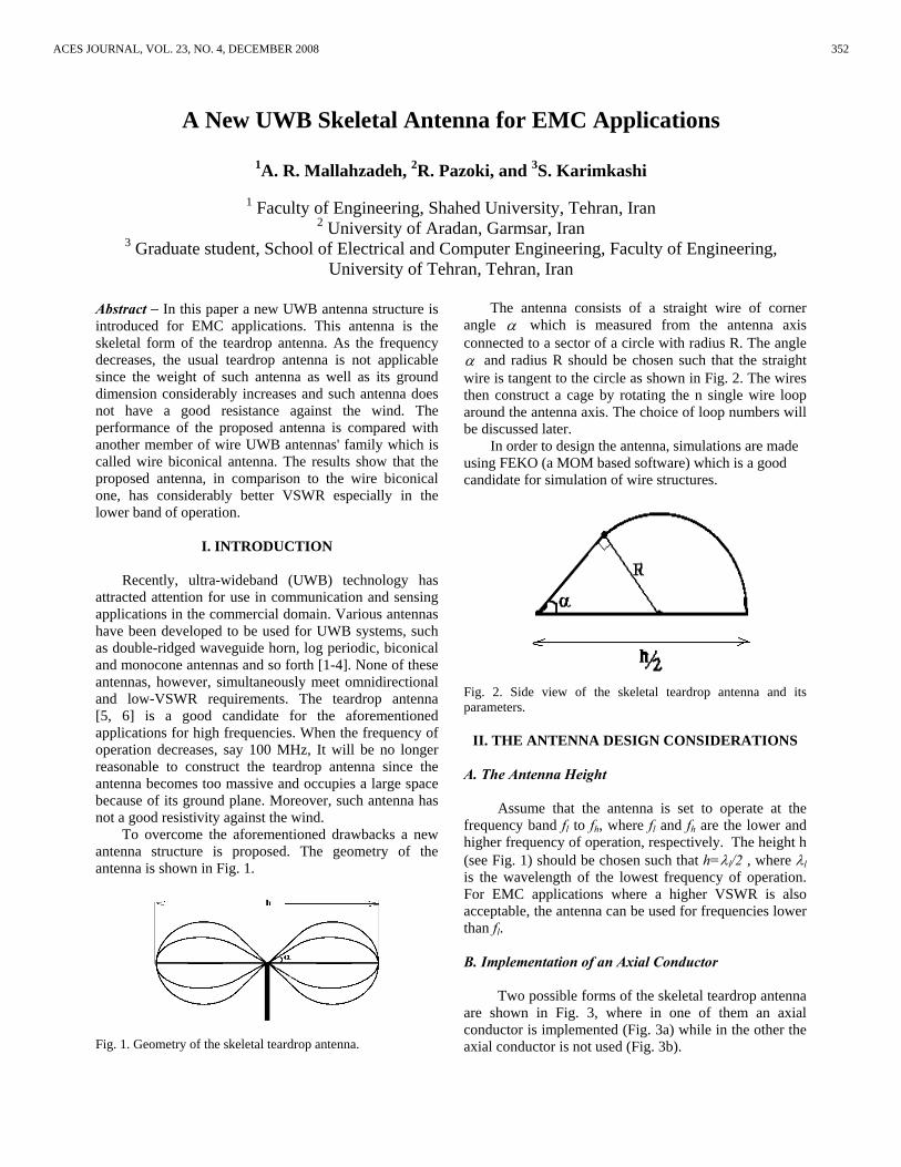
A New UWB Skeletal Antenna for EMC Applications
1A. R. Mallahzadeh, 2R. Pazoki, and 3S. Karimkashi
1 Faculty of Engineering, Shahed University, Tehran, Iran 2 University of Aradan, Garmsar, Iran
3 Graduate student, School of Electrical and Computer Engineering, Faculty of Engineering, University of Tehran, Tehran, Iran
Abstract − In this paper a new UWB antenna structure is introduced for EMC applications. This antenna is the skeletal form of the teardrop antenna. As the frequency decreases, the usual teardrop antenna is not applicable since the weight of such antenna as well as its ground dimension considerably increases and such antenna does not have a good resistance against the wind. The performance of the proposed antenna is compared with another member of wire UWB antennas' family which is called wire biconical antenna. The results show that the proposed antenna, in comparison to the wire biconical one, has considerably better VSWR especially in the lower band of operation.
I. INTRODUCTION
Recently, ultra-wideband (UWB) technology has attracted attention for use in communication and sensing applications in the commercial domain. Various antennas have been developed to be used for UWB systems, such as double-ridged waveguide horn, log periodic, biconical and monocone antennas and so forth [1-4]. None of these antennas, however, simultaneously meet omnidirectional and low-VSWR requirements. The teardrop antenna [5, 6] is a good candidate for the aforementioned applications for high frequencies. When the frequency of operation decreases, say 100 MHz, It will be no longer reasonable to construct the teardrop antenna since the antenna becomes too massive and occupies a large space because of its ground plane. Moreover, such antenna has not a good resistivity against the wind.
To overcome the aforementioned drawbacks a new antenna structure is proposed. The geometry of the antenna is shown in Fig. 1.
Fig. 1. Geometry of the skeletal teardrop antenna.
The antenna consists of a straight wire of corner angle α which is measured from the antenna axis connected to a sector of a circle with radius R. The angle α and radius R should be chosen such that the straight wire is tangent to the circle as shown in Fig. 2. The wires then construct a cage by rotating the n single wire loop around the antenna axis. The choice of loop numbers will be discussed later.
In order to design the antenna, simulations are made using FEKO (a MOM based software) which is a good candidate for simulation of wire structures.
Fig. 2. Side view of the skeletal teardrop antenna and its parameters.
II. THE ANTENNA DESIGN CONSIDERATIONS
A. The Antenna Height
Assume that the antenna is set to operate at the frequency band fl to fh, where fl and fh are the lower and higher frequency of operation, respectively. The height h (see Fig. 1) should be chosen such that h=λl/2 , where λl is the wavelength of the lowest frequency of operation. For EMC applications where a higher VSWR is also acceptable, the antenna can be used for frequencies lower than fl. B. Implementation of an Axial Conductor
Two possible forms of the skeletal teardrop antenna are shown in Fig. 3, where in one of them an axial conductor is implemented (Fig. 3a) while in the other the axial conductor is not used (Fig. 3b).
352ACES JOURNAL, VOL. 23, NO. 4, DECEMBER 2008
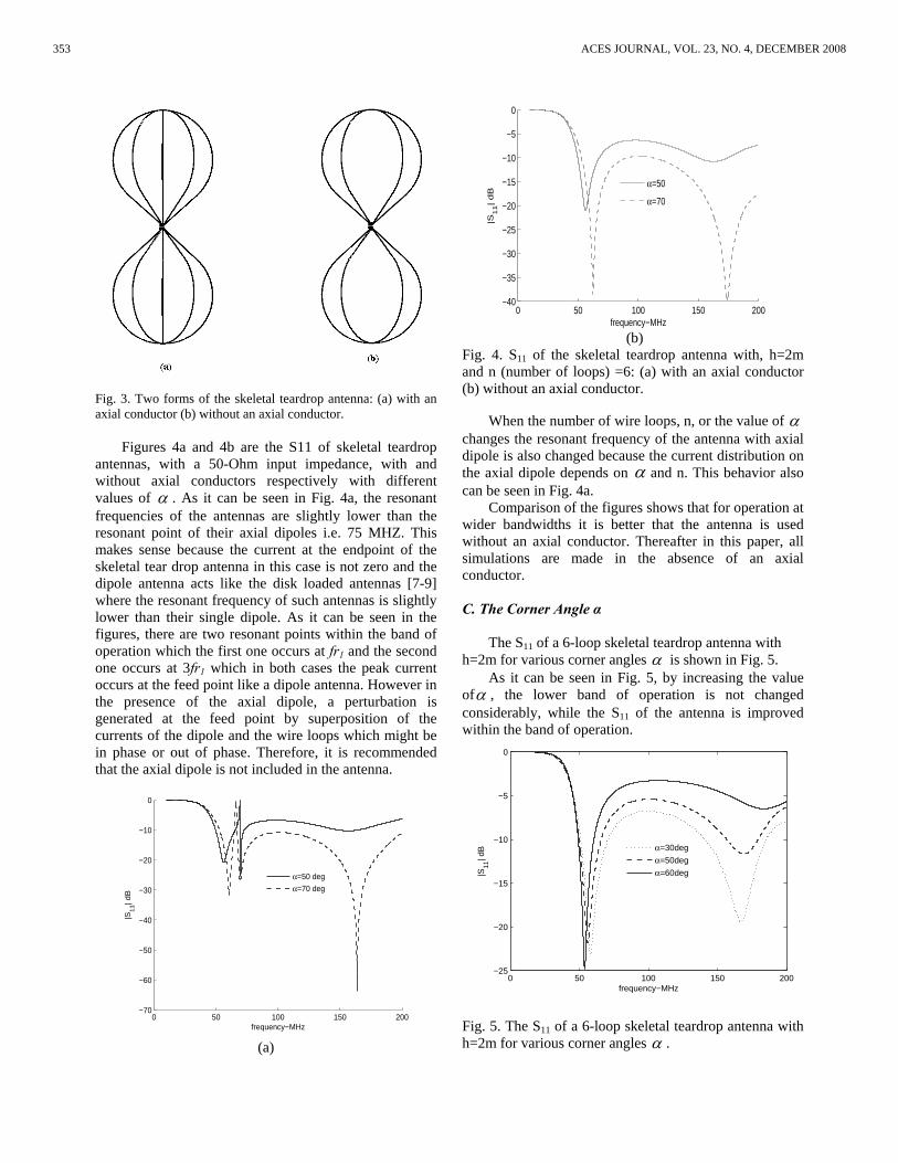
Fig. 3. Two forms of the skeletal teardrop antenna: (a) with an axial conductor (b) without an axial conductor.
Figures 4a and 4b are the S11 of skeletal teardrop
antennas, with a 50-Ohm input impedance, with and without axial conductors respectively with different values of α . As it can be seen in Fig. 4a, the resonant frequencies of the antennas are slightly lower than the resonant point of their axial dipoles i.e. 75 MHZ. This makes sense because the current at the endpoint of the skeletal tear drop antenna in this case is not zero and the dipole antenna acts like the disk loaded antennas [7-9] where the resonant frequency of such antennas is slightly lower than their single dipole. As it can be seen in the figures, there are two resonant points within the band of operation which the first one occurs at fr1 and the second one occurs at 3fr1 which in both cases the peak current occurs at the feed point like a dipole antenna. However in the presence of the axial dipole, a perturbation is generated at the feed point by superposition of the currents of the dipole and the wire loops which might be in phase or out of phase. Therefore, it is recommended that the axial dipole is not included in the antenna.
0 50 100 150 200−70
−60
−50
−40
−30
−20
−10
0
frequency−MHz
|S11| d
B
α=50 deg
α=70 deg
(a)
0 50 100 150 200−40
−35
−30
−25
−20
−15
−10
−5
0
frequency−MHz
|S11| dB
α=50
α=70
(b)
Fig. 4. S11 of the skeletal teardrop antenna with, h=2m and n (number of loops) =6: (a) with an axial conductor (b) without an axial conductor.
When the number of wire loops, n, or the value of α
changes the resonant frequency of the antenna with axial dipole is also changed because the current distribution on the axial dipole depends on α and n. This behavior also can be seen in Fig. 4a.
Comparison of the figures shows that for operation at wider bandwidths it is better that the antenna is used without an axial conductor. Thereafter in this paper, all simulations are made in the absence of an axial conductor.
C. The Corner Angle α
The S11 of a 6-loop skeletal teardrop antenna with h=2m for various corner angles α is shown in Fig. 5.
As it can be seen in Fig. 5, by increasing the value ofα , the lower band of operation is not changed considerably, while the S11 of the antenna is improved within the band of operation.
0 50 100 150 200−25
−20
−15
−10
−5
0
frequency−MHz
|S11
| dB α=30deg
α=50deg
α=60deg
Fig. 5. The S11 of a 6-loop skeletal teardrop antenna with h=2m for various corner angles α .
353 ACES JOURNAL, VOL. 23, NO. 4, DECEMBER 2008
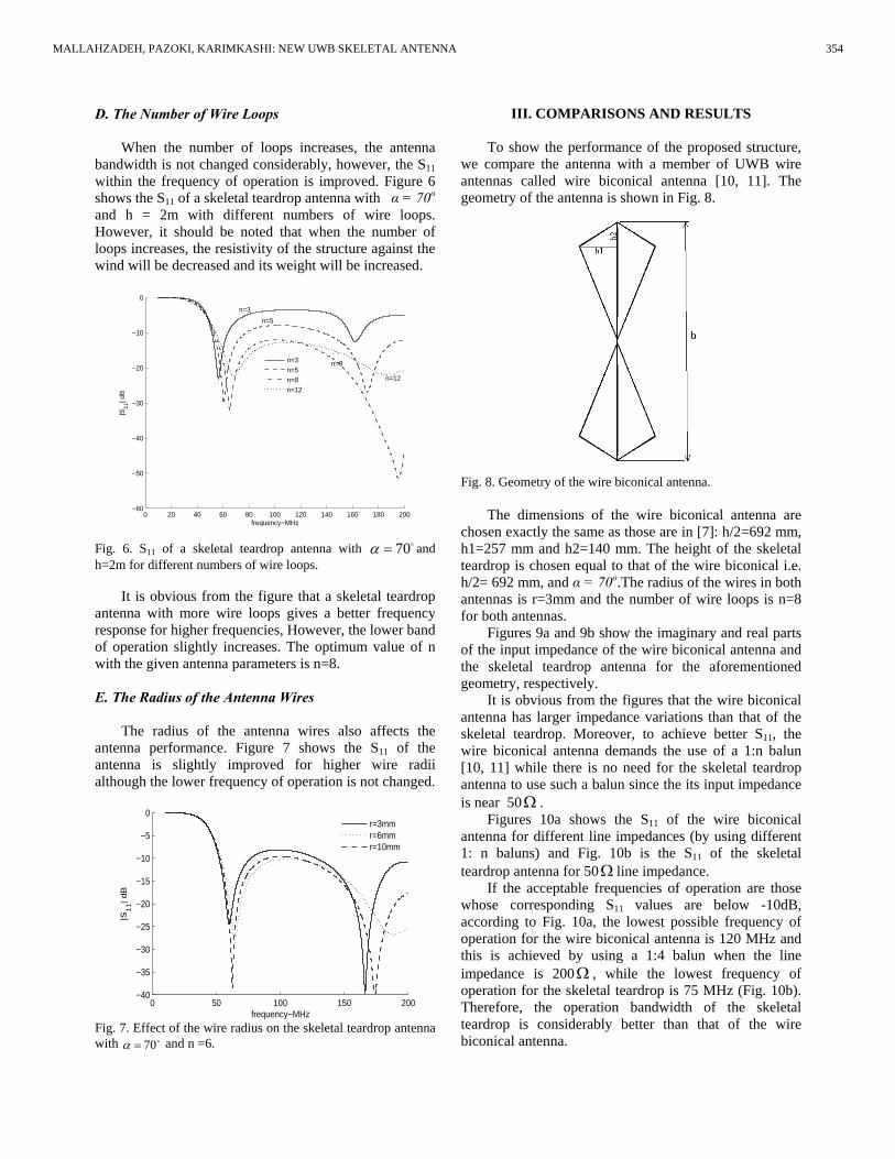
D. The Number of Wire Loops
When the number of loops increases, the antenna bandwidth is not changed considerably, however, the S11 within the frequency of operation is improved. Figure 6 shows the S11 of a skeletal teardrop antenna with α = 70o
and h = 2m with different numbers of wire loops. However, it should be noted that when the number of loops increases, the resistivity of the structure against the wind will be decreased and its weight will be increased.
0 20 40 60 80 100 120 140 160 180 200−60
−50
−40
−30
−20
−10
0
frequency−MHz
|S11
| dB
n=3n=5n=8n=12
n=3
n=5
n=8
n=12
Fig. 6. S11 of a skeletal teardrop antenna with 70=α and h=2m for different numbers of wire loops.
It is obvious from the figure that a skeletal teardrop antenna with more wire loops gives a better frequency response for higher frequencies, However, the lower band of operation slightly increases. The optimum value of n with the given antenna parameters is n=8.
E. The Radius of the Antenna Wires
The radius of the antenna wires also affects the antenna performance. Figure 7 shows the S11 of the antenna is slightly improved for higher wire radii although the lower frequency of operation is not changed.
0 50 100 150 200−40
−35
−30
−25
−20
−15
−10
−5
0
frequency−MHz
|S11| dB
r=3mmr=6mmr=10mm
Fig. 7. Effect of the wire radius on the skeletal teardrop antenna with 70=α and n =6.
III. COMPARISONS AND RESULTS
To show the performance of the proposed structure, we compare the antenna with a member of UWB wire antennas called wire biconical antenna [10, 11]. The geometry of the antenna is shown in Fig. 8.
Fig. 8. Geometry of the wire biconical antenna.
The dimensions of the wire biconical antenna are
chosen exactly the same as those are in [7]: h/2=692 mm, h1=257 mm and h2=140 mm. The height of the skeletal teardrop is chosen equal to that of the wire biconical i.e. h/2= 692 mm, and α = 70o.The radius of the wires in both antennas is r=3mm and the number of wire loops is n=8 for both antennas.
Figures 9a and 9b show the imaginary and real parts of the input impedance of the wire biconical antenna and the skeletal teardrop antenna for the aforementioned geometry, respectively.
It is obvious from the figures that the wire biconical antenna has larger impedance variations than that of the skeletal teardrop. Moreover, to achieve better S11, the wire biconical antenna demands the use of a 1:n balun [10, 11] while there is no need for the skeletal teardrop antenna to use such a balun since the its input impedance is near 50Ω .
Figures 10a shows the S11 of the wire biconical antenna for different line impedances (by using different 1: n baluns) and Fig. 10b is the S11 of the skeletal teardrop antenna for 50Ω line impedance.
If the acceptable frequencies of operation are those whose corresponding S11 values are below -10dB, according to Fig. 10a, the lowest possible frequency of operation for the wire biconical antenna is 120 MHz and this is achieved by using a 1:4 balun when the line impedance is 200Ω , while the lowest frequency of operation for the skeletal teardrop is 75 MHz (Fig. 10b). Therefore, the operation bandwidth of the skeletal teardrop is considerably better than that of the wire biconical antenna.
354MALLAHZADEH, PAZOKI, KARIMKASHI: NEW UWB SKELETAL ANTENNA
0 50 100 150 200−1000
−800
−600
−400
−200
0
200
400
frequency−MHz
Impedance
(Ω
)
real(Zin)Image(Zin)
(a)
0 50 100 150 200−600
−500
−400
−300
−200
−100
0
100
frequency−MHz
Impe
danc
e (Ω
)
real(Zin)
Image(Zin)
(b)
Fig. 9. Imaginary and real parts of the input impedance of (a) the wire biconical antenna and (b) the skeletal teardrop antenna.
The radiation pattern and the maximum gain values of the two antennas at different frequencies are compared in Figs. 11a and 11b.
0 50 100 150 200−20
−18
−16
−14
−12
−10
−8
−6
−4
−2
0
frequency (MHz)
S11
(dB
)
Z0=50 Ω
Z0=100 Ω
Z0=150 Ω
Z0=200 Ω
(a)
0 50 100 150 200−35
−30
−25
−20
−15
−10
−5
0
frequency (MHz)
S11
(dB
) f=75 MHz
(b)
Fig. 10. S11 of (a) the wire biconical antenna for different input impedances and (b) the skeletal teardrop antenna.
100
30
210
60
240
90
270
120
300
150
330
180 0
gain(dB)
f=50MHz
Gmax
=1.83dB
100
30
210
60
240
90
270
120
300
150
330
180 0
gain(dB)
f=100MHz
Gmax
=2.08dB
100
30
210
60
240
90
270
120
300
150
330
180 0
gain(dB)
f=150MHz
Gmax
=2.53dB
(a)
100
30
210
60
240
90
270
120
300
150
330
180 0
gain(dB)
f=50MHz
Gmax
=1.81dB
100
30
210
60
240
90
270
120
300
150
330
180 0
gain(dB)
f=100MHz
Gmax
=2.02dB
100
30
210
60
240
90
270
120
300
150
330
180 0
gain(dB)
f=150MHz
Gmax
=2.35dB
(b) Fig. 11. the radiation patterns of (a) the wire biconical antenna and (b) the skeletal teardrop antenna at different frequencies.
Figure 11a shows the radiation pattern of the wire
biconical antenna and Fig. 11b shows the radiation pattern of the skeletal teardrop antenna at 3 different frequencies. As it can be seen, there is no considerable
355 ACES JOURNAL, VOL. 23, NO. 4, DECEMBER 2008
difference between the radiation patterns and the maximum gain values of the two antenna structures.
IV. CONCLUSION
A new skeletal antenna structure was proposed in
this paper. This antenna structure is the skeletal form of the conventional teardrop antenna which is used at microwave frequencies. The skeletal form is preferred to its continuous one at low frequencies due to difficulties of practical considerations of the continuous form. The performance of the antenna was compared to another wire-cage antenna called wire biconical antenna. The results show that with the same dimensions, the operation bandwidth (especially at lower frequencies) of the proposed structure is considerably better than that of the wire biconical antenna. Therefore, with the same frequency of operation the skeletal teardrop antenna can be much smaller than the wire biconical antenna (nearly half). Moreover, unlike the wire biconical antenna, there is no need for the proposed antenna to use a 1:n balun.
REFERENCES
[1] S. Sadat, M. Houshmand, and M. Roshandel,
“Design of a microstrip square-ring slot antenna filled by an h-shape slot for UWB applications,” Progress In Electromagnetics Research, PIER 70, 191-198, 2007.
[2] C. Burns, P. Leuchtmann, and R. Vahldieck, “Analysis and simulation of a 1-18 GHz broadband double-ridged horn antenna,” IEEE Transactions on Electromagnetic Compatibility, vol. 45, Feb. 2003.
[3] D. J. Muller, and K. Sarabandi, “Design and analysis of a 3-Arm spiral antenna” IEEE Transactions on Antennas and Propagation, vol. 55, no. 2, Feb. 2007
[4] A. S. Turk, “Ultra-wideband TEM horn design for ground penetrating impulse radar systems,” Microwave and Optical Technology Letters, vol. 41, Issue 5, pp. 333-336, April 2004.
[5] T. Taniguchi and T. Kobayashi, “An omnidirectional and low-VSWR antenna for ultra-wideband wireless systems,” IEEE conference, 2002
[6] T. Taniguchi and T. Kobayashi, “An omnidirectional and low-VSWR antenna for the FCC-approved UWB frequency band,” IEEE conference, 2003
[7] C. A. Balanis, Antenna Theory, Analysis and Design, John Wiley and Sons, 1997.
[8] T. A. Milligan, Modern Antenna Design, John Wiley and Sons, 2005.
[9] A. A. Eldek, “Design of double dipole antenna with enhanced usable bandwidth for wideband phased array applications,” Progress In Electromagnetics Research, PIER 59, 1-15, 2006.
[10] B. A. Austin, and A. P. C. Fourie, “Characteristics of the wire biconical antenna used for EMC
measurements,” IEEE Transactions on Electromagnetic Compatibility, vol. 33, no. 3, Nov. 1991
[11] S. M. Mann and A. C. Marvin, “Characteristics of the skeletal biconical antenna as used for EMC applications,” IEEE Transactions on Electromagnetic Compatibility, vol. 36, no. 4, Nov. 1994.
Alireza Mallahzadeh was born in Bushehr, a beautiful city in the south of Iran in 1977. He received the B.S. degree in electrical engineering from Isfahan University of Technology, Isfahan, Iran, in 1999 and the MSc. degree in electrical engineering from Iran University of Science and Technology, Tehran, Iran, in 2001,
and the Ph.D. degree in electrical engineering from Iran University of Science and Technology, Tehran, Iran, in 2006. He is a member of academic staff, Faculty of Engineering, Shahed University. He is interested in numerical modeling, antennas and microwaves.
Reza Pazoki received the B.S. and M.S. degrees from Iran's KNT and IUST universities in 2002 and 2004 respectively,and currently he is a Ph.D. student at the Iran's university of science and technology(IUST). He has publications including FDTD, ADI-FDTD, slot antennas, biconical antennas and power dividers.
Shaya Karimkashi is currently working toward Ph.D. degree at the University of Mississippi. His research interests include reflector antennas, dielectric resonator antennas, array antennas and optimization algorithms in electromagnetics. He holds a MSc. in communications engineering from
University of Tehran, Iran.
356MALLAHZADEH, PAZOKI, KARIMKASHI: NEW UWB SKELETAL ANTENNA
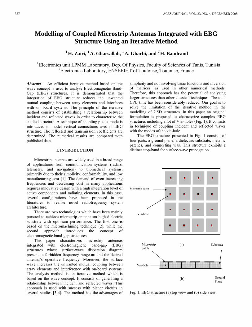
Modelling of Coupled Microstrip Antennas Integrated with EBG Structure Using an Iterative Method
1 H. Zairi, 1 A. Gharsallah, 1 A. Gharbi, and 2 H. Baudrand
1 Electronics unit LPMM Laboratory, Dep. Of Physics, Faculty of Sciences of Tunis, Tunisia
2Electronics Laboratory, ENSEEIHT of Toulouse, Toulouse, France Abstract − An efficient iterative method based on the wave concept is used to analyse Electromagnetic Band-Gap (EBG) structures. It is demonstrated that the integration of EBG structure reduces the unwanted mutual coupling between array elements and interfaces with on board systems. The principle of the iterative method consists of establishing a relationship between incident and reflected waves in order to characterize the studied structure. A technique of coupling pixels-mode is introduced to model vertical connections used in EBG structure. The reflected and transmission coefficients are determined. The numerical results are compared with published data.
I. INTRODUCTION
Microstrip antennas are widely used in a broad range of applications from communication systems (radars, telemetry, and navigation) to biomedical systems, primarily due to their simplicity, conformability, and low manufacturing cost [1]. The demand of even increasing frequencies and decreasing cost in many applications requires innovative design with a high integration level of active components and radiating elements. In this case, several configurations have been proposed in the literatures to realise novel radiofrequency system architecture.
There are two technologies which have been mainly pursued to achieve microstrip antenna on high dielectric substrate with optimum performance. The first one is based on the micromachining technique [2], while the second approach introduces the concept of electromagnetic band-gap structures.
This paper characterizes microstrip antennas integrated with electromagnetic band-gap (EBG) structures whose surface-wave dispersion diagram presents a forbidden frequency range around the desired antenna’s operative frequency. Moreover, the surface wave increases the unwanted mutual coupling between array elements and interference with on-board systems. The analysis method is an iterative method which is based on the wave concept. It consists of generating a relationship between incident and reflected waves. This approach is used with success with planar circuits in several studies [3-4]. The method has the advantages of
simplicity and not involving basic functions and inversion of matrices, as used in other numerical methods. Therefore, this approach has the potential of analysing larger structures than other classical techniques. The total CPU time has been considerably reduced. Our goal is to solve the limitation of the iterative method in the modelling of 2.5D structures. In this paper an original formulation is proposed to characterize complex EBG structures including a lot of Via–holes (Fig. 1). It consists in technique of coupling incident and reflected waves with the modes of the via-hole.
The EBG structure presented in Fig. 1 consists of four parts: a ground plane, a dielectric substrate, metallic patches, and connecting vias. This structure exhibits a distinct stop-band for surface-wave propagation. Fig. 1. EBG structure (a) top view and (b) side view.
(a)
Microstrip patch
Via-hole
(b) Ground Plane
Microstrip patch
Via-hole
Substrate
357 ACES JOURNAL, VOL. 23, NO. 4, DECEMBER 2008
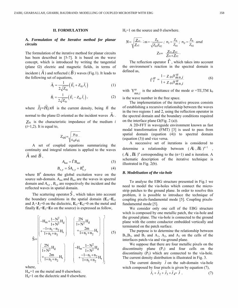
II. FORMULATION
A. Formulation of the Iterative method for planar circuits The formulation of the iterative method for planar circuits has been described in [5-7]. It is based on the wave concept, which is introduced by writing the tangential (plane Ω) electric and magnetic fields, in terms of incident ( A ) and reflected ( B ) waves (Fig.1). It leads to the following set of equations,
( )00
12i i i i
iA E Z J
Z= + (1)
( )00
12i i i i
iB E Z J
Z= − , (2)
where nxiHiJ = is the current density, being n the
normal to the plane Ω oriented as the incident waves iA .
iZ0 is the characteristic impedance of the medium i (i=1,2). It is equal to,
rioooiZεε
µ=
A set of coupled equations summarizing the continuity and integral relations is applied to the waves A and B ,
ˆmn mnA B= Γ (3)
0, , ,
ˆx y x y x yB SA B= + (4)
where B0 denotes the global excitation wave on the source sub-domain. Amn and Bmn are the waves in spectral domain and Ax,y , Bx,y are respectively the incident and the reflected waves in spatial domain.
The scattering operator S , which takes into account the boundary conditions in the spatial domain (Et1=Et2 and J1+J2=0 on the dielectric, Et1=Et2=0 on the metal and finally E1=E2=Eo on the source) is expressed as follow,
2m dd 22
1 2 ss1 21 2
2md d2 2
1 2s s1 2 1 2
2N1 N HH H1 N1 N
2m1 n n HH 1 n n1 n n
2N 1 NH H H1 N 1 N
2m 1 n nH H1 n n 1 n n
S
⎡ ⎤⎛ ⎞ ⎛ ⎞⎢ ⎥⎜ ⎟ ⎜ ⎟⎢ ⎥⎜ ⎟ ⎜ ⎟⎢⎜ ⎟ ⎜ ⎟⎢⎜ ⎟ ⎜ ⎟⎢⎜ ⎟ ⎜ ⎟⎜ ⎟⎢ ⎝ ⎠⎝ ⎠⎢⎢⎢ ⎛ ⎞⎛ ⎞⎢ ⎜ ⎟⎜ ⎟⎢ ⎜ ⎟⎜ ⎟⎢ ⎜ ⎟⎜ ⎟⎢ ⎜ ⎟⎜ ⎟⎢ ⎜ ⎟⎜ ⎟ ⎜ ⎟⎢ ⎝ ⎠ ⎝ ⎠⎣ ⎦
− − +++
− + − ++ + ++ +
−− −+ +
− − ++ ++ + + +
=
⎥⎥⎥⎥⎥⎥⎥⎥⎥⎥⎥⎥⎥
(5)
where, Hm=1 on the metal and 0 elsewhere. Hd=1 on the dielectric and 0 elsewhere.
Hs=1 on the source and 0 elsewhere.
2
1
o
o
ZZN= ; and n; n; 21
02
0
01
0
0201
0
ZZ
ZZ
ZZZm ===
0201
02010 . Z ZZZZ
+= .
The reflection operator Γ , which takes into account the environment’s reaction in the spectral domain is defined as,
1 ,ˆ1 ,
YZ oi m n ii YZ oi m n i
αα
α−
=Γ + (6)
with ,
Ymn iα is the admittance of the mode α =TE,TM k0
is the wave number in the free space. The implementation of the iterative process consists
of establishing a recursive relationship between the waves in the two regions 1 and 2, using the reflection operator in the spectral domain and the boundary conditions required on the interface plane Ω(Fig. 2 (a)).
A 2D-FFT in waveguide environment known as fast modal transformation (FMT) [3] is used to pass from spatial domain (equation (4)) to spectral domain (equation (3)) and vice versa.
A successive set of iterations is considered to determine a relationship between ( iAα , iBα )n+1 , ( iAα , iBα )n corresponding to the (n+1) and n iteration. A schematic description of the iterative technique is illustrated in Fig. 2(b).
B. Modelisation of the via-hole
To analyse the EBG structure presented in Fig.1 we need to model the via-holes which connect the micro-strip patches to the ground plane. In order to resolve this problem, it is possible to introduce the technique of coupling pixels-fundamental mode [5]. Coupling pixels-fundamental mode [5].
We consider only one cell of the EBG structure witch is composed by one metallic patch, the via-hole and the ground plane. The via-hole is connected to the ground plane with the centre conductor embedded vertically and terminated on the patch surface.
The purpose is to determine the relationship between B1,B2, and B3 and A1, A2, and A3 on the cells of the interfaces patch-via and via-ground plane.
We suppose that there are four metallic pixels on the discontinuity plane (P1) and four cells on the discontinuity (P2) which are connected to the via-hole. The current density distribution is illustrated in Fig. 3.
The current density J on the sub-domain via-hole witch composed by four pixels is given by equation (7),
JJJJJ =+++ 4321 . (7)
358ZAIRI, GHARSALLAH, GHARBI, BAUDRAND: MODELLING OF COUPLED MICROSTRIP WITH EBG
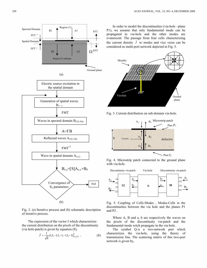
(a)
(b)
Fig. 2. (a) Iterative process and (b) schematic description of iterative process.
The expression of the vector J which characterizes the current distribution on the pixels of the discontinuity (via hole-patch) is given by equation (8),
TyxJ ),()1,1,1,1,1,1,1,1(
81
−−−−= . (8)
In order to model the discontinuities (via-hole –plane P1), we assume that only fundamental mode can be propagated in via-hole and the other modes are evanescent. The passage from four cells characterizing the current density J to modes and vice versa can be considered as multi-port network depicted in Fig. 5.
Fig. 3. Current distribution on sub-domain via-hole.
Fig. 4. Microstrip patch connected to the ground plane with via-hole.
Discontinuity via-patch Via-hole Discontinuity via-patch
a2 b2
b3 a3
A2 B2
M
M
Q
A3 B3
Fig. 5. Coupling of Cells-Modes , Modes-Cells in the discontinuities between the via hole and the planes P1 and P2 .
Where A, B and a, b are respectively the waves on the pixels of the discontinuity via-patch and the fundamental mode witch propagate in the via-hole.
The symbol Q is a two-network port which characterizes the via-hole, using the theory of transmission line. The scattering matrix of this two-port network is given by,
1J 4J2J 3J
Metallic
Via-hole Ground plane
FFT
Ground plane
Spatial Domain
Spectral Domain
1FFT− FFT A1 B1
B2 A2
Region (1)
Region (2) subtrate
Ω1FFT−
FMT
Electric source excitation in the spatial domain
Generation of spatial waves B(x y)
Waves in spectral domain B(TE,TM)
Reflected waves A(TE,TM)
Wave in spatial domain A(x,y)
Convergence of Sij parameters
End
A=ΓB
FMT-1
Bx,y=[S]Ax,y+B0
Microstrip patch
Plan P2
Plan P1
A3
dielectric
A1 B1
A2 B2
B3
h Via-hole
359 ACES JOURNAL, VOL. 23, NO. 4, DECEMBER 2008
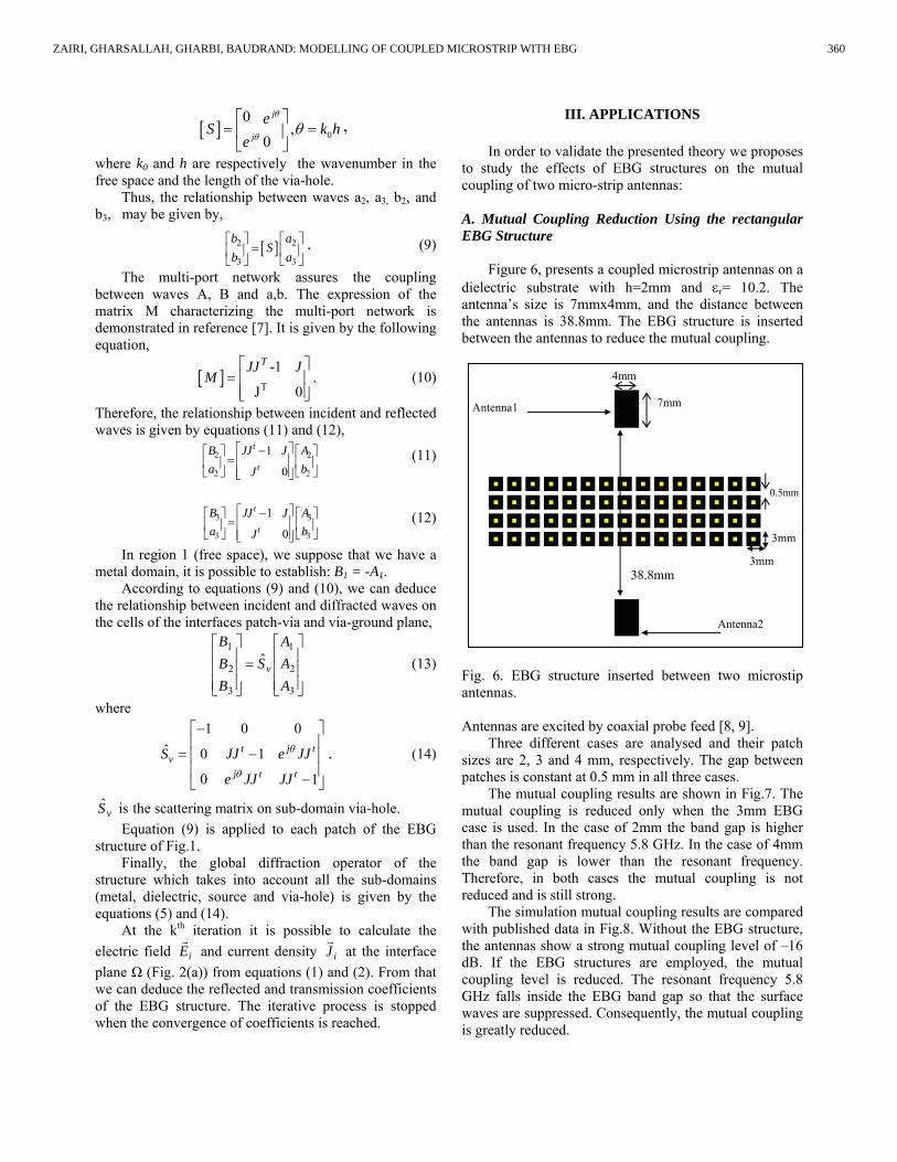
[ ] 0
0,
0
j
j
eS k h
e
θ
θθ
⎡ ⎤= =⎢ ⎥
⎣ ⎦,
where k0 and h are respectively the wavenumber in the free space and the length of the via-hole.
Thus, the relationship between waves a2, a3, b2, and b3, may be given by,
[ ]2 2
3 3
b aS
b a⎡ ⎤ ⎡ ⎤
=⎢ ⎥ ⎢ ⎥⎣ ⎦ ⎣ ⎦
. (9) The multi-port network assures the coupling
between waves A, B and a,b. The expression of the matrix M characterizing the multi-port network is demonstrated in reference [7]. It is given by the following equation,
[ ] T
-1
J 0
TJJ JM
⎡ ⎤= ⎢ ⎥
⎢ ⎥⎣ ⎦. (10)
Therefore, the relationship between incident and reflected waves is given by equations (11) and (12),
2 2
2 2
1
0
t
t
B JJ J Aa bJ
⎡ ⎤−⎡ ⎤ ⎡ ⎤= ⎢ ⎥⎢ ⎥ ⎢ ⎥
⎣ ⎦ ⎢ ⎥ ⎣ ⎦⎣ ⎦
(11)
3 3
3 3
1
0
t
t
B AJJ Ja bJ
⎡ ⎤−⎡ ⎤ ⎡ ⎤= ⎢ ⎥⎢ ⎥ ⎢ ⎥
⎢ ⎥⎣ ⎦ ⎣ ⎦⎣ ⎦
(12)
In region 1 (free space), we suppose that we have a metal domain, it is possible to establish: B1 = -A1.
According to equations (9) and (10), we can deduce the relationship between incident and diffracted waves on the cells of the interfaces patch-via and via-ground plane,
⎥⎥⎥
⎦
⎤
⎢⎢⎢
⎣
⎡=
⎥⎥⎥
⎦
⎤
⎢⎢⎢
⎣
⎡
3
2
1
3
2
1ˆ
AAA
SBBB
v (13)
where
1 0 0
ˆ 0 1
0 1
jt tv
j t t
S JJ e JJ
e JJ JJ
θ
θ
−⎡ ⎤⎢ ⎥
= −⎢ ⎥⎢ ⎥−⎣ ⎦
. (14)
vS is the scattering matrix on sub-domain via-hole. Equation (9) is applied to each patch of the EBG
structure of Fig.1. Finally, the global diffraction operator of the
structure which takes into account all the sub-domains (metal, dielectric, source and via-hole) is given by the equations (5) and (14).
At the kth iteration it is possible to calculate the electric field iE and current density iJ at the interface plane Ω (Fig. 2(a)) from equations (1) and (2). From that we can deduce the reflected and transmission coefficients of the EBG structure. The iterative process is stopped when the convergence of coefficients is reached.
III. APPLICATIONS
In order to validate the presented theory we proposes to study the effects of EBG structures on the mutual coupling of two micro-strip antennas:
A. Mutual Coupling Reduction Using the rectangular EBG Structure
Figure 6, presents a coupled microstrip antennas on a dielectric substrate with h=2mm and εr= 10.2. The antenna’s size is 7mmx4mm, and the distance between the antennas is 38.8mm. The EBG structure is inserted between the antennas to reduce the mutual coupling.
Fig. 6. EBG structure inserted between two microstip antennas. Antennas are excited by coaxial probe feed [8, 9].
Three different cases are analysed and their patch sizes are 2, 3 and 4 mm, respectively. The gap between patches is constant at 0.5 mm in all three cases.
The mutual coupling results are shown in Fig.7. The mutual coupling is reduced only when the 3mm EBG case is used. In the case of 2mm the band gap is higher than the resonant frequency 5.8 GHz. In the case of 4mm the band gap is lower than the resonant frequency. Therefore, in both cases the mutual coupling is not reduced and is still strong.
The simulation mutual coupling results are compared with published data in Fig.8. Without the EBG structure, the antennas show a strong mutual coupling level of –16 dB. If the EBG structures are employed, the mutual coupling level is reduced. The resonant frequency 5.8 GHz falls inside the EBG band gap so that the surface waves are suppressed. Consequently, the mutual coupling is greatly reduced.
7mm
4mm
38.8mm
0.5mm
3mm
3mm
Antenna1
Antenna2
360ZAIRI, GHARSALLAH, GHARBI, BAUDRAND: MODELLING OF COUPLED MICROSTRIP WITH EBG
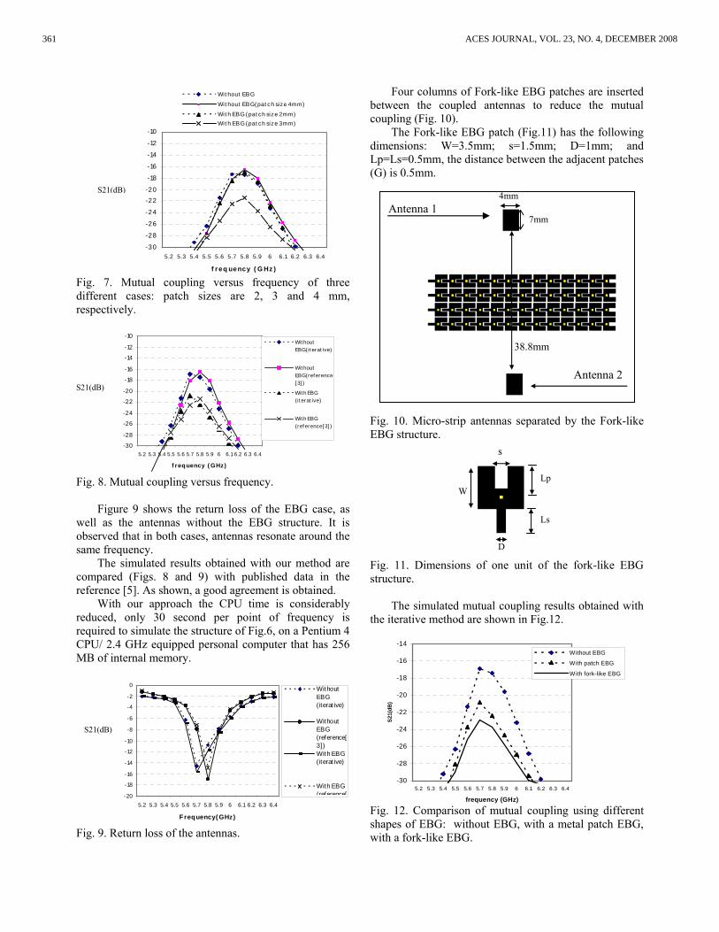
Fig. 7. Mutual coupling versus frequency of three different cases: patch sizes are 2, 3 and 4 mm, respectively.
Fig. 8. Mutual coupling versus frequency.
Figure 9 shows the return loss of the EBG case, as well as the antennas without the EBG structure. It is observed that in both cases, antennas resonate around the same frequency.
The simulated results obtained with our method are compared (Figs. 8 and 9) with published data in the reference [5]. As shown, a good agreement is obtained.
With our approach the CPU time is considerably reduced, only 30 second per point of frequency is required to simulate the structure of Fig.6, on a Pentium 4 CPU/ 2.4 GHz equipped personal computer that has 256 MB of internal memory.
Fig. 9. Return loss of the antennas.
Four columns of Fork-like EBG patches are inserted between the coupled antennas to reduce the mutual coupling (Fig. 10).
The Fork-like EBG patch (Fig.11) has the following dimensions: W=3.5mm; s=1.5mm; D=1mm; and Lp=Ls=0.5mm, the distance between the adjacent patches (G) is 0.5mm.
Fig. 10. Micro-strip antennas separated by the Fork-like EBG structure.
Fig. 11. Dimensions of one unit of the fork-like EBG structure.
The simulated mutual coupling results obtained with the iterative method are shown in Fig.12.
-30
-28
-26
-24
-22
-20
-18
-16
-14
5.2 5.3 5.4 5.5 5.6 5.7 5.8 5.9 6 6.1 6.2 6.3 6.4
frequency (GHz)
S21(
dB)
Without EBG
With patch EBG
With fork-like EBG
Fig. 12. Comparison of mutual coupling using different shapes of EBG: without EBG, with a metal patch EBG, with a fork-like EBG.
S21(dB)
-30
-28
-26
-24
-22-20
-18
-16
-14
-12
-10
5.2 5.3 5.4 5.5 5.6 5.7 5.8 5.9 6 6.1 6.2 6.3 6.4
f r eq uency ( G Hz )
Wit hout EBG
Wit hout EBG(pat ch size 4mm)
Wit h EBG (pat ch size 2mm) Wit h EBG (pat ch size 3mm)
S21(dB)
-20
-18
-16
-14
-12
-10
-8
-6
-4
-2
0
5.2 5.3 5.4 5.5 5.6 5.7 5.8 5.9 6 6.1 6.2 6.3 6.4
Frequency( GHz)
WithoutEBG(iterat ive)
WithoutEBG(reference[3])With EBG(iterat ive)
With EBG(reference[
S21(dB)
-30
-28
-26
-24
-22
-20
-18
-16
-14
-12
-10
5.2 5.3 5.4 5.5 5.6 5.7 5.8 5.9 6 6.1 6.2 6.3 6.4
f requency ( GHz)
Wit houtEBG(it erat ive)
Wit houtEBG(ref erence[ 3] )
Wit h EBG(it erat ive)
Wit h EBG(ref erence[ 3] )
Antenna 1
Antenna 2
7mm
4mm
38.8mm
D
s
Lp
Ls
W
361 ACES JOURNAL, VOL. 23, NO. 4, DECEMBER 2008
Without the EBG structure, the antennas show a strong mutual coupling of -16 dB. When the metal patches EBG structure is employed, the mutual coupling is reduced to -21 and when the fork-like EBG is used the mutual coupling is reduced to -23 at 5.8 GHz, which proves that the surface wave is suppressed and demonstrates the capability of the fork-like EBG structure to reduce the mutual coupling. It also demonstrates that the EBG band gap of the Fork-like structure is deeper than the one of EBG patch structure.
IV. CONCLUSION
The formulation of an iterative method is developed to analyse different EBG structures. A technique of coupling pixels-fundamental mode has been successfully applied for the modelisation of the via-holes. As applications, the electromagnetic band-gap structure is inserted between the antenna elements to reduce the mutual coupling. This mutual coupling reduction technique can be used in various antenna array applications. Numerical results show good agreement with those obtained from the FDTD in [5]. Also compared is the mutual coupling of microstrip antennas with different shapes of EBG structures.
REFERENCES
[1] D. M. Pozar, “Microstrip antennas” Proc. IEE, vol, pp.
79-91, Jan 1992 [2] I. Papapolymerous, R. F. Drayton, and L. P. B. Katehi
“Micromachined patch antennas,” IEEE Trans. Antennas and Propagation, vol. 46, no. 2. pp.275-283, February 1998.
[3] A. Gharsallah, A.Gharbi, L. Desclos, and H. Baudrand, “Analysis of interdigital capacitor and quasi-lumped miniaturized filters using iterative method,” International Journal Of Numerical Modelling, vol. 15, pp.169-179, 2002.
[4] A. Mami, H. Zairi, A. Gharsallah, and H. Baudrand, “Analysis of micro-strip spiral inductor by using iterative method,” Microwave and Optical Technology Letters. vol. 35, no. 4, pp. 302-306, November 2002.
[5] F. Yang, and Y. Rahmat-Samii, “Microstrip antennas integrated with electromagnetic band-gap (EBG) structures: A low mutual coupling design for array applications” IEEE Trans. Antennas and Propagation, vol. 51, no. 10. pp. 2936-2946, October 2003.
[6] R. Coccioli,, F.-R. Yang, K.-P. Ma, and T. Itoh, “Aperture-coupled patch antenna on UC-PBG substrate,” IEEE Trans. Microwave Theory and Techniques, vol. 47, no. 11, pp. 2123-2130, November 1999.
[7] D. Sievenpiper, L. Zhang, R. F. J. Broas, N. G. Alexopolous, and E. Yablonovitch, “High-impedance electromagnitic surfaces with a forbidden frequency band,” IEEE Trans. on Microwave Theory and
Thechniques, vol. 47, no. 11, pp. 2059-2074, November 1999.
[8] H. Zairi, A. Gharsallah, and H. Baudrand, “Modelisation of probe feed excitation using iterative method,” ACES Journal, vol.19, no. 3, pp. 198-205, November 2004.
[9] L. Yang, M. Fan, F. Chen, J. She, and Z. Feng, “A novel compact electromagnetic-bandgap (EBG) structure and its applications for microwave circuits,” IEEE Trans. Microwave Theory and Techniques, vol. 53, no. 1, January 2005.
Hassen.Zairi received his master’s degree and the phD degree in physics from the Faculty of Sciences, Tunis, Tunisia, in 2002 and 2005 respectively. His research interests include modern numerical techniques for modeling electromagnetic fields of millimeter-wave and microwave circuits.
Ali. Gharsallah Professor in the Faculty of Sciences of Tunis. He received the degrees in radio-electrical engineering from the Ecole Supérieure de Télécommunication de Tunis in 1986 and the phD degree in 1994 from the Ecole Nationale d’Ingénieurs de Tunis. Since 1991, he was with the departement of physics at the Faculty of Sciences, Tunis. His current
research interests include antennas, multilayered structures and microwave integrated circuits.
Gharbi Abdelhafidh Professor in the Faculty of Sciences of Tunis, his current research interests are in the areas of dielectric and electromagnetic fields. Henri Baudrand (M’86–SM’90) was born in Chatou, France, in 1939. He received the Dipl.Ing. and Ph.D. degrees from the National Polytechnic Institute, Toulouse, France, in 1962 and 1966, respectively. Since 1966, he has been involved with the modeling of active and passive microwave circuits by integral methods in the Electronic
Laboratory, Ecole Nationale Supérieure de l’Electronique, l’Electrotechnique, d’Informatique, d’Hydraulique et des Télécommunications (ENSEEHIT), Toulouse, France, where he is currently a Professor of microwaves in charge of the Microwave Research Group. He has authored or coauthored over 100 papers in journals, 250 papers in international meetings, Introduction au calcul des éléments de circuits passifs en hyperfréquences [tomes I and II (exercises)], and Conception de circuits linéaires et non linéaires en microondes (editions CEPADUES). Dr. Baudrand is a Doctor Honoris Causa of Iasi (Romania) University.He was chairman of the French chapter of the IEEE Microwave Theory and Techniques Society (IEEE MTT-S) and the IEEE Electron Devices Society from 1996 to 1998.
362ZAIRI, GHARSALLAH, GHARBI, BAUDRAND: MODELLING OF COUPLED MICROSTRIP WITH EBG


2008 INSTITUTIONAL MEMBERS
AUSTRALIAN DEFENCE LIBRARY Northcott Drive Canberra, A.C.T. 2600 Australia BAE SYSTEMS Technology Center – Library W. Hanningfield Road Great Baddow, Chelmsford United Kingdom CM2 8HN BEIJING BOOK COMPANY 701 East Linden Avenue Linden, NJ 07036 DARTMOUTH COLLEGE 6193 Murdough Center Hanover, NH 03755-3560 DSTO-DSTORL EDINBURGH Jets AU/33851-99, PO Box 562 Milsons Point, NSW Australia 1565 DTIC-OCP/LIBRARY 8725 John J. Kingman Rd. Ste 0944 Ft. Belvoir, VA 22060-6218 ELSEVIER Bibliographic Databases PO Box 2227 Amsterdam, Netherlands 1000 CE ENGINEERING INFORMATION, INC PO Box 543 Amsterdam, Netherlands 1000 Am ETSE TELECOMUNICACION Biblioteca, Campus Lagoas Vigo, 36200 Spain FGAN-FHR Neuenahrerstrasse 20 Wachtberg, Germany 53343 FLORIDA INTERNATIONAL UNIV 10555 W. Flagler Street Miami, FL 33174 GEORGIA TECH LIBRARY 225 North Avenue, NW Atlanta, GA 30332-0001 HANYANG UNIVERSITY Paiknam Academic Info. Ctr Library 17 Haengdang-Dong Seongdong-Ku Seoul, South Korea 133-791
HELSINKI UNIVERSITY Otakaari 5-A, PO Box 3000 Espoo, Finland 02015 TKK HRL LABS, RESEARCH LIBRARY 3011 Malibu Canyon Malibu, CA 90265 IEE INSPEC/Acquisitions Section Michael Faraday House 6 Hills Way Stevenage, Herts UK SG1 2AY INSTITUTE FOR SCIENTIFIC INFO. Publication Processing Dept. 3501 Market St. Philadelphia, PA 19104-3302 IPS RADIO & SPACE SERVICES PO Box 1386 Haymarket NSW Australia 1240 KUWAIT UNIVERSITY Postfach/ PO Box 432 Basel, Switzerland 4900 KYUNGPOOK NATL UNIVERSITY CPO Box 5907 Seoul, South Korea100-659 LIBRARY – DRDC OTTAWA 3701 Carling Avenue Ottawa, Ontario, Canada K1A OZ4 LIBRARY of CONGRESS Reg. Of Copyrights Attn: 40T Deposits Washington DC, 20559 LINDA HALL LIBRARY 5109 Cherry Street Kansas City, MO 64110-2498 MISSISSIPPI STATE UNIV LIBRARY PO Box 9570 Mississippi State, MS 39762 MISSOURI S&T 400 W 14th Street Rolla, MO 56409 MIT LINCOLN LABORATORY Periodicals Library 244 Wood Street Lexington, MA 02420
NAVAL POSTGRADUATE SCHOOL Attn:J. Rozdal/411 Dyer Rd./ Rm 111 Monterey, CA 93943-5101 NAVAL RESEARCH LAB Code 3516 4555 Overlook Avenue SW Washington, DC 20375 NDL KAGAKU C/0 KWE-ACCESS PO Box 300613 (JFK A/P) Jamaica, NY 11430-0613 OHIO STATE UNIVERSITY 1320 Kinnear Road Columbus, OH 43212 OVIEDO LIBRARY PO Box 830679 Birmingham, AL 35283 PENN STATE UNIVERSITY 126 Paterno Library University Park, PA 16802-1808 CHRIS A. PENWELL 3500 Long Drive Minder, NV 89423 PHILIPS RESEARCH LABORATORY Cross Oak Lane, Stella Cox Salfords, Redhill UK RH1 5HA DAVID J. PINION 1122 E Pike Street #1217 Seattle, WA 98122 SOUTHWEST RESEARCH INSTITUTE 6220 Culebra Road San Antonio, TX 78238 SWETS INFORMATION SERVICES 160 Ninth Avenue, Suite A Runnemede, NJ 08078 TECHNISCHE UNIV. DELFT Mekelweg 4, Delft, Holland, 2628 CD Netherlands TELSTRA TRL/M2/770 Blackburn Road Clayton, Victoria, Australia 3168

TIB & UNIV. BIB. HANNOVER DE/5100/G1/0001 Welfengarten 1B Hannover, Germany 30167 TU DARMSTADT Schlossgartenstrasse 8 Darmstadt, Hessen Germany D-64289 UNIV OF CENTRAL FLORIDA LIB. 4000 Central Florida Boulevard Orlando, FL 32816-8005 UNIV OF COLORADO LIBRARY Campus Box 184 Boulder, CO 80309-0184 UNIV OF MISSOURI-ROLLA LIB. 1870 Miner Circle Rolla, MO 65409-0001 USAE ENG. RES. & DEV. CENTER Attn: Library/Journals 72 Lyme Road Hanover, NH 03755-1290

ACES COPYRIGHT FORM
This form is intended for original, previously unpublished manuscripts submitted to ACES periodicals and conference publications. The signed form, appropriately completed, MUST ACCOMPANY any paper in order to be published by ACES. PLEASE READ REVERSE SIDE OF THIS FORM FOR FURTHER DETAILS. TITLE OF PAPER: RETURN FORM TO:
Dr. Atef Z. Elsherbeni University of Mississippi Dept. of Electrical Engineering
AUTHORS(S) Anderson Hall Box 13 PUBLICATION TITLE/DATE: University, MS 38677 USA
PART A - COPYRIGHT TRANSFER FORM (NOTE: Company or other forms may not be substituted for this form. U.S. Government employees whose work is not subject to copyright may so certify by signing Part B below. Authors whose work is subject to Crown Copyright may sign Part C overleaf). The undersigned, desiring to publish the above paper in a publication of ACES, hereby transfer their copyrights in the above paper to The Applied Computational Electromagnetics Society (ACES). The undersigned hereby represents and warrants that the paper is original and that he/she is the author of the paper or otherwise has the power and authority to make and execute this assignment. Returned Rights: In return for these rights, ACES hereby grants to the above authors, and the employers for whom the work was performed, royalty-free permission to:
1. Retain all proprietary rights other than copyright, such as patent rights. 2. Reuse all or portions of the above paper in other works. 3. Reproduce, or have reproduced, the above paper for the author’s personal use or for internal company use provided that (a) the source and
ACES copyright are indicated, (b) the copies are not used in a way that implies ACES endorsement of a product or service of an employer, and (c) the copies per se are not offered for sale.
4. Make limited distribution of all or portions of the above paper prior to publication. 5. In the case of work performed under U.S. Government contract, ACES grants the U.S. Government royalty-free permission to reproduce all
or portions of the above paper, and to authorize others to do so, for U.S. Government purposes only. ACES Obligations: In exercising its rights under copyright, ACES will make all reasonable efforts to act in the interests of the authors and employers as well as in its own interest. In particular, ACES REQUIRES that: 1. The consent of the first-named author be sought as a condition in granting re-publication permission to others. 2. The consent of the undersigned employer be obtained as a condition in granting permission to others to reuse all or portions of the paper for promotion or marketing purposes. In the event the above paper is not accepted and published by ACES or is withdrawn by the author(s) before acceptance by ACES, this agreement becomes null and void. AUTHORIZED SIGNATURE TITLE (IF NOT AUTHOR) EMPLOYER FOR WHOM WORK WAS PERFORMED DATE FORM SIGNED
Part B - U.S. GOVERNMENT EMPLOYEE CERTIFICATION
(NOTE: if your work was performed under Government contract but you are not a Government employee, sign transfer form above and see item 5 under Returned Rights). This certifies that all authors of the above paper are employees of the U.S. Government and performed this work as part of their employment and that the paper is therefor not subject to U.S. copyright protection.
AUTHORIZED SIGNATURE TITLE (IF NOT AUTHOR) NAME OF GOVERNMENT ORGANIZATION DATE FORM SIGNED

PART C - CROWN COPYRIGHT
(NOTE: ACES recognizes and will honor Crown Copyright as it does U.S. Copyright. It is understood that, in asserting Crown Copyright, ACES in no way diminishes its rights as publisher. Sign only if ALL authors are subject to Crown Copyright). This certifies that all authors of the above Paper are subject to Crown Copyright. (Appropriate documentation and instructions regarding form of Crown Copyright notice may be attached). AUTHORIZED SIGNATURE TITLE OF SIGNEE NAME OF GOVERNMENT BRANCH DATE FORM SIGNED
Information to Authors
ACES POLICY ACES distributes its technical publications throughout the world, and it may be necessary to translate and abstract its publications, and articles contained therein, for inclusion in various compendiums and similar publications, etc. When an article is submitted for publication by ACES, acceptance of the article implies that ACES has the rights to do all of the things it normally does with such an article. In connection with its publishing activities, it is the policy of ACES to own the copyrights in its technical publications, and to the contributions contained therein, in order to protect the interests of ACES, its authors and their employers, and at the same time to facilitate the appropriate re-use of this material by others. The new United States copyright law requires that the transfer of copyrights in each contribution from the author to ACES be confirmed in writing. It is therefore necessary that you execute either Part A-Copyright Transfer Form or Part B-U.S. Government Employee Certification or Part C-Crown Copyright on this sheet and return it to the Managing Editor (or person who supplied this sheet) as promptly as possible. CLEARANCE OF PAPERS ACES must of necessity assume that materials presented at its meetings or submitted to its publications is properly available for general dissemination to the audiences these activities are organized to serve. It is the responsibility of the authors, not ACES, to determine whether disclosure of their material requires the prior consent of other parties and if so, to obtain it. Furthermore, ACES must assume that, if an author uses within his/her article previously published and/or copyrighted material that permission has been obtained for such use and that any required credit lines, copyright notices, etc. are duly noted. AUTHOR/COMPANY RIGHTS If you are employed and you prepared your paper as a part of your job, the rights to your paper initially rest with your employer. In that case, when you sign the copyright form, we assume you are authorized to do so by your employer and that your employer has consented to all of the terms and conditions of this form. If not, it should be signed by someone so authorized.
NOTE RE RETURNED RIGHTS: Just as ACES now requires a signed copyright transfer form in order to do “business as usual”, it is the intent of this form to return rights to the author and employer so that they too may do “business as usual”. If further clarification is required, please contact: The Managing Editor, R. W. Adler, 798 Lighthouse Ave. PMB 331, Monterey, CA 93940-1010, USA (408)656-2352. Please note that, although authors are permitted to re-use all or portions of their ACES copyrighted material in other works, this does not include granting third party requests for reprinting, republishing, or other types of re-use. JOINT AUTHORSHIP For jointly authored papers, only one signature is required, but we assume all authors have been advised and have consented to the terms of this form. U.S. GOVERNMENT EMPLOYEES Authors who are U.S. Government employees are not required to sign the Copyright Transfer Form (Part A), but any co-authors outside the Government are. Part B of the form is to be used instead of Part A only if all authors are U.S. Government employees and prepared the paper as part of their job.
NOTE RE GOVERNMENT CONTRACT WORK: Authors whose work was performed under a U.S. Government contract but who are not Government employees are required so sign Part A-Copyright Transfer Form. However, item 5 of the form returns reproduction rights to the U. S. Government when required, even though ACES copyright policy is in effect with respect to the reuse of material by the general public. January 2002

APPLIED COMPUTATIONAL ELECTROMAGNETICS SOCIETY JOURNAL http://aces.ee.olemiss.edu
INFORMATION FOR AUTHORS
PUBLICATION CRITERIA Each paper is required to manifest some relation to applied computational electromagnetics. Papers may address general issues in applied computational electromagnetics, or they may focus on specific applications, techniques, codes, or computational issues. While the following list is not exhaustive, each paper will generally relate to at least one of these areas: 1. Code validation. This is done using internal checks or
experimental, analytical or other computational data. Measured data of potential utility to code validation efforts will also be considered for publication.
2. Code performance analysis. This usually involves
identification of numerical accuracy or other limitations, solution convergence, numerical and physical modeling error, and parameter tradeoffs. However, it is also permissible to address issues such as ease-of-use, set-up time, run time, special outputs, or other special features.
3. Computational studies of basic physics. This involves
using a code, algorithm, or computational technique to simulate reality in such a way that better, or new physical insight or understanding, is achieved.
4. New computational techniques or new applications for
existing computational techniques or codes. 5. “Tricks of the trade” in selecting and applying codes
and techniques. 6. New codes, algorithms, code enhancement, and code
fixes. This category is self-explanatory, but includes significant changes to existing codes, such as applicability extensions, algorithm optimization, problem correction, limitation removal, or other performance improvement. Note: Code (or algorithm) capability descriptions are not acceptable, unless they contain sufficient technical material to justify consideration.
7. Code input/output issues. This normally involves
innovations in input (such as input geometry standardization, automatic mesh generation, or computer-aided design) or in output (whether it be tabular, graphical, statistical, Fourier-transformed, or otherwise signal-processed). Material dealing with input/output database management, output interpretation, or other input/output issues will also be considered for publication.
8. Computer hardware issues. This is the category for
analysis of hardware capabilities and limitations of various types of electromagnetics computational requirements. Vector and parallel computational techniques and implementation are of particular interest.
Applications of interest include, but are not limited to, antennas (and their electromagnetic environments), networks, static fields, radar cross section, inverse scattering, shielding, radiation hazards, biological effects, biomedical applications, electromagnetic pulse (EMP), electromagnetic interference (EMI), electromagnetic compatibility (EMC), power transmission, charge transport, dielectric, magnetic and nonlinear materials, microwave components, MEMS, RFID, and MMIC technologies, remote sensing and geometrical and physical optics, radar and communications systems, sensors, fiber optics, plasmas, particle accelerators, generators and motors, electromagnetic wave propagation, non-destructive evaluation, eddy currents, and inverse scattering. Techniques of interest include but not limited to frequency-domain and time-domain techniques, integral equation and differential equation techniques, diffraction theories, physical and geometrical optics, method of moments, finite differences and finite element techniques, transmission line method, modal expansions, perturbation methods, and hybrid methods. Where possible and appropriate, authors are required to provide statements of quantitative accuracy for measured and/or computed data. This issue is discussed in “Accuracy & Publication: Requiring, quantitative accuracy statements to accompany data,” by E. K. Miller, ACES Newsletter, Vol. 9, No. 3, pp. 23-29, 1994, ISBN 1056-9170. SUBMITTAL PROCEDURE All submissions should be uploaded to ACES server through ACES web site (http://aces.ee.olemiss.edu) by using the upload button, journal section. Only pdf files are accepted for submission. The file size should not be larger than 5MB, otherwise permission from the Editor-in-Chief should be obtained first. Automated acknowledgment of the electronic submission, after the upload process is successfully completed, will be sent to the corresponding author only. It is the responsibility of the corresponding author to keep the remaining authors, if applicable, informed. Email submission is not accepted and will not be processed. PAPER FORMAT (INITIAL SUBMISSION) The preferred format for initial submission manuscripts is 12 point Times Roman font, single line spacing and single column format, with 1 inch for top, bottom, left, and right margins. Manuscripts should be prepared for standard 8.5x11 inch paper. EDITORIAL REVIEW In order to ensure an appropriate level of quality control, papers are peer reviewed. They are reviewed both for

technical correctness and for adherence to the listed guidelines regarding information content and format. PAPER FORMAT (FINAL SUBMISSION) Only camera-ready electronic files are accepted for publication. The term “camera-ready” means that the material is neat, legible, reproducible, and in accordance with the final version format listed below. The following requirements are in effect for the final version of an ACES Journal paper: 1. The paper title should not be placed on a separate page.
The title, author(s), abstract, and (space permitting) beginning of the paper itself should all be on the first page. The title, author(s), and author affiliations should be centered (center-justified) on the first page. The title should be of font size 16 and bolded, the author names should be of font size 12 and bolded, and the author affiliation should be of font size 12 (regular font, neither italic nor bolded).
2. An abstract is required. The abstract should be a brief
summary of the work described in the paper. It should state the computer codes, computational techniques, and applications discussed in the paper (as applicable) and should otherwise be usable by technical abstracting and indexing services. The word “Abstract” has to be placed at the left margin of the paper, and should be bolded and italic. It also should be followed by a hyphen () with the main text of the abstract starting on the same line.
3. All section titles have to be centered and all the title
letters should be written in caps. The section titles need to be numbered using roman numbering (I. II. ….)
4. Either British English or American English spellings
may be used, provided that each word is spelled consistently throughout the paper.
5. Internal consistency of references format should be
maintained. As a guideline for authors, we recommend that references be given using numerical numbering in the body of the paper (with numerical listing of all references at the end of the paper). The first letter of the authors’ first name should be listed followed by a period, which in turn, followed by the authors’ complete last name. Use a coma (,) to separate between the authors’ names. Titles of papers or articles should be in quotation marks (“ ”), followed by the title of journal, which should be in italic font. The journal volume (vol.), issue number (no.), page numbering (pp.), month and year of publication should come after the journal title in the sequence listed here.
6. Internal consistency shall also be maintained for other
elements of style, such as equation numbering. As a guideline for authors who have no other preference, we suggest that equation numbers be placed in parentheses at the right column margin.
7. The intent and meaning of all text must be clear. For authors who are not masters of the English language, the ACES Editorial Staff will provide assistance with grammar (subject to clarity of intent and meaning). However, this may delay the scheduled publication date.
8. Unused space should be minimized. Sections and
subsections should not normally begin on a new page. ACES reserves the right to edit any uploaded material, however, this is not generally done. It is the author(s) responsibility to provide acceptable camera-ready pdf files. Incompatible or incomplete pdf files will not be processed for publication, and authors will be requested to re-upload a revised acceptable version. COPYRIGHTS AND RELEASES Each primary author must sign a copyright form and obtain a release from his/her organization vesting the copyright with ACES. Copyright forms are available at ACES, web site (http://aces.ee.olemiss.edu). To shorten the review process time, the executed copyright form should be forwarded to the Editor-in-Chief immediately after the completion of the upload (electronic submission) process. Both the author and his/her organization are allowed to use the copyrighted material freely for their own private purposes. Permission is granted to quote short passages and reproduce figures and tables from and ACES Journal issue provided the source is cited. Copies of ACES Journal articles may be made in accordance with usage permitted by Sections 107 or 108 of the U.S. Copyright Law. This consent does not extend to other kinds of copying, such as for general distribution, for advertising or promotional purposes, for creating new collective works, or for resale. The reproduction of multiple copies and the use of articles or extracts for commercial purposes require the consent of the author and specific permission from ACES. Institutional members are allowed to copy any ACES Journal issue for their internal distribution only. PUBLICATION CHARGES All authors are allowed for 8 printed pages per paper without charge. Mandatory page charges of $75 a page apply to all pages in excess of 8 printed pages. Authors are entitled to one, free of charge, copy of the journal issue in which their paper was published. Additional reprints are available for a nominal fee by submitting a request to the managing editor or ACES Secretary. Authors are subject to fill out a one page over-page charge form and submit it online along with the copyright form before publication of their manuscript. ACES Journal is abstracted in INSPEC, in Engineering Index, DTIC, Science Citation Index Expanded, the Research Alert, and to Current Contents/Engineering, Computing & Technology.