advanced design system 2011.01 - examples 1 - keysight
TRANSCRIPT

Advanced Design System 2011.01 - Examples
1
Advanced Design System 2011.01
Feburary 2011Examples

Advanced Design System 2011.01 - Examples
2
© Agilent Technologies, Inc. 2000-20115301 Stevens Creek Blvd., Santa Clara, CA 95052 USANo part of this documentation may be reproduced in any form or by any means (includingelectronic storage and retrieval or translation into a foreign language) without prioragreement and written consent from Agilent Technologies, Inc. as governed by UnitedStates and international copyright laws.
AcknowledgmentsMentor Graphics is a trademark of Mentor Graphics Corporation in the U.S. and othercountries. Mentor products and processes are registered trademarks of Mentor GraphicsCorporation. * Calibre is a trademark of Mentor Graphics Corporation in the US and othercountries. "Microsoft®, Windows®, MS Windows®, Windows NT®, Windows 2000® andWindows Internet Explorer® are U.S. registered trademarks of Microsoft Corporation.Pentium® is a U.S. registered trademark of Intel Corporation. PostScript® and Acrobat®are trademarks of Adobe Systems Incorporated. UNIX® is a registered trademark of theOpen Group. Oracle and Java and registered trademarks of Oracle and/or its affiliates.Other names may be trademarks of their respective owners. SystemC® is a registeredtrademark of Open SystemC Initiative, Inc. in the United States and other countries and isused with permission. MATLAB® is a U.S. registered trademark of The Math Works, Inc..HiSIM2 source code, and all copyrights, trade secrets or other intellectual property rightsin and to the source code in its entirety, is owned by Hiroshima University and STARC.FLEXlm is a trademark of Globetrotter Software, Incorporated. Layout Boolean Engine byKlaas Holwerda, v1.7 http://www.xs4all.nl/~kholwerd/bool.html . FreeType Project,Copyright (c) 1996-1999 by David Turner, Robert Wilhelm, and Werner Lemberg.QuestAgent search engine (c) 2000-2002, JObjects. Motif is a trademark of the OpenSoftware Foundation. Netscape is a trademark of Netscape Communications Corporation.Netscape Portable Runtime (NSPR), Copyright (c) 1998-2003 The Mozilla Organization. Acopy of the Mozilla Public License is at http://www.mozilla.org/MPL/ . FFTW, The FastestFourier Transform in the West, Copyright (c) 1997-1999 Massachusetts Institute ofTechnology. All rights reserved.
The following third-party libraries are used by the NlogN Momentum solver:
"This program includes Metis 4.0, Copyright © 1998, Regents of the University ofMinnesota", http://www.cs.umn.edu/~metis , METIS was written by George Karypis([email protected]).
Intel@ Math Kernel Library, http://www.intel.com/software/products/mkl
SuperLU_MT version 2.0 - Copyright © 2003, The Regents of the University of California,through Lawrence Berkeley National Laboratory (subject to receipt of any requiredapprovals from U.S. Dept. of Energy). All rights reserved. SuperLU Disclaimer: THISSOFTWARE IS PROVIDED BY THE COPYRIGHT HOLDERS AND CONTRIBUTORS "AS IS"AND ANY EXPRESS OR IMPLIED WARRANTIES, INCLUDING, BUT NOT LIMITED TO, THEIMPLIED WARRANTIES OF MERCHANTABILITY AND FITNESS FOR A PARTICULAR PURPOSEARE DISCLAIMED. IN NO EVENT SHALL THE COPYRIGHT OWNER OR CONTRIBUTORS BELIABLE FOR ANY DIRECT, INDIRECT, INCIDENTAL, SPECIAL, EXEMPLARY, ORCONSEQUENTIAL DAMAGES (INCLUDING, BUT NOT LIMITED TO, PROCUREMENT OFSUBSTITUTE GOODS OR SERVICES; LOSS OF USE, DATA, OR PROFITS; OR BUSINESSINTERRUPTION) HOWEVER CAUSED AND ON ANY THEORY OF LIABILITY, WHETHER INCONTRACT, STRICT LIABILITY, OR TORT (INCLUDING NEGLIGENCE OR OTHERWISE)ARISING IN ANY WAY OUT OF THE USE OF THIS SOFTWARE, EVEN IF ADVISED OF THEPOSSIBILITY OF SUCH DAMAGE.
7-zip - 7-Zip Copyright: Copyright (C) 1999-2009 Igor Pavlov. Licenses for files are:7z.dll: GNU LGPL + unRAR restriction, All other files: GNU LGPL. 7-zip License: This libraryis free software; you can redistribute it and/or modify it under the terms of the GNULesser General Public License as published by the Free Software Foundation; eitherversion 2.1 of the License, or (at your option) any later version. This library is distributedin the hope that it will be useful,but WITHOUT ANY WARRANTY; without even the impliedwarranty of MERCHANTABILITY or FITNESS FOR A PARTICULAR PURPOSE. See the GNULesser General Public License for more details. You should have received a copy of theGNU Lesser General Public License along with this library; if not, write to the FreeSoftware Foundation, Inc., 59 Temple Place, Suite 330, Boston, MA 02111-1307 USA.unRAR copyright: The decompression engine for RAR archives was developed using sourcecode of unRAR program.All copyrights to original unRAR code are owned by AlexanderRoshal. unRAR License: The unRAR sources cannot be used to re-create the RARcompression algorithm, which is proprietary. Distribution of modified unRAR sources inseparate form or as a part of other software is permitted, provided that it is clearly statedin the documentation and source comments that the code may not be used to develop aRAR (WinRAR) compatible archiver. 7-zip Availability: http://www.7-zip.org/

Advanced Design System 2011.01 - Examples
3
AMD Version 2.2 - AMD Notice: The AMD code was modified. Used by permission. AMDcopyright: AMD Version 2.2, Copyright © 2007 by Timothy A. Davis, Patrick R. Amestoy,and Iain S. Duff. All Rights Reserved. AMD License: Your use or distribution of AMD or anymodified version of AMD implies that you agree to this License. This library is freesoftware; you can redistribute it and/or modify it under the terms of the GNU LesserGeneral Public License as published by the Free Software Foundation; either version 2.1 ofthe License, or (at your option) any later version. This library is distributed in the hopethat it will be useful, but WITHOUT ANY WARRANTY; without even the implied warranty ofMERCHANTABILITY or FITNESS FOR A PARTICULAR PURPOSE. See the GNU LesserGeneral Public License for more details. You should have received a copy of the GNULesser General Public License along with this library; if not, write to the Free SoftwareFoundation, Inc., 51 Franklin St, Fifth Floor, Boston, MA 02110-1301 USA Permission ishereby granted to use or copy this program under the terms of the GNU LGPL, providedthat the Copyright, this License, and the Availability of the original version is retained onall copies.User documentation of any code that uses this code or any modified version ofthis code must cite the Copyright, this License, the Availability note, and "Used bypermission." Permission to modify the code and to distribute modified code is granted,provided the Copyright, this License, and the Availability note are retained, and a noticethat the code was modified is included. AMD Availability:http://www.cise.ufl.edu/research/sparse/amd
UMFPACK 5.0.2 - UMFPACK Notice: The UMFPACK code was modified. Used by permission.UMFPACK Copyright: UMFPACK Copyright © 1995-2006 by Timothy A. Davis. All RightsReserved. UMFPACK License: Your use or distribution of UMFPACK or any modified versionof UMFPACK implies that you agree to this License. This library is free software; you canredistribute it and/or modify it under the terms of the GNU Lesser General Public Licenseas published by the Free Software Foundation; either version 2.1 of the License, or (atyour option) any later version. This library is distributed in the hope that it will be useful,but WITHOUT ANY WARRANTY; without even the implied warranty of MERCHANTABILITYor FITNESS FOR A PARTICULAR PURPOSE. See the GNU Lesser General Public License formore details. You should have received a copy of the GNU Lesser General Public Licensealong with this library; if not, write to the Free Software Foundation, Inc., 51 Franklin St,Fifth Floor, Boston, MA 02110-1301 USA Permission is hereby granted to use or copy thisprogram under the terms of the GNU LGPL, provided that the Copyright, this License, andthe Availability of the original version is retained on all copies. User documentation of anycode that uses this code or any modified version of this code must cite the Copyright, thisLicense, the Availability note, and "Used by permission." Permission to modify the codeand to distribute modified code is granted, provided the Copyright, this License, and theAvailability note are retained, and a notice that the code was modified is included.UMFPACK Availability: http://www.cise.ufl.edu/research/sparse/umfpack UMFPACK(including versions 2.2.1 and earlier, in FORTRAN) is available athttp://www.cise.ufl.edu/research/sparse . MA38 is available in the Harwell SubroutineLibrary. This version of UMFPACK includes a modified form of COLAMD Version 2.0,originally released on Jan. 31, 2000, also available athttp://www.cise.ufl.edu/research/sparse . COLAMD V2.0 is also incorporated as a built-infunction in MATLAB version 6.1, by The MathWorks, Inc. http://www.mathworks.com .COLAMD V1.0 appears as a column-preordering in SuperLU (SuperLU is available athttp://www.netlib.org ). UMFPACK v4.0 is a built-in routine in MATLAB 6.5. UMFPACK v4.3is a built-in routine in MATLAB 7.1.
Qt Version 4.6.3 - Qt Notice: The Qt code was modified. Used by permission. Qt copyright:Qt Version 4.6.3, Copyright (c) 2010 by Nokia Corporation. All Rights Reserved. QtLicense: Your use or distribution of Qt or any modified version of Qt implies that you agreeto this License. This library is free software; you can redistribute it and/or modify it undertheterms of the GNU Lesser General Public License as published by the Free SoftwareFoundation; either version 2.1 of the License, or (at your option) any later version. Thislibrary is distributed in the hope that it will be useful,but WITHOUT ANY WARRANTY; without even the implied warranty of MERCHANTABILITYor FITNESS FOR A PARTICULAR PURPOSE. See the GNU Lesser General Public License formore details. You should have received a copy of the GNU Lesser General Public Licensealong with this library; if not, write to the Free Software Foundation, Inc., 51 Franklin St,Fifth Floor, Boston, MA 02110-1301 USA Permission is hereby granted to use or copy thisprogram under the terms of the GNU LGPL, provided that the Copyright, this License, andthe Availability of the original version is retained on all copies.Userdocumentation of any code that uses this code or any modified version of this code mustcite the Copyright, this License, the Availability note, and "Used by permission."Permission to modify the code and to distribute modified code is granted, provided theCopyright, this License, and the Availability note are retained, and a notice that the codewas modified is included. Qt Availability: http://www.qtsoftware.com/downloads PatchesApplied to Qt can be found in the installation at:$HPEESOF_DIR/prod/licenses/thirdparty/qt/patches. You may also contact Brian

Advanced Design System 2011.01 - Examples
4
Buchanan at Agilent Inc. at [email protected] for more information.
The HiSIM_HV source code, and all copyrights, trade secrets or other intellectual propertyrights in and to the source code, is owned by Hiroshima University and/or STARC.
Errata The ADS product may contain references to "HP" or "HPEESOF" such as in filenames and directory names. The business entity formerly known as "HP EEsof" is now partof Agilent Technologies and is known as "Agilent EEsof". To avoid broken functionality andto maintain backward compatibility for our customers, we did not change all the namesand labels that contain "HP" or "HPEESOF" references.
Warranty The material contained in this document is provided "as is", and is subject tobeing changed, without notice, in future editions. Further, to the maximum extentpermitted by applicable law, Agilent disclaims all warranties, either express or implied,with regard to this documentation and any information contained herein, including but notlimited to the implied warranties of merchantability and fitness for a particular purpose.Agilent shall not be liable for errors or for incidental or consequential damages inconnection with the furnishing, use, or performance of this document or of anyinformation contained herein. Should Agilent and the user have a separate writtenagreement with warranty terms covering the material in this document that conflict withthese terms, the warranty terms in the separate agreement shall control.
Technology Licenses The hardware and/or software described in this document arefurnished under a license and may be used or copied only in accordance with the terms ofsuch license. Portions of this product include the SystemC software licensed under OpenSource terms, which are available for download at http://systemc.org/ . This software isredistributed by Agilent. The Contributors of the SystemC software provide this software"as is" and offer no warranty of any kind, express or implied, including without limitationwarranties or conditions or title and non-infringement, and implied warranties orconditions merchantability and fitness for a particular purpose. Contributors shall not beliable for any damages of any kind including without limitation direct, indirect, special,incidental and consequential damages, such as lost profits. Any provisions that differ fromthis disclaimer are offered by Agilent only.
Restricted Rights Legend U.S. Government Restricted Rights. Software and technicaldata rights granted to the federal government include only those rights customarilyprovided to end user customers. Agilent provides this customary commercial license inSoftware and technical data pursuant to FAR 12.211 (Technical Data) and 12.212(Computer Software) and, for the Department of Defense, DFARS 252.227-7015(Technical Data - Commercial Items) and DFARS 227.7202-3 (Rights in CommercialComputer Software or Computer Software Documentation).
Advanced Design System 2011.01 - Examples
5
Application Examples . . . . . . . . . . . . . . . . . . . . . . . . . . . . . . . . . . . . . . . . . . . . . . . . . . . . . 10 A-to-D D-to-A Applications Guide . . . . . . . . . . . . . . . . . . . . . . . . . . . . . . . . . . . . . . . . . . . 10 Budget Analysis Application Guide . . . . . . . . . . . . . . . . . . . . . . . . . . . . . . . . . . . . . . . . . . . 13 Load-Pull Simulations . . . . . . . . . . . . . . . . . . . . . . . . . . . . . . . . . . . . . . . . . . . . . . . . . . . 19 Radar Applications Guide . . . . . . . . . . . . . . . . . . . . . . . . . . . . . . . . . . . . . . . . . . . . . . . . . 21 Signal Integrity Simulations . . . . . . . . . . . . . . . . . . . . . . . . . . . . . . . . . . . . . . . . . . . . . . . 25 VPI ADS Link . . . . . . . . . . . . . . . . . . . . . . . . . . . . . . . . . . . . . . . . . . . . . . . . . . . . . . . . . 28 Wireline Applications . . . . . . . . . . . . . . . . . . . . . . . . . . . . . . . . . . . . . . . . . . . . . . . . . . . . 33
Behavioral Model Examples . . . . . . . . . . . . . . . . . . . . . . . . . . . . . . . . . . . . . . . . . . . . . . . . . 37 AmplifierP2D_Setup and AmplifierP2D . . . . . . . . . . . . . . . . . . . . . . . . . . . . . . . . . . . . . . . . 37 AmplifierS2D_Setup and AmplifierS2D . . . . . . . . . . . . . . . . . . . . . . . . . . . . . . . . . . . . . . . . 42 Data Based Amplifier . . . . . . . . . . . . . . . . . . . . . . . . . . . . . . . . . . . . . . . . . . . . . . . . . . . . 46 Data Based IQ Demodulator . . . . . . . . . . . . . . . . . . . . . . . . . . . . . . . . . . . . . . . . . . . . . . . 48 Data Based IQ Modulator . . . . . . . . . . . . . . . . . . . . . . . . . . . . . . . . . . . . . . . . . . . . . . . . . 50 Data Based Load Pull Amplifier . . . . . . . . . . . . . . . . . . . . . . . . . . . . . . . . . . . . . . . . . . . . . 52 Data Based Mixer . . . . . . . . . . . . . . . . . . . . . . . . . . . . . . . . . . . . . . . . . . . . . . . . . . . . . . 53 Data Based Models for Differentially Fed Components . . . . . . . . . . . . . . . . . . . . . . . . . . . . . 55 Extraction and use of IMT Based System Level Mixers . . . . . . . . . . . . . . . . . . . . . . . . . . . . . 57 VCA_Setup and VCA_Data . . . . . . . . . . . . . . . . . . . . . . . . . . . . . . . . . . . . . . . . . . . . . . . . 65
Communication Systems Examples . . . . . . . . . . . . . . . . . . . . . . . . . . . . . . . . . . . . . . . . . . . . 70 Adaptive Equalizer with Training Sequence . . . . . . . . . . . . . . . . . . . . . . . . . . . . . . . . . . . . . 70 Bit-Error-Rate Estimation . . . . . . . . . . . . . . . . . . . . . . . . . . . . . . . . . . . . . . . . . . . . . . . . . 72 BlueTooth Example System . . . . . . . . . . . . . . . . . . . . . . . . . . . . . . . . . . . . . . . . . . . . . . . 74 CATV Example System . . . . . . . . . . . . . . . . . . . . . . . . . . . . . . . . . . . . . . . . . . . . . . . . . . . 75 Convolution Coder-Viterbi Decoder BER example . . . . . . . . . . . . . . . . . . . . . . . . . . . . . . . . 76 Cosimulation of a Rectifier Circuit . . . . . . . . . . . . . . . . . . . . . . . . . . . . . . . . . . . . . . . . . . . 78 Cosimulation of Baseband Sine Wave and Amplifier Circuit . . . . . . . . . . . . . . . . . . . . . . . . . . 80 Cosimulation of I/Q Signals with RF Subnetwork . . . . . . . . . . . . . . . . . . . . . . . . . . . . . . . . . 81 Cosimulation of QPSK and RF Downconverting Mixer . . . . . . . . . . . . . . . . . . . . . . . . . . . . . . 83 Cosimulation of QPSK and RF Upconverting Mixer . . . . . . . . . . . . . . . . . . . . . . . . . . . . . . . . 84 Cosimulation of QPSK Modulation and Behavioral Model Amplifier . . . . . . . . . . . . . . . . . . . . . 85 Delta Sigma Converter . . . . . . . . . . . . . . . . . . . . . . . . . . . . . . . . . . . . . . . . . . . . . . . . . . . 86 GSM System - Basic Simulation . . . . . . . . . . . . . . . . . . . . . . . . . . . . . . . . . . . . . . . . . . . . 87 IS-95 CDMA Filter . . . . . . . . . . . . . . . . . . . . . . . . . . . . . . . . . . . . . . . . . . . . . . . . . . . . . . 89 IS-95 CDMA Forward-Channel Test Modulator . . . . . . . . . . . . . . . . . . . . . . . . . . . . . . . . . . . 90 Linear Budget Analysis . . . . . . . . . . . . . . . . . . . . . . . . . . . . . . . . . . . . . . . . . . . . . . . . . . . 92 LSF (Load Sharing Facility) usage with BER simulation . . . . . . . . . . . . . . . . . . . . . . . . . . . . . 92 Multi-Channel Nonlinear Budget Analysis . . . . . . . . . . . . . . . . . . . . . . . . . . . . . . . . . . . . . . 94 OFDM Modulation . . . . . . . . . . . . . . . . . . . . . . . . . . . . . . . . . . . . . . . . . . . . . . . . . . . . . . 95 Prototype 8-VSB Modulator . . . . . . . . . . . . . . . . . . . . . . . . . . . . . . . . . . . . . . . . . . . . . . . . 96 QAM System Co-Simulation Including LNA Noise . . . . . . . . . . . . . . . . . . . . . . . . . . . . . . . . . 97 RFID Reader and Tag Basic Mode 1 Link . . . . . . . . . . . . . . . . . . . . . . . . . . . . . . . . . . . . . . . 99 RFID Transponder and Antenna Design using Advanced Model Composer . . . . . . . . . . . . . . . . 101 Simulation of Spurious Signals . . . . . . . . . . . . . . . . . . . . . . . . . . . . . . . . . . . . . . . . . . . . . 102 SINAD Measurements . . . . . . . . . . . . . . . . . . . . . . . . . . . . . . . . . . . . . . . . . . . . . . . . . . . 104 Subband Speech Codec . . . . . . . . . . . . . . . . . . . . . . . . . . . . . . . . . . . . . . . . . . . . . . . . . . 105 Test Benches for Evaluating PDC/TDMA Receivers . . . . . . . . . . . . . . . . . . . . . . . . . . . . . . . . 106 Various Examples on RF System-Level Simulations . . . . . . . . . . . . . . . . . . . . . . . . . . . . . . . 107 Wideband CDMA Test Modulator . . . . . . . . . . . . . . . . . . . . . . . . . . . . . . . . . . . . . . . . . . . . 109 Wireless MAN 802.16d Transmitter Test Project . . . . . . . . . . . . . . . . . . . . . . . . . . . . . . . . . 110
Connected Solutions Examples . . . . . . . . . . . . . . . . . . . . . . . . . . . . . . . . . . . . . . . . . . . . . . . 114 3GPP Uplink BER Receiver Characteristics Test . . . . . . . . . . . . . . . . . . . . . . . . . . . . . . . . . . 114 WLAN 802.11a Receiver Minimum Input Level Sensitivity Test . . . . . . . . . . . . . . . . . . . . . . . 115
Design Kit Examples . . . . . . . . . . . . . . . . . . . . . . . . . . . . . . . . . . . . . . . . . . . . . . . . . . . . . . 118 Demonstration PDK Used by Other ADS Examples . . . . . . . . . . . . . . . . . . . . . . . . . . . . . . . . 118 Using the Graphical Cell Compiler to Create a FET . . . . . . . . . . . . . . . . . . . . . . . . . . . . . . . . 118
Digital Signal Processing Examples . . . . . . . . . . . . . . . . . . . . . . . . . . . . . . . . . . . . . . . . . . . . 119 16-Point FFT in Synthesizable Logic . . . . . . . . . . . . . . . . . . . . . . . . . . . . . . . . . . . . . . . . . . 119 16-QAM Modem . . . . . . . . . . . . . . . . . . . . . . . . . . . . . . . . . . . . . . . . . . . . . . . . . . . . . . . 120 Adaptive Differential Pulse Code Modulation (ADPCM) Codec . . . . . . . . . . . . . . . . . . . . . . . . 121 A Low Pass Filter . . . . . . . . . . . . . . . . . . . . . . . . . . . . . . . . . . . . . . . . . . . . . . . . . . . . . . . 122 DSP Cosimulation with Transient Circuit Simulation . . . . . . . . . . . . . . . . . . . . . . . . . . . . . . . 123 Equalized 16-QAM with Multipath and Phase Noise . . . . . . . . . . . . . . . . . . . . . . . . . . . . . . . 125 Example of using A/D-D/A Models . . . . . . . . . . . . . . . . . . . . . . . . . . . . . . . . . . . . . . . . . . . 126 Eye Diagram with Variable Noise Generator . . . . . . . . . . . . . . . . . . . . . . . . . . . . . . . . . . . . 128 MATLAB and Agilent Ptolemy Co-simulation . . . . . . . . . . . . . . . . . . . . . . . . . . . . . . . . . . . . 129 Matlab Cosimulation . . . . . . . . . . . . . . . . . . . . . . . . . . . . . . . . . . . . . . . . . . . . . . . . . . . . 130 PLL Demo 1 in DSP . . . . . . . . . . . . . . . . . . . . . . . . . . . . . . . . . . . . . . . . . . . . . . . . . . . . . 131 PLL Demo 2 in DSP . . . . . . . . . . . . . . . . . . . . . . . . . . . . . . . . . . . . . . . . . . . . . . . . . . . . . 132 Sine and Cosine Wave Generator . . . . . . . . . . . . . . . . . . . . . . . . . . . . . . . . . . . . . . . . . . . 133 Timed QAM Modem . . . . . . . . . . . . . . . . . . . . . . . . . . . . . . . . . . . . . . . . . . . . . . . . . . . . . 134
FEM Simulator Examples . . . . . . . . . . . . . . . . . . . . . . . . . . . . . . . . . . . . . . . . . . . . . . . . . . . 136
Advanced Design System 2011.01 - Examples
6
Directional Coupler . . . . . . . . . . . . . . . . . . . . . . . . . . . . . . . . . . . . . . . . . . . . . . . . . . . . . 136 Low Pass Filter . . . . . . . . . . . . . . . . . . . . . . . . . . . . . . . . . . . . . . . . . . . . . . . . . . . . . . . . 138 LTCC Balun . . . . . . . . . . . . . . . . . . . . . . . . . . . . . . . . . . . . . . . . . . . . . . . . . . . . . . . . . . . 140 Panel Antenna With Radome . . . . . . . . . . . . . . . . . . . . . . . . . . . . . . . . . . . . . . . . . . . . . . . 141 QFN Package . . . . . . . . . . . . . . . . . . . . . . . . . . . . . . . . . . . . . . . . . . . . . . . . . . . . . . . . . 142
Instrument Examples . . . . . . . . . . . . . . . . . . . . . . . . . . . . . . . . . . . . . . . . . . . . . . . . . . . . . 145 CM_Infiniium_548xx_Source2 to acquire digitized data from an oscilloscope . . . . . . . . . . . . . 145
Knowledge Center Examples . . . . . . . . . . . . . . . . . . . . . . . . . . . . . . . . . . . . . . . . . . . . . . . . 147 Disclaimer . . . . . . . . . . . . . . . . . . . . . . . . . . . . . . . . . . . . . . . . . . . . . . . . . . . . . . . . . . . 147 8DPSK Modulator . . . . . . . . . . . . . . . . . . . . . . . . . . . . . . . . . . . . . . . . . . . . . . . . . . . . . . 147 Another Method of Drawing Limit Lines . . . . . . . . . . . . . . . . . . . . . . . . . . . . . . . . . . . . . . . 148 Calculating NF Along an RF Path . . . . . . . . . . . . . . . . . . . . . . . . . . . . . . . . . . . . . . . . . . . . 148 Calculating Q on a Resonator . . . . . . . . . . . . . . . . . . . . . . . . . . . . . . . . . . . . . . . . . . . . . . 148 Circuit Optimization for Differential and Common Mode Impedances for Coupled Lines . . . . . . 148 Class C Amplifier Design Using Load and Source Pull Simulation . . . . . . . . . . . . . . . . . . . . . . 149 Constant Mismatch Analysis of Power RF Transistors . . . . . . . . . . . . . . . . . . . . . . . . . . . . . . 149 Constant VSWR Circles . . . . . . . . . . . . . . . . . . . . . . . . . . . . . . . . . . . . . . . . . . . . . . . . . . . 149 Coplanar Differential Lines - Finite GND . . . . . . . . . . . . . . . . . . . . . . . . . . . . . . . . . . . . . . . 150 Deriving Differential Impedance . . . . . . . . . . . . . . . . . . . . . . . . . . . . . . . . . . . . . . . . . . . . 150 Design Name - Time Stamp examples . . . . . . . . . . . . . . . . . . . . . . . . . . . . . . . . . . . . . . . . 150 Two Methods to Compute Differential and Common Mode Impedances for Coupled Lines . . . . . 151 Eye Diagram Optimization . . . . . . . . . . . . . . . . . . . . . . . . . . . . . . . . . . . . . . . . . . . . . . . . 152 find_index_spec . . . . . . . . . . . . . . . . . . . . . . . . . . . . . . . . . . . . . . . . . . . . . . . . . . . . . . . 152 Find Z0 . . . . . . . . . . . . . . . . . . . . . . . . . . . . . . . . . . . . . . . . . . . . . . . . . . . . . . . . . . . . . 153 Fixture deembed example . . . . . . . . . . . . . . . . . . . . . . . . . . . . . . . . . . . . . . . . . . . . . . . . 153 Frequency Dependent Lumped Components for ADS . . . . . . . . . . . . . . . . . . . . . . . . . . . . . . 155 Frequency divider simulations, up to divide-by-128, ADS 2005A version . . . . . . . . . . . . . . . . 155 Group Delay . . . . . . . . . . . . . . . . . . . . . . . . . . . . . . . . . . . . . . . . . . . . . . . . . . . . . . . . . . 155 Injection locking oscillator simulation . . . . . . . . . . . . . . . . . . . . . . . . . . . . . . . . . . . . . . . . . 156 Creating Limit Lines in the Data Display with Limitlines ADS DesignGuide... . . . . . . . . . . . . . . 156 Loadpull Contours of Oscillators . . . . . . . . . . . . . . . . . . . . . . . . . . . . . . . . . . . . . . . . . . . . 163 Loadpull Simulation with a Modulated Souce - ACPR, Pdel, PAE Contours . . . . . . . . . . . . . . . . 163 Macro Model S-parameter Optimization from Multiple S-Parameter Files . . . . . . . . . . . . . . . . 164 Measuring the Settling Time of a Transient Signal . . . . . . . . . . . . . . . . . . . . . . . . . . . . . . . . 164 ADS Mixed-Mode S-Parameter Basics Data Display Template . . . . . . . . . . . . . . . . . . . . . . . . 165 ADS Optimization/Yield: How to write optimization or yield analysis goal statements to specifya sloped or curved line (Ex: filter mask)? . . . . . . . . . . . . . . . . . . . . . . . . . . . . . . . . . . . . . . . 170 Optimizing a Nonlinear Model of a Capacitor to Match Bias-Dependent S-Parameter Data . . . . 173 PCI Express Examples/Workshop . . . . . . . . . . . . . . . . . . . . . . . . . . . . . . . . . . . . . . . . . . . 173 PLL Example with an Active Filter . . . . . . . . . . . . . . . . . . . . . . . . . . . . . . . . . . . . . . . . . . . 173 Save Simulation Data to ASCII File Directly (writepara) . . . . . . . . . . . . . . . . . . . . . . . . . . . . 173 Simple Sourcepull and Loadpull Explained . . . . . . . . . . . . . . . . . . . . . . . . . . . . . . . . . . . . . 174 ADS [Signal Integrity Primer 1/2]: Basic Principles of Convolution . . . . . . . . . . . . . . . . . . . . 174 ADS [Signal Integrity Primer 2 of 2]: TDR/TDT Simulations and Measurements . . . . . . . . . . . 179 S-Parameter Simulations Using HB . . . . . . . . . . . . . . . . . . . . . . . . . . . . . . . . . . . . . . . . . . 184 S-Parameters Versus Bias . . . . . . . . . . . . . . . . . . . . . . . . . . . . . . . . . . . . . . . . . . . . . . . . 185 Swept Optimization/Simulation . . . . . . . . . . . . . . . . . . . . . . . . . . . . . . . . . . . . . . . . . . . . . 185 Synthesizing Geometries of Inductors Based on Desired L and Q . . . . . . . . . . . . . . . . . . . . . 186 Time-Domain Optimization; Improving the Rise Time of a Signal . . . . . . . . . . . . . . . . . . . . . 186 TOI & SOI example . . . . . . . . . . . . . . . . . . . . . . . . . . . . . . . . . . . . . . . . . . . . . . . . . . . . . 187 Two-Tone Loadpull Simulation using Envelope Simulator; Potentially Better Convergence . . . . 187 VCO Behavioral Model from Simulated Data . . . . . . . . . . . . . . . . . . . . . . . . . . . . . . . . . . . . 188 Waveprobe Model to Measure the Forward and Reverse Wave and also the Power Delivered . . 188
Microwave Circuit Examples . . . . . . . . . . . . . . . . . . . . . . . . . . . . . . . . . . . . . . . . . . . . . . . . . 190 2GHz BJT Low Noise Amplifier . . . . . . . . . . . . . . . . . . . . . . . . . . . . . . . . . . . . . . . . . . . . . . 190 12GHz Two Section Microstrip Filter . . . . . . . . . . . . . . . . . . . . . . . . . . . . . . . . . . . . . . . . . . 191 Computing ACPR, Modulated Output Power, and EVM from a 1-tone, Swept Harmonic BalanceSimulation . . . . . . . . . . . . . . . . . . . . . . . . . . . . . . . . . . . . . . . . . . . . . . . . . . . . . . . . . . . . 192 Design for Manufacturing Example Using Yield Sensitivity Histograms, DOE, and SensitivityAnalysis . . . . . . . . . . . . . . . . . . . . . . . . . . . . . . . . . . . . . . . . . . . . . . . . . . . . . . . . . . . . . . 198 Design of a 1GHz Low Noise Amplifier . . . . . . . . . . . . . . . . . . . . . . . . . . . . . . . . . . . . . . . . 199 EM Simulation of MMIC passive components and circuits . . . . . . . . . . . . . . . . . . . . . . . . . . . 201 Large Signal Amplifier Simulations . . . . . . . . . . . . . . . . . . . . . . . . . . . . . . . . . . . . . . . . . . 203 MMIC Amplifier . . . . . . . . . . . . . . . . . . . . . . . . . . . . . . . . . . . . . . . . . . . . . . . . . . . . . . . . 204 MMIC Oscillator . . . . . . . . . . . . . . . . . . . . . . . . . . . . . . . . . . . . . . . . . . . . . . . . . . . . . . . . 207 Optimizing A Linear FET Model to Match Measured S-Parameters . . . . . . . . . . . . . . . . . . . . . 209 Statistical Design of an X-Band LNA . . . . . . . . . . . . . . . . . . . . . . . . . . . . . . . . . . . . . . . . . . 210 Test Lab for Two Stage Amplifier Design . . . . . . . . . . . . . . . . . . . . . . . . . . . . . . . . . . . . . . 211 Using the Design Rule Checker (DRC) . . . . . . . . . . . . . . . . . . . . . . . . . . . . . . . . . . . . . . . . 214 Using SP_Probes to design a simple, two-stage LNA . . . . . . . . . . . . . . . . . . . . . . . . . . . . . . 215 Yield Sensitivity Histogram Design Templates . . . . . . . . . . . . . . . . . . . . . . . . . . . . . . . . . . . 219 Using Momentum to simulate an entire amplifier layout . . . . . . . . . . . . . . . . . . . . . . . . . . . . 223
Momentum Examples . . . . . . . . . . . . . . . . . . . . . . . . . . . . . . . . . . . . . . . . . . . . . . . . . . . . . 224

Advanced Design System 2011.01 - Examples
7
1x4 E-Plane Linear Patch Antenna Array . . . . . . . . . . . . . . . . . . . . . . . . . . . . . . . . . . . . . . 224 Antenna with Circular Polarization . . . . . . . . . . . . . . . . . . . . . . . . . . . . . . . . . . . . . . . . . . . 226 Box Example . . . . . . . . . . . . . . . . . . . . . . . . . . . . . . . . . . . . . . . . . . . . . . . . . . . . . . . . . . 227 Broadband Planar Antenna for GPS, DCS-1800, IMT-2000, and WLAN Applications . . . . . . . . . 228 Coplanar Waveguide Bend . . . . . . . . . . . . . . . . . . . . . . . . . . . . . . . . . . . . . . . . . . . . . . . . 230 Coplanar Waveguide Line with Finite Metal Thickness and Loss . . . . . . . . . . . . . . . . . . . . . . . 231 Coplanar Waveguide Notch . . . . . . . . . . . . . . . . . . . . . . . . . . . . . . . . . . . . . . . . . . . . . . . . 232 Coplanar Waveguide Open . . . . . . . . . . . . . . . . . . . . . . . . . . . . . . . . . . . . . . . . . . . . . . . . 233 Coupled Stripline Filter . . . . . . . . . . . . . . . . . . . . . . . . . . . . . . . . . . . . . . . . . . . . . . . . . . . 234 Coupled Stubs . . . . . . . . . . . . . . . . . . . . . . . . . . . . . . . . . . . . . . . . . . . . . . . . . . . . . . . . . 235 Elliptic Filter Simulation with Model Composer models . . . . . . . . . . . . . . . . . . . . . . . . . . . . . 235 EM-Circuit Cosimulation with 1GHz LNA . . . . . . . . . . . . . . . . . . . . . . . . . . . . . . . . . . . . . . . 237 EM-Circuit Co-Simulation with a LTCC low pass filter . . . . . . . . . . . . . . . . . . . . . . . . . . . . . . 239 Low-Pass Filter . . . . . . . . . . . . . . . . . . . . . . . . . . . . . . . . . . . . . . . . . . . . . . . . . . . . . . . . 240 Low-Pass Filter with Hairpin Bend . . . . . . . . . . . . . . . . . . . . . . . . . . . . . . . . . . . . . . . . . . . 241 Low-Pass Filter with High Out-of-Band Rejection . . . . . . . . . . . . . . . . . . . . . . . . . . . . . . . . . 241 Low-Pass Stripline Filter with/without Side Walls . . . . . . . . . . . . . . . . . . . . . . . . . . . . . . . . . 242 Microstrip Line with Via Stubs . . . . . . . . . . . . . . . . . . . . . . . . . . . . . . . . . . . . . . . . . . . . . . 243 Microstrip Meander Line . . . . . . . . . . . . . . . . . . . . . . . . . . . . . . . . . . . . . . . . . . . . . . . . . . 243 Optimization of A Microstrip Line . . . . . . . . . . . . . . . . . . . . . . . . . . . . . . . . . . . . . . . . . . . . 244 Optimization of A Microstrip Resonator . . . . . . . . . . . . . . . . . . . . . . . . . . . . . . . . . . . . . . . . 246 Printed Dipole Antenna for Ultra High Frequency RFID Handheld Reader . . . . . . . . . . . . . . . . 249 Proximity Coupled Two Semi-Circular Patch Radiators . . . . . . . . . . . . . . . . . . . . . . . . . . . . . 251 RF Board Simulation Comparison between Momentum RF and Momentum Microwave . . . . . . . 252 RF Board with Holes in the Ground . . . . . . . . . . . . . . . . . . . . . . . . . . . . . . . . . . . . . . . . . . 253 Simple Microstrip Patch Antenna . . . . . . . . . . . . . . . . . . . . . . . . . . . . . . . . . . . . . . . . . . . . 254 Simulation of A Ball Grid Array with 96 Solder Balls . . . . . . . . . . . . . . . . . . . . . . . . . . . . . . . 255 Simulation of a Balun . . . . . . . . . . . . . . . . . . . . . . . . . . . . . . . . . . . . . . . . . . . . . . . . . . . . 256 Simulation of Coupled Lines on Printed Circuit Board . . . . . . . . . . . . . . . . . . . . . . . . . . . . . . 257 Slanted Coupled Line Filter . . . . . . . . . . . . . . . . . . . . . . . . . . . . . . . . . . . . . . . . . . . . . . . . 258 Slot Dipole Antenna with CPW Feeding . . . . . . . . . . . . . . . . . . . . . . . . . . . . . . . . . . . . . . . . 259 SMD and Delta Gap Port Calibration . . . . . . . . . . . . . . . . . . . . . . . . . . . . . . . . . . . . . . . . . . 260 Spiral Inductor on Silicon Substrate . . . . . . . . . . . . . . . . . . . . . . . . . . . . . . . . . . . . . . . . . . 261 Spiral Inductor with Hole in The Ground Plane . . . . . . . . . . . . . . . . . . . . . . . . . . . . . . . . . . 262 Spiral Splitter on GaAs Substrate . . . . . . . . . . . . . . . . . . . . . . . . . . . . . . . . . . . . . . . . . . . 263 Stripline Low-Pass Filter . . . . . . . . . . . . . . . . . . . . . . . . . . . . . . . . . . . . . . . . . . . . . . . . . . 264 Strip Lines with Different Via Structures . . . . . . . . . . . . . . . . . . . . . . . . . . . . . . . . . . . . . . . 264 Sweep Substrate Parameters using DataFileList . . . . . . . . . . . . . . . . . . . . . . . . . . . . . . . . . 265 Thick Conductor Spiral . . . . . . . . . . . . . . . . . . . . . . . . . . . . . . . . . . . . . . . . . . . . . . . . . . . 267 Tuning Using Layout Components and Momentum . . . . . . . . . . . . . . . . . . . . . . . . . . . . . . . . 269 X-Band Balun . . . . . . . . . . . . . . . . . . . . . . . . . . . . . . . . . . . . . . . . . . . . . . . . . . . . . . . . . 271
MultiTech_Module Examples . . . . . . . . . . . . . . . . . . . . . . . . . . . . . . . . . . . . . . . . . . . . . . . . 272 Front-end Transceiver Circuit Design using Multi-Technology . . . . . . . . . . . . . . . . . . . . . . . . 272 MMIC Chip on a QFN package . . . . . . . . . . . . . . . . . . . . . . . . . . . . . . . . . . . . . . . . . . . . . . 273
Ptolemy Doc Examples . . . . . . . . . . . . . . . . . . . . . . . . . . . . . . . . . . . . . . . . . . . . . . . . . . . . 276 BER Validation Guide . . . . . . . . . . . . . . . . . . . . . . . . . . . . . . . . . . . . . . . . . . . . . . . . . . . . 276 Ptolemy Cosimulation with Simple SystemC Sink . . . . . . . . . . . . . . . . . . . . . . . . . . . . . . . . 287 Ptolemy Cosimulation with SystemC FIR (RTL Implementation) . . . . . . . . . . . . . . . . . . . . . . 287 Ptolemy Cosimulation with SystemC Sine Wave Generator . . . . . . . . . . . . . . . . . . . . . . . . . . 288 Ptolemy CoSimulation with SystemC UpSample . . . . . . . . . . . . . . . . . . . . . . . . . . . . . . . . . 289 Ptolemy-SystemC-Transient Cosimulation . . . . . . . . . . . . . . . . . . . . . . . . . . . . . . . . . . . . . 290
RF Board Examples . . . . . . . . . . . . . . . . . . . . . . . . . . . . . . . . . . . . . . . . . . . . . . . . . . . . . . . 293 A 28-32GHz 3-dB Lange Coupler Simulation . . . . . . . . . . . . . . . . . . . . . . . . . . . . . . . . . . . . 293 Comparing SPICE Model and ADS Distributed Model for Coupled Transmission Line Simulation . 294 Fifth-Order Phase-Locked Loop . . . . . . . . . . . . . . . . . . . . . . . . . . . . . . . . . . . . . . . . . . . . . 295 Fraction-N PLL . . . . . . . . . . . . . . . . . . . . . . . . . . . . . . . . . . . . . . . . . . . . . . . . . . . . . . . . 296 Frequency and Time Domain Simulation of Multi-Coupled Microstrip Lines . . . . . . . . . . . . . . . 297 Graphical Cell Compiler Examples . . . . . . . . . . . . . . . . . . . . . . . . . . . . . . . . . . . . . . . . . . . 298 Loadpull Simulations in ADS . . . . . . . . . . . . . . . . . . . . . . . . . . . . . . . . . . . . . . . . . . . . . . . 299 Low Power Mixer for Pager Applications . . . . . . . . . . . . . . . . . . . . . . . . . . . . . . . . . . . . . . . 301 Multi-Layer Printed Circuit Board Filter . . . . . . . . . . . . . . . . . . . . . . . . . . . . . . . . . . . . . . . . 303 NADC Power Amplifier . . . . . . . . . . . . . . . . . . . . . . . . . . . . . . . . . . . . . . . . . . . . . . . . . . . 304 Open and Closed Loop Simulation of PLL . . . . . . . . . . . . . . . . . . . . . . . . . . . . . . . . . . . . . . 306 Optimization of A Multi-Harmonic Source and Load . . . . . . . . . . . . . . . . . . . . . . . . . . . . . . . 307 PCS Cellular Power Amplifier Design and Analysis . . . . . . . . . . . . . . . . . . . . . . . . . . . . . . . . 309 Phase Noise Simulation . . . . . . . . . . . . . . . . . . . . . . . . . . . . . . . . . . . . . . . . . . . . . . . . . . 311 Phase Noise Simulations using Small Signal Model Loop Components . . . . . . . . . . . . . . . . . . 312 PLL Simulation of DECT Radio System . . . . . . . . . . . . . . . . . . . . . . . . . . . . . . . . . . . . . . . . 313 Power Amplifier Layout and Design Rule Checker . . . . . . . . . . . . . . . . . . . . . . . . . . . . . . . . 315 Power Amplifier using Cartesian Feedback . . . . . . . . . . . . . . . . . . . . . . . . . . . . . . . . . . . . . 316 Power Amplifier with an IS-95 CDMA Source Input . . . . . . . . . . . . . . . . . . . . . . . . . . . . . . . 317 Simulation of An Automatic Gain Control Loop . . . . . . . . . . . . . . . . . . . . . . . . . . . . . . . . . . 318

Advanced Design System 2011.01 - Examples
8
TDR Analysis of Board Level Crosstalk . . . . . . . . . . . . . . . . . . . . . . . . . . . . . . . . . . . . . . . . 320 TDR and S-parameter Simulations of Microstrip Step Discontinuities . . . . . . . . . . . . . . . . . . . 321
RFIC Examples . . . . . . . . . . . . . . . . . . . . . . . . . . . . . . . . . . . . . . . . . . . . . . . . . . . . . . . . . . 323 Analog-to-Digital Converter, Track-and-Hold . . . . . . . . . . . . . . . . . . . . . . . . . . . . . . . . . . . 323 CMOS VCO Examples . . . . . . . . . . . . . . . . . . . . . . . . . . . . . . . . . . . . . . . . . . . . . . . . . . . . 324 IQ Modulator Cosimulation . . . . . . . . . . . . . . . . . . . . . . . . . . . . . . . . . . . . . . . . . . . . . . . . 325 RFIC Oscillator Simulations . . . . . . . . . . . . . . . . . . . . . . . . . . . . . . . . . . . . . . . . . . . . . . . . 328 Simulation of a Differential-Mode Mixer . . . . . . . . . . . . . . . . . . . . . . . . . . . . . . . . . . . . . . . 329 Simulation of A Downconverter with FSK Input Signal . . . . . . . . . . . . . . . . . . . . . . . . . . . . . 331 Using Graphic Cell Compiler to Create A Parameterized FET Layout . . . . . . . . . . . . . . . . . . . . 332 Various Simulations of a Gilbert Cell Mixer . . . . . . . . . . . . . . . . . . . . . . . . . . . . . . . . . . . . . 333 Various Simulations of A Power Amplifier . . . . . . . . . . . . . . . . . . . . . . . . . . . . . . . . . . . . . . 335
RF System in Package (SiP) Examples . . . . . . . . . . . . . . . . . . . . . . . . . . . . . . . . . . . . . . . . . . 339 An LTCC modeling and design example . . . . . . . . . . . . . . . . . . . . . . . . . . . . . . . . . . . . . . . 339 RF System-in-Package BPF design example . . . . . . . . . . . . . . . . . . . . . . . . . . . . . . . . . . . . 341
SDF HDL Cosimulation Examples . . . . . . . . . . . . . . . . . . . . . . . . . . . . . . . . . . . . . . . . . . . . . 344 HDL Cosimulation Example . . . . . . . . . . . . . . . . . . . . . . . . . . . . . . . . . . . . . . . . . . . . . . . . 344
Signal Integrity Examples . . . . . . . . . . . . . . . . . . . . . . . . . . . . . . . . . . . . . . . . . . . . . . . . . . 345 Examples . . . . . . . . . . . . . . . . . . . . . . . . . . . . . . . . . . . . . . . . . . . . . . . . . . . . . . . . . . . . 345 Channel Simulation for PCIe . . . . . . . . . . . . . . . . . . . . . . . . . . . . . . . . . . . . . . . . . . . . . . . 345 Channel Simulator Demonstration . . . . . . . . . . . . . . . . . . . . . . . . . . . . . . . . . . . . . . . . . . . 345 Convert Spectre Transient Data for use with ADS . . . . . . . . . . . . . . . . . . . . . . . . . . . . . . . . 345 Impulse Writer Demonstration . . . . . . . . . . . . . . . . . . . . . . . . . . . . . . . . . . . . . . . . . . . . . 350 Jitter Analysis using Ptolemy DF data . . . . . . . . . . . . . . . . . . . . . . . . . . . . . . . . . . . . . . . . . 351 PRBS Jitter using Transient Analysis . . . . . . . . . . . . . . . . . . . . . . . . . . . . . . . . . . . . . . . . . 355 StatEye Demonstration . . . . . . . . . . . . . . . . . . . . . . . . . . . . . . . . . . . . . . . . . . . . . . . . . . 359 VtPRBS Features and Use Model . . . . . . . . . . . . . . . . . . . . . . . . . . . . . . . . . . . . . . . . . . . . 363
Timed Examples . . . . . . . . . . . . . . . . . . . . . . . . . . . . . . . . . . . . . . . . . . . . . . . . . . . . . . . . . 382 A 3GPP Receiver with RF PLL for Recovery of Carrier and CPICH Symbols . . . . . . . . . . . . . . . 382 RF AGC Loop Simulation . . . . . . . . . . . . . . . . . . . . . . . . . . . . . . . . . . . . . . . . . . . . . . . . . . 384
Tutorial Examples . . . . . . . . . . . . . . . . . . . . . . . . . . . . . . . . . . . . . . . . . . . . . . . . . . . . . . . . 387 A Model B Test Lab Optimization . . . . . . . . . . . . . . . . . . . . . . . . . . . . . . . . . . . . . . . . . . . . 387 A Simple Integrator . . . . . . . . . . . . . . . . . . . . . . . . . . . . . . . . . . . . . . . . . . . . . . . . . . . . . 389 Behavioral Amplifier model - Amplifier2 . . . . . . . . . . . . . . . . . . . . . . . . . . . . . . . . . . . . . . . 390 Bit-Error-Rate Measurement Tutorial . . . . . . . . . . . . . . . . . . . . . . . . . . . . . . . . . . . . . . . . . 392 Bus Wire Basic Example . . . . . . . . . . . . . . . . . . . . . . . . . . . . . . . . . . . . . . . . . . . . . . . . . . 392 Use Data Access Component to Construct A Three-Port S-Parameter File from Two-PortMeasurement Datasets . . . . . . . . . . . . . . . . . . . . . . . . . . . . . . . . . . . . . . . . . . . . . . . . . . . 393 Test Lab for Two Stage Amplifier Design . . . . . . . . . . . . . . . . . . . . . . . . . . . . . . . . . . . . . . 394 FIR Digital Filter . . . . . . . . . . . . . . . . . . . . . . . . . . . . . . . . . . . . . . . . . . . . . . . . . . . . . . . 396 Generate Various Modulated Sources . . . . . . . . . . . . . . . . . . . . . . . . . . . . . . . . . . . . . . . . . 397 Learn Tuning an Elliptic Filter, a Dynamic Load Line, and a Microstrip Bandpass Filter . . . . . . . 399 LSSP (Large-Signal S-Parameters), Basic Example . . . . . . . . . . . . . . . . . . . . . . . . . . . . . . . 402 Mixer2 Model Validation Example File . . . . . . . . . . . . . . . . . . . . . . . . . . . . . . . . . . . . . . . . . 403 Noise Power Ratio Simulation . . . . . . . . . . . . . . . . . . . . . . . . . . . . . . . . . . . . . . . . . . . . . . 405 Noise Simulation in Envelope Analysis . . . . . . . . . . . . . . . . . . . . . . . . . . . . . . . . . . . . . . . . 407 Optimization and Parameter Sweeps Using DSP Schematic . . . . . . . . . . . . . . . . . . . . . . . . . . 407 Optimization Final Analysis Demonstration . . . . . . . . . . . . . . . . . . . . . . . . . . . . . . . . . . . . . 408 Optimization of a Low Pass Filter . . . . . . . . . . . . . . . . . . . . . . . . . . . . . . . . . . . . . . . . . . . . 409 Optimization of An Impedance Transformation Network . . . . . . . . . . . . . . . . . . . . . . . . . . . . 410 Oscillator Simulations using Transient, Harmonic Balance and Envelope Simulators . . . . . . . . 411 Physical Layout Connectivity Check . . . . . . . . . . . . . . . . . . . . . . . . . . . . . . . . . . . . . . . . . . 412 Power Amplifier Behavior Model . . . . . . . . . . . . . . . . . . . . . . . . . . . . . . . . . . . . . . . . . . . . 414 Ptolemy DSP Sink Export to GoldenGate . . . . . . . . . . . . . . . . . . . . . . . . . . . . . . . . . . . . . . 415 Ptolemy DSP Source Export to GoldenGate . . . . . . . . . . . . . . . . . . . . . . . . . . . . . . . . . . . . . 416 Quick Tour of Communication System Design in Ptolemy . . . . . . . . . . . . . . . . . . . . . . . . . . . 417 RF System Budget Measurements for 2-port Cascaded Networks . . . . . . . . . . . . . . . . . . . . . 418 Sensitivity Analysis, Basic Example . . . . . . . . . . . . . . . . . . . . . . . . . . . . . . . . . . . . . . . . . . 420 Simple Example Showing Application of DOE . . . . . . . . . . . . . . . . . . . . . . . . . . . . . . . . . . . 422 Simple Ptolemy Sequencer Example . . . . . . . . . . . . . . . . . . . . . . . . . . . . . . . . . . . . . . . . . 422 S-Parameter Simulation Example . . . . . . . . . . . . . . . . . . . . . . . . . . . . . . . . . . . . . . . . . . . 424 S-Parameters of 2-Port Terminated with Other Networks . . . . . . . . . . . . . . . . . . . . . . . . . . . 425 Statistical Correlation in ADS . . . . . . . . . . . . . . . . . . . . . . . . . . . . . . . . . . . . . . . . . . . . . . 426 Statistical Design Example for Oscillator Yield Analysis . . . . . . . . . . . . . . . . . . . . . . . . . . . . 427 Swept Optimization, Basic Example . . . . . . . . . . . . . . . . . . . . . . . . . . . . . . . . . . . . . . . . . . 429 Tutorial on Budget Analysis (Archive) . . . . . . . . . . . . . . . . . . . . . . . . . . . . . . . . . . . . . . . . 430 User-Compiled Model Examples . . . . . . . . . . . . . . . . . . . . . . . . . . . . . . . . . . . . . . . . . . . . 432 Using DataAccessComponent (DAC) and S2PMDIF Component . . . . . . . . . . . . . . . . . . . . . . . 432 Using Expressions in the Data Display Window . . . . . . . . . . . . . . . . . . . . . . . . . . . . . . . . . . 434 Using Frequency-Domain Defined Devices (FDD) . . . . . . . . . . . . . . . . . . . . . . . . . . . . . . . . 435 Using HB Noise Controller . . . . . . . . . . . . . . . . . . . . . . . . . . . . . . . . . . . . . . . . . . . . . . . . . 436 Using N-State Modulator Component to Generate Modulated Signals . . . . . . . . . . . . . . . . . . . 437

Advanced Design System 2011.01 - Examples
9
Using Measured Load Pull Data to Design and Optimize Impedance-Matching Networks . . . . . . 438 Using OscPort2 in Oscillator Simulation . . . . . . . . . . . . . . . . . . . . . . . . . . . . . . . . . . . . . . . 440 Using SP_Probe in ADS . . . . . . . . . . . . . . . . . . . . . . . . . . . . . . . . . . . . . . . . . . . . . . . . . . 441 Using Symbolically Defined Devices (SDD) . . . . . . . . . . . . . . . . . . . . . . . . . . . . . . . . . . . . . 447 Various Examples on using ADS Simulation Controllers . . . . . . . . . . . . . . . . . . . . . . . . . . . . 448 VCO Simulations . . . . . . . . . . . . . . . . . . . . . . . . . . . . . . . . . . . . . . . . . . . . . . . . . . . . . . . 449 X-Parameters: Generating a Model and Comparing it with a Transistor-Level Simulation . . . . . 450 X-Parameters: Various Simulations of X-Parameter Models Generated from Measurements . . . 452 Yield Analysis of An Impedance Transformer . . . . . . . . . . . . . . . . . . . . . . . . . . . . . . . . . . . . 454 Yield Optimization of An Impedance Transformer . . . . . . . . . . . . . . . . . . . . . . . . . . . . . . . . 455 Yield Sensitivity Analysis of A Low Pass Filter . . . . . . . . . . . . . . . . . . . . . . . . . . . . . . . . . . . 456 Low Pass Filter Demo . . . . . . . . . . . . . . . . . . . . . . . . . . . . . . . . . . . . . . . . . . . . . . . . . . . . 457 W-element Extraction Example . . . . . . . . . . . . . . . . . . . . . . . . . . . . . . . . . . . . . . . . . . . . . 457
Advanced Design System 2011.01 - Examples
10
Application ExamplesDetailed application examples of how ADS can be used to solve real-life problems.
A-to-D D-to-A Applications Guide (examples)Budget Analysis Application Guide (examples)Load-Pull Simulations (examples)Radar Applications Guide (examples)Signal Integrity Applications (examples)VPI ADS Link (examples)Wireline Applications (examples)
A-to-D D-to-A Applications GuideThe Analog-to-Digital Converters Application Guide is accessible from the schematicwindow under the DesignGuide menu.
Objective
The objective of the A-to-D D-to-A Applications guide is to demonstrate the capability ofAdvanced Design System to design Analog to Digital and Digital to Analog converters.
The DUT blocks used in this application guide can be replaced with circuit blocks forsimulation after making some simulation setup and parameter adjustment to support thereplacing DUT.
Figure 1: Clocked ADC Schematic
ADC Tests
In these series of test templates, ADCs can be fully characterized. Two types of ADCmodels are used: with clock and without clock. Those without a clock use the simulatortime step to sample the input analog. ADCs can be fully characterized with the followingtests.
"Test_ADC_with_clock_DNL" and "Test_ADC_without_clock_DNL" testDifferential NonLinearity (DNL)"Test_ADC_with_clock_INL" and "Test_ADC_without_clock_INL" testIntegral Nonlinearity (INL)"Test_ADC_with_clock_SNR" and "Test_ADC_without_clock_SNR" test Signalto NoiseRatio (SNR)"Test_ADC_with_clock_SINAD" and "Test_ADC_without_clock_SINAD" testSignalNoise and Distortion (SINAD)"Test_ADC_without_clock_OffsetError" tests Offset Error"Test_ADC_without_clock_Gain Error" tests Gain Error"Test_ADC_without_clock_THD" tests Total Harmonic Distortion (THD)"Test_ADC_without_clock_SFDR" tests Spurious-free Dynamic Range(SFDR)"Test_ADC_without_clock_IMD" tests Intermodulation Distortion (IMD)
Figure 2: SINAD Test for 8-Bit ADC with Clock
Advanced Design System 2011.01 - Examples
11
ADC Examples
The following ADC examples are included:
"ADC_with_clock_Demo" is an example using a clock. It demonstrates a sinusoidalsignal input to an 8-bit A-D. The output of the A-D is reconstructed with an idealPtolemy D-A and Lowpass filter, and can be observed with a TK plot. The data displayalso shows the output of the ADC using the TimedSink data collector."ADC_without_clock_Demo" is an example without a clock. It demonstrates asinusoidal signal input to an 8-bit A-D. The output of the A-D is branched into twopaths. The first path goes through an ideal Ptolemy D-A to reconstruct the digitizedsignal back to analog and observe it with TK plot.The second path is used to analyzethe output bits. The data display shows each bit and their combinations that make upnumerical "words"."Test_ADC_4bit_Flash" is an example of a 4-bit ADC."Test_ADC_pipeline" is an example of an 8-bit pipelined MOS ADC."Test_8Bit_Pipelined_ADC_DNL" is an example of a DNL test for the 8-bit pipelinedMOS ADC."Test_DNL_in_Edge" is an application example using EDGE modulation.
Figure 3: 8-Bit Pipelined MOS ADC.
Advanced Design System 2011.01 - Examples
12
DAC Tests
In these series of test templates, DACs can be fully characterized with the following tests.
"Test_DAC_without_clock_DNL" tests Differential Non Linearity (DNL)"Test_DAC_without_clock_SNR" tests Signal to Noise Ratio (SNR)"Test_DAC_without_clock_SINAD" tests Signal Noise and Distortion(SINAD)"Test_DAC_without_clock_OffsetError" tests Offset Error"Test_DAC_without_clock_GainError" tests Gain Error"Test_DAC_without_clock_THD" tests Total Harmonic Distortion (THD)"Test_DAC_without_clock_SFDR" tests Spurious-free Dynamic Range(SFDR)
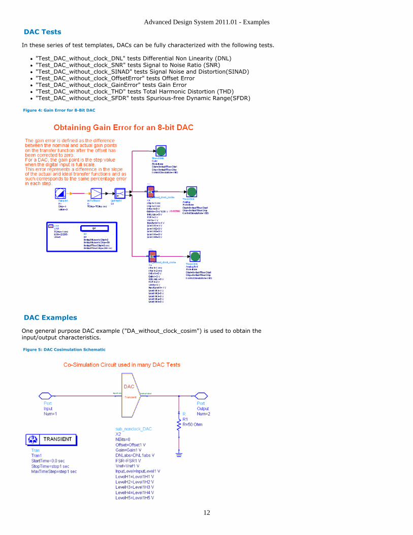
Figure 4: Gain Error for 8-Bit DAC
DAC Examples
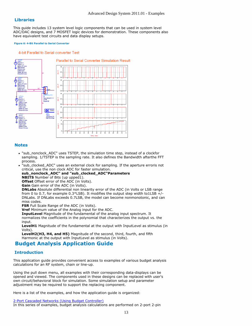
One general purpose DAC example ("DA_without_clock_cosim") is used to obtain theinput/output characteristics.
Figure 5: DAC Cosimulation Schematic
Advanced Design System 2011.01 - Examples
13
Libraries
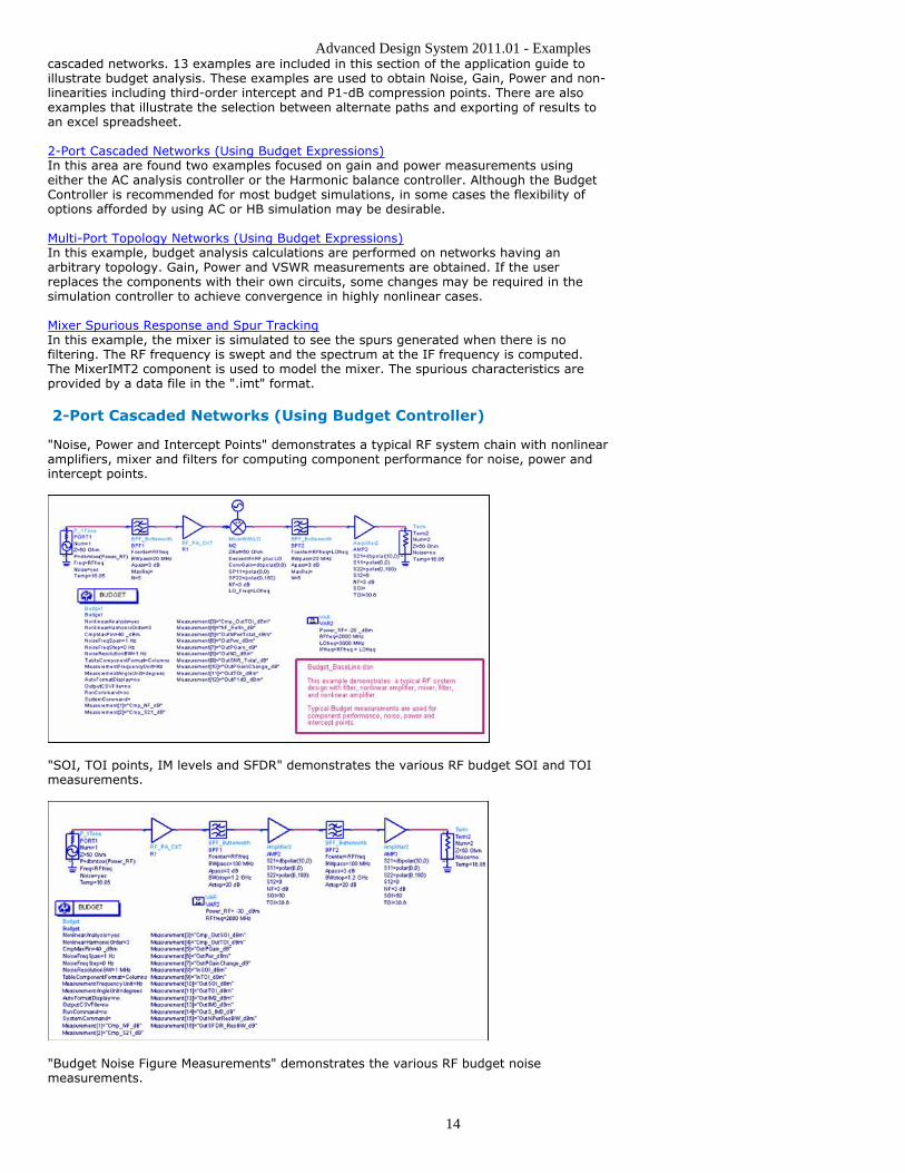
This guide includes 13 system level logic components that can be used in system levelADC/DAC designs, and 7 MOSFET logic devices for demonstration. These components alsohave equivalent test circuits and data display setups.
Figure 6: 4-Bit Parallel to Serial Converter
Notes
"sub_nonclock_ADC" uses TSTEP, the simulation time step, instead of a clockforsampling. 1/TSTEP is the sampling rate. It also defines the Bandwidth afterthe FFTprocess."sub_clocked_ADC" uses an external clock for sampling. If the aperture erroris notcritical, use the non clock ADC for faster simulation.sub_nonclock_ADC" and "sub_clocked_ADC"ParametersNBITS Number of Bits (up upped1).Offset Offset error of the ADC (in Volts).Gain Gain error of the ADC (in Volts).DNLabs Absolute differential non linearity error of the ADC (in Volts or LSB rangefrom 0 to 0.7, for example 0.3*LSB). It modifies the output step width to1LSB +/-DNLabs. If DNLabs exceeds 0.7LSB, the model can become nonmonotonic, and canmiss codes.FSR Full Scale Range of the ADC (in Volts).Vref Minimum value of the Analog input for the ADC.InputLevel Magnitude of the fundamental of the analog input spectrum. Itnormalizes the coefficients in the polynomial that characterizes the output vs. theinput.LevelH1 Magnitude of the fundamental at the output with InputLevel as stimulus (inVolts).LevelH2(H3, H4, and H5) Magnitude of the second, third, fourth, and fifthHarmonic at the output with InputLevel as stimulus (in Volts).
Budget Analysis Application Guide
Introduction
This application guide provides convenient access to examples of various budget analysiscalculations for an RF system, chain or line-up.
Using the pull down menu, all examples with their corresponding data-displays can beopened and viewed. The components used in these designs can be replaced with user'sown circuit/behavioral block for simulation. Some simulation setup and parameteradjustment may be required to support the replacing component.
Here is a list of the examples, and how the application guide is organized:
2-Port Cascaded Networks (Using Budget Controller)In this series of examples, budget analysis calculations are performed on 2-port 2-pin
Advanced Design System 2011.01 - Examples
14
cascaded networks. 13 examples are included in this section of the application guide toillustrate budget analysis. These examples are used to obtain Noise, Gain, Power and non-linearities including third-order intercept and P1-dB compression points. There are alsoexamples that illustrate the selection between alternate paths and exporting of results toan excel spreadsheet.
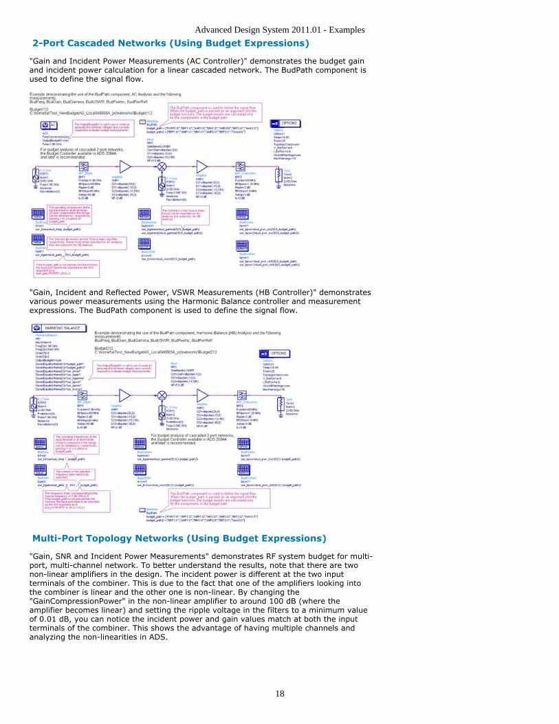
2-Port Cascaded Networks (Using Budget Expressions)In this area are found two examples focused on gain and power measurements usingeither the AC analysis controller or the Harmonic balance controller. Although the BudgetController is recommended for most budget simulations, in some cases the flexibility ofoptions afforded by using AC or HB simulation may be desirable.
Multi-Port Topology Networks (Using Budget Expressions)In this example, budget analysis calculations are performed on networks having anarbitrary topology. Gain, Power and VSWR measurements are obtained. If the userreplaces the components with their own circuits, some changes may be required in thesimulation controller to achieve convergence in highly nonlinear cases.
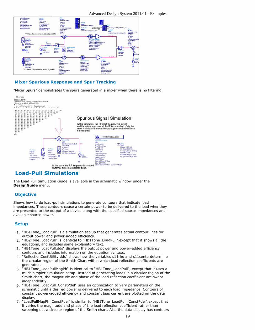
Mixer Spurious Response and Spur TrackingIn this example, the mixer is simulated to see the spurs generated when there is nofiltering. The RF frequency is swept and the spectrum at the IF frequency is computed.The MixerIMT2 component is used to model the mixer. The spurious characteristics areprovided by a data file in the ".imt" format.
2-Port Cascaded Networks (Using Budget Controller)
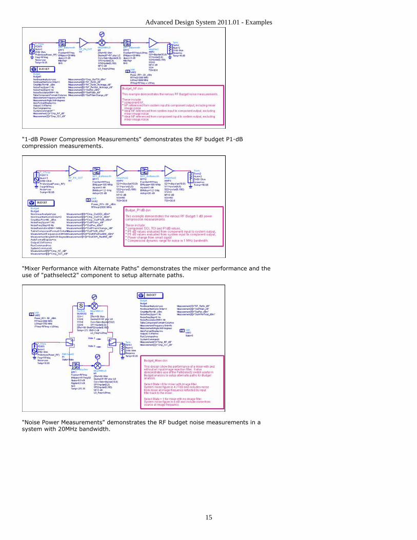
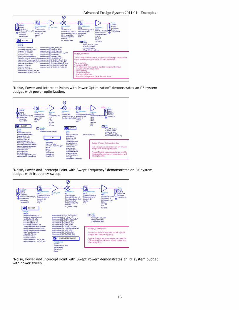
"Noise, Power and Intercept Points" demonstrates a typical RF system chain with nonlinearamplifiers, mixer and filters for computing component performance for noise, power andintercept points.
"SOI, TOI points, IM levels and SFDR" demonstrates the various RF budget SOI and TOImeasurements.
"Budget Noise Figure Measurements" demonstrates the various RF budget noisemeasurements.
Advanced Design System 2011.01 - Examples
15
"1-dB Power Compression Measurements" demonstrates the RF budget P1-dBcompression measurements.
"Mixer Performance with Alternate Paths" demonstrates the mixer performance and theuse of "pathselect2" component to setup alternate paths.
"Noise Power Measurements" demonstrates the RF budget noise measurements in asystem with 20MHz bandwidth.
Advanced Design System 2011.01 - Examples
16
"Noise, Power and intercept Points with Power Optimization" demonstrates an RF systembudget with power optimization.
"Noise, Power and Intercept Point with Swept Frequency" demonstrates an RF systembudget with frequency sweep.
"Noise, Power and Intercept Point with Swept Power" demonstrates an RF system budgetwith power sweep.
Advanced Design System 2011.01 - Examples
17
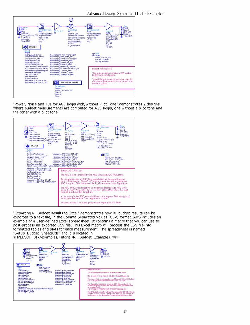
"Power, Noise and TOI for AGC loops with/without Pilot Tone" demonstrates 2 designswhere budget measurements are computed for AGC loops, one without a pilot tone andthe other with a pilot tone.
"Exporting RF Budget Results to Excel" demonstrates how RF budget results can beexported to a text file, in the Comma Separated Values (CSV) format. ADS includes anexample of a user-defined Excel spreadsheet. It contains a macro that you can use topost-process an exported CSV file. This Excel macro will process the CSV file intoformatted tables and plots for each measurement. The spreadsheet is named"SetUp_Budget_Sheets.xls" and it is located in$HPEESOF_DIR/examples/Tutorial/RF_Budget_Examples_wrk.
Advanced Design System 2011.01 - Examples
18
2-Port Cascaded Networks (Using Budget Expressions)
"Gain and Incident Power Measurements (AC Controller)" demonstrates the budget gainand incident power calculation for a linear cascaded network. The BudPath component isused to define the signal flow.
"Gain, Incident and Reflected Power, VSWR Measurements (HB Controller)" demonstratesvarious power measurements using the Harmonic Balance controller and measurementexpressions. The BudPath component is used to define the signal flow.
Multi-Port Topology Networks (Using Budget Expressions)
"Gain, SNR and Incident Power Measurements" demonstrates RF system budget for multi-port, multi-channel network. To better understand the results, note that there are twonon-linear amplifiers in the design. The incident power is different at the two inputterminals of the combiner. This is due to the fact that one of the amplifiers looking intothe combiner is linear and the other one is non-linear. By changing the"GainCompressionPower" in the non-linear amplifier to around 100 dB (where theamplifier becomes linear) and setting the ripple voltage in the filters to a minimum valueof 0.01 dB, you can notice the incident power and gain values match at both the inputterminals of the combiner. This shows the advantage of having multiple channels andanalyzing the non-linearities in ADS.
Advanced Design System 2011.01 - Examples
19
Mixer Spurious Response and Spur Tracking
"Mixer Spurs" demonstrates the spurs generated in a mixer when there is no filtering.
Load-Pull SimulationsThe Load Pull Simulation Guide is available in the schematic window under theDesignGuide menu.
Objective
Shows how to do load-pull simulations to generate contours that indicate loadimpedances. These contours cause a certain power to be delivered to the load whentheyare presented to the output of a device along with the specified source impedances andavailable source power.
Setup
"HB1Tone_LoadPull" is a simulation set-up that generates actual contour lines for1.output power and power-added efficiency."HB2Tone_LoadPull" is identical to "HB1Tone_LoadPull" except that it shows all the2.equations, and includes some explanatory text."HB1Tone_LoadPull.dds" displays the output power and power-added efficiency3.contours and includes information on the equation syntaxs."ReflectionCoefUtility.dds" shows how the variables s11rho and s11centerdetermine4.the circular region of the Smith Chart within which load reflection coefficients aregenerated."HB1Tone_LoadPullMagPh" is identical to "HB1Tone_LoadPull", except that it uses a5.much simpler simulation setup. Instead of generating loads in a circular region of theSmith chart, the magnitude and phase of the load reflection coefficient are sweptindependently."HB1Tone_LoadPull_ConstPdel" uses an optimization to vary parameters on the6.schematic until a desired power is delivered to each load impedance. Contours ofconstant power-added efficiency and constant bias current are plotted on the datadisplay."LoadPullMagPh_ConstPdel" is similar to "HB1Tone_LoadPull_ConstPdel",except that7.it varies the magnitude and phase of the load reflection coefficient rather thansweeping out a circular region of the Smith chart. Also the data display has contours
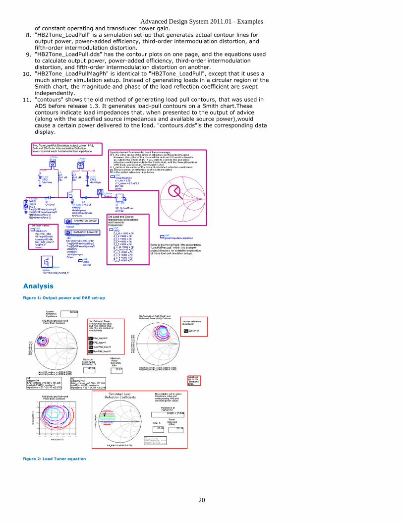
Advanced Design System 2011.01 - Examples
20
of constant operating and transducer power gain."HB2Tone_LoadPull" is a simulation set-up that generates actual contour lines for8.output power, power-added efficiency, third-order intermodulation distortion, andfifth-order intermodulation distortion."HB2Tone_LoadPull.dds" has the contour plots on one page, and the equations used9.to calculate output power, power-added efficiency, third-order intermodulationdistortion, and fifth-order intermodulation distortion on another."HB2Tone_LoadPullMagPh" is identical to "HB2Tone_LoadPull", except that it uses a10.much simpler simulation setup. Instead of generating loads in a circular region of theSmith chart, the magnitude and phase of the load reflection coefficient are sweptindependently."contours" shows the old method of generating load pull contours, that was used in11.ADS before release 1.3. It generates load-pull contours on a Smith chart.Thesecontours indicate load impedances that, when presented to the output of advice(along with the specified source impedances and available source power),wouldcause a certain power delivered to the load. "contours.dds"is the corresponding datadisplay.
Analysis
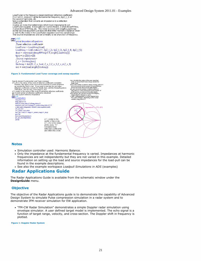
Figure 1: Output power and PAE set-up
Figure 2: Load Tuner equation
Advanced Design System 2011.01 - Examples
21
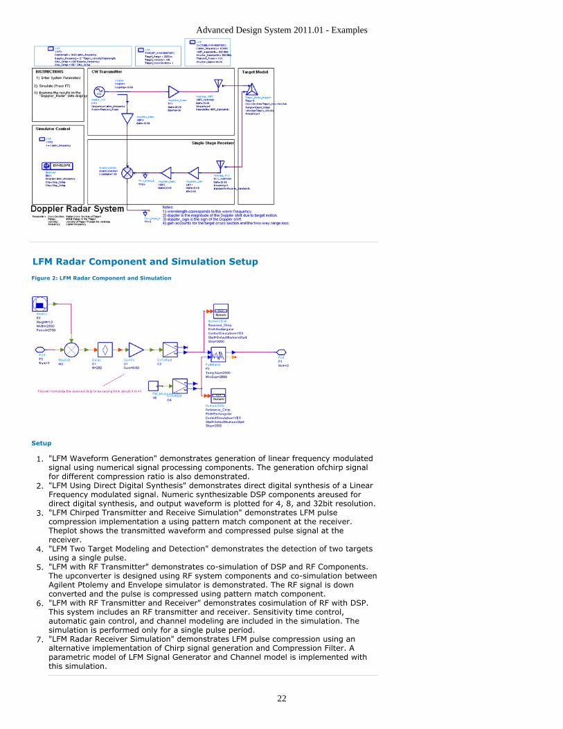
Figure 3: Fundamental Load Tuner coverage and sweep equation
Notes
Simulation controller used: Harmonic Balance.Only the impedance at the fundamental frequency is varied. Impedances at harmonicfrequencies are set independently but they are not varied in this example. Detailedinformation on setting up the load and source impedances for the load-pull can befound in the example descriptions.See also the example workspace Loadpull Simulations in ADS (examples)
Radar Applications GuideThe Radar Applications Guide is available from the schematic window under theDesignGuide menu.
Objective
The objective of the Radar Applications guide is to demonstrate the capability of AdvancedDesign System to simulate Pulse compression simulation in a radar system and todemonstrate IFM receiver simulation for EW application.
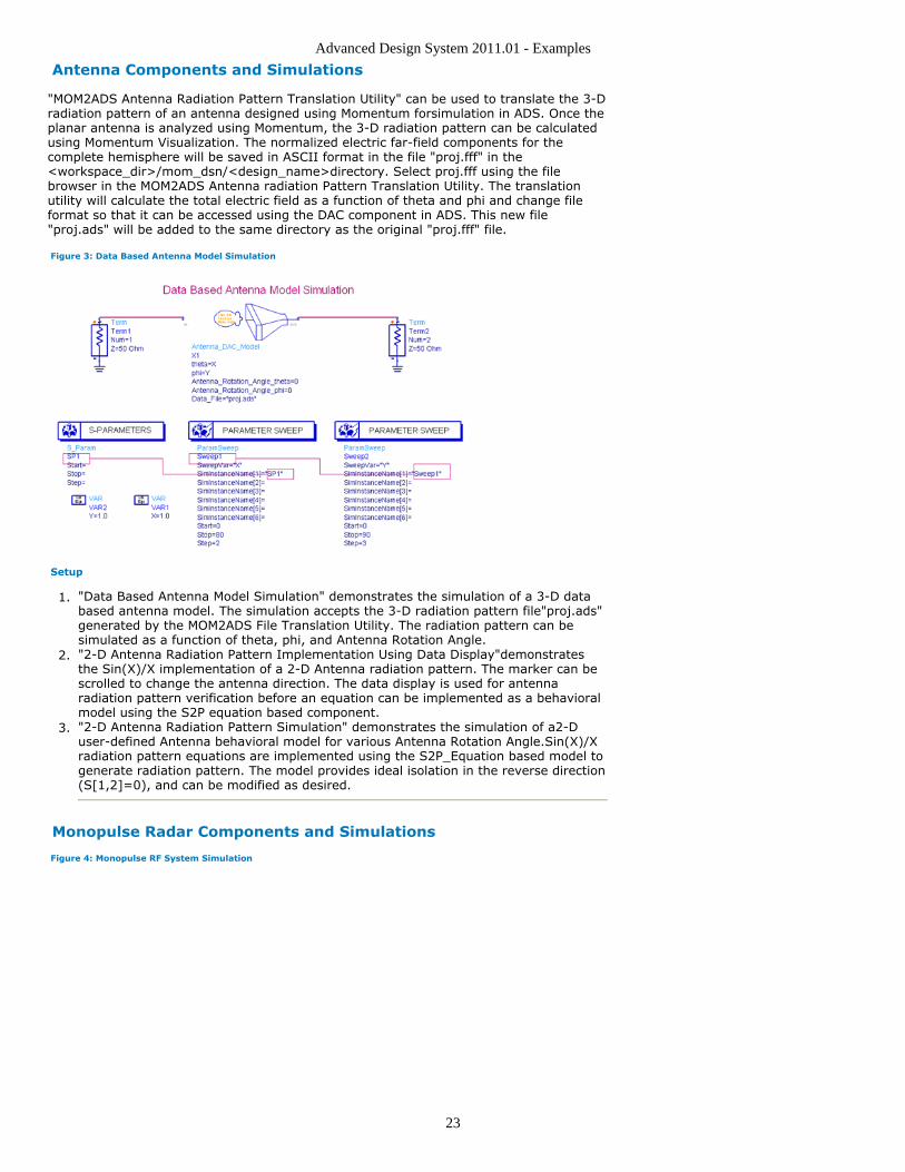
"FM-CW Radar Simulation" demonstrates a simple Doppler radar simulation usingenvelope simulator. A user defined target model is implemented. The echo signal is afunction of target range, velocity, and cross-section. The Doppler shift in frequency isplotted.
Figure 1: Doppler Radar System
Advanced Design System 2011.01 - Examples
22
LFM Radar Component and Simulation Setup
Figure 2: LFM Radar Component and Simulation
Setup
"LFM Waveform Generation" demonstrates generation of linear frequency modulated1.signal using numerical signal processing components. The generation ofchirp signalfor different compression ratio is also demonstrated."LFM Using Direct Digital Synthesis" demonstrates direct digital synthesis of a Linear2.Frequency modulated signal. Numeric synthesizable DSP components areused fordirect digital synthesis, and output waveform is plotted for 4, 8, and 32bit resolution."LFM Chirped Transmitter and Receive Simulation" demonstrates LFM pulse3.compression implementation a using pattern match component at the receiver.Theplot shows the transmitted waveform and compressed pulse signal at thereceiver."LFM Two Target Modeling and Detection" demonstrates the detection of two targets4.using a single pulse."LFM with RF Transmitter" demonstrates co-simulation of DSP and RF Components.5.The upconverter is designed using RF system components and co-simulation betweenAgilent Ptolemy and Envelope simulator is demonstrated. The RF signal is downconverted and the pulse is compressed using pattern match component."LFM with RF Transmitter and Receiver" demonstrates cosimulation of RF with DSP.6.This system includes an RF transmitter and receiver. Sensitivity time control,automatic gain control, and channel modeling are included in the simulation. Thesimulation is performed only for a single pulse period."LFM Radar Receiver Simulation" demonstrates LFM pulse compression using an7.alternative implementation of Chirp signal generation and Compression Filter. Aparametric model of LFM Signal Generator and Channel model is implemented withthis simulation.
Advanced Design System 2011.01 - Examples
23
Antenna Components and Simulations
"MOM2ADS Antenna Radiation Pattern Translation Utility" can be used to translate the 3-Dradiation pattern of an antenna designed using Momentum forsimulation in ADS. Once theplanar antenna is analyzed using Momentum, the 3-D radiation pattern can be calculatedusing Momentum Visualization. The normalized electric far-field components for thecomplete hemisphere will be saved in ASCII format in the file "proj.fff" in the<workspace_dir>/mom_dsn/<design_name>directory. Select proj.fff using the filebrowser in the MOM2ADS Antenna radiation Pattern Translation Utility. The translationutility will calculate the total electric field as a function of theta and phi and change fileformat so that it can be accessed using the DAC component in ADS. This new file"proj.ads" will be added to the same directory as the original "proj.fff" file.
Figure 3: Data Based Antenna Model Simulation
Setup
"Data Based Antenna Model Simulation" demonstrates the simulation of a 3-D data1.based antenna model. The simulation accepts the 3-D radiation pattern file"proj.ads"generated by the MOM2ADS File Translation Utility. The radiation pattern can besimulated as a function of theta, phi, and Antenna Rotation Angle."2-D Antenna Radiation Pattern Implementation Using Data Display"demonstrates2.the Sin(X)/X implementation of a 2-D Antenna radiation pattern. The marker can bescrolled to change the antenna direction. The data display is used for antennaradiation pattern verification before an equation can be implemented as a behavioralmodel using the S2P equation based component."2-D Antenna Radiation Pattern Simulation" demonstrates the simulation of a2-D3.user-defined Antenna behavioral model for various Antenna Rotation Angle.Sin(X)/Xradiation pattern equations are implemented using the S2P_Equation based model togenerate radiation pattern. The model provides ideal isolation in the reverse direction(S[1,2]=0), and can be modified as desired.
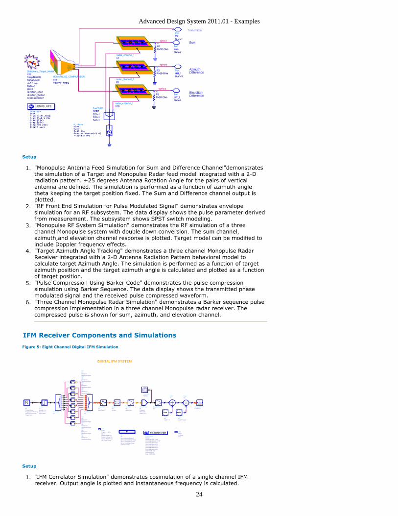
Monopulse Radar Components and Simulations
Figure 4: Monopulse RF System Simulation
Advanced Design System 2011.01 - Examples
24
Setup
"Monopulse Antenna Feed Simulation for Sum and Difference Channel"demonstrates1.the simulation of a Target and Monopulse Radar feed model integrated with a 2-Dradiation pattern. +25 degrees Antenna Rotation Angle for the pairs of verticalantenna are defined. The simulation is performed as a function of azimuth angletheta keeping the target position fixed. The Sum and Difference channel output isplotted."RF Front End Simulation for Pulse Modulated Signal" demonstrates envelope2.simulation for an RF subsystem. The data display shows the pulse parameter derivedfrom measurement. The subsystem shows SPST switch modeling."Monopulse RF System Simulation" demonstrates the RF simulation of a three3.channel Monopulse system with double down conversion. The sum channel,azimuth,and elevation channel response is plotted. Target model can be modified toinclude Doppler frequency effects."Target Azimuth Angle Tracking" demonstrates a three channel Monopulse Radar4.Receiver integrated with a 2-D Antenna Radiation Pattern behavioral model tocalculate target Azimuth Angle. The simulation is performed as a function of targetazimuth position and the target azimuth angle is calculated and plotted as a functionof target position."Pulse Compression Using Barker Code" demonstrates the pulse compression5.simulation using Barker Sequence. The data display shows the transmitted phasemodulated signal and the received pulse compressed waveform."Three Channel Monopulse Radar Simulation" demonstrates a Barker sequence pulse6.compression implementation in a three channel Monopulse radar receiver. Thecompressed pulse is shown for sum, azimuth, and elevation channel.
IFM Receiver Components and Simulations
Figure 5: Eight Channel Digital IFM Simulation
Setup
"IFM Correlator Simulation" demonstrates cosimulation of a single channel IFM1.receiver. Output angle is plotted and instantaneous frequency is calculated.
Advanced Design System 2011.01 - Examples
25
"Single Channel simulation of IFM" demonstrates envelope simulation for an RF2.subsystem. The data display shows the pulse parameter derived frommeasurement.The subsystem shows SPST switch modeling."Two Tone Simulation of IFM" demonstrates an IFM single channel cosimulationin the3.presence of two input independent frequencies. The power level of one signal tone iskept fixed while the power level of the other signal tone is varied from minimumvalue to maximum value. The data display shows IFM always respond to the highestpower level signal, and when two-power levels are nearly equal, the output of IFMshows uncertainty in angle measurement."Four Channel Simulation of IFM" demonstrates a four-channel simulation of an IFM4.system. A DSP algorithm can be implemented to resolve ambiguity infrequencymeasurement over a wide frequency bandwidth."Eight Channel Digital IFM System Simulation" demonstrates the Agilent Ptolemy5.implementation of an eight channel IFM system. The instantaneous output frequencyas a function of input RF frequency is plotted.
NoteThe information on this page is obsolete, but is kept here for archival purposes. Please go to SignalIntegrity Examples (examples) for an up-to-date introduction and examples for signal integrity. Click here(sigint) for documentation of the Signal Integrity DesignGuide (sigint)
Signal Integrity Simulations
Setup
"Eye Closure Measurement " shows three new functions for eye parameter1.calculation. This is used to demonstrate the customization capabilities of ADS.TheAEL function shown on the data display page can be copied to$HPEESOF_DIR/expressions/ael/ user_defined_fun.ael to calculate eye amplitude,eye height, and eye closure."IBIS Simulation of cross talk" demonstrates a partial IBIS model implementation in2.ADS. Pullup/pulldown, power and ground clamps are simulated using SDD andDataAccess Components. The data display shows crosstalk. Slew rate is notimplemented in this example."TDR Simulation" shows time domain simulation of Multilayer Interconnect3.transmission line models using TDR simulation instrument. The simulated andmeasurement data is compared."Differential and Common mode S Parameter Basic" shows the data display convert4.four port single ended S-parameter to Differential and common mode S-parameter."Differential Impedance Simulation" shows how ADS can be used to calculate5.differential impedance."Common Impedance Simulation" demonstrates how ADS can be used to calculate6.common mode impedance.
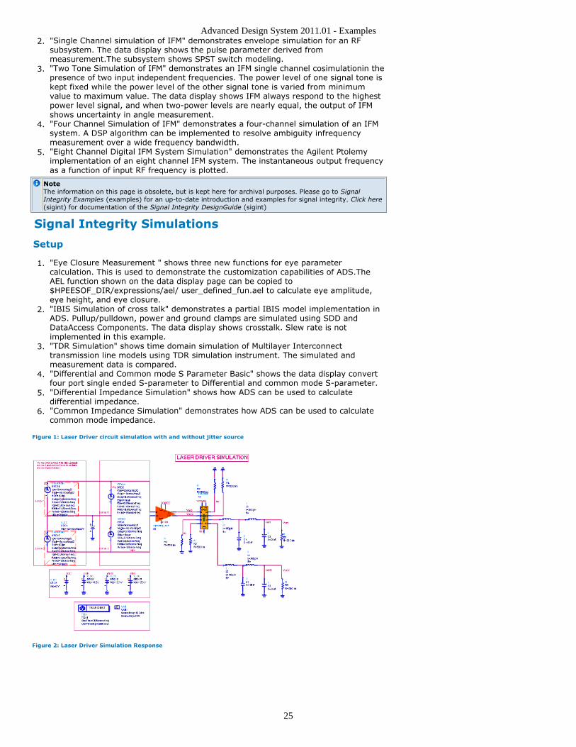
Figure 1: Laser Driver circuit simulation with and without jitter source
Figure 2: Laser Driver Simulation Response
Advanced Design System 2011.01 - Examples
26
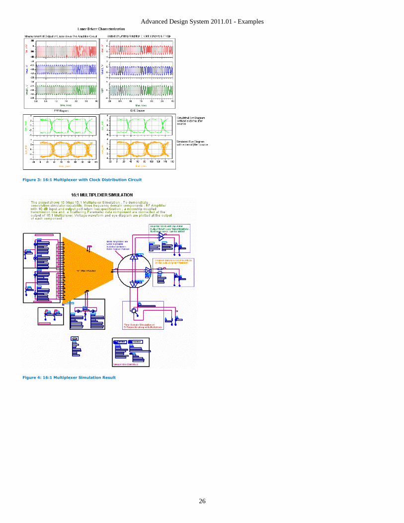
Figure 3: 16:1 Multiplexer with Clock Distribution Circuit
Figure 4: 16:1 Multiplexer Simulation Result
Advanced Design System 2011.01 - Examples
27
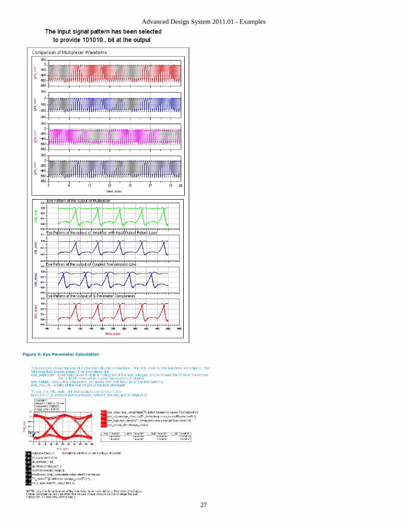
Figure 5: Eye Parameter Calculation
Advanced Design System 2011.01 - Examples
28
VPI ADS Link
Waveform transfer between VPItransmissionMaker and AdvancedDesign System
The increased data rate in optical fiber communication poses many design challenges tohigh-speed designers. Accurate modeling and simulation of the complete communicationsignal path is essential to overcome many complex design issues and to reduces theproduct design cycle.
VPI software provides the designer an excellent optical signal simulation environment andan exhaustive photonic model library for optical system design. The Advanced DesignSystem from Agilent EEsof provides some unique and powerful simulation capabilities todesign high speed Analog circuits.
This application note is written for the designer who may want to use the best of both theoptical and electrical world and wants to design electrical circuits for optical systems.There is no EDA tool existing today, which is capable of providing true co-simulationcapability between optical system models and electrical circuits to predict performance ofthe complete communication signal path.
In an effort to integrate the optical and electrical design environments, this applicationnote highlights a simple process to translate the output signal of VPItransmissionMakersoftware used for photonic system design to the Advanced Design System for electricalcircuit design and vice versa using VPI Link utility. The VPI Link utility will enable the userto simulate the complete communication signal path of any high speed electro-opticdesign. The VPI Link utility can be downloaded from Agilent EEsof web site for free andcan be installed over the Advanced Design System. The VPI Link utility will help you totranslate the file format between the two software and demonstrate the use of simulationresults to define data based time domain sources to analyze electrical circuits in AdvancedDesign System or Optical system in VPItransmissionMaker software. An example of a 10Gbps direct detection receiver using an optical preamplifier and a PIN photodiode is usedhere to demonstrate data transfer between VPI and ADS software. In ADS this data isused for a 10 Gbps transimpedance amplifier simulation.
File translation from VPItransmissionMaker software to ADS software uses a four-stepprocedure:
Generate the time domain electrical signal waveform at the output of optical receiver1.in VPItransmissionMaker software.Output the time domain electrical waveform signal to an ASCII file.2.Convert the file format from VPItransmissionMaker to Advanced Design System.3.Use the time domain data file to define time dependent voltage and current sources4.in Advanced Design System.
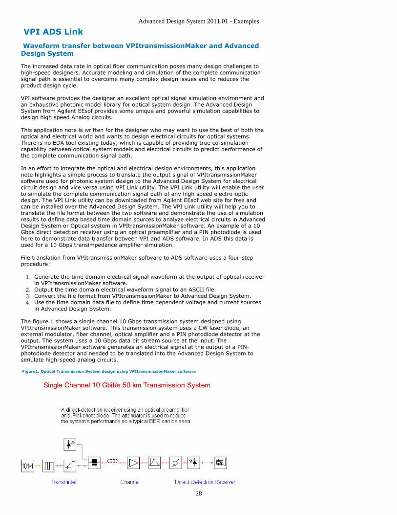
The figure 1 shows a single channel 10 Gbps transmission system designed usingVPItransmissionMaker software. This transmission system uses a CW laser diode, anexternal modulator, fiber channel, optical amplifier and a PIN photodiode detector at theoutput. The system uses a 10 Gbps data bit stream source at the input. TheVPItransmissionMaker software generates an electrical signal at the output of a PIN-photodiode detector and needed to be translated into the Advanced Design System tosimulate high-speed analog circuits.
Figure1: Optical Transmission System design using VPItransmissionMaker software
Advanced Design System 2011.01 - Examples
29
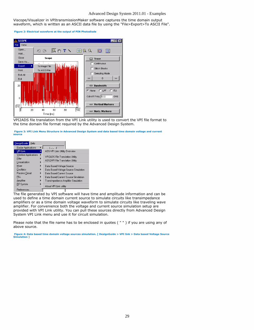
Viscope/Visualizer in VPItransmissionMaker software captures the time domain outputwaveform, which is written as an ASCII data file by using the "File>Export>To ASCII File".
Figure 2: Electrical waveform at the output of PIN Photodiode
VPI2ADS file translation from the VPI Link utility is used to convert the VPI file format tothe time domain file format required by the Advanced Design System.
Figure 3: VPI Link Menu Structure in Advanced Design System and data based time domain voltage and currentsource
The file generated by VPI software will have time and amplitude information and can beused to define a time domain current source to simulate circuits like transimpedanceamplifiers or as a time domain voltage waveform to simulate circuits like traveling waveamplifier. For convenience both the voltage and current source simulation setup areprovided with VPI Link utility. You can pull these sources directly from Advanced DesignSystem VPI Link menu and use it for circuit simulation.
Please note that the file name has to be enclosed in quotes ( " " ) if you are using any ofabove source.
Figure 4: Data based time domain voltage sources simulation. [ DesignGuide > VPI link > Data based Voltage SourceSimulation ]
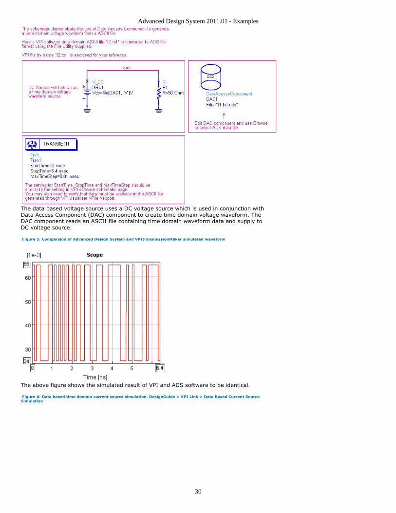
Advanced Design System 2011.01 - Examples
30
The data based voltage source uses a DC voltage source which is used in conjunction withData Access Component (DAC) component to create time domain voltage waveform. TheDAC component reads an ASCII file containing time domain waveform data and supply toDC voltage source.
Figure 5: Comparison of Advanced Design System and VPItransmissionMaker simulated waveform
The above figure shows the simulated result of VPI and ADS software to be identical.
Figure 6: Data based time domain current source simulation. DesignGuide > VPI Link > Data Based Current SourceSimulation
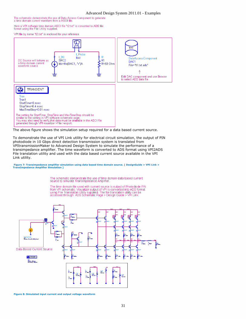
Advanced Design System 2011.01 - Examples
31
The above figure shows the simulation setup required for a data based current source.
To demonstrate the use of VPI Link utility for electrical circuit simulation, the output of PINphotodiode in 10 Gbps direct detection transmission system is translated fromVPItransmissionMaker to Advanced Design System to simulate the performance of atransimpedance amplifier. The time waveform is converted to ADS format using VPI2ADSFile translation utility and used with the data based current source available in the VPILink utility.
Figure 7: Transimpedance amplifier simulation using data based time domain source. [ DesignGuide > VPI Link >TransImpedance Amplifier Simulation ]
Figure 8: Simulated input current and output voltage waveform
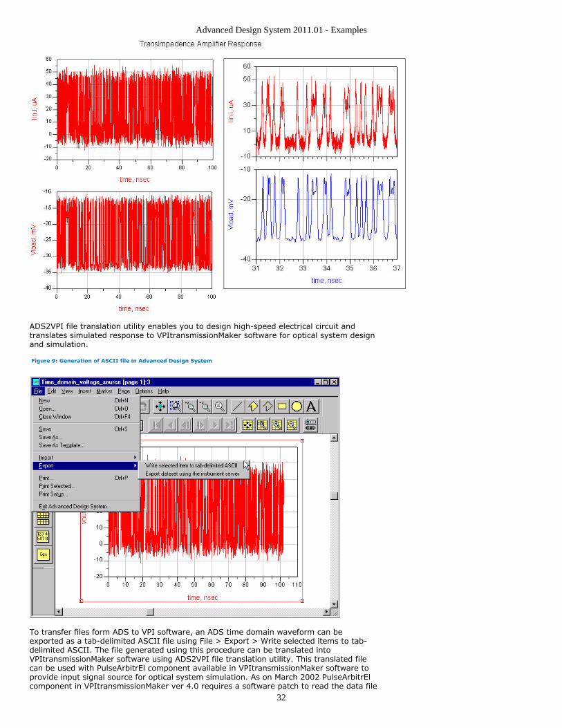
Advanced Design System 2011.01 - Examples
32
ADS2VPI file translation utility enables you to design high-speed electrical circuit andtranslates simulated response to VPItransmissionMaker software for optical system designand simulation.
Figure 9: Generation of ASCII file in Advanced Design System
To transfer files form ADS to VPI software, an ADS time domain waveform can beexported as a tab-delimited ASCII file using File > Export > Write selected items to tab-delimited ASCII. The file generated using this procedure can be translated intoVPItransmissionMaker software using ADS2VPI file translation utility. This translated filecan be used with PulseArbitrEl component available in VPItransmissionMaker software toprovide input signal source for optical system simulation. As on March 2002 PulseArbitrElcomponent in VPItransmissionMaker ver 4.0 requires a software patch to read the data file
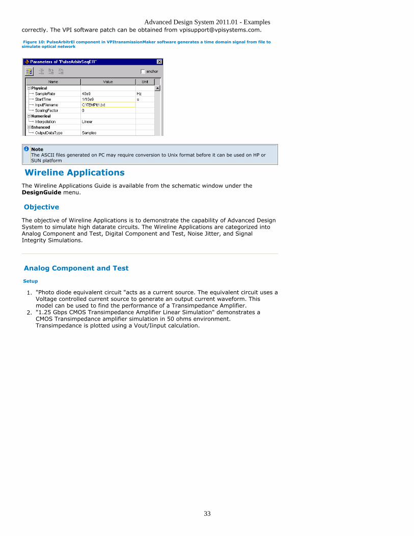
Advanced Design System 2011.01 - Examples
33
correctly. The VPI software patch can be obtained from [email protected].
Figure 10: PulseArbitrEl component in VPItransmissionMaker software generates a time domain signal from file tosimulate optical network
NoteThe ASCII files generated on PC may require conversion to Unix format before it can be used on HP orSUN platform
Wireline ApplicationsThe Wireline Applications Guide is available from the schematic window under theDesignGuide menu.
Objective
The objective of Wireline Applications is to demonstrate the capability of Advanced DesignSystem to simulate high datarate circuits. The Wireline Applications are categorized intoAnalog Component and Test, Digital Component and Test, Noise Jitter, and SignalIntegrity Simulations.
Analog Component and Test
Setup
"Photo diode equivalent circuit "acts as a current source. The equivalent circuit uses a1.Voltage controlled current source to generate an output current waveform. Thismodel can be used to find the performance of a Transimpedance Amplifier."1.25 Gbps CMOS Transimpedance Amplifier Linear Simulation" demonstrates a2.CMOS Transimpedance amplifier simulation in 50 ohms environment.Transimpedance is plotted using a Vout/Iinput calculation.
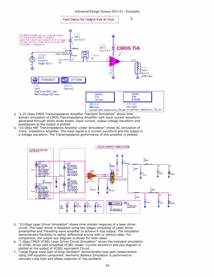
Advanced Design System 2011.01 - Examples
34
"1.25 Gbps CMOS Transimpedance Amplifier Transient Simulation" shows time3.domain simulation of CMOS Transimpedance Amplifier with input current waveformgenerated through photo diode model. Input current, output voltage waveform andeyediagram at the output is plotted."10 Gbps HBT Transimpedance Amplifier Linear Simulation" shows AC simulation of4.Trans- impedance Amplifier. The input signal is a current waveform and the output isa voltage waveform. The Transimpedance performance of this amplifier is plotted.
"10 Gbps Laser Driver Simulation" shows time domain response of a laser driver5.circuit. The Laser driver is designed using two stages consisting of Laser driverpreamplifier and Travelling wave amplifier to achieve 6 Vpp output. The simulationdemonstrates flexibility to define differential source with or without jitter. Forcomparison, the output eye diagram is shown for both cases."1 Gbps CMOS VCSEL Laser Driver Circuit Simulation" shows the transient simulation6.of VCSEL driver with simplified VCSEL model. Current waveform and eye diagram isplotted at the output of VCSEL equivalent Circuit."Large Signal Loop Gain of Ring Oscillator" demonstrates loop gain measurement7.using S4P equation component. Harmonic Balance Simulation is performed tocalculate Loop Gain and phase response of ring oscillator.

Advanced Design System 2011.01 - Examples
35
"Ring Oscillator Loop Optimization" shows the set up to Optimize Oscillator loop gain8.and phase response at the required frequency."Ring Oscillator Initial Guess Simulation" demonstrates the creation of initial guess9.file using transient simulation.This file can be used as initial guess solution to performTime Assisted Harmonic Balance Simulation."Ring Oscillator Time Assisted Harmonic Balance Simulation" shows time assisted10.harmonic balance simulation of Ring Oscillator. The initial Guess file generated inprevious step is used to reduce simulation time and to avoid convergence problems.

Advanced Design System 2011.01 - Examples
36
Digital Component and Test
Setup
"Data buffer", "10 Gbps HBT Clock Buffer", "10 Gbps HBT Divide by 2", "10Gbps HBT1.Divider Buffer" , "10 Gbps HBT Output Amplifier" , "10 Gbps HBT Latch"and "10 Gbps2:1 Selector" provides some samples of sub components used in designingMultiplexer and De-Multiplexer circuits."Test_Latch" demonstrates time domain simulation of High Speed Latch using2.differential signal source."2:1 Selector Simulation" shows basic Multiplexer building block simulation.Two3.differential data sources with different delay parameters are used as input signal. Theoutput waveform demonstrates multiplexing action on two input waveforms."Clock Distribution Simulation" provides time domain simulation of Clock distribution4.circuit for 16:1 Multiplexer. The Clock distribution circuit divides a 10 GHz inputfrequency to generate 5 GHz, 2.5 GHz, 1.25 GHz and 625 MHz clock signal. The datadisplay shows the input and divided output waveforms."16:1 Multiplexer with Clock Distribution Circuit " demonstrates time domain5.simulation of 16:1 Multiplexer for 10 GB application. Frequency domain models ofMicrostrip line, behavioral model for RF System Amplifier and S-Parameter block areconnected at the output of Multiplexer to demonstrate time domain simulationcapability of frequency domain models."1:16 De-Multiplexer Simulation With Clock Distribution Circuit" shows time domain6.simulation of 1:16 De-Multiplexer for 10 Gbps input signal. TheDe-Multiplexer isdesigned using a modular approach, consisting of 1:2De-Multipexer and clockdistribution circuits.
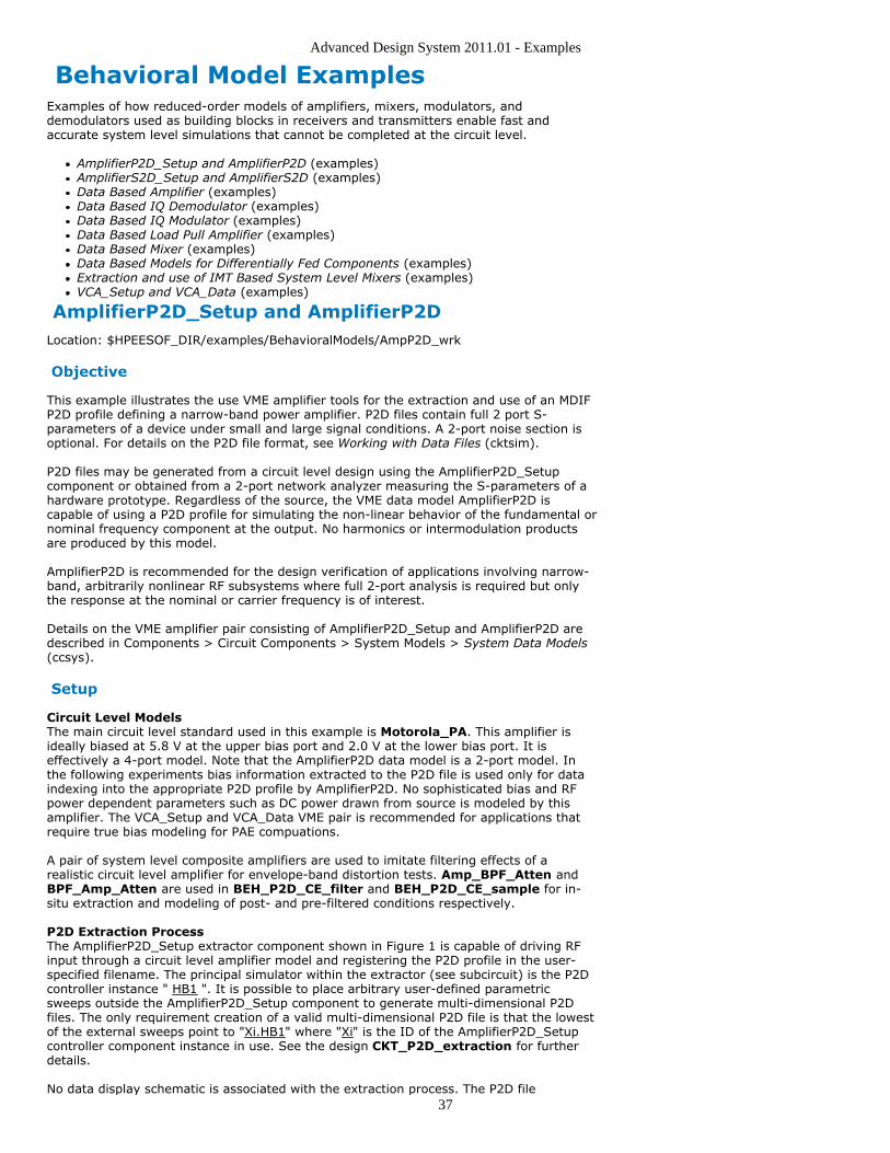
Advanced Design System 2011.01 - Examples
37
Behavioral Model ExamplesExamples of how reduced-order models of amplifiers, mixers, modulators, anddemodulators used as building blocks in receivers and transmitters enable fast andaccurate system level simulations that cannot be completed at the circuit level.
AmplifierP2D_Setup and AmplifierP2D (examples)AmplifierS2D_Setup and AmplifierS2D (examples)Data Based Amplifier (examples)Data Based IQ Demodulator (examples)Data Based IQ Modulator (examples)Data Based Load Pull Amplifier (examples)Data Based Mixer (examples)Data Based Models for Differentially Fed Components (examples)Extraction and use of IMT Based System Level Mixers (examples)VCA_Setup and VCA_Data (examples)
AmplifierP2D_Setup and AmplifierP2DLocation: $HPEESOF_DIR/examples/BehavioralModels/AmpP2D_wrk
Objective
This example illustrates the use VME amplifier tools for the extraction and use of an MDIFP2D profile defining a narrow-band power amplifier. P2D files contain full 2 port S-parameters of a device under small and large signal conditions. A 2-port noise section isoptional. For details on the P2D file format, see Working with Data Files (cktsim).
P2D files may be generated from a circuit level design using the AmplifierP2D_Setupcomponent or obtained from a 2-port network analyzer measuring the S-parameters of ahardware prototype. Regardless of the source, the VME data model AmplifierP2D iscapable of using a P2D profile for simulating the non-linear behavior of the fundamental ornominal frequency component at the output. No harmonics or intermodulation productsare produced by this model.
AmplifierP2D is recommended for the design verification of applications involving narrow-band, arbitrarily nonlinear RF subsystems where full 2-port analysis is required but onlythe response at the nominal or carrier frequency is of interest.
Details on the VME amplifier pair consisting of AmplifierP2D_Setup and AmplifierP2D aredescribed in Components > Circuit Components > System Models > System Data Models(ccsys).
Setup
Circuit Level ModelsThe main circuit level standard used in this example is Motorola_PA. This amplifier isideally biased at 5.8 V at the upper bias port and 2.0 V at the lower bias port. It iseffectively a 4-port model. Note that the AmplifierP2D data model is a 2-port model. Inthe following experiments bias information extracted to the P2D file is used only for dataindexing into the appropriate P2D profile by AmplifierP2D. No sophisticated bias and RFpower dependent parameters such as DC power drawn from source is modeled by thisamplifier. The VCA_Setup and VCA_Data VME pair is recommended for applications thatrequire true bias modeling for PAE compuations.
A pair of system level composite amplifiers are used to imitate filtering effects of arealistic circuit level amplifier for envelope-band distortion tests. Amp_BPF_Atten andBPF_Amp_Atten are used in BEH_P2D_CE_filter and BEH_P2D_CE_sample for in-situ extraction and modeling of post- and pre-filtered conditions respectively.
P2D Extraction ProcessThe AmplifierP2D_Setup extractor component shown in Figure 1 is capable of driving RFinput through a circuit level amplifier model and registering the P2D profile in the user-specified filename. The principal simulator within the extractor (see subcircuit) is the P2Dcontroller instance " HB1 ". It is possible to place arbitrary user-defined parametricsweeps outside the AmplifierP2D_Setup component to generate multi-dimensional P2Dfiles. The only requirement creation of a valid multi-dimensional P2D file is that the lowestof the external sweeps point to "Xi.HB1" where "Xi" is the ID of the AmplifierP2D_Setupcontroller component instance in use. See the design CKT_P2D_extraction for furtherdetails.
No data display schematic is associated with the extraction process. The P2D file
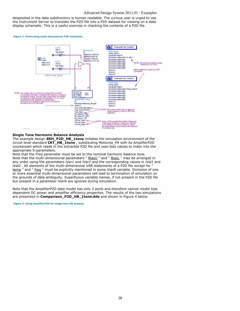
Advanced Design System 2011.01 - Examples
38
desposited in the data subdirectory is human readable. The curious user is urged to usethe Instrument Server to translate the P2D file into a P2D dataset for viewing on a datadisplay schematic. This is a useful exercise in checking the contents of a P2D file.
Figure 1: Performing multi-dimensional P2D extraction
Single Tone Harmonic Balance AnalysisThe example design BEH_P2D_HB_1tone imitates the simulation environment of thecircuit level standard CKT_HB_1tone , substituting Motorola_PA with its AmplifierP2Dcounterpart which reads in the extracted P2D file and uses bias values to index into theappropriate S-parameters.Note that the Freq parameter must be set to the nominal harmonic balance tone.Note that the multi-dimensional parameters " BiasU " and " BiasL " may be arranged inany order using the parameters iVar1 and iVar2 and the corresponding values in iVal1 andiVal2 . All elements of the multi-dimensional VAR statements of a P2D file except for "temp " and " freq " must be explicitly mentioned in some iVarN variable. Omission of oneor more essential multi-dimensional parameters will lead to termination of simulation onthe grounds of data ambiguity. Superfluous variable names, if not present in the P2D filebut present in a parameter iVarN are ignored during simulation.
Note that the AmplifierP2D data model has only 2 ports and therefore cannot model biasdependent DC power and amplifier efficiency properties. The results of the two simulationsare presented in Comparison_P2D_HB_1tone.dds and shown in Figure 4 below.
Figure 2: Using AmplifierP2D for single tone HB analysis
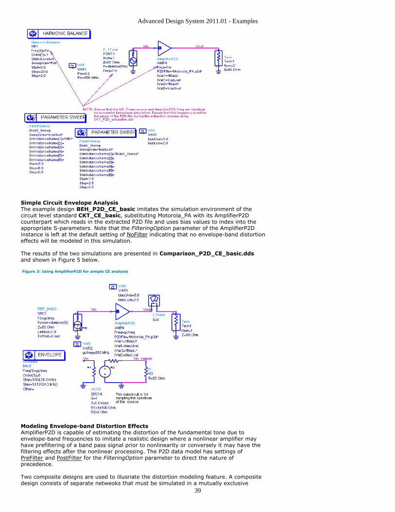
Advanced Design System 2011.01 - Examples
39
Simple Circuit Envelope AnalysisThe example design BEH_P2D_CE_basic imitates the simulation environment of thecircuit level standard CKT_CE_basic, substituting Motorola_PA with its AmplifierP2Dcounterpart which reads in the extracted P2D file and uses bias values to index into theappropriate S-parameters. Note that the FilteringOption parameter of the AmplifierP2Dinstance is left at the default setting of NoFilter indicating that no envelope-band distortioneffects will be modeled in this simulation.
The results of the two simulations are presented in Comparison_P2D_CE_basic.ddsand shown in Figure 5 below.
Figure 3: Using AmplifierP2D for simple CE analysis
Modeling Envelope-band Distortion EffectsAmplifierP2D is capable of estimating the distortion of the fundamental tone due toenvelope-band frequencies to imitate a realistic design where a nonlinear amplifier mayhave prefiltering of a band pass signal prior to nonlinearity or conversely it may have thefiltering effects after the nonlinear processing. The P2D data model has settings ofPreFilter and PostFilter for the FilteringOption parameter to direct the nature ofprecedence.
Two composite designs are used to illusriate the distortion modeling feature. A compositedesign consists of separate netweoks that must be simulated in a mutually exclusive
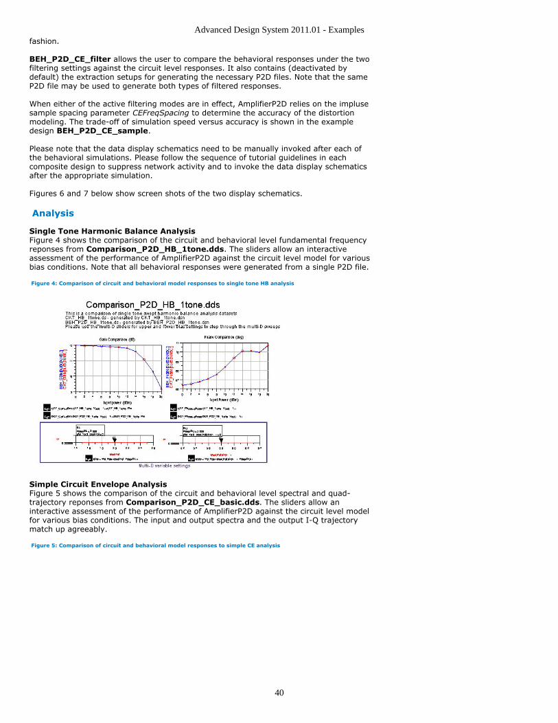
Advanced Design System 2011.01 - Examples
40
fashion.
BEH_P2D_CE_filter allows the user to compare the behavioral responses under the twofiltering settings against the circuit level responses. It also contains (deactivated bydefault) the extraction setups for generating the necessary P2D files. Note that the sameP2D file may be used to generate both types of filtered responses.
When either of the active filtering modes are in effect, AmplifierP2D relies on the implusesample spacing parameter CEFreqSpacing to determine the accuracy of the distortionmodeling. The trade-off of simulation speed versus accuracy is shown in the exampledesign BEH_P2D_CE_sample.
Please note that the data display schematics need to be manually invoked after each ofthe behavioral simulations. Please follow the sequence of tutorial guidelines in eachcomposite design to suppress network activity and to invoke the data display schematicsafter the appropriate simulation.
Figures 6 and 7 below show screen shots of the two display schematics.
Analysis
Single Tone Harmonic Balance AnalysisFigure 4 shows the comparison of the circuit and behavioral level fundamental frequencyreponses from Comparison_P2D_HB_1tone.dds. The sliders allow an interactiveassessment of the performance of AmplifierP2D against the circuit level model for variousbias conditions. Note that all behavioral responses were generated from a single P2D file.
Figure 4: Comparison of circuit and behavioral model responses to single tone HB analysis
Simple Circuit Envelope AnalysisFigure 5 shows the comparison of the circuit and behavioral level spectral and quad-trajectory reponses from Comparison_P2D_CE_basic.dds. The sliders allow aninteractive assessment of the performance of AmplifierP2D against the circuit level modelfor various bias conditions. The input and output spectra and the output I-Q trajectorymatch up agreeably.
Figure 5: Comparison of circuit and behavioral model responses to simple CE analysis
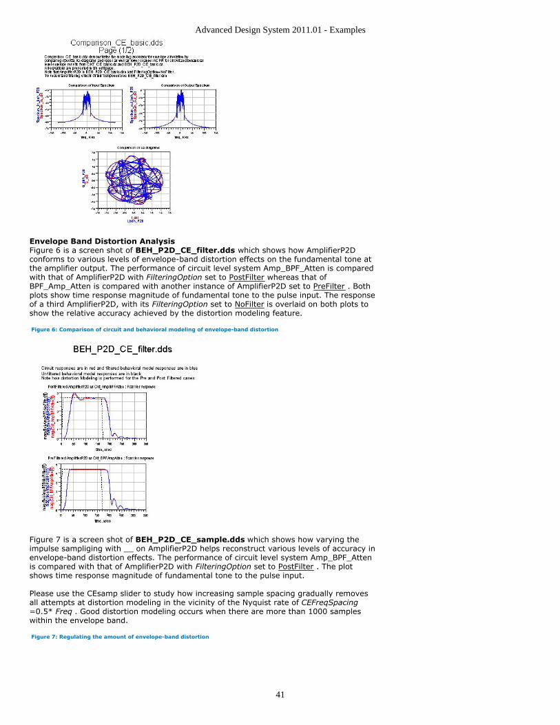
Advanced Design System 2011.01 - Examples
41
Envelope Band Distortion AnalysisFigure 6 is a screen shot of BEH_P2D_CE_filter.dds which shows how AmplifierP2Dconforms to various levels of envelope-band distortion effects on the fundamental tone atthe amplifier output. The performance of circuit level system Amp_BPF_Atten is comparedwith that of AmplifierP2D with FilteringOption set to PostFilter whereas that ofBPF_Amp_Atten is compared with another instance of AmplifierP2D set to PreFilter . Bothplots show time response magnitude of fundamental tone to the pulse input. The responseof a third AmplifierP2D, with its FilteringOption set to NoFilter is overlaid on both plots toshow the relative accuracy achieved by the distortion modeling feature.
Figure 6: Comparison of circuit and behavioral modeling of envelope-band distortion
Figure 7 is a screen shot of BEH_P2D_CE_sample.dds which shows how varying theimpulse sampliging with __ on AmplifierP2D helps reconstruct various levels of accuracy inenvelope-band distortion effects. The performance of circuit level system Amp_BPF_Attenis compared with that of AmplifierP2D with FilteringOption set to PostFilter . The plotshows time response magnitude of fundamental tone to the pulse input.
Please use the CEsamp slider to study how increasing sample spacing gradually removesall attempts at distortion modeling in the vicinity of the Nyquist rate of CEFreqSpacing=0.5* Freq . Good distortion modeling occurs when there are more than 1000 sampleswithin the envelope band.
Figure 7: Regulating the amount of envelope-band distortion
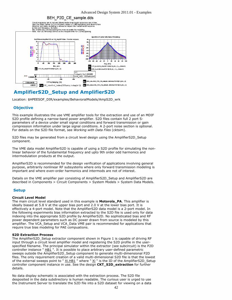
Advanced Design System 2011.01 - Examples
42
AmplifierS2D_Setup and AmplifierS2DLocation: $HPEESOF_DIR/examples/BehavioralModels/AmpS2D_wrk
Objective
This example illustrates the use VME amplifier tools for the extraction and use of an MDIFS2D profile defining a narrow-band power amplifier. S2D files contain full 2 port S-parameters of a device under small signal conditions and forward transmission or gaincompression information under large signal conditions. A 2-port noise section is optional.For details on the S2D file format, see Working with Data Files (cktsim).
S2D files may be generated from a circuit level design using the AmplifierS2D_Setupcomponent.
The VME data model AmplifierS2D is capable of using a S2D profile for simulating the non-linear behavior of the fundamental frequency and upto 9th order odd harmonics andintermodulation products at the output.
AmplifierS2D is recommended for the design verification of applications involving generalpurpose, arbitrarily nonlinear RF subsystems where only forward transmission modeling isimportant and where even-order harmonics and intermods are not of interest.
Details on the VME amplifier pair consisting of AmplifierS2D_Setup and AmplifierS2D aredescribed in Components > Circuit Components > System Models > System Data Models.
Setup
Circuit Level ModelThe main circuit level standard used in this example is Motorola_PA. This amplifier isideally biased at 5.8 V at the upper bias port and 2.0 V at the lower bias port. It iseffectively a 4-port model. Note that the AmplifierS2D data model is a 2-port model. Inthe following experiments bias information extracted to the S2D file is used only for dataindexing into the appropriate S2D profile by AmplifierS2D. No sophisticated bias and RFpower dependent parameters such as DC power drawn from source is modeled by thisamplifier. The VCA_Setup and VCA_Data VME pair is recommended for applications thatrequire true bias modeling for PAE compuations.
S2D Extraction ProcessThe AmplifierS2D_Setup extractor component shown in Figure 1 is capable of driving RFinput through a circuit level amplifier model and registering the S2D profile in the user-specified filename. The principal simulator within the extractor (see subcircuit) is the P2Dcontroller instance " HB1 ". It is possible to place arbitrary user-defined parametricsweeps outside the AmplifierS2D_Setup component to generate multi-dimensional P2Dfiles. The only requirement creation of a valid multi-dimensional S2D file is that the lowestof the external sweeps point to " Xi.HB1 " where " Xi " is the ID of the AmplifierS2D_Setupcontroller component instance in use. See the design CKT_S2D_extraction for furtherdetails.
No data display schematic is associated with the extraction process. The S2D filedesposited in the data subdirectory is human readable. The curious user is urged to usethe Instrument Server to translate the S2D file into a S2D dataset for viewing on a data
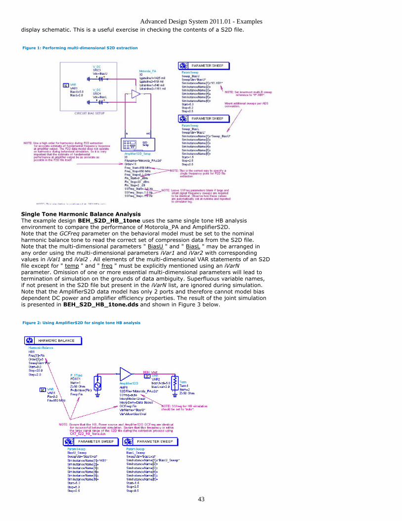
Advanced Design System 2011.01 - Examples
43
display schematic. This is a useful exercise in checking the contents of a S2D file.
Figure 1: Performing multi-dimensional S2D extraction
Single Tone Harmonic Balance AnalysisThe example design BEH_S2D_HB_1tone uses the same single tone HB analysisenvironment to compare the performance of Motorola_PA and AmplifierS2D.Note that the GCFreq parameter on the behavioral model must be set to the nominalharmonic balance tone to read the correct set of compression data from the S2D file.Note that the multi-dimensional parameters " BiasU " and " BiasL " may be arranged inany order using the multi-dimensional parameters iVar1 and iVar2 with correspondingvalues in iVal1 and iVal2 . All elements of the multi-dimensional VAR statements of an S2Dfile except for " temp " and " freq " must be explicitly mentioned using an iVarNparameter. Omission of one or more essential multi-dimensional parameters will lead totermination of simulation on the grounds of data ambiguity. Superfluous variable names,if not present in the S2D file but present in the iVarN list, are ignored during simulation.Note that the AmplifierS2D data model has only 2 ports and therefore cannot model biasdependent DC power and amplifier efficiency properties. The result of the joint simulationis presented in BEH_S2D_HB_1tone.dds and shown in Figure 3 below.
Figure 2: Using AmplifierS2D for single tone HB analysis
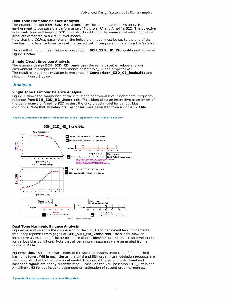
Advanced Design System 2011.01 - Examples
44
Dual Tone Harmonic Balance AnalysisThe example design BEH_S2D_HB_2tone uses the same dual tone HB analysisenvironment to compare the performance of Motorola_PA and AmplifierS2D. The objectiveis to study how well AmplifierS2D reconstructs odd-order harmonics and intermodulationproducts compared to a circuit level model.Note that the GCFreq parameter on the behavioral model must be set to the one of thetwo harmonic balance tones to read the correct set of compression data from the S2D file.
The result of the joint simulation is presented in BEH_S2D_HB_2tone.dds and shown inFigure 4 below.
Simple Circuit Envelope AnalysisThe example design BEH_S2D_CE_basic uses the same circuit envelope analysisenvironment to compare the performance of Motorola_PA and AmplifierS2D.The result of the joint simulation is presented in Comparison_S2D_CE_basic.dds andshown in Figure 5 below.
Analysis
Single Tone Harmonic Balance AnalysisFigure 3 shows the comparison of the circuit and behavioral level fundamental frequencyreponses from BEH_S2D_HB_1tone.dds. The sliders allow an interactive assessment ofthe performance of AmplifierS2D against the circuit level model for various biasconditions. Note that all behavioral responses were generated from a single S2D file.
Figure 3: Comparison of circuit and behavioral model responses to single tone HB analysis
Dual Tone Harmonic Balance AnalysisFigures 4a and 4b show the comparison of the circuit and behavioral level fundamentalfrequency reponses from pages of BEH_S2D_HB_2tone.dds. The sliders allow aninteractive assessment of the performance of AmplifierS2D against the circuit level modelfor various bias conditions. Note that all behavioral responses were generated from asingle S2D file.
Figure4A shows solid reconstructions of the spectral clusters around the first and thirdharmonic tones. Within each cluster the third and fifth order intermodulation products arewell reconstructed by the behavioral model. In contrast the second order band andbaseband signals are poorly reconstructed. Please use the VME pair AmpH1H2_Setup andAmplifierH1H2 for applications dependent on estimation of second order harmonics.
Figure 4a: Spectral responses to dual tone HB analysis
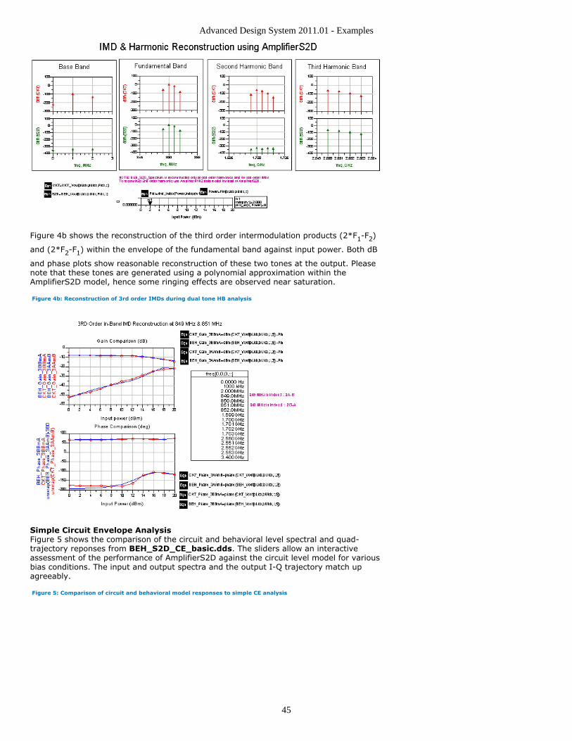
Advanced Design System 2011.01 - Examples
45
Figure 4b shows the reconstruction of the third order intermodulation products (2*F1-F2)
and (2*F2-F1) within the envelope of the fundamental band against input power. Both dB
and phase plots show reasonable reconstruction of these two tones at the output. Pleasenote that these tones are generated using a polynomial approximation within theAmplifierS2D model, hence some ringing effects are observed near saturation.
Figure 4b: Reconstruction of 3rd order IMDs during dual tone HB analysis
Simple Circuit Envelope AnalysisFigure 5 shows the comparison of the circuit and behavioral level spectral and quad-trajectory reponses from BEH_S2D_CE_basic.dds. The sliders allow an interactiveassessment of the performance of AmplifierS2D against the circuit level model for variousbias conditions. The input and output spectra and the output I-Q trajectory match upagreeably.
Figure 5: Comparison of circuit and behavioral model responses to simple CE analysis
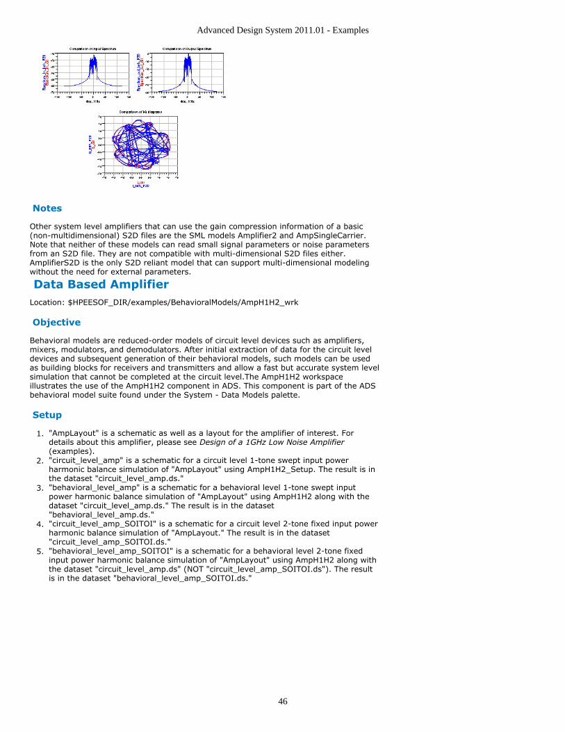
Advanced Design System 2011.01 - Examples
46
Notes
Other system level amplifiers that can use the gain compression information of a basic(non-multidimensional) S2D files are the SML models Amplifier2 and AmpSingleCarrier.Note that neither of these models can read small signal parameters or noise parametersfrom an S2D file. They are not compatible with multi-dimensional S2D files either.AmplifierS2D is the only S2D reliant model that can support multi-dimensional modelingwithout the need for external parameters.
Data Based AmplifierLocation: $HPEESOF_DIR/examples/BehavioralModels/AmpH1H2_wrk
Objective
Behavioral models are reduced-order models of circuit level devices such as amplifiers,mixers, modulators, and demodulators. After initial extraction of data for the circuit leveldevices and subsequent generation of their behavioral models, such models can be usedas building blocks for receivers and transmitters and allow a fast but accurate system levelsimulation that cannot be completed at the circuit level.The AmpH1H2 workspaceillustrates the use of the AmpH1H2 component in ADS. This component is part of the ADSbehavioral model suite found under the System - Data Models palette.
Setup
"AmpLayout" is a schematic as well as a layout for the amplifier of interest. For1.details about this amplifier, please see Design of a 1GHz Low Noise Amplifier(examples)."circuit_level_amp" is a schematic for a circuit level 1-tone swept input power2.harmonic balance simulation of "AmpLayout" using AmpH1H2_Setup. The result is inthe dataset "circuit_level_amp.ds.""behavioral_level_amp" is a schematic for a behavioral level 1-tone swept input3.power harmonic balance simulation of "AmpLayout" using AmpH1H2 along with thedataset "circuit_level_amp.ds." The result is in the dataset"behavioral_level_amp.ds.""circuit_level_amp_SOITOI" is a schematic for a circuit level 2-tone fixed input power4.harmonic balance simulation of "AmpLayout." The result is in the dataset"circuit_level_amp_SOITOI.ds.""behavioral_level_amp_SOITOI" is a schematic for a behavioral level 2-tone fixed5.input power harmonic balance simulation of "AmpLayout" using AmpH1H2 along withthe dataset "circuit_level_amp.ds" (NOT "circuit_level_amp_SOITOI.ds"). The resultis in the dataset "behavioral_level_amp_SOITOI.ds."
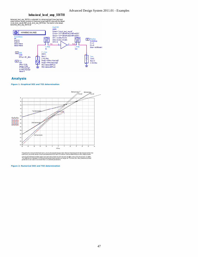
Advanced Design System 2011.01 - Examples
47
Analysis
Figure 1: Graphical SOI and TOI determination
Figure 2: Numerical SOI and TOI determination
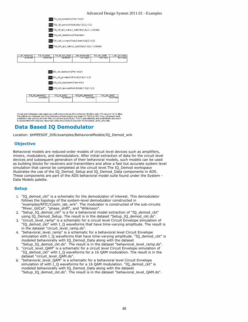
Advanced Design System 2011.01 - Examples
48
Data Based IQ DemodulatorLocation: $HPEESOF_DIR/examples/BehavioralModels/IQ_Demod_wrk
Objective
Behavioral models are reduced-order models of circuit level devices such as amplifiers,mixers, modulators, and demodulators. After initial extraction of data for the circuit leveldevices and subsequent generation of their behavioral models, such models can be usedas building blocks for receivers and transmitters and allow a fast but accurate system levelsimulation that cannot be completed at the circuit level.The IQ_Demod workspaceillustrates the use of the IQ_Demod_Setup and IQ_Demod_Data components in ADS.These components are part of the ADS behavioral model suite found under the System -Data Models palette.
Setup
"IQ_demod_ckt" is a schematic for the demodulator of interest. This demodulator1.follows the topology of the system-level demodulator constructed in"examples/RFIC/Cosim_lab_wrk". The modulator is constructed of the sub-circuits"Mixer_GilCel", "phase_shift", and "Wilkinson"."Setup_IQ_demod_ckt" is a for a behavioral model extraction of "IQ_demod_ckt"2.using IQ_Demod_Setup. The result is in the dataset "Setup_IQ_demod_ckt.ds"."circuit_level_ramp" is a schematic for a circuit level Circuit Envelope simulation of3."IQ_demod_ckt" with I_Q waveforms that have time-varying amplitude. The result isin the dataset "circuit_level_ramp.ds"."behavioral_level_ramp" is a schematic for a behavioral level Circuit Envelope4.simulation with I_Q waveforms that have time-varying amplitude. "IQ_demod_ckt" ismodeled behaviorally with IQ_Demod_Data along with the dataset"Setup_IQ_demod_ckt.ds". The result is in the dataset "behavioral_level_ramp.ds"."circuit_level_QAM" is a schematic for a circuit level Circuit Envelope simulation of5."IQ_demod_ckt" with I_Q waveforms for a 16 QAM modulation. The result is in thedataset "circuit_level_QAM.ds"."behavioral_level_QAM" is a schematic for a behavioral level Circuit Envelope6.simulation of with I_Q waveforms for a 16 QAM modulation. "IQ_demod_ckt" ismodeled behaviorally with IQ_Demod_Data along with the dataset"Setup_IQ_demod_ckt.ds". The result is in the dataset "behavioral_level_QAM.ds".

Advanced Design System 2011.01 - Examples
49
Analysis
Figure 1: Circuit and behavioral level results for I_Q waveforms with time varying amplitude
Figure 2: Circuit and behavioral level results for 16 QAM modulation
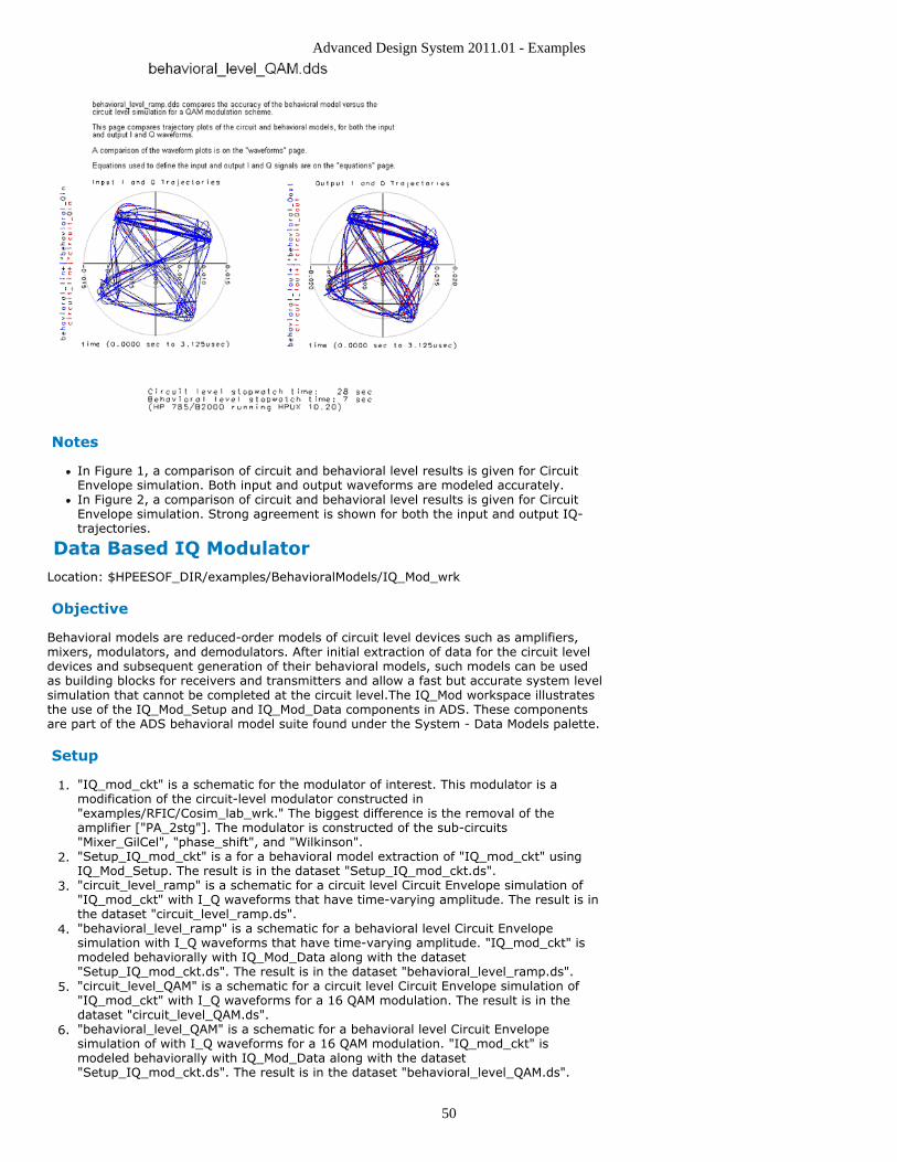
Advanced Design System 2011.01 - Examples
50
Notes
In Figure 1, a comparison of circuit and behavioral level results is given for CircuitEnvelope simulation. Both input and output waveforms are modeled accurately.In Figure 2, a comparison of circuit and behavioral level results is given for CircuitEnvelope simulation. Strong agreement is shown for both the input and output IQ-trajectories.
Data Based IQ ModulatorLocation: $HPEESOF_DIR/examples/BehavioralModels/IQ_Mod_wrk
Objective
Behavioral models are reduced-order models of circuit level devices such as amplifiers,mixers, modulators, and demodulators. After initial extraction of data for the circuit leveldevices and subsequent generation of their behavioral models, such models can be usedas building blocks for receivers and transmitters and allow a fast but accurate system levelsimulation that cannot be completed at the circuit level.The IQ_Mod workspace illustratesthe use of the IQ_Mod_Setup and IQ_Mod_Data components in ADS. These componentsare part of the ADS behavioral model suite found under the System - Data Models palette.
Setup
"IQ_mod_ckt" is a schematic for the modulator of interest. This modulator is a1.modification of the circuit-level modulator constructed in"examples/RFIC/Cosim_lab_wrk." The biggest difference is the removal of theamplifier ["PA_2stg"]. The modulator is constructed of the sub-circuits"Mixer_GilCel", "phase_shift", and "Wilkinson"."Setup_IQ_mod_ckt" is a for a behavioral model extraction of "IQ_mod_ckt" using2.IQ_Mod_Setup. The result is in the dataset "Setup_IQ_mod_ckt.ds"."circuit_level_ramp" is a schematic for a circuit level Circuit Envelope simulation of3."IQ_mod_ckt" with I_Q waveforms that have time-varying amplitude. The result is inthe dataset "circuit_level_ramp.ds"."behavioral_level_ramp" is a schematic for a behavioral level Circuit Envelope4.simulation with I_Q waveforms that have time-varying amplitude. "IQ_mod_ckt" ismodeled behaviorally with IQ_Mod_Data along with the dataset"Setup_IQ_mod_ckt.ds". The result is in the dataset "behavioral_level_ramp.ds"."circuit_level_QAM" is a schematic for a circuit level Circuit Envelope simulation of5."IQ_mod_ckt" with I_Q waveforms for a 16 QAM modulation. The result is in thedataset "circuit_level_QAM.ds"."behavioral_level_QAM" is a schematic for a behavioral level Circuit Envelope6.simulation of with I_Q waveforms for a 16 QAM modulation. "IQ_mod_ckt" ismodeled behaviorally with IQ_Mod_Data along with the dataset"Setup_IQ_mod_ckt.ds". The result is in the dataset "behavioral_level_QAM.ds".
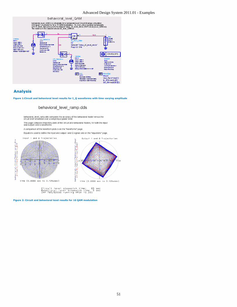
Advanced Design System 2011.01 - Examples
51
Analysis
Figure 1:Circuit and behavioral level results for I_Q waveforms with time varying amplitude
Figure 2: Circuit and behavioral level results for 16 QAM modulation
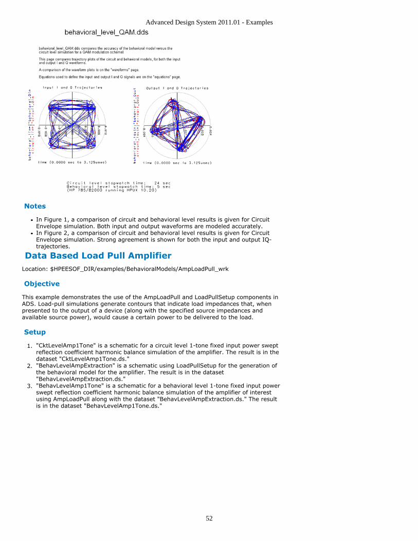
Advanced Design System 2011.01 - Examples
52
Notes
In Figure 1, a comparison of circuit and behavioral level results is given for CircuitEnvelope simulation. Both input and output waveforms are modeled accurately.In Figure 2, a comparison of circuit and behavioral level results is given for CircuitEnvelope simulation. Strong agreement is shown for both the input and output IQ-trajectories.
Data Based Load Pull AmplifierLocation: $HPEESOF_DIR/examples/BehavioralModels/AmpLoadPull_wrk
Objective
This example demonstrates the use of the AmpLoadPull and LoadPullSetup components inADS. Load-pull simulations generate contours that indicate load impedances that, whenpresented to the output of a device (along with the specified source impedances andavailable source power), would cause a certain power to be delivered to the load.
Setup
"CktLevelAmp1Tone" is a schematic for a circuit level 1-tone fixed input power swept1.reflection coefficient harmonic balance simulation of the amplifier. The result is in thedataset "CktLevelAmp1Tone.ds.""BehavLevelAmpExtraction" is a schematic using LoadPullSetup for the generation of2.the behavioral model for the amplifier. The result is in the dataset"BehavLevelAmpExtraction.ds.""BehavLevelAmp1Tone" is a schematic for a behavioral level 1-tone fixed input power3.swept reflection coefficient harmonic balance simulation of the amplifier of interestusing AmpLoadPull along with the dataset "BehavLevelAmpExtraction.ds." The resultis in the dataset "BehavLevelAmp1Tone.ds."
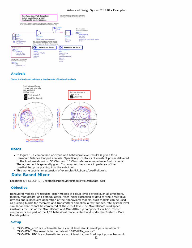
Advanced Design System 2011.01 - Examples
53
Analysis
Figure 1: Circuit and behavioral level results of load pull analysis
Notes
In Figure 1, a comparison of circuit and behavioral level results is given for aHarmonic Balance loadpull analysis. Specifically, contours of constant power deliveredto the load are shown on 50 Ohm and 10 Ohm reference impedance Smith charts.The agreement is generally good. You may set the source impedance of theLoadPullSetup by pushing into the subcircuit.This workspace is an extension of examples/RF_Board/LoadPull_wrk.
Data Based MixerLocation: $HPEESOF_DIR/examples/BehavioralModels/MixerHBdata_wrk
Objective
Behavioral models are reduced-order models of circuit level devices such as amplifiers,mixers, modulators, and demodulators. After initial extraction of data for the circuit leveldevices and subsequent generation of their behavioral models, such models can be usedas building blocks for receivers and transmitters and allow a fast but accurate system levelsimulation that cannot be completed at the circuit level.The MixerHBdata workspaceillustrates the use of the MixerHBdata and MixerHBsetup components in ADS. Thesecomponents are part of the ADS behavioral model suite found under the System - DataModels palette.
Setup
"GilCellMix_env" is a schematic for a circuit level circuit envelope simulation of1."GilCellMix". The result is in the dataset "GilCellMix_env.ds"."GilCellMix_HB" is a schematic for a circuit level 1-tone fixed input power harmonic
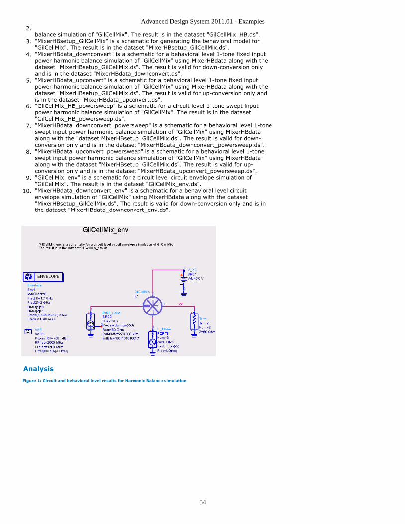
Advanced Design System 2011.01 - Examples
54
2.balance simulation of "GilCellMix". The result is in the dataset "GilCellMix_HB.ds"."MixerHBsetup_GilCellMix" is a schematic for generating the behavioral model for3."GilCellMix". The result is in the dataset "MixerHBsetup_GilCellMix.ds"."MixerHBdata_downconvert" is a schematic for a behavioral level 1-tone fixed input4.power harmonic balance simulation of "GilCellMix" using MixerHBdata along with thedataset "MixerHBsetup_GilCellMix.ds". The result is valid for down-conversion onlyand is in the dataset "MixerHBdata_downconvert.ds"."MixerHBdata_upconvert" is a schematic for a behavioral level 1-tone fixed input5.power harmonic balance simulation of "GilCellMix" using MixerHBdata along with thedataset "MixerHBsetup_GilCellMix.ds". The result is valid for up-conversion only andis in the dataset "MixerHBdata_upconvert.ds"."GilCellMix_HB_powersweep" is a schematic for a circuit level 1-tone swept input6.power harmonic balance simulation of "GilCellMix". The result is in the dataset"GilCellMix_HB_powersweep.ds"."MixerHBdata_downconvert_powersweep" is a schematic for a behavioral level 1-tone7.swept input power harmonic balance simulation of "GilCellMix" using MixerHBdataalong with the "dataset MixerHBsetup_GilCellMix.ds". The result is valid for down-conversion only and is in the dataset "MixerHBdata_downconvert_powersweep.ds"."MixerHBdata_upconvert_powersweep" is a schematic for a behavioral level 1-tone8.swept input power harmonic balance simulation of "GilCellMix" using MixerHBdataalong with the dataset "MixerHBsetup_GilCellMix.ds". The result is valid for up-conversion only and is in the dataset "MixerHBdata_upconvert_powersweep.ds"."GilCellMix_env" is a schematic for a circuit level circuit envelope simulation of9."GilCellMix". The result is in the dataset "GilCellMix_env.ds"."MixerHBdata_downconvert_env" is a schematic for a behavioral level circuit10.envelope simulation of "GilCellMix" using MixerHBdata along with the dataset"MixerHBsetup_GilCellMix.ds". The result is valid for down-conversion only and is inthe dataset "MixerHBdata_downconvert_env.ds".
Analysis
Figure 1: Circuit and behavioral level results for Harmonic Balance simulation
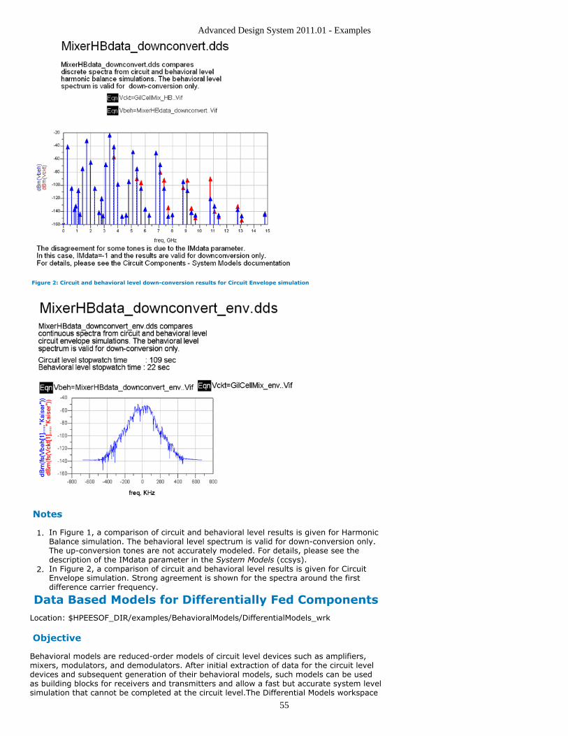
Advanced Design System 2011.01 - Examples
55
Figure 2: Circuit and behavioral level down-conversion results for Circuit Envelope simulation
Notes
In Figure 1, a comparison of circuit and behavioral level results is given for Harmonic1.Balance simulation. The behavioral level spectrum is valid for down-conversion only.The up-conversion tones are not accurately modeled. For details, please see thedescription of the IMdata parameter in the System Models (ccsys).In Figure 2, a comparison of circuit and behavioral level results is given for Circuit2.Envelope simulation. Strong agreement is shown for the spectra around the firstdifference carrier frequency.
Data Based Models for Differentially Fed ComponentsLocation: $HPEESOF_DIR/examples/BehavioralModels/DifferentialModels_wrk
Objective
Behavioral models are reduced-order models of circuit level devices such as amplifiers,mixers, modulators, and demodulators. After initial extraction of data for the circuit leveldevices and subsequent generation of their behavioral models, such models can be usedas building blocks for receivers and transmitters and allow a fast but accurate system levelsimulation that cannot be completed at the circuit level.The Differential Models workspace

Advanced Design System 2011.01 - Examples
56
illustrates the use of the Balun3Port and Balun4Port components in ADS. Thesecomponents are part of the ADS behavioral model suite found under the System - DataModels palette. They are also available from the System - Passive palette. For details oncreating data based models for single ended mixers, please see Data Based Mixer(examples).
Setup
"DiffMix_HB" is a schematic for a circuit level 1-tone fixed input power harmonic1.balance simulation of "DiffMix". The result is in the dataset "DiffMix_HB.ds"."MixerHBsetup_DiffMix" is a schematic for generating the behavioral model for2."DiffMix". The result is in the dataset "MixerHBsetup_DiffMix.ds"."MixerHBdata_downconvert" is a schematic for a behavioral level 1-tone fixed input3.power harmonic balance simulation of "DiffMix" using MixerHBdata along with thedataset "MixerHBsetup_DiffMix.ds". The result is valid for down-conversion only andis in the dataset "MixerHBdata_downconvert.ds"."DiffMix_env" is a schematic for a circuit level circuit envelope simulation of "DiffMix".4.The result is in the dataset "DiffMix_env.ds"."MixerHBdata_downconvert_env" is a schematic for a behavioral level circuit5.envelope simulation of "DiffMix" using MixerHBdata along with the dataset"MixerHBsetup_DiffMix.ds". The result is valid for down-conversion only and is in thedataset "MixerHBdata_downconvert_env.ds".
Analysis
Figure 1: Circuit and behavioral level results for Harmonic Balance simulation

Advanced Design System 2011.01 - Examples
57
Notes
In Figure 1, a comparison of circuit and behavioral level results is given for Harmonic1.Balance simulation. The behavioral level spectrum is valid for down-conversion only.The up-conversion tones are not accurately modeled. For details, please see thedescription of the IMdata parameter of the MixerHBdata (2-Tone HB Mixer) (ccsys)component in the System Models (ccsys) documentation.
Extraction and use of IMT Based System Level MixersLocation: $HPEESOF_DIR/examples/BehavioralModels/MixIMT_wrk
Objective
To provide the Use Model of the MixIMT FamilyThe MixIMT family provides a behavioral modeling solution for mixers. The family consistsof two IMT data extractor components MixIMTA_Setup and MixIMTB_Setup and a datamodel component MixIMT_Data. All three components are available from the System-DataModels library.This example workspace shows how the two extractors can be set up togenerate IMT files from a circuit level mixer model in ADS environment and how the datamodel can be used to interpret such IMT files to regenerate mixer behavior.This examplealso shows how to use original IMT files obtained from manufacturer specification sheetsor legacy projects with the MixIMT_Data model.This example does not explicitly containinstances of MixerIMT or MixerIMT2. However, descriptive and graphical references aremade to these two legacy components to illustrate the capabilities of MixIMT_Data.
Setup
Extraction of IMT DataMixer behavior has been defined using intermodulation table (IMT) data or spur chartssince the 1980s. Such charts used to be sufficient only for single RF signals and containonly single side banded IF strengths without phase data. Application of such incomplete IMtables to multi-tone RF systems was insupportable in theory and frustrating in practice. Asof ADS2006A it is possible to perform automatic extraction of single or multi-RF spurcharts using the MixIMT*_Setup components as shown below. Both extractors generatecomplex double side banded spur information with some capability of sweeping signalpower and frequency such that the same IMT file can capture.MixIMTA_Setup is designedto extract IMT data for a mixer response to the classic single RF, single LO. The degree ofdistortion expected to contribute to the mixing matrix can be specified at RF and LO portsvia relevant parameters. Both LO and RF frequencies and powers can be swept with anIMT being captured at each combination of the 4-tuple {RFfreq, LOfreq, RFpowr, LOpowr}as shown in CKT_IMTA_extraction.
Figure 1: Extraction of A-type IMT data
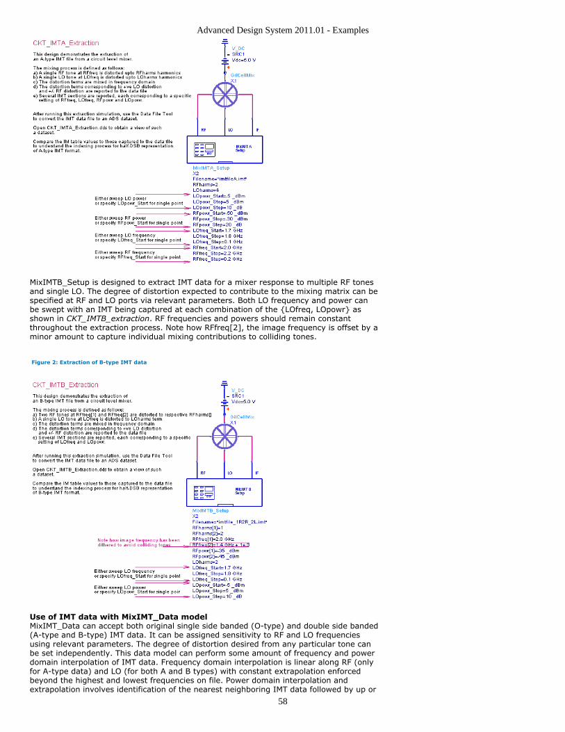
Advanced Design System 2011.01 - Examples
58
MixIMTB_Setup is designed to extract IMT data for a mixer response to multiple RF tonesand single LO. The degree of distortion expected to contribute to the mixing matrix can bespecified at RF and LO ports via relevant parameters. Both LO frequency and power canbe swept with an IMT being captured at each combination of the {LOfreq, LOpowr} asshown in CKT_IMTB_extraction. RF frequencies and powers should remain constantthroughout the extraction process. Note how RFfreq[2], the image frequency is offset by aminor amount to capture individual mixing contributions to colliding tones.
Figure 2: Extraction of B-type IMT data
Use of IMT data with MixIMT_Data modelMixIMT_Data can accept both original single side banded (O-type) and double side banded(A-type and B-type) IMT data. It can be assigned sensitivity to RF and LO frequenciesusing relevant parameters. The degree of distortion desired from any particular tone canbe set independently. This data model can perform some amount of frequency and powerdomain interpolation of IMT data. Frequency domain interpolation is linear along RF (onlyfor A-type data) and LO (for both A and B types) with constant extrapolation enforcedbeyond the highest and lowest frequencies on file. Power domain interpolation andextrapolation involves identification of the nearest neighboring IMT data followed by up or
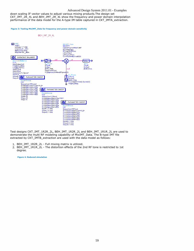
Advanced Design System 2011.01 - Examples
59
down scaling IF vector values to adjust various mixing products.The design setCKT_IMT_2R_4L and BEH_IMT_2R_4L show the frequency and power domain interpolationperformance of the data model for the A-type IM table captured in CKT_IMTA_extraction.
Figure 3: Testing MixIMT_Data for frequency and power domain sensitivity
Test designs CKT_IMT_1R2R_2L, BEH_IMT_1R2R_2L and BEH_IMT_1R1R_2L are used todemonstrate the multi-RF modeling capability of MixIMT_Data. The B-type IMT fileextracted by CKT_IMTB_extraction are used with the data model as follows:
BEH_IMT_1R2R_2L - Full mixing matrix is utilized.1.BEH_IMT_1R1R_2L - The distortion effects of the 2nd RF tone is restricted to 1st2.degree.
Figure 4: Reduced simulation
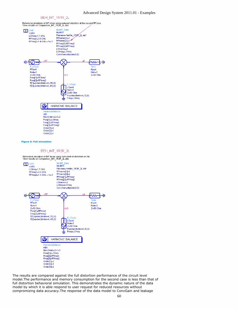
Advanced Design System 2011.01 - Examples
60
Figure 5: Full simulation
The results are compared against the full distortion performance of the circuit levelmodel.The performance and memory consumption for the second case is less than that offull distortion behavioral simulation. This demonstrates the dynamic nature of the datamodel by which it is able respond to user request for reduced resources withoutcompromizing data accuracy.The response of the data model to ConvGain and leakage
Advanced Design System 2011.01 - Examples
61
and reflection parameters are shown in BEH_IMT_2R_4L_ConvGain andBEH_IMT_2R_4L_LeakageReflection respectively. See analysis section for results.The MixIMT_Data model is capable of generating fast and accurate envelope responses tocomplex modulated waveforms e.g. a 3GPP Uplink signal.
Figure 6: Using MixIMT_Data in an envelope simulation for a 3GPP signal
Analysis
Verifying frequency and power domain accuracy of MixIMT_DataComparison_IMT_2R_4L.dds shows the accuracy of the behavioral model in modeling A-type IMT data for swept RF and LO powers and frequencies. The extremal points of powersand frequencies along each of the four independent axes are on file, with the middlepoints being interpolated estimates.
Advanced Design System 2011.01 - Examples
62
Customized distortion effects from MixIMT_DataComparison_IMT_1R2R_2L.dds shows that comparable levels of accuracy are acheievedfor mixing products common to full scale IMT modeling in BEH_IMT_1R2R_2L and reducedscale IMT modeling in BEH_IMT_1R1R_2L.
Conversion GainConversion Gain is a voltage valued parameter defined on the mixer model that allows theIF side output to be impacted by a fixed vector. The test designBEH_IMT_2R_4L_ConvGain demonstrates how the dB and phase values of this parametermay be swept to achieve relevant IF offsets from the baseline behavior defined in the dataprofile. Note that ConvGain affects behavior only at IF port with no impact at the RF or LO
Advanced Design System 2011.01 - Examples
63
inputs.
Figure 7: Effect of conversion gain { 5 dB, -25 deg} raises power while adding phase lag at IF port
Leakage and ReflectionLeakge and reflection at the three mixer ports can be defined using nine S-parameters onthe MixIMT_Data model. Note that these are not the FSP parameters captured to IMT filesin CKT_IMTA_extraction.dds. These S-parameters are not frequency-translated. Theyindicate alternate routes for flow of power between the ports other than through thenonlinear mixing element. In the example design BEH_IMT_2R_4L_LeakageReflection asingle complex number is associated with one of the nine S-parameters and its magnitudeand phase swept to generate the mixer response to user-imposed perturbations. Theimpacted complex parameter can be changed to view the effects of various port to portleakages and reflections. The data display allows interactive viewing of the changes to RF,LO and IF voltage vectors relative to the unperturbed state defined in the IM table.
Figure 8: Effect of setting RFreflection = polar(0.75, 45)
Advanced Design System 2011.01 - Examples
64
Note impact on vRF and vIF spectra.
3GPP Envelope SimulationAs shown in the figure below, the behavioral response (blue) matches the circuit levelresponse of the input and output side envelopes within respective passbands. Simulationtime for the behavioral model was found to be less than 10 sec compared to 1 hour 10minutes for the circuit level model.
Figure 9: Comparison of behavioral and circuit level spectra for mixing of a 3GPP signal at 1.95 GHz with a localoscillator at 1.9 GHz
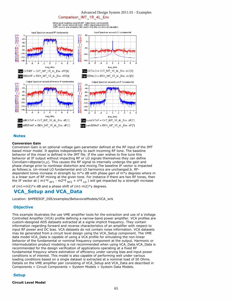
Advanced Design System 2011.01 - Examples
65
Notes
Conversion GainConversion Gain is an optional voltage gain parameter defined at the RF input of the IMTbased mixer model. It applies independently to each incoming RF tone. The baselinebehavior of the mixer is defined in the IMT file. If the user wishes to fine tune thisbehavior at IF output without impacting RF or LO signals themselves they can defineConvGain=dbpolar(x,y). This causes the RF signal to internally undergo the gain andphase change prior to nonlinear distortion and mixing.The baseline IF vector is impactedas follows:a. Un-mixed LO fundamental and LO harmonics are unchanged.b. RF-dependent tones increase in strength by m*x dB with phase gain of m*y degrees where mis a linear sum of RF mixing at the given tone. For instance if there are two RF tones, thenthe IF vector at ( m1*f RF1 - m2*f RF2 + n*f LO ) will get impacted by a strength increase
of (m1+m2)*x dB and a phase shift of (m1-m2)*y degrees.
VCA_Setup and VCA_DataLocation: $HPEESOF_DIR/examples/BehavioralModels/VCA_wrk
Objective
This example illustrates the use VME amplifier tools for the extraction and use of a VoltageControlled Amplifier (VCA) profile defining a narrow-band power amplifier. VCA profiles arecustom-designed ADS datasets extracted at a signle implicit frequency. They containinformation regarding forward and reverse characteristics of an amplifier with respect toinput RF power and DC bias. VCA datasets do not contain noise information. VCA datasetsmay be generated from a circuit level design using the VCA_Setup component. The VMEdata model VCA_Data is capable of using a VCA profile for simulating the non-linearbehavior of the fundamental or nominal frequency component at the output. Harmonic orintermodulation product modeling is not recommended when using VCA_Data.VCA_Data isrecommended for the design verification of applications operating at a fixed RFfundamental frequncy where estimation of efficiency under varying bias and input powerconditions is of interest. This model is also capable of performing well under variousloading conditions based on a single dataset is extracted at a nominal load of 50 Ohms.Details on the VME amplifier pair consisting of VCA_Setup and VCA_Data are described inComponents > Circuit Components > System Models > System Data Models.
Setup
Circuit Level Model
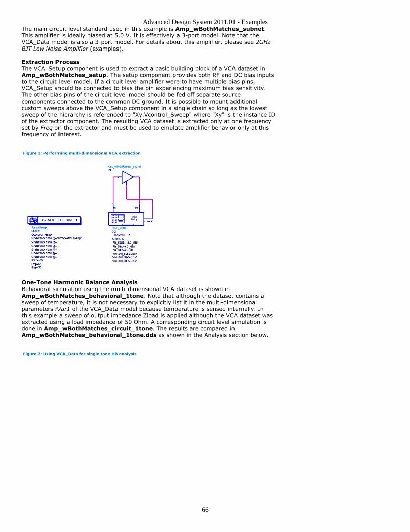
Advanced Design System 2011.01 - Examples
66
The main circuit level standard used in this example is Amp_wBothMatches_subnet.This amplifier is ideally biased at 5.0 V. It is effectively a 3-port model. Note that theVCA_Data model is also a 3-port model. For details about this amplifier, please see 2GHzBJT Low Noise Amplifier (examples).
Extraction ProcessThe VCA_Setup component is used to extract a basic building block of a VCA dataset inAmp_wBothMatches_setup. The setup component provides both RF and DC bias inputsto the circuit level model. If a circuit level amplifier were to have multiple bias pins,VCA_Setup should be connected to bias the pin experiencing maximum bias sensitivity.The other bias pins of the circuit level model should be fed off separate sourcecomponents connected to the common DC ground. It is possible to mount additionalcustom sweeps above the VCA_Setup component in a single chain so long as the lowestsweep of the hierarchy is referenced to "Xy.Vcontrol_Sweep" where "Xy" is the instance IDof the extractor component. The resulting VCA dataset is extracted only at one frequencyset by Freq on the extractor and must be used to emulate amplifier behavior only at thisfrequency of interest.
Figure 1: Performing multi-dimensional VCA extraction
One-Tone Harmonic Balance AnalysisBehavioral simulation using the multi-dimensional VCA dataset is shown inAmp_wBothMatches_behavioral_1tone. Note that although the dataset contains asweep of temperature, it is not necessary to explicitly list it in the multi-dimensionalparameters iVar1 of the VCA_Data model because temperature is sensed internally. Inthis example a sweep of output impedance Zload is applied although the VCA dataset wasextracted using a load impedance of 50 Ohm. A corresponding circuit level simulation isdone in Amp_wBothMatches_circuit_1tone. The results are compared inAmp_wBothMatches_behavioral_1tone.dds as shown in the Analysis section below.
Figure 2: Using VCA_Data for single tone HB analysis
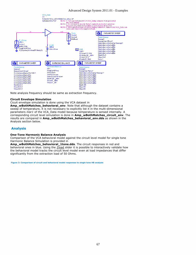
Advanced Design System 2011.01 - Examples
67
Note analysis frequency should be same as extraction frequency.
Circuit Envelope SimulationCicuit envelope simulation is done using the VCA dataset inAmp_wBothMatches_behavioral_env. Note that although the dataset contains asweep of temperature, it is not necessary to explicitly list it in the multi-dimensionalparameters iVar1 of the VCA_Data model because temperature is sensed internally. Acorresponding circuit level simulation is done in Amp_wBothMatches_circuit_env. Theresults are compared in Amp_wBothMatches_behavioral_env.dds as shown in theAnalysis section below.
Analysis
One-Tone Harmonic Balance AnalysisComparison of the VCA behavioral model against the circuit level model for single toneHarmonic Balance Simulation is provided inAmp_wBothMatches_behavioral_1tone.dds. The circuit responses in red andbehavioral ones in blue. Using the Zload slider it is possible to interactively validate howthe behavioral model tracks the circuit level model even at load impedances that differsignificantly from the extraction load of 50 Ohms.
Figure 3: Comparison of circuit and behavioral model responses to single tone HB analysis
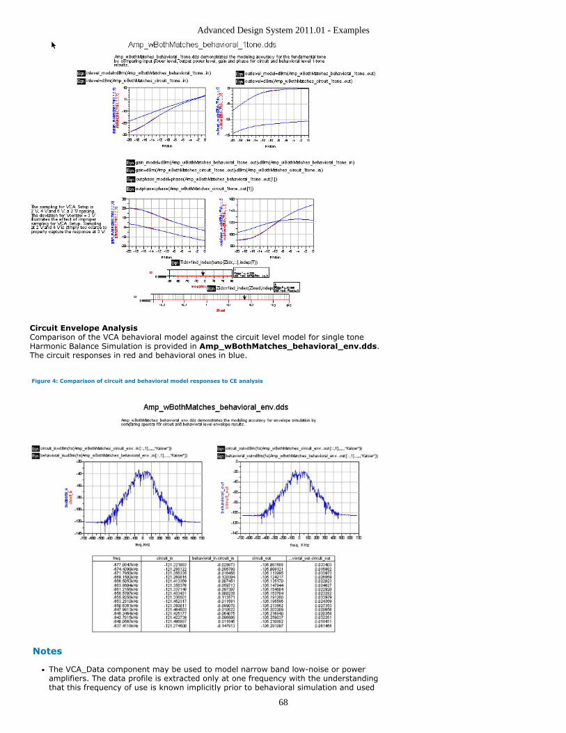
Advanced Design System 2011.01 - Examples
68
Circuit Envelope AnalysisComparison of the VCA behavioral model against the circuit level model for single toneHarmonic Balance Simulation is provided in Amp_wBothMatches_behavioral_env.dds.The circuit responses in red and behavioral ones in blue.
Figure 4: Comparison of circuit and behavioral model responses to CE analysis
Notes
The VCA_Data component may be used to model narrow band low-noise or poweramplifiers. The data profile is extracted only at one frequency with the understandingthat this frequency of use is known implicitly prior to behavioral simulation and used

Advanced Design System 2011.01 - Examples
69
in that process.It is possible to include sweeps of additional user-specified parameters above thebasic control voltage and power sweeps necessary in VCA dataset.VCA_Data accurately models DC power drawn from the bias source based on biasvoltage and supplied RF power at amplifier input. This model can therefore be usedfor PAE estimation of RF amplifiers.VCA_Data is able to provide accurate output voltage and current for a wide range ofvarying load conditions.
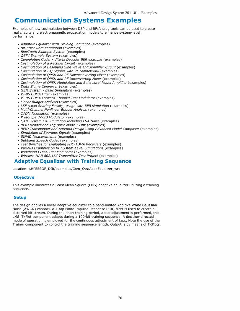
Advanced Design System 2011.01 - Examples
70
Communication Systems ExamplesExamples of how cosimulation between DSP and RF/Analog tools can be used to createreal circuits and electromagnetic propagation models to enhance system-levelperformance.
Adaptive Equalizer with Training Sequence (examples)Bit-Error-Rate Estimation (examples)BlueTooth Example System (examples)CATV Example System (examples)Convolution Coder - Viterbi Decoder BER example (examples)Cosimulation of a Rectifier Circuit (examples)Cosimulation of Baseband Sine Wave and Amplifier Circuit (examples)Cosimulation of I-Q Signals with RF Subnetwork (examples)Cosimulation of QPSK and RF Downconverting Mixer (examples)Cosimulation of QPSK and RF Upconverting Mixer (examples)Cosimulation of QPSK Modulation and Behavioral Model Amplifier (examples)Delta Sigma Converter (examples)GSM System - Basic Simulation (examples)IS-95 CDMA Filter (examples)IS-95 CDMA Forward-Channel Test Modulator (examples)Linear Budget Analysis (examples)LSF (Load Sharing Facility) usage with BER simulation (examples)Multi-Channel Nonlinear Budget Analysis (examples)OFDM Modulation (examples)Prototype 8-VSB Modulator (examples)QAM System Co-Simulation Including LNA Noise (examples)RFID Reader and Tag Basic Mode 1 Link (examples)RFID Transponder and Antenna Design using Advanced Model Composer (examples)Simulation of Spurious Signals (examples)SINAD Measurements (examples)Subband Speech Codec (examples)Test Benches for Evaluating PDC-TDMA Receivers (examples)Various Examples on RF System-Level Simulations (examples)Wideband CDMA Test Modulator (examples)Wireless MAN 802.16d Transmitter Test Project (examples)
Adaptive Equalizer with Training SequenceLocation: $HPEESOF_DIR/examples/Com_Sys/AdapEqualizer_wrk
Objective
This example illustrates a Least Mean Square (LMS) adaptive equalizer utilizing a trainingsequence.
Setup
The design applies a linear adaptive equalizer to a band-limited Additive White GaussianNoise (AWGN) channel. A 4-tap Finite Impulse Response (FIR) filter is used to create adistorted bit stream. During the short training period, a tap adjustment is performed, theLMS_TkPlot component adapts during a 100-bit training sequence. A decision-directedmode of operation is employed for the continuous adjustment of taps. Note the use of theTrainer component to control the training sequence length. Output is by means of TKPlots.
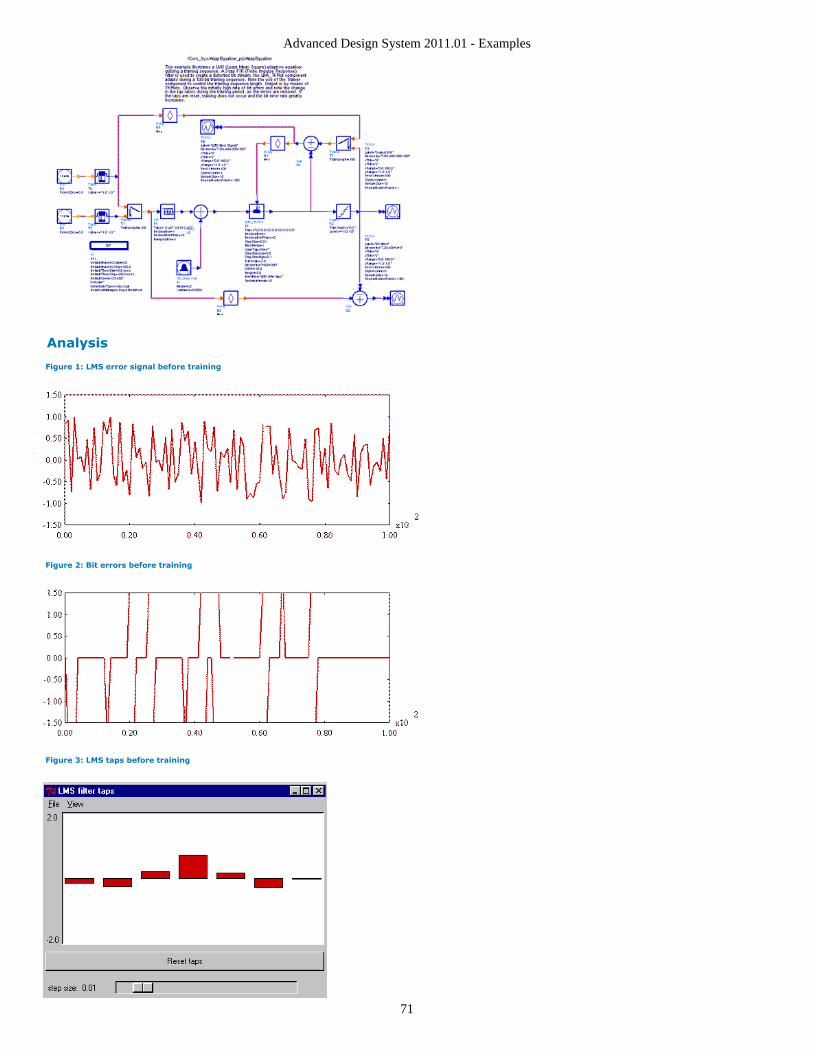
Advanced Design System 2011.01 - Examples
71
Analysis
Figure 1: LMS error signal before training
Figure 2: Bit errors before training
Figure 3: LMS taps before training
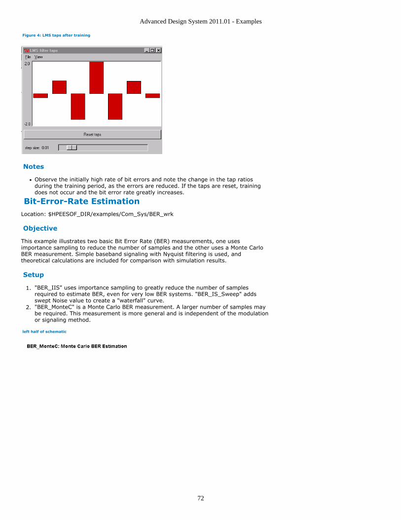
Advanced Design System 2011.01 - Examples
72
Figure 4: LMS taps after training
Notes
Observe the initially high rate of bit errors and note the change in the tap ratiosduring the training period, as the errors are reduced. If the taps are reset, trainingdoes not occur and the bit error rate greatly increases.
Bit-Error-Rate EstimationLocation: $HPEESOF_DIR/examples/Com_Sys/BER_wrk
Objective
This example illustrates two basic Bit Error Rate (BER) measurements, one usesimportance sampling to reduce the number of samples and the other uses a Monte CarloBER measurement. Simple baseband signaling with Nyquist filtering is used, andtheoretical calculations are included for comparison with simulation results.
Setup
"BER_IIS" uses importance sampling to greatly reduce the number of samples1.required to estimate BER, even for very low BER systems. "BER_IS_Sweep" addsswept Noise value to create a "waterfall" curve."BER_MonteC" is a Monte Carlo BER measurement. A larger number of samples may2.be required. This measurement is more general and is independent of the modulationor signaling method.
left half of schematic
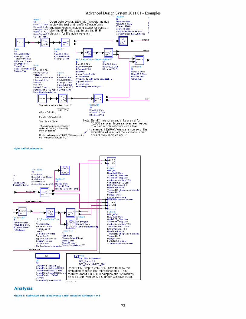
Advanced Design System 2011.01 - Examples
73
right half of schematic
Analysis
Figure 1: Estimated BER using Monte Carlo, Relative Variance = 0.1
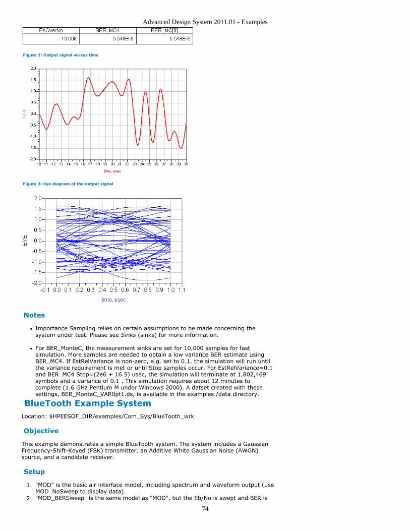
Advanced Design System 2011.01 - Examples
74
Figure 2: Output signal versus time
Figure 3: Eye diagram of the output signal
Notes
Importance Sampling relies on certain assumptions to be made concerning thesystem under test. Please see Sinks (sinks) for more information.
For BER_MonteC, the measurement sinks are set for 10,000 samples for fastsimulation. More samples are needed to obtain a low variance BER estimate usingBER_MC4. If EstRelVariance is non-zero, e.g. set to 0.1, the simulation will run untilthe variance requirement is met or until Stop samples occur. For EstRelVariance=0.1and BER_MC4 Stop=(2e6 + 16.5) usec, the simulation will terminate at 1,802,469symbols and a variance of 0.1 . This simulation requires about 12 minutes tocomplete (1.6 GHz Pentium M under Windows 2000). A datset created with thesesettings, BER_MonteC_VAR0pt1.ds, is available in the examples /data directory.
BlueTooth Example SystemLocation: $HPEESOF_DIR/examples/Com_Sys/BlueTooth_wrk
Objective
This example demonstrates a simple BlueTooth system. The system includes a GaussianFrequency-Shift-Keyed (FSK) transmitter, an Additive White Gaussian Noise (AWGN)source, and a candidate receiver.
Setup
"MOD" is the basic air interface model, including spectrum and waveform output (use1.MOD_NoSweep to display data)."MOD_BERSweep" is the same model as "MOD", but the Eb/No is swept and BER is2.
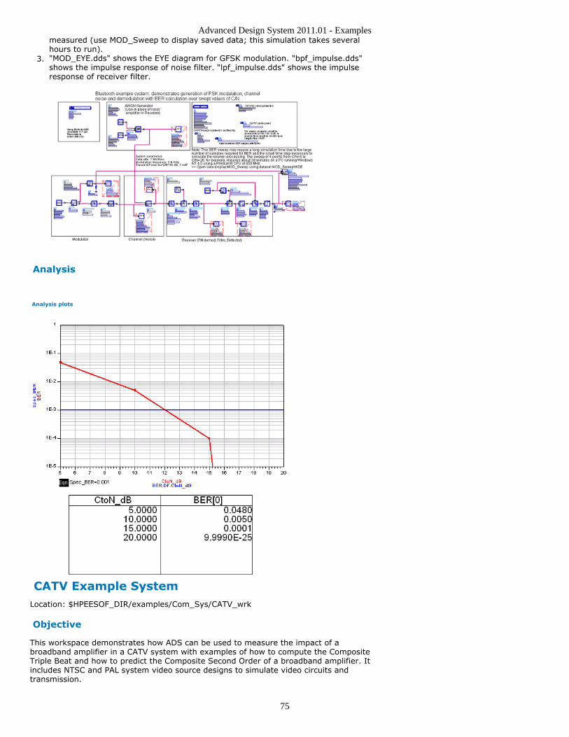
Advanced Design System 2011.01 - Examples
75
measured (use MOD_Sweep to display saved data; this simulation takes severalhours to run)."MOD_EYE.dds" shows the EYE diagram for GFSK modulation. "bpf_impulse.dds"3.shows the impulse response of noise filter. "lpf_impulse.dds" shows the impulseresponse of receiver filter.
Analysis
Analysis plots
CATV Example SystemLocation: $HPEESOF_DIR/examples/Com_Sys/CATV_wrk
Objective
This workspace demonstrates how ADS can be used to measure the impact of abroadband amplifier in a CATV system with examples of how to compute the CompositeTriple Beat and how to predict the Composite Second Order of a broadband amplifier. Itincludes NTSC and PAL system video source designs to simulate video circuits andtransmission.
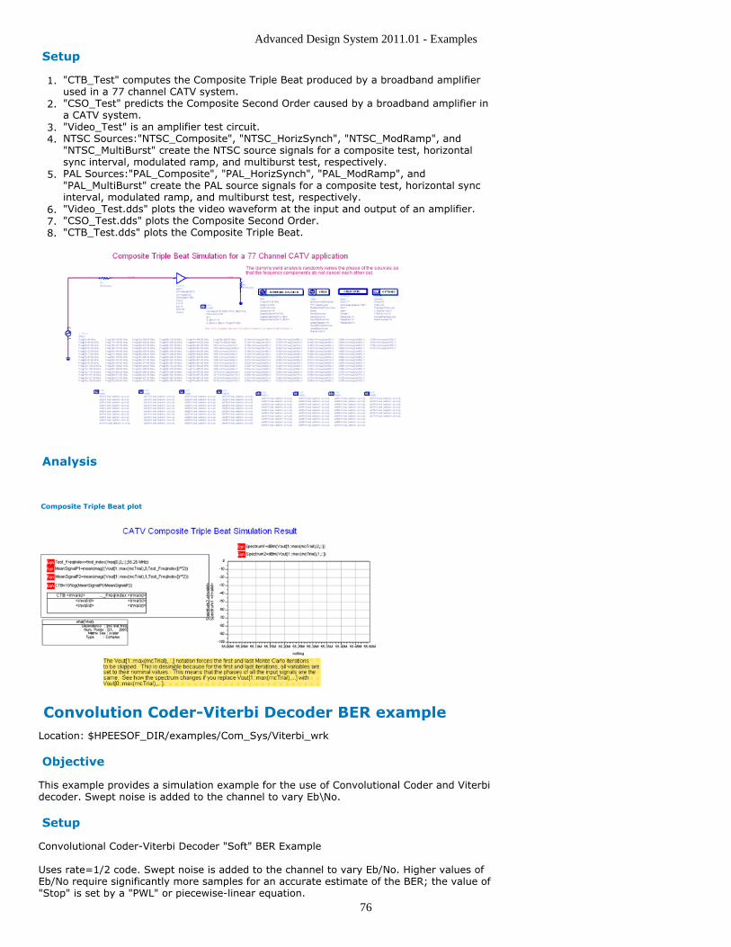
Advanced Design System 2011.01 - Examples
76
Setup
"CTB_Test" computes the Composite Triple Beat produced by a broadband amplifier1.used in a 77 channel CATV system."CSO_Test" predicts the Composite Second Order caused by a broadband amplifier in2.a CATV system."Video_Test" is an amplifier test circuit.3.NTSC Sources:"NTSC_Composite", "NTSC_HorizSynch", "NTSC_ModRamp", and4."NTSC_MultiBurst" create the NTSC source signals for a composite test, horizontalsync interval, modulated ramp, and multiburst test, respectively.PAL Sources:"PAL_Composite", "PAL_HorizSynch", "PAL_ModRamp", and5."PAL_MultiBurst" create the PAL source signals for a composite test, horizontal syncinterval, modulated ramp, and multiburst test, respectively."Video_Test.dds" plots the video waveform at the input and output of an amplifier.6."CSO_Test.dds" plots the Composite Second Order.7."CTB_Test.dds" plots the Composite Triple Beat.8.
Analysis
Composite Triple Beat plot
Convolution Coder-Viterbi Decoder BER exampleLocation: $HPEESOF_DIR/examples/Com_Sys/Viterbi_wrk
Objective
This example provides a simulation example for the use of Convolutional Coder and Viterbidecoder. Swept noise is added to the channel to vary Eb\No.
Setup
Convolutional Coder-Viterbi Decoder "Soft" BER Example
Uses rate=1/2 code. Swept noise is added to the channel to vary Eb/No. Higher values ofEb/No require significantly more samples for an accurate estimate of the BER; the value of"Stop" is set by a "PWL" or piecewise-linear equation.
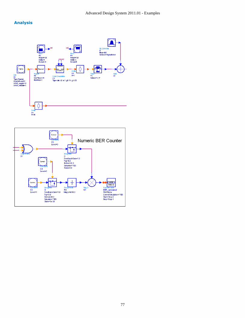
Advanced Design System 2011.01 - Examples
77
Analysis
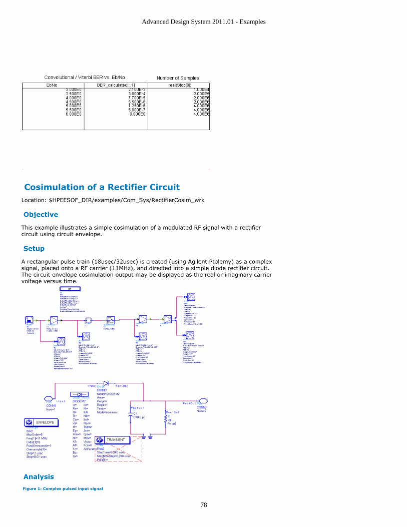
Advanced Design System 2011.01 - Examples
78
Cosimulation of a Rectifier CircuitLocation: $HPEESOF_DIR/examples/Com_Sys/RectifierCosim_wrk
Objective
This example illustrates a simple cosimulation of a modulated RF signal with a rectifiercircuit using circuit envelope.
Setup
A rectangular pulse train (18usec/32usec) is created (using Agilent Ptolemy) as a complexsignal, placed onto a RF carrier (11MHz), and directed into a simple diode rectifier circuit.The circuit envelope cosimulation output may be displayed as the real or imaginary carriervoltage versus time.
Analysis
Figure 1: Complex pulsed input signal
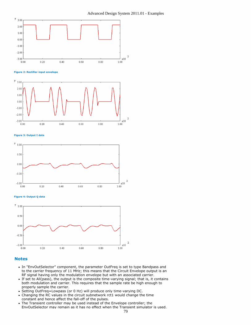
Advanced Design System 2011.01 - Examples
79
Figure 2: Rectifier input envelope
Figure 3: Output I data
Figure 4: Output Q data
Notes
In "EnvOutSelector" component, the parameter OutFreq is set to type Bandpass andto the carrier frequency of 11 MHz; this means that the Circuit Envelope output is anRF signal having only the modulation envelope but with an associated carrier.If set to All(pass), the output is the composite time-varying signal; that is, it containsboth modulation and carrier. This requires that the sample rate be high enough toproperly sample the carrier.Setting OutFreq=Lowpass (or 0 Hz) will produce only time-varying DC.Changing the RC values in the circuit subnetwork rct1 would change the timeconstant and hence affect the fall-off of the pulses.The Transient controller may be used instead of the Envelope controller; theEnvOutSelector may remain as it has no effect when the Transient simulator is used.
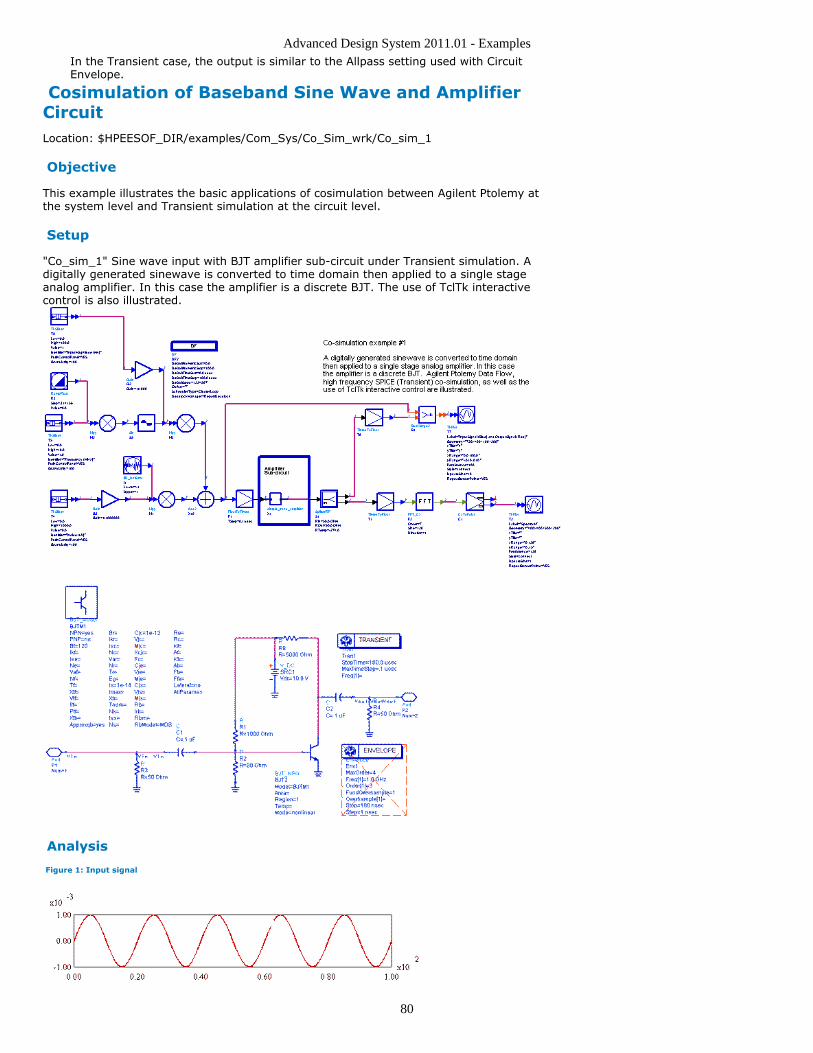
Advanced Design System 2011.01 - Examples
80
In the Transient case, the output is similar to the Allpass setting used with CircuitEnvelope.
Cosimulation of Baseband Sine Wave and AmplifierCircuitLocation: $HPEESOF_DIR/examples/Com_Sys/Co_Sim_wrk/Co_sim_1
Objective
This example illustrates the basic applications of cosimulation between Agilent Ptolemy atthe system level and Transient simulation at the circuit level.
Setup
"Co_sim_1" Sine wave input with BJT amplifier sub-circuit under Transient simulation. Adigitally generated sinewave is converted to time domain then applied to a single stageanalog amplifier. In this case the amplifier is a discrete BJT. The use of TclTk interactivecontrol is also illustrated.
Analysis
Figure 1: Input signal
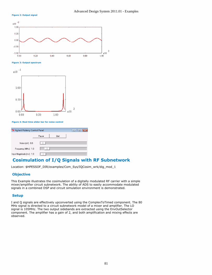
Advanced Design System 2011.01 - Examples
81
Figure 2: Output signal
Figure 3: Output spectrum
Figure 4: Real-time slider bar for noise control
Cosimulation of I/Q Signals with RF SubnetworkLocation: $HPESSOF_DIR/examples/Com_Sys/IQCosim_wrk/dig_mod_1
Objective
This Example illustrates the cosimulation of a digitally modulated RF carrier with a simplemixer/amplifier circuit subnetwork. The ability of ADS to easily accommodate modulatedsignals in a combined DSP and circuit simulation environment is demonstrated.
Setup
I and Q signals are effectively upconverted using the ComplexToTimed component. The 80MHz signal is directed to a circuit subnetwork model of a mixer and amplifier. The LOsignal is 105MHz. The two output sidebands are extracted using the EnvOutSelectorcomponent. The amplifier has a gain of 2, and both amplification and mixing effects areobserved.
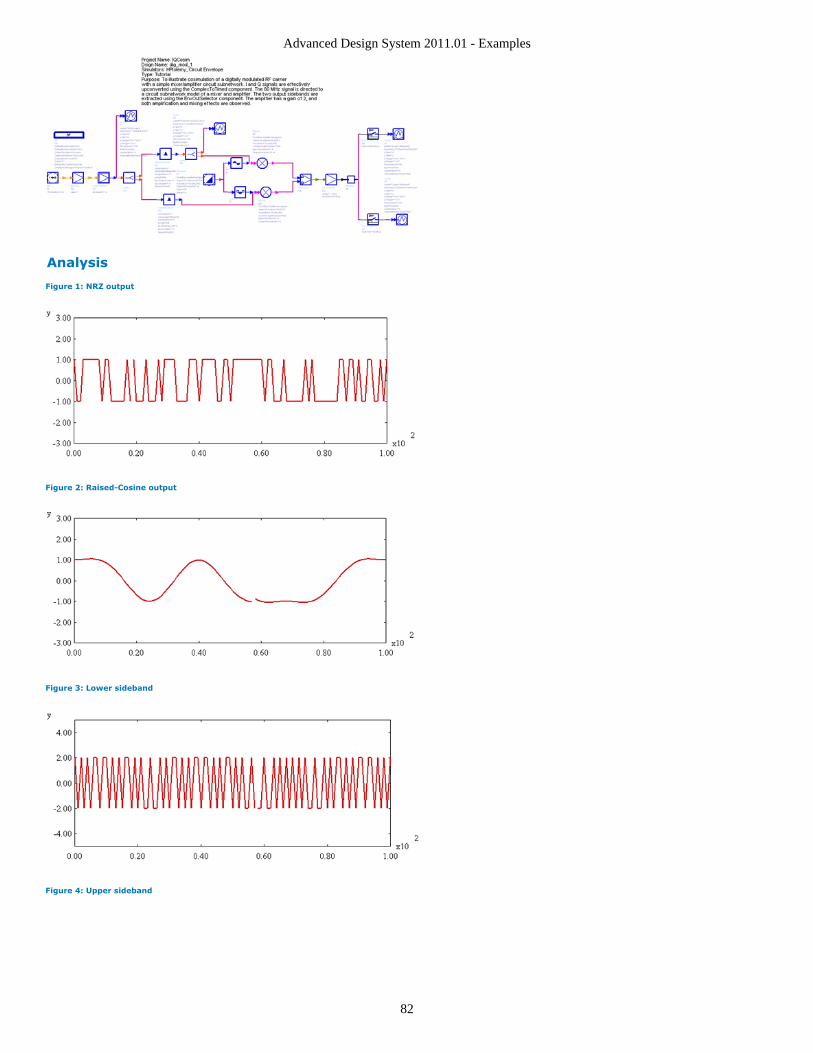
Advanced Design System 2011.01 - Examples
82
Analysis
Figure 1: NRZ output
Figure 2: Raised-Cosine output
Figure 3: Lower sideband
Figure 4: Upper sideband
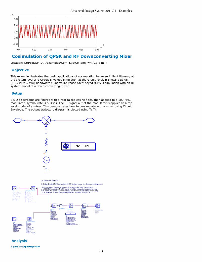
Advanced Design System 2011.01 - Examples
83
Cosimulation of QPSK and RF Downconverting MixerLocation: $HPEESOF_DIR/examples/Com_Sys/Co_Sim_wrk/Co_sim_4
Objective
This example illustrates the basic applications of cosimulation between Agilent Ptolemy atthe system level and Circuit Envelope simulation at the circuit level. It shows a IS-95(1.25 MHz CDMA) bandwidth Quadrature Phase-Shift Keyed (QPSK) simulation with an RFsystem model of a down-converting mixer.
Setup
I & Q bit streams are filtered with a root raised cosine filter, then applied to a 100 MHZmodulator, symbol rate is 50Ksps. The RF signal out of the modulator is applied to a toplevel model of a mixer. This demonstrates how to co-simulate with a mixer using CircuitEnvelope. The output trajectory diagram is plotted using TclTk.
Analysis
Figure 1: Output trajectory
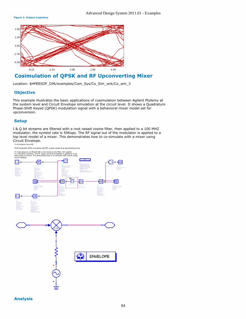
Advanced Design System 2011.01 - Examples
84
Figure 1: Output trajectory
Cosimulation of QPSK and RF Upconverting MixerLocation: $HPEESOF_DIR/examples/Com_Sys/Co_Sim_wrk/Co_sim_3
Objective
This example illustrates the basic applications of cosimulation between Agilent Ptolemy atthe system level and Circuit Envelope simulation at the circuit level. It shows a QuadraturePhase-Shift Keyed (QPSK) modulation signal with a behavioral mixer model set forupconversion.
Setup
I & Q bit streams are filtered with a root raised cosine filter, then applied to a 100 MHZmodulator, the symbol rate is 50Ksps. The RF signal out of the modulator is applied to atop level model of a mixer. This demonstrates how to co-simulate with a mixer usingCircuit Envelope.
Analysis
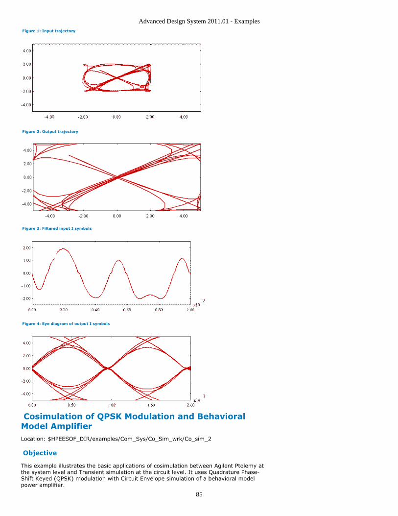
Advanced Design System 2011.01 - Examples
85
Figure 1: Input trajectory
Figure 2: Output trajectory
Figure 3: Filtered input I symbols
Figure 4: Eye diagram of output I symbols
Cosimulation of QPSK Modulation and BehavioralModel AmplifierLocation: $HPEESOF_DIR/examples/Com_Sys/Co_Sim_wrk/Co_sim_2
Objective
This example illustrates the basic applications of cosimulation between Agilent Ptolemy atthe system level and Transient simulation at the circuit level. It uses Quadrature Phase-Shift Keyed (QPSK) modulation with Circuit Envelope simulation of a behavioral modelpower amplifier.
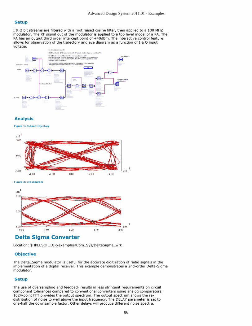
Advanced Design System 2011.01 - Examples
86
Setup
I & Q bit streams are filtered with a root raised cosine filter, then applied to a 100 MHZmodulator. The RF signal out of the modulator is applied to a top level model of a PA. ThePA has an output third order intercept point of +40dBm. The interactive control featureallows for observation of the trajectory and eye diagram as a function of I & Q inputvoltage.
Analysis
Figure 1: Output trajectory
Figure 2: Eye diagram
Delta Sigma ConverterLocation: $HPEESOF_DIR/examples/Com_Sys/DeltaSigma_wrk
Objective
The Delta_Sigma modulator is useful for the accurate digitization of radio signals in theimplementation of a digital receiver. This example demonstrates a 2nd-order Delta-Sigmamodulator.
Setup
The use of oversampling and feedback results in less stringent requirements on circuitcomponent tolerances compared to conventional converters using analog comparators.1024-point FFT provides the output spectrum. The output spectrum shows the re-distribution of noise to well above the input frequency. The DELAY parameter is set toone-half the downsample factor. Other delays will produce different noise spectra.
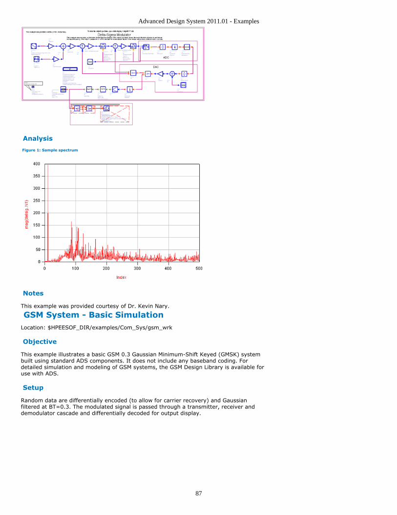
Advanced Design System 2011.01 - Examples
87
Analysis
Figure 1: Sample spectrum
Notes
This example was provided courtesy of Dr. Kevin Nary.
GSM System - Basic SimulationLocation: $HPEESOF_DIR/examples/Com_Sys/gsm_wrk
Objective
This example illustrates a basic GSM 0.3 Gaussian Minimum-Shift Keyed (GMSK) systembuilt using standard ADS components. It does not include any baseband coding. Fordetailed simulation and modeling of GSM systems, the GSM Design Library is available foruse with ADS.
Setup
Random data are differentially encoded (to allow for carrier recovery) and Gaussianfiltered at BT=0.3. The modulated signal is passed through a transmitter, receiver anddemodulator cascade and differentially decoded for output display.
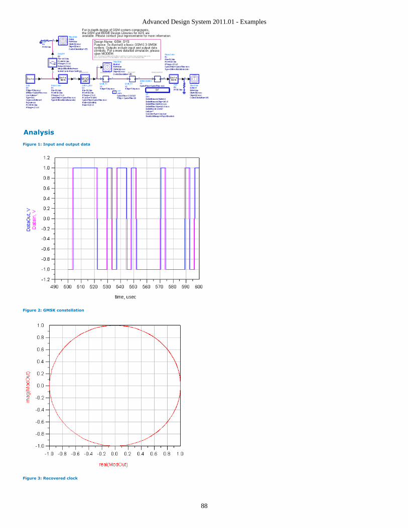
Advanced Design System 2011.01 - Examples
88
Analysis
Figure 1: Input and output data
Figure 2: GMSK constellation
Figure 3: Recovered clock
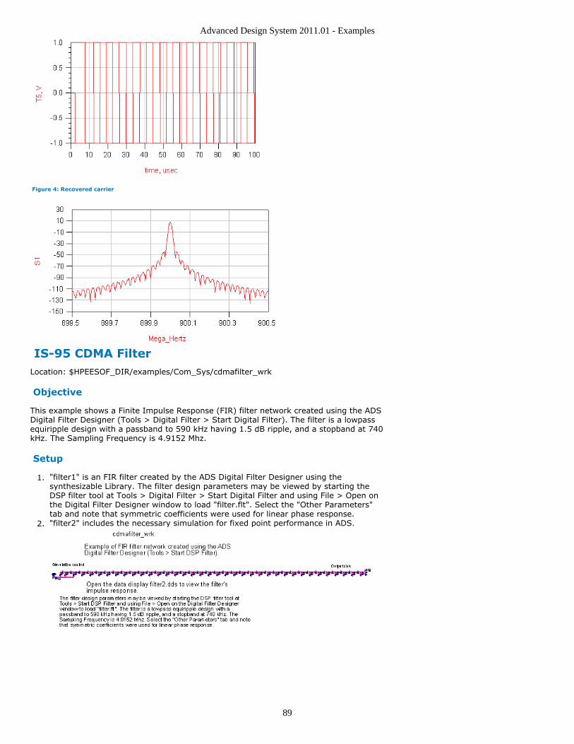
Advanced Design System 2011.01 - Examples
89
Figure 4: Recovered carrier
IS-95 CDMA FilterLocation: $HPEESOF_DIR/examples/Com_Sys/cdmafilter_wrk
Objective
This example shows a Finite Impulse Response (FIR) filter network created using the ADSDigital Filter Designer (Tools > Digital Filter > Start Digital Filter). The filter is a lowpassequiripple design with a passband to 590 kHz having 1.5 dB ripple, and a stopband at 740kHz. The Sampling Frequency is 4.9152 Mhz.
Setup
"filter1" is an FIR filter created by the ADS Digital Filter Designer using the1.synthesizable Library. The filter design parameters may be viewed by starting theDSP filter tool at Tools > Digital Filter > Start Digital Filter and using File > Open onthe Digital Filter Designer window to load "filter.flt". Select the "Other Parameters"tab and note that symmetric coefficients were used for linear phase response."filter2" includes the necessary simulation for fixed point performance in ADS.2.
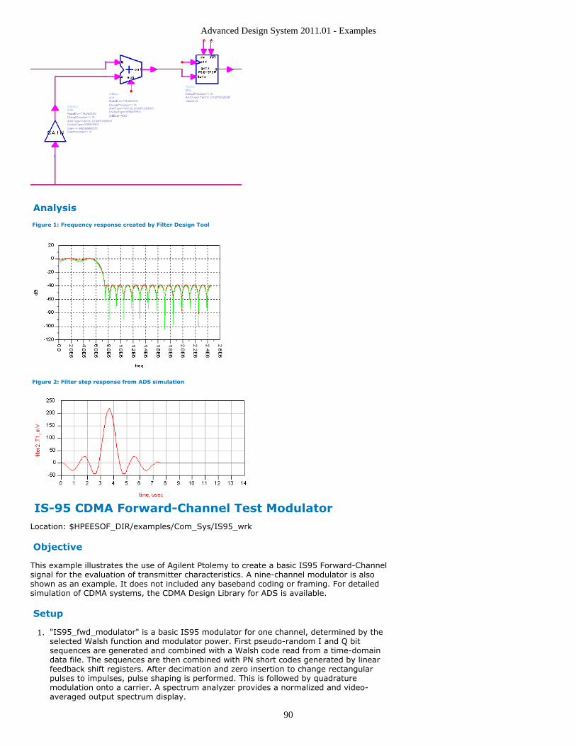
Advanced Design System 2011.01 - Examples
90
Analysis
Figure 1: Frequency response created by Filter Design Tool
Figure 2: Filter step response from ADS simulation
IS-95 CDMA Forward-Channel Test ModulatorLocation: $HPEESOF_DIR/examples/Com_Sys/IS95_wrk
Objective
This example illustrates the use of Agilent Ptolemy to create a basic IS95 Forward-Channelsignal for the evaluation of transmitter characteristics. A nine-channel modulator is alsoshown as an example. It does not included any baseband coding or framing. For detailedsimulation of CDMA systems, the CDMA Design Library for ADS is available.
Setup
"IS95_fwd_modulator" is a basic IS95 modulator for one channel, determined by the1.selected Walsh function and modulator power. First pseudo-random I and Q bitsequences are generated and combined with a Walsh code read from a time-domaindata file. The sequences are then combined with PN short codes generated by linearfeedback shift registers. After decimation and zero insertion to change rectangularpulses to impulses, pulse shaping is performed. This is followed by quadraturemodulation onto a carrier. A spectrum analyzer provides a normalized and video-averaged output spectrum display.
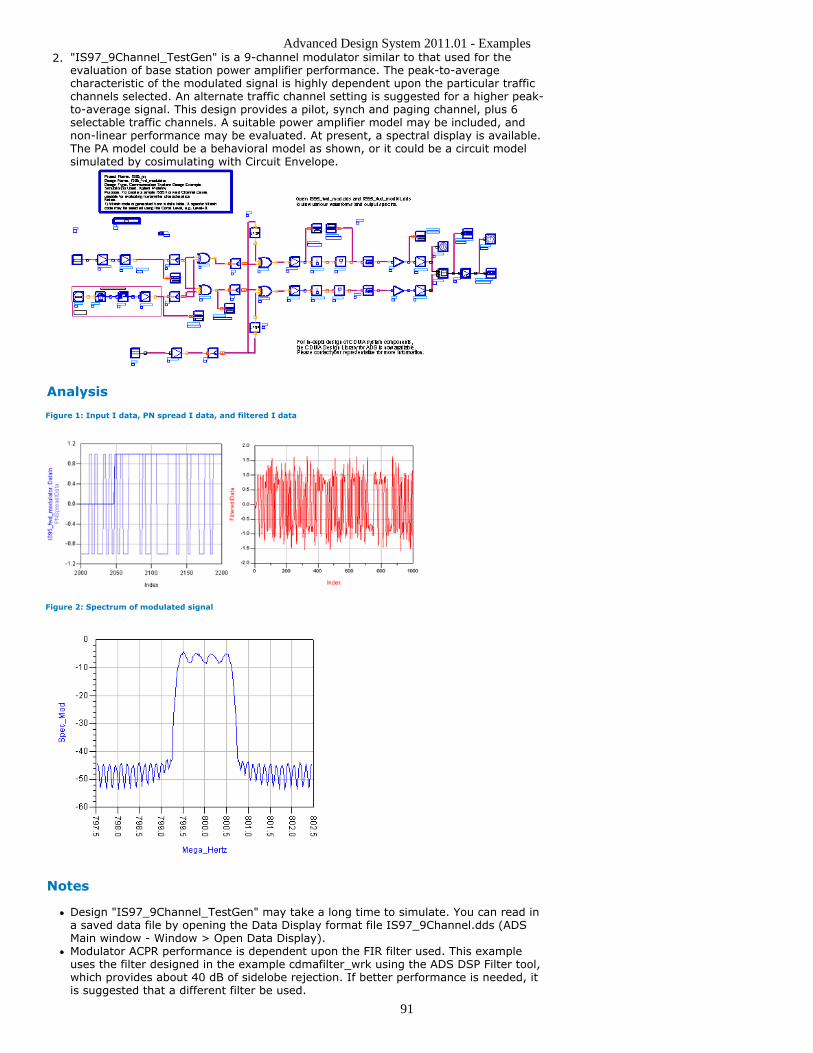
Advanced Design System 2011.01 - Examples
91
"IS97_9Channel_TestGen" is a 9-channel modulator similar to that used for the2.evaluation of base station power amplifier performance. The peak-to-averagecharacteristic of the modulated signal is highly dependent upon the particular trafficchannels selected. An alternate traffic channel setting is suggested for a higher peak-to-average signal. This design provides a pilot, synch and paging channel, plus 6selectable traffic channels. A suitable power amplifier model may be included, andnon-linear performance may be evaluated. At present, a spectral display is available.The PA model could be a behavioral model as shown, or it could be a circuit modelsimulated by cosimulating with Circuit Envelope.
Analysis
Figure 1: Input I data, PN spread I data, and filtered I data
Figure 2: Spectrum of modulated signal
Notes
Design "IS97_9Channel_TestGen" may take a long time to simulate. You can read ina saved data file by opening the Data Display format file IS97_9Channel.dds (ADSMain window - Window > Open Data Display).Modulator ACPR performance is dependent upon the FIR filter used. This exampleuses the filter designed in the example cdmafilter_wrk using the ADS DSP Filter tool,which provides about 40 dB of sidelobe rejection. If better performance is needed, itis suggested that a different filter be used.
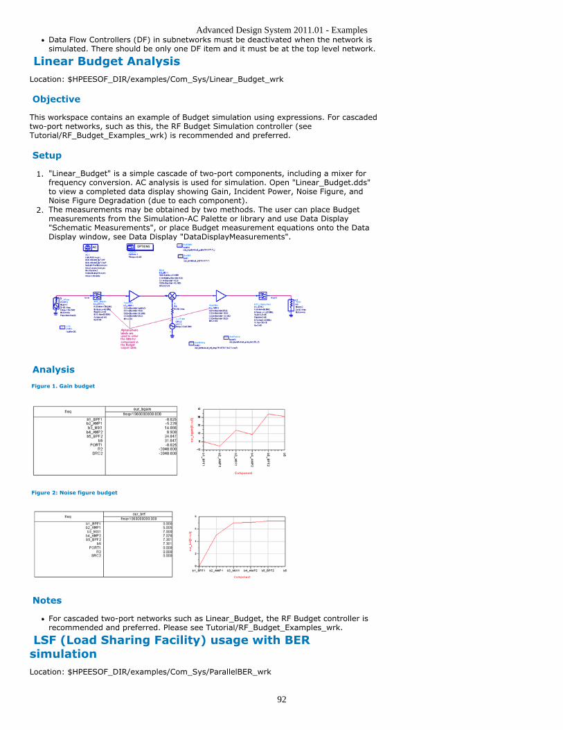
Advanced Design System 2011.01 - Examples
92
Data Flow Controllers (DF) in subnetworks must be deactivated when the network issimulated. There should be only one DF item and it must be at the top level network.
Linear Budget AnalysisLocation: $HPEESOF_DIR/examples/Com_Sys/Linear_Budget_wrk
Objective
This workspace contains an example of Budget simulation using expressions. For cascadedtwo-port networks, such as this, the RF Budget Simulation controller (seeTutorial/RF_Budget_Examples_wrk) is recommended and preferred.
Setup
"Linear_Budget" is a simple cascade of two-port components, including a mixer for1.frequency conversion. AC analysis is used for simulation. Open "Linear_Budget.dds"to view a completed data display showing Gain, Incident Power, Noise Figure, andNoise Figure Degradation (due to each component).The measurements may be obtained by two methods. The user can place Budget2.measurements from the Simulation-AC Palette or library and use Data Display"Schematic Measurements", or place Budget measurement equations onto the DataDisplay window, see Data Display "DataDisplayMeasurements".
Analysis
Figure 1. Gain budget
Figure 2: Noise figure budget
Notes
For cascaded two-port networks such as Linear_Budget, the RF Budget controller isrecommended and preferred. Please see Tutorial/RF_Budget_Examples_wrk.
LSF (Load Sharing Facility) usage with BERsimulationLocation: $HPEESOF_DIR/examples/Com_Sys/ParallelBER_wrk
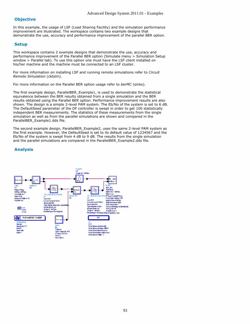
Advanced Design System 2011.01 - Examples
93
Objective
In this example, the usage of LSF (Load Sharing Facility) and the simulation performanceimprovement are illustrated. The workspace contains two example designs thatdemonstrate the use, accuracy and performance improvement of the parallel BER option.
Setup
This workspace contains 2 example designs that demonstrate the use, accuracy andperformance improvement of the Parallel BER option (Simulate menu > Simulation Setupwindow > Parallel tab). To use this option one must have the LSF client installed onhis/her machine and the machine must be connected to an LSF cluster.
For more information on installing LSF and running remote simulations refer to CircuitRemote Simulation (cktsim).
For more information on the Parallel BER option usage refer to berMC (sinks).
The first example design, ParallelBER_Example1, is used to demonstrate the statisticalequivalence between the BER results obtained from a single simulation and the BERresults obtained using the Parallel BER option. Performance improvement results are alsoshown. The design is a simple 2-level PAM system. The Eb/No of the system is set to 6 dB.The DefaultSeed parameter of the DF controller is swept in order to get 100 statisticallyindependent BER measurements. The statistics of these measurements from the singlesimulation as well as from the parallel simulations are shown and compared in theParallelBER_Example1.dds file.
The second example design, ParallelBER_Example2, uses the same 2-level PAM system asthe first example. However, the DefaultSeed is set to its default value of 1234567 and theEb/No of the system is swept from 4 dB to 9 dB. The results from the single simulationand the parallel simulations are compared in the ParallelBER_Example2.dds file.
Analysis
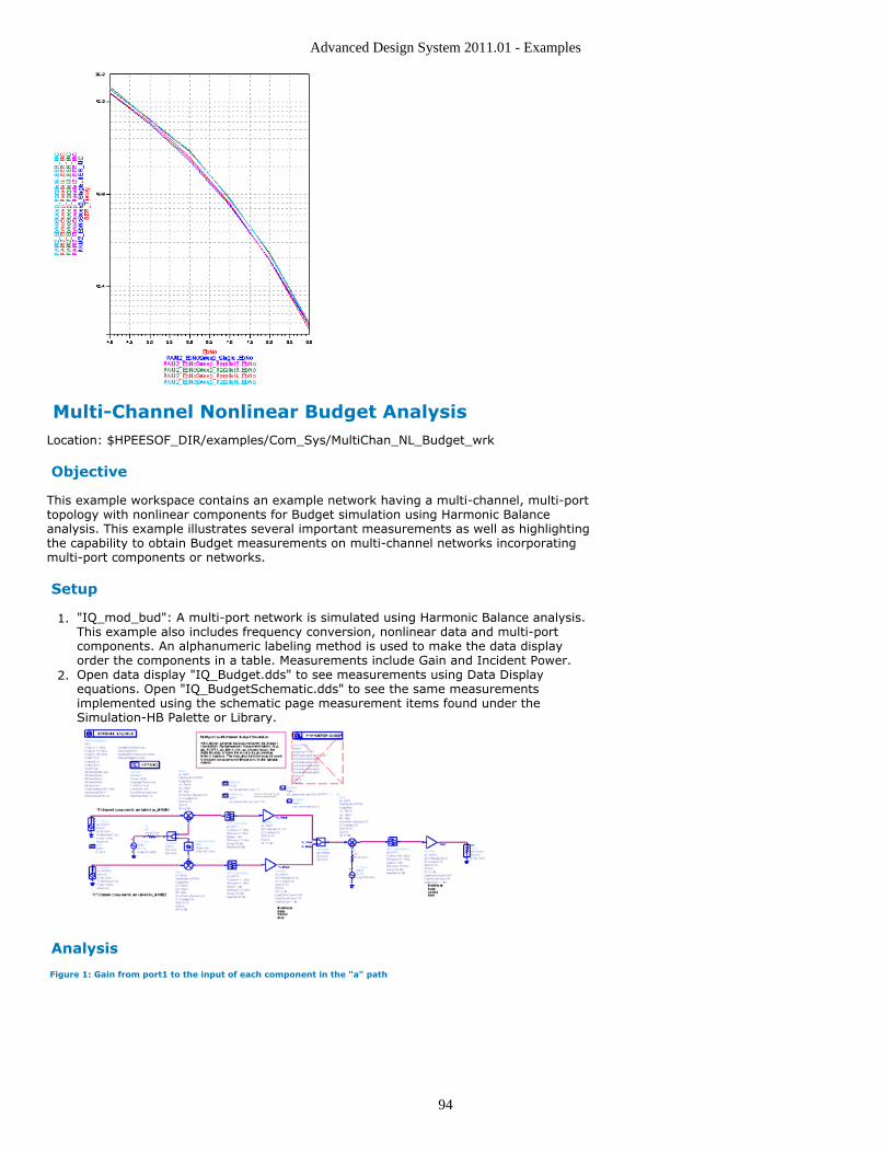
Advanced Design System 2011.01 - Examples
94
Multi-Channel Nonlinear Budget AnalysisLocation: $HPEESOF_DIR/examples/Com_Sys/MultiChan_NL_Budget_wrk
Objective
This example workspace contains an example network having a multi-channel, multi-porttopology with nonlinear components for Budget simulation using Harmonic Balanceanalysis. This example illustrates several important measurements as well as highlightingthe capability to obtain Budget measurements on multi-channel networks incorporatingmulti-port components or networks.
Setup
"IQ_mod_bud": A multi-port network is simulated using Harmonic Balance analysis.1.This example also includes frequency conversion, nonlinear data and multi-portcomponents. An alphanumeric labeling method is used to make the data displayorder the components in a table. Measurements include Gain and Incident Power.Open data display "IQ_Budget.dds" to see measurements using Data Display2.equations. Open "IQ_BudgetSchematic.dds" to see the same measurementsimplemented using the schematic page measurement items found under theSimulation-HB Palette or Library.
Analysis
Figure 1: Gain from port1 to the input of each component in the "a" path
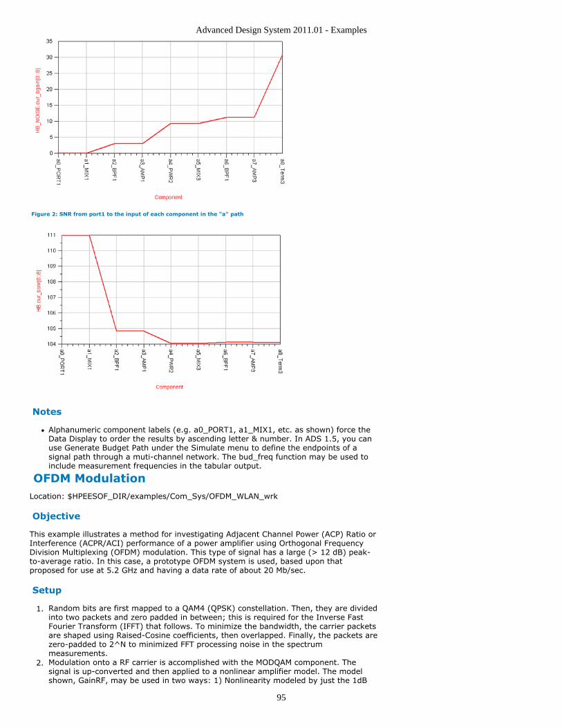
Advanced Design System 2011.01 - Examples
95
Figure 2: SNR from port1 to the input of each component in the "a" path
Notes
Alphanumeric component labels (e.g. a0_PORT1, a1_MIX1, etc. as shown) force theData Display to order the results by ascending letter & number. In ADS 1.5, you canuse Generate Budget Path under the Simulate menu to define the endpoints of asignal path through a muti-channel network. The bud_freq function may be used toinclude measurement frequencies in the tabular output.
OFDM ModulationLocation: $HPEESOF_DIR/examples/Com_Sys/OFDM_WLAN_wrk
Objective
This example illustrates a method for investigating Adjacent Channel Power (ACP) Ratio orInterference (ACPR/ACI) performance of a power amplifier using Orthogonal FrequencyDivision Multiplexing (OFDM) modulation. This type of signal has a large (> 12 dB) peak-to-average ratio. In this case, a prototype OFDM system is used, based upon thatproposed for use at 5.2 GHz and having a data rate of about 20 Mb/sec.
Setup
Random bits are first mapped to a QAM4 (QPSK) constellation. Then, they are divided1.into two packets and zero padded in between; this is required for the Inverse FastFourier Transform (IFFT) that follows. To minimize the bandwidth, the carrier packetsare shaped using Raised-Cosine coefficients, then overlapped. Finally, the packets arezero-padded to 2^N to minimized FFT processing noise in the spectrummeasurements.Modulation onto a RF carrier is accomplished with the MODQAM component. The2.signal is up-converted and then applied to a nonlinear amplifier model. The modelshown, GainRF, may be used in two ways: 1) Nonlinearity modeled by just the 1dB
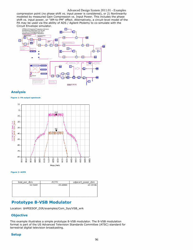
Advanced Design System 2011.01 - Examples
96
compression point (no phase shift vs. input power is considered), or 2) Nonlinearitymodeled by measured Gain Compression vs. Input Power. This includes the phaseshift vs. input power, or "AM-to-PM" effect. Alternatively, a circuit-level model of thePA may be used via the ability of ADS / Agilent Ptolemy to co-simulate with theCircuit Envelope simulator.
Analysis
Figure 1: PA output spectrum
Figure 2: ACPR
Prototype 8-VSB ModulatorLocation: $HPEESOF_DIR/examples/Com_Sys/VSB_wrk
Objective
This example illustrates a simple prototype 8-VSB modulator. The 8-VSB modulationformat is part of the US Advanced Television Standards Committee (ATSC) standard forterrestrial digital television broadcasting.
Setup
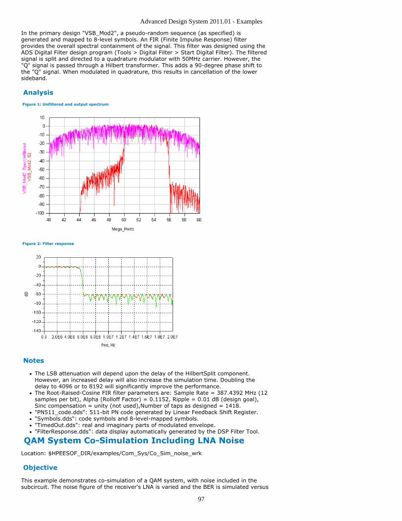
Advanced Design System 2011.01 - Examples
97
In the primary design "VSB_Mod2", a pseudo-random sequence (as specified) isgenerated and mapped to 8-level symbols. An FIR (Finite Impulse Response) filterprovides the overall spectral containment of the signal. This filter was designed using theADS Digital Filter design program (Tools > Digital Filter > Start Digital Filter). The filteredsignal is split and directed to a quadrature modulator with 50MHz carrier. However, the"Q" signal is passed through a Hilbert transformer. This adds a 90-degree phase shift tothe "Q" signal. When modulated in quadrature, this results in cancellation of the lowersideband.
Analysis
Figure 1: Unfiltered and output spectrum
Figure 2: Filter response
Notes
The LSB attenuation will depend upon the delay of the HilbertSplit component.However, an increased delay will also increase the simulation time. Doubling thedelay to 4096 or to 8192 will significantly improve the performance.The Root-Raised-Cosine FIR filter parameters are: Sample Rate = 387.4392 MHz (12samples per bit), Alpha (Rolloff Factor) = 0.1152, Ripple = 0.01 dB (design goal),Sinc compensation = unity (not used),Number of taps as designed = 1418."PN511_code.dds": 511-bit PN code generated by Linear Feedback Shift Register."Symbols.dds": code symbols and 8-level-mapped symbols."TimedOut.dds": real and imaginary parts of modulated envelope."FilterResponse.dds": data display automatically generated by the DSP Filter Tool.
QAM System Co-Simulation Including LNA NoiseLocation: $HPEESOF_DIR/examples/Com_Sys/Co_Sim_noise_wrk
Objective
This example demonstrates co-simulation of a QAM system, with noise included in thesubcircuit. The noise figure of the receiver's LNA is varied and the BER is simulated versus
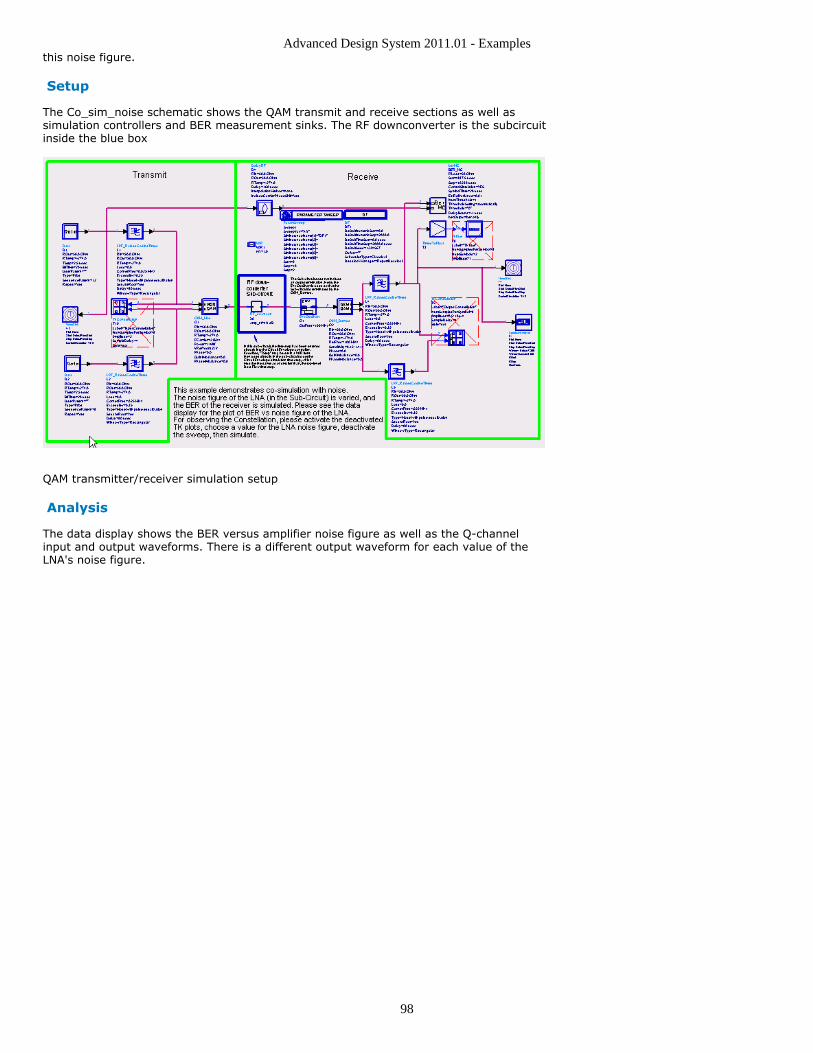
Advanced Design System 2011.01 - Examples
98
this noise figure.
Setup
The Co_sim_noise schematic shows the QAM transmit and receive sections as well assimulation controllers and BER measurement sinks. The RF downconverter is the subcircuitinside the blue box
QAM transmitter/receiver simulation setup
Analysis
The data display shows the BER versus amplifier noise figure as well as the Q-channelinput and output waveforms. There is a different output waveform for each value of theLNA's noise figure.
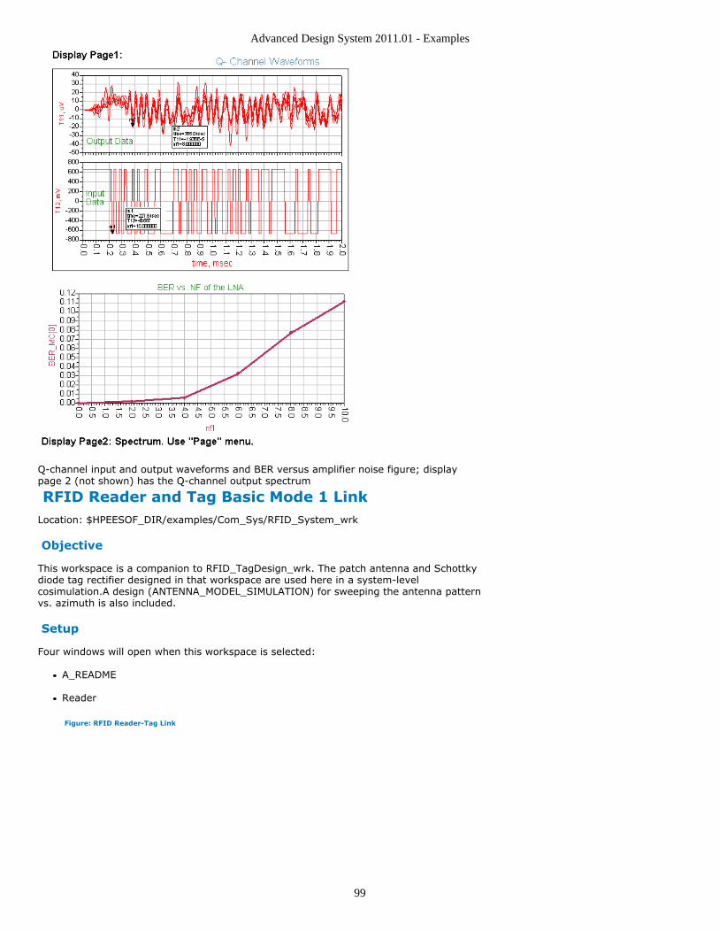
Advanced Design System 2011.01 - Examples
99
Q-channel input and output waveforms and BER versus amplifier noise figure; displaypage 2 (not shown) has the Q-channel output spectrum
RFID Reader and Tag Basic Mode 1 LinkLocation: $HPEESOF_DIR/examples/Com_Sys/RFID_System_wrk
Objective
This workspace is a companion to RFID_TagDesign_wrk. The patch antenna and Schottkydiode tag rectifier designed in that workspace are used here in a system-levelcosimulation.A design (ANTENNA_MODEL_SIMULATION) for sweeping the antenna patternvs. azimuth is also included.
Setup
Four windows will open when this workspace is selected:
A_README
Reader
Figure: RFID Reader-Tag Link
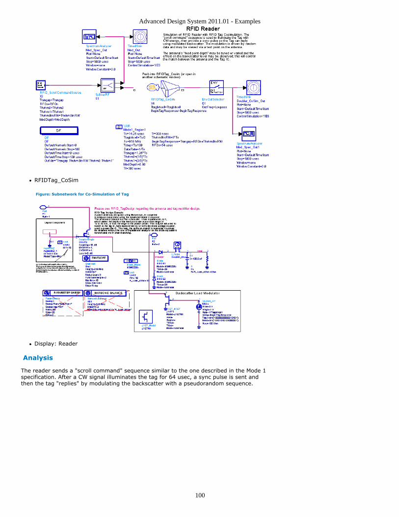
Advanced Design System 2011.01 - Examples
100
RFIDTag_CoSim
Figure: Subnetwork for Co-Simulation of Tag
Display: Reader
Analysis
The reader sends a "scroll command" sequence similar to the one described in the Mode 1specification. After a CW signal illuminates the tag for 64 usec, a sync pulse is sent andthen the tag "replies" by modulating the backscatter with a pseudorandom sequence.
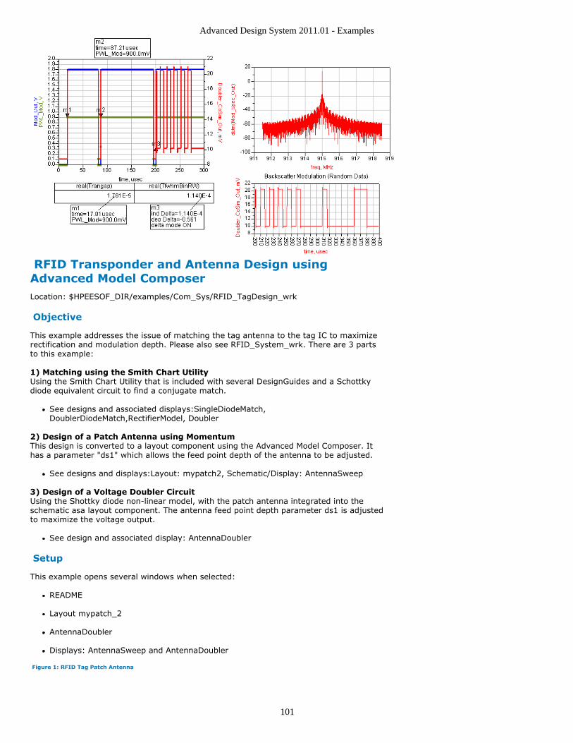
Advanced Design System 2011.01 - Examples
101
RFID Transponder and Antenna Design usingAdvanced Model ComposerLocation: $HPEESOF_DIR/examples/Com_Sys/RFID_TagDesign_wrk
Objective
This example addresses the issue of matching the tag antenna to the tag IC to maximizerectification and modulation depth. Please also see RFID_System_wrk. There are 3 partsto this example:
1) Matching using the Smith Chart UtilityUsing the Smith Chart Utility that is included with several DesignGuides and a Schottkydiode equivalent circuit to find a conjugate match.
See designs and associated displays:SingleDiodeMatch,DoublerDiodeMatch,RectifierModel, Doubler
2) Design of a Patch Antenna using MomentumThis design is converted to a layout component using the Advanced Model Composer. Ithas a parameter "ds1" which allows the feed point depth of the antenna to be adjusted.
See designs and displays:Layout: mypatch2, Schematic/Display: AntennaSweep
3) Design of a Voltage Doubler CircuitUsing the Shottky diode non-linear model, with the patch antenna integrated into theschematic asa layout component. The antenna feed point depth parameter ds1 is adjustedto maximize the voltage output.
See design and associated display: AntennaDoubler
Setup
This example opens several windows when selected:
README
Layout mypatch_2
AntennaDoubler
Displays: AntennaSweep and AntennaDoubler
Figure 1: RFID Tag Patch Antenna
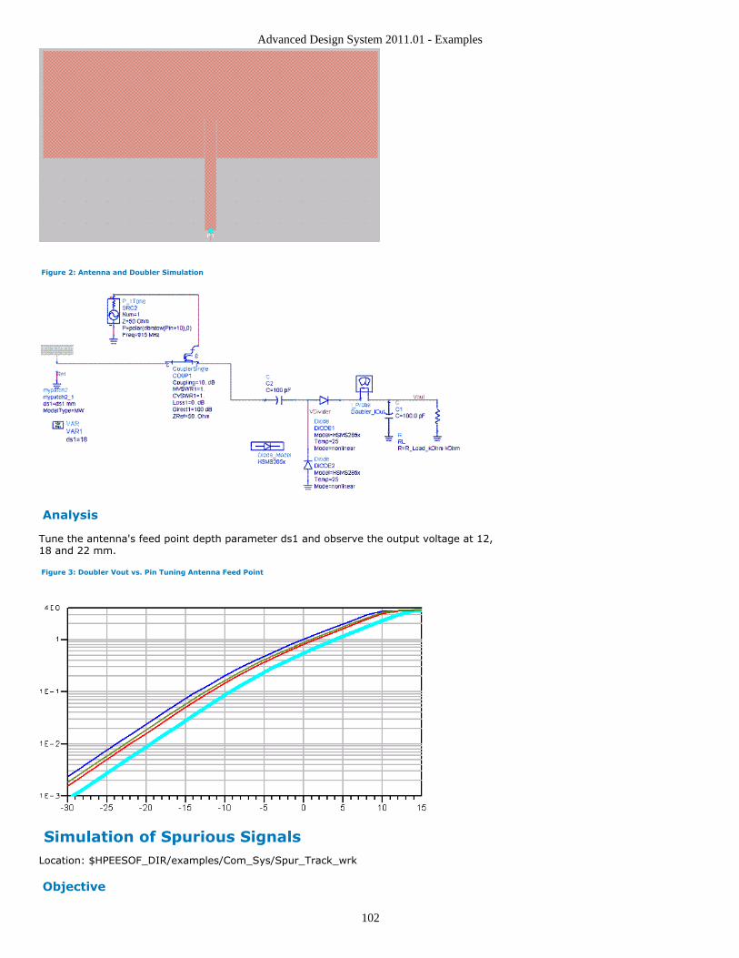
Advanced Design System 2011.01 - Examples
102
Figure 2: Antenna and Doubler Simulation
Analysis
Tune the antenna's feed point depth parameter ds1 and observe the output voltage at 12,18 and 22 mm.
Figure 3: Doubler Vout vs. Pin Tuning Antenna Feed Point
Simulation of Spurious SignalsLocation: $HPEESOF_DIR/examples/Com_Sys/Spur_Track_wrk
Objective
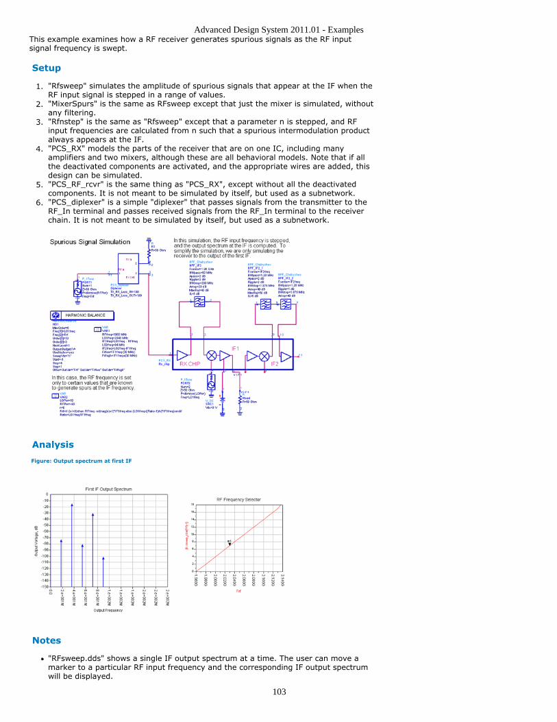
Advanced Design System 2011.01 - Examples
103
This example examines how a RF receiver generates spurious signals as the RF inputsignal frequency is swept.
Setup
"Rfsweep" simulates the amplitude of spurious signals that appear at the IF when the1.RF input signal is stepped in a range of values."MixerSpurs" is the same as RFsweep except that just the mixer is simulated, without2.any filtering."Rfnstep" is the same as "Rfsweep" except that a parameter n is stepped, and RF3.input frequencies are calculated from n such that a spurious intermodulation productalways appears at the IF."PCS_RX" models the parts of the receiver that are on one IC, including many4.amplifiers and two mixers, although these are all behavioral models. Note that if allthe deactivated components are activated, and the appropriate wires are added, thisdesign can be simulated."PCS_RF_rcvr" is the same thing as "PCS_RX", except without all the deactivated5.components. It is not meant to be simulated by itself, but used as a subnetwork."PCS_diplexer" is a simple "diplexer" that passes signals from the transmitter to the6.RF_In terminal and passes received signals from the RF_In terminal to the receiverchain. It is not meant to be simulated by itself, but used as a subnetwork.
Analysis
Figure: Output spectrum at first IF
Notes
"RFsweep.dds" shows a single IF output spectrum at a time. The user can move amarker to a particular RF input frequency and the corresponding IF output spectrumwill be displayed.
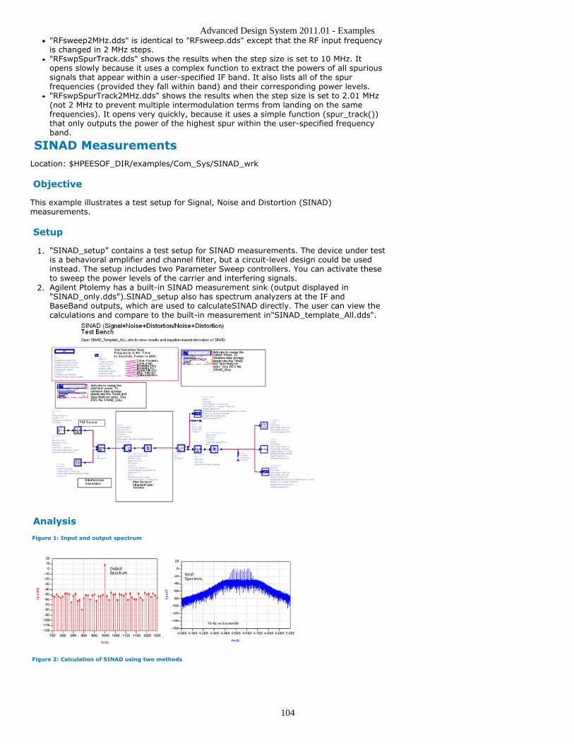
Advanced Design System 2011.01 - Examples
104
"RFsweep2MHz.dds" is identical to "RFsweep.dds" except that the RF input frequencyis changed in 2 MHz steps."RFswpSpurTrack.dds" shows the results when the step size is set to 10 MHz. Itopens slowly because it uses a complex function to extract the powers of all spurioussignals that appear within a user-specified IF band. It also lists all of the spurfrequencies (provided they fall within band) and their corresponding power levels."RFswpSpurTrack2MHz.dds" shows the results when the step size is set to 2.01 MHz(not 2 MHz to prevent multiple intermodulation terms from landing on the samefrequencies). It opens very quickly, because it uses a simple function (spur_track())that only outputs the power of the highest spur within the user-specified frequencyband.
SINAD MeasurementsLocation: $HPEESOF_DIR/examples/Com_Sys/SINAD_wrk
Objective
This example illustrates a test setup for Signal, Noise and Distortion (SINAD)measurements.
Setup
"SINAD_setup" contains a test setup for SINAD measurements. The device under test1.is a behavioral amplifier and channel filter, but a circuit-level design could be usedinstead. The setup includes two Parameter Sweep controllers. You can activate theseto sweep the power levels of the carrier and interfering signals.Agilent Ptolemy has a built-in SINAD measurement sink (output displayed in2."SINAD_only.dds").SINAD_setup also has spectrum analyzers at the IF andBaseBand outputs, which are used to calculateSINAD directly. The user can view thecalculations and compare to the built-in measurement in"SINAD_template_All.dds".
Analysis
Figure 1: Input and output spectrum
Figure 2: Calculation of SINAD using two methods
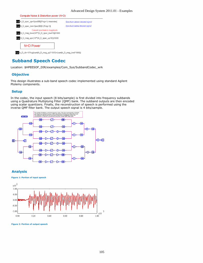
Advanced Design System 2011.01 - Examples
105
Subband Speech CodecLocation: $HPEESOF_DIR/examples/Com_Sys/SubbandCodec_wrk
Objective
This design illustrates a sub-band speech codec implemented using standard AgilentPtolemy components.
Setup
In the codec, the input speech (8 bits/sample) is first divided into frequency subbandsusing a Quadrature Multiplying Filter (QMF) bank. The subband outputs are then encodedusing scalar quantizers. Finally, the reconstruction of speech is performed using theinverse QMF filter bank. The output speech signal is 4 bits/sample.
Analysis
Figure 1: Portion of input speech
Figure 2: Portion of output speech
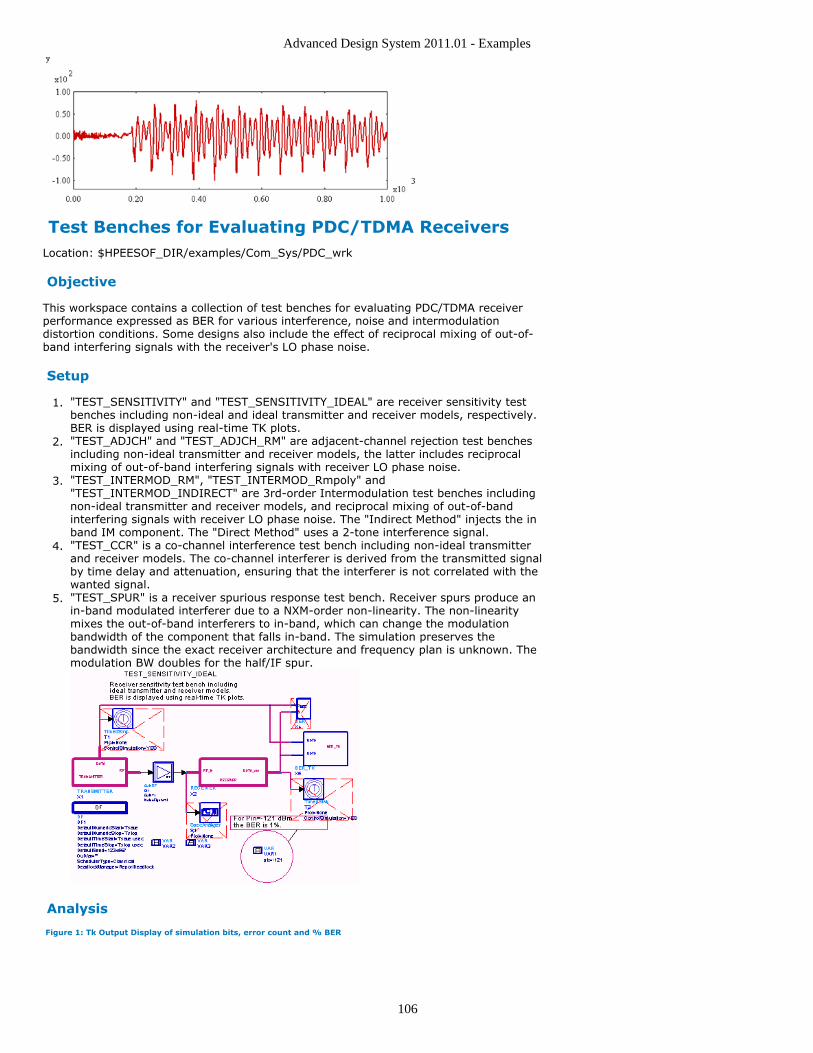
Advanced Design System 2011.01 - Examples
106
Test Benches for Evaluating PDC/TDMA ReceiversLocation: $HPEESOF_DIR/examples/Com_Sys/PDC_wrk
Objective
This workspace contains a collection of test benches for evaluating PDC/TDMA receiverperformance expressed as BER for various interference, noise and intermodulationdistortion conditions. Some designs also include the effect of reciprocal mixing of out-of-band interfering signals with the receiver's LO phase noise.
Setup
"TEST_SENSITIVITY" and "TEST_SENSITIVITY_IDEAL" are receiver sensitivity test1.benches including non-ideal and ideal transmitter and receiver models, respectively.BER is displayed using real-time TK plots."TEST_ADJCH" and "TEST_ADJCH_RM" are adjacent-channel rejection test benches2.including non-ideal transmitter and receiver models, the latter includes reciprocalmixing of out-of-band interfering signals with receiver LO phase noise."TEST_INTERMOD_RM", "TEST_INTERMOD_Rmpoly" and3."TEST_INTERMOD_INDIRECT" are 3rd-order Intermodulation test benches includingnon-ideal transmitter and receiver models, and reciprocal mixing of out-of-bandinterfering signals with receiver LO phase noise. The "Indirect Method" injects the inband IM component. The "Direct Method" uses a 2-tone interference signal."TEST_CCR" is a co-channel interference test bench including non-ideal transmitter4.and receiver models. The co-channel interferer is derived from the transmitted signalby time delay and attenuation, ensuring that the interferer is not correlated with thewanted signal."TEST_SPUR" is a receiver spurious response test bench. Receiver spurs produce an5.in-band modulated interferer due to a NXM-order non-linearity. The non-linearitymixes the out-of-band interferers to in-band, which can change the modulationbandwidth of the component that falls in-band. The simulation preserves thebandwidth since the exact receiver architecture and frequency plan is unknown. Themodulation BW doubles for the half/IF spur.
Analysis
Figure 1: Tk Output Display of simulation bits, error count and % BER
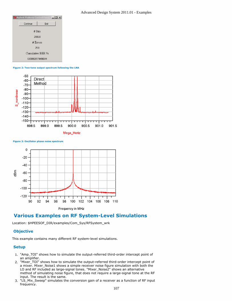
Advanced Design System 2011.01 - Examples
107
Figure 2: Two-tone output spectrum following the LNA
Figure 3: Oscillator phase noise spectrum
Various Examples on RF System-Level SimulationsLocation: $HPEESOF_DIR/examples/Com_Sys/RFSystem_wrk
Objective
This example contains many different RF system-level simulations.
Setup
"Amp_TOI" shows how to simulate the output-referred third-order intercept point of1.an amplifier."Mixer_TOI" shows how to simulate the output-referred third-order intercept point of2.a mixer. Mixer_Noise1 shows a simple receiver noise figure simulation with both theLO and RF included as large-signal tones. "Mixer_Noise2" shows an alternativemethod of simulating noise figure, that does not require a large-signal tone at the RFinput. The result is the same."LS_Mix_Sweep" simulates the conversion gain of a receiver as a function of RF input3.frequency.
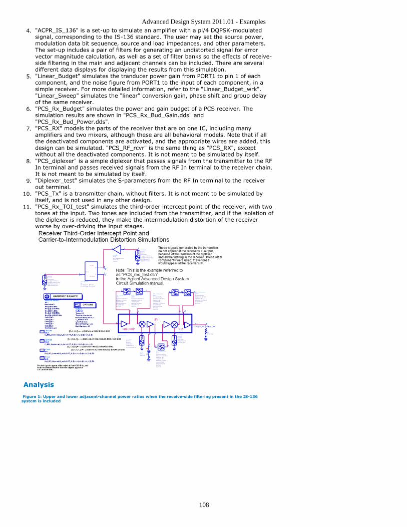
Advanced Design System 2011.01 - Examples
108
"ACPR_IS_136" is a set-up to simulate an amplifier with a pi/4 DQPSK-modulated4.signal, corresponding to the IS-136 standard. The user may set the source power,modulation data bit sequence, source and load impedances, and other parameters.The set-up includes a pair of filters for generating an undistorted signal for errorvector magnitude calculation, as well as a set of filter banks so the effects of receive-side filtering in the main and adjacent channels can be included. There are severaldifferent data displays for displaying the results from this simulation."Linear_Budget" simulates the tranducer power gain from PORT1 to pin 1 of each5.component, and the noise figure from PORT1 to the input of each component, in asimple receiver. For more detailed information, refer to the "Linear_Budget_wrk"."Linear_Sweep" simulates the "linear" conversion gain, phase shift and group delayof the same receiver."PCS_Rx_Budget" simulates the power and gain budget of a PCS receiver. The6.simulation results are shown in "PCS_Rx_Bud_Gain.dds" and"PCS_Rx_Bud_Power.dds"."PCS_RX" models the parts of the receiver that are on one IC, including many7.amplifiers and two mixers, although these are all behavioral models. Note that if allthe deactivated components are activated, and the appropriate wires are added, thisdesign can be simulated. "PCS_RF_rcvr" is the same thing as "PCS_RX", exceptwithout all the deactivated components. It is not meant to be simulated by itself."PCS_diplexer" is a simple diplexer that passes signals from the transmitter to the RF8.In terminal and passes received signals from the RF In terminal to the receiver chain.It is not meant to be simulated by itself."Diplexer_test" simulates the S-parameters from the RF In terminal to the receiver9.out terminal."PCS_Tx" is a transmitter chain, without filters. It is not meant to be simulated by10.itself, and is not used in any other design."PCS_Rx_TOI_test" simulates the third-order intercept point of the receiver, with two11.tones at the input. Two tones are included from the transmitter, and if the isolation ofthe diplexer is reduced, they make the intermodulation distortion of the receiverworse by over-driving the input stages.
Analysis
Figure 1: Upper and lower adjacent-channel power ratios when the receive-side filtering present in the IS-136system is included
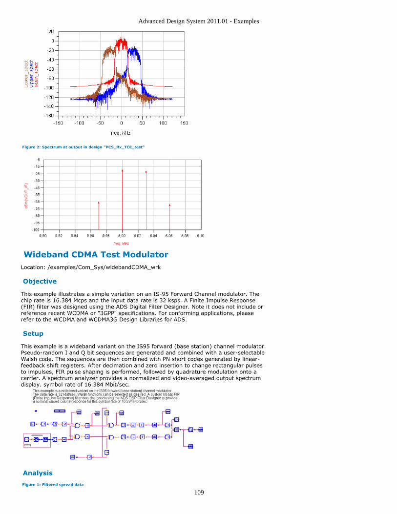
Advanced Design System 2011.01 - Examples
109
Figure 2: Spectrum at output in design "PCS_Rx_TOI_test"
Wideband CDMA Test ModulatorLocation: /examples/Com_Sys/widebandCDMA_wrk
Objective
This example illustrates a simple variation on an IS-95 Forward Channel modulator. Thechip rate is 16.384 Mcps and the input data rate is 32 ksps. A Finite Impulse Response(FIR) filter was designed using the ADS Digital Filter Designer. Note it does not include orreference recent WCDMA or "3GPP" specifications. For conforming applications, pleaserefer to the WCDMA and WCDMA3G Design Libraries for ADS.
Setup
This example is a wideband variant on the IS95 forward (base station) channel modulator.Pseudo-random I and Q bit sequences are generated and combined with a user-selectableWalsh code. The sequences are then combined with PN short codes generated by linear-feedback shift registers. After decimation and zero insertion to change rectangular pulsesto impulses, FIR pulse shaping is performed, followed by quadrature modulation onto acarrier. A spectrum analyzer provides a normalized and video-averaged output spectrumdisplay. symbol rate of 16.384 Mbit/sec.
Analysis
Figure 1: Filtered spread data
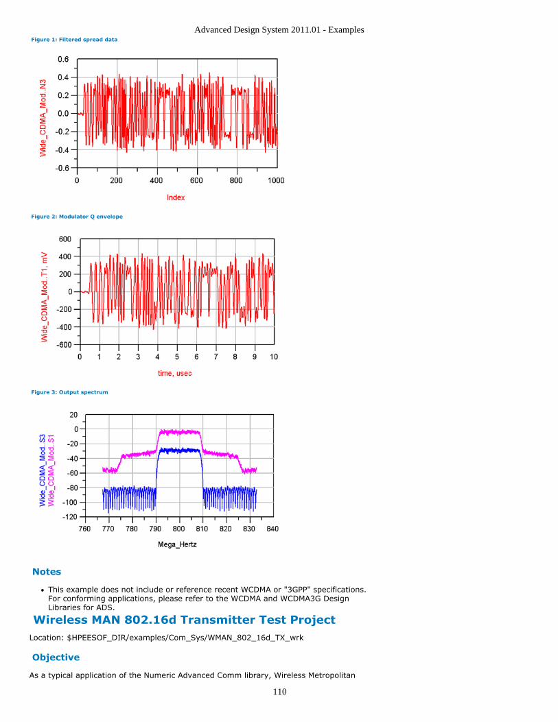
Advanced Design System 2011.01 - Examples
110
Figure 1: Filtered spread data
Figure 2: Modulator Q envelope
Figure 3: Output spectrum
Notes
This example does not include or reference recent WCDMA or "3GPP" specifications.For conforming applications, please refer to the WCDMA and WCDMA3G DesignLibraries for ADS.
Wireless MAN 802.16d Transmitter Test ProjectLocation: $HPEESOF_DIR/examples/Com_Sys/WMAN_802_16d_TX_wrk
Objective
As a typical application of the Numeric Advanced Comm library, Wireless Metropolitan
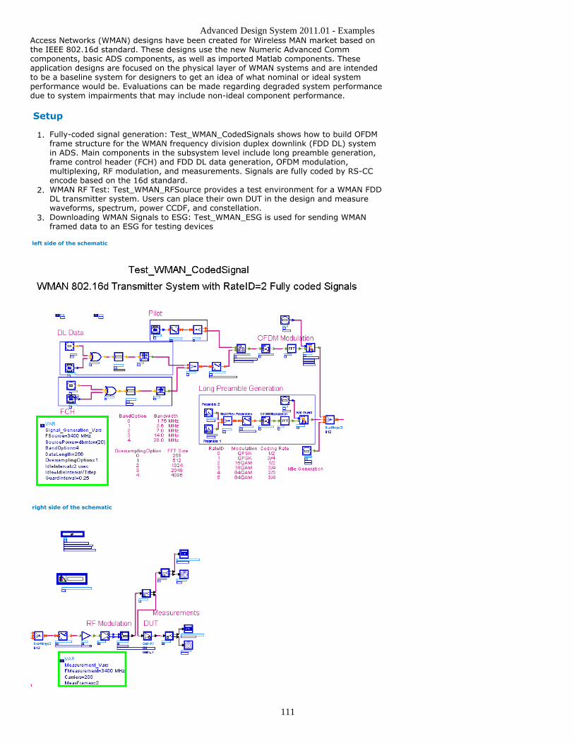
Advanced Design System 2011.01 - Examples
111
Access Networks (WMAN) designs have been created for Wireless MAN market based onthe IEEE 802.16d standard. These designs use the new Numeric Advanced Commcomponents, basic ADS components, as well as imported Matlab components. Theseapplication designs are focused on the physical layer of WMAN systems and are intendedto be a baseline system for designers to get an idea of what nominal or ideal systemperformance would be. Evaluations can be made regarding degraded system performancedue to system impairments that may include non-ideal component performance.
Setup
Fully-coded signal generation: Test_WMAN_CodedSignals shows how to build OFDM1.frame structure for the WMAN frequency division duplex downlink (FDD DL) systemin ADS. Main components in the subsystem level include long preamble generation,frame control header (FCH) and FDD DL data generation, OFDM modulation,multiplexing, RF modulation, and measurements. Signals are fully coded by RS-CCencode based on the 16d standard.WMAN RF Test: Test_WMAN_RFSource provides a test environment for a WMAN FDD2.DL transmitter system. Users can place their own DUT in the design and measurewaveforms, spectrum, power CCDF, and constellation.Downloading WMAN Signals to ESG: Test_WMAN_ESG is used for sending WMAN3.framed data to an ESG for testing devices
left side of the schematic
right side of the schematic
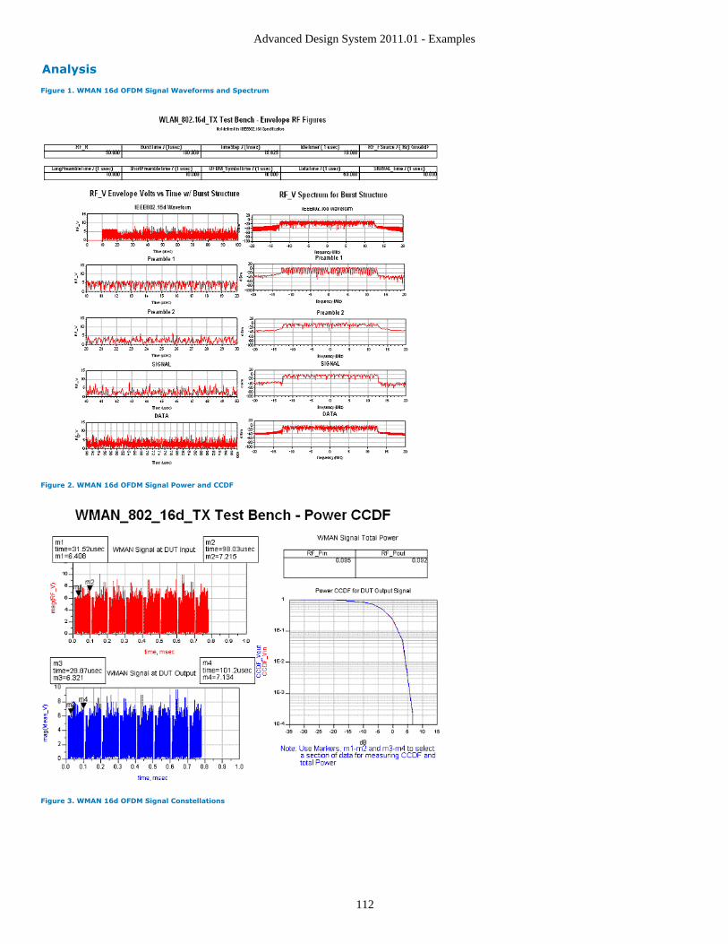
Advanced Design System 2011.01 - Examples
112
Analysis
Figure 1. WMAN 16d OFDM Signal Waveforms and Spectrum
Figure 2. WMAN 16d OFDM Signal Power and CCDF
Figure 3. WMAN 16d OFDM Signal Constellations
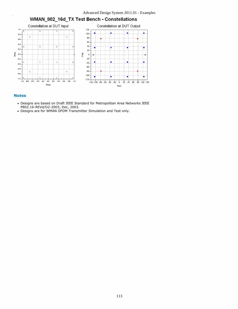
Advanced Design System 2011.01 - Examples
113
Notes
Designs are based on Draft IEEE Standard for Metropolitan Area Networks IEEEP802.16-REVd/D2-2003, Dec, 2003.Designs are for WMAN OFDM Transmitter Simulation and Test only.
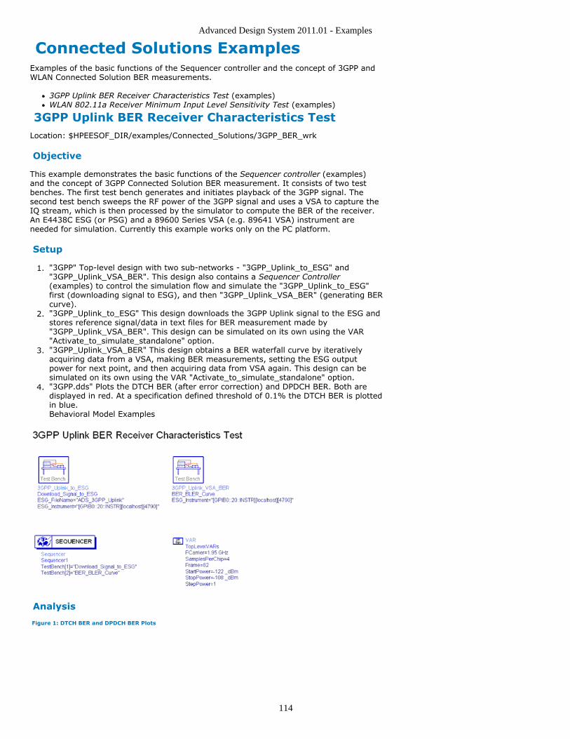
Advanced Design System 2011.01 - Examples
114
Connected Solutions ExamplesExamples of the basic functions of the Sequencer controller and the concept of 3GPP andWLAN Connected Solution BER measurements.
3GPP Uplink BER Receiver Characteristics Test (examples)WLAN 802.11a Receiver Minimum Input Level Sensitivity Test (examples)
3GPP Uplink BER Receiver Characteristics TestLocation: $HPEESOF_DIR/examples/Connected_Solutions/3GPP_BER_wrk
Objective
This example demonstrates the basic functions of the Sequencer controller (examples)and the concept of 3GPP Connected Solution BER measurement. It consists of two testbenches. The first test bench generates and initiates playback of the 3GPP signal. Thesecond test bench sweeps the RF power of the 3GPP signal and uses a VSA to capture theIQ stream, which is then processed by the simulator to compute the BER of the receiver.An E4438C ESG (or PSG) and a 89600 Series VSA (e.g. 89641 VSA) instrument areneeded for simulation. Currently this example works only on the PC platform.
Setup
"3GPP" Top-level design with two sub-networks - "3GPP_Uplink_to_ESG" and1."3GPP_Uplink_VSA_BER". This design also contains a Sequencer Controller(examples) to control the simulation flow and simulate the "3GPP_Uplink_to_ESG"first (downloading signal to ESG), and then "3GPP_Uplink_VSA_BER" (generating BERcurve)."3GPP_Uplink_to_ESG" This design downloads the 3GPP Uplink signal to the ESG and2.stores reference signal/data in text files for BER measurement made by"3GPP_Uplink_VSA_BER". This design can be simulated on its own using the VAR"Activate_to_simulate_standalone" option."3GPP_Uplink_VSA_BER" This design obtains a BER waterfall curve by iteratively3.acquiring data from a VSA, making BER measurements, setting the ESG outputpower for next point, and then acquiring data from VSA again. This design can besimulated on its own using the VAR "Activate_to_simulate_standalone" option."3GPP.dds" Plots the DTCH BER (after error correction) and DPDCH BER. Both are4.displayed in red. At a specification defined threshold of 0.1% the DTCH BER is plottedin blue.Behavioral Model Examples
Analysis
Figure 1: DTCH BER and DPDCH BER Plots
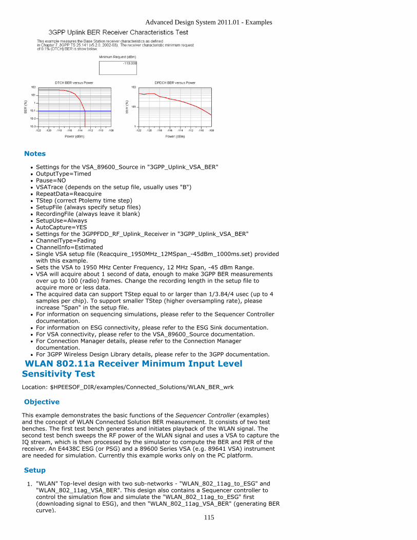
Advanced Design System 2011.01 - Examples
115
Notes
Settings for the VSA_89600_Source in "3GPP_Uplink_VSA_BER"OutputType=TimedPause=NOVSATrace (depends on the setup file, usually uses "B")RepeatData=ReacquireTStep (correct Ptolemy time step)SetupFile (always specify setup files)RecordingFile (always leave it blank)SetupUse=AlwaysAutoCapture=YESSettings for the 3GPPFDD_RF_Uplink_Receiver in "3GPP_Uplink_VSA_BER"ChannelType=FadingChannelInfo=EstimatedSingle VSA setup file (Reacquire_1950MHz_12MSpan_-45dBm_1000ms.set) providedwith this example.Sets the VSA to 1950 MHz Center Frequency, 12 MHz Span, -45 dBm Range.VSA will acquire about 1 second of data, enough to make 3GPP BER measurementsover up to 100 (radio) frames. Change the recording length in the setup file toacquire more or less data.The acquired data can support TStep equal to or larger than 1/3.84/4 usec (up to 4samples per chip). To support smaller TStep (higher oversampling rate), pleaseincrease "Span" in the setup file.For information on sequencing simulations, please refer to the Sequencer Controllerdocumentation.For information on ESG connectivity, please refer to the ESG Sink documentation.For VSA connectivity, please refer to the VSA_89600_Source documentation.For Connection Manager details, please refer to the Connection Managerdocumentation.For 3GPP Wireless Design Library details, please refer to the 3GPP documentation.
WLAN 802.11a Receiver Minimum Input LevelSensitivity TestLocation: $HPEESOF_DIR/examples/Connected_Solutions/WLAN_BER_wrk
Objective
This example demonstrates the basic functions of the Sequencer Controller (examples)and the concept of WLAN Connected Solution BER measurement. It consists of two testbenches. The first test bench generates and initiates playback of the WLAN signal. Thesecond test bench sweeps the RF power of the WLAN signal and uses a VSA to capture theIQ stream, which is then processed by the simulator to compute the BER and PER of thereceiver. An E4438C ESG (or PSG) and a 89600 Series VSA (e.g. 89641 VSA) instrumentare needed for simulation. Currently this example works only on the PC platform.
Setup
"WLAN" Top-level design with two sub-networks - "WLAN_802_11ag_to_ESG" and1."WLAN_802_11ag_VSA_BER". This design also contains a Sequencer controller tocontrol the simulation flow and simulate the "WLAN_802_11ag_to_ESG" first(downloading signal to ESG), and then "WLAN_802_11ag_VSA_BER" (generating BERcurve).
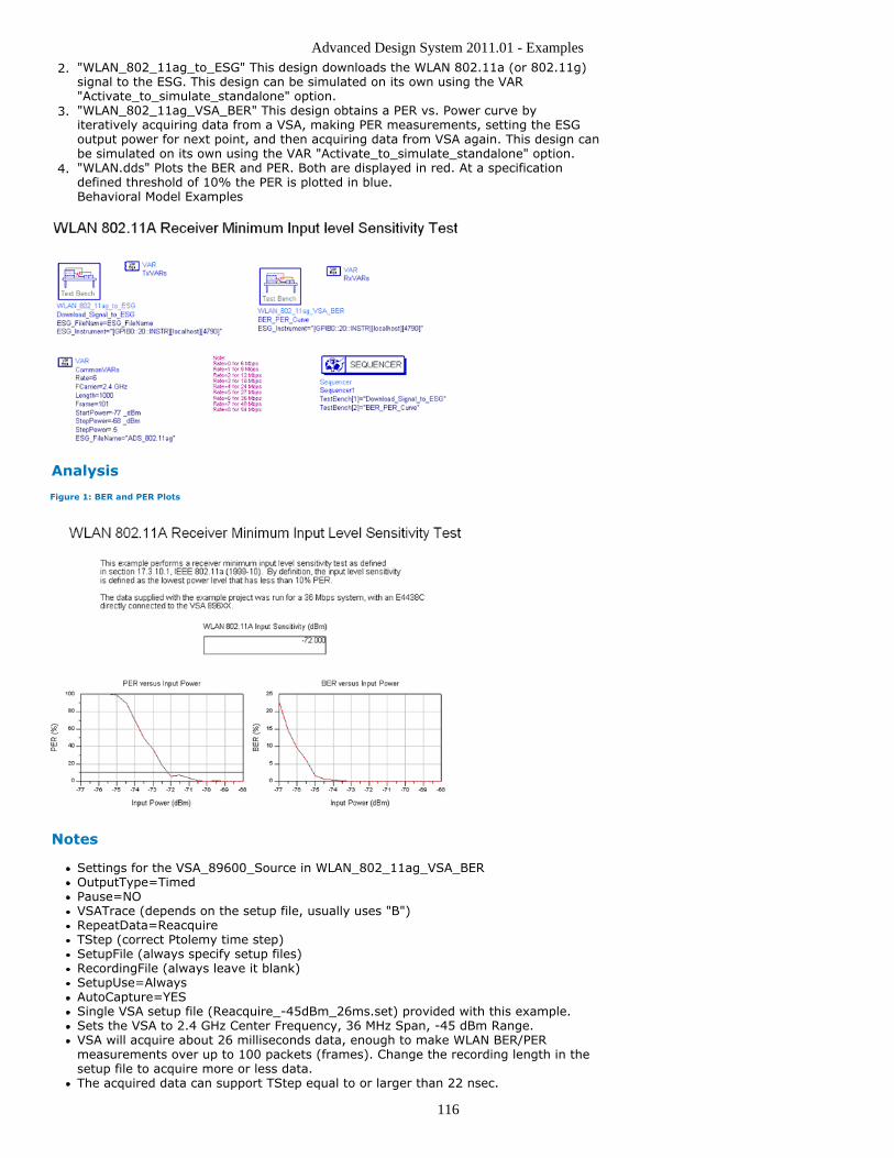
Advanced Design System 2011.01 - Examples
116
"WLAN_802_11ag_to_ESG" This design downloads the WLAN 802.11a (or 802.11g)2.signal to the ESG. This design can be simulated on its own using the VAR"Activate_to_simulate_standalone" option."WLAN_802_11ag_VSA_BER" This design obtains a PER vs. Power curve by3.iteratively acquiring data from a VSA, making PER measurements, setting the ESGoutput power for next point, and then acquiring data from VSA again. This design canbe simulated on its own using the VAR "Activate_to_simulate_standalone" option."WLAN.dds" Plots the BER and PER. Both are displayed in red. At a specification4.defined threshold of 10% the PER is plotted in blue.Behavioral Model Examples
Analysis
Figure 1: BER and PER Plots
Notes
Settings for the VSA_89600_Source in WLAN_802_11ag_VSA_BEROutputType=TimedPause=NOVSATrace (depends on the setup file, usually uses "B")RepeatData=ReacquireTStep (correct Ptolemy time step)SetupFile (always specify setup files)RecordingFile (always leave it blank)SetupUse=AlwaysAutoCapture=YESSingle VSA setup file (Reacquire_-45dBm_26ms.set) provided with this example.Sets the VSA to 2.4 GHz Center Frequency, 36 MHz Span, -45 dBm Range.VSA will acquire about 26 milliseconds data, enough to make WLAN BER/PERmeasurements over up to 100 packets (frames). Change the recording length in thesetup file to acquire more or less data.The acquired data can support TStep equal to or larger than 22 nsec.

Advanced Design System 2011.01 - Examples
117
For information on sequencing simulations, please refer to the Sequencer Controllerdocumentation.For information on ESG connectivity, please refer to the ESG Sink documentation.For VSA connectivity, please refer to the VSA_89600_Source Doc documentation.For Connection Manager details, please refer to the Connection Managerdocumentation.For WLAN Wireless Design Library details, please refer to the WLAN documentation.
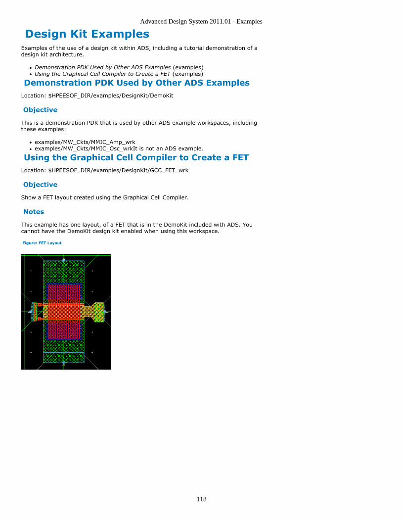
Advanced Design System 2011.01 - Examples
118
Design Kit ExamplesExamples of the use of a design kit within ADS, including a tutorial demonstration of adesign kit architecture.
Demonstration PDK Used by Other ADS Examples (examples)Using the Graphical Cell Compiler to Create a FET (examples)
Demonstration PDK Used by Other ADS ExamplesLocation: $HPEESOF_DIR/examples/DesignKit/DemoKit
Objective
This is a demonstration PDK that is used by other ADS example workspaces, includingthese examples:
examples/MW_Ckts/MMIC_Amp_wrkexamples/MW_Ckts/MMIC_Osc_wrkIt is not an ADS example.
Using the Graphical Cell Compiler to Create a FETLocation: $HPEESOF_DIR/examples/DesignKit/GCC_FET_wrk
Objective
Show a FET layout created using the Graphical Cell Compiler.
Notes
This example has one layout, of a FET that is in the DemoKit included with ADS. Youcannot have the DemoKit design kit enabled when using this workspace.
Figure: FET Layout
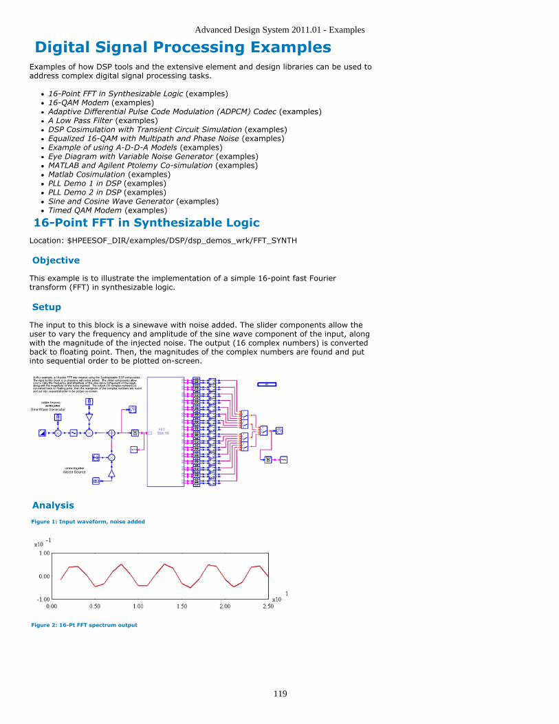
Advanced Design System 2011.01 - Examples
119
Digital Signal Processing ExamplesExamples of how DSP tools and the extensive element and design libraries can be used toaddress complex digital signal processing tasks.
16-Point FFT in Synthesizable Logic (examples)16-QAM Modem (examples)Adaptive Differential Pulse Code Modulation (ADPCM) Codec (examples)A Low Pass Filter (examples)DSP Cosimulation with Transient Circuit Simulation (examples)Equalized 16-QAM with Multipath and Phase Noise (examples)Example of using A-D-D-A Models (examples)Eye Diagram with Variable Noise Generator (examples)MATLAB and Agilent Ptolemy Co-simulation (examples)Matlab Cosimulation (examples)PLL Demo 1 in DSP (examples)PLL Demo 2 in DSP (examples)Sine and Cosine Wave Generator (examples)Timed QAM Modem (examples)
16-Point FFT in Synthesizable LogicLocation: $HPEESOF_DIR/examples/DSP/dsp_demos_wrk/FFT_SYNTH
Objective
This example is to illustrate the implementation of a simple 16-point fast Fouriertransform (FFT) in synthesizable logic.
Setup
The input to this block is a sinewave with noise added. The slider components allow theuser to vary the frequency and amplitude of the sine wave component of the input, alongwith the magnitude of the injected noise. The output (16 complex numbers) is convertedback to floating point. Then, the magnitudes of the complex numbers are found and putinto sequential order to be plotted on-screen.
Analysis
Figure 1: Input waveform, noise added
Figure 2: 16-Pt FFT spectrum output
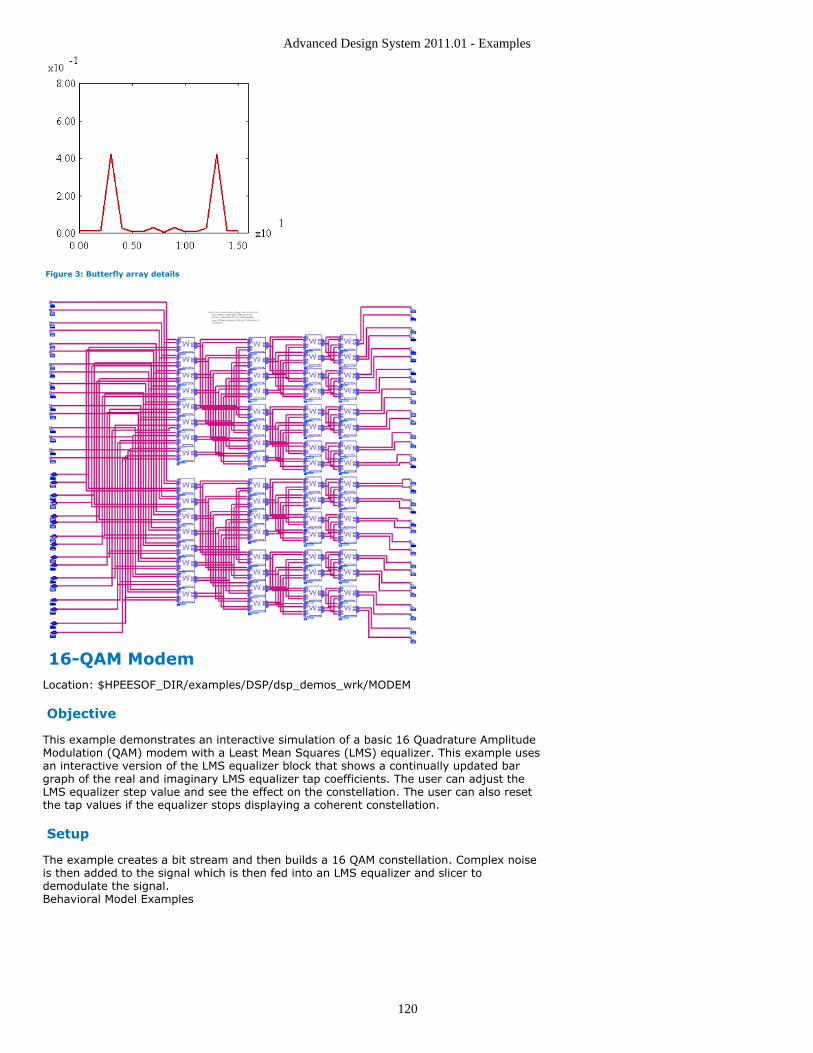
Advanced Design System 2011.01 - Examples
120
Figure 3: Butterfly array details
16-QAM ModemLocation: $HPEESOF_DIR/examples/DSP/dsp_demos_wrk/MODEM
Objective
This example demonstrates an interactive simulation of a basic 16 Quadrature AmplitudeModulation (QAM) modem with a Least Mean Squares (LMS) equalizer. This example usesan interactive version of the LMS equalizer block that shows a continually updated bargraph of the real and imaginary LMS equalizer tap coefficients. The user can adjust theLMS equalizer step value and see the effect on the constellation. The user can also resetthe tap values if the equalizer stops displaying a coherent constellation.
Setup
The example creates a bit stream and then builds a 16 QAM constellation. Complex noiseis then added to the signal which is then fed into an LMS equalizer and slicer todemodulate the signal.Behavioral Model Examples
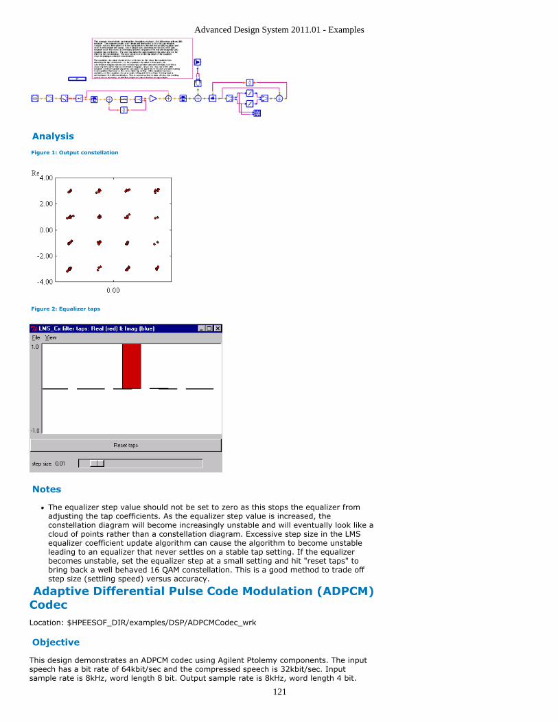
Advanced Design System 2011.01 - Examples
121
Analysis
Figure 1: Output constellation
Figure 2: Equalizer taps
Notes
The equalizer step value should not be set to zero as this stops the equalizer fromadjusting the tap coefficients. As the equalizer step value is increased, theconstellation diagram will become increasingly unstable and will eventually look like acloud of points rather than a constellation diagram. Excessive step size in the LMSequalizer coefficient update algorithm can cause the algorithm to become unstableleading to an equalizer that never settles on a stable tap setting. If the equalizerbecomes unstable, set the equalizer step at a small setting and hit "reset taps" tobring back a well behaved 16 QAM constellation. This is a good method to trade offstep size (settling speed) versus accuracy.
Adaptive Differential Pulse Code Modulation (ADPCM)CodecLocation: $HPEESOF_DIR/examples/DSP/ADPCMCodec_wrk
Objective
This design demonstrates an ADPCM codec using Agilent Ptolemy components. The inputspeech has a bit rate of 64kbit/sec and the compressed speech is 32kbit/sec. Inputsample rate is 8kHz, word length 8 bit. Output sample rate is 8kHz, word length 4 bit.
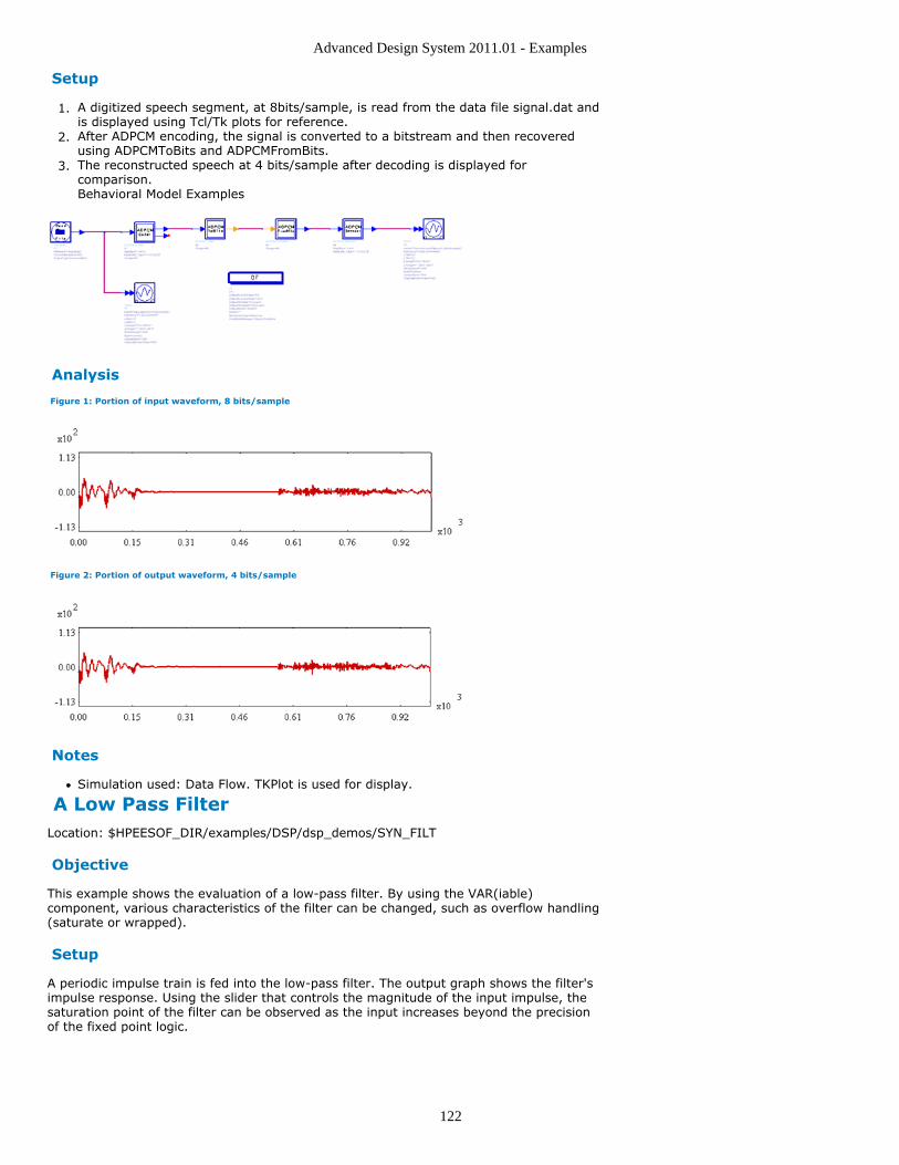
Advanced Design System 2011.01 - Examples
122
Setup
A digitized speech segment, at 8bits/sample, is read from the data file signal.dat and1.is displayed using Tcl/Tk plots for reference.After ADPCM encoding, the signal is converted to a bitstream and then recovered2.using ADPCMToBits and ADPCMFromBits.The reconstructed speech at 4 bits/sample after decoding is displayed for3.comparison.Behavioral Model Examples
Analysis
Figure 1: Portion of input waveform, 8 bits/sample
Figure 2: Portion of output waveform, 4 bits/sample
Notes
Simulation used: Data Flow. TKPlot is used for display.
A Low Pass FilterLocation: $HPEESOF_DIR/examples/DSP/dsp_demos/SYN_FILT
Objective
This example shows the evaluation of a low-pass filter. By using the VAR(iable)component, various characteristics of the filter can be changed, such as overflow handling(saturate or wrapped).
Setup
A periodic impulse train is fed into the low-pass filter. The output graph shows the filter'simpulse response. Using the slider that controls the magnitude of the input impulse, thesaturation point of the filter can be observed as the input increases beyond the precisionof the fixed point logic.
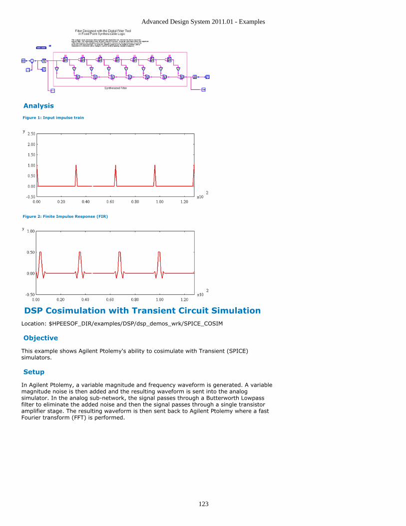
Advanced Design System 2011.01 - Examples
123
Analysis
Figure 1: Input impulse train
Figure 2: Finite Impulse Response (FIR)
DSP Cosimulation with Transient Circuit SimulationLocation: $HPEESOF_DIR/examples/DSP/dsp_demos_wrk/SPICE_COSIM
Objective
This example shows Agilent Ptolemy's ability to cosimulate with Transient (SPICE)simulators.
Setup
In Agilent Ptolemy, a variable magnitude and frequency waveform is generated. A variablemagnitude noise is then added and the resulting waveform is sent into the analogsimulator. In the analog sub-network, the signal passes through a Butterworth Lowpassfilter to eliminate the added noise and then the signal passes through a single transistoramplifier stage. The resulting waveform is then sent back to Agilent Ptolemy where a fastFourier transform (FFT) is performed.
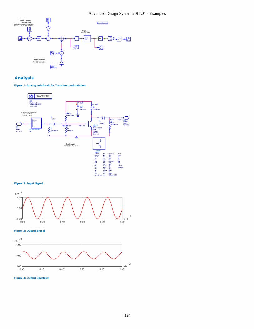
Advanced Design System 2011.01 - Examples
124
Analysis
Figure 1: Analog subcircuit for Transient cosimulation
Figure 2: Input Signal
Figure 3: Output Signal
Figure 4: Output Spectrum
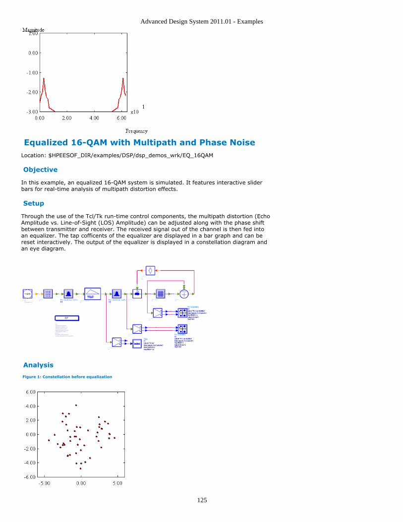
Advanced Design System 2011.01 - Examples
125
Equalized 16-QAM with Multipath and Phase NoiseLocation: $HPEESOF_DIR/examples/DSP/dsp_demos_wrk/EQ_16QAM
Objective
In this example, an equalized 16-QAM system is simulated. It features interactive sliderbars for real-time analysis of multipath distortion effects.
Setup
Through the use of the Tcl/Tk run-time control components, the multipath distortion (EchoAmplitude vs. Line-of-Sight (LOS) Amplitude) can be adjusted along with the phase shiftbetween transmitter and receiver. The received signal out of the channel is then fed intoan equalizer. The tap cofficents of the equalizer are displayed in a bar graph and can bereset interactively. The output of the equalizer is displayed in a constellation diagram andan eye diagram.
Analysis
Figure 1: Constellation before equalization
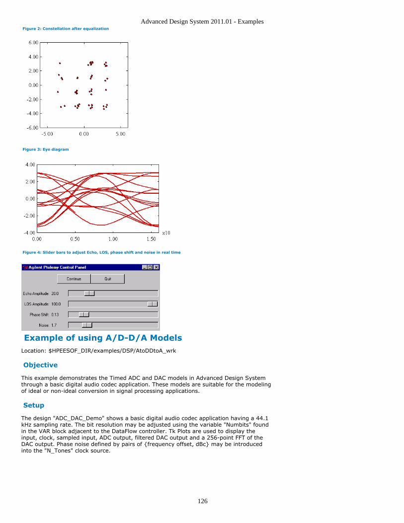
Advanced Design System 2011.01 - Examples
126
Figure 2: Constellation after equalization
Figure 3: Eye diagram
Figure 4: Slider bars to adjust Echo, LOS, phase shift and noise in real time
Example of using A/D-D/A ModelsLocation: $HPEESOF_DIR/examples/DSP/AtoDDtoA_wrk
Objective
This example demonstrates the Timed ADC and DAC models in Advanced Design Systemthrough a basic digital audio codec application. These models are suitable for the modelingof ideal or non-ideal conversion in signal processing applications.
Setup
The design "ADC_DAC_Demo" shows a basic digital audio codec application having a 44.1kHz sampling rate. The bit resolution may be adjusted using the variable "Numbits" foundin the VAR block adjacent to the DataFlow controller. Tk Plots are used to display theinput, clock, sampled input, ADC output, filtered DAC output and a 256-point FFT of theDAC output. Phase noise defined by pairs of {frequency offset, dBc} may be introducedinto the "N_Tones" clock source.
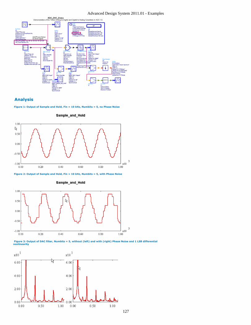
Advanced Design System 2011.01 - Examples
127
Analysis
Figure 1: Output of Sample and Hold, Fin = 10 kHz, Numbits = 5, no Phase Noise
Figure 2: Output of Sample and Hold, Fin = 10 kHz, Numbits = 5, with Phase Noise
Figure 3: Output of DAC filter, Numbits = 5, without (left) and with (right) Phase Noise and 1 LSB differentialnonlinearity
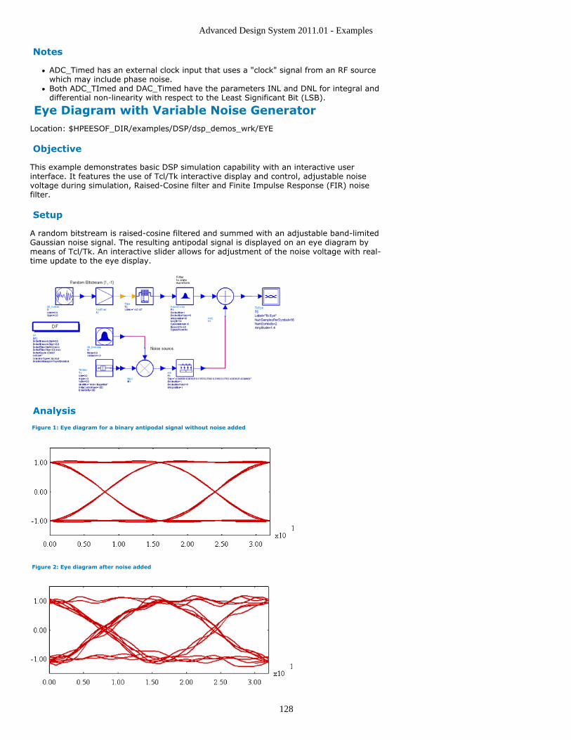
Advanced Design System 2011.01 - Examples
128
Notes
ADC_Timed has an external clock input that uses a "clock" signal from an RF sourcewhich may include phase noise.Both ADC_TImed and DAC_Timed have the parameters INL and DNL for integral anddifferential non-linearity with respect to the Least Significant Bit (LSB).
Eye Diagram with Variable Noise GeneratorLocation: $HPEESOF_DIR/examples/DSP/dsp_demos_wrk/EYE
Objective
This example demonstrates basic DSP simulation capability with an interactive userinterface. It features the use of Tcl/Tk interactive display and control, adjustable noisevoltage during simulation, Raised-Cosine filter and Finite Impulse Response (FIR) noisefilter.
Setup
A random bitstream is raised-cosine filtered and summed with an adjustable band-limitedGaussian noise signal. The resulting antipodal signal is displayed on an eye diagram bymeans of Tcl/Tk. An interactive slider allows for adjustment of the noise voltage with real-time update to the eye display.
Analysis
Figure 1: Eye diagram for a binary antipodal signal without noise added
Figure 2: Eye diagram after noise added
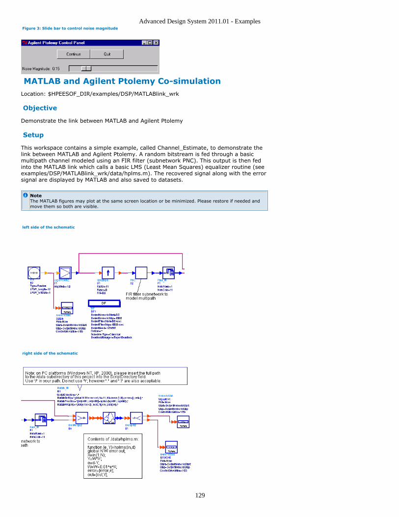
Advanced Design System 2011.01 - Examples
129
Figure 3: Slide bar to control noise magnitude
MATLAB and Agilent Ptolemy Co-simulationLocation: $HPEESOF_DIR/examples/DSP/MATLABlink_wrk
Objective
Demonstrate the link between MATLAB and Agilent Ptolemy
Setup
This workspace contains a simple example, called Channel_Estimate, to demonstrate thelink between MATLAB and Agilent Ptolemy. A random bitstream is fed through a basicmultipath channel modeled using an FIR filter (subnetwork PNC). This output is then fedinto the MATLAB link which calls a basic LMS (Least Mean Squares) equalizer routine (seeexamples/DSP/MATLABlink_wrk/data/hplms.m). The recovered signal along with the errorsignal are displayed by MATLAB and also saved to datasets.
NoteThe MATLAB figures may plot at the same screen location or be minimized. Please restore if needed andmove them so both are visible.
left side of the schematic
right side of the schematic
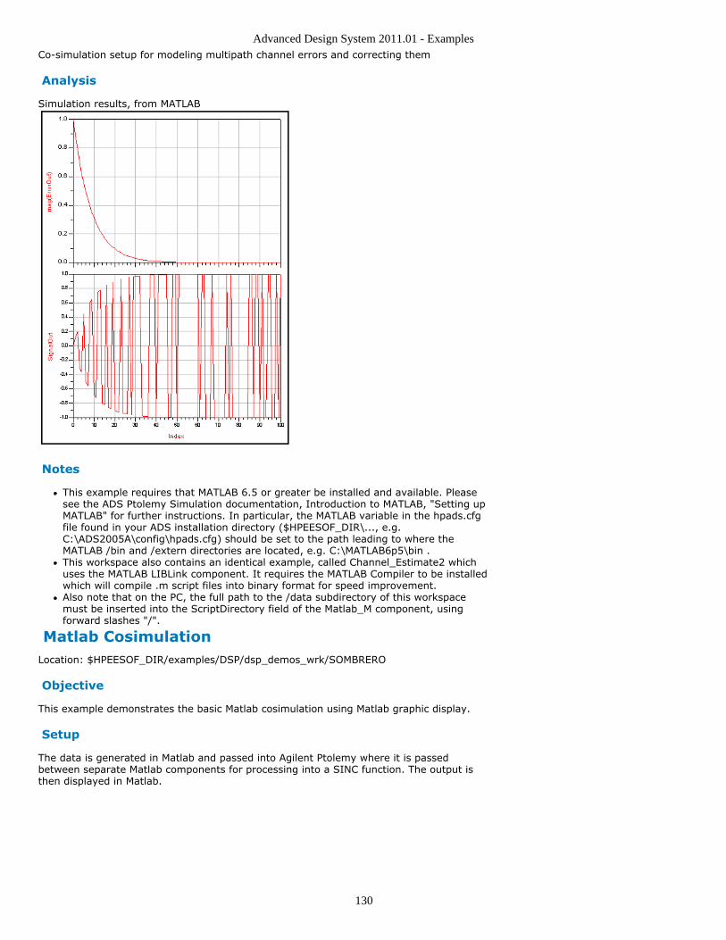
Advanced Design System 2011.01 - Examples
130
Co-simulation setup for modeling multipath channel errors and correcting them
Analysis
Simulation results, from MATLAB
Notes
This example requires that MATLAB 6.5 or greater be installed and available. Pleasesee the ADS Ptolemy Simulation documentation, Introduction to MATLAB, "Setting upMATLAB" for further instructions. In particular, the MATLAB variable in the hpads.cfgfile found in your ADS installation directory ($HPEESOF_DIR\..., e.g.C:\ADS2005A\config\hpads.cfg) should be set to the path leading to where theMATLAB /bin and /extern directories are located, e.g. C:\MATLAB6p5\bin .This workspace also contains an identical example, called Channel_Estimate2 whichuses the MATLAB LIBLink component. It requires the MATLAB Compiler to be installedwhich will compile .m script files into binary format for speed improvement.Also note that on the PC, the full path to the /data subdirectory of this workspacemust be inserted into the ScriptDirectory field of the Matlab_M component, usingforward slashes "/".
Matlab CosimulationLocation: $HPEESOF_DIR/examples/DSP/dsp_demos_wrk/SOMBRERO
Objective
This example demonstrates the basic Matlab cosimulation using Matlab graphic display.
Setup
The data is generated in Matlab and passed into Agilent Ptolemy where it is passedbetween separate Matlab components for processing into a SINC function. The output isthen displayed in Matlab.
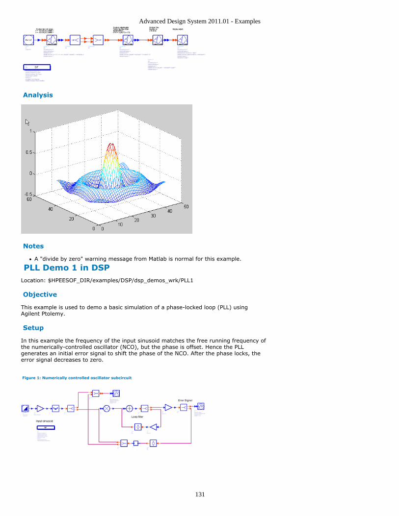
Advanced Design System 2011.01 - Examples
131
Analysis
Notes
A "divide by zero" warning message from Matlab is normal for this example.
PLL Demo 1 in DSPLocation: $HPEESOF_DIR/examples/DSP/dsp_demos_wrk/PLL1
Objective
This example is used to demo a basic simulation of a phase-locked loop (PLL) usingAgilent Ptolemy.
Setup
In this example the frequency of the input sinusoid matches the free running frequency ofthe numerically-controlled oscillator (NCO), but the phase is offset. Hence the PLLgenerates an initial error signal to shift the phase of the NCO. After the phase locks, theerror signal decreases to zero.
Figure 1: Numerically controlled oscillator subcircuit
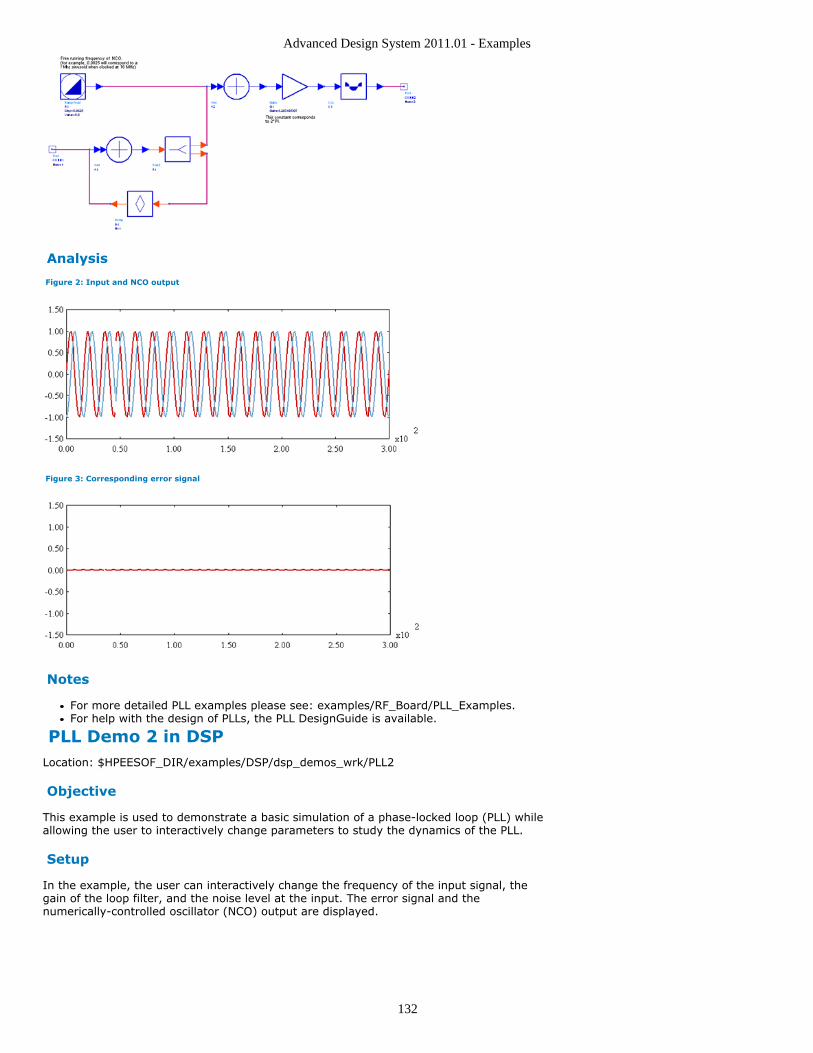
Advanced Design System 2011.01 - Examples
132
Analysis
Figure 2: Input and NCO output
Figure 3: Corresponding error signal
Notes
For more detailed PLL examples please see: examples/RF_Board/PLL_Examples.For help with the design of PLLs, the PLL DesignGuide is available.
PLL Demo 2 in DSPLocation: $HPEESOF_DIR/examples/DSP/dsp_demos_wrk/PLL2
Objective
This example is used to demonstrate a basic simulation of a phase-locked loop (PLL) whileallowing the user to interactively change parameters to study the dynamics of the PLL.
Setup
In the example, the user can interactively change the frequency of the input signal, thegain of the loop filter, and the noise level at the input. The error signal and thenumerically-controlled oscillator (NCO) output are displayed.
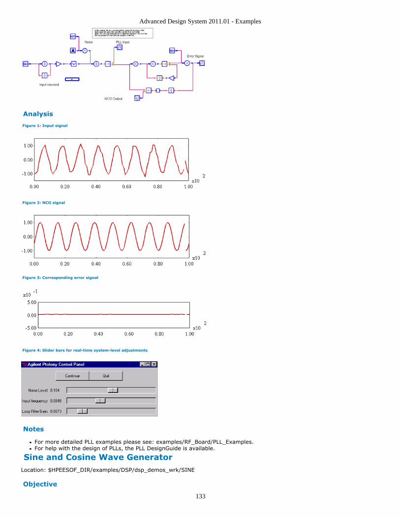
Advanced Design System 2011.01 - Examples
133
Analysis
Figure 1: Input signal
Figure 2: NCO signal
Figure 3: Corresponding error signal
Figure 4: Slider bars for real-time system-level adjustments
Notes
For more detailed PLL examples please see: examples/RF_Board/PLL_Examples.For help with the design of PLLs, the PLL DesignGuide is available.
Sine and Cosine Wave GeneratorLocation: $HPEESOF_DIR/examples/DSP/dsp_demos_wrk/SINE
Objective
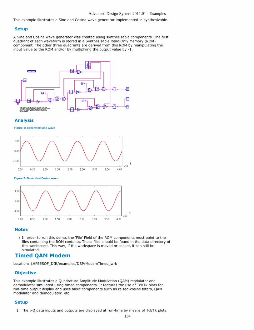
Advanced Design System 2011.01 - Examples
134
This example illustrates a Sine and Cosine wave generator implemented in synthesizable.
Setup
A Sine and Cosine wave generator was created using synthesizable components. The firstquadrant of each waveform is stored in a Synthesizable Read Only Memory (ROM)component. The other three quadrants are derived from this ROM by manipulating theinput value to the ROM and/or by multiplying the output value by -1.
Analysis
Figure 1: Generated Sine wave
Figure 2: Generated Cosine wave
Notes
In order to run this demo, the 'File' Field of the ROM components must point to thefiles containing the ROM contents. These files should be found in the data directory ofthis workspace. This way, if the workspace is moved or copied, it can still besimulated.
Timed QAM ModemLocation: $HPEESOF_DIR/examples/DSP/ModemTimed_wrk
Objective
This example illustrates a Quadrature Amplitude Modulation (QAM) modulator anddemodulator simulated using timed components. It features the use of Tcl/Tk plots forrun-time output display and uses basic components such as raised-cosine filters, QAMmodulator and demodulator, etc.
Setup
The I-Q data inputs and outputs are displayed at run-time by means of Tcl/Tk plots.1.
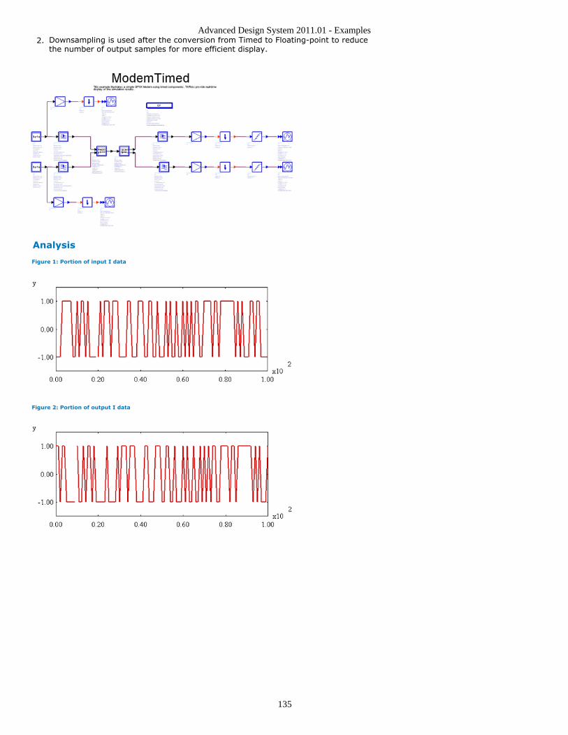
Advanced Design System 2011.01 - Examples
135
Downsampling is used after the conversion from Timed to Floating-point to reduce2.the number of output samples for more efficient display.
Analysis
Figure 1: Portion of input I data
Figure 2: Portion of output I data
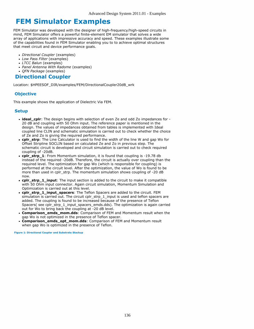
Advanced Design System 2011.01 - Examples
136
FEM Simulator ExamplesFEM Simulator was developed with the designer of high-frequency/high-speed circuits inmind, FEM Simulator offers a powerful finite-element EM simulator that solves a widearray of applications with impressive accuracy and speed. These examples illustrate someof the capabilities found in FEM Simulator enabling you to to achieve optimal structuresthat meet circuit and device performance goals.
Directional Coupler (examples)Low Pass Filter (examples)LTCC Balun (examples)Panel Antenna With Radome (examples)QFN Package (examples)
Directional CouplerLocation: $HPEESOF_DIR/examples/FEM/DirectionalCoupler20dB_wrk
Objective
This example shows the application of Dielectric Via FEM.
Setup
ideal_cplr: The design begins with selection of even Ze and odd Zo impedances for -20 dB and coupling with 50 Ohm input. The reference paper is mentioned in thedesign. The values of impedances obtained from tables is implemented with Idealcoupled line CLIN and schematic simulation is carried out to check whether the choiceof Ze and Zo is giving the required performance.cplr_strp: The Line Calculator is used to find the width of the line W and gap Wo forOffset Stripline SOCLIN based on calculated Ze and Zo in previous step. Theschematic circuit is developed and circuit simulation is carried out to check requiredcoupling of -20dB.cplr_strp_1: From Momentum simulation, it is found that coupling is -19.78 dbinstead of the required -20dB. Therefore, the circuit is actually over coupling than therequired level. The optimization for gap Wo (which is responsible for coupling) isperformed at the circuit level. After the optimization, the value of Wo is found to bemore than used in cplr_strp. The momentum simulation shows coupling of -20 dBnow.cplr_strp_1_input: The input section is added to the circuit to make it compatiblewith 50 Ohm input connector. Again circuit simulation, Momentum Simulation andOptimization is carried out at this level.cplr_strp_1_input_spacers: The Teflon Spacers are added to the circuit. FEMsimulation is carried out. The circuit cplr_strp_1_input is used and teflon spacers areadded. The coupling is found to be increased because of the presence of TeflonSpacers( see cplr_strp_1_input_spacers_emds.dds). The optimization is again carriedout for Wo to bring back the coupling at -20 dB level.Comparison_emds_mom.dds: Comparison of FEM and Momentum result when thegap Wo is not optimized in the presence of Teflon spacer.Comparison_emds_opt_mom.dds: Comparison of FEM and Momentum resultwhen gap Wo is optimized in the presence of Teflon.
Figure 1: Directional Coupler and Substrate Stackup
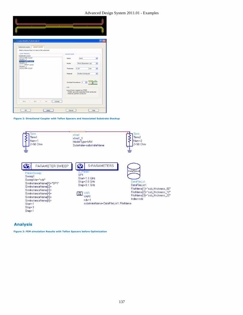
Advanced Design System 2011.01 - Examples
137
Figure 2: Directional Coupler with Teflon Spacers and Associated Substrate Stackup
Analysis
Figure 3: FEM simulation Results with Teflon Spacers before Optimization
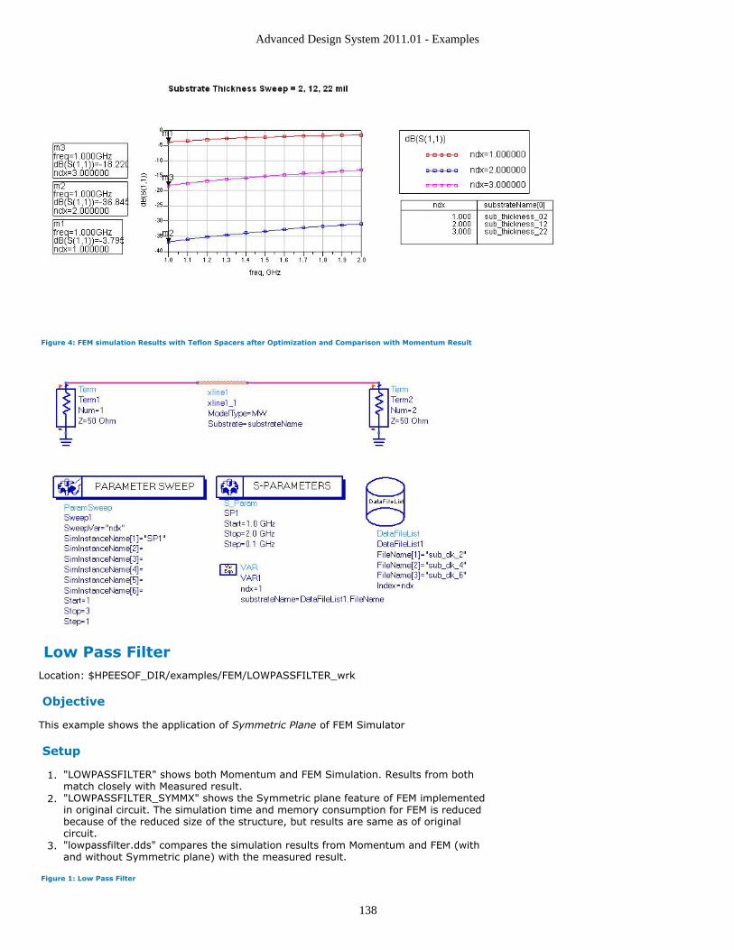
Advanced Design System 2011.01 - Examples
138
Figure 4: FEM simulation Results with Teflon Spacers after Optimization and Comparison with Momentum Result
Low Pass FilterLocation: $HPEESOF_DIR/examples/FEM/LOWPASSFILTER_wrk
Objective
This example shows the application of Symmetric Plane of FEM Simulator
Setup
"LOWPASSFILTER" shows both Momentum and FEM Simulation. Results from both1.match closely with Measured result."LOWPASSFILTER_SYMMX" shows the Symmetric plane feature of FEM implemented2.in original circuit. The simulation time and memory consumption for FEM is reducedbecause of the reduced size of the structure, but results are same as of originalcircuit."lowpassfilter.dds" compares the simulation results from Momentum and FEM (with3.and without Symmetric plane) with the measured result.
Figure 1: Low Pass Filter
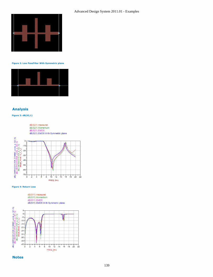
Advanced Design System 2011.01 - Examples
139
Figure 2: Low PassFilter With Symmetric plane
Analysis
Figure 3: dB(S2,1)
Figure 4: Return Loss
Notes
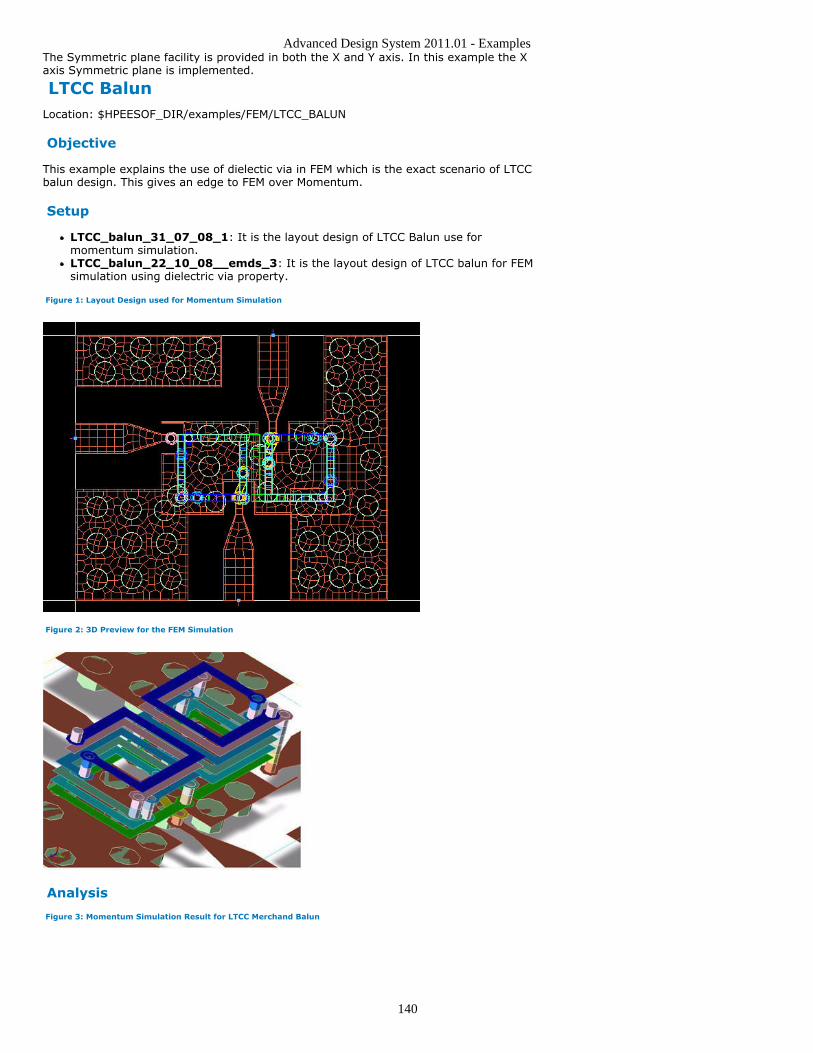
Advanced Design System 2011.01 - Examples
140
The Symmetric plane facility is provided in both the X and Y axis. In this example the Xaxis Symmetric plane is implemented.
LTCC BalunLocation: $HPEESOF_DIR/examples/FEM/LTCC_BALUN
Objective
This example explains the use of dielectic via in FEM which is the exact scenario of LTCCbalun design. This gives an edge to FEM over Momentum.
Setup
LTCC_balun_31_07_08_1: It is the layout design of LTCC Balun use formomentum simulation.LTCC_balun_22_10_08__emds_3: It is the layout design of LTCC balun for FEMsimulation using dielectric via property.
Figure 1: Layout Design used for Momentum Simulation
Figure 2: 3D Preview for the FEM Simulation
Analysis
Figure 3: Momentum Simulation Result for LTCC Merchand Balun
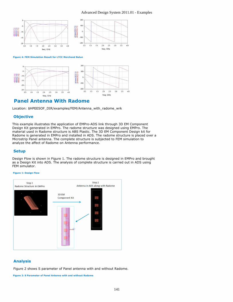
Advanced Design System 2011.01 - Examples
141
Figure 4: FEM Simulation Result for LTCC Merchand Balun
Panel Antenna With RadomeLocation: $HPEESOF_DIR/examples/FEM/Antenna_with_radome_wrk
Objective
This example illustrates the application of EMPro-ADS link through 3D EM ComponentDesign Kit generated in EMPro. The radome structure was designed using EMPro. Thematerial used in Radome structure is ABS Plastic. The 3D EM Component Design kit forRadome is generated in EMPro and installed in ADS. The radome structure is placed over aMicrostrip Panel antenna. The complete structure is subjected to FEM simulation toanalyze the affect of Radome on Antenna performance.
Setup
Design Flow is shown in Figure 1. The radome structure is designed in EMPro and broughtas a Design Kit into ADS. The analysis of complete structure is carried out in ADS usingFEM simulator.
Figure 1: Design Flow
Analysis
Figure 2 shows S parameter of Panel antenna with and without Radome.
Figure 2: S Parameter of Panel Antenna with and without Radome
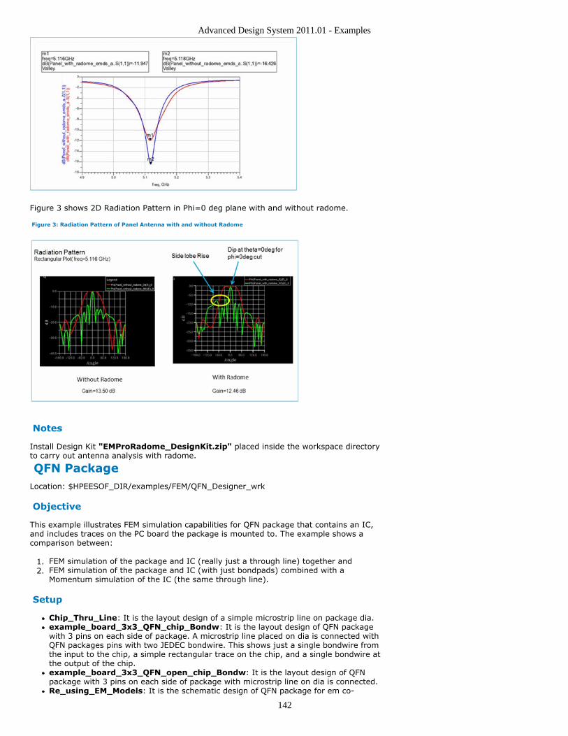
Advanced Design System 2011.01 - Examples
142
Figure 3 shows 2D Radiation Pattern in Phi=0 deg plane with and without radome.
Figure 3: Radiation Pattern of Panel Antenna with and without Radome
Notes
Install Design Kit "EMProRadome_DesignKit.zip" placed inside the workspace directoryto carry out antenna analysis with radome.
QFN PackageLocation: $HPEESOF_DIR/examples/FEM/QFN_Designer_wrk
Objective
This example illustrates FEM simulation capabilities for QFN package that contains an IC,and includes traces on the PC board the package is mounted to. The example shows acomparison between:
FEM simulation of the package and IC (really just a through line) together and1.FEM simulation of the package and IC (with just bondpads) combined with a2.Momentum simulation of the IC (the same through line).
Setup
Chip_Thru_Line: It is the layout design of a simple microstrip line on package dia.example_board_3x3_QFN_chip_Bondw: It is the layout design of QFN packagewith 3 pins on each side of package. A microstrip line placed on dia is connected withQFN packages pins with two JEDEC bondwire. This shows just a single bondwire fromthe input to the chip, a simple rectangular trace on the chip, and a single bondwire atthe output of the chip.example_board_3x3_QFN_open_chip_Bondw: It is the layout design of QFNpackage with 3 pins on each side of package with microstrip line on dia is connected.Re_using_EM_Models: It is the schematic design of QFN package for em co-
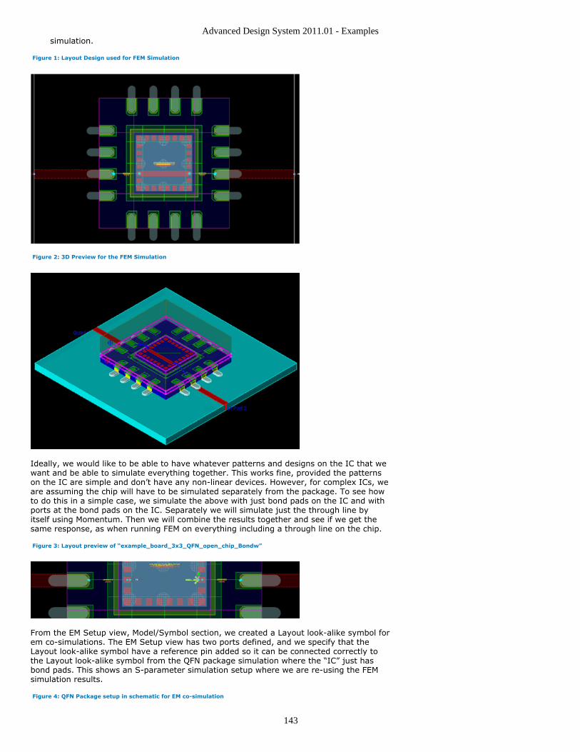
Advanced Design System 2011.01 - Examples
143
simulation.
Figure 1: Layout Design used for FEM Simulation
Figure 2: 3D Preview for the FEM Simulation
Ideally, we would like to be able to have whatever patterns and designs on the IC that wewant and be able to simulate everything together. This works fine, provided the patternson the IC are simple and don’t have any non-linear devices. However, for complex ICs, weare assuming the chip will have to be simulated separately from the package. To see howto do this in a simple case, we simulate the above with just bond pads on the IC and withports at the bond pads on the IC. Separately we will simulate just the through line byitself using Momentum. Then we will combine the results together and see if we get thesame response, as when running FEM on everything including a through line on the chip.
Figure 3: Layout preview of “example_board_3x3_QFN_open_chip_Bondw”
From the EM Setup view, Model/Symbol section, we created a Layout look-alike symbol forem co-simulations. The EM Setup view has two ports defined, and we specify that theLayout look-alike symbol have a reference pin added so it can be connected correctly tothe Layout look-alike symbol from the QFN package simulation where the “IC” just hasbond pads. This shows an S-parameter simulation setup where we are re-using the FEMsimulation results.
Figure 4: QFN Package setup in schematic for EM co-simulation
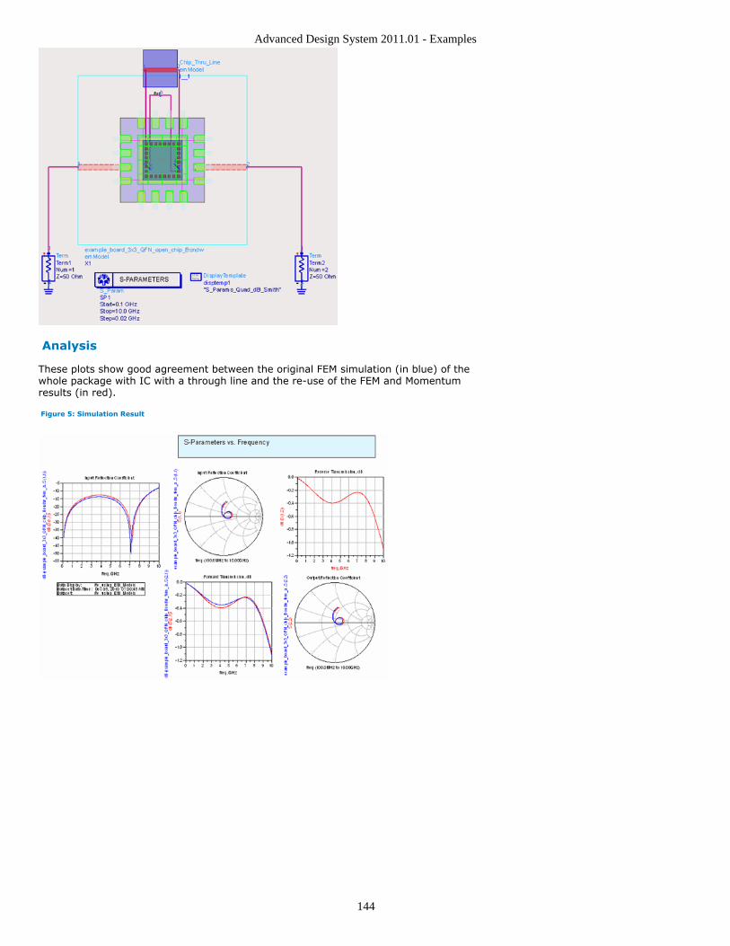
Advanced Design System 2011.01 - Examples
144
Analysis
These plots show good agreement between the original FEM simulation (in blue) of thewhole package with IC with a through line and the re-use of the FEM and Momentumresults (in red).
Figure 5: Simulation Result
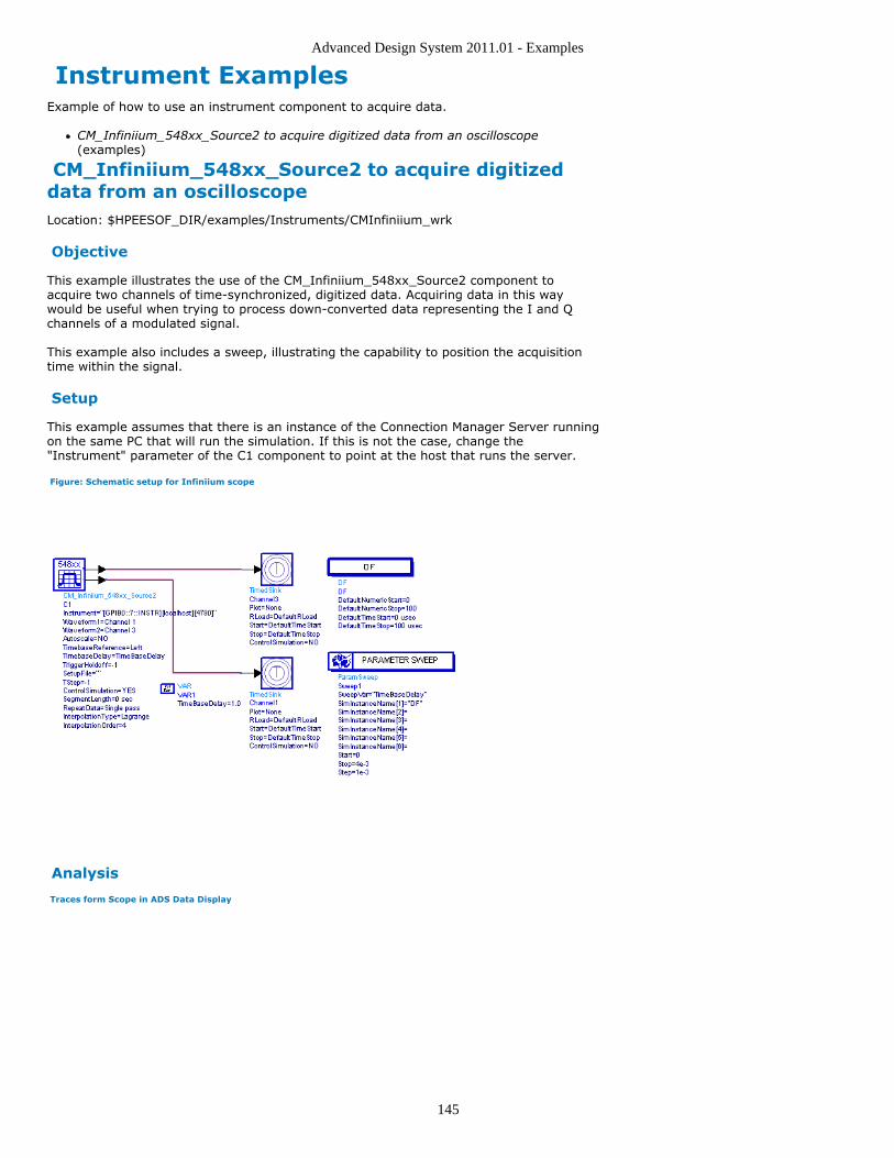
Advanced Design System 2011.01 - Examples
145
Instrument ExamplesExample of how to use an instrument component to acquire data.
CM_Infiniium_548xx_Source2 to acquire digitized data from an oscilloscope(examples)
CM_Infiniium_548xx_Source2 to acquire digitizeddata from an oscilloscopeLocation: $HPEESOF_DIR/examples/Instruments/CMInfiniium_wrk
Objective
This example illustrates the use of the CM_Infiniium_548xx_Source2 component toacquire two channels of time-synchronized, digitized data. Acquiring data in this waywould be useful when trying to process down-converted data representing the I and Qchannels of a modulated signal.
This example also includes a sweep, illustrating the capability to position the acquisitiontime within the signal.
Setup
This example assumes that there is an instance of the Connection Manager Server runningon the same PC that will run the simulation. If this is not the case, change the"Instrument" parameter of the C1 component to point at the host that runs the server.
Figure: Schematic setup for Infiniium scope
Analysis
Traces form Scope in ADS Data Display
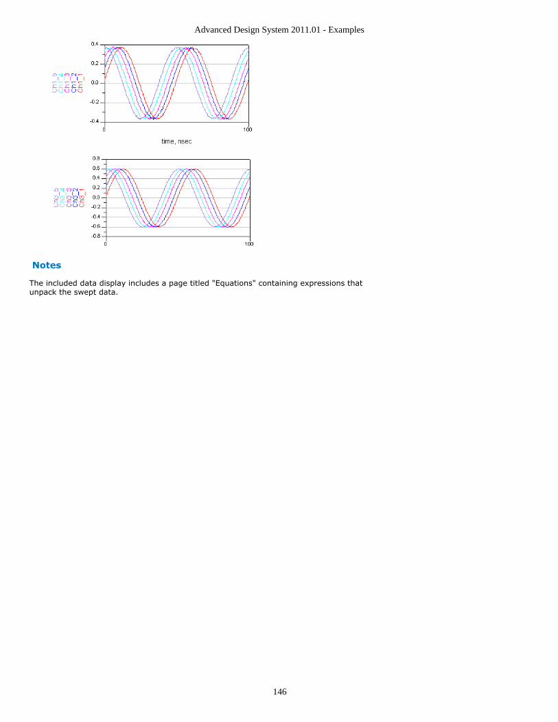
Advanced Design System 2011.01 - Examples
146
Notes
The included data display includes a page titled "Equations" containing expressions thatunpack the swept data.
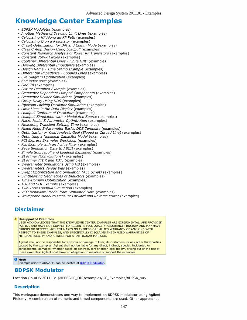
Advanced Design System 2011.01 - Examples
147
Knowledge Center Examples8DPSK Modulator (examples)Another Method of Drawing Limit Lines (examples)Calculating NF Along an RF Path (examples)Calculating Q on a Resonator (examples)Circuit Optimization for Diff and Comm Mode (examples)Class C Amp Design Using Loadpull (examples)Constant Mismatch Analysis of Power RF Transistors (examples)Constant VSWR Circles (examples)Coplanar Differential Lines - Finite GND (examples)Deriving Differential Impedance (examples)Design Name - Time Stamp Example (examples)Differential Impedance - Coupled Lines (examples)Eye Diagram Optimization (examples)find index spec (examples)Find Z0 (examples)Fixture Deembed Example (examples)Frequency Dependent Lumped Components (examples)Frequency Divider Simulations (examples)Group Delay Using DDS (examples)Injection Locking Oscillator Simulation (examples)Limit Lines in the Data Display (examples)Loadpull Contours of Oscillators (examples)Loadpull Simulation with a Modulated Source (examples)Macro Model S-Parameter Optimization (examples)Measuring Transient Settling Time (examples)Mixed Mode S-Parameter Basics DDS Template (examples)Optimization or Yield Analysis Goal (Sloped or Curved Line) (examples)Optimizing a Nonlinear Capacitor Model (examples)PCI Express Examples Workshop (examples)PLL Example with an Active Filter (examples)Save Simulation Data to ASCII (examples)Simple Sourcepull and Loadpull Explained (examples)SI Primer (Convolutions) (examples)SI Primer (TDR and TDT) (examples)S-Parameter Simulations Using HB (examples)S-Parameters Versus Bias (examples)Swept Optimization and Simulation (AEL Script) (examples)Synthesizing Geometries of Inductors (examples)Time-Domain Optimization (examples)TOI and SOI Example (examples)Two-Tone Loadpull Simulation (examples)VCO Behavioral Model from Simulated Data (examples)Waveprobe Model to Measure Forward and Reverse Power (examples)
Disclaimer
Unsupported ExamplesUSER ACKNOWLEDGES THAT THE KNOWLEDGE CENTER EXAMPLES ARE EXPERIMENTAL, ARE PROVIDED"AS-IS", AND HAVE NOT COMPLETED AGILENT'S FULL QUALITY ASSURANCE PROGRAM AND MAY HAVEERRORS OR DEFECTS. AGILENT MAKES NO EXPRESS OR IMPLIED WARRANTY OF ANY KIND WITHRESPECT TO THESE EXAMPLES, AND SPECIFICALLY DISCLAIMS THE IMPLIED WARRANTIES OFMERCHANTABILITY AND FITNESS FOR A PARTICULAR PURPOSE.
Agilent shall not be responsible for any loss or damage to User, its customers, or any other third partiescaused by the examples. Agilent shall not be liable for any direct, indirect, special, incidental, orconsequential damages, whether based on contract, tort or other legal theory, arising out of the use ofthese examples. Agilent shall have no obligation to maintain or support the examples.
NoteExample prior to ADS2011 can be located at 8DPSK Modulator.
8DPSK ModulatorLocation (in ADS 2011+): $HPEESOF_DIR/examples/KC_Examples/8DPSK_wrk
Description
This workspace demonstrates one way to implement an 8DPSK modulator using AgilentPtolemy. A combination of numeric and timed components are used. Other approaches
Advanced Design System 2011.01 - Examples
148
exist for such an implementation.
Knowledge Center examples are experimental workspaces; please see Disclaimer (examples).
NoteExample prior to ADS2011 can be located at Another Method of Drawing Limit Lines.
Another Method of Drawing Limit LinesLocation (in ADS 2011+): $HPEESOF_DIR/examples/KC_Examples/SPEC_LINE2_wrk
Description
Limit lines (specification lines) can be drawn on a rectangular chart for a quick assessmentof circuit performance. However, they have their own independent variables because ofthe way the vectors are created and make the plot look busy. Especially, if the x-axis isfrequency. This example shows how to create spec lines and still retain the cleanfrequency format from ADS.
After unarchiving the workspace, the user can open the data display immediately to learnabout this example. No need to rerun the simulation.
Knowledge Center examples are experimental workspaces; please see Disclaimer (examples).
NoteExample prior to ADS2011 can be located at Calculating NF Along an RF Path.
Calculating NF Along an RF PathLocation (in ADS 2011+): $HPEESOF_DIR/examples/KC_Examples/INTER_NF_wrk
Description
This example workspace contains schematic set-ups and data display calculations tomeasure noise figure along an RF signal path using the IEEE definition. This is useful fornoise figure budget analysis.
This example has been updated for ADS 2008 and utilizes the P_Probe power probecomponent.
Knowledge Center examples are experimental workspaces; please see Disclaimer (examples).
NoteExample prior to ADS2011 can be located at Calculating Q on a Resonator.
Calculating Q on a ResonatorLocation (in ADS 2011+): $HPEESOF_DIR/examples/KC_Examples/Q_CalculationR2_wrk
Description
This example shows how to compute the Q of a resonator using markers and equations inthe data display.
Updated September 2008 to show simpler method of computing Q.
Knowledge Center examples are experimental workspaces; please see Disclaimer (examples).
NoteExample prior to ADS2011 can be located at Circuit Optimization for Diff and Comm Mode.
Circuit Optimization for Differential and CommonMode Impedances for Coupled LinesLocation (in ADS 2011+): $HPEESOF_DIR/examples/KC_Examples/ZDIFF_CM_wrk
Description
This example shows how to calculate even and odd mode impedance for coupledtransmission line, which are directly related to differential and common mode impedance.
Advanced Design System 2011.01 - Examples
149
Knowledge Center examples are experimental workspaces; please see Disclaimer (examples).
NoteExample prior to ADS2011 can be located at Class C Amp Design Using Loadpull.
Class C Amplifier Design Using Load and Source PullSimulationLocation (in ADS 2011+):$HPEESOF_DIR/examples/KC_Examples/ClassC_AmpDesR2_wrk
Description
This example shows a sequence of steps for designing a Class C amplifier.
A load pull was run on an active device, and a load impedance was chosen that was acompromise between PAE and power delivered. Impedance values at the 2nd and 3rdharmonic frequencies were chosen experimentally. Then a matching network wasdesigned to set the desired impedances at the fundamental and harmonic frequencies. Asource pull was run with the load matching network in place, and then a source matchingnetwork was designed. Finally the amplifier including input and output matching networkswas simulated as a function of input power level, giving about 80% PAE and almost 37dBm power delivered (using ideal, lumped-element components in the matching networks,however.)
See Also
Loadpull DesignGuide for ADS 2009 Update 1 with new content (This is the most advancedLoad Pull DesignGuide for use with ADS 2009 Update 1, but it does not have theenhancements of the ADS 2011 version.)
Knowledge Center examples are experimental workspaces; please see Disclaimer (examples).
NoteExample prior to ADS2011 can be located at Constant Mismatch Analysis of Power RF Transistors.
Constant Mismatch Analysis of Power RF TransistorsLocation (in ADS 2011+):$HPEESOF_DIR/examples/KC_Examples/LoadMismatchAnalysisR1_wrk
Description
Problem: You're designing a power amplifier and know the optimal load impedance topresent to the device you are using. What happens (how much degradation in outputpower, power dissipated within the device, efficiency, etc.) if the load impedance is not atthis optimal value?
This example shows a method of simulating how the output power, dissipated power,drain efficiency, and input return loss of a device or amplifier vary as the VSWR of theload reflection coefficient (relative to the optimum value) is varied. The magnitude of theVSWR may be swept in an arbitrary range and the phase of the load impedance used togenerate the VSWR may be swept over an arbitrary range of values.
This technique was created by John Pritiskutch and Craig Rotay of STMicroelectronics. Seetheir article discussing this technique: "A Constant Mismatch Analysis of Power RFTransistors Using EDA Tools," High Frequency Electronics, June 2008.
Knowledge Center examples are experimental workspaces; please see Disclaimer (examples).
NoteExample prior to ADS2011 can be located at Constant VSWR Circles.
Constant VSWR CirclesLocation (in ADS 2011+): $HPEESOF_DIR/examples/KC_Examples/vswr_circle_wrk
Description
In ADS there is no direct way to plot constant VSWR circles, which are frequently used forLNA design. In this example it is shown how to accomplish this task using a few equations
Advanced Design System 2011.01 - Examples
150
on the data display based on a textbook example.
Knowledge Center examples are experimental workspaces; please see Disclaimer (examples).
NoteExample prior to ADS2011 can be located at Coplanar Differential Lines - Finite GND.
Coplanar Differential Lines - Finite GNDLocation (in ADS 2011+):$HPEESOF_DIR/examples/KC_Examples/CPW_Diff_Lines_Finite_wrk
Description
This workspace shows how to simulate a coplanar differential line with a finite groundplane. Both the conductors and the groundplanes are drawn on a strip layer and theground planes are connected to ground with via holes.
The Momentum simulation is using Single ports only, also for the ground planes. We thenrecombine the S-parameters in a schematic simulation using the correct groundreferences for each port.
Simulating this structure as a slot layer is much more efficient. This method should onlybe used when your groundplanes are small and you are concerned about end effects etc.
Knowledge Center examples are experimental workspaces; please see Disclaimer (examples).
NoteExample prior to ADS2011 can be located at Deriving Differential Impedance.
Deriving Differential ImpedanceLocation (in ADS 2011+): $HPEESOF_DIR/examples/KC_Examples/differential_lines_wrk
Description
This example shows how to find the differential impedance from a pair of microstrip lines.The S-parameters of a coupled pair of lines are simulated with Momentum using 4 ports.The differential input impedance is found by a S-Parameter circuit analysis where sourceand load impedances are swept. Using the data display, the differential impedance is thesweep value of impedance that results in the smallest reflection.
Knowledge Center examples are experimental workspaces; please see Disclaimer (examples).
NoteExample prior to ADS2011 can be located at Design Name - Time Stamp Example.
Design Name - Time Stamp examplesLocation (in ADS 2011+): $HPEESOF_DIR/examples/KC_Examples/name_timeR1_wrk
Description
Example of how to create an AEL function to display design workspace information (designname, time and environment variables) in the data set and data display.
This workspace shows various ways of displaying information such as design name, timeand environmental variables.
In the workspace directory you will find a custom AEL Expression, design_name.ael.Once you have installed this function you can use it in a MeasEqn on a schematic to sendthe current design name to the dataset. Please see A_README in the workspace for moreinformation.
Notes from A_README
This workspace illustrates various methods of displaying information like design name,time and environmental variables. Open the design name_time and simulate it. Thecorresponding data display shows the values of the various variables.
Advanced Design System 2011.01 - Examples
151
NoteA custom AEL Expression, design_name.ael, needs to be installed if you wish to get the design nameinto the dataset.
Copy the file design_name.ael to the folder $HOME/hpeesof/expressions/ael.1.$HOME is your ADS home directory (typically c:\users\default on PC).2.The expressions folder does not exist by default; you may need to create it.3.Create a file, user_defined_fun.ael, in the same directory (if it doesn't exist already).4.Open user_defined_fun.ael in a text editor and add the following line:5.load("design_name");
Restart ADS.6.
See AEL Expressions Installation Instructions for more information about installingcustom AEL Expressions.
Knowledge Center examples are experimental workspaces; please see Disclaimer (examples).
NoteExample prior to ADS2011 can be located at Differential Impedance - Coupled Lines.
Two Methods to Compute Differential and CommonMode Impedances for Coupled LinesLocation (in ADS 2011+): $HPEESOF_DIR/examples/KC_Examples/diff_ex_wrk
Description
This example contains two examples of how to calculate the differential impedance of aline:
diff_imp
Using an S-parameter optimization to find the differential- and odd-mode impedances ofthe line.
diff_imp_alt
Advanced Design System 2011.01 - Examples
152
Using an AC simulation and a set of equations to calculate the differential-, even- andodd-mode impedances directly.
Click on the thumbnail images above to see full size schematics.
Knowledge Center examples are experimental workspaces; please see Disclaimer (examples).
NoteExample prior to ADS2011 can be located at Eye Diagram Optimization.
Eye Diagram OptimizationLocation (in ADS 2011+):$HPEESOF_DIR/examples/KC_Examples/Optimizing_Eye_KC_wrk
Description
This Example shows how you can optimize your Eye Diagram. You can use measurementssuch as Eye Height, Eye Width, Eye Opening Factor, Eye SNR, Rise/Fall Time and Jitter,and others.
Open the schematic Test_Circuit_2. Push into the Control_2 sub-circuit to access theMeasurements and Optimization Setup.
Meta Description
Article from Printed Circuit Design & Manufacture magazine on Thursday, 31 August2006... entitled "Optimizing Interconnect Performance with Eye Diagrams" byAgilent's By Sanjeev Gupta and Gunnar Boe:http://pcdandm.com/cms/cms/content/view/2876/95/
Knowledge Center examples are experimental workspaces; please see Disclaimer (examples).
NoteExample prior to ADS2011 can be located at find index spec.
find_index_specLocation (in ADS 2011+): $HPEESOF_DIR/examples/KC_Examples/find_index_spec_wrk
Description
An alternative to the find_index() function. This function works better in some cases
Advanced Design System 2011.01 - Examples
153
where the data is non-monotonic.
This function does find the index of the independent variable which is closest to the lookupvalue. It supports multi-dimensional data up to 3 swept parameters.
The workspace contains the AEL function, find_index_spec.ael, as well as two test cases.
See AEL Expressions Installation Instructions for more information about installingcustom AEL Expressions. It is also explained in Introduction to Measurement Expressionsin ADS manuals.
Knowledge Center examples are experimental workspaces; please see Disclaimer (examples).
NoteExample prior to ADS2011 can be located at Find Z0.
Find Z0Location (in ADS 2011+): $HPEESOF_DIR/examples/KC_Examples/find_Zo_wrk
Description
Momentum calculates Z0 when you are using Single Ports, but not when you are usingInternal Ports. Here is one example of how to find Z0 by optimization.
Knowledge Center examples are experimental workspaces; please see Disclaimer (examples).
NoteExample prior to ADS2011 can be located at Fixture Deembed Example.
Fixture deembed exampleLocation (in ADS 2011+):
$HPEESOF_DIR/examples/KC_Examples/Deembed/deembed_2port/Fixture_deembed_wrk$HPEESOF_DIR/examples/KC_Examples/Deembed/deembed_2port_6A/Fixture_deembed_wrk$HPEESOF_DIR/examples/KC_Examples/Deembed/deembed_2port_8U1/Fixture_deembed_wrk
Description
This workspace shows how deembed data for a fixture can be generated from calibrationmeasurements. The fixture is assumed to have perfect symmetry, so that the output halfof the fixture is the mirror image of the input half of the fixture. The half fixture is notassumed to be symmetrical.
The calibration measurements include thru measurements and S11 of a known load.
Here are the steps for deembedding S-parameters for a DUT from measurements taken ofthe DUT in a fixture. You need three calibration devices that can be placed in the fixture: atransmission line of length L, a transmission line of length 2*L, and a known load. Youneed a data file with S11 of the known load. Let's assume you've put the data in a datasetcalled Gamma.ds.
SET UP EXAMPLE WORKSPACE WITH MEASURED OR MODELED KNOWN LOAD S11 DATA:1.
Copy the workspace Fixture_deembed_wrk to a directory with writepermission. Remove all of the data files from the data directory. StoreGamma.ds in the data directory. (In the example, this step is artificiallysimulated by gamma.dsn.)
NWA CALIBRATION:2.
Perform an appropriate network analyzer calibration at the input planes of thefixture.
MEASURE S-PARAMETERS OF SHORT LENGTH "L" LINE IN FIXTURE/BRING DATA INTO ADS:3.
Place the short transmission line in the fixture. Measure the s-parameters of theshort transmission line. Put the data in a dataset called L1.ds. Store it in thedata directory. (In the example, this step is artificially simulated by L1.dsn.)
MEASURE S-PARAMETERS OF LONG LENGTH "2*L" LINE IN FIXTURE/BRING DATA INTO ADS:4.
Place the long transmission line in the fixture. Measure the s-parameters of thelong transmission line. Put the data in a dataset called L2.ds. Store it in the data

Advanced Design System 2011.01 - Examples
154
directory. (In the example, this step is artificially simulated by L2.dsn.) MEASURE KNOWN LOAD S11 DATA IN FIXTURE/BRING DATA INTO ADS:5.
Place the known load in the fixture. Measure S11 of the known load. Put thedata in a dataset called Load_meas.ds. Store it in the data directory. (In theexample, this step is artificially simulated by Load_meas.dsn.)
MEASURE DUT IN FIXTURE/BRING DATA INTO ADS:6.
Place your device under test (DUT) in the fixture. Measure the s-parameters ofthe DUT. Put the data in a dataset called DUT_meas.ds. Store it in the datadirectory.. (In the example, this step is artificially simulated by DUT_meas.dsn.)
RUN ADS DESIGN EQUATIONS TO REMOVE LONG AND SHORT THROUGH, EXTRACT ONLY INPUT/OUTPUT HALFFIXTURE:
7.
In ADS, open Thru.dsn and run the simulation. This will derive thru data fromL1.ds and L2.ds. Results will be stored in the data directory in a file calledThru.ds.
RUN ADS DESIGN EQUATIONS TO CALCULATE HALF-FIXTURE S-PARAMENTERS:8.
In ADS, open Half_fixture_model.dsn and run the simulation. This will calculatethe s-parameters of the half fixture from Thru.ds, Load_meas.ds, andGamma.ds. Results will be stored in the data directory in a file calledHalf_fixture_model.ds.
FINALLY RUN ADS DESIGN W/ Deembed2 COMPONENT TO DEEMBED DUT FROM THE FIXTURE:9.
In ADS, open use_Deembed2.dsn and run the simulation. This will deembedthe DUT from the fixture. The default dataset name will be use_Deembed2.ds. Ifdesired, change the dataset name before running the simulation.
Note that steps 3, 4, 5, 7, and 8 only need to be performed once. Once you haveHalf_fixture_model.ds, you can reuse the model data to deembed future DUTmeasurements.
UPDATE NEW N-PORT DE-EMBEDDING COMPONENTS AVAILABLE STARTING IN ADS2008Update 1 – De_EmbedN and De_EmbedSnPN (where N=2,4,6,8,10 or 12).
The attached archived file includes examples based on the Fixture dembeding discussionabove that are ADS version specific. Please read the ReadME_1st.txt file included in thearchive for further details.
Contents of ReadMe_1st.txt
This archived file (.zip) includes three ADS archived workspaces. They are examples onhow to use the deembed components. Prior to ADS 2006A, only the "Deembed1" (1-Port)and "Deembed2" (2-Port) components were available to use in ADS RF/Analogsimulations. Starting in ADS 2006A, new multi-port de-embedding components areavailable in the form of "DeembedN" where N=1,2,4,6,8,12 port de-embedding and aresupported up to the ADS2008 release inclusive.
The proper use of Deembed2 was not well documented in the ADS manual in priorreleases. In older releases (prior to ADS2006A), customers can get correct answers withDeembed2 even if they don't use it as designed.
In ADS2006A, a change was deliberately made to the Deembed2 component to bring it inline with theoretical definition and to implement the newly introduced DeembedNcomponents. As a result, the statement in the ADS manual that for cancellation behaviorthe de-embed component should be set back-to-back against the SnP component, mustnow be strictly adhered to.
Staring in ADS2008 Update 1 two new sets of deembed components were introducedDe_EmbedN and De_EmbedSnPN. These latest deembed components offer much moreflexibility and ease of use when compared to the old DeembedN components. For moredetails about the new components, see your ADS2008 Update 1 or greaterdocumentation.
Description of the files included:
deembed_2port.zap - 2 port deembed example that has been verified with1.ADS2004A and ADS2005A. This will NOT work properly in ADS2006A and laterreleases.deembed_2port_6A.zap - 2 port deembed example (similar to above) that properly2.
Advanced Design System 2011.01 - Examples
155
connects the DUT and Deembed2 components back to back. This example will workproperly in ADS2006A or later releases only.deembed_2port_8U1.zap - 2 port deembed example (similar to above) that uses the3.newly introduced De_Embed2 component.
NoteStarting with ADS2008 Update 1 release the DeemdbedN components are no longer available on thecompomponent palettes but will still work.
Knowledge Center examples are experimental workspaces; please see Disclaimer (examples).
NoteExample prior to ADS2011 can be located at Frequency Dependent Lumped Components for ADS.
Frequency Dependent Lumped Components for ADSLocation (in ADS 2011+):$HPEESOF_DIR/examples/KC_Examples/FreqDependentRLCs_wrk
Description
Simulating frequency-dependent lumped elements in ADS is challenging, because ADSdoes not normally provide for frequency-related variation of lumped elements. Thisworkspace shows both file-based and equation-based methods of making frequency-dependent lumped components.
Knowledge Center examples are experimental workspaces; please see Disclaimer (examples).
NoteExample prior to ADS2011 can be located at Frequency Divider Simulations.
Frequency divider simulations, up to divide-by-128,ADS 2005A versionLocation (in ADS 2011+):$HPEESOF_DIR/examples/KC_Examples/FreqDivHigherOrder_wFETsR4_wrk
Description
This example has simulations of frequency dividers. Included are simulations of dividersup to divide-by-128. There are also simulations that include a VCO at the input, and somephase noise simulations.
This example was updated on October 28, 2005, showing a method of gettingaccurate phase noise simulation results when using Krylov.
This example was updated on November 1, 2005, and now includes a phase noisesimulation of the VCO with divide-by-64, that must be run on a machine with 2GBytes of RAM.
This example was updated on January 13, 2005. The convergence tolerances,I_RelTol and V_RelTol, that affect the transient simulations to generate an initialguess, where loosened. This dramatically speeds up the transient part of thesimulations.
Knowledge Center examples are experimental workspaces; please see Disclaimer (examples).
NoteExample prior to ADS2011 can be located at Group Delay Using DDS.
Group DelayLocation (in ADS 2011+): $HPEESOF_DIR/examples/KC_Examples/numDerivsR1_wrk
Description
This example has been updated to use the diff() and unwrap() functions, whichgreatly simplify the calculation.
This workspace shows how to calculate the group delay on the data display. If you do anS-parameter simulation, you don't need to use this function, since you can just enableGroup Delay in the S-parameter analysis controller. But if you are doing any other

Advanced Design System 2011.01 - Examples
156
simulation, you can use this method to calculate the group delay from the phaseresponse.
Knowledge Center examples are experimental workspaces; please see Disclaimer (examples).
NoteExample prior to ADS2011 can be located at Injection Locking Oscillator Simulation.
Injection locking oscillator simulationLocation (in ADS 2011+):$HPEESOF_DIR/examples/KC_Examples/InjectionLockingOscR1_wrk
Description
This example shows some injection locking experiments. The simulations use a MOS VCO,that uses MOSFETs as the capacitive tuning elements. One interpretation of "injectionlocking" is the coupling of some stable oscillating signal into a free-running oscillator insuch a way that the free-running oscillator's frequency becomes the same as the morestable oscillator's. The Envelope simulator may be used for these simulations. You have toknow the free-running oscillator's oscillation frequency and the stable oscillator'sfrequency must be within the same envelope bandwidth (=1/timestep) as the free-runningoscillator's.
VCO_wFETcaps uses harmonic balance and shows the large-signal steady-state solutionsversus tuning voltage.
VCO_HB_Test uses harmonic balance to simulate the VCO subcircuit used in the othersimulations. It is just used to verify the performance of the subcircuit.
VCO_wFETcapsEnv simulates the VCO using Envelope. It does not run an oscillatoranalysis, but still detects an oscillating signal within the envelope bandwidth centered onthe analysis frequency.
InjectionLockingTest simulates two identical free-running oscillators with their outputscoupled together via a resistive power combiner. The two oscillators are tuned to slightlydifferent frequencies but end up oscillating at the same frequency in this simulation. Thisshows that ADS is able to simulate multiple oscillators in the same schematic.
InjectionLocking_wIdealSig_FSwp simulates the free-running oscillator coupled (via aresistive power combiner) to an ideal, behavioral VCO, which acts as the stable oscillator.The frequency of the ideal VCO is varied by applying a sinusoid to its control input. Theoutput indicates approximately the range of frequencies over which the free-runningoscillator is locked to the ideal VCO.
InjectionLocking_wIdealSig_PSwp simulates how the amplitude of the ideal stable signalaffects the ability to achieve lock. The power of this signal is stepped in a piecewise-linearfashion. When it reaches -5 dBm, the free-running oscillator suddenly locks to it.
VCO_EnvTest_wFM applies frequency modulation to the open-loop VCO.
See Also
Starting Examples For Setting Up Injection Locking Oscillator Simulation
Knowledge Center examples are experimental workspaces; please see Disclaimer (examples).
NoteExample prior to ADS2011 can be located at Limit Lines in the Data Display.
Creating Limit Lines in the Data Display withLimitlines ADS DesignGuide...
Issue
Q: How do you add limit lines to the data display?
How to get the ADS Limitlined ADS DesignGuide...
Location (in ADS 2011+): $HPEESOF_DIR/examples/KC_Examples/Limitlines
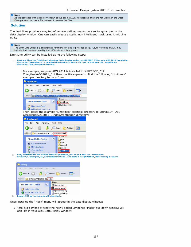
Advanced Design System 2011.01 - Examples
157
NoteAs the contents of the directory shown above are not ADS workspaces, they are not visible in the OpenExample window; use a file browser to access the files.
Solution
The limit lines provide a way to define user defined masks on a rectangular plot in thedata display window. One can easily create a static, non intelligent mask using Limit Lineutility.
NoteThe Limit Line utility is a contributed functionality, and is provided as-is. Future versions of ADS mayinclude limit line functionality that differs from this approach.
Limit Line utility can be installed using the following steps:
Copy and Place the "Limitlines" directory folder located under \<$HPEESOF_DIR or your ADS 2011 InstallationDirectory\>/examples/KC_Examples/Limitlines to \<$HPEESOF_DIR or your ADS 2011 InstallationDirectory\>/dds/frontpanel directory.
1.
For example, suppose ADS 2011 is installed in $HPEESOF_DIRC:\agilent\ADS2011_01\ then use file explorer to find the following "Limitlines"example directory to copy from:
Then, paste the example "Limitlines" example directory to $HPEESOF_DIRC:\agilent\ADS2011_01\dds\frontpanel\ directory:
Copy usermenu.res file located under \<$HPEESOF_DIR or your ADS 2011 InstallationDirectory\>/examples/KC_Examples/Limitlines... and paste it in <$HPEESOF_DIR>/config directory:
2.
Restart ADS so the changes will take effect...3.
Once installed the "Mask" menu will appear in the data display window:
Here is a glimpse of what the newly added Limitlines "Mask" pull down window willlook like in your ADS DataDisplay window:
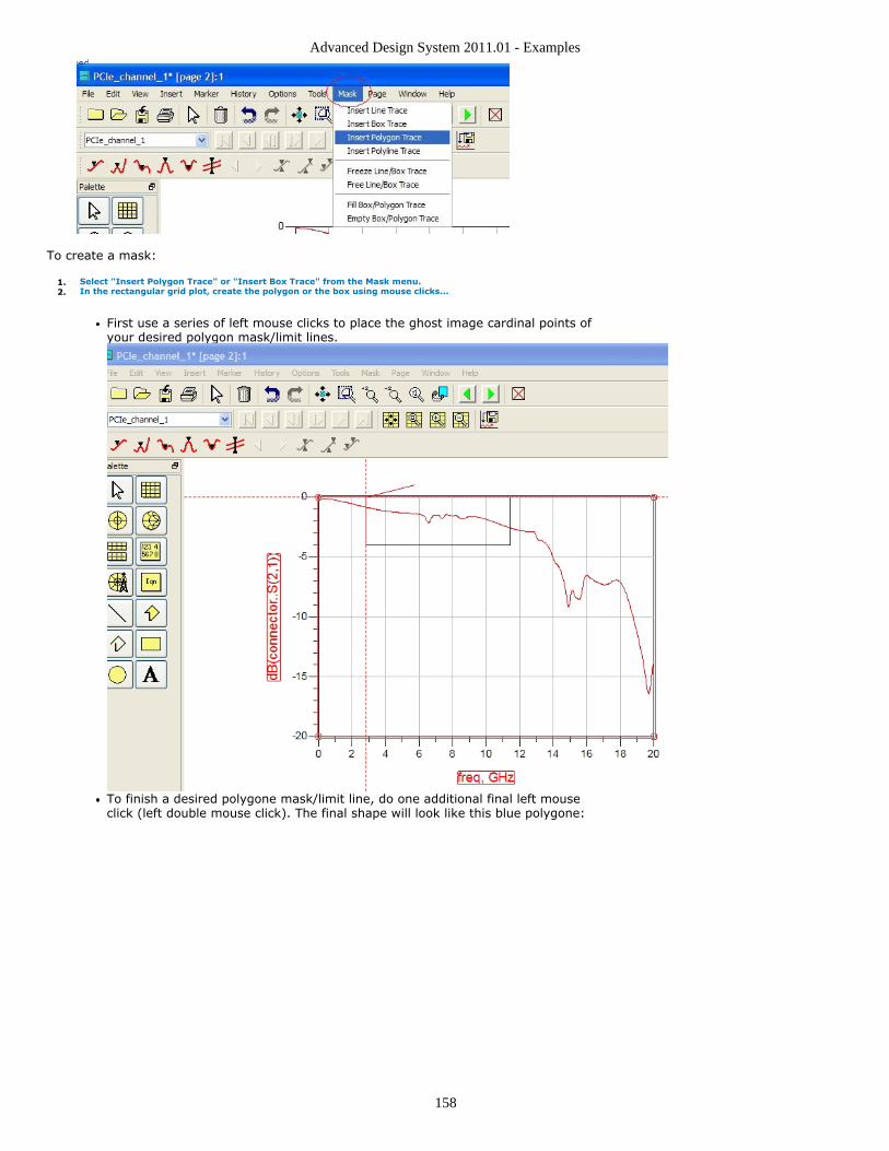
Advanced Design System 2011.01 - Examples
158
To create a mask:
Select "Insert Polygon Trace" or "Insert Box Trace" from the Mask menu.1. In the rectangular grid plot, create the polygon or the box using mouse clicks...2.
First use a series of left mouse clicks to place the ghost image cardinal points ofyour desired polygon mask/limit lines.
To finish a desired polygone mask/limit line, do one additional final left mouseclick (left double mouse click). The final shape will look like this blue polygone:
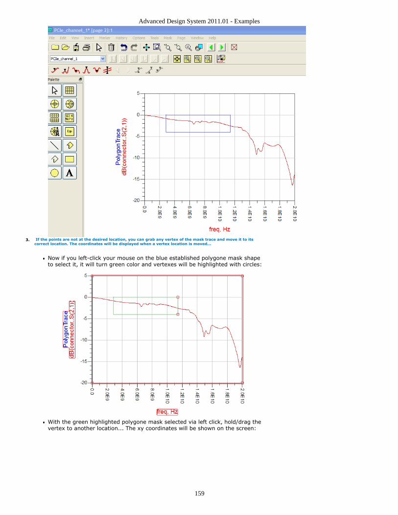
Advanced Design System 2011.01 - Examples
159
If the points are not at the desired location, you can grab any vertex of the mask trace and move it to itscorrect location. The coordinates will be displayed when a vertex location is moved...
3.
Now if you left-click your mouse on the blue established polygone mask shapeto select it, it will turn green color and vertexes will be highlighted with circles:
With the green highlighted polygone mask selected via left click, hold/drag thevertex to another location... The xy coordinates will be shown on the screen:
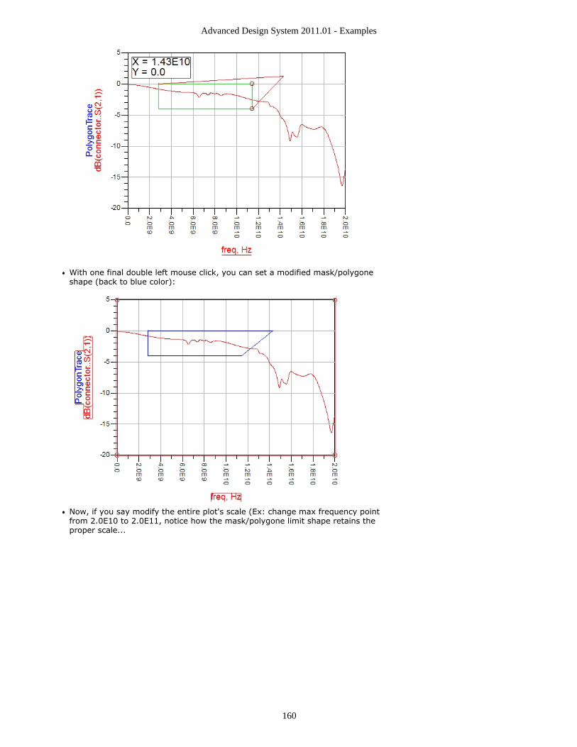
Advanced Design System 2011.01 - Examples
160
With one final double left mouse click, you can set a modified mask/polygoneshape (back to blue color):
Now, if you say modify the entire plot's scale (Ex: change max frequency pointfrom 2.0E10 to 2.0E11, notice how the mask/polygone limit shape retains theproper scale...
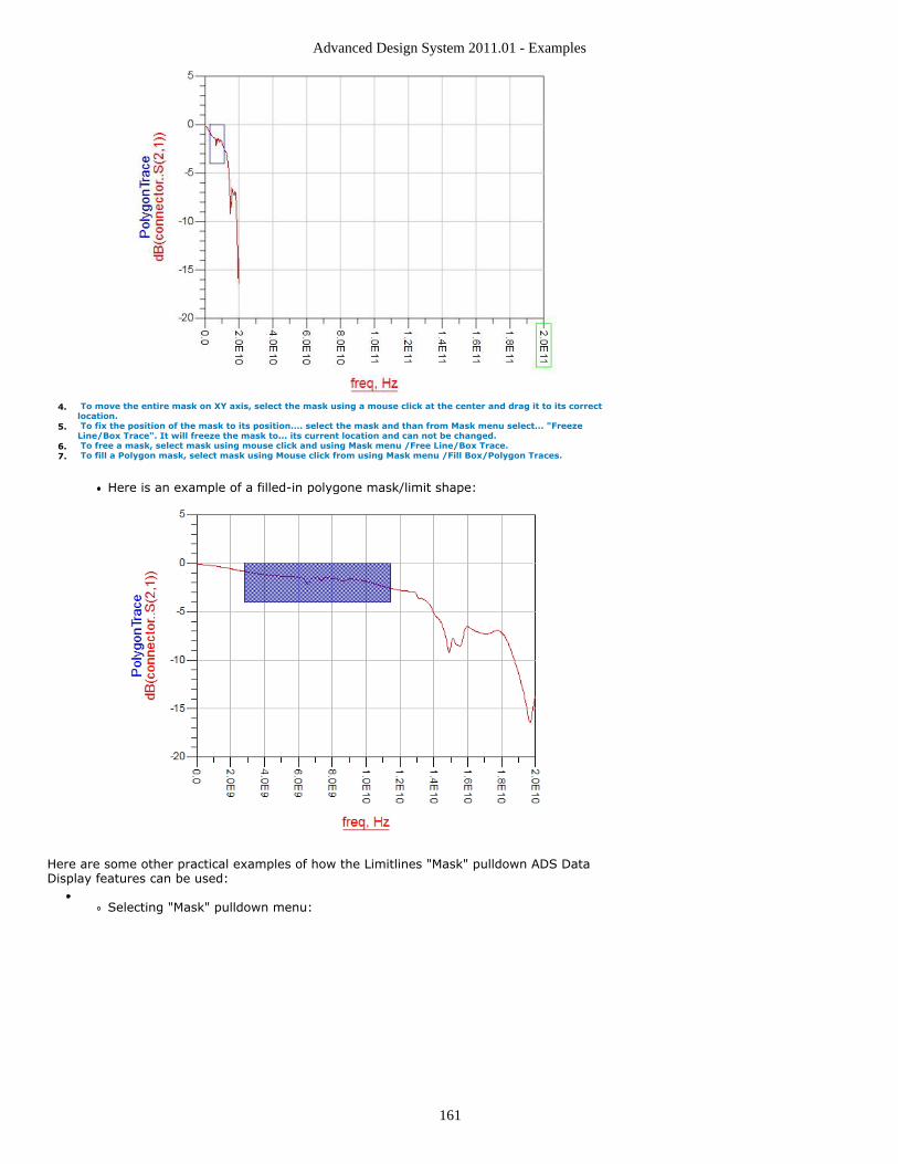
Advanced Design System 2011.01 - Examples
161
To move the entire mask on XY axis, select the mask using a mouse click at the center and drag it to its correctlocation.
4.
To fix the position of the mask to its position.... select the mask and than from Mask menu select... "FreezeLine/Box Trace". It will freeze the mask to... its current location and can not be changed.
5.
To free a mask, select mask using mouse click and using Mask menu /Free Line/Box Trace.6. To fill a Polygon mask, select mask using Mouse click from using Mask menu /Fill Box/Polygon Traces.7.
Here is an example of a filled-in polygone mask/limit shape:
Here are some other practical examples of how the Limitlines "Mask" pulldown ADS DataDisplay features can be used:
Selecting "Mask" pulldown menu:
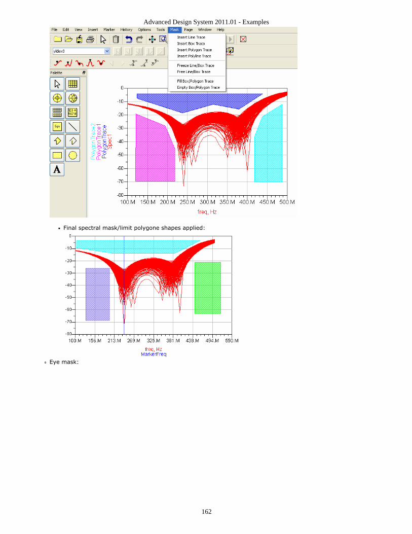
Advanced Design System 2011.01 - Examples
162
Final spectral mask/limit polygone shapes applied:
Eye mask:
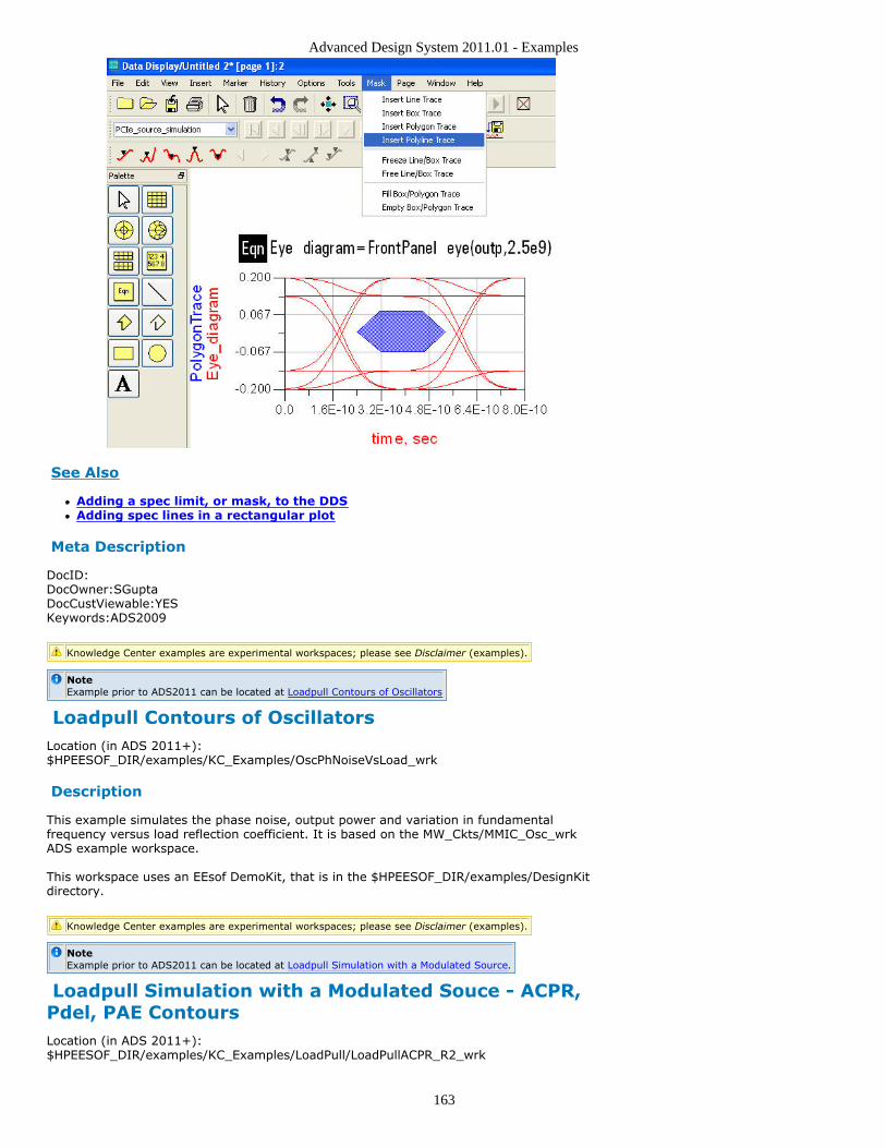
Advanced Design System 2011.01 - Examples
163
See Also
Adding a spec limit, or mask, to the DDSAdding spec lines in a rectangular plot
Meta Description
DocID:DocOwner:SGuptaDocCustViewable:YESKeywords:ADS2009
Knowledge Center examples are experimental workspaces; please see Disclaimer (examples).
NoteExample prior to ADS2011 can be located at Loadpull Contours of Oscillators
Loadpull Contours of OscillatorsLocation (in ADS 2011+):$HPEESOF_DIR/examples/KC_Examples/OscPhNoiseVsLoad_wrk
Description
This example simulates the phase noise, output power and variation in fundamentalfrequency versus load reflection coefficient. It is based on the MW_Ckts/MMIC_Osc_wrkADS example workspace.
This workspace uses an EEsof DemoKit, that is in the $HPEESOF_DIR/examples/DesignKitdirectory.
Knowledge Center examples are experimental workspaces; please see Disclaimer (examples).
NoteExample prior to ADS2011 can be located at Loadpull Simulation with a Modulated Source.
Loadpull Simulation with a Modulated Souce - ACPR,Pdel, PAE ContoursLocation (in ADS 2011+):$HPEESOF_DIR/examples/KC_Examples/LoadPull/LoadPullACPR_R2_wrk
Advanced Design System 2011.01 - Examples
164
Description
This example shows how to do loadpull simulations while using a CDMA 2000 signalsource. (It could be modified to use other modulated signal sources.) These simulationsgenerate contours that indicate load impedances that, when presented to the output of adevice (along with the specified source impedances and available source power), wouldcause a certain power to be delivered to the load. Contours for ACPR, power delivered,and power-added efficiency (PAE) are all generated.
The PAE (power-added efficiency) calculation has been updated.
See Also
If you have ADS, from any schematic, select DesignGuide > Loadpull > WCDMALoadpull > Constant Power Delivered... for better examples.
Knowledge Center examples are experimental workspaces; please see Disclaimer (examples).
See also: Simple Sourcepull and Loadpull Explained (examples).
NoteExample prior to ADS2011 can be located at Macro Model S-Parameter Optimization.
Macro Model S-parameter Optimization from MultipleS-Parameter FilesLocation (in ADS 2011+):$HPEESOF_DIR/examples/KC_Examples/optim_multi_sparam_files_wrk
Description
This example is designed to solve the following problem: you have multiple S-parameterfiles (which may come from various sources, such as measurement, parametricsimulation, and so on). You want to optimize your macro model so that you will get theelement values of the model for each sparameter file.
The sparameter files in this example are named:spar_1.s2p, spar_2.s2p to spar_5.s2p.
To use this example you only need the S-parameter files and your macro-model. Theworkspace has one design called optim_sp.
Under the data folder you will find the touchstone .s2p files.
Optim_sp consists of: a var block that reads by means of a DAC the touchstone .s2p files,a special variable that sweeps the file name as a function of sweep index, a measurementequation to create the optimization goals, a sweep parameter, a simulation SP, and theoptimizer.
The optimization method we use here is: for each sweep index, we optimize the modeland keep the last optimization value for display.
In this example the value of the PI capacitor is being optimized and its value will be 1 to5. This is the same as optimization index and it is like this just for simplicity.
In data display you will see OPTSOLNVALS.c1, which is a function of index and has thefinal optimized capacitor C1 values.
Meta Description
EX: Create Multiple S-parameter files from a Sweep S-parameter Simulation
Knowledge Center examples are experimental workspaces; please see Disclaimer (examples).
NoteExample prior to ADS2011 can be located at Measuring Transient Settling Time.
Measuring the Settling Time of a Transient SignalLocation (in ADS 2011+): $HPEESOF_DIR/examples/KC_Examples/T_SettleR2_wrk
Description
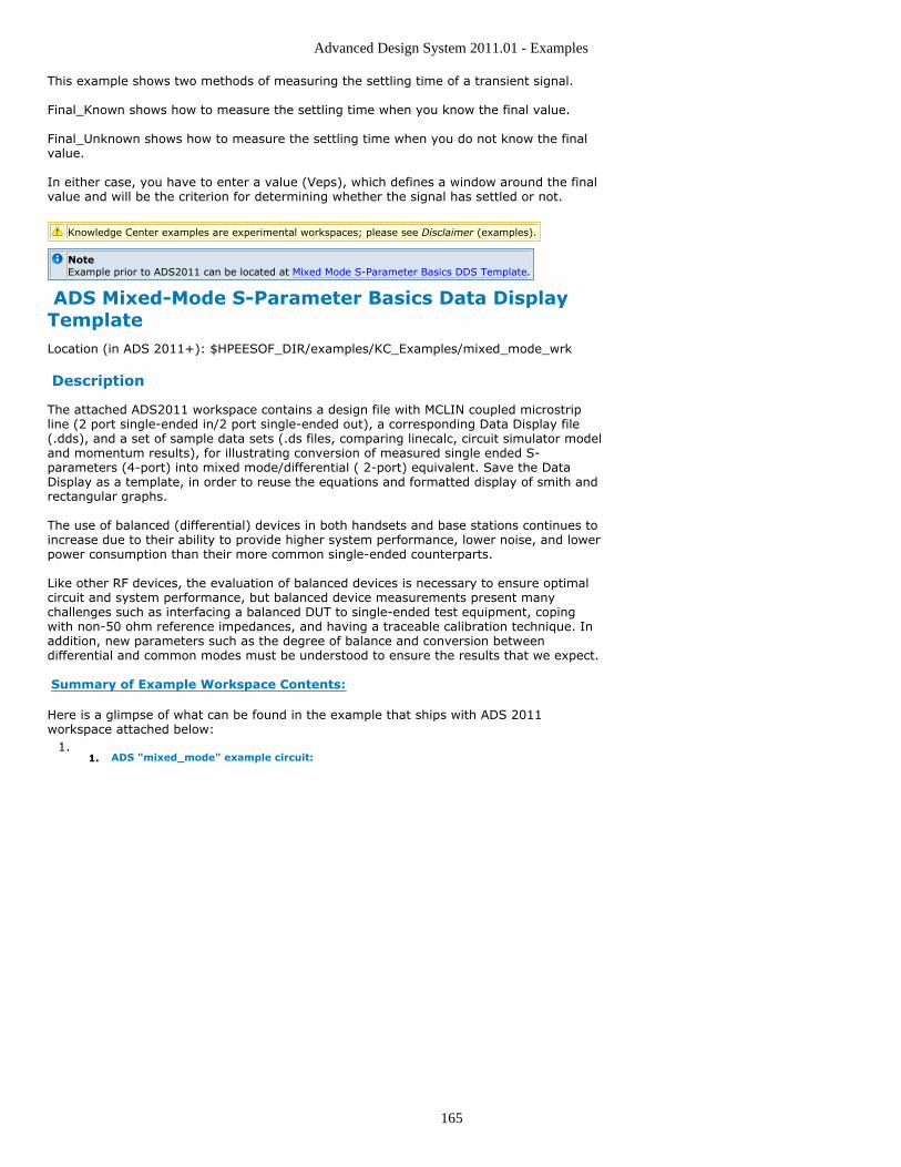
Advanced Design System 2011.01 - Examples
165
This example shows two methods of measuring the settling time of a transient signal.
Final_Known shows how to measure the settling time when you know the final value.
Final_Unknown shows how to measure the settling time when you do not know the finalvalue.
In either case, you have to enter a value (Veps), which defines a window around the finalvalue and will be the criterion for determining whether the signal has settled or not.
Knowledge Center examples are experimental workspaces; please see Disclaimer (examples).
NoteExample prior to ADS2011 can be located at Mixed Mode S-Parameter Basics DDS Template.
ADS Mixed-Mode S-Parameter Basics Data DisplayTemplateLocation (in ADS 2011+): $HPEESOF_DIR/examples/KC_Examples/mixed_mode_wrk
Description
The attached ADS2011 workspace contains a design file with MCLIN coupled microstripline (2 port single-ended in/2 port single-ended out), a corresponding Data Display file(.dds), and a set of sample data sets (.ds files, comparing linecalc, circuit simulator modeland momentum results), for illustrating conversion of measured single ended S-parameters (4-port) into mixed mode/differential ( 2-port) equivalent. Save the DataDisplay as a template, in order to reuse the equations and formatted display of smith andrectangular graphs.
The use of balanced (differential) devices in both handsets and base stations continues toincrease due to their ability to provide higher system performance, lower noise, and lowerpower consumption than their more common single-ended counterparts.
Like other RF devices, the evaluation of balanced devices is necessary to ensure optimalcircuit and system performance, but balanced device measurements present manychallenges such as interfacing a balanced DUT to single-ended test equipment, copingwith non-50 ohm reference impedances, and having a traceable calibration technique. Inaddition, new parameters such as the degree of balance and conversion betweendifferential and common modes must be understood to ensure the results that we expect.
Summary of Example Workspace Contents:
Here is a glimpse of what can be found in the example that ships with ADS 2011workspace attached below:
1. ADS "mixed_mode" example circuit:1.
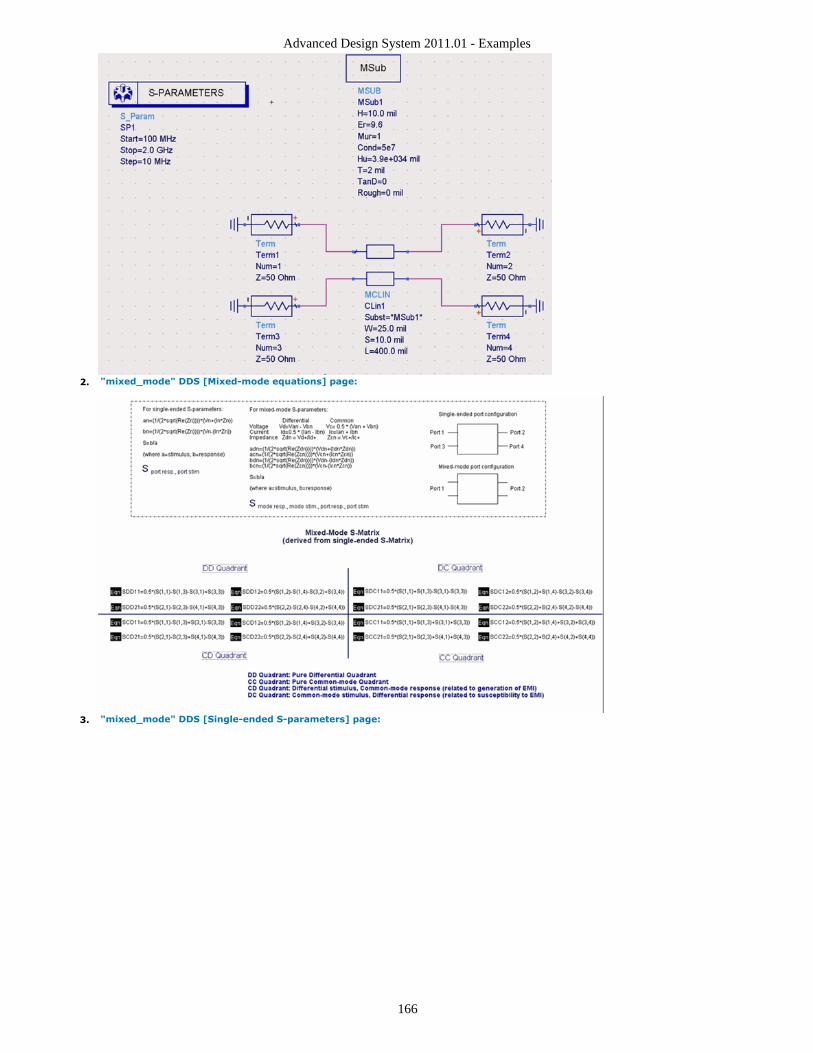
Advanced Design System 2011.01 - Examples
166
"mixed_mode" DDS [Mixed-mode equations] page:2.
"mixed_mode" DDS [Single-ended S-parameters] page:3.
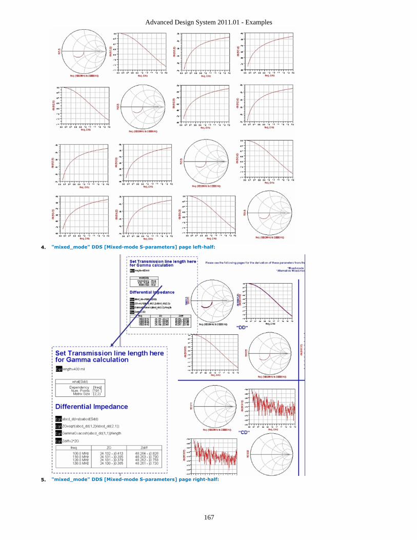
Advanced Design System 2011.01 - Examples
167
"mixed_mode" DDS [Mixed-mode S-parameters] page left-half:4.
"mixed_mode" DDS [Mixed-mode S-parameters] page right-half:5.
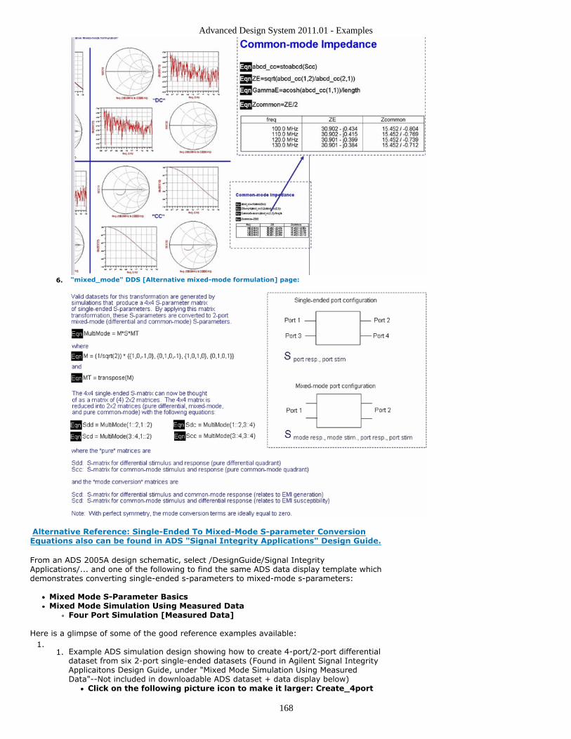
Advanced Design System 2011.01 - Examples
168
"mixed_mode" DDS [Alternative mixed-mode formulation] page:6.
Alternative Reference: Single-Ended To Mixed-Mode S-parameter ConversionEquations also can be found in ADS "Signal Integrity Applications" Design Guide.
From an ADS 2005A design schematic, select /DesignGuide/Signal IntegrityApplications/... and one of the following to find the same ADS data display template whichdemonstrates converting single-ended s-parameters to mixed-mode s-parameters:
Mixed Mode S-Parameter BasicsMixed Mode Simulation Using Measured Data
Four Port Simulation [Measured Data]
Here is a glimpse of some of the good reference examples available:1.
Example ADS simulation design showing how to create 4-port/2-port differential1.dataset from six 2-port single-ended datasets (Found in Agilent Signal IntegrityApplicaitons Design Guide, under "Mixed Mode Simulation Using MeasuredData"--Not included in downloadable ADS dataset + data display below)
Click on the following picture icon to make it larger: Create_4port
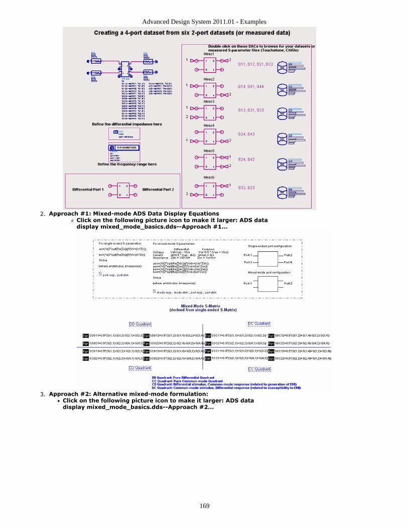
Advanced Design System 2011.01 - Examples
169
Approach #1: Mixed-mode ADS Data Display Equations2.Click on the following picture icon to make it larger: ADS datadisplay mixed_mode_basics.dds--Approach #1...
Approach #2: Alternative mixed-mode formulation:3.Click on the following picture icon to make it larger: ADS datadisplay mixed_mode_basics.dds--Approach #2...
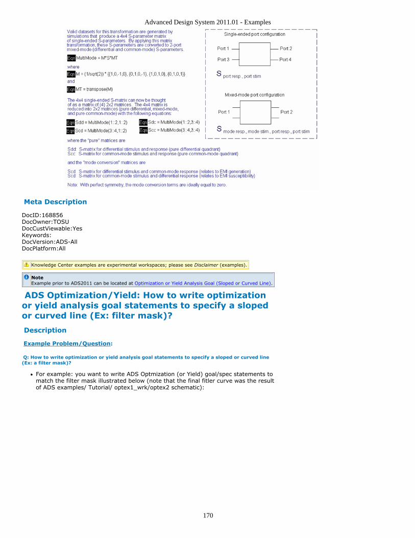
Advanced Design System 2011.01 - Examples
170
Meta Description
DocID:168856DocOwner:TOSUDocCustViewable:YesKeywords:DocVersion:ADS-AllDocPlatform:All
Knowledge Center examples are experimental workspaces; please see Disclaimer (examples).
NoteExample prior to ADS2011 can be located at Optimization or Yield Analysis Goal (Sloped or Curved Line).
ADS Optimization/Yield: How to write optimizationor yield analysis goal statements to specify a slopedor curved line (Ex: filter mask)?
Description
Example Problem/Question:
Q: How to write optimization or yield analysis goal statements to specify a sloped or curved line(Ex: a filter mask)?
For example: you want to write ADS Optmization (or Yield) goal/spec statements tomatch the filter mask illustrated below (note that the final fitler curve was the resultof ADS examples/ Tutorial/ optex1_wrk/optex2 schematic):
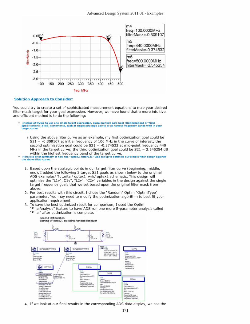
Advanced Design System 2011.01 - Examples
171
Solution Approach to Consider:
You could try to create a set of sophisticated measurement equations to map your desiredfilter mask target for your goal expression. However, we have found that a more intuitiveand efficient method is to do the following:
Instead of trying to use one single target expression, place multiple ADS Goal (Optimization) or YieldSpecifications (Yield) statements, each at single strategic points or at narrow frequency bands with in yourtarget curve.
Using the above filter curve as an example, my first optimization goal could beS21 = -0.309107 at initial frequency of 100 MHz in the curve of interest; thesecond optimization goal could be S21 = -0.374532 at mid-point frequency 440MHz in the target curve; the third optimization goal could be S21 = 2.545254 dBwithin the highest frequency band of the target curve.
Here is a brief summary of how the "optex2_filterS21" was set up to optimize our simple filter design againstthe above filter curve:
Based upon the strategic points in our target filter curve (beginning, middle,1.end), I added the following 3 target S21 goals as shown below to the originalADS examples/ Tutorital/ optex1_wrk/ optex2 schematic. This design willoptimize the "L1v", C1v", "L2v", "C2v" variables in the design against the singletarget frequency goals that we set based upon the original filter mask fromabove.For best results with this circuit, I chose the "Random" Optim "OptimType"2.parameter. You may need to modify the optimization algorithm to best fit yourapplication requirement.To save the best optimized result for comparison, I used the Optim3."FinalAnalysis" feature to have ADS run one more S-parameter analysis called"Final" after optimization is complete.
If we look at our final results in the corresponding ADS data display, we see the4.
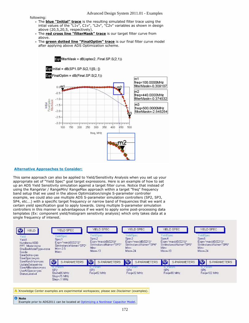
Advanced Design System 2011.01 - Examples
172
following:The blue "Initial" trace is the resulting simulated filter trace using theintial values of the "L1v", C1v", "L2v", "C2v" variables as shown in designabove (20,5,20,5, respectively).The red cross line "filterMask" trace is our target filter curve fromabove.The green dotted line "FinalOptim" trace is our final filter curve modelafter applying above ADS Optimization scheme.
Alternative Approaches to Consider:
This same approach can also be applied to Yield/Sensitivity Analysis when you set up yourappropriate set of "Yield Spec" goal target expressions. Here is an example of how to setup an ADS Yield Sensitivity simulation against a target filter curve. Notice that instead ofusing the RangeVar / RangeMin/ RangeMax approach within a target "freq" frequencyband setup that we used in the above Optimization/single S-parameter controllerexample, we could also use multiple ADS S-parameter simulation controllers (SP2, SP3,SP4, etc...) with a specific target frequency or narrow band of frequencies that we want acertain yield specification goal to apply towards. Using multiple S-parameter simulationcontrollers in this manner is advantageous if we want to apply some post-processing datatemplates (Ex: component yield/histogram sensitivity analysis) which only takes data at asingle frequency of interest.
Knowledge Center examples are experimental workspaces; please see Disclaimer (examples).
NoteExample prior to ADS2011 can be located at Optimizing a Nonlinear Capacitor Model.
Advanced Design System 2011.01 - Examples
173
Optimizing a Nonlinear Model of a Capacitor to MatchBias-Dependent S-Parameter DataLocation (in ADS 2011+):$HPEESOF_DIR/examples/KC_Examples/NonlinearC_L_Modeling_wrk
Description
This example shows how to optimize a nonlinear model of a capacitor to match bias-dependent S-parameter data. The same technique could be used to generate some othernonlinear model, such as a nonlinear inductor.
A simple nonlinear inductor model, implemented with an SDD (Symbolically-DefinedDevice) is included.
Knowledge Center examples are experimental workspaces; please see Disclaimer (examples).
NoteExample prior to ADS2011 can be located at PCI Express Examples Workshop
PCI Express Examples/WorkshopLocation (in ADS 2011+): $HPEESOF_DIR/examples/KC_Examples/PCI_Express/PCIE.DEB
Description
The PCI Express workshop provides the PCI express related simulation examples forADS2011 in a design guide form. The .deb file can be installed using ADS mainwindow>DesignGuide> Add DesignGuide menu
The installation allows both global and personal installation.
Once installed it will appear under DesignGuide window of your RF/Analog Schematicpage.
Knowledge Center examples are experimental workspaces; please see Disclaimer (examples).
NoteExample prior to ADS2011 can be located at PLL Example with an Active Filter.
PLL Example with an Active FilterLocation (in ADS 2011+): $HPEESOF_DIR/examples/KC_Examples/pll_testR1_wrk
Description
This example contains one design: PLL_tranAH shows the transient response simulation ofa simple, behavioral PLL with an active filter. After a brief delay at the start, the divideratio is stepped and the transient response of the loop is shown.
The reference and divided VCO signals (phases) are in phase at the input to thephase/frequency detector, and vtune is stable, at 0 V at time=0, so there is no turn-ontransient.
There are other PLLs with active filters in the PLL DesignGuide.
Knowledge Center examples are experimental workspaces; please see Disclaimer (examples).
NoteExample prior to ADS2011 can be located at Save Simulation Data to ASCII.
Save Simulation Data to ASCII File Directly(writepara)Location (in ADS 2011+): $HPEESOF_DIR/examples/KC_Examples/writepara_wrk
Description
These AEL expressions export the passed data to a text file.
Advanced Design System 2011.01 - Examples
174
You can write a Measurement Equation on a schematic window and pass the parametersthat you wish to export. For example:
X = writepara2d("c:/temp/data.txt", "W", "My Simulation Data", ",", freq,
db(S21))
This was developed as a way to export data to a text file in ADS 1.1. ADS 1.3 solved thatproblem by providing a way to export listings in the Data Display. However, there areother types of applications for this script. In swept optimizations, for example, you canuse this script to write the best values out to a text file after each parameter iteration. Youcan also use it to export the simulation data to a third party tool and bypass the ADS DataDisplay entirely.
The workspace writepara.7zap contains several examples on how to use the writepara()functions.
NoteIn ADS 2003C and later you can use the built-in function write_snp() to write Touchstone files from S-parameter data. In ADS 2004A and later there is a built-in function called write_var() which is similar towritepara2d().
Knowledge Center examples are experimental workspaces; please see Disclaimer (examples).
NoteExample prior to ADS2011 can be located at Simple Sourcepull and Loadpull Explained
Simple Sourcepull and Loadpull ExplainedLocation (in ADS 2011+):$HPEESOF_DIR/examples/KC_Examples/Loadpull/LOADNSOURCEPULL_wrk
Description
This example workspace provides an alternative to the source pull and load pull examplesin ADS. The set up is straightforward and allows users to familiarize themselves with thisconcept in ADS.
Updated 08-20-2003
See Also
Loadpull DesignGuide for ADS 2009 Update 1 with new content (This is the most advancedLoad Pull DesignGuide for use with ADS 2009 Update 1, but it does not have theenhancements of the ADS 2011 version.)
Knowledge Center examples are experimental workspaces; please see Disclaimer (examples).
See also: Loadpull Simulation with a Modulated Source (examples).
NoteExample prior to ADS2011 can be located at SI Primer part 1 of 2 Convolution.
ADS [Signal Integrity Primer 1/2]: Basic Principles ofConvolutionLocation ( in ADS 2011+):$HPEESOF_DIR/examples/KC_Examples/ConvolutionBasics_2006U1_wrk
Description
Q: Where can I find some basic ADS examples for analyzing convolved signals?
For the most comprehensive walk-through, hands-on labs we recommend you considertaking one of the following Signal Integrity training courses offered by the Agilent EEsofCustomer Education team:
N3215A: Designing for Signal Integrity with Advanced Design SystemN3216A: Designing for Signal Integrity with Advanced Design System 2
The following excerpts provide an introduction to some of the deeper analysistools that you can master quicker by taking an EEsof training course such asN3215A.

Advanced Design System 2011.01 - Examples
175
What Is Convolution?
Time-domain simulation – requires time-domain component characterizationMany components – frequency-domain characterizationConvolution engine performs the following tasks:
Detects components defined in the frequency-domainCalculates impulse response from frequency responseConvolves input signal with impulse response (time-domain process)
All these – as part of transient simulation, transparent to the user
Time-to/from-Frequency Conversions
Time-to-frequency (time-waveform to spectrum)*
the fs() functionimplements a Fourier Transform (like a spectrum analyzer)
Eqn Vspectrum=fs(Vtime)
Frequency-to-time (spectrum to time-waveform)*
the ts() functionImplements an Inverse Fourier Transform
Eqn Vtime=ts(Vspectrum)
Time-Step versus Span
Time-step small enough to capture all high-frequency variationsSpan large enough to capture all frequency-domain energyMaximum time-step (Nyquist): MaxTimeStep = 1/(2*Span)Recommended: Timestep <= 1/(5*Span)
Time-Length versus RBW (Resolution Bandwidth)
Time-length long enough to ensure IR goes to 0RBW small enough to capture all relevant spectral componentsTimeLength = 1/RBW
Creating an S-Parameter Model for Convolution
From simulations or from measurement (network-analyzer)Set span large enough to capture highest freq componentSet RBW small enough to capture variations of freq responseSave the S-parameters in a fileAdd/review the DC point in the S-parameter file
Impulse versus Frequency Response
The hierarchical design shown on this slide is used to compare the impulse response andthe frequency response of the filter when AC simulation is used.
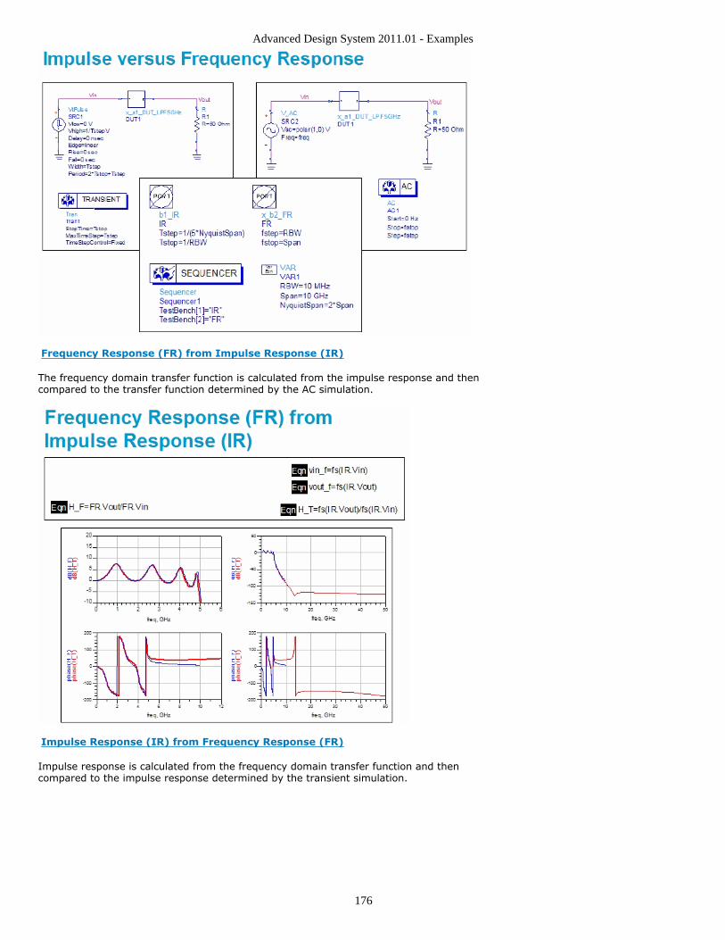
Advanced Design System 2011.01 - Examples
176
Frequency Response (FR) from Impulse Response (IR)
The frequency domain transfer function is calculated from the impulse response and thencompared to the transfer function determined by the AC simulation.
Impulse Response (IR) from Frequency Response (FR)
Impulse response is calculated from the frequency domain transfer function and thencompared to the impulse response determined by the transient simulation.
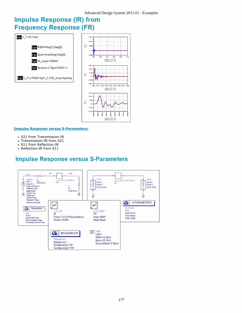
Advanced Design System 2011.01 - Examples
177
Impulse Response versus S-Parameters:
S21 from Transmission-IRTransmission-IR from S21S11 from Reflection-IRReflection-IR from S11
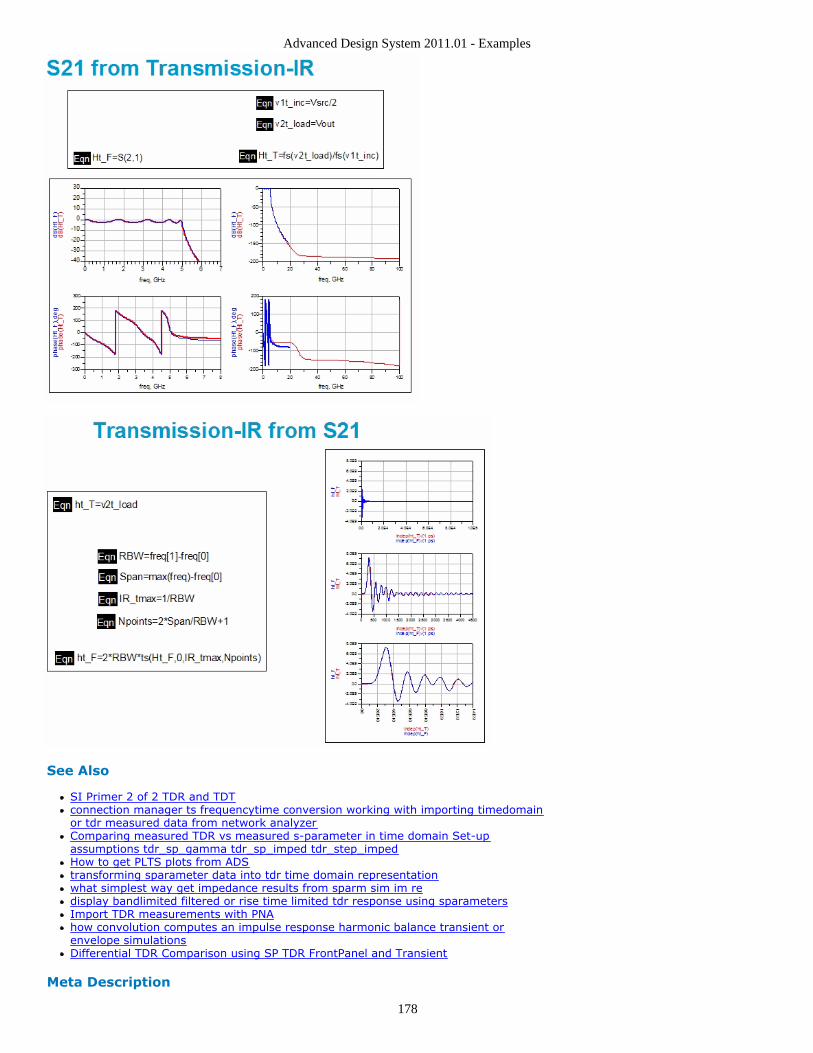
Advanced Design System 2011.01 - Examples
178
See Also
SI Primer 2 of 2 TDR and TDTconnection manager ts frequencytime conversion working with importing timedomainor tdr measured data from network analyzerComparing measured TDR vs measured s-parameter in time domain Set-upassumptions tdr_sp_gamma tdr_sp_imped tdr_step_impedHow to get PLTS plots from ADStransforming sparameter data into tdr time domain representationwhat simplest way get impedance results from sparm sim im redisplay bandlimited filtered or rise time limited tdr response using sparametersImport TDR measurements with PNAhow convolution computes an impulse response harmonic balance transient orenvelope simulationsDifferential TDR Comparison using SP TDR FrontPanel and Transient
Meta Description
Advanced Design System 2011.01 - Examples
179
DocID:316598DocOwner:MKNUTSONDocCustViewable:YesKeywords:Basic Principles of Convolution Signal Integrity SIDocVersion:ADS2008,ADS-AllDocPlatform:All <#comment>
Knowledge Center examples are experimental workspaces; please see Disclaimer (examples).
NoteExample prior to ADS2011 can be located at SI Primer 2 of 2 TDR and TDT.
ADS [Signal Integrity Primer 2 of 2]: TDR/TDTSimulations and MeasurementsLocation (in ADS2011+): $HPEESOF_DIR/examples/KC_Examples/TDR_2006U1_wrk
Description
Q: Where can I find some basic ADS examples for generating and analyzingTDR(Time-Domain Reflectometry)/TDT(Time-Domain Transmission) stimulus,response?
For the most comprehensive walk-through, hands-on labs we recommend you considertaking one of the following Signal Integrity training courses offered by the Agilent EEsofCustomer Education team:
N3215A: Designing for Signal Integrity with Advanced Design SystemN3216A: Designing for Signal Integrity with Advanced Design System 2
The following excerpts provide a glimpse of some of the deeper analysis toolsthat you can master faster by taking an EEsof training course such as N3215A.
Delayed Reflections
Both the input and output voltage-waveforms show a staircase shape. This is caused bythe reflections on various discontinuities in the circuit, combined with the time necessaryfor these reflections to propagate through the system.
The observation of such effects at the input of the system is usually referred to asTDR, or Time-Domain Reflectometer.The observation of such effects at the output of the system is usually referred to asTDT, or Time-Domain Transmission.
TDR Simulations and Measurements
Detect discontinuitiesLocate discontinuities = distance from inputQuantify discontinuities = calculate Z0 after discontinuity, when Z0 beforediscontinuity is known
TDR - Locate/Quantify Discontinuities
Measure time-delayKnown propagation-speed (?)Propagation speed:Conventional structures; known formulas for prop.-speed (theoretical calculations)Un-conventional structures; calibration (simulations / measurements)
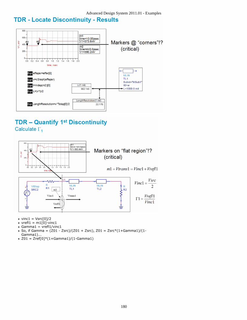
Advanced Design System 2011.01 - Examples
180
vinc1 = Vsrc[0]/2vrefl1 = m1[0]-vinc1Gamma1 = vrefl1/vinc1So, if Gamma = (Z01 - Zsrc)/(Z01 + Zsrc), Z01 = Zsrc*(1+Gamma1)/(1-Gamma1)...Z01 = Zref[0]*(1+Gamma1)/(1-Gamma1)
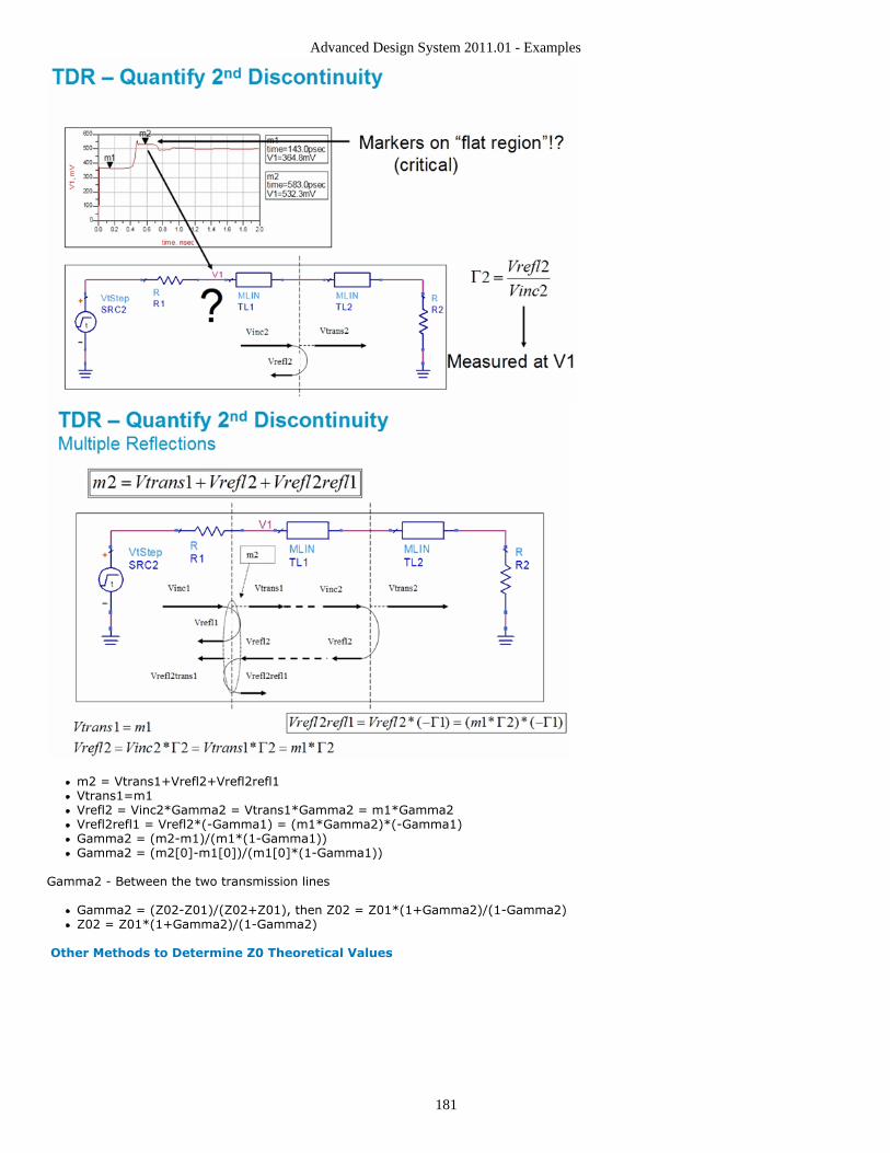
Advanced Design System 2011.01 - Examples
181
m2 = Vtrans1+Vrefl2+Vrefl2refl1Vtrans1=m1Vrefl2 = Vinc2*Gamma2 = Vtrans1*Gamma2 = m1*Gamma2Vrefl2refl1 = Vrefl2*(-Gamma1) = (m1*Gamma2)*(-Gamma1)Gamma2 = (m2-m1)/(m1*(1-Gamma1))Gamma2 = (m2[0]-m1[0])/(m1[0]*(1-Gamma1))
Gamma2 - Between the two transmission lines
Gamma2 = (Z02-Z01)/(Z02+Z01), then Z02 = Z01*(1+Gamma2)/(1-Gamma2)Z02 = Z01*(1+Gamma2)/(1-Gamma2)
Other Methods to Determine Z0 Theoretical Values
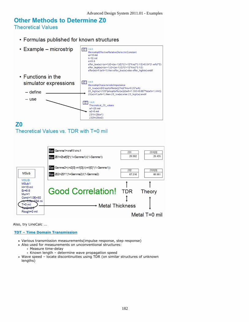
Advanced Design System 2011.01 - Examples
182
Also, try LineCalc ...
TDT – Time Domain Transmission
Various transmission measurements(impulse response, step response)Also used for measurements on unconventional structures:
Measure time-delayKnown length – determine wave propagation speed
Wave speed – locate discontinuities using TDR (on similar structures of unknownlengths)
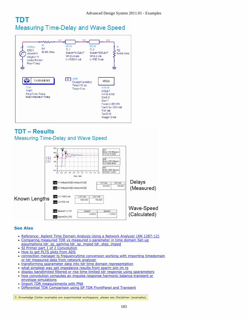
Advanced Design System 2011.01 - Examples
183
See Also
Reference: Agilent Time Domain Analysis Using a Network Analyzer (AN 1287-12)Comparing measured TDR vs measured s-parameter in time domain Set-upassumptions tdr_sp_gamma tdr_sp_imped tdr_step_impedSI Primer part 1 of 2 ConvolutionHow to get PLTS plots from ADSconnection manager ts frequencytime conversion working with importing timedomainor tdr measured data from network analyzertransforming sparameter data into tdr time domain representationwhat simplest way get impedance results from sparm sim im redisplay bandlimited filtered or rise time limited tdr response using sparametershow convolution computes an impulse response harmonic balance transient orenvelope simulationsImport TDR measurements with PNADifferential TDR Comparison using SP TDR FrontPanel and Transient
Knowledge Center examples are experimental workspaces; please see Disclaimer (examples).
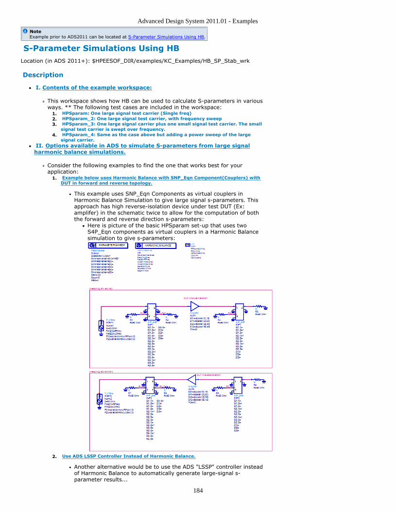
Advanced Design System 2011.01 - Examples
184
NoteExample prior to ADS2011 can be located at S-Parameter Simulations Using HB.
S-Parameter Simulations Using HBLocation (in ADS 2011+): $HPEESOF_DIR/examples/KC_Examples/HB_SP_Stab_wrk
Description
I. Contents of the example workspace:
This workspace shows how HB can be used to calculate S-parameters in variousways. ** The following test cases are included in the workspace:
HPSparam: One large signal test carrier (Single freq)1. HPSparam_2: One large signal test carrier, with frequency sweep2. HPSparam_3: One large signal carrier plus one small signal test carrier. The smallsignal test carrier is swept over frequency.
3.
HPSparam_4: Same as the case above but adding a power sweep of the largesignal carrier.
4.
II. Options available in ADS to simulate S-parameters from large signalharmonic balance simulations.
Consider the following examples to find the one that works best for yourapplication:
Example below uses Harmonic Balance with SNP_Eqn Component(Couplers) withDUT in forward and reverse topology.
1.
This example uses SNP_Eqn Components as virtual couplers inHarmonic Balance Simulation to give large signal s-parameters. Thisapproach has high reverse-isolation device under test DUT (Ex:amplifer) in the schematic twice to allow for the computation of boththe forward and reverse direction s-parameters:
Here is picture of the basic HPSparam set-up that uses twoS4P_Eqn components as virtual couplers in a Harmonic Balancesimulation to give s-parameters:
Use ADS LSSP Controller Instead of Harmonic Balance.2.
Another alternative would be to use the ADS "LSSP" controller insteadof Harmonic Balance to automatically generate large-signal s-parameter results...
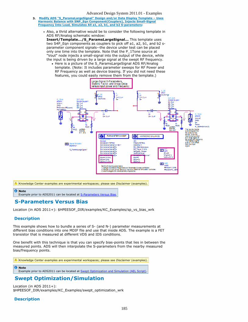
Advanced Design System 2011.01 - Examples
185
Modify ADS "S_ParamsLargeSignal" Design and/or Data Display Template – UsesHarmonic Balance with SNP_Eqn Component(Couplers), Injects Small-SignalFrequency Into Load, Simulates All a1, a2, b1, and b2 S-parameters:
3.
Also, a thrid alternative would be to consider the following template inADS RF/Analog schematic window:Insert/Template.../S_ParamsLargeSignal... This template usestwo S4P_Eqn components as couplers to pick off a1, a2, b1, and b2 s-parameter component signals--the device under test can be placedonly one time into the template. Note that the P_1Tone source at"Vout" node injects a small-signal into the output of the device, whilethe input is being driven by a large signal at the swept RF frequency.
Here is a picture of the S_ParamsLargeSignal ADS RF/Analogtemplate. (Note: It includes parameter sweeps for RF Power andRF Frequency as well as device biasing. If you did not need thesefeatures, you could easily remove them from the template.)
Knowledge Center examples are experimental workspaces; please see Disclaimer (examples).
NoteExample prior to ADS2011 can be located at S-Parameters Versus Bias.
S-Parameters Versus BiasLocation (in ADS 2011+): $HPEESOF_DIR/examples/KC_Examples/sp_vs_bias_wrk
Description
This example shows how to bundle a series of S- (and N-) parameter measurements atdifferent bias conditions into one MDIF file and use that inside ADS. The example is a FETtransistor that is measured at different VDS and IDS conditions.
One benefit with this technique is that you can specify bias-points that lies in between themeasured points. ADS will then interpolate the S-parameters from the nearby measuredbias/frequency points.
Knowledge Center examples are experimental workspaces; please see Disclaimer (examples).
NoteExample prior to ADS2011 can be located at Swept Optimization and Simulation (AEL Script).
Swept Optimization/SimulationLocation (in ADS 2011+):$HPEESOF_DIR/examples/KC_Examples/swept_optimization_wrk
Description
Advanced Design System 2011.01 - Examples
186
Problem: You have a set of different files of measured S-parameters and you need tocreate a matching network to match them to 50 Ohms.
This example shows several different methods of doing this. sweptopt2 optimizationgenerates a different matching network for each of the different measured S-parameterfiles. sweptopt3 generates a single matching network that is optimized to work with all ofthe measured S-parameter files.
sweptopt_2_orig uses an AEL file to run the swept optimization (this was necessary up toADS 1.5 releases). It generates one generic MDIF file with all optimum values. There is noreason to use this unless you want to create an MDIF file.
Knowledge Center examples are experimental workspaces; please see Disclaimer (examples).
NoteExample prior to ADS2011 can be located at Synthesizing Geometries of Inductors.
Synthesizing Geometries of Inductors Based onDesired L and QLocation (in ADS 2011+):$HPEESOF_DIR/examples/KC_Examples/Inductor_Synthesis_wrk
Description
The design problem of interest to most users of spiral inductors, whether single(microstrip) or multilayer (LTCC, Silicon, RF Board), is to determine the geometry of sucha spiral based on a desired value of inductance, L, and quality factor, Q. Until recently,modeling of inductors was a very complex task with no real practical method to synthesizegeometries based on a specified L and Q. Due to the availability of Advanced ModelComposer, this synthesis task is now a practical possibility. This example file does notfocus on the generation of the required data, only on the synthesis aspect of the deviceusing contour functions in the data display window.
The example file contains a large dataset that is generated by doing a multi-dimensionalsweep of an AMC generated spiral model. The assumption is that one has a spiral with afixed spacing and fixed number of turns/layers in this data file, and that the AMC modelwas generated over a continuous width, W, and diameter, D. Then the circuit simulator isrun over the entire range of W, D, and freq to cover the complete design space.
A user goes to page "Synthesis" of the self_extract.dds file. First, the slider bars are usedto choose the frequency. Then one reads the possible values of L (min/max). Next, usingthe equation "self=4", the user types in a desired value of inductance. Finally, one slidesthe Q-value for this inductance. If unrealizable values are selected, then the contour plotswill display traces as "Invalid". If they are possible, then the user will find the redL_iso_synthesis trace and the blue Q_iso_synthesis trace. These are contours centeredaround a narrow range of the desired values. The magenta iso_L_extract1 and the cyaniso_Q_extract1 contours display the entire design space. If the synthesized L and Q tracesintersect, then a device with the specified properties is realizable by reading off thediameter on the X-axis and the width on the Y-axis. Note that the Y-axis is not labeled as"W" but instead shows the names of the contour traces.
Knowledge Center examples are experimental workspaces; please see Disclaimer (examples).
NoteExample prior to ADS2011 can be located at Time-Domain Optimization.
Time-Domain Optimization; Improving the Rise Timeof a SignalLocation (in ADS 2011+): $HPEESOF_DIR/examples/KC_Examples/FilterRiseTimeOpt_wrk
Description
This example shows three different ways of optimizing the rise time of a step signalpassing through a simple low-pass filter.
Low_Pass_Filter_Opt1 utilizes two TimeStamp components to measure when theoutput signal passes through the 10% and 90% thresholds. The filter 3-dBbandwidth, passband attenuation, and stopband attenuation are also included in theoptimization.
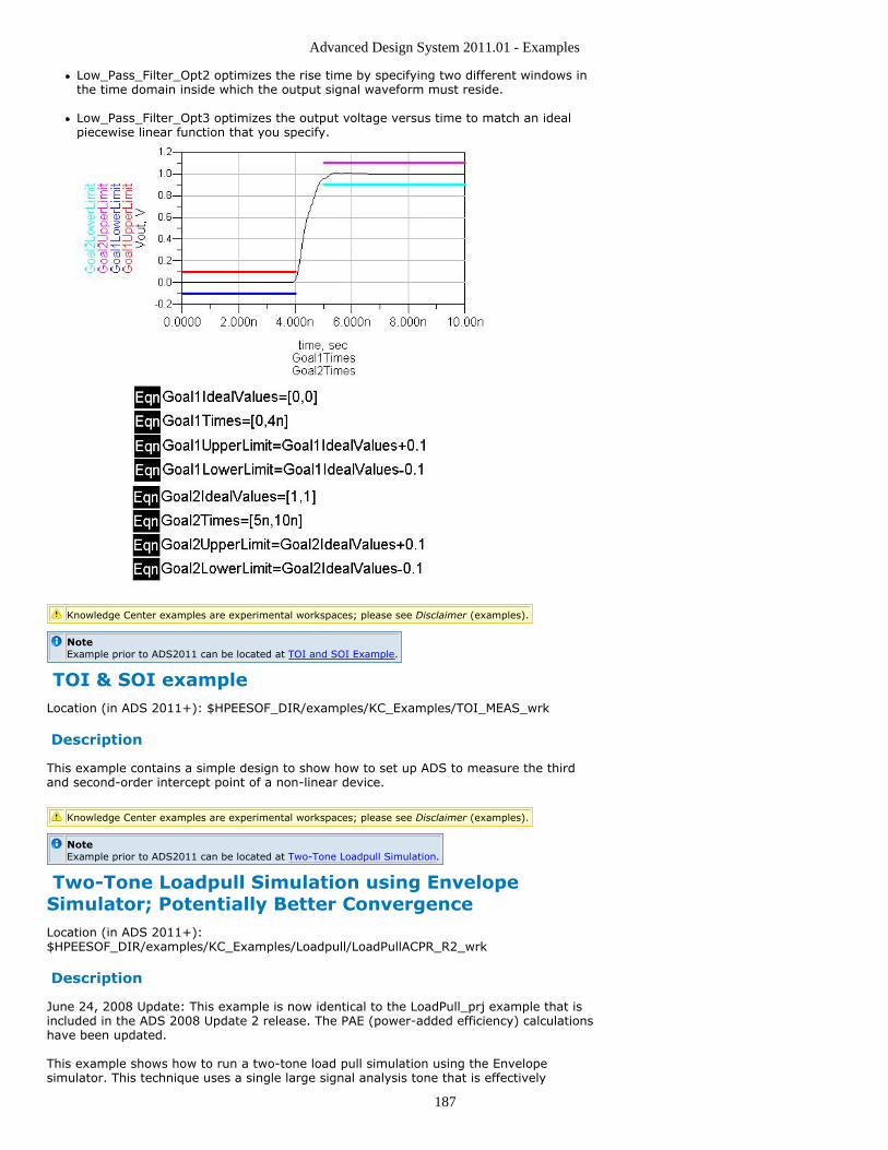
Advanced Design System 2011.01 - Examples
187
Low_Pass_Filter_Opt2 optimizes the rise time by specifying two different windows inthe time domain inside which the output signal waveform must reside.
Low_Pass_Filter_Opt3 optimizes the output voltage versus time to match an idealpiecewise linear function that you specify.
Knowledge Center examples are experimental workspaces; please see Disclaimer (examples).
NoteExample prior to ADS2011 can be located at TOI and SOI Example.
TOI & SOI exampleLocation (in ADS 2011+): $HPEESOF_DIR/examples/KC_Examples/TOI_MEAS_wrk
Description
This example contains a simple design to show how to set up ADS to measure the thirdand second-order intercept point of a non-linear device.
Knowledge Center examples are experimental workspaces; please see Disclaimer (examples).
NoteExample prior to ADS2011 can be located at Two-Tone Loadpull Simulation.
Two-Tone Loadpull Simulation using EnvelopeSimulator; Potentially Better ConvergenceLocation (in ADS 2011+):$HPEESOF_DIR/examples/KC_Examples/Loadpull/LoadPullACPR_R2_wrk
Description
June 24, 2008 Update: This example is now identical to the LoadPull_prj example that isincluded in the ADS 2008 Update 2 release. The PAE (power-added efficiency) calculationshave been updated.
This example shows how to run a two-tone load pull simulation using the Envelopesimulator. This technique uses a single large signal analysis tone that is effectively

Advanced Design System 2011.01 - Examples
188
amplitude modulated by the Envelope simulator to generate two tones. It uses lessmemory and may allow convergence at a higher input power level than when a two-toneharmonic balance load pull is run. This example includes comparisons between theharmonic balance and Envelope techniques, which show nearly identical results.
See Also
Loadpull DesignGuide for ADS 2009 Update 1 with new content (This is the most advancedLoad Pull DesignGuide for use with ADS 2009 Update 1, but it does not have theenhancements of the ADS 2011 version.)
Knowledge Center examples are experimental workspaces; please see Disclaimer (examples).
NoteExample prior to ADS2011 can be located at VCO Behavioral Model from Simulated Data.
VCO Behavioral Model from Simulated DataLocation (in ADS 2011+): $HPEESOF_DIR/examples/KC_Examples/VCO_BehModwPN_wrk
Description
This example shows how to reuse data (frequency, fundamental signal amplitude, andphase noise) from a transistor-level HB simulation of an oscillator, in a behavioral model.This type of model would be useful for simulating phase-locked loops with ADS.
VCO_HB simulates the transistor oscillator subcircuit (VCO_5_2GHz), versus tuningvoltage. The dataset includes frequency, amplitude and phase noise data.VCO_5_2GHz is a 5.2 GHz VCO that uses the eesofDemoKit PDK.VCOsubckt comes from the MOS_VCO_prj example in examples/RFIC, and is analternative VCO that could be used.VCO_Data is a behavioral model of the 5.2 GHz oscillator that re-uses theharmonic balance simulation results but does not include phase noise.test_VCO_Data simulates the behavioral model.VCOwPN_Data is the same as VCO_Data, except that it includes phase noise data inthe model.test_VCOwPN_Data simulates the phase noise generated by the behavioralmodel.
Knowledge Center examples are experimental workspaces; please see Disclaimer (examples).
NoteExample prior to ADS2011 can be located at Waveprobe Model to Measure Forward and Reverse Power.
Waveprobe Model to Measure the Forward andReverse Wave and also the Power DeliveredLocation (in ADS 2011+): $HPEESOF_DIR/examples/KC_Examples/WaveProbe_wrk
Description
The attached workspace shows the approach that uses a WaveProbe. It's inserted just likea current probe and has a single parameter Z0 todefine the characteristic wave impedance. It then computes and stores to the dataset theforward wave, the reverse wave, and the power delivered (in dBm).
In the dataset presentations, you can then define whatever ratio of these you would like:to show reflection/impedance at intermediate points, gain to intermediate points,delivered power, distortion, etc.
It should work for all analyses except for noise, unfortunately. For that, you probably stillneed the coupler or some other approach.
If you add a ParamSweep to switch the source from the input to the output, you couldthen compute and display forward and reverse parameters.
Changes were recently done to the original example and a method to do "impedanceprobing" has now been added.
There are 4 designs:

Advanced Design System 2011.01 - Examples
189
WaveProbe : Actual subcircuit which contains the equations to measure the forwardand reverse waves.TestWaveProbe : A Harmonic Balance simulation which shows the WaveProbecomponent being usedNetwork1 : Shows how to convert the reflection coefficient into an input impedance.Network2_SP : Shows how to use the SProbe element but this gives the small-signal input impedance.
Knowledge Center examples are experimental workspaces; please see Disclaimer (examples).

Advanced Design System 2011.01 - Examples
190
Microwave Circuit ExamplesExamples of how to create and analyze microwave, hybrid, and MMIC design solutions andapplications such as amplifiers, filters, mixers, oscillators, and subsystems.
2GHz BJT Low Noise Amplifier (examples)12GHz Two Section Microstrip Filter (examples)Computing ACPR, Modulated Output Power, and EVM from a 1-tone, Swept HarmonicBalance Simulation (examples)Design for Manufacturing Example Using Yield Sensitivity Histograms, DOE, andSensitivity Analysis (examples)Design of a 1GHz Low Noise Amplifier (examples)EM Simulation of MMIC passive components and circuits (examples)Large Signal Amplifier Simulations (examples)MMIC Amplifier (examples)MMIC Oscillator (examples)Optimizing A Linear FET Model to Match Measured S-Parameters (examples)Statistical Design of an X-Band LNA (examples)Test Lab for Two Stage Amplifier Design (examples)Using the Design Rule Checker (DRC) (examples)Using SP_Probes to design a simple, two-stage LNA (examples)Yield Sensitivity Histogram Design Templates (examples)Using Momentum to simulate an entire amplifier layout (examples)
2GHz BJT Low Noise AmplifierLocation: $HPEESOF_DIR/examples/MW_Ckts/LNA_wrk
Objective
This example shows a simple procedure for designing a low-noise amplifier. Thespecifications are: 3 V supply, 2 mA collector current, lowest noise at 2 GHz, gain > 10 dBat 2 GHz, input and output reflection coefficients better than -10 dB at 2 GHz andunconditionally stable.
Setup
"Curve_Tracer" simulates the collector current versus collector voltage with the base1.current swept as a parameter."DC_and_Sparams" shows a bias network design, and includes a simulation of the S-2.parameters and a calculation of the stability of the biased device."Gain_and_Stab_opt" shows the addition of an optimized stabilizing networks added3.to achieve unconditional stability, simulated from 0 to 3 GHz."Circles" simulates the S-parameters, noise parameters and stability parameters4.before the addition of input and output matching networks."Input_match" designs the input matching network to generate a source impedance5.that is a tradeoff between gain and noise figure."Amp_wInputMatch" shows a simulation of the amplifier with both stability networks6.and the input matching network added."Output_match" designs the output matching network for simultaneous conjugate7.match."Amp_wBothMatches" simulates the amplifier with stability networks and both8.matching networks added. The results are not as good as expected, so anoptimization is run next."Amp_wMatchOpt" is an optimization of the input and output matching component9.values to achieve a better gain, input match, and output match at 2 GHz, while notdegrading the noise figure."DC_OP_POINT" simulates the colelctor current versus base voltage, with the10.collector voltage set to 3 V.
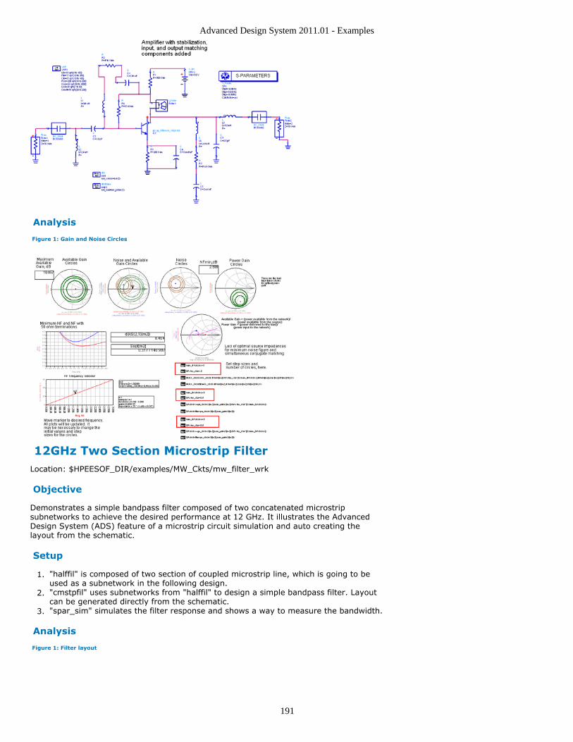
Advanced Design System 2011.01 - Examples
191
Analysis
Figure 1: Gain and Noise Circles
12GHz Two Section Microstrip FilterLocation: $HPEESOF_DIR/examples/MW_Ckts/mw_filter_wrk
Objective
Demonstrates a simple bandpass filter composed of two concatenated microstripsubnetworks to achieve the desired performance at 12 GHz. It illustrates the AdvancedDesign System (ADS) feature of a microstrip circuit simulation and auto creating thelayout from the schematic.
Setup
"halffil" is composed of two section of coupled microstrip line, which is going to be1.used as a subnetwork in the following design."cmstpfil" uses subnetworks from "halffil" to design a simple bandpass filter. Layout2.can be generated directly from the schematic."spar_sim" simulates the filter response and shows a way to measure the bandwidth.3.
Analysis
Figure 1: Filter layout
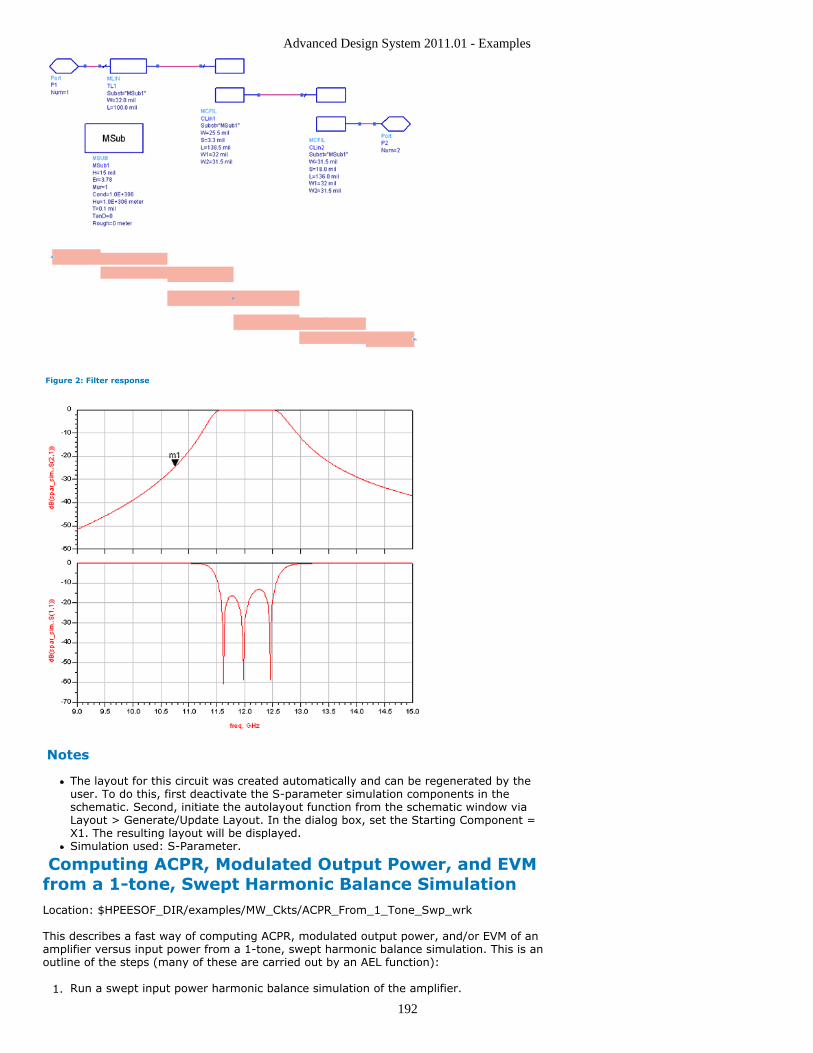
Advanced Design System 2011.01 - Examples
192
Figure 2: Filter response
Notes
The layout for this circuit was created automatically and can be regenerated by theuser. To do this, first deactivate the S-parameter simulation components in theschematic. Second, initiate the autolayout function from the schematic window viaLayout > Generate/Update Layout. In the dialog box, set the Starting Component =X1. The resulting layout will be displayed.Simulation used: S-Parameter.
Computing ACPR, Modulated Output Power, and EVMfrom a 1-tone, Swept Harmonic Balance SimulationLocation: $HPEESOF_DIR/examples/MW_Ckts/ACPR_From_1_Tone_Swp_wrk
This describes a fast way of computing ACPR, modulated output power, and/or EVM of anamplifier versus input power from a 1-tone, swept harmonic balance simulation. This is anoutline of the steps (many of these are carried out by an AEL function):
Run a swept input power harmonic balance simulation of the amplifier.1.
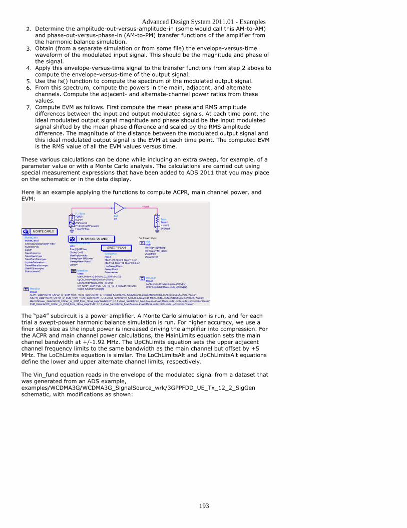
Advanced Design System 2011.01 - Examples
193
Determine the amplitude-out-versus-amplitude-in (some would call this AM-to-AM)2.and phase-out-versus-phase-in (AM-to-PM) transfer functions of the amplifier fromthe harmonic balance simulation.Obtain (from a separate simulation or from some file) the envelope-versus-time3.waveform of the modulated input signal. This should be the magnitude and phase ofthe signal.Apply this envelope-versus-time signal to the transfer functions from step 2 above to4.compute the envelope-versus-time of the output signal.Use the fs() function to compute the spectrum of the modulated output signal.5.From this spectrum, compute the powers in the main, adjacent, and alternate6.channels. Compute the adjacent- and alternate-channel power ratios from thesevalues.Compute EVM as follows. First compute the mean phase and RMS amplitude7.differences between the input and output modulated signals. At each time point, theideal modulated output signal magnitude and phase should be the input modulatedsignal shifted by the mean phase difference and scaled by the RMS amplitudedifference. The magnitude of the distance between the modulated output signal andthis ideal modulated output signal is the EVM at each time point. The computed EVMis the RMS value of all the EVM values versus time.
These various calculations can be done while including an extra sweep, for example, of aparameter value or with a Monte Carlo analysis. The calculations are carried out usingspecial measurement expressions that have been added to ADS 2011 that you may placeon the schematic or in the data display.
Here is an example applying the functions to compute ACPR, main channel power, andEVM:
The “pa4” subcircuit is a power amplifier. A Monte Carlo simulation is run, and for eachtrial a swept-power harmonic balance simulation is run. For higher accuracy, we use afiner step size as the input power is increased driving the amplifier into compression. Forthe ACPR and main channel power calculations, the MainLimits equation sets the mainchannel bandwidth at +/-1.92 MHz. The UpChLimits equation sets the upper adjacentchannel frequency limits to the same bandwidth as the main channel but offset by +5MHz. The LoChLimits equation is similar. The LoChLimitsAlt and UpChLimitsAlt equationsdefine the lower and upper alternate channel limits, respectively.
The Vin_fund equation reads in the envelope of the modulated signal from a dataset thatwas generated from an ADS example,examples/WCDMA3G/WCDMA3G_SignalSource_wrk/3GPPFDD_UE_Tx_12_2_SigGenschematic, with modifications as shown:
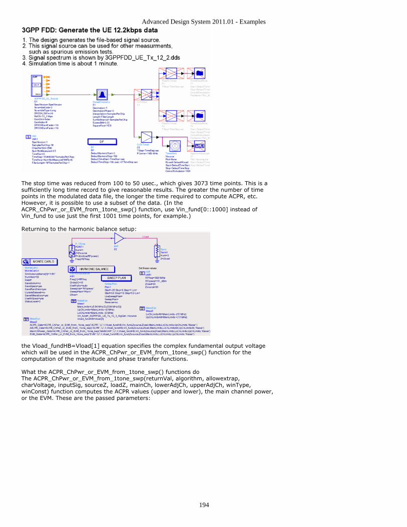
Advanced Design System 2011.01 - Examples
194
The stop time was reduced from 100 to 50 usec., which gives 3073 time points. This is asufficiently long time record to give reasonable results. The greater the number of timepoints in the modulated data file, the longer the time required to compute ACPR, etc.However, it is possible to use a subset of the data. (In theACPR_ChPwr_or_EVM_from_1tone_swp() function, use Vin_fund[0::1000] instead ofVin_fund to use just the first 1001 time points, for example.)
Returning to the harmonic balance setup:
the Vload_fundHB=Vload[1] equation specifies the complex fundamental output voltagewhich will be used in the ACPR_ChPwr_or_EVM_from_1tone_swp() function for thecomputation of the magnitude and phase transfer functions.
What the ACPR_ChPwr_or_EVM_from_1tone_swp() functions doThe ACPR_ChPwr_or_EVM_from_1tone_swp(returnVal, algorithm, allowextrap,charVoltage, inputSig, sourceZ, loadZ, mainCh, lowerAdjCh, upperAdjCh, winType,winConst) function computes the ACPR values (upper and lower), the main channel power,or the EVM. These are the passed parameters:
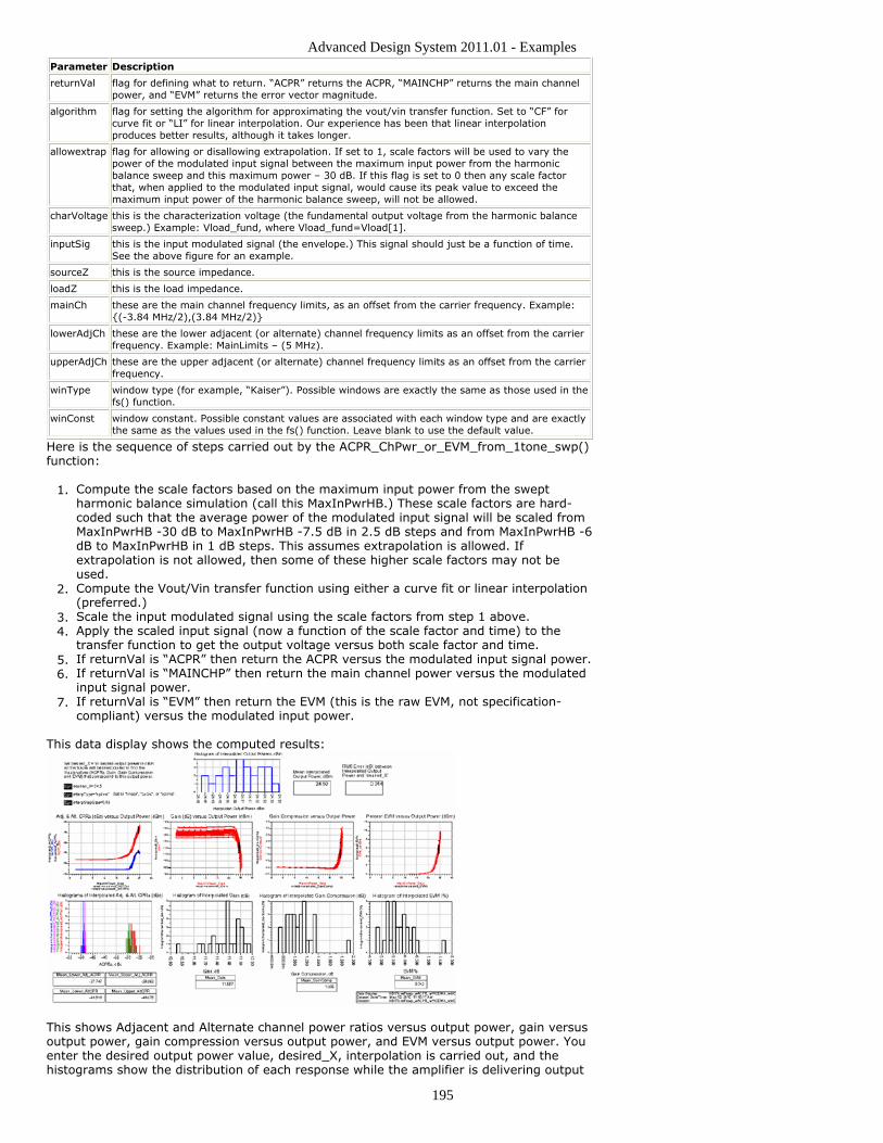
Advanced Design System 2011.01 - Examples
195
Parameter Description
returnVal flag for defining what to return. “ACPR” returns the ACPR, “MAINCHP” returns the main channelpower, and “EVM” returns the error vector magnitude.
algorithm flag for setting the algorithm for approximating the vout/vin transfer function. Set to “CF” forcurve fit or “LI” for linear interpolation. Our experience has been that linear interpolationproduces better results, although it takes longer.
allowextrap flag for allowing or disallowing extrapolation. If set to 1, scale factors will be used to vary thepower of the modulated input signal between the maximum input power from the harmonicbalance sweep and this maximum power – 30 dB. If this flag is set to 0 then any scale factorthat, when applied to the modulated input signal, would cause its peak value to exceed themaximum input power of the harmonic balance sweep, will not be allowed.
charVoltage this is the characterization voltage (the fundamental output voltage from the harmonic balancesweep.) Example: Vload_fund, where Vload_fund=Vload[1].
inputSig this is the input modulated signal (the envelope.) This signal should just be a function of time.See the above figure for an example.
sourceZ this is the source impedance.
loadZ this is the load impedance.
mainCh these are the main channel frequency limits, as an offset from the carrier frequency. Example:{(-3.84 MHz/2),(3.84 MHz/2)}
lowerAdjCh these are the lower adjacent (or alternate) channel frequency limits as an offset from the carrierfrequency. Example: MainLimits – (5 MHz).
upperAdjCh these are the upper adjacent (or alternate) channel frequency limits as an offset from the carrierfrequency.
winType window type (for example, “Kaiser”). Possible windows are exactly the same as those used in thefs() function.
winConst window constant. Possible constant values are associated with each window type and are exactlythe same as the values used in the fs() function. Leave blank to use the default value.
Here is the sequence of steps carried out by the ACPR_ChPwr_or_EVM_from_1tone_swp()function:
Compute the scale factors based on the maximum input power from the swept1.harmonic balance simulation (call this MaxInPwrHB.) These scale factors are hard-coded such that the average power of the modulated input signal will be scaled fromMaxInPwrHB -30 dB to MaxInPwrHB -7.5 dB in 2.5 dB steps and from MaxInPwrHB -6dB to MaxInPwrHB in 1 dB steps. This assumes extrapolation is allowed. Ifextrapolation is not allowed, then some of these higher scale factors may not beused.Compute the Vout/Vin transfer function using either a curve fit or linear interpolation2.(preferred.)Scale the input modulated signal using the scale factors from step 1 above.3.Apply the scaled input signal (now a function of the scale factor and time) to the4.transfer function to get the output voltage versus both scale factor and time.If returnVal is “ACPR” then return the ACPR versus the modulated input signal power.5.If returnVal is “MAINCHP” then return the main channel power versus the modulated6.input signal power.If returnVal is “EVM” then return the EVM (this is the raw EVM, not specification-7.compliant) versus the modulated input power.
This data display shows the computed results:
This shows Adjacent and Alternate channel power ratios versus output power, gain versusoutput power, gain compression versus output power, and EVM versus output power. Youenter the desired output power value, desired_X, interpolation is carried out, and thehistograms show the distribution of each response while the amplifier is delivering output
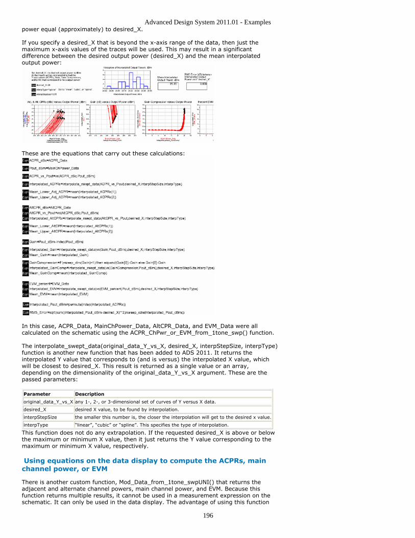
Advanced Design System 2011.01 - Examples
196
power equal (approximately) to desired_X.
If you specify a desired_X that is beyond the x-axis range of the data, then just themaximum x-axis values of the traces will be used. This may result in a significantdifference between the desired output power (desired_X) and the mean interpolatedoutput power:
These are the equations that carry out these calculations:
In this case, ACPR_Data, MainChPower_Data, AltCPR_Data, and EVM_Data were allcalculated on the schematic using the ACPR_ChPwr_or_EVM_from_1tone_swp() function.
The interpolate_swept_data(original_data_Y_vs_X, desired_X, interpStepSize, interpType)function is another new function that has been added to ADS 2011. It returns theinterpolated Y value that corresponds to (and is versus) the interpolated X value, whichwill be closest to desired_X. This result is returned as a single value or an array,depending on the dimensionality of the original_data_Y_vs_X argument. These are thepassed parameters:
Parameter Description
original_data_Y_vs_X any 1-, 2-, or 3-dimensional set of curves of Y versus X data.
desired_X desired X value, to be found by interpolation.
interpStepSize the smaller this number is, the closer the interpolation will get to the desired x value.
interpType “linear”, “cubic” or “spline”. This specifies the type of interpolation.
This function does not do any extrapolation. If the requested desired_X is above or belowthe maximum or minimum X value, then it just returns the Y value corresponding to themaximum or minimum X value, respectively.
Using equations on the data display to compute the ACPRs, mainchannel power, or EVM
There is another custom function, Mod_Data_from_1tone_swpUNI() that returns theadjacent and alternate channel powers, main channel power, and EVM. Because thisfunction returns multiple results, it cannot be used in a measurement expression on theschematic. It can only be used in the data display. The advantage of using this function
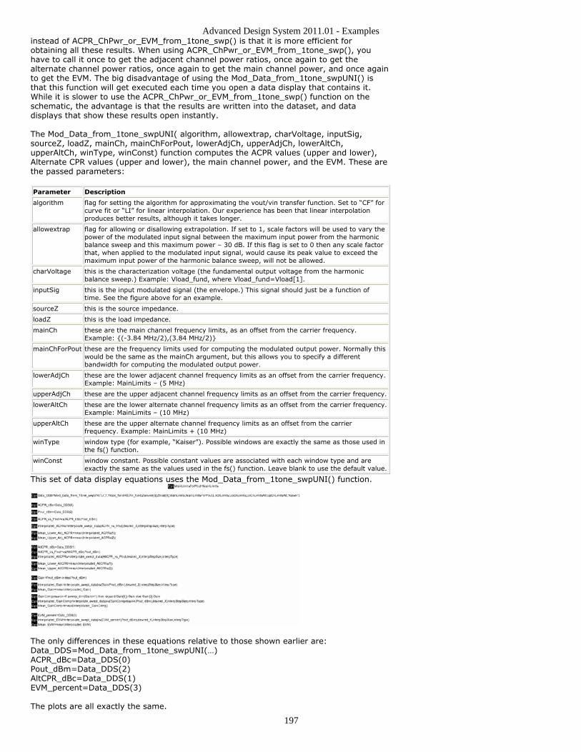
Advanced Design System 2011.01 - Examples
197
instead of ACPR_ChPwr_or_EVM_from_1tone_swp() is that it is more efficient forobtaining all these results. When using ACPR_ChPwr_or_EVM_from_1tone_swp(), youhave to call it once to get the adjacent channel power ratios, once again to get thealternate channel power ratios, once again to get the main channel power, and once againto get the EVM. The big disadvantage of using the Mod_Data_from_1tone_swpUNI() isthat this function will get executed each time you open a data display that contains it.While it is slower to use the ACPR_ChPwr_or_EVM_from_1tone_swp() function on theschematic, the advantage is that the results are written into the dataset, and datadisplays that show these results open instantly.
The Mod_Data_from_1tone_swpUNI( algorithm, allowextrap, charVoltage, inputSig,sourceZ, loadZ, mainCh, mainChForPout, lowerAdjCh, upperAdjCh, lowerAltCh,upperAltCh, winType, winConst) function computes the ACPR values (upper and lower),Alternate CPR values (upper and lower), the main channel power, and the EVM. These arethe passed parameters:
Parameter Description
algorithm flag for setting the algorithm for approximating the vout/vin transfer function. Set to “CF” forcurve fit or “LI” for linear interpolation. Our experience has been that linear interpolationproduces better results, although it takes longer.
allowextrap flag for allowing or disallowing extrapolation. If set to 1, scale factors will be used to vary thepower of the modulated input signal between the maximum input power from the harmonicbalance sweep and this maximum power – 30 dB. If this flag is set to 0 then any scale factorthat, when applied to the modulated input signal, would cause its peak value to exceed themaximum input power of the harmonic balance sweep, will not be allowed.
charVoltage this is the characterization voltage (the fundamental output voltage from the harmonicbalance sweep.) Example: Vload_fund, where Vload_fund=Vload[1].
inputSig this is the input modulated signal (the envelope.) This signal should just be a function oftime. See the figure above for an example.
sourceZ this is the source impedance.
loadZ this is the load impedance.
mainCh these are the main channel frequency limits, as an offset from the carrier frequency.Example: {(-3.84 MHz/2),(3.84 MHz/2)}
mainChForPout these are the frequency limits used for computing the modulated output power. Normally thiswould be the same as the mainCh argument, but this allows you to specify a differentbandwidth for computing the modulated output power.
lowerAdjCh these are the lower adjacent channel frequency limits as an offset from the carrier frequency.Example: MainLimits – (5 MHz)
upperAdjCh these are the upper adjacent channel frequency limits as an offset from the carrier frequency.
lowerAltCh these are the lower alternate channel frequency limits as an offset from the carrier frequency.Example: MainLimits – (10 MHz)
upperAltCh these are the upper alternate channel frequency limits as an offset from the carrierfrequency. Example: MainLimits + (10 MHz)
winType window type (for example, “Kaiser”). Possible windows are exactly the same as those used inthe fs() function.
winConst window constant. Possible constant values are associated with each window type and areexactly the same as the values used in the fs() function. Leave blank to use the default value.
This set of data display equations uses the Mod_Data_from_1tone_swpUNI() function.
The only differences in these equations relative to those shown earlier are:Data_DDS=Mod_Data_from_1tone_swpUNI(…)ACPR_dBc=Data_DDS(0)Pout_dBm=Data_DDS(2)AltCPR_dBc=Data_DDS(1)EVM_percent=Data_DDS(3)
The plots are all exactly the same.

Advanced Design System 2011.01 - Examples
198
Benchmark test results
A simulation of a much more complex amplifier with these custom equations just on thedata displaytook about 4 minutes for 10 MC trials (+1 for the nominal case) and about 1 minute and31 seconds to open the data display. This was using a modulated input signal with 3073time points.
The same simulation with 4 equations, each using theACPR_ChPwr_or_EVM_from_1tone_swp() function to compute the adjacent channel powerratios, alternate channel power ratios, main channel power, and EVM took about 3minutes 54 seconds to run the simulation and another 4 minutes and 45 seconds toevaluate the equations.
Technical discussion comparing this 1-tone swept power harmonic balance simulationtechnique for computing ACPR and EVM and the Ptolemy co-simulation approach.
For EVM, the single-tone method is not specification-compliant. It just measures the “raw”EVM, computed at each time point. The EVM is computed after correcting for the averagephase difference and RMS amplitude difference between the output and input modulatedsignals. If the modulated signal at the output of the amplifier has only a constant phaseshift and a constant gain (meaning that neither vary with the amplitude of the inputmodulated signal), then the EVM will be zero. With this method, the EVM is computed ateach time point, not at just the symbol times. There is no demodulation or decoding of thesignal, so you can’t calculate the EVM of each sub-carrier, say for an LTE signal.
With the Ptolemy method, the EVM calculation uses an EVM sink that is specification-compliant.
The only advantage of the single-tone method is that it may be faster. Clearly it is not asaccurate, but might still be useful as a proxy for the specification-compliant EVM.
For ACPR, the single-tone method does not include any receive-side filtering. It justgenerates the spectrum at the output of the amplifier, integrates the power in the main,adjacent, and alternate channels, then computes the ratios.The single-tone method of computing EVM (and ACPR) will tend to become less accurateas the bandwidth of the signal gets larger. This is because this method assumes theresponse of the amplifier is constant across the modulation bandwidth (we’re modeling thenonlinearity by injecting a single tone at the carrier frequency, after all.)
With Ptolemy fast co-simulation, the behavioral model that is created can includefrequency variation across the modulation bandwidth.
Design for Manufacturing Example Using YieldSensitivity Histograms, DOE, and Sensitivity AnalysisLocation: $HPEESOF_DIR/examples/MW_Ckts/Ku_Band_LNA_DFM_wrk
Objective
Demonstrates all of the statistical design tools in ADS used to build robust designs thatare insensitive to process variations, temperature variations, changes in the supplyvoltages, and package and bond wire effects.
Setup
To work with this example, very little setup is needed. All of the circuit designs are set tobegin using immediately:
Install the design kit DemoKit_V3 which is included in this workspace.1.Open any of the circuit designs.2.Simulate the design. The results will appear when the simulation completes.3.
The following table describes the designs and templates that are available in the exampleworkspace. This workspace is organized into the following sub-folders which are viewableon the ADS Main window's Folder View tab:
Advanced Design System 2011.01 - Examples
199
Folder Description
A_Sensitivity_Analysis Illustrates the Sensitivity Analysis tool to find the sensitive elements tothe specs in the design.
B_Yield_Analysis Illustrates Monte Carlo Yield Analysis.
C_Yield_YSH_Templates Illustrates how the post processes yield information is used in YieldSensitivity Histograms Templates to extract very useful information onthe design and help turn it into a highly manufacturable design with first-pass success and high yield. For details about using these templates, seeYield Sensitivity Histogram Design Templates (examples).
D_DOE_on_Matching_Networks Illustrates the use of Design of Experiments (DOE) to find out whichmatching network(s) are sensitive and cause problems in the yield.Designers are then able to come up with other less-sensitive matchingnetworks to make the design less sensitive to process variations.
E_DOE_on_elements Illustrates the use of Design of Experiments (DOE) to find out whichcomponent is sensitive in the design and cause problems in yield.
F_Fix_Design Based on the analysis done above, this is the fixed design that resultswith high yield and low sensitivity to process variation, temperature andvoltage variation.
G_Network_to_test_YSH_templates This is a dummy circuit that is included here in order to illustrate how touse of the Yield Sensitivity Histogram templates outside of this example.Please also see Yield Sensitivity Histogram Design Templates (examples)for more information on the use of these templates. These displays areavailable as templates which can be inserted using the Insert > Templatecommand in the Data Display window. On your own designs, select therequired number of specifications (1-5) and set the name of each YieldSpec to Spec1, Spec2, etc.
Notes
To use this workspace, you must first install the design kit DemoKit_V3 which isincluded in this workspace.
Design of a 1GHz Low Noise AmplifierLocation: $HPEESOF_DIR/examples/MW_Ckts/LNA_1GHz_wrk
Objective
This example shows how to examine stability, noise and gain, and how to design the inputand output matching networks for a 1GHz LNA. It also compares the simulation data withthose from layout.
Setup
"ModelVerif" shows how to compare two sets of data: the device model and1.measured S-parameters for the device are simulated to validate the model."BiasSetup" determines the required VBE so that the operating point of the model2.matches that of the S-parameter-based component."Bias_Network" performs an optimization to calculate the required bias network3.resistors for the device."SparamsNoise" shows how to set up the S-parameter simulation control to calculate4.noise parameters for the device and how to generate constant noise figure circles."Stability" calculates and displays input and output stability circles for the device and5.also shows the effect of adding a stabilizing networks on the output."Match1" and "Match2" calculate the required input match network for minimum6.noise figure at 1GHz."Match3" and "Match4" calculate the required output matching network for the device7.with the optimum input noise match network in place."FinishedAmp" calculates gain, input and output match, and noise figure for the8.completed amplifier."AmpLayout" is a subcircuit containing the layout and schematic of the finished9.amplifier, replacing ideal components with models from the SMT Passive ComponentLibrary."SimFromLayout" contains the symbol for AmpLayout and simulation controllers.10.Results are compared to the ideal results from FinishedAmp.
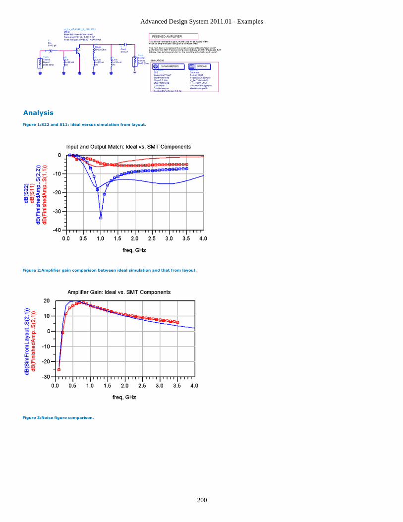
Advanced Design System 2011.01 - Examples
200
Analysis
Figure 1:S22 and S11: ideal versus simulation from layout.
Figure 2:Amplifier gain comparison between ideal simulation and that from layout.
Figure 3:Noise figure comparison.
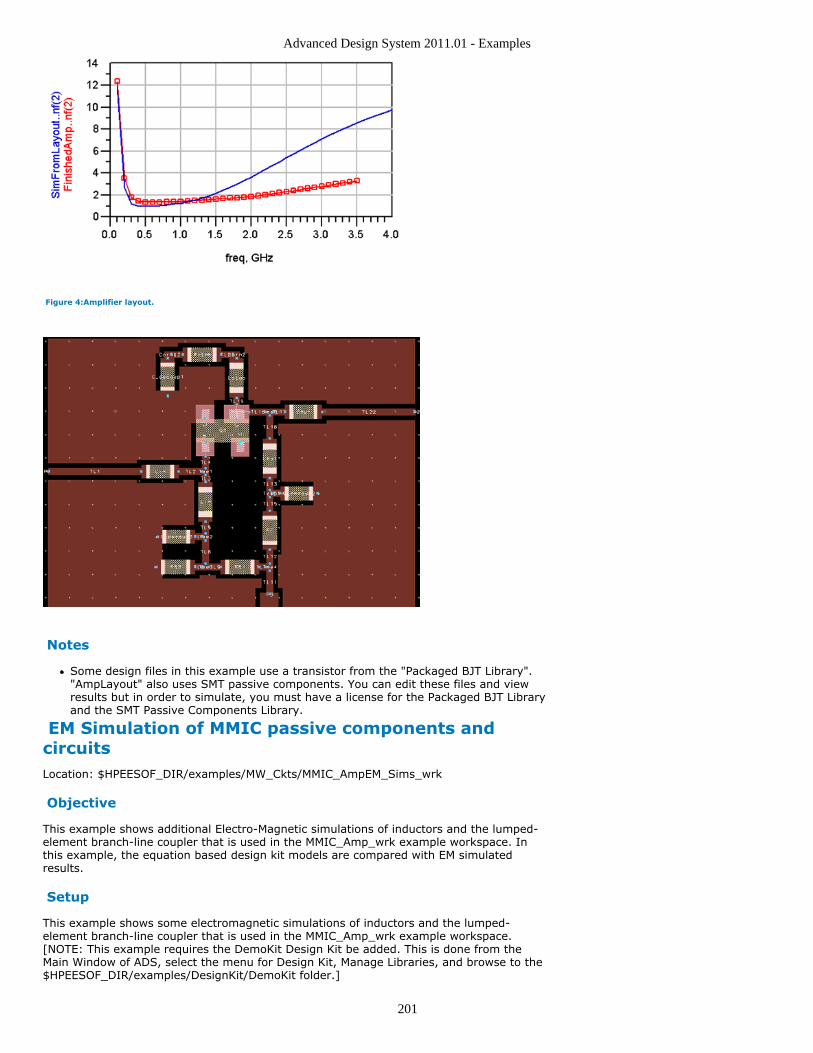
Advanced Design System 2011.01 - Examples
201
Figure 4:Amplifier layout.
Notes
Some design files in this example use a transistor from the "Packaged BJT Library"."AmpLayout" also uses SMT passive components. You can edit these files and viewresults but in order to simulate, you must have a license for the Packaged BJT Libraryand the SMT Passive Components Library.
EM Simulation of MMIC passive components andcircuitsLocation: $HPEESOF_DIR/examples/MW_Ckts/MMIC_AmpEM_Sims_wrk
Objective
This example shows additional Electro-Magnetic simulations of inductors and the lumped-element branch-line coupler that is used in the MMIC_Amp_wrk example workspace. Inthis example, the equation based design kit models are compared with EM simulatedresults.
Setup
This example shows some electromagnetic simulations of inductors and the lumped-element branch-line coupler that is used in the MMIC_Amp_wrk example workspace.[NOTE: This example requires the DemoKit Design Kit be added. This is done from theMain Window of ADS, select the menu for Design Kit, Manage Libraries, and browse to the$HPEESOF_DIR/examples/DesignKit/DemoKit folder.]
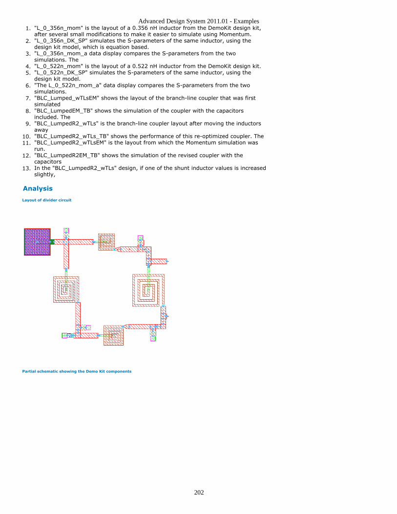
Advanced Design System 2011.01 - Examples
202
"L_0_356n_mom" is the layout of a 0.356 nH inductor from the DemoKit design kit,1.after several small modifications to make it easier to simulate using Momentum."L_0_356n_DK_SP" simulates the S-parameters of the same inductor, using the2.design kit model, which is equation based."L_0_356n_mom_a data display compares the S-parameters from the two3.simulations. The"L_0_522n_mom" is the layout of a 0.522 nH inductor from the DemoKit design kit.4."L_0_522n_DK_SP" simulates the S-parameters of the same inductor, using the5.design kit model."The L_0_522n_mom_a" data display compares the S-parameters from the two6.simulations."BLC_Lumped_wTLsEM" shows the layout of the branch-line coupler that was first7.simulated"BLC_LumpedEM_TB" shows the simulation of the coupler with the capacitors8.included. The"BLC_LumpedR2_wTLs" is the branch-line coupler layout after moving the inductors9.away"BLC_LumpedR2_wTLs_TB" shows the performance of this re-optimized coupler. The10."BLC_LumpedR2_wTLsEM" is the layout from which the Momentum simulation was11.run."BLC_LumpedR2EM_TB" shows the simulation of the revised coupler with the12.capacitorsIn the "BLC_LumpedR2_wTLs" design, if one of the shunt inductor values is increased13.slightly,
Analysis
Layout of divider circuit
Partial schematic showing the Demo Kit components
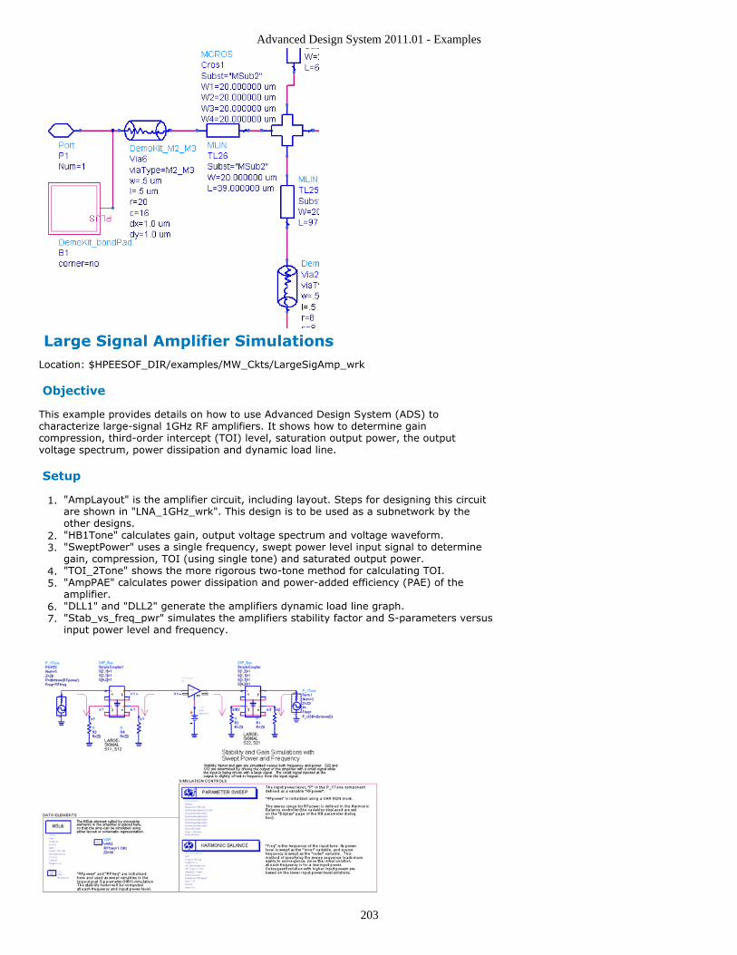
Advanced Design System 2011.01 - Examples
203
Large Signal Amplifier SimulationsLocation: $HPEESOF_DIR/examples/MW_Ckts/LargeSigAmp_wrk
Objective
This example provides details on how to use Advanced Design System (ADS) tocharacterize large-signal 1GHz RF amplifiers. It shows how to determine gaincompression, third-order intercept (TOI) level, saturation output power, the outputvoltage spectrum, power dissipation and dynamic load line.
Setup
"AmpLayout" is the amplifier circuit, including layout. Steps for designing this circuit1.are shown in "LNA_1GHz_wrk". This design is to be used as a subnetwork by theother designs."HB1Tone" calculates gain, output voltage spectrum and voltage waveform.2."SweptPower" uses a single frequency, swept power level input signal to determine3.gain, compression, TOI (using single tone) and saturated output power."TOI_2Tone" shows the more rigorous two-tone method for calculating TOI.4."AmpPAE" calculates power dissipation and power-added efficiency (PAE) of the5.amplifier."DLL1" and "DLL2" generate the amplifiers dynamic load line graph.6."Stab_vs_freq_pwr" simulates the amplifiers stability factor and S-parameters versus7.input power level and frequency.
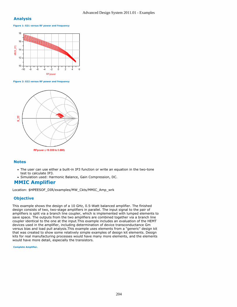
Advanced Design System 2011.01 - Examples
204
Analysis
Figure 1: S21 versus RF power and frequency
Figure 2: S22 versus RF power and frequency
Notes
The user can use either a built-in IP3 function or write an equation in the two-tonetest to calculate IP3.Simulation used: Harmonic Balance, Gain Compression, DC.
MMIC AmplifierLocation: $HPEESOF_DIR/examples/MW_Ckts/MMIC_Amp_wrk
Objective
This example shows the design of a 10 GHz, 0.5-Watt balanced amplifier. The finisheddesign consists of two, two-stage amplifiers in parallel. The input signal to the pair ofamplifiers is split via a branch line coupler, which is implemented with lumped elements tosave space. The outputs from the two amplifiers are combined together via a branch linecoupler identical to the one at the input.This example includes an evaluation of the HEMTdevices used in the amplifier, including determination of device transconductance Gmversus bias and load pull analysis.This example uses elements from a "generic" design kitthat was created to show some relatively simple examples of design kit elements. Designkits for real manufacturing processes would have many more elements, and the elementswould have more detail, especially the transistors.
Complete Amplifier.
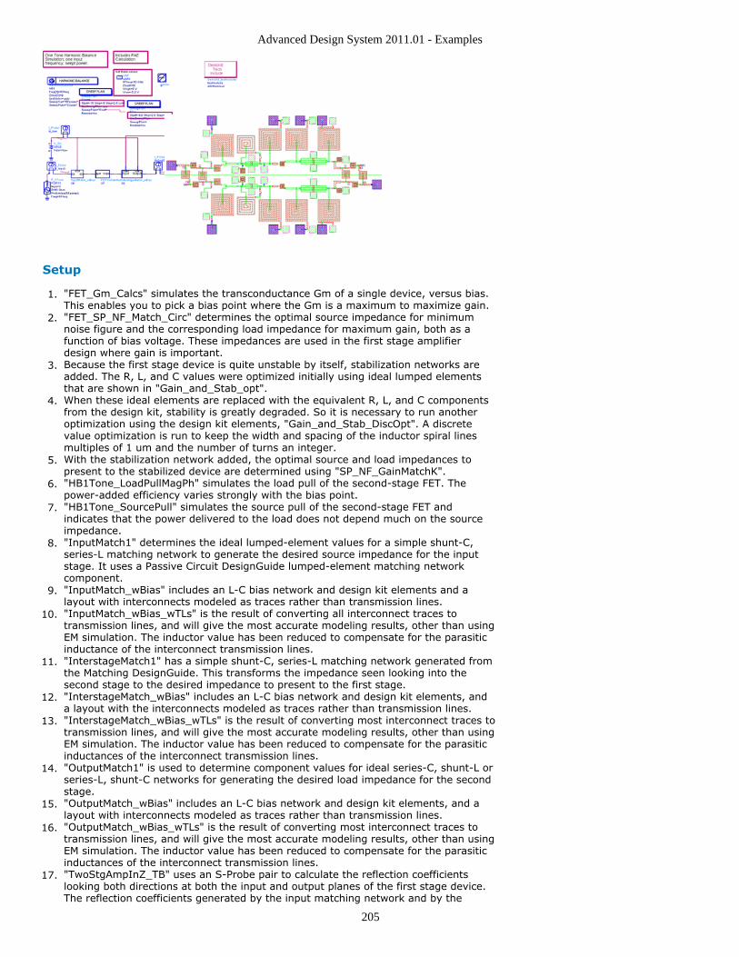
Advanced Design System 2011.01 - Examples
205
Setup
"FET_Gm_Calcs" simulates the transconductance Gm of a single device, versus bias.1.This enables you to pick a bias point where the Gm is a maximum to maximize gain."FET_SP_NF_Match_Circ" determines the optimal source impedance for minimum2.noise figure and the corresponding load impedance for maximum gain, both as afunction of bias voltage. These impedances are used in the first stage amplifierdesign where gain is important.Because the first stage device is quite unstable by itself, stabilization networks are3.added. The R, L, and C values were optimized initially using ideal lumped elementsthat are shown in "Gain_and_Stab_opt".When these ideal elements are replaced with the equivalent R, L, and C components4.from the design kit, stability is greatly degraded. So it is necessary to run anotheroptimization using the design kit elements, "Gain_and_Stab_DiscOpt". A discretevalue optimization is run to keep the width and spacing of the inductor spiral linesmultiples of 1 um and the number of turns an integer.With the stabilization network added, the optimal source and load impedances to5.present to the stabilized device are determined using "SP_NF_GainMatchK"."HB1Tone_LoadPullMagPh" simulates the load pull of the second-stage FET. The6.power-added efficiency varies strongly with the bias point."HB1Tone_SourcePull" simulates the source pull of the second-stage FET and7.indicates that the power delivered to the load does not depend much on the sourceimpedance."InputMatch1" determines the ideal lumped-element values for a simple shunt-C,8.series-L matching network to generate the desired source impedance for the inputstage. It uses a Passive Circuit DesignGuide lumped-element matching networkcomponent."InputMatch_wBias" includes an L-C bias network and design kit elements and a9.layout with interconnects modeled as traces rather than transmission lines."InputMatch_wBias_wTLs" is the result of converting all interconnect traces to10.transmission lines, and will give the most accurate modeling results, other than usingEM simulation. The inductor value has been reduced to compensate for the parasiticinductance of the interconnect transmission lines."InterstageMatch1" has a simple shunt-C, series-L matching network generated from11.the Matching DesignGuide. This transforms the impedance seen looking into thesecond stage to the desired impedance to present to the first stage."InterstageMatch_wBias" includes an L-C bias network and design kit elements, and12.a layout with the interconnects modeled as traces rather than transmission lines."InterstageMatch_wBias_wTLs" is the result of converting most interconnect traces to13.transmission lines, and will give the most accurate modeling results, other than usingEM simulation. The inductor value has been reduced to compensate for the parasiticinductances of the interconnect transmission lines."OutputMatch1" is used to determine component values for ideal series-C, shunt-L or14.series-L, shunt-C networks for generating the desired load impedance for the secondstage."OutputMatch_wBias" includes an L-C bias network and design kit elements, and a15.layout with interconnects modeled as traces rather than transmission lines."OutputMatch_wBias_wTLs" is the result of converting most interconnect traces to16.transmission lines, and will give the most accurate modeling results, other than usingEM simulation. The inductor value has been reduced to compensate for the parasiticinductances of the interconnect transmission lines."TwoStgAmpInZ_TB" uses an S-Probe pair to calculate the reflection coefficients17.looking both directions at both the input and output planes of the first stage device.The reflection coefficients generated by the input matching network and by the
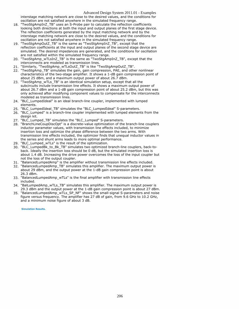
Advanced Design System 2011.01 - Examples
206
interstage matching network are close to the desired values, and the conditions foroscillation are not satisfied anywhere in the simulated frequency range."TwoStgAmpInZ_TB" uses an S-Probe pair to calculate the reflection coefficients18.looking both directions at both the input and output planes of the first stage device.The reflection coefficients generated by the input matching network and by theinterstage matching network are close to the desired values, and the conditions foroscillation are not satisfied anywhere in the simulated frequency range."TwoStgAmpOutZ_TB" is the same as "TwoStgAmpInZ_TB", except that the19.reflection coefficients at the input and output planes of the second stage device aresimulated. The desired impedances are generated, and the conditions for oscillationare not satisfied within the simulated frequency range."TwoStgAmp_wTLsInZ_TB" is the same as "TwoStgAmpInZ_TB", except that the20.interconnects are modeled as transmission lines."Similarly, "TwoStgAmp_wTLsOutZ_TB" is like "TwoStgAmpOutZ_TB".21."TwoStgAmp_TB" simulates the gain, gain compression, PAE, and other nonlinear22.characteristics of the two-stage amplifier. It shows a 1-dB gain compression point ofabout 25 dBm, and a maximum output power of about 26.7 dBm."TwoStgAmp_wTLs_TB" is an identical simulation setup, except that all the23.subcircuits include transmission line effects. It shows a maximum output power ofabout 26.7 dBm and a 1-dB gain compression point of about 25.2 dBm, but this wasonly achieved after modifying component values to compensate for the interconnectsmodeled as transmission lines."BLC_LumpedIdeal" is an ideal branch-line coupler, implemented with lumped24.elements."BLC_LumpedIdeal_TB" simulates the "BLC_LumpedIdeal" S-parameters.25."BLC_Lumped" is a branch-line coupler implemented with lumped elements from the26.design kit."BLC_Lumped_TB" simulates the "BLC_Lumped" S-parameters.27."BranchLineCoupDiscOpt" is a discrete-value optimization of the branch-line couplers28.inductor parameter values, with transmission line effects included, to minimizeinsertion loss and optimize the phase difference between the two arms. Withtransmission line effects included, the optimizer finds that unequal inductor values inthe series and shunt arms leads to more optimal performance."BLC_Lumped_wTLs" is the result of the optimization.29."BLC_LumpedBk_to_Bk_TB" simulates two optimized branch-line couplers, back-to-30.back. Ideally the insertion loss should be 0 dB, but the simulated insertion loss isabout 1.4 dB. Increasing the drive power overcomes the loss of the input coupler butnot the loss of the output coupler."BalancedLumpedAmp" is the amplifier without transmission line effects included.31."BalancedLumpedAmp_TB" simulates this amplifier. The maximum output power is32.about 29 dBm, and the output power at the 1-dB gain compression point is about26.3 dBm."BalancedLumpedAmp_wTLs" is the final amplifier with transmission line effects33.included."BalLumpedAmp_wTLs_TB" simulates this amplifier. The maximum output power is34.29.3 dBm and the output power at the 1-dB gain compression point is about 27 dBm."BalancedLumpedAmp_wTLs_SP_NF" shows the small-signal S-parameters and noise35.figure versus frequency. The amplifier has 27 dB of gain, from 9.6 GHz to 10.2 GHz,and a minimum noise figure of about 3 dB.
Simulation Results.
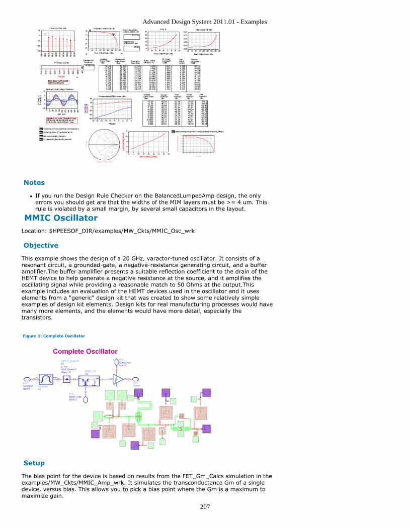
Advanced Design System 2011.01 - Examples
207
Notes
If you run the Design Rule Checker on the BalancedLumpedAmp design, the onlyerrors you should get are that the widths of the MIM layers must be >= 4 um. Thisrule is violated by a small margin, by several small capacitors in the layout.
MMIC OscillatorLocation: $HPEESOF_DIR/examples/MW_Ckts/MMIC_Osc_wrk
Objective
This example shows the design of a 20 GHz, varactor-tuned oscillator. It consists of aresonant circuit, a grounded-gate, a negative-resistance generating circuit, and a bufferamplifier.The buffer amplifier presents a suitable reflection coefficient to the drain of theHEMT device to help generate a negative resistance at the source, and it amplifies theoscillating signal while providing a reasonable match to 50 Ohms at the output.Thisexample includes an evaluation of the HEMT devices used in the oscillator and it useselements from a "generic" design kit that was created to show some relatively simpleexamples of design kit elements. Design kits for real manufacturing processes would havemany more elements, and the elements would have more detail, especially thetransistors.
Figure 1: Complete Oscillator
Setup
The bias point for the device is based on results from the FET_Gm_Calcs simulation in theexamples/MW_Ckts/MMIC_Amp_wrk. It simulates the transconductance Gm of a singledevice, versus bias. This allows you to pick a bias point where the Gm is a maximum tomaximize gain.
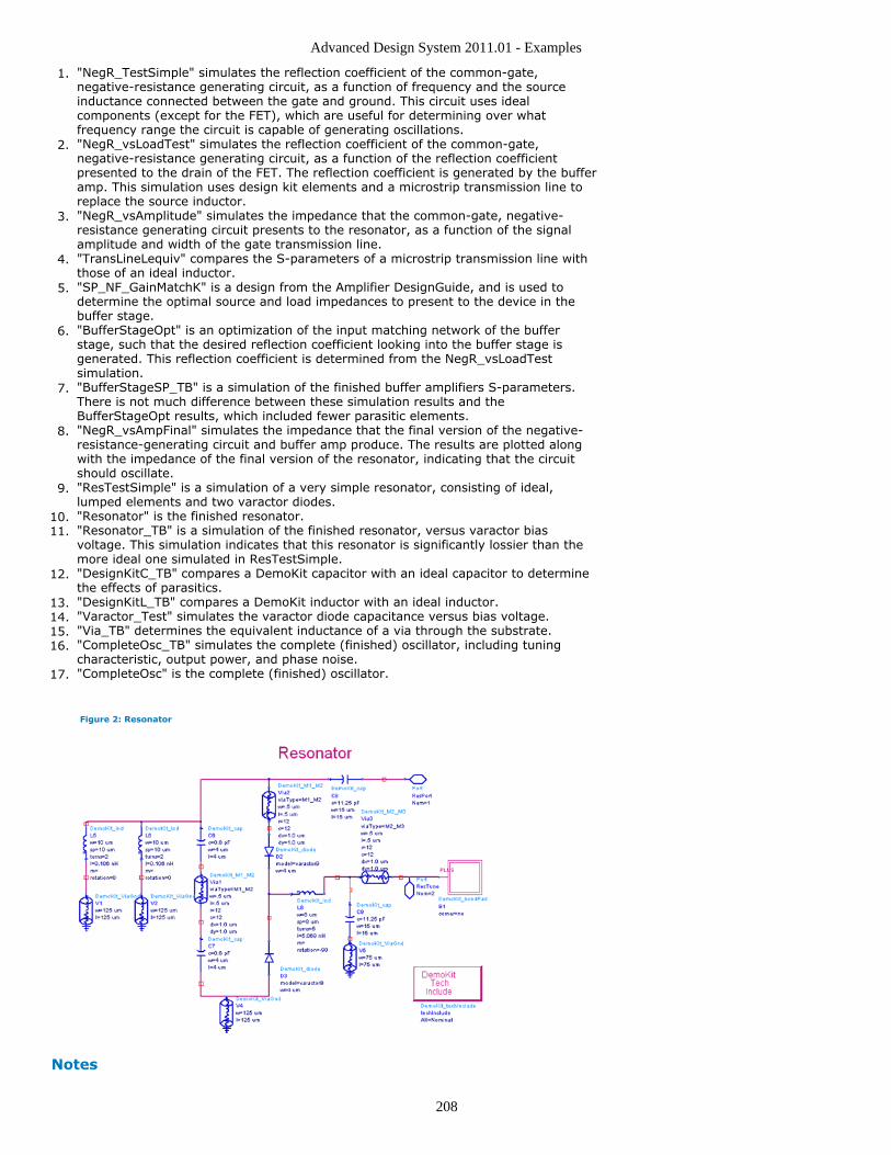
Advanced Design System 2011.01 - Examples
208
"NegR_TestSimple" simulates the reflection coefficient of the common-gate,1.negative-resistance generating circuit, as a function of frequency and the sourceinductance connected between the gate and ground. This circuit uses idealcomponents (except for the FET), which are useful for determining over whatfrequency range the circuit is capable of generating oscillations."NegR_vsLoadTest" simulates the reflection coefficient of the common-gate,2.negative-resistance generating circuit, as a function of the reflection coefficientpresented to the drain of the FET. The reflection coefficient is generated by the bufferamp. This simulation uses design kit elements and a microstrip transmission line toreplace the source inductor."NegR_vsAmplitude" simulates the impedance that the common-gate, negative-3.resistance generating circuit presents to the resonator, as a function of the signalamplitude and width of the gate transmission line."TransLineLequiv" compares the S-parameters of a microstrip transmission line with4.those of an ideal inductor."SP_NF_GainMatchK" is a design from the Amplifier DesignGuide, and is used to5.determine the optimal source and load impedances to present to the device in thebuffer stage."BufferStageOpt" is an optimization of the input matching network of the buffer6.stage, such that the desired reflection coefficient looking into the buffer stage isgenerated. This reflection coefficient is determined from the NegR_vsLoadTestsimulation."BufferStageSP_TB" is a simulation of the finished buffer amplifiers S-parameters.7.There is not much difference between these simulation results and theBufferStageOpt results, which included fewer parasitic elements."NegR_vsAmpFinal" simulates the impedance that the final version of the negative-8.resistance-generating circuit and buffer amp produce. The results are plotted alongwith the impedance of the final version of the resonator, indicating that the circuitshould oscillate."ResTestSimple" is a simulation of a very simple resonator, consisting of ideal,9.lumped elements and two varactor diodes."Resonator" is the finished resonator.10."Resonator_TB" is a simulation of the finished resonator, versus varactor bias11.voltage. This simulation indicates that this resonator is significantly lossier than themore ideal one simulated in ResTestSimple."DesignKitC_TB" compares a DemoKit capacitor with an ideal capacitor to determine12.the effects of parasitics."DesignKitL_TB" compares a DemoKit inductor with an ideal inductor.13."Varactor_Test" simulates the varactor diode capacitance versus bias voltage.14."Via_TB" determines the equivalent inductance of a via through the substrate.15."CompleteOsc_TB" simulates the complete (finished) oscillator, including tuning16.characteristic, output power, and phase noise."CompleteOsc" is the complete (finished) oscillator.17.
Figure 2: Resonator
Notes
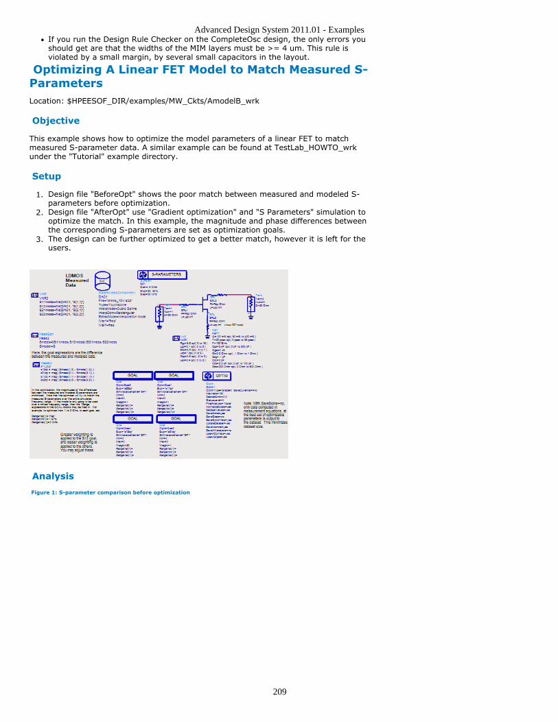
Advanced Design System 2011.01 - Examples
209
If you run the Design Rule Checker on the CompleteOsc design, the only errors youshould get are that the widths of the MIM layers must be >= 4 um. This rule isviolated by a small margin, by several small capacitors in the layout.
Optimizing A Linear FET Model to Match Measured S-ParametersLocation: $HPEESOF_DIR/examples/MW_Ckts/AmodelB_wrk
Objective
This example shows how to optimize the model parameters of a linear FET to matchmeasured S-parameter data. A similar example can be found at TestLab_HOWTO_wrkunder the "Tutorial" example directory.
Setup
Design file "BeforeOpt" shows the poor match between measured and modeled S-1.parameters before optimization.Design file "AfterOpt" use "Gradient optimization" and "S Parameters" simulation to2.optimize the match. In this example, the magnitude and phase differences betweenthe corresponding S-parameters are set as optimization goals.The design can be further optimized to get a better match, however it is left for the3.users.
Analysis
Figure 1: S-parameter comparison before optimization
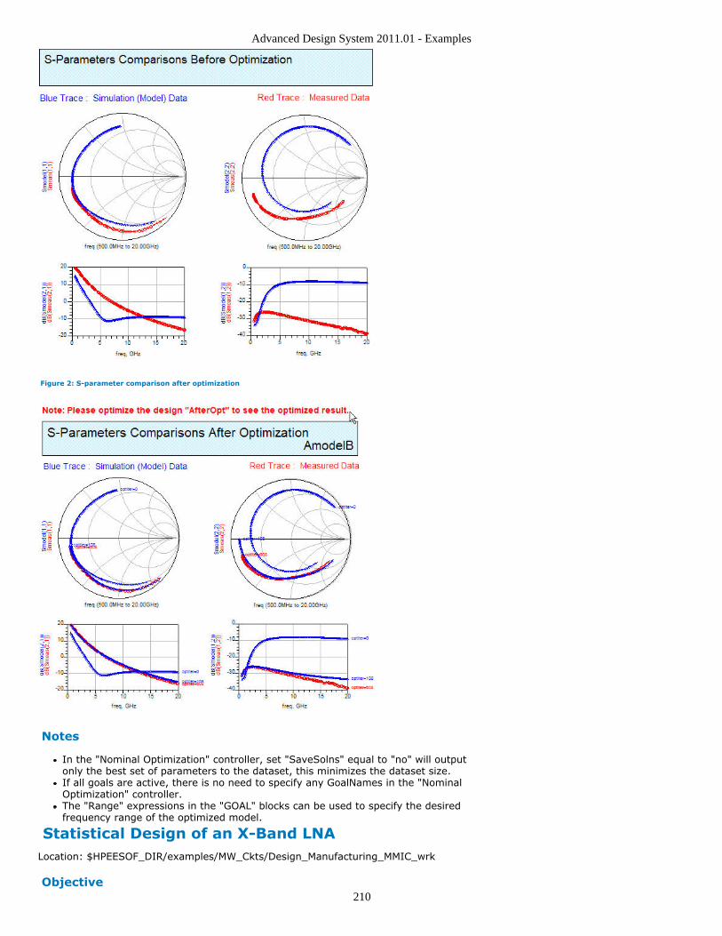
Advanced Design System 2011.01 - Examples
210
Figure 2: S-parameter comparison after optimization
Notes
In the "Nominal Optimization" controller, set "SaveSolns" equal to "no" will outputonly the best set of parameters to the dataset, this minimizes the dataset size.If all goals are active, there is no need to specify any GoalNames in the "NominalOptimization" controller.The "Range" expressions in the "GOAL" blocks can be used to specify the desiredfrequency range of the optimized model.
Statistical Design of an X-Band LNALocation: $HPEESOF_DIR/examples/MW_Ckts/Design_Manufacturing_MMIC_wrk
Objective
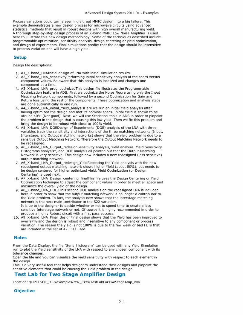
Advanced Design System 2011.01 - Examples
211
Process variations could turn a seemingly great MMIC design into a big failure. Thisexample demonstrates a new design process for microwave circuits using advancedstatistical methods that result in robust designs with high overall manufacturing yield.A thorough step-by-step design process of an X-band MMIC Low Noise Amplifier is usedhere to illustrate this new design methodology. Some of the techniques described includeprogrammable optimization, sensitivity analysis, design centering or yield optimization,and design of experiments. Final simulations predict that the design should be insensitiveto process variation and will have a high yield.
Setup
Design file descriptions:
A1_X-band_LNAInitial design of LNA with initial simulation results.1.A2_X-band_LNA_sensitivityPerforming initial sensitivity analysis of the specs versus2.component values. Be aware that this analysis is localized and changes onecomponent at a time.A3_X-band_LNA_prog_optimizedThis design file illustrates the Programmable3.Optimization feature in ADS. First we optimize the Noise Figure using only the InputMatching Network components, followed by a second Optimization for Gain andReturn loss using the rest of the components. These optimization and analysis stepsare done automatically in one run.A4_X-band_LNA_initial_Yield_analysisHere we run an initial Yield analysis after4.having optimized the design and met its nominal specs. Initial Yield is shown to bearound 40% (Not good). Next, we will use Statistical tools in ADS in order to pinpointthe problem in the design that is causing this low yield. Then we fix this problem andbring the design to be robust with close to 100% yield.A5_X-band_LNA_DOEDesign of Experiments (DOE) analysis of the LNA with three5.variables track the sensitivity and interactions of the three matching networks (Input,Interstage, and Output matching networks) shows that the yield problem is due to asensitive Output Matching Network. Therefore the Output Matching Network needs tobe redesigned.A6_X-band_LNA_Output_redesignSensitivity analysis, Yield analysis, Yield Sensitivity6.Histograms analysis*, and DOE analysis all pointed out that the Output MatchingNetwork is very sensitive. This design now includes a new redesigned (less sensitive)output matching network.A6_X-band_LNA_Output_redesign_YieldRepeating the Yield analysis with the new7.redesigned output matching network shows higher Yield (about 80%), but needs tobe design centered for higher optimized yield. Yield Optimization (or DesignCentering) is used next.A7_X-band_LNA_Design_centering_finalThis file uses the Design Centering or Yield8.Optimization technique to adjust the component values in order to meet all specs andmaximize the overall yield of the design.A8_X-band_LNA_DOE2This second DOE analysis on the redesigned LNA is included9.here in order to show that the output matching network is no longer a contributor tothe Yield problem. In fact, the analysis now shows that the interstage matchingnetwork is the next main contributor to the S22 variation.It is up to the designer to decide whether or not to spend time to create a lesssensitive Interstage network or not. Of course it is highly recommended in order toproduce a highly Robust circuit with a first pass success.A9_X-band_LNA_Final_designFinal design shows that the Yield has been improved to10.over 97% and the design is robust and insensitive to any component or processvariation. The reason the yield is not 100% is due to the few weak or bad FETs thatare included in the set of 42 FETs used.
Notes
From the Data Display, the file "Sens_histogram" can be used with any Yield Simulationrun to plot the Yield sensitivity of the LNA with respect to any chosen component with itstolerance changes.Open the file and you can visualize the yield sensitivity with respect to each element inthe design.This is a very useful tool that helps designers understand their designs and pinpoint thesensitive elements that could be causing the Yield problem in the design.
Test Lab for Two Stage Amplifier DesignLocation: $HPEESOF_DIR/examples/MW_Ckts/TestLabForTwoStageAmp_wrk
Objective
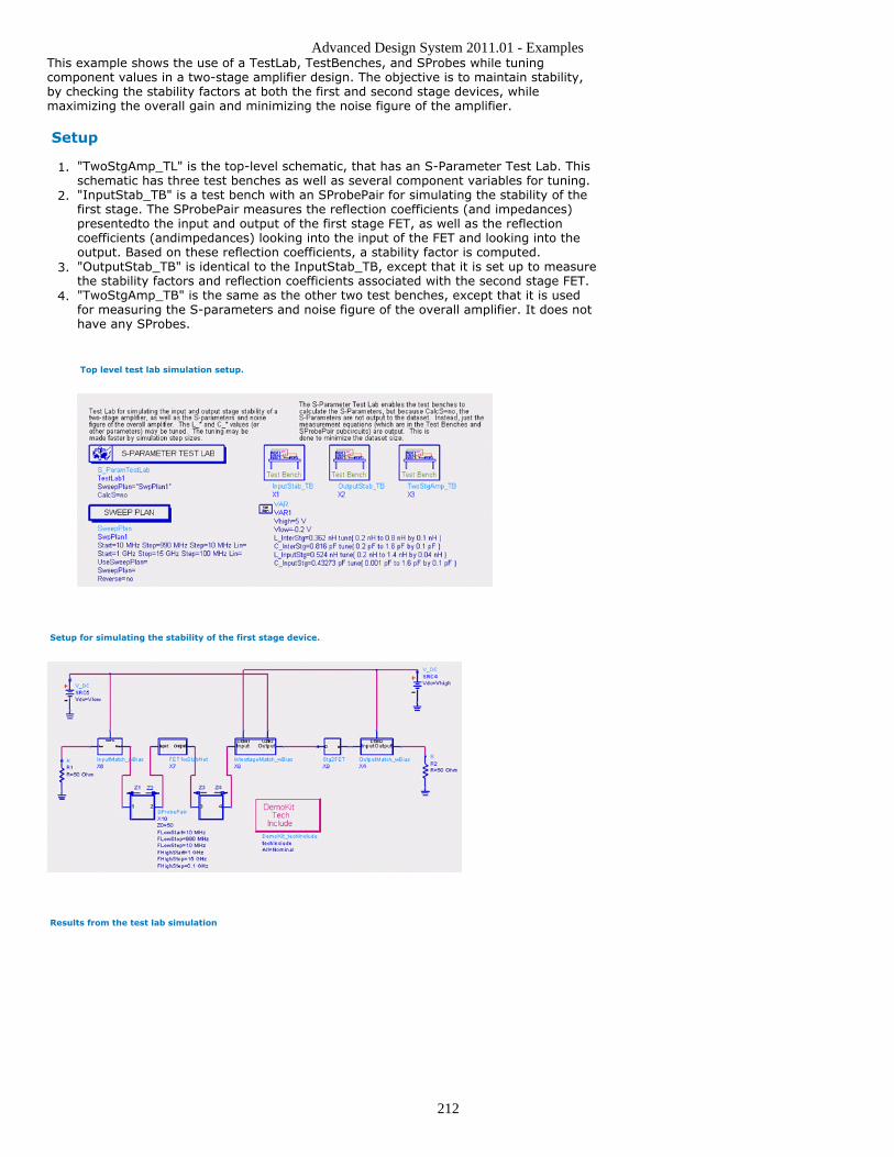
Advanced Design System 2011.01 - Examples
212
This example shows the use of a TestLab, TestBenches, and SProbes while tuningcomponent values in a two-stage amplifier design. The objective is to maintain stability,by checking the stability factors at both the first and second stage devices, whilemaximizing the overall gain and minimizing the noise figure of the amplifier.
Setup
"TwoStgAmp_TL" is the top-level schematic, that has an S-Parameter Test Lab. This1.schematic has three test benches as well as several component variables for tuning."InputStab_TB" is a test bench with an SProbePair for simulating the stability of the2.first stage. The SProbePair measures the reflection coefficients (and impedances)presentedto the input and output of the first stage FET, as well as the reflectioncoefficients (andimpedances) looking into the input of the FET and looking into theoutput. Based on these reflection coefficients, a stability factor is computed."OutputStab_TB" is identical to the InputStab_TB, except that it is set up to measure3.the stability factors and reflection coefficients associated with the second stage FET."TwoStgAmp_TB" is the same as the other two test benches, except that it is used4.for measuring the S-parameters and noise figure of the overall amplifier. It does nothave any SProbes.
Top level test lab simulation setup.
Setup for simulating the stability of the first stage device.
Results from the test lab simulation
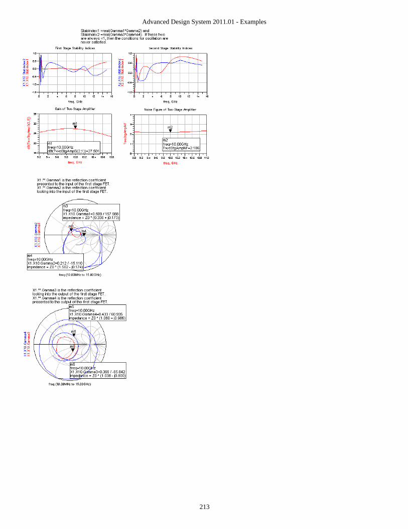
Advanced Design System 2011.01 - Examples
213
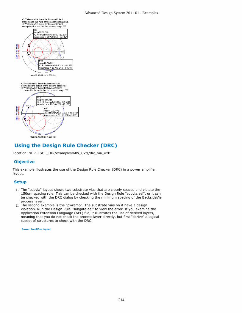
Advanced Design System 2011.01 - Examples
214
Using the Design Rule Checker (DRC)Location: $HPEESOF_DIR/examples/MW_Ckts/drc_via_wrk
Objective
This example illustrates the use of the Design Rule Checker (DRC) in a power amplifierlayout.
Setup
The "subvia" layout shows two substrate vias that are closely spaced and violate the1.150um spacing rule. This can be checked with the Design Rule "subvia.ael", or it canbe checked with the DRC dialog by checking the minimum spacing of the BacksideViaprocess layer.The second example is the "pwramp". The substrate vias on it have a design2.violation. Run the Design Rule "subgate.ael" to view the error. If you examine theApplication Extension Language (AEL) file, it illustrates the use of derived layers,meaning that you do not check the process layer directly, but first "derive" a logicalsubset of structures to check with the DRC.
Power Amplifier layout
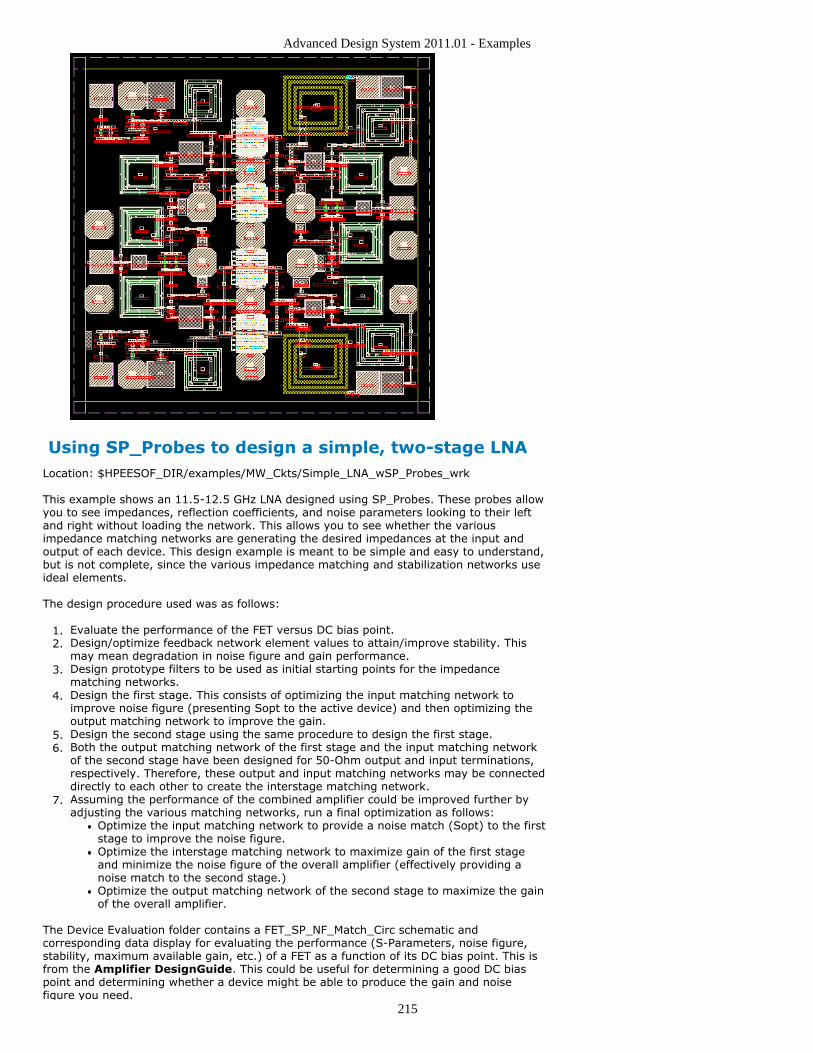
Advanced Design System 2011.01 - Examples
215
Using SP_Probes to design a simple, two-stage LNALocation: $HPEESOF_DIR/examples/MW_Ckts/Simple_LNA_wSP_Probes_wrk
This example shows an 11.5-12.5 GHz LNA designed using SP_Probes. These probes allowyou to see impedances, reflection coefficients, and noise parameters looking to their leftand right without loading the network. This allows you to see whether the variousimpedance matching networks are generating the desired impedances at the input andoutput of each device. This design example is meant to be simple and easy to understand,but is not complete, since the various impedance matching and stabilization networks useideal elements.
The design procedure used was as follows:
Evaluate the performance of the FET versus DC bias point.1.Design/optimize feedback network element values to attain/improve stability. This2.may mean degradation in noise figure and gain performance.Design prototype filters to be used as initial starting points for the impedance3.matching networks.Design the first stage. This consists of optimizing the input matching network to4.improve noise figure (presenting Sopt to the active device) and then optimizing theoutput matching network to improve the gain.Design the second stage using the same procedure to design the first stage.5.Both the output matching network of the first stage and the input matching network6.of the second stage have been designed for 50-Ohm output and input terminations,respectively. Therefore, these output and input matching networks may be connecteddirectly to each other to create the interstage matching network.Assuming the performance of the combined amplifier could be improved further by7.adjusting the various matching networks, run a final optimization as follows:
Optimize the input matching network to provide a noise match (Sopt) to the firststage to improve the noise figure.Optimize the interstage matching network to maximize gain of the first stageand minimize the noise figure of the overall amplifier (effectively providing anoise match to the second stage.)Optimize the output matching network of the second stage to maximize the gainof the overall amplifier.
The Device Evaluation folder contains a FET_SP_NF_Match_Circ schematic andcorresponding data display for evaluating the performance (S-Parameters, noise figure,stability, maximum available gain, etc.) of a FET as a function of its DC bias point. This isfrom the Amplifier DesignGuide. This could be useful for determining a good DC biaspoint and determining whether a device might be able to produce the gain and noisefigure you need.
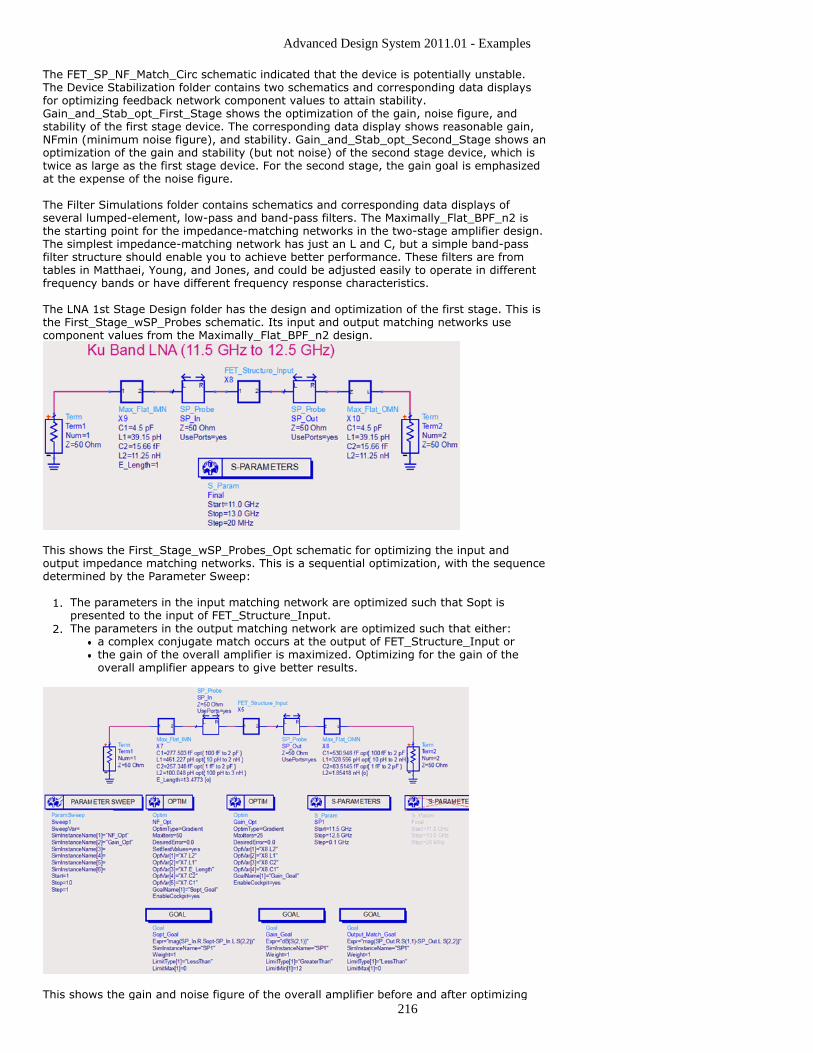
Advanced Design System 2011.01 - Examples
216
The FET_SP_NF_Match_Circ schematic indicated that the device is potentially unstable.The Device Stabilization folder contains two schematics and corresponding data displaysfor optimizing feedback network component values to attain stability.Gain_and_Stab_opt_First_Stage shows the optimization of the gain, noise figure, andstability of the first stage device. The corresponding data display shows reasonable gain,NFmin (minimum noise figure), and stability. Gain_and_Stab_opt_Second_Stage shows anoptimization of the gain and stability (but not noise) of the second stage device, which istwice as large as the first stage device. For the second stage, the gain goal is emphasizedat the expense of the noise figure.
The Filter Simulations folder contains schematics and corresponding data displays ofseveral lumped-element, low-pass and band-pass filters. The Maximally_Flat_BPF_n2 isthe starting point for the impedance-matching networks in the two-stage amplifier design.The simplest impedance-matching network has just an L and C, but a simple band-passfilter structure should enable you to achieve better performance. These filters are fromtables in Matthaei, Young, and Jones, and could be adjusted easily to operate in differentfrequency bands or have different frequency response characteristics.
The LNA 1st Stage Design folder has the design and optimization of the first stage. This isthe First_Stage_wSP_Probes schematic. Its input and output matching networks usecomponent values from the Maximally_Flat_BPF_n2 design.
This shows the First_Stage_wSP_Probes_Opt schematic for optimizing the input andoutput impedance matching networks. This is a sequential optimization, with the sequencedetermined by the Parameter Sweep:
The parameters in the input matching network are optimized such that Sopt is1.presented to the input of FET_Structure_Input.The parameters in the output matching network are optimized such that either:2.
a complex conjugate match occurs at the output of FET_Structure_Input orthe gain of the overall amplifier is maximized. Optimizing for the gain of theoverall amplifier appears to give better results.
This shows the gain and noise figure of the overall amplifier before and after optimizing
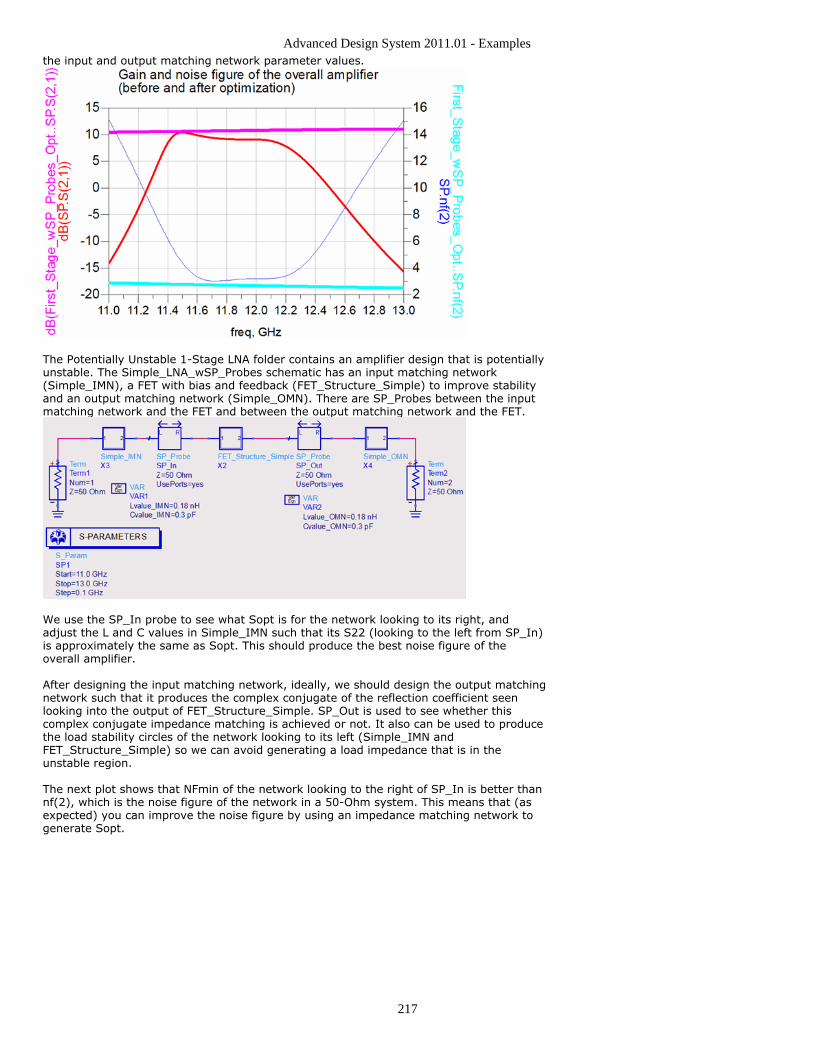
Advanced Design System 2011.01 - Examples
217
the input and output matching network parameter values.
The Potentially Unstable 1-Stage LNA folder contains an amplifier design that is potentiallyunstable. The Simple_LNA_wSP_Probes schematic has an input matching network(Simple_IMN), a FET with bias and feedback (FET_Structure_Simple) to improve stabilityand an output matching network (Simple_OMN). There are SP_Probes between the inputmatching network and the FET and between the output matching network and the FET.
We use the SP_In probe to see what Sopt is for the network looking to its right, andadjust the L and C values in Simple_IMN such that its S22 (looking to the left from SP_In)is approximately the same as Sopt. This should produce the best noise figure of theoverall amplifier.
After designing the input matching network, ideally, we should design the output matchingnetwork such that it produces the complex conjugate of the reflection coefficient seenlooking into the output of FET_Structure_Simple. SP_Out is used to see whether thiscomplex conjugate impedance matching is achieved or not. It also can be used to producethe load stability circles of the network looking to its left (Simple_IMN andFET_Structure_Simple) so we can avoid generating a load impedance that is in theunstable region.
The next plot shows that NFmin of the network looking to the right of SP_In is better thannf(2), which is the noise figure of the network in a 50-Ohm system. This means that (asexpected) you can improve the noise figure by using an impedance matching network togenerate Sopt.
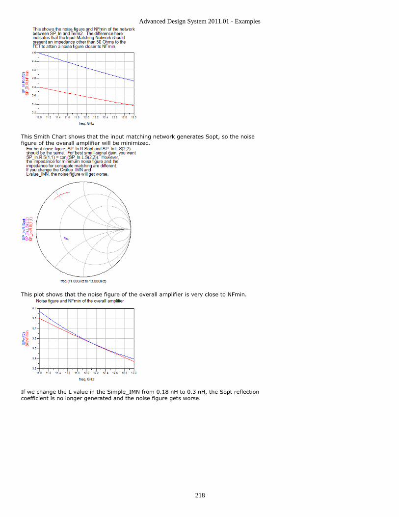
Advanced Design System 2011.01 - Examples
218
This Smith Chart shows that the input matching network generates Sopt, so the noisefigure of the overall amplifier will be minimized.
This plot shows that the noise figure of the overall amplifier is very close to NFmin.
If we change the L value in the Simple_IMN from 0.18 nH to 0.3 nH, the Sopt reflectioncoefficient is no longer generated and the noise figure gets worse.
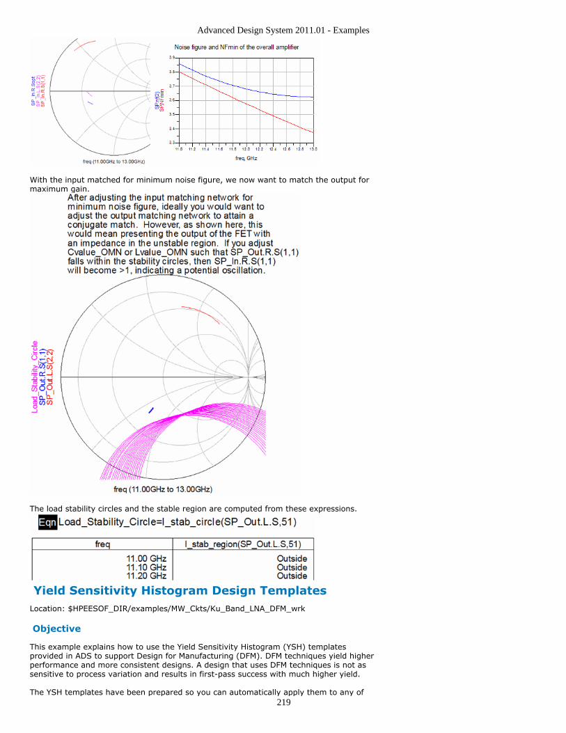
Advanced Design System 2011.01 - Examples
219
With the input matched for minimum noise figure, we now want to match the output formaximum gain.
The load stability circles and the stable region are computed from these expressions.
Yield Sensitivity Histogram Design TemplatesLocation: $HPEESOF_DIR/examples/MW_Ckts/Ku_Band_LNA_DFM_wrk
Objective
This example explains how to use the Yield Sensitivity Histogram (YSH) templatesprovided in ADS to support Design for Manufacturing (DFM). DFM techniques yield higherperformance and more consistent designs. A design that uses DFM techniques is not assensitive to process variation and results in first-pass success with much higher yield.
The YSH templates have been prepared so you can automatically apply them to any of
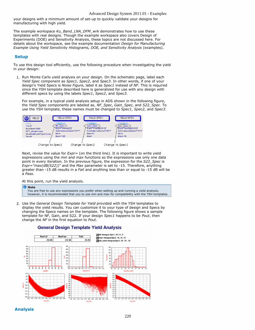
Advanced Design System 2011.01 - Examples
220
your designs with a minimum amount of set-up to quickly validate your designs formanufacturing with high yield.
The example workspace Ku_Band_LNA_DFM_wrk demonstrates how to use thesetemplates with real designs. Though the example workspace also covers Design ofExperiments (DOE) and Sensitivity Analysis, these topics are not discussed here. Fordetails about the workspace, see the example documentation Design for ManufacturingExample Using Yield Sensitivity Histograms, DOE, and Sensitivity Analysis (examples).
Setup
To use this design tool efficiently, use the following procedure when investigating the yieldin your design:
Run Monte Carlo yield analysis on your design. On the schematic page, label each1.Yield Spec component as Spec1, Spec2, and Spec3. In other words, if one of yourdesign's Yield Specs is Noise Figure, label it as Spec1 instead of NF. This is requiredsince the YSH template described here is generalized for use with any design withdifferent specs by using the labels Spec1, Spec2, and Spec3.
For example, in a typical yield analysis setup in ADS shown in the following figure,the Yield Spec components are labeled as, NF_Spec, Gain_Spec, and S22_Spec. Touse the YSH template, these names must be changed to Spec1, Spec2, and Spec3.
Next, revise the value for Expr= (on the third line). It is important to write yieldexpressions using the min and max functions so the expressions use only one datapoint in every iteration. In the previous figure, the expression for the S22_Spec isExpr="max(dB(S22))" and the Max parameter is set to -15. Therefore, anythinggreater than -15 dB results in a Fail and anything less than or equal to -15 dB will bea Pass.
At this point, run the yield analysis.
NoteYou are free to use any expressions you prefer when setting up and running a yield analysis;however, it is recommended that you to use min and max for compatibility with the YSH templates.
Use the General Design Template for Yield provided with the YSH templates to2.display the yield results. You can customize it to your type of design and Specs bychanging the Specs names on the template. The following figure shows a sampletemplate for NF, Gain, and S22. If your design Spec1 happens to be Pout, thenchange the NF in the first equation to Pout.
Analysis
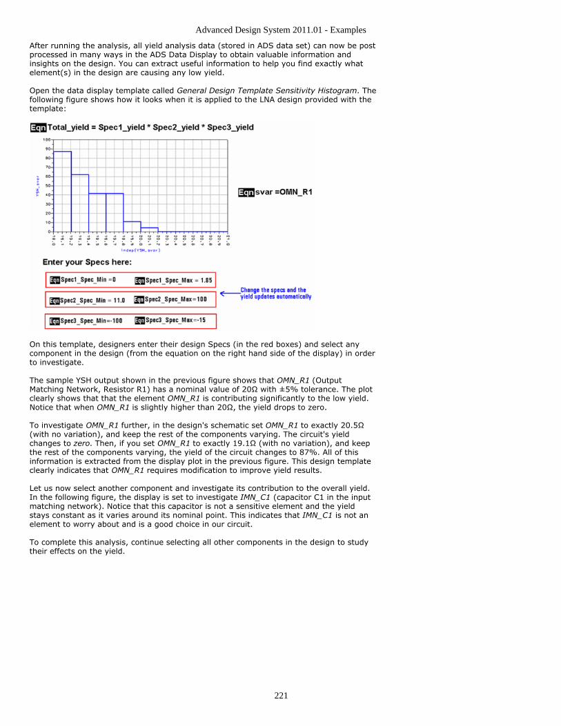
Advanced Design System 2011.01 - Examples
221
After running the analysis, all yield analysis data (stored in ADS data set) can now be postprocessed in many ways in the ADS Data Display to obtain valuable information andinsights on the design. You can extract useful information to help you find exactly whatelement(s) in the design are causing any low yield.
Open the data display template called General Design Template Sensitivity Histogram. Thefollowing figure shows how it looks when it is applied to the LNA design provided with thetemplate:
On this template, designers enter their design Specs (in the red boxes) and select anycomponent in the design (from the equation on the right hand side of the display) in orderto investigate.
The sample YSH output shown in the previous figure shows that OMN_R1 (OutputMatching Network, Resistor R1) has a nominal value of 20Ω with ±5% tolerance. The plotclearly shows that that the element OMN_R1 is contributing significantly to the low yield.Notice that when OMN_R1 is slightly higher than 20Ω, the yield drops to zero.
To investigate OMN_R1 further, in the design's schematic set OMN_R1 to exactly 20.5Ω(with no variation), and keep the rest of the components varying. The circuit's yieldchanges to zero. Then, if you set OMN_R1 to exactly 19.1Ω (with no variation), and keepthe rest of the components varying, the yield of the circuit changes to 87%. All of thisinformation is extracted from the display plot in the previous figure. This design templateclearly indicates that OMN_R1 requires modification to improve yield results.
Let us now select another component and investigate its contribution to the overall yield.In the following figure, the display is set to investigate IMN_C1 (capacitor C1 in the inputmatching network). Notice that this capacitor is not a sensitive element and the yieldstays constant as it varies around its nominal point. This indicates that IMN_C1 is not anelement to worry about and is a good choice in our circuit.
To complete this analysis, continue selecting all other components in the design to studytheir effects on the yield.
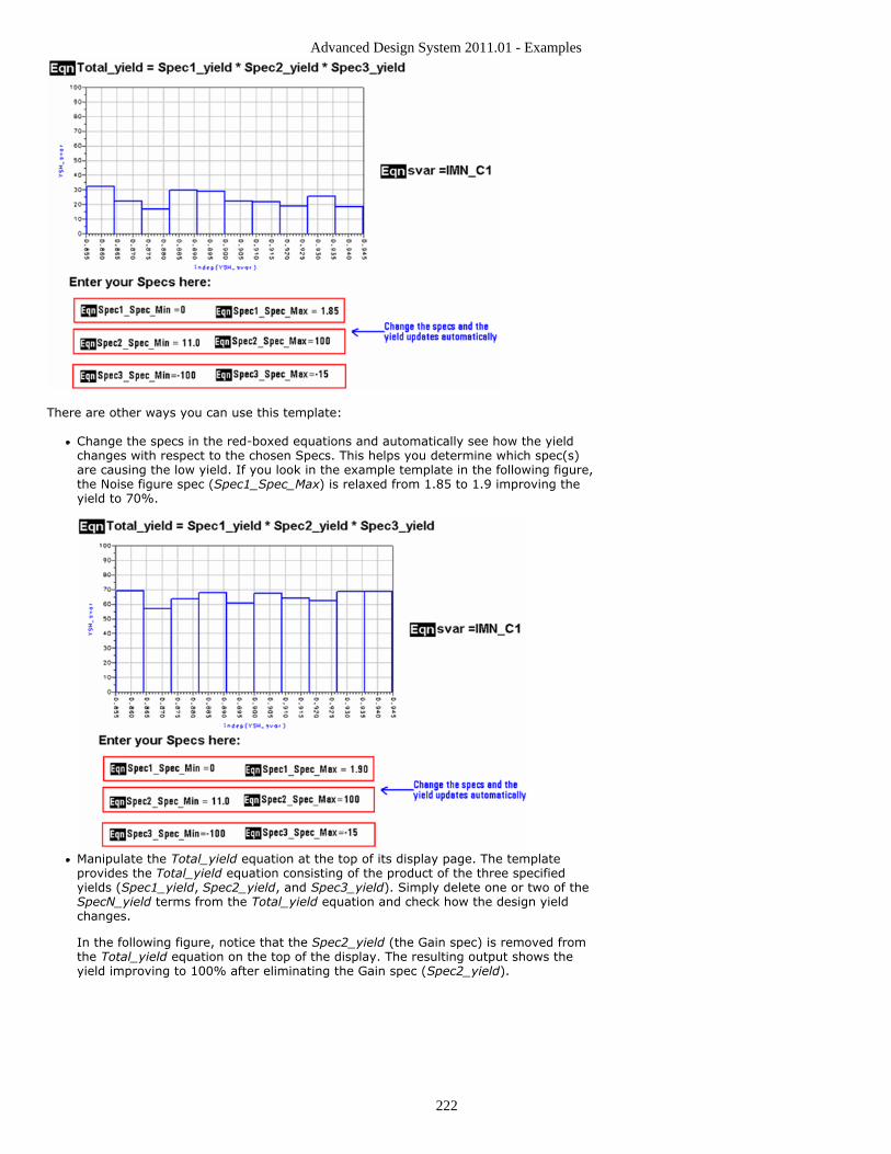
Advanced Design System 2011.01 - Examples
222
There are other ways you can use this template:
Change the specs in the red-boxed equations and automatically see how the yieldchanges with respect to the chosen Specs. This helps you determine which spec(s)are causing the low yield. If you look in the example template in the following figure,the Noise figure spec (Spec1_Spec_Max) is relaxed from 1.85 to 1.9 improving theyield to 70%.
Manipulate the Total_yield equation at the top of its display page. The templateprovides the Total_yield equation consisting of the product of the three specifiedyields (Spec1_yield, Spec2_yield, and Spec3_yield). Simply delete one or two of theSpecN_yield terms from the Total_yield equation and check how the design yieldchanges.
In the following figure, notice that the Spec2_yield (the Gain spec) is removed fromthe Total_yield equation on the top of the display. The resulting output shows theyield improving to 100% after eliminating the Gain spec (Spec2_yield).
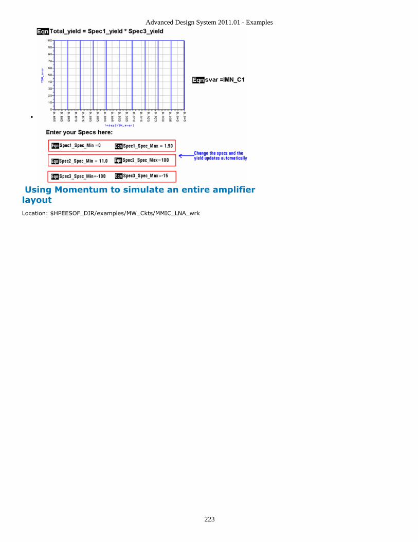
Advanced Design System 2011.01 - Examples
223
Using Momentum to simulate an entire amplifierlayoutLocation: $HPEESOF_DIR/examples/MW_Ckts/MMIC_LNA_wrk
Advanced Design System 2011.01 - Examples
224
Momentum ExamplesExamples on how to evaluate and design modern communications systems for RF andmicrowave antennas and circuits. Also includes examples on optimization of geometryparameters to achieve optimal structures that meet circuit and device performance goals.
1x4 E-Plane Linear Patch Antenna Array (examples)Antenna with Circular Polarization (examples)Box Example (examples)Broadband Planar Antenna (examples)Coplanar Waveguide Bend (examples)Coplanar Waveguide Line with Finite Metal Thickness and Loss (examples)Coplanar Waveguide Notch (examples)Coplanar Waveguide Open (examples)Coupled Stripline Filter (examples)Coupled Stubs (examples)Elliptic Filter Simulation with Model Composer models (examples)EM-Circuit Co-simulation with 1GHz LNA (examples)EM-Circuit Co-Simulation with a LTCC low pass filter (examples)Low-Pass Filter (examples)Low-Pass Filter with Hairpin Bend (examples)Low-Pass Filter with High Out-of-Band Rejection (examples)Low-Pass Stripline Filter with-without Side Walls (examples)Microstrip Line with Via Stubs (examples)Microstrip Meander Line (examples)Optimization of A Microstrip Line (examples)Optimization of A Microstrip Resonator (examples)Printed Dipole Antenna (examples)Proximity Coupled Two Semi-Circular Patch Radiators (examples)RF Board Simulation Comparison between Momentum RF and Momentum Microwave(examples)RF Board with Holes in the Ground (examples)Simple Microstrip Patch Antenna (examples)Simulation of A Ball Grid Array with 96 Solder Balls (examples)Simulation of a Balun (examples)Simulation of Coupled Lines on Printed Circuit Board (examples)Slanted Coupled Line Filter (examples)Slot Dipole Antenna with CPW Feeding (examples)SMD and Delta Gap Port Calibration (examples)Spiral Inductor on Silicon Substrate (examples)Spiral Inductor with Hole in The Ground Plane (examples)Spiral Splitter on GaAs Substrate (examples)Stripline Low-Pass Filter (examples)Strip Lines with Different Via Structures (examples)Sweep Substrate Properties using DataFileList (examples)Thick Conductor Spiral (examples)Tuning Using Layout Components and Momentum (examples)X-Band Balun (examples)
1x4 E-Plane Linear Patch Antenna ArrayLocation: /examples/Momentum/Antenna/E_plane_wrk
Objective
This example shows a Momentum simulation of a four element linear patch antenna array.
Setup
"E_plane" shows the layout of the four element patch array with microstip line1.feeding from underneath."E_plane.dds" shows the return loss as well as the mutual coupling between the2.elements. Comparison between Momentum simulation and measurements is alsoshown."E_plane_FF_10_GHz_phi90_uniform.dds" shows the array pattern, efficiency as well3.as gain when all elements are fed in phase."E_plane_FF_10_GHz_phi90_phaseShift.dds" is for the case when there is a phasetaper in the excitation.
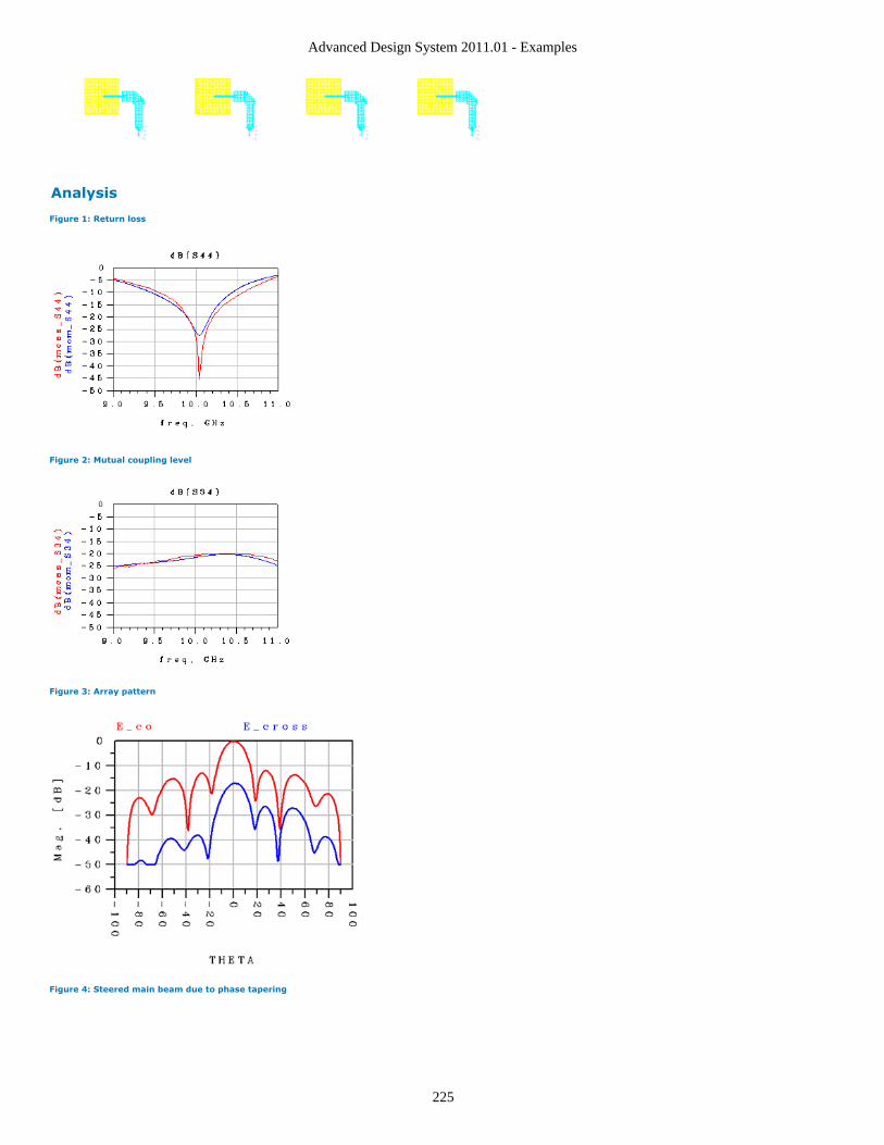
Advanced Design System 2011.01 - Examples
225
Analysis
Figure 1: Return loss
Figure 2: Mutual coupling level
Figure 3: Array pattern
Figure 4: Steered main beam due to phase tapering
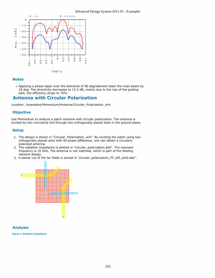
Advanced Design System 2011.01 - Examples
226
Notes
Applying a phase taper over the elements of 90 deg/element steer the main beam by18 deg. The directivity decreases to 13.3 dB, mainly due to the rise of the gratinglobe, the efficiency drops to 70%.
Antenna with Circular PolarizationLocation: /examples/Momentum/Antenna/Circular_Polarization_wrk
Objective
Use Momentum to analyze a patch antenna with circular polarizaiton. The antenna isexcited by two microstrip line through two orthogonally placed slots in the ground plane.
Setup
The design is shown in "Circular_Polarization_wrk". By exciting the patch using two1.orthogonally placed slots with 90 phase difference, one can obtain a circularlypolarized antenna.The radiation impedance is plotted in "circular_polarization.dds". The resonant2.frequency is 10 GHz. The antenna is not matched, which is part of the feedingnetwork design.A planar cut of the far fields is stored in "circular_polarization_FF_left_phi0.dds".3.
Analysis
Figure 1: Radiation Impedance
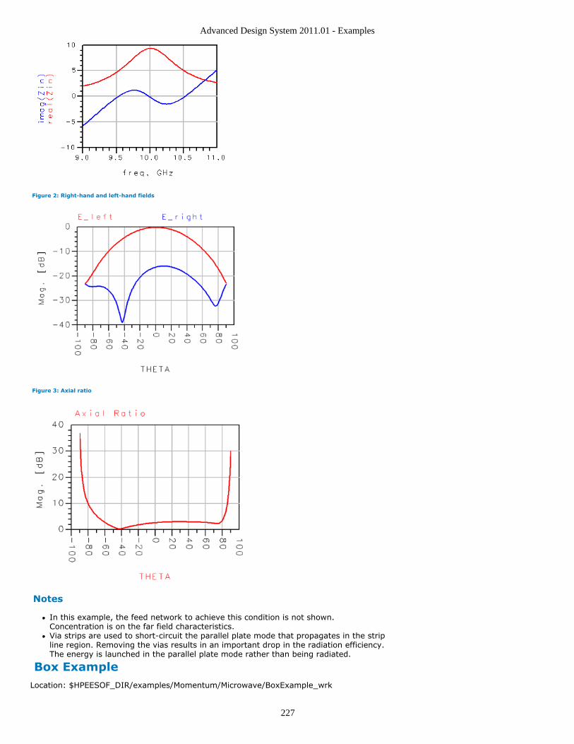
Advanced Design System 2011.01 - Examples
227
Figure 2: Right-hand and left-hand fields
Figure 3: Axial ratio
Notes
In this example, the feed network to achieve this condition is not shown.Concentration is on the far field characteristics.Via strips are used to short-circuit the parallel plate mode that propagates in the stripline region. Removing the vias results in an important drop in the radiation efficiency.The energy is launched in the parallel plate mode rather than being radiated.
Box ExampleLocation: $HPEESOF_DIR/examples/Momentum/Microwave/BoxExample_wrk
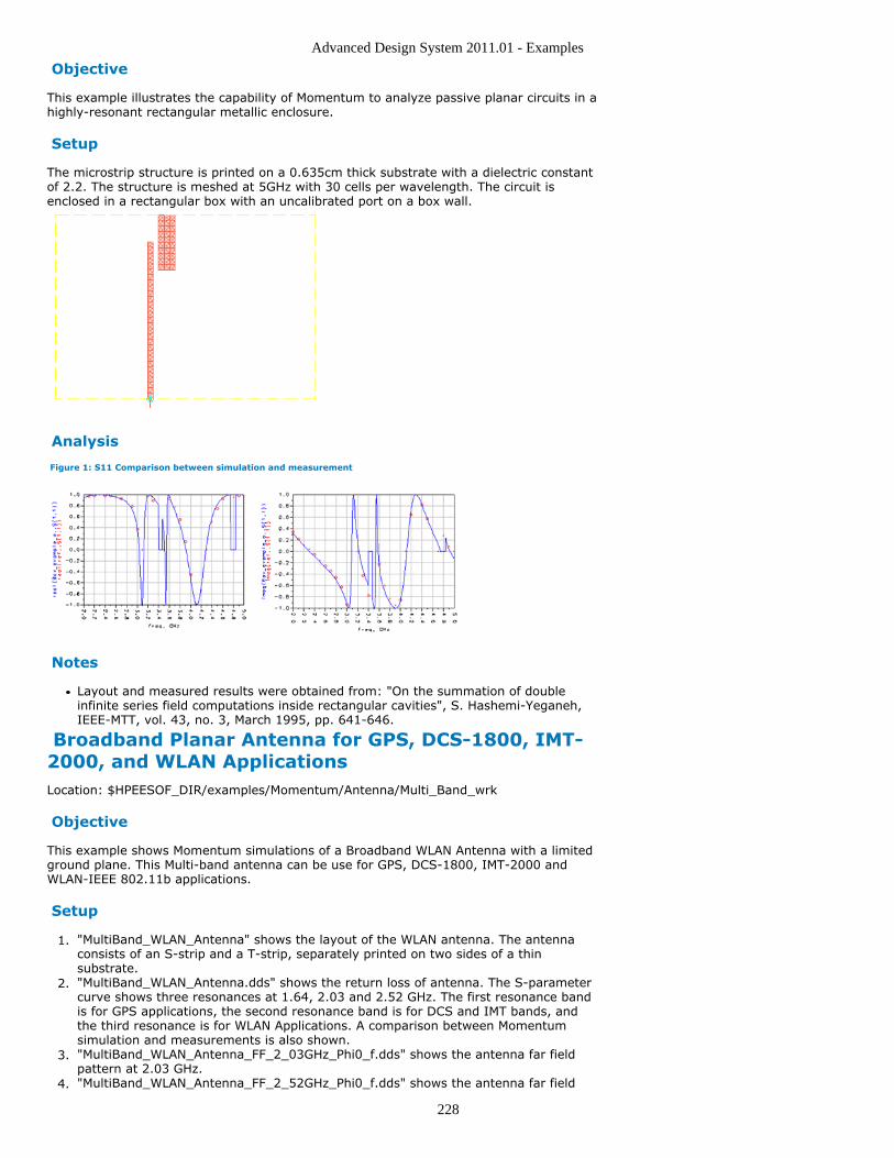
Advanced Design System 2011.01 - Examples
228
Objective
This example illustrates the capability of Momentum to analyze passive planar circuits in ahighly-resonant rectangular metallic enclosure.
Setup
The microstrip structure is printed on a 0.635cm thick substrate with a dielectric constantof 2.2. The structure is meshed at 5GHz with 30 cells per wavelength. The circuit isenclosed in a rectangular box with an uncalibrated port on a box wall.
Analysis
Figure 1: S11 Comparison between simulation and measurement
Notes
Layout and measured results were obtained from: "On the summation of doubleinfinite series field computations inside rectangular cavities", S. Hashemi-Yeganeh,IEEE-MTT, vol. 43, no. 3, March 1995, pp. 641-646.
Broadband Planar Antenna for GPS, DCS-1800, IMT-2000, and WLAN ApplicationsLocation: $HPEESOF_DIR/examples/Momentum/Antenna/Multi_Band_wrk
Objective
This example shows Momentum simulations of a Broadband WLAN Antenna with a limitedground plane. This Multi-band antenna can be use for GPS, DCS-1800, IMT-2000 andWLAN-IEEE 802.11b applications.
Setup
"MultiBand_WLAN_Antenna" shows the layout of the WLAN antenna. The antenna1.consists of an S-strip and a T-strip, separately printed on two sides of a thinsubstrate."MultiBand_WLAN_Antenna.dds" shows the return loss of antenna. The S-parameter2.curve shows three resonances at 1.64, 2.03 and 2.52 GHz. The first resonance bandis for GPS applications, the second resonance band is for DCS and IMT bands, andthe third resonance is for WLAN Applications. A comparison between Momentumsimulation and measurements is also shown."MultiBand_WLAN_Antenna_FF_2_03GHz_Phi0_f.dds" shows the antenna far field3.pattern at 2.03 GHz."MultiBand_WLAN_Antenna_FF_2_52GHz_Phi0_f.dds" shows the antenna far field4.
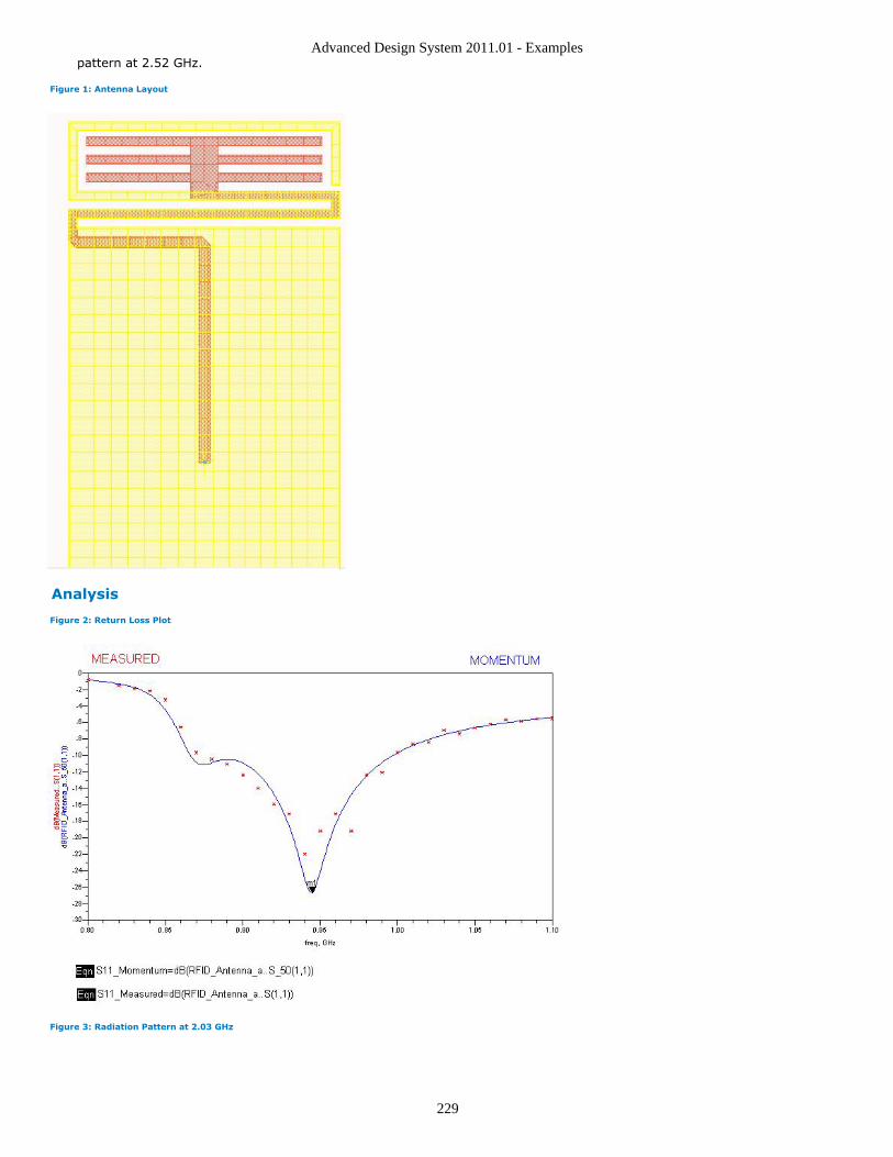
Advanced Design System 2011.01 - Examples
229
pattern at 2.52 GHz.
Figure 1: Antenna Layout
Analysis
Figure 2: Return Loss Plot
Figure 3: Radiation Pattern at 2.03 GHz
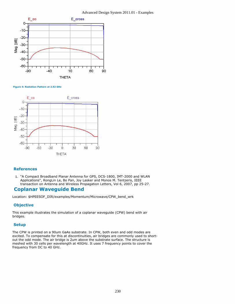
Advanced Design System 2011.01 - Examples
230
Figure 4: Radiation Pattern at 2.52 GHz
References
"A Compact Broadband Planar Antenna for GPS, DCS-1800, IMT-2000 and WLAN1.Applications", RongLin Le, Bo Pan, Joy Lasker and Monos M. Tentzeris, IEEEtransaction on Antenna and Wireless Propagation Letters, Vol 6, 2007, pp 25-27.
Coplanar Waveguide BendLocation: $HPEESOF_DIR/examples/Momentum/Microwave/CPW_bend_wrk
Objective
This example illustrates the simulation of a coplanar waveguide (CPW) bend with airbridges.
Setup
The CPW is printed on a 90um GaAs substrate. In CPW, both even and odd modes areexcited. To compensate for this at discontinuities, air bridges are commonly used to short-out the odd mode. The air bridge is 2um above the substrate surface. The structure ismeshed with 30 cells per wavelength at 40GHz. It uses 7 frequency points to cover thefrequency from DC to 40 GHz.
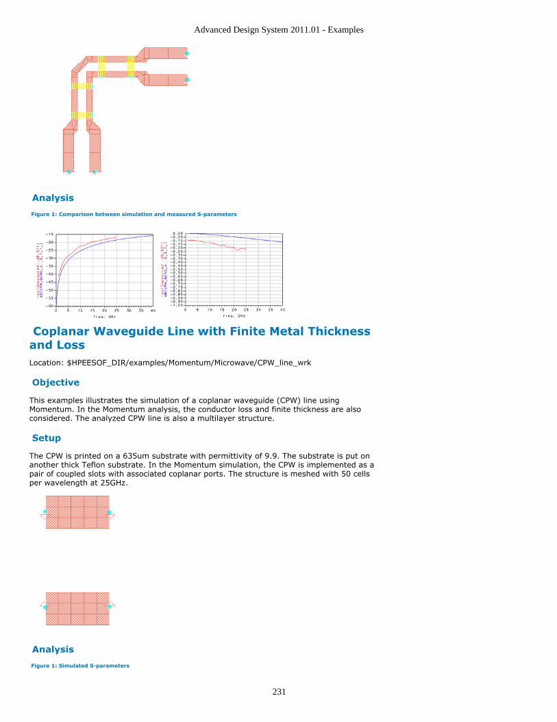
Advanced Design System 2011.01 - Examples
231
Analysis
Figure 1: Comparison between simulation and measured S-parameters
Coplanar Waveguide Line with Finite Metal Thicknessand LossLocation: $HPEESOF_DIR/examples/Momentum/Microwave/CPW_line_wrk
Objective
This examples illustrates the simulation of a coplanar waveguide (CPW) line usingMomentum. In the Momentum analysis, the conductor loss and finite thickness are alsoconsidered. The analyzed CPW line is also a multilayer structure.
Setup
The CPW is printed on a 635um substrate with permittivity of 9.9. The substrate is put onanother thick Teflon substrate. In the Momentum simulation, the CPW is implemented as apair of coupled slots with associated coplanar ports. The structure is meshed with 50 cellsper wavelength at 25GHz.
Analysis
Figure 1: Simulated S-parameters
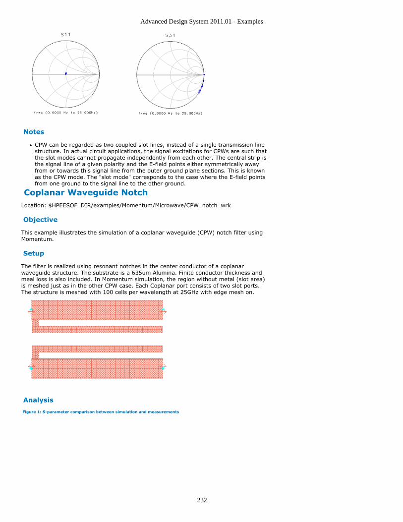
Advanced Design System 2011.01 - Examples
232
Notes
CPW can be regarded as two coupled slot lines, instead of a single transmission linestructure. In actual circuit applications, the signal excitations for CPWs are such thatthe slot modes cannot propagate independently from each other. The central strip isthe signal line of a given polarity and the E-field points either symmetrically awayfrom or towards this signal line from the outer ground plane sections. This is knownas the CPW mode. The "slot mode" corresponds to the case where the E-field pointsfrom one ground to the signal line to the other ground.
Coplanar Waveguide NotchLocation: $HPEESOF_DIR/examples/Momentum/Microwave/CPW_notch_wrk
Objective
This example illustrates the simulation of a coplanar waveguide (CPW) notch filter usingMomentum.
Setup
The filter is realized using resonant notches in the center conductor of a coplanarwaveguide structure. The substrate is a 635um Alumina. Finite conductor thickness andmeal loss is also included. In Momentum simulation, the region without metal (slot area)is meshed just as in the other CPW case. Each Coplanar port consists of two slot ports.The structure is meshed with 100 cells per wavelength at 25GHz with edge mesh on.
Analysis
Figure 1: S-parameter comparison between simulation and measurements
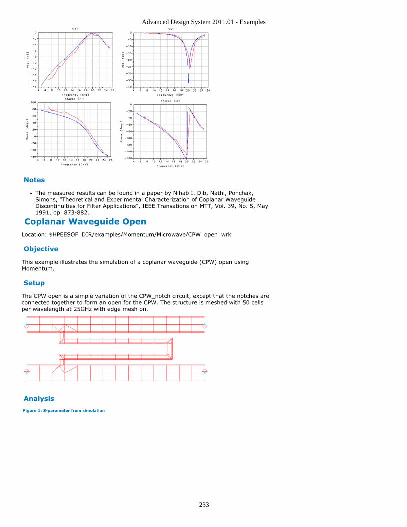
Advanced Design System 2011.01 - Examples
233
Notes
The measured results can be found in a paper by Nihab I. Dib, Nathi, Ponchak,Simons, "Theoretical and Experimental Characterization of Coplanar WaveguideDiscontinuities for Filter Applications", IEEE Transations on MTT, Vol. 39, No. 5, May1991, pp. 873-882.
Coplanar Waveguide OpenLocation: $HPEESOF_DIR/examples/Momentum/Microwave/CPW_open_wrk
Objective
This example illustrates the simulation of a coplanar waveguide (CPW) open usingMomentum.
Setup
The CPW open is a simple variation of the CPW_notch circuit, except that the notches areconnected together to form an open for the CPW. The structure is meshed with 50 cellsper wavelength at 25GHz with edge mesh on.
Analysis
Figure 1: S-parameter from simulation
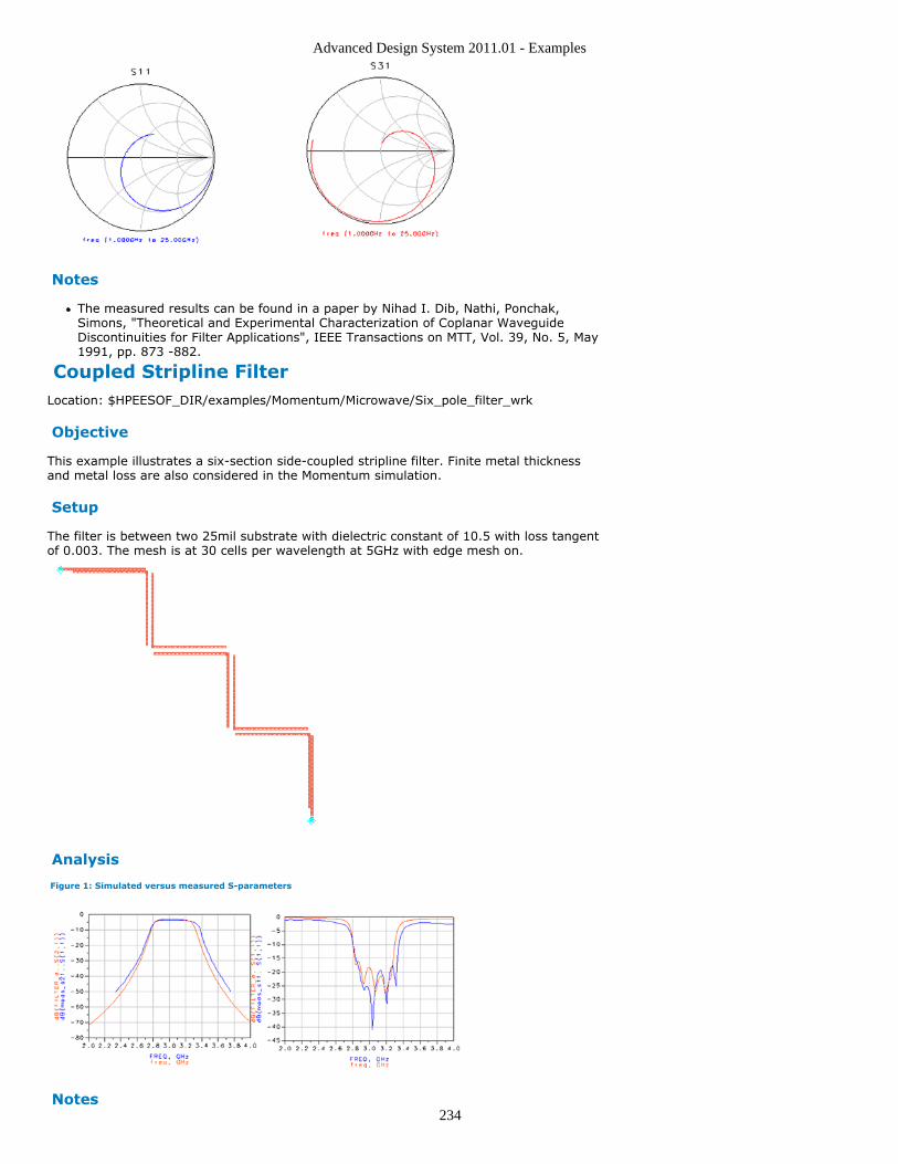
Advanced Design System 2011.01 - Examples
234
Notes
The measured results can be found in a paper by Nihad I. Dib, Nathi, Ponchak,Simons, "Theoretical and Experimental Characterization of Coplanar WaveguideDiscontinuities for Filter Applications", IEEE Transactions on MTT, Vol. 39, No. 5, May1991, pp. 873 -882.
Coupled Stripline FilterLocation: $HPEESOF_DIR/examples/Momentum/Microwave/Six_pole_filter_wrk
Objective
This example illustrates a six-section side-coupled stripline filter. Finite metal thicknessand metal loss are also considered in the Momentum simulation.
Setup
The filter is between two 25mil substrate with dielectric constant of 10.5 with loss tangentof 0.003. The mesh is at 30 cells per wavelength at 5GHz with edge mesh on.
Analysis
Figure 1: Simulated versus measured S-parameters
Notes
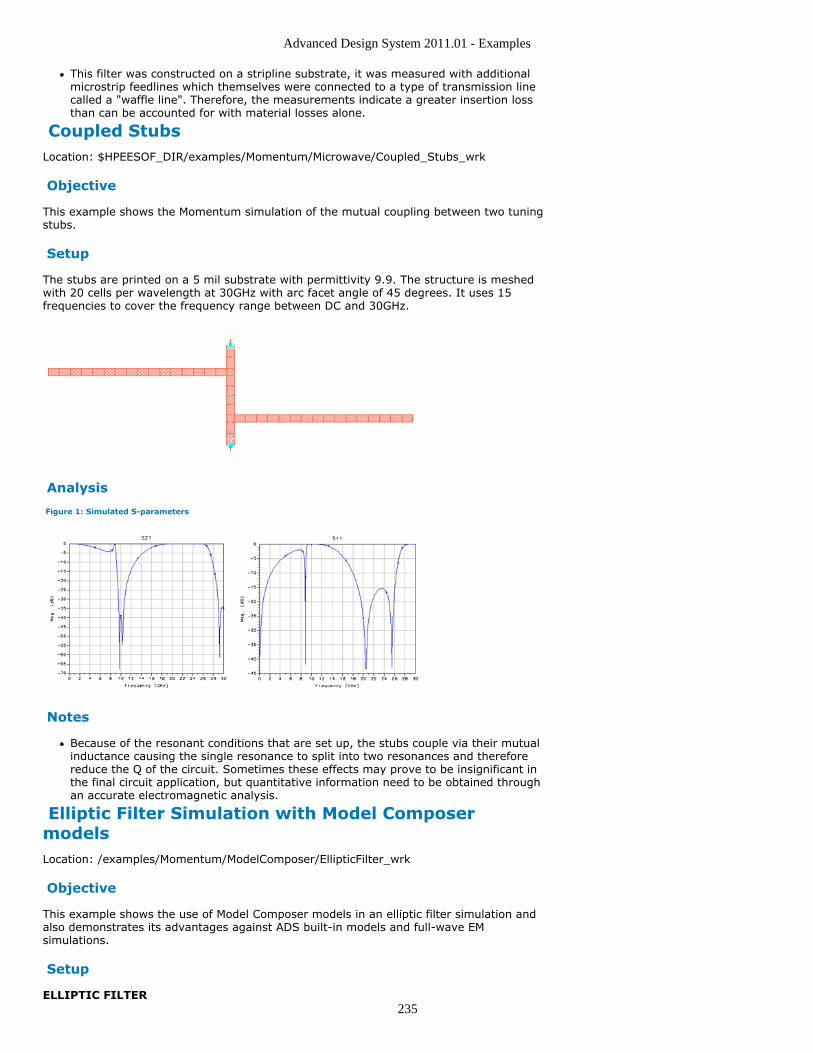
Advanced Design System 2011.01 - Examples
235
This filter was constructed on a stripline substrate, it was measured with additionalmicrostrip feedlines which themselves were connected to a type of transmission linecalled a "waffle line". Therefore, the measurements indicate a greater insertion lossthan can be accounted for with material losses alone.
Coupled StubsLocation: $HPEESOF_DIR/examples/Momentum/Microwave/Coupled_Stubs_wrk
Objective
This example shows the Momentum simulation of the mutual coupling between two tuningstubs.
Setup
The stubs are printed on a 5 mil substrate with permittivity 9.9. The structure is meshedwith 20 cells per wavelength at 30GHz with arc facet angle of 45 degrees. It uses 15frequencies to cover the frequency range between DC and 30GHz.
Analysis
Figure 1: Simulated S-parameters
Notes
Because of the resonant conditions that are set up, the stubs couple via their mutualinductance causing the single resonance to split into two resonances and thereforereduce the Q of the circuit. Sometimes these effects may prove to be insignificant inthe final circuit application, but quantitative information need to be obtained throughan accurate electromagnetic analysis.
Elliptic Filter Simulation with Model ComposermodelsLocation: /examples/Momentum/ModelComposer/EllipticFilter_wrk
Objective
This example shows the use of Model Composer models in an elliptic filter simulation andalso demonstrates its advantages against ADS built-in models and full-wave EMsimulations.
Setup
ELLIPTIC FILTER
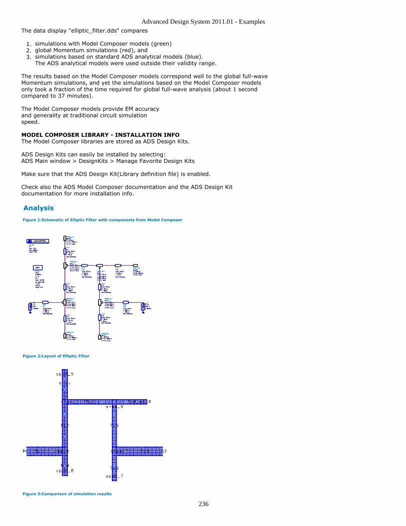
Advanced Design System 2011.01 - Examples
236
The data display "elliptic_filter.dds" compares
simulations with Model Composer models (green)1.global Momentum simulations (red), and2.simulations based on standard ADS analytical models (blue).3.The ADS analytical models were used outside their validity range.
The results based on the Model Composer models correspond well to the global full-waveMomentum simulations, and yet the simulations based on the Model Composer modelsonly took a fraction of the time required for global full-wave analysis (about 1 secondcompared to 37 minutes).
The Model Composer models provide EM accuracyand generality at traditional circuit simulationspeed.
MODEL COMPOSER LIBRARY - INSTALLATION INFOThe Model Composer libraries are stored as ADS Design Kits.
ADS Design Kits can easily be installed by selecting:ADS Main window > DesignKits > Manage Favorite Design Kits
Make sure that the ADS Design Kit(Library definition file) is enabled.
Check also the ADS Model Composer documentation and the ADS Design Kitdocumentation for more installation info.
Analysis
Figure 1:Schematic of Elliptic Filter with components from Model Composer
Figure 2:Layout of Elliptic Filter
Figure 3:Comparison of simulation results
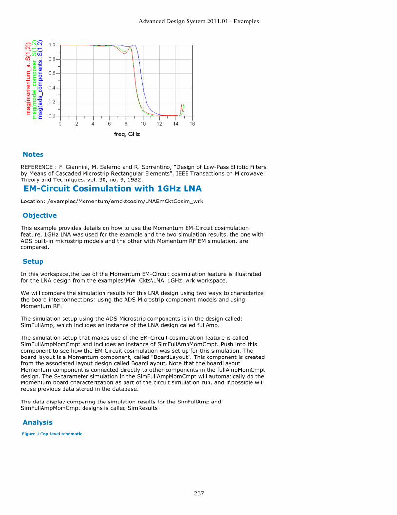
Advanced Design System 2011.01 - Examples
237
Notes
REFERENCE : F. Giannini, M. Salerno and R. Sorrentino, "Design of Low-Pass Elliptic Filtersby Means of Cascaded Microstrip Rectangular Elements", IEEE Transactions on MicrowaveTheory and Techniques, vol. 30, no. 9, 1982.
EM-Circuit Cosimulation with 1GHz LNALocation: /examples/Momentum/emcktcosim/LNAEmCktCosim_wrk
Objective
This example provides details on how to use the Momentum EM-Circuit cosimulationfeature. 1GHz LNA was used for the example and the two simulation results, the one withADS built-in microstrip models and the other with Momentum RF EM simulation, arecompared.
Setup
In this workspace,the use of the Momentum EM-Circuit cosimulation feature is illustratedfor the LNA design from the examples\MW_Ckts\LNA_1GHz_wrk workspace.
We will compare the simulation results for this LNA design using two ways to characterizethe board interconnections: using the ADS Microstrip component models and usingMomentum RF.
The simulation setup using the ADS Microstrip components is in the design called:SimFullAmp, which includes an instance of the LNA design called fullAmp.
The simulation setup that makes use of the EM-Circuit cosimulation feature is calledSimFullAmpMomCmpt and includes an instance of SimFullAmpMomCmpt. Push into thiscomponent to see how the EM-Circuit cosimulation was set up for this simulation. Theboard layout is a Momentum component, called "BoardLayout". This component is createdfrom the associated layout design called BoardLayout. Note that the boardLayoutMomentum component is connected directly to other components in the fullAmpMomCmptdesign. The S-parameter simulation in the SimFullAmpMomCmpt will automatically do theMomentum board characterization as part of the circuit simulation run, and if possible willreuse previous data stored in the database.
The data display comparing the simulation results for the SimFullAmp andSimFullAmpMomCmpt designs is called SimResults
Analysis
Figure 1:Top-level schematic
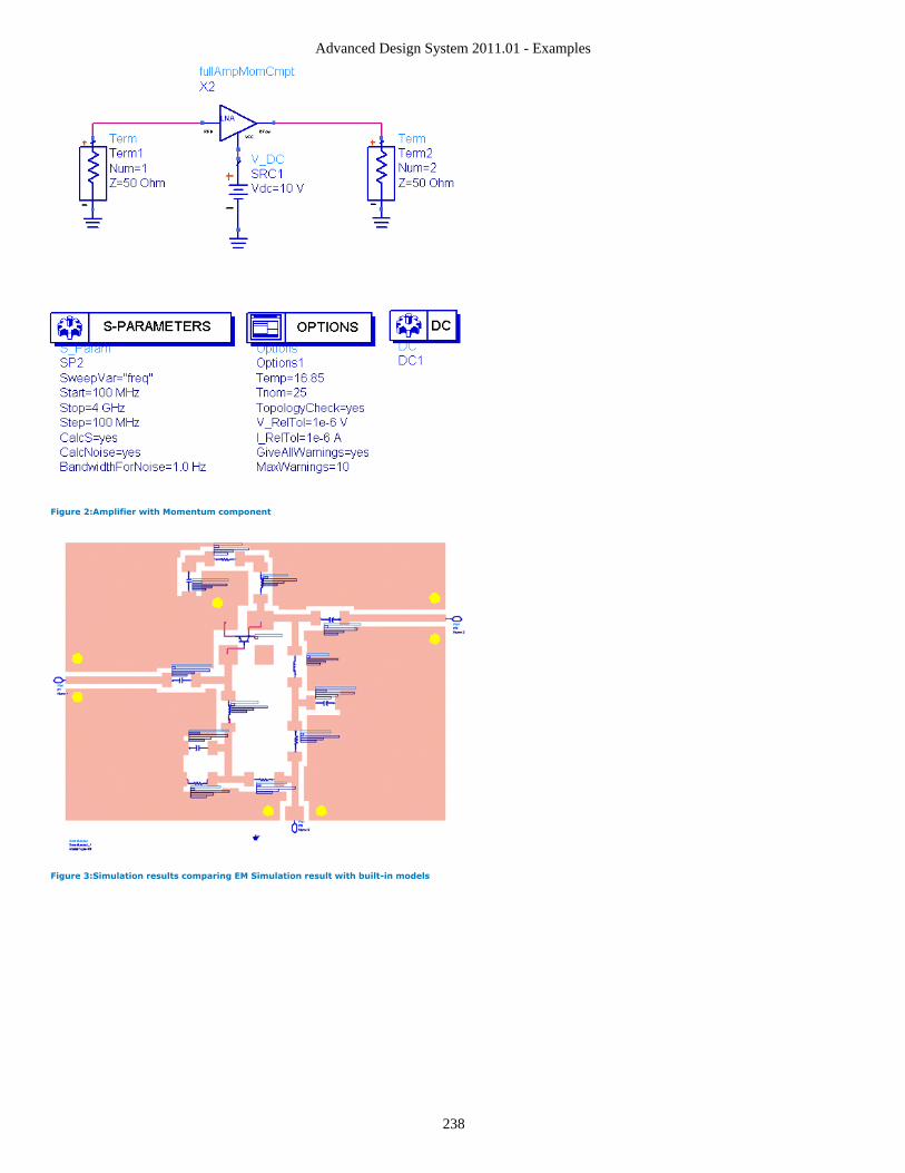
Advanced Design System 2011.01 - Examples
238
Figure 2:Amplifier with Momentum component
Figure 3:Simulation results comparing EM Simulation result with built-in models
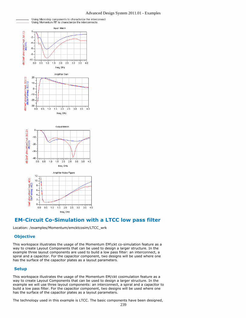
Advanced Design System 2011.01 - Examples
239
EM-Circuit Co-Simulation with a LTCC low pass filterLocation: /examples/Momentum/emcktcosim/LTCC_wrk
Objective
This workspace illustrates the usage of the Momentum EM\ckt co-simulation feature as away to create Layout Components that can be used to design a larger structure. In theexample three layout components are used to build a low pass filter: an interconnect, aspiral and a capacitor. For the capacitor component, two designs will be used where onehas the surface of the capacitor plates as a layout parameters.
Setup
This workspace illustrates the usage of the Momentum EM/ckt cosimulation feature as away to create Layout Components that can be used to design a larger structure. In theexample we will use three layout components: an interconnect, a spiral and a capacitor tobuild a low pass filter. For the capacitor component, two designs will be used where onehas the surface of the capacitor plates as a layout parameters.
The technology used in this example is LTCC. The basic components have been designed,
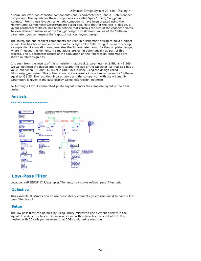
Advanced Design System 2011.01 - Examples
240
a spiral inductor, two capacitor components (one is parameterized) and a T interconnectcomponent. The layouts for these componens are called 'spiral', 'cap', 'cap_p' and'connect'. From these layouts, schematic components have been created using theMomentum> Component>Create/Update dialog box. Note that for the 'cap_p' design, alayout parameter 'deltalen' has been defined that controls the size of the capacitor plates.To view different instances of the 'cap_p' design with different values of the 'deltalen'parameter, you can inspect the 'cap_p_instances' layout design.
The spiral, cap and connect components are used in a schematic design to build a biggercircuit. This has been done in the schematic design called "filterdesign". From this designa simple circuit simulation run generates the S-parameter result for the complete design,where if needed the Momentum simulations are run in automatically as part of thisprocess. The S-parameter results of the simulation on the 'filterdesign' schematic areshown in filterdesign.dds.
It is seen from the results of this simulation that the S11 parameter at 2 GHz is - 8.5db.We will optimize the design (more particularly the size of the capacitor) so that S11 has avalue inbetween -15 and -16 dB at 2 GHz. This is done using the design called'filterdesign_optimize'. This optimization process results in a optimized value for 'deltalen'equal to -31.25. The resulting S-paramaters and the comparison with the original S-parameters is given in the data display called 'filterdesign_optimize'.
Performing a Layout>Generate/Update Layout creates the complete layout of the filterdesign.
Analysis
Filter with Momentum components
Low-Pass FilterLocation: $HPEESOF_DIR/examples/Momentum/Microwave/Low_pass_filter_wrk
Objective
This example illustrates how to use basic library elements (microstrip lines) to creat a low-pass filter layout.
Setup
The low pass filter can be built by using library microstrip line element directly in thelayout. The structure has a thickness of 25 mil with a dielectric constant of 9.9. It ismeshed with 20 cells per wavelength at 20GHz with edge mesh on.
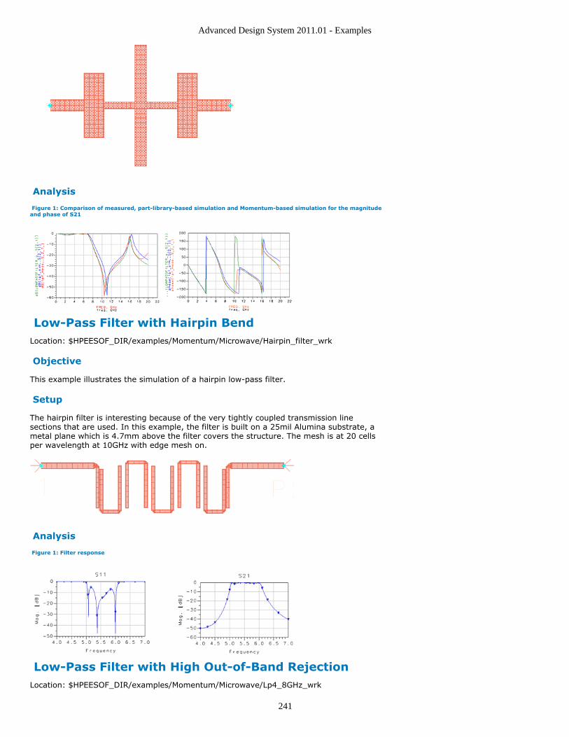
Advanced Design System 2011.01 - Examples
241
Analysis
Figure 1: Comparison of measured, part-library-based simulation and Momentum-based simulation for the magnitudeand phase of S21
Low-Pass Filter with Hairpin BendLocation: $HPEESOF_DIR/examples/Momentum/Microwave/Hairpin_filter_wrk
Objective
This example illustrates the simulation of a hairpin low-pass filter.
Setup
The hairpin filter is interesting because of the very tightly coupled transmission linesections that are used. In this example, the filter is built on a 25mil Alumina substrate, ametal plane which is 4.7mm above the filter covers the structure. The mesh is at 20 cellsper wavelength at 10GHz with edge mesh on.
Analysis
Figure 1: Filter response
Low-Pass Filter with High Out-of-Band RejectionLocation: $HPEESOF_DIR/examples/Momentum/Microwave/Lp4_8GHz_wrk
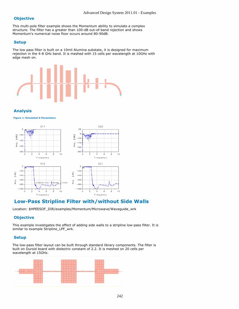
Advanced Design System 2011.01 - Examples
242
Objective
This multi-pole filter example shows the Momentum ability to simulate a complexstructure. The filter has a greater than 100-dB out-of-band rejection and showsMomentum's numerical noise floor occurs around 80-90dB.
Setup
The low pass filter is built on a 10mil Alumina substate, it is designed for maximumrejection in the 4-8 GHz band. It is meshed with 15 cells per wavelength at 10GHz withedge mesh on.
Analysis
Figure 1: Simulated S-Parameters
Low-Pass Stripline Filter with/without Side WallsLocation: $HPEESOF_DIR/examples/Momentum/Microwave/Waveguide_wrk
Objective
This example investigates the effect of adding side walls to a stripline low-pass filter. It issimilar to example Stripline_LPF_wrk.
Setup
The low-pass filter layout can be built through standard library components. The filter isbuilt on Duroid board with dielectric constant of 2.2. It is meshed on 20 cells perwavelength at 15GHz.
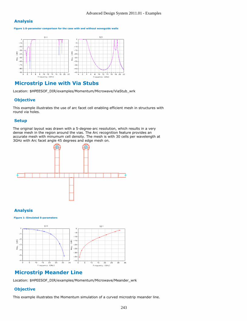
Advanced Design System 2011.01 - Examples
243
Analysis
Figure 1:S-parameter comparison for the case with and without waveguide walls
Microstrip Line with Via StubsLocation: $HPEESOF_DIR/examples/Momentum/Microwave/ViaStub_wrk
Objective
This example illustrates the use of arc facet cell enabling efficient mesh in structures withround via holes.
Setup
The original layout was drawn with a 5-degree-arc resolution, which results in a verydense mesh in the region around the vias. The Arc recognition feature provides anaccurate mesh with minumum cell density. The mesh is with 30 cells per wavelength at3GHz with Arc facet angle 45 degrees and edge mesh on.
Analysis
Figure 1: Simulated S-parameters
Microstrip Meander LineLocation: $HPEESOF_DIR/examples/Momentum/Microwave/Meander_wrk
Objective
This example illustrates the Momentum simulation of a curved microstrip meander line.
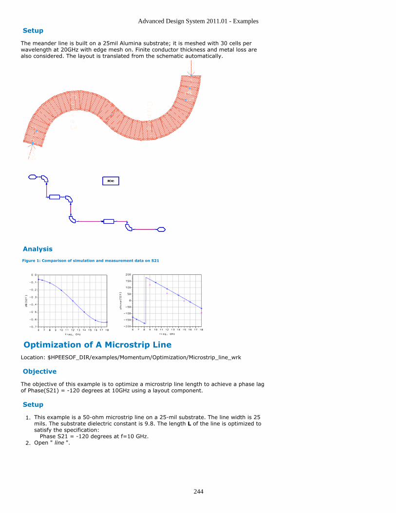
Advanced Design System 2011.01 - Examples
244
Setup
The meander line is built on a 25mil Alumina substrate; it is meshed with 30 cells perwavelength at 20GHz with edge mesh on. Finite conductor thickness and metal loss arealso considered. The layout is translated from the schematic automatically.
Analysis
Figure 1: Comparison of simulation and measurement data on S21
Optimization of A Microstrip LineLocation: $HPEESOF_DIR/examples/Momentum/Optimization/Microstrip_line_wrk
Objective
The objective of this example is to optimize a microstrip line length to achieve a phase lagof Phase(S21) = -120 degrees at 10GHz using a layout component.
Setup
This example is a 50-ohm microstrip line on a 25-mil substrate. The line width is 251.mils. The substrate dielectric constant is 9.8. The length L of the line is optimized tosatisfy the specification: Phase S21 = -120 degrees at f=10 GHz.Open " line ".2.
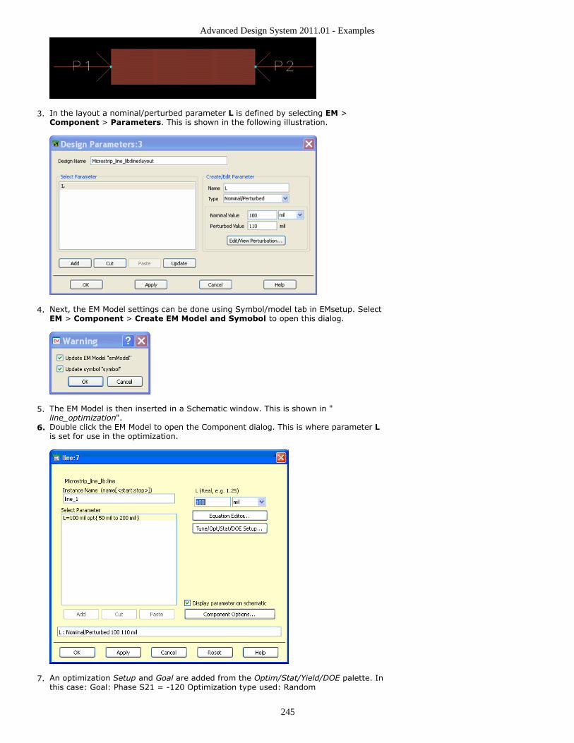
Advanced Design System 2011.01 - Examples
245
In the layout a nominal/perturbed parameter L is defined by selecting EM >3.Component > Parameters. This is shown in the following illustration.
Next, the EM Model settings can be done using Symbol/model tab in EMsetup. Select 4.EM > Component > Create EM Model and Symobol to open this dialog.
The EM Model is then inserted in a Schematic window. This is shown in "5.line_optimization".Double click the EM Model to open the Component dialog. This is where parameter L6.is set for use in the optimization.
An optimization Setup and Goal are added from the Optim/Stat/Yield/DOE palette. In7.this case: Goal: Phase S21 = -120 Optimization type used: Random
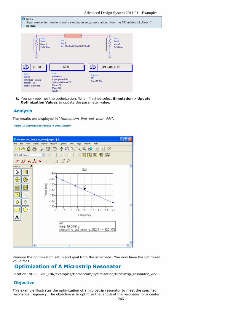
Advanced Design System 2011.01 - Examples
246
NoteS-parameter terminations and a simulation setup were added from the "Simulation-S_Param"palette.
You can now run the optimization. When finished select Simulation > Update8.Optimization Values to update the parameter value.
Analysis
The results are displayed in "Momentum_line_opt_mom.dds".
Figure 1: Optimization results in Data Display.
Remove the optimization setup and goal from the schematic. You now have the optimizedvalue for L.
Optimization of A Microstrip ResonatorLocation: $HPEESOF_DIR/examples/Momentum/Optimization/Microstrip_resonator_wrk
Objective
This example illustrates the optimization of a microstrip resonator to meet the specifiedresonance frequency. The objective is to optimize the length of the resonator for a center
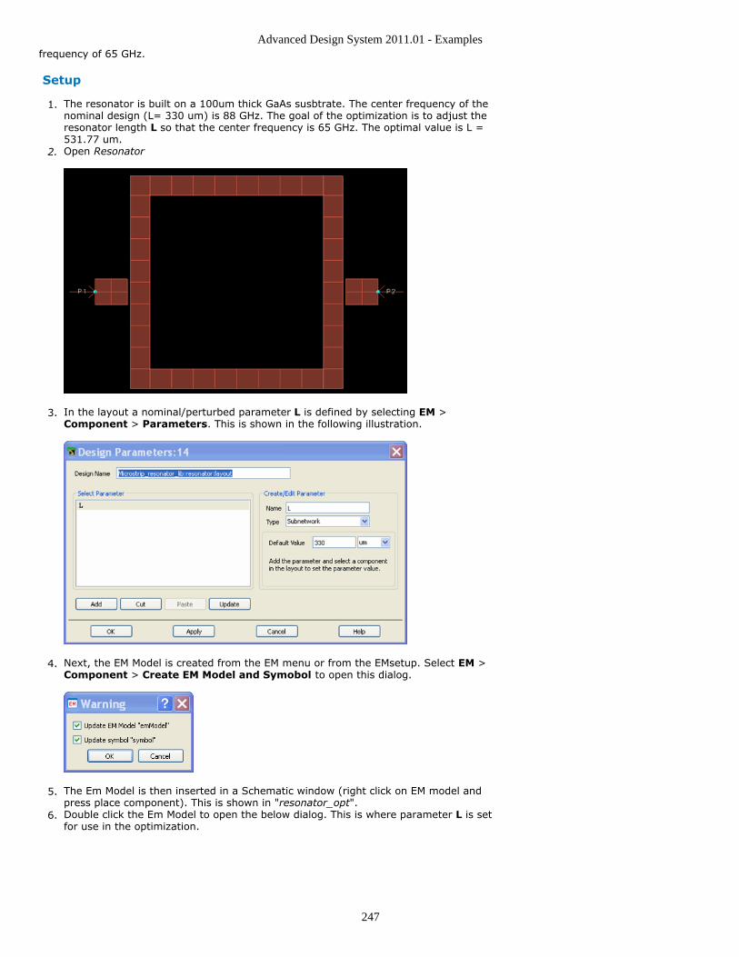
Advanced Design System 2011.01 - Examples
247
frequency of 65 GHz.
Setup
The resonator is built on a 100um thick GaAs susbtrate. The center frequency of the1.nominal design (L= 330 um) is 88 GHz. The goal of the optimization is to adjust theresonator length L so that the center frequency is 65 GHz. The optimal value is L =531.77 um.Open Resonator2.
In the layout a nominal/perturbed parameter L is defined by selecting EM >3.Component > Parameters. This is shown in the following illustration.
Next, the EM Model is created from the EM menu or from the EMsetup. Select EM >4.Component > Create EM Model and Symobol to open this dialog.
The Em Model is then inserted in a Schematic window (right click on EM model and5.press place component). This is shown in "resonator_opt".Double click the Em Model to open the below dialog. This is where parameter L is set6.for use in the optimization.
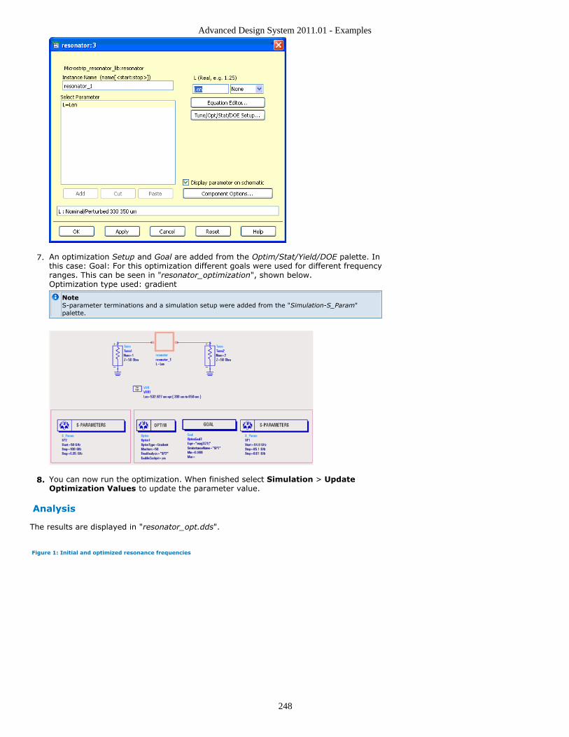
Advanced Design System 2011.01 - Examples
248
An optimization Setup and Goal are added from the Optim/Stat/Yield/DOE palette. In7.this case: Goal: For this optimization different goals were used for different frequencyranges. This can be seen in "resonator_optimization", shown below.Optimization type used: gradient
NoteS-parameter terminations and a simulation setup were added from the "Simulation-S_Param"palette.
You can now run the optimization. When finished select Simulation > Update8.Optimization Values to update the parameter value.
Analysis
The results are displayed in "resonator_opt.dds".
Figure 1: Initial and optimized resonance frequencies
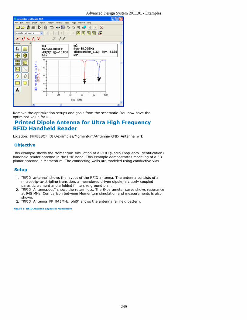
Advanced Design System 2011.01 - Examples
249
Remove the optimization setups and goals from the schematic. You now have theoptimized value for L.
Printed Dipole Antenna for Ultra High FrequencyRFID Handheld ReaderLocation: $HPEESOF_DIR/examples/Momentum/Antenna/RFID_Antenna_wrk
Objective
This example shows the Momentum simulation of a RFID (Radio Frequency Identification)handheld reader antenna in the UHF band. This example demonstrates modeling of a 3Dplanar antenna in Momentum. The connecting walls are modeled using conductive vias.
Setup
"RFID_antenna" shows the layout of the RFID antenna. The antenna consists of a1.microstrip-to-stripline transition, a meandered driven dipole, a closely coupledparasitic element and a folded finite size ground plan."RFID_Antenna.dds" shows the return loss. The S-parameter curve shows resonance2.at 945 MHz. Comparison between Momentum simulation and measurements is alsoshown."RFID_Antenna_FF_945MHz_phi0" shows the antenna far field pattern.3.
Figure 1: RFID Antenna Layout in Momentum
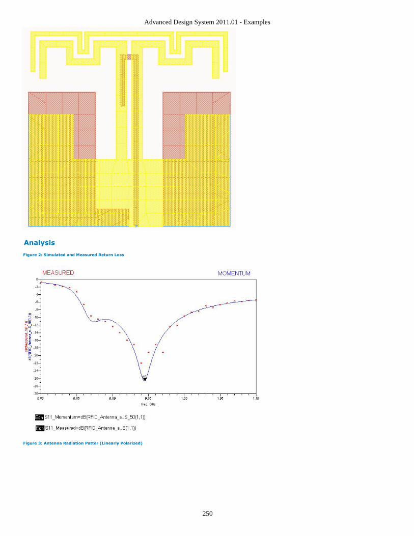
Advanced Design System 2011.01 - Examples
250
Analysis
Figure 2: Simulated and Measured Return Loss
Figure 3: Antenna Radiation Patter (Linearly Polarized)
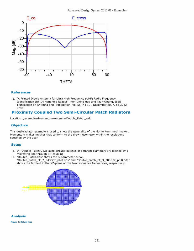
Advanced Design System 2011.01 - Examples
251
References
"A Printed Dipole Antenna for Ultra High Frequency (UHF) Radio Frequency1.Identification (RFID) Handheld Reader", Ren-Ching Hua and Tzyh-Ghung, IEEETransaction on Antenna and Propagation, Vol 55, No 12 , December 2007, pp 3742-3745.
Proximity Coupled Two Semi-Circular Patch RadiatorsLocation: /examples/Momentum/Antenna/Double_Patch_wrk
Objective
This dual-radiator example is used to show the generality of the Momentum mesh maker.Momentum makes meshes that conform to the drawn geometry within the resolutionsspecified by the user.
Setup
In "Double_Patch", two semi-circular patches of different diameters are excited by a1.microstrip line through EM coupling."Double_Patch.dds" shows the S-parameter curve.2."Double_Patch_FF_2_943Ghz_phi0.dds" and "Double_Patch_FF_3_203Ghz_phi0.dds"shows the far field in the XZ-plane at the two resonance frequencies, respectively.
Analysis
Figure 1: Return loss
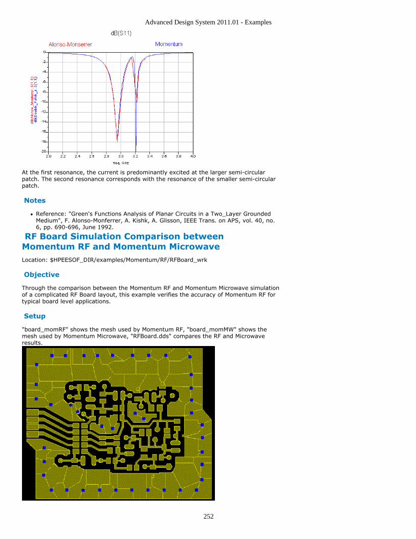
Advanced Design System 2011.01 - Examples
252
At the first resonance, the current is predominantly excited at the larger semi-circularpatch. The second resonance corresponds with the resonance of the smaller semi-circularpatch.
Notes
Reference: "Green's Functions Analysis of Planar Circuits in a Two_Layer GroundedMedium", F. Alonso-Monferrer, A. Kishk, A. Glisson, IEEE Trans. on APS, vol. 40, no.6, pp. 690-696, June 1992.
RF Board Simulation Comparison betweenMomentum RF and Momentum MicrowaveLocation: $HPEESOF_DIR/examples/Momentum/RF/RFBoard_wrk
Objective
Through the comparison between the Momentum RF and Momentum Microwave simulationof a complicated RF Board layout, this example verifies the accuracy of Momentum RF fortypical board level applications.
Setup
"board_momRF" shows the mesh used by Momentum RF, "board_momMW" shows themesh used by Momentum Microwave, "RFBoard.dds" compares the RF and Microwaveresults.
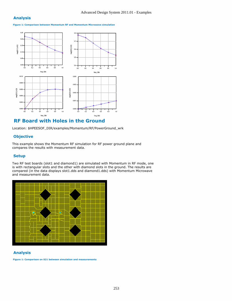
Advanced Design System 2011.01 - Examples
253
Analysis
Figure 1: Comparison between Momentum RF and Momentum Microwave simulation
RF Board with Holes in the GroundLocation: $HPEESOF_DIR/examples/Momentum/RF/PowerGround_wrk
Objective
This example shows the Momentum RF simulation for RF power ground plane andcompares the results with measurement data.
Setup
Two RF test boards (slot1 and diamond1) are simulated with Momentum in RF mode, oneis with rectangular slots and the other with diamond slots in the ground. The results arecompared (in the data displays slot1.dds and diamond1.dds) with Momentum Microwaveand measurement data.
Analysis
Figure 1: Comparison on S21 between simulation and measurements
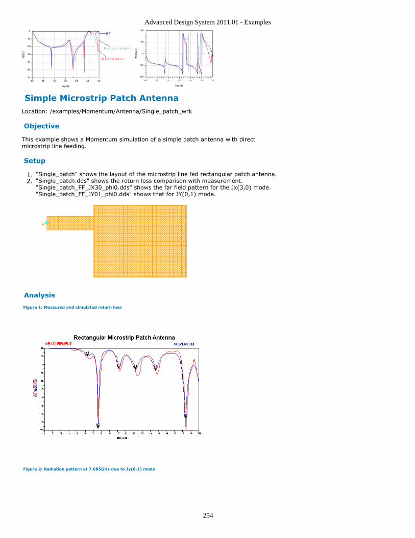
Advanced Design System 2011.01 - Examples
254
Simple Microstrip Patch AntennaLocation: /examples/Momentum/Antenna/Single_patch_wrk
Objective
This example shows a Momentum simulation of a simple patch antenna with directmicrostrip line feeding.
Setup
"Single_patch" shows the layout of the microstrip line fed rectangular patch antenna.1."Single_patch.dds" shows the return loss comparison with measurement.2."Single_patch_FF_JX30_phi0.dds" shows the far field pattern for the Jx(3,0) mode."Single_patch_FF_JY01_phi0.dds" shows that for JY(0,1) mode.
Analysis
Figure 1: Measured and simulated return loss
Figure 2: Radiation pattern at 7.685GHz due to Jy(0,1) mode
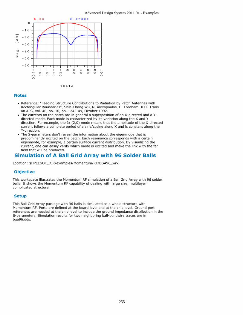
Advanced Design System 2011.01 - Examples
255
Notes
Reference: "Feeding Structure Contributions to Radiation by Patch Antennas withRectangular Boundaries", Shih-Chang Wu, N. Alexopoulos, O. Fordham, IEEE Trans.on APS, vol. 40, no. 10, pp. 1245-49, October 1992.The currents on the patch are in general a superposition of an X-directed and a Y-directed mode. Each mode is characterized by its variation along the X and Ydirection. For example, the Jx (2,0) mode means that the amplitude of the X-directedcurrent follows a complete period of a sine/cosine along X and is constant along theY-direction.The S-parameters don't reveal the information about the eigenmode that ispredominantly excited on the patch. Each resonance corresponds with a certaineigenmode, for example, a certain surface current distribution. By visualizing thecurrent, one can easily verify which mode is excited and make the link with the farfield that will be produced.
Simulation of A Ball Grid Array with 96 Solder BallsLocation: $HPEESOF_DIR/examples/Momentum/RF/BGA96_wrk
Objective
This workspace illustrates the Momentum RF simulation of a Ball Grid Array with 96 solderballs. It shows the Momentum RF capability of dealing with large size, multilayercomplicated structure.
Setup
This Ball Grid Array package with 96 balls is simulated as a whole structure withMomentum RF. Ports are defined at the board level and at the chip level. Ground portreferences are needed at the chip level to include the ground impedance distribution in theS-parameters. Simulation results for two neighboring ball-bondwire traces are inbga96.dds.
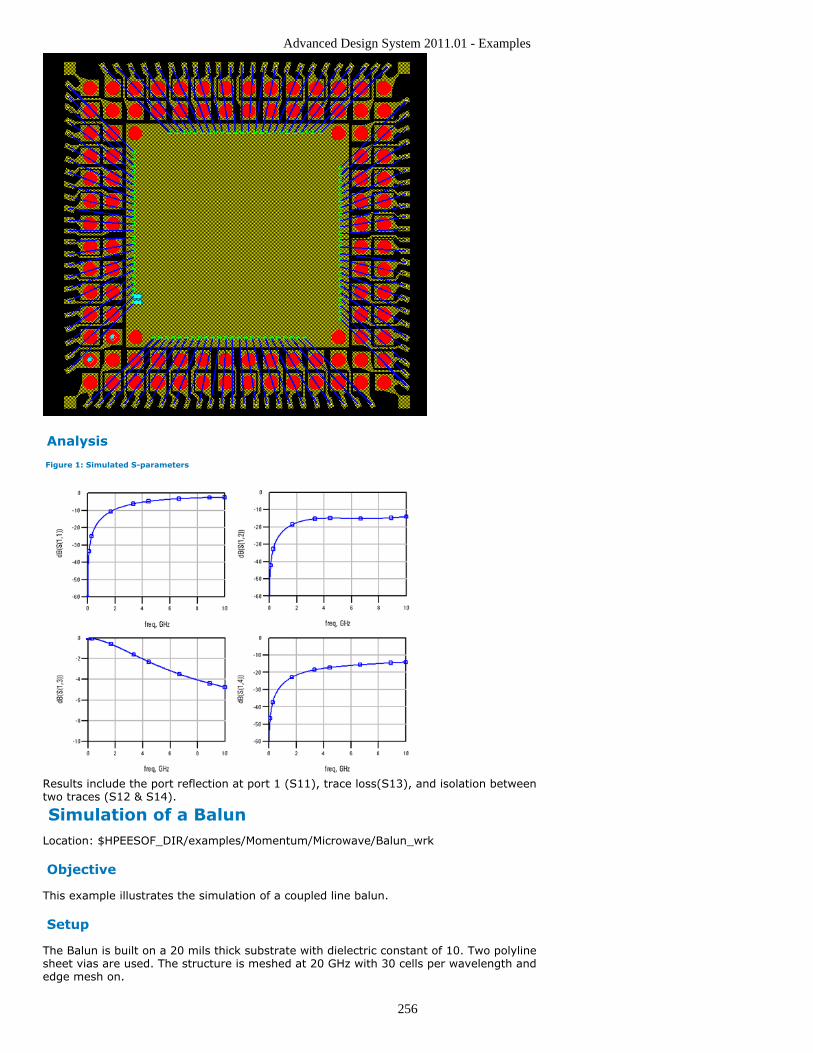
Advanced Design System 2011.01 - Examples
256
Analysis
Figure 1: Simulated S-parameters
Results include the port reflection at port 1 (S11), trace loss(S13), and isolation betweentwo traces (S12 & S14).
Simulation of a BalunLocation: $HPEESOF_DIR/examples/Momentum/Microwave/Balun_wrk
Objective
This example illustrates the simulation of a coupled line balun.
Setup
The Balun is built on a 20 mils thick substrate with dielectric constant of 10. Two polylinesheet vias are used. The structure is meshed at 20 GHz with 30 cells per wavelength andedge mesh on.
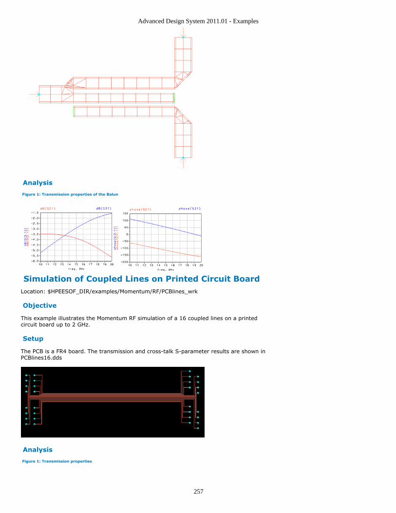
Advanced Design System 2011.01 - Examples
257
Analysis
Figure 1: Transmission properties of the Balun
Simulation of Coupled Lines on Printed Circuit BoardLocation: $HPEESOF_DIR/examples/Momentum/RF/PCBlines_wrk
Objective
This example illustrates the Momentum RF simulation of a 16 coupled lines on a printedcircuit board up to 2 GHz.
Setup
The PCB is a FR4 board. The transmission and cross-talk S-parameter results are shown inPCBlines16.dds
Analysis
Figure 1: Transmission properties
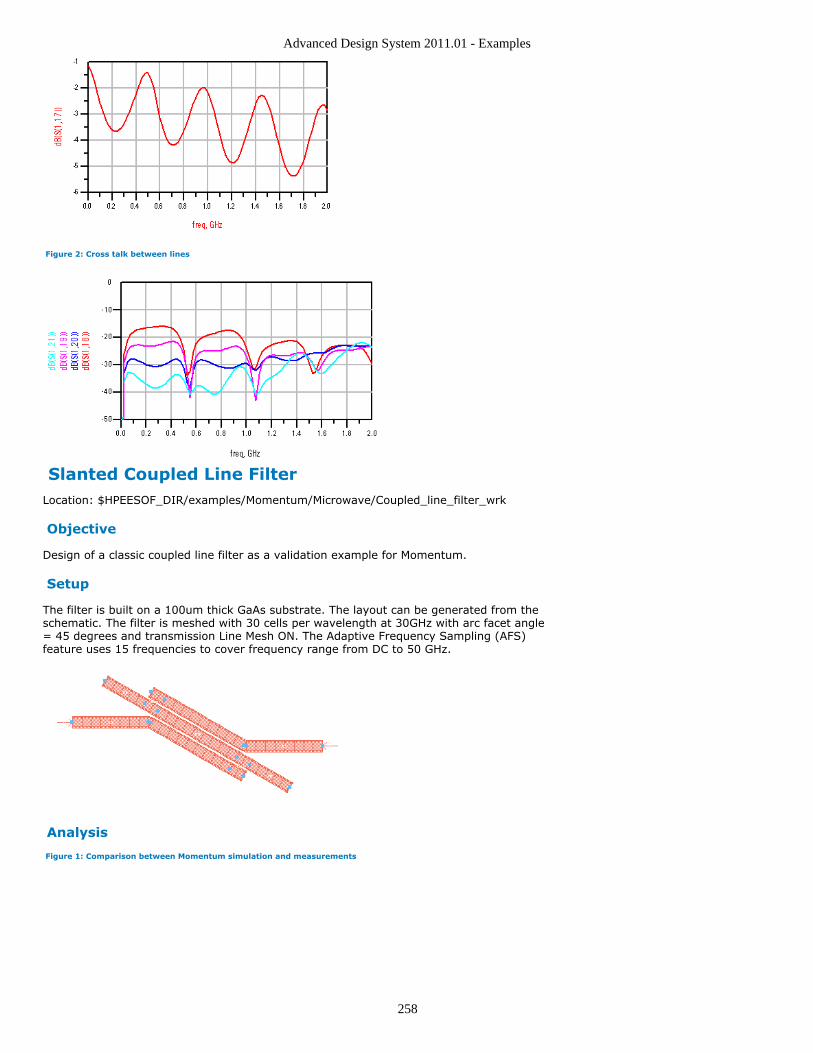
Advanced Design System 2011.01 - Examples
258
Figure 2: Cross talk between lines
Slanted Coupled Line FilterLocation: $HPEESOF_DIR/examples/Momentum/Microwave/Coupled_line_filter_wrk
Objective
Design of a classic coupled line filter as a validation example for Momentum.
Setup
The filter is built on a 100um thick GaAs substrate. The layout can be generated from theschematic. The filter is meshed with 30 cells per wavelength at 30GHz with arc facet angle= 45 degrees and transmission Line Mesh ON. The Adaptive Frequency Sampling (AFS)feature uses 15 frequencies to cover frequency range from DC to 50 GHz.
Analysis
Figure 1: Comparison between Momentum simulation and measurements
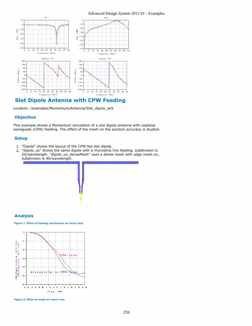
Advanced Design System 2011.01 - Examples
259
Slot Dipole Antenna with CPW FeedingLocation: /examples/Momentum/Antenna/Slot_dipole_wrk
Objective
This example shows a Momentum simulation of a slot dipole antenna with coplanarwaveguide (CPW) feeding. The effect of the mesh on the solution accuracy is studied.
Setup
"Dipole" shows the layout of the CPW fed slot dipole.1."dipole_us" shows the same dipole with a microstrip line feeding, subdivision is2.20/wavelength. "dipole_us_denseMesh" uses a dense mesh with edge mesh on,subdivision is 40/wavelength.
Analysis
Figure 1: Effect of feeding mechanism on return loss
Figure 2: Effect of mesh on return loss
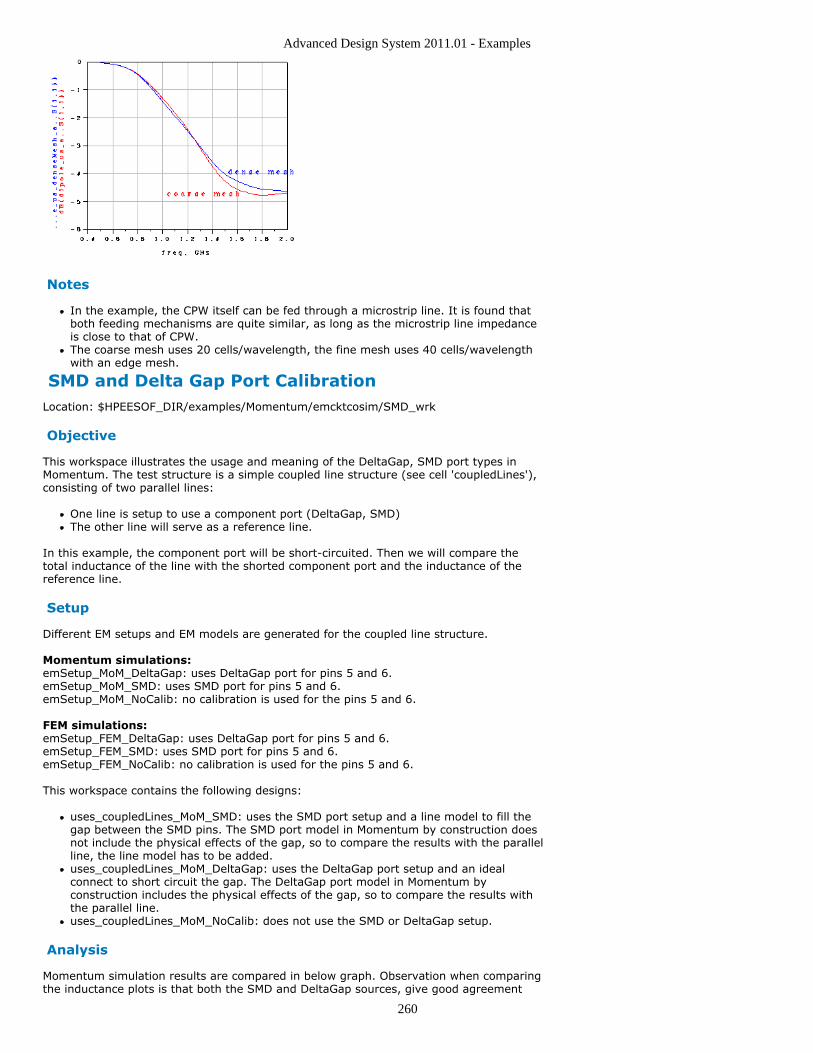
Advanced Design System 2011.01 - Examples
260
Notes
In the example, the CPW itself can be fed through a microstrip line. It is found thatboth feeding mechanisms are quite similar, as long as the microstrip line impedanceis close to that of CPW.The coarse mesh uses 20 cells/wavelength, the fine mesh uses 40 cells/wavelengthwith an edge mesh.
SMD and Delta Gap Port CalibrationLocation: $HPEESOF_DIR/examples/Momentum/emcktcosim/SMD_wrk
Objective
This workspace illustrates the usage and meaning of the DeltaGap, SMD port types inMomentum. The test structure is a simple coupled line structure (see cell 'coupledLines'),consisting of two parallel lines:
One line is setup to use a component port (DeltaGap, SMD)The other line will serve as a reference line.
In this example, the component port will be short-circuited. Then we will compare thetotal inductance of the line with the shorted component port and the inductance of thereference line.
Setup
Different EM setups and EM models are generated for the coupled line structure.
Momentum simulations:emSetup_MoM_DeltaGap: uses DeltaGap port for pins 5 and 6.emSetup_MoM_SMD: uses SMD port for pins 5 and 6.emSetup_MoM_NoCalib: no calibration is used for the pins 5 and 6.
FEM simulations:emSetup_FEM_DeltaGap: uses DeltaGap port for pins 5 and 6.emSetup_FEM_SMD: uses SMD port for pins 5 and 6.emSetup_FEM_NoCalib: no calibration is used for the pins 5 and 6.
This workspace contains the following designs:
uses_coupledLines_MoM_SMD: uses the SMD port setup and a line model to fill thegap between the SMD pins. The SMD port model in Momentum by construction doesnot include the physical effects of the gap, so to compare the results with the parallelline, the line model has to be added.uses_coupledLines_MoM_DeltaGap: uses the DeltaGap port setup and an idealconnect to short circuit the gap. The DeltaGap port model in Momentum byconstruction includes the physical effects of the gap, so to compare the results withthe parallel line.uses_coupledLines_MoM_NoCalib: does not use the SMD or DeltaGap setup.
Analysis
Momentum simulation results are compared in below graph. Observation when comparingthe inductance plots is that both the SMD and DeltaGap sources, give good agreement
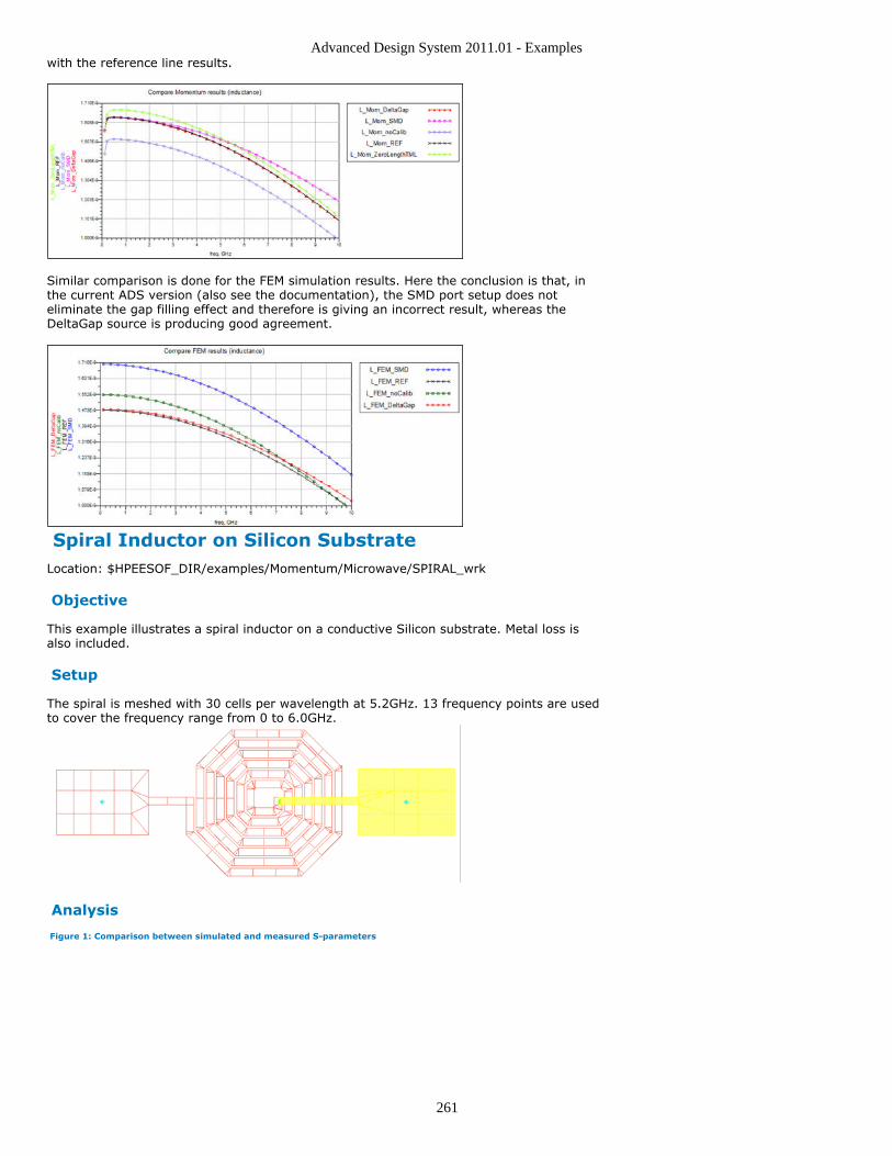
Advanced Design System 2011.01 - Examples
261
with the reference line results.
Similar comparison is done for the FEM simulation results. Here the conclusion is that, inthe current ADS version (also see the documentation), the SMD port setup does noteliminate the gap filling effect and therefore is giving an incorrect result, whereas theDeltaGap source is producing good agreement.
Spiral Inductor on Silicon SubstrateLocation: $HPEESOF_DIR/examples/Momentum/Microwave/SPIRAL_wrk
Objective
This example illustrates a spiral inductor on a conductive Silicon substrate. Metal loss isalso included.
Setup
The spiral is meshed with 30 cells per wavelength at 5.2GHz. 13 frequency points are usedto cover the frequency range from 0 to 6.0GHz.
Analysis
Figure 1: Comparison between simulated and measured S-parameters
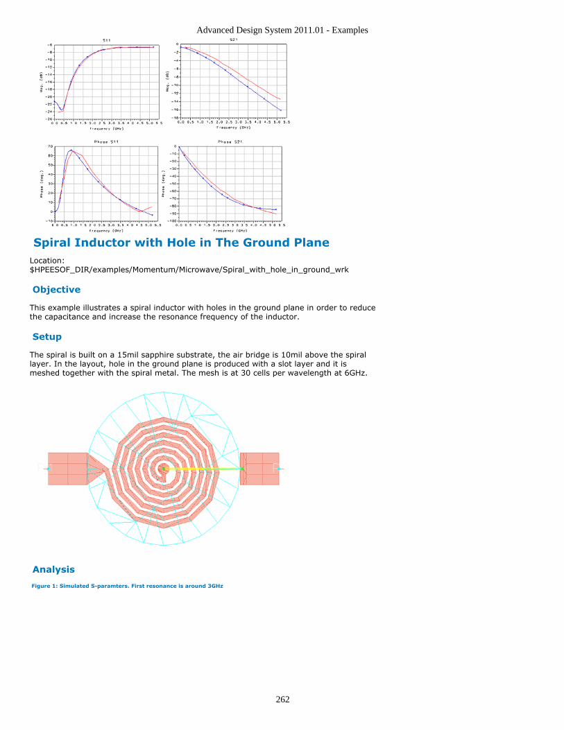
Advanced Design System 2011.01 - Examples
262
Spiral Inductor with Hole in The Ground PlaneLocation:$HPEESOF_DIR/examples/Momentum/Microwave/Spiral_with_hole_in_ground_wrk
Objective
This example illustrates a spiral inductor with holes in the ground plane in order to reducethe capacitance and increase the resonance frequency of the inductor.
Setup
The spiral is built on a 15mil sapphire substrate, the air bridge is 10mil above the spirallayer. In the layout, hole in the ground plane is produced with a slot layer and it ismeshed together with the spiral metal. The mesh is at 30 cells per wavelength at 6GHz.
Analysis
Figure 1: Simulated S-paramters. First resonance is around 3GHz
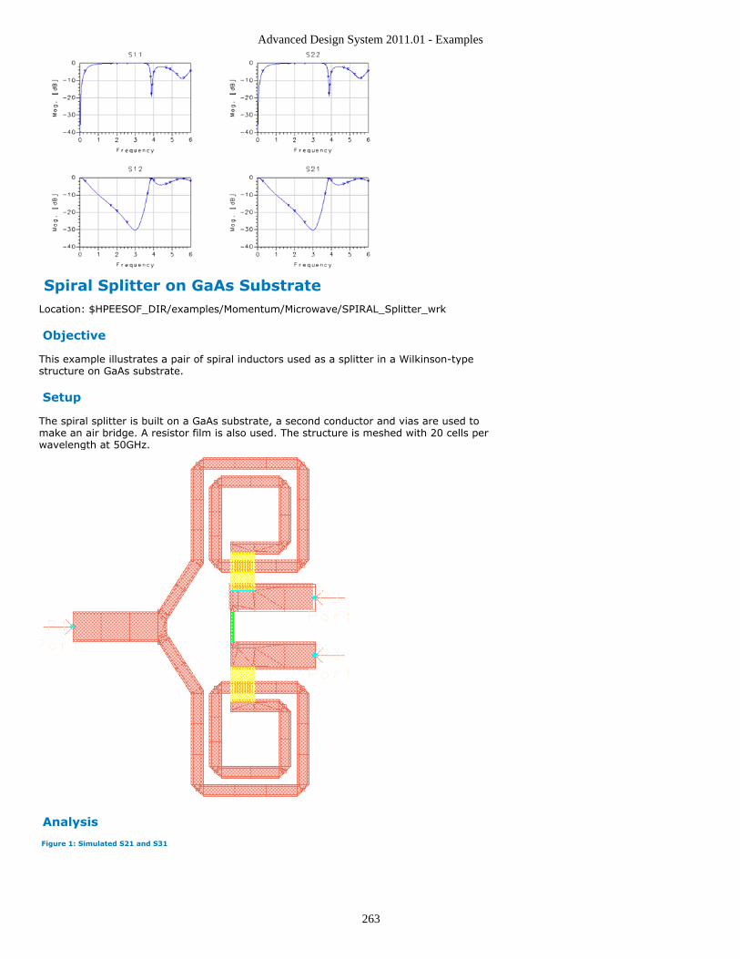
Advanced Design System 2011.01 - Examples
263
Spiral Splitter on GaAs SubstrateLocation: $HPEESOF_DIR/examples/Momentum/Microwave/SPIRAL_Splitter_wrk
Objective
This example illustrates a pair of spiral inductors used as a splitter in a Wilkinson-typestructure on GaAs substrate.
Setup
The spiral splitter is built on a GaAs substrate, a second conductor and vias are used tomake an air bridge. A resistor film is also used. The structure is meshed with 20 cells perwavelength at 50GHz.
Analysis
Figure 1: Simulated S21 and S31
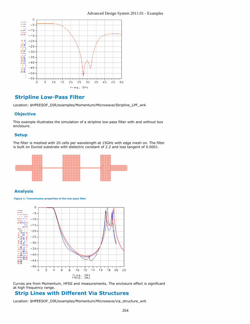
Advanced Design System 2011.01 - Examples
264
Stripline Low-Pass FilterLocation: $HPEESOF_DIR/examples/Momentum/Microwave/Stripline_LPF_wrk
Objective
This example illustrates the simulation of a stripline low-pass filter with and without boxenclosure.
Setup
The filter is meshed with 20 cells per wavelength at 15GHz with edge mesh on. The filteris built on Duroid substrate with dielectric constant of 2.2 and loss tangent of 0.0001.
Analysis
Figure 1: Transmission properties of the low-pass filter
Curves are from Momentum, HFSS and measurements. The enclosure effect is significantat high frequency range.
Strip Lines with Different Via StructuresLocation: $HPEESOF_DIR/examples/Momentum/Microwave/via_structure_wrk
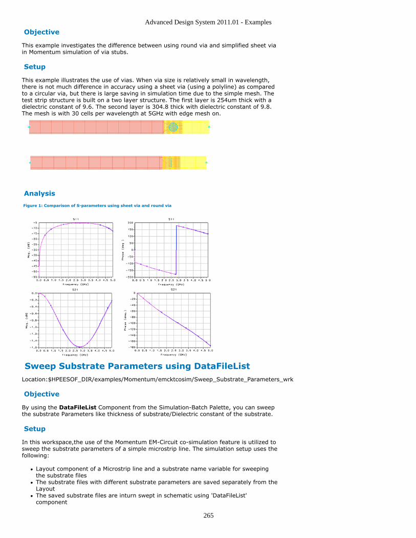
Advanced Design System 2011.01 - Examples
265
Objective
This example investigates the difference between using round via and simplified sheet viain Momentum simulation of via stubs.
Setup
This example illustrates the use of vias. When via size is relatively small in wavelength,there is not much difference in accuracy using a sheet via (using a polyline) as comparedto a circular via, but there is large saving in simulation time due to the simple mesh. Thetest strip structure is built on a two layer structure. The first layer is 254um thick with adielectric constant of 9.6. The second layer is 304.8 thick with dielectric constant of 9.8.The mesh is with 30 cells per wavelength at 5GHz with edge mesh on.
Analysis
Figure 1: Comparison of S-parameters using sheet via and round via
Sweep Substrate Parameters using DataFileListLocation:$HPEESOF_DIR/examples/Momentum/emcktcosim/Sweep_Substrate_Parameters_wrk
Objective
By using the DataFileList Component from the Simulation-Batch Palette, you can sweepthe substrate Parameters like thickness of substrate/Dielectric constant of the substrate.
Setup
In this workspace,the use of the Momentum EM-Circuit co-simulation feature is utilized tosweep the substrate parameters of a simple microstrip line. The simulation setup uses thefollowing:
Layout component of a Microstrip line and a substrate name variable for sweepingthe substrate filesThe substrate files with different substrate parameters are saved separately from theLayoutThe saved substrate files are inturn swept in schematic using 'DataFileList'component
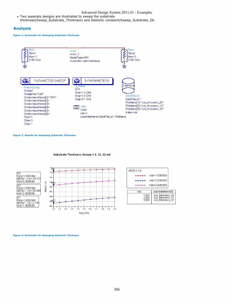
Advanced Design System 2011.01 - Examples
266
Two separate designs are illustrated to sweep the substratethickness(Sweep_Substrate_Thickness) and Dielectic constant(Sweep_Substrate_Dk
Analysis
Figure 1: Schematic for Sweeping Substrate Thickness
Figure 2: Results for Sweeping Substrate Thickness
Figure 3: Schematic for Sweeping Dielectric Thickness
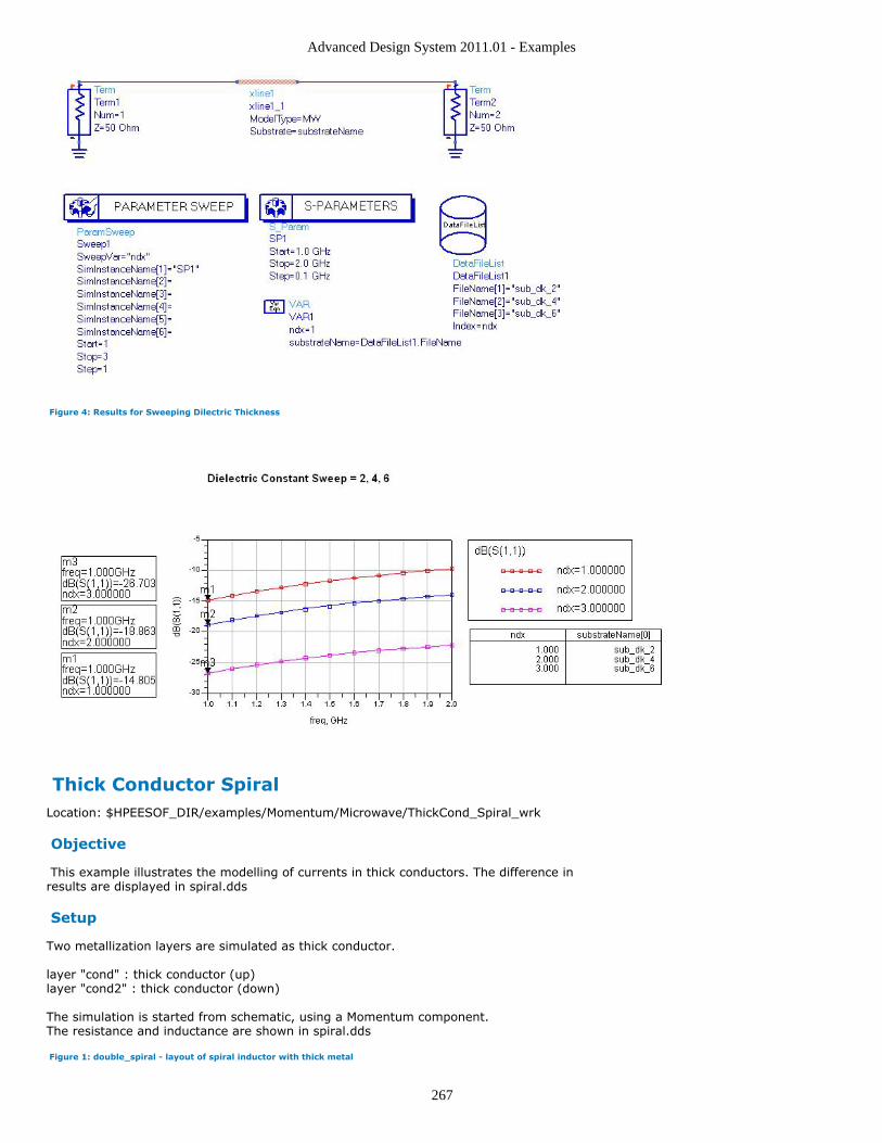
Advanced Design System 2011.01 - Examples
267
Figure 4: Results for Sweeping Dilectric Thickness
Thick Conductor SpiralLocation: $HPEESOF_DIR/examples/Momentum/Microwave/ThickCond_Spiral_wrk
Objective
This example illustrates the modelling of currents in thick conductors. The difference inresults are displayed in spiral.dds
Setup
Two metallization layers are simulated as thick conductor.
layer "cond" : thick conductor (up)layer "cond2" : thick conductor (down)
The simulation is started from schematic, using a Momentum component.The resistance and inductance are shown in spiral.dds
Figure 1: double_spiral - layout of spiral inductor with thick metal
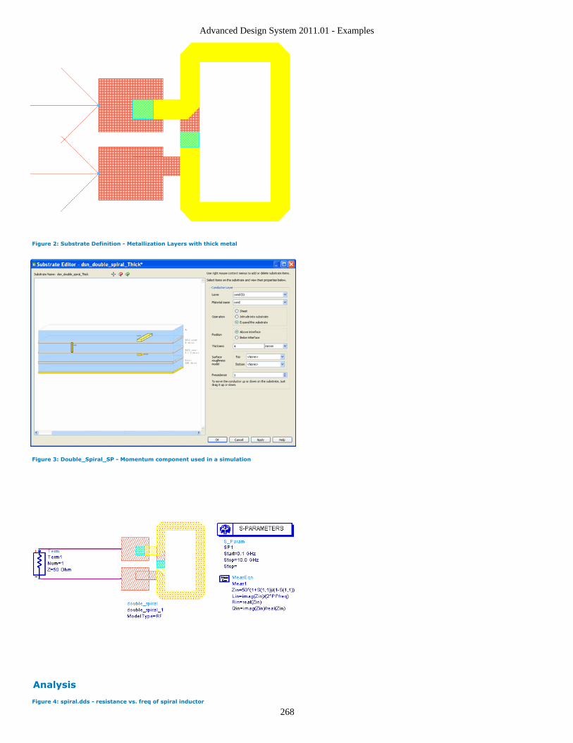
Advanced Design System 2011.01 - Examples
268
Figure 2: Substrate Definition - Metallization Layers with thick metal
Figure 3: Double_Spiral_SP - Momentum component used in a simulation
Analysis
Figure 4: spiral.dds - resistance vs. freq of spiral inductor
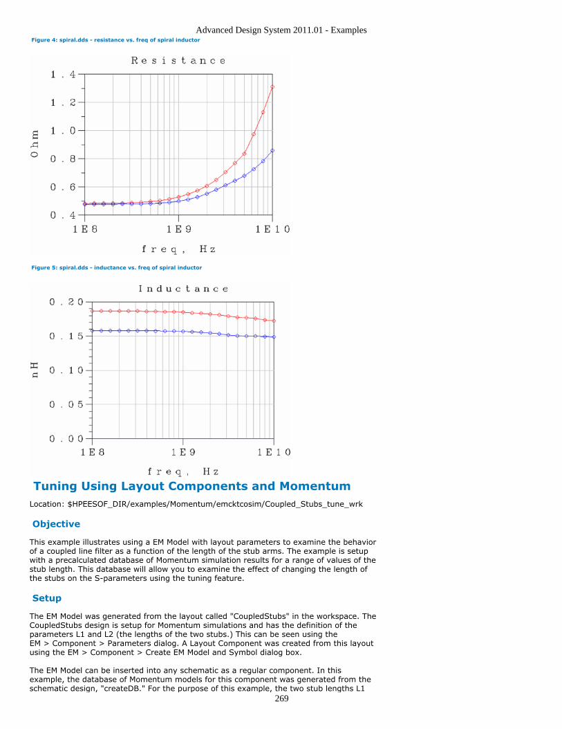
Advanced Design System 2011.01 - Examples
269
Figure 4: spiral.dds - resistance vs. freq of spiral inductor
Figure 5: spiral.dds - inductance vs. freq of spiral inductor
Tuning Using Layout Components and MomentumLocation: $HPEESOF_DIR/examples/Momentum/emcktcosim/Coupled_Stubs_tune_wrk
Objective
This example illustrates using a EM Model with layout parameters to examine the behaviorof a coupled line filter as a function of the length of the stub arms. The example is setupwith a precalculated database of Momentum simulation results for a range of values of thestub length. This database will allow you to examine the effect of changing the length ofthe stubs on the S-parameters using the tuning feature.
Setup
The EM Model was generated from the layout called "CoupledStubs" in the workspace. TheCoupledStubs design is setup for Momentum simulations and has the definition of theparameters L1 and L2 (the lengths of the two stubs.) This can be seen using theEM > Component > Parameters dialog. A Layout Component was created from this layoutusing the EM > Component > Create EM Model and Symbol dialog box.
The EM Model can be inserted into any schematic as a regular component. In thisexample, the database of Momentum models for this component was generated from theschematic design, "createDB." For the purpose of this example, the two stub lengths L1
Advanced Design System 2011.01 - Examples
270
and L2 will be varied simultaneously using the variable L. The design is setup with aparameter sweep to vary L from 100 to 130 mil in steps of 1.5 mil (note that the step sizein the database is chosen to be smaller than the default interpolation step which can beviewed under EM Model Interpolation tab.) Simulating the "createDB" schematic generatedthe Layout Component database. The contents of the database can be inspected from theEM Model under database tab.
The next step is to examine the behavior of the filter while changing the stub lengthlayout parameter using tuning. This is illustrated in the design called "tuneL." In thisdesign, an S-parameter simulation has been setup with a corresponding data displaywindow. To tune the stub length parameter (L) and view the results, open the "tuneL"design and open the "tuneL" data display. You can then tune the parameter between 100and 130 mil while examining the effect on the S-parameters.
Figure 1: Coupled stub filter layout
Figure 2: Layout Component in a schematic
Analysis
Figure 3: Filter frequency response for one stub length
Advanced Design System 2011.01 - Examples
271
X-Band BalunLocation: $HPEESOF_DIR/examples/Momentum/Microwave/Rat_Race_wrk
Objective
This example illustrates a rat race balun designed for use in the X-band.
Setup
The balun is built on a sapphire substrate. The center frequency is 11.31GHz. If port 1 isexcited, the power is equally split over port 2 and 3 in phase, port 4 is isolated from port1. If port 4 is excited, the power is split equally to port 2 and 3, which are about 180degrees out of phase. The structure is meshed with 20 cells per wavelength at 20GHz.
Analysis
Figure 1: S-Paramaters from simulation
Advanced Design System 2011.01 - Examples
272
MultiTech_Module ExamplesThis section lists the Multi-technology examples.
Front-end Transceiver Circuit Design using Multi-Technology (examples)MMIC Chip on a QFN package (examples)
Front-end Transceiver Circuit Design using Multi-TechnologyLocation: $HPEESOF_DIR/examples/MultiTech_Module/Antenna_SPDT_LNA_PA_wrk
Objective
This example illustrates the Multi Technology Flow for Front-End Transceiver CircuitDesign. This flow demonstrates the usage of two different technologies of PDKs defined inseparate libraries along with ADS standard libraries to realize the complete design oftransceiver circuit.
The transceiver circuit that has been designed consists of mainly four major components:
AntennaSPDTLNAPower Amplifier
The LNA and SPDT are designed using two different PDKs having different technologiesdefined in two separate libraries whereas as Antenna and PA are designed using ADSstandard libraries. The complete transceiver circuit is then created with and without usingthe Module substrate. The design is then simulated for S-Parameter.
The workspace includes four major designs based on the following technologies:
Antenna Design using Momentum simulated data1.SPDT Design the model of MMIC Chip from the DemoKit_V32.LNA Design using the model of MMIC Chip from DemoKit_Non_Linear3.Power Amplifier using X-Parameter simulated data4.
Setup
Antenna_Data: Antenna design using momentum simulated data.1.SPDT_Design2: SPDT circuit design using DemoKit_V3 PDK. SPDT_SP: simulation on2.SPDT circuitLNA_Design: LNA circuit design DemoKit_Non_Linear PDK. LNA_SP: simulation3.performed on LNA circuitPower_Amplifier: Power Amplifier design using X-Parameter simulated data.4.LNA_SPDT_Patch_PA1: Integrated Transceiver circuit design without using Module5.SubstrateLNA_SPDT_Patch_PA3: Integrated Transceiver circuit design using Module Substrate6.
Analysis
The below graphs illustrate the SPDT S-Parameter simulated data:
Figure 1: Insertion and Isolation Data from SPDT circuit simulation
Advanced Design System 2011.01 - Examples
273
Figure 2: Gain, Loss, Stability and NF measurement on LNA Circuit
Figure 3: Complete Transceiver Circuit simulation without using Module Substrate
Figure 4: Complete Transceiver Circuit simulation using Module Substrate
Notes
For more details, see Multi-Technology for Circuit Simulation.
MMIC Chip on a QFN packageLocation:$HPEESOF_DIR/examples/MultiTech_Module/MTM_Flow_MMIC_Chip_QFN_Package_wrk
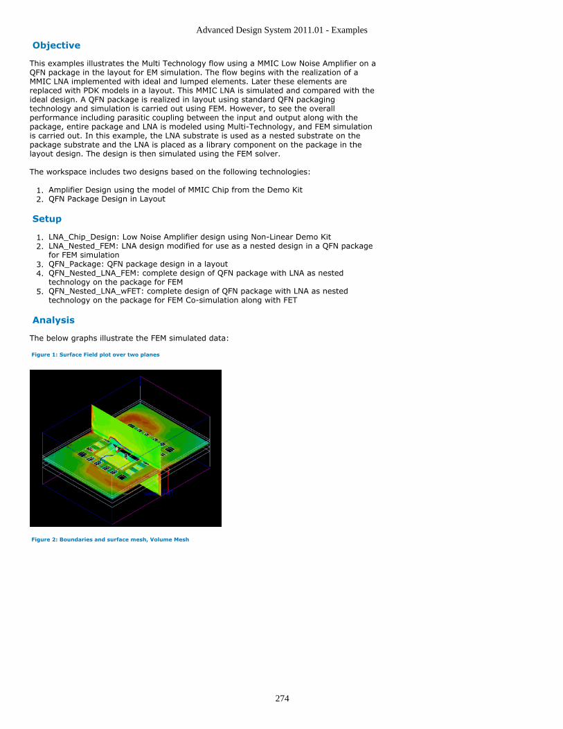
Advanced Design System 2011.01 - Examples
274
Objective
This examples illustrates the Multi Technology flow using a MMIC Low Noise Amplifier on aQFN package in the layout for EM simulation. The flow begins with the realization of aMMIC LNA implemented with ideal and lumped elements. Later these elements arereplaced with PDK models in a layout. This MMIC LNA is simulated and compared with theideal design. A QFN package is realized in layout using standard QFN packagingtechnology and simulation is carried out using FEM. However, to see the overallperformance including parasitic coupling between the input and output along with thepackage, entire package and LNA is modeled using Multi-Technology, and FEM simulationis carried out. In this example, the LNA substrate is used as a nested substrate on thepackage substrate and the LNA is placed as a library component on the package in thelayout design. The design is then simulated using the FEM solver.
The workspace includes two designs based on the following technologies:
Amplifier Design using the model of MMIC Chip from the Demo Kit1.QFN Package Design in Layout2.
Setup
LNA_Chip_Design: Low Noise Amplifier design using Non-Linear Demo Kit1.LNA_Nested_FEM: LNA design modified for use as a nested design in a QFN package2.for FEM simulationQFN_Package: QFN package design in a layout3.QFN_Nested_LNA_FEM: complete design of QFN package with LNA as nested4.technology on the package for FEMQFN_Nested_LNA_wFET: complete design of QFN package with LNA as nested5.technology on the package for FEM Co-simulation along with FET
Analysis
The below graphs illustrate the FEM simulated data:
Figure 1: Surface Field plot over two planes
Figure 2: Boundaries and surface mesh, Volume Mesh
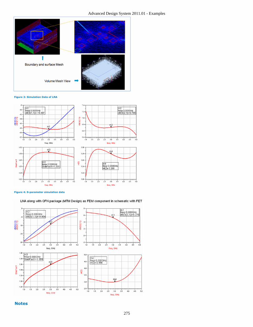
Advanced Design System 2011.01 - Examples
275
Figure 3: Simulation Data of LNA
Figure 4: S-parameter simulation data
Notes

Advanced Design System 2011.01 - Examples
276
For more details, see Multi-Technology for EM Simulation.
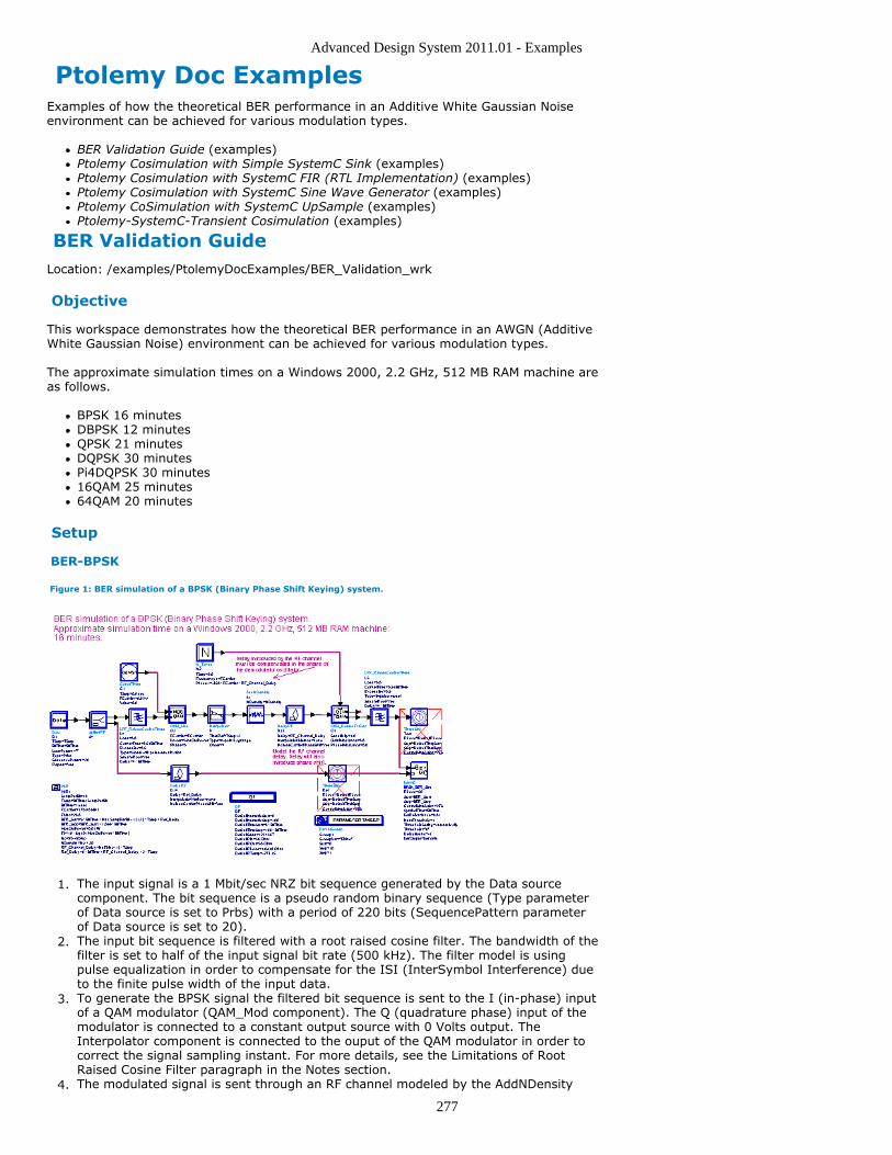
Advanced Design System 2011.01 - Examples
277
Ptolemy Doc ExamplesExamples of how the theoretical BER performance in an Additive White Gaussian Noiseenvironment can be achieved for various modulation types.
BER Validation Guide (examples)Ptolemy Cosimulation with Simple SystemC Sink (examples)Ptolemy Cosimulation with SystemC FIR (RTL Implementation) (examples)Ptolemy Cosimulation with SystemC Sine Wave Generator (examples)Ptolemy CoSimulation with SystemC UpSample (examples)Ptolemy-SystemC-Transient Cosimulation (examples)
BER Validation GuideLocation: /examples/PtolemyDocExamples/BER_Validation_wrk
Objective
This workspace demonstrates how the theoretical BER performance in an AWGN (AdditiveWhite Gaussian Noise) environment can be achieved for various modulation types.
The approximate simulation times on a Windows 2000, 2.2 GHz, 512 MB RAM machine areas follows.
BPSK 16 minutesDBPSK 12 minutesQPSK 21 minutesDQPSK 30 minutesPi4DQPSK 30 minutes16QAM 25 minutes64QAM 20 minutes
Setup
BER-BPSK
Figure 1: BER simulation of a BPSK (Binary Phase Shift Keying) system.
The input signal is a 1 Mbit/sec NRZ bit sequence generated by the Data source1.component. The bit sequence is a pseudo random binary sequence (Type parameterof Data source is set to Prbs) with a period of 220 bits (SequencePattern parameterof Data source is set to 20).The input bit sequence is filtered with a root raised cosine filter. The bandwidth of the2.filter is set to half of the input signal bit rate (500 kHz). The filter model is usingpulse equalization in order to compensate for the ISI (InterSymbol Interference) dueto the finite pulse width of the input data.To generate the BPSK signal the filtered bit sequence is sent to the I (in-phase) input3.of a QAM modulator (QAM_Mod component). The Q (quadrature phase) input of themodulator is connected to a constant output source with 0 Volts output. TheInterpolator component is connected to the ouput of the QAM modulator in order tocorrect the signal sampling instant. For more details, see the Limitations of RootRaised Cosine Filter paragraph in the Notes section.The modulated signal is sent through an RF channel modeled by the AddNDensity4.
Advanced Design System 2011.01 - Examples
278
and DelayRF components. The RF channel noise power is swept so that the Eb/No ofthe system is swept from 0 to 10 dB. For more details, see the Setting the NoisePower and the RF Channel Delay paragraphs in the Notes section.BPSK modulation requires coherent (or synchronous) demodulation. A QAM5.demodulator (QAM_DemodExtOsc component) is used with a local oscillator signalgenerated by an N_Tones source as explained in the Coherent and Non-coherentDemodulation paragraph in the Notes section. Only the I signal at the output of theQAM demodulator is used.The I signal at the output of the QAM demodulator is filtered using a root raised6.cosine filter. This filter has the same characteristics as the root raised cosine filter onthe transmitter side except that it does not include pulse equalization.The signal at the output of the receiver root raised cosine filter is connected to the7.test input of the berMC sink. The input bit sequence generated by the Data source isthe reference signal. This design synchronizes the test and reference signalsmanually by first determining the delay between them. The delay between the testand reference signals is 8 x SymbolTime (due to the root raised cosine filters in thetransmitter and receiver) + RF_Channel_Delay (due to the RF channel) + 2 x TStep(due to the Interpolator). Therefore, the output of the Data source is delayed by thisamount and connected to the reference input of the berMC sink.The berMC sink is set up as explained in the BER Sink Setup paragraph of the Notes8.section. With this setup, the estimation relative variance achieved for Eb/No between0 dB and 8 dB is the desired 0.01. For Eb/No=9 dB the estimation relative variance isapproximately 0.037. Although this is not too close to the desired 0.01, it is still quitelow and so the BER result is expected to be accurate. For Eb/No=10 dB theestimation relative variance is approximately 0.33. This variance is quite high and sothe BER result for Eb/No=10 dB is expected to be less accurate. To achieve anestimation relative variance of 0.01 at Eb/No of 9 dB and 10 dB, the Stop parameterof the berMC sink needs to be set to a higher value, e.g. BER_Start + 1.0e7 *BitTime. Simulation time will increase accordingly.The simulation results are shown below. As can be seen, the simulation results agree9.very well with theory except for Eb/No=10 dB. At Eb/No=10 dB, the deviationbetweeen the simulation and the theoretical results is larger compared to lowerEb/No values. This is because of the higher estimation relative variance achieved atEb/No=10 dB.
Figure 2: BPSK BER simulation results.
BER - DBPSK
Figure 3: BER simulation of a DBPSK (Differential Binary Phase Shift Keying) system.
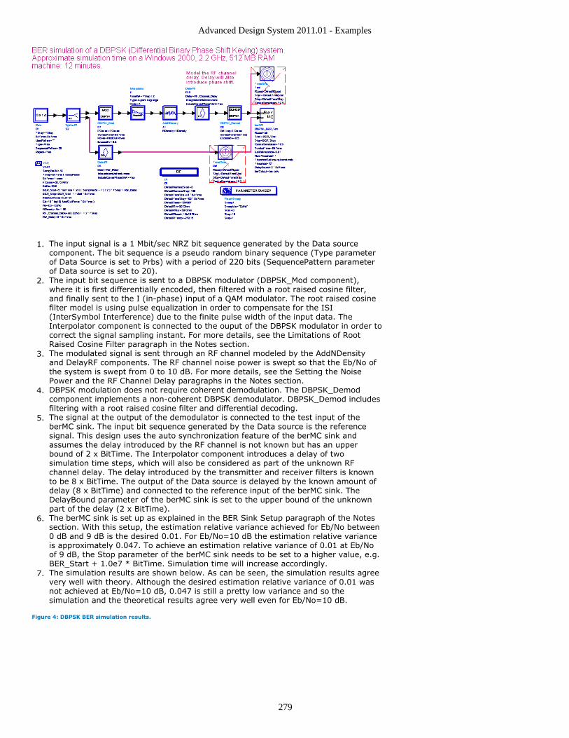
Advanced Design System 2011.01 - Examples
279
The input signal is a 1 Mbit/sec NRZ bit sequence generated by the Data source1.component. The bit sequence is a pseudo random binary sequence (Type parameterof Data Source is set to Prbs) with a period of 220 bits (SequencePattern parameterof Data source is set to 20).The input bit sequence is sent to a DBPSK modulator (DBPSK_Mod component),2.where it is first differentially encoded, then filtered with a root raised cosine filter,and finally sent to the I (in-phase) input of a QAM modulator. The root raised cosinefilter model is using pulse equalization in order to compensate for the ISI(InterSymbol Interference) due to the finite pulse width of the input data. TheInterpolator component is connected to the ouput of the DBPSK modulator in order tocorrect the signal sampling instant. For more details, see the Limitations of RootRaised Cosine Filter paragraph in the Notes section.The modulated signal is sent through an RF channel modeled by the AddNDensity3.and DelayRF components. The RF channel noise power is swept so that the Eb/No ofthe system is swept from 0 to 10 dB. For more details, see the Setting the NoisePower and the RF Channel Delay paragraphs in the Notes section.DBPSK modulation does not require coherent demodulation. The DBPSK_Demod4.component implements a non-coherent DBPSK demodulator. DBPSK_Demod includesfiltering with a root raised cosine filter and differential decoding.The signal at the output of the demodulator is connected to the test input of the5.berMC sink. The input bit sequence generated by the Data source is the referencesignal. This design uses the auto synchronization feature of the berMC sink andassumes the delay introduced by the RF channel is not known but has an upperbound of 2 x BitTime. The Interpolator component introduces a delay of twosimulation time steps, which will also be considered as part of the unknown RFchannel delay. The delay introduced by the transmitter and receiver filters is knownto be 8 x BitTime. The output of the Data source is delayed by the known amount ofdelay (8 x BitTime) and connected to the reference input of the berMC sink. TheDelayBound parameter of the berMC sink is set to the upper bound of the unknownpart of the delay (2 x BitTime).The berMC sink is set up as explained in the BER Sink Setup paragraph of the Notes6.section. With this setup, the estimation relative variance achieved for Eb/No between0 dB and 9 dB is the desired 0.01. For Eb/No=10 dB the estimation relative varianceis approximately 0.047. To achieve an estimation relative variance of 0.01 at Eb/Noof 9 dB, the Stop parameter of the berMC sink needs to be set to a higher value, e.g.BER_Start + 1.0e7 * BitTime. Simulation time will increase accordingly.The simulation results are shown below. As can be seen, the simulation results agree7.very well with theory. Although the desired estimation relative variance of 0.01 wasnot achieved at Eb/No=10 dB, 0.047 is still a pretty low variance and so thesimulation and the theoretical results agree very well even for Eb/No=10 dB.
Figure 4: DBPSK BER simulation results.
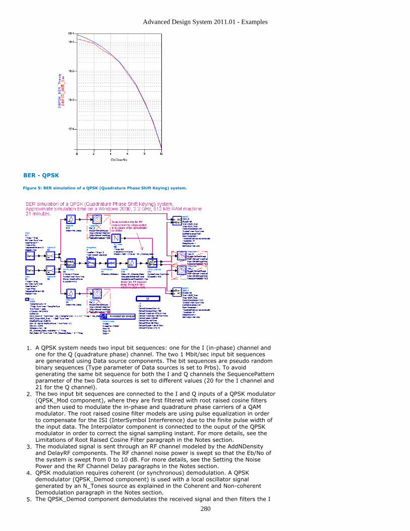
Advanced Design System 2011.01 - Examples
280
BER - QPSK
Figure 5: BER simulation of a QPSK (Quadrature Phase Shift Keying) system.
A QPSK system needs two input bit sequences: one for the I (in-phase) channel and1.one for the Q (quadrature phase) channel. The two 1 Mbit/sec input bit sequencesare generated using Data source components. The bit sequences are pseudo randombinary sequences (Type parameter of Data sources is set to Prbs). To avoidgenerating the same bit sequence for both the I and Q channels the SequencePatternparameter of the two Data sources is set to different values (20 for the I channel and21 for the Q channel).The two input bit sequences are connected to the I and Q inputs of a QPSK modulator2.(QPSK_Mod component), where they are first filtered with root raised cosine filtersand then used to modulate the in-phase and quadrature phase carriers of a QAMmodulator. The root raised cosine filter models are using pulse equalization in orderto compensate for the ISI (InterSymbol Interference) due to the finite pulse width ofthe input data. The Interpolator component is connected to the ouput of the QPSKmodulator in order to correct the signal sampling instant. For more details, see theLimitations of Root Raised Cosine Filter paragraph in the Notes section.The modulated signal is sent through an RF channel modeled by the AddNDensity3.and DelayRF components. The RF channel noise power is swept so that the Eb/No ofthe system is swept from 0 to 10 dB. For more details, see the Setting the NoisePower and the RF Channel Delay paragraphs in the Notes section.QPSK modulation requires coherent (or synchronous) demodulation. A QPSK4.demodulator (QPSK_Demod component) is used with a local oscillator signalgenerated by an N_Tones source as explained in the Coherent and Non-coherentDemodulation paragraph in the Notes section.The QPSK_Demod component demodulates the received signal and then filters the I5.
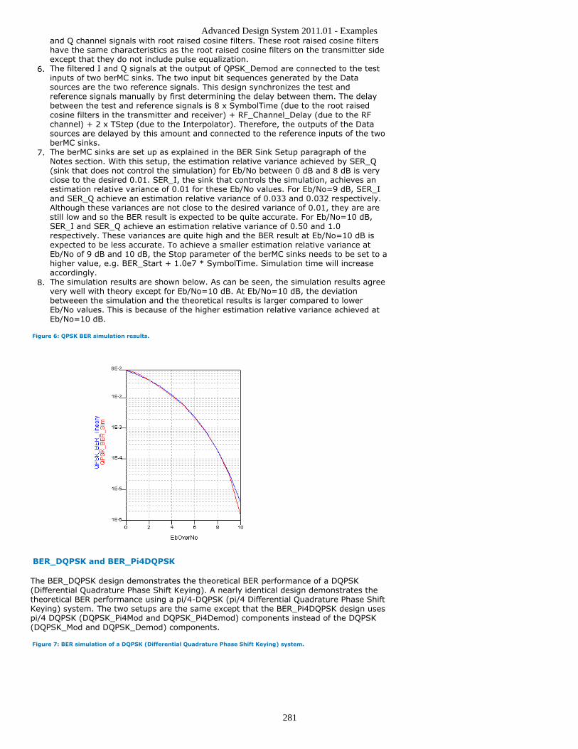
Advanced Design System 2011.01 - Examples
281
and Q channel signals with root raised cosine filters. These root raised cosine filtershave the same characteristics as the root raised cosine filters on the transmitter sideexcept that they do not include pulse equalization.The filtered I and Q signals at the output of QPSK_Demod are connected to the test6.inputs of two berMC sinks. The two input bit sequences generated by the Datasources are the two reference signals. This design synchronizes the test andreference signals manually by first determining the delay between them. The delaybetween the test and reference signals is 8 x SymbolTime (due to the root raisedcosine filters in the transmitter and receiver) + RF_Channel_Delay (due to the RFchannel) + 2 x TStep (due to the Interpolator). Therefore, the outputs of the Datasources are delayed by this amount and connected to the reference inputs of the twoberMC sinks.The berMC sinks are set up as explained in the BER Sink Setup paragraph of the7.Notes section. With this setup, the estimation relative variance achieved by SER_Q(sink that does not control the simulation) for Eb/No between 0 dB and 8 dB is veryclose to the desired 0.01. SER_I, the sink that controls the simulation, achieves anestimation relative variance of 0.01 for these Eb/No values. For Eb/No=9 dB, SER_Iand SER_Q achieve an estimation relative variance of 0.033 and 0.032 respectively.Although these variances are not close to the desired variance of 0.01, they are arestill low and so the BER result is expected to be quite accurate. For Eb/No=10 dB,SER_I and SER_Q achieve an estimation relative variance of 0.50 and 1.0respectively. These variances are quite high and the BER result at Eb/No=10 dB isexpected to be less accurate. To achieve a smaller estimation relative variance atEb/No of 9 dB and 10 dB, the Stop parameter of the berMC sinks needs to be set to ahigher value, e.g. BER_Start + 1.0e7 * SymbolTime. Simulation time will increaseaccordingly.The simulation results are shown below. As can be seen, the simulation results agree8.very well with theory except for Eb/No=10 dB. At Eb/No=10 dB, the deviationbetweeen the simulation and the theoretical results is larger compared to lowerEb/No values. This is because of the higher estimation relative variance achieved atEb/No=10 dB.
Figure 6: QPSK BER simulation results.
BER_DQPSK and BER_Pi4DQPSK
The BER_DQPSK design demonstrates the theoretical BER performance of a DQPSK(Differential Quadrature Phase Shift Keying). A nearly identical design demonstrates thetheoretical BER performance using a pi/4-DQPSK (pi/4 Differential Quadrature Phase ShiftKeying) system. The two setups are the same except that the BER_Pi4DQPSK design usespi/4 DQPSK (DQPSK_Pi4Mod and DQPSK_Pi4Demod) components instead of the DQPSK(DQPSK_Mod and DQPSK_Demod) components.
Figure 7: BER simulation of a DQPSK (Differential Quadrature Phase Shift Keying) system.
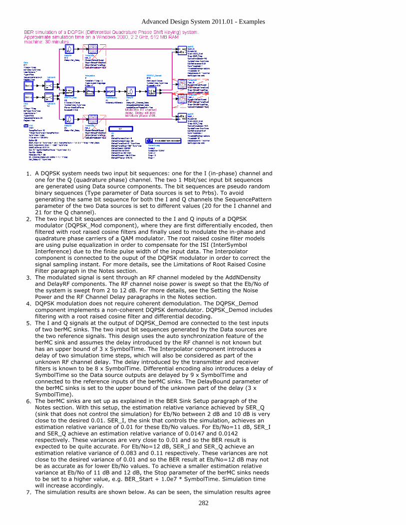
Advanced Design System 2011.01 - Examples
282
A DQPSK system needs two input bit sequences: one for the I (in-phase) channel and1.one for the Q (quadrature phase) channel. The two 1 Mbit/sec input bit sequencesare generated using Data source components. The bit sequences are pseudo randombinary sequences (Type parameter of Data sources is set to Prbs). To avoidgenerating the same bit sequence for both the I and Q channels the SequencePatternparameter of the two Data sources is set to different values (20 for the I channel and21 for the Q channel).The two input bit sequences are connected to the I and Q inputs of a DQPSK2.modulator (DQPSK_Mod component), where they are first differentially encoded, thenfiltered with root raised cosine filters and finally used to modulate the in-phase andquadrature phase carriers of a QAM modulator. The root raised cosine filter modelsare using pulse equalization in order to compensate for the ISI (InterSymbolInterference) due to the finite pulse width of the input data. The Interpolatorcomponent is connected to the ouput of the DQPSK modulator in order to correct thesignal sampling instant. For more details, see the Limitations of Root Raised CosineFilter paragraph in the Notes section.The modulated signal is sent through an RF channel modeled by the AddNDensity3.and DelayRF components. The RF channel noise power is swept so that the Eb/No ofthe system is swept from 2 to 12 dB. For more details, see the Setting the NoisePower and the RF Channel Delay paragraphs in the Notes section.DQPSK modulation does not require coherent demodulation. The DQPSK_Demod4.component implements a non-coherent DQPSK demodulator. DQPSK_Demod includesfiltering with a root raised cosine filter and differential decoding.The I and Q signals at the output of DQPSK_Demod are connected to the test inputs5.of two berMC sinks. The two input bit sequences generated by the Data sources arethe two reference signals. This design uses the auto synchronization feature of theberMC sink and assumes the delay introduced by the RF channel is not known buthas an upper bound of 3 x SymbolTime. The Interpolator component introduces adelay of two simulation time steps, which will also be considered as part of theunknown RF channel delay. The delay introduced by the transmitter and receiverfilters is known to be 8 x SymbolTime. Differential encoding also introduces a delay ofSymbolTime so the Data source outputs are delayed by 9 x SymbolTime andconnected to the reference inputs of the berMC sinks. The DelayBound parameter ofthe berMC sinks is set to the upper bound of the unknown part of the delay (3 xSymbolTime).The berMC sinks are set up as explained in the BER Sink Setup paragraph of the6.Notes section. With this setup, the estimation relative variance achieved by SER_Q(sink that does not control the simulation) for Eb/No between 2 dB and 10 dB is veryclose to the desired 0.01. SER_I, the sink that controls the simulation, achieves anestimation relative variance of 0.01 for these Eb/No values. For Eb/No=11 dB, SER_Iand SER_Q achieve an estimation relative variance of 0.0147 and 0.0142respectively. These variances are very close to 0.01 and so the BER result isexpected to be quite accurate. For Eb/No=12 dB, SER_I and SER_Q achieve anestimation relative variance of 0.083 and 0.11 respectively. These variances are notclose to the desired variance of 0.01 and so the BER result at Eb/No=12 dB may notbe as accurate as for lower Eb/No values. To achieve a smaller estimation relativevariance at Eb/No of 11 dB and 12 dB, the Stop parameter of the berMC sinks needsto be set to a higher value, e.g. BER_Start + 1.0e7 * SymbolTime. Simulation timewill increase accordingly.The simulation results are shown below. As can be seen, the simulation results agree7.
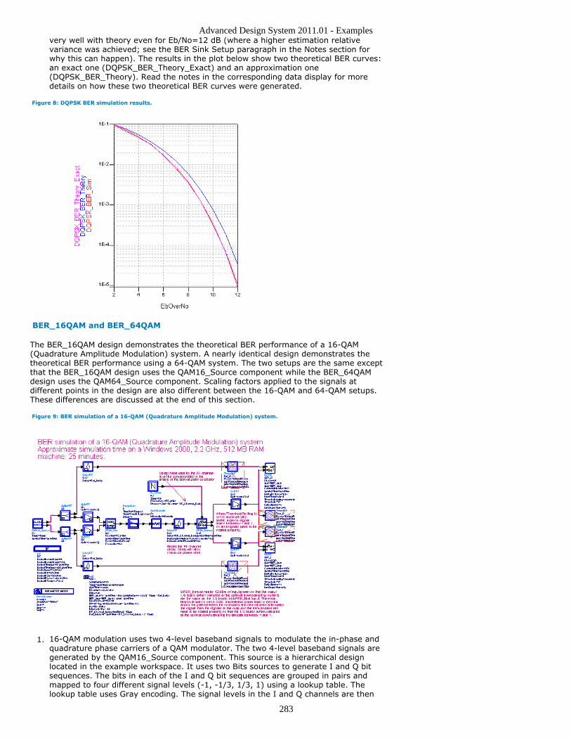
Advanced Design System 2011.01 - Examples
283
very well with theory even for Eb/No=12 dB (where a higher estimation relativevariance was achieved; see the BER Sink Setup paragraph in the Notes section forwhy this can happen). The results in the plot below show two theoretical BER curves:an exact one (DQPSK_BER_Theory_Exact) and an approximation one(DQPSK_BER_Theory). Read the notes in the corresponding data display for moredetails on how these two theoretical BER curves were generated.
Figure 8: DQPSK BER simulation results.
BER_16QAM and BER_64QAM
The BER_16QAM design demonstrates the theoretical BER performance of a 16-QAM(Quadrature Amplitude Modulation) system. A nearly identical design demonstrates thetheoretical BER performance using a 64-QAM system. The two setups are the same exceptthat the BER_16QAM design uses the QAM16_Source component while the BER_64QAMdesign uses the QAM64_Source component. Scaling factors applied to the signals atdifferent points in the design are also different between the 16-QAM and 64-QAM setups.These differences are discussed at the end of this section.
Figure 9: BER simulation of a 16-QAM (Quadrature Amplitude Modulation) system.
16-QAM modulation uses two 4-level baseband signals to modulate the in-phase and1.quadrature phase carriers of a QAM modulator. The two 4-level baseband signals aregenerated by the QAM16_Source component. This source is a hierarchical designlocated in the example workspace. It uses two Bits sources to generate I and Q bitsequences. The bits in each of the I and Q bit sequences are grouped in pairs andmapped to four different signal levels (-1, -1/3, 1/3, 1) using a lookup table. Thelookup table uses Gray encoding. The signal levels in the I and Q channels are then

Advanced Design System 2011.01 - Examples
284
sampled and held (repeated) so that they remain constant during the symbol period.The RMS value of the signal at the output of the source (considered as a complexsignal with the I channel being the real part and the Q channel being the imaginarypart) is equal to sqrt(10)/3.To generate the 16-QAM signal, the I and Q signals at the output of the2.QAM16_Source need to be filtered and applied to the I and Q inputs of a QAMmodulator. The QPSK_Mod component, which includes root raised cosine filters and aQAM modulator, can be used to generate other multi-level QAM signals, as long asthe IQ signal at its input has an RMS value of sqrt(2) (otherwise the power at itsoutput will not be correct). To achieve this, the I and Q signals at the output of theQAM16_Source are scaled by 3/sqrt(5). The root raised cosine filter models are usingpulse equalization in order to compensate for the ISI (InterSymbol Interference) dueto the finite pulse width of the input data. The Interpolator component is connectedto the ouput of the QPSK modulator in order to correct the signal sampling instant.For more details, see the Limitations of Root Raised Cosine Filter paragraph in theNotes section.The modulated signal is sent through an RF channel modeled by the AddNDensity3.and DelayRF components. The RF channel noise power is swept so that the Eb/No ofthe system is swept from 4 to 14 dB. For more details, see the Setting the NoisePower and the RF Channel Delay paragraphs in the Notes section.16-QAM modulation requires coherent (or synchronous) demodulation. A QPSK4.demodulator (QPSK_Demod component) is used with a local oscillator signalgenerated by an N_Tones source as explained in the Coherent and Non-coherentDemodulation paragraph in the Notes section. The QPSK_Demod componentdemodulates the received signal and then filters the I and Q channel signals with rootraised cosine filters. These root raised cosine filters have the same characteristics asthe root raised cosine filters on the transmitter side except that they do not includepulse equalization.To measure BER of signals with more than two levels the BER sink uses more than5.one error detection threshold and so the exact level of the test and reference signalsis important (see the Scaling of Test and Reference Signals sub-section in the Settingup BER Simulations section in the Sinks > PE Estimator Usage documentation). Thereference I and Q signals in this example are the signals at the ouput of theQAM16_Source. These signals were generated so that they can be used with thethreshold settings the BER sink uses when the thresholds are set automatically(ThresholdSetting parameter of the BER sink set to automatically). The level of the Iand Q signals at the ouput of the QPSK_Demod component can be determined in twoways:
By plotting the eye diagrams one can determine the signal levels at the optimal1.sampling instant. In this case, it is recommended that noise and otherimpairments in the system are turned off, so that the eye diagram is as clean aspossible and the signal levels are determined more accurately.By tracking the signal amplitude changes through the system.2.
In this design, it is very easy to track the signal amplitude changes through the6.system and come up with the exact scale factor needed to scale the signals at theouput of the QPSK_Demod component. Starting at the ouput of the QAM16_Source,the signal is first scaled by 3/sqrt(5). The QPSK_Mod component also affects thesignal amplitude depending on the value of the Power parameter. The Powerparameter of QPSK_Mod is set to 0.02 W = 13 dBm. This is based on the fact thatwhen the signal power at the input of QPSK_Demod is 13 dBm, its output I and Qlevels (when sampled at the optimal sampling instant) are the same as the I and Qlevels at the input of QPSK_Mod. Since the path between the modulator anddemodulator does not attenuate/amplify the signal, the power at the input ofQPSK_Demod is the same as the power at the output of QPSK_Mod, which is equal to13 dBm. Therefore, the QPSK_Demod output I and Q levels (when sampled at theoptimal sampling instant) are the same as the I and Q levels at the input ofQPSK_Mod and so in order to make the test signals have the same level as thereference signals, the I and Q signals at the ouput of QPSK_Demod need to be scaledby sqrt(5)/3. The demodulator output signals will need to be scaled by a differentscale factor if the power at the input of QPSK_Demod is not 13 dBm.The scaled demodulator output I and Q signals are connected to the test inputs of7.two berMC sinks. The I and Q signals at the output of the QAM16_Source are the tworeference signals. This design synchronizes the test and reference signals manuallyby first determining the delay between them. The delay between the test andreference signals is 8 x SymbolTime (due to the root raised cosine filters in thetransmitter and receiver) + RF_Channel_Delay (due to the RF channel) + 2 x TStep(due to the Interpolator). Therefore, the I and Q outputs of the QAM16_Source aredelayed by this amount and connected to the reference inputs of the two berMCsinks.The berMC sinks are set up as explained in the BER Sink Setup paragraph of the8.Notes section. With this setup, the estimation relative variance achieved by SER_Q(sink that does not control the simulation) for Eb/No between 4 dB and 12 dB is very
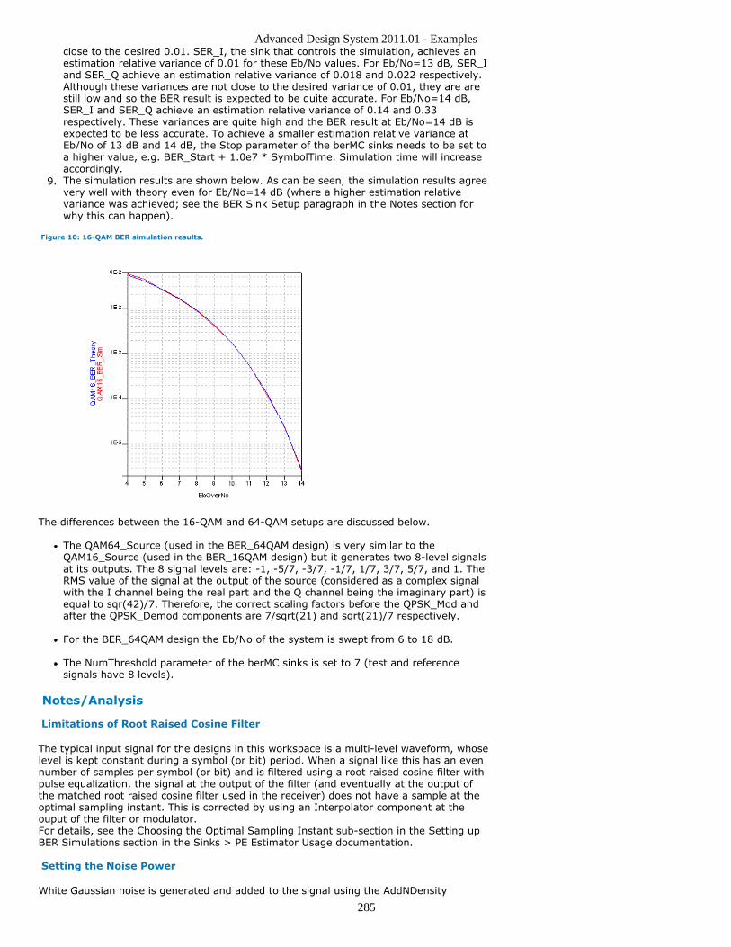
Advanced Design System 2011.01 - Examples
285
close to the desired 0.01. SER_I, the sink that controls the simulation, achieves anestimation relative variance of 0.01 for these Eb/No values. For Eb/No=13 dB, SER_Iand SER_Q achieve an estimation relative variance of 0.018 and 0.022 respectively.Although these variances are not close to the desired variance of 0.01, they are arestill low and so the BER result is expected to be quite accurate. For Eb/No=14 dB,SER_I and SER_Q achieve an estimation relative variance of 0.14 and 0.33respectively. These variances are quite high and the BER result at Eb/No=14 dB isexpected to be less accurate. To achieve a smaller estimation relative variance atEb/No of 13 dB and 14 dB, the Stop parameter of the berMC sinks needs to be set toa higher value, e.g. BER_Start + 1.0e7 * SymbolTime. Simulation time will increaseaccordingly.The simulation results are shown below. As can be seen, the simulation results agree9.very well with theory even for Eb/No=14 dB (where a higher estimation relativevariance was achieved; see the BER Sink Setup paragraph in the Notes section forwhy this can happen).
Figure 10: 16-QAM BER simulation results.
The differences between the 16-QAM and 64-QAM setups are discussed below.
The QAM64_Source (used in the BER_64QAM design) is very similar to theQAM16_Source (used in the BER_16QAM design) but it generates two 8-level signalsat its outputs. The 8 signal levels are: -1, -5/7, -3/7, -1/7, 1/7, 3/7, 5/7, and 1. TheRMS value of the signal at the output of the source (considered as a complex signalwith the I channel being the real part and the Q channel being the imaginary part) isequal to sqr(42)/7. Therefore, the correct scaling factors before the QPSK_Mod andafter the QPSK_Demod components are 7/sqrt(21) and sqrt(21)/7 respectively.
For the BER_64QAM design the Eb/No of the system is swept from 6 to 18 dB.
The NumThreshold parameter of the berMC sinks is set to 7 (test and referencesignals have 8 levels).
Notes/Analysis
Limitations of Root Raised Cosine Filter
The typical input signal for the designs in this workspace is a multi-level waveform, whoselevel is kept constant during a symbol (or bit) period. When a signal like this has an evennumber of samples per symbol (or bit) and is filtered using a root raised cosine filter withpulse equalization, the signal at the output of the filter (and eventually at the output ofthe matched root raised cosine filter used in the receiver) does not have a sample at theoptimal sampling instant. This is corrected by using an Interpolator component at theouput of the filter or modulator.For details, see the Choosing the Optimal Sampling Instant sub-section in the Setting upBER Simulations section in the Sinks > PE Estimator Usage documentation.
Setting the Noise Power
White Gaussian noise is generated and added to the signal using the AddNDensity

Advanced Design System 2011.01 - Examples
286
component. The power spectral density No of the noise added by AddNDensity is NDensitydBm/Hz, where NDensity is the value of the NDensity parameter. Therefore, in order toset Eb/No to a desired value NDensity must be set to 10*log10(P*BitTime)-(Eb/No)+30,where P is the modulator output power in watts and (Eb/No) is in dB.
RF Channel Delay
The Delay RF component is used to model the RF channel delay between the modulatorand demodulator. The delay introduced varies with the swept value of Eb/No todemonstrate that the provided setup can work for arbitrary delays. In addition to delayingthe signal, the RF channel delay will also result in a carrier phase shift. For differentialmodulation types (DBPSK, DQPSK) this helps demonstrate the immunity of differentialmodulation to carrier phase shifts.
Coherent and Non-coherent Demodulation
Some modulation types (such as BPSK, QPSK, 16-QAM, and 64-QAM) require coherent orsynchronous demodulation, which means that the frequency and phase of the localoscillator in the receiver need to be synchronized with the frequency and phase of thecarrier at the demodulator input. The local oscillator signal can be generated using anN_Tones source. The frequency of N_Tones (Frequency1 parameter) is set to the samevalue as the FCarrier parameter of the modulator. To synchronize the phase of the signalat the ouput of N_Tones to the phase of the carrier at the demodulator input, the Phase1parameter of N_Tones must be set to (-360 x FCarrier x Delay), where Delay is the delaybetween the modulator and demodulator. For the example designs in this workspace, thedelay between the modulator and demodulator is only due to the RF channel and is equalto RF_Channel_Delay.
The Interpolator component also introduces a delay of two simulation time steps.However, this delay is only applied to the RF signal envelope and does not result in acarrier phase shift. For this reason, it must not be included in the delay between themodulator and demodulator for the purpose of adjusting the receiver local oscillatorphase.
Systems that use differential modulation (such as DBPSK, DQPSK) do not require coherentdemodulation because the information they carry is encoded in the carrier phase changes.For these systems a local oscillator is not needed in the receiver to demodulate the signal.
BER Sink Setup
For systems with two channels (I and Q) two BER sinks are needed to measure theBER performance of the system. In addition, the SER (Symbol Error Rate)performance is also of interest. The BER and SER performance of the overall systemcan be derived by combining the results recorded in the two sinks. To combine theresults of the two sinks in an unbiased way, it is important that the sinks process thesame amount of data. This can be done by setting one of the sinks to control thesimulation (ControlSimulation parameter set to YES) and the other one to not controlthe simulation. When using two BER sinks in this configuration, it is not guaranteedthat the sink that is not controlling the simulation will achieve the desired estimationrelative variance before the sink that controls the simulation forces the simulation tofinish. However, the estimation relative variance achieved by both sinks should bevery similar.The BER measurement is set to achieve an estimation relative variance of 0.01(EstRelVariance parameter of berMC sinks). However, the upper limit on the numberof symbols (or bits) to be simulated is set to 1 million (Stop parameter is set toBER_Start + 1.0e6 * SymbolTime, where BER_Start is the value of the Startparameter).A smaller estimation relative variance means higher probability (higher confidence)that the result is accurate. Not all the examples in this workspace achieve the 0.01variance for all values of Eb/No. However, in some cases, even though the variance ismuch higher, the simulation results still seem to agree pretty well with the theoreticalones. This can happen because the noise signal is generated using random numbergeneration algorithms. If the simulation random number generator seed (DefaultSeedparameter in the DF controller) is changed, a different noise signal will be generatedand the design that achieved a variance of 0.1 will give BER results that vary a lotmore compared to a design that achieved a variance of 0.01. So higher variancemeans less repeatable results (with different DefaultSeed values), which in turnmeans lower confidence that the result of a specific simulation run is accurate.The values for some of the other parameters of the berMC sink are as follows:
Start: based upon the recommendations in the Choosing the Optimal SamplingInstant sub-section of the Setting up BER Simulations section in the Sinks > PEEstimator Usage documentation, Start is set to
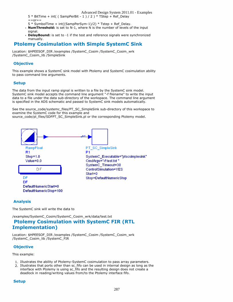
Advanced Design System 2011.01 - Examples
287
5 * BitTime + int( ( SampPerBit - 1 ) / 2 ) * TStep + Ref_Delay==or==5 * SymbolTime + int((SampPerSym-1)/2) * Tstep + Ref_Delay.NumThreshold: is set to N-1, where N is the number of levels of the inputsignal.DelayBound: is set to -1 if the test and reference signals were synchronizedmanually.
Ptolemy Cosimulation with Simple SystemC SinkLocation: $HPEESOF_DIR /examples /SystemC_Cosim /SystemC_Cosim_wrk/SystemC_Cosim_lib /SimpleSink
Objective
This example shows a SystemC sink model with Ptolemy and SystemC cosimulation abilityto pass command line arguments.
Setup
The data from the input ramp signal is written to a file by the SystemC sink model.SystemC sink model accepts the command line argument "-f filename" to write the inputdata to a file under the data sub-directory of the workspace. The command line argumentis specified in the ADS schematic and passed to SystemC sink models automatically.
See the source_code/systemc_files/PT_SC_SimpleSink sub-directory of this workspace toexamine the SystemC code for this example andsource_code/pl_files/SDFPT_SC_SimpleSink.pl or the corresponding Ptolemy model.
Analysis
The SystemC sink will write the data to
/examples/SystemC_Cosim/SystemC_Cosim_wrk/data/test.txt
Ptolemy Cosimulation with SystemC FIR (RTLImplementation)Location: $HPEESOF_DIR /examples /SystemC_Cosim /SystemC_Cosim_wrk/SystemC_Cosim_lib /SystemC_FIR
Objective
This example:
Illustrates the ability of Ptolemy-SystemC cosimulation to pass array parameters.1.Illustrates that ports other than sc_fifo can be used in internal design as long as the2.interface with Ptolemy is using sc_fifo and the resulting design does not create adeadlock in reading/writing values from/to the Ptolemy interface fifo.
Setup
Advanced Design System 2011.01 - Examples
288
The SystemC FIR (RTL implementation) example that is shipped with OSCI SystemC 2.1,is modified in this example to cosimulate with ptolemy. The modified code is available inthe following subdirectory of this workspace:
source_code/systemc_files/PT_SC_FIR
The stimulus and display SystemC modules are modified to read and write values toPtolemy instead of generating ramp as stimuli and writing outputs to standard output. Thefir_top and fir_data modules are also modified to read Taps values fromSystemcPtolemyInterface_PT_SC_FIR instead of reading from a header file. Thecorresponding Ptolemy model can be found at:
source_code/pl_files/SDFPT_SC_FIR.pl
This example generates the impulse response of the FIR filter. The same Taps are used asin the standalone SystemC example which is shipped with OSCI SystemC 2.1.
Analysis
Ptolemy Cosimulation with SystemC Sine WaveGeneratorLocation: $HPEESOF_DIR /examples /SystemC_Cosim /SystemC_Cosim_wrk/SystemC_Cosim_lib /SineSource
Objective
This example shows SystemC cosimulation ability to write to a parameterized SystemCSource model. Where parameter values are specified in the ADS schematic and used inthe SystemC model.
Advanced Design System 2011.01 - Examples
289
Setup
In this example, a Sine wave generator written in SystemC, is cosimulating with Ptolemy.User parameters can be changed in the schematic and read in SystemC code to generatethe corresponding sine wave. SystemC code for this example is available in the followingsub-directory of this workspace:
source_code/systemc_files/PT_SC_SineGen
The corresponding Ptolemy model can be found at:
source_code/pl_files/SDFPT_SC_SineGen.pl
Analysis
Figure 1: Output of SystemC Sine wave generator
Ptolemy CoSimulation with SystemC UpSampleLocation: $HPEESOF_DIR /examples /SystemC_Cosim /SystemC_Cosim_wrk/SystemC_Cosim_lib /UpSampler
Objective
This example shows how to cosimulate Ptolemy with a multi-rate SystemC design.
Setup
In this example, Ptolemy Cosimulates with an UpSampler written in SystemC. This designshows how to use multi-rate properties in SystemC Cosim. The multi-rate parameter(Factor) can be set in the Schematic and read in SystemC. For comparison purposes anative Ptolemy UpSample is also used in this design. The parameters Factor, Phase, andFill can be changed in the ADS schematic to control these parameters in SystemC.SystemC code for this design is available in the following sub-directory of this workspace:
source_code/systemc_files/PT_SC_UpSample
The corresponding Ptolemy model is located at:
Advanced Design System 2011.01 - Examples
290
source_code/pl_files/SDFPT_SC_UpSample.pl
Analysis
Figure 1: Upsampled values
Ptolemy-SystemC-Transient CosimulationLocation: $HPEESOF_DIR /examples /SystemC_Cosim /SystemC_Cosim_wrk/SystemC_Cosim_lib /TransientCosim
Objective
This example shows ADS Ptolemy's ability to simultanously cosimulate with SystemC andTransient Simulator.
Setup
Advanced Design System 2011.01 - Examples
291
In this example, Ptolemy's interactive TkSlider is used to select the input signal, noiseamplitude and input frequency during simulation. These three items are sent to theSystemC signal generator. The signal generator creates the signal with input signalmagnitude/frequency and adds variable noise. The output of the SystemC signal generatoris sent to the analog simulator. In the analog sub-network, the signal passes through a 1Mhz Butterworth Lowpass filter to eliminate the added noise, and then through a singletransister amplifier stage. The resulting waveform is sent back to ADS Ptolemy, where anFFT is performed.
SystemC code for this example is available in the following sub-directory of thisworkspace:source_code/systemc_files/PT_SC_InputSignalThe corresponding Ptolemy models are available at:source_code/pl_files/SDFPT_SC_InputSignal.pl
Analysis
Figure 1: Analog subcircuit for Transient cosimulation
Figure 2: Input signal generated by SystemC model
Advanced Design System 2011.01 - Examples
292
Figure 3: Output signal
Figure 4: Output Spectrum
Figure 5: Slider bars for real-time input signal adjustments
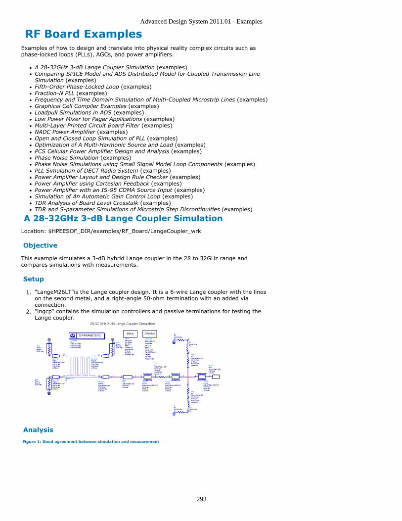
Advanced Design System 2011.01 - Examples
293
RF Board ExamplesExamples of how to design and translate into physical reality complex circuits such asphase-locked loops (PLLs), AGCs, and power amplifiers.
A 28-32GHz 3-dB Lange Coupler Simulation (examples)Comparing SPICE Model and ADS Distributed Model for Coupled Transmission LineSimulation (examples)Fifth-Order Phase-Locked Loop (examples)Fraction-N PLL (examples)Frequency and Time Domain Simulation of Multi-Coupled Microstrip Lines (examples)Graphical Cell Compiler Examples (examples)Loadpull Simulations in ADS (examples)Low Power Mixer for Pager Applications (examples)Multi-Layer Printed Circuit Board Filter (examples)NADC Power Amplifier (examples)Open and Closed Loop Simulation of PLL (examples)Optimization of A Multi-Harmonic Source and Load (examples)PCS Cellular Power Amplifier Design and Analysis (examples)Phase Noise Simulation (examples)Phase Noise Simulations using Small Signal Model Loop Components (examples)PLL Simulation of DECT Radio System (examples)Power Amplifier Layout and Design Rule Checker (examples)Power Amplifier using Cartesian Feedback (examples)Power Amplifier with an IS-95 CDMA Source Input (examples)Simulation of An Automatic Gain Control Loop (examples)TDR Analysis of Board Level Crosstalk (examples)TDR and S-parameter Simulations of Microstrip Step Discontinuities (examples)
A 28-32GHz 3-dB Lange Coupler SimulationLocation: $HPEESOF_DIR/examples/RF_Board/LangeCoupler_wrk
Objective
This example simulates a 3-dB hybrid Lange coupler in the 28 to 32GHz range andcompares simulations with measurements.
Setup
"LangeM26LT"is the Lange coupler design. It is a 6-wire Lange coupler with the lines1.on the second metal, and a right-angle 50-ohm termination with an added viaconnection."lngcp" contains the simulation controllers and passive terminations for testing the2.Lange coupler.
Analysis
Figure 1: Good agreement between simulation and measurement
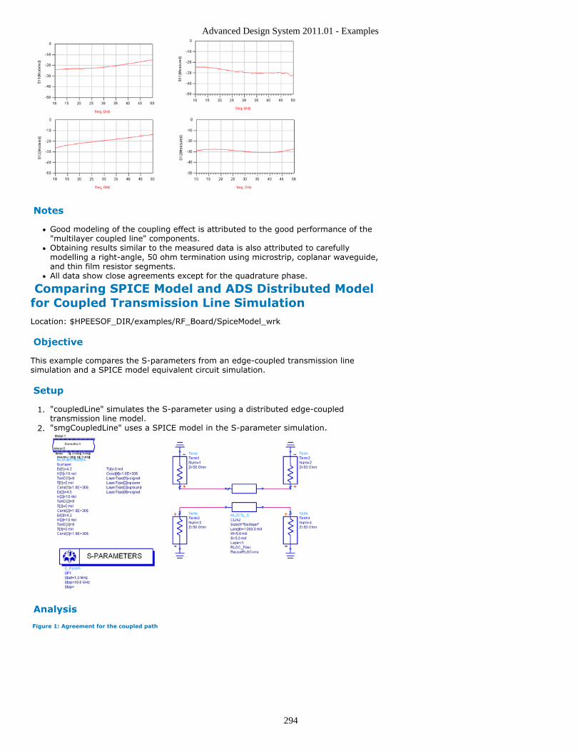
Advanced Design System 2011.01 - Examples
294
Notes
Good modeling of the coupling effect is attributed to the good performance of the"multilayer coupled line" components.Obtaining results similar to the measured data is also attributed to carefullymodelling a right-angle, 50 ohm termination using microstrip, coplanar waveguide,and thin film resistor segments.All data show close agreements except for the quadrature phase.
Comparing SPICE Model and ADS Distributed Modelfor Coupled Transmission Line SimulationLocation: $HPEESOF_DIR/examples/RF_Board/SpiceModel_wrk
Objective
This example compares the S-parameters from an edge-coupled transmission linesimulation and a SPICE model equivalent circuit simulation.
Setup
"coupledLine" simulates the S-parameter using a distributed edge-coupled1.transmission line model."smgCoupledLine" uses a SPICE model in the S-parameter simulation.2.
Analysis
Figure 1: Agreement for the coupled path
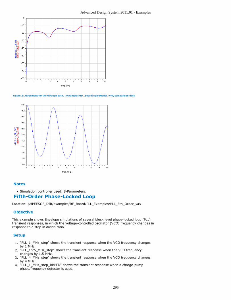
Advanced Design System 2011.01 - Examples
295
Figure 2: Agreement for the through path. (/examples/RF_Board/SpiceModel_wrk/comparison.dds)
Notes
Simulation controller used: S-Parameters.
Fifth-Order Phase-Locked LoopLocation: $HPEESOF_DIR/examples/RF_Board/PLL_Examples/PLL_5th_Order_wrk
Objective
This example shows Envelope simulations of several block level phase-locked loop (PLL)transient responses, in which the voltage-controlled oscillator (VCO) frequency changes inresponse to a step in divide ratio.
Setup
"PLL_1_MHz_step" shows the transient response when the VCO frequency changes1.by 1 MHz."PLL_1pt5_MHz_step" shows the transient response when the VCO frequency2.changes by 1.5 MHz."PLL_4_MHz_step" shows the transient response when the VCO frequency changes3.by 4 MHz."PLL_1_MHz_step_BBPFD" shows the transient response when a charge-pump4.phase/frequency detector is used.
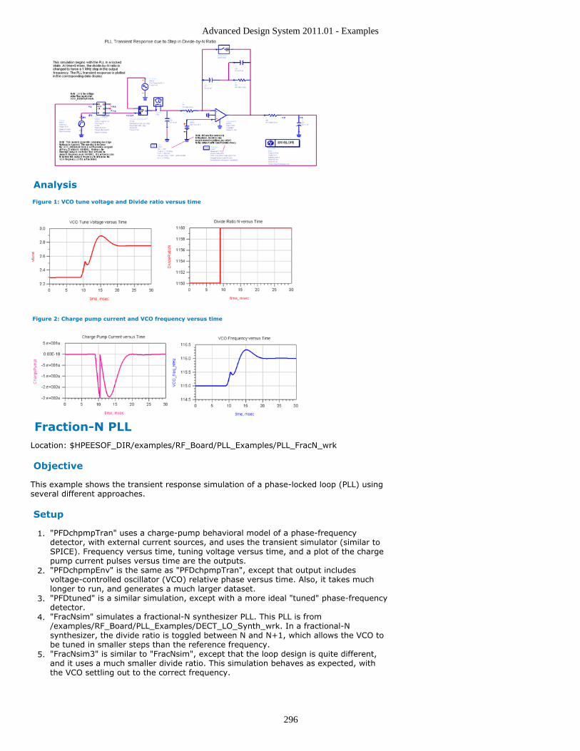
Advanced Design System 2011.01 - Examples
296
Analysis
Figure 1: VCO tune voltage and Divide ratio versus time
Figure 2: Charge pump current and VCO frequency versus time
Fraction-N PLLLocation: $HPEESOF_DIR/examples/RF_Board/PLL_Examples/PLL_FracN_wrk
Objective
This example shows the transient response simulation of a phase-locked loop (PLL) usingseveral different approaches.
Setup
"PFDchpmpTran" uses a charge-pump behavioral model of a phase-frequency1.detector, with external current sources, and uses the transient simulator (similar toSPICE). Frequency versus time, tuning voltage versus time, and a plot of the chargepump current pulses versus time are the outputs."PFDchpmpEnv" is the same as "PFDchpmpTran", except that output includes2.voltage-controlled oscillator (VCO) relative phase versus time. Also, it takes muchlonger to run, and generates a much larger dataset."PFDtuned" is a similar simulation, except with a more ideal "tuned" phase-frequency3.detector."FracNsim" simulates a fractional-N synthesizer PLL. This PLL is from4./examples/RF_Board/PLL_Examples/DECT_LO_Synth_wrk. In a fractional-Nsynthesizer, the divide ratio is toggled between N and N+1, which allows the VCO tobe tuned in smaller steps than the reference frequency."FracNsim3" is similar to "FracNsim", except that the loop design is quite different,5.and it uses a much smaller divide ratio. This simulation behaves as expected, withthe VCO settling out to the correct frequency.
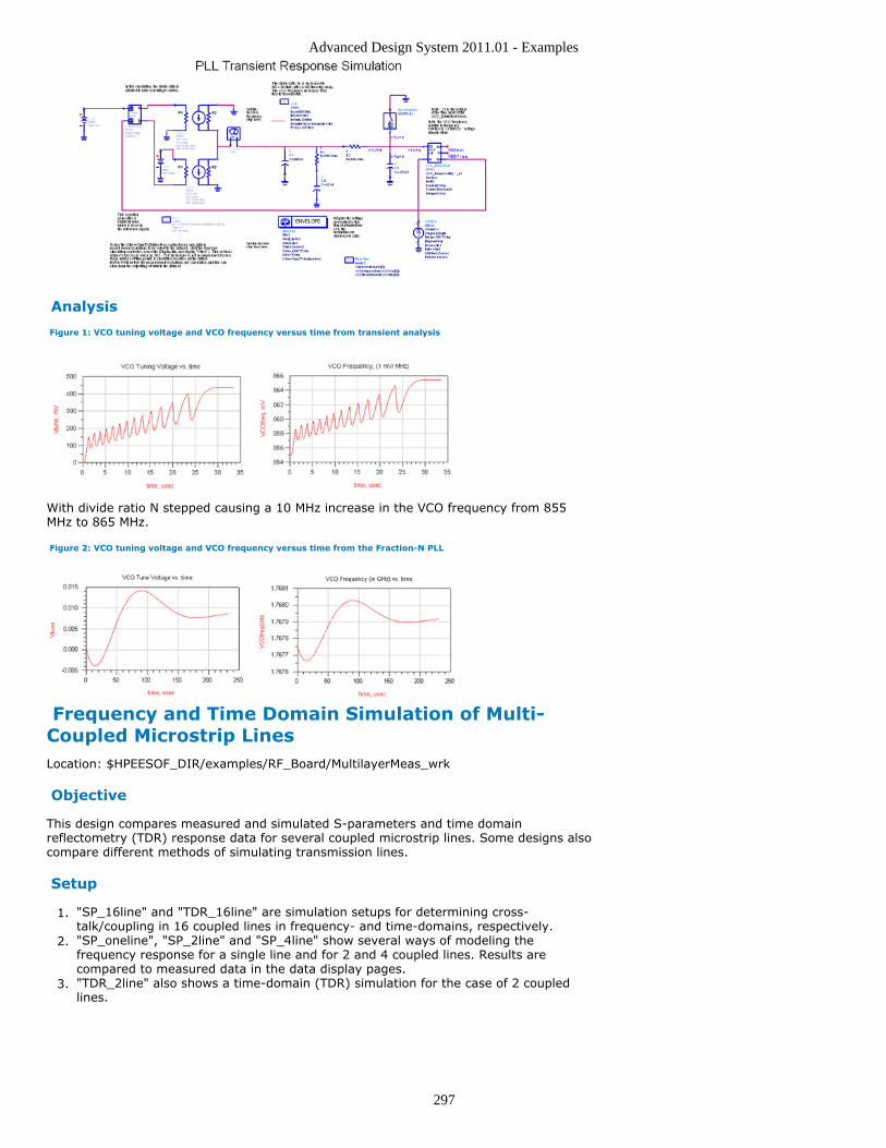
Advanced Design System 2011.01 - Examples
297
Analysis
Figure 1: VCO tuning voltage and VCO frequency versus time from transient analysis
With divide ratio N stepped causing a 10 MHz increase in the VCO frequency from 855MHz to 865 MHz.
Figure 2: VCO tuning voltage and VCO frequency versus time from the Fraction-N PLL
Frequency and Time Domain Simulation of Multi-Coupled Microstrip LinesLocation: $HPEESOF_DIR/examples/RF_Board/MultilayerMeas_wrk
Objective
This design compares measured and simulated S-parameters and time domainreflectometry (TDR) response data for several coupled microstrip lines. Some designs alsocompare different methods of simulating transmission lines.
Setup
"SP_16line" and "TDR_16line" are simulation setups for determining cross-1.talk/coupling in 16 coupled lines in frequency- and time-domains, respectively."SP_oneline", "SP_2line" and "SP_4line" show several ways of modeling the2.frequency response for a single line and for 2 and 4 coupled lines. Results arecompared to measured data in the data display pages."TDR_2line" also shows a time-domain (TDR) simulation for the case of 2 coupled3.lines.
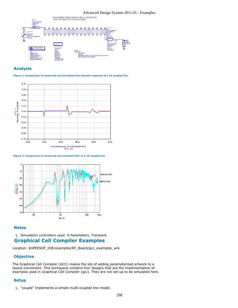
Advanced Design System 2011.01 - Examples
298
Analysis
Figure 1: Comparison of measured and simulated time domain response of a 16 coupled line
Figure 2: Comparison of measured and simulated S21 of a 16 coupled line
Notes
Simulation controllers used: S Parameters, Transient.1.
Graphical Cell Compiler ExamplesLocation: $HPEESOF_DIR/examples/RF_Board/gcc_examples_wrk
Objective
The Graphical Cell Compiler (GCC) makes the job of adding parameterized artwork to alayout convenient. This workspace contains four designs that are the implementation ofexamples used in Graphical Cell Compiler (gcc). They are not set-up to be simulated here.
Setup
"couple" implements a simple multi-coupled line model.1.
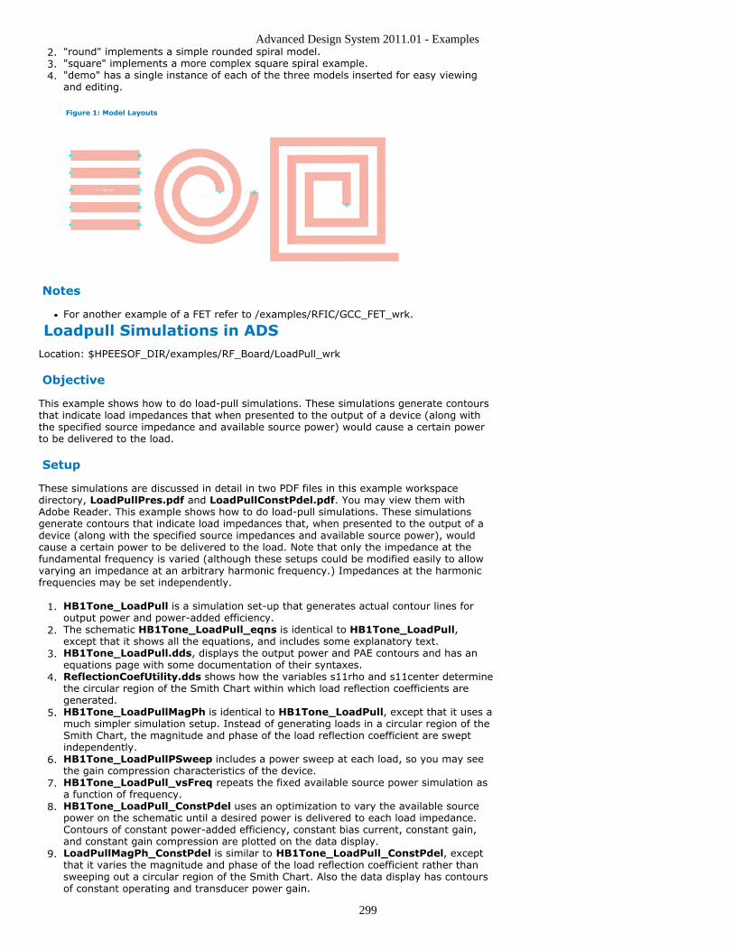
Advanced Design System 2011.01 - Examples
299
"round" implements a simple rounded spiral model.2."square" implements a more complex square spiral example.3."demo" has a single instance of each of the three models inserted for easy viewing4.and editing.
Figure 1: Model Layouts
Notes
For another example of a FET refer to /examples/RFIC/GCC_FET_wrk.
Loadpull Simulations in ADSLocation: $HPEESOF_DIR/examples/RF_Board/LoadPull_wrk
Objective
This example shows how to do load-pull simulations. These simulations generate contoursthat indicate load impedances that when presented to the output of a device (along withthe specified source impedance and available source power) would cause a certain powerto be delivered to the load.
Setup
These simulations are discussed in detail in two PDF files in this example workspacedirectory, LoadPullPres.pdf and LoadPullConstPdel.pdf. You may view them withAdobe Reader. This example shows how to do load-pull simulations. These simulationsgenerate contours that indicate load impedances that, when presented to the output of adevice (along with the specified source impedances and available source power), wouldcause a certain power to be delivered to the load. Note that only the impedance at thefundamental frequency is varied (although these setups could be modified easily to allowvarying an impedance at an arbitrary harmonic frequency.) Impedances at the harmonicfrequencies may be set independently.
HB1Tone_LoadPull is a simulation set-up that generates actual contour lines for1.output power and power-added efficiency.The schematic HB1Tone_LoadPull_eqns is identical to HB1Tone_LoadPull,2.except that it shows all the equations, and includes some explanatory text.HB1Tone_LoadPull.dds, displays the output power and PAE contours and has an3.equations page with some documentation of their syntaxes.ReflectionCoefUtility.dds shows how the variables s11rho and s11center determine4.the circular region of the Smith Chart within which load reflection coefficients aregenerated.HB1Tone_LoadPullMagPh is identical to HB1Tone_LoadPull, except that it uses a5.much simpler simulation setup. Instead of generating loads in a circular region of theSmith Chart, the magnitude and phase of the load reflection coefficient are sweptindependently.HB1Tone_LoadPullPSweep includes a power sweep at each load, so you may see6.the gain compression characteristics of the device.HB1Tone_LoadPull_vsFreq repeats the fixed available source power simulation as7.a function of frequency.HB1Tone_LoadPull_ConstPdel uses an optimization to vary the available source8.power on the schematic until a desired power is delivered to each load impedance.Contours of constant power-added efficiency, constant bias current, constant gain,and constant gain compression are plotted on the data display.LoadPullMagPh_ConstPdel is similar to HB1Tone_LoadPull_ConstPdel, except9.that it varies the magnitude and phase of the load reflection coefficient rather thansweeping out a circular region of the Smith Chart. Also the data display has contoursof constant operating and transducer power gain.
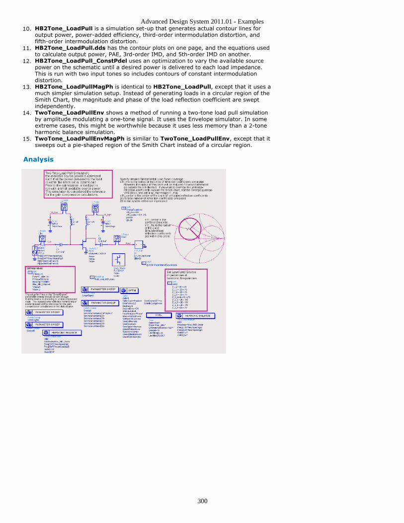
Advanced Design System 2011.01 - Examples
300
HB2Tone_LoadPull is a simulation set-up that generates actual contour lines for10.output power, power-added efficiency, third-order intermodulation distortion, andfifth-order intermodulation distortion.HB2Tone_LoadPull.dds has the contour plots on one page, and the equations used11.to calculate output power, PAE, 3rd-order IMD, and 5th-order IMD on another.HB2Tone_LoadPull_ConstPdel uses an optimization to vary the available source12.power on the schematic until a desired power is delivered to each load impedance.This is run with two input tones so includes contours of constant intermodulationdistortion.HB2Tone_LoadPullMagPh is identical to HB2Tone_LoadPull, except that it uses a13.much simpler simulation setup. Instead of generating loads in a circular region of theSmith Chart, the magnitude and phase of the load reflection coefficient are sweptindependently.TwoTone_LoadPullEnv shows a method of running a two-tone load pull simulation14.by amplitude modulating a one-tone signal. It uses the Envelope simulator. In someextreme cases, this might be worthwhile because it uses less memory than a 2-toneharmonic balance simulation.TwoTone_LoadPullEnvMagPh is similar to TwoTone_LoadPullEnv, except that it15.sweeps out a pie-shaped region of the Smith Chart instead of a circular region.
Analysis
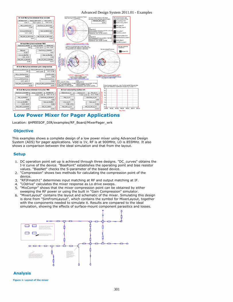
Advanced Design System 2011.01 - Examples
301
Low Power Mixer for Pager ApplicationsLocation: $HPEESOF_DIR/examples/RF_Board/MixerPager_wrk
Objective
This examples shows a complete design of a low power mixer using Advanced DesignSystem (ADS) for pager applications. Vdd is 1V, RF is at 900MHz, LO is 855MHz. It alsoshows a comparison between the ideal simulation and that from the layout.
Setup
DC operation point set up is achieved through three designs. "DC_curves" obtains the1.I-V curve of the device. "BiasPoint" establishes the operating point and bias resistorvalues. "BiasNet" checks the S-parameter of the biased device."Compression" shows two methods for calculating the compression point of the2.device."RFIFmatch1" determines input matching at RF and output matching at IF.3."LOdrive" calculates the mixer response as Lo drive sweeps.4."MixCompr" shows that the mixer compression point can be obtained by either5.sweeping the RF power or using the built in "Gain Compression" simulator."MixerLayout" contains the layout and schematic of the mixer. Simulating this design6.is done from "SimFromLayout", which contains the symbol for MixerLayout, togetherwith the components needed to simulate it. Results are compared to the idealsimulation, showing the effects of surface-mount component parasitics and losses.
Analysis
Figure 1: Layout of the mixer
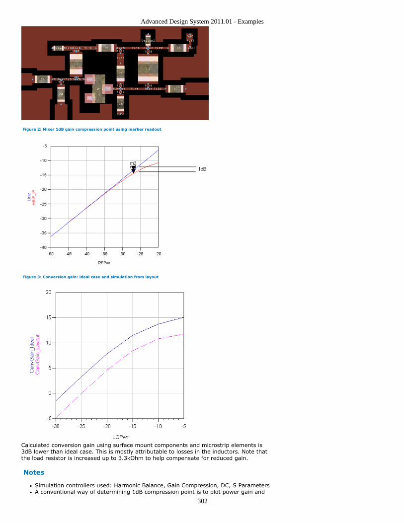
Advanced Design System 2011.01 - Examples
302
Figure 2: Mixer 1dB gain compression point using marker readout
Figure 3: Conversion gain: ideal case and simulation from layout
Calculated conversion gain using surface mount components and microstrip elements is3dB lower than ideal case. This is mostly attributable to losses in the inductors. Note thatthe load resistor is increased up to 3.3kOhm to help compensate for reduced gain.
Notes
Simulation controllers used: Harmonic Balance, Gain Compression, DC, S ParametersA conventional way of determining 1dB compression point is to plot power gain and
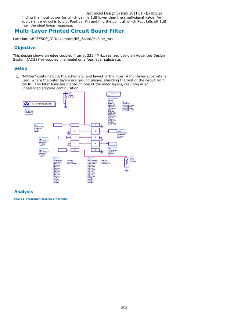
Advanced Design System 2011.01 - Examples
303
finding the input power for which gain is 1dB lower than the small-signal value. Anequivalent method is to plot Pout vs. Pin and find the point at which Pout falls off 1dBfrom the ideal linear response.
Multi-Layer Printed Circuit Board FilterLocation: $HPEESOF_DIR/examples/RF_Board/MLfilter_wrk
Objective
This design shows an edge coupled filter at 321.4MHz, realized using an Advanced DesignSystem (ADS) five coupled line model on a four layer substrate.
Setup
"Mlfilter" contains both the schematic and layout of the filter. A four layer substrate is1.used, where the outer layers are ground planes, shielding the rest of the circuit fromthe RF. The filter lines are placed on one of the inner layers, resulting in anunbalanced stripline configuration.
Analysis
Figure 1: Frequency response of the filter
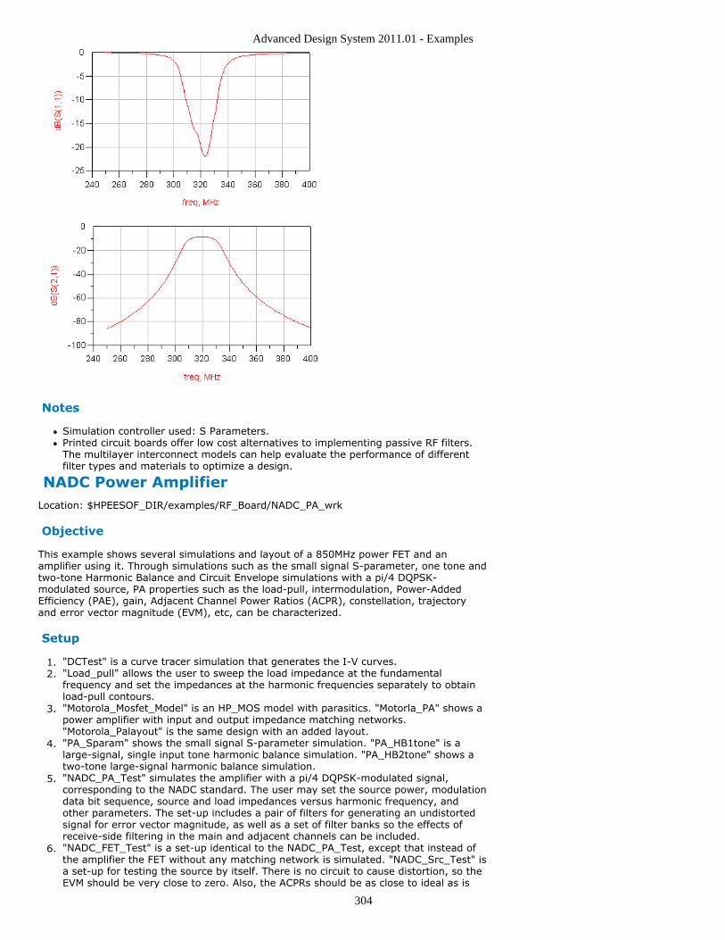
Advanced Design System 2011.01 - Examples
304
Notes
Simulation controller used: S Parameters.Printed circuit boards offer low cost alternatives to implementing passive RF filters.The multilayer interconnect models can help evaluate the performance of differentfilter types and materials to optimize a design.
NADC Power AmplifierLocation: $HPEESOF_DIR/examples/RF_Board/NADC_PA_wrk
Objective
This example shows several simulations and layout of a 850MHz power FET and anamplifier using it. Through simulations such as the small signal S-parameter, one tone andtwo-tone Harmonic Balance and Circuit Envelope simulations with a pi/4 DQPSK-modulated source, PA properties such as the load-pull, intermodulation, Power-AddedEfficiency (PAE), gain, Adjacent Channel Power Ratios (ACPR), constellation, trajectoryand error vector magnitude (EVM), etc, can be characterized.
Setup
"DCTest" is a curve tracer simulation that generates the I-V curves.1."Load_pull" allows the user to sweep the load impedance at the fundamental2.frequency and set the impedances at the harmonic frequencies separately to obtainload-pull contours."Motorola_Mosfet_Model" is an HP_MOS model with parasitics. "Motorla_PA" shows a3.power amplifier with input and output impedance matching networks."Motorola_Palayout" is the same design with an added layout."PA_Sparam" shows the small signal S-parameter simulation. "PA_HB1tone" is a4.large-signal, single input tone harmonic balance simulation. "PA_HB2tone" shows atwo-tone large-signal harmonic balance simulation."NADC_PA_Test" simulates the amplifier with a pi/4 DQPSK-modulated signal,5.corresponding to the NADC standard. The user may set the source power, modulationdata bit sequence, source and load impedances versus harmonic frequency, andother parameters. The set-up includes a pair of filters for generating an undistortedsignal for error vector magnitude, as well as a set of filter banks so the effects ofreceive-side filtering in the main and adjacent channels can be included."NADC_FET_Test" is a set-up identical to the NADC_PA_Test, except that instead of6.the amplifier the FET without any matching network is simulated. "NADC_Src_Test" isa set-up for testing the source by itself. There is no circuit to cause distortion, so theEVM should be very close to zero. Also, the ACPRs should be as close to ideal as is
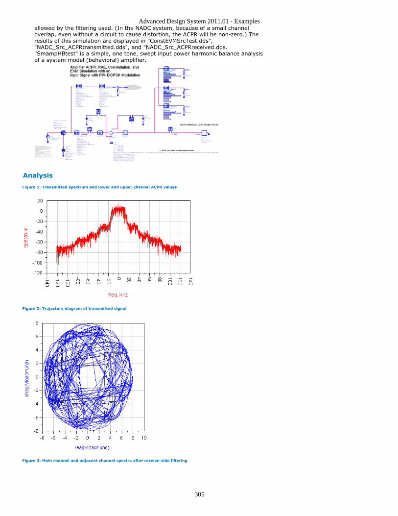
Advanced Design System 2011.01 - Examples
305
allowed by the filtering used. (In the NADC system, because of a small channeloverlap, even without a circuit to cause distortion, the ACPR will be non-zero.) Theresults of this simulation are displayed in "ConstEVMSrcTest.dds","NADC_Src_ACPRtransmitted.dds", and "NADC_Src_ACPRreceived.dds."SmampHBtest" is a simple, one tone, swept input power harmonic balance analysisof a system model (behavioral) amplifier.
Analysis
Figure 1: Transmitted spectrum and lower and upper channel ACPR values
Figure 2: Trajectory diagram of transmitted signal
Figure 3: Main channel and adjacent channel spectra after receive-side filtering
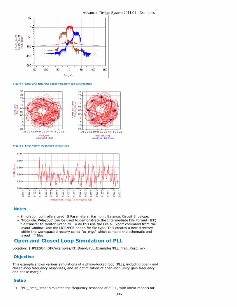
Advanced Design System 2011.01 - Examples
306
Figure 4: Ideal and distorted signal trajectory and constellation
Figure 5: Error vector magnitude versus time
Notes
Simulation controllers used: S Parameters, Harmonic Balance, Circuit Envelope."Motorola_PAlayout" can be used to demonstrate the Intermediate File Format (IFF)file transfer to Mentor Graphics. To do this use the File > Export command from thelayout window. Use the MGC/PCB option for file type. This creates a new directorywithin the workspace directory called "to_mgc" which contains the schematic andlayout .iff files.
Open and Closed Loop Simulation of PLLLocation: $HPEESOF_DIR/examples/RF_Board/PLL_Examples/PLL_Freq_Resp_wrk
Objective
This example shows various simulations of a phase-locked loop (PLL), including open- andclosed-loop frequency responses, and an optimization of open-loop unity gain frequencyand phase margin.
Setup
"PLL_Freq_Resp" simulates the frequency response of a PLL, with linear models for1.
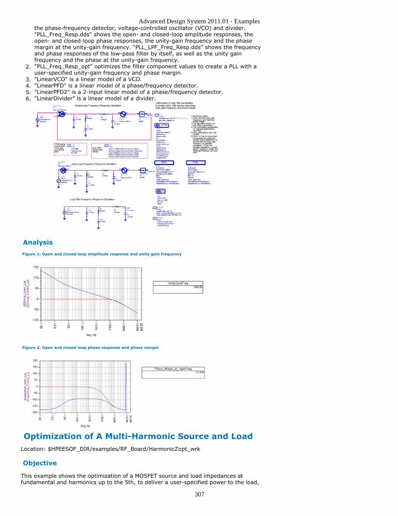
Advanced Design System 2011.01 - Examples
307
the phase-frequency detector, voltage-controlled oscillator (VCO) and divider."PLL_Freq_Resp.dds" shows the open- and closed-loop amplitude responses, theopen- and closed-loop phase responses, the unity-gain frequency and the phasemargin at the unity-gain frequency. "PLL_LPF_Freq_Resp.dds" shows the frequencyand phase responses of the low-pass filter by itself, as well as the unity gainfrequency and the phase at the unity-gain frequency."PLL_Freq_Resp_opt" optimizes the filter component values to create a PLL with a2.user-specified unity-gain frequency and phase margin."LinearVCO" is a linear model of a VCO.3."LinearPFD" is a linear model of a phase/frequency detector.4."LinearPFD2" is a 2-input linear model of a phase/frequency detector.5."LinearDivider" is a linear model of a divider.6.
Analysis
Figure 1: Open and closed loop amplitude response and unity gain frequency
Figure 2: Open and closed loop phase response and phase margin
Optimization of A Multi-Harmonic Source and LoadLocation: $HPEESOF_DIR/examples/RF_Board/HarmonicZopt_wrk
Objective
This example shows the optimization of a MOSFET source and load impedances atfundamental and harmonics up to the 5th, to deliver a user-specified power to the load,
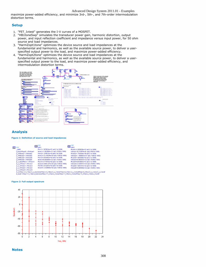
Advanced Design System 2011.01 - Examples
308
maximize power-added efficiency, and minimize 3rd-, 5th-, and 7th-order intermodulationdistortion terms.
Setup
"FET_Ivtest" generates the I-V curves of a MOSFET.1."HB1toneSwp" simulates the transducer power gain, harmonic distortion, output2.power, and input reflection coefficient and impedance versus input power, for 50 ohmsource and load impedances."HarmZopt1tone" optimizes the device source and load impedances at the3.fundamental and harmonics, as well as the available source power, to deliver a user-specified output power to the load, and maximize power-added efficiency."HarmZopt2tone" optimizes the device source and load impedances at the4.fundamental and harmonics, as well as the available source power, to deliver a user-specified output power to the load, and maximize power-added efficiency, andintermodulation distortion terms.
Analysis
Figure 1: Definition of source and load impedances
Figure 2: Full output spectrum
Notes
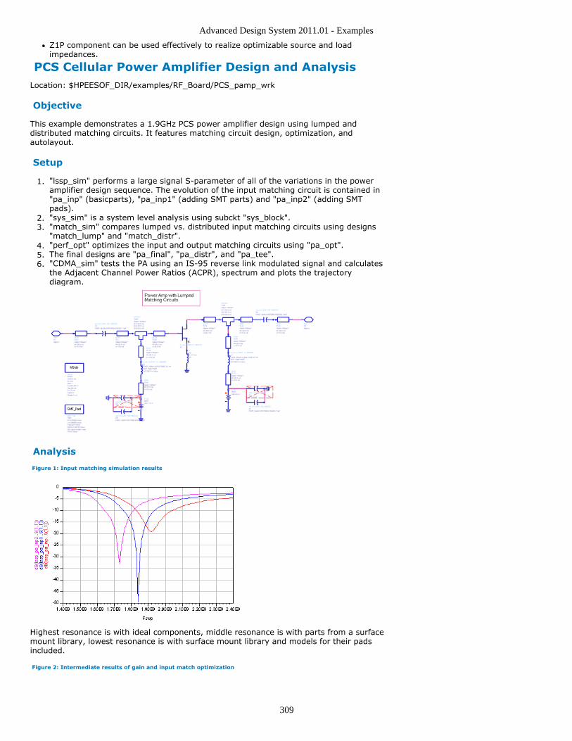
Advanced Design System 2011.01 - Examples
309
Z1P component can be used effectively to realize optimizable source and loadimpedances.
PCS Cellular Power Amplifier Design and AnalysisLocation: $HPEESOF_DIR/examples/RF_Board/PCS_pamp_wrk
Objective
This example demonstrates a 1.9GHz PCS power amplifier design using lumped anddistributed matching circuits. It features matching circuit design, optimization, andautolayout.
Setup
"lssp_sim" performs a large signal S-parameter of all of the variations in the power1.amplifier design sequence. The evolution of the input matching circuit is contained in"pa_inp" (basicparts), "pa_inp1" (adding SMT parts) and "pa_inp2" (adding SMTpads)."sys_sim" is a system level analysis using subckt "sys_block".2."match_sim" compares lumped vs. distributed input matching circuits using designs3."match_lump" and "match_distr"."perf_opt" optimizes the input and output matching circuits using "pa_opt".4.The final designs are "pa_final", "pa_distr", and "pa_tee".5."CDMA_sim" tests the PA using an IS-95 reverse link modulated signal and calculates6.the Adjacent Channel Power Ratios (ACPR), spectrum and plots the trajectorydiagram.
Analysis
Figure 1: Input matching simulation results
Highest resonance is with ideal components, middle resonance is with parts from a surfacemount library, lowest resonance is with surface mount library and models for their padsincluded.
Figure 2: Intermediate results of gain and input match optimization
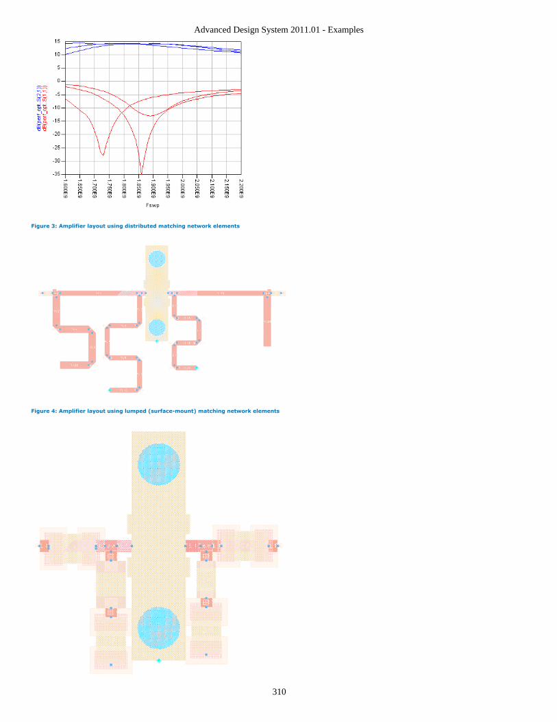
Advanced Design System 2011.01 - Examples
310
Figure 3: Amplifier layout using distributed matching network elements
Figure 4: Amplifier layout using lumped (surface-mount) matching network elements
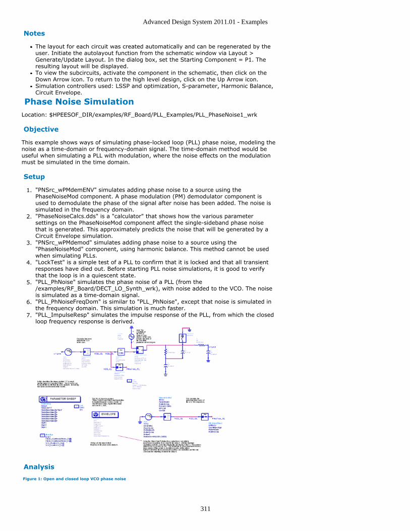
Advanced Design System 2011.01 - Examples
311
Notes
The layout for each circuit was created automatically and can be regenerated by theuser. Initiate the autolayout function from the schematic window via Layout >Generate/Update Layout. In the dialog box, set the Starting Component = P1. Theresulting layout will be displayed.To view the subcircuits, activate the component in the schematic, then click on theDown Arrow icon. To return to the high level design, click on the Up Arrow icon.Simulation controllers used: LSSP and optimization, S-parameter, Harmonic Balance,Circuit Envelope.
Phase Noise SimulationLocation: $HPEESOF_DIR/examples/RF_Board/PLL_Examples/PLL_PhaseNoise1_wrk
Objective
This example shows ways of simulating phase-locked loop (PLL) phase noise, modeling thenoise as a time-domain or frequency-domain signal. The time-domain method would beuseful when simulating a PLL with modulation, where the noise effects on the modulationmust be simulated in the time domain.
Setup
"PNSrc_wPMdemENV" simulates adding phase noise to a source using the1.PhaseNoiseMod component. A phase modulation (PM) demodulator component isused to demodulate the phase of the signal after noise has been added. The noise issimulated in the frequency domain."PhaseNoiseCalcs.dds" is a "calculator" that shows how the various parameter2.settings on the PhaseNoiseMod component affect the single-sideband phase noisethat is generated. This approximately predicts the noise that will be generated by aCircuit Envelope simulation."PNSrc_wPMdemod" simulates adding phase noise to a source using the3."PhaseNoiseMod" component, using harmonic balance. This method cannot be usedwhen simulating PLLs."LockTest" is a simple test of a PLL to confirm that it is locked and that all transient4.responses have died out. Before starting PLL noise simulations, it is good to verifythat the loop is in a quiescent state."PLL_PhNoise" simulates the phase noise of a PLL (from the5./examples/RF_Board/DECT_LO_Synth_wrk), with noise added to the VCO. The noiseis simulated as a time-domain signal."PLL_PhNoiseFreqDom" is similar to "PLL_PhNoise", except that noise is simulated in6.the frequency domain. This simulation is much faster."PLL_ImpulseResp" simulates the impulse response of the PLL, from which the closed7.loop frequency response is derived.
Analysis
Figure 1: Open and closed loop VCO phase noise
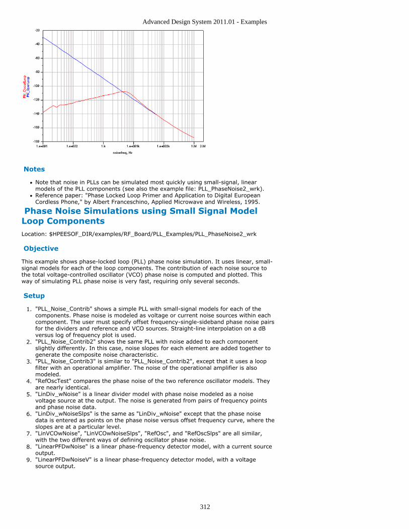
Advanced Design System 2011.01 - Examples
312
Notes
Note that noise in PLLs can be simulated most quickly using small-signal, linearmodels of the PLL components (see also the example file: PLL_PhaseNoise2_wrk).Reference paper: "Phase Locked Loop Primer and Application to Digital EuropeanCordless Phone," by Albert Franceschino, Applied Microwave and Wireless, 1995.
Phase Noise Simulations using Small Signal ModelLoop ComponentsLocation: $HPEESOF_DIR/examples/RF_Board/PLL_Examples/PLL_PhaseNoise2_wrk
Objective
This example shows phase-locked loop (PLL) phase noise simulation. It uses linear, small-signal models for each of the loop components. The contribution of each noise source tothe total voltage-controlled oscillator (VCO) phase noise is computed and plotted. Thisway of simulating PLL phase noise is very fast, requiring only several seconds.
Setup
"PLL_Noise_Contrib" shows a simple PLL with small-signal models for each of the1.components. Phase noise is modeled as voltage or current noise sources within eachcomponent. The user must specify offset frequency-single-sideband phase noise pairsfor the dividers and reference and VCO sources. Straight-line interpolation on a dBversus log of frequency plot is used."PLL_Noise_Contrib2" shows the same PLL with noise added to each component2.slightly differently. In this case, noise slopes for each element are added together togenerate the composite noise characteristic."PLL_Noise_Contrib3" is similar to "PLL_Noise_Contrib2", except that it uses a loop3.filter with an operational amplifier. The noise of the operational amplifier is alsomodeled."RefOscTest" compares the phase noise of the two reference oscillator models. They4.are nearly identical."LinDiv_wNoise" is a linear divider model with phase noise modeled as a noise5.voltage source at the output. The noise is generated from pairs of frequency pointsand phase noise data."LinDiv_wNoiseSlps" is the same as "LinDiv_wNoise" except that the phase noise6.data is entered as points on the phase noise versus offset frequency curve, where theslopes are at a particular level."LinVCOwNoise", "LinVCOwNoiseSlps", "RefOsc", and "RefOscSlps" are all similar,7.with the two different ways of defining oscillator phase noise."LinearPFDwNoise" is a linear phase-frequency detector model, with a current source8.output."LinearPFDwNoiseV" is a linear phase-frequency detector model, with a voltage9.source output.
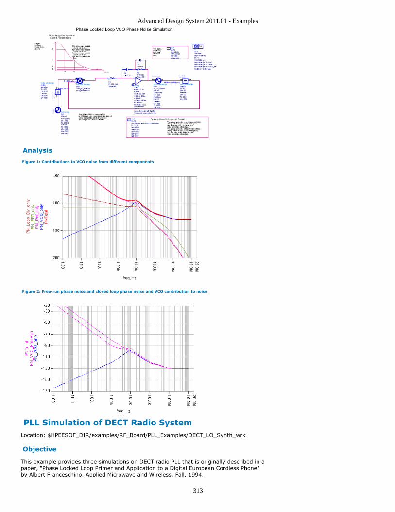
Advanced Design System 2011.01 - Examples
313
Analysis
Figure 1: Contributions to VCO noise from different components
Figure 2: Free-run phase noise and closed loop phase noise and VCO contribution to noise
PLL Simulation of DECT Radio SystemLocation: $HPEESOF_DIR/examples/RF_Board/PLL_Examples/DECT_LO_Synth_wrk
Objective
This example provides three simulations on DECT radio PLL that is originally described in apaper, "Phase Locked Loop Primer and Application to a Digital European Cordless Phone"by Albert Franceschino, Applied Microwave and Wireless, Fall, 1994.
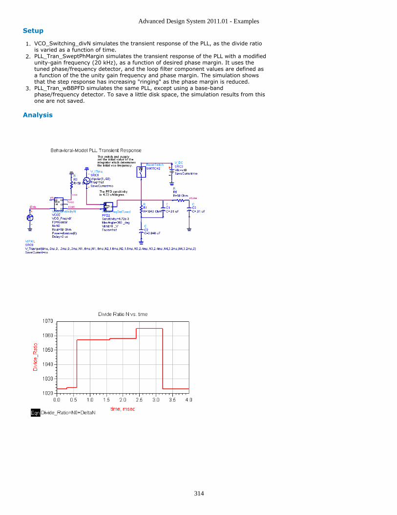
Advanced Design System 2011.01 - Examples
314
Setup
VCO_Switching_divN simulates the transient response of the PLL, as the divide ratio1.is varied as a function of time.PLL_Tran_SweptPhMargin simulates the transient response of the PLL with a modified2.unity-gain frequency (20 kHz), as a function of desired phase margin. It uses thetuned phase/frequency detector, and the loop filter component values are defined asa function of the the unity gain frequency and phase margin. The simulation showsthat the step response has increasing "ringing" as the phase margin is reduced.PLL_Tran_wBBPFD simulates the same PLL, except using a base-band3.phase/frequency detector. To save a little disk space, the simulation results from thisone are not saved.
Analysis
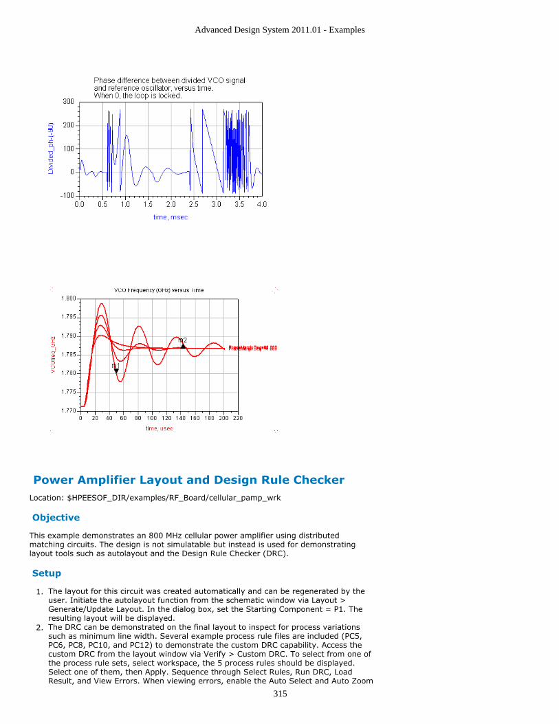
Advanced Design System 2011.01 - Examples
315
Power Amplifier Layout and Design Rule CheckerLocation: $HPEESOF_DIR/examples/RF_Board/cellular_pamp_wrk
Objective
This example demonstrates an 800 MHz cellular power amplifier using distributedmatching circuits. The design is not simulatable but instead is used for demonstratinglayout tools such as autolayout and the Design Rule Checker (DRC).
Setup
The layout for this circuit was created automatically and can be regenerated by the1.user. Initiate the autolayout function from the schematic window via Layout >Generate/Update Layout. In the dialog box, set the Starting Component = P1. Theresulting layout will be displayed.The DRC can be demonstrated on the final layout to inspect for process variations2.such as minimum line width. Several example process rule files are included (PC5,PC6, PC8, PC10, and PC12) to demonstrate the custom DRC capability. Access thecustom DRC from the layout window via Verify > Custom DRC. To select from one ofthe process rule sets, select workspace, the 5 process rules should be displayed.Select one of them, then Apply. Sequence through Select Rules, Run DRC, LoadResult, and View Errors. When viewing errors, enable the Auto Select and Auto Zoom
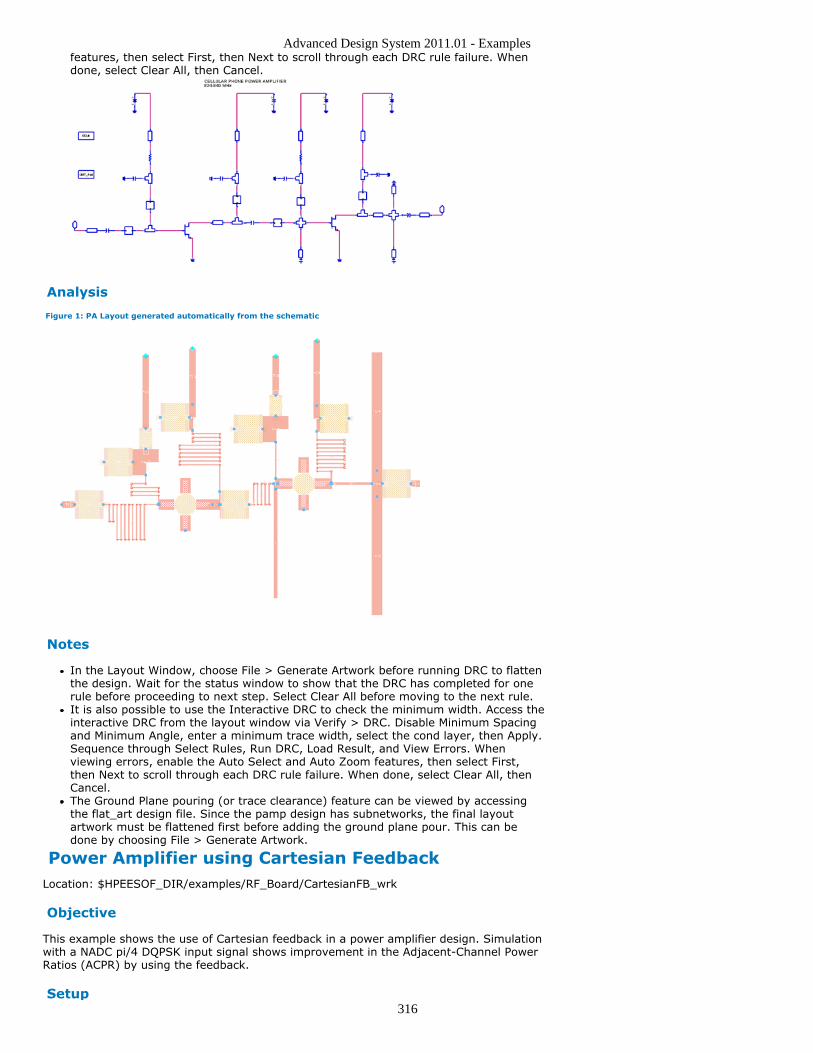
Advanced Design System 2011.01 - Examples
316
features, then select First, then Next to scroll through each DRC rule failure. Whendone, select Clear All, then Cancel.
Analysis
Figure 1: PA Layout generated automatically from the schematic
Notes
In the Layout Window, choose File > Generate Artwork before running DRC to flattenthe design. Wait for the status window to show that the DRC has completed for onerule before proceeding to next step. Select Clear All before moving to the next rule.It is also possible to use the Interactive DRC to check the minimum width. Access theinteractive DRC from the layout window via Verify > DRC. Disable Minimum Spacingand Minimum Angle, enter a minimum trace width, select the cond layer, then Apply.Sequence through Select Rules, Run DRC, Load Result, and View Errors. Whenviewing errors, enable the Auto Select and Auto Zoom features, then select First,then Next to scroll through each DRC rule failure. When done, select Clear All, thenCancel.The Ground Plane pouring (or trace clearance) feature can be viewed by accessingthe flat_art design file. Since the pamp design has subnetworks, the final layoutartwork must be flattened first before adding the ground plane pour. This can bedone by choosing File > Generate Artwork.
Power Amplifier using Cartesian FeedbackLocation: $HPEESOF_DIR/examples/RF_Board/CartesianFB_wrk
Objective
This example shows the use of Cartesian feedback in a power amplifier design. Simulationwith a NADC pi/4 DQPSK input signal shows improvement in the Adjacent-Channel PowerRatios (ACPR) by using the feedback.
Setup
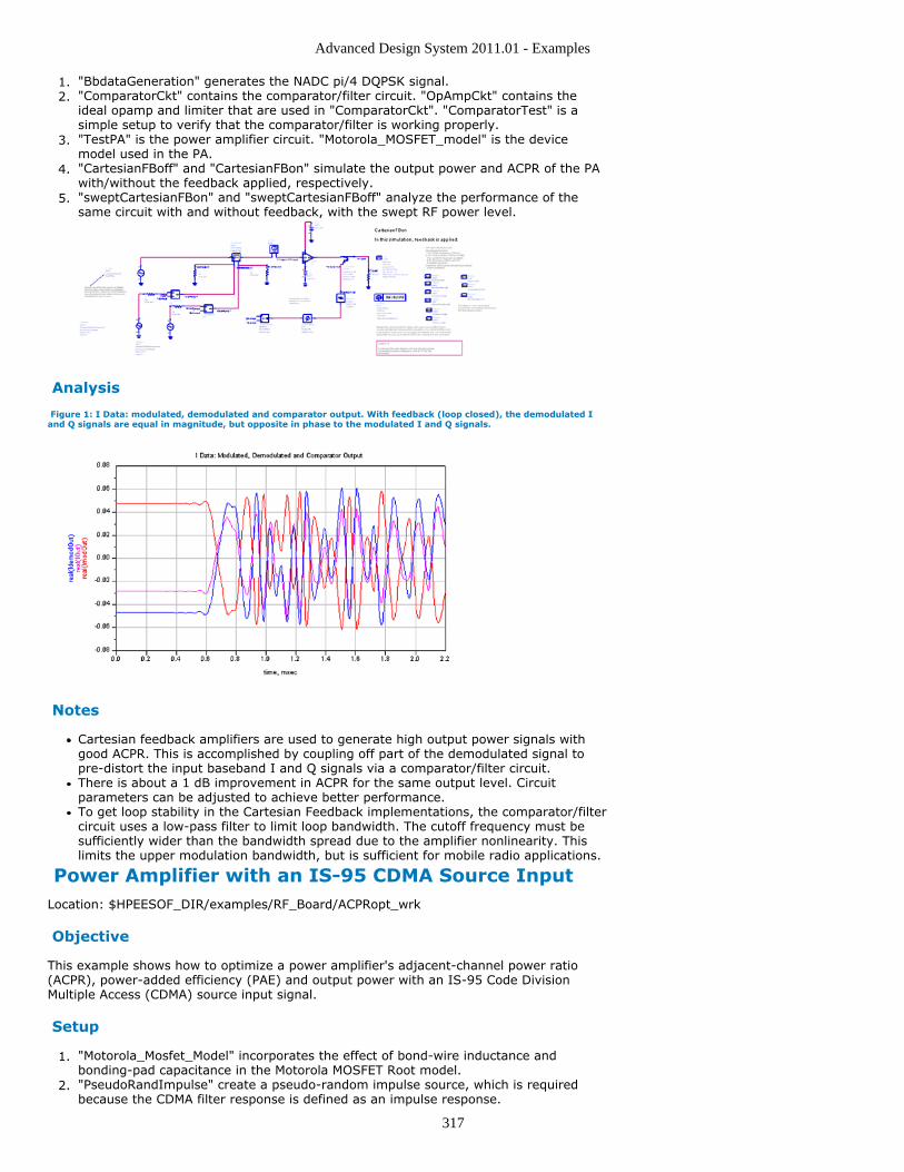
Advanced Design System 2011.01 - Examples
317
"BbdataGeneration" generates the NADC pi/4 DQPSK signal.1."ComparatorCkt" contains the comparator/filter circuit. "OpAmpCkt" contains the2.ideal opamp and limiter that are used in "ComparatorCkt". "ComparatorTest" is asimple setup to verify that the comparator/filter is working properly."TestPA" is the power amplifier circuit. "Motorola_MOSFET_model" is the device3.model used in the PA."CartesianFBoff" and "CartesianFBon" simulate the output power and ACPR of the PA4.with/without the feedback applied, respectively."sweptCartesianFBon" and "sweptCartesianFBoff" analyze the performance of the5.same circuit with and without feedback, with the swept RF power level.
Analysis
Figure 1: I Data: modulated, demodulated and comparator output. With feedback (loop closed), the demodulated Iand Q signals are equal in magnitude, but opposite in phase to the modulated I and Q signals.
Notes
Cartesian feedback amplifiers are used to generate high output power signals withgood ACPR. This is accomplished by coupling off part of the demodulated signal topre-distort the input baseband I and Q signals via a comparator/filter circuit.There is about a 1 dB improvement in ACPR for the same output level. Circuitparameters can be adjusted to achieve better performance.To get loop stability in the Cartesian Feedback implementations, the comparator/filtercircuit uses a low-pass filter to limit loop bandwidth. The cutoff frequency must besufficiently wider than the bandwidth spread due to the amplifier nonlinearity. Thislimits the upper modulation bandwidth, but is sufficient for mobile radio applications.
Power Amplifier with an IS-95 CDMA Source InputLocation: $HPEESOF_DIR/examples/RF_Board/ACPRopt_wrk
Objective
This example shows how to optimize a power amplifier's adjacent-channel power ratio(ACPR), power-added efficiency (PAE) and output power with an IS-95 Code DivisionMultiple Access (CDMA) source input signal.
Setup
"Motorola_Mosfet_Model" incorporates the effect of bond-wire inductance and1.bonding-pad capacitance in the Motorola MOSFET Root model."PseudoRandImpulse" create a pseudo-random impulse source, which is required2.because the CDMA filter response is defined as an impulse response.
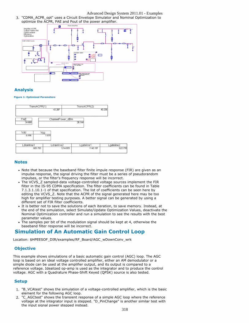
Advanced Design System 2011.01 - Examples
318
"CDMA_ACPR_opt" uses a Circuit Envelope Simulator and Nominal Optimization to3.optimize the ACPR, PAE and Pout of the power amplifier.
Analysis
Figure 1: Optimized Parameters
Notes
Note that because the baseband filter finite impule response (FIR) are given as animpulse response, the signal driving the filter must be a series of pseudorandomimpulses, or the filter's frequency response will be incorrect.The VCVS_Z sampled-data voltage-controlled voltage sources implement the FIRfilter in the IS-95 CDMA specification. The filter coefficients can be found in Table7.1.3.1.10.1-1 of that specification. The list of coefficients can be seen here byediting the VCVS_Z. Note that the ACPR of the signal generated here may be toohigh for amplifier testing purposes. A better signal can be generated by using adifferent set of FIR filter coefficients.It is better not to save the solutions of each iteration, to save memory. Instead, atthe end of the simulation, select Simulate/Update Optimization Values, deactivate theNominal Optimization controller and run a simulation to see the results with the bestparameter values.The samples per bit of the modulation signal should be kept at 4, otherwise thebaseband filter response will be incorrect.
Simulation of An Automatic Gain Control LoopLocation: $HPEESOF_DIR/examples/RF_Board/AGC_wDownConv_wrk
Objective
This example shows simulations of a basic automatic gain control (AGC) loop. The AGCloop is based on an ideal voltage controlled amplifier, either an AM demodulator or asimple diode can be used at the amplifier output, and its output is compared to areference voltage. Idealized op-amp is used as the integrator and to produce the controlvoltage. AGC with a Quadrature Phase-Shift Keyed (QPSK) source is also tested.
Setup
"B_VCAtest" shows the simulation of a voltage-controlled amplifier, which is the basic1.element for the following AGC loop."C_AGCtest" shows the transient response of a simple AGC loop where the reference2.voltage at the integrator input is stepped. "D_PinChange" is another similar test withthe input signal power stepped instead.
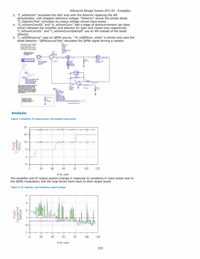
Advanced Design System 2011.01 - Examples
319
"F_wDetector" simulates the AGC loop with the detector replacing the AM3.demodulator, with stepped reference voltage. "Detector" shows the simple diode."E_DetectorTest" simulates its output voltage versus input power."G_wDownConvOL" and "H_wDownConv" add a stage of downconversion (an ideal4.mixer) between the amplifier and detector for open and closed loop respectively."I_wDownConvOL" and "J_wDownConvOpAmp0" use an AM instead of the diodedetector."L_wQPSKsource" uses an QPSK source. " M_wQPSKsrc_wDet" is similar and uses the5.diode detector. "QPSKsourceTest" simulates the QPSK signal driving a resistor.
Analysis
Figure 1: Amplifier, IF output power, and stepped input power
The amplifier and IF output powers change in response to variations in input power due tothe QPSK modulation, but the loop forces them back to their target levels.
Figure 2: IF, detector, and integrator output voltage
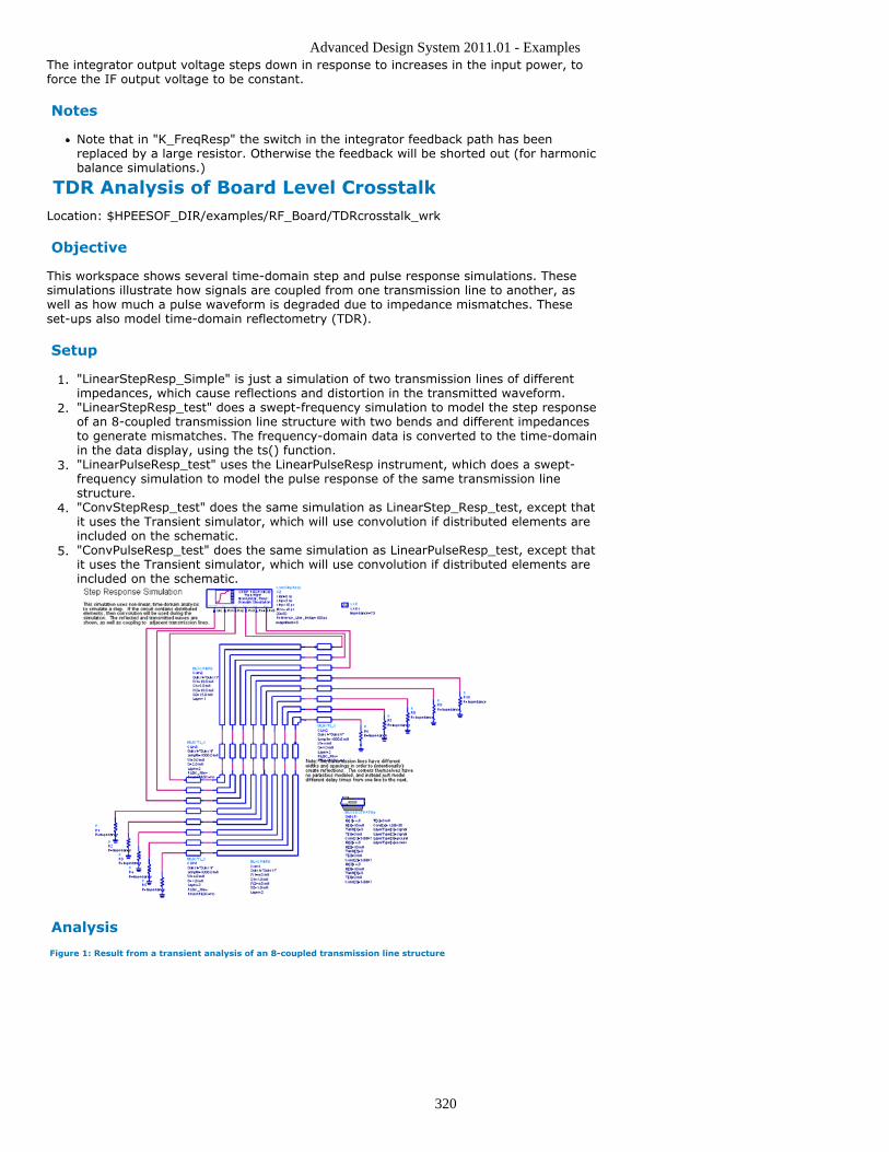
Advanced Design System 2011.01 - Examples
320
The integrator output voltage steps down in response to increases in the input power, toforce the IF output voltage to be constant.
Notes
Note that in "K_FreqResp" the switch in the integrator feedback path has beenreplaced by a large resistor. Otherwise the feedback will be shorted out (for harmonicbalance simulations.)
TDR Analysis of Board Level CrosstalkLocation: $HPEESOF_DIR/examples/RF_Board/TDRcrosstalk_wrk
Objective
This workspace shows several time-domain step and pulse response simulations. Thesesimulations illustrate how signals are coupled from one transmission line to another, aswell as how much a pulse waveform is degraded due to impedance mismatches. Theseset-ups also model time-domain reflectometry (TDR).
Setup
"LinearStepResp_Simple" is just a simulation of two transmission lines of different1.impedances, which cause reflections and distortion in the transmitted waveform."LinearStepResp_test" does a swept-frequency simulation to model the step response2.of an 8-coupled transmission line structure with two bends and different impedancesto generate mismatches. The frequency-domain data is converted to the time-domainin the data display, using the ts() function."LinearPulseResp_test" uses the LinearPulseResp instrument, which does a swept-3.frequency simulation to model the pulse response of the same transmission linestructure."ConvStepResp_test" does the same simulation as LinearStep_Resp_test, except that4.it uses the Transient simulator, which will use convolution if distributed elements areincluded on the schematic."ConvPulseResp_test" does the same simulation as LinearPulseResp_test, except that5.it uses the Transient simulator, which will use convolution if distributed elements areincluded on the schematic.
Analysis
Figure 1: Result from a transient analysis of an 8-coupled transmission line structure
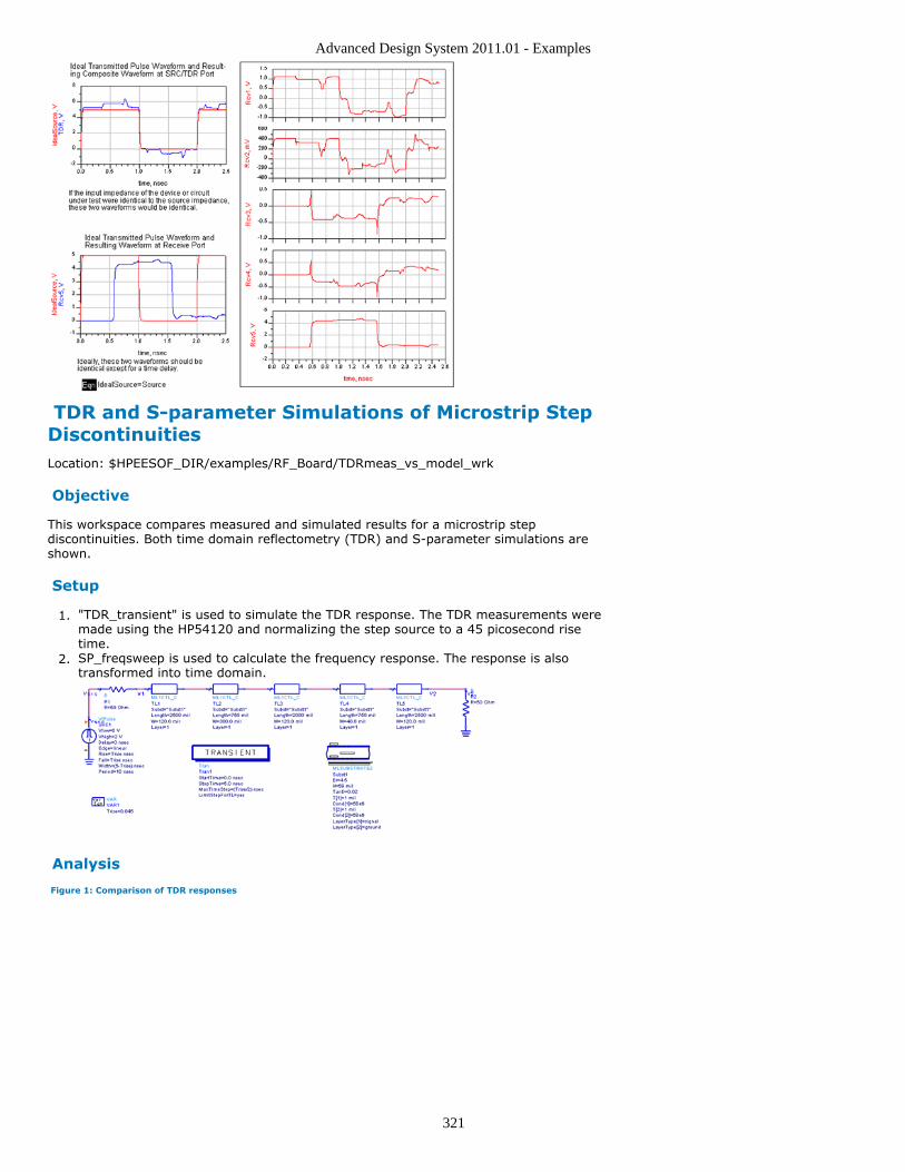
Advanced Design System 2011.01 - Examples
321
TDR and S-parameter Simulations of Microstrip StepDiscontinuitiesLocation: $HPEESOF_DIR/examples/RF_Board/TDRmeas_vs_model_wrk
Objective
This workspace compares measured and simulated results for a microstrip stepdiscontinuities. Both time domain reflectometry (TDR) and S-parameter simulations areshown.
Setup
"TDR_transient" is used to simulate the TDR response. The TDR measurements were1.made using the HP54120 and normalizing the step source to a 45 picosecond risetime.SP_freqsweep is used to calculate the frequency response. The response is also2.transformed into time domain.
Analysis
Figure 1: Comparison of TDR responses
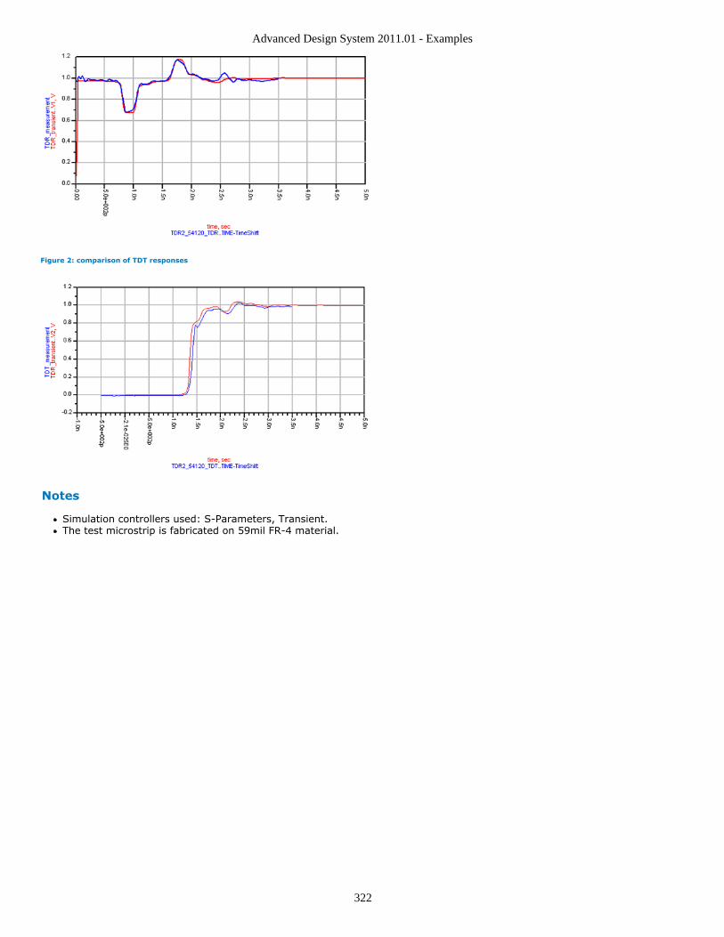
Advanced Design System 2011.01 - Examples
322
Figure 2: comparison of TDT responses
Notes
Simulation controllers used: S-Parameters, Transient.The test microstrip is fabricated on 59mil FR-4 material.
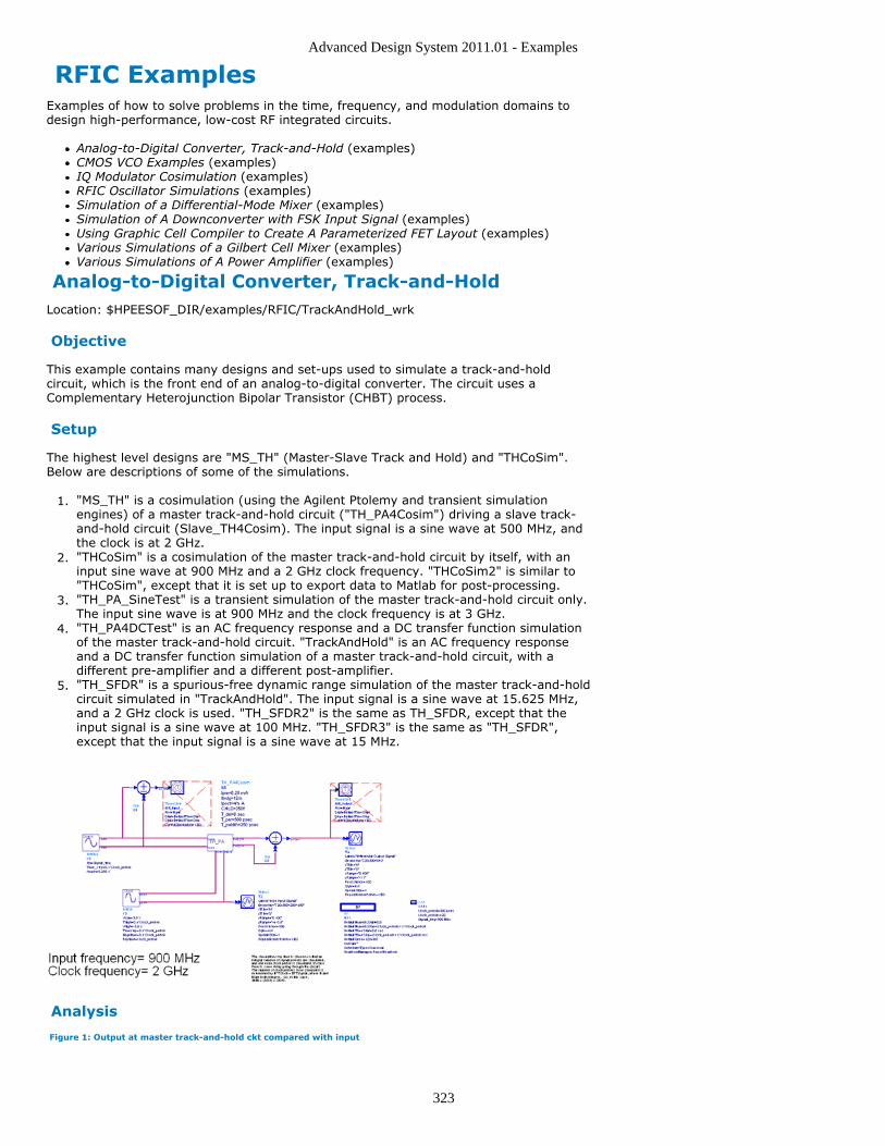
Advanced Design System 2011.01 - Examples
323
RFIC ExamplesExamples of how to solve problems in the time, frequency, and modulation domains todesign high-performance, low-cost RF integrated circuits.
Analog-to-Digital Converter, Track-and-Hold (examples)CMOS VCO Examples (examples)IQ Modulator Cosimulation (examples)RFIC Oscillator Simulations (examples)Simulation of a Differential-Mode Mixer (examples)Simulation of A Downconverter with FSK Input Signal (examples)Using Graphic Cell Compiler to Create A Parameterized FET Layout (examples)Various Simulations of a Gilbert Cell Mixer (examples)Various Simulations of A Power Amplifier (examples)
Analog-to-Digital Converter, Track-and-HoldLocation: $HPEESOF_DIR/examples/RFIC/TrackAndHold_wrk
Objective
This example contains many designs and set-ups used to simulate a track-and-holdcircuit, which is the front end of an analog-to-digital converter. The circuit uses aComplementary Heterojunction Bipolar Transistor (CHBT) process.
Setup
The highest level designs are "MS_TH" (Master-Slave Track and Hold) and "THCoSim".Below are descriptions of some of the simulations.
"MS_TH" is a cosimulation (using the Agilent Ptolemy and transient simulation1.engines) of a master track-and-hold circuit ("TH_PA4Cosim") driving a slave track-and-hold circuit (Slave_TH4Cosim). The input signal is a sine wave at 500 MHz, andthe clock is at 2 GHz."THCoSim" is a cosimulation of the master track-and-hold circuit by itself, with an2.input sine wave at 900 MHz and a 2 GHz clock frequency. "THCoSim2" is similar to"THCoSim", except that it is set up to export data to Matlab for post-processing."TH_PA_SineTest" is a transient simulation of the master track-and-hold circuit only.3.The input sine wave is at 900 MHz and the clock frequency is at 3 GHz."TH_PA4DCTest" is an AC frequency response and a DC transfer function simulation4.of the master track-and-hold circuit. "TrackAndHold" is an AC frequency responseand a DC transfer function simulation of a master track-and-hold circuit, with adifferent pre-amplifier and a different post-amplifier."TH_SFDR" is a spurious-free dynamic range simulation of the master track-and-hold5.circuit simulated in "TrackAndHold". The input signal is a sine wave at 15.625 MHz,and a 2 GHz clock is used. "TH_SFDR2" is the same as TH_SFDR, except that theinput signal is a sine wave at 100 MHz. "TH_SFDR3" is the same as "TH_SFDR",except that the input signal is a sine wave at 15 MHz.
Analysis
Figure 1: Output at master track-and-hold ckt compared with input
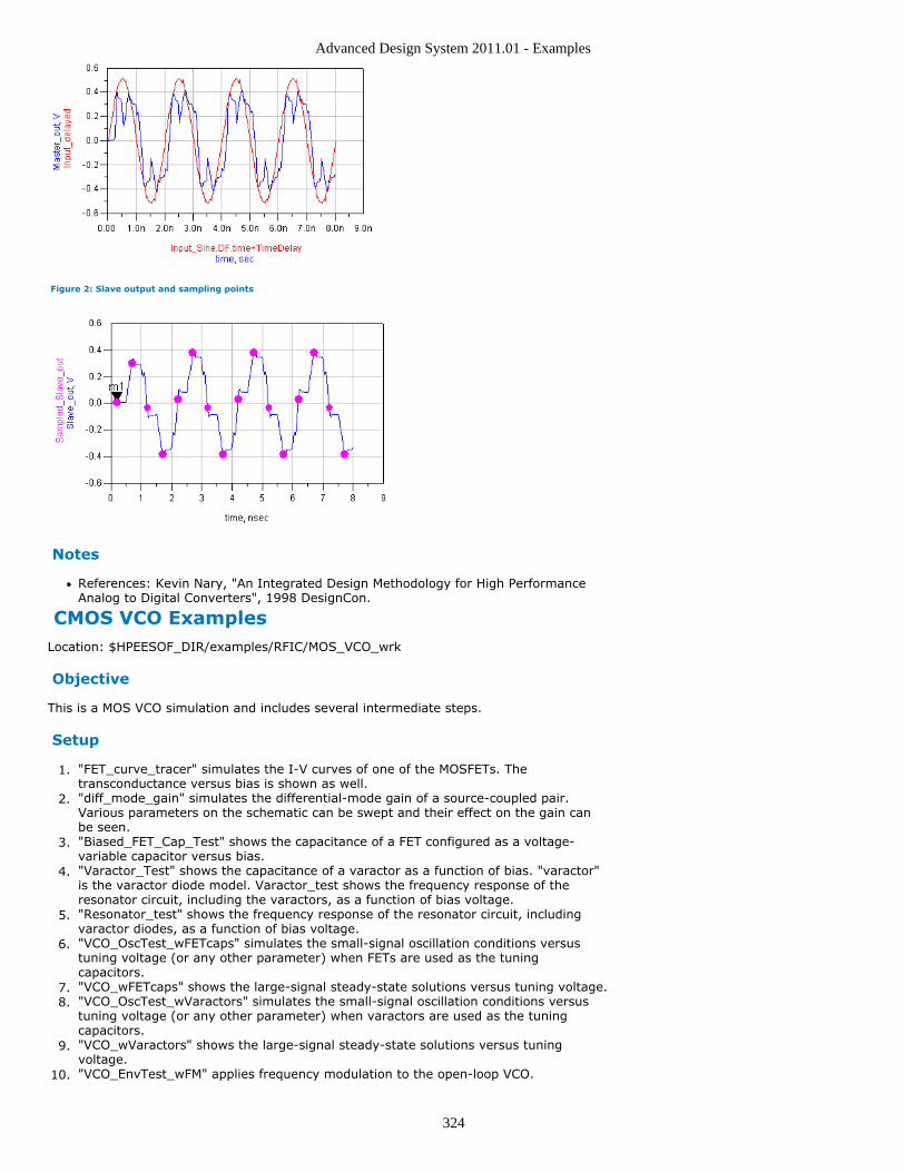
Advanced Design System 2011.01 - Examples
324
Figure 2: Slave output and sampling points
Notes
References: Kevin Nary, "An Integrated Design Methodology for High PerformanceAnalog to Digital Converters", 1998 DesignCon.
CMOS VCO ExamplesLocation: $HPEESOF_DIR/examples/RFIC/MOS_VCO_wrk
Objective
This is a MOS VCO simulation and includes several intermediate steps.
Setup
"FET_curve_tracer" simulates the I-V curves of one of the MOSFETs. The1.transconductance versus bias is shown as well."diff_mode_gain" simulates the differential-mode gain of a source-coupled pair.2.Various parameters on the schematic can be swept and their effect on the gain canbe seen."Biased_FET_Cap_Test" shows the capacitance of a FET configured as a voltage-3.variable capacitor versus bias."Varactor_Test" shows the capacitance of a varactor as a function of bias. "varactor"4.is the varactor diode model. Varactor_test shows the frequency response of theresonator circuit, including the varactors, as a function of bias voltage."Resonator_test" shows the frequency response of the resonator circuit, including5.varactor diodes, as a function of bias voltage."VCO_OscTest_wFETcaps" simulates the small-signal oscillation conditions versus6.tuning voltage (or any other parameter) when FETs are used as the tuningcapacitors."VCO_wFETcaps" shows the large-signal steady-state solutions versus tuning voltage.7."VCO_OscTest_wVaractors" simulates the small-signal oscillation conditions versus8.tuning voltage (or any other parameter) when varactors are used as the tuningcapacitors."VCO_wVaractors" shows the large-signal steady-state solutions versus tuning9.voltage."VCO_EnvTest_wFM" applies frequency modulation to the open-loop VCO.10.
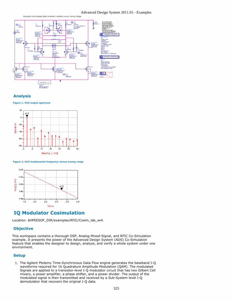
Advanced Design System 2011.01 - Examples
325
Analysis
Figure 1: VCO output spectrum
Figure 2: VCO fundamental frequency versus tuning range
IQ Modulator CosimulationLocation: $HPEESOF_DIR/examples/RFIC/Cosim_lab_wrk
Objective
This workspace contains a thorough DSP, Analog-Mixed-Signal, and RFIC Co-Simulationexample. It presents the power of the Advanced Design System (ADS) Co-Simulationfeature that enables the designer to design, analyze, and verify a whole system under oneenvironment.
Setup
The Agilent Ptolemy Time-Synchronous Data Flow engine generates the baseband I-Q1.waveforms required for 16 Quadrature Amplitude Modulation (QAM). The modulatedSignals are applied to a transistor-level I-Q modulator circuit that has two Gilbert Cellmixers, a power amplifier, a phase shifter, and a power divider. The output of themodulated signal is then transmitted and received by a Sub-System level I-Qdemodulator that recovers the original I-Q data.
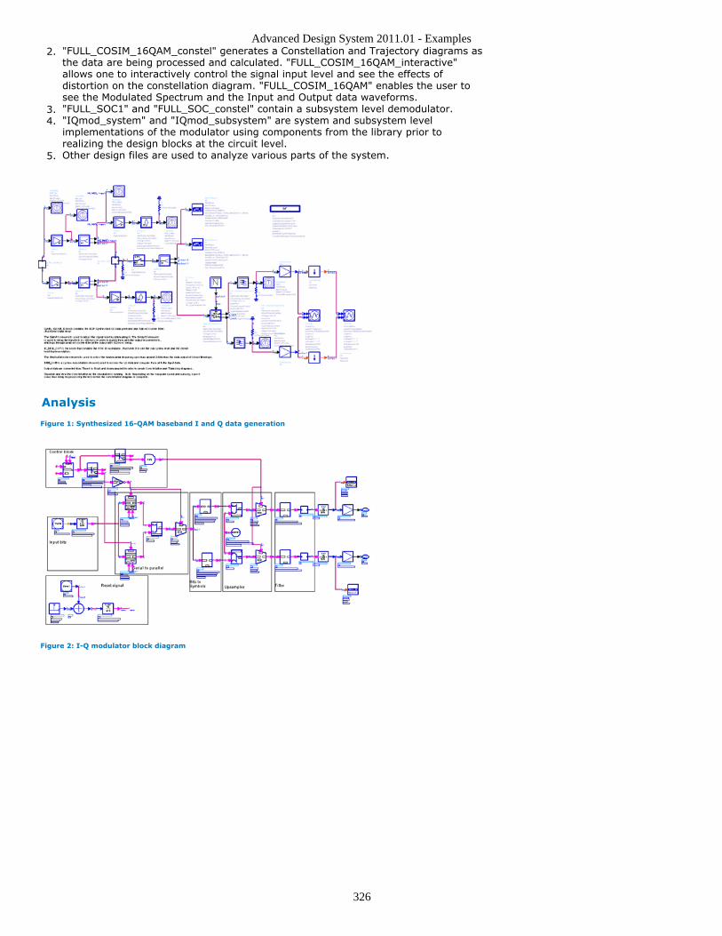
Advanced Design System 2011.01 - Examples
326
"FULL_COSIM_16QAM_constel" generates a Constellation and Trajectory diagrams as2.the data are being processed and calculated. "FULL_COSIM_16QAM_interactive"allows one to interactively control the signal input level and see the effects ofdistortion on the constellation diagram. "FULL_COSIM_16QAM" enables the user tosee the Modulated Spectrum and the Input and Output data waveforms."FULL_SOC1" and "FULL_SOC_constel" contain a subsystem level demodulator.3."IQmod_system" and "IQmod_subsystem" are system and subsystem level4.implementations of the modulator using components from the library prior torealizing the design blocks at the circuit level.Other design files are used to analyze various parts of the system.5.
Analysis
Figure 1: Synthesized 16-QAM baseband I and Q data generation
Figure 2: I-Q modulator block diagram
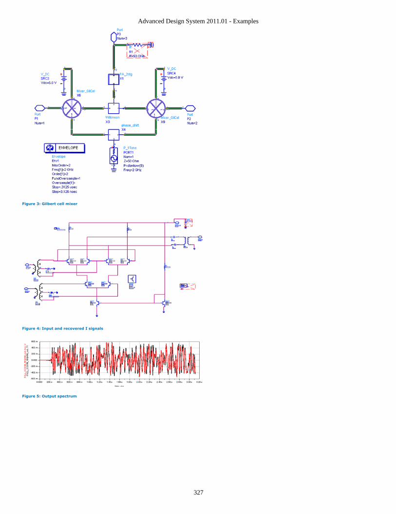
Advanced Design System 2011.01 - Examples
327
Figure 3: Gilbert cell mixer
Figure 4: Input and recovered I signals
Figure 5: Output spectrum
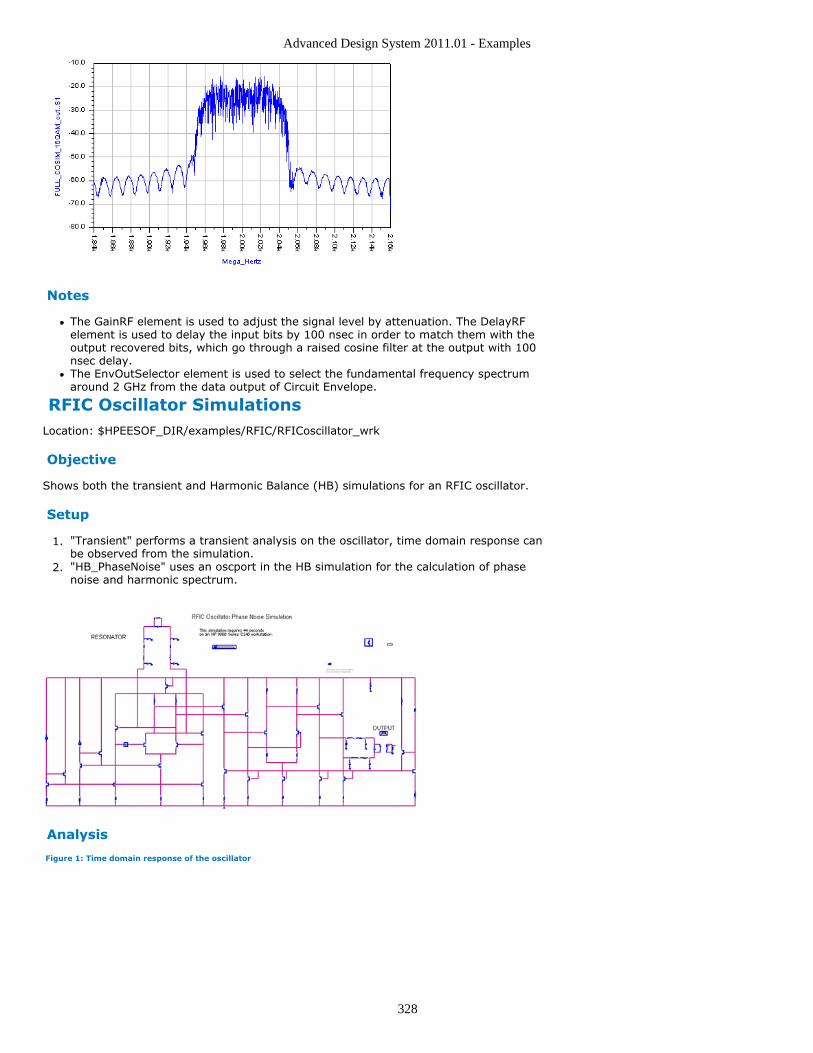
Advanced Design System 2011.01 - Examples
328
Notes
The GainRF element is used to adjust the signal level by attenuation. The DelayRFelement is used to delay the input bits by 100 nsec in order to match them with theoutput recovered bits, which go through a raised cosine filter at the output with 100nsec delay.The EnvOutSelector element is used to select the fundamental frequency spectrumaround 2 GHz from the data output of Circuit Envelope.
RFIC Oscillator SimulationsLocation: $HPEESOF_DIR/examples/RFIC/RFICoscillator_wrk
Objective
Shows both the transient and Harmonic Balance (HB) simulations for an RFIC oscillator.
Setup
"Transient" performs a transient analysis on the oscillator, time domain response can1.be observed from the simulation."HB_PhaseNoise" uses an oscport in the HB simulation for the calculation of phase2.noise and harmonic spectrum.
Analysis
Figure 1: Time domain response of the oscillator
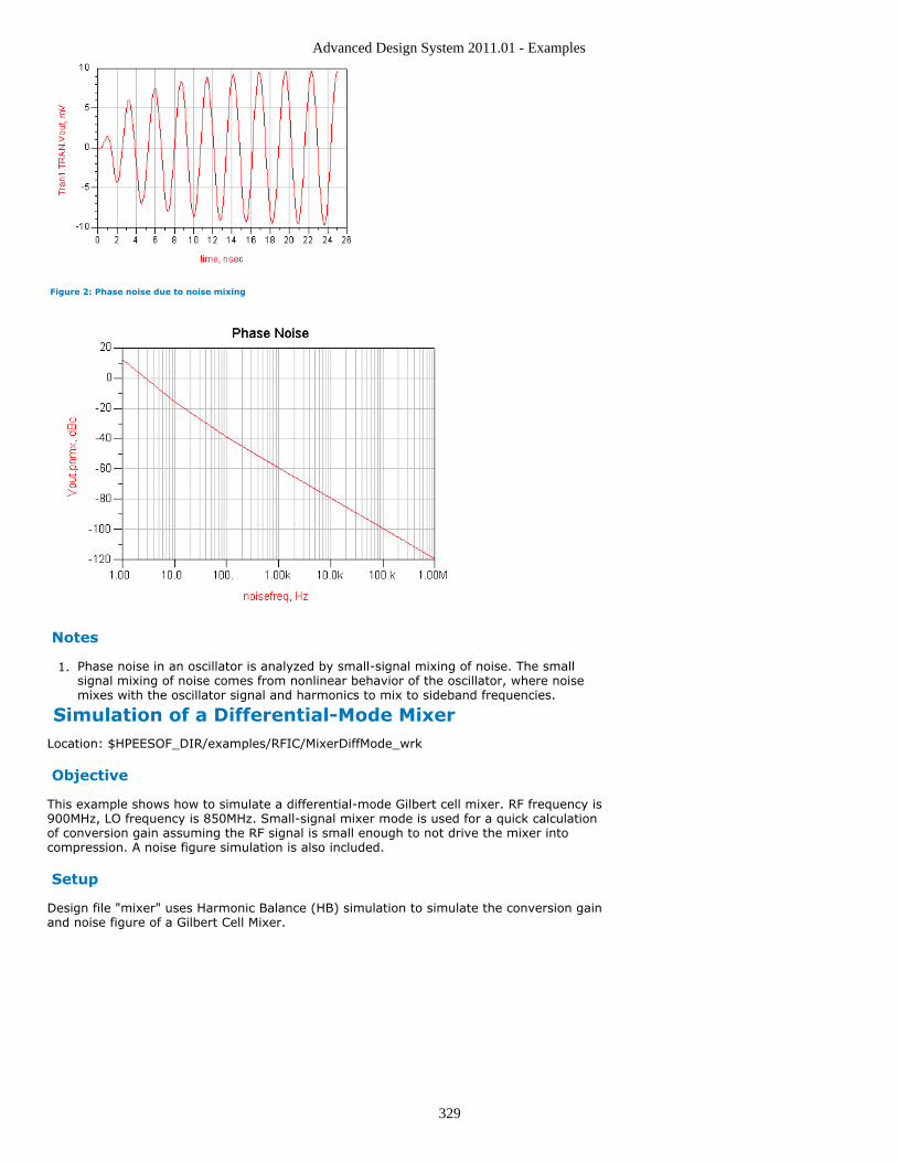
Advanced Design System 2011.01 - Examples
329
Figure 2: Phase noise due to noise mixing
Notes
Phase noise in an oscillator is analyzed by small-signal mixing of noise. The small1.signal mixing of noise comes from nonlinear behavior of the oscillator, where noisemixes with the oscillator signal and harmonics to mix to sideband frequencies.
Simulation of a Differential-Mode MixerLocation: $HPEESOF_DIR/examples/RFIC/MixerDiffMode_wrk
Objective
This example shows how to simulate a differential-mode Gilbert cell mixer. RF frequency is900MHz, LO frequency is 850MHz. Small-signal mixer mode is used for a quick calculationof conversion gain assuming the RF signal is small enough to not drive the mixer intocompression. A noise figure simulation is also included.
Setup
Design file "mixer" uses Harmonic Balance (HB) simulation to simulate the conversion gainand noise figure of a Gilbert Cell Mixer.
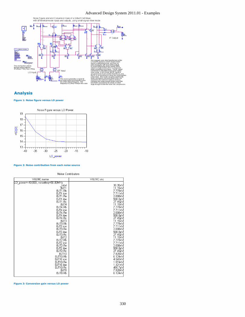
Advanced Design System 2011.01 - Examples
330
Analysis
Figure 1: Noise figure versus LO power
Figure 2: Noise contribution from each noise source
Figure 3: Conversion gain versus LO power
Advanced Design System 2011.01 - Examples
331
Notes
Small signal mixer mode is used in the HB simulation to achieve fast simulationspeed. However, this mode should not be used if the RF tone is large enough to drivethe mixer into compression.
Simulation of A Downconverter with FSK Input SignalLocation: $HPEESOF_DIR/examples/RFIC/FSK_receiver_wrk
Objective
Shows how to use circuit envelope in the simulation of a down-conversion mixer with a 4-level frequency-shift keying (FSK) input signal.
Setup
In design "FSK_receiver_wrk", a 4-level FSK source is generated using a VCO1.component. An FM demodulator is used at the output to obtain the baseband signal.The downconversion mixer is from workspace .../examples/RFIC/Mixers_wrk.2.The data display compares the ideal input waveform and the distorted, demodulated3.output waveform. The rms frequency error is also computed, and the user mayadjust where the sampling instances are in the demodulated output waveform. Thespectrum centered on the IF output frequency is also plotted.
Analysis
Figure 1: Comparison between the ideal input waveform and the demodulated output waveform after compensatingfor time delay
Advanced Design System 2011.01 - Examples
332
Figure 2: Output spectrum centered on IF frequency
Using Graphic Cell Compiler to Create AParameterized FET LayoutLocation: $HPEESOF_DIR/examples/RFIC/GCC_FET_wrk
Objective
This example illustrates the use of Graphical Cell Compiler (GCC) to create aparameterized FET layout.
Setup
A complete non-parameterized FET geometry was imported using the GDS-II translator.The Boolean logic operator was used to separate the complete structure into the five unitcells used to create the FET layout (center cell, top cell, bottom cell and the input andoutput conductor). The GCC re-assembles the five unit cells, replicating the center cell asmany times as required. The resulting macro is parameterized as a function of fingerwidth and number of fingers.
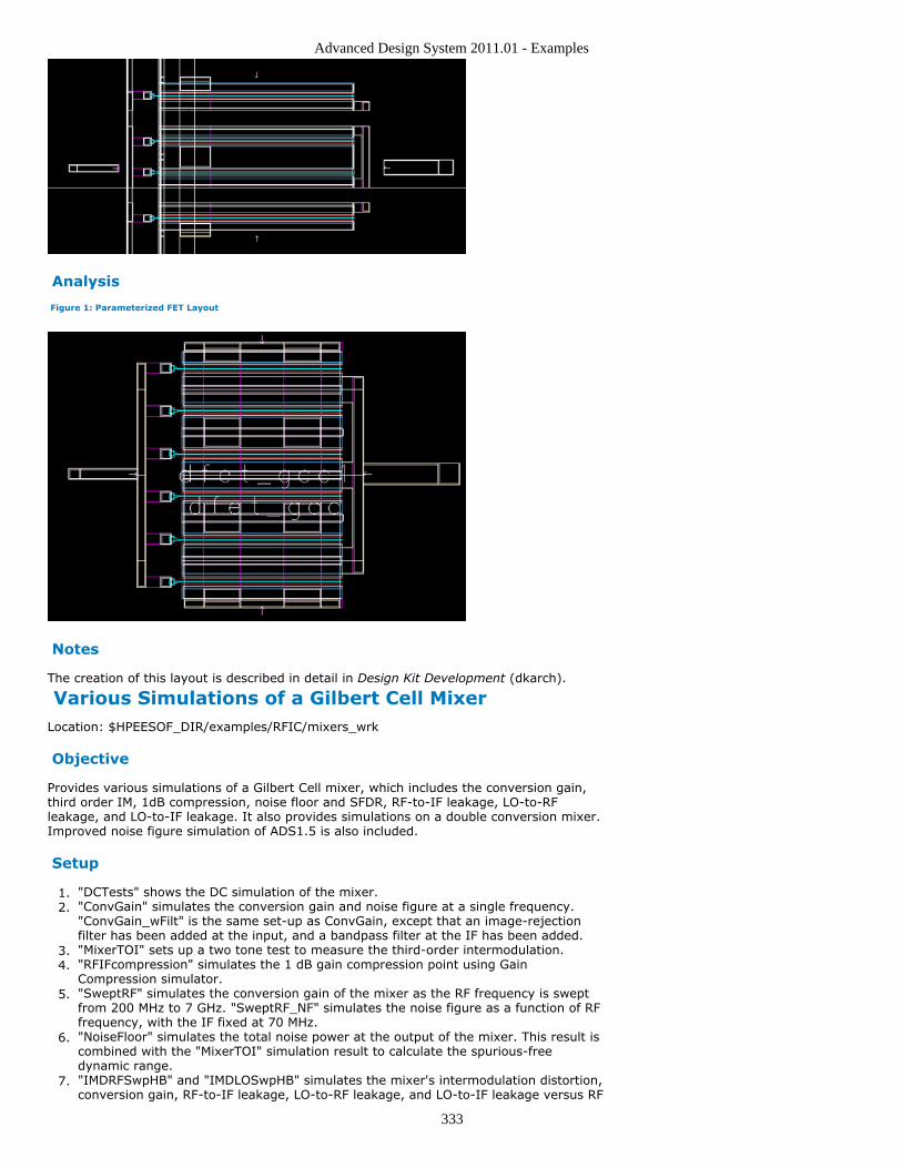
Advanced Design System 2011.01 - Examples
333
Analysis
Figure 1: Parameterized FET Layout
Notes
The creation of this layout is described in detail in Design Kit Development (dkarch).
Various Simulations of a Gilbert Cell MixerLocation: $HPEESOF_DIR/examples/RFIC/mixers_wrk
Objective
Provides various simulations of a Gilbert Cell mixer, which includes the conversion gain,third order IM, 1dB compression, noise floor and SFDR, RF-to-IF leakage, LO-to-RFleakage, and LO-to-IF leakage. It also provides simulations on a double conversion mixer.Improved noise figure simulation of ADS1.5 is also included.
Setup
"DCTests" shows the DC simulation of the mixer.1."ConvGain" simulates the conversion gain and noise figure at a single frequency.2."ConvGain_wFilt" is the same set-up as ConvGain, except that an image-rejectionfilter has been added at the input, and a bandpass filter at the IF has been added."MixerTOI" sets up a two tone test to measure the third-order intermodulation.3."RFIFcompression" simulates the 1 dB gain compression point using Gain4.Compression simulator."SweptRF" simulates the conversion gain of the mixer as the RF frequency is swept5.from 200 MHz to 7 GHz. "SweptRF_NF" simulates the noise figure as a function of RFfrequency, with the IF fixed at 70 MHz."NoiseFloor" simulates the total noise power at the output of the mixer. This result is6.combined with the "MixerTOI" simulation result to calculate the spurious-freedynamic range."IMDRFSwpHB" and "IMDLOSwpHB" simulates the mixer's intermodulation distortion,7.conversion gain, RF-to-IF leakage, LO-to-RF leakage, and LO-to-IF leakage versus RF
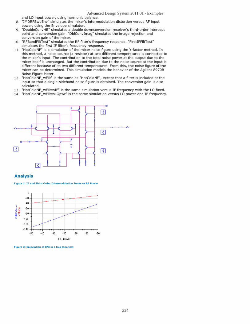
Advanced Design System 2011.01 - Examples
334
and LO input power, using harmonic balance."IMDRFSwpEnv" simulates the mixer's intermodulation distortion versus RF input8.power, using the Envelope simulator."DoubleConvHB" simulates a double downconversion receiver's third-order intercept9.point and conversion gain. "DblConvImag" simulates the image rejection andconversion gain of the mixer."RFBandFiltTest" simulates the RF filter's frequency response. "FirstIFFiltTest"10.simulates the first IF filter's frequency response."HotColdNF" is a simulation of the mixer noise figure using the Y-factor method. In11.this method, a noise source (a resistor) at two different temperatures is connected tothe mixer's input. The contribution to the total noise power at the output due to themixer itself is unchanged. But the contribution due to the noise source at the input isdifferent because of its two different temperatures. From this, the noise figure of themixer can be determined. This simulation models the behavior of the Agilent 8970BNoise Figure Meter."HotColdNF_wFilt" is the same as "HotColdNF", except that a filter is included at the12.input so that a single-sideband noise figure is obtained. The conversion gain is alsocalculated."HotColdNF_wFiltvsIF" is the same simulation versus IF frequency with the LO fixed.13."HotColdNF_wFiltvsLOpwr" is the same simulation versus LO power and IF frequency.14.
Analysis
Figure 1: IF and Third Order Intermodulation Tones vs RF Power
Figure 2: Calculation of IP3 in a two tone test
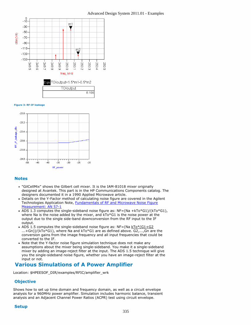
Advanced Design System 2011.01 - Examples
335
Figure 3: RF-IF leakage
Notes
"GilCellMix" shows the Gilbert cell mixer. It is the IAM-81018 mixer originallydesigned at Avantek. This part is in the HP Communications Components catalog. Thedesigners documented it in a 1990 Applied Microwave article.Details on the Y-Factor method of calculating noise figure are covered in the AgilentTechnologies Application Note, Fundamentals of RF and Microwave Noise FigureMeasurement: AN 57-1ADS 1.3 computes the single-sideband noise figure as: NF=(Na +kTo*G1)/(kTo*G1),where Na is the noise added by the mixer, and kTo*G1 is the noise power at theoutput due to the single side-band downconversion from the RF input to the IFoutput.ADS 1.5 computes the single-sideband noise figure as: NF=(Na kTo*(G1+G2...+Gn))/(kTo*G1), where Na and kTo*G1 are as defined above. G2,...,Gn are theconversion gains from the image frequency and all input frequencies that could beconverted to the IF.Note that the Y-factor noise figure simulation technique does not make anyassumptions about the mixer being single-sideband. You make it a single-sidebandmixer by adding an image-reject filter at the input. The ADS 1.5 technique will giveyou the single-sideband noise figure, whether you have an image-reject filter at theinput or not.
Various Simulations of A Power AmplifierLocation: $HPEESOF_DIR/examples/RFIC/amplifier_wrk
Objective
Shows how to set up time domain and frequency domain, as well as a circuit envelopeanalysis for a 960MHz power amplifier. Simulation includes harmonic balance, transientanalysis and an Adjacent Channel Power Ratios (ACPR) test using circuit envelope.
Setup
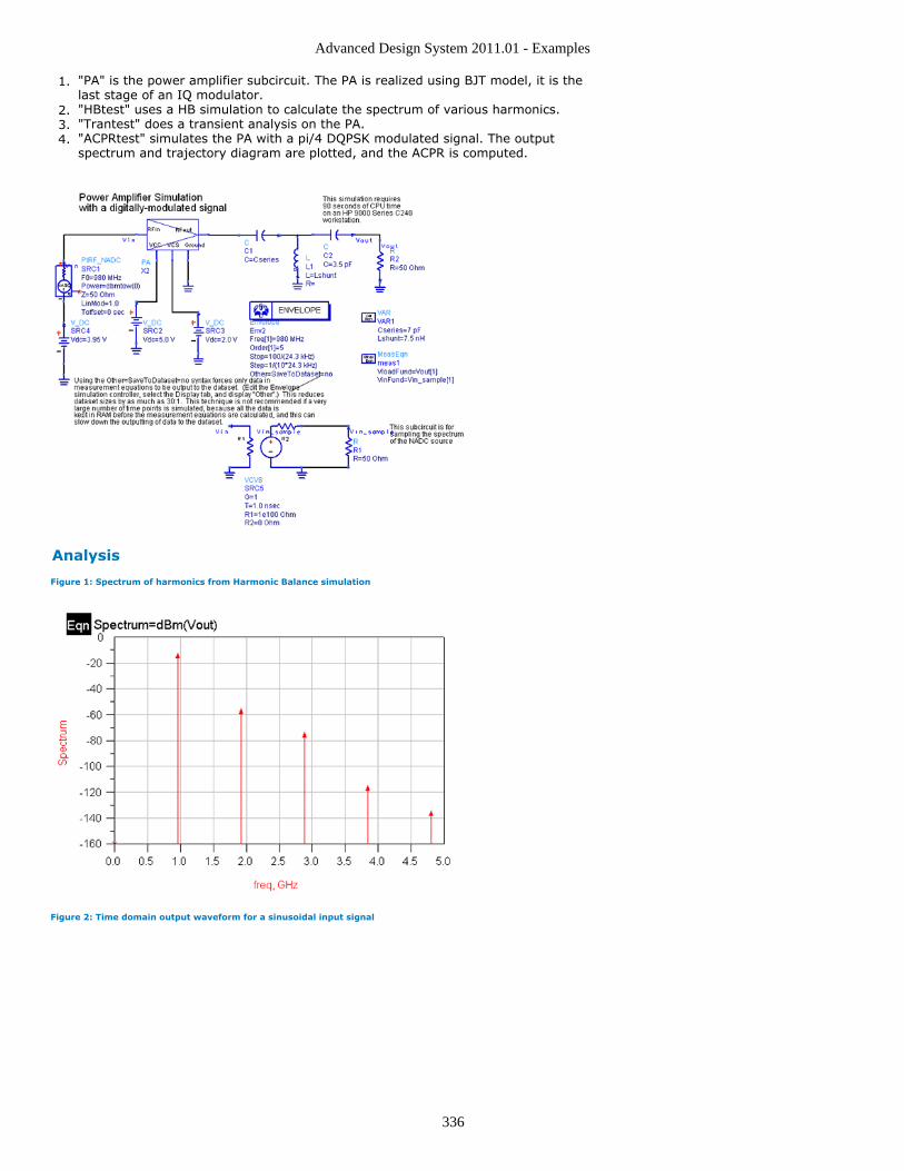
Advanced Design System 2011.01 - Examples
336
"PA" is the power amplifier subcircuit. The PA is realized using BJT model, it is the1.last stage of an IQ modulator."HBtest" uses a HB simulation to calculate the spectrum of various harmonics.2."Trantest" does a transient analysis on the PA.3."ACPRtest" simulates the PA with a pi/4 DQPSK modulated signal. The output4.spectrum and trajectory diagram are plotted, and the ACPR is computed.
Analysis
Figure 1: Spectrum of harmonics from Harmonic Balance simulation
Figure 2: Time domain output waveform for a sinusoidal input signal
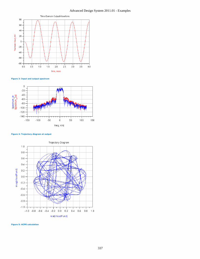
Advanced Design System 2011.01 - Examples
337
Figure 3: Input and output spectrum
Figure 4: Trajectory diagram at output
Figure 5: ACPR calculation

Advanced Design System 2011.01 - Examples
338
Notes
The acpr_vr() function uses built-in Application Extension Language (AEL)expressions to compute the adjacent channel power ratios. These are the ratios ofthe power in the frequency bands specified by UpChlimits and mainlimits andLoChlimits and mainlimits. The acpr_vr() function can be used when the terminatingimpedance is just a resistor. There is also an acpr_vi() function for use when theterminating impedance is complex, in which case the power delivered must becomputed in terms of voltage and current. In this case, a current probe must be usedto sample the current in the terminating impedance.The channel_power_vr() and channel_power_vi() functions are similar to theacpr_vr() and acpr_vi() functions except that they compute the power in Watts in aparticular frequency band. They operate on Envelope data.
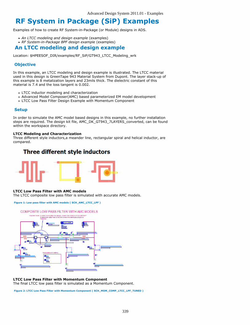
Advanced Design System 2011.01 - Examples
339
RF System in Package (SiP) ExamplesExamples of how to create RF System-in-Package (or Module) designs in ADS.
An LTCC modeling and design example (examples)RF System-in-Package BPF design example (examples)
An LTCC modeling and design exampleLocation: $HPEESOF_DIR/examples/RF_SiP/GT943_LTCC_Modeling_wrk
Objective
In this example, an LTCC modeling and design example is illustrated. The LTCC materialused in this design is GreenTape 943 Material System from Dupont. The layer stack-up ofthis example is 8 metalization layers and 23mils thick. The dielectric constant of thismaterial is 7.4 and the loss tangent is 0.002.
LTCC inductor modeling and characterizationAdvanced Model Composer(AMC) based parameterized EM model developmentLTCC Low Pass Filter Design Example with Momentum Component
Setup
In order to simulate the AMC model based designs in this example, no further installationsteps are required. The design kit file, AMC_DK_GT943_7LAYERS_converted, can be foundwithin the workspace directory.
LTCC Modeling and CharacterizationThree different style inductors,a meander line, rectangular spiral and helical inductor, arecompared.
LTCC Low Pass Filter with AMC modelsThe LTCC composite low pass filter is simulated with accurate AMC models.
Figure 1: Low pass filter with AMC models ( SCH_AMC_LTCC_LPF )
LTCC Low Pass Filter with Momentum ComponentThe final LTCC low pass filter is simulated as a Momentum Component.
Figure 2: LTCC Low Pass Filter with Momentum Component ( SCH_MOM_COMP_LTCC_LPF_TUNED )
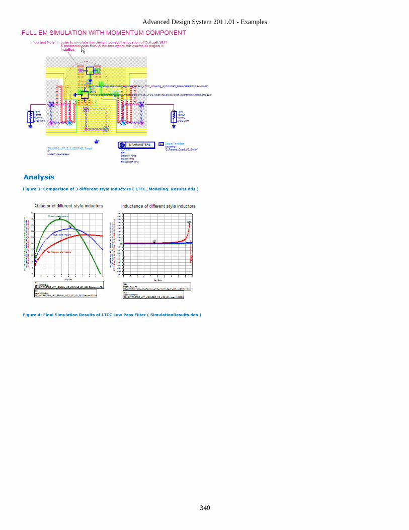
Advanced Design System 2011.01 - Examples
340
Analysis
Figure 3: Comparison of 3 different style inductors ( LTCC_Modeling_Results.dds )
Figure 4: Final Simulation Results of LTCC Low Pass Filter ( SimulationResults.dds )
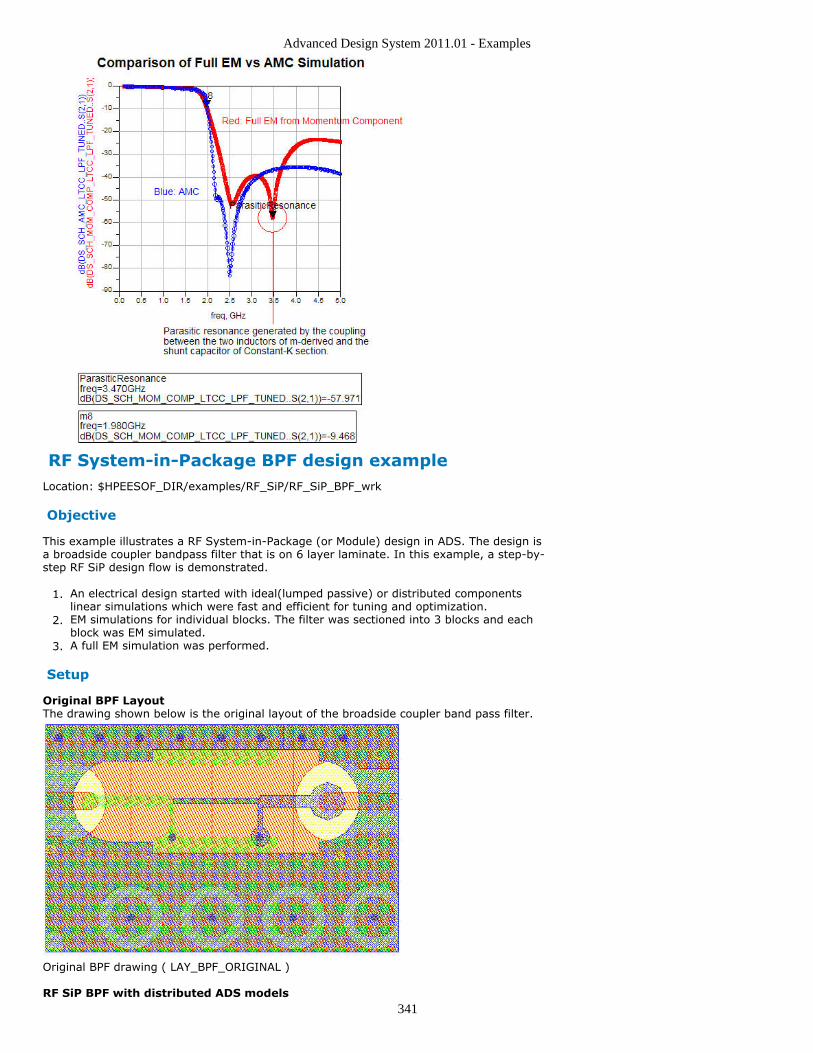
Advanced Design System 2011.01 - Examples
341
RF System-in-Package BPF design exampleLocation: $HPEESOF_DIR/examples/RF_SiP/RF_SiP_BPF_wrk
Objective
This example illustrates a RF System-in-Package (or Module) design in ADS. The design isa broadside coupler bandpass filter that is on 6 layer laminate. In this example, a step-by-step RF SiP design flow is demonstrated.
An electrical design started with ideal(lumped passive) or distributed components1.linear simulations which were fast and efficient for tuning and optimization.EM simulations for individual blocks. The filter was sectioned into 3 blocks and each2.block was EM simulated.A full EM simulation was performed.3.
Setup
Original BPF LayoutThe drawing shown below is the original layout of the broadside coupler band pass filter.
Original BPF drawing ( LAY_BPF_ORIGINAL )
RF SiP BPF with distributed ADS models
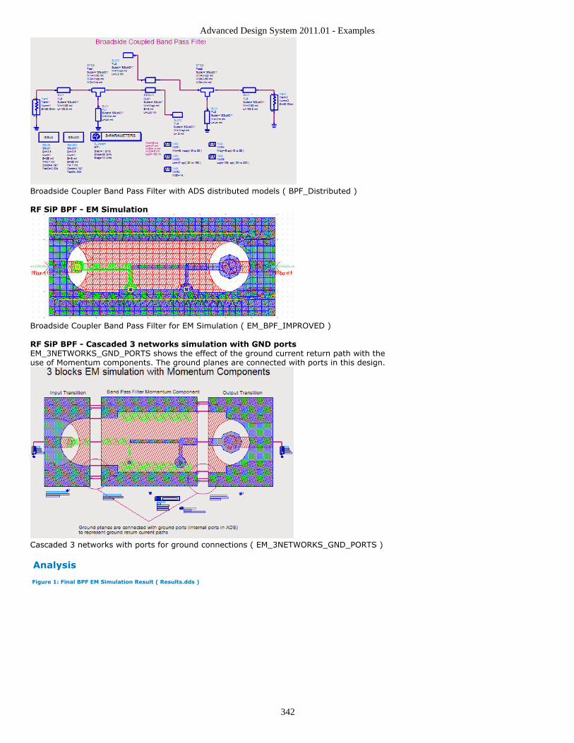
Advanced Design System 2011.01 - Examples
342
Broadside Coupler Band Pass Filter with ADS distributed models ( BPF_Distributed )
RF SiP BPF - EM Simulation
Broadside Coupler Band Pass Filter for EM Simulation ( EM_BPF_IMPROVED )
RF SiP BPF - Cascaded 3 networks simulation with GND portsEM_3NETWORKS_GND_PORTS shows the effect of the ground current return path with theuse of Momentum components. The ground planes are connected with ports in this design.
Cascaded 3 networks with ports for ground connections ( EM_3NETWORKS_GND_PORTS )
Analysis
Figure 1: Final BPF EM Simulation Result ( Results.dds )
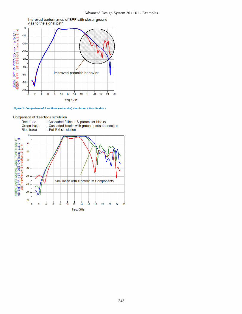
Advanced Design System 2011.01 - Examples
343
Figure 2: Comparison of 3 sections (networks) simulation ( Results.dds )
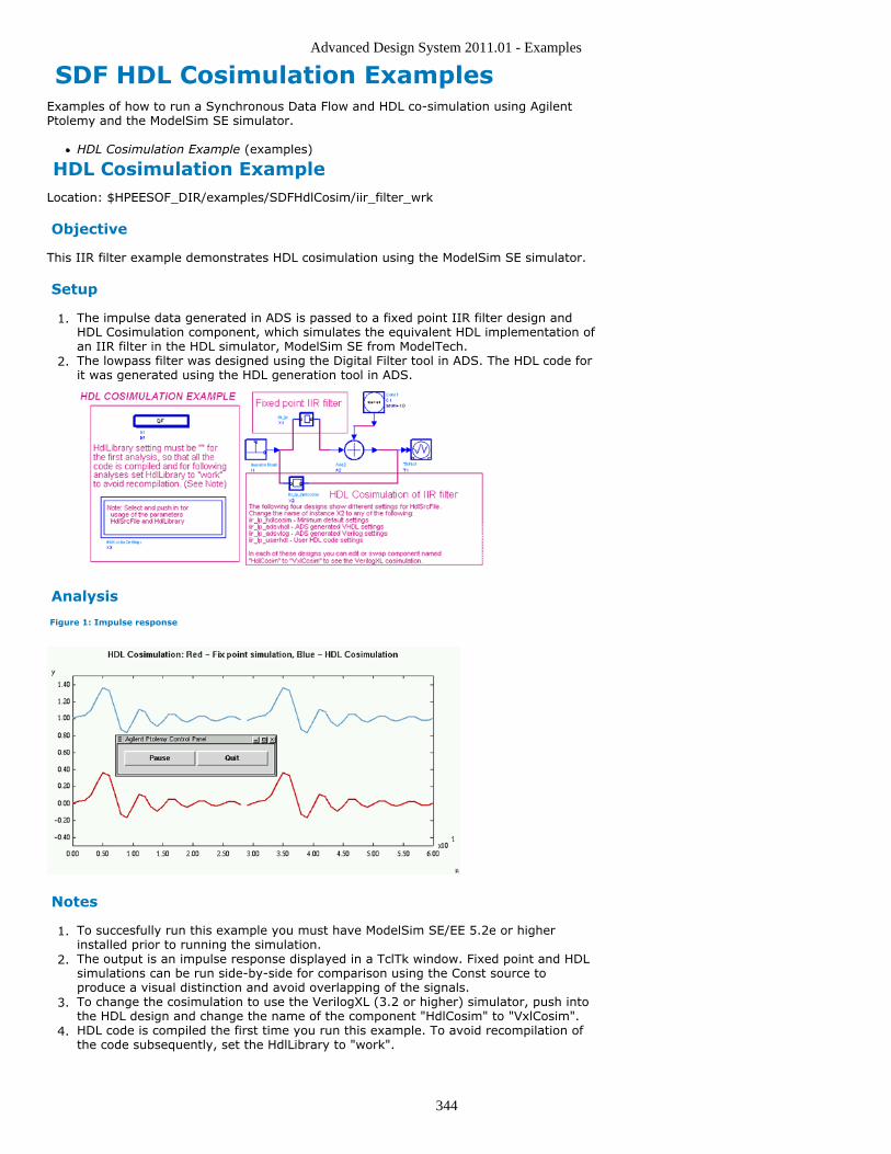
Advanced Design System 2011.01 - Examples
344
SDF HDL Cosimulation ExamplesExamples of how to run a Synchronous Data Flow and HDL co-simulation using AgilentPtolemy and the ModelSim SE simulator.
HDL Cosimulation Example (examples)
HDL Cosimulation ExampleLocation: $HPEESOF_DIR/examples/SDFHdlCosim/iir_filter_wrk
Objective
This IIR filter example demonstrates HDL cosimulation using the ModelSim SE simulator.
Setup
The impulse data generated in ADS is passed to a fixed point IIR filter design and1.HDL Cosimulation component, which simulates the equivalent HDL implementation ofan IIR filter in the HDL simulator, ModelSim SE from ModelTech.The lowpass filter was designed using the Digital Filter tool in ADS. The HDL code for2.it was generated using the HDL generation tool in ADS.
Analysis
Figure 1: Impulse response
Notes
To succesfully run this example you must have ModelSim SE/EE 5.2e or higher1.installed prior to running the simulation.The output is an impulse response displayed in a TclTk window. Fixed point and HDL2.simulations can be run side-by-side for comparison using the Const source toproduce a visual distinction and avoid overlapping of the signals.To change the cosimulation to use the VerilogXL (3.2 or higher) simulator, push into3.the HDL design and change the name of the component "HdlCosim" to "VxlCosim".HDL code is compiled the first time you run this example. To avoid recompilation of4.the code subsequently, set the HdlLibrary to "work".
Advanced Design System 2011.01 - Examples
345
Signal Integrity ExamplesNoteThis page has links to the example projects for signal integrity. For related pages please see:
Signal Integrity Product Support page which has information for signal integrity engineers who arenew to ADSSignal Integrity Task Groups page which has a mapping of signal integrity tasks to ADS elements.It includes a set of element overviews and links to their documentation.
ExamplesExamples of various analyses used for signal integrity applications.
Channel Simulation for PCIe (examples)Channel Simulator Demonstration (examples)Convert Spectre Transient Data for use with ADS (examples)Impulse Writer Demonstration (examples)Jitter Analysis using Ptolemy DF data (examples)PRBS Jitter using Transient Analysis (examples)Statistical Eye Diagram Demonstration (examples)VtPRBS Features and Use Model (examples)
Channel Simulation for PCIeLocation: $HPEESOF_DIR/examples/SignalIntegrity/Channel_SimulatorPCIe2_wrk
Objective
This workspace demonstrates a channel simulation of a PCIe Gen 2 system.
Setup
PCIe_channel_1 is a PCIe channel analysis, with a single TX_Diff component and nocrosstalk effects.PCIe_channel_2 demonstrates the effects of crosstalk.PCIe_channel_3 includes the effects of crosstalk and 8B10B encoding.PCIe_channel_4 shows the effects of crosstalk, 8B10B encoding, and receiver jitter.
Channel Simulator DemonstrationLocation: $HPEESOF_DIR/examples/SignalIntegrity/ChannelSimulatorTutorial_wrk
Objective
This workspace demonstrate various applications of the ADS Channel Simulator.
Setup
DocExample includes the example described in section Using Channel Simulation(cktsimchan).FileSweep provides an example of sweeping S-parameter files through a channelsimulation using the DataFileList (cktsimbatch) component.Tuning demonstrates the ADS tuning features in conjunction with the ChannelSimcontroller.BatchEQ demonstrates the use of Batch Simulation to sweep through several sets ofequalizer coefficients and study eye diagram response. See Batch Simulation(cktsimbatch) for more information.
Convert Spectre Transient Data for use with ADSLocation: Application Note only
Objective
This Application Note describes how to manually convert Spectre's transient data into aTIM format for use with ADS.
Setup
Open the Wavescan and select the trace.
Advanced Design System 2011.01 - Examples
346
Step 1 - select the trace
Select Trace > Save
This will save the file with the name that you provide, and it will add the extension ".vcsv"
Advanced Design System 2011.01 - Examples
347
Step 2 - save the trace
Edit the trace file - modify the header
Use a text editor to locate and edit the saved trace file. The header and footer informationwill have to be changed in order to convert it into a TIM file.
The original *.vcsv file
Remove all of the comment lines from the trace file and replace them with the following:
BEGIN TIMEDATA
% time voltage
"time" will be the independent variable, and "voltage" will be the dependent variable. Thename "voltage" is arbitrary, and can be given any descriptive name. This will be the nameof the data when it is used in ADS.
Advanced Design System 2011.01 - Examples
348
Step 3 - Add the header information to define it as a TIM format.
Edit the trace file - modify the footer
The last line of the TIM file will be the word "END". Save the file and change the extensionto .tim.
Step 4 - Add the footer information to end the file.
Open the Data File Tool in ADS and Import the data
From an ADS Data Display, select the Data File tool (note: the Data File tool is alsoavailable from a schematic page)
The Data File tool will provide a way to select the *.tim file and to save it as a dataset foruse in ADS.
set the "Mode" to "Read data file into dataset".1.Set the "File format to read" to "MDIF"2.Set the "MDIF sub type" to "TIM MDIF"3.In the "Data File to Read" area, use "Browse" to locate the *.tim file.4.Enter the dataset name to be whatever name you want for the dataset.5.Select the "Read File" button to start the translation, which will produce an ADS6.dataset.
Advanced Design System 2011.01 - Examples
349
Step 6 - Import the data into a dataset.
Display the results in the ADS Data Display
Now that the data is available in a dataset, it can be plotted directly, or used in asimulation as a source (not illustrated)
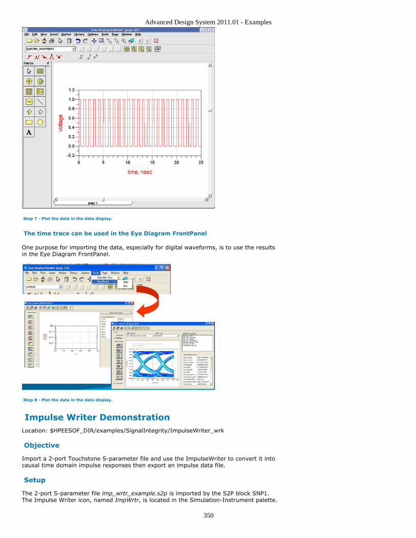
Advanced Design System 2011.01 - Examples
350
Step 7 - Plot the data in the data display.
The time trace can be used in the Eye Diagram FrontPanel
One purpose for importing the data, especially for digital waveforms, is to use the resultsin the Eye Diagram FrontPanel.
Step 8 - Plot the data in the data display.
Impulse Writer DemonstrationLocation: $HPEESOF_DIR/examples/SignalIntegrity/ImpulseWriter_wrk
Objective
Import a 2-port Touchstone S-parameter file and use the ImpulseWriter to convert it intocausal time domain impulse responses then export an impulse data file.
Setup
The 2-port S-parameter file imp_wrtr_example.s2p is imported by the S2P block SNP1.The Impulse Writer icon, named ImpWrtr, is located in the Simulation-Instrument palette.
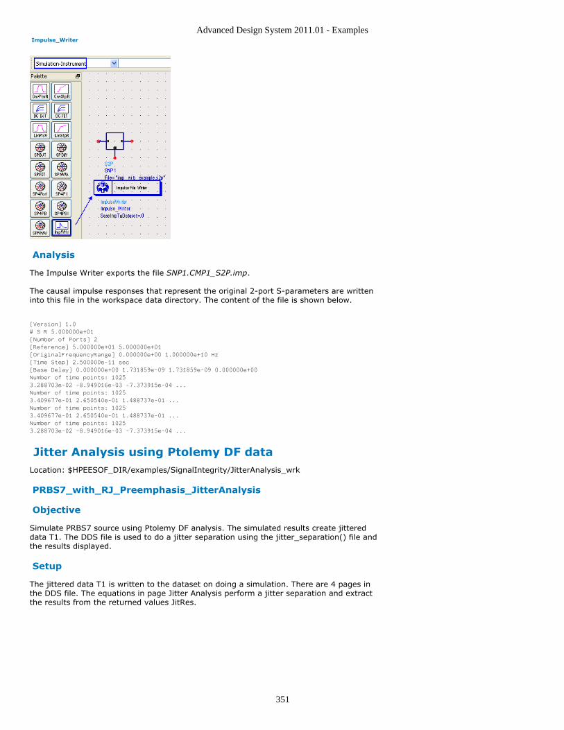
Advanced Design System 2011.01 - Examples
351
Impulse_Writer
Analysis
The Impulse Writer exports the file SNP1.CMP1_S2P.imp.
The causal impulse responses that represent the original 2-port S-parameters are writteninto this file in the workspace data directory. The content of the file is shown below.
[Version] 1.0
# S R 5.000000e+01
[Number of Ports] 2
[Reference] 5.000000e+01 5.000000e+01
[OriginalFrequencyRange] 0.000000e+00 1.000000e+10 Hz
[Time Step] 2.500000e-11 sec
[Base Delay] 0.000000e+00 1.731859e-09 1.731859e-09 0.000000e+00
Number of time points: 1025
3.288703e-02 -8.949016e-03 -7.373915e-04 ...
Number of time points: 1025
3.409677e-01 2.650540e-01 1.488737e-01 ...
Number of time points: 1025
3.409677e-01 2.650540e-01 1.488737e-01 ...
Number of time points: 1025
3.288703e-02 -8.949016e-03 -7.373915e-04 ...
Jitter Analysis using Ptolemy DF dataLocation: $HPEESOF_DIR/examples/SignalIntegrity/JitterAnalysis_wrk
PRBS7_with_RJ_Preemphasis_JitterAnalysis
Objective
Simulate PRBS7 source using Ptolemy DF analysis. The simulated results create jittereddata T1. The DDS file is used to do a jitter separation using the jitter_separation() file andthe results displayed.
Setup
The jittered data T1 is written to the dataset on doing a simulation. There are 4 pages inthe DDS file. The equations in page Jitter Analysis perform a jitter separation and extractthe results from the returned values JitRes.
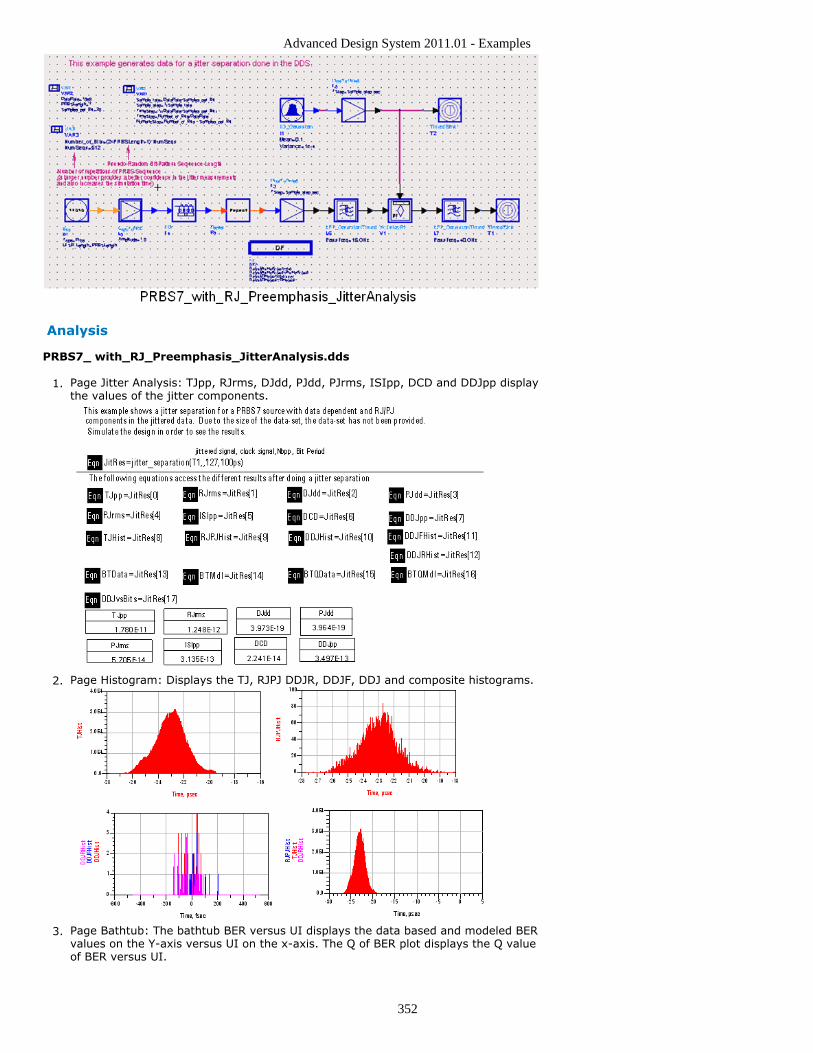
Advanced Design System 2011.01 - Examples
352
Analysis
PRBS7_ with_RJ_Preemphasis_JitterAnalysis.dds
Page Jitter Analysis: TJpp, RJrms, DJdd, PJdd, PJrms, ISIpp, DCD and DDJpp display1.the values of the jitter components.
Page Histogram: Displays the TJ, RJPJ DDJR, DDJF, DDJ and composite histograms.2.
Page Bathtub: The bathtub BER versus UI displays the data based and modeled BER3.values on the Y-axis versus UI on the x-axis. The Q of BER plot displays the Q valueof BER versus UI.
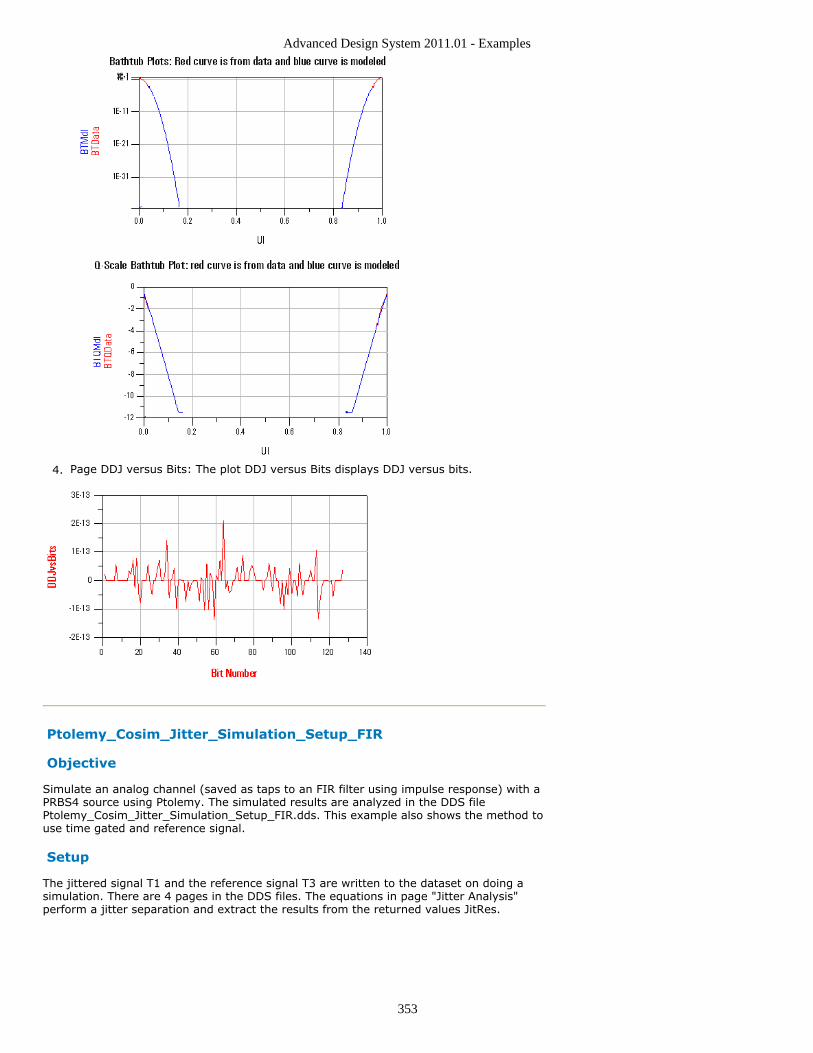
Advanced Design System 2011.01 - Examples
353
Page DDJ versus Bits: The plot DDJ versus Bits displays DDJ versus bits.4.
Ptolemy_Cosim_Jitter_Simulation_Setup_FIR
Objective
Simulate an analog channel (saved as taps to an FIR filter using impulse response) with aPRBS4 source using Ptolemy. The simulated results are analyzed in the DDS filePtolemy_Cosim_Jitter_Simulation_Setup_FIR.dds. This example also shows the method touse time gated and reference signal.
Setup
The jittered signal T1 and the reference signal T3 are written to the dataset on doing asimulation. There are 4 pages in the DDS files. The equations in page "Jitter Analysis"perform a jitter separation and extract the results from the returned values JitRes.
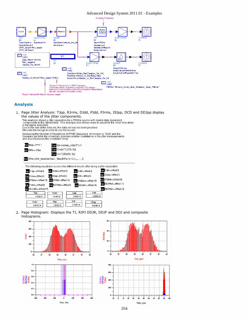
Advanced Design System 2011.01 - Examples
354
Analysis
Page Jitter Analysis: TJpp, RJrms, DJdd, PJdd, PJrms, ISIpp, DCD and DDJpp display1.the values of the jitter components.
Page Histogram: Displays the TJ, RJPJ DDJR, DDJF and DDJ and composite2.histograms.
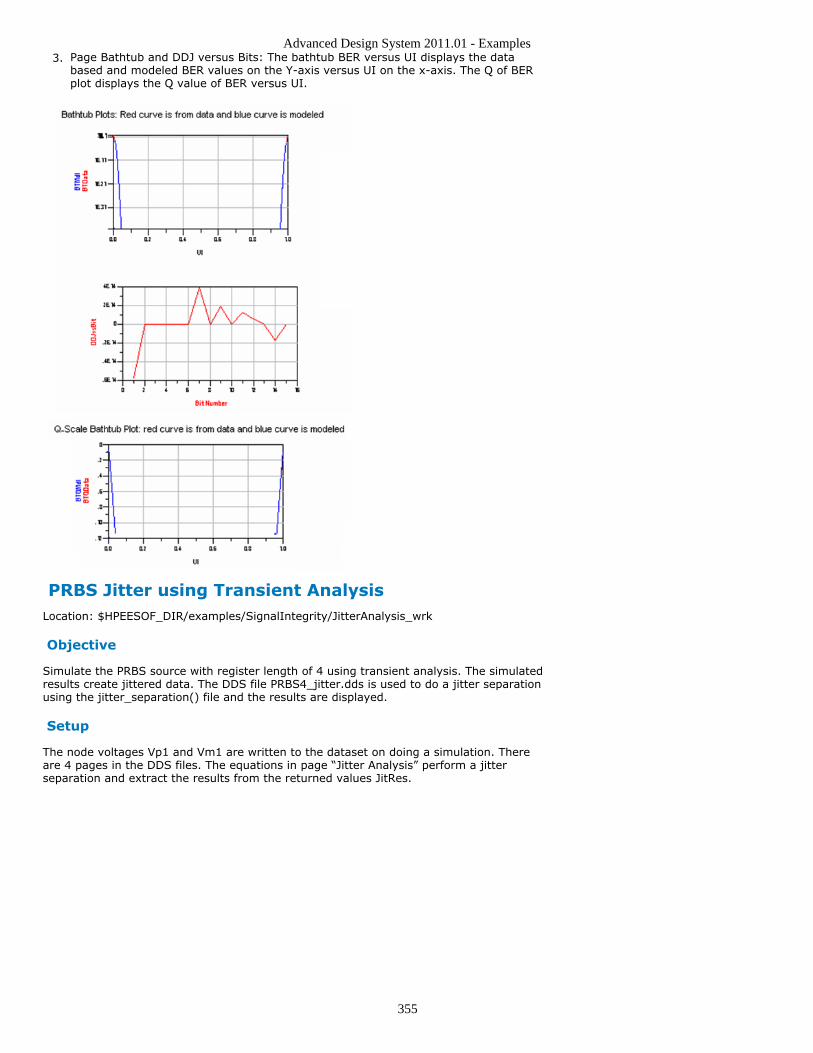
Advanced Design System 2011.01 - Examples
355
Page Bathtub and DDJ versus Bits: The bathtub BER versus UI displays the data3.based and modeled BER values on the Y-axis versus UI on the x-axis. The Q of BERplot displays the Q value of BER versus UI.
PRBS Jitter using Transient AnalysisLocation: $HPEESOF_DIR/examples/SignalIntegrity/JitterAnalysis_wrk
Objective
Simulate the PRBS source with register length of 4 using transient analysis. The simulatedresults create jittered data. The DDS file PRBS4_jitter.dds is used to do a jitter separationusing the jitter_separation() file and the results are displayed.
Setup
The node voltages Vp1 and Vm1 are written to the dataset on doing a simulation. Thereare 4 pages in the DDS files. The equations in page “Jitter Analysis” perform a jitterseparation and extract the results from the returned values JitRes.
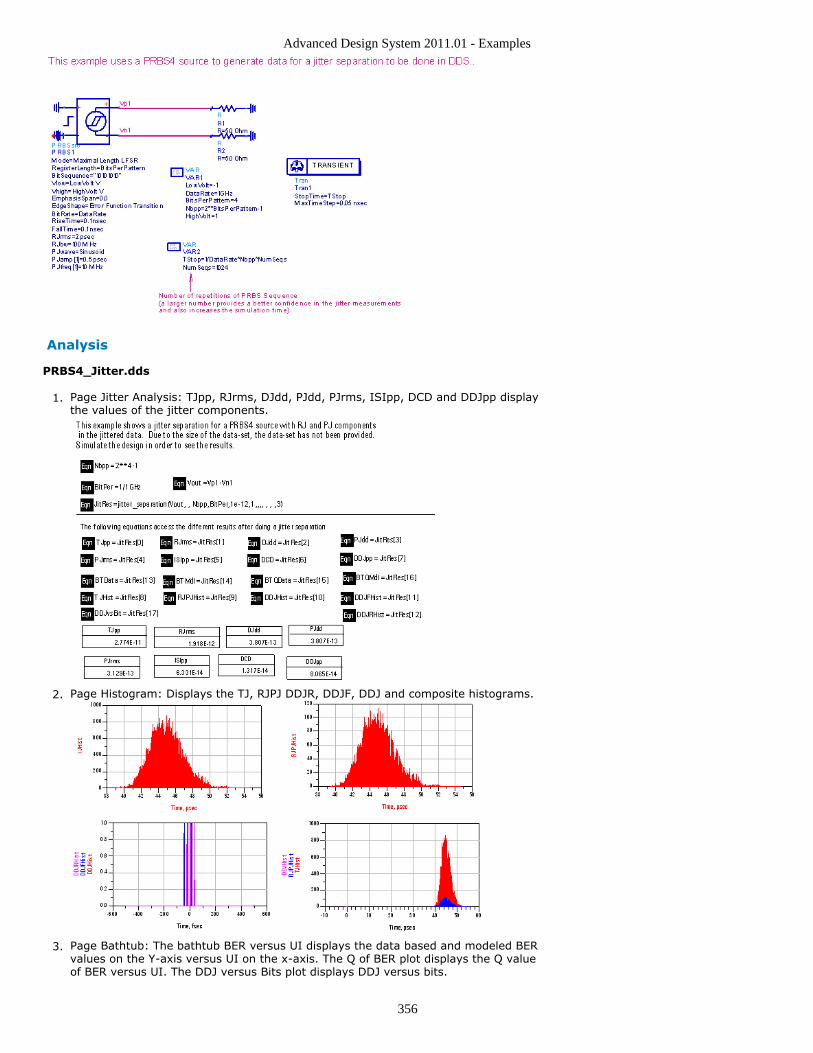
Advanced Design System 2011.01 - Examples
356
Analysis
PRBS4_Jitter.dds
Page Jitter Analysis: TJpp, RJrms, DJdd, PJdd, PJrms, ISIpp, DCD and DDJpp display1.the values of the jitter components.
Page Histogram: Displays the TJ, RJPJ DDJR, DDJF, DDJ and composite histograms.2.
Page Bathtub: The bathtub BER versus UI displays the data based and modeled BER3.values on the Y-axis versus UI on the x-axis. The Q of BER plot displays the Q valueof BER versus UI. The DDJ versus Bits plot displays DDJ versus bits.
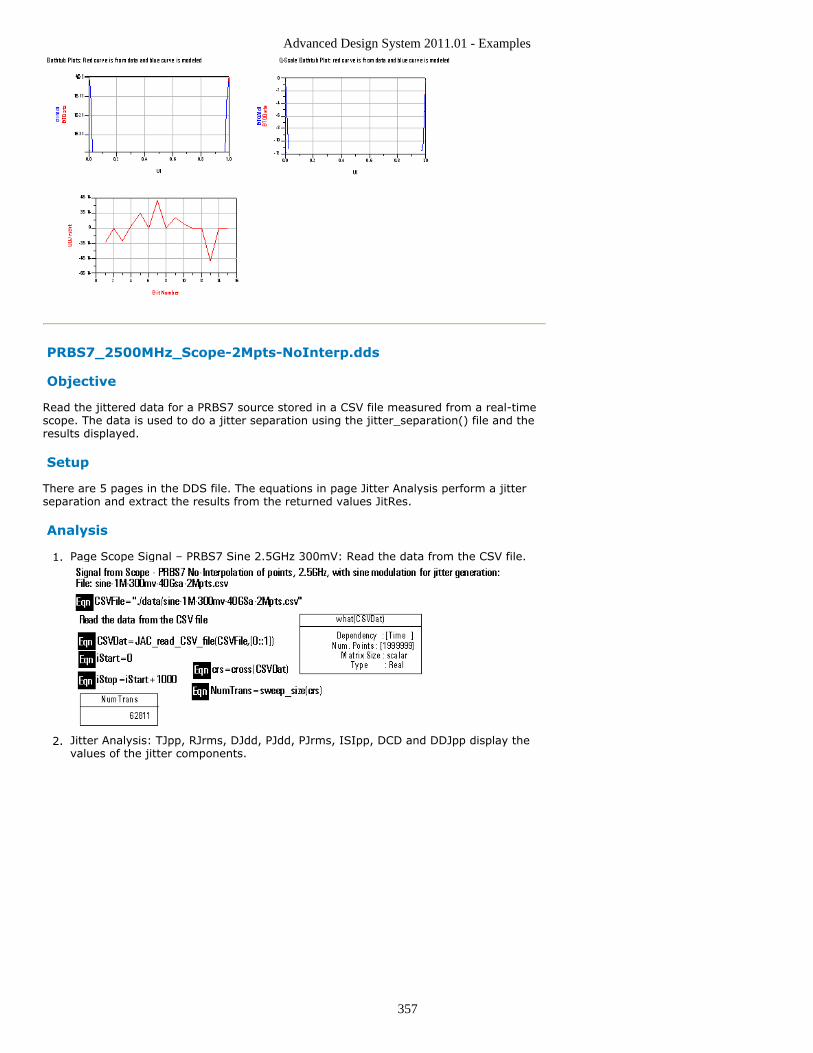
Advanced Design System 2011.01 - Examples
357
PRBS7_2500MHz_Scope-2Mpts-NoInterp.dds
Objective
Read the jittered data for a PRBS7 source stored in a CSV file measured from a real-timescope. The data is used to do a jitter separation using the jitter_separation() file and theresults displayed.
Setup
There are 5 pages in the DDS file. The equations in page Jitter Analysis perform a jitterseparation and extract the results from the returned values JitRes.
Analysis
Page Scope Signal – PRBS7 Sine 2.5GHz 300mV: Read the data from the CSV file.1.
Jitter Analysis: TJpp, RJrms, DJdd, PJdd, PJrms, ISIpp, DCD and DDJpp display the2.values of the jitter components.
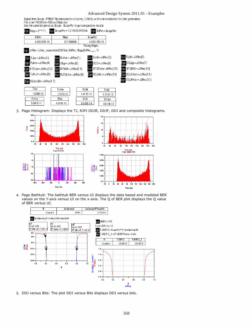
Advanced Design System 2011.01 - Examples
358
Page Histogram: Displays the TJ, RJPJ DDJR, DDJF, DDJ and composite histograms.3.
Page Bathtub: The bathtub BER versus UI displays the data based and modeled BER4.values on the Y-axis versus UI on the x-axis. The Q of BER plot displays the Q valueof BER versus UI.
DDJ versus Bits: The plot DDJ versus Bits displays DDJ versus bits.5.
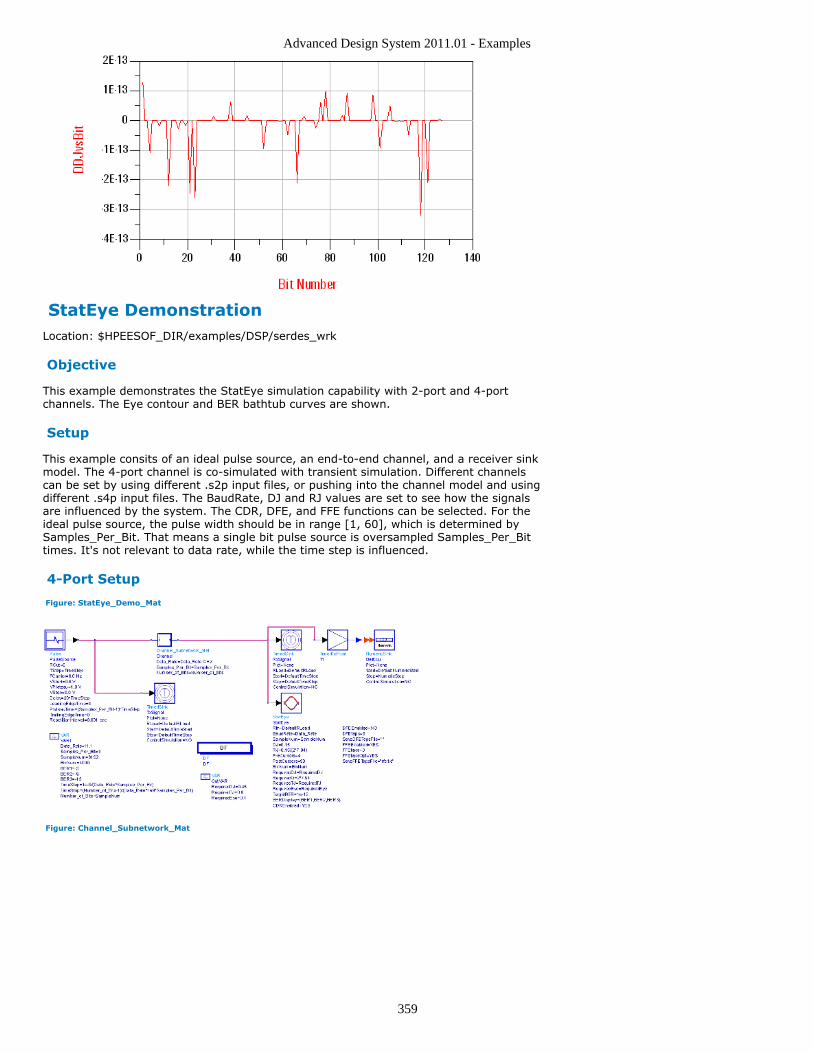
Advanced Design System 2011.01 - Examples
359
StatEye DemonstrationLocation: $HPEESOF_DIR/examples/DSP/serdes_wrk
Objective
This example demonstrates the StatEye simulation capability with 2-port and 4-portchannels. The Eye contour and BER bathtub curves are shown.
Setup
This example consits of an ideal pulse source, an end-to-end channel, and a receiver sinkmodel. The 4-port channel is co-simulated with transient simulation. Different channelscan be set by using different .s2p input files, or pushing into the channel model and usingdifferent .s4p input files. The BaudRate, DJ and RJ values are set to see how the signalsare influenced by the system. The CDR, DFE, and FFE functions can be selected. For theideal pulse source, the pulse width should be in range [1, 60], which is determined bySamples_Per_Bit. That means a single bit pulse source is oversampled Samples_Per_Bittimes. It's not relevant to data rate, while the time step is influenced.
4-Port Setup
Figure: StatEye_Demo_Mat
Figure: Channel_Subnetwork_Mat
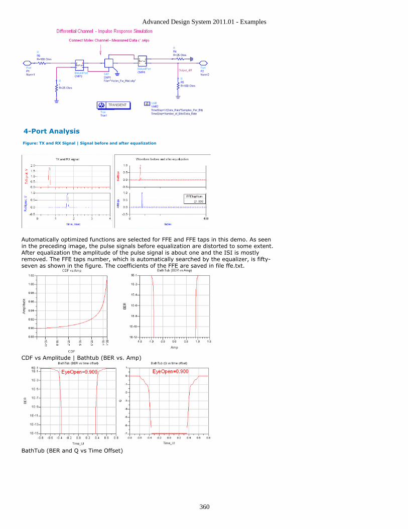
Advanced Design System 2011.01 - Examples
360
4-Port Analysis
Figure: TX and RX Signal | Signal before and after equalization
Automatically optimized functions are selected for FFE and FFE taps in this demo. As seenin the preceding image, the pulse signals before equalization are distorted to some extent.After equalization the amplitude of the pulse signal is about one and the ISI is mostlyremoved. The FFE taps number, which is automatically searched by the equalizer, is fifty-seven as shown in the figure. The coefficients of the FFE are saved in file ffe.txt.
CDF vs Amplitude | Bathtub (BER vs. Amp)
BathTub (BER and Q vs Time Offset)
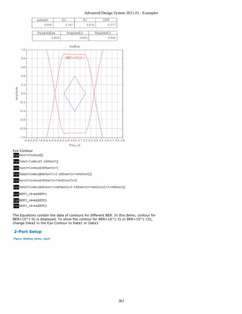
Advanced Design System 2011.01 - Examples
361
Eye Contour
The Equations contain the data of contours for different BER. In this demo, contour forBER=10^(-9) is displayed. To show the contour for BER=10^(-3) or BER=10^(-15),change Data2 in the Eye Contour to Data1 or Data3.
2-Port Setup
Figure: StatEye_Demo_2port
Advanced Design System 2011.01 - Examples
362
2-Port Analysis
TX and RX Signal
CDF vs Amplitude | Bathtub (BER vs. Amp)
BathTub (BER and Q vs Time Offset)
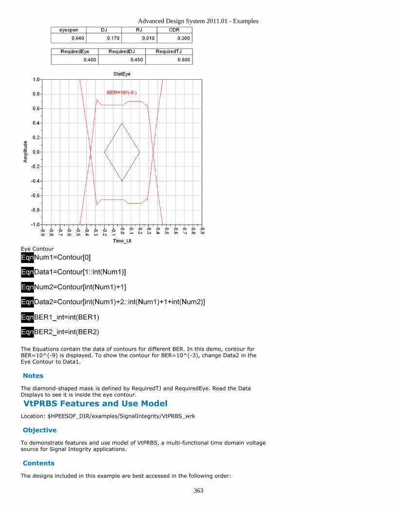
Advanced Design System 2011.01 - Examples
363
Eye Contour
The Equations contain the data of contours for different BER. In this demo, contour forBER=10^(-9) is displayed. To show the contour for BER=10^(-3), change Data2 in theEye Contour to Data1.
Notes
The diamond-shaped mask is defined by RequiredTJ and RequiredEye. Read the DataDisplays to see it is inside the eye contour.
VtPRBS Features and Use ModelLocation: $HPEESOF_DIR/examples/SignalIntegrity/VtPRBS_wrk
Objective
To demonstrate features and use model of VtPRBS, a multi-functional time domain voltagesource for Signal Integrity applications.
Contents
The designs included in this example are best accessed in the following order:
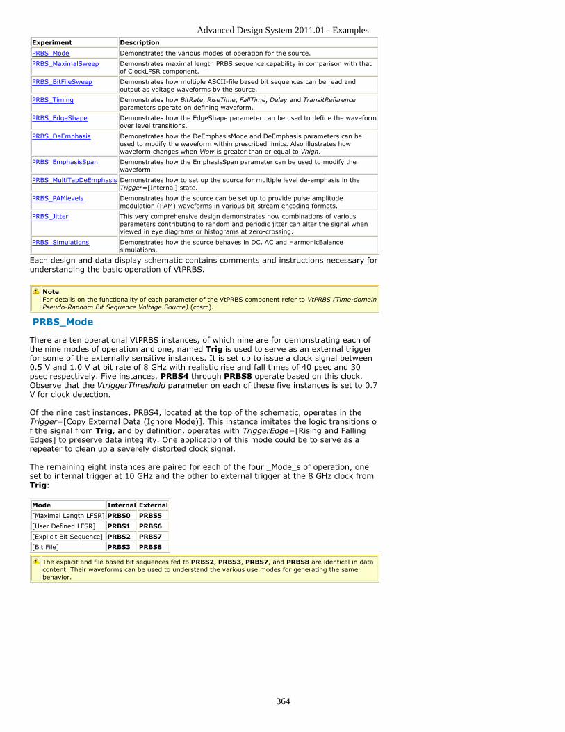
Advanced Design System 2011.01 - Examples
364
Experiment Description
PRBS_Mode Demonstrates the various modes of operation for the source.
PRBS_MaximalSweep Demonstrates maximal length PRBS sequence capability in comparison with thatof ClockLFSR component.
PRBS_BitFileSweep Demonstrates how multiple ASCII-file based bit sequences can be read andoutput as voltage waveforms by the source.
PRBS_Timing Demonstrates how BitRate, RiseTime, FallTime, Delay and TransitReferenceparameters operate on defining waveform.
PRBS_EdgeShape Demonstrates how the EdgeShape parameter can be used to define the waveformover level transitions.
PRBS_DeEmphasis Demonstrates how the DeEmphasisMode and DeEmphasis parameters can beused to modify the waveform within prescribed limits. Also illustrates howwaveform changes when Vlow is greater than or equal to Vhigh.
PRBS_EmphasisSpan Demonstrates how the EmphasisSpan parameter can be used to modify thewaveform.
PRBS_MultiTapDeEmphasis Demonstrates how to set up the source for multiple level de-emphasis in theTrigger=[Internal] state.
PRBS_PAMlevels Demonstrates how the source can be set up to provide pulse amplitudemodulation (PAM) waveforms in various bit-stream encoding formats.
PRBS_Jitter This very comprehensive design demonstrates how combinations of variousparameters contributing to random and periodic jitter can alter the signal whenviewed in eye diagrams or histograms at zero-crossing.
PRBS_Simulations Demonstrates how the source behaves in DC, AC and HarmonicBalancesimulations.
Each design and data display schematic contains comments and instructions necessary forunderstanding the basic operation of VtPRBS.
NoteFor details on the functionality of each parameter of the VtPRBS component refer to VtPRBS (Time-domainPseudo-Random Bit Sequence Voltage Source) (ccsrc).
PRBS_Mode
There are ten operational VtPRBS instances, of which nine are for demonstrating each ofthe nine modes of operation and one, named Trig is used to serve as an external triggerfor some of the externally sensitive instances. It is set up to issue a clock signal between0.5 V and 1.0 V at bit rate of 8 GHz with realistic rise and fall times of 40 psec and 30psec respectively. Five instances, PRBS4 through PRBS8 operate based on this clock.Observe that the VtriggerThreshold parameter on each of these five instances is set to 0.7V for clock detection.
Of the nine test instances, PRBS4, located at the top of the schematic, operates in theTrigger=[Copy External Data (Ignore Mode)]. This instance imitates the logic transitions of the signal from Trig, and by definition, operates with TriggerEdge=[Rising and FallingEdges] to preserve data integrity. One application of this mode could be to serve as arepeater to clean up a severely distorted clock signal.
The remaining eight instances are paired for each of the four _Mode_s of operation, oneset to internal trigger at 10 GHz and the other to external trigger at the 8 GHz clock fromTrig:
Mode Internal External
[Maximal Length LFSR] PRBS0 PRBS5
[User Defined LFSR] PRBS1 PRBS6
[Explicit Bit Sequence] PRBS2 PRBS7
[Bit File] PRBS3 PRBS8
The explicit and file based bit sequences fed to PRBS2, PRBS3, PRBS7, and PRBS8 are identical in datacontent. Their waveforms can be used to understand the various use modes for generating the samebehavior.
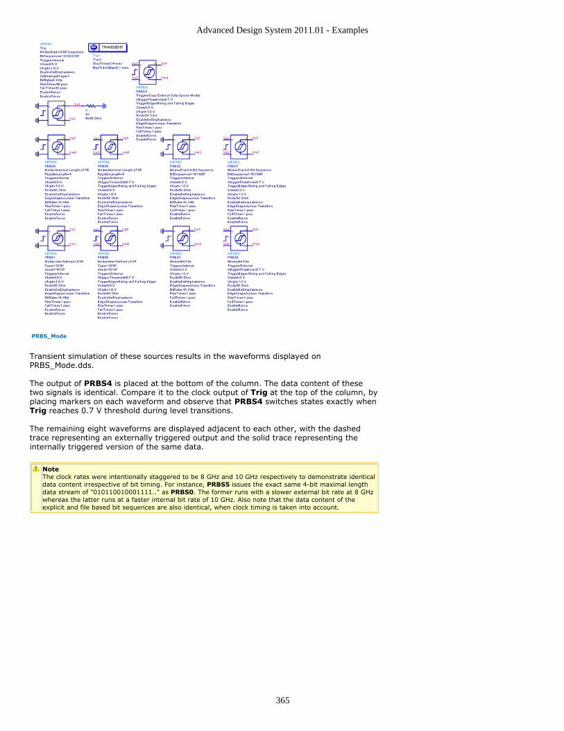
Advanced Design System 2011.01 - Examples
365
PRBS_Mode
Transient simulation of these sources results in the waveforms displayed onPRBS_Mode.dds.
The output of PRBS4 is placed at the bottom of the column. The data content of thesetwo signals is identical. Compare it to the clock output of Trig at the top of the column, byplacing markers on each waveform and observe that PRBS4 switches states exactly whenTrig reaches 0.7 V threshold during level transitions.
The remaining eight waveforms are displayed adjacent to each other, with the dashedtrace representing an externally triggered output and the solid trace representing theinternally triggered version of the same data.
NoteThe clock rates were intentionally staggered to be 8 GHz and 10 GHz respectively to demonstrate identicaldata content irrespective of bit timing. For instance, PRBS5 issues the exact same 4-bit maximal lengthdata stream of "010110010001111.." as PRBS0. The former runs with a slower external bit rate at 8 GHzwhereas the latter runs at a faster internal bit rate of 10 GHz. Also note that the data content of theexplicit and file based bit sequences are also identical, when clock timing is taken into account.
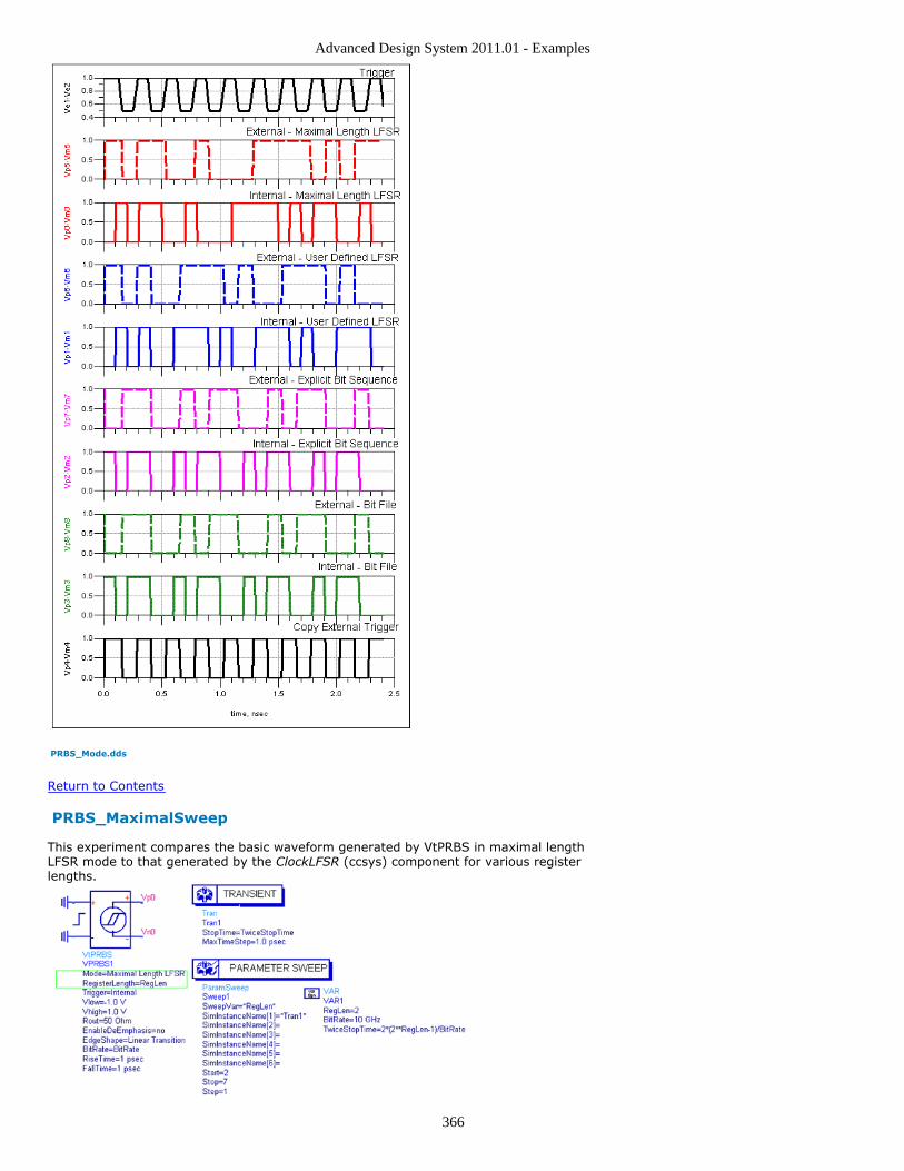
Advanced Design System 2011.01 - Examples
366
PRBS_Mode.dds
Return to Contents
PRBS_MaximalSweep
This experiment compares the basic waveform generated by VtPRBS in maximal lengthLFSR mode to that generated by the ClockLFSR (ccsys) component for various registerlengths.
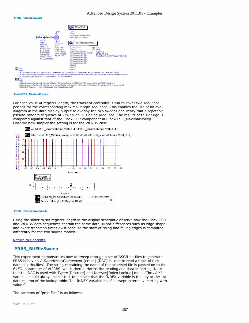
Advanced Design System 2011.01 - Examples
367
PRBS_MaximalSweep
ClockLFSR_MaximalSweep
For each value of register length, the transient controller is run to cover two sequenceperiods for the corresponding maximal length sequence. This enables the use of an eye-diagram in the data display output to overlay the two sweeps and verify that a repetablepseudo-random sequence of 2^RegLen-1 is being produced. The results of this design iscompared against that of the ClockLFSR component in ClockLFSR_MaximalSweep.Observe how simpler the setting is for the VtPRBS case.
PRBS_MaximalSweep.dds
Using the slider to set register length in the display schematic observe how the ClockLFSRand VtPRBS data sequences contain the same data. Minor differences such as edge shapeand exact transition times exist because the start of rising and falling edges is computeddifferently for the two source models.
Return to Contents
PRBS_BitFileSweep
This experiment demonstrates how to sweep through a set of ASCII bit files to generatePRBS behavior. A DataAccessComponent (ccsim) (DAC) is used to read a table of filesnamed "prbs.files". The string containing the name of the accessed file is passed on to theBitFile parameter of VtPRBS, which then performs the reading and data importing. Notethat the DAC is used with Type=[Discrete] and Interp=[Index Lookup] mode. The iVar1variable should always be set to 1 to indicate that the INDEX variable is the key to the 1stdata column of the lookup table. The INDEX variable itself is swept externally starting withvalue 0.
The contents of "prbs.files" is as follows:
begin dscrdata
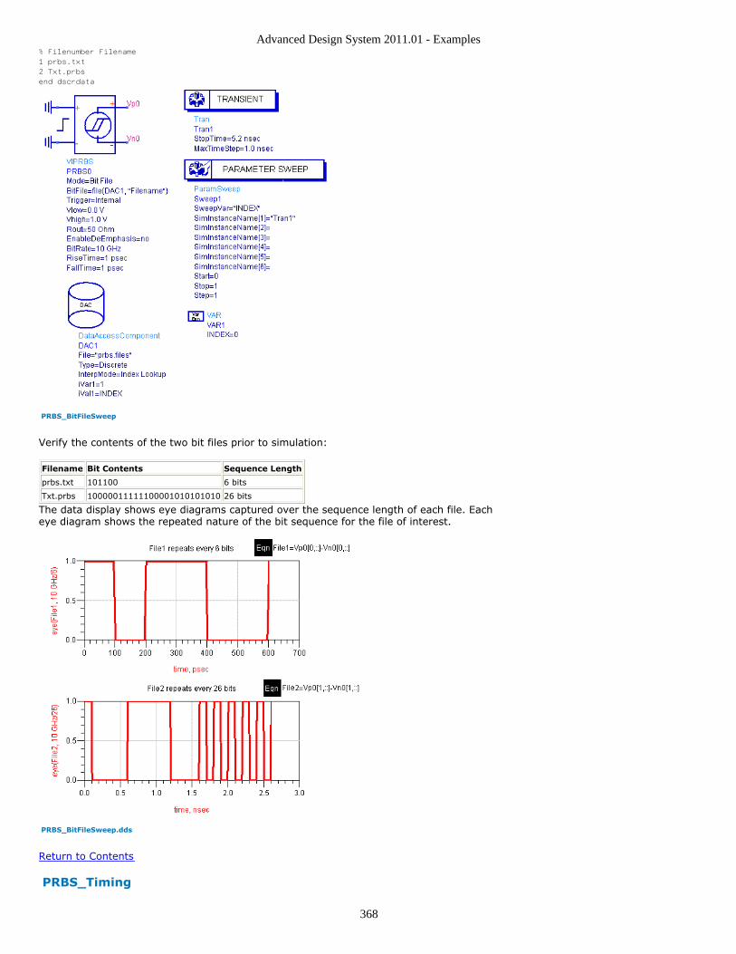
Advanced Design System 2011.01 - Examples
368
% Filenumber Filename
1 prbs.txt
2 Txt.prbs
end dscrdata
PRBS_BitFileSweep
Verify the contents of the two bit files prior to simulation:
Filename Bit Contents Sequence Length
prbs.txt 101100 6 bits
Txt.prbs 10000011111100001010101010 26 bits
The data display shows eye diagrams captured over the sequence length of each file. Eacheye diagram shows the repeated nature of the bit sequence for the file of interest.
PRBS_BitFileSweep.dds
Return to Contents
PRBS_Timing
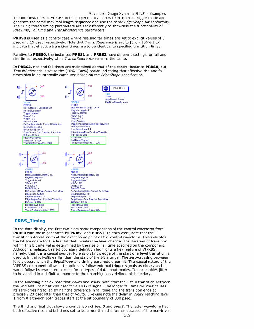
Advanced Design System 2011.01 - Examples
369
The four instances of VtPRBS in this experiment all operate in internal trigger mode andgenerate the same maximal length sequence and use the same EdgeShape for conformity.Their un-jittered timing parameters are set differently to showcase the functionality ofRiseTime, FallTime and TransitReference parameters.
PRBS0 is used as a control case where rise and fall times are set to explicit values of 5psec and 15 psec respectively. Note that TransitReference is set to [0% - 100% ] toindicate that effective transition times are to be identical to specified transition times.
Relative to PRBS0, the instances PRBS1 and PRBS2 have different settings for fall andrise times respectively, while TransitReference remains the same.
In PRBS3, rise and fall times are maintained as that of the control instance PRBS0, butTransitReference is set to the [10% - 90%] option indicating that effective rise and falltimes should be internally computed based on the EdgeShape specification.
PRBS_Timing
In the data display, the first two plots show comparisons of the control waveform fromPRBS0 with those generated by PRBS1 and PRBS2. In each case, note that thetransition interval starts at the exact same point as the control waveform. This indicatesthe bit boundary for the first bit that initiates the level change. The duration of transitionwithin this bit interval is determined by the rise or fall time specified on the component.Although simplistic, this bit boundary definition highlights a key feature of VtPRBS,namely, that it is a causal source. No a priori knowledge of the start of a level transition isused to initial roll-offs earlier than the start of the bit interval. The zero-crossing betweenlevels occurs when the EdgeShape and timing parameters permit. The causal nature of theVtPRBS component allows it to optionally follow external trigger signals as closely as itwould follow its own internal clock for all types of data input modes. It also enables jitterto be applied in a definitive manner to the unambiguously defined bit boundary.
In the following display note that Vout0 and Vout1 both start the 1 to 0 transition betweenthe 2nd and 3rd bit at 200 psec for a 10 GHz signal. The longer fall time for Vout causesits zero-crossing to lag by half the difference in fall time and the transition ends atprecisely 20 psec later than that of Vout0. Likewise note the delay in Vout2 reaching level1 from 0 although both traces start at the bit boundary of 300 psec.
The third and final plot shows a comparison of Vout0 and Vout3. The latter waveform hasboth effective rise and fall times set to be larger than the former because of the non-trivial
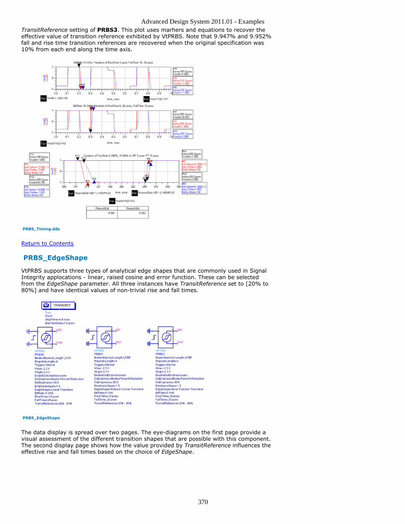
Advanced Design System 2011.01 - Examples
370
TransitReference setting of PRBS3. This plot uses marhers and equations to recover theeffective value of transition reference exhibited by VtPRBS. Note that 9.947% and 9.952%fall and rise time transition references are recovered when the original specification was10% from each end along the time axis.
PRBS_Timing.dds
Return to Contents
PRBS_EdgeShape
VtPRBS supports three types of analytical edge shapes that are commonly used in SignalIntegrity applocations - linear, raised cosine and error function. These can be selectedfrom the EdgeShape parameter. All three instances have TransitReference set to [20% to80%] and have identical values of non-trivial rise and fall times.
PRBS_EdgeShape
The data display is spread over two pages. The eye-diagrams on the first page provide avisual assessment of the different transition shapes that are possible with this component.The second display page shows how the value provided by TransitReference influences theeffective rise and fall times based on the choice of EdgeShape.
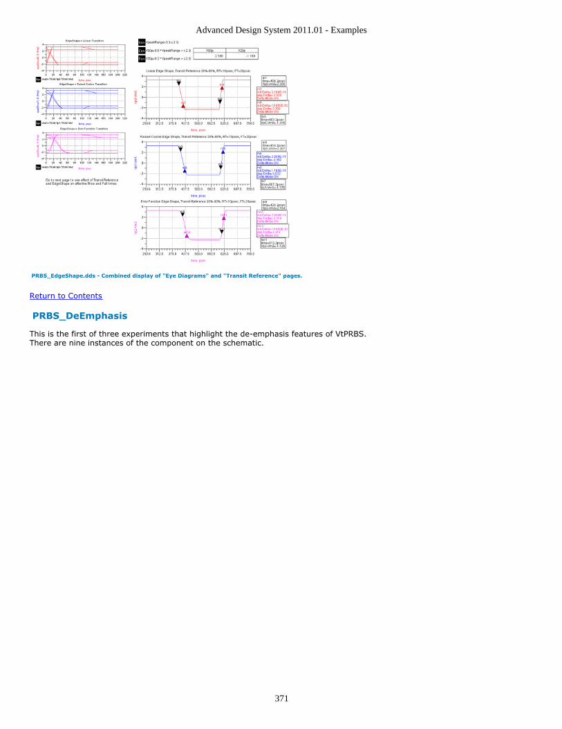
Advanced Design System 2011.01 - Examples
371
PRBS_EdgeShape.dds - Combined display of "Eye Diagrams" and "Transit Reference" pages.
Return to Contents
PRBS_DeEmphasis
This is the first of three experiments that highlight the de-emphasis features of VtPRBS.There are nine instances of the component on the schematic.
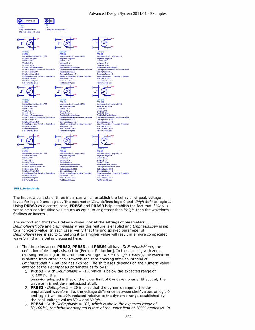
Advanced Design System 2011.01 - Examples
372
PRBS_DeEmphasis
The first row consists of three instances which establish the behavior of peak voltagelevels for logic 0 and logic 1. The parameter Vlow defines logic 0 and Vhigh defines logic 1.Using PRBS0 as a control case, PRBS8 and PRBS9 help establish the fact that if Vlow isset to be a non-intuitive value such as equal to or greater than Vhigh, then the waveformflatlines or inverts.
The second and third rows takes a closer look at the settings of parametersDeEmphasisMode and DeEmphasis when this feature is enabled and EmphasisSpan is setto a non-zero value. In each case, verify that the undisplayed parameter ofDeEmphasisTaps is set to 1. Setting it to a higher value will result in a more complicatedwaveform than is being discussed here.
The three instances PRBS2, PRBS3 and PRBS4 all have DeEmphasisMode, the1.definition of de-emphasis, set to [Percent Reduction]. In these cases, with zero-crossing remaining at the arithmetic average : 0.5 * ( Vhigh + Vlow ), the waveformis shifted from either peak towards the zero-crossing after an interval ofEmphasisSpan * / BitRate has expired. The shift itself depends on the numeric valueentered at the DeEmphasis parameter as follows:
PRBS2 - With DeEmphasis = -10, which is below the expected range of1.[0,100]%, thebehavior adopted is that of the lower limit of 0% de-emphasis. Effectively thewaveform is not de-emphasized at all.PRBS3 - DeEmphasis = 20 implies that the dynamic range of the de-2.emphasized waveform i.e. the voltage difference between shelf values of logic 0and logic 1 will be 10% reduced relative to the dynamic range established bythe peak voltage values Vlow and Vhigh.PRBS4 - With DeEmphasis = 103, which is above the expected range of3.[0,100]%, the behavior adopted is that of the upper limit of 100% emphasis. In
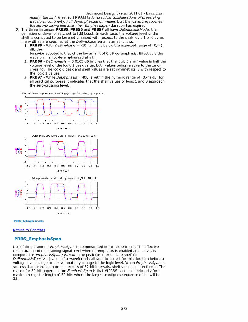
Advanced Design System 2011.01 - Examples
373
reality, the limit is set to 99.9999% for practical considerations of preservingwaveform continuity. Full de-emphasization means that the waveform touchesthe zero-crossing line after the _EmphasisSpan duration has expired.
The three instances PRBS5, PRBS6 and PRBS7 all have DeEmphasisMode, the2.definition of de-emphasis, set to [dB Loss]. In each case, the voltage level of theshelf is computed to be lowered or raised with respect to the peak logic 1 or 0 by asmany dB as are specified at the DeEmphasis parameter as follows:
PRBS5 - With DeEmphasis = -10, which is below the expected range of [0,∞)1.dB, thebehavior adopted is that of the lower limit of 0 dB de-emphasis. Effectively thewaveform is not de-emphasized at all.PRBS6 - DeEmphasis = 3.0103 dB implies that the logic 1 shelf value is half the2.voltage level of the logic 1 peak value, both values being relative to the zero-crossing. The logic 0 peak and shelf values are set symmetrically with respect tothe logic 1 values.PRBS7 - While DeEmphasis = 400 is within the numeric range of [0,∞) dB, for3.all practical purposes it indicates that the shelf values of logic 1 and 0 approachthe zero-crossing level.
PRBS_DeEmphasis.dds
Return to Contents
PRBS_EmphasisSpan
Use of the parameter EmphasisSpan is demonstrated in this experiment. The effectivetime duration of maintaining signal level when de-emphasis is enabled and active, iscomputed as EmphasisSpan / BitRate. The peak (or intermediate shelf forDeEmphasisTaps > 1) value of a waveform is allowed to persist for this duration before avoltage level change occurs without any change to the logic level. When EmphasisSpan isset less than or equal to or is in excess of 32 bit intervals, shelf value is not enforced. Thereason for 32-bit upper limit on EmphasisSpan is that VtPRBS is enabled primarily for amaximum register length of 32-bits where the largest contiguos sequence of 1's will be32.
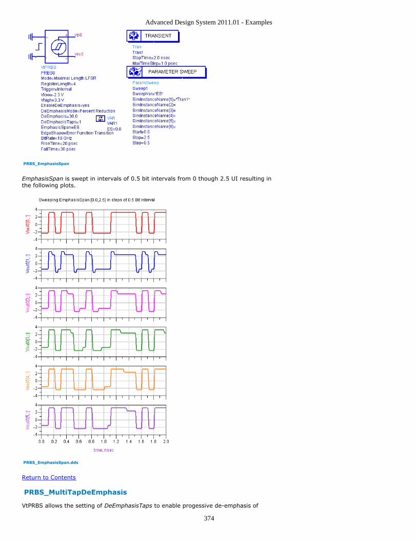
Advanced Design System 2011.01 - Examples
374
PRBS_EmphasisSpan
EmphasisSpan is swept in intervals of 0.5 bit intervals from 0 though 2.5 UI resulting inthe following plots.
PRBS_EmphasisSpan.dds
Return to Contents
PRBS_MultiTapDeEmphasis
VtPRBS allows the setting of DeEmphasisTaps to enable progessive de-emphasis of
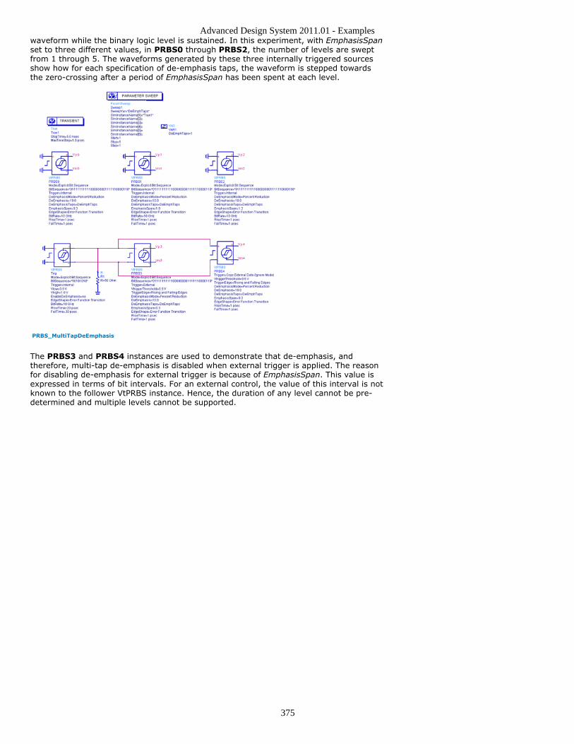
Advanced Design System 2011.01 - Examples
375
waveform while the binary logic level is sustained. In this experiment, with EmphasisSpanset to three different values, in PRBS0 through PRBS2, the number of levels are sweptfrom 1 through 5. The waveforms generated by these three internally triggered sourcesshow how for each specification of de-emphasis taps, the waveform is stepped towardsthe zero-crossing after a period of EmphasisSpan has been spent at each level.
PRBS_MultiTapDeEmphasis
The PRBS3 and PRBS4 instances are used to demonstrate that de-emphasis, andtherefore, multi-tap de-emphasis is disabled when external trigger is applied. The reasonfor disabling de-emphasis for external trigger is because of EmphasisSpan. This value isexpressed in terms of bit intervals. For an external control, the value of this interval is notknown to the follower VtPRBS instance. Hence, the duration of any level cannot be pre-determined and multiple levels cannot be supported.
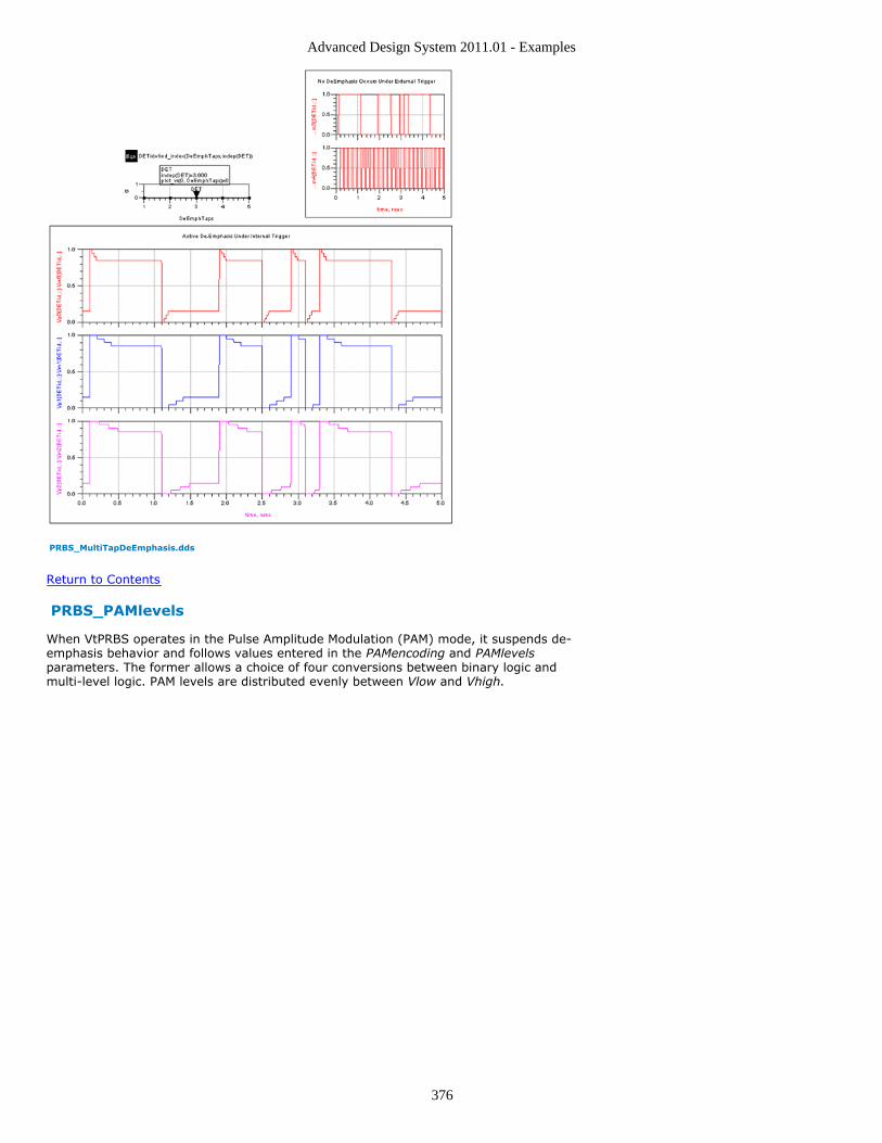
Advanced Design System 2011.01 - Examples
376
PRBS_MultiTapDeEmphasis.dds
Return to Contents
PRBS_PAMlevels
When VtPRBS operates in the Pulse Amplitude Modulation (PAM) mode, it suspends de-emphasis behavior and follows values entered in the PAMencoding and PAMlevelsparameters. The former allows a choice of four conversions between binary logic andmulti-level logic. PAM levels are distributed evenly between Vlow and Vhigh.
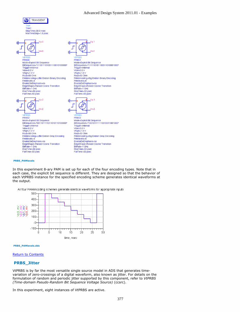
Advanced Design System 2011.01 - Examples
377
PRBS_PAMlevels
In this experiment 8-ary PAM is set up for each of the four encoding types. Note that ineach case, the explicit bit sequence is different. They are designed so that the behavior ofeach VtPRBS instance for the specified encoding scheme generates identical waveforms atthe output.
PRBS_PAMlevels.dds
Return to Contents
PRBS_Jitter
VtPRBS is by far the most versatile single source model in ADS that generates time-variation of zero-crossings of a digital waveform, also known as jitter. For details on theformulation of random and periodic jitter supported by this component, refer to VtPRBS(Time-domain Pseudo-Random Bit Sequence Voltage Source) (ccsrc).
In this experiment, eight instances of VtPRBS are active.
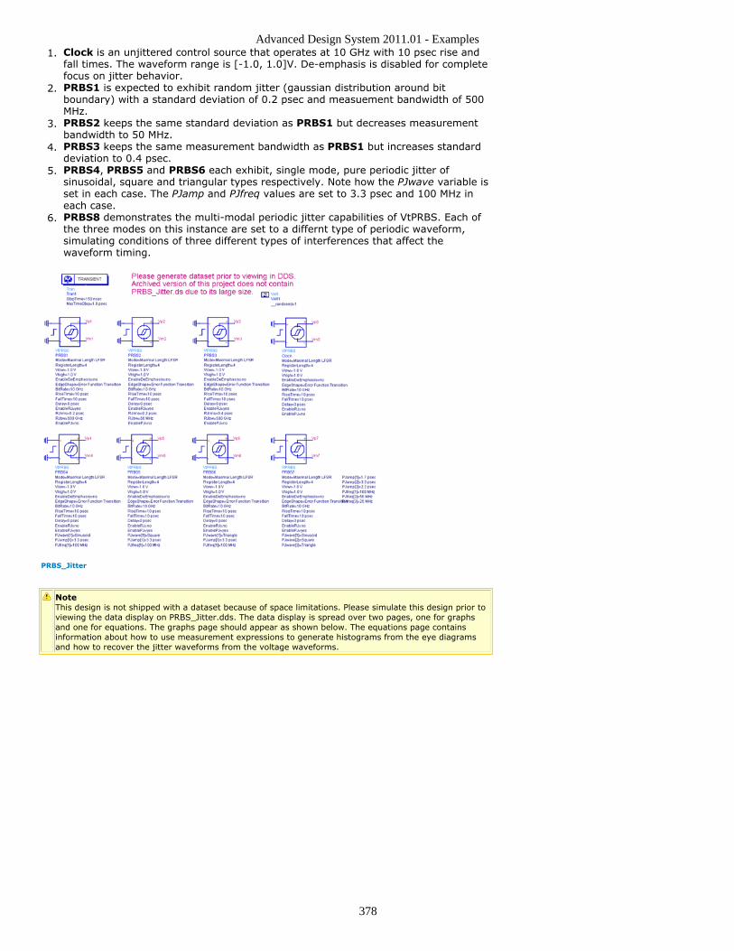
Advanced Design System 2011.01 - Examples
378
Clock is an unjittered control source that operates at 10 GHz with 10 psec rise and1.fall times. The waveform range is [-1.0, 1.0]V. De-emphasis is disabled for completefocus on jitter behavior.PRBS1 is expected to exhibit random jitter (gaussian distribution around bit2.boundary) with a standard deviation of 0.2 psec and measuement bandwidth of 500MHz.PRBS2 keeps the same standard deviation as PRBS1 but decreases measurement3.bandwidth to 50 MHz.PRBS3 keeps the same measurement bandwidth as PRBS1 but increases standard4.deviation to 0.4 psec.PRBS4, PRBS5 and PRBS6 each exhibit, single mode, pure periodic jitter of5.sinusoidal, square and triangular types respectively. Note how the PJwave variable isset in each case. The PJamp and PJfreq values are set to 3.3 psec and 100 MHz ineach case.PRBS8 demonstrates the multi-modal periodic jitter capabilities of VtPRBS. Each of6.the three modes on this instance are set to a differnt type of periodic waveform,simulating conditions of three different types of interferences that affect thewaveform timing.
PRBS_Jitter
NoteThis design is not shipped with a dataset because of space limitations. Please simulate this design prior toviewing the data display on PRBS_Jitter.dds. The data display is spread over two pages, one for graphsand one for equations. The graphs page should appear as shown below. The equations page containsinformation about how to use measurement expressions to generate histograms from the eye diagramsand how to recover the jitter waveforms from the voltage waveforms.
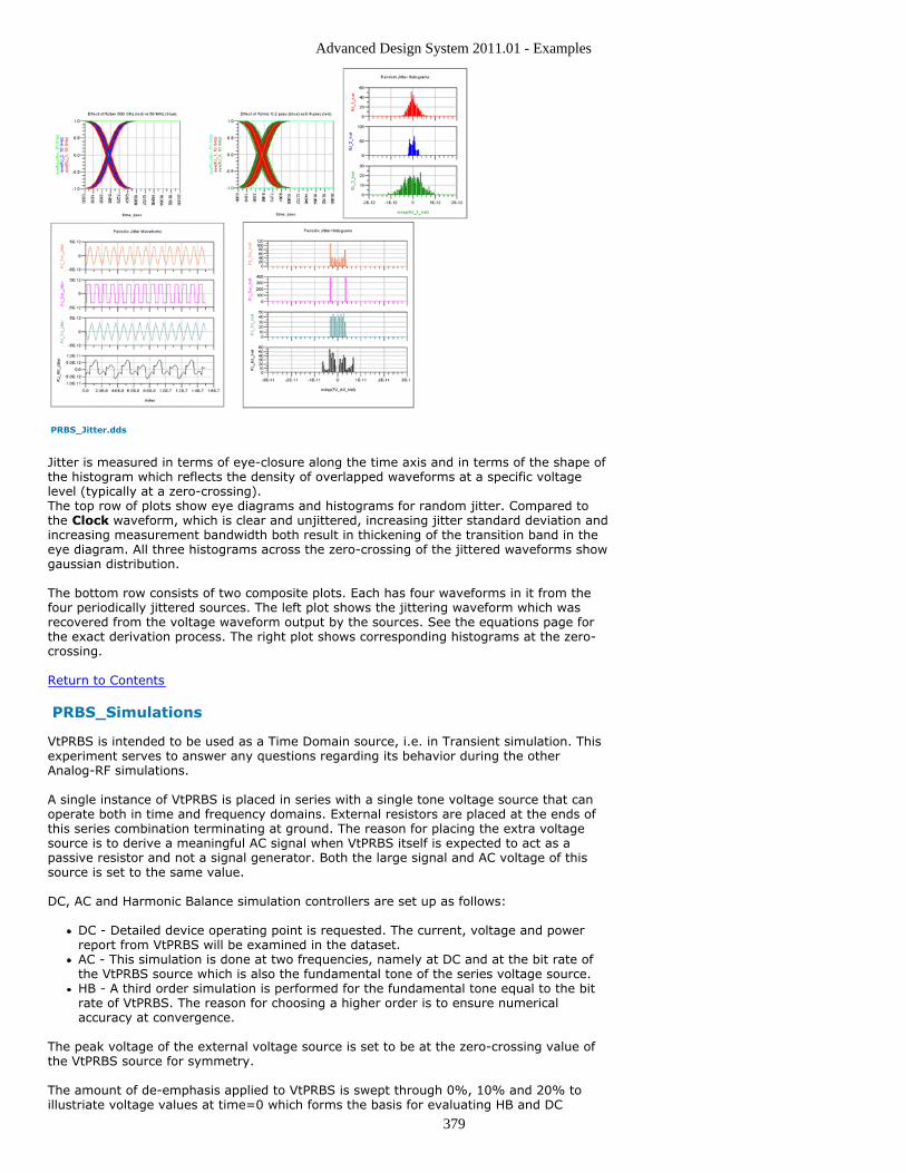
Advanced Design System 2011.01 - Examples
379
PRBS_Jitter.dds
Jitter is measured in terms of eye-closure along the time axis and in terms of the shape ofthe histogram which reflects the density of overlapped waveforms at a specific voltagelevel (typically at a zero-crossing).The top row of plots show eye diagrams and histograms for random jitter. Compared tothe Clock waveform, which is clear and unjittered, increasing jitter standard deviation andincreasing measurement bandwidth both result in thickening of the transition band in theeye diagram. All three histograms across the zero-crossing of the jittered waveforms showgaussian distribution.
The bottom row consists of two composite plots. Each has four waveforms in it from thefour periodically jittered sources. The left plot shows the jittering waveform which wasrecovered from the voltage waveform output by the sources. See the equations page forthe exact derivation process. The right plot shows corresponding histograms at the zero-crossing.
Return to Contents
PRBS_Simulations
VtPRBS is intended to be used as a Time Domain source, i.e. in Transient simulation. Thisexperiment serves to answer any questions regarding its behavior during the otherAnalog-RF simulations.
A single instance of VtPRBS is placed in series with a single tone voltage source that canoperate both in time and frequency domains. External resistors are placed at the ends ofthis series combination terminating at ground. The reason for placing the extra voltagesource is to derive a meaningful AC signal when VtPRBS itself is expected to act as apassive resistor and not a signal generator. Both the large signal and AC voltage of thissource is set to the same value.
DC, AC and Harmonic Balance simulation controllers are set up as follows:
DC - Detailed device operating point is requested. The current, voltage and powerreport from VtPRBS will be examined in the dataset.AC - This simulation is done at two frequencies, namely at DC and at the bit rate ofthe VtPRBS source which is also the fundamental tone of the series voltage source.HB - A third order simulation is performed for the fundamental tone equal to the bitrate of VtPRBS. The reason for choosing a higher order is to ensure numericalaccuracy at convergence.
The peak voltage of the external voltage source is set to be at the zero-crossing value ofthe VtPRBS source for symmetry.
The amount of de-emphasis applied to VtPRBS is swept through 0%, 10% and 20% toillustriate voltage values at time=0 which forms the basis for evaluating HB and DC
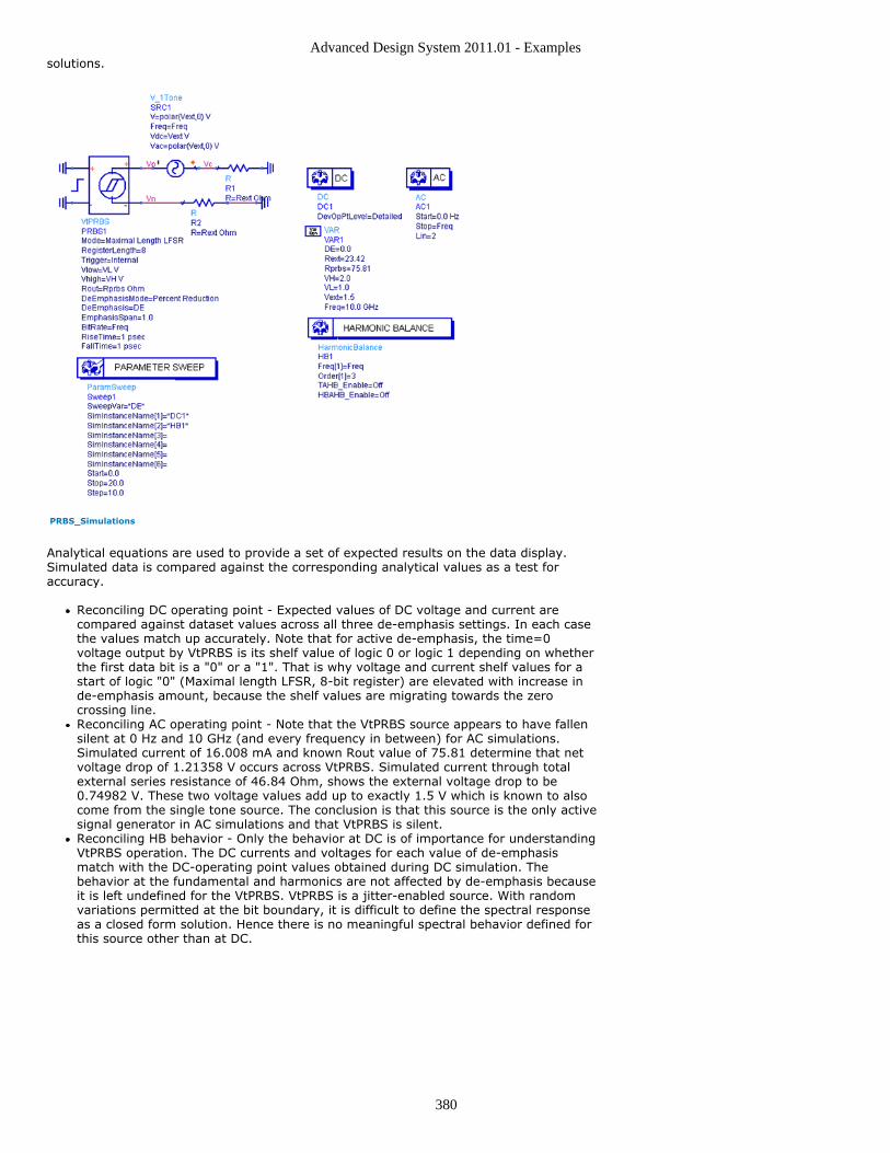
Advanced Design System 2011.01 - Examples
380
solutions.
PRBS_Simulations
Analytical equations are used to provide a set of expected results on the data display.Simulated data is compared against the corresponding analytical values as a test foraccuracy.
Reconciling DC operating point - Expected values of DC voltage and current arecompared against dataset values across all three de-emphasis settings. In each casethe values match up accurately. Note that for active de-emphasis, the time=0voltage output by VtPRBS is its shelf value of logic 0 or logic 1 depending on whetherthe first data bit is a "0" or a "1". That is why voltage and current shelf values for astart of logic "0" (Maximal length LFSR, 8-bit register) are elevated with increase inde-emphasis amount, because the shelf values are migrating towards the zerocrossing line.Reconciling AC operating point - Note that the VtPRBS source appears to have fallensilent at 0 Hz and 10 GHz (and every frequency in between) for AC simulations.Simulated current of 16.008 mA and known Rout value of 75.81 determine that netvoltage drop of 1.21358 V occurs across VtPRBS. Simulated current through totalexternal series resistance of 46.84 Ohm, shows the external voltage drop to be0.74982 V. These two voltage values add up to exactly 1.5 V which is known to alsocome from the single tone source. The conclusion is that this source is the only activesignal generator in AC simulations and that VtPRBS is silent.Reconciling HB behavior - Only the behavior at DC is of importance for understandingVtPRBS operation. The DC currents and voltages for each value of de-emphasismatch with the DC-operating point values obtained during DC simulation. Thebehavior at the fundamental and harmonics are not affected by de-emphasis becauseit is left undefined for the VtPRBS. VtPRBS is a jitter-enabled source. With randomvariations permitted at the bit boundary, it is difficult to define the spectral responseas a closed form solution. Hence there is no meaningful spectral behavior defined forthis source other than at DC.
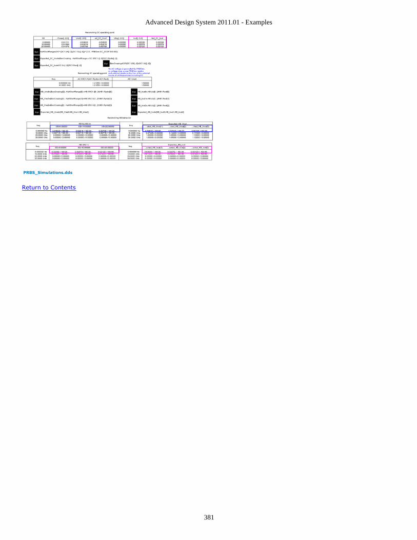
Advanced Design System 2011.01 - Examples
381
PRBS_Simulations.dds
Return to Contents
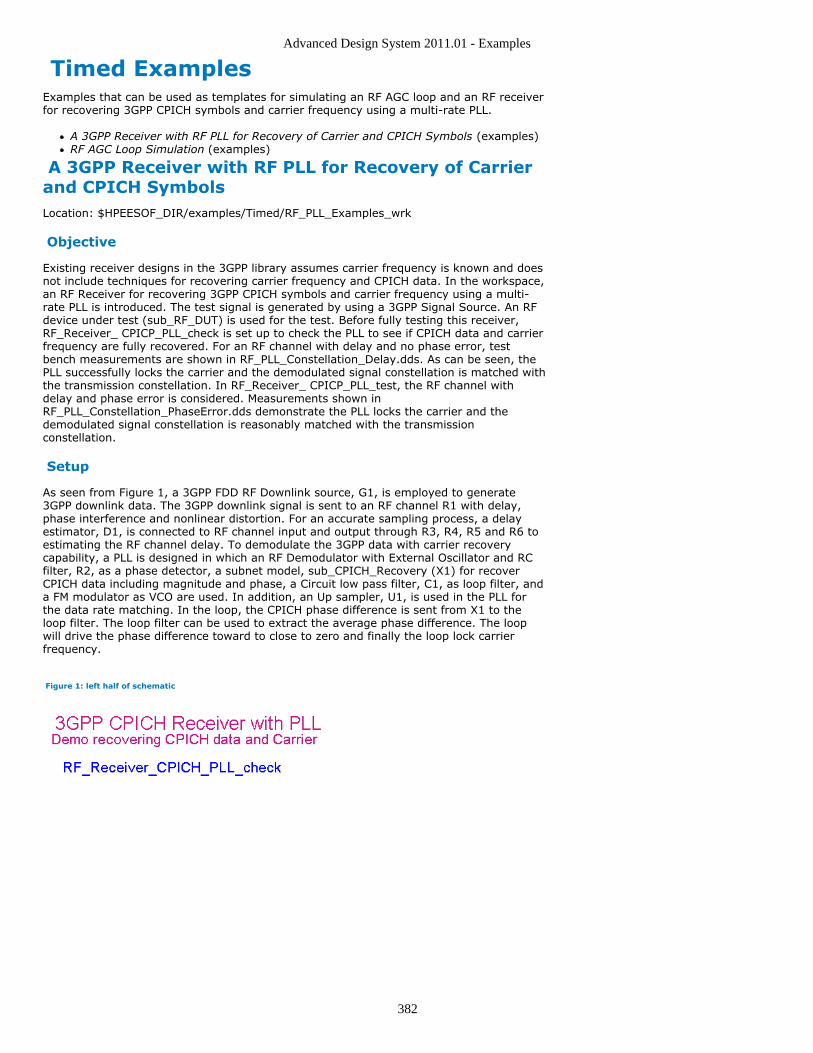
Advanced Design System 2011.01 - Examples
382
Timed ExamplesExamples that can be used as templates for simulating an RF AGC loop and an RF receiverfor recovering 3GPP CPICH symbols and carrier frequency using a multi-rate PLL.
A 3GPP Receiver with RF PLL for Recovery of Carrier and CPICH Symbols (examples)RF AGC Loop Simulation (examples)
A 3GPP Receiver with RF PLL for Recovery of Carrierand CPICH SymbolsLocation: $HPEESOF_DIR/examples/Timed/RF_PLL_Examples_wrk
Objective
Existing receiver designs in the 3GPP library assumes carrier frequency is known and doesnot include techniques for recovering carrier frequency and CPICH data. In the workspace,an RF Receiver for recovering 3GPP CPICH symbols and carrier frequency using a multi-rate PLL is introduced. The test signal is generated by using a 3GPP Signal Source. An RFdevice under test (sub_RF_DUT) is used for the test. Before fully testing this receiver,RF_Receiver_ CPICP_PLL_check is set up to check the PLL to see if CPICH data and carrierfrequency are fully recovered. For an RF channel with delay and no phase error, testbench measurements are shown in RF_PLL_Constellation_Delay.dds. As can be seen, thePLL successfully locks the carrier and the demodulated signal constellation is matched withthe transmission constellation. In RF_Receiver_ CPICP_PLL_test, the RF channel withdelay and phase error is considered. Measurements shown inRF_PLL_Constellation_PhaseError.dds demonstrate the PLL locks the carrier and thedemodulated signal constellation is reasonably matched with the transmissionconstellation.
Setup
As seen from Figure 1, a 3GPP FDD RF Downlink source, G1, is employed to generate3GPP downlink data. The 3GPP downlink signal is sent to an RF channel R1 with delay,phase interference and nonlinear distortion. For an accurate sampling process, a delayestimator, D1, is connected to RF channel input and output through R3, R4, R5 and R6 toestimating the RF channel delay. To demodulate the 3GPP data with carrier recoverycapability, a PLL is designed in which an RF Demodulator with External Oscillator and RCfilter, R2, as a phase detector, a subnet model, sub_CPICH_Recovery (X1) for recoverCPICH data including magnitude and phase, a Circuit low pass filter, C1, as loop filter, anda FM modulator as VCO are used. In addition, an Up sampler, U1, is used in the PLL forthe data rate matching. In the loop, the CPICH phase difference is sent from X1 to theloop filter. The loop filter can be used to extract the average phase difference. The loopwill drive the phase difference toward to close to zero and finally the loop lock carrierfrequency.
Figure 1: left half of schematic
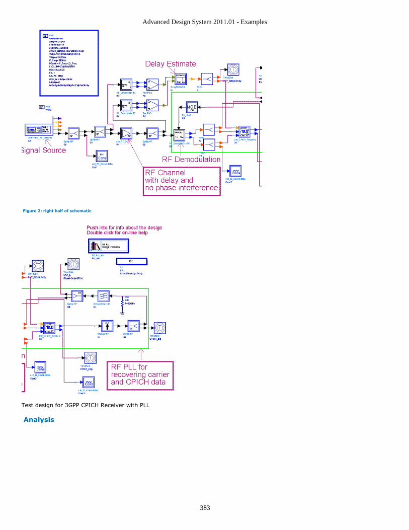
Advanced Design System 2011.01 - Examples
383
Figure 2: right half of schematic
Test design for 3GPP CPICH Receiver with PLL
Analysis
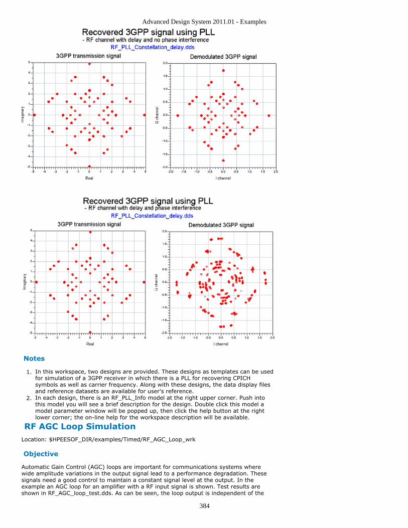
Advanced Design System 2011.01 - Examples
384
Notes
In this workspace, two designs are provided. These designs as templates can be used1.for simulation of a 3GPP receiver in which there is a PLL for recovering CPICHsymbols as well as carrier frequency. Along with these designs, the data display filesand reference datasets are available for user's reference.In each design, there is an RF_PLL_Info model at the right upper corner. Push into2.this model you will see a brief description for the design. Double click this model amodel parameter window will be popped up, then click the help button at the rightlower corner; the on-line help for the workspace description will be available.
RF AGC Loop SimulationLocation: $HPEESOF_DIR/examples/Timed/RF_AGC_Loop_wrk
Objective
Automatic Gain Control (AGC) loops are important for communications systems wherewide amplitude variations in the output signal lead to a performance degradation. Thesesignals need a good control to maintain a constant signal level at the output. In theexample an AGC loop for an amplifier with a RF input signal is shown. Test results areshown in RF_AGC_loop_test.dds. As can be seen, the loop output is independent of the
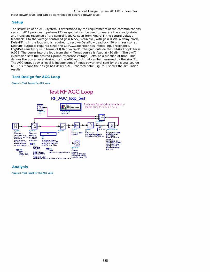
Advanced Design System 2011.01 - Examples
385
input power level and can be controlled in desired power level.
Setup
The structure of an AGC system is determined by the requirements of the communicationssystem. ADS provides top-down RF design that can be used to analyze the steady-stateand transient response of the control loop. As seen from Figure 1, the control voltagefeedback is to the voltage controlled gain block, VcGainRF, with gain dB/V. A delay block,DelayRF, is in the loop and is required to resolve DataFlow deadlock. 50 ohm resistor atDelayRF output is required since the CktAGCLoopFilter has infinite input resistance.LogVDet sensitivity is in terms of 0.025 volts/dB. The gain outside the CktAGCLoopFilter is0.025. The power into the loop from the N_Tones source is fixed at -30 dBm. The pwl()expression sets the desired OpAmp reference voltage, RefV, as a function of time. Thisdefines the power level desired for the AGC output that can be measured by the sink T1.The AGC output power level is independent of input power level sent by the signal sourceN1. This means the design has desired AGC characteristic. Figure 2 shows the simulationresults.
Test Design for AGC Loop
Figure 1: Test Design for AGC Loop
Analysis
Figure 2: Test result for the AGC Loop
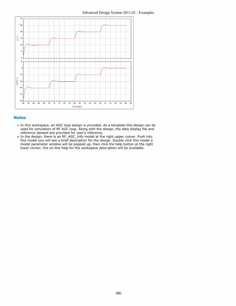
Advanced Design System 2011.01 - Examples
386
Notes
In this workspace, an AGC loop design is provided. As a template this design can beused for simulation of RF AGC loop. Along with the design, the data display file andreference dataset are provided for user's reference.In the design, there is an RF_AGC_Info model at the right upper corner. Push intothis model you will see a brief description for the design. Double click this model amodel parameter window will be popped up, then click the help button at the rightlower corner; the on-line help for the workspace description will be available.

Advanced Design System 2011.01 - Examples
387
Tutorial ExamplesExamples of basic usage and functionality concepts in the tutorials included with thedocumentation.
A Model B Test Lab Optimization (examples)A Simple Integrator (examples)Behavioral Amplifier model - Amplifier2 (examples)Bit-Error-Rate Measurement Tutorial (examples)Bus Wire Basic Example (examples)Construct Three-Port S-Parameter File from Two-Port Measurement Datasets(examples)Example Test Lab for Two Stage Amplifier Design (examples)FIR Digital Filter (examples)Generate Various Modulated Sources (examples)Learn Tuning an Elliptic Filter, a Dynamic Load Line, and a Microstrip Bandpass Filter(examples)LSSP (Large-Signal S-Parameters), Basic Example (examples)Mixer2 Model Validation Example File (examples)Noise Power Ratio Simulation (examples)Noise Simulation in Envelope Analysis (examples)Optimization and Parameter Sweeps Using DSP Schematic (examples)Optimization Final Analysis Demonstration (examples)Optimization of a Low Pass Filter (examples)Optimization of An Impedance Transformation Network (examples)Oscillator Simulations using Transient, Harmonic Balance and Envelope Simulators(examples)Physical Layout Connectivity Check (examples)Power Amplifier Behavior Model (examples)Ptolemy DSP Sink Export to GoldenGate (examples)Ptolemy DSP Source Export to GoldenGate (examples)Quick Tour of Communication System Design in Ptolemy (examples)RF System Budget measurements for 2port cascaded networks (examples)Sensitivity Analysis, Basic Example (examples)Simple Example Showing Application of DOE (examples)Simple Ptolemy Sequencer Example (examples)S-Parameter Simulation Example (examples)S-Parameters of 2-Port Terminated with Other Networks (examples)Statistical Correlation in ADS (examples)Statistical Design Example for Oscillator Yield Analysis (examples)Swept Optimization, Basic Example (examples)Tutorial on Budget Analysis (Archive) (examples)User-Compiled Model Examples (examples)Using DataAccessComponent (DAC) and S2PMDIF Component (examples)Using Expressions in the Data Display Window (examples)Using Frequency-Domain Defined Devices (FDD) (examples)Using HB Noise Controller (examples)Using N-State Modulator Component to Generate Modulated Signals (examples)Using Measured Load Pull Data to Design and Optimize Impedance-MatchingNetworks (examples)Using OscPort2 in Oscillator Simulation (examples)Using SP_Probe in ADS (examples)Using Symbolically Defined Devices (SDD) (examples)Various Examples on using ADS Simulation Controllers (examples)VCO Simulations (examples)X-Parameters, Generating a Model and Comparing it with a Transistor-LevelSimulation (examples)X-Parameters, Various Simulations Using Models Generated from Measurements(examples)Yield Analysis of An Impedance Transformer (examples)Yield Optimization of An Impedance Transformer (examples)Yield Sensitivity Analysis of A Low Pass Filter (examples)Low Pass Filter Demo (examples)W-element Extraction Example (examples)
A Model B Test Lab OptimizationLocation: $HPEESOF_DIR/examples/Tutorial/TestLab_HOWTO_wrk
Objective
This example uses a Series IV style of Test Lab Optimization to demonstrate an alternative
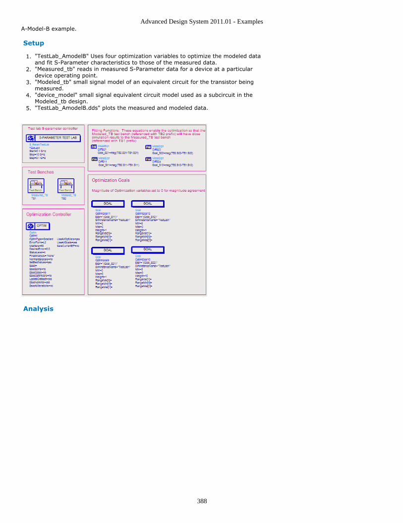
Advanced Design System 2011.01 - Examples
388
A-Model-B example.
Setup
"TestLab_AmodelB" Uses four optimization variables to optimize the modeled data1.and fit S-Parameter characteristics to those of the measured data."Measured_tb" reads in measured S-Parameter data for a device at a particular2.device operating point."Modeled_tb" small signal model of an equivalent circuit for the transistor being3.measured."device_model" small signal equivalent circuit model used as a subcircuit in the4.Modeled_tb design."TestLab_AmodelB.dds" plots the measured and modeled data.5.
Analysis
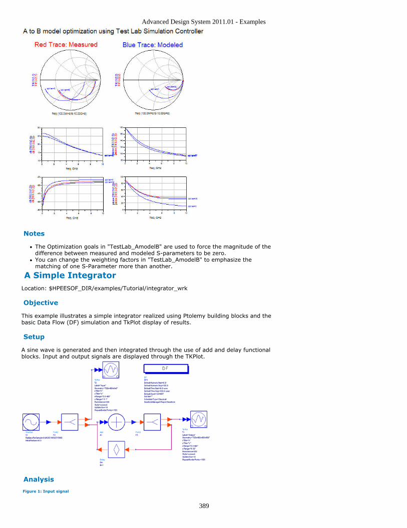
Advanced Design System 2011.01 - Examples
389
Notes
The Optimization goals in "TestLab_AmodelB" are used to force the magnitude of thedifference between measured and modeled S-parameters to be zero.You can change the weighting factors in "TestLab_AmodelB" to emphasize thematching of one S-Parameter more than another.
A Simple IntegratorLocation: $HPEESOF_DIR/examples/Tutorial/integrator_wrk
Objective
This example illustrates a simple integrator realized using Ptolemy building blocks and thebasic Data Flow (DF) simulation and TkPlot display of results.
Setup
A sine wave is generated and then integrated through the use of add and delay functionalblocks. Input and output signals are displayed through the TKPlot.
Analysis
Figure 1: Input signal
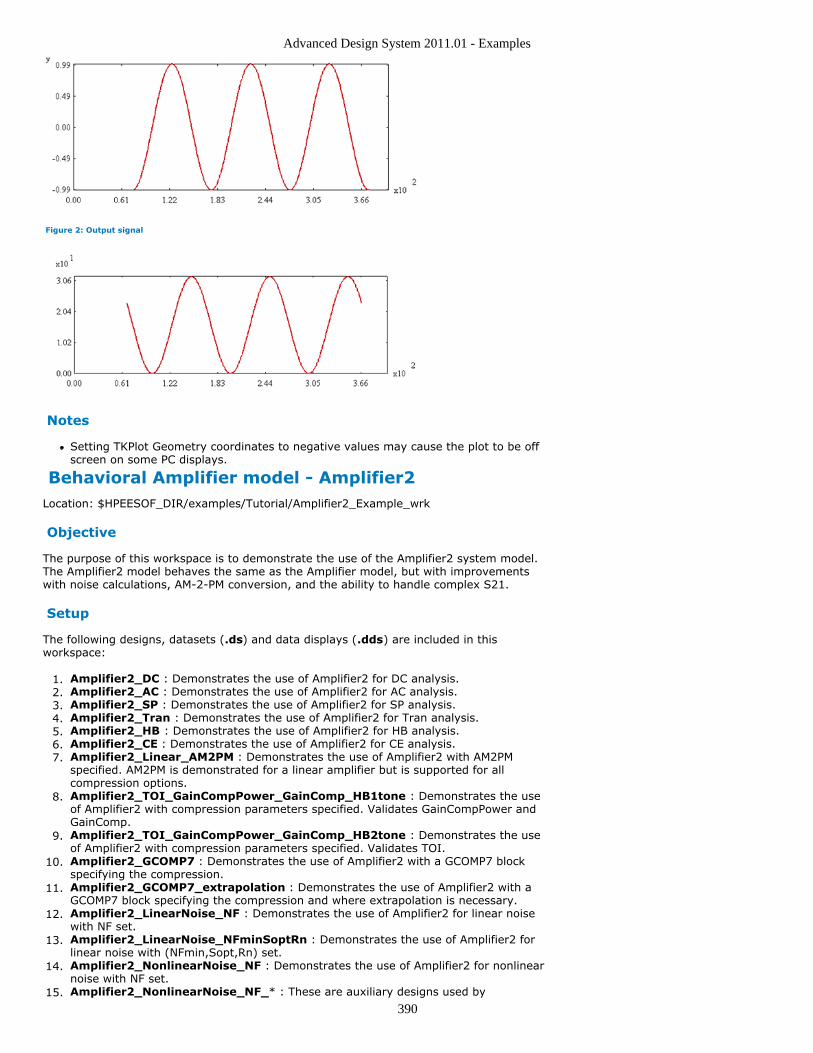
Advanced Design System 2011.01 - Examples
390
Figure 2: Output signal
Notes
Setting TKPlot Geometry coordinates to negative values may cause the plot to be offscreen on some PC displays.
Behavioral Amplifier model - Amplifier2Location: $HPEESOF_DIR/examples/Tutorial/Amplifier2_Example_wrk
Objective
The purpose of this workspace is to demonstrate the use of the Amplifier2 system model.The Amplifier2 model behaves the same as the Amplifier model, but with improvementswith noise calculations, AM-2-PM conversion, and the ability to handle complex S21.
Setup
The following designs, datasets (.ds) and data displays (.dds) are included in thisworkspace:
Amplifier2_DC : Demonstrates the use of Amplifier2 for DC analysis.1.Amplifier2_AC : Demonstrates the use of Amplifier2 for AC analysis.2.Amplifier2_SP : Demonstrates the use of Amplifier2 for SP analysis.3.Amplifier2_Tran : Demonstrates the use of Amplifier2 for Tran analysis.4.Amplifier2_HB : Demonstrates the use of Amplifier2 for HB analysis.5.Amplifier2_CE : Demonstrates the use of Amplifier2 for CE analysis.6.Amplifier2_Linear_AM2PM : Demonstrates the use of Amplifier2 with AM2PM7.specified. AM2PM is demonstrated for a linear amplifier but is supported for allcompression options.Amplifier2_TOI_GainCompPower_GainComp_HB1tone : Demonstrates the use8.of Amplifier2 with compression parameters specified. Validates GainCompPower andGainComp.Amplifier2_TOI_GainCompPower_GainComp_HB2tone : Demonstrates the use9.of Amplifier2 with compression parameters specified. Validates TOI.Amplifier2_GCOMP7 : Demonstrates the use of Amplifier2 with a GCOMP7 block10.specifying the compression.Amplifier2_GCOMP7_extrapolation : Demonstrates the use of Amplifier2 with a11.GCOMP7 block specifying the compression and where extrapolation is necessary.Amplifier2_LinearNoise_NF : Demonstrates the use of Amplifier2 for linear noise12.with NF set.Amplifier2_LinearNoise_NFminSoptRn : Demonstrates the use of Amplifier2 for13.linear noise with (NFmin,Sopt,Rn) set.Amplifier2_NonlinearNoise_NF : Demonstrates the use of Amplifier2 for nonlinear14.noise with NF set.Amplifier2_NonlinearNoise_NF_* : These are auxiliary designs used by15.
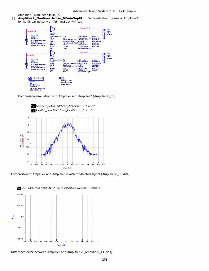
Advanced Design System 2011.01 - Examples
391
Amplifier2_NonlinearNoise_*.Amplifier2_NonlinearNoise_NFminSoptRn : Demonstrates the use of Amplifier216.for nonlinear noise with (NFmin,Sopt,Rn) set.
Comparison simulation with Amplifier and Amplifer2 (Amplifier2_CE)
Comparison of Amplifier and Amplifier 2 with modulated signal (Amplifier2_CE.dds)
Difference error between Amplifier and Amplifier 2 (Amplifier2_CE.dds)
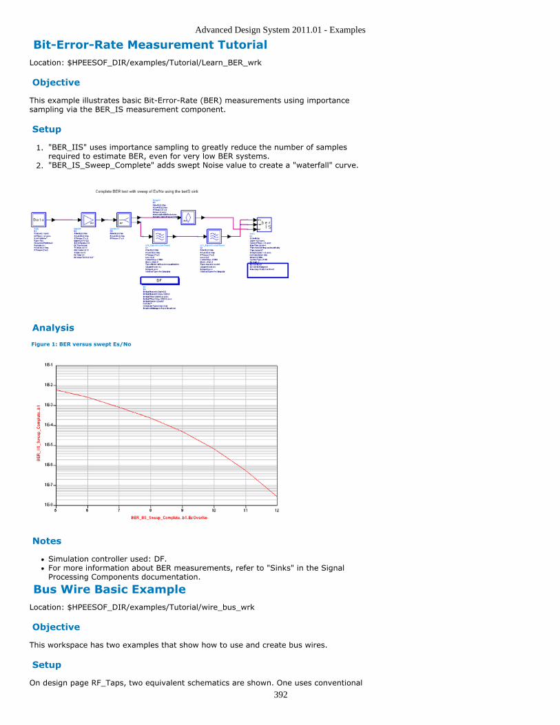
Advanced Design System 2011.01 - Examples
392
Bit-Error-Rate Measurement TutorialLocation: $HPEESOF_DIR/examples/Tutorial/Learn_BER_wrk
Objective
This example illustrates basic Bit-Error-Rate (BER) measurements using importancesampling via the BER_IS measurement component.
Setup
"BER_IIS" uses importance sampling to greatly reduce the number of samples1.required to estimate BER, even for very low BER systems."BER_IS_Sweep_Complete" adds swept Noise value to create a "waterfall" curve.2.
Analysis
Figure 1: BER versus swept Es/No
Notes
Simulation controller used: DF.For more information about BER measurements, refer to "Sinks" in the SignalProcessing Components documentation.
Bus Wire Basic ExampleLocation: $HPEESOF_DIR/examples/Tutorial/wire_bus_wrk
Objective
This workspace has two examples that show how to use and create bus wires.
Setup
On design page RF_Taps, two equivalent schematics are shown. One uses conventional
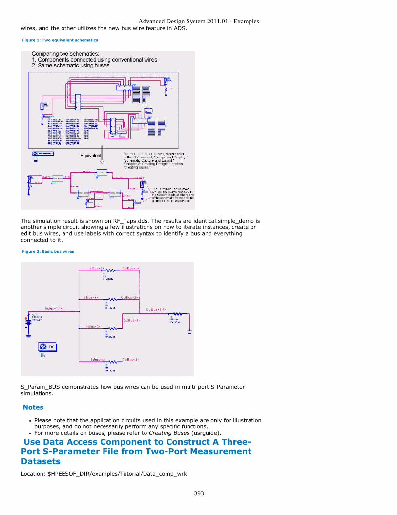
Advanced Design System 2011.01 - Examples
393
wires, and the other utilizes the new bus wire feature in ADS.
Figure 1: Two equivalent schematics
The simulation result is shown on RF_Taps.dds. The results are identical.simple_demo isanother simple circuit showing a few illustrations on how to iterate instances, create oredit bus wires, and use labels with correct syntax to identify a bus and everythingconnected to it.
Figure 2: Basic bus wires
S_Param_BUS demonstrates how bus wires can be used in multi-port S-Parametersimulations.
Notes
Please note that the application circuits used in this example are only for illustrationpurposes, and do not necessarily perform any specific functions.For more details on buses, please refer to Creating Buses (usrguide).
Use Data Access Component to Construct A Three-Port S-Parameter File from Two-Port MeasurementDatasetsLocation: $HPEESOF_DIR/examples/Tutorial/Data_comp_wrk
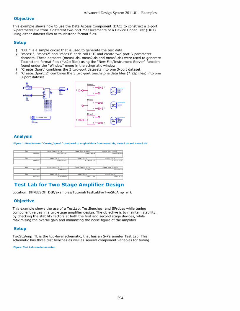
Advanced Design System 2011.01 - Examples
394
Objective
This example shows how to use the Data Access Component (DAC) to construct a 3-portS-parameter file from 3 different two-port measurements of a Device Under Test (DUT)using either dataset files or touchstone format files.
Setup
"DUT" is a simple circuit that is used to generate the test data.1."meas1", "meas2" and "meas3" each call DUT and create two-port S-parameter2.datasets. These datasets (meas1.ds, meas2.ds and meas3.ds) were used to generateTouchstone format files (*.s2p files) using the "New File/Instrument Server" functionfound under the "Window" menu in the schematic window."Create_3port" combines the 3 two-port datasets into one 3-port dataset.3."Create_3port_2" combines the 3 two-port touchstone data files (*.s2p files) into one4.3-port dataset.
Analysis
Figure 1: Results from "Create_3port2" compared to original data from meas1.ds, meas2.ds and meas3.ds
Test Lab for Two Stage Amplifier DesignLocation: $HPEESOF_DIR/examples/Tutorial/TestLabForTwoStgAmp_wrk
Objective
This example shows the use of a TestLab, TestBenches, and SProbes while tuningcomponent values in a two-stage amplifier design. The objective is to maintain stability,by checking the stability factors at both the first and second stage devices, whilemaximizing the overall gain and minimizing the noise figure of the amplifier.
Setup
TwoStgAmp_TL is the top-level schematic, that has an S-Parameter Test Lab. Thisschematic has three test benches as well as several component variables for tuning.
Figure: Test Lab simulation setup
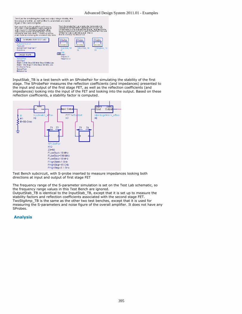
Advanced Design System 2011.01 - Examples
395
InputStab_TB is a test bench with an SProbePair for simulating the stability of the firststage. The SProbePair measures the reflection coefficients (and impedances) presented tothe input and output of the first stage FET, as well as the reflection coefficients (andimpedances) looking into the input of the FET and looking into the output. Based on thesereflection coefficients, a stability factor is computed.
Test Bench subcircuit, with S-probe inserted to measure impedances looking bothdirections at input and output of first stage FET
The frequency range of the S-parameter simulation is set on the Test Lab schematic, sothe frequency range values in this Test Bench are ignored.OutputStab_TB is identical to the InputStab_TB, except that it is set up to measure thestability factors and reflection coefficients associated with the second stage FET.TwoStgAmp_TB is the same as the other two test benches, except that it is used formeasuring the S-parameters and noise figure of the overall amplifier. It does not have anySProbes.
Analysis
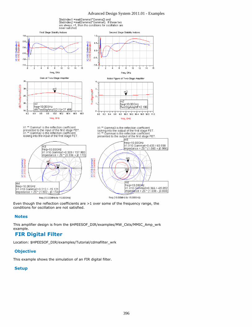
Advanced Design System 2011.01 - Examples
396
Even though the reflection coefficients are >1 over some of the frequency range, theconditions for oscillation are not satisfied.
Notes
This amplifier design is from the $HPEESOF_DIR/examples/MW_Ckts/MMIC_Amp_wrkexample.
FIR Digital FilterLocation: $HPEESOF_DIR/examples/Tutorial/cdmafilter_wrk
Objective
This example shows the simulation of an FIR digital filter.
Setup
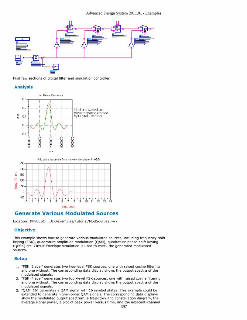
Advanced Design System 2011.01 - Examples
397
First few sections of digital filter and simulation controller
Analysis
Generate Various Modulated SourcesLocation: $HPEESOF_DIR/examples/Tutorial/ModSources_wrk
Objective
This example shows how to generate various modulated sources, including frequency-shiftkeying (FSK), quadrature amplitude modulation (QAM), quadrature phase-shift keying(QPSK) etc. Circuit Envelope simulation is used to check the generated modulatedsources.
Setup
"FSK_2level" generates two two-level FSK sources, one with raised cosine filtering1.and one without. The corresponding data display shows the output spectra of themodulated signals."FSK_4level" generates two four-level FSK sources, one with raised cosine filtering2.and one without. The corresponding data display shows the output spectra of themodulated signals."QAM_16" generates a QAM signal with 16 symbol states. This example could be3.extended to generate higher-order QAM signals. The corresponding data displaysshow the modulated output spectrum, a trajectory and constellation diagram, theaverage signal power, a plot of peak power versus time, and the adjacent-channel
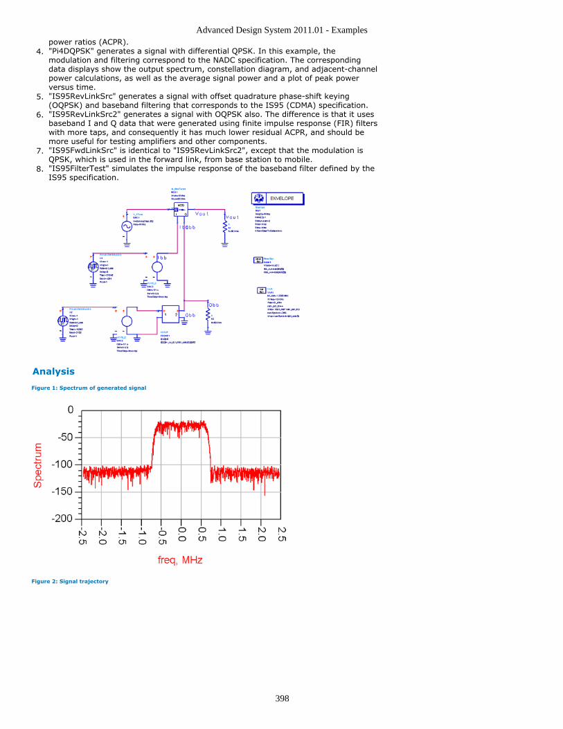
Advanced Design System 2011.01 - Examples
398
power ratios (ACPR)."Pi4DQPSK" generates a signal with differential QPSK. In this example, the4.modulation and filtering correspond to the NADC specification. The correspondingdata displays show the output spectrum, constellation diagram, and adjacent-channelpower calculations, as well as the average signal power and a plot of peak powerversus time."IS95RevLinkSrc" generates a signal with offset quadrature phase-shift keying5.(OQPSK) and baseband filtering that corresponds to the IS95 (CDMA) specification."IS95RevLinkSrc2" generates a signal with OQPSK also. The difference is that it uses6.baseband I and Q data that were generated using finite impulse response (FIR) filterswith more taps, and consequently it has much lower residual ACPR, and should bemore useful for testing amplifiers and other components."IS95FwdLinkSrc" is identical to "IS95RevLinkSrc2", except that the modulation is7.QPSK, which is used in the forward link, from base station to mobile."IS95FilterTest" simulates the impulse response of the baseband filter defined by the8.IS95 specification.
Analysis
Figure 1: Spectrum of generated signal
Figure 2: Signal trajectory
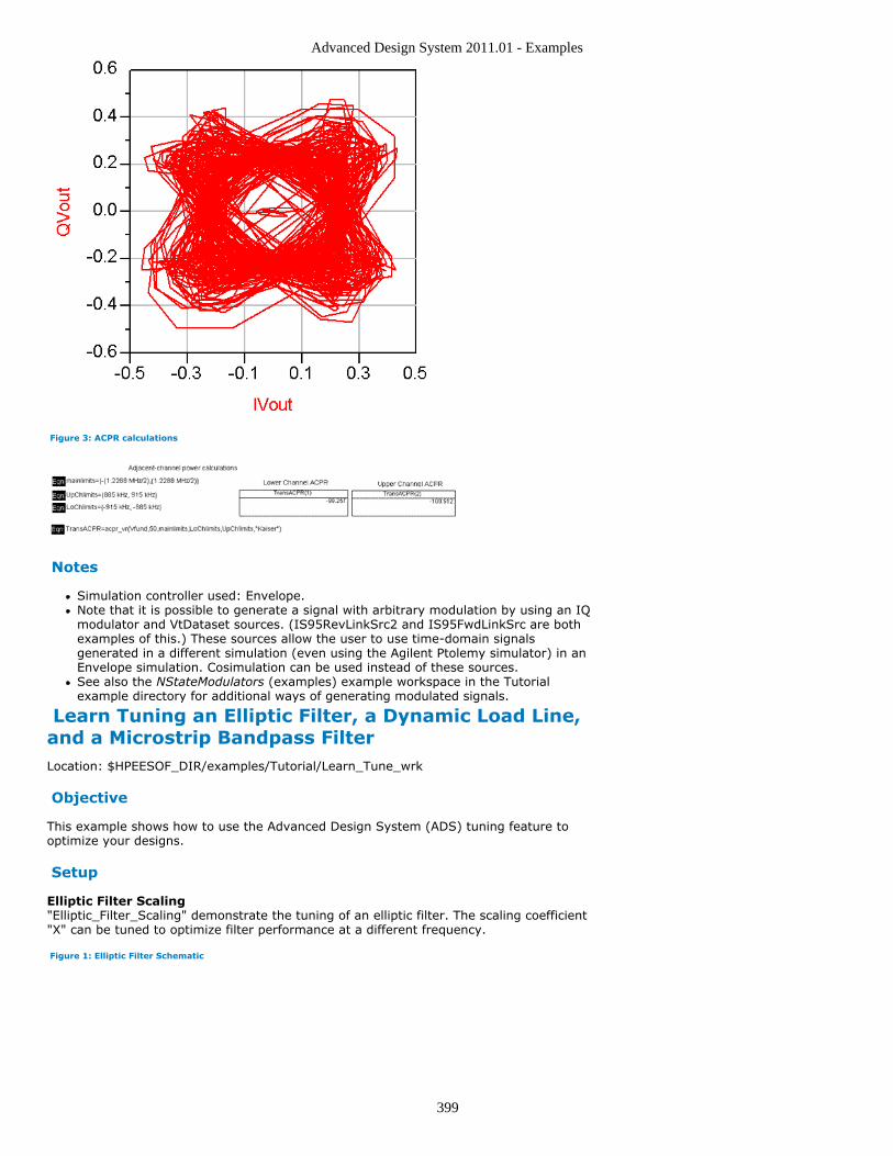
Advanced Design System 2011.01 - Examples
399
Figure 3: ACPR calculations
Notes
Simulation controller used: Envelope.Note that it is possible to generate a signal with arbitrary modulation by using an IQmodulator and VtDataset sources. (IS95RevLinkSrc2 and IS95FwdLinkSrc are bothexamples of this.) These sources allow the user to use time-domain signalsgenerated in a different simulation (even using the Agilent Ptolemy simulator) in anEnvelope simulation. Cosimulation can be used instead of these sources.See also the NStateModulators (examples) example workspace in the Tutorialexample directory for additional ways of generating modulated signals.
Learn Tuning an Elliptic Filter, a Dynamic Load Line,and a Microstrip Bandpass FilterLocation: $HPEESOF_DIR/examples/Tutorial/Learn_Tune_wrk
Objective
This example shows how to use the Advanced Design System (ADS) tuning feature tooptimize your designs.
Setup
Elliptic Filter Scaling"Elliptic_Filter_Scaling" demonstrate the tuning of an elliptic filter. The scaling coefficient"X" can be tuned to optimize filter performance at a different frequency.
Figure 1: Elliptic Filter Schematic
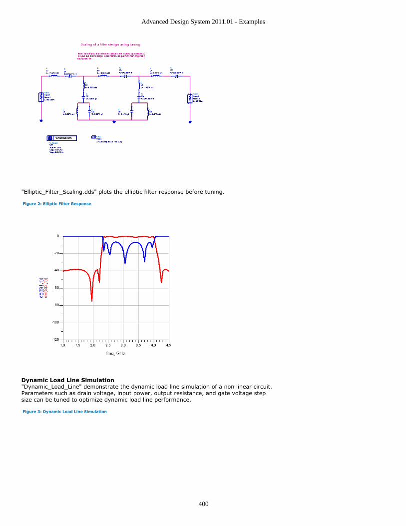
Advanced Design System 2011.01 - Examples
400
"Elliptic_Filter_Scaling.dds" plots the elliptic filter response before tuning.
Figure 2: Elliptic Filter Response
Dynamic Load Line Simulation"Dynamic_Load_Line" demonstrate the dynamic load line simulation of a non linear circuit.Parameters such as drain voltage, input power, output resistance, and gate voltage stepsize can be tuned to optimize dynamic load line performance.
Figure 3: Dynamic Load Line Simulation
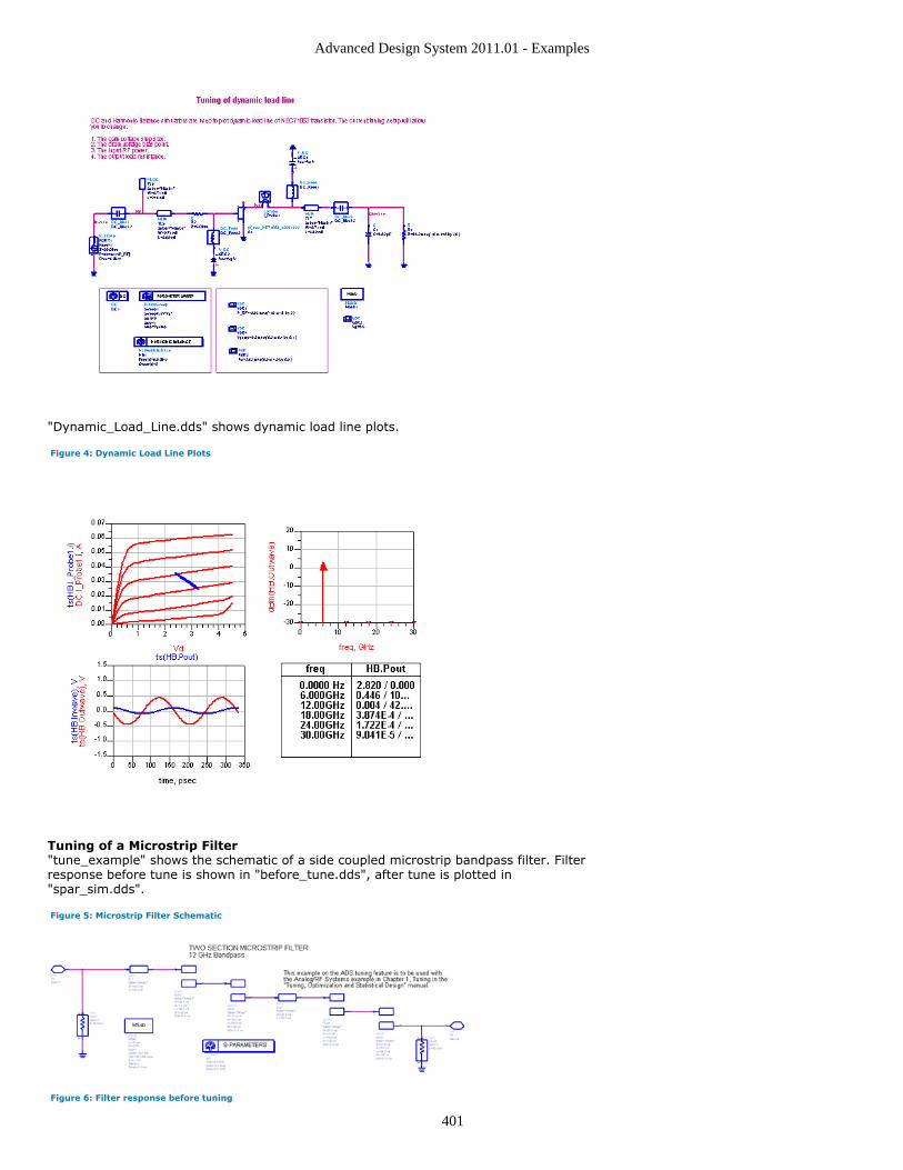
Advanced Design System 2011.01 - Examples
401
"Dynamic_Load_Line.dds" shows dynamic load line plots.
Figure 4: Dynamic Load Line Plots
Tuning of a Microstrip Filter"tune_example" shows the schematic of a side coupled microstrip bandpass filter. Filterresponse before tune is shown in "before_tune.dds", after tune is plotted in"spar_sim.dds".
Figure 5: Microstrip Filter Schematic
Figure 6: Filter response before tuning
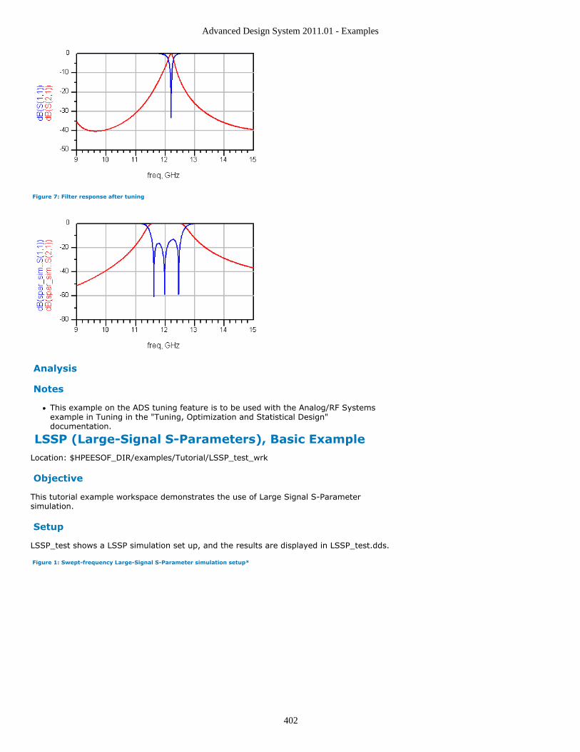
Advanced Design System 2011.01 - Examples
402
Figure 7: Filter response after tuning
Analysis
Notes
This example on the ADS tuning feature is to be used with the Analog/RF Systemsexample in Tuning in the "Tuning, Optimization and Statistical Design"documentation.
LSSP (Large-Signal S-Parameters), Basic ExampleLocation: $HPEESOF_DIR/examples/Tutorial/LSSP_test_wrk
Objective
This tutorial example workspace demonstrates the use of Large Signal S-Parametersimulation.
Setup
LSSP_test shows a LSSP simulation set up, and the results are displayed in LSSP_test.dds.
Figure 1: Swept-frequency Large-Signal S-Parameter simulation setup*
Advanced Design System 2011.01 - Examples
403
SP_test is simply a small-signal S-Parameter simulation of the same circuit.The simulation results are displayed in SP_test.dds.
Analysis
Figure 2: Large-Signal S-Parameter simulation results
Notes
Large-Signal S-Parameter simulation may give erroneous results for the output impedanceof an amplifier. This is because amplifiers are normally driven with a signal at the input,not a large signal at the output with nothing at the input. To determine the outputimpedance of an amplifier while the input is being driven with a large signal, seeexamples/MW_Ckts/LargeSigAmp_wrk/Stab_vs_freq_pwr.
Mixer2 Model Validation Example FileLocation: $HPEESOF_DIR/examples/Tutorial/Mixer2_Example_wrk
Objective
The purpose of this workspace is to validate the Mixer2 system model. This model wasintroduced as a replacement for the Mixer system model for everything but FCAC/Budgetanalysis. In many cases, Mixer and Mixer2 give the same results. In other cases such asTran analysis, multiple RF tones and complex ConvGain values, Mixer2 gives better resultsthan Mixer. In other cases such as reverse conversion, certain feedthru terms, finitesideband suppression, image rejection, AM-to-PM and LO limiting, Mixer2 supportsbehaviors that Mixer does not. This makes Mixer2 the recommended system model formixer modeling for anything but FCAC/Budget analysis.

Advanced Design System 2011.01 - Examples
404
Setup
The following designs (), datasets (.ds) and data displays (*.dds) are included in thisworkspace:
Mixer2_DC: Demonstrates the use of Mixer2 for DC analysis. Mixer and Mixer2 agree.1.Mixer2_Tran: Demonstrates the use of Mixer2 for Tran analysis. Mixer does not2.provide sideband suppression for Tran analysis.Mixer2_HB: Demonstrates the use of Mixer2 for HB analysis. Mixer and Mixer2 agree.3.Mixer2_CE: Demonstrates the use of Mixer2 for CE analysis. Mixer and Mixer2 agree.4.Mixer2_ConvGain_S11: Demonstrates how Mixer2 works when ConvGain and S11 are5.specified. Mixer and Mixer2 agree.Mixer2_ConvGain_S21_S31: Demonstrates how Mixer2 works when S21 and S31 are6.specified. Mixer and Mixer2 agree for S21, but Mixer does not support S31.Mixer2_RevConvGain_S12: Demonstrates how Mixer2 works when RevConvGain and7.S12 are specified. Mixer does not support RevConvGain.Mixer2_RF1_plus_minus_RF2: Demonstrates how Mixer2 passes sums/differences of8.two RF tones provided SP21 and SOI are set properly. Sums/differences of two RFtones are not passed for Mixer.Mixer2_Image_SideBand_Amount: Demonstrates the amount of image rejection and9.sideband suppression provided by the various image/sideband options for Mixer2.Most of these cases are not supported for Mixer.Mixer2_Image_SideBand_ConvGain: Demonstrates how the phase of ConvGain10.affects the phase of the image rejection and sideband suppression provided by thevarious image/sideband options for Mixer2. The phase of ConvGain is handleddifferently for Mixer, leading to confusing results for Mixer.Mixer2_AM2PM: Demonstrates the use of Mixer2 with AM2PM specified. AM2PM is11.demonstrated for a mixer with no compression but is supported for all compressionoptions. AM-to-PM is not supported for Mixer.Mixer2_TOI_GainCompPower_GainComp_HB1tone: Demonstrates the use of Mixer212.with compression parameters specifed. Validates GainCompPower and GainComp.Mixer and Mixer2 agree.Mixer2_TOI_GainCompPower_GainComp_HB2tone: Demonstrates the use of Mixer213.with compression parameters specifed. Validates TOI. Mixer and Mixer2 agree.Mixer2_PminLO: Demonstrates how PminLO affects the IF output of Mixer2. Mixer14.and Mixer2 agree.Mixer2_Nonharmonically_Related_LO_Frequencies: Demonstrates that large DetBW15.values (original Mixer2 LO limiting) should be used for LO limiting when the LO porthas two nonharmonically related tones. Also demonstrates that Mixer2 can do thesame LO limiting that Mixer does, making Mixer2 a superset of Mixer as far as LOlimiting is concerned.Mixer2_Harmonically_Related_LO_Frequencies: Demonstrates that small DetBW16.values (Mixer LO limiting) should be used for LO limiting when the LO port has twoharmonically related tones. Also demonstrates that Mixer2 can do the same LOlimiting that Mixer does, making Mixer2 a superset of Mixer as far as LO limiting isconcerned.Mixer2_GainCompFile_GCOMP1: Demonstrates the use of Mixer2 with a GCOMP117.block specifying the compression. Mixer and Mixer2 agree.Mixer2_GainCompFile_GCOMP7: Demonstrates the use of Mixer2 with a GCOMP718.block specifying the compression. Since the polynomial fitting for Mixer and Mixer2 isnot the same, Mixer and Mixer2 disagree.Mixer2_NonlinearNoise_NF_BOTH: Demonstrates the use of Mixer2 for nonlinear19.noise with NF set and SideBand=BOTH. Mixer and Mixer2 agree.Mixer2_NonlinearNoise_NF_LOWER: Demonstrates the use of Mixer2 for nonlinear20.noise with NF set and SideBand=LOWER. Mixer and Mixer2 agree.Mixer2_NonlinearNoise_NF_LOWER_IMAGE_REJECTION: Demonstrates the use of21.Mixer2 for nonlinear noise with NF set and SideBand=LOWER IMAGE REJECTION.Image rejection is not supported for Mixer.Mixer2_NonlinearNoise_NF_UPPER: Demonstrates the use of Mixer2 for nonlinear22.noise with NF set and SideBand=UPPER. Mixer and Mixer2 agree.Mixer2_NonlinearNoise_NF_UPPER_IMAGE_REJECTION: Demonstrates the use of23.Mixer2 for nonlinear noise with NF set and SideBand=UPPER IMAGE REJECTION.Image rejection is not supported for Mixer.Mixer2_NonlinearNoise_NF_UPPER_IMAGE_REJECTION_PowerSweep: Demonstrates24.how Mixer2 noise properties degrade in compression for a mixer with NF set andSideBand=UPPER IMAGE REJECTION. Image rejection is not supported for Mixer.Mixer2_NonlinearNoise_NFminSoptRn_BOTH: Demonstrates the use of Mixer2 for25.nonlinear noise with (NFmin,Sopt,Rn) set and SideBand=BOTH.Mixer and Mixer2agree.Mixer2_NonlinearNoise_NFminSoptRn_LOWER: Demonstrates the use of Mixer2 for26.nonlinear noise with (NFmin,Sopt,Rn) set and SideBand=LOWER.Mixer and Mixer2agree.
Advanced Design System 2011.01 - Examples
405
Mixer2_NonlinearNoise_NFminSoptRn_LOWER_IMAGE_REJECTION: Demonstrates27.the use of Mixer2 for nonlinear noise with (NFmin,Sopt,Rn) set andSideBand=LOWERIMAGE REJECTION. Image rejection is not supported for Mixer.Mixer2_NonlinearNoise_NFminSoptRn_UPPER: Demonstrates the use of Mixer2 for28.nonlinear noise with (NFmin,Sopt,Rn) set and SideBand=UPPER.Mixer and Mixer2agree.Mixer2_NonlinearNoise_NFminSoptRn_UPPER_IMAGE_REJECTION: Demonstrates the29.use of Mixer2 for nonlinear noise with (NFmin,Sopt,Rn) set andSideBand=UPPERIMAGE REJECTION. Image rejection is not supported for Mixer.Mixer2_NonlinearNoise_NFminSoptRn_UPPER_IMAGE_REJECTION_PowerSweep:30.Demonstrates how Mixer2 noise properties degrade in compression for a mixer with(NFmin,Sopt,Rn) set and SideBand=UPPER IMAGE REJECTION. Image rejection is notsupported for Mixer.
Notes
For more information about Mixer2, see Mixer2 (RF System Mixer) (ccsys).
Noise Power Ratio SimulationLocation: $HPEESOF_DIR/examples/Tutorial/NoisePowerRatio_wrk
Objective
This example shows two methods of simulating noise power ratio and a method ofcharacterizing the distortion generated by an amplifier.
Setup
NarrowBandNPR simulates noise power ratio by generating a narrow band (relative to1.the carrier frequency) noise signal via a bandpass filter and a bandstop filter. TheEnvelope simulator is used, and the noise signal is generated via two baseband noisesources and an I-Q modulator.BPF_wNotchSparams simulates the S-Parameters of the filters used to band-limit the2.noise and generate the notch filter.MultiTone_Test shows how to set-up and simulate an amplifier with multiple input3.tones. This sort of simulation would be of interest to a CATV system or amplifierdesigner. It uses harmonic balance and a Monte Carlo simulation to model multipletones, and is appropriate when you want to simulate a number of tones over a broadfrequency range.
Analysis
Figure 1: Spectra at the Input and Output of the Amplifier in NarrowBandNPR design
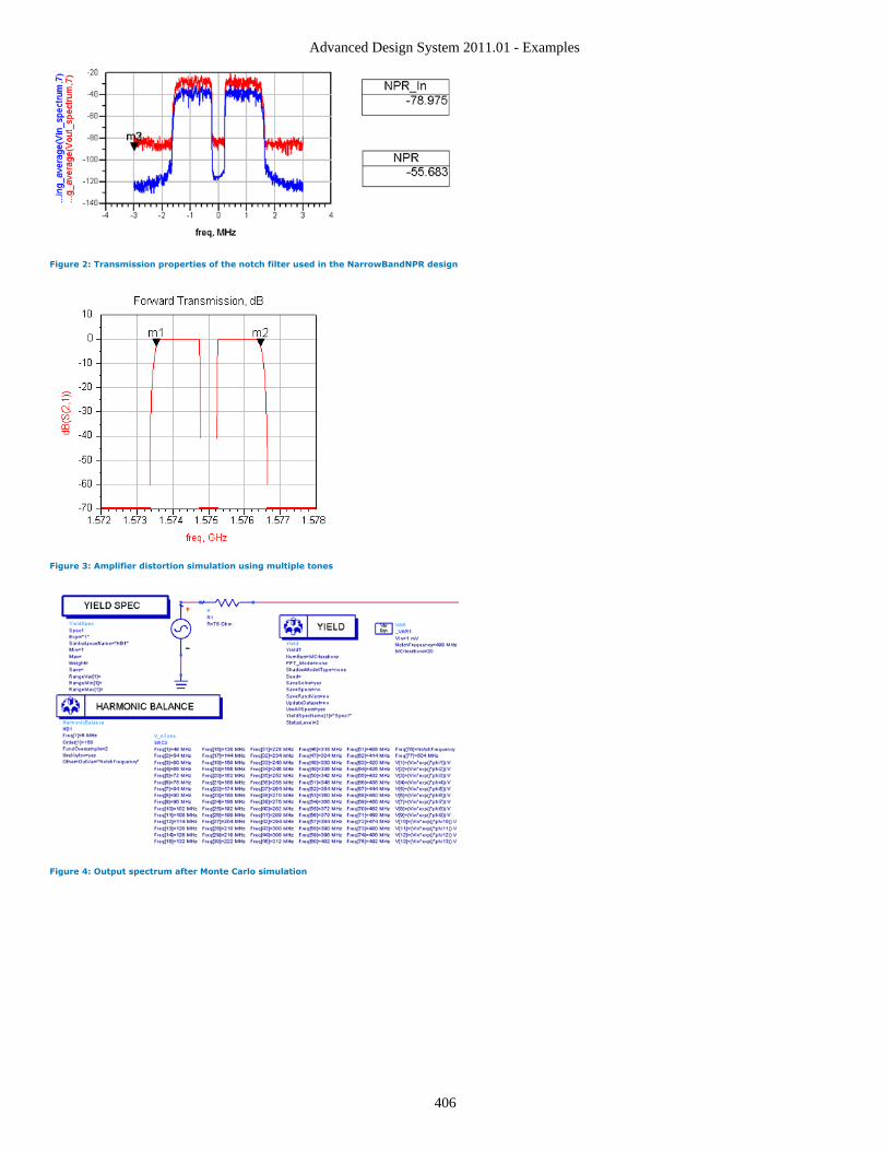
Advanced Design System 2011.01 - Examples
406
Figure 2: Transmission properties of the notch filter used in the NarrowBandNPR design
Figure 3: Amplifier distortion simulation using multiple tones
Figure 4: Output spectrum after Monte Carlo simulation
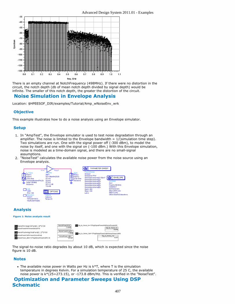
Advanced Design System 2011.01 - Examples
407
There is an empty channel at NotchFrequency (498MHz). If there were no distortion in thecircuit, the notch depth (db of mean notch depth divided by signal depth) would beinfinite. The smaller of this notch depth, the greater the distortion of the circuit.
Noise Simulation in Envelope AnalysisLocation: $HPEESOF_DIR/examples/Tutorial/Amp_wNoiseEnv_wrk
Objective
This example illustrates how to do a noise analysis using an Envelope simulator.
Setup
In "AmpTest", the Envelope simulator is used to test noise degradation through an1.amplifier. The noise is limited to the Envelope bandwidth = 1/(simulation time step).Two simulations are run. One with the signal power off (-300 dBm), to model thenoise by itself, and one with the signal on (-100 dBm.) With this Envelope simulation,noise is modeled as a time-domain signal, and there are no small-signalassumptions."NoiseTest" calculates the available noise power from the noise source using an2.Envelope analysis.
Analysis
Figure 1: Noise analysis result
The signal-to-noise ratio degrades by about 10 dB, which is expected since the noisefigure is 10 dB.
Notes
The available noise power in Watts per Hz is k*T, where T is the simulationtemperature in degrees Kelvin. For a simulation temperature of 25 C, the availablenoise power is k*(25+273.15), or -173.8 dBm/Hz. This is verified in the "NoiseTest".
Optimization and Parameter Sweeps Using DSPSchematic
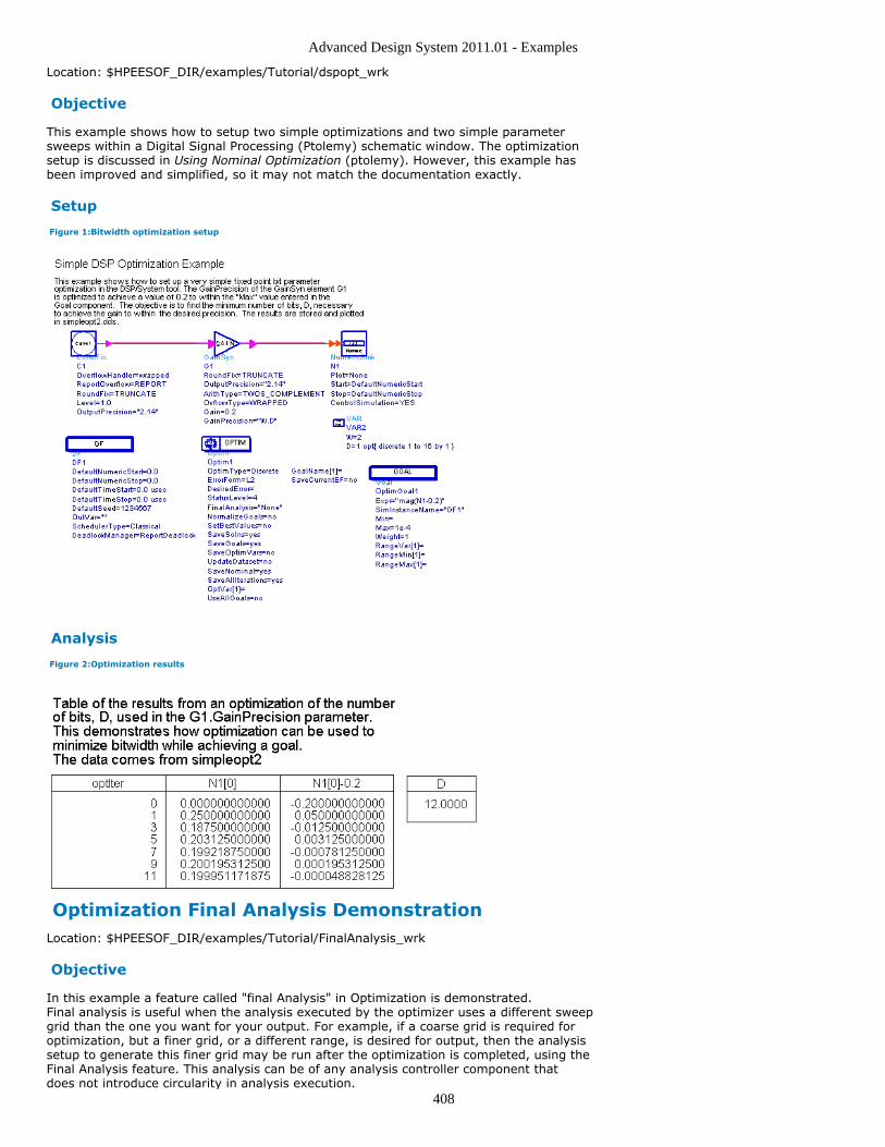
Advanced Design System 2011.01 - Examples
408
Location: $HPEESOF_DIR/examples/Tutorial/dspopt_wrk
Objective
This example shows how to setup two simple optimizations and two simple parametersweeps within a Digital Signal Processing (Ptolemy) schematic window. The optimizationsetup is discussed in Using Nominal Optimization (ptolemy). However, this example hasbeen improved and simplified, so it may not match the documentation exactly.
Setup
Figure 1:Bitwidth optimization setup
Analysis
Figure 2:Optimization results
Optimization Final Analysis DemonstrationLocation: $HPEESOF_DIR/examples/Tutorial/FinalAnalysis_wrk
Objective
In this example a feature called "final Analysis" in Optimization is demonstrated.Final analysis is useful when the analysis executed by the optimizer uses a different sweepgrid than the one you want for your output. For example, if a coarse grid is required foroptimization, but a finer grid, or a different range, is desired for output, then the analysissetup to generate this finer grid may be run after the optimization is completed, using theFinal Analysis feature. This analysis can be of any analysis controller component thatdoes not introduce circularity in analysis execution.
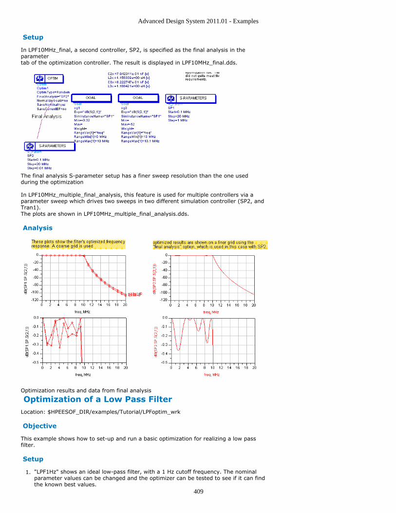
Advanced Design System 2011.01 - Examples
409
Setup
In LPF10MHz_final, a second controller, SP2, is specified as the final analysis in theparametertab of the optimization controller. The result is displayed in LPF10MHz_final.dds.
The final analysis S-parameter setup has a finer sweep resolution than the one usedduring the optimization
In LPF10MHz_multiple_final_analysis, this feature is used for multiple controllers via aparameter sweep which drives two sweeps in two different simulation controller (SP2, andTran1).The plots are shown in LPF10MHz_multiple_final_analysis.dds.
Analysis
Optimization results and data from final analysis
Optimization of a Low Pass FilterLocation: $HPEESOF_DIR/examples/Tutorial/LPFoptim_wrk
Objective
This example shows how to set-up and run a basic optimization for realizing a low passfilter.
Setup
"LPF1Hz" shows an ideal low-pass filter, with a 1 Hz cutoff frequency. The nominal1.parameter values can be changed and the optimizer can be tested to see if it can findthe known best values.
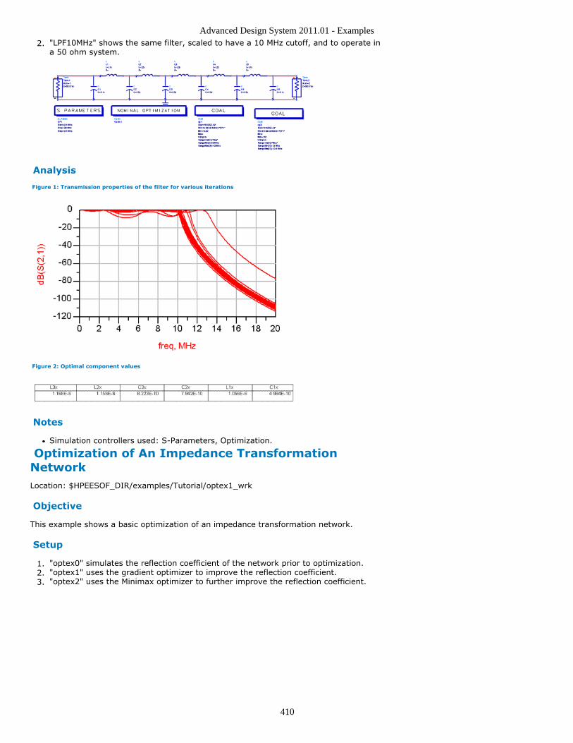
Advanced Design System 2011.01 - Examples
410
"LPF10MHz" shows the same filter, scaled to have a 10 MHz cutoff, and to operate in2.a 50 ohm system.
Analysis
Figure 1: Transmission properties of the filter for various iterations
Figure 2: Optimal component values
Notes
Simulation controllers used: S-Parameters, Optimization.
Optimization of An Impedance TransformationNetworkLocation: $HPEESOF_DIR/examples/Tutorial/optex1_wrk
Objective
This example shows a basic optimization of an impedance transformation network.
Setup
"optex0" simulates the reflection coefficient of the network prior to optimization.1."optex1" uses the gradient optimizer to improve the reflection coefficient.2."optex2" uses the Minimax optimizer to further improve the reflection coefficient.3.
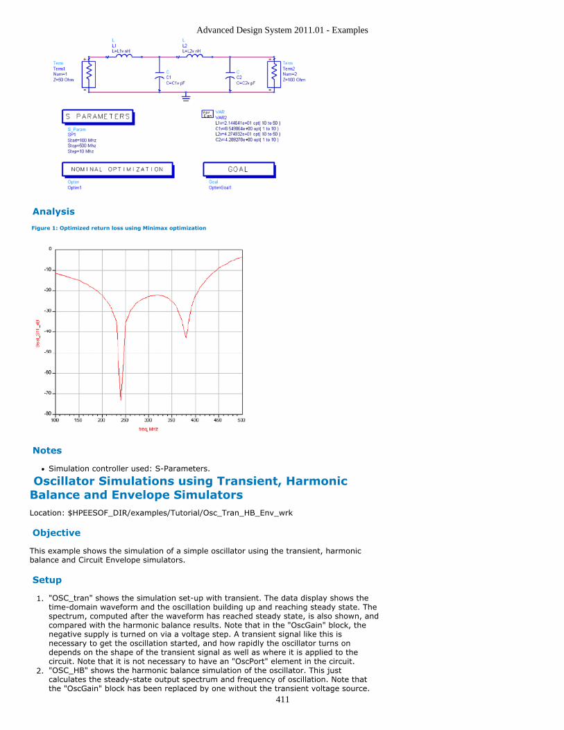
Advanced Design System 2011.01 - Examples
411
Analysis
Figure 1: Optimized return loss using Minimax optimization
Notes
Simulation controller used: S-Parameters.
Oscillator Simulations using Transient, HarmonicBalance and Envelope SimulatorsLocation: $HPEESOF_DIR/examples/Tutorial/Osc_Tran_HB_Env_wrk
Objective
This example shows the simulation of a simple oscillator using the transient, harmonicbalance and Circuit Envelope simulators.
Setup
"OSC_tran" shows the simulation set-up with transient. The data display shows the1.time-domain waveform and the oscillation building up and reaching steady state. Thespectrum, computed after the waveform has reached steady state, is also shown, andcompared with the harmonic balance results. Note that in the "OscGain" block, thenegative supply is turned on via a voltage step. A transient signal like this isnecessary to get the oscillation started, and how rapidly the oscillator turns ondepends on the shape of the transient signal as well as where it is applied to thecircuit. Note that it is not necessary to have an "OscPort" element in the circuit."OSC_HB" shows the harmonic balance simulation of the oscillator. This just2.calculates the steady-state output spectrum and frequency of oscillation. Note thatthe "OscGain" block has been replaced by one without the transient voltage source.
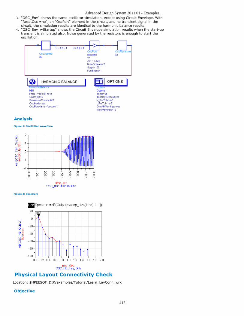
Advanced Design System 2011.01 - Examples
412
"OSC_Env" shows the same oscillator simulation, except using Circuit Envelope. With3."ResetOsc =no", an "OscPort" element in the circuit, and no transient signal in thecircuit, the simulation results are identical to the harmonic balance results."OSC_Env_wStartup" shows the Circuit Envelope simulation results when the start-up4.transient is simulated also. Noise generated by the resistors is enough to start theoscillation.
Analysis
Figure 1: Oscillation waveform
Figure 2: Spectrum
Physical Layout Connectivity CheckLocation: $HPEESOF_DIR/examples/Tutorial/Learn_LayConn_wrk
Objective
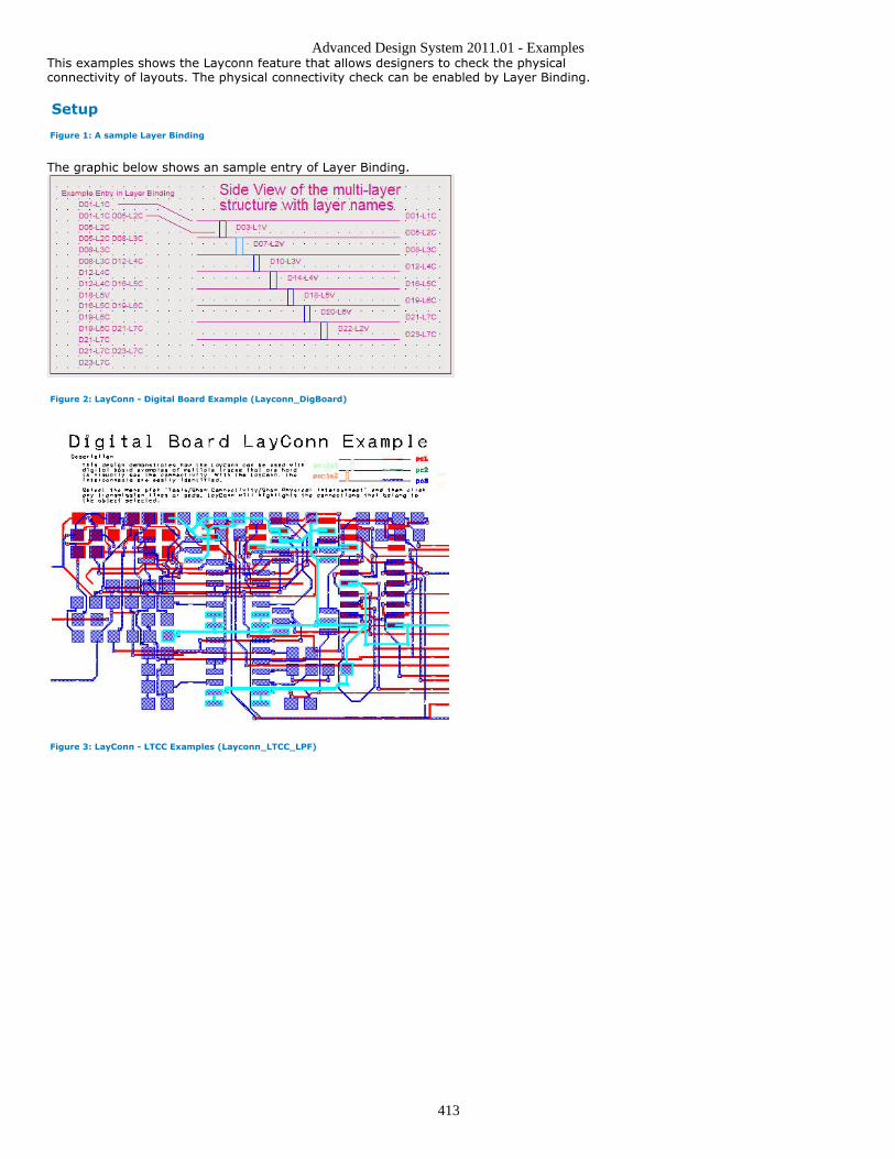
Advanced Design System 2011.01 - Examples
413
This examples shows the Layconn feature that allows designers to check the physicalconnectivity of layouts. The physical connectivity check can be enabled by Layer Binding.
Setup
Figure 1: A sample Layer Binding
The graphic below shows an sample entry of Layer Binding.
Figure 2: LayConn - Digital Board Example (Layconn_DigBoard)
Figure 3: LayConn - LTCC Examples (Layconn_LTCC_LPF)
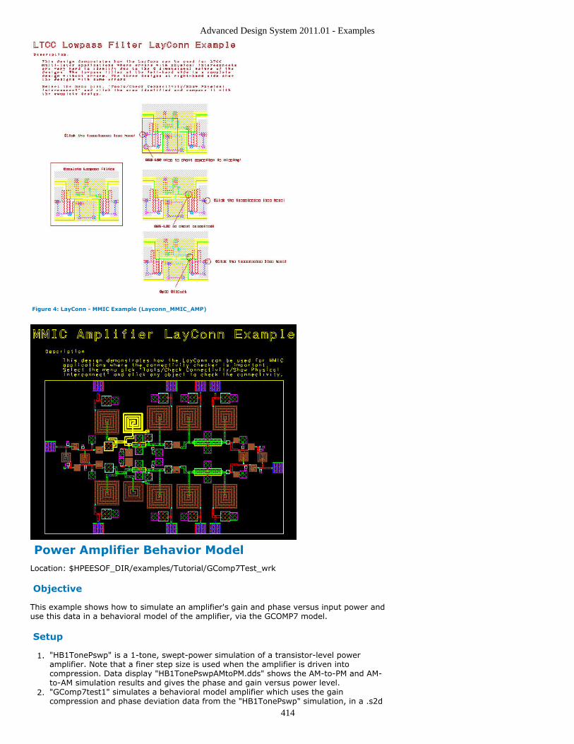
Advanced Design System 2011.01 - Examples
414
Figure 4: LayConn - MMIC Example (Layconn_MMIC_AMP)
Power Amplifier Behavior ModelLocation: $HPEESOF_DIR/examples/Tutorial/GComp7Test_wrk
Objective
This example shows how to simulate an amplifier's gain and phase versus input power anduse this data in a behavioral model of the amplifier, via the GCOMP7 model.
Setup
"HB1TonePswp" is a 1-tone, swept-power simulation of a transistor-level power1.amplifier. Note that a finer step size is used when the amplifier is driven intocompression. Data display "HB1TonePswpAMtoPM.dds" shows the AM-to-PM and AM-to-AM simulation results and gives the phase and gain versus power level."GComp7test1" simulates a behavioral model amplifier which uses the gain2.compression and phase deviation data from the "HB1TonePswp" simulation, in a .s2d
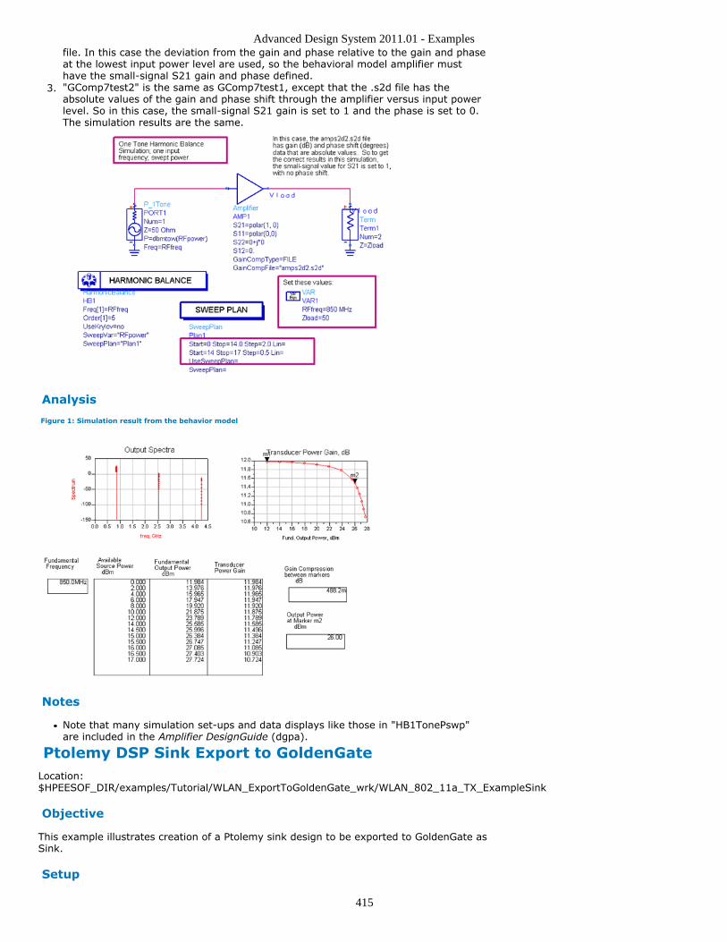
Advanced Design System 2011.01 - Examples
415
file. In this case the deviation from the gain and phase relative to the gain and phaseat the lowest input power level are used, so the behavioral model amplifier musthave the small-signal S21 gain and phase defined."GComp7test2" is the same as GComp7test1, except that the .s2d file has the3.absolute values of the gain and phase shift through the amplifier versus input powerlevel. So in this case, the small-signal S21 gain is set to 1 and the phase is set to 0.The simulation results are the same.
Analysis
Figure 1: Simulation result from the behavior model
Notes
Note that many simulation set-ups and data displays like those in "HB1TonePswp"are included in the Amplifier DesignGuide (dgpa).
Ptolemy DSP Sink Export to GoldenGateLocation:$HPEESOF_DIR/examples/Tutorial/WLAN_ExportToGoldenGate_wrk/WLAN_802_11a_TX_ExampleSink
Objective
This example illustrates creation of a Ptolemy sink design to be exported to GoldenGate asSink.
Setup
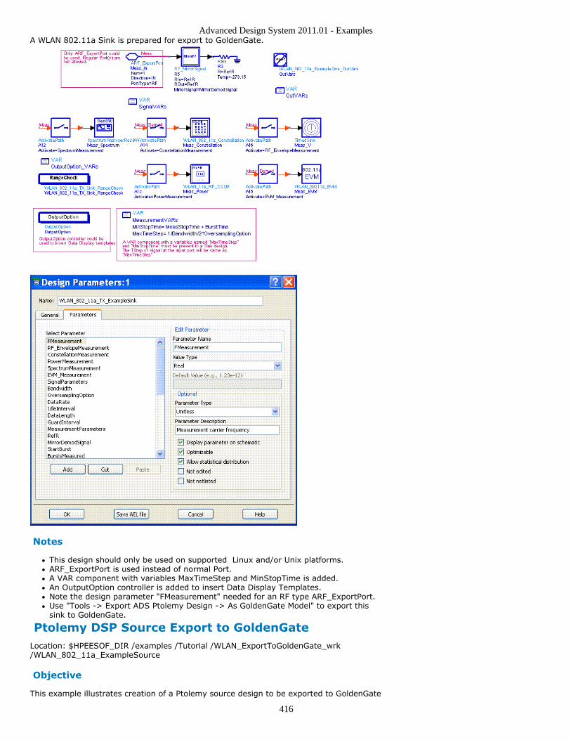
Advanced Design System 2011.01 - Examples
416
A WLAN 802.11a Sink is prepared for export to GoldenGate.
Notes
This design should only be used on supported Linux and/or Unix platforms.ARF_ExportPort is used instead of normal Port.A VAR component with variables MaxTimeStep and MinStopTime is added.An OutputOption controller is added to insert Data Display Templates.Note the design parameter "FMeasurement" needed for an RF type ARF_ExportPort.Use "Tools -> Export ADS Ptolemy Design -> As GoldenGate Model" to export thissink to GoldenGate.
Ptolemy DSP Source Export to GoldenGateLocation: $HPEESOF_DIR /examples /Tutorial /WLAN_ExportToGoldenGate_wrk/WLAN_802_11a_ExampleSource
Objective
This example illustrates creation of a Ptolemy source design to be exported to GoldenGate
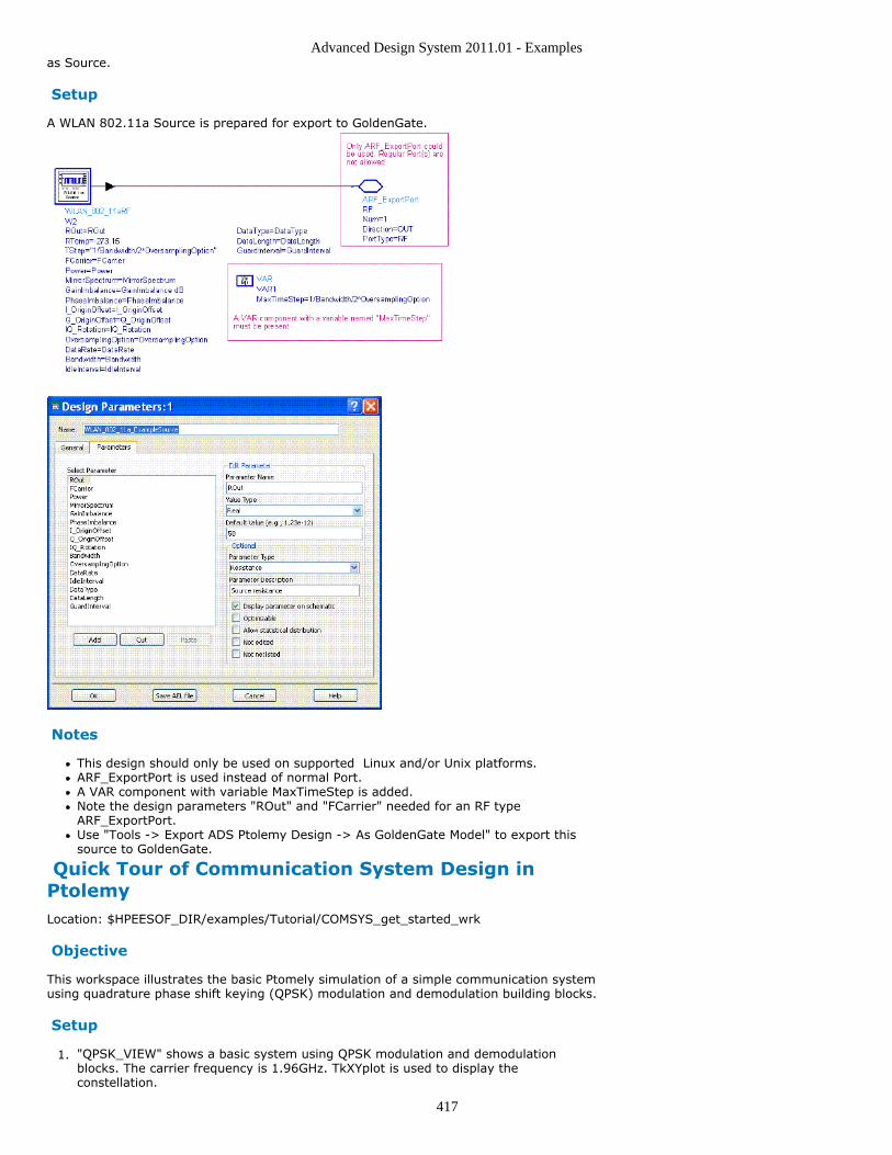
Advanced Design System 2011.01 - Examples
417
as Source.
Setup
A WLAN 802.11a Source is prepared for export to GoldenGate.
Notes
This design should only be used on supported Linux and/or Unix platforms.ARF_ExportPort is used instead of normal Port.A VAR component with variable MaxTimeStep is added.Note the design parameters "ROut" and "FCarrier" needed for an RF typeARF_ExportPort.Use "Tools -> Export ADS Ptolemy Design -> As GoldenGate Model" to export thissource to GoldenGate.
Quick Tour of Communication System Design inPtolemyLocation: $HPEESOF_DIR/examples/Tutorial/COMSYS_get_started_wrk
Objective
This workspace illustrates the basic Ptomely simulation of a simple communication systemusing quadrature phase shift keying (QPSK) modulation and demodulation building blocks.
Setup
"QPSK_VIEW" shows a basic system using QPSK modulation and demodulation1.blocks. The carrier frequency is 1.96GHz. TkXYplot is used to display theconstellation.
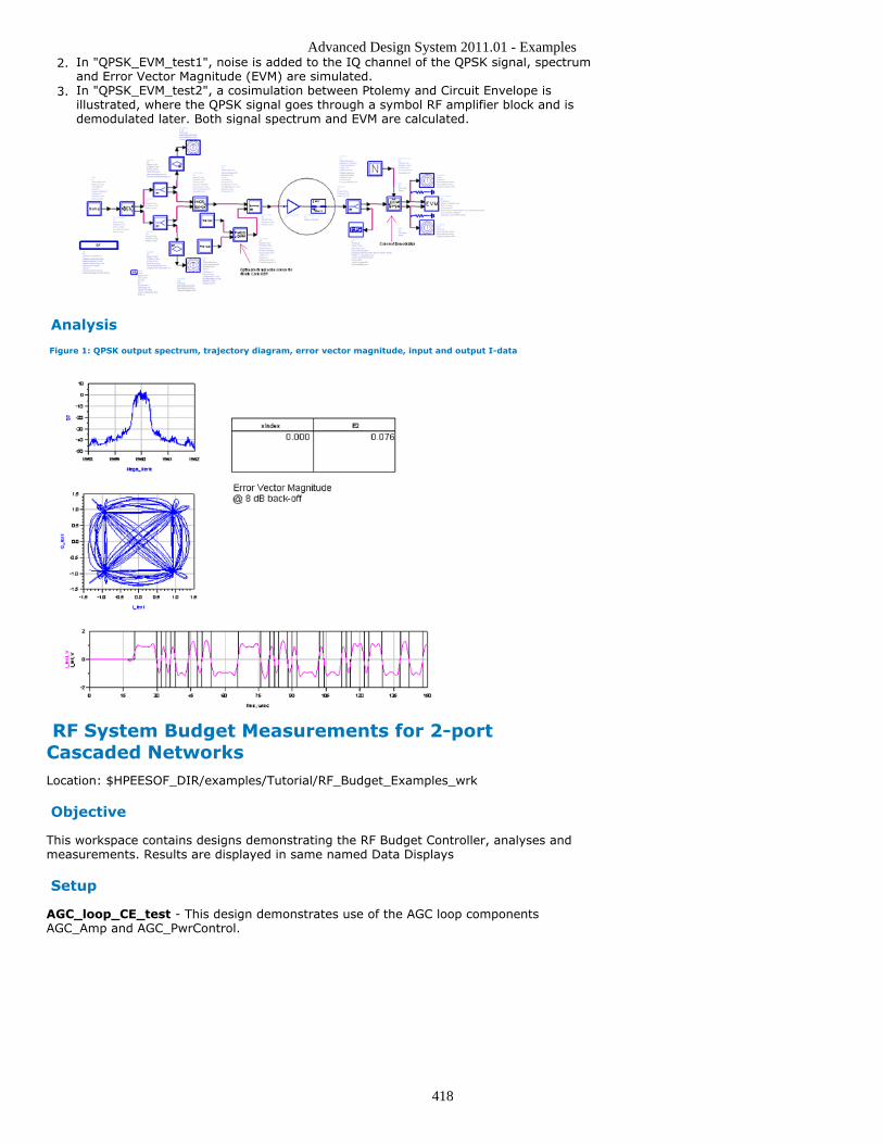
Advanced Design System 2011.01 - Examples
418
In "QPSK_EVM_test1", noise is added to the IQ channel of the QPSK signal, spectrum2.and Error Vector Magnitude (EVM) are simulated.In "QPSK_EVM_test2", a cosimulation between Ptolemy and Circuit Envelope is3.illustrated, where the QPSK signal goes through a symbol RF amplifier block and isdemodulated later. Both signal spectrum and EVM are calculated.
Analysis
Figure 1: QPSK output spectrum, trajectory diagram, error vector magnitude, input and output I-data
RF System Budget Measurements for 2-portCascaded NetworksLocation: $HPEESOF_DIR/examples/Tutorial/RF_Budget_Examples_wrk
Objective
This workspace contains designs demonstrating the RF Budget Controller, analyses andmeasurements. Results are displayed in same named Data Displays
Setup
AGC_loop_CE_test - This design demonstrates use of the AGC loop componentsAGC_Amp and AGC_PwrControl.
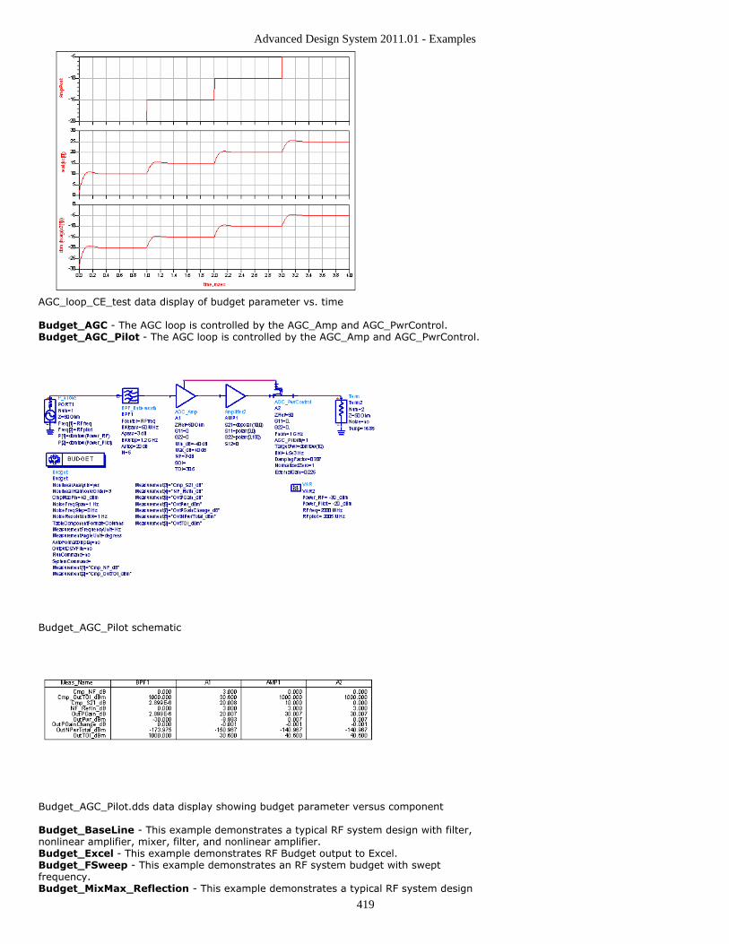
Advanced Design System 2011.01 - Examples
419
AGC_loop_CE_test data display of budget parameter vs. time
Budget_AGC - The AGC loop is controlled by the AGC_Amp and AGC_PwrControl.Budget_AGC_Pilot - The AGC loop is controlled by the AGC_Amp and AGC_PwrControl.
Budget_AGC_Pilot schematic
Budget_AGC_Pilot.dds data display showing budget parameter versus component
Budget_BaseLine - This example demonstrates a typical RF system design with filter,nonlinear amplifier, mixer, filter, and nonlinear amplifier.Budget_Excel - This example demonstrates RF Budget output to Excel.Budget_FSweep - This example demonstrates an RF system budget with sweptfrequency.Budget_MixMax_Reflection - This example demonstrates a typical RF system design
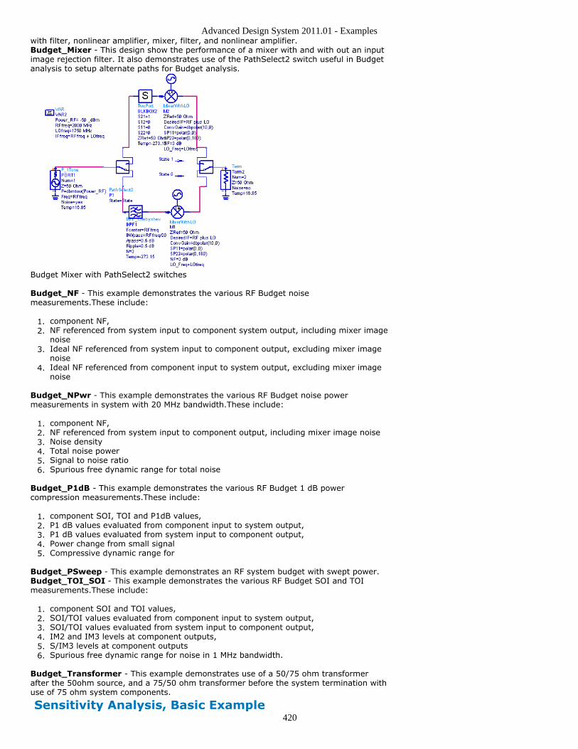
Advanced Design System 2011.01 - Examples
420
with filter, nonlinear amplifier, mixer, filter, and nonlinear amplifier.Budget_Mixer - This design show the performance of a mixer with and with out an inputimage rejection filter. It also demonstrates use of the PathSelect2 switch useful in Budgetanalysis to setup alternate paths for Budget analysis.
Budget Mixer with PathSelect2 switches
Budget_NF - This example demonstrates the various RF Budget noisemeasurements.These include:
component NF,1.NF referenced from system input to component system output, including mixer image2.noiseIdeal NF referenced from system input to component output, excluding mixer image3.noiseIdeal NF referenced from component input to system output, excluding mixer image4.noise
Budget_NPwr - This example demonstrates the various RF Budget noise powermeasurements in system with 20 MHz bandwidth.These include:
component NF,1.NF referenced from system input to component output, including mixer image noise2.Noise density3.Total noise power4.Signal to noise ratio5.Spurious free dynamic range for total noise6.
Budget_P1dB - This example demonstrates the various RF Budget 1 dB powercompression measurements.These include:
component SOI, TOI and P1dB values,1.P1 dB values evaluated from component input to system output,2.P1 dB values evaluated from system input to component output,3.Power change from small signal4.Compressive dynamic range for5.
Budget_PSweep - This example demonstrates an RF system budget with swept power.Budget_TOI_SOI - This example demonstrates the various RF Budget SOI and TOImeasurements.These include:
component SOI and TOI values,1.SOI/TOI values evaluated from component input to system output,2.SOI/TOI values evaluated from system input to component output,3.IM2 and IM3 levels at component outputs,4.S/IM3 levels at component outputs5.Spurious free dynamic range for noise in 1 MHz bandwidth.6.
Budget_Transformer - This example demonstrates use of a 50/75 ohm transformerafter the 50ohm source, and a 75/50 ohm transformer before the system termination withuse of 75 ohm system components.
Sensitivity Analysis, Basic Example
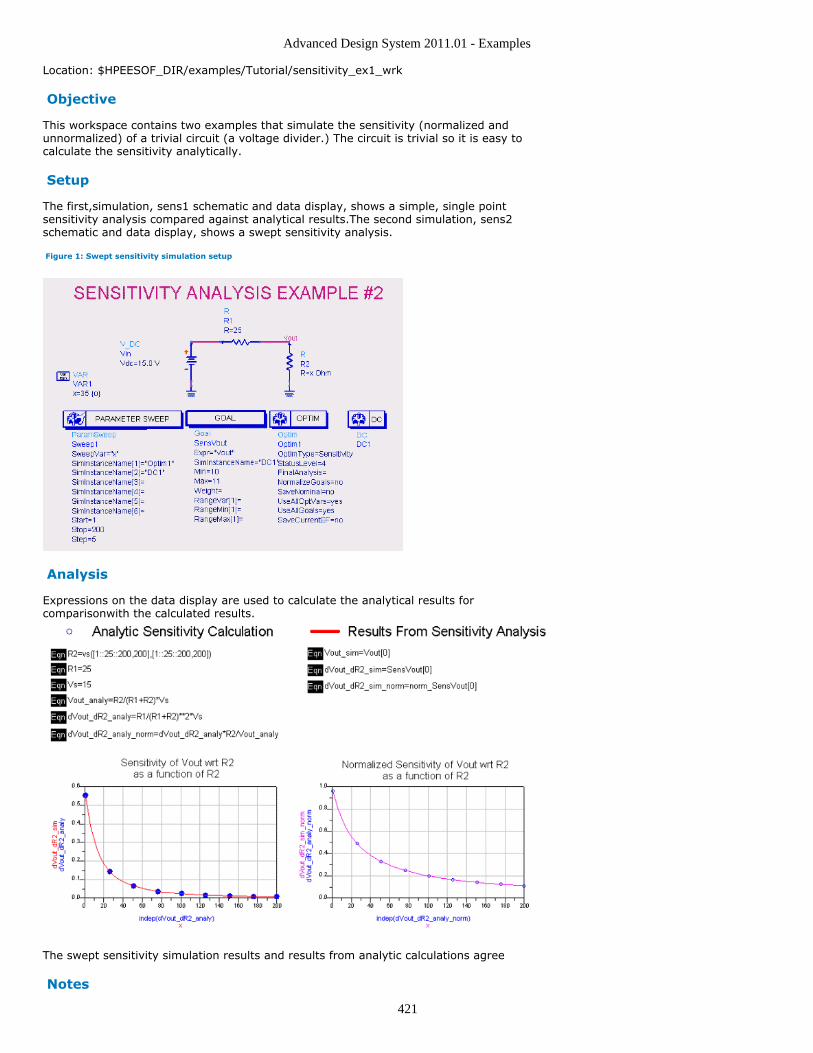
Advanced Design System 2011.01 - Examples
421
Location: $HPEESOF_DIR/examples/Tutorial/sensitivity_ex1_wrk
Objective
This workspace contains two examples that simulate the sensitivity (normalized andunnormalized) of a trivial circuit (a voltage divider.) The circuit is trivial so it is easy tocalculate the sensitivity analytically.
Setup
The first,simulation, sens1 schematic and data display, shows a simple, single pointsensitivity analysis compared against analytical results.The second simulation, sens2schematic and data display, shows a swept sensitivity analysis.
Figure 1: Swept sensitivity simulation setup
Analysis
Expressions on the data display are used to calculate the analytical results forcomparisonwith the calculated results.
The swept sensitivity simulation results and results from analytic calculations agree
Notes
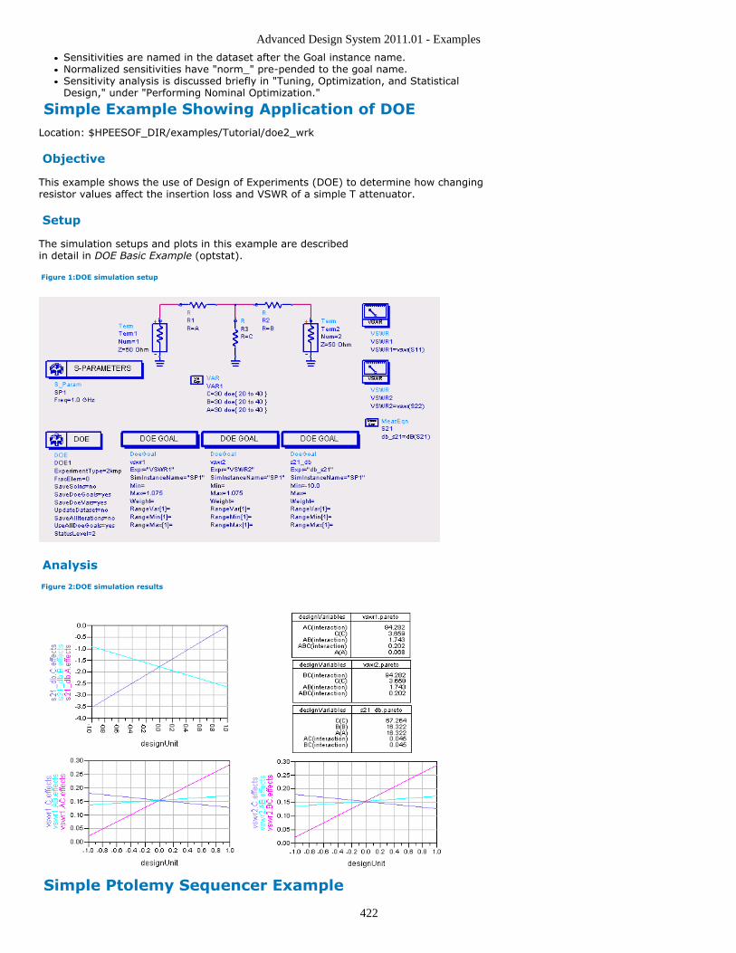
Advanced Design System 2011.01 - Examples
422
Sensitivities are named in the dataset after the Goal instance name.Normalized sensitivities have "norm_" pre-pended to the goal name.Sensitivity analysis is discussed briefly in "Tuning, Optimization, and StatisticalDesign," under "Performing Nominal Optimization."
Simple Example Showing Application of DOELocation: $HPEESOF_DIR/examples/Tutorial/doe2_wrk
Objective
This example shows the use of Design of Experiments (DOE) to determine how changingresistor values affect the insertion loss and VSWR of a simple T attenuator.
Setup
The simulation setups and plots in this example are describedin detail in DOE Basic Example (optstat).
Figure 1:DOE simulation setup
Analysis
Figure 2:DOE simulation results
Simple Ptolemy Sequencer Example
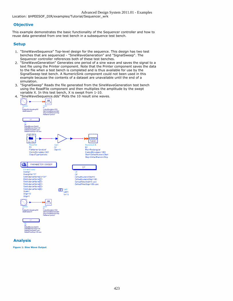
Advanced Design System 2011.01 - Examples
423
Location: $HPEESOF_DIR/examples/Tutorial/Sequencer_wrk
Objective
This example demonstrates the basic functionality of the Sequencer controller and how toreuse data generated from one test bench in a subsequence test bench.
Setup
"SineWaveSequence" Top-level design for the sequence. This design has two test1.benches that are sequenced - "SineWaveGeneration" and "SignalSweep". TheSequencer controller references both of these test benches."SineWaveGeneration" Generates one period of a sine wave and saves the signal to a2.text file using the Printer component. Note that the Printer component saves the datato the file when a test bench is completed and is thus available for use by theSignalSweep test bench. A NumericSink component could not been used in thisexample because the contents of a dataset are unavailable until the end of asimulation."SignalSweep" Reads the file generated from the SineWaveGeneration test bench3.using the ReadFile component and then multiplies the amplitude by the sweptvariable X. In this test bench, X is swept from 1-10."SineWaveSequence.dds" Plots the 10 result sine waves.4.
Analysis
Figure 1: Sine Wave Output
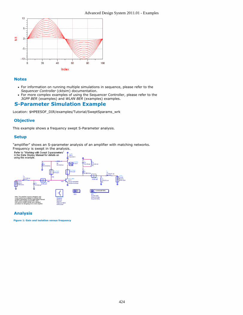
Advanced Design System 2011.01 - Examples
424
Notes
For information on running multiple simulations in sequence, please refer to theSequencer Controller (cktsim) documentation.For more complex examples of using the Sequencer Controller, please refer to the3GPP BER (examples) and WLAN BER (examples) examples.
S-Parameter Simulation ExampleLocation: $HPEESOF_DIR/examples/Tutorial/SweptSparams_wrk
Objective
This example shows a frequency swept S-Parameter analysis.
Setup
"amplifier" shows an S-parameter analysis of an amplifier with matching networks.Frequency is swept in the analysis.
Analysis
Figure 1: Gain and isolation versus frequency
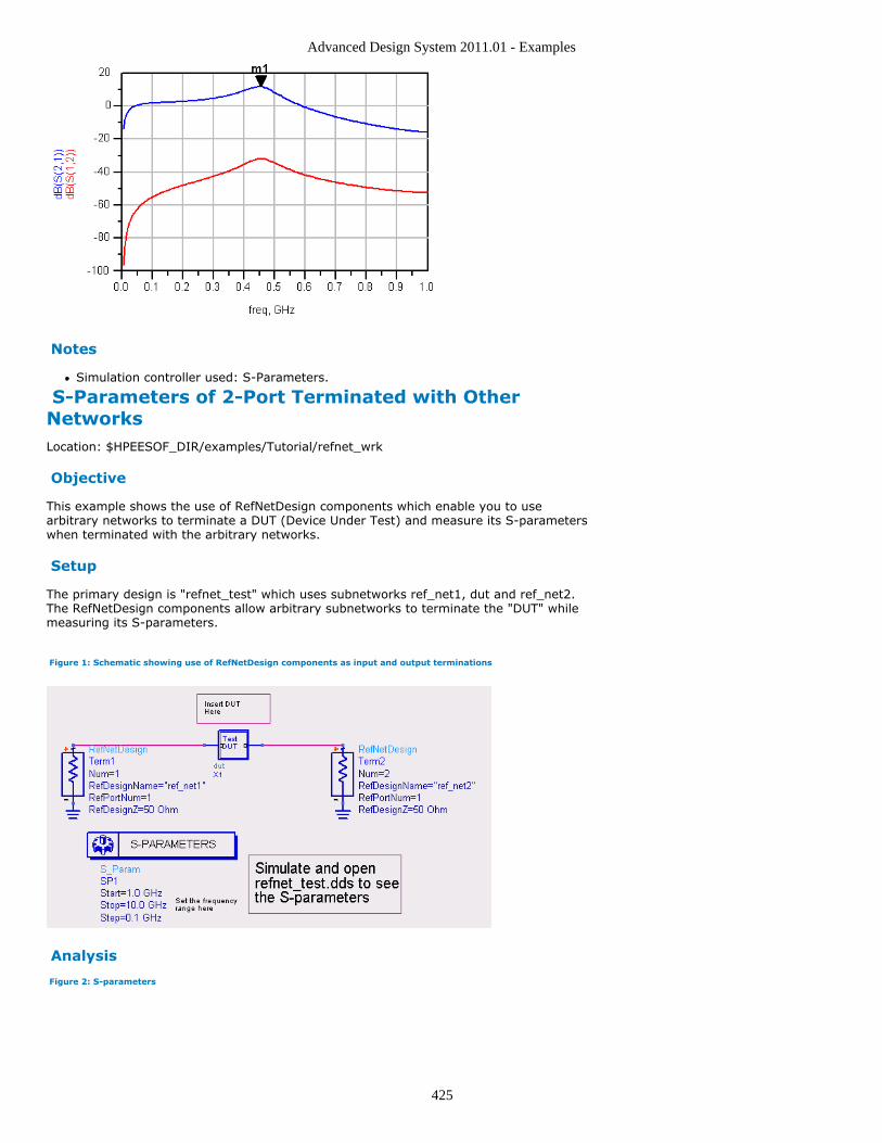
Advanced Design System 2011.01 - Examples
425
Notes
Simulation controller used: S-Parameters.
S-Parameters of 2-Port Terminated with OtherNetworksLocation: $HPEESOF_DIR/examples/Tutorial/refnet_wrk
Objective
This example shows the use of RefNetDesign components which enable you to usearbitrary networks to terminate a DUT (Device Under Test) and measure its S-parameterswhen terminated with the arbitrary networks.
Setup
The primary design is "refnet_test" which uses subnetworks ref_net1, dut and ref_net2.The RefNetDesign components allow arbitrary subnetworks to terminate the "DUT" whilemeasuring its S-parameters.
Figure 1: Schematic showing use of RefNetDesign components as input and output terminations
Analysis
Figure 2: S-parameters
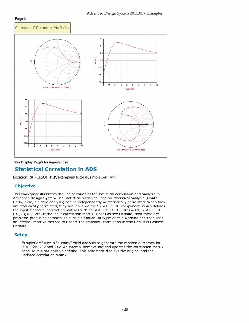
Advanced Design System 2011.01 - Examples
426
Statistical Correlation in ADSLocation: $HPEESOF_DIR/examples/Tutorial/simpleCorr_wrk
Objective
This workspace illustrates the use of variables for statistical correlation and analysis inAdvanced Design System.The Statistical variables used for statistical analysis (MonteCarlo, Yield, Yieldopt analysis) can be independently or statistically correlated. When theyare statistically correlated, they are input via the "STAT CORR" component, which definesthe input statistical correlation matrix (such as STAT CORR (R1 , R2) =0.9, STATCORR(R1,R3)=-9, etc).If the input correlation matrix is not Positive Definite, then there areproblems producing samples. In such a situation, ADS provides a warning and then usesan internal iterative method to update the statistical correlation matrix until it is PositiveDefinite.
Setup
"simpleCorr" uses a "dummy" yield analysis to generate the random outcomes for1.R1v, R2v, R3v and R4v. An internal iterative method updates the correlation matrixbecause it is not positive definite. This schematic displays the original and theupdated correlation matrix.
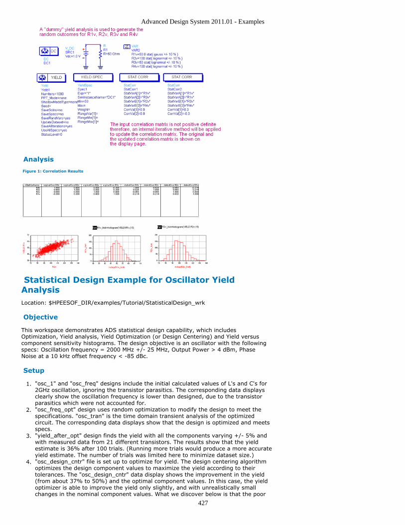
Advanced Design System 2011.01 - Examples
427
Analysis
Figure 1: Correlation Results
Statistical Design Example for Oscillator YieldAnalysisLocation: $HPEESOF_DIR/examples/Tutorial/StatisticalDesign_wrk
Objective
This workspace demonstrates ADS statistical design capability, which includesOptimization, Yield analysis, Yield Optimization (or Design Centering) and Yield versuscomponent sensitivity histograms. The design objective is an oscillator with the followingspecs: Oscillation frequency = 2000 MHz +/- 25 MHz, Output Power > 4 dBm, PhaseNoise at a 10 kHz offset frequency < -85 dBc.
Setup
"osc_1" and "osc_freq" designs include the initial calculated values of L's and C's for1.2GHz oscillation, ignoring the transistor parasitics. The corresponding data displaysclearly show the oscillation frequency is lower than designed, due to the transistorparasitics which were not accounted for."osc_freq_opt" design uses random optimization to modify the design to meet the2.specifications. "osc_tran" is the time domain transient analysis of the optimizedcircuit. The corresponding data displays show that the design is optimized and meetsspecs."yield_after_opt" design finds the yield with all the components varying +/- 5% and3.with measured data from 21 different transistors. The results show that the yieldestimate is 36% after 100 trials. (Running more trials would produce a more accurateyield estimate. The number of trials was limited here to minimize dataset size.)"osc_design_cntr" file is set up to optimize for yield. The design centering algorithm4.optimizes the design component values to maximize the yield according to theirtolerances. The "osc_design_cntr" data display shows the improvement in the yield(from about 37% to 50%) and the optimal component values. In this case, the yieldoptimizer is able to improve the yield only slightly, and with unrealistically smallchanges in the nominal component values. What we discover below is that the poor
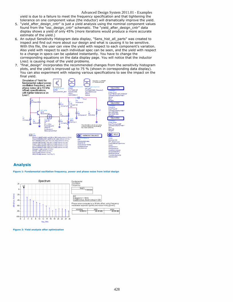
Advanced Design System 2011.01 - Examples
428
yield is due to a failure to meet the frequency specification and that tightening thetolerance on one component value (the inductor) will dramatically improve the yield."yield_after_design_cntr" is just a yield analysis using the nominal component values5.found from the "osc_design_cntr" schematic. The "yield_after_design_cntr" datadisplay shows a yield of only 45% (more iterations would produce a more accurateestimate of the yield.)An output Sensitivity Histogram data display, "Sens_hist_all_parts" was created to6.inspect and find out more about our design and what is causing it to be sensitive.With this file, the user can view the yield with respect to each component's variation.Also yield with respect to each individual spec can be seen, and the yield with respectto a change in specs can be updated instantantly. You have to change thecorresponding equations on the data display page. You will notice that the inductorLres1 is causing most of the yield problems."final_design" incorporates the recommended changes from the sensitivity histogram7.plots, and the yield is improved up to 75 % (shown in corresponding data display).You can also experiment with relaxing various specifications to see the impact on thefinal yield.
Analysis
Figure 1: Fundamental oscillation frequency, power and phase noise from initial design
Figure 2: Yield analysis after optimization
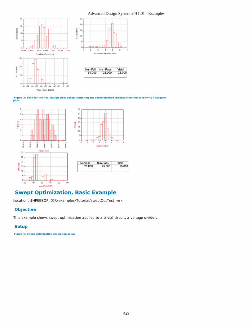
Advanced Design System 2011.01 - Examples
429
Figure 3: Yield for the final design after design centering and recommended changes from the sensitivity histogramplots
Swept Optimization, Basic ExampleLocation: $HPEESOF_DIR/examples/Tutorial/sweptOptTest_wrk
Objective
This example shows swept optimization applied to a trivial circuit, a voltage divider.
Setup
Figure 1: Swept optimization simulation setup
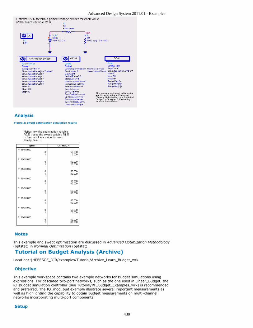
Advanced Design System 2011.01 - Examples
430
Analysis
Figure 2: Swept optimization simulation results
Notes
This example and swept optimization are discussed in Advanced Optimization Methodology(optstat) in Nominal Optimization (optstat).
Tutorial on Budget Analysis (Archive)Location: $HPEESOF_DIR/examples/Tutorial/Archive_Learn_Budget_wrk
Objective
This example workspace contains two example networks for Budget simulations usingexpressions. For cascaded two-port networks, such as the one used in Linear_Budget, theRF Budget simulation controller (see Tutorial/RF_Budget_Examples_wrk) is recommendedand preferred. The IQ_mod_bud example illustrate several important measurements aswell as highlighting the capability to obtain Budget measurements on multi-channelnetworks incorporating multi-port components.
Setup
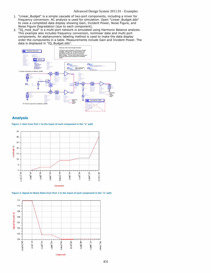
Advanced Design System 2011.01 - Examples
431
"Linear_Budget" is a simple cascade of two-port components, including a mixer for1.frequency conversion. AC analysis is used for simulation. Open "Linear_Budget.dds"to view a completed data display showing Gain, Incident Power, Noise Figure, andNoise Figure Degradation (due to each component)."IQ_mod_bud" is a multi-port network is simulated using Harmonic Balance analysis.2.This example also includes frequency conversion, nonlinear data and multi-portcomponents. An alphanumeric labeling method is used to make the data displayorder the components in a table. Measurements include Gain and Incident Power. Thedata is displayed in "IQ_Budget.dds".
Analysis
Figure 1: Gain from Port 1 to the Input of each component in the "a" path
Figure 2: Signal-to-Noise Ratio from Port 1 to the Input of each component in the "a" path

Advanced Design System 2011.01 - Examples
432
Notes
For cascaded two-port networks such as Linear_Budget, the RF Budget controller isrecommended and preferred. Please see Tutorial/RF_Budget_Examples_wrk.
The AC Analysis Controller is not included with design "Linear_Budget". Please seeUsing Circuit Simulators for RF System Analysis (cktsim).
User-Compiled Model ExamplesLocation: $HPEESOF_DIR/examples/Tutorial/UserCompiledModel_wrk
Objective
This workspace has several examples of User-Compiled Models.
Setup
MutInd model shows two coupled inductors. MutInd_test shows that the simulation resultswith user-compiled mutual inductor are consistent with simulation results with built-inMUC2 component.
PNDIODE model is a nonlinear, user-compiled model of a PN diode.PNDIODE_test is a test design of this model in a circuit.
U2PA model is a model of three resistors in a "PI" connection.The equivalent circuit of theU2PA model is given in U2PA_test.
U2PB model is a coaxial line component. U2PB_test is a test of the model.
U2PC model is a lossy transmission line. U2PC_test is a test of the model.
RepeatParam_R is a simple resistor model. It demonstrates how to access the value of arepeated parameter.
VectorValue_R is a simple resistor model. It demonstrates how to access a parameterwhich has vector values.
Res is a simple resistor model. It demonstrates how to define parameters through anotherUCM model.
ucm_SnP is a UserCompiledModel version SnP model. It demontrates how to use a UCMmodel which supports variable number of external nodes.ucm_SnP_test is a test of the 2-port ucm_SnP model and the 3-port ucm_SnP model.
UCM_Param_Test is the test of RepeatParam_R, VectorValue_R and VariableNodes_R.
Notes
Please note that this workspace only contains model source code. You must compile andlink the models in order to run a simulation. To do this for the PNDIODE model, open thePNDIODE symbol view. Select Tools > User-Compiled Model > Open User-CompiledModel. In the User-Compiled Circuit Model dialog that appears, the No. of Internal Nodesshould be 1 below the Model Code and, Transient Function should be checked below CodeOptions. Click Compile in the User-Compiled Circuit Model dialog. When you see the"Compile and link complete" message, click OK. Now you can run a simulation.
User-compiled models are discussed in "User-Defined Models," in "Building User-CompiledAnalog Models."
Using DataAccessComponent (DAC) and S2PMDIFComponentLocation: $HPEESOF_DIR/examples/Tutorial/DataAccess_wrk
Objective
This example shows several ways of accessing data. Most of the designs use theDataAccessComponent (DAC). Others show using S2PMDIF component to accessmeasured S-Parameter data.
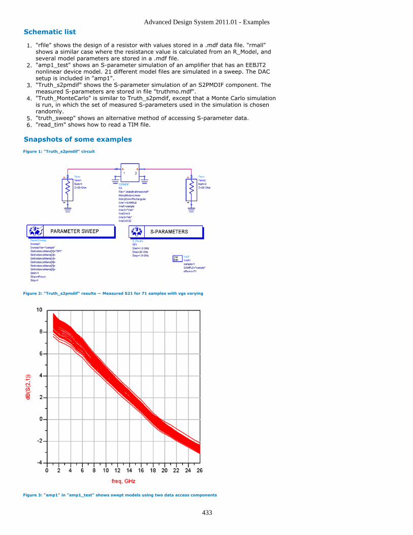
Advanced Design System 2011.01 - Examples
433
Schematic list
"rfile" shows the design of a resistor with values stored in a .mdf data file. "rmall"1.shows a similar case where the resistance value is calculated from an R_Model, andseveral model parameters are stored in a .mdf file."amp1_test" shows an S-parameter simulation of an amplifier that has an EEBJT22.nonlinear device model. 21 different model files are simulated in a sweep. The DACsetup is included in "amp1"."Truth_s2pmdif" shows the S-parameter simulation of an S2PMDIF component. The3.measured S-parameters are stored in file "truthmo.mdf"."Truth_MonteCarlo" is similar to Truth_s2pmdif, except that a Monte Carlo simulation4.is run, in which the set of measured S-parameters used in the simulation is chosenrandomly."truth_sweep" shows an alternative method of accessing S-parameter data.5."read_tim" shows how to read a TIM file.6.
Snapshots of some examples
Figure 1: "Truth_s2pmdif" circuit
Figure 2: "Truth_s2pmdif" results — Measured S21 for 71 samples with vgs varying
Figure 3: "amp1" in "amp1_test" shows swept models using two data access components
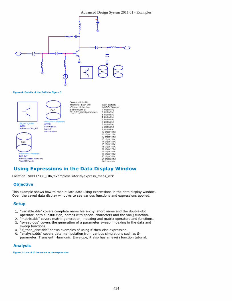
Advanced Design System 2011.01 - Examples
434
Figure 4: Details of the DACs in Figure 3
Using Expressions in the Data Display WindowLocation: $HPEESOF_DIR/examples/Tutorial/express_meas_wrk
Objective
This example shows how to manipulate data using expressions in the data display window.Open the saved data display windows to see various functions and expressions applied.
Setup
"variable.dds" covers complete name hierarchy, short name and the double-dot1.operator, path substitution, names with special characters and the var() function."matrix.dds" covers matrix generation, indexing and matrix operators and functions.2."sweep.dds" covers the generation of a parameter sweep, indexing in the data and3.sweep functions."if_then_else.dds" shows examples of using if-then-else expression.4."analysis.dds" covers data manipulation from various simulations such as S-5.parameter, Transient, Harmonic, Envelope, it also has an eye() function tutorial.
Analysis
Figure 1: Use of if-then-else in the expression
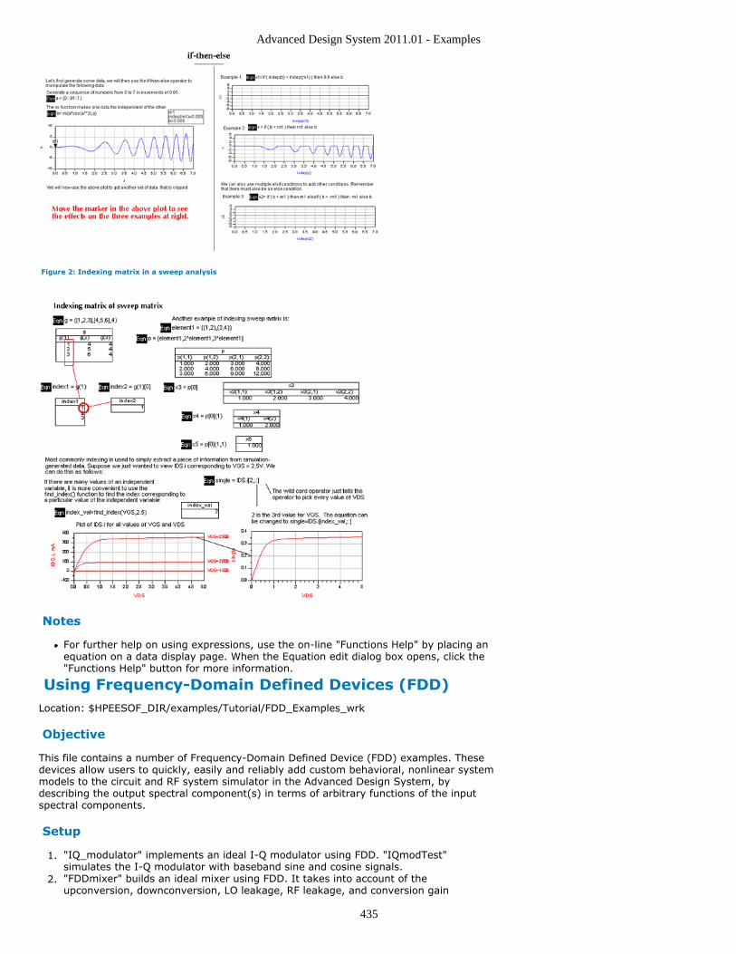
Advanced Design System 2011.01 - Examples
435
Figure 2: Indexing matrix in a sweep analysis
Notes
For further help on using expressions, use the on-line "Functions Help" by placing anequation on a data display page. When the Equation edit dialog box opens, click the"Functions Help" button for more information.
Using Frequency-Domain Defined Devices (FDD)Location: $HPEESOF_DIR/examples/Tutorial/FDD_Examples_wrk
Objective
This file contains a number of Frequency-Domain Defined Device (FDD) examples. Thesedevices allow users to quickly, easily and reliably add custom behavioral, nonlinear systemmodels to the circuit and RF system simulator in the Advanced Design System, bydescribing the output spectral component(s) in terms of arbitrary functions of the inputspectral components.
Setup
"IQ_modulator" implements an ideal I-Q modulator using FDD. "IQmodTest"1.simulates the I-Q modulator with baseband sine and cosine signals."FDDmixer" builds an ideal mixer using FDD. It takes into account of the2.upconversion, downconversion, LO leakage, RF leakage, and conversion gain
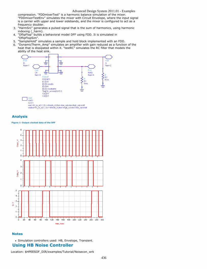
Advanced Design System 2011.01 - Examples
436
compression. "FDDmixerTest" is a harmonic balance simulation of the mixer."FDDmixerTestEnv" simulates the mixer with Circuit Envelope, where the input signalis a carrier with upper and lower sidebands, and the mixer is configured to act as afrequency doubler."HarmSrc" generates a pulsed signal that is the sum of harmonics, using harmonic3.indexing (_harm)."DflipFlop" builds a behavioral model DFF using FDD. It is simulated in4."DflipFlopSim"."SampleHold" simulates a sample and hold block implemented with an FDD.5."DynamicTherm_Amp" simulates an amplifier with gain reduced as a function of the6.heat that is dissipated within it. "testRC" simulates the RC filter that models theability of the heat sink.
Analysis
Figure 1: Output clocked data of the DFF
Notes
Simulation controllers used: HB, Envelope, Transient.
Using HB Noise ControllerLocation: $HPEESOF_DIR/examples/Tutorial/Noisecon_wrk
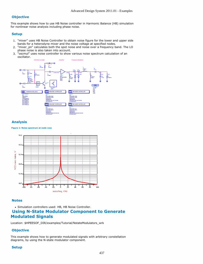
Advanced Design System 2011.01 - Examples
437
Objective
This example shows how to use HB Noise controller in Harmonic Balance (HB) simulationfor nonlinear noise analysis including phase noise.
Setup
"mixer" uses HB Noise Controller to obtain noise figure for the lower and upper side1.bands for a heterodyne mixer and the noise voltage at specified nodes."mixer_pn" calculates both the spot noise and noise over a frequency band. The LO2.phase noise is also taken into account."oscmul" uses noise controller to show various noise spectrum calculation of an3.oscillator.
Analysis
Figure 1: Noise spectrum at node vosc
Notes
Simulation controllers used: HB, HB Noise Controller.
Using N-State Modulator Component to GenerateModulated SignalsLocation: $HPEESOF_DIR/examples/Tutorial/NstateModulators_wrk
Objective
This example shows how to generate modulated signals with arbitrary constellationdiagrams, by using the N-state modulator component.
Setup
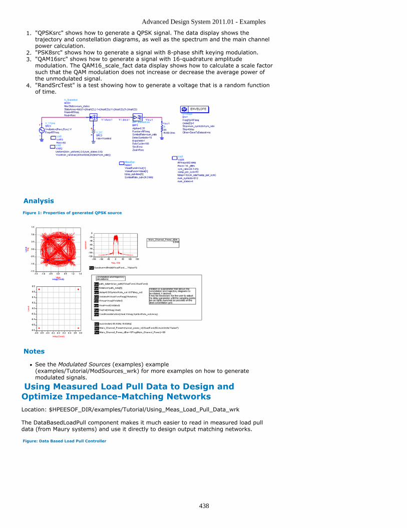
Advanced Design System 2011.01 - Examples
438
"QPSKsrc" shows how to generate a QPSK signal. The data display shows the1.trajectory and constellation diagrams, as well as the spectrum and the main channelpower calculation."PSK8src" shows how to generate a signal with 8-phase shift keying modulation.2."QAM16src" shows how to generate a signal with 16-quadrature amplitude3.modulation. The QAM16_scale_fact data display shows how to calculate a scale factorsuch that the QAM modulation does not increase or decrease the average power ofthe unmodulated signal."RandSrcTest" is a test showing how to generate a voltage that is a random function4.of time.
Analysis
Figure 1: Properties of generated QPSK source
Notes
See the Modulated Sources (examples) example(examples/Tutorial/ModSources_wrk) for more examples on how to generatemodulated signals.
Using Measured Load Pull Data to Design andOptimize Impedance-Matching NetworksLocation: $HPEESOF_DIR/examples/Tutorial/Using_Meas_Load_Pull_Data_wrk
The DataBasedLoadPull component makes it much easier to read in measured load pulldata (from Maury systems) and use it directly to design output matching networks.
Figure: Data Based Load Pull Controller
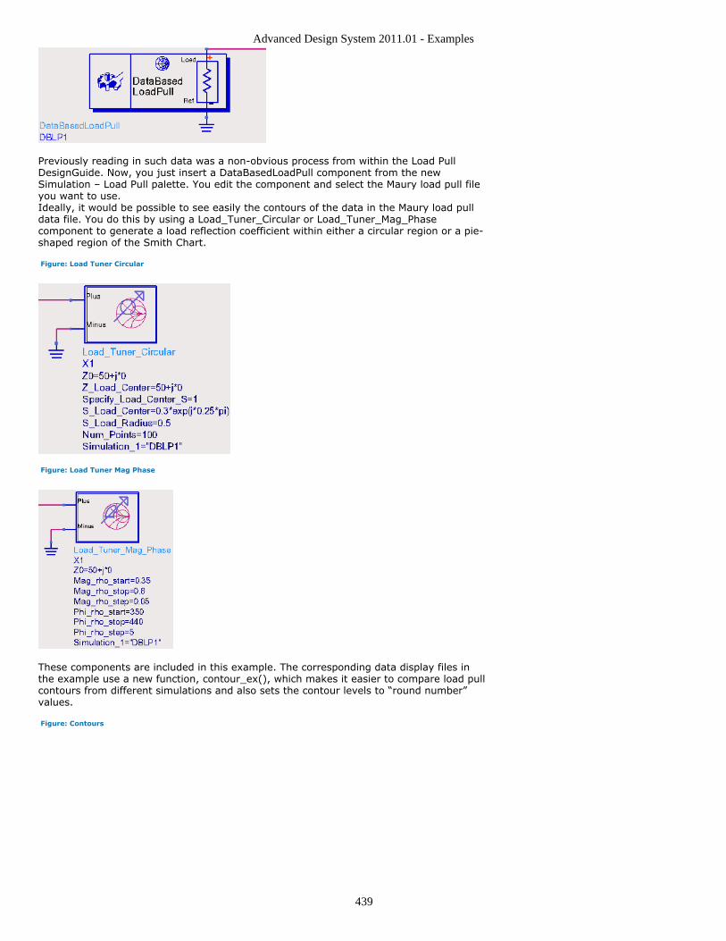
Advanced Design System 2011.01 - Examples
439
Previously reading in such data was a non-obvious process from within the Load PullDesignGuide. Now, you just insert a DataBasedLoadPull component from the newSimulation – Load Pull palette. You edit the component and select the Maury load pull fileyou want to use.Ideally, it would be possible to see easily the contours of the data in the Maury load pulldata file. You do this by using a Load_Tuner_Circular or Load_Tuner_Mag_Phasecomponent to generate a load reflection coefficient within either a circular region or a pie-shaped region of the Smith Chart.
Figure: Load Tuner Circular
Figure: Load Tuner Mag Phase
These components are included in this example. The corresponding data display files inthe example use a new function, contour_ex(), which makes it easier to compare load pullcontours from different simulations and also sets the contour levels to “round number”values.
Figure: Contours
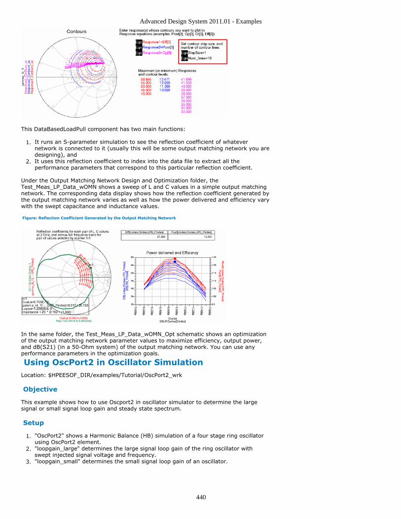
Advanced Design System 2011.01 - Examples
440
This DataBasedLoadPull component has two main functions:
It runs an S-parameter simulation to see the reflection coefficient of whatever1.network is connected to it (usually this will be some output matching network you aredesigning), andIt uses this reflection coefficient to index into the data file to extract all the2.performance parameters that correspond to this particular reflection coefficient.
Under the Output Matching Network Design and Optimization folder, theTest_Meas_LP_Data_wOMN shows a sweep of L and C values in a simple output matchingnetwork. The corresponding data display shows how the reflection coefficient generated bythe output matching network varies as well as how the power delivered and efficiency varywith the swept capacitance and inductance values.
Figure: Reflection Coefficient Generated by the Output Matching Network
In the same folder, the Test_Meas_LP_Data_wOMN_Opt schematic shows an optimizationof the output matching network parameter values to maximize efficiency, output power,and dB(S21) (in a 50-Ohm system) of the output matching network. You can use anyperformance parameters in the optimization goals.
Using OscPort2 in Oscillator SimulationLocation: $HPEESOF_DIR/examples/Tutorial/OscPort2_wrk
Objective
This example shows how to use Oscport2 in oscillator simulator to determine the largesignal or small signal loop gain and steady state spectrum.
Setup
"OscPort2" shows a Harmonic Balance (HB) simulation of a four stage ring oscillator1.using OscPort2 element."loopgain_large" determines the large signal loop gain of the ring oscillator with2.swept injected signal voltage and frequency."loopgain_small" determines the small signal loop gain of an oscillator.3.
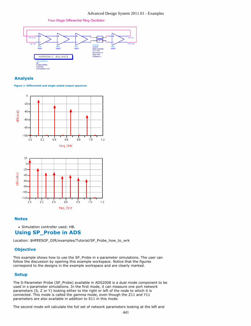
Advanced Design System 2011.01 - Examples
441
Analysis
Figure 1: Differential and single ended output spectrum
Notes
Simulation controller used: HB.
Using SP_Probe in ADSLocation: $HPEESOF_DIR/examples/Tutorial/SP_Probe_how_to_wrk
Objective
This example shows how to use the SP_Probe in s-parameter simulations. The user canfollow the discussion by opening this example workspace. Notice that the figurescorrespond to the designs in the example workspace and are clearly marked.
Setup
The S-Parameter Probe (SP_Probe) available in ADS2008 is a dual mode component to beused in s-parameter simulations. In the first mode, it can measure one port networkparameters (S, Z or Y) looking either to the right or left of the node to which it isconnected. This mode is called the gamma mode, even though the Z11 and Y11parameters are also available in addition to S11 in this mode.
The second mode will calculate the full set of network parameters looking at the left and
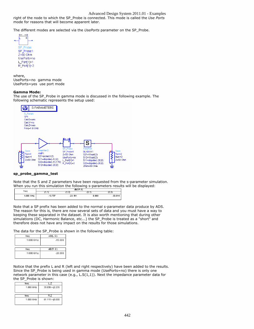
Advanced Design System 2011.01 - Examples
442
right of the node to which the SP_Probe is connected. This mode is called the Use Portsmode for reasons that will become apparent later.
The different modes are selected via the UsePorts parameter on the SP_Probe.
where,UsePorts=no gamma modeUsePorts=yes use port mode
Gamma Mode:The use of the SP_Probe in gamma mode is discussed in the following example. Thefollowing schematic represents the setup used:
sp_probe_gamma_test
Note that the S and Z parameters have been requested from the s-parameter simulation.When you run this simulation the following s-parameters results will be displayed:
Note that a SP prefix has been added to the normal s-parameter data produce by ADS.The reason for this is, there are now several sets of data and you must have a way tokeeping these separated in the dataset. It is also worth mentioning that during othersimulations (DC, Harmonic Balance, etc...) the SP_Probe is treated as a "short" andtherefore does not have any impact on the results for those simulations.
The data for the SP_Probe is shown in the following table:
Notice that the prefix L and R (left and right respectively) have been added to the results.Since the SP_Probe is being used in gamma mode (UsePorts=no) there is only onenetwork parameter in this case (e.g., L.S(1,1)). Next the impedance parameter data forthe SP_Probe is shown:
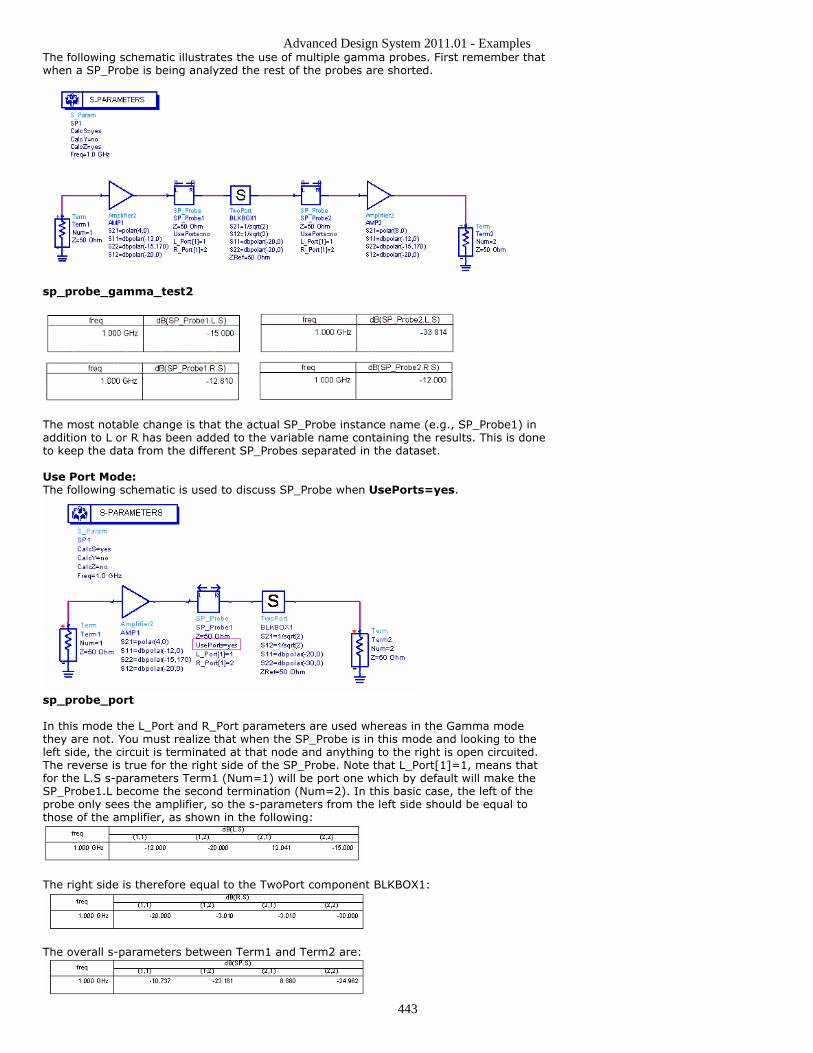
Advanced Design System 2011.01 - Examples
443
The following schematic illustrates the use of multiple gamma probes. First remember thatwhen a SP_Probe is being analyzed the rest of the probes are shorted.
sp_probe_gamma_test2
The most notable change is that the actual SP_Probe instance name (e.g., SP_Probe1) inaddition to L or R has been added to the variable name containing the results. This is doneto keep the data from the different SP_Probes separated in the dataset.
Use Port Mode:The following schematic is used to discuss SP_Probe when UsePorts=yes.
sp_probe_port
In this mode the L_Port and R_Port parameters are used whereas in the Gamma modethey are not. You must realize that when the SP_Probe is in this mode and looking to theleft side, the circuit is terminated at that node and anything to the right is open circuited.The reverse is true for the right side of the SP_Probe. Note that L_Port[1]=1, means thatfor the L.S s-parameters Term1 (Num=1) will be port one which by default will make theSP_Probe1.L become the second termination (Num=2). In this basic case, the left of theprobe only sees the amplifier, so the s-parameters from the left side should be equal tothose of the amplifier, as shown in the following:
The right side is therefore equal to the TwoPort component BLKBOX1:
The overall s-parameters between Term1 and Term2 are:
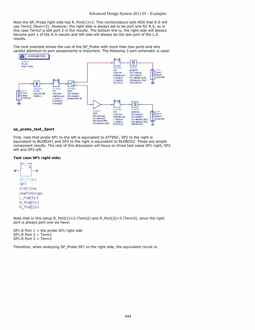
Advanced Design System 2011.01 - Examples
444
Note the SP_Probe right side has R_Port[1]=2. This nomenclature tells ADS that R.S willuse Term2 (Num=2). However, the right side is always set to be port one for R.S, so inthis case Term2 is still port 2 in the results. The bottom line is, the right side will alwaysbecome port 1 of the R.S results and left side will always be the last port of the L.Sresults.
The next example shows the use of the SP_Probe with more than two ports and whycareful attention to port assignments is important. The following 3 port schematic is used:
sp_probe_test_3port
First, note that probe SP1 to the left is equivalent to ATTEN1, SP2 to the right isequivalent to BLKBOX1 and SP3 to the right is equivalent to BLKBOX2. These are simplecomponent results. The rest of this discussion will focus on three test cases SP1 right, SP2left and SP3 left.
Test case SP1 right side:
Note that in this setup R_Port[1]=2 (Term2) and R_Port[2]=3 (Term3), since the rightport is always port one we have:
SP1.R Port 1 = the probe SP1 right sideSP1.R Port 2 = Term2SP1.R Port 3 = Term3
Therefore, when analyzing SP_Probe SP1 to the right side, the equivalent circuit is:
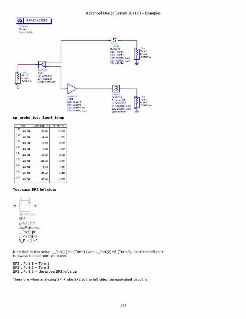
Advanced Design System 2011.01 - Examples
445
sp_probe_test_3port_temp
Test case SP2 left side:
Note that in this setup L_Port[1]=1 (Term1) and L_Port[2]=3 (Term3), since the left portis always the last port we have:
SP2.L Port 1 = Term1SP2.L Port 2 = Term3SP2.L Port 3 = the probe SP2 left side
Therefore when analyzing SP_Probe SP2 to the left side, the equivalent circuit is:
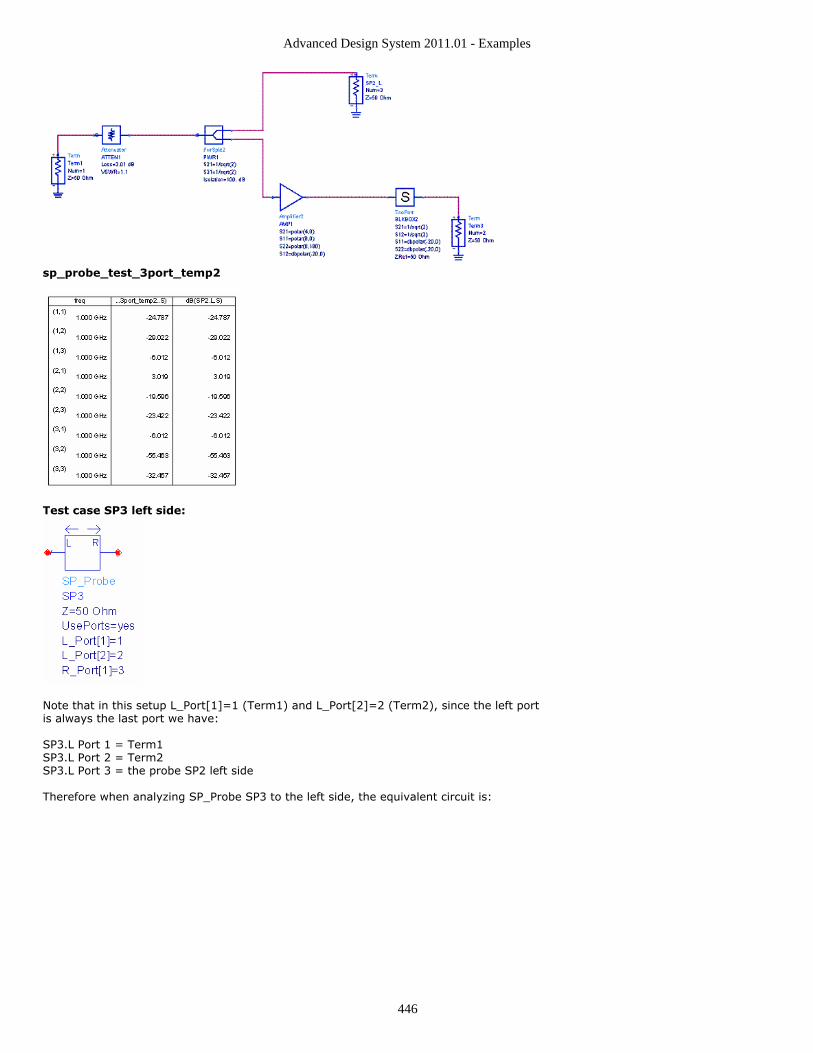
Advanced Design System 2011.01 - Examples
446
sp_probe_test_3port_temp2
Test case SP3 left side:
Note that in this setup L_Port[1]=1 (Term1) and L_Port[2]=2 (Term2), since the left portis always the last port we have:
SP3.L Port 1 = Term1SP3.L Port 2 = Term2SP3.L Port 3 = the probe SP2 left side
Therefore when analyzing SP_Probe SP3 to the left side, the equivalent circuit is:
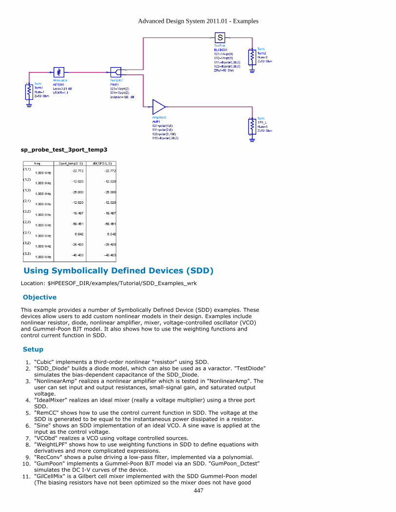
Advanced Design System 2011.01 - Examples
447
sp_probe_test_3port_temp3
Using Symbolically Defined Devices (SDD)Location: $HPEESOF_DIR/examples/Tutorial/SDD_Examples_wrk
Objective
This example provides a number of Symbolically Defined Device (SDD) examples. Thesedevices allow users to add custom nonlinear models in their design. Examples includenonlinear resistor, diode, nonlinear amplifier, mixer, voltage-controlled oscillator (VCO)and Gummel-Poon BJT model. It also shows how to use the weighting functions andcontrol current function in SDD.
Setup
"Cubic" implements a third-order nonlinear "resistor" using SDD.1."SDD_Diode" builds a diode model, which can also be used as a varactor. "TestDiode"2.simulates the bias-dependent capacitance of the SDD_Diode."NonlinearAmp" realizes a nonlinear amplifier which is tested in "NonlinearAmp". The3.user can set input and output resistances, small-signal gain, and saturated outputvoltage."IdealMixer" realizes an ideal mixer (really a voltage multiplier) using a three port4.SDD."RemCC" shows how to use the control current function in SDD. The voltage at the5.SDD is generated to be equal to the instantaneous power dissipated in a resistor."Sine" shows an SDD implementation of an ideal VCO. A sine wave is applied at the6.input as the control voltage."VCObd" realizes a VCO using voltage controlled sources.7."WeightLPF" shows how to use weighting functions in SDD to define equations with8.derivatives and more complicated expressions."RecConv" shows a pulse driving a low-pass filter, implemented via a polynomial.9."GumPoon" implements a Gummel-Poon BJT model via an SDD. "GumPoon_Dctest"10.simulates the DC I-V curves of the device."GilCellMix" is a Gilbert cell mixer implemented with the SDD Gummel-Poon model11.(The biasing resistors have not been optimized so the mixer does not have good
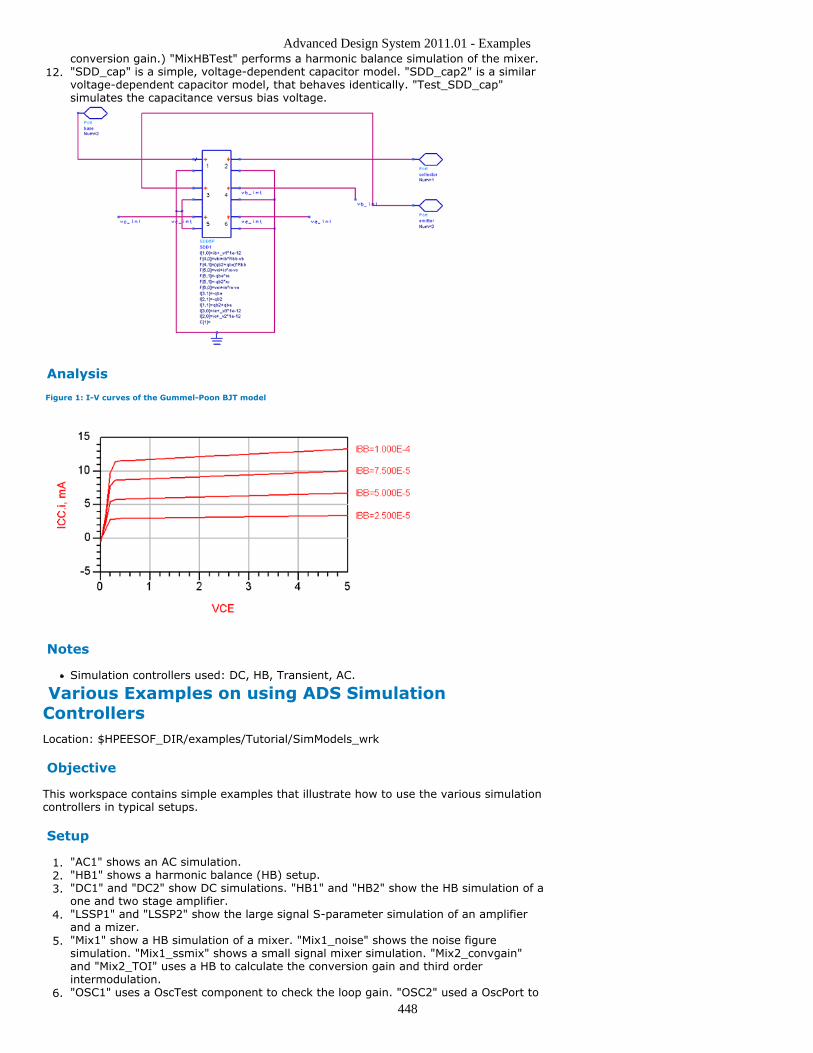
Advanced Design System 2011.01 - Examples
448
conversion gain.) "MixHBTest" performs a harmonic balance simulation of the mixer."SDD_cap" is a simple, voltage-dependent capacitor model. "SDD_cap2" is a similar12.voltage-dependent capacitor model, that behaves identically. "Test_SDD_cap"simulates the capacitance versus bias voltage.
Analysis
Figure 1: I-V curves of the Gummel-Poon BJT model
Notes
Simulation controllers used: DC, HB, Transient, AC.
Various Examples on using ADS SimulationControllersLocation: $HPEESOF_DIR/examples/Tutorial/SimModels_wrk
Objective
This workspace contains simple examples that illustrate how to use the various simulationcontrollers in typical setups.
Setup
"AC1" shows an AC simulation.1."HB1" shows a harmonic balance (HB) setup.2."DC1" and "DC2" show DC simulations. "HB1" and "HB2" show the HB simulation of a3.one and two stage amplifier."LSSP1" and "LSSP2" show the large signal S-parameter simulation of an amplifier4.and a mizer."Mix1" show a HB simulation of a mixer. "Mix1_noise" shows the noise figure5.simulation. "Mix1_ssmix" shows a small signal mixer simulation. "Mix2_convgain"and "Mix2_TOI" uses a HB to calculate the conversion gain and third orderintermodulation."OSC1" uses a OscTest component to check the loop gain. "OSC2" used a OscPort to6.
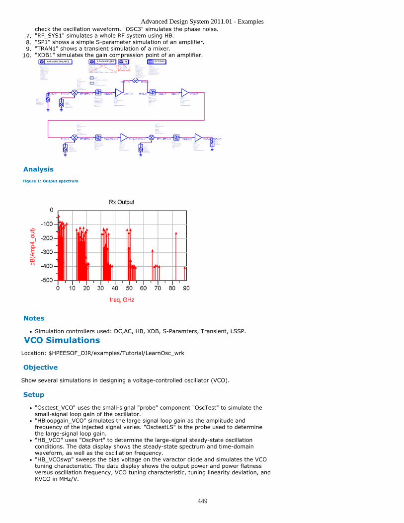
Advanced Design System 2011.01 - Examples
449
check the oscillation waveform. "OSC3" simulates the phase noise."RF_SYS1" simulates a whole RF system using HB.7."SP1" shows a simple S-parameter simulation of an amplifier.8."TRAN1" shows a transient simulation of a mixer.9."XDB1" simulates the gain compression point of an amplifier.10.
Analysis
Figure 1: Output spectrum
Notes
Simulation controllers used: DC,AC, HB, XDB, S-Paramters, Transient, LSSP.
VCO SimulationsLocation: $HPEESOF_DIR/examples/Tutorial/LearnOsc_wrk
Objective
Show several simulations in designing a voltage-controlled oscillator (VCO).
Setup
"Osctest_VCO" uses the small-signal "probe" component "OscTest" to simulate thesmall-signal loop gain of the oscillator."HBloopgain_VCO" simulates the large signal loop gain as the amplitude andfrequency of the injected signal varies. "OsctestLS" is the probe used to determinethe large-signal loop gain."HB_VCO" uses "OscPort" to determine the large-signal steady-state oscillationconditions. The data display shows the steady-state spectrum and time-domainwaveform, as well as the oscillation frequency."HB_VCOswp" sweeps the bias voltage on the varactor diode and simulates the VCOtuning characteristic. The data display shows the output power and power flatnessversus oscillation frequency, VCO tuning characteristic, tuning linearity deviation, andKVCO in MHz/V.
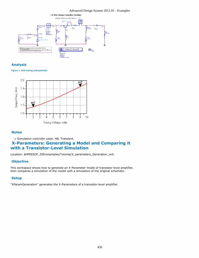
Advanced Design System 2011.01 - Examples
450
Analysis
Figure 1: VCO tuning characteristic
Notes
Simulation controller used: HB, Transient.
X-Parameters: Generating a Model and Comparing itwith a Transistor-Level SimulationLocation: $HPEESOF_DIR/examples/Tutorial/X_parameters_Generation_wrk
Objective
This workspace shows how to generate an X-Parameter model of transistor-level amplifier,then compares a simulation of the model with a simulation of the original schematic.
Setup
"XParamGeneration" generates the X-Parameters of a transistor-level amplifier.
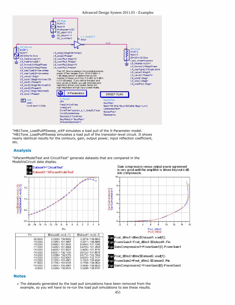
Advanced Design System 2011.01 - Examples
451
"HB1Tone_LoadPullPSweep_wXP simulates a load pull of the X-Parameter model."HB1Tone_LoadPullPSweep simulates a load pull of the transistor-level circuit. It showsnearly identical results for the contours, gain, output power, input reflection coefficient,etc.
Analysis
"XParamModelTest and CircuitTest" generate datasets that are compared in theModelVsCircuit data display.
Notes
The datasets generated by the load pull simulations have been removed from theexample, so you will have to re-run the load pull simulations to see these results.
Advanced Design System 2011.01 - Examples
452
X-Parameters: Various Simulations of X-ParameterModels Generated from MeasurementsLocation: $HPEESOF_DIR/examples/Tutorial/X_parameters_Demo_wrk
Objective
This workspace shows various simulations of X-parameter models generated frommeasurements of amplifiers. It includes one-, two-tone, and modulated input signals aswell as input power and frequency sweeps.
Setup
The xnp files containing X-parameters for the measured amplifiers in this workspace areretrieved from the data subdirectory. These files were obtained from physical DUTmeasurements on Agilent's Nonlinear Vector Network Analyzer (NVNA.)
The following X-parameter xnp data files are used:
a) ZFL_11AD_X2P..xnp - X-parameter measurements of first individual DUTb) Z60_2522M_X2P.xnp - X-parameter measurements of second Individual DUTc) ZFL_11AD_ZX60_2522M_Cascaded_X2P.xnp - X-parameter measurements of aboveDUTs in cascaded) ZX60_2252M_DC_X3P.xnp - X-parameter measurements of second Individual DUT withmeasured DC bias currente) FP2189_LoadPull_X2P.xnp - Load-dependent X-parameter measurements taken on apackaged FET using NVNA together with a Maury tuner.
The six simulatable designs are best studied in the following order:
a) X2P_SingleAmp_HB_1Tone - This Harmonic Balance simulation provides anintroductory view of theharmonic behavior represented by the measured X-parameters at the input and at theoutput of an amplifier.Sweeps of the frequency and power of the single input fundamental tone provide a basisfor observingvariations in amplifier behaviors such as in Gain Compression.
b) X2P_CascadedAmps_HB_1Tone - This Harmonic Balance simulation compares thecascading of twoamplifiers represented by X2P components with measured X-parameters to a single X2Pcomponent withthe measured X-parameters of the physically cascaded amplifiers, thereby demonstratingfidelity undercascaded conditions.
c) X3P_SingleAmp_LoadPull_HB_1Tone - This Harmonic Balance simulation demonstrateshow X-parameters can beused to track load-pull based variations. The X3P component used in this simulationincludes measured DC bias currentinformation, and is therefore able to predict PAE in addition to power delivered as afunction of load.
d) X2P_PackagedFET_LoadPull_HB_1Tone - This Harmonic Balance simulationdemonstrates the use of load-dependentX-parameters measured with the NVNA and a Maury tuner to enable accurate simulationof device behavior over a widerange of load conditions.
e) X2P_SingleAmp_CE_2Tone - This Circuit Envelope simulation demonstrates the use ofan X2P component to estimateIMD3 response to a two-tone input. The simulation is very accurate for narrowly spacedtones, and provides areasonable estimate over wider bandwidths using the static gain and phase compressioncharacteristics of the DUT.
f) X3P_SingleAmp_CE_CDMA - This Circuit Envelope simulation demonstrates use of anX3P component in acommunications system analysis. Again, the simulation is very accurate for narrowbandwidths, and provides a reasonableestimate over wider bandwidths.
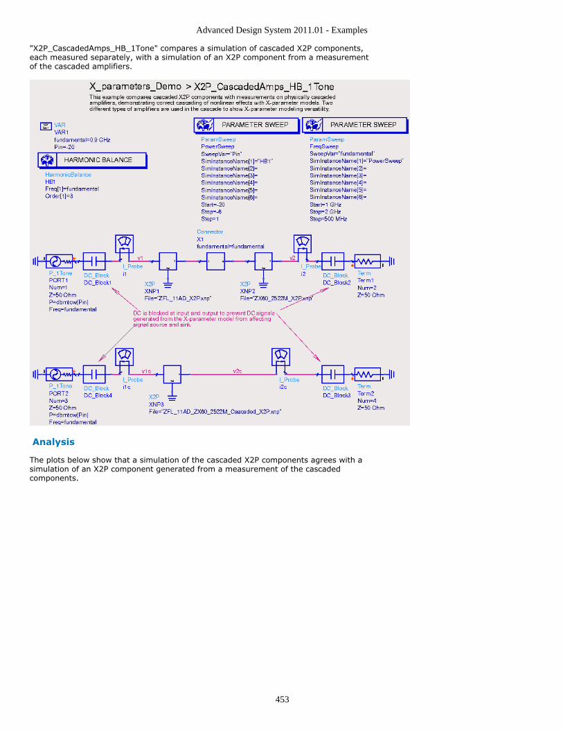
Advanced Design System 2011.01 - Examples
453
"X2P_CascadedAmps_HB_1Tone" compares a simulation of cascaded X2P components,each measured separately, with a simulation of an X2P component from a measurementof the cascaded amplifiers.
Analysis
The plots below show that a simulation of the cascaded X2P components agrees with asimulation of an X2P component generated from a measurement of the cascadedcomponents.
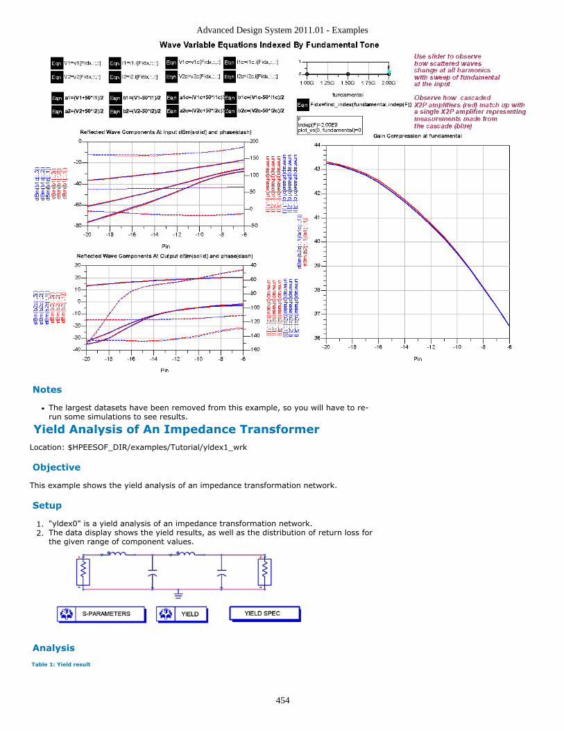
Advanced Design System 2011.01 - Examples
454
Notes
The largest datasets have been removed from this example, so you will have to re-run some simulations to see results.
Yield Analysis of An Impedance TransformerLocation: $HPEESOF_DIR/examples/Tutorial/yldex1_wrk
Objective
This example shows the yield analysis of an impedance transformation network.
Setup
"yldex0" is a yield analysis of an impedance transformation network.1.The data display shows the yield results, as well as the distribution of return loss for2.the given range of component values.
Analysis
Table 1: Yield result
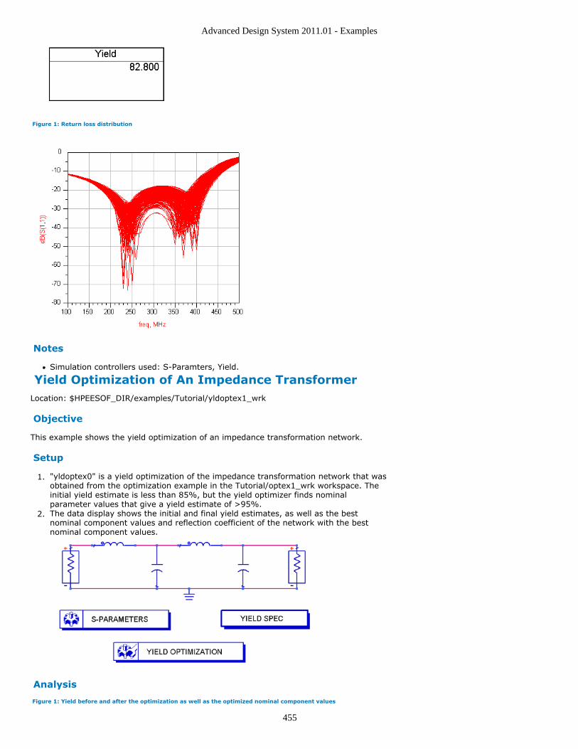
Advanced Design System 2011.01 - Examples
455
Figure 1: Return loss distribution
Notes
Simulation controllers used: S-Paramters, Yield.
Yield Optimization of An Impedance TransformerLocation: $HPEESOF_DIR/examples/Tutorial/yldoptex1_wrk
Objective
This example shows the yield optimization of an impedance transformation network.
Setup
"yldoptex0" is a yield optimization of the impedance transformation network that was1.obtained from the optimization example in the Tutorial/optex1_wrk workspace. Theinitial yield estimate is less than 85%, but the yield optimizer finds nominalparameter values that give a yield estimate of >95%.The data display shows the initial and final yield estimates, as well as the best2.nominal component values and reflection coefficient of the network with the bestnominal component values.
Analysis
Figure 1: Yield before and after the optimization as well as the optimized nominal component values
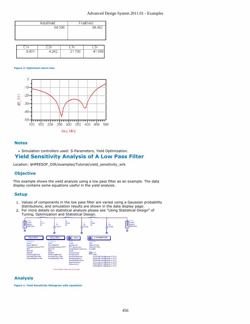
Advanced Design System 2011.01 - Examples
456
Figure 2: Optimized return loss
Notes
Simulation controllers used: S-Parameters, Yield Optimization.
Yield Sensitivity Analysis of A Low Pass FilterLocation: $HPEESOF_DIR/examples/Tutorial/yield_sensitivity_wrk
Objective
This example shows the yield analysis using a low pass filter as an example. The datadisplay contains some equations useful in the yield analysis.
Setup
Values of components in the low pass filter are varied using a Gaussian probability1.distributions, and simulation results are shown in the data display page.For more details on statistical analysis please see "Using Statistical Design" of2.Tuning, Optimization and Statistical Design.
Analysis
Figure 1: Yield Sensitivity Histogram with equations
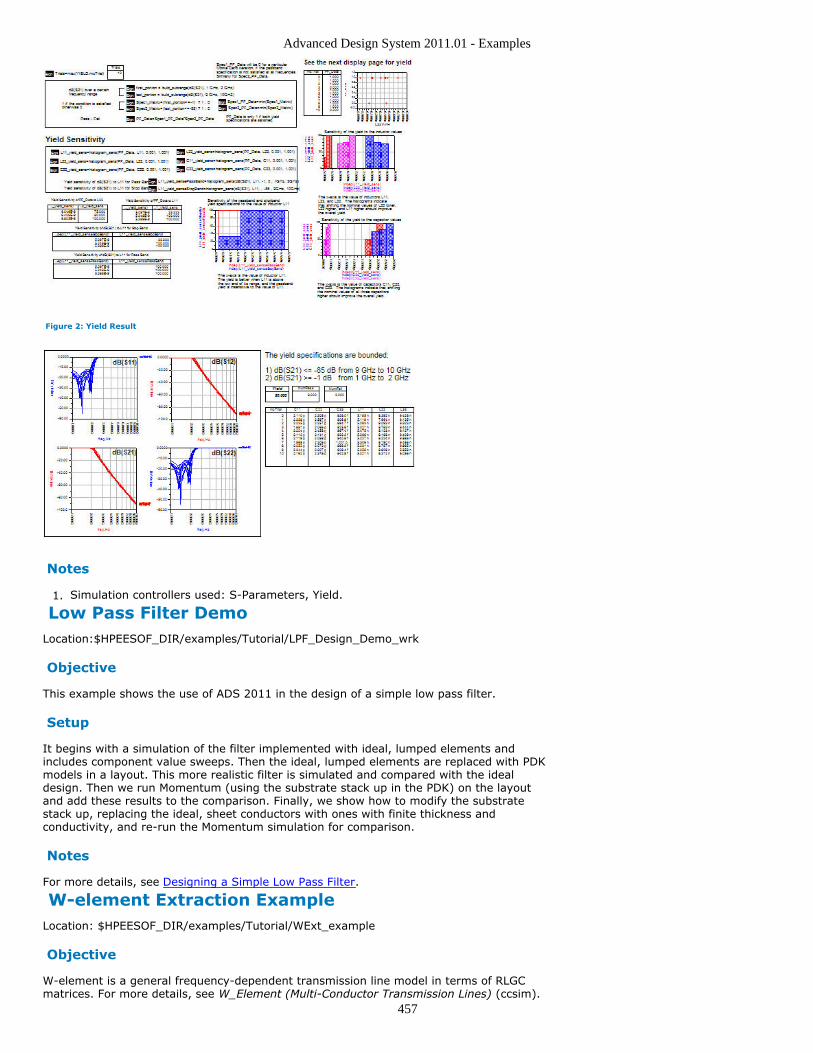
Advanced Design System 2011.01 - Examples
457
Figure 2: Yield Result
Notes
Simulation controllers used: S-Parameters, Yield.1.
Low Pass Filter DemoLocation:$HPEESOF_DIR/examples/Tutorial/LPF_Design_Demo_wrk
Objective
This example shows the use of ADS 2011 in the design of a simple low pass filter.
Setup
It begins with a simulation of the filter implemented with ideal, lumped elements andincludes component value sweeps. Then the ideal, lumped elements are replaced with PDKmodels in a layout. This more realistic filter is simulated and compared with the idealdesign. Then we run Momentum (using the substrate stack up in the PDK) on the layoutand add these results to the comparison. Finally, we show how to modify the substratestack up, replacing the ideal, sheet conductors with ones with finite thickness andconductivity, and re-run the Momentum simulation for comparison.
Notes
For more details, see Designing a Simple Low Pass Filter.
W-element Extraction ExampleLocation: $HPEESOF_DIR/examples/Tutorial/WExt_example
Objective
W-element is a general frequency-dependent transmission line model in terms of RLGCmatrices. For more details, see W_Element (Multi-Conductor Transmission Lines) (ccsim).

Advanced Design System 2011.01 - Examples
458
This example shows how to use W-element Extraction controller to generate W-elementfiles in various formats for multilayer T-Line components. This feature allows you to obtainW-element models from the accurate and efficient ADS multilayer T-Line models, whichare advanced in many aspects such as skin effect modeling, conductor surface roughnessmodeling, dielectric loss modeling etc. Note that only the tabular format can preserve thefull accuracy while static format cannot by definition. For more information on W-elementExtraction, see W-element Extraction (ccdist).
In this example, the W-element files (RLGC) are generated for a multilayer T-Linecomponent in both static and tabular formats. S-Parameter results calculated from bothare compared to that from the original multilayer component. It is illustrated that thetabular format preserves the accuracy of the multilayer model while the static format losesaccuracy for higher frequencies.
Setup
Multilayer: Generates the W-element file and does the S-Parameter simulationusing the original multilayer T-Line component. Use parameter
W_FileFormat in CLine1 to change the output W-element file format.W_File to change the output file name and also the HSPICE subckt name.HSPICE subckt ckt_case1 uses the static file and ckt_case2 uses the tabular file.
Static: Does the S-Parameter simulation using the static W-element file.Tabular: Does the S-Parameter simulation using the tabular W-element file.
Notes
The S-Parameters controller and the terminations are not necessary for outputting W-element files. Removing them will not affect the W-element output. If the S-Parametercontroller is removed from the design Multilayer, a warning message "no output wasgenerated" will occur during simulations because the W-element Extraction controller doesnot writes any data to the dataset file. If the terminations and connections to them areremoved, there might be warning messages regarding unconnected nodes.