adsorption of 4,4′−bipyridine on the cd(0001) single crystal electrode surface
TRANSCRIPT
In situ scanning tunneling microscopy (STM), electrochemical impedance spectroscopy have been applied to study the adsorption of 4,4′−bipyridine (4,4′−BP) on the Cd(0001) single crystal electrode from 0.1 M Na2SO4 + 1.0×10⁻⁵ M H2SO4 + x M 4,4′−BP aqueous solutions (x from 0.0 to 3.0×10⁻³). Influence of the electrode potential (E) on the adsorption characteristics of 4,4′−BP on Cd(0001) has been demonstrated. T wo regions with low capacitance values have been observed in the series capacitance vs. E curve. The in situ STM data revealed that 4,4′−BP forms a stripe pattern on the Cd(0001) single crystal electrode surface. The results of density functional theory (DFT) calculations and surface enhanced infrared adsorption spectroscopy data have been applied in order to establish the adsorption layer structure and possible orientation of the 4,4′−BP molecules on the Cd(0001) surface. DFT calculations, used to compliment the experimental data, demonstrate the importance of the van der Waals interactions for the formation of the stripe pattern. Keywords: In situ STM, Cd(0001), 4,4′−bipyridine, adsorption, nanoscale molecular stripes.
1 ISE member * Corresponding author. Tel.: +372 7 375 165; fax: +372 7 375 264. E−mail address:[email protected], (E. Lust).
Adsorption of 4,4′−bipyridine on the Cd(0001) single crystal electrode surface
P. Pikma1, H. Kasuk1, O. Oll1, V. Ivaništšev1, T. Romann1, V. Grozovski1, K. Lust1,E. Lust1*
Institute of Chemistry, University of Tartu, 14A Ravila Street, 50411 Tartu, Estonia
Original Publication:Pikma, P., Kasuk, H., Oll, O., Ivaništšev, V., Romann, T., Grozovski, V., Lust, K., Lust, E., 2015. Adsorption of 4,4′−bipyridine on the Cd(0001) single crystal electrode surface. Electrochim. Acta 180, 965–976. doi:10.1016/j.electacta.2015.08.003
ABSTRACT
Page 1
1. IntroductionThe molecular self−assembly of organic molecules on solid surfaces, resulting in the formation ofnanostructures with well−controlled properties and functionality, reveals fascinating perspectivesin the nanoscale science and nanotechnology [1,2]. In light of this, extensive studies have beenconducted in recent years to analyze organic monolayer structures on metal substrates. Electrical,magnetic, mechanical and optical properties of self−assembled monolayers depend on theorientation of the adsorbed molecules and their arrangement in the two−dimensional (2D) lattice.It is well known that the kinetics of 2D condensation is remarkably influenced by the chemicalcomposition of the supporting electrolyte [2–13] as well as chemical nature and crystallographicstructure of the crystal plane studied [14–24]. Extensive and comprehensive understanding of thecomplex structure of the adsorbed molecular layers cannot be achieved using a single method ofmeasurements. The understanding and interpretation of interfacial structures is possible only bycombining the results of different methods, such as electrochemical impedance spectroscopy(EIS), in situ scanning tunneling microscopy (STM), surface enhanced infrared adsorptionspectroscopy (SEIRAS) and X−ray scattering techniques [2]. The results of these measurementscan be complemented by modern density functional theory (DFT) calculations, which providesadditional information on the strength of the interactions of adsorbate–adsorbate, adsorbate–electrolyte, and adsorbate–electrode interfaces, that determine the adsorption energy of theself−assembly process and the structural characteristics of the 2D layer [1,25]. Since early 2000sa deeper understanding of the governing parameters of self−assembly started to emerge as aresult of combining the computational and in situ experimental approaches [26].
Novel solvent−based preparation methods of 2D layers are very attractive in light of promising applications of organic thin films in light−emitting diodes, organic photovoltaic cells, organic field effect transistors, and organic spintronics [27]. Ordered layers of some molecules, such as 4,4′−bipyridine (4,4′−BP), can be prepared using conventional electrochemical potentiostatic method, i.e. deposition from aqueous electrolytes by applying a fixed electrode potential.
4,4′−BP is a bifunctional non−chelating molecule [28], which has been used as a ligand to design new metal complexes with interesting photochemical properties for application in the dye−sensitized solar cells [29], as an electroluminescent material [30], and as a component of molecular electronic devices [31]. 4,4′−BP has the ability to bond through the π−electron system (if adsorbed in parallel orientation to the surface), or through the lone−electron pair localized at the nitrogen atom [4,32–34]. 4,4′−BP tends to self−assemble on the solid surfaces and can be used as a building block for the two− and three−dimensional supramolecular lattices [35–38]. Taking into account the bifunctionality of the 4,4′−BP molecules, it is possible to divide the factors governing the self-assemble structure formed under given electrochemical conditions for a given application. Thus, understanding of the factors helps in designing new functional interfaces with tunable properties.
The adsorption of 4,4′−BP on transition metals has been investigated in many studies using scanning probe microscopy, EIS, infrared (IR) spectroscopy and Raman spectroscopy. Papers describing the formation of self−assembled monolayer on single crystal Au(111) [4,33],
Page 2
Bi(111) [38] and Cu(111) [32] electrodes have been published and noticeable influence of the metal water adsorption energy on the 4,4′−BP structural characteristics has been demonstrated [38].
Cadmium is an important metal due to its versatile applications. Especially, electrodeposition of cadmium has been widely used in the production of materials for conductive devices that require advanced physical, chemical and mechanical properties like narrow band gap, low electrical contact resistance, high corrosion resistance, solderability, ductility, etc. Cadmium coating has great importance in aerospace and defense industries. Understanding of the electrochemical behavior of the Cd | electrolyte interface is important for these applications, since Cd(0001) surface has high H2O adsorption energy [39,40]. In this study, cyclic voltammetry (CV), EIS, in situ STM and SEIRAS methods have been combined to obtain the adsorption characteristics of 4,4′−BP on the electrochemically polished Cd(0001) electrode surface from 0.1 M Na2SO4 + 1.0×10⁻⁵ M H2SO4 aqueous solutions. The experimental study of the 4,4′−BP self−assembled structures has been complemented by the DFT calculations, applying Perdew−Burke−Ernzerhof (PBE) [41] and van der Waals (vdW−DF2) [42] density functionals, which have been designed to describe the van der Waals interactionsbetween aromatic molecules and adsorption interactions (including chemical bonding) with metalsurface atoms.
The main aim of this study was to combine CV, EIS, in situ STM, SEIRAS and DFT calculation results to determine the probable unit cell parameters, packing positions, orientation, Gibbs adsorption values, and limiting steps for the adsorption of 4,4′−BP at Cd(0001) electrode plane.
2. Experimental2.1. Materials and methodsThe surface of Cd(0001) electrode plane was electrochemically polished in a hot (T = 80 °C) 1:1solution of concentrated phosphoric acid and Milli Q+ water at current density j = 1.48 A cm−2.The electrode was submerged under cathodic polarization (E = −1.10 V vs. Ag | AgCl in saturatedKCl aqueous solution) into 0.1 M Na2SO4 + 1.0×10⁻⁵ M H2SO4 + x M 4,4′−BP aqueous solutions(x from 0.0 to 3.0×10⁻³), previously saturated with Ar (95%) + H2 (5%) mixture. The self−madehermetic three−electrode cell with large Pt counter electrode and Ag | AgCl | sat. KCl referenceelectrode was used. The region of ideal polarizability was established using the CV method and agood agreement with previous results obtained using the EIS method at different ac frequencies(f) was observed (applying AUTO−LAB PGSTAT 30 with FRA 2 measurement system,0.1 < f < 10000 Hz, 5 mV modulation) [40,43–47].
For STM analysis Molecular Imaging PicoSPMTM system with ApiezonTM coated tungsten STM tips, prepared in our laboratory, were used. The STM−tips and measurement system were tested and calibrated using the basal (0001) plane of highly orientated pyrolytic graphite (SPITM). All STM images were recorded in constant current mode within the tunneling current region from 0.5 to 10.0 nA. Gwyddion [48] free software program was used for image processing and surface roughness analysis.
Page 3
For detailed comparison, in situ IR spectra were measured on a 20 nm thick magnetron sputtered layer of cadmium with polycrystalline surface structure, using Perkin−Elmer Spectrum GX FTIR system equipped with a liquid nitrogen−cooled midrange MCT detector [49–51]. The measured IR bands have been assigned to corresponding vibrations using DFT/B3LYP method. Solutions were prepared volumetrically using H2SO4 (double distilled, Aldrich), 4,4′−bipyridine (Fluka purum, purity > 99%) and Milli Q+ water. The used Na2SO4 was purified by triple recrystallization from water and heated up to 700 °C to remove organic impurities. During experiments the temperature was 22 ± 1 °C.
2.2. Computational details Density functional theory calculations were performed with the GPAW [52] software, a grid based implementation of the projector augmented wave method [53] using the Atomic Simulation Environment interface [54]. A grid spacing of 0.16 Å was used to ensure convergence of relative energies. The vdW−DF2 method [55], previously shown to give reasonable results for the adsorption of aromatic molecules on transition metal surfaces [56], was applied. 3 layers of cadmium with 25 atoms in each layer were used to model the Cd(0001) surface interacting with a single 4,4′−BP molecule. Two bottom Cd layers were fixed with the geometry of the bulk using the lattice parameters a = 2.9793 Å and c = 5.6196 Å. Periodic boundary conditions were used in the X and Y directions, while in the Z direction the dipole correction was applied and at least 60 Å vacuum was added between the model Cd surface and the cell boundaries. Starting configurations with the center of the molecule at the top, bridge and hollow sites were tested for the adsorption of a single 4,4′−BP molecule with the orientation parallel or perpendicular to the Cd(0001) surface. In the latter case the 4,4′−BP molecule is oriented either with N−atom (N−tip orientation) or C–H (edge orientation) towards the surface. Six different models of 4,4′−BP molecular stripes on the Cd(0001) electrode surface were selected based on the results of the single molecule adsorption data. All structures were relaxed to a maximum force of 0.20 eV/Å. The Brillouin zone was sampled with the Monkhorst–Pack scheme with a number of k−points times cell length larger than 16 Å in X and Y directions. The structure with the lowest energy was selected, relaxed with 4×6×1 k−points, and used to establish the simulated STM images based on the Tersoff−Hamann model [57].
3. Experimental results3.1. Cyclic voltammetry and series capacitance plotsBased on the data in Fig. 1a, it was confirmed, that the cadmium single crystal (0001) plane isnearly ideally polarizable within the region of electrode potentials (E) from −1.40 V to −0.90 V(vs. Ag | AgCl in sat. KCl) in 0.1 M Na2SO4 + 1.0×10⁻⁵ M H2SO4 aqueous solution [40,43–47].Nearly exponential increase of negative current values has been measured at E < −1.40 V (Fig.1a) and can be explained by the cathodic hydrogen evolution from H3O+. This process alsoinfluences the shape of the series capacitance (Cs) vs. E curve for 0.1 M Na2SO4 + 1.0×10⁻⁵ MH2SO4 system (Fig. 2). Data in Figs. 1 and 2 indicate that the hydrogen evolution overvoltage atCd(0001) is noticeably lower than that at Bi(hkl) or Hg [40,43–47]. Moderate capacitance
Page 4
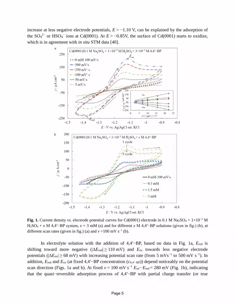
increase at less negative electrode potentials, E > −1.10 V, can be explained by the adsorption of the SO4
2− or HSO4− ions at Cd(0001). At E > −0.85V, the surface of Cd(0001) starts to oxidize,
which is in agreement with in situ STM data [40].
Fig. 1. Current density vs. electrode potential curves for Cd(0001) electrode in 0.1 M Na2SO4 + 1×10⁻⁵ M H2SO4 + x M 4,4′−BP system, x = 3 mM (a) and for different x M 4,4′−BP solutions (given in fig.) (b), at different scan rates (given in fig.) (a) and v =100 mV s−1 (b).
In electrolyte solution with the addition of 4,4′−BP, based on data in Fig. 1a, Ered is shifting toward more negative (|∆Ered| ≥ 110 mV) and Eox towards less negative electrode potentials (|∆Eox| ≥ 68 mV) with increasing potential scan rate (from 5 mVs−1 to 500 mV s−1). In addition, Ered and Eox (at fixed 4,4′−BP concentration (c4,4′−BP)) depend noticeably on the potential scan direction (Figs. 1a and b). At fixed v = 100 mV s−1 Eox−Ered = 280 mV (Fig. 1b), indicating that the quasi−reversible adsorption process of 4,4′−BP with partial charge transfer (or true
Page 5
faradaic charge transfer) takes place on the Cd(0001) surface. Surprisingly, there is a nearly linear dependence of jred, as well as of jox, on ν1/2 (inset in Fig. 1a), demonstrating that mainly mass transfer step limited processes take place [58–67]. However, the mass transfer (diffusion) coefficient values, that can be calculated from the slopes of jred vs. ν1/2− or jox vs. ν1/2− plots, depend somewhat on the organic compound concentration in the solution, being lower for more concentrated 4,4′−BP solutions. This can be explained by the formation of a more compact 4,4′−BP adsorption layer on the charged Cd(0001) surface from more concentrated 4,4′−BP solutions.
Similarly to the adsorption of 4,4′−BP on the Bi(111) electrode surface [38], the current density values slightly decrease with subsequent potential sweeps (Fig. 1b). Therefore, the adsorption of 4,4′−BP can be considered as a quasi−reversible adsorption process (with partial charge transfer step) within the potential region investigated.
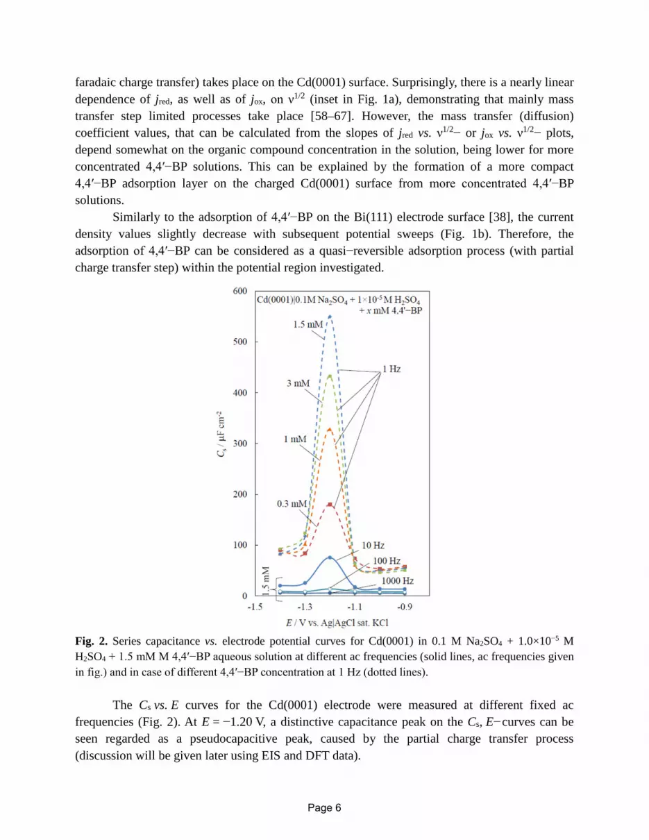
Fig. 2. Series capacitance vs. electrode potential curves for Cd(0001) in 0.1 M Na2SO4 + 1.0×10⁻⁵ M H2SO4 + 1.5 mM M 4,4′−BP aqueous solution at different ac frequencies (solid lines, ac frequencies given in fig.) and in case of different 4,4′−BP concentration at 1 Hz (dotted lines).
The Cs vs. E curves for the Cd(0001) electrode were measured at different fixed ac frequencies (Fig. 2). At E = −1.20 V, a distinctive capacitance peak on the Cs, E−curves can be seen regarded as a pseudocapacitive peak, caused by the partial charge transfer process (discussion will be given later using EIS and DFT data).
Page 6
The Cs values at E = −1.20 V strongly depend on f (Fig. 2), as well as on c4,4′−BP, which is also characteristic of organic compounds adsorption on Hg and Bi electrodes [58−63]. It is interesting that the reorientation peak potential is mostly independent of the concentration of 4,4′−BP in the solution, implying that the formation of a stable 2D structure occurs already in very dilute 4,4′−BP solutions.
However, applying in situ STM method (discussed later) the 4,4′−BP molecular rows have only been observed in 1.5×10⁻³ M 4,4′−BP solution within a very narrow electrode potential region −1.30 V ≤ E ≤ −1.25 V.
Two capacitance depression regions in the Cs, E−curves have been detected. According to the Helmholtz model for electrical double layer (C=𝜀𝜀0 ×𝜀𝜀𝑒𝑒𝑒𝑒𝑒𝑒
𝑑𝑑𝑒𝑒𝑒𝑒𝑒𝑒, where ɛ0 is the dielectric constant for
vacuum, ɛeff is the macroscopic dielectric constant of the electrolyte and/or adsorption layer (in the case of adsorption), deff is the effective thickness of the double layer (or of the adsorption layer)) an increase of the adsorption layer thickness and the decrease of ɛeff occurs at E > −1.15 V and E < −1.30 V (Fig. 2).
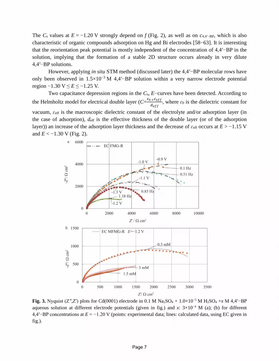
Fig. 3. Nyquist (Z″,Z′) plots for Cd(0001) electrode in 0.1 M Na2SO4 + 1.0×10⁻⁵ M H2SO4 +x M 4,4′−BP aqueous solution at different electrode potentials (given in fig.) and x: 3×10⁻⁴ M (a); (b) for different 4,4′−BP concentrations at E = −1.20 V (points: experimental data; lines: calculated data, using EC given in fig.).
Page 7
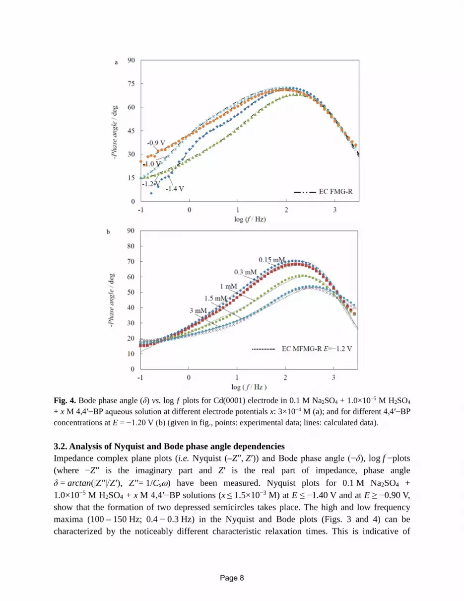
Fig. 4. Bode phase angle (δ) vs. log ƒ plots for Cd(0001) electrode in 0.1 M Na2SO4 + 1.0×10⁻⁵ M H2SO4 + x M 4,4′−BP aqueous solution at different electrode potentials x: 3×10⁻⁴ M (a); and for different 4,4′−BPconcentrations at E = −1.20 V (b) (given in fig., points: experimental data; lines: calculated data).
3.2. Analysis of Nyquist and Bode phase angle dependencies Impedance complex plane plots (i.e. Nyquist (–Z′′, Z′)) and Bode phase angle (−δ), log f −plots (where −Z′′ is the imaginary part and Z′ is the real part of impedance, phase angle δ = arctan(|Z′′|/Z′), Z′′= 1/Csω) have been measured. Nyquist plots for 0.1 M Na2SO4 + 1.0×10⁻⁵ M H2SO4 + x M 4,4′−BP solutions (x ≤ 1.5×10⁻³ M) at E ≤ −1.40 V and at E ≥ −0.90 V, show that the formation of two depressed semicircles takes place. The high and low frequency maxima (100 – 150 Hz; 0.4 − 0.3 Hz) in the Nyquist and Bode plots (Figs. 3 and 4) can be characterized by the noticeably different characteristic relaxation times. This is indicative of
Page 8
parallel existence of slow adsorption (with following partial charge transfer step) and true faradaic oxidation processes at E ≥ −0.90 V. Reduction of 2D 4,4′−BP layer [64] and a faradaic electroreduction processes takes place at E ≤ −1.40 V. There are no linear areas with the slope values varying from 45° to 60° in the Nyquist plots (Figs. 3a and b), characteristic of the finite length mass transfer step limited adsorption processes at f < 10 Hz.
Within E region from −0.9 V to −1.4 V the phase angle values strongly depend on the concentration of 4,4′−BP in solution (Fig. 4b). The quick adsorption layer formation, i.e. more negative δ values at higher ac frequencies (followed by the slower partial charge transfer step at f < 1.0 Hz), has been verified for the most concentrated 4,4′−BP solutions (c4,4′−BP ≥ 1.5×10⁻³ M). At more negative electrode potentials (E ≤ −1.40 V), the region of intensive decrease in |δ| is shifted towards higher f values with the increase of negative polarization (Fig. 4a), which could be explained by reductive desorption of 4,4′−BP from the Cd(0001)|electrolyte interface [68,69].
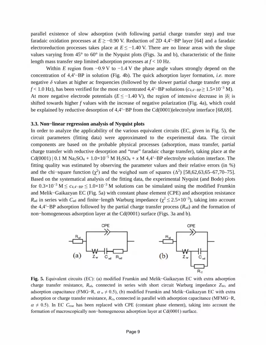
3.3. Non−linear regression analysis of Nyquist plots In order to analyze the applicability of the various equivalent circuits (EC, given in Fig. 5), the circuit parameters (fitting data) were approximated to the experimental data. The circuit components are based on the probable physical processes (adsorption, mass transfer, partial charge transfer with reductive desorption and “true” faradaic charge transfer), taking place at the Cd(0001) | 0.1 M Na2SO4 + 1.0×10⁻⁵ M H2SO4 + x M 4,4′−BP electrolyte solution interface. The fitting quality was estimated by observing the parameter values and their relative errors (in %) and the chi−square function (χ2) and the weighed sum of squares (Δ2) [58,62,63,65–67,70–75]. Based on the systematical analysis of the fitting data, the experimental Nyquist (and Bode) plots for 0.3×10⁻³ M ≤ c4,4′−BP
≤ 1.0×10⁻³ M solutions can be simulated using the modified Frumkin and Melik−Gaikazyan EC (Fig. 5a) with constant phase element (CPE) and adsorption resistance Rad in series with Cad and finite−length Warburg impedance (χ2 ≤ 2.5×10⁻³), taking into account the 4,4′−BP adsorption followed by the partial charge transfer process (Rad) and the formation of non−homogeneous adsorption layer at the Cd(0001) surface (Figs. 3a and b).
Fig. 5. Equivalent circuits (EC): (a) modified Frumkin and Melik−Gaikazyan EC with extra adsorption charge transfer resistance, Rad, connected in series with short circuit Warburg impedance ZWs and adsorption capacitance (FMG−R, α w ≠ 0.5), (b) modified Frumkin and Melik−Gaikazyan EC with extra adsorption or charge transfer resistance, Rct, connected in parallel with adsorption capacitance (MFMG−R, α ≠ 0.5). In EC Ctrue has been replaced with CPE (constant phase element), taking into account the formation of macroscopically non−homogeneous adsorption layer at Cd(0001) surface.
Page 9
More detailed analysis of Nyquist and Bode plots demonstrates that at E = −1.20 V, a better fit has been observed if an additional charge transfer resistance, Rct, has been added in parallel with Cad (Fig. 5b), simulating the occurrence of parallel adsorption and charge transfer processes (Fig. 3b) .
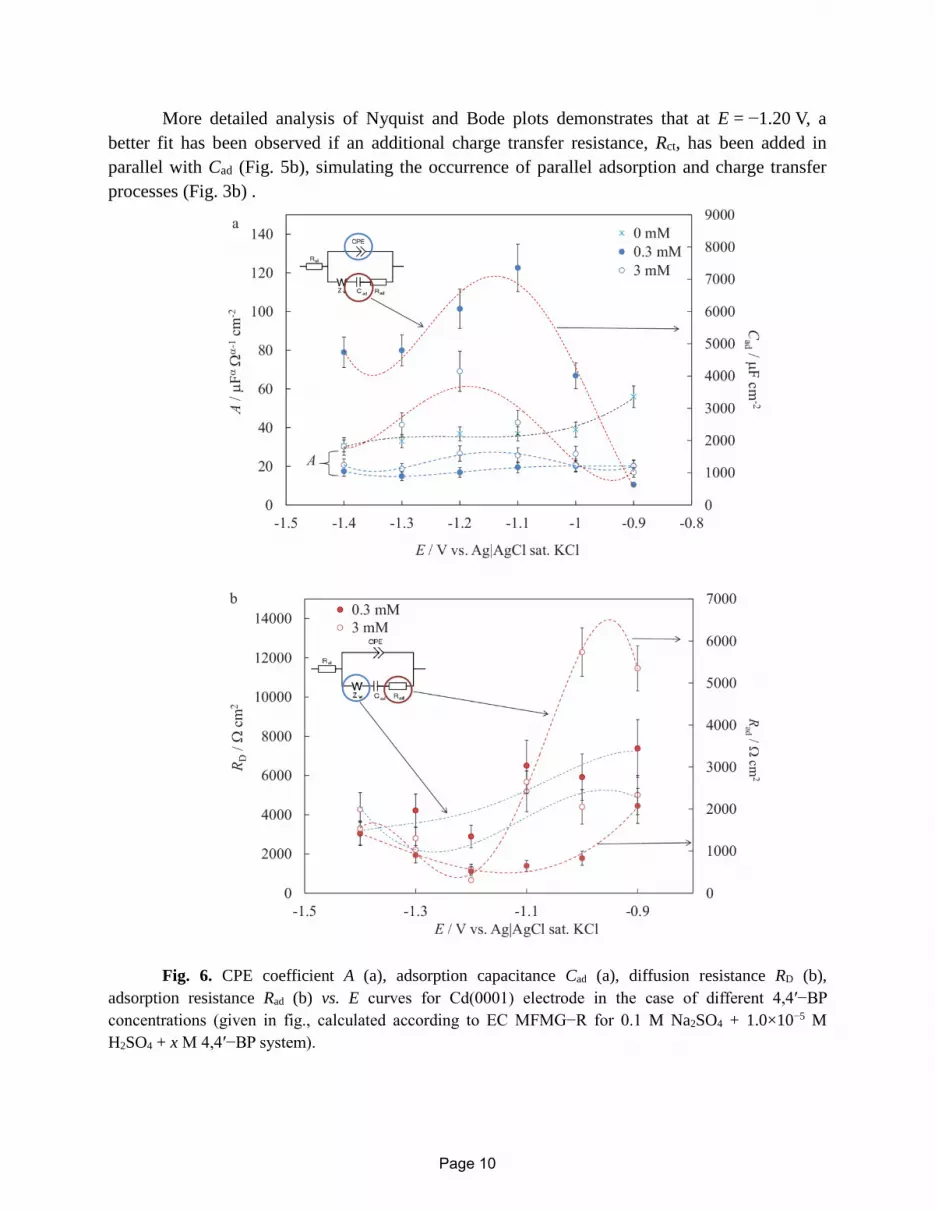
Fig. 6. CPE coefficient A (a), adsorption capacitance Cad (a), diffusion resistance RD (b), adsorption resistance Rad (b) vs. E curves for Cd(0001) electrode in the case of different 4,4′−BP concentrations (given in fig., calculated according to EC MFMG−R for 0.1 M Na2SO4 + 1.0×10⁻⁵ M H2SO4 + x M 4,4′−BP system).
Page 10

The values of the CPE coefficient A, for less concentrated 4,4′−BP solutions (Fig. 6a), weakly depend on E. The calculated values of CPE fractional exponent α are higher than 0.85, illustrating that the system only slightly deviates from ideal capacitive behavior towards complex capacitive−resistive behavior. It is interesting that the values of A decrease noticeably at very low 4,4′−BP concentrations. This illustrates the very strong adsorption of 4,4′−BP on the Cd(0001) electrode, decreasing the εeff values and or increasing deff values.
The adsorption capacitance, Cad (Cs at ω →0) characterizes the dependence of the surface coverage (Gibbs adsorption) on the electrode potential [62,67,72,73] (Fig. 6a). Within E region, where the structural reorganization processes of a 2D layer are taking place, the obtained Cad values are comparable with the series capacitance values measured at low frequencies (Fig. 2). The noticeable increase of Cad at −1.30 V ≤ E ≤ −1.00 V can be explained by the reorganization and reductive desorption of the 2D 4,4′−BP layer as well as by adsorption accompanied by partial charge transfer process. The small increase of Cad at E < −1.40 V can be interpreted as the reduction of 4,4′−BP molecules and H3O+ cations [68,69].
Moderate diffusion resistance (RD) values (Fig. 6b), calculated from the values of the generalized finite−length Warburg−like finite−length diffusion impedance ZWs, depend weakly on the concentration of 4,4′−BP and illustrate the strong 2D adsorption layer formation process of 4,4′−BP. RD increases with the decrease of the negative electrode potential. At E = −1.20 V, the so−called reorientation maximum in CS vs. E curve can be seen, which is indicative of the restructuring of the adsorption layer from a very compact 2D layer (E > −1.00 V) to a less compact adsorption layer (E < −1.20 V).
The values of the adsorption and / or charge transfer resistance Rad (Fig. 6b) quickly increase at less negative electrode potentials (E ≥ −1.20 V). Very high Rad values have been calculated for more concentrated 4,4′−BP solutions within the so−called strong 2D “blocking” adsorption region. At E ≤ −1.30 V, Rad very slowly increases as the “true” faradaic processes start.
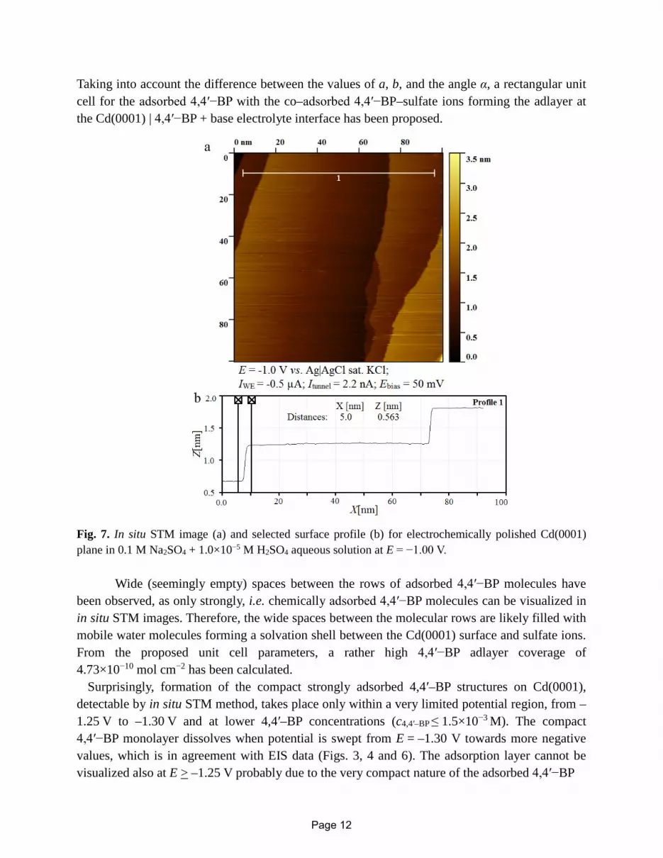
3.4. In situ STM data In accordance with our previous studies [40] and based on the stability of the in situ STM data collected, it was confirmed that the cadmium single crystal (0001) plane is ideally polarizable within the E region from −1.40 V to −0.90 V (vs. Ag | AgCl in sat. KCl) in the supporting electrolyte solution and consists of atomically smooth areas (Fig. 7).
It has been established that at E = −1.25 V (vs. Ag | AgCl in sat. KCl) 4,4′−BP molecules adsorb in a stripe pattern on the Cd(0001) electrode surface from 0.1 M Na2SO4 + 1.0×10⁻⁵ M H2SO4 + 1.5×10⁻³ M 4,4′−BP solution (Fig. 8a). Similar patterns have been observed on the Au(111) [5,33], Bi(111) [38] and Cu(111) [32] electrodes, where the structures of the 4,4′−BP molecules are formed by translation and rotation of the molecules towards the surface [4,33].
In the high−resolution in situ STM (15 nm×15 nm) image of adsorbed 4,4′−BP molecules on the Cd(0001) surface (Fig. 8a), periodic arrays of bright features are clearly visible at tip bias voltage Ebias = 50 mV and at tunneling current −1.70 nA. The calculated characteristic dimensions for the unit cell of the adsorption layer are: a = 2.70 nm and b = 0.52 nm (Fig. 8b).
Page 11
Taking into account the difference between the values of a, b, and the angle α, a rectangular unit cell for the adsorbed 4,4′−BP with the co–adsorbed 4,4′−BP–sulfate ions forming the adlayer at the Cd(0001) | 4,4′−BP + base electrolyte interface has been proposed.
Fig. 7. In situ STM image (a) and selected surface profile (b) for electrochemically polished Cd(0001) plane in 0.1 M Na2SO4 + 1.0×10⁻⁵ M H2SO4 aqueous solution at E = −1.00 V.
Wide (seemingly empty) spaces between the rows of adsorbed 4,4′−BP molecules have been observed, as only strongly, i.e. chemically adsorbed 4,4′−BP molecules can be visualized in in situ STM images. Therefore, the wide spaces between the molecular rows are likely filled with mobile water molecules forming a solvation shell between the Cd(0001) surface and sulfate ions. From the proposed unit cell parameters, a rather high 4,4′−BP adlayer coverage of 4.73×10⁻¹⁰ mol cm−2 has been calculated.
Surprisingly, formation of the compact strongly adsorbed 4,4′–BP structures on Cd(0001), detectable by in situ STM method, takes place only within a very limited potential region, from –1.25 V to –1.30 V and at lower 4,4′–BP concentrations (c4,4′–BP ≤ 1.5×10⁻³ M). The compact 4,4′−BP monolayer dissolves when potential is swept from E = –1.30 V towards more negative values, which is in agreement with EIS data (Figs. 3, 4 and 6). The adsorption layer cannot be visualized also at E > –1.25 V probably due to the very compact nature of the adsorbed 4,4′−BP
Page 12
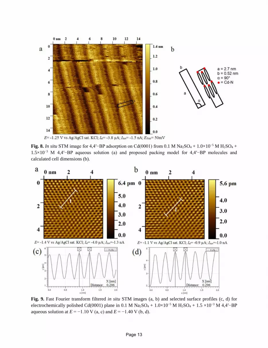
Fig. 8. In situ STM image for 4,4′−BP adsorption on Cd(0001) from 0.1 M Na2SO4 + 1.0×10⁻⁵ M H2SO4 + 1.5×10⁻³ M 4,4′−BP aqueous solution (a) and proposed packing model for 4,4′−BP molecules and calculated cell dimensions (b).
Fig. 9. Fast Fourier transform filtered in situ STM images (a, b) and selected surface profiles (c, d) for electrochemically polished Cd(0001) plane in 0.1 M Na2SO4 + 1.0×10⁻⁵ M H2SO4 + 1.5 ×10⁻³ M 4,4′−BP aqueous solution at E = −1.10 V (a, c) and E = −1.40 V (b, d).
Page 13
layer and strong chemical bonding of the adsorbed molecules on Cd(0001) surface (with partial charge transfer step). However, no structural changes were observed in the adsorbed layer, while cycling the electrode potential during a long time within the narrow potential region (–1.30 V ≤ E ≤ −1.25 V), where the so−called reorientation of the 4,4′−BP molecules takes place. At E < −1.35 V and E > −1.25 V, the atomic resolution level picture, characteristic of the inactive supporting electrolyte | Cd(0001) interface, was observed (Fig. 9) [40].
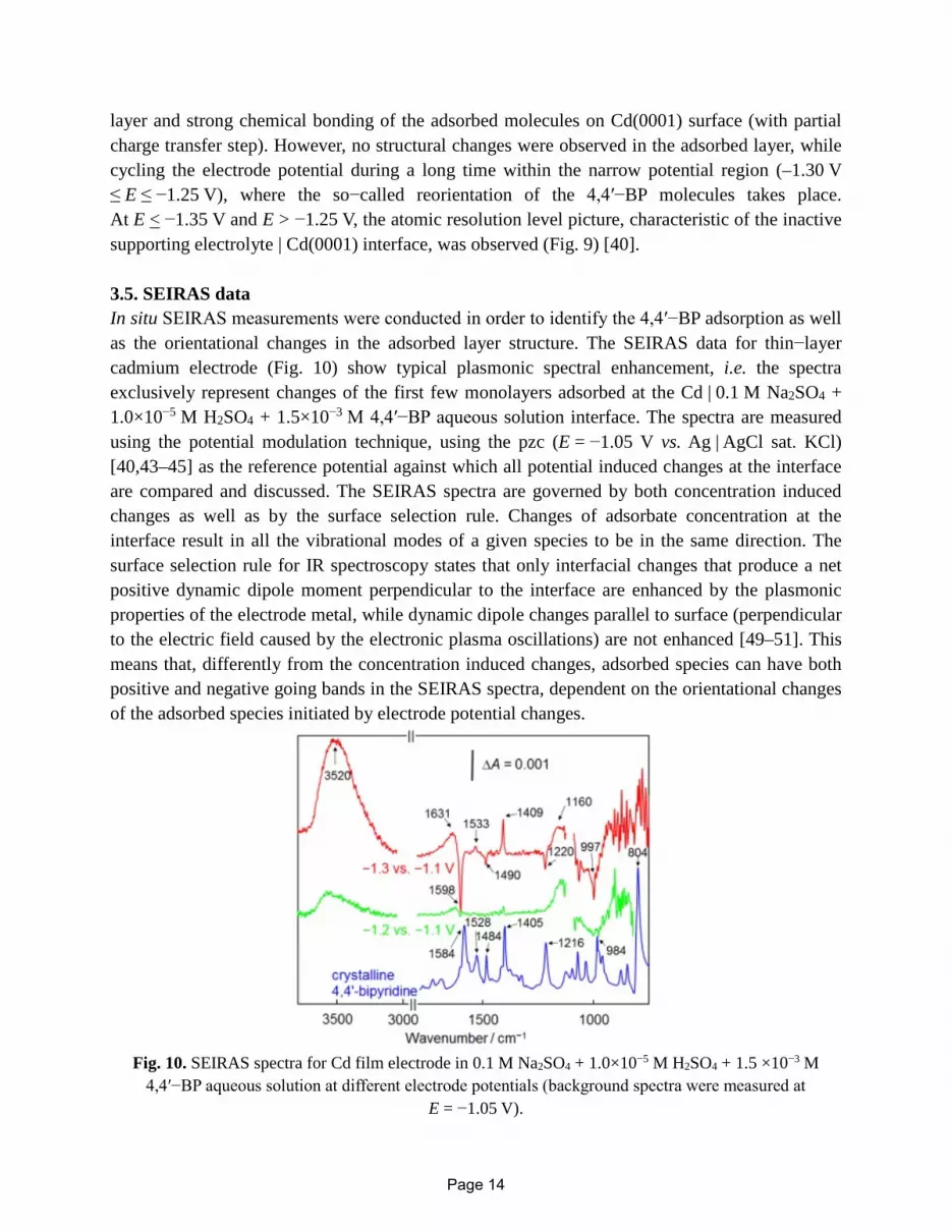
3.5. SEIRAS data In situ SEIRAS measurements were conducted in order to identify the 4,4′−BP adsorption as well as the orientational changes in the adsorbed layer structure. The SEIRAS data for thin−layer cadmium electrode (Fig. 10) show typical plasmonic spectral enhancement, i.e. the spectra exclusively represent changes of the first few monolayers adsorbed at the Cd | 0.1 M Na2SO4 + 1.0×10⁻⁵ M H2SO4 + 1.5×10⁻³ M 4,4′−BP aqueous solution interface. The spectra are measured using the potential modulation technique, using the pzc (E = −1.05 V vs. Ag | AgCl sat. KCl) [40,43–45] as the reference potential against which all potential induced changes at the interface are compared and discussed. The SEIRAS spectra are governed by both concentration induced changes as well as by the surface selection rule. Changes of adsorbate concentration at the interface result in all the vibrational modes of a given species to be in the same direction. The surface selection rule for IR spectroscopy states that only interfacial changes that produce a net positive dynamic dipole moment perpendicular to the interface are enhanced by the plasmonic properties of the electrode metal, while dynamic dipole changes parallel to surface (perpendicular to the electric field caused by the electronic plasma oscillations) are not enhanced [49–51]. This means that, differently from the concentration induced changes, adsorbed species can have both positive and negative going bands in the SEIRAS spectra, dependent on the orientational changes of the adsorbed species initiated by electrode potential changes.
Fig. 10. SEIRAS spectra for Cd film electrode in 0.1 M Na2SO4 + 1.0×10⁻⁵ M H2SO4 + 1.5 ×10⁻³ M 4,4′−BP aqueous solution at different electrode potentials (background spectra were measured at
E = −1.05 V).
Page 14
The SEIRAS data show that there are large spectral changes between E = −1.20 V and E = −1.30 V, thus, within the potential region where the so−called reorientation capacitance maximum has been visualized using the CV and EIS methods. The spectrum measured at E = −1.20 V mainly shows the weak absorption bands that are characteristic of changes within the electrical double layer. The spectrum at E = −1.30 V shows extremely strong absorption bands characteristic of large−scale interfacial interaction changes. Thus, increase in the amount of crystalline water at the interface (seen by the broad H−bonded water absorption bands at 3520 and 1630 cm−1) and a decrease in the amount of 4,4′−BP at the Cd film electrode | solution interface have been established. Interestingly, it can be seen that the bands representative of the molecular vibrations parallel to the longitudinal axis of the neutral 4,4′−BP molecule (bands at 1598, 1490, 1220 and 997 cm−1) are strongly negative, while the bands representative of vibrations perpendicular to this axis are weakly positive (bands at 1533 and 1409 cm−1). Therefore, as seen from the CV and EIS experiments, there is indeed a slight decrease in the interfacial concentration of 4,4′−BP at more negative electrode potentials (at E = −1.30 V) being replaced by the well−ordered (so−called crystalline) water structure and electrolyte ions (sulfate band at 1160 cm−1). On the other hand, it was also established that the orientation of the adsorbed 4,4′−BP molecules on Cd(0001) changes relative to the pzc. While the molecules are likely perpendicular (similar to that shown for the Au(111) interface [4] due to end−on bonding) to the surface at the Cd(0001) electrode at pzc (seen by strong absorption bands along the longitudinal axis of the molecule, perpendicular to the surface), they are shifted to the orientation more parallel to the metal | solution interface at more negative electrode potentials. SEIRAs measurements also confirm that the faradic reduction process at E ≤ −1.4 V corresponds to the reduction of 4,4′−BP molecules, similar to what has been established by previous in situ Raman measurements[68,69].
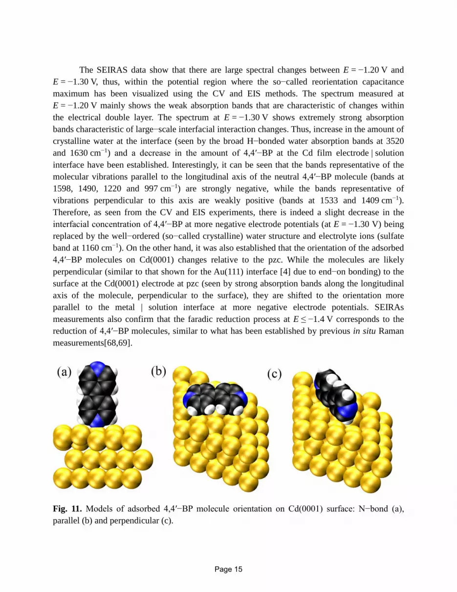
Fig. 11. Models of adsorbed 4,4′−BP molecule orientation on Cd(0001) surface: N−bond (a), parallel (b) and perpendicular (c).
Page 15
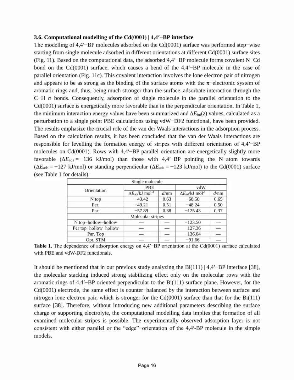
3.6. Computational modelling of the Cd(0001) | 4,4′−BP interface The modelling of 4,4′−BP molecules adsorbed on the Cd(0001) surface was performed step−wise starting from single molecule adsorbed in different orientations at different Cd(0001) surface sites (Fig. 11). Based on the computational data, the adsorbed 4,4′−BP molecule forms covalent N−Cd bond on the Cd(0001) surface, which causes a bend of the 4,4′−BP molecule in the case of parallel orientation (Fig. 11c). This covalent interaction involves the lone electron pair of nitrogen and appears to be as strong as the binding of the surface atoms with the π−electronic system of aromatic rings and, thus, being much stronger than the surface–adsorbate interaction through the C−H σ−bonds. Consequently, adsorption of single molecule in the parallel orientation to the Cd(0001) surface is energetically more favorable than in the perpendicular orientation. In Table 1, the minimum interaction energy values have been summarized and ΔEint(z) values, calculated as a perturbation to a single point PBE calculations using vdW−DF2 functional, have been provided. The results emphasize the crucial role of the van der Waals interactions in the adsorption process. Based on the calculation results, it has been concluded that the van der Waals interactions are responsible for levelling the formation energy of stripes with different orientation of 4,4′−BP molecules on Cd(0001). Rows with 4,4′−BP parallel orientation are energetically slightly more favorable (ΔEads = −136 kJ/mol) than those with 4,4′−BP pointing the N−atom towards (ΔEads = −127 kJ/mol) or standing perpendicular (ΔEads = −123 kJ/mol) to the Cd(0001) surface (see Table 1 for details).
Single molecule
Orientation PBE vdW ΔEad/kJ mol-1 d/nm ΔEad/kJ mol-1 d/nm
N top −43.42 0.63 −68.50 0.65 Per. −49.21 0.51 −48.24 0.50 Par. −57.89 0.38 −125.43 0.37
Molecular stripes N top−hollow−hollow — — −123.50 —
Per top−hollow−hollow — — −127.36 — Par. Top — — −136.04 —
Opt. STM — — −91.66 — Table 1. The dependence of adsorption energy on 4,4′−BP orientation at the Cd(0001) surface calculated with PBE and vdW-DF2 functionals.
It should be mentioned that in our previous study analyzing the Bi(111) | 4,4′−BP interface [38], the molecular stacking induced strong stabilizing effect only on the molecular rows with the aromatic rings of 4,4′−BP oriented perpendicular to the Bi(111) surface plane. However, for the Cd(0001) electrode, the same effect is counter−balanced by the interaction between surface and nitrogen lone electron pair, which is stronger for the Cd(0001) surface than that for the Bi(111) surface [38]. Therefore, without introducing new additional parameters describing the surface charge or supporting electrolyte, the computational modelling data implies that formation of all examined molecular stripes is possible. The experimentally observed adsorption layer is not consistent with either parallel or the “edge”−orientation of the 4,4′-BP molecule in the simple models.
Page 16
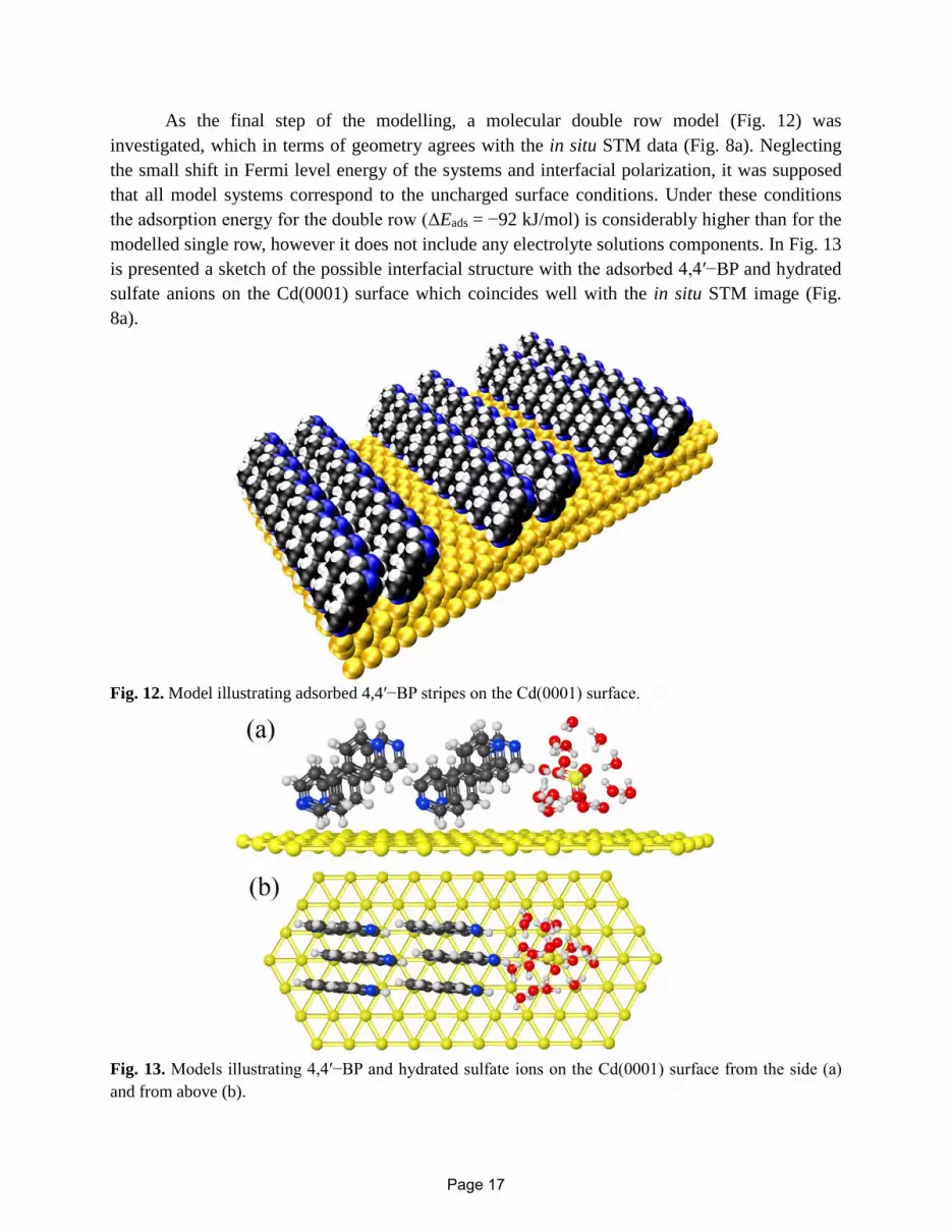
As the final step of the modelling, a molecular double row model (Fig. 12) was investigated, which in terms of geometry agrees with the in situ STM data (Fig. 8a). Neglecting the small shift in Fermi level energy of the systems and interfacial polarization, it was supposed that all model systems correspond to the uncharged surface conditions. Under these conditions the adsorption energy for the double row (ΔEads = −92 kJ/mol) is considerably higher than for the modelled single row, however it does not include any electrolyte solutions components. In Fig. 13 is presented a sketch of the possible interfacial structure with the adsorbed 4,4′−BP and hydrated sulfate anions on the Cd(0001) surface which coincides well with the in situ STM image (Fig. 8a).
Fig. 12. Model illustrating adsorbed 4,4′−BP stripes on the Cd(0001) surface.
Fig. 13. Models illustrating 4,4′−BP and hydrated sulfate ions on the Cd(0001) surface from the side (a) and from above (b).
Page 17
4. DiscussionThe results of the CV, EIS and fitting data of Nyquist and Bode plots for the Cd(0001) | baseelectrolyte + 4,4′−BP interface indicate that there are two distinct potential areas of interest,where the adsorption and the formation of 2D 4,4′−BP monolayer takes place. At less negativeelectrode potentials, E ≥ −1.20 V, 4,4′−BP adsorbs forming densely packed stripes. Comparableresults have been shown for the Au(111) | 4,4′−BP + supporting electrolyte interface, where the4,4′−BP molecules are adsorbed head−on through a metal−nitrogen bond [4]. Unfortunately, todetect this structure with in situ STM, extremely low tunneling currents are necessary in order tonot saturate the through−molecule tunneling, which has been very difficult even for theAu(111) | 4,4′−BP interface [4]. At more negative electrode potentials (E ≤ −1.25 V) some of the4,4′−BP molecules desorb, giving rise to a reorientation peak in the cyclic voltammograms aswell as the so−called reorientational capacitive peak in the CS vs. E curve. As the packagingdensity of the organic adlayer of 4,4′−BP decreases (E = −1.25 V), a striped structure is formedon the Cd(0001) plane structure, clearly seen on in situ STM images. From the in situ STMimages it was determined that the fine structure parameters for the formed layer are: 2.70 nmbetween the stripes and 0.26 nm in the direction of the stripes (between adsorbed 4,4′−BPmolecules). These parameters were used to construct an adsorption unit cell. It is also seen fromthe in situ STM data, that at E < −1.20 V, the entire surface is not covered with an orderedorganic adsorption layer. The calculated adlayer coverage is about 4.73×10⁻¹⁰ mol cm−2.
In situ SEIRAS measurements were conducted in order to identify the adsorbate molecules, as well as the orientational changes of the adsorbate on the Cd(0001) surface due to the changes of electrode potential, i.e. by the increase of negative electrode potential. The SEIRAS results collected show that the 4,4′−BP is adsorbing on Cd(0001) in the molecular form and not as on acidic radical found for the Bi(111) | 4,4′−BP system adsorbed in acidified surface inactive electrolyte solution [38]. The results also indicate that at more negative electrode potentials the 4,4′−BP molecules are probably orientated nearly parallel to the Cd(0001) surface and in a more reclined position relative to the orientation and structure near pzc.
Using the information from in situ STM and SEIRAS measurements, modelling of the interfacial structure was partaken in order to determine the orientation of the organic molecules and to establish a probable adlayer structure. It was determined that the parameters for the unit cell nearly correspond to the distances within the metal cluster (d = 0.27 nm). Thus, it was likely that the bonds between the metal and nitrogen atoms remain stable. Different adlayer structures were tested and evaluated based on both optimal packaging density and minimal energy values. The best fitting results were also evaluated against the in situ STM results until a reasonable fit was found.
5. ConclusionsThe study of 4,4′−bipyridine (4,4′−BP) adsorption from weakly acidified surface interactivesodium sulfate electrolyte solution on the Cd(0001) surface revealed the presence ofwell−organized nanoscale 4,4′−BP structure within the electrode potential region from −1.30 V to−1.20 V. It was demonstrated by in situ STM data, that at moderate negative electrode potential
Page 18

(E = −1.25 V), the adsorbed 4,4′−BP molecules form parallel stripes on Cd(0001) surface with an adlayer coverage of 4.73×10⁻¹⁰ mol cm−2. From the in situ STM images it was determined that the fine structure parameters for the formed layer are: 2.70 nm between the stripes and 0.26 nm in the direction of the stripes. Interfacial modelling data demonstrated that the stripes consist of multiple molecules and the 4,4′−BP molecules are oriented in a reclined, nearly parallel position on the Cd(0001) plane surface. A good agreement between the theoretically modelled and measured in situ STM data, as well as between calculated and measured SEIRAS spectra, supports the hypothesis of reclined alignment of the 4,4′−BP molecules on the Cd(0001) surface. However, we would like to stress that the key factor leading to the formation of the well−ordered nanoscale adsorption structures on the single crystal Cd(0001) surface is the close matching of the optimum distance for intermolecular interactions with the distance between adsorption positions of molecules and atoms at the Cd(0001) surface. Therefore, it can be concluded, that the formation of well−ordered interfacial structures, similar to that observed for the adsorption patterns of 4,4′−BP on top of the Cd(0001) electrode surface, can be calculated and analyzed by applying DFT calculations including proper description of the van der Waals interactions.
6. AcknowledgmentsThis study was partially funded by the Estonian Science Foundation Grant No. 8786, EstonianEnergy Technology Program Project SLOKT10209T, Estonian Institutional Research ProjectIUT20−13 and Estonian Centers of Excellence in Science Project: High−technology Materials forSustainable Development TK117.
7. References[1] L.-J. Wan, Fabricating and controlling molecular self-organization at solid surfaces: Studies by
scanning tunneling microscopy, Acc. Chem. Res. 39 (2006) 334–342.[2] T. Wandlowski, Phase Transitions in Two-dimensional Adlayers at Electrode Surfaces:
Thermodynamics, Kinetics, and Structural Aspects, Encycl. Electrochem. (2002).http://onlinelibrary.wiley.com/doi/10.1002/9783527610426.bard010303/full (accessed May 20,2015).
[3] D.M. Kolb, Reconstruction phenomena at metal-electrolyte interfaces, Prog. Surf. Sci. 51 (1996)109–173.
[4] D. Mayer, T. Dretschkow, K. Ataka, T. Wandlowski, Structural transitions in 4, 4′-bipyridineadlayers on Au (111)—an electrochemical and in-situ STM-study, J. Electroanal. Chem. 524 (2002)20–35.
[5] T. Dretschkow, T. Wandlowski, An order–disorder–order adlayer transition of 2,2’-bipyridine onAu(111), Electrochimica Acta. 45 (1999) 731–740. doi:10.1016/S0013-4686(99)00252-2.
[6] T. Dretschkow, D. Lampner, T. Wandlowski, Structural transitions in 2, 2′-bipyridine adlayers on Au(111)—an in-situ STM study, J. Electroanal. Chem. 458 (1998) 121–138.
[7] Q. Jin, J.A. Rodriguez, C.Z. Li, Y. Darici, N.J. Tao, Self-assembly of aromatic thiols on Au (111),Surf. Sci. 425 (1999) 101–111.
[8] I. Burgess, C.A. Jeffrey, X. Cai, G. Szymanski, Z. Galus, J. Lipkowski, Direct visualization of thepotential-controlled transformation of hemimicellar aggregates of dodecyl sulfate into a condensed
Page 19
monolayer at the Au (111) electrode surface, Langmuir. 15 (1999) 2607–2616. [9] P. Müller, S. Ando, T. Yamada, K. Itaya, Formation of an ordered structure of iodine adsorbed on Ni
(111) and the anodic dissolution processes: in-situ STM study, J. Electroanal. Chem. 467 (1999)282–290.
[10] V. Maurice, L.H. Klein, H.-H. Strehblow, P. Marcus, In situ STM study of the initial stages of anodicoxidation of Cu (111) in the presence of sulfates, J. Electrochem. Soc. 150 (2003) B316–B324.
[11] K.G. Baikerikar, S. Sathyanarayana, Adsorption of camphor, camphene, pinene, naphthalene andnonylic acid at the mercury-solution interface, J. Electroanal. Chem. Interfacial Electrochem. 24(1970) 333–344.
[12] N.A. Paltusova, A.R. Alumaa, U.V. Palm, Camphor Adsorption on the Faces of Bismuth Single-Crystals-Surface Microstructure and Phase-transition in the Adsorption Layer, Plenum Publ CorpConsultants Bureau, 233 Spring St, New York, NY 10013, 1979.
[13] C. Buess-Herman, C. Franck, L. Gierst, On the influence of molecular structure on the orientationand the occurrence of phase transitions in organic adsorbed layers at the mercury—water interface,J. Electroanal. Chem. 329 (1992) 91–102.
[14] H. Striegler, D. Krznarić, D.M. Kolb, Two-dimensional condensation of camphor and its derivativeson Au (111) electrodes, J. Electroanal. Chem. 532 (2002) 227–235.
[15] M. Danckwerts, Y.-J. Li, J. Oslonovitch, B. Pettinger, K. Krischer, Adsorption of camphor on Au(111) and its effect on the electroreduction of periodate (IO4-), J. Phys. Chem. B. 108 (2004) 14398–14406.
[16] S. Kallip, E. Lust, In situ STM studies of Bi (111) electrodes in aqueous electrolyte solutions,Electrochem. Commun. 7 (2005) 863–867.
[17] H. Striegler, P. Skoluda, D.M. Kolb, On the stability of unreconstructed Au (100)-(1x1) at negativepotentials in aqueous sulfate solution, J. Electroanal. Chem. 471 (1999) 9–13.
[18] S. Sathyanarayana, K.G. Baikerikar, Interpretation of differential capacitance curves obtained duringa two-dimensional association of organic molecules, J. Electroanal. Chem. Interfacial Electrochem.21 (1969) 449–455.
[19] S. Sathyanarayana, K.G. Baikerikar, Kinetics of adsorption of camphor, camphene, pinene andnonylic acid at the mercury-solution interface, J. Electroanal. Chem. Interfacial Electrochem. 25(1970) 209–218.
[20] U. Retter, H. Jehring, Untersuchungen der adsorptionskinetik an der phasengrenzequecksilber/elektrolyt durch analoge sessung der doppelschichtadmittanz, J. Electroanal. Chem.Interfacial Electrochem. 46 (1973) 375–380.
[21] R. Sridharan, R. De Levie, On diffusion-controlled film formation and dissolution, J. Electroanal.Chem. Interfacial Electrochem. 205 (1986) 303–307.
[22] V.A. Benderskii, G.I. Velichko, B. Damaskin, E. Stenina, N. Fedorovich, Phase-transitions of the 1stkind in condensed-layer formation on the mercury-electrode, Sov. Electrochem. 25 (1989) 1220–1224.
[23] C.G. Phillips, The steady-state current for a microelectrode near diffusion-limited conditions, J.Electroanal. Chem. Interfacial Electrochem. 291 (1990) 251–256.
[24] E. Stenina, B. Damaskin, N. Fedorovich, Determination of the Attraction Constant for CamphorAdsorption on the Mercury-electrode, Plenum Publ Corp Consultants Bureau, 233 Spring St, NewYork, NY 10013, 1979.
[25] A. Kühnle, Self-assembly of organic molecules at metal surfaces, Curr. Opin. Colloid Interface Sci.
Page 20
14 (2009) 157–168. [26] C. Vericat, M.E. Vela, G. Benitez, P. Carro, R.C. Salvarezza, Self-assembled monolayers of thiols
and dithiols on gold: new challenges for a well-known system, Chem. Soc. Rev. 39 (2010) 1805–1834.
[27] M.M. Ling, Z. Bao, Thin film deposition, patterning, and printing in organic thin film transistors,Chem. Mater. 16 (2004) 4824–4840.
[28] P.J. Steel, Aromatic nitrogen heterocycles as bridging ligands; a survey, Coord. Chem. Rev. 106(1990) 227–265.
[29] S. Yu, S. Ahmadi, P. Palmgren, F. Hennies, M. Zuleta, M. Gothelid, Modification of Charge Transferand Energy Level Alignment at Organic/TiO2 Interfaces, J. Phys. Chem. C. 113 (2009) 13765–13771.
[30] Y. Chi, P.-T. Chou, Contemporary progresses on neutral, highly emissive Os (II) and Ru (II)complexes, Chem. Soc. Rev. 36 (2007) 1421–1431.
[31] B. Xu, N.J. Tao, Measurement of single-molecule resistance by repeated formation of molecularjunctions, Science. 301 (2003) 1221–1223.
[32] Y.-X. Diao, M.-J. Han, L.-J. Wan, K. Itaya, T. Uchida, H. Miyake, et al., Adsorbed structures of 4,4’-bipyridine on Cu (111) in acid studied by STM and IR, Langmuir. 22 (2006) 3640–3646.
[33] T. Wandlowski, K. Ataka, D. Mayer, In situ infrared study of 4, 4’-bipyridine adsorption on thin goldfilms, Langmuir. 18 (2002) 4331–4341.
[34] J. Jia, P. Hubberstey, N.R. Champness, M. Schröder, Supramolecular Chemistry of 4, 4′-Bipyridine-N, N′-dioxide in Transition Metal Complexes: A Rich Diversity of Co-ordinate, Hydrogen-Bond andAromatic Stacking Interactions, in: Mol. Netw., Springer, 2009: pp. 135–161.http://link.springer.com/chapter/10.1007/978-3-642-01367-6_10 (accessed May 20, 2015).
[35] H.W. Roesky, M. Andruh, The interplay of coordinative, hydrogen bonding and π–π stackinginteractions in sustaining supramolecular solid-state architectures.: A study case of bis (4-pyridyl)-and bis (4-pyridyl-N-oxide) tectons, Coord. Chem. Rev. 236 (2003) 91–119.
[36] A.N. Khlobystov, A.J. Blake, N.R. Champness, D.A. Lemenovskii, A.G. Majouga, N.V. Zyk, et al.,Supramolecular design of one-dimensional coordination polymers based on silver (I) complexes ofaromatic nitrogen-donor ligands, Coord. Chem. Rev. 222 (2001) 155–192.
[37] S.C. Manna, E. Zangrando, J. Ribas, N.R. Chaudhuri, Cobalt (ii)–(dpyo)–dicarboxylate networks:unique H-bonded assembly and rare bridging mode of dpyo in one of them [dpyo= 4, 4′-dipyridyl N,N′-dioxide], Dalton Trans. (2007) 1383–1391.
[38] V. Grozovski, V. Ivaništšev, H. Kasuk, T. Romann, E. Lust, Balance of the interfacial interactions of4, 4′-bipyridine at Bi (111) surface, Electrochimica Acta. 120 (2014) 86–95.
[39] S. Saha, T. Taguchi, N. Tachikawa, K. Yoshii, Y. Katayama, Electrochemical Behavior of Cadmiumin 1-Butyl-1-methylpyrrolidinium Bis (trifluoromethylsulfonyl) amide Room-temperature IonicLiquid, Electrochimica Acta. (2015).http://www.sciencedirect.com/science/article/pii/S0013468615011299 (accessed May 20, 2015).
[40] P. Pikma, V. Grozovski, H. Kasuk, E. Lust, In situ STM studies of electrochemically polished Cd(0001) electrode in aqueous electrolyte solutions, Surf. Sci. 628 (2014) 86–91.
[41] M. Ernzerhof, K. Burke, J.P. Perdew, Density functional theory, the exchange hole, and themolecular bond, Theor. Comput. Chem. 4 (1996) 207–238.
[42] J. Wellendorff, T. Bligaard, On the importance of gradient-corrected correlation for van der Waalsdensity functionals, Top. Catal. 54 (2011) 1143–1150.
Page 21
[43] E. Lust, A. Jänes, V. Sammelselg, P. Miidla, K. Lust, Surface roughness of bismuth, antimony andcadmium electrodes, Electrochimica Acta. 44 (1998) 373–383.
[44] E.J. Lust, K.K. Lust, A.-J. Jänes, Influence of the crystallographic structure of the electrode surfaceon the structure of the electrical double layer and adsorption of organic molecules, Russ. J.Electrochem. 31 (1995) 807–821.
[45] E.I. Lust, A.-Y. Yanes, K.K. Lust, Y.I. Erlikh, The structure of the electrical double layer at the facesof bismuth, antimony, or cadmium single crystals in surface-inactive electrolytes, Russ. J.Electrochem. 32 (1996) 552–564.
[46] E. Lust, A. Jänes, K. Lust, M. Väärtnõu, Electric double layer structure and adsorption ofcyclohexanol on single crystal cadmium, antimony and bismuth electrodes, Electrochimica Acta. 42(1997) 771–783.
[47] E. Lust, A. Jänes, K. Lust, R. Pullerits, Adsorption of organic compounds and hydrophilicity ofbismuth, cadmium and antimony electrodes, J. Electroanal. Chem. 431 (1997) 183–201.
[48] D. Nečas, P. Klapetek, Gwyddion: an open-source software for SPM data analysis, Cent. Eur. J.Phys. 10 (2012) 181–188.
[49] T. Romann, O. Oll, P. Pikma, H. Tamme, E. Lust, Surface chemistry of carbon electrodes in 1-ethyl-3-methylimidazolium tetrafluoroborate ionic liquid – an in situ infrared study, Electrochimica Acta.125 (2014) 183–190. doi:10.1016/j.electacta.2014.01.077.
[50] T. Romann, Preparation and surface modification of bismuth thin film, porous, and microelectrodes,Thesis, 2010. http://dspace.utlib.ee/dspace/handle/10062/14871 (accessed April 8, 2015).
[51] T. Romann, O. Oll, P. Pikma, E. Lust, Abnormal infrared effects on bismuth thin film–EMImBF4ionic liquid interface, Electrochem. Commun. 23 (2012) 118–121.
[52] J. Enkovaara, C. Rostgaard, J.J. Mortensen, J. Chen, M. Dułak, L. Ferrighi, et al., Electronicstructure calculations with GPAW: a real-space implementation of the projector augmented-wavemethod, J. Phys. Condens. Matter. 22 (2010) 253202.
[53] P.E. Blöchl, Projector augmented-wave method, Phys. Rev. B. 50 (1994) 17953.[54] S.R. Bahn, K.W. Jacobsen, An object-oriented scripting interface to a legacy electronic structure
code, Comput. Sci. Eng. 4 (2002) 56–66.[55] Y. Zhao, D.G. Truhlar, A new local density functional for main-group thermochemistry, transition
metal bonding, thermochemical kinetics, and noncovalent interactions, J. Chem. Phys. 125 (2006)194101.
[56] L. Ferrighi, G.K. Madsen, B. Hammer, Self-consistent meta-generalized gradient approximationstudy of adsorption of aromatic molecules on noble metal surfaces, J. Chem. Phys. 135 (2011)084704.
[57] J. Tersoff, D.R. Hamann, Theory of the scanning tunneling microscope, in: Scanning TunnelingMicrosc., Springer, 1993: pp. 59–67. http://link.springer.com/chapter/10.1007/978-94-011-1812-5_5(accessed May 23, 2015).
[58] B.B. Damaskin, O.A. Petrii, V.V. Batrakov, Adsorption of organic compounds on electrodes, (1971).http://agris.fao.org/agris-search/search.do?recordID=US201300475705 (accessed May 20, 2015).
[59] D. Rolle, J.W. Schultze, The electrosorption valency of organic electrosorbates: Part II. Aromaticand heterocyclic compounds, J. Electroanal. Chem. Interfacial Electrochem. 229 (1987) 141–164.
[60] A.R. Alumaa, U.V. Palm, Adsorption of Phenol on a Bismuth Electrode, Elektrokhimiya. 6 (1970)580–583.
[61] U.V. Palm, B.B. Damaskin, Structure of the electrical double layer and adsorption phenomena on a
Page 22
bismuth electrode, Itogi Nauki Tekhniki. 12 (1977) 99. [62] H. Kasuk, G. Nurk, K. Lust, E. Lust, Adsorption kinetics of uracil on bismuth single crystal planes,
J. Electroanal. Chem. 550 (2003) 13–31.[63] V. Grozovski, H. Kasuk, S. Kallip, E. Lust, Adsorption of thiourea on Bi (111) electrode surface, J.
Electroanal. Chem. 712 (2014) 103–112.[64] I.A. Vinokurov, M. Morin, J. Kankare, Mechanism of reductive desorption of self-assembled
monolayers on the basis of Avrami theorem and diffusion, J. Phys. Chem. B. 104 (2000) 5790–5796.[65] S. Kallip, H. Kasuk, V. Grozovski, P. Möller, E. Lust, Adsorption of camphor and 2, 2′-bipyridine on
Bi (111) electrode surface, Electrochimica Acta. 53 (2008) 4035–4045.[66] R. Jäger, S. Kallip, V. Grozovski, K. Lust, E. Lust, Electroreduction of anions on chemically etched
and electrochemically polished Bi (111) electrode, J. Electroanal. Chem. 622 (2008) 79–89.[67] G. Nurk, A. Jänes, K. Lust, E. Lust, Adsorption kinetics of 2-methyl-2-butanol on bismuth single
crystal planes, J. Electroanal. Chem. 515 (2001) 17–32.[68] T. Lu, T.M. Cotton, R.L. Birke, J.R. Lombardi, Raman and surface-enhanced Raman spectroscopy of
the three redox forms of 4,4’-bipyridine, Langmuir. 5 (1989) 406–414. doi:10.1021/la00086a021.[69] T.M. Cotton, M. Vavra, Simultaneous raman and cyclic voltammetry study of the redox behavior of
4,4′-bipyridine on silver, Chem. Phys. Lett. 106 (1984) 491–497. doi:10.1016/0009-2614(84)85369-5.
[70] A. Lasia, Electrochemical impedance spectroscopy and its applications, in: Mod. Asp. Electrochem.,Springer, 2002: pp. 143–248. http://link.springer.com/chapter/10.1007/0-306-46916-2_2 (accessedMay 20, 2015).
[71] D. Johnson, ZView: a Software Program for IES Analysis, Version 2.8, Scribner Associates, IncSouth. Pines NC. 200 (2002).
[72] W. Lorenz, F. Möckel, Adsorptionsisotherme und Adsorptionskinetik kapillaraktiver organischerMolekeln an der Quecksilberelektrode, Z. Für Elektrochem. Berichte Bunsenges. Für Phys. Chem.60 (1956) 507–515.
[73] A.N. Frumkin, V.I. Melik-Gaykazyan, Determination of the kinetics of organic substances bymeasuring the capacitance and conductivity at the electrode-solution boundary, in: Dokl Akad NaukUSSR, 1951: pp. 855–858.
[74] R. de Levie, T. Wandlowski, Hydrogen bonding and two-dimensional condensation in uracils, J.Electroanal. Chem. 366 (1994) 265–270.
[75] J. Lipkowski, P.N. Ross, Adsorption of molecules at metal electrodes.[Vol. 1], VCH, 1992.
Page 23