a novel resistor-free electronically adjustable current-mode instrumentation amplifier
TRANSCRIPT
Circuits Syst Signal Process (2013) 32:1025–1038DOI 10.1007/s00034-012-9522-y
A Novel Resistor-Free Electronically AdjustableCurrent-Mode Instrumentation Amplifier
Leila Safari · Shahram Minaei
Received: 26 March 2012 / Revised: 8 November 2012 / Published online: 27 November 2012© Springer Science+Business Media New York 2012
Abstract In this paper, a novel topology for implementing resistor-free current-modeinstrumentation amplifier (CMIA) is presented. Unlike the other previously reportedinstrumentation amplifiers (IAs), in which input and/or output signals are in voltagedomain, the input and output signals in the proposed structure are current signals andsignal processing is also completely done in current domain benefiting from the fulladvantages of current-mode signal processing. Interestingly the CMRR of the pro-posed topology is wholly determined by only five transistors. Compared to the mostof the previously reported IAs in which at least two active elements are used to attainhigh common-mode rejection ratio (CMRR) resulting in a complicated circuit, theproposed structure enjoys from an extremely simple circuit. It also exhibits low in-put impedance employing negative feedback principal. Of more interest is that, usingsimple degenerate current mirrors, the differential-mode gain of the proposed CMIAcan be electronically varied by control voltage. This property makes it completelyfree of resistors. The very low number of transistors used in the structure of the pro-posed CMIA grants it such desirable properties as low-voltage low-power operation,suitability for integration, wide bandwidth etc. SPICE simulation results using theTSMC 0.18-µm CMOS process model under supply voltage of ±0.8 V show a highCMRR of 91 dB and a low input impedance of 291.5 � for the proposed CMIA. Tem-perature simulation results are also provided, which prove low temperature sensitivityof the proposed CMIA.
L. Safari (�)Department of Electrical and Electronics Engineering, Iran University of Science and Technology(IUST), Tehran, Irane-mail: [email protected]
S. MinaeiDepartment of Electronics and Communications Engineering, Dogus University, Acibadem,Kadikoy 34722, Istanbul, Turkeye-mail: [email protected]
1026 Circuits Syst Signal Process (2013) 32:1025–1038
Keywords Current-mode · Instrumentation amplifier · High CMRR · Low power ·Low voltage
1 Introduction
In the last years, analog circuit designers have been faced with serious challengesdue to the increasing demand for low-voltage low-power mobile and battery pow-ered equipments and also technology down scaling trend [2, 19]. Using the standardCMOS technology which is optimized for designing digital circuits (and does notfeature the performance required for developing analog ones) along with trade-offbetween dynamic range, bandwidth, chip area and the like, have increased the analogcircuit design procedure complexity. A promising approach to meeting these chal-lenges is provided by the current-mode signal processing. The low-voltage operation,wider dynamic range, simpler circuitry, wider bandwidth and lower consumed powerrequirement of the current-mode circuits are the main reasons of its popularity inrecent years [1, 16, 18]. Therefore due to its many benefits, current-mode design iswidely used to implement high-performance circuits under restrictions imposed bytechnology and market.
Instrumentation amplifiers (IAs) are one of the most widely used circuits in manyapplications such as medical instrumentation, the read-out circuit of biosensors, elec-trocardiography and signal processing [3–14, 20, 21]. Literature survey shows thatthose IAs which utilize the current-mode approach exhibit superior performancecompared to the conventional IAs based on three operational amplifiers (OA) andseven resistors. Actually they remove the two main disadvantages of conventionalOA-based IAs i.e. (1) strict matching conditions required to achieve high CMRRand (2) narrow gain-dependent bandwidth (which is due to the constant gain band-width product of OA). IAs which use current-mode active building blocks such ascurrent conveyors (CCs) instead of OAs, exhibit extended gain-independent band-width. They also do not require matched resistors. Despite these attractive features,the previously reported current-mode-based IAs [3–11, 13, 14, 20, 21], suffer fromsome major weaknesses:
(1) In [3–7, 9–11, 13, 14, 20], the overall CMRR is determined by means of two ac-tive elements used at the input stage. This increases chip area, power consump-tion and circuit complexity due to the large number of transistors used. However,it should be pointed out that the circuits reported in [3, 6, 7, 9–11, 13, 20, 21] havethe advantage of implementing with commercially available active elements.
(2) The input and/or output signals in [3–11, 13] are in voltage domain and due tothe very limited voltage room available in modern technologies (as a result of lowsupply voltages), they suffer from low dynamic range (DR). On the other wordsthey have the same limitations of conventional voltage-mode signal processing inthe case of dynamic range and output voltage swing under low supply voltages.
(3) Most of the above mentioned IAs, unavoidably require external passive compo-nents (i.e. resistors) to change the differential gain. This makes them inappropri-ate for IC implementation due to occupying large chip area.
Circuits Syst Signal Process (2013) 32:1025–1038 1027
(4) They are unable to take the full advantage of current-mode signal processing.Because some part of signal processing is done in voltage domain.
Some IAs realizations have been reported based on new differential-input current-mode active building blocks such as differential voltage current conveyor (DVCC) [8]which alleviate the need for two matched CCs or other active building blocks at theinput stage of IA. Unfavorably, these implementations suffer from voltage-mode op-eration limitations and also require additional gain controlling resistors. A large num-ber of transistors, high supply voltage requirement, and high power consumption areconsidered as their other drawbacks. Some electronically controllable IAs realiza-tions have been reported in [4, 9, 14]. While these implementations lend electronictuning capability to the resulted IAs, their input and output signals are in voltagedomain. They have also high power consumption and high supply voltage require-ment. A few current input, current output IAs topologies using current feedback op-erational amplifiers (CFOAs) are presented in [20, 21]. Unfavorably they are basedon the voltage signals because additional resistors are required at the input stage toconvert current signals to voltage.
Despite the large number of CMIA realizations reported in technical literature [3–11, 13, 14, 20, 21], a careful study shows that the reported work cannot benefit fromthe full advantage of current-mode signal processing. Their input signals are voltageand part of signal processing is done in voltage domain. They usually lack the desir-able electronic controlling capability and their operation also depends on the floatingor grounded resistors which makes the integration difficult. Therefore in this article,a novel topology for implementing current-mode instrumentation amplifier (CMIA)is presented. Unlike the all previously reported ones, its operation is not based onthe multiple conversion of current to voltage and voltage to current signals. On theother hand, as primary requirement of any current-mode circuit, its both input andoutput signals are in current domain and it directly process current signals. It alsoenjoys from low input impedance and high output impedance nodes and is usefulwhen input and output signals are current. Favorably, the gain of the proposed CMIAcan be controlled electronically by adjusting the value of control voltage alleviatingthe need for gain controlling resistors. The gain controlling section is based on asimple degenerate current mirror consisting of only four transistors. The electroniccontrollability and simple structure grants the proposed CMIA highly flexible andversatile structure and makes it more suitable for integration. The superiority of theproposed topology over all previously reported ones gets more significant by con-sidering the fact that it alleviates the need for two matched active devices such asCCs at the input stage or complicated fully differential building blocks to achievehigh CMRR. Because it achieves high CMRR employing an extremely simple highCMRR differential-input single-output current-mode input stage realized with onlyfive transistors. To the authors’ best knowledge, the proposed CMIA is the first yetreported CMIA which resembles to an ideal current-mode circuit due to its inherentlow impedance input nodes, low-voltage low-power operation, simple circuitry, di-rect processing of current signals and wide bandwidth. The organization of this paperis as follows:
In Sect. 2 the proposed CMIAs is presented. Simulation results are presented inSect. 3 and finally Sect. 4 concludes the paper.
1028 Circuits Syst Signal Process (2013) 32:1025–1038
2 The Proposed CMIA
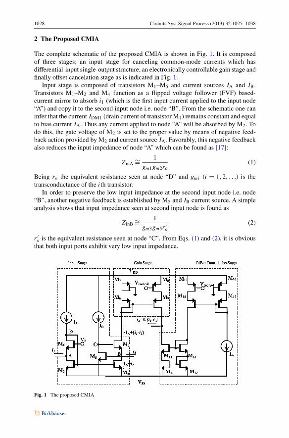
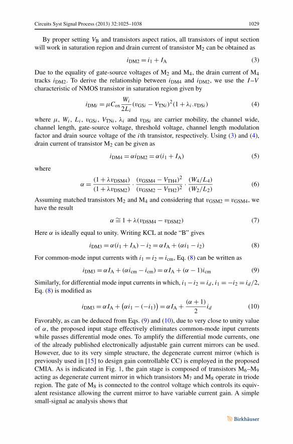
The complete schematic of the proposed CMIA is shown in Fig. 1. It is composedof three stages; an input stage for canceling common-mode currents which hasdifferential-input single-output structure, an electronically controllable gain stage andfinally offset cancelation stage as is indicated in Fig. 1.
Input stage is composed of transistors M1–M5 and current sources IA and IB.Transistors M1–M2 and M4 function as a flipped voltage follower (FVF) based-current mirror to absorb i1 (which is the first input current applied to the input node“A”) and copy it to the second input node i.e. node “B”. From the schematic one caninfer that the current IDM1 (drain current of transistor M1) remains constant and equalto bias current IA. Thus any current applied to node “A” will be absorbed by M2. Todo this, the gate voltage of M2 is set to the proper value by means of negative feed-back action provided by M2 and current source IA. Favorably, this negative feedbackalso reduces the input impedance of node “A” which can be found as [17]:
ZinA ∼= 1
gm1gm2ro(1)
Being ro the equivalent resistance seen at node “D” and gmi (i = 1,2, . . .) is thetransconductance of the ith transistor.
In order to preserve the low input impedance at the second input node i.e. node“B”, another negative feedback is established by M5 and IB current source. A simpleanalysis shows that input impedance seen at second input node is found as
ZinB ∼= 1
gm3gm5r ′o
(2)
r ′o is the equivalent resistance seen at node “C”. From Eqs. (1) and (2), it is obvious
that both input ports exhibit very low input impedance.
Fig. 1 The proposed CMIA
Circuits Syst Signal Process (2013) 32:1025–1038 1029
By proper setting VB and transistors aspect ratios, all transistors of input sectionwill work in saturation region and drain current of transistor M2 can be obtained as
iDM2 = i1 + IA (3)
Due to the equality of gate-source voltages of M2 and M4, the drain current of M4tracks iDM2. To derive the relationship between iDM4 and iDM2, we use the I–V
characteristic of NMOS transistor in saturation region given by
iDMi = μCoxWi
2Li
(vGSi − VTNi )2(1 + λi.vDSi ) (4)
where μ, Wi , Li , vGSi , VTNi , λi and vDSi are carrier mobility, the channel wide,channel length, gate-source voltage, threshold voltage, channel length modulationfactor and drain source voltage of the ith transistor, respectively. Using (3) and (4),drain current of transistor M2 can be given as
iDM4 = αiDM2 = α(i1 + IA) (5)
where
α = (1 + λvDSM4)
(1 + λvDSM2)· (vGSM4 − VTH4)
2
(vGSM2 − VTH2)2· (W4/L4)
(W2/L2)(6)
Assuming matched transistors M2 and M4 and considering that vGSM2 = vGSM4, wehave the result
α ∼= 1 + λ(vDSM4 − vDSM2) (7)
Here α is ideally equal to unity. Writing KCL at node “B” gives
iDM3 = α(i1 + IA) − i2 = αIA + (αi1 − i2) (8)
For common-mode input currents with i1 = i2 = icm, Eq. (8) can be written as
iDM3 = αIA + (αicm − icm) = αIA + (α − 1)icm (9)
Similarly, for differential mode input currents in which, i1 − i2 = id , i1 = −i2 = id/2,Eq. (8) is modified as
iDM3 = αIA + (αi1 − (−i1)
) = αIA + (α + 1)
2id (10)
Favorably, as can be deduced from Eqs. (9) and (10), due to very close to unity valueof α, the proposed input stage effectively eliminates common-mode input currentswhile passes differential mode ones. To amplify the differential mode currents, oneof the already published electronically adjustable gain current mirrors can be used.However, due to its very simple structure, the degenerate current mirror (which ispreviously used in [15] to design gain controllable CC) is employed in the proposedCMIA. As is indicated in Fig. 1, the gain stage is composed of transistors M6–M9
acting as degenerate current mirror in which transistors M7 and M8 operate in trioderegion. The gate of M8 is connected to the control voltage which controls its equiv-alent resistance allowing the current mirror to have variable current gain. A simplesmall-signal ac analysis shows that
1030 Circuits Syst Signal Process (2013) 32:1025–1038
id6 = −gm6
1 + gm6.rDS7· vg6 (11)
id9 = −gm9
1 + gm9.rDS8· vg6 (12)
where idi and gmi (i = 6,9) are, respectively, the small-signal ac drain current (flow-ing out of the drain terminal) and transconductance of the ith transistor; vg6 is small-signal ac gate voltage of M6. Moreover, rDS7 and rDS8 are the resistances providedby M7 and M8 (working in triode region), respectively. Using (11) and (12), one canwrite
id9 = gm9
gm6· 1 + gm6.rDS7
1 + gm9.rDS8· id6 = k · id6 (13)
where
k = gm9
gm6· 1 + gm6.rDS7
1 + gm9.rDS8=
1gm6
+ rDS7
1gm9
+ rDS8(14)
The resistances rDS7 and rDS8 can be found as
rDS7 = 1
μCoxW7L7
(VSG7 − |VTHP|) = 1
μCoxW7L7
(VDD − |VTHP|) (15)
rDS8 = 1
μCoxW8L8
(VSG8 − |VTHP|) = 1
μCoxW8L8
(VDD − Vcont − |VTHP|) (16)
From (14)–(16) it can be seen that the value of k can be adjusted by control voltageVcont granting the proposed circuit the popular property of electronic tuning capabil-ity.
Current mirrors M10–M13 and M14–M17 are used for offset cancelation purposes.These current mirrors and current source IA in the offset cancelation stage producea DC current which is used to cancel the DC current K · α · IA transferred from thecurrent source IA (in the input stage) to the drain of the M9 at the output node. HereK is the multiplying factor of the gain stage constructed with M6–M9 for DC currentand α is the gain of the input current mirror M1–M4 defined in (6) and (7). Assumingideal DC cancelation at the output node we obtain
io ∼= k · (α.i1 − i2) (17)
From (17) it can be realized that the parameters α and k affect the linearity of thecircuit.
Replacing i1 = icm + id/2 and i2 = icm − id/2 into (17) gives
io = k ·[(α − 1)icm + (α + 1)
2id
](18)
Thus differential-mode and common-mode gains of the proposed CMIA can be foundas
Ad = io
id= k · (α + 1)
2(19)
Ac = io
icm= k · (α − 1) (20)
Circuits Syst Signal Process (2013) 32:1025–1038 1031
From Eqs. (19) and (20), the CMRR of the proposed CMIA can be approximatelyexpressed as
CMRR =∣∣∣∣Ad
Ac
∣∣∣∣ =∣∣∣∣
α + 1
2(α − 1)
∣∣∣∣∼=
∣∣∣∣1
α − 1
∣∣∣∣ (21)
where α is assumed to be in the vicinity of unity. According to Eq. (21), CMRRof the proposed circuit does not depend on k. On the other words, the proposedcircuit exhibits constant CMRR for different values of differential mode gain. Forhigh CMRR, the proposed circuit requires matched M2 and M4 transistors and anymismatch between these transistors limits the performance of the circuit. A very in-teresting property of the proposed CMIA is that only NMOS transistors are used toachieve high CMRR making it easy to set α very close to unity. On the other handthe variation of the nominator and denominator of Eq. (6) for different temperaturesare the same, because all electrical parameters in Eq. (6) belong to matched NMOStransistors. Therefore α would experience a low variation for different values of tem-peratures. This fact implies that CMRR of the proposed circuit (which is determinedby α according to Eq. (21)) will be robust against temperature variation.
Here it is assumed that the parameter α can be described by a single-pole fre-quency model as
α(jω) = α0
1 + jωωα
(22)
where α0 and ωα are the dc values and −3 dB frequency of α, respectively.Substituting (22) into (21) and manipulating we have the result
CMRR ∼=∣∣∣∣
1
α0 − 1× 1 + jω
ωα
1 + jω(1−α0)ωα
∣∣∣∣ (23)
As can be seen from (23), CMRR of the proposed circuit has one zero and one poledefined as
ωP = (1 − α0) × ωα (24)
ωZ = ωα (25)
According to (24), due to the close to unity value of α0, the pole occurs at low fre-quencies. Therefore there is a trade-off between DC value and −3 dB bandwidth ofCMRR in the proposed circuit. For large DC values of CMRR α0 should be close tounity which results in reduced −3 dB bandwidth of CMRR.
Thanks to the cascode structure of the offset cancelation section and degeneratecurrent mirror, a high output impedance is obtained:
Zo∼= (gm9 · ro9 · rDS8)‖(gm10 · ro10 · ro11) (26)
where roi is the output resistance of the ith transistor operating in saturation regionand rDS8 is the equivalent resistance provided by M8 working in triode region.
1032 Circuits Syst Signal Process (2013) 32:1025–1038
3 Simulation Results
The proposed CMIA of Fig. 1 is tested using SPICE simulation program under supplyvoltage of ±0.8 V. The simulations are based on 0.18 µm TSMC CMOS technologyparameters. The dimensions of the MOS transistors are given in Table 1. Aspect ratiosof transistors are chosen such that all transistors (except M7, M8, M15, M16) operatein the saturation region. Current sources IA and IB are implemented with simple two-transistor current mirrors with aspect ratios of 10.8 µm/1.08 µm. The values of thesecurrent sources are both set to 5 µA and the load is also 1 k�. It should be noted that inorder to cancel the output offset current successfully, the main and offset cancelationcircuits should be identical. Thus the current source IA in the offset cancelation stageis implemented with a current mirror similar to the input current mirror composed oftransistors M1–M5.
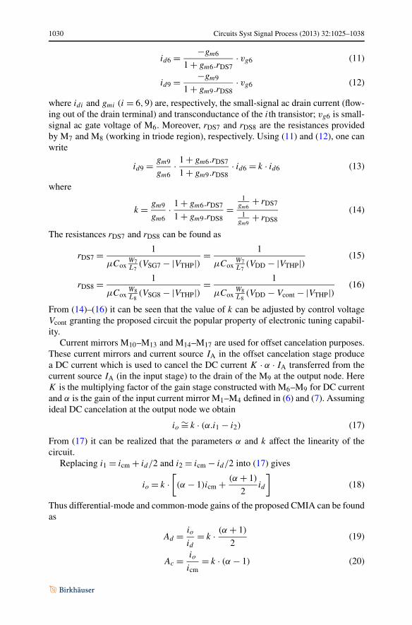
For the CMIA of Fig. 1 the control voltage (Vcont) is varied from 0 V to −0.8 Vto obtain different current gains. Figure 2 reports the differential-mode current gainfrequency performance of the proposed CMIA of Fig. 1 for different gains. As can beseen, the proposed circuit current gain varies from 9.5 to 46. The −3 dB bandwidthis 16.78 MHz for gain of 9.5 (19.5 dB) and decreases to 10.18 MHz for gain of 46(33.2 dB).
Table 1 Transistor dimensionsfor the proposed CMIA of Fig. 1 MOSFET Aspect ratio
M1, M3 39.6 µm/0.54 µm
M2, M4 3.96 µm/1.62 µm
M5 15.12 µm/0.36 µm
M6, M17 5.04 µm/0.54 µm
M7, M16 0.9 µm/0.54 µm
M9, M14 50.4 µm/0.54 µm
M8, M15 9 µm/0.54 µm
M10, M11, M12, M13 72 µm/0.72 µm
Fig. 2 Differential-mode current gain frequency response of Fig. 1 for different values of Vcont rangingfrom 0 to −0.8 V
Circuits Syst Signal Process (2013) 32:1025–1038 1033
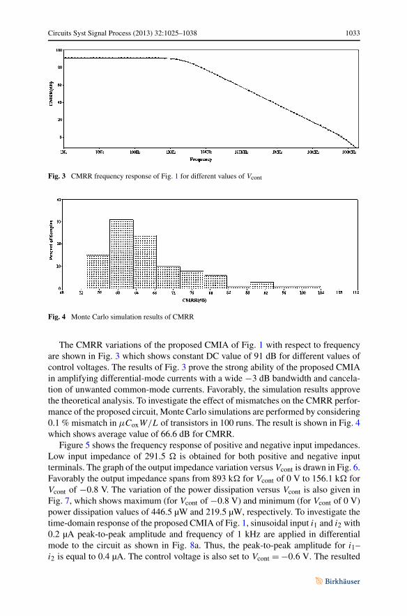
Fig. 3 CMRR frequency response of Fig. 1 for different values of Vcont
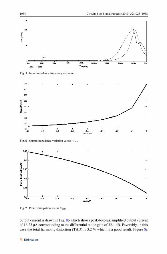
Fig. 4 Monte Carlo simulation results of CMRR
The CMRR variations of the proposed CMIA of Fig. 1 with respect to frequencyare shown in Fig. 3 which shows constant DC value of 91 dB for different values ofcontrol voltages. The results of Fig. 3 prove the strong ability of the proposed CMIAin amplifying differential-mode currents with a wide −3 dB bandwidth and cancela-tion of unwanted common-mode currents. Favorably, the simulation results approvethe theoretical analysis. To investigate the effect of mismatches on the CMRR perfor-mance of the proposed circuit, Monte Carlo simulations are performed by considering0.1 % mismatch in μCoxW/L of transistors in 100 runs. The result is shown in Fig. 4which shows average value of 66.6 dB for CMRR.
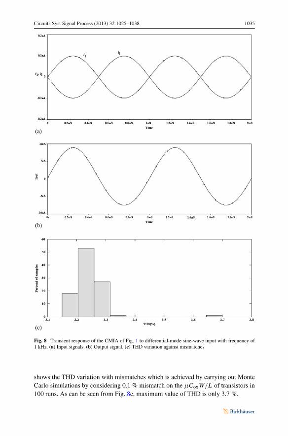
Figure 5 shows the frequency response of positive and negative input impedances.Low input impedance of 291.5 � is obtained for both positive and negative inputterminals. The graph of the output impedance variation versus Vcont is drawn in Fig. 6.Favorably the output impedance spans from 893 k� for Vcont of 0 V to 156.1 k� forVcont of −0.8 V. The variation of the power dissipation versus Vcont is also given inFig. 7, which shows maximum (for Vcont of −0.8 V) and minimum (for Vcont of 0 V)power dissipation values of 446.5 µW and 219.5 µW, respectively. To investigate thetime-domain response of the proposed CMIA of Fig. 1, sinusoidal input i1 and i2 with0.2 µA peak-to-peak amplitude and frequency of 1 kHz are applied in differentialmode to the circuit as shown in Fig. 8a. Thus, the peak-to-peak amplitude for i1–i2 is equal to 0.4 µA. The control voltage is also set to Vcont = −0.6 V. The resulted
1034 Circuits Syst Signal Process (2013) 32:1025–1038
Fig. 5 Input impedance frequency response
Fig. 6 Output impedance variation versus Vcont
Fig. 7 Power dissipation versus Vcont
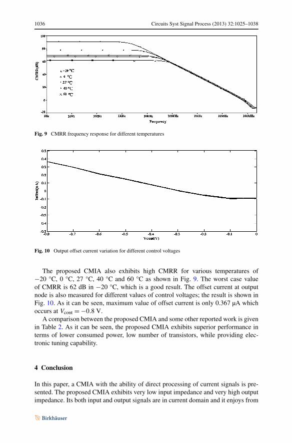
output current is drawn in Fig. 8b which shows peak-to-peak amplified output currentof 16.23 µA corresponding to the differential mode gain of 32.1 dB. Favorably, in thiscase the total harmonic distortion (THD) is 3.2 % which is a good result. Figure 8c
Circuits Syst Signal Process (2013) 32:1025–1038 1035
Fig. 8 Transient response of the CMIA of Fig. 1 to differential-mode sine-wave input with frequency of1 kHz. (a) Input signals. (b) Output signal. (c) THD variation against mismatches
shows the THD variation with mismatches which is achieved by carrying out MonteCarlo simulations by considering 0.1 % mismatch on the μCoxW/L of transistors in100 runs. As can be seen from Fig. 8c, maximum value of THD is only 3.7 %.
1036 Circuits Syst Signal Process (2013) 32:1025–1038
Fig. 9 CMRR frequency response for different temperatures
Fig. 10 Output offset current variation for different control voltages
The proposed CMIA also exhibits high CMRR for various temperatures of−20 °C, 0 °C, 27 °C, 40 °C and 60 °C as shown in Fig. 9. The worst case valueof CMRR is 62 dB in −20 °C, which is a good result. The offset current at outputnode is also measured for different values of control voltages; the result is shown inFig. 10. As it can be seen, maximum value of offset current is only 0.367 µA whichoccurs at Vcont = −0.8 V.
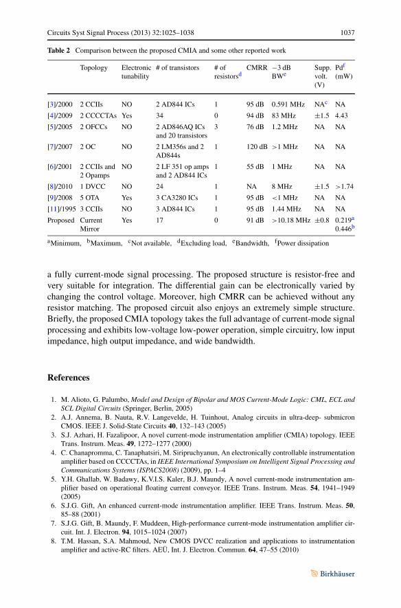
A comparison between the proposed CMIA and some other reported work is givenin Table 2. As it can be seen, the proposed CMIA exhibits superior performance interms of lower consumed power, low number of transistors, while providing elec-tronic tuning capability.
4 Conclusion
In this paper, a CMIA with the ability of direct processing of current signals is pre-sented. The proposed CMIA exhibits very low input impedance and very high outputimpedance. Its both input and output signals are in current domain and it enjoys from
Circuits Syst Signal Process (2013) 32:1025–1038 1037
Table 2 Comparison between the proposed CMIA and some other reported work
Topology Electronictunability
# of transistors # ofresistorsd
CMRR −3 dBBWe
Supp.volt.(V)
(mW)
[3]/2000 2 CCIIs NO 2 AD844 ICs 1 95 dB 0.591 MHz NAc NA
[4]/2009 2 CCCCTAs Yes 34 0 94 dB 83 MHz ±1.5 4.43
[5]/2005 2 OFCCs NO 2 AD846AQ ICsand 20 transistors
3 76 dB 1.2 MHz NA NA
[7]/2007 2 OC NO 2 LM356s and 2AD844s
1 120 dB >1 MHz NA NA
[6]/2001 2 CCIIs and2 Opamps
NO 2 LF 351 op ampsand 2 AD844 ICs
1 55 dB 1 MHz NA NA
[8]/2010 1 DVCC NO 24 1 NA 8 MHz ±1.5 >1.74
[9]/2008 5 OTA Yes 3 CA3280 ICs 1 95 dB <1 MHz NA NA
[11]/1995 3 CCIIs NO 3 AD844 ICs 1 95 dB 1.44 MHz NA NA
Proposed CurrentMirror
Yes 17 0 91 dB >10.18 MHz ±0.8 0.219a
0.446b
aMinimum, bMaximum, cNot available, dExcluding load, eBandwidth, fPower dissipation
a fully current-mode signal processing. The proposed structure is resistor-free andvery suitable for integration. The differential gain can be electronically varied bychanging the control voltage. Moreover, high CMRR can be achieved without anyresistor matching. The proposed circuit also enjoys an extremely simple structure.Briefly, the proposed CMIA topology takes the full advantage of current-mode signalprocessing and exhibits low-voltage low-power operation, simple circuitry, low inputimpedance, high output impedance, and wide bandwidth.
References
1. M. Alioto, G. Palumbo, Model and Design of Bipolar and MOS Current-Mode Logic: CML, ECL andSCL Digital Circuits (Springer, Berlin, 2005)
2. A.J. Annema, B. Nauta, R.V. Langevelde, H. Tuinhout, Analog circuits in ultra-deep- submicronCMOS. IEEE J. Solid-State Circuits 40, 132–143 (2005)
3. S.J. Azhari, H. Fazalipoor, A novel current-mode instrumentation amplifier (CMIA) topology. IEEETrans. Instrum. Meas. 49, 1272–1277 (2000)
4. C. Chanapromma, C. Tanaphatsiri, M. Siripruchyanun, An electronically controllable instrumentationamplifier based on CCCCTAs, in IEEE International Symposium on Intelligent Signal Processing andCommunications Systems (ISPACS2008) (2009), pp. 1–4
5. Y.H. Ghallab, W. Badawy, K.V.I.S. Kaler, B.J. Maundy, A novel current-mode instrumentation am-plifier based on operational floating current conveyor. IEEE Trans. Instrum. Meas. 54, 1941–1949(2005)
6. S.J.G. Gift, An enhanced current-mode instrumentation amplifier. IEEE Trans. Instrum. Meas. 50,85–88 (2001)
7. S.J.G. Gift, B. Maundy, F. Muddeen, High-performance current-mode instrumentation amplifier cir-cuit. Int. J. Electron. 94, 1015–1024 (2007)
8. T.M. Hassan, S.A. Mahmoud, New CMOS DVCC realization and applications to instrumentationamplifier and active-RC filters. AEÜ, Int. J. Electron. Commun. 64, 47–55 (2010)
1038 Circuits Syst Signal Process (2013) 32:1025–1038
9. A. Julsereewong, N. Tananchai, V. Riewruja, Electronically tunable gain instrumentation amplifierusing OTAs, in IEEE International Conference on Control, Automation and Systems (ICCAS 2008)(2008), pp. 1820–1823
10. T. Kaulberg, A CMOS current-mode operational amplifier. IEEE J. Solid-State Circuits 10, 849–852(1993)
11. A.A. Khan, M.A. Al-Turaigi, M.A. El-Ela, An improved current-mode instrumentation amplifier withbandwidth independent of gain. IEEE Trans. Instrum. Meas. 44, 887–891 (1995)
12. C. Kitchin, L. Counts, A Designer’s Guide to Instrumentation Amplifier, 3rd edn. (Analog DevicesInc., Norwood, 2006)
13. K. Koli, K.A.I. Halonen, CMRR enhancement techniques for current-mode instrumentation ampli-fiers. IEEE Trans. Circuits Syst. I, Fundam. Theory Appl. 47, 622–632 (2000)
14. S. Maheshwari, High CMRR wide bandwidth instrumentation amplifier using current controlled con-veyors. Int. J. Electron. 89, 889–896 (2002)
15. A.D. Marcellis, G. Ferri, N.C. Guerrini, G. Scotti, V. Stornelli, A. Trifiletti, The VCG-CCII: a novelbuilding block and its application to capacitance multiplication. Analog Integr. Circuits Signal Pro-cess. 58, 55–59 (2009)
16. S. Minaei, O.K. Sayin, H. Kuntman, A new CMOS electronically tunable current conveyor and itsapplication to current-mode filters. IEEE Trans. Circuits Syst. I. 53, 1448–1457 (2006)
17. I. Padilla, J.R. Angulo, R.G. Carvajal, A.L. Martin, Highly linear V/I converter with programmablecurrent mirrors, in IEEE International Symposium on Circuits and Systems (2007), pp. 941–944
18. G. Palmisano, G. Palumbo, S. Pennisi, CMOS Current Amplifiers (Kluwer Academic, Dordrecht,1999)
19. Ch.J. Sus, B. Fayomi, M. Sawan, G.W. Roberts, Reliable circuit techniques for low-voltage analogdesign in deep submicron standard CMOS: a tutorial. Analog Integr. Circuits Signal Process. 39,21–38 (2004)
20. E. Yuce, Various current-mode and voltage-mode instrumentation amplifier topologies suitable forintegration. J. Circuits Syst. Comput. 19, 689–699 (2010)
21. E. Yuce, S. Minaei, New CCII-based versatile structure for realizing PID controller and instrumenta-tion amplifier. Microelectron. J. 41, 311–316 (2010)