494/494p - xdevs.com
TRANSCRIPT

Part No . 070-4416-00Product G roup 26
494/494PSPECTRUM ANALYZEROPTIONS INCLUDEDVOLUME
WARNINGTHE FOLLOWING SERVICING INSTRUC-TIONS ARE FOR USE BY QUALIFIEDPERSONNEL ONLY . TO AVOID PERSONALINJURY, DO NOT PERFORM ANY SERVIC-ING OTHER THAN THAT CONTAINED INOPERATING INSTRUCTIONS UNLESS YOUARE QUALIFIED TO DO SO . REFER TOOPERATORS SAFETY SUMMARY ANDSERVICE SAFETY SUMMARY PRIOR TOPERFORMING ANY SERVICE.
Please Check forCHANGE INFORMATIONat the Rear of This Manual

TABLE OF CONTENTSService instructions are contained in two volumes as follows:
VOLUME 1
49414941P Service Vol . 1
LIST OF ILLUSTRATIONS . . . . . . . . . . . . . . . . . . . .LIST OF TABLES . . . . . . . . . . . . . . . . . . . . . . . . . . .SERVICING SAFETY SUMMARY . . . . . . . . . . . . . . .
Page
viixx
Section 3 INSTALLATION AND REPACKAGINGIntroduction . . . . . . . . . . . . . . . . . . . .Unpacking and Initial Inspection . . . .Power Source and Power
Page
3-13-1
Section 1 GENERAL INFORMATION Requirements . . . . . . . . . . . . . . . . . . 3-2Introduction . . . . . . . . . . . . . . . . . . . . 1-1 Repackaging for Shipment . . . . . . . . 3-3History . . . . . . . . . . . . . . . . . . . . . . . . 1-1 Storage . . . . . . . . . . . . . . . . . . . . . . . 3-4Level of Competences . . . . . . . . . . . . 1-1Standards and Conventions Used . . 1-1 Section 4 PERFORMANCE CHECKConformance to Industry Standards . 1-1 Introduction . . . . . . . . . . . . . . . . . . . . 4-1Product Description . . . . . . . . . . . . . . 1-2 Incoming Inspection . . . . . . . . . . . . . 4-1Product Service . . . . . . . . . . . . . . . . . 1-2 Verification of Tolerance Values . . . . 4-1Instrument Construction . . . . . . . . . . 1-2 History Information . . . . . . . . . . . . . . 4-1Elapsed Time Meter . . . . . . . . . . . . . 1-3 Equipment Required . . . . . . . . . . . . . 4-1Installation, Preparation for Use, and Performance Check Procedure . . . . . 4-2Repackaging . . . . . . . . . . . . . . . . . . . 1-3 Preliminary Preparation . . . . . . . . . . . . 4-5Changing Input Power Range . . . . . . 1-3 1 . Check Operation of Front PanelStandard Accessories . . . . . . . . . . . . 1-3 Pushbuttons and Controls . . . . . 4-6Options . . . . . . . . . . . . . . . . . . . . . . . 1-3 2 . Check Reference OscillatorOptional Accessories . . . . . . . . . . . . . 1-3 Accuracy . . . . . . . . . . . . . . . . . . 4-13Selected Components . . . . . . . . . . . . 1-3 3 . Check Counter Accuracy . . . . . . 4-13Component Circuit Numbering Scheme 1-3 4 . Check Counter Sensitivity . . . . . . 4-13Firmware Version and Error Message 5 . Check Center FrequencyReadout . . . . . . . . . . . . . . . . . . . . . . . 1-3 Accuracy . . . . . . . . . . . . . . . . . . . . 4-14Rackmount/Benchtop Versions . . . . . 1-4 6 . Check Center Frequency Drift orReplacing Fuses . . . . . . . . . . . . . . . . 1-4 Stability . . . . . . . . . . . . . . . . . . . . 4-15Options for Power Cord Configuration 1-4 7 . Check Residual FM . . . . . . . . . . . 4-16Standard Accessories . . . . . . . . . . . . 1-4 8 . Check Frequency Span/IDiv
Accuracy . . . . . . . . . . . . . . . . . . . 4-17Section 2 SPECIFICATION 9 . Check Time/Div Accuracy . . . . . . 4-19
Introduction . . . . . . . . . . . . . . . . . . 2-1 10 . Check Pulse Stretcher . . . . . . . . 4-19Electrical Characteristics . . . . . . . 2-1 11 . Check Resolution Bandwidth and
Verification of Tolerance Values 2-1 Shape Factor . . . . . . . . . . . . . . . . . 4-19Frequency Related 12 . Check Noise Sidebands . . . . . . . 4-20Characteristics . . . . . . . . . . . . . 2-1 13 . Check Calibrator Output . . . . . . . 4-21Amplitude Related 14 . Check Frequency Response . . . . 4-22Characteristics . . . . . . . . . . . . . 2-5 15 . Check Display Accuracy andInput Signal Characteristics . . . 2-9 Range . . . . . . . . . . . . . . . . . . . . . 4-25Output Signal Characteristics . 2-10 16 . Check Preselector UltimateGeneral Characteristics . . . . . . 2-11 Rejection . . . . . . . . . . . . . . . . . . . 4-26Power Requirements . . . . . . . . 2-12 17 . Check RF Attenuator Accuracy . 4-26
Environmental Characteristics . . . 2-12 18 . Check IF Gain Accuracy . . . . . . . 4-27Physical Characteristics . . . . . . . . 2-14 19 . Check Gain Variation BetweenIndustry Safety Standard Resolution Bandwidths . . . . . . . . 4-27Conformance . . . . . . . . . . . . . . . . 2-15 20 . Sensitivity . . . . . . . . . . . . . . . . . . 4-28

494/494P Service Vol . 1
Secton 4
Section 5
TABLE OF CONTENTS (cont)
REV JUN 1984
Page Page
PERFORMANCE CHECK (cont) Section 6 MAINTENANCE21 . Check Spurious (Residual) Introduction . . . . . . . . . . . . . . . . . . . . 6-1
Response . . . . . . . . . . . . . . . . . . 4-29 Removing the Instrument from its22 . Intermodulation Distortion . . . . . . 4-29 Cabinet . . . . . . . . . . . . . . . . . . . . . . . 6-123 . Check Harmonic Distortion . . . . . 4-31 Static Sensitive Components . . . 6-124 Check LO Emission Out the RF PREVENTIVE MAINTENANCE : . . . . . 6-2
Input . . . . . . . . . . . . . . . . . . . . . . 4-32 Elapsed Time Meter . . . . . . . . - - . 6-225 . Check 1 dB Compression Point . 4-32 Cleaning . . . . . . . . . . . . . . . . . . . . 6-226 . Check External Reference Input Lubrication . . . . . . . . . . . . - . . . . . 6-2
Power . . . - . . . . . . . . . . . . . . . . . 4-33 Fixtures and Tools For27. Check Triggering Operation and Maintenance . . . . . . . . . . - . . . . . . 6-2
Sensitivity . . . . . . . . . . . . . . . . . . 4-34 Visual Inspection . . . . . . . . . . . . . 6-328. Check External Sweep Performance Checks and
Operation . . . . - . . . . . . . . . . . . . . 4-35 Recalibration . . . . . . . . . . . . . . . . . 6-329. Check Vertical Output Signal . . . 4-36 Saving Stored Data in Non--volatile30. Check Horizontal Signal Output Memory for 494P Instruments . . . 6-3
Level . . . . . . . . . . . . . . . . . . . . . . 4-37 TROUBLESHOOTING . . . . . . . . . . . . 6-431 . GPIB Verification Program (494P Troubleshooting Aids . . . . . . . . . . 6-4
Only) . . . . . . . . - . . . . . . . . . . . . . 4-38 General TroubleshootingTechniques . . . . . . . . . . . . . . . . . . 6-4
ADJUSTMENT PROCEDURE DIAGNOSTIC . . . . . . . . . . . . . . . . . . 6-7Introduction . . . . . . . . . . . . . . . . . . . . 5-1 Troubleshooting the 4941494PAdjustment Steps . . . . . . . . . . . . . . . 5-2 Using the Error Message Display 6-71 . Check and Adjust Low Voltage 494/494P Trace Modes . - - . . . . - 6-21
Power Supply . . . . . . . . . . . . . . . 5-2 CORRECTIVE MAINTENANCE . . . . 6-232 . Crt Display (Z-Axis and High Handling Static Sensitivity
Voltage circuits) . . . . . . . . . . . . . . 5-4 Components . . . . . . . . . . . . . . . . . 6-233 . Deflection Amplifier (gain and Obtaining Replacement Parts . . . . 6-23
frequency response) . . . . . . . . . . 5-6 Parts Repair and Return Program 6-234 . Adjust Sweep Timing . . . . . . . . . 5-8 Firmware Version and Error5 . Frequency Control System Message Readout . . . . . . . . . . . . 6-23
Calibration . . . . . . . . . . . . . . . . . . 5-9 Selected Components . . . . . . . . . 6-236 . Adjust Start (0 Hz) Response Replacing EPROM's and ROM's - 6-23
Amplitude and Mixer Bias . . . . . . 5-12 Transistor and Integrator Circuit7 . Adjust 1 st Converter Bias . . . . . . 5-13 Electrode Configuration . . . . . . . . 6-248 . Log Amplifier Calibration . . . . . . . 5-14 Diode Color Code . . . . . . . . . . . . . 6-249 . Calibrating the Resolution Band- Multiple Terminal (Harmonica)
width and Shape Factor . . . . . . . 5-17 Connectors . . . . . . . . . . . . . . . . . . 6-2410 . Presetting the Variable Resolution Resistor Values . . . . . . . . . . . . . . . 6-24
Gain and Band Leveling . . . . . . . 5-20 Capacitor Markings . . . . . . . . . . . 6-2411 . Calibrator Output Level . . . . . . . . 5-21 Soldering Techniques . . . . . . . . . . 6-2412 . IF Gain Calibration . . . . . . . . . . . . 5-21 Replacing the Square-pin for the13 . Digital Storage Calibration . . . . . 5-22 Multi-pin Connectors . . . . . . . . . . 6-2514 . Setting B-Save A Reference Servicing the VR Module . . . . . . . 6-25
Level . . . . . . . . . . . . . . . . . . . . . . 5-24 REPLACING ASSEMBLIES AND15 . Preselector Driver Calibration . . . 5-24 SUBASSEMBLIES . . . . . . . . . . . . . . 6-2516 . Baseline Leveling (Video Removing and Installing the GPIB
Processor) . . . . . . . . . . . . . . . . . . 5-27 Board for the 494P Instrument . . 6-2617 . Band Leveling for Coaxial Bands Removing or Replacing Serni-rigid
(Bands 1-5) . . . . . . . . . . . . . . . . 5-30 Coaxial Cables . . . . . . . . . . . . . . . 6-2618 . Band Leveling for Waveguide Replacing the Crt . . . . . . . . . . . . . 6-29
Bands (Bands 6-11) . . . . . . . . . 5-3119 . Phase Lock Calibration . - . . . . . . 5-32

Section 6
TABLE OF CONTENTS (cont)
4941494P Service Vol . 1
Page Page
MAINTENANCE {cont} Section 6 MAINTENANCE (cont)Repairing the Crt Trace Rotation 494P MICROCOMPUTERcoil . . . . . . . . . . . . . . . . . . . . . . . . 6-30 SYSTEM MAINTENANCE . . . . . . 6-50Front Panel Assembly . . . . . . . . . 6-30 Memory Board Option Switch . 6-50Front Panel Board . . . . . . . . . . . . 6-30 Power-up Self Test Mode . . . . 6-50Main Power Supply Module . . . . . 6-31 Microcomputer Test Mode . . . . 6-53High Voltage Power Supply . . . . . 6-32 Instrument Bus Check Mode . . 6-54Replacing the 1st (YIG) Local TROUBLESHOOTING ON THEOscillator Interface Board . . . . . . . 6-32 INSTRUMENT BUS . . . . . . . . . . . 6-55Fan Assembly . . . . . . . . . . . . . . . . 6-32 Instrument Bus Data Transfers 6-55
MAINTENANCE ADJUSTMENTS . . 6-33 Instrument Bus Registers . . . . 6-57110 MHz IF Assembly Return A . Variable Resolution . . . . . . . 6-57Loss Calibration . . . . . . . . . . . . . . 6-33 B . Log and Video Amplifier . . . 6-572072 MHz 2nd Converter . . . . . . . 6-34 C . Video Processor . . . . . . . . . 6-57
Four Cavity Filter . . . . . . . . . . . 6-35 D . Digital Storage . . . . . . . . . . . 6-57Mixer . . . . . . . . . . . . . . . . . . . . 6-35 E . Z-Axis & RF Interface . . . . . 6-58
110 MHz Three Cavity Filter . . . . 6-35 F . Crt Readout . . . . . . . . . . . . . 6-58820 MHz Converter Maintenance 6-36 G . Sweep . . . . . . . . . . . . . . . . . 6-58
1 . To Gain Access to the LO H. Span Attenuator . . . . . . . . . 6-58Section . . . . . . . . . . . . . . . . 6-36 I . 1st LO Driver . . . . . . . . . . . . 6-58
2 . To Gain Access to the IF J . Preselector Driver . . . . . . . . 6-58Section . . . . . . . . . . . . . . . . 6-36 K . Center Frequency Control . . 6-58
3 . 719 MHz Oscillator Range L . Auxiliary SynthesizerAdjustment . . . . . . . . . . . . . 6-36 Control . . . . . . . . . . . . . . . . . 6-58
4 . 829 MHz Coaxial Band-pass M . Phase Lock Control . . . . . . . 6-58Filter Adjustment . . . . . . . . . 6-37 N . Front Panel . . . . . . . . . . . . . 6-58
Troubleshooting and Calibrating Front Panel Registers . . . . . . . . . . 6-66the 2182 MHz Phase Locked Auxiliary Synthesizer Table of2nd LO . . . . . . . . . . . . . . . . . . . . . 6-39 Values . . . . . . . . . . . . . . . . . . . . . . 6-67
1 . Preparation . . . . . . . . . . . . . 6-40 PROGRAM FOR MOVING2 . Adjust and Check Oscillator STORED DATA FROM THE 494P
Frequency . . . . . . . . . . . . . . 6-41 TO TAPE AND RETURNING IT3 . Measure Output Power . . . . 6-42 TO NON-VOLATILE MEMORY . . 6-684 . Check the 2200 MHz
Reference Mixer . . . . . . . . . 6-425 . Check Tune Range . . . . . . . 6-42 Section 7 THEORY OF OPERATION6 . Reassembly . . . . . . . . . . . . . 6-43 FUNCTIONAL AND GENERAL
Troubleshooting and Calibrating DESCRIPTION . . . . . . . . . . . . . . . . . 7-1the 16-20 MHz Phase Lock What it Does . . . . . . . . . . . . . . . . . 7-1Section . . . . . . . . . . . . . . . . . . . . . 6-43 How it Works . . . . . . . . . . . . . . . . 7-1
1 . Preliminary . . . . . . . . . . . . . . 6-45 1st, 2nd, and 3rd Converters . . . . 7-12 . Check Voltages . . . . . . . . . . 6-45 IF Section . . . . . . . . . . . . . . . . . . . 7-23 . Setting Center Frequency . . 6-45 Display Section . . . . . . . . . . . . . . . 7-24 . Setting Tune Sensitivity Frequency Control Section . . . . . . 7-2
and Range . . . . . . . . . . . . . - 6-46 Microwave Counter and Phase5 . Setting Sweep Range . . . . . 6-46 Lock Section . . . . . . . . . . . . . . . . . 7-26 . Check and Adjust Tune Digital Control Section . . . . . . . . . 7-2
Linearity . . . . . . . . . . . . . . . . 6-46 Power Supply Section . . . . . . . . . 7-37 . Conclusion . . . . . . . . . . . . . . 6-48 Other Sections . . . . . . . . . .. . . . . . 7-3
110 MHz Oscillator in the 3rd DETAILED DESCRIPTION . . . . . . . . 7-3Converter . . . . . . . . . . . . . . . . . . . 6-48 1st Converter Assemblies . . . . . . 7-4Reference Lock Module . . . . . . . . 6-48 RF Interface Circuits . . . . . . . . . . . 7-4

494/494P Service Vol . 1
Section 7
TABLE OF CONTENTS (cont)
THEORY OF OPERATION (cont)
Page Page
Section 7 THEORY OF OPERATION (cont)
RF Signal Path . . . . . . . . . . . . . . . 7-4 Digital Control Circuits . . . . 7-251st Mixer . . . . . . . . . . . . . . . . . 7-4 +5 V Regulator Circuit . . . . 7-261st Local Oscillator . . . . . . . . . 7-5 2nd Filter Select Circuits . . . 7-26Power Divider . . . . . . . . . . . . . 7-5 Post VR Amplifier Circuits 7-27Transfer Switch . . . . . . . . . . . . 7-5 Logarithmic Amplifier andDirectional Filter . . . . . . . . . . . . 7-5 Detector . . . . . . . . . . . . . . . . . . 7-272072 MHz IF Filters . . . . . . . . . 7-5 Log Amplifier Circuits . . . . . 7-27Diplexer and Filter . . . . . . . . . . 7-5 Detector Circuit . . . . . . . . . . 7-29
2nd Converter Circuits . . . . . . . . . 7-6 Display Section . . . . . . . . . . . . . . . 7-312072 MHz 2nd Converter . . . . 7-7 Functional Description . . . . . . . 7-31
Four Cavity Filter . . . . . . . . 7-7 Video Amplifier . . . . . . . . . . . . . 7-31Mixer Circuit . . . . . . . . . . . . 7-7 Log Mode Circuits . . . . . . . . 7-31
Precision External Cables . . . . . . . 7-8 Linear Mode Circuits . . . . . . 7-322182 MHz Phase Locked 2nd LO 7-9 Pulse Stretch Circuits, . . . . . 7-33
General Desciption . . . . . . . . . . 7-9 Digital Control Circuit . . . . . 7-332182 MHz Microstrip Oscillator 7-9 Video Processor . . . . . . . . . . . 7-332200 MHz Reference Board . . 7-10 Interface with 1405 TV2200 MHz Reference Mixer . . . 7-10 Sideband Adapter . . . . . . . . 7-3316-20 MHz Phase Lock Board 7-10 Video Marker . . . . . . . . . . . 7-34
829 MHz 2nd Converter . . . . . . . . 7-12 Video Leveling . . . . . . . . . . . 7-35IF Section . . . . . . . . . . . . . . . . . 7-12 Video Filter Circuits . . . . . . . 7-35
829 MHz Diplexer Circuits 7-12 Video Blanking Circuits . . . . 7-37829 MHz Amplifier Circuit . . 7-12 Digital Storage . . . . . . . . . . . . . 7-37829 MHz Mixer Circuit . . . . 7-13 Vertical Section . . . . . . . . . . 7-38110 MHz IF Select Circuits . 7-14 Horizontal Section . . . . . . . . 7-42
829 MHz 2nd Converter LO Deflection Amplifiers . . . . . . . . 7-44Section . . . . . . . . . . . . . . . . . . . 7-15 Horizontal Section . . . . . . . . 7-44
Phase Lock Circuit . . . . . . . 7-15 Vertical Section . . . . . . . . . . 7-45Front Panel 2nd Local Z-Axis & RF Interface Board . . 7-45Oscillator Output Circuit . . . 7-17 RF Interface Circuits . . . . . . 7-45719 MHz Output Circuit . . . 7-17 Z-Axis Circuits . . . . . . . . . . 7-46
110 MHz IF Amplifier . . . . . . . . 7-18 Power-Fail Detector . . . . . . 7-46110 MHz Band-pass Filter . . . . 7-19 Power-Supply Monitor . . . . 7-463rd Converter . . . . . . . . . . . . . . 7-20 Timer . . . . . . . . . . . . . . . . . . 7-47
100 MHz Oscillator . . . . . . . 7-20 High-Voltage Supply . . . . . . . . 7-47Mixer . . . . . . . . . . . . . . . . . . 7-20 Crt Readout . . . . . . . . . . . . . . . 7-47Distribution Amplifier . . . . . . 7-20 Generating Readout . . . . . . 7-48Calibrator . . . . . . . . . . . . . . . 7-20 Instrument Bus Interface . . 7-51
Reference Lock . . . . . . . . . . . . 7-21 Frequency Dot Marker . . . . 7-53External Reference Detector 7-21 Frequency Control Section . . . 7-55Frequency Synchronizer . . . 7-21 Sweep . . . . . . . . . . . . . . . . . 7-55Phase/Frequency Detector . 7-21 Span Attenuator . . . . . . . . . 7-59Tune Amplifier . . . . . . . . . . . 7-21 1st Local Oscillator Driver . . 7-61Lock Detector . . . . . . . . . . . 7-21 Preselector Driver . . . . . . . . 7-64
IF Section . . . . . . . . . . . . . . . . . . . 7-22 Center Frequency Control . . 7-66Variable Resolution Circuits . . . 7-22 Counter and Phase Lock
VR Input Circuit . . . . . . . . . 7-22 Section . . . . . . . . . . . . . . . . . . . 7-711st Filter Select Circuit . . . . 7-22 Functional Description . . . . . 7-7110 dB Gain Steps Circuit . . 7-24 Phase Lock Assembly . . . . . 7-7120 dB Gains Circuit . . . . . . . 7-24 Frequency Control . . . . . . . . 7-72Band Leveling Circuit . . . . . 7-24 Harmonic Mixer . . . . . . . . . . . 7-72

Section 7
Section 8
SERVICING SAFETY SUMMARY
Section 9
TABLE OF CONTENTS (cont)
REPLACEABLE ELECTRICAL PARTS
VOLUME 2
494I494P Service Vol . 1
Section 10
DIAGRAMS
Section 11
REPLACEABLE MECHANICAL PARTS
Page Page
THEORY OF OPERATION (cant) Section 8 OPTIONS (cont)
Auxiliary Synthesizer . . . . . . 7-73 Option 30 and 31 . . . . . . . . . . . . . . . 8-3Counter Board . . . . . . . . . . 7-76 Introduction . . . . . . . . . . . . . . . . . . 8-3
Phase Lock Synthesizer . . . . . 7-78 Electrical Characteristics . . . . . . . 8-3Error Amplifier, Controlled Environmental and PhysicalOscillator, Offset Mixer, and Characteristics . . . . . . . . . . . . . . . 8-3Strobe Driver . . . . . . . . . . . . 7-78 Safety Requirements . . . . . . . . . . 8-4
Error Amplifier . . . . . . . . 7-78 Accessories . . . . . . . . . . . . . . . . . 8-4Controlled Oscillator . . . . 7-80 Installation Dimensions . . . . . . . . . 8-5Offset Mixer . . . . . . . . . . 7-80 Slide-Out Tracks . . . . . . . . . . . . . . 8-5Strobe Driver Circuit . . . . 7-81 Installation Procedure . . . . . . . 8-5
Digital Control Section . . . . . . . . . 7-81 Alternate Installation Procedure 8-8Microcomputer . . . . . . . . . . . . . 7-81 Slide-Out Track Lubrication . . . 8-9Processor Board . . . . . . . . . . . 7-82 Removing the Side, Top, andMemory Board . . . . . . . . . . . . . 7-86 Bottom Panels . . . . . . . . . . . . . . . 8-9Front Panel . . . . . . . . . . . . . . . 7-88 Installing Semi-rigid Coaxial
Power Supply . . . . . . . . . . . . . . . . 7-92 Cables . . . . . . . . . . . . . . . . . . . . . . 8-9Line Input Circuits . . . . . . . . . . 7-92 Preparing the Instrument forInverter Circuit . . . . . . . . . . . . . 7-93 Adjustment or Repair . . . . . . . . . . 8-10
Soft Start and Primary Over-current Option 32 . . . . . . . . . . . . . . . . . . . . . . 8-11Circuits . . . . . . . . . . . . . . . . . . . . . 7-94 Introduction . . . . . . . . . . . . . . . . . . 8-11
Rectifier Filter Circuits . . . . . . . 7-94 Electrical, Environmental, and+5 V Over-voltage Protection Physical Characteristics . . . . . . . . 8-11Circuit . . . . . . . . . . . . . . . . . . . . 7-95 Accessories . . . . . . . . . . . . . . . . . 8-13Fan Drive Circuit . . . . . . . . . . . 7-95 Removing the Instrument from the
Cabinet . . . . . . . . . . . . . . . . . . . . . 8-13Option 41 . . . . . . . . . . . . . . . . . . . . . . 8-13
OPTIONS Option 52 . . . . . . . . . . . . . . . . . . . . . . 8-13Power Cord Options . . . . . . . . . . . . . 8-1Option 08 . . . . . . . . . . . . . . . . . . . . . . 8-1 Appendix A GLOSSARYOption 12 . . . . . . . . . . . . . . . . . . . . . . 8-1 General Terms . . . . . . . . . . . . . . . . . . A-1Option 14 . . . . . . . . . . . . . . . . . . . . . . 8-1 Terms Related to Frequency . . . . . . . A-2Option 13 . . . . . . . . . . . . . . . . . . . . . . 8-1 Terms Related to Amplitude . . . . . . . A-2Option 14 . . . . . . . . . . . . . . . . . . . . . . 8-1 Terms Related to Digital Storage forOption 20 . . . . . . . . . . . . . . . . . . . . . . 8-2 Spectrum Analyzers . . . . . . . . . . . . . A-4Option 21 . . . . . . . . . . . . . . . . . . . . . . 8-2Option 22 . . . . . . . . . . . . . . . . . . . . . . 8-2 CHANGE INFORMATION

494/494P Service Vol . 1
Fig .No.
2-12-23-1
3-2
4-14-2
4-3
4-4
4-5
4-6
4-7
4-8
4-9
4-10
4-11
4-12
4-13
4-14
4-15
4-164-17
4-18
4-19
4-20
4-21
LIST OF ILLUSTRATIONS
line fuse . . . . . . . . . . . . . . . . . . . . . . . . . . . .
3-2International power cord and plug configura-tion for the 494/494P
. . . . . . . . . . . . . . . . .
3-3
Video Filter effect on VSWR . . . . . . . . . . . .
4-7Typical display with SAVE A on to observeIDENTify mode . . . . . . . . . . . . . . . . . . . . . . 4-9Test equipment setup for checking centerfrequency accuracy . . . . . . . . . . . . . . . . . . . 4-14Typical display that illustrates how residualFM is measured . . . . . . . . . . . . . . . . . . . . . . 4-16Test equipment setup for checking frequencyspanldiv and sweep timeldiv accuracy . . . .
4-17Typical marker display that shows howspanldiv accuracy is measured . . . . . . . . . .
4-18Typical display to illustrate how timeldivaccuracy is measured . . . . . . . . . . . . . . . . .
4-19Typical display to illustrate how responsebandwidth and shape factor are determined
4-20Typical display showing how to measurenoise sidebands . . . . . . . . . . . . . . . . . . . . . . 4-20Test equipment setup for checking the cali-brator output level . . . . . . . . . . . . . . . . . . . .
4-21Test equipment setup for measuring 10 kHzto 10 MHz frequency response . . . . . . . . . .
4-23Display showing frequency response patternfrom a sweeping source . . . . . . . . . . . . . . .
4-23Test equipment setup for measuring .01 to21 GHz frequency response . . . . . . . . . . . . 4-24Test equipment setup for checking displayaccuracy, attenuator and gain accuracy,and preselector image rejection . . . . . . . . . 4-25Test equipment setup for checkingintermodulation distortion . . . . . . . . . . . . . .
4-30Intermodulation products . . . . . . . . . . . . . . 4-30Equipment setup for checking harmonicdistortion . . . . . . . . . . . . . . . . . . . . . . . . . . . 4-31Test equipment setup for checking 1 dB in-put compression point . . . . . . . . . . . . . . . . .
4-32Test equipment setup for checking externalreference input power . . . . . . . . . . . . . . . . .
4-34Equipment setup for checking internal triggercharacteristics . . . . . . . . . . . . . . . . . . . . . . . 4-35External video select pins onACCESSORIES connector and inputto MARKER/VIDEO for signal tocheck internal triggering . . . . . . . . . . . . . . . 4-35
4-24
5-1
5-2
5-3
5-4
5-55-6
5-7
5-B
5-9
5-10
5-11
5-12
5-13
5-145-15
5-16
5-17
5-18
5-195-20
5-215-22
Page
4-36
(1 .0 volt peak at 2 .0 V peak-to-peak) . . . . .
4-36Test oscilloscope display of VERTical outputwith a full screen display on the 494
. . . . .
4-37
Low voltage power supply adjustments andtest point locations . . . . . . . . . . . . . . . . . . .
5-3Location of adjustments and test points onthe Deflection Amplifier board, HighVoltage module, Z-Axis board, and Sweepboard . . . . . . . . . . . . . . . . . . . . . . . . . . . . . . 5-5Location of test points and adjustments onthe High Voltage module . . . . . . . . . . . . . . .
5-5Test equipment setup for calibrating theDeflection Amplifier . . . . . . . . . . . . . . . . . . . 5-6Test points on the Crt Readout board . . . .
5-7Test points and adjustments on the Deflec-tion Amplifier for gain and frequencyresponse . . . . . . . . . . . . . . . . . . . . . . . . . . . 5-7Test equipment setup for calibrating sweeptiming . . . . . . . . . . . . . . . . . . . . . . . . . . . . . . 5-8Timing adjustments and test points on theSweep board . . . . . . . . . . . . . . . . . . . . . . . .
5-9Test equipment setup for calibrating thefrequency control system . . . . . . . . . . . . . .
5-11Adjustment and test point locations for cali-brating the frequency control system . . . . .
5-11Location of Option switch S1038 on theMemory board . . . . . . . . . . . . . . . . . . . . . . . 5-12Location of select resistor R1028 on the 1stLO Driver . . . . . . . . . . . . . . . . . . . . . . . . . . . 5-12Adjustment and test points on the 1 st LODriver board . . . . . . . . . . . . . . . . . . . . . . . . . 5-13Location of the 1st Mixer tuning adjustment 5-14Location of P3035 on the Video Processorboard . . . . . . . . . . . . . . . . . . . . . . . . . . . . . . 5-15Test equipment setup for calibrating the LogAmplifier . . . . . . . . . . . . . . . . . . . . . . . . . . . . 5-15Location of test points and adjustments forcalibrating the Log and Video Amplifier . . .
5-16Equipment setup for calibrating the VRsystem . . . . . . . . . . . . . . . . . . . . . . . . . . . . . 5-17Adjustments on the VR#2 module . . . . . . . 5-18Response of the 100 kHz filter over the re-sponse of the 10 kHz filter . . . . . . . . . . . . .
5-19Adjustments on the VR#1 module . . . . . . .
5-19Typical response of the 10 kHz, 100 kHz,and 1 MHz bandwidth filters . . . . . . . . . . . .
5-20
PageFig .No .
The 494P Spectrum Analyzer . . . . . . . . . . . xii 4-22 Equipment setup for checking external trig-Probe Power connector . . . . . . . . . . . . . . . 2-12 gering and horizontal input characteristics .Dimensions . . . . . . . . . . . . . . . . . . . . . . . . . 2-14 4-23 Test oscilloscope display of a sinewave inputLocation of input power selector switch and signal to the external TRIG connector

Fig .No .
5-23
5-245-25
5-26
5-27
5-28
5-29
5-30
5-31
5-32
5-33
5-34
6-26-36-46-5
6-6
6-7
6-86-96-10
6-11
6-126-13
6-14
6-15
REV JUN 1984
LIST OF ILLUSTRATIONS (cont)
Test equipment setup for adjusting the IFgain and the location of adjustments andconnectors . . . . . . . . . . . . . . . . . . . . . . . . . .Digital storage calibration adjustments . . . .Test equipment setup for Preselector Driveradjustments . . . . . . . . . . . . . . . . . . . . . . . . .Preselector Driver adjustment and testpoints . . . . . . . . . . . . . . . . . . . . . . . . . . . . . .Test equipment setup for adjusting baselineleveling . . . . . . . . . . . . . . . . . . . . . . . . . . . . .Typical response when adjusting baselineleveling . . . . . . . . . . . . . . . . . . . . . . . . . . . . .Adjustments and test points on the VideoProcessor . . . . . . . . . . . . . . . . . ._ . . . . . . .Typical response when adjusting compensa-tion of the baseline leveling circuits
. . . . . .Test equipment setup for adjusting band lev-eling for the coaxial and waveguide bands .Band leveling adjustments and gain diodeson the VR#2 Mother board . . . . . . . . . . . .Test equipment setup for calibrating thePhase Lock assembly . . . . . . . . . . . . . . . . .Adjustments and test points in the PhaseLock assembly
. . . . . . . . . . . . . . . . . . . . . .
Electrode configuration for semi-conductorcomponents . . . . . . . . . . . . . . . . . . . . . . . . .Diode polarity markings . . . . . . . . . . . . . . .Multipin (harmonica) connector configurationColor code for some tantalum capacitors . .Preparing the VR assembly for servicing,showing how it is supported when on anextender board . . . . . . . . . . . . . . . . . . . . . .Top deck of the 4941494P identifying majorassemblies or circuit boards . . . . . . . . . . . .RF deck of the 494/494P identifying majorassemblies . . . . . . . . . . . . . . . . . . . . . . . . . .Removing the YIG oscillator interface boardFan assembly mounting . . . . . . . . . . . . . . .Test equipment setup for adjusting returnloss in the 110 MHz IF assembly . . . . . . . .110 MHz IF assembly showing the locationof test points and adjustments . . . . . . . . . .110 MHz Filter adjustments
. . . . . . . . . . . .LO section of the 829 MHz converter show-ing test points and connectors . . . . . . . . . .Location of test jack and jumper on the829 MHz amplifier board . . . . . . . . . . . . . . .Test equipment setup for aligning the829 MHz filter . . . . . . . . . . . . .
. . . . . . .
494/494P Service Vol . 1
PageFig .No. Page
6-16 Filter tune tabs in the 829 MHz converter 6-396-17 Typical response when the first and second
5-22 resonators of the 829 MHz filter are adjusted5-23 correctly . . . . . . . . . . . . . . . . . . . . . . . . . . . . 6-39
6-18 Typical response when the third and fourth5-25 resonators are tuned correctly . . . . . . . . . . 6-40
6-19 Test equipment setup for calibrating the os-5-25 cillator section of the 2182 MHz Phase
Locked 2nd LO . . . . . . . . . . . . . . . . . . . . . . 6-415-27 6-20 Adjustments and test point locations within
the 829 MHz Converter oscillator section . 6-425-28 6-21 Construction details of a coaxial test probe
for the 2182 MHz Phase Locked 2nd LO . . 6-435-29 6-22 Test equipment setup for calibrating the
Phase Lock section of the 2182 MHz 2nd LO 6-445-30 6-23 Test points and component location pertain-
ing to calibrating the 16-20 MHz Phase Lock5-31 circuit for the 2182 MHz 2nd LO . . . . . . . . 6-45
6-24 Location of R4040 on the CF Control board 6-475-32 6-25 Test points and adjustments in the 3rd
Converter . . . . . . . . . . . . . . . . . . . . . . . . . . . 6-495-33 6-26 Test points and adjustments inside the
Reference Lock module . . . . . . . . . . . . . . . 6-495-34 6-27 Typical display showing the delay through
U2046A on the Reference Lock . . . . . . . . . 6-506-28 Option switch bank S1038 on the Memory
board . . . . . . . . . . . . . . . . . . . . . . . . . . . . . . 6-516-5 6-29 A15 through A12 in microcomputer test6-24 mode . . . . . . . . . . . . . . . . . . . . . . . . . . . . . . 6-536-24 6-30 OXXX and Y0 through Y2 of address6-25 decoder U 1046 on the Memory board . . . . 6-53
6-31 3800 and Y3 of address decoder U1041 onthe Memory board . . . . . . . . . . . . . . . . . . . . 6-54
6-26 6-32 Address decoder U1020 on the Processorboard and U1036 on the Memory board . . 6-54
6-27 6-33 T/0- and Y2 through Y4 of address decoderU1032 on the GPIB board . . . . . . . . . . . . . 6-55
6-28 6-34 Instrument bus check . . . . . . . . . . . . . . . . , 6-556-326-33
7-1 Cross section of a four-cavity filter . . . . . . . 7-76-34 7-2 Equivalent circuit of the four-cavity filter . . . 7-8
7-3 Simplified diagram of the diplexer . . . . . . . . 7-126-35 7-4 Equivalent ac circuit of an amplifier stage in6-35 the 829 MHz 2nd converter . . . . . . . . . . . . 7-12
7-5 Simplified diagram of the do path in an6-36 amplifier stage . . . . . . . . . . . . . . . . . . . . . . . 7-13
7-6 Simplified block diagram of the phase lock6-37 loop in the 829 MHz 2nd converter . . . . . . 7-15
7-7 Bridged "T" attenuator equivalent circuit . . 7-186-38 7-8 Block diagram of a three stage log amplifier 7-28

494/494P Service Vol. 1
LIST OF ILLUSTRATIONS (cont)
Fig .No.
Page
7-9
Log amplifier gain curve showing the breakpoints . . . . . . . . . . . . . . . . . . . . . . . . . . . . . . 7-28
7-10
Curve showing end-of-range for a logamplifier . . . . . . . . . . . . . . . . . . . . . . . . . . . . 7-29
7-11
Simplified detector circuit
. . . . . . . . . . . . . .
7-307-12
Selection of display position on the log scale
7-317-13
Functional diagram of the 494/494P with the1405 TV Sideband Adapter System . . . . . .
7-347-14
Simplified diagram of a video filter . . . . . . .
7-367-15
Vertical control IC, U1023, block diagram
.
7-397-16
Horizontal control IC, U2035, block diagram 7-437-17
Block diagram of crt readout
. . . . . . . . . . .
7-487-18
Character on/off timing . . . . . . . . . . . . . . . .
7-497-19
Character scan . . . . . . . . . . . . . . . . . . . . . . 7-507-20
Character generator (U2048) block diagram
7-517-21
Character timing diagram . . . . . . . . . . . . . .
7-527-22
Frequency dot marker simplified diagramwith timing waveforms
. . . . . . . . . . . . . . . .
7-547-23
Simplified digital-to-analog converter (DAC)
7-607-24
Simplified span decade attenuator . . . . . . .
7-617-25
DAC variance graph
. . . . . . . . . . . . . . . . . .
7-677-26
Simplified tune voltage converter . . . . . . . .
7-687-27
Simplified schematic of harmonic mixer . . .
7-737-28
Block diagram of a basic synthesizer . . . . .
7-747-29
Basic block diagram of a -N synthe-sizer with a variable modulus prescaler
. . .
7-757-30
System memory map for 4941494P
. . . . . .
7-837-31
I/0 space memory map . . . . . . . . . . . . . . . .
7-847-32
PIA and timer memory map . . . . . . . . . . . .
7-857-33
Front panel switch matrix code . . . . . . . . . . 7-907-34
Primary regulator input/output waveform(stylized) . . . . . . . . . . . . . . . . . . . . . . . . . . . 7-94
7-35
Timing waveform (stylized) for soft-startcircuit . . . . . . . . . . . . . . . . . . . . . . . . . . . . . . 7-95
8-1
Slide-out track assemblies . . . . . . . . . . . . .
8-68-2
Installing the stationary sections and alterna-tive installation method using rear supportbrackets (B) and (C) . . . . . . . . . . . . . . . . . .
8-68-3
Installing and removing option 30 from thecabinet rack . . . . . . . . . . . . . . . . . . . . . . . . . 8-7

LIST OF TABLES
494/4941D Service Vol . 1
TableNo. Page
TableNo. Page
1-1 Standard Accessories . . . . . . . . . . . . . . . . . 1-4 6-8 RAM Test . . . . . . . . . . . . . . . . . . . . . . . . . . 6-526-9 ROM Test . . . . . . . . . . . . . . . . . . . . . . . . . . 6-52
2-1 Frequency Related Characteristics . . . . . . . 2-1 6-10 Instrument Bus Registers . . . . . . . . . . . . . . 6-592-2 IF Frequency, LO Range, and Harmonic 6-11 Front Panel Registers . . . . . . . . . . . . . . . . . 6-66
Number (N) . . . . . . . . . . . . . . . . . . . . . . . . . 2-5 6-12 Auxiliary Synthesizer Table of Values . . . . . 6-672-3 Amplitude Related Characteristics . . . . . . . 2-52-4 Sensitivity . . . . . . . . . . . . . . . . . . . . . . . . . . 2-82-5 Input Signal Characteristics . . . . . . . . . . . . 2-9 7-1 2nd Converter IF Selection . . . . . . . . . . . . . 7-62-6 Output Signal Characteristics . . . . . . . . . . . 2-10 7-2 Switch and Amplifier Selection Summary . . 7-142-7 General Characteristics . . . . . . . . . . . . . . . . 2-11 7-3 Bandwidth Selection . . . . . . . . . . . . . . . . . . 7-232-8 Power Requirements . . . . . . . . . . . . . . . . . . 2-12 7-4 Gain Step Combinations . . . . . . . . . . . . . . . 7-252-9 Environmental Characteristics . . . . . . . . . . . 2-12 7-5 Progression of Gain Reduction . . . . . . . . . . 7-282-10 Physical Characterisics . . . . . . . . . . . . . . . . 2-14 7-6 Filter Component Combinations . . . . . . . . . 7-362-11 494/494P Safety Standard and 7-7 RF Interface Lines . . . . . . . . . . . . . . . . . . . . 7-45
Regulatory Requirements Conformance . . . 2-15 7-8 Truth Table . . . . . . . . . . . . . . . . . . . . . . . . . 7-467-9 Control Port . . . . . . . . . . . . . . . . . . . . . . . . . 7-53
3-1 Shipping Carton Test Strength . . . . . . . . . . 3-3 7-10 Address/Data Port . . . . . . . . . . . . . . . . . . . 7-537-11 Sweep Rate Selection Codes . . . . . . . . . . . 7-56
4-1 Equipment Required . . . . . . . . . . . . . . . . . . 4-2 7-12 Trigger Selection Modes . . . . . . . . . . . . . . . 7-564-2 Center Frequency Accuracy Check Points for 7-13 Sweep Holdoff Selection Modes . . . . . . . . . 7-56
Unlocked 1st LO . . . . . . . . . . . . . . . . . . . . . 4-15 7-14 Calibration Control Selection Modes . . . . . 7-614-3 SpanIDiv versus Time Markers for SpanIDiv 7-15 Attenuation Selection Codes . . . . . . . . . . . . 7-61
Accuracy Check . . . . . . . . . . . . . . . . . . . . . 4-18 7-16 U4017 Output Lines . . . . . . . . . . . . . . . . . . 7-624-4 Correction Factor to Determine True Signal 7-17 U5031 Output Lines . . . . . . . . . . . . . . . . . . 7-65
Level . . . . . . . . . . . . . . . . . . . . . . . . . . . . . . 4-28 7-18 Preselector Frequency Bands . . . . . . . . . . . 7-664-5 494/494P Sensitivity . . . . . . . . . . . . . . . . . . 4-29 7-19 Address 70 Format . . . . . . . . . . . . . . . . . . . 7-69
7-20 DAC Tuning Codes . . . . . . . . . . . . . . . . . . . 7-695-1 Power Supply Voltage Tolerances . . . . . . . 5-4 7-21 U2025 Output Lines . . . . . . . . . . . . . . . . . . 7-795-2 Sweep Rate as a Function Of Span in the 7-22 List of POLL Bits . . . . . . . . . . . . . . . . . . . . . 7-82
Auto Mode . . . . . . . . . . . . . . . . . . . . . . . . . . 5-9 7-23 Levels of Memory Bank . . . . . . . . . . . . . . . 7-875-3 Ext Mixer Band Leveling Adjustments . . . . 5-32
6-1 Relative Susceptabiltly to Static Damage . . 6-1 8-1 Power Cord Options . . . . . . . . . . . . . . . . . . 8-16-2 Service Kits and Tools . . . . . . . . . . . . . . . . . 6-3 6-2 Option 20 (General Purpose Waveguide6-3 Voltage Ranges, Test Points, and Circuit Mixers) Characteristics . . . . . . . . . . . . . . . . 8-2
Protection for the Low Voltage Power 8-3 Option 21 (WM 490-2) Characteristics . . . . 8-2Supply . . . . . . . . . . . . . . . . . . . . . . . . . . . . 6-10 8-4 Option 22 (WM 490-3) Characteristics . . . . 8-2
6-4 Power Supply Edge Connector Voltages . . 6-11 8-5 Environmental Characteristics Option 306-5 Equipment Required for Return Loss & 31 . . . . . . . . . . . . . . . . . . . . . . . . . . . . . . . 8-4
Adjustment . . . . . . . . . . . . . . . . . . . . . . . . . 6-34 8-6 Physical Characteristics Option 30 & 31 . . 8-46-6 Equipment Required for 2nd LO Calibration 6-40 8-7 Installation Dimensions Option 30 & 31 . . . 8-56-7 Equipment Required for Calibrating the 8-8 Environmental Characteristics Optiion 32 . . 8-12
16-20 MHz Phase Lock Circuit . . . . . . . . . . 6-44 8-9 Physical Characteristics Option 32 . . . . . . . 8-12

494/494P Service Vol . 1
Do Not Service Alone
Do not perform internal service or adjustment of this prod-uct unless another person capable of rendering first aid andresuscitation is present .
Do Not Wear Jewelry
Remove jewelry prior to servicing . Rings, necklaces, andother metallic objects could come into contact with danger-ous voltages and currents .
Use Care When Servicing With Power On
Dangerous voltages exist at several points in this product .To avoid personal injury, do not touch exposed connectionsand components while power is on .
Disconnect power before removing protective panels, sol-dering, or replacing components .
Power Source
SERVICING SAFETY SUMMARY
FOR QUALIFIED SERVICE PERSONNEL ONLY
This product is intended to operate from a power sourcethat will not apply more than 250 volts rms between thesupply conductors or between either supply conductor andground . A protective ground connection by way of thegrounding conductor in the power cord is essential for safeoperation .
X-Radiation
X-ray emission generated within this instrument has beensufficiently shielded . Do not modify or otherwise alter thehigh voltage circuitry or the CRT enclosure .
In This Manual
TERMS
CAUTION statements identify conditions or practices thatcould result in damage to the equipment or other property .
WARNING statements identify conditions or practices thatcould result in personal injury or loss of life .
As Marked on Equipment
CAUTION indicates a personal injury hazard not immedi-ately accessible as one reads the marking, or a hazard toproperty including the equipment itself .
DANGER indicates a personal injury hazard immediately ac-cessible as one reads the marking .
In This Manual
D
As Marked On Equipment
Grounding the Product
SYMBOLS
This symbol indicates where applicablecautionary or other information is to befound.
DANGER-High Voltage .
Protective ground (earth) terminal .
ATTENTION-Refer to manual .
Refer to manual .
This product is grounded through the grounding conductorof the power cord . To avoid electrical shock, plug the powercord into a properly wired receptacle before connecting tothe product input or output terminals . A protective groundconnection by way of the grounding conductor in the powercord is essential for safe operation .

Danger Arising From Loss of Ground
Upon loss of the protective-ground connection, all accessi-ble conductive parts (including knobs and controls that mayappear to be insulating) can render an electric shock .
Use the Proper Power Cord
Use only the power cord and connector specified for yourproduct .
494/494P Service Vol . 1
Use only a power cord that is in good condition .
For detailed information on power cords and connectors,see the General Information and Specifications section inVolume 1 of the 494/494P Service manual.
Refer cord and connector changes to cualified servicepersonnel .

494/494P Service Vol . 1
The 494P Spectrum Analyzer .

History
GENERAL INFORMATION
The service instructions for this product consists of twovolumes. Volume 1 contains the written information such asspecifications, maintenance, and calibration . Volume 2 con-tains the diagrams and parts lists . Our intent is to provideboth accurate and complete information for this product .The Table of Contents, at the beginning of this manual, liststhe location and contents of each section that make up thetwo volume service manuals .
Change information that involves manual correctionsand/or additions, pending manual reprint and bind, is locatedat the back of each service manual as a CHANGE IN-FORMATION section .
History information, with the updated data, is integratedinto the text or diagrams . When a page is updated, the re-vised pages are identified by a revision date in the lowerinside corner of the page . When a diagram is updated, therevision date is placed at the lower center of the diagram .History information is indicated with a gray tint . When acomponent value is changed, the designator on the drawingis boxed with a grey outline . When a circuit is deleted orchanged, the original configuration is shown in grey, drawneither at its original location or to the side of the drawing . Ifyou have a manual other than the one that came with yourinstrument it may contain revisions that do not apply to yourinstrument ; however all history information that pertains tothe earlier instruments is retained .
When a major modification has been made to an assem-bly or circuit board, the data for the replaced assembly willfollow the new information and will be identified with appro-priate titles or headings ; such as instrument serial numberrange, or the assembly or board part numbers .
Level of Competence
It is assumed that whoever uses these instructions isfamiliar with basic digital, analog, and RF circuitry . Circuitanalysis is mostly functional and should provide the techni-cian with the information necessary to isolate the majority ofmalfunctions to a board or block of circuitry . The technician
INTRODUCTION
Section 1-494/49412 Service Vol . 1
should then be able, with the aid of test equipment, to iso-late the malfunction to a specific component orcomponents .
This instrument contains internal firmware which pro-vides a complete instrument check during power up andduring operation, and if needed, guides the user through afront panel calibration procedure. If calibration cannot beachieved, a diagnostic test detects and isolates most prob-lems to the system, such as 1 st LO . The technician can thenrun trouble shooting diagnostic to further isolate the prob-lem to the board or in some cases to the IC level . Refer tothe Diagnostic part of the Maintenance section .
Standards and Conventions Used
Most terminology is in accordance with those standardsadapted by IEEE and IEC . A glossary of terms is providedas an appendix . Abbreviations in the documentation are inaccordance with ANSI Y1 .1-1972, with exceptions and ad-ditions explained in parentheses after the abbreviation .Graphic symbols comply with ANSI Y32 .2-1975 . Logic sym-bology is based on ANSI Y32 .14-1973 and the manufactur-er's data description . GPIB functions for the programmableversion conforms to IEEE 488-1978 Standard . A copy ofANSI and IEEE standards may be obtained from, the Insti-tute of Electrical and Electronic Engineers Inc ., 345 East47th Street, New York, N .Y . 10017 .
Conformance to Industry Standards
The 494/494P complies with the following IndustrySafety Standards and Regulatory Requirements :
Safety.
CSA-Electrical Bulletin
FM-Electrical Utilization Standard Class 3820ANSI C39 .5---Safety Requirements for Electricaland Electronic Measuring and ControllingInstrumentation .IEC 348 (2nd addition)-Safety Requirements forElectronic Measuring Apparatus .
Regulatory Requirements
VDE 0871 Class 13-Regulations for RIFI Suppressionof High Frequency Apparatus and Installations .

General Information-4941494P Service Vol. 1
Product Description
The 494 and the 494P programmable instruments arehigh performance, compact, portable spectrum analyzers .Microcomputer control of most functions simplifies and en-hances operation . Its features synthesizer frequency accu-racy and stability, precision signal counting ability, preciseamplitude measurement capability, digital storage display,battery-powered memory to retain front panel settings anddisplays, and crt message readout that describes function ofthe front panel controls and selectors along with messagesthat explain operating errors . Some of the options provide asecond language for display messages, waveguide mixersto extend the frequency range to 325 GHz, rackmount andbenchtop versions, and enhanced measurement capabilityfor digital microwave radio .
The frequency range is 10 kHz to 21 GHz with the inter-nal mixer, and up to 325 GHz when using external wave-guide mixers . A minimum resolution bandwidth of 30 Hz,with a minimum span of 50 Hzldiv, provides measurementresolution that is commmensurate with the frequency accu-racy . Digital storage provides flicker free displays plus func-tions such as SAVE A, B- SAVE A, MAX HOLD with whichto compare and subtract displays, save maximum values . Inaddition to the conventional digital storage feature, up tonine separate displays with their parameter readouts, canbe stored in battery-powered memory, then later recalled foradditional analysis and comparison . Up to ten differentfront-panel control setups can also be stored for futurerecall .
Center frequency may be selected by means of the front-panel tuning knob or directly entered via the Data Entry key-board . When using the keyboard, it is not necessary to alterthe Span/Div setting regardless of the frequency selected .Other parameters, such as vertical display and referencelevel, may also be keyboard selected with the flexibility pre-viously available only under GPIB program control . Counteraccuracy to 1 Hz resolution is available .
In addition, the 494/494P requires only a short warm-uptime for stable operation . In 15 minutes or less, the fre-quency drift is less than 500 Hz per minute of sweep time .After one hour, it is less than 50 Hz per minute of sweeptime . Display dynamic range is 80 clB, with calibrated refer-ence level readout from -117 dBm to +30 dBm, inselectable steps from 1 to 15 dB, and 0 .25 dB for a A A(amplitude) mode. When the vertical display is selected withthe Data Entry keyboard, the reference level steps corre-spond to the display mode (see Operating instructions) .Sensitivity at 30 Hz resolution bandwidth is -121 dBm to7 .1 GHz, decreasing to -96 dBm at 21 GHz .
The 494P adds remote control capability 'to the standardinstrument features of the 494 . The front-panel controls (ex-cept those intended for local use, such as INTENSITY) canbe remotely operated through the GPIB port, which allowsthe 494P to be used with a variety of systems and control-lers . This operation is described in detail in the Program-mers manual .
Product Service
To assure adequate product service and maintenance forour instruments, Tektronix has established Field Offices andService Centers at strategic points throughout the UnitedStates and in countries where our products are sold . Sev-eral types of maintenance or repair agreements are avail-able . For example ; for a fixed fee, a maintenance agreementprogram provides maintenance and re calibration on a regu-lar basis . Tektronix will remind you when a product is duefor recalibration and perform the service within a specifiedtime . Contact your local Service Center, representative, orsales engineer for details regarding : Warranty, Calibration,Emergency Repair, Repair Parts, Schedules! Maintenance,Maintenance Agreements, Pickup and Delivery, On-SiteService for fixed installations, and other services availablethrough these centers .
Tektronix emergency repair service provides immediateattention to instrument malfunctions if you are in an emer-gency situation such as a field trip . Again, contact anyTektronix Service Center for assistance to get you on yourway within a minimum of time .
Instrument Construction
The modular construction of the 4941494P instrumentprovides ready access to the major circuits . Circuit boardsthat contain sensitive circuits are either mounted on metalextrusions, each of which provides shielding between adja-cent modules, or they are mounted within honeycomb-likeextrusions, with feedthrough connectors through the wall ofthe compartment . All boards and assemblies plug onto acommon mother board which provides the interconnectionfor these boards and assemblies . Most adjustments andtest points are accessible while the instrument is operationaland the modules or assemblies secured in their normal posi-tion . Extenders are provided with an optional Service Kit(see Maintenance section under Service Fixtures and Toolsfor Maintenance) .
Any module or board can be removed without disturbingthe structural or functional integrity of the other modules .The extenders allow .most circuit board assemblies to func-tion in an extended position for service or adjustment . Thecircuit boards mounted on the metal extrusion can be re-moved by removing the securing screws . All other circuitboards (which should require minimal service) are accessibleby removing a cover plate over the assembly or module .

NOTE
Disassembly of some modules may require specialtools and procedures. These procedures will be foundin the Maintenance section .
To obtain and maintain the frequency stability, sensitiv-ity, and EMI characteristics, circuits are completely RF iso-lated to ensure spurious free response ; yet the closeproximity minimizes losses or interactions with other func-tions . All compartments are enclosed on both sides by metalplates and all interconnections between compartments aremade by feedthrough terminals rather than cables . If thecompartments are opened, be sure that the shields and cov-ers are properly reinstalled before operating .
Elapsed Time Meter
A 5000 hour elapsed time indicator, graduated in 500hour increments, is installed on the Z Axis/RF Interface cir-cuit board. This provides a convenient way to check operat-ing time . The meter on new instruments may indicate from200 to 300 hours elapsed time . Most instruments gothrough a factory burn-in time to improve reliability . This issimilar to using aged components to improve reliability andoperating stability .
Installation, Preparation for Use, and RepackagingThis section provides unpacking information and the pro-
cedures to prepare the instrument for use. It also includesrepackaging information .
Changing Power Input Range
The procedure for changing the input voltage range isdescribed under the Installation and Repackaging section .
The power cord that is supplied with the instrument andthe instrument power voltage requirements depend on theavailable power source (see Specification section) . Powercord options are described in the Installation and Prepara-tion for Use section and the Options section .
Standard Accessories
Standard accessories for the 494/494P and rackmount/benchtop versions are listed in Table 1-1 and in Volume 2 ofthe Service Instructions, following the Replaceable Mechan-ical Parts list . The list in Volume 2 of the Service instructionsprovides part numbers for these accessories .
Options
General Information-4941494P Service Vol . 1
Options for the 494I494P are described iin the Optionssection of the manuals including rackmountlbenchtopversions .
Optional Accessories
Optional accessories that play a significant : role in the fulloperational applications and servicing of the 494I494P arereferenced, where appropriate, throughout these instruc-tions as well as the operating instructions .
Selected Components
Some components, such as microcircuits, are selected tomeet Tektronix specifications . These components are indi-cated in the parts list and carry a Tektronix Part Numberunder the Mfr . Part Number column.
Selected value components that compensate for param-eter differences between active components are identifiedon the circuit diagram and in the parts list as a "SEL" value .The component description lists either the nominal value ora range of value . If the procedure for selection is not obvi-ous, such as setting the gain or response of a stage, thecriteria for selection is explained in the Adjustment or Main-tenance section of the manual .
Component Circuit Numbering Scheme
In this instrument, circuit numbers were assigned accord-ing to the physical location of the component on the board .For example, a resistor, located within row 2 column 08, is82080 . The fourth digit of the number is an expander usedto designate two or more common components within agiven grid, such as 82080, 82082, etc . Chassis mountedcomponents are assigned a three digit number . This identi-fies these components from the board mountedcomponents .
The Replaceable Electrical Parts list prefixes these circuitnumbers with an assembly number . R2080 on assemblyA20 becomes A20R2080. Assembly and subassembly num-bers are assigned in numerical order by location within theinstrument .
Firmware Version and Error Message Readout
This feature of the 492/492P provides readout of thefirmware version when the power on/off is cycled . Duringinitial power-up cycle, the firmware version flashes onscreen for approximately two seconds . The ReplaceableElectrical Parts list section, under Memory Board (A54), liststhe ROM's and their Tektronix part number for Pach firm-ware version .

General Information-4941494P Service Vol. 1
An additional feature is error message readout. When aroutine fails, a message comes on screen describing theerror and what can be done to bypass the problem if it cannot be corrected.
Rackmount/Benchtop Versions
A rackmount version of the 492/492P Spectrum Analyzeris available to install the instrument in a standard 19 inchrack . The benchtop version is the same as the rackmountwith the exception of the side rails. Complete informationcan be found in the Options section of this manual .
bOeleted with Option 08
Replacing Fuses
Table 1-1STANDARD ACCESSORIES
Refer to the Installation and Preparation for Use sectionfor line fuse replacement and the Maintenance section forreplacing the power supply fuses.
Options For Power Cord Configuration
Tektronix has implemented options that provide interna-tionally approved power cord and plug configurations .These are illustrated and described in Installation andPreparation for Use section and the Options section.
a The power cord (161-0104-00) and fuses are replaced with an appropriate power cord, for the international power cord options (A1,A2, A3, A4, and A5) and the fuses are replaced with 2A slow blow .
Option 52 (North American configuration for 220 V with standard power cord) also replaces fuses with 2A slow blow.
Nomenclature Oty. Storage
50 S2 coax cable, N to N connector, 6 ft 1 Cover or Drawer
50 S2 coax cable, bnc to bnc connector, 18 inches 1 Cover or Drawer
Visor Crt 1
Manual, Operators Handbook 1 Cover or Drawer
Manual, Operators 1
Manual, Service Vol . 1 1
Manual, Service Vol . 2 1
Manual, Programmers (494P only) 1
Adapter, N male to bnc female 1 Cover or Drawer
aFuses, 4A, Fast 2 Cover or Drawer
aPower cord 1
Cord clamp 1
Crt Light Filter, Amber 1 Cover or Drawer
Crt Light Filter, Gray 1 Cover or Drawer
Crt Mesh Filter 1 Cover or Drawer
bDiplexer Assembly
1-Adapter, TNC to SMA
1-Cable, semi-rigid coax
1
1
1
Cover or Drawer
(Part of Diplexer Assembly)
(Part of Diplexer Assembly)
Cable, GPIB Interconnect (494P only) I 1

Introduction
This section includes electrical, physical, environmental,and safety characteristics of this instrument . Changes tothis specification, due to options are listed in the Optionssection .
ELECTRICAL CHARACTERISTICS
The following tables of electrical characteristics and fea-tures apply to the 494/494P Spectrum Analyzer after a 30-minute warmup, except as noted . The PerformanceRequirement column defines some characteristics inquanitative terms and in limit form . The Supplemental col-umn explains performance requirements or provides perfor-mance information . Statements in this column are notconsidered to be guaranteed performance and are not ordi-narily supported by a performance check procedure . Proce-dure to verify performance requirements are provided in thePerformance section of the service manual .
SPECIFICATION
Table 2-1FREQUENCY RELATED CHARACTERISTICS
Section 2-49414941P Service Vol . 1
The instrument microprocessor performs an internal cali-bration check each time power is turned on and verifies thatthe instrument frequency and amplitude performance is asspecified . An operation or functional check procedure, whichdoes not require external test equipment or technical exper-tise, is provided in the operators instructions to satisfy mostincoming inspections and help familiarize the operator withthe capabilities of the instrument .
Verification of Tolerance Values
Compliance tests of specified limits, listed in the Perfor-mance Requirement column, shall be performed after suffi-cient warmup time and preliminary preparation (such asfront panel adjustments) . Measurement shall be made byinstruments that do not affect the values measured . Mea-surement tolerance of test equipment should be negligible incomparison to the specified tolerance and when not negligi-ble, the error of the measuring device shall Ibe added to thetolerance specified .
Characteristic Performance Requiremeni Supplemental Information
Center Frequency Range (internal 10 kHz to 21 GHz . Tuned by the frontmixer) panel knob or front panel Data Entry
keyboard .
Accuracy (after the front panel CAL Accuracy of the center frequency is ahas been performed) function of the accuracy to which the
center frequency is set between sweeps(covered by CF accuracy specification),and the amount of center frequency driftduring a sweep . Center frequency driftcan be significant during the first 30 min .after turn-on, or after a change in ambienttemperature .
Bands 1 & 5-12 with SpanIDiv ± [(20% of SpanIDiv or Resoln Refer to "IF Frequency, LO Range, andX200 kHz, and Bands 2-4, with Bandwidth, whichever is greater) + Harmonic Number" specification for valueSpanIDiv > 100 kHz (CF x ref freq error) + (N X 15 kHz)] of N . The 1st LO is unlocked in these
spans.When the center frequency is changedwithin a band, a settling time of 1 s/GHzchange in center frequency, divided by Nshould be allowed .
Bands 1 & 5-12 with SpanIDiv t [(20°/0 of SpanIDiv or Resoln The 1st LO is phase locked in these_200 kHz and bands 2-4 with Bandwidth, whichever is greater) +- spansSpanIDiv _100 kHz (CF X ref freq error) + (2N + 25 Hz)]

Specification-4941494P Service Vol. 1
Performance Requirement
-<50 Hz per minute of sweep time
± [(Counter frequency
X
frequencyreference error) + (10 + 2N)Hz + 1LSD]
Signal level at center screen must20 dB or more above the averagenoise level and within 60 dB of theReference Level
--(7 kHz)N total excursion in 20 ms
,-(10+2N)Hz total excursion in 20 ms
Characteristic
CF Drift (constant ambienttemperature and fixed center frequncy)
After 30 minute warmup :Bands 1 & 5-12 with Span/DivX200 kHz, and Bands 2-4 withSpan/Div >100 kHz
Bands 1 & 5-12 with Span/Div--200 kHz Bands 2-4 withSpan/Div `100 kHz
After 1 hour warmup :Bands 1 & 5-12 with Span/DivX200 kHz and Bands 2-4 withSpan/Div X100 kHz
Bands 1 & 5-12 with Span/Div,200 kHz and Bands 2-4 withSpan/Div <100 kHz
Readout Resolution
Signal Counter Accuracy
Sensitivity
Readout Resolution
Reference Frequency ErrorAging Rate
Accuracy during warmup at 25°C(ambient) and 30 minutes afterpower on
Temperature sensitivity
Residual FM (short term) after 1 hourwarmup :
Bands 1 & 5-12 with Span/DivX200 kHz, and bands 2-4 withSpan/Div >100 kHz
Bands 1 & 5-12 with Span/Div--200 kHz Bands 2-4 withSpan/Div -- 100 kHz
Table 2-1 (cont)
Supplemental Information
Since the center frequency is correctedbefore each sweep the only errorobserved is during sweep time .
_(25 kHz)N per minute of sweep time
-<150 Hz per minute of sweep time
--(5 kHz) N per minute of sweep time
At least 10% of Span/Div
1 Hz through 1 GHz, selectable withCOUNT RESOLN control
1 x10⁻⁷ for first six months then lessthan 1x10 -7 per year
Within 5X10..$
of the frequency after 24hours
Within 2X10 -8 over the instrumentoperating range of -15'C to +55 1 C,referenced to +25-C

Performance Requirement
30 Hz then 100 Hz to 1 MHz in decadesteps plus an AUTO position .Resolution bandwidth is within 20% ofthe selected bandwidth .
7 .5 :1 or less, and 15 :1 or less for30 Hz resolution bandwidth .
At least -75 dBc at 30 times theresolution offset (-70 dBc forresolution bandwidths X100 Hz) .
Suppleme
In AUTO positiautomatically selcomputer whosesetting of theVertical Display,selectors . WhenBANDWIDTH andset to AUTO thethe optimum resolsettings .
Reduces video bandwidth toapproximately 11300 of the selectedresolution bandwidth and 11100 for 30 Hzbandwidth .
Reduces videapproximately 1
(110-325 GHz)
Two additional po(MAX Span) displdisplay .
"Static" Resolution Bandwidth (6 dBdown)
Shape Factor (60 dB/6 dB)
Noise Sidebands
Video FilterNarrow
Wide
Characteristic
Accuracy/Linearity
Table 2-1 (cont)
Within 5%, of the selected SpanlDivover the center B divisions of a 10division display .
Specification-4941494P Service Vol . 1
ntal Information
on the bandwidth isected Iby an internaloutput depends on theSPANIDIV, TIMEIDIV,
and Video Filterthe RESOLUTION
TIMEIDIV selectors aremicrocomputer selectsution for the SPANIDIV
o bandwidth to130 of the selected
sitions provide full banday or 0 Hz (Zero Span)
resolution bandwibandwidth .
dth and 1110 for 30 Hz
Pulse Stretcher Fall-time
Frequency SpanlDivRange-in a 1-2-5 sequence withthe SPANIDIV control, or by two
30,sldiv (±50%)
BandNarrowSpanlDiv
~ WideSpanlDiv
significant digits from the Data 1-3 50 Hz 200 MHzEntry keyboard (0-7 .1 GHz)
4-5 50 H ,z 500 MHz(5.4-21 GHz)
6 50 Hz 1 GHz(18-26 GHz)
7-9 50 Hz 2 GHz(26-90 GHz)
10 50 Hz 5 GHz(75-140 GHz
11-12 50 Hz 10 GHz

Specification---4941494P Service Vol . 1
Table 2-1 (cont)
'Refer to "Verification of Tolerance Limits" at the beginning of this specification.
Characteristic Performance Requirement Supplemental Information
'Frequency Response About the mid- Frequency response is imeasured withpoint (mean) 10 dB of RF attenuation and Peaking op-between two Referenced timized for each center frequency setting,
Coaxial (direct) Input extremes to 100 MHz when applicable . Response includes theBand 1 effect of input vswr, mixing mode (N), gain
50 kHz-1 .8 GHz + 1 .5 dB ±2.5 dB variation, pre-selector, and mixer . Digital10 kHz-1 .8 GHz - 2 .0 ±3.0 dB storage typically increases errors by
±0.5°/0 . Display flatness is typically 1 dBBand 2 greater than frequency response . Refer to
1 .7-5.5 GHz ± 2.5 dB ± 3.5 dB Rackmount/Benchtop data (Option 30,Band 3 31, and 32) in the Options section for
3.0-7.1 GHz ± 2.5 dB ±3.5 dB variance .
Band 45.4-18.0 GHz +3.5 dB ±4.5 dB
Band 515 .0-21 .0 GHz + 5.0 dB ± 6.5 dB
External Tektronix HighPerformance Waveguide Mixers
Band 618.0-26 GHz ±3.0 dB ±6.0 dB
Band 726 .0-40.0 GHz ±3.0 dB ±6.0 dB
Band 833 .0-60.0 GHz ±3.0 dB +6.0 dB
Band 9 Typically ± 3 dB over any50 .0-90.0 GHz 5 GHz bandwidth
Band 10 Typically +3 dB over any75 .0-140 .0 GHz 5 GHz bandwidth
Band 11 Typically ±3 dB over any110-220 GHz 5 GHz bandwidth
Band 12 Typically ±3 dB over any170-325 GHz 5 GHz bandwidth

Table 2-2IF Frequency, LO Range, and Harmonic Number (N)
Specification-494/494P Service Vol. 1
Table 2-3AMPLITUDE RELATED CHARACTERISTICS
Band and Freq RangeLO Range andHarmonic (N)
1st IF(MHz)
1 (0-1 .8 GHz) 2072-3872 (1-) 20722 (1 .7-5.5 GHz) 2529-6329 (1-) 8293 (3.0-7.1 GHz) 2171-6271 (1 +) 8294 (5 .4-18.0 GHz) 2072-6276 (3-) 8295 (15-21 GHz) 4309-6309 (3+) 20726 (18-26 GHz) 2655-4071 (6+) 20727 (26--40 GHz) 2443-3793 (10+) 20728 (33-60 GHz) 3792-5790 (10+) 20729 (50-90 GHz) 3195-5862 (15+) 2072
10 (75-140 GHz) 3170-6000 (23+) 207211 (110-220 GHz) 2917-5790 (37+) 207212 (170-325 GHz) 2998-5841 (56+) 2072
Characteristic Performance Requirement Supplemental Information
Vertical Display Modes 10 dBIDiv, 2 dBIDiv, and linear . Any integerbetween 1-15 dBIDiv can also be selected withthe Data Entry keyboard.
Reference Level (full screen)Range -117 dBm to +40 dBm ; +40 dBm includes
10 dS of IF gain reduction, +30 dBm is themaximum safe input for log mode . In LIN mode,range is 50 nVIDiv to 2 VIDiv, 1 W maximumsafe input
Steps In the 10 dBIDIV display mode, steps are 10 dBfor the coarse mode and 1 dE3 for the FINEmode . In the 2 dBIDIV mode, steps are 1 dB forcoarse and 0.25 dB for FINE .When the dBIDiv is set through the Data Entrykeyboard, the coarse steps correspond to thedisplay mode . The FINE steps are 1 dB whenthe mode is 5 dBIDiv or more and 0.25 dBIDivfor display modes of 4 dBIDiv or less (referredto as AA mode).In LIN mode the steps are in equivalent 1 dBincrements for FINE and in a 1-2-5 Volts/Divsequence for coarse .

Specification-4941494P Service Vol. 1
Table 2-3 (cont)
Characteristic Performance Requirement Supplemental Information
Accuracy Accuracy is a function of RF attenuation, IFgain, resolution bandwidth, display mode,calibrating source (i .e ., internal calibrator),frequency band and response . Refer toaccuracies of these characteristics . When theCAL button is activated the processor runs acalibrating routine, which if completed, reducesthe REF LEVEL error between differentresolution bandwidths . Also, if the instrumentambient temperature is changed after acalibration is run, the REF LEVEL error typicallycan change ±0.05 dB/'C but may increase tox-0 .15 dBl°C with some instrument settings .The input RF attenuator steps 10 dB forreference level changes above -30 dBm(-20 dBm when MIN MOISE is active) unlessthe MIN RF ATTEN setting is greater than zero .The IF gain increases 10 dB for each 10 dBreference level change below -30 dBm(-20 dBm for MIN NOISE mode).
Display Dynamic Range 80 dB maximum, for log mode, and 8 divisionslinear
Accuracy ± 1 .0 dB/1 0 dB to a maximumcumulative error of ± 2 .0 dB over80 dB range± 0 .4 dB/2 dB to a maximumcumulative error of ± 1 .0 dB over16 dB rangeLIN mode is ±5% of full scale
RF AttenuatorRange 0-60 dB in 10 dB steps
Accuracy8Dc to 4 GHz Within 0.3 dB110 dB to a maximum of
0 .7 dB over the 60 dB range
4 GHz to 18 GHz Within 0.5 dB/1 0 dB to a maximum of1 .4 dB over the 60 dB range
IF GainRange 87 dB of gain increase, 10 dB of gain decrease
(MIN NOISE activated), in 10 dB and 1 dBsteps.
Accuracy Gain steps are monotonic (samedirection) with the following limits :Within 0.2 dB/dB to a maximum of0.5 d619 dB, except at the decadetransistions of --19 to -20 dBm, -29to -30 dBm, -39 to -40 dBm, -49to -50 dBm, and -59 to --60 dBm ;where an additional 0.5 dB can occur,for a total of 1 .0 dB per decade .Maximum deviation over the 97 dBrange is within ±2 dB .

Table 2-3 (cont)
"Refer to "Verification of Tolerance Limits" at the beginning of this specification .
Specification-4941494P Service Vol. 1
Characteristic Performance Requirement Supplemental Information
Gain Variation between Measured at -20 dBm MIN DISTORTIONResolution Bandwidths ; (after modeCAI. routine has been run)
With respect to 1 MHz filter Less than ±0.4 dB
Between any two filters Less than 0.8 dB
Differential Amplitude AA mode provides differential measurements inMeasurement 0 .25 dB increments .
Range 0 dB above to 48 dB below the reference levelestablished when the AA mode was activated .DO NOT USE AA mode above +30 dBmreference level .
Accuracy dB Difference Steps Error
0 .25 1 0 .15 dB2 8 0.4 dB10 40 1 .0 dB50 200 2.0 dB
Spurious ResponsesResidual (no input signal), -100 dBm or lessreferenced to mixer input,and fundamental mixing forhands 1-3 .
Intermodulation products50 kHz to 1 .8 GHz (Band 1 At least -70 dBc from any two on _ -100 dBc when signals are separatedand 1 .8 to 21 .0 GHz for screen signals within any frequency 100 MHz or more in preselected bandsBands 2-4) span1 .7-1 .8 GHz (Band 2 only) At least -70 dBc from any two
-40 dBm signals within any frequencyspan
Harmonic Distortion50 kHz-1 .8 GHz (Band 1) At least -i30 dBc below a full screen
signal in MIN DISTORTION mode
1 .7-21 GHz At least -100 dBc
LO Emission, with no (0) RF Less than -70 dBm to 21 GHzattenuation

Specification-4941494P Service Vol . 1
Equivalent maximum input noise for each resolution bandwidth, using the internal mixer for bands 1-5 (50 kHz-18 GHz), and TektronixHigh Performance Waveguide Mixers for bands 6-12 (18-325 GHz) .
BandjFrequency
Band 1
50 kHz-1 .8 GHz
Bands 2 & 3
1 .7--7.1 GHz
Band 4
5.4-12.0 GHz
Band 4
12.0-18.0 GHz
Band 5
15.0-21 .0 GHz
aBand 6
18.0-26.5 GHz
aBand 7
26.5-40.0 GHz
aBand 8
33.0-60.0 GHz
aBand 9
50.0-90.0 GHz
aBand 10
75.0-140 GHz
aBand 11
110-220 GHz
aBand 12
170-325 GHz
aTektronix High Performance Waveguide Mixers
Table 2-4SENSITIVITY
Equivalent Input Noise in dBm versus Resolution Bandwidth
30 Hz
100 Hz
1 kHz
10 kHz
100 kHz
1 MHz
-121 -118 -110 -100 -90 -80
-121 -118 -110 -100 -90 -80
-106 -103 -95 -85 -75 -65
-101 -98 -90 -80 -70 -60
-96 -93 -85 -75 -65 -55
-111 -108 -100 -90 -80 -70
-106 -103 -95 -85 -75 -65
-106 -103 -95 -85 --75 -65
Typically -95 dBm for 1 kHz bandwidth at 50 GHz, degrading to -85 dBm at90 GHz
Typically -90 dBrn for 1 kHz bandwidth at 75 GHz, degrading to -75 dBm at140 GHz
Typically --80 dBm for 1 kHz resolution bandwidth at 110 GHz, degrading to-65 dBm at 220 GHz
Typically -70 dBm for 1 kHz resolution bandwidth at 170 GHz, degrading to-55 dBm at 325 GHz

Table 2-5INPUT SIGNAL CHARACTERISTICS
Specification-49414941? Service Vol . 1
2-9
Characteristic Performance Requirement Supplemental Information
RF INPUT Type N female connector, specified to21 GHz .
Input Impedance 50 St ; vswr with RF attenuation -10 dB:50 kHz-2 .5 GHz ; 1 .3 :1 (tyypically, 1 .2:1)2 .5-6.0 GHz ; 1 .7 :1 (typically 1 .5 :1)6 .0--18 GHz ; 2 .3 :1 (typically 1 .9:1)18-21 GHz; 3.5 :1 (typical ly 2 .7:1)
Maximum Safe Input +30 dBm (1 W) continuous, 75 W peak,pulse width 1 us or less with a maximumduty factor of 0.001 (attenuator limit).DO NOT APPLY DC VOLTAGE TO THE RFINPUT
1 dB Compression Point(minumum)
1 .7-2.0 GHz -28 dBm With no RF attenuation
Otherwise -18 dBm With no RF attenuation
Optimum level for -30 dBm, referenced to input mixer . This islinear operation achieved in MIN DISTORTION mode when
not exceeding full screen display .
External Mixer Input for an IF signal and the source of biasfor external waveguide mixers . Bias range+1 .0 to -2.0 V, 70 0 source .
EXTERNAL REFERENCEFrequency 1, 2, 5, or 10 MHz, ±5 ppm
Power - 15 dBm to +15 dBm .
Waveshape Sinewave, ECL or TTL. (Allovrable duty cyclesymmetry is 40-60%)
Input Impedance 50 s2 ac, 500 Q do
HORIZITRIG Dc coupled input for horizontal drive and accoupled for trigger signal
Input Voltage RangeSweep 0 to + 10 V (dc + peak ac) for full screen
deflection
Trigger 1 .0 V peak, frequency 15 Hz to Maximum input : 50 V (dc + peak ac) .1 MHz Maximum ac input : 30 Vrms to 10 kHz then
derate linearly to 3.5 Vrms at 100 kHz andabove. Pulse width is 0.1 ps minimum .
MARKER/VIDEO Video, 0 to +4 V, if Ext Video is selected ; or,it interfaces with the 1405 TV SidebandAdapter to insert an externally generatedmarker on internal video . Ma rker 0 to-10 V
ACCESSORY (J104)Pin 1-External Video Select TTL logic 0 selects the External Video Input
Pin 2-External Preselector Out ± 15 V maximum
Pin 3-External Preselector Return
Pin 5-Chassis Gnd

Specification-4941494P Service Vol. 1
Table 2-6OUTPUT SIGNAL CHARACTERISTICS
Characteristic Performance Requirement Supplemental Information
Calibrator (CAL OUT) -20 dBm * 0.3 dB at 100 MHz 100 MHz comb of markers provide amplitude(phase locked to reference calibration at 100 MHz and markers foroscillator) frequency and span calibration, to 1 .0 GHz
1 st LO and 2nd LO Provides access to the output of therespective local oscillators . 1 st LO+7 .5 dBm minimum, to a maximum of+15 dBm ; 2nd LO -22 dBmi minimum, to amaximum of + 15 dBm.THESE PORTS MUST BE TE=RMINATED IN50 0 AT ALL TIMES.
EXTERNAL MIXER In the EXTERNAL MIXER mode, bias rangeis +1 .0 to -2.0 V ; or, with change ofinternal straps, -1 .0 to +2 .{l V.
VERTical Provides 0.5 V ±5% of signal per division ofvideo that is above and below the centerline.Source impedance approximately 1 kQ.
HORIZ Out Provides 0.5 Vldiv either side of center . Fullrange -2 .5 V to +2.5 V. Source impedanceapproximately 1 kQ.
PEN LIFT TTL compatible, nominal +5 volts to lift pen.
10 MHz IF Access to the 10 MHz IF . Output level isapproximately -5 dBm for a full screensignal at -30 dBm reference level . Nominalimpedance approximately 50Q.

Table 2-7GENERAL CHARACTERISTICS
Specification-494/494P Service Vol . 1
Characteristic Performance Requirement Supplemental Information
IEEE Std 488-1978 Port (GPIB) 494P In accordance with IEEE 488 standard, andTektronix codes and format standardVersion 81 .1
PROBE POWER Provides operating voltages for activeprobes . Output voltages are :Pin 1, +5 V @ 100 mA max . Pin 2, ground.Pin 3, -15 V @ 100 mA max. Pin 4, +15 V@ 100 mA max. (see Figure 2-1)
Sweep Triggered, auto, manual, andl external .Sweep Time 20 us/Div to 5 s/Div in 1-2-5
sequence (10 s/Div available inAUTO) .
Accuracy ± 5%.
Triggering 2 division or more of signal forinternal ; and 1 .0 V peak,minimum, for external
Crt Readout Displays : Reference level, frequency, verticaldisplay mode, frequency spanldiv, frequencyrange, resolution bandwidth, RF attenuation,internal or external frequency reference, andGPIB states (494P only)
Non-volatile Memory Instrument settings, displays, calibrationoffsets, and preselector peaking codes foreach band are stored in back-up batterypowered CMOS RAM . Battery life @+55°C instrument ambient temperature, is1-2 years . At +25°C, life should be greaterthan 5 years . Retention of data in non-volatile memory will occur over the range of-15'C to +55'C operating, and -30 to+85°C non-operating .

Specification-4941494P Service Vol . 1
PROBE POWER. The PROBE POWER connector on the rearpanel of this instrument provides operating power for activeprobe systems. ft is not recommended that these connectors beused as a power source for applications otherthanthe compatibleprobes or other accessories which are specifically designed foruse with this source.
-15V, 100mA max.
+15V, 100mA max.
GNO.
+5V, 100mA max.
2726-21
Figure 2-1 . Probe Power connector pin out.
Table 2-8POWER REQUIREMENTS
Temperature
Operating and Humidity
Non-operating
Characteristic
NOTE
Ifpower to this instrument is interrupted, it maybe necessary to re-initialize the microcomputer; when power is restored,turn the POWER switch OFF for 5 seconds then back ON.
Table 2-9ENVIRONMENTAL CHARACTERISTICS
Meets MIL T-28800C, type 111 class 3, style C specifications, comprised of the following:
-10 to +55°C195% (+5%, -0%) relative humidity . (Instru-ment is tested and meets -15 to +551C)
-62 to +85°C .
Description
Characteristic Description
Input Voltage 90 to 132 Vac or 180 to 250 Vac, 48 to 440 Hz .
PowerPower At 115 V, 60 Hz ; 210 watts maximum, 3.2 amperes .
Leakage Current 5 mA maximum

Characteristic
Table 2-9 (cont)
NOTE
Specification-49414941? Service Vol . 1
Description
After storage at temperatures Below the operating range, the microcomputer may not initialize on power-up . If so, allowthe instrument to warm up for 15 minutes and re-initialize the microcomputer by turning the POWER Off for 5 secondsthen back On .
2-13
Altitude
Operating 15,000 feet
Non-operating 40,000 feet
Humidity (Non-operating) Five cycles (120 hours) in accordance with Mil-'Std-810
Vibration
Operating (instrument secured to a vibration MIL-Std-81 0,Method 514 Procedure X (modified) . Resonantplatform during test) searches along all three axis at 0 .020 inch displacement, fre-
quency varied from 5-55 Hz for 15 minutes . All major reso-nances must be minimum/axis plus dwell at the resonantfrequency, or 55 Hz if no resonance is found for 10 minutesminimum . Total vibration time about 75 minutes .
Shock (operating and non-operating) Three shocks of 30 g, one-half sine, 11 ms duration each direc-tion along each major axis . Guillotine-type shocks . Total of 18shocks.
Transit drop (free fall) 8 inch, one per each of six faces and eight corners . (Instrumentis tested and meets drop height o f 12 inches.)
Electromagnetic Interference (EMI) Meets requirements described in Mil-Std-461 B Part 4, exceptas noted
Test Method Remarks
Conducted Emissions CE01-60 Hz to 15 kHz . 1 kHz to 15 kHz only .
CE03-15 kHz to 50 MHz 15 kHz to 50 kHz ., relaxed bypower leads . 15 dB .
Conducted Susceptibility CS01-30 Hz to 50 kHz Full limits .power leads .
CS02-50 kHz to Full limits .400 MHz power leads .
CS06-spike power Full limits .leads .
Radiated Emissions REO1-30 Hz to 50 kHz Relaxed by 10 dB formagnetic field . fundamental to 10th harmonic of
power line .Exceptioned, 30 kHz to 36 kHz .
RE02-14 kHz to Full limit .10 GHz.
Radiated Susceptibility RSO1-30 Hz to 50 kHz . Full limit .
RS02-Magnetic To 5 A onlyInduction
RS03-14 kHz to 10 GHz Up to 1 GHz

Specification-4941494P Service Vol . 1
Table 2-1QPHYSICAL CHARACTERISTICS
Figure 2-2. 4941494P Dimensions .
Characteristic Description
Weight (standard accessories and cover, except 52 pounds (24 kg) maximummanuals)
DimensionsWithout front cover, handle, or feet 6.9 X 12.87 X 19 .65 inches (175 X 327 X 499 millimeters)
With front cover, feet, and handle 9.15 X 15 .05 X 23.1 inches (232 X 382 X 587 millimeters) With the handlefolded back over the instrument, 28.85 inches (732.8 mm) with the handledfully extended

Specification-494/4941 Service Vol . 1
Table 2-11494/494P SAFETY STANDARD AND REGULATORY REQUIREMENT CONFORMANCE
Subject Description
Safety Standards
CSA Electrical Bulletin
FM Electrical Utilization Standard Class 3820
ANSI C39.5 Safety Requirements for Electrical and Electronic Measuringand Controlling Instrumentation
IEC 348 (2nd edition) Safety Requirements for Electronic Measuring Apparatus
Regulatory Requirement
VDE 0871 Class B Regulations for RFI Suppression of High Frequency Apparatusand Installations


Before unpacking the 494/494P from its shipping con-tainer or carton, inspect for signs of external damage . If thecarton is damaged, notify the carrier . The shipping cartoncontains the basic instrument and its standard accessories .Refer to the Standard Accessories list in Section 1 of eitherthe Operators or Service Vol . 1, manual . The list with illus-trations is also in Volume 2 of the Service manual followingthe Mechanical Parts Replacement listing .
If the contents of the shipping container are incomplete, ifthere is mechanical damage or defect, or if the instrumentdoes not meet operational check requirements, contact yourlocal Tektronix Field Office or representative . If the shippingcontainer is damaged, notify the carrier as well as Tektronix,Inc .
The instrument was inspected both mechanically andelectrically before shipment . It should be free of mechanicaldamage and meet or exceed all electrical specifications .Procedures to check functional or operational performanceare in the Operation section . Performing the functionalcheck procedure verifies instrument is operating properly .This check should satisfy the requirements for most receiv-ing or incoming inspections . A detailed electrical perfor-mance verification procedure in the Service instructionsprovides a check of all specified performance requirements,as listed in the Specification section .
The 494/494P can be installed in any position that allowsair flow in the bottom and out the rear of the instrument .Feet on the four corners allow ample clearance even if theinstrument is stacked with other instruments . A fan drawsair in through the bottom and expels air out the back . Avoidlocating the instrument where paper, plastic, or like materialmight block the air intake.
INTRODUCTION
UNPACKING AND INITIAL INSPECTION
Section 3-494149413, Service Vol . 1
INSTALLATION, PREPARATION FOR USE,REPACKAGING AND STORAGE
This section contains unpacking, installation, power requirements, repackaging information, and long- and short-termstorage for the 494/494P Spectrum Analyzer .
The front panel cover provides a dust-tight seal and con-venient place to store accessories and external waveguidemixers . Use the cover to protect the front panel when stor-ing or transporting the instrument . The cover is removed byfirst pulling up and in on the two release latches, then pull upon the cover . The door to the accessories compartment isunlatched and opened by pressing the latch to the side andlifting the cover .
The handle of the 494/494P can be positioned at severalangles to serve as a tilt stand, or it can be positioned at thetop rear of the instrument between the feet and the rearpanel, so instruments can be stacked . To position the han-dle, press in at both pivot points and rotate the handle to thedesired position .
Removing or replacing the cabinet on the instrumentcan be hazardous . The cabinet should only be re-moved by qualified service personnel. Removal in-structions are contained in the Maintenance section .
Installation instructions for the rackmountlbenchtop ver-sions of the instrument are described in the Options Sectionof this manual . Refer installation to qualified servicepersonnel .
If the rackmount version is extended out of the rackand tipped up to gain access to the bottom or backpanels of the cabinet, it can fall back into the rackunless it is held. Use care when doing this to avoiddamaging the front panel or equipment that may bemounted above the 494/494P.

Installation, Preparation for Use, Repackaging and Storage-494/494P Service Vol . 1
POWER SOURCE AND POWER REQUIREMENTS
The 494/494P is designed to operate from a single-phasepower source that has one of its current-carrying conduc-tors (neutral) at ground (earth) potential . Operating frompower sources where both current-carrying conductors areisolated or above ground potential (such as phase-to-phaseon a multi-phase system or across the legs of a 110-220 Vsingle-phase, three-wire system) is not recommended, sinceonly the line conductor has over-current (fuse) protectionwithin the unit . Refer to the Safety Summary at the front ofthis manual .
The ac power connector is a three-wire polarized plugwith the ground (earth) lead connected directly to the instru-ment frame to provide electrical shock protection . If the unitis connected to any other power source, the unit frame mustbe connected to an earth ground.
The 494/494P can be operated from either 115 Vac or230 Vac nominal line voltage with a range of 90 to 132 or180 to 250 Vac, at 48 to 440 Hz . Power and voltage require-ments are printed on a back-panel plate mounted below thepower input lack .
WARNING
Only qualified service personnel should attempt tochange the power input requirements. Unfamiliaritywith safety procedures can result in personal injury .Refer to the Safety Summary at the front of thismanual.
Input power requirements are changed with a switch onthe back panel (see Figure 3-1) and the replacment of theinput line fuse, F301 . F301 is a 4A fast blow for 115 Vacnominal, and 2A slow blow for 220 Vac nominal .
Remove the protective cover and position the switch tothe desired setting .
Remove the holder and line fuse and replace with a fusethat is rated according to the input voltage specification .
The power cord should also be replaced . Figure 3-2 illus-trates these power cord options and the following table liststhere part number.
3-2
/-N 20
0
LINE SELECT SWITCH S302o~oooooQOo0M0 r
0n
WATTS (MAX) 210AMPS 3.2AT115V60HzFRED 48 TO 440 HzRANGE90-132 V
CAUTIONDISCONNECT POWER BEFORE RE-PLACING FUSE . FOR CONTINUEDFIRE PROTECTION, REPLACE FUSEONLY WITH SPECIFIED 250 V 4A FAST FUSE.
Figure 3-1 . Location of input power selector switch and linefuse .
Power Cord Options
4416-13
Option Description P/N
A1 Universal Euro, 161-0132-00220 V150 Hz @ 16A
A2 United Kingdom U .K ., 161-0133-00240 V150 Hz @ 13A
A3 Australian, 161-0135-00240 V150 Hz, @ 10A
A4 North American, 161-0134-00240 V160 Hz, @ 12A
A5 Swiss, 161-0167-00250 VI50 Hz, @ 6A

Power Cord Option Number
A3
1 . Obtain a carton of corrugated cardboard having insidedimensions that are at least six inches more than the equip-ment dimensions, to allow for cushioning . Table 3-1 listsinstrument weights and the carton strength requirements .
2 . Install the front cover and surround the instrumentwith polyethylene sheeting to protect the finish .
Installation, Preparation for Use, Repackaging and Storage-4941494P Service Vol . 1
NM-
North American
Universal Euro
UK120V/1 5A
220V/1 3A
240V/1 3A
A4
Australian
North American
Swiss240V/1 OA
240V/1 5A
250V/6A
Figure 3-2. International power cord and plug configuration for the 494/494P.
REPACKAGING FOR SHIPMENT
0
O
When the 4941494P is to be shipped to a Tektronix Ser-
4. Seal with shipping tape or industrial stapler.vice Center for service or repair, attach a tag showing :owner and address, name of individual at your firm that canbe contacted, complete serial number, and a description of
Table 3-1the service required . If the original package is unfit for use or
SHIPPING CARTON TEST STRENGTHnot available, repackage the equipment as follows :
4418-17
3 . Cushion the equipment on all sides with packing mate-rial or urethane foam between the carton and the sides of
If you have any questions, contact your local Tektronixthe instrument .
Field Office or representative .
Gross Weight Carton Test Strength
Pounds Kilograms Pounds Kilograms
0-10 0-3.73 200 74.610-30 3.73-11 .19 275 102.530-120 11 .19-44 .76 375 140.0120-140 44 .76-52 .22 500 186.5140-160 52 .22-59 .68 600 223.8

Installation, Preparation for Use, Repackaging and Storage-4941494P Service Vol . 1
Short Term
There are no requirements for short term storage (lessthan 90 days) other than store the instrument in an environ-ment that meets the non-operating environmentalspecifications .
STORAGE
Long Term
If you plan to store the instrument for more than 90 days,retain the shipping container to repackage the instrument .The battery in the instrument is lethium, which does notrequire removal . Package the instrument in a vapor bag withdessicant and store in a location that meets the environmen-tal non-operating specifications .

PERFORMANCE CHECK
The procedures in this section verify that the instrumentis performing according to the characteristics that have lim-its and performance requirements as specified under thePerformance Requirement column in the Specifications sec-tion . Some of the non-specified parameters and instrumentfunctions are also checked. This check verifies that the in-strument is calibrated and will perform as described . Alltests can be performed without access to the interior of theinstrument .
Checks should be performed in sequence because sometests rely on the satisfactory performance of related circuits,and the procedures are arranged to minimize test equip-ment setup . If a performance measurement is marginal orbelow specification, an adjustment procedure to optimizethe circuit performance will be found, under a similar head-ing, in the Adjustment section . After adjustment, recheckthe performance . We recommend adjusting only those cir-cuits that do not meet performance criteria .
If adjustment fails to return the circuit to specified perfor-mance, refer to the Maintenance section for troubleshootingand repair procedures .
Procedures that are unique to instrument options, aredescribed as a sub-part of the step within this section .
INCOMING INSPECTION TEST
The Operators manual contains an operational or func-tional check that checks all functions of the 4941494P . Thischeck is recommended for incoming inspections because itrequires no external equipment or special expertise and is areliable indication that the instrument is performing properly .
VERIFICATION OF TOLERANCE VALUES
Compliance tests, of those limits listed in the Perfor-mance Requirement column of the instrument specifica-
INTRODUCTION
Section 4-494/494P Service Vol . 1
tions, shall be performed after sufficient warm-up time andcompletion of preliminary preparation steps (such as front-panel adjustments) . Measurements shall be performed byinstruments that do not affect the values measured.
Measurement tolerance of test equipment : should be neg-ligible in comparison to the specified tolerance ; and, whennot negligible, the error of the measuring apparatus shall beadded to the tolerance specified .
HISTORY INFORMATION
The instrument and manual are periodically evaluatedand updated . If modifications require changes in the proce-dures, information applicable to earlier instruments will beincluded within a step or as a sub-part to a step .
EQUIPMENT REQUIRED
Table 4-1 lists the test equipment and calibration fixturesrecommended for the Performance Check. This equipmentis also applicable for the adjustment procedures in the nextsection . The characteristics specified are the minimum re-quired for the checks . Substitute equipment must meet orexceed these characteristics . Special calibration fixtures arelisted because they facilitate the procedure . These fixturesare available from Tektronix, Inc ., and may be orderedthrough your local Tektronix Field Office or representative .
Because some characteristics may require sophisticatedtests equipment and/or procedures to accurately measurewhich may not be practical . In this case a compromise maybe made in these procedures to facilitate checking thecharacteristic . If this is the case a statement or footnote tothis fact is added to the step . The more exact method ofmeasuring the characteristic can be supplied by yourTektronix Service Center .

Performance Check-4941494P Service Vol . 1
Equipment or Test Fixture
~ Characteristics
~ Recommendation and Use
Table 4-1EQUIPMENT REQUIRED
PERFORMANCE CHECK
Test Oscilloscope Vertical sensitivity, 50 mVIDiv to 5 VIDiv Any TEKTRONIX 7000-Series oscilloscopewith plug-in units for real-time display suchas : 7A1117B50A, and P6108 1 X Probe (usedto monitor signal and voltage levels)
Two (2) Time Mark Generators Marker output, 1 s to 1 ps ; accuracy TEKTRONIX TG 501 with TM 500-Series0.001% Power Module (used to check timeldiv and
span accuracy)
Digital Counter 0 to 200 MHz, 1 Hz resolution, 25 mV TEKTRONIX DC 510 or 501 CI with TM 504sensitity . Must have an internal or Power Module, or Hewlett-Packard 5316Aexternal reference oscillator with an (used to measure Calibrator frequency)absolute accuracy that is better than 10-9
Function or Sine-Wave 1 Hz to 1 MHz ; 0 to 20 V - p-p TEKTRONIX FG 503 Function GeneratorGenerator (used to check external trigger and horizontal
input requirements)
Signal Generator(s) 10 Hz to 10 MHz,constant output . Hewlett-Packard Model 654A (used to check250 kHz-110 MHz, leveled output attenuator and gain accuracy)
Two (2) 500 kHz to 2 .0 GHz generators TEKTRONIX SG 504, Hewlett-Packardcalibrated and leveled . Output, Model 8640A/B and Model 81514A-100 dBm to +10 dBm; spectral purity generators (used to check frequency60 dB or more below the fundamental . response ; and as a signal source for IM and
display accuracy checks)
Sweep Oscillator .01 to 21 GHz ; frequency response, Hewlett-Packard Model 8350A with Model± 1 .0 dB, or 2.0 to 21 GHz (with 500 kHz 83595A Option 002 Plug-in ; or, 8620C andto 2.0 GHz generators) 86290B Option 40 Plug-in (used to check
frequency response and flatness)
Power Divider Dc to 22 GHz Wienchel Model 1579E
Coaxial Detector .01 to 26 GHz Hewlett-Packard Model 8473C
Power Meter with Power -60 dBm to -20 dBm full scale ; Hewlett-Packard Model 435A or 436A withSensors 100 kHz to 26 GHz 8482A and 8485A Power Sensors
Vector Voltmeter Frequency to 100 MHz Hewlett-Packard Model 8405A (used tocheck CALibrator OUTput)
orPower Meter with Low-pass Measure -20 dBm, within ±0.1 dB . The Hewlett-Packard Model 435A with 8482AFilter filter must have rolloff of 40 dB or more at Sensor (used to check CALibrator Output).
200 MHz. Filter : Texscan or Lark

Equipment or Test Fixture
Table 4-1 (cont)
Characteristics
PERFORMANCE CHECK (cons)
Performance Check-4941494P Service Vol . 1
Recommendation and Use
ADJUSTMENTS
All the items listed above plus the following are required for the Adjustment Procedure .
UHF Comb Generator Provide comb line to 18 MHz; accuracy TEKTRONIX Calibration Fixture0 .0% 067-0885-00 with TM 500 Power Module
(used to check frequency readout accuracy)
Spectrum Analyzer Frequency range, 50 kHz - 2.2 GHz TEKTRONIX 492, 494,or 7L18, 7L14 Option39 (used to check compression point)
One 10 dB and One 1 dB Range, 0-110 dB, in 10 dB and 1 dB Step attenuator ; such as Hewlett PackardStep Attenuator steps ; accuracy ±0.1 dB ; frequency 8494B and 8496E with 11716A inter connect
range, do - 18 GHz kit, calibrated by precision standardattenuators ; such as Weinchel Model AS-6attenuator (used to check RF attenuator)
Step Attenuator Range, 0 - 12 dB, in 1 dB steps ; do -- Hewlett Packard 355C (used to check inputOne (1) 1 GHz, accuracy ±0.25 dB to 0.5 GHz compression)
Attenuator (SMA connectors) 3 dB, 50 St ; do to 20 GHz Weinchel Model 4M . Tektronix connectors)Part No. 015-1053-00
Two attenuators (bnc 20 dB, 50 Q ; do to 2 .0 GHz Tektronix Part No . 011-0059-02connectors)
Coaxial cable (50 9, 5 ns, sma Tektronix Part No . 015-1006-00connectors)
Adapter (N male to sma male) Tektronix Part 015-0369-00
Adapter (N male to No . bnc Tektronix Part 103-0045-00female)
"T" Connector (bnc) Tektronix Part No . 103-0030-00
Coaxial Cables (50 st) two Tektronix Part No . 012-0482-00required
Return Loss Bridge 10 MHz to 1 GHz, 50 SZ Wiltron VSWR Bridge Model 62BF50
Microwave Frequency Counter 10 Hz to 10 GHz, -20 dBm sensitivity Hewlett-Packard Microwave CounterFrequency Counter 5342A (used to measurethe 2nd LO frequency)
Attenuator (3 dB miniature) Frequency to 5 GHz; connectors 5 mm Weinchel Model 4M, Tektronix Part No . 015-1053-00

Performance Check-4941494P Service Vol . 1
Table 4-1 (cont)
Equipment or Test Fixture
Characteristics
Recommendation and Use
ADJUSTMENTS (cont)
a These fixtures are part of the Service Kit 006-3286-00 listed in the Maintenance section.
Autotransformer Capable of varying line voltage from 90 to130 Vac
General Radio Variac Type Vt110MT3
Digital Multimeter
Dc Block
10 AV to 350 V do TEKTRONIX DM
Tektronix Part No.
501A or DM 502A.
015-0221-00
Adapter (Sealectro male to male) Tektronix Part 103-0098-00 ; Sealectro PartNo.51-072-0000
Adapter (bnc female to Sealectromale)
Tektronix Part No. 103-0180-00
Three Extension Cables(Sealectro female to Sealectromale)
Tektronix Part No. 175-2902-00
Adapter (bnc to No . Sealectro) Tektronix Part No . 175-2412-00
Adapter (bnc female to smamale)
Tektronix Part No . 015-1018-00
Cable (20' 1 ), Tip plugs to bnc Tektronix Part No . 175-1178-00
Coaxial cable (8") Tektronix Part No . 012-0208-00
Screwdriver, turfing Tektronix Part No . 003-0675-00
Alignment tool Tektronix Part No .adjustment tool for
003-0968-00 (square-pinVR calibration
Screwdriver, flat, 6 ,1 with 118 1, tip
Screwdriver, Phillips No . 1
Allen wrenches (3), 313211, 5164°,71641
Service Kit (Extender boards)a Tektronix Part No . 672-0865-00 .
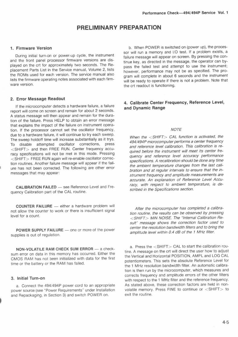
1 . Firmware Version
During initial turn-on or power-up cycle, the instrumentand the front panel processor firmware versions are dis-played on the crt for approximately two seconds . The Re-placement Parts List in the Service manual, Volume 2, liststhe ROMs used for each version . The service manual alsolists the firmware operating notes associated with each firm-ware version .
2. Error Message Readout
If the microcomputer detects a hardware failure, a failurereport will come on screen and remain for about 2 seconds .A status message will then appear and remain for the dura-tion of the failure . Press HELP to obtain an error messagethat explains the impact of the failure on instrument opera-tion . If the processor cannot set the oscillator frequency,due to a hardware failure, it will continue to try each sweep .The sweep holdoff time will increase substantially as it trys .To disable attempted oscillator corrections, press<SHIFT> and then FREE RUN. Center frequency accu-racy specifications will not be met in this mode. Pressing<SHIFT> FREE RUN again will re-enable oscillator correc-tion routines . Another failure message will appear if the fail-ure has not been corrected . The following are other errormessages that may appear :
CALIBRATION FAILED - see Reference Level and Fre-quency Calibration part of the CAL routine .
COUNTER FAILURE - either a hardware problem willnot allow the counter to work or there is insufficient signallevel for a count .
POWER SUPPLY FAILURE - one or more of the powersupplies is out of regulation .
NON-VOLATILE RAM CHECK SUM ERROR - a check-sum error on data in this memory has occurred . Either theCMOS RAM has not been initialized with data for the firsttime or the battery or the RAM has failed .
3 . Initial Turn-on
a . Connect the 494/494P power cord to an appropriatepower source (see "Power Requirements" under Installationand Repackaging, in Section 3) and switch POWER on.
PRELIMINARY PREPARATION
Performance Check-4941494P Service Vol . 1
b . When POWER is switched on (power up), the proces-sor will run a memory and IIO test . If a problem exists, afailure message will appear on screen . By pressing the con-tinue key, as directed in the message, the operator can by-pass the failed test and attempt to use -the instrument ;however, performance may not be as specified . The pro-gram will complete in about 6 seconds and the instrumentwill be ready to operate if there is not a problem . Note thatthe crt readout is functioning .
4. Calibrate Center Frequency, Reference Level,and Dynamic Range
NOTE
When the < SHIFTS CAL function is activated, the4941494P microcomputer performs a center frequencyand reference level calibration. This calibration is re-quired before the instrument will meet its center fre-quency and reference level accuracy performancespecifications . A recalibration should be done any timethe ambient temperature changes from the last cali-bration and at regular intervals to ensure that the in-strument frequency and amplitude measurements areaccurate . An explanation of Reference Level Accu-racy, with respect to ambient temperature, is de-scribed in the Specifications section .
After the microcomputer has completed a calibra-tion routine, the results can be observed by pressingSHIFTS MIN NOISE. The "Internal Calibration Re-
sult" message shows the correction factor used tocenter the resolution bandwidth filters and to bring theamplitude level within 0.4 dB of the 1 MHz filter,
a . Press the <SHIFT> CAL to start the calibration rou-tine . A message on the crt will direct the user how to adjustthe Vertical and Horizontal POSITION, AM PL and LOG CALpotentiometers . This sets the absolute Reference Level forthe 1 MHz resolution bandwidth filter . An automatic calibra-tion is then run by the microcomputer, which measures andcorrects frequency and amplitude errors of the other filterswith respect to the 1 MHz filter and the reference frequency .As stated above, these correction factors are held in non-volatile memory . Press FINE to continue or <SHIFT> toexit the routine .

Performance Check-494/494P Service Vol. 1
b . If the processor can complete the routine, the instru-ment control settings will return for normal operation . If aCALIBRATION FAILED message appears, refer to the cor-rection factors by pressing <SHIFT> MIN NOISE.
1 . Check Operation of Front Panel Pushbuttonsand Controls
Shift Functions - In the shift mode, those buttons withtwo or more functions, indicated by the blue and/or orangelettered nomenclature beside the button, activate the shiftfunction when pressed . In some cases a parameter or com-mand is entered followed by data, via the Data Entry key-board, then terminated with a multiplier, unit value, ordisplay scale factor.
The following procedures check the operation of all frontpanel pushbuttons, selectors, and controls . The buttonsshould illuminate when the function is active .
a . Set the FREQUENCY to 100 MHz, REF LEVEL to-20 dBm, and FREQ SPANIDIV to 20 kHz . Apply the CALOUT signal to the RF INPUT, by using the 50 Sf cable andbnc-to-N adapter, then change the Vertical Display to2 dB/DIV .
b . Note that the following pushbuttons and controls op-erate as described when they are activated .
INTENSITY - Rotate the control through its range andnote crt beam brightness change .
READOUT - When this button is not illuminated, offmode, crt readout is off . In the active state (buttonillumintated), there is crt readout of REF LEVEL, FRE-QUENCY, FREQ SPANIDIV, VERT DISPLAY, RF ATTEN,FREQ RANGE, REFERENCE OSCILLATOR, and RESO-LUTION BANDWIDTH . The INTENSITY control changesthe brightness of readout characters as well as the display .
GRAT ILLUM - When activated (active state) the grati-cule is illuminated . In the off mode the graticule lights aredim .
PERFORMANCE CHECK PROCEEDURE
If any amplitude correction factor, at room temperature,for a filter is greater than 1 dB, the filter in the VR assemblyshould be readjusted . Refer to the Adjustment Proceduresection .
BASELINE CLIP - When activated (illluminated) thebaseline of the display, up to about one graticule division, isclipped (blanked) .
Triggering - Triggering mode is activated by pressingone of four pushbuttons . Button illuminates when in the ac-tive state . Pressing any one of the buttons cancels or deac-tivates the other mode.
FREE RUN - Trace free runs .
INT - Sweep is triggered when noise level or modu-lation amplitude of a signal is _2.0 division . Triggering ischecked near the end of this procedure .
LINE - Trace is triggered at power line frequency .Switch Triggering mode to LINE and note sweep istriggered .
EXT - The trace runs only when an external signal,1 .0 V peak, is applied to the back panel External
HORIZ/TRIG connector . Since external test equipment isrequired to check this function, a check is not included atthis time .
SINGLE SWEEP - When activated, single sweep abortsthe current sweep ; pressing the button again will arm thesweep generator and light the READY indicator . The indi-cator will remain lit until the sweep has run . When triggeringconditions are met, after the circuit is armed/, the analyzerwill make only one sweep . Single sweep mode is canceledwhen any Triggering button is pressed . The effect of SIN-GLE SWEEP may be more apparent with digital storage off .
a . Press FREE RUN Triggering and set the TIME/DIV to0.5s,
b . Press SINGLE SWEEP and note that the sweepaborts .

c . Press SINGLE SWEEP again and note that theREADY indicator lights and the sweep runs .
d. Press FREE RUN to cancel single sweep and returnthe TIMEIDIV to AUTO position .
TIMEIDIV - This control selects sweep rate, manualscan, and external sweep operation . In the MNL position,MANUAL SCAN control should move the crt beam acrossthe full frequency span or horizontal axis of the crt graticule.In the EXT position a voltage of 0 to +10 V, applied to therear panel HORIZ/TRIG connector, should deflect the crtbeam across the full 10 division screen .
Vertical Display -- Display modes are activated bythree pushbuttons. Pressing any of these buttons cancelsthe other mode .
10 dBIDIV - When this button is activated, the dis-play is a calibrated 10 dB/division with an 80 dB dynamicrange.
(a) With a REF LEVEL of -20 dBm, activate10 dBIDIV and AUTO RESOLN . Set the FREQSPANIDIV to 20 kHz and tune the calibrator signal tocenter screen .
(b) Change REF LEVEL and note that the displaysteps in one division increments, representing10 dB/division . Return the REF LEVEL to -20 dBm .
2 dBIDIV - When this button is pressed, the displayis a calibrated 2 dBldivision with 16 dB of dynamic range.
(a) Activate the 2 dBIDIV mode and change theREF LEVEL to -6 dBm .
(b) Note that the display steps 1 .0 division for eachtwo steps of the REFERENCE LEVEL control .
LIN - When this button is actived, the display is lin-ear between the reference level (top of graticule) andzero volt (bottom of graticule) ; the crt VERT DISPLAYreads out in volts/division .
Activate the LIN mode and note that the Vertical Dis-play readout changes to 2.80 mV/division.
PULSE STRETCHER - When activated, the fall-time ofvideo signals increases so narrow video pulses will show onthe display. This function is checked later with external testequipment.
RFV JUN 1984
(c) Return the REF LEVEL to -20 dBm .
Performance Check-4941494P Service Vol. 1
Video Filter -Two filters can be independently selectedto provide, WIDE or NARROW (1130th or 11300th of theresolution bandwidth) filtering to average the noise.
(1) Change the FREQ SPANIDIV to 500 kHz, activate10 dBIDIV and AUTO RESOLN, and tune the calibratorsignal to center screen .
(2) Activate WIDE and NARROW Video Filters andnote the reduction in noise as each filter is switched in(see Figure 4-1) . The NARROW filter will have a morepronounced effect on noise reduction. Also note thechange in sweep rate, if the TIMEIDIV selector is in theAUTO position .
(3) Switch both Video Filters off.
-60DBM
1 .390 658 1GHZ
1KHZ/
10DB/ T DDB 0-1.8 1NT 100HZ
A. Spurii and IM obscured in the noise.
REF LFVFI
FRE4UFr;:r
-60DBM
1.399 658 LGHZI
f ..
10DB/ T ODB 0-1 .8 INT 100HZ
B. Same display with Video Filter activated .
Figure 4-1 . Video Filter effect on noise.
441 8-05
4-7

Performance Check-494/494P Service Vol . 1
DIGITAL STORAGE - Either one or both the "A" and"B" waveforms, from digital storage, can be selected . Theamplitude of a signal should remain constant when digitalstorage is switched on (VIEW A or VIEW B activated) . ThePEAK/AVERAGE control positions a cursor over the verticalwindow of the screen Noise and signal level will be averagedbelow the cursor and peaked above the cursor . Check oper-ation according to the following description .
VIEW A - When pressed, the °A" waveform, fromdigital storage, is displayed . With SAVE A off, the "A"waveform is updated each sweep as the beam travelsfrom left to right . With SAVE A on, the waveform andreadout are not updated .
VIEW B - When actived, the "B" waveform is dis-played . When both VIEW A and VIEW B are active, the"A" and °B" waveform are interlaced and displayed . Bothwaveforms are updated each sweep. Update of the "A"waveform depends on the state of SAVE A .
SAVE A - When actived, the "A" waveform, with itsreadout, is saved . In this mode the data for `A" waveform is not updated each sweep . Switch VIEW B off thenchange REF LEVEL and note that the °A" display doesnot change . The readout for the saved waveform will bedisplayed anytime SAVE A is on and VIEW B andB- SAVE A are off . If either VIEW B or B-SAVE A ison, the readout reflects current analyzer setup .
MAX HOLD - When on, the maximum signal ampli-tude at each memory location is stored . The waveform isupdated only when signal data is greater than that previ-ously stored . Verify operation by changing FREQUENCYor REF LEVEL and note that the maximum level at eachlocation is retained .
B-SAVE A - The arithmetic difference between anupdated "B" waveform and a SAVE A waveform is dis-played . SAVE A function is also activated when13-SAVE A is pressed .
Press B-SAVE A then change the REF LEVEL sothe difference between the "B" and SAVE A waveform isdisplayed with VIEW A and VIEW B off . The reference(zero difference) level is factory set at graticule center .The position of this reference level can be changed byqualified service personnel . Positive differences betweenthe two displays appear above and negative differencesbelow the line .
PEAK/AVERAGE - When digital storage is on, thiscontrol positions a horizontal line or cursor over the verticalgraticule window . Signals above the cursor are peak de-tected, signals below the cursor are averaged by the digitalstorage . Verify operation by moving the cursor within thenoise level and note the noise amplitude change as thecursor is positioned .
IDENTify - When the identify function is activated, ev-ery other sweep, with its waveform, is vertiically displacedfrom the other . The frequencies of the 1st and 2nd localoscillators are moved such that true signals are not dis-placed horizontally on alternate sweeps while spurious sig-nals are shifted 100 MHz or more, which is off screen for thenarrower spans . The FREQ SPAN/DIV must be 50 kHz orless for the coaxial bands and 50 MHz or less for the wave-guide bands (21 GHz or more) before the processor will acti-vate the Identify mode .
(1) With the 500 MHz marker tuned to center fre-quency, decrease the FREQ SPAN/DIV to 50 kHz or lessand press IDENT .
(2) Note that there is no horizontal dlisplacement ofthe 500 MHz signal on alternate sweeps . To help deter-mine if the signal is true or false,decrease the sweep rateor activate SAVE A, with both VIEW A and VIEW B on,so a comparison is easily observed (see Figure4-2) .
(3) Switch IDENT off .
AUTO RESOLN - When this function is on, resolutionbandwidth automatically changes to maintain a calibrateddisplay, as FREQ SPAN/DIV and TIMEIDIV are changed .Check operation by changing FREQ SPAN/IV or TIME/DIVsettings and note the RESOLUTION BANDWIDTH change .UNCAL indicator should not light over the FREQ SPAN/IVrange if the TIME/DIV selector is in AUTO position .
MAX SPAN - When this function is activated, the spanswitches to maximum and the analyzer sweeps the fullband . When deactivated, the span/div will return to its previ-ous setting .
ZERO SPAN - When this button is activated, the spanshould shift to zero for a time-domain display . When deacti-vated, the span returns to its previous setting .
FREQUENCY SPAN/DIV - As this control is rotated,the Span/Div should change from Max to 0, counter clock-wise from MAX position, in a 2, 1, 5 sequency . The displayshould indicate this change .
RESOLUTION BANDWIDTH - As this control is rotatedfrom the 30 Hz position, the resolution bandwidth shouldchange from 30 Hz to 100 Hz and then in decade steps to1 MHz .
REFERENCE LEVEL - In the 10 dB/DIV Vertical Dis-play mode, with FINE off, the REF LEVEL should step in10 dB increments as the control is rotated . When FINE isactivated, the steps are 1 dB. In the 2 dBY!DIV mode, the

-30DBM
53.720 BGHZ
5MHZ/R(F
100B/ T EX1 33-60 INT 1MHZVERTICAL
RF
FRELI REFEREMCE RESO . .L'71CNOISPL6r AT'IIENUATION R6NGE OSCILLATOR EAROWIUTN
A. Typical response of a true or real signal .
101)9/ T EXT 33-60 INT 100KHZVER- :CA~
R~
FREL1 REFERENCE RESOLUTION-I SPLAY
A17ERLA11ON
RANG.
OSCILLATOR
BA!JDVTDTH
B. Typical response from a false signal . Signal for bottomsweep is off screen. 4418-pa
Figure 4-2 . Typical display with SAVE A on to observe IDENTifymode .
steps are 1 dB, with FINE off, and 0 .25 dB with FINE active .When the Vertical Display factor is 4 dB/div or less, withFINE on, the analyzer should switch to the delta A modewhere the REF LEVEL readout goes to 0 .00 dB then stepsin 0.25 dB increments as the REFERENCE LEVEL control isrotated in a clockwise direction . Note, the REF LEVEL dBreading does not go above 0.00 dB if the control is rotatedcounterclockwise .
(1) Set the MIN RF ATTEN to 0 dB, Vertical Displayto 10 dBIDIV, and rotate the REFERENCE LEVEL con-trol counterclockwise to +30 dBm then clockwise to--110 dBm.
(2) Note that the REF LEVEL readout changes in10 dB increments .
Performance Check-4941494P Service Vol . 1
(3) Press FINE and rotate the REFERENCE LEVELcounterclockwise to -117 dBm . Note the REF LEVELnow steps in 1 dB increments .
(4) Press <SHIFT> REF LEVEL and select-30 dBm with the Data Entry keyboard, then press<SHIFT> dB/DIV and enter 4 dB, with the Data Entrykeyboard . Press FINE and note that the REF LEVELgoes to 0.00 dB .
(5) Rotate the REFERENCE LEVEL control clockwiseand note the REF LEVEL now steps in 0 .25 dB incre-ments from the 0.00 dB reference .
(6) Continue turning the control until the REF LEVELreads -10 dBm then press 10 dBIDIV and deactivateFINE .
(7) Return the REF LEVEL to -20 dBm and notethat 10 dB of RF ATTEN is switched in at a REF LEVELof -20 dBm . This prevents signal compression of anysignals whose amplitude is within the graticule area .
MIN RF ATTEN - This control sets the minimumamount of RF attenuation in the signal path, regardless ofthe REF LEVEL setting . Verify proper operation by settingthe MIN RF ATTEN dB selector to 20 and change the REFLEVEL settings . Note that the RF ATTEN readout does notgo below 20 dB.
FINE - When this button is activated, the REFERENCELEVEL steps decrease to the Fine mode as described andchecked under Reference Level .
MIN NOISE/MIN DISTORTION - This button selectsone of two algorithms that select attenuatior and IF gain .MIN NOISE (button illuminated) reduces the noise level byreducing the RF attenuation 10 dB and decreasing IF gain10 dB. MIN DISTORTION reduces IM distortion due to inputmixer overload . The normal mode of operation is with mini-mum distortion . To observe any change, the amount of RFATTEN, displayed by the crt readout, must be 10 dB higherthan the MIN RF ATTEN selector setting .
(1) Set the REF LEVEL to -20 dBm and the MIN RFATTEN at 0 dB . Note that the RF ATTEN readout indi-cates 10 dB.
(2) Activate MIN NOISE and note that the noise floordrops approximately 10 dB and the RF ATTEN readoutchanges to 0 dB . Deactivate MIN NOISE mode .
UNCAL - This indicator lights when the display isuncalibrated .

Performance Check-494/494P Service Vol . 1
SHIFT - Pressing this button shifts those pushbuttonswith more than one function, to their secondary function .The function of this secondary mode is nomenclated in blueor orange lettering next to the pushbutton . The shift modedeactivates after the function has been performed . SHIFT isalso used to abort from menus or other multi-key functions .
HELP - When activated, pressing or operating any con-trol or selector produces a help message on the crt thatexplains the function . Help messages will also prompt theuser to the next operational move or explain any error mes-sage that may appear . Activate this mode and press variousbuttons to observe the applicable crt messages . Press thebutton again to cancel . <SHIFT> HELP lists currenterrors .
RECALL SETTINGSISTORE - When pressed in the"Recall Settings" mode, this button will produce a listing ofthe memory registers and the center frequency of the setupstored . The 0 register retains the power-down settings . Allcan be recalled after power-up . In the <SHIFTi:, STOREmode, the existing front panel setup is stored in one of nineselected locations . A listing of all registers with the centerfrequency of the stored setup is displayed . A blank entryindicates no settings stored .
COUNT/COUNT RESOLN - A count for any signal be-low the dot marker, that is 20 dB above the noise floor andno more than 60 dB down from the REF LEVEL, is madebetween each sweep with the counter on (buttonilluminated).The counted signal frequency appears in placeof the center frequency . <SHIFT> COUNT RESOLN al-lows the selection of the counter resolution to 1 Hz, via theData Entry keyboard .
(1) Set the TIMEIDIV to 50 ms, deactivate the AUTORESOLUTION, and set the RESOLUTION BANDWIDTHto 10 kHz .
(2) UNCAL indicator should light and remain lit untilthe FREQ SPANIDIV is reduced to 200 kHz or theRESOLUTION BANDWIDTH is increased to 1 MHz .
(3) Return the TIMEIDIV to AUTO, press AUTORESOLN, and set the FREQ SPANIDIV to 100 MHz .
(1) Press <SHIFT> STORE, then select registernumber 1 to store the current front panel setup .
(2) Change front panel control and selector settings .
(3) Press RECALL and select the Data Entry key 1,to recall the setup .
(4) Note that the instrument front panel set-up re-turns to that previously entered .
(1) Set the FREQUENCY to 100 MHz. Establish acounter resolution of 100 Hz by pressing <SHIFT>COUNT RESOLN and enter 100 Hz, via the Data Entrykeyboard .
(2) Tune to any signal that is 20 dB or more above thenoise level and less than 60 dB down from the REFLEVEL. Activate COUNTER and note that the frequencyreadout has a resolution of 100 Hz .
AF - When the J F function is activated, center FRE-QUENCY readout initializes to 0.0 MHz or 0.00 kHz depend-ing on the FREQ SPANIDIV setting . The frequencydifference to another point in the span can now be deter-mined by tuning that point to center screen and noting thereadout . Check, by measuring the difference between cali-brator markers . If the frequency is tuned below "0.0" thereadout will indicate (-) sign . Deactivate and note that thereadout returns to the previous center FREQUENCY .
COUNT-CF -- This button is used when a close-inanalysis of a signal, in narrow spans, is desired . When thispushbutton is pressed, the signal under the frequency dot iscounted once (even if the COUNTER mode is inactive) thenthe Center Frequency is shifted to the counted frequency .Any Freq Span/Div can now be selected and the signal willremain centered on screen . The count resolution and theresulting accuracy of the tuning is equal to the currentcounter resolution .
(1) Decrease the FREQ SPANIDIV and increase theRESOLUTION BANDWIDTH so the calibrator signalspans 3 or 4 divisions on the screen . Tune the signal soapproximately 20 dB of signal level, above the noisefloor, is under the dot .
(2) Press COUNT-CF and note that the signal movesunder the frequency dot and the FREQUENCY readoutchanges to indicated the frequency of the marker.
FREQUENCY RANGE - These pushbuttons shift the494/494P frequency range up or down from the currentband . Press first one and then the other and note that thefrequency bands change accordingly . If the operator se-lects FREQUENCY via the Data Entry keyboard, themicroprocessor will automatically select the appropriatefrequency range .
AUTO PEAKIEXT MIXER - Selects Auto Peaking inits primary mode, and External Mixer in 'the shift mode.When AUTO PEAK is activated (button ilfuminated) oneof two things occur :
(1) If the analyzer is operating in the preselectorbands (1 .7 - 21 GHz), the preselector initiates a peakingroutine on any signal within the center two divisions of

the screen . The algorithm peaks the preselector tuningfor this center frequency setting, then stores this settingin non-volatile (battery powered) memory . If a signal isnot on screen, the algorithm will revert to the code thatwas previously stored in memory ; or, if there is no set-ting, to the mid point of the peaking range. After a centerfrequency setting for a band has been stored, the oper-ator can then switch back to this band with the assur-ance that the preselector is peaked well enough to trackthe oscillator and provide reasonable sensitivity .
(2) If the analyzer is operating in the External Mixermode, the peaking routine sets the external mixer bias sothe response is peaked . If a signal is not present, thealgorithm reverts to the previous bias setting stored inmemory or, if there is no previous setting, it sets the biasvoltage mid range .
When <SHIFT> EXT MIXER is pressed, External Mixeroperation is initiated, which do couples the EXTERNALMIXER port to an internal bias source for external mix-ers, and ac couples the IF return from the external mixerto the 2nd converter . This bias voltage is either manuallyset, with the MANUAL PEAK control, or automaticallyset by the Auto Peak algorithm . When in the ExternalMixer mode, the crt readout for RF ATTEN reads EXT.To exit this mode, press <SHIFT> EXT MIXER . TheREF LEVEL will shift to +30 dBm and the RF ATTEN to60 dB to protect the internal mixer from high level signalsthat might be applied to the RF INPUT.
a . Auto Peak
(1) With the Calibrator signal applied to the RF IN-PUT, select a frequency of 3.0 GHz, by pressing<SHIFT> FREQ then 3 GHz, via the Data Entry key-board . Select a REF LEVEL of -40 dBm, a FREQSPANIDIV of 10 kHz, and a RESOLUTION BAND-WIDTH of 1 kHz .
(2) Peak the 3.0 GHz signal with the MANUAL PEAKcontrol .
(3) Press AUTO PEAK . Note the message "PEAK-ING" on screen and the READY indicator for SINGLESWEEP mode flash as the processor runs the auto peakroutine .
(4) When complete, the signal amplitude should equalor exceed that obtained with manual peaking .
(5) Change bands by increasing or decreasing theFREQUENCY RANGE, then return to band 2 . Note thatauto peak maintains the setting stored in memory.
Performance Check-4941494P Service Vol . 1
b . External Mixer
(1) Press <SHIFT> EXT MIXER, the analyzershould shift to the External Mixer mode (indicated by areadout of EXT above RF ATTEN) . If AUTO PEAK modeis still active the button will remain lit as it does not indi-cate external mixer but auto peak status .
(2) Connect a voltmeter between the EXTERNALMIXER port and ground . Measure the bias voltage . If inthe Auto Peak mode, the bias should be a steady dovoltage . (If Auto Peak has not been run for this band, thebias voltage will read approximately --0 .8 V or midrange .)
(3) Switch to the manual peak mode by pressingAUTO PEAK again . The button should not be illuminatedand the bias voltage at the EXTERNAL MIXER portshould now vary between approximately -2.5 V to+1 .0V, as the MANUAL PEAK control is rotatedthrough its range .
(4) Press <SHIFT> EXT MIXER to deactivate EX-TERNAL MIXER mode.
Setting Parameters via the Data Entry Keyboard
(1) Set the FREQ SPANIDIV to 50 kHz and switchAUTO RESOLN on . Set the center frequency to 2.0 GHzby pressing <SHIFT> FREQ, then enter 2 GHz via theData Entry keyboard . Note that the FREQUENCY sets to2 .000 GHz . (The number of digits is a 'function of thespanldiv or the count resolution if the counter is on .
(2) Enter frequencies of 200 MHz, 200 kHz, and200 Hz by repeating the above procedure . Note that theFREQUENCY sets to that entered via the Data Entrykeyboard .
(3) Set the SPANIDIV to some setting via the key-board and note that the entered SpanlDiv is set .
(4) Enter a REF LEVEL with the keyboard and notethat the entry is set .
(5) Enter a desired Vertical Display factor with thekeyboard and note that the keyed-in dBldiv is set .
STORE DISPLAY and RECALL
Pressing <SHIFT> STORE DISP starts a sequence tostore, either the "A" or "B" waveform and its associatedreadout, in a numbered (0-8) memory register. This informa-

Performance Check-4941494P Service Vol. 1
tion is retained in non-volatile memory so it can be recalledat a later time . Informative messages, displayed on the crt,aid the user in completing the multiple button sequence .First a list of the center frequencies of current stored dis-plays is shown. The number of digits in the readout is anindication of the Span/Div of each stored display (a greaterresolution indicates a narrower span) . A register without anassociated frequency is empty . This display includes aprompt for the register number into which the display will bestored . The registser is selected, via the Data Entry key-board, then a prompt asks which display ("A" or "B") tostore in the selected register? Selection of the waveformcompletes the sequence and returns the instrument to nor-mal operation .
To exit Store Display function press the <SHIFT> but-ton . Pressing <SHIFT> RECALL recalls a selected wave-form, with its readout, from memory, so it can be sent to the"A" or "B" part of digital storage . To see the display, acti-vate the respective part of digital storage (VIEW A or VIEWB) . The readout for the "A" waveform will only be shown ifVIEW B and B- SAVE A are off, whereas the readout for arecalled "B" waveform will only be displayed if VIEW B orB-SAVE A are on . When RECALL is actived, SAVE A isalso activated to protect the recalled waveform from over-write if it is placed in "A" and to protect the current wave-form if it is placed in "B" . SINGLE SWEEP must beactivated before a waveform is placed in "B", to prevent anoverwrite by the next sweep. VIEW B must be activated toobserve the recalled waveform in "B" .
(1) Establish a display on the screen . Press<SHIFT> STORE DISPLAY then enter the memoryregister number (0-8) for the display and select display" A � .
(2) Change the current display with the REF LEVELor FREQUENCY control .
(3) Press -<SHIFT> RECALL then select the registernumber that contains the above display (note the centerfrequency listing of the stored displays in each register) .Press VIEW A and deactivate VIEW B.
(4) The recalled display, with its readout, should nowbecome the "A" display . SAVE A should activate to savethe display so the next sweep will not overwrite the re-called display . If VIEW B is on, both the recalled display(VIEW A) and the "B" display will be on screen . Since themost current display is the "B" waveform, the readoutwill depict the parameters for the "B" display . SwitchVIEW B off so the readout will represent the recalleddisplay .
(5) Activate SINGLE SWEEP then repeat part (3) ex-cept select "B" for the display . Activate VIEW B to viewthe recalled waveform .
(6) Repeat part (5) without activating SINGLESWEEP and note that a message on screen warns thatunless SINGLE SWEEP is on, the recalled display will beoverwritten by the next sweep .
<SHIFT> PLOT (494P only)
When the 494P is connected to a plotter over the GPIBcable, pressing <SHIFT> PLOT will send the digital stor-age waveform(s) that are displayed, as well as the graticuleand bezel (if GRAT ILLUM is on), and the crt readout (ifREADOUT is on) to the plotter .
To use or check the plot feature, connect the Digital Plot-ter to the 494P with a IEEE STD 488 (GPIB) cable and per-form the following :
(1) Set the corners of the plot for a 3:2 aspect ratiofor Tektronix plotters, or 6 :5 for the Hewlett-Packardplotter . The Digital Plotter must be in the Listen Onlymode and the 494P must be in either the TALK ONLY orTALK/LISTEN ONLY mode (appropriate ;switches on therear panel GPIB ADDRESS switch, closed or in the 1position) .
(2) Set the Plotter Interface switches as follows :
TEKTRONIX 4662 or 4662 Option 31 (rear panel)
A=0,1,8,or9B-CorDC = X (don't care)D = X (don't care)
TEKTRONIX 4663
Interface Select = 1 if Option 04 or 2 if Option 01Initial Command/Response Format = 5Interface Mode = Listen Only
HEWLETT-PACKARD
Address -- 31
(3) Select the plotter type by pressing <SHIFT>SAVE A, on the 4941494P, and answer the type plotterquestion on the crt message . The selection is stored inbattery-powered memory and need not be selected againunless the type plotter is changed . To use a 4663 emulat-ing a 4662, select 0 (4662) for a one-pen configuration orselect 1 (4662 Option 31) for a two pen configuration .Select the display and the information that you wish toplot .
The zero level for a B
SAVE A waveform is assummedto be the graticule center line . (Switches within theinstruument can set the zero level, contact your service

personnel for this change .) If you desire to shift the zerolevel for the PLOT only, press <SHIFT>, B-SAVE A,and enter the desired level in display units (25 is bottomgraticule line, 25 unitsldiv is required) . This zero level isretained in non-volatile memory ; however, it is not relatedto the display zero level since the processor has no wayof determining the internally set zero level for the crt dis-play or no way of changing it .
(4) Press <SHIFT> PLOT. During the plot opera-tion, the front panel controls are operational exceptSTORE DISP, RECALL, and AUTO PEAK; so the instru-ment can be used for other measurements .
This completes the operational check of the front panelcontrols and selectors .
2 . Check Reference Oscillator Accuracy
Reference oscillator accuracy is not a performance re-quirement ; however, it must be checked so the center fre-quency accuracy can be verified . Since the Calibrator islocked to the reference oscillator this procedure verifies ac-curacy by counting the frequency of the calibrator signal .Allow 30 minutes or more warm-up time for the oscillator tostabilize before proceeding with this check .
a . Connect the counter to the CAL OUT. Set the counterdisplay resolution to 1 Hz .
b . Check - Frequency of the calibrator must be100 MHz -±- 10 Hz .
c . Disconnect the counter from the CAL OUT connector .
3 . Check Counter Accuracy ±](10 + 2N)Hz -+- 1 LSD]
a . Set the FREQUENCY to 500 MHz and the FREQSPANIDIV to 20 kHz, via the Data Entry keyboard . Activate10 dBIDIV Vertical Display, set the TIMEIDIV to AUTO,REF LEVEL -30 dBm, and activate AUTO RESOLN.
b . Apply the CAL OUT signal to the RF INPUT and cen-ter the 500 MHz marker under the dot marker .
c . Press <SHIFT> COUNT RESOLN and enter 1 Hzvia the Data Entry keyboard .
d . Press COUNTER and note that the error over severalcounts does not exceed 13 Hz .
Performance Check-4941494P Service Vol . 1
e . Change FREQ SPANIDIV to 500 kHz and repeatpart d .
f . Press <SHIFT> COUNT RESOLN and enter 1 kHzfor a counter resolution of 1 kHz .
g . Press COUNTER and note that the error over severalcounts does not exceed 1 kHz .
h . Change the FREQ SPANIDIV to 200 kHz and repeatpart g .
i . Set the FREQUENCY to 1 .8 or 1 .7 GHz and repeat thecounter accuracy check for this end of the band.
4. Check Counter SensitivityCounter should count a signal that is 20 dB above the
noise floor and above a level that is 60 dB down from theREF LEVEL.
a . Test equipment setup is shown in Figure 4-3 . Applythe CAL OUT signal through 1 dB and 10 d[3 step attenua-tors to the RF INPUT.
b . Set the FREQUENCY to 100 MHz, FREQ SPANIDIVto 1 MHz, RESOLUTION BANDWIDTH to 1 MHz, REFLEVEL to 0 dBm, and activate NARROW Video Filter .
c . Adjust CENTER FREQUENCY to position the peak ofthe 100 MHz signal directly below the dot marker . Addattenuation to reduce the signal amplitude until it is 20 dBabove the noise floor .
d . Press <SHIFT> COUNT RESOLN and enter 1 Hzvia the Data Entry keyboard .
e . Press COUNTER and note that the counter is count-ing the signal with the accuracy noted in step 3 .
f. Change FREQ SPANIDIV and RESOLUTION BAND-WIDTH to 100 Hz, REF LEVEL to -30 dBrn, and activateWIDE Video Filter .
g . Increase the attenuation until the signal amplitude de-creases to a level that is is 60 dB below the R EF LEVEL andadjust CENTER FREQUENCY to place the signal directlyunder the dot marker .

Performance Check-494/494P Service Vol . 1
CounterTime Mark
DigitalGenerator Voltmeter
h . Press COUNTER and note that the counter is count-ing the signal and the count is accurate .
i . Deactivate COUNTER and WIDE Video Filter. ActivateAUTO RESOLN and switch FREQ SPAN/DIV to 200 kHz .
5 . Check Center Frequency Accuracy
This is a two part procedure ; part 1 checks center fre-quency accuracy without the 1st LO phase locked, part 2checks accuracy with the 1 st LO phase locked . A frontpanel CAL should be done before performing this check .
Center frequency accuracy is a function of how accuratethe center frequency is set between sweeps and the amountof frequency drift during the sweep . Frequency drift can besignificant during the first 30 minutes after turn-on or whenthe ambient temperature changes . With a span/div of 50 Hzand 30 Hz resolution bandwidth, the sweep rate is slowenough that frequency drift can be noted if the warmup timeis insufficient or the ambient temperature is changing . "N" isthe 1st LO harmonic number used for the first conversion(refer to IF Frequency, LO Range, and Harmonic Number, inSpecifications section for value of N, or activate the HELPmessage for the (down) FREQUENCY RANGE).
This check is dependent on the performance of the refer-ence oscillator and the counter accuracy ( see steps 2 and3) .
494 Spectrum Analyzer
Figure 4-3 . Test equipment setup for checking center frequency accuracy .
Part 1 - 1st LO not phase locked
Accuracy for bands 1 & 5--12 with Span/DivX200 kHz, and bands 2-4 with Span/Div X100 kHz :± [(20% of the Span/Div or Resoln Bandwidth, whichever is greater) + (CF x reference frequency error) -~ (Nx 15 kHz)] A settling time of 1 s/GHz change in centerfrequency divided by "N" must be allowed before check-ing accuracy . A front panel CAL should tie done beforeproceeding with this check .
(1) Equipment setup is shown in Figure 4-3
441$-44
(2) Apply the output of the comb generator to the RFINPUT . Set the FREQUENCY to 500 MHz and the FREQSPAN/DIV to 210 kHz, via the Data Entry keyboard . Ac-tivate AUTO RESOLN, 10 dB/DIV, and set REF LEVELto +20 dBm
(3) Press COUNT-CF and change the RESOLUTIONBANDWIDTH to 10 kHz .
(4) Note that the signal is within ± [(20"/6 of Span/Divor Resoln Bandwidth) + (N X 15 kHz)] or -±57 kHz(± 1 .35 minor div) of the dot marker .
(5) Set the FREQUENCY to 1 .0 GHz and RESOLU-TION BANDWIDTH to 1 MHz.
(6) Press COUNT-CF and change the RESOLUTIONBANDWIDTH to 10 kHz .
(7) Check - that the signal is within 57 kHz of thedot marker,

(8) Repeat the procedure to check accuracy at a cen-ter frequency of 1 .5 GHz (the upper end of band 1) .
(9) Using the above procedure and Table 4-2, checkcenter frequency accuracy to 21 GHz for those spanldivsettings in which the 1st LO is not phase locked .
Part 2 - 1st LO phase locked
Accuracy for bands 1 & 5-12 with SpanIDiv200 kHz and bands 2-4 with SpanIDiv _100 kHz : +
[(20% of the SpanIDiv or Resoln Bandwidth, whichever isgreater) + (CF x reference frequency error) + (2N +25)]Hz .
(1) Apply the CAL OUT signal to the RF INPUT .Press <SHIFT> FREQ and enter 100 MHz via the DataEntry keyboard . Set FREQ SPANIDIV to 50 Hz and theREF LEVEL to --20 dBm . Activate AUTO RESOLN and2 dB/DIV, then adjust the REFERENCE LEVEL so thetop of the signal is below the dot marker .
(2) Check 100 MHz center frequency accuracy bymeasuring the deviation of the 100 MHz signal from thedot marker . Error must not exceed ±(20% of thespanlDiv) + (25 + 2N) or ± 37 Hz (± 3.7 minor division) .
Table 4-2CENTER FREQUENCY ACCURACY CHECK POINTS
FOR UNLOCKED 1st LO
Performance Check-4941494P Service Vol . 1
(3) Repeat this procedure to check the center fre-quency accuracy to 1 .8 GHz in 100 MHz increments . Ad-just the REF LEVEL as necessary to observe the combof 100 MHz markers at the upper end of the range .
6 . Check Center Frequency Drift or Stability
Drift is 50 Hz or less per minute of sweep time, with 1 stLO phase locked (FREQ SPANIDIV 200 kHz or less forbands 1 & 5-12 and 100 kHz or less for bands 2-4) - after1 hour of warmup, and within a stable ambient temperature .
a . With the Calibrator signal applied to the RF INPUT,set the FREQUENCY to 100 MHz, TIMEIDIV to AUTO,FREQ SPANIDIV at 50 Hz, RESOLUTION BANDWIDTH at30 HZ, Vertical Display of 2 dB/DIV, and REF LEVEL of-23 dBm . Switch VIEW A and VIEW B on .
b . Adjust the CENTER FREQUENCY control so one sideof the signal intersects the sixth division graticule line, fromthe left edge, then press SINGLE SWEEP. Activate SAVE Ato save the display .
Band N CenterFreq
FreqSpanIDiv
MaximumError
ErrorMinor Div
1 1 0.5 GHz 210 kHz ±57 kHz +1 .351 .0 GHz 210 kHz ±57 kHz * 1 .351 .5GHz 210 kHz ± 57 kHz ±11 .35
2 1 2.0 GHz 110 kHz ±37 kHz ±1 .353.OGHz 110 kHz ±37 kHz +1 ..354.0 GHz 110 kHz ±37 kHz +1 .355.0GHz 110 kHz +37 kHz ±1 .35
3 1 6.0 GHz 110 kHz ±37 kHz ±1 .356.5GHz 110 kHz ± 37 kHz ±1,357.0 GHz 110 kHz ±37 kHz +11 .35
4 3 7.5 GHz 110 kHz +67 kHz ±1 .359 .5 GHz 110 kHz ±67 kHz ±11 .3511 .5GHz 110 kHz ± 67 kHz ± 1 .3513.5 GHz 110 kHz +67 kHz 2- 1,3515.5GHz 110 kHz ±67 kHz ±1 .3517 .5 GHz 110 kHz + 67 kHz ±1-3518 .OGHz 110 kHz ±67 kHz +1 .35
5 3 18 .5 GHz 210 kHz + 87 kHz ±11 .3520 .OGHz 210 kHz ±87 kHz 1. 1 .3521 .0 GHz 210 kHz ±87 kHz ± 135

Performance Check-494/494P Service Vol . 1
c . Select the NARROW Video Filter and press SINGLESWEEP again to start the sweep . The sweep will now run ata 1 0 s/div rate .
d . Note the frequency difference between the two dis-plays, at the 6th graticule line as A f .
e . Check - the frequency drift rate/minute . Drift is (300x A f) / (250 + A f) per minute . Drift rate must not exceed50 Hz/min .
7 . Check Residual FM
Within (7 kHz)N over 20 ms, with FREQ SPAN/DIVgreater than 200 kHz, and within (10 + 2 N) Hz over 20 ms,with FREQ SPAN/DIV of 200 kHz or less)
a . With the Calibrator signal applied to the RF INPUT,set the FREQUENCY to 100 MHz, FREQ SPAN/DIV to1 MHz, RESOLUTION BANDWIDTH to 100 kHz, VerticalDisplay to 2 dB/DIV, and REF LEVEL to -23 dBm.
b . Press <SHIFT> FREE RUN. A message "FRE-QUENCY CORRECTIONS DISABLED" will come onscreen, which indicates that the 1 st LO synthesis and phaselock are disabled ; this is normal . It is now possible to switchthe FREQ SPAN/DIV to narrower spans with phase lockdisabled .
c . Decrease the FREQ SPAN/DIV and RESOLUTIONBANDWIDTH to 100 kHz and keep the 100 MHz calibratorsignal centered on screen with the CENTER FREQUENCYcontrol .
d . Switch the Vertical Display to LIN . Position the signalso the slope (horizontal versus vertical excursion) of the re-sponse can be determined as illustrated in Figure 4-4A . Itmay help to determine slope by switching VIEW B off andusing SAVE A and VIEW A to freeze the display at a conve-nient point on the graticule for measurement . Slope shouldcalculate to approximately S kHz/division .
e . If SAVE A was used in step d, de-activate SAVE Aand VIEW B . Activate ZERO SPAN, set TIME/DIV to 20 ms,and adjust CENTER FREQUENCY control to position thedisplay near center screen as shown in Figure 4-4B . UseSAVE A to freeze the display for ease in measuring the FM .The peak-to-peak amplitude of the display per any horizon-tal division, scaled to the vertical deflections according tothe slope estimated in part d is the FM . Residual FM mustnot exceed 7 kHz for 20 ms or 7 kHz/division .
-23DBM 103. J903MHZ IOKHZI
2.00MV/ T 1008
0-1.9
INT
10KHZ
A. Calculating slope of response.
-230BM 103.905MHZ 2'OM5/I
Slope = 2 kHz or 400 Hz/div5 div
2.OOMVl'T
100B
0'-1. 0
INT
10KHZ~:: ..',
.- . ., ,r .,l P, : , .
u. .` .'r
B. Measuring FM as 1he deviation/division of theresponse.
441&08
Figure 4-4 . Typical display that illustrates how residual FM ismeasured .
f . Press <SHIFT> FREE RUN to re-enable the phaselock, set the FREQUENCY to 100 MHz and switch theTIME/DIV to AUTO. Reduce the FREQ SPAN/DIV andRESOLUTION BANDWIDTH to 100 Hz .
g . Adjust the CENTER FREQUENCY control to positionthe signal so its slope can be determined . Again, it will beeasier if you use SINGLE SWEEP and SAVE A to freeze thedisplay at a convenient position on the graticule .
h . Deactivate SAVE A and SINGLE SWEEP and switchthe TIME/DIV to 20 ms . Activate ZERO SPAN and positionthe display near center screen so the vertical excursions perhorizontal division (20 ms) can be measured . Residual FMmust not exceed 12 Hz within any one horizontal division .

8. Check Frequency Span/Div Accuracy ± 5% of theselected spanldiv
Span accuracy is checked by noting the displacement ofcalibrated markers from their respective graticule line overthe center eight divisions of the screen . The frequencyspanldiv accuracy is checked, for all FREQ SPAN/DIVsettings on band 1, at 100 kHz/Div on band 2, (2nd LOcheck) and at 500 MHz/Div on band 4 . The accuracy of the1 GHz, 5 GHz, and 10 GHz spanldiv selections, for the up-per bands, is directly related to the 100 MHzldiv and 200MHzldiv selections : therefore, they are not included in thisprocedure .
FREQUENCY SPANIDIV range is 50 Hz to 200 MHz forthe 0 to 7.1 GHz bands, increasing in a 5, 1, 2, 5 sequenceto 10 GHz for bands 11 and 12 . Selection is in a 5, 2, 1sequence with the FREQUENCY SPANIDIV control and bytwo significant digits with the Data Entry keyboard.
a . Equipment setup is shown in Figure 4-5 .
b . Set the FREQUENCY to 1 GHz, FREQ SPANIDIV to200 MHz, RESOLUTION BANDWIDTH to 1 MHz, TIME/D IV at 0.5 s, REF LEVEL to -30 dBm, and Vertical Displayto 10 dB/DIV.
TM 500 Main Frame
Performance Check-4941494P Service Vol . 1
c . Apply the CAL OUT signal to the RF INPUT and ad-just the FREQUENCY to align the 100 MHz markers so the200 MHzldiv accuracy can be measured over the centereight divisions of the display (two markers per division). Itmay be necessary to change the REF LEVEL to obtain ade-quate markers . Maximum deviation (see Figure 4-6) mustnot exceed 10 MHz (0.25 minor divisions) .
d . Change the FREQ SPANIDIV to 100 MHz and checkthe spanldiv accuracy . Error must not exceed 5% of theFREQ SPANIDIV or 5 MHz .
e . Remove the CAL OUT signal to the RF INPUT andapply the output of the Microwave Comb Generator, asshown in Figure 4-5 . Set the FREQUENCY to 10 GHz,(band 4, 5 .4 to 18 GHz) FREQ SPANIDIV to 500 MHz,RESOLUTION BANDWIDTH to 100 kHz, and REF LEVELto -10 d8m. Peak the response with the MANUAL PEAKcontrol and adjust REF LEVEL for the best marker defini-tion . It may also help to adjust the CENTER FREQUENCYfor better marker definition .
f .
Tune a marker to center screen then check the accu-racy over the center eight divisions of the display . Deviationmust not exceed ± 25 MHz.
494/494P Spectrum Analyzer
Figure 4-5 . Test equipment setup for checking frequency spanldiv and sweep timeldiv accuracy .

Performance Check-494/494P Service Vol . 1
Figure 4-6. Typical marker display that shows how span/div ac-curacy is measured .
g.
Set the FREQUENCY to 2.0 GHz, FREQ SPAN/DIVto 100 kHz, RESOLUTION BANDWIDTH to 1 kHz, TIME/DIV to 50 ms, and REF LEVEL to -20 dBm .
h .
Modulate the Comb Generator signal with 10 usmarkers, from the Time Mark Generator, by applying theMarker Output to the Pulse Input of the Comb Generator asshown in Figure 4-5. Adjust the MANUAL PEAK control foroptimum marker definition .
i .
Check FREQ SPAN/DIV accuracy . Error must not ex-ceed +5 kHz.
j .
Remove the Comb Generator signal from the RF IN-PUT and connect the Marker Output of the Time Mark Gen-erator to the RF INPUT. Set the FREQUENCY to 100 MHz,FREQ SPAN/DIV to 50 MHz, RESOLUTION BANDWIDTHto 100 kHz, REF LEVEL to +20 dBm, and apply 20 ns timemarkers from the Time Mark Generator .
k.
Adjust the REF LEVEL for the best marker definitionand the CENTER FREQUENCY to align the markers sospan/div accuracy can be checked for the 50 MHz/div .
I . Reduce the FREQ SPAN/DIV to 20 MHz, CENTERFREQUENCY to 100 MHz, and apply 50 ns (20 MHz)markers.
m . Check the 20 MHz FREQ SPAN/DIV accuracy .
n . Repeat the procedure and check the FREQ SPAN/DIV accuracy from 10 MHz down to 200 kHz . Use Table 4-3as a guide to relate time markers to FREQ SPAN/DIVsettings . Reduce RESOLUTION BANDWIDTH and CEN-TER FREQUENCY as each setting is checked to maintainmarker amplitude and definition .
o. Change the TIME/DIV to 0.5 s and RESOLUTIONBANDWIDTH to 100 Hz . Repeat the above procedure tocheck the 100 kHz to 10 kHz FIR EQ SPAN/DIV selections .
p. Set the FREQUENCY to 100 kHz, RESOLUTIONBANDWIDTH to 30 Hz, TI ME/DIV to 1 s and REF LEVEL to0 dBm . Repeat the above procedure to check the 5 kHz to200 Hz FREQ SPAN/DIV selections .
q. Activate the 2 dB/DIV Vertical Display imode, increaseREF LEVEI to approximately -28 dBm . Repeat the proce-dure to check the 100 Hz and 50 Hz FREQ SPAN/DIVselections .
Table 4-3SPAN/DIV VERSUS TIME MARKERS FOR
SPAN/DIV ACCURACY CHECK
REF LEVEL FREQUFNn FrU SPANIOTY-30DBM e_g0GHZ 200MHZ1
Measure deviationof any markerwithin the center8 divisions fromits respective graticule~~ -a
-onAlign marker
centerline _
Lasm
IMP T 0OB 0-1 .8 INT MHzVERTICAL RF FREO REFERE?ICE RE"0LUTIONDISPLAY ATTENUATION RANGE OSCIIIATOR BANMIUTH
4416-,s
FREQUENCYSPAN/DIV
Time Mark GeneratorMarker Output
20 MHz 50 ns10 MHz . 1 pis5 MHz . 2 Fis
2 MHz . 5 us1 MHz 1 As
500 kHz 2 us200 kHz 5 us100 kHz 10 Ps
50 kHz 20 us20 kHz 50 us10 kHz . 1 ms5 kHz . 2 ms2 kHz . 5 ms1 kHz 1 m;,500 Hz 2 ms200 Hz 5 ms100 Hz 10 ms50 Hz 20 ms

9. Check Time/Div Accuracy (accuracy within 5% oftime selected)
a .
Test equipment setup is the same as that required forstep 8 .
b .
Apply the Marker Output from the Time Mark Gen-erator directly to the RF INPUT . Apply the Trigger Output tothe 494/494P HORIZ/TRIG connector on the back panel .
c . Activate ZERO SPAN . Set the RESOLUTION BAND-WIDTH to 100 kHz, REF LEVEL at 0 dBm, TIME/DIV to50 ms, MIN RF ATTEN to 20 dB, FREQUENCY to 1 MHzand the Triggering mode to EXT.
d . Apply 50 ms time markers . Adjust CENTER FRE-QUENCY, if necessary, to display the markers on the timedomain display (see Figure 4-7) .
e .
Use the horizontal position control to align a markeron the 1st graticule line, then check the displacement ofmarkers from their respective positions over the center eightdivisions . Individual marker displacement must not exceed5% or 2 minor divisions .
f . Check the accuracy of the 50 ms to 2 ms TIME/DIVsettings,then the portion and note the displacement as de-scribed in part "e" of this step .
g .
Deactivate the VIEW A and VIEW B mode . Changethe RESOLUTION BANDWIDTH to 100 kHz, the VerticalDisplay to 2 dB/DIV, and the REF LEVEL to -10 dBm .
h . Check the accuracy of the 1 ms to 20 us TIME/DIVselections .
10 . Check Pulse StretcherThis is an operational check only .
a .
With the equipment setup the same as step 9, apply1 ms time marks, from the Time Mark Generator, to the RFINPUT. Set the TIME/DIV to 0.1 ms, RESOLUTION BAND-WIDTH to 100 kHz, Vertical Display to 10 dB/DIV, and REFLEVEL to 0 dBrn . Set the FREQUENCY to 2 .0 MHz, switchVIEW A and VIEW B off, and activate ZERO SPAN .
b . Activate PULSE STRETCHER and note that thismode extends the fall-time of the markers .
Performance Check-494/494P Service Vol . 1
Position marker on graticule line
zF)J .W,
FRea sa
Error over 8 divisions
3kGB
0-1 .8
. 111T
I t)~1°hr
PFO
i1CrrsDavr arse:
Figure 4-7 . Typical display to illustrate how timeldiv accuracyis measured .
c .
Remove the Time Mark Generator outputs to the FIFINPUT and HORIZ/TRIG inputs of the 494/494P . DeactivatePULSE STRETCHER, ZERO SPAN and return the MIN RFATTEN to 0 dB.
11 . Check Resolution Bandwidth and ShapeFactor
Bandwidth is within 20% of the 1 MHz to 30 Hz range, indecade steps to 100 Hz, then 30 Hz ; shape factor is 7 .5 :1 orless to 100 Hz, and 15 :1 or less for the 30 Hz bandwidth .
a . With the Calibrator output applied to the RF INPUTand the FREQUENCY set to 100 MHz, set the REF LEVELto -20 dBm, FREQ SPAN/DIV to 500 kHz, RESOLUTIONBANDWIDTH to 1 MHz, TIME/DIV at AUTO, and VerticalDisplay to 2 dB/DIV . Activate MIN NOISE.
b . Measure the 6 dB down bandwidth (see Figure 4-8A) .Bandwidth should equal 1 MHz ±200 kHz.
c . Change the Vertical Display to 10 dB,fDIV and mea-sure the 60 dB down bandwidth (see Figure 4-8B) .
d . Calculate the shape factor as the ratio of -60 dB/-6 dB bandwidths (see Figure 4-8) . Shape factor shouldequal 7.5:1 or less .
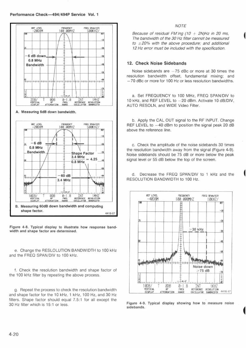
Performance Check-494/494P Service Vol. 1
A . Measuring 6dB down bandwidth .
B . Measuring 60dB down bandwidth and computingshape factor.
4418-07
Figure 4-8 . Typical display to illustrate how response band-width and shape factor are determined .
e . Change the RESLOLUTION BANDWIDTH to 100 kHzand the FREQ SPAN/DIV to 100 kHz .
f . Check the resolution bandwidth and shape factor ofthe 100 kHz filter by repeating the above process .
g . Repeat the process to check the resolution bandwidthand shape factor for the 10 kHz, 1 kHz, 100 Hz, and 30 Hzfilters . Shape factor should equal 7.5 :1 for all except the30 Hz filter which is 15 :1 or less .
NOTE
Because of residual FM'ing (10 + 2N)Hz in 20 ins,The bandwidth of the 30 Hz filter cannot be measuredto ±20% with the above procedure ; and additional12 Hz error must be included with the specification .
12 . Check Noise Sidebands
Noise sidebands are -75 dBc or more at 30 times theresolution bandwidth offset, fundamental mixing : and-70 dBc or more for 100 Hz or less resolution bandwidths .
a . Set FREQUENCY to 100 MHz, FREQ SPANIDIV to10 kHz, and REF LEVEL to -20 d6m. Activate 10 dB/DIV,AUTO RESOLN, and WIDE Video Filter .
b . Apply the CAL OUT signal to the RF INPUT . ChangeREF LEVEL to -40 dBm to position the signal peak 20 dBabove the reference line.
c . Check the amplitude of the noise sidebands 30 timesthe resolution bandwidth away from the signal (Figure 4-9) .Noise sidebands should be 75 dB or more below the peaksignal level or 55 dB below the top of the screen .
d . Decrease the FREQ SPAN/DIV to 11 kHz and theRESOLUTION BANDWIDTH to 100 Hz .
Figure 4-9 . Typical display showing how to measure noisesidebands.
REF LEVEL FREQUENCY FREQ SPAN/DIY-20DBM t00,0OMHZ -___S00KHZ/_ . ._
ridnloomMENEM
-6 dB down0.8 MHz
1 I
NNE000110011 No11MENEffin min
2DB/ T 0DB 0-1 .8 INT 1MHZVEPTICAI Rr FREQ REFERENCE RESOLUTIONDISPLAY ATTa -~_ _~ ~T
REF LEVEL FREQUENCY FREQ SPANmIV-20DBM 100 .00MHZ 500KHZ/
too
-4-s 6 dB
NAj~gm1ONE_ REF
-W
0.8 MF8andwi . "S Shape
3.4 MHz -Factor
4.25
1 -
0.8 MHz
3.4 MHz60.:I...
- .. . . ._ .-.10D81 T ODB 9-1.8 ..DT i MHZVERTICAL RF FRFa REFF7RETNCE RESOLLITIttNDISPLAY ATTENUATION sE asC T Mrs. _
WF LM FREXEhn FRED SPAN/DIV
-40DBM 100 .000MHZ IOKHZ/11
u
tip
-el
11i
-2B
-30 kHz
l I-r
" iwnB
10DB/ T 0DB 0-1 .8 INT IKHZVERTICAL RF FREO REFERENCE RESOLUTIONDISPLAY ATTENUATION RANGE OSCIIIATOR EIANDYIDTH 4416-17

e . Check the amplitude of the noise sidebands 3 kHzaway from the signal . Noise sidebands should be 70 dBbelow the signal level or 50 dB below the top of the screen .
13.
Check Calibrator Output -20 dBm ±0.3 dB at100 MHz
Three procedures for measuring output level are de-scribed : vector voltmeter, power meter, and comparison be-tween an accurate - 20 dBm source and the Calibratoroutput .
Vector Voltmeter Method
(1) Test equipment setup is shown in Figure 4-10 .
(2) Terminate the voltmeter probe with a 50 St feed-through termination and then connect the terminatedprobe to the CAL OUT connector
(3) Set the vector voltmeter frequency to 100 MHz .
(4) Check - for an rms reading between 21 .11 mVand 22 .69 mV . (22.36 mV rms, across 5012, is-20 dBm .)
Power Meter Measurement
(1) Test equipment setup is shown in Figure 4-10.
494/494P Spectrum Analyzer
150 MHz Low Pass Filter
(2)
Connect the power meter sensor through a low-pass filter (a40 dB, at 200 MHz, to remove harmonics ofthe fundamental) to the CAL OUT connector .
Insertion loss of the filter with pads, measured at100 MHz, must be determined to within 0.05 dB. Toensure a 50 ,fl match, use approximately 3 dBminimum-loss matching pads (attenuator) on bothsides of the filter.
(3) Note the power reading . Readincl, plus the lossthrough the filter and pads, must equal -20 dBm,±0.3 dB .
Signal Substitution Method
A powermeter is used to verify the output level of thereference signal . Harmonics of the signal source mustbe greater than 40 dB down.
(1)
Apply a 100 MHz signal from a signal source (sig-nal generator) through a 3 dB attenuator to the powermeter . Adjust the output level for -20 dBm reading onthe power meter .
Method #1Vector Voltmeter
Figure 4-10 . Test equipment setup for checking the calibrator output level,
Performance Check-494/494P Service Vol . 1
NOTE
NOTE
Method #2Power Meter
4++6 'a

Performance Check-4941494P Service Vol . 1
(2)
Set the FREQUENCY to 100 MHz, FREQ SPAN/DIV to 100 kHz,RESOLUTION BANDWIDTH to 1 MHz,and set the REF LEVEL to -18 dBm . Set TIME/DIV toAUTO and turn the PEAK/AVERAGE control fullyclockwise
(3)
Disconnect the meter and (using the same instru-ment cable and attenuator) apply the calibrated referencesignal to the RF INPUT .
(4)
Set the Vertical Display factor to the A A mode bypressing FINE . Adjust the REF LEVEL so the top of thesignal is on a graticule line near the top of the screen .Reset the REF LEVEL to 0 .00 dB by pressing FINEtwice . If desired, store the display by activating SAVE A.
(5) Remove the reference signal and apply the CALOUT signal to the RF INPUT .
(6)
Adjust the REF LEVEL until the signal is the sameamplitude as the reference established in part 4 . Note thedisplacement, of the CAL signal from the reference, asthe A A readout .
An alternate method to measure the difference is asfollows : Decrease the RESOLUTION BANDWIDTH to100 kHz, activate B -SAVE A, and note the displace-ment between the CAL signal and the reference . Dis-placement must not exceed 0.3 dB .
14. Check Frequency ResponseResponse, about the midpoint of the two extremes, is :
1 .5 dB from 50 kHz to 1 .8 GHz ; t2 .0 dB from 10 kHz to1 .86 Hz ; ± 2.5 dB from 1 .7 to 7.1 GHz ; ± 3.5 dB from 5.4 to18 GHz ; and ±5 .0 dB from 15 to 21 GHz . Response withrespect to 100 MHz: ±3.5 dB from 1 .7 to 7.1 GHz ;±4.5 dB from 5 .4 to 18 GHz ; and ±fi.5 dB from 15 .0 to21 GHz .
Frequency response is the peak-to-peak variation of thedisplayed amplitude over a specified center frequencyrange, measured at the center frequency . It is measuredwith 10 dB of RF attenuation, with Peaking optimized, forthose bands that are applicable, for each center frequencysetting . Response includes the effect of input vswr, mixingmode (N), gain variation, and preselector or mixer . Digitalstorage typically increases errors by 0.5% .
Accurate measurement requires many small incrementalchecks across the frequency range . The response at eachcheck point, above band 1, should be peaked with MANUALPEAK or by activating the AUTO PEAK mode. When check-ing the external mixer bands the signal must be identified asa true response and peaked .
If your instrument is the rackmount version, with semi-rigid cables to the back panel (Option 31), frequency re-sponse may degrade at the higher frequency end (seeRackmountiBenchtop Version, Options section for details) .
NOTE
Loss of signal through interconnecting cables be-comes significant above 1 GHz; therefore, short(25 inch or less) semi-rigid cable with precision fittingsto interconnect the test equiment should be used. Pre-cise matching terminations and power dividers arealso used to minimize reflections.
To expedite the measurement, this procedlure uses a lev-eled output sweep oscillator rather than incremental checks .Digital storage is also used to provide a complete display ofthe swept frequency . VIEW A, VIEW B and MAX HOLD arereactivated for each sweep .
a . Test equipment setup is shown in Figure 4-11 . Setthe FREQUENCY to 5 MHz, FREQ SPAN/DIV to 1 MHz,TIME/DIV to 20 ms, REF LEVEL to 0 dBm, and MIN RFATTEN to 30 dB . Activate 1 dB/div and AUTO RESOLN .
b . Apply the output of a constant level and calibrated10 kHz to 10 MHz Signal Generator to the RF INPUT of the494/494P . Set the generator frequency to 100 kHz and itsoutput for about -10 dBm .
c . Adjust the REF LEVEL so the amplitude of the100 kHz signal is about half screen, in the 2 dB/DIV mode.Activate VIEW A, SAVE A, and MAX HOLD .
d . Slowly tune the Signal Generator frequency from10 kHz to 10 MHz, monitoring the output to ensure it re-mains constant . Note the frequency response (amplitudedeviation above and below the average) . Frequency re-sponse or amplitude deviation must not exceed +1 .5 dBfrom 50 kHz to 10 MHz or -- 2.0 dB trom 10 kHz to 10 MHz.(See Figure 4-12 for the average level .)
e . Replace the 10 kHz to 10 MHz signal source with a0.01 to 2.4 GHz sweep oscillator and connect the testequipment as shown in Figure 4-13 . The output of theSweep Generator is applied through a 3 dB attenuator andhigh performance coaxial cable to a power divider . Connectone output of the power divider to the RF INPUT of the494/494P and the other output to the sensor for the powermeter or to the ALC input of the sweep oscillator .
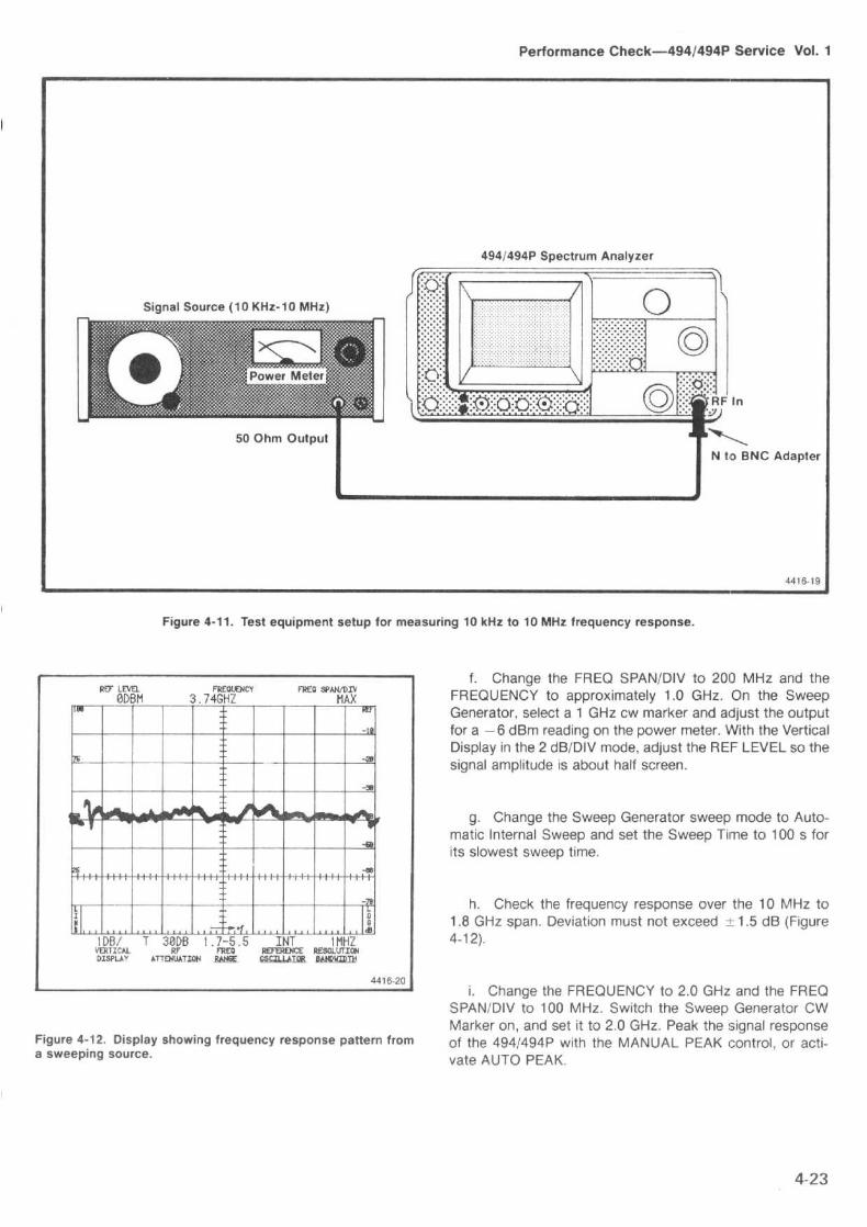
Figure 4-11 . Test equipment setup for measuring 10 kHz to 10 MHz frequency response .
Figure 4-12 . Display showing frequency response pattern froma sweeping source.
Performance Check-494/494P Service Vol. 1
494/494P Spectrum Analyzer
4416-19
f . Change the FREQ SPAN/DIV to 2017 MHz and theFREQUENCY to approximately 1 .0 GHz. On the SweepGenerator, select a 1 GHz cw marker and adjust the outputfor a -6 dBm reading on the power meter. With the VerticalDisplay in the 2 dB/DIV mode, adjust the REF LEVEL so thesignal amplitude is about half screen .
g. Change the Sweep Generator sweep mode to Auto-matic Internal Sweep and set the Sweep Tirne to 100 s forits slowest sweep time .
h. Check the frequency response over the 10 MHz to1 .8 GHz span. Deviation must not exceed -_- 1 .5 dB (Figure4-12).
i .
Change the FREQUENCY to 2 .0 GHz and the FREQSPAN/DIV to 100 MHz. Switch the Sweep Generator CWMarker on, and set it to 2.0 GHz. Peak the ;signal responseof the 494/494P with the MANUAL. PEAK control, or acti-vate AUTO PEAK.
REF LEVEL FREQUENCY FWD SPAWDIVODBM 3 .74GHZ MAX
Rff
MOM%_ . rr.a MOA..
Now1DB/ T 38DB 1 .7-5 .5 ZNT 1MH7VERTICAL RE rREQ REFERENCE RESOLUTIONDISPLAY ATTENUATIDN RAAK QSCaI.A T.f6t 9AWWIPSN
4416-20

Performance Check-4941494P Service Vol. 1
NOTE
r
aleiIIIIII
To Recorder Out connector (Back Panel)
RG158 BNC Cable
j .
Return the Sweep Generator to its Sweep mode andset the Start/Stop markers far 1 .5 and 2 .5 GHz . Sweep the1 .7 to 2.5 GHz span for Band 2 and note the frequencyresponse . Frequency response or deviation must not ex-ceed ±2.5 dB .
!f any segment or portion of the span fails to meet the+2.5 dB specification, set the FREQUENCY to thecenter of this portion; apply a cw marker at this centerfrequency and re-peak with the MANUAL PEAK orAUTO PEAK mode . Decrease the FRED SPAN/DlV todisplay that portion and then recheck the frequencyresponse for this portion.
k. Replace the 0 .01 to 2 .4 GHz sweep source with asweep oscillator that covers the frequency range to 21 GHz.Connect the test equipment as shown in Figure 4-13 . On theRF plug-in, switch the ALC to Mtr position and connect a
Power Meter
Low Loss Coax Cable with SMA Connectors
Figure 4-13 . Test equipment setup for measuring .01 to 21 GHz frequency response .
To Ext ALCon Sweep Generator
orThrough Power Meter
to ALC Connector
4416-62
coaxial cable between the Recorder Output of the powermeter and the Ext ALC Input of the plug-in unit . Decreasethe Power Level to approximately -6 dBm then adjust theGain for stable operation (output stops oscillating) .
I . Set the FI=iEQ SPANIDIV to 200 MHz and the FRE-QUENCY to 4.0 GHz. Re-peak the response with the peak-ing controls, then sweep the upper portion of band 2 andcheck frequency response . If necessary, recheck those por-tions that do not meet specification after peaking the re-sponse at the center of those portions of the frequencyspectrum .
m . Increase the FREQUENCY RANGE to the 3.0 to7.1 GHz band . Tune the CENTER FREQUENCY to approxi-mately 5.0 GHz. Apply a 5.0 GHz cw marker, and peak theresponse . Activate MAX SPAN and check the frequency re-sponse by sweeping the 3 .0 to 7.1 GHz frequency range. Itmay be necessary, if the response does not meet the±2 .5 dB performance, to again peak the response at the

center of those portions that do not meet specifications andrecheck frequency response in smaller segments .
n . Repeat the foregoing procedure to check the re-sponse of the remaining bands to 21 GHz . Frequency re-sponse for band 4 (5.4-18 GHz) is ±3.5 dB and ±5.0 dBfor band 5 (15 .0-21 .0 GHz) .
15 .
Check Display Accuracy and Range
80 dB in 10 dBIDIV mode, with an accuracy of+1 .0 dB/10 dB to a maximum cumulative error of +2.0 dBover the 80 dB window ; 16 dB in 2 dBIDIV mode with anaccuracy of t 0.4 dB/2 dB to a maximum cumulative errorof ± 1 .0 dB/dB over the 16 dB window ; Lin mode is + 5%of full scale,
a . Test equipment setup is shown in Figure 4-14 . Applya 100 MHz, +10 dBm signal, from the Signal Generator,through external attenuators set to 0 dB, to the RF INPUT .
Signal Source+30 d8m to -80 dBm100 kHz to10GHz
0
Performance Check-494/494P Service Vol . 1
b . Set the FREQUENCY to 100 MHz, FREQ SPANIDIVto 20 kHz, Vertical Display to 10 dBIDIV, MIN RF ATTEN at0 clB, REF LEVEL to +10 dBm, and PEAKIAVERAGE con-trol fully clockwise . Activate AUTO RESOLN and the NAR-ROW Video Filter .
c . Carefully adjust the generator output so the signallevel is at the top graticule line .
d .
Add 80 dB of external attenuation in 10 dB steps andnote that the signal steps down screen in 10 dB (±1 .0 dB)steps . Maximum cumulative error should not exceed 2 .0 dBover the display window .
e .
Return the external attenuation to 0 dB and changethe Vertical Display to 2 dBIDIV . Change the RESOLUTIONBANDWIDTH to 100 kHz and set the signal peak at thereference (top) graticule line, with the generator outputcontrol .
Calibrated Attenuators10 dB &20 dB
494/494P Spectrum Analyzer
Calibrated 10 dB and 1 dB step attenuatorsor separate 10 dB and 1 dB attenuators .
Figure 4-14. Test equipment setup for checking display accuracy, attenuator and gain accuracy, and preselector irnage rejection .
4-25

Performance Check-494/494P Service Vol . 1
f .
Add 16 dB of external attenuation, in 2 dB steps, andcheck the display accuracy . Error should not exceed± 0 .4 dB/2 dB or exceed a cumulative deviation of ± 1 .0 dBover the 16 dB window .
g .
Return the external attenuation to 0 dB . Change theVertical Display to LIN . Adjust the signal generator outputfor a full screen signal display .
h .
Add 6 dB of external attenuation . Note that the signalamplitude decreases to within t0.4 dB of half screen .
i . Add an additional 6 dB of attenuation . Note that thesignal amplitude decreases to within ±0.4 divisions of 114screen or half the previous amplitude .
j . Add an additional 6 dB of attenuation . Signal ampli-tude should decrease to 1 .0 ±0 .4 divisions .
k .
Return the Vertical Display to 10 dBIDIV and discon-nect the Signal to the RF INPUT .
16 . Check Preselector Ultimate Rejection
This is a check of preselector operation, not a perfor-mance requirement specification .
a .
Test equipment setup is shown in Figure 4-14. Applya 3.5 GHz, -30 dBm, signal from the Signal Generator tothe RF INPUT .
b .
Set the FREQUENCY to 3.5 GHz, FREQ SPANIDIVto 10 kHz, REF LEVEL to -30 dBm, MIN RF ATTEN at0 dB,
TIME/DIV
to
AUTO,
and
Vertical
Display
of10 dB/DIV . Activate AUTO RESOLN and WIDE Video Filter .
c . Adjust the Signal Generator output for a full screendisplay . Peak the response with the MANUAL PEAK controlor AUTO PEAK mode.
d .
Change the FREQ RANGE to band 3 (3.0-7.1 GHz) .
e .
Check the display for any spurious signals . Any spuriiabove 70 dB down from the level established in part c, is anindication that the YIG-tuned preselector filter could bedefective .
17. Check RF Attenuator Accuracy
Error is within 0 .3 dB110 dB to a maximum of 0.7 dB,over the 60 dB range, to 4 GHz ; and within 0 .5 dBi10 dB toa maximum of 1 .4 dB, over the 60 dB range, to 21 GHz.
NOTE
The RFAttenuator is factory checked to ensure accu-racy. Any change in characteristics should be readilynoticed in operation. The Operational Check of thecontrols and selectors, should detect any defect . Inthis procedure, external 10 dB, 20 dB, or 30 dB stepattenuators, calibrated by the user or manufacturer towithin 0.05 dB, are used as a standard to check theattenuation steps of the RF attenuator.
a . Test equipment is shown in Figure 4-14 . Apply a0 dBm, 4 GHz signal, from a Signal Generator through30 dB of calibrated attenuation, to the RF INPUT .
b . Set the FREQUENCY to 4 GHz, FREQ SPAN/DIV to20 kHz, RESOLUTION BANDWIDTH to 1'00 kHz, REFLEVEL to -30 dBm, and Vertical Display factor to10 dB/DIV .
c . Peak the signal response with MANUAL PEAK orAUTO PEAK mode . Activate 1 dB/div, via the Data Entrykeyboard, and press NARROW Video Filter . ,Adjust the Sig-nal Generator output so the top of the signal is on somegraticule reference line, such as seven divisions . ActivateSAVE A .
d . Change the REFERENCE LEVEL 10 dB by switchingto -20 dBm (this will add 10 dB of RF ATTENuation) .
e . Remove 10 dB of external attenuation and activateB-SAVE A . Compare the difference between the referencelevel and the new level . Variation, plus the calibrated 10 dBexternal attenuator correction factor, must not exceed0 .3 clB . Deactivate SAVE A and B -SAVE A.
f . Readjust the Signal Generator output to establish anew reference level . Repeat the process to check the 20 dBattenuator by switching the REF LEVEL from -30 dBm to-10 dBm, for 20 dB ATTEN, then remove 20 dB of externalattenuation . Attenuation error must not exceed 0 .6 dB .
g . Reinstall the 30 dB of external attenuation and set theREF LEVEL to -30 dBm. Re-establish a signal referencelevel as described above .

h . Check the 30 dB attenuator against the external stan-dard, by switching the REF LEVEL to 0 dBm, for 30 dB RFATTEN, then remove 30 dB of external attenuation . Errormust not exceed 0.7 dB . (Include the calibrated attenuatorcorrection factor .)
i . Since the remaining 60 dB range of the RF ATTENua-tor is obtained by the combination of these three attenua-tors, this completes the check of the RF attenuator. Error ofany combination must not exceed 0.7 clB .
18 .
Check IF Gain Accuracy ± 0,2 dB/dB and±0 .5 dB/9 dB to a maximum of -_2 dB over the full 97 dBrange
NO TE
This check requires calibrated attenuators as thestandard to check the 10 dB and i dB steps . Whenmaking signal measurements within 10 dB of thenoise floor, a correction factor should be used to cor-rect for the logarithmic addition of noise in the systemand analyzer, as shown in Table 4-4 .
a . Equipment setup is shown in Figure 4-14 . Apply a100 MHz, -20 dBm signal, from the Signal Generator,through 10 dB and 1 dB step attenuators (set at 0 dB), tothe RF INPUT ; or, directly to the RF INPUT of the4941494P, if individual fixed attenuators are to be used asthe standard .
b . Set the FREQUENCY to 100 MHz, FREQ SPANIDIVto 10 kHz, RESOLUTION BANDWIDTH to 10 kHz, REFLEVEL to -20 dBm, and MIN RF ATTENUATOR to 0 dB.Activate 1 dBldiv and WIDE Video Filter .
c . Adjust the output of the Signal Generator for a signalamplitude of six divisions, with the top of the signal posi-tioned at the 6th graticule line .
d . Activate MIN NOISE and note signal level shift . Shiftmust not exceed ± 0.8 dB, or 4 minor divisions (attenuatorplus gain accuracies) .
e . Adjust the output of the Signal Generator to re-posi-tion the signal level to the graticule reference line .
f . Switch the REF LEVEL from -10 dBm to -20 dBm in1 dB steps, adding 1 dB of external attenuation at eachstep . Note incremental accuracy and the 10 dB gain accu-
Performance Check-4941494P Service Vol . 1
racy . incremental accuracy must be within 0.2 dB/dB (0.5minor division) . Maximum cumulative error must not exceed0 .5 dB (1 .5 minor divisions) except when stepping from the9 dB to 10 dB increment, where the error could be an addi-tional 0.5 dB . This exception does not apply when steppingfrom -69 to -70 dBm, -79 to -80, etc .
g . Deactivate MIN NOISE. Return the 1 dB step attenu-ator to 0 dB, decrease the Signal Generator output to 10 dBor add 10 dB of external attenuation . Readjust the genera-tor output so the signal level is again at the reference line (6division amplitude) .
h . Change the REF LEVEL from -20 dBm to -30 dBm,in 1 dB increments, with the 1 dB step attenuator, and noteincremental and 10 dB step accuracies .
i . Return the 1 dB step attenuator to 0 clB . Decrease thesignal level 10 dB, with external attenuation, or with theSignal Generator output level control, then re-establish thesignal reference amplitude .
j . Check the -30 dBm to -40 dBm gain accuracies us-ing the above procedure .
k . Repeat the procedure checking gain accuracies to-60 d6m .
I . Establish a signal reference amplitude of -60 dBm,activate NARROW Video Filter, then check gain accuracy to-70 dBm .
rn . Decrease the RESOLUTION BANDWIDTH andFREQ SPANIDIV to 1 kHz . Re-establish a signal referencelevel of -70 dBm as described previously .
n . Check the -70 dBm to -80 dBm gain accuracies byrepeating the process previously described ;
o . Decrease the RESOLUTION BANDWIDTH and FREQSPANIDIV to 100 Hz or 50 Hz, reestablish the signal refer-ence level and check the -80 dBm to -90 dBm and -90to -100 dBm gain accuracies . These ranges are directlyrelated to the -60 to -70 dBm check (parts e-o).
19. Check Gain Variation Between ResolutionBandwidths
Variation is less than 0.4 dB with respect : to the 1 MHzfilter and less than 0.8 dB between any two filters . Before

Performance Check-494/494P Service Vol . 1
Table 4-4CORRECT10N FACTOR TO DETERMINE TRUE SIGNAL LEVEL
performing this check, do a front panel CAL procedure(press <SHIFT> CAL and perform the steps called out) .
a . Apply the Calibrator signal to the RF INPUT, set theFREQUENCY to 100 MHz, FREQ SPAN/DIV to 100 kHz,RESOLUTION BANDWIDTH to 1 MHz, REF LEVEL to-18 dBm, TIME/DIV at AUTO, and Vertical Display to2 dB/DIV . Activate the MIN NOISE so RF ATTEN is 0 dB .
b. Change the Vertical Display to 1 dB/DIV by pressing<SHIFT> dB/DIV, and enter 1 dB/DIV via the Data Entrykeyboard . Press FINE to activate the delta A mode .
c . Adjust the REFERENCE LEVEL for a signal amplitudeof six divisions, then change the RESOLUTION BAND-WIDTH to 100 kHz and FREQ SPAN/DIV to 10 kHz .
d . Check - The signal amplitude deviation from the1 MHz reference should not change more than 0 .4 dB.
e. Change the RESOLUTION BANDWIDTH to 10 kHzand the FREQ SPAN/DIV to 1 kHz .
f. Check - The signal amplitude should not changemore than 0.8 dB from the amplitude at 100 kHz resolutionand no more than 0.4 dB from the 1 MHz reference level .
g. Repeat the procedure to check the remaining filters(1 kHz, 100 Hz, and 30 Hz) to verify that the signal ampli-tude does not change more than 0 .4 dB from the 1 MHzfilter level or a total of 0.8 dB from any filter .
20. Sensitivity (refer to Table 4-5)
NOTE
Sensitivity is specified according to the input mixeraverage noise level. The Calibrator signal is the refer-ence used to calibrate the display.
a . Remove the Calibrator signal from the RF INPUT . Setthe Vertical Display to 10 dB/DIV, REF LEVEL to -30 dBm,FREQ SPAN/DIV to 5 MHz, RESOLUTION BANDWIDTH to1 MHz, TIME/DIV at 1 s, and FREQ RANGE 0 - 1 .8 GHz .Turn the PEAK/AVERAGE control fully clockwise so thecursor is at the top of the screen and activate the WIDEVideo Filter .
b. Check- The noise floor (level) should be -80 dBmor less (as indicated in Table 4-5) or 50 dB down from the-30 dBm REF LEVEL.
c . Change the REF LEVEL to -40 dBm, FREQSPAN/DIV to 1 MHz, and RESOLUTION BANDWIDTH to100 KHz .
d . Check - The average noise level should be
I-90 dBm or less or 50 dB below the REF LEVEL.
e . Change REF LEVEL to -60 dBm, FREQ SPAN/DIVto 10 kHz, TIMEIDIV to AUTO, RESOLUTION BAND-WIDTH to 1 kHz, and activate the NARROW Video Filter .
f . Check -The average noise level for the 1 kHz resolu-tion bandwith should be below the level listed in Table 4-5 .
g . Change REF LEVEL to -70 dBm, FREQ SPAN/DIVto 200 Hz, and RESOLUTION BANDWIDTH BANDWIDTHto 100 Hz .
h. Check - The noise level for the 100 Hz resolutionbandwidth is no more than that listed in Table 4-5.
i . Change RESOLUTION BANDWIDTH to 30 Hz, andFREQ SPAN/DIV to 50 Hz.
j . Check - The noise level for the 30 , Hz resolutionbandwidth is as listed in Table 4-5.
Ratio in dB of signal plus noise 3.0 4.0 5.0 6.0 7.0 8.0 9.0 10.0 112.0 14.0
Subtract this correction factorfor true signal level 3.0 2.20 1 .65 1 .26 0.97 0.75 0.58 0.46 0.28 0.18

k . Repeat this procedure for the remaining coaxial inputfrequency range (0 to 21 GHz) . If desired, the sensitivity forthe waveguide bands can be checked as per the listings inTable 4-5 . The Figures for the 50 GHz to 140 GHz range aretypical and not intended as a performance requirement.
21 . Check Spurious (Residual) Response
With no input signal, residual spurii are -100 dBm orless, with reference to the mixer input and fundamental mix-ing for bands 1-3.
a. Remove any signal connected to the RF INPUT. Setthe FREQ SPANIDIV to 10 MHz, RESOLUTION BAND-WIDTH to 10 kHz, REF LEVEL to -50 dBm, TIMEIDIV atAUTO, and activate 10 dB/DIV .
aBand 950-90 GHz
aBand 1075-140 GHz
,'Band 11110-220 GHz
aBand 12170-325 GHz
aTEKTRONIX High Performance Waveguide Mixers
Table 4-5
494/494P SENSITIVITY
Equivalent Input Noise (dBm) versus Resolution Bandwidth
Performance Check-4941494P Service Vol. 1
b . Scan the frequency range of bands 1, 2, or 3 in100 MHz increments . Note the amplitude of any spuriousresponse . Spuril amplitude must not exceed -100 dBm. (ifdelta F is activated after each increment, it easier to deter-mine 100 MHz increments .)
22. Intermodulation Distortion
Third order products, within any frequency span, from50 kHz to 18 GHz, are 70 dB down from any two on-screensignals ; and from 1 .7 to 1 .8 GHz within any frequency span,IM from any two -40 dBm signals, is at least -70 dBc.
a. Equipment setup is shown in Figure 4-15 . Set theFREQ SPANIDIV to 5 MHz, RESOLUTION BANDWIDTH to100 kHz, REF LEVEL to -30 dBm, and FREQUENCY
This table shows the equivalent maximum input noise (average noise for each resolution bandwidth with internal mixer and
TEKTRONIX High Performance Waveguide Mixers .
Typically -95 dBm for 1 kHz resolution bandwidth at 50 GHz, degrading to -65 dBm at
90 GHz.
Typically -90 dBm for 1 kHz bandwidth at 75 GHz, degrading to -75 dBm at 140 GHz .
Typically -80 dBm for 1 kHz bandwidth at 110 GHz, degrading to -65 cIBm at 220 GHz.
Typically -70 dBm for 1 kHz bandwidth at 170 GHz, degrading to -55 dBm at 325 GHz.
Band/Frequency 1 MHz 100 MHz 10 kHz 1 kHz 100 Hz 30 Hz
Band 1-350 kHz-7 .1 GHz -80 -90 -100 -110 -118 -121
Band 45.4-12.0 GHz -65 -75 --. 85 -95 -103 -106
Band 515 .0-21 .0 GHz -55 -65 -75 -85 -93 -96
aBand 618 .0-26 .5 GHz -70 -80 -90 -100 -108 -111
aBand 726 .5-40 .0 GHz -65 -75 -85 -95 -103 -106
aBand 833-60 GHz -65 -75 -85 -95 -103 -106

Performance Check-4941494P Service Vol . 1
Figure 4-15 . Test equipment setup for checking intermodulation distortion .
RANGE to Band 1 . Activate 10 dB/DIV, and switch MINNOISE off.
b. Apply two signals, from two 50 52 sources, that areseparated about 2 MHz and within the frequency range ofband 1 . Apply the signals through 20 dB attenuators (forisolation), a bnc "T" connector, and bnc-to-n adapter, to theRF INPUT (see Figure 4-15).
c. Adjust the output of the Signal Generators for fullscreen signals (-10 dBm). Decrease the frequency separa-tion of the signals to 1 MHz and the FREQ SPANIDIV to500 kHz . Set the RESOLUTION BANDWIDTH to 10 kHz.
d. Check - that third order intermodulation products(see Figure 4-16) are 70 dB or more down from the inputsignal level .
NOTE
e. Decrease the signal separation and FREQ SPANIDIVsettings and re-check for sidebands. Check for IM productsat other spans of the frequency range. IM products shouldbe -70 dBc or more .
f. Change the FREQUENCY RANGE to 1 .7 - 5.5 GHz(band 2), FREQ SPANIDIV to 50 MHz, and RESOLUTIONBANDWIDTH to 100 kHz.
4-30
Use the Video Filter and very slow sweep rates tohelp resolve these sidebands.
2f 1 - f2
freq .
t 1
f 2Third (3rd) Order Intermodulation Products
Figure 4-16 . Intermodulation products .
2727-15
g. Apply two full screen (-30 dBm) signals that areabove 1 .8 GHz to the RF INPUT. Reduce the FREQSPANIDIV and RESOLUTION BANDWIDTH so the noisefloor is at least 70 dB down from the reference level .
h. Check - to ensure IM products are at least 70 dBdown from the input signal level or top of the screen .
i . Change the frequencies of the Signal Generators tofrequencies within the 1 .7-1 .8 GHz range and set the inputsignal level to -40 dBm by increasing the output of theSignal Generators .
j . Check - that IM products are at least -70 dBc.
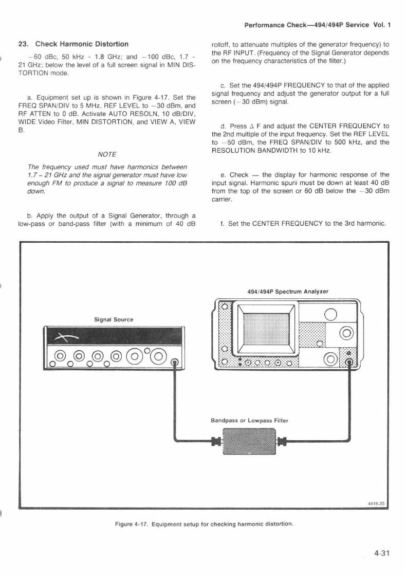
23. Check Harmonic Distortion
-60 dBc, 50 kHz - 1 .8 GHz ; and -100 dBc, 1 .7 -21 GHz; below the level of a full screen signal in MIN DIS-TORTION mode .
a . Equipment set up is shown in Figure 4-17 . Set theFR EQ SPANIDIV to 5 MHz, REF LEVEL to -30 dBm, andRF ATTEN to 0 dB . Activate AUTO RESOLN, 10 dBIDIV,WIDE Video Filter, MIN DISTORTION, and VIEW A, VIEWB.
NOTE
The frequency used must have harmonics between1 .7-21 GHz and the signal generator must have lawenough FM to produce a signal to measure 100 dBdown .
b . Apply the output of a Signal Generator, through alow-pass or band-pass filter (with a minimum of 40 dB
Figure 4- 1 7. Equipment setup for checking harmonic distortion .
Performance Check-4941494P Service Vol. 1
rolloff, to attenuate multiples of the generator frequency) tothe RF INPUT. (Frequency of the Signal Generator dependson the frequency characteristics of the filter .)
c . Set the 4941494P FREQUENCY to that of the appliedsignal frequency and adjust the generator output for a fullscreen (-30 dBm) signal .
d . Press A F and adjust the CENTER FREQUENCY tothe 2nd multiple of the input frequency . Set the REF LEVELto -50 dBm, the FREQ SPANIDIV to 500 kHz, and theRESOLUTION BANDWIDTH to 10 kHz .
e . Check - the display for harmonic response of theinput signal . Harmonic spurii must be down at least 40 dI3from the top of the screen or 60 dB below the -30 dBmcarrier .
f . Set the CENTER FREQUENCY to the 3rd harmonic .
4941494P 5pecirum Analyzer
4416-23

Performance Check-4941494P Service Vol . 1
g . Check - for harmonic spurii . Again, responses mustbe at least 40 dB down from the top of the screen or-60 dBc from the fundamental .
h . Set the REF LEVEL to -70 dBm, the FREQSPANIDIV to 2 kHz, and the RESOLUTION BANDWIDTHto 100 Hz . Deactivate the WIDE Video Filter .
i . Check - that harmonic spurii are at least 60 dB downfrom the top of the screen (-100 dBc) .
24. Check LO Emission Out the RF Input
a . Connect a sensitive power meter to the RF INPUT soemissions can be measured directly, or connect a high fre-quency Spectrum Analyzer, set to observe the 2 GHz to6 GHz range, to the RF INPUT,
c . Check - for any indication of LO emission . Any emis-sion must be less than -70 d6m .
Emission is no more than -70 dBm.
b . Set the TIMEIDIV to MNL.
25. Check 1 dB Compression Point1 dB compression, 1 .7 - 2.0 GHz, is -. 28 dBm or more,
otherwise -18 dBm .
a . Equipment setup is shown in Figure 4-18 .
b . Connect the power meter with its sensor to the Cali-brated Output of the Signal Generator, Set the generator to1 .7 GHz and adjust the output for 0 dBm, as indicated onthe power meter .
NO TE
Calibrate the power meter before making thismeasurement.
c . Disconnect the power meter from the Signal Genera-tor and connect the generator output through 1 dB and10 dB step attenuators to the RF INPUT of the 4941494P .Set the attenuators for 20 dB of attenuation (10 dB perattenuator) .
d . Connect the 10 MHz IF output (on the rear panel ofthe 4941494P) through a 1 dB step attenuator, to the RF
Figure 4- 1 8. Test equipment setup for checking 1 dB input compression point.

Input of a test Spectrum Analyzer . Set the step attenuatorfor 0 dB attenuation .
e . Set the test Spectrum Analyzer Frequency to10 MHz, Frequency Span/Div to 100 MHz, Ref Level to-20 dBm, Time/Div to Auto, and activate 2 dBIDiv andAuto Resoln .
f . Set the 494I494P FREQUENCY to 1 .7 GHz, FREQSPANIDIV to 100 kHz, REF LEVEL to -30 dBm, TIMEIDIVto AUTO, and activate 10 dBIDIV and AUTO RESOLN.
g . On the 494I494P, activate ZERO SPAN and adjustthe CENTER FREQUENCY control to maximize the 10 MHzsignal on the test Spectrum Analyzer display .
h . Adjust the test Spectrum Analyzer Ref Level for a fourdivision signal amplitude .
i . Increase the input signal level, to the 494I494P, 1 dBby switching out 1 dB of attenuation between the SignalGenerator and the input to the 494I494P . Add 1 dB of atten-uation between the 10 MHz output and the test SpectrumAnalyzer .
j . Check - the 10 MHz signal amplitude on the testSpectrum Analyzer display should remain the same .
k . Continue to increase the input signal level to the494I494P by 1 dB increments while increasing the attenua-tion between the 10 MHz out and the test Spectrum Ana-lyzer until the signal amplitude decreases 1 dB (0.5 division) .
I . Check - the 1 dB compression point should be-18 dBm or less (18 dB or less attenuation between thegenerator and the input of the 494I494P) .
m . Check Band 2 (1 .7 - 2 .0 GHz) compression point asfollows :
(1) Deactivate ZERO SPAN, switch the FREQUENCYRANGE to Band 2, and set the FREQUENCY to 1 .7 GHz(reference Level -30 dBm) .
(2) Set the step attenuators, between the Signal Gen-erator and the RF INPUT, to 30 dB (input to the494I494P is now --30 dBm).
(3) Peak the signal response with MANUAL PEAK orAUTO PEAK.
Performance Check-494/494P Service Vol . 1
(4) Set the attenuator, between the 10 MHz IF outand the test Spectrum Analyzer, to 0 dB.
(5) Activate ZERO SPAN and adjust the test Spec-trum Analyzer Reference Level for an on screen display .Maximize the response by tuning the 494I494P CENTERFREQUENCY control .
(6) Set the test Spectrum Analyzer response to somereference level (such as 4 divisions) and repeat the aboveprocedure to check the 1 dB compression point at1 .7 GHz .
(7) Compression should not occur until the input sig-nal level is -28 dBm or more (28 dB external attenuationbetween the Signal Generator and the 494I494P RFINPUT) .
(8) Deactivate ZERO SPAN and set the 494 FRE-QUENCY to 2 .0 GHz.
(9) Return the step attenuators to 30 dB and 0 dB.Set the frequency of the Signal Generator to 2.0 GHzand repeat the above procedure to check 1 dB compres-sion point at 2.0 GHz .
(10) 1 dB compression point should not occur unitlthe input signal level to the RF INPUT is -28 dBm ormore .
26. Check External Reference Input (Power+15 dBm to -15 dBm ; 1,2,5, or 10 MHz .
a . Equipment setup is shown in Figure 4-1'9 . Connect theoutput of the Signal Generator to a Frequency Counter andset the generator frequency to 10 MHz ± 50 Hz .
b . Disconnect the counter and apply the generator out-put to the EXTERNAL REFERENCE Input connector (on therear panel) of the 494I494P . Set the generator output to+15 dBm .
c . Check - the crt readout for REF OSC IN USE shouldread °EXT" .
d . Connect the 494I494P CAL OUT to the counter andnote that the counter readout is 10 times the external refer-ence source .
e . Decrease the Signal Genertor output to -15 dBmand note that the crt readout is still "EXT" and the Fre-quency Counter still reads 10X the reference signal fre-quency . If the crt readout changes to : "EXT-UNLK",recheck the external reference source for 10 MHz ±100 Hzat -15 dBm .

Performance Check-494/494P Service Vol. 1
TO EXTERNAL REFERENCE(REAR PANEL)
Figure 4-19 . Test equipment setup for checking external reference input power .
27.
Check Triggering Operation and Sensitivity
Sensitivity, for internal trigger, is 2.0 divisions or more ;and 1 .0 V peak, 15 Hz to 1 MHz, for external trigger .
a . Equipment setup is shown in Figure 4-20 . Apply100 MHz at -30 dBm from a Signal Generator, that is mod-ulated by the output of a Sine-Wave Generator, to the RFINPUT. Monitor the output of the Sine-Wave Generator witha test Oscilloscope .
b . Set the FREQUENCY to 100 MHz, FREQ SPAN/DIVto 10 kHz, RESOLUTION BANDWIDTH to 1 MHz, TIME/DIV to 20 ms, and REF LEVEL to -30 dBm. Activate LINVertical Display .
c . Decrease the output of the Signal Generator so thedisplay is half screen, then modulate the signal with a 1 kHzsine wave.
d . Activate ZERO SPAN and adjust the CENTER FRE-QUENCY control if necessary for maximum response .
e . Adjust the Sine Wave Generator output for a modula-tion amplitude of two divisions, then activate INT Triggering .
f . Check the internal trigger operation through the 15 Hzto 1 MHz frequency range .
NOTE
Because of deflection amplifier response, the displayamplitude will decrease at the high frequency end.
The triggering signal can also be applied to theMARKER/VIDEO connector on the back panel if ajumper is connected between pins 1 and 5 (Video Se-lect) of the rear-panel ACCESSORIES connector (Fig-ure 4-21).
g . Disconnect the test equipment . Apply a 1 kHz signalfrom the Sine Wave Generator, through a bnc "T" connectorand coaxial cable, to the HORIZ/TRIG connector (on theback panel of the 494/494P (see Figure 4-22) Monitor theinput signal amplitude with a test Oscilloscope .
h . Set the output level of the signal to 2 V peak-to-peak(1 .0 V peak) as indicated on the test Oscilloscope (see Fig-ure 4-23) .
i . Change
the
TIME/DIV
to
0.2 s.
Activate
EXTTriggering .
j . Check - that the sweep is triggered over the fre-quency range of 15 Hz to 1 MHz .
k . Return the Triggering to FREE RUN and the input sig-nal level to 0 V .

Performance Check-4941494P Service Vol- 1
Figure 4-20, Equipment setup for checking internal trigger characteristics .
Figure 4-21 . External video select pins on ACCESSORIES con-nector and input to MARKER/VIDEO for signal to check internaltriggering .
28. Check External Sweep Operation
0 to 10 V ± 1 V should provide a full sweep across the 10division graticule span . This is an operational check, not aperformance requirement.
a . With the test equipment connected as directed for theprevious step, set the TIMEIDIV to EXT, Vertical Display to2 dB/DIV, and deactivate VIEW A, VIEW B .
b . With an input signal to the HORIZITRIG connector of0 volt, position the crt beam on the left graticule edge, withthe POSITION adjustment . This establishes the 0 Vreference .
c. Set the generator frequency to 1 kHz and increase itsoutput for a full 10-division sweep.
d. Check - the peak-to-peak voltage out of the SignalGenerator should equal 20 V ± 2 V, peak-to-peak, or 10 Vt 1 V peak .
4-35
PROBE HORIZ TRIG MARKER ) I VIDEO
POWER 0-10V 1 VPK 0-{-10 V7 0-4V
-15VMAX -50V MAX 10VIVIExT IN
CAUTIQNTo AVOID ELECTRICAL SHOCK THE POWER CCONDUCTOR MUST BE CONNECTED TO FARTENCLOSURE . REFER SERVICING TO QUALIFIE
J104 ACCESSORYPin 1, VideD Select'
Pin 5, Ground00
0
a oooanoonvo aNOT RS232 COMPATIBLE
Place jumper between pin 1 and pin 5 to selectEXTERNAL VIDEO.
4416-27

Performance Check-4941494P Service Vol . i
3783-21
Figure 4-23 . Test oscilloscope display of a sinewave input sig-nal to the external TRIG connector (1 .0 volt peak at 2.0 V peak-to-peak) .
Figure 4-22. Equipment setup for checking external triggering and horizontal input charactertistics .
NOTE
A variable voltage source can be used in place of theSine Wave Generator, to check external sweepoperation.
e . Disconnect and remove the test equipment . ReturnTIMEIDIV to AUTO .
29.
Check Vertical Output Signal
Output provides 0,5 V ± 5% of signal per division of dis-play from the centerline . This is an operational check, not aperformance requirement .
a . Connect the VERT OUTPUT to the input of a dc-coupled test Oscilloscope with a sensitivity of 1 Vldiv and asweep rate of 10 ms .

b . Set the FREQUENCY to 100 MHz, FREQ SPAWDIVto 100 kHz, TIMEIDIV to AUTO, REF LEVEL -20 dBm .Activate 2 dB/DIV and AUTO RESOLN, deactivate VIEW Aand VIEW B.
c . Apply the CAL OUT signal to the RF INPUT and verifythat the signal amplitude is full screen .
d . Check - the amplitude of the output vertical signalon the test Oscilloscope . Output level should equal, plus andminus 2 V for a total of 4 V } 0.2 V (see Figure 4-24) .
30. Check Horizontal Signal Output Level
Output 0.5 Vldivision, ± 5% either side of center screen .This is an operational check, not a performance requirment .
a . Connect a dc-coupled test oscilloscope to the HORIZOUTPUT connector . Set the TIMEIDIV to the MNL position .
b .
Adjust MANUAL SCAN control for five division beamdeflection from the left to right side of center screen andnote the voltage sweep on the test Oscilloscope . The outputvoltage should vary from - 2.5 V to + 2 .5 V, ± 10% .
c . Return the TIMEIDIV to AUTO ; disconnect and re-move the test equipment .
31 . GPIB Verification Program (494P only)
This verification program can be used with aTEKTRONIX 4050-Series Computer Terminal to check thefunctional operation of the GPIB interface in the 494P Spec-trum Analyzer . All interface lines are verified as well as allinterface messages, except those for parallel poll . In addi-tion, the instrument interface is checked for operation onother primary addresss, as well as the talk-only and listen-only modes.
The program is written in Tektronix 4050 BASIC, and isdivided into individual tests, each for a specific interface line,message, or function . The tests start on even 1000 linenumbers to allow easy modification of the program .
The following describes the function of each test in theprogram .
Lines 1-5000 : Interfaces to user definable keys for re-covery from a failed test .
Performance Check-4941494P Service Vol . 1
--05 Vldivision of display on the 4941494P(4.0 V for full screen`
0 V
4416-29
Figure 4-24 . Test oscilloscope display of VER'Tical output witha full screen display on the 494.
Lines 5000-6000 : Inputs the primary address of the494P under test (1 should be used) .
Lines 6000-7000 : ID query response test . The instru-ment must be able to talk and listen, to send out its ID?response and manipulate all eight of the DIO lines for thetest to be successful .
Lines 7000-8000 : Local lock-out test . Tests correct op-eration of the interface message that should disable all pro-grammable front panel controls .
Lines 8000-9000 : Go to LOCAL test . Tests correct oper-ation of the interface message that should enable all frontpanel controls .
Lines 9000-10000: Group Execute Trigger test . Checksthat a GET message does cause the 494P to abort thepresent sweep and re-arm the trigger, causing a sweep tostart and end, sending out an End-of-Sweep SRO . Thus,the SRQ line, as well as the GET message, is verified .
Lines 10000-11000 : Selected Device Clear Test . Thistest verifies that an SDC message does indeed reset the494P's GPIB output buffer clearing out it's ID? response .
Lines 11000-12000 : Device clear test . This test is identi-cal to the selected device clear test, except the universalcommand DCL is used instead .

Performance Check-494/494P Service Vol . 1
Lines 12000-13000 : Addressed as listener, talker test .This test checks to see that the 494P microprocessor cor-rectly recognized that the GPIA chip has been addressed tolisten or talk, and sends the appropriate character to the crtreadout (L or T) .
Lines 13000-14000 : Serial Poll test . This checks correctoperation of the serial poll enable (SPE) and serial poll dis-able (SPD) interface messages . The status byte is read, andif anything other than ordinary operation is indicated, theinstrument fails the test .
Lines 14000-15000 : GPIB rear panel switch test . All fiveprimary address switches are checked for correct operation .Three subroutines are called in the process of testing oneaddress switch . The first two send a formatted messge tothe 4050 display, and the third performs the address switchtest .
Lines 15000-16000 : Line feed or EOI switch test .Checks for correct selection of line feed as a terminationwhen selected by this switch by sending an I D? terminatedonly by a line feed .
Lines 16000-17000 : Talk-only mode test . When se-lected, this mode should cause the instrument to send aSET? response and (optionally) a CURVE? response when-ever the RESET-TO-LOCAL button is pressed . The stringreceived from the instrument is thus examined for existenceof a portion of the correct SET? response after the RESET-TO-LOCAL button is pressed .
Lines 17000-18000 : Listen-only mode test . When se-lected, this mode will cause the instrument to respond toany message on the bus, since it is always addressed tolisten . The command REF 0 is sent to the bus without ad-dressing the instrument, then the listen-only mode is dese-lected and the instrument interrogated to see if it didrespond to the REF command while in the listen-only mode .
Lines 18000-19000 : Interface clean (and Remote En-able) test . This IFC line on the GPIB will unaddress the in-strument's interface . This fact is verified by noting that the Lis not present in the crt readout, indicating that the IFC lineworked ; also the REN line will be unasserted when the endstatement is executed (except for some early 4052 and4054's) . Thus, a front panel in the local mode is evidencethat the REN line was successfully unasserted . (Evidence itwas asserted is that the instrument was able to executecommands sent to it by previous tests .)
Lines 19000-end : Utility routines . Rear panel interfaceswitch test text routine puts headers on the interface switchtest display . The rear panel test text routine tells the oper-ator what to do after changing the address switches . Testaddress switch acquires an ID? response from the instru-ment on its new address during the address switch test . TheSRQ handler will handle any 49X SRO's that occur, al-though none, except the power-up SRO, would be ex-pected . (The end of sweep SRO during the GET test ishandled by another SRO handier .) Delay Generator gener-ates delays for other tests . The Failure Decision Handlerallows the program to be restarted with the user definablekeys if any test fails .

1 GO TO 50004 B2=15 RETURN20 B2=521 RETURN5000 REM * ` * 49XP GPIB VERIFICATION PROGRAM * *'5030 INIT5040 ON SRQ THEN 192805050 DIM V$ (400 ),W$ (400 )5060 I7=05070 PAGE5080 PRINT "JJJENTER 49XP' S PRIMARY ADDRESS
(DEFAULT = 15090 INPUT T$5100 IF T$<>""THEN 51305110 A1=15120 GO TO 51805130 A1=VAL (T$ }5140 IF A1>O AND A1<31 THEN 51805150 PRINT "JJJGERROR! ! " ;A1 ; " IS NOT A VALID ADDRESS" ;5160 PRINT " ONLY 0 THRU 30 ARE VALID ADDRESSESKK"5170 GO TO 50805180 PAGE51.90 REM5200 REM5210 REM5220 REM5230 REM6000 REM ***"ID"QUERY RESPONSE ***6010 PRINT " * * * ""ID "" QUERY RESPONSE * * * '6020 PRINT @Al :"INIT ;ID? ;SIG °6030 INPUT @Al :T$6040 V$=SEG (T$ , 1 , 9 )6050 IF V$= "ID TEK149 "THEN 60806060 PRINT "JJJ * * * ""ID"" QUERY RESPONSE *' * FAIL * * *G "6070 GO TO 195306080 WBYTE a32+Al :64,128,-1276090 PRINT @aAI :"WFM ENC :BIN ;CUR? "6100 PRINT @37,0 :37,255,2556110 INPUT %Al :T$6120 WBYTE @64+A1 :6130 RBYTE R,R,R,T66140 WBYTE @95 :6150 IF R=>128 AND T6<128 THEN 70006160 PRINT "JJJ * * * D108 TEST * * * FAIL * * *G"6170 GO TO 195306180 REM6190 REM6200 REM6210 REM6220 REM7000 REM ***LOCAL LOCK -OUT . . . . . . . . . . . . . . LLO
'**7010 PRINT "***LOCAL LOCK-OUT . . . . . . . . . . LLO ***'7020 WBYTE @32+A1,17 :7030 PRINT @A1 : "SET? "7040 INPUT PAIN$
Performance Check-4941494P' Service Vol . 1

Performance Check-494/494P Service Vol. 1
7050 PRINT "II49XP IN LOCAL LOCK-OUT MODE (LLO )"7060 PRINT "IIATTEMPT TO USE 49XP CONTROLS7070 PRINT "IIPRESS RETURN <CR> WHEN DONE " ;7080 INPUT T$7090 PRINT @A1 : "SET? `7100 INPUT @A1 -W$7110 IF W$<>V$ THEN 71307120 GO TO 80007130 PRINT "J***LOCAL LOCK- OUT . . . . . . . . . . . . . LLO7140 GO TO 195307150 REM7160 REM7170 REM7180 REM7190 REM8000 REM ***GO TO LOCAL . . . . . . . . . . . . . GTL **8010 PRINT @Al :"INIT ;TIM? "8020 INPUT @A1 :R8030 PRINT @Al : "TIM INC"8040 PRINT "***GO TO LOCAL . . . . . . . . . . . . . GTL8050 WBYTE @32+A1,1 :8060 PRINT @A1 : "TIM?"8070 INPUT @Al :T68080 IF R<>T6 THEN 81008090 GO TO 90008100 PRINT "J****GO TO LOCAL . . . . . . . . . . . GTL8110 GO TO 195308120 REM8130 REM8140 REM
8150 REM8160 REM9000 REM *** GROUP EXECUTE TRIGGER . . . . . . . . GET9010 PRINT " " ** GROUP EXECUTE TRIGGER . . . GET9020 ON SRQ THEN 91209030 I7=09040 PRINT @A1 :"INIT ;TIM 100M ;SIG ;EOS ON"9050 WBYTE @32+Al,8 :9060 T6=39070 GOSUB 193909080 PRINT @Al : "EOS OFF"9090 IF 17<>l THEN 91509100 ON SRQ THEN 192809110 GO TO 100009120 WBYTE @20 :9130 I7=19140 RETURN9150 PRINT "GROUP EXECUTE TRIGGER . . . GET ***FAIL9160 GO TO 195309170 REM9180 REM9190 REM9200 REM9210 REM10000 REM **"SELECTED DEVICE CLEAR . . . SDC
*** FAIL ***G"
***FAIL ***G"

10010 PRINT "***SELECTED DEVICE CLEAR . . .SDC ***"10020 PRINT @Al :"ID?"10030 WBYTE @32+A1,4 :10040 WBYTE Ca64+Al :10050 RBYTE R10060 IF ABS (R )<>255 THEN 1008010070 GO TO 1100010080 PRINT "***SELECTED DEVICE CLEAR . . . . . . . . SDC **'FAIL
10090 GO TO 1953010100 REM10110 REM10120 REM10130 REM10140 REM11000 REM ***DEVICE CLEAR . . . . . . . . . . . DCL ***11010 PRINT "***DEVICE CLEAR . . . . . . . . . . . . DCL ***"11020 PRINT @A1:"ID? '11030 WBYTE @20 :11040 WBYTE @64+Al :11050 RBYTE R11060 IF ABS (R )<>255 THEN 1108011070 GO TO 1200011080 PRINT "***DEVICE CLEAR . . . . . . . . . . . DCL ***FAIL ***G'11090 GO TO 1953011100 REM11110 REM11120 REM11130 REM11140 REM12 000 REM "* ADDRESSED AS LISTENER, TALKER ***12010 PRINT `* * * 49XP ADDRESSED AS LISTENER . . * * *'
12020 WBYTE @32+Al :76,79,82,68,79, -6312030 T6=112040 GOSUB 1939012050 INPUT @Al :V$12060 T$=SEG (V$ , 16 , 1 )12070 IF T$= "L " THEN 1210012080 PRINT "J * * * 49XP ADDRESSED AS LISTENER * * * FAIL
*G
12090 GO TO 1953012100 PRINT " * * * 49XP ADDRESSED AS TALKER . . . . * * *12110 PRINT @A1 :"INIT ;TIM 50M;SIC,SIG ;WAI ;LORDO?"12120 INPUT C}AI :V$12130 T$=SEG (V$, 16 , 1 )12140 IF T$= "T " THEN 1300012150 PRINT " * * * 49XP ADDRESSED AS TALKER * * * FAIL * * * "
12160 GO TO 1953012170 REM12180 REM12190 REM12200 REM12210 REM13000 REM * * * SERIAL POLL13010 PRINT "*** SERIAL POLL . . . . . . . . . SPD/SPE ***13020 WBYTE C795,63,24,64+A1 :13030 RBYTE R
Performance Check-494/494P Service Vol. 1
***G"
4-41

Performance Check--4941494P Service Vol. 1
13040 WBYTE @95,25 :13050 IF R=0 OR R=16 THEN 1308013060 PRINT "J * - * SERIAL POLL - * " FAIL * * *G "13070 GO TO 1953013080 T6=313090 GOSUB 1939013100 REM13110 REM13120 REM13130 REM13140 REM
14250 REM14260 REM14270 REM14280 REM14290 REM15000 REM "` * * "LF" OR "EOI ° SWITCH15010 PAGE15020 A1=115030 GOSUB 1900015040 PRINT"
0
I_ 0
1
1
100001"15050 GOSUB 1907015060 PRINT "JJTESTING" "LF" "OR" "EOI" "SWITCH"15070 GOSUB 1919015080 WBYTE @32+Al :73,68,63,1015090 INPUT @A1 .- T$15100 T$=SEG (T$,1,9 )15110 IF T$= "ID TFR/49 "THEN 1514015120 PRINT "J .,
"LF" "OR" "EOI " "SWITCH15130 GO TO 19530
*** FAIL ***G"
14000 REM * * * GPIB INTERFACE REAR PANEL SWITCH TEST14010 PAGE14020 A1=214030 GOSUB 1900014040 PRINT " 0 I_0 I 0 I_0 0 0 1 014050 GOSUB 1907014060 GOSUB 1919014070 PAGE14080 A1=414090 GOSUB 1900014100 PRINT " 0 I 0 I_0 1_0 0 1 0 0"14110 GOSUB 1907014120 GOSUB 1919014130 PAGE14140 A1=814150 GOSUB 1900014160 PRINT " 0 I_0 I_0 1_0 1 0 0 0"14170 GOSUB 1907014180 GOSUB 1919014190 PAGE14200 A1=1614210 GOSUB 1900014220 PRINT " 0 I 0 I_ 0 1_ 1 0 0 0 0 "14230 GOSUB 1907014240 GOSUB 19190
15140 T6=215150 GOSUB 1939015160 REM15170 REM15180 REM15190 REM15200 REM16000 REM * * * TALK ONLY MODE * * '"16010 PAGE16020 GOSUB 1900016030 PRINT " 0
1 1
1_0 1_0 0 0 0 1"16040 GOSUB 1907016050 PRINT " JJJTESTING TALK ONLY"16060 INPUT @A1 :V$16070 17=POS (V$, `FINE OFF", 1 }16080 IF 17<>O THEN 1700016090 PRINT "JJJTALK ONLY MODE *** FAIL `**G"16100 GO TO 1953016110 REM16120 REM16130 REM16140 REM16150 REM17000 REM * * * LISTEN ONLY MODE17010 PAGE17020 GOSUB 1900017030 PRINT " I 1_ 0 1_ 0 1 0 0 0 0 1 "17040 GOSUB 1907017050 PRINT "JJJTESTING LISTEN ONLY"17060 PRINT @Al : "INI "17070 T6=0 .517080 GOSUB 1939017090 WBYTE 82,69,70,32,-4817100 PAGE17110 GOSUB 1900017120 PRINT "01_ 01_ 0100001"_17130 GOSUB 1907017140 PRINT @A1:"REF7"17150 INPUT @Al :V$17160 IF V$ < > "REFLVL +0 . 0 " THEN 1718017170 GO TO 1800017180 PRINT "JJJLISTEN ONLY MODE ' * x FAIL *"*G"17190 GO TO 1953017200 REM17210 REM17220 REM17230 REM17240 REM18000 REM *'"* INTERFACE CLEAR AND REMOTE ENABLE TEST . . . . . . IFC & REN18010 PAGE18020 PRINT "JJJTESTING IFC (INTERFACE CLEAR ), AND REN (REMOTE ENABLE }"18030 WBYTE @32+A1 :18040 T6=318050 GOSUB 1939018060 PRINT "JJCHECK THE 49XP CRT, FOR AN" "L" "BETWEEN THE VERTICAL"
Performance Check-4941494P Service Vol. 1

Performance Check-494/494P Service Vol. 1
18070 PRINT "DISPLAY AND THE MIN RF ATTEN READOUTS . "18080 PRINT "JPRESS RETURN TO CONTINUE . ";18090 INPUT P$18100 INIT18110 PRINT "JIF AN" "L" "IS STILL PRESENT, THE IFC LINE IS FAULTY, "18120 PRINT "IF THE" "L" "VANISHED, IFC TESTED OK .181,30 PRINT "JJCHECK ALSO THE 49XP FRONT PANEL FOR PROPER LOCAL CONTROL"18140 PRI "IF THE FRONT PANEL IS LOCKED OUT, THE REN LINE IS FAULTY, IF"
NOT, REN TESTED OK""JJJGPIB VERIFICATION COMPLETEG'
18150 PRINT18160 PRINT18170 END18180 REM18190 REM18200 REM19000 REM * * * REAR PANEL INTERFACE SWITCH TEST TEXT ROUTINE * *'19010 PRINT "SET GPIB ADDRESS SWITCHES TO : "19020 PRINT "JJLISTENITALKILF ORI ADDRESS19030 PRINT " ONLYIONLYIEOI116 8 4 2 1 "19040 PRINT
------------19050 RETURN19060 REM19070 REM * * * REAR PANEL TEST TEXT ROUTINE
"JJAFTER CHANGING THE SWITCHES, ";"PRESS THE REMOTE/LOCAL BUTTON ONCEJ_J""I (NOTE : IF YOU GET A GPIB INTERFACE ERROR MESSAGE,"I
IT MEANS THAT THE SWITCH (ES ) WEREN "T "READ CORRECTLY . T O RE-TEST, TYPE"""RUN"" FOLLOWED BY THE LINE NUMBER IN THE"ERROR MESSAGE ) "
19080 PRINT19090 PRINT19100 PRINT19110 PRINT19120 PRINT "I19130 PRINT "I19140 PRINT "I19150 PRINT "JJIPRESS RETURN <CR> WHEN DONE ";19160 INPUT T$T^19170 RETURN19180 REM19190 REM * * * TEST ADDRESS SWITCH19200 PRINT @Al : "ID?19210 INPUT @A1 :T$19220 T$=SEG (T$ , 1 , 9 )19230 IF T$="ID TEK/49"THEN 1926019240 PRINT "ADDRESS SWITCH TEST FAIL"19250 GO TO 1953019260 RETURN19270 REM19280 REM ***SRQ HANDLER19290 T6=319300 GOSUB 1939019310 POLL Z1,Z1 ;A119320 PRINT @A1:"ERR?"19330 INPUT @A1 : S$19340 PRINT "GGAN INTERRUPT OCCURRED ON THE19,350 PRINT "JPRESS RETURN <CR> TO CONTINUE ";19360 INPUT T$19370 RETURN19380 REM19390 REM ***DELAY GENERATOR19410 REM * * * T6 GIVEN IN SEC
(GLOBAL ) . . . 19 SCRATCH
BUS, THE 49XP RETURNS " ; S$

19420 IF T6<0 THEN 1951019430 IF RND (0 )>0 .5 THEN 1949019440 REM `4051* 4051 "19450 T6=T6 *22019460 FOR 19=1 TO T619470 NEXT 1919480 GO TO 1951019490 REM * * * 405219500 CALL °WAIT",T619510 T6=019520 RETURN19530 REM ****FAILURE DECISION HANDLER ****19540 PRINT "JJISELECT A UDK : "19550 PRINT "1
(1) RE-START19560 PRINT "I
(5) END"19570 SET KEY19580 B2=019590 IF B2<>1 AND B2<>5 THEN 1959019600 IF B2=5 THEN 1963019610 PAGE19620 GO TO 600019630 END


ADJUSTMENT PROCEDURE
If the instrument performance is not within specified re-quirements for a particular characteristic, determine thecause, repair if necessary, then use the appropriate adjust-ment procedure to return the instrument operation to perfor-mance specification . After any adjustment, verify perfor-mance by repeating that part of the Performance Check .
Allow the instrument to warm up for at least one hour, inambient air of +20°C to +30°C before making any adjust-ments . Waveform illustrations in these instructions may beidealized and should not be referenced as representative ofspecification tolerances .
Adjustment steps that interact are noted and reference ismade, within the procedure, to the affected circuit or steps .
w"r-.rwv-vvCAUTION
STATIC DISCHARGE CAN DAMAGE MANY SEMI-CONDUCTOR COMPONENTS USED IN THISINSTRUMENT.
Many semiconductor components, especially MOStypes, can be damaged by static discharge . Damagemay not be catastrophic, therefore, not immediatelyapparent. It usually appears as a 'weakening' of thesemiconductor characteristics . Devices that are par-
Introduction
Section 5-4941494P Service Vol . 1
ticularly susceptible are : MOS, CMOS, JFETs, andhigh impedance operational amplifiers. Damage canbe significantly reduced by observing the followingprecautions .
1 . Handle static-sensitive components or circuit as-semblies at or on a static-free surface. Work stationareas should contain a static-free bench cover orwork plane such as conductive polyethylene sheetingand a grounding wrist strap. The work ,plane shouldbe connected to earth ground.
2. All test equipment, accessories, and solderingtools should be connected to earth ground.
3. Minimize handling by keeping the components intheir original containers until ready for use . Minimizethe removal and installation of semiconductors fromtheir circuit boards .
4 . Hold the IC devices by their body rather than theterminals .
5. Use containers made of conductive material orfilled with conductive material for storage and trans-portation. Avoid using ordinary plastic containers . Anystatic sensitive part or assembly (circuit board) that isto be returned to Tektronix, Inc ., should be packagedin its original container or one with anti-static packag-ing material.
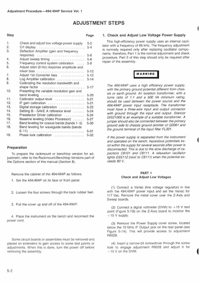
Adjustment Procedure-494/494P Service Vol. 1
Preparation
To prepare the rackmount or benchtop version for ad-justment, refer to the Rackmount/Benchtop Versions part ofthe Options section of this manual (Section 8) .
Remove the cabinet of the 494l494P as follows .
1 . Set the 494l494P on its face or front panel .
2 . Loosen the four screws through the back rubber feet .
3 . Pull the cover up and off of the 494l494P .
4 . Place the instrument on the bench and reconnect thepower cord .
Some circuit boards or assemblies must be removed andplaced on extenders to gain access to some test points oradjustments . When this is done, turn the power off beforeremoving the assembly .
ADJUSTMENT STEPS
1 . Check and Adjust Low Voltage Power Supply
This high-efficiency power supply uses an internal oscil-lator with a frequency of 66 kHz . The frequency adjustmentis normally required only after replacing oscillator compo-nents ; therefore, Part 1 is the normal adjustment and checkprocedure, Part 2 of this step should only be required afterrepair of the assembly.
WARMING
The 494l494P uses a high efficiency power supply,with the primary ground potential different from chas-sis or earth ground. An isolation transformer, with aturns ratio of 1:1 and a 500 VA minimum rating,should be used between the power source and the494l494P power input receptacle . The transformermust have a three-wire input and output connectorwith ground through the input and output . StancorGIS21000 is an example of a suitable transformer. Ajumper should also be connected between the primaryground side to chassis ground (emitter o1 Q2061 andthe ground terminal of the input filter FL301 .
If the power supply is separated from the instrumentand operated on the bench, hazardous potentials ex-ist within the supply for several seconds afterpower isdisconnected. This is due to the slow discharge of ca-pacitors C6101 and C6111 . A relaxation oscillatorlights DS5112 (next to C6111) when the potential ex-ceeds 80 V.
PART 1Check and Adjust Low Voltages
(1) Connect a Variac (line voltage regulator) in linewith the 494l494P power input and set the Variac for117 Vac. Remove the metal cover over the Z-Axis andSweep boards .
(2) Connect a digital voltmeter (DVM) to +15 V testpoint (Figure 5-1 B) on the Z-Axis board to monitor the+ 15 V supply .
(3) Remove the Power Supply cover screw, locatedbelow the 10 MHz IF Output jack on the rear panel (seeFigure 5-1A), This will provide access to adjustmentR6028.
(4) Insert a narrow-bit screwdriver through the screwhole to engage adjustment R6028 and adjust it for+15 V on the DVM .
1 . Check and adjust low voltage power supply 5-22 . Crt display . . . . . . . . . . . . . . . . . . . . . . . . . 5-43 . Deflection Amplifier (gain and frequency
response) . . . . . . . . . . . . . . . . . . . . . . . . . . 5-64 . Adjust sweep timing . . . . . . . . . . . . . . . . . . 5-85 . Frequency control system calibration . . . . 5-96 . Adjust start (0 Hz) response amplitude and
mixer bias . . . . . . . . . . . . . . . . . . . . . . . . . . 5-127 . Adjust 1st Converter bias . . . . . . . . . . . . . 5-128 . Log Amplifier calibration . . . . . . . . . . . . . . . 5-149 . Calibrating the resolution bandwidth and
shape factor . . . . . . . . . . . . . . . . . . . . . . . . 5-1710 . Presetting the variable resolution gain and
band leveling . . . . . . . . . . . . . . . . . . . . . . . . 5-2011 . Calibrator output level . . . . . . . . . . . . . . . . 5-2112 . IF gain calibration . . . . . . . . . . . . . . . . . . . . 5-2113 . Digital storage calibration . . . . . . . . . . . . . . 5-2214 . Setting B-SAVE A reference level . . . . . . 5-2415 . Preselector Driver calibration . . . . . . . . . . . 5-2416 . Baseline leveling (Video Processor) . . . . . . 5-2717 . Band leveling for coaxial bands (bands 1-5) 5-3018 . Band leveling for waveguide bands (bands
6-11) . . . . . . . . . . . . . . . . . . . . . . . . . . . . . . 5-3119 . Phase lock calibration . . . . . . . . . . . . . . . . 5-32

Figure 5-1 . Low voltage power supply adjustments and test point locations .
Adjustment Procedure-4941494P' Service Vol . 1
F1013
Fi017
F2013
TP1011+9V
F1035 F1033
86028 (+15 V adjust) is accessiblethrough screw hole
81068
"r".
86061
TP6053
TP1034
TP1044+5 V
TP1047TP1036
+17 V-5V
01
TP1048+ 100 V
0
POWERSTATUS
&"All
-qqMI
n M®~y
gene
a~edee
!4YWRATP1035- 15 V
TP1037-7 V
TP1046+15V
TP1052+300 V
04058
Q4059
4416-36

Adjustment Procedure-4941494P Service Vol. 1
(5) Vary the input voltage from 90 to 132 Vac andnote that the + 15 V supply remains regulated .
(6) Check the other supply voltages at the test pointsindicated in Figure 5-1 B, against tolerances listed inTable 5-1 .
(7) Remove the line voltage regulator (Variac) and re-connect the 494/494P directly to the power source .
Table 5-1POWER SUPPLY VOLTAGE TOLERANCES
PART 2Adjusting the Power Supply Oscillator Frequency
(1) Remove the Power Supply module, as describedin the Maintenance section, then remove the Power Sup-ply module cover and disconnect P3045.
(2) Plug the power cord into the power input recepta-cle and connect it to a suitable power source (115 Vac or230 Vac, depending on the position of S302).
(3) Use a plastic or insulated tuning tool or equivalent,to insert between the two on/off power switches (S300)to close these switches (Figure 5-1) .
(4) Connect a test oscilloscope probe, with a deflec-tion sensitivity of 5 Vldiv and sweep rate of 10 usldiv toTP6053 (Figure 5-1) . Note the amplitude of the outputwaveform, of the oscillator U6059, is approximately10 V.
(5) Adjust 86061 (Oscillator Freq Adj) for a waveformperiod of 15 acs (66 kHz) .
(6) Reconnect P3045 and replace the Power Supplymodule cover, then re-install the module on the494/494P .
2 . Crt Display (Z-Axis and High Voltage Circuits)
a . Switch POWER off and preset the INTENSITY controlfully counterclockwise, MANUAL SCAN to midrange, andTIMEIDIV to MNL position . Remove the cover over the Z-Axis and Sweep board. Set the Intensity Limit 81027, onthe Z-Axis board (Figure 5-2) fully counterclockwise and CrtBias 82040, on the High Volt age board ( Figure 5-3) fullyclockwise .
b . Switch POWER on and after the power-up state hasstabilized, change the Vertical Display mode to 2 dB/DIV .Deactivate READOUT and VIEW A, VIEW B for no digitalstorage.
c. Adjust Crt Bias as follows:
(1) Using a voltmeter in the 20 volt range, measureand record the collector voltage of 04058 or 04059(Figure 5-1A) on the Z-Axis board.
(2) Turn the INTENSITY clockwise until a crt beamdot appears on screen .
(3) Focus by adjusting R3033 on the High Voltageboard (Figure 5-3) for the smallest round dot.
(4) Set the INTENSITY for a collector voltage 5 .5 Vhigher than the voltage noted in part 1 .
(5) Use the non-metallic screwdriver to adjust CrtBias, 82040, counterclockwise until the crt beam is visi-ble, then clockwise until the beam dot just extinguishes,with the screen shaded . (If no dot appears, with the ad-justment fully counterclockwise, this will be the biassetting.)
(6) Turn the INTENSITY clockwise until a dot is visi-ble then defocus the dot with the Focus adjustment83033. Adjust Astigmatism 81058 (Figure 5-2) for around dot then refocus with 83033 for the smallestsharpest dot.
(7) Turn the INTENSITY counterclockwise until thedot just disappears and again measure the collector volt-age of 04058 or 04059. Voltage should equal or exceedthe voltage noted in part 4. If the voltage is less, repeatthe procedure for setting crt bias .
d . Adjust the crt cathode current as follows :
(1) Switch POWER off then remove P4036 (Figure5-3) on the High Voltage board . Turn INTENSITY fullyclockwise, MANUAL SCAN fully counterclockwise, andensure that the TIMEIDIV is in the MNL position . Set theIntensity Limit 81027, on the Z-Axis board, (Figure 5-2)fully clockwise.
Supply Tolerance
+9V +8 .5Vto+10.5V
-5V -4 .8Vto-5.2V
-7V -7Vto-8.5V
-15V -14.85Vto-15,15V
+5V +4.8Vto+5.2V
+17V +16.8Vto+18.6V
+100V +95Vto+105V
+300 V +280 V to +310 V

Geometry81051
IntensityR1030
1'P1041
Figure 5-2. Location of adjustments and test points on the Deflection Amplifier board, High Voltage module, 2-Axis board, and Sweepboard.
(2) Connect the voltmeter between TP4028 (Figure 5-3) and the ground lug on the crt shield .
(3) Switch POWER on. After the instrument initial-izes, activate 2 dBIDIV and switch Digital Storage off.
(4) Adjust Intensity Limit R1027 (Figure 5-2) for a volt-age reading of 0.9 volts at TP4028 .
(5) Switch POWER off and re-install the jumperP4036 on the High Voltage board. Turn POWER on andadjust the INTENSITY for normal viewing.
e. Apply the CAL OUT signal to the RF INPUT and setFREQUENCY to 100 MHz, FREQ SPANIDIV to 10 MHz,TIMEIDIV to AUTO, and REF LEVEL to -20 dBm . Activate2 dBIDIV, AUTO RESOLN, NARROW Video Filter, andswitch VIEW A and VIEW B off.
f . Activate ZERO SPAN and adjust REFERENCELEVEL until the trace is approximately mid-screen ; then ad-just Trace Rotation 81021 (Figure 5-2) so the trace isaligned with the graticule lines .
g. Activate VIEW A and VIEW B then use thePEAKIAVERAGE cursor, positioned at the top then bottomof the screen, as a reference line to adjust Geometry 81051(Figure 5-2) for the straightest trace at top and bottom ofthe screen .
Adjustment Procedure-494/494P Service Vol. 1
Figure 5-3 . Location of test points and adjustments on the HighVoltage module .
h. Change the REF LEVEL to position the trace withinthe graticule area with Vertical Display mode of 2 dB/DIV .Adjust INTENSITY so the trace is just visible .
i . Adjust A Intensity 81030 (Figure 5-2) so the brightnessof the readout characters is slightly higher than the trace .Readout characters should be just visible after the trace hasdisappeared . This ratio provides the best setting for photo-graph purposes . Disconnect CAL OUT signal from the RFINPUT.

Adjustment Procedure-4941494P Service Vol. 1
3. Deflection Amplifier (gain and frequency
response)
a .
Test equipment setup is shown in Figure 5-4. Set theTIMEIDIV to 1 ms . Position the trace on the bottom grati-cule line .
b. Apply a 500 kHz signal, with an amplitude of 0 to+4 V, from the sine-wave generator, to the ExtMARKERIVIDEO input. Connect a jumper between pin 1(Ext Video Select) and pin 5 (ground) of the ACCESSORIESjack (Figure 5-4) . Deactivate VIEW A and VIEW B and setTriggering to INT.
c.
Adjust Vert Gain R1066 (Figure 5-2) for a full screendisplay .
d . Disconnect the 500 kHz signal from theMARKERIVIDEO input. Remove the jumper between pins 1and 5 of the ACCESSORIES connector if you are not goingto adjust sweep timing (step 4) . Set Triggering to FREERUN .
Digital FunctionMultimeter Generator
Partial 494 Back Panelshowing J t 04 AccessoryConnector
Test Oscilloscope
e. Set TIMEIDIV to MNL, connect a digital voltmeter(DVM) to TP1041, on the Sweep board (Figure 5-2) andadjust MANUAL SCAN for 0.0 V at TP1041 . Adjust Hori-zontal Position control to center the Crt beam .
f . Adjust MANUAL SCAN for a reading of +5 V atTP1041 . Now adjust Horiz Gain 81055 (Figure 5-2) to posi-tion the crt beam to the right graticule edge (1 Oth graticuleline).
g.
Adjust MANUAL SCAN so crt beam nnoves to the leftedge of the graticule and check that the voltage at TP1041is now approximately -5 .0 V .
h. Disconnect the DVM, set TIMEIDIV to AUTO,change the test oscilloscope to Ext Trigger, and apply theReadout Off signal, at TP1038 on the Crt Readout board(Figure 5-5), to the test oscilloscope Ext Triigger input. Settest oscilloscope Time/Div to 2 ,us .
CAUTfONCl---
Figure 5-4. Test equipment setup for calibrating the Deflection Amplifier.
4416-39

Figure 5-5. Test points on the Crt Readout board.
i . Adjust the controls for a triggered sweep then switchthe 494/494P sweep off by activating SINGLE SWEEP, andensure READOUT is on .
Adjustment Procedure-4941494F' Service Vol. 1
j . Connect the test oscilloscope probe to the collectorsof 01031 and 01024, on the Deflection Amplifier board (seeFigure 5-6) . Adjust C5021 for the best frequency response(no overshoot or rolloff) .
k . Connect the probe to the collectors of 01043 and01049, on the Deflection Amplifier board and adjust C4057(Figure 5-6) for the best response .
I . Connect the probe to the collectors of 01072, 02078(Figure 5-6) and adjust C4061 for the best response .
m. Connect the probe to the collectors of 01095, 02096(Figure 5-6) and adjust C5104 for best response .
n . Disconnect the connection to TP1038 and the testoscilloscope probe . Check the appearance of "Z" in GHz ofthe frequency readout . If necessary, adjust C5104 andC4061 (vertical output) for the straightest top on the Z.
o. Set the Vertical Display to LIN and adjust REFLEVEL for 100 uV . Set TIME/DIV to MNL and adjust MAN-UAL SCAN fully clockwise.
p.
Adjust 05021 and 04057 for best REF LEVEL read-out (straightest letters and numerals).
Figure 5-6. Test points and adjustments on the Deflection Amplifier for gain and frequency response.

Adjustment Procedure-494/494P Service Vol. 1
4. Adjust Sweep Timing
a. Test equipment setup is shown in Figure 5-7. SelectEXT Triggering, TIMElDIV of 10 ms, and a FREQ SPANIDIVof 10 MHz or less . Digital Storage (VIEW A and VIEW B)must be off .
b. Apply 10 ms time marks from the time-mark genera-tor to the EXT MARKERIVIDEO connector and connect ajumper between pins 1 and 5 of the ACCESSORIES con-nector . Apply the Trigger Output of the time-mark generatorto the TRIGIHORIZ input, on the back panel of the4941494P . This should provide a display of 10 ms markers.
c. Adjust Sweep Timing R1068 (see Figure 5-8) for 1marker/division. (Use Horizontal Position adjustment toalign markers with graticule lines .)
Time MarkGenerator
d. Check the accuracy of the remaining TIMElDIV selec-tions. Error over the center eight divisions must not exceed+5% .
e. Set the TIMElDIV to AUTO, FREQ SPANIDIV toMAX, and activate AUTO RESOLN.
f. Check the Time/Div versus Resolution Bandwidth asper Table 5-2, for all FREQ SPANIDIV settings .
g. Return Triggering to FREE RUN. Disconnect the time-mark generator markers and trigger signal to the 4941494P .Remove the jumper between pins 1 and 5 of the ACCES-SORIES connector. Reposition the trace if moved in part c.
Trig/Horiz
u
To:
To: Marker/Video
CAUTION
JlM ACCESSORY
C OHO
Partial of 494 Back Panel showing J104 Accessory connector
494 Spectrum Analyzer
Figure 5-7. Test equipment setup for calibrating sweep timing .
-z I raG
M.-w, `-
Connect jumper
-between pins 1 & 5.
4416-42

Table 5-2SWEEP RATE AS A FUNCTION OF SPAN
IN THE AUTO MODE
Figure 5-S . Timing adjustments and test points on the Sweep board .
Adjustment Procedure-494/494P Service Vol . 1
5 . Frequency Control System Calibration
441643
The 494/494P has a procedure in firmware for calibratingthe frequency control system . However, it is possible thatsome adjustments may be misadjusted enough to cause themicrocomputer to display an error message . If this occursbypass the step then return to the calibration routine .
The adjustment tool for this step should be a long (6inches), small diameter (1/8 inch), non-metallic screwdriverso adjustments mounted on the lower portion of the boardscan be accessed, otherwise the CF Control board must beremoved and mounted on an extender .
5-9
FRED SPAN/DIV TIMEIDIVRESOLUTIONBANDWIDTH
MAX 50 ms 1 MHz200 MHz 20 ms 1 MHz100 MHz 10 ms 1 MHz50 MHz 10 ms 1 MHz20 MHz 10 ms 1 MHz10 MHz 10 ms 1 MHz5 MHz 10 ms 1 MHz2 MHz 10 ms 100 kHz1 MHz 10 ms 100 kHz500 kHz 10 ms 100 kHz200 kHz 50 ms 10 kHz100 kHz 20 ms 10 kHz50 kHz 10 ms 10 kHz20 kHz 10 ms 10 kHz10 kHz 100 ms 1 kHz5 kHz 50 ms 1 kHz2 kHz 20 ms 1 kHz1 kHz is 100 Hz500 Hz -5s 100 Hz200 Hz .2s 100 Hz100 H z .5s 30 H z50 Hz -5s 30 Hz

Adjustment Procedure-494/494P Service Vol . 1
a . Test equipment is shown in Figure 5-9 . Set the FRE-QUENCY to 0.0 MHz, FREQ SPAN/DIV to 5 MHz, and Trig-gering to FREE RUN.
b . Connect a shorting strap from TP1035, on the SpanAttenuator board, to chassis ground (Figure 5-10) . Connectthe DVM between TP1073 and ground.
d . Remove the shorting strap and set switch #3 ofS1038 on the Memory board, (Figure 5-11) to the open (1)position . Set FREQ SPANIDIV to 5 MHz . (This enables thecalibration mode and diagnostic functions that are in theinternal firmware.) Press <SHIFT> PULSE STRETCHERand select "0" (Overall System calibration) from the menu .Perform the calibration steps in the directory to the PhaseLock Synthesizer portion ("Connect a DVM to pin B on theControlled Oscillator board and ground"), then press<SHIFT> to abort .
c . Adjust Sweep Offset R1063 (Figure 5-10) for 0.00 V .
(1) If a "Calibration Step Cannot Be Completed" mes-sage is displayed, bypass the step, perform the otheradjustments then return to the adjustment and try tobring the adjustment in range . If this doesn't take care ofthe problem, refer to ; Troubleshooting the FrequencyControl System procedure, in the Maintenance section .
(2) Disable the diagnostic mode by setting switch #3of S1038 on the Memory board to the close (0) position .
e . Adjust 1 st LO Sweep as follows :
(1) Apply the CAL OUT signal to the RF INPUT, setthe FREQUENCY to 600 MHz, FREQ SPANIDIV to 100MHz and adjust REF LEVEL to display the markers .
(2) Adjust Tune Coil Swp R1065, on the Span Attenu-ator board (Figure 5-10) for one marker per division over
the center eight divisions of the graticule . Adjust theCENTER FREQUENCY as necessary to align themarkers .
(3) Remove the Calibrator signal and apply 0 .2 ,ustime marks from the time mark generator to the RFINPUT .
(4) Set the FREQ SPANIDIV to 5 MHz, REF LEVELto + 10 dBm, and FREQUENCY to about 10 MHz.
(5) Adjust the 1st LO FM Coil Swp, R1071 (Figure5-10), for 1 marker/division over the center eight divisionsof the display .
f . Max Span Dot (Offset to align dot with display) .
(1) Disconnect the CAL OUT signal from 492 RFINPUT . Set FREQUENCY to 0 .00 GHz, FREQ SPAN/DIV to MAX, and activate AUTO RESOLN . Switch VIEWA and VIEW B Off .
(2) Select a value for R1028, on the 1st LO Driverboard (Figure 5-12), to set the frequency dot marker di-rectly on the start spurious response .
NO E
Increasing the value of R1028 will move the Dot to theright. Changing the resistance 1k will move the dotapproximately 1 minor division .
(3) Apply the CAL OUT signal to the RF INPUT .Press <SHIFT> FREQ and enter 1 .8 GHz, set FREQSPANIDIV to MAX, REF LEVEL to -30 dBm and checkthat the dot marker is over the 1 .8 GHz marker -!-0.5minor division .

CounterTime Mark
DigitalGenerator Voltmeter
Adjustment Procedure-4941494P Service Vol. 1
494 Spectrum Analyzer
Figure 5-9. Test equipment setup for calibrating the frequency control system .
//TP1011
1st LO Tune Coil Sweep 81065-1st LO FM Coil Sweep R1071lif
-`.' )l
lSpan Attenuator
circuit board
nCenter Frequency- 'control board
Course TuneSensitivityR1028
-1 st LO DriverI circuit board
1st LO Offset 81032
- to V Adjust . 81034 ,~ PreselectorDriver Bd
VideoProcessor Bd
441 6-45
Figure 5- 10 . Adjustment and test point locations for calibrating the frequency control system.
4416-44

Adjustment Procedure-4941494P Service Vol . 1
Figure 5-12 . Location of select resistor R1028 on the 1st LODriver.
O
Figure 5-11 . Location of Option switch S1038 on the Memory board.
4415-46
fi . Adjust Start (0 Hz) Response Amplitude andMixer Bias
This adjustment should only be done if frequency re-sponse problems are encountered .
a . Set the FREQUENCY to 2.0 MHz, FREQ SPANIDIVto 200 kHz, RESOLUTION BANDWIDTH to 100 kHz, REFLEVEL to -30 dBm, and activate WIDE Video Filter,
b . Connect a DVM between TP1011, on the 1st LODriver board (Figure 5-13) and ground (crt shield) . AdjustR1013 (Figure 5-13) for --1 .0 V .
c . Apply a calibrated -13 dBm 2 MHz signal to the RFINPUT (input to 1st mixer is now -13 dBm) .
d . Activate SAVE A to save the 2 MHz, -13 dBm signalas a reference .

Adjustment Procedure-4941494P Service Vol . i
e . Change the FREQUENCY to 0.0 MHz to bring thestart (0 Hz) response to center screen,
f . Adjust R1013 for a null in the amplitude of the 0 Hzresponse . (DO NOT exceed 0.1 V positive when adjustingfor a null because this will degrade flatness .) Use a thinscrew driver to adjust the tuning screw on the 1st MixerDiode assembly A12A1 . (The tuning screw is towards therear of the instrument, see Figure 5-14 .) Alternately adjustR1013 and the tuning screw for minimum amplitude .
Care should be taken to not force the tuning screwpast the point where it bottoms out. The null shouldoccur about a full turn from the bottom.
g . 'The start (0 Hz) response should now be narrowerthan the 2 MHz reference signal . Turn the diode mixer tun-ing screw counterclockwise until the start spur responsewidth equals the 2 MHz, -13 dBm reference . The amplitudelevel is now -13 dBm. This will provide the best overallflatness . Remove the 2 MHz signal from the RF INPUT anddeactivate SAVE A and WIDE Video Filter .
Figure 5-13 . Adjustment and test points on the 1st LO Driver board.
7. Adjust 1st Converter Bias
NOTE
These adjustments should only be necessary if fre-quency response or flatness problems on Bands 4and 5, are encountered. Bias 1 for the i`undamentalbands is adjusted in the previous step .
a . Connect the DVM between TP1011, on the 1st LODriver board, and ground . Increase the FREQUENCYRANGE to Band 4 (5.4-1$ GHz) .
b . Adjust R1022 (Bias 2) for -0.25 V at TP1011 .
c . Change the FREQUENCY RANGE control to Band 5(15-21 GHz) .
d . Adjust R1026 (Bias 3) for -0.25 V at TP1011 .
e . Perform the frequency response check in the Perfor-mance Check section . If the instrument fails to meet speci-fications, adjust the respective bias slightly from these initialsettings and recheck frequency response.

Adjustment Procedure-4941494P Service Vol . 1
8 . Log Amplifier Calibration
SN -IR)Note : Adjustment is
facing the backof the instrument
CAUTION
Use only an insulated screwdriver or tuning tool, suchas Tektronix Part No. 003-0675-00, to make theseadjustments .
a . Before calibrating the Log Amplifier, set the correctionfactors to zero . Press <SHIFT> 10 dBIDIV and select"SET CORRECTION FACTORS TO ZERO" . Remove Lev-eler Disable plug P3035 on the Video Processor board(Figure 5-15) .
b . Switch POWER off . Remove the Log Amplifier andDetector board assembly from the instrument then removethe shield so adjustments are accessible . Replace the as-sembly in the instrument and switch POWER on .
c . Test equipment setup is shown in Figure 5-16 . Set theREF LEVEL to -60 d8m, FREQUENCY to 2 MHz, FREQSPANIDIV to 2 MHz, and the TIMEIDIV to 10 ms. ActivateAUTO RESOLN and 10 dB/DIV .
d . Center the two front panel LOG and AMPL CAL ad-justments . Remove P621 and apply a 10 MHz, +6 dBm,
Figure 5-14 . Location of the 1st Mixer tuning adjustment.
signal from the signal generator through 10 dB and 1 dBstep attenuators, to the input of the Log Amplifier at J621(Figure 5-17) . Set the step attenuators for 50 dB ofattenuation .
e . Position the display at a graticule reference line withthe Variable Output Control of the signal generator ; thenswitch the REF LEVEL from -60 dBm to --110 dBm andadjust the front panel LOG CAL so each 10 dB step equalsone division .
f . Set the REF LEVEL to -20 dBm and the step attenu-ators for 0 dB .
g . Increase the attenuation through the step attenuatorsin 10 dB steps to 50 dB and adjust the Log Gain 84020(Figure 5-17) so each 10 dB of change produces a divisionof change on the display .
h . Return the step attenuator to 0 dB . Display should befull screen (+6 dBm); if not, readjust the signal generatoroutput for +6 dBm .
i . Alternately switch the Vertical Display between10 dBIDIV and 2 dBIDIV while adjusting Input Ref Lvl84071 (Figure 5-17) for minimum amplitude change be-tween the two displays .

--ik-R1061 (low) through 81013 (high) leveler adjustments
10 MHz Leveled SignalGenerator, 0-10 dBm
Figure 5-15 . Location of P3035 on the Video Processor board .
Adjustment Procedure-4941494P Service Vol . 1
t3NC to Sealectro Adapter
Figure 5- 1 6 . Test equipment setup for calibrating the Log Amplifier.
To J621on Log Ampl Bd
4416-51

Adjustment Procedure-4941494P Service Vol . 1
Log Gain R4020
Lin . Bal . 84052
j . Activate 2 dBIDIV and add 10 dB of attenuation . If the10 dB step (5 division) is short, adjust the gain slightly withR4020 in the same direction ; then remove the 10 dB ofexternal attenuation and adjust 81071 for a full screen dis-play . Repeat this check until the 10 dB step is within 0.2 dBof 10 dB . Activate 10 dBIDIV and recheck 10 dB logging .
k . Activate 2 dBIDIV and momentarily remove the inputsignal to the Log Amplifier . Position the baseline on the bot-tom graticule line then reapply the signal to the LogAmplifier .
I . Adjust Output Ref Lvl R4081 (Figure 5-17) for a fullscreen (eight divisions) display .
m . Switch to the 10 dBIDIV mode and set the stepattenuators for 40 dB of attenuation . Adjust Log Linearity81085 (Figure 5-17) so the display is mid-screen .
n . If a large change in the setting of 81085 was requiredin part m, repeat the adjustments of 84071 and R4081 be-cause of interaction .
b, CA
Input Ref . Level 84071 Log Linearity 81085
Figure 5-17 . Location of test points and adjustments for calibrating the Log and Video Amplifier.
_ P1105JJ620)
~---_P2105{J621)
84081Output Ref . Level
4416 ,52
o . Check the accuracy of 10 dBIDIV and 2 dBIDIV dis-play modes by adding attenuation in 10 dB steps for10 dBIDIV mode and 1 dB steps for the 2 dB/DIV mode andobserve that the display steps 1 major divisiion, ±0.25 mi-nor division, for each 10 dB step, and 1 division, ± 1 .0 minordivision, for the 2 dB mode . (Readjust the signal generatoroutput to establish a new reference level after each step .)After the accuracy of the individual steps is verified, resetthe signal level for full screen . Now add appropriate stepattenuation to step the display down screen and measurethe worst case error over the dynamic range . Error must notexceed ± 1 .5 dB over the first 80 dB of rancle, or ± 1 .0 dBover the 16 dB range .
p . If the 10 dB log step in the 2 dBIDIV mode is long,adjust gain with 84020 for less gain and rebalance 84071 .
q . Set the step attenuators to 10 dB and activate2 dB/DIV .
r . Set the Ref Level to -15 dBm and adjust the signalgenerator output for a full screen display in the 2 dBIDIVmode .

s . Press LIN and adjust Lin Bal R4052 (Figure 5-17) for afull screen display . Amplitude of LIN, 2 dBIDIV, and10 dBIDIV display should now be the same .
t . Check LIN display linearity by adding 6 dB, 12 dB, and18 dB of attenuation and note the display step down fromfull screen to, 4 + 0 .4, 6 + 0.4, and 7 ±0 .4 divisions .
u . Remove the signal generator signal connection to theLog Amplifier input jack and replace P621 . Switch POWERoff, remove Log Amplifier board and replace the shield . Re-place P3035 on the Video Processor board . Re-install theassembly and switch POWER on .
9 . Calibrating the Resolution Bandwidth and ShapeFactor
NOTE
The filters in each section are aligned separately, thena signal is applied through both the VR#1 and VR#2sections . The final adjustments trim filter shape andbandwidth . Because of interaction, it is easy to offsetone filter to compensate for another misadjusted filter;therefore, only adjust each filter in small increments .
a . Equipment setup is shown in Figure 5-18 .
Figure 5- 1 8 . Equipment setup for calibrating the VA system .
Adjustment Procedure-4941494P Service Vol . 1
The 3 dB down bandwidth of each filter section should beas wide or slightly wider than the 6 dB down point of thecombined two filter sections . Gain levels are given in theTheory of Operation section and on the diagrams inVolume 2 .
Before calibrating the VR Bandwidth and Gain, the cor-rection factors must be set to zero . Refer to Log AmplifierCalibration (previous step) for the procedure .
(1) Remove and install the VR module on an ex-tender . Connect the output 10 MHz IF signal, from the3rd Converter, to the input of the VR#2 section . Use aSealectro male-to-male adapter and coaxiial cable to con-nect between P693 and J683 .
(2) Connect the output of VR#2 to the input of theLog Amplifier assembly by connecting a cable from J682to J621 (see Figures 5-18 and 5-17) .
(3) Apply the CAL OUT signal to the RF INPUT . Setthe FREQUENCY to 100 MHz, FRED SPANIDIV to50 kHz, RESOLUTION BANDWIDTH to 10 kHz, REFLEVEL- to -20 dBm, and activate 2 dB/DIV .

Adjustment Procedure-4941494P Service Vol . 1
b . Adjust the REF LEVEL for a seven division signal .Tune the display to center screen and activate SAVE A.
c . Change the RESOLUTION BANDWIDTH to 100 kHzand adjust REF LEVEL to bring the signal amplitude toabout the same level as the 10 kHz response .
d . Adjust C2050 and C5055 on the 2nd Filter Select inVR#2 (Figure 5-19) for the best 100 kHz filter response(100 kHz bandwidth, 3 dB down, that is centered about the10 kHz reference) . Refer to Figure 5-20 .
e . Return the RESOLUTION BANDWIDTH to 10 kHz,deactivate and reactivate SAVE A to re-establish the 10 kHzreference .
f . Switch the FREQ SPANIDIV to 500 kHz and theRESOLUTION BANDWIDTH to 1 MHz. Adjust REF LEVELto set the 1 MHz response amplitude to that of the 10 kHzreference, then adjust C2026 and C1022 (Figure 5-20) forthe best 1 MHz response centered about the 10 kHz filterresponse .
g . Switch the RESOLUTION BANDWIDTH to 30 Hz andFREQ SPANIDIV to 500 Hz . Adjust REF LEVEL so the re-sponse is near the amplitude of the reference .
Figure 5-1 9. Adjustments on the VR#2 module .
h . Adjust the frequency of the temperature compensatedcrystral filter with R4025 (Figure 5-19) for maximum signalamplitude . Deactivate SAVE A.
i . Disconnect the 10 MHz third converter IF signal fromthe input to VR#2 input and reconnect it to J693 (the inputof VR#1, see Figure 5-21) . Connect the output of VR#1(P683) through a Sealectro male-to-male adapter and coax-ial cable to the input of the Log Amplifier at J621 (Figures5-17 and 5-18) .
j . Set the FREQ SPANIDIV to 1 kHz, RESOLUTIONBANDWIDTH to 1 kHz and adjust REF LEVEL for a 7 divi-sion display . Activate SAVE A .
k . Set the FREQ SPANIDIV to 10 kHz, RESOLUTIONBANDWIDTH to 10 kHz and adjust REF LEVEL for a 7division display .
I . Adjust the 10 kHz filter with C2037 (Figure 5-21) forbest filter response shape around the 1 kHz reference .
m . Deactivate SAVE A and then reactivate to save the10 kHz display .
830251 kHzGAIN0 R3039
FREQ
10 kHzR4025 GAIN

Figure 5-20. Response of the 100 kHz filter over the responseof the 10 kHz filter.
Figure 5- 2 1. Adjustments on the VR#1 module .
Adjustment Procedure-4941494P Service Vol. 1
n. Now, set the FREQ SPANIDIV to 50 kHz, RESOLU-TION BANDWIDTH to 100 kHz, and adjust the 100 kHzfilter with C3023 and C3035 (Figure 5-21) for filter shapeand centering about the 10 kHz filter reference.
o. Set the RESOLUTION BANDWIDTH to 1 MHz,FREQ SPANIDIV to 500 kHz, and adjust the 1 MHz filterresponse and centering with C1033 and C1026 in the VRInput board (Figure 5-21). Deactivate SAVE A.
p. Set the RESOLUTION BANDWIDTH to 30 Hz and theFREQ SPANIDIV to 50 Hz . Readjust R4025 for maximumresponse .
q. Disconnect the cable between P683 and the Log Am-plifier input (J621) . Reconnect P683 to J683 and connectthe output from the VR#2 to the Log Amplifier input (J621) .The signal should now pass through both VFt#1 and VR#2to the input of the Log Amplifier.
r . Check the waveshape, bandwidth, and centering of allfilters . If necessary, make only fine or minor adjustments.Figure 5-22 shows typical response shapes .
8202530 HzLEVEL
R303510 dB Gain
REF EEL FRE0A1l,Y ruEO SPAWDIV
-19DBM 99 .995MHZ 50KHZlLIF
- ,
.
100 kHz FILTER
I
_~
10 kHz FILTERI
r
Irn
uuIs
2DBl T 20DB 0-1 .8 INT 10007VERTICAL RF FM REMENCE REM710NDITUV ATTFua1r0N RATA 0sc;uaTW HANNIDTH
4416-55
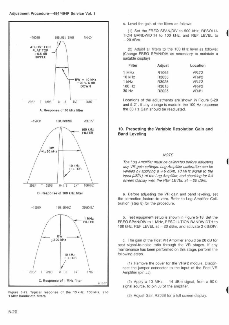
Adjustment Procedure-494/494P Service Vol. 1
-20DBM
ADJUST FORFLAT TOP J
-- . 0.5 dBRIPPLE
2DB/ T IODB
-19DBM
-19DBM
100 001 OMHZ
8-t .$
A. Response of 10 kHz fitter
100 .001 MHz
2DB/ T 20DB 8-1 .8 INT 10007
B. Response of 100 kHz filter
t 00 .00MHz
0-t .s
BW = 10 kHz+20% 6 dBDOWN
INT
INT2DS/ T 20DB
C. Response of 1 MHz filter
5KHZI
IOKHZ
20KHZ/
200KHZ/
I MHz
4416-57
Figure 5-22 . Typical response of the 10 kHz, 100 kHz, and1 MHz bandwidth filters.
s. Level the gain of the filters as follows :
(1) Set the FREQ SPANIDIV to 500 kHz, RESOLU-TION BANDWIDTH to 100 kHz, and REF LEVEL to-20 dBm .
(2) Adjust all filters to the 100 kHz level as follows:(Change FREQ SPAN/DIV as necessary to maintain asuitable display)
Locations of the adjustments are shown in Figure 5-20and 5-21 . If any change is made in the 100 Hz responsethe 30 Hz Gain should be readjusted .
10 . Presetting the Variable Resolution Gain andBand Leveling
NOTE
The Log Amplifier must be calibrated before adjustingany VR gain settings . Log Amplifier calibration can beverified by applying a f 6 dBm, 10 MHz signal to theinput (J621), of the Log Amplifier, and checking for fullscreen display with the REFLEVEL at -20 dBm.
a. Before adjusting the VR gain and band leveling, setthe correction factors to zero . Refer to Log Amplifier Cali-bration (step 8) for the procedure.
b. Test equipment setup is shown in Figure 5-18 . Set theFREQ SPAN/DIV to 1 MHz, RESOLUTION BANDWIDTH to100 kHz, REF LEVEL at -20 dBm * and activate 2 dB/DIV .
c. The gain of the Post VR Amplifier should be 20 dB forbest signal-to-noise ratio through the VR stages . If anymaintenance has been performed on this stage, perform thefollowing steps.
(1) Remove the cover for the VR#2 module . Discon-nect the jumper connector to the input of the Post VRAmplifier (pin JJ).
(2) Apply a 10 MHz, -14 dBm signal, from a 50 SZsignal source, to pin JJ of the amplifier.
(3) Adjust Gain R2038 for a full screen display .
Filter Adjust Location
1 MHz R1065 VR#210 kHz 83035 VR#21 kHz R3025 VR#2100 Hz R3015 VR#230 Hz 82025 VR#1

(4) Remove the signal from the input to the Post VRAmplifier and replace the jumper connector to pins JJ atthe input to the Post VR Amplifier . Replace the cover forthe VR#2 module .
d . Adjust the front panel AMPL CAL to its fully counter-clockwise position and set the Band 1 Gain R2031 onVR#2 (Figure 5-19) fully counterclockwise .
e . Disconnect P693 from the input to VR#1 module(Figure 5-21) and activate MIN NOISE. Apply a 10 MHz,-25 dBm, signal, from the signal generator, through a bnc-to-Sealectro adapter to J693. Adjust the generator fre-quency to peak the signal amplitude . (Signal amplitudeshould be between 3.5 and 6.5 divisions . If signal amplitudeis not within these limits it indicates a gain problem in theV R .)
f . If the signal amplitude is over 5 divisions, adjust PostVR Gain R2038 on VR#2, (Figure 5-19) for a 5 divisionsignal amplitude . If the signal amplitude is less than 5 divi-sions proceed to part "g" of this step .
g . Adjust the front panel AMPL CAL for a 7 divisionsignal .
h . Switch MIN NOISE off, decrease the generator outputto -35 dBm, leave the REF LEVEL at -20 dBm, and ad-just the 10 dB Gain, 83035, on the 10 dB Gain board ofVR#1 (Figure 5-21) so the signal amplitude is 7 divisions .
i . Change the generator output to -45 dBm, the REFLEVEL to -40 dBm, and adjust 20 dB Gain R2023 on the20 dB Gain Step board (Figure 5-21) for a 7 division signalamplitude .
j . Change the generator output to -65 dBm, the REFLEVEL to -60 dBm, and adjust the 10 dB Gain, 82060, onthe 20 dB Gain Step board (Figure 5-21) for a 7 divisionsignal amplitude .
k . Set the REF LEVEL to -30 dBm and the generatoroutput to -35 dBm . Check for a 7 division signal amplitude .Repeat this check for --45, -55, and -65 dBm input lev-els . Note that each maintains the 7 division signal to verifythat the gain of the VR gain stages are correct . Readjustgain if necessary .
I . Remove the 10 MHz signal to J680 and reconnectP680 . The final band level adjustments are described after
Adjustment Procedure-4941494P Service Vol . 1
calibrating the Preselector Tracking and checking flatness .The mean level for each band is set to the level of band 1 .
m . Press <SHIFT> CAL to rerun a calibration routineand re-establish processor correction factors .
11 . Calibrator Output Level
The calibrator output level is calibrated to a known refer-ence . The procedure for checking the level is described inthe Performance Check section . Output level is adjustedwith Cal Level 81041, in the 3rd converter (#2 in Figure5-23) .
12 . IF Gain Calibration
a . Test equipment setup is shown in Figure 5-23 . Set theRESOLUTION BANDWIDTH to 100 kHz, REF LEVEL to-20 dBm, and apply a -21 .5 dBm, 110 MHz signal,through step attenuators, to the input (J365) of the 110 MHzfilter .
b. Set the step attenuators for 0 clB . (With --21 .5 dBminput, the signal level should be 7 divisions or more .) Adjustthe generator output for a 7 division signal reference level .
c . Remove the 110 MHz signal to the 110 MHz filter andreconnect P365 .
d . Set the step attenuators for 21 dB attenuation andapply the 110 MHz signal to the input (J321) of the 110 MHzIF amplifier (Figure 5-23) .
e . Adjust the gain of the IF Amplifier, with 81015, for adisplay amplitude that equals the seven division referenceset in part b .
f . Remove the 110 MHz signal and reconnect P321 . Ap-ply the CAL OUT signal to the RF INPUT. Set the REFLEVEL to -20 dBm, FREQUENCY to 1010 MHz, FREQSPANIDIV to 100 kHz, and RESOLUTION BANDWIDTH of100 kHz .
g . Set the front panel AMPL CAL fully counterclockwiseand adjust 110 MHz IF Gain 81015 for 5 division of signal .(If this cannot be achieved, it indicates excessive lossthrough the front end .)
h . Adjust the AMPL CAL for a full screen signal . AMPLCAL adjustment should now have 6 dB down range and6 dB or more up range .
5-21

Adjustment Procedure-4941494P Service Voi . 1
NOTE
Two variable capacitors, C325 and C2047 on the110 MHz IF board, do not require adjustment duringcalibration . This adjustment requires return loss mea-surement which is a maintenance andrepair function.
13 . Digital Storage Calibration
NOTE
This is a two-part procedure; the first calibrates the494, the second is a program to be used withTEKTRONIX 4050-Series Computer terminal and a494P instrument.
10 dB and 1 dB Step Attenuators
Figure 5-23 . Test equipment setup for adjusting the IF gain and the location of adjustments and connectors.
PART 1, 494 PROCEDURE
c. On the Horizontal Digital Storage board:
4416-58
a . Set the FREQUENCY to 200 MHz, FREQ SPANIDIVto 20 MHz, REF LEVEL to -20 dBm, and activate AUTORESOLN, 10 dBIDIV, and VIEW A.
b . Apply the CAL OUT signal to the RF INPUT and ad-just the PEAKIAVERAGE cursor so it is about one divisionabove the bottom of the screen .
(1) adjust output Offset, R1039 (Figure 5-24) so theleft edge of the cursor is at the left edge of the crt (about0.25 division over-span from the left graticule line);

(2) adjust Output Gain, R1041 (Figure 5-24) so theright edge of the cursor is at the right edge of the crt ;
(3) alternately switch VIEW A on and off while adjust-ing Input Gain, 81048 (Figure 5-24) so the storage signalat the right edge tracks with the non-store signal .
(4) alternately switch VIEW A on and off while adjust-ing Input Offset 81046, so the stored display at the leftedge tracks with the non-store display .
d . On the Vertical Digital Storage board :
(1) Output Gain R1024 and Output Offset R1036(Figure 5-24) are adjusted at the factory . In the 494Ponly, an alternate procedure follows . These adjustmentsshould not be changed ; however, if they are disturbed,center the adjustments and Input Gain R1034 beforeproceeding ;
(2) activate 2 dBIDIV display mode and turn PEAK/AVERAGE control clockwise ;
(3) using a signal near the bottom of the display, ad-just Vertical Offset R1030 (Figure 5-24) so the storeddisplay is the same amplitude as the non-store signal ;
Figure 5-24 . Digital storage calibration adjustments.
Adjustment Procedure-494/494F' Service Vol . 1
(4) change the REF LEVEL to raise the amplitude ofthe signal to full screen ;
(5) adjust Input Gain 81034, so the stored display, ofthe high amplitude signal, is the same as the non-storedisplay ;
(6) repeat the low level and high level adjustments tocompensate for interaction .
PART 2, 494P PROCEDURE
a. Set the FREQUENCY to 100 MHz, FREQ SPAN/DIVto 10 MHz, RESOLUTION BANDWIDTH to 1 MHz, REFLEVEL to -10 d6m, PEAK/AVERAGE control fully counter-clockwise, and activate 2 dB/DIV, VIEW A and VIEW B, andNARROW Video Filter .
b . Connect CAL OUT to the RF INPUT and interconnectthe 494P with the 4050-Series Controller, via a GPIB cable(both should already be turned on) . Set the 494P GPIB AD-DRESS switches on the rear panel for address 1 (switch 1up, all others down) .

Adjustment Procedure-4941494P Service Vol . 1
100110120130140150160170180180200210220230
c . Enter and run the following program :
DIM C (1040 )K=125I1=0FOR I=1 TO 10FOR J=1 TO 100C (I 1+J )=KNEXT JK=K-25I1=I1+100IF K>---25 THEN 210K=225NEXT IPRINT @1 ; "SIGSWP"WBYTE @33 :64, C,-255
d . Adjust the POSITION controls to center the frequencydot and place the baseline on the bottom graticule line .
e . Adjust the following to match the step waveformthe graticule : (Figure 5-24)
Assembly
Horizontal Digital StorageHorizontal Digital StorageVertical Digital StorageVertical Digital Storage
Adjustment
Output Offset, 81039Output Gain, 81041Output Offset, R1036Output Gain, 81024
to
Be sure that the left and right edges of the step wave-form coincide with the left and right edges of the graticule .This matches the horizontal display width of a 1000-pointwaveform to the graticule .
f . Press REMOTE TO LOCAL and activate FREE RUNTriggering . Reduce the FREQ SPANIDIV to 200 kHz .
g . Adjust REF LEVEL so the signal peak is about onedivision above the bottom of the graticule .
h . Deactivate VIEW A. Press VIEW B repeatedly, andadjust Vertical Offset 81030, on the Vertical Digital Storageboard, to minimize the amplitude difference between thestored and non-store waveforms .
i . Adjust the REF LEVEL to bring the signal peak closeto the tap of the graticule .
j . Again, while pressing VIEW B repeatedly, adjust InputGain R1034 on the Vertical Digital Storge board (Figure5-24) to minimize the amplitude difference between thestored and non-store waveforms .
k . Because the offset and gain adjustments interact, re-peat parts h through k as necessary .
I . Deactivate NARROW Video Filter, increase FREQSPANIDIV to 10 MHz and tune the signal to within one divi-sion of the right edge of the graticule .
m . Press VIEW B repeatedly and adjust Input Gain81048 on the Horizontal Digital Storage board (Figure 5-24)so the horizontal position of the stored signal matches thatof the non-stored signal .
n . Tune the signal to within 1 divison to the left edge ofthe graticule . Alternately switch VIEW B on and off whileadjusting the Input Offset 81046 so the horizontal positionof the stored display is the same as the non-store display .
14 . Setting B-SAVE A Reference Level
When B-SAVE A is selected, the expression imple-mented is (B-SAVE A)+k, where k is a constant set by theinput data for an 8-to-4 line encoder, U1015 . Each bit willmove the reference level about 0.2 minor division . Normally,the reference level is set at the center gratlicule line ; how-ever, it can be set anywhere within the graticule area by thesetting of an 8-bit binary switch, S1014 (Figure 5-24), TheMSB (switch #8) shifts the display about five divisions,switch #7 half this amount, etc . The following proceduresets the reference level .
Estimate the amount and direction the reference level isto be shifted, then close or open the switches on S1014 toobtain the desired B-SAVE A reference level .
15. Preselector Driver Calibration
a . Test equipment setup is shown in Figure 5-25 .
b . Set the offset for driver U2054 as follows : (Offsetshould only require adjusting if U2054 is changed .) SwitchPOWER off, pull the Preselector Driver board and install onextender board (Figure 5-26) then switch POWER on.
(1) Set the FREQUENCY RANGE to band 1(0-1 .8 GHz) ;
(2) Pull P3055 and connect a DVM between TP4054and analog ground (Figure 5-26) . Set the voltmeter rangeto 30 QV or less ;
(3) Starting from a fully counterclockwise position,adjust Driver Offset 82066 (Figure 5-26) for 0 V atTP4054 ;

P2011
TM 500 Main Frame
Digital
Comb GeneratorVoltmeter Source
I
Figure 5-25. Test equipment setup for Preselector Driver adjustments.
Figure 5- 26. Preselector Driver adjustment and test points .
Adjustment Procedure-4941494P Service Vol. 1
n n n n rn n MI rn rn °TP1072 (/~7)
ci v~-- TP1Q69a -
LO
in ;n
(0
cep rip
(EXT PRESELECTOR)a o 0 0 o c o ° o
rr ¢ ct
oc [[ CC
(}~TP4054
f-R4049
82066
4416-61

Adjustment Procedure-4941494P Service Vol . 1
(4) Disconnect the DVM, replace P3055, then switchPOWER off and reinstall the Preselector Driver board .Switch POWER on .
c . Connect DVM between the center tap of the MAN-UAL PEAK potentiometer and ground. Adjust the control for0 V indication . If index on the knob is not aligned with themark on the front panel, loosen knob and position the markso it is aligned .
d . Apply the CAL OUT signal to the RF INPUT . Set theREF LEVEL to -30 dBm, FREQ SPANIDIV to 20 MHz andactivate AUTO RESOLN . Select the 1 .7-5.5 GHz FRE-QUENCY RANGE and adjust the CENTER FREQUENCY tocenter the 2.1 GHz marker. Center the Input Offset adjust-ment 81031 (Figure 5-26) then center the 2 .1 GHz markerwith the CENTER FREQUENCY control .
e . Ground TP1069 with a jumper strap and adjust thePreselector Offset 81064 for maximum response of the2 .1 GHz signal . Remove the grounding strap .
f . Peak the 2.1 GHz signal with the -829 MHz IF OffsetR1049 (Figure 5-26)
g . Remove the Calibrator signal to the RF INPUT andconnect the output of the Microwave Comb Generator tothe RF INPUT . Change the REF LEVEL to 0 derv, set FRE-QUENCY to 5.5 GHz, and center the 5 .5 GHz comb markeron screen .
h . Peak the 5.5 GHz signal with the Preselector Sense,81065, adjustment.
i . Repeat parts f through h to ensure that the 2.1 and5 .5 Hz frequency points track the input tuning .
j . Change the FREQUENCY RANGE to 5.4-18 .0 GHz(band 4) . Adjust REF LEVEL and RESOLUTION BAND-WIDTH to observe the 6 GHz marker . Adjust MANUALPEAK to peak the 6 GHz signal .
k . Set FREQUENCY to 9 GHz and observe the 9 GHzmarker on screen . Peak this response with the X3 GainR1052 adjustment .
I . Repeat parts j and k to ensure tracking over thisrange .
m . Increase FREQUENCY to the 12 GHz marker, thenpeak the 12 GHz point with Shaper #1 R1Cl54 adjustment(Figure 5-26) .
n . Adjust FREQUENCY to center the 17 GHz marker,then peak the signal with Shaper #2, 81056 adjustment .
o . Recheck the 6, 9, 12, and 17 GHz points to verify thatthey all peak at the same position of the front-panel MAN-UAL PEAKING control . If they do not, repeat parts gthrough n .
p . Change the FREQUENCY RANGE to 1 .7-5 .5 GHz(band 2) . Center a comb marker between 5.4 and 5 .5 GHz,then peak the signal with the front-panel MANUAL PEAKcontrol .
q . Change FREQUENCY RANGE to the 5.4-18.0 GHz(band 4) . Center the same signal used in part p with theCENTER FREQUENCY control . Adjust Input Offset 81031,to peak the signal .
r. Repeat parts p through q until the signal amplitudepeaks, on both bands, occur at the same position of theMANUAL PEAK control .
s . Set MANUAL PEAK control so the index mark alignswith the front panel mark . Change FREQUENCY RANGE to1 .7-5.5 GHz, and adjust CENTER FREQUENCY to centerthe 3.5 GHz comb marker .
t . Adjust -829 MHz IF Offset R1049 (Figure 5-26) topeak the 3.5 GHz response,
u . Change FREQUENCY RANGE to 3.0-7 .1 GHz, setthe FREQUENCY to 5 .0 GHz to observe the marker, thenpeak the 5.0 GHz signal with +829 MHz IF' Offset R1045adjustment .
v . Change FREQUENCY RANGE to 15-21 GHz . Set theFREQUENCY to 15 GHz, then peak the 15 GHz signal withR1064 .
w . Tune the 19 GHz marker to center screen then peakthe 19 GHz signal with Shaper #3 81061 adjustment(Figure 5-26) .
x . Tune to the 21 GHz marker then peak the signal withShaper #4, 81063, adjustment .

y . Recheck the 15, 19, and 21 GHz points to verify thatthey all peak at the same position of the MANUAL PEAKcontrol .
z . Change FREQUENCY RANGE to 3.0-7 .1 GHz, cen-ter a 5.0 GHz signal on screen, then peak the signal with+829 MHz IF, R1045, adjustment .
aa . Change to the 1 .7-5.5 GHz band, center a 3.5 GHzmarker on screen, then peak the 3.5 GHz signal with-829 MHz IF, R1049, adjustment,
ab . All bands should now track or the signal peak for allbands should occur with the MANUAL PEAK knob indexmarker near the front-panel mark .
RF EXTOUT ALC
To Recorder Out connector (Back Panel)
Low Loss Coax Cable with SMA Connectors
Figure 5-27 . Test equipment setup for adjusting baseline leveling .
Adjustment Procedure-4941494P Service Vol . 1
16 . Baseline Leveling (Video Processor)
This procedure sets response slope for band 1 and ad-justs the baseline so response perturbations for band 4 areoffset to level the display .
a . Test equipment setup is shown in Figure 5-27 . Theoutput of the sweep generator is applied through a 3 dBattenuator and high performance coaxial cable to a powerdivider . Connect one output of the power divider directly tothe RF INPUT of the 494/494P and the other to the sensorfor the power meter . Set the RF plug-in ALC switch to MTRposition and connect a coaxial cable between Recorder Out-put of the power meter and the Ext ALC Input of the plug-inunit on the sweeper . Set the Power Level to approximately-10 dBm then adjust the Gain on the unit for stable opera-tion (output stops oscillating) .
Power Meter
To Ext ALCon Sweep Generator
orThrough Power Meterto AL( : Connector
4416-62

Adjustment Procedure-4941494P Service Vol . 1
b . Set the FREQUENCY to 0 .00 GHz. FREQ SPANIDIVto MAX, REF LEVEL to -20 dBm, TIMEIDIV to AUTO, andactivate AUTO RESOLN and 2 dB/DIV . SetPEAK/AVERAGE control fully counterclockwise .
c . Apply the output of the sweep oscillator to the RFINPUT, as shown in Figure 5-27 . Set the sweep oscillator tothe Automatic Internal Sweep (Marker Sweep), sweep timeto 100 s, and set it so the oscillator sweeps from 10 MHz to1 .8 GHz .
d . Activate MAX HOLD, VIEW A, and VIEW B and selecta TIMEIDIV so there are no breaks in the digitized storeddisplay (Figure 5-28A) .
-6DBM 11 .758GUZ MAX
A. Typical response before baseline leveling .
-1408M 10_024"ZHZ NP):
~
0 BB 5 .4-1 8_- 1 ~
kHz
B_ Typical response after baseline leveling .
44 T6-63
Figure 5-28 . Typical response when adjusting baselineleveling .
e . Reactivate MAX HOLD and SAVE A. Trace andrecord the response of band 1 . Note the number of divisionsfrom the baseline to the lowest point in the first 5 divisionsof the display .
f . Adjust the CENTER FREQUENCY to place the dotmarker directly over the lowest point within the last 3 divi-sions of the display .
g . Set the sweep oscillator CW Marker control On andadjust it so a signal is at center screen on the 4941494P .
h . Adjust band 1 Slope R1012, on the Video Processorboard (Figure 5-29), to set the top of the signal to the sameamplitude level noted above, in part e .
i . Repeat until the frequency response is within 1 .5 dB ofthe mid-point between the two extremes .
j . On the Video Processor board pull the (Leveler Disableplug P3035 (Figure 5-29) .
k . Set the FREQUENCY to 10 GHz, FREQUENCYRANGE to 5.4-18 .0 GHz (band 4) FREQ SPANIDIV toMAX, REF LEVEL to -10 dBm, and TIMEIDIV to 10 ms.Activate 10 d6IDIV, and AUTO RESOLN . (UINCAL indicatorwill light .)
I . On the sweep oscillator select a 5 .5 GHz cw markerand adjust the output for -10 dBm reading on the powermeter .
m. Activate 2 dBIDIV and adjust the REF LEVEL so thesignal amplitude is half screen . Adjust MANUAL PEAK formaximum response or activate AUTO PEAK .
n . On the sweep oscillator change to the automatic inter-nal sweep (Marker Sweep) and set the sweep time for100 slsweep (its slowest sweep) .
o . Activate VIEW A and VIEW B then select a sweeptime, on the 494/494P so the stored display is solid (nobreaks in the digitized display, (Figure 5-28) .
p . Activate MAX HOLD and SAVE A. Trace and recordthe response of band 4 .
q . Deactivate VIEW A and MAX HOLD (SAVE A andVIEW B still active) .

, r
A rr IS1St1YIS
Ly W y y W A ri r, ri n h W
IrIllis -M___=1
~p m v, m m r~ ri m p1
-4-R1061 (low) through 81013 (high) leveler adjustments
7
R3030m
P3035P2060
1111111111~~ti1~11ti`t111i
R1012BAND 1SLOPE r
1~
-7-R-11369- R1070
4416-50
r . Activate 10 dBIDIV and note the baseline . ActivateNARROW Video Filter and adjust the REF LEVEL so thebaseline moves to the top of the screen .
s . Press 2 dBIDIV and VIEW A, then adjust the REFLEVEL so SAVE A display and the baseline are at centerscreen .
t . Unplug 1)2060 (Figure 5-29) and move it from Normalto Invert mode position (one pin to the left) . Replace LevelerDisable plug 1)3035 .
u . Start with 81061 and adjust the leveling potentiom-eters sequentially, from 81061 through 81013, so the con-tour of the baseline is an average of the SAVE A display . Inthe process use Horiz adjust 81069 (Figure 5-29) to shift thebaseline to the right or left so the baseline aligns with theaverage contour of SAVE A display .
v . . Replace 1)2060 to the Normal mode position (one pinto the right) . The baseline will now be 180° or the inverse ofits previous position .
w . Deactivate and then activate VIEW A, VIEW B, SAVEA, and MAX HOLD. Retrace and check new response . Re-sponse should appear flat (Figure 5-2813) .
Figure 5-29 . Adjustments and test points on the Video Processor.
Adjustment Procedure-49414941) Service Vol . 1
x . Disconnect and remove the signal to the RF INPUTfrom the test equipment .
y . Compensation adjustment R3030 is set at the factoryand usually does not require adjustment . Pull Leveler Dis-able plug 1)3035 then replace it. If the baseline remainsstraight or breaks up after the plug is replaced, compensa-tion is required . Adjustment procedure is as follows :
(1) With the front-panel controls set as directed inpart b, activate NARROW Video Filter and changeTIMEIDIV to 50 ms. Alternately turn the 19 level adjust-ments clockwise and counterclockwise so every otherpotentiometer is fully clockwise and the adjacent poten-tiometer is fully counterclockwise. Display should nowappear as a periodic triangular waveform .
(2) Adjust the REF LEVEL so the baseline is near fullscreen then switch to the 2 dBIDIV mode and adjust sothe display is mid-screen (Figure 5-30A) .
(3) Turn Compensation adjustment F13030 counter-clockwise until the display breaks up (Figure 5-3013) .
(4) Now turn 83030 clockwise 1 .5 to "? turns past thepoint the display again becomes a periodic triangularwaveform .
(5) Turn Horiz Adjust 81069 to center the display .

Adjustment Procedure-494/494P Service Vol. I
1 IWIFERM"Eff1i
NZ
A. Series of waveforms. Amplitude approximately
t5 dB above and below baseline reference.
B. Typical display when display breaks up .
4416-64
Figure 5-3Q. Typical response when adjusting compensation ofthe baseline leveling circuits.
(6) Return the baseline leveler adjustments to theirmidrange position for a straight line display and proceedwith the baseline leveling alignment as previously de-scribed (parts a through x) .
z . Adjust the slope of band 5 as follows:
(1) Readjust the Sweep Oscillator so it sweeps from15 GHz to 21 GHz (Marker Sweep) and adjust the outputso the power meter reads approximately -10 dBm.
(2) Adjust R1070 (Band 5 Slope) on the Video Pro-cessor board, fully counterclockwise .
(3) Set the CENTER FREQUENCY to 15 GHz, FRE-QUENCY RANGE to 15-21 GHz (band 5), FREQ SPAN/
DIV to MAX, REF LEVEL to -10 dBm and the TIMEIDIVto 50 ms. Activate 10 dBIDIV and AUTO RESOLIN(UNCAL indicator will light) .
(4) Select a 15 GHz marker on the Sweep Oscillatorand adjust the output for -10 dBm as indicated on thepower meter .
(5) Activate 2 dBIDIV and adjust the REF LEVEL sothe signal amplitude is approximately 6 divisions. AdjustMANUAL PEAK for maximum response or activateAUTO PEAK .
(6) Change the Sweep Oscillator to Automatic Inter-nal Sweep and set the Sweep Time for 100 s or its slow-est sweep .
(7) Activate View A, View B, and MAX HOLD. Notethe response as the oscilator sweeps .
(8) Activate SAVE A and deactivate MAX HOLD, thenselect CW Marker on the Sweep Oscillator and move thesignal to the upper end of band 5 (19-21 GHz) .
(9) Visualize an imaginary line through the midpoint ofthe saved display and select a point on the saved display(between 19 and 20 GHz) that intersects the imaginedline .
(10) Switch VIEW A on and off as required while mov-ing the CW Marker to the selected point .
(11) Switch VIEW A off and adjust R1070 until theCW Marker is at the 6 division level or maximum, which-ever occurs first .
(12) Deactivate SAVE A and repeat steps (6 through10) until the best overall flatness is achieved .
17 . Band Leveling for Coaxial Bands (bands 1-5)
NOTE
The mean value of the frequency response far eachband is set to a -20 dBm reference at 100 MHz. Ifthe range of anyband gain adjustments is insufficient,add a diode between the emitter of 03036 and pinsDD, on the VR#2 Mother board, as shown on theschematic diagram for Variable Resolution #2.
a . Perform Frequency Response Check of bands 1through 5 as described in the Performance Check sectionand note the frequency at the mean level (average level be-tween two extremes) for each band.

b . Perform "Presetting the Variable Resolution Gain andBand Leveling" adjustment step prior to proceeding withthis step .
c . Test equipment setup is shown in Figure 5-31 . Set theFREQUENCY RANGE to 1 .7-5 .5 (band 2), FREQ SPAN/DIV to 10 MHz, REF LEVEL to -20 dBm, and activateAUTO RESOLN, 2 dB/DIV, VIEW A and VIEW B.
d . Apply a calibrated -20 dBm signal, whose frequencyis the same as that noted for the mean level in part a, to theRF INPUT . Set the FREQUENCY to the input signal andreduce the FREQ SPAN/DIV to 500 kHz .
NOTE
If a power meter is used to monitor signal level, con-nect the power meter sensor in line with the signal tothe RF INPUT.
e . Adjust band 2 Gain 83034 on the VR#2 Motherboard (Figure 5-32) for a full screen (-20 dBm) display .
f . Change the FREQUENCY RANGE to 3 .0-7 .1 GHz(band 3) and apply a calibrated --20 dBm signal with thesame frequency as noted for the mean level in Band 3 forpart a of this step .
2072 MHz Signal GeneratorPower meter
-54dBm to -80 dBm
Adjustment Procedure-4941494P Service Vol. 1
g. Set the FREQUENCY to the incomming signal, FREQSPANIDIV to 500 kHz/Div and adjust band 3 Gain, 83030,(Figure 5-32) for a full screen display .
h . Repeat the above procedure for each coaxial band(1-5) and set the gain of each with the appropriate adjust-ment . If the range of any adjustment is insufficient, add orremove the appropriate diode (see schematics and compo-nent locator, in Volume 2) to obtain the regdired range. Add-ing the diode increases gain .
18 . Band Leveling for Waveguide Bands (bands6-11)
a . Test equipment setup is shown in Figure 5-31 . Apply2072 MHz at -30 dBm, through a dc-blocking capacitor tothe EXT MIXER input . Monitor the input with a power meterto set the power level then add a known 310 dB attenuatorso the input level to the EXTERNAL (MIXER port is-60 dBm. Set the FREQUENCY RANGE to 18-26 GHz(band 6), FREQ SPANIDIV to 200 MHz, REF LEVEL to-30 dBm, and activate AUTO RESOLN.
NOTE
The baseline of the display will rise when 21272 MHzsignal is applied to the EXTERNAL MIXER input portconnector.
b . With - 60 dBm input level applied, adjust Band 6 GainLeveling, 83024, (Figure 5-32) for full screen display .
494 Spectrum Analyzer
Figure 5-31 . Test equipment setup far adjusting band leveling for the coaxial and waveguide bands.
44,6 .65
5-31
0 0 ~ a ~ ~00 0 0 0

Adjustment Procedure-4941494P Service Vol. 1
Table 5-3EXT MIXER BAND LEVELING ADJUSTMENTS
19 . Phase Lock Calibration
Figure 5-32 . Band leveling adjustments and gain diodes on theVR#2 Mother board:
c. Change the FREQUENCY RANGE and input signalfrequency and level as listed in Table 5-3, and adjust theappropriate Band Gain adjustments for a full screen display.Gain adjustment for the waveguide bands need to be ad-justed only if these bands will be used.
d . Switch POWER off; replace VR module, then switchPOWER back on.
The Phase Lock assembly normally requires calibrationonly after some part of the assembly has been repaired orreplaced . Phase noise, produced by the phase lock loop, isspecified for -70 dBc or better, 3 kHz out from the re-sponse . This should be checked before calibrating theassembly.
a. Test equipment setup is shown in Figure 5-33 . Re-move the Phase Lock module and the two cover plates soall circuit test points and adjustments are accessible . Plugthe assembly on extender boards and into the instrument .Use extender cables and adapters to reconnect signal ca-bles to their respective connector (cable with yellow band toJ501, and the cable with black band to J502).
If desired, the direct reading counter can be connected tothe Vertical Output of the test oscilloscope . lfhis will enablethe user to observe the display of a test point and get acount, if appropriate, throughout this procedure. The groundside of the test oscilloscope probe will serve as the commonground return for both instruments .
b. Press <SHIFT> CAL and do the directed calibrationroutine through adjusting the LOG CAL- . Press <SHIFT~to return the instrument to normal operation and set REFLEVEL to -30 dBM . Check that the AUTO RESOLN isactive (button lit) .
c. Check Offset Mixer-This part of the procedure isonly required after repair or replacement of the Mixer board .
(1) Connect the Direct Input of the FrequencyCounter to pin N (Figure 5-34) and adjust the countercontrols for a count. Note the frequency .
(2) Connect the counter to pin K and note thefrequency .
(3) Connect the counter to the collector of 01040 andnote the frequency . Frequency should equal the differ-ence between pins N and K (e.g ., 25 .080 -25.000 =80 kHz) . Disconnect the counter probe from the collectorof 01040.
(4) Connect the probe of a test oscilloscope to thecollector of 01040 and check for a 50% duty cycle of theapproximately 80 kHz signal and an amplitude that isapproximately 5 V peak-to-peak .
d. Check Synthesizer
(1) With the FREQ SPANIDIV at 200 kHz, phase lockshould occur.
(2) Change FREQ SPANIDIV to 500 kFiz and connectthe counter to J500 on the Synthesizer board. Check fora reading of 50.00 MHz .
(3) Connect the counter to TP2040 (Figure 5-34A)and check for a reading that is near 25 .0 MHz .
Band Input LevelGain
Adjustment
6 (1 B-26 GHz) -60 dBm 830247 (26-40 GHz) -60 dBm R30268 (40-60 GHz) -60 dBm 830329 (50-90 GHz) -60 dBm 83029
10 (75-140 GHz) -60 dBm R302811 (110-220 GHz) -60 dBm R302812 (170-325 GHz) -60 dBM 83028

TM 500 Main Frame
Counter
(4) Connect the test oscilloscope to TP1040 (Figure5-34A) and check for positive pulses with an amplitude ofapproximately 4 V peak-to-peak .
(5) Change the FRED} SPANIDIV to 200 kHz and ob-serve that the signal on TP1040, in part (4), is still there .
e . Controlled Oscillator-This part of the check is onlyrequired after repair or replacement of the Controlled Oscil-lator board .
(1) Press <SHIFT> PULSE STRETCHER and se-lect "Phase Lock Synthesizer" (#5) from the displayedmenu .
(2) Follow the instructions until the message, "VER-IFY LAST STEP" . Due to the interaction of C1013 and02011 adjustments, the two steps will have to be re-peated until the voltages are correct. Alternately pressAUTO RESOLN and IDENT and adjust until the two volt-age readings are correct.
(3) Connect the counter to TP2011 on the ControlledOscillator board (Figure 5-34A) and alternately pressAUTO RESOLN and IDENT and check for a count read-ing of either 25.0943 MHz or 25.0328 MHz.
f. Check Operation of Strobe Driver
Phase Lock assembly on extenders
o°DirectInput
Frequency 494 Spectrum Analyzer
Probe
To: VERT SIGNAL OUT(Back Panel)
Figure 5-33 . Test equipment setup for calibrating the Phase Lock assembly .
Adjustment Procedure-4941494FO Service Vol. 1
Test Oscilloscope
(5) Press <SHIFT> to abort the test .
4415-67
The "Phase Lock Synthesizer" test is still used for thistest . If aborted, press <SHIFT> PULSE STRETCHER toreturn to the Synthesizer routine . Any step in the routine willwork .
(1) Connect the test oscilloscope to TP2015 on theStrobe Driver board (Figure 5-34B) and check for asquare wave response with a Time/Div setting of .05 ,ps .Amplitude should be approximately 5 V peak-to-peak .
(2) Connect the test oscilloscope to TP2087 andcheck for a sinusoidal waveform of approximately 5 Vpeak-to-peak .
(3) Connect the counter to TP2087 and check for acount of either 5.018868 or 5.006477 MHz .
(4) Connect the test oscilloscope to P502 or P504and check for 5 V logic level signals respectively .
g. Error Amplifier-This procedure sets loop gain whichis required when either the Phase Lock assembly, 1st LO,Phase Detector, or Error Amplifier is replaced .
(1) Set FREQ SPANIDIV to 200 k.Hz then press<SHIFT> EXT Triggering . The "Diagnostic Aids" menuwill now be displayed. Select "1st LO Phase Lock" (0)and press HELP, phase lock should be disabled .
J501
E .
II ifs a
0 000 .0

Adjustment Procedure-494/494P Service Vol. 1
0C1013
Controlled Oscillator
J504
J502 C]
A. Synthesizer, Offset Mixer and Controlled Oscillator,
bTP1031
bTP2037
OP2035
Error Amplifier
Strobe Driver
Error Count Break Point R1061
B. Strobe Driver and Error Amplifier.
Loop Gain R3082
P3057a
TP3081
C2105a
F- -1
TP2015b
Figure 5-34. Adjustments and test points in the Phase Lack assembly .
4416-68

(2) Connect the test oscilloscope to TP2038 (Figure5-34B) and set test oscilloscope TimelDiv to 20 ms.Check for a waveform with an amplitude that is approxi-mately 6 V peak-to-peak .
(3) Press HELP to enable phase lock and note thatthe message indicates "LOCK ENABLED" . Connect thetest oscilloscope to TP3081 (Figure 5-3413) and adjust83082 from stop to stop and note that the beat notesignal varies in amplitude . Press <SHIFT> to abort theCal routine .
(4) Set the TIMEIDIV to AUTO, FREQUENCYRANGE to band 2 (1 .7-5 .5 GHz), and FREQUENCYSPANIDIV to 50 kHz .
(5) Pull P3057 (Figure 5-34B), this turns the strobe tothe Phase Gate on . Turn Loop Gain 83082 fullycounterclockwise .
(6) Connect the test oscilloscope probe to TP3081and trigger the test oscilloscope on the signal at TP2037(U2048-6) shown in Figure 5-348 . Set the test oscillo-scope TimelDiv to 5 ms and Volts/Div to 0.5 V . Note thebeat notes . Beat notes are produced by the differencebetween strobes from the phase lock (one every 5 MHz)and the particular frequency the 1 st LO is tuned to .
(7) Increase FREQ SPANIDIV to MAX, set nESOLU-TION BANDWIDTH to 100 Hz, and TIMEIDIV to AUTO.Deactivate VIEW A and VIEW B if needed .
(8) As the sweep scans across the span, note theposition of the smallest beat note . Tune the CENTERFREQUENCY to position the frequency dot at this loca-tion, then reduce the FREQ SPANIDIV to 20 MHz. SetTIMEIDIV to 1 s and activate VIEW A .
(9) Check that the beat note is 3 V peak-to-peak ormore . If this does not occur, it is an indication the PhaseGate is defective .
Adjustment Procedure-4941494P Service Vol . 1
(10) Install P3057, disconnect the test oscilloscopetrigger and probe connections . Ensure that P3057 is in-stalled correctly ; its absence will produce spurious re-sponses on the display .
(11) Reduce FREQ SPANIDIV to 200 kHz and ensurethat phase lock occurs, by the absence of error messageand a sweep . Replace the covers on the assembly andreinstall the module in the instrument . Perform the phaselock noise check as described in the Performance Checksection .
h Check Strobe Driver-Excessive noise on the displayand intermittent lock are indications that the strobe pulseout of the Strobe Driver is noisy or low in amplitude . Thiscan be caused by a mismatch in input or output impedanceto the band-pass filter FL2064 . The following procedure isrequired if the filter or any component that affects the inputor output impedance match is replaced .
(1) With the instrument in phase lock -, mode (FREQSPANIDIV 200 kHz or less), connect a test oscilloscopeprobe to TP2087 . Note the amplitude of the 5 MHzstrobe signal . Amplitude of the sinusodial strobe signal isnormally 5 to 6 V peak-to-peak .
(2) If the strobe signal amplitude is low and noisy,change the value of select capacitors C1032 and C2105to obtain the maximum strobe pulse amplitude atTP2087 . Value of these capacitors range from 3 .3 to27 pF .
(3) If the signal amplitude is still low, connect a fre-quency counter probe to TP2015 . Frequency must rangefrom 5.0067 to 5.0188 MHz. Frequency is a function ofthe Controlled Oscillator assembly and counter U1022 .
This concludes the Adjustment Procedure . Repeat theappropriate Performance Check to verify specification .


This section describes procedures for reducing and pre-venting instrument malfunction, troubleshooting methods,corrective maintenance, and procedures for recalibratingthose assemblies that normally do not require routinecalibration .
Removing the Instrument from its Cabinet
To prepare the rackmount or benchtop version for main-tenance or adjustment, refer to the Rackmount/Benchtoppart in the Options section for instructions on removing theinstrument from its cabinent . The following applies to thestandard 494/494P instrument :
Static-Sensitive Components
This instrument contains electrical components that canbe damaged by static discharge . See Table 6-1 for the rela-tive susceptibility of various classes of semiconductors .Static voltages of 1 kV to 30 kV can occur in unprotectedenvironments .
Static discharge can damage any semiconductorcomponent in this instrument.
Observe the following precautions to avoid damage :
1 . Minimize handling of static-sensitive components.
2 . Transport and store static-sensitive components or. assemblies in their original containers, on metalilizedor conductive foam . Label packages that containsstatic-sensitive assemblies or components .
3 . Discharge body static voltage by wearing agrounded wrist strap while handling these compo-nents . Static-sensitive assemblies or componentsshould be handled and serviced only at static-freework stations by qualified service personnel .
MAINTENANCEINTRODUCTION
Section 6-4941494FF Service Vol . 1
4 . Nothing capable of generating or holding a staticcharge should be allowed on the work stationsurface .
5 . Keep the component leads shorted together when-ever possible .
6 . Pick up components by the body, never by the leads .
7 . Do not slide the components over any surface .
8 . Avoid handling components in areas that have afloor or work-surface covering capable of generatinga static charge .
Table 6-1RELATIVE SUSCEPTIBILITY
TO STATIC DISCHARGE DAMAGE
'Voltage equivalent for levels :
1 = 100 to 500 V
4 = 500 V
7 = 400 to 1000 V(est.)2=200to500V 5=400to600V e=900V3=250V
6=600to800V 9--1200V
(Voltage discharged from a 100 pF capacitor through a resis-tance of 100 n.)
Semiconductor ClassesRelative
SusceptibilityLevels"
MOS or CMOS microcircuits ordiscretes, or linear microcircuitswith MOS inputs . (Most Sensitive) 1
ECL 2
Schottky signal diodes 3
Schottky TTL 4
High-frequency bipolar transistors 5
JFETs 6
Linear microcircuits 7
Low-power Schottky TTL 8
TTL (Least Sensitive) 9
1 . Set the instrument on its face or front panel .2 . Loosen the four screws through the back rubber 9 . Use a soldering iron that is connected to earth
feet . ground .3 . Pull the cover up and off the 4941494P.4 . Place the instrument on the work space (bench) and 10 . Use only special anti-static suction type or wick type
reconnect the power cord . desoldering tools .
Maintenance-4941494P Service Vol . 1
Preventive maintenance consists of cleaning, visual in-spection, performance check, and if needed a recalibration .The preventive maintenance schedule that is established forthe instrument should be based on the environment in whichthe instrument is operated and the amount of use . Underaverage conditons (laboratory situation) a preventive main-tenance check should be performed every 1000 hours ofinstrument operation .
Elapsed Time Meter
A 5000 hour elapsed time indicator, graduated in 500hour increments, is installed on the Z-Axis/RF Interface cir-cuit board . This provides a convenient way to check operat-ing time . The meter on new instruments may indicate from200 to 300 hours elapsed time because most instrumentsgo through a factory burn-in time to improve reliability . Thisis similar to using aged components to improve reliabilityand operating stability .
Cleaning
Clean the instrument often enough to prevent dust or dirtfrom accumulating in or on it . Accumulation of dirt andgrease acts as a thermal insulating blanket and preventsefficient heat dissipation . It also provides high resistanceelectrical leakage paths between conductors or componentsin a humid environment .
Exterior. Clean the dust from the outside of the instru-ment by wiping or brushing the surface with a soft cloth orsmall brush . The brush will remove dust from around thefront-panel selector buttons . Hardened dirt may be removedwith a cloth dampened in water that contains a mild deter-gent . Abrasive cleaners should not be used .
PREVENTIVE MAINTENANCE
Interior . Clean the interior by loosening accumulateddust with a dry soft brush, then remove the loosened dirtwith low pressure air to blow the dust clear . (High velocityair can damage some components.) Hardened dirt or greasemay be removed with a cotton tipped applicator dampenedwith a solution of mild detergent in water. Do not leave de-tergent on critical memory components . Abrasive cleanersshould not be used . If the circuit board assemblies needcleaning, remove the circuit board by referring to the instruc-tions under Corrective Maintenance in this section .
After cleaning, allow the interior to thoroughly dry beforeapplying power to the instrument .
Do not allow water to get inside any enclosed assem-bly or components such as the hybrid assemblies, RFAttenuator assembly, potentiometers, etc . Instruc-tions for removing these assemblies are provided inthe Corrective Maintenance part of this section . Donot clean any plastic materials with organic cleaningsolvents such as benzene, toluene, xylene, acetone orsimilar compounds because they may damage theplastic.
Lubrication
CAUTION
Components in this instrument do not require lubrication .
Fixtures and Tools for Maintenance
Table 6-2 lists kits and fixtures that are available to aid inservicing the 4941494P :

Nomenclature
Service Kitconsisting of :
1 Front panel extender1 Power module extender1 Accessories Interface extender1 Ribbon cable3 Coaxial cables, Sealectro male-to-Sealectro1 VR module handle1 Circuit board extender assembly kit,consisting of :1 Left extender board2 Right extender boards1 Right GPIB extender board1 Frame (extrusion for circuit board extender)6 Screws, panhead with flat and lockwashers
Screwdriver, flat, with 114 to 3l8-inch bit .
Screwdriver, Posidrive°, 440-2 .Wrench, 5116-inch open-end (used to remove or replace semi-rigid coax-ial cable connectors) .
Hex drive wrenches, 3132, 5164, 7164-inch (used to removethat hold module assemblies and their covers in place) .
Visual Inspection
After cleaning, carefully check the instrument for suchdefects as defective connections, damaged parts, and im-properly seated transistors and integrated circuits . The rem-edy for most visible defects is obvious . If heat-damagedparts are discovered, try to determine the cause of over-heating before the damaged part is replaced ; otherwise, thedamage may be repeated .
Transistor and Integrated Circuit Checks
female
Most transistors and integrated circuits are soldered onthe boards to prevent pin contact problems . Periodic checksof the transistors and integrated circuits is not recom-mended . The best measure of performance is the actual op-eration of the component in the circuit . In most cases anydegradation in performance will be detected by the micro-computer when it runs its power up routine . Performance ofthese components is also checked during the performancecheck or recalibration ; any sub-standard transistors or inte-grated circuits will usually be detected at that time .
Table 6-2SERVICE KITS AND TOOLS
hex screws
Maintenance-49414941P Service Vol . 1
Tektronix Part No.
006-3286-00
067-0973-00067-0971-00067-0972-00175-2901-00175-2902-00367-0285-00672-0865-01
670-5562-00670-5563-00670-8493-00426-1527-00211-0116-00
When handling MOS FET's, keep the shorting strap inplace until the transistor is in its socket .
Performance Checks and Recalibration
The instrument performance should be checked aftereach 1000 hours of operation or every six months if theinstrument is used intermittently to ensure maximum perfor-mance and assist in locating defects that may not be appar-ent during regular operation . Instructions for conducting aperformance check are provided by the Performance Checksection of the service instructions .
Saving Stored Data in Non-Volatile Memory for494P Instruments
If either the Memory or GPIB board are removed fromthe instrument, data stored in non-volatile memory will belost because the back-up battery on the GF'IB board is dis-connected . A program for storing data on tape is providedat the end of this section .

Maintenance-4941494P Service Vol . 1
The 494/494P contains firmware that will troubleshootthe frequency control system and the power supply . Trou-bleshooting procedure for this system and the power supplyis provided in the Diagnostics part of this section . Also in-cluded with this part is a description of the 494/494P tracemodes and their actions . After the defective assembly orcomponent has been located, refer to the Replacing Assem-blies and/or Sub-assemblies part of this section for removaland replacement instructions .
The following aids and techniques may help locate aproblem or trouble in the instrument .
Troubleshooting Aids
Diagrams-Functional block and circuit diagrams, onfoldout pages in the Diagrams section,, contain significantwaveforms, voltages, and logic data information . Any nec-essary information as to how the data was acquired, suchas operational state of the instrument, is provided on thediagram or adjacent to it . Refer to the Replaceable ElectricalParts list section for a description of all assemblies andcomponents . Diagrams are arranged in signal flow se-quence and by sections, such as RF section, IF section,frequency control section, etc ., with an accompanying func-tional block diagram .
Schematic diagrams list the Tektronix Part No . (670-xxxx- ) for the assembly or board along with the assemblynumber (A50) and name. The last two digits or suffix of thepart number are not indicated on the diagram ; however,they are listed in the Electrical Parts section . These twodigits reflect changes or modifications to the assembly orboard . When a change is made to the assembly, the suffixrolls one digit . The diagram indicates these changes with agrey tint drawing of the original circuit or if a componentchanges value the symbol is enclosed with a grey tint box .When a major modification is made to an assembly or boardand it is no longer compatable with earlier instruments, anew part number is assigned and a separate schematic withassociated illustrations is added. All diagrams indicate thenew part number and the instrument serial number break. Ifthe assembly is compatable with earlier instruments and thechange is significant enough to require a separate sche-matic, this will also be identified .
NOTE
Corrections to the manual and instrument modifica-tions. if significant, are documented by adding inserts,bound into the rear of the manual, until the informationis added to the manual text. Check this "Change In-formation" section for these changes to the manual orthe instrument .
TROUBLESHOOTING
Circuit Board Illustrations and Component LocatorCharts-Electrical components, connectors, and test pointsare identified on circuit board illustrations that are locatedon the inside fold of the corresponding circuit diagram or theback of the preceding diagram . A grid on the circuit boardillustration and the circuit schematic, plus a look-up table,provide the means to quickly locate components on eitherthe diagram or the circuit board .
In most cases, circuit numbers are assigned according tothe physical location of the component on the board or as-sembly . The first digit designates the row of a grid, the sec-ond the column, with the last two reserved as an expander.Three digit numbers designate chassis mountedcomponents .
General Troubleshooting Techniques
Before using test equipment, to measure across static-sensitive components or assemblies, be certain that volt-ages or current supplied by the test equipment does notexceed the limits of the components to be tested .
Try to isolate the problem to a component through signalanalysis . Determine that circuit voltages will not damage thereplacement .
Semiconductor Checks-Semiconductor failures ac-count for the majority of electronic equipment failures . Mostsemiconductors are soldered to the boards to reduce pincontact problems . The following guidelines should be ob-served if you substitute any of these components .
1 . Turn the power off before removing an assembly orboard .
2 . Use a de-soldering tool and 25 W or less soldering ironto remove the components .
3 . Use only good components for substitution . Be surethe new component is inserted into the board properly be-fore soldering . Refer to the manufacturer's data sheet orFigure 6-1 for IC and transistor lead configuration . IC sock-ets have a square or rectangular socket to identify pin 1 ofthe device .

v
ali
~,
BE~
Plastic-Cased Transistors
Voltage Regulator
inputGrid r
OutputTab Key
FET's
ROM
NOTE
If a substitute is not available, check the transistor orMOS FET with a dynamic tester such as theTEKTRONIX Type 576 Curve Tracer. Static typetesters, such as an ohmmeter, can be used to checkthe resistance ratio across some semiconductorjunc-tions if no other method is available, however, DONOT MEASURE RESISTANCE ACROSS MOSFET's because they are very susceptible to staticcharges. Use the high resistance ranges (R X 1k orhigher) so the external test current is limited to lessthan 6 mA . Ifuncertain, measure the external test cur-rent with an ammeter. Resistance ratios across base-to-emitter or base-to-collector junctions usually run100:1 or higher. The ratio is measured by connectingthe meter leads across the terminals, note the read-ing, then reverse the leads and note the secondreading.
Diode Checks-Most diodes can be checked in the cir-cuit by taking measurements across the diode and compar-ing these with voltages listed on the diagram .Forward-to-back resistance ratios can usually be taken byreferring to the schematic and pulling appropriate transis-tors and pin connectors to remove low resistance loopsaround the diode.
Maintenance-49414941' Service Vol. 1
Metal-Cased Transistors
Figure B-1 . Electrode configuration for semi-conductor components .
Diagnostic Firmware
Troubleshooting Steps
Leadless in-line IC
B
4416-71
Do not use an ohmmeter scale with a high externalcurrent to check diode junctions. Do not check theforward-to-back resistance ratios of mixer diodes .See Replacing the Dual Diode Assembly under Re-moving and Replacing Assemblies .
The 494/494P has firmware that contains diagnosticroutines that can be used with the Diagnostic part of thissection to troubleshoot the Frequency Control system anddiagnose Power Supply problems . This part follows GeneralTroubishooting information. Refer to this part to help isolateproblems within this loop . The following are also some gen-eral suggestions that may help isolate a problem whentroubleshooting.
1 . Ensure that the problem exists in the 494 by checkingthe operation of associated equipment and recheck the op-eration of the 494i494P .

Maintenance-494/494P Service Vol . 1
2 . Try to isolate the problem to a circuit or at least boardlevel by evaluating operational symptoms ; for example, ab-sence of the frequency dot could be caused by a malfunc-tion in the video summing stage, the marker generator, orswitching circuits .
3 . Three levels of block diagrams are provided to aid inunderstanding the theory of operation . The most detailedlevel is adjacent to the schematic and usually provides sig-nal and voltage levels at critical points within the circuits .Signal levels are usually the levels required to produce fullscreen deflection .
4 . Instructions on how to remove or replace those as-semblies, which are not obvious, are provided in this sec-tion . Refer to this part before removing any assembly fortesting or repairing .
5 . Visually inspect the area or assembly for such defectsas broken or loose connections, improperly seated compo-nents, overheated or burned components, chafed insulation,etc . Repair or replace all obvious defects . In the case ofoverheated components, try to determine the cause of theoverheated condition and correct before applying power .
6 . Use successive electrical checks to try to locate theproblem . An oscilloscope or signature analyzer is a valuabletest item for evaluating circuit performance . If applicable,check the calibration adjustments ; however, before chang-ing an adjustment note its position so it can be returned toits original setting . This will facilitate recalibration after thetrouble has been located and repaired .
7 . Determine the extent of the repair needed ; if complex,we recommend contacting your local Tektronix Field Officeor representative . If minor, such as a component replace-ment, see the Replaceable Parts list for replacement in-formation . Removal and replacement procedure of theassemblies and sub- assemblies are described under Cor-rective Maintenance .
When measuring vottages and waveforms, use ex-treme care when placing meter leads or probes . Somecircuit boards have a high component density, accesstopoints within circuits is limited. An inadvertent moveof test leads or probe can short a circuit and generatetransient voltages that can destroy many static sensi-tive components .

Introduction
DIAGNOSTICThis part consists of explanations and procedures for troubleshooting the frequency control system and the power supply
using diagnostic firmware that is in the 4941494P .
TROUBLESHOOTING THE 494/494P USING THE ERROR MESSAGE DISPLAY
This part contains procedures for troubleshooting the frequency control system and the power supply . When the micro-processor detects a failure or error in the Frequency Control loops, or a failure in the Power Supply voltages, it will cause the494/494P to display an error message near center screen for a few seconds ; this is followed by an error status message nearthe top of the screen which remains as long as the error or problem exists .
These error messages pertain to problems that exist under current instrument operational modes or front panel settings ; forexample, an error that pertains to the hardware in the phase lock loop will exist only when the instrument is in the phase lockmode (narrower spanldiv settings) .
Combination of Error Messages
NOTE
Because the frequency control loop may be unlocked when using the internal reference frequency in a 'cold" instrument,no error message is displayed for the internal reference unlocked condition . However, "INT-UNLK" is displayed at theREFERENCE OSCILLATOR position for the normal instrument readout. The procedure that deals with "FREQUENCYREFERENCE UNLOCKED" message should be followed if "INT-UNLK appears after the instrument is warm .
The following troubleshooting procedures are keyed to the brief error messages . Some problems may produce more thanone error message in which case the 494/494P will display only the predominent error . A listing of all error messages will bedisplayed if you press <SHIFT -> HELP . Combinations of error messages may help determine and expedite the process offinding the problem .
Some of the procedures use firmware diagnostics aid routines which can only be accessed by placing switch #3 of theOptions switch (51038) on the Memory board in the open position .
The following is a list of error message combinations and suggestions as to their cause . If the problem is not resolved withthe following suggestions, or if the combination of error messages displayed is not covered, proceed to the listing of each errormessage and how to troubleshoot the problem .
"POWER SUPPLY OUT OF REGULATION" in combination with any other messages) .
Maintenance-4941494P Service Vol . 1
A missing or inaccurate supply voltage is probably causing the other errors . Proceed to the "POWER SUPPLY OUT OFREGULATION" procedure which follows .
"FREQUENCY REFERENCE UNLOCKED" in combination with any or all of "TUNING FAILURE - 1ST LO," "TUNINGFAILURE - 2ND LO," "PHASELOCK FAILURE - 1ST LO," and "COUNT NOT ACCURATE"
The 100 MHz oscillator probably has failed . If the "COUNT NOT ACCURATE" message appears when in counter mode,there is probably no oscillator output . Check, by applying the CAL OUT to the RF INPUT and tune to 100 MHz, with the FREQSPANIDIV set to 10 MHz, and AUTO RESOLN activated .

Maintenance-4941494P Service Vol . 1
If the counter mode does not produce an error message, there is output from the 100 MHz oscillator ; however, theoscillator frequency may be off . If the oscillator frequency has shifted enough to cause other problems, the crystal oscillator,and not other portions of the reference loop, has failed . Note, however, when using the internal reference frequency, the loopmay not lock for up to 5 minutes, after initial turn on . This is normal during instrument warmup time . Such a condition is not areal failure and cannot drive the 100 MHz oscillator far enough to produce the other error messages . If this combination oferror messages occurs within 5 minutes of power-up, wait until the instrument warms up or use an external reference to see ifthe frequency reference system has really failed .
"TUNING FAILURE - 1ST LO" and "TUNING FAILURE - 2ND LO"
Select the counter mode, and if the "COUNT NOT ACCURATE" message appears, refer to the next part of this procedure .The CF Control board is probably the cause, particularly if signals do not tune or do not tune smoothly . The problem isprobably the voltage reference or in the digital control section .
"TUNING FAILURE - 1ST LO," "TUNING FAILURE - 2ND LO," and "COUNT NOT ACCURATE."
The failure is probably on the Counter board or in the 100 MHz path from the 3rd Converter through the Auxiliary Synthe-sizer board to the Counter board .
Procedure Format
The format for these procedures is such that the problem is diagnosed in a descending order . The aim, to isolate a problemdown to one part of the system, usually an assembly (such as a module or board) or a functional section of the assembly . Afterthe problem has been isolated to the assembly or circuit level, refer to the diagrams and circuit description, as suggested underGeneral Troubleshooting Techniques, for further isolation .
The procedures are structured as follows :
Error Message
Troubleshooting procedure
Steps at the same level are either sequential or alternative steps, based on measurement or observation . Proceed to thelower-level steps only if the conditions of the higher-level steps are met . If the conditions are not met, proceed to the next stepat the same level . An "(E)" at the end of a step, signifies this is as far as this procedure can take you to locate the problem .
Several of the troubleshooting procedures require that frequencies be counted and compared to either an expected value orthe number counted by the internal 494/494P counter . To prevent any errors, the external frequency counter and the 494counter should be operated from the same reference . If the external counter has a reference frequency output that has theproper frequency and amplitude level--the recommended frequency counter has this output--connect its output to the EXTRef= INput for the 4941494P . The 4941494P counter and the external counter can also use the same external reference . If thecounter and analyzer cannot be operated from the same reference, the error introduced may be up to several hundred HZIGHzof measured frequency .
1 .
a .
b . (E)
1)
2) (E)
2 . etc

"POWER SUPPLY OUT OF REGULATION"
Troubleshooting Procedure
WA RMtKG
Maintenance-4941494P Service Vol . 1
These procedures, unless specified, assume the frequency range is either band 1 ( 0-1 .8 GHz) or band 2 (1 .7-5 .5 GHz).
Some failures, in the frequency control system, may appear only at specific oscillator frequencies . If this occurs, in a higherfrequency range, the fundamental frequency of the appropriate oscillator should be determined so it can be set to the samefrequency in the lower bands . This can be done by : 1) Switch #3 of S1038 (Options) on the Memory Board to the "open"position . 2) Press <SHIFT> READOUT and select from the readout menu, "1" for the 1 st LO readout or "2" for the 2nd LOreadout . 3) After noting the frequency of the oscillator, press <SHIFT> READOUT and "0" to return to the normal centerfrequency readout mode.
Since the instrument's power is usually switched on and off during troubleshooting, the power-down settings, that areautomatically stored in register 0 of nonvolatile memory, should be recalled so the instrument settings and operating modeduplicate those that existed when the error message was generated .
The following, describes each error message and the procedures recommended to locate the problem .
Any out-of-tolerance voltage will cause this error message to be displayed . A power supply status circuit within the powersupply will change the status LED on the Z-Axis board from green to red when any supply, except -17 V, changes by morethan 25% . An error message will be also be displayed . An apparent power supply failure can be produced when either thesupply fails or a circuit demands excessive current and blows a protective fuse or produces a current limit condition . Thefollowing procedure should determine those voltages that are out of range and whether the failure is in the supply or in a circuitoutside the supply . Use a DVM to measure voltages .
The 4941494P uses a high efficiency power supply, with the primary ground potential different from chassis or earthground. An isolation transformer, with a turns ratio of 1:1 and a 500 VA minimum rating, should be used between thepower source and the 4941494P power input receptacle . The transformer must have three-wire input and outputconnectors with a through ground between input and output. Stancor GIS 1000 is an example of a suitable transformer.A jumper should also be connected between the primary ground side to chassis ground (emitter of Q2'061 and theground terminal of the input filter FL301).
If the power supply is separated from the instrument and operated on the bench, hazardous potentials exist within thesupply for several seconds after power is disconnected. This is due to the slow discharge of capacitors C6101 andC6111 . OS5112 (next to C6111) lights when the potential exceeds 80 V.
1 .
Verify that the power supply status LED, on the Z-Axis board, is red . If the LED is green, there is probably a failure inthe microprocessor interface . (E)
2 .
Measure the power supply voltages at the test points on the Z-Axis board . To access the test points, remove the holddown cover over the Sweep and Z-Axis boards .

Maintenance-494/494P Service Vol. 1
The ranges for each supply are listed in Table 6-3. These are tolerance limits which are much tighter than the limits usedby the power supply sensing circuit . A supply that exceeds these limits may not trigger the error message or cause theinstrument to malfunction. The +15 V supply is adjustable and affects the other supplies . Refer to the Adjustment Proceduresection of the manual for adjustment information if a supply is just out of tolerance .
WARNING
300 V and 100 Vare present on the Z-axis board.
$The -17 V supply is not monitored by the power supply status circuit nor does it have a test point on the Z-Axis board. It this supplyfails, the cooling fan will not run. (The fan will also not run if the ambient temperature is low.) The -17 V supply will probably affectother supplies as well .
a.
If all supplies are within limits and the power supply status LED is red, the problem is probably in the power supplystatus circuit on the Z-Axis board. R1065 may be misadjusted; adjust R1065 to see if the LED changes to green. If itchanges, set 81065 at the center of the "green" range . (E)
b.
If the +17 V or -17 V supply and any other supply or supplies are inaccurate, or if both the +9 V and +5 Vsupplies are inaccurate, the trouble is likely in the Power Supply . (E)
c .
If the voltage is high (in absolute value), the trouble is probably in the Power Supply . (E)
d .
If the voltage from a fused supply is inaccurate, the trouble is probably in the Power Supply . (E)
e . If the voltage from a fused supply is absent, it indicates the fuse could be blown . To access the fuses, remove thecover at the top left hand corner of the Power Supply module (as viewed from the front of the instrument) . A blownfuse generally indicates that one of the circuits that this supply furnishes is defective; however, a fuse may openwithout an overcurrent condition. Replace the fuse and try again. If the fuse blows, the trouble is definitely in one ofthe circuits the supply furnishes .
If the fuse is not blown and the voltage is still absent, it indicates the trouble is in the Power Supply . (E)
Supply
POWER
Range
Table 6-3SUPPLY RANGES
Test Point Circuit Protection
300 V 280Vto310V TP1052 Fuse (F1033)+100 V 95Vto105V TP1048 Fuse (F1035)+17 V 16.8 V to 18 .6 V TP1047 Fuse(F2013)+15 V 14.85Vto15.15V TP1046 Current limit
+9V 8.5 V to 10 .5 V TP1011 Fuse (F1017)
+5V 4.8 V to 5.2 V TP1044 Current limit-5V ---4.8Vto -5.2V TP1036 Current limit-7V -7 V to -8.5 V TP1037 Fuse (F1013)--15 V -14.85Vto -15.15V TP1035 Current limit-17 Va Fuse (F3038)Gnd TP1034 Ground Reference

f . If the voltage from a current limited supply is absent or low, the problem could be the supply, or circuits the supplyfurnishes may be drawing excessive current . Turn the POWER off, then disconnect the suspect assemblies ormodules from the supply and re-measure the voltage, see Table 6-4 ; or, remove the Power Supply from theinstrument and measure the unloaded voltages on the Power Supply connector .
Supply
I
Pin on Edge Connector
+300 V+100 V+17 V+15 V+9 V+5V-5 V-7 V-15 V
Table 6-4POWER SUPPLY EDGE CONNECTOR VOLTAGES
Maintenance-4941494P Service Vol . 1
W20UC,D,3T,16R, S,14,15H
17E,F,6
1)
If the supply voltage is correct with assembly or module removed, or when the voltage with the power supplyremoved is normal, the circuits this supply furnishes are causing the problem . (E)
2)
If the voltage for the unloaded supply voltage is still inaccurate, the power supply is defective . (E)
"FREQUENCY REFERENCE UNLOCKED"
This error message is displayed when a comparator, on the tuning voltage line for the 100 MHz VCO, detects that thevoltage is outside its normal range . The unlocked condition is normal for up to 5 minutes after power-up of a "cold" instrument,when using the internal reference . This time is required for the 10 MHz reference to reach operating temperature and fre-quency . If the internal reference is unlocked, the "INT-UNLK" message is displayed on the Normal readout, but no errormessage is displayed .
The following procedure should isolate the failure to either the Reference Oscillator, the 3rd Converter, the Reference Lockmodule, or the reference switching circuitry .
Troubleshooting Procedure
1 .
Check to see if the error occurs when using the internal reference, the external reference, or either reference . If there isno external reference available, the following procedure can be used to check external reference input .
Set the FREQUENCY to 0.00 kHz, FREQ SPANIDIV to 500 Hz, REF LEVEL to --30 dBm, MIN RF ATTENUATION to0 d13, RESOLUTION BANDWIDTH to 1 KHz, TIMEIDIV to 0.5 s, and Triggering to FREE RUN .
Connect the 10 MHz IF output to the EXT REF INput connector . As the instrument sweeps, the IF frequency will movethrough the external reference lock range . The REFERENCE OSCILLATOR readout should change to EXT for part ofthe sweep . The "FREQUENCY REFERENCE UNLOCKED" error message will appear during part of the sweep .

Maintenance-4941494P Service Vol . 1
a .
If the REFERENCE OSCILLATOR readout does not change to EXT when the external input is used, check that theinput external reference signal meets the input frequency and amplitude specifications . It it does, the external inputbuffer is malfunctioning . (E)
b .
If the error message appears only when the external reference input is used, check to see that the external referencesignal meets the input frequency and amplitude specifications . If it does, failure of the internal/external signalmultiplexing is indicated . (E)
c .
If the error message is present only when the internal reference is used (after the proper warmup time has beenmet), measure the output signal at P260 of the 10 MHz frequency standard .
1)
If the 10 MHz output signal is absent, measure the voltage at pin 2 of P1026. If this voltage is +2 .0 V or more,failure of the frequency standard is indicated . (E)
2)
If this voltage is below +2 .0 V, disconnect P1026 from the Mother board .
a)
If the voltage remains low, failure of the internal reference shutdown circuit is indicated . (E)
b)
If the voltage rises to above 2.0 V, failure of the frequency standard is indicated . (E)
3)
If there is a 10 MHz signal, check that it meets the frequency and amplitude specifications for the internalreference .
a)
If signal characteristics meet the specifications, failure of the Reference Lock Module is indicated . (E)
b)
If the signal does not meet specifications, failure of the frequency standard is indicated . (E)
2 .
Measure the frequency of the 100 MHz calibrator signal at the CAL OUT connector .
a .
If the calibrator frequency is off more than 1 .5 kHz from 100 MHz, failure of the 100 MHz voltage-controlled crystaloscillator is indicated . (E)
b .
If the frequency is within 1 .5 KHz of 100 MHz, measure the oscillator tuning voltage on Pin 1 of P1017 . The normalvoltage range is 0 to +12 V. With the loop unlocked, the voltage should be at or slightly beyond one of the limits .
1)
If the tuning voltage and the calibrator frequency are on the same side of the centers of their respective ranges(6 V and 100 MHz), 01038, in the VCO circuit, may be misadjusted . If this adjustment does not correct theproblem it is not in the VCO by somewhere else in the loop . (E)
2)
If the tuning voltage and the calibrator frequency are on opposite sides of the centers of their respective ranges(6 V and 100 MHz), failure of the VCO is indicated . (E)

"TUNING FAILURE - 1ST LO"
Maintenance-4941494F' Service Vol . 1
The 1 st LO is set by a combination hardware/software loop . There are two distinct hardware blocks to the loop : the blockthat measures the oscillator frequency and the block that sets the oscillator to frequency . The microprocessor system "closesthe loop" by determining how far the oscillator must be moved to bring it to the desired frequency . Setting is an iterativeprocess wherein the microprocessor indirectly counts the 1 st LO, moves it as needed, and counts again . The 1 st LO TuningFailure error message is displayed when the 1 st LO has not been set correctly after a number of iterations which varies with in-strument settings .
The 1 st LO Control Diagnostic Aid displays data on the crt screen which can be used to determine which part of the loophas failed . A typical display is shown below .
1ST LO CONTROL DIAGNOSTIC AID
TUNE VOLTS
-6.79 V
-6.80 VSENSE VOLTS
3.43 V
3.43 V
1ST LO FREQ
2.720 504 GHZ
2.719 735 GHZMIXER FREQ
45.896 MHZ
46.665 MHZ
1ST LO SETTING ACCURACY
4.981 MHZAUXILIARY SYNTHESIZER
212.840 MHZ
PRESS "SHIFT" TO EXIT
NOMINAL
DAC SET
DESIRED COUNTED
The first two lines list the voltage to be expected at the output of the 1 st LO section of the Center Frequency Control andthe voltage across the sense resistor of the 1 st LO Driver . The nominal values are based on the Desired 1 st LO Freq and thenominal tuning sensitivity of the oscillator . The DAC Set values are based on the setting of the 1 st LO tuning DAC's . The DACSet values can differ from the Nominal values because the system cannot be exactly calibrated, the tuning sensitivity of theoscillator is prossibly not its nominal value, and the DAC's will be moved in an attempt to set the oscillator .
The Desired 1 st LO Freq is the frequency to which the processor is trying to move the oscillator . The Counted 1 st LO Freqis the frequency the microcomputer has calculated from, the internally counted harmonic mixer output frequency, the AuxiliarySynthesizer frequency, and the assumed harmonic number of the Auxiliary Synthesizer. Because of this last assumption, if the1 st LO is not near the Desired Frequency, the Counted Frequency will not be the actual oscillator frequency, even though thecounter is functioning .
The Desired Mixer Freq is the difference between the the Desired 1st LO Freq and the nearest harmonic of the AuxiliarySynthesizer . (The Auxiliary Synthesizer harmonic will always be higher in frequency than the desired 1 st LO frequency.)
The 1st LO Setting Accuracy is the maximum permitted difference between the actual and desired LO frequencies . Thesetting process will end when the difference becomes less than, or equal to, this value . The tolerance depends on frequencyspan and band .
The Auxiliary Synthesizer Freq is the frequency that is programmed into the -N synthesizer .

Maintenance--4941494P Service Vol . 1
This troubleshooting procedure should localize a problem to the oscillator, the oscillator setting block, or the oscillatorcounting block . If the failure is not in the oscillator, it is further localized within one of the hardware blocks .
Troubleshooting Procedure
1 .
Press <SHIFT> EXT to display the Diagnostic Aids menu, then select °1 " to display the 1 st LO Control Diagnostic Aidinformation . (If the error message "UNDEFINED FUNCTION" appears after the first step, check that #3 switch ofS1038 (Options), on the Memory Board, is in the "open" position .)
2 .
If the Counted 1st LO Freq is within the 1st LO Setting Accuracy of the Desired Freq readout, press <SHIFT> toreturn to normal operation . Now determine if the error occurs, for the same center frequency, at frequencyspans/division above 5 MHz only, or at spans less than 5 MHz/div . (Frequency range must be 0-1 .8 G,Hz or1 .7-5 .5 GHz .)
a .
If the frequency control error occurs only at frequency spans of 5 MHzldiv or more, the capacitor switching relay, onthe 1st LO assembly, is probably shorted . (E)
b .
If the error occurs with a frequency spanldiv of 5 MHz or less, the 1st LO is probably defective . (E)w
3 .
Measure the voltage across the sense resistor (R1040) on the 1 st LO Driver board . If this voltage is within 50 mV of theDAC Set value, measure the frequency on the 1 ST LO Output connector . This measured frequency should be within50 MHz of the frequency calculated by multiplying 800 MHz/V by the voltage that was measured across the senseresistor R1040 .
a .
If the calculated and measured frequencies are within 50 MHz of each other and the measured fregluency agreeswith the internally Counted 1 st LO Freq readout or differs from it by a multiple of the Auxiliary Synthesizer Freq,return to normal operation (by pressing <SHIFT>) . Now attempt to calibrate the CF Control board and the 1st LODriver board by pressing <SHIFT> PULSE STRETCHER and select "1", for the CF Control board, or "2", for the1st LO Driver board, from the menu . Exit from the CF Control board calibration routine by pressing <SHIFT> whenthe step for R4040 is displayed . If you are able to complete the calibration routine, check to see if the error messageis still present. If it is, or if the calibration routines cannot be completed, continue troubleshooting with step 3c . (E)
b .
If the calculated and measured frequencies are within 50 MHz, but do not meet the conditions in step 3a, measurethe Auxiliary Synthesizer output frequency at P1060 on the Auxiliary Synthesizer board .
1)
If the Auxiliary Synthesizer output frequency is correct, measure the input frequency from the Harmonic Mixerwith a spectrum analyzer, at the cable connection to P261 on the Auxiliary Synthesizer board. (A counter wouldprobably give an erroneous reading because of the harmonic mixing process) . The frequency measured with thespectrum analyzer should equal the Desired Mixer Freq + (the measured 1 st LO frequency---the Desired 1 st LOFreq) if the calculated frequency is between 10 MHz and 90 MHz. If the calculated frequency is outside the10 MHz to 90 MHz range, the 1st LO frequency is far from the desired value . Repeat the previous steps in thisprocedure .
a)
If the Harmonic Mixer output frequency is correct, measure the frequency at edge connector 15, on theAuxiliary Synthesizer board, with a counter . This should be 11100 of the Harmonic Mixer output frequency .
(1) A correct frequency measurement indicates the Counter board is defective . (E)

(2)
An incorrect frequency measurement indicates the Auxiliary Synthesizer is defective . (E)
b)
The Harmonic Mixer is probably defective if no signal is present at the output or the signal frequency isincorrect . (E)
2)
If the output frequency, at P1060 is incorrect, measure the tune voltage for the 200-220 MHz VCO, betweenTP1066 and TIP1074 on the Auxiliary Synthesizer board . The range of the tuning voltage is normally +5 V to+12 V .
a)
If the tune voltage is within the center of its normal range and the output frequency at P1060 its stable (variesno more than 1-2 Hz), the programmable divider in the phase-locked loop is probably defective . (E)
b)
If the tune voltage is in the center portion of its normal range and the output frequency at P1061 is unstable,the loop amplifier is probably defective . (E)
c)
If the tune voltage and oscillator frequency are at the end or outside their range, in the same direction (high orlow), C1070 in the VCO may be misadjusted . If adjustment of the capacitor does not correct the problem it isnot in the VCO but somewhere else in the loop . (E)
d)
If the tuning voltage and the Auxiliary Synthesizer frequency are in opposite directions from the center of theirrespective ranges (8.5 V and 210 MHz), the VCO is probably defective . (E)
e)
If the calculated and measured frequencies differ by more than 50 MHz, remove the jumper plug P3043 on the1 st LO Driver board and measure the oscillator current .
Maintenance-494/494F) Service Vol . 1
The oscillator coil has significant inductance. Interrupting the oscillator current will generate high voltage.Remove/replace P3043 or connect/disconnect a current meter after the power is off. (Typical voltages at P3043 canrange as high as 35 V.)
The coil current should be : 40 mA/V1 (V1 is the sense resistor voltage, as previously measured across R1040).The measured current should be within 1 % of this value .
1)
If the measured and calculated currents are within 1%, return to normal operation (by pressing <SHIFT>) anddetermine if the frequency control error occurs with frequency spanldiv of 5 MHz or less, or above 5 MHzldiv,with the same center frequency . (The frequency range should be in either band 1 (0-1 .8 GiHz) or band 2(1 .7-5.5 GHz) .
a)
If the frequency control error occurs only with frequency spans of 5 MHzldiv or less, one of the noise filtercapacitors on the t st LO Assembly is probably defective . (E)
b)
If the error occurs with frequency spans greater than 5 MHzldiv, the 1st LO is probably defective . (E)
2)
If the measured and calculated currents are not equal, the problem is likely in the final stage of the LO Driver . (E)

Maintenance-4941494P Service Vol . 1
4 .
Measure the 1 st LO tuning voltage at edge connector 47, of the Center Frequency Control board . This voltage shouldbe within 200 mV of the listed DAC Set value .
a .
If the voltage is within this limit, failure of the 1st LO Driver board is indicated . (E)
b .
If the voltage is not within the limit, failure of the Center Frequency Control board is indicated . (E)
"TUNING FAILURE - 2ND LO"
The 2nd LO is set by a combination hardwarelsoftware loop . There are two distinct hardware blocks in the loop ; the blockwhich measures the oscillator frequency and the block which sets the oscillator to frequency . The microprocessor "closes theloop" by determining how far the oscillator must be moved to bring it to the desired frequency . Setting is an iterative processwherein the microprocessor counts the oscillator frequency, moves it as needed, and counts again . The error message isdisplayed if the 2nd LO is not set to the desired frequency after a number of iterations, depending on instrument settings .
The 2nd LO Control Diagnostic Aid displays data which can be used to determine which part of the loop has failed . A typicaldisplay is shown below . (Ensure that the #3 switch of the Options switch, on the Memory board, is in the open positon .) Press<SHIFT> EXT and select 2nd LO Control (#2) from the menu .
2ND LO CONTROL DIAGNOSTIC AID
NOMINAL
DAC SET
TUNE VOLTS
0.01 V
0.19 V
DESIRED COUNTED
2ND LO FREQ
2.182 000 GHZ
2.182 140 GHZOFFSET FREQ
18.000 000 MHZ
17.860 MHZ
OFFSET SETTING ACCURACY
540.672 KHZ
PRESS "SHIFT" TO EXIT
The Tune Volts is the voltage that would be expected at the output of the 2nd LO section of the Center Frequency Control .The Nominal voltage is the value needed for the Desired frequency of the oscillator in a perfectly calibrated system . The DACSet voltage should be produced by the present setting of the 2nd LO tuning DAC's . The DAC Set voltage may differ from theNominal value because the system may not be fully calibrated and the DAC's will be moved to try to set the oscillator .
The Desired 2nd LO Freq is the frequency to which the microcomputer is trying to move the oscillator. The Counted 2nd LOFreq is that frequency the microcomputer has calculated from the Counted Offset Freq .
The Offset Freq is the frequency of the low-frequency offset VCO in the 2nd LO Assembly . In the 2182 MHz LO, thisfrequency is the difference between 2200 MHz and the LO frequency . (The 719 MHz LO is derived from the 2182 MHz LO, andthe frequency relationships are more complex .) Again, the Desired Freq is the frequency the microcomputer is trying to set theoffset, and the Counted Freq is the value read by the internal counter .

The Offset Setting Accuracy is the maximum permitted difference between the actual and desired offset frequencies . Thesetting process ends when the difference becomes less than or equal to this value . The tolerance depends on frequency spanand band .
The following procedure should localize the failure to the 2nd LO assembly, the hardware setting block, or the hardwarecounting block .
Troubleshooting Procedure1 .
Display the diagnostic information for the 2nd LO control loop as outlined above .
Maintenance-4941494P Service Vol . 1
2 .
If the Counted Offset Freq and the Desired Offset Freq are within the Offset Setting Accuracy, the 2nd LO probably hasfailed .
3 .
If the Counted Offset Freq is within 100 kHz of the Desired Offset Freq, make sure that P1048 is properly seated onJ1048 . If the fine tune ground lead is not making good contact, the tuning voltage can shift sufficiently to cause settingfailures . (E)
4 .
If the Counted Offset Freq readout is within 100 kHz of the Desired Offset Freq, the oscillator may be out of calibration .Return to normal operation by pressing <SHIFT> . Try to calibrate the 2nd LO by pressing <SHIFT> PULSESTRETCHER and select "4" (2nd LO) from the menu . Now, follow the instructions of the displayed messages . If youare able to complete the calibration routine, check to see if the error condition still exists . If the error is still there, or youwhere unable to complete the calibration routine, proceed to the next step . (E)
5 .
Measure the 2nd LO Tune Volts at TP1044 on the Center Frequency Control board.
a .
If the 2nd LO tuning voltage is within 200 mV of the DAC Set value, measure the 2nd LO frequency at the front-panel 2ND LO Output connector .
1)
If the measured frequency does not agree with the internally Counted readout, the Counter board is probably atfault . (E)
2)
If the frequency agrees with the Counted value, measure the mixed down frequency at the cable going to P513on the Counter board . This frequency should equal : Desired Offset Freq + (Desired 2nd LO Freq - themeasured 2nd LO frequency)
a)
If this frequency is present, measure the 2182 MHz oscillator tuning voltage on the feedthrough capacitorC2203 between the 16-20 MHz Phase Lock circuit and the 2182 MHz Microstrip Oscillator in the 2182 MHzPhase Locked 2nd LO Assembly . The normal range of this voltage is 0 V to -12.5 V . With the phase lockedloop unlocked, this voltage will probably be slightly outside one end of the range .
(1) If the absolute value (magnitude) of the tuning voltage and the oscillator frequency are off in the samedirection from the centers of their respective ranges [6 (-6) V and 2182 MHz], the Microstrip Oscillator hasprobably failed . (E)
(2)
If the absolute value (magnitude) of the tuning voltage and the oscillator frequency are off in the oppositedirection from the center or their respective ranges [6 (-6) V and 2182 MHz], some other part of the lockloop, besides the Microstrip Oscillator, has probably failed . (E)

Maintenance-4941494P Service Vol . 1
b)
If the mixed-down frequency is absent, either the 2200 MHz Reference, the 2182 MHz Microstrip Oscillator orthe 2200 MHz Reference Mixer probably has failed . (E)
b .
If the tuning voltage is not within 200 mV of the DAC Set value, the Center Frequency Control board probably hasfailed . (E)
"COUNT NOT ACCURATE"
This error message is displayed when the internal counter is not receiving the proper signal from the 10 MHz IF . The 3rd IFCounter Diagnostic Aid lists troubleshooting information on the crt . The following is a typical display of this diagnostic aid .
3RD IF COUNTER DIAGNOSTIC AID
NOMINAL COUNTED
3RD IF FREQ
10.000 000 MHZ
10.000 448 MHZ
PRESS "SHIFT" TO EXIT
The Nominal 3rd IF Freq is the frequency to be expected at the IF output to the counter when counting ,a center-screensignal . The Counted 3rd IF Freq is the frequency measured by the 494/494P counter .
This procedure should help isolate the failure to the Log Amplifier or the Counter board .
Troubleshooting Procedure
1 .
Set the amplitude of a stable signal, such as the calibrator signal, at the top graticule line (full screen) at center screen .
2 .
Display the diagnostic information for the IF counter by pressing <SHIFT> HELP and select #3 to display the 3rd IFCounter Aid information . (If an error message "UNDEFINED FUNCTION" appears after the 1st step, check the settingof switch #3 of the Options swith S1038, on the Memory board . It must be in the "open" position .)
3 .
Measure the signal at P622 of the Log and Video Amplifier board . With a full screen signal, this signal level should be-43 dBm .
a .
If there is not a signal or its amplitude is less than -50 dBm, it indicates a problem in the Log and Video Amplifierboard . (E)
f

Maintenance-49414941? Service Vol . 1
b .
If the proper signal is present, it indicates the problem is in the Counter board . (E)
"PHASELOCK FAILURE - 1ST LO"
The following procedure assumes that the oscillator is at the correct frequency, so the problem must be in the phase locksystem .
The 1st LO Phase Lock Diagnostic Aid crt display shown below displays data for troubleshooting the 1st LO phase lockloop .
1ST LO PHASE LOCK DIAGNOSTIC AID
1ST LO FREQ
2.072 000 000 GHZSTROBE FREQ
5.016 949 MHZ
LOCK DISABLED.
PRESS "HELP" TO ENABLE .
PRESS "SHIFT" TO EXIT
While the troubleshooting information is displayed, the 1 st LO is repetitively being stepped ±750 KHz . If "LOCK DIS-ABLED" is displayed, the lock loop is open between the output of the phase gate and the input to the FIIA coil . If lock isenabled, the loop is closed, and the fourth line of the display changes to "LOCK ENABLED PRESS "HELP" TO DISABLE" .
The 1st LO Freq readout is the frequency the oscillator should be at when locked . The frequency that is measured at thefront-panel 1ST LO Out connector will not check exactly with this value because the oscillator is unlocked and stepping infrequency .
The Strobe Freq is the frequency at P502 and P504 of the Phase Lock module.
This procedure should help localize the failure to the Phase Gate or to a section of the phase lock circuitry .
Troubleshooting Procedure
Before troubleshooting data on the phase lock loop is displayed, the Freq Span/Div must be in those span, that enable thephase lock mode (200 kHz or less for band 1) .
1 .
Press <SHIFT> EXT then select "0", from the diagnostic aids menu, to display the "1st LO Phase Lock DiagnosticAid" information . (If an error message "UNDEFINED FUNCTION" appears after the 1st step, it indicates switch #3 ofS1038 (Options) on the Memory board is not in its "open" position .)

Maintenance-494/494P Service Vol . 1
2 .
With an oscilloscope, examine the signal at P242 on the Phase Gate . Beat notes (bursts of signal at up to 500 kHz) at a10 Hz rate should be present as the oscillator is stepped . Beat note amplitude should be about 6 V peak-to-peak . Theamplitude of the positive and negative peaks should not differ by more than 20% .
a .
If beat notes are present, press HELP to enable the lock . Check the Error Amplifier output at TP2037, on the ErrorAmplifier board in the Phase Lock module . Output signal amplitude should be approximately 6 V peak-to-peak andits frequency should be 10 Hz . The up and down out-of-range signals, on edge connectors 8 and 10 of the ErrorAmplifier board, should be toggling between 0 V and +5 V.
1)
If there is a signal at TP2037 but one or both of the out-of-range lines is not toggling, the out-of-range compara-tor on the Error Amplifier board, or the sensing circuit on the Phase Lock Control board, has probably failed . Thiscould cause problems in maintaining lock but not in acquiring lock . If the instrument does not acquire lock, notethe out-of-range problem and continue troubleshooting with step 3) .
2)
If there is no signal at TP2037, the Error Amplifier has probably failed . (E)
3)
If there is a signal at TP2037, the switching circuit that connects the output of the Error Amplifier too the FM coil ofthe 1 st LO has probably failed . (E)
b .
If beat notes are present, but their amplitude is less than 3.8 V (peak-to-peak), or the amplitude difference of thepositive and negative excursions is more than 20%, the Phase Gate is probably defective . (E)
c .
If there are no beat notes, measure the strobe frequency, at P504 on the Phase Lock module .
1)
If the strobe frequency is the same as the readout on the diagnostic aid display, it is possible, but not probable,that the 1 st LO system is miscalibrated and that the 1 st LO is near the wrong harmonic of the Auxiliary Synthe-sizer . Press <SHIFT> to return to normal operation and look at the calibrator line that is closest in frequency tothe frequency (in Band 1) at which the error occurs . If the frequency indicated for the calibrator line is correct ( amultiple fo 100 MHz), the Phase Gate has probably failed .
If the frequency indicated is incorrect, attempt to calibrate the 1st LO system by pressing <SHIFT> PULSESTRETCHER and select 0 (Overall System Cal) from the menu. Exit from the calibration routine when the displayfor R4040, on the CF Control board appears by pressing <SHIFT>, If the calibration can not be completed, or itit does not result in the correct frequency indication for the calibrator line, troubleshoot the 1 st LO system usingthe procedure under "TUNING FAILURE - 1st LO" error message step 3b . (E)
2)
If there is no strobe signal, check for a signal on feedthrough "M", on the Strobe Driver board in the Phase Lockmodule .
a)
If there is a signal, the Strobe Driver has probably failed . (E)
b)
If there is no signal, the Controlled Oscillator has probably failed . (E)
3)
If the frequency of the strobe signal is erroneous, but is stable (within 1-2 Hz), in the normal strobe range of5 .006477 MHz to 5.018868 MHz, the programmable divider in the Synthesizer has probably failed . (E)
4)
If the listed Strobe Freq is below 5 .007 100 MHz and the actual strobe frequency is slightly above the desiredfrequency, or above 5.018 240 MHz and the actual strobe frequency is slightly below the desired frequency,attempt to calibrate the Phase Lock Synthesizer . Press <SHIFT>, to return to normal operation, then press<SHIFT> PULSE STRETCHER and select "5" from the menu . If you are able to complete the calibration, checkto see if the error message is still present . If it is still displayed, or the calibration routine could not be completed,proceed to the next step as if the strobe frequency was not within the above range. (E)
5)
If the listed Strobe Freq is outside the range in the preceding step, measure the tune voltage for the VCO, atfeedthrough "H" on the Controlled Oscillator board in the Phase Lock module . The normal range is from 5 .9 V to11 .3 V . With the loop unlocked, the voltage will probably be near or beyond one end of the range .
of
If the voltage is around the center of the range, the loop filter and amplifier, on the Error Amplifier board, areprobably at fault . (E)
b)
If the tuning voltage and the strobe frequency are displaced from the center of their range (8.6 V and5.013 MHz) in the same direction, the VCO is good and something else within the loop has fabled . (E)
c)
If the tuning voltage and the strobe frequency are displaced in opposite directions from the center of theirrange, the VCO has probably failed . (E)
49414942 TRACE MODES
Maintenance--49414942 'Service Vol . 1
Trace Mode provides information on how the frequency control system is working . It is accessed by pressing <SHIFT>GRAT ILLUM then select either "0", "ll", "2", "3 � , or "4", from the menu.
The sequence <SHIFT> GRAT ILLUM "1", starts tracing the 1st LO control actions . The sequence <SHIFT> GRATILLUM "2", starts tracing the 2nd LO control actions . The sequence <SHIFT> GRAT ILLUM "3", starts tracing signal counts .Information from these three trace modes is stored in RAM and can be displayed by pressing <SHIFT> GRAT ILLUM "4" .This mode displays up to 16 lines of data gathered by the trace modes.
The first field of the display indicates which mode was active at the time the information was gathered . For modes 1 and 2(1st LO Control and 2nd LO Control), the second field of the display indicates which attempt at tuning or correcting theoscillator the data is for . The next field contains the tuning DAC settings before a tune or correction took place . The first threedigits are the upper DAC settings, the next three digits the lower DAC settings . The next field contains the DAC settings afterthe tuning or correction was attempted . Again, the first three digits are the upper DAC, and the next three digits - the lower DACsettings . The next field indicates the time delay between setting the DACs to the new values and reading the resultingfrequency, in units of millisecond . The final field contains the frequency of the oscillator in question, after the tune or correctionattempt . Actually, the displayed frequency is the beat note frequency from the auxiliary mixer for the 1 st LO (in KHz), and the16-20 MHz oscillator frequency for the 2nd LO.
The second field for the signal count mode (3rd mode) indicates the frequency of the 2nd LO (which is the frequency of the16-20 MHz oscillator) . The next field shows the frequency of the 10 MHz IF, and the last field the frequency of the 1st LO .
The sequence <SHIFT> GRAT ILLUM "0", terminates trace actions and erases the RAM of all data .
Alternate Frequency Display
The Alternate Frequency Display mode selects an alternate frequency display instead of the normal Center Frequencydisplay . These alternate frequencies are selected with the key sequence < SHIFTS READOUT followed by "0", "1", "2", or "3"as indicated by the menu.

Maintenance-494/494P Service Vol . 1
The normal Center Frequency is displayed with the sequence <SHIFT> READOUT "0" .
The frequency of the 1st LO is displayed with the sequence <SHIFT> READOUT "ll" . This display is updated each timethe 1 st LO frequency is counted .
The frequency of the 2nd LO is displayed by pressing <SHIFTI READOUT "2" . This display is updated each time thefrequency of the 2nd LO is counted .
The frequency of the 10 MHz IF is displayed after the sequence <SHIFT> READOUT "3", has been entered . This displayis updated each time the IF is counted, which is at the end of each sweep while trace mode is on .
Auxiliary Synthesizer Control
The Auxiliary Synthesizer Control can be turned on continuously, or turned on only during correction for the 1 st LO tunes .This mode is toggled (turned on continuously or during 1st LO corrections) by pressing <SHIFT> LINE . A message will comeon screen indicating which mode the Auxiliary Synthesizer is in .
Correction Disable/Enable
Correction of the 1 st and 2nd LO frequencies can be disabled or enabled by pressing <SHIFT> INT . When corrections aredisabled, the oscillator frequencies are counted but no further action is taken . This mode can be used to monitor the drift of theoscillators by activating the respective trace mode . When corrections are disabled, the 1st LO cannot be phase locked!
Synthesis Disable/Enable
Synthesis of the LO frequencies can be disable or enabled by pressing <SHIFT> FREE RUN . When synthesis is disabled,the local oscillators can be tuned however their frequencies are not counted . When synthesis is disabled, the 1 st LO cannot bephase locked!

Corrective maintenance consists of component replace-ment and instrument repair . Special techniques and proce-dures that may be required to remove and replaceassemblies and/or components in this instrument are de-scribed here .
Handling Static Sensitive Components
Most semiconductor types, both separately and in as-semblies, are susceptible to damage to static charge, seeTable 6-1 for voltage levels . We recommend static sensitiveprocedures be implemented for all operations involvingsemiconductor handling .
Obtaining Replacement Parts
All electrical and mechanical parts are available throughyour local Tektronix Field Office or representative . The Re-placeable Parts list section contains information on how toorder these replacement parts .
NOTE
Some components that are heat sinked to the circuitboard extrusion or module wall, are soldered to theboard after the board is mounted in place . This is nec-essary to avoid cracking the IC case when the mount-ing screw is tightened. These components areidentified by a note on the schematic drawing. Theirpart number appears with chassis mounted compo-nents in the Replaceable Electrical Parts list.
Parts orientation and lead dress should be duplicated be-cause some components are oriented so as to reduce inter-action between circuits or to control circuit characteristics .
Any component that has been replaced with a different orimproved part will be substituted when you order a replace-ment . If the change is complex, your local Field Office orrepresentative will contact you concerning the change . Afterrepair, the circuits may need recalibration .
Parts. Repair and Return Program
Assemblies containing hybrid circuits or substrates in asemi-sealed module, and complex assemblies such as theYiG oscillator, 829 MHz converter, or phase gate detector,can be returned to Tektronix for repair under the repair andreturn program .
CORRECTIVE MAINTENANCE
Maintenance-494/494P Service Vol, 1
Tektronix repair centers provide replacement or repairservice on major assemblies as well as the unit . Return theinstrument or assembly to your local Field Office for thisservice, or contact your local Field Office for repair and ex-change rates .
Firmware Version and Error Message Readout
This feature of the 494/494P provides readout of thefirmware version when the power on/off is cycled . Duringthe initial power-up cycle, the instrument firmware and frontpanel firmware versions flashes on screen for approximatelytwo seconds . The Replaceable Electrical Parts list section,under Memory board (A54), lists the ROM's and theirTektronix part number for each firmware version .
Whenever an error occurs in an operational routine, anerror message on screen describes the nature of the error .Messages are also displayed, when running a calibrationprocedure or diagnostic test, that inform the user as to thestatus of the instrument or guide the user through an adjust-ment procedure (see Diagnositics part of this section) .
Selected Components
Components that are selected to meet Tektronix speci-fications, carry only Tektronix part numbers in the Replace-able Parts list . In some cases the value of a component is tocompensate for parameter differences between active com-ponents . These are identified as selectable on the circuitdiagram and in the Replaceable Electrical Parts list . TheReplaceble Parts list description for the component giveseither a nominal value or range of value . If the procedure forselection is not obvious, such as setting the gain or re-sponse of a stage, the procedure for selection is explainedin the adjustment part of recalibration procedure .
Replacing EPROM's or ROM's
Firmware for the microcomputer is contained in ROM'son the Memory and GPIB boards . Refer to the ReplaceableElectrical Parts list (Vol . 2) under these assemblies (A54Memory and A56 GPIB) for the versions and IC part num-bers . Most IC's are soldered into sockets on the board toreduce problems that occur due to poor contact because ofcorrosion or loose pins . Refer to replacing Transistor andIntegrated Circuit (IC's) for procedure .

Maintenance-4941494P Service Vol . 1
Transistor and Integrated Circuit ElectrodeConfiguration
Lead identification for transistors, MOS FET's, and IC's,is shown in Figure 6-1 . IC pin-outs for Vcc and ground areshown either with a table or box on the schematic diagram .Refer to Soldering Technique in Corrective Maintenancepart for unsoldering and soldering instructions . The socketfor the IC has a square or rectangular socket for pin 1 .
Diode Color Code
The cathode of each glass encased diode is indicated bya stripe, a series of stripes, or a dot . Some diodes have adiode symbol printed on one side . Figure 6-2 illustrates di-ode types and polarity markings that are used in thisinstrument .
Multiple Terminal (Harmonica) Connectors
Some intercircuit connections are made through pin con-nectors that are mounted in a harmonica type holder . Theterminals in the holder, are identified by numbers that ap-
Figure 6-2 . Diode polarity markings .
pear on the holder and the circuit diagrams . Connectors areidentified on the schematic and board with either the prefexletter " P" or "J" followed by a circuit number . Connectororientation to the circuit board is keyed by a triangle on theholder and the circuit board (see Figure 6-3) . In some cases,the triangle or arrow is screened on the chassis adjacent tothe connector. Some connectors contain more than onesection .
Figure 6-3 . Mullipin (harmonica) connector configuration.
Resistor Values
Capacitor Marking
Soldering Techniques
Many types of resistors (such as composition, metal film,tapped, thick film resistor network package, plate, etc .) areused in the 494/494P . The value is either color coded inaccordance with the EIA color code, or printed on the bodyof the component .
The capacitance value of ceramic disc, plate, and slug, orsmall electrolytic capacitors, is marked in miarofarads on theside of the component body . The ceramic tubular capacitorsand feedthrough capacitors are color coded in pico-farads . Tantalum capacitors are color coded as shown inFigure 6-4 .
Disconnect the instrument from its power sourcebefore replacing or soldering components .
Some of the circuit boards in this instrument are multi-layer ; therefore, extreme caution must be used when a sol-

Polarity &Voltage
DIPPED TANTALUM CAPACITOR MARKINGA AND B CASE
CAPACITANCE AND VOLTAGE COLOR CODE
(1733) 1735-9
Figure 6-4 . Color code for some tantalum capacitors.
dered component is removed or replaced . Excess heat fromthe soldering iron and bent component leads may pull theplating out of the hole . We suggest clipping the old compo-nent free . Leave enough lead length so the new componentleads can be soldered in place . If you desire to remove thecomponent leads, use a 15 W or less pencil type iron .Straighten the leads on the back side of the board; thenwhen .the solder melts, gently pull the soldered lead throughthe hole . A desoldering tool should be used to remove theold solder . Use a desoldering tool that has a low build-up ofstatic charge, such as Silverstat Soldapullt desoldering tool,when unsoldering IC's or transistors from their sockets .
Maintenance-494/494F3 Service Vol . 1
Replacing the Square Pin for the Multi-pinConnectors
It is important not to damage or disturb the ferrule whenremoving the old stub of a broken pin . The ferrule is pressedinto the circuit board and provides a base for soldering thepin connector .
If the broken stub is long enough, grasp it with a pair ofneedle nose pliers, apply heat, with a small soldering iron, tothe pin base of the ferrule and pull the old pin out . (The pin ispressed into the ferrule so a firm pull is required to pull itout .)
If the broken stub is too short to grasp with pliers, use asmall dowel (0.028 inch in diameter) clamped in a vise topush the pin out of the ferrule after the solder has melted .
The old ferrule can be cleaned by reheating socket andplacing a sharp object such as a toothpick or small dowelinto the hole . A 0.031 inch drill mounted in a pin vise mayalso be used to ream the solder out of the old ferrule .
Use a pair of diagonal cutters to remove the ferrule fromthe new pin ; then insert the pin into the old ferrule and sol-der the pin to both sides of the ferrule .
If it is necessary to bend the new pin, grasp the base ofthe pin with needle-nose pliers and bend against the pres-sure of the pliers to avoid breaking the board around theferrule .
Servicing the VR Module
The VR module requires mechanical support when it isinstalled on board extenders . Mechanical support is pro-vided by moving the mounting plate at the upper side of themodule (Figure 6-5A) to the bottom side . This allows instal-lation of a mounting screw through a support bracket intothe mounting plate screw hole as shown in Figure 6-55. Forbetter support, we recommend using a second bracket onthe other end . Remove the bracket, turn it over and install itso the threaded studs are below the module .
REPLACING ASSEMBLIES ANDSUBASSEMBLIES
Most assemblies or sub-assemblies in this instrumentare easily removed and replaced . The following describes
RatedCODE FOR CAPACITANCE
IN PICOFARADSVoltageVDC 2500
Color
1st Figure 2nd Figure Multiplier
3-4 Black 0 0 None3-6 Brown 1 1 x10³-10 Red 2 2 X10²³-15 Orange 3 3 X1033-20 Yellow 4 4 X1043-25 Green 5 5 X1053-35 Blue 6 6 X1063-50 Violet 7 7 X10'
Gray a 83 white 9 9

Maintenance-4941494P Service Vol . 1
A. Location and position of mounting plate.
VR Mounting Plate
B . VR module on extender boards and secured for serviCing .-� -,
Figure 6-5 . Preparing the VR assembly for servicing, showinghow it is supported when on an extender board .
procedures for replacing those assemblies that require spe-cial attention . Top and bottom views of the 4941494P areshown in Figures 6-6 and 6-7 . These illustrations show thelocation and identify most assemblies by their name andassembly number .
Removing and Installing the GPIB Board for the494P Instrument
The GPIB board connects to the GPIB port on the backpanel, through a GPIB Extender board (A56Al), a ribboncable (W560), and a GPIB Interface board (A30A57) in thePower Supply module . The GPIB Extender board edge con-nector is clamped to the connector on the GPIB board bymeans of a locking key that extends through the connector .When the key is turned, so it faces inward, the connector is
clamped . To release the connector, so the GPIB board canbe removed, proceed as follows :
1 . Unscrew the mounting screws that hhold the metalshield over the GPIB, Processor, and Digital ;Storage boardsand remove the shield .
2 . Lift the key to the GPIB Extender board connector upso it just clears the board and turn it 90°, so it faces the rearof the instrument . This will spread the connector so theGPIB board can now be pull from the connector on theMother board .
3 . Use a board puller to pull the GPI B board free from theMother board .
Install the board as follows :
1 . With the key for the GPIB Extender board connectorturned so the connector is spread (top of the key facing tothe rear of the instrument), slide the GPIB board through theguides and onto the Mother board connector. Ensure thatthe board is well seated .
2 . Turn the key 90° to lock the connectors of the GPIBExtender board and the GPIB board together . Push the keydown to its rest position .
3 . Re-install the shield over the GPIB, Processor, andDigital Storage boards .
NOTE
If the version number message "0" keeps coming upon the crt, or if the instrument does not respond to achange in address with the GPIB ADDRESSswitches, it indicates that the GPIB hoard is notseated properly onto the Mother board connector, orthat the GPIB and GPIB Extender connectors are notmaking contact.
Removing or Replacing Semi-rigid Coaxial Cables
Performance of the instrument is easily degraded if theseconnectors are loose, dirty, or damaged . The following pro-cedure will help ensure that the connection is good enoughto maintain proper performance .
1 . Use a 5116 inch open-end wrench to loosen or tightenthe connectors. It is good practice to use a second wrenchto hold the rigid (receptacle) portion of the connector to pre-vent bending or twisting the cable .
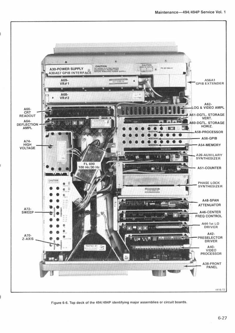
CAUTIONA30-POWER SUPPLYA30A67 GPIS
INTERFACE4
LV7 rp1L
r~N! r
tom+ :
CAUTION
- L---I ,-~
Figure 6-6 . Top deck of the 4941494P identifying major assemblies or circuit boards .
Maintenance--494/49413 Service Vol . 1
FIN 7372553 -^
A62-LOG & VIDEO AMPL
~'A61-DGTL . STORAGEVERT .
A60-I)GTL . STORAGEHORIZ .
--
A58-PROCESSOR
- A56-GPIS
_~ A54-MEMORY
A46-CENTERFREQ CONTROL
4416-72
6-27

Maintenance-494/494P
Service Vol
.
1
Figure
6-7
.
RF deck of the 4941494P identifying major assemblies
.

2 . Ensure that the plug and receptacle are clean and freeof any foreign matter .
3 . Insert the plug connector fully into the receptacle be-fore screwing the nut on . Tighten the connection to 8 inchpounds to ensure that the connection is tight . Do notovertighten (15 to 20 inch pounds) because this can damagethe connector .
Replacing the Crt
Removal
1 . Remove the snap-in printed bezel and crt light filter .
2 . Use an 8164 inch Allen wrench to remove the fourbezel screws, unplug and remove the inner bezel .
3 . Unsolder the ground wire from the front panel castingand unplug the crt cables at their respective board connec-tions (High Voltage module, Deflection Amplifier board, andZ-Axis board) .
4 . Slide the crt, with its shield, out through the frontpanel .
5 . Remove the crt shield as follows :a .
remove the tube base cap and unplug the socket ;
b .
remove the two side screws that hold the uppershield in place, then remove the shield ;
c .
loosen the screws that clamp the plastic bracket
Replacement
REV JUN 1984
around the crt, then remove the bracket .
1 . Install the plastic bracket so the back on the clamp is5 .07 inches from the back of the crt socket guide .
2 . Replace the crt shield plus the socket and base shieldby reversing the removal procedure . The finished crt assem-bly length, with cap installed, must equal 11 .05 inches . If it islonger, the assembly may short circuit the Deflection Ampli-fier circuit board when it is installed .
Maintenance-4941494P Service Vol . 1
3 . Place the 494/494P on its rear panel then loosen thefour crt blue plastic mounting blocks on the (front casting sothey can be readily positioned when the crt is installed .
4 . Install the crt, with shield assembly, through the frontpanel ; seat the wedges on the side of the crt, into the blueplastic mounting blocks .
5 . Postion the cast bezel and implosion shield in place toensure that there is clearance between the crt face and thebezel . (The bezel must bottom on the front casting .)
It is very important that the four mounting blocks areloose enough so the bezel retaining screws can betightened without the bezel touching the crt face . Itnot the crt or the bezel may crack when the screwsare tightened.
6 . Remove the bezel and tighten the mounting blockscrews evenly in a cross pattern to approximately 8 inchpounds . Make sure the crt stays centered in the blue plasticmounting blocks as the screws are tightened .
7 . Replace the bezel and implosion shield, reconnect ca-bles to their respective board connectors, and resolder theground lead to its terminal .
8 . Replace crt light filter and snap-in printed bezel .
Repairing the Crt Trace Rotation Coil
The trace rotation coil is part of the crt assembly . If thecoil is damaged beyond repair, the crt with the coil must bereplaced .
6-29

Maintenance-494/494P Service Vol . 1
If the "finish" (red) lead is broken, remove the tape andunwind one or two turns so it can be respliced and solderedto the lead wire . Rewind and retape .
If the "start" (black) lead is broken and the lead is tooshort to re-splice, attempt to fish out the broken end so oneor two turns can be unwound, re-splice and solder to thelead ; then rewind and retape .
Front Panel Assembly
It is not necessary to remove the front panel assembly toreplace any of the pushbuttons . (Refer to Replacing FrontPanel Pushbuttons, that follows this procedure .) The crt isremoved with the front-panel assembly .
Removal
1 . Set the instrument upright on its rear panel, then un-screw and remove the mounting nuts and washers for theRF INPUT, EXT MIXER, and the two 1st and 2nd LO OUT-PUT connectors .
2 . Remove the two screws that hold the front panel tothe RF deck (center and left side) .
3 . Unplug the CAL OUT coaxial cable from the 3rd Con-verter ; then disconnect the five crt cables from theZ-Axis/RF Interface, High Voltage module, and DeflectionAmplifier .
4 . Looking at the top of the instrument, remove the onescrew that holds the front panel to the side extrusion be-tween the crt and the right side of the instrument . Removethe four screws that hold the front panel to the side rails .
5 . Pull the front panel up and off the Mother board .
Replacement
Replace the front panel by reversing the removalprocedure .
$-30
Front Panel Board
NOTE
replacement Front Panel board comes withswitches and controls for the 494P. Before replacingan existing board, remove the switches and controlson the new board that are not used on the 494 versioninstrument.
Removal
1 . Remove the front panel assembly as previously de-scribed, then remove all the knobs.
2 . Place the front panel on its face and remove the elevencircuit board screws plus the screw that heat-sinks andholds IC U6090 on the board . Note that the screw next tothe connector plug has a fiber washer .
3 . To prevent losing the grounding rings or bushings, be-tween the front panel controls and the front panel casting,hold the circuit board against the front panel casting whileturning the complete assembly so it rests on the base of thecrt assembly .
4 . Gently lift the casting from the circuit board . Ensurethat the grounding rings remain on the shaft of all controlsas the casting is removed .
Replacement
Reverse the removal procedure, ensuring that the fiberwasher is on the board screw next to the connector plug .This washer prevents the screw from shorting a circuitboard run to the front panel casting .
3 . Align connectors P5041 and P1034 with their respec-tive Mother board and Interface board connectors, thenpress the module into place between the side rails .
4 . Replace the four module holding screws and the threeflange screws .
REV JUN 1984

Replacing Front Panel Pushbutton Switches
Removal of the front panel assembly is not required toreplace any pushbutton switch . The procedure follows .
1 . Remove the front panel knobs . Loosen and removenuts and washers for the RF INPUT, EXTERNAL MIXER,and the 1 st and 2nd LO connectors .
2 . Remove the screw under the CENTER FREQUENCYtuning knob that holds the panel to the front panel casting .
3 . Loosen the black screws through the crt bezel so thepanel can be moved enough to lift it off the casting .
4 . Unplug and replace the desired switches .
Main Power Supply Module
To avoid damage to the Mother board connectorJ5041 and Interface connector J1034, during removalor installation of the Power Supply module, use thefollowing procedure .
Removal
1 . Disconnect the power cord, set the 494/494P on itsface or front panel and remove the instrument cover .
2 . On the circuit board side of the instrument, unplug thecoaxial cable connector P620 from the Log and Video Am-plifier assembly . On the RF deck side disconnect the plugfor the cable to the Reference Lock assembly, at the lowerright corner of the Power Supply module .
REV JUN 1984
Maintenance-4941494P Service Vol . 1
3 . For 494P instruments, remove the cable clamp for theGPIB interconnect cable and unplug P560 to the GPIB Ex-tender board .
4 . Remove the three screws that hold the power moduleto the RF deck flange (bottom right side), then remove thefour screws that hold the power supply module to the siderails .
5 . With the instrument on its face and the RF deck on thenear side, pull the left side of the power module from itsside-rail (no more than 1 .5 inch) . Now grasp both sides ofthe module and lift to separate the module from the Motherboard .
Because C6111 and C6101 discharge very slowly,hazardous potentials exist within the power supply forseveral minutes after the power switch is turned off. Arelaxation oscillator, formed by 05113, R5111, andDS5112, indicate the presence of voltages in the cir-cuit until the potential across the filter capacitors isbelow 80 V.
6 . Loosen and remove the two screws, that hold themounting bracket for P361 . Lift the cover off the module andunplug P3045 to the Fan Drive board . The power supplyshould now be accessible .
Replacement
1 . Reinstall P361 mounting bracket then plug P3045 ontothe power supply board and replace the cover .
2 . Set the instrument face down with the RF deck on thenear side,then hold the power supply module over the in-strument so the right side is touching the side-rail and theleft side is about 1 .5 inch above its side-rail .
3 . Align connectors P5041 and P1034 with their respec-tive Mother board and Interface board connectors, thenpress the module into place between the side rails .
4 .
Replace the four module holding screws and the threeflange screws .
6-3 1

Maintenance-4941494P Service Vol . 1
5 . Reconnect the coaxial cables and GPIB cable, if ap-propriate, then install the cable clamp .
6 . Replace the instrument cover .
High Voltage Power Supply
Before the High Voltage Power Supply circuit board canbe unplugged and removed, a screw, through the side-railinto a nylon standoff bushing at the bottom corner of theboard, must be removed .
Removing and Replacing the 1st LO (YIGOscillatory A16
1 . Unplug and remove the multipin connectors to the as-sembly . Cut the tie-down that holds the black encased RFcoil to the semi-rigid cable .
2 . Using a 5116 inch open-end wrench, loosen and dis-connect the semi-rigid coaxial cable .
3 . Loosen and remove the four mounting screws thathole the assembly to the RF deck . Remove the 1st LOassembly .
4 . To replace the assembly, reverse the removal proce-dure . Use a tie-down to re-tie the RF coil to the semi-rigidcable to prevent vibration from breaking the coil leads
Replacing the 1st (YIG) Local Oscillator InterfaceBoard
The YIG oscillator assembly includes an interface circuitboard that can be replaced . To replace the board refer toFigure 6-8 and the following procedure . Use a desolderingtool to remove the solder as the leads are unsoldered.
1 . Unsolder and lift one end of C1014 (820 kF capacitor)at the top of the board.
6-3 2
2 . Unsolder and lift one end of VR1010 .
A . Oscillator assembly.
Unsolder circled connections .
Unsollder and lift
B . Interface board showing terminals to unsolder forremoval .
Figure 6-8 . Removing the YIG oscillator interface board .
Fan Assembly
4418-102
3 . Unsolder and lift the + lead of C1016 from the YIGterminal .
4 . Unsolder the eight leads to the YIG and lift the boardoff the assembly .
Removal
1 . Remove the power supply as described in this section .
REV JUN 1984

2 . Remove the six screws that hold the power supplycover in place . Take the coaxial cable out of the plastic re-tainer clip and lift the power supply cover with fan up, soharmonica connector P3045 can be disconnected and thecover removed .
3 . Remove the nuts and lockwashers that hold the fanbrackets from the back side of the power supply housing .The fan will fall free from the brackets .
4 . The resilient mounts at the corners of the fan frameshould be replaced if a new fan is to be installed or fanvibration is generating spurs on the display .
Replacement
1 . Insert four resilient mounts into the corners of the fan,flush with the fan frame .
2 . Install the fan assembly one of the fan brackets to thepower supply housing by attaching its lock washers andnuts to the back of the housing .
NOTE
Fan brackets should be installed as in Figure 6-9.
Figure fi-9 . Fan assembly mounting .
Maintenance-4941494P Service Vol . 1
3 . Insert the posts of the brackets into the holes providedin the resilient mount and install the remaining bracket, withlockwashers and nuts, to the back side of the power supplyhousing .
4 . Reconnect the fan to the Fan Drive board then replacethe cover, with the fan, onto the power supply module .
5 . After installing the six screws that hold the cover inplace, ensure that the fan assembly moves freely . Replacethe coaxial cable in the plastic retaining clip .
6 . Reinstall the Power Supply assembly as directed un-der Power Supply Replacement . Apply power and check fornormal fan operation .
MAINTENANCE ADJUSTMENTS
The following procedures are not part of the regular cali-bration . They are only applicable when these assemblies arereplaced or after major repair .
110 MHz IF Assembly Return Loss Calibration-{Table6-5 lists test equipment required to adjust this assembly.)
1 . Test equipment setup is shown in Figure 6-10 . The IFassembly must be removed to gain access to theadjustments .
2 .
Apply
110 MHz
at
2 V
peak-to-peak
(+ 10 dBm)through 35 dB attenuation to the RF Input of the VSWRbridge . Connect the RF Out of the VSWR bridge, to the RFInput of the spectrum analyzer . (Do not connect the110 MHz IF to the VSWR bridge .)
3 . Set the test spectrum analyzer Center Frequency to110 MHz, Frequency Span/Div to 5 MHz, Resolution Band-width to 3 MHz, Vertical Display to 10 dBIDiv, and Ref Levelto -20 dBm.
4 . Adjust the step attenuator for a full screen (-20 dBm)display .
5 . Connect the 110 MHz IF input to the VSWR bridgeand connect a 50 Q termination to the output of the IF ampli-fier . Now plug the power cable P3045 into the + and -15 Vsource and ground the case of the assembly .

Maintenance-4941494P Service Vol . 1
Figure 6-10 . Test equipment setup for adjusting return loss in the 110 MHz IF assembly .
6 . Adjust C2047 and C1054 (Figure 6-11) simultaneouslyfor minimum signal amplitude on the spectrum analyzer dis-play . Minimum amplitude must be at least 35 dB down fromthe full screen reference of -20 dBm .
7 . Disconnect test equipment setup and replace the110 MHz IF assembly .
6-34
Table 6-5EQUIPMENT REQUIRED FOR RETURN LOSS ADJUSTMENT
2072 MHz 2nd Converter
The 2072 MHz Converter assembly consists of a four-cavity 2072 MHz band-pass filter, mixer, and 110 MHz low-pass filter . Because of the interaction between the 1 st, 2nd,and 3rd converters, and the critical lengths of the intercon-nect RF cables, adjustments to the band-pass filter andmixer is not possible with the assembly in the instrument .
REV JUN 1984
Test Equipment Characteristics Recommended Type
Spectrum Analyzer Frequency range _110 MHz TEKTRONIX 49X-Series or 7L1I3Spectrum Analyzer
Signal Generator Frequency 110 MHz at +10 dBm TEKTRONIX SG 503 for the TM 500-Series
VSWR Bridge Wiltron VSWR Bridge, Model 62BF50
10 dB and 1 dB Step Attenuators 50 12, 0 dB to 40 dB Hewlett-Packard 355C & 355D StepAttenuator
Termination 50 i2 Tektronix Part No . 011-00 49-0 1
Adapter Bnc-to-Sealectro Tektronix Part No. 175-0419-00

Figure 6-11 . 110 MHz IF assembly showing the location of testpoints and adjustments .
The assembly is precalibrated at the factory prior to installa-tion, therefore, we recommend replacing the assembly andreturning the defective one to Tektronix, Inc. The followingprocedure describes adjustments that can be made to thelow-pass filter .
REV JUN 1984
110 MHz Three Cavity Filter
Maintenance-4941494P Service Vol. 1
Alignment of this filter is not required unless the494/494P fails to meet bandwidth specifications . The filtersare adjusted for center frequency and response shape sothe resolution bandwidth is within specifications . The adjust-ment procedure is as follows:
1 . With the CAL OUT signal applied to late RF INPUT,tune the signal to center screen and reduce the RESOLU-TION BANDWIDTH to 1 kHz.
2. Tune the signal to center screen to establish centerfrequency reference ; then increase the RESOLUTIONBANDWIDTH to 1 MHz .
3. Adjust the tuning slugs for best response shape, cen-tered around the reference (Figure 6-12). Ensure bandwidth(6 dB down) is 1 MHz .
4. Check resolution bandwidth accuracy over the rangeof the RESOLUTION BANDWIDTH selector as per instruc-tions in the Performance Check section to ensure that band-width is within specification.
Figure $-12 . 110 MHz filter adjustments.
6-35

Maintenance-4941494P Service Vol . 1
829 MHz Converter Maintenance
Some circuit boards in this assembly contain criticallength printed elements . When damaged, these elementsare usually not repairable ; therefore, the circuit board mustbe replaced . Even though replacement boards areprecalibrated and repair can be accomplished by replacingthe board, we recommend sending the instrument or assem-bly to your Tektronix Service Center for repair andcalibration .
The 829 MHz band-pass filter in the IF section, and the719 MHz LO in the LO section, require adjustment only ifthe board has been damaged or active components (transis-tor or varactor) have been replaced . The following describespreparation for service and replacement procedures . Thefirst two steps describe how to gain access to either the LOor the IF section ; the remaining steps describe adjustmentprocedure for each section .
1 . To gain access to the LO section
a . Switch POWER off ; use a 5/64 Allen wrench toloosen and remove the cover screws .
b . Remove the cover .
c . Refer to step 3 for adjustment procedure .
2 . To gain access to the IF section
a . Switch POWER off ; use a 5116 inch wrench to discon-nect and remove all coaxial connectors to the 829 MHzconverter .
b . Unscrew and remove the six mounting screws, un-plug the input power connector P4050, then remove the829 MHz converter assembly.
c . Turn the assembly over and remove the cover for theIF section .
6- 36
d . To troubleshoot or calibrate the circuits, set the as-sembly at a location so the input power plug P4050 can bereconnected to the Mother board . Be sure to observe plugorientation (pin 1 to pin 1) .
e . Refer to step 4 (within this procedure) for adjustmentprocedure .
3 . 719 MHz Oscillator Range Adjustment
a . Adjustment requires the following test equipment :
A frequency counter with a frequency range to 1 GHz(nine digit readout), sensitivity of 20 mV rms prescale,15 mV rms direct (such as TEKTRONIX DC 508A); a digitalvoltmeter with a 3 .5 digit readout (such as TEKTRONIXDM 502A) ; test leads for the DVM, a 50 S2 coaxial cable withbnc connectors (Tektronix part number 012-0482-00) and asma male-to-bnc female adapter (Tektronix part number015-1018-00) .
b . The 2nd LO range is 714 .5 MHz to 723 .5 MHz (withthe cover off) . 719 MHz is the optimum center frequency .Frequency of the oscillator is controlled by the Tune Voltsfrom the 25 MHz Phase Lock circuit (located at TP1011)which varies from +5 V (low end) to +11 .9 V (high end)with +6 .75 to +7.5V as the limits for operation at719 MHz . Set the digital voltmeter to measure 12 V thenconnect it between TP1011 (Figure 6-13) andl ground .
\, I '' I
i ll.! Stub Part of 1I4 A tuned LineI
441 E79
Figure 6-13 . LO section of the 829 MHz converter showing tealpoints and connectors .
REV JUN 1984

c . Disconnect the 100 MHz reference from the 3rd Con-verter by unplugging P235 (Figure 6-13) . The oscillatorshould go to its upper limit and the voltmeter indicate about11 .9 V .
d . Connect the 75 MHz-1000 MHz input of the fre-quency counter through a 50 4 coaxial cable to the frontpanel 2nd LO OUTPUT connector .
e . The 719 MHz oscillator frequency is a function of thelength of the printed 114 wavelength transmission line . Minoradjustments to the oscillator frequency are made by short-ening the U-shaped transmission line stub, off the main line .Graduation marks (see Figure 6-13) along the side of thestub provide a guide to calculate frequency correction . Eachminor mark from the end or cut across the stub, representsan approximate change of 2 MHz .
Check the frequency by noting the reading on the fre-quency counter . If above 723.900 MHz, the stub must belengthened . Solder a bridge across the cut and recheck fre-quency. Nominal frequency for an uncut stub is 710 MHz.
f . Shorten the line so the frequency is near723 .500 MHz . For example : The frequency difference be-tween the desired and the actual divided by 2 MHz, equalsthe number of minor divisions from the line end for the newcut . Make a cut across the line and check that the newfrequency is between 723.100 and 723 .900 MHz . Repeat asnecessary .
g . Cover the 719 MHz oscillator cavity with the 829 MHzConverter cover, press down to ensure good shielding, andnote the frequency readout of the counter . Frequencyshould fall within 723.600 and 724.400 MHz .
h . Reconnect P234 (100 MHz) and P237 (2182 MHz)and confirm that phase lock is operating by noting that thevoltage on TP1011 is between 6.75 and 7 .5 V . This com-pletes the adjustment of the 719 MHz LO . Replace thecover and reinstall the 829 MHz converter assembly .
4 . 829 MHz Coaxial Band-pass Filter Adjustment
NOTE
This procedure is necessary if the position of one ofthe variable capacitor loops (tabs) has been altered,changing the bandpass characteristics of the filter.
a . Test equipment required :
Maintenance-4941494F) Service Vol . 1
Spectrum analyzer with tracking generator (such as 49X-Series Spectrum Analyzer with TR 503 Tracking Generator ;or 71_13 with a TR 502 Tracking Generator)-, FrequencyCounter (such as TEKTRONIX DC 508) ; Return LossBridge (such as Wiltron Model 62BF50) .
b . Unsolder and reconnect the jumper, on the 829 MHzAmplifier board, to the test Peltola jack )102'9 (see Figure 6-14) .
929 MHz Converter
UH[4416-80
Figure 6-14 . Location of test jack and jumper on the 829 MHzamplifier board.
c . Connect the spectrum analyzer, tracking generator,and frequency counter together as a system, with the fre-quency counter connected to the Auxiliary RF Output of thetracking generator (see Figure 6-15) .
d . Connect the spectrum analyzerltracking generatorsystem through the return loss bridge to the Peltola jack()1029) on the 829 MHz amplifier board (see Figure 6-15) .Reconnect P235 (100 MHz reference signal) and P237(2182 MHz input) to the LO section of the converter .
Terminate the 110 MHz Output ()232) connector with50 s2, using a bnc-to Sealectro adapter and 20 dB bnc atten-uator . Pull the IF SELECT line high by switching to band 2(1 .7-5 .5 GHz) .

Maintenance-494/494P Service Vol . 1
e . Set the test spectrum analyzer Reference Level to-20 dBm, Vertical Display mode to 2 dBldiv, ResolutionBandwidth to 300 kHz, and Freq Span/Div to 20 MHz. Tunethe Center Frequency for a readout of 829.00 MHz on thefrequency counter .
f . Adjust the 114 wavelength lines in the filter in se-quence, starting with the resonator at the 829 1 MHz input(see Figure 6-16) . Adjustment is made by shorting the adja-cent resonator to ground with a low inductance conductor,such as a broad blade screwdriver, then bend the loop ortab of the respective stub with a non-metallic tuning tool tochange the series capacitance of the resonator .
Figure fi-15 . Test equipment setup for aligning the 829 MHz filter.
g . With the adjacent resonator (seconl) shorted toground, adjust the series capacitance by bending the tab sothe response on the spectrum analyzer display is centeredat 829 MHz (see Figure 6-17Ay.
h . Now move the shorting strap (screwdriver) to the nextresonator and adjust the tab of the second resonator for aresponse as indicated in Figure 6-17B .
i . Remove the short from the third resonator and shortthe fourth resonator. Adjust the third resonator for a re-sponse similar to that shown in Figure 6-18A .

SHORT TO ADJUST STAGE :
3. Slep ,,-~ 2, S[ep--n 1 . 5[ep7:~ -. -
4416-a1
Figure 6-16 . Filter tune tabs in the 829 MHz converter.
j . Repeat the procedure for the final (fourth) resonatorfor a response similar to that shown in Figure 6-18B .
k . Check that the return loss is equal to or greater than12 dB.
l . Disconnect the return loss Device Under Test lead tothe Peltola jack ,11029 on the 829 MHz Amplifier board, thenunsolder and reconnect the jumper to the amplifier output .
m . Replace the 829 MHz Converter cover and reinstallthe assembly in the 4941494P .
Troubleshooting and Calibrating the 2182 MHzPhase Locked 2nd LO
The assembly contains a microstrip phase locked2182 MHz oscillator and its phase locking circuits . The14-22 MHz Phase Lock board is contained in the mu metalhousing ; the 2182 MHz Oscillator, 2200 MHz Reference,and 2200 MHz Reference Mixer are contained in the ma-chined aluminum housing .
Maintenance-4941494P Service Vol . 1
NOON0 EEMENE
2d0/
2d0/
if
A . 1st Resonator Response
0MENMENINEEN
B. 2nd Resonator Response
ON-T
2727-159
Figure 6-17 . Typical response when the first and second reso-nators of the 829 MHz filter are adjusted correctly.
The 2182 MHz Microstrip Oscillator and the 2200 MHzReference Mixer contain critical length printed elements.These elements are difficult to repair ; therefore, the boardshould be replaced if damaged . If either the varactor diodeor the oscillator transistor for the 2182 MHz Oscillator isreplaced and the oscillator frequency is beyond adjustmentwith the frequency adjust tab, described in this procedure,the circuit board must be replaced .
Even though replacement boards are precalibrated at thefactory and repair can be accomplished by replacing theboard, we recommend sending the instrument or assemblyto your Tektronix Service Center for repair to insure bestperformance .

Maintenance-4941494P Service Vol . 1
A. 3rd Resonator
S. 4th Resonator and Filter
2727-160
Figure 6-18 . Typical response when the third and fourth reso-
nators are tuned correctly.
Table 6-6EQUIPMENT REQUIRED FOR 2nd LO CALIBRATION
The 2182 MHz Phase Locked 2nd LO should only requirecalibration when a component within the assembly has beenreplaced . This procedure is in two parts, the l_O section andthe Phase Lock section . Equipment required to calibrateboth the LO section is listed in Table 6-6 and equipment forthe Phase Lock section in Table 6-7 .
1 . Preparation
a . Test equipment setup is shown in Figure 6-19 . Turnthe POWER off . Place the 494/494P Spectrum Analyzer up-side down so the RF deck is exposed . Use a 5116 inchwrench to loosen and remove the two semi-rigid cable con-nections to the assembly . Remove the flexible coaxial cableconnection to the 100 MHz input .
b . Remove the 14 screws that hold the cover on the mu-metal section and remove the cover . Unsolder the leads tofeedthrough capacitors C2203 and C2204 . (These are thecenter two feedthroughs that feed through the circuit board,as shown in Figure 6-23 .)
c . Replace the cover using two or three screws to holdthe cover in place . Remove the 2nd LO assembly mountingscrews and carefully remove the 2nd LO assembly so thepower input connections remain intact . Turn the assemblyover so the machined aluminum housing is up and place theassembly on a flat surface . Use a 5164 Allen wrench to re-move the screws holding the lid on the machined aluminumhousing . Place the screws in a safe place ; then remove thelid for the aluminum housing, exposing the three RF circuitboards within the oscillator section .
d . Install a 50 St terminator on the 2182' MHz bufferedoutput port, P222, (see Figure 6-20) . Set the variable powersupply to 0 V . Connect the plus (+) terminal to the 2nd LOhousing and the negative (-) terminal to the exposed end ofC2203 and L2031, through a 1 kQ resistor .
Test Equipment Characteristics Recommended Type
Spectrum Analyzer Frequency range to 2.2 GHz TEKTRONIX 49X-Series
Signal Generator Calibrated 100 MHz, with x-20 kHz Hewlett-Packard Mode 86,40 AIBaccuracy and an amplitude that is settableto 0 dBm.
Digital Voltmeter Measures to within 0.01 V, impedance TEKTRONIX TM 500-Series DM 501 A,1 MU. DM 502A, or DM 5010
Variable Power Supply 0 to 12.5 V, accurate to 0.1 V TEKTRONIX TM 500-Series, such asPS 501 or PS 5010
Terminations (2) 50 Q, 3mm connectors Tektronix Part No . 011-0049-01

DigitalVoltmeter
0 to - 12 .5 VPower Supply
To 2182 MHz Tune Line
494/494P Spectrum Analyzer (inverted)
Figure 6-19 . Test equipment setup for calibrating the oscillator section of the 2182 MHz Phase Locked 2nd LO .
e . Apply a 100 MHz, 0 dBm signal from the signal gen-erator to the 100 MHz Reference input port, P221 . (Fre-quency must be within 20 kHz of 100 MHz.)
f. Connect a test spectrum analyzer to the 2182 MHzunbuffered output port, P220 . Set the test analyzer CenterFrequency to 2182 MHz, Freq Spanldiv to 20 MHz, VerticalDisplay to 10 dBIDiv, and the Reference Level to +10 dBm .Do not position any of the cables over the 2nd LO assemblyoscillator section because they can affect the frequency ofthe oscillator .
2182 MHz from Unbuffered Output Port
100 MHz ReferenceInputfi
Maintenance-4941494P Service Vol . 1
4416-a :
g . Bend the feedback and frequency adjusting tabs,C1021 and C1022 (see Figure 6-20), with your finger so theyare approximately 30° above the board surface .
2 . Adjust and Check Oscillator Frequency (Refer toFigure 6-20)
a . Switch the Power to both the 494/494P and the vari-able power supply on . Adjust the voltage output from thevariable power supply to 5 .0 V . Voltage on C2203 shouldnow equal -5 V and a signal should appear on the testspectrum analyzer .

Maintenance-4941494P Service Vol. 1
P2222182 MHz Buffered Output Port
6-42
-12 V +12 VSupplies
A = Center frequency tuning stubB = Base-emitter voltage testpoint TP1015C = Feedback adjustment tab C1021D = Center frequency adjustment tab 01022
3. Measure Output Power
NOTE
P220
P22121132 MHz Unbuffered Output Port
100 MHz Reference Input -0 dBm
2200 MHz Reference Mixer
2200 MHz Reference
2182 MHz Tune Input
Difference Frequency
b . Check for a collector voltage across C2023 of + 10.0,0 .7 V.
C . Check Vb, at TP1015 (B in Figure 6-20) . If V,, isgreater than +0 .5V, push the feedback adjustment tabdown slightly and if less than -0.3 V, lift the tab. If V,, isgreater than +0.8 V, replace the microstrip oscillator board.If Vbe is more negative than -1 V, check the bias circuitry.Adjust the tab so Vbe is +0.15 V, ±0.05 V at TP1015, Donot touch the feedback tab while measuring voltages .
d . Check for an oscillator frequency of 2182 MHz,±5 MHz . Bend the frequency adjustment tab C1022 (D inFigure 6-20) to bring the oscillator within tolerance. (Bendthe tab up to increase frequency and down to lower fre-quency .) If unable to bring the oscillator frequency withinrange, replace the 2182 MHz microstrip oscillator board.
Before making power measurements, ensure that theunused port is terminated into 50Il. Unterminatedports will degrade both frequency and powermeasurements .
a . Check
for
0 dBm
±3 dB
output
power
at
theunbuffered port, P220 .
5. Check the Tune Range
Figure 6-20. Adjustments and test point locations within the 829 MHz Converter oscillator section.
4. Check the 2200 MHz Reference Mixer
4416-137
b. Connect the test spectrum analyzer to P222, termi-nate P220, then check for an output level of +10 dBm±3 dB from the buffered port .
a. Use a probe, consisting of a short length of semi-rigidcoaxial cable with a do block (see Figure 6-21), to connectthe output of the reference mixer at C2204 to the input ofthe test spectrum analyzer . Ground the outer shield of thecoaxial cable against the 2nd LO housing .
b. Confirm that the output signal frequency is 18 MHz+ 1 MHz. Adjust the tab C1022 (Figure 6-20) for the2182 MHz Microstrip Oscillator, to bring the 18 MHz withinthe 1 MHz tolerance .
c. Confirm that the output level of the 18 MHz signal isapproximately -36 dBm . If the level is below -46 dBm,check the signal levels from the 2200 MHz Reference Mixerand the 2182 MHz Microstrip Oscillator (-28 dBm, ±8 dBfrom the 2200 MHz Reference Mixer and +8 dBm, ±3 dBfrom the oscillator) .
a. Adjust the variable supply to vary the voltage to the2182 MHz tune line from 0 to -12.5 V and note the fre-quency change at C2204 (output of the 2200 MHz Refer-ence Mixer) .

b . Frequency change or tune range should equal 20 to35 MHz for a voltage change of 0 to -12.5 V on the tuneline .
6 . Reassembly
a. Disconnect and remove the connections from the vari-able power supply and the test spectrum analyzer .
b . Replace the lid for the oscillator housing and installthe 26 screws . Install the screws loosely, then tighten themstarting from the center of the lid and progress along theedges toward the corners to insure that no gaps exist be-tween the lid and the housing . Any gaps will allow RF leak-age that can produce spurious responses .
c . Reinstall the assembly on the RF deck . Remove the50 9 terminations and reconnect the cables . Use a 5116 inch
CABLE ASSEMBLY#012-0208-00
(SEMI-RIGID COAXIAL)
Figure 6-21 . Construction details of a coaxial test probe for the 2182 MHz Phase Locked 2nd LO.
Maintenance-4941494P Service Vol . 1
ADAPTER
#24931 29JP 124-1
3793-37
open-end wrench to tighten the semi-rigid coaxial connec-tors to 8 to 10 inch-pounds .
d . Remove the mu-metal lid and reconnect the leads tofeedthrough capacitors C2203 and C2204, on the PhaseLock board (Figure 6-23) . Replace the lid and install the 14screws . Tighten the screws from the center toward the cor-ners of the lid to prevent gaps between the Ed and the hous-ing . Do not overtighten because the screws are easilystripped .
Troubleshooting and Calibrating the 116-20 MHzPhase Lock Section
This side of the assembly contains the 16-20 MHzPhase Lock circuit board (see Figure 6-23) . Replacing oscil-lator components in this section may alter sweep linearityand frequency of the 16--,20 MHz oscillator . The followingchecks and calibration should aid in repairing and returningthe assembly to satisfactory operation .

Maintenance-4941494P Service Vol. 1
CENTER FREQUENCYCONTROL BOARDON EXTENDER
494/494P SPECTRUM ANALYZER
DIGITAL TIMEVOLT DIGITAL MARKMETER COUNTER GENERATOR
Figure 6-22 . Test equipment setup for calibrating the Phase Lock section of the 2'182 MHz 2nd LO .
Table 6-7EQUIPMENT REQUIRED FOR CALIBRATING THE
16-20 MHz PHASE LOCK CIRCUIT
Test Equipment Characteristics Recommended Type
Digital Voltmeter Floating input, measures to within TEKTRONIX TM 500-Series DM 501 A,0.01 V DM 502A, or DM 5010
de
Frequency Counter Frequency to 80 MHz TEKTRONIX TM 500-Series DC 503A,DC 508A, DC 509, DC 5009, or DC 50 1 0
Time-Mark Generator Marker output, 1 s to 1 us ; accuracy TEKTRONIX TG 5010 .001
Service Kit Extender board Tektronix Part No . 672-0865-00

1 . Preliminary
a. Test equipment setup is shown in Figure 6-22 . Re-move and install the Center Frequency Control board on anextender board .
b. Switch POWER on and set the FREQ SPAN/DIV to1 MHz .
2. Check Voltages
a . Check all input voltages at the feedthrough capacitorsin the housing wall . Refer to Figure 6-23 or the data printedon the lid . Voltage at the sweep and tune input lines shouldequal 0 V ±0.05 V with the FREQ SPAN/DIV _500 kHz .
b. Switch the POWER off. Remove the lid from the mu-metal housing assembly to gain access to internal circuitry.
c. Switch POWER on, then check the internal regulatedvoltages ; +12V -0.4V at C2201, -12V _+0.4V atC2202, and +5.2 V ±0 .25 Vat TP10109 (see Figure 6-23).Check the output of the shaper at TP1083 for 0 .0 V ± 0 .3 V .
3 . Setting Center Frequency
a. Connect a frequency counter to TP2035 and note thefrequency. If the frequency is 18 ± 0.050 MHz no correction
Maintenance-494/494P Service Vol. 1
Figure 6-23 . Test points and component location pertaining to calibrating the 16-20 MHz Phase Lock circuit for the 2 , 182 MHz 2nd LO.
is necessary ; proceed to part 4 (Setting Tune Sensitivityand Range) . If outside the range proceed as follows:
1) Turn POWER oft . Unsolder and remove one end ofShaper Offset resistor R1070. Unsolder the wire strapbetween T2092 and T1091, at the T109'I end, and lift itfree .
2) Solder a flexible wire jumper to the T2092 end;then, by means of a a plastic tuning tool, attach the freeend to one of the three pads for T1091 and note thefrequency readout of the counter.
[CA urroHsN~r~
If this flexible wire touches ground while the circuit isoperating, the supply regulators can be damaged. Theregulators are not protected against a short ciruit.
3) If one of the pads provides a frequency that iswithin the range of 17 .5 ±0.25 MHz, solder the wirestrap to this pad. If the frequency is still outside therange, move the jumper to the other pad for T2092 andrepeat the procedure. Frequency must equal 17 .5±0.25 MHz .
b . Turn POWER OFF . Substitute a 10 turn 25 M2 poten-tiometer in series with a 5 k12 resistor in place of R1070.

Maintenance-4941494P Service Vol . 1
c . Turn POWER on and with the counter connected toTP2035, adjust the poteniometer for a frequency readout of18 MHz ± 50 kHz .
d . Switch POWER off, measure the total resistancevalue and replace R1070 with a 1 % resistor of this mea-sured value . Switch POWER on and recheck the frequencyto ensure that it is 18 MHz ±50 kHz . Disconnect thecounter from TP2035.
4. Setting Tune Sensitivity and Range
a . Center the Fine Tune adjustment 84040, on the Cen-ter Frequency Control board and the 2nd LO Sweep adjust-ment 81067, on the Span Attenuator board (Figure 6-24) .
b . Decrease the FREQ SPANIDIV from above 200 kHzto 200 kHz or less . The 2nd LO is now in the center of itstune range .
c . Press <SHIFT> INT to disable frequency correction ;then press <SHiFT> READOUT and select frequency dis-play of 2nd LO (2) from the menu . Readout will now indicatethe 2nd LO frequency .
d . Tune the 2nd LO to one end of its range where thefrequency readout no longer changes . Note the frequencyand measure the voltage on the Tune Line at the input feed-through capacitor (Figure 6-23) .
e . Tune the 2nd LO to the other end of its range andagain note the frequency and the new voltage reading .
f . Calculate the frequency change per volt (frequencyrange versus voltage range) . Frequency change per voltshould equal 1280 kHz -- 5% or range between 1216 kHzand 1344 kHz .
g . If the frequency/volt change is low, decrease the valueof select resistor R2072 and increase the value of R2070(Figure 6-23) . Keep the ratio of 82072 and R2070 the same.If the frequency/volt change is high, increase R2072 anddecrease 82070.
h . Press <SHIFT> PULSE STRETCHER and select2nd LO for calibration . Perform the procedure that is calledout to adjust the Fine Tune Range R4040 and Fine TuneSensitivity R3040 to calibrate the 2nd LO tuning range .
5 . Setting Sweep Range
a . Apply 5,us time markers from the Time Mark Genera-tor to the RF INPUT . Set the FREQ SPANIDIV to 500 kHzthen back to 200 kHz to center the 2nd LO frequency .
b . Adjust the REF LEVEL to display the 200 kHz mark-ers then center one of the markers with the CENTER FRE-QUENCY control .
c . Adjust the 2nd LO Sweep 81067, on the Span Atten-uator board (Figure 6-24), so the comb lines on oppositesides of the screen, are exactly 8 major divisions apart .
6 . Check and Adjust Tune Linearity
a . With Frequency Corrections disabled (see part 4c),apply 5 ps markers from a Time Mark Generator to the RFINPUT . Set the FREQUENCY to 20 MHz, FREQ SPANIDIVto 200 kHz and activate AUTO RESOLN. Adjust the REFLEVEL so a comb of 200 kHz markers is displayed .
b . Turn the CENTER FREQUENCY control counter-clockwise until the center frequency stops tuning, decreaseFREQ SPANIDIV to 50 kHz then tune the CENTER FRE-QUENCY up until a marker signal is one major division fromthe left edge of the graticule . A comb line (or marker signal)should appear on or near the first major division in from theright side of the screen .
c . If the right marker is not exactly 8 divisions from theleft marker, note the error to the nearest 0.5 minor division .
d . Turn the CENTER FREQUENCY control clockwise, toincrease center frequency, until the next marker signal isone division in from the left edge and again note the spacingbetween this marker and the marker near the right edge.
e. Continue this process of tuning up in frequency untilthe center frequency stops tuning, noting the signal spacingat each check point .
f . If the peak-to-peak error is 2.5 minor divisions(25 kHz) or less, the linearity over the center 2 MHz ofsweep is satisfactory ; if more, the shaper needs adjustmentor repair .
g . Switch the FREQ SPANIDIV to 200 kHz, tune to thelow end of the sweep range and note the linearity over thecenter eight divisions of span, then tune to the high end ofthe 2nd LO range and again note the linearity . Peak-to-peakdeviation should not exceed 0.5 minor division .

Figure 6-24. Location of R4040 on the CF Control board.
Maintenance-494/494F' Service Vol. 1
A. Location of R4040, Fine tune Range .
B. Location of R1067, 2nd LO Sweep.
s ~f~ s s ~ s s s s s s ~ s ~ s s s ~ s s ~

Maintenance-494/494P Service Vol . 1
h . If the shaper needs adjustment or repair proceed asfollows :
1) A shaper diode or resistor may be defective if thecomb line spacing is consistent for part of the tuningrange and 30 kHz or more off for the other parts of thesweep . To test the diodes for forward conduction, tuneto the low end of the range and short R2049 (Figure 6-23) . The output of U1073A (pin 1) should equal about+3 V. 01059 diodes B through G and U2059 diodes Athrough F should all have a 0.48 V forward drop . Use afloating or digital voltmeter to check the drop .
2) Switch POWER off then temporarily replaceShaper resistor R2049 with a 20 kQ potentiometer.Switch POWER on, and adjust the poteniometer to ob-tain the best overall linearity ; decreasing resistance willdecrease the spacing between comb lines in the upperportion of the tune range and spread the spacing for thelower portion . Increasing the resistance of R2049 will re-verse the effect . When the correct setting is found, turnPOWER off, measure the resistance, and replace with afixed resistor of the same or near the same value .
7 . Conclusion
a . Replace the housing lid with its 14 screws .
b. Tighten the screws sequentially, starting from thecenter of the lid and progressing toward the corners to pre-vent gaps between the lid and the housing . Use care to notstrip the screws as you tighten them .
c . This completes the 2182 MHz Phase Locked 2nd LOcalibration . Refer to "Frequency Control System Calibra-tion" in the Adjustment section for recalibrating the system.
Troubleshooting Aids for the 2182 MHz PhaseLocked 2nd LO Assembly
NOTE
If the Phase Locked assembly is in the instrument, setthe FREQ SPAN/DIV to 500kHz or more so the 2ndLO is not swept.
The difference frequency from the 2200 MHz ReferenceMixer is amplified and fed to output port P224 . Nominallythe signal at the 18 MHz port is 18 MHz with an output levelof approximately -5 dBm into 50 St . This port is convenientfor monitoring the operation of the 16 to 20 MHz voltagecontrolled oscillator . When phase lock is operating, the dif-ference frequency exactly equals the frequency of the VCO.If loop lock is not functioning properly, the difference fre-quency signal will either disappear completely or tune to its
range limit of approximately 6 MHz or 30 MHz . Note thatwhen the loop is unlocked, RF leakage from the 16-20 MHzoscillator buffer can be seen at P224 with a level of approxi-mately -35 dBm. The amplified difference frequency can bemonitored at TP2035 .
Another check of phase lock operation can be done bymeasuring the do voltage on the 2182 MHz Tune Line atfeedthrough capacitor C2203 . Nominally this, voltage is ap-proximately -5 V when phase locked . Use a FREQ SPAN/DIV of 500 kHz or greater before measuring . If there is nodifference frequency, the voltage will be about 0 V . A volt-age of -13 V may indicate loss of signal from the VCO.
Narrow-band noise on the 2nd LO signal may be due tonoise modulation of the 16-20 MHz VCO. Monitor the sig-nal at the 18 MHz port to see if the oscillator signal is noisy .Noise on this line is often caused by noise on the ± 12 Vlines . Use a differential oscilloscope with 1 Hz to 300 Hzbandwidth limits to check supply noise . Measure the ac dif-ferential between the supply and the 2nd LO housing . Lessthan 5 uV peak-to-peak of noise will cause noticeable per-formance degradation . Output noise from the shaper is typi-cally less than 5 yV peak-to-peak .
When making power measurements of microwave cir-cuitry, at circuit board interfaces, use a coaxial probe withvery little stray inductance ( see Figure 6-21) . Ground theouter conductor of the probe to the circuit housing as closeas possible to the measurement port . Disconnect otherloads from the measurement point .
110 MHz Oscillator in the 3rd Converter
A variable capacitor, C1038, inside the cover (Figure6-25), should only need adjusting after replacing a compo-nent or components in the 100 MHz oscillator circuit .
1 . With the cover removed, connect a DVM betweenTP3042 and TP1011 (ground) and adjust C1038, with anon-metallic tunning tool, for a reading of +5V. (in the494/494P, J2042 does not have a plug on it .)
2 . The Cal Amplitude adjustment, R1041, is described inthe Adjustment procedure section .
Reference Lock Module
If a Frequency Reference Lock failure error message isdisplayed, and through troubleshooting procedure it nar-rows to this module, apply a 1 MHz reference signal to theback panel EXT REF INput connector or to P2025 on theReference Lock module . If the system now locks, the timing

circuit for the Frequency Synchronizer U2046A, needs ad-justing . The procedure is as follows .
1 . Switch POWER off, then use a 1/4 inch nut driver toremove the two nuts for the assembly mounting studs .Carefully lift the assembly up and back so the cover can beremoved . Be careful to not unplug P2025 from the Motherboard connector . (If this connector is unplugged, it may benecessary to free the Frequency Standard assembly andmove it forward so the connector P2025 can be reinstalled .)
2 . Remove the cover and reconnect any cables that hadto be removed in order to gain access to the circuit board .Switch POWER on.
3 . Connect Channel 1 of a dual channel test oscilloscopeto TP1044 and Channel 2 to TP2046 (Figure 6-26) . Set thedeflection sensitivity to 2 Vldiv, Time/Div to 20 ns, and trig-ger the display on Channel 1 signal .
4 . Adjust R2042 so the falling edge of the signal atTP1044, lags the falling edge of the signal at TP2046 by
Figure 6-25 . Test points and adjustments in the 3rd Converter.
Maintenance-4941494F' Service Vol. 1
4416-87
Figure 6-26 . Test points and adjustments insider the ReferenceLock module .
65 ns (Figure 6-27) . This is to prevent U2046A frompretriggering when the input signal is some multiple of1 MHz .
5 . Check the operation to ensure the error message nolonger exists and the instrument operation is normal . Re-install the cover and the assembly and again verify that theinstrument operates satisfactory .

Maintenance-4941494P Service Vol . 1
INTRODUCTION
Several maintenance aids are built into the 494P micro-computer system. These are microcomputer operating testmodes that demonstrate correct performance or indicatethe location of a problem, if any .
The switch bank that sets up two of these test modes isdescribed first . This is followed by instructions for the threetest modes .
In the first test mode, the microcomputer executes a self-test that verifies, as much as possible, correct operation .RAM, ROM, and interface adapters are checked . Any failurefound is indicated .
The second test mode hardwires the microcprocessor toexecute an instruction that toggles the address bus . Thismode requires less of the system to run, so it may be usedto troubleshoot problems that disable the first test mode.
The third test mode addresses communication betweenthe miocrocomputer and the rest of the instrument . Themicrocomputer exercises the instrument bus to help isolateproblems that, although they do not show up in the first testmode, they prevent normal instrument operation because ofa breakdown in communication .
This maintenance procedure concludes with some noteson operation of several versions of instrument firmware .
SWEEP SPEED 4.2 ps(20 ns/Div)
4416-88
Figure 6-27 . Typical display showing the delay through U2046Aon the Reference Lock.
494P MICROCOMPUTER SYSTEM MAINTENANCE
INSTRUMENT TEST MODES
Memory Board Option Switch
51038 on the Memory board informs the microcomputerat power up whether to configure itself to exercise testmodes or to enable instrument modifications . Figure 6-28shows the correct setting of the individual switches in the51038 switch bank for normal operation .
The microcomputer reads these switches only at power-up . For a change in a switch position to take effect, theswitch must be changed before the instrument is poweredup .
Power-Up Self-Test Mode
The microcomputer automatically enters a self-test modewhen power is switched on . S1038 chooses between twomethods . Most of the power-up self-test is performed withswitch 7 open ; the first method . If any parts of the test fail,the results are displayed on the crt . With switch 7 open, theinstrument continues operating as normally as possible afterthe self-test is completed .
With switch 7 closed, the instrument will riot operate nor-mally . The microcomputer performs the following steps inthe order given . If a problem is found, the test is stoppedand the source of the problem is indicated by a blinking LI=Don the Processor board. If no problem is found, this self-testtakes two minutes to complete .

00 = NORMAL OPERATION01 -- POWER-UP SELF TEST10 = NOT DEFINED11 -- INSTRUMENT BUS CHECK
OFF (open) =
ON (closed) =
Addresses are specified as hexadecimal numbers in thisdescription .
1 . At power-up, the microcomputer vectors to the self-test in the ROM at the top of address space U1014 on theMemory board . The microcomputer first verifies the checksum of U1014 . If the correct check sum for the ROM IS notobtained when the test is run, the routine halts and blinksthe ROM 9 LED, DS1049.
This step uses only U1014 and no other memory, andworks the same in both self-test modes. If the test does notblink the LED and does not proceed, U1014 is probably atfault . Consider first, however, that the correct ROM must beinstalled, both phases of the clock on the Processor boardmust be present, the clock on the Processor board must bepresent, and the microcomputer system (exclusive of theinstrument bus or GPIB) must be operating correctly . If indoubt about the 6802 microprocessor, its bus, or the micro-computer bus, skip to the instructions under MicrocomputerTest Mode later in this section to exercise the micro-computer in a more simple manner .
OPEN (1) CAUSES INSTRUMENT TO REPORT SETTINGS (NO WAVEFORMS) IN TALK ONLY MODE .
CLOSED (0) CAUSES INSTRUMENT TO REPORT BOTH SETTINGS AND WAVEFORMS IN TALK ONLY MODE .
OPEN (1) ENABLES POWER-ON SROCLOSED (0) DISABLES POWER-ON SRO
OPEN (1) FOR DIAGNOSTIC FUNCTIONSCLOSED (0) DISABLES DIAGNOSTIC FUNCTIONS
OPEN (1) FOR OPTION 41
Figure 6-28 . Option switch bank S1038 on the Memory board.
Maintenance-4941494P Service Vol. 1
OPEN (1) DISABLES EXTERNAL MIXERS (OPTION 08)CLOSED (0) FOR EXTERNAL MIXER CAPABILITY
4416-89
2 . The microcomputer next checks part of the instrumentbus PIA, U2010, on the Processor board . The micro-computer first writes to the A control register and thenreads back from the register . Next, it repeats these opera-tions with the A data direction register. If either of theseattempts fail, the routine stops and lights the bus LED,DS 1046. This step works the same in bath self-test modes.Following this step the message "PROCESSOR SYSTEMTEST, PLEASE WAIT" appears on the crt .
3 . The microcomputer now checks the condition of RAM .This test contains three parts, the first part performs a quicktest of all RAM addresses in volatile RAM (RAMs 1, 2, 3,and 4) . This step does not rely on the RAM being good toexecute . The microcomputer loads the bit pattern 01010101into a RAM location, reads the location, and compares whatis returned to what was stored . The microcomputer thenrepeats this test with the pattern 10101010 .
If switch 7 is closed and an error is found on the Memoryboard, the microcomputer notes the failed RAM identifica-tion and sends the information to the crt to be displayed . If

Maintenance-4941494P Service Vol . 1
switch 7 is open, it stops the test and pulses the RAM LED,DS1048, a number of times corresponding to the number ofthe RAM that failed the test (refer to Table 6-8) .
Table 6-8RAM TEST
The second part of the test is a one-minute test of allRAM (volatile and non-volatile - RAMS 1-7) . The test (TheMoving Inversions Test) consists of a dynamic test of alladdress and data functions . This test application dependson the top few bytes of RAM 7 being good . The test isperformed with switch 7 open and pulses the LEDs .
Finally, another one-minute test similar to the one per-formed in the first part is done, with switch 7 open . In thistest the memory contents are allowed to "soak" for thirtyseconds before being read back and compared to whatshould be there .
4 . The microcomputer proceeds to check sum all theROMs. A check sum is stored in the header of each ROM .This is compared to a check sum formed by the successive16-bit spiral sum of each byte in the ROM, starting at thethird location in the ROM . The identification in the seventhbyte of each ROM indicates where in the system the ROM isexpected to be installed . A check is made to be sure that theROMs are installed in the proper locations . If a ROM is in-stalled in the wrong socket, a ROM error will result .
This step starts by looking at the part number suffix andits complement, which are stored in the fifth and sixth bytes,respectively . If these two bytes are not true complements, itis assumed that no ROM is installed at this location .
If switch 7 is closed and a bad ROM is found because ofeither a bad check sum or a placement error, a message isprinted on the crt . Missing ROMs are not reported . If switch7 is open, the test halts and the bad ROM is identified bypulsing ROM LED DS1047, N+ 1 times, where N is the iden-tification number of the ROM in error (e.g ., a bad ROM #3
will cause four pulses ; refer to Table 6-9) . Missing ROMsare reported by pulsing the OK LED described in part 6 .
Table 6-9ROM TEST
(GPIB Board Version 670-8431-00)
vROM #4 was U2013 on GPIB board version 670-7896-00 .bROM #5 was U2018 on GPIB board version 670-7896-00.FROM #6 was U2022 on GPIB board version 670-7896-00 .dROM #7 was not installed on GPIB board version 670-7896-00 .
5 . The microcomputer next tests timer IC, U1016 on theProcessor board. U1016 is initialized so that timer 1 will timedelays, with 1 ms accuracy, and timer 3 will time delays with8 ms accuracy . Timer 1 is then set for a 1701 ms delay, andthe microcomputer software delay is 169 ms. The micro-computer than checks to see if timer 1 has timed out yet . Iftimer 1 has not timed out, the microcomputer waits 2 msand checks it again . Timer 1 should now be. timed out . Anearly or late interrupt from the timer returns an error . Timer3 is tested similarly with a 680 ms delay, checked at 672 msand 688 ms.
If switch 7 is closed and there is a failure, a failed timertest is reported on the crt . If switch 7 is open and there is afailure, the test halts and timer LED DS1044 is lit .
This step is executed only if switch 7 is open . The micro-computer resets the GPIA, U2036, on the GPIB board andchecks to see that the GPIA is not addressed to talk orlisten . The GPIA is set to the listen-only mode and checkedto see that it is addressed to listen . The GPIA is then set tothe talk-only mode and checked to see that it is addressedto talk . If any part of this step fails, the test stops and GPIBLED DS1045 is lit .
If switch 7 is closed, the remainder of the power-up se-quence is executed when the testing is completed . This puts
ROMIdentification
ROMSocket
DS1047Board Pulses
0 U2015 A54 Memory 11 111012 A56 GPI6 22 U1018 A56 GPIB 33 U1022 A56 GPIB 44 U1024a A56 GPIB 55 U2013a A56 GPIB 66 U2018c A56 GP113 77 U2022a A56 GPIB 88 U1021 A54 Memory 99 U1014 A54 Memory 10
RAMIdentification
RAMSocket
DS1048Pulses
1 U1026 12 U1031 23 U2026 34 U2021 45 U2044 56 U2037 67 U2032 7

the instrument into the normal operating condition . Whenswitch 7 is open and the test completes successfully, thelast thing the microcomputer does is light OK LED DS1043to indicate that the processor check is successfully com-plete, with no errors detected . The LED is lit continuously ifno empty ROM sockets are found, or pulsed according tothe number of empty ROM sockets found . If the LED blinksmore times than is indicated by the number of missingROMs, a ROM (or ROMs) failed to respond in part 4 . Lookfor a possible problem on the chip-select line or on the MSB(bit 7) data line .
If the microcomputer seems to be good, but does notcontrol the instrument, skip to the Instrument Bus CheckMode later in this section . There the microcomputer commu-nication with the rest of the instrument is exercised .
Microcomputer Test Mode
Select the microcomputer test mode by moving jumperP1026 on the Processor board to the TEST position . Thishardwires the 6802 data lines to hexadecimal 5F. As a re-sult, the 6802 continuously executes a CLRB instruction,repetitively cycling through all of its address space . Thespectrum analyzer will not function in this mode . It sets up aknown pattern on the microcomputer address, data, andcontrol lines and at the output of address decoders . Thisallows qualified service personnel to correct problems thatprevent the microcomputer from running its self-test check .
Microcomputer Bus . As the microcomputer cyclesthrough its address space, it toggles the address lines . TheMSB, A15, has a period of approximately 1540 ms . The pe-riod of A14 through AO is divided by two from the line abovedown to the LSB, A0, with a period of approximately 4 .7 us .High-order lines At 5 through Al 2 are shown in Figure 6-29 .Ignore the narrow pulses that may be evident during the lowportion of each cycle .
The data lines on the microprocessor side of U1026 onthe Processor board are static ; D7 and D5 are low, the oth-ers are high . In the TEST position, P1026 disables U1026 .On the other side of this buffer, the data lines are beingdriven by the various memory devices on the bus as theyare addressed.
Examining the data lines can locate shorted or openlines ; i .e ., lines inactive at high, low, or in-between states orchanging in unison, usually to indeterminate logic levels of+1 V to +2 V . A problem related to a particular device maybe evident only while that device is addressed . Compare aproblem that occurs only during a portion of the A15 cycleto the address decoder outputs in Figure 6-30 .
A17_FL
Maintenance-494/494P Service Vol . 1
5V 5V 2,OmS
5V 5V
0-4
Figure 6-29 . A15 through A12 in microcomputer test mode .
2727 75A
4416-90
Figure 6-30. oxxx and YO through Y2 of address decoderU1046 on the Memory board .
Memory Address Decoder . Address decoder U1046 onthe Memory board sets its outputs low in turn to access ablock of memory space . In Figure 6-30 the YO through Y2outputs are compared to OXXX . The other outputs follow insequence with similar pulse widths . The self_-test LEDs con-nected to the decoder outputs blink in sequence as themicrocomputer cycles through its address space .
A portion of one address block decoded by U1046 isfurther decoded by U1041 . Figure 6-31 shows the 38xx lineon top and below it .
JY
no .L= EF-T
OXXX . . . . . . . . . .
IU1046-YO
n-t-I
U104 . ""
U1046-Y2

Maintenance-494/494P Service Vol. 1
U10
U10
4416-91
Figure 6-31 . 3800 and Y3 of address decoder U1041 on theMemory board.
Ignore the narrow pulses evident during the time eachoutput is asserted . The pulses result from address lines tog-gling between microcomputer cycles .
Address decoder U1046 on the Memory board sets itsoutputs low to access blocks of RAM addresses. Theseoutputs are shown in relation to A15 in Figure 6-29 . TheROM, U1044, chip-select lines and option switch register,U1036, enable lines are also shown decoded on the Mem-ory board as shown in part B of Figure 6-32 .
Processor Address Decoders . Address decoder U1020on the Processor board decodes several chip-selects . Y0,Y1, and Y5 are shown in relation to the I/O line in part A ofFigure 6-32 .
GPIB Board Address Decoders . Address decoderU1032 on the GPIB board sets its outputs low in sequencewhile the 494P is operating in the microcomputer test mode .Y2, Y4, and Y6 are shown in relation to 110 in Figure 6-33 .The ROM chip-enable lines are asserted by U1032 . U1032decodes data lines, not address lines, so it cannot be moni-tored in this mode .
Clocks and Control Lines. The 6802 clock lines arecomplementary, nonoverlapping square waves with periodsof approximatley 1 .17 ps . VMA, RESET, NMI, and RIWshould be high (logic one) . IRQ may be either high or low,depending on how assemblies on the insrument buspowered up.
A . Ild and U1020 outputs Y0, Y1, and Y5 on the Processorboard.
r ~~==armom
A15
oxxx
4xxx
oxxx
3y 5V ~
Instrument Bus Check Mode
B . A15 ROM chip-selects U1044 and option switch U1036
enable lines on the Memory board.4416-92
Figure 6-32 . Address decoder U1020 on the Processor boardand U1036 on the Memory board.
If the microcomputer performs the power-up self-test,but fails to properly control the instrument, the instrumentbus check may uncover the problem . Select the instrumentbus check mode by setting the option switch as shown inFigure 6-28. The microcomputer continuously writes to theinstrument bus to exercise it in a repetitive manner, so theinstrument does not operate normally .
The pattern on the instrument bus toggles DATA VALIDand POLL and exercises the address and data lines at sepa-
$V
46-Y3
4i-Y3-___ 1 . 1~Ilim-_
4
~v sv
lio
r ~_II YS . .I`

4416-93
Figure 6-33 . 110 and Y2 through Y4 of address decoder U1032on the GPIB board.
rate times. The address lines change when DATA VALID islow and the data lines change when DATA VALID is high .There may be an exception on DB4 through DBO. If an as-sembly on the bus is requesting service because of the wayit powered up, these lines may continue to change afterDATA VALID goes low. In this case, an assembly or assem-blies may respond to the high state of POLL and the chang-ing state of AF37 and attempt to report status.
The pattern for the upper address and data lines isshown in Figure 6-34 . Each lower order line changes at arate that is twice the next higher line, resulting in 128 cycleson the LSB lines. The initial pulse on the upper four datalines is not part of the divide-by-two pattern and is not re-peated on the lower four data lines. It is possible to discoveropen or shorted lines by comparing the lines to those inFigure 6-34, checking that they divide-by-two . Look for linesthat stay high or low, change together or at wrong times inthe pattern, or go to indeterminate logic levels (1 to 2 V) .
TROUBLESHOOTING ON THEINSTRUMENT BUS
Instrument Bus Data Transfers
There are two 494P commands and queries provided toaid troubleshooting of circuit functions that are interfaced tothe instrument bus. These functions are configured by datasent from the microcomputer or respond with data for themicrocomputer. In either case, the data is transferred overthe instrument bus. The ADDR command and ADDR? query
DATA VALID i7mmlsiii=~
POLL
DATA VALID
DB6
5V 5V
A. DATA VALID, POLL . the upper two address lines,AB7 and AB6.
Maintenance-4941494F) Service Vol, 1
5V 5V
8. DATA VALID, POLL, the upper two data valid lines,DB7 and D136 .
4416-94
Figure 6-34 . Instrument bus check.
set and return the address for the DATA command. TheDATA command and DATA? query set and return data onthe 494P instrument bus .
Because the DATA command can change the status ofinternal functions, its use may prevent normal 494Poperation.
r
FIO ~,
" +y r+
Y4 .-
Y66-

Maintenance-4941494P Service Vol. 1
Using a 4050-Series controller, these commands andqueries are transmitted to the 494P with the PRINTstatement.
For the GPIB PRIMARY ADDRESS, enter the decimalequivalent of the 494P rear-panel GPIB ADDRESS switchsettings .
The 494P response to a query is input with the INPUTstatement.
ADDR (instrument bus address) Command
4416-12
4416-11
A string variable is formed by adding a dollar sign ($) to avariable name such as A or X1, making A$ or X1 $.
4416-04
HEX DIGIT-A character in the sequence 0 through 9and A through F that represents a hexadecimal digit . Thetwo digits (in order) form a number to represent a locationon the instrument bus used by following DATA commands .If a character is not a hexadecimal digit or part of a pair ofdigits, it is not used to execute the ADDR command, and anerror is reported .
ADDR (instrument bus address) Query
4416-05
Response to ADDR Query
DATA (instrument bus data) Command
4416-06
4416-07
HEX DIGITS-As with ADDR, a pair of digits forms ahexadecimal number . The number is a data value to be senton the instrument bus to the location specified by the lastADDR command. This allows internal 494P parameters tobe set for service; these parameters control functions bysetting the status or mode of 494P circuit assemblies . Up to16 pairs of characters are accepted . If a character is not ahexadecimal digit or part of a pair of digits, the data byteformed by the pair is not executed and an error is reported .Also, an error is reported when data is sent to an invalidaddress.
DATA (instrument bus data) Query
4416-06

Response to DATA Query
Combined ADDR Command and DATA Command
4416-09
4416-10
The address command may precede a data command orquery to identify the instrument bus location as part of thesame message .
Errors related to these commands are 41, invalid DATAor ADDR argument contents, and 42, DATA direction notcompatible with ADDR direction .
Instrument Bus Registers
Registers provide the link between the instrument busand microcomputer controlled functions . The registers aredefined here in the same order as they appear in the Dia-grams section . The definitions are provided to help in con-structing DATA commands and interpreting responses toDATA queries .
The data is presented here as binary . In some cases thedata occupies the entire register width, as does a value indigital storage, for instance . In other cases, a single bit orgroup of bits in the register conveys a code . The upper fivebits in the sweep rate and mode register indicate the sweeptime/division, for instance . The meaning of the data is notfully defined here; refer to the description of the circuit mod-ule in Section 7 for details .
To use the binary data and codes presented here withthe DATA command and query statements, you must con-vert binary to hexadecimal . The binary code number01001011 is used as an example in the following steps .
Maintenance--494!49412 Service Vol. 1
1 . Group the lower four bits and the upper four bits(break the data byte in half) .
01001011 = 0100 1011
2 . Convert each group of four bits to a hexadecimal digit .Hexadecimal digits range from 0 to F ins the sequence0123456789ABCDEF .
0100 = 41011 = B (i .e ., 8+0+2+1---11, which is hexadeci-
mal B)
3 . Group the two hexadecimal digits together, keepingtheir respective places .
4 and B make the two-digit hexadecimal number 413
The information in Table 6-10 is separated by registers .The following information is related to the table informationby leading alpha designators .
A . Variable Resolution (refer to diagram 20)
The microcomputer writes to two variable resolution reg-isters . The data MSB steers the other bits that are definedinto the desired register . When DB7 equals 1, it steers DB0through DB2 to select the resolution bandwidth . When DB7equals 0, it steers DB6 through DBO to select the amount ofgain added in the VR section and the band leveling gain(gain adjustment related to front-end response in eachband) . These two functions are addressed and set togetherby the same data byte .
B. Log and Video Amplifier (refer to diagram 23)
There are two registers that receive data from the micro-computer . One register controls video offset (78) and theother controls the display modes and the vertical scale fac-tor (79) .
C. Video Processor (refer to diagram 24)
Register 7C controls out-of-band clamping, video filter-ing, and leveling .
D . Digital Storage, Vertical (refer to diagram 25)
Registers 7A and FA on the Vertical Digital Storageboard transfer display data to and from the microcomputerfor 494P GPIB operations . Register 713 controls digital stor-age functions .

Maintenance-494/494P Service Vol . 1
E. Z-Axis & RF Interface (refer to digram 28)
Register 4F on the Z-Axis & RF Interface board enablesZ-axis and RF attenuator control . Register CF reportspower supply status .
F . Crt Readout (refer to diagram 30)
Register 5F controls crt readout and data steering . Reg-ister 2F accepts data from the microcomputer .
G. Sweep (refer to diagram 31)
The microcomputer writes to registers OF and 1 F to con-trol sweep rate, mode, holdoff, interrupts, and triggering .
H . Span Attenuator (refer to diagram 32)
1 . 1 st LO Driver (refer to diagram 33)
Register 72 controls functions on the 1 st LO Driverboard. Register 7E is added to make the PEAKing controlprogrammable .
J . Preselector Driver (refer to diagram 34)
Register 77 controls functions on the Preselector Driver .The single bit DB3 responds on the data bus to indicate thatthe board is installed when the microcomputer performs aread at F7 .
Registers 75 and 76 control the span attenuator .
K . Center Frequency Control (refer to diagram 38)
Register 70 is provided for control functions and register71 is provided for data values for center frequency DAC(s).A read, F0, returns the results of a comparison of the DACoutput voltage and a memory voltage .
L . Auxiliary Synthesizer Control (refer to diagram37)
Register 7D accepts data to set the synthesizer chip,U4041, to output 200 MHz to 220 MHz in 400 kHz steps .Values of R, A, and N are given to determine the outputfrequency as given by the formula
fout T(1/R)(NP+A)
where R, the reference division ratio, is set at 5 and P is theprescale value of 32 . N values needed are 31 through 34,while A ranges from 0 to 31 . (Table 6-12 shows the f o , tresults for given N and A values .)
M. Phase Lock (refer to diagram 39)
Register 73 accepts data to preload the --N counter andcontrol the synthesizer . Successive reads from register F3obtain status and counter outputs . After resetting thecounter output register selector, three read cycles returnstatus bits and counter bits in the most significant byte andremaining counter bits in following bytes .
N . Front Panel (refer to diagram 43)
Reading from F4 accesses the keyboard encoder and theCENTER FREQUENCY knob encoder .

in dBldiv
Maintenance-49414941P Service Vol . 1
Data Bits
Table 6-10INSTRUMENT BUS REGISTERS
7 6 5 4 3 2 1 0 Description
A. Variable Resolution (3F)
Resolution Bandwidth
1 x x x x 0 0 1 1 MHz Resolution Bandwidth1 x x x x 0 1 0 100 kHz Resolution Bandwidth1 x x x x 0 1 1 10 kHz Resolution Bandwidth1 x x x x 1 0 0 1 kHz Resolution Bandwidth1 x x x x 1 0 1 100 Hz Resolution Bandwidth1 x x x x 1 1 0 30 Hz Resolution Bandwidth
Gain, Leveling
0 0 0 0 0 x x x Band 1 Leveling0 0 1 0 0 x x x Band 2 Leveling0 0 0 1 0 x x x Band 3 Leveling0 0 1 1 0 x x x Band 4 Leveling0 0 0 0 1 x x x Band 5 Leveling0 0 1 0 1 x x x Band 6 Leveling0 0 0 1 1 x x x Band 7 Leveling0 0 1 1 1 x x x Band 8 Leveling0 1 0 0 0 x x x Band 9 Leveling0 1 1 0 0 x x x Band 10 Leveling0 x x x x 0 0 0 0 d B Gain0 x x x x 0 0 1 10 dB Gain0 x x x x 1 0 0 20 dB Gain0 x x x x 1 0 1 30 dB Gain0 x x x x 1 1 1 40 dB Gain
B . Log & Video Amplifier
Video Offset (78)
DB7-DBO LSB = 1/4 dBTotal range ~ 63.75 dB
Modes and Scale Factor (79)1 x x x x x x x Pulse stretcher on0 x x x x x x x Pulse stretcher offx 1 x x x x x x Identify offset onx 0 x x x x x x Identify offset offx x 0 1 x x x x Linx x 1 0 x x x x Logx x 0 0 x x x x Full-screen deflection
D63-DBO Log vertical scale factor

Maintenance-4941494P Service Vol . 1
Table 6-10 (cont)
Data Bits7 6 5 4 3 2 1 0 Description
C . Video Processor (7C)
0 1 1 x x x x x Out-of-band clamp = no clamp0 0 1 x x x x x Out-of-band clamp ~ clamp upper 5 div1 1 1 x x x x x Out-of-band clamp = clamp lower div0 1 0 x x x x x Out-of-band clamp = clamp lower 5 divx x x 0 0 0 0 x Video filter offx x x 0 0 0 1 x Video filter 30 kHzx x x 1 0 0 1 x Video filter 3 kHzx x x 1 1 0 1 x Video filter 300 Hzx x x 0 0 1 1 x Video filter 30 Hzx x x 1 0 1 1 x Video filter 3 Hzx x x 1 1 1 1 x Video filter 0.3 Hzx x x x x x x 1 Base-line leveling onx x x x x x x 0 Base-line leveling off
D . Digital Storage
Input (7A)
D67-DBO Data values for digital storage . A write to 7B clears the address counterso values are stored for points on the display starting at the left andproceeding to the right in order .
Output (FA)
DB7-DBO Data values from digital storage . A write to 7B initializes output to beginat the left of the trace and proceed to the right .
Control (7B)
x x x x x x x x Run storage acquisition0 x x x x x x x Halt storage acquisitionx 1 1 x x x x x Peak/average cursor in knob positionx 1 0 x x x x x Peak/average cursor in PEAK positionx 0 1 x x x x x Peak/average cursor in AVERAGE positionx x x 1 x x x x MAX HOLD onx x x 0 x x x x MAX HOLD offx x x x 1 x x x B-SAVE A onx x x x 0 x x x B-SAVE A offx x x x x 1 x x VIEW B onx x x x x 0 x x VIEW B offx x x x x x 1 x VIEW A onx x x x x x 0 x VIEW A offx x x x x x x 1 SAVE A onx x x x x x x 0 SAVE A off
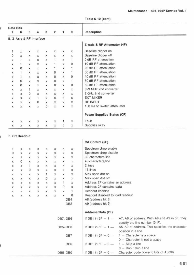
I
Data Bits7 6 5 4 3 2 1 0
E . Z-Axis & RF Interface
DB7, DB6
DB5-DBO
DB7
DB6
DB5-DBO
Table 6-10 (cont)
Description
Z-Axis & RF Attenuator (4F)
Baseline clipper onBaseline clipper off0 dB RF attenuation10 dB RF attenuation20 dB RF attenuation30 dB RF attenuation40 dB RF attenuation50 dB RF attenuation60 dB RF attenuation829 MHz 2nd converter2 GHz 2nd converterEXT MIXERRF INPUT100 ms to switch attenuator
Power Supplies Status (CF)
FaultSupplies okay
Crt Control (5F)
Spectrum chop enableSpectrum chop disable32 characters/line40 characters/line2 lines16 linesMax span dot onMax span dot offAddress 2F contains an addressAddress 2F contains dataReadout enabledReadout disabled to load readoutA8 (address bit 8)A9 (address bit 9)
Address/Data (2F)
If DB1 in 5F = 1 -
If DB1 in 5F -- 1 -
If DB1 in 5F = 0 -
If DB1 in 5F = 0 -
If DB1 in 5F = 0 -
Maintenance-49414941? Service Vol . 1
A7, A6 of address . With A8 and A9 in 5F, theyspecify the line number (0-F) .A5--AO of address . This specifies the characterposition in a line .1 = Character is a space0 = Character is not a space1 = Skip a line0 = Don't skip a lineCharacter code (lower 6 bits of ASCII)
6-6 1
1 x x x x x x x0 x x x x x x xx 1 x x x 1 x 1x 1 x x x 1 x 0x 0 x x x 1 x 1x 1 x x x 0 x 1x 1 x x x 0 x 0x 0 x x x 0 x 1x 0 x x x 0 x 0x x 1 x x x x xx x 0 x x x x xx x x 1 x x x xx x x 0 x x x xx x x x 0 x x x
x x x x x x 1 xx x x x x x 0 x
F . Crt Readout
1 x x x x x x x0 x x x x x x xx 1 x x x x x xx 0 x x x x x xx x 1 x x x x xx x 0 x x x x xx x x x 1 x x xx x x x 0 x x xx x x x x x 1 xx x x x x x 0 xx x x x x x x 1x x x x x x x 0
DB4DB2

Table 6-10 (cont)
Description
Sweep Rate and Mode (OF)
20 us TimelDiv50 us TimelDiv100 ps TimelDiv200 As TimelDiv500 ps TimelDiv1 ms TimelDiv2 ms TimelDiv5 ms TimelDiv10 ms TimelDiv20 ms TimelDiv50 ms Time/Div100 ms TimelDiv200 ms TimelDiv500 ms Time/Div1 s Time/Div2 s TimelDiv5 s Time/Div10 s Time/DivManualExternalSets single-sweep modeInternal reference shut downInternal reference onSets trigger in single-sweep mode
Holdoff, Interrupt, Trigger (IF)
Enables end-of-sweep interruptShort sweep holdoffMedium sweep holdoffLong sweep holdoffFree run trigger modeInternal trigger modeExternal trigger modeLine trigger modeDisable SWPGATEEnable SWPGATEDisable triggerEnable triggerAborts sweep

Data Bits7 6 5 4 3 2 1 0
DB5-DBO
Table 6-10 (cant)
Description
Maintenance-494149410' Service Vol . 1
1 sent to DB4 of upper latch disables front-panel PEAKing control ;DB3-DBO of upper latch and DB5-DBO of lower latch form 10-bit inputto DAC for programmable peaking voltage
x x x 1 0 x x
D61,
xDB2DBO
2nd LO output select and calibrationFor future useUpper two bits of attenuation code
I . 1st LO Driver
1st LO Driver Functions (72)
1 x x x x x x x Normal span mode0 x x x x x x x Max span modex 1 x x x x x x Connect sweep voltage to driverx 0 x x x x x x Disconnect sweep voltage to driverx x 1 x x x x x Driver off (for degauss)x x 0 x x x x x Driver onx x x 1 x x x x Filter on at driver output (for unphase-locked narrow spans)x x x 0 x x x x Filter off at driver outputx x x x 1 x x x External mixer disconnectedx x x x 0 x x x External mixer connected (connected in bands 1-5 if external mixer se-
lected ; always connected in higher bands)x x x x x 1 1 0 Internal mixer bias for Band 1x x x x x 1 1 0 Internal mixer bias for Band 2x x x x x 1 1 0 Internal mixer bias for Band 3x x x x x 1 0 1 Internal mixer bias for Band 4x x x x x 0 1 1 Internal mixer bias for Band 5x x x x x 1 1 1 No internal mixer bias selected
PEAKing Control (7E)
0 x x x x x x x Steers DB4-DBO to upper latchx 0 x x x x x x Steers DB5-DBO to lower latch
FI . Span Attenuator
DB7-DBO
Span Magnitude (75)
Lower 8 bits of 10-bit attenuation code (000 is max attenuation)
Span Magnitude and Attenuator (76)
1 x x x x x x x Gain of U3032 is + 10 x x x x x x x Gain of U3032 is -1x 0 0 x x x x x X1 .0 sweep decade attenuatorx 0 1 x x x x x X0.1 sweep decade attenuatorx 1 0 x x x x x X0.01 sweep decade attenuatorx x x 0 0 x x x 1 st LO main coil output select and calibrationx x x 0 1 x x x 1 st LO FM coil output select and calibration

Maintenance-494/494P Service Vol . 1
Table 8-10 (cont)
Data Bits7 fi 5 4 3 2 1 0 Description
J . Preselector Driver (77)
0 1 x x x x x x -Conversion, 829 MHz offset1 0 x x x x x x +Conversion, 829 MHz offset0 0 x x x x x x 829 MHz IF not usedx x 1 x x x x x Driver output filter on (for narrow spans)x x 0 x x x x x Driver output filter offx x x 1 x x x x Preselector switchx x x 0 x x x x LPF switchx x x x 1 x x x 1 st LO FM coil not sweptx x x x 0 x x x 1 st LO FM coil sweptx x x x x 1 x x Driver onx x x x x 0 x x Driver off (for degauss)x x x x x x x 1 3rd harmonic 1st LO conversionx x x x x x x 0 1 st harmonic 1 st LO conversion
K . CENTER FREQUENCY Control
Control (70)
1 x x x x x x x 1st LO storage gate open0 x x x x x x x 1st LO storage gate closedx 0 x x x x x x Steers DAC data to 1 st LO high bytex x 0 x x x x x Steers DAC data to 1 st LO mid bytex x x 0 x x x x Steers DAC data to 1 st LO low bytex x x x 1 x x x 2nd LO storage gate openx x x x 0 x x x 2nd LO storage gate closedx x x x x 0 x x Steers DAC data to 2nd LO high bytex x x x x x 0 x Steers DAC data to 2nd LO mid bytex x x x x x x 0 Steers DAC data to 2nd LO low byte
DAC Data (71)
DB7-DBO Data for center frequency DAC(s) steered by control register
Center Frequency Control Read (F0)
DB7 1 st LO DAC stored voltage comparatorDBO 2nd LO DAC stored voltage comparator

Table 6-10 (cont)
Data Bits7 6 5 4 3 2 1 0 Description
L. Auxiliary Synthesizer Control (713)
DB7-DB4D132-DBO
x x x x 1 x x xx x x x 0 x x x
0 1 0 1 x 1 0 10 0 0 0 x 1 1 00 0 0 0 x 1 1 1
A A A A x 0 0 00 0 0 A x 0 0 1
DB6-13130
Synthesizer chip data (133-DO)Synthesizer chip addresses (A2-AO)VCO enableVCO disable
This section sets R, the reference divider to 5 yielding a 200 kHz refer-ence frequency .
This section sets the value of A from 0 to 31 .LSB
N
N
N
N
x
0
1
0
This section sets N from 31 to 34 .0
0
N
N
x
0
1
1
31=1111
32-- 0000
33 =0001
34-0010001001
10
10
10
Write (73)
Clocks data on DBO into a latchClears the countersTransfers DBO serial data to control latch outputsResets the counter output register selectorTransfers DBO serial data to synthesizer N latchesGate mode latchNVRAM switch latchSerial data for control of synthesizer N latches
Read (F3)-Mast Significant Byte
Error voltage below a preset amountError voltage above a preset amountValid count is in countersUpper five bits of counter output ; the remaining 16 bits acre in the follow-ing two bytes
Reading Data From Switch Encoders (F4)
CENTER FREQUENCY downCENTER FREQUENCY upSwitch codes (see Figure 7-33 in Section 7)
Maintenance-4941494P Service Vol . 1
0 0 0 0 x 1 0 0
M . Phase Lock Control
1 x x x x x x xx x 1 x x x x xx x x 1 x x x xx x x x 1 x x xx x x x x x 1 x
DB6DB2DBO
1 x x x x x x xx 1 x x x x x xx x 1 x x x x x
D84-DBO
N. Front Panel
1 x x x x x x x0 x x x x x x x

Maintenance-494/494P Service Vol . 1
Front-Panel Registers
Writing to register 74 loads data into shift registers that drive all the lights on the front panel, including the one for the crtgraticule . Four 8-bit shift registers store the data, requiring eight writes of four bits each time (one bit for each register) toupdate the front-panel lights . Table 6-11 shows the order that data is entered to control the lights . A 0 turns on the light(except in the case of the crt graticule), and a 1 turns off the light .
aDB3=1-initializes encoder at power up .
Table 6-11FRONT-PANEL REGISTERS
Writing Data to Shift Registers for Lights (74)s
WriteNumber DB5 DB4 D132 D131 D130
1 not used MAX HOLD ZERO SPAN GRAT ILLUM COUNTER2 not used BASELINE CLIP REMOTE FINE LIN3 not used ADDRESSED 10 dB/DIV READY WIDE4 not used READOUT 20 dB/DIV LINE TRIG NARROW5 STORE SETTINGS SHIFT IDENT SINGLE SWEEP B-SAVE A6 HELP AUTO PEAK MIN NOISE FREE RUN TRIG VIEW B
7 COUNT-CF MAX SPAN AUTO RESOLN INT TRIG VIEW A8 A F PULSE STRETCHER UNCAL EXT TRIG SAVE A

Maintenance-494/4941? Service Vol . 1
AUXILIARY
N Value
Table 6-12SYNTHESIZER TABLE
A Value
OF VALUES
FvutResult
AUXILIARY
N Value
Table 6-12 (cont)SYNTHESIZER TABLE
A Value
OF VALUES
F,outResult
32 26 2'10.0 MHz31 8 200 .0 MHz32 27 2'10.2 MHz31 9 200 .2 MHz 32 28 2'10.4 MHz31 10 200 .4 MHz32 29 2'10.6 MHz31 11 200 .6 MHz32 30 2'10.8 MHz31 12 200 .8 MHz32 31 2'11 .0 MHz31 13 201 .0 MHz 33 0 2'11 .2 MHz31 14 201 .2 MHz
31 15 201 .4 MHz 33 1 2'11 .4 MHz33 2 2'11 .6 MHz31 16 201 .6 MHz 33 3 2'11 .8 MHz31 17 201 .8 MHz33 4 2'12.0 MHz31 18 202.0 MHz33 5 2'12.2 MHz31 19 202.2 MHz33 6 2'12.4 MHz31 20 202.4 MHz33 7 212.6 MHz31 21 202.6 MHz
31 22 202.8 MHz 33 8 212.8 MHz33 9 213.0 MHz31 23 203.0 MHz
31 24 203.2 MHz 33 10 213.2 MHz33 11 213.4 MHz31 25 203.4 MHz33 12 213.6 MHz31 26 203.6 MHz33 13 213.8 MHz31 27 203.8 MHz33 14 214 .0 MHz31 28 204 .0 MHz33 15 214 .2 MHz31 29 204 .2 MHz33 16 214 .4 MHz31 30 204 .4 MHz33 17 214 .6 MHz31 31 204.6 MHz33 18 214 .8 MHz32 0 204.8 MHz
32 1 205.0 MHz 33 19 215 .0 MHz33 20 215 .2 MHz32 2 205.2 MHz
32 3 205.4 MHz 33 21 215 .4 MHz
32 4 205.6 MHz 33 22 215 .6 MHz33 23 215 .8 MHz32 5 205.8 MHz33 24 216.0 MHz32 6 206.0 MHz
32 7 206.2 MHz 33 25 216.2 MHz33 26 216.4 MHz32 8 206 .4 MHz
32 9 206 .6 MHz 33 27 216.6 MHz
32 10 206 .8 MHz 33 28 216.8 MHz33 29 217.0 MHz32 11 207 .0 MHz33 30 217.2 MHz32 12 207 .2 MHz33 31 217.4 MHz32 13 207 .4 MHz34 0 217 .6 MHz32 14 207.6 MHz
32 15 207.8 MHz 34 1 217 .8 MHz34 2 218 .0 MHz32 16 208.0 MHz 34 3 218.2 MHz32 17 208.2 MHz34 4 218.4 MHz32 18 208.4 MHz 34 5 218.6 MHz32 19 208.6 MHz34 6 218.8 MHz32 20 208.8 MHz34 7 219.0 MHz32 21 209.0 MHz34 8 219.2 MHz32 22 209.2 MHz34 9 219.4 MHz32 23 209.4 MHz34 10 219.6 MHz32 24 209.6 MHz34 11 219.8 MHz32 25 209.8 MHz34 12 220.0 MHz

Maintenance-4941494P Service Vol . 1
PROGRAM FOR MOVING STORED DATA FROM THE 494P TO TAPE ANDRETURNING IT TO NON-VOLATILE MEMORY
If either the Memory or GPIB boards are removed from the instrument, data stored in non-volatile memory will be lostbecause the back-up battery on the GPIB board is disconnected. The following program will move this data to a tape andreplace the data by using a Tektronix 4050-Series Computer connected over the GPIB bus to the 494P .
100 PAGE110
PRINT "ANALYZER ADDRESS IS : " ;120
INPUT Al125 PRINT130
PRINT @Al :"RQS OFF"140
PRINT "SAVE NON-VOLATILE MEMORY ON TAPE?150
INPUT B$160
B$=SEG(B$,1,1 )170
IF B$<>"N" THEN 2000175 PRINT180
GO TO 1000
1000
REM THIS ROUTINE MOVES DATA FROM THE TAPE TO THE ANALYZER1010
PRINT "DISPLAYS AND SETTINGS ARE ON THE FOLLOWING DATA FILES"1020
PRINT " (2560 X 9 FOR DISPLAYS, 768 X 10 FOR SETTINGS )"1030 PRINT1040 TLIST1050 PRINT1060
PRINT "ENTER NUMBER OF FIRST DATA FILE :" ;1070
INPUT T11080 PAGE1090
GOSUB 90001100
PRINT "REWRITE OVER ALL DISPLAYS AND SETTINGS (01110
PRINT "OR WRITE ONLY IN BLANK . . . . . . . . MEMORY (11120
INPUT Y$1130
IF Y$="O" OR Y$="1" THEN 11601140
PRINT """1"" OR ""2"", PLEASE : " ;1150
GO TO 11201180
Y=VAL (Y$ )1170 HOME1180
DELETE I$1190
DIM 1$ (512 )1200
PRINT @Al :"SET?"1210
INPUT @Al :I$1220 W1=01230
PRINT @Al :"BVIEW OFF"1240 PRINT1250 PRINT1260
FOR I=1 TO 91270
GOSUB 80001280
GOSUB 60001290
IF Z=0 THEN 13201300
PRINT Wl ;"= WAVEFORM FROM DATA FILE " ;T11310
GO TO 13301320
PRINT W1 ;"= . . . . . . . . NOT WRITTEN . " ;T1 ;" FILE NOT USED ."1330 Wl=W1+1

1340 T1=Tl+l1350
NEXT I1360
FIND T11370 S1=01380 PRINT1390 PRINT1400 PRINT1410
FOR 1=1 TO 101420
GOSUB 50001430
IF Z=0 THEN 14601440
PRINT Sl ;"= SETTINGS FROM DATA FILE " ;T11450
GO TO 14701460
PRINT S1 . . . . . . . . NOT WRITTEN . " ;T1 ;" FILE NOT USED .1470 S1=S1+11480 T1=Tl+l1490
NEXT 11500
PRINT @Al :I$1510 PRINT1520 PRINT1530 PRINT1540 PRINT1550
PRINT " * * * FINISHED * * *"1560 END
"
2000
REM THIS ROUTINE MOVES DATA FROM THE ANALYZER TO THE TAPE2010
DELETE I$2020
DIM 1$ (512 }2030
PRINT @A1 :"SET?"2040
INPUT @A1 :I$2050 PAGE2060 TLIST2070 PRINT2080
PRINT "ENTER NUMBER OF LAST TAPE FILE :" ;2090
INPUT T12100
FIND T12110 PAGE2120
GOSUB 90002130 HOME2140
MARK 9,25002150
FIND T12160 PRINT2170 PRINT2180
PRINT @A1 :"BVIEW OFF"2190 W1=02200
FOR I=1 TO 92210
GOSUB 30002220
GOSUB 70002230
IF Z=0 THEN 22602240
PRINT W1 ;"=WAVEFORM SENT TO FILE " ;T12250
GO TO 22702260
PRINT Wl ;"= . . . . . . . . SKIPPED OVER . " ;TI ;" FILE NOT USED ."2270 Wl=W1+12280 Tl=T1+12290
NEXT I2300
PRINT @Al :l$
Maintenance-49414941 Service Vol . 1

Maintenance-4941494P Service Vol. 1
2310
REM SETTINGS ARE SENT TO TAPE2320
FIND T12330
MARK 10,5122340
FIND T12350 S1=02360 PRINT2370 PRINT2380 PRINT2390
FOR I=1 TO 102400
GOSUB 40002410
IF Z=O THEN 24402420
PRINT Sl ; "= SETTINGS SENT TO FILE * ; T12430
GO TO 24502440
PRINT S1 ;"= . . . . . . . . SKIPPED OVER . " ;T1 ;" FILE NOT USED ."2450 Sl=S1+12460 Tl=T1+12470
NEXT I2480
PRINT @Al :I$2490 PRINT2500 PRINT2510
FINISHED * * *"2520 END
3000
REM ACQUIRE WAVEFOEM AND SETTINGS .3010
REM X9 I S 500-POINT WAVEFORM, L$ I S LOWER READOUT,3020
REM M$ I S UPPER READOUT, AND E$ I S AN ERROR MESSAGE .3030
DELETE E$,H$,L$,M$,X93040 Z=03050
DIM H$ (1100 )3060
DIM X9 (500 }3070
DIM L$ (50 )3080
DIM M$ (50 )3090
PRINT C1aAl :"SAVEA OFF ;DRECAL A :", W13100
PRINT @Al :"ERR?"3110
INPUT @Al :E$3120
E$=SEG (E$ , 5 , 2 )3130
IF E$<>"62" THEN 31903140 V=O3150 X9=03160 M$=""3170 L$~""3180
GO TO 33303190
V=1 3200 PRINT @A1:"UPRDO?"3210
INPUT @Al :M$3220
PRINT @Al :"LORDO?"3230
INPUT @Al :L$3 240
M$=SEG (M$ , 8 , 40 )3250 L$=SEG(L$,8,40)3260
PRINT @37,0 :44,255,2553270
PRINT @Al :"WFM WFID :A,ENCDG :BIN ;CUR?"3280
INPUT %Al :H$3290
WBYTE @a66 .3300
RBYTE P9, R8, R9, X9, C93310
WBYTE @95 :3320 Z=13330 RETURN
6-70

4000
REM REMOVE NON-VOLATILE SETTINGS (S$
FROM ANALYZER4010 Z=04020
DELETE S$4030
DIM S$ (512 )4040
PRINT @AI : "RECALL
314050
PRINT @A1 : "ERR?"4060
INPUT @A1 : E$4070
E$=SEG (E$ , 5 , 2 )4080
IF E$<>"62" THEN 41204090 V1=04100 S$=""4110
GO 10 41704120
PRINT @A1 : "SET?"4130
INPUT @A1 :S$4140 PRINT @A1:"RQS OFF"4150 V1=14160 Z=14170
FIND T14180
PRINT @33 ;V1,S$4190 RETURN
5000
REM RETRIEVE TAPED SETTINGS (S$ ) AND SEND TO NVRAM LOCATIONS (SI )5010 Z=05020
DELETE S$5030
DIM 5$ (512 }5040
FIND T15050
INPUT @33 .V1, S$5060
IF V1=0 THEN 51505070
IF Y=O THEN 51205080
PRINT @AI :"RECALL " ;S1 ;" ;RQS OFF ;WAIT ;ERR?"5090
INPUT @A1 :E$5100
E$=SEG (E$ , 5 , 2 )5110
IF E$<>"62" THEN 51505120
PRINT @A1 :S$5130
PRINT @A1 : "STORE " ;S1 ;" ;RQS OFF"5140 Z=15150 RETURN
6000
REM SEND WAVEFORM (X9 ) & READOUTS (M$,L$ ) TO NVRAM LOCATION (W1 } .6010 Z=06020
IF V=0 THEN 61806030
IF Y=0 THEN 60806040
PRINT @AI :"SAVER OFFORECAL At
;W1 ;
;ERR?*6050
INPUT @AI :E$6060
E$=SEG (E$, 5 , 2 )6070
IF E$<>"62" THEN 61806080 PRINT @A1:"WAIT ;TRI?"6090
INPUT @A1 :H$6100
PRINT @A1 :"RDOUT '" ;M$ ;6110
PRINT @A1 :"RDOUT '" ;L$ ;"'"6120
PRINT @A1 :"WFM WFID :A,ENCDG :BIN ;SIG ;SAVEA ON"6130
WBYTE @33 :64,X9,-16140
WBYTE @63 :6150
PRINT @A1;"DSTORE A : ",W1
Maintenance-494/494P Service Vol. 1
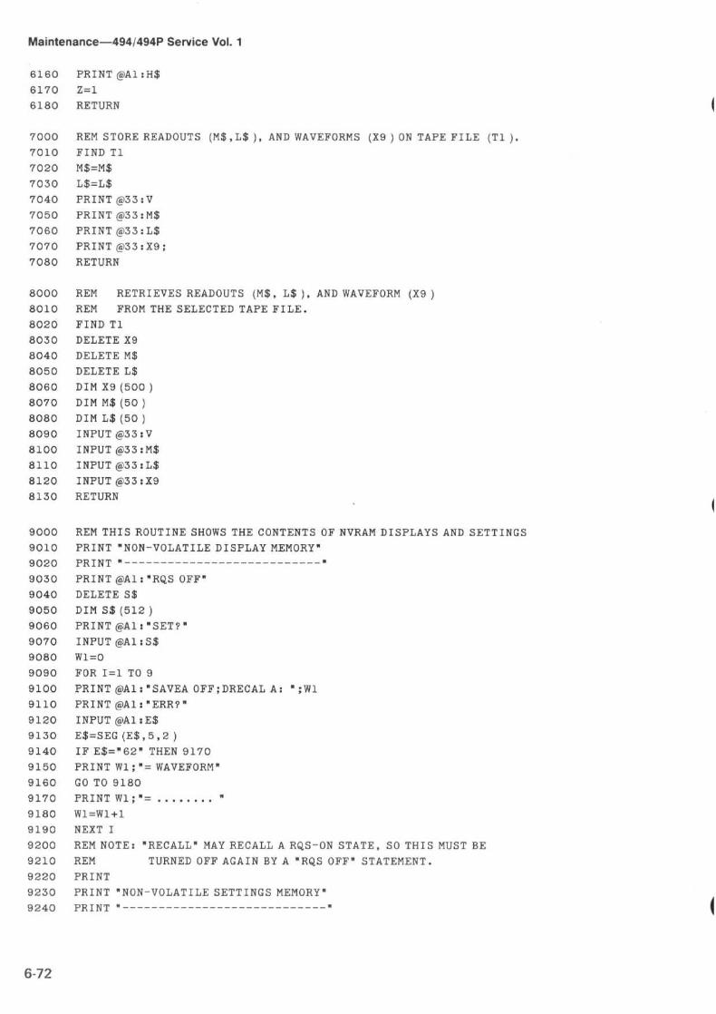
Maintenance-4941494P Service Vol. 1
6160
PRINT @aA1 :H$6170 Z=16180 RETURN
7000
REM STORE READOUTS (M$,L$ ), AND WAVEFORMS (X9 ) ON TAPE FILE (T1 ) .7010
FIND TI7020 M$=M$7030 L$=L$7040
PRINT @a33 :V7050
PRINT @33 .M$7060
PRINT @a33 :L$7070
PRINT @33 :X9 ;7080 RETURN
8000
REM
RETRIEVES READOUTS (M$, L$ ), AND WAVEFORM (X9 )8010
REM
FROM THE SELECTED TAPE FILE .8020
FIND T18030
DELETE X98040
DELETE M$8050
DELETE L$8060
DIM X9 (500 )8070
DIM M$ (50 )8080
DIM L$ (50 )8090
INPUT @33 :V8100
INPUT @33 :M$8110
INPUT @33 :L$8120
INPUT @33 :X98130 RETURN
9000
REM THIS ROUTINE SHOWS THE CONTENTS OF NVRAM DISPLAYS AND SETTINGS9010
PRINT "NON-VOLATILE DISPLAY MEMORY"9020
PRINT -----------------------------9030
PRINT @Al :"RQS OFF"9040
DELETE S$9050
DIM S$ (512 )9060
PRINT @Al :"SET?"9070
INPUT @Al .S$9080 WI=09090
FOR I=1 TO 99100
PRINT @aAl :"SAVEA OFF ;DRECAL A : " ;W19110
PRINT @aAl :"ERR?"9120
INPUT @aAl :E$9130
E$=SEG (E$ , 5 , 2 )9140
IF E$="62" THEN 91709150
PRINT W1 ;"= WAVEFORM"9160
GO TO 91809170
PRINT W1 ;"= . . . . . . . . "9180 W1=W1+19190
NEXT I9200
REM NOTE : "RECALL" MAY RECALL A RQS-ON STATE, SO THIS MUST BE9210
REM
TURNED OFF AGAIN BY A "RQS OFF" STATEMENT .9220 PRINT9230
PRINT "NON-VOLATILE SETTINGS MEMORY"9240
PRINT ----------------------------- "

9250 S1=09260
FOR I=1 TO 109270
PRINT @A1 ; "RECALL " ; S1RQS OFF ; WAIT"9280 PRINT @A1:"ERR?"9290
INPUT @A1 :E$9300
E$=SEG (E$ , 5 , 2 )9310
IF E$="62" THEN 93409320
PRINT S1 ;"= SETTINGS"9330
GO TO 93509340
PRINT S1 . . . . . . . . "9350 S1=S1+19360
NEXT I9370 PRINT9380
PRINT @A1 :S$9390 RETURN


This section of the manual describes the circuitry in the4941494P Spectrum Analyzer . The section begins with ageneral or functional description of the major circuit blocksand systems that make up the 4941494P . This is followed bya more detailed description of the circuitry within each blockor section, for example ; the display section .
What It Does
THEORY OF OPERATION
The 494/494P Spectrum Analyzer accepts an electricalsignal as its input and displays the signal's frequency com-ponents on a crt . Signals can be applied directly to the RFINPUT or, if the analyzer is equipped for external mixer op-eration, to an external mixer, which extends the measure-ment range of the 4941494P .
The display of the frequency components of the inputsignal appears on the crt as a graph where the horizontalaxis is frequency and the vertical axis is amplitude . The dis-play can be plotted, if desired, by connecting a chart re-corder through rear-panel connectors . If the instrument isprogrammable, the display can also be transmitted digitallyvia the IEEE 488 bus to a GPIB plotter .
Manual operation of the 494/494P Spectrum Analyzer isaccomplished with front-panel controls and switches . The494P (programmable version) can also be operated via theIEEE 488 bus using a straightforward language format .
How It Works
A functional block diagram, located at the front of theDiagrams section in Volume 2, shows how the major sec-tions in the instrument relate and the paths of most majorsignals . Refer to the diagram while reading this generaldescription .
The 494/494P operates as a swept, narrow-band re-ceiver . As it sweeps or spans a range of frequencies, itmoves the crt beam horizontally . When a frequency compo-nent of an input signal is detected the beam is deflected
Section 7-4941494F' Service Vol, 1
The number in the diamond that is adjacent to the sec-tion title refers to the corresponding schematic diagramnumber . Note that these same numbers are included on dia-grams to designate the interconnection between circuits, or,in the case of block diagrams, to the more detailed diagramof that block . Schematic diagrams of the circuits are part ofVolume 2, section 10 .
FUNCTIONAL AND GENERAL DESCRIPTIONvertically as a function of input power at that frequency .Thecenter frequency of each span is set by the CENTER FRE-QUENCY control or FREQUENCY entry via a Data Entrykeyboard . The frequency range of each span is set by theFREQ SPANIDIV control or settings . The power level, rep-resented by the top of the screen, is set by either the REF-ERENCE LEVEL control or the Data Entry keyboard.
First, Second, and Third Converters
In the 4941494P Spectrum Analyzer, this swept-fre-quency analysis is achieved by means of a triple-conversionsuperheterodyne technique . Each of three frequency con-verters consist of a mixer, a local oscillator, and appropriatefilters . Only one frequency is converted in each mixer topass through band-pass filters to the detector . This fre-quency can be changed by changing the frequency of thelocal oscillators in any one of the converters .
The first converter, usually referred to as the front end,converts the input signal frequency to an intermediate fre-quency (IF) of either 829 MHz or 2072 MHz, depending onwhich band is in use . The internal mixer converts signalsfrom 10 kHz to 21 GHz, and external mixers may be usedfor signals in the millimeter wavelengths . When the internalmixer is used, a preselector or low-pass filter is inserted inthe signal path to reduce unwanted signals or images andspurious responses from cluttering the display .
One of two second converters is selected automaticallyfor each band so the input frequency range does not overlapthe first IF frequency . Each second converter has its ownlocal oscillator (LO), mixer, and filters . Both down-convertthe signal to 110 MHz which is sent to the 'third converter.

Theory of Operation-4941494P Service Vol . 1
The third converter amplifies the 110 MHz IF signal andconverts it to the final intermediate frequency of 10 MHz.The third converter passes the signal to the main IF sectionfor processing and detection .
IF Section
In this section the signal is processed for frequencyresolution .Three functions are performed here :
1 . Weak signals can be amplified, by switchable amplifi-ers, so the vertical window (dynamic display range) isshifted up or down . The REFERENCE LEVEL selects thegain and input RF attenuation to frame this window betweenthe top of the display screen or reference level, in dBm orvolts, and the bottom of the display .
2 . The signal is processed through one of several10 MHz band-pass filters that can be selected by theRESOLUTION BANDWIDTH control . In the auto mode themicrocomputer will select the best combination of band-width and sweep time for the selected span, unless overrid-den by the operator .
3 . The signal is amplified by a logarithmic then detected .The output from this detector is a voltage that correspondsto the signal strength, in decibels, which is sent to the verti-cal channel of the display section to drive the vertical axis ofthe crt and display the strength of the signal .
Display Section
The display section drives the X,Y, and Z axis of the crtdisplay . Vertical deflection of the beam is increased as theoutput of the amplitude detector increases . The horizontalposition of a signal is controlled by the frequency controlsection and corresponds to the frequency analyzed at thatinstant . As the 4941494P spans from low to high frequen-cies during its analysis, the beam is swept from left to right .When the analyzer tunes through a signal frequency, a verti-cal deflection shows the strength of the signal .This signal istherefore displayed at a postion on the span that corre-sponds to its frequency, or, the display is one of amplitudeas a function of frequency .
The video amplifier scales the output of the detector forvertical deflection in dBldiv or performs a log1linear conver-sion, depending on the vertical display mode . The video pro-cessor filters the video if either the wide or narrow filter isselected .
The display section also drives the crt readout to showcontrol settings . This readout is based on data from the
microcomputer which is reading the settings of the frontpanel controls or data on the GPIB bus .
The sweep is usually fast enough so the display is flicker-free, but at times the sweep must be slowed below theflicker rate . With digital storage the display can be recordedand refreshed at a flicker-free rate.The 494P can read-outthe display data, from digital storage, through the IEEE 488interface .
Frequency Control Section
The 494/494P sweeps through a frequency range that iscentered about a frequency set by the frequency controlsection . The CENTER FREQUENCY control sets the centerfrequency of either the 1st or 2nd local oscillator .
The output of a sweep generator is scaled by a spanattenuator to sweep a range or span of frequencies eitherside of center . The output of the span attenuator drives the1st LO for wide spans and the 2nd LO for narrow spans .The output sweep also deflects the crt beam across thehorizontal axis as the local oscillators are swept so the dis-play is a spectrum of frequency versus power.
The frequency control section also tunes the preselectorso it tracks the signal frequency being detected over the 1 .7to 21 GHz range .
Microwave Counter and Phase Lock Section
The microwave Counter, Harmonic Mixer, and AuxiliarySynthesizer comprise the nucleus of the frequency controlhardware . Both the 1 st LO and 2nd LO frequencies are con-trolled via the firmware based control loop . Data from theCounter, is used as feedback to control the oscillator fre-quency . Accurate signal frequency measurement is alsopossible by counting the frequency of the 3rd IF .
The Phase Lock system stabilizes the 1st LO frequencyto minimize FM'ing or display jitter and increase resolution .
Digital Control Section
Operational modes and internal functions of the494/494P analyzer are selected and controlled directly fromthe front panel or remotely controlled from an external con-troller through a IEEE 488 connector. This connector inter-faces to an instrument microcomputer through a GeneralPurpose Interface Bus (GPIB) . The modes and functionsthat are selected are processed and activated by the instru-ment master microcomputer which talks and listens to allcircuits over the instrument bus .

Front panel control and selector data is processed by afront panel CPU that interfaces with the master micro-computer over the instrument bus . The master micro-computer receives and sends all of its information over theinstrument bus to the internal circuits . It communicates withthe outside world through the GPIB to the IEEE Std 488connector or through the Accessories Interface to the Ac-cessories connector located on the rear panel . Control lan-guage corresponds to front-panel nomenclature of the494/494P Spectrum Analyzer .
Power Supply Section
The power supply section provides regulated do powerand forced air cooling for all circuits within the instrument .The switching supply is capable of providing regulated volt-ages over wide input line frequency and voltage ranges. Thecooling system consists of an intake on the bottom of thecase, air passages within the instrument, a fan, and a rearpanel exhaust . Air is routed to all section of the instrumentin proportion to the heat generated by circuits within thatsection . Internal temperature variation is small so as to pro-vide reliable operation .
Other Sections
Signal, power, and control lines between circuit boardsand assemblies interconnect through a common Motherboard . Most circuit board assemblies plug onto the the top
The following description is arranged by sections or sys-tems ; such as 1st Converter, 2nd Converter, etc ., followedby circuit analysis of the circuits within that section . Eachsystem/section is introduced with a description of the sys-tem using the system block diagram found in the Diagrams
Timer (Running time indicator)
For Further Information
DETAILED DESCRIPTION
Theory of Operation-4941494P Service Vol . 1
side of the Mother board, assemblies or modules, such asoscillators, of the RF deck, plug through cables and connec-tors to the bottom side of the Mother board .
An electromechanical timer (M1019) is installed on the Z-Axis board . This timer is calibrated for a duration of 5000operating hours . Current through the timer causes a copperband to progress along a scale to indicate operating hours .
The circuits that make up the different sections of the494/494P are described under headings that correspond tothose shown in the Functional Block diagram . Detailed blockdiagrams of these main sections follow the F=unctional Blockdiagram, All diagrams are located in the Diagrams section ofVolume 2. Detailed block diagrams and circuit schematics ofeach circuit board and assembly within a section follow thebreakdown of the sections .
Circuit theory of operation is described under the De-tailed Description that follows . Adjacent to each schematicis a detailed block diagram and a parts location illustrationwith look-up tables . The parts location illustration and look-up tables should aid in finding components on either theschematic or parts location illustration .
section of the manual . This is followed by a description ofeach circuit board or major circuit within the system . Adja-cent to the title of each section or part is the diagramsnumber .

Theory of Operation-4941494P Service Vol. i
RF Interface Circuits
1ST CONVERTER ASSEMBLIES
The 1 st Converter consists of the following assemblies : The0-60 dB Step Attenuator, the Filter Select switch, a 2 GHzLimiter and 1 .8 GHz Low-Pass Filter, a 1 .7 to 21 GHzPreselector, the Mixer, the 1st LO and Power Divider,Transfer Switch, 2.072 GHz Directional Filter, Diplexer andtwo 4.5 GHz Low-Pass Filters . External circuits that controlor drive the assemblies within the 1st Converter are ; thePreselector Driver, 1st LO Driver, Microwave Counter andPhase Lock system, and the RF Interface board.
The 1st Converter converts the incoming RF signals tothe 1st IF . Incoming signals are applied through a calibrated0-60 dB decade attenuator to a filter select switch . Signalswithin band 1 (10 kHz-1 .8 GHz) are routed through a limiterand 1 .8 GHz low-pass filter to the mixer, signals withinbands 2 through 5 (1 .8-21 GHz) are routed through a tun-able preselector to the mixer . The RF signals are mixed withthe output from a tunable (2.072-6.329 GHz) local oscillatorto generate modulation products at the intermediate fre-quency in use .
The output of the 1st mixer is applied,through TransferSwitch S13, to a directional filter which separates intermedi-ate frequencies 2 .072 GHz and 829 MHz for the 2072 MHz2nd Converter or 829 MHz 2nd Converter . The 2072 MHzIF is applied through a 4.5 GHz low-pass filter to the2072 MHz 2nd Converter to reject the re-entrant modes ofthe directional and four cavity band-pass filters . The829 MHz IF is fed through a diplexer and a 4 .5 GHz low-pass filter before it is applied to the 829 MHz IF stages . The4.5 GHz filter is used to reject re-entrant modes of the829 MHz band-pass filter internal to the 829 MHz 2ndConverter .
An EXTERNAL MIXER port permits an external mixer tobe connected to the instrument to serve as the 1st IFsource . The IF signals from external mixers are routedthrough the Transfer switch to the Directional Filter. Thisfeature is primarily for use with waveguide mixers .
Two intermediate frequencies (2072 MHz and 829 MHz)are used in the analyzer to prevent baseline rise caused bylocal oscillator feedthrough and crossover ofintermodulation products . The 2072 MHz IF is selected forbands 1 and 5, plus the waveguide bands. 829 MHz IF isselected for bands 2-4 .
The RF interface circuits receive instruction from themicrocomputer and produce control voltages that drive theRF Attenuator, the Transfer Switch, and the IF Select .
These circuits are located on the Z-Axis board and theiroperation is described under the Z-Axis board part of theDisplay section .
RF Signal Path
The 0-60 dB Step Attenuator consists of 10 dB, 20 dB,and 30 dB sections which are controlled by relays that areactuated by voltages from the RF Interface circuit .
Coaxial relays S11 and S12 select either the low-passfilter (FL10) and limiter or the Preselector and 3 dB attenua-tor (AT11) for the RF signal path . The relay coils are drivenby circuitry on the Preselector Driver board . The low-passfilter path is used for band 1, band 2 through 5 (signals withfrequencies 1 .7 to 21 GHz) are routed through thePreselector .
The 2 GHz Limiter operates from 100 kHz to 2 GHz . Ithas a linear two-port transfer characteristic of unity (-1 dB)until the input exceeds +5 dBm . Above this (point, the inter-nal detector diodes conduct, reflecting part of the RF inputenergy back to the source . As the input level rises, the Lim-iter reflects more signal, limiting the amount that can passthrough the mixer, thus protecting the mixer from burnout .
The 1 .8 GHz low-pass filter (FL10) strips the incomingsignal of any frequencies above 1 .8 GHz and passes thesignal below 1 .8 GHz to the output segment of selectorswitch S11 .
The Preselector is a 1 .7-18 GHz YIG filter that provideshigh selectivity and image-frequency rejection . Tuning cur-rent, which is near 500 mA at 21 GHz, is provided by thePreselector Driver circuits . The Preselector operates onbands 2, 3, 4, and 5 . The signal from the Preselector passesthrough a 3 dB attenuator to the output section of the FilterSelector switch . The Preselector is sensitive to output loadimpedance so an attenuator is used to help isolate thisloading .
1st Mixer
The 1 st Mixer is a single balanced design . This has lessconversion loss, in comparison to an unbalanced mixer, andthis design also cancels local oscillator feedthrough to theRF port . The local oscillator input is split through a broad-band multi-section coupler whose outputs are equal inpower but 90° out of phase . An additional 90° phase shift iscascaded with the appropriate signal to create a 180°phase difference that is applied across a pair of series-con-

nected Schottky diodes . The result is that the diodes arealternately switched on and off as the local oscillator cycles .
The node between the two diodes is isolated from the 1 stLO input by about 30 dB so the RF input is applied to thisnode . The blocking capacitor at the input connector permitsbroadband signal application from the RF port, while block-ing the do diode bias to the RF port and the analyzer input .Dc bias for the mixer is via the Transfer Switch, DirectionalFilter, Diplexer, and 4 .5 GHz Filter through the 829 MHz IFcircuits . Bias return is through assembly Al 1 to ground .Bias is supplied from the 1st LO Driver board .
Not counting the IF filtering circuitry, the fundamentalconversion loss of the 1st Converter is about 14 dB ; thirdharmonic conversion loss is about 24 dB. The Schottky di-odes are mounted in a sub-assembly of the mixer so theycan be easily replaced .
1st Local Oscillator
The 1st LO is a YIG (Yitrium-Iron-Garnet) oscillator thathas a tuning range of 2.072 to 6 .35 GHz . The oscillator as-sembly includes the interface circuit board that couples op-erating and tuning voltages from the 1st LO Driver, SpanAttenuator, and Error Amplifier circuits to the oscillator.
The + 15 V, voltage provides operating bias for the oscil-lator . The supply is protected and decoupled by VR1010,C1016, and R1011 . The second supply, +15V2 , is for fu-ture applications . VR1018 and VR1019 clamp transient volt-ages from the tune voltage coil . It also protects the drivingcircuits from the transients induced when degaussing .
Relay K1015 is closed when the FM coil is used to sweepthe oscillator . C1012 and C1014 are connected across thetune coil to lower the noise bandwidth of the main coil driv-ing circuit while the FM coil is in operation . The heater pro-vides temperature stability .
Power Divider (A13)
The Power Divider splits the output of the 1st LO (YIGoscillator) to isolate the 1 st Mixer from the 1 st LO OUTPUT
Transfer Switch
Directional Filter
Diplexer and Filter
Theory of Operation-4941494P Service Vol . 1
front panel connector . The unit is essentially two multi-sec-tion directional couplers that are multi-port cascaded to pro-duce two ports having equal power . The isolation betweenoutput ports is 15 dB or more at the operating frequency .The Power Divider also provides an improved load to thelocal oscillator .
The Transfer Switch is a three-port coaxial switch thatpermits application of 1st IF signals from inside or outsidethe analyzer . This allows the use of an external mixer by by-passing the 1 st Converter circuitry . The function is con-trolled by circuitry on the RF Interface board . It isautomatically actuated when waveguide bands are selectedor the front panel EXT MIXER push button is pressed .
The Directional Filter (FL16) couples the 2072 MHz signalto the 2nd Converter via low-pass and band-passfilters,FL11 and FL14. As mixing products pass throughFL16, they induce a selected current into a one-wavelengthdistributed ring, which couples the 2072 MHz. IF signal outto the low-pass filter FL11 . The remainder of the IM prod-ucts pass on through, since the ring is excited only with2072 MHz signals . The bandwidth of this unit is approxi-mately 45 MHz. The unfiltered signals are passed on to theDiplexer .
2072 MHz IF Filters
The 2072 MHz signal, from the Directional Filter, passesthrough a low-pass filter (FL11) which rejects all signalsabove 4.5 MHz . The signal is then sent through a 15 MHzband-pass filter (FL14) which rejects IM products either sideof the 2072 MHz IF .
The Diplexer (A14) passes the 829 MHz IF signal fromthe mixer output through a low-pass filter (FI_15) to the 2ndConverter . The Diplexer and directional filter provide abroadband impedance match to the 1st Mixer IF port . Thismatch contributes to the overall flatness and frequency re-sponse of the analyzer .

Theory of Operation-4941494P Service Vol . 1
2ND CONVERTER CIRCUITS
Two 2nd Converter systems are used in the 494/494PSpectrum Analyzer . One converts 2072 MHz to 110 MHzand the other converts 829 MHz to 110 MHz. The operationof either converter is a function of the selected frequencyband . The IF selection for each band is shown in Table 7-1along with the center frequency range and the local oscil-lator frequency range . Two 2nd IF's are used by the ana-lyzer for the following reasons :
1 . If a frequency band were to include the first intermedi-ate frequency within its range, it is possible for some inputsignals to pass through the Preselector and the 1st Con-verter (without conversion), into the 2nd Converter at the1 st intermediate frequency . The resultant spurious signalwill cause the baseline level on the screen to rise and ob-scure real signals . By the use of two 2nd converters, theanalyzer can overlap frequency bands so they do not in-clude the first intermediate frequency, and avoid thisproblem .
2 . With two IF'S, IF feedthrough in band 2 and higherorder spurs in bands 3 and 4 can be eliminated .
3 . Because of the limited tunning range of the 719 MHzLO, the lower I F cannot be used above band 4 .
The 2072 MHz 2nd Converter mixes the 2072 MHz fromthe 1st Converter with the output from a 2182 MHz phase-locked 2nd local oscillator . This local oscillator is swept andtuned over a 4 MHz range . The 2072 MHz input IF signal is
Table 7-12ND CONVERTER IF SELECTION
passed through a four-cavity band-pass filter, (FL14) to allowonly the 2072 MHz 1 st IF signal to pass through and pre-vent other signals, generated within the 2nd Converter, fromgetting back to the 1st Converter . A diode rnixer combinesthe 2072 MHz IF input and the local oscillator signals togenerate the 110 MHz IF output which then passes througha 110 MHz low-pass filter to reject any higher order signalsfrom the mixer .
The 829 MHz 2nd Converter uses a phase-locked volt-age controlled oscillator to produce the 719 MHz signal thatis mixed with the 829 MHz first IF signal . The swept2182 MHz 2nd Local Oscillator is used as a reference forthe phase locked oscillator . The 719 MHz oscillator can bedisabled upon command from the microcomputer in the IFselection process . The phase lock circuit maintains a con-stant relationship between the two local oscillators as the719 MHz oscillator is swept and tuned over a 1 .33 MHzrange . A four section coaxial band-pass filter is used beforethe mixer to exclude any RF signals other than the desired829 MHz . Again, a diode mixer is used to mix the 829 MHzinput and local oscillator signals to produce the 110 MHzsecond IF output .
Selection between the two IF signals also takes placewithin the 829 MHz converter system . Under command ofthe microcomputer (by way of the RF Interface circuits) adiode selector switching network connects one of the two110 MHz second IF signals to the output for application tothe 3rd Converter .
Frequency Band Center Frequency Range2nd Local Oscillator
Frequency (MHz) Range Converter System IF
1 0-1 .8 GHz 2182 ±2.25 2072 MHz2 1 .7-5 .5 GHz 719 ±0.75 829 MHz3 3.0-7 .1 GHz 719 ±0.75 829 MHz4 5.4-18.0 GHz 719 ±0.75 829 MHz5 15.0-21 .0 GHz 2182 ±2 .25 2072 MHz6 18.0-26 GHz 2182 +2 .25 2072 MHz7 26-40.0 GHz 2182 ±2 .25 2072 MHz8 40.0-60.0 GHz 2182 ±2 .25 2072 MHz9 50.0-0.0 GHz 2182 - 2 .25 2072 MHz10 75-40.0 GHz 2182 ±2 .25 2072 MHz11 110-220 GHz 2182 ±2 .25 2072 MHz12 170-325 GHZ 2182 ±2 .25 2072 MHz

The 2072 MHz 2nd Converter converts the 2072 MHzsignal output from the 1 st Converter to 110 MHz for even-tual application to the 3rd Converter . The assembly consistsof a low-loss, narrow band, four-cavity filter, connected,through an external cable, to a low conversion loss narrowband diode mixer, a 110 MHz low-pass filter, and a mixerbiasing circuit that will disable the mixer when directed bythe microcomputer .
Four-Cavity Filter
The four-cavity (band-pass) filter, which is depicted onDiagrams 11, 12, and 13, is designed to pass only the2072 MHz IF signal to the mixer and to reflect any otherfrequencies back to the 1st Converter for termination . Inaddition, the filter keeps the converter LO and mixer prod-ucts from entering the 1 st Converter.
This filter has a 1 dB bandwidth of 15 MHz and an inser-tion loss of 1 .2 dB . Each end resonator is capacity coupledto external circuits through a coupling hat plugged into a 3millimeter connector . Intercavity coupling is provided by
INPUT OROUTPUTPORT
COUPLING HAT COUPLING LOOP FREQUENCY DETERMINING GAP
I.W~jq 01
CAVITY POST
~~INTER-CAVITY WALL
FIRST CAVITY
SECOND CAVITY
FILTER TOP
MAIN CAVITYMILLING
2727-IOTA
2072 MHz 2ND CONVERTER
Figure 7-1 . Cross section of a four-cavity filter .
Theory of Operation-4941494P Service Vol . 1
coupling loops that protrude from the machined filter top .The resonant frequency of each cavity is determined primar-ily by the depth of a gap in the underside of the filter top,and is fine tuned with a tuning screw on the side of eachcavity . All of the tight machining tolerances are confined tothe top . Thus, the main cavity milling need not be a highprecision part . When properly tuned, using a network ana-lyzer, the filter return loss is greater than 25 dB from eitherend (in a 50 Sf system) . Figure 7-1 shows a cross sectionalview of the filter ; Figure 7-2 shows the equivalent electricalcircuit .
Mixer Circuit
The mixer circuit in the 2072 MHz 2nd Converter is of thesingle-balanced, two diode type . It consists of the mixer, anoperational amplifier bias circuit, a delay line, and a low-pass filter . In opertion, both diodes of the mixer are turnedon and off by the output signal from the 2182 MHz 2ndLocal Oscillator through coaxial connector 1'183 . Althoughthe diodes are connected for opposite polarity, both areturned on at the same time because of the 1~BO° phase shiftdelay line in the input line to the upper deck . Note that thediodes are matched and must be replaced as a pair if onefails .

Theory of Operation-4941494P Service Vol . 1
2072 MHz RF from the four-cavity filter (FL14) enters themixer, where it is switched on and off at a 2182 MHz rate bythe mixer diodes . Conduction of the diodes is controlled bythe much stronger 2182 MHz LO signal . Several mixingproducts result ; one, the difference frequency of 110 MHz isseparated from the others by a low-pass filter for use as theIF output .
The two inductors and one capacitor, at the output of themixer, form a low-pass filter that passes 110 MHzunattenuated to the 829 MHz 2nd Converter, via coaxialconnector P182 . Capacitors, at each of the three inputs tothe mixer, keep the diode bias from being impressed uponthe RF and local oscillator lines .
The bias circuit, which consists of operational amplifierU 1014 and the associated components, establishes the biasfor the mixer diodes and also provides the means for effec-tively switching the mixer off (under control of the micro-computer) . When the mixer is active, each diode hasapproximately 2 mA of forward bias . For this condition, theIF SELECT signal from the Z Axis/RF Interface circuits (ap-plied through feedthrough capacitor C182) is low . Thiscauses the output from U1014A to be at } 14 V and theoutput from U1014B to be -14V. Diodes CR1014 andCR1018 are thereby reverse-biased . Thus, the series resis-tances of potentiometer R1019 plus resistor 81014, and
Figure 7-2 . Equivalent circuit of the four-cavity filter.
Precision External Cables
2727-102A
potentiometer 81010 plus resistor 81017, provide forwardbias to the diodes . The potentiometers are set to balancethe bias levels .
In operation where the mixer is not active, the IF SE-LECT signal is high . This reverses the states of the U1014outputs and forward-biases diodes CR1014 and CR1018 .With these diodes conducting, resistors IR1014, R101f,81017, and R1018 form two voltage dividers that set thereverse bias, to the mixer diodes, at 5V . This effectivelyturns the mixer off and attenuates the 110 MHz signal byabout 55 dB.
The external cable that connects the four-cavity filter out-put to the mixer circuit and the external cable that connectsthe 2nd local oscillator to the mixer circuit are both criticallength cables .
The Four-Cavity Filter-to-Mixer Input Cable (W140) .Several products and harmonics of the local oscillator andRF input frequencies will exit the mixer via the RF input portof the mixer . The image (RF input minus the 2nd LO) and thesum (RF input plus the 2nd LO) are two significant products .There is enough energy in these two signals to warrant ef-forts to recover that energy .

Only the RF signal at 2072 MHz can pass through thefour-cavity filter . Thus, any other signal frequency that isapplied to the filter (that is, signals exiting the mixer via theRF port) is reflected back to the mixer by the filter . If thecable between the filter and the mixer is the correct length,the most significant reflected signals (that is, the image andthe sum) can be returned to the mixer in phase and con-verted into additional energy at the intermediate frequency .This technique is called "image enhancement mixing" andtypically improves conversion loss by approximately 3 dB atthe design frequencies .
The image frequency, in this instance, is very near the RFfrequency . A very sharp cut-off filter is required to pass theRF, yet reflect the image . The four-cavity filter performs thisfunction .
The 2nd Local Oscillator-to-Mixer LO Input Cable(W222) . The image and sum products are also present atthe LO port of the mixer . These signals leave the mixer viathe cable to the 2nd LO and are reflected back to the mixerby the LO The oscillators resonator appears highly reflec-tive to the image and sum signals because it is tuned to theLO frequency . Again, the length of the cable from the LO tothe mixer LO port is adjusted so the image and sum signalsare reflected back to the mixer, in the proper phase, for re-conversion to supply additional energy at the IF frequency .
2182 MHz PHASE LOCKED 2ND LO
General Description
The 2182 MHz phase locked 2nd LO assembly containsa tunable microwave oscillator, frequency reference, andphase lock circuitry within a two-section housing . Micro-wave circuitry is packaged within the machined aluminumportion of the housing . Low frequency phase lock circuitry iswithin the mu-metal compartment .
In the microwave or LO portion of the assembly, the2182 MHz Microstrip Oscillator generates 2182 MHz for the2nd converters and the 2nd LO internal reference circuitry .The 2200 MHz Reference circuit receives a 100 MHz drivesignal from the 3rd converter crystal oscillator and produces100 MHz harmonics . The 22nd harmonic or 2200 MHz ismixed with 2182 MHz from the microstrip oscillator in the2200 MHz Reference Mixer circuit . The difference frequencyof 18 MHz is then fed to the phase lock side of the module .
A phase/frequency detector, on the 16-20 MHz PhaseLock circuit board, compares the 18 MHz difference fre-quency with a signal from a linearized varactor tuned,18 MHz voltage controlled oscillator . The detector outputtunes the 2182 MHz Microstrip Oscillator such that the dif-
Theory of Operation-494/494F' Service Vol . 1
ference frequency exactly matches the frequency of the18 MHz reference VCO.
Sweep and tune signals from the Span Attenuator andCenter Frequency Control circuits tune the 18 MHz VCO .The output voltage from the phase/frequency detectorforces the Microstrip Oscillator to tune the same amount .
2182 MHz Microstrip OscillatorThis oscillator consists of a printed halt wavelength reso-
nator driven by a common-emitter feedback amplifier(01021) . The base of 01021 is capacitively tapped into theresonator . The resonator serves as a tuned phase inverterand impedance transformer, connected between the baseand collector of 01021 . Part of the base feedback capaci-tance is provided by a bendable tab (C1021) . This allowsfine adjustment of the total feedback . This feedback RF sig-nal is detected, by the base-emitter junction of 01021, toproduce a change in bias voltage that is related to theamount of feedback . The base voltage can be monitored atTP1015 with a high impedance voltmeter without signifi-cantly disturbing the oscillator .
The do collector voltage and current for 01021 is regu-lated by an active feedback circuit containing transistor02021 . Voltage at the junction of 82023 and L2023 is afunction of 01021 collector current . This voltage is sensedby 02021, which alters the base current to 01021 therebyregulating the collector current and maintaining + 10 V doon the resonator . Decoupling and control of bias loop dy-namics are provided by C2104 . Resistor 82016 swamps thenegative base resistance of 01021 to provide stabilization .Resistor 82015 protects the base-emitter junction of 01021from excessive reverse bias in the event the + 12 V supplyfails .
The oscillator is tuned by varactor diode CR1028, con-nected to one end of the resonator . Decoulpling for the va-ractor is provided by the low-pass elements in the tune line .Bendable tab C1022 can be used to fine tune the oscillatorcenter frequency .
Three output taps are coupled to the resonator throughprinted capacitors under the resonator . One output supplies2182 MHz through a 6 dB attenuator to the Harmonic Mixerin the 829 MHz 2nd Converter . The other two output tapscouple LO power through 6 dB attenuators to buffer amplifi-ers 01031 and 01011 . The amplifiers provide approxi-mately +10 dBm to the 2072 MHz 2nd Converter and +8d6m to the Reference Mixer .
Since the two buffers are nearly identical, only the 2ndConverter buffer is described . Gain is provided by a single

Theory of Operation---4941494P Service Vol . 1
common-emitter transistor (01011) . Printed elements pro-vide input and output impedance matching . Out-of-banddamping is provided by R1011 in series with a 114 wave-length shorted stub . Dc is blocked by C1014 and 01011 . A114 wavelength open stub is used at the output to reflectone of the 2nd Converter's image frequencies at 4254 MHz(the other buffer does not use nor need this stub) . Collectorbias for 01011 is provided through 81012, L1011, the 114wavelength shorted stub, and 81011 . The 114 wavelengthshorted stub is grounded through C2011 (02011, 01013,and L1011 are also used for decoupling). Collector voltageis determined by divider 81013 and 82013 ; this controls thedo feedback to the collector-base junction of 01011 . Thebias network is decoupled from the RF path by L1014 . Di-ode CR2013 protects the base of 01011 from excessivereverse bias if the + 12 V supply fails .
2200 MHz Reference Board
This circuit generates harmonics of the 100 MHz input .The 22nd harmonic or 2200 MHz is used by the ReferenceMixer . The input 100 MHz signal is applied through a match-ing network (consisting of L1034, L1025, 01036, 01029,and 01025) to a differential amplifier (01024 and 02024) .The emitters of this amplifier are ac coupled through 02026,reducing low frequency gain and ensuring balanced opera-tion . A snap-off diode (CR2014) is driven by the amplifier,via transformer T2015, to generate multiple harmonics ofthe 100 MHz signal including the 2200 MHz reference . Theoutput passes through a 3 dB attenuator, for isolation, tothe Reference Mixer circuit .
2200 MHz Reference Mixer
Signals from the 2200 MHz Reference circuit are filteredby a printed 2200 MHz bandpass filter . Diodes CR1011 andCR1012 are the switching elements of a single-balancedmixer . The microstrip oscillator output is applied to CR1011and through a half wavelength delay line to CR1012. Thedelay line shifts the oscillator signal 180° so both diodesswitch together . Mixing the 2200 MHz with the oscillator2182 MHz signal produces the difference frequency of18 MHz . This 18 MHz signal is fed through a 37 MHz low-pass filter to the 16-20 MHz phase lock circuit . The low-pass filter prevents unwanted products, such as 82 MHz(product of 2100 MHz and 2182 MHz), from passing into thephase lock circuit .
16-20 MHz Phaselock Board
This board contains regulated power supplies, a16-20 MHz (18 MHz nominal) voltage controlled oscillatorwith linearizing circuitry, and a phase/frequency detector cir-cuit . Its main function is control of the 2182 MHz MicrostripOscillator . The entire circuit board is housed in a magneticshield to reduce spurious effects of external ac fields . Allpower supply and control inputs enter the circuit board via
feedthrough capacitors in the housing wall . All connectionswith the microwave circuitry are through feedthrough capac-itors 02200-02204, in the floor of the housing .
The + 15, -15, and + 9 V supply inputs are re-regulateddown to + 12, -12, and +5.2 V by regulators using quietoperational amplifiers . IC U2025 provides a stable -6.2 Vreference that is filtered by R2018 and 020'15 and amplifiedby U201 fib to produce the -12 V supply . IC U2016B usesemitter-follower 02024 to increase the current capability ofthe supply . Resistor R2013 ensures sufficient base drive,while collector resistor R2025 reduces power dissipation in02024 . Diode CR2019 protects the base-emitter junctionduring power supply shutdown . Feedback resistors R2016and R2017 set the gain of U2016B and control the -12,+ 12, and +5 .2 supply voltages . The -12 V supply is ap-plied to inverting amplifier U2016A to produce the + 12 Vsupply, and inverting amplifier U1017 tic) produce the+5.2 V supply . The output circuitry for the +12 V and+5.2 V supplies are similar to the -12 V supply .
Differential amplifier U2072A accepts the 2nd LO sweepvoltages . One input senses the sweep voltage while theother input senses the ground potential at the Sweep board .Sweep sensitivity is adjusted by selecting resistor 82070 . Inwide spans, the sweep signal passes through parallel resis-tors R2082 and 82083 . In narrow spans, R2082 may beswitched out by 02084, which reduces the sweep sensitivityby a factor of ten . When the TTL signal to 02076 is high,02076 is turned off, R2086 holds the gate of 02084 to-15 V, 02084 is turned off, and R2082 is switched out .This reduces the sweep sensitivity . When the TTL signal islow, 02076 saturates with the collector slightly above 0 V,02084 turns on, and full sweep sensitivity is restored .
Amplifier U2072B accepts the 2nd LO tune voltage . theTune board senses the ground potential of the 16-20 MHzPhase Lock board and floats the tune voltage . Tune sensi-tivity is adjusted by selecting resistor 82072 .
The sweep and tune signals combine at the summingnode input of a non-linear shaping amplifier . The non-linear-ity of the shaping amplifier compensates for the non-lineartuning of the reference oscillator varactor to give a lineartuning characteristic from 16 to 20 MHz . The shaping func-tion is produced by a resistor-diode array in the feedbackloop of inverting amplifier U1073A .
All of the amplifier's feedback is through 81072 when theoutput swings to the negative limit . As the output voltageswings less negative, it sequentially passes the tap-pointvoltages of a series of voltage dividers connected between0 V (the summing node at pin 12) and a negative referenceset by 01047. If the output becomes positive with respectto a given divider tap, a corresponding diode in U2059 for-

ward biases and connects the output to the tap, which cre-ates additional feedback through one leg of the divider tothe summing node . This causes 82051, then 82052, thenR2053 (as so on through R2056) to be connected in parallelwith R1072 as the amplifier output becomes less negative .This progressively increases the feedback, which causesthe gain of U1073A to decrease .
Another series of dividers connected between the amplifi-er's output and a negative voltage reference causes the di-odes in U1059 to sequentially conduct as the outputbecomes more positive . Resistors 82060, then 82061, thenR2062 (as so on through 82065) are sequentially added inparallel with the existing feedback . Soft diode turn-oncharacteristics and a large number of breakpoints result insmooth gain changes . The non-linear amplifier's voltage-gain characteristic is controlled by the shaper reference volt-age, which is set by 82049. Altering 82049 will make thebreakpoints either closer together or further apart ; in prac-tice, this resistor is selected to correct the tolerance varia-tions of the 18 MHz VCO varactor .
The forward drop of the shaper diodes gives U1073A anoffset voltage . Temperature correction diodes CR1086,CR1087, and CR1088 correct this offset over a wide tem-perature range by summing a correction voltage through81074 . These diodes also compensate for the lack of seriesdiode drop across 81072 and eliminate offsets at the sum-ming input of U1073B . Selecting R1070 provides fine ad-justment of the VCO's center frequency . IC U1073B is aninverting amplifier that increases the shaper output voltageswing to a level that can control the varactor of the 18 MHzVCO .
A differential amplifier with well-defined limiting charac-teristics is used for the 18 MHz VCO . Emitter degenerationis used to control loop gain . Transistors 02096 and 02087form the differential pair of transistors, with the emitterscoupled through C2091 . Transformer T2092 provides acfeedback for the collector-base junction of 02096 and alsocreates the majority of the resonator inductance . The totalresonator inductance may be adjusted by trying differentcombinations of connections between taps on inductorT1091 and transformer T2092. These taps allow coarse ad-justment of the VCO center frequency . The capacitor of theresonator is varactor CR 1089 . Capacitor C1088 completesthe resonator ac path and acts as a do block, which allows abias voltage to be impressed on the varactor . Resistor82092 and capacitor C2090 damp the 02096 collector,which prevents high-frequency instability in the oscillator .Transistor 02087 provides a buffered oscillator output .
A discrete two-stage amplifier provides an unsaturatedvoltage gain of approximately 43 dB for the 18 MHz signalfrom the 2200 MHz Reference Mixer board . Transistor01041 is the common-emitter first stage while 01042 and
Theory of Operation-4941494P Service Vol . 1
01043 form the differential second stage . 'The differentialstage limits the output swing to 0.8 V to prevent over-driv-ing the following ECL circuitry . Dc bias is maintained by01041, which has do collector-base feedback via R1046and the R10431R1048 voltage divider . Transistor 01043 re-ceives its base bias through 81042 . Each transistor oper-ates with 5 mA of quiescent current .
ECL line receivers U2041 D and U2041 B amplify andbuffer the 18 MHz signals from the Reference Mixer and theVCO, respectively . These two signals are then applied tothe phase/frequency detector for comparison.
A pair of ECL D-type flip-flops, U2031A, and U2031B,comprise the phase/frequency detector . The flip-flops drivea common reset line with a wired-AND output . The clockinput of U2031 B is driven with the signal from the 18 MHzVCO, and the clock input of U2031 A is driven with the signalfrom the 18 MHz signal from the Reference Mixer .
Both flip-flops are configured to reset together wheneverboth are set . If they are clocked with signals that exactlymatch in frequency and phase, then both flip-flops set simul-taneously and then almost immediately reset . If the Refer-ence Mixer signal has a slight phase lead, U2031A willremain set longer than U2031 B . If the Reference Mixer sig-nal has a slight phase lag, U2031 B will set first and remainset the longest . The signal that has the phase lead willcause the associated flip-flop to be set a greater percentageof time than the lagging flip-flop . If there is a frequency dif-ference between the two inputs, the flip-flop with the higherinput frequency will be set more of the time than the otherflip-flop . The ratio between the filtered output signals of thetwo flip-flops indicates whether the Reference Mixer signalleads, lags, or differs in frequency from the 18 MHz VCOsignal .
The outputs of the flip-flops are low-pass filtered byC1031 and C1028 and applied to differential amplifier01031 . U1031 compares the outputs of the flip-flops andproduces an output that controls the tuning of the2182 MHz microstrip oscillator . The phase-lock loop band-width is controlled by 81026, C1029, R102 , 7, and C1026 .The gain slope breaks to -12 dB/octave for frequenciesbelow 16 kHz . Resistors R1033 and 81034 divide and off-set the output of 01031 so the tune voltage ranges between0 and -12.5 V .
The output of divider R10331R1034 is applied to the va-ractor of the 2182 MHz microstrip oscillator (2nd LO) . Thiscloses the phase-lock loop, tuning the 2nd LO so that itclosely tracks the 18 MHz VCO . When the 18 MHz VCO istuned, 01031 simultaneously tunes the microstrip oscillatoran equal amount . Within the loop bandwidth, the 2nd LOperformance is determined by the 18 MHz VCO instead of

Theory of Operation-4941494P Service Vol . 1
the microstrip oscillator, giving a significant improvement infrequency stability and reduction of phase noise .
829 MHz 2ND CONVERTER
If Section
The
829 MHz
2nd
Converter
down-converts
the829 MHz signal from the 1st Converter to 110 MHz forapplication to the 3rd Converter and provides the switchingcapability for the microcomputer controlled selection of ei-ther the 2072 or the 829 MHz converter system . The con-verter circuits consist basically of an input diplexer, anamplifier, a band-pass filter, a mixer, and a diode switch .
829 MHz Diplexer Circuit
The diplexer passes signals at 829 MHz with minimumattenuation (approximately 1 dB) and has a pass-band ofapproximately 200 MHz . All frequencies outside the pass-band, from approximately 50 kHz to 2 GHz, are terminatedin 50 St loads with a match of at least 10 dB. Figure 7-3shows a simplified schematic of the diplexer .
At 829 MHz, the series resonators provide a low imped-ance path from input to output . (Note on Diagram 15 thatthe input is from the 1 st Converter through coaxial connec-tor P231 .) Ideally, signal loss across the 50 St resistors iszero because of the low impedance path around these resis-tors . The parallel resonator appears as an open circuit at829 MHz.
At frequencies above or below the pass-band, the seriesresonators appear as large reactances, shifting the primarysignal flow through the 50 SZ resistors . The out-of-band im-pedance of the parallel resonator is now small compared to501 . Thus, the resistors are essentially grounded at oneend, terminating both the input and output ports . A widebandwidth is used to minimize loss in the resonators andeliminate adjustments . Relative bandwidths of the seriesand parallel resonators are optimized to provide reasonablematch at the band edges .
As shown in Diagram 15, the diplexer contains compo-nents not shown in Figure 7-3 . Two pairs of 100 SZ resistors(R1012/R1015 and R1011/R1012) are used in parallel toform each 50 tt termination . This reduces load inductance . Asmall capacitor is connected across each load (C1010 andC1013) to improve impedance match at frequencies abovethe pass-band . The inductor in the parallel resonator is aprinted length of transmission line that is tapped to establishthe correct bandwidth . One end of this inductor is groundedthrough four capacitors (C1017, C1016, C1019, and C1018)so that do bias from the 1 st Local Oscillator Driver can beintroduced to the mixer through the diplexer. Four capac-itors are used in parallel to minimize inductance variations
SERIES
SERIESRESONATOR to = 829 MHz
RESONATOR to -- 829 MHz~iE-_fvrvt l
r_YYr~(_7
INPUT a
w -WOUTPUT50 S1
-Wr
PARALLELRESONATOR f4 = 829 MHz
4416-95
Figure 7-3. Simplified diagram of the diplexer .
and circuit CZ degradation . A low-pass filter is included in thebias line to keep noise from the 1 st Converter .
The diplexer is followed in the signal path by a printedcircuit five-element low-pass filter that consists of threeshunt capacitors and two series inductors . Cutoff frequencyfor this filter is approximately 1 .2 GHz .
829 MHz Amplifier Circuit
The 829 MHz Amplifier provides approximately 18 dB ofsignal gain at 829 MHz and consists of two nearly identicalamplifier stages in cascade (01017 and 01025), plus a 3 dBattenuator . The overall noise figure is approximately 2 .8 dB .The gain stages are designed as general purpose, uncondi-tionally stable amplifiers for use in a 50 it system . Operationof a stage is covered by describing the ac and do signalpaths separately . Figures 7-4 and 7-5 are simplified dia-grams of the ac and do signal paths .
"PRINTED COMPONENT4416-96
Figure 7-4 . Equivalent ac circuit of an amplifier stage in the 829MHz 2nd converter .

Figure 7-5. Simplified diagram of the do path in an amplifierstage.
In the ac circuit (Figure 7-4) capacitor C1 and printedcircuit inductors L1 and L2 form the input matching network.(In the first stage, inductor L1 is actually the series induc-tance of do blocking capacitor 01016) The collector circuitis matched to 50 Q by inductor L4 and capacitor C2 . Gain isprimarily controlled by printed circuit emitter inductor L3 .High frequency stability is enhanced by resistors R1 and R2 .That is, at frequencies well above 829 MHz, resistor R1 en-sures low common-base gain and resistor R2 helps todampen the collector circuit .
In the do circuit (Figure 7-5) negative feedback throughthe voltage divider, consisting of resistors R3 and R4, setsthe collector voltage as a fixed proportion of the -12 Vreference supply . Collector current is determined by resistorR5. Current requirments for the first stage is less than therequirements for the second because the first stage requiresless intermodulation distortion performance . Reverse break-down of the base-emitter junction can degrade the transis-tor performance, so a diode base clamp is provided in eachcircuit (CR1013 and CR1022) to protect the transistor if the+12 V supply should fail .
Not shown in Figures 7-4 and 7-5 are inductor L1014 anda capacitor C1014 in the base circuit for 01017 andL1021,C1023 for 01025 plus a capacitor in the collector
Theory of Operation-494/494P Service Vol. 1
circuits (01013 for 01017 ; C1027 for 01025) . Thesedecouple the signal path from the bias network.
The 3 dB attenuator (R1026,R1O27,R1025, and R1029)helps maintain a wideband 50 St interface between the sec-ond amplifier stage and the 829 MHz bandpass filter . A testpoint (J1029) at the output of the attenuator is used to verifyamplifier performance and to aid in adjustment of the follow-ing 829 MHz band-pass filter . From the attenuator, the sig-nal is applied to the 829 MHz 2nd Converter Mixer circuit .
829 MHz Mixer Circuits
Frequency conversion from 829 MHz to 110 MHz occurson the 829 MHz 2nd Converter board. The board contains acoaxial band-pass filter, a 1 .3 GHz low-pass filter, a 3 dBattenuator, and a two-diode, single-balanced mixer with as-sociated frequency diplexing circuitry .
829 MHz 1st IF signals, from the 829 MHz Amplifier, en-ters the converter through an 829 MHz band-pass filter . Thefilter blocks unwanted inputs, primarily the 1509 MHz imagesignal . A 1 .3 GHz printed element low-pass filter blocks highfrequency signals that would otherwise be admitted at there- entrant frequencies of the band-pass in excess of 2 GHz.The function of the 1 .3 GHz low-pass filter is shared by the1 .2 GHz low-pass filter, located on the 829 MHz Diplexerboard. A 3 dB attenuator on the 829 MHz Amplifier boardand one following the 1 .3 GHz low-pass filter help ensureconsistent 50 Q interfaces for the 829 MHz band-pass filter .
The 829 MHz band-pass filter consists of four, quarter-wave, coaxial type resonators, mounted on the 829 MHz2nd Converter board. The end resonators are tapped neartheir grounded end to facilitate the filter's input and outputcoupling . Inter-resonator coupling is provided by printed"through-the-board" capacitors that connect between theresonators at their high impedance end . A bendable tab islocated at the high impedance end of each resonator for fineadjustment of resonant frequency . The bendable tab acts asa small, variable capacitance from the end of the resonatorto ground, making fine adjustments of resonant frequencypossible . When properly tuned, the filter presents an inputreturn loss of at least 12 dB at 829 MHz and an insertionloss of about 2 dB .
829 MHz enters the mixer diodes through a 450 MHzhigh-pass filter . The high-pass filter blocks the lower IF sig-nals generated within the mixer. The mixer dliodes are trans-former driven by a large amplitude (+12 dBm) 719 MHzfrom the local oscillator . This large signal drives the diodesin and out of conduction and switches the smaller 829 MHzsignal on and off, at a 719 MHz rate, to generate several IMproducts.Only the difference frequency of 110 MHz is al-lowed to leave the mixer by way of a 300 MHz low-pass

Theory of Operation-4941494P Service Vol . 1
filter which blocks LO, RF, and higher frequency products .The sum product of 1548 MHz, is reflected back to themixer by the 829 MHz band-pass filter, in-phase with LOharmonics, to increase the energy of the 110 MHz signal . Aprinted delay line, between the 829 MHz band-pass and1 .3 GHz low-pass filters, controls the phase delay . The netresult of this "image enhancement" is low conversion lossand good inter-modulation distortion performance . The 3 dBattenuator reduces the image enhancement affect and per-mits the use of non-critical line lengths and filter characteris-tics . Overall conversion loss, from 829 MHz to 110 MHz, isabout 8.5 dB, including 2 dB from the 829 MHz band-passfilter and 3 dB from the attenuator .
110 MHz IF Select Circuits
The 110 MHz IF Select circuits select the 110 MHz IFsignal from either the 829 MHz 2nd Converter or the2072 MHz 2nd Converter for transmission to the 110 MHzIF Amplifier . The 110 MHz IF signal, from the 829 MHz Con-verter, is applied directly to the select switch circuit . The110 MHz IF signal, from the 2072 MHz converter, is applied(via coaxial connector P233) through a controlled amplifierto the select switch circuit . The switch circuit diodes areCR2011, CR2012, CR2013, and CR1015 .
When the IF SELECT line to the 829 MHz 2nd Converter(via feedthrough 0236) is low, series diode switch CR2011is turned on . This steers the 110 MHz IF signal, from the829 MHz 2nd Converter, to the output port . At the sametime shunt diodes CR2012, CR2013, and CR1015 turn onand 01011 turns off to isolate the output port from anyspurious signals from the 2072 MHz 2nd Converter .
When the IF SELECT line goes high, amplifier 01011turns on and shunt diodes C R2012, CR2013, and CR1015turn off to allow the 110 MHz IF signal, from the 2072 MHz2nd Converter, to be applied to the output port . Series diodeCR2011 also turns off to prevent signal loss into the inactive829 MHz 2nd Converter . Isolation for the 829 MHz 2ndConverter is not critical, when the 829 MHz Converter isinactive, because the 719 MHz LO is also turned off by thestate of the IF SELECT Iine .The switch and amplifier logic issummarized in Table 7-2 .
As described above, diodes are used as the basic switchelements . When forward biased, with current of severalmilliamps, the diodes present only a few ohms of series re-sistance to RF signals . When reverse biased, the diodespresent essentially an open circuit . The control signal fromswitch driver 02015 is connected in a series path throughthe four diodes (CR2011, CR2012, CR2013, and CR1015)and inductors L2011, L2013, and L2019 so only a smallcurrent is required to forward bias all four diodes . This biascurrent is also used to turn off 01011 .
Table 7-2SWITCH AND AMPLIFIER SELECTION SUMMARY
Diodes CR2012 and CR2013 are incorporated into a pi-type snatching network, consisting of inductors L2011,L2013, and capacitor C2012, so both switches shunt thesignal at moderately high impedance points . In addition,when the switch diodes are turned on, parallel resonance,between inductor L2011 and capacitor C2012, presents vir-tually an open circuit to signals passed by switch diodeCR2011 . Switch diode CR2013 is located at the high imped-ance node created by series resonant inductor L2019 andcapacitor C2017. Diode CR1015 directly shunts the outputfrom 01011 .
Transistor 01011 operates as a common-emitter ampli-fier for the 110 MHz IF signal from the 2072 MHz 2nd Con-verter . Its gain and impedance match are controlledprimarily by feedback resistors R1011 and 81012 . Resis-tors R1013 and R1018 attenuate the output by approxi-mately 6 dB for enhanced control of match and stabilitycharacteristics . Dc collector current from Q1 011 develops avoltage across resistor 81017 . Bias control transistor01012 then compares this voltage with the fixed voltage ofthe voltage divider, 81015 and 81016 . Any variation in thecollector current of 01011 is sensed by 01012 and offset bya resulting change in the 01011 base current . Collector cur-rent for 01011 is set, in this manner, at approximately15 mA .
When the control current from Q2015,, through theswitching diodes, develops a voltage across 81017 that ex-ceeds the control limits of 01012,it effectively removes thebase-bias from 01011 and turns 01011 off . Negative cur-rent, supplied through resistor 81014, ensures that 01011is turned off by the loss of positive base drive . DiodeCR1011 protects the base of 01011 from excessive reversebias . Voltage across 81017 is approximately 3.4V when01011 is turned on and approximately 4.4 V when it is off .Overall gain is approximately 12.8 dB when the amplifier isturned on .
From the diode switch circuit, the 110 MHz IF signal istransmitted via coaxial connector P232 to the 110 MHz IFAmplifier .
IF Select Series ShuntLine Switch Amplifier 110 MHz IF Source
High On Off 829 MI-Iz 2nd Conv .Low Off On 2072 M Hz 2nd Conv.

829 MHz 2nd Converter,LO Section
The 829 MHz 2nd Converter LO generates the 719 MHzfrequency that is mixed with the 829 MHz IF to produce the110 MHz IF signal . In the following description, the circuitsare referred to as the 719 MHz LO . The 719 MHz LO con-sists of a phase lock loop, a 719 MHz output circuit, and a2nd LO front panel output circuit . Refer to Diagram 16 whilereading the following description .
Phase Lock Circuit
The phase lock circuit receives reference frequency in-puts and uses phaselfrequency detection techniques to usethose signals in controlling the output frequency of the719 MHz oscillator. The circuit consists of a voltage con-trolled oscillator (VCO), a phase/frequency detector, a har-monic mixer, and various amplification stages and powersplitters . When the 719 MHz LO is enabled, the 2182 MHzLO output frequency is used as a swept reference to derivethe 719 MHz frequency . The VCO is controlled so that thethird harmonic of its output frequency is a constant differ-ence from the 2182 MHz reference . This control is accom-plished by the phase lock loop . Refer to Figure 7-6 for asimplified block diagram .
In the phase lock loop, the harmonic mixer generates afrequency that is the difference between the swept
2182 MHz input reference and the third harmonic of theVCO output frequency . Ideally, this difference is 25 MHz,which in turn, is compared with the 25 MHz that is divideddown from the 100 MHz oscillator output supplied from the3rd Converter . This comparison is done by thephase/frequency detector whose output is a correction volt-age that drives the VCO and shifts the oscillator frequencyin the direction to hold the nominal output frequency at719 MHz. This completes the loop that causes the VCO totrack the 2182 MHz reference .
Because the 3rd harmonic of 719 MHz is locked to the2182 MHz reference, the tuning range of the 719 MHz oscil-lator is only one third of the tuning range of the reference .Since the range is 4 MHz, the range of the 719 MHz oscil-lator is 719 ±1 .33 MHz.
The 719 MHz VCO (02014) uses a Colpitts configura-tion, with a printed circuit quarter-wavelength transmissionline resonator, to achieve high spectral purity and good ther-mal stability . Correction voltage is applied to varactor diodeCR1011 (which is connected at the midpoint of the trans-mission line resonator) to vary the resonant frequency of thetransmission line over a 1 .5 MHz range. A tunable transmis-sion line (also printed) adjacent to the printed resonatorcompensates for variations in component tolerances andresonator dimensions. This adjustable transmission line iscut, at factory calibration, to the correct length for properVCO operation . A scale with minor divisions every 2 MHz is
25 MHz DIFFERENCE FREQUENCY
CORRECTION VOLTAGE
Theory of Operation-4941494P Service Vol . 1
719 MHzVOLTAGE CONTOLLED
OSCILLATOR
Figure 7-6 . Simplified block diagram of the phase lock loop in the 829 MHz 2nd converter .
719 MHzOUTPUT
4416-97

Theory of Operation-494/494P Service Vol . 1
printed next to the adjustable line to aid in calibration . Theoutput from the oscillator is extracted near one end of thequarter-wavelength line through two printed inductors andapplied to output amplifiers through a power splitter .
The 719 MHz VCO is enabled or disabled, under micro-processor control, dependent upon the frequency band be-ing analyzed, by the IF SELECT line . When this line is low,02017 is cut off, which turns 02016 off . This, in turn, cutsoff transistor 03015 (which is the current source for oscil-lator transistor 02014), thus disabling the 719 MHzoscillator .
From the oscillator, the +6 dBm 719 MHz output signalis applied,through a power divider consisting of resistors81021, 81022, and 81020, to isolation amplifier 01021 .From the other side of this power divider, the signal is ap-plied to an output amplifier (02021) for transmission to the829 MHz 2nd Converter Mixer circuit . A second isolationamplifier (03021), identical in configuration, provides isola-tion between the 719 MHz oscillator output and any unde-sired Harmonic Mixer products .
The 829 MHz Harmonic Mixer produces not only the re-quired 25 MHz difference frequency, but also many higherorder IM products . Two of these frequencies, 744 MHz and694 MHz, are 25 MHz from the 719 MHz oscillator fre-quency . The isolation amplifiers, 01021 and 03021, providesufficient attenuation in the reverse direction to preventthese products from getting into the 829 MHz mixer to pro-duce spurious signals .
To provide maximum reverse attenuation in each ampli-fier circuit, external RF feedback is kept to a minimum . Anoutput matching LC network, consisting of capacitor C1025plus a printed inductor for 01021, and capacitor C3021 plusa printed inductor for 03021, presents an optimum load im-pedance to the collector of each transistor to allow maxi-mum power transfer to the attenuator that precedes theharmonic mixer . An input LC matching network consistingof capacitors C1023, C1022, plus a printed inductor for01021 and capacitors C3023, C3022, plus a printed induc-tor for 03021, establishes the 50 S2 input impedance to eachtransistor .
A 3 dB attenuator consisting of resistors 83021, 83022,82021, and 83023, at the output of isolation amplifier03021, provides a non-reflective source impedance to themixer . Without the attenuator, mixer conversion loss couldvary from unit to unit .
The 829 MHz Harmonic Mixer, consisting of diodeCR2021, inductor L2014, and a half-wavelength (at2182 MHz) transmission line, produces the difference fre-
quency between the third harmonic of the 719 MHz oscil-lator frequency (nominally 2157 MHz) and the 2182 MHzreference frequency . Note that the 2182 MHz signal is sup-plied from the 2182 MHz 2nd Local Oscillator through coax-ial connector P237 and the power divider, consisting ofresistors 81021, 81023, and 81022, to a half wavelengthtransmission line . The VCO input to the mixer switches di-ode CR2021 at a 719 MHz rate . The 2182 MHz referenceacts as the RF and is applied to the diode from the transmis-sion line . The resultant 25 MHz intermediate frequency isdiplexed from the mixer through the 100 MHz low-pass filterconsisting of capacitor C3014 and inductor L3014 . (DiodeCR2021 is mounted in printed circuit board cut-outs to re-lieve any necessity of bending the diode leads . Lead bendingmay fracture the diode case .) Inductor L2014 provides abias return path to allow the diode to switch at a 719 MHzrate .
From the 829 MHz Harmonic Mixer, the signal is appliedthrough the above mentioned low-pass filter to cascadedamplifiers 01053 and U1044B . These amplifiers boost the-32 dBm mixer output signal to a level appropriate to drivethe phase/frequency detector . IC amplifier (01053) containstwo differential amplifiers in cascade ; amplifier IC 01044contains only one differential amplifier and acts as a buffer .When the loop is first acquiring lock, such as at power-on,the nominal 25 MHz IF may be as high as 34 MHz . Twostages of amplification are necessary to ensure enough gainfor the phase/frequency detector to drive the IF back to25 MHz; the buffer is necessary to provide ECL levels to thedetector .
The second input to the phase/frequency detector is the100 MHz signal, from the reference oscillator in the 3rd Con-verter, via two amplifier stages, U1 022A and U1 02213, and a
--4 circuit, U1036A and U1036B. The 100 MHz signal isdivided down to a 25 MHz reference for application to thephase/frequency detector . Two stages of amplification areused to isolate the 100 MHz reference bus from signals gen-erated in the local oscillator section of the 2nd Converter .This stable 25 MHz reference signal is used to lock the dif-ference frequency from the Harmonic Mixer to 25 MHz.
The phase/frequency detector output is a voltage that isproportional to the phase difference between the 25 MHzreference and the IF signal from the 829 MHz HarmonicMixer . This correction voltage is then applied to the719 MHz VCO to lock it to the reference .
The detector circuit consists of two D.-type flip-flops,U2047A and U2047B, and a differential amplifier stage usedas a HAND-gate (U1044A) . The 25 MHz reference signal,from the frequency divider, is applied to the clock input offlip-flop U2047A ; the nominal 25 MHz signal from the829 MHz Harmonic Mixer is applied to the clock input of flip-flop U2047B . The rising edge of the input signal to each flip-

flop causes the Q(bar) outputs to return to the low level onlyafter both flip-flops have been clocked .
If the frequency out of the 829 MHz Harmonic Mixer isbelow 25 MHz, or if its phase lags that of the 25 MHz refer-ence, the Q output of flip-flop U2047A will remain highlonger than the Q output of U20478 . If the frequency out ofthe Harmonic Mixer is above 25 MHz, or if its phase leads,the opposite will occur . When the two flip-flops are clockedat the same frequency and phase, the two outputs will behigh for the same amount of time . The Q outputs are ap-plied to a compensation or differential amplifier U3053,thatdetermines which output is high for the longer time .
Compensation amplifier U3053 provides part of the loopgain to ensure that the 719 MHz oscillator will track thesweep of the 2182 MHz reference oscillator. The com-pensation amplifier also limits the loop bandwidth to100 kHz to make certain that the loop will not oscillate . Notethe differential inputs to the amplifier each include a low-pass RC filter to attenuate the undesired high frequencyclock pulses from the phase/frequency detector .
The nominal swing of the U3053 output is from + 12 to-12 V. Since the compensation amplifier is capable of con-siderably more output than is needed to control the oscil-lator, a voltage divider is used to limit the output and reduceamplifier related noise . This voltage divider, consisting ofresistors 82053, 82054, 83051, and 83052, reduces thepossible + 12 V swing to +5 V to +12 V, as required byvaractor diode CR1011 . Nominal voltage swing in a lockedcondition is +6 .75 to +7 .5V. Thus, dependent uponwhether the Harmonic Mixer frequency is above or below25 MHz, the correction voltage swing, applied to diodeCR1011, is more than nominal to correct the oscillatorfrequency .
Theory of Operation-49414941) Service Vol . 1
Front Panel 2nd Local Oscillator Output Circuit
A portion of each 2nd LO output signal is sent to thefront panel 2nd LO OUT connector. This output providessignal for external accessory equipment, such as a trackinggenerator . Each local oscillator (719 MHz and 2182 MHz)output is applied through power dividers to a power com-biner for application to the 2nd LO OUT connector .
The 719 MHz oscillator frequency is applied from apower splitter (83027, 83028, 83029) through a 1 GHz low-pass filter (C3025,C2024, C1023, C1021, and three printedinductors), to the power combiner (82024, 82025, 82026),and the front panel 2nd LO OUTPUT. The 2182 MHz oscil-lator signal is applied through a power splitter (81021,81022, 81023), a 2 .2 GHz band-pass filter (consisting ofcoupled quarter wavelength printed lines) to the power di-vider (82024, 82025, 82026) and the front panel 2nd LOOUTPUT .
Both
2nd
local
oscillator
signals,
2182 MHz
and719 MHz, are present at the front panel when the 829 MHz2nd Converter is selected .
719 MHz Output Circuit
The 719 MHz 2nd Local Oscillator signal is applied is ap-plied through divider resistors 82021, 82023, and 82024 toisolation amplifier 02021 . 02021 boosts the signal levelfrom about 0 dBm to +12 dBm to drive the 829 MHz mixer .The output of the amplifier includes a 3 dB attenuator (con-sisting of resistors 82027, 82028, and 82029), to ensure a50 ~2 non-reflective source impedance . The signal level attest point J2026 is typically -6 dBm.

Theory of Operation-4941494P Service Vol. 1
110 MHz IF AMPLIFIER, 3RD CONVERTER, J00REFERENCE LOCK
The 110 MHz IF Amplifier and 3rd Converter down convertsthe 110 MHz output signal from the 2nd Converter to10 MHz for the Variable Resolution circuits . A 100 MHzcrystal controlled local oscillator is phase locked to either aprecise internal 10 MHz reference or an external 1, 2, 5,or10 MHz reference . This 100 MHz is applied to the mixerand, through output amplifiers, to many other circuitsthroughout the instrument as a reference signal . It is alsoavailable for external use at the front-panel CAL OUTconnector.
The 110 MHz signal is amplified in a three-stage gainblock and applied to a three-section band-pass filter . Thisfilter uses helical resonators and has a nominal bandwidth of1 MHz. From the band-pass filter, the signal is applied to theconverter, which consists of a mixer, an oscillator, and vari-ous output amplifiers .
110 MHz IF AMPLIFIER
Initial gain for the analyzer is provided by the 110 MHz IFAmplifier . This gain compensates for conversion losses inthe three mixers . Typical gain for the amplifier is 21 dB. Theamplifier consists of three stages of amplification and anattenuator . The first two mixers in the RF system offer nohigh-frequency gain ; therefore, it is important that this am-plifier exhibit low noise characteristics . It must also be rela-tively free from third-order intermodulation distortion .
Signal input is applied through an impedance matchingband-pass filter (L2044 and C325) to a parallel tuned circuit .The signal is injected into the parallel-tuned circuit through atap in the inductor and taken out at the high impedance sidethrough variable capacitor 02047 . Inductive input providesfor conversion to high impedance within the tuned circuit ;the extra capacitor on the output provides for conversionback to 50 2 nominal . The primary tuning capacitor, C325,adjusts the resonant point ; the output capacitor, C2047, isadjusted in combination with C325 for good impedancematch at 110 MHz . This is done with a return loss bridge .The nominal return loss is 35 dB . The Q of the input filter isapproximately 20 .
From the input filter, the signal is applied to 04053,which is the first stage of amplification . This is a broad-bandfeedback amplifier to provide good input and output imped-ance and controlled gain . All feedback is through reactivecomponents (transformer T3054), not resistive components .Thus, the impedance and gain can be controlled without sig-nificant noise problems .
Hz REFERENCE, AND
The second amplifier stage, Q4037, is essentially thesame as the first, with only minor bias differences . Gainthrough each of these stages is approximately 9 dB. Theoutput is applied through a 3 dB attenuator, to preserve theimpedance figure, to the bridged "T" adjustable attenuator .The 3 dB attenuator consists of resistors 112039, 82038,and 112043 .
From the 3 dB attenuator, the signal is capacitively cou-pled through C2037 to the adjustable attenuator . This atten-uator uses two PIN diodes, CR3030 and CR1029, in themode when the resistance to RF signal flow is controlled bythe current through the diodes . Refer to Figure 7-7 to aid inunderstanding the following description .
If resistor R1 in Figure 7-7 were set to infinite resistanceand resistor R2 were set to zero resistance, the RF signalpath would be through R2 to ground, to produce infinitesignal attenuation . If resistor R1 were set to zero resistanceand resistor R2 were set to infinite resistance, the RF signalpath would be through R1 to the load, to produce almost noattenuation . This, basically, is how the adjustable attenuatoroperates, except that resistors R1 and R2 are actually PINdiodes and the RF path resistance through these diodes iscontrolled by the current through the diodes in an inverseproportion (higher current results in less resistance to RF) .
Figure 7-7 . Bridged "T" attenuator equivalent circuit .
4416-9B
Resistors R3035 and 82030 on the 110 MHz Amplifierboard, A32A1, establish a constant current of approxi-mately 2 mA from the 15 V supply to the diodes . This cur-rent is divided according to the bias on the diodes . The bias,in turn, is established by gain adjustment 111015, from the+ 15 V supply . If 111015 is set low (near aground), diodeCR3030 is reverse biased and the 2 mA flows through diodeCR1029 . This routes the RF signal through resistors 112032and R3029 and capacitor C2029, with the impedancecharacteristics of CR1029 added for maximum attenuation .

If 81015 is set higher (nearer +15 V), diode CR3030 isforward biased and starts to conduct . Since the 2 mA sup-ply current is relatively constant, this subtracts from the cur-rent through CR1029 . Thus, the impedance of the diodes isrelatively constant, which results in a good impedancematch over a broad range . The RF signal path is determinedby the exact amount of current through CR3030 ; part of theRF signal path is through CR3030 to the output amplifierand part is through R2032 and diode CR1029 to ground .This results in reduced signal attenuation .
If R 1015 is set to the positive limit, the entire 2 mA flowsthrough CR3030 . This routes the RF signal through CR3030(which exhibits little resistance with high current) to the out-put amplifier with almost no attenuation . (The insertion lossis approximately 1 dB.)
From the adjustable attenuator, the signal is applied tothe final amplifier 03018 . This stage is a broad-band feed-back amplifier that supplies relatively substantial output cur-rent and exhibits good intermodulation distortionperformance . This is provided primarily through the largecurrent capacity, by negative feedback through resistor83014, and emitter degeneration through resistor 84029 .These resistors are sized to provide a resonably good im-pedance match at 110 MHz . Nominal gain of the stage is13 dB .
With Gain potentiometer 81015 set for maximum gain(least attenuation), the gain of the 110 MHz IF Amplifier isapproximately 26 dB to 27 dB. 81015 is normally adjustedfor total gain of 21 dB .
Theory of Operation-494/494P Service Vol . 1
The output signal from the 110 MHz IF Amplifier is ap-plied through the 110 MHz band-pass filter, IFL36, to the 3rdConverter .
110 MHz BAND-PASS FILTER
The 110 MHz band-pass filter is a three-'section filter us-ing helical resonators, which determine the widest resolutionbandwidth of the analyzer . The filter provides image rejec-tion to prevent the mixer from producing 110 MHz outputsfrom input signals of 90 MHz, and it also limits the noisespectrum that appears at the 10 MHz IF circuits to thosefrequencies at which signals also appear .
Though the filter is a sealed unit, in the interest of systemunderstanding, the following brief description is provided .
The filter consists of three small encapsulated helical res-onators that are tuned with multi-turn trimmer capacitors .For purposes of impedance matching, the filter is symmetri-cal . The end resonators are connected to external circuitsby 10 pF capacitors attached to taps on the coils . Couplingbetween resonators is accomplished through holes in theresonator cans .
Adjustment of the filter for minimum attenuation is per-formed by setting the three trimmer capacitors . Insertionloss is approximately 4 dB to 4.5 dB . From the filter, the 110MHz signal is applied to the 3rd Converter .

Theory of Operation-4941494P Service Vol . 1
The 3rd Converter consists of a crystal and phase locked100 MHz oscillator and mixer . It outputs the 3rd IF of10 MHz, for the VR, and a stable 100 MHz reference forother circuits within the instrument .
100 MHz Oscillator
A Coipitts oscillator is formed by 02038, L1041, C1038,and related components . Y3038 is a 100 MHz crystal thatoperates in a series resonant mode in the feedback loop ofthe oscillator . L3041, varactor diode CR3039, and Y3038form a series resonator that is used to tune the oscillatorapproximately ± 1 kHz (the voltage on CR3039 is varied,which changes its capacitance) . RPL GND is tied to groundin the Reference Lock module . RPL VOLTS TUNE variesfrom 0 V to +12 V to tune the oscillator to exactly100 MHz . P2042 shorts across the tune circuit for adjust-ment purposes . The output of the oscillator is coupledthrough C2042 to differential amplifier Q20421Q2041 . Thetwo separate outputs of approximately 2 V peak-to-peakamplitude go to three hybrids (mixer U3051, distribution am-plifier U3031, and calibrator U2022) on the 3rd Convertorboard .
Mixer
3rd CONVERTER
At mixer U3051, 100 MHz enters on pin 2 and is ampli-fied to drive a ring diode mixer . 110 MHz enters on pin 10and is mixed with the 100 MHz to yield mixing products at10 MHz and 90 MHz . The 10 MHz signal passes through alow-pass filter and is sent to the Variable Resolution Inputcircuit, while the unwanted 90 MHz signal is terminated in a50 12 resistance within the mixer .
Distribution Amplifier
U3031 distributes a 100 MHz signal to other modules inthe instrument . The input level on pin 2 is typically 2 V peak-to-peak, while the output level is 0 dBm into a 50 S? load .
Calibrator
U2022 and related components regulate a 100 MHz sig-nal to -20 dBm for the front-panel CAL OUT connector,through coaxial connector J1011 . VR1051 serves as an ac-curate 6.2 V reference, which is attenuated to approxi-mately 1 .2 V and applied to pin 6 of U2022 . The 100 MHzsignal enters pin 1 and passes through a variable attenuatorpin diode . The signal is then amplified and passed through alow-pass filter to remove any harmonics . The signal thenenters a peak detector and comparator where the peak am-plitude of the 100 MHz signalis compared to the 1 .2 V refer-ence on pin 6 . An operational amplifier then adjusts theattenuation level of the pin diode to maintain a constantsignal level . The output of this operational amplifier can bemeasured on TP3011 . A small portion of the 100 MHz signalis attenuated through 82011 to -20 dBm. 81021 and81022 supply bias current to the peak detector circuits . Thevoltage on pins 7 and 8 should typically be +5 V.
C2023, C2011, and related components, form a high-pass filter to allow harmonics of 100 MHz to pass throughto the front panel . The final result is a calibrator signal rich inharmonics with an accurate 100 MHz amplitude .

The Reference Lock module consists of a reference detec-tor, frequency synchronizer, phase/frequency detector, andtune window detector . Either an internal 10 MHz referenceor an external 1, 2, 5,or 10 MHz reference frequency isrouted through the reference detector to the frequency syn-chronizer . The local oscillator's 100 MHz output is dividedby 100 and applied to one input of a phase/frequency detec-tor which compares it with the 1 MHz reference frequency .The resultant error signal is amplified by the tune amplifierand applied, as a corrective voltage, to the voltage con-trolled 3rd LO .
External Reference Detector
REFERENCE LOCK
Buffer amplifier 02014 converts External Reference sig-nals, within the range of -15 dBm to +15 dBm, into TTLcompatible level . When an external signal,within the levelrange, is applied, it triggers multivibrator U2046B . The out-put of U2046B enables external signal control NAND gateU2032D, and disables the internal signal control gateU2032A . It also disables the internal 10 MHz reference os-cillator by turning 01031 on, which biases 010_33 off, andremoves the +5 V supply for the oscillator . The 0 output ofU2046B is sent to the processor, on the EXT REF line, toindicate that an external reference frequency is in use . Themicroprocessor can also pull the INTERNAL SHUT-DOWNline down, during a diagnostic test, to turn the Internal Ref-erence Oscillator off and check for loop unlock . U2032B is awired-OR gate that gates, either, the 10 MHz from the inter-nal gate U2032A, or the external reference from U2032D, tothe frequency synchronizer U2046A .
Frequency Synchronizer
Multivibrator U2046A, synchronizes it's 1 MHz outputwith any of the 1 MHz multiple input signals by edge-trigger-ing the time-out period . The 1 MHz output frequency is setby the timing components R2039,C2038, and adjustment82042 . With a 10 MHz signal applied to U2046A, adjust-
Theory of Operation-494/494P Service Vol . 1
ment 82042 is set for a 1 ps period, with 65 ns between thefalling edge on TP2046 and the next falling edge on TP1044 .
Phase/Frequency Detector
The 100 MHz, from the 3rd Local Oscillator, is divided by100 and converted to a TTL level by prescaller U2020 . The1 MHz from U2020, is fed to the clock input of D-type flip-flop U1044A . The 1 MHz from U2046A, is applied to theclock input of D-type flip-flop U1044f3 . The two flip-flopsand NAND gate U2032C, form the Phase/Frequency Detec-tor . 81034, 81035, and C1037, along with it's counterpart,on the output of U 1044A,form a low-pass averaging filter forthe outputs of the flip-flops . When the two input frequenciesare equal and in phase, the composite output of the averag-ing filter is x-2 .5 Vdc .
Tune Amplifier
The FET input operational amplifier (U11034) takes theoutput of the phase/frequency detector, amplifies the errorand supplies an appropriate tune voltage to the 100 MHzvoltage controlled oscillator . The tune amplifier, with feed-back components C1031, C1038, 81028, and 81029, de-termine the loop transfer characteristics . The loop do gain isvery high which takes advantage of the high accuracy of theinternal or external references . The loop ac gain (determinedby C1031) rolls off very quickly so any phase noise, on anexternal reference signal, is not amplified .
Lock Detector
U1012 is used as a tune volts window detector . 81013,81012, and 81011 set the upper threshold at 11 Vdc, andthe lower threshold at 2 Vdc. As long as the tune volts stayswithin these limits, a high output tells the processor that the3rd LO loop is locked . A low output from U1012, indicatesthat the reference oscillator frequency is beyond the 3rdLO's tune range . This REF LOCK status line, along with theother two processor interface lines, is routed through theSweep board for processor interrupt generation.The pro-cessor reads the lines and displays their status on the crtreadout .

Theory of Operation-4941494P Service Vol . 1
IF SECTION
The IF section receives the 10 MHz IF signal from the 3rdConverter, establishes the system resolution through selec-tive filtering, levels the gain for all bands, and logarithmicallyamplifies and detects the signal to produce the video outputto the Display section .
System bandwidth resolution is selectable, under micro-computer control, from 1 MHz to 100 Hz in decade stepsplus 30 Hz.This selection is performed by the VariableResolution circuits . Two sets of filters are used to establishthe bandwidth . Band-pass filters are also included at thecircuits input and output .
Significant gain is also provided by several stages ofamplification within the Variable Resolution circuit block .Other gain steps, under microcomputer control, are alsoprovided by switching gain blocks in or out of the signalpath . These gain blocks when switched in combination, pro-vide -10, +20, or +30 dB of additional gain .
Leveling, to compensate for front-end losses, is also in-cluded in the Variable Resolution circuit block . Becausethere are greater front-end losses in the higher frequencybands, band leveling amplification is required for thesebands .
To calibrate the graticule in dB/division, a logarithmicamplification of the signal is required . This is performed by aseven stage amplifier that produces an output proportionalto the logarithm of the input ; thus, the screen displacementcan be selectable as to amount of change per division, andcan be proportional to the input level change . For example,in the 10 dBldiv display mode, each division of displacementon the screen represents a signal level change of 10 dBregardless of whether it is at the top or bottom of thescreen .
An area detector follows the logarithmic amplifier to pro-duce a positive- going output signal that is applied to thedisplay section as the VIDEO signal .
CircuitsVariable Resolution
The Variable Resolution (VR) circuits establish the reso-lution bandwidth, under microcomputer control, and pro-vides approximately 41 dB of system gain in band 1 . Theassembly consists of two sets of filters plus gain stages .Since the input to the VR circuits is nominally at -35 dBmand the Log Amplifier input requires +6 dBm for full screen,
the VR circuits must provide the gain difference . ( In the494/494P the VR supplies 30 dB of additional gain and10 dB of gain reduction for all vertical display modes as wellas 30 dB of additional gain for band leveling .)
Physically, the VR section consists of two sub-assem-blies that plug onto the analyzer Mother board . The inputcircuits are in one sub-assembly and the output section anddigital interface are in the other . Each of the sub-assembliesconsists of boards that plug onto a four-layer VR Motherboard with a ground plane on both outside layers . Onlypower supply and control voltages travel through the VRMother board . All signal interconnection is via coaxial cable.
VR Input Circuit
The VR Input circuit receives the 35 dBm 10 MHz signalfrom the 3rd Mixer through J693 . This signal! is applied to atwo-pole, 1 .2 MHz bandpass filter, which augments the1 MHz filter that precedes the 3rd Mixer and provides initialselectivity . This 1 .2 MHz filter includes 01037 and C1031and all of the components between . Filter tuning is providedby variable capacitors C1033 and 01026, Input Align .
From the filter, the signal is applied to broadband feed-back amplifier Q1023, which is biased at a relatively sub-stantial output current (approximately 50 mA) to exhibitgood intermodulation distortion performance . This perfor-mance is provided primarily through the large current capac-ity by negative feedback through resistor R1025 and byemitter degeneration resistor R1023 .
A 6 dB attenuator at the output of amplifier Q1023 pro-vides a clean 50 S2 output to the 1 st Filter Select circuit andreflects a 50 4 termination back through the amplifier forproper termination of the 1 .2 MHz band-pass filter . The out-put signal is transmitted via jumper B .
1st Filter Select Circuit
The 1st Filter Select circuit operates in conjunction withthe 2nd Filter Select circuit to determine the overall systembandwidth through banks of switched filters that areselectable under the analyzer microcomputer control . Databits 0, 1, and 2 from the data bus are applied to decimaldecoder IC U4035 (it provides a low signal on the appropri-ate output pin to enable the selected filter) . Bandwidth se-lections are 1 MHz to 100 Hz in decade steps plus30 Hz .The data bits select a filter bandwidth according toTable 7-3 .

Table 7-3BANDWIDTH SELECTION
Filter selection is done by PIN diode switching . At theinput and output of each filter is a series and a shunt diode .When a filter is selected, the series diodes are biased on andthe shunt diodes are biased off . For the filters that are notselected (only one is on at a time), the diode conditions areopposite . Since the switching operation is the same for allfilters, the description for the 100 kHz filter selection is appli-cable to all filters with the appropriate componentdesignators .
With a content of 010 for the three data bits, line 2 fromU4035 will be low . This turns on transistors 03019 and03055, which operate as do switches . With input switch03019 turned on, the current path is through 84012, L3012,CR3010, L3013, 83014, and 03019 . This current is deter-mined by decoupling resistor 83014 and resistor 84012 .The voltage drop across 83014 and R4012 is sufficient toturn CR3010 on and reverse-bias CR3012 . The same oper-ational situation exists for the filter output switch, 03055.Resistors R3057 and 81067 establish the current to for-ward-bias CR3061 and reverse-bias CR3060.
Thus the signal from the input circuit, via jumper B, isapplied through the selected filter and transmitted to the10 dB Gain Steps circuit via jumper K. Nominal loss throughthe filter circuit is approximately 13 dB, with slight variationsamong the filters . The output level is nominally -32 dBm.
In the non-selected filter sections, the input and outputswitch transistors are turned off by the high outputs fromdecimal decoder U4035 . The collectors are pulled toward-15 V by pulldown resistors, which forward-bias the shuntdiodes (input : CR3014, CR3012, CR2013, CR2011,CR1013, and CR1011 ; output : CR3062, CR3060, CR2066,CR2055, CR1055, and CR4065) . Since one filter is alwaysselected, the voltage drop across the common input andoutput resistors (84012 and 81067, respectively) back-biasthe series diodes (input : CR3011, CR3010, CR2012,CR2010, and CR1010 ; output : CR4068, CR2062, CR2059,CR1059, and CR4064) .
Theory of Operation-4941494F) Service Vol . 1
Design of the filter for each bandwidth is determined bythe requirements of each band and ranges in complexityfrom no filter to an electronically switched dual-bandwidthfilter, for the 100 Hz/30 Hz resolutions .
A filter is not used in the 1 MHz section, because thiscircuit section is preceded by two filters that accomplish therequired function ; the first is the 1 MHz filter between the2nd and 3rd Converters, the second is the '1 .2 MHz filter inthe input circuit . Instead of a filter, a 6 dB attenuator is con-tained in the 1 MHz selection circuit . This attenuator pro-vides initial leveling to compensate for the loss when a filteris used .
The 100 kHz filter is a double-tuned LC circuit that isdesigned for a good time-domain response shape . Variablecapacitors C3023 and C3035 provide for input and outputadjustments . Impedance matching is accomplished at bothinput and output by series capacitors C3020 and C3048,respectively .
The 10 kHz filter uses a pair of two-pole monolithic crys-tal filters that are interconnected by variable shunt capacitorC2037 . Input and output impedances are matched withbroadband transformers T3026 and T3055. A 3 dB attenua-tor consisting of 82027, 82026, and 82028 is included atthe filter input .
The 1 kHz resolution filter consists of a single two-polemonolithic crystal filter, matched to the 50 i2 impedance withbroadband transformers T2035 and T2055 . A 2 dB attenua-tor consisting of 82024, 82023, and R20251 is also part ofthe filter .
The 100 Hz/30 Hz filter is an electronically switched filterthat has a bandwidth of 100 Hz when its input and outputports are low (-15 V) and 30 Hz when high (+15 V dc) .When 100 Hz is selected, output 5 (pin 6) of decoder U4035,outputs a low . This low turns transistor 01020 on whichforward biases CR1010 and back biases CR1011 . This ap-plies the IF to the input of the 100 Hz/30 Hz filter FL690 . Atthe same time 04050 is turned on which applies forwardbias to CR4064 and back bias on CR4065 . The output ofFL690 is now connected to the input of the 10 dB Gain Stepboard through pin K .
When output 6 (pin 7) of decoder U4035 is high,Q1019and 01055 are off . This applies -15 V to the input andoutput ports of the 100 Hz/30 Hz filter FL690 so it is in the100 Hz mode. When output 6 of U4035 is low, 01019 and01020 are on as well as 01055 and 04050 . This providesforward bias for CR1010 and CR4064 . At the same time
DBO DB1 DB2 Bandwidth
1 0 0 1 MHz0 1 0 100 kHz1 1 0 10 kHz0 0 1 1 kHz1 0 1 100 Hz0 1 1 30 Hz

Theory of Operation-4941494P Service Vol. 1
01019 and 01055 are turned off which applies +15 V tothe input and output ports of FL690 switching it to its 30 Hzmode .
Diodes CR1017, CR1021 and CR1018, CR1022 providelimiter and clamping action at the filter input to remove RFexcursions when the do potential at the filter input and out-put switches .
10 dB Gain Steps Circuit
The 10 dB Gain Steps circuit provides 10 dB of signalgain when selected by the microcomputer. The circuit con-sists of three stages of amplification; one stage providesvariable gain and the other two are fixed gain steps. Thenominal input signal level from the 1 st Filter Select circuit is-25 dBm for a resolution bandwidth of 100 kHz. (All levelslisted in this description relate to the 100 kHz resolution .)
The input signal is applied through an impedance trans-former, T4019, to the first amplifier stage consisting of adifferential pair, 03016 and 02027, and an emitter followeroutput amplifier, 01036 . Negative feedback through 81031and R2051 provide gain stabilization. An output resistor,82035, increases the output impedance of the compositeamplifier to approximately 50 St .
Gain of the input stage is fixed for all resolution band-widths except 30 Hz . The gain for 30 Hz resolution is set toa precise level by activating 02015 . Transistor 02015 isturned on when pin L goes low. This adds 82025 (30 HzLevel) across feedback resistor 82051 . Adjustment 82025can now set the gain of the stage .)
The output from the 1st stage is then applied to a com-mon emitter stage (02043). Gain of this stage, when tran-sistor 04039 is turned on, is 10 dB . When the base of04039 is pulled low by data bit 0 from 04035 on the VR #1Mother board, A69A1, the transistor saturates and shuntsthe emitter load resistor 83048 with R3038 and 10 dB Gainadjustment 83035.
The output of 02043 drives the input of the third amplifierstage . This stage operates the same as the first stage ex-cept for gain variation . Feedback resistor R1060 is shuntedby PIN diode CR1053 . As the current through the diodeincreases, the resistance decreases and the gain of thestage increases. Gain control of the stage is established bythe setting of the front-panel AMPL CAL adjustment . Gainrange is approximately 14 clB.
Output impedance of the stage is 50 Q, set by resistor81064 . Nominal output level is -2 dBm for a full screen
display . This level may be as high as +8 dBm when MINNOISE is active . A 10 dB gain is removed from the LogAmplifier to reduce the noise level and must be supplied bythe VR section.
20 dB Gain Steps Circuit
The 20 dB Gain Steps circuit provides -6 dB, +4 dB,+14 dB, and +24 dB of gain in precise 1[} dB steps. Thenominal -2 dBm input is supplied through pin P from the10 dB Gain Steps circuit. This signal is applied to a chain ofthree common emitter amplifiers, each using emitter degen-eration. A change of the emitter resistance is used tochange the amplifier gain under the direction of themicrocomputer .
The nominal gain of the complete circuit lis -10 dB, with02018, 02042, and 01062 biased off . This provides a nomi-nal -12 dBm output . In this condition, control pins V and Yare high, causing switching transistors 02018, 02042, and01062 to be cut off.
02018 and 02042 are turned on, when pin V is low,increasing the total gain of the first two amplifiers 20 dB.Poteniomenter R2023 (20 dB Gain) is used to adjust thegain shift of the first stage (01025) while the gain shift of thesecond stage (01035) is fixed at +10 dB. This adjustmentallows the gain shift to be set exactly to +20 dB.
When pin Y is low, 01062 is saturated . This raises thegain of the third amplifier (01043) by 10 dB . Variable resis-tor 82060 allows the gain shift to be set exactly to + 10 dB .
Gain of the 20 dB and 10 dB gain step circuits is con-trolled by data bits 0, 1, and 2. Data is latched on the outputof decoder U3017, on the VR #2 Mother board and whenthe bits are high, turns on transistor 04035, 03035, and04037. The resultant low out, turns on the respective gainstep circuit . Table 7-4 shows the state of bits 2, 1, and 0 andthe gain shifts of amplifier stages 02043, 01025 plus01035, and 01043.
The output signal from the 20d[3 Gain Steps circuit isapplied through an interconnect coaxial cable to the VRBand Leveling circuit .
Band Leveling Circuit
The two amplifiers,in the Variable Resolution Band Level-ing circuit, correct gain variations through the front end .These band-to-band variations are due to the differentmodulation products out of the 1 st Converter and lossesthrough the Preselector.

Nominal signal input level for band 1 at 100 kHz resolu-tion, in the Min Distortion mode, is -12 dBm . This de-creases some for the higher bands . The output level isabout -2 dBrn . This output level is kept constant by usingthe microcomputer to adjust the amplification through thiscircuit for each band .
The two amplifier stages on this board are similar to the10 dB gain steps circuits . A stage consists of a three-tran-sistor circuit using a differential pair connected to an emit-ter-follower. The gain is controlled by altering the feedbacknetwork .
The first stage (02015, 02019, and 01025) has a gainrange of 13.5 dB by controlling the bias of PIN diodeCR2021 in the feedback loop . Bias for this diode dependson a voltage divider network consisting of an array of vari-able resistors on the VR #2, Mother board A68A1 with thedivider network selected by the microcomputer .
The second stage (01031, 01033, and 01041) is similar,except the gain change is a one step change of approxi-mately 12 .5 clB . This gain step occurs in the higher bands (4through 11) . If required, gain change is activated by themicrocomputer through user-selected diodes and transistor02046.
The 494/494P is normally calibrated with the band 1 gaincontrol resistor set for minimum gain . Gain is then added asrequired for the higher bands . Data bits 3 through 6 selectgain for each band selection .
The output from this board is applied through connectorEE to the 2nd Filter Select circuit .
Table 7-4GAIN STEP COMBINATIONS
Theory of Operation-4941494P Service Vol . 1
Digital Control Circuits
The digital control circuits, on the VR #2, Mother boardprovide address and data decoding for resolution band-width, gain step selection, and band identification for theband leveling control .
Address and data valid lines from the analyzer addressbus are applied to address decoder U4022 . Data bit 7 isapplied to the select input A, of the decoder, as a supple-mental address bit . This bit is used to select either an ad-dress to latch data for the resolution bandwidth selection oran address to latch data for band identification and gainstep selection .
Data from the analyzer data bus is applied to datalatches U3010 and U3017 . Note that only data bits 0, 1, and2 are applied to latch U3010 .
Latch U3010 stores the data that selects the filters in the1st and 2nd Filter Select circuits . Outputs from pins 2, 19,and 16 of U3010 are applied to the decimal decoders in thefilter select circuits through edge connector pins G, F, and Eto control the filter selection .
Data that selects gain steps and identifies the selectedfrequency band for control of the band leveling function islatched on the output of U3017 . Output on pins 2, 5, and 6of U3017 (corresponding to data bits 0, 1, and 2) are appliedthrough transistors 04035, 03035, and 04037, respec-tively, to the gain switching circuits in the 10 dB and 20 dBGain Step circuits .
Required GainAddition Data Bits
10 dB GainStep Circuit 20 dB Gain Step Circuit
2 1 1 02043 Pin N 01025+01035 Pin V 01043 Pin Y
10clB 0 0 1 10 dB 0 OdB 1 0 dB 1
20 dB 1 0 0 O dB 1 20 d13 0 0 d13 1
30 dB 1 0 1 10 dB 0 20 dB 0 0 dB 1
40 d6 1 1 1 10 d13 0 20 dB 0 10 d13 0

Theory of Operation-4941494P Service Vol . 1
The output on pins 15, 16, 19, and 12 of U3017 (cor-responding to data bits 3, 4, 5, and 6) are applied to banddecoder U3023, an open collector decoder . If band 1 is se-lected, pin 1 of U3023 goes low and if band 2 is selected pin2 goes low, etc . This output in conjunction with a 7.5 V ref-erence source (provided by operational amplifier U3038Band driver transistor 03036) produces a voltage at the out-put of a operational amplifier, U3038A . This voltage is indic-ative of the gain that must be set for each band so the levelremains constant at the output for all bands.
The output of U3038A is applied through edge connectorpin BB to the gain control PIN diode in the Band Levelingcircuit . For example ; when band 1 is selected (U3023 pin 1low), current through Band 1 Gain potentiometer,R2031,and the emitter of 03036 sets the voltage throughR2033 to the summing input of operational amplifierU3038A . The increased output of U3038A increases thecurrent through band leveling PIN diode CR2021 and in-creases the gain of the stage according to the setting ofBand 1 Gain potentiometer 82031 . In similar fashion, theother potentiometers (83034, 83030, 83019, 83022,83024, 83026, 83032, 83029, and 83028) allow adjust-ment of the current for each of the other bands .
An additional diode may be added to each decoder out-put, for bands 4 through 10, to transmit the low, via edgeconnector pin DD, to the gain control transistor, in the BandLeveling circuit, and increase the gain more for these bands .These diodes are CR3022, CR3023, CR3024, CR3025,CR3031, CR3027, and CR3026 . If needed these diodes areinstalled during instrument calibration .
+5 V Regulator Circuit
The +5 V regulator circuit, U3041, supplies a noise-free+5 V source for the VR system . This is required because ofnoise in the +5 V main supply .
2nd Filter Select Circuits
Circuits on the 2nd Filter Select board operate in con-junction with the circuits on the 1 st Filter Select board to setthe overall system bandwidth . Banks of filters are selectedunder the master microcomputer control . Data bits 0, 1, and2, from the data bus, are applied to decimal decoder U3070(which outputs a low on the appropriate output pin to enablethe selected filter) . Bandwidth selections are 1 MHz to100 Hz in decade steps and 30 Hz .
Filter bandwidth selection is shown in Table 7-3 . Filterselection is accomplished as previously described for the1 st Filter Select circuit except the 100 Hz and 30 Hz filter.
When 100 Hz resolution is selected, pin 6 (output 4) ofU3070 is low . Diode CR3068 turns on and pulls line 5 low .02020 turns on to enable the 100 Hz130 Hz path throughCR1017 . 03013 is also biased on and shunts R3013 toground through 04014 . When 30 Hz resolution is selected,pin 7 (output 6) is low . 02020 is again biased on to enablethe 100 Hz/30 Hz path . 03013 is biased off and R3013 isnow part of the attenuator network at the input side to thecrystal filter FL6015 . This decreases the amount of attenua-tion and offsets or compensates for signal loss when in30 Hz resolution .
The input signal, from the Band Leveling circuit viajumper EE, is routed through the selected filter to the PostVR Amplifier circuit, via jumper JJ . Nominal loss through thefilter circuit is approximately 13 dB, with internal adjustmentcompensation for variations between the filters .The outputlevel is nominally -14 dBm .
The filter for each bandwidth ranges from no filter at all toa temperature compensated crystal filter . An important dif-ference between the 1st and 2nd filter select circuits is theaddition of a gain adjustment in all except the 100 kHz cir-cuit . This adjusts the amount of attenuation through theother filters and matches the output level to that of the100 kHz filter . Since the Band Leveling circuit furnishescompensation gain to obtain equal signal levels for allbands, this adjustment compensates for variations betweenthe filters .
No filter is used in the 1 MHz path because of the 1 MHzband-pass filter (FL 36) between the 2nd and 3rd Convert-ers and the 1 .2 MHz filter in the VR Input stage . An adjust-able attenuator, adjusted by 81065, is used to provide initialsignal leveling to compensate or offset the gain loss associ-ated with the other filters in the resolution circuits .
The 100 kHz filter is a double-tuned LC circuit that isdesigned for a good time-domain response shape . Variablecapacitors 02050 and C5055 provide for filter tuning . A6 dB attenuator (resistors 82048, 82047, and 82049) is in-cluded at the filter input . This attenuator and the filter form areference to which the levels of the other circuits are ad-justed . Impedance matching is accomplished at both inputand output by series capacitors 01047 and 06052,respectively
The 10 kHz filter uses a two-pole monolithic crystal filter .The impedances at the input and output are matched to50 St by T5047 and T7050 . An attenuator that contains Gainadjustment 83039 is included at the filter input for filter vari-ation compensation .

The 1 kHz filter is also a two-pole monolithic crystal withimpedance matching transformers T4044 and T7043 . AGain adjustment is also part of the attenuator .
The 100 Hz130 Hz filter is a compensated high-Q crystalfilter . An attenuator that contains the gain adjustment is in-cluded at the filter input for filter variation compensation. AFreq Adjust, 84025 in a voltage divider circuit, calibrates thecenter frequency of the crystal filter .
Post VR Amplifier Circuit
The Post VR Amplifier circuit provides the final VR sys-tem gain to bring the signal to the required +6 dBm outputlevel, and provides the final band-pass filtering . The circuitconsists of two stages of gain followed by a filter.
The input signal, at a nominal -14 dBm, is appliedthrough toroid transformer T2063 to the base of common-emitter amplifier 02056. Gain adjustment 82038, in theemitter circuit, sets the Post VR amplifier gain . The output istransformer coupled, by T1059, to the base of feedback am-plifier 01048 . This circuit includes emitter degenerationthrough resistor R2042 and collector-to-base feedbackthrough resistor 81052 . The collector feedback helps toprovide a well-defined output impedance of 5012 . Input im-pedance is a function of transformer T1059 and resistor81058 across the primary winding .
From the final amplifier, the signal is applied through the1 .2 MHz band-pass filter comprised of capacitors C2033and C2018 and the components between . This filter is adouble-tuned design with an insertion loss of approximately2 clB .
As an aid to understanding the overall VR system func-tions, it is helpful to understand some aspects of filter de-sign . When designing a wide band-pass filter, on the orderof ten percent or greater, stop-band attenuation becomes asevere problem in two-pole filters . The result is that a givenfilter design will degenerate into either a high-pass or a low-pass filter . The design of the filter in the Post VR Amplifiercircuit degenerates into a low-pass unit . However, since theVR system includes a band-pass filter at both the input andthe output, and since the input filter in the Input circuit de-generates into a high-pass unit, the overall VR system ex-hibits clean stop-band performance . The output signal fromthe filter is applied through coaxial connector J682 to theLog Amplifier . The output level is nominally at +6 dBm.
Theory of Operation-494/494P Service Vol . 1
LOGARITHMIC AMPLIFIER ANDDETECTOR
The Logarithmic (Log) Amplifier and Detector accepts in-put signals from the VR circuits with a dynamic range to90 dB. The signals are amplified so the output is propor-tional to the logarithm of the input . The output is then ap-plied to a linear detector which outputs a video signal . Bycontrolling the compression curve characteristics, each dBof change in the input signal level results in an equal incre-ment of change in the output . In the 10 dBldiv mode, eachdivision of displacement on the screen represents a 10 dBchange of input signal level .
Log Amplifier Circuits
The Log Amplifier circuits logarithmically amplify the in-put signal from the VR circuits and apply the output signalto the Detector circuit . These circuits consist of seven ac-coupled amplifier stages . Each stage has two gain valuesthat depend on signal amplitude . In addition, the first threestages have an extra automatically selected gain value . Thecombined circuits provide high gain for low-level signals andlow gain for high-level signals . For the output signal to beproportional to the logarithm of the input, more gain is re-quired for a change from -80 dBm to -79 dBm than achange from -1 dBm to 0 dBm. For a given stage of thecircuit, the gain starts at approximately 10 dl3 for a low-levelsignal and decreases to unity as the input signal level in-creases . In the first three stages, the gain becomes lessthan unity as the signal amplitude increases .
Input signal levels nominally range between -84 dBmand +6 dBm . As the signal level increases, the gain de-crease begins with the final stage and proceeds, in succes-sion, back through the remaining six stages to the first .Each stage initially produced approximately 10 dB of gain .That gain was reduced to unity, so the total gain reduction is70 dB . With further increases in input signal level, threemore gain change steps take place . The gain of the firstthree stages is reduced below unity approximately 7 dB foreach stage . This reduction starts with the first stage andproceeds to the third, to provide an additional gain reductionof approximately 20 dB.
As the input signal increases from -84 dBm to +6 dBm,the gain through the amplifier decreases logarithmically sothat the output signal is exactly proportional to the loga-rithm of the input . This is accomplished through a system ofseries diode limiting in each stage, with a second set ofdiodes for extra limiting in each of the first three stages .

Theory of Operation-4941494P Service Vol . 1
Figure 7-8 . Block diagram of a three stage log amplifier.
The following description of a simple three-stage log am-plifier, with one gain step in each stage, provides an aid tounderstanding the concept of a logarithmic amplifier . For theexample amplifier described and shown in Figures 7-8, 7-9,and 7-10, the gain of each stage is 3 .16 V (10 dB) up to anoutput level of 1 V peak, then unity for output levels greaterthan 1 V peak ; that is, each stage uses one breakpoint . Thebreakpoint voltage is used for ease of illustration ; the actualbreakpoint voltage is significantly lower .
Figure 7-8 illustrates the amplifier and the input signalsource . Assume that the source has a step attenuator at theoutput that allows the input signal to be incremented in10 dB steps . Table 7-5 shows the progression of gain re-duction above 1 V at each amplifier stage output . Note thatwith each input level change of 10 dB, the output change atpoint 4 is 0.684 V . The gain curve for one stage is illustrated
Table 7-5PROGRESSION OF GAIN REDUCTION
+11 .684
VOLTS OUT
+1
-1 -0.316+0.316
+1
VOLTS IN
-1.684
BREAKPOINT
11416-4()1)
Figure 7-9 . Log amplifier gain curve showing the break points .
in Figure 7-9 . Also note that when the level at point 1 isincreased beyond 1 V, it is beyond the logging range of theamplifier . Similarly, if the input level is decreased 10 dB be-low the nominal minimum input level, the output increment is
InputLevel
Point1
Point2
Point3
Point4
Beyond Lagging Range
X-10 dB 0.00316 0.01 0.316 0 .1___ __ _-_- 0,216
X Level 0 .01 0 .316 0 .1 0.3160.684
X+10 dB 0 .0316 0.1 0 .316 1 .0--F-0.684 -0.684
X+20 dB 0.1 0 .316 1 .0 1 .684-0.684 ---1 r-- 0.684 --l 0.684
X+30 dB 0 .316 1 .0 1 .684F-0-684- ~ - - -- -1 0.684 X0.684
2.3680.684
X+40 dB 1 .0 1 .684 2 .368 3.052
X+50 dB 3.16 Beyond Logging Range

different . A curve of the ends of the logging range is shownin Figure 7-10 .
LINVOLTSOUT END OF AMPLIFIER DYNAMIC RANGE
dB INPUT
4416-111
Figure 7-10 . Curve showing end-of-range for a log amplifier.
The signal is applied, from the VR circuits, to input pre-amplifier 03105, in the Log Amplifier circuits, through coax-ial connector P621 . The input preamplifier provides transferfrom 5012 to the high-impedance input of the first amplifierstage . The input signal is also applied to transistor 02105, acommon-base amplifier that acts as a buffer to supply the10 MHz IF signal to the rear panel connector .
From the input preamplifier, the signal is applied to thefirst of seven cascaded amplifiers that consist of 03100101095, Q30901Q1080, Q30751Q1070, Q3055IQ1050,03045101035, 03030101025, and Q3015JQ6010, plus theassociated circuitry . These stages are similar, with the ex-ception the first three stages contain an extra set of diodesfor a second gain step .
Typically, when the input level to transistor 03015 is lessthan approximately 60 mV peak-to-peak, the transistor con-ducts enough to maintain forward bias on series limiting di-odes CR4015 and CR4012 . The RF signal path at that levelis through both diodes, capacitor C5014, and resistorsR4010H, R4010B, 84015, and R4010D, to common-baseamplifier 06010. The gain of the stage, under these condi-tions, is approximately 10 dB . As the input signal voltageincreases, more current flows through CR4015 to increasethe reverse bias of CR4012 . This sharply reduces the stagegain to unity . The signal current then flows only in R4010B,84015, and R4010D . This change takes place during the
positive-going portion of each cycle . The opposite occursduring the negative-going portion of the signal above theminimum input level . As the input signal increases beyondthe point at which the gain of the final stage decreases tounity, the same sequence occurs in the preceding stage,03030101025, and in succession, back to the first stage,03100101095 .
Signal levels above this point activate the second tier ofgain reduction in the first three stages . Each stage incorpo-rates a second set of diodes that reduces lthe gain by an-other 7 dB. In the first tier of gain reduction, reductionstarted at the last stage and proceeded to the first ; in thesecond tier, the reduction starts at the first stage and pro-ceeds to the third .
In the first stage, diodes CR3089 and CR2087 are for-ward biased when the stage is in the unity gain mode. Limit-ing occurs in the same manner as previously described, witha further increase in input signal level, and results in lessthan unity gain through the stage (approximately 113) . Theone-two-three reduction sequence is established by the val-ues of pull-down resistors 83082, 82076, and 82066.
Detector Circuit
Theory of Operation-4941494P Service Vol . 1
The Detector circuit detects and filters the Log Amplifiercircuit output signal and produces the VIDEO signal that istransmitted to the Video Amplifier circuits . The circuit con-sists of an operational amplifier with a diode detector in thefeedback path and a low-pass filter at the output .
Although the circuit is called an operational amplifier, it isnot easily recognized as such . It is made up of groundedemitter amplifier 04025 and a differential amplifier that con-sists of 04030 and 04035. The summing node for the nega-tive input is the base of 04025 (the positive input is at thegrounded emitter of 04025) . Also, the differential amplifier isdesigned for high impedance output to allow the current thatis available from 04025 to drive the operational amplifiervery rapidly during the period when both detector diodes,CR5033 and CR5027, are effectively open clircuited ; that is,when the output is near 0 V . When neither diode is conduct-ing, it is necessary that the output change rapidly throughthat zone . Note that the network consisting of resistors85032, 85029, 85020, and capacitor C5029 is included tostabilize the point of do operation .
Figure 7-11 shows a simplified schematic diagram of thedetector circuit . As shown in this diagram, detector diodesCR5033 and CA5027 are used, but only the negative halfcycle is taken as the output (from CR5027). The output fromthe collector of transistor 04035 is applied to the diodesthrough capacitor C5035. Ac coupling is used on both sidesof the detector to prevent temperature coefficient effects of

Theory of Operation-4941494P Service Vol. 1
1N
C5024
04025 C50350403004035
the operational amplifier from affecting the detector output .This isolation occurs when the detector charges and dis-charges capacitors C5035 and 05024, by the current in-duced in each half cycle of the signal without a change tovoltage level .
Figure 7-11 . Simplified detector circuit .
C7024 T
T C7014 =r C7021
rn /77
aaiU
As shown in Diagram 22, the positive-going output signalfrom the detector to the Video Amplifier is applied through alow-pass filter that consists of capacitors 07024, 07014,07021, C7011, C6021, and inductors L6011, L8021 .

FUNCTIONAL DESCRIPTION
The display section consists of the following majorblocks :
1 . The Video Amplifier processes the detected IF signalthrough logarithmic gain amplifiers or linear amplifiers for logor linear displays, and provides pulse stretching if selectedfor narrow pulsed signals .
2 . The Video Processor provides band leveling to correctfront-end unflatness through the bands,video filtering fornoise averaging, out-of-band blanking to clamp the displayto the baseline when the sweep is outside the range of theselected band, and video marker capability for use with a TVsideband adapter .
3 . The Digital Storage digitizes the video and sweep sig-nals and stores the data in memory . Stored data is thenconverted to analog signals for the Deflection Amplifier and2-Axis circuits .
4 . The Deflection Amplifier provides the drive voltagesfor the crt . This includes vertical and horizontal deflectionsignals as well as readout characters from the Crt Readoutboard .
5 . The Z-Axis circuits receive and decodes data from themicrocomputer ; accepts control levels from the front-panelbeam controls and generates unblanking signals to controlthe display appearance, brightness, and focus ; detectspower failure ; monitors the instrument voltage supplies ; andrecords the elapsed operating time .
6 . The Crt Readout circuits generate the alphanumericcharacters (letters and numbers) for the display .
VIDEO AMPLIFIER
Video signals, from the detector and log amplifier in theIF section, are received by the Video Amplifier . In the loga-rithmic mode, the signals are amplified linearly and appliedto the Video Processor . In the linear mode, exponentialamplification converts the logarithmic gain characteristic tolinear function . In either mode, baseline compensation fromthe Video Processor is applied to the video signal to com-pensate for any unflatness in the front-end response . The
DISPLAY SECTION
Log Mode Circuits
LINOUT
Theory of Operation-4941494P Service Vol . 1
pulse stretch circuit at the output of the Video Amplifier al-ters narrow pulses so data can be acquired and displayedby the Digital Storage logic . Signal amplitude offset circuitsprovide display offset for the "Identify" mode operation .
The log mode circuits process VIDEO signal from the LogAmplifier, and add offset for selecting that segment of thelog amplifier gain curve to be displayed . The circuits alsoselect screen display gain steps from 1 dB/div to 15 dB/div .
The VIDEO and the VIDEO 1 signals are summed at theinput to operational amplifier U4090A . Front-end unflatnessis compensated by the VIDEO I signals, which are equal andopposite in amplitude to the unflatness . The two signals arealso summed with the reference level, set by R4071, and theoutput of DAC U5041 .
U5041 converts the microcomputer commands to an off-set signal that selects the location on the log amplifier curvefor the display (see Figure 7-12).In dBldiv or log display, achange in Vertical POSITION control produces an effect,after the log amplifier, that is the same as a signal level orgain change before the log amplifier . Instead of using a largeamount of linear gain before the log amplifier, the output of
dB IN
THIS 16 dBSEGMENT
MAY BE MOVEDTO ANY POSITIONON LOG CURVE
4416-113
Figure 7-t2 . Selection of display position on the log scale .

Theory of Operation-4941494P Service Vol . 1
19525 MHz-URpP , SOebaed193_25 MHz,+Carrier191 25 MHzi Lower Sideband
LOAD
mixed with a 2.26725 GHz signal from the 1st LO, formingthree products . The subsequent stages of the analyzer ac-cept only the 2.072 GHz product and reject the rest . Forfrequencies used in this example, the accepted product isthe difference between the 1st LO and the upper sidebandof the TV signal . The product is converted twice more, am-plified, filtered, logged, and detected . This detected signal isapplied either directly to the video amplifiers of the crt or todigital storage .
The spectrum analyzer 1 st LO signal is applied to the RFmixer of the sideband adapter . The 2.26525 GHz signalfrom the tunable LO is subtracted from the 2.26725 GHzsignal from the spectrum analyzer LO, yielding a 2 MHzproduct . This video frequency signal is conditioned withsync and blanking signals and applied to the video input ofthe TV transmitter .
When the 494/494P Spectrum Analyzer is sweeping, thevideo signal starts at 3 MHz, falls to 0 Hz, and rises up to7 MHz . During this interval, the analyzer displays the lowersideband as it moves toward the carrier, displays the carrier,and then displays the upper sideband moving away from thecarrier . Since the 494/494P and 1405 TV Sideband Adapter
1405 TV SIDEBAND ADAPTER(Tuned t o Channel 10)
4941494P SPECTRUM ANALYZER
lTuned to 195,25 MHz Tv Carner
2 DtV to left of Ctr . Freq . & 1 MHz!Div,
(1 MARKFR ; VI0E0
v J1F 0 2"S volt
Video Marker
Figure 7-13 . Functional diagram showing the 494/494P with the 1405 TV Sideband Adapter System.
4 .75 MHz
Marker Oscillators~
Ezt InlOut
system is similar to a tracking generator system, it rejectsnoise and uncorrelated signal . This allows normal in-serviceuse of the transmitter by adding a low level (1 to 3 IRE units)cw signal to the video or by using full levels with a VITinserter .
The sideband adapter can insert frequency markers atpreselected deviations from the carrier frequency . Sixselectable crystal oscillators have their outputs mixed withvideo signal and applied to a Z-Axis circuit . This circuit pro-duces two negative pulses as the video signal sweepsthrough the crystal oscillator frequency . These pulses areapplied to the spectrum analyzer marker input, where theyappear on the crt as two notches on either side of themarker frequency . The sideband adapter allows the widthand depth of the notches to be adjusted with the Width andIntensity controls .
The Z-Axis signal from the sideband adapter is applied tothe MARKER input connector on the rear panel of the494/494P instrument, This negative-going signal is appliedthrough the Accessories and Mother boards to the Vrdeo

Processor board . The signal is applied to the emitter of04060 and turns the transistor on, which pulls the VIDEOOUT line down . This produces a notch in the video signal ofthe display to signify the location of the marker on thedisplay .
Video Leveling
A minor slope in frequency response, caused by the1 .86 GHz low-pass filter in the front end, is corrected withband 1 Slope adjustment 81012 . When operating in band 1,contacts 6 and 7 of U3025 are closed ; therefore, a portionof the PRESELECTOR DRIVE signal is applied to theVIDEO 1 output signal, providing the offset necessary tocorrect slope difference .
Video Leveler Circuits
Video leveling compensates for analyzer front-end micro-wave circuit characteristics that cause unflat response inband 4 (5.4 GHz to 18 GHz) . Since band 4 is a multipliedband, any unflatness is accentuated . Leveling is accom-plished through programmable perturbation of the displaybaseline that is opposite in direction to the flatness error . Asthe signal power output decreases, the baseline rises anequal amount to compensate, and as power output in-creases, the baseline falls an equal amount . The perturba-tion is produced by a normalizer integrated circuit thatproduces 19 evenly spaced values of the input voltage, witheach value corrected to compensate for unflatness .
The PRESELECTOR DRIVE signal from the 1st LOdriver circuits is applied to a translation circuit that consistsof two current drivers (U3045A and half of 03038, plusU3045B and the other half of 03038) . The PRESELECTORDRIVE signal is directly related in amplitude to displayedanalyzer frequency . The nominal + 10 V to -10 V excur-sion voltage versus frequency curve, in maximum span, re-lates to the full bandwidth . This 20 V maximum excursion isscaled to a precise current (from 1 mA at +10 V to 0 cur-rent at -10 V) that is applied to the normalizer IC to gener-ate the baseline perturbation . Actual signal scaling is doneby current driver U3045AiQ3038 . The output signal is ap-plied to the normalizer SWP IN input, pin 5 of U2039 . Thesecond current driver, U3045BIQ3038, generates a 2 mAreference current for the normalizer . Horizontal Freq adjust-ment 81069, in the input translation circuits, shifts the 19evenly spaced points up or down in frequency to compen-sate for unflatness .
Normalizer IC U2039 operates as a shaper and contains19 bi-polar transistors that turn on and off in sequence asthe current input to pin 5 decreases from 1 mA to 0 . Thecollector of each of these IC transistors is connected to a
Theory of Operation-4941494P , Service Vol . 1
potentiometer that allows output trimming as shown on Dia-gram 24 . Potentiometer 81061 is active with no current, andR1013 is active at 1 mA. The trimming operation is de-scribed later .
From the normalizer, the output is applied through ajumper switch to buffer amplifier U2055B, which has a gainof five, then to offset amplifier U2055A . This amplifier has again of two, but its primary purpose is to offset the 0 to+ 5 V (normal), 0 to --5 V (invert), buffer output to the levelsrequired by the Log Amplifier circuits . The range required bythe Log Amplifier is 0 to -10 V . The output voltage is aseries of linear interpolations of the voltage between adja-cent trimming resistors at the outputs of the normalizer .Compensation adjustment 83030 sets correct interpolation .
Jumper plug P2060 selects the input side of buffer ampli-fier U2055B and proper offset voltage for U2'055A . This pro-vides the means to invert the buffer output during theinstrument adjustment procedure . The adjustment proce-dure is described in that section of this manual .
As previously noted, only band 4 requires significantcompensation . Selection of band 4 is indicated by data bit 0switching to a 1 (see the Leveling table at the top right cor-ner of Diagram 24) . When DBO is a 1, pins 3 and 2 of switchU2015 are connected, and the output from offset amplifierU2055A is supplied out as the VIDEO 1 signal .
Minor compensation is required for Band 1, to correct aminor slope caused by the 1 .8 GHz low-pass filter and2 GHz limiter . When pins 6 and 7 of switch U3025 are con-nected, the PRESELECTOR DRIVE signal is offset byR4023 and R4011 and Band Slope adjustment R1012 toprovide an attenuated negative-going ramp to the VIDEO 1output line . Switch U3025 is controlled by inverter 04025 .04025 is activated by data bit 6 going low . As shown in theVideo Blanking table on the schematic diagram, DB 6 is 1except when Band 1 is selected .
Video Fitter Circuits
Video filtering provides selection of once of six band-widths, under microcomputer control . As shown in theVideo Filter table on Diagram 24, data bits 1 through 4 se-lect any of six bandwidths : 30 kHz, 3 kHz, 300 Hz, 30 Hz,3 Hz, and 0.3 Hz . Either wide or narrow-band filtering is se-lected at the front panel (Wide band is defined as 1130th ofthe selected resolution bandwidth and narrow is defined as11300th of the resolution bandwidth) . The microcomputermakes the selection, based on such factors as sweep rateand total dispersion . With no video filtering (all data bits are0), the video system bandwidth is 500 kHz .

Theory of Operation-494/494P Service Vol . 1
Two signal inputs (EXT MARKER/VIDEO) can be appliedto the video filter circuits . The EXT VIDEO signal, from therear-panel MARKERIVIDEO connector, is applied to pin 15of switch U3063A through edge connector pin 53 . The INTLVIDEO signal, from the Video Amplifier circuits (via thefront-panel LOG CAL control), is applied to pin 2 of switchU3063A through edge connector pin 51 . Note that the inter-nal video sections of switch U3063A are normally held ener-gized (pins 2 and 3 connected, pins 15 and 14 disconnected)by the +5 V supply through resistor 83064 . If theEXT VIDEO SELECT line (from the rear-panel ACCES-SORIES INTERFACE connector, through edge connectorpin 55) is grounded, the external video section of U3063Aare de-energized . When this occurs, the EXT VIDEO signalis applied through, or around, the filter to become theVIDEO FILTER OUT signal at edge connector pin 57 . This isshown in the simplified schematic diagram of Figure 7-14 .
7-36
Figure 7-14 . Simplified diagram of a video filter .
Table 7-6FILTER COMPONENT COMBINATIONS
As shown in Figure 7-14, when no filtering is selected (alldata bits are 0), either the internal or external signal isrouted through U3062 and around the filter, because thetwo sections of U3063B is selected by DB1 . When DB 1 ishigh, the video is routed through the some filter value will beselected by bits 2, 3, and 4 . These data bits control threesections of switch U2015B to add or delete filter timeconstant .
The filter consists of resistors 82023, 82021, 82022,and capacitors C3026 and C2016, connected betweenU3062 and U2066 . Table 7-6 lists the filter components inthe circuit for each of the six bandwidths . Data bits 2, 3, and4 are applied to switch U2015B (pins 8, 16, and 9) whichselects the components . From U2066, the signal is routedthrough contacts 7 and 6 of switch U3063B to edge connec-tor pin 57 as the VIDEO FILTER OUT signal .
4416-114
Bandwidth DB~1 82023 C3026 82021 R2022 C2016
30 kHz 1 X X X X3 kHz 1,4 X X X300 Hz 1, 3, 4 X X30 Hz 1,2 X X X X X3 Hz 1, 2,4 X X X X X0.3 Hz 1, 2,3,4 X X X X

Video Blanking Circuits
The video blanking circuits allow selective blanking of thelower and upper ends of the local oscillator range . Selectiveblanking is required because the local oscillator sweeps thefull span regardless of the band limits . The video system isdesigned to effectively open a display window only duringthe time for display . Data bits 5 . 6, and 7, under control ofthe microcomputer, select the appropriate amount of dis-play for each and .
Video blanking and the PRESELECTOR DRIVE signal(which provides frequency information, in voltage form) arelocated on the Video Processor board . Switch U3063 incor-porates a disable function that, when provided a low input,opens all switch sections regardless of individual section in-put . This feature allows the VIDEO FILTER OUT signal tobe easily blanked at will .
This disable function is controlled by a combination ofoutputs from comparators U3015A and U3015B. Inputs tothese comparators are from the PRESELECTOR DRIVEsignal and a combination of voltage dividers that are switchselected under control of data bits 5, 6, and 7 . ThePRESELECTOR DRIVE signal is applied from edge connec-tor pin 54 through divider resistors R4013 and 84012 to theminus input side of U3015A, and through divider resistorsR4014 and R4011 to the plus input side of U3015B . Thesedividers reduce the +10 V to -10 V excursion of the drivesignal to +2.5 V to -2.5 V, which is the maximum inputlevel to the comparators .
Input to the plus side of U3015A is from divider resistors83011, 83012, and selected resistors 84024, and 84015 .The inclusion of 84024 is controlled by DB5, through pins15 and 14 of U3025, and R4015 is added by DB 7, throughpins 2 and 3 of the same switch . The junction of dividerresistors R3011 and R3012 may be connected to -5 Vthrough 84024 or to ground through 84015 . Refer to theVideo Blanking table on the schematic diagram for data bitstates for different bands .
Input to the minus side of U30156 is from divider resis-tors R4018, 84017, and selected resistor 83028 . The inclu-sion of R3028 is controlled by D B6 through pins 10 and 11of U3025 . The junction of R4018 and 84017 is connected to+5 V through R3028 when it is selected .This switching ar-rangement of negative and positive levels for comparisonwith the reduced PRESELECTOR DRIVE signal enables thetop and bottom extremes of the frequency excursion to beblanked . The blanking is activated by the disable function ofswitch U3063, which is microcomputer controlled .
Theory of Operation-494/494P Service Vol . 1
DIGITAL STORAGE
0
40The Digital Storage circuits select the display and pro-
cess methods for information contained in the digital stor-age memories . This includes determination of the highestamplitude that occurred during a selected period (Max Holdmode), storage of a signal for later examination (Save Amode), subtraction of one signal from another (B-Save Amode), signal averaging (Averaging mode), and signal com-parison (View A and View B modes) . Two memories areused independently in these operations to store two com-plete signals that are each digitized at 512 points across thesweep . Therefore, two signals may be observed simulta-neously or processed in separate ways .
In the Max Hold mode, the highest amplitude at each ofthe 1024 points in successive sweeps is stored and dis-played . In the Save A mode, a signal is stored in one mem-ory for later examination, and is not updated. In the13- Save A mode, the A signal is stored and not updated,then arithmetically subtracted from the B signal, which isstored, but continually updated . In the averaging mode, thedisplay area is divided by a horizontal cursor . Signals abovethe cursor are peak detected and displayed, and signals be-low the cursor are averaged . In the View A and View Bmodes, the contents of the selected memory or memoriesare displayed .
Graphical presentation of mathematic functions or ex-perimental data is common. One such graph has a single Yvalue for each X value . An alternate presentation of the datain this graph would be a table simply listing the X coordinatevalues along with a corresponding Y value for each X value .To further simplify the graph, if the first X value and thespacing between X values were known (all spaces assumedequal), the two-column table could be reduced to a singlecolumn with the X value implied by the position of the Yvalue in the column . This is the essence of digitalstorage-to convert a vertical analog voltage (Y coordinatevalue) to a binary number and insert that number in a storedtable . The location of the Y value in the table is determinedby the analog sweep voltage (X coordinate value) binaryconversion . Once a set of binary numbers that representvalues across a waveform is stored to create a table, thewaveform can be recreated at any time by conversion of thetable values (Y) and positions (X) back to analog voltagesthat represent amplitude and sweep positions .
The digital storage system uses a Table A, and a Table B .Table B is updated every sweep. Table A is also changedunless the Save A mode is selected . There are 512 A valuesand 512 B values . The spacing between values is the samethroughout both tables, but the starting point for Table B isshifted slightly so that when both tables are read, the read-out values are interlaced .

Theory of Operation--4941494P Service Vol . 1
When the signals are recreated, the contents of eitherTable A or Table B can be displayed, or both tables A and Bcan be displayed . If both Tables A and B are to be dis-played, and the Save A mode is selected, the contents ofboth Table A and Table B are drawn, each display in its owntrace . If the Save A mode is not selected, the contents ofboth Table A and Table B are displayed on one trace, with1024 value positions across the screen . A third trace optionis also available . In the B-Save A mode, the displayed val-ues are those that result from an arithmetic operation andare the difference between the contents of Table A and Ta-ble B for each X value of analog sweep voltage .
Since a signal waveform is continuous and a table hasdiscrete X values, an algorithm determines the Y value to bestored for a particular X value . This allows the operator toselect one of two methods to determine Y values ; peak oraverage . The Y analog voltage is continuously sampled,with the sampling rate dependent upon sweep speed . Foreach X value, there are always at least two samples, andthere may be as many as 211 samples . From this set ofsamples, either the largest sample value (peak value) or themean of all the samples (average value) can be selected .Selection between peak and average is controlled by thefront-panel PEAK/AVERAGE control, which sets a do levelthat is compared with the analog vertical input to producethe PEAKIAVG logic signal . When the input signal is belowthe level selected by the front-panel control, the signal isaveraged ; when the input is above that level, the peak sig-nal is displayed . The do level appears on the display as apositionable horizontal line . This marker line is created whenthe do level to the analog output line is switched during themarker cycle to produce the MARKER logic control signal .
Superimposed on the marker line is an intensified spotcalled the update marker, which indicates the X value atwhich new Y values are being computed for display update .The update marker is formed when the analog sweep inputis compared to the display analog X output . When the twoare the same value, the sweep is forced to pause, whichincreases the marker intensity at that point . Refer to theblock diagrams adjacent to Diagrams 25 and 26 .
U1023 and U2032 are the heart of the digital storagecircuits . 01023 contains the vertical acquisition and displaylogic, peak detection, signal averaging, Z-Axis blanking, andspecial Y-value processing circuits . U2032 contains the hori-zontal acquisition address counter, horizontal displaycounter, 10-bit RAM address multiplexer, and a pro-grammable logic array system control matrix . The remainderof the digital storage control circuits consists of two 8-bitdigital-to-analog converters, two 10-bit digital-to-analogconverters, one 10-bit latch, 8k bits of random access mem-ory, and various auxiliary circuits . Timing is controlled by rb2clock pulses (at 1 MHz) from the Processor board to theHorizontal Digital Storage board .
Vertical Section
Vertical Control IC block diagram is shown in Figure 7-15. The vertical analog voltage is converted to a Y binaryvalue by an 8-bit successive approximation register . Nineclock cycles are required for each Y conversion . After theconversion has taken place, the successive approximationregister produces the negative-going SYNC signal . Mostfunctions on both the vertical and horizontal control ICs aresynchronized by this signal . On the negative-going transitionof SYNC, the successive approximation register is reset to10 00 00 00 (binary) and the next conversion cycle begins .Incoming data bits are latched into the register on the nega-tive-going clock transition . From the register, the outputdata is applied to the peak and the averaging circuits .
The averaging circuit consists of three groups of circuits ;those that accumulate all of the Y values for a given X valueinto a grand total (called the numerator), those that countthe number of samples that make up the numerator (thistotal is called the denominator), and those that subtract andshift to perform the division process .
As each new Y value is converted, it is added to the eightleast significant bits of the numerator . Each carry from themost significant bit of this addition is counted by a 17-bitripple counter . The contents of this counter and the 8-bitsum are cascaded to form a 25-bit grand total . Each time anew sample is added to the numerator, another 17-bit ripplecounter is incremented to produce the denominator .
A division cycle is initiated when horizontal control IC02035, detects a change in the X value . At that time it gen-erates the ST DIV (start divide) signal . Upon receipt of thissignal, and in synchronization with the SYNC signal, verticalcontrol IC U1023 performs five functions (refer to Figure 7-15 .
1 . 01023 latches the current numerator in a 25-bit latch(25-to-1 data concentrator in Figure 7-15) and latches thedenominator in a 17-bit latch (17-to-1 data concentrator) .
2 . U1023 clears the numerator adder circuits (25-bitsummation register in Figure 7-15) .
3 . 01023 performs a 17-bit priority encode on the de-nominator and loads a 1 in the appropriate cell of the 25-bitshift register .
4 . 01023 loads the latched numerator and denominatorserially into the divide circuit (subtractor in Figure 7-15) us-ing the contents of the 25-bit shift register as a mask .

Theory of Operation-4941494P' Service Vol . 1
Figure 7-15 . Vertical control IC, IJ1Q23, block diagram.

Theory of Operation-494/494P Service Vol . 1
5 . U1023 clears the denominator ripple counter (17-bitcounter in the block diagram) to zero .
Ten clock periods are required to load the numerator anddenominator into the divide circuit . The cycle starts on aSYNC pulse . The first bit of the quotient is available shortlyafter the first clock pulse that follows the next SYNC pulse .Division is performed by repeated subtract and shift opera-tions . The quotient is arrived at serially with the most signifi-cant bit first . Since only 8-bit accuracy is required, with thepriority encoder output used as a mask, the divider circuit isloaded with the 8 most significant bits of the denominatorand the 16 most significant bits of the numerator . (Rippleborrow for a 17- by 25-bit subtractor would be so long as tobe impractical .)
The peak circuit consists of a peak detector and an 8-bitpeak shift register . In operation, the previous peak Y valuefrom the last set of samples is still stored in the peak shiftregister at the start of a conversion cycle . At that time, thepeak detector, which is a serial compare circuit, is set to thestate that questions whether the old or new number islarger . Each bit of the new value is then compared with thecorresponding bit of the old value, most significant bit first .When one value is found to be larger, a flip-flop is set andthe smaller number is gated out of the shift register . Thestart divide logic signal being true then forces the peak de-tector to select the new value and ignore the number in theshift register .
The peak/average selector, a multiplexer, selects eitherthe peak or average value to be routed to the memoriesunder control of the PEAK/ AVG signal . The selector outputis routed through the Max Hold circuit, which functions inthe same manner as the peak detector . When the MAXHOLD signal is high, the value that is routed to the outputmultiplexer is the larger of two values ; the current memoryvalue at the subject X coordinate or the previously-selectedpeak or average value .
Timing to set up the divide operation and clear the nu-merator, denominator, and peak circuit is controlled by a 10-stage Johnson counter . NOR gate taps are taken fromappropriate stages to develop the necessary clear and latchtiming pulses . Because the denominator is loaded into thedivide circuit using a priority encoder, the most significant bitis always a 1 . Space and power are saved by modifying thesubtractor and not storing this 1 .
All data enters and leaves the memory serially . Data readfrom memory enters an 8-bit shift register and, timed by theSYNC signal, is transferred to the vertical display outputlatch (display register on Figure 7-15).The same shift regis-ter is used for other purposes, so the DSPL EN (displayenable) signal prevents non-display information from being
transferred to the output latches . An example of data mov-ing through this shift register is seen in the IB-Save A dis-play mode. The A value is first read from memory andstored in the shift register . As the B value is read, the sub-traction is done serially and the answer is applied to the shiftregister . Since the subtraction must be performed with theleast significant bit first, a set of exclusive-OR gates changethe order of extracting B from memory . The shift registerdirection is reversed to present the most significant bit tothe proper display latch . The shift register output is alsoapplied to the output multiplexer .
In subtraction, the operation performed by the serial cal-culator is not merely B minus A . The actual expression im-plemented is (B-A)+K, where K is a serial input externalconstant specified by the user . This permits zero to beplaced anywhere on the screen . To avoid confusion when(B-A)+K results in an off-screen position, the subtractorblanks the display . (The subtractor examines the carry bitand borrow bit when the most significant bit is calculated . Ifeither bit is a 1, the screen is blanked .)
When the Save A mode is not selected and both A and Bare being displayed, maximum resolution is obtained (1024points across the display) . If this display includes a verynarrow pulse, it is possible that the top of the pulse is onlyas wide as a single X coordinate (2" samples) . If this maxi-mum value were in the B Table and the Save A mode wasselected and B turned off, there would be an apparent dropin amplitude . For this reason, when the Save A mode isselected, a special set of circuits in U1023 compares all Aand B values that have the same X value, and stores thelarger in Table A . The B value is read and stored in thedisplay shift register . Then, as the A value is read, it is com-pared with the B value and the larger of the two is loadedinto the display shift register . Finally, the number in the shiftregister is written into memory . This operation is performedonce each time that the Save A mode is selected .
Vertical control IC U1023 contains a 3-bit synchronouscounter that identifies the specific bit of an 8-bit verticalvalue that is to be read from memory or written into mem-ory . This is the only memory addressing that is performedby 01023 . All other addressing is performed by horizontalcontrol IC 02035 .
Digitizing Circuits . The input vertical signal, VID FLTROUT, coupled through edge connector pint 60 is appliedthrough buffer U2033 to sample and hold switch U1033C .U1033C is controlled by flip-flop U1011 B . Flip-flop U1011 Bgenerates the sample pulse, and is enabled during the clockcycle after the last sample, as indicated by the least signifi-cant bit from the successive approximation register in01023 . The switched sample is then applied through bufferU2032 to a summing junction . At this point, the output cur-rent from digital-to-analog converter U2024, that is supplied

from the successive approximation register, is subtractedfrom the sample current . The difference current is then ap-plied through comparator U1031B and synchronizing flip-flop, U1017A, to pin 18 of U1023 as the UP/D0WN signal .The binary equivalent of the input sample is effectively pro-duced by the combination of the successive approximationregister, the digital-to-analog converter, and the sample andhold circuit .
Address Decoding . The address decode logic acceptsinputs from the address bus and produces the control sig-nals for read and write operations ; CONT W (control write),DATA W (data write), and DATA R(data read) . The controlwrite signal is used to gate the control word from the databus into control register U1022 to generate mode controlsignals . This control word consists of five bits that representfront-panel functions . If output Q6 is low, a peak operationis forced ; if output Q6 is high and Q7 is low, an averageoperation is forced . The data read and data write signals areapplied to the interface logic to control memory read andwrite operations .
Interface Logic. The interface logic, in general, performscontrol and interface functions between the active data cir-cuits in the vertical and horizontal sections and the rest ofthe 494I494P . It allows the microcomputer to control thestorage system functions and to access the digital storagememory . It also contains the circuitry for serial-to-paralleland parallel-to-serial conversion . (The microcomputer usesparallel transfer ; the digital storage memory uses serialtransfer .) Shift register U2021 is used to read data frommemory to the data bus . Register U1021 is used to storeinformation from the data bus for transfer to memory . Multi-plexer U2016 performs the parallel-to-serial conversion andapplies the data output to gate U2015B, which acts as abuffer to supply either the multiplexer output or the MEMOUT (memory output) signal from U1023 to the memory asthe DSDI (digital storage data input) data train .
The interface circuit group on the Vertical Digital Storageboard is the handshake logic that works with the horizontalcontrol circuits to access the memory and to determinewhen to increment the memory address counter . In either adata read or data write operation (when the correspondingsignal goes high), flip-flop U2014B is triggered . This re-leases the BUS REQ (bus request) line to allow that signalto go high and signals the horizontal control circuit thatmemory access is required . When the horizontal circuits rec-ognize the request, those circuits pull the BUS REQ line lowat the same time that SYNC is low . The interface logic de-tects the BUS REQ and SYNC low condition throughU101 3A, U1013B , U201 1A, and U2012A, and produces thelow BUS GRANT signal to indicate memory access . TheBUS GRANT signal then enables shift register U2021 toshift data from memory or enable register 01021 .
Theory of Operation-494/494P Service Vol . 1
BUS GRANT also enables multiplexer U201 6 to shift datato memory as indicated by the DATA R and DATA W lines .At the end of a data read cycle, gates U 1012 B and U2023Cproduce the INCR ADRS (increment address) signal to in-crement the address register in the horizontal circuits .
Maximum Hold . As described previously, when the MaxHold mode is selected, the signal from Q5 of control registerU1022 causes the circuits in U1023 to compare the binaryequivalent of the input signal for a given X value with theinformation in memory for that same X value . This causesthe larger value of the two to be stored in memory . Thesignal from Q5, in combination with the VALID signal fromthe horizontal circuits, produces the MAX HOLD commandto U1023 through buffer U2023E and gate U1025A .
Constant Circuit . As described previouslly, in the B-- Aoperation, a constant is used . This constant is selected in-ternally with switch S1014 . This switch, in combination withmultiplexer U1015, supplies the CONSTANT data to 01023.Multiplexer U1015 is, in turn, controlled by address bits 0, 1,and 2 to provide the proper constant data bit to U 1023 .
Output Circuits . From the U1023 vertical display regis-ter, the parallel data output is applied to 8-bit digital-to-ana-log converter U1024. The converter output is then applied tothe output storage/cursor switch, U1033B, through a vectorgenerator that consists of an integrator (U 1032 and C1031)with an associated feedback loop sample and hold circuit .Integrator U1032 has a time constant that provides a rampto last between the existing sample and the new sample(that is, between sync pulses) . Circuits U1033A and U1034and capacitor 01038 make up a sample and hold circuit withU1034 acting as an output buffer . From 01034, the outputcurrent through resistor 81032 subtracts from the digital-to-analog converter output current to modify the slope of theoutput ramp . The output of the vector generator is then ap-plied to switch U1033B . U1033B, controlled by the MKA(marker) signal from the horizontal section, selects betweenthe recreated video signal from 010;32 and a do(Peak/Average) level from buffer U2034, to be sent out asthe vertical signal . The do level is displayed only during re-trace as the PEAK/AVERAGE cursor .
PeaklAverage Level Circuits . The buffered PKIAVGLVL signal, from U2034, is compared with the sampledVideo Filter Out signal, from U2032, by comparatorU1031A. The output of U1031A is a high (1) if the VideoFilter Out signal is greater than the PKIAVG LVL, or low if itis less . This output commands U1023, via U1025C andU1025D, to send peak or average data to the output .U1 025B, C, and D are used it the instrument is under GPIBcontrol to select one of three possible modes ; Peak, Aver-age, or front panel control knob.

Theory of Operation-494/494P Service Vol . 1
Horizontal Section
40Figure 7-16 is a block diagram for the Horizontal Control
IC U2035 . The horizontal analog voltage is converted to acurrent table value through a 10-bit tracking analog-to-digi-tal converter, which consists of up/down interlock and 10-bitup/down counter in U2035, and external 10-bit digital-to-analog converter U2042 . As the sweep moves right, thecounter increments ; as the sweep retraces, the counter dec-rements . Each time the counter increments, it generates anew X coordinate value (the D to A input) and a ST DIV(start divide) signal to start the storage cycle . The incrementclock is the SYNC signal, and the decrement clock is thebasic digital storage clock divided by two . When the Save Amode is selected, the counter skips every other binary num-ber, so only B coordinates appear as addresses .
A programmable logic array ROM state device (PLA) pro-vides the horizontal system intelligence . This PLA deter-mines which trace is to be written on the screen, determineswhen to switch from read to write, generates the B-A co-ordination signals for vertical control IC U1023, controls theincrementing of the 9-bit display counter, and processes re-quests for the memory bus . The only one of these functionsthat is not obvious is the memory bus request .
When an external device elects to read from or write tomemory, it allows the BUS REQ (bus request) signal to gohigh to request permission from the PLA. When the timebecomes available, the PLA pulls the BUS REQ line low,which signals the start of a request cycle . For the next eightclock cycles, the internal multiplexer output lines are drivento the high impedance tri-state mode.
The combination of the up/down interlock, 10-bitup/down register, 9-bit display counter, and horizontal dis-play multiplexer constitute the primary circuits that eitherwrite to or read from memory . To generate X values to bewritten into memory, the circuits convert the sweep voltageto binary form . These circuits also count the sync cycles tocause the external logic to read stored data from memoryand produce a vertical signal (Y value) for each correspond-ing X value .
During acquisition cycles, the 10-bit up/down counter,controlled by the up/down interlock, operates in a loop withthe external 10-bit digital-to-analog converter . This allowsthe counter to acquire the equivalent (X value) of a samplesection of the sweep voltage . From the counter, the 10-bitoutput is applied to the 10-bit up/down register . During dis-play cycles, the 9-bit display counter counts sync pulses toacquire the X value . Either the 10-bit up/down register out-put or the display register output is applied to the horizontalmultiplexer under control of the SELECT signal from thePLA. From the multiplexer, the output is applied to thememories as an address .
Address Registers and Buffers . Registers U2023,U2016, and U2014 perform address counting for bus trans-fer . These registers count INCR ADRS (increment address)pulses after having been reset to zero by the CONT W (con-trol write) signal from the vertical section . From the addressregister, the outputs are applied to tri-state buffers U1023and U1016 Then, the 10 bits of address from the countersare buffered as well as the DS R/W (digital storageread/write) signal line from the vertical section interfacelogic . Those signals are multiplexed onto the HD (horizontaldisplay) lines and R/W (read/write) line to the memories .These buffers are enabled only during the bus grant portionof the cycle for display of memory data . At all other times,horizontal control IC U2035 outputs control the HD lines todetermine the memory address for update of memory data .
Tracking Digital-to-Analog Converter . The 10-bit digi-tal-to-analog converter operates as part of the loop that ac-quires a binary equivalent of the SWP (sweep) input signalfrom the Sweep board . Converter U2042 accepts the outputfrom the 10-bit up/down counter of U2035 and converts thatoutput to an analog current . The analog current is then sub-tracted from the SWP signal (which is applied at edge con-nector pin 60 through buffer U2047B) . The result of thissubtraction is supplied to up comparator U11345A and downcomparator U1045B . This creates the UP or DOWN signal,as appropriate to control the count direction of the 10-bitup/down counter in U2035 . The counter then counts in theappropriate direction, which changes the digital-to-analogconverter output to reflect the proper value . Overflow detec-tor U1035 and underflow detector U104 , 1 prevent thecounter from counting too high or too low .
Update Marker Circuits . From U3025, the HD (horizon-tal display) signals are applied to 10-bit latches (U1022 andU1027) and clocked into the latch with DSPL EN . WhenDSPL EN is high, it indicates that the data currently in thevertical shift register in U1023, on the Vertical Digital Stor-age board, is to be displayed by shifting the data to thevertical display output latch in U1023 . Lack of DSPL ENindicates that the display latches are not to be changed . Theoutputs of these latches are applied to 10-bit digital-to-ana-log converter U1042 . The output current of the converter isapplied through buffer U2047A, where it is converted to avoltage called HORIZ SIG . HORIZ SIG is a voltage that issent to the Defelection Amplifier to deflect the crt beam hori-zontally when digital storage is being displayed . HORIZ SIGis compared to the sweep voltage in U2043 . The output ofthe comparator is applied to a one shot multivibratorU1014A . The period of this one shot is determined bycounter U2024, which is incremented by the rising edge ofDSPL EN (display enable) from the PIA in the horizontalcontrol IC U3025 . The rising edge of the output fromU1014A produces the INTENSITY signal that temporarilyprevents counting by the 9-bit display counter in U2035.This effectively stops the beam for a short time and causesa bright spot on the marker trace (cursor) to indicate the Xpoint being updated . Note that buffer U2047A also pro-duces the HORIZ SIG (horizontal signal) that is sent to theDeflection Amplifiers .

Theory of Operation-4941494P Service Vol . 1
BUSREG
INTENSITY
VIEW A
VIEW B
B -SAVEA
SAVE A
SYNC
DS CLOCK
DOWN
UP
Figure 7-16 . Horizontal control IC, U2035, block diagram.
DISPLAY ENABLE
COMPARE
READIWRITE
MARKER
LEFT/RIGHT
B
A/B
HORIZONTALDISPLAY
START DIVIDE
HORIZONTALACQUISITION
441il 3 ,

Theory of Operation--494/494P Service Vol . 1
Fast Retrace Blanking . Between the display of the Bmemory contents and display of the A memory contents, afast retrace occurs . This retrace, unlike the one that followsthe A memory display (cursor), is not required to be seenand is blanked . This is accomplished by blanking control flip-flop U1014B, which is controlled by the most significant bitof the memory address and the DSPL EN signal during amarker cycle .
Memories. Integrated circuits U1026 and U2026 provide8 k bits of random access memory for storage of the 1024data points used in the digital storage system . Addressingduring bus transfer of memory data is controlled by addresstri-state buffers U1023 and U1016 and by horizontal controlIC U2035 during memory update .
DEFLECTION AMPLIFIERS
Horizontal Section
Refer to the block diagram adjacent to Diagram 27 aswell as the schematic diagram . The Deflection Amplifier re-ceives vertical signal information from the vertical section ofDigital Storage or the Video Processor, and horizontal orsweep voltage from the horizontal section of Digital Storageor the Sweep board . Readout data for the display comesfrom the Crt Readout circuits . The output of the DeflectionAmplifier drives the crt deflection plates . The amplifiers con-tain the switching circuits necessary to perform the selec-tion functions and they also contain the amplifier stagesneeded to produce the deflection plate drive signals .
Signal lines HORIZONTAL SIGNAL, (from the digitalstorage circuits through edge connector pin 49) and SWEEP(from the Sweep circuit through edge connector pin 51) areapplied to switch IC U7055A. 07055, under control of theSTORAGE OFF signal (from the digital storage circuitsthrough edge connector pin 7) selects either the HORIZON-TAL SIGNAL or SWEEP input . The SWEEP signal is se-lected when the STORAGE OFF line is floating or pulledhigh . The HORIZONTAL SIGNAL is selected when the lineis pulled low . Resistive divider R7051 and 87081 reducesthe selected signal from 1 Vldiv to 0 .5 Vldiv . 07073 buffersthe selected signal . It goes out to the HORIZ OUT rear-panel connector via edge connector pin 48 . U7073 appliesthe signal to switch U7055B . The HORIZ RIO signal, fromthe Crt Readout circuits, is also applied to U7055B . TheRIO OFF signal, from the Crt Readout circuits selects be-tween these two signals . When Rl0 OFF is floating or pulledhigh, the switch transmits the signal from buffer U7073 tothe shaper . When the line is pulled low, it selects the HORI-ZONTAL Rl0 signal .
U7055B applies the signal to a shaper network to com-pensate for non-linearity in the crt deflection characteristics .This network consists of resistors 85059, 85058, 85057,
85062, 84061, and 84059, plus diodes CR4052, CR4051,CR4058, and CR4056 . The HORIZONTAL POSITION volt-age, from the front panel via edge connector pin 47, throughresistor 86032 . is applied to the shaper circuit so the shapecorrection factor relates to the crt deflection .
The shaped signal is then applied through preamplifier02060 to the deflection amplifier circuits . Horiz Gain adjust-ment 81055, calibrates the amount of gain compensationrequired for proper deflection sensitivity .
The horizontal deflection amplifier consists of two circuitssimilar to each other, one for each horizontal deflectionplate . One circuit is an inverting amplifier, the other operatesin-phase . Inputs to 04038A of the inverting side are throughthe parallel combination of resistors R4049 and R4048 andcapacitor 04057 . The series connection of resistor R4048
and variable capacitor C4057 provides high-frequency re-sponse compensation . Capacitor C2047 controls high-fre-quencyfeedback .
Input to the non-inverting side is through resistor 85029to the base of Q4025A . R4019 and R5035 'set the do levelfor the feedback loop to the base of 04025~B . Variable ca-pacitor C5021 provides adjustment to set transient gain .High-frequency feedback is controlled by capacitor 03021 .
Gain of each amplifier section is approximately 20. (Hori-zontal deflection sensitivity of the crt is approximately21 .3 Vldiv per side .) Each section is single-ended and incor-porates a gain-degenerated dual PNP transistor at the inputside (for temperature compensation) connected as a dif-ferential amplifier . For example, 0403813 of the right deflec-tion amplifier drives emitter follower 04047 .
Signals with a low rate of change drive the output tran-sistor through R5037 and P3033. As the rate of rise in-creases, the drop across R5037 increases and when itreaches 0.6 V, either 04035 or 04042 are biased on. Thesetransistors provide the high current drive for the output tran-sistors . When the signal rate of change is love, 01043 drivesthe crt deflection plate and 01049 provides bias current forthe amplifier . As the rate of rise increases, C3039 couplesthe signal to the base of 01049 . 01049 provides the posi-tive drive to the deflection plate, and 01043 provides thenegative drive . Each output transistor can provide a 200 Vexcursion in approximately 1 /s .
The horizontal amplifiers operate with approximately1 mA of bias current in the output stage, as set by the cur-rent through resistor 83031, 81052, and R1049 at the baseand emitter of 01049 . Current through resistor R3031 alsoprovides the current for the input stage, Q4038AIQ4038B .Emitter follower 04047, operates at approximately 2 .5 mA.
Resistors 81045 and 81034, in the emitter circuit of 01049and 01043, degenerate the output stage for fast steps . Cur-rent from the -15 V source through resistor 84033, setsthe output operating level . Feedback resistor R3045 setsthis output level at approximately 142 V .
Operation of the right-hand (inverting) section is basicallythe same as the left-hand (non-inverting) section .
Vertical Section
VIDEO FILTER OUT, from the Video Processor, andVERTICAL SIGNAL, from the Digital Storage, are routedthrough switch IC U6055A, under control of the STORAGEOFF signal from the Digital Storage board . Note that theVIDEO FILTER OUT signal is buffered by IC U7065 to pre-vent a change in load transients from affecting the signallevel . A high on the STORAGE OFF line selects the bufferedVIDEO FILTER OUT signal, and a low selects the VERTI-CAL SIGNAL . U6065 inverts the selected signal and clampsit to ground . Both the VIDEO FILTER OUT and the VERTI-CAL SIGNAL are specified at 0 .5 Vldiv with 0 V for thebaseline and positive voltages above the baseline .
The signal is re-inverted and offset by buffer U6073 socenter screen represents 0 V . Buffer U6073 supplies a sam-ple of this centered signal to the rear-panel VERT OUT con-nector via edge connector pin 46 . The output of U6073 isalso applied through switch U6055B, when the Rl0 OFF lineis high, to the vertical shaper circuit . When RIO OFF line islow, the VERTICAL RIO signal is applied to the shaper .
The vertical section shaper (84062, 84065, 84067,84069, 84064, and CR4063, CR4064, plus the preamplifierU2062) operates the same as the horizontal section . 04078limits positive excursions to approximately one divisionabove the top of the screen to protect the output stagesfrom being overdriven .
The vertical output stages are similar to the horizontalstages, with the exception of higher bias current . Currentflow of approximately 1 mA, through resistors R3089 and83098, produces approximately 5 mA in the output stages .To correct for the increased current in the dual input stagetransistors, 04083 and 04101, resistors 85081 and R5099are lower value than their counterparts 85041 and 85027 inthe horizontal amplifier .
U6024 compares the signal level from the baselineclamp, U6065, with a reference level set by dividerR70321R7034 . This produces the CLIP signal for the Z-Axisinterface circuits . When the VIDEO FILTER OUT signal ismore negative than the reference level (approximately 1 divi-sion above baseline), it pulls the CLIP line low . 87021 pulls
Theory of 0peration-4941494P Service Vol . 1
the CLIP line high if the signal is more positive than thereference level .
Z-AXIS AND RF INTERFACEBOARD
Refer to the block diagram adjacent to Diagram 28 aswell as the schematic . The Z-Axis and RF Interface boardcontains the RF interface circuits, crt Z-axis drive circuits,power monitor circuits, and a timer that measures opera-tional hours . This board provides beam intensity (nominallyfrom the front panel), baseline clipping, and unblanking logicfor the signals or readout data. Unblanking logic comes fromthe Sweep board, the Crt Readout, the Deflection Amplifi-ers, and the Digital Storage . The RF Interface circuits re-ceive data from the microcomputer that controls the RFAttenuation, transfer switch, and IF selection . A power failcircuit on the board detects any change in input power fre-quency or power supply voltage and notifies the micro-computer . An elapsed time meter is also (located on theboard to give a indication of total instrument operating time .
RF Interface Circuits
The RF interface includes the digital control circuits thatreceive the address and instruction data from the micro-computer and decode it to control the RF Attienuator, Trans-fer Switch, and IF selection . The power supplies that arerequired to drive the attenuator and switches are alsoincluded .
Digital Control . Address decoder U2045 Latches the dataat the input of U3046 whenever the microcomputer selectsaddress 4F . Table 7-7 lists the purpose of each data linefrom the buffer .
Line
Q102Q3040506
07Q8
Table 7-7RF INTERFACE LINES
Purpose
Enables 10 dB attenuatorNo connectionEnables 30 dB attenuatorEnables current drivers 02025 and 03028
Enables transfer switch driverSelects 829 MHz IF (high state) or 2072 MHzIF (low state)Enables 20 dB attenuatorEnables baseline clipping

Theory of Operation-494/494P Service Vol. 1
When 04 of U3046 goes low, 02025 and 03028 con-duct . This raises the Vcc of attenuator drivers U3034,U3029, and U3038 to + 16 V for approximately 100 ms toenergize the attenuator solenoids . A diode protects eachattenuator driver output line from the inductive voltagesurge that occurs when the solenoids change state.
Transfer Switch . Operation of the Transfer Switch is de-pendent on the output of 03025103024 . The 05 output ofU3046 is applied to the input of operational amplifier U4023,which drives differential amplifier 02025103024. When 05goes high, 03025 is biased on and the Transfer Switch se-lects the external mixer. When 05 goes low, 03024 is bi-ased on, and the internal mixer is selected . Diodes CR3018and CR3017 protect the transistors from voltage spikes in-duced when the Transfer Switch changes state .
Z-Axis Circuits
The Z-Axis circuits provide the drive currents and biasvoltage to operate the crt. They consist of the intensity con-trol logic circuits, which control the crt beam current for nor-mal signal display operations, and the unblanking gates,which furnish current to the Z-Axis drive amplifier to drivethe crt control grid .
Z-Axis Drive Amplifier. The Z-Axis Drive Amplifier is anoperational amplifier that consists of transistors 03047,04058, and 04059, and related components . R1050 is theinput resistance for the amplifier, and R2066 is the feedbackresistor . The output is clamped by diodes CR3059 andCR3066 to protect the amplifier from transient surges incase of crt arcing . The amplifier is driven by two sources,exclusive of each other; U2038BIQ2042 drives the amplifierduring readout display periods, and U2038A/Q2044 drivesthe amplifier during sweep display periods. U2039 is anAND-NOR gate that provides the logic to one input of NANDgate U2038A to turn 02044 on or off. The Rl0 OFF line andthe output of U2039 must both be high for U2038A to fur-nish current to 02044 . Table 7-8 lists the conditions underwhich U2039 will output a high to U2038A .
Only the combinations shown in Table 7-8 plus a high onthe Rl0 OFF line will gate a low out of U2038A . When theU2038A output is low, emitter current is furnished to 02044,which in turn furnishes current through 82051 (the inputresistance of the Z-Axis drive amplifier) to 03047 . U2034Bis a single-shot multivibrator that produces a 3 ps pulse toblank the crt beam during trace return, between readout andsignal display .
The other source of input current to the 2'-Axis drive am-plifier is 02042 . This transistor is turned on by U2038Bwhen Rl0 UNBLANK is high and 810 OFF its low .
01028 is the current source for divider R10301R1025that establishes the operating point for 02042 and 02044,which sets the intensity level . Diodes CR104.5 and CR1043,connected from the base of 02042 and 02044 to the emit-ter of 02022, limit the display intensity . These diodes pre-vent the bases from going more positive than approximately0.6 V above the emitter voltage of 02022 . This circuit,which includes Int Limit adjustment 81027, sets the maxi-mum current for both 02042 and 02055.
Transistors 01017 and 01015 provide current for thetrace rotation coil . Trace Rotation adjustment R1021 setsthe current so the displayed trace is aligned with thegraticule.
Power-Fail Detector
This circuit detects an instrument power failure andtransmits the information to the Processor and Memoryboards . The LINE TRIGGER signal from the Power Supplyboard through edge connector pin 60 is supplied to 02011 .02011 buffers the signal and applies it to the input ofretriggerable one-shot U2034A . U2034A performs as amissing-pulse detector to generate a power-fail signalthrough 03011 to notify the Processor and Memory boardsif more than two 60 Hz cycles are dropped. To avoid anundefined state, the output from U2034A is latched low byU2051 . Under normal operating conditions, thePOWER-FAIL signal from 03011 is high .
Power-Supply Monitor
This circuit detects if one or more of the instrumentpower supplies have failed . Each voltage supply in the in-strument is fed into thick film resistor network 83051, whichbalances the currents to provide a null output (approxi-mately 1 Vdc) . Any line change of more than ±25% drivesthe input to window comparator U3051 beyond its±200 mV threshold and generates a low output . 02059and 02067 drive the dual light emitting diode DS1062 toprovide visual indication of power-supply status (green indi-
TableU2039
7-8TRUTH TABLE
Condition
U3046 output (line 08) 000111000CLIP 000000111Z-Axis Blank 111111111Storage Off 001001001SWP GATE 101101101
U2034, pin 10 000000000

cates normal operation and red indicates a fault condition) .The output of U3051 is also fed to tri-state buffer U3052 .After instrument power up or if a failure is detected, themicroprocessor will poll address CF to determine power-supply status over the data bus.
Timer
An electromechanical timer, M1019, is calibrated for aduration of 5000 operating hours. The current throughR1015 and the timer causes the copper band to progressalong the scale .
HIGH-VOLTAGE SUPPLY
Refer to the block diagram adjacent to Diagram 29 aswell as the schematic diagram . The High-Voltage Supplyfurnishes the -3860 V crt bias and 6 .3 Vac filament voltageto the crt cathode, and provides do restoration for the Z-AXIS DRIVE signal . The supply consists of the followingfour main circuits :
1 . The high-voltage oscillator circuit produces the crt fila-ment voltage and the 200 Vac that is stepped up and ap-plied to the voltage doubler circuit .
2 . The voltage doubler circuit rectifies and filters the highvoltage for application to the crt cathode .
3 . The high-voltage regulator circuit samples the highvoltage and regulates the operation of the high-voltageoscillator .
4 . The Z-Axis clipper and rectifier circuits couple the Z-AXIS DRIVE signal to the crt control grid .
High-Voltage Oscillator . This circuit consists of transis-tor 01073, transformer T2065, and associated compo-nents . The approximately 200 Vac, oscillator output iscoupled across T2065, where it is stepped up for applicationto the voltage doubler, and stepped down for application tothe crt filament .
Voltage Doubler. The voltage doubler consists ofCR4041, CR4035, 04027, 05021, C4024, 83038, and81039 . The output of the doubler is taken off the anode ofCR4035 and applied to the crt cathode through the filterconsisting of 83038, 81039, and 04024 . Reference voltagefor the regulator is also taken off the end of 81039 . 81039keeps the filament at the same potential as the cathode .
Theory of Operation-4941494P Service Vol . 1
High-Voltage Regulator. This circuit consists of amplifierU4083 and surrounding components . The high voltage isapplied through a voltage divider that consists of R1017Band R1017C . This voltage divider is connected through81042 to +15 V. The sample of the high voltage at pin U isapplied through R4075 to the input of comparator U4083 .The correction signal, in the form of do drive, is applied asbias to 01073 to set the oscillator current .
CR4078 and CR4077 at the input to U4083, protect theinput against excessive voltage excursions . The high-volt-age oscillator is protected by CR4071, 83079, and R4074 incase the + 100 V supply should fail . Normally, CR4071 isback biased . If the + 100 V is not present, CR4071 con-ducts and clamps the input negative ; the output of U4083swings negative and 01073 remains cut off . This circuit en-sures that 01073 will begin to oscillate only after the 100 Vsupply reaches a voltage sufficient to sustain oscillation .CR3077 (in the regulator output circuit) protects the base of01073 from excessive negative voltage .
Z-Axis Clipper . This circuit consists of diodes CR1056and CR1046, plus associated components . The 225 Vacfrom pin 8 of T2065 is coupled through C10513 and 81048 tothe junction of CR1046 and CR1056. The regulator circuit,that consists of VR1041, 82050, 82040, and 02048 holdsholds the cathode of CR1046 at approximately +100 V to143 V, depending on the setting of 82040 . CR1046 andCR1056 clip the incoming 225 Vac to a total excursion of(VCR1046 oathode - Vz Axis DRIVE + 1 .2 V) . 82040 is adjusted forcomplete out-off of crt with Z-Axis DRIVE at minimum . Thevoltage that passes the clipper circuit is coupled throughC1031 to the Z-Axis rectifier .
The clipped Z-AXIS DRIVE signal is rectified by CR2044and CR2046, which are the principle components of the sec-ond section of the Z-Axis circuit . The rectified voltage isthen fed to the grid of the crt . C1041 couples the fastchanges of drive voltage to the crt grid to speed up theresponse of the grid circuit . The crt grid is protected fromhigh-voltage arcs by neons DS2052, DS2054, and DS2057 .R1043 protects CR2046 and CR2044, respectively, fromhigh-voltage surges if the crt should are .
CRT READOUT
The Crt Readout assembly stores readout charactersand generates deflection and Z-Axis signals to display thosecharacters . It also handles the frequency dot marker dis-play . Both characters and frequency dot displays are time-shared with the spectrum trace .

Theory of Operation-494/494P Service Vol . 1
Generating Readout
Crt readout is handled by sequential logic, clocked at3.41 MHz, supplied by the Processor board . The readoutcircuitry (Figure 7-17) is composed of the followingelements .
1 . Readout On Timing---RAM for character storage .
2 . Character Counter-to access the RAM and controlthe scan .
3 . Character Generator-to unblank the crt beam.
Figure 7-1 7. Block diagram of crt readout.
4 . D/A Converters-to deflect the crt beam .
5 . Instrument Bus Interface-to store characters andcontrol the display . A more detailed block drawing is pro-vided adjacent to Diagram 30 .
Forty (40) characters can be displayed per line, with up to16 lines selected, under software control . Normally, up tothree lines are displayed while simultaneously displaying thespectrum . When over three lines are to be displayed, thespectrum display is disabled in order to keep the readoutrefresh rate above 60 Hz .
W RIO OFF
R/OOW UNBLANK
RIO HORIZDEFLECTION
R/O VERTDEFLECTION
2727-11 7F.

Readout-On/Off Timing, Characters are written one at atime . This allows a portion of the spectrum to be drawnbetween each character. The character duty cycle is be-tween 10% and 25% because it varies with the characterdrawn. The time sharing between character writing andspectrum display is pseudo-random to reduce the effect ofgaps in the spectrum display by moving them on the trace.
The readout-off time is set to 140 us by one-shotmultivibrator U1 G55 (Figure 7-18). Flip-flop U1041 B assertsGEN RUNNING after U1055 times out, allowing a characterto be drawn. After a character is written, ROW 0 COL 0 re-sets the flip-flop, which clocks off time one-shot U1055. TheON control bit must have been asserted by the micro-computer to get readout (as described under InstrumentBus Interface later in this section).
GEM ON -1111-4-0~
-175,.
GENERATORRUNNINGU1041
CHOP ENABLEY
OFF TIMEU1055-Q
OFF-TIMER U1055
ROW 0
COL0
GEN ON F/F U1041B
Figure 7- 1 8. Character on/off timing .
Theory of Operation-49414941P Service Vol. 1
If BLANK (MSB of the character data) is not set, theGEN RUNNING flip-flop unasserts R10 01=F through ORgate U2044B ; this switches the readout deflection signalsfor the deflection amplifier inputs (Diagram 27). BLANK canbe set by the microcomputer to load a space into the char-acter RAM so the readout does not use time for the spec-trum trace to scan a blank character.
Character Scan. Although the 8678 character generatorIC, U2048, is often used in raster scans, in this application itis used to write complete characters, as shown in Figure 7-19 . A character is drawn as a pattern of dots in an 8 x 8matrix where the top row and first three columns are blank .These blank dots allow for beam retrace and spacing. Theidle position between characters is indicated on the figure .
GENERATORRUNNING
U2044Br---_ U1025A
BLANK
FRED DOT
-~ R/OOFF
4416-117
Theory of Operation-4941494P Service Vol . 1
IDLEPOSITION
X = BLANK
0 = DOT ON OR OFF
4416-118
Character counters synchronize the horizontal and verti-cal scan with the Z-Axis signal from the character generatorIC to draw the character . These counters, 02022, 02018,02026, and U2014, are wired to divide by 8 for the columnswithin a character (columns A, B, C), divide by 8 for the rowswithin a character (rows A, B, C), divide by 40 for the char-acters within a line (characters A, B, C, D, E, F), and divideby 16 for the lines within a display . The counters are enabledonly when the generator has control of the crt beam (GENRUNNING line asserted) and INCR (increment) is high (whenINCR is low, the crt beam is stopped to write a dot on thecrt) .
The SKIP line from U2052 permits software control ofthe allowable states of line counter U2014 . By placing a onein this bit of a character, the line counter is allowed to countup to the next state . This will continue until a character isencountered with the "skip" bit set to zero . This allows theaddition of a third line to the normal two-line readout forstatus messages, by operating with the circuit normally inthe 16-line mode (all but the bottom and top lines start witha readout character of 40 hex, which has the SKIP line sethigh) . Thus, all but the bottom and top lines are skipped .When large messages are to be displayed, the SKIP line isset low for all characters and 16 lines are displayed .
The counters are wired to force the DIA converters tostep through the character horizontally, a row at a time . Atthe same time, the pattern of dots is accessed under thecontrol of the timing decoder logic, U2039B and U2031 . TheAND gate and decoder combine to control the charactergenerator, 02048, which generates the correct pattern of
Figure 7-19 . Character scan .
blanking to draw the pattern of dots for the character .02048, the 8678 character generator IC (Figure 7-20) con-tains a ROM with the correct pattern of 64 bits for each ofthe 64 characters in its repertoire . The bit patterns areaccessed by a decoder that operates on the ASCII code onthe character generator inputs . The pattern of bits ismultiplexed, one 8-bit line at a time, into a shift register thatis clocked out one bit at a time to control the crt Z-axis .
Character Generator Timing . The character generatortiming lines are called DOT, LINE CLK, LE, and CLR . Eachcycle of DOT clocks one dot (bit) out of the shift register . Apositive transition on LINE CLK switches the next line (row)of dots onto the shift register inputs ; the dots are latched bya negative transition on LE (load enable), setting up theshift register to display another row of dots . CLR resets theline counter to begin drawing another character .
GEN RUNNING, INCR, and CRT CLK are combinedthrough AND gate U1037B to generate DOT to clock thecharacter generator, 02048 . Inversion by the gate restoresthe phase relationship of the DOT input and the invertedLINE CLK . CE is gated by U2039B when the charactercounter reaches column 2 . This loads the shift register withthe next row of dots, which is displayed starting at column3 . LINE CLK advances the line (row) counter after the scanof the current row begins to set up the next row of dots onthe shift register inputs ; this occurs at column count 4, De-coder U2031 outputs a ROW 1 COL 1 when the charactercounter reaches row 1, column 1 (the first non-blank row ofdots scanned in each character) . This is asserted once dur-ing the scan of each character .
The sequence of events to scan a character is illustratedin the character timing diagram (Figure 7-21) . At 1, the char-acter generator finishes a character . Then, when thecounter advances, decoder U2031 asserts ROW 0 COL 0,resetting the GEN RUNNING flip-flop, 010411 B, on the nextclock . This stops the counter at row 0, column 1 (2 on thefigure) . When readout-off time one-shot U1055 completesthe time-out period, it allows the GEN RUNNING flip-flop tobe set . Just before the scan enters the actual characterclack area (at 6), CLR resets the character generator linecounter (at 5) . LE (at 5a) loads one row of dots into theoutput shift register so that the first dot is output at 6 . Thebreak (7 on the figure) indicates that the scan continues .After the character is scanned, the scan returns to the idlestate ; 8 and 9 correspond to 1 and 2 on the timing figure .
Dot Delay. Each bit shifted out of the character genera-tor is the value of a dot in the 5 x 7 character matrix ; 0 for ablank and 1 for a dot that is to be written . As the scanprogresses at 3.4133 MHz, a rather faint character displaymight be expected . To brighten the dots that are written, ashift register is used as a delay element so that dots aredisplayed and counters disabled for 3 clock cycles .
COLUMN
0 1 2
0-7
3 4 5 6 70 x x x x x x x x1 x x x 0 0 0 0 02 x x x 0 0 0 0 0
0 3 x x x 0 0 0 0 00 4 x x x 0 0 0 0 0a
5 x x x 0 0 0 0 06 x x x 0 0 0 0 07 x x x 0 0 0 0 0

Assume that no dots have been displayed for several dotclock cycles, so the output of the character generator, pin11 of U2048, is low . Thus, U1020B output is high, and theoutputs of the delay shift register U1025C and U1020B arelow . When a dot is displayed, the character generator out-put (pin 11 of U2048) goes high . This causes INCR to golow and disable the counters . It also causes the input to thedelay shift register, pin 11 of U1020B, to go high . On thenext clock pulse, U1020A output follows INCR and goeslow . The shift register clocks the one in, and the unblankflip-flop, U1016B, goes high, turning the crt beam on . This isthe only °1" it will clock in, because the output of U1020A isnow low . The circuit is now in a lock-up state with thecounters disabled . Two more clock cycles will go by until the"1" in the shift register is clocked out, allowing the output of
Figure 7-20 . Character generator (112048) block diagram .
Theory of Operation-49414941' Service Vol . 1
U1033C to go high . A high on the output of U1033C startsthe counters again and resets unblank flip-flop U1041A .
Instrument Bus Interface
The microcomputer controls the crt readout and fre-quency marker dot over the instrument bus through the fol-lowing ports .
Port
Flex Address
Control/Address 5FAddress/Data 2F

Theory of Operation-4941494P Service Vol . 1
*OA,OB,QC, ARE COLUMN COUNTER OUTPUTS
COLUMNSROWS
Decoder U3051 asserts 5F when it sees a value of 5 onthe upper four bits of the instrument bus address lines, and2F when it sees a value of 2 . The decoder must be enabledby DATA VALID high on the instrument bus . The false tran-sition of DATA VALID causes the addressed port to latchthe data on the instrument bus .
Control Port . The control address port, U3034, turns thereadout on or off, steers data sent to the address/data port,controls the mode of the frequency marker dot, and con-tains two bits of the RAM address . The bits are defined inTable 7-9 . Bit numbering on the instrument bus starts atzero . However, the D and 0 pins of U3034 (and some otherICs) are numbered in accordance with their data sheets,starting at one .
Figure 7-21 . Character timing diagram .
Bit 0 turns the crt readout display on (1) or off (0) . Whenset, this bit releases CLEAR from the GEN RUNNING flip-flop and allows the off timer, U1055, to set U1041B . Also,when the ON/OFF line goes high, it enables the INCR gate,U1037C, to steer the position counter onto the characterRAM address inputs through line driver U3042 and multi-plexers U1050 and U104$ . When cleared, this bit places anaddress, latched in U3038 and U3034, on the
Bit 1 interprets data sent to the address/data port as anaddress (1) or data (0) for the character RAM . Setting thisbit disables the character RAM for input and sets up theclock signal to latch the address .

When this bit is set, 08 of U3034 gates a high on theoutput of U2044A . This high prevents input to_the characterRAMS, U2057 and U2052, by setting its R/W input high .This high also disconnects the instrument bus from thecharacter RAM data inputs by disabling U3047 ; meanwhile,U2037A is enabled to gate the clock signal that latches theaddress . The positive clock transition is applied to U3038when DATA VALID goes false at the end of a write cycle tothe addressldata port . releasing 2F .
When this bit is cleared and 2F is asserted, U2044A en-ables the character RAM for input and passes the datathrough U3047 .
Bit
Function
Table 7-9CONTROL PORT
Bit 2 is the MSB of the RAM address .
Bit 3 controls the frequency dot marker . This bit is set inthe MAX SPAN mode to position the frequency dot withBFRD TUNE VOLTS from the first local oscillator . Whencleared, this bit centers the frequency dot on the spectrumdisplay .
Bit 4 is the A8 address line for the character RAMs.
Bit 5 is the select for 16 lines mode .
Bit 6 selects the 40 character/line mode.
Bit 7 enables the clipped display with the spectrum .When high, U1055 is enabled and causes 140 us periods tooccur between characters when the spectrum is disabled .When low, U1055 is disabled, Rl0 OFF is forced low todisable the spectrum display, and W1028E forces the cur-rent boost addition to be disabled . Also, U1016 is disabledso that the marker dot is not displayed .
Theory of Operation-4941494P Service Vol . 1
Address/Data Port . The microcomputer loads charac-ters for crt display through the address/data port . Eachcharacter requires the following four write cycles .
1 . Bit 2 in the control port is set for an address transfer,and the upper 2 bits of the RAM address (A8, A9) are sent .
2 . The lower 8 bits of the address in the character RAMare sent to the address/data port .
3 . Bit 2 in the control port is cleared .
4 . The data is sent to the address/data port . The bits aredefined in Table 7-10 . Bits 0-5 are the lower six bits of thecharacter RAM address or are the ASCII code for thecharacter .
Frequency Dot Marker
Bit 6 causes the line counter, U2014, to skip a line, if set .
Bit 7 is used to reduce overhead readout display. It is setwhen a space is transferred to the character RAM, so thereadout does not steal time from the spectrum trace to scarfa blank . When set, this bit prevents the GEN RUNNING flip-flop from gating RIO OFF low through U2044B .
The frequency dot marker is refreshed immediately afterthe last character position in the lower readout is scanned .Normally, the marker is centered on the screen just belowthe upper readout as a pointer for the center frequencyreadout . When MAX SPAN is selected, however, the dotmarker moves to a point on the display that corresponds tothe center frequency value .
The negative transition of line D triggers the marker gen-erator . A simplified diagram of the circuit and its timing isshown in Figure 7-22 .
0 Readout on/off1 Address/data
Table 7-10ADDRESS/DATA PORT
2 A9 of RAM address3 Max Span dot4 A8 of RAM address Bit Function
5 16 line mode6 40
0-5 Address pf ASCII codecharacters/line 6 Skip bit
7 Spectrum display available 7 Blank character

LINE D
MAX SPAN 4w
BFRDTUNEVOLTS
DOT
DOT INTVL
RETRACE ONE-SHOTOUTPUT U1016A-0
UNBLANK ONE-SHOTOUTPUT U10168-QDISPLAY MKR DOT
RIO OFF GATEU103BB-5 (DOT INT)INPUT U1025D-13
Rl0 UNBLANK GATEOUTPUT U1037A-12
R 0 UNBLANK
UNBLANK U1016B
U1025A&D
i:FD-
, 5 us _t
U1037A
"DIODE AND" GATECR1013CR1012C1011R1015
_15V
Figure 7-22 . Frequency dal marker simplified diagram with timing waveforms .
am- R10 OFF
R10 UNBLANK
DOTINT
R'10 HORIZ
R10 VERT
4416-121

U1016A delays the marker dot to allow retrace while gat-ing DOT INV low to set up the display . DOT INV affects thereadout deflection outputs in the following ways .
1 . The horizontal output is connected either to ground,for a center-screen dot, or BFRD TUNE VOLTS, for a maxspan pointer . BFD TUNE VOLTS is proportional to the cen-ter-frequency readout offset from the center of the fre-quency range .
2 . The U1025B output goes low during the dot interval tocause 0301 B to insert an offset current into the vertical out-put, to shift the dot position down on the screen .
FREQUENCY CONTROL SECTION
The Frequency Control section performs the tuning andscan function for the Preselector, 1st LO, and 2nd LO. Italso provides the sweep voltage for the deflection amplifiersin the Display section so the crt display is coincident withthe frequency scan and tuning . This section contains thefollowing major circuits .
Sweep. Circuits on the Sweep board accept trigger in-puts from line, internal and extenal sources, and the normalfree-run made of operation . They also receive external hori-zontal and manual sweep inputs . The circuits produce aPEN LIFT signal for chart recorder applications, a SWEEPGATE signal for crt display blanking, a SWEEP signal todrive the crt beam across the horizontal axis and drive thehorizontal portion of the digital storage circuit, plus a ramp(OSC SWEEP) that is fed through the Span Attenuator tothe Preselector Driver, the 1st LO Driver, and the 2nd L0 .
Span Attenuator . This circuit attenuates the ramp signalas required, to sweep the frequency of the 1 st and 2nd localoscillators, and tune the Preselector so it tracks the centerfrequency .
Center Frequency Control . The Center Frequency Con-trol circuit provides a tuning voltage for the 1st and 2ndLocal Oscillator circuits that results in a linear center fre-quency change as the front panel FREQUENCY control ischanged . The circuit is directly controlled by the micro-computer, so remote control of the frequency is possible, byway of the GPIB rear-panel connector . The COARSE TUNEVOLTS signal from this circuit is applied to the 1 st LO Drivercircuits for summing with the SPAN signal to drive the 1stLO. The FINE TUNE VOLTS signal is applied to the
Theory of Operation-494/494P Service Vol . 1
3 . 810 OFF is gated low to switch the deflection amplifierinputs from the Trace Mode to the Readout Mode, using themarker dot horizontal and vertical signals .
When the retrace one-shot times out (approximately5.9 f.4s), it's 0 line triggers the unblanking one-shot U1016B,which sets RIO UNBLANK high for approximately 5 ps, viaDISP LAY MKR DOT through U1037A . This refreshes thedot . DISPLAY MKR DOT also holds DOT INTVL lowthrough CR1013, until the dot marker is drawn . R1015 andC1011 slow the rise of DOT INTVL to prevent a spurioussignal through the "diode AND" gate .
Preselector Driver for summing with the IF Offset voltages,and to the 2182 MHz Phase Locked 2nd LO circuit for sum-ming with the 2nd LO SWEEP signal .
1st LO Driver. The 1st LO Driver performs the following :1) combines the COARSE TUNE VOLTS signal with theSPAN signal and outputs a current to drive the 1st LO; 2)produces the tuning and sweeping signal for , application tothe Preselector Driver circuits ; 3) produces the mixer biasvoltages ; 4) produces the BUFFERED TUNE VOLTS signalthat is applied to the Display section ; 5) produces a refer-ence voltage that is used in both the 1st LO Driver circuitand the Preselector driver ; 6) produces a supply voltage forthe 1 st LO.
Preselector Driver . The Preselector Driver combines theFINE TUNE VOLTS signal,from the Center Frequency Con-trol board with the PRESELECTOR DRIVE signal and theSPAN VOLTS signal from the 1st LO Driver . This combinedsignal is offset, to compensate for the selected 1st IF, thenshaped so the Preselector tracks with the 1 st or 2nd LO asit is tuned by the output current . The Preselector Driver alsodrives the Filter Select switch that selects either thePreselector or the Low-pass Filter, depending on the fre-quency band selected .
SWEEP
An overall block diagram of these circuits appears adja-cent to Diagram 31 . The circuits on this board provide theramp voltage that drives the horizontal deflection amplifier,the 1st LO Driver and the Preselector Driver, and the 2nd

Theory of Operation-4941494P Service Vol . 1
LO . The sweep board also provides signals for the Z-Axiscircuitry, an external plotter pen, digital storage, and it is theinterface between the microcomputer and the ReferenceLock module located on the RF deck .
Three instrument bus addresses are associated with thesweep board . Address OF and 1 F are write addresses and9F is a read address .
U3032 is the instrument bus address decoder and out-puts a low on the appropriate pin if address OF, 1 F, or 9F isselected . U2032 is an eight bit register (D flip flops) whichretains data written on the data bus at address OF . Ul032 isanother eight bit register that retains data written at addressIF . Only seven sections of U1032 and U2032 are used(0130-Df37), DBO is routed through U13038C . These regis-ters are responsible for storing the microcomputer's latestcommand and controlling most of the operation of thesweep board .
Commands that can be written at address OF are : 1)sweep start for single sweep mode (bit 0 high) ; 2) internalfrequency reference on or off (bit 1 low for on and high foroff) ; 3) single sweep operation (bit 2 high) ; 4) sweep rateselection (bits 3-7, see Table 7-11)
TABLE 7-11SWEEP RATE SELECTION CODES
Commands written to address 1 F control the triggersand sweep holdoff time.These commands are as follows : 1)abort sweep without starting another in the single sweepmode (bit 0 goes high) ; 2) ignore input trigger signals (bit 1high) ; 3) disable sweep gate and blank non-store display (bit2 high) ; 4) trigger mode (controlled by bits 3 & 4, see Table7-12 ; 5) sweep holdoff time (bits 5 & 6, see Table 7-13 ; 6)interrupt at end of sweep (bit 7 goes high) .
ShortMediumLong
SWEEP HOLDOFF
Table 7-12
Table 7-13
D6
001
D5
010
Address 9F reads the Frequency Reference Lock modulestatus . An interrupt is generated when a change in status ofthe reference lock occurs . When the internal reference fre-quency is in use, bit 0 is high . When an external reference isused, the bit goes low . When the 100 Ml-1z, 3rd LO, islocked to the frequency reference, bit 1 is high ; and con-versely, if the bit is low the 3rd LO is not locked .
The sweep board consists of five major circuits : 1) thesweep generator, which generates the voltage ramp thatdrives the Deflection Amplifiers, Digital Storage, thePreselector, and the swept oscillators ; 2) the trigger circuits,which process and multiplex the three trigger signals ; 3) thesweep control circuit, which generates the SWEEP GATEand PEN LIFT signals and determines the holdoff time forthe sweep generator ; 4) the digital control circuits, whichreceive and decode the address and instructions from themicrocomputer, select the sweep rate, holdoff time, triggersource, sweep mode, select internal or external referencefrequency, and control interrupts to the microcomputer; 5)the interface between the microcomputer and the ReferenceLock module .
4
The analog section of the Sweep board consists of, the
'ramp or sweep generator plus its output buffers that drive
Sweep Rate D7 D6 D5 D4 D3
20 Psldiv 1 1 0 1 150 1 0 1 1 1100 1 0 0 1 1200 0 1 0 1 1500 0 0 1 1 11 msldiv 0 0 0 1 12 1 1 0 0 15 1 0 1 0 110 1 0 0 0 120 0 1 0 0 150 0 0 1 0 1100 0 0 0 0 1200 1 1 0 0 0500 1 0 1 0 01 sldiv 1 0 0 0 02 0 1 0 0 05 0 0 1 0 010 0 0 0 0 0Manual 1 1 1 1 1External 0 1 1 1 1

the deflection amplifiers, the oscillators, digital storage, Zaxis, and the trigger circuits . The sweep and trigger circuitsare digitally controlled .
The Sweep Generator
The sweep generator is an integrator circuit consisting ofoperational amplifier U2062 with one fixed and twoselectable capacitors in the feedback circuit . The fixed ca-pacitor (01061) is used for the faster sweep rates . The othertwo capacitors (01065 or C1062)are added, to change thetime constant, when either 01061 or 01058 are switchedon by compactors in U3054.These comparators are drivenby register U2032, which interfaces to the instrument bus .For manual sweep operation, 01064 is turned on and theintegrator (U2062) becomes an amplifier .
Timing resistors are connected between a -12 V refer-ence, out of U3059B, and the input to the integrator U2062by multiplexer U3064 . Data bits D5, D6, and D7 of addressOF drive the select inputs of the multiplexer . The voltagereference of -10 V out of U2061 is boosted to -12 V byU3059B . A voltage divider (82065, 82063) sets the non-inverting input of U2062 to --8 V and feedback sets theinverting input to the same potential . Therefore a differenceof about 4 volts exists across the timing resistors . The tim-ing current through the resistors varies over two decadessuch that 1ll is proportional to a 2-5-10 sequence by U2061 .
Switching in feedback capacitors 01061, 01065, and01062, changes the sweep rate 100 times . Sweep Accu-racy adjustment (81063) compensates for differences intiming voltage or timing circuit values . The timing capacitorsare matched so one adjustment compensates for small vari-ations in each set .
Trigger Circuits:
The sweep circuit can be triggered by-, an externally ap-plied signal, the internal video, or from the line . Each triggersignal is converted to TTL level before it is applied to thetrigger multiplexer which is part of the trigger control circuit .The trigger control circuit selects the desired triggering sig-nal and triggering mode or rejects the trigger so the sweepcircuit free runs, is manually controlled or the externalsweep mode is used .
An external trigger signal, that is applied to the externalHORIZITRIG connector, is converted to TTL level by01052. CR1046 and CR1044 limit any voltage surges thatmay be on the line . Line trigger signals, from the powersupply, are filtered by 81026 and C1039 then appliedthrough comparator amplifier U1015C to the multiplexer .Video signals from the Video Processor are buffered by01051 and converted to TTL level by 01053 . Both the ex-
Theory of Operation-4941494P Service Vol . 1
ternal and video trigger signals are applied to multiplexerU2026, through a Schmitt trigger inverter in U1037 .
Under control of the data (D3, D4) out of register U1032,the multiplexer selects the trigger signal and passes it toflip-flop U1026B . After retrace and holdoff time, U1026B al-lows a trigger to pass through U2026 and U2015C to resetthe Sweep State Control flip-flop U3021 . When U3021 isreset the integrator starts a new sweep .
Sweep Output Circuits
The sweep ramp from the integrator is applied throughbuffer amplifiers, U3042 and U3048, and a bus on theMother board to ; the Deflection Amplifiers, Span Attenua-tor, and Digital Storage board . The sweep out of U3042 isan 11 V peak-to-peak ramp centered around 0 V . Thesweep out of U3048 is a 22 V peak-to-peak ramp for theoscillator .
The sweep signal also drives a pen-lift comparatorU1015B, and the end-of-sweep comparator U1015A . Thethreshold for the pen-lift comparator is +7.4 V . The thresh-old for the end-of-sweep comparator is +,B V . The sweepramp, from the integrator, starts at -8 V and rises towards+ 8 V . When the signal reaches +7.4 V, the pen lift com-parator toggles.This output is gated through U3015B andthe pen lift signal goes high . When the sweep ramp reaches+8 V, the end-of-sweep comparator, U1015A, toggles . Theresultant low output is applied through U1 037A to becomethe EOS (end-of-sweep) signal .
Sweep Control Algorithm
U3021 is the Sweep State Control flip-flop . When reset,the high at the 0 output turns the FET 01062 off and allowsthe integrator capacitors to charge . When the Sweep StateControl flip-flop (U3021) is set, by a low on pin 4, its 0 goeslow . This switches the output of comparator U3054B so itsoutput turns 01062 on and discharges the timing capac-itors . The Q output of U3021 connects to pin 5 of U2021 Aso this low switches the output pin 6 to its high impendancestate (its output is open collector) . The 0 output of U3021 ishigh . Both U1 026A and U1 026B where previously set whenthe 0 output was low . This starts the holdoff cycle or re-trace time which is described detail further on .
The Sweep State Control flip-flop U3021, is set by a lowout of NOR gate U2015A when either the EOS (end-of-sweep) or the ABORT SWEEP lines go high . ABORTSWEEP is generated when a 1 is written to DO that is coin-cident with address 1 F . The Sweep Control flip-flop is resetby either a trigger signal from multiplexer U2026 or a highon the MNL or EXT SWP line . The microcomputer writes to

Theory of Operation-494/494P Service Vol . 1
bits 5 and 6 at address OF for the manual or external sweepmode.
Trigger Control Algorithm
A sweep is initiated by the microcomputer, in singlesweep or manual mode as noted above, or by one of threetrigger signals selected by the multiplexer 02026 . Data bitsD4 and D3, at address 1 F (see Table 7-12) select the inputtrigger signals and route them to the clock input of U1026B .During sweep time the flip-flop U1026B is set by a low onthe Q output of 03021 .
The high on the Q output of U3021 is also appliedthrough an inverter buffer, in U2021 A, and the resultant lowout discharges the holdoff capacitor C1018, at the input toU1015D . The output of U1015D is low so the output ofNAND gate U1 038D is high . The multiplexer U2026 requiresa high-to-low transistion to clock any input through . Since itis high, incoming trigger signals will have no effect on thecircuit .
At the end of sweep, the a output of U3021 goes low .This switches the output of U2021 A to its high impedancestate and the holdoff capacitor, C1018, starts to charge to-wards + 15 V through 81020 . When it reaches +5 V thecomparator output switches high . This, along with a high onpin 13 of NAND gate U1038D, causes the output to go lowand the high-to-low transistion clocks U2026 so the incom-ing trigger signal can now clock U1026B and produce a highat the Q output . This is gated through U2026 to the input ofU2015C, so the output of the NOR gate will now reset theSweep Control flip-flop, 03021, and start a new sweep.
In the free-run mode the multiplexer U2026, selects the+5 V on pin 6 . This high is clocked through to the SweepState Control flip-flop immediately after retrace . Incomingtrigger signals are ignored and the sweep runs in an astablemode. The microcomputer writes a "1 " to bit 1 at address1 F . This is inverted by the buffer in U2021 and pulls theinput to NAND gate U1038D, low which disables the multi-plexer 02026 .
In single sweep mode the sweep circuit cannot be re-triggered until it is armed by the microcomputer . A "1" iswritten into bit 2 at address OF . This appears as a high onpin 2 of U3015A . Since U1026A has been set by the previ-ous sweep, the two highs at the input produce a low at pin13 of U1038D . Incoming triggers therefore, are disabled .The sweep is now in an idle state and can not run until themicrocomputer "arms" the trigger circuit again . This is doneby writing a "1 " to address OF which produces a high out ofU3038C and clocks flip-flop U1026A . The resultant low atpin 1 of U3015A forces a high at pin 11 of U1038D, andarms the trigger circuit . Thus a signal can now trigger thesweep circuit and the single sweep cycle repeats .
7-58
Sweep Holdoff
During retrace, the sweep must be held off long enoughfor the timing capacitors in the integrator to discharge andthe circuit to stabilize . To prevent flicker, the holdoff periodmust vary as sweep time changes . U1015E and threeselectable timing capacitors (C1018, C2022, and C2023)plus a resistor (81020) form the holdoff circuit .
During sweep time pin 5 of U2021 A is high . This pulls pin6 low and discharges C1018 . During retrace, pin 6 is re-leased and the timing capacitors start to charge . When theyreach +5 V, compactor U1015E toggles and its output goeshigh . This, along with the high on pin 13 of the NAND gateU1038D, provides the clock pulse for 02026 to pass a trig-ger signal through to the Sweep State Control, 03021 .
interface Circuits
In addition to the sweep circuits, there are circuits thatinterface between the microcomputer and the ReferenceLock module . These circuits ; generate an interrupt (SERREQ) when a change of status in the Reference Lock mod-ule occurs, respond to the POLL routine, and provide dataso the microcomputer can monitor the statues of the Refer-ence Lock module .
To determine the status of the Reference Lock module,the microcomputer reads the status of bits 0 and 1 (DBO &DB1) of the data bus . These two bits connect, through tri-state buffers U1042A and U1042D, to the INTL REF andREF LOCK lines from the Reference Lock module . INTLREF line is high when the internal reference is used and lowfor external reference . REF LOCK goes highs when the 3rdLO is not locked to the frequency reference and low when itis locked . The buffers in U1042D are enabled when address9F is read .
At the time a read is done, U2043 is enabled and latchesthe input data . Thus, the bits on pins 1, 2, and 5, 6, of theexclusive-nor gates on U1048 match each other . The open-collector outputs are wired together, so when the outputsare high, inverter U2021 B applies a low to the clock input offlip-flop U2048A . When a change in status occurs, one ofthe bits to the exclusive-nor gates (pin 1 or pin 5) changes .There is now a difference between the present status andthe previous status, stored in U2043 . One Output of U1048now outputs a "0" and a low-to-high transition occurs on theclock pin of U2048A . This triggers an interrupt and causesthe microcomputer to inquire about the new status . Readingthe new status, activates the latch and resets the circuit .Transistor 02038, driven by bit 1 at address 0, turns theINTL REF (internal reference) on or off . When "0' is writtenat address OF, the status of data bit 1 turns the frequencyreference off or on .

U2048 is part of a circuit that generates the instrumentbus interrupts and responds to the subsequent poll routinefrom the microcomputer . There are two sources of an inter-rupt from the sweep board, either an EOS (end-of- sweep)has occurred or a change of status of the reference lockmodule has occurred . When an EOS occurs, and providedthe EOS Interrupt Enable bit is high, the flip-flop U 1022A isclocked and its 0 goes low . This produces a high out ofU1038B which turns 02036 on to pull the instrument busline SER REQ (service request) low and forces an interrupt .
The microcomputer response to an interrupt is with a pollroutine . It first writes "FF" to the instrument address bus .None of the decoders respond, but bit 7 of the address bus(AB7) goes high . The microcomputer raises the POLL lineand reads the instrument data bus . The output of U3038Agoes low . This, anded with the low out of U1022A, gener-ates a high to turn 02034 on and pull bit 4, of the instrumentbus, low . When the microcomputer reads a low on bit 4 itlowers the POLL line and writes 7F on the instrument bus .None of the decoders respond, however, bit 7 (AB7) of theaddress is pulled low . The microcomputer now writes aword to the data bus with all bits except 4 high . This ac-knowledges the interrupt . The microcomputer now raisesthe POLL line and, since both inputs to U3038B are high,the output of the gate goes low . The POLL line is then pulledlow and the low-to-high transition clocks the low on the Dinput of U1022B through to reset U1022A . Its Q output thensets U10228 . 02036 is cut off, the interrupt is removed, andthe circuit is now ready for another EOS.
When a change-of-status occurs, in the reference lockmodule, a low-to-high transition occurs on the clock_input ofU2048A to latch the Q (pin 5) output high and the Q outputIow.This low is gated through U1038B to turn 02036 on,and pull SER REQ line low . When the microcomputer re-sponds, by writing "FF" and raising the POLL line, U3038Aoutput goes low, however, at this time U2015B output goeshigh, because of the low on pin 6 of U2048A-6 . This turns02018 on and bit 6 on the data bus goes low . The micro-computer reads this and pulls the POLL line low . Address°7F" is written on the address bus and the POLL line israised . This forces U3038B to output a low and the POLLline again goes low to toggle U2048B . The low output at 0resets U2048A to remove the interrupt or SER REQ. At thesame time U2048B is reset and the circuit is ready to repeatthe sequence .
SPAN ATTENUATOR
The Span Attenuator, under control of the micro-computer, selects the appropriate attenuation factor for theincoming sweep signal, to establish the frequency span . Re-fer to the block diagram adjacent to Diagram 32 as well as
Digital Control
Input Section
Theory of Operation-4941494P , Service Vol . 1
the schematic diagram . The Span Attenuator consists ofdigital control circuits, which receive and decode the ad-dress and instructions from the microcomputer ; the inputamplifiers, which perform noise reduction and signal inver-sion on the incoming sweep signal ; the digital-to-analogconverter, which attenuates the sweep signal to the desiredamplitude for driving the 1st LO Driver and PreselectorDriver circuits ; and the decade attenuator, which providesthree decades of attenuation for the output signals .
Decoder U5025 decodes the address information fromthe address bus and sends a low signal to either of the twolatches, U1025 (address 75) or U2015 (address 76), when alatch is addressed and the DATA VALID line moves high .{The data is stored in the latches on the trailing edge of theDATA VALID signal . Logic buffer U4015 redluces loading ofthe data bus . Latch U1025 stores data that controls theeight least significant digits of the span attenuation factor .Latch U2015 stores data that controls the two most signifi-cant digits of the span attenuation factor, and other func-tions on the board . When a span attenuation factor isselected, the microcomputer selects an address and placesthe first byte of the data on the bus . The DATA VALID sig-nal causes the data to be stored in one of the two latches .Then the second address is called and the next byte isstored in the other latch . The block diagram illustrates thesignificance of each bit in tables near the affected circuit . Alogic 1 represents the more positive of two levels or highstate, and a logic 0 represents the more negative of twolevels or low state .
The sweep signal and its ground reference are applied todifferential input buffer U3036 . Any signals or noise inducedin the two signal transmission paths are cancelled by thisstage .
The following stage consists of amplifier U3032, plusswitching transistors 02025, 02028, and 02023 . Differentmixing modes require the 2nd LO frequency to either in-crease or decrease to increase the signal firequency . Thus,this circuit is a unity gain amplifier that can be changed frominverting to non-inverting, under bus control . When line Q8of latch U2015 is low, 02023 conducts and its collectormoves positive to about +5 V . This in turn causes both02025 and 02028 to conduct . Pin 3 of U3032 is effectivelygrounded, the sweep signal is applied through R3028 to thesumming node of the amplifier, and the gain of the stage is-1 . If line 08 is high, 02023 does not conduct and thevoltage at its collector falls to nearly -15 V . Neither 02025nor 02028 are now in conduction, so the sweep signal isapplied to pin 3 of U3032, and pin 2 is disconnected . Now,the gain of the stage is ..1-1 .

Theory of Operation-494/494P Service Vol . 1
Digital-To-Analog Converter
The magnitude of the sweep signal is determined by thedesired frequency span, band, and option installed in theinstrument . The microcomputer calculates the proper mag-nitude for each combination, and sends the appropriatecodes to the data latches, which in turn control the attenua-tion factor of the digital-to-analog converter . This stage con-sists of converter U1042, amplifier U2042, and acomplementary pair, 02062 and 03056, that form the out-put current buffer .
Figure 7-23 illustrates a simplified two-bit digital-to-ana-log converter . The circuit works by current division . Sincethe summing node of the amplifier is at ground potential, themagnitude of the current through a resistor is not affectedby the position of the switch that selects that resistor. Forexample, when switch S1 is at position B, the current isshunted to ground . When S1 is at position A, the currentthrough R1 becomes part of the total output current . Thus,the output current can be 0, 114, 1/2, or 314 of the totalcurrent available . Because of the resistance ratios, the ratioof the output voltage to the input voltage equals the ratio ofthe output to the total current (V,,,/V, n = lo~t/Itotai) . In this 2-bit converter, there are 22 or 4 output values possible . In theactual 10-bit converter, there are 2'° or 1024 output valuesranging from 0 to 1023/1024 of the input .
Figure 7-23 . Simplified digital-to-analog converter (DAC) .
In converter U1042, each internal resistance is switchedin or out by a CMOS FET (internal to the device) . TheCMOS inputs are each protected by a series input resistor .Since the sweep signal is applied to the V,,f input, U1042serves as a digitally controlled attenuater for the sweepsignal .
The attenuated sweep signal from U1042 is applied toU2042, an operational amplifier . It in turn drives an outputcurrent buffer, consisting of complementary pair 02062/03056. The pair is biased to produce a standing current ofabout 10 mA in the absence of an applied signal . This elimi-nates crossover distortion of the output signal . DiodesCR2051, CR2053, CR1051, and CR1049 provide tempera-ture stabilization for the bias current in the stage . When highcurrent is passing through the pair, diodes CR1056 andCR1061 clamp the voltage across the emitter resistors toreduce voltage drop.
Feedback for the output stage is provided by R1056,plus an internal resistor in U1042. The internal feedback re-sistor ensures better temperature tracking . The internal re-sistor provides a gain slightly less than unity ; R1056increases the stage gain and permits gain calibration, asdescribed below .

One-of-four decoder, U4025, uses data bits DB3 andDB4 lines from U2015, to control three sections of a quadFET switch, U3025 . (RC circuit inputs of each FET controlline filter out noise from the digital circuits .) The code is ex-clusive ; i .e ., only one FET is switched on at a time . SeeTable 7-14 for a listing of the codes . When a FET isswitched on, it connects a calibration adjustment potentiom-eter to the summing node of the operational amplifier, Ad-justment R1065 sets the 1st LO tune coil sweep, 81071sets the 1 st LO FM coil sweep, and 81067 sets the 2nd LOspan .
Table 7-14CALIBRATION CONTROL SELECTION CODES
Decade Attenuator
8 1065 (main coil)81071 (FM coil)81067 (2nd LO)
Since accuracy of the digital-to-analog converter is speci-fied as a percentage of full scale, the accuracy decreases asthe attenuation is increased . To maintain accuracy at 1%, itis never used at an attenuation factor of more than ten . Ifmore attenuation is required, the decade attenuator, con-sisting of K4072, K3075, K3065 and the connected dividernetwork, provides further sweep attenuation of X0.01, X0.1,and X1 (see Figure 7-24 for a simplified circuit diagram) .
The "2" side of U4025 is controlled by data bits, DB5 andDB6,on the 06 and 07 lines from U2015. The "2Y" outputsof U4025 are applied through buffers in U4042 to select theappropriate attenuation factor for the output sweep. Table7-15 lists the states required to energize the attenuationrelays . A diode across each relay coil protects the drivingcircuit from inductive feedback transients .
Table 7-15ATTENUATION SELECTION CODES
X1 (K3065)X 0.1 (K3075)X 0.01 (K4072)
Theory of Operation-4941494P , Service Vol . 1
Figure 7-24 . Simplified span decade attenuator.
1st LOCAL OSCILLATORDRIVER
4416-123
The 1st LO Driver performs the following functions : 1)Buffers the TUNE VOLTS signal and applies it to the dotmarker circuit ; 2) combines the SPAN VOLTS with theCOARSE TUNE VOLTS and outputs the cornbination to thePreselector Driver (the combined signal is also applied to theOscillator Driver circuits, which drive the 1 st Local Oscillatorcoil) ; 3) selects and outputs the appropriate bias voltage tothe internal or external 1 st Mixer ; 4) outputs a voltage to thePreselector Driver that peaks the Preselector ; 5) controlsthe oscillator filter switch ; 6) produces a stable and precise-10V reference for both the 1st LO Driver and thePreselector Driver circuits .

Theory of Operation-4941494P Service Vol . 1
The major circuits and their function are as follows :
1 . The digital control circuits buffer the incoming datafrom the data bus, decode the address data, select the re-quired mixer bias, connect or disconnect the TUNE VOLTSand SPAN VOLTS signals to the summing amplifier, ener-gize the filter switch in the 1 st LO assembly, and control thedrive and filtering of the oscillator driver stage .
2 . The tune volts buffer buffers the COARSE TUNEVOLTS signal between the Center Frequency Control andthe dot marker circuit on the Crt Readout board. It alsoreduces the signal amplitude to drive the dot marker circuits .
3 . The oscillator filter switch driver furnishes drive cur-rent to the capacitor switching relay in the 1 st LO assembly .
4 . The input switching circuit connects or disconnectsthe SPAN VOLTS and COARSE TUNE VOLTS signals tothe input of the summing amplifier .
5 . The summing amplifier furnishes the drive signal tothe oscillator driver . The summing amplifier sums the SPANVOLTS ramp signal, from the Span Attenuator, with theCOARSE TUNE voltage, from the Center Frequency Con-trol circuit . In less than maximum span, a sweep voltage of± 10 V sweeps the oscillator at a rate of 333 MHz/division,As the TUNE VOLTS signal varies from -10 to +10 V, theoscillator's center frequency is moved over its full range .
6 . The oscillator driver furnishes the current drive for the1st LO coil .
Digital Control
7 . The -10 V reference supply produces a precise-10 V reference for the 1 st LO Driver and the PreselectorDriver .
8 . The mixer bias circuit produces and outputs the re-quired bias voltages for the 1st Mixer .
9 . The programmable bias circuit provides peaking volt-age for the Preselector or external mixers bias voltagebased on data supplied by the microcomputer .
The digital control circuit sets the oscillator span volts,the 1st Mixer bias and programmable bias for the 494P.Decoder U4034 output Yi (pin 14) goes low when the inputaddress is 72 and output Y7 goes low for address 7E . Whenoutput Y1 goes high, data is clocked or latched into U4017,and when Y7 goes high data is latched into U4024 andU4022 .
Data for U4017 consists of control codes for the oscil-lator drive circuits and the switches in U1016, which select1st Mixer bias or the bias set by the front panel MANUALPEAKING control . The codes are described where each ap-plies to the description and in Table 7-16 . Data for DACU3022 is converted to an analog signal which provides theProgrammable Bias for the instrument .
Tune Volts Buffer . The tune volts buffer consists of am-plifier U1025B and surrounding components . The COARSETUNE VOLTS signal, from the Center Frequency Controlcircuits, is divided down by R1028,R1027, and appliedthrough a unity gain amplifier, U1025B, to the dot markerstage in the Crt Readout circuits .
Table 7-16U4017 OUTPUT
Low
LINES
High
Q1(DBO) Bias 1 connected Bias 1 disconnectedQ2(DB1) Bias 2 connected Bias 2 disconnectedQ3(DB2) Bias 3 connected Bias 3 disconnectedQ4(DB3) Manual peaking connected Peaking disconnectedQ5(DB4) Driver filter disconnected Driver filter connectedQ6(DB5) Driver input connected Driver input disconnectedQ7(DB6) SPAN VOLTS line disconnected, oscillator filter SPAN VOLTS line connected, oscillator filter
connected disconnectedQ8(DB7) Maximum span ; TUNE VOLTS line disconnected Normal span; TUNE VOLTS line connected

Input Switching . This stage consists of FET 02033,comparators U3014A and U3014C, and FET 02026. Whenmaximum span is selected, line 08 of U4017 goes low,causing U3014C to switch . This turns 02026 on and shuntsR2031 with 82030, increasing the stage gain of U2032. Thislow is also applied to the comparator U3014A, whichswitches and cuts off 02033 . This disconnects the TUNEVOLTS signal to the summing amplifier U2032 ; the TUNEVOLTS is now used to position a marker on the display atthe center frequency . The span voltage sweeps the oscil-lator over its full frequency range .
If the main coil of the oscillator is not to be swept, DB6(line Q7 of U4017) goes low . This cuts 03028 off, de-ener-gizes K3034 and disconnects the SPAN VOLTS signal tothe summing amplifier . Diode CR3031 protects 03028 fromthe inductive feedback surges that occur at turn-off .
Oscillator Filter Switch Driver . When relay K3034 isdeenergized, DB6 is low, 02029 is biased on which drives acapacitor-switching relay on the 1 st LO Interface board . Thecapacitors are switched across the main coil, when it is notbeing swept, to filter noise riding on the tuning current . Ca-pacitor C2025 provides a gradual decay of current throughthe relay after power is turned off .
Summing Amplifier . Amplifer U2032 and the comple-mentary pair of transistors, 02035 and 02039, plus relatedcomponents, comprise an operational amplifier . TheCOURSE TUNE VOLTS and the SPAN VOLTS aresummed at the input to U2032 . The feedback resistor, forthe operational amplifier, is R1038.The input resistance is82027 for the COARSE TUNE VOLTS signal and R2031 forthe SPAN VOLTS signals . (82030 is switched across82031, as mentioned previously,to increase stage gain formaximum span operation .) The output of the summing am-plifier, which can swing from -10 V to +10 V, is applied tothe Preselector Driver circuits and to the Video Processorboard .
Oscillator Driver . The output of the summing amplifieralso drives the input to the oscillator driver stage when FET02040 is switched on . The oscillator driver stage consists ofactive components 02045, U2043, 03047, and Q352 . Theinput resistance consists of 82041, the 1st LO Sensitivityadjustment R1031, plus 82043 . The feedback resistance is82042. The amplifier converts a voltage input into a currentdrive .for the 1 st LO tuning coil by controlling the voltageacross current sense resistor 81040, which is in series withthe oscillator tune coil . 03047 assures that Q352 base cur-rent remains within the oscillator tuning coil circuit . 02040 isbiased on except when the oscillator is degaussed . The out-put of the operational amplifier U2032, 02039 and 02035,is applied through the 1 st LO Sensitivity adjustment 81031,and summed with an offset voltage set by the 1 st LO Offsetadjustment 81032, at the input to the preamplifier stage
Theory of Operation-4941494P Service Vol . 1
02045. Adjustments (31031 and 81032 match the oscillatordriver stage to the oscillator characteristics . R1032 addsoffset to the input of the preamplifier to place the oscillatorat center operating frequency when the ampllifier input is atzero volts .
02045 is a low-noise, matched, dual transistor . The feed-back path through R3040 and R2042 seats the voltageacross a four-terminal resistor 81040. This voltage sets thecurrent through the resistor which is also emitter current fordriver transistor Q352 . The 1 st LO Sensitivity adjustment81031, sets the voltage gain of the amplifier . This in turn,changes the current drive to the oscillator coil .
Capacitor 03038 lowers the noise bandWidth of the out-put amplifier when it is switched into the circuit by 03042.Because of its effect on the tuning rate of the 1st LO, thecapacitor is only in the circuit in phase locked spans with the0 Lock switch off (other than 494/494P spectrum Analyz-ers) . Since the 494/494P control system does not allow thephase lock to be turned off, DB4 is held low, and 03042 isbiased off, effectively removing C3038 from the circuit .
Reference Supply. Preamplifier 02052 plus amplifierU2052 and emitter follower 02051, are the active compo-nents of the -10 V reference supply . Bias for one side of02052 is set by VR1055 . The other side is set by the-10 V Ad. 81034. Any change in the supply is amplified by02052 which changes the drive to the pass transistor02051 which compensates for the change.The diode net-work across the base-emitter junction limits the emitter cur-rent to about 30 mA, protecting the transistor from damage.
Mixer Bias Driver . The mixer bias driver circuit, whichconsists of quad FET switch U1016, amplifier U1025A, andbuffer Q20251Q1028, plus associated circuitry, furnishes therequired bias current (up to 20 mA) to the 1st Mixer circuit .The bias voltage varies from +1 V to -1 V for the internalmixer, and from + 1 V to -2.25 V for an external mixer.External mixer bias voltage range can be changed to -1 to+2.25 V by moving the strap J2014 from +12 V to the-12 V supply .
Mixer bias is selected, by the data out of U4017 to thequad FET switch U1016, and fed to the inverting input ofU1025A . The output of U1025A drives the base of a pair ofcomplementary transistors 01028 and 02025 which pro-vide the 1 st Mixer Bias voltage . When any of the Q1through 04 (DO to D3) lines of U4017 go low, the respectiveswitch within U1016 closes and connects one of the Biasadjustment potentiometers or the output of U2018 (the pro-grammable bias line) to the input of U1025A .

Theory of Operation-494/494P Service Vol . 1
When the 04 (DB3) line of U4017 goes low, U1016 se-lects the Programmable Bias line as the 1 st Mixer Biassource . This occurs when External Mixer mode is selected .The Programmable Bias is set by the data loaded into DACU3022, by the microcomputer, or by the front panel MAN-UAL PEAK control . The MANUAL PEAK control is con-nected to the input of U2018 when the Q5 line (DB4)ofU4024 goes low and turns 03019 on . When MANUALPEAK is selected, the DAC output is set for 0 V .
Programmable Bias. When the microcomputer sendsaddress 7E to decoder U4034, pin 7 (output Y7) goes low .At the end of data output cycle, data is clocked into eitherU4024 or U4022, depending on which latch is enabled byDB6 or DB7. This data is then converted to an analog cur-rent by U3022 which is the current source for operationalamplifier U2018 . The resistance between output terminals16, 2, and 15 of U3022 is the input resistance for opera-tional amplifier U2018 . R2022 is the feedback resistance .The output of U2018 is a bias voltage that is fed, via theProgrammable Bias line, to either the Preselector Driverboard where it is summed with the drive voltage for thePreselector ; or, it is fed through U10161U1025A, and01025102025 to the 829 MHz Diplexer, then through theTransfer Switch on the RF deck to the External Mixer port .
Oscillator Collector Supply . This circuit comprises am-plifier U4055, buffer 03049, and surrounding circuitry .U4055 holds 03049 in saturation, so the collector of thetransistor remains at a fraction of a volt below + 15 V . Thisvoltage is applied to the 1 st LO collector .
PRESELECTOR DRIVER
40The Preselector provides RF input selectivity between
1 .7 and 21 GHz.This selectivity reduces spurious responsesover this frequency range . Refer to the block diagram adja-cent to Diagram 34 as well as the schematic . ThePreselector Driver supplies the drive current to thePreselector coil, depicted on Diagram 12, to tune thePreselector . It also furnishes a voltage that is proportionalto frequency change through the rear-panel ACCES-SORIES connector for an external preselector, if used . Thecircuit also operates the filter select relay that selects eitherthe Preselector or Low-pass Filter . The major circuits andtheir function are as follows :
1 . The digital control circuit, which stores and decodesthe data from the microcomputer and controls the other cir-cuits within the Preselector Driver . The digital control circuit ;applies the SPAN VOLTS signal to the oscillator voltageprocessor when FM coil spans are selected, selects the gainof the oscillator voltage processor, turns off the drive signalto the current driver for degauss cycles or when thepreselector is not in use, selects the IF offset voltages to be
combined with the FINE TUNE VOLTS signal, adds noisefiltering at the driver output when the preselector is not be-ing swept, and controls the filter select switch ;
2 . The oscillator voltage processor, which attenuatesand offsets the input signal for application to the summingamplifier .
3 . The IF offset stage, which applies an offset voltage tothe summing amplifier . This offset is proportional to the 1 stIF frequency in use, including the effects of fine tuning fre-quency changes of the 2nd Local Oscillator .
4 . The summing amplifier, which combines the effectiveoscillator frequency voltage and the IF Offset voltage todrive the tracking adjustment circuits .
5 . The tracking adjustment circuit, which compensatesfor different preselector sensitivities, compensates anypreselector offset, and compensates for non-linear opera-tion caused by magnetic saturation of the Preselector .
6 . The final driver stage, which changes the applied sig-nal voltage into a current drive for the freselector coil .
7 . The preselector switch driver, which drives the filterselect switch, depicted on Diagram 12 . The switch requiresa positive pulse to select the Low-pass Filter and a negativepulse to select the Preselector .
Digital Control Circuits
The microcomputer interface circuits, which exercise dig-ital control of the Preselector Driver circuits, consist of ad-dress decoder U5036 and latch U5031 . Both the writeaddress (77) and the read address (F7) are decoded byU5036 .
Data is latched into U5031 on the trailing edge of theDATA VALID signal for address 77 . This event coincideswith the rising edge of the pulse on pin 3 of U5036 . Table 7-17 lists output lines from U5031 .
In some 49X series instruments, the read address func-tion is used by the microcomputer to determine if the instru-ment is equipped with an option that includes thePreselector . The Preselector is installed in all versions of the4941494P . When address F7 is specified, the Y7 line ofU5036 goes low . This pulls data line D4 low, informing themicrocomputer that a Preselector is used .

Oscillator Voltage Processor
The oscillator voltage processor consists of 01011 A,02028, and related components . The Preselector Drive sig-nal from the 1 st LO Driver is applied to a voltage divider andscaling network consisting of 81022, 81023, 81024, andInput Offset adjustment 81031 . The input voltage is ± 10 V.This voltage is the summation of the sweep and tune volt-ages, with appropriate scaling. The output of the voltageprocessor is about 1 V at 2 .072 GHz to about 3 V at6 .35 GHz, which corresponds to a scale factor of2 .1 GHzlvolt . The voltage is directly proportional to fre-quency ; thus the offset is such that if the oscillator couldoperate to 0 Hz, the voltage processor output would be at0 V .
Since the preselector drive input is not swept by the 1 stLO Driver, when FM Coil spans are used, the SPANVOLTS,from the Span Attenuator, must be summed by thisstage. Line DB3 (Q4 of 05031) goes low when FM coilspans are selected, which turns 01011 on . This switchesthe FET 01022 on so the Span Volts signal is now appliedto the inverting input of U1011 A, where it is inverted andapplied to the input of 02028 .
Operational amplifier 02028, has a gain of 1 or 3, asdirected by the microcomputer. The output signal in the X3gain mode represents the effective oscillator frequencyswing for bands 4 and 5 when the 3rd harmonic of the LO isused . When the DBO (01 line of 05031) goes low, the re-spective output of quad comparator 05022 is also low,which holds FET 02024 cut off. 02028 is now a unity-gain,non-inverting amplifier. When the DBO goes high, 02024switches on and the gain of U2028 is a factor of three . TheX3 Gain adjustment, 81052, sets the gain to precisely threein the tripler mode .
Table 7-1705031 OUTPUT LINES
IF Offset
Theory of Operation-494/494P Service Vol. 1
The -10 V reference, from the oscillator driver, furnishesthe precise reference voltage for the IF offset circuit. Sincethe offset voltage is proportional to the IF ---2.072 GHz, nooffset is required for the +2.072 GHz IF . FET 02034 addsthe +829 MHz network into the circuit and 02036 adds the-829 MHz network . DB6 and D137 (Q7 �Q8 of 05031)through two comparators in 05022, control the two FETswitches 02034, 02036. One, but not both, transistorsare switched on to provide the offset voltage to theinverting input of 02045. An output voltage of -9 V fromthe amplifier corresponds to (-829 MHz) -2072 MHz or-2901 MHz .
The signal on the FINE TUNE VOLTS line, from the Cen-ter Frequency Control board, which is used to tune the 2ndLocal Oscillator, is applied to the input of U2047.Since it isapplied here,it is independent of the voltage tripling action inthe voltage processor circuit.The tuning voltage is also ap-plied to the input networks of 02045 through 83044,02034, and 81037, 02036. By varying the magnitude ofsignal in the inverting path compared to the direct path, theproper magnitude and polarity of fine tune offset for each IFis provided . Table 7-18 lists the offset voltage required foreach frequency band .
Summing Amplifier
The effective oscillator frequency voltage, from 02028,and the offset IF voltage, from 02045, are applied to theinverting input of 02047 . This stage drives - the tracking ad-justments stage and furnishes a signal for externalpreselector drive circuits as well . The external drive line hasits own return to reduce ground loops.
High Low
01(DBO) Selects X1 gain for 02028 . Selects X3 gain for 02028.
Q2(DB1) Not used . Not used .03(DB2) Connects tracking adjustment output to final Disconnects tracking adjustment output from final driver
driver stage . stage. (Preselector current goes to zero .)
04(DB3) Connects SPAN VOLTS signal to U1011A input Disconnect SPAN VOLTS from U1011A .
for FM coil spans .Q5(DB4) Selects Low-pass Filter (Band 1) . Selects Preselector (Bands 2-5) .
Q6(DB5) Disconnects output filtering . Adds output filtering .
07(DB6) Connects -829 MHz offset . Disconnects -829 MHz offset .
08(DB7) Connects +829 MHz offset . Disconnects +829 MHz offset .

Theory of Operation-494/494P Service Vol_ 1
Table 7-18PRESELECTOR FREQUENCY BANDS
Tracking and Shaper Circuits
This stage consists of gain-setting, offset, and shapingcircuits . Presel Sensitivity adjustment 81065 compensatesfor sensitivity variations between preselectors . Presel Offsetadjustment 81064 compensates for the offset in thepreselector . This adjustment sets the preselector frequencyto 2072 MHz when the output of U2047 is at zero volts .
The four other adjustments 81054, 81056, 81061, and81063, are part of a shaper network . The network compen-sates for magnetic saturation in the Preselector, whichwould cause a deviation from linearity at frequencies above14 GHz . Each shaper network is switched in by a resistivedivider that, at a given frequency, provides forward-bias tothe diode in the shaper to shape the current output .
The front panel MANUAL PEAK control applies a smalloffset through R5065 to the input of the current driverstage . This corrects for non-linearity or temperature drift inthe 1 st LO and Preselector .
Current Driver
This stage consists of the output stage Q5651Q5052 ;FETs 03061, 03077, and 02074; amplifiers U2054 andU3054; and transistor 04037. When the Preselector is notin use, DB2 goes low and turns 02074 off to reduce the coilcurrent to zero .
Preamplifier U2054 reduces the temperature drift of theoutput stage . Driver Offset adjustment, 82066 nulls the off-set voltage (at which point the temperature drift is least) .U2054 drives amplifier U3054 . 03061 isolates U3054 fromthe output driver Q50521Q565 .
Current amplifier 05052 drives the main preselectordriver transistor, 0565 . The stage is biased so the currentdivides, with most of the current going through the outputtransistor, and a lesser portion through the bias circuits . Thecurrents rejoin at the Preselector coil . One set of terminalsfor 84049 carries the coil current, the other set senses thevoltage .
7-66
When DB5 line goes low, the Preselector is not swept,04037 and 03077 turn on, which adds C4071 across thePreselector coil to reduce noise at the output .
Preselector Switch Driver
Operational amplifier U1011 B and the complementarypair of transistors 04025103025, form the preselectorswitch driver . This circuit drives the filter select relay as isshown on Diagram 12 . This relay requires a positive pulse toselect the Low-pass Filter and a negative pulse to select thePreselector .
When DB4 line (Q5 of U5031) goes high, a positive pulseof about 100 ms in duration, generated through RC networkC3021 /R3021, is applied to the input of U1011 B . The outputof the operational amplifier drops to about -12 V and apositive pulse is passed through the transistor pair, select-ing the Low-pass Filter . When the DB5 line goes low, a neg-ative pulse of the same duration is passed to U1011B . Theamplifier output rises to about +12 V and a negative pulseis passed through the transistor pair to select thePreselector .
When the circuit is quiescent neither 03025 nor 04025conduct, since the sum of the zener voltages of VR3011 andVR3012 is greater than the combined supply voltages .When the output of the operational amplifier comes nearone of the supply voltages, the transistor, that is connectedto the other supply, becomes saturated, and supplies thedrive current to actuate the relay coil . CR4012 and CR4013protect the driver transistors from induced voltage surgesand C3028 and R3028 dampen oscillation that occur in thecoil .
CENTER FREQUENCYCONTROL
Refer to the block diagram adjacent to Diagram 35 aswell as the schematic . The Center Frequency Control con-verts digital information, from the front panel FREQUENCYcontrol or on the GPIB bus, via the microcomputer, to ana-log voltages for the 1 st LO Driver and Preselector Driver .
ApproximateBand Frequency Range IF Harmonic Voltage Offset
2 1 .7-5.5 GHz -829 MHz 1 st 9.0 V3 3.0-7.1 GHz +829 MHz 1st 3.9 V4 5.4-18.0 GHz - 829 MHz 3rd 9 .0 V5 15 .0-21 .0 GHz +2.072 GHz 3rd 0 V

These in turn control the center frequency of the analyzer .The Center Frequency Control board contains the followingmajor circuits :
1 . The Digital Control circuit, which buffers and decodesthe addresses and other data to control the other circuits .
2 . The coarse and fine storage registers (latches), whichstore the numerical bytes that control the DAC (digital-to-analog converter) stages .
3 . The coarse and fine DAC stages, which convert thedigital inputs from the storage registers into analog currentand voltage equivalent values .
4 . The coarse and fine track/hold amplifiers, which storethe analog output values during the approximation routineand compare the stored value to the approximated value forthe microcomputer.
5 . The write-back circuits, which inform the micro-computer when the stored value and the approximated val-ues are equal .
Operating Modes
An explanation of circuit design principles is given beforethe operation of the circuit is described . Althought DAC IC'scan now furnish high resolution, two DAC IC's are used intandem to get the required resolution for the 4941494P . Thismethod, however, can cause errors and non-monotonic be-havior in the overall converter circuit . To circumvent thisproblem, the outputs of the tandem DAC units are summedtogether so that the two units are overlapped by three bits(that is, the MSB of the low-order DAC is weighted equallywith the third least significant bit, or 2E-10 bit of the highorder DAC) . The overlap means that the lower DAC willhave sufficient range to monotonically tune the output of theconverter over the entire range of the analyzer, but only ifthe proper codes of the lower DAC device can be found .Now, suppose that the tandem DAC is loaded as follows :
Upper order :
100000000000Lower order :
1111111111111
The contents of the devices are shown overlapped toillustrate the bit weighting . Now assume that the low-orderdevice is to be incremented one bit . The MSB of the low-order device must be moved into the high-order device be-fore the low-order device can be incremented . Thus, the twomust appear as follows :
High-order : 100000000000Low order :
1111111111111
Theory of Operation-4941494P Service Vol . 1
If the high-order device operated with no overall linearityinaccuracy, the operation would now be complete and thelow-order incrementation could occur . However, the DACdevice can vary by one LSB of the correct value . Figure 7-25illustrates a graph of the best and worst case output . Note,that even in the worst case, the output may move only onceevery two or three state changes, but the output is alwaysmonotonic and within one LSB of the correct value .
A B
I~ -
v
--! WORST-CASEOUTPUT
t BEST-CASE OUTPUT
Figure 7-25. DAC variance graph .
4416-124
If, in the example shown previously,the high-order deviceis at point A in Figure 7-25, incrementing the device to pointB has no effect on the output . If the MSS of the low-orderdevice is set to zero, as shown in the first example, thecombined output will actually decrease . Ordinarily, the Cen-ter Frequency Control circuit can increment and decrementwhenever the microcomputer commands without goingthrough a special routine . However, as just described, somemicrocomputer adjustment is necessary to compensate forthe disparity that usually occurs between the low-order andhigh-order DAC units .
The first operating mode is the tracking mode, where thepreamplifier and integrator are connected together by thedisconnect stage, and the entire unit acts as an operationalamplifier . Figure 7-26 illustrates the basic circuit . While thecircuit operates in this mode, the amplifier tracks the DACstage and sends the voltage out to the tuning circuits .
When the transfer of bits from the lower to the upperDAC is required, the microcomputer commands the circuit

Theory of Operation-4941494P Service Vol . 1
to shift to the hold mode. The command comes through thedecoder to shut off the disconnect stage, and the preampli-fier output is disconnected from the integrator . The integra-tor holds the voltage that was previously at the output forcomparison, and the approximation cycle begins .
The microcomputer resets the low-order DAC to zero .Then, the highest order bit in the low-order DAC is set toone, and the circuit is queried to find if the DAC output andintegrator output is greater or less than required . If less, themicrocomputer loads the next lower bit in addition and que-ries the circuit once more . This process goes on until thetwo values are the same. Had the microcomputer found thatthe DAC output was greater than the integrator output atthe first inquiry, it would have set the highest order bit to
Figure 7-26 . Simplified tune voltage converter.
zero and loaded the second-order bit into the low-orderDAC, then continued to load successively lower order bits,one at a time, until the circuit signalled that the comparisonhad reversed . By this process, which is known as thesuccessive approximation method, the circuit finally reachesthe point where the outputs are equal, and the micro-computer commands the circuit to shift back to the trackmode .
Digital Control
The digital control circuits consist of buffer U2016, ad-dress decoder U2014, steering register U2022, and thesteering gates (U2024A, U2024B, U2024D, U2026A,U20266, and U2026C) . Because of the quantity of data that

must pass through these circuits, a steering register is usedthat has a separate address . The first byte of data, which isthe steering byte, is clocked into U2022 by ADDRESS 70.The output levels are applied to the steering gates, and thecircuit waits for the next byte . The microcomputer then fur-nishes the first byte of data to be sent to low-order, fine-tune, digital-to-analog converter (DAC); for example, viastorage register 03022. The byte is clocked into the registerby the coincidence of low states at the inputs of U2026C ;one from the steering byte and the other from the AD-DRESS 71 signal, which is used to clock the steered databytes into the correct register . This continues until sevenbytes of data have been clocked into the circuits, includingthe steering bytes . The third output from 02014, ADDRESS80, controls transistors 02043 and 01039, which enable thewrite-back function .
In addition to the six steering lines, that drive the steeringgates, 02022 also controls, by means of the TRACKf andTRACKc lines, the hold/track selector transistor for eachconverter side . Table 7-19 illustrates the format for AD-DRESS 70 . Addresses are expressed as hexadecimal num-bers . Table 7-20 lists some of the significant states that areused to tune the DAC .
DBODB1082Di33DB4DB5DB6DB7
Table 7-19ADDRESS 70 FORMATS
Fine Tune low byte enableFine Tune mid byte enableFine Tune high byte enableFine Tune holdCoarse Tune low byte enableCoarse Tune mid byte enableCoarse Tune high byte enableCoarse Tune hold
Table 7-20DAC TUNING CODES
Theory of Operation-4941494P Service Vol . 1
Storage Registers. Six storage registers are used in thecircuit (01014, 01016, 01022, 03014, 030 ,16, and 03022respectively) . Since both sets are identical, only the firstthree are described .
Data from 02016, the data buffer, is clocked into theregisters each time a different tune voltage is required .01022 feeds the lowest eight bits to the low-order DAC,01020 ; 01014 feeds the highest eight bits of the high-orderDAC, 01026 ; and U1016 feeds the remaining bits to bothunits .
Digital-To-Analog Converters. Each side of the con-verter has two DAC stages contained on sub-assembliesA46A1 DAC 1200 Interface and A46A3 DAC 1200 Interface .These sub assemblies plug into the Center Frequency Con-trol board, A46, through IC sockets J1024 and J1030, forthe Coarse Tune circuit, and J3024 and J3030, for the FineTune circuit . Since both sets operate the same, only CoarseTune units are described . Each DAC furnishes current orvoltage outputs that are commensurate to the data applied .Figure 7-26 is a functional block diagram of each DAC, illus-trating its operation in the circuit . 01020 is the low-orderDAC, 01026 is the high-order DAC . 01012 and 01018 andthe associated circuitry are used to filter and buffer the+ 10 V Ref output of the high order DAC to provide the VRef in voltage for both DAC's .
The DAC unit is basically a programmable current gen-erator that drives an internal high quality operational ampli-fier . In this configuration, only the low-order DAC uses theinternal operational amplifier . Thus, the low-order unit oper-ates in the voltage output mode, and the high-order unitoperates in the current output mode. The two devices feedthe two inputs of preamplifier 01044, which sums the twoinputs, amplifies the sum, and sends it through the switch-ing circuit to the integrator .
Tuning Point Data Address Results
Positive full-range 00 70 Enables all latches, track mode
00 71 Loads zeros into all positions of both DAC's .
Mid-range 00 70 Enables all latches, track mode
00 71 Loads zeros into all positions of both DAC's
33 70 Enables high byte latch, track mode
80 71 Loads 80 into DAC's. Midrange value
Negative-full-range 00 70 Enables all latches, track mode
FF 71 Loads FF into all positions of both DAC's

Theory of Operation-4941494P Service Vol . 1
Since the DAC units generate the do voltage that tunesthe entire instrument, noise and extraneous signals must bekept at a minimum . Thus, each tune voltage is provided withan isolated ground system, U1042AIU1042B for the CoarseTune voltage converter, and U3041 AIU3041 B for the FineTune voltage converter .
Track/Hold Amplifiers
Since the coarse and fine amplifiers are identical in oper-ation, only the coarse amplifier is described here . The ampli-fier consists of preamplifier U1044, control transistor02044, storage gate FET 02046, and integrator amplifierU2046 .
The output of the low-order DAC (U1020) is fed throughinput resistor R1048 to the inverting input of preamplifierU1044 . The current output of the high-order DAC U1026, isfed directly into the non-inverting input of the preamplifier .Feedback resistor 81044 establishes the gain of the stageat about 10,000 (ratio of 81044 to 81046) . The combinationof CR1046, CR1045, and R1047 in the feedback circuit, pre-vents the output from swinging to extreme voltages withlarge input signals . Thus, whenever the output exceedsabout one volt in either direction, one of the diodes conductsand connects 81047 and 81045 across the feedback pathto reduce the gain of the stage to about unity .
The output signal from the preamplifier is connected tothe source of storage gate FET 02046. The gate of thisdevice is controlled by transistor 02044 . Normally the circuitis tracking, so TRACKc line (Q8 of U2022) is low and02044 is conducting . CR2042 is cut off since the voltagedrop across R2043 holds the gate of 02046 at about 0.3 V .(The 0.3 V back bias on the source-gate junction reducesmemory stewing while switching modes.) 02044 holds thediode back-biased as long as the transistor continues toconduct . This permits 02046 to pass the signal from thepreamplifier output to the integrator input .
Integrator U2046 tracks the preamplifier output duringtrack mode and serves as the inverting amplifier for thefeedback system shown in Figure 7-26 . Under normal cir-cumstances the incoming signal is routed through 82046 .To improve the amplifier's stewing rate, CR2044 andCR2045 conduct to connect R2047 in parallel with R2046when signals in excess of one volt are applied . This speedsup the response of the circuit when large scale tuningchanges are required .
When the hold mode is selected, the TRACKc line (Q8 ofU2022) moves high, 02044 cuts off and CF12044 pulls thegate of 02046 low enough to cut off the FET. This discon-nects the preamplifier from the integrator which then main-tains the charge on C2046 during the approximation routine .COARSE TUNE RANGE adjustment 81032 is connectedacross pins 16 and 18 of U1030 . It compensates for thedifferent resistance values inside the DAC . This variation ismore serious in the higher-order DAC owing to its greatereffect on the output .
Write-Back Circuits
These circuits consist of amplifier U2044 and U3045,plus enabling transistors 01039 and 02043 . Since both areidentical, only the coarse circuit is described .
Following the command to shift to the hold mode, themicrocomputer will interrogate the circuit to see if the DACoutput and the stored voltage match . It does this by pullingADRS 80 low . This turns 01039 off, which enables U2044 .The output of U1044 is at zero volts when its two inputvoltages match . If the loop error voltage is high, U2044 willpull down on DB7 line, and if the loop error voltage is lowU2044 will allow DB7 to go high . This informs the micro-computer whether the bit just set is too large or too small .The output of U2044 is open collector, so it has no affect onthe data line when it is not disabled .

FUNCTIONAL DESCRIPTION
s
This section of the 4941494P consists of a Counter,Phase Lock assembly, Phase Gate, Harmonic Mixer, andAuxiliary Synthesizer . The Counter, Harmonic Mixer, andAuxiliary Synthesizer, comprise the nucleus of the fre-quency control hardware for the instrument . Both the 1stLO and 2nd LO frequencies are controlled via a firmwarebased control loop that uses data from the Counter as feed-back to control oscillator frequency . The 10 MHz IF is alsocounted to accurately calculate signal frequency .
The Phase Lock assembly stabilizes the 1st LO fre-quency . It consists of an outer and inner loop . The innerloop uses the subharmonic of the 100 MHz reference fre-quency, from the 3rd Converter, to mix with the output froma 25 .032 to 25 .095 VCO and compares this IF differencewith a =N number (between 32 and 94 kHz) set by the pro-cessor . Any deviation is detected by a phase/frequency de-tector whose output error voltage is used to pull the VCOfrequency and phase into lock with the inner loop reference .The outer loop consists of the inner loop, a Strobe Driver,Phase Gate Detector,Error Amplifier, and the 1st LO . Thefrequency of the inner loop VCO is divided down and appliedas a strobe pulse to the Phase Gate Detector. This strobepulse generates a spectra of equally spaced line spectraacross the spectrum . One of these lines will be within 2.5MHz of the 1st LO frequency (the other input to the PhaseGate Detector) . The Phase Gate Detector outputs an errorsignal that is proportional to the difference between thenearest strobe and the 1 st LO frequency . This error signal isamplified and filtered by the Error Amplifier and applied tothe FM coil of the 1 st LO to pull it into frequency and phaselock with the strobe .
The Harmonic Mixer mixes the 1st LO frequency and aharmonic of a synthesized 200-220 MHz signal from theAuxiliary Synthesizer . The exact frequency of the signalfrom the synthesizer is a function of the ~ N factor from theprocessor . The output of the Harmonic Mixer is a signalwithin the 10 to 80 MHz range . This signal is divided down inthe Auxiliary Synthesizer and sent to the Counter . Themicrocomputer looks at the resultant count and determineswhich direction to move the 1 st LO to bring it to frequency .
Phase Lock Assembly
As previously stated, the phase lock system consists oftwo frequency servo loops, called the outer loop and innerloop . In the inner loop operation, the 100 MHz referencesignal from the 3rd Converter, is divided down to 25 MHz,on the Synthesizer board, and applied as the reference sig-
COUNTER AND PHASE LOCK SECTION
Theory of Operation-49414941? Service Vol. 1
nal to the mixer on the Offset Mixer board . The 25 MHzsignal is also applied as a clock signal to =N counter cir-cuits, on the Synthesizer board, which output a frequency(depending on the =N number from the processor) between32 kHz and 94 kHz . This signal is applied to thephase/frequency detector on the Offset Mixer board, whereit is compared to the IF output (difference between the25 MHz reference and the output from the VCO (voltagecontrolled oscillator) and any difference is output as an errorvoltage to the Error Amplifier .
The
VCO
operates
between
25.032 MHz
and25 .094 MHz,depending on the drive from the Error Ampli-fier . This signal is applied to the RF input of the mixer on theOffset Mixer board, where it mixes with the 25 MHz refer-ence frequency . The difference frequency, which is between32 kHz and 94 kHz, is applied to the phase/frequency de-tector and compared to the =N frequency . If the two sig-nals are edge and frequency coincident, phase lock occurs .If they do not coincide, an error signal is generated, passedthrough the Error Amplifier, and applied to the VCO to shiftthe oscillator frequency until it is phase locked . This evolu-tion typically lasts for only a few milliseconds, so the innerloop phase lock is, for all practical purposes, instantaneous .
The outer loop, which includes the inner loop circuits(Offset Mixer, Error Amplifier, and VCO) consists of theStrobe Driver, Phase Gate, Error Amplifier, and 1 st LO . (TheHarmonic Mixer, Auxiliary Synthesizer, and Counter, are apart of the operation, but are not considered a part of theloop .)
The signal between 25.032 MHz and 25.094 MHz fromthe VCO is applied to the Strobe Driver where it is dividedby five, filtered, and sent to the Phase Gate : Detector as astrobe signal between 5.006 MHz and 5.019 MHz . Thisstrobe generates line spectra that are equally spaced ap-proximately 5 MHz over the spectrum . At about the 400thline, which corresponds to approximately 2 GHz, assumingthat the 1 st LO is tuned to a frequency near 2 GHz, one ofthese lines (at about the 400th line) will be within 2 .5 MHz ofthe 1st LO frequency . The Phase Gate Detector will thenoutput an error signal that is proportional to the differencebetween the 1st LO frequency and that of the neareststrobe line, if that difference frequency is less than approxi-mately 1 MHz.
For phase-lock acquisition, the microcomputer calculatesthe strobe frequency required for the desired 1st LO fre-quency . The strobe is set to this frequency and the 1 st LO isset to the required harmonic of the strobe . The outer loop is

Theory of Operation-4941494P Service Vol . 1
closed, and the microcomputer tunes the 1 st LO frequencythrough the following sequence ; up 750 kHz, down1 .5 MHz, up 1 .5 MHz, and down 750 kHz . During one ofthese "firmware searches" the 1st LO frequency passesthrough the strobe harmonic frequency and the loop ac-quires lock .
Any frequency difference between the strobe signal andthe 1 st LO will generate a low frequency correction voltage .This correction voltage is filtered by the F(s) amplifier, thenused to drive the oscillator FM coil to pull the oscillator fre-quency back to the strobe position . It the 1st LO drifts be-yond the error voltage range of the F(s) amplifier,comparators on the Error Amplifier board, that monitor theerror voltage, will interrupt the microcomputer and indicatethe direction of drift . The microcomputer then tunes theCenter Frequency Control circuits to null out any FM coilcurrent in the phase lock loop .
Frequency ControlThe 21-bit counter and its associated control circuitry, on
the Counter board, plus the Harmonic Mixer and AuxiliarySynthesizer, comprise the frequency control hardware nu-cleus for the 4941494P . A firmware-based control loop, thatuses data from the counter as feedback on the oscillatorfrequency, controls both the 1st LO and the 2nd LO fre-quencies . The 10 MHz IF is also counted by the Counter todetermine the input signal frequency to the analyzer .
A mix down counting scheme is used to count the 1 st LOfrequency, which varies between 2 GHz and 6 GHz . The200-220 MHz output from the Auxiliary Synthesizer is posi-tioned so one of the signal harmonics is approximately45 MHz above the 1 st LO frequency . This output drives theLO input to the Harmonic Mixer, the 1st LO drives the RFinput . One of the IF outputs from the Harmonic Mixer iswithin the 10 to 80 MHz range (approximately 45 MHz).ThisIF signal is passed through a 10-80 MHz band-passfilter,divided by 100, then counted by the Counter . Sincethe Processor knows the Synthesizer frequency, the 1 st LOfrequency can be calculated if the Processor knows whichharmonic of the Synthesizer frequency was used to gener-ate the IF frequency being counted . The harmonic of theSynthesizer frequency is calculated from the 1st LO tuningDAC (digital-to-analog converter) code,since it indicates the1st LO frequency to within approximately ± 10 MHz .
Counting the 2nd LO frequency is much simpler . Thecontrollable 16-20 MHz VCO in the 2nd LO assembly deter-mines the frequency of the 2nd LO ; therefore, the 2nd LOfrequency is calculated by directly counting the 16-20 MHzsignal . The 2nd LO frequency is then calculated from thisfrequency .
Controlling the Oscillator Frequency-The frequencycontrol loop is only closed between sweeps . After the com-pletion of each sweep, the processor switches the span/divto zero and then counts the 1 st LO and the 2ind LO frequen-cies . If they are not at the frequency required to generatethe displayed center frequency, they are set to the correctfrequency by repeating the process (i .e ., the DACs arechanged to tune the LO, the LO is counted, etc .) .
In the single sweep mode, the oscillator frequencies arecorrected after each single-sweep actuation, and before thesweep starts . In the manual sweep mode, or other non-recurring sweeps, the oscillators are corrected at periodicintervals .
Counting the IF-In addition to counting the frequencyof the 1 st and 2nd LO, the 10 MHz IF is counted when theCounter mode is actuated ; thus, the incoming signal fre-quency can be calculated from the frequency conversionequation for the analyzer . The 1st LO is actually phaselocked before the 2nd LO and IF are counted, in order toreduce Wing in the IF signal . This allows very accuratesignal counting, even in wide spans .
HARMONIC MIXER
The Harmonic Mixer combines a portion of the 2-6 GHZ1 st LO signal with harmonics of the 200-220 MHz referencesignal from the Auxilliary Synthesizer to provide an outputsignal in the 10-80 MHz range . This signal is amplified andreturned to the Auxiliary Synthesizer where it is counted toget an exact computation of the oscillator frequency . TheHarmonic Mixer consists of a directional coupler, an inputamplifier,the mixer, and an output amplifier, all on a hybridalumina circuit . Figure 7-27 shows a functional block dia-gram of the Harmonic Mixer .
Input signal level, from the ist LO to directional couplerA25A1, is a about +10 dBm . The coupling ratio is 10 dB,therefore, the coupler will deliver about 1 mW (0 dl6m) to theRF input of the harmonic mixer . The through-port contrib-utes about 0.5 dB of loss for the 2-6 GHz signal .
The 200-220 MHz reference signal,at a level of about10 mW from the Auxilliary Synthesizer, is amplified to a levelof about 100 mW (+20 dBm) by a differential amplifier 01and 02 . Resistor R27 couples the emitters together and thecurrent is set by R13 and R14 . Output is transformer cou-pled to the input of the mixer . Input signal level to the ampli-fier is +7 dBm minimun .

Two additional directional couplers are used to couplethe 2-6 GHz signal into the mixer circuit.A power splitter(R1, R2, R3) splits the signal into two paths . Each signal(approximately --6 dBm each) is then coupled throughthese couplers to the mixer . The through ports are termi-nated in 50 St . Thus the 2-6 GHz signal is coupled into themixer differentially at a power level of about -16 dBm.
The 200-220 MHz reference signal is also coupled dif-ferentially into the mixer circuit, since the output of trans-former T1 is applied across the two terminating resistors R4and R5 . The level of this signal is high enough to drive thesnap-off diode into its operational region . Harmonics of this200-220 MHz signal mix with the 2-6 GHz signal to gener-ate numerous IF products which are detected by diodesCR2 and CR3 and fed to the output amplifier .
The output amplifier is a two stage common-emitter cas-cade amplifier with do coupling between stages . The stand-ing current through the second stage (Q4) is higher than inthe first stage (Q3) to provide better power and IM perfor-mance . The amplifier is designed for a 10 to 80 MHz re-sponse . Signals above 80 MHz are rejected by a low-passfilter in the Auxiliary Synthesizer . Output level of signals inthe 10-80 MHZ range is typically -20 dBm for input signallevels as described .
Figure 7-27 . Simplified schematic of harmonic mixer.
Theory of Operation-4941494P Service Vol . 1
AUXILIARY SYNTHESIZER
The Auxiliary Synthesizer is part of the Direct FrequencyReadout (DFR) system for the 494 . This, along with a har-monic mixer, counter circuits, supporting filters and amplifi-ers, and appropriate firmware, make up the DFR orintegrated microwave counter . The DFR provides the meansfor measuring and determining the frequency of all oscil-lators and the center of the IF, so the center screen fre-quency is always known . Since the IF signal can becounted, this allows direct frequency measurement of anysignal applied to the input port of the 494 .
A functional block diagram of a simple or basic synthe-sizer is shown in Figure 7-28 . The VCO frequency is dividedby "N" in a programmable down-counter which outputs apulse every Nth input pulse . This frequency along with afrequency reference is then fed to a phase/frequency detec-tor . The difference between the two signals is filtered andfed back as a control voltage to the VCO to phaselock theoscillator to the reference . The VCO frequency is related tothe reference by, Fret = NF,f . As N is changed the VCOfrequency will change by Fief for each step in N . This pro-duces outputs separated by Fref . To get closely spacedchannels, in tuning the VCO, the reference frequency mustbe relatively low .

Theory of Operation-4941494P Service Vol . 1
VCO
m
Error Or Control Voltage
D PHASEIFREQDETECTOR
FREQREFERENCE
F,�= F, or Fin = NF,
The synthesizer in the 494 uses a variable modulusprescaler to divide the frequency of the VCO down before isprocessed by the "=N" counter, such as shown in Figure 7-29 . The variable modulus prescaler is controlled by a modu-lus control input . When the line is high the prescaler is adivide by P+1 and when the line is low the division changesto P . A common type of prescaler is a divide by 10111 . Acycle of system operation starts with all programmablecounters loaded and ready to count . The variable modulusprescaler initially divides by P+1 .
Two programmable dividers are used with this system,both triggered by the output of the prescaler . One is a =N,with N being a relatively large number, the other is a "=A",where A is a small number . One possible state includesA=0.
The operation of this system is as follows : The lowercase letters represent variables, the upper case letters rep-resent the programmed values . At the beginning of the cy-cle, p=P+1, a=A, and n--N . Afer P+1 pulses from theVCO, one pulse is applied to the "a" and "n" counters and"a" and "n" decrease by 1 (a = A-1,n = N-1) This contin-ues until a = 0 at which time the modulus control linechanges state and p = P while n = N-A . The countingcontinues until n = 0 . Both the "n" and "a" counters nowreturn to the programmed condition . The total number ofpulses applied from the VCO is :
F
Figure 7-28 . Block diagram of a basic synthesizer.
N tota, - (P+1)A + P(N-A) = A +PN
FILTER
4416-127
Both N and A are programmable so; F,,o == (A + PN)Frer .This leads to a possible channel spacing of F, . ef , obtained bychanging A by 1 .
A functional block diagram of the Auxiliary Synthesizer isshown adjacent to the schematic in the diagrams section .The VCO (02071) is configured in a Colpitts oscillator circuitwith the inductance as a three turn air core coil with feed-back provided by C2072 and C2071 . Coarse tuning is ac-complished with C1070, while the voltage control of thefrequency comes from the varactor diode, Ci"112068 . This di-ode provides a frequency shift of over 30 MHz from a volt-age swing of +5 to -+-11 V, which is ample overlap for the20 MHz tuning range.The output power of the oscillator is0 dBm into 50 S? . The oscillator is biased so it can be turnedoff and on rapidly .
The VCO is turned off by turning 02076 on . In operation,the synthesizer is turned off during periods when informa-tion is presented on the crt . Synthesis and counting is doneduring retrace time to prevent possible interference on thedisplay from any radiated energy from the synthesizer .

Theory of Operation-494I494FF Service Vol. 1
Figure 7-29 . Basic block diagram of a =N synthesizer with a variable modulus prescaler_
The VCO output is split by a resistive power divider . Oneoutput drives transistor U2058, which provides +7 dBm ofsignal output to the Harmonic Mixer . This device is biased toa 20 mA collector current by transistor 02055.
The other VCO output drives a low gain amplifier, 02049,which is biased by transistor 02051 .Negative feedback, inthe form of emitter degeneration and shunt current feed-back, sets and stabilizes the gain to ensure stability withregards to spurious oscillations . The output of 02049, todrive the variable modulus prescaler is 0 dBm . The variablemodulus prescaler U3051, is a =32133 IC that features anECL input with a TTL or CMOS compatible output .
The major circuit of the synthesizer is U4041, a MotorolaMC-145146 . This IC is a large scale integration CIVICS de-vice intended for frequency synthesis applications with avariable modulus prescaler . U4041 contains three pro-grammable counters ; a =N, a modulus control counter =A,and a reference divider which divides an input from a crystalcontrolled source or other reference frequency down to adesired frequency . This CMOS device has a speed com-parable to TTL . It also contains a phase-frequency detectorwhich drives an external loop filter that uses an operationalamplifier . U4041 will accept data for N,A, and R inputs froma 4-bit data bus while a 3-bit address bus selects the in-formation to be loaded . Data contained on instrument buslines DB4 to DB7 is loaded when the enable line goes high .Address information is contained on instrument bus linesDB0, DB1, and DB2. The appropriate 32 latches are alsocontained within this IC .
The output from the phase/frequency detector in U4041is a chain of pulse signals at the reference frequency .Thepulses contain both ac and do components . The ac part ofthe signal causes reference sidebands to appear on theVCO output . These sidebands are suppressed by two activeloop filters consisting of U2040A and U2040B . The outputs(0 Ref and Ova,) from the detector,which are similar but withreversed polarity, are applied differentially to the input ofU2040A . Slight differences in pulse width between the twooutputs generate a do voltage which is further filtered, tosuppress frequencies above 20 kHz, by an active low-passfilter (U2040B) before it is applied to the varactor diodeCR2068 in the 200-220 MHz VCO.
U2040A is an integrator with a series resistor added tothe feedback capacitor . This controls the slope of the loopgain at gain crossover . To provide additional suppression ofthe reference sidebands, an RC active two pole filter,U2040B, is added . Cutoff frequency is about 20 kHz . Theloop filter (U2040A) and the VCO provide the dominentpoles that determine the system response . A damping fac-tor near unity provides the stability . Additional filtering in theform of passive components, with a high frequencycutoff,are added between the output of U2038B and thevaractor diode CR2068 . CR1065 provides a clamp to pre-vent a control line voltage less than 5 V . Capacitor C1070sets the low end of the control voltage to about 6 V . Rangeof the control voltage, over the 200-220 MHz VCO range, isabout + 6 to +11 V.

Theory of Operation-4941494P Service Vol . 1
The off/on status of the VCO is controlled by U4074which is activated by D3 from the data bus . The value islatched in U4074 and its output turns 02076 off or on . Theoutput also controls the sensitivity of divider U5015 . Duringthe period when the VCO is off and there is no input signal,the divider sensitivity is lowered so stray signals will notactivate the divider . This is done by turning 05027 on andpulling input pin 6 of U5015 low .
The 100 MHz signal from the 3rd converter is appliedthrough a resistive power splitter to divider U2017 and tobuffer amplifier 01015. The 1 MHz output from the divider,U2017, is futher divided by 5 within the synthesizer IC, tobecome the 200 kHz reference frequency for the synthe-sizer. The amplifier 01015 has negative feedback for gainstabilization . Its output signal is applied to the counterboard .
The 10-80 MHz signal from the harmonic mixer ispassed through a 7-pole low-pass filter with 80 MHz cutoff .The signal is then amplified by U4021 with a broad bandgain of about 24 dB.
COUNTER BOARD
Address DecoderThe addresses from the microcomputer are decoded by
address decoder U2040. The counter circuits have both atalk address, where the counter-buffer circuits are in-structed to talk on the data bus, and a listen address, whereU3024 is directed to receive data from the data bus. Thetalk address is F3 ; the listen address is 73 .
Service Request Circuits
The Counter board circuits and function are : 1) The ad-dress decoder which receives and decodes the talk and lis-ten commands for the microcomputer . 2) The servicerequest circuits that sense an impending loss of 1st LOphase lock and sends a service request to the micro-computer . i t then cancels the request when directed by themicrocomputer . 3) The data buffers transmit data to andfrom the microcomputer. 4) The input amplifiers and multi-plexes amplify input signals up to TTL levels and then selectwhich of the input signals is to be counted . 5) The =2"counter divides the selected input signal by some power of 2as determined by the microcomputer. 6) The 21-bit countercounts at a 100 MHz rate for a given number of cycles ofthe selected input signal .
The service request circuits consist of multiplexer U3040,latch U3048B, and associated circuitry . This circuitry alertsthe microcomputer in the event that the 1 st LO has driftedtoo far . The UP and DOWN signals from the window com-
parator (located on the Error Amplifier board) drive NORgate U3010C . Both signals are also sent to U3034, wheretheir status can be read by the microcomputer . When one ofthese signals is high, it indicates that the Error Amplifier isapproaching its operating limits and the microcomputershould adjust the 1st LO frequency so the Error Amplifierreturns to the center of its range . A high at either input ofU301 0C produces a negative transistion that is inverted byU3046C . C2050 pulls the set input of U304EIB high for ap-proximately 10 ps . The 0 output of U3048B then goes high,causing 04052 to pull the SR (service request) line low .
The Q output of U3048B pulls the G1 and G2 inputs ofmultiplexer U3040 low, enabling both sides . This device al-lows 04034 and U3048B to respond to inquiries by themicrocomputer to determine which address rrequested ser-vice . The microcomputer initiates the polling routine, whichis to pull the POLL signal and AB7 high, then interogateeach data bus line in succession to determine which addressrequested service ; i .e ., which data line is low . To do this, theY1 output of U3040 is set high, which causes 04034 to pullthe 02 line low . To affirm which address requested service,the microcomputer now causes the 7 address line to movelow, which, via the Y2 line from U3040, clocks U3048B tothe reset state as the microcomputer holds data bus line 2low . This cancels the service request because it cuts off04052 permits its output to move high . In addition, the com-plement output of U3048B moves high, which disables theinputs to U3040 . This brings the service request circuitryback to its original state .
Data Buffers
The data buffers consist of U3024, U3034, U3030, andU2026 . U3024 is the listen buffer . When address decoderU2040 is addressed by the microcomputer tic) listen � it en-ables U3024, which passes on the buffered data to theother circuits in the Counter board . The function of eachdata bit is as follows .
DO-This line carries the serial data that selects whichinput signal is to be counted and what n numbers to use inthe =2" counter . This data is loaded into shift registerU1022 . DO also carries the data for the -=N counter in thePhase Lock Synthesizer circuits .
D1-The N LATCH signal for the 1st LO phase lock issent on this line .
D2-Reserved for future applications .
D3-This line resets the buffer sequences at the outsetof a talk cycle for the counters .

D4-This line (CONTROL LATCH) latches a controlword into the output buffers of U2025 on the Error Amplifierboard .
D5-This signal clears all the counter stages in thecounter-buffer circuits in preparation for a count sequence .
D6-This line latches the N data in U1022 .
D7-This line is used as a clock to step data into U1022and U3048A, and for the data sent in the 1 st LO phase lock .R3012 and C2010 act as a delay to provide adequate setuptime for the data prior to the clock signal arriving .
Buffers U3034, U3030, and U2026 are the talk buffersthat send data to the microcomputer . U3018 and U2030Amake up a step-enabler that enables the talk buffers one ata time when requested by the microcomputer .
Input Amplifiers and Multiplexer
01018 brings the -5 dBm, 16 MHz to 20 MHz signalfrom the 2nd LO up to TTL levels . U2010 divides the16-20 MHz by 32 and 256 before it sends it to multiplexerU1018 . U2056 amplifies the -50 dBm, 10 MHz IF . L2056and C2056 act as a 10 MHz bandpass filter on the input ofU2056 . R3056 provides current to the open collector outputof U2056 . C3052 couples the 10 MHz signal into U4056 .U4056 acts as a divide-by-128 counter . The signal thengoes to U1018.
All other input signals are at TTL levels and are con-nected directly to U1018 . The ouput of U3010A is con-nected to U1018 so that the clock can be counted fordiagnostic purposes . U1018 selects one of its inputs ac-cording to the data in U1022.
2^ Counter
The output of U1018 goes into a series off dividers madeup of U1050 and U2050A . Various outputs of these dividersare connected to mulitplexer U1046 to give a =2") counterwhere n = 1, 2, 4, 6, 8, 10, 11, or 12 (n is selected by thedata stored in U1022) . A strobe input to U1046 disables themultiplexer when pulled high .
21-Bit Counter
Theory of Operation--494/494P Service Vol . 1
The 21-bit counter counts the 100 MHz reference fre-quency to give a measurement of the time required to com-plete a given number of cycles of the selected input signal .The counter itself consists of U1038, U2018, U1028, andU2034 . U1038 is an ECL divider . 01034 and 01044 areECL-to-TTL translators for the =2 and -4, respectively .The -4 goes to U2018 where it is counted with TTL divid-ers, and the divider chain continues through U2034 . Theoutput of each stage goes to an ouput buffer so the micro-computer can read the final number of counts . Therefore,measure the time period during which the counter was en-abled . The counter is enabled by U2050B and U2046 for atime period equal to eight cycles of the output of the - 2r,counter .
At the start of a count, the microcomputer selects theinput signal to be counted and selects the n number for the-2" counter . The COUNT/RESET line is then pulled high toreset all of the counters . U2046A is preset with 0 in the highstate, which disables the 21-bit counter . The COUNT/RE-SET line then goes high to start the measurement process .The output of U1046 goes to U2050B where it is furtherdivided down . On the first rising edge at 0A of U2050B, 0of U2046A goes low to start the 21-bit counter. On theeighth count of U20508, U2046A steps back to its originalstate, which stops the 21-bit counter . At the same time,U2046B pulls the strobe to the =2r' counter high to stopany further counts in U2050B . The microcomputer can nowread the VALID COUNT line to determine when the countprocess is completed, and then read the data that is storedin the 21-bit counter .

Theory of Operation-4941494P Service Vol . 1
The Phase Lock Synthesizer consists of : the Error Ampli-fier, the Synthesizer, Offset Mixer, Controlled Oscillator,and Strobe Driver, The following describes the circuits andtheir function .
Synthesizer
PHASE LOCK SYNTHESIZER
The Synthesizer uses the 100 MHz reference frequencyfrom the 3rd Converter to generate the 25 MHz referencefrequency for the Offset Mixer and the , N frequency (deter-mined by the N number from the Processor) for thephase/frequency detector in the Offset Mixer . The -: N num-ber is within the 32 to 94 kHz range .
The Synthesizer can be divided into three functionalblocks : the 100 MHz divider, the 50 MHz divider, and the=- N counter .
The 100 MHz divider consists of flip-flop U3030 and dif-ferential pair 03040 and 03041 . The 100 MHz signal fromthe 3rd Converter stage is applied to the clock input ofU3030. (One-half of U3030 is used to furnish a stable biassource for the clock input .) The 50 MHz signal from the Qoutput is applied through buffer amplifier 03041 to P500 ; itis not used in the 494 . The signal from the complement out-put of U3030 is applied through 03040 to U1040B, the50 MHz divider .
The 50 MHz divider consists of the flip-flop U1040B . The50 MHz from the collector of 03040 is applied to the clockinput of U1040B which divides the signal to 25 MHz. Thesignal from the Q output is sent to the Offset Mixer circuits .The complement signal is applied to the =N counter .
The =N counter consists of two shift register/latchesU2020 and U2030; three counters, U2010, U1020, andU1030; and flip-flop U1040A . The circuit is controlled bythree signals from the microcomputer via the Counterboard .The output of the =N counter is a frequency withinthe range of 32 to 94 kHz which is applied to thephase/frequency detector in the Offset Mixer . When poweris first applied, and before phase lock is selected, thiscounter typically outputs a frequency of approximatelyfi kHz .
When phase lock operation is selected, the micro-computer sends data and a data clock to load a number intothe latches, which accept and store serial data . The num-
Error Amplifier
bers that come from the microcomputer, range from about3300 to 3830, so the count remaining, until the countersoverflow, is from about 265 to 795 . When the number isloaded, the N LATCH signal transfers the number from theinput shift registers to the output registers of U2020 andU2030 where they are available to the counter stages . Thispresets the counters to a predetermined value, as just men-tioned . Once loaded, the counters count at a 25 MHz rate toaccumulate the remaining number of digits until they are full .The TC output of U1030 then moves high and U1040Achanges state . This presets the N number in the counterstages for another count cycle . The TC Output of U1030 isagain simultaneously set low so the next cycle of the25 MHz clocks U1040A back to the reset condition . Theresultant output of U1040A is a series of positive pulsesthat range in period from 10 ys to 31 us which is equivalentto 94 to 32 kHz . This signal is sent to the phase/frequencydetector in the Offset Mixer for comparison with the differ-ence frequency generated in the mixer circuit .
ERROR AMPLIFIER, CONTROLLEDOSCILLATOR, OFFSET MIXER, AND
STROBE DRIVER
The Error Amplifier : 1) Integrates the error signals fromthe Offset Mixer and produces a correction voltage to pullthe VCO to a frequency that is synchronous with the =Nsignal . 2) Generates a STROBE ENABLE to enable thestrobe generator in the Strobe Driver circuit . 3) Produces anUP or DOWN signal to alert the microcomputer that thedrive current to the 1st LO FM coil is reaching its limit inholding the 1 st LO in phase lock . 4) Generates an F ERRORsignal, from the outer loop ERROR 1 signal, to be used bythe Counter board for diagnostics . 5) Provides the F(s) am-plifier for the outer loop .
The digital control circuits consist of shift register U2025and quad switch U2037 . Data from the microcomputer isfed serially, via the Counter board circuits, into the shift reg-ister, then transferred to the output lines by the CONTROLLATCH signal . Table 7-21 lists the purpose of the outputlines .
Differential amplifier,U3075 compares the FsEl and FsAoutputs from the phase/frequency detector on the OffsetMixer board and furnishes the oscillator tune voltage for theVCO. Refer to the Offset Mixer description that follows, fora more detailed description of this circuit .

The loop amplifier circuit consists of amplifier U2048 andsurrounding components . The ERROR 1 signal from thePhase Gate Detector and Error Amplifier is applied throughLOOP GAIN adjustment R3082 to the inverting input of02048. The signal (ERROR 1) is a result of the comparisonof the 1st Local Oscillator frequency and the nearest multi-ple of the STROBE signal from the Strobe Driver circuit . TheERROR 1 signal varies from zero to about 500 kHz, and isup to four volts peak-to-peak in amplitude .
When phase lock is not required, data into U2025 setsoutput 02 and Q4 low and Q3 high . This opens the connec-tion between pins 11 and 10 of U2037 and the connectionbetween pins 2 and 3 . STROBE ENABLE line to the StrobeDriver goes high and disables the strobe pulse . The FM coilof the oscillator is opened by U2037 which opens the outerloop .
To establish phase lock,the microprocessor sets the 1 stLO near the desired lock point and loads the proper N num-ber into the synthesizer . The 5 MHz strobe is then turned on(Q4 and 02 output of U2025 set high) and the micro-processor tunes the 1 st LO up or down 750 kHz either sideof the desired lock point at a 10 Hz rate . When the oscillatorfrequency crosses the desired lock point, the ERROR 1 fre-quency is reduced to a do voltage which results in U2048pulling the 1st LO in the direction required to maintain aconstant frequency . When the microporcessor measuresthe 1st LO frequency and finds it held constant, at the de-sired frequency, it then sets 03 output of U2025 low toreduce the bandwidth of the phase lock loop .
Window comparator, consisting of U1015 and the asso-ciated components, is used to sense when U2048 has ap-proached its operating limits . When the microcomputercauses the 02 signal to close the path from U2048 to theFM coil, 02048 begins to furnish current to the coil whichcauses the 1 st LO to track the stable strobe signal . That is,each time the 1st LO frequency drifts, the ERROR 1 signalchanges and U2048 shifts the FM coil current to bring the1 st LO back to its original frequency . At the same time, themicrocomputer causes lines 01 and 05 to be low, closingthe contacts that connect the output of U2048 to the input
Theory of Operation-494/494P Service Vol . 1
of the window comparator through a divider network . Now,as the 1st LO frequency drifts, the loop amplifier will com-pensate for the drift . If the drift is excessive, however,U2048 will approach its design limits and will be unable tofurnish any more current to the FM coil .
Window comparator U1015 is a dual comparator thatsenses a deviation of --15 mV. For example,if a frequencyshift forces U2048 to move positive enough (approximately3 V), the upper half of the comparator conducts, and the UPline goes high . This triggers the service request circuits onthe Counter board, which in turn alerts the microcomputerso it begins adjusting the TUNE voltage from the CenterFrequency Control circuits to reduce U2048 output to zero .If the output drifts negative, the other half of U1015 con-ducts, causing reverse action to occur .
Normally, the input signal to the window comparator isattenuated by R2043, which reduces the voltage applied to01015 to 0.3% of the output from U2048 . This allowsU2048 to drift up and down without immediately triggeringeither comparator . When R2043 is in the circuit, it is called"wide window" operation . When phase lock is de-selected,the microcomputer selects narrow window (which bypassesR2043). The Center Frequency Control circuit is then in-structed by the microcomputer to move the 1st LO fre-quency until the window comparator indicates that the FMcoil current is near zero . This prevents the 1 st LO frequencyfrom shifting too far from the lock point when phase lock iscancelled .
The ERROR signal filter circuit, consists of an active low-pass filter U2065 and Schmitt trigger U1035 . This circuitfilters and squares the incoming ERROR 1 signal for appli-cation to the Counter board . The ERROR 1 signal is appliedthrough C2067 to an RC, 500 kHz, low-pass filter and am-plifier U2065 . After filtering, the signal is applied throughError Count Breakpoint adjustment R1061 to the input of01035, a Schmitt trigger circuit . The squared output signalis then applied to circuits on the Counter board, where it isused by the microcomputer for determining the relationshipbetween 1st LO frequency and the strobe line .
Line
Table 7-21U2025 OUTPUT LINES
High Low
01 Window disabled (Q5 low) Wide window (Q5 low)02 Lock (connected FM coil) Unlock (disconnected FM coil)03 Wide loop gain response Narrow loop gain response04 Strobe enabled Strobe disabledQ5 Narrow window Wide window (with 01 low)

Theory of Operation-494/494P Service Vol . 1
Controlled Oscillator (VCO)
The Controlled Oscillator (VCO) is a voltage-controlledcrystal oscillator whose frequency is controlled by the out-put of the Error Amplifier. The oscillator generates a refer-ence signal that is used to stabilize the 1st LO frequency .Refer to the block diagram adjacent to Diagram 40 for afunctional description of this part .
The control voltage from the Error Amplifier, which is afunction of the difference between the microcomputer con-trolled =N signal and the Offset Mixer difference frequency,is applied to the VCO on the Controlled Oscillator board toregulate its frequency of operation . The circuit has two out-puts : the first, which is part of the inner loop of the phaselock circuits, is fed to the Offset Mixer, where it is used toderive the difference frequency that is compared against the=N signal . The second output, which is part of the outerloop, is fed to the Strobe Driver circuits, where it is divideddown to become the STROBE signal that is comparedagainst the 1 st LO signal in the Phase Gate .
The VCO consists of five major circuits, four of which areconnected in a positive feedback loop to sustain oscillation .These circuits are the resonator stage, the differential ampli-fier, the band-pass filter, the isolation amplifier, and the out-put amplifier . The resonator stage operates at a frequencyof 25.032 MHz to 25.094 MHz . The output signal from theresonator is applied to the input of a differential amplifierwhich drives the output amplifier and the band-pass filter .The output from the output amplifier is fed to the OffsetMixer and the Strobe Driver. The band-pass filter strips thesignal of any spurii either side of center frequency and feedsthe signal to the isolation amplifier . This stage furnishes thepositive feedback drive to the resonator stage and isolatesthe band-pass filter from the resonator stage .
The resonator stage consists of crystal Y1012, varactordiodes CR1011 and CR1012, and related components . Thestage operates within the frequency range of 25 .032 to25.094 MHz, which is controlled by the voltage applied tovaractor diodes CR 1011 and CR 1012 . Feedback energy forsustaining oscillations comes from the isolation amplifier byway of coil L1025 .
The resonator output signal is applied to a differentialamplifier 02033 and 02041 . The 02033 side drives the out-put amplifier and serves to isolate the output load from thefeedback loop . Gain from this side is less than one . Thesignal is fed from the collector of 02041, following amplifica-tion, to the band-pass filter .
The band-pass filter consists of passive components,and is used to strip the signal of any frequency componentsmore than about 40 kHz away from the center operating
frequency, which is approximately 25 .06 MHz . CapacitorsC1041 and C1042 are adjusted at the factory to set thebandwidth and center the frequency of the filter .
The isolation amplifier, 01028, is a common-base con-figuration, in order to match the impedance of the filter tothe resonator . Output current from the stage furnishes posi-tive feedback for the resonator .
The output amplifier, consisting of transistors 02025 and02026, is connected as a differential amplifier with 02026driving one side of the Offset Mixer and 02025 driving theinput of the Strobe Driver circuit, for eventual application tothe Phase Gate circuits .
Offset Mixer
The Offset Mixer consists of a ring diode mixer circuit, adifferential amplifier, and a phase/frequency detector . Forexplanatory purposes, assume that the Controlled Oscil-lator (VCO) frequency is at 25 .06 MHz and the =N signal is50 kHz . The 25.06 MHz signal from the VCO enters theboard at pin N of the Offset Mixer assembly . It is applied tothe base of transistor 02021 which drives transformerT2010 . The output of T2010 is connected across the ringdiode mixer. The 25 MHz reference frequency is applied atpin K of the Offset Mixer and coupled through T1010 to thering diode mixer . The four frequency components are pickedoff at the center tap of T2010 . The two fundamental fre-quencies and the sum are blocked by a ,T filter, and the60 kHz difference is coupled across T2030 to a differentialpair 01020/01030, then amplified to TTL levels by amplifier01040 and applied to the clock input of flip-flop U1050B(part of the phase/frequency detector) .
The phaselfrequency detector consists of flip-flopsU1050A and U1050B, NAND gate U2050B, and inverterU2050A . Now, if the loop had been locked, the two flip-flopclock input signals would have been edge-coincident . Pin 4and 5 inputs of U2050B would have moved high and afterthe signal at TP1058 goes low, the NAND gate would havereset both flip-flops . This results in a series of pulses ofequal amplitude and width from each of the flip-flops which,when applied to the Error Amplifier, would not shift the fre-quency of the VCO .
It is assumed, however, that the - N signal is 50 kHz andthe difference frequency from the collector of 01040 is60 kHz . Thus, the output of 01040 is leading the =N signal .U1050B will "set" first, placing a high at the inverting inputof U3075 . This pulls the output of U3075 low until U1050Asets . A short time later U2050B resets both flip-flops andU3075 will switch back, until the next correction cycle . Thisprocess continues until the two signals, applied to thePhase/Frequency Detector, are edge coincident .

The correction voltage, in this example, from U3075, isapplied to the frequency determining components of theVCO and its frequency shifts downward . The frequency ofthe oscillator will continue to decrease until the output ofU3075 is stable .
The Error Amplifier, is described here because it is anintegral part of the inner loop . The stage consists of differen-tial amplifier, U3075, with its two inputs being driven by theoutput of U1050A and U1050B. As the signals driving theamplifier continue toward one direction, the output of U3075
continues to drive the oscillator down in frequency . VR2065,CR3069, R2067, and C2072 clamp the output of U3075 toprevent forward biasing the varactor diode and stopping theoscillator .
The Digital Control section provides the operator/494 anddigital controller/494 interfaces . It translates changes infront-panel controls and instructions received, via the acces-sories interface or GPIB interface (494P only), into codesthat control the instrument via the instrument bus .
The Digital Control section simplifies operating and pro-gramming the 494 and 494P . Unless overridden by the oper-ator, the microcomputer automatically selects secondaryparameters . Some examples are : when the operator selectsspan, the microcomputer chooses an appropriate band-width ; when the operator changes the reference level, themicrocomputer trades off input attenuation and IF gain .
The microcomputer can also perform many operationsautomatically, such as ; automatic peaking, centering signalsin the span, and directing the user through a calibrationprocedure .
The digital control operating program is defined by themeaning of the controls and commands given in the operat-ing and programming manuals and is not further definedhere . The following description focuses on the hardware forthe following major circuits that comprise the digital controlsection :
1 . Microcomputer, including Processor and Memoryboards .
Theory of Operation-4941494P Service Vol . 1
Strobe Driver Circuit
DIGITAL CONTROL SECTION
The Strobe Driver circuit consists of counter U1022,bandpass filter FL2064, source follower 02'.091, and ANDgates U1091 A and U1091 B .
The VCO output is applied to the clock input of a =5counter U1022. The STROBE ENABLE line from the ErrorAmplifier permits the counter to operate when the line is lowand is the means by which the microcomputer can turn thestrobe pulses on or off.The output of the counter is coupledthrough an impedance matching network consisting ofC2030, L1031, 02033, and 01032, to the input of band- -pass filter FL2064 . The impedance matching circuit raisesthe line impedance to about 8200 ohms. The output of thefilter drives another impedance matching network for thegate input of 02091 . The output of 02091 derives two bufferamplifiers U1091A and U1091B . U1091B drives the PhaseGate circuitry, and U1091A is reserved for future applica-tions . Capacitors C1032 and C2105 are selected to providemaximum signal amplitude at TP2087 .
2 . Addressable registers on the instrument bus .
3 . Front panel .
4 . Accessories interface .
5 . GPIB interface (494P only) .
MICROCOMPUTER
The microcomputer consists of a Motorola 6802 micro-processor, a 6840 timer IC, a 6821 PIA IC,a 9914 GPIAinterface, 48K bytes of EPROM, and 14K bytes of RAM. Anadditional 96K bytes of EPROM is bank-switched betweenaddresses 4000 and 8000 (hex) . Switches are provided tomodify the instrument configuration for performing self di-agnostics . Refer to the appropriate Motorola or Texas In-struments data sheet for descriptions of the microprocessorand the three peripheral devices .
Storage of the instrument front panel control settingsand displays is provided by 6K bytes of battery-poweredRAM. This is CMOS RAM in 2K x 8 chips, powered by a 5 Vline when the instrument is operating and by a 3 V lithiumbattery when the instrument is turned off . An additional 8Kof RAM is provided for use by the instrument operatingsystem .

Theory of Operation-4941494P Service Vol . 1
The microprocessor (U1034) communicates with thememory and 1/0 ports via the microprocessor bus and withthe rest of the instrument via the instrument bus . The micro-computer bus consists of 8 data lines (DO-D8), 16 addresslines (AO-A15), a VMA line, the R/W (read/write) line, the 02clock line, and the RESET line .
The microprocessor communicates with the instrumentbus through a 6821 PIA IC (U2010) . The instrument busconsists of 8 data lines (DBO-DB7 Table 7-22), 8 addresslines (ABO-AB7), a POLL line, a DATA VALID line and aSER REQ line .
Additional control lines connect different portions of theprocessor system : a GPIB SRQ line, a SWP GATE line, aPWR FAIL line, a CRT CLK line, an 110 (3XXX) line, and theINTL CONT line .
Interrupts are handled by the microprocessor in the fol-lowing manner . interrupts can be generated by hardware onthe instrument bus, the GPIA interface IC, or the 6840 timerIC . The 6802 will first determine which of the three sourcesinitiated the interrupt . It the interrupt is on the instrumentbus, the 6802 initiates a poll routine to determine the par-ticular piece of hardware, on the instrument bus, that gener-ated the interrupt .
The instrument bus poll sequence is as follows : When aninterrupt is received, from the instrument bus, the micro-computer puts an FF (hex) on the instrument address lines .This sets the poll circuits to reply . The microcomputer thenraises the POLL line and asserts DATA VALID . At thispoint, the circuit that generated the interrupt asserts its re-spective bit on the instrument data bus . The microcomputerreads the data bus and remembers the bit . The poll line islowered, then address 7F is put on the address bus . Thedata valid line is then raised . This sets up the poll circuits toreceive the poll bit in reply . The microcomputer now writesthe poll bit back on the data bus and the circuit that initiatedthe interrupt, resets and removes the interrupt signal . Themicrocomputer then services the interrupt .
7-82
Bit 7Bit 6Bit 5Bit 4Sit 3Bit 2Bit 1Bit 0
TABLE 7-22LIST OF POLL BITS
Not usedReference Lock moduleNot UsedEnd Of SweepCENTER FREQUENCY knobPhase LockNot usedFront Panel
Figure 7-30 (System Memory Map) depicts the entire ad-dress range of the processor, including the bank-switchedEPROM's between 4000 and 8000 . The diagnostic LED'sare at addresses 0800 to 3800 .
Figure 7-31 (110 Address Map) depicts the address rangebetween 3800 and 4000 . Data is transferred between themicroprocessor and various external systems (instrumentbus, GPIB bus, switches, etc .) within this range . Most of theaddresses are unused ; this is shown by the stippled areasof the address range .
Figure 7-32 (PIA & Timer Address Map) show details ofthe PIA and Timer address structure .
PROCESSOR BOARDThe 6802 processor (U1034) has its data lines buffered
by U1026, a bi-directional bus transceiver IC .The processoraddress lines are buffered by U2032 and U2028 . In addition,gates on U2024 are used to buffer the RIW, the VMA, theCLOCK ENABLE, and the RESET lines .
The 6821 PIA IC (U2010) is used by the processor tointerface with the instrument bus . This IC is buffered fromthe instrument bus by, U2012 for the address lines, and bi-directional buffer U2018, for the PIA data lines . Other gateswithin U2024, buffer the POLL line and the DATA VALIDline . The direction of data through U2018 is controlled by themost significant bit of the instrument address bus . (As aresult, all instrument bus addresses above 7F are read ad-dresses and all addresses including 7F and below are writeaddresses .)
Y1036, 01036, and Q2038 make up a discrete deviceclock circuit that oscillates at a frequency of 3.4133 MHz .Q1036 and Y1036 form a Colpitts crystal oscillator which isbuffered and conditioned by 02038 to give a TTL compat-ible clock signal . This signal is further buffered by a gate onU2024 before is is applied to the E XTAL input of the micro-processor . This frequency is divided by four, within themicroprocessor, and called the (fi2 (enable) chock . It is usedby other devices on the microprocessor bus . The3 .4133 MHz clock is called the CRT CLK and is used by theCrt Readout board and the GPIA interface IC on the GPIBboard .
U1016 is a programmable timer and counter that is usedby the micro- processor U1034 as a timer to generate vari-able time delays . In this mode, the processor programs agiven time interval into the timer and enables it . When thegiven time interval expires, the timer generates an interruptand thus notifies the microprocessor. The chock signal forthe timer is the (¢2 clock line .

LED's
FFFF
0000
8000
4000
38DO
3000
2800
2000
1800
1000
080D
0000
16KEPROM
110 SPACE
2K RAM
2K RAM
2K RAM
2K RAM
2K RAM
2K RAM
2K RAM
MEMORY BOARD
i
ON GFI~BOARD
GPIB BUS I10
(a94P ONLY)
INSTRUMENT BUSW
0T
3E00
NON-VOLATILE RAM
SYSTEM RAM
SYSTEM MEMORY MAP FOR 4941494P
Figure 7-34 . System memory map for 4941494P .
Theory of Operation-494/490 1 Service Vol .
BANK SELECT REGISTER {on GPIB Brd-}
1"d 3EDU
441&-129

Theory of Operation-4941494P Service Vol . 1
REAR-PANELGPIB SWITCH(494P ONLY)
EPROM
Figure 7-31 . 110 space memory map .
SWP GATETIMER SROGPIB SROSER REOPWR FAIL
MEMORY BOARDOPTION SWITCH
GPIB SRO
IJO SPACE MEMORY MAP

Figure 7-32 . PIA and timer memory map .
Theory of Operation-494/4941) Service Vol. 1
READ FROM INSTRUMENTWRITE TO INSTRUMENT

Theory of operation-4941494P Service Vol . 1
U1020 is an address decoder that is activated by a signalderived from the Memory board . This signal is assertedwhen addresses from 3000 to 3FFF are asserted-The de-coder further sorts addresses in this range and when ad-dress 38XX is asserted, the timer module is activated . Whenaddress 39XX is asserted, the PIA is activated . When ad-dress 3DXX is asserted, the Il0 port (U1014) is activated .
U1014 is a tri-state buffer that is used by the micro-processor to monitor three interrupt lines and the sweepgate .
A circuit on the Z-Axis board monitors the power input acline . If a power loss is detected,the PWR FAIL line goes lowwhich tells the processor that power is about to fail . ThePWR FAIL line is connected to the NMI (non-maskable inter-rupt) input on the processor and when the line goes low, theprocessor gets a non-maskable interrupt and starts itspower-fail routine .
The PWR FAIL line is also applied, through a gate, withinU2020 and 02028, to the Reset input of U1034. When thePWR FAIL goes low, 02028 is turned on and C1022 beginsto discharge through 82022 . If the line stays low for a pe-riod of time, the RESET line will also go low and the micro-processor resets itself if the power has been interruptedlong enough to seriously disturb the logic power supplies .As part of its power down routine, the processor keepschecking the PWR FAIL line through U1014 . If the PWRFAIL line returns to its high state, within the prescribed time,the processor will do a power-up initialization to ensure thatthe instrument operation will not be affected by a possiblylaw +5 V line to the various control latches .
MEMORY BOARDThe Memory board contains all the memory within the
address range of 6802 processor . On this board are 48Kbytes of ROM contained in three 16K byte EPROMs. Theseare Intel type 27128 EPROMS which can be programmedand then erased by exposure to ultraviolet light (see an Intel27128 data sheet for a description of these EPROMs) .There are also seven 2K byte CMOS RAMs, that comprisethe read/write memory . To aid in self-diagnostics and instru-ment configuration, a set of LEDs and switches areprovided .
inn e e /- . nnnn,
I I-^n
i-~ r,nnnt
-_ I u .nnnn r-. nnnn,
ments for each RAM is less than 1 g.A these RAM's holddata as long as the VM voltage is above 2 V, referred to asthe data retention mode .
The "D" flip-flop, U2049, is used by the processor topower-up and enable all the non-volatile RAMs . On initialturn-on, U2049 is reset by the RESET line . This causes thenon-volatile RAM to remain in its data retention mode . Afterthe processor has finished its initialization power-up se-quence, it writes to the instrument address bus (73) to setU2049's output high . This allows C1045 to charge to +5 Vand 01042 and 01043 are turned on . 01042 turns on firstand connects the VOd input for the RAM to +5 V through01041 . 01043 then turns on and pulls CE2 input low totake the RAM out of the data retention mode. If for somereason the processor crashes on power up, non-volatileRAM is protected from alteration since U2049 output willremain low .
On power-down the processor, after it completes tasksrequired for power-down (storing power-down settings innon-volatile RAMS and switching the RF attenuator to60 dB attenuation), will set the output of U2049 low . Thistakes about 10 ms after POWER FAIL goes low . C1045 dis-charges and turns 01043 and 01042 off, which switchesthe Vdd input for the RAMS to the battery voltage backupsupply on the GPIE3 board . At the same time the RAM's areswitched to the data retention mode, since CE2 is con-nected to Vda through R1039 . About 60 ms afterPOWER FAIL goes low, the RESET line goes low andU2049 is reset to ensure that the RAM has been switchedto the data retention mode, before power fails .
U2015 (at 4000), U1021 (at 8000), and U1014 (at C000)are the 27128 EPROMs. U2015 is wired to form bank 0 ofthe bank-switched ROM system .
U 1036, U 1046, and U 1041 are address decoders . U 1036decodes the higher order addresses : 0000, 4000, 8000, andC000. U1046 decodes addresses for the RAMs at 0000,0800, 1000, 1800, 2000, 2800, and 3000. U1041 is an ad-dress decoder for the Il0 space . Address 3800 is used toaccess the Options switch .
U1036, S1038, and pull-up resistors in 81038, comprisethe Options switch . Switches within S1038 can be set toconfigure different instruments, inform the processor of re-vised hardware, or initiate self diagnostics .
DS1046, DS1047, DS1048, and DS1049, connected in theoutput lines of decoder U 1046, are diagnostic LEDs used toindicate the results of the processor self-diagnostics .

GENERAL PURPOSE INTERFACE
The GPIB board contains ROM for the basic instrumentfunctions as well as for the GPIB interface plus the GPIA toconnect the microprocessor to the GPIB . The board alsocontains bank-switch circuitry for accessing additional ROMon this board and on the Memory board, plus a voltageback-up circuit for non-volatile RAM's on the Memoryboard .
Since the 6802 microprocessor is only capable of directlyaddressing 65 .536 bytes of address space, 96K bytes ofROM on this board plus 16K on the Memory board, areaddressed by a process called bank switching .
32K bytes of ROM (8000 to FFFF) on the Memory boardare directly addressed by the processor . The remaining112K bytes, stacked in banks 16K bytes wide and 7 deep,are accessed by means of bank switching . The bank num-ber, from 0 to 6, is written by the processor to registerU1033 at address 3E00 . The number in the register is de-coded by U1032 and its output turns the appropriateEPROM on . The processor can now access that EPROM inthe usual manner at addresses 4000 to 7FFF . If the proces-sor wishes to access another bank, it must first put a newnumber in the bank switch register 01033.
01012, 01018, 01022, 01024, 02013, 02018, andU2022 comprise the bank-switched ROMs and consist of16K byte EPROMs (Intel 27128'5) . These, plus U2015 onthe Memory board, comprise the seven level bank as de-picted in Table 7-23 .
Level 0Level 1Level 2Level 3Level 4Level 5Level 6Level 7
TABLE 7-23LEVELS OF MEMORY BANK
02015 Memory board01012 GPIB board01018 GPIB boardU1022 GPIB boardU1024 GPIB boardU2013 GPIB boardU2018 GPIB boardU2022 GPIB board
in the IIO space. It is driven from a decoder on the Memoryboard. Address 3E00 will access the bank switch register,address 3C00 the GPIB switches, and address 3A00 theGPIB interface IC 02036 .
Theory of Operation-4941494P Service Vol . 1
Tristate buffer U2027 is used to read the rear panel GPIBswitches . Each input line is decoupled by a resistor capac-itor combination to minimize noise and unwanted pulses .R2030 contains pull-up resistors for the Iines.This buffer isaccessed at address 3000 .
02036 translates microprocessor commands, on themicrocomputer bus, into appropriate codes and protocol forthe GPIB bus . It also decodes data from the GPIB for themicrocomputer bus . Interrupts are generated by pullingdown on the GPIB SRQ line . The CRT CLK line provides theclock reference . This IC is accessed at address 3A00.
The voltage backup supply for the non-volatile RAM,consists of a small, high-energy, 3 V (lithium battery(BT1022) . During normal operation, when +!5 V for the non-volatile RAM is supplied from the power supply, via 01041on the Memory board, CR1025 is reverse biased so thebattery is protected from reverse charge . When a powerfailure occurs,the 5 V supply to the non-volatile RAM's onthe Memory board deteriorates . CR1025 is then forward bi-ased so power is provided from the battery for power-offdata retention in the RAM's.
ACCESSORIES INTERFACE BOARD
The Accessories Interface board provides access to theinstrument bus and input and output for two analog signals .This access, to the instrument bus, can be used for diagnos-tics or by other accessories .
The two analog signals are ; an input MARKERNIDEO,through a coaxial connector, an output EXT PRESEL and aEXT PRESEL RETURN (a differential signal ion the ACCES-SORIES connector) . To display an external signal that isapplied to the MARKERNIDEO input, pull the EXT VIDEOSELECT line (pin 1 of the ACCESSORIES connecto low .The EXT PRESEL output will drive an external preselector .It is valid only in preselector bands (1 .7 Ghlz to 21 GHz) .This signal tracks the instantaneous frequency at a nominal2.1 GHz/V with zero output corresponding to 2.072 GHz .
The instrument bus is buffered and brought out to therear panel with the lines named to indicate their relation tothe internal bus : ADV for DATA VALID, APOLL for POLL,etc .
the 4941external device interface . INTL C019T is assertedlow by an external controller to disable the internal micro-computer's instrument bus buffers . This sets the addressbuffer U2033 and control-lines buffer 0201,5, to drive the

Theory of Operation-494/494P Service Vol . 1
address lin es, DATA VALID and POLL lines, and listen toSER REQ . It also sets U2038 to indicate the direction ofdata through the data lines buffer U2025, depending on thesense of the MSB of address AB7 . When INTL CONT linegoes low, U2038 is set to drive the buffer in a manner similarto the Processor board data buffer-a. write to the internalbus if AB7 is low and a read if AB7 is high . When INTLCONT is high, the buffer is enabled to write to the externalbus when AB7 is low and read when AB7 is high .
The DATA BUS ENABLE line is asserted low by an ex-ternal device to enable the data buffer . As long as this line isunasserted, the data buffer is set to its high impedancestate and the data direction input has no effect on its output .
The Front Panel board is an interface between the userand the instrument . It translates an operator action, of afront panel control, into data for the microcomputer to readand implement . It outputs data showing current operatingmodes to the user, via LED's and Crt readout .
!n this descripition, the front panel CPU (8741) orslave, is referred to as CPU. The instrument proces-sor (6802) is the master processor or mastermicrocomputer.
Output of data is provided by five shift registers thatdrive LED's (light emitting diodes) to illuminate various frontpanel push buttons and indicators to show the instrumentoperating mode. Operator input information,via push but-tons or rotary switches, is read by the CPU . The front panelCPU then outputs the data to the master processor for ac-tion . The front panel CPU scans all push buttons and rotaryselectors, on the keyboard matrix, plus the coder for theFREQUENCY knob, looking for changes in the keyboardcodes or frequency coder . It then translates these changesinto an appropriate code for the master processor so it cantake appropriate action . The following is a description of thehardware and a brief description of the software used by thefront panel CPU .
Potentiometers
FRONT PANEL
NOTE
The following controls or adjustments generate analogsignals that are used by other functions of the instrument .These controls are non-programmable .
INTENSITY is an input to the Z-AxisJRF Interface boardto control trace brightness .
PEAKIAVERAGE is a digital storage input that causessignals to be either peak detected above or averaged belowa displayed cursor line that tracks this control .
MANUAL SCAN sweeps the spectrum or display in man-ual sweep mode .
POSITION centers the horizontal and vertical deflectionon the crt .
LOG/AMPL CAL varies the video signal level prior to theVideo Processor board and adjusts 10 MHz IF gain to cali-brate the log display .
PEAKING controls the front-end response of the ana-lyzer by fine tuning the internal preselector or by varying thebias on an external mixer .
Output Mode Shift Registers and LED's
As previously described the mode of operation is illumi-nated by LED's that are mounted behind a . pushbutton orbelow some front-panel nomenclature . There are 35 ofthese LED's. Some 49X versions may not use all indicators ;for example,the non-programmable versions do not have aRESET TO LOCAL button .
The LED's are driven by shift registers (U5045, U6081,U6028, U6045, and Ul049) that reside at address 74 on theinstrument bus . The shift registers that drive the LEDs arereloaded each time a LED changes state . The master pro-cessor changes the appropriate bit in the LED code thenreloads all registers . The shift register U6081 that drives theGRAT ILLUM, LED, also controls the voltage regulatorU6090, which provides power for the graticule lightsDS1011 and DS1013 .
Processor
The CPU (Intel 8741) is a self-contained 8-bit processorwith on-chip EPROM and RAM . (Refer to Intel UPI Usersmanual for a complete description of the 8741)
The IC has a self contained clock that uses Y3030 (a6 MHz crystal) as the resonator, and a timer that functionseither as a programmable timer or counter . The CPU hastwo input/output ports . Port P10-P17 is input only andP20-P27 in an input/output port . Each port is 8-bits wide . Inaddition, the CPU has an 8-bit data port (D()-D7) called theoutput buffer, which talks to the master processor.ln thisapplication all data is output only with U40310 being a buffer

between the CPU and the instrument bus.lnformation thatthe CPU wishes to relay to the master processor, is loadedinto a latch connected to the output buffer U4030 . The mas-ter processor accesses the CPU by pulling address F4, outof decoder U6024, low to activate the output buffer andenable U4030 so data is passed onto the instrument bus .
The CPU is reset by the master processor . When DB3 isselected for more than 10 ms (same as writing 08 at ad-dress 74) C1016 charges and U1024A output resets theCPU .
Scanning the Keyboard
The front panel keyboard contains 74 keys arranged in amatrix of 4 rows of 8 columns and 6 rows of 7 columns (seeFigure 7-33) . The RESOLUTION BANDWIDTH, SPANIDIV,TIMEIDIV, MIN RF ATTEN dB, and REFERENCE LEVELselectors are rotary switches where each contact occupiesa position in the keyboard switch matrix . The TIMEIDIV andMIN RF ATTEN are position dependent . The master proces-sor notes the current setting of these selectors by notingwhich contacts are closed . When a change is made themaster microcomputer notes which direction the selectorwas moved by noting the relative position of the currentcontact closure with the previous setting . Pull-up resistors,within R2041 plus R2044,on each column of the row cur-rently being read, will pull that column high if the switch isopen . The basic algorithm of scanning is to pull one row at atime down and note which columns have a 1 or 0 . Port one,1310-1317, (pins 27-34) read the columns . Part of port two(pins 21-24) are responsible for activating the rows . Basi-cally the process consists of pulling one row at a time downto a logic 0 and then reading all the columns . If a switchcontact is open it reads a "1" and if it is closed it reads a "0" .
Since there are 10 rows to scan and only 4 pins(1320-1323) available at the number 2 port, the output ismultiplexed through U4021 and U5021 . These IC's are opencollector output, TTL compatible multiplexers . They decodedata out of P20, P21, P22, and P23 (pins 21-24) and theiroutput pulls the appropriate row of keys down. Figure 7-33is a chart showing the switch matrix codes, and which keyscorrespond to a given address in the matrix code . Note thatcolumn 6 contains the MIN RF ATTEN settings, column 7the SPANIDIV and RESOLUTION BANDWIDTH settings,column 8 the REFERENCE LEVEL settings, and columns 1& 2 are devoted entirely to the TIMEIDIV selections .
Due to the characteristics of the switch matrix, if twokeys, in any row or column are closed, and a third is closedso three corners of a rectangle are established in the keymatrix, the CPU will see a phantom closure at the fourthcorner . For example ; if Y6/X3, Y61X7 are closed, and thenY3/X7 is closed, the CPU will see a phantom closure atY2/X3 as it scans the key matrix . To suppress these phan-
Theory of Operation-494149413 Service Vol . 1
tom key closures, diodes have been added in series with theRESOLUTION BANDWIDTH, MIN RF ATTEN, SPANIDIV,and certain other keys in column 6 and 7 of the key matrix .In addition, an error detection algorithm is used in the CPUto eliminate additional phantom key closures that mightoccur .
Scanning the FREQUENCY Control Coder
The FREQUENCY control contains a pair ofphototransistors that output a gray code through U1024Band U1024C to P27 and P26 ( pins 37 & 38) of the CPU.This gray code signifies the direction the control is turned .During a scan cycle, the CPU looks at the status of theFREQUENCY control code and if it detects a change, theCPU performs a shift and exclusive-OR operation which de-rives the correct code to output over the instrument bus tothe master processor to tell it which direction to tune thecenter frequency .
Outputting the Correct code
The remaining two bits out of port 2 (1324 . and P25) drivethe appropriate hardware and initiate an SRO on the instru-ment bus . When the SER REQ line is pulled down, the mas-ter processor will service either the keyboard or thefrequency coder . The front panel CPU (U3039) initiates aSRO by pulling down P24 or P25 . A low out of P24 (pin 35)will initiate a keyboard SRO. The master processor will nowservice the request by reading the keyboard data in outputbuffer U4030 . A low out of P25 (pin 36) initiates a FRE-QUENCY control SRO and causes the master processor toservice the request by reading the frequency code in theoutput buffer .
A low out of P24 is inverted by U2020C so it clocks theflip-flop U3013B . The resultant low on the Q output pullsthe SER REQ line down .(Refer to the instrurnent bus POLLsequence described under the master processor descriptionfor the service request sequence .) The master processornow raises both the POLL line and AB7. This is gatedthrough U4014A as a low to DBO on the iinstrument bus .The master processor reads the bus and sees a low onDBO . This indicates that a keyboard interrupt has occuredand it must read the new keyboard code . The master pro-cessor first clears the interrupt by pulling AB7 and then thePOLL line low . DBO now goes high . The processor nowwrites a 0 to DBO, the same as it read, and raises the POLLline . This clocks U3013A and resets U301313 which re-moves the SRO . The instrument processor now reads thedata in the output buffer, U4030, at address F4 . The frontpanel CPU now recognizes that its output buffer has beenread and it resets P24 to a 1 . It is now ready for anothercycle .

Theory of Operation-494/494P Service Vol . 1
Figure 7-33 . Front panel switch matrix code.
Coy Rowx1 x2 x3 x4 X5 xs x7 x8TIME/DI'V MIN FREQ R
Y1 RF ATTEN SPAN/DIV E20 Ps 50 ms EXT INT READOUT F
O dB E00 0A 14 1 E 28 32 3C 46 R_ - E
N
Y2 50 us 0.1 s SINGLE FREE GRAT 10 dB GSWEEP RUN ILLUM E
01 OB 15 1F 29 33 3D 47 L_E
Y3 0 .1 ms 0-2s SAVE A NARROW MAX HOLD 20 dB VE2 5 . L
02 OC 20 22 213 34 3E 48PULSE
Y4 0.2 ms 0.5s 2 dBIDIV LIN STRETCHER 30 dB4
03 OD 17 21 30 35 3F 49
VIEW B R
Y5 0 .5 ms 1 s B-SAVE A RECALL BASELINE 40 dB ES
6 CLIP O04 OE 16 18 2C 36 40 L
U -VIEW A
10 dBIDIV WIDEY6 1 ms 2s STORE DISP 50 dB O
7 8 9 N05 OF 19 23 24 37 41
BZERO SPAN A
Y7 2 ms 5 $ HELP dBIDIV SHIFT 60 dB NDHz/dB W
06 10 1A 2A 2D 38 42 1RECALL DMAX SPAN AUTO RESOLN IDENT SETTINGS TY8 5 ms AUTO REF LEVEL SPAN/DIV FREQ STORE
kHz/-dBm MHZI+dBm GHz BACKSPACE07 11 2F 25 27 39 43
FREQUENCY FREQUENCY COUNTER AF RESETTO LOCAL
Y9 10 ms MNL RANGE RANGE COUNT ALTERNATE REMOTERESOLN LANGUAGEPLOT
081 12 1 C 26 2E 3A 4A
Y10 20 ms EXT FINE MIN NOISE AUTO PEAKCAL MIN DISTORTION EXT MIXER COUNT-CF LINE
09 13 - 1D - 1B 31 313 45 4416- 132

A similar process occurs when P25 (pin 36) of the CPU ispulled low by a FREQUENCY coder interrupt . A low on P25is propogated through U2020B, U2013A, U2013B,andU4014C ; only this time DB3 is involved in the poll . U2020Aand U40148 decode a low on AB7 and high on POLL line toclock U2013A and 3013A .
Software
The algorithm that the CPU follows consists of a mainscan routine, which is an endless loop, and four subroutinesthat can be called . One sub-routine runs the on-chip timerthat is used to debounce the keys, another reads the fre-quency knob coder and derives the proper code to output tothe master processor, the third subroutine reads the key-board and stores the address of all keys that were closed,and the fourth subroutine looks at the keycode from the keyaddresses that were stored, and outputs the key codesand/or frequency code for the master processor. There arealso a number of checks and tests that have to be done ineach routine in addition to the obvious tasks .
Main Scan Routine
There are two types of scan ; the first is made after areset, the second type consists of the following scans ; thekeyboard, frequency coder, and the output data . During thefirst scan, data in the CPU is initialized . The CPU reservespart of its RAM to store and remember all key and fre-quency knob coder settings . During all scans, the CPUreads the frequency code and each row of keys on the key-board . It compares what it read to that stored in RAM and ifthere is a difference, the CPU calls the appropriate subrou-tine for either the keyboard or the frequency coder knob.After a complete scan, the CPU checks to see if new in-formation needs to be output to the instrument processor . Ifit does the CPU calls up the output subroutine .
Prior to the first scan, after reset, the CPU puts all 1's(highs) into its keyboard memory . This corresponds to openkeys . On the first scan, the CPU will note five apparant clo-sures due to the TIME/DIV, MIN RF ATTEN, SPAN/DIV,RESOLUTION BANDWDITH, and REFERENCE= LEVELselectors.These closures are noted and output to the mas-ter processor . Because the master processor memoryknows the position of each selector to close a key, the pro-cessor calls these the power-up settings . When a frontpanel knob changes position the master processor can de-termine which direction the knob changed and what it mustdo to respond to the change . A complete scan, without de-tecting any key closures takes about 800 us .
Keyboard Check Subroutine
This subroutine is called when the main scan routine de-tects a change in the keyboard matrix which occurs when akey opens or closes . A key opening usually signifies that an
action has been completed, whereas a closure indicatesthat an operation or action is requested by the user ; there-fore, the two are treated differently by the CPU .
Because mechanical keys tend to bounce when theyopen or close, the subroutine must debounce each keychange . To debounce, the subroutine calls up the timer sub-routine . This sets a number into the internal timer and startsit running . When the timer has timed out, in about a millisec-ond, the keyboard subroutine again scans the row and com-pares this scan with the scan before the debounce check . Ifthe scan does not compare, the routine assumes the keychange was a bounce or fluke, and it returns to the mainscan routine .lf it does compare, the routine then recognizesthat a key state has changed . It then checks to see if this isthe first scan that looked for a key change after it has out-putted previous information to the master processor. If it isthe first pass then the routine causes the CPU to re-scanthe full keyboard matrix to ensure that there is not a phan-tom key closure . If this is the second or subsequent passand an actual key change has occured, the routine thennotes if the key change was an opening or closure. If it wasan opening the CPU memory is updated to the fact that thekey is open . If a closure has occurred, the routine will thencheck the column that has the closure and output a new keyaddress onto the output stack . This address consists of thekey's row and column location . After outputting the ad-dress, the subroutine returns to scanning the remainder ofthe keybord matrix .
Frequency Coder Subroutine Check
This subroutine is called when the main scan routine de-tects a change in the frequency coder switch . Like the key-board subroutine, this routine also debounces the frequencycoder switch after every change to ensure 'that the switchcode has changed . If a real change is noted, the routineproceeds to determine the direction of the change . The fre-quency knob outputs a two-bit code with only one bit at atime changing as the control is rotated . The direction theknob is rotated is determined by the property of a graycode, generated by an exclusive-OR logical operation withinthe CPU . The previous state of one bit is compared with thecurrent state of the other bit . Down (counterclockwiseroatation) yields unequal inputs, while up (clockwise rota-tion) yields the opposite . The bit that indicates direction isinserted as the MSB for the frequency coder byte . This byteis then loaded into the output stack . The subroutine thenreturns to the main scan routine .
Output Subroutine
Theory of Operation-4941494P Service Vol . 1
After each scan, the CPU checks its output register tosee if any information needs to be output . I f it needs to beoutput,the output subroutine is called up ; if not, anotherscan is started . The output subroutine checks a number ofthings before it outputs any information to the output regis-

Theory of Operation-494/494P Service Vol . 1
ter . It first determines if the CPU is on its first or initial scanafter a reset . The first scan will contain more than one clo-sure . All of these closures must be output before it contin-ues . On all scans that follow, the routine looks for more thanone closure by checking the number of entries into the out-put stack . I ¬ more than one closure has been entered, theoutput routine aborts . This eliminates outputting phantomkey closures .
The Main Power Supply furnishes all the regulated voltagesfor the 4941494P, except the crt high-voltage supply . Thehigh-efficiency design of the Main Power Supply reducestotal weight and conserves energy . The power supply con-sists of the following : the line input circuit, which rectifiesand filters the incoming line voltage ; the inverter, whichdrives the primary of the power transformer ; the rectifier-filter circuit, which rectifies and filters the secondary volt-ages ; the voltage reference circuit, which furnishes a stableand precise reference for the regulators ; and the regulatorcircuits, which control the voltage and current for the sup-plies that require precise regulation .
The Fan Driver board houses the Fan Driver circuit,which furnishes the appropriate drive current for the fan mo-tor . It also contains the Over-Voltage Protection circuit,which shuts down the +5 V supply in case of over-voltage .Refer to Diagram 46 .
Line Input Circuits
Power is applied through line filter FL301, line Fuse F301,and through FL302 (for additional normal mode/commonmode EMI filtering) to POWER switch 5300 . The power isthen sent through line selector connector J1091 . The linefilter prevents power-line interference from entering thepower supply, and it also prevents internally-generated sig-nals from radiating out the power cord .
Line selector switch S302 allows instrument operationfrom either a 115 V nominal or 230 V nominal line voltagesource . With S302 is in the 115 V position, pins 1 and 2 ofP1091 are connected to the input power, and rectifiersCR3096 and CR4094 operate in conjunction with energystorage filter capacitors C6101 and C6111 as a full-wavedoubler ; thus, the voltage across the two capacitors is thepeak-to-peak value of the line voltage . With S302 in the230 V position, pins 2 and 3 of P1091 are connected to theinput power and CR3096, CR4095, CR3098, and CR4094
POWER SUPPLY
The routine is now ready to output information . It pulls akey address from the output stack and lookks up the codefrom a look-up table in ROM . This key code is loaded intothe data port or output buffer . The appropriate port P24 orP25 (pins 35 & 36) is pulled low . The routine continuouslyreads the frequency coder and updates its memory while itis waiting for the master processor to read the data in theoutput buffer . Once the data has been read, P24 or P25goes high and the subroutine starts to check the outputstack for more key closures . When the output stack isempty, the first scan flag is rescinded and the CPU returnsto its main scanning routine .
operate as a bridge rectifier . As a result, the output voltageapplied to the inverter is about the same for '115 V or 230 Voperation .
Thermistors RT2093 and RT2097 limit current surge atturn on . After the instrument warms up, the current demanddrops. The increase in temperature decreases the resis-tance value of the thermistors so they have minimum affecton the circuit .
Because C6011 and C6101 discharge very slowly,hazardous potentials exist within the power supply forseveral minutes after the POWER switch is turned off.A relaxation oscillator formed by C5113, R5111, andDS5112, indicates the presence of voltages in the cir-cuit until the paten- tial across the filter capacitors isbelow 80 V.
Thermal cutout switch S2103 opens if the interior of theinstrument reaches 103°C to prevent overheating in casethe cooling fan fails .
E1094 and E2095 are surge voltage protectors . Whenthe line selector switch is in the 115 V position, only E1094is connected across the line input . If a peak voltage surge inexcess of 230 V occurs across the input, or if the instrumentis accidentally connected to a 230 V source, El 094 willbreak down and demand enough current to open the linefuse . When the instrument is operated with the line selectorat 230 V, El 094 and E2095 operate in series to protect theinput against line surges of approximately 460 V peak .
The voltage for the line trigger is taken across CR3096 .This 48 Hz to 440 Hz voltage drives optical isolator U5043 .

The pulsating 5 V output is ac coupled, then sent both to theSweep circuit to provide instrument triggering at the linefrequencies and to the Z-Axis board for the Power-Fall De-tector circuit .
Inverter Circuit
The inverter consists of a multivibrator that produces arectangular shaped signal to drive the ramp generator andthe inverter logic circuits . The ramp generator produces alow-level sawtooth ramp that is applied to the primary regu-lator circuit . The inverter logic circuits control the duty cycleof the inverter driver and the inverter output stage . The pri-mary regulator circuit compares the +17 V supply outputwith a reference voltage, then gates the inverter logic cir-cuits off and on to control the inverter duty cycle and theeffective primary voltage . The inverter driver stage amplifiesthe signal from the inverter logic circuit and drives the outputstage . The output stage consists of two power switchingtransistors that drive the primary of main power transformerT4071 . The primary over-current sense and soft start cir-cuits add protection .
Multivibrator . 06059, a low-power 555 timer, is amultivibrator that operates at approximately 66 kHz and90% duty cycle . Oscillator frequency is adjusted by R6061 .The output rectangular shaped signal is applied throughR6052 to the primary of T6044 in the ramp generator andalso directly to U6053, U6063A, U6063B, and 06069 .
Ramp Generator. The ramp generator circuit is a gatedsawtooth generator that consists of T6044, 05023, 06034,05032, and related components. The negative excursion ofthe rectangular shaped signal from U6059 is coupled acrossT6044 to force 06034 into conduction . This forward-biases05032. Its collector moves toward + 17 V to charge C5038to this value . 06034 loses drive (since the pulse coupledacross T6044 has died away) and the two transistors cutoff . 05023 acts as a constant-current drain to linearly dis-charge C5038. This signal is coupled across dividerR50361R6032, then applied through C6039 to the input ofcomparator U6036, which is part of the primary regulator .
Primary Regulator. The primary regulator circuit con-sists of comparator U6036 and U6046, photocoupler06043 * and related components . The circuit varies the dutycycle of the driving signal for the inverter . The + 17 V isdivided by R6038 and R6037 to approximately +4 .8 V andapplied to the inverting input of U6036 . The +5 V referenceis applied through 86022 to the non-inverting input of06036, where it is combined with the ramp signal from theramp generator stage . The non-inverting input receives asawtooth signal of approximately 500 mV peak-to-peak su-perimposed on a +5 Vdc level . This is compared with the+4.8 V on the other input, so the comparator switches witheach sawtooth cycle . Note in Figure 7-34 that as the level at
Theory of Operation-4941494P Service Vol . 1
pin 3 (which corresponds to the + 17 V supply variations)rises and falls, the duty cycle of the output waveform variesaccordingly .
The output signal of U6036 is applied to optical isolator06043, which drives the input of 06069 .
Inverter Logic. This stage consists of steering flip-flopU6063B and dual quad input HAND gate 06069 . The flip-flop is connected so it toggles to enable first one gate thenthe other . The square-wave output from the multivibratordrives the clock input of U6063B . The signal also enableseach gate to ready it for the other signals that arrive later .The output state of U6063 determines whether the upper orlower section of U6069 will be ready for the enabling signal .Assume that the Q output of U6063B is holding pin 2 ofU6069 high . This means that the complement output of thelatch is holding the opposite side of the gated pair disabled .When the output of U6043 moves high (U6043 controls theduty cycle of the inverter, the upper section of U6069 pro-duces a low state . This causes current to flow through halfthe primary and 06078 only . On the opposite cycle of themultivibrator signal, the latch is reset, so the lower half ofU6069 is enabled and 06077 is now in the conduction path .
Inverter Driver . The inverter driver consists of transis-tors 06077 and 06078, transformer T6081, and relatedcomponents . This is a push-pull amplifier with diode protec-tion in the collector circuits to prevent damage from voltagetransients during operation . The drive signal is induced intothe two secondary windings of T6081 and coupled to theoutput stage .
Output Stage. This circuit consists of transistors 02071and 02061, series LC tank L10811C1063, and transformerT4071 . The output transistors are connected in a half-bridgeconfiguration . The two transistors drive the series tank,which acts as an energy storage element and an averagingcircuit . Output transformer T4071 is driven by the tank cir-cuit, and it, in turn, drives the secondary circuits .
Primary regulation, as discussed previously, occurs whenthe duty cycle of the inverter driver main switching transis-tors is varied . Maximum duty cycle occurs at low input line(90 V) and fully loaded output . At maximum duty cycle, bothtransistors are off for only 10% of the period, or 1 .5 us . Thisshort interval allows any stored base charge to deplete, sothere is no chance both transistors will conduct at the sametime . Minimum duty cycle occurs at high input line (132 V)and minimum loaded output . At minimum duty cycle, eachtransistor is off for approximately 6 Ns, or 413% of the totalperiod .

Theory of Operation-494/494P Service Vol . 1
-12V
X1XzX3X4
KEYBOARDENCODER
Y2Y3Y4
NOMENOME
Y1 Nowj!A-W I
X1
X2I
aV--__----~
X4
Y1
Y2
Ya
Y4
SWITCH CLOSED
MATRIX POSITION = X3, Y4
I ~-
4416-133
Figure 7-34 . Primary regulator input/output waveform (stylized) .
Soft Start and Primary Over-Current Circuits . The softstart circuit consists of U6053 and associated components .Soft start gradually increases the switching transistor's dutycycle at turn-on or after over-current shutdown to preventexcessive transistor current due to charging output capac-itors . Refer to Figure 7-35 for timing waveforms.
The primary over-current circuit protects against second-ary shorts that could destroy the switching transistors .T2080 senses the collector current in 02071 and creates avoltage on pin 5 of U6046B . If the bias on pin 5 surpassesthe 2 .5 V reference on pin 6, at approximately 6 A through02071, the output of U6046B sets U6063A . U6063A is a D-type flip-flop used as a timer to shut down the inverter logicfor approximately 1 sec and to reset the soft start circuit .
Rectifier-Filter Circuits (secondary section).
Transformer T4071 has three secondary windings . Thefirst furnishes current to the +300 V and +100 V supplies ;the second furnishes current to the -7 V, +7 V, and +9 Vsupplies ; and the third furnishes current to 'the + 17 V and-17 V supplies . The linear regulated supplies (+5 V refer-ence, +5 V, -5 V, +15 V, and --15 V) derive their currentfrom the rectifier-filter circuits .
The ac voltage from pins 7 and 8 of T40711 is applied to abridge rectifier composed of CR3053, CR3056, CR3055,and CR3054 . The output of this rectifier is filtered, then ap-plied to the remainder of the instrument as the +100 Vsupply .
The +300 V supply is derived by stacking a 2X multiplieron the +100V supply . CR3052, CR1042, CR1034,CR1022 and associated capacitors,compose this circuit .
The ac voltage from pins 9 and 10 supply current to full-wave rectifier CR40611CR4062 . The output is filtered andsent to the rest of the instrument as the -+9 V supply . Twoother taps off the same winding (pins 11 and 12) supplycurrent to the bridge rectifier that consists of CR4063,CR4057, CR4053, and CR4065 . The output divides acrossfilter capacitors C3051 and C4051 to become the +7 V and-7 V supplies . The +7 V supply is only used on the MainPower Supply board ; the -7 V supply is used by other cir-cuits in the instrument .
The third winding of T4071 (pins 13, 14, and 15) fur-nishes current to full-wave bridge rectifier CR5052, CR5062,CR5065, and CR5055 . The output is divided to become the+ 17 V and -17 V supplies . The -17 V supply is used onlyon the Main Power Supply board; the + 17 V supply is usedboth on the Main Power Supply board and elsewhere in theinstrument .
+5 V Voltage Reference Supply . The + 17 V is divideddown by a voltage divider to Zener diode VR6026 . The6.2 V from VR6026 is divided across R602'9, 86028, andR6023. CR5031 provides a regulated source of bias toVR6026 after +15 V comes up.The +5 V REF adjustment,R6028, is set by monitoring the + 15 V supply and setting itfor a precise + 15.00 V.
Regulator Circuits . The +15 V, -15 V,
+5 V, and-5 V are regulated. Since all four regulators are basicallythe same, only the +5 V regulator is described. Significantdifferences are discussed following this description .

POLL
AB7
DATAVALID
ON DBO-DB7
ADDRESS FF
U2037A, the voltage regulator part of the circuit, com-pares the +5 VREF and +5 V SENSE voltages, amplifiesthe difference, and applies the change to driver transistor02023 . The change is amplified by this stage and applied tothe base of series-pass transistor 02024 to change its con-duction and correct for the original change to the +5 V . The+5 V sense samples the +5 V at a distribution point on theMother board . This signal compensates for voltage (IR)losses to that point .
U2037B is the current limiter portion of the regulator. Theamplifier detects the voltage differential across the currentsensing resistor 82017, which is in series with the outputload . When the overload threshold is reached, as set by82017, 82039, 83032, and 83031 . U2037B removes biascurrent from driver transistor 02023 and 02024. The nega-tive bias on R3031 allows the limiter to remain active undershort circuit conditions .
The +15 V regulator is the same as the +5 V regulator,except that the current limiter, U2037D supplies additionalpositive bias for 02031 when it is not active . The -15 Vregulator is virtually identical to the +5 V regulator. The-5 V regulator differs from the others in that a driver stageis not required, so the preamplifiers drive series-pass tran-sistor 05013 directly .
+5V Over-Voltage Protection Circuit. Zener diodeVR1015 and SCR 01010 form the over-voltage protection
READ OF PARALLEL POLL STATUS BYTE
l
E
E
ADDRESS 7F
WRITE OF PARALLEL POLL STATUS BYTE'TO CLEAR INTERRUPTS THAT WERE READ
Figure 7-35 . Timing waveform (stylized) for soft-start circuit.
Theory of Operation-494/490' Service Vol. 1
2727-136A
circuit . If the +5 V supply passes +6 V, the potential on thegate of 01010 biases it into conduction . This forces the+5 V supply to ground ; it remains at ground potential untilthe analyzer is de-energized and turned on again .
Fan Drive Circuit. The fan drive circuit provides a tem-perature-controlled current drive to the fan imotor . The cir-cuit produces a three-phase drive current of approximately240 Hz operating frequency. The actual drive circuit oper-ates as a ring counter.
Transistors 01038 and 01044 form a voltage regulatorcontrolled by thermistor RT2045 . The value of RT2045 var-ies inversely with the internal temperature of the analyzer .The thermistor and a companion resistor, 82042, fix theturn-on voltage at the emitter of 01044 at approximately-13V ; the voltage goes more positive as the analyzerwarms up . VR 2038 is connected with jumper P2043 whenthe rackmount fan is used to prevent the output voltagefrom going below approximately 9 V .
The ring counter consists of three stages : 01025 and01020, with R1031JC1032 and R1027JC1018 as the fre-quency-determining components ; 02025 and 01018, withR1033IC1033 and R20191C1019 as the frequency-deter-mining components ; and 02030 and 02020, withR20141C2012 and R2016IC2018 as the frequency-deter-mining components . When the analyzer is energized, one ofthe three ring counter stages begins to conduct before the

Theory of Operation-494/494P Service Vol . 1
others ; owing to circuit imbalances . Assume that the upperstage (01025 and 01020) begins to conduct first . The col-lector voltage of Q1025 is near -17V, which fixes thatpoint as the most negative in a ring consisting of 81032,81029, 81028, 82036, 82034, and 81036. Since the emit-ter voltage of the three control transistors (01020, 01018,and 02020) is the same, the voltage division around theresistive ring is such that Q1018 and Q2020 remain cut off.When the capacitive charge that holds 01020 in conductionbleeds oft, the transistor cuts off and the next stage canbegin to conduct . Operation of the other two stages is pre-vented until the RC combination discharges . The fan motorinductance works in conjunction with the RC components toregulate the switching of the stages .
This ring-counter action builds up slowly until the circuitproduces a three-phase drive signal of approximately240 Hz . the inductance of the motor coils round off the oth-erwise sharp corners of the drive signal, so the currentwaveform looks a great deal like the output of a half-waverectifier at P2020 pins 1, 2, and 3 . Each drive signal is ap-proximately 120° apart, so as to drive the motor .
The rackmountlbenchtop versions of the 494l494P re-quire an external fan, B200. When this fan is installed, theinternal fan, B100, is removed .

OPTIONSThe following describes the various options that are available for the 494/494P . Information on or about some of these
options may also be integrated within the appropriate sections of the manual(s) . Options are factory installed and supplied,except as noted .
Table 8-1POWER CORD OPTIONS
OPTION oa
OPTION 12
Contains dual language in firmware that provides English and German for display messages .
OPTION 13
Contains dual language in firmware that provides English and French for display messages .
OPTION 14
Contains dual language in firmware that provides English and Spanish for display messages .
Section 8-494I494P Service Vol . 1
Deletes external mixer capability . Standard accessories do not include the Diplexer . Frequency range is 10 kHz to 21 GHz .
Option Decription Tektronix Part No .
Al Universal Euro, 220 V/50 Hz @ 16A 161-0132-00A2 United Kingdom U .K ., 240 V/50 Hz @ 13A 161-0133-00A3 Australian, 240 V/50 Hz, @ 10A 161-0135-00A4 North American, 240 V/60 Hz @ 12A 161-0134-00A5 Swiss, 250 V150 Hz @ 6A 161-0167-00

Options-4941494P Service Vol. 1
Includes General Purpose Waveguide Mixers ; frequency range 12 .5 to 40 GHz, as listed in Table 8-2 .
Table 8-2OPTION 20 (GENERAL PURPOSE WAVEGUIDE MIXERS) CHARACTERISTICS
TEKTRONIX PART NO. 016-0640-00
Cable : SMA to SMA connector ; 012-0649-00
Cable : SMA to SMA male connectors, 012-0649-00
OPTION 20
OPTION 21
Table 8-3OPTION 21 (WM 490-2) CHARACTERISTICS
Includes High Performance Waveguide Mixers ; frequency range 18-40 GHz as described in Table 8-3.
OPTION 22
Includes High Performance Waveguide Mixers that cover the frequency range 18-60 GHz as listed in Table= 8-4.
Table 8-4OPTION 22 (WM 490-3) CHARACTERISTICS
Sensitivity: Equivalent Input Noise Frequency ReferencedFrequency Range Nomenclature @ 1 kHz Bandwidth (maximum) Response to 100 MHz
18-26.5 GHz WM 490K -100 dBm ±3.0 dB ±6.0 dB26.5-40 GHz WM 490A -95 dBm ±3.0 dB ±6.0 dB
Sensitivity: Equivalent Input Noise Frequency ReferencedFrequency Range Nomenclature @ 1 kHz Bandwidth (maximum) Response to 100 MHz
18-26 .5 GHz WM 490K -100 dBm ±3.0 dB ± 6.0 dB26.5-40 GHz WM 490A -95 dBm ±3.0 dB } 6.0 dB40-60 GHz WM 490U --95 dBm ±3.0 dB ±6.0 dB
Frequency Range Part No .Sensitivity: Equivalent Input Noise@ 1 kHz Bandwidth (Typical)
12.4-18 GHz 119-0097-00 -75 dBm18-26.5 GHz 119-0098-00 -70 dBm26.5-40 GHz 119-0090-00 -60 dBm

NO TE
These characteristics assume that the waveguide mixer is connected to a cw signal source and that the,PEAKINGcontrol is adjusted for maximum signal amplitude. The signal must be stable (not frequency modulated more thanthe resolution bandwidth), otherwise, frequency response performance cannot be met.
Introduction
OPTIONS 30 AND 31
Options--4941494P Service Vol. 1
Option 30 is the rackmount version of the 494/494P Spectrum Analyzer . It is designed to mount in a standard 19-inch rack .A larger fan is installed to provide additional cooling . Option 31 is the Option 30 with added semi-rigid cables to provide accessto all front-panel connections via the cabinet rear panel . Pull-out cards are not included with these options .
Electrical CharacteristicsElectrical characteristics for the 4941494P are applicable for both options, except residual (FM'ing) response, and frequency
response when Option 31 is included . If these instruments are subject to externally-induced vibrations from rack cooling fansor the surrounding equipment, they may show degradation of the FM'ing characteristic . Because of different rack configura-tions, this degradation cannot be specified . In a typical fan-cooled rack, degradation increases by a factor of two .
With Option 31, the frequency response and display flatness performance typically degrades up to 2 dB in the negativedirection, above 3 .0 GHz.
Environmental and Physical Characteristics
Option 30 and 31 instruments meet MILT-28800C, type III, class 5, style F specifications . Some of the details are shown inTable 8-5 .
The physical characteristics for Option 30 are listed in Table 8-6 .
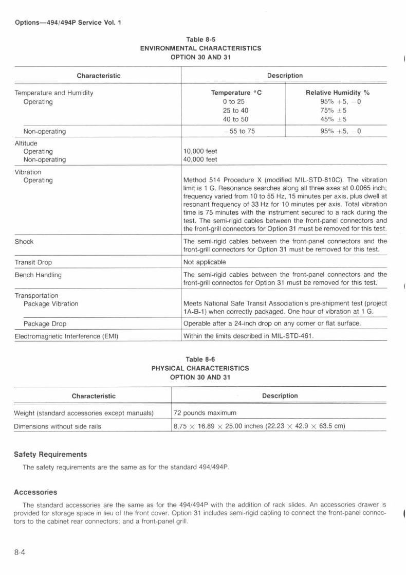
Options-4941494P Service Vol . 1
Weight (standard accessories except manuals)
Dimensions without side rails
Accessories
Characteristic
Table 8-5ENVIRONMENTAL CHARACTERISTICS
OPTION 30 AND 31
Table 8-6PHYSICAL CHARACTERISTICS
OPTION 30 AND 31
72 pounds maximum
Safety Requirements
The safety requirements are the same as for the standard 494/494P .
Description
8.75 X 16.89 X 25.00 inches (22.23 X 42 .9 X 63.5 crn)
The standard accessories are the same as for the 494/494P with the addition of rack slides . An accessories drawer isprovided for storage space in lieu of the front cover . Option 31 includes semi-rigid cabling to connect the front-panel connec-tors to the cabinet rear connectors ; and a front-panel grill .
Characteristic Description
Temperature and Humidity Temperature °C Relative HumidityOperating 0 to 25 95% +5, -0
25 to 40 75% ± 540 to 50 45% ± 5
Non-operating -55 to 75 95% + 5, -0
AltitudeOperating 10,000 feetNon-operating 40,000 feet
VibrationOperating Method 514 Procedure X (modified MIL-STD-810C) . The vibration
limit is 1 G . Resonance searches along all three axes at 0.0065 inch ;frequency varied from 10 to 55 Hz, 15 minutes per axiis, plus dwell atresonant frequency of 33 Hz for 10 minutes per axis . Total vibrationtime is 75 minutes with the instrument secured to a rack during thetest . The semi-rigid cables between the front-panel connectors andthe front-grill connectors for Option 31 must be removed for this test .
Shock The semi-rigid cables between the front-panel connectors and thefront-grill connectors for Option 31 must be removed for t his test .
Transit Drop Not applicable
Bench Handling The semi-rigid cables between the front-panel connectors and thefront-grill connectos for Option 31 must be removed for t his test .
TransportationPackage Vibration Meets National Safe Transit Association's pre-shipment test (project
1A-B-1) when correctly packaged . One hour of vibrat ion at 1 G .
Package Drop Operable after a 24-inch drop on any corner or flat surface .
Electromagnetic Interference (EMI) Within the limits described in MIL-STD-461 .

The optional accessories available for the 494/494P are listed in the current Tektronix catalog . These same optionalaccessories are available for Options 30 and 31, except that the transit case is not offered .
Installation Dimensions (Table 8-7)
The Options 30 and 31 require at least nine inches of vertical space to be mounted in a cabinet rack . At least 17.9 inches isrequired between the left and right front rails of the rack . This minimum width allows room on each side of the instrument forthe slide-out tracks to operate freely, permitting smooth movement in and out of the rack . At least 25 inches are requiredbehind the front rails for the instrument and necessary mounting hardware to fit with adequate air circulation and power cordavailability .
Slide-Out Tracks
Installation Procedure
Table 8-7INSTALLATION DIMENSIONS
OPTION 30 AND 31
Options-4941494P Service Vol . 1
If the left and right slide-out tracks are reversed, the safety latch can be defeated, allowing the instrument to bepulled out of the rack . There are green labels on each track near the mounting flange that are stamped with LH orRH to indicate left hand and right hand, respectively. Be sure to mount the tracks on the correct sides, and only asdirected in these instructions .
The slide-out tracks consist of a complete assembly for the left side of the instrument and one for the right side . Eachassembly consists of three sections . See Figure 8-1 . The stationary section of each assembly attaches to the front and rearrails of the cabinet rack . The chassis section is attached to the instrument at the factory . The intermediate section slidesbetween the stationary and chassis sections and allows the instrument to be extended out of the track . When the instrument isshipped, the stationary and intermediate sections of the tracks are packaged as matched sets and should not be separated .When mounted in the cabinet rack, the automatic latch should be at the top of both assemblies .
Extra hardware is provided with the slide-out track assemblies . Since the hardware is intended to make the tracks compat-ible with a variety of cabinet racks and installation methods, not all of the hardware will be used for any installation procedure .
The following procedure describes how to mount the slide-out tracks to untapped rack rails, using the hardware provided . Ifthe rack rails are tapped for 10-32 screws, the slide-out tracks can be mounted in front of the front rails and in back of the rearrack rails using pan head screws . The flat bar nuts are not needed .
1 .
Mount the stationary sections to the untapped front rack rails using either of the following methods .
Characteristic Dimension
Height At least 9 inches
Width 17 .9 inches minimum between left and right front rails of the rack
Depth At least 25 inches behind the front rails

Options--4941494P Service Vol . 1
Figure 8-1 . Slide-out track assemblies .
a .
It the front rails are not countersunk, use the truss head screws and bar nuts, using Figure 8-2 as a guide .
Figure 8- 2. Installing the stationary sections (A) and alternative installation methods using rear-support brackets (B), (C) .
FRONT RAIL OF CABINET RACK REAR RAIL OF CABINET RACK
DEEP RACK MOUNTING METHOD SHALLOW RACK MOUNTING METHOD
IFRONT RAIL J
10-32 1 0v
SCREWS 1(2) 0_
ism
40
a ..~
BAR NUT
REAR RAIL REAR RAIL
(A) (g) (C) 4416-01

b .
If the front rails are countersunk, use the flat head screws and bar nuts .
2.
Refer to Figure 8-3 to insert the instrument into the rack . Do not connect the power cord or install the securing screwsuntil all adjustments have been made .
0000a0a00000000a000
000aa0000
H000a0 (D) Stop Latch Hole
3. Disconnect the power cord .
Figure 8-3. Installing and removing Option 30 from the cabinet rack .
Options-494/494P , Service Vol. 1
TO INSERT THE OPTION 30 INTO THE CABINETRACK :
1 . Pull the intermediate section (A) of each sii-deout track out to its fully-extended position .
2. Insert the chassis sections (B) attached to theinstrument into the intermediate sections (A).
3. Press both stop latches (C), and push the in-strument into the cabinet rack until the latchessnap into the stop latch holes (D).
4. Connect the power cord between the instru-ment and the power source . Connect the coaxialcables to their respective connections.
5 . Again, press the stop latches (C) and push theinstrument all the way into the cabinet rack .
6. To secure the Option 30 to the rack, insert the2 securing screws (E) (with finishing washers andteflon washers) through the slots in the instrumentfront panel and screw them into the front rails ofthe cabinet rack .
TO REMOVE THE OPTION 30 FROM THE CABINETRACK :
1 . Remove the securing screws (E) and washers.
2. Pull the instrument outward until the stop latch-es (C) snap into the stop latch holes (D) .
4. Press both stop latches (C) and pull the instru-ment out of the rack .
4416-03

Options-494l494P Service Vol . 1
3 .
Position the instrument so the pivot screws (widest part of instrument) are approximately even with the front rails, andadjust the alignment of the stationary sections according to the following procedure .
a .
Position the instrument with the pivot screws approximately even with the front rails .
b .
Loosen the mounting screws at the front of both stationary sections (left side shown) .
c .
Allow the tracks to seek their normal positions with the instrument centered in the rack .
d .
Tighten the mounting screws .
e .
Push the instrument all the way into the rack . If tracks do not slide smoothly, check for correct spacing between therear supports .
f .
Check the vertical positioning of the instrument front panel with respect to adjacent instruments or panels . If notcorrect, reposition as necessary .
4 .
When track operation is smooth, connect the power cord to the power source .
5 .
Push the instrument fully into the rack and latch .
6 .
The instruments are shipped with vinyl trim strips on the cabinet flange . These strips cover two holes in the flange thatcan be used to insert screws to secure the cabinet to the rack frame . If you need the instrument secured better than thelatches on each side provide, cut out the vinyl cover around the hole with a sharp knife . Install the securing screws asshown in Figure 8-2C .
The slide-out tracks permit it to be extended out of the rack for access to the back connectors . Before attempting tooperate the instrument in the extended position, be sure the power cord and any interconnecting cables are long enough forthis purpose .
If the instrument is extended out of the rack and tipped up to gain access to the bottom or back panels of theinstrument, it can swing past center and fall back into the rack unless it is held . Use care when doing this to avoiddamaging the front panel or equipment that may be mounted above Options 30 or 31 .
Alternate Installation Procedures
!-I~Nc~srTIon
r .r~r r
While the following methods provide satisfactory installation under normal conditons, they do not provide solidsupport for the rear of the instrument. !f the instrument might be subjected to severe shock or vibration, consultyour local Tektronix Field Engineer for information on a more substantial procedure .

An alternate procedure for securing Options 30 and 31 using rear-support brackets is shown in Figure 8-2 . The rear supportbrackets that are supplied with the instrument are to be used in a rack with 15 to 26 inches of space between the front and rearrails . (If the depth of the rack is less than 22 inches, the instrument will stick out of the back of the rack .)
Mount the stationary sections to the untapped rear rails as shown in Figure 8-2B or 8-2C . Note that the rear mountingbracket can be installed either way so the slide-out tracks will fit a deep or shallow cabinet rack . Be sure that the stationarysections are aligned horizontally, i .e ., level and parallel with each other .
If the rack does not have a rear rail, or if the distance between the front and rear rails is too great, the instrument may be in-stalled without the use of the slide-out tracks . Fasten the instrument to the front rails of the rack with the securing screws, andprovide a means of securing the rear of the instrument . This method should be used only if the instrument will riot be subjectedto shock or vibration and it is installed in a stationary location .
Slide-Out Track Lubrication
The special finish on the sliding surfaces of the tracks provides permanent lubrication . However, if the tracks do not slidesmoothly even after proper adjustment, a thin coating of paraffin rubbed onto the sliding surfaces may improve operation .
Removing the Side, Top, and Bottom Panels
To remove the side, top, or bottom panels from the Option 30 or 31, follow the instructions in Figure 8-21 to remove theinstrument from the rack . Then, perform the following procedure .
1 .
Use a Torx "720" screwdriver to remove the fillister screws that hold the feet on the back four corners of Options 30and 31 .
2 .
On the cabinet side panels, remove the pivot screw for the side rail track assembly .
3 .
Slide the panel back and off the cabinet .
4 .
To remove the EMI strip, remove the back feet mounting plate and slide the strip out of its channel .
Replacement
To replace the side, top, and bottom panels, perform steps 3 through 1 . Be sure to start the EMI strip under the panelbefore sliding the panel forward . If this is not done, the panel will catch the strip and bend the end . Use a pointed object, suchas a screwdriver, to push the end of the EMI strip down while pushing the panel forward .
Installing Semi-Rigid Coaxial Cables (Option 31)
Options-494/49411" Service Vol . 1
Perform the following steps to install the semi-rigid coaxial cables of Option 31 . These cables permit rear-pianei access tothe instrument front-panel connectors .
1 .
Remove the instrument from the rack, and slide the bottom panel off according to the instructions or) removing thepanels .
2 .
Remove the horizontal support bar across the front section of the cabinet to gain access to the mounting nuts that holdthe front panel grill in place . Remove the mounting nuts .

Options-4941494P Service Vol, 1
3 .
Install the SMA coaxial connectors in the Option 31 grill .
4 .
Remove the front-panel grill and install the Option 31 grill .
5 .
Position the cables with RF connectors in their appropriate back-panel access hole . Install the mounting nuts for eachconnector and secure .
6 .
Connect the semi-rigid cables to the S MA connectors mounted in the front-panel grill, and tighten to 8-110 inch-pounds .
Do not overtighten coaxial connectors beyond the recommended 8 to 10 inch-pounds torque . Use a secondwrench to hold the connector or cable nut as the other nut is tightened.
7 .
Attach the cable clamps to hold the cables to the mounting posts on the bottom of the instrument housing,
8 .
Reinstall the horizontal support bar, and reinstall the bottom panel .
9 . Reinstall the instrument in the rack and install the semi-rigid cables between the front-panel connectors and theconnectors on the cabinet grill .
a .
Ensure that the plugs and receptacles are clean and free of any foreign matter .
b .
Insert the plug connectors fully into the receptacle . Since the cables are all approximately the sarne length, thecables for the 1 st and 2nd LOS are labeled to avoid confusion . Do not force a cable in place if it does not fit easily .
c .
Screw the mounting nut on finger tight to ensure it is not cross-threaded .
d .
Use a 5116 inch open-end wrench to tighten the nut to 8-10 inch-pounds torque .
Preparing the Instrument for Adjustment or Repair
The fan assembly must be removed before the instrument can be removed from the cabinet . After the instrument isremoved from the cabinet, the fan must be reconnected before power can be applied to allow the instrument to be turned on .The following steps prepare the instrument for adjustment or repair .
1 .
If the Option 31 is installed in a rack with the semi-rigid cables to the back panel, disconnect the cables between theinstrument front panel and the connectors on the front grill of the cabinet .
2 .
Disconnect all external connections to the instrument, including the power cord, and remove the instrument from therack .
3 .
Place the instrument face-down on a bench .

4 .
Loosen the two fan assembly mounting screws and remove the fan assembly .
7 .
The instrument is now ready for adjustment or repair .
Introduction
OPTION 32
Electrical, Environmental, and Physical Characteristics
The electrical characteristics for the 494/494P are applicable for Option 32 .
The physical characteristics for Option 32 are listed in Table 8-9 .
Options-494/494P Service Vol . 1
5 .
Use a 5132-inch Allen wrench to loosen and remove the four screws that hold the instrument to the cabinet back paneland remove the instrument from the cabinet .
6 .
Carefully align the fan assembly power connector pins to the receptacle on the back panel of the instrument andreinstall the fan assembly . Reconnect the power cord .
Option 32 is the benchtop version of the 494/494P Spectrum Analyzer . The Option 32 configuration adds feet to the bottomof the instrument and also adds side panels with handles . A larger fan is installed to provide additional coolincf . Pull-out cardsare not included with this option .
Option 32 instruments meet MIL T-288a0C, type III, class 5, style E specifications . Some of the detains are shown inTable 8-8 .

Options-4941494P Service Vol . 1
Table 8-8ENVIRONMENTAL CHARACTERISTICS
OPTION 32
Table 8-9PHYSICAL CHARACTERISTICS
OPTION 32
Characteristic Description
Temperature and Humidity Temperature °C Relative HumidityOperating 0 to 25 95% d-5, -0
25 to 40 75% ± 540 to 50 45% i.5
Non-operating -55 to 75 95% +5, -0Altitude
Operating 10,000 feetNon-operating 40,000 feet
VibrationOperating Method 514 Procedure X (modified MIL-STD-810C) . The vibration
limit is 1 G . Resonance searches along all three axes at 0 .0065 inch ;frequency varied from 10 to 55 Hz, 15 minutes per axis, plus dwelt atresonant frequency of 33 Hz for 10 minutes per axis . Total vibrationtime is 75 minutes with the instrument secured to a vibration platformduring the test . The bail for tilting must be folded for t his test .
Shock The bail for tilting must be folded for th is test .
Transit Drop Not applicable
Bench Handling The bail for tilting must be folded for th i s test .
TransportationPackage Vibration Meets National Safe Transit Association's pre-shipment test (project
1A-B-1) when correctly packaged . One hour of vibration at 1 G .Package Drop Operable after a 24-inch drop on any corner o r fl at surface .
Electromagnetic Interference (EMI) Within the limits described in MIL-STD-461 .
Characteristic Description
Weight (standard accessories except manuals) 70 pounds maximum
Dimensionswith feet and handles 9.25 x 17.9 x 25 .00 inches (23.5 x 45.47 X 63.5 cm)without feet and handles 8.75 X 16.89 x 25 .00 inches (22.23 x 42.90 x 63 .5 crn)

Safety Requirements
The safety requirements are the same as for the standard 4941494P .
Accessories
The standard accessories are the same as for the 494/494P instrument . An accessories drawer is provided for storagespace in lieu of the front cover . The optional accessories available for the 494/494P are listed in the current Tektronix catalog .These same optional accessories are available for Option 32, except that the transit case is not offered .
Removing the Instrument From the Cabinet
Before attempting any adjustment or repair, the Option 32 must be removed from its cabinet .
1 .
Place the instrument face-down on a bench .
2 .
Loosen the two fan assembly mounting screws and remove the fan assembly .
3 .
Use a 5132 Allen wrench to loosen and remove the four screws that hold the instrument to the cabinet back panel .
4 .
Push or pull the instrument from the cabinet .
Replacement
To replace the Option 32 in the cabinet, perform steps 4 through 1 of this procedure .
OPTION 41
Options-4941494P Service Vol . 1
5 .
Carefully align the fan assembly power connector pins to the receptable on the back panel of the instrument andreinstall the fan assembly . Reconnect the power cord .
Provides enhanced measurement capability for Digital Microwave Radio . These include : 1) A wider bandwidth preselectorfor better signal symmetry in the digital radio bands ; 2) A narrow video filter (approrximately 113000th of the resolutionbandwidth) to improve amplitude variation analyses, at specific frequency spans that are unique to the digital radio measure-ments ; 3) Improved frequency spanldiv accuracy at 5 MHz/DIV span, to make accurate signal band- width measurements .
OPTION 52
North American 220 V configuration with standard power cord . Fuses are replaced with 2A slow blow .


The following glossary is presented as an aid to betterunderstand the terms as they are used in this document andwith reference to spectrum analyzers .
Baseline Clipper (Intensifier) . Increasing the brightnessof the signal relative to the baseline portion of the display .
Center Frequency . That frequency which correspondsto the center of a frequency span, expressed in hertz .
Effective Frequency Range. That range of frequencyover which the instrument performance is specified . Thelower and upper limits are expressed in hertz .
Envelope Display. The display produced on a spectrumanalyzer when the resolution bandwidth is greater than thespacing of the individual frequency components .
dBc. dB below carrier level .
Frequency Band. A part of effective frequency rangeover which the frequency can be adjusted, expressed inhertz .
Full Span (Maximum Span). A mode of operation inwhich the spectrum analyzer scans an entire frequencyband .
Zero Span. A mode of operation in which the frequencyspan is reduced to zero .
Line Display . The display produced on a spectrum ana-lyzer when the resolution bandwidth is less than the spacingof the signal amplitudes of the individual frequencycomponents .
Line Spectrum . A spectrum composed of signal ampli-tudes of the discrete frequency components .
GLOSSARY
GENERAL TERMS
Maximum Safe Input Power
Appendix A-494/494P Service Vol . 1
WITHOUT DAMAGE . The maximum power applied atthe input which will not cause degradation of the instrumentcharacteristics .
WITH DAMAGE. The minimum power applied at the in-put which will damage the instrument .
Intermodulation Spurious Response (IntermodulationDistortion) . An unwanted spectrum analyzer response re-sulting from the mixing of the nth order frequencies, due tonon-linear elements of the spectrum analyzer, the resultantunwanted response being displayed .
Pulse Stretcher . A pulse shaper that produces an outputpulse, whose duration is greater than that of the input pulse,and whose amplitude is proportional to that of the peakamplitude of the input pulse .
Spectrum Analyzer . An apparatus which is generallyused to display the power distribution of an incoming signalas a function of frequency .
NOTE
It is useful in analyzing the characteristics of repetitiveelectrical waveforms in general, since repetitivelysweeping through the frequency range of interest willdisplay all components of the signal.
Signal Identifier . A means to identify the spectrum of theinput signal when spurious responses are possible .
Scanning Velocity_ Frequency span divided by sweeptime and expressed in hertz per second .
Video Filter. A post detection lowpass filter .

Glossary-4941494P Service Vol . 1
Display Frequency . The input frequency as indicated bythe spectrum analyzer and expressed in hertz .
Frequency Span (Dispersion) . The magnitude of thefrequency band displayed, expressed in hertz or hertz perdivision .
Frequency Linearity Error. The error of the relationshipbetween the frequency of the input signal and the frequencydisplayed (expressed as a ratio) .
Frequency Drift. Gradual shift or change in displayed fre-quency over the specified time due to internal changes in thespectrum analyzer, and expressed in hertz per second,where other conditions remain constant .
Residual FM (Incidental FM) . Short term displayed fre-quency instability or jitter due to instability in the spectrumanalyzer local oscillators, given in terms of peak-to-peak fre-quency deviation and expressed in hertz or percent of thedisplayed frequency .
Deflection Coefficient. The ratio of the input signal mag-nitude to the resultant output indication .
NOTE
Display Reference Level. A designated vertical positionrepresenting a specified input level .
The ratio may be expressed in terms of volts (rms) perdivision, decibels per division, watts per division, orany other specified factor.
NOTE
The level may be expressed in decibels (e.g ., 1 mW),volts, or any other units .
TERMS RELATED TO FREQUENCY
TERMS RELATED TO AMPLITUDE
Impulse Bandwidth . The displayed spectral level of anapplied pulse divided by its spectral voltage density levelassumed to be flat within the pass-band .
Static (Amplifier) Resolution Bandwidth . The specifiedbandwidth of the spectrum analyzer's reponse to a cw sig-nal, if sweep time is kept substantially long .
NOTE
This bandwidth is the frequency separation of twodown points, usually 6 dB, on the response curve, if itis measured either by manual scan (true staticmethod) or by using a very low speed sweep (quasi-static method) .
Shape Factor (Skirt Selectivity) . The ratio of the fre-quency separation of the two (6Q dB/6 dB) down points onthe response curve to the static resolution bandwidth .
Zero Pip (Response). An output indication which corre-sponds to zero input frequency .
Sensitivity . Measure of a spectrum anallyzer's ability todisplay minimum level signals, at a given IF bandwidth, dis-play mode, and any other influencing factors, and expressedin decibels (e.g ., 1 mW).
Equivalent Input Noise Sensitivity . The average level ofa spectrum analyzer's internally generated noise referencedto the input .
Display Flatness . The unwanted variation of the dis-played amplitude over a specified frequency span, ex-pressed in decibels .
Relative Display Flatness. The display flatness mea-sured relative to the display amplitude at a fixed frequencywithin the frequency span, expressed in decibels .

The following cases apply:
NOTE
Display flatness is closely related to frequency re-sponse . The main difference is that the spectrum dis-play is not recentered.
Frequency Response . The unwanted variation of thedisplayed amplitude over a specified center frequencyrange, measured at the center frequency, expresed indecibels .
Display Law. The mathematical law that defines theinput-output function of the instrument .
NOTE
7 . Linear-A display in which the scale divisions are alinear function of the input signal voltage ;
2. Square law (power)-A display in which the scaledivisions are a linear function of the input signalpower;
3 . Logarithmic-A display in which the scale divisionsare a logarithmic function of the input signal voltage.
Dynamic Range. The maximum ratio of the levels of twosignals simultaneously present at the input which can bemeasured to a specified accuracy .
Display Dynamic Range. The maximum ratio of the lev-els of two non-harmonically related sinusoidal signals each
Glossary-494/494P Service Vol . 1
of which can be simultaneously measured on the screen to aspecified accuracy .
Gain Compression. Maximum input level where thescale linearity error is below that specified .
Spurious Response . A response of a spectrum analyzerwherein the displayed frequency does not conform to theinput frequency .
Hum Sidebands . Undesired responses created withinthe spectrum analyzer, appearing on the display, that areseparated from the desired response by the fundamental orharmonic of the power line frequency .
Noise Sidebands . Undesired response caused by noiseinternal to the spectrum analyzer appearing on the displayaround a desired response .
Residual Response . A spurious response in the ab-sence of an input signal . (Noise and zero pip are excluded .)
Input Impedance . The impedance at the desired inputterminal .
NOTE
Usually expressed in terms of vswr, return loss, orother related terms for low impedance devices andresistance-capacitance parameters for high imped-ance devices.

Glossary-4941494P Service Vol. 1
TERMS RELATED TO DIGITAL STORAGE FOR SPECTRUM ANALYZERS
Digitally Stored Display . A display method whereby thedisplayed function is held in a digital memory . The display isgenerated by reading the data out of memory .
Digitally Averaged Display . A display of the averagevalue of digitized data computed by combining serial sam-ples in a defined manner.
Multiple Display Memory. A digitally stored display hav-ing multiple memory sections which can be displayed sepa-rately or simultaneously .
Clear (Erase) . Presets memory to a prescribed state,usually that denoting zero .
Save . A function which inhibits storage update, savingexisting data in a section of a multiple memory (e.g ., SaveA) .
View (Display) . Enables viewing of contents of the cho-sen memory section (e .g ., "View A" displays the contents ofmemory A; "View B" displays the contents of memory B) .
Max Hold (Peak Mode). Digitally stored display modewhich, at each frequency address, compares the incomingsignal level to the stored level and retains the greater . In thismode, the display indicates the peak level at each frequencyafter several successive sweeps .
Scan Address . A number representing each horizontaldata position increment on a directed beam type display . Anaddress in a memoryis associated with each scan address .
Volatile/Non-volatile Storage. A volatile storage systemis one where any total loss of power to the system will resultin a loss of the stored information .

MANUAL CHANGE INFORMATION
At Tektronix, we continually strive to keep up with latest electronic developmentsby adding circuit and component improvements to our instruments as soon as theyare developed and tested .
Sometimes, due to printing and shipping requirements, we can't get thesechanges immediately into printed manuals . Hence, your manual may contain newchange information on following pages .
A single change may affect several sections . Sincethe change information sheetsare carried in the manual until all changes are permanently entered, someduplication may occur. If no such change pages appear following this page, yourmanual is correct as printed .


TEKTRONIX MANUALS CHANGE INFORMATION
Date :
11-14-83Product :
494/494P Serv . Val . 1 Manual Part No . : 474--4416-00Change Ref .
01/1183 Rev . #2
Product Group :
26
DESCRIPTION
Revised 12-20-83Revised 5--16-84
TEXT CHANGES
MAINTENANCE Section page 6-73, preceding the Theory of Operation ;ADD the following :
FIRMWARE OPERATING NOTES
The following exceptions apply to 494P instruments with firmwareversion 2 . 2 .
Using the Tektronix 4662 Option 31 Plotter
The 4662 Option 31 Plotter does not respond to the first "move" commandthat immediately follows a "pen selection" or "pen change" command,consequently the pen starts to draw from its "home" position insteadof the selected position . This can be averted by using either aone-pen (one-color) plot or by manually selecting the second pen .The following procedure describes hour to make a two-color plot .
1 . Switch the GRAT ILLUM on, READOUT and Digital Storage off .
2 . Manually select a pen, then plot the graticule .
3. Switch the GRAT ILLUM off. READOUT and Digital Storage on .
4 . Manually select the second pen, then plot the stored displayand crt readout .
Auto Peaking Function with External Mixers
With instruments that have version 2.2 the Auto Peak functiondoes not always set the bias for external mixers to the correct peakvalve . To ensure maximum peaking use the PEAK/AVERAGE control oruse a "peak" command with specific numeric arguments .


TEKTRONIX MANUAL CHANGE NOTICE
L)a t e :
7-31-e4Product :
494/494P Ser .1
Manual Part No . : 070-4416-00Change Ref : C2/ee4
Product Group :
26
DESCRIPTION
TEXT CHANGES
NOTE
If the Reference Oscillator has not beenpowered up for a long period of time,additional warm-up time may be neededbefore the final frequency adjustmentis made .
REPLACE step c . of the procedure to check the Reference 0scil--lator Accuracy an page 4-13 with the following :
c . If the Reference Oscillator needs adjustment, unscrew theprotective screw on the Oscillator . Turn the oscillatorfrequency adjustment carefully and slowly with a small screw-driver or adjustment tool to 100 MHz . +/- 10 Hz on the counter .Replace the protective screw . Disconnect the counter fromthe CAL OUT connector .


TEKTRONIX MANUAL CHANGE NOTICE
Date :
i 1--16-84Product :
494/494P 8er . 1
Manual Part No . : 070-44-16-00Change Ref : 03/1184
Product Group :
26
DESCRIPTION
TEXT CHANGES
REMOVE the last two paragraphs from the right--hand columinof Page 6-30 .


Tektronbcoco"+wwTTEOTOEXCELLENCE
Date :
5-2-84
Change Reference : _
C1011584
Product :
494/494P
Manual Part No. : 070-441b-00
Page
8--13, after Option 41
f ADD :
110
MHz
_c enter3 dB bbandpasssymmetry about110
MHz
power
output with
-30
dB input and
signal
at full
screen
(band 1)
(band
5)
Tracking
Generator
with
logic cable
2
RF Cable Assem-
blies
50
Ohm Termination
~3
Bnc-5"1B Flexible
Gables
MANUAL CHANGE INFORMATION
ELECTRICAL
CHARACTERISTICS
DESCRIPTION
Product
Group 26
OPTION
42
In
Option 42 instruments the MARKER/VIDEO input port on the rear panel
is
replaced with an 110 MHz IF output port
.
It
provides a signal with a
bandwidth
greater than 5 MHz, which makes the spectrum analyzer suitable
for
broadband swept-receiver applications
.
Page
4-3r ADD to Equipment Required for the Performance Check
:
Page
4-4, ADD to Equipment Required for the Adjustment Procedure
:
Performance
Requirement
Supplemental
Information
-------------------------------
---------------------------
nominal
output impedance=
50
ohm
in
MIN DISTORTION mode
only
1
dB compression of
output
==/= O dfim
Frequency
Range 100 kHz to 1
.8
GHz
TEKTRONIX
TR502 (used
to
check Option 42)
Tektronix
Part No
012-0649-00
011-0049-01

Product : 4941494P SPr3z1 cE_Yn111mi- 1
Date:
S-9-R4
- Change Reference : C 1 0 1 15884
DESCRIPTION
Page 4--45, ADD after the 494P GPIB Verification Program :
32. For Option 42 instruments . Check Power Output at the 120 MHz OUTConnector on Band 1 (!/= 0 dBm)
a . Using the flatness data for the instrument being tested find the signal.with the highest amplitude .
b . Connect a signal, generator to the frequency determined in step a andpower level to -30 dBm .
c . Set the 494/494P Option 42 REFERENCE LEVEL to -30 dBm and RF ATTENUATIONto 0 dL .
d . Keeping the signal centered with the CENTER FREQUENCY control, switchthe FREQUENCY SPAN/DIV to 0 (the crt FRED SPAN/DIV will indicate 10 ms) .
e . Adjust the CENTER FREQUENCY control, of the 494 Option 42 to center thesignal displayed on the 7L14 .
f . Check that the 110 MHz IF OUT output pow=er is <:_/= 0 dBm.
33 . For Option 42 instruments . Check Power Output at the 110 MHz OUTConnector can Band 5
-40 dBm)
a . Using the flatness data for the instrument being tested, find the signs!with the lowest amplitude on Band 5,
b . Connect a signal generator capable of the frequency determined instep a to the 494 Option 42 RF INPUT .
c . Set the signal generator to the frequency determined in step a andthe power level to -30 dBm .
d . Set the 494 Option 42 REFERENCE LEVEL to -50 dBm and RF ATTENUATION to0 dB .
e . Keeping the signal centered with the CENTER FREQUENCY control, switchthe FRED SPAN/DIV to 0 (the crt Freq Span/Div will indicate 10 ms) .
f . Adjust the CENTER FREQUENCY control of the 494 Option 42 to center thesignal displayed on the 7L14 .
g . Check that the 110 MHz IF OUT output power is : ;_ -40 dBlm

b
D
Product : 494/494P Service Volume 1
Date:
5-2-S4
Change Reference : C 10 1
584
L_
DESCRIPTION
.34 . For Option 42 instruments . Check Bandwidth (_r5 MHz) . Center Frequency
(109 .5 r1Hz--113. .5 MHz), Bandpass ripple (</=0 .5 dB), and Symmetry about 110 C-"HZ(+/-- 1,0 MHz)
a . Connect the test equipment as shown in Fig .4-24A .
Fig . 4-24A
b .
Digital storage
offTime/Div
manualTriggering
Source
free runMode
normVideo filter
on
DC510 Function
Frequency AAuto Trig
on
Ohm
Page 3 of 7
c:et the instrument front--panel controls as follows :TR502 Output level -dBm 30
Var dL, 0Dot intensity off
7L14 Center frequency 0110Freq span/div 1 Ml-AzHz Resolution 3 MH7_Reference level 0 dBm
Reference level mode 21 dB/Div
Channel AAttn k1Coupl doTerm 50

Product : 494/494F Service Volume 1
Date :
5-2-84
Change Reference : ,'101/584
DESCRIPTION
494/494P Option 42
REFERENCE LEVEL
-30 d13mCENTER FREQUENCY
110 MHzFREQUENCY SPAN/DIV
1 MHzHz RESOLUTION
1 MHzVERTICAL DISPLAY
2 dB/DIVMIN RF ATTEN
0 dB
c . Set the 7L14 Time/Div to Mnl and adjust the dot to center screen withthe Manual Scan control .
d . Adjust the 7L14 Center Frequency control for an indication of 110.01 or,the Frequency Counter,
e . While keeping the signal centered with the CENTER FREQUENCY controlset the 494 Option 42 FREQUENCY SPAN/DIV control to 0 (the Frequency Span/Divon the crt will indicate 10 ms) .
f . Set the 7L14 Time/Div for a calibrated display and adjust the ReferenceLevel and TR502 Var dB for full screen signal .
g . Switch the TR502 Dot Intensity to "on", and adjust the 7L14 CenterFrequency for an indication of 110.0 on the Frequency Counter .
h . Check the bandwidth at a point 3 dB (1 .5 divisions) from the peak ofthe signal to be =:/= 5 MHz .
i . Cheek that any ripple present on the waveform is -=/= 0 . 5 dB (</= 0,25divisions) .
. Check that the waveform symmetry is +/- 1 .0 MHz (+/- 1 .0 division) bgassuring that the 3dL and bdB points on the waveform are equidistant fromcenter screen . (The peak of the signal may not be at center of the screen) .
This concludes the Performance Check part of the Calibration Procedure .
a
is

Product : 494/494P Serivce Volume 1
Date :
5-2-84
Change Reference : C1071594
DESCRIPTION
Page 5-35 : ADD after
14 . For Optionadjustment needreplaced .
42 instruments . Adjustment of Option 42 Module . Thisonly be done after the circuit board in the module has been
a . Connect the test equipment as shown in Fig . 5--35 .
b . Set the instrument front-panelTR502 Output level -dBm
Var dB
7L14
Center frequencyFreq span/divHz ResolutionVertical displayReference LevelDisplay A and E
DC 510
Ch
ATermSlopeAttenCaupl
Frequency AAutotrig
the adjustment for Phaselock Calibration :
Fig . 5-35
controls as follows :
0
Page 5 of 7
01102 MHz3 MHz2 dB0off
c . Set the 7L14 Time/Div to Manual, and adjust the crt beam (dot) to cerster -screen

Product : 494/494P Service Vol, 1
Date :
5-2-84
Change Reference : ClOIZ584
DESCRIPTION
d . The DC503A readout should indicate approximately 110.000 MHz . AdjusLevel as necessary, and adjust the 7L14 Center Frequency for an indication110.0 MHz .
e . Set the 7L14 Time/Div to calibrated display .
f . Adjust variable capacitors C1016, C1020 and C1024 for maximum amplitudesymmetry and bandpass (3dB and 6dB points) .
9
1 . Adjust the bandwidth symmetry +/- 0.5 divisions (+/- 0.5 MHz) at the3 dB and 6 d)? points,
i . Check Forward Gain
NOTECheck that points W dB (1 .5 divisions) and 6 dB?(3 divisions) down from the top of the signalare equidistant (+/- 0.5 divisions) from centerscreen .
2. Check that bandwidth at the 3 dB point is 7 . 5 MHz, +/- 1 . 5 MHz .
3 . Check that any ripple present on the waveform is ~:!= 0.2 div(0 . 4 dB) .
NOTEA slight change in display may be observed whenthe cover is reinstalled on the module .
Check the Coupled Forward Gain (IF OUT port - P1024)
1 . Set the 7L14 Spectrum Analyzer Reference Level to 0 dam .
2 . Check that the display on the 7L14 is between 4 and 7 divisionsin amplitude (-S dfim, +/-3 dam) .
h . Check the Input Compression .
1 . Set the TR503 Output Level and 494 REFERENCE LEVEL in one dBincrements, to higher power level (-24 dbm, -23 darn etc .)
2 . Continue changing the power level until the signal displayed bythe 7L14 amplitude decreases Lcompresses 1 dB) 0.5 division .
3 . Check that the signal displayed on the 7114 indicates
0 dam.
1 . Return the TR502 Output Level to -25 and remove the connectionto the module IF OUT .
Page 6 of 7

Product :
494/494P Service Vol . 1
Date :
5-?-84
Change Reference :
C1011584
DESCRIPTION
2. Connect a 50 ohm termination to the IF OUT (P1024) connector .
3 . Connect the OUT (P1012) connector to the 7L14 RF Input with a 50ohm cable .
4 . Adjust the 7L14 Reference Level until the displayed signal is nearfull screen (B divisions) .
5 . Check that the signal displayed on the 7L14 indicates -20dBm to-23 dBrn (-21 . 5 dBm +/-1 . 5 dBm) .


TEKTRONIX MANUAL CHANGE NOTICE
Date : 2-25-85Product :
494 Ser .l
Manual Part No . :
070-4416-00Change Ref : C102/285
Product Group :
26
DESCRIPTION
TEXT CHANGES
ADD on Page 6-29, REPLACING ASSEMBLIES AND SUBASSEMBLIES in theMaintenance Section, after the procedure on Removing or ReplacingSemi-rigid Coaxial Cables :
Replacing the Dual Diode Assembly in the 1st Converter
The diode subassembly, which houses the Schottky mixer diodes, isheld in place by four 0-80 screws . An 8-32 threaded hole is providedto facilitate insertion and removal of the subassembly . There arethree contact points located on the substrate side of the subassembly .Use care when mounting and orienting these contacts with the matingcontacts in the mixer assembly, to ensure proper fit and function .Insertion and removal of the subassembly more than twice is riotrecommended due to the gold ribbon attach technique used infabrication .
A tuning screw, mounted through the top of the diode assembly, andadjacent to the 8-32 screw, is adjusted to null a start spur onband 1 as described in the Adjustment Procedure section . Althoughpre-calibrated, care should be taken to not force the tuning screwafter it bottoms out on the surface of the quartz-suspended substrate .
The diode subassembly is packaged in a static-free package . Keepthe diode subassembly in this package until ready to install .
Thefollowing procedure should be used when replacing the subassembly .
CAUTION
The diodes are beam-lead devices mounted on a quartz-suspended substrate ; these diodes are extremely staticsensitive . Refer to the Caution note on static thatprecedes this section . Do not expose the diode assemblyto any RF field .
1 . Loosen and disconnect the three coaxial cable connections tothe 1st Converter assembly, then remove the two mounting screws andremove the assembly from the 494/494P .
2 . Remove the four 0-80 screws that hold the diode subassembly inthe 1st Converter and insert a 8-32 screw into the threaded holeprovided in the center of the diode assembly .
Page 1 of 6

Product : 494 Ser .1
Date : 2-25-85
Change Reference : C102/285
3 . Lift the diode assembly out of the mixer assembly by means ofthe 8-32 screw, then remove the screw .
4 . Open the diode package, grasp the diode assembly by its sidewith tweezers and place it on a static-free surface .
Grasp the sideof the assembly with the fingers to avoid contact with the diodes,and insert the 8-32 screw .
5 . Orient the diode assembly so the three contact tips are alignedwith their respective contacts in the mixer ; then using the indexfingers of both hands so equal pressure is applied, press the sub-assembly into place .
6 . Insert the four mounting screws, tighten, then replace andtighten the three coaxial connectors to 8 inch lbs . Remount thelst Converter assembly by installing the two mounting screws thathold the assembly to the RF deck of the 494/494P .
. A procedure to adjust the First Converter Bias and Start SpurAmplitude is provided in the Maintenance Adjustments section .
NOTEAfter replacement of the A12A1 Dual Diode Assemblyin First Converter 119-1017-01, the 494/494PSpectrum Analyzer may not meet the flatnessspecification .After replacement of the A12A1 Dual Diode Assemblyin First Converter 119-1017-00, the 494/494PSpectrum Analyzer may not meet the flatness or thestart spur specification .
ADD on Page 6--49, after Troubleshooting Aids for the 2182 MHz Phase-locked 2nd LO Assembly :
First Converter Bias and Start Spur Amplitude
NOTE
Page 2 of 6
After replacement of the A12A1 Dual Diode Assemblyin First Converter 119-1017-01, the 494/494PSpectrum Analyzer may not meet the flatnessspecification .After replacement of the A12A1 Dual Diode Assemblyin First Converter 119-1017-00, the 494/494PSpectrum Analyzer may not meet the flatness or thestart spur specification .

Product : 494 Ser .l
Date : 2-25-85
Change Reference : (:102/285
1 . Preparation
Connect to AT10with 175-3310-00cable
a . Remove the First Converter assembly from the spectrum analyzer,and connect the cables as shown in Fig .6-26A .
Fig .6-26A First Converter test equipment setup .
Page 3 of 6
Connect: to A13with 17'5 - 2765-00cable
Connect to A10with 175 - ,2337-00cable
J
EQUIPMENT REQUIREDAND
Table 6-7A
FOR ADJUSTING FIRSTSTART SPUR AMPLITUDE
CONVERTER BIAS
Test Equipment Characteristics [Recommended Type
Digital Multimeter 1</=10 uV to >/=350 Vdc TEKTRONIX DM502A andATM 500-Series Power Module
Sinewave Generator 12 .0 MHz, 0 dBm (TEKTRONIX SG5031+10 dBm to -100 dBm
Power Meter must measure 0 dBm jHewlett-Packard 435B
Power Sensor (must measure 0 dBm Hewlett-Packard E1482A1 @2 MHz
Attenuator (13 dB) I ITEKTRONIX 2701
Coaxial Cable Tektronix Part No .(50 ohm) 1 175-2765-00
Coaxial Cable (Tektronix Part No .(50 ohm) 1 175-2337-00
Coaxial Cable Tektronix Part No .(50 ohm) r 1 175-3310-00

Product : 494 Ser .1
Date : 2-25-85
Change Reference : C102/285
b . Set the spectrum analyzer front-panel controls as follows, :
TIME/DIV AUTOREFERENCE LEVEL
-30 dBMFREQUENCY RANGE
5.4-18 GHz (band 4)FREQ SPAN/DIV
MAXDIGITAL STORAGE
DISPLAY A
offDISPLAY B
offMIN RF ATTEN
0PEAK/AVERAGE clockwise
c . Set the DM502 controls as follows :
Range Switch
20 DC VoltsDB pushbutton
outInt pushbutton
out
d . Connect the DM502 red test lead to TP1011 on the 1st LO Driverboard, and the black test lead to the instrument chassis, seeFig.6-26B .
o~~~Q~~t~ ooooas
Fig.6-26B Adjustments and test points on the 1st LO Driver board .
Page 4 of 6

Product : 494 Ser .l
Date : 2-25-85
Change Reference : 0102/285
2 . Bias Adjustment
a . Adjust R1022 (see Fig .6-26B) for a reading of -0 .25 on theDM502 .
b . Push FREQUENCY RANGE i to band 5 (15-21 GHz), and adjustR1026 (see Fig .6-26B)for a reading of -0 .25 on the DM502 .
3 . Start Spurious Amplitude and Band 1 Bias Adjustment .
a . Push FREQUENCY RANGE V
to band 1 (0-4 .2 GHz), and adjustthe CENTER FREQUENCY to 0 MHz .
b . Connect a 50 ohm cable from the SG503 Output to the 2701Port 1/Input, and connect a second 50 ohm cable to the Power Sensor .
NOTE
Calibrate the Power Meter before making measurements .
c . Set front-panel controls as follows :
SG503Frequency Range
1-2 .5Frequency Variable
for an indication of 2 .00 MHz on the readoutAmplitude Multiplier x1Output Amplitude
counterclockwise
Power MeterLine
onRange
0 (on the dBm scale)
d . Adjust the SG503 Output Amp control for an indication of 0 onthe Power Meter dBm scale .
e . Disconnect the Power Meter from the 50 ohm cable and connect the50 ohm cable from the 2701 Port 2/Output connector to the 494 RF INPUTconnector .
f . While keeping the 2 MHz signal centered with the CENTER FREQUENCYcontrol, set the 494 FREQUENCY SPAN/DIV to 200 kHz .

Product : 494 Ser .l
Date : 2-25-85
Change Reference : C102/285
g . Set the front-panel controls as follows :
494RESOLUTION BANDWIDTH 100 kHzVIDEO FILTER (WIDE)
on
h . Measure and record for reference the bandwidth of the 2 W[zsignal at a point 6 divisions down from the top graticule line .
i . Adjust 81013 on the 1st LO Driver board for approximately-1 .0 V at TP1011 .
NOTE
During the following procedure, do not allow this voltageto go more positive than 0 .1 V .
j . Bring the Start Spur signal to center screen with the CENTERFREQUENCY control . Frequency readout will indicate 0 .00 MHz .
NOTE
For the least overall signal variations with frequency(flatness), the adjustments on the 1st Converter must bemade in conjunction with 81013 (bias for bands 1, 2, and3) .
k . Alternately adjust 81013 and the adjustments on the 1stConverter (see Fig .4-23A) until the bandwidth, at the 6 dB point,matches the bandwidth of the previously displayed 2 MHz signal .
NOTE
It will be necessary to alternate between the aboveadjustments to decrease the amplitude of the startspur . While this is being done, assure that thevoltage at TP1011 does not exceed +1 .0 V .
It will not be possible to null the start spur toa point where the top of the signal will be on screen .To assure that the signal meets the specification(-13 dBm), the bandwidth is matched to the bandwidthof the previously displayed 2 MHz signal . Do notadjust the start spur lower than -13 dBm .
l . Remove all test leads from the test setup .
Page 6 of 6