3gpp ts 25.141 v5.15.0 (2007-09)
TRANSCRIPT
3GPP TS 25.141 V5.15.0 (2007-09)Technical Specification
3rd Generation Partnership Project;Technical Specification Group Radio Access Network;
Base Station (BS) conformance testing (FDD)(Release 5)
The present document has been developed within the 3rd Generation Partnership Project (3GPP TM) and may be further elaborated for the purposes of 3GPP. The present document has not been subject to any approval process by the 3GPP Organizational Partners and shall not be implemented. This Specification is provided for future development work within 3GPP only. The Organizational Partners accept no liability for any use of this Specification.Specifications and reports for implementation of the 3GPP TM system should be obtained via the 3GPP Organizational Partners' Publications Offices.
3GPP
3GPP TS 25.141 V5.15.0 (2007-09)2Release 5
Keywords UMTS, base station, testing
3GPP
Postal address
3GPP support office address 650 Route des Lucioles - Sophia Antipolis
Valbonne - FRANCE Tel.: +33 4 92 94 42 00 Fax: +33 4 93 65 47 16
Internet http://www.3gpp.org
Copyright Notification
No part may be reproduced except as authorized by written permission. The copyright and the foregoing restriction extend to reproduction in all media.
© 2007, 3GPP Organizational Partners (ARIB, ATIS, CCSA, ETSI, TTA, TTC).
All rights reserved.
3GPP
3GPP TS 25.141 V5.15.0 (2007-09)3Release 5
Contents Foreword...........................................................................................................................................................12 1 Scope ......................................................................................................................................................13 2 References ..............................................................................................................................................13 3 Definitions and abbreviations.................................................................................................................14 3.1 Definitions ....................................................................................................................................................... 14 3.2 Void ................................................................................................................................................................. 14 3.3 Abbreviations................................................................................................................................................... 14 3.4 Radio Frequency bands.................................................................................................................................... 15 3.4.1 Frequency bands......................................................................................................................................... 15 3.4.2 TX–RX frequency separation..................................................................................................................... 15 3.5 Channel arrangement ....................................................................................................................................... 16 3.5.1 Channel spacing ......................................................................................................................................... 16 3.5.2 Channel raster............................................................................................................................................. 16 3.5.3 Channel number ......................................................................................................................................... 16 4 General test conditions and declarations................................................................................................16 4.1 Acceptable uncertainty of Test System............................................................................................................ 17 4.1.1 Measurement of test environments............................................................................................................. 17 4.1.2 Measurement of transmitter ....................................................................................................................... 18 4.1.3 Measurement of receiver ............................................................................................................................ 19 4.1.4 Measurement of performance requirement ................................................................................................ 20 4.2 Test Tolerances (informative).......................................................................................................................... 20 4.2.1 Transmitter ................................................................................................................................................. 21 4.2.2 Receiver ..................................................................................................................................................... 21 4.2.3 Performance requirement ........................................................................................................................... 21 4.2.4 RRM measurements ................................................................................................................................... 22 4.3 Interpretation of measurement results.............................................................................................................. 22 4.3A Output power and determination of power class.............................................................................................. 22 4.4 Test environments............................................................................................................................................ 22 4.4.1 Normal test environment ............................................................................................................................ 22 4.4.2 Extreme test environment........................................................................................................................... 23 4.4.2.1 Extreme temperature............................................................................................................................. 23 4.4.3 Vibration .................................................................................................................................................... 23 4.4.4 Power supply.............................................................................................................................................. 23 4.4.5 Definition of Additive White Gaussian Noise (AWGN) Interferer............................................................ 24 4.5 Selection of configurations for testing ............................................................................................................. 24 4.6 BS Configurations ........................................................................................................................................... 24 4.6.1 Receiver diversity....................................................................................................................................... 24 4.6.2 Duplexers ................................................................................................................................................... 24 4.6.3 Power supply options ................................................................................................................................. 25 4.6.4 Ancillary RF amplifiers.............................................................................................................................. 25 4.6.5 BS using antenna arrays ............................................................................................................................. 25 4.6.5.1 Receiver tests........................................................................................................................................ 26 4.6.5.2 Transmitter tests ................................................................................................................................... 26 4.6.6 Transmit diversity ...................................................................................................................................... 27 4.7 Regional requirements ..................................................................................................................................... 27 4.8 Specified frequency range ............................................................................................................................... 29 5 Format and interpretation of tests...........................................................................................................30 6 Transmitter .............................................................................................................................................30 6.1 General............................................................................................................................................................. 30 6.1.1 Test Models................................................................................................................................................ 31 6.1.1.1 Test Model 1......................................................................................................................................... 31 6.1.1.2 Test Model 2......................................................................................................................................... 34 6.1.1.3 Test Model 3......................................................................................................................................... 34
3GPP
3GPP TS 25.141 V5.15.0 (2007-09)4Release 5
6.1.1.4 Test Model 4......................................................................................................................................... 35 6.1.1.4A Test Model 5......................................................................................................................................... 35 6.1.1.5 DPCH Structure of the Downlink Test Models .................................................................................... 37 6.1.1.6 Common channel Structure of the Downlink Test Models................................................................... 38 6.1.1.6.1 P-CCPCH........................................................................................................................................ 38 6.1.1.6.2 PICH ............................................................................................................................................... 38 6.1.1.6.3 Primary scrambling code and SCH................................................................................................. 38 6.1.1.6.4 S-CCPCH containing PCH ............................................................................................................. 38 6.1.1.7 HS-PDSCH Structure of the Downlink Test Model 5 .......................................................................... 39 6.1.1.8 HS-SCCH Structure of the Downlink Test Model 5 ............................................................................ 39 6.2 Base station output power................................................................................................................................ 39 6.2.1 Base station maximum output power ......................................................................................................... 39 6.2.1.1 Definition and applicability .................................................................................................................. 39 6.2.1.2 Minimum Requirement......................................................................................................................... 39 6.2.1.3 Test purpose.......................................................................................................................................... 39 6.2.1.4 Method of test....................................................................................................................................... 40 6.2.1.4.1 Initial conditions ............................................................................................................................. 40 6.2.1.4.2 Procedure ........................................................................................................................................ 40 6.2.1.5 Test Requirements ................................................................................................................................ 40 6.2.2 CPICH power accuracy.............................................................................................................................. 40 6.2.2.1 Definition and applicability .................................................................................................................. 40 6.2.2.2 Minimum Requirement......................................................................................................................... 40 6.2.2.3 Test purpose.......................................................................................................................................... 40 6.2.2.4 Method of test....................................................................................................................................... 40 6.2.2.4.1 Initial conditions ............................................................................................................................. 40 6.2.2.4.2 Procedure ........................................................................................................................................ 41 6.2.2.5 Test Requirement.................................................................................................................................. 41 6.3 Frequency error................................................................................................................................................ 41 6.3.1 Definition and applicability........................................................................................................................ 41 6.3.2 Minimum Requirement .............................................................................................................................. 41 6.3.3 Test purpose ............................................................................................................................................... 41 6.3.4 Method of test ............................................................................................................................................ 41 6.3.5 Test requirement......................................................................................................................................... 41 6.4 Output power dynamics ................................................................................................................................... 41 6.4.1 Inner loop power control ............................................................................................................................ 42 6.4.2 Power control steps .................................................................................................................................... 42 6.4.2.1 Definition and applicability .................................................................................................................. 42 6.4.2.2 Minimum Requirement......................................................................................................................... 42 6.4.2.3 Test purpose.......................................................................................................................................... 42 6.4.2.4 Method of test....................................................................................................................................... 43 6.4.2.4.1 Initial conditions ............................................................................................................................. 43 6.4.2.4.2 Procedure ........................................................................................................................................ 43 6.4.2.5 Test requirement ................................................................................................................................... 43 6.4.3 Power control dynamic range..................................................................................................................... 44 6.4.3.1 Definition and applicability .................................................................................................................. 44 6.4.3.2 Minimum Requirement......................................................................................................................... 44 6.4.3.3 Test purpose.......................................................................................................................................... 44 6.4.3.4 Method of test....................................................................................................................................... 44 6.4.3.4.1 Initial conditions ............................................................................................................................. 44 6.4.3.4.2 Procedure ........................................................................................................................................ 44 6.4.3.5 Test requirement ................................................................................................................................... 44 6.4.4 Total power dynamic range........................................................................................................................ 45 6.4.4.1 Definition and applicability .................................................................................................................. 45 6.4.4.2 Minimum Requirement......................................................................................................................... 45 6.4.4.3 Test purpose.......................................................................................................................................... 45 6.4.4.4 Method of test....................................................................................................................................... 45 6.4.4.5 Test requirement ................................................................................................................................... 45 6.4.5 IPDL time mask ......................................................................................................................................... 45 6.4.5.1 Definition and applicability .................................................................................................................. 45 6.4.5.2 Minimum Requirement......................................................................................................................... 45 6.4.5.3 Test purpose.......................................................................................................................................... 46 6.4.5.4 Method of test....................................................................................................................................... 46
3GPP
3GPP TS 25.141 V5.15.0 (2007-09)5Release 5
6.4.5.4.1 Initial conditions ............................................................................................................................. 46 6.4.5.4.2 Procedure ........................................................................................................................................ 46 6.4.5.5 Test Requirements ................................................................................................................................ 46 6.5 Output RF spectrum emissions ........................................................................................................................ 47 6.5.1 Occupied bandwidth................................................................................................................................... 47 6.5.1.1 Definition and applicability .................................................................................................................. 47 6.5.1.2 Minimum Requirements ....................................................................................................................... 47 6.5.1.3 Test purpose.......................................................................................................................................... 47 6.5.1.4 Method of test....................................................................................................................................... 47 6.5.1.4.1 Initial conditions ............................................................................................................................. 47 6.5.1.4.2 Procedure ........................................................................................................................................ 47 6.5.1.5 Test requirements ................................................................................................................................. 48 6.5.2 Out of band emission.................................................................................................................................. 48 6.5.2.1 Spectrum emission mask ...................................................................................................................... 48 6.5.2.1.1 Definitions and applicability........................................................................................................... 48 6.5.2.1.2 Minimum Requirements ................................................................................................................. 48 6.5.2.1.3 Test purpose.................................................................................................................................... 50 6.5.2.1.4 Method of test ................................................................................................................................. 50 6.5.2.1.4.1 Initial conditions........................................................................................................................ 50 6.5.2.1.4.2 Procedures....................................................................................................................................... 50 6.5.2.1.5 Test requirements............................................................................................................................ 50 6.5.2.2 Adjacent Channel Leakage power Ratio (ACLR) ................................................................................ 52 6.5.2.2.1 Definition and applicability ............................................................................................................ 52 6.5.2.2.2 Minimum Requirement ................................................................................................................... 52 6.5.2.2.3 Test purpose.................................................................................................................................... 52 6.5.2.2.4 Method of test ................................................................................................................................. 52 6.5.2.2.4.1 Initial conditions........................................................................................................................ 52 6.5.2.2.4.2 Procedure................................................................................................................................... 53 6.5.2.2.5 Test Requirement ............................................................................................................................ 53 6.5.3 Spurious emissions..................................................................................................................................... 53 6.5.3.1 Definition and applicability .................................................................................................................. 53 6.5.3.2 (void) .................................................................................................................................................... 53 6.5.3.3 (void) .................................................................................................................................................... 53 6.5.3.4 Minimum Requirements .................................................................................................................... 53 6.5.3.4.1 Spurious emissions (Category A) ................................................................................................... 53 6.5.3.4.1.1 Minimum Requirement ............................................................................................................. 54 6.5.3.4.2 Spurious emissions (Category B).................................................................................................... 54 6.5.3.4.2.1 Minimum Requirement ............................................................................................................. 54 6.5.3.4.3 Protection of the BS receiver of own or different BS ..................................................................... 54 6.5.3.4.3.1 Minimum Requirement ............................................................................................................. 54 6.5.3.4.4 Co-existence with GSM 900 ........................................................................................................... 55 6.5.3.4.4.1 Operation in the same geographic area...................................................................................... 55 6.5.3.4.4.1.1 Minimum Requirement........................................................................................................ 55 6.5.3.4.4.2 Co-located base stations ............................................................................................................ 55 6.5.3.4.4.2.1 Minimum Requirement........................................................................................................ 55 6.5.3.4.5 Co-existence with DCS 1800.......................................................................................................... 55 6.5.3.4.5.1 Operation in the same geographic area...................................................................................... 55 6.5.3.4.5.1.1 Minimum Requirement........................................................................................................ 55 6.5.3.4.5.2 Co-located basestations ............................................................................................................. 56 6.5.3.4.5.2.1 Minimum Requirement........................................................................................................ 56 6.5.3.4.6 Co-existence with PHS ................................................................................................................... 56 6.5.3.4.6.1 Minimum Requirement ............................................................................................................. 56 6.5.3.4.7 Co-existence with services in adjacent frequency bands ................................................................ 56 6.5.3.4.7.1 Minimum requirement............................................................................................................... 56 6.5.3.4.8 Co-existence with UTRA-TDD ...................................................................................................... 57 6.5.3.4.8.1 Operation in the same geographic area...................................................................................... 57 6.5.3.4.8.1.1 Minimum Requirement........................................................................................................ 57 6.5.3.4.8.2 Co-located base stations ............................................................................................................ 57 6.5.3.4.8.2.1 Minimum Requirement........................................................................................................ 57 6.5.3.4.9 Co-existence with UTRA FDD in frequency band I....................................................................... 57 6.5.3.4.9.1 Operation in the same geographic area...................................................................................... 57 6.5.3.4.9.1.1 Minimum Requirement........................................................................................................ 57
3GPP
3GPP TS 25.141 V5.15.0 (2007-09)6Release 5
6.5.3.4.9.2 Co-located base stations ............................................................................................................ 58 6.5.3.4.9.2.1 Minimum Requirement........................................................................................................ 58 6.5.3.4.10 Co-existence with UTRA FDD in frequency band III .................................................................... 58 6.5.3.4.10.1 Operation in the same geographic area...................................................................................... 58 6.5.3.4.10.1.1 Minimum Requirement........................................................................................................ 58 6.5.3.4.10.2 Co-located base stations ............................................................................................................ 58 6.5.3.4.10.2.1 Minimum Requirement........................................................................................................ 59 6.5.3.4.11 Co-existence with PCS1900............................................................................................................ 59 6.5.3.4.11.1 Operation in the same geographic area...................................................................................... 59 6.5.3.4.11.1.1 Minimum Requirement........................................................................................................ 59 6.5.3.4.11.2 Co-located base stations ............................................................................................................ 59 6.5.3.4.11.2.1 Minimum Requirement........................................................................................................ 59 6.5.3.4.12 Co-existence with GSM850............................................................................................................ 59 6.5.3.4.12.1 Operation in the same geographic area...................................................................................... 59 6.5.3.4.12.1.1 Minimum Requirement........................................................................................................ 60 6.5.3.4.12.2 Co-located base stations ............................................................................................................ 60 6.5.3.4.12.2.1 Minimum Requirement........................................................................................................ 60 6.5.3.5 Test purpose.......................................................................................................................................... 60 6.5.3.6 Method of Test ..................................................................................................................................... 60 6.5.3.6.1 Initial conditions ............................................................................................................................. 60 6.5.3.6.2 Procedure ........................................................................................................................................ 60 6.5.3.7 Test requirements ................................................................................................................................. 60 6.5.3.7.1 Spurious emissions (Category A) ................................................................................................... 61 6.5.3.7.2 Spurious emissions (Category B).................................................................................................... 61 6.5.3.7.3 Protection of the BS receiver of own or different BS ..................................................................... 61 6.5.3.7.4 Co-existence with GSM 900 ........................................................................................................... 62 6.5.3.7.4.1 Operation in the same geographic area...................................................................................... 62 6.5.3.7.4.2 Co-located base stations ............................................................................................................ 62 6.5.3.7.5 Co-existence with DCS 1800.......................................................................................................... 62 6.5.3.7.5.1 Operation in the same geographic area...................................................................................... 62 6.5.3.7.5.2 Co-located base stations ............................................................................................................ 62 6.5.3.7.6 Co-existence with PHS ................................................................................................................... 62 6.5.3.7.7 Co-existence with services in adjacent frequency bands ................................................................ 63 6.5.3.7.8 Co-existence with UTRA-TDD ...................................................................................................... 63 6.5.3.7.8.1 Operation in the same geographic area...................................................................................... 63 6.5.3.7.8.2 Co-located base stations ............................................................................................................ 63 6.5.3.7.9 Co-existence with UTRA FDD in frequency band I....................................................................... 63 6.5.3.7.9.1 Operation in the same geographic area...................................................................................... 63 6.5.3.7.9.2 Co-located base stations ............................................................................................................ 63 6.5.3.7.10 Co-existence with UTRA FDD in frequency band III .................................................................... 64 6.5.3.7.10.1 Operation in the same geographic area...................................................................................... 64 6.5.3.7.10.2 Co-located base stations ............................................................................................................ 64 6.5.3.7.11 Co-existence with PCS1900............................................................................................................ 64 6.5.3.7.11.1 Operation in the same geographic area...................................................................................... 64 6.5.3.7.11.2 Co-located base stations ............................................................................................................ 64 6.5.3.7.12 Co-existence with GSM850............................................................................................................ 65 6.5.3.7.12.1 Operation in the same geographic area...................................................................................... 65 6.5.3.7.12.2 Co-located base stations ............................................................................................................ 65 6.6 Transmit intermodulation ................................................................................................................................ 65 6.6.1 Definition and applicability........................................................................................................................ 65 6.6.2 Minimum Requirement .............................................................................................................................. 65 6.6.3 Test purpose ............................................................................................................................................... 65 6.6.4 Method of test ............................................................................................................................................ 65 6.6.4.1 Initial conditions ................................................................................................................................... 65 6.6.4.2 Procedures ............................................................................................................................................ 66 6.6.5 Test Requirements...................................................................................................................................... 66 6.7 Transmit modulation........................................................................................................................................ 66 6.7.1 Error Vector Magnitude ............................................................................................................................. 66 6.7.1.1 Definition and applicability .................................................................................................................. 66 6.7.1.2 Minimum Requirement......................................................................................................................... 67 6.7.1.3 Test Purpose ......................................................................................................................................... 67 6.7.1.4 Method of Test ..................................................................................................................................... 67
3GPP
3GPP TS 25.141 V5.15.0 (2007-09)7Release 5
6.7.1.4.1 Initial Conditions ............................................................................................................................ 67 6.7.1.4.2 Procedure ........................................................................................................................................ 67 6.7.1.5 Test Requirement.................................................................................................................................. 67 6.7.2 Peak Code Domain Error ........................................................................................................................... 68 6.7.2.1 Definition and applicability .................................................................................................................. 68 6.7.2.2 Minimum requirement.......................................................................................................................... 68 6.7.2.3 Test Purpose ......................................................................................................................................... 68 6.7.2.4 Method of test....................................................................................................................................... 68 6.7.2.4.1 Initial conditions ............................................................................................................................. 68 6.7.2.4.2 Procedure ........................................................................................................................................ 68 6.7.2.5 Test requirement ................................................................................................................................... 68 6.7.3 Time alignment error in Tx Diversity ........................................................................................................ 68 6.7.3.1 Definition and applicability .................................................................................................................. 68 6.7.3.2 Minimum Requirement......................................................................................................................... 69 6.7.3.3 Test Purpose ......................................................................................................................................... 69 6.7.3.4 Method of Test ..................................................................................................................................... 69 6.7.3.4.1 Initial Conditions ............................................................................................................................ 69 6.7.3.4.2 Procedure ........................................................................................................................................ 69 6.7.3.5 Test Requirement.................................................................................................................................. 69 7 Receiver characteristics..........................................................................................................................69 7.1 General............................................................................................................................................................. 69 7.2 Reference sensitivity level ............................................................................................................................... 70 7.2.1 Definition and applicability........................................................................................................................ 70 7.2.2 Minimum Requirement .............................................................................................................................. 70 7.2.3 Test purpose ............................................................................................................................................... 70 7.2.4 Method of testing ....................................................................................................................................... 71 7.2.4.1 Initial conditions ................................................................................................................................... 71 7.2.4.2 Procedure.............................................................................................................................................. 71 7.2.5 Test requirement......................................................................................................................................... 71 7.3 Dynamic range................................................................................................................................................. 71 7.3.1 Definition and applicability........................................................................................................................ 71 7.3.2 Minimum Requirement .............................................................................................................................. 71 7.3.3 Test purpose ............................................................................................................................................... 72 7.3.4 Method of test ............................................................................................................................................ 72 7.3.4.1 Initial conditions ................................................................................................................................... 72 7.3.4.2 Procedure.............................................................................................................................................. 72 7.3.5 Test Requirements...................................................................................................................................... 72 7.4 Adjacent Channel Selectivity (ACS) ............................................................................................................... 73 7.4.1 Definition and applicability........................................................................................................................ 73 7.4.2 Minimum Requirement .............................................................................................................................. 73 7.4.3 Test purpose ............................................................................................................................................... 73 7.4.4 Method of test ............................................................................................................................................ 73 7.4.4.1 Initial conditions ................................................................................................................................... 73 7.4.4.2 Procedure.............................................................................................................................................. 73 7.4.5 Test Requirements...................................................................................................................................... 74 7.5 Blocking characteristics ................................................................................................................................... 74 7.5.1 Definition and applicability........................................................................................................................ 74 7.5.2 Minimum Requirements............................................................................................................................. 74 7.5.3 Test purpose ............................................................................................................................................... 75 7.5.4 Method of test ............................................................................................................................................ 76 7.5.4.1 Initial conditions ................................................................................................................................... 76 7.5.4.2 Procedure.............................................................................................................................................. 76 7.5.5 Test Requirements...................................................................................................................................... 76 7.6 Intermodulation characteristics........................................................................................................................ 78 7.6.1 Definition and applicability........................................................................................................................ 78 7.6.2 Minimum Requirement .............................................................................................................................. 78 7.6.3 Test purpose ............................................................................................................................................... 78 7.6.4 Method of test ............................................................................................................................................ 78 7.6.4.1 Initial conditions ................................................................................................................................... 78 7.6.4.2 Procedures ............................................................................................................................................ 78 7.6.5 Test requirements ....................................................................................................................................... 79
3GPP
3GPP TS 25.141 V5.15.0 (2007-09)8Release 5
7.7 Spurious Emissions.......................................................................................................................................... 79 7.7.1 Definition and applicability........................................................................................................................ 79 7.7.2 Minimum Requirements............................................................................................................................. 79 7.7.3 Test purpose ............................................................................................................................................... 80 7.7.4 Method of test ............................................................................................................................................ 80 7.7.4.1 Initial conditions ................................................................................................................................... 80 7.7.4.2 Procedure.............................................................................................................................................. 80 7.7.5 Test requirements ....................................................................................................................................... 80 7.8 Verification of the internal BER calculation.................................................................................................... 81 7.8.1 Definition and applicability........................................................................................................................ 81 7.8.2 Minimum Requirement .............................................................................................................................. 81 7.8.3 Test purpose ............................................................................................................................................... 82 7.8.4 Method of test ............................................................................................................................................ 82 7.8.4.1 Initial conditions ................................................................................................................................... 82 7.8.4.2 Procedure.............................................................................................................................................. 82 7.8.5 Test Requirement ....................................................................................................................................... 82 8 Performance requirement .......................................................................................................................82 8.1 General............................................................................................................................................................. 82 8.2 Demodulation in static propagation conditions ............................................................................................... 83 8.2.1 Demodulation of DCH ............................................................................................................................... 83 8.2.1.1 Definition and applicability .................................................................................................................. 83 8.2.1.2 Minimum requirement.......................................................................................................................... 83 8.2.1.3 Test purpose.......................................................................................................................................... 83 8.2.1.4 Method of test....................................................................................................................................... 83 8.2.1.4.1 Initial conditions ............................................................................................................................. 83 8.2.1.4.2 Procedure ........................................................................................................................................ 83 8.2.1.5 Test requirements ................................................................................................................................. 84 8.3 Demodulation of DCH in multipath fading conditions.................................................................................... 84 8.3.1 Multipath fading Case 1 ............................................................................................................................. 84 8.3.1.1 Definition and applicability .................................................................................................................. 84 8.3.1.2 Minimum requirement.......................................................................................................................... 84 8.3.1.3 Test Purpose ......................................................................................................................................... 84 8.3.1.4 Method of test....................................................................................................................................... 84 8.3.1.4.1 Initial conditions ............................................................................................................................. 84 8.3.1.4.2 Procedure ........................................................................................................................................ 85 8.3.1.5 Test requirements ................................................................................................................................. 85 8.3.2 Multipath fading Case 2 ............................................................................................................................. 85 8.3.2.1 Definition and applicability .................................................................................................................. 85 8.3.2.2 Minimum requirement.......................................................................................................................... 85 8.3.2.3 Test Purpose ......................................................................................................................................... 86 8.3.2.4 Method of test....................................................................................................................................... 86 8.3.2.4.1 Initial conditions ............................................................................................................................. 86 8.3.2.4.2 Procedure ........................................................................................................................................ 86 8.3.2.5 Test requirements ................................................................................................................................. 86 8.3.3 Multipath fading Case 3 ............................................................................................................................. 86 8.3.3.1 Definition and applicability .................................................................................................................. 86 8.3.3.2 Minimum requirement.......................................................................................................................... 87 8.3.3.3 Test purpose.......................................................................................................................................... 87 8.3.3.4 Method of test....................................................................................................................................... 87 8.3.3.4.1 Initial conditions ............................................................................................................................. 87 8.3.3.4.2 Procedure ........................................................................................................................................ 87 8.3.3.5 Test requirements ................................................................................................................................. 87 8.3.4 Multipath fading Case 4 ............................................................................................................................. 88 8.3.4.1 Definition and applicability .................................................................................................................. 88 8.3.4.2 Minimum requirement.......................................................................................................................... 88 8.3.4.3 Test purpose.......................................................................................................................................... 88 8.3.4.4 Method of test....................................................................................................................................... 88 8.3.4.4.1 Initial conditions ............................................................................................................................. 88 8.3.4.4.2 Procedure ........................................................................................................................................ 88 8.3.4.5 Test requirements ................................................................................................................................. 89 8.4 Demodulation of DCH in moving propagation conditions .............................................................................. 89
3GPP
3GPP TS 25.141 V5.15.0 (2007-09)9Release 5
8.4.1 Definition and applicability........................................................................................................................ 89 8.4.2 Minimum requirement................................................................................................................................ 89 8.4.3 Test purpose ............................................................................................................................................... 89 8.4.4 Method of test ............................................................................................................................................ 90 8.4.4.1 Initial conditions ................................................................................................................................... 90 8.4.4.2 Procedure.............................................................................................................................................. 90 8.4.5 Test requirements ....................................................................................................................................... 90 8.5 Demodulation of DCH in birth/death propagation conditions ......................................................................... 90 8.5.1 Definition and applicability........................................................................................................................ 90 8.5.2 Minimum requirement................................................................................................................................ 90 8.5.3 Test purpose ............................................................................................................................................... 91 8.5.4 Method of test ............................................................................................................................................ 91 8.5.4.1 Initial conditions ................................................................................................................................... 91 8.5.4.2 Procedure.............................................................................................................................................. 91 8.5.5 Test requirements ....................................................................................................................................... 91 8.6 Verification of the internal BLER calculation ................................................................................................. 92 8.6.1 Definition and applicability........................................................................................................................ 92 8.6.2 Minimum requirement................................................................................................................................ 92 8.6.3 Test purpose ............................................................................................................................................... 92 8.6.4 Method of test ............................................................................................................................................ 92 8.6.4.1 Initial conditions ................................................................................................................................... 92 8.6.4.2 Procedure.............................................................................................................................................. 93 8.6.5 Test requirement......................................................................................................................................... 93 8.7 void .................................................................................................................................................................. 93 8.8 RACH performance ......................................................................................................................................... 93 8.8.1 RACH preamble detection in static propagation conditions ...................................................................... 93 8.8.1.1 Definition and applicability .................................................................................................................. 93 8.8.1.2 Minimum requirement.......................................................................................................................... 93 8.8.1.3 Test purpose.......................................................................................................................................... 93 8.8.1.4 Method of test....................................................................................................................................... 94 8.8.1.4.1 Initial conditions ............................................................................................................................. 94 8.8.1.4.2 Procedure ........................................................................................................................................ 94 8.8.1.5 Test requirements ................................................................................................................................. 94 8.8.2 RACH preamble detection in multipath fading case 3 ............................................................................... 94 8.8.2.1 Definition and applicability .................................................................................................................. 94 8.8.2.2 Minimum requirement.......................................................................................................................... 95 8.8.2.3 Test purpose.......................................................................................................................................... 95 8.8.2.4 Method of test....................................................................................................................................... 95 8.8.2.4.1 Initial conditions ............................................................................................................................. 95 8.8.2.4.2 Procedure ........................................................................................................................................ 95 8.8.2.5 Test requirements ................................................................................................................................. 95 8.8.3 Demodulation of RACH message in static propagation conditions ........................................................... 96 8.8.3.1 Definition and applicability .................................................................................................................. 96 8.8.3.2 Minimum requirement.......................................................................................................................... 96 8.8.3.3 Test purpose.......................................................................................................................................... 96 8.8.3.4 Method of test....................................................................................................................................... 96 8.8.3.4.1 Initial conditions ............................................................................................................................. 96 8.8.3.4.2 Procedure ........................................................................................................................................ 96 8.8.3.5 Test requirements ................................................................................................................................. 97 8.8.4 Demodulation of RACH message in multipath fading case 3 .................................................................... 97 8.8.4.1 Definition and applicability .................................................................................................................. 97 8.8.4.2 Minimum requirement.......................................................................................................................... 97 8.8.4.3 Test purpose.......................................................................................................................................... 98 8.8.4.4 Method of test....................................................................................................................................... 98 8.8.4.4.1 Initial conditions ............................................................................................................................. 98 8.8.4.4.2 Procedure ........................................................................................................................................ 98 8.8.4.5 Test requirements ................................................................................................................................. 98 8.9 Void ................................................................................................................................................................. 99 8.10 Void ................................................................................................................................................................. 99
3GPP
3GPP TS 25.141 V5.15.0 (2007-09)10Release 5
Annex A (normative): Measurement channels................................................................................100 A.1 Summary of UL reference measurement channels...............................................................................100 A.2 UL reference measurement channel for 12,2 kbps...............................................................................101 A.3 UL reference measurement channel for 64 kbps..................................................................................102 A.4 UL reference measurement channel for 144 kbps................................................................................103 A.5 UL reference measurement channel for 384 kbps................................................................................104 A.6 Void......................................................................................................................................................104 A.7 Reference measurement channels for UL RACH ................................................................................105 A.8 Void......................................................................................................................................................105
Annex B (informative): Measurement system set-up........................................................................106 B.1 Transmitter ...........................................................................................................................................106 B.1.1 Maximum output power, total power dynamic range .................................................................................... 106 B.1.2 Frequency, Code Power and Transmit Modulation ....................................................................................... 106 B.1.3 Power control steps and power control dynamic range.................................................................................. 106 B.1.4 Out of band emission ..................................................................................................................................... 107 B.1.5 Transmit intermodulation .............................................................................................................................. 107 B.1.6 Time alignment error in TX Diversity ........................................................................................................... 107 B.2 Receiver................................................................................................................................................108 B.2.1 Reference sensitivity level ............................................................................................................................. 108 B.2.2 Dynamic range............................................................................................................................................... 108 B.2.3 Adjacent Channel Selectivity (ACS) ............................................................................................................. 109 B.2.4 Blocking characteristics ................................................................................................................................. 109 B.2.5 Intermodulation characteristics...................................................................................................................... 110 B.2.6 Receiver spurious emission...................................................................................................................... 110 B.3 Performance requirement .....................................................................................................................111 B.3.1 Demodulation of DCH and RACH in static conditions ................................................................................. 111 B.3.2 Demodulation of DCH, RACH and CPCH in multipath fading conditions................................................... 111 B.3.3 Verification of the internal BER and BLER calculation................................................................................ 111
Annex C (normative): General rules for statistical testing.............................................................113 C.1 Statistical testing of receiver BER/BLER performance .......................................................................113 C.1.1 Error Definition ............................................................................................................................................. 113 C.1.2 Test Method ................................................................................................................................................... 113 C.1.3 Test Criteria ................................................................................................................................................... 113 C.1.4 Calculation assumptions ................................................................................................................................ 113 C.1.4.1 Statistical independence ........................................................................................................................... 113 C.1.4.2 Applied formulas ........................................................................................................................................... 113 C.1.4.3 Approximation of the distribution............................................................................................................ 114 C.1.5 Definition of good pass fail decision. ............................................................................................................ 114 C.1.6 Good balance between test time and statistical significance.......................................................................... 115 C.1.7 Pass fail decision rules................................................................................................................................... 116 C.1.8 Test conditions for BER,BLER,Pd tests ........................................................................................................ 117 C.1.9 Practical Use (informative) ............................................................................................................................ 119
3GPP
3GPP TS 25.141 V5.15.0 (2007-09)11Release 5
Annex D (normative): Propagation conditions................................................................................122 D.1 Static propagation condition.................................................................................................................122 D.2 Multi-path fading propagation conditions............................................................................................122 D.3 Moving propagation conditions ...........................................................................................................122 D.4 Birth-Death propagation conditions .....................................................................................................123
Annex E (normative): Global In-Channel TX-Test ........................................................................124 E.1 General .................................................................................................................................................124 E.2 Definition of the process ......................................................................................................................124 E.2.1 Basic principle ............................................................................................................................................... 124 E.2.2 Output signal of the TX under test................................................................................................................. 124 E.2.3 Reference signal............................................................................................................................................. 124 E.2.4 Classification of measurement results............................................................................................................ 125 E.2.5 Process definition to achieve results of type “deviation”............................................................................... 125 E.2.5.1 Decision Point Power ............................................................................................................................... 126 E.2.5.2 Code-Domain Power ................................................................................................................................ 126 E.2.6 Process definition to achieve results of type “residual”................................................................................. 126 E.2.6.1 Error Vector Magnitude (EVM)............................................................................................................... 127 E.2.6.2 Peak Code Domain Error (PCDE)............................................................................................................ 127 E.3 Notes ....................................................................................................................................................127 E.3.1 Symbol length................................................................................................................................................ 127 E.3.2 Deviation ....................................................................................................................................................... 128 E.3.3 Residual ......................................................................................................................................................... 128 E.3.4 Scrambling Code ........................................................................................................................................... 128 E.3.5 IQ................................................................................................................................................................... 128 E.3.6 Synch Channel ............................................................................................................................................... 128 E.3.7 Formula for the minimum process ................................................................................................................. 128 E.3.8 Power Step ..................................................................................................................................................... 129 E.3.9 Formula for EVM .......................................................................................................................................... 130
Annex F (informative): Derivation of Test Requirements................................................................131
Annex G (informative): Acceptable uncertainty of Test Equipment ...............................................135 G.1 Transmitter measurements ...................................................................................................................135 G.2 Receiver measurements........................................................................................................................135 G.3 Performance measurements..................................................................................................................136
Annex H (Informative): UTRAN Measurement Test Cases..............................................................137 H.1 Purpose of Annex.................................................................................................................................137 H.2 Received Total Wideband Power .........................................................................................................137 H.2.1 Absolute RTWP measurement....................................................................................................................... 137 H.2.2 Relative RTWP measurement........................................................................................................................ 137 H.3 Transmitted code power .......................................................................................................................137 H.4 Transmitted carrier power ....................................................................................................................138
Annex I (normative): Characteristics of the W-CDMA interference signal ...............................139
Annex J (informative): Change History ............................................................................................139
3GPP
3GPP TS 25.141 V5.15.0 (2007-09)12Release 5
Foreword This Technical Specification (TS) has been produced by the 3rd Generation Partnership Project (3GPP).
The contents of the present document are subject to continuing work within the TSG and may change following formal TSG approval. Should the TSG modify the contents of the present document, it will be re-released by the TSG with an identifying change of release date and an increase in version number as follows:
Version x.y.z
where:
x the first digit:
1 presented to TSG for information;
2 presented to TSG for approval;
3 or greater indicates TSG approved document under change control.
y the second digit is incremented for all changes of substance, i.e. technical enhancements, corrections, updates, etc.
z the third digit is incremented when editorial only changes have been incorporated in the document.
3GPP
3GPP TS 25.141 V5.15.0 (2007-09)13Release 5
1 Scope The present document specifies the Radio Frequency (RF) test methods and conformance requirements for UTRA Base Stations (BS) operating in the FDD mode. These have been derived from, and are consistent with the UTRA Base Station (BS) specifications defined in [1].
The present document establishes the minimum RF characteristics of the FDD mode of UTRA for the Base Station (BS).
2 References The following documents contain provisions which, through reference in this text, constitute provisions of the present document.
• References are either specific (identified by date of publication, edition number, version number, etc.) or non-specific.
• For a specific reference, subsequent revisions do not apply.
• For a non-specific reference, the latest version applies. In the case of a reference to a 3GPP document (including a GSM document), a non-specific reference implicitly refers to the latest version of that document in the same Release as the present document.
[1] 3GPP TS 25.104: "UTRA(BS) FDD; Radio transmission and Reception".
[2] 3GPP TS 25.942: "RF system scenarios".
[3] 3GPP TS 25.113: "Base station EMC".
[4] ITU-R recommendation SM.329: " Unwanted Emissions in the spurious domain ".
[5] ITU-T recommendation O.153: "Basic parameters for the measurement of error performance at bit rates below the primary rate".
[6] IEC 60721-3-3 (1994): "Classification of environmental conditions - Part 3: Classification of groups of environmental parameters and their severities - Section 3: Stationary use at weather protected locations".
[7] IEC 60721-3-4 (1995): "Classification of environmental conditions - Part 3: Classification of groups of environmental parameters and their severities - Section 4: Stationary use at non-weather protected locations".
[8] IEC 60068-2-1 (1990): "Environmental testing - Part 2: Tests. Tests A: Cold".
[9] IEC 60068-2-2 (1974): "Environmental testing - Part 2: Tests. Tests B: Dry heat".
[10] IEC 60068-2-6 (1995): "Environmental testing - Part 2: Tests - Test Fc: Vibration (sinusoidal)".
[11] ITU-R recommendation SM.328: "Spectra and bandwidth of emissions".
[12] 3GPP TS 45.004: "Digital cellular telecommunications system (Phase 2+); Modulation”.
[13] 3GPP TS 25.214: “Physical layer procedures (FDD)”
[14] 3GPP TS 25.213: "Spreading and modulation (FDD)".
3GPP
3GPP TS 25.141 V5.15.0 (2007-09)14Release 5
3 Definitions and abbreviations
3.1 Definitions For the purposes of the present document, the following terms and definitions apply:
Ancillary RF amplifier: a piece of equipment, which when connected by RF coaxial cables to the BS, has the primary function to provide amplification between the transmit and/or receive antenna connector of a BS and an antenna without requiring any control signal to fulfil its amplifying function.
Bit Error Ratio: The Bit Error Ratio is defined as the ratio of the bits wrongly received to all data bits sent. The bits are the data bits above the convolutional/turbo decoder. The BER is the overall BER independent of frame erasures or when erased frames are not defined.
Block Error Ratio: A Block Error Ratio is defined as the ratio of the number of erroneous blocks received to the total number of blocks sent. An erroneous block is defined as a Transport Block, the cyclic redundancy check (CRC) of which is wrong.
Mean power: When applied to a W-CDMA modulated signal this is the power (transmitted or received) in a bandwidth of at least (1+ α) times the chip rate of the radio access mode. The period of measurement shall be at least one timeslot unless otherwise stated.
RRC filtered mean power: The mean power as measured through a root raised cosine filter with roll-off factor α and a bandwidth equal to the chip rate of the radio access mode.
NOTE 1: The RRC filtered mean power of a perfectly modulated W-CDMA signal is 0.246 dB lower than the mean power of the same signal.
NOTE 2: The roll-off factor α factor is defined in section 6.8.1.
Code domain power: That part of the mean power which correlates with a particular (OVSF) code channel. The sum of all powers in the code domain equals the mean power in a bandwidth of (1+ α) times the chip rate of the radio access mode. See Annex E.2.5.1.
Output power: The mean power of one carrier of the base station, delivered to a load with resistance equal to the nominal load impedance of the transmitter.
Rated output power: Rated output power of the base station is the mean power level per carrier that the manufacturer has declared to be available at the antenna connector.
Maximum output power: The mean power level per carrier of the base station measured at the antenna connector in a specified reference condition.
Power control dynamic range: The difference between the maximum and the minimum code domain power of a code channel for a specified reference condition.
Total power dynamic range: The difference between the maximum and the minimum total power for a specified reference condition.
3.2 Void
3.3 Abbreviations For the purposes of the present document, the following abbreviations apply:
16QAM 16 Quadrature Amplitude Modulation ACLR Adjacent Channel Leakage power Ratio ACS Adjacent Channel Selectivity BER Bit Error Ratio BLER Block Error Ratio
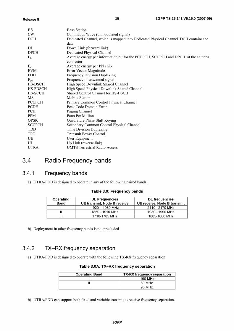
3GPP
3GPP TS 25.141 V5.15.0 (2007-09)15Release 5
BS Base Station CW Continuous Wave (unmodulated signal) DCH Dedicated Channel, which is mapped into Dedicated Physical Channel. DCH contains the
data DL Down Link (forward link) DPCH Dedicated Physical Channel Eb Average energy per information bit for the PCCPCH, SCCPCH and DPCH, at the antenna
connector Ec Average energy per PN chip EVM Error Vector Magnitude FDD Frequency Division Duplexing Fuw Frequency of unwanted signal HS-DSCH High Speed Downlink Shared Channel HS-PDSCH High Speed Physical Downlink Shared Channel HS-SCCH Shared Control Channel for HS-DSCH MS Mobile Station PCCPCH Primary Common Control Physical Channel PCDE Peak Code Domain Error PCH Paging Channel PPM Parts Per Million QPSK Quadrature Phase Shift Keying SCCPCH Secondary Common Control Physical Channel TDD Time Division Duplexing TPC Transmit Power Control UE User Equipment UL Up Link (reverse link) UTRA UMTS Terrestrial Radio Access
3.4 Radio Frequency bands
3.4.1 Frequency bands a) UTRA/FDD is designed to operate in any of the following paired bands:
Table 3.0: Frequency bands
Operating Band
UL Frequencies UE transmit, Node B receive
DL frequencies UE receive, Node B transmit
I 1920 – 1980 MHz 2110 –2170 MHz II 1850 –1910 MHz 1930 –1990 MHz III 1710-1785 MHz 1805-1880 MHz
b) Deployment in other frequency bands is not precluded
3.4.2 TX–RX frequency separation a) UTRA/FDD is designed to operate with the following TX-RX frequency separation
Table 3.0A: TX–RX frequency separation
Operating Band TX-RX frequency separation I 190 MHz II 80 MHz. III 95 MHz.
b) UTRA/FDD can support both fixed and variable transmit to receive frequency separation.
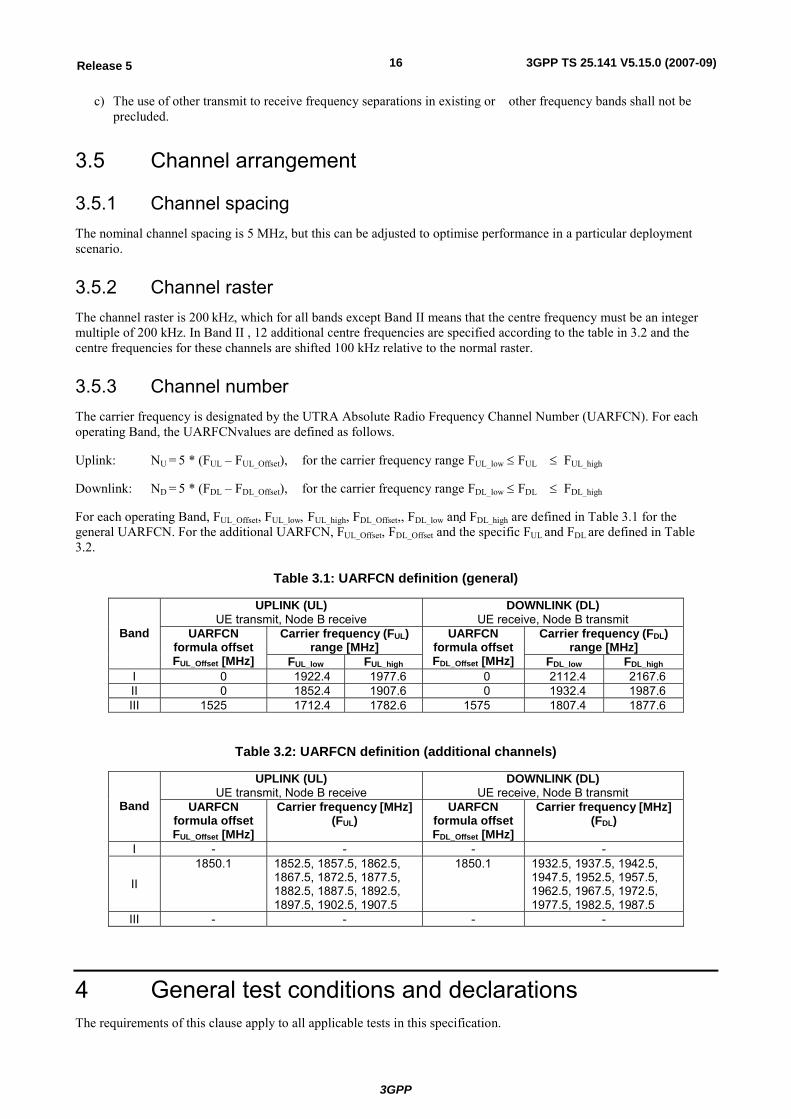
3GPP
3GPP TS 25.141 V5.15.0 (2007-09)16Release 5
c) The use of other transmit to receive frequency separations in existing or other frequency bands shall not be precluded.
3.5 Channel arrangement
3.5.1 Channel spacing The nominal channel spacing is 5 MHz, but this can be adjusted to optimise performance in a particular deployment scenario.
3.5.2 Channel raster The channel raster is 200 kHz, which for all bands except Band II means that the centre frequency must be an integer multiple of 200 kHz. In Band II , 12 additional centre frequencies are specified according to the table in 3.2 and the centre frequencies for these channels are shifted 100 kHz relative to the normal raster.
3.5.3 Channel number The carrier frequency is designated by the UTRA Absolute Radio Frequency Channel Number (UARFCN). For each operating Band, the UARFCNvalues are defined as follows.
Uplink: NU = 5 * (FUL – FUL_Offset), for the carrier frequency range FUL_low ≤ FUL ≤ FUL_high
Downlink: ND = 5 * (FDL – FDL_Offset), for the carrier frequency range FDL_low ≤ FDL ≤ FDL_high
For each operating Band, FUL_Offset, FUL_low, FUL_high, FDL_Offset,, FDL_low and FDL_high are defined in Table 3.1 for the general UARFCN. For the additional UARFCN, FUL_Offset, FDL_Offset and the specific FUL and FDL are defined in Table 3.2.
Table 3.1: UARFCN definition (general)
UPLINK (UL) UE transmit, Node B receive
DOWNLINK (DL) UE receive, Node B transmit
Carrier frequency (FUL) range [MHz]
Carrier frequency (FDL) range [MHz]
Band UARFCN formula offset FUL_Offset [MHz] FUL_low FUL_high
UARFCN formula offsetFDL_Offset [MHz] FDL_low FDL_high
I 0 1922.4 1977.6 0 2112.4 2167.6 II 0 1852.4 1907.6 0 1932.4 1987.6 III 1525 1712.4 1782.6 1575 1807.4 1877.6
Table 3.2: UARFCN definition (additional channels)
UPLINK (UL) UE transmit, Node B receive
DOWNLINK (DL) UE receive, Node B transmit
Band UARFCN formula offset FUL_Offset [MHz]
Carrier frequency [MHz](FUL)
UARFCN formula offsetFDL_Offset [MHz]
Carrier frequency [MHz](FDL)
I - - - -
II
1850.1
1852.5, 1857.5, 1862.5, 1867.5, 1872.5, 1877.5, 1882.5, 1887.5, 1892.5, 1897.5, 1902.5, 1907.5
1850.1
1932.5, 1937.5, 1942.5, 1947.5, 1952.5, 1957.5, 1962.5, 1967.5, 1972.5, 1977.5, 1982.5, 1987.5
III - - - -
4 General test conditions and declarations The requirements of this clause apply to all applicable tests in this specification.
3GPP
3GPP TS 25.141 V5.15.0 (2007-09)17Release 5
Many of the tests in this specification measure a parameter relative to a value that is not fully specified in the UTRA specifications. For these tests, the Minimum Requirement is determined relative to a nominal value specified by the manufacturer.
Certain functions of a BS are optional in the UTRA specifications. Some requirements for the BS may be regional as listed in subclause 4.7.
When specified in a test, the manufacturer shall declare the nominal value of a parameter, or whether an option is supported.
4.1 Acceptable uncertainty of Test System The maximum acceptable uncertainty of the Test System is specified below for each test, where appropriate. The Test System shall enable the stimulus signals in the test case to be adjusted to within the specified tolerance and the equipment under test to be measured with an uncertainty not exceeding the specified values. All tolerances and uncertainties are absolute values, and are valid for a confidence level of 95 %, unless otherwise stated.
A confidence level of 95% is the measurement uncertainty tolerance interval for a specific measurement that contains 95% of the performance of a population of test equipment.
For RF tests, it should be noted that the uncertainties in subclause 4.1 apply to the Test System operating into a nominal 50 ohm load and do not include system effects due to mismatch between the DUT and the Test System.
4.1.1 Measurement of test environments The measurement accuracy of the BS test environments defined in Subclause 4.4, Test environments shall be.
- Pressure ±5 kPa.
- Temperature ±2 degrees.
- Relative Humidity ±5 %.
- DC Voltage ±1,0 %.
- AC Voltage ±1,5 %.
- Vibration 10 %.
- Vibration frequency 0,1 Hz.
The above values shall apply unless the test environment is otherwise controlled and the specification for the control of the test environment specifies the uncertainty for the parameter.
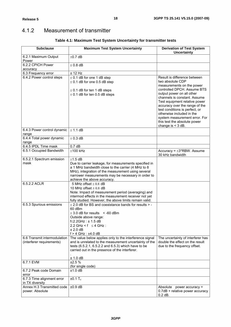
3GPP
3GPP TS 25.141 V5.15.0 (2007-09)18Release 5
4.1.2 Measurement of transmitter
Table 4.1: Maximum Test System Uncertainty for transmitter tests
Subclause Maximum Test System Uncertainty Derivation of Test System Uncertainty
6.2.1 Maximum Output Power
±0.7 dB
6.2.2 CPICH Power accuracy
± 0.8 dB
6.3 Frequency error ± 12 Hz 6.4.2 Power control steps ± 0.1 dB for one 1 dB step
± 0.1 dB for one 0.5 dB step ± 0.1 dB for ten 1 dB steps ± 0.1 dB for ten 0.5 dB steps
Result is difference between two absolute CDP measurements on the power controlled DPCH. Assume BTS output power on all other channels is constant. Assume Test equipment relative power accuracy over the range of the test conditions is perfect, or otherwise included in the system measurement error. For this test the absolute power change is < 3 dB.
6.4.3 Power control dynamic range
± 1.1 dB
6.4.4 Total power dynamic range
± 0.3 dB
6.4.5 IPDL Time mask 0.7 dB 6.5.1 Occupied Bandwidth ±100 kHz Accuracy = ±3*RBW. Assume
30 kHz bandwidth 6.5.2.1 Spectrum emission mask
±1.5 dB Due to carrier leakage, for measurements specified in a 1 MHz bandwidth close to the carrier (4 MHz to 8 MHz), integration of the measurement using several narrower measurements may be necessary in order to achieve the above accuracy.
6.5.2.2 ACLR 5 MHz offset ± 0.8 dB 10 MHz offset ± 0.8 dB Note: Impact of measurement period (averaging) and intermod effects in the measurement receiver not yet fully studied. However, the above limits remain valid.
6.5.3 Spurious emissions ± 2.0 dB for BS and coexistance bands for results > -60 dBm ± 3.0 dB for results < -60 dBm Outside above range: f≤2.2GHz : ± 1.5 dB 2.2 GHz < f ≤ 4 GHz : ± 2.0 dB f > 4 GHz : ±4.0 dB
6.6 Transmit intermodulation (interferer requirements)
The value below applies only to the interference signal and is unrelated to the measurement uncertainty of the tests (6.5.2.1, 6.5.2.2 and 6.5.3) which have to be carried out in the presence of the interferer. . ± 1.0 dB
The uncertainty of interferer has double the effect on the result due to the frequency offset.
6.7.1 EVM ±2.5 % (for single code)
6.7.2 Peak code Domain error
±1.0 dB
6.7.3 Time alignment error in TX diversity
±0.1 Tc
Annex H.3 Transmitted code power. Absolute
±0.9 dB Absolute power accuracy = 0.7dB + relative power accuracy 0.2 dB.
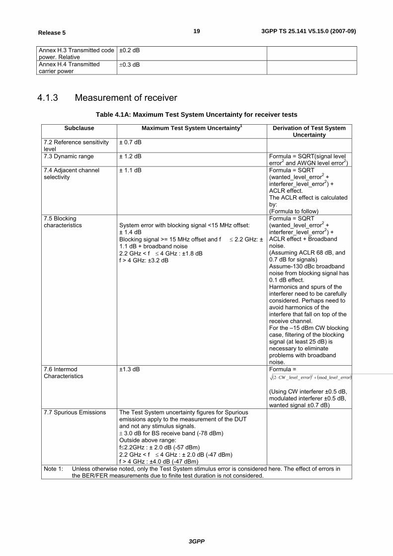
3GPP
3GPP TS 25.141 V5.15.0 (2007-09)19Release 5
Annex H.3 Transmitted code power. Relative
±0.2 dB
Annex H.4 Transmitted carrier power
±0.3 dB
4.1.3 Measurement of receiver
Table 4.1A: Maximum Test System Uncertainty for receiver tests
Subclause Maximum Test System Uncertainty1 Derivation of Test System Uncertainty
7.2 Reference sensitivity level
± 0.7 dB
7.3 Dynamic range ± 1.2 dB
Formula = SQRT(signal level error2 and AWGN level error2)
7.4 Adjacent channel selectivity
± 1.1 dB
Formula = SQRT (wanted_level_error2 + interferer_level_error2) + ACLR effect. The ACLR effect is calculated by: (Formula to follow)
7.5 Blocking characteristics
System error with blocking signal <15 MHz offset: ± 1.4 dB Blocking signal >= 15 MHz offset and f ≤ 2.2 GHz: ± 1.1 dB + broadband noise 2.2 GHz < f ≤ 4 GHz : ±1.8 dB f > 4 GHz: ±3.2 dB
Formula = SQRT (wanted_level_error2 + interferer_level_error2) + ACLR effect + Broadband noise. (Assuming ACLR 68 dB, and 0.7 dB for signals) Assume-130 dBc broadband noise from blocking signal has 0.1 dB effect. Harmonics and spurs of the interferer need to be carefully considered. Perhaps need to avoid harmonics of the interfere that fall on top of the receive channel. For the –15 dBm CW blocking case, filtering of the blocking signal (at least 25 dB) is necessary to eliminate problems with broadband noise.
7.6 Intermod Characteristics
±1.3 dB Formula = ( ) ( )22 _mod___2 errorlevelerrorlevelCW +⋅
(Using CW interferer ±0.5 dB, modulated interferer ±0.5 dB, wanted signal ±0.7 dB)
7.7 Spurious Emissions The Test System uncertainty figures for Spurious emissions apply to the measurement of the DUT and not any stimulus signals. ± 3.0 dB for BS receive band (-78 dBm) Outside above range: f≤2.2GHz : ± 2.0 dB (-57 dBm) 2.2 GHz < f ≤ 4 GHz : ± 2.0 dB (-47 dBm) f > 4 GHz : ±4.0 dB (-47 dBm)
Note 1: Unless otherwise noted, only the Test System stimulus error is considered here. The effect of errors in the BER/FER measurements due to finite test duration is not considered.
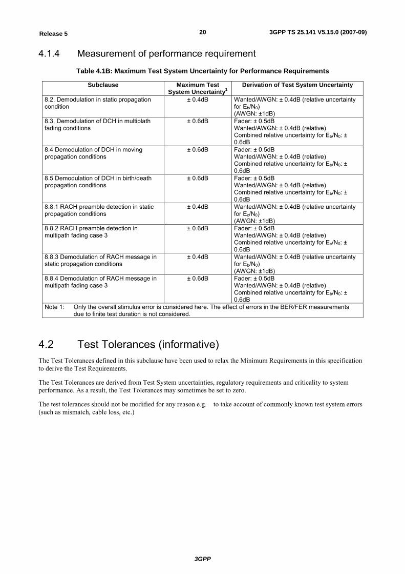
3GPP
3GPP TS 25.141 V5.15.0 (2007-09)20Release 5
4.1.4 Measurement of performance requirement
Table 4.1B: Maximum Test System Uncertainty for Performance Requirements
Subclause Maximum Test System Uncertainty1
Derivation of Test System Uncertainty
8.2, Demodulation in static propagation condition
± 0.4dB Wanted/AWGN: ± 0.4dB (relative uncertainty for Eb/N0) (AWGN: ±1dB)
8.3, Demodulation of DCH in multiplath fading conditions
± 0.6dB Fader: ± 0.5dB Wanted/AWGN: ± 0.4dB (relative) Combined relative uncertainty for Eb/N0: ± 0.6dB
8.4 Demodulation of DCH in moving propagation conditions
± 0.6dB Fader: ± 0.5dB Wanted/AWGN: ± 0.4dB (relative) Combined relative uncertainty for Eb/N0: ± 0.6dB
8.5 Demodulation of DCH in birth/death propagation conditions
± 0.6dB Fader: ± 0.5dB Wanted/AWGN: ± 0.4dB (relative) Combined relative uncertainty for Eb/N0: ± 0.6dB
8.8.1 RACH preamble detection in static propagation conditions
± 0.4dB Wanted/AWGN: ± 0.4dB (relative uncertainty for Ec/N0) (AWGN: ±1dB)
8.8.2 RACH preamble detection in multipath fading case 3
± 0.6dB Fader: ± 0.5dB Wanted/AWGN: ± 0.4dB (relative) Combined relative uncertainty for Ec/N0: ± 0.6dB
8.8.3 Demodulation of RACH message in static propagation conditions
± 0.4dB Wanted/AWGN: ± 0.4dB (relative uncertainty for Eb/N0) (AWGN: ±1dB)
8.8.4 Demodulation of RACH message in multipath fading case 3
± 0.6dB Fader: ± 0.5dB Wanted/AWGN: ± 0.4dB (relative) Combined relative uncertainty for Eb/N0: ± 0.6dB
Note 1: Only the overall stimulus error is considered here. The effect of errors in the BER/FER measurements due to finite test duration is not considered.
4.2 Test Tolerances (informative) The Test Tolerances defined in this subclause have been used to relax the Minimum Requirements in this specification to derive the Test Requirements.
The Test Tolerances are derived from Test System uncertainties, regulatory requirements and criticality to system performance. As a result, the Test Tolerances may sometimes be set to zero.
The test tolerances should not be modified for any reason e.g. to take account of commonly known test system errors (such as mismatch, cable loss, etc.)
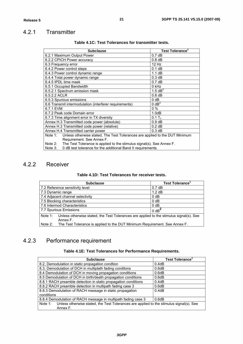
3GPP
3GPP TS 25.141 V5.15.0 (2007-09)21Release 5
4.2.1 Transmitter
Table 4.1C: Test Tolerances for transmitter tests.
Subclause Test Tolerance1 6.2.1 Maximum Output Power 0.7 dB 6.2.2 CPICH Power accuracy 0.8 dB 6.3 Frequency error 12 Hz 6.4.2 Power control steps 0.1 dB 6.4.3 Power control dynamic range 1.1 dB 6.4.4 Total power dynamic range 0.3 dB 6.4.5 IPDL time mask 0.7 dB 6.5.1 Occupied Bandwidth 0 kHz 6.5.2.1 Spectrum emission mask 1.5 dB3 6.5.2.2 ACLR 0.8 dB 6.5.3 Spurious emissions 0 dB 6.6 Transmit intermodulation (interferer requirements) 0 dB2 6.7.1 EVM 0 % 6.7.2 Peak code Domain error 1.0dB 6.7.3 Time alignment error in TX diversity 0.1 Tc Annex H.3 Transmitted code power (absolute) 0.9 dB Annex H.3 Transmitted code power (relative) 0.2 dB Annex H.4 Transmitted carrier power 0.3 dB Note 1: Unless otherwise stated, The Test Tolerances are applied to the DUT Minimum
Requirement. See Annex F. Note 2: The Test Tolerance is applied to the stimulus signal(s). See Annex F. Note 3: 0 dB test tolerance for the additional Band II requirements.
4.2.2 Receiver
Table 4.1D: Test Tolerances for receiver tests.
Subclause Test Tolerance1 7.2 Reference sensitivity level 0.7 dB 7.3 Dynamic range 1.2 dB 7.4 Adjacent channel selectivity 0 dB 7.5 Blocking characteristics 0 dB 7.6 Intermod Characteristics 0 dB 7.7 Spurious Emissions 0 dB2 Note 1: Unless otherwise stated, the Test Tolerances are applied to the stimulus signal(s). See
Annex F. Note 2: The Test Tolerance is applied to the DUT Minimum Requirement. See Annex F.
4.2.3 Performance requirement
Table 4.1E: Test Tolerances for Performance Requirements.
Subclause Test Tolerance1 8.2, Demodulation in static propagation condtion 0.4dB 8.3, Demodulation of DCH in multiplath fading conditons 0.6dB 8.4 Demodulation of DCH in moving propagation conditions 0.6dB 8.5 Demodulation of DCH in birth/death propagation conditions 0.6dB 8.8.1 RACH preamble detection in static propagation conditions 0.4dB 8.8.2 RACH preamble detection in multipath fading case 3 0.6dB 8.8.3 Demodulation of RACH message in static propagation conditions
0.4dB
8.8.4 Demodulation of RACH message in multipath fading case 3 0.6dB Note 1: Unless otherwise stated, the Test Tolerances are applied to the stimulus signal(s). See
Annex F.
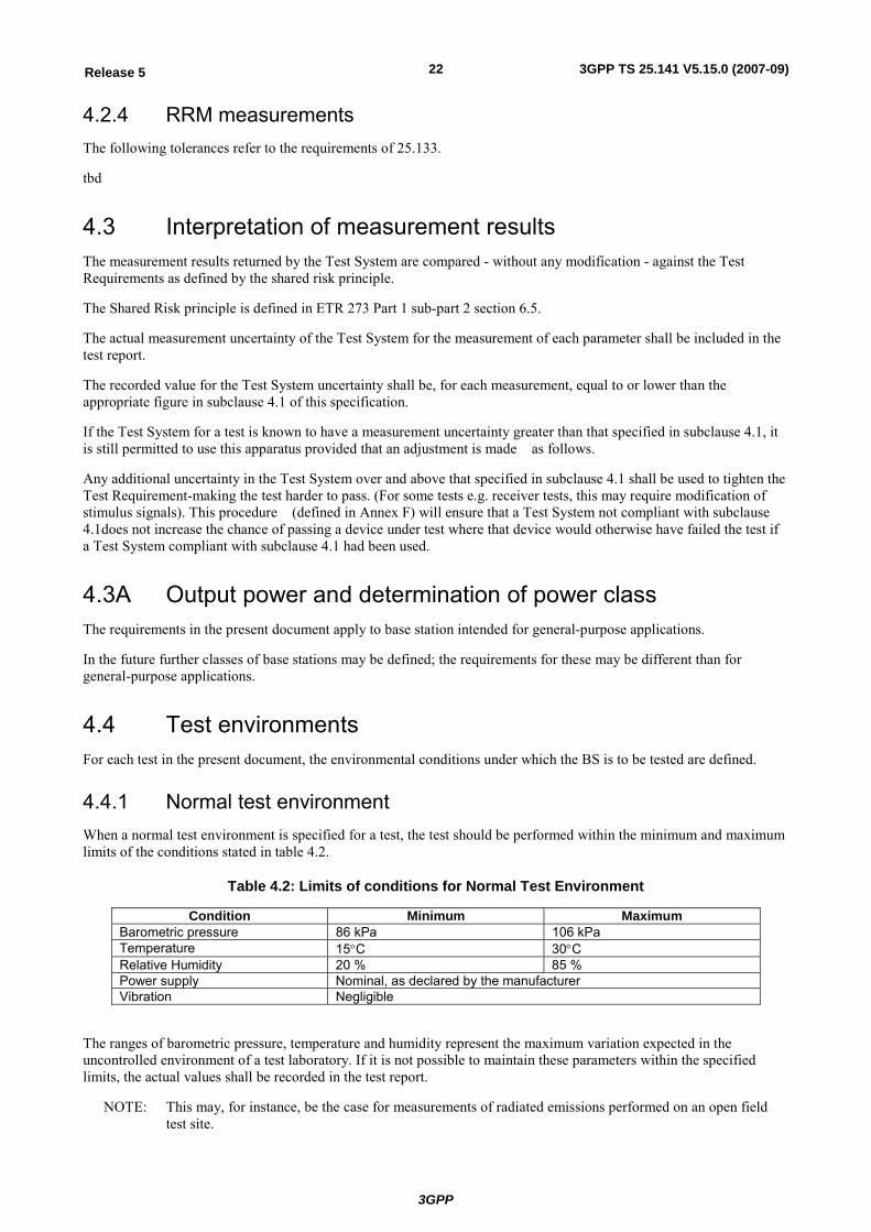
3GPP
3GPP TS 25.141 V5.15.0 (2007-09)22Release 5
4.2.4 RRM measurements The following tolerances refer to the requirements of 25.133.
tbd
4.3 Interpretation of measurement results The measurement results returned by the Test System are compared - without any modification - against the Test Requirements as defined by the shared risk principle.
The Shared Risk principle is defined in ETR 273 Part 1 sub-part 2 section 6.5.
The actual measurement uncertainty of the Test System for the measurement of each parameter shall be included in the test report.
The recorded value for the Test System uncertainty shall be, for each measurement, equal to or lower than the appropriate figure in subclause 4.1 of this specification.
If the Test System for a test is known to have a measurement uncertainty greater than that specified in subclause 4.1, it is still permitted to use this apparatus provided that an adjustment is made as follows.
Any additional uncertainty in the Test System over and above that specified in subclause 4.1 shall be used to tighten the Test Requirement-making the test harder to pass. (For some tests e.g. receiver tests, this may require modification of stimulus signals). This procedure (defined in Annex F) will ensure that a Test System not compliant with subclause 4.1does not increase the chance of passing a device under test where that device would otherwise have failed the test if a Test System compliant with subclause 4.1 had been used.
4.3A Output power and determination of power class The requirements in the present document apply to base station intended for general-purpose applications.
In the future further classes of base stations may be defined; the requirements for these may be different than for general-purpose applications.
4.4 Test environments For each test in the present document, the environmental conditions under which the BS is to be tested are defined.
4.4.1 Normal test environment When a normal test environment is specified for a test, the test should be performed within the minimum and maximum limits of the conditions stated in table 4.2.
Table 4.2: Limits of conditions for Normal Test Environment
Condition Minimum Maximum Barometric pressure 86 kPa 106 kPa Temperature 15°C 30°C Relative Humidity 20 % 85 % Power supply Nominal, as declared by the manufacturer Vibration Negligible
The ranges of barometric pressure, temperature and humidity represent the maximum variation expected in the uncontrolled environment of a test laboratory. If it is not possible to maintain these parameters within the specified limits, the actual values shall be recorded in the test report.
NOTE: This may, for instance, be the case for measurements of radiated emissions performed on an open field test site.
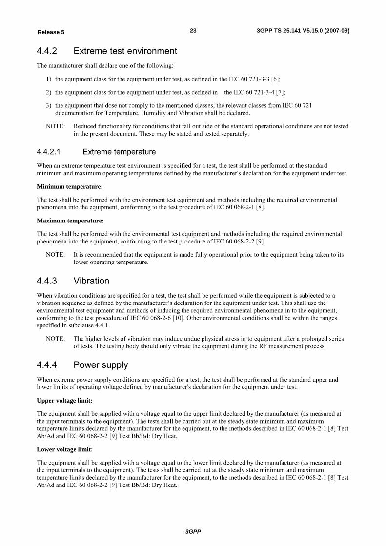
3GPP
3GPP TS 25.141 V5.15.0 (2007-09)23Release 5
4.4.2 Extreme test environment The manufacturer shall declare one of the following:
1) the equipment class for the equipment under test, as defined in the IEC 60 721-3-3 [6];
2) the equipment class for the equipment under test, as defined in the IEC 60 721-3-4 [7];
3) the equipment that dose not comply to the mentioned classes, the relevant classes from IEC 60 721 documentation for Temperature, Humidity and Vibration shall be declared.
NOTE: Reduced functionality for conditions that fall out side of the standard operational conditions are not tested in the present document. These may be stated and tested separately.
4.4.2.1 Extreme temperature
When an extreme temperature test environment is specified for a test, the test shall be performed at the standard minimum and maximum operating temperatures defined by the manufacturer's declaration for the equipment under test.
Minimum temperature:
The test shall be performed with the environment test equipment and methods including the required environmental phenomena into the equipment, conforming to the test procedure of IEC 60 068-2-1 [8].
Maximum temperature:
The test shall be performed with the environmental test equipment and methods including the required environmental phenomena into the equipment, conforming to the test procedure of IEC 60 068-2-2 [9].
NOTE: It is recommended that the equipment is made fully operational prior to the equipment being taken to its lower operating temperature.
4.4.3 Vibration When vibration conditions are specified for a test, the test shall be performed while the equipment is subjected to a vibration sequence as defined by the manufacturer’s declaration for the equipment under test. This shall use the environmental test equipment and methods of inducing the required environmental phenomena in to the equipment, conforming to the test procedure of IEC 60 068-2-6 [10]. Other environmental conditions shall be within the ranges specified in subclause 4.4.1.
NOTE: The higher levels of vibration may induce undue physical stress in to equipment after a prolonged series of tests. The testing body should only vibrate the equipment during the RF measurement process.
4.4.4 Power supply When extreme power supply conditions are specified for a test, the test shall be performed at the standard upper and lower limits of operating voltage defined by manufacturer's declaration for the equipment under test.
Upper voltage limit:
The equipment shall be supplied with a voltage equal to the upper limit declared by the manufacturer (as measured at the input terminals to the equipment). The tests shall be carried out at the steady state minimum and maximum temperature limits declared by the manufacturer for the equipment, to the methods described in IEC 60 068-2-1 [8] Test Ab/Ad and IEC 60 068-2-2 [9] Test Bb/Bd: Dry Heat.
Lower voltage limit:
The equipment shall be supplied with a voltage equal to the lower limit declared by the manufacturer (as measured at the input terminals to the equipment). The tests shall be carried out at the steady state minimum and maximum temperature limits declared by the manufacturer for the equipment, to the methods described in IEC 60 068-2-1 [8] Test Ab/Ad and IEC 60 068-2-2 [9] Test Bb/Bd: Dry Heat.
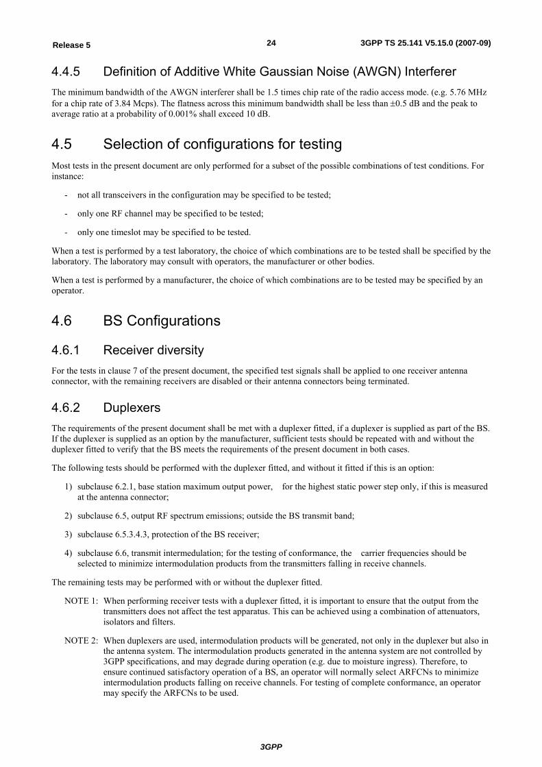
3GPP
3GPP TS 25.141 V5.15.0 (2007-09)24Release 5
4.4.5 Definition of Additive White Gaussian Noise (AWGN) Interferer The minimum bandwidth of the AWGN interferer shall be 1.5 times chip rate of the radio access mode. (e.g. 5.76 MHz for a chip rate of 3.84 Mcps). The flatness across this minimum bandwidth shall be less than ±0.5 dB and the peak to average ratio at a probability of 0.001% shall exceed 10 dB.
4.5 Selection of configurations for testing Most tests in the present document are only performed for a subset of the possible combinations of test conditions. For instance:
- not all transceivers in the configuration may be specified to be tested;
- only one RF channel may be specified to be tested;
- only one timeslot may be specified to be tested.
When a test is performed by a test laboratory, the choice of which combinations are to be tested shall be specified by the laboratory. The laboratory may consult with operators, the manufacturer or other bodies.
When a test is performed by a manufacturer, the choice of which combinations are to be tested may be specified by an operator.
4.6 BS Configurations
4.6.1 Receiver diversity For the tests in clause 7 of the present document, the specified test signals shall be applied to one receiver antenna connector, with the remaining receivers are disabled or their antenna connectors being terminated.
4.6.2 Duplexers The requirements of the present document shall be met with a duplexer fitted, if a duplexer is supplied as part of the BS. If the duplexer is supplied as an option by the manufacturer, sufficient tests should be repeated with and without the duplexer fitted to verify that the BS meets the requirements of the present document in both cases.
The following tests should be performed with the duplexer fitted, and without it fitted if this is an option:
1) subclause 6.2.1, base station maximum output power, for the highest static power step only, if this is measured at the antenna connector;
2) subclause 6.5, output RF spectrum emissions; outside the BS transmit band;
3) subclause 6.5.3.4.3, protection of the BS receiver;
4) subclause 6.6, transmit intermedulation; for the testing of conformance, the carrier frequencies should be selected to minimize intermodulation products from the transmitters falling in receive channels.
The remaining tests may be performed with or without the duplexer fitted.
NOTE 1: When performing receiver tests with a duplexer fitted, it is important to ensure that the output from the transmitters does not affect the test apparatus. This can be achieved using a combination of attenuators, isolators and filters.
NOTE 2: When duplexers are used, intermodulation products will be generated, not only in the duplexer but also in the antenna system. The intermodulation products generated in the antenna system are not controlled by 3GPP specifications, and may degrade during operation (e.g. due to moisture ingress). Therefore, to ensure continued satisfactory operation of a BS, an operator will normally select ARFCNs to minimize intermodulation products falling on receive channels. For testing of complete conformance, an operator may specify the ARFCNs to be used.
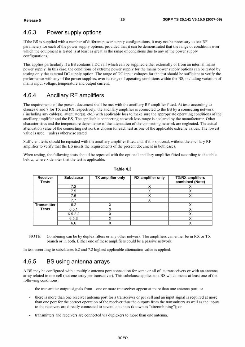
3GPP
3GPP TS 25.141 V5.15.0 (2007-09)25Release 5
4.6.3 Power supply options If the BS is supplied with a number of different power supply configurations, it may not be necessary to test RF parameters for each of the power supply options, provided that it can be demonstrated that the range of conditions over which the equipment is tested is at least as great as the range of conditions due to any of the power supply configurations.
This applies particularly if a BS contains a DC rail which can be supplied either externally or from an internal mains power supply. In this case, the conditions of extreme power supply for the mains power supply options can be tested by testing only the external DC supply option. The range of DC input voltages for the test should be sufficient to verify the performance with any of the power supplies, over its range of operating conditions within the BS, including variation of mains input voltage, temperature and output current.
4.6.4 Ancillary RF amplifiers The requirements of the present document shall be met with the ancillary RF amplifier fitted. At tests according to clauses 6 and 7 for TX and RX respectively, the ancillary amplifier is connected to the BS by a connecting network ( including any cable(s), attenuator(s), etc.) with applicable loss to make sure the appropriate operating conditions of the ancillary amplifier and the BS. The applicable connecting network loss range is declared by the manufacturer. Other characteristics and the temperature dependence of the attenuation of the connecting network are neglected. The actual attenuation value of the connecting network is chosen for each test as one of the applicable extreme values. The lowest value is used unless otherwise stated.
Sufficient tests should be repeated with the ancillary amplifier fitted and, if it is optional, without the ancillary RF amplifier to verify that the BS meets the requirements of the present document in both cases.
When testing, the following tests should be repeated with the optional ancillary amplifier fitted according to the table below, where x denotes that the test is applicable:
Table 4.3
Subclause TX amplifier only RX amplifier only TX/RX amplifiers combined (Note)
7.2 X X 7.5 X X 7.6 X X
Receiver Tests
7.7 X 6.2 X X
6.5.1 X X 6.5.2.2 X X 6.5.3 X X
Transmitter Tests
6.6 X X
NOTE: Combining can be by duplex filters or any other network. The amplifiers can either be in RX or TX branch or in both. Either one of these amplifiers could be a passive network.
In test according to subclauses 6.2 and 7.2 highest applicable attenuation value is applied.
4.6.5 BS using antenna arrays A BS may be configured with a multiple antenna port connection for some or all of its transceivers or with an antenna array related to one cell (not one array per transceiver). This subclause applies to a BS which meets at least one of the following conditions:
- the transmitter output signals from one or more transceiver appear at more than one antenna port; or
- there is more than one receiver antenna port for a transceiver or per cell and an input signal is required at more than one port for the correct operation of the receiver thus the outputs from the transmitters as well as the inputs to the receivers are directly connected to several antennas (known as “aircombining”); or
- transmitters and receivers are connected via duplexers to more than one antenna.
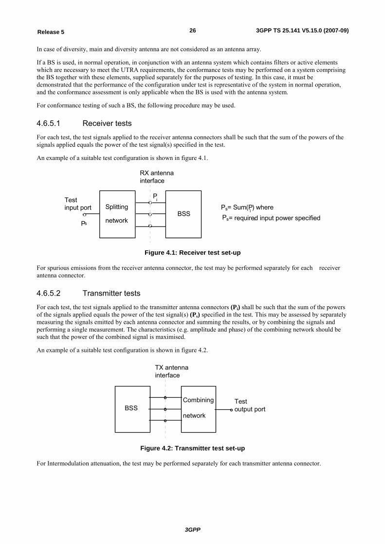
3GPP
3GPP TS 25.141 V5.15.0 (2007-09)26Release 5
In case of diversity, main and diversity antenna are not considered as an antenna array.
If a BS is used, in normal operation, in conjunction with an antenna system which contains filters or active elements which are necessary to meet the UTRA requirements, the conformance tests may be performed on a system comprising the BS together with these elements, supplied separately for the purposes of testing. In this case, it must be demonstrated that the performance of the configuration under test is representative of the system in normal operation, and the conformance assessment is only applicable when the BS is used with the antenna system.
For conformance testing of such a BS, the following procedure may be used.
4.6.5.1 Receiver tests
For each test, the test signals applied to the receiver antenna connectors shall be such that the sum of the powers of the signals applied equals the power of the test signal(s) specified in the test.
An example of a suitable test configuration is shown in figure 4.1.
RX antennainterface
Splitting
network
Testinput port
BSS
Pi
Ps= Sum(Pi ) where
PsPs= required input power specifiedi
Figure 4.1: Receiver test set-up
For spurious emissions from the receiver antenna connector, the test may be performed separately for each receiver antenna connector.
4.6.5.2 Transmitter tests
For each test, the test signals applied to the transmitter antenna connectors (Pi) shall be such that the sum of the powers of the signals applied equals the power of the test signal(s) (Ps) specified in the test. This may be assessed by separately measuring the signals emitted by each antenna connector and summing the results, or by combining the signals and performing a single measurement. The characteristics (e.g. amplitude and phase) of the combining network should be such that the power of the combined signal is maximised.
An example of a suitable test configuration is shown in figure 4.2.
TX antennainterface
Combining
network
Testoutput portBSS
Figure 4.2: Transmitter test set-up
For Intermodulation attenuation, the test may be performed separately for each transmitter antenna connector.
3GPP
3GPP TS 25.141 V5.15.0 (2007-09)27Release 5
4.6.6 Transmit diversity Unless otherwise stated, for the tests in clause 6 of the present document, the signal shall be measured at both main and diversity transmitters antenna connectors, with the remaining antenna connector being terminated.
4.7 Regional requirements Some requirements in TS 25.141 may only apply in certain regions. Table 4.4 lists all requirements that may be applied differently in different regions.
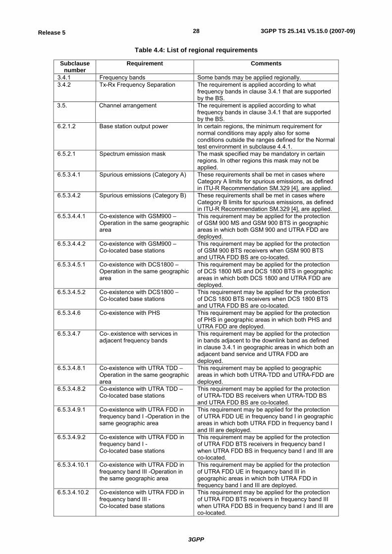
3GPP
3GPP TS 25.141 V5.15.0 (2007-09)28Release 5
Table 4.4: List of regional requirements
Subclause number
Requirement Comments
3.4.1 Frequency bands Some bands may be applied regionally. 3.4.2 Tx-Rx Frequency Separation The requirement is applied according to what
frequency bands in clause 3.4.1 that are supported by the BS.
3.5. Channel arrangement The requirement is applied according to what frequency bands in clause 3.4.1 that are supported by the BS.
6.2.1.2 Base station output power In certain regions, the minimum requirement for normal conditions may apply also for some conditions outside the ranges defined for the Normal test environment in subclause 4.4.1.
6.5.2.1 Spectrum emission mask The mask specified may be mandatory in certain regions. In other regions this mask may not be applied.
6.5.3.4.1 Spurious emissions (Category A) These requirements shall be met in cases where Category A limits for spurious emissions, as defined in ITU-R Recommendation SM.329 [4], are applied.
6.5.3.4.2 Spurious emissions (Category B) These requirements shall be met in cases where Category B limits for spurious emissions, as defined in ITU-R Recommendation SM.329 [4], are applied.
6.5.3.4.4.1 Co-existence with GSM900 –Operation in the same geographic area
This requirement may be applied for the protection of GSM 900 MS and GSM 900 BTS in geographic areas in which both GSM 900 and UTRA FDD are deployed.
6.5.3.4.4.2 Co-existence with GSM900 – Co-located base stations
This requirement may be applied for the protection of GSM 900 BTS receivers when GSM 900 BTS and UTRA FDD BS are co-located.
6.5.3.4.5.1 Co-existence with DCS1800 –Operation in the same geographic area
This requirement may be applied for the protection of DCS 1800 MS and DCS 1800 BTS in geographic areas in which both DCS 1800 and UTRA FDD are deployed.
6.5.3.4.5.2 Co-existence with DCS1800 – Co-located base stations
This requirement may be applied for the protection of DCS 1800 BTS receivers when DCS 1800 BTS and UTRA FDD BS are co-located.
6.5.3.4.6 Co-existence with PHS This requirement may be applied for the protection of PHS in geographic areas in which both PHS and UTRA FDD are deployed.
6.5.3.4.7 Co-.existence with services in adjacent frequency bands
This requirement may be applied for the protection in bands adjacent to the downlink band as defined in clause 3.4.1 in geographic areas in which both an adjacent band service and UTRA FDD are deployed.
6.5.3.4.8.1 Co-existence with UTRA TDD – Operation in the same geographic area
This requirement may be applied to geographic areas in which both UTRA-TDD and UTRA-FDD are deployed.
6.5.3.4.8.2 Co-existence with UTRA TDD – Co-located base stations
This requirement may be applied for the protection of UTRA-TDD BS receivers when UTRA-TDD BS and UTRA FDD BS are co-located.
6.5.3.4.9.1 Co-existence with UTRA FDD in frequency band I -Operation in the same geographic area
This requirement may be applied for the protection of UTRA FDD UE in frequency band I in geographic areas in which both UTRA FDD in frequency band I and III are deployed.
6.5.3.4.9.2 Co-existence with UTRA FDD in frequency band I - Co-located base stations
This requirement may be applied for the protection of UTRA FDD BTS receivers in frequency band I when UTRA FDD BS in frequency band I and III are co-located.
6.5.3.4.10.1 Co-existence with UTRA FDD in frequency band III -Operation in the same geographic area
This requirement may be applied for the protection of UTRA FDD UE in frequency band III in geographic areas in which both UTRA FDD in frequency band I and III are deployed.
6.5.3.4.10.2 Co-existence with UTRA FDD in frequency band III - Co-located base stations
This requirement may be applied for the protection of UTRA FDD BTS receivers in frequency band III when UTRA FDD BS in frequency band I and III are co-located.
3GPP
3GPP TS 25.141 V5.15.0 (2007-09)29Release 5
6.5.3.4.11.1 Co-existence with PCS1900 - Operation in the same geographic area
This requirement may be applied for the protection of PCS 1900 BTS receivers in geographic areas in which both PCS 1900 and UTRA FDD are deployed.
6.5.3.4.11.2 Co-existence with PCS1900 - Co-located base stations
This requirement may be applied for the protection of PCS 1900 BTS receivers when PCS 1900 BTS and UTRA FDD BS are co-located.
6.5.3.4.12.1 Co-existence with GSM850 - Operation in the same geographic area
This requirement may be applied for the protection of GSM 850 MS and GSM 850 BTS receivers in geographic areas in which both GSM 850 and UTRA FDD are deployed.
6.5.3.4.12.2 Co-existence with GSM 850 - Co-located base stations
This requirement may be applied for the protection of GSM 850 BTS receivers when GSM 850 BTS and UTRA FDD BS are co-located.
7.5 Blocking characteristic The requirement is applied according to what frequency bands inclause 3.4.1 that are supported by the BS.
7.5 Blocking characteristics This requirement may be applied for the protection of UTRA FDD BS receivers when UTRA FDD BS and GSM 900, GSM850, PCS 1900 and BS operating in the /DCS1800 band (GSM or UTRA) are co-located.
7.6 Intermodulation characteristics The requirement is applied according to what frequency bands in clause 3.4.1 that are supported by the BS.
7.7 Spurious emissions The requirement is applied according to what frequency bands in clause 3.4.1 that are supported by the BS.
4.8 Specified frequency range The manufacturer shall declare:
- which of the frequency bands defined in sub-clause 3.4 is supported by the BS.
- the frequency range within the above frequency band(s) supported by the BS.
Many tests in this TS are performed with appropriate frequencies in the bottom, middle and top of the operating frequency band of the BS. These are denoted as RF channels B (bottom), M (middle) and T (top).
Unless otherwise stated, the test shall be performed with a single carrier at each of the RF channels B, M and T.
When the requirements are specific to multiple carriers, and the BS is declared to support N>1 carriers, numbered from 1 to N, the interpretation of B, M and T for test purposes shall be as follows:
For testing at B,
- the carrier of lowest frequency shall be centred on B
For testing at M,
- if the number N of carriers supported is odd, the carrier (N+1)/2 shall be centred on M,
- if the number N of carriers supported is even, the carrier N/2 shall be centred on M.
For testing at T
- the carrier of highest frequency shall be centred on T
When a test is performed by a test laboratory, the UARFCNs to be used for RF channels B, M and T shall be specified by the laboratory. The laboratory may consult with operators, the manufacturer or other bodies.
When a test is performed by a manufacturer, the UARFCNs to be used for RF channels B, M and T may be specified by an operator.
3GPP
3GPP TS 25.141 V5.15.0 (2007-09)30Release 5
5 Format and interpretation of tests Each test in the following clauses has a standard format:
X Title
All tests are applicable to all equipment within the scope of the present document, unless otherwise stated.
X.1 Definition and applicability
This subclause gives the general definition of the parameter under consideration and specifies whether the test is applicable to all equipment or only to a certain subset.
X.2 Minimum Requirement
This subclause is an informative copy of the Minimum Requirement defined by the core specification.
In addition, this subclause contains the reference to the subclause to the 3GPP reference (or core) specification which defines the Minimum Requirement.
X.3 Test purpose
This subclause defines the purpose of the test.
X.4 Method of test
X.4.1 Initial conditions
This subclause defines the initial conditions for each test, including the test environment, the RF channels to be tested and the basic measurement set-up.
X.4.2 Procedure
This subclause describes the steps necessary to perform the test and provides further details of the test definition like point of access (e.g. antenna port), domain (e.g. frequency-span), range, weighting (e.g. bandwidth), and algorithms (e.g. averaging).
X.5 Test Requirement
This subclause defines the pass/fail criteria for the equipment under test. See subclause 4.3 Interpretation of measurement results.
6 Transmitter
6.1 General Unless otherwise stated, the requirements in Section 6 assume transmission without diversity. In case of transmit diversity the requirements apply to each antenna connector separately, with the other one terminated. Unless otherwise stated, the requirements are unchanged.
Unless otherwise stated, all tests in this clause shall be performed at the BS antenna connector (test port A) with a full complement of transceivers for the configuration in normal operating conditions. If any external apparatus such as a TX amplifier, a filter or the combination of such devices is used, the tests according to subclauses 4.6.2 and/or 4.6.4, depending on the device added, shall be performed to ensure that the requirements are met at test port B.
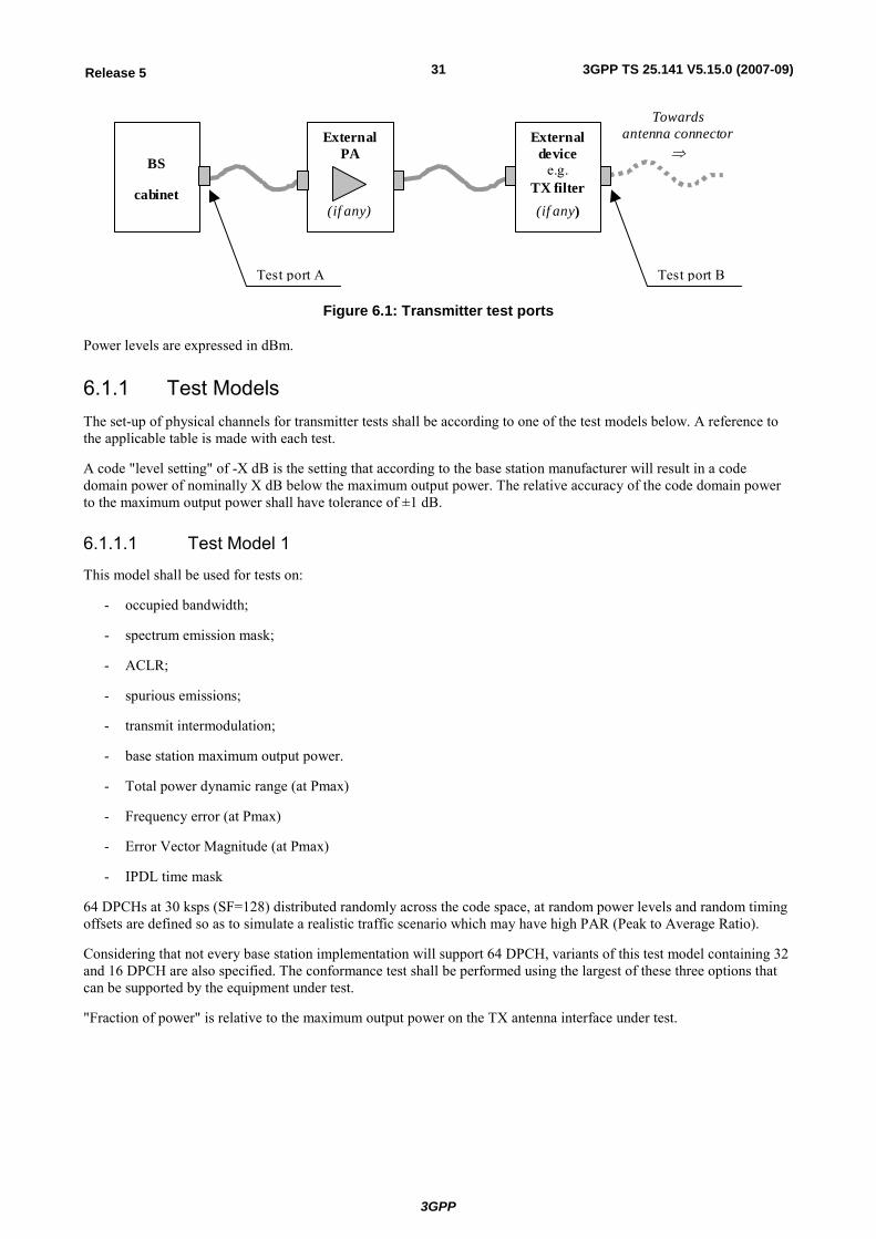
3GPP
3GPP TS 25.141 V5.15.0 (2007-09)31Release 5
BS
cabinet
Test port A Test port B
External device
e.g. TX filter
(if any)
External PA
(if any)
Towards antenna connector
⇒
Figure 6.1: Transmitter test ports
Power levels are expressed in dBm.
6.1.1 Test Models The set-up of physical channels for transmitter tests shall be according to one of the test models below. A reference to the applicable table is made with each test.
A code "level setting" of -X dB is the setting that according to the base station manufacturer will result in a code domain power of nominally X dB below the maximum output power. The relative accuracy of the code domain power to the maximum output power shall have tolerance of ±1 dB.
6.1.1.1 Test Model 1
This model shall be used for tests on:
- occupied bandwidth;
- spectrum emission mask;
- ACLR;
- spurious emissions;
- transmit intermodulation;
- base station maximum output power.
- Total power dynamic range (at Pmax)
- Frequency error (at Pmax)
- Error Vector Magnitude (at Pmax)
- IPDL time mask
64 DPCHs at 30 ksps (SF=128) distributed randomly across the code space, at random power levels and random timing offsets are defined so as to simulate a realistic traffic scenario which may have high PAR (Peak to Average Ratio).
Considering that not every base station implementation will support 64 DPCH, variants of this test model containing 32 and 16 DPCH are also specified. The conformance test shall be performed using the largest of these three options that can be supported by the equipment under test.
"Fraction of power" is relative to the maximum output power on the TX antenna interface under test.
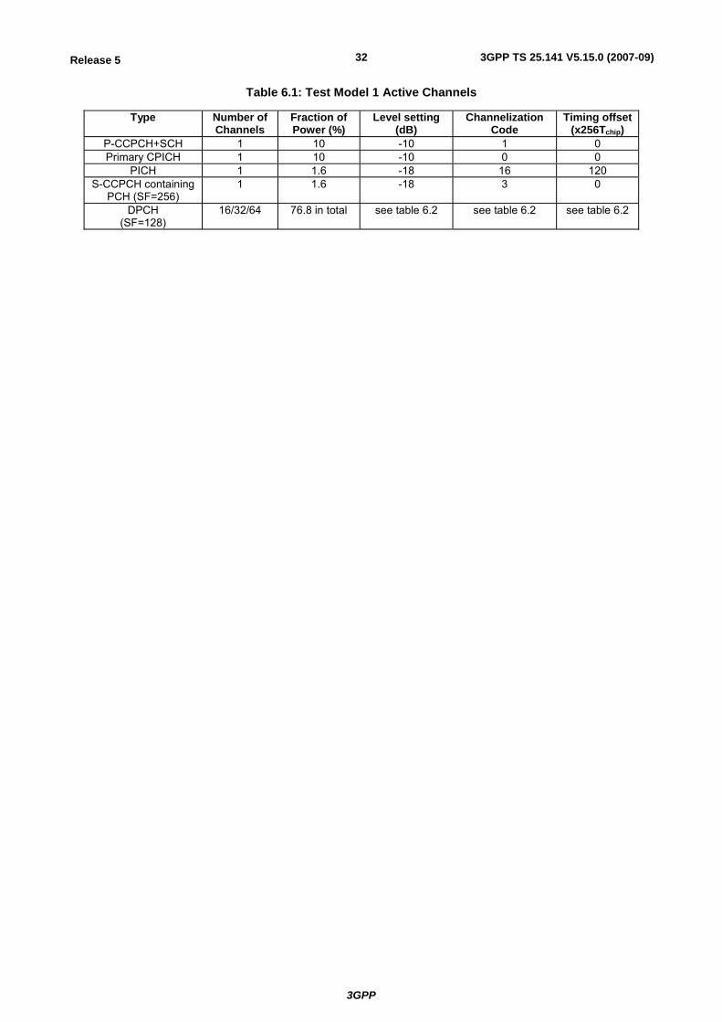
3GPP
3GPP TS 25.141 V5.15.0 (2007-09)32Release 5
Table 6.1: Test Model 1 Active Channels
Type Number of Channels
Fraction of Power (%)
Level setting (dB)
Channelization Code
Timing offset (x256Tchip)
P-CCPCH+SCH 1 10 -10 1 0 Primary CPICH 1 10 -10 0 0
PICH 1 1.6 -18 16 120 S-CCPCH containing
PCH (SF=256) 1 1.6 -18 3 0
DPCH (SF=128)
16/32/64 76.8 in total see table 6.2 see table 6.2 see table 6.2
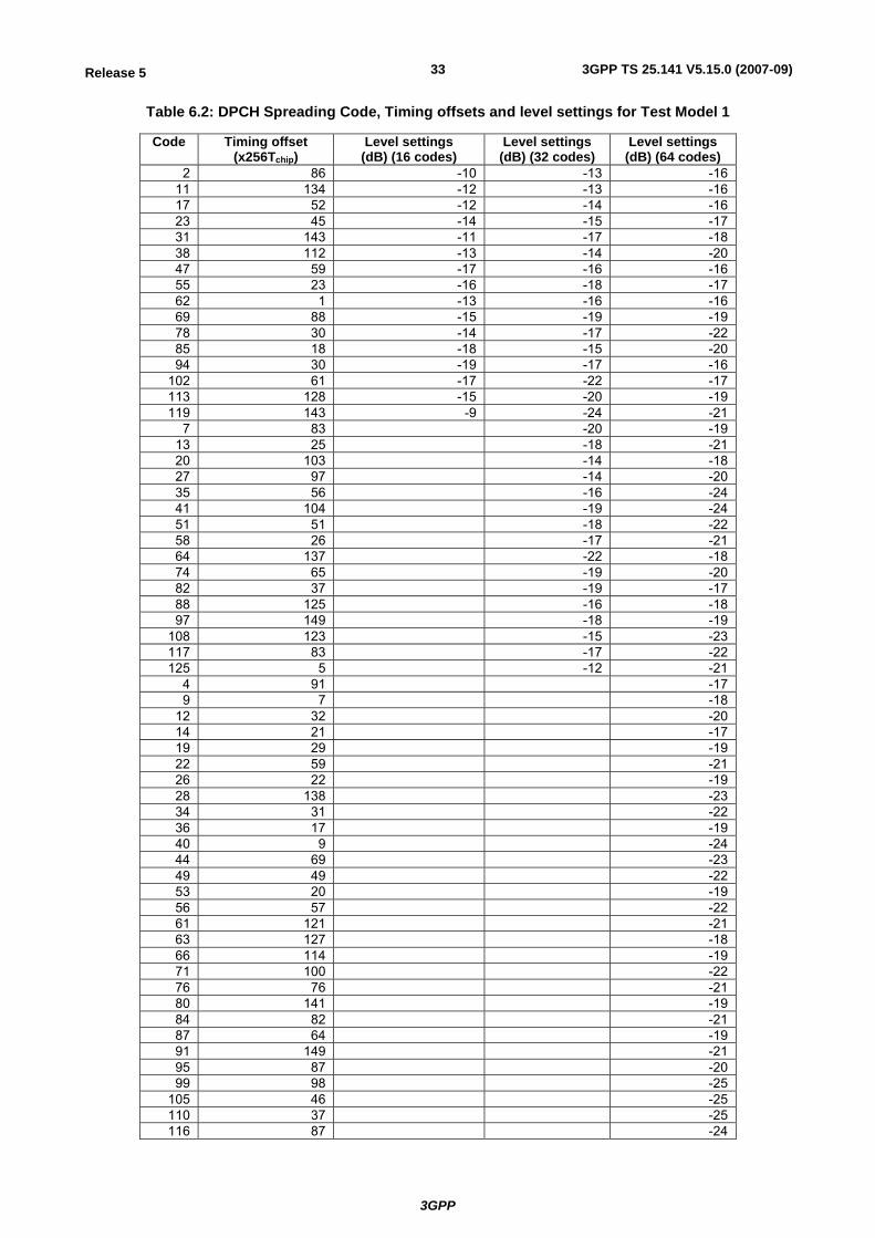
3GPP
3GPP TS 25.141 V5.15.0 (2007-09)33Release 5
Table 6.2: DPCH Spreading Code, Timing offsets and level settings for Test Model 1
Code Timing offset (x256Tchip)
Level settings (dB) (16 codes)
Level settings (dB) (32 codes)
Level settings (dB) (64 codes)
2 86 -10 -13 -1611 134 -12 -13 -1617 52 -12 -14 -1623 45 -14 -15 -1731 143 -11 -17 -1838 112 -13 -14 -2047 59 -17 -16 -1655 23 -16 -18 -1762 1 -13 -16 -1669 88 -15 -19 -1978 30 -14 -17 -2285 18 -18 -15 -2094 30 -19 -17 -16
102 61 -17 -22 -17113 128 -15 -20 -19119 143 -9 -24 -21
7 83 -20 -1913 25 -18 -2120 103 -14 -1827 97 -14 -2035 56 -16 -2441 104 -19 -2451 51 -18 -2258 26 -17 -2164 137 -22 -1874 65 -19 -2082 37 -19 -1788 125 -16 -1897 149 -18 -19
108 123 -15 -23117 83 -17 -22125 5 -12 -21
4 91 -179 7 -18
12 32 -2014 21 -1719 29 -1922 59 -2126 22 -1928 138 -2334 31 -2236 17 -1940 9 -2444 69 -2349 49 -2253 20 -1956 57 -2261 121 -2163 127 -1866 114 -1971 100 -2276 76 -2180 141 -1984 82 -2187 64 -1991 149 -2195 87 -2099 98 -25
105 46 -25110 37 -25116 87 -24
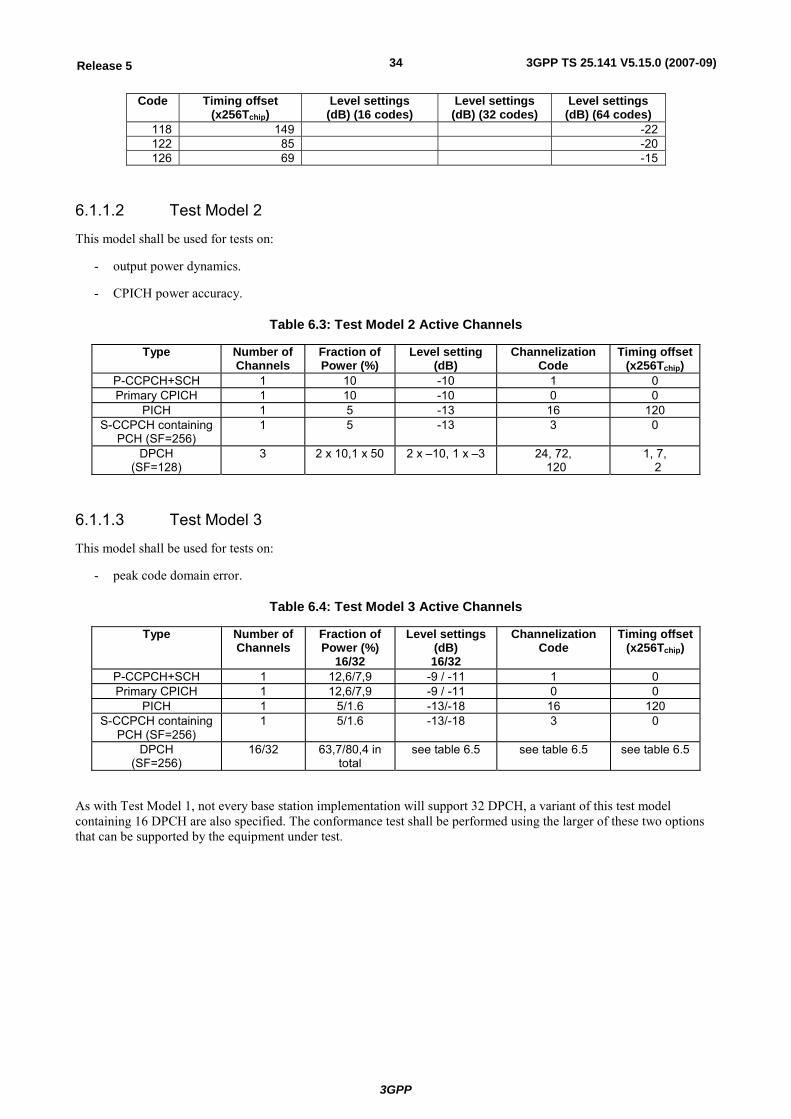
3GPP
3GPP TS 25.141 V5.15.0 (2007-09)34Release 5
Code Timing offset (x256Tchip)
Level settings (dB) (16 codes)
Level settings (dB) (32 codes)
Level settings (dB) (64 codes)
118 149 -22122 85 -20126 69 -15
6.1.1.2 Test Model 2
This model shall be used for tests on:
- output power dynamics.
- CPICH power accuracy.
Table 6.3: Test Model 2 Active Channels
Type Number of Channels
Fraction of Power (%)
Level setting (dB)
Channelization Code
Timing offset (x256Tchip)
P-CCPCH+SCH 1 10 -10 1 0 Primary CPICH 1 10 -10 0 0
PICH 1 5 -13 16 120 S-CCPCH containing
PCH (SF=256) 1 5 -13 3 0
DPCH (SF=128)
3 2 x 10,1 x 50 2 x –10, 1 x –3 24, 72, 120
1, 7, 2
6.1.1.3 Test Model 3
This model shall be used for tests on:
- peak code domain error.
Table 6.4: Test Model 3 Active Channels
Type Number of Channels
Fraction of Power (%)
16/32
Level settings (dB) 16/32
Channelization Code
Timing offset (x256Tchip)
P-CCPCH+SCH 1 12,6/7,9 -9 / -11 1 0 Primary CPICH 1 12,6/7,9 -9 / -11 0 0
PICH 1 5/1.6 -13/-18 16 120 S-CCPCH containing
PCH (SF=256) 1 5/1.6 -13/-18 3 0
DPCH (SF=256)
16/32 63,7/80,4 in total
see table 6.5 see table 6.5 see table 6.5
As with Test Model 1, not every base station implementation will support 32 DPCH, a variant of this test model containing 16 DPCH are also specified. The conformance test shall be performed using the larger of these two options that can be supported by the equipment under test.
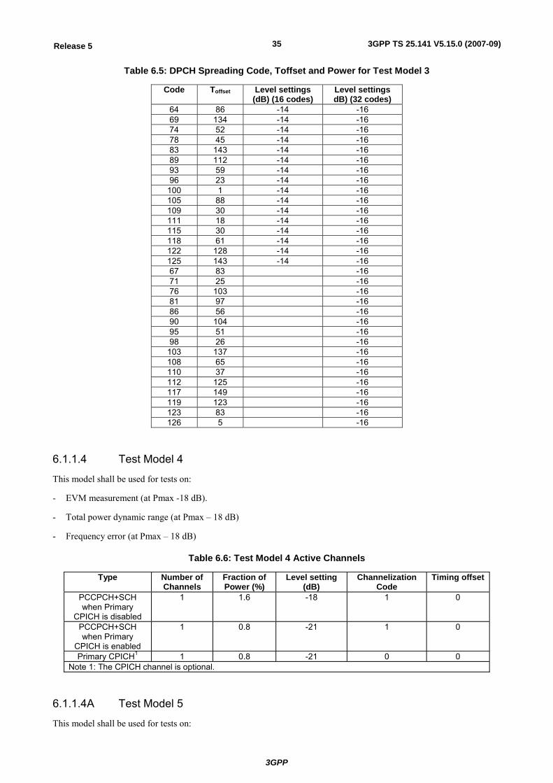
3GPP
3GPP TS 25.141 V5.15.0 (2007-09)35Release 5
Table 6.5: DPCH Spreading Code, Toffset and Power for Test Model 3
Code Toffset Level settings (dB) (16 codes)
Level settings dB) (32 codes)
64 86 -14 -16 69 134 -14 -16 74 52 -14 -16 78 45 -14 -16 83 143 -14 -16 89 112 -14 -16 93 59 -14 -16 96 23 -14 -16
100 1 -14 -16 105 88 -14 -16 109 30 -14 -16 111 18 -14 -16 115 30 -14 -16 118 61 -14 -16 122 128 -14 -16 125 143 -14 -16 67 83 -16 71 25 -16 76 103 -16 81 97 -16 86 56 -16 90 104 -16 95 51 -16 98 26 -16
103 137 -16 108 65 -16 110 37 -16 112 125 -16 117 149 -16 119 123 -16 123 83 -16 126 5 -16
6.1.1.4 Test Model 4
This model shall be used for tests on:
- EVM measurement (at Pmax -18 dB).
- Total power dynamic range (at Pmax – 18 dB)
- Frequency error (at Pmax – 18 dB)
Table 6.6: Test Model 4 Active Channels
Type Number of Channels
Fraction of Power (%)
Level setting (dB)
Channelization Code
Timing offset
PCCPCH+SCH when Primary
CPICH is disabled
1 1.6 -18 1 0
PCCPCH+SCH when Primary
CPICH is enabled
1 0.8 -21 1 0
Primary CPICH1 1 0.8 -21 0 0 Note 1: The CPICH channel is optional.
6.1.1.4A Test Model 5
This model shall be used for tests on:
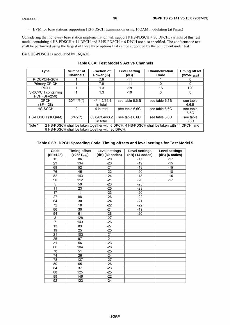
3GPP
3GPP TS 25.141 V5.15.0 (2007-09)36Release 5
- EVM for base stations supporting HS-PDSCH transmission using 16QAM modulation (at Pmax)
Considering that not every base station implementation will support 8 HS-PDSCH + 30 DPCH, variants of this test model containing 4 HS-PDSCH + 14 DPCH and 2 HS-PDSCH + 6 DPCH are also specified. The conformance test shall be performed using the largest of these three options that can be supported by the equipment under test.
Each HS-PDSCH is modulated by 16QAM.
Table 6.6A: Test Model 5 Active Channels
Type Number of Channels
Fraction of Power (%)
Level setting (dB)
Channelization Code
Timing offset (x256Tchip)
P-CCPCH+SCH 1 7.9 -11 1 0 Primary CPICH 1 7.9 -11 0 0
PICH 1 1.3 -19 16 120 S-CCPCH containing
PCH (SF=256) 1 1.3 -19 3 0
DPCH (SF=128)
30/14/6(*) 14/14.2/14.4 in total
see table 6.6.B see table 6.6B see table 6.6.B
HS-SCCH 2 4 in total see table 6.6C see table 6.6C see table 6.6C
HS-PDSCH (16QAM) 8/4/2(*) 63.6/63.4/63.2 in total
see table 6.6D see table 6.6D see table 6.6D
Note *: 2 HS-PDSCH shall be taken together with 6 DPCH, 4 HS-PDSCH shall be taken with 14 DPCH, and 8 HS-PDSCH shall be taken together with 30 DPCH.
Table 6.6B: DPCH Spreading Code, Timing offsets and level settings for Test Model 5
Code (SF=128)
Timing offset (x256Tchip)
Level settings (dB) (30 codes)
Level settings (dB) (14 codes)
Level settings (dB) (6 codes)
15 86 -20 -17 -17 23 134 -20 -19 -15 68 52 -21 -19 -15 76 45 -22 -20 -18 82 143 -24 -18 -16 90 112 -21 -20 -17 5 59 -23 -25
11 23 -25 -23 17 1 -23 -20 27 88 -26 -22 64 30 -24 -21 72 18 -22 -22 86 30 -24 -19 94 61 -28 -20 3 128 -27 7 143 -26
13 83 -27 19 25 -25 21 103 -21 25 97 -21 31 56 -23 66 104 -26 70 51 -25 74 26 -24 78 137 -27 80 65 -26 84 37 -23 88 125 -25 89 149 -22 92 123 -24
3GPP
3GPP TS 25.141 V5.15.0 (2007-09)37Release 5
Table 6.6C: HS-SCCH Spreading Code, Timing offsets and level settings for Test Model 5
Code (SF=128)
Timing offset (x256Tchip)
Level settings (dB)
9 0 -15 29 0 -21
Table 6.6D: HS-PDSCH Spreading Code, Timing offsets, level settings for Test Model 5
Code (SF=16)
Timing offset (x256Tchip)
Level settings(dB) (8 codes)
Level settings (dB) (4 codes)
Level settings (dB) (2 codes)
4 0 -11 -8 -5 5 0 -11 -8 6 0 -11 7 0 -11
12 0 -11 -8 -5 13 0 -11 -8 14 0 -11 15 0 -11
6.1.1.5 DPCH Structure of the Downlink Test Models
For the above test models the following structure is adopted for the DPCH. The DPDCH and DPCCH have the same power level. The timeslot structure should be as described by TS 25.211-slot format 10 and 6 that are reproduced in table 6.7.
Table 6.7: DPCH structure of the downlink test models
Slot Format
Channel Bit
Channel Symbol
SF Bits/Frame Bits/ Slot
DPDCH Bits/Slot DPCCH Bits/Slot
#I Rate (kbps)
Rate (ksps)
DPDCH DPCCH TOT NData1 Ndata2 NTFCI NTPC Npilot
10 60 30 128 450 150 600 40 6 24 0 2 8 6 30 15 256 150 150 300 20 2 8 0 2 8
The test DPCH has frame structure so that the pilot bits are defined over 15 timeslots according to the relevant columns of TS 25.211, which are reproduced in table 6.8.
Table 6.8: Frame structure of DPCH
Npilot = 8 Symbol # 0 1 2 3
Slot #0 1 2 3 4 5 6 7 8 9
10 11 12 13 14
111111111111111111111111111111
110001001011111001110110100000
11 11 11 11 11 11 11 11 11 11 11 11 11 11 11
101001000110000010110111001111
The TPC bits alternate 00 / 11 starting with 00 in timeslot 0.
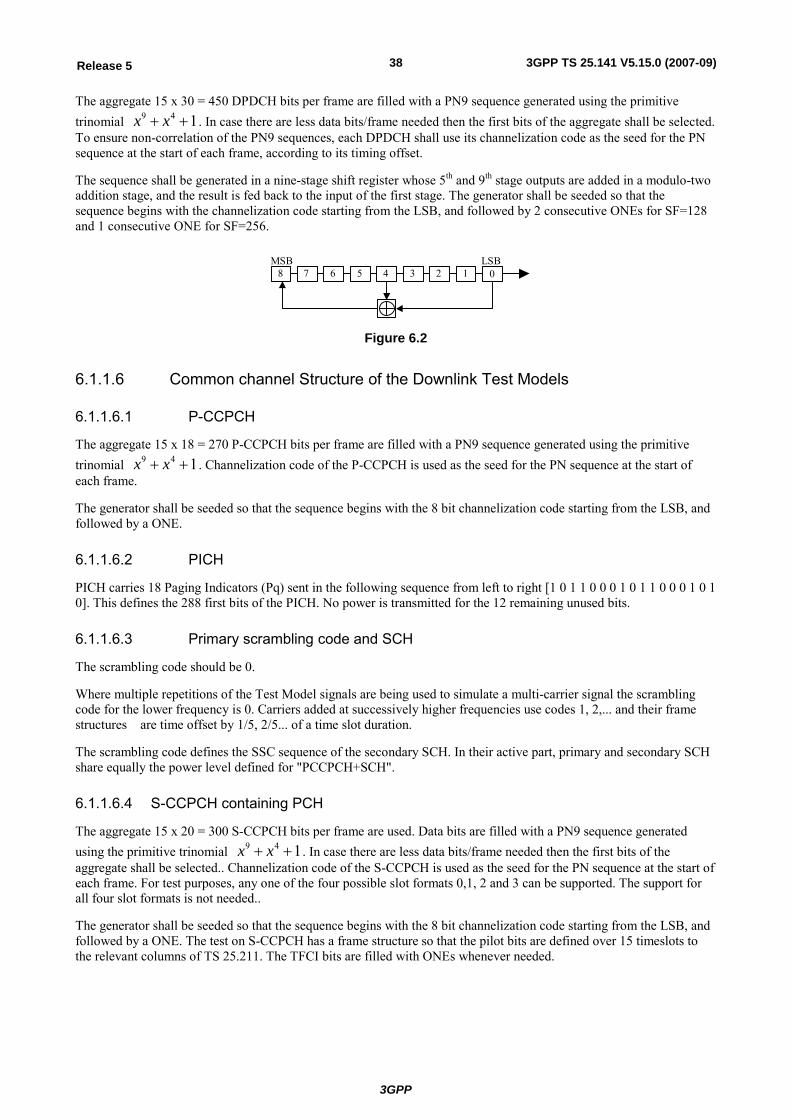
3GPP
3GPP TS 25.141 V5.15.0 (2007-09)38Release 5
The aggregate 15 x 30 = 450 DPDCH bits per frame are filled with a PN9 sequence generated using the primitive trinomial 9 4 1x x+ + . In case there are less data bits/frame needed then the first bits of the aggregate shall be selected. To ensure non-correlation of the PN9 sequences, each DPDCH shall use its channelization code as the seed for the PN sequence at the start of each frame, according to its timing offset.
The sequence shall be generated in a nine-stage shift register whose 5th and 9th stage outputs are added in a modulo-two addition stage, and the result is fed back to the input of the first stage. The generator shall be seeded so that the sequence begins with the channelization code starting from the LSB, and followed by 2 consecutive ONEs for SF=128 and 1 consecutive ONE for SF=256.
LSBMSB 1 0234567 8
Figure 6.2
6.1.1.6 Common channel Structure of the Downlink Test Models
6.1.1.6.1 P-CCPCH
The aggregate 15 x 18 = 270 P-CCPCH bits per frame are filled with a PN9 sequence generated using the primitive trinomial 9 4 1x x+ + . Channelization code of the P-CCPCH is used as the seed for the PN sequence at the start of each frame.
The generator shall be seeded so that the sequence begins with the 8 bit channelization code starting from the LSB, and followed by a ONE.
6.1.1.6.2 PICH
PICH carries 18 Paging Indicators (Pq) sent in the following sequence from left to right [1 0 1 1 0 0 0 1 0 1 1 0 0 0 1 0 1 0]. This defines the 288 first bits of the PICH. No power is transmitted for the 12 remaining unused bits.
6.1.1.6.3 Primary scrambling code and SCH
The scrambling code should be 0.
Where multiple repetitions of the Test Model signals are being used to simulate a multi-carrier signal the scrambling code for the lower frequency is 0. Carriers added at successively higher frequencies use codes 1, 2,... and their frame structures are time offset by 1/5, 2/5... of a time slot duration.
The scrambling code defines the SSC sequence of the secondary SCH. In their active part, primary and secondary SCH share equally the power level defined for "PCCPCH+SCH".
6.1.1.6.4 S-CCPCH containing PCH
The aggregate 15 x 20 = 300 S-CCPCH bits per frame are used. Data bits are filled with a PN9 sequence generated using the primitive trinomial 9 4 1x x+ + . In case there are less data bits/frame needed then the first bits of the aggregate shall be selected.. Channelization code of the S-CCPCH is used as the seed for the PN sequence at the start of each frame. For test purposes, any one of the four possible slot formats 0,1, 2 and 3 can be supported. The support for all four slot formats is not needed..
The generator shall be seeded so that the sequence begins with the 8 bit channelization code starting from the LSB, and followed by a ONE. The test on S-CCPCH has a frame structure so that the pilot bits are defined over 15 timeslots to the relevant columns of TS 25.211. The TFCI bits are filled with ONEs whenever needed.
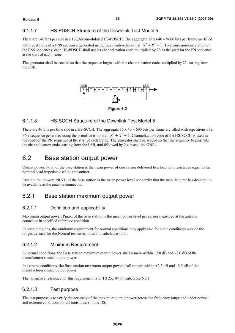
3GPP
3GPP TS 25.141 V5.15.0 (2007-09)39Release 5
6.1.1.7 HS-PDSCH Structure of the Downlink Test Model 5
There are 640 bits per slot in a 16QAM-modulated HS-PDSCH. The aggregate 15 x 640 = 9600 bits per frame are filled with repetitions of a PN9 sequence generated using the primitive trinomial 9 4 1x x+ + . To ensure non-correlation of the PN9 sequences, each HS-PDSCH shall use its channelization code multiplied by 23 as the seed for the PN sequence at the start of each frame.
The generator shall be seeded so that the sequence begins with the channelization code multiplied by 23 starting from the LSB.
LSBMSB 1 0234567 8
Figure 6.2
6.1.1.8 HS-SCCH Structure of the Downlink Test Model 5
There are 40 bits per time slot in a HS-SCCH. The aggregate 15 x 40 = 600 bits per frame are filled with repetitions of a PN9 sequence generated using the primitive trinomial 9 4 1x x+ + . Channelization code of the HS-SCCH is used as the seed for the PN sequence at the start of each frame. The generator shall be seeded so that the sequence begins with the channelization code starting from the LSB, and followed by 2 consecutive ONEs.
6.2 Base station output power Output power, Pout, of the base station is the mean power of one carrier delivered to a load with resistance equal to the nominal load impedance of the transmitter.
Rated output power, PRAT, of the base station is the mean power level per carrier that the manufacturer has declared to be available at the antenna connector.
6.2.1 Base station maximum output power
6.2.1.1 Definition and applicability
Maximum output power, Pmax, of the base station is the mean power level per carrier measured at the antenna connector in specified reference condition.
In certain regions, the minimum requirement for normal conditions may apply also for some conditions outside the ranges defined for the Normal test environment in subclause 4.4.1.
6.2.1.2 Minimum Requirement
In normal conditions, the Base station maximum output power shall remain within +2.0 dB and –2.0 dB of the manufacturer's rated output power.
In extreme conditions, the Base station maximum output power shall remain within +2.5 dB and –2.5 dB of the manufacturer's rated output power.
The normative reference for this requirement is in TS 25.104 [1] subclause 6.2.1.
6.2.1.3 Test purpose
The test purpose is to verify the accuracy of the maximum output power across the frequency range and under normal and extreme conditions for all transmitters in the BS.
3GPP
3GPP TS 25.141 V5.15.0 (2007-09)40Release 5
6.2.1.4 Method of test
6.2.1.4.1 Initial conditions
Test environment: normal; see subclause 4.4.1.
RF channels to be tested: B, M and T; see subclause 4.8.
In addition, on one UARFCN only, the test shall be performed under extreme power supply as defined in subclause 4.4.2
NOTE: Tests under extreme power supply also test extreme temperature.
1) Connect the power measuring equipment to the base station RF output port.
6.2.1.4.2 Procedure
1) Set the base station to transmit a signal modulated with a combination of PCCPCH, SCCPCH and Dedicated Physical Channels specified as test model1 in subclause 6.1.1.1.
2) Measure the mean power at the RF output port.
6.2.1.5 Test Requirements
In normal conditions, the measurement result in step 2 of 6.2.1.4.2 shall remain within +2.7 dB and –2.7 dB of the manufacturer's rated output power.
In extreme conditions, measurement result in step 2 of 6.2.1.4.2 shall remain within +3.2 dB and –3.2 dB of the manufacturer's rated output power.
NOTE: If the above Test Requirement differs from the Minimum Requirement then the Test Tolerance applied for this test is non-zero. The Test Tolerance for this test is defined in subclause 4.2 and the explanation of how the Minimum Requirement has been relaxed by the Test Tolerance is given in Annex F.
6.2.2 CPICH power accuracy
6.2.2.1 Definition and applicability
CPICH power accuracy is defined as the maximum deviation between the Primary CPICH code domain power indicated on the BCH and the Primary CPICH code domain power measured at the TX antenna interface. The requirement is applicable for all BS types.
6.2.2.2 Minimum Requirement
The measured Primary CPICH code domain power shall be within ±2.1dB of the Primary CPICH code domain power indicated on the BCH. In case of transmit diversity the Primary CPICH code domain power per antenna connector shall be within +/- 2.1dB of the Primary CPICH code domain power intended for that particular antenna connector. The normative reference for this requirement is in TS 25.104 [1] subclause 6.4.4
6.2.2.3 Test purpose
The purpose of the test is to verify, that the BS under test delivers Primary CPICH code domain power within margins, thereby allowing reliable cell planning and operation.
6.2.2.4 Method of test
6.2.2.4.1 Initial conditions
Test environment: normal; see subclause 4.4.1.
3GPP
3GPP TS 25.141 V5.15.0 (2007-09)41Release 5
RF channels to be tested: B, M and T; see subclause 4.8
1) Connect BS to code domain analyser as shown in annex B.
2) Disable inner loop power control.
3) Set-up BS transmission at maximum total power as specified by the supplier. Channel set-up shall be according to Test Model 2 subclause 6.1.1.2. In case of transmit diversity the Primary CPICH code domain power intended per antenna connector shall be declared by the manufacturer.
6.2.2.4.2 Procedure
- Measure the code domain power of the PCPICH in one timeslot according to annex E.
6.2.2.5 Test Requirement
The measured CPICH code domain power shall be within ±2.9dB of the ordered absolute value. In case of transmit diversity the measured Primary CPICH code domain power per antenna connector shall be within +/- 2.9dB of the Primary CPICH code domain power for that particular antenna connector declared by the manufacturer.
NOTE: If the above Test Requirement differs from the Minimum Requirement then the Test Tolerance applied for this test is non-zero. The Test Tolerance for this test is defined in subclause 4.2 and the explanation of how the Minimum Requirement has been relaxed by the Test Tolerance is given in Annex F.
6.3 Frequency error
6.3.1 Definition and applicability Frequency error is the measure of the difference between the actual BS transmit frequency and the assigned frequency. The same source shall be used for RF frequency and data clock generation.
It is not possible to verify by testing that the data clock is derived from the same frequency source as used for RF generation. This may be confirmed by a manufacturers declaration
6.3.2 Minimum Requirement The Frequency Error shall be within ± 0.05 PPM.
The normative reference for this requirement is in TS 25.104 [1] subclause 6.3
6.3.3 Test purpose To verify that the Frequency Error is within the limit specified in 6.3.2
6.3.4 Method of test Requirement is tested together with Error Vector Magnitude test, as described in subclause 6.7.1.4.
6.3.5 Test requirement The Frequency Error shall be within the range (–0.05 PPM – 12 Hz) to (+0.05 PPM + 12 Hz).
6.4 Output power dynamics Power control is used to limit the interference level. The BS transmitter uses a quality-based power control on the downlink. The physical channels for the following test(s) shall be set-up according to subclause 6.1.1.2.
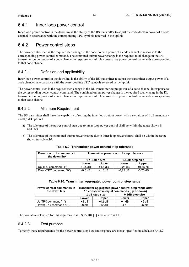
3GPP
3GPP TS 25.141 V5.15.0 (2007-09)42Release 5
6.4.1 Inner loop power control Inner loop power control in the downlink is the ability of the BS transmitter to adjust the code domain power of a code channel in accordance with the corresponding TPC symbols received in the uplink.
6.4.2 Power control steps The power control step is the required step change in the code domain power of a code channel in response to the corresponding power control command. The combined output power change is the required total change in the DL transmitter output power of a code channel in response to multiple consecutive power control commands corresponding to that code channel.
6.4.2.1 Definition and applicability
Inner loop power control in the downlink is the ability of the BS transmitter to adjust the transmitter output power of a code channel in accordance with the corresponding TPC symbols received in the uplink.
The power control step is the required step change in the DL transmitter output power of a code channel in response to the corresponding power control command. The combined output power change is the required total change in the DL transmitter output power of a code channel in response to multiple consecutive power control commands corresponding to that code channel.
6.4.2.2 Minimum Requirement
The BS transmitter shall have the capability of setting the inner loop output power with a step sizes of 1 dB mandatory and 0,5 dB optional.
a) The tolerance of the power control step due to inner loop power control shall be within the range shown in table 6.9.
b) The tolerance of the combined output power change due to inner loop power control shall be within the range shown in table 6.10.
Table 6.9: Transmitter power control step tolerance
Power control commands in the down link
Transmitter power control step tolerance
1 dB step size 0,5 dB step size Lower Upper Lower Upper
Up(TPC command "1") +0,5 dB +1,5 dB +0,25 dB +0,75 dB Down(TPC command "0") -0,5 dB -1,5 dB -0,25 dB -0,75 dB
Table 6.10: Transmitter aggregated power control step range
Power control commands in the down link
Transmitter aggregated power control step range after 10 consecutive equal commands (up or down)
1 dB step size 0.5dB step size Lower Upper Lower Upper
Up(TPC command "1") +8 dB +12 dB +4 dB +6 dB Down(TPC command "0") -8 dB -12 dB -4 dB -6 dB
The normative reference for this requirement is TS 25.104 [1] subclause 6.4.1.1.1
6.4.2.3 Test purpose
To verify those requirements for the power control step size and response are met as specified in subclause 6.4.2.2.
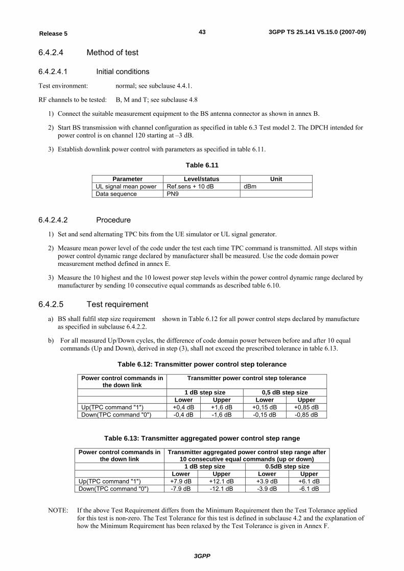
3GPP
3GPP TS 25.141 V5.15.0 (2007-09)43Release 5
6.4.2.4 Method of test
6.4.2.4.1 Initial conditions
Test environment: normal; see subclause 4.4.1.
RF channels to be tested: B, M and T; see subclause 4.8
1) Connect the suitable measurement equipment to the BS antenna connector as shown in annex B.
2) Start BS transmission with channel configuration as specified in table 6.3 Test model 2. The DPCH intended for power control is on channel 120 starting at –3 dB.
3) Establish downlink power control with parameters as specified in table 6.11.
Table 6.11
Parameter Level/status Unit UL signal mean power Ref.sens + 10 dB dBm Data sequence PN9
6.4.2.4.2 Procedure
1) Set and send alternating TPC bits from the UE simulator or UL signal generator.
2) Measure mean power level of the code under the test each time TPC command is transmitted. All steps within power control dynamic range declared by manufacturer shall be measured. Use the code domain power measurement method defined in annex E.
3) Measure the 10 highest and the 10 lowest power step levels within the power control dynamic range declared by manufacturer by sending 10 consecutive equal commands as described table 6.10.
6.4.2.5 Test requirement
a) BS shall fulfil step size requirement shown in Table 6.12 for all power control steps declared by manufacture as specified in subclause 6.4.2.2.
b) For all measured Up/Down cycles, the difference of code domain power between before and after 10 equal commands (Up and Down), derived in step (3), shall not exceed the prescribed tolerance in table 6.13.
Table 6.12: Transmitter power control step tolerance
Power control commands in the down link
Transmitter power control step tolerance
1 dB step size 0,5 dB step size Lower Upper Lower Upper
Up(TPC command "1") +0,4 dB +1,6 dB +0,15 dB +0,85 dB Down(TPC command "0") -0,4 dB -1,6 dB -0,15 dB -0,85 dB
Table 6.13: Transmitter aggregated power control step range
Power control commands in the down link
Transmitter aggregated power control step range after 10 consecutive equal commands (up or down)
1 dB step size 0.5dB step size Lower Upper Lower Upper
Up(TPC command "1") +7.9 dB +12.1 dB +3.9 dB +6.1 dB Down(TPC command "0") -7.9 dB -12.1 dB -3.9 dB -6.1 dB
NOTE: If the above Test Requirement differs from the Minimum Requirement then the Test Tolerance applied for this test is non-zero. The Test Tolerance for this test is defined in subclause 4.2 and the explanation of how the Minimum Requirement has been relaxed by the Test Tolerance is given in Annex F.
3GPP
3GPP TS 25.141 V5.15.0 (2007-09)44Release 5
6.4.3 Power control dynamic range
6.4.3.1 Definition and applicability
The power control dynamic range is the difference between the maximum and the minimum code domain power of a code channel for a specified reference condition. Transmit modulation quality shall be maintained within the whole dynamic range as specified in TS 25.104 [1] subclause 6.8.
6.4.3.2 Minimum Requirement
Down link (DL) power control dynamic range:
- maximum code domain power: BS maximum output power -3 dB or greater;
- minimum code domain power: BS maximum output power -28 dB or less.
The normative reference for this requirement is TS 25.104 [1] subclause 6.4.2.1.
6.4.3.3 Test purpose
To verify that the minimum power control dynamic range is met as specified in subclause 6.4.3.2.
6.4.3.4 Method of test
6.4.3.4.1 Initial conditions
Test environment: normal; see subclause 4.4.1.
RF channels to be tested: B, M and T; see subclause 4.8
1) Connect the measurement equipment to the BS antenna connector as shown in annex B.
2) Channel configuration defined in table 6.3 Test model 2 shall be used.
3) Set BS frequency.
4) Star BS transmission.
6.4.3.4.2 Procedure
Pmax shall be defined as described in subclause 6.2.1 Base station maximum output power.
1) Re-measure Pmax according to subclause 6.2.1 (using test model 1).
2) Using test model 2,set the code domain power of the DPCH under test to Pmax-3 dB. Power levels for other code channels may be adjusted if necessary.
3) Measure the code domain power of the code channel under test. Use the code domain power measurement method defined in annex E.
4) Set the code domain power of the DPCH under test to Pmax-28 dB by means determined by the manufacturer. The power levels for the other code channels used in step 2 shall remain unchanged (the overall output power will drop by approximately 3 dB).
5) Measure the code domain power of the code channel under test.
6.4.3.5 Test requirement
Down link (DL) power control dynamic range:-
- maximum code domain power: BS maximum output power –4.1 dB or greater;
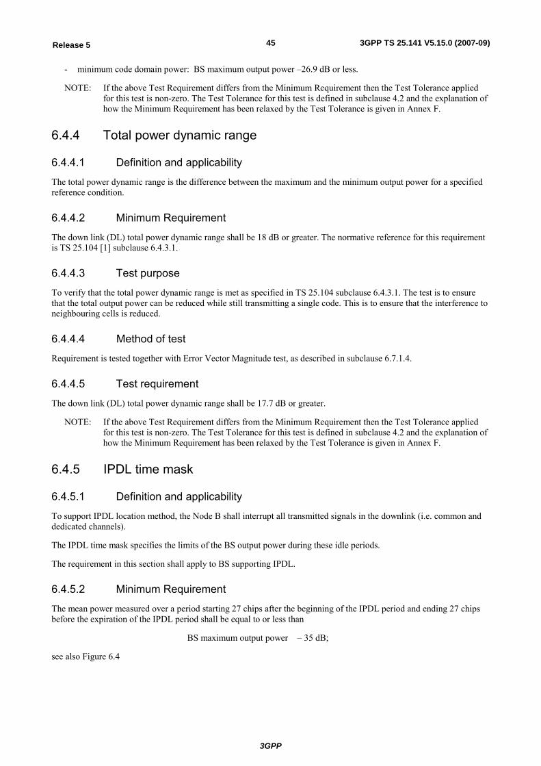
3GPP
3GPP TS 25.141 V5.15.0 (2007-09)45Release 5
- minimum code domain power: BS maximum output power –26.9 dB or less.
NOTE: If the above Test Requirement differs from the Minimum Requirement then the Test Tolerance applied for this test is non-zero. The Test Tolerance for this test is defined in subclause 4.2 and the explanation of how the Minimum Requirement has been relaxed by the Test Tolerance is given in Annex F.
6.4.4 Total power dynamic range
6.4.4.1 Definition and applicability
The total power dynamic range is the difference between the maximum and the minimum output power for a specified reference condition.
6.4.4.2 Minimum Requirement
The down link (DL) total power dynamic range shall be 18 dB or greater. The normative reference for this requirement is TS 25.104 [1] subclause 6.4.3.1.
6.4.4.3 Test purpose
To verify that the total power dynamic range is met as specified in TS 25.104 subclause 6.4.3.1. The test is to ensure that the total output power can be reduced while still transmitting a single code. This is to ensure that the interference to neighbouring cells is reduced.
6.4.4.4 Method of test
Requirement is tested together with Error Vector Magnitude test, as described in subclause 6.7.1.4.
6.4.4.5 Test requirement
The down link (DL) total power dynamic range shall be 17.7 dB or greater.
NOTE: If the above Test Requirement differs from the Minimum Requirement then the Test Tolerance applied for this test is non-zero. The Test Tolerance for this test is defined in subclause 4.2 and the explanation of how the Minimum Requirement has been relaxed by the Test Tolerance is given in Annex F.
6.4.5 IPDL time mask
6.4.5.1 Definition and applicability
To support IPDL location method, the Node B shall interrupt all transmitted signals in the downlink (i.e. common and dedicated channels).
The IPDL time mask specifies the limits of the BS output power during these idle periods.
The requirement in this section shall apply to BS supporting IPDL.
6.4.5.2 Minimum Requirement
The mean power measured over a period starting 27 chips after the beginning of the IPDL period and ending 27 chips before the expiration of the IPDL period shall be equal to or less than
BS maximum output power – 35 dB;
see also Figure 6.4
3GPP
3GPP TS 25.141 V5.15.0 (2007-09)46Release 5
27 chips 27 chips
BS maximum output power
35 dB
IP_Length
Figure 6.4: IPDL Time Mask
The requirement applies to all output powers within the total power dynamic range as specified in TS 25.104 [1] subclause 6.4.3.
The normative reference for this requirement is in TS 25.104 [1] subclause 6.4.5.1.
6.4.5.3 Test purpose
The test purpose is to verify the ability of the BS to temporarily reduce its output power below a specified value to improve time difference measurements made by UE for location services.
6.4.5.4 Method of test
6.4.5.4.1 Initial conditions
Test environment: normal; see subclause 4.4.1.
RF channels to be tested: B, M and T; see subclause 4.8.
1) Connect the power measuring equipment to the BS antenna connector.
2) Set the BS to transmit a signal according to test model 1 as defined in subclause 6.1.1.1, at the manufacturers specified maximum output power.
3) Configure the BS to produce idle periods in continuous mode. The IPDL parameters as defined in TS 25.214 [12] shall have the following values:
IP_Spacing = 5
IP_Length = 10 CPICH symbols
Seed = 0
6.4.5.4.2 Procedure
1) Measure the mean power at the BS antenna connector over a period starting 27 chips after the beginning of the IPDL period and ending 27 chips before the expiration of the IPDL period.
6.4.5.5 Test Requirements
The mean power measured according to step (1) in subclause 6.4.5.4.2 shall be equal to or less than
BS maximum output power – 34.3 dB.
NOTE: If the above Test Requirement differs from the Minimum Requirement then the Test Tolerance applied for this test is non-zero. The Test Tolerance for this test is defined in subclause 4.2 and the explanation of how the Minimum Requirement has been relaxed by the Test Tolerance is given in Annex F.
3GPP
3GPP TS 25.141 V5.15.0 (2007-09)47Release 5
6.5 Output RF spectrum emissions The physical channels for the following test(s) shall be set-up according to subclause 6.1.1.1.
6.5.1 Occupied bandwidth
6.5.1.1 Definition and applicability
The occupied bandwidth is the width of a frequency band such that, below the lower and above the upper frequency limits, the mean powers emitted are each equal to a specified percentage β/2 of the total mean transmitted power.
The value of β/2 should be taken as 0,5%.
6.5.1.2 Minimum Requirements
The occupied bandwidth shall be less than 5 MHz based on a chip rate of 3,84 Mcps.
The normative reference for this requirement is TS 25.104 subclause 6.6.1.
6.5.1.3 Test purpose
The occupied bandwidth, defined in the Radio Regulations of the International Telecommunication Union ITU, is a useful concept for specifying the spectral properties of a given emission in the simplest possible manner; see also Recommendation ITU-R Recommendation SM.328 [11]. The test purpose is to verify that the emission of the BS does not occupy an excessive bandwidth for the service to be provided and is, therefore, not likely to create interference to other users of the spectrum beyond undue limits.
6.5.1.4 Method of test
6.5.1.4.1 Initial conditions
Test environment: normal; see subclause 4.4.1.
RF channels to be tested: B, M and T; see subclause 4.8
1) Connect the Measurement device to the BS antenna connector.
2) Start transmission on a single carrier according to test model 1 defined in subclause 6.1.1.1 at the manufacturer’s specified maximum output power.
6.5.1.4.2 Procedure
1) Measure the spectrum of the transmitted signal across a span of 10 MHz, based on an occupied bandwidth requirement of 5 MHz. The selected resolution bandwidth (RBW) filter of the analyser shall be 30 kHz or less. The spectrum shall be measured at 400 or more points across the measurement span.
NOTE: The detection mode of the spectrum analyzer will not have any effect on the result if the statistical properties of the out-of-OBW power are the same as those of the inside-OBW power. Both are expected to have the Rayleigh distribution of the amplitude of Gaussian noise. In any case where the statistics are not the same, though, the detection mode must be power responding. There are at least two ways to be power responding. The spectrum analyser can be set to "sample" detection, with its video bandwidth setting at least three times its RBW setting. Or the analyser may be set to respond to the average of the power (root-mean-square of the voltage) across the measurement cell.
2) Compute the total of the power, P0, (in power units, not decibel units) of all the measurement cells in the measurement span. Compute P1, the power outside the occupied bandwidth on each side. P1 is half of the total power outside the bandwidth. P1 is half of (100 % - (occupied percentage)) of P0. For the occupied percentage of 99 %, P1 is 0.005 times P0.
3GPP
3GPP TS 25.141 V5.15.0 (2007-09)48Release 5
3) Determine the lowest frequency, f1, for which the sum of all power in the measurement cells from the beginning of the span to f1 exceeds P1.
4) Determine the highest frequency, f2, for which the sum of all power in the measurement cells from the end of the span to f2 exceeds P1.
5) Compute the occupied bandwidth as f2 - f1.
6.5.1.5 Test requirements
The occupied bandwidth shall be less than 5 MHz based on a chip rate of 3,84 Mcps
NOTE: If the above Test Requirement differs from the Minimum Requirement then the Test Tolerance applied for this test is non-zero. The Test Tolerance for this test is defined in subclause 4.2 and the explanation of how the Minimum Requirement has been relaxed by the Test Tolerance is given in Annex F.
6.5.2 Out of band emission Out of band emissions are unwanted emissions immediately outside the channel bandwidth resulting from the modulation process and non-linearity in the transmitter but excluding spurious emissions. This out of band emission limit is specified in terms of a spectrum emission mask and adjacent channel leakage power ratio for the transmitter.
6.5.2.1 Spectrum emission mask
6.5.2.1.1 Definitions and applicability
The mask defined in Tables 6.14 to 6.17 below may be mandatory in certain regions. In other regions this mask may not be applied.
6.5.2.1.2 Minimum Requirements
For regions where this clause applies, the requirement shall be met by a base station transmitting on a single RF carrier configured in accordance with the manufacturer's specification. Emissions shall not exceed the maximum level specified in tables 6.14 to 6.17 for the appropriate BS maximum output power, in the frequency range from Δf =2.5 MHz to Δfmax from the carrier frequency, where:
- Δf is the separation between the carrier frequency and the nominal –3dB point of the measuring filter closest to the carrier frequency.
- f_offset is the separation between the carrier frequency and the centre of the measurement filter;
- f_offsetmax is either 12.5 MHz or the offset to the UMTS Tx band edge as defined in subclause 3.4.1, whichever is the greater.
- Δfmax is equal to f_offsetmax minus half of the bandwidth of the measuring filter.
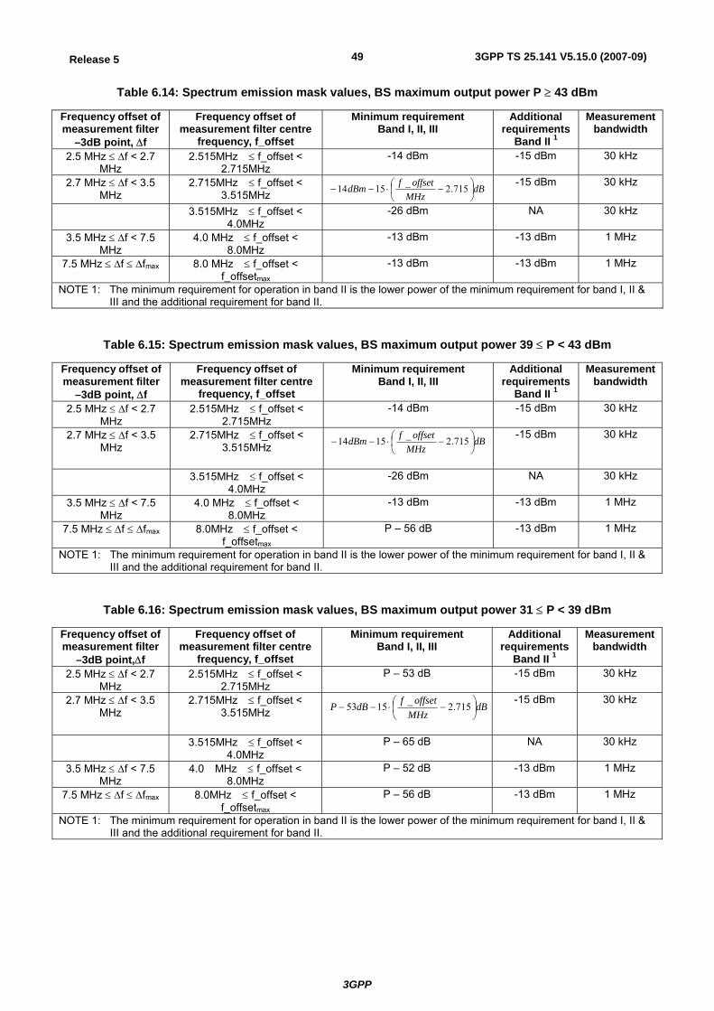
3GPP
3GPP TS 25.141 V5.15.0 (2007-09)49Release 5
Table 6.14: Spectrum emission mask values, BS maximum output power P ≥ 43 dBm
Frequency offset of measurement filter
–3dB point, Δf
Frequency offset of measurement filter centre
frequency, f_offset
Minimum requirement Band I, II, III
Additional requirements
Band II 1
Measurement bandwidth
2.5 MHz ≤ Δf < 2.7 MHz
2.515MHz ≤ f_offset < 2.715MHz
-14 dBm -15 dBm 30 kHz
2.7 MHz ≤ Δf < 3.5 MHz
2.715MHz ≤ f_offset < 3.515MHz dB
MHzoffsetfdBm ⎟
⎠⎞
⎜⎝⎛ −⋅−− 715.2_1514 -15 dBm 30 kHz
3.515MHz ≤ f_offset < 4.0MHz
-26 dBm NA 30 kHz
3.5 MHz ≤ Δf < 7.5 MHz
4.0 MHz ≤ f_offset < 8.0MHz
-13 dBm -13 dBm 1 MHz
7.5 MHz ≤ Δf ≤ Δfmax 8.0 MHz ≤ f_offset < f_offsetmax
-13 dBm -13 dBm 1 MHz
NOTE 1: The minimum requirement for operation in band II is the lower power of the minimum requirement for band I, II & III and the additional requirement for band II.
Table 6.15: Spectrum emission mask values, BS maximum output power 39 ≤ P < 43 dBm
Frequency offset of measurement filter
–3dB point, Δf
Frequency offset of measurement filter centre
frequency, f_offset
Minimum requirement Band I, II, III
Additional requirements
Band II 1
Measurement bandwidth
2.5 MHz ≤ Δf < 2.7 MHz
2.515MHz ≤ f_offset < 2.715MHz
-14 dBm -15 dBm 30 kHz
2.7 MHz ≤ Δf < 3.5 MHz
2.715MHz ≤ f_offset < 3.515MHz dB
MHzoffsetfdBm ⎟
⎠⎞
⎜⎝⎛ −⋅−− 715.2_1514
-15 dBm 30 kHz
3.515MHz ≤ f_offset < 4.0MHz
-26 dBm NA 30 kHz
3.5 MHz ≤ Δf < 7.5 MHz
4.0 MHz ≤ f_offset < 8.0MHz
-13 dBm -13 dBm 1 MHz
7.5 MHz ≤ Δf ≤ Δfmax 8.0MHz ≤ f_offset < f_offsetmax
P – 56 dB -13 dBm 1 MHz
NOTE 1: The minimum requirement for operation in band II is the lower power of the minimum requirement for band I, II & III and the additional requirement for band II.
Table 6.16: Spectrum emission mask values, BS maximum output power 31 ≤ P < 39 dBm
Frequency offset of measurement filter
–3dB point,Δf
Frequency offset of measurement filter centre
frequency, f_offset
Minimum requirement Band I, II, III
Additional requirements
Band II 1
Measurement bandwidth
2.5 MHz ≤ Δf < 2.7 MHz
2.515MHz ≤ f_offset < 2.715MHz
P – 53 dB -15 dBm 30 kHz
2.7 MHz ≤ Δf < 3.5 MHz
2.715MHz ≤ f_offset < 3.515MHz dB
MHzoffsetfdBP ⎟
⎠⎞
⎜⎝⎛ −⋅−− 715.2_1553
-15 dBm 30 kHz
3.515MHz ≤ f_offset < 4.0MHz
P – 65 dB NA 30 kHz
3.5 MHz ≤ Δf < 7.5 MHz
4.0 MHz ≤ f_offset < 8.0MHz
P – 52 dB -13 dBm 1 MHz
7.5 MHz ≤ Δf ≤ Δfmax 8.0MHz ≤ f_offset < f_offsetmax
P – 56 dB -13 dBm 1 MHz
NOTE 1: The minimum requirement for operation in band II is the lower power of the minimum requirement for band I, II & III and the additional requirement for band II.
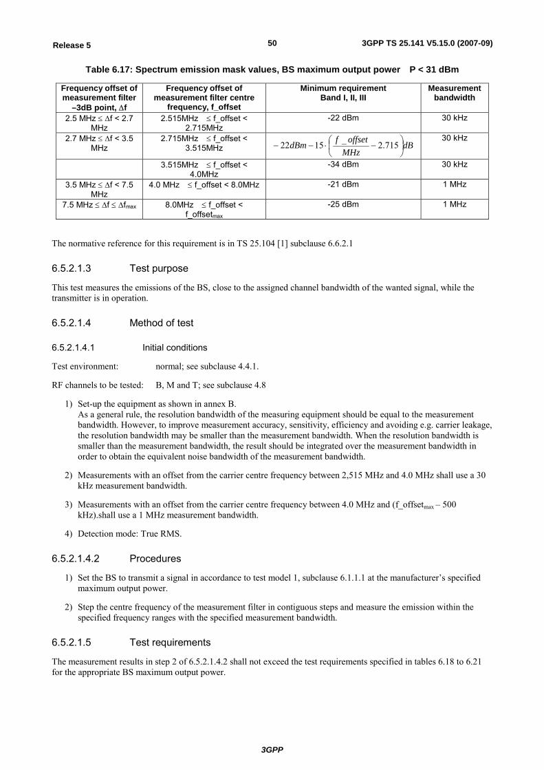
3GPP
3GPP TS 25.141 V5.15.0 (2007-09)50Release 5
Table 6.17: Spectrum emission mask values, BS maximum output power P < 31 dBm
Frequency offset of measurement filter
–3dB point, Δf
Frequency offset of measurement filter centre
frequency, f_offset
Minimum requirement Band I, II, III
Measurement bandwidth
2.5 MHz ≤ Δf < 2.7 MHz
2.515MHz ≤ f_offset < 2.715MHz
-22 dBm 30 kHz
2.7 MHz ≤ Δf < 3.5 MHz
2.715MHz ≤ f_offset < 3.515MHz dB
MHzoffsetfdBm ⎟
⎠⎞
⎜⎝⎛ −⋅−− 715.2_1522 30 kHz
3.515MHz ≤ f_offset < 4.0MHz
-34 dBm 30 kHz
3.5 MHz ≤ Δf < 7.5 MHz
4.0 MHz ≤ f_offset < 8.0MHz -21 dBm 1 MHz
7.5 MHz ≤ Δf ≤ Δfmax 8.0MHz ≤ f_offset < f_offsetmax
-25 dBm 1 MHz
The normative reference for this requirement is in TS 25.104 [1] subclause 6.6.2.1
6.5.2.1.3 Test purpose
This test measures the emissions of the BS, close to the assigned channel bandwidth of the wanted signal, while the transmitter is in operation.
6.5.2.1.4 Method of test
6.5.2.1.4.1 Initial conditions
Test environment: normal; see subclause 4.4.1.
RF channels to be tested: B, M and T; see subclause 4.8
1) Set-up the equipment as shown in annex B. As a general rule, the resolution bandwidth of the measuring equipment should be equal to the measurement bandwidth. However, to improve measurement accuracy, sensitivity, efficiency and avoiding e.g. carrier leakage, the resolution bandwidth may be smaller than the measurement bandwidth. When the resolution bandwidth is smaller than the measurement bandwidth, the result should be integrated over the measurement bandwidth in order to obtain the equivalent noise bandwidth of the measurement bandwidth.
2) Measurements with an offset from the carrier centre frequency between 2,515 MHz and 4.0 MHz shall use a 30 kHz measurement bandwidth.
3) Measurements with an offset from the carrier centre frequency between 4.0 MHz and (f_offsetmax – 500 kHz).shall use a 1 MHz measurement bandwidth.
4) Detection mode: True RMS.
6.5.2.1.4.2 Procedures
1) Set the BS to transmit a signal in accordance to test model 1, subclause 6.1.1.1 at the manufacturer’s specified maximum output power.
2) Step the centre frequency of the measurement filter in contiguous steps and measure the emission within the specified frequency ranges with the specified measurement bandwidth.
6.5.2.1.5 Test requirements
The measurement results in step 2 of 6.5.2.1.4.2 shall not exceed the test requirements specified in tables 6.18 to 6.21 for the appropriate BS maximum output power.
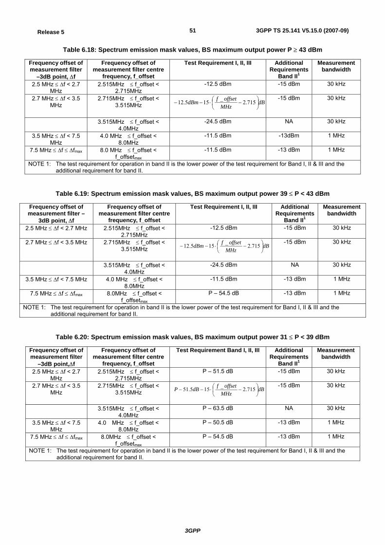
3GPP
3GPP TS 25.141 V5.15.0 (2007-09)51Release 5
Table 6.18: Spectrum emission mask values, BS maximum output power P ≥ 43 dBm
Frequency offset of measurement filter
–3dB point, Δf
Frequency offset of measurement filter centre
frequency, f_offset
Test Requirement I, II, III Additional Requirements
Band II1
Measurement bandwidth
2.5 MHz ≤ Δf < 2.7 MHz
2.515MHz ≤ f_offset < 2.715MHz
-12.5 dBm -15 dBm 30 kHz
2.7 MHz ≤ Δf < 3.5 MHz
2.715MHz ≤ f_offset < 3.515MHz dB
MHzoffsetfdBm ⎟
⎠⎞
⎜⎝⎛ −⋅−− 715.2_155.12
-15 dBm 30 kHz
3.515MHz ≤ f_offset < 4.0MHz
-24.5 dBm NA 30 kHz
3.5 MHz ≤ Δf < 7.5 MHz
4.0 MHz ≤ f_offset < 8.0MHz
-11.5 dBm -13dBm 1 MHz
7.5 MHz ≤ Δf ≤ Δfmax 8.0 MHz ≤ f_offset < f_offsetmax
-11.5 dBm -13 dBm 1 MHz
NOTE 1: The test requirement for operation in band II is the lower power of the test requirement for Band I, II & III and the additional requirement for band II.
Table 6.19: Spectrum emission mask values, BS maximum output power 39 ≤ P < 43 dBm
Frequency offset of measurement filter –
3dB point, Δf
Frequency offset of measurement filter centre
frequency, f_offset
Test Requirement I, II, III Additional Requirements
Band II1
Measurement bandwidth
2.5 MHz ≤ Δf < 2.7 MHz 2.515MHz ≤ f_offset < 2.715MHz
-12.5 dBm -15 dBm 30 kHz
2.7 MHz ≤ Δf < 3.5 MHz 2.715MHz ≤ f_offset < 3.515MHz dB
MHzoffsetfdBm ⎟
⎠⎞
⎜⎝⎛ −⋅−− 715.2_155.12
-15 dBm 30 kHz
3.515MHz ≤ f_offset < 4.0MHz
-24.5 dBm NA 30 kHz
3.5 MHz ≤ Δf < 7.5 MHz 4.0 MHz ≤ f_offset < 8.0MHz
-11.5 dBm -13 dBm 1 MHz
7.5 MHz ≤ Δf ≤ Δfmax 8.0MHz ≤ f_offset < f_offsetmax
P – 54.5 dB -13 dBm 1 MHz
NOTE 1: The test requirement for operation in band II is the lower power of the test requirement for Band I, II & III and the additional requirement for band II.
Table 6.20: Spectrum emission mask values, BS maximum output power 31 ≤ P < 39 dBm
Frequency offset of measurement filter
–3dB point,Δf
Frequency offset of measurement filter centre
frequency, f_offset
Test Requirement Band I, II, III Additional Requirements
Band II1
Measurement bandwidth
2.5 MHz ≤ Δf < 2.7 MHz
2.515MHz ≤ f_offset < 2.715MHz
P – 51.5 dB -15 dBm 30 kHz
2.7 MHz ≤ Δf < 3.5 MHz
2.715MHz ≤ f_offset < 3.515MHz dB
MHzoffsetfdBP ⎟
⎠⎞
⎜⎝⎛ −⋅−− 715.2_155.51
-15 dBm 30 kHz
3.515MHz ≤ f_offset < 4.0MHz
P – 63.5 dB NA 30 kHz
3.5 MHz ≤ Δf < 7.5 MHz
4.0 MHz ≤ f_offset < 8.0MHz
P – 50.5 dB -13 dBm 1 MHz
7.5 MHz ≤ Δf ≤ Δfmax 8.0MHz ≤ f_offset < f_offsetmax
P – 54.5 dB -13 dBm 1 MHz
NOTE 1: The test requirement for operation in band II is the lower power of the test requirement for Band I, II & III and the additional requirement for band II.
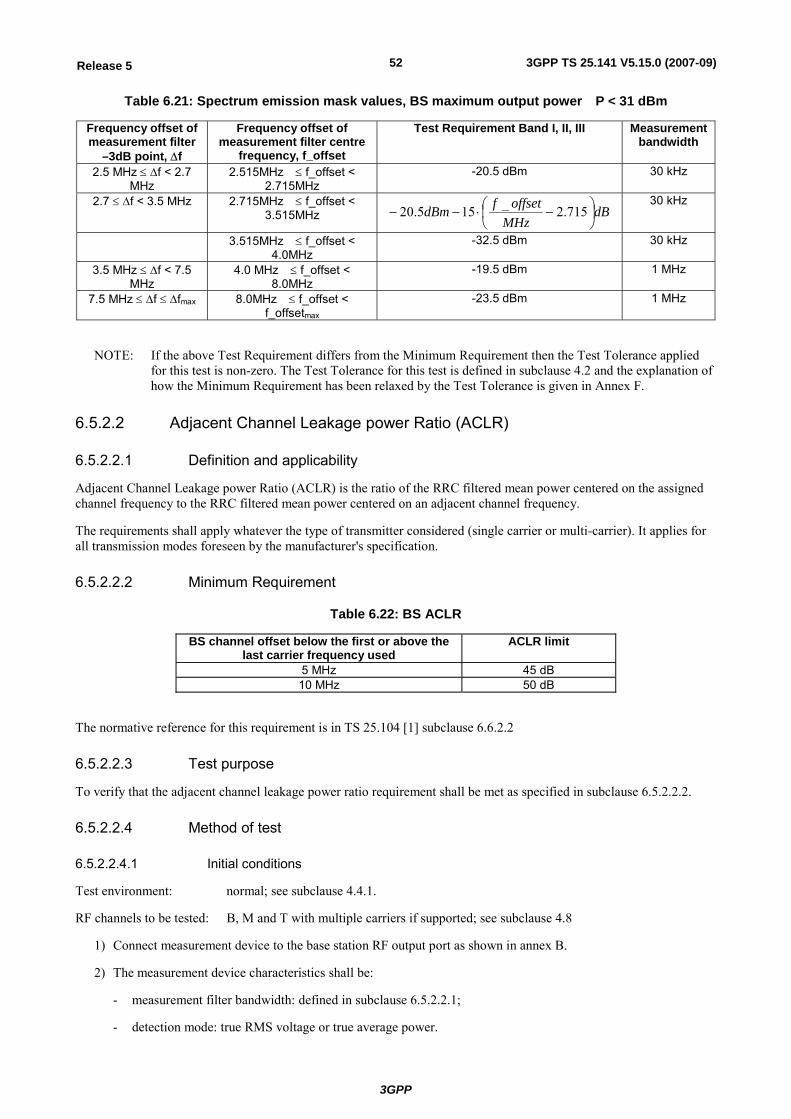
3GPP
3GPP TS 25.141 V5.15.0 (2007-09)52Release 5
Table 6.21: Spectrum emission mask values, BS maximum output power P < 31 dBm
Frequency offset of measurement filter
–3dB point, Δf
Frequency offset of measurement filter centre
frequency, f_offset
Test Requirement Band I, II, III Measurement bandwidth
2.5 MHz ≤ Δf < 2.7 MHz
2.515MHz ≤ f_offset < 2.715MHz
-20.5 dBm 30 kHz
2.7 ≤ Δf < 3.5 MHz 2.715MHz ≤ f_offset < 3.515MHz dB
MHzoffsetfdBm ⎟
⎠⎞
⎜⎝⎛ −⋅−− 715.2_155.20
30 kHz
3.515MHz ≤ f_offset < 4.0MHz
-32.5 dBm 30 kHz
3.5 MHz ≤ Δf < 7.5 MHz
4.0 MHz ≤ f_offset < 8.0MHz
-19.5 dBm 1 MHz
7.5 MHz ≤ Δf ≤ Δfmax 8.0MHz ≤ f_offset < f_offsetmax
-23.5 dBm 1 MHz
NOTE: If the above Test Requirement differs from the Minimum Requirement then the Test Tolerance applied for this test is non-zero. The Test Tolerance for this test is defined in subclause 4.2 and the explanation of how the Minimum Requirement has been relaxed by the Test Tolerance is given in Annex F.
6.5.2.2 Adjacent Channel Leakage power Ratio (ACLR)
6.5.2.2.1 Definition and applicability
Adjacent Channel Leakage power Ratio (ACLR) is the ratio of the RRC filtered mean power centered on the assigned channel frequency to the RRC filtered mean power centered on an adjacent channel frequency.
The requirements shall apply whatever the type of transmitter considered (single carrier or multi-carrier). It applies for all transmission modes foreseen by the manufacturer's specification.
6.5.2.2.2 Minimum Requirement
Table 6.22: BS ACLR
BS channel offset below the first or above the last carrier frequency used
ACLR limit
5 MHz 45 dB 10 MHz 50 dB
The normative reference for this requirement is in TS 25.104 [1] subclause 6.6.2.2
6.5.2.2.3 Test purpose
To verify that the adjacent channel leakage power ratio requirement shall be met as specified in subclause 6.5.2.2.2.
6.5.2.2.4 Method of test
6.5.2.2.4.1 Initial conditions
Test environment: normal; see subclause 4.4.1.
RF channels to be tested: B, M and T with multiple carriers if supported; see subclause 4.8
1) Connect measurement device to the base station RF output port as shown in annex B.
2) The measurement device characteristics shall be:
- measurement filter bandwidth: defined in subclause 6.5.2.2.1;
- detection mode: true RMS voltage or true average power.
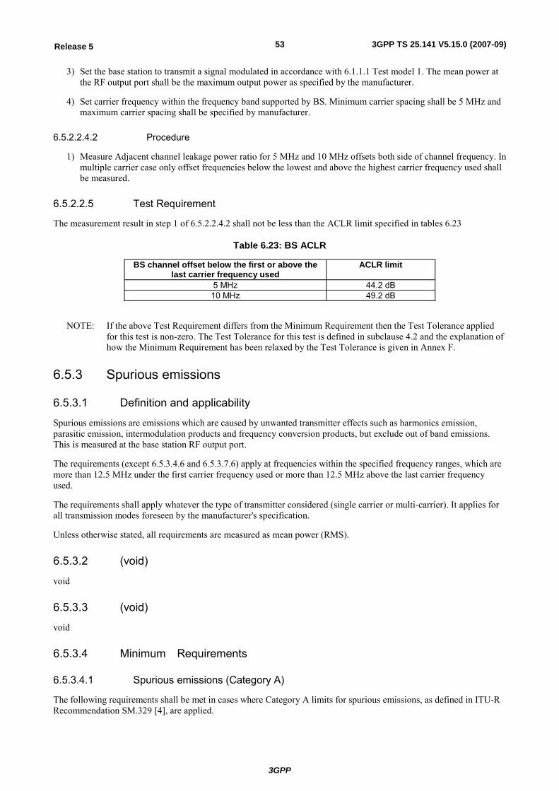
3GPP
3GPP TS 25.141 V5.15.0 (2007-09)53Release 5
3) Set the base station to transmit a signal modulated in accordance with 6.1.1.1 Test model 1. The mean power at the RF output port shall be the maximum output power as specified by the manufacturer.
4) Set carrier frequency within the frequency band supported by BS. Minimum carrier spacing shall be 5 MHz and maximum carrier spacing shall be specified by manufacturer.
6.5.2.2.4.2 Procedure
1) Measure Adjacent channel leakage power ratio for 5 MHz and 10 MHz offsets both side of channel frequency. In multiple carrier case only offset frequencies below the lowest and above the highest carrier frequency used shall be measured.
6.5.2.2.5 Test Requirement
The measurement result in step 1 of 6.5.2.2.4.2 shall not be less than the ACLR limit specified in tables 6.23
Table 6.23: BS ACLR
BS channel offset below the first or above the last carrier frequency used
ACLR limit
5 MHz 44.2 dB 10 MHz 49.2 dB
NOTE: If the above Test Requirement differs from the Minimum Requirement then the Test Tolerance applied for this test is non-zero. The Test Tolerance for this test is defined in subclause 4.2 and the explanation of how the Minimum Requirement has been relaxed by the Test Tolerance is given in Annex F.
6.5.3 Spurious emissions
6.5.3.1 Definition and applicability
Spurious emissions are emissions which are caused by unwanted transmitter effects such as harmonics emission, parasitic emission, intermodulation products and frequency conversion products, but exclude out of band emissions. This is measured at the base station RF output port.
The requirements (except 6.5.3.4.6 and 6.5.3.7.6) apply at frequencies within the specified frequency ranges, which are more than 12.5 MHz under the first carrier frequency used or more than 12.5 MHz above the last carrier frequency used.
The requirements shall apply whatever the type of transmitter considered (single carrier or multi-carrier). It applies for all transmission modes foreseen by the manufacturer's specification.
Unless otherwise stated, all requirements are measured as mean power (RMS).
6.5.3.2 (void)
void
6.5.3.3 (void)
void
6.5.3.4 Minimum Requirements
6.5.3.4.1 Spurious emissions (Category A)
The following requirements shall be met in cases where Category A limits for spurious emissions, as defined in ITU-R Recommendation SM.329 [4], are applied.
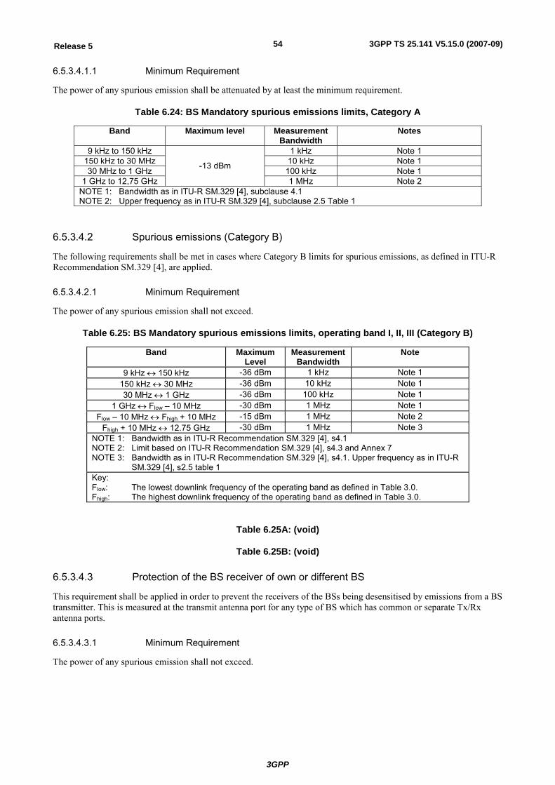
3GPP
3GPP TS 25.141 V5.15.0 (2007-09)54Release 5
6.5.3.4.1.1 Minimum Requirement
The power of any spurious emission shall be attenuated by at least the minimum requirement.
Table 6.24: BS Mandatory spurious emissions limits, Category A
Band Maximum level Measurement Bandwidth
Notes
9 kHz to 150 kHz 1 kHz Note 1 150 kHz to 30 MHz 10 kHz Note 1 30 MHz to 1 GHz 100 kHz Note 1
1 GHz to 12,75 GHz
-13 dBm
1 MHz Note 2 NOTE 1: Bandwidth as in ITU-R SM.329 [4], subclause 4.1 NOTE 2: Upper frequency as in ITU-R SM.329 [4], subclause 2.5 Table 1
6.5.3.4.2 Spurious emissions (Category B)
The following requirements shall be met in cases where Category B limits for spurious emissions, as defined in ITU-R Recommendation SM.329 [4], are applied.
6.5.3.4.2.1 Minimum Requirement
The power of any spurious emission shall not exceed.
Table 6.25: BS Mandatory spurious emissions limits, operating band I, II, III (Category B)
Band Maximum Level
Measurement Bandwidth
Note
9 kHz ↔ 150 kHz -36 dBm 1 kHz Note 1 150 kHz ↔ 30 MHz -36 dBm 10 kHz Note 1 30 MHz ↔ 1 GHz -36 dBm 100 kHz Note 1
1 GHz ↔ Flow – 10 MHz -30 dBm 1 MHz Note 1 Flow – 10 MHz ↔ Fhigh + 10 MHz -15 dBm 1 MHz Note 2
Fhigh + 10 MHz ↔ 12.75 GHz -30 dBm 1 MHz Note 3 NOTE 1: Bandwidth as in ITU-R Recommendation SM.329 [4], s4.1 NOTE 2: Limit based on ITU-R Recommendation SM.329 [4], s4.3 and Annex 7 NOTE 3: Bandwidth as in ITU-R Recommendation SM.329 [4], s4.1. Upper frequency as in ITU-R
SM.329 [4], s2.5 table 1 Key: Flow: The lowest downlink frequency of the operating band as defined in Table 3.0. Fhigh: The highest downlink frequency of the operating band as defined in Table 3.0.
Table 6.25A: (void)
Table 6.25B: (void)
6.5.3.4.3 Protection of the BS receiver of own or different BS
This requirement shall be applied in order to prevent the receivers of the BSs being desensitised by emissions from a BS transmitter. This is measured at the transmit antenna port for any type of BS which has common or separate Tx/Rx antenna ports.
6.5.3.4.3.1 Minimum Requirement
The power of any spurious emission shall not exceed.
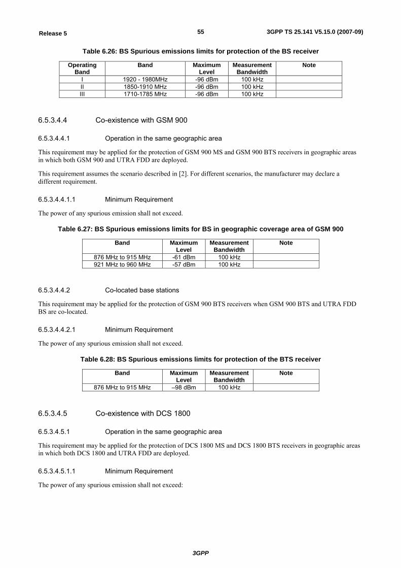
3GPP
3GPP TS 25.141 V5.15.0 (2007-09)55Release 5
Table 6.26: BS Spurious emissions limits for protection of the BS receiver
Operating Band
Band Maximum Level
Measurement Bandwidth
Note
I 1920 - 1980MHz -96 dBm 100 kHz II 1850-1910 MHz -96 dBm 100 kHz III 1710-1785 MHz -96 dBm 100 kHz
6.5.3.4.4 Co-existence with GSM 900
6.5.3.4.4.1 Operation in the same geographic area
This requirement may be applied for the protection of GSM 900 MS and GSM 900 BTS receivers in geographic areas in which both GSM 900 and UTRA FDD are deployed.
This requirement assumes the scenario described in [2]. For different scenarios, the manufacturer may declare a different requirement.
6.5.3.4.4.1.1 Minimum Requirement
The power of any spurious emission shall not exceed.
Table 6.27: BS Spurious emissions limits for BS in geographic coverage area of GSM 900
Band Maximum Level
Measurement Bandwidth
Note
876 MHz to 915 MHz -61 dBm 100 kHz 921 MHz to 960 MHz -57 dBm 100 kHz
6.5.3.4.4.2 Co-located base stations
This requirement may be applied for the protection of GSM 900 BTS receivers when GSM 900 BTS and UTRA FDD BS are co-located.
6.5.3.4.4.2.1 Minimum Requirement
The power of any spurious emission shall not exceed.
Table 6.28: BS Spurious emissions limits for protection of the BTS receiver
Band Maximum Level
Measurement Bandwidth
Note
876 MHz to 915 MHz –98 dBm 100 kHz
6.5.3.4.5 Co-existence with DCS 1800
6.5.3.4.5.1 Operation in the same geographic area
This requirement may be applied for the protection of DCS 1800 MS and DCS 1800 BTS receivers in geographic areas in which both DCS 1800 and UTRA FDD are deployed.
6.5.3.4.5.1.1 Minimum Requirement
The power of any spurious emission shall not exceed:
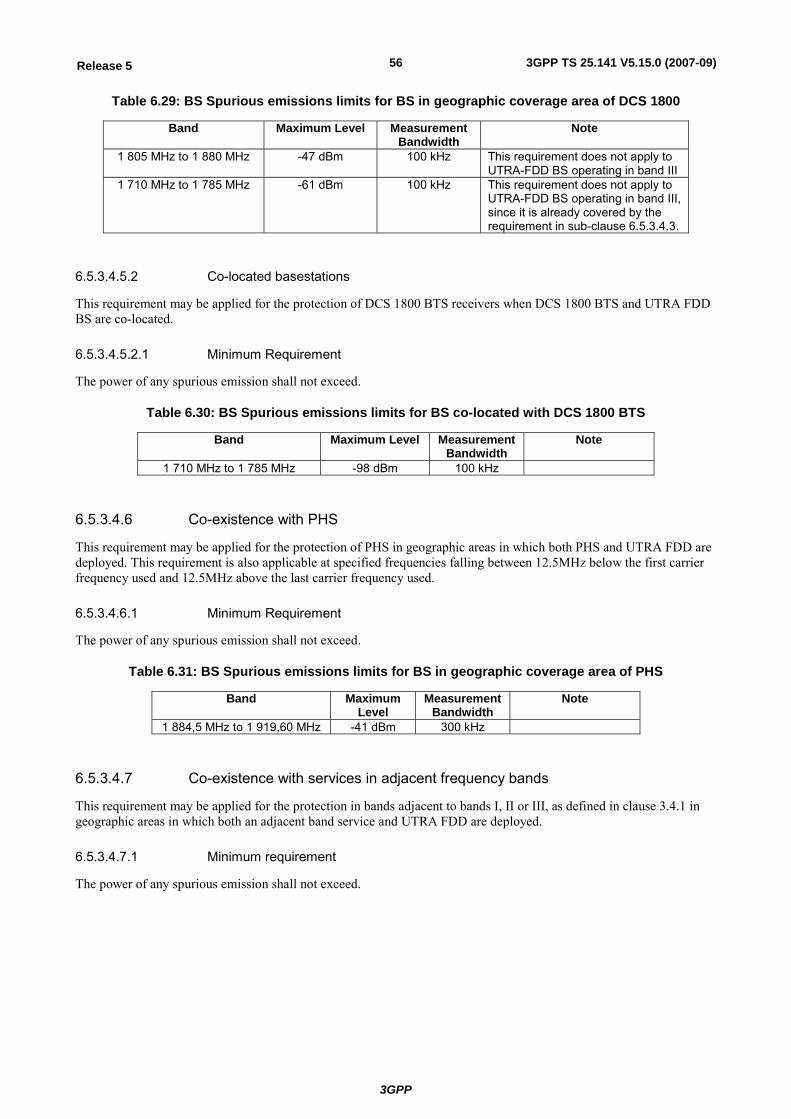
3GPP
3GPP TS 25.141 V5.15.0 (2007-09)56Release 5
Table 6.29: BS Spurious emissions limits for BS in geographic coverage area of DCS 1800
Band Maximum Level Measurement Bandwidth
Note
1 805 MHz to 1 880 MHz -47 dBm 100 kHz This requirement does not apply to UTRA-FDD BS operating in band III
1 710 MHz to 1 785 MHz -61 dBm 100 kHz This requirement does not apply to UTRA-FDD BS operating in band III, since it is already covered by the requirement in sub-clause 6.5.3.4.3.
6.5.3.4.5.2 Co-located basestations
This requirement may be applied for the protection of DCS 1800 BTS receivers when DCS 1800 BTS and UTRA FDD BS are co-located.
6.5.3.4.5.2.1 Minimum Requirement
The power of any spurious emission shall not exceed.
Table 6.30: BS Spurious emissions limits for BS co-located with DCS 1800 BTS
Band Maximum Level Measurement Bandwidth
Note
1 710 MHz to 1 785 MHz -98 dBm 100 kHz
6.5.3.4.6 Co-existence with PHS
This requirement may be applied for the protection of PHS in geographic areas in which both PHS and UTRA FDD are deployed. This requirement is also applicable at specified frequencies falling between 12.5MHz below the first carrier frequency used and 12.5MHz above the last carrier frequency used.
6.5.3.4.6.1 Minimum Requirement
The power of any spurious emission shall not exceed.
Table 6.31: BS Spurious emissions limits for BS in geographic coverage area of PHS
Band Maximum Level
Measurement Bandwidth
Note
1 884,5 MHz to 1 919,60 MHz -41 dBm 300 kHz
6.5.3.4.7 Co-existence with services in adjacent frequency bands
This requirement may be applied for the protection in bands adjacent to bands I, II or III, as defined in clause 3.4.1 in geographic areas in which both an adjacent band service and UTRA FDD are deployed.
6.5.3.4.7.1 Minimum requirement
The power of any spurious emission shall not exceed.
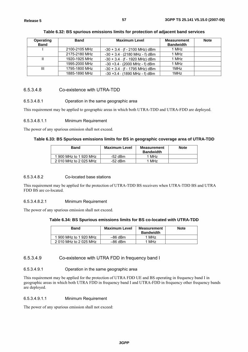
3GPP
3GPP TS 25.141 V5.15.0 (2007-09)57Release 5
Table 6.32: BS spurious emissions limits for protection of adjacent band services
Operating Band
Band Maximum Level Measurement Bandwidth
Note
2100-2105 MHz -30 + 3.4 ⋅ (f - 2100 MHz) dBm 1 MHz I 2175-2180 MHz -30 + 3.4 ⋅ (2180 MHz - f) dBm 1 MHz 1920-1925 MHz -30 + 3.4 ⋅ (f - 1920 MHz) dBm 1 MHz II 1995-2000 MHz -30 +3.4 ⋅ (2000 MHz - f) dBm 1 MHz 1795-1800 MHz -30 + 3.4 ⋅ (f - 1795 MHz) dBm 1MHz III 1885-1890 MHz -30 +3.4 ⋅ (1890 MHz - f) dBm 1MHz
6.5.3.4.8 Co-existence with UTRA-TDD
6.5.3.4.8.1 Operation in the same geographic area
This requirement may be applied to geographic areas in which both UTRA-TDD and UTRA-FDD are deployed.
6.5.3.4.8.1.1 Minimum Requirement
The power of any spurious emission shall not exceed.
Table 6.33: BS Spurious emissions limits for BS in geographic coverage area of UTRA-TDD
Band Maximum Level Measurement Bandwidth
Note
1 900 MHz to 1 920 MHz -52 dBm 1 MHz 2 010 MHz to 2 025 MHz -52 dBm 1 MHz
6.5.3.4.8.2 Co-located base stations
This requirement may be applied for the protection of UTRA-TDD BS receivers when UTRA-TDD BS and UTRA FDD BS are co-located.
6.5.3.4.8.2.1 Minimum Requirement
The power of any spurious emission shall not exceed.
Table 6.34: BS Spurious emissions limits for BS co-located with UTRA-TDD
Band Maximum Level Measurement Bandwidth
Note
1 900 MHz to 1 920 MHz –86 dBm 1 MHz 2 010 MHz to 2 025 MHz –86 dBm 1 MHz
6.5.3.4.9 Co-existence with UTRA FDD in frequency band I
6.5.3.4.9.1 Operation in the same geographic area
This requirement may be applied for the protection of UTRA FDD UE and BS operating in frequency band I in geographic areas in which both UTRA FDD in frequency band I and UTRA-FDD in frequency other frequency bands are deployed.
6.5.3.4.9.1.1 Minimum Requirement
The power of any spurious emission shall not exceed:
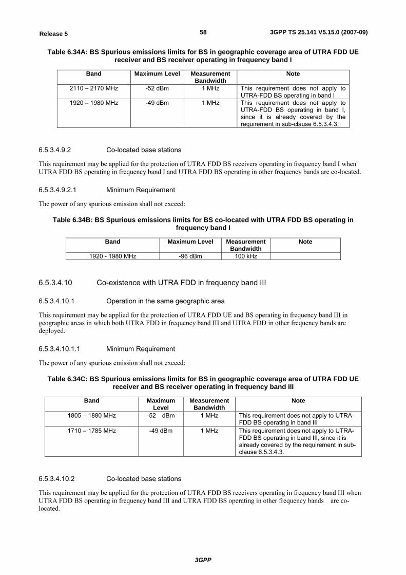
3GPP
3GPP TS 25.141 V5.15.0 (2007-09)58Release 5
Table 6.34A: BS Spurious emissions limits for BS in geographic coverage area of UTRA FDD UE receiver and BS receiver operating in frequency band I
Band Maximum Level Measurement Bandwidth
Note
2110 – 2170 MHz -52 dBm 1 MHz This requirement does not apply to UTRA-FDD BS operating in band I
1920 – 1980 MHz -49 dBm 1 MHz This requirement does not apply to UTRA-FDD BS operating in band I, since it is already covered by the requirement in sub-clause 6.5.3.4.3.
6.5.3.4.9.2 Co-located base stations
This requirement may be applied for the protection of UTRA FDD BS receivers operating in frequency band I when UTRA FDD BS operating in frequency band I and UTRA FDD BS operating in other frequency bands are co-located.
6.5.3.4.9.2.1 Minimum Requirement
The power of any spurious emission shall not exceed:
Table 6.34B: BS Spurious emissions limits for BS co-located with UTRA FDD BS operating in frequency band I
Band Maximum Level Measurement Bandwidth
Note
1920 - 1980 MHz -96 dBm 100 kHz
6.5.3.4.10 Co-existence with UTRA FDD in frequency band III
6.5.3.4.10.1 Operation in the same geographic area
This requirement may be applied for the protection of UTRA FDD UE and BS operating in frequency band III in geographic areas in which both UTRA FDD in frequency band III and UTRA FDD in other frequency bands are deployed.
6.5.3.4.10.1.1 Minimum Requirement
The power of any spurious emission shall not exceed:
Table 6.34C: BS Spurious emissions limits for BS in geographic coverage area of UTRA FDD UE receiver and BS receiver operating in frequency band III
Band Maximum Level
Measurement Bandwidth
Note
1805 – 1880 MHz -52 dBm 1 MHz This requirement does not apply to UTRA-FDD BS operating in band III
1710 – 1785 MHz -49 dBm 1 MHz This requirement does not apply to UTRA-FDD BS operating in band III, since it is already covered by the requirement in sub-clause 6.5.3.4.3.
6.5.3.4.10.2 Co-located base stations
This requirement may be applied for the protection of UTRA FDD BS receivers operating in frequency band III when UTRA FDD BS operating in frequency band III and UTRA FDD BS operating in other frequency bands are co-located.
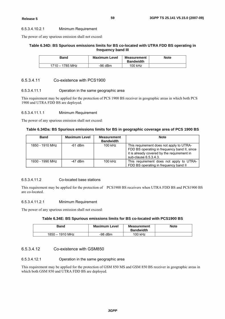
3GPP
3GPP TS 25.141 V5.15.0 (2007-09)59Release 5
6.5.3.4.10.2.1 Minimum Requirement
The power of any spurious emission shall not exceed:
Table 6.34D: BS Spurious emissions limits for BS co-located with UTRA FDD BS operating in frequency band III
Band Maximum Level Measurement Bandwidth
Note
1710 – 1785 MHz -96 dBm 100 kHz
6.5.3.4.11 Co-existence with PCS1900
6.5.3.4.11.1 Operation in the same geographic area
This requirement may be applied for the protection of PCS 1900 BS receiver in geographic areas in which both PCS 1900 and UTRA FDD BS are deployed.
6.5.3.4.11.1.1 Minimum Requirement
The power of any spurious emission shall not exceed:
Table 6.34Da: BS Spurious emissions limits for BS in geographic coverage area of PCS 1900 BS
Band Maximum Level Measurement Bandwidth
Note
1850 - 1910 MHz -61 dBm 100 kHz This requirement does not apply to UTRA-FDD BS operating in frequency band II, since it is already covered by the requirement in sub-clause 6.5.3.4.3.
1930 - 1990 MHz -47 dBm 100 kHz This requirement does not apply to UTRA-FDD BS operating in frequency band II
6.5.3.4.11.2 Co-located base stations
This requirement may be applied for the protection of PCS1900 BS receivers when UTRA FDD BS and PCS1900 BS are co-located.
6.5.3.4.11.2.1 Minimum Requirement
The power of any spurious emission shall not exceed:
Table 6.34E: BS Spurious emissions limits for BS co-located with PCS1900 BS
Band Maximum Level Measurement Bandwidth
Note
1850 – 1910 MHz -98 dBm 100 kHz
6.5.3.4.12 Co-existence with GSM850
6.5.3.4.12.1 Operation in the same geographic area
This requirement may be applied for the protection of GSM 850 MS and GSM 850 BS receiver in geographic areas in which both GSM 850 and UTRA FDD BS are deployed.
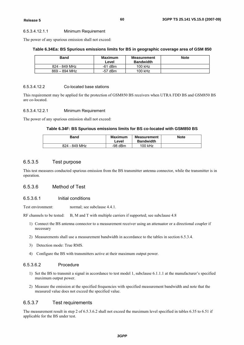
3GPP
3GPP TS 25.141 V5.15.0 (2007-09)60Release 5
6.5.3.4.12.1.1 Minimum Requirement
The power of any spurious emission shall not exceed:
Table 6.34Ea: BS Spurious emissions limits for BS in geographic coverage area of GSM 850
Band Maximum Level
Measurement Bandwidth
Note
824 - 849 MHz -61 dBm 100 kHz 869 – 894 MHz -57 dBm 100 kHz
6.5.3.4.12.2 Co-located base stations
This requirement may be applied for the protection of GSM850 BS receivers when UTRA FDD BS and GSM850 BS are co-located.
6.5.3.4.12.2.1 Minimum Requirement
The power of any spurious emission shall not exceed:
Table 6.34F: BS Spurious emissions limits for BS co-located with GSM850 BS
Band Maximum Level
Measurement Bandwidth
Note
824 - 849 MHz -98 dBm 100 kHz
6.5.3.5 Test purpose
This test measures conducted spurious emission from the BS transmitter antenna connector, while the transmitter is in operation.
6.5.3.6 Method of Test
6.5.3.6.1 Initial conditions
Test environment: normal; see subclause 4.4.1.
RF channels to be tested: B, M and T with multiple carriers if supported; see subclause 4.8
1) Connect the BS antenna connector to a measurement receiver using an attenuator or a directional coupler if necessary
2) Measurements shall use a measurement bandwidth in accordance to the tables in section 6.5.3.4.
3) Detection mode: True RMS.
4) Configure the BS with transmitters active at their maximum output power.
6.5.3.6.2 Procedure
1) Set the BS to transmit a signal in accordance to test model 1, subclause 6.1.1.1 at the manufacturer’s specified maximum output power.
2) Measure the emission at the specified frequencies with specified measurement bandwidth and note that the measured value does not exceed the specified value.
6.5.3.7 Test requirements
The measurement result in step 2 of 6.5.3.6.2 shall not exceed the maximum level specified in tables 6.35 to 6.51 if applicable for the BS under test.
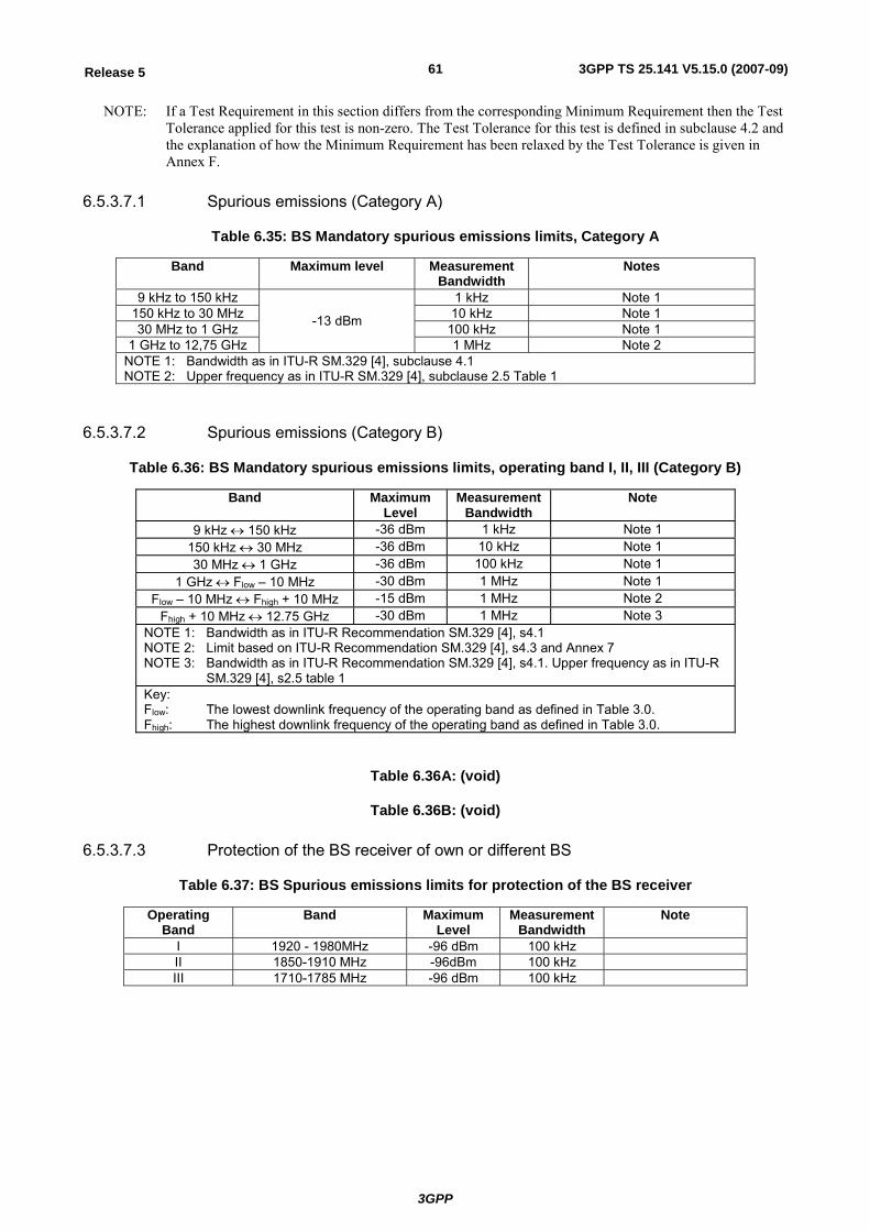
3GPP
3GPP TS 25.141 V5.15.0 (2007-09)61Release 5
NOTE: If a Test Requirement in this section differs from the corresponding Minimum Requirement then the Test Tolerance applied for this test is non-zero. The Test Tolerance for this test is defined in subclause 4.2 and the explanation of how the Minimum Requirement has been relaxed by the Test Tolerance is given in Annex F.
6.5.3.7.1 Spurious emissions (Category A)
Table 6.35: BS Mandatory spurious emissions limits, Category A
Band Maximum level Measurement Bandwidth
Notes
9 kHz to 150 kHz 1 kHz Note 1 150 kHz to 30 MHz 10 kHz Note 1 30 MHz to 1 GHz 100 kHz Note 1
1 GHz to 12,75 GHz
-13 dBm
1 MHz Note 2 NOTE 1: Bandwidth as in ITU-R SM.329 [4], subclause 4.1 NOTE 2: Upper frequency as in ITU-R SM.329 [4], subclause 2.5 Table 1
6.5.3.7.2 Spurious emissions (Category B)
Table 6.36: BS Mandatory spurious emissions limits, operating band I, II, III (Category B)
Band Maximum Level
Measurement Bandwidth
Note
9 kHz ↔ 150 kHz -36 dBm 1 kHz Note 1 150 kHz ↔ 30 MHz -36 dBm 10 kHz Note 1 30 MHz ↔ 1 GHz -36 dBm 100 kHz Note 1
1 GHz ↔ Flow – 10 MHz -30 dBm 1 MHz Note 1 Flow – 10 MHz ↔ Fhigh + 10 MHz -15 dBm 1 MHz Note 2
Fhigh + 10 MHz ↔ 12.75 GHz -30 dBm 1 MHz Note 3 NOTE 1: Bandwidth as in ITU-R Recommendation SM.329 [4], s4.1 NOTE 2: Limit based on ITU-R Recommendation SM.329 [4], s4.3 and Annex 7 NOTE 3: Bandwidth as in ITU-R Recommendation SM.329 [4], s4.1. Upper frequency as in ITU-R
SM.329 [4], s2.5 table 1 Key: Flow: The lowest downlink frequency of the operating band as defined in Table 3.0. Fhigh: The highest downlink frequency of the operating band as defined in Table 3.0.
Table 6.36A: (void)
Table 6.36B: (void)
6.5.3.7.3 Protection of the BS receiver of own or different BS
Table 6.37: BS Spurious emissions limits for protection of the BS receiver
Operating Band
Band Maximum Level
Measurement Bandwidth
Note
I 1920 - 1980MHz -96 dBm 100 kHz II 1850-1910 MHz -96dBm 100 kHz III 1710-1785 MHz -96 dBm 100 kHz
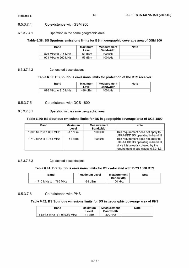
3GPP
3GPP TS 25.141 V5.15.0 (2007-09)62Release 5
6.5.3.7.4 Co-existence with GSM 900
6.5.3.7.4.1 Operation in the same geographic area
Table 6.38: BS Spurious emissions limits for BS in geographic coverage area of GSM 900
Band Maximum Level
Measurement Bandwidth
Note
876 MHz to 915 MHz -61 dBm 100 kHz 921 MHz to 960 MHz -57 dBm 100 kHz
6.5.3.7.4.2 Co-located base stations
Table 6.39: BS Spurious emissions limits for protection of the BTS receiver
Band Maximum Level
Measurement Bandwidth
Note
876 MHz to 915 MHz –98 dBm 100 kHz
6.5.3.7.5 Co-existence with DCS 1800
6.5.3.7.5.1 Operation in the same geographic area
Table 6.40: BS Spurious emissions limits for BS in geographic coverage area of DCS 1800
Band Maximum Level
Measurement Bandwidth
Note
1 805 MHz to 1 880 MHz -47 dBm 100 kHz This requirement does not apply to UTRA-FDD BS operating in band III
1 710 MHz to 1 785 MHz -61 dBm 100 kHz This requirement does not apply to UTRA-FDD BS operating in band III, since it is already covered by the requirement in sub-clause 6.5.3.4.3.
6.5.3.7.5.2 Co-located base stations
Table 6.41: BS Spurious emissions limits for BS co-located with DCS 1800 BTS
Band Maximum Level Measurement Bandwidth
Note
1 710 MHz to 1 785 MHz -98 dBm 100 kHz
6.5.3.7.6 Co-existence with PHS
Table 6.42: BS Spurious emissions limits for BS in geographic coverage area of PHS
Band Maximum Level
Measurement Bandwidth
Note
1 884,5 MHz to 1 919,60 MHz -41 dBm 300 kHz
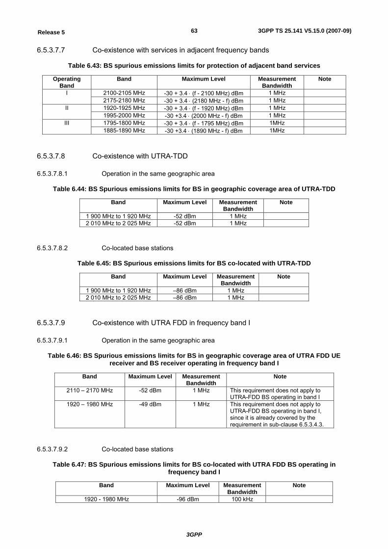
3GPP
3GPP TS 25.141 V5.15.0 (2007-09)63Release 5
6.5.3.7.7 Co-existence with services in adjacent frequency bands
Table 6.43: BS spurious emissions limits for protection of adjacent band services
Operating Band
Band Maximum Level Measurement Bandwidth
Note
2100-2105 MHz -30 + 3.4 ⋅ (f - 2100 MHz) dBm 1 MHz I 2175-2180 MHz -30 + 3.4 ⋅ (2180 MHz - f) dBm 1 MHz 1920-1925 MHz -30 + 3.4 ⋅ (f - 1920 MHz) dBm 1 MHz II 1995-2000 MHz -30 +3.4 ⋅ (2000 MHz - f) dBm 1 MHz 1795-1800 MHz -30 + 3.4 ⋅ (f - 1795 MHz) dBm 1MHz III 1885-1890 MHz -30 +3.4 ⋅ (1890 MHz - f) dBm 1MHz
6.5.3.7.8 Co-existence with UTRA-TDD
6.5.3.7.8.1 Operation in the same geographic area
Table 6.44: BS Spurious emissions limits for BS in geographic coverage area of UTRA-TDD
Band Maximum Level Measurement Bandwidth
Note
1 900 MHz to 1 920 MHz -52 dBm 1 MHz 2 010 MHz to 2 025 MHz -52 dBm 1 MHz
6.5.3.7.8.2 Co-located base stations
Table 6.45: BS Spurious emissions limits for BS co-located with UTRA-TDD
Band Maximum Level Measurement Bandwidth
Note
1 900 MHz to 1 920 MHz –86 dBm 1 MHz 2 010 MHz to 2 025 MHz –86 dBm 1 MHz
6.5.3.7.9 Co-existence with UTRA FDD in frequency band I
6.5.3.7.9.1 Operation in the same geographic area
Table 6.46: BS Spurious emissions limits for BS in geographic coverage area of UTRA FDD UE receiver and BS receiver operating in frequency band I
Band Maximum Level Measurement Bandwidth
Note
2110 – 2170 MHz -52 dBm 1 MHz This requirement does not apply to UTRA-FDD BS operating in band I
1920 – 1980 MHz -49 dBm 1 MHz This requirement does not apply to UTRA-FDD BS operating in band I, since it is already covered by the requirement in sub-clause 6.5.3.4.3.
6.5.3.7.9.2 Co-located base stations
Table 6.47: BS Spurious emissions limits for BS co-located with UTRA FDD BS operating in frequency band I
Band Maximum Level Measurement Bandwidth
Note
1920 - 1980 MHz -96 dBm 100 kHz
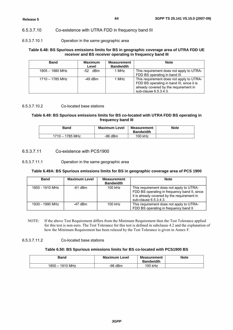
3GPP
3GPP TS 25.141 V5.15.0 (2007-09)64Release 5
6.5.3.7.10 Co-existence with UTRA FDD in frequency band III
6.5.3.7.10.1 Operation in the same geographic area
Table 6.48: BS Spurious emissions limits for BS in geographic coverage area of UTRA FDD UE receiver and BS receiver operating in frequency band III
Band Maximum Level
Measurement Bandwidth
Note
1805 – 1880 MHz -52 dBm 1 MHz This requirement does not apply to UTRA-FDD BS operating in band III
1710 – 1785 MHz -49 dBm 1 MHz This requirement does not apply to UTRA-FDD BS operating in band III, since it is already covered by the requirement in sub-clause 6.5.3.4.3.
6.5.3.7.10.2 Co-located base stations
Table 6.49: BS Spurious emissions limits for BS co-located with UTRA FDD BS operating in frequency band III
Band Maximum Level Measurement Bandwidth
Note
1710 – 1785 MHz -96 dBm 100 kHz
6.5.3.7.11 Co-existence with PCS1900
6.5.3.7.11.1 Operation in the same geographic area
Table 6.49A: BS Spurious emissions limits for BS in geographic coverage area of PCS 1900
Band Maximum Level Measurement Bandwidth
Note
1850 - 1910 MHz -61 dBm 100 kHz This requirement does not apply to UTRA-FDD BS operating in frequency band II, since it is already covered by the requirement in sub-clause 6.5.3.4.3.
1930 - 1990 MHz -47 dBm 100 kHz This requirement does not apply to UTRA-FDD BS operating in frequency band II
NOTE: If the above Test Requirement differs from the Minimum Requirement then the Test Tolerance applied for this test is non-zero. The Test Tolerance for this test is defined in subclause 4.2 and the explanation of how the Minimum Requirement has been relaxed by the Test Tolerance is given in Annex F.
6.5.3.7.11.2 Co-located base stations
Table 6.50: BS Spurious emissions limits for BS co-located with PCS1900 BS
Band Maximum Level Measurement Bandwidth
Note
1850 – 1910 MHz -98 dBm 100 kHz
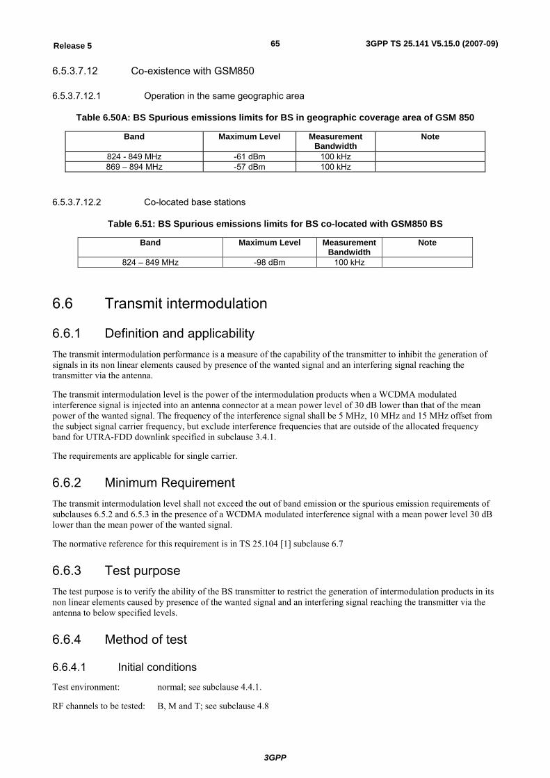
3GPP
3GPP TS 25.141 V5.15.0 (2007-09)65Release 5
6.5.3.7.12 Co-existence with GSM850
6.5.3.7.12.1 Operation in the same geographic area
Table 6.50A: BS Spurious emissions limits for BS in geographic coverage area of GSM 850
Band Maximum Level Measurement Bandwidth
Note
824 - 849 MHz -61 dBm 100 kHz 869 – 894 MHz -57 dBm 100 kHz
6.5.3.7.12.2 Co-located base stations
Table 6.51: BS Spurious emissions limits for BS co-located with GSM850 BS
Band Maximum Level Measurement Bandwidth
Note
824 – 849 MHz -98 dBm 100 kHz
6.6 Transmit intermodulation
6.6.1 Definition and applicability The transmit intermodulation performance is a measure of the capability of the transmitter to inhibit the generation of signals in its non linear elements caused by presence of the wanted signal and an interfering signal reaching the transmitter via the antenna.
The transmit intermodulation level is the power of the intermodulation products when a WCDMA modulated interference signal is injected into an antenna connector at a mean power level of 30 dB lower than that of the mean power of the wanted signal. The frequency of the interference signal shall be 5 MHz, 10 MHz and 15 MHz offset from the subject signal carrier frequency, but exclude interference frequencies that are outside of the allocated frequency band for UTRA-FDD downlink specified in subclause 3.4.1.
The requirements are applicable for single carrier.
6.6.2 Minimum Requirement The transmit intermodulation level shall not exceed the out of band emission or the spurious emission requirements of subclauses 6.5.2 and 6.5.3 in the presence of a WCDMA modulated interference signal with a mean power level 30 dB lower than the mean power of the wanted signal.
The normative reference for this requirement is in TS 25.104 [1] subclause 6.7
6.6.3 Test purpose The test purpose is to verify the ability of the BS transmitter to restrict the generation of intermodulation products in its non linear elements caused by presence of the wanted signal and an interfering signal reaching the transmitter via the antenna to below specified levels.
6.6.4 Method of test
6.6.4.1 Initial conditions
Test environment: normal; see subclause 4.4.1.
RF channels to be tested: B, M and T; see subclause 4.8
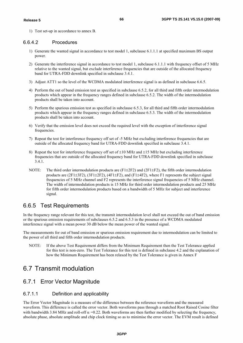
3GPP
3GPP TS 25.141 V5.15.0 (2007-09)66Release 5
1) Test set-up in accordance to annex B.
6.6.4.2 Procedures
1) Generate the wanted signal in accordance to test model 1, subclause 6.1.1.1 at specified maximum BS output power.
2) Generate the interference signal in accordance to test model 1, subclause 6.1.1.1 with frequency offset of 5 MHz relative to the wanted signal, but exclude interference frequencies that are outside of the allocated frequency band for UTRA-FDD downlink specified in subclause 3.4.1.
3) Adjust ATT1 so the level of the WCDMA modulated interference signal is as defined in subclause 6.6.5.
4) Perform the out of band emission test as specified in subclause 6.5.2, for all third and fifth order intermodulation products which appear in the frequency ranges defined in subclause 6.5.2. The width of the intermodulation products shall be taken into account.
5) Perform the spurious emission test as specified in subclause 6.5.3, for all third and fifth order intermodulation products which appear in the frequency ranges defined in subclause 6.5.3. The width of the intermodulation products shall be taken into account.
6) Verify that the emission level does not exceed the required level with the exception of interference signal frequencies.
7) Repeat the test for interference frequency off set of -5 MHz but excluding interference frequencies that are outside of the allocated frequency band for UTRA-FDD downlink specified in subclause 3.4.1.
8) Repeat the test for interference frequency off set of ±10 MHz and ±15 MHz but excluding interference frequencies that are outside of the allocated frequency band for UTRA-FDD downlink specified in subclause 3.4.1.
NOTE: The third order intermodulation products are (F1±2F2) and (2F1±F2), the fifth order intermodulation products are (2F1±3F2), (3F1±2F2), (4F1±F2), and (F1±4F2), where F1 represents the subject signal frequencies of 5 MHz channel and F2 represents the interference signal frequencies of 5 MHz channel. The width of intermodulation products is 15 MHz for third order intermodulation products and 25 MHz for fifth order intermodulation products based on a bandwidth of 5 MHz for subject and interference signal.
6.6.5 Test Requirements In the frequency range relevant for this test, the transmit intermodulation level shall not exceed the out of band emission or the spurious emission requirements of subclauses 6.5.2 and 6.5.3 in the presence of a WCDMA modulated interference signal with a mean power 30 dB below the mean power of the wanted signal.
The measurements for out of band emission or spurious emission requirement due to intermodulation can be limited to the power of all third and fifth order intermodulation products.
NOTE: If the above Test Requirement differs from the Minimum Requirement then the Test Tolerance applied for this test is non-zero. The Test Tolerance for this test is defined in subclause 4.2 and the explanation of how the Minimum Requirement has been relaxed by the Test Tolerance is given in Annex F
6.7 Transmit modulation
6.7.1 Error Vector Magnitude
6.7.1.1 Definition and applicability
The Error Vector Magnitude is a measure of the difference between the reference waveform and the measured waveform. This difference is called the error vector. Both waveforms pass through a matched Root Raised Cosine filter with bandwidth 3.84 MHz and roll-off α =0.22. Both waveforms are then further modified by selecting the frequency, absolute phase, absolute amplitude and chip clock timing so as to minimise the error vector. The EVM result is defined
3GPP
3GPP TS 25.141 V5.15.0 (2007-09)67Release 5
as the square root of the ratio of the mean error vector power to the mean reference power expressed as a %. The measurement interval is one timeslot as defined by the C-PICH (when present) otherwise the measurement interval is one timeslot starting with the beginning of the SCH. The requirement is valid over the total power dynamic range as specified in 25.104 subclause 6.4.3. See Annex E of this specification for further details
6.7.1.2 Minimum Requirement
The Error Vector Magnitude shall be less than 17.5% when the base station is transmitting a composite signal using only QPSK modulation and shall be less than 12.5 % when the base station is transmitting a composite signal that includes 16QAM modulation.
The normative reference for this requirement is in TS 25.104 [1] subclause 6.8.2
6.7.1.3 Test Purpose
To verify that the Error Vector Magnitude is within the limit specified in 6.7.1.2
6.7.1.4 Method of Test
This test method includes the procedure for subclause 6.3.4 Frequency error and 6.4.4.4 Total power dynamic range.
6.7.1.4.1 Initial Conditions
Test environment: normal; see subclause 4.4.1.
RF channels to be tested: B, M and T; see subclause 4.8
Refer to annex B for a functional block diagram of the test set-up.
1) Connect the base station RF output port to the measurement equipment.
2) Set the base station to transmit a signal according to 6.1.1.1 (test model 1)
3) Set BS frequency
6.7.1.4.2 Procedure
1) Start BS transmission at Pmax
2) Measure the Error Vector Magnitude and frequency error as defined in annex E and the mean power of the signal.
3) Set the total output power to Pmax-18dB using 6.1.1.4 (test model 4) and repeat step 2)
The following test shall be additionally performed if the base station supports HS-PDSCH transmission using 16QAM.
4) Set the total output power to Pmax using 6.1.1.4A (test model 5)
5) Measure the Error Vector Magnitude as defined in annex E and the mean power of the signal.
6.7.1.5 Test Requirement
The Error Vector Magnitude shall be less than 17.5% when the base station is transmitting a composite signal using only QPSK modulation and shall be less than 12.5 % when the base station is transmitting a composite signal that includes 16QAM modulation.
NOTE: If the above Test Requirement differs from the Minimum Requirement then the Test Tolerance applied for this test is non-zero. The Test Tolerance for this test is defined in subclause 4.2 and the explanation of how the Minimum Requirement has been relaxed by the Test Tolerance is given in Annex F.
3GPP
3GPP TS 25.141 V5.15.0 (2007-09)68Release 5
6.7.2 Peak Code Domain Error
6.7.2.1 Definition and applicability
The Peak Code Domain Error is computed by projecting the error vector (as defined in 6.7.1) onto the code domain at a specific spreading factor. The Code Domain Error for every code in the domain is defined as the ratio of the mean power of the projection onto that code, to the mean power of the composite reference waveform. This ratio is expressed in dB. The Peak Code Domain Error is defined as the maximum value for the Code Domain Error for all codes. The measurement interval is one timeslot as defined by the C-PICH (when present), otherwise the measurement interval is one timeslot starting with the beginning of the SCH. See Annex E of this specification for further details.
6.7.2.2 Minimum requirement
The peak code domain error shall not exceed -33 dB at spreading factor 256.
The normative reference for this requirement is in TS 25.104[1] subclause 6.8.3.
6.7.2.3 Test Purpose
It is the purpose of this test to discover and limit inter-code cross-talk.
6.7.2.4 Method of test
6.7.2.4.1 Initial conditions
Test environment: normal; see subclause 4.4.1.
RF channels to be tested: B, M and T; see subclause 4.8
1) Connect the measurement equipment to the BS antenna connector as shown in Figure B.2 annex B.
2) Channel configuration defined in subclause 6.1.1.3 Test model 3 shall be used.
3) Set BS frequency.
4) Start BS transmission at maximum output power.
6.7.2.4.2 Procedure
1) Measure Peak code domain error according to annex E.
6.7.2.5 Test requirement
The peak code domain error shall not exceed -32 dB at spreading factor 256.
NOTE: If the above Test Requirement differs from the Minimum Requirement then the Test Tolerance applied for this test is non-zero. The Test Tolerance for this test is defined in subclause 4.2 and the explanation of how the Minimum Requirement has been relaxed by the Test Tolerance is given in Annex F.
6.7.3 Time alignment error in Tx Diversity
6.7.3.1 Definition and applicability
In Tx Diversity, signals are transmitted from two antennas. These signals shall be aligned. The time alignment error in Tx Diversity is specified as the delay between the signals from the two diversity antennas at the antenna ports.
This test is only applicable for Node B supporting TX diversity transmission.
3GPP
3GPP TS 25.141 V5.15.0 (2007-09)69Release 5
6.7.3.2 Minimum Requirement
The time alignment error in Tx Diversity shall not exceed ¼ Tc.
The normative reference for this requirement is in TS 25.104 [1] subclause 6.8.4
6.7.3.3 Test Purpose
To verify that the timing alignment error in TX diversity is within the limit specified in 6.7.3.2
6.7.3.4 Method of Test
6.7.3.4.1 Initial Conditions
Test environment: normal; see subclause 4.4.1.
RF channels to be tested: Middle. See subclause 4.8
Refer to annex B 1.6 for a functional block diagram of the test set-up.
1) Connect both base station RF antenna ports to the measurement equipment according to figure B.6.
2) Set the base station to transmit Test Model 1 according to subclause 6.1.1.1 using TX diversity.
3) Set BS frequency.
6.7.3.4.2 Procedure
1) Start BS transmission at Pmax.
2) Measure the time alignment error between the CPICH on the main antenna port and the CPICH on the diversity antenna port.
6.7.3.5 Test Requirement
The time alignment error shall be less than 0.35 Tc.
NOTE: If the above Test Requirement differs from the Minimum Requirement then the Test Tolerance applied for this test is non-zero. The Test Tolerance for this test is defined in subclause 4.2 and the explanation of how the Minimum Requirement has been relaxed by the Test Tolerance is given in Annex F.
7 Receiver characteristics
7.1 General Unless otherwise stated, all tests in this clause shall be performed at the BS antenna connector (test port A) with a full complement of transceivers for the configuration in normal operating conditions. If any external apparatus such as a RX amplifier, a filter or the combination of such devices is used, the tests according to subclauses 4.6.2 and/or 4.6.4, depending on the device added, shall be performed to ensure that the requirements are met at test port B.
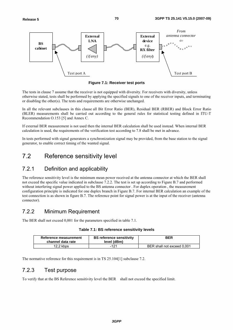
3GPP
3GPP TS 25.141 V5.15.0 (2007-09)70Release 5
BS
cabinet
Test port A Test port B
External device
e.g. RX filter
(if any)
External LNA
(if any)
From antenna connector
⇐
Figure 7.1: Receiver test ports
The tests in clause 7 assume that the receiver is not equipped with diversity. For receivers with diversity, unless otherwise stated, tests shall be performed by applying the specified signals to one of the receiver inputs, and terminating or disabling the other(s). The tests and requirements are otherwise unchanged.
In all the relevant subclauses in this clause all Bit Error Ratio (BER), Residual BER (RBER) and Block Error Ratio (BLER) measurements shall be carried out according to the general rules for statistical testing defined in ITU-T Recommendation O.153 [5] and Annex C.
If external BER measurement is not used then the internal BER calculation shall be used instead. When internal BER calculation is used, the requirements of the verification test according to 7.8 shall be met in advance.
In tests performed with signal generators a synchronization signal may be provided, from the base station to the signal generator, to enable correct timing of the wanted signal.
7.2 Reference sensitivity level
7.2.1 Definition and applicability The reference sensitivity level is the minimum mean power received at the antenna connector at which the BER shall not exceed the specific value indicated in subclause 7.2.2. The test is set up according to Figure B.7 and performed without interfering signal power applied to the BS antenna connector . For duplex operation , the measurement configuration principle is indicated for one duplex branch in Figure B.7. For internal BER calculation an example of the test connection is as shown in figure B.7. The reference point for signal power is at the input of the receiver (antenna connector).
7.2.2 Minimum Requirement The BER shall not exceed 0,001 for the parameters specified in table 7.1.
Table 7.1: BS reference sensitivity levels
Reference measurement channel data rate
BS reference sensitivity level (dBm)
BER
12,2 kbps -121 BER shall not exceed 0,001
The normative reference for this requirement is in TS 25.104[1] subclause 7.2.
7.2.3 Test purpose To verify that at the BS Reference sensitivity level the BER shall not exceed the specified limit.
3GPP
3GPP TS 25.141 V5.15.0 (2007-09)71Release 5
7.2.4 Method of testing
7.2.4.1 Initial conditions
Test environment: normal; see subclause 4.4.1
RF channels to be tested: B, M and T; see subclause 4.8.
The following additional tests shall be performed:
a) On each of B, M and T, the test shall be performed under extreme power supply as defined in subclause 4.4.2
NOTE: Tests under extreme power supply also test extreme temperature.
1) Connect BS to be tested to RF signal source.
2) Set frequency.
3) Start transmit 12,2kbps DPCH with reference measurement channel defined in annex A to the BS under test (PN-9 data sequence or longer).
4) Disable TPC function.
7.2.4.2 Procedure
1) Calculate BER according to annex C.
2) Set the test signal mean power as specified in table 7.1A.
3) Measure BER.
7.2.5 Test requirement The BER measurement result in step 3 of 7.2.4.2 shall not be greater than the limit specified in table 7.1A.
Table 7.1A: BS reference sensitivity levels
Reference measurement channel data rate
BS reference sensitivity level (dBm)
BER
12,2 kbps -120.3 BER shall not exceed 0,001
NOTE: If the above Test Requirement differs from the Minimum Requirement then the Test Tolerance applied for this test is non-zero. The Test Tolerance for this test is defined in subclause 4.2 and the explanation of how the Minimum Requirement has been relaxed by the Test Tolerance is given in Annex F.
7.3 Dynamic range
7.3.1 Definition and applicability Receiver dynamic range is the receiver ability to handle a rise of interference in the reception frequency channel. The receiver shall fulfil a specified BER requirement for a specified sensitivity degradation of the wanted signal in the presence of an interfering AWGN signal in the same reception frequency channel.
7.3.2 Minimum Requirement The BER shall not exceed 0,001 for the parameters specified in table 7.2.
3GPP
3GPP TS 25.141 V5.15.0 (2007-09)72Release 5
Table 7.2: Dynamic range
Parameter Level Unit Data rate 12,2 kbps Wanted signal mean power
-91 dBm
Interfering AWGN signal -73 dBm/3.84 MHz
The normative reference for this requirement is in TS 25.104[1] subclause 7.3
7.3.3 Test purpose The test purpose is to verify the ability of the BS to receive a single-code test signal of maximum with a BER not exceeding a specified limit.
7.3.4 Method of test
7.3.4.1 Initial conditions
Test environment: normal; see subclause 4.4.1.
RF channels to be tested: B, M and T; see subclause 4.8
1) Connect the test equipment as shown in annex B.
7.3.4.2 Procedure
1) Adjust the signal generator for the wanted signal as specified in Table 7.2A.
2) Adjust the AWGN generator level as specified in Table 7.2A and set the frequency to the same frequency as the tested channel.
3) Measure the BER for the tested service and verify that it is below the specified level.
Repeat the measurement for the other RX port.
7.3.5 Test Requirements The BER measurement result in step 3 of 7.3.4.2 shall not be greater than 0,001 using the parameters specified in tables 7.2A.
Table 7.2A: Dynamic range
Parameter Level Unit Reference measurement channel data rate
12,2 Kbps
Wanted signal mean power
-89.8 dBm
Interfering AWGN signal -73 dBm/3.84 MHz
NOTE: If the above Test Requirement differs from the Minimum Requirement then the Test Tolerance applied for this test is non-zero. The Test Tolerance for this test is defined in subclause 4.2 and the explanation of how the Minimum Requirement has been relaxed by the Test Tolerance is given in Annex F.
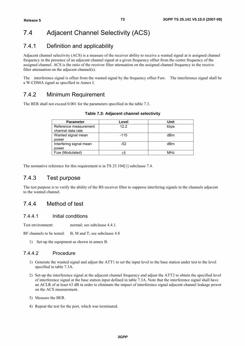
3GPP
3GPP TS 25.141 V5.15.0 (2007-09)73Release 5
7.4 Adjacent Channel Selectivity (ACS)
7.4.1 Definition and applicability Adjacent channel selectivity (ACS) is a measure of the receiver ability to receive a wanted signal at is assigned channel frequency in the presence of an adjacent channel signal at a given frequency offset from the center frequency of the assigned channel. ACS is the ratio of the receiver filter attenuation on the assigned channel frequency to the receive filter attenuation on the adjacent channel(s).
The interference signal is offset from the wanted signal by the frequency offset Fuw. The interference signal shall be a W-CDMA signal as specified in Annex I.
7.4.2 Minimum Requirement The BER shall not exceed 0.001 for the parameters specified in the table 7.3.
Table 7.3: Adjacent channel selectivity
Parameter Level Unit Reference measurement channel data rate
12.2 kbps
Wanted signal mean power
-115 dBm
Interfering signal mean power
-52 dBm
Fuw (Modulated) ±5 MHz
The normative reference for this requirement is in TS 25.104[1] subclause 7.4.
7.4.3 Test purpose The test purpose is to verify the ability of the BS receiver filter to suppress interfering signals in the channels adjacent to the wanted channel.
7.4.4 Method of test
7.4.4.1 Initial conditions
Test environment: normal; see subclause 4.4.1.
RF channels to be tested: B, M and T; see subclause 4.8
1) Set-up the equipment as shown in annex B.
7.4.4.2 Procedure
1) Generate the wanted signal and adjust the ATT1 to set the input level to the base station under test to the level specified in table 7.3A.
2) Set-up the interference signal at the adjacent channel frequency and adjust the ATT2 to obtain the specified level of interference signal at the base station input defined in table 7.3A. Note that the interference signal shall have an ACLR of at least 63 dB in order to eliminate the impact of interference signal adjacent channel leakage power on the ACS measurement.
3) Measure the BER.
4) Repeat the test for the port, which was terminated.
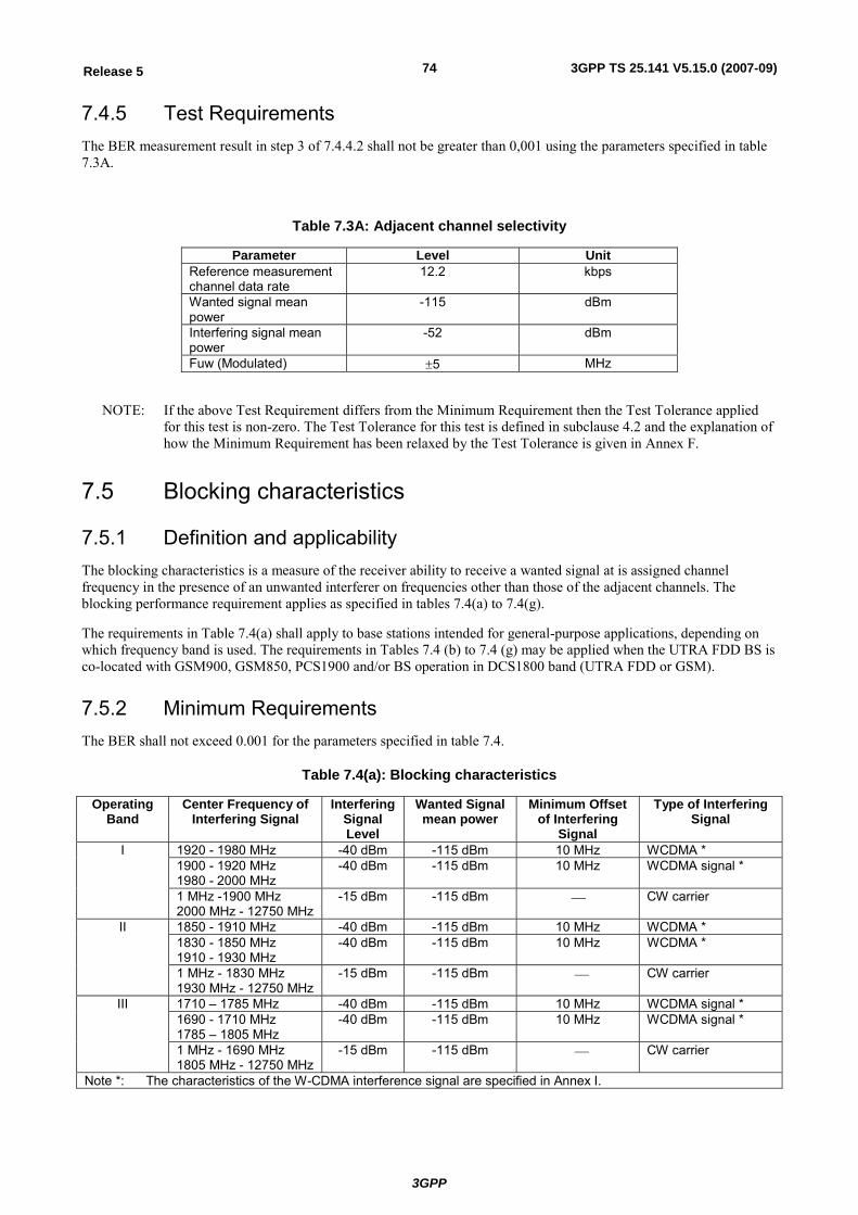
3GPP
3GPP TS 25.141 V5.15.0 (2007-09)74Release 5
7.4.5 Test Requirements The BER measurement result in step 3 of 7.4.4.2 shall not be greater than 0,001 using the parameters specified in table 7.3A.
Table 7.3A: Adjacent channel selectivity
Parameter Level Unit Reference measurement channel data rate
12.2 kbps
Wanted signal mean power
-115 dBm
Interfering signal mean power
-52 dBm
Fuw (Modulated) ±5 MHz
NOTE: If the above Test Requirement differs from the Minimum Requirement then the Test Tolerance applied for this test is non-zero. The Test Tolerance for this test is defined in subclause 4.2 and the explanation of how the Minimum Requirement has been relaxed by the Test Tolerance is given in Annex F.
7.5 Blocking characteristics
7.5.1 Definition and applicability The blocking characteristics is a measure of the receiver ability to receive a wanted signal at is assigned channel frequency in the presence of an unwanted interferer on frequencies other than those of the adjacent channels. The blocking performance requirement applies as specified in tables 7.4(a) to 7.4(g).
The requirements in Table 7.4(a) shall apply to base stations intended for general-purpose applications, depending on which frequency band is used. The requirements in Tables 7.4 (b) to 7.4 (g) may be applied when the UTRA FDD BS is co-located with GSM900, GSM850, PCS1900 and/or BS operation in DCS1800 band (UTRA FDD or GSM).
7.5.2 Minimum Requirements The BER shall not exceed 0.001 for the parameters specified in table 7.4.
Table 7.4(a): Blocking characteristics
Operating Band
Center Frequency of Interfering Signal
Interfering Signal Level
Wanted Signal mean power
Minimum Offset of Interfering
Signal
Type of Interfering Signal
1920 - 1980 MHz -40 dBm -115 dBm 10 MHz WCDMA * 1900 - 1920 MHz 1980 - 2000 MHz
-40 dBm -115 dBm 10 MHz WCDMA signal * I
1 MHz -1900 MHz 2000 MHz - 12750 MHz
-15 dBm -115 dBm ⎯ CW carrier
1850 - 1910 MHz -40 dBm -115 dBm 10 MHz WCDMA * 1830 - 1850 MHz 1910 - 1930 MHz
-40 dBm -115 dBm 10 MHz WCDMA * II
1 MHz - 1830 MHz 1930 MHz - 12750 MHz
-15 dBm -115 dBm ⎯ CW carrier
1710 – 1785 MHz -40 dBm -115 dBm 10 MHz WCDMA signal * 1690 - 1710 MHz 1785 – 1805 MHz
-40 dBm -115 dBm 10 MHz WCDMA signal * III
1 MHz - 1690 MHz 1805 MHz - 12750 MHz
-15 dBm -115 dBm ⎯ CW carrier
Note *: The characteristics of the W-CDMA interference signal are specified in Annex I.
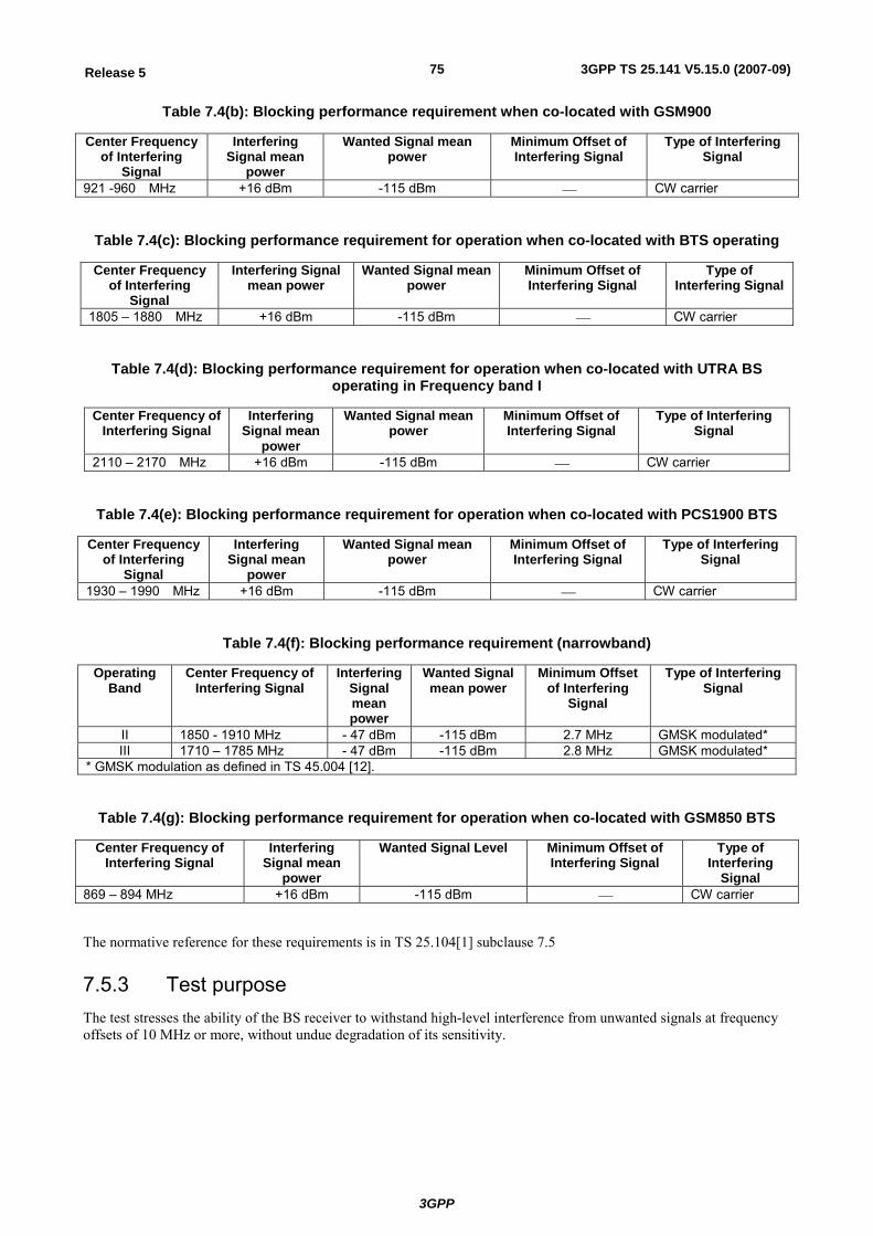
3GPP
3GPP TS 25.141 V5.15.0 (2007-09)75Release 5
Table 7.4(b): Blocking performance requirement when co-located with GSM900
Center Frequency of Interfering
Signal
Interfering Signal mean
power
Wanted Signal mean power
Minimum Offset of Interfering Signal
Type of Interfering Signal
921 -960 MHz +16 dBm -115 dBm ⎯ CW carrier
Table 7.4(c): Blocking performance requirement for operation when co-located with BTS operating
Center Frequency of Interfering
Signal
Interfering Signal mean power
Wanted Signal mean power
Minimum Offset of Interfering Signal
Type of Interfering Signal
1805 – 1880 MHz +16 dBm -115 dBm ⎯ CW carrier
Table 7.4(d): Blocking performance requirement for operation when co-located with UTRA BS operating in Frequency band I
Center Frequency of Interfering Signal
Interfering Signal mean
power
Wanted Signal mean power
Minimum Offset of Interfering Signal
Type of Interfering Signal
2110 – 2170 MHz +16 dBm -115 dBm ⎯ CW carrier
Table 7.4(e): Blocking performance requirement for operation when co-located with PCS1900 BTS
Center Frequency of Interfering
Signal
Interfering Signal mean
power
Wanted Signal mean power
Minimum Offset of Interfering Signal
Type of Interfering Signal
1930 – 1990 MHz +16 dBm -115 dBm ⎯ CW carrier
Table 7.4(f): Blocking performance requirement (narrowband)
Operating Band
Center Frequency of Interfering Signal
Interfering Signal mean power
Wanted Signal mean power
Minimum Offset of Interfering
Signal
Type of Interfering Signal
II 1850 - 1910 MHz - 47 dBm -115 dBm 2.7 MHz GMSK modulated* III 1710 – 1785 MHz - 47 dBm -115 dBm 2.8 MHz GMSK modulated*
* GMSK modulation as defined in TS 45.004 [12].
Table 7.4(g): Blocking performance requirement for operation when co-located with GSM850 BTS
Center Frequency of Interfering Signal
Interfering Signal mean
power
Wanted Signal Level Minimum Offset of Interfering Signal
Type of Interfering
Signal 869 – 894 MHz +16 dBm -115 dBm ⎯ CW carrier
The normative reference for these requirements is in TS 25.104[1] subclause 7.5
7.5.3 Test purpose The test stresses the ability of the BS receiver to withstand high-level interference from unwanted signals at frequency offsets of 10 MHz or more, without undue degradation of its sensitivity.
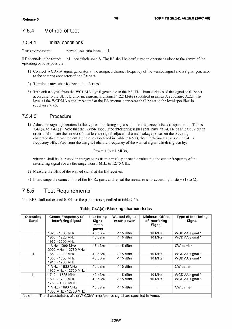
3GPP
3GPP TS 25.141 V5.15.0 (2007-09)76Release 5
7.5.4 Method of test
7.5.4.1 Initial conditions
Test environment: normal; see subclause 4.4.1.
RF channels to be tested: M see subclause 4.8. The BS shall be configured to operate as close to the centre of the operating band as possible.
1) Connect WCDMA signal generator at the assigned channel frequency of the wanted signal and a signal generator to the antenna connector of one Rx port.
2) Terminate any other Rx port not under test.
3) Transmit a signal from the WCDMA signal generator to the BS. The characteristics of the signal shall be set according to the UL reference measurement channel (12,2 kbit/s) specified in annex A subclause A.2.1. The level of the WCDMA signal measured at the BS antenna connector shall be set to the level specified in subclause 7.5.5.
7.5.4.2 Procedure
1) Adjust the signal generators to the type of interfering signals and the frequency offsets as specified in Tables 7.4A(a) to 7.4A(g). Note that the GMSK modulated interfering signal shall have an ACLR of at least 72 dB in order to eliminate the impact of interference signal adjacent channel leakage power on the blocking characteristics measurement. For the tests defined in Table 7.4A(a), the interfering signal shall be at a frequency offset Fuw from the assigned channel frequency of the wanted signal which is given by:
Fuw = ± (n x 1 MHz),
where n shall be increased in integer steps from n = 10 up to such a value that the center frequency of the interfering signal covers the range from 1 MHz to 12,75 GHz.
2) Measure the BER of the wanted signal at the BS receiver.
3) Interchange the connections of the BS Rx ports and repeat the measurements according to steps (1) to (2).
7.5.5 Test Requirements The BER shall not exceed 0.001 for the parameters specified in table 7.4A.
Table 7.4A(a): Blocking characteristics
Operating Band
Center Frequency of Interfering Signal
Interfering Signal mean power
Wanted Signal mean power
Minimum Offset of Interfering
Signal
Type of Interfering Signal
1920 - 1980 MHz -40 dBm -115 dBm 10 MHz WCDMA signal * 1900 - 1920 MHz 1980 - 2000 MHz
-40 dBm -115 dBm 10 MHz WCDMA signal * I
1 MHz -1900 MHz 2000 MHz - 12750 MHz
-15 dBm -115 dBm ⎯ CW carrier
1850 - 1910 MHz -40 dBm -115 dBm 10 MHz WCDMA signal * 1830 - 1850 MHz 1910 - 1930 MHz
-40 dBm -115 dBm 10 MHz WCDMA signal * II
1 MHz - 1830 MHz 1930 MHz - 12750 MHz
-15 dBm -115 dBm ⎯ CW carrier
1710 – 1785 MHz -40 dBm -115 dBm 10 MHz WCDMA signal * 1690 - 1710 MHz 1785 – 1805 MHz
-40 dBm -115 dBm 10 MHz WCDMA signal * III
1 MHz - 1690 MHz 1805 MHz - 12750 MHz
-15 dBm -115 dBm ⎯ CW carrier
Note *: The characteristics of the W-CDMA interference signal are specified in Annex I.
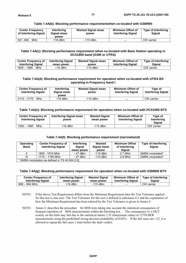
3GPP
3GPP TS 25.141 V5.15.0 (2007-09)77Release 5
Table 7.4A(b): Blocking performance requirementwhen co-located with GSM900
Center Frequency of Interfering Signal
Interfering Signal mean
power
Wanted Signal mean power
Minimum Offset of Interfering Signal
Type of Interfering Signal
921 -960 MHz +16 dBm -115 dBm ⎯ CW carrier
Table 7.4A(c): Blocking performance requirement when co-located with Base Station operating in DCS1800 band (GSM or UTRA)
Center Frequency of Interfering Signal
Interfering Signal mean power
Wanted Signal mean power
Minimum Offset of Interfering Signal
Type of Interfering Signal
1805 – 1880 MHz +16 dBm -115 dBm ⎯ CW carrier
Table 7.4A(d): Blocking performance requirement for operation when co-located with UTRA BS operating in Frequency band I
Center Frequency of Interfering Signal
Interfering Signal mean
power
Wanted Signal mean power
Minimum Offset of Interfering Signal
Type of Interfering Signal
2110 – 2170 MHz +16 dBm -115 dBm ⎯ CW carrier
Table 7.4A(e): Blocking performance requirement for operation when co-located with PCS1900 BTS
Center Frequency of Interfering Signal
Interfering Signal mean power
Wanted Signal mean power
Minimum Offset of Interfering Signal
Type of Interfering
Signal 1930 – 1990 MHz +16 dBm -115 dBm ⎯ CW carrier
Table 7.4A(f): Blocking performance requirement (narrowband)
Operating Band
Center Frequency of Interfering Signal
Interfering Signal
mean power
Wanted Signal mean
power
Minimum Offset of Interfering
Signal
Type of Interfering Signal
II 1850 - 1910 MHz - 47 dBm -115 dBm 2.7 MHz GMSK modulated* III 1710 – 1785 MHz - 47 dBm -115 dBm 2.8 MHz GMSK modulated*
* GMSK modulation as defined in TS 45.004 [12].
Table 7.4A(g): Blocking performance requirement for operation when co-located with GSM850 BTS
Center Frequency of Interfering Signal
Interfering Signal mean power
Wanted Signal mean power
Minimum Offset of Interfering Signal
Type of Interfering Signal
869 – 894 MHz +16 dBm -115 dBm ⎯ CW carrier
NOTE: If the above Test Requirement differs from the Minimum Requirement then the Test Tolerance applied for this test is non-zero. The Test Tolerance for this test is defined in subclause 4.2 and the explanation of how the Minimum Requirement has been relaxed by the Test Tolerance is given in Annex F.
NOTE: Annex C describes the procedure for BER tests taking into account the statistical consequence of frequent repetition of BER measurements within the blocking test . The consequence is: a DUT exactly on the limit may fail due to the statistical nature 2.55 times(mean value) in 12750 BER measurements using the predefined wrong decision probability of 0.02%. If the fail cases are ≤12, it is allowed to repeat the fail cases 1 time before the final verdict.
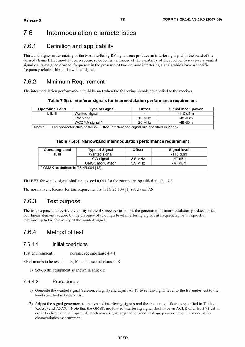
3GPP
3GPP TS 25.141 V5.15.0 (2007-09)78Release 5
7.6 Intermodulation characteristics
7.6.1 Definition and applicability Third and higher order mixing of the two interfering RF signals can produce an interfering signal in the band of the desired channel. Intermodulation response rejection is a measure of the capability of the receiver to receiver a wanted signal on its assigned channel frequency in the presence of two or more interfering signals which have a specific frequency relationship to the wanted signal.
7.6.2 Minimum Requirement The intermodulation performance should be met when the following signals are applied to the receiver.
Table 7.5(a): Interferer signals for intermodulation performance requirement
Operating Band Type of Signal Offset Signal mean power Wanted signal - -115 dBm CW signal 10 MHz -48 dBm
I, II, III
WCDMA signal * 20 MHz -48 dBm Note *: The characteristics of the W-CDMA interference signal are specified in Annex I.
Table 7.5(b): Narrowband intermodulation performance requirement
Operating band Type of Signal Offset Signal level Wanted signal - -115 dBm
CW signal 3.5 MHz - 47 dBm II, III
GMSK modulated* 5.9 MHz - 47 dBm * GMSK as defined in TS 45.004 [12].
The BER for wanted signal shall not exceed 0,001 for the parameters specified in table 7.5.
The normative reference for this requirement is in TS 25.104 [1] subclause 7.6
7.6.3 Test purpose The test purpose is to verify the ability of the BS receiver to inhibit the generation of intermodulation products in its non-linear elements caused by the presence of two high-level interfering signals at frequencies with a specific relationship to the frequency of the wanted signal.
7.6.4 Method of test
7.6.4.1 Initial conditions
Test environment: normal; see subclause 4.4.1.
RF channels to be tested: B, M and T; see subclause 4.8
1) Set-up the equipment as shown in annex B.
7.6.4.2 Procedures
1) Generate the wanted signal (reference signal) and adjust ATT1 to set the signal level to the BS under test to the level specified in table 7.5A.
2) Adjust the signal generators to the type of interfering signals and the frequency offsets as specified in Tables 7.5A(a) and 7.5A(b). Note that the GMSK modulated interfering signal shall have an ACLR of at least 72 dB in order to eliminate the impact of interference signal adjacent channel leakage power on the intermodulation characteristics measurement.
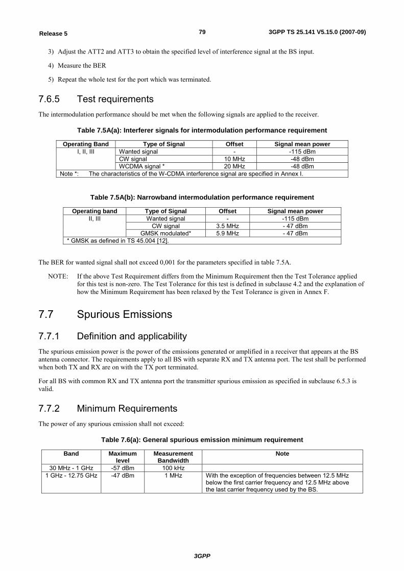
3GPP
3GPP TS 25.141 V5.15.0 (2007-09)79Release 5
3) Adjust the ATT2 and ATT3 to obtain the specified level of interference signal at the BS input.
4) Measure the BER
5) Repeat the whole test for the port which was terminated.
7.6.5 Test requirements The intermodulation performance should be met when the following signals are applied to the receiver.
Table 7.5A(a): Interferer signals for intermodulation performance requirement
Operating Band Type of Signal Offset Signal mean power Wanted signal - -115 dBm CW signal 10 MHz -48 dBm
I, II, III
WCDMA signal * 20 MHz -48 dBm Note *: The characteristics of the W-CDMA interference signal are specified in Annex I.
Table 7.5A(b): Narrowband intermodulation performance requirement
Operating band Type of Signal Offset Signal mean power Wanted signal - -115 dBm
CW signal 3.5 MHz - 47 dBm II, III
GMSK modulated* 5.9 MHz - 47 dBm * GMSK as defined in TS 45.004 [12].
The BER for wanted signal shall not exceed 0,001 for the parameters specified in table 7.5A.
NOTE: If the above Test Requirement differs from the Minimum Requirement then the Test Tolerance applied for this test is non-zero. The Test Tolerance for this test is defined in subclause 4.2 and the explanation of how the Minimum Requirement has been relaxed by the Test Tolerance is given in Annex F.
7.7 Spurious Emissions
7.7.1 Definition and applicability The spurious emission power is the power of the emissions generated or amplified in a receiver that appears at the BS antenna connector. The requirements apply to all BS with separate RX and TX antenna port. The test shall be performed when both TX and RX are on with the TX port terminated.
For all BS with common RX and TX antenna port the transmitter spurious emission as specified in subclause 6.5.3 is valid.
7.7.2 Minimum Requirements The power of any spurious emission shall not exceed:
Table 7.6(a): General spurious emission minimum requirement
Band Maximum level
Measurement Bandwidth
Note
30 MHz - 1 GHz -57 dBm 100 kHz 1 GHz - 12.75 GHz -47 dBm 1 MHz With the exception of frequencies between 12.5 MHz
below the first carrier frequency and 12.5 MHz above the last carrier frequency used by the BS.
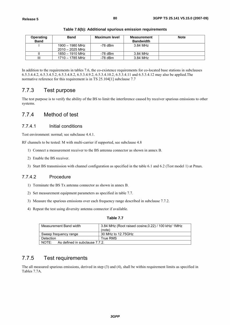
3GPP
3GPP TS 25.141 V5.15.0 (2007-09)80Release 5
Table 7.6(b): Additional spurious emission requirements
Operating Band
Band Maximum level Measurement Bandwidth
Note
I 1900 – 1980 MHz 2010 – 2025 MHz
-78 dBm 3.84 MHz
II 1850 – 1910 MHz -78 dBm 3.84 MHz III 1710 – 1785 MHz -78 dBm 3.84 MHz
In addition to the requirements in tables 7.6, the co-existence requirements for co-located base stations in subclauses 6.5.3.4.4.2, 6.5.3.4.5.2, 6.5.3.4.8.2, 6.5.3.4.9.2, 6.5.3.4.10.2, 6.5.3.4.11 and 6.5.3.4.12 may also be applied.The normative reference for this requirement is in TS 25.104[1] subclause 7.7
7.7.3 Test purpose The test purpose is to verify the ability of the BS to limit the interference caused by receiver spurious emissions to other systems.
7.7.4 Method of test
7.7.4.1 Initial conditions
Test environment: normal; see subclause 4.4.1.
RF channels to be tested: M with multi-carrier if supported, see subclause 4.8
1) Connect a measurement receiver to the BS antenna connector as shown in annex B.
2) Enable the BS receiver.
3) Start BS transmission with channel configuration as specified in the table 6.1 and 6.2 (Test model 1) at Pmax.
7.7.4.2 Procedure
1) Terminate the BS Tx antenna connector as shown in annex B.
2) Set measurement equipment parameters as specified in table 7.7.
3) Measure the spurious emissions over each frequency range described in subclause 7.7.2.
4) Repeat the test using diversity antenna connector if available.
Table 7.7
Measurement Band width 3.84 MHz (Root raised cosine,0.22) / 100 kHz/ 1MHz (note)
Sweep frequency range 30 MHz to 12.75GHz Detection True RMS NOTE: As defined in subclause 7.7.2.
7.7.5 Test requirements The all measured spurious emissions, derived in step (3) and (4), shall be within requirement limits as specified in Tables 7.7A.
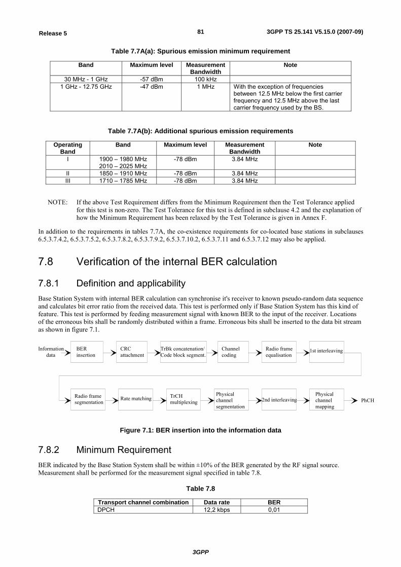
3GPP
3GPP TS 25.141 V5.15.0 (2007-09)81Release 5
Table 7.7A(a): Spurious emission minimum requirement
Band Maximum level Measurement Bandwidth
Note
30 MHz - 1 GHz -57 dBm 100 kHz 1 GHz - 12.75 GHz -47 dBm 1 MHz With the exception of frequencies
between 12.5 MHz below the first carrier frequency and 12.5 MHz above the last carrier frequency used by the BS.
Table 7.7A(b): Additional spurious emission requirements
Operating Band
Band Maximum level Measurement Bandwidth
Note
I 1900 – 1980 MHz 2010 – 2025 MHz
-78 dBm 3.84 MHz
II 1850 – 1910 MHz -78 dBm 3.84 MHz III 1710 – 1785 MHz -78 dBm 3.84 MHz
NOTE: If the above Test Requirement differs from the Minimum Requirement then the Test Tolerance applied for this test is non-zero. The Test Tolerance for this test is defined in subclause 4.2 and the explanation of how the Minimum Requirement has been relaxed by the Test Tolerance is given in Annex F.
In addition to the requirements in tables 7.7A, the co-existence requirements for co-located base stations in subclauses 6.5.3.7.4.2, 6.5.3.7.5.2, 6.5.3.7.8.2, 6.5.3.7.9.2, 6.5.3.7.10.2, 6.5.3.7.11 and 6.5.3.7.12 may also be applied.
7.8 Verification of the internal BER calculation
7.8.1 Definition and applicability Base Station System with internal BER calculation can synchronise it's receiver to known pseudo-random data sequence and calculates bit error ratio from the received data. This test is performed only if Base Station System has this kind of feature. This test is performed by feeding measurement signal with known BER to the input of the receiver. Locations of the erroneous bits shall be randomly distributed within a frame. Erroneous bits shall be inserted to the data bit stream as shown in figure 7.1.
BER insertion
CRC attachment
TrBk concatenation/Code block segment.
Channelcoding
Radio frameequalisation
1st interleaving
Radio framesegmentation
Rate matching TrCH multiplexing
Physical channelsegmentation
Physical channelmapping
2nd interleaving
Information data
PhCH
Figure 7.1: BER insertion into the information data
7.8.2 Minimum Requirement BER indicated by the Base Station System shall be within ±10% of the BER generated by the RF signal source. Measurement shall be performed for the measurement signal specified in table 7.8.
Table 7.8
Transport channel combination Data rate BER DPCH 12,2 kbps 0,01
3GPP
3GPP TS 25.141 V5.15.0 (2007-09)82Release 5
7.8.3 Test purpose To verify that the internal BER calculation accuracy shall meet requirements for conformance testing.
7.8.4 Method of test
7.8.4.1 Initial conditions
Test environment: normal; see subclause 4.4.1.
RF channels to be tested: B, M and T; see subclause 4.8
1) Connect BS RX antenna connector to the RF signal source or UE simulator as shown in annex B.
2) Set correct signal source parameters as specified in table 7.9.
Table 7.9
Parameter Level/status Unit UL signal level Ref.sens +10 dB dBm/3,84 MHz Data sequence PN9 or longer
7.8.4.2 Procedure
1) Measure the BER of received signal from RF signal source or UE simulator to BS antenna connector.
2) BER calculation shall be done at least over 50 000 bits.
7.8.5 Test Requirement BER indicated by the Base Station System shall be within requirement as specified in subclause 7.8.2.
8 Performance requirement
8.1 General All Bit Error Ratio (BER) and Block Error ratio (BLER) measurements shall be carried out according to the general rules for statistical testing defined in ITU-T Recommendation O.153 [5].
If external BLER measurement is not used then the internal BLER calculation shall be used instead. When internal BLER calculation is used, the requirements of the verification test according to 8.6 shall be met in advance.
Performance requirements are specified for a number of test environments and multi-path channel classes.
The requirements only apply to those measurement channels that are supported by the base station.
The requirements only apply to a base station with dual receiver antenna diversity. The required Eb/N0 shall be applied separately at each antenna port.
In tests performed with signal generators a synchronization signal may be provided, from the base station to the signal generator, to enable correct timing of the wanted signal.
3GPP
3GPP TS 25.141 V5.15.0 (2007-09)83Release 5
8.2 Demodulation in static propagation conditions
8.2.1 Demodulation of DCH
8.2.1.1 Definition and applicability
The performance requirement of DCH in static propagation conditions is determined by the maximum Block Error Ratio (BLER ) allowed when the receiver input signal is at a specified Eb/N0 limit. The BLER is calculated for each of the measurement channels supported by the base station.
The requirement in this subclause shall apply to base stations intended for general-purpose applications.
8.2.1.2 Minimum requirement
The BLER should not exceed the limit for the Eb/N0 specified in table 8.1.
Table 8.1: Performance requirements in AWGN channel.
Measurement channel data rate (Rb)
Eb/N0for required BLER < 10-1
Eb/N0 for required BLER < 10-2
12.2 kbps n.a. 5.1 dB 64 kbps 1.5 dB 1.7 dB 144 kbps 0.8 dB 0.9 dB 384 kbps 0.9 dB 1.0 dB
The reference for this requirement is TS 25.104 subclause 8.2.1.1.
8.2.1.3 Test purpose
The test shall verify the receiver's ability to receive the test signal under static propagation conditions with a BLER not exceeding a specified limit.
8.2.1.4 Method of test
8.2.1.4.1 Initial conditions
Test environment: normal; see subclause 4.4.1.
RF channels to be tested: B, M and T; see subclause 4.8
1) Connect the BS tester generating the wanted signal and AWGN generators to both BS antenna connectors for diversity reception via a combining network as shown in annex B.
8.2.1.4.2 Procedure
1) Adjust the AWGN generator to -84 dBm/3.84 MHz at the BS input.
2) The characteristics of the wanted signal shall be configured according to the corresponding UL reference measurement channel defined in annex A.
3) Adjust the equipment so that required Eb/N0 specified in table 8.2 is achieved. To achieve the specified Eb/NO, the ratio of the wanted signal level relative to the AWGN signal at the BS input should be adjusted to: 10*Log10(Rb /3.84*106)+Eb/N0 [dB].
4) For each of the data rates in table 8.2 applicable for the base station, measure the BLER.
3GPP
3GPP TS 25.141 V5.15.0 (2007-09)84Release 5
8.2.1.5 Test requirements
The BLER measured according to subclause 8.2.1.4.2 shall not exceed the BLER limits for the Eb/N0 levels specified in table 8.2.
Table 8.2: Test requirements in AWGN channel.
Measurement channel data rate (Rb)
Eb/N0for required BLER < 10-1
Eb/N0 for required BLER < 10-2
12.2 kbps n.a. 5.5 dB 64 kbps 1.9 dB 2.1 dB 144 kbps 1.2 dB 1.3 dB 384 kbps 1.3 dB 1.4 dB
NOTE: If the above Test Requirement differs from the Minimum Requirement then the Test Tolerance applied for this test is non-zero. The Test Tolerance for this test is defined in subclause 4.2 and the explanation of how the Minimum Requirement has been relaxed by the Test Tolerance is given in Annex F.
8.3 Demodulation of DCH in multipath fading conditions
8.3.1 Multipath fading Case 1
8.3.1.1 Definition and applicability
The performance requirement of DCH in multipath fading Case 1 is determined by the maximum Block Error Ratio (BLER ) allowed when the receiver input signal is at a specified Eb/N0 limit. The BLER is calculated for each of the measurement channels supported by the base station.
The requirement in this subclause shall apply to base stations intended for general-purpose applications.
8.3.1.2 Minimum requirement
The BLER should not exceed the limit for the Eb/N0 specified in table 8.3.
Table 8.3: Performance requirements in multipath Case 1 channel
Measurement channel data rate (Rb)
Eb/N0for required BLER < 10-1
Eb/N0 for required BLER < 10-2
12.2 kbps n.a. 11.9 dB 64 kbps 6.2 dB 9.2 dB 144 kbps 5.4 dB 8.4 dB 384 kbps 5.8 dB 8.8 dB
The reference for this requirement is TS 25.104 subclause 8.3.1.1
8.3.1.3 Test Purpose
The test shall verify the receiver's ability to receive the test signal under slow multipath fading propagation conditions with a BLER not exceeding a specified limit.
8.3.1.4 Method of test
8.3.1.4.1 Initial conditions
Test environment: normal; see subclause 4.4.1.
RF channels to be tested: B, M and T; see subclause 4.8
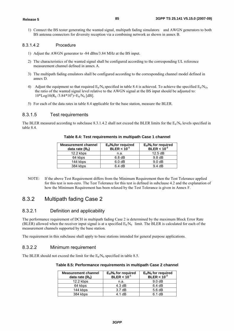
3GPP
3GPP TS 25.141 V5.15.0 (2007-09)85Release 5
1) Connect the BS tester generating the wanted signal, multipath fading simulators and AWGN generators to both BS antenna connectors for diversity reception via a combining network as shown in annex B.
8.3.1.4.2 Procedure
1) Adjust the AWGN generator to -84 dBm/3.84 MHz at the BS input.
2) The characteristics of the wanted signal shall be configured according to the corresponding UL reference measurement channel defined in annex A.
3) The multipath fading emulators shall be configured according to the corresponding channel model defined in annex D.
4) Adjust the equipment so that required Eb/N0 specified in table 8.4 is achieved. To achieve the specified Eb/NO, the ratio of the wanted signal level relative to the AWGN signal at the BS input should be adjusted to: 10*Log10(Rb /3.84*106)+Eb/N0 [dB].
5) For each of the data rates in table 8.4 applicable for the base station, measure the BLER.
8.3.1.5 Test requirements
The BLER measured according to subclause 8.3.1.4.2 shall not exceed the BLER limits for the Eb/N0 levels specified in table 8.4.
Table 8.4: Test requirements in multipath Case 1 channel
Measurement channel data rate (Rb)
Eb/N0for required BLER < 10-1
Eb/N0 for required BLER < 10-2
12.2 kbps n.a. 12.5 dB 64 kbps 6.8 dB 9.8 dB 144 kbps 6.0 dB 9.0 dB 384 kbps 6.4 dB 9.4 dB
NOTE: If the above Test Requirement differs from the Minimum Requirement then the Test Tolerance applied for this test is non-zero. The Test Tolerance for this test is defined in subclause 4.2 and the explanation of how the Minimum Requirement has been relaxed by the Test Tolerance is given in Annex F.
8.3.2 Multipath fading Case 2
8.3.2.1 Definition and applicability
The performance requirement of DCH in multipath fading Case 2 is determined by the maximum Block Error Rate (BLER) allowed when the receiver input signal is at a specified Eb/N0 limit. The BLER is calculated for each of the measurement channels supported by the base station.
The requirement in this subclause shall apply to base stations intended for general purpose applications.
8.3.2.2 Minimum requirement
The BLER should not exceed the limit for the Eb/N0 specified in table 8.5.
Table 8.5: Performance requirements in multipath Case 2 channel
Measurement channel data rate (Rb)
Eb/N0 for required BLER < 10-1
Eb/N0 for required BLER < 10-2
12.2 kbps n.a. 9.0 dB 64 kbps 4.3 dB 6.4 dB 144 kbps 3.7 dB 5.6 dB 384 kbps 4.1 dB 6.1 dB
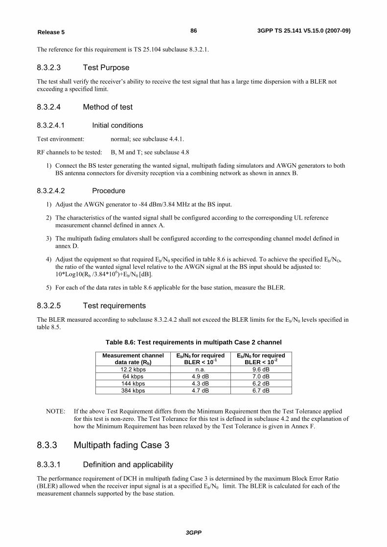
3GPP
3GPP TS 25.141 V5.15.0 (2007-09)86Release 5
The reference for this requirement is TS 25.104 subclause 8.3.2.1.
8.3.2.3 Test Purpose
The test shall verify the receiver’s ability to receive the test signal that has a large time dispersion with a BLER not exceeding a specified limit.
8.3.2.4 Method of test
8.3.2.4.1 Initial conditions
Test environment: normal; see subclause 4.4.1.
RF channels to be tested: B, M and T; see subclause 4.8
1) Connect the BS tester generating the wanted signal, multipath fading simulators and AWGN generators to both BS antenna connectors for diversity reception via a combining network as shown in annex B.
8.3.2.4.2 Procedure
1) Adjust the AWGN generator to -84 dBm/3.84 MHz at the BS input.
2) The characteristics of the wanted signal shall be configured according to the corresponding UL reference measurement channel defined in annex A.
3) The multipath fading emulators shall be configured according to the corresponding channel model defined in annex D.
4) Adjust the equipment so that required Eb/N0 specified in table 8.6 is achieved. To achieve the specified Eb/NO, the ratio of the wanted signal level relative to the AWGN signal at the BS input should be adjusted to: 10*Log10(Rb /3.84*106)+Eb/N0 [dB].
5) For each of the data rates in table 8.6 applicable for the base station, measure the BLER.
8.3.2.5 Test requirements
The BLER measured according to subclause 8.3.2.4.2 shall not exceed the BLER limits for the Eb/N0 levels specified in table 8.5.
Table 8.6: Test requirements in multipath Case 2 channel
Measurement channel data rate (Rb)
Eb/N0 for required BLER < 10-1
Eb/N0 for required BLER < 10-2
12.2 kbps n.a. 9.6 dB 64 kbps 4.9 dB 7.0 dB 144 kbps 4.3 dB 6.2 dB 384 kbps 4.7 dB 6.7 dB
NOTE: If the above Test Requirement differs from the Minimum Requirement then the Test Tolerance applied for this test is non-zero. The Test Tolerance for this test is defined in subclause 4.2 and the explanation of how the Minimum Requirement has been relaxed by the Test Tolerance is given in Annex F.
8.3.3 Multipath fading Case 3
8.3.3.1 Definition and applicability
The performance requirement of DCH in multipath fading Case 3 is determined by the maximum Block Error Ratio (BLER) allowed when the receiver input signal is at a specified Eb/N0 limit. The BLER is calculated for each of the measurement channels supported by the base station.
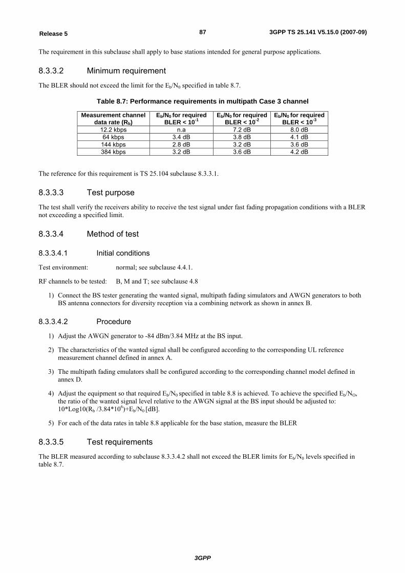
3GPP
3GPP TS 25.141 V5.15.0 (2007-09)87Release 5
The requirement in this subclause shall apply to base stations intended for general purpose applications.
8.3.3.2 Minimum requirement
The BLER should not exceed the limit for the Eb/N0 specified in table 8.7.
Table 8.7: Performance requirements in multipath Case 3 channel
Measurement channel data rate (Rb)
Eb/N0 for required BLER < 10-1
Eb/N0 for requiredBLER < 10-2
Eb/N0 for required BLER < 10-3
12.2 kbps n.a 7.2 dB 8.0 dB 64 kbps 3.4 dB 3.8 dB 4.1 dB
144 kbps 2.8 dB 3.2 dB 3.6 dB 384 kbps 3.2 dB 3.6 dB 4.2 dB
The reference for this requirement is TS 25.104 subclause 8.3.3.1.
8.3.3.3 Test purpose
The test shall verify the receivers ability to receive the test signal under fast fading propagation conditions with a BLER not exceeding a specified limit.
8.3.3.4 Method of test
8.3.3.4.1 Initial conditions
Test environment: normal; see subclause 4.4.1.
RF channels to be tested: B, M and T; see subclause 4.8
1) Connect the BS tester generating the wanted signal, multipath fading simulators and AWGN generators to both BS antenna connectors for diversity reception via a combining network as shown in annex B.
8.3.3.4.2 Procedure
1) Adjust the AWGN generator to -84 dBm/3.84 MHz at the BS input.
2) The characteristics of the wanted signal shall be configured according to the corresponding UL reference measurement channel defined in annex A.
3) The multipath fading emulators shall be configured according to the corresponding channel model defined in annex D.
4) Adjust the equipment so that required Eb/N0 specified in table 8.8 is achieved. To achieve the specified Eb/NO, the ratio of the wanted signal level relative to the AWGN signal at the BS input should be adjusted to: 10*Log10(Rb /3.84*106)+Eb/N0 [dB].
5) For each of the data rates in table 8.8 applicable for the base station, measure the BLER
8.3.3.5 Test requirements
The BLER measured according to subclause 8.3.3.4.2 shall not exceed the BLER limits for Eb/N0 levels specified in table 8.7.
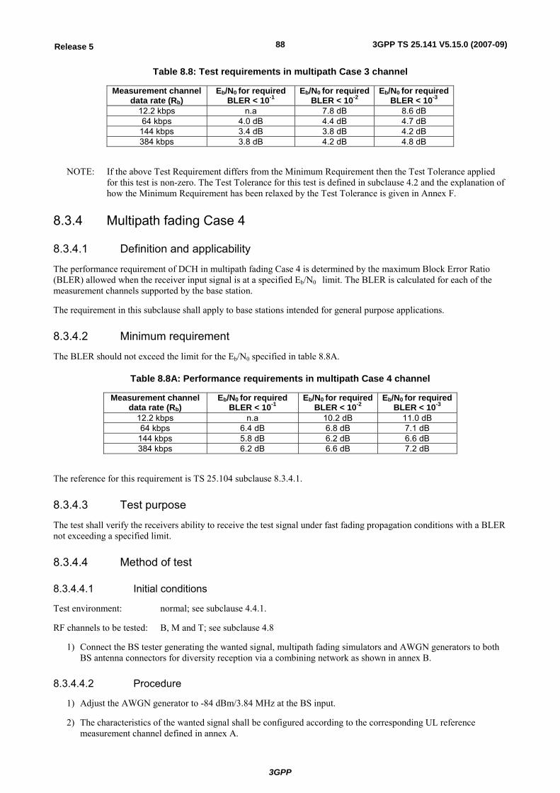
3GPP
3GPP TS 25.141 V5.15.0 (2007-09)88Release 5
Table 8.8: Test requirements in multipath Case 3 channel
Measurement channel data rate (Rb)
Eb/N0 for required BLER < 10-1
Eb/N0 for requiredBLER < 10-2
Eb/N0 for required BLER < 10-3
12.2 kbps n.a 7.8 dB 8.6 dB 64 kbps 4.0 dB 4.4 dB 4.7 dB
144 kbps 3.4 dB 3.8 dB 4.2 dB 384 kbps 3.8 dB 4.2 dB 4.8 dB
NOTE: If the above Test Requirement differs from the Minimum Requirement then the Test Tolerance applied for this test is non-zero. The Test Tolerance for this test is defined in subclause 4.2 and the explanation of how the Minimum Requirement has been relaxed by the Test Tolerance is given in Annex F.
8.3.4 Multipath fading Case 4
8.3.4.1 Definition and applicability
The performance requirement of DCH in multipath fading Case 4 is determined by the maximum Block Error Ratio (BLER) allowed when the receiver input signal is at a specified Eb/N0 limit. The BLER is calculated for each of the measurement channels supported by the base station.
The requirement in this subclause shall apply to base stations intended for general purpose applications.
8.3.4.2 Minimum requirement
The BLER should not exceed the limit for the Eb/N0 specified in table 8.8A.
Table 8.8A: Performance requirements in multipath Case 4 channel
Measurement channel data rate (Rb)
Eb/N0 for required BLER < 10-1
Eb/N0 for requiredBLER < 10-2
Eb/N0 for required BLER < 10-3
12.2 kbps n.a 10.2 dB 11.0 dB 64 kbps 6.4 dB 6.8 dB 7.1 dB
144 kbps 5.8 dB 6.2 dB 6.6 dB 384 kbps 6.2 dB 6.6 dB 7.2 dB
The reference for this requirement is TS 25.104 subclause 8.3.4.1.
8.3.4.3 Test purpose
The test shall verify the receivers ability to receive the test signal under fast fading propagation conditions with a BLER not exceeding a specified limit.
8.3.4.4 Method of test
8.3.4.4.1 Initial conditions
Test environment: normal; see subclause 4.4.1.
RF channels to be tested: B, M and T; see subclause 4.8
1) Connect the BS tester generating the wanted signal, multipath fading simulators and AWGN generators to both BS antenna connectors for diversity reception via a combining network as shown in annex B.
8.3.4.4.2 Procedure
1) Adjust the AWGN generator to -84 dBm/3.84 MHz at the BS input.
2) The characteristics of the wanted signal shall be configured according to the corresponding UL reference measurement channel defined in annex A.
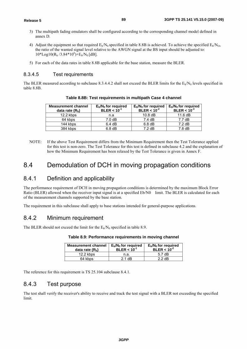
3GPP
3GPP TS 25.141 V5.15.0 (2007-09)89Release 5
3) The multipath fading emulators shall be configured according to the corresponding channel model defined in annex D.
4) Adjust the equipment so that required Eb/N0 specified in table 8.8B is achieved. To achieve the specified Eb/NO, the ratio of the wanted signal level relative to the AWGN signal at the BS input should be adjusted to: 10*Log10(Rb /3.84*106)+Eb/N0 [dB].
5) For each of the data rates in table 8.8B applicable for the base station, measure the BLER.
8.3.4.5 Test requirements
The BLER measured according to subclause 8.3.4.4.2 shall not exceed the BLER limits for the Eb/N0 levels specified in table 8.8B.
Table 8.8B: Test requirements in multipath Case 4 channel
Measurement channel data rate (Rb)
Eb/N0 for required BLER < 10-1
Eb/N0 for requiredBLER < 10-2
Eb/N0 for required BLER < 10-3
12.2 kbps n.a 10.8 dB 11.6 dB 64 kbps 7.0 dB 7.4 dB 7.7 dB
144 kbps 6.4 dB 6.8 dB 7.2 dB 384 kbps 6.8 dB 7.2 dB 7.8 dB
NOTE: If the above Test Requirement differs from the Minimum Requirement then the Test Tolerance applied for this test is non-zero. The Test Tolerance for this test is defined in subclause 4.2 and the explanation of how the Minimum Requirement has been relaxed by the Test Tolerance is given in Annex F.
8.4 Demodulation of DCH in moving propagation conditions
8.4.1 Definition and applicability The performance requirement of DCH in moving propagation conditions is determined by the maximum Block Error Ratio (BLER) allowed when the receiver input signal is at a specified Eb/N0 limit. The BLER is calculated for each of the measurement channels supported by the base station.
The requirement in this subclause shall apply to base stations intended for general-purpose applications.
8.4.2 Minimum requirement The BLER should not exceed the limit for the Eb/N0 specified in table 8.9.
Table 8.9: Performance requirements in moving channel
Measurement channel data rate (Rb)
Eb/N0 for required BLER < 10-1
Eb/N0 for required BLER < 10-2
12.2 kbps n.a. 5.7 dB 64 kbps 2.1 dB 2.2 dB
The reference for this requirement is TS 25.104 subclause 8.4.1.
8.4.3 Test purpose The test shall verify the receiver's ability to receive and track the test signal with a BLER not exceeding the specified limit.
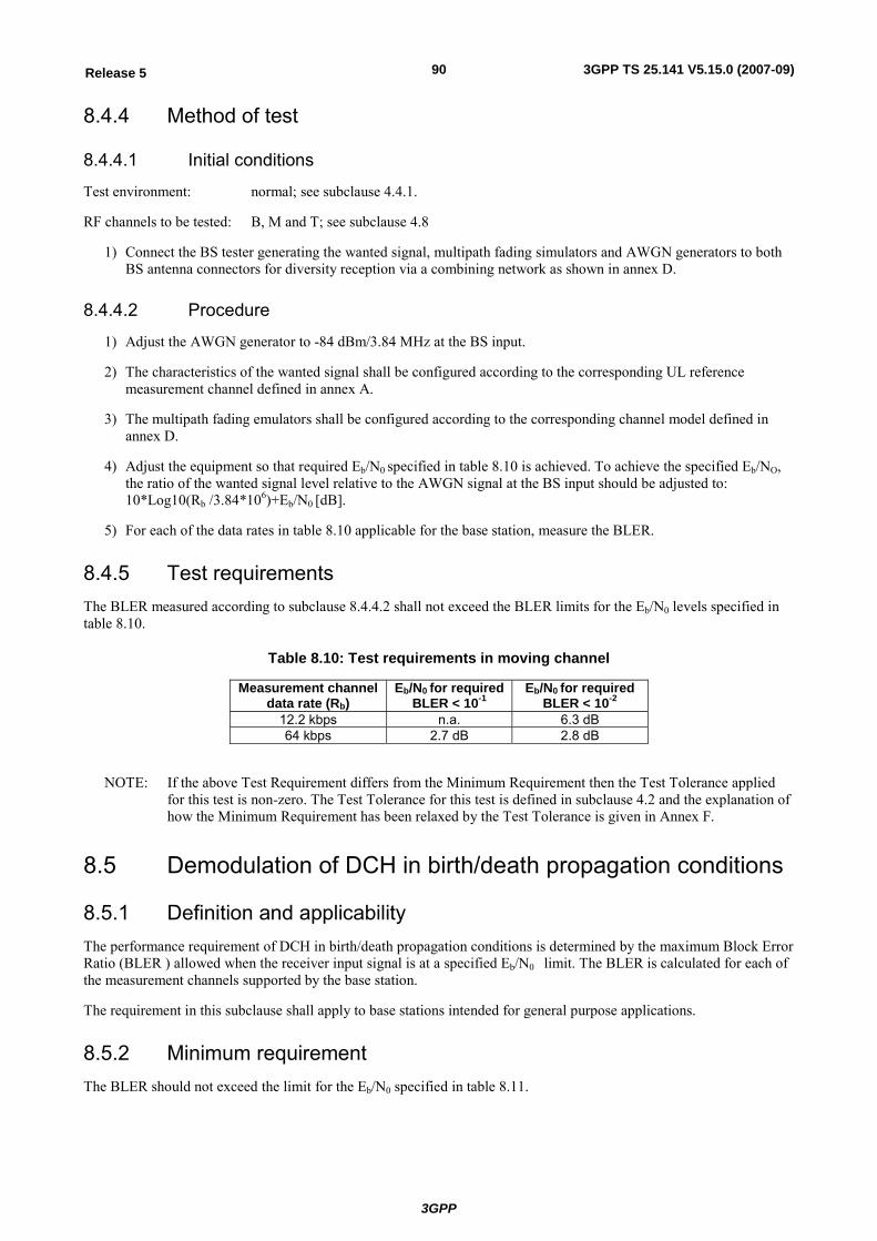
3GPP
3GPP TS 25.141 V5.15.0 (2007-09)90Release 5
8.4.4 Method of test
8.4.4.1 Initial conditions
Test environment: normal; see subclause 4.4.1.
RF channels to be tested: B, M and T; see subclause 4.8
1) Connect the BS tester generating the wanted signal, multipath fading simulators and AWGN generators to both BS antenna connectors for diversity reception via a combining network as shown in annex D.
8.4.4.2 Procedure
1) Adjust the AWGN generator to -84 dBm/3.84 MHz at the BS input.
2) The characteristics of the wanted signal shall be configured according to the corresponding UL reference measurement channel defined in annex A.
3) The multipath fading emulators shall be configured according to the corresponding channel model defined in annex D.
4) Adjust the equipment so that required Eb/N0 specified in table 8.10 is achieved. To achieve the specified Eb/NO, the ratio of the wanted signal level relative to the AWGN signal at the BS input should be adjusted to: 10*Log10(Rb /3.84*106)+Eb/N0 [dB].
5) For each of the data rates in table 8.10 applicable for the base station, measure the BLER.
8.4.5 Test requirements The BLER measured according to subclause 8.4.4.2 shall not exceed the BLER limits for the Eb/N0 levels specified in table 8.10.
Table 8.10: Test requirements in moving channel
Measurement channel data rate (Rb)
Eb/N0 for required BLER < 10-1
Eb/N0 for required BLER < 10-2
12.2 kbps n.a. 6.3 dB 64 kbps 2.7 dB 2.8 dB
NOTE: If the above Test Requirement differs from the Minimum Requirement then the Test Tolerance applied for this test is non-zero. The Test Tolerance for this test is defined in subclause 4.2 and the explanation of how the Minimum Requirement has been relaxed by the Test Tolerance is given in Annex F.
8.5 Demodulation of DCH in birth/death propagation conditions
8.5.1 Definition and applicability The performance requirement of DCH in birth/death propagation conditions is determined by the maximum Block Error Ratio (BLER ) allowed when the receiver input signal is at a specified Eb/N0 limit. The BLER is calculated for each of the measurement channels supported by the base station.
The requirement in this subclause shall apply to base stations intended for general purpose applications.
8.5.2 Minimum requirement The BLER should not exceed the limit for the Eb/N0 specified in table 8.11.
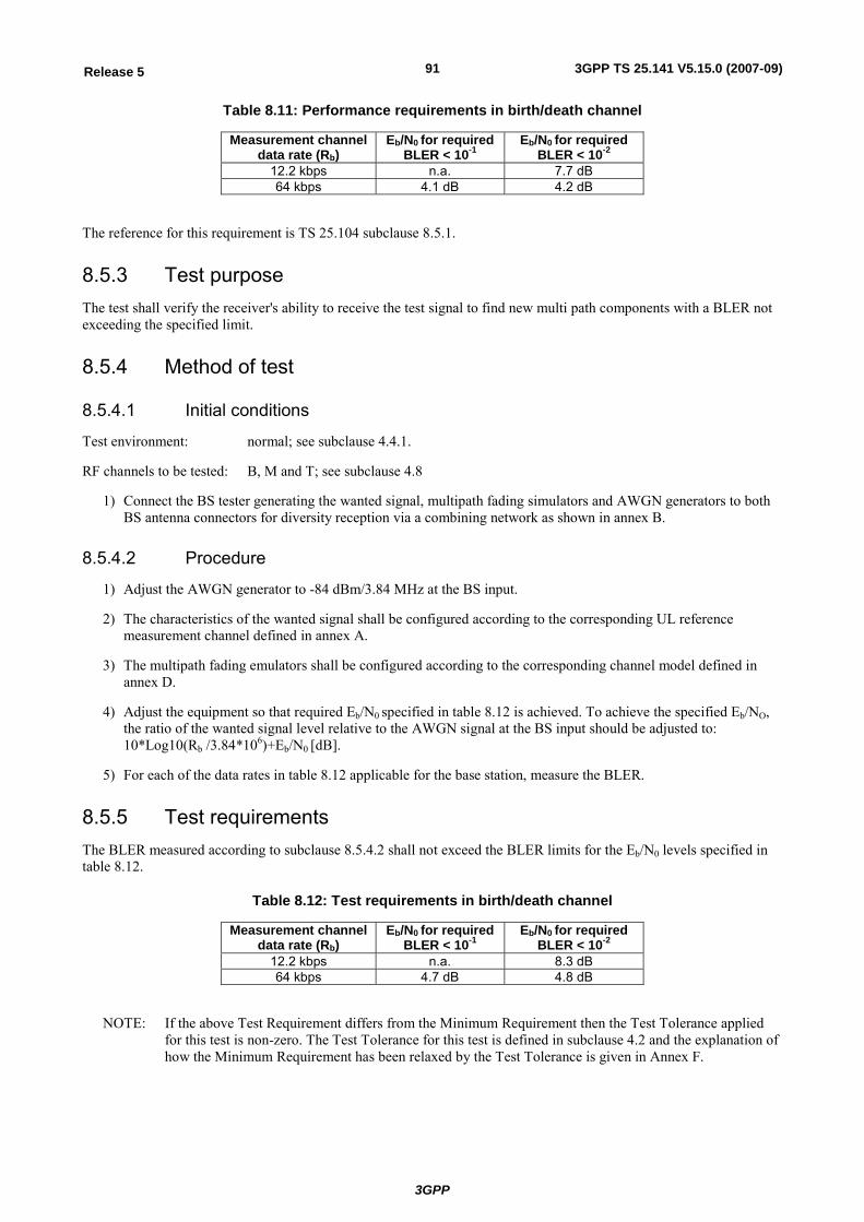
3GPP
3GPP TS 25.141 V5.15.0 (2007-09)91Release 5
Table 8.11: Performance requirements in birth/death channel
Measurement channel data rate (Rb)
Eb/N0 for required BLER < 10-1
Eb/N0 for required BLER < 10-2
12.2 kbps n.a. 7.7 dB 64 kbps 4.1 dB 4.2 dB
The reference for this requirement is TS 25.104 subclause 8.5.1.
8.5.3 Test purpose The test shall verify the receiver's ability to receive the test signal to find new multi path components with a BLER not exceeding the specified limit.
8.5.4 Method of test
8.5.4.1 Initial conditions
Test environment: normal; see subclause 4.4.1.
RF channels to be tested: B, M and T; see subclause 4.8
1) Connect the BS tester generating the wanted signal, multipath fading simulators and AWGN generators to both BS antenna connectors for diversity reception via a combining network as shown in annex B.
8.5.4.2 Procedure
1) Adjust the AWGN generator to -84 dBm/3.84 MHz at the BS input.
2) The characteristics of the wanted signal shall be configured according to the corresponding UL reference measurement channel defined in annex A.
3) The multipath fading emulators shall be configured according to the corresponding channel model defined in annex D.
4) Adjust the equipment so that required Eb/N0 specified in table 8.12 is achieved. To achieve the specified Eb/NO, the ratio of the wanted signal level relative to the AWGN signal at the BS input should be adjusted to: 10*Log10(Rb /3.84*106)+Eb/N0 [dB].
5) For each of the data rates in table 8.12 applicable for the base station, measure the BLER.
8.5.5 Test requirements The BLER measured according to subclause 8.5.4.2 shall not exceed the BLER limits for the Eb/N0 levels specified in table 8.12.
Table 8.12: Test requirements in birth/death channel
Measurement channel data rate (Rb)
Eb/N0 for required BLER < 10-1
Eb/N0 for required BLER < 10-2
12.2 kbps n.a. 8.3 dB 64 kbps 4.7 dB 4.8 dB
NOTE: If the above Test Requirement differs from the Minimum Requirement then the Test Tolerance applied for this test is non-zero. The Test Tolerance for this test is defined in subclause 4.2 and the explanation of how the Minimum Requirement has been relaxed by the Test Tolerance is given in Annex F.
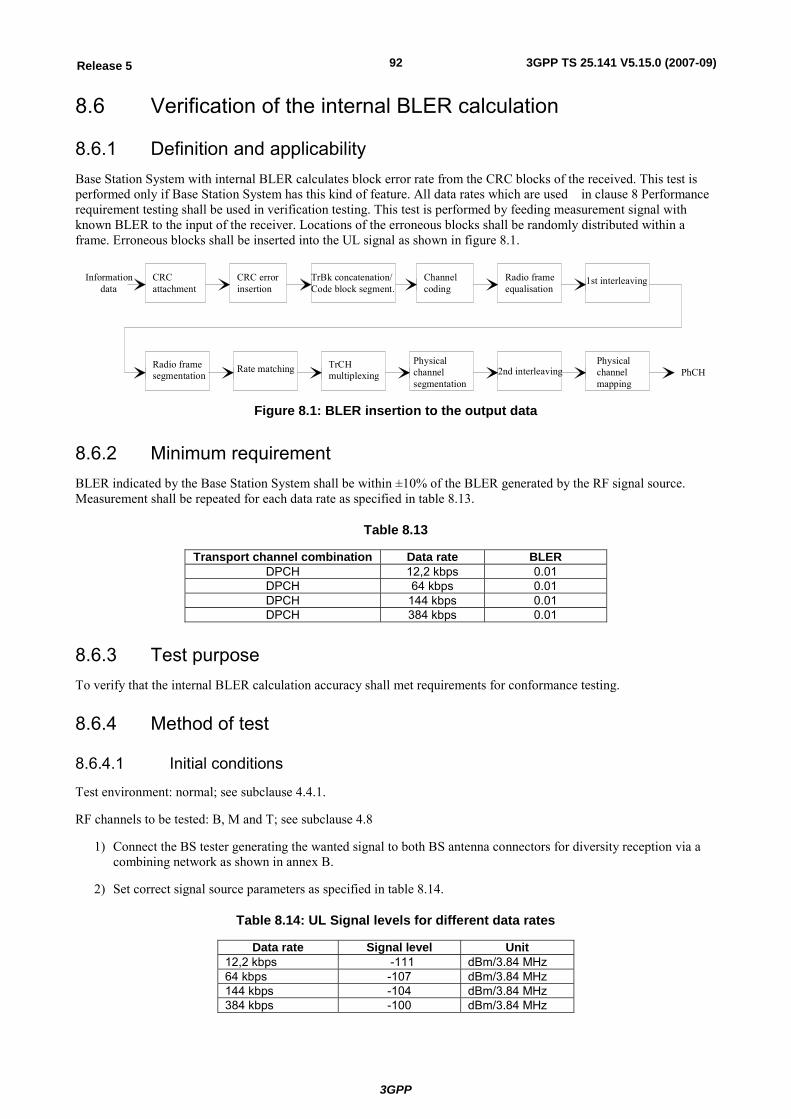
3GPP
3GPP TS 25.141 V5.15.0 (2007-09)92Release 5
8.6 Verification of the internal BLER calculation
8.6.1 Definition and applicability Base Station System with internal BLER calculates block error rate from the CRC blocks of the received. This test is performed only if Base Station System has this kind of feature. All data rates which are used in clause 8 Performance requirement testing shall be used in verification testing. This test is performed by feeding measurement signal with known BLER to the input of the receiver. Locations of the erroneous blocks shall be randomly distributed within a frame. Erroneous blocks shall be inserted into the UL signal as shown in figure 8.1.
CRC error insertion
CRC attachment
TrBk concatenation/Code block segment.
Channelcoding
Radio frameequalisation
1st interleaving
Radio framesegmentation
Rate matching TrCH multiplexing
Physical channelsegmentation
Physical channelmapping
2nd interleaving
Information data
PhCH
Figure 8.1: BLER insertion to the output data
8.6.2 Minimum requirement BLER indicated by the Base Station System shall be within ±10% of the BLER generated by the RF signal source. Measurement shall be repeated for each data rate as specified in table 8.13.
Table 8.13
Transport channel combination Data rate BLER DPCH 12,2 kbps 0.01 DPCH 64 kbps 0.01 DPCH 144 kbps 0.01 DPCH 384 kbps 0.01
8.6.3 Test purpose To verify that the internal BLER calculation accuracy shall met requirements for conformance testing.
8.6.4 Method of test
8.6.4.1 Initial conditions
Test environment: normal; see subclause 4.4.1.
RF channels to be tested: B, M and T; see subclause 4.8
1) Connect the BS tester generating the wanted signal to both BS antenna connectors for diversity reception via a combining network as shown in annex B.
2) Set correct signal source parameters as specified in table 8.14.
Table 8.14: UL Signal levels for different data rates
Data rate Signal level Unit 12,2 kbps -111 dBm/3.84 MHz 64 kbps -107 dBm/3.84 MHz 144 kbps -104 dBm/3.84 MHz 384 kbps -100 dBm/3.84 MHz
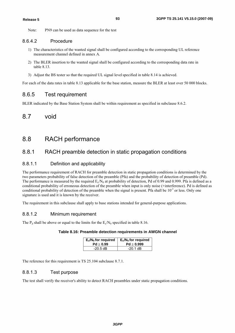
3GPP
3GPP TS 25.141 V5.15.0 (2007-09)93Release 5
Note: PN9 can be used as data sequence for the test
8.6.4.2 Procedure
1) The characteristics of the wanted signal shall be configured according to the corresponding UL reference measurement channel defined in annex A.
2) The BLER insertion to the wanted signal shall be configured according to the corresponding data rate in table 8.13.
3) Adjust the BS tester so that the required UL signal level specified in table 8.14 is achieved.
For each of the data rates in table 8.13 applicable for the base station, measure the BLER at least over 50 000 blocks.
8.6.5 Test requirement BLER indicated by the Base Station System shall be within requirement as specified in subclause 8.6.2.
8.7 void
8.8 RACH performance
8.8.1 RACH preamble detection in static propagation conditions
8.8.1.1 Definition and applicability
The performance requirement of RACH for preamble detection in static propagation conditions is determined by the two parameters probability of false detection of the preamble (Pfa) and the probability of detection of preamble (Pd). The performance is measured by the required Ec/N0 at probability of detection, Pd of 0.99 and 0.999. Pfa is defined as a conditional probability of erroneous detection of the preamble when input is only noise (+interference). Pd is defined as conditional probability of detection of the preamble when the signal is present. Pfa shall be 10-3 or less. Only one signature is used and it is known by the receiver.
The requirement in this subclause shall apply to base stations intended for general-purpose applications.
8.8.1.2 Minimum requirement
The Pd shall be above or equal to the limits for the Ec/N0 specified in table 8.16.
Table 8.16: Preamble detection requirements in AWGN channel
Ec/N0 for requiredPd ≥ 0.99
Ec/N0 for requiredPd ≥ 0.999
-20.5 dB -20.1 dB
The reference for this requirement is TS 25.104 subclause 8.7.1.
8.8.1.3 Test purpose
The test shall verify the receiver's ability to detect RACH preambles under static propagation conditions.
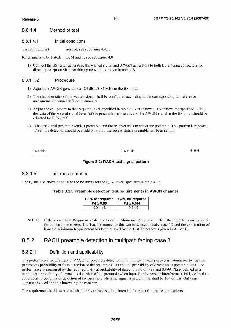
3GPP
3GPP TS 25.141 V5.15.0 (2007-09)94Release 5
8.8.1.4 Method of test
8.8.1.4.1 Initial conditions
Test environment: normal; see subclause 4.4.1.
RF channels to be tested: B, M and T; see subclause 4.8
1) Connect the BS tester generating the wanted signal and AWGN generators to both BS antenna connectors for diversity reception via a combining network as shown in annex B.
8.8.1.4.2 Procedure
1) Adjust the AWGN generator to -84 dBm/3.84 MHz at the BS input.
2) The characteristics of the wanted signal shall be configured according to the corresponding UL reference measurement channel defined in annex A.
3) Adjust the equipment so that required Ec/N0 specified in table 8.17 is achieved. To achieve the specified Ec/NO, the ratio of the wanted signal level (of the preamble part) relative to the AWGN signal at the BS input should be adjusted to: Ec/N0 [dB].
4) The test signal generator sends a preamble and the receiver tries to detect the preamble. This pattern is repeated. Preamble detection should be made only on those access slots a preamble has been sent in.
Preamble Preamble
Figure 8.2: RACH test signal pattern
8.8.1.5 Test requirements
The Pd shall be above or equal to the Pd limits for the Ec/N0 levels specified in table 8.17.
Table 8.17: Preamble detection test requirements in AWGN channel
Ec/N0 for requiredPd ≥ 0.99
Ec/N0 for requiredPd ≥ 0.999
-20.1 dB -19.7 dB
NOTE: If the above Test Requirement differs from the Minimum Requirement then the Test Tolerance applied for this test is non-zero. The Test Tolerance for this test is defined in subclause 4.2 and the explanation of how the Minimum Requirement has been relaxed by the Test Tolerance is given in Annex F.
8.8.2 RACH preamble detection in multipath fading case 3
8.8.2.1 Definition and applicability
The performance requirement of RACH for preamble detection in in multipath fading case 3 is determined by the two parameters probability of false detection of the preamble (Pfa) and the probability of detection of preamble (Pd). The performance is measured by the required Ec/N0 at probability of detection, Pd of 0.99 and 0.999. Pfa is defined as a conditional probability of erroneous detection of the preamble when input is only noise (+interference). Pd is defined as conditional probability of detection of the preamble when the signal is present. Pfa shall be 10-3 or less. Only one signature is used and it is known by the receiver.
The requirement in this subclause shall apply to base stations intended for general-purpose applications.
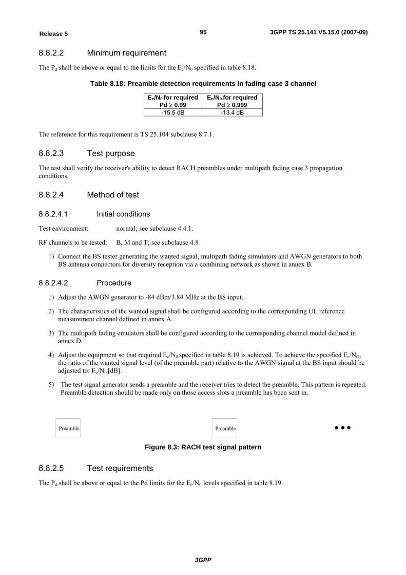
3GPP
3GPP TS 25.141 V5.15.0 (2007-09)95Release 5
8.8.2.2 Minimum requirement
The Pd shall be above or equal to the limits for the Ec/N0 specified in table 8.18.
Table 8.18: Preamble detection requirements in fading case 3 channel
Ec/N0 for requiredPd ≥ 0.99
Ec/N0 for requiredPd ≥ 0.999
-15.5 dB -13.4 dB
The reference for this requirement is TS 25.104 subclause 8.7.1.
8.8.2.3 Test purpose
The test shall verify the receiver's ability to detect RACH preambles under multipath fading case 3 propagation conditions.
8.8.2.4 Method of test
8.8.2.4.1 Initial conditions
Test environment: normal; see subclause 4.4.1.
RF channels to be tested: B, M and T; see subclause 4.8
1) Connect the BS tester generating the wanted signal, multipath fading simulators and AWGN generators to both BS antenna connectors for diversity reception via a combining network as shown in annex B.
8.8.2.4.2 Procedure
1) Adjust the AWGN generator to -84 dBm/3.84 MHz at the BS input.
2) The characteristics of the wanted signal shall be configured according to the corresponding UL reference measurement channel defined in annex A.
3) The multipath fading emulators shall be configured according to the corresponding channel model defined in annex D.
4) Adjust the equipment so that required Ec/N0 specified in table 8.19 is achieved. To achieve the specified Ec/NO, the ratio of the wanted signal level (of the preamble part) relative to the AWGN signal at the BS input should be adjusted to: Ec/N0 [dB].
5) The test signal generator sends a preamble and the receiver tries to detect the preamble. This pattern is repeated. Preamble detection should be made only on those access slots a preamble has been sent in.
Preamble Preamble
Figure 8.3: RACH test signal pattern
8.8.2.5 Test requirements
The Pd shall be above or equal to the Pd limits for the Ec/N0 levels specified in table 8.19.
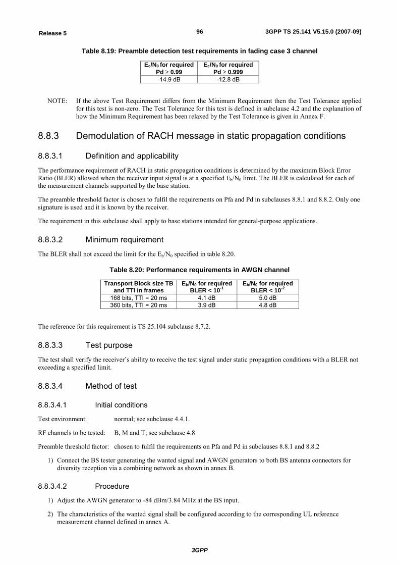
3GPP
3GPP TS 25.141 V5.15.0 (2007-09)96Release 5
Table 8.19: Preamble detection test requirements in fading case 3 channel
Ec/N0 for requiredPd ≥ 0.99
Ec/N0 for requiredPd ≥ 0.999
-14.9 dB -12.8 dB
NOTE: If the above Test Requirement differs from the Minimum Requirement then the Test Tolerance applied for this test is non-zero. The Test Tolerance for this test is defined in subclause 4.2 and the explanation of how the Minimum Requirement has been relaxed by the Test Tolerance is given in Annex F.
8.8.3 Demodulation of RACH message in static propagation conditions
8.8.3.1 Definition and applicability
The performance requirement of RACH in static propagation conditions is determined by the maximum Block Error Ratio (BLER) allowed when the receiver input signal is at a specified Eb/N0 limit. The BLER is calculated for each of the measurement channels supported by the base station.
The preamble threshold factor is chosen to fulfil the requirements on Pfa and Pd in subclauses 8.8.1 and 8.8.2. Only one signature is used and it is known by the receiver.
The requirement in this subclause shall apply to base stations intended for general-purpose applications.
8.8.3.2 Minimum requirement
The BLER shall not exceed the limit for the Eb/N0 specified in table 8.20.
Table 8.20: Performance requirements in AWGN channel
Transport Block size TB and TTI in frames
Eb/N0 for required BLER < 10-1
Eb/N0 for required BLER < 10-2
168 bits, TTI = 20 ms 4.1 dB 5.0 dB 360 bits, TTI = 20 ms 3.9 dB 4.8 dB
The reference for this requirement is TS 25.104 subclause 8.7.2.
8.8.3.3 Test purpose
The test shall verify the receiver’s ability to receive the test signal under static propagation conditions with a BLER not exceeding a specified limit.
8.8.3.4 Method of test
8.8.3.4.1 Initial conditions
Test environment: normal; see subclause 4.4.1.
RF channels to be tested: B, M and T; see subclause 4.8
Preamble threshold factor: chosen to fulfil the requirements on Pfa and Pd in subclauses 8.8.1 and 8.8.2
1) Connect the BS tester generating the wanted signal and AWGN generators to both BS antenna connectors for diversity reception via a combining network as shown in annex B.
8.8.3.4.2 Procedure
1) Adjust the AWGN generator to -84 dBm/3.84 MHz at the BS input.
2) The characteristics of the wanted signal shall be configured according to the corresponding UL reference measurement channel defined in annex A.
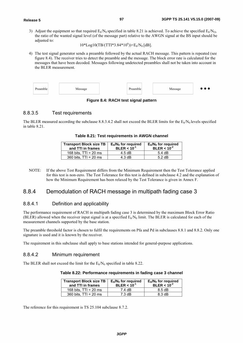
3GPP
3GPP TS 25.141 V5.15.0 (2007-09)97Release 5
3) Adjust the equipment so that required Eb/N0 specified in table 8.21 is achieved. To achieve the specified Eb/NO, the ratio of the wanted signal level (of the message part) relative to the AWGN signal at the BS input should be adjusted to:
10*Log10(TB/(TTI*3.84*106))+Eb/N0 [dB].
4) The test signal generator sends a preamble followed by the actual RACH message. This pattern is repeated (see figure 8.4). The receiver tries to detect the preamble and the message. The block error rate is calculated for the messages that have been decoded. Messages following undetected preambles shall not be taken into account in the BLER measurement.
Preamble Message Preamble Message
Figure 8.4: RACH test signal pattern
8.8.3.5 Test requirements
The BLER measured according the subclause 8.8.3.4.2 shall not exceed the BLER limits for the Eb/N0 levels specified in table 8.21.
Table 8.21: Test requirements in AWGN channel
Transport Block size TB and TTI in frames
Eb/N0 for required BLER < 10-1
Eb/N0 for required BLER < 10-2
168 bits, TTI = 20 ms 4.5 dB 5.4 dB 360 bits, TTI = 20 ms 4.3 dB 5.2 dB
NOTE: If the above Test Requirement differs from the Minimum Requirement then the Test Tolerance applied for this test is non-zero. The Test Tolerance for this test is defined in subclause 4.2 and the explanation of how the Minimum Requirement has been relaxed by the Test Tolerance is given in Annex F.
8.8.4 Demodulation of RACH message in multipath fading case 3
8.8.4.1 Definition and applicability
The performance requirement of RACH in multipath fading case 3 is determined by the maximum Block Error Ratio (BLER) allowed when the receiver input signal is at a specified Eb/N0 limit. The BLER is calculated for each of the measurement channels supported by the base station.
The preamble threshold factor is chosen to fulfil the requirements on Pfa and Pd in subclauses 8.8.1 and 8.8.2. Only one signature is used and it is known by the receiver.
The requirement in this subclause shall apply to base stations intended for general-purpose applications.
8.8.4.2 Minimum requirement
The BLER shall not exceed the limit for the Eb/N0 specified in table 8.22.
Table 8.22: Performance requirements in fading case 3 channel
Transport Block size TB and TTI in frames
Eb/N0 for required BLER < 10-1
Eb/N0 for required BLER < 10-2
168 bits, TTI = 20 ms 7.4 dB 8.5 dB 360 bits, TTI = 20 ms 7.3 dB 8.3 dB
The reference for this requirement is TS 25.104 subclause 8.7.2.
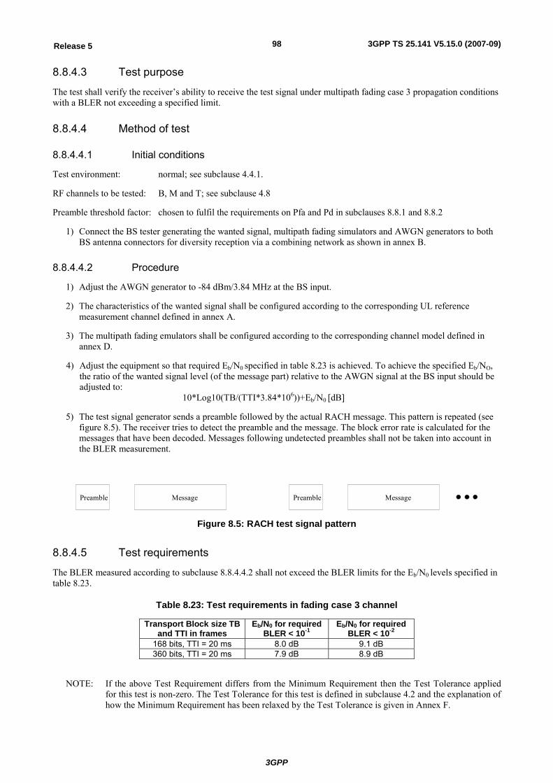
3GPP
3GPP TS 25.141 V5.15.0 (2007-09)98Release 5
8.8.4.3 Test purpose
The test shall verify the receiver’s ability to receive the test signal under multipath fading case 3 propagation conditions with a BLER not exceeding a specified limit.
8.8.4.4 Method of test
8.8.4.4.1 Initial conditions
Test environment: normal; see subclause 4.4.1.
RF channels to be tested: B, M and T; see subclause 4.8
Preamble threshold factor: chosen to fulfil the requirements on Pfa and Pd in subclauses 8.8.1 and 8.8.2
1) Connect the BS tester generating the wanted signal, multipath fading simulators and AWGN generators to both BS antenna connectors for diversity reception via a combining network as shown in annex B.
8.8.4.4.2 Procedure
1) Adjust the AWGN generator to -84 dBm/3.84 MHz at the BS input.
2) The characteristics of the wanted signal shall be configured according to the corresponding UL reference measurement channel defined in annex A.
3) The multipath fading emulators shall be configured according to the corresponding channel model defined in annex D.
4) Adjust the equipment so that required Eb/N0 specified in table 8.23 is achieved. To achieve the specified Eb/NO, the ratio of the wanted signal level (of the message part) relative to the AWGN signal at the BS input should be adjusted to:
10*Log10(TB/(TTI*3.84*106))+Eb/N0 [dB]
5) The test signal generator sends a preamble followed by the actual RACH message. This pattern is repeated (see figure 8.5). The receiver tries to detect the preamble and the message. The block error rate is calculated for the messages that have been decoded. Messages following undetected preambles shall not be taken into account in the BLER measurement.
Preamble Message Preamble Message
Figure 8.5: RACH test signal pattern
8.8.4.5 Test requirements
The BLER measured according to subclause 8.8.4.4.2 shall not exceed the BLER limits for the Eb/N0 levels specified in table 8.23.
Table 8.23: Test requirements in fading case 3 channel
Transport Block size TB and TTI in frames
Eb/N0 for required BLER < 10-1
Eb/N0 for required BLER < 10-2
168 bits, TTI = 20 ms 8.0 dB 9.1 dB 360 bits, TTI = 20 ms 7.9 dB 8.9 dB
NOTE: If the above Test Requirement differs from the Minimum Requirement then the Test Tolerance applied for this test is non-zero. The Test Tolerance for this test is defined in subclause 4.2 and the explanation of how the Minimum Requirement has been relaxed by the Test Tolerance is given in Annex F.
3GPP
3GPP TS 25.141 V5.15.0 (2007-09)99Release 5
8.9 Void Table 8.24: Void
Figure 8.6: Void
Table 8.25: Void
Table 8.26: Void
Figure 8.7: Void
Table 8.27: Void
8.10 Void Table 8.28: Void
Table 8.29: Void
3GPP
3GPP TS 25.141 V5.15.0 (2007-09)100Release 5
Annex A (normative): Measurement channels
A.1 Summary of UL reference measurement channels The parameters for the UL reference measurement channels are specified in Table A.1 and the channel coding is detailed in figure A.2 through A.6 respectively.
NOTE: For all cases, one DPCCH shall be attached to DPDCH(s).
Table A.1: Reference measuremet channels for UL DCH
Parameter DCH for DTCH / DCH for DCCH Unit Information bit rate 12,2/2,4 64/2,4 144/2,4 384/2,4 kbps Physical channel 60/15 240/15 480/15 960/15 kbps Spreading factor 64 16 8 4 Repetition rate 22/22 19/19 8/9 -18/-17 % Interleaving 20 40 40 40 ms
DPDCH
Number of DPDCHs 1 1 1 1 Dedicated pilot 6 bit/slot Power control 2 bit/slot TFCI 2 bit/slot FBI 0 / 2 bit/slot
DPCCH
Spreading factor 256 Power ratio of DPCCH/DPDCH
-2,69 -5,46 -9,54 -9,54 dB
Amplitude ratio of DPCCH/DPDCH
0,7333 0,5333 0,3333 0,3333
Note: Combination of TFCI bit of 0 bit/slot and FBI bit of 2 bit /slot is applied in test of Site Selection Diversity Transmission specified in 8.10.
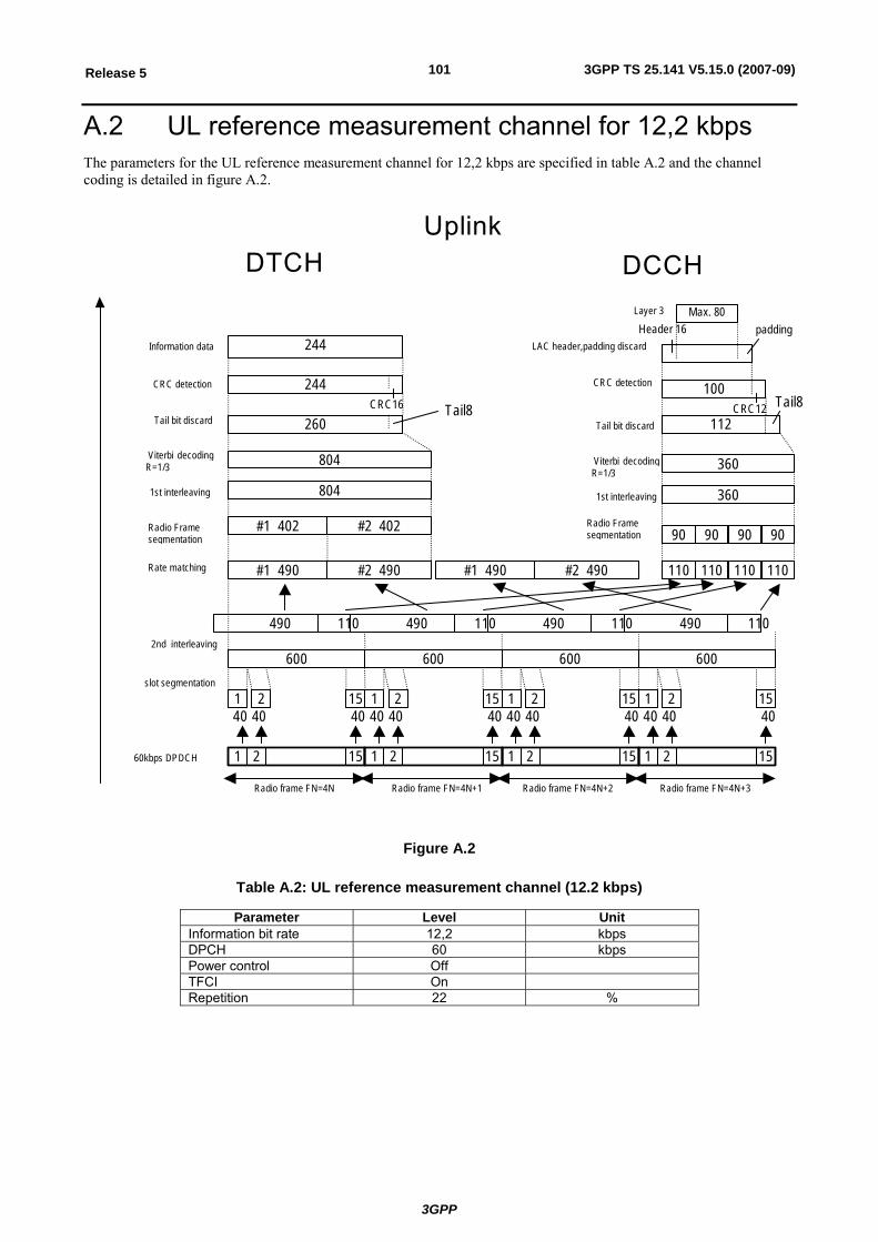
3GPP
3GPP TS 25.141 V5.15.0 (2007-09)101Release 5
A.2 UL reference measurement channel for 12,2 kbps The parameters for the UL reference measurement channel for 12,2 kbps are specified in table A.2 and the channel coding is detailed in figure A.2.
DCCH Uplink
DTCH
60kbps DPDCH
Viterbi decoding R=1/3
Radio frame FN=4N+1 Radio frame FN=4N+2 Radio frame FN=4N+3 Radio frame FN=4N
Information data
CRC detection
Tail bit discard
Rate matching
2nd interleaving 600
40 401
40
490 110
110
804
260 Tail8 CRC16
244
244
360
112Tail8
100
Header 16
CRC12
paddingMax. 80
1st interleaving
Radio Frame segmentation
slot segmentation
CRC detection
Layer 3
LAC header,padding discard
Tail bit discard
Viterbi decoding R=1/3
1st interleaving
#1 402 Radio Frame segmentation
804
#2 402
#2 490#1 490 #2 490#1 490
490 110 490 110 490 110
600 600 600
2 15
1 2 15
40 401
402 15
1 2 15
40 401
40 2 15
1 2 15
40 40 1
402 15
1 2 15
110 110 110
90 90 90 90
360
Figure A.2
Table A.2: UL reference measurement channel (12.2 kbps)
Parameter Level Unit Information bit rate 12,2 kbps DPCH 60 kbps Power control Off TFCI On Repetition 22 %
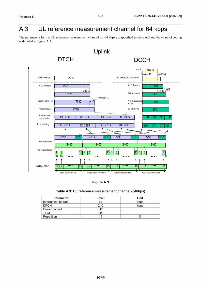
3GPP
3GPP TS 25.141 V5.15.0 (2007-09)102Release 5
A.3 UL reference measurement channel for 64 kbps The parameters for the UL reference measurement channel for 64 kbps are specified in table A.3 and the channel coding is detailed in figure A.3.
DCCH Uplink
DTCH
240kbps DPDCH
Turbo Code R=1/3
1 2 15 • • • • 1 2 15• • • • 1 2 15• • • • 1 2 15 • • • •
Radio frame FN=4N+1 Radio frame FN=4N+2 Radio frame FN=4N+3 Radio frame FN=4N
Information data
CRC detection
Rate matching
2nd interleaving 2400
160 160 1 2 15
• • • • 1 2 15
• • • •1 2 15
• • • •1 2
160 15
• • • •
2293 107 2293 107 2293 107 2293
#1 2293 #2 2293 #3 2293 #4 2293 107 107 107 107
2400 2400 2400
7740
7740
2576 Termination 12
CRC16
2560
2560
107
360
360
112 Tail8
100
Header 16
CRC12
padding Max. 80
1st interleaving
Radio Frame segmentation
slot segmentation
CRC detection
Layer 3
LAC header,padding discard
Tail bit discard
Viterbi decoding R=1/3
1st interleving
#1 1935 #2 1935 #3 1935 #4 1935 90 90 90 90
Figure A.3
Table A.3: UL reference measurement channel (64kbps)
Parameter Level Unit Information bit rate 64 kbps DPCH 240 kbps Power control Off TFCI On Repetition 19 %
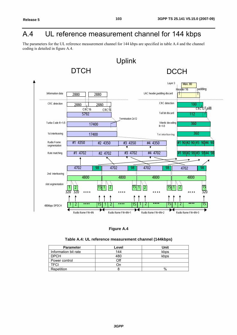
3GPP
3GPP TS 25.141 V5.15.0 (2007-09)103Release 5
A.4 UL reference measurement channel for 144 kbps The parameters for the UL reference measurement channel for 144 kbps are specified in table A.4 and the channel coding is detailed in figure A.4.
DCCH Uplink
DTCH
480kbps DPDCH
Turbo Code R=1/3
1 2 15• • • • 1 2 15• • • • 1 2 15 • • • • 1 2 15• • • •
Radio frame FN=4N+1 Radio frame FN=4N+2 Radio frame FN=4N+3 Radio frame FN=4N
Information data
CRC detection
Rate matching
2nd interleaving 4800
320 320 1 2 15
• • • • 1 2 15
• • • •1 2 15
• • • •1 2
320 15
• • • •
4702
98 4702 98 4702 98 4702
#1 4702 #2 4702 #3 4702 #4 4702 #1 98 #2 98 #3 98 #4 98
4800 4800 4800
17400
17400
5792 Termination 2x12
CRC16
2880
98
360
360
112 Tail8
100
Header 16
CRC12
paddingMax. 80
1st interleaving
Radio Frame segmentation
slot segmentation
CRC detection
Layer 3
LAC header,padding discard
Tail bit discard
Viterbi decoding R=1/3
1 st interleaving
#1 4350 #2 4350 #3 4350 #4 4350 #1 90 #2 90 #3 90#4 90
2880
2880 2880CRC16
Figure A.4
Table A.4: UL reference measurement channel (144kbps)
Parameter Level Unit Information bit rate 144 kbps DPCH 480 kbps Power control Off TFCI On Repetition 8 %
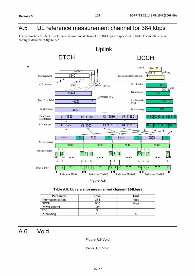
3GPP
3GPP TS 25.141 V5.15.0 (2007-09)104Release 5
A.5 UL reference measurement channel for 384 kbps The parameters for the UL reference measurement channel for 384 kbps are specified in table A.5 and the channel coding is detailed in figure A.5.
DCCH Uplink
DTCH
960kbps DPDCH
Turbo Code R=1/3
1 2 15• • • • 1 2 15• • • • 1 2 15 • • • • 1 2 15• • • •
Radio frame FN=4N+1 Radio frame FN=4N+2 Radio frame FN=4N+3 Radio frame FN=4N
Information data
CRC detection
Rate matching
2nd interleaving 9600
640 640 1 2 15
• • • • 1 2 15
• • • •1 2 15
• • • •1 2
640 15
• • • •
9525
75 9525 75 9525 75 9525
#1 9525 #2 9525 #3 9525 #4 9525 #1 75 #2 75 #3 75#4 75
9600 9600 9600
46320
46320
15424 Termination 4 x12
CRC1615360
75
360
360
112 Tail8
100
Header 16
CRC12
paddingMax. 80
1st interleaving
Radio Frame segmentation
slot segmentation
CRC detection
Layer 3
LAC header,padding discard
Tail bit discard
Viterbi decoding R=1/3
1st interleaving
#1 11580 #2 11580 #3 11580 #4 11580 #1 90 #2 90 #3 90#4 90
38403840 3840 3840 384038403840 3840
Figure A.5
Table A.5: UL reference measurement channel (384kbps)
Parameter Level Unit Information bit rate 384 kbps DPCH 960 kbps Power control Off TFCI On Puncturing 18 %
A.6 Void Figure A.6 Void
Table A.6: Void
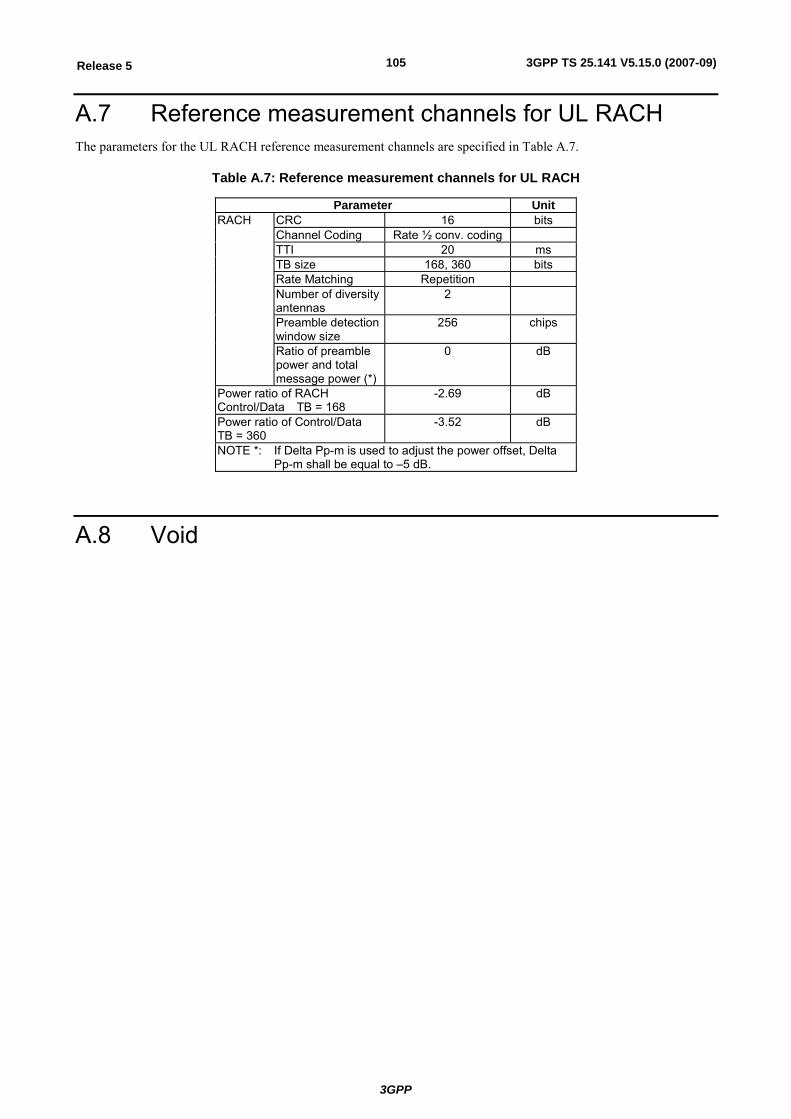
3GPP
3GPP TS 25.141 V5.15.0 (2007-09)105Release 5
A.7 Reference measurement channels for UL RACH The parameters for the UL RACH reference measurement channels are specified in Table A.7.
Table A.7: Reference measurement channels for UL RACH
Parameter Unit CRC 16 bits Channel Coding Rate ½ conv. coding TTI 20 ms TB size 168, 360 bits Rate Matching Repetition Number of diversity antennas
2
Preamble detection window size
256 chips
RACH
Ratio of preamble power and total message power (*)
0 dB
Power ratio of RACH Control/Data TB = 168
-2.69 dB
Power ratio of Control/Data TB = 360
-3.52 dB
NOTE *: If Delta Pp-m is used to adjust the power offset, Delta Pp-m shall be equal to –5 dB.
A.8 Void
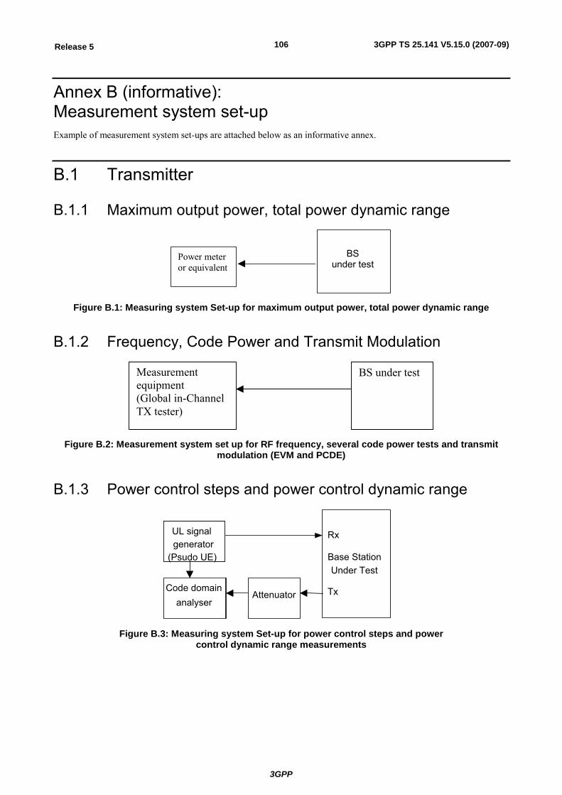
3GPP
3GPP TS 25.141 V5.15.0 (2007-09)106Release 5
Annex B (informative): Measurement system set-up Example of measurement system set-ups are attached below as an informative annex.
B.1 Transmitter
B.1.1 Maximum output power, total power dynamic range
Power meter or equivalent
BS under test
Figure B.1: Measuring system Set-up for maximum output power, total power dynamic range
B.1.2 Frequency, Code Power and Transmit Modulation
Measurement equipment (Global in-Channel TX tester)
BS under test
Figure B.2: Measurement system set up for RF frequency, several code power tests and transmit modulation (EVM and PCDE)
B.1.3 Power control steps and power control dynamic range
UL signal generator
(Psudo UE)
Base Station
Under Test
Attenuator
Code domain
analyser
Rx
Tx
Figure B.3: Measuring system Set-up for power control steps and power control dynamic range measurements
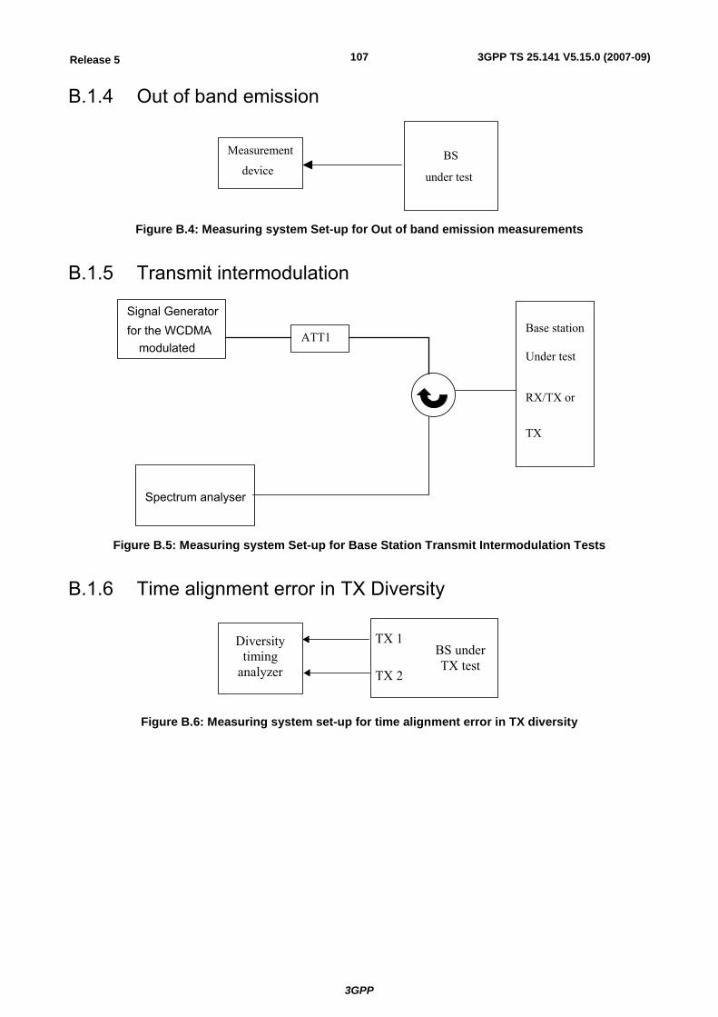
3GPP
3GPP TS 25.141 V5.15.0 (2007-09)107Release 5
B.1.4 Out of band emission
Measurement device
BS
under test
Figure B.4: Measuring system Set-up for Out of band emission measurements
B.1.5 Transmit intermodulation
Base station
Under test
RX/TX or
TX
Spectrum analyser
Signal Generator for the WCDMA
ATT1modulated
Figure B.5: Measuring system Set-up for Base Station Transmit Intermodulation Tests
B.1.6 Time alignment error in TX Diversity
Diversity timing
analyzer
BS under TX test
TX 1
TX 2
Figure B.6: Measuring system set-up for time alignment error in TX diversity
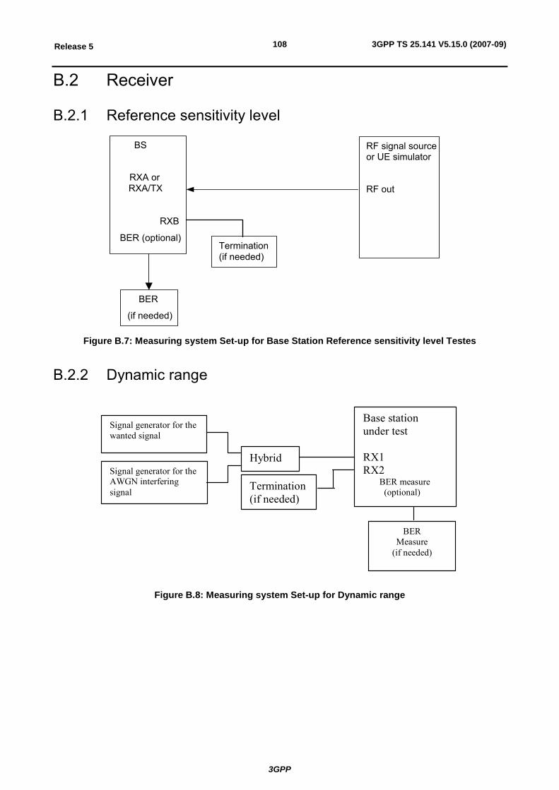
3GPP
3GPP TS 25.141 V5.15.0 (2007-09)108Release 5
B.2 Receiver
B.2.1 Reference sensitivity level
BS
RXA orRXA/TX
RXB
BER (optional)
BER
(if needed)
RF signal source or UE simulator RF out
Termination (if needed)
Figure B.7: Measuring system Set-up for Base Station Reference sensitivity level Testes
B.2.2 Dynamic range
Signal generator for the wanted signal
Signal generator for the AWGN interfering signal
Hybrid
Base station under test RX1 RX2 BER measure (optional)
BER Measure
(if needed)
Termination(if needed)
Figure B.8: Measuring system Set-up for Dynamic range
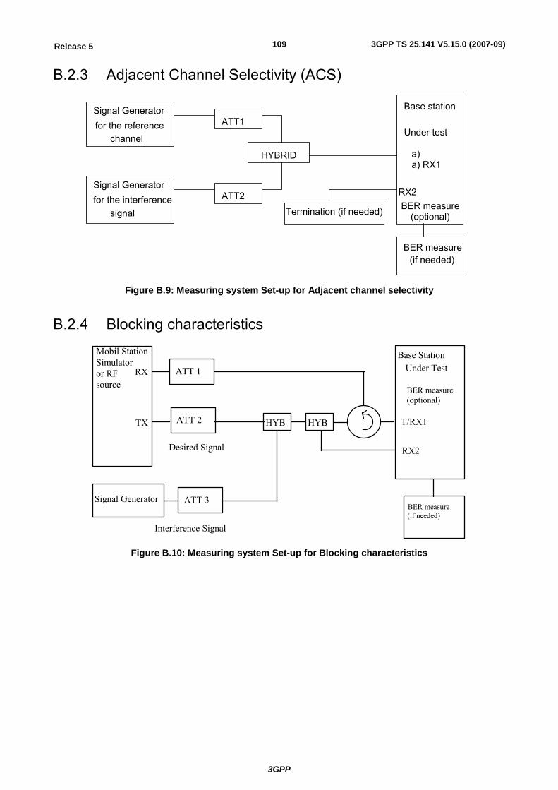
3GPP
3GPP TS 25.141 V5.15.0 (2007-09)109Release 5
B.2.3 Adjacent Channel Selectivity (ACS)
Base station
Under test
a)
a) RX1
RX2
(optional)
HYBRID
ATT2
ATT1Signal Generatorfor the reference
channel
Signal Generatorfor the interference
signal
BER measure
(if needed)
Termination (if needed)
BER measure
Figure B.9: Measuring system Set-up for Adjacent channel selectivity
B.2.4 Blocking characteristics
Mobil StationSimulatoror RFsource
RX
TX
ATT 1
Signal Generator
Under TestBase Station
T/RX1
RX2Desired Signal
Interference Signal
BER measure (if needed)
HYB HYBATT 2
ATT 3
BER measure(optional)
Figure B.10: Measuring system Set-up for Blocking characteristics
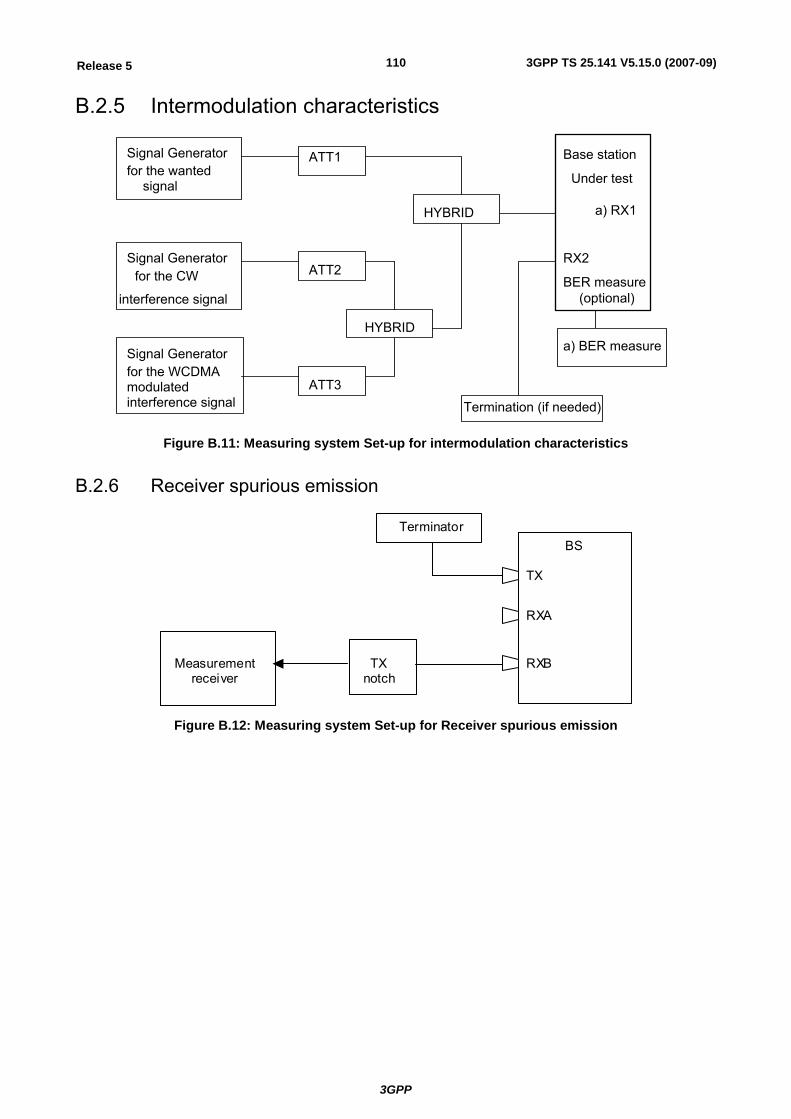
3GPP
3GPP TS 25.141 V5.15.0 (2007-09)110Release 5
B.2.5 Intermodulation characteristics
HYBRID
ATT2
ATT1Signal Generator for the wanted
signal
Signal Generator for the CW
interference signal
Termination (if needed)
Signal Generator for the WCDMA
modulated interference signal
ATT3
HYBRID
Base station
Under test
a) RX1
RX2
BER measure(optional)
a) BER measure
Figure B.11: Measuring system Set-up for intermodulation characteristics
B.2.6 Receiver spurious emission
Measurement receiver
TX notch
BS
TX
RXB
Terminator
RXA
Figure B.12: Measuring system Set-up for Receiver spurious emission
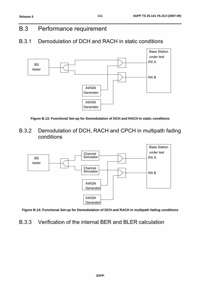
3GPP
3GPP TS 25.141 V5.15.0 (2007-09)111Release 5
B.3 Performance requirement
B.3.1 Demodulation of DCH and RACH in static conditions
RX A
RX B
Base Stationunder test
BS
tester
AWGN Generator
AWGN
Generator
Figure B.13: Functional Set-up for Demodulation of DCH and RACH in static conditions
B.3.2 Demodulation of DCH, RACH and CPCH in multipath fading conditions
RX A
RX B
Base Stationunder test
BS tester
ChannelSimulator
or ChannelSimulator
AWGN Generator
AWGN Generator
Figure B.14: Functional Set-up for Demodulation of DCH and RACH in multipath fading conditions
B.3.3 Verification of the internal BER and BLER calculation
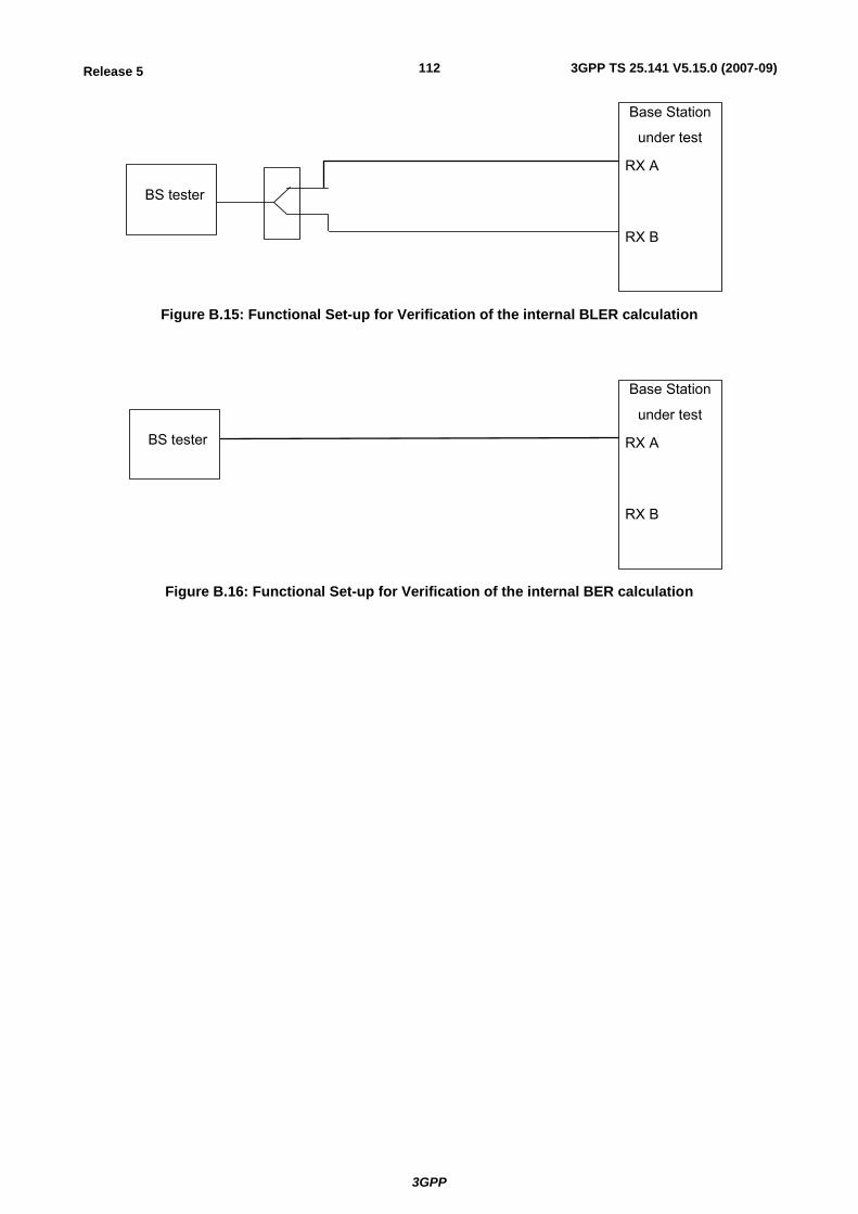
3GPP
3GPP TS 25.141 V5.15.0 (2007-09)112Release 5
BS tester
RX A
RX B
Base Station
under test
Figure B.15: Functional Set-up for Verification of the internal BLER calculation
BS tester RX A
RX B
Base Station
under test
Figure B.16: Functional Set-up for Verification of the internal BER calculation
3GPP
3GPP TS 25.141 V5.15.0 (2007-09)113Release 5
Annex C (normative): General rules for statistical testing
C.1 Statistical testing of receiver BER/BLER performance
C.1.1 Error Definition Bit Error Ration (BER) and Block Error Ratio (BLER) are defined in section 3.1.
C.1.2 Test Method Each test is performed in the following manner:
a) Setup the required test conditions.
b) Record the number of samples tested and the number of occurred events (bit error or block error)
c) Stop the test at a stop criterion which is minimum test time or an early pass or an early fail event.
d) Once the test is stopped decide according to the pass fail decision rules ( subclause C.1.7)
C.1.3 Test Criteria The test shall fulfil the following requirements:
a) good pass fail decision
1) to keep reasonably low the probability (risk) of passing a bad unit for each individual test;
2) to have high probability of passing a good unit for each individual test;
b) good balance between test time and statistical significance
3) to perform measurements with a high degree of statistical significance;
4) to keep the test time as low as possible.
C.1.4 Calculation assumptions
C.1.4.1 Statistical independence a) It is assumed, that error events are rare (lim BER BLER 0) independent statistical events. However the
memory of the convolutional /turbo coder is terminated after one TTI. Samples and errors are summed up every TTI. So the assumption of independent error events is justified.
b) In the BLER test with fading there is the memory of the multipath fading channel which interferes the statistical independence. A minimum test time is introduced to average fluctuations of the multipath fading channel. So the assumption of independent error events is justified approximately.
C.1.4.2 Applied formulas The formulas, applied to describe the BER BLER test, are based on the following experiments:
3GPP
3GPP TS 25.141 V5.15.0 (2007-09)114Release 5
1) After having observed a certain number of errors (ne) the number of samples are counted to calculate BER BLER. Provisions are made (note 1) such that the complementary experiment is valid as well:
2) After a certain number of samples (ns) the number of errors, occurred, are counted to calculate BER BLER.
Experiment 1) stipulates to use the following Chi Square Distribution with degree of freedom ne:
2*dchisq(2*NE,2*ne).
Experiment 2) stipulates to use the Poisson Distribution:
dpois(ne,NE)
(NE: mean of the distribution)
To determine the early stop conditions, the following inverse cumulative operation is applied:
0.5 * qchisq(D,2*ne). This is applicable for experiment (1) and (2).
D: wrong decision risk per test step
Note: other inverse cumulative operations are available, however only this is suited for experiment (1) and (2).
C.1.4.3 Approximation of the distribution The test procedure is as follows:
During a running measurement for a UE ns (number of samples) and ne (number of errors) are accumulated and from this the preliminary BER BLER is calculated. Then new samples up to the next error are taken. The entire past and the new samples are basis for the next preliminary BER BLER. Depending on the result at every step, the UE can pass, can fail or must continue the test.
As early pass- and early fail-UEs leave the statistical totality under consideration, the experimental conditions are changed every step resulting in a distribution that is truncated more and more towards the end of the entire test. Such a distribution can not any more be handled analytically. The unchanged distribution is used as an approximation to calculate the early fail and early pass bounds.
C.1.5 Definition of good pass fail decision. This is defined by the probability of wrong decision F at the end of the test. The probability of a correct decision is 1-F.
The probability (risk) to fail a good DUT shall be ≤ F according to the following definition: The failed DUT is still better than the specified error ratio (Test requirement)with a probability of ≤ F.
The probability to pass a bad DUT shall be ≤ F according to the following definition: The passed DUT is still worse than M times the specified error ratio (M>1 is the bad DUT factor) with a probability of ≤ F.
This definitions lead to an early pass and an early fail limit:
Early fail: ber≥ berlimfail
)*2,(
*2),(limneDqchisq
neneDber fail = (1)
For ne≥7
Early pass: ber ≤berlimbadpass
)*2,1(
**2),(limneDqchisq
MneneDbadber pass −= (2)
3GPP
3GPP TS 25.141 V5.15.0 (2007-09)115Release 5
For ne ≥ 1
With
ber (normalized BER,BLER): BER,BLER according to C.1.1 divided by Test requirement
D: wrong decision probability for a test step . This is a numerically evaluated fraction of F, the wrong decision probability at the end of the test. See table C.1.
ne: Number of error events
M: bad DUT factor see table C.1.
qchisq: inverse-cumulative-function of the chi-squared-distribution
C.1.6 Good balance between test time and statistical significance Three independent test parameters are introduced into the test and shown in Table C.1. These are the obvious basis of test time and statistical significance. From the first two of them four dependent test parameters are derived. The third independent test parameter is justified separately.
Table C.1: independent and dependent test parameters
Independent test parameters Dependent test parameters Test Parameter Value Reference Test parameter Value Reference
Bad DUT factor M 1.5 Tables C.3 to C.6 Early pass/fail condition
Curves Subclause C.1.5 Figure C.1.9
Final probability of wrong pass/fail
decision F
0.2%, (0.02%, note 2)
Subclause C.1.5 Target number of error events
345 Tables C.3 to C.6
Probability of wrong pass/fail
decision per test step D
0.0085%, (0.0008% and
0.008%, note 2)
Test limit factor TL 1.234 Tables C.3 to C.6 Minimum test time Table C.2
The minimum test time is derived from the following justification:
1) For no propagation conditions and static propagation condition
No early fail calculated from fractional number of errors <1 (see note 1)
2) For multipath fading condition
No stop of the test until 990 wavelengths are crossed with the speed given in the fading profile.
3) For birth death propagation conditions
No stop of the test until 200 birth death transitions occur
4) For moving propagation conditions: 628 sec
This is necessary in order to pass all potential critical points in the moving propagation profile 4 times: Maximum rake window, Maximum adjustment speed, Intersection of moving taps
3GPP
3GPP TS 25.141 V5.15.0 (2007-09)116Release 5
Table C.2: minimum Test time
Fading profile Minimum test time Multipath propagation 3 km/h 164 sec Multipath propagation 50 km/h 9.8 sec Multipath propagation 120 km/h 4.1 sec Multipath propagation 250 km/h 2 sec Birth Death propagation 38.2 sec Moving propagation 628 sec
In table C.3 to C.8 the minimum test time is converted in minimum number of samples.
C.1.7 Pass fail decision rules No decision is allowed before the minimum test time is elapsed.
1) If minimum Test time < time for target number of error events then the following applies: The required confidence level 1-F (= correct decision probability) shall be achieved. This is fulfilled at an early pass or early fail event.
For BER:
For every TTI (Transmit Time Interval) sum up the number of bits (ns) and the number if errors (ne) from the beginning of the test and calculate
BER1 (including the artificial error at the beginning of the test (Note 1))and
BER0 (excluding the artificial error at the beginning of the test (Note 1)).
If BER0 is above the early fail limit, fail the DUT.
If BER1 is below the early pass limit, pass the DUT.
Otherwise continue the test
For BLER:
For every TTI sum up the number of blocks (ns) and the number of erroneous blocks (ne) from the beginning of the test and calculate
BLER1 (including the artificial error at the beginning of the test (Note 1))and
BLER0 (excluding the artificial error at the beginning of the test (Note 1)).
If BLER1 is below the early pass limit, pass the DUT.
If BLER0 is above the early fail limit, fail the DUT.
Otherwise continue the test
2) If the minimum test time ≥ time for target error events, then the test runs for the minimum test time and the decision is done by comparing the result with the test limit.
For BER:
For every TTI (Transmit Time Interval) sum up the number of bits (ns) and the number if errors (ne) from the beginning of the test and calculate BER0
For BLER:
For every TTI sum up the number of blocks (ns) and the number of erroneous blocks (ne) from the beginning of the test and calculate BLER0
If BER0/BLER0 is above the test limit, fail the DUT.
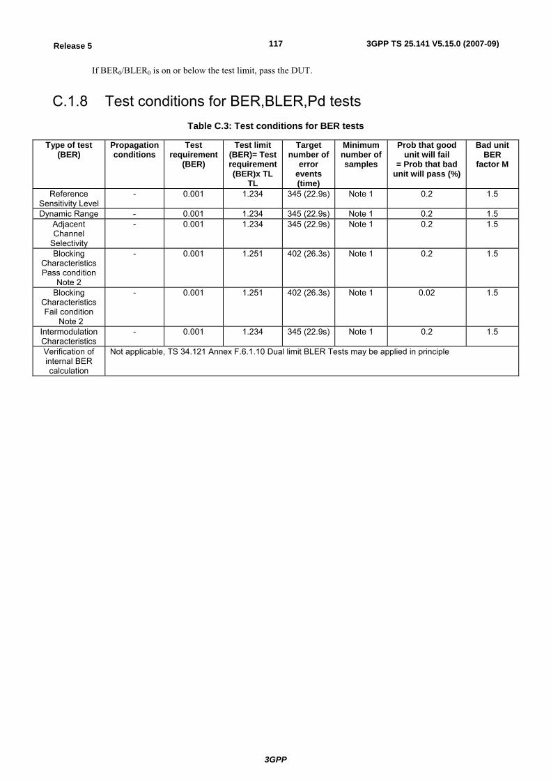
3GPP
3GPP TS 25.141 V5.15.0 (2007-09)117Release 5
If BER0/BLER0 is on or below the test limit, pass the DUT.
C.1.8 Test conditions for BER,BLER,Pd tests Table C.3: Test conditions for BER tests
Type of test (BER)
Propagation conditions
Test requirement
(BER)
Test limit (BER)= Test requirement (BER)x TL
TL
Target number of
error events (time)
Minimum number of samples
Prob that good unit will fail
= Prob that bad unit will pass (%)
Bad unit BER
factor M
Reference Sensitivity Level
- 0.001 1.234 345 (22.9s) Note 1 0.2 1.5
Dynamic Range - 0.001 1.234 345 (22.9s) Note 1 0.2 1.5 Adjacent Channel
Selectivity
- 0.001 1.234 345 (22.9s) Note 1 0.2 1.5
Blocking Characteristics Pass condition
Note 2
- 0.001 1.251 402 (26.3s) Note 1 0.2 1.5
Blocking Characteristics Fail condition
Note 2
- 0.001 1.251 402 (26.3s) Note 1 0.02 1.5
Intermodulation Characteristics
- 0.001 1.234 345 (22.9s) Note 1 0.2 1.5
Verification of internal BER calculation
Not applicable, TS 34.121 Annex F.6.1.10 Dual limit BLER Tests may be applied in principle
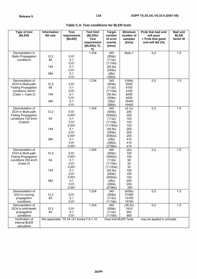
3GPP
3GPP TS 25.141 V5.15.0 (2007-09)118Release 5
Table C.4: Test conditions for BLER tests
Type of test (BLER)
Information Bit rate
Test requirement
(BLER)
Test limit (BLER)=
Test requirement (BLER)x TL
TL
Target number of error events (time)
Minimum number of samples
(time)
Prob that bad unit will pass
= Prob that good unit will fail (%)
Bad unit BLER
factor M
Demodulation in Static Propagation
conditions
12.2 64
144
384
0.01 0.1
0.01 0.1
0.01 0.1
0.01
1.234 345 (559s) (112s)
(1118s) (55.9s) (559s) (28s)
(280s)
Note 1 0.2 1.5
Demodulation of DCH in Multi-path
Fading Propagation conditions 3km/h (Case 1, Case 2)
12.2 64
144
384
0.01 0.1
0.01 0.1
0.01 0.1
0.01
1.234 345 (559s) (112s)
(1118s) (55.9s) (559s) (28s)
(280s)
(164s) 8200 4100 4100 8200 8200
16400 16400
0.2 1.5
Demodulation of DCH in Multi-path
Fading Propagation conditions 120 km/h
(Case3)
12.2
64
144
384
0.01
0.001 0.1
0.01 0.001
0.1 0.01
0.001 0.1
0.01 0.001
1.234 345 (559s)
(5592s) (112s)
(1118s) (11183s)(55.9s) (559s)
(5592s) (28s)
(280s) (2796s)
(4.1s) 205 205 103 103 103 205 205 205 410 410 410
0.2 1.5
Demodulation of DCH in Multi-path
Fading Propagation conditions 250 km/h
(Case 4)
12.2
64
144
384
0.01
0.001 0.1
0.01 0.001
0.1 0.01
0.001 0.1
0.01 0.001
1.234 345 (559s)
(5592s) (112s)
(1118s) (11183s)(55.9s) (559s)
(5592s) (28s)
(280s) (2796s)
(2s) 100 100 50 50 50
100 100 100 200 200 200
0.2 1.5
Demodulation of DCH in moving
propagation conditions
12.2 64
0.01 0.1
0.01
1.234 345 (559s) (112s)
(1118s)
(628s) 31400 15700 15700
0.2
1.5
Demodulation of DCH in birth/death
propagation conditions
12.2 64
0.01 0.1
0.01
1.234 345 (559s) (112s)
(1118s)
(38.2s) 1910 955 955
0.2 1.5
Verification of internal BLER
calculation
Not applicable, TS 34.121 Annex F.6.1.10 Dual limit BLER Tests may be applied in principle
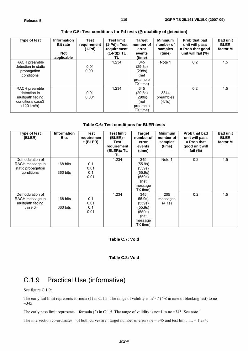
3GPP
3GPP TS 25.141 V5.15.0 (2007-09)119Release 5
Table C.5: Test conditions for Pd tests (Probability of detection)
Type of test InformationBit rate
Not
applicable
Test requirement
(1-Pd)
Test limit (1-Pd)= Test requirement (1-Pd)x TL
TL
Target number of
error events (time)
Minimum number of samples
(time)
Prob that bad unit will pass
= Prob that good unit will fail (%)
Bad unit BLER
factor M
RACH preamble detection in static
propagation conditions
0.01
0.001
1.234 345 (29.8s) (298s)
(net preamble TX time)
Note 1 0.2 1.5
RACH preamble detection in
multipath fading conditions case3
(120 km/h)
0.01
0.001
1.234 345 (29.8s) (298s)
(net preamble TX time)
3844
preambles(4.1s)
0.2 1.5
Table C.6: Test conditions for BLER tests
Type of test (BLER)
Information Bits
Test requiremen
t (BLER)
Test limit (BLER)=
Test requirement (BLER)x TL
TL
Target number of
error events (time)
Minimum number of samples
(time)
Prob that bad unit will pass = Prob that
good unit will fail (%)
Bad unit BLER
factor M
Demodulation of RACH message in static propagation
conditions
168 bits
360 bits
0.1
0.01 0.1
0.01
1.234 345 (55.9s) (559s) (55.9s) (559s)
(net message TX time)
Note 1 0.2 1.5
Demodulation of RACH message in
multipath fading case 3
168 bits
360 bits
0.1
0.01 0.1
0.01
1.234 345 55.9s) (559s) (55.9s) (559s)
(net message TX time)
205 messages
(4.1s)
0.2 1.5
Table C.7: Void
Table C.8: Void
C.1.9 Practical Use (informative) See figure C.1.9:
The early fail limit represents formula (1) in C.1.5. The range of validity is ne≥ 7 ( ≥8 in case of blocking test) to ne =345
The early pass limit represents formula (2) in C.1.5. The range of validity is ne=1 to ne =345. See note 1
The intersection co-ordinates of both curves are : target number of errors ne = 345 and test limit TL = 1.234.
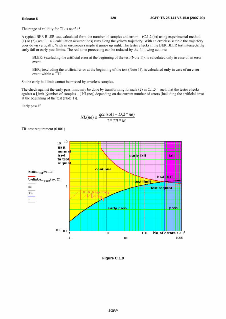
3GPP
3GPP TS 25.141 V5.15.0 (2007-09)120Release 5
The range of validity for TL is ne>345.
A typical BER BLER test, calculated form the number of samples and errors (C.1.2.(b)) using experimental method (1) or (2) (see C.1.4.2 calculation assumptions) runs along the yellow trajectory. With an errorless sample the trajectory goes down vertically. With an erroneous sample it jumps up right. The tester checks if the BER BLER test intersects the early fail or early pass limits. The real time processing can be reduced by the following actions:
BLER0 (excluding the artificial error at the beginning of the test (Note 1)). is calculated only in case of an error event.
BER0 (excluding the artificial error at the beginning of the test (Note 1)). is calculated only in case of an error event within a TTI.
So the early fail limit cannot be missed by errorless samples.
The check against the early pass limit may be done by transforming formula (2) in C.1.5 such that the tester checks against a Limit-Number-of-samples ( NL(ne)) depending on the current number of errors (including the artificial error at the beginning of the test (Note 1)).
Early pass if
MTR
neDqchisqneNL**2
)*2,1()( −≥
TR: test requirement (0.001)
Figure C.1.9
3GPP
3GPP TS 25.141 V5.15.0 (2007-09)121Release 5
Note 1: At the beginning of the test, an artificial error is introduced. This ensures that an ideal DUT meets the valid range of the early pass limit. In addition this ensures that the complementary experiment (C.1.4.2 bullet point (2)) is applicable as well. For the check against the early fail limit the artificial erroneous sample, introduced at the beginning of the test , is disregarded. Due to the nature of the test, namely discrete error events, the early fail condition shall not be valid, when fractional errors <1 are used to calculate the early fail limit: Any early fail decision is postponed until number of errors ne ≥7. In the blocking test any early fail decision is postponed until number of errors ne ≥ 8.
Note2: F=0.2% is intended to be used for a test containing a few BER/BLER tests (e.g. receiver sensitivity is repeated 12 times(3 RF Channels * 2 Power-supplies * 2 Temperatures). For a test containing many BER/BLER tests (e.g. blocking test) this value is not appropriate for a single BER/BLER test. The blocking test contains approx. 12750 single BER tests. A DUT on the limit will fail approx. 25 to 26 times due to statistical reasons using wrong decision probability at the end of the test F= 0.2%. This shall be solved by the following rule:
All passes (based on F=0.2%) are accepted, including the wrong decisions due to statistical reasons.
An early fail limit based on F=0.02% instead of 0.2% is established. That ensures that wrong decisions due to statistical reasons are reduced to 2 to 3 in 12750 BER measurements. If the fail cases are ≤12, it is allowed to repeat each fail cases 1 time before the final verdict. These asymmetric test conditions ensure that a DUT on the limit consumes hardly more test time for a blocking test than in the symmetric case and reduces the wrong decision probability considerably and on the other hand the repetition allowance sufficiently suppresses the residual statistically caused wrong verdict for the aggregate test.
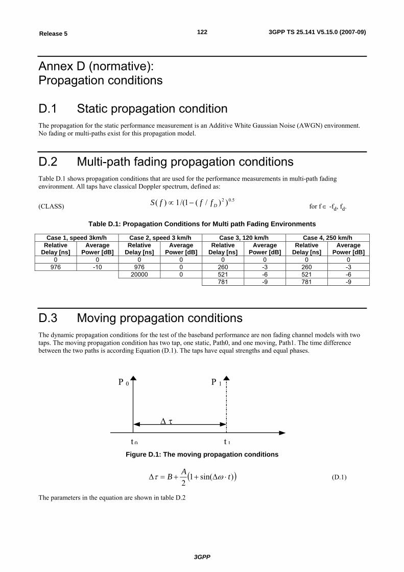
3GPP
3GPP TS 25.141 V5.15.0 (2007-09)122Release 5
Annex D (normative): Propagation conditions
D.1 Static propagation condition The propagation for the static performance measurement is an Additive White Gaussian Noise (AWGN) environment. No fading or multi-paths exist for this propagation model.
D.2 Multi-path fading propagation conditions Table D.1 shows propagation conditions that are used for the performance measurements in multi-path fading environment. All taps have classical Doppler spectrum, defined as:
(CLASS) 5.02 ))/(1/(1)( DfffS −∝ for f ∈ -fd, fd.
Table D.1: Propagation Conditions for Multi path Fading Environments
Case 1, speed 3km/h Case 2, speed 3 km/h Case 3, 120 km/h Case 4, 250 km/h Relative
Delay [ns] Average
Power [dB] Relative
Delay [ns] Average
Power [dB]Relative
Delay [ns] Average
Power [dB]Relative
Delay [ns] Average
Power [dB]0 0 0 0 0 0 0 0
976 -10 976 0 260 -3 260 -3 20000 0 521 -6 521 -6 781 -9 781 -9
D.3 Moving propagation conditions The dynamic propagation conditions for the test of the baseband performance are non fading channel models with two taps. The moving propagation condition has two tap, one static, Path0, and one moving, Path1. The time difference between the two paths is according Equation (D.1). The taps have equal strengths and equal phases.
t 1
P 1
Δ τ
P 0
t 0
Figure D.1: The moving propagation conditions
( ))sin(12
tAB ⋅Δ++=Δ ωτ (D.1)
The parameters in the equation are shown in table D.2
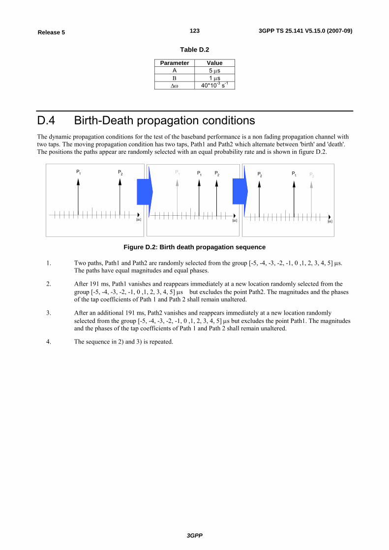
3GPP
3GPP TS 25.141 V5.15.0 (2007-09)123Release 5
Table D.2
Parameter Value A 5 μs Β 1 μs
Δω 40*10-3 s-1
D.4 Birth-Death propagation conditions The dynamic propagation conditions for the test of the baseband performance is a non fading propagation channel with two taps. The moving propagation condition has two taps, Path1 and Path2 which alternate between 'birth' and 'death'. The positions the paths appear are randomly selected with an equal probability rate and is shown in figure D.2.
P 1 P 2 P 1
[ us]
P 1 P 2
[ us]
P 2 P 1
[ us]
P 2
Figure D.2: Birth death propagation sequence
1. Two paths, Path1 and Path2 are randomly selected from the group [-5, -4, -3, -2, -1, 0 ,1, 2, 3, 4, 5] μs. The paths have equal magnitudes and equal phases.
2. After 191 ms, Path1 vanishes and reappears immediately at a new location randomly selected from the group [-5, -4, -3, -2, -1, 0 ,1, 2, 3, 4, 5] μs but excludes the point Path2. The magnitudes and the phases of the tap coefficients of Path 1 and Path 2 shall remain unaltered.
3. After an additional 191 ms, Path2 vanishes and reappears immediately at a new location randomly selected from the group [-5, -4, -3, -2, -1, 0 ,1, 2, 3, 4, 5] μs but excludes the point Path1. The magnitudes and the phases of the tap coefficients of Path 1 and Path 2 shall remain unaltered.
4. The sequence in 2) and 3) is repeated.
3GPP
3GPP TS 25.141 V5.15.0 (2007-09)124Release 5
Annex E (normative): Global In-Channel TX-Test
E.1 General The global in-channel Tx test enables the measurement of all relevant parameters that describe the in-channel quality of the output signal of the Tx under test in a single measurement process. The parameters describing the in-channel quality of a transmitter, however, are not necessarily independent. The algorithm chosen for description inside this annex places particular emphasis on the exclusion of all interdependencies among the parameters. Any other algorithm (e.g. having better computational efficiency) may be applied, as long as the results are the same within the acceptable uncertainty of the test system as defined in subclause 4.1
E.2 Definition of the process
E.2.1 Basic principle The process is based on the comparison of the actual output signal of the TX under test, received by an ideal receiver, with a reference signal, that is generated by the measuring equipment and represents an ideal error free received signal. The reference signal shall be composed of the same number of codes at the correct spreading factors as contained In the test signal. Note, for simplification, the notation below assumes only codes of one spreading factor although the algorithm is valid for signals containing multiple spreading factors. All signals are represented as equivalent (generally complex) baseband signals.
E.2.2 Output signal of the TX under test The output signal of the TX under test is acquired by the measuring equipment, filtered by a matched filter (RRC 0.22, correct in shape and in position on the frequency axis) and stored for further processing
The following form represents the physical signa l in the entire measurement interval:
one vector Z, containing N = ns x sf complex samples;
with
ns: number of symbols in the measurement interval;
sf: number of chips per symbol. (sf: spreading factor) (see Note: Symbol length)
E.2.3 Reference signal The reference signal is constructed by the measuring equipment according to the relevant TX specifications.
It is filtered by the same matched filter, mentioned in E.2.2., and stored at the Inter-Symbol-Interference free instants. The following form represents the reference signal in the entire measurement interval:
one vector R, containing N = ns x sf complex samples
where
ns: number of symbols in the measurement interval;
sf: number of chips per symbol. (see Note: Symbol length)
3GPP
3GPP TS 25.141 V5.15.0 (2007-09)125Release 5
E.2.4 Classification of measurement results The measurement results achieved by the global in-channel TX test can be classified into two types:
- Results of type “deviation”, where the error-free parameter has a non-zero magnitude. (These are the parameters that quantify the integral physical characteristic of the signal).These parameters are:
RF Frequency
Power (in case of single code)
Code Domain Power (in case of multi code)
Timing (only for UE) (see Note: Deviation)
(Additional parameters: see Note: Deviation)
- Results of type “residual”, where the error-free parameter has value zero. (These are the parameters that quantify the error values of the measured signal, whose ideal magnitude is zero). These parameters are:
Error Vector Magnitude (EVM);
Peak Code Domain Error (PCDE).
(Additional parameters: see Note: Residual)
E.2.5 Process definition to achieve results of type “deviation” The reference signal (R; see subclause E.2.3) and the signal under Test (Z; see subclause E.2.2) are varied with respect to the parameters mentioned in subclause E.2.4 under "results of type deviation" in order to achieve best fit. Best fit is achieved when the RMS difference value between the varied signal under test and the varied reference signal is an absolute minimum.
Overview:
[ ] !)~,...,~,~,,,(),...,,,~,~,~( 2121 MinimumgggtfRgggtfZFCT synchsynch =− ϕϕ
Z : Signal under test.
R: Reference signal,
with frequency f, the timing t, the phase ϕ, gain of code1 (g1), gain of code2 (g2) etc, and the gain of the synch channel gsynch See Note: Power Step
The parameters marked with a tilde in Z and R are varied in order to achieve a best fit.
Detailed formula: see Note: Formula for the minimum process
The varied reference signal, after the best fit process, will be called R’.
The varied signal under test, after the best fit process, will be called Z’.
The varying parameters, leading to R’ and Z represent directly the wanted results of type “deviation”. These measurement parameters are expressed as deviation from the reference value with the same units as the reference value.
In the case of multi code, the type-“deviation”-parameters (frequency, timing and (RF-phase)) are varied commonly for all codes such that the process returns one frequency-deviation, one timing deviation, (one RF-phase –deviation).
(These parameters are not varied on the individual code signals such that the process would return kr frequency errors... . (kr: number of codes)).
The only type-“deviation”-parameters varied individually are the code domain gain factors (g1, g2, …)
See Note: Power Step.
3GPP
3GPP TS 25.141 V5.15.0 (2007-09)126Release 5
E.2.5.1 Decision Point Power The mean-square value of the signal-under-test, sampled at the best estimate of the of Intersymbol-Interference-free points using the process defined in subclause 2.5, is referred to the Decision Point Power (DPP):
( )2'=DPP mean Z
E.2.5.2 Code-Domain Power The samples, Z’, are separated into symbol intervals to create ns time-sequential vectors z with sf complex samples comprising one symbol interval. The Code Domain Power is calculated according to the following steps:
1) Take the vectors z defined above.
2) To achieve meaningful results it is necessary to descramble z, leading to z’ (see Note: Scrambling code)
3) Take the orthogonal vectors of the channelization code set C (all codes belonging to one spreading factor) as defined in TS 25.213 and TS 25.223 (range +1, -1), and normalize by the norm of the vectors to produce Cnorm=C/sqrt(sf). (see Note: Symbol length)
4) Calculate the inner product of z’ with Cnorm.. Do this for all symbols of the measurement interval and for all codes in the code space. This gives an array of format k x ns, each value representing a specific symbol and a specific code, which can be exploited in a variety of ways.
k: total number of codes in the code space
ns: number of symbols in the measurement interval
5) Calculate k mean-square values, each mean-square value unifying ns symbols within one code. (These values can be called "Absolute CodeDomainPower (CDP)" [Volt2].) The sum of the k values of CDP is equal to DPP.
6) Normalize by the decision point power to obtain
=Absolute CodeDomainPowerRelative CodeDomain Power
DecisionPointPower
E.2.6 Process definition to achieve results of type “residual” The difference between the varied reference signal (R’; see subclauseE.2.5.) and the varied TX signal under test (Z’; see subclauseE.2.5) is the error vector E versus time:
E = Z’ – R’
Depending on the parameter to be evaluated, it is appropriate to represent E in one of the following two different forms:
Form EVM (representing the physical error signal in the entire measurement interval)
One vector E, containing N = ns x sf complex samples;
with
ns: number of symbols in the measurement interval
sf: number of chips per symbol (see Note: Symbol length)
Form PCDE (derived from Form EVM by separating the samples into symbol intervals)
ns time-sequential vectors e with sf complex samples comprising one symbol interval.
E and e give results of type “residual” applying the two algorithms defined in subclauses E.2.6.1 and E.2.6.2.
3GPP
3GPP TS 25.141 V5.15.0 (2007-09)127Release 5
E.2.6.1 Error Vector Magnitude (EVM) The Error Vector Magnitude (EVM) is calculated according to the following steps:
1) Take the error vector E defined in subclause E.2.6 (Form EVM) and calculate the RMS value of E; the result will be called RMS(E).
2) Take the varied reference vector R’ defined in subclause E.2.5 and calculate the RMS value of R’; the result will be called RMS(R’).
3) Calculate EVM according to:
100% x )'(RMS)(RMSEVM
RE
= (here, EVM is relative and expressed in %)
(see Note: Formula for EVM)
E.2.6.2 Peak Code Domain Error (PCDE) The Peak Code Domain Error is calculated according to the following steps:
1) Take the error vectors e defined in subclause E.2.6 (Form PCDE)
2) To achieve meaningful results it is necessary to descramble e, leading to e’ (see Note: Scrambling code)
3) Take the orthogonal vectors of the channelization code set C (all codes belonging to one spreading factor) as defined in TS 25.213 and TS 25.223 (range +1, -1). (see Note: Symbol length) and normalize by the norm of the vectors to produce Cnorm= C/sqrt(sf). (see Note: Symbol length)
4) Calculate the inner product of e’ with Cnorm. Do this for all symbols of the measurement interval and for all codes in the code space. This gives an array of format k x ns, each value representing an error-vector representing a specific symbol and a specific code, which can be exploited in a variety of ways.
k: total number of codes in the code space
ns: number of symbols in the measurement interval
5) Calculate k RMS values, each RMS value unifying ns symbols within one code. (These values can be called "Absolute CodeEVMs" [Volt].)
6) Find the peak value among the k "Absolute CodeEVMs". (This value can be called "Absolute PeakCodeEVM" [Volt].)
7) Calculate PCDE according to:
dBRRMS
MPeakCodeEVAbsolute2
2
))'(()"("lg10 ∗ (a relative value in dB).
(see Note IQ)
(see Note Synch channel)
E.3 Notes
E.3.1 Symbol length A general code multiplexed signal is multicode and multirate. In order to avoid unnecessary complexity, the measurement applications use a unique symbol-length, corresponding to a spreading factor, regardless of the really
3GPP
3GPP TS 25.141 V5.15.0 (2007-09)128Release 5
intended spreading factor. Nevertheless the complexity with a multicode / multirate signal can be mastered by introducing appropriate definitions.
E.3.2 Deviation It is conceivable to regard more parameters as type „deviation“ e.g. Chip frequency and RF-phase.
As chip-frequency and RF-frequency are linked together by a statement in the core specifications [1] it is sufficient to process RF frequency only.
A parameter RF-phase must be varied within the best fit process (E.2.5.). Although necessary, this parameter-variation doesn’t describe any error, as the modulation schemes used in the system don’t depend on an absolute RF-phase.
The parameter Timing must be varied within the best fit process (E.2.5.) This parameter variation does not describe any error, when applied to the Node B test. However when applied to the UE test, it describes the error of the UE’s Timing Advance.
E.3.3 Residual It is conceivable to regard more parameters as type „residual“ e.g. IQ origin offset. As it is not the intention of the test to separate for different error sources, but to quantify the quality of the signal, all such parameters are not extracted by the best fit process, instead remain part of EVM and PCDE.
E.3.4 Scrambling Code In general a signal under test can use more than one scrambling code. Note that PCDE is primarily processed to investigate the unused channelization codes. In order to know which scrambling code shall be applied on unused channelization codes, it is necessary to restrict the test conditions: The signal under test shall use exactly one scrambling code.
E.3.5 IQ As in FDD/uplink each channelization code can be used twice, on the I and on the Q channel, the measurement result may indicate separate values of CDP or PCDE for I and Q on which channel (I or Q) they occur.
E.3.6 Synch Channel A Node B signal contains a physical synch channel, which is non orthogonal, related to the other channels. In this context note: The code channel bearing the result of PCDE is exactly one of the other physical channels (never the synch channel). The origin of PCDE (erroneous code power) can be any channel (including synch channel) This means that the error due to the synch channel is projected onto the other (orthogonal) codes that make up the code domain.
E.3.7 Formula for the minimum process
21
0sec )()()~,~,...,~,~,~,~( ∑
−
=
−=ΔΔΔΔΔΔN
primc RZgggtfLν
ννϕ
where:
L : the function to be minimised
The parameters to be varied in order to minimize are:
f~Δ the RF frequency offset
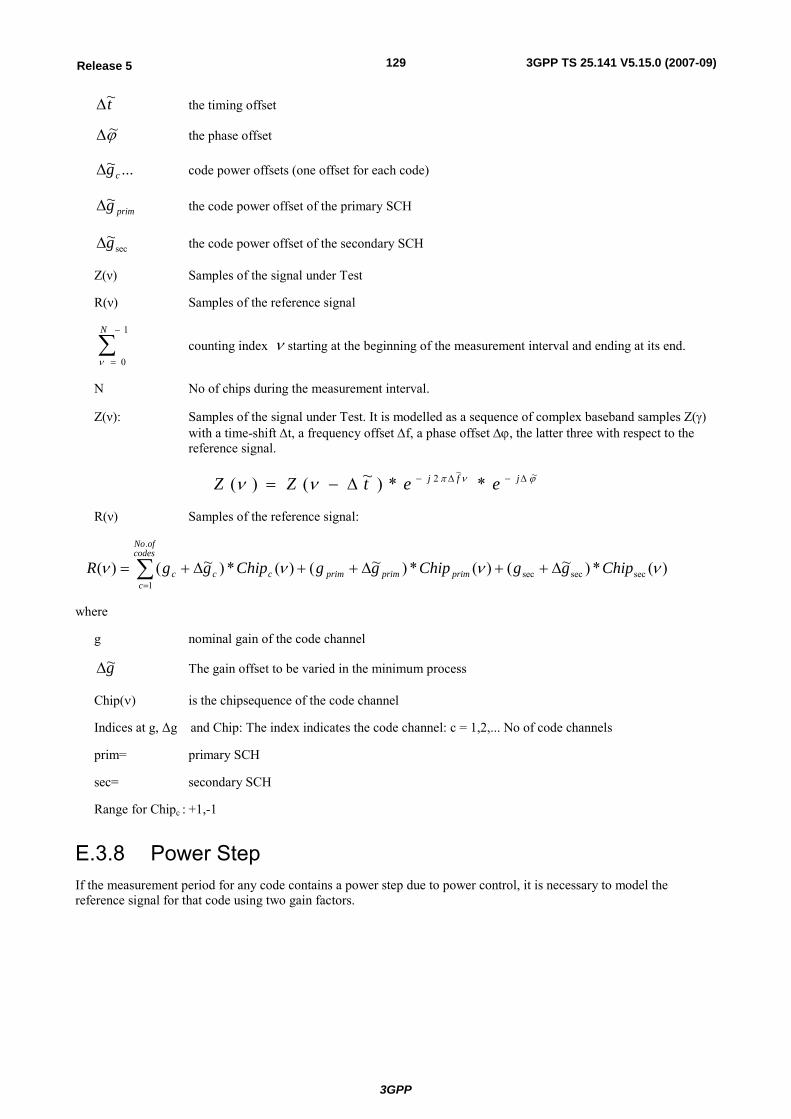
3GPP
3GPP TS 25.141 V5.15.0 (2007-09)129Release 5
t~Δ the timing offset
ϕ~Δ the phase offset
...~cgΔ code power offsets (one offset for each code)
primg~Δ the code power offset of the primary SCH
sec~gΔ the code power offset of the secondary SCH
Z(ν) Samples of the signal under Test
R(ν) Samples of the reference signal
∑−
=
1
0
N
ν counting index ν starting at the beginning of the measurement interval and ending at its end.
N No of chips during the measurement interval.
Z(ν): Samples of the signal under Test. It is modelled as a sequence of complex baseband samples Z(γ) with a time-shift Δt, a frequency offset Δf, a phase offset Δϕ, the latter three with respect to the reference signal.
ϕνπνν~~2 **)~()( Δ−Δ−Δ−= jfj eetZZ
R(ν) Samples of the reference signal:
)(*)~()(*)~()(*)~()( secsecsec
.
1
νννν ChipggChipggChipggR primprimprim
codesofNo
cccc Δ++Δ++Δ+= ∑
=
where
g nominal gain of the code channel
g~Δ The gain offset to be varied in the minimum process
Chip(ν) is the chipsequence of the code channel
Indices at g, Δg and Chip: The index indicates the code channel: c = 1,2,... No of code channels
prim= primary SCH
sec= secondary SCH
Range for Chipc : +1,-1
E.3.8 Power Step If the measurement period for any code contains a power step due to power control, it is necessary to model the reference signal for that code using two gain factors.
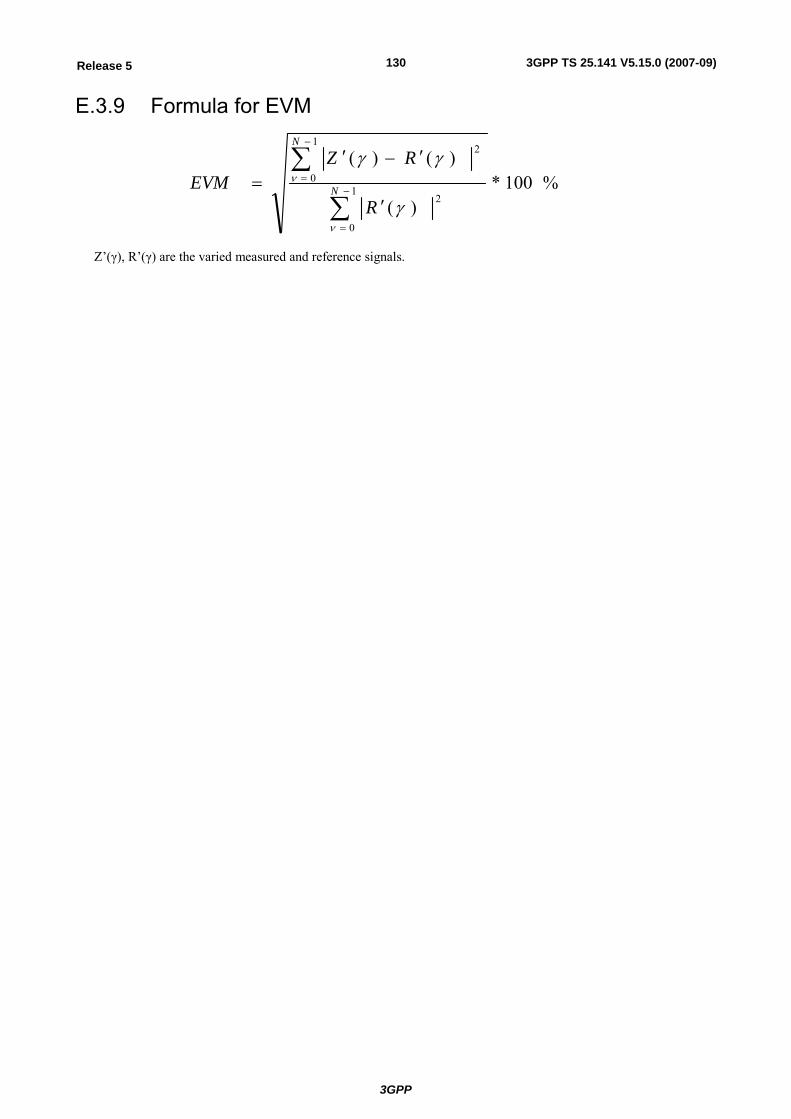
3GPP
3GPP TS 25.141 V5.15.0 (2007-09)130Release 5
E.3.9 Formula for EVM
%100*)(
)()(
21
0
21
0
∑
∑−
=
−
=
′
′−′= N
N
R
RZEVM
ν
ν
γ
γγ
Z’(γ), R’(γ) are the varied measured and reference signals.
3GPP
3GPP TS 25.141 V5.15.0 (2007-09)131Release 5
Annex F (informative): Derivation of Test Requirements The Test Requirements in this specification have been calculated by relaxing the Minimum Requirements of the core specification using the Test Tolerances defined in subclause 4.2. When the Test Tolerance is zero, the Test Requirement will be the same as the Minimum Requirement. When the Test Tolerance is non-zero, the Test Requirements will differ from the Minimum Requirements, and the formula used for this relaxation is given in tables F.1, F.2 and F.3
Note that a formula for applying Test Tolerances is provided for all tests, even those with a test tolerance of zero. This is necessary in the case that the Test System uncertainty is greater than that allowed in subclause 4.1. In this event, the excess error shall be subtracted from the defined test tolerance in order to generate the correct tightened Test Requirements as defined in subclause 4.3.
For example, a Test System having 0.9 dB accuracy for test 6.2.1 Base Station maximum output power (which is 0.2 dB above the limit specified in subclause 4.) would subtract 0.2 dB from the Test Tolerance of 0.7 dB defined in subclause 4.2. This new test tolerance of 0.5 dB would then be applied to the Minimum Requirement using the formula defined in Table F.1 to give a new range of ±2.5 dB of the manufacturer's rated output power.
Using this same approach for the case where a test had a test tolerance of 0 dB, an excess error of 0.2 dB would result in a modified test tolerance of –0.2 dB.
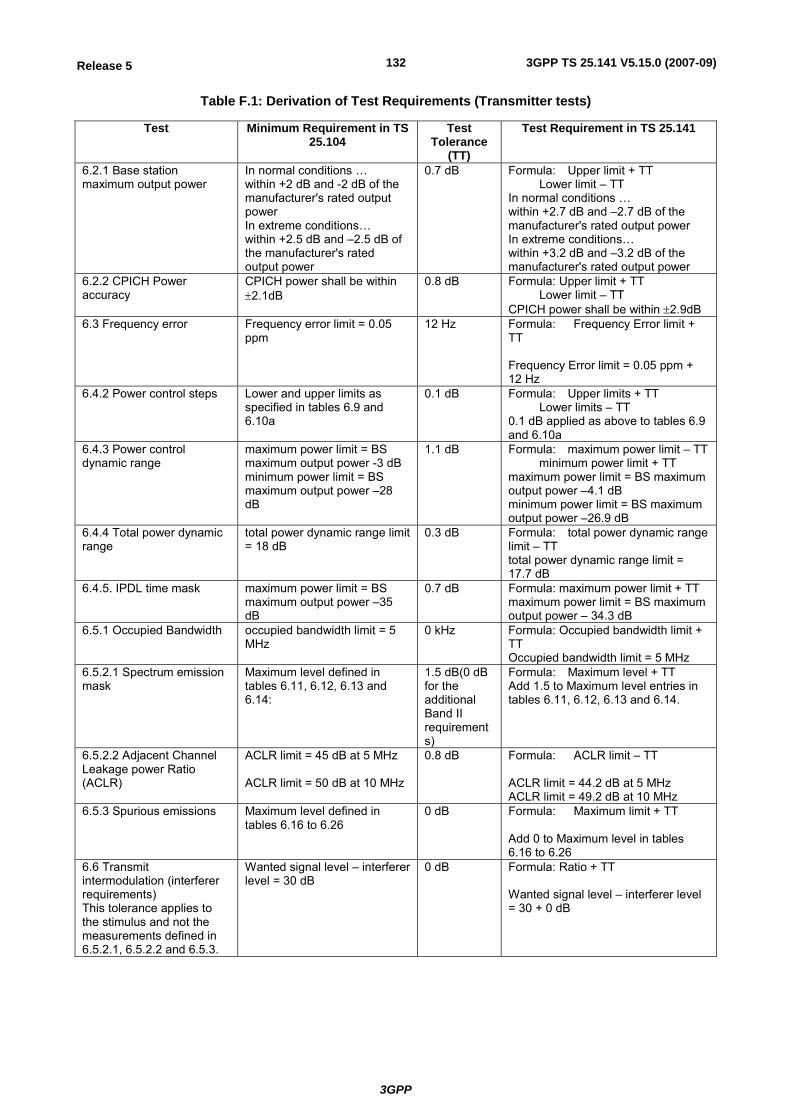
3GPP
3GPP TS 25.141 V5.15.0 (2007-09)132Release 5
Table F.1: Derivation of Test Requirements (Transmitter tests)
Test Minimum Requirement in TS 25.104
Test Tolerance
(TT)
Test Requirement in TS 25.141
6.2.1 Base station maximum output power
In normal conditions … within +2 dB and -2 dB of the manufacturer's rated output power In extreme conditions… within +2.5 dB and –2.5 dB of the manufacturer's rated output power
0.7 dB Formula: Upper limit + TT Lower limit – TT In normal conditions … within +2.7 dB and –2.7 dB of the manufacturer's rated output power In extreme conditions… within +3.2 dB and –3.2 dB of the manufacturer's rated output power
6.2.2 CPICH Power accuracy
CPICH power shall be within ±2.1dB
0.8 dB Formula: Upper limit + TT Lower limit – TT CPICH power shall be within ±2.9dB
6.3 Frequency error Frequency error limit = 0.05 ppm
12 Hz Formula: Frequency Error limit + TT Frequency Error limit = 0.05 ppm + 12 Hz
6.4.2 Power control steps Lower and upper limits as specified in tables 6.9 and 6.10a
0.1 dB Formula: Upper limits + TT Lower limits – TT 0.1 dB applied as above to tables 6.9 and 6.10a
6.4.3 Power control dynamic range
maximum power limit = BS maximum output power -3 dB minimum power limit = BS maximum output power –28 dB
1.1 dB Formula: maximum power limit – TT minimum power limit + TT maximum power limit = BS maximum output power –4.1 dB minimum power limit = BS maximum output power –26.9 dB
6.4.4 Total power dynamic range
total power dynamic range limit = 18 dB
0.3 dB Formula: total power dynamic range limit – TT total power dynamic range limit = 17.7 dB
6.4.5. IPDL time mask maximum power limit = BS maximum output power –35 dB
0.7 dB Formula: maximum power limit + TT maximum power limit = BS maximum output power – 34.3 dB
6.5.1 Occupied Bandwidth occupied bandwidth limit = 5 MHz
0 kHz Formula: Occupied bandwidth limit + TT Occupied bandwidth limit = 5 MHz
6.5.2.1 Spectrum emission mask
Maximum level defined in tables 6.11, 6.12, 6.13 and 6.14:
1.5 dB(0 dB for the additional Band II requirements)
Formula: Maximum level + TT Add 1.5 to Maximum level entries in tables 6.11, 6.12, 6.13 and 6.14.
6.5.2.2 Adjacent Channel Leakage power Ratio (ACLR)
ACLR limit = 45 dB at 5 MHz ACLR limit = 50 dB at 10 MHz
0.8 dB Formula: ACLR limit – TT ACLR limit = 44.2 dB at 5 MHz ACLR limit = 49.2 dB at 10 MHz
6.5.3 Spurious emissions Maximum level defined in tables 6.16 to 6.26
0 dB Formula: Maximum limit + TT Add 0 to Maximum level in tables 6.16 to 6.26
6.6 Transmit intermodulation (interferer requirements) This tolerance applies to the stimulus and not the measurements defined in 6.5.2.1, 6.5.2.2 and 6.5.3.
Wanted signal level – interferer level = 30 dB
0 dB Formula: Ratio + TT Wanted signal level – interferer level = 30 + 0 dB
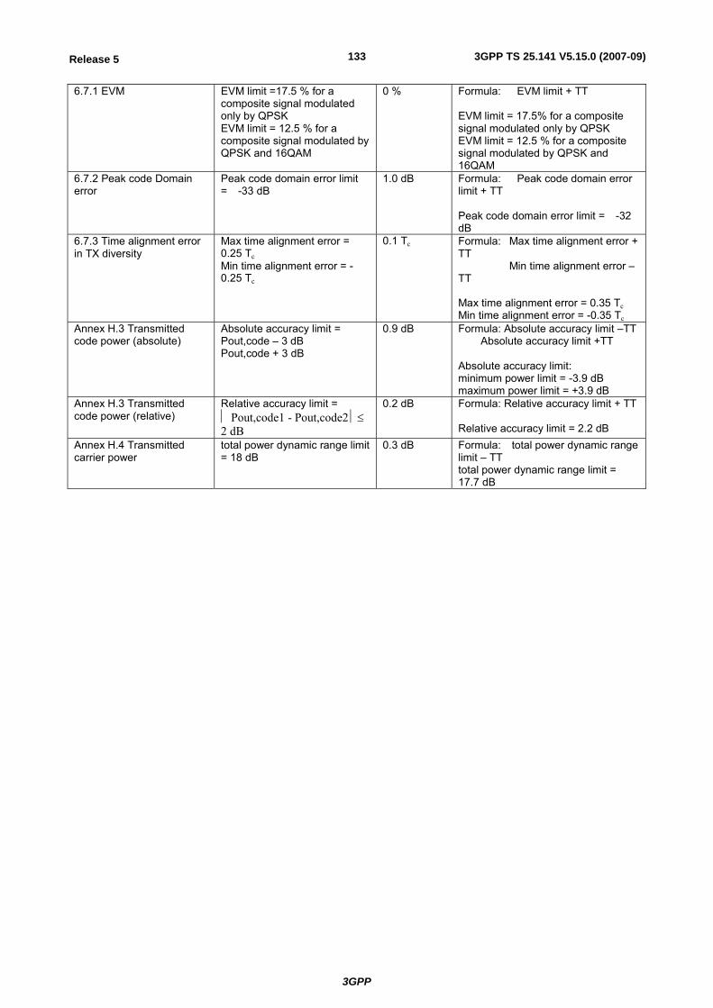
3GPP
3GPP TS 25.141 V5.15.0 (2007-09)133Release 5
6.7.1 EVM EVM limit =17.5 % for a composite signal modulated only by QPSK EVM limit = 12.5 % for a composite signal modulated by QPSK and 16QAM
0 % Formula: EVM limit + TT EVM limit = 17.5% for a composite signal modulated only by QPSK EVM limit = 12.5 % for a composite signal modulated by QPSK and 16QAM
6.7.2 Peak code Domain error
Peak code domain error limit = -33 dB
1.0 dB Formula: Peak code domain error limit + TT Peak code domain error limit = -32 dB
6.7.3 Time alignment error in TX diversity
Max time alignment error = 0.25 Tc Min time alignment error = -0.25 Tc
0.1 Tc Formula: Max time alignment error + TT Min time alignment error – TT Max time alignment error = 0.35 Tc Min time alignment error = -0.35 Tc
Annex H.3 Transmitted code power (absolute)
Absolute accuracy limit = Pout,code – 3 dB Pout,code + 3 dB
0.9 dB Formula: Absolute accuracy limit –TT Absolute accuracy limit +TT Absolute accuracy limit: minimum power limit = -3.9 dB maximum power limit = +3.9 dB
Annex H.3 Transmitted code power (relative)
Relative accuracy limit = ⏐ Pout,code1 - Pout,code2 ⏐≤ 2 dB
0.2 dB Formula: Relative accuracy limit + TT Relative accuracy limit = 2.2 dB
Annex H.4 Transmitted carrier power
total power dynamic range limit = 18 dB
0.3 dB Formula: total power dynamic range limit – TT total power dynamic range limit = 17.7 dB
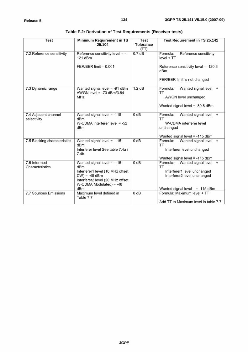
3GPP
3GPP TS 25.141 V5.15.0 (2007-09)134Release 5
Table F.2: Derivation of Test Requirements (Receiver tests)
Test Minimum Requirement in TS 25.104
Test Tolerance
(TT)
Test Requirement in TS 25.141
7.2 Reference sensitivity Reference sensitivity level = -121 dBm FER/BER limit = 0.001
0.7 dB Formula: Reference sensitivity level + TT Reference sensitivity level = -120.3 dBm FER/BER limit is not changed
7.3 Dynamic range Wanted signal level = -91 dBmAWGN level = -73 dBm/3.84 MHz
1.2 dB Formula: Wanted signal level + TT AWGN level unchanged Wanted signal level = -89.8 dBm
7.4 Adjacent channel selectivity
Wanted signal level = -115 dBm W-CDMA interferer level = -52 dBm
0 dB Formula: Wanted signal level + TT W-CDMA interferer level unchanged Wanted signal level = -115 dBm
7.5 Blocking characteristics Wanted signal level = -115 dBm Interferer level See table 7.4a / 7.4b
0 dB Formula: Wanted signal level + TT Interferer level unchanged Wanted signal level = -115 dBm
7.6 Intermod Characteristics
Wanted signal level = -115 dBm Interferer1 level (10 MHz offset CW) = -48 dBm Interferer2 level (20 MHz offset W-CDMA Modulated) = -48 dBm
0 dB Formula: Wanted signal level + TT Interferer1 level unchanged Interferer2 level unchanged Wanted signal level = -115 dBm
7.7 Spurious Emissions Maximum level defined in Table 7.7
0 dB Formula: Maximum level + TT Add TT to Maximum level in table 7.7
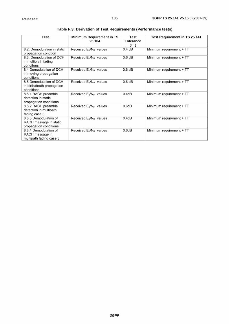
3GPP
3GPP TS 25.141 V5.15.0 (2007-09)135Release 5
Table F.3: Derivation of Test Requirements (Performance tests)
Test Minimum Requirement in TS 25.104
Test Tolerance
(TT)
Test Requirement in TS 25.141
8.2, Demodulation in static propagation condtion
Received Eb/N0 values 0.4 dB Minimum requirement + TT
8.3, Demodulation of DCH in multiplath fading conditons
Received Eb/N0 values 0.6 dB Minimum requirement + TT
8.4 Demodulation of DCH in moving propagation conditions
Received Eb/N0 values 0.6 dB Minimum requirement + TT
8.5 Demodulation of DCH in birth/death propagation conditions
Received Eb/N0 values 0.6 dB Minimum requirement + TT
8.8.1 RACH preamble detection in static propagation conditions
Received Ec/N0 values 0.4dB Minimum requirement + TT
8.8.2 RACH preamble detection in multipath fading case 3
Received Ec/N0 values 0.6dB Minimum requirement + TT
8.8.3 Demodulation of RACH message in static propagation conditions
Received Eb/N0 values 0.4dB Minimum requirement + TT
8.8.4 Demodulation of RACH message in multipath fading case 3
Received Eb/N0 values 0.6dB Minimum requirement + TT
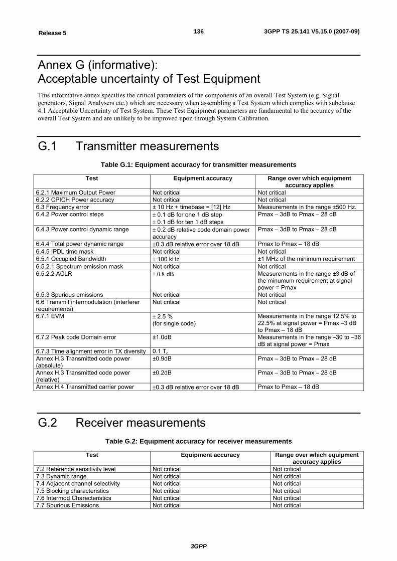
3GPP
3GPP TS 25.141 V5.15.0 (2007-09)136Release 5
Annex G (informative): Acceptable uncertainty of Test Equipment This informative annex specifies the critical parameters of the components of an overall Test System (e.g. Signal generators, Signal Analysers etc.) which are necessary when assembling a Test System which complies with subclause 4.1 Acceptable Uncertainty of Test System. These Test Equipment parameters are fundamental to the accuracy of the overall Test System and are unlikely to be improved upon through System Calibration.
G.1 Transmitter measurements Table G.1: Equipment accuracy for transmitter measurements
Test Equipment accuracy Range over which equipment accuracy applies
6.2.1 Maximum Output Power Not critical Not critical 6.2.2 CPICH Power accuracy Not critical Not critical 6.3 Frequency error ± 10 Hz + timebase = [12] Hz Measurements in the range ±500 Hz. 6.4.2 Power control steps ± 0.1 dB for one 1 dB step
± 0.1 dB for ten 1 dB steps Pmax – 3dB to Pmax – 28 dB
6.4.3 Power control dynamic range ± 0.2 dB relative code domain power accuracy
Pmax – 3dB to Pmax – 28 dB
6.4.4 Total power dynamic range ±0.3 dB relative error over 18 dB Pmax to Pmax – 18 dB 6.4.5 IPDL time mask Not critical Not critical 6.5.1 Occupied Bandwidth ± 100 kHz ±1 MHz of the minimum requirement 6.5.2.1 Spectrum emission mask Not critical Not critical 6.5.2.2 ACLR ± 0.8 dB Measurements in the range ±3 dB of
the minumum requirement at signal power = Pmax
6.5.3 Spurious emissions Not critical Not critical 6.6 Transmit intermodulation (interferer requirements)
Not critical Not critical
6.7.1 EVM ± 2.5 % (for single code)
Measurements in the range 12.5% to 22.5% at signal power = Pmax –3 dB to Pmax – 18 dB
6.7.2 Peak code Domain error ±1.0dB Measurements in the range –30 to –36 dB at signal power = Pmax
6.7.3 Time alignment error in TX diversity 0.1 Tc Annex H.3 Transmitted code power (absolute)
±0.9dB Pmax – 3dB to Pmax – 28 dB
Annex H.3 Transmitted code power (relative)
±0.2dB Pmax – 3dB to Pmax – 28 dB
Annex H.4 Transmitted carrier power ±0.3 dB relative error over 18 dB Pmax to Pmax – 18 dB
G.2 Receiver measurements Table G.2: Equipment accuracy for receiver measurements
Test Equipment accuracy Range over which equipment accuracy applies
7.2 Reference sensitivity level Not critical Not critical 7.3 Dynamic range Not critical Not critical 7.4 Adjacent channel selectivity Not critical Not critical 7.5 Blocking characteristics Not critical Not critical 7.6 Intermod Characteristics Not critical Not critical 7.7 Spurious Emissions Not critical Not critical
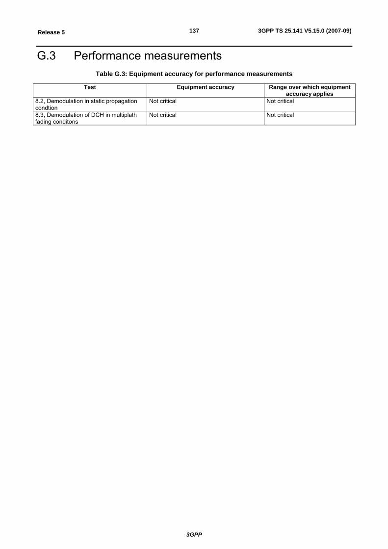
3GPP
3GPP TS 25.141 V5.15.0 (2007-09)137Release 5
G.3 Performance measurements Table G.3: Equipment accuracy for performance measurements
Test Equipment accuracy Range over which equipment accuracy applies
8.2, Demodulation in static propagation condtion
Not critical Not critical
8.3, Demodulation of DCH in multiplath fading conditons
Not critical Not critical
3GPP
3GPP TS 25.141 V5.15.0 (2007-09)138Release 5
Annex H (Informative): UTRAN Measurement Test Cases
H.1 Purpose of Annex This Annex specifies test specific parameters for some of the UTRAN requirements in chapter 9.2 TS 25.133. The tests provide additional information to how the requirements should be tested. Some requirements may lack a test.
Unless explicitly stated:
- Measurement channel is 12.2 kbps as defined in TS 25.104 annex A, sub-clause A.2 for UL measurements
- Test models defined in TS 25.141 sub-clause 6.1 are used for DL measurements
H.2 Received Total Wideband Power
H.2.1 Absolute RTWP measurement 1. Terminate the BS RX inputs, measure the RTWP and record it.
2. Connect a signal generator and increase the signal generator power until the reported RTWP level (Irep) has increased 3dB.
3. Measure the signal level power at the antenna connector port. This signal level is now called the "Internally generated noise" (Ni).
4. Sweep the sum of internally generated noise (Ni) and signal generator power (I) through the defined accuracy range.
5. Check that: |(Ni+I)-Irep| meets the requirements in chapter 9.2.1.
Note that Io= (Ni+I)
H.2.2 Relative RTWP measurement 1. Terminate the BS RX inputs, measure the RTWP and record it.
2. Attach a signal generator to the RX input and increase the power until the by the BS reported RTWP value (Irep) has increased 3 dB.
3. Measure the signal level power at the antenna connector port. This signal level is now called the "Internally generated noise" (Ni).
4. Calculate the required signal levels I such that the sum of the internally generated noise (Ni) and the signal generator power (I)
5. The difference between the reported RTWP values shall meet the requirements specified in chapter 9.2.1.
H.3 Transmitted code power 1. Generate the wanted signal in accordance to test model 2, subclause 6.1.1.2. Set power of the DPCH under test
to the Pmax-3 dB level. Power levels for other code channels shall be adjusted as necessary.
3GPP
3GPP TS 25.141 V5.15.0 (2007-09)139Release 5
2. Measure the output power on code channel under test, Pout,code, at the antenna connector. Record the transmitted code power reported in the BS, Pcode.
3. Check that Pout,code meets the absolute accuracy requirement in TS 25.133 chapter 9.2.5.1. If STTD or closed loop transmit diversity is supported by the BS, the transmitted code power for each branch are measured, summed together and reported to higher layers. In case of TX diversity both branches need to be measured and summed together in order to find out the wanted value. The absolute accuracy of Pcode can be accepted if Pout,code will fullfill the following conditions:
Pcode-3.9 dB ≤ Pout,code ≤ Pcode + 3.9 dB
4. Check that the relative accuracy requirement for Pcode in TS 25.133 chapter 9.2.5.2 is met. Set Pcode1 and Pcode2 to transmit with the same power level. The relative accuracy between Pcode1 and Pcode2 can be accepted if the difference between the measured power of one code channel, Pout,code1 and another code channel Pout,code 2 will fullfill the following conditions:
⏐ Pout,code1 - Pout,code2 ⏐ ≤ 2.2 dB.
5. Set the power of the DPCH under test to the minimum power of the power control dynamic range and repeat steps 2, 3 and 4.
H.4 Transmitted carrier power 1) Set the BS to transmit with the maximum transmission power and measure the output power at the antenna
connector, PMTP. Maximum transmission power is the mean power on one carrier measured at the antenna connector with the code level settings that according to the base station manufacturer will result in an output power of nominally the maximum output power in a specified reference condition. Test model 2, subclause 6.1.1.2, when the code powers are set according to table 6.3. shall be used.
2) Operate the BS in closed loop power control until the output power has reached a stable state. Measure the output power, Pout, at the antenna connector and record the transmitted carrier power measured and reported in the BS, Prep. Note that Prep is normalised to the output power measured in Test Model 2 with all codes at their default levels. If STTD or closed loop transmit diversity is supported by the BS, only the highest of the transmit powers is reported to higher layers. In case of TX diversity both branches need to be measured in order to find out which one is the highest.
3) Check that the Pout meets the requirement in TS 25.133 chapter 9.2.4.1, with the same test equipment accuracy as in chapter 6.4.4. in TS 25.141. Prep can be accepted if Pout will fullfill the following conditions:
( ) ( ) 3.0log103.0log10 1005Pr
1005Pr
++≤≤−++− epep PMTPPoutPMTP [dBm]
4) Repeat step 2 and 3 over the 5%-95% range of the Prep. Use first the standard code powers of test model 2 to verify the Prep range from 50% to 95%. After that put the other dedicated channels off and reduce the powers of the control codes in order to be able to verify the Prep range from 5% to 50%.
Note: Pout shall be tested immediately after PMTP in order to avoid the influence of long term stability variation to measurement results.
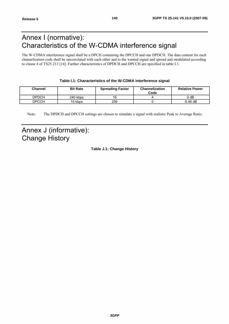
3GPP
3GPP TS 25.141 V5.15.0 (2007-09)140Release 5
Annex I (normative): Characteristics of the W-CDMA interference signal The W-CDMA interference signal shall be a DPCH containing the DPCCH and one DPDCH. The data content for each channelization code shall be uncorrelated with each other and to the wanted signal and spread and modulated according to clause 4 of TS25.213 [14]. Further characteristics of DPDCH and DPCCH are specified in table I.1.
Table I.1: Characteristics of the W-CDMA interference signal
Channel Bit Rate Spreading Factor Channelization Code
Relative Power
DPDCH 240 kbps 16 4 0 dB DPCCH 15 kbps 256 0 -5.46 dB
Note: The DPDCH and DPCCH settings are chosen to simulate a signal with realistic Peak to Average Ratio.
Annex J (informative): Change History
Table J.1: Change History
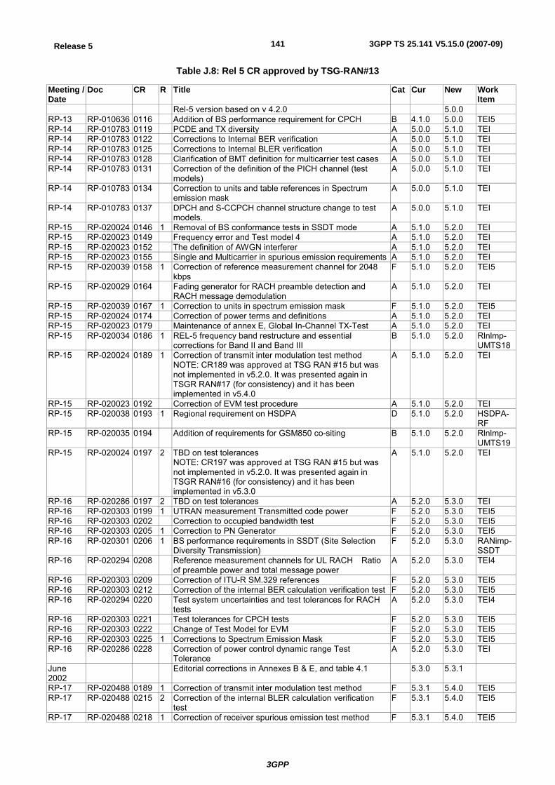
3GPP
3GPP TS 25.141 V5.15.0 (2007-09)141Release 5
Table J.8: Rel 5 CR approved by TSG-RAN#13
Meeting / Date
Doc CR R Title Cat Cur New Work Item
Rel-5 version based on v 4.2.0 5.0.0 RP-13 RP-010636 0116 Addition of BS performance requirement for CPCH B 4.1.0 5.0.0 TEI5 RP-14 RP-010783 0119 PCDE and TX diversity A 5.0.0 5.1.0 TEI RP-14 RP-010783 0122 Corrections to Internal BER verification A 5.0.0 5.1.0 TEI RP-14 RP-010783 0125 Corrections to Internal BLER verification A 5.0.0 5.1.0 TEI RP-14 RP-010783 0128 Clarification of BMT definition for multicarrier test cases A 5.0.0 5.1.0 TEI RP-14 RP-010783 0131 Correction of the definition of the PICH channel (test
models) A 5.0.0 5.1.0 TEI
RP-14 RP-010783 0134 Correction to units and table references in Spectrum emission mask
A 5.0.0 5.1.0 TEI
RP-14 RP-010783 0137 DPCH and S-CCPCH channel structure change to test models.
A 5.0.0 5.1.0 TEI
RP-15 RP-020024 0146 1 Removal of BS conformance tests in SSDT mode A 5.1.0 5.2.0 TEI RP-15 RP-020023 0149 Frequency error and Test model 4 A 5.1.0 5.2.0 TEI RP-15 RP-020023 0152 The definition of AWGN interferer A 5.1.0 5.2.0 TEI RP-15 RP-020023 0155 Single and Multicarrier in spurious emission requirements A 5.1.0 5.2.0 TEI RP-15 RP-020039 0158 1 Correction of reference measurement channel for 2048
kbps F 5.1.0 5.2.0 TEI5
RP-15 RP-020029 0164 Fading generator for RACH preamble detection and RACH message demodulation
A 5.1.0 5.2.0 TEI
RP-15 RP-020039 0167 1 Correction to units in spectrum emission mask F 5.1.0 5.2.0 TEI5 RP-15 RP-020024 0174 Correction of power terms and definitions A 5.1.0 5.2.0 TEI RP-15 RP-020023 0179 Maintenance of annex E, Global In-Channel TX-Test A 5.1.0 5.2.0 TEI RP-15 RP-020034 0186 1 REL-5 frequency band restructure and essential
corrections for Band II and Band III B 5.1.0 5.2.0 Rlnlmp-
UMTS18RP-15 RP-020024 0189 1 Correction of transmit inter modulation test method
NOTE: CR189 was approved at TSG RAN #15 but was not implemented in v5.2.0. It was presented again in TSGR RAN#17 (for consistency) and it has been implemented in v5.4.0
A 5.1.0 5.2.0 TEI
RP-15 RP-020023 0192 Correction of EVM test procedure A 5.1.0 5.2.0 TEI RP-15 RP-020038 0193 1 Regional requirement on HSDPA D 5.1.0 5.2.0 HSDPA-
RF RP-15 RP-020035 0194 Addition of requirements for GSM850 co-siting B 5.1.0 5.2.0 Rlnlmp-
UMTS19RP-15 RP-020024 0197 2 TBD on test tolerances
NOTE: CR197 was approved at TSG RAN #15 but was not implemented in v5.2.0. It was presented again in TSGR RAN#16 (for consistency) and it has been implemented in v5.3.0
A 5.1.0 5.2.0 TEI
RP-16 RP-020286 0197 2 TBD on test tolerances A 5.2.0 5.3.0 TEI RP-16 RP-020303 0199 1 UTRAN measurement Transmitted code power F 5.2.0 5.3.0 TEI5 RP-16 RP-020303 0202 Correction to occupied bandwidth test F 5.2.0 5.3.0 TEI5 RP-16 RP-020303 0205 1 Correction to PN Generator F 5.2.0 5.3.0 TEI5 RP-16 RP-020301 0206 1 BS performance requirements in SSDT (Site Selection
Diversity Transmission) F 5.2.0 5.3.0 RANimp-
SSDT RP-16 RP-020294 0208 Reference measurement channels for UL RACH Ratio
of preamble power and total message power A 5.2.0 5.3.0 TEI4
RP-16 RP-020303 0209 Correction of ITU-R SM.329 references F 5.2.0 5.3.0 TEI5 RP-16 RP-020303 0212 Correction of the internal BER calculation verification test F 5.2.0 5.3.0 TEI5 RP-16 RP-020294 0220 Test system uncertainties and test tolerances for RACH
tests A 5.2.0 5.3.0 TEI4
RP-16 RP-020303 0221 Test tolerances for CPCH tests F 5.2.0 5.3.0 TEI5 RP-16 RP-020303 0222 Change of Test Model for EVM F 5.2.0 5.3.0 TEI5 RP-16 RP-020303 0225 1 Corrections to Spectrum Emission Mask F 5.2.0 5.3.0 TEI5 RP-16 RP-020286 0228 Correction of power control dynamic range Test
Tolerance A 5.2.0 5.3.0 TEI
June 2002
Editorial corrections in Annexes B & E, and table 4.1 5.3.0 5.3.1
RP-17 RP-020488 0189 1 Correction of transmit inter modulation test method F 5.3.1 5.4.0 TEI5 RP-17 RP-020488 0215 2 Correction of the internal BLER calculation verification
test F 5.3.1 5.4.0 TEI5
RP-17 RP-020488 0218 1 Correction of receiver spurious emission test method F 5.3.1 5.4.0 TEI5
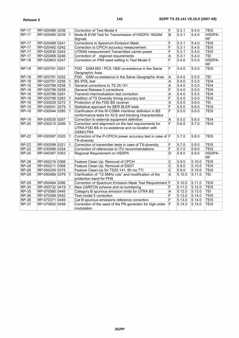
3GPP
3GPP TS 25.141 V5.15.0 (2007-09)142Release 5
RP-17 RP-020488 0236 Correction of Test Model 4 F 5.3.1 5.4.0 TEI5 RP-17 RP-020495 0239 1 Node-B EVM Test for Transmission of HSDPA 16QAM
Signals B 5.3.1 5.4.0 HSDPA-
RF RP-17 RP-020488 0241 Corrections to Spectrum Emission Mask F 5.3.1 5.4.0 TEI5 RP-17 RP-020492 0242 Correction to CPICH accuracy measurement F 5.3.1 5.4.0 TEI5 RP-17 RP-020530 0243 UTRAN measurement Transmitted carrier power F 5.3.1 5.4.0 TEI5 RP-17 RP-020468 0246 Correction of regional requirements A 5.3.1 5.4.0 TEI RP-18 RP-020803 0247 Correction on PN9 seed setting in Test Model 5 F 5.4.0 5.5.0 HSDPA-
RF RP-18 RP-020781 0251 FDD GSM 850 / PCS 1900 co-existence in the Same
Geographic Area F 5.4.0 5.5.0 TEI5
RP-18 RP-020781 0252 FDD GSM co-existence in the Same Geographic Area A 5.4.0 5.5.0 TEI RP-18 RP-020791 0256 1 BS IPDL test A 5.4.0 5.5.0 TEI4 RP-18 RP-020788 0258 1 General corrections to TS 25.141 A 5.4.0 5.5.0 TEI4 RP-18 RP-020799 0259 General Release 5 corrections F 5.4.0 5.5.0 TEI5 RP-18 RP-020788 0261 Transmit intermodulation test correction A 5.4.0 5.5.0 TEI4 RP-18 RP-020799 0263 1 Addition of TX Diversity timing accuracy test F 5.4.0 5.5.0 TEI5 RP-19 RP-030029 0272 1 Protection of the FDD BS receiver A 5.5.0 5.6.0 TEI RP-19 RP-030041 0279 1 Statistical approach for BER BLER tests F 5.5.0 5.6.0 TEI5 RP-19 RP-030044 0285 1 Clarification of the W-CDMA interferer definition in BS
conformance tests for ACS and blocking characteristics F 5.5.0 5.6.0 TEI5
RP-19 RP-030035 0287 Correction to external equipment definition A 5.5.0 5.6.0 TEI4 RP-20 RP-030215 0299 1 Correction and alignment on the test requirements for
UTRA-FDD BS in co-existence and co-location with GSM/UTRA
F 5.6.0 5.7.0 TEI5
RP-22 RP-030597 0320 1 Correction of the P-CPICH power accuracy test in case of TX-diversity
F 5.7.0 5.8.0 TEI5
RP-22 RP-030599 0321 1 Correction of transmitter tests in case of TX-diversity F 5.7.0 5.8.0 TEI5 RP-22 RP-030596 0324 Correction of references to ITU recommendations F 5.7.0 5.8.0 TEI5 RP-25 RP-040367 0353 - Regional Requirement on HSDPA D 5.8.0 5.9.0 HSDPA-
RF RP-28 RP-050216 0366 Feature Clean Up: Removal of CPCH C 5.9.0 5.10.0 TEI5 RP-28 RP-050211 0368 Feature Clean Up: Removal of SSDT C 5.9.0 5.10.0 TEI5 RP-28 RP-050259 0375 Feature Clean-Up for TS25.141, 80 ms TTI C 5.9.0 5.10.0 TEI5 RP-29 RP-050489 0379 1 Clarification of “12.5MHz rule” and modification of the
protection band for PHS A 5.10.0 5.11.0 TEI
RP-29 RP-050494 0386 Correction of Spectrum Emission Mask Test Requirement F 5.10.0 5.11.0 TEI5 RP-30 RP-050732 0419 1 New UARFCN scheme and re-numbering F 5.11.0 5.12.0 TEI5 RP-35 RP-070080 0445 Category B spurious emission limits for UTRA BS A 5.12.0 5.13.0 TEI RP-36 RP-070369 0452 Test model 5 correction F 5.13.0 5.14.0 TEI5 RP-36 RP-070371 0449 Cat B spurious emissions reference correction F 5.13.0 5.14.0 TEI5 RP-37 RP-070652 0458 Correction of the seed of the PN generator for high-order
modulation F 5.14.0 5.15.0 TEI5