3d x-ray microscopy for fa of micro-bumps p.12
TRANSCRIPT

SEMICONDUCTORS • PACKAGING • MEMS • LEDS • DISPLAYS
www.solid-state.com
Big Changes in Mask Manufacturing P. 18
Understanding ALD, MLD and SAMs P. 22
Outlook for 2018 P. 25
3D X-ray Microscopy for FA of Micro-bumps P.12
JANUARY/FEBRUARY 2018
Plan Now - Atte
nd The ConFab 20
18
May 20-2
3, Las V
egas
Details I
nside Back Cove
r


www.solid-state.com SOLID STATE TECHNOLOGY JANUARY/FEBRUARY 2018 1www.solid-state.com SOLID STATE TECHNOLOGY JANUARY/FEBRUARY 2018 1
CO
VE
R
F E A T U R E S
D E P A R T M E N T SC O L U M N S
JANUARY/FEBRUARY 2018 VOL. 61 NO. 1
X-ray imaging is widely employed for non-destructive FA inspection because it can explore interior structures of chips and packages.
12
22
22
25
INSPECTION | High-res 3D X-ray microscopy for non-destructive failure analysis of chip-to-chip micro-bump interconnects in stacked die packagesChip-to-chip interconnects require new defect localization techniques and failure analysis flowsSyahirah Md Zulkifli, Bernice Zee and Wen Qiu, Advanced Micro Devices, Singapore; and Allen Gu, ZEISS Semiconductor Manufacturing Technology Process Control Solutions, Pleasanton, CA
LITHOGRAPHY | 2018: Big changes in mask manufacturing and what it means for mask modelsChanges are driving the need for more detailed and more accurate modeling for mask manufacturing. Ryan Pearman, D2S, Inc., San Jose, CA
DEPOSITION | Understanding ALD, MLD and SAMs as they enter the fab As the world of advanced manufacturing enters the sub-nanometer scale era, it is clear that ALD, MLD and SAM represent viable options for delivering the required few-atoms-thick layers required with uniformity, conformality, and purity. Barry Arkles, Jonathan Goff, Gelest Inc., Morrisville PA, and Alain E. Kaloyeros, SUNY Polytechnic Institute, Albany, NY
BUSINESS | Executive viewpoints: 2018 outlookEach year, Solid State Technology turns to industry leaders to hear viewpoints on the technological and economic outlook for the upcoming year. Read through these expert opinions on what to expect in 2018.
3 Web Exclusives
4 News
30 Ad Index
2 Editorial | Join us at The ConFab 2018, Pete Singer, Editor-in-Chief
10 Packaging | Advances in packaging polymers Phil Garrou, Contributing Editor
11 Semiconductors | Logic densities advance at IEDM 2017, Pete Singer, Editor-in-Chief
31 Industry Forum | Work to do to keep the good times rolling, Ajit Manocha, President and CEO of SEMI

2 JANUARY/FEBRUARY 2018 SOLID STATE TECHNOLOGY www.solid-state.com
CREATIVE/PRODUCTION/ONLINE
Marjorie Sharp, Production Traffic Coordinator
Nicky Jacobson, Senior Graphic Designer
Simone Bradley, Graphic Designer
Slava Dotsenko, Senior Web Developer
MARKETING/CIRCULATIONJenna Johnson, [email protected]
CORPORATE OFFICERS
Extension Media, LLCVince Ridley, President and [email protected]
Clair Bright, Vice President and PublisherEmbedded Electronics Media [email protected]
For subscription inquiries: Tel: 847.559.7500; Fax: 847.291.4816; Customer Service e-mail: [email protected]; Subscribe: www.sst-subscribe.com
Solid State Technology is published eight times a year by Extension Media LLC, 1786 Street, San Francisco, CA 94107. Copyright © 2018 by Extension Media LLC. All rights reserved. Printed in the U.S.
1786 18th StreetSan Francisco, CA 94107
2 JANUARY/FEBRUARY 2018 SOLID STATE TECHNOLOGY www.solid-state.com
JANUARY/FEBRUARY 2018 VOL. 61 NO. 1 • Solid State Technology ©2018 (ISSN 0038-111X) Subscriptions: Domestic: one year: $258.00, two years: $413.00; one year Canada/Mexico: $360.00, two years: $573.00; one-year international airmail: $434.00, two years: $691.00; Single copy price: $15.00 in the US, and $20.00 elsewhere. Digital distribution: $130.00. You will continue to receive your subscription free of charge. This fee is only for air mail delivery. Address correspondence regarding subscriptions (including change of address) to: Solid State Technology, 1786 18th Street, San Francisco, CA 94107-2343. (8 am – 5 pm, PST).
Pete Singer, Editor-in-Chief Ph: 978.470.1806, [email protected]
Shannon Davis, Editor, Digital Media Ph: 603.547.5309 [email protected]
Ed Korczynski, Senior Technical Editor, [email protected]
Dave Lammers, Contributing Editor
Phil Garrou, Contributing Editor
Dick James, Contributing Editor
Vivek Bakshi, Contributing Editor
editorial
The ConFab 2018, to be held May 20-23 at The Cosmopolitan of Las Vegas, is a conference and networking event designed to inform and connect leading semiconductor executives from all parts of the supply chain. Now in its 14th year, it is produced by Solid State Technology magazine, the semiconductor industry’s oldest and most respected business publication.
The goal of The ConFab this year is to show how today’s semicon-ductor manufacturers and their suppliers can they best position themselves to take advantage of the tremendous growth the industry is expecting to see in the near future, propelled by a wide array of new applications, including artificial intelligence, virtual and augmented reality, automotive, 5G, the IoT, cloud computing and healthcare.
Here’s a quick look at the agenda as it stands now.
After a welcome reception on Sunday evening, we’ll kick things off on Monday with a talk by IBM’s Rama Divakaruni on “How A.I. is Driving the New Semiconductor Era.” Although A.I. (and associated deep learning and machine learning) is now in its infancy, it will likely to have a major impact on how semicon-ductors will be designed and manufactured in the future. A.I. will demand dramatic enhancement in computational perfor-mance and efficiency, which in turn will drive fundamental changes in algorithms, systems and chip design. Devices and materials will also change.
Following Rama’s talk, we’ll hear from John M. Martinis, Google who heads up Google’s Quantum A.I. Lab. The lab is particularly interested in applying quantum computing to artificial intelligence and machine learning.
After the keynote talks, we’ll hear from a number of industry visionaries, including John Hu, Director of Advanced Technology for Nvidia, Dan Armbrust, Founder and Director of
Silicon Catalyst, and Tom Sonderman, President of Sky Water Technology Foundry. On Monday afternoon, invited industry experts, such as Bill Von Novak of Qualcomm will drill down into the applications most critical to semiconductor industry growth, including automotive, networking, healthcare and the IoT.
On Tuesday, the talks will focus on manufacturing trends and challenges with mainstream semiconductor manufacturing the focus of the morning session and advanced packaging the focus in the afternoon. George Gomba, VP of technology research at GlobalFoundries, will provide an update on EUV lithography, followed by Koukou Suu, of Ulvac, a leading expert on materials for phase change memories. Howard Witham, Vice President of Texas Operations, Qorvo, will provide some insights in using artificial intelligence and automation in semiconductor manufacturing.
The advanced packaging session on Tuesday afternoon is organized and sponsored by IEEE CPMT, notably Li Li, Distin-guished Engineer, Cisco and William Chen, Fellow, ASE. The semiconductor industry is increased relying on advanced packaging to deliver far more integrated, complex and advanced solutions for different market segments.
On Wednesday, we’ll hear from leading analysts, including Len Jenelik, Senior Director, Semiconductor Manufacturing at IHS Markit, and Jim Feldhan, President of Semico, on market trends and the expected business climate moving forward.
You can register and keep up-to-date by visiting www.theconfab.com. For sponsorship inquiries, contact Kerry Hoffman at [email protected]. For those interested in attending as a guest or qualifying as a VIP, contact Sally Bixby at [email protected].
Join Us at The ConFab 2018
—Pete Singer, Editor-in-Chief

www.solid-state.com SOLID STATE TECHNOLOGY JANUARY/FEBRUARY 2018 3
1786 18th StreetSan Francisco, CA 94107
Web Exclusives nb&news and blogs
online@ www.solid-state.com
Talent pipeline key to enabling industry growth: Takeaways from SEMI Member ForumElectronic manufacturing is becoming cool to today’s youth. STEM skills are hot in the global job market – though the number of females pursuing a STEM education continues to lag. Work-based learning is key to mastering new tech-nologies. And the electronics industry needs a global talent pipeline more than ever.http://bit.ly/2mMSPgL
New speakers for The ConFab 2018The ConFab staff is presently lining up speakers and VIPs for our 2018 Agenda/Program and networking event, which will be held May 20-23 at The Cosmopolitan of Las Vegas. Many different topics have been considered for the talks and key-note addresses, as there are many new drivers and technolo-gies for the semiconductor industry to be considered.http://bit.ly/2Do9jpd
Revision to SEMI E142: Specification for substrate mappingAs dynamic back-end related technologies such as TSV (Through-Silicon Vias), InFO (Integrated Fan Out), etc., en-able electronic devices to downsize with higher performance, the importance of back-end processing is greater than ever. Due to this, more and more customers are requesting “quality control” by tracing raw materials to assembly and packaging companies and the need for a standard is clear.http://bit.ly/2FJLxCg
Insights from the Leading Edge: Broadcom continues consolidationOn November 6, Broadcom announced its intention to buy its rival, Qualcomm, for ~ $130B, including debt. If success-ful, it would be the largest deal in the history of the technol-ogy acquisitions.http://bit.ly/2DiYyVh
IEDM 2017: Intel’s 10nm platform processIEDM this year was its usual mixture of academic exotica and industrial pragmatica (to use a very broad-brush description), but the committee chose to keep us all waiting until the Wednesday morning before we got to the CMOS platform papers. Of course, the talk we were all anticipating was Intel’s Chris Auth on “A 10nm High Performance and Low-Power CMOS Technology Featuring 3rd Generation FinFET Transistors, Self-Aligned Quad Patterning, Contact over Active Gate and Cobalt Local Interconnects”.http://bit.ly/2DDtVHG
Insights from the Leading Edge: IWPLC Part 3Tanja Braun of IZM Fraunhoffer discussed “Fan-out and Panel level technology for Advanced LED Packaging.”http://bit.ly/2mLnQ50
Surprising changes to semiconductor equipment market share in 2017Through three quarters of calendar year 2017, market shares of top semiconductor equipment manufacturers indicate large gains by Tokyo Electron and Lam Research, according to the report “Global Semiconductor Equipment: Markets, Market Shares, Market Forecasts,” recently published by The Information Network, a New Tripoli-based market research company.http://bit.ly/2re3vKa
Luc Van den hove to receives SEMI Sales and Marketing Excellence AwardSEMI today announced that Luc Van den hove, president and CEO of imec, has been selected as the 2018 recipient of the SEMI Sales and Marketing Excellence Award, inspired by Bob Graham. He was honored for outstanding achievement in semiconductor equipment and materials marketing during ceremonies at ISS 2018 on January 17 in Half Moon Bay, California.http://bit.ly/2mEjvzD

4 JANUARY/FEBRUARY 2018 SOLID STATE TECHNOLOGY www.solid-state.com
newsPlease send news articles to
worldnews
Worldwide semiconductor revenue totalled$419.7 billion in 2017, a 22.2 percent increasefrom 2016, according to preliminary resultsby Gartner, Inc. Undersupply helped drive64 percent revenue growth in the memorymarket, which accounted for 31 percent oftotal semiconductor revenue in 2017.
“The largest memory supplier, SamsungElectronics, gained the most market shareand took the No. 1 position from Intel — thefirst time Intel has been toppled since 1992,”said Andrew Norwood, research vice presi-dent at Gartner. “Memory accounted formore than two-thirds of all semiconductorrevenue growth in 2017, and became thelargest semiconductor category.”
The key driver behind the booming memoryrevenue was higher prices due to a supplyshortage. NAND flash prices increased yearover year for the first time ever, up 17 percent,while DRAM prices rose 44 percent.
Equipment companies could not absorbthese price increases so passed them ontoconsumers, making everything from PCs tosmartphones more expensive in 2017.
Other major memory vendors, includ-ing SK Hynix and Micron Technology, alsoperformed strongly in 2017 and rose in therankings (see Table 1).
Worldwide semiconductor revenue grew 22.2% in 2017; Samsung takes over No. 1 position
Second-placed Intel grew its revenue 6.7percent in 2017, driven by 6 percent growthin data center processor revenue due todemand from cloud and communicationsservice providers. Intel’s PC processorrevenue grew more slowly at 1.9 percent,but average PC prices are on the rise againafter years of decline following the market’sshift from traditional desktops towardtwo-in-one and ultramobile devices.
The current rankings may not last long,however, “Samsung’s lead is literally built onsand, in the form of memory silicon,” said Mr.Norwood. “Memory pricing will weaken in2018, initially for NAND flash and then DRAMin 2019 as China increases its memory produc-tion capacity. We then expect Samsung to losea lot of the revenue gains it has made.”
2017 was a relatively quiet year for mergersand acquisitions. Qualcomm’s acquisitionof NXP was one big deal that was expectedto close in 2017, but did not. Qualcomm stillplans to complete the deal in 2018, but thishas now been complicated by Broadcom’sattempted takeover of Qualcomm.
“The combined revenues of Broadcom,Qualcomm and NXP were $41.2 billion in 2017
— a total beaten only by Samsung and Intel,”said Mr. Norwood. “If Broadcom can final-ize this double acquisition and Samsung’s
memory revenuefalls as forecast, thenSamsung could slipto third place duringthe next memorydownturn in 2019.” �
EUROPE: Picosun Oy announced a partnership with STMicroelectronics S.r.l. to develop the next generation 300mm production solutions for advanced power electronics.
USA: Boston Semi Equipment announced that it has received a multisystem order for its Zeus gravity feed systems for handling pressure MEMS devices.
ASIA: UMC filed a patent infringe-ment lawsuit against Micron.
USA: ON Semiconductor and ConvenientPower Systems announced a strategic collaboration in automotive wireless charging.
EUROPE: The SEMI European 3D Summit will make its Dresden, Germany, debut 22-24 January, 2018, featuring a broader scope of 3D topics driving innovation and business opportunities in the 3D market.
USA: Arrow Electronics, Inc. announced the successful completion of its acquisition of eInfochips, one of the world’s largest design and managed services companies.
EUROPE: STMicroelectronics and USound deliver first advanced MEMS silicon micro-speakers.
USA: Micron and Intel announced an update to their successful NAND joint development partnership that has helped the companies develop and deliver industry-leading NAND technologies to market.
ASIA: UMC announced availability of 40nm SST embedded flash process.
USA: Nordson Corporation acquired Sonoscan.
ASIA: Samsung Electronics announced that it has begun mass producing the industry’s first 2nd-generation of 10-nanometer class (1y-nm), 8-gigabit (Gb) DDR4 DRAM.
USA: Intersil to start operations as Renesas Electronics America in January 2018.
2017 Rank
2016 Rank
Vendor 2017 Revenue
2017 Market Share (%)
2016 Revenue
2016-2017 Growth (%)
1 2 Samsung Electronics 61,215 14.6 40,104 52.62 1 Intel 57,712 13.8 54,091 6.73 4 SK Hynix 26,309 6.3 14,700 79.04 6 Micron Technology 23,062 5.5 12,950 78.15 3 Qualcomm 17,063 4.1 15,415 10.76 5 Broadcom 15,490 3.7 13,223 17.17 7 Texas Instruments 13,806 3.3 11,901 16.08 8 Toshiba 12,813 3.1 9,918 29.29 17 Western Digital 9,181 2.2 4,170 120.210 9 NXP 8,651 2.1 9,306 -7.0 Others 174,418 41.6 157,736 10.6 Total Market 419,720 100.0 343,514 22.2
TABLE 1. Source: Gartner (January 2018)


6 JANUARY/FEBRUARY 2018 SOLID STATE TECHNOLOGY www.solid-state.com
Nanostructured gate dielectric boosts stability of organic thin-film transistors
A nanostructured gate dielectric may have addressed themost significant obstacle to expanding the use of organicsemiconductors for thin-film transistors. The structure,composed of a fluoropolymer layer followed by a nanolam-inate made from two metal oxide materials, serves as gatedielectric and simultaneously protects the organic semicon-ductor – which had previously been vulnerable to damagefrom the ambient environment – and enables the transis-tors to operate with unprecedented stability.
The new structure gives thin-film transistors stability compa-rable to those made with inorganic materials, allowing themto operate in ambient conditions – even underwater. Organicthin-film transistors can be made inexpensively at low temper-ature on a variety of flexible substrates using techniques suchas inkjet printing, potentially opening new applications thattake advantage of simple, additive fabrication processes.
“We have now proven a geometry that yields lifetime perfor-mance that for the first time establish that organic circuitscan be as stable as devices produced with conventionalinorganic technologies,” said Bernard Kippelen, the JosephM. Pettit professor in Georgia Tech’s School of Electrical andComputer Engineering (ECE) and director of Georgia Tech’sCenter for Organic Photonics and Electronics (COPE). “Thiscould be the tipping point for organic thin-film transistors,addressing long-standing concerns about the stability oforganic-based printable devices.”
The research was reported January 12 in the journal ScienceAdvances. The research is the culmination of 15 years of devel-opment within COPE and was supported by sponsors including
the Office of Naval Research, the Air Force Office of ScientificResearch, and the National Nuclear Security Administration.
Transistors comprise three electrodes. The source and drainelectrodes pass current to create the “on” state, but onlywhen a voltage is applied to the gate electrode, which isseparated from the organic semiconductor material by a thindielectric layer. A unique aspect of the architecture devel-oped at Georgia Tech is that this dielectric layer uses twocomponents, a fluoropolymer and a metal-oxide layer.
“When we first developed this architecture, this metal oxidelayer was aluminum oxide, which is susceptible to damagefrom humidity,” said Canek Fuentes-Hernandez, a seniorresearch scientist and coauthor of the paper. “Working incollaboration with Georgia Tech Professor Samuel Graham,we developed complex nanolaminate barriers which couldbe produced at temperatures below 110 degrees Celsiusand that when used as gate dielectric, enabled transistorsto sustain being immersed in water near its boiling point.”
The new Georgia Tech architecture uses alternating layersof aluminum oxide and hafnium oxide – five layers of one,then five layers of the other, repeated 30 times atop thefluoropolymer – to make the dielectric. The oxide layers areproduced with atomic layer deposition (ALD). The nanolam-inate, which ends up being about 50 nanometers thick, isvirtually immune to the effects of humidity.
“While we knew this architecture yielded good barrier proper-ties, we were blown away by how stably transistors operatedwith the new architecture,” said Fuentes-Hernandez. “Theperformance of these transistors remained virtuallyunchanged even when we operated them for hundreds ofhours and at elevated temperatures of 75 degrees Celsius.This was by far the most stable organic-based transistor wehad ever fabricated.”
For the laboratory demonstration, the researchers used aglass substrate, but many other flexible materials – includ-ing polymers and even paper – could also be used.
In the lab, the researchers used standard ALD growth techniquesto produce the nanolaminate. But newer processes referred toas spatial ALD – utilizing multiple heads with nozzles deliver-ing the precursors – could accelerate production and allow thedevices to be scaled up in size. “ALD has now reached a level ofmaturity at which it has become a scalable industrial process,and we think this will allow a new phase in the development oforganic thin-film transistors,” Kippelen said.
newscont.
FIGURE 1. Image shows organic-thin film transistors with a nanostructured gate dielectric under continuous testing on a probe station. (Credit: Rob Felt, Georgia Tech)

www.solid-state.com SOLID STATE TECHNOLOGY JANUARY/FEBRUARY 2018 7www.solid-state.com SOLID STATE TECHNOLOGY JANUARY/FEBRUARY 2018 7
An obvious application is for the transistors that controlpixels in organic light-emitting displays (OLEDs) used in suchdevices as the iPhone X and Samsung phones. These pixelsare now controlled by transistors fabricated with conventionalinorganic semiconductors, but with the additional stabilityprovided by the new nanolaminate, they could perhaps bemade with printable organic thin-film transistors instead.
Internet of things (IoT) devices could also benefit from fabri-cation enabled by the new technology, allowing productionwith inkjet printers and other low-cost printing and coatingprocesses. The nanolaminate technique could also allowdevelopment of inexpensive paper-based devices, suchas smart tickets, that would use antennas, displays andmemory fabricated on paper through low-cost processes.
But the most dramatic applications could be in very largeflexible displays that could be rolled up when not in use.
“We will get better image quality, larger size and betterresolution,” Kippelen said. “As these screens become larger,the rigid form factor of conventional displays will be a limita-tion. Low processing temperature carbon-based technologywill allow the screen to be rolled up, making it easy to carryaround and less susceptible to damage.
For their demonstration, Kippelen’s team – which alsoincludes Xiaojia Jia, Cheng-Yin Wang and Youngrak Park
– used a model organic semiconductor. The material haswell-known properties, but with carrier mobility values of1.6 cm2/Vs isn’t the fastest available. As a next step, theyresearchers would like to test their process on newer organicsemiconductors that provide higher charge mobility. Theyalso plan to continue testing the nanolaminate under differ-ent bending conditions, across longer time periods, and inother device platforms such as photodetectors.
Though the carbon-based electronics are expanding theirdevice capabilities, traditional materials like silicon havenothing to fear.
“When it comes to high speeds, crystalline materials like siliconor gallium nitride will certainly have a bright and very longfuture,” said Kippelen. “But for many future printed applica-tions, a combination of the latest organic semiconductor withhigher charge mobility and the nanostructured gate dielectricwill provide a very powerful device technology.” �

8 JANUARY/FEBRUARY 2018 SOLID STATE TECHNOLOGY www.solid-state.com
Industry enters the age of WOWBy Christian G. Dieseldorff, Industry Research & Statistics Group, SEMI, Milpitas, California
The semiconductor industry has been there before, withlarge increases in investments followed by dramaticdownturns. While the most dramatic downturns, 2001 and2009, were due to, in a large part, acro-economic factors,the industry has typically observed one to two years ofincreased investment spending followed by a down period.This time around, the industry will achieve a “WOW” withthree consecutive years of fab investment growth, a patternnot observed since the mid-1990s.
Why are things different this time? A diverse array of technol-ogy drivers promise more robust long-term growth, suchas Mobile applications, Internet of Things (IoT), Automotive& Robotics, Industrial, Augmented Reality & Virtual Reality(AR&VR), Artificial Intelligence (AI), and 5G networking. Eachof these new technologies inspires a big “WOW” as the indus-try embarks on the beginning of a promising journey of growth.
Driven by these technologies, on average the semiconduc-tor revenue CAGR from 2016 to 2021 is forecasted to be6 percent (in comparison to the previous 2011-2016 CAGRof 2.3 percent). For the first time in the industry’s history,semiconductor revenues will exceed the US$400 billionrevenue milestone in 2017. Demand for chips is high, pricingis strong for memory, and the competition is fierce. All of thisis spurring increased fab investments, with many companiesinvesting at previously unseen levels for new fab construc-tion and fab equipment. See Figure 1.
The World Fab Forecast report, published on December 4, 2017,by SEMI, is modeling that fab equipment spending in 2017 willtotal US$57 billion or 41 percent year-over-year (YoY) growth.In 2018, spending is expected to shoot up another 11 percentat US$63 billion. The two spending jumps in 2017 and 2018 arecontributing to the “WOW” factor and to two consecutive yearsof record fab investments. Following historic large investments,some slowdown is expected for 2019.
Many companies, such as Intel, Micron, Toshiba (and Western Digital), and GLOBALFOUNDRIES, have increased fab invest-ments in 2017 and 2018; however, the strong increases we see in both years are not caused by these companies but by one company and primarily one region. See Figure 2.
The first jump – a Big WOW – in 2017 is the surge of invest-ments in Korea, due mainly to Samsung. Samsung is expected to increase its fab equipment spending by 128 percent in 2017 from US$8 billion to US$18 billion. No single company has invested so much in a single year in its fabs and much of its spending is in Korea. SK Hynix also increased fab equipment spending, by about 70 percent, to US$5.5 billion, its largest spending level in its history. While the bulk of Samsung’s and SK Hynix’s spending remains in Korea, some will also go to China, and in the case of Samsung to the United States. Both Samsung and SK Hynix are expected to maintain high levels of investments for 2018.
The second jump – another WOW – is investment growth for 2018 in China. China is expected to begin equipping the many fabs that were constructed in 2017. In the past, non-Chinese companies made the majority of the fab investments in China but for the first time in 2018, Chinese-owned companies will approach parity, spending nearly as much on fab equipment as non-Chinese device manufacturers.
Between 2013 and 2017, fab equipment spending in China by Chinese-owned companies typically ranged between US$1.5 billion to US$2.5 Billion per year, while non-Chinese compa-nies invested between US$2.5 billion to US$5 billion per year. In 2018, Chinese-owned companies are expected to invest about US$5.8 billion, while non-Chinese will invest US$6.7 billion. Many new companies such as Yangtze Memory Technology, Fujian Jin Hua, Hua Li, and Hefei Chang Xin Memory are investing heavily in the region.
FIGURE 1.
FIGURE 2.
newscont.

www.solid-state.com SOLID STATE TECHNOLOGY JANUARY/FEBRUARY 2018 9
TechCon 2018TechCon 2018Orlando61st Annual SVC Technical Conference • May 5-10, 2018Gaylord Palms Resort and Convention Center, Orlando, Florida, USA
Technical ProgramMay 7–10Education ProgramMay 5–10Technology ExhibitMay 8–9
Learn more at www.svc.org or send an Email to [email protected]. Box 10628, Albuquerque, NM 87184 • Telephone: +1 (505) 897-7743 • Fax: +1 (866) 577-2407
Technical Program May 7–10Featuring a Symposium on Multi-functional Thin Films - The Tailoring of InterfacesToday’s High Performance Films Shape Tomorrow’s Products Plus! Interactive Networking Forums, Discussion Groups and Experts Corner • Free Passes for May 8th or 9th
Education Program May 5–10Problem-Solving Tutorial Courses
Technology Exhibit May 8–9 The Largest Expo Dedicated to Vacuum Coating Technologies • Over 150 Exhibitors + Free AdmissionRegionally located with NPE 2018 – The Plastics Show
New fabs being builtHistoric highs in equipment spending in 2017 and 2018 reflectgrowing demand. This spending follows unprecedentedgrowth in construction spending for new fabs also detailedin SEMI’s World Fab Forecast report. Construction spendingwill reach all-time highs with China construction spendingtaking the lead: US$6 billion in 2017 and US$6.6 billion in2018, shattering another record – no region has ever spentmore than US$6 billion in a single year for construction.More new fabs mean another wave of spending on equip-ping fabs in the next few years. See Figure 3.
Considering all of these “WOW” factors, there is good reasonto feel positive about the semiconductor industry. Even witha slowdown, the industry has and will continue to enjoy apositive outlook for long-term growth. In the meantime, holdon tight and enjoy the “WOW.”
FIGURE 3.
More details are available in SEMI’s just-published World FabForecast, December 4, 2017, edition which covers quarterlydata (spending, capacity, technology nodes, wafer sizes, andproduct types) per fab until end of 2018. �

10 JANUARY/FEBRUARY 2018 SOLID STATE TECHNOLOGY www.solid-state.com
Packaging
PHIL GARROU, Contributing Editor
Presentations that described new polymer dielectric advance-ments were a highlight of last year’s IWLPC (InternationalWafer Level Packaging Conference), held in October in San Jose.
Matsukawa of HD Micro described their “Low temp curablePI/PBO for Wafer Level Packaging.”
For next generation advanced packaging technologies, themost important requirements for dielectric materials are lowtemperature curability, high lithographic performance, highchemical resistance, and low warpage. He reported on newlow temperature (<2000C) curable PI and PBO.
Conventional photosensitive PIs and PBOs have requiredcuring temperatures greater than 300ºC to complete cycli-zation as well as advance polymerization. To formulate lowtemperature curable materials, they re-designed the polymerbackbone in order to enhance cyclization and changed thecross-linker to form a strong network structure even whencured <2000C.
Generally positive tone photo-definable materials arecomposed of a PBO precursor, a photo acid generator, cross-linker etc. Regarding the new positive tone PBO, a suitablephoto acid generator and cross-linker combination wasselected to increase the resolution while also improving theadhesion to Cu, which has been a significant problem for pastgeneration products.
Araki of Toray discussed their “Novel Low Temp curablepositive tone photo dielectric material with high elongationfor panel processing”.
Dielectric materials for redistribution layers (RDL) are oneof the most important materials for fan out panel levelprocessing (FOPLP). Toray introduces a low-temperaturecurable positive-tone photosensitive dielectric material withthe high elongation property for fabricating RDL on FOPLP.The high elongation property was achieved by the intro-duction of flexible molecular skeleton in the base polymerbackbone to increase the entanglement of each polymer chain.Cured films showed elongation up to 80%. This positive-tonephotosensitive material offers fine pattern (3 µm trench and 5µm line and space) with good sensitivity (300 mJ/cm2 (i-line))and shows high chemical resistance toward resist strippers.
Fukuhara of Hitachi Chemical describedtheir “Photo-sensitive Insulation Filmfor Encapsulation and Embedding.”Conventional PoP with flip chips
Advances in packaging polymersmounted on BGA like substratesis shown in Figure 1 compared toa fan out PoP.
In order to make a high densityconnection between upper andlower packages, it is necessary to form fine pitch throughholes on the bottom package. These through hole vias can beformed by laser drilling. HC has developed a laminate photofilm which allows encapsulation of the die and subsequentphoto formation of the required vias through the film.
Onozeki of Hitachi Chemical discussed “Wafer Level PackagingMaterials and Processes” where he examined the influencesof the material properties of temp bond adhesives (TBA) andepoxy mold cmpds (EMC) on the warpage of FO-WLP duringthe fabrication process by both of the experiments and finiteelement analysis.
For TBA, it was found that “the deformation of TBA results inrelatively free shrinkage of EMC on the support, and Young’smodulus of TBA influences on the warpage most significantly.The small Young’s modulus TBA suppressed the warpageregardless of the support materials”. As for the EMC, “…thelow Young’s modulus, low CTE and low Tg are effective toreduce the warpage after post mold curing. The warpage aftergrinding EMC was smaller than those after post mold cure andthere was no big difference in the influence of the mechanicalproperties.” As for FO-WLP structure, the wide die pitch, thinEMC and thick die are effective to reduce warpage. Especially,the wide die pitch contributes to reduce the warpage. 4 layersre-distribution layer with line and space of 2 and 2 µm wassuccessfully fabricated. The layers were interconnected withsmall diameter filled Cu vias of 5 µm. The vias were formedin the photosensitive dielectric material. A bias HAST testrevealed that this material had enough insulation reliability.
Okamoto from JSR discussed “Fine Pitch Plating Resist forHigh Density FOWLP.” For the next generation of high densityFO-WLP, RDLs as low as 2 µm are reportedly required tosupport more I/O’s and multiple RDL layers. �

www.solid-state.com SOLID STATE TECHNOLOGY JANUARY/FEBRUARY 2018 11
Semiconductors
DAVE LAMMERS Contributing Editor
to create fins with a tight pitch. The SAQP approach required two sacri-ficial layers, with lithography defining the first large pattern and four additional steps to remove the spacers and create the final lines and spaces. The Intel 10 nm fins are 46nm in height.
The SAQP approach starts by exposing a 130nm line, depos-iting the two spacers, halving the pattern to 68nm, and again to 34nm. “It is a grating and cut process similar to what we showed at 22nm, except it is SAQP instead of SADP,” using patterning to form a grating of fins, and cutting the ends of the fins with a cut mask.
“There were no additional lithography steps required. The result was fins that are tighter, straighter, and taller, with better drive current and matching” than Intel’s 14nm-generation fins. Intel continued to use self-aligned double patterning (SADP) for M 2-5, and for gate patterning.
GlobalFoundries -- which has been in production for 18 months with the 14nm process used by AMD, IBM, and others -- plans to ramp its 7nm logic generation starting in mid-2018. The 7nm high-density SRAM cell measures .0269 µm2, slightly smaller than TSMC’s published 7nm cell, while Intel reported a .0312 µm2 cell size for its 10nm process.
GlobalFoundries chief technology officer Gary Patton said “all of us are in the same zip code” when it comes to SRAM density. What is increasingly important is how the standard cells are designed to minimize the track height and thereby deliver the best logic cell technology to designers, Patton said.
Britt Turkot, senior principal engineer at Intel, discussed the readiness of EUV lithography at an IEDM session, giving a cautiously bullish report. With any multi-patterning solution for leading-edge silicon, including etch and CMP steps, placement error is the biggest challenge. With quad patterning, Turkot said multiple masks are involved, creating “compounded alignment errors.”
EUV has its own challenges, including significant secondary ions from the EUV photons. The key challenge for much of the decade, source power, seems to be partially resolved. “We are confident that the 250 Watts of source power needed for volume manufacturing will be ready once the field tools are upgraded,” she said. �
The 63rd International Electron Devices Meeting brought an optimistic slant to transistor density scaling. While some critics have declared the death of Moore’s Law, there was little evidence of that -- on the density front at least -- at the IEDM.
And an Intel engineering manager gave a presentation at IEDM that took a somewhat optimistic view of EUV lithog-raphy readiness, auguring further patterning improvements, starting with contacts and vias.
GlobalFoundries, which is skipping the 10nm node, presented its 7nm logic technology, expected to move into manufacturing in mid-2018. John Pellerin, vice president of global R&D, said the foundry has worked closely with its two lead customers, AMD and IBM, to define a high-performance-computing 7nm logic technology that achieves a 2.8X improvement of routed logic density compared with its 14nm technology.
Pellerin said the current 7nm process of record (POR) delivers “the right mix of performance, power, and area (PPA),” adding that GlobalFoundries plans to bring in EUV patterning at an undefined later point in the 7+ generation for further improvements.
Chris Auth, director of advanced transistor development at Intel Corp., described a 10nm logic technology that sharply increased the transistor density compared with the 14nm generation, partly due to a contact-over-active-gate (COAG) architecture. The 10nm ring oscillator performance was improved by 20 percent compared with the comparable 14nm test vehicle.
Auth said the COAG approach was a key contributor to Intel’s ability to increase its transistor density by 2.7 times over the company’s previous generation, to 100 million transistors per square millimeter of silicon. While the traditional approach puts the contact via over the isolation area, COAG places the contact via directly over the gate. Auth said while the approach does require a second etch stop layer and other process complex-ities, it contributes “a sizable 10 percent reduction in area.” Elimination of the dummy gate for cell boundary isolation, and the use of cobalt at three layers also contributed.
While there has been much hand wringing in the industry over the costs involved with multi-level patterning, Auth didn’t
appear phased by it. Intel used a self-aligned quad patterning (SAQP) scheme
Logic densities advance at IEDM 2017

12 JANUARY/FEBRUARY 2018 SOLID STATE TECHNOLOGY www.solid-state.com
INSPECTION
High-res 3D X-ray microscopy for non-destructive failure analysis of chip-to-chip micro-bump interconnects in stacked die packagesSYAHIRAH MD ZULKIFLI, BERNICE ZEE AND WEN QIU, Advanced Micro Devices, Singapore;
ALLEN GU, ZEISS, Pleasanton, CA
3D integration and packaging has challenged failure analysis (FA) techniques and workflows due to the high complexity of multichip architec-tures, the large variety of materials, and small form factors in highly miniaturized devices [1].
The drive toward die stacking with High Bandwidth Memory (HBM) allows the ability to move higher bandwidth closer to the CPU and offers an oppor-tunity to significantly expand memory capacity and maximize local DRAM storage for high throughput in the data center. However, the integration of HBM results in more complex electrical communications, due to the emerging use of a physical layer (PHY) design to connect the chip and subsystems. FIGURE1 shows the schematic of a 2.5D stacked die package designed so that some HBM µbumps are electrically connected to the main CPU through a PHY connection. In general, the HBM and CPU signal length needs to be minimized to reduce drive strength requirements
and power consumption at the PHY.
This requirement poses new challenges in FA fault isolation. A traditional FA workflow using electrical fault isolation (EFI) techniques to isolate the defect becomes less effective for chip-to-chip interconnects because there are no BGA balls for electrically probing the µbumps at the PHY. As a result, new defect localization techniques and FA flows must be investigated.
XRM theory X-ray imaging is widely employed for non-destructive FA inspection because it can explore interior struc-tures of chips and packages, such as solder balls, silver paste and lead frames. Thus, many morphological failures, such as solder-ball crack/burn-out and bumping failure inside IC packages, can be imaged and analyzed through X-ray tools. In 2D X-ray inspection,
an X-ray irradiates samples and a 2D detector utilizes the projection shadow to construct 2D images. This technique, however, is not adequate for revealing true 3D structures since it projects 3D structures onto a 2D plane. As a result, important information, such as internal faulty regions of electronic packages, may remain hidden. This disadvantage can be overcome by using 3D X-ray microscopic technology, derived from the original computed tomography (CT) technique. In a 3D imaging system, a series of 2D X-ray images are captured at different angles while a sample rotates.
FIGURE 1. Schematic of HBM µbump interconnect between the HBM and CPU die.

www.solid-state.com SOLID STATE TECHNOLOGY JANUARY/FEBRUARY 2018 13
INSPECTION
Exclusively from Conax…
+1 800 223 2389 conaxtechnologies.com/etchdefender
Lower annual spend. Lower annual spend. Longer TC life.
EtchDefender™ technology extends the life of quartz thermocouple sheaths in ASM® Epsilon® epitaxial reactors up to 3X longer. Find out how EtchDefender™ can eliminate 1-2 maintenance cycles and reduce your annual spend by 30%.
ASM® and EPSILON® are registered trademarks of ASM® International. Neither Conax Technologies nor its products are a� liated with, approved by or sponsored by ASM® International.
These 2D images are used to reconstruct 3D X-raytomographic slices using mathematic models andalgorithms. The spatial resolution of the imagingtechnique can be improved through the integrationof an optical microscopy system. This improvedtechnology is called 3D X-ray microscopy (XRM) [2].FIGURE 2 shows an example 3D XRM image for astacked die. The image clearly shows the internalstructures - including the TSV, C4 bumps and µbumpof the electronic components - without physicallydamaging or altering the sample. The high resolutionand quality shown here are essential to inspect smallstructural defects inside electronic devices. With itsnon-destructive nature, 3D XRM has been useful fornon-destructive FA for IC packaging devices.
Failure analysis approachThe purpose of an FA workflow is to have a sequenceof analytical techniques that can help to effectivelyand quickly isolate the failure and determine theroot cause. Typical FA workflows for flip-chip devices
consist of non-destructive techniques such as C-Modescanning acoustic microscopy (C-SAM) and timedomain reflectometry (TDR) to isolate the failure,followed by destructive physical failure analysis(PFA). However, there are limitations to each of thesetechniques when posed with the failure analysis of amore complex stacked die package.
C-SAM allows the inspection of abnormal bumps,delamination and any mechanical failure. A focusedsoundwave is directed from a transducer to a smallpoint on a target object and is reflected when it
encounters a defect, inhomogeneity or a boundaryinside the material. The transducer transformsthe reflected sound pulses into electromagneticpulses, which are displayed as pixels with definedgrey values thereby creating an image [3]. However,stacked die composed of a combination of multiplethin layers may complicate C-SAM analysis. This isbecause the thin layers have smaller spacing betweenthe adjacent interface, and shorter delay times forultrasound traveling from one interface to another.Therefore, failures between the die and die attachmay not be easily detected, and false readings mayeven be expected.
TDR is an electrical fault isolation tool that enablesfailure localization through electrical signal data. TheTDR signal carries the impedance load informationof electrical circuitry; hence, the reflected signalsshow the discontinuity location that has caused themismatch of impedance. In-depth theory on TDR isfurther discussed in Chin et al [4]. However, TDR canonly estimate where the failure lies, whether it is in
FIGURE 2. 3D XRM images showing the interior structures of a CPU stacked die.

14 JANUARY/FEBRUARY 2018 SOLID STATE TECHNOLOGY www.solid-state.com
INSPECTION
the substrate, die or interposer region. To pin point the exact location within the area of failure is difficult, due to limitations in separating the various small structures through the TDR signal. Additionally, some of the pulse power is reflected for every impedance change, posing challenges regarding unique defect isolation and signal complexity - especially for stacked die [5]. In cases where the failure pins reside in the HBM µbump region, no BGA ball out is available to probe and send an electrical pulse through.
Physical Failure Analysis (PFA) is a destructive method to find and image the failure once non-destructive fault isolation is complete. PFA can be done both mechanically and by focused ion beam (FIB). For stacked dies, FIB is predominantly used to image smaller interconnect structures such as TSVs and µbumps. However, the drawback is that the success of documenting the failure through PFA is largely dependent on how well the non-destructive FA techniques can isolate the failure region. Without good clear fault isolation direction, the failure region might be destroyed or missed during the PFA process, and thus no root cause can be derived.
The integration of XRM into the FA flow can help to overcome the limitations of the various analysis techniques to isolate the failure. It is a great advantage to image small structures and failures with the high spatial resolution and contrast provided by XRM and without destroying the sample. For failures in stacked die, XRM can be integrated into the FA flow for further fault isolation with high accuracy. The visualization of defects and failed material prior to destructive analysis increases FA success rates. However, the trade-off for imaging small defects at high resolution is time. For stacked die failures, C-SAM and TDR can first be performed to isolate the region of failure. With a known smaller region of interest to focus on, the time taken for XRM to visualize the area at high resolution is significantly reduced.
In cases where failures are identified in the HBM µbump, XRM is an effective technique to isolate the failure through 3D defect visualization. With the failure region isolated, XRM can then act as a guide to perform further PFA. Following are three case studies where XRM was used to image HBM packages with stacked dies.
Case studiesIn the first case study, we explore the application of XRM as the primary means of defect visualization where other non-destructive testing and FA techniques
are not possible. An open failure was reported for non-underfilled stacked die packages during a chip package interaction (CPI) study. The suspected open location was within the µbump joints at the HBM stack/interposer interface. The initial approach exposed the bottom-most die of the HBM stack, followed by FIB cross-sectioning at the specified location. Performing the destructive approach to visualize the integrity of µbump joints in non-underfilled stack die packages was virtually impossible due to the fragility of silicon. The absence of underfill (UF) means that the HBM does not properly adhere to the interposer and is susceptible to peel off. In addition, there was no medium to release shear stresses experienced by the µbump joints upon bending stresses, which could not be absorbed by the package. As seen in FIGURE 3, parallel lapping of the HBM stack without UF caused die crack and peeling.
Consequently, to avoid aggravating the damage on the sample, 3D XRM was performed to inspect and visualize the suspected location using a 0.7µm/voxel and 4X objective without any sample preparation. FIGURE 4 shows an example virtual slice where the micro-cracks throughout the row of µbump joints are visualized. The micro-cracks are measured a few microns wide. It is worth noting that the micro-cracks were visible with a short scan time of 1.5 hrs.
With the critical defect information in 3D, PFA was performed on a sample that was underfilled to facil-itate ease of sample preparation. SEM images in FIGURE 5 validated the existence of µbump micro-cracks observed by 3D XRM inspection.
FIGURE 3. HBM dies were damaged during PFA sample preparation.

www.solid-state.com SOLID STATE TECHNOLOGY JANUARY/FEBRUARY 2018 15
INSPECTION
In the second case study, the 3D XRM technique was applied to a stacked die package with a failure at a specific HBM/XPU physical interface (PHY) µbump connection. This µbump connection provides specific commu-nication between the HBM stack and XPU die, and there is no package BGA ball out to enable electrical probing. Accordingly, it was not possible to verify if the failure type was an open or short. In addition, there was no means to determine if the failure was at the HBM or XPU die. Since defects from previous lots were open failures at the PHY µbump of the HBM, 3D XRM was performed at the suspected HBM open region using a 0.85µm/voxel and 4X objective.
As no defect was observed, XRM was then applied to the corresponding XPU PHY µbump. Contrary to the anticipated µbump open, a short was observed between two µbumps as shown in FIGURES 6a and 6b.
The µbump short resulted from a solder extrusion bridging two adjacent µbumps. If 3D XRM had not been performed, a blind physical cross-section likely would have been performed on the initially suspected open region. As a result, the actual failure region may have been missed and/or destroyed.
In the final case study, an open failure was reported at a signal pin of a stack die package. As per the traditional FA flow, C-SAM and TDR techniques were applied to isolate the fault. C-SAM results showed an anomaly, and TDR suggested an open in the substrate as demonstrated in FIGURE 7a and 7b respectively.
To verify the observations made by C-SAM and TDR non-destructive techniques, 3D XRM was performed using a 0.80µm/voxel and 4X objective at the region of
interest.
FIGURE 8 revealed a crack between the failure C4 bump and associated TSV. A physical cross-section was performed and the passivation cracks between the TSV and interposer backside redistribution layer (RDL) was observed as shown in FIGURE 9.
In this case, 3D XRM provided 3D information for the FA engineer to focus on. Without the visual
knowledge on the defect’s nature and location, the defect would have been missed during PFA.
FIGURE 6. 3D X-ray microscopy slice image of (a) solder extrusion from top view and (b) side view.
FIGURE 5. SEM images show similar cracks in the µbumps visualized by XRM.
FIGURE 7. Zoomed in C-SAM image shows anomaly at a C4 bump (a), and TDR shows an open in the substrate (b).
FIGURE 4. 3D X-ray microscopy image and measurement of cracked µbump in the non-underfilled HBM packages.

16 JANUARY/FEBRUARY 2018 SOLID STATE TECHNOLOGY www.solid-state.com
INSPECTION
FIGURE 8. 3D X-ray microscopy slice image of a fine crack between C4 bump and TSV.
FIGURE 9. SEM images show the cracks between TSV and RDL.
Summary and conclusions3D integration and packaging have brought about new challenges for effective defect localization, especially when traditional electrical fault isolation is not possible. 3D XRM enables 3D tomographic imaging of internal structures in chips, interconnects and packages, providing 3D structural information of failure areas without the need to destroy the sample. 3D XRM is a vital and powerful tool that helps failure analysis engineers to overcome FA challenges for novel 3D stacked-die packages.
AcknowledgementThis article is based on a paper that was presented at the 24th International Symposium on the Physical and Failure Analysis of Integrated Circuits (IPFA 2017).
References1. F. Altmann and M. Petzold, “Innovative Failure Analysis Techniques for
3-D Packaging Developments,” IEEE Design & Test, Vol. 33, No. 3, pp.
46-55, June 2016.
2. C. Y. Liu, P. S. Kuo, C. H. Chu, A. Gu and J. Yoon, “High resolution 3D
X-ray microscopy for streamlined failure analysis workflow,” 2016 IEEE
23rd International Symposium on the Physical and Failure Analysis of
Integrated Circuits (IPFA), Singapore, 2016, pp. 216-219.
3. M. Yazdan Mehr et al., “An overview of scanning acoustic microscope,
a reliable method for non-destructive failure analysis of microelec-
tronic components,” 2015 16th International Conference on Thermal,
Mechanical and Multi-Physics Simulation and Experiments in Micro-
electronics and Microsystems, Budapest, 2015, pp.1-4.
4. J. M. Chin et al., “Fault isolation in semiconductor product, process,
physical and package failure analysis: Importance and overview,”
Microelectronics Reliability, Vol. 51, Issue 9, pp. 1440-8, Nov. 2011.
5. W. Yuan et al., “Packaging Failure Isolation with Time-Domain
Reflectometry (TDR) for Advanced BGA Packages,” 2007 8th Inter-
national Conference on Electronic Packaging Technology, Shanghai,
2007, pp. 1-5.�


18 JANUARY/FEBRUARY 2018 SOLID STATE TECHNOLOGY www.solid-state.com
LITHOGRAPHY
2018: Big changes in mask manufacturing and what it means for mask modelsRYAN PEARMAN, D2S, Inc., San Jose, CA
There are big changes on the horizon for semicon-ductor mask manufacturing, including the imminent first production use of multi-beam mask writers, and the preparation of all phases of semiconductor manufacturing for the intro-
duction of extreme ultra-violet (EUV) lithography within the next few years. These changes, along with the increasing use of multiple patterning and inverse-lithography technology (ILT) with 193i lithography, are driving the need for more detailed and more accurate modeling for mask manufacturing.
New solutions bring new mask modeling challengesBoth EUV and multi-beam mask writing provide solutions to many long-standing challenges for the semiconductor industry. However, they both create new challenges for mask modeling as well. Parameters once considered of negligible impact must be added to mask models targeted for use with EUV and/or multi-beam mask writers. In particular, the correct treatment of dose profiles has emerged as a critical component for mask models targeting these new technologies. This is in addition to scattering effects, such as the well-known EUV mid-range scatter, that must be included in mask models to accurately predict the final mask results. Gaussian models, which form the basis for most tradi-tional mask models, will not be sufficient as many of these new parameters are more properly represented with arbitrary point-spread functions (PSFs).
The most obvious – and most desperately needed – benefit of EUV lithography is greater accuracy due to its enhanced resolution. However, this benefit comes along with a mask-making challenge: wafer-printing defects due to mask errors will appear more readily
because of this enhanced resolution. Therefore, the introduction of EUV will require the mean-to-target (MTT) variability on photomasks to become smaller. From a mask manufacturability perspective, all sources of printing errors, systematic and random, must be improved. This means that mask models must also be more accurate, not only in predicting measurements, but also in predicting variability.
A well-known challenge for EUV mask modeling is the EUV mid-range scatter effect. The more complex topology of EUV masks leads to broader scattering effects. In addition to “classical” forward- and back-scatter effects, which dominate 193i lithography, there is a mid-range (1µm) scatter that now requires modeling. This phenomenon is non-Gaussian in nature, so cannot be simulated accurately with simple Gaussian (“1G”) models. In combination with better treatment of resist effects, a PSF-based model is a much better represen-tation of the critical lithography process.
The eagerly anticipated introduction of EUV will demand a lower-sensitivity resist to be used for EUV masks due to the smaller size of EUV features. This is one of the reasons why multi-beam mask writers have emerged as the replacement for variable shaped beam (VSB) tools for the next generation of mask writers. Slower resists require higher currents, and VSB tools today are limited thermally in ways the massively parallel multi-beam tools are not. In addition to thermal effects, VSB mask writers are runtime-limited by shot count; we are already approaching the practical limit for many advanced masks. Shot count is only expected to grow in the future as pitches shrink and complex small features become prevalent in EUV masks – and even in 193i masks due to increased use of ILT to improve process windows for 193i lithography.
RYAN PEARMAN is Chief Scientist, TrueModel at D2S, Inc., San Jose, CA

www.solid-state.com SOLID STATE TECHNOLOGY JANUARY/FEBRUARY 2018 19
LITHOGRAPHY
In contrast to VSB mask writers, which use shaped apertures to project the shapes (usually rectangles) created by optical-proximity correction (OPC) onto the mask, multi-beam mask writers rasterize the desired mask shapes into a field of pixels, each of which are written by one of hundreds of thousands of individual beamlets (FIGURE 1). This enables multi-beam mask writers to write masks in constant time, no matter how complicated the mask shapes. Each of these beamlets can be turned on and off independently to create the desired eBeam input, which enables the fine resolution of smaller shapes. However, it also means that the dose profiles for the multi-beam writers are far more complex, leading to the need for more advanced, separable dose and shape modeling.
Since the beamlets of a multi-beam tool are smaller than the primary length-scale of the dose blur, a key second advantage of multi-beam writers emerges: the patterns written are intrinsically curvilinear. In contrast, VSB mask writers can only print features with limited shapes – principally rectangular and 45-degree diagonals, although some tools enable circular patterns. The critical process-window enhancements for ILT also rely on curvilinear mask shapes, so a synergy appears: better treatment of curved edges at the mask writing step will lead to better wafer yield.
Dose and shape: New requirements for multi-beam and EUV mask modelsMulti-beam mask writers, EUV masks, and even the proliferation of ILT will require mask models to change substantially. Until very recently, curvi-linear mask features have been ignored when characterizing masks, and models, when used, have assumed simplicity. Primary electron blur (“forward scattering”), including chemically amplified resist (CAR) effects, historically have been assumed to be a set of Gaussians, with length scales between 15nm and 300nm. All other effects of the mask making
processes – long-range electron scattering (“back-scatter” and “fogging”), electron charging, devel-opment, and plasma-etching effects – have either been assumed to be constant regardless of mask shape or the dose applied, or have been accounted for approxi-mately by inline corrections in the exposure tool.
To meet the challenges posed by both EUV and multi-beam writing – especially since they are likely to be employed together – mask models will need to treat dose and shape separately, and to explicitly account for the various scattering, fogging, etch, and charging effects (FIGURE 2).
When masks were written entirely at nominal dose, dose-based effects could be handled together with shape-based effects as a single term. Several years ago, overlapping shots were introduced by D2S for VSB tools to both improve margins and reduce shot-count for complex mask shapes. At this time, it became clear that dose modulation (including overlapping shots) required specific modeling. Some effects (like etch) varied only with respect to the resist contour shapes, while other print bias effects were based on
FIGURE 1. ILT target shape (left), fractured for conventional VSB (center), and rasterized for multi-beam mask writing. The multi-beam rasterization enables more faithful representation of the target shape, without impact on write-time.
FIGURE 2. Simple (standard) mask model (a) versus complex (separable) mask model (b). (Images courtesy: Cliff Henderson, Lithoguru.com). Slides presented at Photomask Japan 2017[1].

20 JANUARY/FEBRUARY 2018 SOLID STATE TECHNOLOGY www.solid-state.com
LITHOGRAPHY
differences in exposure slope near the contour edge. For all the complexity of VSB overlapping shots, all identical patterns were guaranteed to print in the same way. Today, with multi-beam writers, there are significant translational differences in features due to dose-profile changes as they align differently with the multi-beam pixel grid.
We discussed earlier that multi-beam tools print curvi-linear shapes. We should point out that even Manhattan designs become corner-rounded on the actual masks at line ends, corners, and jogs. Why? Physics is almost never Manhattan, and treating it as such will be inaccurate, as in the case of etching effects computed in the presence of Manhattan jogs. We need to embrace the fact that all printed mask shapes will be curvilinear and ensure that any shape-based simulation is able to predict effects at all angles, not just 0 and 90.
Increasing mask requirements drive the need for mask model accuracyAs we continue to move forward to more advanced processes with ever-smaller feature sizes, the requirement for better accuracy increases. There is quite literally less room for any defects. This increased emphasis on accuracy and precision is what drives the adoption of new technologies such as EUV and multi-beam mask writing; it drives the increased need for better model performance as well.
We have already discussed several model param-eters that will need to be re-evaluated and handled differently in order to achieve greater accuracy. Accuracy also requires a more rigorous approach to the calibration and validation of models with test chips that isolate specific physics effects with specific test structures. For example, masks that include complex shapes require 2D validation. Today’s VSB mask writers are Manhattan (1D) writing instru-ments, so models built using these tools are by definition 1D-centric. Inaccuracies in 1D models are exacerbated when tested against a 2D validation. Physics-based models are far more likely to extrapolate to 2D shapes, and are better for ILT.
As features shrink, the accuracy of individual shapes on the mask is impacted increasingly by their proximity to other shapes. The context for each shape on the mask becomes as important as the shape itself. The solution is to model each
shape within the context of its surroundings. This is driving the need for simulation-based modeling and mask-correction methodologies.
GPU acceleration: Making simulation-based mask modeling practicalHistorically, simulation-based processing of mask models resulted in unacceptably long simulation runtimes. The most common approach until recently has been to use model-based or rules-based method-ologies that, while providing less accuracy, result in faster runtimes. The advent of GPU-accelerated mask simulation has changed this picture. GPU acceleration is particularly suited to “single instruction, multiple data” (SIMD) computing, which makes it a very good fit for simulation of physical phenomena, and enables full-reticle mask simulation within reasonable runtimes.
An additional advantage of GPU acceleration is the ability to employ PSFs without runtime impact (FIGURE3). As we’ve already discussed, PSFs are a natural choice for the mask-exposure model, including EUV mask mid-range scattering effects, forward-scattering details, and modeling back-scattering by construction. Using PSFs, any dose effect of any type can be exactly modeled during simulation-based processing.
GPU acceleration opens the door for simulation-based correction of a multitude of complex mask effects based on physics-based models, affording practical simulation runtimes for these more complex models.
FIGURE 3. The runtimes for etch-bias and PSF examples on a CPU-only computing platform, versus an accelerated CPU + GPU platform. Runtimes with CPU + GPU are 10 times faster.

www.solid-state.com SOLID STATE TECHNOLOGY JANUARY/FEBRUARY 2018 21
LITHOGRAPHY
PLDC: New mask models at work in multi-beam mask writersAs with any big changes to the semiconductor manufac-turing process, the industry has been preparing for EUV and multi-beam mask writing for several years. These preparations have required various members of the supply chain to work together to deploy effective solutions. One example of this collaboration in the mask-modeling realm is the introduction by NuFlare Technology of pixel-level dose correction (PLDC) in its MBM-1000 multi-beam mask writer. At the 2017 SPIE Photomask Japan conference, NuFlare and D2S jointly presented a paper [2] detailing the mask modeling – and GPU acceleration – used in this new inline mask correction.
PLDC manipulates the dose of pixels to perform short-range (effects in the 10nm scale to 3-5µm scale) linearity correction while improving the overall printability of the mask. In addition to the traditional four-Gaussian (4G) PEC model, PLDC combines for the first time an inline 10nm-100nm short-range linearity correction with a 1µm scale mid-range linearity correction (FIGURE 4). This mid-range correction is particularly useful for EUV mid-range scatter correction.
The dose-based effects portion of the D2S mask model, TrueModel, are expressed as a PSF for an interaction range up to 3-5µm, and with a 4G PEC model for inter-action range up to 40-50µm. Being able to express any arbitrary PSF as the correction model allows smoothing of “shoulders” that are often present on multiple Gaussian models, and allows proper modeling of effects that are not fundamentally Gaussian in nature (such as the EUV mid-range scatter). This ability to model physical effects and correct for them inline with mask writing results in more accurate masks, including for smaller EUV shapes and for curvilinear ILT mask shapes.
PLDC is simulation-based, so it has the ability to be very accurate regardless of targeted shape, regardless of mask type (e.g., positive, negative EUV, ArF, NIL master) with the right set of mask modeling parameters.
GPU acceleration enables fast computing of PSF convo-lutions for all dose-based effects up to 3-5µm range, performed inline in the MBM-1000, which helps to maintain turnaround time in the mask shop.
ConclusionsMask models need some significant adaptations to meet the coming challenges. The new EUV/multi-beam mask writer era will require mask models to be more detailed and more accurate. More complex dose profiles and more complex electron scattering require PSFs be added to the industry-standard Gaussian models. More rigorous mask models with specific dose and specific shape effects are now needed. Simulation-based mask processing, made practical by GPU acceleration, is necessary to take context-based mask effects into account.
The good news is that the mask industry has been preparing for these changes for several years and stands ready with solutions to the challenges posed by these new technologies. Big changes are coming to the mask world, and mask models will be ready.
References1. Pearman, Ryan, et al, “EUV modeling in the multi-beam mask writer era,” SPIE Photomask Japan, 2017.2. “GPU-accelerated inline linearity correction: pixel-level dose correction (PLDC) for the MBM-1000,” Zable, Matsumoto, et al, SPIE Photomask Japan, 2017.�FIGURE 4. PLDC in the context of other correction
mechanisms in MBM-1000.

22 JANUARY/FEBRUARY 2018 SOLID STATE TECHNOLOGY www.solid-state.com
DEPOSITION
Understanding ALD, MLD and SAMs as they enter the fab BARRY ARKLES, JONATHAN GOFF, Gelest Inc., Morrisville PA;
ALAIN E. KALOYEROS, SUNY Polytechnic Institute, Albany, NY
As the world of advanced manufacturing enters the sub-nanometer scale era, it is clear that ALD, MLD and SAM represent viable options for delivering the required few-atoms-thick layers required with uniformity, conformality, and purity.
Device and system technologies across several industries are on the verge of entering the sub-nanometer scale regime. This regime requires processing techniques that enable exceptional atomic level control of the thickness, uniformity,
and morphology of the exceedingly thin (as thin as a few atomic layers) film structures required to form such devices and systems.[1]
In this context, atomic layer deposition (ALD) has emerged as one of the most viable contenders to deliver these require-ments. This is evidenced by the flurry of research and devel-opment activities that explore the applicability of ALD to a variety of material systems,[2,3] as well as the limited introduction of ALD TaN in full-scale manufacturing of nanoscale integrated circuitry (IC) structures.[4] Both the success and inherent limitations of ALD associated with repeated dual-atom interactions have stimulated great interest in additional self-limiting deposition processes, particularly Molecular Layer Deposition (MLD) and Self-Assembled Monolayers (SAM). MLD and SAM are being explored both as replacements and extensions of ALD as well as surface modification techniques prior to ALD.[5]
ALD is a thin film growth technique in which a substrate is exposed to alternate pulses of source precursors, with intermediate purge steps typically consisting of an inert gas to evacuate any remaining precursor after reaction with the substrate surface. ALD differs from chemical vapor deposition (CVD) in that the evacuation steps ensure that the different precursors are never present in the reaction zone at the same time. Instead, the precursor doses are applied as successive, non-overlapping gaseous injections. Each does is followed by an inert gas purge that serves to
remove both byproducts and unreacted precursor from the reaction zone.
The fundamental premise of ALD is based on self-limiting surface reactions, wherein each individual precursor-substrate interaction is instantaneously terminated once all surface reactive sites have been depleted through exposure to the precursor. For the growth of binary materials, each ALD cycle consists of two precursor and two purge pulses, with the thickness of the resulting binary layer per cycle (typically about a monolayer) being determined by the precursor-surface reaction mode. The low growth rates associated with each ALD cycle enable precise control of ultimate film thickness via the application of repeated ALD cycles. Concurrently, the self-limiting ALD reaction mecha-nisms allow excellent conformality in ultra-high-aspect-ratio nanoscale structures and geometries.[6]
A depiction of an individual ALD cycle is shown in FIGURE 1. In Fig. 1(a), a first precursor A is intro-duced in the reaction zone above the substrate surface.
FIGURE 1. Schematic Depiction of an ALD Cycle of a Binary Film.

www.solid-state.com SOLID STATE TECHNOLOGY JANUARY/FEBRUARY 2018 23
DEPOSITION
FIGURE 2. Schematic Depiction of an MLD Cycle for Ultrathin Film Formation.
Precursor A then adsorbs intact or reacts (partially) with the substrate surface to form a first monolayer, as shown in Fig. 1(b), with any excess precursor and potential byproducts being evacuated from the reaction zone through a subsequent purge step. In Fig. 1(d), a second precursor Y is injected into the reaction zone and is made to react with the first monolayer to form a binary atomic layer on the substrate surface, as displayed in Fig. 1(e). Again, all excess precursors and reaction byproducts are flushed out with a second purge step 1(f). The entire process is performed repeatedly to achieve the targeted binary film thickness.
In some applications, a direct or remote plasma is used as an intermediate treatment step between the two precursor-surface interactions. This treatment has been reported to increase the probability of surface adsorption by boosting the number of active surface sites and lowering the reaction activation energy. As a result, such treatment has led to increased growth rates and reduce processing temperatures.[7]
A number of benefits have been cited for the use of ALD, including high purity films, absence of particle contami-nation and pin-holes, precise control of thickness at the atomic level, excellent thickness uniformity and step coverage in complex via and trench topographies, and the ability to grow an extensive array of binary material systems. However, issues with surface roughness and large surface grain morphology have also been reported. Another limitation of ALD is the fact that it is primarily restricted to single or binary material systems. Finally, extremely slow growth rates continue to be a challenge, which could potentially restrict ALD’s applicability to exceptionally ultrathin films and coatings.
These concerns have spurred a renewed interest in other molecular level processing technologies that share the self-limiting surface reaction characteristics of ALD. Chief among them are MLD and SAM. MLD refers principally to ALD-like processes that also involve successive precursor-surface reactions in which the various precursors never cross paths in the reaction zone.[8] However, while ALD is employed to grow inorganic material systems, MLD is mainly used to deposit organic molecular films. It should be noted that this definition of MLD, although the most common, is not yet universally accepted. An alternative characterization refers to MLD as a process for the growth of organic molecular compo-nents that may contain inorganic fragments, yet it does not exhibit the self-limiting growth features of ALD or its uniformity of film thickness and step coverage.[2]
A depiction illustrating a typical MLD cycle, according to the most common definition, is shown in FIGURE 2. In Fig. 2(a), a precursor is introduced in the reaction zone above the substrate surface. Precursor C adsorbs to the substrate surface and is confined by physisorption (Fig. 2(b)). The precursor then undergoes a quick chemisorption reaction with a significant number of active surface sites, leading to the self-limiting formation of molecular attach-ments in specific assemblies or regularly recurring structures, as displayed in Fig. 2(c). These structures form at significantly lower process temperatures compared to traditional deposition techniques.
To date, MLD has been successfully applied to grow excep-tionally thin films for applications as organic, inorganic, and hybrid organic-inorganic dielectrics and polymers for IC applications; [1,9] nanoprobes for in-vitro imaging and interrogation of biological cells; [10] photoluminescent devices; [7] and lithium-ion battery electrodes.[11]
SAM is a deposition technique that involves the sponta-neous adherence of organized organic structures on a substrate surface. Such adherence takes place through adsorption from the vapor or liquid phase through relatively weak interactions with the substrate surface.Initially, the structures are adsorbed on the surface by physisorption through, for instance, van der Waals forces or polar interactions. Subsequently, the self-assembled monolayers become slowly confined by a chemisorption process, as depicted in FIGURE 3.

24 JANUARY/FEBRUARY 2018 SOLID STATE TECHNOLOGY www.solid-state.com
DEPOSITION
The ability of SAM to grow layers as thin as a single molecule through chemisorption-driven interactions with the substrate has triggered enthusiasm for its potential use in the formation of “near-zero-thickness” activation or barrier layers. It has also sparked interest in its appli-cability to area-selective or area-specific deposition. Molecules can be directed to exhibit preferential reactions with specific segments of the underlying substrate rather than others to facilitate or obstruct subsequent material growth. This feature makes SAM desirable for incorpo-ration in area-selective ALD (AS-ALD) or CVD (AS-CVD), where the SAM-formed layer would serve as a foundation or blueprint to drive AS-ALD or AS-CVD. [12,13]
To date, SAM has been effectively employed to form organic layers as thin as a single molecule for applications as organic, inorganic, and hybrid organic-inorganic dielec-trics; polymers for IC applications; [13,14] encapsulation and barrier layers for IC metallization; [15] photolumi-nescent devices; [5] molecular and organic electronics; [16] and liquid crystal displays.[17]
As the world of advanced manufacturing enters the sub-nanometer scale era, it is clear that ALD, MLD and SAM represent viable options for delivering the required few-atoms-thick layers required with uniformity, confor-mality, and purity. By delivering the constituents of the material systems individually and sequentially into the processing environment, and precisely controlling the resulting chemical reactions with the substrate surface, these techniques enable excellent command of processing parameters and superb management of the target speci-fications of the resulting films. In order to determine whether one or more ultimately make it into full-scale manufacturing, a great deal of additional R&D is required in the areas of understanding and establishing libraries of fundamental interactions, mechanisms of source chemis-tries with various substrate surfaces, engineering viable solutions for surface smoothness and rough morphology, and developing protocols to enhance growth rates and overall throughput.
References1. Belyansky, M.; Conti, R.; Khan, S.; Zhou, X.; Klymko, N.; Yao,
Y.; Madan, A.; Tai, L.; Flaitz, P.; Ando, T. Silicon Compat. Mater. Process. Technol. Adv. Integr. Circuits Emerg. Appl. 4 2014, 61 (3), 39–45.
2. George, S. M.; Yoon, B. Mater. Matters 2008, 3 (2), 34–37.3. George, S. M.; Yoon, B.; Dameron, A. A. Acc. Chem. Res.
2009, 42 (4), 498–508.4. Graef, E.; Huizing, B. International Technology Roadmap for
Semiconductors 2.0, 2015th ed.; 2015.5. Kim, D.; Zuidema, J. M.; Kang, J.; Pan, Y.; Wu, L.; Warther,
D.; Arkles, B.; Sailor, M. J. J. Am. Chem. Soc. 2016, 138 (46), 15106–15109.
6. George, S. M. Chem. Rev. 2010, 110 (1), 111–131.7. Provine, J.; Schindler, P.; Kim, Y.; Walch, S. P.; Kim, H. J.; Kim,
K. H.; Prinz, F. B. AIP Adv. 2016, 6 (6).8. Räupke, A.; Albrecht, F.; Maibach, J.; Behrendt, A.; Polywka,
A.; Heiderhoff, R.; Helzel, J.; Rabe, T.; Johannes, H.-H.; Kowalsky, W.; Mankel, E.; Mayer, T.; Görrn, P.; Riedl, T. 226th Meet. Electrochem. Soc. (2014 ECS SMEQ) 2014, 64 (9), 97–105.
9. Fichtner, J.; Wu, Y.; Hitzenberger, J.; Drewello, T.; Bachmann, J. ECS J. Solid State Sci. Technol. 2017, 6 (9), N171–N175.
10. Culic-Viskota, J.; Dempsey, W. P.; Fraser, S. E.; Pantazis, P. Nat. Protoc. 2012, 7 (9), 1618–1633.
11. Loebl, A. J.; Oldham, C. J.; Devine, C. K.; Gong, B.; Atanasov, S. E.; Parsons, G. N.; Fedkiw, P. S. J. Electrochem. Soc. 2013, 160 (11), A1971–A1978.
12. Sundaram, G. M.; Lecordier, L.; Bhatia, R. ECS Trans. 2013, 58 (10), 27–37.
13. Kaufman-Osborn, T.; Wong, K. T. Self-assembled monolayer blocking with intermittent air-water exposure. US20170256402 A1, 2017.
14. Arkles, B.; Pan, Y.; Kaloyeros, A. ECS Trans. 2014, 64 (9), 243–249.
15. Tan, C. S.; Lim, D. F. In ECS Transactions; 2012; Vol. 50, pp 115–123.
16. Kong, G. D.; Yoon, H. J. J. Electrochem. Soc. 2016, 163 (9), G115–G121.
17. Wu, K. Y.; Chen, W. Y.; Wang, C.-H.; Hwang, J.; Lee, C.-Y.; Liu, Y.-L.; Huang, H. Y.; Wei, H. K.; Kou, C. S. J. Electrochem. Soc. 2008, 155 (9), J244. �
FIGURE 3. Schematic Depiction of SAM Formation of a Monolayer-thick Film.

www.solid-state.com SOLID STATE TECHNOLOGY JANUARY/FEBRUARY 2018 25
BUSINESS
Executive viewpoints: 2018 outlookEach year, Solid State Technology turns to industry leaders to hear viewpoints on the technological and economic outlook for the upcoming year. Read through these expert opinions on what to expect in 2018.
Enabling the AI Era with Materials EngineeringPrabu Raja, Senior Vice President, Semiconductor Products Group, Applied Materials
A broad set of emerging market trends such as IoT, Big Data, Industry 4.0, VR/AR/MR, and autonomous vehicles is acceler-ating the transformative era of Artificial Intelligence (AI). AI, when employed in the cloud and in the edge, will usher in the age of “Smart Everything” from automobiles, to planes, factories, buildings, and our homes, bringing fundamental changes to the way we live.
Semiconductors and semiconductor processing technol-ogies will play a key enabling role in the AI revolution. The increasing need for greater computing perfor-mance to handle Deep Learning/Machine Learning workloads requires new processor architectures beyond traditional CPUs, such as GPUs, FPGAs and TPUs, along with new packaging solutions that employ high-density DRAM for higher memory bandwidth and reduced latency. Edge AI computing will require processors that balance the performance and power equation given their dependency on battery life. The exploding demand for data storage is driving adoption of 3D NAND SSDs in cloud servers with the roadmap for continued storage density increase every year.
In 2018, we will see the volume ramp of 10nm/7nm devices in Logic/Foundry to address the higher perfor-mance needs. Interconnect and patterning areas present a myriad of challenges best addressed by new materials and materials engineering technologies. In Inter-connect, cobalt is being used as a copper replacement metal in the lower level wiring layers to address the ever growing resistance problem. The introduction of
Cobalt constitutes the biggest material change in the back-end-of-line in the past 15 years. In addition to its role as the conductor metal, cobalt serves two other critical functions - as a metal capping film for electro-migration control and as a seed layer for enhancing gapfill inside the narrow vias and trenches.
In patterning, spacer-based double patterning and quad patterning approaches are enabling the continued shrink of device features. These schemes require advanced precision deposition and etch technologies for reduced variability and greater pattern fidelity. Besides conventional Etch, new selective materials removal technologies are being increasingly adopted for their unique capabilities to deliver damage- and residue-free extreme selective processing. New e-beam inspection and metrology capabilities are also needed to analyze the fine pitch patterned structures. Looking ahead to the 5nm and 3nm nodes, placement or layer-to-layer vertical alignment of features will become a major industry challenge that can be primarily solved through materials engineering and self-aligned structures. EUV lithography is on the horizon for industry adoption in 2019 and beyond, and we expect 20 percent of layers to make the migration to EUV while the remaining 80 percent will use spacer multi-patterning approaches. EUV patterning also requires new materials in hardmasks/underlayer films and new etch solutions for line-edge-roughness problems.
Packaging is a key enabler for AI performance and is poised for strong growth in the coming years. Stacking DRAM chips together in a 3D TSV scheme helps bring High Bandwidth Memory (HBM) to market; these chips are further packaged with the GPU in a 2.5D interposer design to bring compute and memory together for a big increase in performance.
In 2018, we expect DRAM chipmakers to continue their device scaling to the 1Xnm node for volume
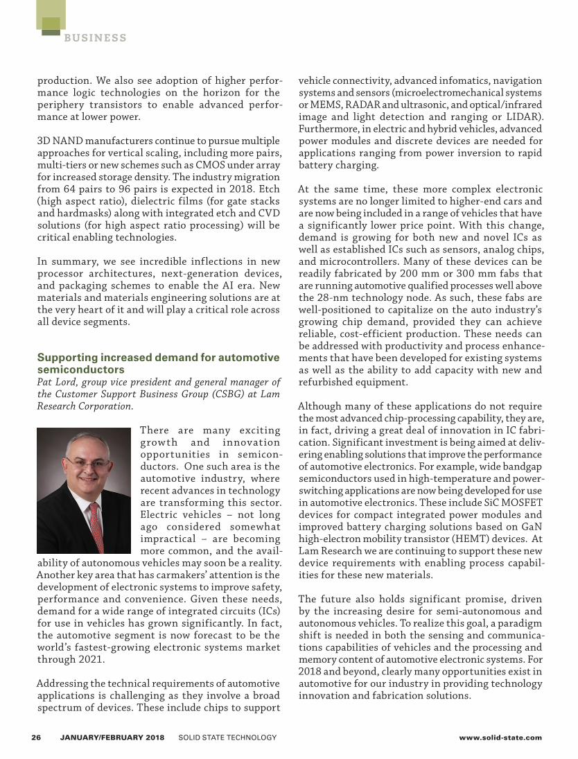
26 JANUARY/FEBRUARY 2018 SOLID STATE TECHNOLOGY www.solid-state.com
BUSINESS
production. We also see adoption of higher perfor-mance logic technologies on the horizon for the periphery transistors to enable advanced perfor-mance at lower power.
3D NAND manufacturers continue to pursue multiple approaches for vertical scaling, including more pairs, multi-tiers or new schemes such as CMOS under array for increased storage density. The industry migration from 64 pairs to 96 pairs is expected in 2018. Etch (high aspect ratio), dielectric films (for gate stacks and hardmasks) along with integrated etch and CVD solutions (for high aspect ratio processing) will be critical enabling technologies.
In summary, we see incredible inflections in new processor architectures, next-generation devices, and packaging schemes to enable the AI era. New materials and materials engineering solutions are at the very heart of it and will play a critical role across all device segments.
Supporting increased demand for automotive semiconductorsPat Lord, group vice president and general manager of the Customer Support Business Group (CSBG) at Lam Research Corporation.
There are many exciting growth and innovation opportunities in semicon-ductors. One such area is the automotive industry, where recent advances in technology are transforming this sector. Electric vehicles – not long ago considered somewhat impractical – are becoming more common, and the avail-
ability of autonomous vehicles may soon be a reality. Another key area that has carmakers’ attention is the development of electronic systems to improve safety, performance and convenience. Given these needs, demand for a wide range of integrated circuits (ICs) for use in vehicles has grown significantly. In fact, the automotive segment is now forecast to be the world’s fastest-growing electronic systems market through 2021.
Addressing the technical requirements of automotive applications is challenging as they involve a broad spectrum of devices. These include chips to support
vehicle connectivity, advanced infomatics, navigation systems and sensors (microelectromechanical systems or MEMS, RADAR and ultrasonic, and optical/infrared image and light detection and ranging or LIDAR). Furthermore, in electric and hybrid vehicles, advanced power modules and discrete devices are needed for applications ranging from power inversion to rapid battery charging.
At the same time, these more complex electronic systems are no longer limited to higher-end cars and are now being included in a range of vehicles that have a significantly lower price point. With this change, demand is growing for both new and novel ICs as well as established ICs such as sensors, analog chips, and microcontrollers. Many of these devices can be readily fabricated by 200 mm or 300 mm fabs that are running automotive qualified processes well above the 28-nm technology node. As such, these fabs are well-positioned to capitalize on the auto industry’s growing chip demand, provided they can achieve reliable, cost-efficient production. These needs can be addressed with productivity and process enhance-ments that have been developed for existing systems as well as the ability to add capacity with new and refurbished equipment.
Although many of these applications do not require the most advanced chip-processing capability, they are, in fact, driving a great deal of innovation in IC fabri-cation. Significant investment is being aimed at deliv-ering enabling solutions that improve the performance of automotive electronics. For example, wide bandgap semiconductors used in high-temperature and power-switching applications are now being developed for use in automotive electronics. These include SiC MOSFET devices for compact integrated power modules and improved battery charging solutions based on GaN high-electron mobility transistor (HEMT) devices. At Lam Research we are continuing to support these new device requirements with enabling process capabil-ities for these new materials.
The future also holds significant promise, driven by the increasing desire for semi-autonomous and autonomous vehicles. To realize this goal, a paradigm shift is needed in both the sensing and communica-tions capabilities of vehicles and the processing and memory content of automotive electronic systems. For 2018 and beyond, clearly many opportunities exist in automotive for our industry in providing technology innovation and fabrication solutions.

www.solid-state.com SOLID STATE TECHNOLOGY JANUARY/FEBRUARY 2018 27
BUSINESS
Materials science creativity is paving the road to innovationDr. Terry Brewer, president and CEO, Brewer Science
Brute-force methods for achieving incremental growth will continue to be the focus of our industry in 2018. Growth in China through government investment and fab construction will ensure this fact. But, the leadership our industry must rely on is its people, its organizations and their combined individual and
collective creativity to deliver new material designs that will solve our current circuit density challenges. These materials will then transcend these obstacles—opening doorways to new science and technology integrations.
The current market drivers of simplicity, balance and accessibility will continue to take the front stage as technology becomes increasingly seamless with human existence. Steve Jobs, Gordon Moore and Albert Einstein have shown us that solutions must be elegant to be sustained. To this point, companies and individuals that put their focus on deep science and material design will bring about technologies that drive sustainable economic growth. A brief glance at the stone, bronze, iron, steel, plastics and silicon ages show how this is true. By the end of 2018, we will already know what this new material age might be.
To foster economic, environmental and societal sustainability, our industry will be more present in encouraging people to embrace deep science through the support of STEM education programs. No longer will education and industry be separate, nor will we see the traditional technology transfer push of post-secondary institutions as the leading driver of innovation. Industry has recognized the need for new creativity, and 2018 will see visible evidence of industry nurturing even more creativity within their own organizations as well as our youth; both inside and outside the classroom. STEM education will be supported in the classroom, but also not be confined by it.
2018 will once again see growth in our industry. Incre-mentally more transistors, incrementally smaller features, incrementally increased investment. Many of the methods used will be familiar to us, such as
mergers and acquisitions, and investments from Asian governments. But, the real story in 2018 will be realized by at most two or three years from now when we reflect on the new, creative materials design threads being sewn into the fabric of our industry and ultimately woven into our daily lives. The future will validate that the material design leaders of 2018 will pave the road for the sustainable economic growth of tomorrow.
New technological trends will increase the focus on sub-fab operationsPaul Rawlings, President, Semiconductor Division, Edwards Vacuum
It has been a good year for the semiconductor industry. We have seen high levels of investment across all sectors: memory, logic, discrete and foundries. Looking forward, we see expansion continuing well into 2019. Reducing total cost-of-ownership, improving safety and limiting negative environmental impacts remain
primary drivers across the industry and continue to drive our product development at Edwards.
There are several technological trends that we expect to impact sub-fab operations. First among these is the dramatic growth projected for 3D NAND memory products. Flammable process gases requiring high dilution rates, larger tools with 5-7 multi-wafer chambers, and longer process cycles will all contribute to higher gas flows and increased risks. Integrated vacuum and abatement systems can provide higher capacity and energy efficiency in a single enclosed module that is inherently safer and more reliable. Etch process steps are also growing longer and more numerous, requiring advanced protective coatings to extend the lifetimes and improve the reliability of the harsh duty pumps used to with corrosive gases.
In another area, we are expecting significant growth in the number of EUV systems coming on line in 2018, introducing, for the first time, critical vacuum requirements in photolithography process modules. Finally, we are seeing dramatic expansion in the appli-cation of data-based fleet management techniques to optimize performance and reliability in the sub-fab. All of these trends can only be addressed effectively by

28 JANUARY/FEBRUARY 2018 SOLID STATE TECHNOLOGY www.solid-state.com
BUSINESS
complete solutions that begin with detailed analysis of specific process requirements and develop into a comprehensive support model throughout the product life-cycle.
On the human side, our industry is challenged to meet the increasing needs for talented and well-educated technologists, particularly in regions of rapid growth. We at Edwards are committed to playing our part in encouraging young people into Science, Technology, Engineering and Math careers and encourage everyone in the industry to support the initiatives the SEMI Organization is making in this area to develop this critical talent pipeline.
3D NAND requires new approaches to automated metrology and process controlJack Hager, Sr. Product Marketing Manager, Materials & Structural Analysis, Thermo Fisher Scientific
NAND memory manufac-turers will continue their rapid transition from planar to three-dimensional (3D) stacked architectures, with 64- and 96-layer devices expected to come into full production in 2018. This transition is driven by the significant advantages offered by 3D NAND in both size and cost. Stacking multi-
plies the number of bits that can be stored in the same footprint, thus reducing cost per bit in a process where costs are roughly proportional to the area of the device on the wafer. It also relaxes the resolution require-ments on photolithographic processes, permitting the use of less expensive tools and technologies. The market for high capacity 3D NAND currently comprises solid state drive and mobile applications, but this space is expected to expand.
As high layer-count 3D NAND moves into production, manufacturers are looking for metrology and process control solutions that can measure the critical dimen-sions (CD) of the very high aspect-ratio tube-within-tube vertical structures used to trap charge and connect individual memory cells across many layers. Critical dimension scanning electron microscopy (CD-SEM) is limited by its top-down point-of-view and challenge to see below the surface. Optical techniques can look below the surface, but are limited, especially in development and early ramp phases, by the need
to develop complex models based on empirical data from the measured structures.
Existing subsurface techniques are continuing to evolve to provide solution pathways. Focused ion beams (FIB) can cut conventional or oblique cross sections to reveal structural information at varying depths to measure with a scanning electron micro-scope (SEM). This technique takes advantage of the relatively large dimensions of particular 3D NAND features to collect sub surface data quickly. Another approach creates thin-section samples in the horizontal plane (planar) at various depths for imaging in a transmission electron microscope (TEM). The TEM approach provides much higher resolution and the ability to enhance contrast among the multiple concentric layers inside each “container” by adding information from other analytical signals, such as Energy Dispersive Spectroscopy (EDS). Both approaches are being enhanced to provide automated, robust and repeatable process control insights.
Perspectives from a materials supplierAdam Manzonie, Dow Electronic Materials, Slurry Business Director
2017 was a very active year for the semiconductor industry with strong loading across mature nodes, and strong ramps in advanced logic and memory. Many suppliers were put to the test just to keep up. Analysts don’t expect the same ramp rate in 2018, but they don’t expect utilization to drop off either. In addition
to demands on volume, our customers are looking for efficiencies in their manufacturing operations. It’s also more evident than ever that suppliers must be able to deliver on consistency and quality.
This has become a critical challenge for the industry. Emerging needs for 3D integration (FinFET, NAND, TSV) make processes more challenging for our customers leading to considerably tighter product specifications. Manufacturers must be confident their integrations are solid and processes are tightly controlled. Our customers place a high level of trust in us to supply consistent high-quality materials, in increasingly large volumes, so they can produce sophisticated devices to meet end market demand.

www.solid-state.com SOLID STATE TECHNOLOGY JANUARY/FEBRUARY 2018 29
BUSINESS
The need for quality and consistency hasn’t replacedthe need for innovation. Successful suppliersposition themselves to offer close collaboration withcustomers to understand emerging requirements andaddress new performance needs. Our advanced CMPpads, for example, deliver the benefits of hard andsoft pads together to achieve unprecedented levelsof planarization and defectivity. Our CMP slurryofferings can lower manufacturing costs by increasingprocess throughput and efficiencies, while at thesame time driving defect levels down by an order ofmagnitude. Here we see historically conflicting needsbecoming not just “nice-to-have,” but mandatory, toenable new device technology.
CMP is also becoming more pervasive with advancingtechnology. FinFET integration has brought on ahost of new polishing steps in advanced logic, somewith material combinations we haven’t seen before.3D-NAND configurations incorporate significantlymore polishing steps compared to historical planartechnology. The growth of TSV has been steady andnow too is evolving into completely new polishingneeds for advanced packaging. These emerging needsare driving Dow’s development of new productstargeting advanced applications, including new metalslurries that will hit the market in 2018.
Our density destiny? Precisely.Chris Davis, Co-founder and VP Sales & Marketing, RenoSub-Systems
In some ways, little changedin the industry focus in 2017,nor will it in 2018. We continueto seek higher performancefrom smaller devices thatconsume less power and workwithin the constraints of thedownward price pressures ofour industry—but we’re havingto look to new technologyadoption to do it. We’re
doubling, tripling and even quadrupling the numberof layers in our chips to meet our goals. And it’s all forthe sake of density. But, as always, serious challengeslie ahead.
Since the outcome of a more precise process is repeat-ability, that goal drives our work. For our part, wesee that vacuum control and measurement havekept pace with industry needs, but gas-flow control,
radio frequency (RF) matching network and solid-state power-generation technologies have not. Forus, “precision” means applying exacting standards tothe science behind our “pulsing” deposition and etchtechnology, to exponentially improve process qualityand speed. For others, it may mean higher materialscompatibility. For some, it may mean controllingnano-contaminants. We believe all these areas willmake great strides this year and next. And they haveto, in order to help us reach our industry goals forperformance and yield in new dimensions at advancednodes. Overall, we are optimistic on growth and cansee it continuing through 2020, at least.
Highly complex designs at smaller geometries requirerigorous controls that reduce process variabilities.Process control is key. For 2018, we see advance-ments in this area from our OEMs and process-enabling partners. A key area that will improve andhelp optimize leading-edge yield and performance isexecutional precision, which is what Reno is enablingequipment and device manufacturers to achieve.
In summary, subsystem technologies for RF powerand precision flow controls are undergoing a genera-tional change. This shift is essential to keep pace withthe density destiny required for global drivers like bigdata, autonomous everything, AI and IoT. �

30 JANUARY/FEBRUARY 2018 SOLID STATE TECHNOLOGY www.solid-state.com
A D V E R T I S E M E N T
Product Showcase
https://www.masterbond.com/tds/ep17htda-1
One Part Epoxy for Die Attach ApplicationsFormulated for die attach applications, Master Bond EP17HTDA-1 epoxy can also be used for conventional bonding and sealing applications. It features superb thermal conductivity and die shear strength properties.
www.ulvac.com
ULVAC has developed the world’s first integrated mass production technology for thin film lithium ion secondary batteries. With the ULVAC turnkey
production line and ULVAC sputtering targets all layers can be formed.
Thin Film Batteries
www.yieldengineering.com
YES-ÉcoClean
Automated Plasma Resist Strip & Descum System
• Automated wafer handling
• Multiple wafer sizes
• Small footprint
• Neutral plasma means gentle process
888-YES-3637
EXECUTIVE OFFICES
Extension Media 1786 18th Street, San Francisco, CA 94107-2343.
ADVERTISING
Sales Manager Kerry Hoffman 1786 18th St. San Francisco, CA 94107-2343 Tel: 978.580.4205 [email protected]
North AmericaKerry Hoffman Tel: [email protected]
Germany, Austria, E. Switzerland & E. EuropeHolger Gerisch Tel: +49.0.8856.8020228 [email protected]
China, Hong KongAdonis MakTel:[email protected]
TaiwanDiana WeiTel: +886.2.23965128 ext: [email protected]
Rest of WorldKerry Hoffman Tel: [email protected]
WebcastsJenna JohnsonTel: [email protected]
The ConFabKerry HoffmanTel: [email protected]
Conax .............................................................................................................13Master Bond ..................................................................................................30Nikon Precision ............................................................................................. C4SEMI ................................................................................................................5S&S Tech ...................................................................................................... C2SVC TechCon ...................................................................................................9 The ConFab ................................................................................................... C3Ulvac ..............................................................................................................30Y.E.S. ............................................................................................................7,30
ad index
Advertiser Pg
www.solid-state.com
Solid State Technology
For over 50 years, Solid State Technology has been the leading independent media resource, covering:
SemiconductorsAdvanced Packaging MEMSDisplays LEDs
Request a FREE subscription to our magazine and
e-Newsletters today atwww.solid-state.com/subscribe
Magazine
Website
Six e-Newsletters
SST_ProductShowcaseAd_Jan2013.indd 1 1/15/13 12:17 PM

www.solid-state.com SOLID STATE TECHNOLOGY JANUARY/FEBRUARY 2018 31
industryforum
Can the industry sustain this growth? The electronics manufacturing supply chain has demonstrated it can generally scale and expedite production to meet the massive new investment projects. The cracks starting to show are in the areas of talent, data management, and Environment, Health, and Safety (EH&S).
Talent has become a pinch point. In Silicon Valley alone, SEMI member companies have thousands of open positions. Globally, there are more than 10,000 open jobs. Attracting new candidates and developing a global workforce are critical to sustaining the pace of innovation and growth.
Data management and effective data sharing are keys to solving problems faster and making practical novel but immature processes at the leading edge. It is ironic that other industries are ahead of semiconductor manufac-turing in harnessing manufacturing data and leveraging AI across their supply chains. Without collaborative Smart Data approaches, there is jeopardy of decreasing the cadence of Moore’s Law below the 10 nm node.
EH&S is critical for an industry that now uses the majority of the elements of the periodic table to make chips – at rates of more than 50,000 wafer starts per month (wspm) for a single fab. The industry came together strongly in the 1990s to develop SEMI Safety Standards and compliance methodologies. Since then, the number of EH&S profes-sionals engaged in our industry has declined while the number of new materials has exploded, new processing techniques have been developed, and manufacturing is expanding across China in areas with no prior semicon-ductor manufacturing experience.
“None of Us is as Strong as All of Us” -SEMI backbone
HTU has been a very effective program with over 218 sessions run to date, over 7,000 students engaged, and over 70 percent of respondents pursuing careers in the STEM field.
To ensure we don’t slow growth, the industry will need to work together in 2018 in these three key areas:
2017 was a terrific year for SEMI members. Chip revenues closed at nearly $440B, an impressive 22 percent year-over-year growth. The equipment industry surpassed revenue levels last reached in the year 2000. Semicon-ductor equipment posted sales of nearly $56B and semiconductor materials $48B in 2017. For semiconductor equipment, this was a giant 36 percent year-over-year growth. Samsung, alone, invested $26B in semiconductor CapEx in 2017 – an incredible single year spend in an incredible year.
MEMS and Sensors gained new growth in telecom and medical markets, adding to existing demand from automotive, industrial and consumer segments. MEMS is forecast to be a $19B industry in 2018. Flexible hybrid electronics (FHE) is also experiencing significant product design and functionality growth with increasing gains in widespread adoption.
No longer is a single monolithic demand driver propelling the electronics manufacturing supply chain. The rapidly expanding digital economy continues to foster innovation with new demand from the IoT, virtual and augmented reality (VR/AR), automobile infotainment and driver assistance, artificial intelligence (AI) and Big Data, among others. With the explosion in data usage, memory demand is nearly insatiable, holding memory device ASPs high and prompting continued heavy investment in new capacity.
2018 is forecast to be another terrific year. IC revenues are expected to increase another 8 percent and semiconductor equipment will grow 11 percent. With diverse digital economy demand continuing, additional manufacturing capacity is being added in China as fab projects come on line to develop and increase the indigenous semiconductor supply chain.
So, why worry?
The cracks starting to show are in the areas of talent, data management, and Environment, Health, and Safety (EH&S).
Work to do to keep the good times rolling
AJIT MANOCHA, President and CEO of SEMI

32 JANUARY/FEBRUARY 2018 SOLID STATE TECHNOLOGY www.solid-state.com
industryforum
Answering the call to innovateTalent development needs to rapidly accelerate by expanding currently working programs and adding additional means to fill the talent funnel. The SEMI Foundation’s High Tech University (HTU) works globally with member companies to increase the number of high school students selecting Science, Technology, Engineering, and Math (STEM) fields – and provides orientation to the semiconductor manufacturing industry. HTU has been a very effective program with over 218 sessions run to date, over 7,000 students engaged, and over 70 percent of respondents pursuing careers in the STEM field. SEMI will increase the number of HTU sessions in 2018.
Plans have already been approved by SEMI’s Board of Directors to work together with SEMI’s membership to leverage existing, and pioneer new, workforce development programs to attract and develop qualified candidates from across the age and experience spectrum (high school through university, diversity, etc.). Additionally, an industry awareness campaign will be developed and launched to make more potential candidates attracted to our member companies as a great career choice. I’ll be providing you with updates on this initiative – and asking for your involvement
– throughout 2018.
Data management is a broad term. Big Data, machine learning, AI are terms that today mean different things to different people in our supply chain. What is clear is that to act together and take advantage of the unimaginable amounts of data being generating to produce materials and make semiconductor devices with the diverse equipment sets across our fabs, we need a common understanding of the data and potential use of the data.
In 2018, SEMI will launch a Smart Data vertical application platform to engage stakeholders along the supply chain to produce a common language, develop Standards, and align expectations for sharing data for mutual benefit. Bench-marking of other industries and pre-competitive pilot programs are being proposed to learn and, here too, we need the support and engagement of thought leaders throughout SEMI’s membership.
EH&S activity must intensify to maintain safe operations and to eliminate business interruptions from supply chain disruptions. There is potential for disruptions from material bans such as the Stockholm Convention action on PFOA and arising from the much wider range of chemicals and materials being used in advanced manufacturing. Being able to reliably identify these in time to guide and coordinate industry action will take a reinvigorated SEMI EH&S stewardship and membership engagement.
As China rapidly develops new fabs in many provinces – some with only limited prior experience and infra-structure – SEMI EH&S Standards orientation and training will accelerate the safe and sustainable operation of fabs, enabling them to keep pace with the ambitious growth trajectory our industry is delivering. In 2018, we’ll be looking for a renewed commitment to EH&S and sustainability for the budding challenges of new materials, methods, and emerging regions.
Remarkable results from a remarkable membershipThank you all for a terrific 2017 and let’s work together on the key initiatives to ensure that our industry’s growth and prosperity will continue in 2018 and beyond.
In a quick review of 2017, I would like to thank SEMI’s members for their incredible results and new revenue records. Foundational to that, SEMI’s members have worked together with SEMI to connect, collaborate, and innovate to increase growth and prosperity for the industry. These founda-tional contributions have been in expositions, programs, Standards, market data, messaging (communications), and workforce development (with HTU).
The infographic below captures these foundational accom-plishments altogether. SEMI strives to speed the time to better business results for its members across the global electronics manufacturing supply chain. To do so, SEMI is dependent upon, and grateful for, the support and volunteer efforts of its membership. Thank you for a terrific 2017 and let’s work together on the key initiatives to ensure that our industry’s growth and prosperity will continue in 2018 and beyond. �

May 20 - 23, 2018 THE COSMOPOLITAN of LAS VEGAS
www.theconfab.com
Are You Fully Leveraging this New Era in Semiconductor Growth?Find Out from Visionary Speakers at The ConFab 2018
Mark Your Calendar for The ConFab 2018 • At this year’s exclusive executive conference and networking event, meet outstanding speakers from companies such as: Google, IBM, Qorvo, Nvidia, GlobalFoundries, Qualcomm, Cisco, ASE, Silicon Catalyst, Skywater Technology Foundry, IHS Markit, Semico Research
• Hear from industry experts and influencers that will address: Semiconductor Manufacturing and Design | the Economics, Trends, New Technologies and Applications | Mainstream Semiconductor Manufacturing | plus Artificial Intelligence, IoT, 5G, EUV Lithography, Advanced Packaging, Virtual and Augmented Reality, Automotive, Cloud Computing, Networking, Healthcare | Market Trends and Expected Business Climate Moving Forward
• The ConFab 2018 delivers high value by connecting key decision-makers, clients and colleagues, analysts, partners and suppliers during conference sessions in addition to multiple networking breakfasts, lunches, private breakout meetings and evening receptions.
RESERVE NOW
Sponsorship details: Kerry Hoffman [email protected]
Attendee/VIP reservations: Sally Bixby [email protected]
www.theconfab.com
Produced by:Presented by: The ConFab 2018 Conference Chair
Solid State Technology Editor-in-Chief, Pete Singer
Dr. Rama DivakaruniIBM Distinguished Engineer
Advanced Process Technology Research
John M. Martinis Google Quantum AI Lab
Worster Chair, Univ. of California Santa Barbara, Experimental Physics
Dr. John HuDirector of Advanced Technology
Nvidia Corporation

‹ and ›
See Nikon at:
www.lithovision.com
www.nikonprecision.com
Today’s lithography systems provide overlay accuracy and throughput capabilities far beyond what was previously thought possible. However, it is real-world, on-product performance that is vital to chipmakers.
Nikon combines a strong history of engineering expertise with superior immersion scanner technology and innovative alignment solutions to deliver exceptional semi- conductor manufacturing performance and productivity—now and for the future.
Nikon. Delivering Real-world Solutions.
Delivering Real-worldSolutions