document number: mrf6v12500h technical data rev. 4, … · c3 c2 c1 c6 c4 c12 c14 c16 c8 c17 c18...
TRANSCRIPT
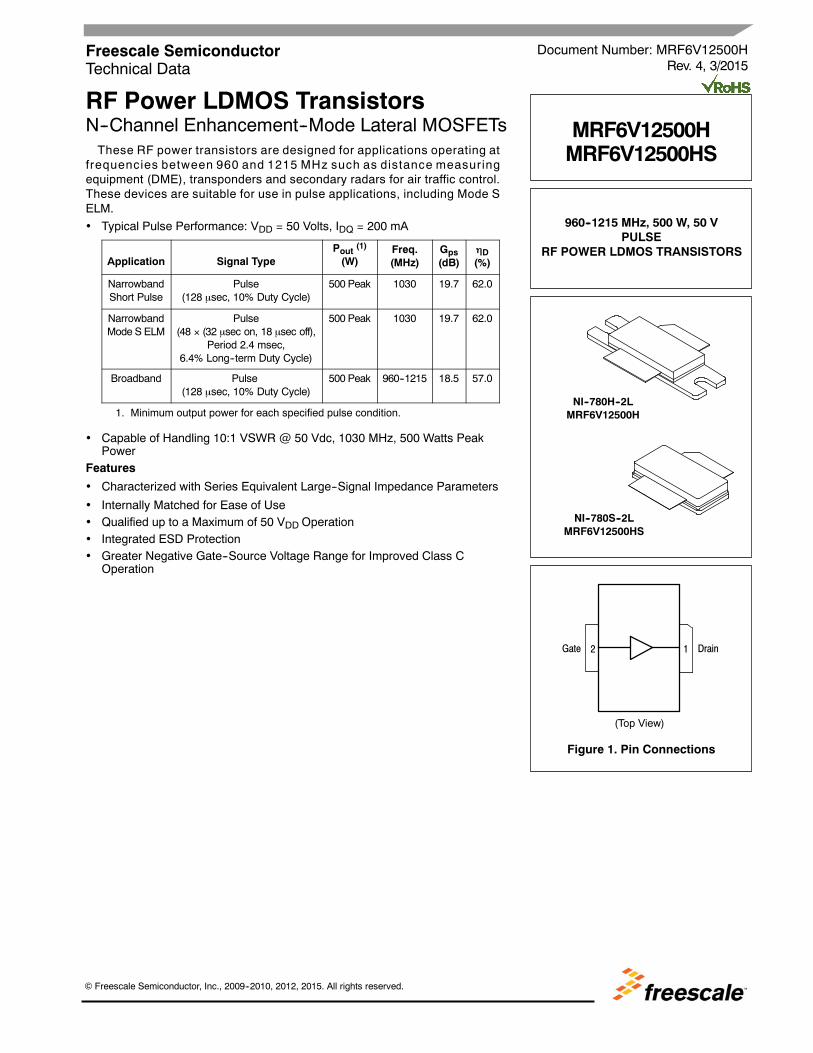
MRF6V12500H MRF6V12500HS
1RF Device DataFreescale Semiconductor, Inc.
RF Power LDMOS TransistorsN--Channel Enhancement--Mode Lateral MOSFETsThese RF power transistors are designed for applications operating at
frequencies between 960 and 1215 MHz such as distance measuringequipment (DME), transponders and secondary radars for air traffic control.These devices are suitable for use in pulse applications, including Mode SELM.
Typical Pulse Performance: VDD = 50 Volts, IDQ = 200 mA
Application Signal TypePout (1)
(W)Freq.(MHz)
Gps(dB)
D(%)
NarrowbandShort Pulse
Pulse(128 sec, 10% Duty Cycle)
500 Peak 1030 19.7 62.0
NarrowbandMode S ELM
Pulse(48 (32 sec on, 18 sec off),
Period 2.4 msec,6.4% Long--term Duty Cycle)
500 Peak 1030 19.7 62.0
Broadband Pulse(128 sec, 10% Duty Cycle)
500 Peak 960--1215 18.5 57.0
1. Minimum output power for each specified pulse condition.
Capable of Handling 10:1 VSWR @ 50 Vdc, 1030 MHz, 500 Watts PeakPower
Features
Characterized with Series Equivalent Large--Signal Impedance Parameters
Internally Matched for Ease of Use Qualified up to a Maximum of 50 VDD Operation Integrated ESD Protection Greater Negative Gate--Source Voltage Range for Improved Class C
Operation
Document Number: MRF6V12500HRev. 4, 3/2015
Freescale SemiconductorTechnical Data
960--1215 MHz, 500 W, 50 VPULSE
RF POWER LDMOS TRANSISTORS
MRF6V12500HMRF6V12500HS
NI--780S--2LMRF6V12500HS
NI--780H--2LMRF6V12500H
Figure 1. Pin Connections
(Top View)
Gate 2 1 Drain
Freescale Semiconductor, Inc., 2009--2010, 2012, 2015. All rights reserved.
2RF Device Data
Freescale Semiconductor, Inc.
MRF6V12500H MRF6V12500HS
Table 1. Maximum Ratings
Rating Symbol Value Unit
Drain--Source Voltage VDSS --0.5, +110 Vdc
Gate--Source Voltage VGS --6.0, +10 Vdc
Storage Temperature Range Tstg -- 65 to +150 C
Case Operating Temperature TC 150 C
Operating Junction Temperature (1,2) TJ 225 C
Table 2. Thermal Characteristics
Characteristic Symbol Value (2,3) Unit
Thermal Impedance, Junction to CaseCase Temperature 80C, 500 W Peak, 128 sec Pulse Width, 10% Duty Cycle ZJC 0.044 C/W
Table 3. ESD Protection Characteristics
Test Methodology Class
Human Body Model (per JESD22--A114) 2, passes 2600 V
Machine Model (per EIA/JESD22--A115) B, passes 200 V
Charge Device Model (per JESD22--C101) IV, passes 2000 V
Table 4. Electrical Characteristics (TA = 25C unless otherwise noted)
Characteristic Symbol Min Typ Max Unit
Off Characteristics
Gate--Source Leakage Current(VGS = 5 Vdc, VDS = 0 Vdc)
IGSS — — 10 Adc
Drain--Source Breakdown Voltage(VGS = 0 Vdc, ID = 200 mA)
V(BR)DSS 110 — — Vdc
Zero Gate Voltage Drain Leakage Current(VDS = 50 Vdc, VGS = 0 Vdc)
IDSS — — 20 Adc
Zero Gate Voltage Drain Leakage Current(VDS = 90 Vdc, VGS = 0 Vdc)
IDSS — — 200 Adc
On Characteristics
Gate Threshold Voltage(VDS = 10 Vdc, ID = 1.32 mA)
VGS(th) 0.9 1.7 2.4 Vdc
Gate Quiescent Voltage(VDD = 50 Vdc, ID = 200 mAdc, Measured in Functional Test)
VGS(Q) 1.7 2.4 3.2 Vdc
Drain--Source On--Voltage(VGS = 10 Vdc, ID = 3.26 Adc)
VDS(on) — 0.25 — Vdc
Dynamic Characteristics (4)
Reverse Transfer Capacitance(VDS = 50 Vdc 30 mV(rms)ac @ 1 MHz, VGS = 0 Vdc)
Crss — 0.2 — pF
Output Capacitance(VDS = 50 Vdc 30 mV(rms)ac @ 1 MHz, VGS = 0 Vdc)
Coss — 697 — pF
Input Capacitance(VDS = 50 Vdc, VGS = 0 Vdc 30 mV(rms)ac @ 1 MHz)
Ciss — 1391 — pF
1. Continuous use at maximum temperature will affect MTTF.2. MTTF calculator available at http://www.freescale.com/rf. Select Software & Tools/Development Tools/Calculators to access MTTF
calculators by product.3. Refer to AN1955, Thermal Measurement Methodology of RF Power Amplifiers. Go to http://www.freescale.com/rf.
Select Documentation/Application Notes -- AN1955.4. Part internally matched both on input and output.
(continued)

MRF6V12500H MRF6V12500HS
3RF Device DataFreescale Semiconductor, Inc.
Table 4. Electrical Characteristics (TA = 25C unless otherwise noted) (continued)
Characteristic Symbol Min Typ Max Unit
Functional Tests (In Freescale Narrowband Test Fixture, 50 ohm system) VDD = 50 Vdc, IDQ = 200 mA, Pout = 500 W Peak (50 W Avg.),f = 1030 MHz, 128 sec Pulse Width, 10% Duty Cycle
Power Gain Gps 18.5 19.7 22.0 dB
Drain Efficiency D 58.0 62.0 — %
Input Return Loss IRL — --18 --9 dB
Typical Broadband Performance — 960--1215 MHz (In Freescale 960--1215 MHz Test Fixture, 50 ohm system) VDD = 50 Vdc,IDQ = 200 mA, Pout = 500 W Peak (50 W Avg.), f = 960--1215 MHz, 128 sec Pulse Width, 10% Duty Cycle
Power Gain Gps — 18.5 — dB
Drain Efficiency D — 57.0 — %
Table 5. Ordering Information
Device Tape and Reel Information Package
MRFE6V12500HR5R5 Suffix = 50 Units, 56 mm Tape Width, 13--inch Reel
NI--780H--2L
MRFE6V12500HSR5 NI--780S--2L

4RF Device Data
Freescale Semiconductor, Inc.
MRF6V12500H MRF6V12500HS
Figure 2. MRF6V12500H(HS) Test Circuit Schematic
Z11 0.161” x 1.500 MicrostripZ12 0.613” x 1.281 MicrostripZ13 0.248” x 0.865 MicrostripZ14 0.087” x 0.425 MicrostripZ15 0.309” x 0.090 MicrostripZ16 0.193” x 0.516 MicrostripZ17 0.279” x 0.080 MicrostripZ18 0.731” x 0.080 MicrostripZ19, Z21 0.507” x 0.040 MicrostripPCB Arlon CuClad 250GX--0300--55--22, 0.030, r = 2.55
Z1 0.457 x 0.080 MicrostripZ2 0.250 x 0.080 MicrostripZ3 0.605 x 0.040 MicrostripZ4 0.080 x 0.449 MicrostripZ5 0.374 x 0.608 MicrostripZ6 0.118 x 1.252 MicrostripZ7 0.778 x 1.710 MicrostripZ8 0.095 x 1.710 MicrostripZ9, Z20 0.482 x 0.050 MicrostripZ10 0.138 x 1.500 Microstrip
Z1
RFINPUT
C1
Z2 Z4
DUT
C2
RFOUTPUT
VBIAS
VSUPPLY
C8
C5 C12 C14
+
Z16
R3
Z3
C15
+
Z5
C7
Z15Z14Z13Z12Z11Z10
Z8Z7Z6
Z9
Z19
R1
C9
Z20
Z21
Z17 Z18
C6 C16
C3
C11 C10
R2
C4
R4
C13
Table 6. MRF6V12500H(HS) Test Circuit Component Designations and Values
Part Description Part Number Manufacturer
C1, C2 5.1 pF Chip Capacitors ATC100B5R1CT500XT ATC
C3, C4, C5, C6 33 pF Chip Capacitors ATC100B330JT500XT ATC
C7, C10 10 F, 50 V Chip Capacitors GRM55DR61H106KA88L Murata
C8, C11, C13, C16 2.2 F, 100 V Chip Capacitors 2225X7R225KT3AB ATC
C9 22 F, 25 V Chip Capacitor TPSD226M025R0200 AVX
C12 1 F, 100 V Chip Capacitor GRM31CR72A105KA01L Murata
C14, C15 470 F, 63 V Electrolytic Capacitors MCGPR63V477M13X26--RH Multicomp
R1, R2 56 , 1/4 W Chip Resistors CRCW120656R0FKEA Vishay
R3, R4 0 , 3 A Chip Resistors CRCW12060000Z0EA Vishay

MRF6V12500H MRF6V12500HS
5RF Device DataFreescale Semiconductor, Inc.
Figure 3. MRF6V12500H(HS) Test Circuit Component Layout
R3
CUTOUTAREA
MRF6V12500H Rev. 1C9 C8 C7 C3
R1
C1
R4
C11 C10
R2C4 C6
C16
C2
C12
C5C13
C14
C15

6RF Device Data
Freescale Semiconductor, Inc.
MRF6V12500H MRF6V12500HS
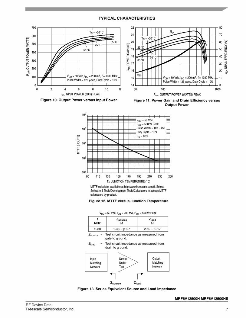
TYPICAL CHARACTERISTICS
500.1
10000
0 2010
VDS, DRAIN--SOURCE VOLTAGE (VOLTS)
Figure 4. Capacitance versus Drain--Source Voltage
C,CAPACITANCE(pF)
30
Ciss
10
1
40
Coss
Crss
Measured with 30 mV(rms)ac @ 1 MHzVGS = 0 Vdc
100
0
160
0
VDD = 50 Vdc, IDQ = 200 mAf = 1030 MHz, Pulse Width = 128 sec
10
100
DUTY CYCLE (%)
Figure 5. Safe Operating Area
MAXIMUMOPERATINGT case(C)
25
140
120
80
60
40
20
5 2015
Pout = 525 W
Pout = 475 W
Pout = 500 W
22
300
100
21
20
80
60
50
40
Pout, OUTPUT POWER (WATTS) PEAK
Figure 6. Power Gain and Drain Efficiencyversus Output Power
Gps,POWER
GAIN(dB)
D,DRAINEFFICIENCY(%)
D
141000
Gps
18
VDD = 50 Vdc, IDQ = 200 mA, f = 1030 MHzPulse Width = 128 sec, Duty Cycle = 10%
62
30
555453
Pin, INPUT POWER (dBm) PEAK
Figure 7. Output Power versus Input Power
56
52515049
32 34 36 38 40 42
P out,OUTPUTPOWER
(WATTS)
P3dB = 57.6 dBm (575 W)
Actual
Ideal
P1dB = 57.1 dBm (511 W)
VDD = 50 Vdc, IDQ = 200 mA, f = 1030 MHzPulse Width = 128 sec, Duty Cycle = 10%
575859
17
22
30
21
Pout, OUTPUT POWER (WATTS) PEAK
Figure 8. Power Gain versus Output Power
Gps,POWER
GAIN(dB)
100
20
IDQ = 800 mA
1000
600 mA
19
18
200 mA
VDD = 50 Vdc, f = 1030 MHzPulse Width = 128 sec, Duty Cycle = 10%
Figure 9. Power Gain versus Output PowerPout, OUTPUT POWER (WATTS) PEAK
Gps,POWER
GAIN(dB)
VDD = 30 V
12
22
30
16
21
35 V
20
45 V
100 1000
50 V
19
18
17
40 V
IDQ = 200 mA, f = 1030 MHzPulse Width = 128 secDuty Cycle = 10%
1000
19
16
17
15
70
30
20
10
6061
400 mA
13
15
14
MRF6V12500H MRF6V12500HS
7RF Device DataFreescale Semiconductor, Inc.
TYPICAL CHARACTERISTICS
120
700
0 62
500
400
Pin, INPUT POWER (dBm) PEAK
Figure 10. Output Power versus Input Power
P out,OUTPUTPOWER
(WATTS)
4 8
600
10
TC = --30_C
VDD = 50 Vdc, IDQ = 200 mA, f = 1030 MHzPulse Width = 128 sec, Duty Cycle = 10%
85_C
55_C
25_C
14
22
300
80
100
60
50
Pout, OUTPUT POWER (WATTS) PEAK
Figure 11. Power Gain and Drain Efficiency versusOutput Power
Gps,POWER
GAIN(dB)
D,DRAINEFFICIENCY(%)
D
21
1000
25_C
TC = --30_C
85_C40
20
18 55_C
VDD = 50 Vdc, IDQ = 200 mA, f = 1030 MHzPulse Width = 128 sec, Duty Cycle = 10%
Gps
200
100
300
19
16
17
15
70
30
20
10
250
109
90
TJ, JUNCTION TEMPERATURE (C)
Figure 12. MTTF versus Junction Temperature
MTTF calculator available at http:/www.freescale.com/rf. SelectSoftware & Tools/Development Tools/Calculators to access MTTFcalculators by product.
107
106
105
110 130 150 170 190
MTTF(HOURS)
210 230
108
VDD = 50 VdcPout = 500 W PeakPulse Width = 128 secDuty Cycle = 10%D = 62%
VDD = 50 Vdc, IDQ = 200 mA, Pout = 500 W Peak
fMHz
Zsource
Zload
1030 1.36 -- j1.27 2.50 -- j0.17
Zsource = Test circuit impedance as measured fromgate to ground.
Zload = Test circuit impedance as measured fromdrain to ground.
Figure 13. Series Equivalent Source and Load Impedance
InputMatchingNetwork
DeviceUnderTest
OutputMatchingNetwork
Zsource Zload
8RF Device Data
Freescale Semiconductor, Inc.
MRF6V12500H MRF6V12500HS
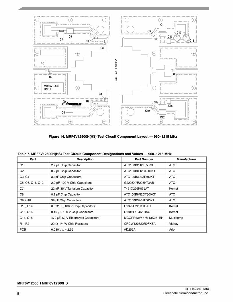
Figure 14. MRF6V12500H(HS) Test Circuit Component Layout — 960--1215 MHz
R1
C10
CUTOUTAREA
MRF6V12500Rev. 1
R2
C7C5
C3
C2
C1
C6
C4
C12
C14C16
C8
C17
C18C15
C13
C9
C11
Table 7. MRF6V12500H(HS) Test Circuit Component Designations and Values — 960--1215 MHz
Part Description Part Number Manufacturer
C1 2.2 pF Chip Capacitor ATC100B2R2JT500XT ATC
C2 0.2 pF Chip Capacitor ATC100B0R2BT500XT ATC
C3, C4 33 pF Chip Capacitors ATC100B330JT500XT ATC
C5, C6, C11, C12 2.2 F, 100 V Chip Capacitors G2225X7R225KT3AB ATC
C7 22 F, 35 V Tantalum Capacitor T491X226K035AT Kemet
C8 8.2 pF Chip Capacitor ATC100B8R2CT500XT ATC
C9, C10 39 pF Chip Capacitors ATC100B390JT500XT ATC
C13, C14 0.022 F, 100 V Chip Capacitors C1825C223K1GAC Kemet
C15, C16 0.10 F, 100 V Chip Capacitors C1812F104K1RAC Kemet
C17, C18 470 F, 63 V Electrolytic Capacitors MCGPR63V477M13X26--RH Multicomp
R1, R2 22 , 1/4 W Chip Resistors CRCW120622R0FKEA Vishay
PCB 0.030, r = 2.55 AD255A Arlon
MRF6V12500H MRF6V12500HS
9RF Device DataFreescale Semiconductor, Inc.
TYPICAL CHARACTERISTICS — 960--1215 MHz
Gps,POWER
GAIN(dB)
1300900
IRL
Gps
f, FREQUENCY (MHz)
Figure 15. Power Gain, Drain Efficiency and IRLversus Frequency
1150110010501000950
20
18
--20
66
62
0
--10
D,DRAIN
EFFICIENCY(%)
D
15
14
11
10
19
17
16 58
13
12
1200 1250
VDD = 50 Vdc, Pout = 500 W Peak (50 W Avg.), IDQ = 200 mAPulse Width = 128 sec, Duty Cycle = 10%
60017
22
40
65
Pout, OUTPUT POWER (WATTS) PEAK
Figure 16. Power Gain and Drain Efficiency versusOutput Power
VDD = 50 VdcIDQ = 200 mAPulse Width = 128 secDuty Cycle = 10%
400200
21
20
19
18
60
55
50
45 DDRAINEFFICIENCY(%)
Gps
D
Gps,POWER
GAIN(dB)
64
60
56
--5
--15
IRL,INPUTRETURN
LOSS
(dB)
250 300 350 450 500 550
1150 MHz
1030 MHz
960 MHz
1215 MHz
1150 MHz
1030 MHz
960 MHz
1215 MHz
10RF Device Data
Freescale Semiconductor, Inc.
MRF6V12500H MRF6V12500HS
Zo = 5
Zload
f = 1215 MHz
f = 960 MHz
Zsource
f = 960 MHz
f = 1215 MHz
VDD = 50 Vdc, IDQ = 200 mA, Pout = 500 W Peak
fMHz
Zsource
Zload
960 2.25 -- j1.78 1.38 -- j1.53
1030 2.51 -- j1.02 1.48 -- j1.11
1090 2.69 -- j0.73 1.51 -- j0.78
1150 2.71 -- j0.65 1.53 -- j0.49
1215 2.48 -- j0.76 1.53 -- j0.33
Zsource = Test circuit impedance as measured fromgate to ground.
Zload = Test circuit impedance as measured fromdrain to ground.
Figure 17. Series Equivalent Source and Load Impedance — 960--1215 MHz
InputMatchingNetwork
DeviceUnderTest
OutputMatchingNetwork
Zsource Zload

MRF6V12500H MRF6V12500HS
11RF Device DataFreescale Semiconductor, Inc.
PACKAGE DIMENSIONS

12RF Device Data
Freescale Semiconductor, Inc.
MRF6V12500H MRF6V12500HS
MRF6V12500H MRF6V12500HS
13RF Device DataFreescale Semiconductor, Inc.
14RF Device Data
Freescale Semiconductor, Inc.
MRF6V12500H MRF6V12500HS
MRF6V12500H MRF6V12500HS
15RF Device DataFreescale Semiconductor, Inc.
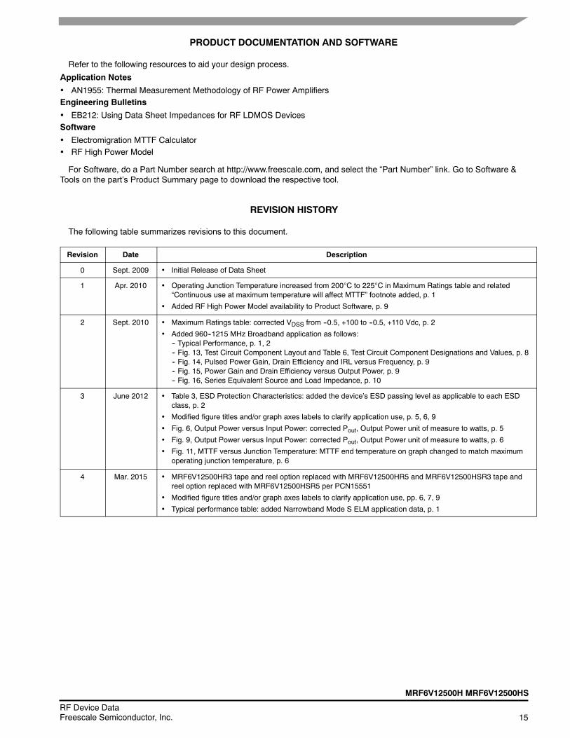
PRODUCT DOCUMENTATION AND SOFTWARE
Refer to the following resources to aid your design process.
Application Notes
AN1955: Thermal Measurement Methodology of RF Power AmplifiersEngineering Bulletins
EB212: Using Data Sheet Impedances for RF LDMOS DevicesSoftware
Electromigration MTTF Calculator RF High Power Model
For Software, do a Part Number search at http://www.freescale.com, and select the “Part Number” link. Go to Software &Tools on the part’s Product Summary page to download the respective tool.
REVISION HISTORY
The following table summarizes revisions to this document.
Revision Date Description
0 Sept. 2009 Initial Release of Data Sheet
1 Apr. 2010 Operating Junction Temperature increased from 200C to 225C in Maximum Ratings table and related“Continuous use at maximum temperature will affect MTTF” footnote added, p. 1
Added RF High Power Model availability to Product Software, p. 9
2 Sept. 2010 Maximum Ratings table: corrected VDSS from --0.5, +100 to --0.5, +110 Vdc, p. 2
Added 960--1215 MHz Broadband application as follows:-- Typical Performance, p. 1, 2-- Fig. 13, Test Circuit Component Layout and Table 6, Test Circuit Component Designations and Values, p. 8-- Fig. 14, Pulsed Power Gain, Drain Efficiency and IRL versus Frequency, p. 9-- Fig. 15, Power Gain and Drain Efficiency versus Output Power, p. 9-- Fig. 16, Series Equivalent Source and Load Impedance, p. 10
3 June 2012 Table 3, ESD Protection Characteristics: added the device’s ESD passing level as applicable to each ESDclass, p. 2
Modified figure titles and/or graph axes labels to clarify application use, p. 5, 6, 9
Fig. 6, Output Power versus Input Power: corrected Pout, Output Power unit of measure to watts, p. 5
Fig. 9, Output Power versus Input Power: corrected Pout, Output Power unit of measure to watts, p. 6
Fig. 11, MTTF versus Junction Temperature: MTTF end temperature on graph changed to match maximumoperating junction temperature, p. 6
4 Mar. 2015 MRF6V12500HR3 tape and reel option replaced with MRF6V12500HR5 and MRF6V12500HSR3 tape andreel option replaced with MRF6V12500HSR5 per PCN15551
Modified figure titles and/or graph axes labels to clarify application use, pp. 6, 7, 9
Typical performance table: added Narrowband Mode S ELM application data, p. 1

16RF Device Data
Freescale Semiconductor, Inc.
MRF6V12500H MRF6V12500HS
Information in this document is provided solely to enable system and softwareimplementers to use Freescale products. There are no express or implied copyrightlicenses granted hereunder to design or fabricate any integrated circuits based on theinformation in this document.
Freescale reserves the right to make changes without further notice to any productsherein. Freescale makes no warranty, representation, or guarantee regarding thesuitability of its products for any particular purpose, nor does Freescale assume anyliability arising out of the application or use of any product or circuit, and specificallydisclaims any and all liability, including without limitation consequential or incidentaldamages. “Typical” parameters that may be provided in Freescale data sheets and/orspecifications can and do vary in different applications, and actual performance mayvary over time. All operating parameters, including “typicals,” must be validated foreach customer application by customer’s technical experts. Freescale does not conveyany license under its patent rights nor the rights of others. Freescale sells productspursuant to standard terms and conditions of sale, which can be found at the followingaddress: freescale.com/SalesTermsandConditions.
Freescale and the Freescale logo are trademarks of Freescale Semiconductor, Inc.,Reg. U.S. Pat. & Tm. Off. All other product or service names are the property of theirrespective owners.E 2009--2010, 2012, 2015 Freescale Semiconductor, Inc.
How to Reach Us:
Home Page:freescale.com
Web Support:freescale.com/support
Document Number: MRF6V12500HRev. 4, 3/2015

Mouser Electronics
Authorized Distributor
Click to View Pricing, Inventory, Delivery & Lifecycle Information: Freescale Semiconductor:
MRF6V12500HR3 MRF6V12500HSR3