distributed active transformer-a new power-combining - california
TRANSCRIPT

316 IEEE TRANSACTIONS ON MICROWAVE THEORY AND TECHNIQUES, VOL. 50, NO. 1, JANUARY 2002
Distributed Active Transformer—ANew Power-Combining andImpedance-Transformation
TechniqueIchiro Aoki, Student Member, IEEE, Scott D. Kee, David B. Rutledge, Fellow, IEEE, and Ali Hajimiri, Member, IEEE
Invited Paper
Abstract—In this paper, we compare the performance of thenewly introduced distributed active transformer (DAT) structureto that of conventional on-chip impedance-transformationsmethods. Their fundamental power-efficiency limitations in thedesign of high-power fully integrated amplifiers in standard siliconprocess technologies are analyzed. The DAT is demonstrated tobe an efficient impedance-transformation and power-combiningmethod, which combines several low-voltage push–pull amplifiersin series by magnetic coupling. To demonstrate the validity of thenew concept, a 2.4-GHz 1.9-W 2-V fully integrated power-ampli-fier achieving a power-added efficiency of 41% with 50- inputand output matching has been fabricated using 0.35-m CMOStransistors.
Index Terms—Circular geometry, CMOS analog integrated cir-cuit, distributed active transformer, double differential, harmonic-control, impedance transformation, low voltage, power amplifier,power combining.
I. INTRODUCTION
A MONG THE several building blocks necessary to con-struct today’sholy grail in wireless communication, the
“single-chip radio,” power amplifiers have been one of the mostsignificant challenges. Several results have been published inthis field, but none have reported a watt-level fully integratedpower amplifier using silicon technology.
Until now, the highest output powers achieved by fully inte-grated power amplifiers in standard silicon processes are 85 mW[1] delivered to a differential 50- load with a power-added ef-ficiency (PAE) of 30% and 100 mW with a drain efficiency of16% [2], both implemented in CMOS technology. Other worksusing CMOS [3], [4] or Si bipolar [5], [6] processes rely on theuse of external passive components such as bond wire inductors,
Manuscript received May 27, 2001. This work was supported by the IntelCorporation, the Army Research Office, the Jet Propulsion Laboratory, Infinion,and the National Science Foundation.
I. Aoki is with the California Institute of Technology, M/C 136-93, Pasadena,CA 91125 (e-mail: [email protected]).
S. D. Kee, D. B. Rutledge, and A. Hajimiri are with the Department of Elec-trical Engineering, California Institute of Technology, Pasadena, CA 91125-9300.
Publisher Item Identifier S 0018-9480(02)00841-4.
off-chip transmission lines, off-chip capacitors, and/or externalbaluns to achieve watt level output power.
Several other works have been reported using alternativeprocess technologies with higher transistor breakdown volt-ages and/or insulating substrates to achieve watt-level outputpower, such as GaAs monolithic microwave integrated circuits(MMICs) [7]–[9] or silicon-on-insulator (SOI) LDMOS with20-V breakdown voltage [10].
These results [1]–[6] demonstrate that while silicon transis-tors are capable of producing watt-level output power in the gi-gahertz-frequency range with reasonable efficiency, the on-chippassive devices are the major limiting factor in the performanceof the amplifier and, therefore, deserve special attention. Thesepassive devices are unavoidable due to the impedance transfor-mation required to achieve high power with low-breakdown sil-icon transistors.
Two major problems associated with the design of on-chippower amplifiers using submicrometer CMOS processes are lowtransistor breakdown voltage [11] and the high loss of on-chipimpedance transformation [12]. The latter is caused by the highlyconductive substrate, as well as thin metal and dielectric layers.These problems become more serious as the minimum featuresizes are scaled down in each new process generation [13].
Today’s submicrometer transistors necessary for gigahertzoperation have breakdown voltages in the range of 4–6 V [14].This low breakdown voltage limits the drain (collector) acvoltage swing to around 2 V. Without any impedance trans-formation, the power delivered to a 50-load for a sinusoidalvoltage waveform is only 40 mW. The necessary impedancetransformation to achieve higher output power might be accom-plished by an on-chip transformer or inductor–capacitor(LC) resonant matching network. Unfortunately, these on-chipcomponents using CMOS processes are very lossy due to thelow substrate resistivity and high metal ohmic loss [12], [15]and, therefore, they significantly degrade the output power andefficiency of the amplifier.
The distributed active transformer (DAT) is presented as analternative method to achieve simultaneous impedance trans-formation and power combining that can be used to overcome
0018–9480/02$17.00 © 2002 IEEE

AOKI et al.: DISTRIBUTED ACTIVE TRANSFORMER 317
the abovementioned problems [16]. This new method relieson extensive use of symmetric push–pull amplifiers, ac virtualgrounds, and magnetic coupling for series power combining.
This paper presents a study of the most common passiveimpedance-transformation networks for watt-level fully inte-grated power amplifiers and compares their efficiencies to thatof the DAT structure. This comparison demonstrates the advan-tages of the DAT approach to the existing ones. Details of theactive device issues and different classes of operation will bepresented in a companion paper [17]. Section II presents simplemodels of common transformation networks, issues related totheir design, and their corresponding lowest achievable powerlosses. Section III explains how the DAT structure alleviatesthe loss in the passive components. In Section IV, the designprocess and measurement results of a 2.4-GHz DAT-basedfully integrated power amplifier will be shown using a standard0.35- m CMOS transistors.
It should be noted that while this paper addresses silicon-based power amplifiers, it may also be possible to apply thesetechniques to other technologies such as GaAs or SOI to providefurther improvements in efficiency, output power, and/or higherpower density compared to conventional power amplifiers.
II. I MPEDANCE-TRANSFORMATION NETWORKS
A low loss impedance transformation with a large ratio is es-sential to deliver a large ac power efficiently into a 50-loadusing low-breakdown submicrometer high-frequency integratedtransistors. For instance, to deliver 2 W to a 50-load using adrain voltage swing of 2 V, a minimum impedance-transfor-mation ratio of 1 : 50 is necessary.
In this section, we will present an analytical study of thepower efficiency of some common impedance-transformationnetworks as a function of their inductor unloaded quality factor
and their transformation ratio. As the quality factors of theon-chip capacitors are significantly higher than that of the in-ductors, their losses are not considered here.
In this paper, we will not consider conventional quarter wave-length transmission-line transformers or power-combining tech-niques, such as Wilkinson combiners [18], because the very highloss of the on-chip silicon transmission lines [19] makes themimpractical for use in power amplifiers.
A. Resonant Impedance Transformation
LC resonant matching [18], [20], [21] is one of the moststraightforward means of impedance transformation. A singleLC section, as shown in Fig. 1, may be used to performimpedance matching. In some cases, it may be desirable tocascade several such sections to enhance the efficiency. Wewill analyze the single section and extend the analysis to thegeneral multisection case.
Using the single section network in Fig. 1, an impedance-transformation ratio is achieved with a parallel inductor and aseries capacitor. The dual network with a parallel capacitor anda series inductor may also be used. However, a series capacitorhas the added advantage of blocking the dc current from flowingthrough the load, and a parallel inductor with a terminal con-nected to ground lowers the energy coupling into the substrate
Fig. 1. Ideal resonantLC impedance-transformation network.
and hence lowers the associated loss of the inductor. The dualnetwork, however, results in better harmonic suppression due toits low-pass nature.
The impedance-transformation ratiois defined as
(1)
where and are the load and its transformed impedanceat port-1, and is the loaded quality factor of the network at theangular frequency, , assuming lossless passive components,i.e.,
(2)
The voltage swing limitations of the active device in combi-nation with desired output power determine . A givenand will set and in (1). Then (2) can be used to cal-culate the value of the inductor, . Knowing , the capacitorvalue can be selected using the following resonant condition:
(3)
While complete models for on-chip inductors have been de-vised [22], the loss of a one-port inductor at a single fre-quency can always be modeled using a single parallel resistor
or by using its unloaded quality factor defined as
(4)
at the frequency of interest. Fig. 2 shows the resonantimpedance-transformation network with the simplifiednarrow-band inductor model. The passive power transferefficiency of this network, calculated as the ratio between theinput RF power and the RF power delivered to the load can becomputed as a function of , and as follows:
(5)

318 IEEE TRANSACTIONS ON MICROWAVE THEORY AND TECHNIQUES, VOL. 50, NO. 1, JANUARY 2002
Fig. 2. ResonantLC impedance-transformation network with loss.
The efficiency is the ratio between the load conductance,, and total conductance, . The
impedance-transformation ratioin the presence of loss can beeasily calculated using (1) as a function of , , unloadedinductor , and total loaded quality factor , namely,
(6)
where the total loaded quality factor is defined as
(7)
Equations (4) and (6) can be solved for in terms of the de-sired transformation ratio, load resistance , and inductorquality factor , i.e.,
(8)
which can be used to calculate the value of in the designprocess. In practice, and are both functions of and,therefore, several iterations may be necessary to obtain the exactvalue of .
The efficiency of the transformation networkcan also becalculated as a function of and from (5) and (8)
(9)
For any matching network, we can define the power enhance-ment ratio (PER) as the ratio of the RF power delivered to theload with a transformation network in place to the powerdelivered to the load for the same sinusoidal input voltage sourcewhen it drives the load directly , i.e.,
(10)
Unlike , PER accounts for the loss in the passive impedance-transformation ratio and is thus particularly important for lossyon-chip passive components in silicon technology.
Fig. 3. Required inductor reactance versus PER and inductorQ for a resonantimpedance-transformation network.
Fig. 4. Efficiency versus PER and inductorQ for a single section resonantimpedance-transformation network.
Using the definition in (10) together with (4)–(6), we canfind a closed-form solution to calculate the passive network ef-ficiency for a necessary and available inductor , as fol-lows:
(11)
Furthermore, can be calculated from and as fol-lows:
(12)
Appendix A contains the derivations leading to (11) and (12).Fig. 3 shows plots of versus for several different
values of and a 50- load resistor for a singleLCsection. As can be seen from these graphs, for a PER of 50, areactance of is necessary if an inductor with of tenis to be used.
Fig. 4 shows plots of versus for several differentfor a single section network. For instance, with a PER of 50 andan inductor of ten, the matching networkalonewill havea maximum passive power efficiency of around 30%. This doesnot include any loss in the active device, the driving network,or the external connections. We can also see in the Fig. 4 that,for a given inductor quality factor , there is an upper bound

AOKI et al.: DISTRIBUTED ACTIVE TRANSFORMER 319
Fig. 5. Multisection resonantLC impedance-transformation network with loss.
on the maximum achievable PER, where the efficiency be-comes zero. This maximum achievable PER can be cal-culated from (11) to be
(13)
Equation (13) provides an upper bound on the value ofin a single inductor–capacitor section. However, it should benoted that the efficiency would drop to zero as we approach this
, making this bound unachievable.A similar analysis can be performed for the more general case
of multisection transformation with segments, as shown inFig. 5. Assuming the same load enhancement ratio foreach individual section to have an overall PER, the derivationsin Appendix A leads to the following expression for passiveefficiency:
(14)
The inductance value for theth parallel inductor in thechain can be calculated as follows:
(15)
In principle, the multisection transformation network has alower loss for high PER compared to a single section. However,it requires a more complex layout and some of its inductors willhave very large or very small reactance compared to a singlesection. This results in a lower overall quality factorsfor thenetwork. Fig. 6 shows plots of versus for several differentvalues of for a multisection network. This figure onlyshows the efficienciesfor the number of sections leading to theminimum loss, so it can also be used to find the optimum numberof sections. For example, we can see that with a PER of 50 andan inductor quality factor of ten, the best matching networkwill have threeLC sections and will have a maximum passiveefficiency of around 60%. Again, this figure does not include anyloss in the active device, the dc feeds, or the external connections.
Equations (11) and (12) have important implications re-garding the necessary reactance, transformation efficiency, andthe PER. In particular, (12) suggests that the inductor reactancenecessary for this type of matching network with a single
Fig. 6. Efficiency versus PER and inductorQ for a multisection resonantnetwork. Vertical gray lines separate regions using different number of sections.The best number of sectionsn from 1–4 is chosen for the highest efficiency fordifferent PERs and inductorQ.
section decreases rapidly as the desired PERis increased asseen in Fig. 3. More importantly, the transformation efficiency
also decreases quickly with higher PER, as can be seenin Fig. 4. In a multisection approach, the loss is improvedsignificantly compared to the single-section network, but stillincreases with higher PER, as can be seen from Fig. 6. Thisanalysis provides the theory for what PA designers have longunderstood by intuition and experience. The lowpassivescurrently available on chip fundamentally limit achievablepower efficiencies at the 1-W level. No amount of complexityin anLC transformation network can overcome this.
B. Magnetically Coupled Transformer ImpedanceTransformation
By magnetically coupling two inductors, we can create a cou-pled-inductor transformer. In a coupled-inductor transformer,the magnetic field created by the port-1 currentthrough theprimary inductor generates a voltage in the secondary in-ductor . At the same time, the current through the secondary
will magnetically induce a voltage in the primary circuit. Theport voltages of the loosely coupled lossy transformerandin Fig. 7(a) are related to its port currents through
(16)
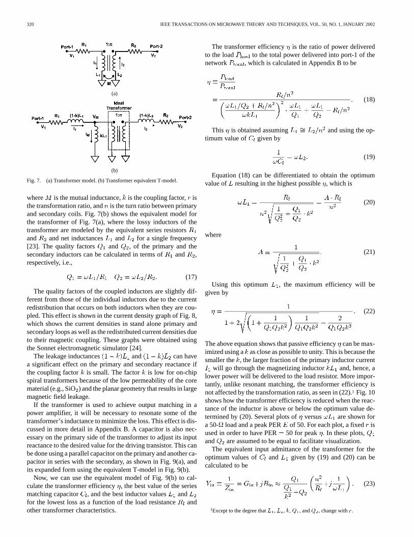
320 IEEE TRANSACTIONS ON MICROWAVE THEORY AND TECHNIQUES, VOL. 50, NO. 1, JANUARY 2002
(a)
(b)
Fig. 7. (a) Transformer model. (b) Transformer equivalent T-model.
where is the mutual inductance,is the coupling factor, isthe transformation ratio, andis the turn ratio between primaryand secondary coils. Fig. 7(b) shows the equivalent model forthe transformer of Fig. 7(a), where the lossy inductors of thetransformer are modeled by the equivalent series resistorsand and net inductances and for a single frequency[23]. The quality factors and , of the primary and thesecondary inductors can be calculated in terms ofand ,respectively, i.e.,
(17)
The quality factors of the coupled inductors are slightly dif-ferent from those of the individual inductors due to the currentredistribution that occurs on both inductors when they are cou-pled. This effect is shown in the current density graph of Fig. 8,which shows the current densities in stand alone primary andsecondary loops as well as the redistributed current densities dueto their magnetic coupling. These graphs were obtained usingthe Sonnet electromagnetic simulator [24].
The leakage inductances and can havea significant effect on the primary and secondary reactance ifthe coupling factor is small. The factor is low for on-chipspiral transformers because of the low permeability of the corematerial (e.g., SiO) and the planar geometry that results in largemagnetic field leakage.
If the transformer is used to achieve output matching in apower amplifier, it will be necessary to resonate some of thetransformer’s inductance to minimize the loss. This effect is dis-cussed in more detail in Appendix B. A capacitor is also nec-essary on the primary side of the transformer to adjust its inputreactance to the desired value for the driving transistor. This canbe done using a parallel capacitor on the primary and another ca-pacitor in series with the secondary, as shown in Fig. 9(a), andits expanded form using the equivalent T-model in Fig. 9(b).
Now, we can use the equivalent model of Fig. 9(b) to cal-culate the transformer efficiency, the best value of the seriesmatching capacitor , and the best inductor values andfor the lowest loss as a function of the load resistanceandother transformer characteristics.
The transformer efficiency is the ratio of power deliveredto the load to the total power delivered into port-1 of thenetwork , which is calculated in Appendix B to be
(18)
This is obtained assuming and using the op-timum value of given by
(19)
Equation (18) can be differentiated to obtain the optimumvalue of resulting in the highest possible, which is
(20)
where
(21)
Using this optimum , the maximum efficiency will begiven by
(22)
The above equation shows that passive efficiencycan be max-imized using a as close as possible to unity. This is because thesmaller the , the larger fraction of the primary inductor current
will go through the magnetizing inductor and, hence, alower power will be delivered to the load resistor. More impor-tantly, unlike resonant matching, the transformer efficiency isnot affected by the transformation ratio, as seen in (22).1 Fig. 10shows how the transformer efficiency is reduced when the reac-tance of the inductor is above or below the optimum value de-termined by (20). Several plots ofversus are shown fora 50- load and a peak PER of 50. For each plot, a fixed isused in order to have PER 50 for peak . In these plots,and are assumed to be equal to facilitate visualization.
The equivalent input admittance of the transformer for theoptimum values of and given by (19) and (20) can becalculated to be
(23)
1Except to the degree thatL , L , k, Q , andQ , change withr.

AOKI et al.: DISTRIBUTED ACTIVE TRANSFORMER 321
Fig. 8. Current densities in planar one turn inductors and a planar transformer.
(a)
(b)
Fig. 9. (a) Transformer model with load and tuning capacitors.(b) Transformer equivalent T-model with load and tuning capacitors.
We now calculate the transformer turn ratiofor a desiredPER using (10) and (23) using the assumption
(24)
(25)
Fig. 11 shows plots of versus and for 0.4, 0.6, 0.8,and1using(22).Asanexample, toobtainatransformationratioof50withprimaryandsecondaryinductorqualityfactorsoftenanda
of0.6,thetransformerprimarycircuitshouldhaveanimpedanceofapproximately at the frequencyofoperation toachieve thehighest efficiency. In this case,should be approximately eightand the best achievable passive efficiency is 70%.
Althoughasingleseriescapacitorwith the loadcanprovide thenecessary negative reactance to resonate the inductive output ofthe transformer, an additional capacitor parallel to the load(Fig.12)canbeusedtoadjusttherealpartoftheimpedanceseenbythesecondaryofthetransformertoloweritsloss.Thisextradegreeof freedom can be used to obtain a lower turn ratioand a lowerprimary inductance for a given load resistance and PER.
Equations (22), (24), and (25) determine the optimum value ofandtheresultant and for .Wecanrecalculate these
parametersfortheotherlimitingcase,whenislarge ,using (10), (16), (19), (20), and (24). The new PERis
(26)
which is obtained for a and an given by
(27)
The new input admittance is
(28)

322 IEEE TRANSACTIONS ON MICROWAVE THEORY AND TECHNIQUES, VOL. 50, NO. 1, JANUARY 2002
Fig. 10. Efficiency versus primary inductor reactance normalized to load resistance, inductorQ, and coupling factork for a transformer with loss.
(a) (b)
(c) (d)
Fig. 11. Efficiency versus primary inductorQ , secondary inductorQ , and coupling factork for a transformer with loss.
Fig. 12. Transformer equivalent T-model for analysis with load, tuning capacitors, and extra tuning capacitor in parallel to the load.
The new turn ratio in this case will be
(29)
The efficiency of this new setup is still given by (22). Notethat plots of Fig. 11 are still valid since they are calculated in
terms of quality factors. The maximum PER is achieved whenis very large. This maximum PER given by (26) is
times larger than (24).2
In the design process, we start from a given transistor and agiven power level that has to be delivered to the load. These twoconditions determine the desired value of the PER. Once this
2In practice, there is no need forC as the transformer dc isolation betweenthe input and output ports allows us to short circuitC .

AOKI et al.: DISTRIBUTED ACTIVE TRANSFORMER 323
is achieved, there is no point in increasing it beyond the re-quired value, and we should maximize the efficiencyinstead.As can be seen from (29), the addition of the parallel capacitor
makes it possible to use smaller turn ratiofor a desired. Typically, a lower results in a higher quality factor in mag-
netically coupled transformers, which translates to a higher ef-ficiency, as can be seen from (22).
A capacitor parallel to the transformer input completesthis circuit. It tunes the reactive part of the transformer inputimpedance to the desired value appropriate to provide the re-quired drain or collector impedance for the chosen class of theamplifier.3
Using the above analysis, we can compare the performanceof a magnetically coupled transformer with anLC-based res-onant impedance transformation discussed in Section II. Un-like the resonantLC matching circuit, in a magnetically cou-pled transformer the efficiency does not depend on the PER
and, hence, does not drop for larger output power level, ascan be seen from (11) and (22). The implicit assumption is thatthe quality factors do not change with larger, which may notbe correct as mentioned earlier. These equations shown graph-ically in Figs. 6 and 10 also show that for a PER above 15, themagnetically coupled transformer provides a higher efficiency
than the resonant matching for a given.This difference in behavior arises from a fundamental
difference between theLC resonant and magnetically coupledtransformer matching, which can be understood using a simplemodel. In both approaches, in order to achieve a high PER,the input ac current has to be larger than the output accurrent and the output ac voltage has to be largerthan the input ac voltage , both approximately by .4 Ina resonant matching network, the loss is proportional to theproduct of and , which are both large. On the otherhand, while in a magnetically coupled transformer, there aretwo loss components, namely, and , eachone is smaller than the single loss component in the case of aresonant matching by . Therefore, loosely speaking, the lossof the resonant matching circuit is larger by a factor of .
In a properly designed impedance-transformation networkusing magnetically coupled transformers, the reactance of theprimary inductor is approximately the load resistance thatshould be seen by the active device, as seen in (20). Similarly,the reactance of output inductor , will be approximatelythe load resistance. Additionally, a negative reactance in serieswith the load is necessary to achieve the highest possibleefficiency. This negative reactance can be generated by acombination of a series and a parallel capacitor, as shown inFig. 12. These observations are particularly important for theDAT structure introduced in the following section.
The disadvantage of a magnetically coupled transformer isthe low primary inductance necessary to achieve the highestefficiency. If spiral transformers on a silicon substrate were tobe used, the small primary inductance results in extremely shortmetal lines. For instance, the necessary inductance to achieve
3Although the tuning capacitor could be placed in series, biasing issues usu-ally favor the parallel setting. However, the series arrangement has the advantageof resulting in yet smallern.
4In a transformer,pr � n.
an of 50 into a 50- load is approximately 80 pH at 2 GHz.Inter-winding these short primary metal lines with the multi-turn secondary forces them to be very narrow. Unfortunately,this reduces the of both primary and secondary circuits,significantly. Noting the limitations of these two conventionalimpedance-transformation methods, we introduce an alterna-tive solution, which does not suffer from these shortcomings.
III. DAT
The analysis in these last two sections show that if we couldincrease the transformer turn ratiowhile maintaining a con-stant , we could achieve a high efficiency for large PER, assuggested by (22) and (24). Unfortunately, the quality factorsuffers if a large turn ratio is to be used for the reasons that willbe discussed in Appendix C. Also (20) shows that the requiredimpedance level at the input can become impractically small forlarge turn ratios because it is inversely proportional to. Theseobservations leave us no choice but to use lower turn ratios. Inpractice, the lowest loss can be achieved for a 1 : 1 ratio, whichis also very appealing since high-coupled slab inductors dis-cussed in Appendix C can be used to realize it.
While 1 : 1 transformers are desirable for the above reasons, itis obvious that we need more than one 1 : 1 transformer to obtainany impedance transformation. A high PER, can be achievedusing independent 1 : 1 transformers by connecting the sec-ondary circuits in series, as shown in Fig. 13(a) and (b). Inthis arrangement, the ac voltages on the secondaries add, whilethe primaries can be driven at a low voltage by separate activedevices. It should be noted that this configuration still has animpedance-transformation ratio . Additionally, as there are
devices being power combined, the PER of such a (lossless)structure is .
Unlike loop or spiral inductors, the two terminals of a slabinductor are not in close proximity of each other. This inherentproperty adds extra constraints to how they can be used. For ex-ample, if one is to make a parallelLC tank using a slab inductor,the parallel capacitor cannot be connected using regular wires,as the inductance and resistance of this wire will be compa-rable to that of the slab inductor. The absence of low-loss groundplanes in silicon technologies exacerbates the situation and de-grades the quality factor of a slab inductors, if they are config-ured in such a way that the return current conducts through thesubstrate.
A double differentialdrive can solve this problem in a poweramplifier. A virtual ac ground is created in the middle of the slabinductor if differential push–pull transistors drive it. This virtualac ground can be used as a dc feed for the power supply, makingthe impedance of the dc biasing networking inconsequential asfar as the differential signal is concerned. The differential drivesolves only half of the problem as the ground connection forthe driving transistors are not going to be in close proximitywith each other. It is necessary to form an ac ground by con-necting the two transistor grounds to stop the ac current fromflowing through the lossy ground line and, thus, induce extraloss. Again, a wire cannot be used to form this ac ground, asits inductance will be comparable to that of the slab inductor it-self. This problem can be solved by a double-differential drive

324 IEEE TRANSACTIONS ON MICROWAVE THEORY AND TECHNIQUES, VOL. 50, NO. 1, JANUARY 2002
(a)
(b)
Fig. 13. (a) Fundamental building block of DAT.N independent powersources combined in series throughN transformers with turn ratio 1 : 1.(b) Same diagram using coupled slab inductors as the transformer.
shown in Fig. 14, where each driving transistor has an oppositephase to companion adjacent to it. In this case, the ac currentflows through the adjacent transistors and hence an ac ground iscreated at their ground connections. Finally, to provide the samevirtual ground for the two active devices at the ends of this com-bined structure, it can be wound to form a DAT, as depicted inFig. 15(a) for slabs. Although this winding will reduce theof the inductors, due to the negative magnetic coupling betweenopposite sides of the polygon, this effect is significantly lowerthan winding each transformer individually as the dimension ofthe total structure is much larger. The schematic of Fig. 15(a)shows the central concept behind the DAT structure. In this con-figuration, the impedance-transformation and power-combiningfunctions are achieved concurrently. Also all the dc currentsare provided to the amplifier through virtual ac grounds, whichmakes the amplifier insensitive to the means used to supply thedc voltages (e.g., length of bonding wires).
The DAT combines the relatively high primary inductance oftheLC matching networks, the PER-independent efficiency ofa magnetically coupled transformer, and the high quality factorof slab inductors, while providing an effective means of powercombining. In the DAT structure the loss is reduced because thevoltages add on the secondary to combine power. Thus, the totalac current through the secondary inductor of the DAT is smallerthan the current through theLC matching inductor by a factorof . Since the impedance of the DAT secondary is larger thanthe LC matching inductor by the same factor, the loss of theDAT is smaller than that of theLC match by approximately afactor of . Additionally, while large currents do flow throughthe magnetizing inductors of the primary circuits in a DAT, thelow-loss slab inductors minimize the associated loss due to theirhigher .
As discussed earlier and shown in Fig. 9(a), the transformer’sinput shunt capacitor is necessary for the transformer topresent the proper impedance to the active device. As mentionedearlier, cannot be placed in parallel with the slab inductorsbecause of the physical distance between its terminals. How-ever, placing capacitors between two adjacent ends of two slab
inductors [see Fig. 15(b)] has exactly the same effect since thevoltage across the capacitor will be identical to that of a ca-pacitor in parallel with the slab. The output matching capacitor
can be simply placed in parallel to the load, as illustratedin Fig. 15(b). A representative drawing of this structure witheight NMOS transistors and four slab transformers is shown inFig. 16.
A modified version of the transformer analysis described inSection II can be used to analyze the DAT. The new requiredprimary inductance and the effective input admittance are givenby
(30)
(31)
where is the number of combined transistors. The new ex-pressions for and in the presence of and can bederived using a similar derivation to that of Section II.
The definition of PER can be generalized to the case of amatching/transformation network with multiple input ports. Inthis scenario, it is natural to define the PERas the ratio ofthe RF power delivered to the load with the network in place
to the power delivered to load for one of the sinusoidalinput voltage sources driving the load directly . Based onthis definition, the PER for the DAT can be calculated to be
(32)
Finally, the efficiency will be the same as the efficiency of astandard transformer matching circuit given by (22).
Several very important observations can be made about theDAT, when compared to conventional impedance-transforma-tion networks.
1) The PER of the DAT is proportional to the square of thenumber of transistors , as shown by (32). This is com-parable to the PER of a standard transformer matchingcircuit with a turn ratio given by (26).
2) Comparing (27) and (30), it can be seen that the primaryinductance will be times larger in the DAT thanthe standard magnetically coupled transformers. This willallow the DAT to use values that are more practical forat the input ports.
3) In the DAT, transistors generate the power and, there-fore, each active device needs to deliver a smaller powerto the passive structure. This difference manifests itself in(28) and (31), where the input conductance of each portin the DAT is times smaller than the input of a standardmagnetically coupled transformer.
4) Unlike LC-resonant matching networks, the loss mecha-nism of the DAT structure is independent of the PER tothe first order. It is noteworthy that standard magneticallycoupled transformers benefit from the same advantage.
5) The geometry of the DAT makes it possible to use 1 : 1slab transformers. In the DAT, we can make the primary

AOKI et al.: DISTRIBUTED ACTIVE TRANSFORMER 325
Fig. 14. N independent power sources combined in series throughN=2 transformers in double-differential configuration with grounds shared between adjacentpower sources, except for the first and last sources in the chain.
(a)
(b)
Fig. 15. (a)N independent power sources combined in series throughN=2transformers in double-differential configuration with grounds shared betweenevery adjacent power sources using the circular geometry. (b) Same diagramwith cross-connected drain tuning capacitors and output capacitor.
slab inductors wide to lower their series resistance. Thisreduction of loss in the primary is particularly importantbecause large magnetizing currents flow in the primarycircuits.
6) The two terminals of the slab inductors are not in closeproximity of each other. The DAT uses a double-differen-tial drive to be able to incorporate slab inductors into thedesign.
7) The distributed nature of the DAT can improve thethermal dissipation capability of the active devices up to
Fig. 16. Representative drawing of a complete DAT with 8 NMOS transistors.
a factor of due to the more even distribution of theactive device area across the chip.
8) The current in the secondary of the DAT is approximatelytimes smaller than inLC-resonant circuits, which al-
lows narrower metal lines to be used on the secondary.Table I summarizes the performances of each one of the dis-
cussed power-combining, impedance-transformation and har-monic tuning techniques.
IV. A D ESIGN EXAMPLE
In this section, we will demonstrate the design process of a2-W power amplifier using 0.35-m CMOS transistors with adrain breakdown voltage around 6 V. The passive parameters ofthis process are summarized in Table II.
For reliability, we should leave some margin for the max-imum drain voltage to avoid junction breakdown. For this reasonwe limit the power supply to 2 V. To achieve 2 W output powerinto a 50- load with a 2-V power supply, we need a PER higherthan 50. For this design example, we have chosen a center fre-quency of 2.45 GHz.
Now, let us compare the performance of the three differentmethods of power enhancement discussed in Sections II and III.To obtain a PER of 50 using resonant impedance transforma-tion (Section II-A), we need to use a three-stage network, asdetermined by Fig. 6. For this frequency and power level, thethree inductors can be calculated using (15) to be 1.6, 0.35, and0.075 nH. To obtain an estimate of the efficiency of the passivenetwork, we can use ASITIC [22] to optimize these inductors,resulting in quality factors of 14, 10, and 3, respectively. Thegeometric mean of these quality factors can be used to approx-imate the efficiency of the passive network using Fig. 6. With a

326 IEEE TRANSACTIONS ON MICROWAVE THEORY AND TECHNIQUES, VOL. 50, NO. 1, JANUARY 2002
TABLE ICOMPARISON OFCHARACTERISTICS OFSEVERAL LUMPED IMPEDANCE MATCHING AND POWER-COMBINING TECHNIQUES
TABLE IIPROCESSCHARACTERISTICS
mean of 7.5 the efficiency of the passive resonant matchingnetwork will be less than 50%. Even using a singleLC sectionwith an optimum5 inductor of 15, Fig. 4 indicates that passiveefficiency cannot exceed 52%. Note that this is the efficiencyof the passive network alone assuming that ideal ac groundscan be provided and layout issues and parasitic components donot limit the performance. In practice, a resonator based passivenetwork will have an even lower efficiency, for such high PER.
The second alternative is a standard coupled-inductor trans-former. If we assume a typical inductor of eight and a cou-pling factor of 0.6, we can obtain an efficiency of up to 68%,based on Fig. 10. Although this is higher than that of resonantnetwork, it is extremely difficult (if not impossible) to layout amoderate- short and wide (70 pH at 2.4 GHz) inductor6
for the primary circuit and simultaneously inter-wind a sec-
5This is the best value that could be obtained using Sonnet [24] EM simulatorfor a spiral inductors in this process.
6The ASITIC optimizedQ of this spiral inductor without the secondary isaround three.
ondary inductor with approximately (3.3 nH at 2.4 GHz)and seven turns without reducing the quality factors. Due tothe physical layout constraints, these standard transformers willhave a very narrow metal width and/or a reactance significantlyhigher than . Due to these limitations, passive efficiency ofthese impedance-transformation networks will be much lowerthan the theoretically predicted upper limit of 68%.
Now, we can compare theLC-matching and coupled-inductortransformers with the DAT structure. Since the primary of theDAT consists of a slab inductor, it achieves aof more than30 in this process technology. The secondary loop of the DATstructure has a of ten and coupling coefficient of 0.6. Thesecondary parameters are comparable to a standard spiral trans-former. Using (22), we predict a theoretical passive efficiencyaround 82%, for the DAT structure. As can be seen, The DATachieves a higher passive efficiency than the resonant and stan-dard transformer networks. Also, the double-differential driveof Fig. 15(b) generating multiple virtual grounds makes it pos-sible to implement a DAT on a lossy silicon substrate without asignificant reduction in this theoretically predicted passive effi-ciency due to biasing and ground connections.
To verify the feasibility of the DAT, the structure of Fig. 16was simulated using Sonnet [24]. The primary slab inductorshave a of 30, while the of the secondary loop is aroundeight. The electromagnetic simulations show a PER of 65. Thistranslates to a maximum achievable output power of 2.5 W witha 2-V power supply. The simulated DAT passive efficiency was70.5%. This in combination with the active device efficiencyof 67.5% (operating in fully saturated class mode [25])and a compressed gain of 10 dB, result in a PAE of 43%. Thepredicted drain efficiency is around 48%.
This truly fully integrated CMOS power amplifier wasfabricated using 0.35-m CMOS transistors. The measurementshows a PAE of 41% with a maximum output power ofof 1.9 W on a 2-V power supply, as shown in Fig. 17. Theamplifier has a small signal gain of 14 dB and a compressed

AOKI et al.: DISTRIBUTED ACTIVE TRANSFORMER 327
Fig. 17. Measured gain and PAE versusP of the DAT power amplifierwhen driving a differential load.
Fig. 18. Microphotograph of the measured DAT power amplifier.
gain of 8.7 dB at 1.9-W output power. Its drain efficiency is48%. The input and output are both matched to 50, with aninput reflection coefficient of 9 dB. The 3-dB bandwidth is510 MHz centered at 2.44 GHz. All harmonics up to 20 GHzwere more than 64 dBc below the fundamental. An on-chipbalun allows for a single ended 50-input. The same amplifieralso provides a PAE of 31% with an output power of 2.2 W foran unbalanced 50-load. The die size was 1.3 2.0 mm andits microphotograph can be seen in Fig. 18.
Judging by the measured efficiency, we believe that everyeight transistors are receiving fairly in-phase signals when thepower amplifier is driving a symmetric differential load. On theother hand, the lower efficiency measured with unbalanced loadis likely due to a phasing problem caused by an undesirableasymmetric feedback from the output.
A summary of these results can be seen in the Table III.
V. CONCLUSION
A fundamental analysis of the loss mechanisms of theconventional on-chip impedance-transformation networksand their limitations are performed. We conclude the studywith a description of the characteristics of the DAT. DATis a new impedance-transformation and series power-com-bining architecture, which offers the advantages ofLC andcoupled-inductor matching simultaneously. Furthermore, itpresents the advantage of power combining in series several
TABLE IIISUMMARY OF MEASURED ANDSIMULATED AMPLIFIER PERFORMANCE
amplifiers distributed across the chip without using additionalcomponents. This new concept combines in series severalpush–pull amplifiers efficiently by extensive use of virtual acgrounds and magnetic couplings.
APPENDIX ARESONANT NETWORK EFFICIENCY COMPUTATION
To calculate theLC matching network efficiency as a func-tion of and , we eliminate the terms and from thedefinition (10) using (5) and (6) and isolate the term
as follows:
(A.1)
This isolated term is by (5)
(A.2)
Equation (A.2) stands as is approximately square ofand is .
Substituting in the definition (4) using (A.1), we can finda solution for , as shown by (12).
For the multisection case, we have
(A.3)
If we assume that each individual ’s are equal, we have
(A.4)
(A.5)

328 IEEE TRANSACTIONS ON MICROWAVE THEORY AND TECHNIQUES, VOL. 50, NO. 1, JANUARY 2002
and from the above, we obtain
(A.6)
The total efficiency of the network is the product of the effi-ciency of each stage. Simultaneously, if the total PER is, thePER of each stage will be . Analyzing the Fig. 5, we cancalculate the inductor value for each stage in a similar way as ina single section network
(A.7)
(A.8)
From (1), (A.1), and (A.2) we have
(A.9)
From (A.7), (A.8) and (A.9) we have
(A.10)
APPENDIX BTRANSFORMEREFFICIENCY COMPUTATION
The transformer efficiency is the ratio of power dissi-pated in the load resistance and total power dissipatedin , , and , shown in (B.1) at the bottom of this page,where
(B.2)
To maximize in the above expression, should resonateat the frequency of interest, i.e.,
(B.3)
This condition minimizes the current through and itsdissipated power by resonating the inductors and
with the capacitor .Assuming and using (17) and (B.3), we can
further simplify (B.1) to
(B.4)
which is obtained by dividing the equivalent load resistanceby the sum of three equivalent resistances, which are, , and reduced by the ratio .
APPENDIX CDESIGN OF ALOW IMPEDANCE INDUCTOR
Inductors are essential blocks to design various forms ofimpedance-transformation networks and their properties cansignificantly affect the performance of such networks, asdiscussed earlier.
Spiral inductors [12], [15], [22] have been widely used inradio frequency integrated circuits. They can be single-turn ormultiturn, as shown in Fig. 19. For a spiral inductor the negativemagnetic coupling between the opposite sides of the polygonlowers its total equivalent inductance. However, this inductancereduction by negative mutual coupling does not occur when thedistance between the opposite sides of the spiral is significantlylarger than the mirror current penetration depth of the transmis-sion line in the substrate.
In a single turn inductor with larger spacing between its op-posite sides, the substrate (back plane) mirror current limits theinductance per metal length. Therefore, it behaves similarly to amicrostrip transmission line of the same length. Also, the prox-imity of the opposite terminals of the inductor provides an al-ternative current path through the shunt-capacitors and the sub-strate that increases the loss.
(B.1)

AOKI et al.: DISTRIBUTED ACTIVE TRANSFORMER 329
Fig. 19. One-turn planar spiral inductor and multiturn planar spiral inductor.
Fig. 20. Short transmission-line inductor with one terminal grounded on adielectric substrate with backside ground plane.
If we use more than one turn to form a spiral inductor, thepositive magnetic couplings between the conductors in the sameside of the polygon enhance the total equivalent inductance.7
We can also build an inductor using a short transmission linewith one of its terminals short-circuited to the ground, as inFig. 20. Standard transmission-line analysis can be used to cal-culate the inductance and theof this inductor [18] as follows:
(C.1)
where and are transmission line’s characteristic impedanceand complex propagation constant given by
(C.2)
In which and , are the series impedanceand shunt admittance per unit length, respectively. Equation(C.1) shows that the inductance is proportional to the trans-mission-line characteristic impedance and its length. If thesubstrate has a low resistivity (e.g., in silicon), the loss terms in(C.2) will be large, which results in a relatively small inductorquality factor. In practice, it is very difficult to obtain analyticalexpressions for these loss components due to the nonuniformityof the conductor and substrate mirror current components, andone should resort to simulation methods [26].
For small lengths, the inductance of the microstrip trans-mission-line inductor is proportional to its length, as shownin (C.1). Also, smaller line width increases and, hence,raise the inductance . However, the dependence is weakerthan linear due to the mutual coupling between parallel currentcomponents on the line. This behavior is shown in Fig. 21where is plotted versus . This plot was obtained for a
7The multiturn spiral inductor also suffers from a larger parasitic capacitancebetween adjacent turns that lowers its self-resonant frequency.
Fig. 21. Inductance of a transmission-line inductor versus metal width forconstant metal length (1500�m).
Fig. 22. Q of a transmission-line inductor versus metal length and metal width.
silicon process using a planar E/M simulator [24]. Fig. 22shows plots of versus for different values of . Theprocess characteristics used in the simulation can be seen in theTable III. Fig. 22 shows that series metal resistance,, is thedominant loss factor for a narrow line (small) and, hence,
is approximately constant as a function of. This is becauseboth the series resistance and the inductance are proportionalto , thus their ratio remains constant, i.e.,
(C.3)
On the other hand, the shunt elementsis the dominant lossfactor for a wide line (large ). In this case, decreases almostquadratically with increasing because both the series induc-tance and shunt-conductance scale with, i.e.,
(C.4)
Fig. 22 shows this behavior, where for m isalmost constant with, while it drops with rapidly for
m. Consequently, we can conclude that microstrip in-ductor increases with increasing when it is short anddegrades with increasing when the line is long, as illustratedin Fig. 22.
Based on this argument, we can find theand that maxi-mize the for a desired inductance. This optimumis plotted

330 IEEE TRANSACTIONS ON MICROWAVE THEORY AND TECHNIQUES, VOL. 50, NO. 1, JANUARY 2002
Fig. 23. Q of a transmission-line inductor versus metal length or metal width and inductance. In the first plot, for each metal length, the width, which providesthe selected inductance, is chosen. In the second plot, for each metal width, the length, which provides the selected inductance, is chosen.
as functions of and in Fig. 23. The lower the inductance, thewider and shorter the optimum inductor. It should be notedthat the optimum of a slab inductor with small is muchlarger than typical quality factors of large spiral inductors, asshown in Fig. 23.
Based on these results, we can compare the three differenttypes of inductor, namely, slab, single-turn, and multiturn in-ductors. The following guidelines can be used to obtain the besttype of inductor in most practical applications.
If for a given the reactance of a slab inductor is muchsmaller than the transmission-line characteristic impedance,it will have a higher compared to spiral inductors. On theother hand, if the desired reactance of the inductor is larger orcomparable to , multiturn spiral inductors should be used.One exception is when the transmission line is very low loss.In this case, a single ended high-inductor can be obtainedusing a transmission line shorter than quarter wavelength withone of its terminals grounded. In this case, the slab inductor isstill preferred.
Another issue is that the terminals of a slab inductor are notadjacent to each other and this may preclude their use in cer-tain applications. It is interesting to note that the slab induc-tors always outperform single loop inductor in terms ofand,therefore, are always preferable unless two adjacent terminalsare necessary.
ACKNOWLEDGMENT
The authors thank Conexant Systems for chip fabrication,particularly R. Magoon, F. In’tveld, J. Powell, A. Vo, and K.Moye. K. Potter, D. Ham, and H. Wu, all of the California Insti-tute of Technology (Caltech), Pasadena, deserve special thanksfor their assistance. The technical support for CAD tools fromAgilent Technologies and Sonnet Software Inc., Liverpool, NY,are also appreciated.
REFERENCES
[1] R. Gupta, B. M. Ballweber, and D. J. Allstot, “Design and optimizationof CMOS RF power amplifiers,”IEEE J. Solid-State Circuits, vol. 36,pp. 166–175, Feb. 2001.
[2] Y. J. E. Chen, M. Hamai, D. Heo, A. Sutono, S. Yoo, and J. Lascar,“RF power amplifier integration in CMOS technology,” inIEEE MTT-SMicrowave Symp. Dig., vol. 1, Boston, MA, June 2000, pp. 545–548.
[3] K. C. Tsai and P. R. Gray, “A 1.9 GHz, 1-W CMOS class-E power am-plifier for wireless communications,”IEEE J. Solid-State Circuits, vol.34, pp. 962–969, July 1999.
[4] C. Yoo and Q. Huang, “A common-gate switched, 0.9W class-E poweramplifier with 41% PAE in 0.25�m CMOS,” in VLSI Circuits Symp.Dig., Honolulu, HI, June 2000, pp. 56–57.
[5] W. Simbürger, H. D. Wohlmuth, P. Weger, and A. Heinz, “A monolithictransformer coupled 5-W silicon power amplifier with 59% PAEat 0.9 GHz,”IEEE J. Solid-State Circuits, vol. 34, pp. 1881–1892, Dec.1999.
[6] W. Simbürger, A. Heinz, H. D. Wohlmuth, J. Böck, K. Aufinger, andM. Rest, “A monolithic 2.5V, 1W silicon bipolar power amplifier with55% PAE at 1.9GHz,” inIEEE MTT-S Int. Microwave Symp. Dig., vol.2, Boston, MA, June 2000, pp. 853–856.
[7] I. J. Bahl, E. L. Griffin, A. E. Geissberger, C. Andricos, and T.F. Brukiewa, “Class-B power MMIC amplifiers with 70 percentpower-added efficiency,”IEEE Trans. Microwave Theory Tech., vol.37, pp. 1315–1320, Sept. 1989.
[8] D. Ngo, B. Beckwith, P. O’Neil, and N. Camilleri, “Low voltage GaAspower amplifiers for personal communications at 1.9GHz,” inIEEEMTT-S Int. Microwave Symp. Dig., vol. 3, Atlanta, GA, June 1993, pp.1461–1464.
[9] J. Portilla, H. García, and E. Artal, “High power-added efficiency MMICamplifier for 2.4 GHz wireless communications,”IEEE J. Solid-StateCircuits, vol. 34, pp. 120–123, Jan. 1999.
[10] Y. Tan, M. Kumar, J. J. O. Sin, L. Shi, and J. Lau, “A 900-MHz fullyintegrated SOI power amplifier for single-chip wireless transceiver ap-plications,” IEEE J. Solid-State Circuits, vol. 35, pp. 1481–1485, Oct.2000.
[11] T. H. Lee,The Design of CMOS Radio-Frequency Integrated Circuits,1st ed. Cambridge, U.K.: Cambridge Univ. Press, 1998.
[12] J. R. Long, “Monolithic transformers for silicon RF IC design,”IEEE J.Solid-State Circuits, vol. 35, pp. 1368–1382, Sept. 2000.
[13] T. H. Lee and S. S. Wong, “CMOS RF integrated circuit at 5GHz andbeyond,”Proc. IEEE, vol. 88, pp. 1560–1571, Oct. 2000.
[14] M. Racanelli, Z. Zhang, K. Liao, J. Zheng, A. Kar-Roy, P. Joshi, C.Compton, C. Hu, D. Mikolas, G. Jolly, and P. Kempf, “BC35: A 0.35�m RF BiCMOS technology for highly integrated wireless systems,” inIEEE RFIC Symp. Dig., Anaheim, CA, June 1999, TUE2-3.
[15] J. R. Long and M. A. Copeland, “The modeling, characterization, anddesign of monolithic inductors for silicon RF IC’s,”IEEE J. Solid-StateCircuits, vol. 32, pp. 357–369, Mar. 1997.
[16] I. Aoki, S. D. Kee, D. B. Rutledge, and A. Hajimiri, “A 2.4-GHz, 2.2-W,2-V fully-integrated CMOS circular-geometry active-transformer poweramplifier,” in IEEE Custom Integrated Circ. Conf. Dig., San Diego, CA,May 2001, pp. 57–60.
[17] I. Aoki, S. D. Kee, D. B. Rutledge, and A. Hajimiri, “Fully-integratedCMOS power amplifier design using distributed active-transformer ar-chitecture,”IEEE J. Solid-State Circuits, submitted for publication.

AOKI et al.: DISTRIBUTED ACTIVE TRANSFORMER 331
[18] D. M. Pozar,Microwave Engineering, 2nd ed. New York: Wiley, 1998.[19] H. Wu and A. Hajimiri, “Silicon-based distributed voltage-controlled
oscillators,” IEEE J. Solid-State Circuits, vol. 36, pp. 493–502, Mar.2001.
[20] K. K. Clarke and D. T. Hess,Communication Circuits: Analysis andDesign, 1st ed. Reading, MA: Addison-Wesley, 1971.
[21] D. B. Rutledge,The Electronics of Radio, 1st ed. Cambridge, U.K.:Cambridge Univ. Press, 1999.
[22] A. M. Niknejad and R. G. Meyer, “Analysis, design and optimization ofspiral inductors and transformers for Si RF IC’s,”IEEE J. Solid-StateCircuits, vol. 33, pp. 1470–1481, Oct. 1998.
[23] W. K. Chen,The Circuits and Filters Handbook. Boca Raton, FL: CRCPress, 1995.
[24] Sonnet Suite User’s Manual, Release 6.0, vol. 1, Sonnet Software, Liv-erpool, NY.
[25] S. D. Kee, I. Aoki, and D. B. Rutledge, “7-MHz, 1.1-kW demonstrationof the new E/F switching amplifier class,” inIEEE MTT-S Int. Mi-crowave Symp. Dig., vol. 3, Phoenix, AZ, June 2001, pp. 1505–1508.
[26] H. Hasegawa, M. Furukawa, and H. Yanai, “Properties of microstrip lineon Si–SiO system,”IEEE Trans. Microwave Theory Tech., vol. 19, pp.869–881, Nov. 1971.
Ichiro Aoki (S’98) was born in Kyoto, Japan, in1965. He received the B.S.E.E. degree from theUniversidade Estadual de Campinas, Campinas SP,Brazil, in 1987, the M.S.E.E. degree from CaliforniaInstitute of Technology (Caltech), Pasadena, in1999, and is currently working toward the Ph.D.degree at Caltech.
He founded and managed the PST IndústriaEletrônica da Amazônia Ltda, SP, Brazil, a carelectronic components manufacturing company with300 employees in 1998 from 1988 to 1998. His
current research interests include high-frequency silicon RF analog integratedcircuits for wireless communications with emphasis on power amplifiers.
Mr. Aoki was the recipient of the Schlumberger Fellowship (1998–1999) andthe 2000 Walker von Brimer Foundation Award presented by Caltech.
Scott D. Keewas born in Albany, OR, in 1976. Hereceived the B.E.E. degree in electrical engineeringfrom the University of Delaware, Newark, in 1998,and is currently working toward the Ph.D. degree atthe California Institute of Technology, Pasadena.
His research interests include high-efficiencypower amplifiers, switching amplifiers, RF andmicrowave design, analog integrated circuits, andelectronics for practicing musicians.
David B. Rutledge (S’77–M’77–SM’89–F’93)received the B.A. degree in mathematics fromWilliams College, Williamstown, MA, in 1973, theM.A. degree in electrical sciences from CambridgeUniversity, Cambridge, U.K., in 1975, and the Ph.D.degree in electrical engineering from the Universityof California at Berkeley, in 1980.
He currently holds the Kiyo and Eiko TomiyasuChair of Electrical Engineering at the CaliforniaInstitute of Technology (Caltech), Pasadena. He isExecutive Officer for Electrical Engineering and
Director of Caltech’s Lee Center for Advanced Networking. His research hasfocused on integrated-circuit antennas, active quasi-optics, computer-aideddesign, and high-efficiency power amplifiers. He authored the electronicstextbook The Electronics of Radio(Cambridge, U.K.: Cambridge Univ.Press,1999) and co-authoed the microwave computer-aided-design softwarepackagePuff, which has sold 30 000 copies.
Dr. Rutledge is the Editor-in-Chief of the IEEE TRANSACTIONS ON
MICROWAVE THEORY AND TECHNIQUES. Six of his former students have wonPresidential Investigator Awards from the National Science Foundation. Hewas the recipient of the Microwave Prize, the Distinguished Educator Awardof the IEEE Microwave Theory and Techniques Society (IEEE MTT-S), theTeaching Award of the Associated Students of Caltech, the Doug DeMawaward of the ARRL, and the Third Millennium Award of the IEEE.
Ali Hajimiri (S’94–M’99) received the B.S. degreein electronics engineering from the Sharif Universityof Technology, Tehran, Iran, and the M.S. and Ph.D.degrees in electrical engineering from Stanford Uni-versity, Stanford, CA, in 1996 and 1998, respectively.
From 1993 to 1994, he was a Design Engineerwith Philips Semiconductors, where he was involvedwith a BiCMOS chipset for GSM cellular units.In 1995, he was with Sun Microsystems, wherehe was involved with the UltraSPARC micropro-cessor’s cache RAM design methodology. During
the summer of 1997, he was with Lucent Technologies (Bell Laboratories),Holmdel, NJ, where he investigated low phase-noise integrated oscillators. In1998, he joined the Faculty of the California Institute of Technology, Pasadena,as an Assistant Professor of electrical engineering. His research interests arehigh-speed and RF ICs. He co-authoredThe Design of Low Noise Oscillators(Norwell, MA: Kluwer, 1999). He holds several U.S. and European patents.
Dr. Hajimiri is a member of the Technical Program Committees of the In-ternational Conference on Computer-Aided Design (ICCAD). He has servedas a guest editor of the IEEE TRANSACTIONS ON MICROWAVE THEORY AND
TECHNIQUES. He was the recipient of the Gold Medal of the National PhysicsCompetition, the Bronze Medal of the 21st International Physics Olympiad,Groningen, The Netherlands, and the IBM Faculty Partnership Award. He was acorecipient of the International Solid-State Circuits Conference 1998 Jack KilbyOutstanding Paper Award.