disi - university of trento design and characterization of...
TRANSCRIPT

PhD Dissertation
December 2010
International Doctorate School in Information and
Communication Technologies
DISI - University of Trento
DESIGN AND CHARACTERIZATION OF A CURRENT ASSISTED
PHOTO MIXING DEMODULATOR FOR TOF BASED 3D CMOS
IMAGE SENSOR
Quazi Delwar Hossain
Advisor:
Prof. Gian-Franco Dalla Betta
DISI,University of Trento,
Trento, Italy

ii
Abstract
Due to the increasing demand for 3D vision systems, many efforts have been recently concentrated to
achieve complete 3D information analogous to human eyes. Scannerless optical range imaging systems
are emerging as an interesting alternative to conventional intensity imaging in a variety of applications,
including pedestrian security, biomedical appliances, robotics and industrial control etc. For this, several
studies have reported to produce 3D images including stereovision, object distance from vision system
and structured light source with high frame rate, accuracy, wide dynamic range, low power consumption
and lower cost. Several types of optical techniques for 3D imaging range measurement are available in
the literature, among them one of the most important is time-of-flight (TOF) principle that is intensively
investigated. The third dimension, i.e. depth information, can be determined by correlating the reflected
modulated light signal from the scene with a reference signal synchronous with the light source
modulation signal.
CMOS image sensors are capable of integrating the image processing circuitry on the same chip as the
light sensitive elements. As compared to other imaging technologies, they have the advantages of lower
power consumption and potentially lower price. The merits make this technology competent for the next-
generation solid-state imaging applications. However, CMOS process technologies are developed for
high-performance digital circuits.
Different types of 3D photodetectors have been proposed for three-dimensional imaging. A major
performance improvement has been found in the adoption of inherently mixing detectors that incorporate
the role of detection and demodulation in a single device. Basically, these devices use a modulated
electric field to guide the photo generated charge carriers to different collection sites in phase with a
modulation signal. One very promising CMOS photonic demodulator based on substrate current
modulation has recently been proposed. In this device the electric field penetrates deeper into the
substrate, thus enhancing the charge separation and collection mechanism. A very good sensitivity and
high demodulation efficiency can be achieved.
The objective of this thesis has been the design and characterization of a Current Assisted Photo mixing
Demodulator (CAPD) to be applied in a TOF based 3D CMOS sensing system. At first, the experimental
investigation of the CAPD device is carried out. As a test vehicle, 10×10 pixel arrays have been
fabricated in 0.18µm CMOS technology with 10×10 µm2 pixel size. The main properties of CAPD devices,
such as the charge transfer characteristic, modulation contrast, noise performance and non-linearity
problem, etc. have been simulated and experimentally evaluated. Experimental results demonstrate a
good DC charge separation efficiency and good dynamic demodulation capabilities up to 45MHz. The
influence of performance parameters such as wavelength, modulation frequency and voltage on this
device is also discussed. This test device corresponds to the first step towards incorporating a high
resolution TOF based 3D CMOS image sensor.
The demodulator structure featuring a remarkably small pixel size 10 × 10 µm
2 is used to realize a 120 ×
160 pixel array of ranging sensor fabricated in standard 0.18µm CMOS technology. Initial results
demonstrate that the demodulator structure is suitable for a real-time 3D image sensor. The prototype
camera system is capable of providing real-time distance measurements of a scene through modulated-
wave TOF measurements with a modulation frequency 20 MHz. In the distance measurement, the sensor
array provides a linear distance range from 1.2m to 3.7m with maximum accuracy error 3.3% and
maximum pixel noise 8.5% at 3.7m distance. Extensive testing of the device and prototype camera system
has been carried out to gain insight into the characteristics of this device, which is a good candidate for
integration in large arrays for time-of-flight based 3D CMOS image sensor in the near future.
Keywords- Time-of-Flight, Range camera, Current Assisted Photo mixing Demodulator, CMOS image
sensor.

iii
Acknowledgement
Above all, I would like to express my gratitude to my supervisor Prof. Gian-Franco Dalla Betta for
accepting me into his research group and also express my heartfelt thanks to him for his guidance,
encouragement and continuous support during my graduate studies. His enthusiasm for teaching and
research offered challenging opportunities to expand my scientific knowledge and my growing interest in
the world of Photonics.
I would like to express my deep appreciation to Dr. Lucio Pancheri for sparing me countless hours of his
precious time, useful discussions and suggestions during all the stages of my thesis work. I will always be
grateful to him. I also wish to give my thanks to Dr. David Stoppa for his frank discussions and unique
ideas.
I want to thank my fellow doctoral students in Nano & Micro Systems group for their helpful
cooperations and assistance. I also thank all the colleagues at SOI group of FBK who contributed in their
personal ways to carry out my Ph.D. thesis work.
I would like to express my sincere gratitude to Prof. Giovanni Verzellesi, University of Modena and
Reggio Emilia and Dr. Giuseppe Martini, University of Pavia for accepting to review my thesis.
I want to thank Dr. S. Farazi Feroz and Mr. Shahin Reza for their help in proof reading of my dissertation.
In overbearing times, I was lucky to have the support of all Bangladeshi students at the University of
Trento which made my stay here in Italy much more fun and enjoying. I also thank all the administrative
associates in Ph.D. office and Welcome office for their kind assistance and cheerful spirit.
This research work is partially supported by the Italian Ministry for Education, University and Research
(MIUR), under the project PRIN07 N.2007AP789Y “Time of Flight Range Image Sensor (TRIS)” and by
the European Community 6th Framework programmed within the project NETCARITY. I would like to
thank all the members of FBK, Italy and UMC, Taiwan for their support in chip fabrication
Finally, I want to thank all my family members for their unconditional support all through out my life and
academic career; special words of appreciation to my wife Nusrat for her encouragement, endless support
and contribution in every aspect along the years. This thesis dissertation is dedicated to them.

iv
TABLE OF CONTENTS
ABSTRACT ii
ACK,OWLEDGEME,T iii
TABLE OF CO,TE,TS iv
LIST OF FIGURES vii
LIST OF TABLES x
CHAPTER 01: I,TRODUCTIO, 1
1.1 Motivation 1
1.2 Thesis Objectives 2
1.3 Thesis Overview 3
CHAPTER 02: THEORETICAL OVERVIEW 5
2.1 Photon and photo sensing physics in semiconductors 5
2.1.1 Description of light and photon 5
2.1.2 Energy band structure of semiconductors 6
2.1.3 Optical absorption in semiconductors 7
2.1.4 Photon-semiconductor interaction 9
2.2 Silicon based photodetectors and light detection 10
2.2.1 Photoconductor 10
2.2.2 Photodiode 12
2.2.3 Phototransistor 13
2.2.4 Photo-gate 14
2.3 Different types of CMOS compatible photodiodes 15
2.4 Considerable parameters of photodetector 16
2.4.1 Responsivity 17
2.4.2 Quantum efficiency 17
2.4.3 Response time 17
2.4.4 Leakage current 18
2.4.5 Capacitance 18
2.4.6 =oise 19
2.5 Review of CCD and CMOS Image Sensor 20
2.5.1 Charged-Coupled Device (CCD) Image Sensor 20
2.5.2 CMOS based Image Sensor 23
2.5.3 Comparison between CCD and CMOS Imagers 24
2.6 Available technologies for Image Sensor 25
2.6.1 CCD Image Sensor technology 25
2.6.2 CMOS Image Sensor technology 25
CHAPTER 03: STATE OF THE ART OF 3D IMAGI,G 27
3.1 Different optical measurement techniques for 3D imaging 27
3.1.1 Triangular method 28
3.1.1.1 Passive Triangular method 28

v
3.1.1.2 Active Triangular method 29
3.1.2 Interferometry 30
3.1.3 Time of Flight (TOF) method 31
3.1.3.1 Pulsed Modulation TOF technique 33
3.1.3.2 Continuous Wave (CW) modulation TOF technique 33
3.1.3.3 Pseudo-=oise modulation TOF technique 34
3.1.4 Comparison between the main optical techniques for range measurement 35
3.2 Time-of-Flight (TOF) based 3D vision sensors 36
3.2.1 Standard photodiode is coupled with complex processing circuit 36
3.2.2 Photo-demodulator fabricated with special technologies 37
3.2.3 Single Photon Avalanche Diode (SPAD) based Imager 39
3.2.4 Photo Mixing Device (PMD) based Imager 39
3.2.5 Gates-on-Field Oxide structure based CMOS Range Image Sensor 41
3.2.6 Field Assisted CMOS Photo-Demodulator based 3D imaging 42
CHAPTER 04: TEST STRUCTURES A,D CHARACTERIZATIO,S 44
4.1 High Resistivity Current Assisted Photo mixing Device (CAPD) 44
4.1.1 Device structure and operation of Linear-shaped CAPD 44
4.1.2 Characterization of Linear-shaped CAPD 46
4.1.3 Device structure, operation and characteristics of a Multiple-strip based
CAPD
48
4.1.4 =on-linearity measurement of the Linear-shaped CAPD and Multi-tap CAPD 51
4.1.5 Device architecture and Operation characteristics of a Square shaped CAPD 52
CHAPTER 05: CURRE,T ASSISTED PHOTO MIXI,G DEMODULATOR I, STA,DARD
CMOS TECH,OLOGY 56
5.1 Device Architecture 56
5.2 Operation principle and Charge transfer 58
5.3 Device performance and Experimental results 60
5.3.1 Device Characterizations 61
5.3.1.1 Measurement setup 61
5.3.1.2 Optical input and modulation signal 62
5.3.1.3 Static and Dynamic performance 62
5.3.2 Influence of wavelength on the device 66
5.3.3 Influence of modulation frequency on the device 67
5.3.4 Demodulation contrast vs. Modulation voltage of the device 67
5.3.5 Spectral Responsivity and Quantum Efficiency 67
5.3.6 Capacitance measurement 69
5.3.7 Phase linearity measurement of the device 70
5.3.8 =oise measurement 72
5.4 Device geometry and power consumptions 73
CHAPTER 06: CAPD BASED 3D-IMAGI,G CAMERA I, STA,DARD CMOS
TECH,OLOGY 75
6.1 Design of Photodemodulator Active Pixel Sensor (APS) 75
6.2 Simulation of Photodemodulator APS 76

vi
6.3 Layout design of an Active Pixel Sensor and its specifications 77
6.4 Photodemodulator Verilog simulations 78
6.5 Architecture of a 120×160 pixels Image Sensor 83
6.5.1 Column Amplifier 84
6.5.2 Double Delta Sampling (DDS) 85
6.5.3 Row and Column Decoder 86
6.6 Characterizations of a 120 ×160 pixels Image Sensor 87
6.6.1 System Description 87
6.6.1.1 Illumination module and Modulation driver 88
6.6.1.2 Light wavelength and power 89
6.6.1.3 Field of View 89
6.6.1.4 Diffuser 90
6.6.2 Correlation function measurement 90
6.7 Distance measurement setup 91
6.8 3D Range measurement and sample pictures 91
CHAPTER 07: CO,CLUSIO, A,D FUTURE WORKS 95
BIBLIOGRAPHY 97
APPE,DIX-A 102
APPE,DIX-B 105

vii
LIST OF FIGURES
Fig. 1.1 Block diagram of 3D TOF ranging Imager. 1
Fig. 2.1 Electromagnetic Spectrum 6
Fig. 2.2 Simplified band structure of (a) GaAs (b) Si (c) Ge
7
Fig. 2.3 Semiconductor under incident light and exponential decay of photon power
8
Fig. 2.4 Absorption coefficient of some optoelectronic Semiconductors
8
Fig. 2.5 Photon-semiconductor Interaction process (a) Photon absorption (b) Photon stimulated
emission
9
Fig. 2.6 Schematic diagram of a photoconductor with semiconductor slab and two ohmic contacts.
10
Fig. 2.7 Device configuration of a p-n photodiode
12
Fig. 2.8 Schematic of a p-n-p phototransistor
14
Fig. 2.9 Cross-sectional view of Photo-gate structure
15
Fig. 2.10 CMOS compatible photodiode structures 16
Fig. 2.11 Charged-Coupled Device (CCD) Cell
21
Fig. 2.12 Charge transfer process
21
Fig. 2.13 Area Array of CCD Architecture
22
Fig. 2.14 CMOS based pixel & pixel read out System
23
Fig. 3.1 Passive triangulation methods.
28
Fig. 3.2 Active triangulation methods 29
Fig. 3.3 Set up of Interferometry Method
31
Fig. 3.4 Time of Flight Principle
32
Fig. 3.5 Phase shift measurement techniques
33
Fig. 3.6 Relative resolutions of three types of 3D optical measurement method 35
Fig. 3.7 Pulsed I-TOF ranging Technique
37
Fig. 3.8 Cross sectional view of the CCD part (IG: integration gate PGL/PGM/PGR: left/middle
and right photogate)
38
Fig. 3.9 Cross section of a pixel by Canesta Inc. 38
Fig. 3.10 SPAD pixel cross sectional view with Readout Circuit 39
Fig. 3.11 Schematic illustrates the cross-section of a PG-PMD receiver 40
Fig. 3.12 Cross-sectional view of finger structure MSM-PMD 41
Fig. 3.13 Gates-on-Field Oxide Structure based Imager (a) cross-sectional view and (b) layout
design
41
Fig. 3.14 Schematic cross section of a Current Assisted Photonic Demodulator
42
Fig. 4.1 Cross sectional view of high resistivity linear-shaped CAPD
44
Fig. 4.2 Layout design of the linear-shaped CAPD
45
Fig. 4.3 Hole current density of linear shaped CAPD1 46
Fig. 4.4 DC Charge transfer characteristic of linear shaped CAPD1
47
Fig. 4.5 Dynamic Demodulation Contrast of CAPD1 at different Voltage
47
Fig. 4.6 Dynamic Demodulation Contrast of two CAPD devices at different geometries
48
Fig. 4.7 Cross sectional view of multiple strip CAPD and Device layout
49

viii
Fig. 4.8 Hole current density of Multiple CAPD device
50
Fig. 4.9 DC characteristics of the device under the illumination of wide spectrum light 50
Fig. 4.10 Growth of demodulation contrast for multi-strip device as a function of different
modulation voltage
51
Fig. 4.11 Phase linearity measurement (a) for Linear shaped CPAD1 (b) Multiple Strip CAPD
52
Fig. 4.12 Square shaped CAPD Device (a) Cross sectional View (b) Device layout (c) Hole current
for square shaped CAPD
53
Fig. 4.13 DC current at the collection diode of device at two different ring voltages 54
Fig. 4.14 (a) Measured average current at two modulation frequencies (b) Measured Demodulation
Contrast
55
Fig. 5.1 Device Cross sectional view of CMOS based CAPD (not to scale) 56
Fig. 5.2 (a) Cross-sectional view (b) 3D geometry of CAPD and (c) top view of the CAPD pixel.
In (a) the SiO2 passivation layer is omitted.
57
Fig. 5.3 Simulated electron current density under illumination. 58
Fig. 5.4 (a) Single device layout (b) 10×10 pixel array layout and (c) Layout and Micro-
photograph of the fabricated test structure.
60
Fig. 5.5 Experimental setup for (a) DC characterizations & (b) Dynamic characterizations
61
Fig. 5.6 Optical signal (a) Modulation signals for Laser and (b) Device Modulation Input.
62
Fig. 5.7 Simulated (solid line) and experimental (dotted line) DC characterizations of CAPD
10×10 array (a) DC current at the collecting electrodes IC1 and IC2 and total current ITOT
and (b) Corresponding charge transfer efficiency.
63
Fig. 5.8 Average current measured at collecting electrode at different modulation frequencies. 64
Fig. 5.9 Demodulation Contrast (a) Experimental and (b) simulated demodulation contrast as a
function of modulation frequency. The laser wavelength is 650 nm.
65
Fig. 5.10 Demodulation Contrast as a function of the modulation frequency at two different
wavelengths.
66
Fig. 5.11 Demodulation Contrast as a function of the modulation voltage for CAPD device.
67
Fig. 5.12 Test setup for spectral response characterization
68
Fig. 5.13 Responsivity vs. Wavelengths for CAPD
68
Fig. 5.14 Quantum efficiency vs. Wavelengths for CAPD
69
Fig. 5.15 Experimental set-up for capacitance measurement
69
Fig. 5.16 C-V response at different frequencies 70
Fig. 5.17 Measured and Real phase delay for (a) Sinusoidal wave (b) Square wave 71
Fig. 5.18 Phase linearity error vs. Applied phase in the case of sine-wave modulation and square-
wave modulation 71
Fig. 5.19 Experimental set-up for shot noise measurement
72
Fig. 5.20 Noise Spectrum Density vs. Frequency
72
Fig. 5.21 Percentage of noise deviation vs. Frequency
73
Fig. 5.22 Simulated power vs. charge-transfer-efficiency (ECT) curves for different modulation-
electrode geometries. Simulated devices are minimum-size CAPD’s (10×10 µm2 pixel).
74
Fig. 6.1 Pixel Circuit Schematic 75
Fig. 6.2 Simulation result of Photodemodulator APS 76
Fig. 6.3 Pixel circuit layouts
77
Fig. 6.4 Schematic of Verilog-CAPD devices 79
Fig. 6.5 I-V curve for Verilog CAPD 79

ix
Fig. 6.6 (a) & (b) Pixel circuit configuration using Verilog-device model.
80
Fig. 6.7 Transient simulation of the pixel circuit using Verilog device model
82
Fig. 6.8 Imaging Chip Architecture
83
Fig. 6.9 Sensor micro-photograph
84
Fig. 6.10 Column Amplifier
85
Fig. 6.11 Double Delta Sampling (DDS)
86
Fig. 6.12 Row and Column Decoder
87
Fig. 6.13 3D measuring system block diagram.
88
Fig. 6.14 (a) Illumination module schematic diagram (b) Modulation driver schematic diagram.
88
Fig. 6.15 Micro Photograph of 3D imager with illumination module 89
Fig. 6.16 (a) Measured differential output as a function of applied phase. (b) Measured time delay
as a function of applied time delay.
90
Fig. 6.17 TOF based measurement Set-up
91
Fig. 6.18 (a) Measured distance of a white diffusing target. (b) Measured distance precision
92
Fig. 6.19 Left: Distance map of two hands in front of a white diffusing target. Distance in meters is
coded in gray levels. Right: Histogram of distance distribution
92
Fig. 6.20 Sample of 3D image 93
Fig. 6.21 Sample frames from a video acquired in 7 3D frames per second 93

x
LIST OF TABLES
Table-I Summarized the comparative study between CCD and CMOS image sensor 24
Table-II Comparison between three optical measurement systems 36
Table-III Performance Comparison Table different types of 3D imager research 43
Table-IV Pixel Summaries 78
Table-V Illumination module Specifications 89
Table-VI Sensor Summary 94

1
Chapter 01
Introduction
1.1 Motivation:
Range-imaging sensors accumulate large amount of three-dimensional (3D) coordinate data from visible
surfaces in a scene and can be used in a large growing applications such as: positioning system,
automobile guidance, security systems, obstacle detection and medical diagnosis. They are unique
imaging devices in that the image data points explicitly correspond to scene surface geometry as sampled
points. A new generation imager is designed to address concerns of compactness, speed and also consider
the power, safety and cost limit of the system.
The importance of visual information to society is measured by the technological endeavour over
millennia to record observed scenes on an independent medium. To capture an image, the electronics in a
3D imaging camera handle a considerable amount of image processing for colour imaging, image
enhancement, compression control and interfacing. These functions are usually implemented with many
chips fabricated in different process technologies. Presently, CMOS image sensor is capable of acting as a
highly intelligent information collector by integrating image processing circuitry on the same chip.
Different types of image sensor design are broadly grouped into two categories: Charge Coupled Device
(CCD) and Complementary Metal Oxide Semiconductor (CMOS) sensor. In CCD, the electric charge
collected by the photo detector array during exposure time is serially shifted out of the sensor chip, thus
resulting in slow readout speed and high power consumption. The key features in favour of the CMOS
image sensor are lower power dissipation, cheaper fabrication, radiation tolerance and the ability to
integrate other electronics in the sensor itself. Pixel size reduction can be achieved with CMOS transistor
scaling but it has traditionally provided inferior image quality when compared to CCD due to noise and
lower sensitivity, although this is improving.
Fig. 1.1: Block diagram of 3D TOF ranging Imager.
Function
Generator
Modulated
light Source LE
NS
L
EN
S
Control Signal Block
CMOS
3D Image
Sensor
Signal
Processing
Unit
3D Data Evaluation

2
One of the most exciting areas of CMOS imager’s research is the integration of electronics with the
sensor. Integration can be beneficial in two ways -- by integrating system functionally with the imager
and several ICs can be replaced with a single chip camera. This reduces board design complexity and the
cost of the system. These appealing advantages of CMOS 3D image sensors further expand their
applications beyond traditional cameras into several fields such as PC cameras, mobile phones and
automobiles. Fig. 1.1 shows the block diagram of a TOF based 3D CMOS Image Sensor.
The field of 3D optical imaging is based on three main techniques: triangulation, interferometry, and
time-of-flight (TOF), using modulated and pulsed laser sources. All these methods have advantages and
disadvantages and have widely been studied. Optical TOF rangefinders using highly collimated coherent
light sources have been technologically feasible for decades. Such devices measure the distance of a
target by calculating the time of an optical ray requires completing a round trip. Nowadays the field of 3D
vision system is developing TOF based 3D image sensor because of the best performance of this
technique in terms of acquisition speed, reliability and overall cost of the system.
Different types of photonic mixing devices have been proposed which employ the same demodulation
principle, among them photo gate-PMD and metal-semiconductor-metal structures are implemented in
CCD and hybrid CCD-CMOS technology. Other devices implemented in standard CMOS process
technology have also been reported based on the modulation of multiple photo gates and inter-fingered
photodiode structures. To enhance the photo detector properties, new emerging techniques have been
introduced for specific functionality. This improves the device sensitivity, speed, demodulation
bandwidth and allows gaining a large sensitive area. One very promising CMOS photonic demodulator
based on substrate current modulation has recently been proposed; this device uses a modulated electric
field to guide the photo generated charge carriers to different collection sites in the phase of modulation
signal. The electric field penetrates deeper into the substrate, thus enhancing the charge separation and
collection mechanism. A very good sensitivity and high demodulation efficiency can be achieved.
This thesis investigates the optical and electrical characteristics of a novel photodetector. A prototype
imaging sensor is fabricated by using this device and the three dimensional distance measurement is
determined. It is expected that the findings of this thesis can develop the performance of CMOS imagers
and enabled them with the advantages of low power consumption, high integration and lower cost that
can be realized in the imager market.
1.2 Thesis Objectives:
According to the state of art and the distance measurement system, the main concerns of this research is
the realization of a TOF based (prototype) 3D CMOS image sensor which would explore a current
assisted photo mixing demodulator (CAPD) having better performance in terms of the minimum pixel
size, fill factor, maximum modulation frequency etc. The design will be followed by the characterization
of both the developed device and the prototype camera. The main objectives and contributions of this
thesis can be summarized as:
i) Reviewing of the different types of optical techniques and TOF based 3D image sensors.
ii) Design and characterization of a CAPD device to be applied in a TOF based 3D CMOS sensing system.
For this purpose, different approaches are investigated. The device functionality is investigated using the
finite element software ISE-TCAD in order to evaluate the capability of reaching the required high
responsivity as well as high demodulation bandwidth of the device. Both DC and dynamic performance
are simulated and optimized to reach the specific optical and electrical characteristics.
iii) To get preliminary idea of the CAPD characteristics, different topological and geometrical structures
are fabricated in a custom technology on the basis of the outcome of device simulation and the
preliminary results. This technology is quite different from standard CMOS process technology, but it
gives initial experience of the device characterizations that allows the simulations to be optimized.

3
iv) To improve the device performance, a CAPD is fabricated in a standard 0.18µm CMOS process
technology and a thorough characterization is carried out including electrical measurement of the test
structures for the process parameters and electro-optical tests of the photo-demodulator. Critical
parameters that is considered particularly: pixel area, fill factor, power consumption, demodulation
efficiency, optical responsivity and maximum operating frequency.
v) The technological and physical parameters of the device simulator are tuned by exploiting the results
of the test device chip. A good charge separation efficiency and demodulation capabilities are achieved
up to modulation frequencies larger than 20 MHz. The impact of important parameters such as
wavelength, modulation frequency and voltage on this test device is also experimentally evaluated.
vi)Finally, a prototype camera system with 120×160 pixel array is fabricated, which is capable of
providing real-time distance measurements of a scene through modulated-wave TOF measurements with
a modulation frequency 20 MHz.
1.3 Thesis Overview:
The remaining portion of this thesis is organized as follows:
Chapter 2 is dedicated to a literature review, which describes the theory of photodetection in
semiconductor devices, especially in CMOS compatible photodetectors, followed by a discussion of
various CMOS compatible photosensor operation and comparing them in terms of their applicability in
CMOS image sensor. It also gives a short overview and comparison of CCD and CMOS image sensors.
To understand photodetector performance several conventional parameters including responsivity,
quantum efficiency, leakage current, capacitance and noise sources are also described in this chapter.
Chapter 3 describes the basic operation principle as well as typical advantages and disadvantages of
different optical measurement techniques and roughly compares Time-of-Flight measurement technique
with other measurement principles--Interferometry and Triangulation methods. This chapter also
discusses about the state of the art of TOF based 3D imagers for different types of photodetector used in
the pixels and show the comparative study of several types of 3D image sensors that are reported in the
literature.
Chapter 4 is devoted to describe the design and characterization of a current assisted photo mixing
demodulator test structure that is fabricated in custom technology. Some photo demodulator test
structures featuring of different topological, geometrical and process options have been designed and
simulated by ISE-TCAD simulation software to understand the device functionality. Finally the electro-
optical characterization of this test device is experimented.
Chapter 5 focuses on a current assisted photo mixing pixels having remarkably small pixel size of 10×10
µm2 designed and fabricated in 0.18 µm CMOS technology. In this chapter, the device charge separation
efficiency and demodulation capabilities are described up to modulation frequencies larger than 20 MHz.
The impact of important parameters such as wavelength, modulation frequency and voltage on this test
device is also experimentally evaluated in this chapter.
Chapter 6 presents a detailed analysis on CMOS active pixel sensors. The pixel architecture and its
schematic simulations are described in this chapter firstly. The description of the system architecture of
CAPD ranging camera and the respective function modules of the ranging systems based on the CAPD
device is explained. Finally, the results of some typical range measurements of the CAPD based prototype
camera are presented.
Chapter 7 discusses the conclusions of the thesis and provides directions of the future work for further
improvement of CMOS imagers.

4
Moreover, in the Appendices we describe some driver circuits that we used in the measurement setup for
various experimental investigations and also define some useful terminology based on the image sensor.
Appendix-A 3D image sensor based terminology
Appendix-B Pseudo Differential Amplifier & Laser Driver Circuit
During my Ph.D. research activities it was possible to use some part of the scientific results of this
dissertation in the following publications and conference presentations:
[01] Gian-Franco Dalla Betta, Silvano Donati, Quazi Delwar Hossain, Giuseppe Martini, Lucio
Pancheri, Davide Saguatti, David Stoppa, Giovanni Verzellesi, “Design and Characterization
of Current Assisted Photonic Demodulators in 0.18-µm CMOS Technology” IEEE
Transactions on Electron Devices, Submitted 26.08.2010.
[02] G.-F Dalla Betta, Q.D.Hossain, S.Donati, G.Martini, M.. Fathi, E.Randone, G.Verzellesi,
D.Saguatti, D.Stoppa, L.Pancheri and N.Massari,“Dispositivo per la Ripresa di Immagini 3D
Basato su Tecnologia CMOSnm e Telemetria a Modulazione Sinusoidale.(Device for the
recovery of 3D images based on 180nm CMOS technology and Sinusoidal Telemetry)” 12th
=ational Conference on Photonic Technology, Photonics 2010, Pisa,Italy, 25-27 May 2010.
[03] Quazi Delwar Hossain, Gian-Franco Dalla Betta, Lucio Pancheri, David Stoppa, “A 3D Image
Sensor based on Current Assisted Photonic Mixing Demodulator in 0.18 µm CMOS
Technology” 6th International Conference on Microelectronics & Electronics,Prime’2010,
IMST GmbH, Berlin, Germany, ISBN number:978-3-9813754-1-1.
[04] Lucio Pancheri, David Stoppa , Nicola Massari, Mattia Malfatti, Lorenzo Gonzo, Quazi
Delwar Hossain, Gian-Franco Dalla Betta “A 160×120 pixel CMOS range image sensor based
on current Assisted photonic demodulators” SPIE Europe conference’2010, SPIE Conference
proceedings, volume 7726, 772615(1-9) Brussels, Belgium, 2010.
[05]
Quazi Delwar Hossain, Gian-Franco Dalla Betta, Lucio Pancheri, David Stoppa, “Current
Assisted Photonic Mixing Demodulator implemented in 0.18µm Standard CMOS
Technology”, 5th International Conference on Microelectronics & Electronics,Prime’2009,
Conference proceedings, IEEE catalog Number: CFP09622-PRT, ISBN 978- 1-4244-3732-0
Page 212-215 University College Cork, Ireland.

5
Chapter 02
Theoretical Overview Single-crystal semiconductors have a significant place in optoelectronics, a large number of
optoelectronic devices consist of a p-type and n-type region, just like a regular p-n diode. The key
difference is that there is an additional interaction between the electrons and holes in the semiconductor
and light. The microscopic interaction between carriers and photons leading to photon absorption or
emission and correspondingly to electron–hole (e-h) pair generation or recombination. In this chapter we
start from the light and photon, energy band structure of semiconductors and explain the concept of
interaction between light and semiconductor. We also show the different types of photodetectors and their
performance parameters and finally we will discuss about the CCD and CMOS based image sensor in the
following chapter.
2.1 Photon and Photo sensing physics in semiconductors:
When an electromagnetic wave hits a material surface, the photon interacts with matter, which contains
electric charges. Regardless of whether the wave is partially absorbed or reflected, the electric field of
light exerts forces on the electric charges and dipoles in atoms, molecules and solids, causing them to
vibrate or accelerate. On the contrary, the vibrating electric charges emit light. We know from the
quantum mechanics of principle- atom, molecules and solids have specific allowed energy band. A
photon may interact with an atom if its energy matches with the difference between two energy levels.
When the photons impart their energy to the atom and raising it to a higher energy level, it is said that the
photon is absorbed. Then again, the atom can undergo a transition to a lower energy level thus resulting in
the emission of a photon. In this section, we will briefly discuss about light and photon, the
semiconductor structure and effect of light on semiconductors.
2.1.1 Description of light and photon:
Light is an electromagnetic radiation of wavelength that propagates in space and time. It carries radiant
energy and exhibits properties of both wavelike and particle-like in space. The electromagnetic wave is
periodic and propagates in a straight line with the speed of light (c) in a homogeneous medium. Given
that the wavelength is λ, so the frequency f can be expressed by the relation-
λc
f = … … … … … 2.1
Light consists of quantum particles called photons. Photons have zero rest mass, carry electromagnetic
energy and momentum. They also carry an intrinsic angular momentum that directs its polarization
properties. The photon can travel at the speed of light in vacuum but its speed is retarded in matter. The
amount of energy carried by a photon along with an electromagnetic wave is Eph that relates with its
frequency f and wave length λ.
λc
hfhE ph == . … … … … …2.2
where h is the Planck’s constant [01]. This equation shows that the photon energy depends on its
frequency. The interaction between an electromagnetic wave and a semiconductor can be analyzed at
several levels. Fig. 2.1 shows the electromagnetic spectrum where energy decreases with respect to the
increase of wavelength. Different types of semiconductors used in photo-detector are Silicon (Si),
Germanium (Ge), Cadmium Zinc Telluride (CdZnTe), Gallium Nitride (GaN) etc [02]. This thesis
concentrates on the basic mechanism of photo-detection using silicon for the visible light spectrum. The

6
Interaction between the photons and silicon is concerned with the attenuation of the incident beam as it
penetrates through the semiconductor and the most important forms of interaction include absorption,
refraction, transmission, angle and diffraction.
For each material, different wavelengths of optical signal are absorbed over different penetration depths.
Thus different types of detector materials respond to specific spectral ranges. Another band is the
frequency range corresponding to radio waves, micro waves or even millimeter waves. High speed
electronic devices and circuits of the optoelectronic systems operate in this range.
Fig. 2.1: Electromagnetic Spectrum
2.1.2 Energy band structure of semiconductors:
The energy regions of semiconductors take the form of groups of closely spaced levels that form bands.
At the thermal excitation T=0K these bands are either completely occupied by electrons or completely
empty. The highest filled band i.e. the lower energy band is called the valance band. The upper energy
band; which is empty is called the conduction band. The separation between the energy of the highest
valance band and that of the lowest conduction band is called the band gap Eg .The energy band gap plays
an important role to determine the optical and electrical properties of the semiconductor materials. The
band structure of a crystalline solid can be characterized by the energy-momentum (E-p) relationship in
free space as follows:
0
22
0
2
22 m
k
m
pE
h== ... … … … … … (2.3)
where p is the magnitude of the momentum and k is the magnitude of the wave vector k = p/ћ associated
with the electrons wave function and m0 is the electron mass.
The semiconductors in which the valance band maximum and the conduction band minimum correspond
to the same momentum are called the direct band gap materials. On the other hand semiconductors in
which this is not maintained are known as indirect band-gap materials. An indirect band gap requires a
substantial change in the electron momentum. The direct band gap materials are often explain electronic
and optical behaviour of a semiconductor. Gallium Arsenide (GaAs) is a typical example of direct band
gap material and able to interact directly with photon. In GaAs, to promote an electron from valence band
to conduction band, an energy larger than the band gap has to be provided but momentum is negligible.
Since the interaction involves only one electron and one photon, the interaction probability is high. On the
other hand, in Silicon (Si) the valence band and the conduction band maintain indirect-band gap. The
Photon interaction leading to band-to-band processes requires a substantial amount of momentum. It also
10
-6nm
10
-4nm
10
-2nm
10
0n
m
1n
m
1m
m
10
um
10
cm
10
m
1k
m
10
0k
m
Gamma rays
Ultrav
iolet-ray
s
X- rays
Visib
le ligh
ts
Infrared
Micro
wav
es Radio waves
Optical Range
Wavelengths

7
maintains a direct band gap with high energy of 3.4eV. Germanium (Ge) has an indirect-band gap at the
lowest conduction band point where the energy is 0.66 eV, but a direct band gap is also available with
high energy of 0.9eV. The typical transport properties of Ge are as like as the indirect-band gap materials
but optical properties can be influenced by the fact that high-energy photons can excite electrons directly
from valance band to conduction band. Fig. 2.2 shows the simplified band structure of GaAs, Si and Ge.
Many compound semiconductor families can be classified in direct and indirect band gap. For examples,
compounds GaAs, InP, GaSb, InAs are the direct band gap materials and AlAs, GaP are indirect ones.
These compound semiconductors are used for high-frequency electronics and optoelectronics.
Fig. 2.2: Simplified band structure of (a) GaAs (b) Si (c) Ge [01]
2.1.3 Optical absorption in semiconductors:
In order for a semiconductor device to be useful as a detector, some property of the device should be
affected by radiation. The most commonly used property is the conversion of light into electron-hole pairs.
When light impinges on a semiconductor, it can scatter an electron in the valence band into conduction
band. This process is called the absorption of a photon. In order to take the electron from the fully
occupied valence band to the empty conduction band, the photon energy must be at least equal to the band
gap of the semiconductor.
For silicon, when incident light impinges some portion of the original optical power is reflected due to the
index of refraction change at the surface. The remaining light enters the silicon piece and gets absorbed
by the material such that the amount of power decays exponentially from the surface. If I(x) represents the
power of the optical signal at depth x from the surface, I(0) is the power level that enter the silicon surface.
I(x) is related to I (0) by the Beer-Lambert law [03]:
( ) ( ) xeIxI α−= .0 ………………………… (2.4)
where α is the absorption coefficient (m-1
) and is a function of the wavelength of the optical signal and x
is the thickness of the semiconductor. α decreases as wavelength increases but in general α cannot be
mathematically computed easily. A shorter wavelength signal at the blue end of the visible spectrum in
fact might be more difficult for a photo-detector to sense depending on the design and architecture of the
detector. We know that, the absorption of photons entering the semiconductor material is a statistical
process and photon-absorption sites are statistically distributed with an exponential dependence of
distance from the semiconductor surface and wavelength of the incoming light. The distance where an

8
amount of 37% of the total photon flux is already absorbed is called the penetration depth (Lα). That is the
inverse of the absorption-coefficient α [01]. So we can write the above equation as:
( ) ( ) αL
x
eIxI−
= .0 … … … … … … … (2.5)
Fig. 2.3 shows the exponential attenuation of photon power.
Fig.2.3: Semiconductor under incident light and exponential decay of photon power
Fig.2.4 shows the absorption spectra of a few semiconductors that are used for optoelectronic applications.
In this figure, the band gap energies are indicated, along with the wavelength. The absorption coefficient
drops off sharply at the band-gap energy, indicating negligible absorption for photons with energy smaller
than Eg [04]. Thus, silicon absorbs photons with λ ≤ 1.1 µm and GaAs absorbs photons with λ ≤ 0.9 µm.
Fig. 2.4: Absorption coefficient of some optoelectronic Semiconductors
I(0)
I(0)e-αx
x W
0
Photon power
∆x
I(x + ∆x) I(x) I(0)
0.4 0.8 1.2 1.6
Wavelength (um)
2.0
Ab
sorp
tion co
efficient, cm
-2
10
102
103
104
105
106
GaP
(2.26)
Si
(1.12)
a-SiHX
(1.55)
GaAs
(1.43)
InP
(1.35)
Ge
(0.67) InGaAsP
(0.92)
InGaAsP
(0.92)

9
2.1.4 Photon-semiconductor interaction:
At a microscopic level, semiconductors are containers of charged particles (electrons and holes) that
interact with the EM wave photons. We know, an EM wave with frequency f is interpreted as a collection
of photons of energy Eph = hf. The magnitude of the photons momentum is 2π/λ. The possibility of
interaction is quite obvious, since charged particles in motion are subject to the Coulomb force (EM wave
electric field) and to the Lorentz force (magnetic field of the EM wave). The useful semiconductor
response is dominated by the ability of radiation to cause band-to-band carrier transitions with
corresponding emission or absorption of a photon. Equation 2.2 is the Planck’s law, where a useful
relation exists between the EM photon energy and the related wavelength.
eVsmeVhc
E
m
sph
µλλλ
24.1
10
/10998.2.10136.46
815
=×
××==
−
−
… … … … … (2.6)
In the EM wave and semiconductor interaction, three cases are possible according to the value of photon
energy Eph and the energy band gap Eg when Eph < Eg, as in RF, Microwave and far infrared, the
interaction is weak and does not involve band-to-band processes but only the dielectric response and
inter band processes, called free electron/hole absorption. If Eph ≈ Eg and Eph > Eg as in the near infrared,
visible light and ultra violet ray; in this case light interacts strongly through band-to-band processes
leading to the generation of e-h pairs. Finally when Eph >> Eg, as for X-rays; high-energy ionizing
interactions take place i.e., each photon causes the generation of a high-energy e-h pair which generates a
large number of electron-hole pairs through avalanche processes. This case is exploited in high-energy
particles and radiation detectors.
(a)
(b)
Fig. 2.5: Photon-semiconductor Interaction process (a) Photon absorption (b) Photon stimulated emission
EC
EV
- Before
hf
hf
hf
+ -
EC
EV
hf = EC-EV
During
Photon absorption
+
- EC
EV
e-h pair generation
hf
Later
EC
EV
Before +
-
hf
-
EC
EV
Photon stimulated
emission
hf = EC-EV
hf
Later
hf
EC
EV
During
e-h pair recombination
+
-

10
In EM wave- semiconductor interaction, optical processes leading to band-to-band transitions involve at
least one photon and one e-h pair. There are three basic processes: In photon absorption process; the
photon energy is supplied to a valence band electron, which is promoted to the conduction band, leaving a
free hole in the valence band. Because of the absorption process, the EM wave decreases its amplitude
and power.
In photon stimulated emission process, a photon stimulates the emission of a second photon with the
same frequency and wave vector; the e-h pair recombines to provide the photon energy. The emitted
photon is coherent with the stimulating EM wave, i.e. it increases the amplitude of the EM field and the
EM wave power through a gain process. The above Fig. 2.5 shows the photon-semiconductor interaction
processes. Finally, photon spontaneous emission process, a photon is emitted spontaneously; the e-h pair
recombines to provide the photon energy. Since the emitted photon is incoherent, the process does not
imply the amplification of an already existing wave, but rather the excitation of an EM field with a
possibly broad frequency spectrum.
2.2 Silicon based photodetectors and light detection:
A photodetector is a semiconductor device that can detect an optical signal and transduce into an
electronic signal. The physical operation phenomena of the photodetector is as follows: (a) optical
generation of free electron-hole pairs due to the absorption of incident light (b) the photo generated
electron- hole pairs are then separated and collected by the external circuit with considerable gain. The
current through the detector in the absence of light is called dark current. Dark current must be accounted
for by calibration if a detector is used to make an accurate optical power measurement and it is also
source of noise when used in optical communication systems. The figures of merit of a photodetector are
photosensitivity of light at various wavelengths, response time, detector noise, dynamic range and so on.
The photodetectors are very important in various fields of applications such as: optical communication,
digital photography, spectroscopy, night vision equipment and laser range finder. In this section different
types of silicon-based photodetectors - photoconductor, photodiode, phototransistor and photo-gate are
briefly described.
2.2.1 Photoconductor:
A photoconductor is a semiconductor light detector consisting of a piece of semiconductor with two
ohmic contacts at opposite ends of the device. Fig. 2.6 shows the schematic diagram of a photoconductor
[03]. Under illumination, the incident light passes through the material thus generating carriers and
increasing the conductivity of the semiconductor.
Fig. 2.6: Schematic of a photoconductor with semiconductor slab and two ohmic contacts.
hν
d
w
l
Ohmic
Contact
Semiconductor

11
The increase of conductivity under illumination is mainly due to the increase in the number of carriers.
These carriers are generated either by the process of intrinsic or extrinsic photoexcitations. Consequently,
the current flowing through the device in response to an applied voltage is a function of the incident
optical power density P'opt.
The performance of a photodetector is measured in terms of quantum efficiency, response time and
sensitivity. Carriers in a semiconductor recombine at the rate n (t)/τ, where n (t) is the carrier
concentration and τ is the lifetime of the carriers. At time zero, the number of generated carriers in a unit
volume is n0. After time t in the same volume the number of generated carriers decay by recombination as
n= n0 exp (-t/τ). For the monochromatic illumination the photon flux impinging uniformly on the surface
of the photoconductor with area A=WL, where W and L is the width and length of the photodetector
respectively. The generation rate of electron-hole pairs per unit volume is proportional to the optical
power density and at the steady state the carrier generation rate must balance the recombination rate.
Therefore,
LWH
WLPG
npR
opt
ω
η
ττ h
'
==∆
=∆
= … … … … … … … (2.7)
where ∆p and ∆n are the generated hole and electron densities by photon absorption and H is the height
of the photoconductor. These carriers increase the conductivity by ∆σ,
Now, pqnq pn ∆+∆=∆ µµσ … … … … … … (2.8)
where nµ and pµ are the electron and hole mobility. For an applied voltage Vb, the photogenerated
current density ∆J is
L
V
LWH
WLPq
LWH
WLPq
l
VJ boptpoptnb
+=∆=∆
ω
τηµ
ω
τηµσ
hh
''
=L
V
H
Pqb
n
pnopt τµ
µ
ω
µη
+1
'
h … … … … . … … (2.9)
Now the induced current ∆I is the current density time the cross-sectional area of the photoconductor:
L
VWPqJWHI b
n
pnopt τµ
µ
ω
µη
+=∆=∆ 1
'
h … … … … (2.10)
The primary photocurrent can be defined ωη h/optopt qPI = , where; Popt = P'optLW is the total optical
power impinging on the detector. Now the light induced current ∆I relates with the primary photocurrent,
the carrier life time and bias voltage. It also inversely proportional to length can be expressed as the
following:
2
1L
VII nb
n
p
opt
τµµ
µ
+=∆
L
EI n
n
p
opt
τµµ
µ
+= 1
L
VI n
n
p
opt
τµ
µ
+= 1
rn
p
optt
Iτ
µ
µ
+= 1 … … … … (2.11)

12
where tr is the average time required for a carrier to pass through the length of the device called transit
time [02]. The gain of the device is the rate of incremental light induced current ∆I to the primary current
Iopt. The gain G depends on the lifetime of carriers relative to their transit time. The gain can assume a
broad range of values, both below and above unity, depending on the parameters of the materials, size of
the device and applied voltage. The gain of a photoconductor cannot generally exceed 106, because of the
constraint enforced by space charge limited current flow, impact ionization and dielectric breakdown.
2.2.2 Photodiode:
The photodiode is an important photo sensor for digital imaging, analytical instrumentation, laser range
finder, optical communication and so on. A planar diffused silicon photodiode is simply a p-n junction
diode. It can be formed by diffusing either an n-type impurity into a p-type bulk silicon wafer or a p-type
impurity into an n-type bulk silicon wafer. The inter diffusion of electrons and holes between the n and p
regions across the junction introduces a region with no free carriers, this is called depletion region. Any
applied reverse bias can be added to increase the depletion region width. When light irradiates into a
diode junction the electron-hole pairs are generated and swept away by drift in the depletion region and
are collected by diffusion from the un-depleted region. The generated current is proportional to the
incident light or radiation power. Fig. 2.7 shows a simple p-n photodiode.
The quantum efficiency of photodiode is one of the most important figures of merit. For larger quantum
efficiency the depletion layer of the photodiode must be thick in order to take up as many photons as
possible. On the other hand the thicker depletion layer increase carrier transit time, so the thickness of the
depletion layer should be carefully chosen to achieve the best trade-off between the quantum efficiency
and response time. The response speed of a photodiode is much faster than that of photoconductor due to
the strong electric field inside the depletion region. Three factors limit the response speed of a photodiode:
the diffusion time of carriers outside the depletion layer, the drift time inside the depletion layer and the
capacitance of the depletion region.
Fig.2.7: Device configuration of a p-n photodiode
Silicon photodiode can be operated in three different modes of operation: photovoltaic mode,
photoconductive mode and integrating mode. In the photovoltaic mode the photodiode is unbiased; while
for the photoconductive mode an external reverse bias is applied. Integrating mode is also known as
storage mode; initially the photodiode is reverse biased then leaving it floating and making the photo
charge be integrated onto the photodiode capacitance. The mode of selection depends upon the speed
requirements of the application and the amount of dark current that is tolerable. In the photovoltaic mode
p+
n+
n
hν
Anti reflection coating
Metal Contact
SiO2

13
dark current is at a minimum level, on the other hand photodiodes exhibit their fastest switching speeds
when operated in photoconductive mode.
Typically the photodiodes are operated in the photoconductive mode with reverse bias condition. Under
the illumination, photons are absorbed everywhere with respect to absorption coefficient and the
photocurrent is generated. The total photocurrent consists of drift current and diffusion current. The drift
current produced due to the carriers generated inside the depletion layer. On the other hand the diffusion
current is produced due to carriers generated outside the depletion region that diffuse into the reverse
biased junction. Both generated photocurrents are dependent on the incident photon flux; therefore, the
steady-state current density through the reverse-biased depletion layer can be expressed as
diffusiondrifttotal JJJ += … … … … … … (2.12)
In the case of p-n diode, the two components of the photocurrent can be expressed from the electron-hole
generation rate as:
xexG ααφ −= 0)( … … … … … … (2.13)
where 0φ is the incident photon flux per unit area given by ,/)1( ωhARPopt − where R is the refection
coefficient and A is the device area. So the drift current driftJ and the diffusion current diffusionJ can be
expressed as:
( )[ ]ddrift WqJ αφ −−= exp1.0 … … … … … … (2.14)
and, ( )p
p
nd
p
p
diffusionL
DqPW
L
LqJ 00 exp
1+−
+= α
α
αφ … … … … … … (2.15)
So the total current density Jtotal which is the sum of drift and diffusion current densities turns out to be
( )
p
p
n
p
dtotal
L
DqP
L
WqJ 00
1
exp1 +
+
−−=
αα
φ … … … … … … (2.15)
where α is the absorption co-efficient, Wd is the depletion width and Lp, Dp and Pn0 are the hole diffusion
length, diffusion co-efficient and equilibrium minority-carrier concentration in the n-type region
respectively [01]. In the absence of optical illumination, a current also flows as a result of leakage current
is generally called dark current Idark. Three different contribution phenomena are responsible for this dark
current: firstly the contribution comes from the thermal generation of charge carriers within the depletion
region, secondly, the diffusion of the minority carriers from the quasi-neutral region to the depletion
region can drive the leakage current and finally the contribution is due to the generation of carriers to the
depleted surface beneath the SiO2 passivation layer.
For a planar photodiode, the active area is defined photo-lithographically after the pattern is etched
through the initial oxide passivation layer. In the case of surface preparation some surface damage leaves
which reduces the collection efficiency of the device. An additional oxide passivation layer is grown over
the active area of the photodiodes to form an anti reflection coating. The photodiode response can be
enhanced up to 25% by adjusting the anti-reflection coating to a particular wavelength, thus the
photodiode performance can be increased.
2.2.3 Phototransistor:
A phototransistor is in essence nothing more than a bipolar transistor. It differs from a conventional
bipolar transistor by having much larger base and collector area as the photon collecting element. These
devices are generally made using diffusion or ion implantation. Phototransistor provides high levels of
14
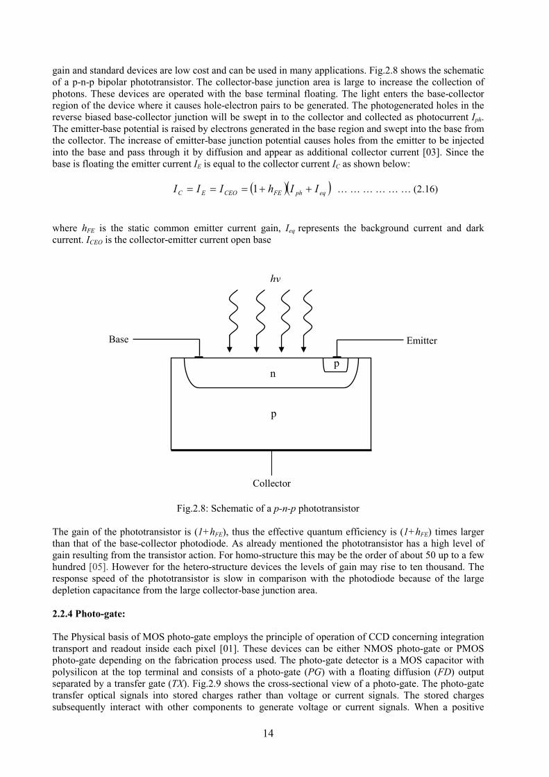
gain and standard devices are low cost and can be used in many applications. Fig.2.8 shows the schematic
of a p-n-p bipolar phototransistor. The collector-base junction area is large to increase the collection of
photons. These devices are operated with the base terminal floating. The light enters the base-collector
region of the device where it causes hole-electron pairs to be generated. The photogenerated holes in the
reverse biased base-collector junction will be swept in to the collector and collected as photocurrent Iph.
The emitter-base potential is raised by electrons generated in the base region and swept into the base from
the collector. The increase of emitter-base junction potential causes holes from the emitter to be injected
into the base and pass through it by diffusion and appear as additional collector current [03]. Since the
base is floating the emitter current IE is equal to the collector current IC as shown below:
( )( )eqphFECEOEC IIhIII ++=== 1 … … … … … … (2.16)
where hFE is the static common emitter current gain, Ieq represents the background current and dark
current. ICEO is the collector-emitter current open base
Fig.2.8: Schematic of a p-n-p phototransistor
The gain of the phototransistor is (1+hFE), thus the effective quantum efficiency is (1+hFE) times larger
than that of the base-collector photodiode. As already mentioned the phototransistor has a high level of
gain resulting from the transistor action. For homo-structure this may be the order of about 50 up to a few
hundred [05]. However for the hetero-structure devices the levels of gain may rise to ten thousand. The
response speed of the phototransistor is slow in comparison with the photodiode because of the large
depletion capacitance from the large collector-base junction area.
2.2.4 Photo-gate:
The Physical basis of MOS photo-gate employs the principle of operation of CCD concerning integration
transport and readout inside each pixel [01]. These devices can be either NMOS photo-gate or PMOS
photo-gate depending on the fabrication process used. The photo-gate detector is a MOS capacitor with
polysilicon at the top terminal and consists of a photo-gate (PG) with a floating diffusion (FD) output
separated by a transfer gate (TX). Fig.2.9 shows the cross-sectional view of a photo-gate. The photo-gate
transfer optical signals into stored charges rather than voltage or current signals. The stored charges
subsequently interact with other components to generate voltage or current signals. When a positive
p
p
n
hν
Emitter Base
Collector

15
voltage is applied to the gate above the p-substrate, holes are pushed away from the surface and
underneath of the photo-gate a depletion layer is formed. The photo-gate has different mode of operation.
When no free charge carriers are available the depletion region extends deep into the semiconductor
resulting in a deep space charge region. With the optical generation of electron-hole pairs free charge
carriers become available. The electron-hole pairs are separated in such a way that the minority carriers,
i.e. electrons are collected at the semiconductor surface while majority carriers, i.e. holes are rejected into
the semiconductor bulk, where they recombine after a certain time [03].
Fig.2.9: Cross-sectional view of Photo-gate structure
The electrons begin to form an inversion layer and at the same time decrease the depth of the space
charge region, thus integrating the optically generated electrons. At the mode of strong inversion no more
free charge carriers can be held by the MOS diode. It is the equilibrium condition of the MOS diode for
the gate voltage applied. The merit of the photo-gate structure is that the sensing node and the integrating
node are separate which allows true Correlated Double Sampling (CDS) operation to suppress kTC noise,
1/f noise and Fixed Pattern Noise (FPN) [06, 12]. Conversely, the demerit of the photo-gate structure is
low spectral response because of the absorption in the polysilicon gate which has an absorption
coefficient corresponding to that of crystalline silicon.
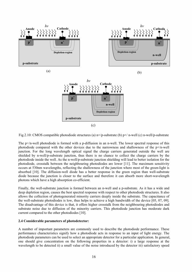
2.3 Different types of CMOS compatible photodiodes: Photodiodes are the doorways to Image Sensors. The characteristics of the detectors, such as bandwidth,
noise, linearity and dynamic range directly affect the performance of the system. Therefore, it is highly
desirable to have as perfect a photodiode as possible. In a standard CMOS process, either p-well or n-well,
several parasitic junction devices can be formed to convert light into an electrical signal. The n+/p-
substrate photodiode, the p+/n-well photodiode and n-well/p-substrate photodiode are the three possible
structures that can be implemented using p-substrate. The first two is “shallow” junction photodiodes
whereas the third is a “deep” junction photodiodes. Fig.2.10 shows the cross sectional view of three
CMOS compatible photodiodes [05, 07].
In the conventional CMOS process n-diffusion and p-substrate junction photodiode is the most widely
used one due to its simple layout and less susceptible to lithographic variations that cause the fixed
pattern noise. The quantum efficiency is better than that of p+/n-well photodiode due to the contribution
of generated carriers in the bulk substrate and the wider depletion layer itself for the same pixel size. On
the other hand, this diode introduces crosstalk and noise because of diffusion and leakage of carriers
through the substrate [05, 07, 09]. As the carriers are generated in the bulk substrate the response time is
expected to be longer than the p+/n-well junction device.
p- Substrate
Photo-gate
(PG)
n+ n+
Gate-oxide
Inversion layer
Poly-Silicon Aluminum
Transfer gate
(TX)
Floating diffusion
node (FD)
16
Fig.2.10: CMOS compatible photodiode structures (a) n+/p-substrate (b) p+/ n-well (c) n-well/p-substrate
The p+/n-well photodiode is formed with a p-diffusion in an n-well. The lower spectral response of this
photodiode compared with the other devices due to the narrowness and shallowness of the p+/n-well
junction. For the long wavelength optical signal the charge carriers generated outside the well are
shielded by n-well/p-substrate junction, thus there is no chance to collect the charge carriers by the
photodiode inside the well. As the n-well/p-substrate junction shielding will lead to better isolation for the
photodiode, crosstalk between the neighbouring photodiodes are lower [11]. The maximum sensitivity
occurs at 530nm wavelengths, reflecting the shallowness of the junction where most of the green-light is
absorbed [10]. The diffusion-well diode has a better response in the green region than well-substrate
diode because the junction is closer to the surface and therefore it can absorb more short-wavelength
photons which have a high absorption co-efficient.
Finally, the well-substrate junction is formed between an n-well and a p-substrate. As it has a wide and
deep depletion region, causes the best spectral response with respect to other photodiode structures. It also
allows the collection of photogenerated minority carriers deeply inside the substrate. The capacitance of
the well-substrate photodiodes is low, thus helps to achieve a high bandwidth of the device [05, 07, 09].
The disadvantage of this device is that, it offers higher crosstalk from the neighbouring photodiodes and
substrate noise due to diffusion of the minority carriers. This photodiode junction has moderate dark
current compared to the other photodiodes [10].
2.4 Considerable parameters of photodetector:
A number of important parameters are commonly used to describe the photodiode performance. These
performance characteristics signify how a photodiode acts in response to an input of light energy. The
photodiode parameters can be used to select an appropriate detector for a particular application. In general,
one should give concentration on the following properties in a detector: i) a large response at the
wavelength to be detected ii) a small value of the noise introduced by the detector iii) satisfactory speed
(a)
p-substrate
n+ p
+
Depletion-region
hν Anode Cathode
(c)
p-substrate
Depletion-region
n+ p
+
hν
n-well
Anode Cathode
(b)
p-substrate
Depletion-region
p+
n+
hν
n-well
Anode Cathode

17
of response to follow variations in the optical signal being detected. To understand the descriptions of
photodetector performance several conventional parameters are described in this section.
2.4.1 Responsivity:
The responsivity of a silicon photodetector gives a measure of the sensitivity to radiant energy. It can be
defined as the ratio of the diode output to the incident power at a given wave length. Thus the
responsivity is essentially a measure of the effectiveness of the device to transduce the electromagnetic
radiation to electrical current or voltage. Responsivity varies with changes in wavelength, bias voltage
and temperature. Since the reflection and absorption characteristics of the detector sensitive material
change with wavelength thus changes the responsivity of the detector. The photodiode that generates a
photocurrent can be derived by integrating the optical generation rate G0 over the device active volume
[14].
( )drPrGqIV
inL ∫= ,0 … … … … … … (2.17)
From IL, the device responsivity can be obtained as
in
L
P
IR = … … … … … … (2.18)
In the real device the number of electrons flowing in the external circuit is lower than the number of
incident photons that lead the responsivity smaller than the ideal value. This happens due to the incident
light has to undergo a number of steps before being converted into a current. Some non-idealities
mechanisms limits the detector response in the following ways: the part of the optical power that is
reflected at the photodiode interface due to dielectric mismatch; part of the power is absorbed in regions
of where it does not contribute to useful output current and finally part of the power is transmitted
through the PD without being absorbed.
2.4.2 Quantum efficiency:
It is defined as the number of incident photons that contribute to photocurrent divided by the number of
the injected photons of specific wavelengths. Quantum efficiency is related to the responsivity as follows:
it is equal to the current responsivity times the photon energy in electron-volts of the incident radiation. It
can be expressed as a percentage,
Quantum Efficiency = %1001240
×λλR … … … … … … (2.19)
where, the Rλ is the responsivity in A/W and λ is the wavelength in nm. The quantum efficiency is
determined by three factors: the absorption coefficient of Si; the transmission co-efficient of the dielectric
layers above silicon and the carrier collection efficiency of the sensor. The quantum efficiency decreases
towards the short and long wavelengths that are caused by the reflections of the thin-film structure on the
top of the silicon [14, 15]. So it is another parameter to measure the effectiveness of the basic radiant
energy to produce electrical current in a detector.
2.4.3 Response time:
The dynamic performance is an important parameter of the photodiode. The photodiode response time is
the root mean square sum of the charge collection time and the RC time constant arising from series plus
load resistance and the junction and stray capacitance. The response time of a photodetector with output
circuit depends on the following factors:

18
i) The transit time td of the photo carriers across the depletion region. This time depends on the carrier
drift velocity vS and depletion layer width W and it can be expressed by
S
dv
Wt = … … … … … … (2.20)
ii) The diffusion time of the photo carriers which are absorbed outside the depletion region.
iii) The RC time constant of the circuit. The circuit after the photodiode acts like RC low pass filter with a
pass band given by
TT CR
Bπ2
1= … … … … … … (2.21)
The capacitance of the photodiode must be kept small to prevent the RC time constant from limiting the
response time. To achieve the higher quantum efficiency, the depletion layer width must be larger than
1/α; where α is the absorption coefficient, so that most of the light will be absorbed. At the same time,
with large width the capacitance is small and RC time constant getting smaller leading to faster response
but large width results in longer transit time. Therefore there is trade off between width and quantum
efficiency.
2.4.4 Leakage current:
The dark current is the leakage current in photodiode and refers to the absorption of carriers that are not
generated by photons but it flows when the reverse bias is applied on the photodiode. As the properties of
leakage current carriers are intrinsically same as the photo-generated carriers, it is difficult to separate
these two carriers from the mixture. It decreases the charge capacity that specified for photo-carriers. This
current component introduces spatial and temporal variation of the output signals that contribute the fixed
pattern noise and shot noise of the imagers respectively. Under the low illumination condition, the effect
of leakage current is more severe because of the total amount of carriers becomes higher. The leakage
current of a photodiode is essentially the same as that of the reverse-bias current for a p-n junction diode.
The total reverse bias current can be approximately given by the sum of the generation current in the
depletion region and the sum of the diffusion components in the neutral region [16]. This can be
expressed as:
e
i
a
i
n
n
r
Wqn
=
nDqJ
ττ+=
2
. … … … … … … (2.22)
where Dn is the diffusion co-efficient and τn is the lifetime of the electrons in the p-type region; ni is the
intrinsic carrier concentration; =a is the doping concentration in the p-type region; W is the width of
depletion region and τe denotes the effective lifetime in the depletion region. The first term of reverse
current density equation comes from minority carrier diffusion from the charge neutral region and the
second term is the generation current in the depletion region. The dark current is temperature dependent.
In this equation the intrinsic carrier concentration ni is strongly temperature dependent and the depletion
layer width W is dependent on the bias voltage. At room temperature, for silicon junction diodes, the
component of generation current usually dominates the reverse-bias current and the diffusion current
dominates at high temperature.
2.4.5 Capacitance:
A capacitance is associated with the depletion region which exists at the p-n junction. The boundaries of
the depletion region act as a parallel plate of the capacitor. The junction capacitance is directly
proportional to the diffused area and inversely proportional to the width of the depletion region. The

19
width of the depletion region and the capacitance value can be determined by the doping profile. Using
abrupt junction approximation, the width of the depletion region can be expressed:
( )
−
+= VV
==qW bi
da
s 112ε … … … … … … (2.23)
where εs is the permittivity of silicon; =a and =d are doping concentration of p-type and n-type region
respectively; Vbi is the built-in potential and V is the applied bias voltage. The depletion capacitance per
unit area can be defined
WdQ
W
dQ
dV
dQC s
s
j
ε
ε
==≡ … … … … … … (2.24)
where dQ is the incremental change in depletion layer charge per unit area and dV is the incremental
applied voltage. So the capacitance can be expressed by using the above two equations
( )( )
−+=
VV==
=q=C
bida
dasj
2
ε … … … … … … (2.25)
We know the junction capacitance at the charge sensing node regulates the capacity and the charge-to-
voltage conversion gain of the photo sensor device. In addition, the lower junction capacitance at the
charge sensing node is usually favoured since it introduces a higher signal-to-noise ratio of the output
signals. Moreover the capacitance is dependent on the reverse bias voltage; increase in the reverse bias
voltage causes the depletion width to increase, thus the drift time of carriers becomes longer across the
depletion region [17].
2.4.6 ,oise:
Noise is a critical performance parameter for the photodetectors. There are several sources of noise in
photodetectors. These include shot noise from detector photocurrent, shot noise from the dark current,
Johnson noise due to the thermal fluctuation in the detector impedance and flicker noise that is inversely
proportional to the measurement frequency [13].
Quantum shot noise arises from the statistical Poisson-distributed nature of the arrival process of photons
and collection of photo generated electron. The standard deviation of the photon shot noise is
( )MFBMqIi PQQ
222 2== σ … … … … … … (2.26)
where IP = Photo current
B = Receiver bandwidth
F (M) is the noise figure and generally F (M) ≈ MX. For the pin photodetector M and F (M) is equal
to 1.
The current that continues to flow through the photodiode device in the absence of light is called dark
current is responsible for dark current shot noise. It arises from electron and hole which is thermally

20
generated in the pn junction of the photodiode in the bulk area. The dark current shot noise can be
expressed as:
( )MFBMqIi DDD
222 2== σ … … … … … … (2.27)
where ID is the dark current. Due to the surface area, surface defects and bias voltage a surface dark
current flows in the device that introduces a noise is called surface dark current shot noise. It can be
defined
BqIi LDSDS 222 == σ … … … … … … (2.28)
where IL is the surface dark current. The shot noise of the photodetectors limits the SNR when the
detected signal is large. Thermal noise, also called Johnson noise or Nyquist noise generated by the
thermal agitation of the electrons inside an electrical conductor at equilibrium, which happens regardless
of any applied voltage. A photodetector thermal noise can be modelled as a voltage source in series with
an ideal resistor R. In this case,
TRBkV B42 = … … … … … … (2.29)
It can also be modelled a current in parallel with R
R
TBkI B42 = … … … … … … (2.30)
where, kB = 1.38 × 10⁻²³
JK-1
is Boltzmann constant. This noise can be suppressed if the sensor is operated
at low temperature.
2.5 Review of CCD and CMOS Image Sensor:
Solid-state optical sensors are used in a wide range of applications. Charge Coupled Device (CCD)
technologies and image sensors have been discovered at the beginning of the seventies which can be
found today in almost all electronic acquisition systems [18]. CCD image sensor is the first solid-state
image sensor that offers good picture resolution, higher fill factor but on the other hand it requires more
power and is generally more expensive. The Complementary Metal Oxide Semiconductor (CMOS)
imaging detectors began to make their move into the CCD detector arena. While CMOS sensors have
generally lagged behind CCD sensors in terms of image quality, it has been able to compete in the
imaging market by taking advantage of standard CMOS process technology. The smaller device size,
light weight and lower cost made CMOS sensors suitable for high-volume consumer and mobile
applications. Traditionally, the CCD vs. CMOS battle has been a trade-off between image quality and
quantity. CCD image sensors have delivered improved quality, while CMOS image sensors have
provided better performance in terms of battery life and lower cost. CMOS image sensors are increasingly
rivalling the image quality that CCD sensors have traditionally provided. Improved architecture and
processes have to overcome to a large extent, the early weakness of CMOS imagers, most likely with
respect to noise and sensitivity. To compete in the high volume marketplace, meanwhile, CCD sensors
have responded by using new methods to reduce clocking voltages and power consumption reported in
[19].The overall architecture, operation and comparative performance of CCD and CMOS based image
sensors are described in this section.
2.5.1 Charged-Coupled Device (CCD) Image Sensor:
A CCD pixel is basically a MOS capacitor [18], usually a buried channel type. Fig.2.11 shows a
schematic cross section of such a capacitor. The device is typically built on a p-type silicon substrate with
larger thickness and an n-type layer with small thickness grown up on the surface. A thin silicon dioxide

21
layer is formed followed by a metal electrode. When a positive voltage is applied to the electrode, due to
the reverse bias action at the p-n junction a potential well is formed in the n-type silicon below the
electrode. Electron-hole pairs are generated in the depletion region when light is incident on the
CCD device. Due to the applied voltage the electrons migrate upwards into the n-type silicon layer and
are trapped in the potential well. The build up of negative charge is thus directly proportional to the level
of incident light.
Fig.2.11: Charged-Coupled Device (CCD) Cell
Readout Process: Considering each pixel is divided into three different areas known as phases shown in
the following Fig.2.12 given below. The integration periods, phi 1 and phi 2 are the charge holding
modes, and phi 3 is the charge blocking mode. When light is incident on the CCD device the charge
carriers are generated and restrained in a potential well below the surface. At the end of the integration
period, when it is time to transfer the captured image out of the array, the following process takes place.
After switching phi1, phi2 and phi3 at different potential by a clock signal the carriers are transported in a
lateral direction.
Fig.2.12: Charge transfer process
Firstly phi 1 is placed in charge blocking mode, which has the effect of transferring the total charge of phi
1 and phi 2 into only phi 2. Phi 3 is then placed in charge holding mode, which allows the charge in phi 2
to distribute itself evenly between phi 2 and phi 3. Next, phi 2 is placed in charge blocking mode, forcing
charges into phi 3. This basic process of charge transport is repeated until the read out sequence is taking
place. More elaborate analysis of operation and physics of Charge Coupled Device (CCD) are reported in
[20, 21].
p-type Si
SiO2
n-type Si
+V
2V 10V 10V 2V
(Phi 1) (Phi 2) (Phi 3)
2V 10V 2V 2V
(Phi1) (Phi2) (Phi 3)
Potential well
containing charge
2V 10V 2~10V 2V
(Phi1) (Phi2) (Phi3)
Well Created
(a) (b) (c)
2V 10V 2V 2V
(Phi 1) (Phi 2) (Phi 3)
2V 10~2V 2V 2V
(Phi 1) (Phi 2) (Phi 3)
Well
Collapsing
(d) (e)

22
Area array of CCD Architecture:
Depending on the different applications the architecture of area array CCD generally falls into one of four
categories: full frame array, frame transfer array, split frame transfer array and interlines transfer array
(Fig. 2.13).
Full Frame array – The image is transferred directly one row at a time from the imaging region of the
sensor to a serial register and finally feeding the charge to an output sense electrode. However, since only
a single row can be transferred to the readout register at a time the rest of the imaging pixels must wait.
Since during this period, pixels are being irradiated continuously this can lead to smearing and blurring of
the final image. Another problem is raised during high-speed applications. In these situations, the
integration time will be only a small percentage of the total time required to record and read out the total
image from the array. This causes lower contrast since very little time is spent actually to record the
image. These problems can be solved by using a mechanical or external electronic shutter to shield the
sensitive area during readout time.
Frame Transfer Array – A frame transfer device utilises two identical arrays: one is the light shielded
storage section and the other is the imaging section of the array. At the integration time, the captured
image is quickly transferred to the adjacent storage section. The storage sections are covered with a metal
shield to prevent them from being irradiated. While the next scene is being captured, the previous scene
that held in the storage section is transferred to the readout register as described above. The use of this
technique effectively increases the time available for integration and maintaining a high frame rate.
Fig.2.13: Area Array of CCD Architecture
Sensitive Area
Readout Register
Sensitive Area
Readout Register
Storage Area
Sensitive Area
Readout Register
Readout Register
Upper Storage Area
Lower Storage Area
Readout Register
Readout Register
Light Shielded Vertical CCD
Imaging CCD Elements
(a) Full Frame Array (b) Frame Transfer Array (c) Split-Frame Transfer Array
(d) Interline Transfer Array

23
Split Frame Transfer Array – The split frame transfer type device is essentially the same as a frame
transfer device, except that the storage section is split into two equal parts, with each half being located
above and below the imaging section. The advantage of this device is that it allows the image to be
transferred out of the imaging section in half the time that is required for a frame transfer device.
Interline Transfer Array –In interline transfer device, within photosensitive matrix the columns of photo-
sensitive elements are separated by columns of light shielded registers. At the end of the integration
period, all of the photosensitive elements simultaneously transfer their accumulated charge to the adjacent
storage registers. The light shielded registers then transfer the charge to the readout register in a very
short time. This type of device has the significant drawback that a large proportion of the imaging section
is not sensitive to light. To minimize the problems, micro lenses are often placed directly over the
imaging section of the array that have the effect of focusing the incoming light onto just the light sensitive
areas of each element.
2.5.2 CMOS based Image Sensor:
CMOS, Complimentary Metal Oxide Semiconductor, image sensors have been around for nearly as long
as CCDs [22]. High performance CMOS image sensors [23] use active pixel structures invented at NASA
Jet Propulsion Laboratory in 1993. CMOS sensors draw less power than CCD and use the same
manufacturing technologies as microprocessors and memory modules, thus they are easier to produce.
CMOS pixels can be divided into two main groups: Active Pixel Sensor (APS) and Passive Pixel Sensor
(PPS). Like CCDs, they are formed from a grid of light sensitive elements, each capable of producing an
electrical signal/charge proportional to the incident light. Each CMOS pixel employs a photodiode, a
capacitor and the amplifier transistors for APS. Prior to the start of the integration period, the capacitor
will be charged to some known voltage. When the integration period begins, the charge on the capacitor is
allowed to slowly discharge through the photodiode, the rate of discharge being directly proportional to
the level of incident light. At the end of the integration period, the charge remaining in the capacitor is
read out and digitized. Fig.2.14 shows the most common three transistors Active Pixel Sensor (APS) [24].
The reset transistor (RES), acts as a switch to reset the floating diffusion which acts in this case as the
photo diode. When the reset transistor is turned on, the photodiode effectively connects to the power
supply clearing all integrated charges. The read-out transistor, SF is a source follower transistor amplifier
which allows the pixel voltage to be observed without removing the accumulated charge. Finally the
select transistor, SEL allows the signal to be read-out. The row decoder and column decoder select each
pixel to read out for further Image processing.
(a) (b)
Fig.2.14: (a) CMOS based pixel (b) Pixel read out System
RO
W D
EC
OD
ER
COLUM, DECODER
OUT
APS APS APS APS
APS APS APS APS
APS APS APS APS
APS APS APS APS
RES
et
VDD
SEL Ro
w
SF
PD

24
2.5.3 Comparison between CCD and CMOS Imagers:
CCD and CMOS image sensors are two different technologies for capturing images. Each has unique
strengths and weaknesses giving advantages in different field of applications. Both CCD and CMOS
imagers convert light into electric charge and process it into electronic signals. In a CCD sensor, the
charge packet of every pixel is transferred through a very limited number of output nodes to be converted
to voltage, buffered, and sent off-chip as an analog signal. All of the pixel can be dedicated to light
capture, therefore the photo sensitive area is large and the output uniformity is high. In a CMOS sensor,
each pixel has its own charge-to-voltage conversion, and also includes amplifiers, noise-correction, and
digitization circuits, so that the chip output is digital bits. The other circuit functionalities enhance the
design complexity and decrease the photosensitive area for light capture. Traditionally CCD imagers
provided the performance benchmarks in the photographic, scientific, and industrial applications that
demand the utmost image quality as measured in quantum efficiency and noise at the expense of system
size. On the other hand CMOS imagers offer more functionality on the chip, lower power dissipation at
the chip level and the possibility of smaller system size. Variations in device characteristics, such as
feature dimensions and silicon doping levels, from pixel to pixel and column to column lead to substantial
fixed pattern noise with CMOS. There is also a high temporal noise from thermal and 1/f sources with
CMOS sensors due to using of multiple transistor stages. In CCD sensors fixed pattern noise and
temporal noise is smaller because charge packets are transferred almost perfectly within the sensor and
pass to the outside of the sensor area by a single output stage [13,23]. In CCD technology the fill factor of
the sensor is high compared to CMOS technology, giving a better photosensitive efficiency. Furthermore,
special attention is paid to minimizing dark current, a parasitic effect in photo detectors; so that it is lower
with CCD technology than with CMOS [25].
Table-I is given below summarized the comparative study between
CCD and CMOS image sensor.
Feature
CCD CMOS
Signal out of pixel Electron packet Voltage
Signal out of chip Voltage (analog) Bits (digital)
Signal out of camera Bits (Digital) Bits (Digital)
Fill factor High Moderate
Amplifier mismatch N/A Moderate
System Noise Low Moderate
Responsivity Moderate Slightly better
Dynamic Range High Moderate
Uniformity High Low to Moderate
Uniform Shuttering Fast, Common Poor
Speed Moderate to high Higher
Biasing and Clocking Multiple and higher Voltage Single and Low Voltage
System Complexity High Low
Sensor Complexity Low High
Unit price
High Comparatively low
25
2.6 Available technologies for Image Sensor:
Now a day different technologies are available to design of image sensor chips. CCD, CMOS, Bi-CMOS
and GaAs (HEMT and MESFET) are the existing technologies that offer advantages and disadvantages in
their limited technological process. CCD sensors have been used in cameras for more than 30 years and
present many advantageous qualities: better light sensitivity than CMOS sensors that translates into better
images in low light conditions, low noise, low non-uniformity, and low dark current. CCD sensors are,
however, more expensive as they are made in a non-standard process and more complex to integrate into
a camera. Over the last decade, CMOS imager technology made huge progress which drastically
improved its performance. The most prominent was the CMOS Passive Pixel Sensor (PPS) fabricated by
VLSI Vision Ltd. [26] and from 1992 to the present, the Active Pixel Sensor (APS) was and still under
continuous development [27]. CMOS has been widely used in many designs and expanded the overall
imaging market due to the development of new applications. Another technology is bipolar transistor in
Bi-CMOS processes. It has better matching properties, and higher speeds but limited availability due to
their complexity and cost. It also needs large silicon area, which makes them unattractive for large
quantity vision chips [05]. In the commercial grade CMOS processes are accessible through fabrication
foundries, such as TSMC, UMC and CMP etc. Finally, GaAs processes have been used only to a very
limited extent due to technological immaturity and process and they are generally expensive. These opto-
electronic devices are only available in very specialized processes [05]. In this section we will briefly
discuss about CCD sensor technology and then CMOS imaging technology that is our Image sensor
interest.
2.6.1 CCD Image Sensor technology:
Charged Coupled Devices are the dominant technology for image sensor. Therefore from the beginning
research has been mainly focused on CCD technology. The device architecture based on series and
parallel connection of capacitors, which are made using a dedicated semiconductor process and switched
it by clocked signal at different phases. CCD technology has some limitations in its fundamental
operation—the need of nearly perfect Transfer Efficiency (CTE) imposes a great impact on CCD
performance. The other considerable limitations of CCD technologies are: [24, 28].
a) Risk to radiation damage.
b) Required complex high speed shifting clocks for its operation.
c) Larger operational power required due to high speed switching.
d) Difficulty in achieving large array size.
e) Difficult to integrate on-chip electronics because of specialized non-standard.
f) Limited frame-rate of CCD and difficult to extend the spectral range.
2.6.2 CMOS Image Sensor technology:
CMOS imagers began to be a well-built alternative of CCD since early nineties. The most important
feature that would satisfy by this technology is the demand for low-power, miniaturised and cost-effective
imaging systems. It also offered the possibility to monolithically integrate a significant amount of
integrated electronics on-chip that incorporates all necessary camera functions and reduces component
and packaging costs. CMOS processes are well established and continue to become more mature. The
demand for digital applications has led to continuous development and attributed to down-scaling of
CMOS processes. CMOS processes are now readily available for prototype designs through fabrication
foundries, such as TSMC, UMC etc. Circuit and system design by this process is supported by CAD
design software such as Cadence. Recently several modifications to standard CMOS technologies to
improve their imaging performance have been reported [29]. To improve the photosensitivity, non-
silicided deep junction diodes and integrated micro lenses are used. The doping profiles of these diodes
are optimised to increase quantum efficiency at visible wavelengths and to lower capacitance. To
minimize the dark non-silicided, double-diffused source/drain implantation is used. Besides these
advantages of CMOS vision chip technology it has some disadvantages too.

26
a) Leading-edge processes of the chip are driven by digital applications and less optimization
for analog circuit design [05].
b) As the gates of all pixels are connected in parallel on a given column that increase the
column-bus capacitance, thus affects the read out speed and read out noise [30].
c) Non- uniformity arises due to multiple levels of amplification at pixel and column level.
d) Due to the mismatch of CMOS devices fixed pattern noise is introduced.

27
Chapter - 03
State of the art of 3D imaging 3D measurement techniques are concerned with extracting information from the geometric evaluation of
three co-ordinates (x, y, z) and the texture of the visible surfaces in a scene. The complete 3D information
can be realized acoustically by ultrasonic sound and radio frequency electromagnetic waves or optically
with light. In all methods, a signal travels from the respective sources of the methods to a target and the
distance measurement can be calculated based on the properties of the reflected signal from the target.
Comparing with the acoustic and RF wave methods, the optical methods are more reliable in terms of
high resolution and accuracy in the distance measurement [31].
Due to the drastic increase in demand of 3D imaging system, recently a lot of effort has been concentrated
to develop a standard 3D imager. The 2D-imaging system can evaluate only the intensity projection of a
scene, there is no information about the depth of the 3D objects. Several approaches have been proposed
on image capturing techniques using specialized photo detector coupled with depth measurement system
of 3D object. A much more practical range measurement method is the Time-Of-Flight (TOF) principle.
In time-of-flight optical ranging, the phase information is used to plot the distance map of the observed
scene, thus enabling the reconstruction of the shape and position of the observed objects[32]. TOF
systems are further divided in different subcategories which are pulsed modulated, continuous wave
modulated and pseudo-noise coded TOF. TOF technique provides the best performance in terms of
acquisition speed, reliability, overall cost of the system and is most suited to integrate electronic circuitry
with more functionality. Several studies on image capturing techniques using specialized pixels coupled
with active illumination have reported to produce images with information even at a low intensity level
[33, 34].
3.1 Different optical measurement techniques for 3D imaging:
The optical distance measurement methods for 3D range imaging can be classified into two ways, active
range imaging and passive range imaging. The active method uses a coherent light source to project onto
a target and determines the shape of the target by its reflections where as the passive rely on the ambient
environment conditions to get the information of the object. There are some other methods for the
distance measurement such as: the image based methods, the distance can be determined with some
algorithm based on shapes and shades or the respective distances of the different points of the object. The
computer vision research community is largely focused on these methods. Another one is the direct
method that can give the instantly recognizable distance to some points in the object [35].
In optical distance measurement, several studies have reported to produce 3D information including
stereo vision cameras [36], system based on structured light and laser scanner vision system [37]. The
advantage and performance of these systems tend to be mutually exclusive by their own limited set of
situations. Different types of optical techniques for 3D imaging range measurement are available in the
literature. According to the working principle, range and accuracy it can be classified in three categories
such as:
3.1.1 Triangular Method
3.1.2 Interferometry Method
3.1.3 Time-of-Flight Method
All of these above techniques mostly work with light in the 400 nm to 1000nm wavelength range
belonging to visible light and near infrared region.

28
3.1.1 Triangular method:
The distance measurement by triangulation method analyzes a triangle by trigonometric approach. A
target on a visible surface is one point of the triangle; the remaining two points are obtained by using two
optical systems. The distance between two optical systems is the baseline of a triangle that can be
calculated. So the two projection lines of two optical systems in the target can construct the triangle.
These two optical systems can determine the two different angles between the baseline and projection line.
The distance of the target can be determined using trigonometric formula. There are two main types in
triangulation system
3.1.1.1 Passive triangular method [38]
3.1.1.2 Active triangular method [39]
3.1.1.1 Passive Triangular method:
In passive triangular method two optical systems observe the same target from two different points with
respect to the same baseline. Two different points to measure must be identified from both viewing
positions and it requires some good features in the scenes with high contrast. At least two cameras are
necessary to observe the scene from different angles. Assuming that the two cameras are observing the
scene from two different distance points x and y of known value α and the measured viewing angles
between the baseline and the two projection lines of two optical systems are φ and θ. Fig.3.1 shows the
passive triangulation method. The distance between the baseline and the target d can be determined by the
trigonometric formula.
… … … … … … … 3.1
Fig.3.1: Passive triangulation method.
Stereovision technique refers to the passive triangulation method [36] and produces 3D information from
at least two slightly different 2D images. This technique is similar to aspects of the human visual process,
where the human eyes are two view points used for the acquisition of images of the same scene. As the
distance between the two eyes results in slightly different 2D images, this phenomenon is used in the
θϕ
α
tan
1
tan
1+
=d
B
asel
ine
Projection line
α
φ
θ
d
Tar
get
x
y

29
stereovision to construct the 3D images. The typical features of both images captured by two cameras are
compared with the help of 2D correlation. The viewing angles between the baseline and projection line of
the camera φ and θ can be deduced and the distance can be calculated using the equation 3.1. The
stereovision system can build the dense depth maps. The system components are highly reliable since it
requires no moving parts. It also captures the entire frame at the same time so that the depth of map of all
pixels can be calculated from the same perspective. The shadowing effect is the typical disadvantage of
the stereovision system like other triangular systems. Although it can be minimized by using more than
two cameras in order to increase the multiple viewpoints, this improvement also increases the data
processing and overall cost of the system.
3.1.1.2 Active Triangular method:
This technique consists of one light source and one camera [39]. The light source is projected to a target
which is observed by a camera. In this method, two similar triangles are formed; based on the optical axis
of the imaging device, the focal length of the system and the position of the projected point on the camera.
Fig.3.2 shows the active triangulation method. Considering the distance between the light source and the
camera is α, so the distance d of the target can be determined by
… … … … … … … … 3.2
where h is the focal length of the camera and αʹ is the projected distance.
Fig.3.2: Active triangulation methods.
The basic phenomena of this method, a focused beam of light illuminates a tiny spot on the surface of the
scene and a camera records an image of the spot. This technique gives a single range point. Moving the
light spot using mirrors allows the surface of the object to be scanned. If the position of the light source,
the orientation of the project plane and the triangulation distance (baseline separation) of the laser and
camera are all known, the depth information from all points on the object can be determined. The
limitation of this approach is that it needs to capture many frames while sweeping the light over the object
and thus increasing the long processing time to get the full depth of information from the whole 3D scene.
α
α
′= hd
α
γ
d
h
α' γ
Tar
get
Light source

30
3.1.2 Interferometry:
Interferometric distance is described by the superposition of two monochromatic waves of the frequency
but with different amplitude and phase [40]. When two light waves are superimposed, the resultant
intensity at any point depends on whether they reinforce or cancel each other. This is a well-known
phenomenon of interference. Consider two monochromatic waves of complex amplitudes X1(r) and X2(r)
are superposed, the result is a monochromatic wave of the same frequency and complex amplitude
)()()( 21 rXrXrX += … … … … … … … 3.3
where )exp( 111 θjIX = and )exp( 222 θjIX = are the complex amplitudes of the two waves. As
we know that the optical intensity of a monochromatic wave is the absolute square of its complex
amplitude, the resultant intensity is therefore
2
XI =
2
21 XX +=
*
212
*
1
2
2
2
1 XXXXXX +++= … … … … … … … 3.4
The explicit dependence on r has been omitted for convenience. Substituting X1 and X2 in equation 3.4,
we obtain
θcos)(2 2121 IIIII +++= … … … … … … … 3.5
The above equation is called the interference equation, where I1 and I2 are the intensities due to the two
waves acting separately and θ = θ1 – θ2 is the difference between the two waves.
Interferometer is an optical instrument that split a light beam into two parts by a beam splitter and travels
two different paths. One ray is projected to a mirror and the other is targeted on the object of variable
distance. Both light beams are reflected back to the beam splitter and projected onto a camera. When
those reflected beams are made to cross each other, the region of crossing will exhibit an interference
fringe. By recording and counting the minimum and maximum transitions in the interference of light
wavelength, the distance between the optical system and the target can be measured.
Consider the superposition of two plane waves, each of intensity I0, propagating in the z direction and
assume that one wave is delayed by a distance l with respect to the other, so that )exp(01 jkzIX −=
and )](exp[01 lzjkIX −−= . The intensity I of the sum of these two waves can be determined by
substituting I1=I2=I0 and θ=kl=2πl/λ in the equation 3.5,
)]2cos(1[2 0 λπ
lII += … … … … … … … 3.6
The dependence of the intensity I is the superposition of two waves, each of intensity I0 and on the delay
distance l. When the delay distance is a multiple of λ, complete constructive interference occurs and the
total intensity becomes I=4I0. On the other hand, if l is an odd integer multiple of λ/2, thus the
interference is destructive and the average intensity is the sum of the two intensities 2I0.
Some common types of interferometer setup can be found, for example the Rayleigh interferometer, the
Michelson interferometer, the Mach-Zehnder interferometer and the Sagnac interferometer [41, 42]. The
main disadvantage of classical interferometer is that the unambiguous distance range is as low as half of
the wavelength and absolute distance measurements are not possible with this method. To overcome these
drawbacks different types of techniques have been proposed in literature such as: Multiple-wavelength

31
Interferometry [40, 43], electronic speckle pattern Interferometry (ESPI) and white light Interferometry or
low-coherence Interferometry [44]. Interferometry requires accurate optical alignment for precise
measurements over small distances ranging from micrometers to several centimetres.
Fig.3.3: Set up of Interferometry Method
3.1.3 Time-of-Flight (TOF) method:
The distance measurement by the Time-of-flight method is an alternative to the triangulation method.
TOF technique is based on the measurement (either direct or indirect method) of the time needed for an
optical signal to travel from a source to a target and back to a sensor [37]. This is called the round trip
transit time (tr). Since the velocity of light is known, we can convert the time measurement into a two-
way distance measurement according to the equation,
rctd =2 ………………………….. (3.7)
where d is the distance of the target and c is the speed of light. TOF systems are further divided in
different subcategories; three methods to accomplished TOF range imaging which is pulsed modulated,
continuous wave modulated and pseudo-noise coded TOF. The advantage TOF technique provides the
best performance in terms of low cost, real time imaging, dynamic range and is most suited to integrate
electronic circuitry with more functionality.
The distance measurement by the TOF method is an alternative to the triangulation method. This
technique is based on the measurement of time; an optical signal is travel from a modulated light source
Reference path
Reference mirror
3D Object
Light source
Beam expanding
lens
Pin hole Collimating lens
Output Focus
Screen

32
to a target and back to a sensor. Each pixel in the sensor device is capable to detect the phase of the
reflected light. This range can be determined by measuring the phase angle (θr) between the transmitted
signal and the received signal. This phase angle can be related to a time delay tr. The relation between
phase angle delay θr, modulation frequency ƒmod and time delay tr is
mod2 f
t rr π
θ= … … … … … … …(3.8)
where time delay tr is equal to the round trip transmit time in second, θr is measured in radians and ƒmod is
in Hz .
The distance d between the sensor and the target is achieved according to the equation (3.7) and (3.8). So
the distance d can be achieved by using the relation:
mod4 f
cd r
πθ
= … … … … … … … (3.9)
Fig.3.4 shows the TOF method for distance measurement. Therefore, as a general rule, it can be stated
that the modulation frequency should be adjusted based on the maximum target distance, with considering
that reflective object beyond the non-ambiguous range are frequently aliased [45].
Fig.3.4: Time of Flight Principle
Fig.3.5 shows a scheme of the phase shift measurement principle. In this figure C is the amplitude of the
transmitted modulated signal from a light source, B is the mean intensity of the received signal which is
reflected from the object and A is its amplitude. The received signal is offset-shifted in intensity with
respect to the emitted signal due to the additional background light [46].
A single phase measurement requires the acquisition of four amplitude measurements with four different
phase delays applied to the received signal i.e. the signal is sampled four times in each cycle, at 90° phase
angle. From the four samples (A0, A1, A2, A3), the parameters A and B and the phase φ can be calculated:
d
Tar
get
Light source
Image Sensor
Reflected light IR(t) =IRsin(2πft-θ)
Incident light IR(t) = sin2πft

33
… … … … … ..3.10
4
3210 AAAAB
+++= … … … … … … … 3.11
−
−=
31
20arctanAA
AAϕ … … … … … … … 3.12
Fig.3.5: Phase shift measurement techniques
According to the different mode of operations the TOF measurement can be classified into three groups
3.1.3.1 Pulsed Modulation TOF technique
3.1.3.2 Continuous wave (CW) Modulation TOF technique
3.1.3.3 Pseudo-Noise Modulation TOF technique
3.1.3.1 Pulsed Modulation TOF technique:
The pulsed laser operation is the most useful method of operating a Time-of-Flight technique system. In
this system there are devices with a pulsed laser and a custom imaging integrated circuit with a counter
behind every pixel. A light pulse is sent out and its turn around time is measured by correlation of start
and stop signal with the parallel running counter. This technique can produce depth values for each pixel
on every frame. The advantage of using pulsed light technique is that a high amount of energy can be
transmitted in a very short time. Thus the influence of background illumination can be reduced. It also
attains a high short term optical signal-to-noise ratio while maintaining a low mean value of optical power.
As the optical threshold is changed with the surface distance of the object and the atmospheric attenuation
leads to dispersion and flattens the slope of the received pulse thus it makes the problem for the receiving
path is to detect exactly the arrival time of the backscattered light pulse. The advantage of using pulsed
light modulation is that it enables the measurement of the long distance. However it requires a receiver
with high dynamics and a large bandwidth. Due to some advantages the TOF rangefinders are operated
with pulsed modulation [47].
3.1.3.2 Continuous Wave (CW) modulation TOF technique:
Continuous wave (CW) modulation also is used in optical ranging systems. Different shapes of
modulation signals such as sinusoidal waves or square waves can be used for this mode of operation and
Received Signal
Transmitted Signal
∆φ
Lig
ht
Inte
nsi
ty
φ
C B
A
( ) ( )2
2
31
2
20 AAAAA
−+−=

34
extremely fast rise and fall times are not required like pulsed modulation. As we know the modulation
frequency, the measured phase delay directly corresponds to time-of-flight. Compared to the pulsed
modulation, the phase difference between the transmitted signal and received signal is usually measured
rather than the directly measure the echo of light pulses turn-around time. As in the case of pulsed time-
of-flight systems, continuous wave-modulation systems have a maximum unambiguous range. This range
is limited to that which causes a phase delay in the sine wave of one complete cycle. The highly accurate
ranging systems often have several modulation frequencies. The lower-frequencies are used to prevent an
ambiguous range measurement. The higher-frequencies are used for more accuracy. Similar to the optical
interferometry, the transmitted modulated light signals of a phase delay τ, reflected from the object is
mixed and correlated with the reference signal at the receiver, thus we can have the total depth
information of the target:
I(τ) = s(t) * g(t-τ)= dttgtsT TT
)(.)(1
lim τ−∆ ∫∆→∝∆
… … … (3.13)
Let’s consider the reference signal and reflected light signal from the object is s (t) and g (t) respectively.
If we ignore the nonlinear effects and the noise behaviour of the systems and assume the sine wave
modulation
s(t) = a0 + am .cos (ω0t) … … … … … …(3.14)
The reflected signal g(t) can be written with the time delay τ.
g(t) = a'0 + a'm .cos [ω0(t-τ)] … … … … … …(3.15)
The correlation function I(τ) can be calculated as
= A. [a0 + am .cos (ω0t)]*[ a'0 + a'm .cos (ω0 (t-τ))]
=B. [1+M. cos(ω0τ)]
where A defines the system attenuation factor and
B = A.a0.a'0
'
00
'
.
..
2
1
aa
aaM mm=
Different types of methods can be used to determine the time delay τ. Heterodyne technique (frequency
shifting), homodyne technique (phase shifting) and FM-chirping modulation technique are the most
applied CW- modulation techniques [48]. If we consider the ranging distance of the system less than the
half of the RF-wavelength the ambiguity problem is reduced. The accuracy of CW ranging systems is
limited by the frequency of the modulation signal; accuracy of the phase-measurement loop that depends
on signal strength, noise, and so on; stability of the modulation oscillator and variations in the index of
refraction of the air.
3.1.3.3 Pseudo-,oise Modulation TOF technique:
Pseudo-noise modulation technique is the combination of Pulsed modulation and Continuous wave
modulation technique [49]. These are periodic, deterministic and binary sequences with a noise like
waveform. As it also known pseudo-random, it looks randomly for the user who does not know the code.
This Technique gives some advantages over the other two TOF techniques. It gives better optical signal-
to-background ratio and larger freedom in choosing modulation signals and components. As it requires

35
the low mean value of optical power that increases the safety of eyes. Due to these features, Pseudo-noise
modulation technique is widely used in the TOF ranging systems.
3.1.4 Comparison between the main optical techniques for Range measurement:
Optical techniques for 3D imaging according to the operation principle, the range and the accuracy can be
grouped in the three categories: Triangulation, Interferometry and time-of-flight are described in the
previous section. Table: II summarizes comparative study of the different optical measurement techniques.
The most important parameters of these systems are the measurement interval and the depth resolution.
By using the Interferometry technique the highest resolutions can be achieved and the measured range up
to 10m using multi-wavelength technique. However, for this technique very accurate optical alignment is
required and these are very expensive systems.
Fig.3.6: Relative resolutions of three types of 3D optical measurement methods.
In the case of triangular method the measurement range is up to several meters where the accuracy
depends on the depth of field and it can be less than 10µm for small depths. The miniaturization of the
complete system reduces the baseline of the triangular thus reducing the accuracy of the system. These
systems with the scanner are also expensive and bulky. The time of Flight technique is completely
different than other optical ranging measurements. These techniques allow the range measurement from
tens of cm up to tens of km. Compare to the other techniques this system is compact, cheaper and the
measurement accuracy is steadily improving. The advantage and performance of these ranging techniques
presented here tend to be mutually exclusive by their own limited set of situations.
Res
olu
tio
n [
m]
100
10-3
10-6
10-9
10-6
10-3
100 10
3
Application Range [m]
I,TERFEROMETRY
TRIA,GULATIO,
TIME-OF-FLIGHT

36
Table II. Comparison between three optical measurement systems
Triangulation m/d Interferometry m/d Time-of-Flight m/d
Measurement Interval
1 mm~ 1km 1mm~1m 10cm~10km
Accuracy 100nm-10um 0.1nm~1um 1mm~1m
Advantages Good accuracy Excellent accuracy Compact and rugged
system, low cost, real
time image is possible,
High dynamic range.
Disadvantages System with scanner,
expensive, heavy and
low acquisition speed.
Required accurate optical
alignment, expensive, low
acquisition speed
Low accuracy
3.2 Time-of-Flight (TOF) based 3D vision sensors:
In recent years, a new generation of active cameras based on the Time-of-Flight principle (TOF) has been
developed. This technique acquires the possibility to get data at video frame rates and achieve 3D point
clouds without scanning and from just one point of view. TOF based cameras usually deliver an
amplitude image and a range image with infrared modulation intensities at video frame rates: the
amplitude image contains for each pixel the strength of the reflected signal from the object, while the
range image contains for each pixel the radial measured distance between the considered pixel and its
projection on the target object. In some cases an intensity image is also delivered, which represents the
mean of the total reflected modulated signal and background light of the observed scene incident on the
sensor. Several types of TOF based 3D imaging techniques have been demonstrated in previous research
works in the scientific literature. The state of the art of TOF based 3D imagers so far reported can be
divided in different categories, differing for the type of photodetector use in the pixels:
3.2.1 Standard photodiode is coupled with complex processing circuit:
A standard photodiode coupled with complex readout circuitry is proposed and the indirect time-of-flight
is used [50-53]. The scene is illuminated with a train of short (~10s of ns) LASER pulses; the back-
reflected light pulses are acquired in each pixel of the sensor through one or more temporal integration
windows synchronized with the LASER pulse trigger. This approach can yield an accuracy of a few cm
over a maximum range of a few meters. The disadvantages of this approach are- the pixel size, that is
quite large due to the number of transistors and capacitors required for signal read-out and
processing circuits and the power consumption, so that it is impossible to realize large two-
dimensional arrays.
Fig.3.7 shows an ITOF based real time 3D imaging system with standard CMOS photodiode [53]. The
laser source is pulsed by the sensor, which is a bi-dimensional array of pixels. A lens is placed in front of
the emitter to obtain the proper illumination of the scene, while a camera objective is used to focus the
scene onto the detector matrix. A pulse train is emitted for pixel-level signal accumulation and white
noise averaging. The first train is integrated according to the timing W1 and the second one by means of
the timing W2 as shown in figure. Depending on the time-of-flight of the photons reflected by the points
of the scene, pixels looking at close objects get their photons earlier than pixels focused on further details;
in this case a bigger part of the reflected is lost. For a specific pixel the distance information can be easily
extracted by dividing the signals collected after the integration of two pulses. Thus the measured results
are independent from the reflectivity condition of the focused point.

37
Fig.3.7: Pulsed I-TOF ranging Technique [53]
3.2.2 Photo-demodulator fabricated with special technologies:
The key element of 3D range camera, the photo demodulator is implemented with different types of
special technologies such as: CMOS/CCD, CCD and non standard CMOS or hybrid approach. In this
demodulator the photogenerated charge is ‘mixed’ on two or more photo-gates thus achieving an intrinsic
demodulation effect [54-57]. The advantage is the read-out channel simplicity which results in a small
pixel size. The disadvantages are the lower sensitivity due to the presence of the “photo-gate”, the lack of
immunity to the ambient light and the cost of the non-standard technology. The CMOS/CCD based TOF
range 3D imager is proposed [54]. The pixel size is 65µm × 21µm and the optical fill factor is more than
20%. Fig.3.8 shows the cross sectional view with potential distribution. By applying the suitable gate
voltages to the Photogates, the potential gradient in the semiconductor can be influenced. If the voltages
of the photogates are changed synchronously with the modulated incoming light, the generated charge
carriers can either be integrated under the integration gate or are dumped to the dump diffusion. This
process can be repeated until the integration gate has accumulated a sufficiently large signal. Each pixel
has its individual amplifier, which can be randomly accessed and reset over on chip address decoder. At
20 MHz modulation frequency, the maximum measurable range of this imager is 7.5m and the achievable
ranging accuracy of better than 5cm over the full distance range.
A similar sensor fabricated in CMOS technology and consisting of 64×64 pixels with chip ADC has been
developed and commercialized by Canesta Inc [58]. This sensor takes advantage of device-level charge
processing to efficiently realize TOF. The sensor has a 64×64 pixel array and is fabricated on a single
chip using ordinary, low-cost CMOS process. The sensor chip also integrates an ADC and circuitry to
generate the high-speed modulation signals. The sensor achieves a depth resolution of a few millimeters
and frame rates of up to 50fps. The sensing part of the imager design is the special pixel structure.
Master
Logic
Column Read-Out USB
Transmitted
Signal
Reflected
Signal
Collected Signal
Time
W1
W2
3D scene
3D Image
TSH
TP 2×TOF
O/P
Pulse Trigger
3D Sensor
Pixel Array

38
Fig.3.8: Cross sectional view of the CCD part (IG: integration gate
PGL/PGM/PGR: left/middle and right photogate) [54]
Fig.3.9 shows the cross-section of the pixel. The differential structure accumulates photo-generated
charges in two collection nodes using two modulated gates. The gate modulation signals are synchronized
with the light source and depending on the phase of incoming light, one node collects more charges than
the other. At the end of integration time, the voltage difference between the two nodes is read out as a
measure of the phase of the reflected light. Thus the pixel simultaneously performs the function of mixing
and low pass filtering.
Fig.3.9: Cross section of a pixel [58]
Based on photo-demodulation a sensor is reported [59], which is fabricated by a modified CMOS process
to improve the charge mixing efficiency. It provides very good results in terms of pixel size that is 15 um
pitch, 336×252 array size and has an accuracy of about 5cm over a range up to 3m. A novel photo
demodulator is proposed [60], which exploits the electric field resulting from the presence of different
poly silicon gates each one biased at a different voltage, so as to rapidly mix the photo-generated charge
carriers. The reported pixel, fabricated with a 0.6µm CCD/CMOS technology, has a 40µm pitch and a
25% fill factor; the distance measurements are achieved in the 50-350 cm range with an accuracy of about
15cm.
Sense
diff OG PGL IG PGM PGR Dump
diff
Po
tential
n+ p+
Reflected light
Gate2=Low Gate1=High
Gate 1 Zone of
influence (large)
Gate 2 Zone of
influence (small)
Differential output voltage
Unmodified CMOS process
psub
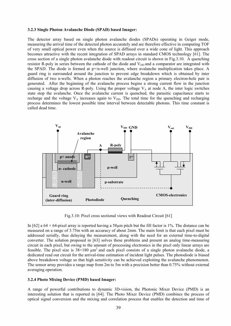
39
3.2.3 Single Photon Avalanche Diode (SPAD) based Imager:
The detector array based on single photon avalanche diodes (SPADs) operating in Geiger mode,
measuring the arrival time of the detected photon accurately and are therefore effective in computing TOF
of very small optical power even when the source is diffused over a wide cone of light. This approach
becomes attractive with the recent integration of SPAD arrays in standard CMOS technology [61]. The
cross section of a single photon avalanche diode with readout circuit is shown in Fig.3.10. A quenching
resistor R-poly in series between the cathode of the diode and VDD and a comparator are integrated with
the SPAD. The diode is formed at p+/n-well junction, where avalanche multiplication takes place. A
guard ring is surrounded around the junction to prevent edge breakdown which is obtained by inter
diffusion of two n-wells. When a photon reaches the avalanche region a primary electron-hole pair is
generated. After the beginning of the avalanche process begins a strong current flow in the junction
causing a voltage drop across R-poly. Using the proper voltage VA at node A, the inter logic switches
state stop the avalanche. Once the avalanche current is quenched, the parasitic capacitance starts to
recharge and the voltage VA increases again to VDD. The total time for the quenching and recharging
process determines the lowest possible time interval between detectable photons. This time constant is
called dead time.
Fig.3.10: Pixel cross sectional views with Readout Circuit [61]
In [62] a 64 × 64-pixel array is reported having a 58µm pitch but the fill factor is 1%. The distance can be
measured on a range of 3.75m with an accuracy of about 2mm. The main limit is that each pixel must be
addressed serially, thus delaying the measurement, along with the need for an external time-to-digital
converter. The solution proposed in [63] solves these problems and present an analog time-measuring
circuit in each pixel, but owing to the amount of processing electronics in the pixel only linear arrays are
feasible. The pixel size is 38×180 µm2
and each pixel consists of a single photon avalanche diode, a
dedicated read out circuit for the arrival-time estimation of incident light pulses. The photodiode is biased
above breakdown voltage so that high sensitivity can be achieved exploiting the avalanche phenomenon.
The sensor array provides a range map from 2m to 5m with a precision better than 0.75% without external
averaging operation.
3.2.4 Photo Mixing Device (PMD) based Imager:
A range of powerful contributions to dynamic 3D-vision, the Photonic Mixer Device (PMD) is an
interesting solution that is reported in [64]. The Photo Mixer Device (PMD) combines the process of
optical signal conversion and the mixing and correlation process that enables the detection and time of
p+ anode
A
n- cathode
n+
n-well
Guard ring
(inter-diffusion) Photodiode Quenching CMOS-electronics
p-substrate
p-well
R-poly
Avalanche
region
p+
Vop VDD G,D VDD Vout

40
flight measurement. The charge transfer mechanism of photo mixer device is comparable to that of
surface channel charge coupled devices (CCD) with significant differences that have to be considered. In
Charge Coupled Devices (CCD) the charge will only be moved in one direction. In the PMD the direction
of the charge movement depends on the electrical reference signal. It is changed into push pull signals
that are applied to the modulation electrodes. Photogate PMD doesn’t storage charges; it serves for a very
fast modulated transport and readout. Different implementations of the PMD principle are under
development and provide a new family of PMD-detectors which are going to realize the dynamic 3D-
vision. The Photo Gate (PG) -PMD is the first implementation of the PMD-principle in low cost CMOS
technology. Fig.3.11 schematically illustrates the cross-section of a PMD receiver. The PG-PMD is a
low-noise and low-dark-current device, being capable of demodulating very low optical signals at photo
current levels.
Fig.3.11: Schematic illustrates the cross-section of a PG-PMD receiver [64].
Another PMD implementation is described in which are similar to the PG-PMD but the photo gates are
replaced by widening the metal shields ME (Metal Electrode) of the read out electrodes. The main
advantage of the ME-PMD is the achievement of an optimized and more homogeneous drift field. It also
increases the modulation bandwidth and the device sensitivity is improved by avoiding the optical
attenuation of the semitransparent photogates.
Finally, another interesting solution employs a Metal-Semiconductor-Metal photo-detector [64, 65]
having a high modulation bandwidth but the sensor is not compatible with CMOS technology and the
pixel dimension is 250µm which is quite large with low fill factor. Typical MSM photodiodes implement
in a slightly doped semiconductor bulk with interdigitated metal fingers on top. The selected
semiconductor and metal have work functions leading to a Schottky contact. Fig.3.12 shows a schematic
of a typical MSM PMD photodiode. Basically, modulation functionality is achieved by varying the
applied bias voltage across the Schottky contact. This results in sensitivity or gain modulation of the
device. The photo current polarity of this symmetrical photo diode depends on the polarity of the supply
voltage ±um. The average of photo current of the non-correlated background light goes to zero on both
coupling capacitors Cm. The required correlated photo current leads to a unidirectional photo current
causing an anti-symmetrical charge on Cma and Cmb. This current is collected by the readout circuitry over
a low pass filter to separate the high frequency modulation voltage.

41
Fig.3.12: Cross-sectional view of finger structure MSM-PMD [64]
3.2.5 Gates-on-Field Oxide structure based CMOS Range Image Sensor:
To achieve TOF based charge integration, the proposed pixel utilizes polysilicon gates on field oxide to
realize high-speed charge transfer structures, while maintaining the compatibility to standard CMOS
process [66]. In the proposed charge draining structure, charge due to background light, which is mixed
into the signal charge, is reduced by using a small duty-cycle light pulse and draining the charge for most
of the time in one cycle. Fig.3.13 shows the cross-sectional view and layout design of the proposed
device. The photogate, PG is the photosensitive region of the pixel. Aside from PG, the other gates are
used to control the direction of photoelectron flow according to their TOF. TX1, TX2 and TXD are also
polysilicon gates placed on field oxide. FD1 and FD2 are floating diffusions used to collect signal charges
from PG through transfer gates TX1 and TX2 respectively. Unwanted background light induced
photoelectrons are transferred to the two charge drains through the charge draining gates TXD.
Fig.3.13 layout design of a Gates-on-Field Oxide structure based Imager [66]
n-
Epitaxial layer
metal
Popt
Si- substrate
Aa Aa Aa Ab Ab Ab
Readout
circuit
U∆
UΣ
L
L
R
R
C
C
C12
UB
Cma
Cmb
-um(t)
+um(t)

42
The proposed CMOS TOF sensor consist of 84672 pixels with a gates-on-field oxide structure with fill
factor of each pixel is 19%. Range measurements are achieved by TOF dependant charge separation. A
new range equation is developed for this technique and for the first time the dependency on range
resolution to PSN is mathematically derived, calculated, and proven through measurements. A linear
distance range between 1.6–12.3m measured to 1.9% accuracy is achievable for a constant measured
signal intensity of 0.55 V. The best range resolution measured is 2.35 cm with light pulse width of 100 ns
at 30 fps.
3.2.6 Field Assisted CMOS Photo-Demodulator based 3D imaging:
In this novel device [67], owing to the presence of an electric field resulting from the flow of a majority
carrier current between two modulation electrodes Vmd1 and Vmd2, the photogenerated charge is guided
towards two collection electrodes Vcd1 and Vcd2. The majority carrier current and the electrical field are
induced due to the potential difference between two modulation electrodes. The induced electric field is
guided the photo generated charge towards one of the two collecting electrodes. A very good responsivity
of 0.32 A/W at 860nm and high demodulation efficiency of about 99% at low frequency can be achieved.
Fig.3.14 shows the schematic of a field assisted photo-demodulator.
Fig.3.14 Schematic cross section of a Current Assisted Photonic Demodulator.
The readout of the collected charge at the two electrodes can be done in charge-integrating mode as in
conventional photodiodes and the circuit complexity of the pixel can be reduced. The device sensitivity
can be optimally adjusted as a function of the incident optical power by adding one control electrode that
is particularly useful for imaging deep scenes [68]. The main drawback of this device is the power
dissipation arising from the modulation current of the device. A trade off between speed of operation and
power dissipation is necessary when dealing with large 2D pixel arrays. Another field-assisted charge
collection mechanism has also been proposed for other active pixels to be used for charged particle
tracking and electron microscopy [69].
n+ n+ p+ p+
Vcd1 Vcd2 Vmd1 Vmd2
p-substrate
Light

43
Dis
ad
va
nta
ges
Lar
ge
pix
el s
ize,
Hig
her
po
wer
con
sum
pti
on
Lo
wer
sen
siti
vit
y,
cost
ly b
ecau
se o
f n
on
stan
dar
d t
ech
nolo
gy
is
use
d
L
ayo
ut
com
ple
xit
y
Eac
h p
ixel
mu
st b
e
add
ress
ed s
eria
lly
; th
us
del
ayin
g t
he
mea
sure
men
t.
L
ow
er m
od
ula
tio
n
freq
uen
cy
Po
wer
dis
sip
atio
n
aris
ing f
rom
th
e
mo
dula
tio
n c
urr
ent.
Ad
va
nta
ges
Can
yie
ld a
n a
ccu
racy
of
few
cm
ov
er a
max
imum
ran
ge
of
few
met
ers.
S
impli
city
of
read
out
chan
nel
, sm
all
pix
el s
ize
Lo
w p
ow
er c
on
sum
pti
on
,
fast
char
ge
tran
spo
rtat
ion
and
hig
h o
pti
cal
fill
fac
tor.
Dis
tan
ce c
an b
e
mea
sure
d o
n a
ran
ge
of
3.7
5m
wit
h a
n a
ccura
cy
of
abou
t 2
mm
Ran
ge
reso
luti
on
2.3
5cm
at
30
fps
Ver
y g
oo
d s
ensi
tivit
y,
hig
h d
emod
ula
tio
n
effi
cien
cy
Fil
l
Fa
cto
r
20
%
22
%
25
%
1%
19
%
N/D
Pix
el S
ize
81
.9×
81
.7 µ
m2
21
× 6
5 µ
m2
40
× 4
0 µ
m2
58
× 5
8 µ
m2
15
×1
5 µ
m2
30
×2
5 µ
m2
Pix
el
Res
olu
tio
n
50
×3
0 a
rray
64
×2
5 a
rray
17
6×
14
4 a
rray
64
×6
4 a
rray
33
6×
25
2 a
rray
N/D
Pro
cess
Tec
hn
olo
gy
0.3
5µ
m C
MO
S
Tec
hn
olo
gy
CC
D/C
MO
S
hy
bri
d
tech
no
logy
0.6
µm
CC
D/C
MO
S
tech
no
logy
0.8
0 µ
m C
MO
S
tech
no
logy
0.3
5 µ
m C
MO
S
tech
no
logy
0.3
5 µ
m C
MO
S
tech
no
logy
Ph
oto
dio
de
Ty
pe
Sta
nd
ard
Ph
oto
dio
de
Ph
oto
gat
e ty
pe
ph
oto
dio
de
Ph
oto
-
dem
odu
lato
r
stru
cture
wit
h
po
ly S
i g
ate
Sin
gle
ph
oto
n
aval
anch
e
Ph
oto
dio
de
Gat
e-o
n-F
ield
–O
xid
e
stru
ctu
re
Cu
rren
t A
ssis
ted
Ph
oto
nic
Dem
od
ula
tor
Sen
sor
Intr
od
uce
d b
y
Dav
id S
top
pa
et.a
l.[5
3]
Ro
ber
t L
ange
et.a
l [5
4]
Ber
nh
ard
Bu
ttgen
et.
al [
60]
Cri
stia
no
Nic
lass
et.a
l. [
62
]
Sh
oji
Kaw
ahit
o
et.a
l [6
6]
Dan
iel
Van
Nie
uw
enh
ov
e
et.a
l [6
8]
Ta
ble
-II
I: P
erfo
rm
an
ce
Co
mp
ari
son
Ta
ble
dif
fere
nt
typ
es o
f
3D
im
ag
er r
esea
rch

44
Chapter 04
Test Structures and Characterizations The test structures provide an easy way to investigate the initial characteristics of a new device. To get a
preliminary idea of current assisted photo mixing demodulator characteristics different topological and
geometrical structures are fabricated in custom process technology at Fondazione Bruno Kessler
(FBK),Trento, Italy. Although this technology is quite different from standard CMOS process technology,
the availability of the geometrical characterizations and process details will allow the simulations to be
optimized. Once the test device satisfies the specific characteristics of operation, a prototype TOF based
current assisted photo mixing demodulator 3D image sensor is designed incorporating full testability
features at device and system levels and fabricated in standard CMOS technology. In the following
section we will describe different types of photo mixing device, its optical and electrical characteristics
fabricated in custom technology.
4.1 High Resistivity Current Assisted Photo mixing Device (CAPD):
The electro-optical mixer in different geometries and topologies based on substrate current modulation is
fabricated in a custom technology on high resistivity silicon substrates [70]. A set of test devices was
fabricated at FBK on high resistivity n-type silicon substrate with 2 × 10¹²
cm-3
doping concentration.
The substrate doping is reduced in order to decrease the modulation current and thus the power
dissipation. Although the use of p-type substrate could lead to a larger bandwidth, these test structures are
fabricated on an n-type substrate in order to get the primary idea on current assisted photonic demodulator
characteristics with a simple fabrication process. Different layouts of test devices are fabricated in FBK
such as: linear shaped CPAD consisting of two collecting electrodes, square shaped CAPD device with
single collecting electrode and multiple collecting electrodes based CAPD device.
Fig.4.1: Cross sectional view of high resistivity linear-shaped CAPD
4.1.1 Device structure and operation of Linear-shaped CAPD:
The architecture of the linear-shaped demodulator is implemented in custom process technology at FBK.
Two different configurations are fabricated; in one structure (CAPD1) the distance between two
modulating electrodes is 20µm and in the second structure (CAPD2) the distance between two
modulating electrodes is 40µm. The width of both p+ and n+ implants is 5µm.
Fig.4.1 shows the cross sectional view of the linear-shaped CAPD device. It contains four electrodes, Vd1
and Vd2 are the collecting electrodes to collect the photo generated charge carriers and Vm1 and Vm2 are
modulating electrodes where the potential is applied. The substrate of this device is n-type high resistivity
p+ p+ n+ n+
n-substrate
Light
Vd1 Vm2 Vm1 Vd2
Electric Field

45
silicon to reduce the high power consumption due to the majority current flow in the substrate. The
collecting electrodes consist of two shallow p+ implantation and n+ implantation for the modulating
electrodes. Each pixel must be surrounded by an n+ bulk-contact, shared along the array. This implant is
placed at a minimum distance of about 20µm from the pixel boundary. For the better isolation a p+ ring is
also placed around the n+ bulk-contact maintaining the distance of about 20µm. Fig.4.2 shows the layout
design of the linear-shaped CAPD device.
(a) (b)
(c)
Fig.4.2: Layout design of the linear-shaped CAPD (a) distance between two modulating electrodes is
20µm (b) distance between two modulating electrodes is 40 µm (c) linear-shaped CAPD layout with bulk
and isolation electrodes.
p+
n+ 20µm
20µm p+ n+ p+ n+
Vd1 Vd2 Vm2 Vm1
Vbulk Visol

46
The electric field is formed in the substrate by applying a potential difference between the modulating
electrodes. When the light impinges on the device, the electric field guides the photo-generated charge
carriers towards one of the two collecting electrodes. In this structure the modulated electric field is not
limited to the surface of the device, thus the collection charge carriers generated deep inside the substrate.
Fig.4.3: Hole current density of CAPD1
The behaviour of this device has been investigated by using the device simulator ISE-TCAD. Fig.4.3
shows the hole current density of CAPD1 with a 0.5V voltage difference applied to the modulating
electrodes and a 780 nm light incident on the device surface. Most of the generated holes move toward
the collecting electrode Vd1, guided by the electric field.
4.1.2 Characterization of Linear-shaped CAPD:
For the static characterization, the voltage applied to the modulating electrode Vmd2 is swept from 0V to
2V, while the voltage of modulating electrode Vmd1 is maintained at 1V. The collecting electrodes are
biased at a constant voltage of 0V. A wide-spectrum lamp was used to illuminate the device. As can be
seen in Fig.4.4, the transfer characteristic shows a good DC charge separation efficiency near to 100% for
the CAPD1 device. The asymmetry in the electrical characteristics is due to the asymmetry to the device
bias.
The average current measurement at the collecting electrodes and the dynamic demodulation contrast of
the test devices CAPD1 and CAPD2 are characterized. In this measurement, the ring voltage (Vbulk) has
been maintained constant at 1V.The guard ring (Visol) and the collection diode were biased at 0V, which is
shown in Fig.4.2(c). For this measurement two sine wave signals have been used with an arbitrary phase
delay ∆φ at different frequencies. A function generator is used to generate three sine wave signals with
appropriate synchronization. One of the three signals is used to modulate a laser emitter with an arbitrary
phase delay ∆φ. The other two signals are connected to the modulating electrodes Vmd1 and Vmd2 with
1800 phase shift. Also in this case the collecting electrodes are biased at a constant voltage of 0V. To
measure the average current, a 650nm red laser with a flat frequency response within the band of interest
and 87% modulation depth was used to illuminate the test device.
Vd1 Vd2 Vm1 Vm2
0 10 20 30 40 50

47
0
100
200
300
400
500
600
0.00 0.50 1.00 1.50 2.00
Modulation Voltage (V)
Collecting Current (nA)
Collecting Current (Id1)
Collecting Current (Id2)
Fig.4.4: DC Charge transfer characteristic of CAPD1
The current flowing through the collecting electrode was read out with a Pico-ammeter at different
modulation voltages and frequencies. Fig.4.5 shows the demodulation contrast of the photo mixing device
CAPD1 at different voltages and frequencies. The Demodulation Contrast (DC) in optics is defined as the
ratio between the amplitude and the average value of the measured signal.
0
5
10
15
20
25
30
1.00E+03 1.00E+04 1.00E+05 1.00E+06 1.00E+07 1.00E+08
Frequency (Hz)
Demodulation Contrast (%
)
DC(%) @ 500mV
DC(%) @ 1V
Fig.4.5: Dynamic Demodulation Contrast of CAPD1 at different Voltage
The above figure shows that the obtained demodulation contrast decreases at high frequencies. At long-
wavelength, photoelectrons are generated deeper in the semiconductor which is far from the electrically
active zone need time to reach the demodulating electric field. This temporal delay in arrival time leads to
decrease in modulation contrast for high frequencies. At the same modulating voltage, increasing the
active area of the CAPD basically increases the sensitivity of the device and thus clearly boosts up the
modulation contrast of the device. Fig.4.6 shows the demodulation contrast of linear-shaped high
resistivity CAPD at the different dimension.

48
0
10
20
30
40
1.00E+03 1.00E+04 1.00E+05 1.00E+06 1.00E+07 1.00E+08
Frequency (Hz)
Demodulation Contrast (%
)
DC(%) @ CAPD1
DC(%) @CAPD2
Fig.4.6: Dynamic Demodulation Contrast of two CAPD devices at different geometries
4.1.3 Device structure, operation and characteristics of a Multiple-strip based CAPD:
This device consists of fingered type electrodes i.e. multi tap CAPD device. Fig.4.7 (a) and (b) shows the
cross sectional view and the layout of the device, respectively. It consists of nine detection electrodes.
Among these detection electrodes, the seven central regions (as shown in Fig.4.7 from region 2 to region
8) consist of a detection junction and two substrate contacts. The rest of detection regions contain one
detection junction and one substrate contact, like the region 1 and 9 shown in Fig.4.7.
(a)
n+
n-substrate
Vd1 Vm2 Vm1 Vd2
p+ p+ p+ p+ p+ n+ n+ n+ n+ n+ n+ n+
1 2 3 9 8

49
(b)
Fig.4.7: (a) Cross sectional view of multiple strip CAPD and (b) Device layout
All of the substrate contacts and the detection junctions are connected as shown in the device cross
sectional diagram. Finally this device has four electrodes, two collecting electrodes (Vd1 and Vd2) that are
connected to the detection junction and two modulating electrodes (Vm1 and Vm2) that are connected to the
device substrate. The collecting electrode Vd1 and the modulating electrode Vm1 are connected to the 2, 4,
6 and 8 regions according to the detection junctions and substrate contacts.
On the other hand, the collecting electrode Vid2 and the modulating electrode Vmod2 are connected to the
region 1, 3, 5, 7 and 9 accordingly. This device is also surrounded by an n+ bulk-contact, shared along the
array and placed at a minimum distance of about 20µm from the pixel boundary. A p+ ring is placed
surround the n+ bulk-contact maintaining the distance of about 20µm for better isolation. The total area of
this device is 400µm × 400 µm. The distance between the adjacent modulating electrodes is 20 µm.
In this device an effective potential gradient is applied to the multiple modulating electrodes that speed up
the signal charges transferring to the detection regions. The potential ∆V = Vm2 ~ Vm1 defines at which
region the hole current is detected. The operational behaviour of the multi tap device is investigated by
using the device simulation software ISE-TCAD. Fig.4.8 shows the hole current density of this device
with a voltage difference applied between two modulating electrodes and a 780 nm light incident on the
device surface. Most of the generated holes move toward the collecting electrode Vd1, guided by the
electric field. In this simulation picture, it shows the region 1, 2 and 3 according to the cross sectional
view of the device shown in Fig.4.7.
1 2 3 8 9
20µm

50
Fig.4.8: Hole current density of Multiple CAPD device
The modulating voltage ∆V allows demodulation of the photonic signal, without having to switch the
totality of the electric field. These results in an increase of the demodulation speed: the carriers are always
guided towards the centre of the device and demodulated there. If Vmod2 > Vmod1 the hole current is
detected in Vid2 region, for Vmod1 > Vmod2 it moves to the opposite detection region. As the collecting
electrodes for Vid1 and Vid2 are not equal, the DC characteristics of this device are not symmetrical as
linear-shaped CAPD. Fig.4.9 shows the DC characteristics of the device under the illumination of wide
spectrum light, it illustrates a good DC charge separation efficiency.
0
5
10
15
20
25
0 0.5 1 1.5 2
Modulation Voltage (V)
Collecting Current (uA)
Collecting Current Id1
Collecting Current Id2
Fig.4.9: DC characteristics of the device under the illumination of wide spectrum light.
Fig.4.10 shows the growth of demodulation contrast for the multi-tap device as a function of different
modulation voltage. Different demodulation frequencies are considered in this case. Increasing the
modulation voltage in essence increases strength of the electric field and it clearly enhances the
modulation contrast of the device. The area of the multi tap device is larger than the linear shaped CAPD
40
1 2 3
Vd1 Vm2 Vm1 Vd2
0 Abs(hCurrent Density)

51
device and its modulating potential is distributed over the whole substrate, thus increasing the charge
transfer efficiency and demodulation contrast of this device.
10
20
30
40
50
0.0 0.5 1.0 1.5 2.0 2.5
Modulation Voltage (V)
Demodulation Contrast (%
)
100Hz
1kHz
500kHz
10MHz
20MHz
30MHz
Fig.4.10: Growth of demodulation contrast for multi-strip device as a
function of different modulation voltage
4.1.4 ,on-linearity measurement of the linear-shaped CAPD and Multi-tap CAPD:
A set of phase measurements is performed on the device CAPD1 and multiple strip CAPD devices. In
these measurements a variable phase delay ∆φ is applied between two modulating electrodes and the laser
input to illuminate the device. The value ∆φ of can be recovered acquiring four amplitude measurements
with four different phase shifts θ1 – θ4 applied to the modulated laser signal. These phase shifts were -
180°,-90°, 0° and +90°, respectively, and the four amplitudes measured, represented by the average DC
currents, I(θ1) – I(θ4), are used in Equation given below to calculate the phase delay ∆φ:
( ) ( )( )42
31
)(arctan
θθθθ
ϕII
II
−
−=∆ .
-180
-120
-60
0
60
120
180
-180 -90 0 90 180
Applied Phase (Degree)
Measured Phase (Degree)
Measured Phase
Actual Phase
(a)

52
-180
-90
0
90
180
-180 -90 0 90 180
Applied Phase (Degree)
Measured Phase (Degree)
Measured phase
Applied Phase
(b)
Fig.4.11: Phase linearity measurement (a) for Linear shaped CPAD1 (b) Multiple Strip CAPD
The measurement is performed considering sinusoidal wave modulation signals at 20 MHz, and the
resulting phase is reported in Fig.4.11 (a) and (b) for CAPD1 and Multiple strips CAPD respectively. The
maximum linearity error of linear shaped and multi strip CAPD device is 28% and 3.9 % for sinusoidal
wave modulation respectively.
4.1.5 Device architecture and Operation characteristics of a Square shaped CAPD:
In Fig.4.12 (a) cross sectional view and layouts are shown for the square shaped CAPD implementations.
It consists of a detection region at the centre of the device. This detection region consists of a detection
junction and two substrate contacts. The rest of detection regions contain one detection junction and one
substrate contact. The distance between two substrate contacts, i.e. the modulation electrode, is 20µm. As
the substrate contact of this device is not uniform, the applied drift field will not be spread equally over
the sensitive area, thus lowering the speed of the device.
(a)
n-substrate
p+ p+ p+ n+ n+ n+ n+
Active Area Active Area
Vpd- Vmod- Vmod+ Vpd+ Vmod- Vpd-

53
(b)
(c)
Fig.4.12: Square shaped CAPD Device (a) Cross sectional View (b) Device layout (c) Hole current
density for square shaped CAPD
This device is surrounded by an n+ bulk ring apart from the pixel boundary of about 20µm. A p+ ring is
also placed surround the n+ bulk-contact keeping a distance of about 20µm for device isolation as shown
in Fig.4.2 for linear shaped CPAD. Based on the operation characteristics of the square shaped CAPD
device, Fig.4.12(c) shows the hole current density of the device when the voltage at Vmod+ is greater
than Vmod-. According to the CAPD principle and depending on the modulating voltage, holes are
generated by light impinging on the substrate are transferred to the detecting junction. The transfer
mechanism is drift, provided by the electric field induced in the substrate.
Vpd-
Vmod- Vmod+
Vpd+
Vmod-

54
0
100
200
300
400
0.00 0.30 0.60 0.90 1.20 1.50
Modulation Voltage (V)
Current (nA)
Ring voltage 1V
Ring voltage 2V
Fig.4.13: DC current at the collection diode of device at two different ring voltages.
The current measured at the collection electrode (Vpd+) of square shaped device under wide spectrum
illumination lamp is shown in Fig.4.13. In this measurement, the ring voltage is maintained constant,
while the modulation voltage is swept from 0V to 1.5V. The collection electrodes are biased at 0V. The
effect of an increase in the ring voltage is a shift of the curve to the right. Also in this case the DC charge
separation efficiency can reach values more than 90%. The dynamic demodulation contrast is characterized of this device same as before for the other two
devices. A dual-output function generator is used to generate two sine-wave signals with an arbitrary
phase delay ∆φ. One of the two signals has been used to modulate a laser emitter, while the other is
connected to the input of the dual output pseudo differential amplifier to get an output of 1800 phase shift.
The output of this amplifier is connected to the modulation electrode of the square shaped CAPD device.
The DC current flowing through the collection electrode is read out with a Pico-ammeter. The electrodes
are biased as in dc measurements. A 650nm red laser with a flat frequency response from in the band of
interest and near to 90% modulation depth is used to illuminate the test device. A sine-wave modulation
voltage with 500mV and 1V amplitude is applied to the device. The DC current measured at several
phases of the laser modulated signal is reported in Fig.4.14 (a) at 500 kHz and 1 MHz modulation
frequency. In both cases an excellent fit is obtained using a sine-wave signal.
(a)
5
9
13
17
21
25
-180 -90 0 90 180
Laser Phase (Degree)
Average current (nA)
500kHz
1MHz

55
0
5
10
15
20
25
30
35
1.E+06 1.E+07 1.E+08
Frequency (Hz)
Demodulation Contrast (%
)
Modulation Voltage @ 500mV
Modulation Voltage @ 1V
(b)
Fig.4.14: (a) Measured average current at two modulation frequencies (b) Measured Demodulation
Contrast
The ratio between the amplitude and the average value of the measured sine-wave known as
demodulation contrast is reported in Fig.4.14 (b) as a function of frequency, taking into account the effect
of the laser modulation depth. The low value of dynamic demodulation contrast with respect to measured
DC contrast could be explained by the presence of holes generated in the chip outside the active device
area reaching the collection electrode by diffusion. A metal screening of the other light sensitive areas
would therefore improve the measured device characteristics.
On the basis of the outcome of device simulation and the preliminary results of the test devices, which
were fabricated by FBK, a linear-shaped demodulator model seemed suitable for further investigation in
terms of small device size, moderate fill factor and overall device performance. A behavioural model has
been developed for the current demodulator, suitable to be incorporated into a circuit simulator cadence
and adopted for simulating at circuit level with read out channel. The numerical device simulation results
and the results from the circuit simulations have shown a very good agreement in both DC and transient
analysis. The result of the electrical and optical characterizations will be used to optimize the devices, and
also it helped us to design a CMOS based current assisted photo mixing demodulator.

56
Chapter-05
Current Assisted Photo mixing Demodulator in standard CMOS
Technology
CMOS imaging technology provides the potential to integrate image processing and it is capable of
achieving substantial image data. The presented CMOS optical ranging sensor makes use of a current
assisted photonic mixing device with an integrated circuit to measure time-of-flight. In this device, an
electric field is used to drive photo generated minority carriers from deep into the substrate towards a
collecting junction. This picks up detector sensitivity and speed, and allows large sensitive area. As a test
vehicle, 10×10 pixel arrays have been fabricated with a 0.18µm CMOS technology. Remarkably, small
pixel size of 10×10 µm2 has been achieved. In this chapter, the device charge separation efficiency and
demodulation capabilities are described up to modulation frequency larger than 20 MHz. The impact of
important parameters such as wavelength, modulation frequency and voltage on this test device is also
experimentally evaluated in this chapter.
5.1 Device Architecture:
The device functionality of the Current Assisted Photon Mixing Demodulator is investigated using the
finite element software ISE-TCAD and the code DESSIS 8.0 (Synopsys Inc.) in order to evaluate the
device capability of reaching the required high responsivity as well as high demodulation bandwidth.
Both DC and dynamic performance are simulated. This simulation is adopted, in particular for, i) the
comparative evaluation of different technological options, such as substrate doping for power
consumption reduction and junction depth ii) the device geometry and layout, by comparing different
layout topologies including linear, interdigitated and circular structures with optimizing of each topology
in dimension and spacing of charge collecting and charge modulating electrodes and iii) finally predict
the effect of an additional n-type electrode for sensitivity control and dynamic range enhancement.
A schematic cross section of the fabricated device is shown in Fig.5.1. It contains four electrodes: C1 and
C2 are the electrodes aimed at collecting the photo generated charge carriers, whereas M1 and M2 are the
modulating electrodes where the potential is applied.
Fig.5.1: Device Cross sectional view (not to scale).
The simulator solves the drift-diffusion transport model. Photo-generation effects are accounted for by
including appropriate terms into the carrier continuity equations [71]. The photonic mixing demodulator
is fabricated in 0.18µm standard CMOS technology. Process details such as layer thicknesses, junction
C2
p+ substrate
p-epi layer
n+ n+ p+ p+
p-well p-well
M1 M2 C1
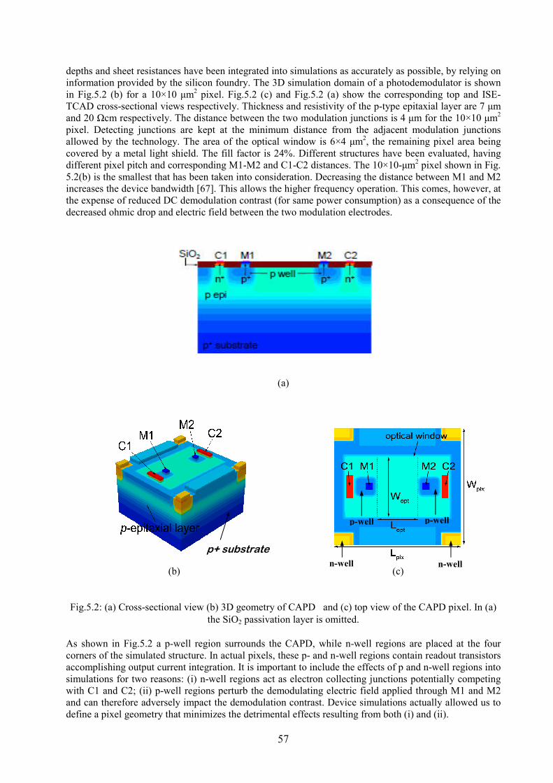
57
depths and sheet resistances have been integrated into simulations as accurately as possible, by relying on
information provided by the silicon foundry. The 3D simulation domain of a photodemodulator is shown
in Fig.5.2 (b) for a 10×10 µm2 pixel. Fig.5.2 (c) and Fig.5.2 (a) show the corresponding top and ISE-
TCAD cross-sectional views respectively. Thickness and resistivity of the p-type epitaxial layer are 7 µm
and 20 Ωcm respectively. The distance between the two modulation junctions is 4 µm for the 10×10 µm2
pixel. Detecting junctions are kept at the minimum distance from the adjacent modulation junctions
allowed by the technology. The area of the optical window is 6×4 µm2, the remaining pixel area being
covered by a metal light shield. The fill factor is 24%. Different structures have been evaluated, having
different pixel pitch and corresponding M1-M2 and C1-C2 distances. The 10×10-µm2 pixel shown in Fig.
5.2(b) is the smallest that has been taken into consideration. Decreasing the distance between M1 and M2
increases the device bandwidth [67]. This allows the higher frequency operation. This comes, however, at
the expense of reduced DC demodulation contrast (for same power consumption) as a consequence of the
decreased ohmic drop and electric field between the two modulation electrodes.
(a)
(b) (c)
Fig.5.2: (a) Cross-sectional view (b) 3D geometry of CAPD and (c) top view of the CAPD pixel. In (a)
the SiO2 passivation layer is omitted.
As shown in Fig.5.2 a p-well region surrounds the CAPD, while n-well regions are placed at the four
corners of the simulated structure. In actual pixels, these p- and n-well regions contain readout transistors
accomplishing output current integration. It is important to include the effects of p and n-well regions into
simulations for two reasons: (i) n-well regions act as electron collecting junctions potentially competing
with C1 and C2; (ii) p-well regions perturb the demodulating electric field applied through M1 and M2
and can therefore adversely impact the demodulation contrast. Device simulations actually allowed us to
define a pixel geometry that minimizes the detrimental effects resulting from both (i) and (ii).
p+ substrate
p-well p-well
n-well n-well

58
5.2 Operation principle and Charge transfer:
The Current Assisted Photonic Mixing device is based on a majority current associated drift field. With
zero voltage applied between M1 and M2, due to the symmetry of the structure, equal amounts of
photogenerated electrons are collected by C1 and C2. If a voltage is applied between M1 and M2, a hole
current is induced between the two modulation electrodes, generating an ohmic drop through the p-type
epitaxial layer. The resulting electric field guides the photogenerated electrons preferentially towards
either C1 or C2 depending on the applied voltage polarity. When VM1 > VM2, a majority current carrier
generates and forms an electric field in the substrate. When the light impinges on the device, the majority
current and the induced electric field separate the photo-generated electron-hole pairs. The separated hole
becomes the part of the majority hole current which is generated by the applied voltage on modulating
electrode. The hole current moves towards the p+ region and the electron is guided by the same electric
field to the collecting electrode C1 and thus the charge is detected. Fig.5.3 shows the simulated electron
current density with a voltage difference applied to the modulating electrodes (M1 & M2) and a 780 nm
light beam incident on the device surface. At the reverse potential (VM1< VM2) the photo-generated charge
carriers are swept away from the collecting electrode C1 to C2.
Fig.5.3: Simulated electron current density under illumination
To get a relationship between AC and DC demodulation contrast, assuming no extra collecting junctions
compete with C1 and C2 within the pixel structure and no considerable photocurrent is collected from
adjacent pixels, currents at the C1 and C2 terminals can be written as:
TOTCC IfI 11 =
(5.1)
TOTCC IfI )1( 12 −=
where, ITOT is the total pixel photocurrent (ITOT =IC1+IC2) and fC1 is the fraction of ITOT that is collected by
C1.
If a sinusoidal-modulated light is used to illuminate the scene, then ITOT can be written as:
)2sin( ϕπ −+= ftIII AC
TOT
DC
TOTTOT (5.2)
where, DC
TOTI andAC
TOTI are the amplitudes of the DC and AC components of ITOT, f is the modulation
1.0E-03
1.0E-04
1.0E-05
1.0E-06
1.0E-07
1.0E-08
Abs (eCurrentDensity)
0 2 4 6 8 10 12
0
-1
-2
-3
-4
-5
-6
-7
-8
C1 M2 C2 M1

59
frequency, and ϕ is the phase difference between the light detected by the sensor and the one emitted by
the illuminator. Ideally, DC
TOTI =AC
TOTI . In practice, background light, non-unity modulation depth of the
illuminator, and roll-off of the AC component amplitude at high modulation frequencies make AC
TOTI <
DC
TOTI . Fromϕ, the distance d of the illuminated scene point is readily obtained as:
f
cd
πϕ
4= (5.3)
where, c is the light velocity.
When a sinusoidal voltage (VM12) is applied between M1 and M2, also fC1 varies with time, alternately
transferring photocurrent from C1 to C2 and vice versa. VM12 is generated of the same frequency and in
phase with the modulated light used to illuminate the scene, i.e.
)2sin(1212 ftVV AC
MM π= . (5.4)
In the approximation that fC1 depends linearly on VM12 (valid rigorously for small VM12 values only), the
time dependence of fC1 is sinusoidal too and can be expressed as
)2sin(2
111 ftff AC
CC π+≈ , (5.5)
where, AC
Cf 1 is the amplitude of the AC component of fC1. The DC component of fC1 is 0.5, so that, as
imposed by the CAPD symmetry, IC1=IC2 at time instants when VM12=0.
Introducing (5.2) and (5.5) into (6.1) yields:
[ ])2sin()2sin(2
111 ϕππ −+⋅
+= ftIIftfI AC
TOT
DC
TOT
AC
CC
(5.6)
[ ])2sin()2sin(2
112 ϕππ −+⋅
−= ftIIftfI AC
TOT
DC
TOT
AC
CC
From (5.6), the DC component of IC1 and IC2 can be obtained as:
ϕcos2
1
2
111
AC
TOT
AC
C
DC
TOTC IfII +=
(5.7)
ϕcos2
1
2
112
AC
TOT
AC
C
DC
TOTC IfII −=
As can be noted, both <IC1> and <IC2> directly contain the distance information ϕ. They can be obtained
from the output currents IC1 and IC2 by filtering out their AC components at frequencies f and 2f. This
low-pass filtering can be accomplished at pixel level by simply integrating the output currents (5.6).
Either a single-ended or a differential readout scheme can be adopted.
The demodulation contrast is the total output-signal change normalized to the output-signal average.
From (5.7), it can be expressed as (5.8) regardless of whether either <IC1> or <IC2> is adopted as output

60
signal.
DC
TOT
AC
TOTAC
CdI
IfC 1= (5.8)
5.3 Device performance and Experimental results:
The electro-optical characteristics are performed on a current assisted photonic mixing demodulator
implemented in standard CMOS 0.18µm technology. The layout of the single device and a 10×10 array is
shown in Fig.5.4 (a) and 5.4(b), respectively.
(a) (b)
(c)
Fig.5.4: (a) single device layout (b) 10×10 pixel array layout and (c) Layout and Micro-photograph of the
fabricated test structure.
A microphotograph of the fabricated test structures is shown in Fig.5.4(c). To ease readout of detected
currents, several 10×10 arrays of 10-µm CAPD arranged in serpentine as shown in the inset of Fig.5.4(c)
and wired in parallel were included in the test chip. In this way, the currents to be measured are 100 times
larger and the information about the average behaviour of a single device is easily retrieved. The
C1
M1
C2
M2
Optical
Window

61
resistance between the modulation electrodes of the current assisted photo mixing demodulator is 250Ω.
In these structures the applied drift field will spread equally over the sensitive area.
5.3.1 Device Characterizations:
After the fabrication of the test device chip at a commercial silicon foundry by using 0.18µm CMOS
process technology, a thorough characterization is carried out including: electrical measurement of the
test structures for the process parameters, electro-optical tests of the photo-demodulator such as static and
dynamic characteristics.
5.3.1.1 Measurement setup:
Fig.5.5 (a) shows the set up for the measurement of DC characterization of the test device. For the DC
characteristics analysis the device is illuminated with a wide spectrum lamp. In this measurement the
required voltage at different electrodes can be supplied by a voltage source. A Pico ammeter is used to
read out the detection current.
(a)
(b)
Fig.5.5: Experimental setup for (a) DC characterizations & (b) Dynamic characterizations
Signal Generator
Out1 Out2
∆Φ
HP 4145
Modulated
laser
Test
Board
Diff.
Amp
Signal
Generator
HP-4145
Modulated
laser
Test Board
Pico-ammeter
Test
Board
Voltage
Source
Wide spectrum
lamp /Modulated
laser
LABVIEW
O/P

62
The average current measurement at the collecting electrodes and the dynamic demodulation contrast is
characterized for the test device by using the set up is shown in Fig.5.5 (b). A dual output signal generator
is used to generate two sine wave signals. One of the two signals is used to modulate a laser emitter and
the other is connected to the input of a differential amplifier. Two output signals of the amplifier with
1800 phase shift are connected to the modulating of electrodes. The detection current through the
collecting electrodes are read out by a HP 4145 Semiconductor Parameter Analyzer. For this
measurement, three sine wave signals are used with an appropriate synchronization. For this purpose, the
optimal design solutions are implemented at different levels. At first the test bench is setup; the PCB
board for the electro-optical characterization of the device and circuit is designed, realized and tested. The
software programs for the interface with PC and the data acquisition is developed with LABVIEW.
5.3.1.2 Optical input and modulation signal:
In this measurement, stable and high quality optical and modulation signals are required. Both optical and
modulation signals are sine-wave providing a wide range frequency modulation more than 40MHz with
high accurate phase shifting. It is quite difficult to get the satisfactory modulated optical output signal
within the whole modulation frequency range. The average current is measured under a 650nm red laser
with 90% modulation depth used to illuminate the test device at different modulation frequencies. Fig.5.6
shows the different signals for laser and modulation electrodes. Here (a) is the modulation signal for
Laser input and (b) is the device modulation input.
(a)
(b)
Fig.5.6: Optical signal (a) Modulation signals for Laser and (b) Device Modulation Input.
5.3.1.3 Static and Dynamic performance:
For the DC characteristics of the device, the experimental set up is configured as shown in Fig.5.5 (a).
Static Characterization of the CAPD structures has been carried out, using a 650-nm laser to illuminate
the device. The voltage applied to the modulating electrode M1 has been swept from -0.5V to 0.5V.
Another modulating electrode VM2 has been maintained at 0V and the collecting electrodes C1 and C2 are
biased at 1V. Fig. 5.7 (a) shows the typical results of two collecting currents IC1, IC2 and their sum ITOT
plotted with respect to the voltage between M1 and M2 (VM12) for a minimum size CAPD. Here the
positive part of the modulating voltage VM12 values are reported in the graph, IC1 and IC2 being
(a)
(b)

63
symmetrical with respect to the point where they intersect the y-axis while ITOT being symmetrical with
respect to the y-axis. In Fig. 5.7 (a) the solid lines represent the simulation results for DC performance of
the device. In the simulations, the light intensity has then been adjusted to fit IC1 and IC2 measured at
VM12=0 V. The overall agreement between measurements and simulations is satisfactory and acceptable;
indicating that the charge transfer mechanism operates in actual devices closely to theoretical predictions.
As can be noted, ITOT slightly increases at increasing VM12. This can be explained to photocurrents that are
collected by the n-well junctions at the four corners of the pixel when VM12=0 V, while they are
progressively transferred to C1 for increasing VM12 due to the increasing modulation electric field. Starting
from IC1 and IC2 curves like those shown in Fig.5.7 (a), the charge transfer efficiency (ECT), i.e., the CAPD
capability of redirecting photogenerated charge towards one of the two collecting junctions under static
conditions, can be quantified as [75]
21
21
CC
CCCT
II
IIE
+−
= (5.9)
Sim.
Meas.
Ic1+Ic2
Ic1
Ic2
(a)
Sim.
Meas.
(b)
Fig.5.7: Simulated (solid line) and experimental (dotted line) DC characterizations of CAPD 10×10 array
(a) DC current at the collecting electrodes IC1 and IC2 and total current ITOT and (b) Corresponding Charge
transfer efficiency.
0.0 0.1 0.2 0.3 0.4 0.5 VM12 (V)
5 4
3
2
1
0
5 4
3
2
1
0
I C1, I C
2 (nA)
I C1 + IC2 (nA)
0.0 0.1 0.2 0.3 0.4 0.5 VM12 [V]
1
0.8
0.6
0.4
0.2
0
ECT
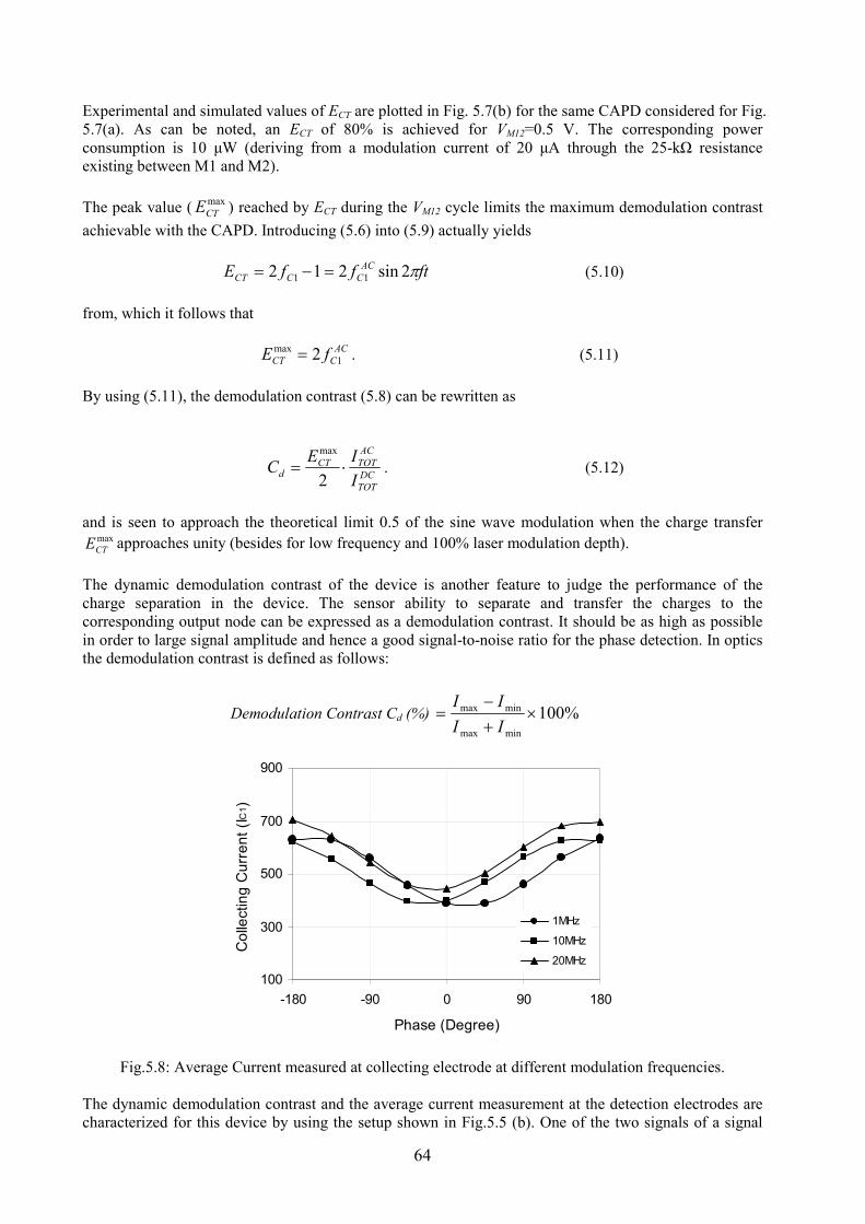
64
Experimental and simulated values of ECT are plotted in Fig. 5.7(b) for the same CAPD considered for Fig.
5.7(a). As can be noted, an ECT of 80% is achieved for VM12=0.5 V. The corresponding power
consumption is 10 µW (deriving from a modulation current of 20 µA through the 25-kΩ resistance
existing between M1 and M2).
The peak value (max
CTE ) reached by ECT during the VM12 cycle limits the maximum demodulation contrast
achievable with the CAPD. Introducing (5.6) into (5.9) actually yields
ftffE AC
CCCT π2sin212 11 =−= (5.10)
from, which it follows that
AC
CCT fE 1
max 2= . (5.11)
By using (5.11), the demodulation contrast (5.8) can be rewritten as
DC
TOT
AC
TOTCTd
I
IEC ⋅=
2
max
. (5.12)
and is seen to approach the theoretical limit 0.5 of the sine wave modulation when the charge transfer max
CTE approaches unity (besides for low frequency and 100% laser modulation depth).
The dynamic demodulation contrast of the device is another feature to judge the performance of the
charge separation in the device. The sensor ability to separate and transfer the charges to the
corresponding output node can be expressed as a demodulation contrast. It should be as high as possible
in order to large signal amplitude and hence a good signal-to-noise ratio for the phase detection. In optics
the demodulation contrast is defined as follows:
Demodulation Contrast Cd (%)
100
300
500
700
900
-180 -90 0 90 180
Phase (Degree)
Collecting Current (IC1)
1MHz
10MHz
20MHz
Fig.5.8: Average Current measured at collecting electrode at different modulation frequencies.
The dynamic demodulation contrast and the average current measurement at the detection electrodes are
characterized for this device by using the setup shown in Fig.5.5 (b). One of the two signals of a signal
%100minmax
minmax ×+
−=
II
II
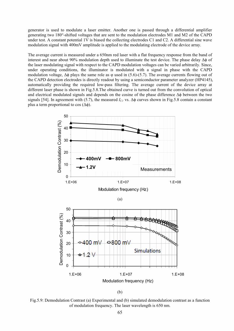
65
generator is used to modulate a laser emitter. Another one is passed through a differential amplifier
generating two 180°-shifted voltages that are sent to the modulation electrodes M1 and M2 of the CAPD
under test. A constant potential 1V is biased the collecting electrodes C1 and C2. A differential sine wave
modulation signal with 400mV amplitude is applied to the modulating electrode of the device array.
The average current is measured under a 650nm red laser with a flat frequency response from the band of
interest and near about 90% modulation depth used to illuminate the test device. The phase delay ∆ϕ of
the laser modulating signal with respect to the CAPD modulation voltages can be varied arbitrarily. Since,
under operating conditions, the illuminator is modulated with a signal in phase with the CAPD
modulation voltage, ∆ϕ plays the same role as φ used in (5.6)-(5.7). The average currents flowing out of
the CAPD detection electrodes is directly readout by using a semiconductor parameter analyzer (HP4145),
automatically providing the required low-pass filtering. The average current of the device array at
different laser phase is shown in Fig.5.8.The obtained curve is turned out from the convolution of optical
and electrical modulated signals and depends on the cosine of the phase difference ∆ϕ between the two
signals [54]. In agreement with (5.7), the measured IC1 vs. ∆ϕ curves shown in Fig.5.8 contain a constant
plus a term proportional to cos (∆ϕ).
0
10
20
30
40
50
1.E+06 1.E+07 1.E+08
Modulation frequency (Hz)
Demodulation Contrast (%
)
400mV 800mV
1.2V
(a)
(b)
Fig.5.9: Demodulation Contrast (a) Experimental and (b) simulated demodulation contrast as a function
of modulation frequency. The laser wavelength is 650 nm.
1.E+06 1.E+07 1.E+08
Modulation frequency (Hz)
Demodulation Contrast (%
)
50
40
30
20
10
0
Measurements

66
Experimental and theoretical values for Cd are plotted in Figs. 5.9(a) and (b) as a function of the
modulation frequency for different modulation voltage amplitudes. Experimental Cd values are obtained
from measurements like those shown in Fig.5.8. Theoretical Cd values can be calculated by plugging
simulatedmax
CTE , DC
TOTI and AC
TOTI values into (5.12). max
CTE and DC
TOTI are obtained but DC simulations,
whereas AC
TOTI is derived from small-signal AC simulations driven by a monochromatic optical stimulus at
the adopted laser wavelength. As can be inferred from Fig.5.9(a), the -3dB bandwidth of the
demodulation contrast is, for all the modulation voltage amplitudes considered, larger than the highest
modulation frequency adopted experimentally (45MHz).
Raising the modulation voltage amplitude boosts Cd over the entire frequency range, as a result of the
increasedmax
CTE . However, the obtained incremental enhancement reduces progressively as the theoretical
limit of 0.5 is approached. Results shown in Fig.5.9(a), if compared with previous works on CAPD
demodulators [67,68] demonstrate that shrinking the pixel dimensions both reduces the power
consumption of a single pixel and enhances the bandwidth of the device, thus enabling the
implementation of moderate sized arrays with a standard process without substrate doping modifications.
The proposed solution can be competitive with existing photo-gate-based mixer technologies [54, 60, 72,
73] because it offers a larger demodulation contrast and a bandwidth comparable with the best devices
presented so far.
5.3.2 Influence of wavelength on the device:
Light absorption length in silicon is strongly dependent on the wavelength. At 650 nm wavelength,
photons are absorbed within a few µm from the surface. The charge carriers that are optically generated in
these regions can be collected easily by the detection electrodes, thus increasing the demodulation
contrast of the device, defined as the sensor ability to separate and transfer the charges to the
corresponding output node.
10
15
20
25
30
35
40
1 10 100
Modulating Frequency (MHz)
Demodulation Contrast (%
)
650nm
780nm
Fig.5.10: Demodulation Contrast as a function of the modulation frequency at two different wavelengths.
On the other hand, higher wavelength photons can penetrate deeper in the device. The photoelectrons
generated far from the surface need more time to reach the demodulating electrical field. This causes
long diffusion times and blurred diffusion directions, thus degrading the device crosstalk and leading to a
lower demodulation contrast. The long diffusion times lower the demodulation cut-off frequency, while
the blurring effect also appears at low modulation frequencies. These effects are confirmed by
experimental results of Fig.5.10, which shows the demodulation contrast as a function of the modulation
frequency in the range from 1MHz to 30 MHz at two wavelengths 650nm and 780nm.

67
5.3.3 Influence of modulation frequency on the device:
We know that the photon absorption length in silicon at 650 nm is few micrometers, the decrease in the
demodulation contrast with frequency can be evaluated with respect to time that photoelectrons generated
deeper in the epitaxial layer of the device. The higher the demodulation frequency, the shorter is the time
available for the single charge carriers to travel from their site of optical generation to the storage area. If
they do not reach the right storage site in time, they will contribute to a wrong sampling point and lower
the demodulation contrast. Fig.5.10 shows the demodulation contrast at different frequencies and
wavelengths. Demodulation contrast is decreased with the increasing of modulation frequency.
5.3.4 Demodulation Contrast vs. Modulation voltage of the device:
We know that the demodulation contrast is an important feature to quantify the perfection of charge
separation in the device. The sensor ability to separate and transfer the charges to the corresponding
output node can be expressed as a demodulation contrast. It should be as high as possible in order to large
signal amplitude and hence a good signal-to-noise ratio for the phase detection.
It is obvious that the demodulation contrast depends on the amplitudes of the modulation voltages. By
using a driver circuit we can control the signal amplitude of the modulation signal. By the exact
adjustment of the modulation voltage of the device at a fixed frequency we can get the optimal
demodulation contrast of the device. Fig.5.11 shows the evolution of demodulation contrast for the device
as a function of the modulation voltage amplitude. Here we considered the different demodulation
frequencies. Increasing the modulation voltage basically increases the majority current that cause the
drift of the minority carriers, namely electrons. As the modulation voltage is applied to the modulating
electrodes, the photo generated electrons arrive at the detector node of the device. When applying the still
larger voltages the electrical field extends deeper in the substrate so that more electrons reach detection
node resulting in a higher demodulation contrast. However, it should be stressed that at the same time this
increases the power consumption in the device, so the value of the modulation voltage amplitude should
be carefully chosen.
0
10
20
30
40
50
0 100 200 300 400 500 600 700
Modulating Voltage (mV)
Demodulation Contrast (%
)
Fig.5.11: Demodulation Contrast as a function of the modulation voltage for CAPD device.
5.3.5 Spectral responsivity and Quantum Efficiency:
We know that responsivity measures the effectiveness of the detector for converting electromagnetic
radiation to electrical current or voltage. The responsivity is the ratio of the rms value of a current signal
generated by the detector to the incident radiant power at the entrance to the detector.

68
Fig.5.12: Test setup for spectral response characterization
The quantum efficiency of a photonic device indicates the efficiency of light with a given wavelength
conversion into electrical signal. It represents the probability of a single photon to generate electron-hole
pair, characterizing the photo converting part of the device. The experimental setup is shown in Fig.5.12.
The mono-chromator with a light source provides monochromatic light with variable wavelengths. The
optical output is connected to an optical fiber with one end shining on a calibrated photo-sensor and the
other end on the photodiode under test. The mono-chromator, the optical power meter and a pico-
ammeter SMU HP 4145 are connected to a PC through a GBIP interfaces for data acquisition and storage.
All the measurements for the photodiodes are conducted in a shield box to isolate optical and electrical
noise.
Since the reflection and absorption characteristics of the photo-detector sensitive material change with
wavelength, so that responsivity depends on wavelengths. Fig.5.13 shows the responsivity vs.
wavelengths of our test device.
0
0.04
0.08
0.12
0.16
0.2
400 500 600 700 800 900 1000
Wavelengths (nm)
Spectral Responsivity(A/W
)
Fig.5.13: Responsivity vs. wavelengths for CAPD
SMU HP 4145
Optical
power meter
Calibrated
photo sensor
Photodiode
chip
PC GPIB
interface
Monochromator
Lamp

69
0
0.1
0.2
0.3
0.4
0.5
400 500 600 700 800 900 1000 1100 1200
Wavelengths (nm)
Quantum Efficiency
Fig.5.14: Quantum efficiency vs. wavelengths for CAPD
Fig.5.14 shows the quantum efficiency of CAPD in different wavelengths. CAPD devices have
potentially higher quantum efficiencies with respect to photo-gate demodulators because their active area
is not covered by polysilicon gates. Our devices show a peak quantum efficiency of 35% at 500 nm and
>20% up to 600 nm.
5.3.6 Capacitance measurement:
Junction capacitance of the image sensors charge sensing node determines the charge capacity and the
charge-to-voltage conversion gain. A smaller capacitance at the charge sensing node is preferred due to
higher signal-to-noise ratio of the output signal. On the other hand, small capacitance has lower charge
capacity and thus a lower dynamic range.
Fig.5.15: Experimental set-up for capacitance measurement
The experimental set-up for capacitance measurement of the CAPD is shown in Fig.5.15. A LCR Meter is
used for accurate measurement of capacitance. The LCR meter is a general purpose meter used to
measure inductor (L), capacitor(C) and resistor (R).
The LCR meter has a built-in power supply and is capable of supplying the bias voltage required for the
device. In this experiment the LCR meter serves two main functions. They are to measure the capacitance
of the device and to supply the required voltage bias across the junction. The LCR meter and the
experiment are controlled by using a LABVIEW program via GPIB interface between the Computer and
the LCR meter.
PC GPIB
interface
LCR Meter
Low
probe
High
probe
Device

70
7.04E-13
7.12E-13
7.20E-13
7.28E-13
7.36E-13
0 1 2 3 4 5 6
Voltage (V)
Capacitance (F)
C(100kHz)
C(500kHz)
C(1MHz)
Fig.5.16: C-V response at different frequencies
Fig.5.16 shows C-V response under different frequencies of the device. It shows that a higher reverse bias
produces a lower capacitance due to a larger depletion width. For higher reverse bias, more electrons are
attracted to the n-side, holes attracted to the p-side. This result increases the depletion region. In this
figure it shows that, at lower frequency the capacitance is larger than at higher frequency. Due to the
deep-level impurities in the space charge region make the capacitance to be frequency dependent because
of their finite charging and discharging time [74, 75].
5.3.7 Phase linearity measurement of the device:
In Time-of Flight technique the phase delay of the modulated light signal is measured by the sensor
receiver. The signal back reflected by the scene is modulated in light intensity and phase, the phase
modulation being caused by the depth of 3D scene. It is possible to recover the signal by synchronously
demodulating the incoming modulated light within the sensor by correlating it with the modulation signal
that is implemented on the modulation electrodes of the sensor. For the phase delay measurement we
consider both sinusoidal wave and square wave at 20 MHz frequency as the modulation signal for both
modulation electrodes, with 180ο phase shift between them. Another wave is used to modulate a laser
emitter with appropriate synchronization between other two modulation signals. By using the same
measurement set-up shown in Fig.5.6 (b) we can measure the phase delay of the device.
-180
-90
0
90
180
-180 -90 0 90 180
Real phase (Deg)
Measured Phase (Deg)
Measured Phase
Real phase
(a)

71
-180
-90
0
90
180
-180 -90 0 90 180
Real Phase (Deg)
Measured Phase (Deg)
Mearsured Phase
Real Phase
(b)
Fig.5.17: Measured and Real phase delay for (a) Sinusoidal wave (b) Square wave.
The modulation wave is sampled in four spaced sampling points of the signal time period. In this
measurement the considered four sampling points are -180ο, -90
ο, 0
ο and +90
ο. At each point of the phase
delay of the input laser modulated signal we measured the amplitude from the collecting electrodes at
four sampling points C1 (-180ο), C2 (-90
ο), C3 (-0
ο) and C4 (+90
ο) of the modulation signal [76]. Now we
can directly measure the phase by using equation (5.13):
( ) ( )( )0
4
0
2
0
3
0
1
90)90(
0180arctan
+−−
−−−=
CC
CCϕ (5.13)
In this way we can measure the phase delay of the incoming modulated light signal within the detector
with respect to the applied phase delay. Fig. 5.17(a) and 5.17(b) show the measured phase and the real
phase of the modulated laser signal for both sinusoidal wave and square wave. The resulting phase and
linearity error are reported in Fig 5.18.
-1
-0.5
0
0.5
1
-180 -90 0 90 180
Applied Phase (Deg)
Phase Error (Deg)
Sine wave
Square wave
Fig.5.18: Phase linearity error vs. Applied phase in the case of sine-wave modulation
and square-wave modulation
The maximum linearity errors for sinusoidal and square waves are 0.11% and 0.16% respectively, thus
confirming the good linearity of the proposed system. The very good linearity obtained also in the case of

72
square-wave modulation indicates that the contribution of high frequency harmonic components
contained in the square wave modulation signals has a small influence on the phase determination. The
measurement method employed thus reveals a good robustness against optical and electrical modulating
signal distortions, which would be inevitably present in a real measuring system.
5.3.8 ,oise measurement:
We know that shot noise is present in all photon detectors due to the random arrival rate of photons from
the source of illumination under measurement and background radiation. This shot noise is often called
"photon noise". Photon noise limits the detector performance even if all internal noise sources were
eliminated. Shot noise also arises from the dark current in the absence of light. A low-frequency noise
measurement arrangement is shown in the Fig.5.19. It consists of a low-noise biasing circuit, a device
under test (DUT), a current amplifier, a spectrum analyser and a personal computer.
Fig.5.19: Experimental set-up for shot noise measurement
It is taken to make sure that the system noise is not influenced by the noise other than that from the DUT.
For this purpose, batteries are employed to provide power to the measurement set-up. A shield metal box
is used to protect the set-up from 50 Hz power line noise and from the surrounding electromagnetic
interference. The connection between the DUT, low noise transimpedance amplifier and the dynamic
signal analyser was made by using double shielded low-noise BNC cables. The connecting cable between
the DUT and the current amplifier was made as short as possible in order to reduce the undesirable noise
to a minimum.
0
50
100
150
200
250
300
350
0 200 400 600 800 1000
Frequency (Hz)
Noise Spectral Density [nA/sqrt (Hz)]
Total Noise
Amplif ier noise
Measured Noise
Theoretical shot noise
Fig.5.20: Noise Spectrum Density vs. Frequency
+Vb
-Vb
DUT
Low noise transimpedance
Amplifier
Spectrum Analyzer
LABVIEW
O/P
Stabilized
lamp

73
In this experiment the shot noise is measured in the frequency range of 200 Hz to 1000 Hz. The
theoretical shot noise can be measured by using the equation IS = (2qIpB)1/2
where q is the electron charge,
Ip is photo current and B is the bandwidth. By using the above experimental set up we can measure the
total noise in the presence of light at different frequencies. In this case the photon shot noise and the
amplifier noises are included. At the same time we can measure amplifier noise in the absence of light
illumination. By calculating the total noise and the amplifier noise it is possible to measure the
experimental shot noise. The measured shot noise at several frequencies is not significantly varied from
the theoretical noise.
-6
-4
-2
0
2
4
6
150 250 350 450 550 650 750 850 950
Frequency (Hz)
Deviations between M
easured and
theoretical noise (%)
Percentage of Deviations
bet'n Measured and
theoretical noise(%)
Fig.5.21: Percentage of noise deviation vs. Frequency
Fig.5.20 shows the experimental results of total noise, amplifier noise, theoretical noise and measured
noise of our device. Fig.5.21 shows the percentage of deviation between measured noise and theoretical
noise. The maximum deviation between them is 5.19%.
5.4 Device geometry and power consumptions:
Device simulations have finally pointed out that, by optimizing the geometry of the modulation junctions,
the trade-off between demodulation contrast and power consumption can actually be relaxed. This is
illustrated by Fig.5.22, showing simulated power-consumption vs. ECT curves for minimum-size CAPDs
differing only for the modulation junction geometry. More specifically, the structure with “short”
modulation junctions is the one adopted for all previously-shown results and depicted in Fig.5.2. This
structure is compared with a CAPD having longer modulation junctions (structure labeled as “long” in
Fig.5.22) and with a CAPD featuring “U-shaped” modulation junctions (structure labelled as “U-shaped”
in Fig.5.22). As can be noted, with the “long” modulation electrodes it is possible to obtain the same ECT
characterizing the standard structure at reduced power consumption or equivalently, an enhanced ECT at
the same power consumption. A further improvement can be achieved by using the “U-shaped”
electrodes. These improvements are due to the larger volume interested by the modulation electric field,
leading to a more effective charge redistribution between the two collecting nodes in response to the
modulation-voltage changes and therefore to a smaller modulation voltage needed to achieve a given ECT.
This in turn results in reduced power consumption, the decrease in required modulation voltage being
only partially compensated by the increase in the modulation hole current. CAPD with optimized
modulation-junction geometries will be implemented in near future.

74
0
2
4
6
8
10
0.0 0.2 0.4 0.6 0.8 1.0
Po
we
r co
nsu
mp
tio
n [µµ µµ
W]
ECT
Short
Long
U-shaped
Simulations
C1(2) M1(2)
C1(2) M1(2)
C1(2) M1(2)
Fig.5.22: Simulated power vs. charge-transfer-efficiency (ECT) curves for different modulation-electrode
geometries. Simulated devices are minimum-size CAPD’s (10×10 µm2 pixel).

75
Chapter - 06
CAPD based 3D-Imaging Camera in standard CMOS Technology
In the previous Chapter, we have discussed the Current Assisted Photo Mixing Demodulator operation
principle and presented the characterization measurements of the device. In this Chapter, we introduce a
120×160 pixels time-of-flight range camera that is realized with our CAPD structure featuring a small
pixel size 10×10µm2 fabricated in an unmodified epitaxial CMOS 0.18µm technology. Compared to
previously published work, we have strongly reduced the photosensor size and optimized the device
topology to minimize power consumption related to the modulation resistance. In this way, no
modification of epitaxial layer doping is necessary. In the previous chapter, the initial results demonstrate
that the demodulator structure is suitable for a real-time 3D image sensor. The prototype camera system is
capable of providing real-time distance measurements of a scene through modulated-wave TOF
measurements with a modulation frequency of 20 MHz. The CAPD device has good electro-optical
correlation properties that can ease the integration of the CAPD pixels to design a 3D ranging system. As
the system is fabricated in CMOS technology, it can reduce the cost of system design, which is very
important for the product development. Firstly, the pixel architecture and its schematic simulations are
described in the following section. The description of the system architecture of CAPD ranging camera
and the respective function modules of the ranging system will be explained. Finally, the results of some
typical range measurements of the CAPD based prototype camera will be presented.
6.1 Design of Photodemodulator Active Pixel Sensor (APS):
Design and simulation results for photo mixing demodulator active pixel sensor are extracted using
virtuoso schematic editor from Cadence. Though there are many other CMOS technologies used for
simulating photodiode APS, we have used UMC single poly-four metal 0.18µm CMOS technology.
Fig.6.1: Pixel Circuit Schematic
The operating voltage supply for this technology is 1.8V which is used for the design of active pixel
sensor. The half of the present photodemodulator APS consists of a photo mixing demodulator that is
integrated with five transistors. These five transistors are employed in each pixel to implement an anti-
blooming (TAB), a global shutter (TGS), pixel reset (TRS), a source follower amplifier (TSF) and row select
(TRWS). Photodemodulator, the sensing element for the light intensity, converts light intensity into current
p-substrate
M1 M2
TRS
TRWS
TSF
Vdd
Vdd TGS
TAB
VAB
Bitline1
C1 1
n+
TRS
TRWS
TSF
Vdd
Vdd TGS
TAB
VAB
Bitline2
C2 2
n+ p+ p+
p-epitaxial
p-well p-well

76
with the help of its sensing node. The charge is converted to the voltage by the capacitance of the
photodiode at the sensing node. Design of the photodemodulator in the schematic shown in Fig.6.1 is
modelled by Verilog simulation. In this implementation of the pixel we adopted PMOS transistors for the
reset and global shutter switches so that the whole voltage range can be measured and analyzed. Source
follower transistor acts as a buffer amplifier to segregate the charge of the sensing node. The data is read
out when the row select transistor is enabled.
6.2 Simulation of Photodemodulator APS:
The active pixel sensor operation is divided into three stages: reset stage, integration stage and the read
out stage.The image acquisition sequence starts by resetting to Vdd the floating diffusions C1 and C2
turning on both the reset and the global shutter transistors for all the pixels. Integration stage follows the
reset stage.
Fig.6.2: Simulation result of Photodemodulator APS
When the reset transistor is switched off, the two modulation electrodes M1 and M2 are modulated and
the light emitter is turned on, so that the photo-generated charge is mixed towards the two collection
nodes C1 and C2 and the DC component of the photocurrent is integrated onto the floating diffusion
capacitance. After a suitable exposure time Texp, The global shutter transistors are then switched off in all
the pixels, sampling the demodulated signals onto the floating diffusions while anti-blooming diodes

77
avoid blooming effects. In the above simulation results Fig: 6.2 indicates transient simulation of the pixel
circuit. In this graph, res, gs and sel represent the voltages at the gate of TRS, TGS and TRWS transistors
respectively. ModA and ModB indicate photodemodulator output at the collecting electrodes C1 and C2.
Finally out1 and out2 represent the pixel output at Bitline1 and Bitline2 respectively.
6.3 Layout design of an Active Pixel Sensor and its specifications:
For the operation of this active pixel sensor, the pixel array needs 1.8V power supply. We know that the
described photo-demodulator device is integrated with 10 transistors, active pixel structure. The half of
the pixel electronics is devoted to reading one of the two collecting junctions, based on a standard source
follower voltage buffer and pixel select, a reset transistor, a global shutter and an anti-blooming diode-
connected transistor.
Fig.6.3: Pixel circuit layouts
Fig.6.3 illustrates the compact 10×10 µm-square pixel layout with a fill factor of 24% by using a 0.18µm
CMOS technology. The 6µm×4µm rectangular part is the sensing area of the pixel layout. The
photodemodulator contains two collecting contacts and two modulation contacts. The modulation
contacts have been realized using p-well diffusions to obtain a deep electric field, while the collection
diodes are made with n+ diffusions. Two metal lines are used both to mask the floating diffusions from
direct light and to distribute the modulation signals. The two vertical parts of this layout are sized and
spaced equally in vertical dimensions to get symmetrical pixel arrays. Table-IV shows the summarized
characteristics of the pixel.

78
Table-IV: Pixel Summaries
Technology : 0.18µm CMOS technology
Pixel area : 10×10 µm2
Transistors per pixel : 10
Fill Factor : 24%
Photodetector type : Current Assisted Photo
Demodulator (CAPD).
Pixel Supply voltage : 1.8V
6.4 Photodemodulator Verilog simulations:
We know that Verilog-AMS is an event-based Hardware Description Language (HDL) for analog and
mixed signal systems and integrated circuits to create and use modules that encapsulate high-level
behavioural descriptions as well as structural descriptions of systems and components [77]. In this pixel
circuit simulation we will use Verilog to simulate our device designs at behavioural level. In other words,
we can check the correction of our device functionally by using Verilog simulation. In this section we
will talk about the current assisted photonic demodulator behaviours and simulate this device with pixel
circuit by using HSPICE circuit simulation tools.
Verilog-A is well-suited for describing nonlinear behaviours. According to the CAPD operation principle
and DC characteristics of the collecting current, the I-V characteristics equation of the device can be
written as:
I (C1) = [-2000e-12 * (tanh (2 * vacross) +1)]
I (C1) = [-2000e-12 * (tanh (- 2 * vacross) +1)]
The CAPD device in the example for DC characteristics code given below is introduced. This provides a
simple example of the anatomy of a Verilog electrical model of the CAPD device.
Include disciplines and
constants
Interface Declarations
Module Scope
Behavioral Description

79
Line 1 & 2 instructs the compiler to insert the contents of the file disciplines and constants into the text.
This file contains the definitions that make the Verilog specific for electrical modeling.
Interface declaration part declares the module block, within which the model behaviour is defined. The
model is named CAPD and has four ports, named "C1 and C2" and "M1 and M2". Ports provide
connections to other parts of the circuit.
Behavioral description of the device is described in the module scope. The keyword analog declares the
analog block. In this case, it is a single statement. However, statements can be grouped together using
begin/end keywords to denote blocks which, in turn, can be named to allow local declarations. The simple,
single statement includes several key aspects of the language. On the right hand side, the access function
vacross returns the voltage difference between M1 and M2. The "<+" in this line is called the
contribution operator and in this example contributes the value of the evaluated right hand side
expression as the voltage from p to n.
Fig.6.4: Schematic of Verilog-CAPD devices.
Fig.6.4 shows the DC characteristics schematic and the symbol of the CAPD device. Here C1 and C2
indicate the collecting electrodes and M1 and M2 indicate the modulation Electrodes.
0.E+00
1.E-09
2.E-09
3.E-09
4.E-09
-1.00 -0.50 0.00 0.50 1.00
Modulation Voltage at M1 (V)
Collecting Current (A)
Collecting Current IC2
Collecting Current IC1
Fig.6.5: I-V curve of Verilog CAPD device model

80
According to the DC characteristics of the CAPD device, similar consideration is taken. The modulation
electrode M1 is swept from -0.5V to 0.5V and another modulation electrode M2 remains 0V. At the same
time the collecting electrodes C1 and C2 is biased by 1V. By using the above code we can find out the
similar DC output characteristics curve that has already shown in Fig.5.8 (a), which is obtained from
device simulation software by ISE-TCAD and device experiment. Fig.6.5 indicates the DC mixing
properties of the CAPD device.
(a)
(b)
Fig.6.6: (a) & (b) Pixel circuit configuration using Verilog-device model.

81
Fig.6.6 (a) & (b) shows the HSPICE simulation of pixel circuit using Verilog model device. Here, in the
Fig.6.6 (a) represents different types of applying voltage to the pixel circuit. Fig.6.5 (b) shows the block
diagram of the pixel circuit. The CAPD device consists of four electrodes as we explained before, another
electrode in represents the equivalent voltage source of the illuminated light source. The half pixel block
indicates the five transistors pixel circuit that we have already described at the beginning of this chapter.
The CM is the current mirror that is used as a load. For this simulation the device model code is written
below:
For this simulation we consider two 20 MHz sinusoidal voltages with 180° phase shift for modulation
electrodes M1 and M2, a constant potential 1V is biased the collecting electrodes C1 and C2. Another
20MHz sinusoidal modulating signal is applied to the electrode of the CAPD device in which can act as a
reflected laser modulated signal.
Applying all required voltages for the reset signal, global shutter, Vpix, anti-blooming, row select signal
and consider the in signal with an arbitrary phase delay ∆φ. From the transient simulation, at arbitrary
phase delay ∆φ of the in signal we get different photodiode output. Finally, the data is read out by
enabling the row select transistor. Fig.6.7 shows the transient simulation of the Verilog CAPD device
based pixel at different phase of the signal in which is equivalent to the laser modulating signal. In this
figure graph 1, 2 and 3 represent reset signal, global shutter and row select signal respectively. Graph 4
indicates the photodemodulator output and graph 6 indicates the bit line output of the pixel circuit.
Include disciplines and
constants
Interface Declarations
Module Scope
Behavioral Description

82
Fig.6.7: Transient simulation of the pixel circuit using Verilog device model
(1)
(2)
(3)
(4)
(5)
(6)

83
6.5 Architecture of a 120 × 160 pixels Image Sensor:
The core of the sensor is formed by a 120×160 pixel array. The image sensor architecture is shown in
Fig.6.8. The two bit lines in each column are connected to a column pseudo-differential amplifier
performing a first filtering of the output signal to reduce pixel Fixed Pattern Noise (FPN). Column FPN is
removed by an output amplifier performing Differential Double Sampling. Because of the large
modulation current flowing in the whole array, a modulation signal distribution tree has been
implemented to equalize the parasitic resistive paths of the metal lines. Column amplifiers and output
stage are based on 3.3V transistors in order to maximize the signal swing.
Fig.6.8: Imaging Chip Architecture
The sensor micrograph is shown in the Fig.6.9, where the main functional blocks have been highlighted:
the pixel array, the column amplifiers, row and column decoder, the output filtering stage and the
modulation signal distribution tree, everything integrated in a 2.5× 2.5 mm2 area.
RO
W D
EC
OD
ER
COLUMN DECODER
Modulation signal distribution tree
Column
Amplifiers Output
Amplifier
Out1
Out2
M1 M2
Pixel
Array

84
Fig.6.9: Sensor micro-photograph
6.5.1 Column Amplifier:
After collection of photodemodulator signal from a pixel array, it is read out by selecting each row and
filtered by Column Filtering Stage (CFS). Fig.6.10 shows the column filtering stage of the sensor. After
row select, the two stored voltage values are sampled at the bottom of each column, onto capacitors CCFS.
Then θ1 is switched off and two different operation modes can be selected. In case of 2D imaging, the
pixel is reset, performing a standard double sampling read out aimed at reducing the FPN due to the in-
pixel source follower mismatches.
When 3D imaging mode is enabled and taking advantage of the pseudo differential pixel structure, firstly
sampled on capacitor CCFS when θ1 and θ2 is high and θ3 is low. The difference between the two pixel
outputs is directly extracted by switching off θ2 first and turning on θ3, thus doubling the swing of the
resulting signal, reducing the noise contribution of subsequent stages.

85
Fig.6.10: Column Amplifier
6.5.2 Double Delta Sampling (DDS):
A Double Delta Sampling (DDS) circuit has been implemented to filter Column Fixed Pattern noise. DDS
is performed after the Column Filtering Stage (CFS) of the sensor. The reset voltage is subtracted from
the integrated values in DDS circuits, eliminating the voltage offset variations due to the output of
Column Filtering Stage. DDS is performed after the column filtering stage (CFS), shown in Fig.6.11. At
the beginning of the measurement, the feedback capacitor CDDS is reset at 4ϕ =High; by doing the Column
Filtering Stage offset is sampled on CDDS to allow its cancellation for the following phase. The input
signal at the end of reset phase the CFS out put of this stage is sampled onto the capacitor CG; in this
C1
p-epitaxial
p+ substrate
p-well
M2 M1
p+
C2
Bit
Lin
e2…
Bit
Lin
e1…
TRS TRS
TRWS TRWS
VDD VDD
X1 X1
n+ n+ p+ p-well
θ3 θ3
θ2 θ2
θ1 θ1
Pixel (i, j)
VrefCFS
CCFS CCFS
COLj COLi
X1
X1
Line1….
Line2….
j-th Column Filtering Stage

86
phase 4ϕ =High and 4ϕ =low. After that the phase 4ϕ is set low; CS is discharged onto the capacitor
CDDS. Thus, the difference between the reset and signal value is obtained at the end of DDS output and
reduce the column filtering stage FPN.
The use of DDS circuits for the entire imager further improves the precision and accuracy by eliminating
Column Filtering Stage Fixed Pattern Noise.
Fig.6.11: Double Delta Sampling (DDS)
6.5.3 Row and Column decoder:
We know that a decoder is a circuit component that decodes an input code. Given a binary code of n-bits,
a decoder will tell which code is this out of the 2n possible codes is shown in Fig.6.12. Each of the 2
n
outputs corresponds to one of the possible 2n input combinations. In a large capacity image sensor a
separate clock signal is used to strobe in either the row or column addresses. In the present sensor, the
row decoder and the column decoder are generally realizing by a shift register. The shift register is
basically a cyclic one with load, clear and preset functions. In general operation, one D Flip-Flop (DFF)
in row shift register and another one in column shift register are set to activate the row and column
switches respectively. Hence a row is addressed and a pixel in the addressed row is selected. The other
pixel cells in the addressed row are sequentially selected. Then follow through the pixels of the other
rows.
Line1….
Line2….
from j-th Column Filtering Stage
Φ4
_
+
+
_
Φ4
Φ4
Φ4
Φ4
CDDS
CDDS
Φ4
CG
CG
Op amp1
Op amp2
VpreDDS
VpreDDS
VrefDDS
Out1
Out2
Output Stage (DDS)

87
Fig.6.12: Row and Column Decoder
6.6 Characterizations of a 120 ×160 pixels Image Sensor:
In the previous sections, we have discussed the Current Assisted Photo mixing Demodulator (CAPD)
based Active pixel sensor architecture and operation principle and presented a 120×160 pixel array image
sensor based on previously described photodemodulator. In the following sections, we introduce the time
of flight ranging system based on CAPD and fabricated in 0.18µm CMOS technology. After that we will
demonstrate the respective function modules of the ranging system based on the CAPD device. Finally
the results of correlation function measurement and some typical range measurements of the realized
CAPD sensors will be presented.
6.6.1 System Description:
The testing setup used to measure the sensor performance is shown in Fig.6.13. The image sensor chip
was mounted on a test board providing the power supplies and reference voltages and currents. The
analog outputs were acquired through an acquisition board, while the timing signals were provided by a
digital pattern generator. The pattern generator provided also the modulation signals to the chip and to an
illumination module. A modulation driver was implemented on a separate circuit board to generate the
high current needed by the modulation input electrodes. A camera objective (f=2.9mm, F/1) was mounted
in front of the sensor chip, while a collimating diffuser was used to match the illumination field with the
camera field of view.
Clear
Load
Clock
Data
Preset
Max
FF FF FF FF FF
To Row or Column Select

88
Fig.6.13: 3D measuring system block diagram.
6.6.1.1 Illumination module and Modulation driver:
The schematic diagram of the illumination module is shown in Fig.6.14 (a). It is composed of 3 high
power LEDs L1 – L3 in series, driven by 3 signal MOSFETs M1-M3 in parallel. This topology has been
determined by the need of modulating the current at high frequency while not exceeding the maximum
power specification of the MOSFETs. Three small-valued resistors RM1-RM3 have been added at each
MOSFET source to reduce the effect of threshold voltage difference among them. The average current
flowing into the LEDs is determined by the voltage at the divider formed by R1 and R2, while the
modulation signal is injected by a pre-driver through a decoupling capacitor C.
(a) (b)
Fig.6.14: (a) Illumination module schematic diagram (b) Modulation driver schematic diagram.
Acquisition
Board
Pattern
Generator
Modulation
Driver
PC
Sensor Board
Camera
Objective
Collimating Optics
Modulating Signals
Illumination module
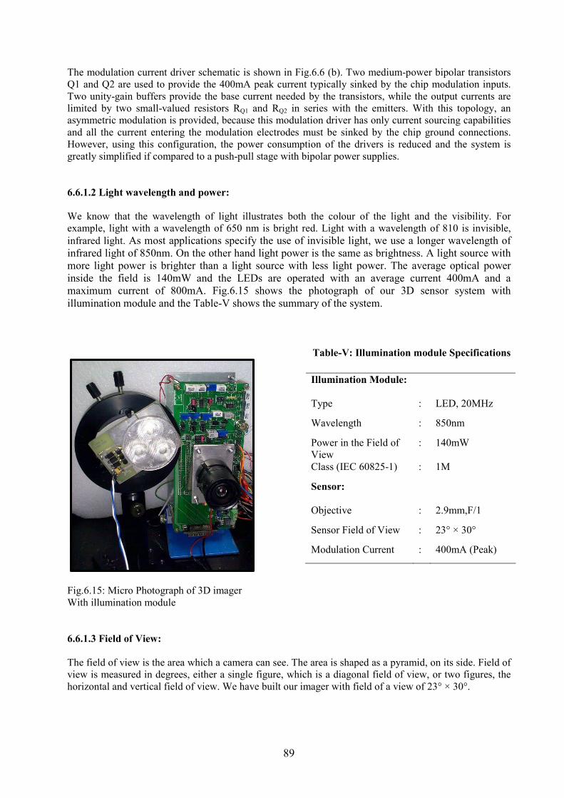
89
The modulation current driver schematic is shown in Fig.6.6 (b). Two medium-power bipolar transistors
Q1 and Q2 are used to provide the 400mA peak current typically sinked by the chip modulation inputs.
Two unity-gain buffers provide the base current needed by the transistors, while the output currents are
limited by two small-valued resistors RQ1 and RQ2 in series with the emitters. With this topology, an
asymmetric modulation is provided, because this modulation driver has only current sourcing capabilities
and all the current entering the modulation electrodes must be sinked by the chip ground connections.
However, using this configuration, the power consumption of the drivers is reduced and the system is
greatly simplified if compared to a push-pull stage with bipolar power supplies.
6.6.1.2 Light wavelength and power:
We know that the wavelength of light illustrates both the colour of the light and the visibility. For
example, light with a wavelength of 650 nm is bright red. Light with a wavelength of 810 is invisible,
infrared light. As most applications specify the use of invisible light, we use a longer wavelength of
infrared light of 850nm. On the other hand light power is the same as brightness. A light source with
more light power is brighter than a light source with less light power. The average optical power
inside the field is 140mW and the LEDs are operated with an average current 400mA and a
maximum current of 800mA. Fig.6.15 shows the photograph of our 3D sensor system with
illumination module and the Table-V shows the summary of the system.
Table-V: Illumination module Specifications
Fig.6.15: Micro Photograph of 3D imager
With illumination module
6.6.1.3 Field of View:
The field of view is the area which a camera can see. The area is shaped as a pyramid, on its side. Field of
view is measured in degrees, either a single figure, which is a diagonal field of view, or two figures, the
horizontal and vertical field of view. We have built our imager with field of a view of 23° × 30°.
Illumination Module:
Type : LED, 20MHz
Wavelength : 850nm
Power in the Field of
View
: 140mW
Class (IEC 60825-1) : 1M
Sensor:
Objective : 2.9mm,F/1
Sensor Field of View : 23° × 30°
Modulation Current : 400mA (Peak)

90
6.6.1.4 Diffuser:
A diffuser is an optical component which converts light from one shape/pattern to another shape/pattern.
A diffuser is typically made from glass or plastic. We use diffusers to take a beam of light from an LED
and change that beam into an even pattern of light across a specific field of view. A relatively simple
solution is to put a diffuser on top of the LED light source that is designed for the particular field of view.
The diffuser provides an even light distribution over a predefined shape.
6.6.2 Correlation function measurement:
A first characterization of the sensor is conducted using a setup slightly different from the one shown in
Fig.6.13. The chip is uniformly illuminated through a diffuser, while a red modulated laser (λ=650nm) is
used as a light source. A commercial high frequency function generator is employed to modulate both the
laser and the modulation electrode current. A 20MHz modulation frequency and both sine-wave and
square-wave signals are used in the measurements.
Fig.6.16 (a) shows the correlation function measured as the output signal difference Out2 – Out1 as a
function of applied phase shift in the case of sine-wave modulation. In the measurement, the outputs are
averaged over all the pixels of the array, thus reducing the temporal noise contribution to a negligible
value with respect to the non-linearity. As can be observed, a good sine-wave fitting obtained, indicating
a potentially low-distortion measurement.
In the final range-imaging system the correlation function is measured only for 4 different phase shifts
and the phase shift is calculated using equation (5.13). To evaluate the linearity error obtained from this
technique, the phase measurement has been repeated several times applying an increasing delay between
modulation signal and optical signal. The measured delay averaged over the whole array is reported in Fig.
6.16(b) as a function of the applied delay. The maximum linearity error is 0.60%, corresponding to an
error of 4.5cm in the distance measurement.
A sine wave correlation function is also observed applying square-wave modulation signal. Although
theoretically the correlation signal between two square waves should be a triangular wave, the high order
harmonics are filtered by the low-pass characteristics of the demodulator and in both cases a sine-wave
correlation function is measured. Therefore, equation (5.13) was applied also in the case of square-wave
modulation.
Fig.6.16: (a) Measured differential output as a function of applied phase. (b) Measured time delay as a
function of applied time delay.

91
6.7 Distance measurement setup:
The 3D ranging performance of the system is finally evaluated using the setup shown in Fig. 6.17 using a
20 MHz-modulation frequency and square wave modulation signals. As described before, the sensor had
a field of view of 23° × 30° and the average optical power inside this field was 140mW. The image sensor
mounts a 2.9mm objective, having an f number of 1. The maximum modulation current was 400mA,
while the LEDs were operated with an average current of 400mA and a maximum current of 800mA. In
this way we could achieve an 80% optical signal modulation depth. A 30ms integration time per frame
was set, giving a range image frame rate of 7fps. A white diffusing target was placed at increasing
distances in front of the sensor and a set of range images was acquired. A white board is placed at
different distances from the sensor and is illuminated by the illumination module described before.
Fig.6.17: TOF based measurement Set-up
6.8 3D range measurement and sample pictures:
The measurement is done in the presence of ambient light. Fig.6.18 shows the actual distance of a white
reflecting board from the sensor and the measured distance by the sensor. It shows the linear distance
range from 1.2m to 3.7m. The maximum linearity error between the original and measured distance is
3.3%, while the distance non-uniformity among the pixels is lower than 2cm. Precision is the closeness of
agreement between independent tests results obtained under specified conditions. The measure of
precision is usually expressed in terms of imprecision and computed as a standard deviation of the test
results. Less precision is reflected by a larger standard deviation. Precision is usually distinguished from
accuracy, the variability of a measurement process around the true value. It is, in turn, can be decomposed
further into short term variation or repeatability, and long term variation, or reproducibility. Beside the
distance function also the relation between distance and standard deviation is of major importance
because the accuracy of the measurements depends heavily on the amount of light received by the camera.
In Fig.6.18 (b), apart from the first point in the series, where the sensor is close to saturation, the
measurement precision increases with the square root of distance.
Driving
circuit
&
IPU
Pattern Generator
LED Array
Sensor 120 × 160
Array
Incident Signal
Reflected Signal
White Target

92
Distance [m]
(a)
(b)
Fig.6.18: (a) Measured distance of a white diffusing target. (b) Measured distance precision
A sample 3D image acquired with an overall exposure time of 400ms is shown in Fig.6.19. The distance
is coded in grayscale levels, while the image histogram can be seen on the right. Three peaks, two
corresponding to the two hands and forearms and one to the back plane can be distinguished. The counts
that are observed between the two hands are due to shadowing effect, due to the non-coaxial placement of
the illuminator with respect to the camera sensor. This shadowing effect can be eliminated by using two
illuminators or by placing the LEDs around the focusing optics of the sensor.
Fig.6.19: Left: Distance map of two hands in front of a white diffusing target. Distance in meters is coded
in gray levels. Right: Histogram of distance distribution.
Distance (m)

93
Fig.6.20: Sample of 3D image.
To demonstrate the 3D ranging capabilities of the TOF sensor Fig.6.20 also illustrates the measurement of
a 3D scene. The distance information is coded in the z-direction and gray level intensity.
Fig.6.21: Sample frames from a video acquired in 7 3D frames per second.
Three sample frames from a video taken at 7fps are shown in Fig.6.21. The video, representing a person
in front of a white panel, has been spatially filtered using a 3×3 median filter. In the video a threshold on
the signal amplitude has been applied to filter out the noisy pixels due to shadowing effects and to
insufficient power of the back-scattered light.
Table-VI summarizes the specifications of the sensor chip. A 120×160 CMOS Time-Of-Flight range
camera based on Current Assisted Photonic Demodulators with 10×10 µm2 pixel area and 24% fill factor.
The chip, having a power consumption of 200mW, mainly due to the contribution of modulation current,
demonstrate the feasibility of CAPD-based pixels in a medium resolution sensor fabricated on epitaxial
wafers with standard resistivity. A range camera system is realized with the proposed sensor and a 3-LED
illumination module delivering 140mW optical power on the target. The system, having 23°× 30° field of
view, is capable of acquiring a stream of 7 3D frames/s with a maximum non-linearity of 3.3% in the
range 1.2m-3.7m and a precision better than 10 cm at 2m and 20 cm at 3m.
Distance (m)
2.4
2.3
2.2
2.1
2.0
1.9
1.8
1.7
1.6

94
Table-VI: Sensor Summary
Technology : 0.18µm 1Poly,4Metal CMOS
technology
Power Supply : 1.8V & 3.3V transistors
Sensor area : 2.5 × 2.5 mm2
Number of Pixels 120 × 160
Pixel size/Fill Factor : 10 × 10 µm2/ 24%
Modulation Frequency : ≥ 20MHz
Maximum non-linearity : 3.3% in the range 1.2m-3.7m
Precision : 10 cm at 2m and 20 cm at 3m
Power consumption : 200mW

95
Chapter 07
Conclusion and Future work
In this century, imaging market continues to expand with new emerging applications. CMOS technology
permits the integration of the circuits in the same die as the sensor, thus reducing the cost, power
consumption, size and weight of the final camera. In this PhD dissertation, we have presented the
development and characterization of a Current Assisted Photo mixing Demodulator (CAPD) and the
realization of a 3D time-of-flight range camera in 0.18µm CMOS technology.
The first part of the thesis provides some theoretical background, including an overview of photodetection
in semiconductors, the definition of some conventional parameters of photodetectors, and a comparison
between the classical CCD image sensors and CMOS imagers, which have achieved more importance in
recent years. Nowadays, CMOS APS explosion is due to the fact that these devices can be fabricated with
standard technologies that are gradually being miniaturized and improved, driven by the computer
industry. This makes possible to employ more and more functionality within the sensor device and to
realize more pixels in the same chip area. We have also given an overview of the different range
measurement techniques, their corresponding advantages and drawbacks and the typical applications in
distinct industrial areas. Among other optical techniques, the time-of-flight (TOF) technique has been
preferred for this project because of the better performance in terms of acquisition speed and wide range
of detectable distance as well as lower cost.
The core of the thesis has covered the most relevant issues related to the design and characterization of
CAPD devices fabricated in a custom technology on high resistivity silicon substrates. Structures with
different shapes and sizes have been considered and compared in terms of electrical and electro-optical
performance. In particular, we have investigated the DC and dynamic demodulation performance of a
linear-shaped CAPD device. For 10 MHz modulation frequency we measured a dynamic demodulation
contrast of 25% for a 650nm modulated laser light source. We also measured the DC demodulation
efficiency of the same device and the obtained result is about 100%. In the multiple strip CAPD devices,
the effective potential gradient is applied to the multiple modulating electrodes, a fact that speeds up the
signal charges transferring to the detection regions. The measured dynamic demodulation contrast is more
than 20% at 30 MHz modulation frequency. The maximum phase linearity error between the applied
phase and the measured phase is 3.9%. However, as multiple strip conductors are used in this device, the
fill factor is very low with respect to the device size. Finally, a round shaped CAPD device has been
characterized. The substrate contact of this device is not uniform and the applied drift field does not
spread equally over the sensitive area, thus lowering the speed of the device, despite the device DC
demodulation contrast is nearly 90%, which indicates good demodulation efficiency of this device at low
frequency. Although not truly representative of the final CMOS CAPD devices, due to the largely
different fabrication process, these test structures have been deemed appropriate to investigate the main
design concepts and to provide a first test bench for comparison of experimental characteristics and
simulation prediction, with reference to a technology for which all the relevant information is available.
Later, we have extensively investigated the simulation and experimental performance of a CMOS based
CAPD device. The demodulator structure has been featured in a small pixel area of 10 × 10 µm2 and
fabricated in the standard 0.18µm CMOS technology. Static characterization of the CAPD structures has
been carried out using a 650nm laser to illuminate the device. Therefore, the device DC charge transfer
efficiency was measured. It was found to be larger than 80% with a modulation voltage of 0.5V. The
corresponding power consumption was measured and is 10 µW. At 45MHz modulation frequency, we
measured the dynamic demodulation contrast of 40% with a modulation voltage of 800mV. Our proposed
device can be competitive with existing photo-gate-based mixer technologies because it offers a larger
demodulation contrast and a bandwidth comparable with the best devices presented so far. Phase
measurement of the device showed an excellent linearity for sinusoidal and square waves where the
maximum linearity error was found to be 0.11% for the former and 0.16% for the latter. In the case of
square-wave modulation, a small phase linearity error indicates a small influence of the high frequency
harmonic components on the phase determination. We obtained a peak quantum efficiency of 35% at

96
500nm wavelength and more than 20% in between 500nm and 600nm. The percentage of maximum
deviation between measured shot noise and theoretical noise is 5.19%, which indicates that the device
shot noise is low. The electro-optical characterization of this device has shown very encouraging results.
The limited power consumption and the high demodulation contrast of the CAPD are suited for
implementing it as a camera pixel for time resolved imaging applications such as time-of-flight range
imaging.
Finally, this PhD thesis has focused on a 3D imaging system, based on CMOS CAPD device, and
consisting of a 120×160 pixel array. The illustrated pixel layout is 10×10 µm2
with a fill factor of 24%.
For the TOF measurement, the illumination module is composed of 3 high power LEDs in series with a
wavelength of 850nm. We have inspected the correlation function of our imaging system. A 20MHz
modulation frequency and both the sine-wave and square-wave signals have been used in this
measurement. We have found the maximum linearity error of the pixel array to be 0.60%, corresponding
to an error of 4.5cm in the distance measurement. The 3D ranging performance of the system was
measured using a square wave modulation signal with 20 MHz frequency. The sensor had a field of view
of 23°× 30° and the average optical power inside this field was 140mW, while the LEDs were operated
with an average current of 400mA and a maximum current of 800mA. The overall power consumption of
the pixel array was found to be 200mW with a modulation current of about 400mA. The optical signal
modulation depth was measured as 80%. A 30 ms integration time per frame was set, giving a range
image frame rate of 7fps. The distance range between 1.2 m and 3.7m was measured and showed that the
sensor was capable of measuring distance maps with quite a good accuracy. The maximum non-linearity
was 3.3% in the range 1.2m-3.7m and a precision better than 10 cm at 2m and 20 cm at 3m was achieved.
Apart from the first point (1.2m) in the range measurement series, where the sensor is close to saturation,
the measurement precision increases with the square root of distance, as can be predicted theoretically for
a diffusing target.
This dissertation has a broad aspect of TOF based 3D CMOS imager including device architecture, pixel
structures, processing parameters and TOF related physical phenomena of the image sensor. However, the
final operation of the system was limited in terms of modulation frequency and distance measurement. In
our case the maximum modulation frequency reached 20MHz. The reason for not being able to increase
the modulation frequency and distance further was the limitation of the available control and driving
electronics and also the intrinsic limitation of the light source we used. To overcome these limitations, it
is necessary to use a higher power illumination module and to optimize the driving electronics to drive the
modulation frequency larger than 20MHz. Recently we have developed a high power CMOS based
illumination module to be used as a light source. For further investigation, it can be possible to measure
longer range distance at high modulation frequencies. For the miniaturization of the pixels and in order to
achieve better image resolution, the evaluation of the integrated imagers in 130nm or 90nm CMOS
technology is a promising research direction. Moreover, a compact 3D range camera with excellent
performance of CAPD sensor can be developed, which will realize additional functionalities such as
illumination system, distance calculation system and image processing tasks. The information of our
present results from CAPD device and 3D image sensor functionalities can be used in advanced tasks,
which lead us to predict broad applications in surveillance, inspection, safety, production and autonomous
navigation systems.

97
Bibliography
[01]
S. Sze, “Physics of semiconductor devices”, John Wiley & Sons, New York, U.S.A., (1981).
[02]
J.D. Eskim, H.H. Barret and H.B. Berber, “Signal induced in semiconductor gamma-rays
imaging detectors.” Journal of applied physics vol85, no2 pp 647-659, January1999.
[03]
Orly Yadid-Pecht, Ralph Etienne-Cummings, ISBN 1-4020-7962-1 “CMOS Imagers: From
Photo-transduction to Image Processing” Kluwer Academic Publishers, (2004)
[04]
Edward S. Yang “Microelectronic Devices”, International Edition, McGraw-Hill Book
Company.
[05]
A. Moini, “Vision chips or seeing silicon,” Center for High Performance Integrated
technologies and Systems, University of Adelaide, Adelaide, Australia, Technical Report,
March 1997.
[06]
S. Mendis, S. Kemeny, R. Gee, B. Pain, Q. Kim, and E. Fossum, “CMOS active pixel image
sensors for highly integrated imaging system,” IEEE J. Solid-State Circuits, vol. 32, p. 187,
Feb. 1997.
[07]
M. Schanz, “Linear CMOS Image Sensors with Integrated Signal Processing,” PhD
dissertation, University of Duisburg, Duisburg, Germany, June 1998.
[08]
P. Aubert et al., ''Monolithic Position Encoder with On Chip Photodiodes,'' IEEE Journal of
Solid State Circuits, Vol. 23, No. 2, pp. 465-473, April 1988.
[09]
A. Mäkynen et al., ''CMOS Photodetectors for Industrial Position Sensing,'' IEEE Transactions
on Instrumentation and Measurement, Vol. 43, No. 3, pp. 489-492,Jun. 1994.
[10]
I. Brouk, and Y. Nemirovsky, “Dimensional effects in CMOS photodiodes,” Solid-State
Electronics Vol. 46, No. 1, pp. 19-28 Jan. 2002.
[11]
O. Y. Pecht, and R. Ginosar, ''A Random Access Photodiode Array for Intelligent Image
Capture, '' IEEE Transactions on Electron Devices, Vol. 38, No. 8, pp. 1772-1779, Aug. 1991.
[12]
B. Dierickx, “CMOS image sensors: Concepts and Limits,” SPIE—The International Society
for Optical Engineering, Photonics West, San Jose, USA, Short-course Notes, Jan 2000.
[13]
H. Tian, B. Fowler, and A. El Gamal, “Analysis of Temporal Noise in CMOS Photodiode
Active Pixel Sensor,” IEEE J. Solid State Circuits, vol. 36, no. 1, pp. 92-101, January 2001.
[14]
P. Seitz, “Image sensing with maximum sensitivity using industrial CMOS technology”,
Proceedings of the SPIE, Vol. 3099, Munich, (1997).
[15] T. Spirig, “Smart CCD/CMOS Based Image Sensors with Programmable, Real-time, Temporal
and Spatial Convolution Capabilities for Applications in Machine Vision and Optical
Metrology”, Ph.D. Dissertation ETH Zurich, Switzerland, No. 11993, (1997).
[16]
S. M. Sze, Physics of semiconductor devices, second edition, New York: John Wiley & Sons,
1985.
[17]
Elisenda Roca, Servando Espejo, Rafael Domínguez-Castro and Angel Rodríguez-Vázquez,
“Light-Sensitive Devices in CMOS”, internet source , gratefully acknowledged.
www.imse.cnm.es/Proyectos/dictam/2ND_PHASE/Dissemination/FULL_TEXT/CMOS/

98
[18]
W.S. Boyle, G. Smith, Charge-coupled semiconductor devices, Bell System Techniques of
Journal 49 (1970) 587–593.
[19]
T. Yamada et.al., “ A ½ -in 1.3 M-Pixel Progressive-Scan IT-CCD for Digital Still Camera
Applications”, IEEE Transections on Electron Devices, Volume 48, No. 02 pp. 222-230, 2001.
[20]
J.D.E. Beynon and D.R. Lamb, “Charge-coupled devices and their applications,” McGraw Hill
Book Company (UK) Limited, 1980.
[21] M.J.Howes and D.V. Morgan, “Charge-coupled Device and Systems,” John Wiley & sons
Limited, 1979.
[22]
Dyson, P.E, Rossello, R.; CMOS Challenges CCD in Vivitar’s 3000; PMA ‘97: new
technology and applications for digital photography; The Seybold Report on Publishing
Systems; April 1997, Vol.26, Num. 13.
[23]
Albert J.P Theuwissen, “CCD or CMOS Image sensors for consumer’s digital photography” in
2001 International Symposium on VLSI Technology System and applications.
[24] E.Fossum “Active Pixel Sensor: are CCD’s Dinosaurs?” Proceedings SPIE charged coupled
devices and solid state optical sensors vol.1900, pp 2-14 San Jose, CA, USA 1993.
[25]
Hon-Sum Wong, “Technology and Device Scaling Considerations for CMOS Imagers”, IEEE
Transactions of Electron Devices, vol43, no.12, pp 2131-2142, 1996.
[26]
VISION home page web site, URL: http://www.vvl.co.uk/.
[27]
E. Fossum, “CMOS Image Sensors: Electronic Camera-on-a-Chip,” IEEE Transaction on
Electron Devices, Vol. 44, No. 10, pp. 1689-1698, Oct. 1997.
[28]
S. K. Mendis, S. E. Kemeny, R. C. Gee, B. Pain, Q. Kim, and E. R. Fossum, 'Progress in
CMOS Active Pixel Image Sensors,” Proc. SPIE, Vol. 2172, pp. 19- 29, 1994.
[29]
S. G. Wuu, H. C. Chien, D. N. Yaung, C. H. Tseng, C. S. Wang, C. K. Chang and Y. K. Hsiao,
“A High Performance Active Pixel Sensor with 0.18-um CMOS Color Imager Technology,”
IEEE IEDM Technical Digest, pp.555-58, December 2001.
[30]
R. Hornsey, “Design and fabrication of integrated image sensors,” Institute for Computer
Research, University of Waterloo, Waterloo, Canada, Short-course =otes, May 1998.
[31] Hovanessian S.A., “Introduction to sensor systems”, Artech house, p.2.
[32] B. Jaehne, H. Haussecker and P. Geissler, Eds., “Handbook of Computer Vision and
Applications. Vol. 1: Sensors and Imaging”, Academic Press, San Diego,1999.
[33] S. Ando and A. Kimachi, "Time-Domain Correlation Image Sensor: First CMOS Realization
of Demodulator Pixels Array", IEEE CCD/AIS Workshop, pp.33-36, Karuizawa, Japan, 1999.
[34] J. Ohta, K. Yamamoto, T. Hirai, K. Kagawa and M. Nunoshita, "An Image Sensor with an In-
Pixel Demodulation Function for Detecting the Intensity of a Modulated Light Signal", IEEE
Trans. ED, vol.50, no.1, pp166-172, January 2003.
[35] Jarvis R.A. “A perspective on range finding techniques for computer vision”, IEEE
transections on pattern analysis and machine Intelligence,Vol PAMI-5(2), pp 122-139, March
1983.

99
[36] P. Besl, “Advances in machine vision” Springer-Verleg, chapter 1-Active optical range
imaging sensors, pp 1-63, 1989.
[37] I.Moring, T.Heikkinem, R.Myllyla and A.Kilpela, “Acquisition of three dimensional image
data by a scanning laser range finder” Opt.Eng. Vol28 pp 897-905,1989.
[38] S.T. Barnard and W.B. Thompson, “Disparity analysis of Images”, IEEE Trans, Pattern Anal.
Mach. Intel, 2(4), 333-340, 1980.
[39] K.L. Boyer and A.C.Kak, “Color-Encoded structured light for rapid active ranging” IEEE
Trans. Pattern Anal.Mach.Intell, 9(1), 14-28, 1987.
[40] E. Zimmermann, Y. Salvade, and R. Dandliker ”Stabilized three-wavelength source
calibratedby electronic means for high-accuracy absolute distance measurements” Optical
letters, vol.21.pp 531-533,1996.
[41] Bahaa E. A. Saleh, Malvin Carl Teich, “Fundamentals of Photonics”, ISBN 0-471-83965-5,
John Wiley & Sons, (1991).
[42] P.Hariharan, “Basics of Interferometry”, ISBN 978-0-12-373589-8, Academic Press, (2007)
[43] R. Schwarte, “Principles of 3D Imaging Techniques”, in Handbook of Computer Vision and
Applications, B. Jähne, H. Haussecker and P.Geissler (Eds.), Academic Press, (1999).
[44] S. Bourquin, “Low-coherence interferometry based on customized detector arrays”, Ph.D.
Dissertation EPFL-Lausanne, Switzerland, No. 2171, (2000).
[45] Price, M.; Kenney, J.; Eastman, RD. Hong, T. “Training and optimization of operating
parameters for flash LADAR cameras”. In Proceedings of IEEE International Conference on
Robotics and Automation, San Antonio, TX, USA, 2007; pp. 3408-3413.
[46] Büttgen, B.; Oggier, T.; Lehmann, M. “CCD/CMOS Lock-in pixel for range imaging:
challenges,limitations and state-of-the-art”. In Proceedings of 1st Range Imaging Research
Day, Zurich,Switzerland, 2005; pp. 21-32.
[47] http://www.riegl.co.at, (1998).
[48] Z. Xu, Investigation of 3D-Imaging Systems Based on Modulated Light and Optical RF-
Interferometry (ORFI) – ZESS – Forscchungsberichte, Shaker Verlag Aachen, ISBN 3-8265-
6736-6, 1999.
[49] Schwarte, R., Heinol, H., Xu, Z., Li, J., and Buxbaum, B.: “Pseudo-Noise (PN)-laser radar
without scanner for xtremely fast 3D-imaging and navigation”, Microwave and Optronics
Conference (MIOP),Stuttgart , pp. 168-176,1997.
[50] R.Jeremias, W.Brockherde, G.Doemens, B.Hosticka, L.List and P.Mengel, “ A CMOS
Photosensor Array for 3D Imaging Using Pulsed Laser” , Proceedings of ISSCC’01,paper
16.5,Sanfransisco (CA) USA,Feb, 2001.
[51] O .M. Schrey, 0. Elkhalili, P. Mengel', M. Petermann, W. Brockherde, B.J. Hosticka “A 4x64
Pixel CMOS Image Sensor for 3D Measurement Applications” , IEEE Journal of Solid State
Circuits, vol.39, no.7, pp.1208-1212,July, 2004.
[52] David Stoppa, Luigi Viarani, Andrea Simoni, Lorenzo Gonzo, Mattia Malfatti, Gianmaria
Pedretti, “A 16x16-Pixel Range-Finding CMOS Image Sensor” Proceedings of IEEE European
Solid-State Circuits Conference- ESSCIRC’04, pp. 419-422, September, 2004.

100
[53] D.Stoppa, L.Viarani ,A.Simoni, L.Gonzo,M.Malfatti, G.Pedretti “ A 50×30 pixel CMOS
sensor for TOF-based real time 3D imaging” proceedings of the IEEE workshop on CCD and
advanced Image sensors, pp.230-233,2005.
[54] R.lange and P. Seitz, “Solid- State Time-of-Flight Camera”, IEEE Journal of Quantum
Electronics, Vol.37,no.3, pp. 390-397, March 2001.
[55] R. Miyagawa and T. Kanade, “CCD-Based Range-Finding Sensor”, IEEE Trans. ED, vol.44,
no.10, pp.1648-1652, 1997.
[56] T. Oggier, M. Lehmann, R.Kaufmann, M. Schweizer, M. Richter, P. Metzler, G.Lang, F.
Lustenberger, N. Blanc,“An all solid-state optical range camera for 3D real-time imaging with
sub-centimeter depth-resolution(SwissRanger), Proceeding of SPIE Vol.5249, pp. 634-645,
2003.
[57] Mesa Imaging website: http: www.swissranger.ch
[58] Cannesta Inc. website: http: www.canesta.com
[59] T.Ushinaga, I.A. Halim, T.Sawada, S.Kawahito,M. Homma, Y.Maeda , “A QVGA- size
CMOS Time-of-Flight range image sensor with background light charge draining structure”
Proceedings of SPIE,vol.6056,Jan,2006.
[60] B. Buttgen, F.Lustenberger, P.Seitz,”Demodulation pixel based on static drift fields”, IEEE
Trans. on Electron Devices, vol.53, no.11 pp. 2741-2747, Nov, 2006.
[61] C. Niclass, A.Rochas, P.-A. Besse, E.Charbon, “Toward a 3D camera based on single photon
avalanche diodes”, IEEE journal of selected topics in Quantum Electronics, Vol.10, no.4, pp-
796-802, July/August 2004.
[62] C. Niclass, E.Charbon, “A single photon detector array with 64×64 resolution and millimetric
depth accuracy for 3D imaging” ISSCC Digest of Technical Papers,pp.364-365, Feb.2005.
[63] D.Stoppa,L.Puncheri ,M.Scandiuzzo,L.Gonzo,G.-F.Dalla Betta, A. Simoni, “A CMOS 3D
imagers based on single photon avalanche diode”. IEEE transaction on circuit and systems I,
pp.4-12 Jan, 2007.
[64] Rudolf Schwarte, “Dynamic 3D Vision”, Proceedings of International Symposium on Electron
Devices for Microwave and Optpelectronic Applications, pp.241-248, 15-16 November, 2001.
[65] B. Buxmbaum, R. Schwarte, T.Ringbeck, M. Grothof, X. Luan, “MSM-PMD as correlation
receiver in a new 3D-ranging system”, Proc.SPIE Vol.4546,pp.145-153,2002.
[66] Shaoji Kawahito, Izhal Abdul Halin,Takeo Ushinaga,Tomonari Sawada, Mitsuru Homma and
Yasunari Maeda, “A CMOS TIme-of-Flight Range Image Sensor with Gates-on-oxide
Structure”, IEEE Sesnors Journal, Vol.7 No.12 pp.1578-1585,December,2007.
[67] D. Van Nieuwenhove, W.VanDer Tempel and M.Kuijik, “Novel Standard Detector using
majority for guiding Photo-Generated Electrons towards Detecting Junctions”, Proceedings
Symposium IEEE/LEOS Benelux Chapter, pp.229-232, 2005.
[68] D.VanNieuwenhove, W.VanDerTempel, R.Grootjans, J.Steins and M.Kuijik, “Photonic
demodulator with sensitivity control”, Sensors journal, IEEE, vol.7, no.3 pp.317-318, March
2007.

101
[69] G. De Geronimo, G.Deptuch, A. Dragone, V. Radeka, P, Rehak, A. Castoldi, A. Fazzi, E.
Gatti, C. Guazzoni, M. Rijssenbeek, W. Dulinski, S. Besson, M. Deveaux, M.Winter, “A novel
position and time sensing active pixel sensor with field-assisted electron collection for charge
particle tracking and electron collection for charge particle tracking and electron microscopy”,
Nuclear Instruments and methods in Physics Research A, vol. 568, pp. 167-175, 2006.
[70] L. Pancheri, D. Stoppa, N. Massari, M. Malfatti, C. Piemonte, G.-F. Dalla Betta, “Current
Assisted Photonic Mixing Devices Fabricated on High Resistivity Silicon” IEEE SENSORS
Conference, Lecce, Italy, pp.981-983, 2008.
[71] DESSIS 8.0 User Manual, Synopsys Inc.
[72] P. Gulden, M. Vossiek, P. Heide, R. Schwarte, “Application of the photoelectronic mixing
device to optical measurement of presence, distance and velocity”, in Proc. 2000 European
Microwave Conference, pp. 1-4.
[73] R. Schwarte, “Dynamic 3D-vision”, in Proc. 2001 International Symposium On Electron
Devices for Microwave and Optoelectronic Applications (EDMO), pp. 241-248.
[74] D. K. Schroder, Semiconductor material and device characterization, 2nd ed. New York:
Wiley, 1998.
[75] C. F. Robinson, "Microprobe analysis," 1973.
[76] R. Lange, P. Seitz, A. Biber and R. Schwarte. “Time-of Flight Range Imaging with a Custom
Solid State Image Sensor”, EOS/SPIE International Symposium. Munich, Germany, June 14-18
1999, pp. 180-191.
[77] Cadence Verilog Language and Simulation, User Manual, Version 3.4, February, 2002,
Cadence Design Systems, Inc.

102
Appendix-A Related terminology of the image sensor used in this thesis
Sources:
http://www.aapn.mcgill.ca/eng/resources/PhotonicsGlossary.pdf &
http://www.datx.com/solution_center_mach_vision/Glossary-of-Machine-vision.pdf (gratefully
acknowledged).
Accuracy- The extent to which a machine vision system can correctly measure or obtain a true value of a
feature. The closeness of the average value of the measurements to the actual dimension.
Ambient Light- Light which is present in the environment of the imaging front end of a vision system
and generated from outside sources. This light, unless used for actual scene illumination, will be treated
as background noise by the vision system.
Bandgap - In a semiconductor material, the minimum energy necessary for an electron to transfer from
the valence band into the conduction band, where it moves more freely.
Bandwidth- The range of frequencies over which a particular device is designed to function within
specified limits.
Beam splitter- An optical device for dividing a beam into two or more separate beams. A simple beam
splitter may be a very thin sheet of glass inserted in the beam at an angle to divert a portion of the beam in
a different direction.
CCD (Charge Coupled Device)- A photo-sensitive image sensor implemented with large scale
integration technology.
Collimated Lighting- Radiation from a given point with every light ray considered parallel. In actuality,
even light from a very distant point source (i.e. a star) diverges somewhat.
Crosstalk- The measurable leakage of optical energy from one optical channel to another. Also known as
optical coupling.
Dark current- The current that flows in a photodetector when there is no optical radiation incident on the
detector and operating voltages are applied.
Depth-of-Field- The range of an imaging system in which objects are in focus.
Detector- A device designed to convert the energy of incident radiation into another form for the
determination of the presence of the radiation. The device may function by electrical, photographic or
visual means and a device that provides an electric output that is a useful measure of the radiation that is
incident on the device.
Dynamic Range- The measure of the range light sensitivity a sensor is able to reproduce, from the
darkest to the brightest portion of a scene. Usually expressed in decibels.
Field-of-View- The 2D area which can be seen through the optical imaging system.
Fill factor (FF)- Ratio between the light sensitive pixel area and the total pixel area.
Focus- The point at which rays of light converge for any given point on the object in the image. Also
called the focal point.

103
Focal Length- The distance from a lens principal point to the corresponding focal point on the object.
Gain- Also known as amplification. The increase in a signal that is transmitted from one point to another
through an amplifier. A material that exhibits gain rather than absorption, at certain frequencies for a
signal passing through it, is known as an active medium. In a photo detector, the ratio of electron-hole
pairs generated per incident photon.
Image- Projection of an object or scene onto a plane (i.e. screen or image sensor).
Image Capture- The process of acquiring an image of a part or scene, from sensor irradiation to
acquisition of a digital image.
Image Processing- Digital manipulation of an image to aid feature visibility, make measurements or alter
image contents.
Incident Light- Light which falls directly onto an object.
Laser illumination- Lighting an object with a laser source for frequency selection, pulse width (strobe)
control or for accurate positioning.
Linearity- For optical measurement instruments, generally used to refer to the deviation of a measured
change of a performance parameter (e.g., power, wavelength) from the expected change.
MOS Array- Metal Oxide Semiconductor camera array sensor with random addressing capability, rows
and columns of photodiodes and charge sent directly from the photodiode to the camera output.
Object- The 3D item to be imaged, gauged or inspected.
Photodiode- A single photoelectric sensor element, either used stand-alone or a pixel site, part of a larger
sensor array.
Photometry- Measurement of light which is visible to the human eye (photopic response).
Photon- A quantum of electromagnetic energy of a single mode; i.e., a single wavelength, direction and
polarization. As a unit of energy, each photon equals hν, h being Planck's constant and ν, the frequency of
the propagating electromagnetic wave. The momentum of the photon in the direction of propagation is
hν/c, c being the velocity of light.
Pixel- An acronym for "picture element." The smallest distinguishable and resolvable area in an image.
The discrete location of an individual photo-sensor in a solid state camera.
Precision- The degree of spread or deviation between each measurement of the same part or Feature.
Quantum efficiency (QE)- Ratio between the number of generated electrons and the number of
impinging photons.
Range Measurement- Determination of the distance from a sensor to the object.
Resolution - Describes the degree to which closely spaced objects in an image can be distinguished from
one another.
Responsivity- Output per unit input of a radiation detector.
Sensitivity- In a radiation detector, the ratio of the output to the input signal.

104
Solid-State Camera- A camera which uses a solid state integrated circuit chip to convert incident light or
other radiation into an analog electrical signal.
Spectral Analysis- Evaluation of the wavelength composition of object irradiance.
Spectral Response- Ratio of current and incoming light power for a given wavelength. Units: A/W.
Structured Light- Points, lines, circles, sheets and other projected configurations used to directly
determine shape and/or range information by observing their deformation as it intersects the object in a
known geometric configuration.
Visible Light- The region of the electromagnetic spectrum in which the human retina is sensitive, ranging
from about 400 to 750 nm in wavelength.
Wavelength- The distance covered by one cycle of a sinusoidal varying wave as it travels at or near the
speed of light. It is inversely proportional to frequency.

105
Appendix-B
B.1 Pseudo Differential Amplifier: The beginning of the integrated circuit led to the development of the
circuit configurations that used the strengths of monolithic technology advantage. The differential
amplifier circuit configuration in particular assumed considerable prominence in this respect. In this
thesis, for the electro-optical characterization of the test device we used a pseudo differential amplifier. In
this experiment a dual output signal generator is used to generate two sine wave signals. One of the two
signals is used to modulate a laser emitter and the other is connected to the input of a pseudo differential
amplifier. Two output signals of the differential amplifier with 1800 phase shift are connected to the
modulating of electrodes of our device [see in Chapter 05 Fig.5.6 (b)]. In the following section we will
describe a pseudo differential amplifier circuit and its operation.
(a)
(b)
Fig.A.1: (a) Differential Amplifier circuit (b) Emitter follower Circuit

106
The differential pair circuits are one of the most widely used circuit building blocks. A differential
amplifier provides two input and two output terminals, the input to be amplified is usually connected
between one input and circuits ground. The other input is used for feedback and other purposes. The two
outputs are taken from the collector terminals of the transistors Q1 and Q2. The basic differential
amplifier circuit using BJTs is shown in Fig. B.1. The circuit consists of two common-emitter amplifiers
with emitter resistor. Ideally both transistors Q1 and Q2 should have equal parameters; in this case the
collector current in the transistor Q1 and Q2 can be described
IC1=IC2 and IE1=IE2=IC3/2
A current source is used to DC bias Q1 and Q2. This current source is designed to overcome variations in
the transistors parameters and for temperature compensation. A simple current source consists of an npn
BJT and a biasing scheme similar to the common-emitter amplifier. The resistance R6 is chosen for the
specified biasing current and insures that the transistor Q3 stays in the active mode of operation.
(a)
(b)
Fig.B.2: Simulation results of Differential Amplifier (a) Input (b) Output signal of the Emitter follower
In the out1 and out2 of the differential amplifier a common collector amplifier is used as a buffer because
of its high input resistance. The collector is connected directly to the dc power supply which is an ac
ground. The out1 of differential amplifier is connected to the base and the output is taken from the emitter.
in
out2
out1

107
The output signal is in phase with the input signal looking from the input coupling capacitor to the base,
the equivalent ac circuit has the bias resistors and the resistors in the emitter circuit as shown in Fig.B.1 (b)
The ac circuit can be simplified by combining the emitter and load resistors into one equivalent resistor
(RE || RL). As in all linear amplifiers, the voltage gain in this common collector amplifier is AV= Vout/Vin.
In this analysis of the gain, the bias resistors are not included because they do not directly affect the input
signal although they do cause the loading effect on the source. In the figure of common collector circuit
the input voltage is across emitter resistance r'e in series with the RE || RL. The output is across only RE ||
RL. In the usual case r'e is small compared to RE || RL, so we can ignore the small drop across r. It means
that the input and output voltages are nearly the same.
Therefore, AV ≅ 1
Because of the small drop across r'e the actual gain is slightly less than 1. Since the output voltage on the
emitter follows the input voltage that’s why it is called emitter-follower. We know the emitter follower is
characterized by a high input resistance which makes it a very useful buffer circuit to minimize the
loading effect. Looking from the source of buffer circuit the total input resistance
Rin (tot) = R1 || R2 || [βac (r'e + RE || RL)]
The signal current gain for the emitter follower is Iload/IS ; where Iload is the ac current in the load resistor
and IS is the ac current from the source. The current IS is calculated using Vin/Rin(tot). Since the voltage gain
is approximately 1, the input voltage is also across the load. Thus, the load current is Vin/RL.
Therefore, AI = )(/
/
totinin
Lin
S
load
RV
RV
I
I=
Fig.B.2 shows the simulation result of the differential amplifier circuit. Fig.B.2 (a) indicates the input
signal of the circuit and Fig.B.2 (b) shows the final output results of the amplifier after the emitter
follower circuit.
B.2 Laser Driver Circuit: For the device experiment we need to use a laser illuminator to illuminate the
device. I laser driver is used to drive the laser. We know solid state lasers use stimulated emission to
generate light by creating a large population of high energy electrons and a small population of low
energy electrons within a cavity surrounded by highly reflective surfaces. The laser driver design is a
simple concept but we need to give some attentions such as large output current requirements and ‘clean’
operation at full bit-rate. Bipolar transistors are the best suited for the design of laser drivers due to their
very high current densities, high gain and bandwidth.
The circuit of Fig.B.3 shows a simple driving circuit, using a common emitter configuration. This
amplifier circuit converts an input base voltage into a collector current. Figure shows the arrangement
most commonly used for biasing a discrete-circuit transistor amplifier if only a single power supply is
available. The technique consists of supplying the base of the transistor with a fraction of the supply
voltage VDD through the voltage divider R1, R2 and R3. Here R3 is a variable resistance to adjust the
circuit biasing. In addition, a resistor R4 is connected to the emitter. The laser is connected to the collector
of the transistor Q1 and the input signal is applied to the collector port also. The common emitter
configuration is adapted with a bipolar transistor providing current gain and the output current flowing
through the Laser. Lasing occurs only at current levels above the threshold current of the laser. A monitor
diode is used to control the current fed through the laser by the constant circuit for stable and reliable
operation. By adjusting the monitor resistance it can be possible to stabilize the laser current.

108
Fig.B.3: Simple laser driving circuit, using a common emitter configuration
Because the laser diodes have to be operated at a high current density and they are at risk of destroying
themselves due to thermal runaway. As a result their electrical operation must be much more carefully
controlled than a LED.
Monitor
Diode Laser
Diode