directional light emission enhancement from led-phosphor
TRANSCRIPT

Directional light emission enhancement from LED-phosphor converters usingdielectric Vogel spiral arraysSean Gorsky, Ran Zhang, Abdullah Gok, Ren Wang, Kidanemariam Kebede, Alan Lenef, Madis Raukas, andLuca Dal Negro
Citation: APL Photonics 3, 126103 (2018); doi: 10.1063/1.5052637View online: https://doi.org/10.1063/1.5052637View Table of Contents: http://aip.scitation.org/toc/app/3/12Published by the American Institute of Physics
Articles you may be interested inInhibition of tunneling and edge state control in polariton topological insulatorsAPL Photonics 3, 120801 (2018); 10.1063/1.5043486
Invited Article: Filamentary deposition of laser energy in glasses with Bessel beamsAPL Photonics 3, 120805 (2018); 10.1063/1.5053085
Electrical tuning of metal-insulator-metal metasurface with electro-optic polymerApplied Physics Letters 113, 231102 (2018); 10.1063/1.5054964
Measuring singularities of cylindrically structured light beams using a radial gratingApplied Physics Letters 113, 221108 (2018); 10.1063/1.5064500
Broadband and tunable time-resolved THz system using argon-filled hollow-core photonic crystal fiberAPL Photonics 3, 111301 (2018); 10.1063/1.5043270
Creation of isotropic super-resolved magnetization with steerable orientationAPL Photonics 3, 116101 (2018); 10.1063/1.5042571

APL PHOTONICS 3, 126103 (2018)
Directional light emission enhancementfrom LED-phosphor converters using dielectricVogel spiral arrays
Sean Gorsky,1 Ran Zhang,1 Abdullah Gok,1 Ren Wang,1Kidanemariam Kebede,1 Alan Lenef,2 Madis Raukas,2and Luca Dal Negro1,3,4,a1Department of Electrical and Computer Engineering, Boston University, Boston,Massachusetts 02215, USA2CTO Materials, OSRAM Opto Semiconductors, Beverly, Massachusetts 01915, USA3Division of Materials Science and Engineering, Boston University, Boston,Massachusetts 02446, USA4Department of Physics, Boston University, Boston, Massachusetts 02215, USA
(Received 20 August 2018; accepted 31 October 2018; published online 4 December 2018)
Increasing light extraction efficiency and narrowing the angular spread of light emit-ted from optically thick light emitting diodes (LEDs) are desirable but difficult goalsto achieve. In this paper, we design, optimize, and fabricate Vogel spiral arrays ofdielectric nanostructures for optical directional extraction enhancement of incoherentemission from optically thick phosphor-converted LEDs. In order to design and opti-mize large-scale structures, we perform a systematic numerical investigation based onfull-vector three-dimensional finite difference time domain simulations using a cloudof randomly positioned and randomly phased dipoles that approximate an incoherentLambertian source. An analytical model based on kinematic scattering is also devel-oped and used to parametrically study changes in the emission profile as the spiralgeometry is tuned. The optimal Vogel spiral arrays are fabricated as TiO2 nanodisksatop YAG:Ce3+ blue-to-white converter layers using electron-beam lithography andreactive ion etching. Photoluminescence spectroscopy is used to experimentally mea-sure extraction enhancement up to 2× compared to a flat reference. Finally, accurateFourier-space (k-space) fluorescence spectroscopy is used to measure the emissionintensity profile up to 54◦ in a single snapshot image, and we find up to a 35%enhancement in power-normalized forward emission compared to a flat reference,under remote laser excitation. The integration of optimized Vogel spiral arrays ofdielectric nanoparticles with phosphor-converted LEDs will increase efficiency andnarrow the directional spread of light. These effects are beneficial to a variety of activedevice applications, including imaging, lighting, and projecting devices that requireenhanced extraction efficiency combined with directional emission. © 2018 Author(s).All article content, except where otherwise noted, is licensed under a CreativeCommons Attribution (CC BY) license (http://creativecommons.org/licenses/by/4.0/).https://doi.org/10.1063/1.5052637
I. INTRODUCTION
Commercial applications such as display, projection, and illumination devices stimulate theresearch on high-brightness, highly directional, and highly efficient light emitters.1–6 Modern semi-conductor based light emitting diodes (LEDs) have almost ideal internal emission properties (almost100% internal quantum efficiency)7,8 and have simple, durable, and robust structures. These prop-erties make them a favorite candidate to the various optical applications. However, not all lightgenerated within the LED is able to escape into free space due to total internal reflection (TIR) at
2378-0967/2018/3(12)/126103/12 3, 126103-1 © Author(s) 2018

126103-2 Gorsky et al. APL Photonics 3, 126103 (2018)
the LED-air interface. Indeed, the light extraction efficiency is a significant limiter in the overallwall-plug efficiency of modern LEDs.9 Furthermore, isotropic emission within optically thick LEDsand flat interfaces results in nearly Lambertian radiant intensity, whereas narrower emission withoutreduction in emitted power would be beneficial for commercial applications.6,10
A typical approach to improve the extraction efficiency and shape the emission is by pattern-ing the surface of the semiconductor LEDs with periodic photonic crystals.11–19 A fraction of thelight that reaches the interface at angles larger than the critical angle can be extracted throughmomentum matching in k-space.20 However, the discrete nature of the reciprocal space of peri-odic photonic crystals limits the domain of extractable wave vectors. Alternative designs such assurface roughening,21,22 angle tilting,23 and multi-facet usage of LEDs24 also yield an increasein the extraction efficiency but at the expense of difficulty in design control, fabrication, or anincrease in etendue.22 Recently, deterministic aperiodic arrays with diffuse and isotropic Fourierspace have been proposed as a versatile approach to radiation engineering in aperiodic recipro-cal space.25 Moreover, it has been demonstrated that for low refractive index contrast, structureswith isotropic k-space lead to omnidirectional scattering.14,25 These structures, when integrated withthin-film active waveguide-coupled LEDs, resulted in enhanced light extraction with controllabledirectional emission.26,27 For instance, it was recently shown that the small number of modes sup-ported by thin-layer waveguide-coupled LED enable simple design rules that leverage the denserand more isotropic Fourier space of Vogel spirals to achieve broadband momentum matching. Inparticular, the golden angle (GA) Vogel spiral is a deterministic pattern which has isotropic light scat-tering properties.28,29 However, many commercial LED applications do not make use of thin-layerwaveguide-coupled geometries but rely instead on optically thick emitting materials that producepartially coherent radiation with angularly broad emission characteristics approximated by a Lam-bertian source. Therefore, there is currently a compelling need to develop alternative approaches thatenhance the extraction efficiency while simultaneously achieving better directionality of the angularemission in optically thick, partially incoherent LEDs. The engineering of directional emission of par-tially coherent radiation is a very challenging task that requires the development of a comprehensivemodeling strategy beyond the traditional approaches of plane waves transmission and single dipoleexcitations.30,31
In this work, we demonstrate enhanced light extraction and directional control using engineeredVogel spiral arrays of dielectric nanoparticles on top of an optically thick LED active material.Coordinates (r, θ) of a Vogel spiral array are generated using the simple rules,28,32,33
rn = a√
n, (1)
θn = nα, (2)
where n = 0, 1, 2,. . . is an integer and a and α are constants. For this research, we use the GA Vogelspiral array which has α ≈ 137.508◦ and has mean particle separation 〈r〉 = 1.7a. The isotropic Fourierspace and deterministic nature of this pattern makes it ideal for engineering directional light extractionfrom LEDs. Numerical Finite Difference Time Domain (FDTD) simulations in three spatial dimen-sions (3D) are performed using an incoherent ensemble of 45 excitation dipoles with random position,orientation, and phase to model isotropic emission within the active LED material and yield approxi-mately Lambertian emission characteristics of optically thick LED materials. Numerical simulationspredict a theoretical maximum extraction enhancement of 2.7× when compared to a flat reference.An analytical model is also developed which allows for expedient prediction of the emission profilefor a given spiral geometry. The optimal Vogel spiral arrays for extraction and directional emissionenhancement are then fabricated by forming TiO2 nanodisks atop a YAG:Ce3+ ceramic material layer(hereto referred to as a “converter layer”) using electron-beam lithography and reactive ion etching.Using photoluminescence (PL) spectroscopy, we measure extraction enhancement up to 2× com-pared to a flat reference. We also use accurate Fourier space (k-space) fluorescence spectroscopy26,34
to measure the full emission profile up to a microscope objective limited 54◦ in a single snapshotand find up to 35% enhancement in power-normalized forward emission enhancement compared to aplanar LED. The measured extraction enhancement and power-normalized directional enhancementare both found to be in good agreement with the results from the kinematic scattering model and

126103-3 Gorsky et al. APL Photonics 3, 126103 (2018)
FDTD simulations. These results suggest that fabricating optimized Vogel spiral arrays of dielec-tric nanoparticles on top of active LED materials is beneficial to the wide variety of active deviceapplications which required increased extraction efficiency and directional control of the emittedlight.
II. FDTD SIMULATION
Lambertian emission of light from LED surfaces results from incoherent and isotropic emissionwithin the converter layer. In order to simulate Lambertian emission, we incoherently average theresults of ten different simulations where each simulation consists of 45 randomly located, oriented,and phased dipoles within the converter layer. A minimum separation of 500 nm between dipoles isenforced to avoid dipole coupling. This technique produces isotropic radiation within the high indexmedium and results in a nearly Lambertian surface emission profile.
The converter layer is rectangular with a length and width of 20 μm each, a depth of 6 μm, andan index of refraction n = 1.82 (k = 0). The simulation window is bound tightly to the sides of theconverter layer with a 2 μm air gap above the top. The dipole sources are placed within the top 3 μmof the converter layer below the air gap with a vertical perfect electric conductor (PEC) boundarysurrounding them to prevent horizontal radiation emission. The PEC boundary is separated from thesimulation boundary by 500 nm on all sides. All boundaries of the simulation windows are set asperfectly matched layers (PMLs) to prevent radiation from reflecting back into the converter. TiO2
disks are arranged in a GA Vogel spiral array atop the converter (see Fig. 4 for measured dispersiondata). The disks have height H, mean separation 〈r〉, and diameter D, and are located at positionsaccording to Eq. (1). The monitor is located 1 μm above the disks, and the far-field intensity ink-space is calculated. Optimization is performed by parametrically studying power extracted fromthe converter surface as the geometric parameters are tuned. Extraction enhancement is estimatedby dividing power extracted from a patterned surface by the power extracted from a flat surface. Allsimulations are performed with free space wavelength λ = 550 nm.
We note that the efficiency measurements presented in this work cannot be compared directlywith a fully packaged LED device. This research is in fact performed with a conversion platelet withall planar surfaces except the one which is patterned and is externally pumped with a blue laser.On the other hand, commercially packaged LEDs have many additional components surroundingthe conversion phosphor, for example, the pump is typically a blue quantum dot emitter glued tothe bottom and there may be reflectors on the sides and bottom. These additional elements mayaffect the internal radiation profile which will in turn modify the emission profile and the extractedpower through the top surface. However, these configuration-dependent features are beyond thescope of this paper whose aim is to investigate the interaction between the nanostructured surfaceand the isotropic internal radiation profile incident at the surface of the device using a flat surfaceas a baseline measurement. This approach enables unambiguous quantitative comparisons with thepublished literature on textured surfaces for extraction enhancement.35–37
Figure 1(a) shows extraction enhancement as a function of D/〈r〉 for four different H values.The shape of the enhancement curve is independent of H and always has a peak value at D/〈r〉 = 0.6,and peak enhancement occurs for H = 300 nm. Figure 1(b) gives enhancement as a function ofD/〈r〉 for various D. The shape is again largely insensitive to D with peak always occurring aroundD/〈r〉 = 0.6. Maximum enhancement of 2.7× occurs for H = 300 nm, D = 130 nm, and 〈r〉 = 220 nm.The k-space intensity distribution from four different spirals and a flat reference are shown inFig. 1(c). These curves are the azimuthally averaged far-field intensity in k-space divided by totalemitted power. In the x-axis, β′ is the transverse component of the free space wave vector. Theflat surface simulation shows approximately Lambertian emission (black solid line) up to β′/ko ≈0.9 (sin−1(0.9) = 64◦), where it suddenly drops to zero. Figure 1(d) shows the power-normalizeddirectional enhancement, γdn, calculated by dividing the flat reference curve with respect to thepatterned curves. This metric shows the redistribution of power in k-space and is insensitive to thetotal extraction enhancement. For 〈r〉 = 220, 340 and 680 nm, the emission profile is nearly identical,with peak enhancement in the forward direction of 1.4×. For 〈r〉 = 510 nm, the peak enhancement isreduced to 1.2×. The shape and magnitude of these curves are in good agreement with measurements

126103-4 Gorsky et al. APL Photonics 3, 126103 (2018)
FIG. 1. (a) Extraction enhancement vs. spiral geometry for four different pillar heights. Peak value for all cases occurs atD/〈r〉 = 0.6, and the optimal pillar height is H = 300 nm. (b) Extraction enhancement vs. spiral geometry for various D. Peakvalues consistently occur around D/〈r〉 = 0.6 with a peak for D = 130 nm (〈r〉 = 215 nm). (c) Power-normalized angularintensity in k-space, where β′ is the transverse component of the free space wave vector. The black solid line is a Lambertiansource, and the black line with squares is a flat surface simulation which yields an approximately Lambertian emission profile.(d) Power-normalized directional enhancement shows enhanced forward emission for all cases, but there is no clear trend as〈r〉 varies.
later shown Fig. 7. In Sec. III, we develop an analytical model to qualitatively predict the intensityprofile for a given particle array. This model gives a deeper understanding into how the scatteringparticles enable light extraction enhancement and why GA Vogel spirals are well suited for the task.Additionally, this model provides a means to more efficiently assess and compare different particlearrays.
III. ANALYTICAL MODEL
The ability to perform systematic studies using 3D-FDTD simulations is limited by the amountof time and computational resources needed to deal with heterogeneous systems whose dimensionsare much larger than the wavelength. This is especially true for the simulation of aperiodic arrays,where it is necessary to simulate a large number of particles without the convenience of periodicboundary conditions allowed by periodic photonic crystals. Furthermore, while numerical simulationyields quantitative results, it is often difficult to extract a genuine understanding of the physicalinteraction which is valuable for engineering application. In this section, we discuss the developmentand application of a kinematic scattering model which qualitatively predicts the LED emission profilefor a given particle array atop a thick incoherent emitter. Using this model, we perform a parametricstudy of the emission profile as the mean particle separation of the GA Vogel spiral array is changed.The results are shown to be in good qualitative agreement with both the FDTD predictions and themeasurements discussed in Sec. V.
Extraction efficiency in optically thick planar LEDs is limited by TIR. For example, with anisotropically emitting source embedded in a material with refractive index n, the fraction of lightextracted from a single surface is given by ηextr = ∫ θc
0 sin(θ)dθ = 12 [1 − cos(θ)]. For YAG:Ce3+,
n = 1.82 for which θc = 33◦ and ηextr = 8.1%. Assuming there are reflective boundaries on theother five surfaces, and neglecting absorption and re-emission or other methods for redistributing thelight, the remaining light is guided within the medium and is unable to escape.

126103-5 Gorsky et al. APL Photonics 3, 126103 (2018)
Nanoparticles on top of the emitting surface act collectively as a diffracting element which canscatter TIR light into free space. This effect has been shown to both increase extraction efficiencyand shape the emitted radiation in optically thin LEDs.9 Shaping the emission can also be achievedby forming a photonic crystals from the converter itself, thereby inhibiting emission at TIR angles,but this is a distinct effect from the one considered in this work.20,38
We model the interaction between upward propagating light and the particle array using Bragg’slaw of diffraction. This method for predicting emission profiles has been successfully applied tomodel the emission profile from a thin active layer which acts as a waveguide and thus only allowsa discrete set of wave vectors to propagate within.9,26 Here we modify the approach and make itapplicable to a thick active layer where an angular continuum of waves are able to propagate.
Figure 2 shows the geometry under consideration. A plane wave with wave vector ko = 2π/λincident on a high-to-low index boundary with transverse wave vector β will undergo TIR if itstransverse momentum is outside the free-space light cone, |β| > ko. If a particle array is presenton the surface then the incident wave can interact with the lattice momentum vector G, and if thetotal transverse momentum |β + G| < ko then a portion of the wave will scatter into free spacewith transverse direction β′ = β + G. The coupling strength, or the fraction of the incident wave thatscatters into free space, is given by the spatial power spectral density of the array, which in the presentcase consists of circular pillars of diameter D located at points ri arranged in a GA Vogel spiral arrayaccording to Eq. (1). The coupling strength can thus be written as
S(G)=πDN
������
J1(DG/2)G
N∑i=1
e jG ·ri
������
2
, (3)
where the Airy function, (πD/G) J1(DG/2), accounts for diffraction by a single disk and thesummation accounts for the array of the disks.
Let I in(β) be the upward propagating intensity incident on the surface with I in(β) = 0 for allβ > nko. The output intensity, Iout(β′), is the incoherent sum of all input intensities which scatterinto the direction β′ weighted by the coupling strength. Given that S(G) = S(β′ − β) is the couplingstrength between input β and output β′, we can write
Iout(β′)=
∫
R2
I(β)S(β′ − β)d2β , (4)
which is a convolution-type integral that can conveniently be calculated via Fourier transforms. Nextwe normalize and azimuthally average Iout ,
Iout(β′)=
1/(2π)
2π∫
0
Iout(β′) dφ
2π∫
0
ko∫
0
Iout(β′) β′dφd β′
. (5)
FIG. 2. Vector geometry used for analytical model. Plane waves with wave vector k are incident on a high-to-low indexinterface. A wave that would normally have TIR at a flat interface (left) can interact with the lattice momentum G to scatterinto free space (right).

126103-6 Gorsky et al. APL Photonics 3, 126103 (2018)
We then calculate a normalized directional enhancement by comparing Iout(β′) with a reference,
γdn(β′)=Iout(β′)Iref (β′)
. (6)
This metric describes the change in the emission profile shape from the reference profile (e.g., Lamber-tian emission) to the output profile (e.g., emission profile from a patterned surface) and is decoupledfrom the total change in power between the two. LED emission is typically well approximated by aLambertian intensity profile in which case the observed intensity falls as the cosine of the observationangle. It is found after a coordinate transformation from angle space to k-space that
Ilam(β′)= Io, (7)
with Io being constant. Alternatively, for an isotropic emitter embedded in the active medium, as isthe case in our FDTD simulations, the emitted intensity is given by Eq. (8), which has higher intensityat the boundary of the light cone than at the center,
Iiso(β′)∝ 1√k2
on2 − β′2. (8)
Figure 3(a) shows the available parameter space of γdn as a function of β′ and the pattern geometryscaling λ/〈r〉with fixed D/〈r〉 = 0.7, n = 1.8, and Lambertian radiance for both the input and reference.In the limits of large and small geometry scaling, we see that γdn approaches unity at all angles, i.e.,there is no directional enhancement in these limits. In the transition from small to large geometry
FIG. 3. (a) Parameter space of γdn. Values above one indicate enhanced directional emission in the output direction β′. (b)illustrates the principle of light scattering from an isotropic k-space structure to enhance directional emission. The dark greenring is a set of wave vectors propagating in the high index medium with approximately the same elevation angle, and the blackring represents the dominant feature of S(G). Each of the light green rings is the set of input vectors scattered by a singlearray momentum vector G; notice that these rings strongly overlap near the center but minimally overlap the edge, leading toenhanced forward emission. The vectors indicate how a single incident wave vector β phase matches with a moment vectorG to produce a scattered vector β′ which is nearer to the center of the light cone. (c) and (d) show S(G) for the extreme casesof enhanced forward scattering and high angle scattering, respectively. White solid circle indicates the boundary of the freespace light cone. White dashed circle indicates boundary of the high-index light cone with n = 1.82.

126103-7 Gorsky et al. APL Photonics 3, 126103 (2018)
scaling, we see a peak appearing in the forward direction (β′ = 0) then shifting to large angles (β′ = 1).Figures 3(c) and 3(d) show S(G) in color as well as the free space (white solid) and high-index (whitedash) light cones for these two extreme cases.
To better understand the parameter space, we first note that for both the isotropic and Lambertianinputs, the largest k-space intensity annulus with differential width dβ, which carries the most opticalpower, is located at the edge of the high-index light cone. This annulus is depicted as a dark greenring in Fig. 3(b). The thin black ring represents S(G). The incident light is shifted (scattered) by eacharray momentum vector G, yielding the light green rings. The light green rings represent a small set ofshifted wave vectors. In fact there is a continuum of rings since S(G) is a continuous function. SinceS(G) nearly overlaps with the incident wave vectors, all of the light green rings strongly overlap atβ′ = 0 and minimally overlap at β′ = ko, resulting in directional enhancement in the forward direction.This is the case shown in Fig. 3(c). Alternatively, Fig. 3(d) is the case where the edge of the high-index light cone is scattered to the edge of the free space light cone, therefore enhancing the highangle emission. Figure 3 also illustrates clearly the benefits of using aperiodic arrays with isotropick-space. For each point of S(G), there is a light green ring which represents light scattered into freespace. For patterns with isotropic k-space, there is a much higher density of light green rings than,for example, in a structure with discrete Bragg peaks (i.e., periodic or quasi-periodic), thus leadingto higher extraction efficiency.
It is apparent from this intuitive understanding that maximum directional enhancement for anyparticle array will occur when the dominant feature of the array’s momentum space is present justinside the edge of the high-index light cone. Arrays such as the GA Vogel spiral, which have narrow,isotropic, and bright k-space features that can be controlled deterministically by the patterns’ geometryare therefore ideal candidates for enhancing directional emission. The analytical parameter space andthe FDTD simulation results provide guidance for the fabrication of GA Vogel spiral arrays withoptimal extraction enhancement and directional emission enhancement. The fabrication of thesedevices is discussed in detail in Sec. IV.
IV. FABRICATION
Recently, various types of ceramic phosphors, in particular YAG:Ce3+, have been developed toproduce white-light emitting LEDs.39,40 These ceramics typically sit on top of a layer of blue emittingLEDs and down convert the blue light to a white-light spectrum. This conversion method for whitelight production is more efficient than mixing multiple LEDs of various colors to produce the desiredspectrum.30,41 YAG:Ce3+ samples with measured index of refraction n = 1.82 were used as the activeLED material in this work.
Forming particle arrays onto YAG:Ce3+ substrates is difficult with standard reactive ion etchingprocesses due to its thermal and chemical stability. A viable alternative is to deposit a thin film ofa different material onto the substrate to form the particle array from. TiO2 is a popular materialfor forming photonic crystals on phosphor plates as it can be deposited over large areas and withrelatively low-cost processes.40,42,43
We fabricated a variety of TiO2 nanodisk arrays on top of the YAG:Ce3+ substrates. For eacharray, the disk centers were arranged in a GA spiral array with an overall footprint of 100 μm, largeenough that aperture diffraction effects could be ignored. The mean nearest neighbor separation 〈r〉and disk diameter D was varied from pattern to pattern so that the effect of geometry scaling couldbe systematically studied. Figure 4(a) outlines the process flow for the fabrication which is heredescribed in detail.
TiO2 thin films were prepared on pre-cleaned YAG substrates by DC magnetron sputtering [seeFig. 4(b) for thin-film dispersion data]. A 3′′ diameter TiO2 target with 99.998% purity from Kurt JLesker was used with 10 cm separation between target and substrate and 240 W of dc power. Thesubstrate was rotated at a constant 5 rpm to yield a homogeneous thin film. The atmosphere consistedof 2 parts argon and 1 part O2 at 2.5 mTorr. Substrates were solvent cleaned after sputtering. Tofabricate arrays of TiO2 disks, PMMA A3 was spun on the thin film and disk array patterns werewritten with electron beam lithography (Zeiss Supra 40) with a dose of 200 μm C/cm2 at a currentof 36 pA. The sample was then developed in IPA:IMBK (3:1) for 2 min followed by the deposition
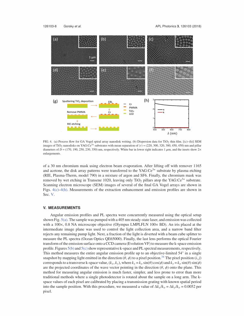
126103-8 Gorsky et al. APL Photonics 3, 126103 (2018)
FIG. 4. (a) Process flow for GA Vogel spiral array nanodisk writing. (b) Dispersion data for TiO2 thin film. [(c)–(h)] SEMimages of TiO2 nanodisks on YAG:Ce3+ substrates with mean separation of 〈r〉 = (220, 300, 320, 380, 450, 450) nm and pillardiameters of D = (170, 190, 250, 230, 350) nm, respectively. White bar in lower right indicates 1 μm, and the insets show 2×enlargements.
of a 30 nm chromium mask using electron beam evaporation. After lifting off with remover 1165and acetone, the disk array patterns were transferred to the YAG:Ce3+ substrate by plasma etching(RIE, Plasma-Therm, model 790) in a mixture of argon and SF6. Finally, the chromium mask wasremoved by wet etching in Transene 1020, leaving only TiO2 pillars atop the YAG:Ce3+ substrate.Scanning electron microscope (SEM) images of several of the final GA Vogel arrays are shown inFigs. 4(c)–4(h). Measurements of the extraction enhancement and emission profiles are shown inSec. V.
V. MEASUREMENTS
Angular emission profiles and PL spectra were concurrently measured using the optical setupshown Fig. 5(a). The sample was pumped with a 405 nm steady-state laser, and emission was collectedwith a 100×, 0.8 NA microscope objective (Olympus LMPLFLN 100× BD). An iris placed at theintermediate image plane was used to control the light collection area, and a narrow band filterrejects any remaining pump light. Next, a fraction of the light is diverted with a beam cube splitter tomeasure the PL spectra (Ocean Optics QE65000). Finally, the last lens performs the optical Fouriertransform of the emission surface onto a CCD camera (Evolution VF) to measure the k-space emissionprofile. Figures 5(b) and 5(c) show representative k-space and PL spectral measurements, respectively.This method measures the entire angular emission profile up to an objective-limited 54◦ in a singlesnapshot by mapping light emitted in the direction (θ, φ) to a pixel position.34 The pixel position (i, j)corresponds to a transverse k-space value, (kx, ky), where kx = ko sin(θ) cos(φ) and ky = ko sin(θ) sin(φ)are the projected coordinates of the wave vector pointing in the direction (θ, φ) onto the plane. Thismethod for measuring angular emission is much faster, simpler, and less prone to error than moretraditional methods where a single photodetector is rotated about the sample on a long arm. The k-space values of each pixel are calibrated by placing a transmission grating with known spatial periodinto the sample position. With this procedure, we measured a value of Δkx/ko = Δky/ko = 0.0052 perpixel.

126103-9 Gorsky et al. APL Photonics 3, 126103 (2018)
FIG. 5. (a) The optical setup for measuring k-space emission profile and PL spectra. Green lines trace out a plane waveemitted along the optical axis. (b) and (c) are representative k-space image and PL spectra, respectively.
Figure 6 shows a number of theoretical and measured k-space images. Each column representsa particular set of geometrical parameters of the particles as described in the caption. The top row isthe simulated output intensity as described in Sec. III. For the input intensity, we used a Lambertianprofile, as most LEDs exhibit Lambertian or near-Lambertian emission profiles.44 In the middle roware measurements from patterned regions of the sample, and in the bottom row are measurements fromnearby unpatterned sections of the sample (hereto referred to as “background” images). Note thatthe background images are consistent from one to another and show higher intensity at high anglesthan at the center. This is indicative of isotropic emission within the bulk which yields a radiantintensity given by Eq. (8). The measured emission profiles are clearly dependent on the geometryscaling of the pattern. Specifically, for both the simulated and measured profiles, increasing the meanpillar separation from 220 nm to 450 nm causes a shift in the intensity distribution from high angleconcentration to forward concentration.
FIG. 6. k-space intensity profiles. Top row is analytical simulations assuming a Lambertian profile incident on the scatteringarray, middle row is measured data from patterned area, and bottom row is measured data from unpatterned area nearby abovepatterned area. Each color bar corresponds to all images in its respective row. Columns (a)–(d) are different spiral geometrieswith mean separation 〈r〉 = (220, 300, 380, 450) nm, respectively.

126103-10 Gorsky et al. APL Photonics 3, 126103 (2018)
FIG. 7. Normalized directional enhancement plots. (a) shows negligible change in γdn with varying pillar diameter, D, andfixed mean separation 〈r〉 = 450 nm. (b) shows γdn has significant sensitivity to 〈r〉, with increasing directional enhancementup to 35% in the forward direction as 〈r〉 increases from 220 nm to 450 nm. (c) modeled directional enhancement taken fromappropriate horizontal slices of Fig. 3. The trend with changing 〈r〉 is in good agreement with measurements in (b).
To quantify the directional enhancement, the intensity profiles are first normalized by the totalpower, then the azimuthally averaged normalized intensity, In(β′), is calculated. Finally, the meannormalized intensity from the patterned region is divided by that of the background to yield the nor-malized directional enhancement, γdn. This is the same procedure used on modeled data as describedin Sec. III. Figures 7(a) and 7(b) show γdn with varying D and 〈r〉. We observe that γdn is relativelyinsensitive to the pillar diameter, with only a slight dip in the forward enhancement (β′ = 0) as thepillar size approaches the mean separation. On the other hand, it is quite sensitive to 〈r〉. Specifically,at 〈r〉 = 220 nm, there is a slight drop in forward scattering and increase in high angle emission, andas 〈r〉 is increased from 220 nm to 450 nm, we measure an increase in the forward enhancement upto 35%. These results are qualitatively in agreement with the modeled predictions shown in Fig. 7(c),which are the appropriate horizontal cuts of Fig. 3 assuming λ = 550 nm.
Measured PL spectra and extraction enhancement are shown in Figs. 8(a) and 8(b), respec-tively. Enhancement was measured by dividing background spectra into patterned spectra, and variedbetween 1.4 and 2.0. As 〈r〉 decreases, the maximum enhancement increases and the enhancementcurve narrows although in all measured cases, the enhancement did not significantly vary over themajority of the emission band (500-600 nm). These measurements clearly demonstrate the capabilityof GA Vogel spiral arrays for enhancing light extraction and directional emission from active LEDmaterials. Furthermore, general agreement between measurements with FDTD simulation (quantita-tively and qualitatively) and modeling (qualitatively) shows a robust ability to predict the performanceof scattering nanoparticle arrays atop active LED materials.
FIG. 8. (a) PL spectrum measurements with varying 〈r〉. Background is measured from an unpatterned surface near thepatterned regions of the sample. (b) Extraction enhancement spectra calculated by dividing background into spectra frompatterned surfaces. Line-styles between panels (a) and (b) correspond.

126103-11 Gorsky et al. APL Photonics 3, 126103 (2018)
VI. CONCLUSION
In this work, we demonstrated the application of all-dielectric scattering nanoparticles in anaperiodic GA Vogel spiral array for the simultaneous enhancement of light extraction and directionalemission from optically thick YAG:Ce3+ LED converter materials. We used full-vector numericalFDTD to find the optimal mean particle spacing and pillar height that maximize extraction enhance-ment. The optimal extraction enhancement is found to be 2.7× compared to a flat reference. We alsodeveloped an analytical model to understand and expediently optimize Vogel spiral array for direc-tional enhancement of incoherent radiation. We patterned YAG:Ce3+ converters with TiO2 nanodisksusing the numerical and model results as guidance and measured peak extraction enhancement of2× from patterned substrates compared to a flat reference using PL spectroscopy. We also measuredpower-normalized directional enhancement by using accurate Fourier-space emission spectroscopyand found a peak forward enhancement of 35%. Measurements were found in good agreement withnumerical modeling predictions and in good qualitative agreement with the developed analyticalmodel. Increasing the efficiency and controlling the direction of emission from LEDs are beneficialto a variety of LED applications. The extraction and directional enhancement capabilities of GAVogel spiral array nanoparticles demonstrated within this work make them an attractive option forintegration with commercially available LED active materials.
ACKNOWLEDGMENTS
We acknowledge the partial support of OSRAM Opto Semiconductors who contributed to thiswork by providing funding, the YAG:Ce3+ converter substrates, and valuable discussions regardingthe integration with white-light LEDs. L.D.N. also wants to acknowledge the partial support of theNSF Grant No. ECCS-1643118 entitled Enhanced solar energy conversion by ultra-slow photonsub-diffusion in aperiodic media.
1 N. Holonyak, Am. J. Phys. 68, 864–866 (2000).2 N. F. Gardner, G. O. Mller, Y. C. Shen, G. Chen, S. Watanabe, W. Gtz, and M. R. Krames, Appl. Phys. Lett. 91, 243506
(2007).3 S. Nakamura, T. Mukai, and M. Senoh, Appl. Phys. Lett. 64, 1687–1689 (1994).4 V. Haerle, B. Hahn, S. Kaiser, A. Weimar, S. Bader, F. Eberhard, A. Plossl, and D. Eisert, Phys. Status Solidi A 201,
2736–2739 (2004).5 O. B. Shchekin, J. E. Epler, T. A. Trottier, T. Margalith, D. A. Steigerwald, M. O. Holcomb, P. S. Martin, and M. R. Krames,
Appl. Phys. Lett. 89, 071109 (2006).6 A. Wilm, Proc. SPIE 7001, 700101–70010F (2008).7 H. Zhao, G. Liu, J. Zhang, R. A. Arif, and N. Tansu, J. Disp. Technol. 9, 212–225 (2013).8 P. Kivisaari, L. Riuttanen, J. Oksanen, S. Suihkonen, M. Ali, H. Lipsanen, and J. Tulkki, Appl. Phys. Lett. 101, 021113
(2012).9 C. Wiesmann, K. Bergenek, N. Linder, and U. Schwarz, Laser Photonics Rev. 3, 262–286 (2009).
10 J. Y. Joo, C. S. Kang, S. S. Park, and S.-K. Lee, Opt. Express 17, 23449–23458 (2009).11 J. Shakya, K. H. Kim, J. Y. Lin, and H. X. Jiang, Appl. Phys. Lett. 85, 142–144 (2004).12 A. David, H. Benisty, and C. Weisbuch, J. Disp. Technol. 3, 133–148 (2007).13 A. David, T. Fujii, R. Sharma, K. McGroddy, S. Nakamura, S. P. DenBaars, E. L. Hu, C. Weisbuch, and H. Benisty, Appl.
Phys. Lett. 88, 061124 (2006).14 C. Wiesmann, K. Bergenek, N. Linder, and U. Schwarz, Proc. SPIE 6989, 69890L (2008).15 H. Benisty, J. Danglot, A. Talneau, S. Enoch, J. M. Pottage, and A. David, IEEE J. Quantum Electron. 44, 777–789 (2008).16 M.-K. Kwon, J.-Y. Kim, I.-K. Park, K. S. Kim, G.-Y. Jung, S.-J. Park, J. W. Kim, and Y. C. Kim, Appl. Phys. Lett. 92,
251110 (2008).17 C.-F. Lai, J.-Y. Chi, H.-H. Yen, H.-C. Kuo, C.-H. Chao, H.-T. Hsueh, J.-F. T. Wang, C.-Y. Huang, and W.-Y. Yeh, Appl.
Phys. Lett. 92, 243118 (2008).18 K. Bergenek, C. Wiesmann, R. Wirth, L. O’Faolain, N. Linder, K. Streubel, and T. F. Krauss, Appl. Phys. Lett. 93, 041105
(2008).19 K. McGroddy, A. David, E. Matioli, M. Iza, S. Nakamura, S. DenBaars, J. S. Speck, C. Weisbuch, and E. L. Hu, Appl.
Phys. Lett. 93, 103502 (2008).20 J. J. Wierer, Jr., A. David, and M. M. Megens, Nat. Photonics 3, 163 (2009).21 A. David, J. Disp. Technol. 9, 301–316 (2013).22 A. Lenef, J. F. Kelso, and A. Piquette, Opt. Lett. 39, 3058–3061 (2014).23 R. Windisch, C. Rooman, S. Meinlschmidt, P. Kiesel, D. Zipperer, G. H. Dhler, B. Dutta, M. Kuijk, G. Borghs, and
P. Heremans, Appl. Phys. Lett. 79, 2315–2317 (2001).24 S. Illek, I. Pietzonka, A. Ploessl, P. Stauss, W. Wegleiter, R. Windisch, R. Wirth, H. Zull, and K. P. Streubel, Proc. SPIE
4996, 18–25 (2003).

126103-12 Gorsky et al. APL Photonics 3, 126103 (2018)
25 A. David, T. Fujii, E. Matioli, R. Sharma, S. Nakamura, S. P. DenBaars, C. Weisbuch, and H. Benisty, Appl. Phys. Lett. 88,073510 (2006).
26 N. Lawrence, J. Trevino, and L. Dal Negro, J. Appl. Phys. 111, 113101 (2012).27 G. Ke, D. Mengqi, C. I. Osorio, and K. A. Femius, Laser Photonics Rev. 11, 1600235 (2017).28 J. Trevino, H. Cao, and L. Dal Negro, Nano Lett. 11, 2008–2016 (2011).29 L. Dal Negro, N. Lawrence, and J. Trevino, Opt. Express 20, 18209–18223 (2012).30 H. Sun, A. Piquette, M. Raukas, and T. D. Moustakas, IEEE Photonics J. 8, 1–10 (2016).31 A. Oskooi, Appl. Phys. Lett. 106, 041111 (2015).32 L. Dal Negro, R. Wang, and F. A. Pinheiro, Crystals 6, 161 (2016).33 N. Lawrence, J. Trevino, and L. Dal Negro, Opt. Lett. 37, 5076–5078 (2012).34 N. Le Thomas, R. Houdre, M. V. Kotlyar, D. O’Brien, and T. F. Krauss, J. Opt. Soc. Am. B 24, 2964–2971 (2007).35 X.-H. Li, R. Song, Y.-K. Ee, P. Kumnorkaew, J. F. Gilchrist, and N. Tansu, IEEE Photonics J. 3, 489–499 (2011).36 T. Wei, Q. Kong, J. Wang, J. Li, Y. Zeng, G. Wang, J. Li, Y. Liao, and F. Yi, Opt. Express 19, 1065–1071 (2011).37 H. Jeong, D. J. Park, H. S. Lee, Y. H. Ko, J. S. Yu, S.-B. Choi, D.-S. Lee, E.-K. Suh, and M. S. Jeong, Nanoscale 6,
4371–4378 (2014).38 S. Fan, P. R. Villeneuve, J. D. Joannopoulos, and E. F. Schubert, Phys. Rev. Lett. 78, 3294–3297 (1997).39 S. Nishiura, S. Tanabe, K. Fujioka, and Y. Fujimoto, Opt. Mater. 33, 688–691 (2011).40 A. Mao, C. D. Schaper, and R. F. Karlicek, Jr., Nanotechnology 24, 085302 (2013).41 M. Raukas, J. Kelso, Y. Zheng, K. Bergenek, D. Eisert, A. Linkov, and F. Jermann, ECS J. Solid State Sci. Technol. 2,
R3168–R3176 (2013).42 B. K. Park, H. K. Park, J. H. Oh, J. R. Oh, and Y. R. Do, J. Electrochem. Soc. 159, J96–J106 (2012).43 J. R. Oh, Y. K. Lee, H. K. Park, and Y. R. Do, J. Appl. Phys. 105, 043103 (2009).44 I. Moreno and C.-C. Sun, Opt. Express 16, 1808–1819 (2008).