directed self-assembly: expectations and … self-assembly: expectations and achievements prashant...
TRANSCRIPT
NANO REVIEW
Directed Self-Assembly: Expectations and Achievements
Prashant Kumar
Received: 7 May 2010 / Accepted: 1 July 2010 / Published online: 21 July 2010
� The Author(s) 2010. This article is published with open access at Springerlink.com
Abstract Nanotechnology has been a revolutionary
thrust in recent years of development of science and
technology for its broad appeal for employing a novel idea
for relevant technological applications in particular and for
mass-scale production and marketing as common man
commodity in general. An interesting aspect of this emer-
gent technology is that it involves scientific research
community and relevant industries alike. Top–down and
bottom–up approaches are two broad division of produc-
tion of nanoscale materials in general. However, both the
approaches have their own limits as far as large-scale
production and cost involved are concerned. Therefore,
novel new techniques are desired to be developed to opti-
mize production and cost. Directed self-assembly seems to
be a promising technique in this regard; which can work as
a bridge between the top–down and bottom–up approaches.
This article reviews how directed self-assembly as a tech-
nique has grown up and outlines its future prospects.
Keywords Nanotechnology � Directed self-assembly �Template assisted growth � Field-induced growth
Introduction
Nanotechnology promises to revolutionize the way we
think about, but more importantly create new materials.
The key to making this promise a reality is a commitment
to fundamental research in critical areas including syn-
thesis, fabrication, and characterization of nanoscale
components. Nanoparticles have attracted wide attention as
such components due to their unique size-dependent
properties including, superparamagnetism, chemilumies-
cence, and catalysis. To fully harness the potential capa-
bilities of nanoparticles, we need to develop new methods
to assemble them into useful patterns or structures. These
self-assembled structures promise new opportunities for
developing miniaturized optical, electronic, optoelectronic,
and magnetic devices.
As the size of device features becomes increasingly
smaller, conventional lithographic processes are limited.
Alternative routes need to be developed to circumvent this
difficulty. As conventional fabrication technologies, such
as optical lithography, develop, they begin to run up
against fundamental limits. New measurement methods are
needed to understand and help mitigate the effects of those
limits. In addition, novel fabrication techniques are
required to help extend both the lifetime and range of
application of existing techniques. Directed self-assembly
is an emergent technology of current interest [1–10].
Directed self-assembly approach is still going through
developmental phases, and leverages existing patterning
methods by combining them with self-organizing systems,
to create manufacturing techniques that can be readily
integrated into existing processes. Directed self-assembly
technique can be appropriately employed to yield func-
tional nanostructures e.g. nanowires and organized array of
nanodots.
As the size scale of device features becomes increas-
ingly smaller, conventional lithographic processes are
limited. Alternative routes need to be developed to cir-
cumvent this hard stop. As conventional fabrication tech-
nologies, such as optical lithography, develop, they begin
to run up against fundamental limits. New measurement
methods are needed to understand and help mitigate the
P. Kumar (&)
Jawaharlal Nehru Centre for Advanced Scientific Research,
Bangalore 560064, India
e-mail: [email protected]
123
Nanoscale Res Lett (2010) 5:1367–1376
DOI 10.1007/s11671-010-9696-9
effects of those limits. In addition, novel fabrication tech-
niques are required to help extend both the lifetime and
range of application of existing techniques. Directed self-
assembly is one of the emergent technologies which find
interest to the researchers currently [1–10]. Directed self-
assembly approach is still going through developmental
phases and leverages existing patterning methods by
combining those with self-organizing systems to create
manufacturing techniques that can be readily integrated
into existing processes. Directed self-assembly technique
can be appropriately employed to yield functional nano-
structures e.g. nanowires and arrays of organized nanodots.
Spontaneous self-assembly is introduced as an evapo-
ration-induced phenomenon that yields random patterns.
Among guided self-assembly approaches (employing some
guiding agent to nanoparticles or vapour of atoms), tem-
plate-guided and field-guided assemblies are two approa-
ches. For template-guided assembly, existing surface
atomic pattern or nano/micro features as templates are
made use of. Among field guided assembly, use of pressure
gradient, magnetic field, electric field, electron beam, light
and laser, etc. are few to count with. The present article
reviews the progress so far in the direction of establishment
of directed self-assembly as a reproducible and robust
technique and its future prospects for its usage at industrial
scale.
Spontaneous Self-Assembly
The use of spontaneous self-assembly as a lithography- and
external field-free which means to construct well-ordered
often intriguing structures has received much attention for
its ease of organizing materials on the nanoscale into
ordered structures and producing complex, large-scale
structures with small feature sizes. An extremely simple
route to intriguing structures is the evaporation-induced
self-assembly (EISA) [11–18] of polymers and nanoparti-
cles from a droplet on a solid substrate. However, flow
instabilities within the evaporating droplet often result in
non-equilibrium and irregular dissipative structures, e.g.,
randomly organized convection patterns and stochastically
distributed multi-rings. [11–14, 16, 19–22]. Therefore, fully
utilizing evaporation as a simple tool for creating well-
ordered structures with numerous technological applica-
tions requires precise control over several factors, including
evaporative flux, solution concentration, and the interfacial
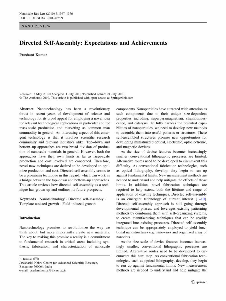
interaction between solute and substrate [23–31] (Fig. 1).
As shown in Fig. 1a, there is no apparent visible spatial
orderliness of nanoparticles in the nickel thin film of
thickness 50 nm coated onto borosilicate glass substrate in
the process of resistive thermal evaporation. The metal
particle size and size distribution depends on the deposition
conditions, e.g., electrical power used for thermal evapo-
ration (which determines remaining energy of the adatoms
when it lands onto the substrate), wettability offered by the
substrate to the thin film material (substrate and thin film
material), diffusivity of thin film material atoms on the
substrate (substrate temperature) etc.
After transport the substrates and conditions on the
substrate surface play an important role in determining the
microstructural evolution of the films. It is pertinent at this
point to recall the process of condensation of vapor into
thin films on substrates [32]. Initially small nuclei,
depending on the effective surface energy available, form
on the substrate. These satisfy the condition of nucleation
(supersaturation ratio [ 1), which in turn is dependent on
the substrate material itself. Once a few nuclei form, they
work as nucleation centers. Coalescence between nuclei
occurs, and this finally gives rise to the growth of contin-
uous layers. Nanoparticulate formation in particular can be
attributed to the metal–substrate interactions. Energetics
decides the contact angle of the condensate onto the sub-
strate, residual strain, and size and shape of the nanopar-
ticles deposited. The capillary model predicts that free
energy of formation of condensed aggregate goes through a
maximum [32]. With heating of the substrate, densification
occurs, and the grain wall boundary width is thinned. At
RT deposition conditions, because sufficient energy is not
available for mobility of adatoms on the substrate surface,
the size is not enhanced much due to coalescence.
Occasionally, some short distance orderlinesses
(as shown in Fig. 1b for nickel thin film growth on [311]
silicon substrate by resistive thermal evaporation at room
temperature) have been observed in thin films achieved by
thermal evaporation; whose origin can be traced in the
atomic scale linear edges formed while cutting the sub-
strate in particular plane which virtually works as template
for few layers of thin film growth.
The organization of inorganic nanostructures within
self-assembled organic or biological templates [33–43] is
receiving the attention of scientists interested in developing
functional hybrid materials. Previous efforts have concen-
trated on using such scaffolds [39, 44] to spatially arrange
nanoscopic elements as a strategy for tailoring the elec-
trical, magnetic, or photonic properties [40–43, 45–48] of
the material. Recent theoretical arguments [48–50] have
suggested that synergistic interactions between self-orga-
nizing particles and a self-assembling matrix material can
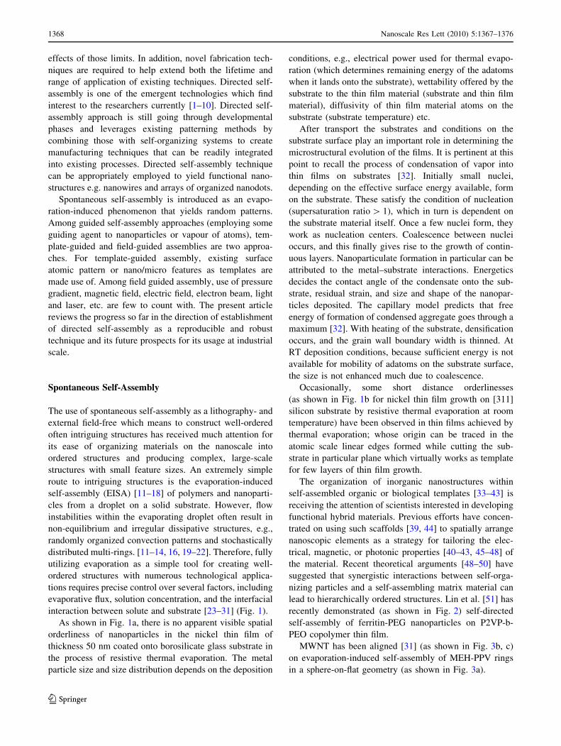
lead to hierarchically ordered structures. Lin et al. [51] has
recently demonstrated (as shown in Fig. 2) self-directed
self-assembly of ferritin-PEG nanoparticles on P2VP-b-
PEO copolymer thin film.
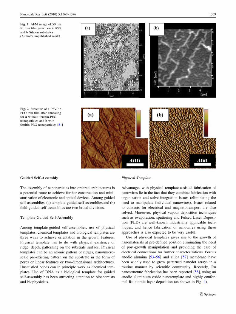
MWNT has been aligned [31] (as shown in Fig. 3b, c)
on evaporation-induced self-assembly of MEH-PPV rings
in a sphere-on-flat geometry (as shown in Fig. 3a).
1368 Nanoscale Res Lett (2010) 5:1367–1376
123
Guided Self-Assembly
The assembly of nanoparticles into ordered architectures is
a potential route to achieve further construction and mini-
aturization of electronic and optical devices. Among guided
self-assemblies, (a) template-guided self-assemblies and (b)
field-guided self-assemblies are two broad divisions.
Template-Guided Self-Assembly
Among template-guided self-assemblies, use of physical
templates, chemical templates and biological templates are
three ways to achieve orientation in the growth features.
Physical template has to do with physical existence of
ridge, depth, patterning on the substrate surface. Physical
templates can be an atomic pattern or ridges, nano/micro-
scale pre-existing pattern on the substrate in the form of
pores or linear features or two-dimensional architectures.
Unsatisfied bonds can in principle work as chemical tem-
plates. Use of DNA as a biological template for guided
self-assembly has been attracting attention to biochemists
and biophysicists.
Physical Template
Advantages with physical template-assisted fabrication of
nanowires lie in the fact that they combine fabrication with
organization and solve integration issues (eliminating the
need to manipulate individual nanowires). Issues related
to contacts for electrical and magnetotransport are also
solved. Moreover, physical vapour deposition techniques
such as evaporation, sputtering and Pulsed Laser Deposi-
tion (PLD) are well-known industrially applicable tech-
niques, and hence fabrication of nanowires using these
approaches is also expected to be very useful.
Use of physical templates gives rise to the growth of
nanomaterials at pre-defined position eliminating the need
of post-growth manipulation and providing the ease of
electrical connections for further characterizations. Porous
anodic alumina [53–56] and silica [57] membrane have
been widely used to grow patterned nanodot arrays in a
routine manner by scientific community. Recently, Ru
nanostructure fabrication has been reported [58], using an
anodic aluminium oxide nanotemplate and highly confor-
mal Ru atomic layer deposition (as shown in Fig. 4).
Fig. 1 AFM image of 50 nm
Ni thin film grown on a BSG
and b Silicon substrates
(Author’s unpublished work)
Fig. 2 Structure of a P2VP-b-
PEO thin film after annealing
for a without ferritin-PEG
nanoparticles and b with
ferritin-PEG nanoparticles [51]
Nanoscale Res Lett (2010) 5:1367–1376 1369
123
Such templates give rise to the growth of nanodots,
vertical nanowires, which can be controllably used to
fabricate FET devices, magnetic tunnel junction devices
and devices for optical applications. Fabrication of
nanomaterials using porous alumina templates has been
reviewed [59]. However, use of in-plane growth of nano-
wires and array of nanodots seems to be more promising.
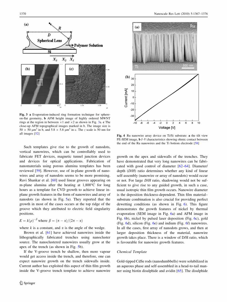
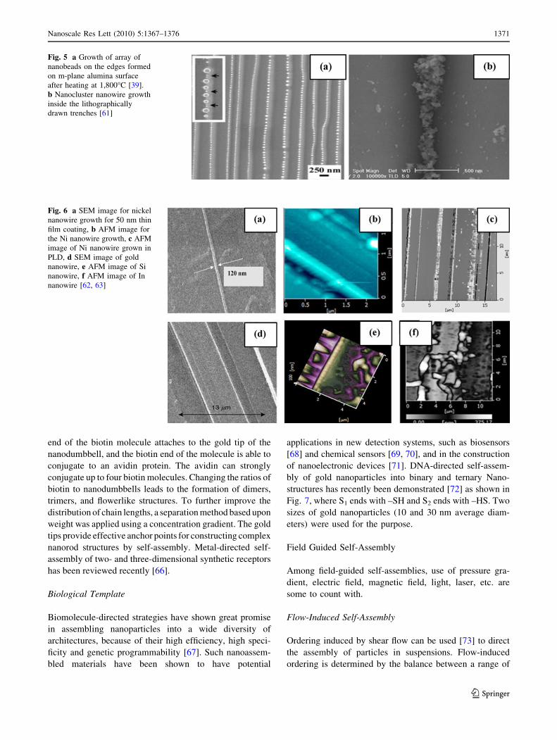
Ravi Shankar et al. [60] used linear grooves appearing on
m-plane alumina after the heating at 1,800�C for long
hours as a template for CVD growth to achieve linear in-
plane growth features in the form of nanowires and array of
nanodots (as shown in Fig. 5a). They reported that the
growth in most of the cases occurs at the top ridge of the
groove which they attributed to electric field singularity
positions.
E ¼ kðqÞ�bwhere b ¼ ðp � aÞ=ð2p � aÞ
where k is a constant, and a is the angle of the wedge.
Brown et al. [61] have achieved nanowires inside the
lithographically fabricated trenches using nanocluster
source. The nanoclustered nanowires usually grow at the
apex of the trench (as shown in Fig. 5b).
If the V-groove trench be shallow, then more vapour
would get access inside the trench, and therefore, one can
expect nanowire growth on the trench sidewalls inside.
Current author has exploited this aspect of thin film growth
inside the V-groove trench template to achieve nanowire
growth on the apex and sidewalls of the trenches. They
have demonstrated that very long nanowires can be fabri-
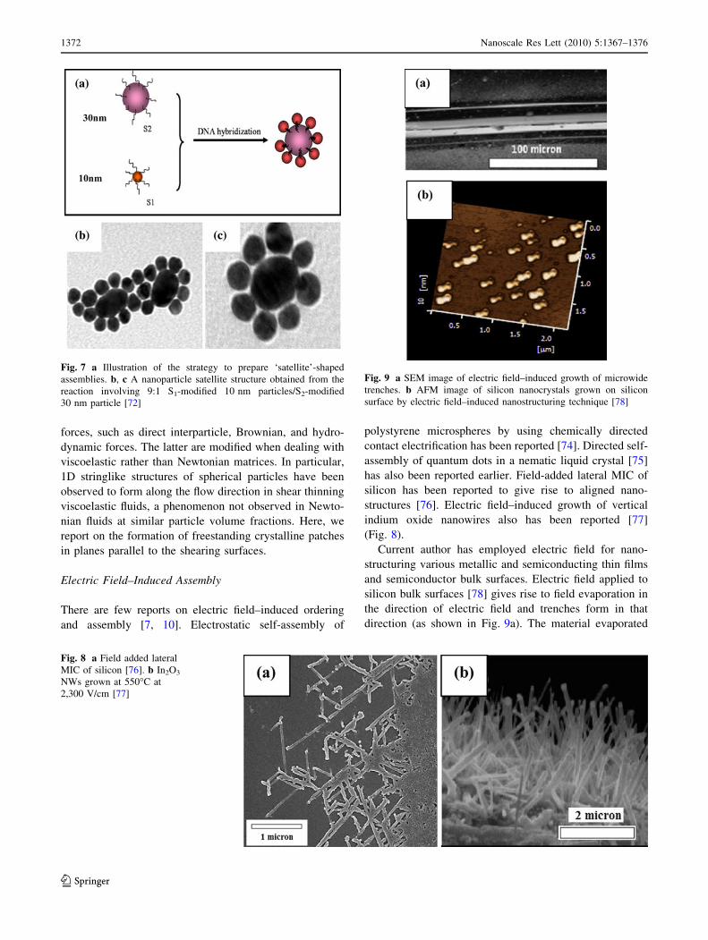
cated with good control of diameter [62–64]. Diameter/
depth (D/H) ratio determines whether any kind of linear
self-assembly (nanowire or array of nanodots) would occur
or not. For large D/H ratio, shadowing would not be suf-
ficient to give rise to any guided growth, in such a case,
usual isotropic thin film growth occurs. Nanowire diameter
is the deposition thickness-dependent. Thin film material–
substrate combination is also crucial for providing perfect
dewetting conditions (as shown in Fig. 6). This figure
demonstrates the growth features of nickel by thermal
evaporation (SEM image in Fig. 6a) and AFM image in
Fig. 6b), nickel by pulsed laser deposition (Fig. 6c), gold
(Fig. 6d), silicon (Fig. 6e) and indium (Fig. 6f) nanowires.
In all the cases, first array of nanodots grows, and then at
larger deposition thickness of the material, nanowire
growth takes place. There is a window of D/H ratio, which
is favourable for nanowire growth features.
Chemical Template
Gold-tipped CdSe rods (nanodumbbells) were solubilized in
an aqueous phase and self-assembled in a head-to-tail man-
ner using biotin disulphide and avidin [65]. The disulphide
Fig. 3 a Evaporation-induced ring formation technique for sphere-
on-flat geometry, b AFM height image of highly ordered MWNT
rings at the region in between 91 and 92 as shown in Fig. 3a. c The
close-up AFM topographical images marked in b. The image size is
50 9 50 lm2 in b, and 5.8 9 5.8 lm2 in c. The z scale is 50 nm for
all images [52]Fig. 4 Ru nanowire array device on Ti/Si substrate: a the tilt view
FE-SEM image, b I–V characteristics showing ohmic contact between
the end of the Ru nanowires and the Ti bottom electrode [58]
1370 Nanoscale Res Lett (2010) 5:1367–1376
123
end of the biotin molecule attaches to the gold tip of the
nanodumbbell, and the biotin end of the molecule is able to
conjugate to an avidin protein. The avidin can strongly
conjugate up to four biotin molecules. Changing the ratios of
biotin to nanodumbbells leads to the formation of dimers,
trimers, and flowerlike structures. To further improve the
distribution of chain lengths, a separation method based upon
weight was applied using a concentration gradient. The gold
tips provide effective anchor points for constructing complex
nanorod structures by self-assembly. Metal-directed self-
assembly of two- and three-dimensional synthetic receptors
has been reviewed recently [66].
Biological Template
Biomolecule-directed strategies have shown great promise
in assembling nanoparticles into a wide diversity of
architectures, because of their high efficiency, high speci-
ficity and genetic programmability [67]. Such nanoassem-
bled materials have been shown to have potential
applications in new detection systems, such as biosensors
[68] and chemical sensors [69, 70], and in the construction
of nanoelectronic devices [71]. DNA-directed self-assem-
bly of gold nanoparticles into binary and ternary Nano-
structures has recently been demonstrated [72] as shown in
Fig. 7, where S1 ends with –SH and S2 ends with –HS. Two
sizes of gold nanoparticles (10 and 30 nm average diam-
eters) were used for the purpose.
Field Guided Self-Assembly
Among field-guided self-assemblies, use of pressure gra-
dient, electric field, magnetic field, light, laser, etc. are
some to count with.
Flow-Induced Self-Assembly
Ordering induced by shear flow can be used [73] to direct
the assembly of particles in suspensions. Flow-induced
ordering is determined by the balance between a range of
Fig. 5 a Growth of array of
nanobeads on the edges formed
on m-plane alumina surface
after heating at 1,800�C [39].
b Nanocluster nanowire growth
inside the lithographically
drawn trenches [61]
Fig. 6 a SEM image for nickel
nanowire growth for 50 nm thin
film coating, b AFM image for
the Ni nanowire growth, c AFM
image of Ni nanowire grown in
PLD, d SEM image of gold
nanowire, e AFM image of Si
nanowire, f AFM image of In
nanowire [62, 63]
Nanoscale Res Lett (2010) 5:1367–1376 1371
123
forces, such as direct interparticle, Brownian, and hydro-
dynamic forces. The latter are modified when dealing with
viscoelastic rather than Newtonian matrices. In particular,
1D stringlike structures of spherical particles have been
observed to form along the flow direction in shear thinning
viscoelastic fluids, a phenomenon not observed in Newto-
nian fluids at similar particle volume fractions. Here, we
report on the formation of freestanding crystalline patches
in planes parallel to the shearing surfaces.
Electric Field–Induced Assembly
There are few reports on electric field–induced ordering
and assembly [7, 10]. Electrostatic self-assembly of
polystyrene microspheres by using chemically directed
contact electrification has been reported [74]. Directed self-
assembly of quantum dots in a nematic liquid crystal [75]
has also been reported earlier. Field-added lateral MIC of
silicon has been reported to give rise to aligned nano-
structures [76]. Electric field–induced growth of vertical
indium oxide nanowires also has been reported [77]
(Fig. 8).
Current author has employed electric field for nano-
structuring various metallic and semiconducting thin films
and semiconductor bulk surfaces. Electric field applied to
silicon bulk surfaces [78] gives rise to field evaporation in
the direction of electric field and trenches form in that
direction (as shown in Fig. 9a). The material evaporated
Fig. 7 a Illustration of the strategy to prepare ‘satellite’-shaped
assemblies. b, c A nanoparticle satellite structure obtained from the
reaction involving 9:1 S1-modified 10 nm particles/S2-modified
30 nm particle [72]
Fig. 8 a Field added lateral
MIC of silicon [76]. b In2O3
NWs grown at 550�C at
2,300 V/cm [77]
Fig. 9 a SEM image of electric field–induced growth of microwide
trenches. b AFM image of silicon nanocrystals grown on silicon
surface by electric field–induced nanostructuring technique [78]
1372 Nanoscale Res Lett (2010) 5:1367–1376
123
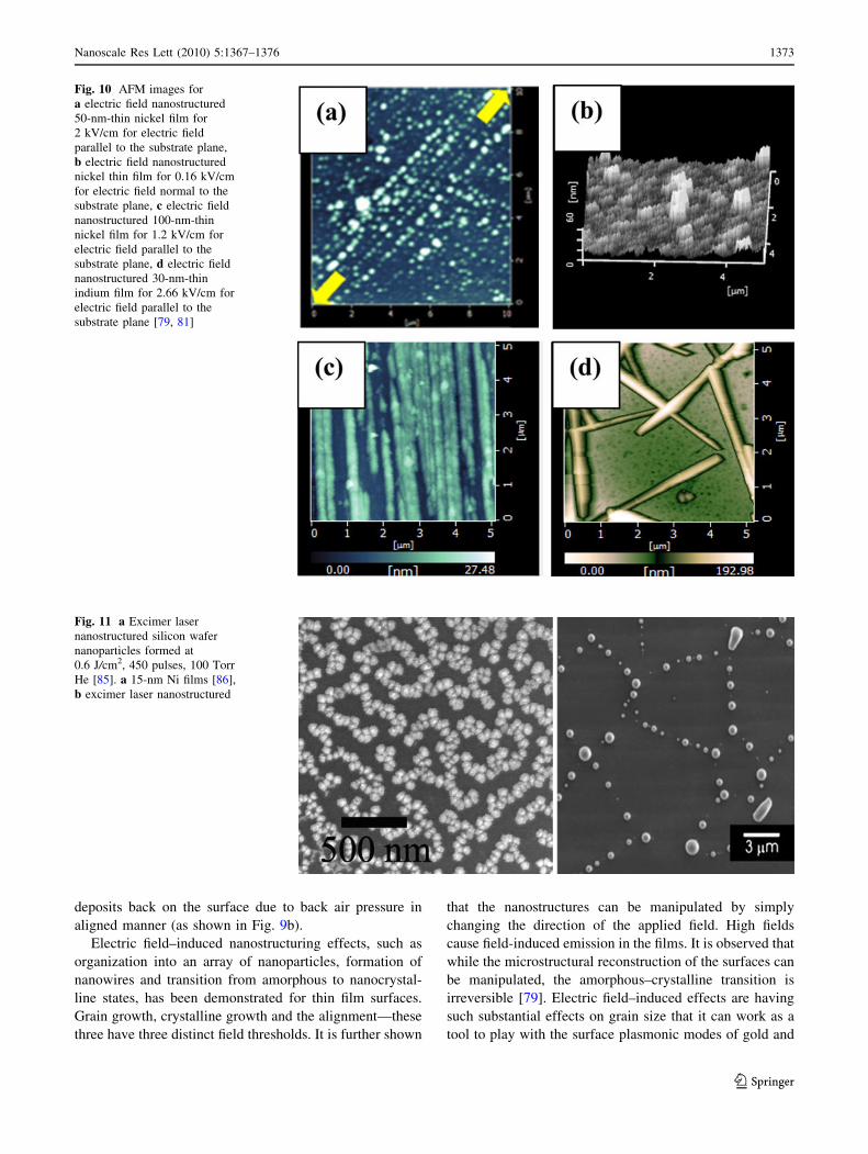
deposits back on the surface due to back air pressure in
aligned manner (as shown in Fig. 9b).
Electric field–induced nanostructuring effects, such as
organization into an array of nanoparticles, formation of
nanowires and transition from amorphous to nanocrystal-
line states, has been demonstrated for thin film surfaces.
Grain growth, crystalline growth and the alignment—these
three have three distinct field thresholds. It is further shown
that the nanostructures can be manipulated by simply
changing the direction of the applied field. High fields
cause field-induced emission in the films. It is observed that
while the microstructural reconstruction of the surfaces can
be manipulated, the amorphous–crystalline transition is
irreversible [79]. Electric field–induced effects are having
such substantial effects on grain size that it can work as a
tool to play with the surface plasmonic modes of gold and
Fig. 10 AFM images for
a electric field nanostructured
50-nm-thin nickel film for
2 kV/cm for electric field
parallel to the substrate plane,
b electric field nanostructured
nickel thin film for 0.16 kV/cm
for electric field normal to the
substrate plane, c electric field
nanostructured 100-nm-thin
nickel film for 1.2 kV/cm for
electric field parallel to the
substrate plane, d electric field
nanostructured 30-nm-thin
indium film for 2.66 kV/cm for
electric field parallel to the
substrate plane [79, 81]
Fig. 11 a Excimer laser
nanostructured silicon wafer
nanoparticles formed at
0.6 J/cm2, 450 pulses, 100 Torr
He [85]. a 15-nm Ni films [86],
b excimer laser nanostructured
Nanoscale Res Lett (2010) 5:1367–1376 1373
123
indium [80]. For 50-nm-thin nickel film, electric field
application has given rise to the growth of array of nickel
nanodots (as shown in Fig. 10a). When 100-nm nickel thin
film was undergone through 0.66 kV/cm electric field,
nanowires do grow on the surface [81] (as shown in
Fig. 9c). Indium metal however having low melting point
has shown less critical field for nanowire growth compared
to nickel metal (as shown in Fig. 10d). Application of
vertical electric field can give rise to vertical nanopillars
[79, 82] (as shown in Fig. 10b). Electric field–mediated
nickel-induced nanocrystallization of amorphous silicon
thin films in the complete absence of external heating has
also been reported [83]. Electric field–induced nanostruc-
turing has been a potential technique for nanotechnology-
driven applications [64, 84].
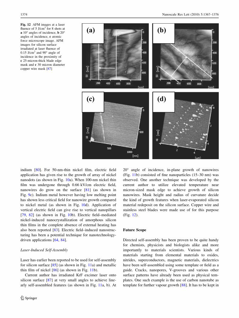
Laser-Induced Self-Assembly
Laser has earlier been reported to be used for self-assembly
for silicon surface [85] (as shown in Fig. 11a) and metallic
thin film of nickel [86] (as shown in Fig. 11b).
Current author has irradiated KrF excimer laser onto
silicon surface [87] at very small angles to achieve line-
arly self-assembled features (as shown in Fig. 11a, b). At
20� angle of incidence, in-plane growth of nanowires
(Fig. 11b) consisted of fine nanoparticles (15–30 nm) was
observed. One another technique was developed by the
current author to utilize elevated temperature near
micron-sized mask edge to achieve growth of silicon
nanowires. Mask height and radius of curvature decide
the kind of growth features when laser-evaporated silicon
material redeposit on the silicon surface. Copper wire and
stainless steel blades were made use of for this purpose
(Fig. 12).
Future Scope
Directed self-assembly has been proven to be quite handy
for chemists, physicists and biologists alike and more
importantly to materials scientists. Various kinds of
materials starting from elemental materials to oxides,
nitrides, superconductors, magnetic materials, dielectrics
have been self-assembled using some template or field as a
guide. Cracks, nanopores, V-grooves and various other
surface patterns have already been used as physical tem-
plates. One such example is the use of carbon nanotube as
template for further vapour growth [88]. It has to be kept in
Fig. 12 AFM images at a laser
fluence of 5 J/cm2 for 8 shots at
a 10� angles of incidence, b 20�angles of incidence, c atomic
force microscope image. AFM
images for silicon surface
irradiated at laser fluence of
0.15 J/cm2 and 90� angle of
incidence in the proximity of
c 25-micron-thick blade edge
mask and c 30 micron diameter
copper wire mask [87]
1374 Nanoscale Res Lett (2010) 5:1367–1376
123
mind that lithography itself can conveniently be used to
direct the growth. Unsatisfied bonds have been conve-
niently used as chemical templates. Similarly, biologists
too have employed bio-alignments (DNA as template is
one example). Electric field, excimer laser, light, magnetic
field, pressure gradient, shear gradient and various fields
have been employed to achieve functional nanostructures
by field-directed self-assembly. Here in this review, use of
electric field and laser has been described in detail. How-
ever, magnetic field [89, 90] and focused ion beam [91] are
the other two fields as competitive for the purpose of
directed self-assembly of materials. Directed self-assembly
of nanomaterials as a discipline is quite versatile in nature.
Guise et al. [92] has achieved patterning of sub-10-nm Ge
islands on Si(100) by directed self-assembly. Greve et al.
[93] have dealt with the directed self-assembly of amphi-
philic regioregular polythiophenes on the nanometer scale.
Xu et al. [94] have demonstrated directed self-assembly
of block copolymers on two-dimensional chemical patterns
fabricated by electro-oxidation nanolithography. Gupta
et al. [95] have described the entropy-driven segregation of
nanoparticles to cracks in multilayered composite polymer
structures. Adam et al. [96] have used NH���O hydrogen
bonding for directed self-assembly and achieved a trilay-
ered supramolecular array formed between 1,2-diaminoe-
thane and benzoic acid. Lee et al. [97] have achieved
self-assembly of 2,6-dimethylpyridine on Cu(1 1 0) direc-
ted by weak hydrogen bonding. Kinge et al. [98] have
reviewed self-assembling of nanoparticles at surfaces and
interfaces. Sitti [99] has demonstrated high aspect ratio
polymer micro/nanostructure manufacturing using directed
self-assembly.
Even though science and technology of directed self-
assembly has advanced manifold, this part of nanotech-
nology as a pursuit of research and development is still
young. To industrialize this technique, control of material
growth has to be understood at atomic scale. Accurate
prediction and tailoring of physical properties at nanoscale
are still a challenge.
Acknowledgments Author would like to acknowledge the moral
support and encouragements from Prof. P. Sen at School of Physical
Sciences, Jawaharlal Nehru University, New Delhi, Dr. M. G. Krishna
from School of Physics, University of Hyderabad and Prof. C. N.
R. Rao at Jawaharlal Nehru Centre for Advanced Scientific Research
(JNCASR), Bangalore. Facilities at University of Hyderabad were
instrumental in carrying out various aspects of research. Funding from
University grants Commision (UGC) and Department of Science and
Technology (DST), Govt. of India are also acknowledged.
Open Access This article is distributed under the terms of the
Creative Commons Attribution Noncommercial License which per-
mits any noncommercial use, distribution, and reproduction in any
medium, provided the original author(s) and source are credited.
References
1. S.H.M. Jafri, A.B. Sharma, C. Thanachayanont, J. Dutta, Mater.
Res. Soc. Symp. Proc. 901E, 0901-Rb18-01.1 (2006)
2. J.F. Conley Jr, L. Stecker, Y. Ono, Nanotechnology 16, 292
(2005)
3. X. Xiong, C.L. Chen, P. Ryan, A.A. Busnaina, Y.J. Jung, M.R.
Dokmeci, Nanotechnology 20, 295302 (2009)
4. J.Y. Cheng, C.T. Rettner, D.P. Sanders, H.C. Kim, W.D.
Hinsberg, Adv. Mater. 20, 3155 (2008)
5. J.Y. Cheng, J. Pitera, O.H. Park, M. Flickner, R. Ruiz, C.T.
Black, H.C. Kim, Appl. Phys. Lett. 91, 143106-1 (2007)
6. J.A. Liddle, Y. Cui, P. Alivisatos, Lithographically directed self-
assembly of nanostructures. J. Vac. Sci. Technol. B 22, 3409
(2004)
7. A. Winkleman, B.D. Gates, L.S. McCarty, G.M. Whitesides,
Adv. Mater. 17, 1507 (2005)
8. M. Lu, M.W. Jang, G. Haugstad, S.A. Campbell, T. Cui, Appl.
Phys. Lett. 94, 261903-1 (2009)
9. T. Vossmeyer, E.D. Ionno, J.R. Heath, Angew. Chem. Int. Ed.
Engl. 36, 1080 (1997)
10. J. Sun, M. Gao, J. Feldmann, J. Nanosci. Nanotechnol. 1, 133
(2001)
11. R.D. Deegan, Phys. Rev. E 61, 475 (2000)
12. R.D. Deegan, O. Bakajin, T.F. Dupont, G. Huber, S.R. Nagel,
T.A. Witten, Nature 389, 827 (1997)
13. R.D. Deegan, O. Bakajin, T.F. Dupont, G. Huber, S.R. Nagel,
T.A. Witten, Phys. Rev. E 62, 756 (2000)
14. E. Adachi, A.S. Dimitro, K. Nagayama, Langmuir 11, 1057
(1995)
15. H. Hu, R.G. Larson, J. Phys. Chem. B 106, 1334 (2002)
16. E. Rabani, D.R. Reichman, P.L. Geissler, L.E. Brus, Nature 426,
271 (2003)
17. T.P. Bigioni, X.-M. Lin, T.T. Nguyen, E.I. Corwin, T.A. Witten,
H.M. Jaeger, Nat. Mater. 5, 265 (2006)
18. R.V. Hameren, P. Schon, A.M. Buul, J.S. Hoogboom, V. Laza-
renko, J.W. Gerritsen, J.A.A.W. Elemans, R.J.M. Nolte, Science
314, 1433 (2006)
19. J.X. Huang, F. Kim, A.R. Tao, Nat. Mater. 4, 896 (2005)
20. C.P. Martin, M.O. Blunt, E. Pauliac-Vaujour, A. Stannard, P.
Moriarty, I. Vancea, U. Thiele, Phys. Rev. Lett. 99, 116103
(2007)
21. P. Moriarty, M.D.R. Taylor, M. Brust, Phys. Rev. Lett. 89,
248303 (2002)
22. L. Shmuylovich, A.Q. Shen, H.A. Stone, Langmuir 18, 3441
(2002)
23. Z.Q. Lin, S. Granick, J. Am. Chem. Soc. 127, 2816 (2005)
24. S.W. Hong, J. Xu, J. Xia, Z. Lin, F. Qiu, Y. Yang, Chem. Mater.
17, 6223 (2005)
25. J. Xu, J. Xia, S.W. Hong, Z.Q. Lin, F. Qiu, Y.L. Yang, Phys. Rev.
Lett. 96, 066104 (2006)
26. J. Xu, J. Xia, S.W. Hong, Z.Q. Lin, Angew. Chem. Int. Ed. 46,
1860 (2007)
27. M. Byun, S.W. Hong, L. Zhu, Z.Q. Lin, Langmuir 24, 3525
(2008)
28. M. Byun, S.W. Hong, F. Qiu, Q. Zou, Z. Lin, Macromolecules
41, 9312 (2008)
29. M. Byun, R. Laskowski, M. He, F. Qiu, M. Jeffries-El, Z. Lin,
Soft Matter 5, 1583 (2009)
30. S.W. Hong, M. Byun, Z. Lin, Angew. Chem. Int. Ed. 48, 512
(2009)
31. S.W. Hong, J. Wang, Z.Q. Lin, Angew. Chem. Int. Ed. 48, 8356
(2009)
Nanoscale Res Lett (2010) 5:1367–1376 1375
123
32. C.A. Neugebauer, Condensation, nucleation and growth of thin
films, in Handbook of Thin Film Technology, Chap. 8, ed. by L.I.
Maissel, R. Glang (McGraw Hill, New York, 1970), p. 8.3
33. J.P. Spatz, S. Mossmer, C. Hartmann, M. Moller, T. Herzog, M.
Krieger, H.G. Boyen, P. Ziemann, B. Kabius, Langmuir 16, 407
(2000)
34. W.A. Lopes, H.M. Jaeger, Nature 414, 735 (2001)
35. R.A. Pai, R. Humayun, M.T. Schulberg, A. Sengupta, J.-N. Sun,
J.J. Watkins, Science 303, 507 (2004)
36. M. Templin, A. Franck, A.D. Chesne, H. Leist, Y. Zhang, Sci-
ence 278, 1795 (1997)
37. H.J. Liang, T.E. Angelini, J. Ho, P.V. Braun, G.C.L. Wong, J.
Am. Chem. Soc. 125, 11786 (2003)
38. M. Li, H. Schnablegger, S. Mann, Nature 402, 393 (1999)
39. M.R. Bockstaller, Y. Lapetnikov, S. Margel, E.L. Thomas, J. Am.
Chem. Soc. 125, 5276 (2003)
40. W. Shenton, D. Pum, U.B. Sleytr, S. Mann, Nature 389, 585
(1997)
41. S. Mann, G.A. Ozin, Nature 382, 313 (1996)
42. T.T. Albrecht, J. Schotter, G.A. Kastle, N. Emley, T. Shibauchi,
Science 290, 2126 (2000)
43. M. Bockstaller, R. Kolb, E.L. Thomas, Adv. Mater. 13, 1783
(2001)
44. C.T. Black, C.B. Murray, R.L. Sandstrom, S.H. Sun, Science 290,
1131 (2000)
45. C. Sanchez, B. Lebeau, MRS Bull. 26, 377 (2001)
46. M. Alexandre, P. Dubois, Mater. Sci. Eng. Rev. 28, 1 (2000)
47. P. Soo, B. Huang, Y.I. Jang, Y.M. Chiang, D.R. Sadoway, A.M.
Mayes, J. Electrochem. Soc. 146, 32 (1999)
48. A.C. Balazs, Curr. Opin. Colloid Interface Sci. 4, 443 (2000)
49. J.Y. Lee, Z. Shou, A.C. Balazs, Phys. Rev. Lett. 91, 136103
(2003)
50. J.Y. Lee, Z. Shou, A.C. Balazs, Macromolecules 36, 7730 (2003)
51. Y. Lin, A.B. Ker, J. He, K. Sill, H. Xiang, C. Abetz, X. Li, J.
Wang, T. Emrick, S. Long, Q. Wang, A. Balazs, T.P. Russell,
Nature 434, 55 (2005)
52. S.W. Hong, W. Jeong, H. Ko, M.R. Kessler, V.V. Tsukruk, Z.
Lin, Adv. Funct. Mater. 18, 2114 (2008)
53. S. Wang, G.J. Yu, J.L. Gong, D.Z. Zhu, H.H. Xia, Nanotech-
nology 18, 015303 (2007)
54. Q. Guo, X. Mei, H. Ruda, T. Tanaka, M. Nishio, H. Ogawa, Jpn.
J. Appl. Phys. 42, L508 (2003)
55. S.K. Park, J.S. Noh, W.B. Chin, D.D. Sung, Curr. Appl. Phys. 7,
180 (2007)
56. M.T. Wu, I.C. Leu, J.H. Yen, M.H. Hon, Solid State Lett. 7, C61(2004)
57. F. Zheng, L. Liang, Y. Gao, J.H. Sukamto, C.L. Aardahl, Nano
Lett. 2, 729 (2002)
58. W.H. Kim, S.J. Park, J.Y. Son, H. Kim, Nanotechnology 19,
045302 (2008)
59. S. Shingubara, J. Nanopart. Res. 5, 17 (2003)
60. N. Ravishankar, V.B. Shenoy, C.B. Carter, Adv. Mater. 16, 76
(2004)
61. E.J. Boyd, S.A. Brown, Nanotechnology 20, 425201 (2009)
62. P. Kumar, M.G. Krishna, A.K. Bhatnagar, A.K. Bhattacharya, Int.
J. Nanomanuf. 2, 477 (2008)
63. P. Kumar, J. Nanopart. Res. doi:10.1007/s11051-009-9813-9
64. M.G. Krishna, P. Kumar, Non-lithographic techniques for nano-
structuring thin films and surfaces, in Emerging nanotechnologyfor manufacturing, ed. by W. Ahmed, M.J. Jackson (Elsevier, The
Netherlands, 2009)
65. S. Asaf, A.S. Ella, B. Uri, J. Am. Chem. Soc. 128, 10006 (2006)
66. M. Fujita, Chem. Soc. Rev. 27, 417 (1998)
67. R.A. Mcmillan, C.D. Paavola, J. Howard, S.L. Chan, N.J. Zal-
uzec, J.D. Trent, Nat. Mater. 1, 247 (2002)
68. T.A. Taton, C.A. Mirkin, R.L. Letsinger, Science 289, 1757
(2000)
69. J.W. Liu, Y. Lu, J. Am. Chem. Soc. 125, 6642 (2003)
70. J.W. Liu, Y. Lu, Angew. Chem. Int. Ed. 45, 90 (2006)
71. K. Keren, R.S. Berman, E. Buchstab, U. Sivan, E. Braun, Science
302, 1380 (2003)
72. H. Yao, C. Yi, C.H. Tzang, J. Zhu, M. Yang, Nanotechnology 18,
015102 (2007)
73. R. Pasquino, F. Snijkers, N. Grizzuti, J. Vermant, Langmuir 26,
3016 (2010)
74. L.S. McCarty, A. Winkleman, G.M. Whitesides, Angew. Chem.
119, 210 (2006)
75. R. Basu, G.S. Iannacchione, arXiv:0812.1585v1 [cond-mat.soft]
76. Y. Wang, L. Wang, B. Tang, D.K. Choi, Thin Solid Films 515,
2507 (2006)
77. S.Q. Li, Y.X. Liang, T.L. Guo, Z.X. Lin, T.H. Wang, Mater. Lett.
60, 1492 (2006)
78. P. Kumar, Micro. Nano. Lett. 5, 110 (2010)
79. P. Kumar, M.G. Krishna, A.K. Bhattacharya, Int. J. Nanosci. 7,
255 (2008)
80. P. Kumar, M.G. Krishna, Phys. Stat. Sol. (a) 207, 947 (2009)
81. P. Kumar, Adv. Sci. Lett. 3, 62 (2010)
82. P. Kumar, Nano. Trends 6(3), (2009)
83. P. Kumar, Appl. Phys. A 98, 473 (2010)
84. P. Kumar, in Employing Electrical Energy in Nanotechnology,
ed. by H.S. Nalwa, in a edited book series ‘‘Encyclopedia of
nanoscience and nanotechnology’’ (American Scientific Pub-
lishers, 2010), ISBN: 1-58883-159-0
85. A.J. Pedraza, J.D. Fowlkes, Y.F. Guan, Appl. Phys. A 77, 277
(2003)
86. S.J. Henley, J.D. Carey, S.R.P. Silva, Appl. Surf. Sci. 253, 8080
(2007)
87. P. Kumar, M.G. Krishna, A.K. Bhattacharya, J. Nanosci. Nano-
technol. 9, 3224 (2009)
88. W.K. Wong, S.H. Lim, J.T.L. Thong, Nanotechnology 17, 2373
(2006)
89. Y. Sahoo, M. Cheon, S. Wang, H. Luo, E.P. Furlani, P.N. Prasad,
J. Phys. Chem. B 108, 3380 (2004)
90. H. Niu, Q. Chen, H. Zhu, Y. Lin, X. Zhang, J. Mater. Chem. 13,
1803 (2003)
91. Y. Du, S. Atha, R. Hull, J.F. Groves, I. Lyubinetsky, D.R. Baer,
Appl. Phys. Lett. 84, 5213 (2004)
92. O. Guise, J. Ahner, J. John, T. Yates, V. Vaithyanathan, D.G.
Schlom, J. Levy, Appl. Phys. Lett. 87, 1902 (2005)
93. D.R. Greve, N. Reitzel, T. Hassenkam, J. Bøgelund, K. Kjaer,
P.B. Howes, N.B. Larsen, M. Jayaraman, R.D. McCullough, T.
Bjørnholm, Synth. Met. 102, 1502 (1999)
94. J. Xu, S. Park, S. Wang, T.P. Russell, B.M. Ocko, A. Checco,
Adv. Mater. doi:10.1002/adma.200903640
95. S. Gupta, Q. Zhang, T. Emrick, A.C. Balazs, T.P. Russell, Nat.
Mater. 5, 229 (2006)
96. K.R. Adam, I.M. Atkinson, R.L. Davis, L.F. Lindoy, M.S.
Mahinay, B.J. McCool, B.W. Skelton, A.H. White, Chem.
Commun. 467, 5/05748I (1997)
97. J. Lee, D.B. Dougherty, J.T. Yates Jr, Surf. Sci. 601, L91 (2007)
98. S. Kinge, M.C. Calama, D.N. Reinhoudt, Chem. Phys. Chem. 9,
20 (2007)
99. M. Sitti, in Proceedings of the 2003 IEEHASME Intl. Conf. Adv.Intelligent Mechatronics (AIM 2003) IEEE 886, 0-7803-7759-1/
03 (2003)
1376 Nanoscale Res Lett (2010) 5:1367–1376
123