direct observation of epitaxial organic film growth ...w0.rz-berlin.mpg.de/hjfdb/pdf/737e.pdf ·...
TRANSCRIPT

29150 | Phys. Chem. Chem. Phys., 2015, 17, 29150--29160 This journal is© the Owner Societies 2015
Cite this:Phys.Chem.Chem.Phys.,
2015, 17, 29150
Direct observation of epitaxial organic filmgrowth: temperature-dependent growthmechanisms and metastability†
Helder Marchetto,ab Thomas Schmidt,*ac Ullrich Groh,c Florian C. Maier,cd
Pierre L. Levesque,ae Rainer H. Fink,f Hans-Joachim Freunda and Eberhard Umbachac
The growth of the first ten layers of organic thin films on a smooth metallic substrate has been investigated
in real-time using the model system PTCDA on Ag(111). The complex behaviour is comprehensively studied
by electron microscopy, spectroscopy and diffraction in a combined PEEM/LEEM instrument revealing
several new phenomena and yielding a consistent picture of this layer growth. PTCDA grows above room
temperature in a Stranski–Krastanov mode, forming three-dimensional islands on a stable bi-layer, in
competition with metastable 3rd and 4th layers. Around room temperature this growth mode changes into
a quasi layer-by-layer growth, while at temperatures below about 250 K a Vollmer–Weber-like behaviour is
observed. By means of laterally resolved soft X-ray absorption spectroscopy the orientation of all adsorbed
molecules is found to be homogeneously flat lying on the surface, even during the growth process. The
films grow epitaxially, showing long-range order with rotational domains. For the monolayer these domains
could be directly analysed, showing an average size of several micrometers extending over substrate steps.
1. Introduction
Organic thin films have gained enormous interest in recent yearsbecause of the large variety of systems with tailored properties,many open scientific questions, and the increasing importanceof organic electronic devices like light emitting diodes, solarcells, field-effect transistors, etc.1–3 It is established that ingeneral the optical and electronic properties of such films maystrongly depend on their structural properties.4 These, in turn,are not only influenced by the molecular shape and the inter-molecular interaction forces but also by the preparation condi-tions including parameters like type of substrate, chemical andgeometric structure of the substrate surface, geometry andfunctional groups of the molecules, deposition rate and tem-perature. Thus, for the optimization of function and efficiency of
an organic thin film a deep understanding of the mechanisms offilm growth and interface formation is required.1–4 Compared tothe very well understood atomic growth of metals or inorganicsemiconductors, the growth of organic molecular films tends tobe much more complex due to the larger size of the molecules,different bonding mechanisms, role of functional groups, aniso-tropic molecular structure, molecular orientation, etc.5
An ideal instrument to study many of these properties andtheir influence on the growth is the spectro-microscope SMART(Spectro-Microscope with Aberration correction for many RelevantTechniques),6–8 which combines photoemission (UV-light or X-rayinduced, i.e. UV-PEEM or XPEEM) with a low-energy electronmicroscope (LEEM) comprising an imaging energy analyzerand a unique aberration correction system for high spectro-scopic resolution, high spatial resolution, and high sensitivity.This instrument enables in situ and real-time experiments forthe investigation of, e.g., the growth mode, its temperaturedependence, the influence of substrate morphology, the internalstructure of deposited nano-objects, and several other properties.
The model system PTCDA on Ag(111) is one of the moststudied organic film systems since it is rather stable, can veryaccurately and purely be prepared, and can even be tuned forepitaxial growth. PTCDA, a planar molecule with D2h symmetry(see inset in Fig. 1a), has mainly been investigated by integraland therefore laterally averaging methods like electron spectro-scopies,9 high-resolution electron energy loss spectroscopy,10
X-ray standing waves,11 or diffraction methods,12,13 but also
a Fritz-Haber-Institut der Max-Planck-Gesellschaft, Chemische Physik, 14195 Berlin,
Germany. E-mail: [email protected] ELMITEC Elektronenmikroskopie GmbH, Albrecht-von-Groddeck-Str.3,
38678 Clausthal-Zellerfeld, Germanyc Universitat Wurzburg, Experimentelle Physik, Am Hubland, 97074 Wurzburg,
Germanyd Forschungszentrum Julich GmbH, IEK-5 Photovoltaik, 52425 Julich, Germanye Universite de Montreal, Departement de Chimie, Montreal, Quebec H3C 3J7,
Canadaf Friedrich-Alexander-Universitat Erlangen-Nurnberg, Department Chemie und
Pharmazie, 91058 Erlangen, Germany
† Electronic supplementary information (ESI) available. See DOI: 10.1039/c5cp05124j
Received 27th August 2015,Accepted 7th October 2015
DOI: 10.1039/c5cp05124j
www.rsc.org/pccp
PCCP
PAPER
Publ
ishe
d on
08
Oct
ober
201
5. D
ownl
oade
d by
Fri
tz H
aber
Ins
titut
der
Max
Pla
nck
Ges
ells
chaf
t on
29/1
0/20
15 1
4:28
:18.
View Article OnlineView Journal | View Issue

This journal is© the Owner Societies 2015 Phys. Chem. Chem. Phys., 2015, 17, 29150--29160 | 29151
local probe (e.g. STM) experiments have been performed,especially in the (sub)mono- and bilayer regime.14–17 Very recently,some co-deposition studies adding similar molecules (e.g., Cu-Pc)to PTCDA/Ag(111) also appeared in the literature (see, e.g. ref. 18).The model system has also been proven useful for phase recon-struction from a focus series in LEEM experiments.19
Whereas above room temperature PTCDA apparently growsin a Stranski–Krastanov mode, a quasi layer-by-layer growth hasbeen derived13 from diffraction data taken below 350 K and isdirectly observed and proven here. The growth is not onlydetermined by the substrate temperature (and deposition rate),but also by the substrate morphology which influences thenucleation process.20 The start of the growth process, i.e. theinteraction of the first organic layer at the interface tothe substrate may play a decisive role for the growth of theentire film and hence also for its electronic and optical proper-ties. In the case of PTCDA on Ag the first layer is chemisorbedand hence bonds more strongly than the subsequent layers.9
The monolayer may form a commensurate superstructure withlong-range order,13,14,17,21 consisting of several (rotational andmirror) domains. NEXAFS investigations of the monolayer andof thick films revealed that the PTCDA molecules are orientedflat-lying, i.e. parallel to the surface.9,22 Because of their integralcharacter, most of the experiments were insensitive to lowconcentrations of inhomogeneities like, e.g., 3D islands ordefects which may play an important role for the electronicand optical properties.
The SMART microscope with several different operationmodes (see Section 2.3) enables new and deeper insights intoorganic layer growth. The possibility of direct and real-timeobservation (Sections 3.1–3.3) allows the monitoring of all stagesof growth and facilitates a reproducible preparation of specific
film structures and thicknesses. Laterally resolved NEXAFSspectroscopy (Section 3.4) is highly sensitive to chemical andorientational inhomogeneities, even if they cover only a smallsurface portion (e.g. less than 0.1%, which is much less thanthe detection limit of differences in integral measurements).The linear dichroism contrast is used to investigate the mole-cular orientation during the growth process (Section 3.4). Finally,the structural sensitivity of back-diffracted low-energy electronsis applied to determine the geometrical structure, orientation,size of the rotational domains of the monolayer and theirinteraction with substrate atomic steps (Section 3.5). We finallynote that only very few studies using PEEM or LEEM instrumentsfor the investigation of organic thin films exist in the literature,and these studies concern different molecules (see, e.g., ref. 23)or only certain aspects (see, e.g., ref. 18).
2. Experimental
The SMART spectro-microscope used for the experiments hasbeen built within a collaboration of several German groups fromthe universities Wurzburg, Erlangen, Clausthal, the Fritz-HaberInstitute of the Max-Planck Society, the Zeiss company, andBESSY (now HZB).6–8 The microscope is installed at the BESSY-IIstorage ring of the Helmholtz-Center Berlin for Material andEnergy (HZB).
2.1. Instrumental set-up
SMART is a new type of spectro-microscope that combines a‘‘standard’’ LEEM/PEEM instrument with aberration correc-tions (both, chromatic and spherical aberrations)40–43 and withenergy resolution using an imaging energy filter. Theoretically,
Fig. 1 Growth of PTCDA/Ag(111) observed at 420 K (upper row) and 375 K (lower row), respectively, by UV-PEEM images taken during growth;deposition rate 0.2 ML per min. The columns indicate the coverage, the labels Ag, 1 to 4, and 3D are meant to help the identification of the Ag substrate,the 1st to the 4th PTCDA layer, and the three-dimensional islands. The detector amplification was adjusted between some of the figures in order tooptimize the contrast, since attenuation causes an exponential decrease of the intensity. Therefore, one cannot use a common grayscale. The PTCDAmolecule is depicted in the inset of (a) with carbon, oxygen and hydrogen atoms in black, red and white colours.
Paper PCCP
Publ
ishe
d on
08
Oct
ober
201
5. D
ownl
oade
d by
Fri
tz H
aber
Ins
titut
der
Max
Pla
nck
Ges
ells
chaf
t on
29/1
0/20
15 1
4:28
:18.
View Article Online

29152 | Phys. Chem. Chem. Phys., 2015, 17, 29150--29160 This journal is© the Owner Societies 2015
a lateral resolution of 0.5 nm at an energy resolution of lessthan 100 meV is achievable at nearly 60 times higher transmis-sion compared to conventional LEEM/PEEM instruments dueto a large acceptance angle which can be used because of theaberration corrections. Experimentally demonstrated is a (con-servatively measured) lateral resolution of 2.6 nm in LEEM and18 nm in energy-filtered XPEEM,42,43 respectively, and anincrease in transmission by a factor of 6.43 The instrument isinstalled at a soft X-ray, high flux-density undulator beam lineat BESSY II with tunable photon energy range between 100and 1000 eV and high photon energy resolution (o0.1 eV).Additionally, SMART is equipped with a Hg short arc lamp asUV light source (hn = 4.9 eV) and an electron gun. The specialso-called Apple type undulator source34,35 allows to vary thedirection of the linear polarization or the helicity of the circularpolarization of the X-rays. The design of the specimen chamberenables the deposition of, e.g., organic material under grazingincidence (201) on the sample surface at the measurementposition in front of the objective lens. Therefore, real timeobservations of the growth could be performed. The experi-ments have been carried out with two versions of the SMART-microscope: (i) an intermediate PEEM set-up with energy filterbut without aberration correction and (ii) the final completeset-up with aberration correction and electron gun.
2.2. Sample and film preparation
A Ag(111) single crystal oriented within an accuracy better than0.21 has been cleaned by cycles of Ar-sputtering (600 eV, 1 mA,5 � 10�5 mbar, 15 min, room temperature) with subsequentannealing at 700–800 K for about 15 min. The cleaning progresswas checked by PEEM, LEEM, LEED, and XPS. After several PTCDAadsorption and cleaning cycles the crystal surface developed intoan alternating sequence of about 10 mm wide flat areas with atomicstep distances of up to several 100 nm and of rough areas with ahigh concentration of steps and step bunches.
For the in situ preparation of the PTCDA films a Knudsencell type evaporator was used. The deposition rate was set toabout 0.2 ML per min and 0.08 ML per min (ML = monolayercoverage) in the real-time PEEM and in the NEXAFS-PEEMexperiments, respectively. 1 ML corresponds to the depositedamount required to saturate the first PTCDA layer (of paralleloriented molecules) on the surface at 330 K (at this temperaturedesorption can be neglected). The base pressure of the measure-ment chamber was o3 � 10�10 mbar.
A potential influence of the instrumental set-up on thegrowth has been carefully checked and could be excluded by‘‘blind’’ experiments, where no accelerating electric field, noUV-light, or no electrons were applied to the sample. For thispurpose the growth process, for instance, was recorded by raresnap shots, where every 2 min high voltage and light wereactivated for only about 5 s. Since in this case we found nochanges of the growth behaviour with respect to the situationwith high voltage and UV light continuously applied, we are surethat electric field and UV light have no influence on the growth.However, for high flux densities of electrons or X-rays exposure-dependent beam damage could be observed, for instance by a
reduction of the respective signals. Therefore, to avoid beamdamage the flux density was reduced, the acquisition time andprocess speed optimized, and the probed field of view chosenlarge enough to increase the signal-to-noise ratio in the images.Additionally, in LEEM experiments the kinetic energy of theelectron beam at the sample surface was reduced below 5 eVwhich is about the threshold below which no beam damageoccurred.
2.3. Multi-method approach for comprehensivecharacterization
The complexity of the organic growth requires a comprehensivecharacterization. The above mentioned observations, namely thatthe growth not only depends on the usual parameters (tempera-ture, flux) leads to the risk that investigations in different experi-mental set-ups and/or at different times (e.g. with ‘‘aged’’ ascompared to ‘‘new’’ substrates) can lead to controversial results,since the preparation parameters, e.g. the surface morphology,were not identical. In the present approach, i.e. using a multi-method spectro-microscope, such as the SMART,6–8,42,43 we couldlimit this risk since a combination of methods could be appliedquasi simultaneously to the same sample, even to the same spoton the sample, in a single instrument. The methods used inthe present work, i.e. UV-PEEM, NEXAFS-PEEM, LEEM, m-spotNEXAFS, and m-spot LEED, will be introduced together with theresults in the following sections.
3. Results and discussion
The growth of atomic layers or organic films is a dynamic pro-cess, involving thermodynamic as well as kinetic aspects likeadsorption, desorption, diffusion, nucleation, growth, agglo-meration, etc. Usually, growth beyond the monolayer is studiedby recording selected ‘‘snap shots’’, i.e. measurements for a staticsituation after preparation of a selected coverage. Dynamicprocesses like phase transitions, Oswald ripening, or influencesof the substrate are then (indirectly) derived from comparisonsof sequences of static results. However, some dynamic processeslike the occurrence of meta-stable domains or the dynamicalre-arrangement during the growth process can in many cases onlybe observed by a direct real-time investigation, i.e. by recording‘‘movies’’ of the growth process.
3.1. Direct observation of Stranski–Krastanov growth
Fig. 1 shows micrographs from the layer growth of PTCDA onAg(111) at two different substrate temperatures, 420 K (top row)and 375 K (bottom row), respectively. The images were selectedfrom movies (see ESI,† Movie_1.mp4) with about three hundred ofsuch frames representing the continuous growth between the baresurface and a coverage of 5 ML. In this case the two displayedsequences were recorded at different times from different samples.The applied method was UV-PEEM, and the recorded signalelectron emission by UV-illumination.
Two different mechanisms contribute to the image contrast:work function change (here only in the range of the first layer)
PCCP Paper
Publ
ishe
d on
08
Oct
ober
201
5. D
ownl
oade
d by
Fri
tz H
aber
Ins
titut
der
Max
Pla
nck
Ges
ells
chaf
t on
29/1
0/20
15 1
4:28
:18.
View Article Online

This journal is© the Owner Societies 2015 Phys. Chem. Chem. Phys., 2015, 17, 29150--29160 | 29153
and attenuation. The former contrast arises because the energyof the UV photons (hn = 4.9 eV) is slightly larger than the workfunction of the clean Ag(111) surface (4.74 eV) leading to astrong emission signal in the case of clean Ag due to electronsstemming from the Ag Fermi level. The adsorption of PTCDAon Ag(111) leads to an increase of the work function by about0.1 eV24 and hence to the formation of a higher potentialbarrier for substrate electrons. Since there is no occupiedPTCDA level with sufficiently low binding energy, much lesselectrons from the substrate and no electrons from the PTCDAmonolayer are emitted: the PTCDA covered areas appear darkin the UV-PEEM image.
For the second layer, the work function changes much less({0.1 eV), and higher layers do not influence the work functionat all.24 Thus, the second contrast mechanism gains importance:attenuation. Even if the cut-off surface potential is (nearly)reached there is still some emission from the substrate becauseof the tails in the electron as well as in the photon distribution.These still lead to (minor) emission from the substrate whichcan be made visible by increasing the amplification of theelectron detector (which is done in the image sequences ofFig. 1 beyond the monolayer). This emission is, however, furtherreduced by each additional layer due to attenuation by inelasticscattering of the emitted electrons by phonons and other elec-trons: the more adsorbed layers the darker the correspondingarea in the image. The attenuation of the emitted electronscorresponds to an inelastic mean free path of less than 1 nm,which is clearly different from a high value expected for very lowkinetic energies in the so-called ‘‘universal curve’’.25,26
The deposition at 420 K (top row) indicates a classic Stranski–Krastanov behaviour, in agreement with ex situ AFM,27 in situSPA-LEED,12 and grazing-incidence XRD-measurements.12 Firsta complete monolayer is formed (Fig. 1a), followed by a completesecond layer (Fig. 1b), and thereafter a complete third layer(Fig. 1c). After completion of the third layer, a 3-dimensionalisland starts growing (Fig. 1c, dark spot at 4 o’clock position),which continues growing for higher coverages (Fig. 1d) while thecoverage of the remaining surface stays constant (3 ML).
A few other observations are interesting to note: first, on theclean Ag(111) surface huge (monolayer) islands are formed withdiameters of 10 mm or more. This means that considerablediffusion of PTCDA molecules over large (many mm) distancesmust take place on the clean Ag surface at this temperature.Second, the islands appear to be rather homogeneous with long(mm) step edges which indicate a highly ordered adsorbatestructure (see below). Thirdly, the situation changes somewhatif the surface is less smooth as seen in the Christmas-tree likesubstrate structure at the right hand side. Here the rim of thisstructure consists of step bunches, i.e. it is characterized by ahigh density of steps, while the large area on the left hand sideis essentially smooth with only single atomic steps at large(a few 100 nm) distances (see also below). We hence derive thatlarge islands are formed on smooth surface areas with mono-atomic steps while high step densities hinder the formationof large islands. This allows the conclusion that epitaxialgrowth over large distances is unlikely if the surface morphology
is unsuited, for instance by the occurrence of a high stepdensity. The latter usually strongly depends on the substratematerial and the surface preparation. After deposition of oneor two monolayers the diffusion barrier of step bunches foradditional molecules is strongly reduced, which has been inves-tigated as function of temperature.20
Fourthly, the situation slightly changes for the second layer.In this case, the islands are less homogeneous and have thetendency to become somewhat smaller (not seen in Fig. 1) inparticular at lower temperatures (see below). This seems toindicate that the diffusion length and/or the direct lateralinteraction within the islands is reduced, but there are noindications why that should be the case. Instead, we believethat a third effect, namely the lateral corrugation of the verticalpotential plays the dominant role in the case of the monolayer,leading to a substrate-mediated, strongly attractive (lateral, inter-molecular) interaction at the edge of monolayer islands. Fifthly,the islands of the first and the second layer (and the 3-dim islands)appear at different surface areas indicating that the nucleation ofsecond and higher layers is not markedly influenced by thesubstrate surface. And sixthly, the 3-dim islands grow in lateralas well as in vertical direction. For instance, the island ofFig. 1d is at least about 60 ML high (derived from the depositedamount and the geometric parameters).
The deposition at 375 K (lower row of Fig. 1) shows largedifferences. First, the islands, in particular those of the mono-layer, are significantly smaller indicating a reduced diffusionlength. This is not surprising in the light of the reduced sub-strate temperature. More surprising is certainly that the size ofthe islands (and hence the diffusion length) is still in range ofmm although the adsorbate bonding in the monolayer is quitelarge.9,21 Second, the third layer is not completed before thefourth layer and even 3-dim islands start to grow (Fig. 1g).Thirdly, the fourth layer seems to be unstable because itdisappears for higher coverages (Fig. 1h) at the expense of the3-dim islands which are smaller but higher in number in thistemperature range.
3.2. Metastable layers
This instability has been investigated in more detail as dis-played in Fig. 2. In the upper row the first three imagesrepresent intermediate coverages of the series shown in thelower part of Fig. 1 whereas the fourth image is the same imageas Fig. 1h but with different magnification. It is clearly seenthat at least four layers compete with each other (layers areindicated by numbers), and that islands of the fourth layerappear and disappear. It can also be observed that the 4th layerisland at the right hand side indicated by a red oval in Fig. 2afirst decreases (Fig. 2b) but then grows into the third dimension(Fig. 2c and d). This leads to the conclusion that the fourthlayer is metastable even under growth conditions, i.e. underpermanent flux of deposited molecules.
A closer inspection reveals that also small changes occurwithin the third layer. This is more clearly seen when themolecular flux is switched off (Fig. 2, lower row). The sequenceof images represents the situation after shutter closure with the
Paper PCCP
Publ
ishe
d on
08
Oct
ober
201
5. D
ownl
oade
d by
Fri
tz H
aber
Ins
titut
der
Max
Pla
nck
Ges
ells
chaf
t on
29/1
0/20
15 1
4:28
:18.
View Article Online

29154 | Phys. Chem. Chem. Phys., 2015, 17, 29150--29160 This journal is© the Owner Societies 2015
elapsed times given in the figure. It is clearly seen that the thirdlayer also disappears on the timescale of about 10 min, and thatit has completely disappeared after about half an hour (Fig. 2h).This means that also the third layer is metastable, and thatdesorption from and adsorption to the edges of the 3rd (and 4th)layer islands is in equilibrium under normal deposition conditions.By the way, in this case ‘‘desorption’’ does not mean desorptioninto the gas phase (vacuum) but dissolution from the 4th (3rd) layerisland and diffusion to a 3-dim island via a two dimensionalsurface gas phase44 between them.
3.3. Growth at lower temperatures, transition toFranck–van der Merwe behaviour
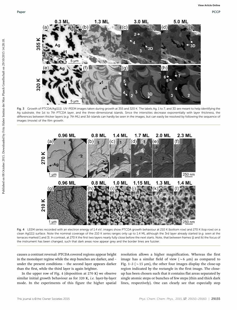
The changes between the two temperatures of Fig. 1 call for afurther lowering of the temperature in order to possibly achievelayer-by-layer growth. The result of two attempts is shown inFig. 3, the selected temperatures being 355 K (upper row) and320 K (lower row), respectively. At 355 K, the trend of Fig. 1is continued: smaller domains, higher density of islands,co-existence of several layers, 3rd and 4th layer metastable,competition of 3rd and 4th layer with 3-dim growth.
At 320 K we observe a nearly perfect layer-by-layer or Franck–van-der-Merwe growth. The first two layers grow successively(as before), for higher exposures several layers grow parallel.The detailed sequence (see ESI,† Movie_2.mp4) in fact revealsthat the discernible large areas are filled stochastically, not allin parallel, but one after the other. This means, that, e.g., onedomain with three layers may get a fourth, afterwards anotherwith five layers a sixth, then another with four layers a fifth,then the same domain a sixth, and so forth. For all moleculesor domains it is common, that the deposited moleculesapparently diffuse over large distances (tens of mm) before theyget trapped at a rim of an island, and that the domains havethe tendency to finish one layer before another domain (or thesame) starts a new layer. Again the domain boundaries aredetermined by step bunches on the substrate surface, and thesmooth areas are rather large (several mm). By the way, in this
case the half-moon shaped structures arose after an intensethermal treatment of the sample for cleaning purposes leadingto a high rate of self-diffusion and the well-known formationof half-circle-shaped step bunches between pinning centres(defects).28–30
It should be emphasized at this point that the sequenceshows true epitaxial multilayer growth of an organic layer on aninorganic substrate since (a) the organic domains are highlyordered as derived from (SPA-)LEED investigations (see ref. 13and Section 3.5), (b) the molecular orientation is uniformwithin the entire film (see ref. 22 and Section 3.4), (c) theorganic layer is in registry with the substrate, in this case evencommensurate to the substrate (see ref. 13, 14, 16 and below),and (d) the single crystalline domains are rather large (several mm)(see Section 3.5). The density of domain boundaries is in factcomparable to that of high quality epitaxial films of inorganiccompound semiconductors.
The results of Fig. 4 were recorded at even lower tempera-tures, 270 K and 210 K, respectively. In this case we switched tothe LEEM mode of the SMART instrument, for several reasons:higher lateral resolution, higher intensity and therefore fastermeasurement, much less beam damage (as compared to X-rayirradiation), negligible heat transfer by irradiation, and demon-stration of the suitability of LEEM (similar to PEEM) for thein situ observation of thin film growth. In the LEEM mode verylow energy electrons (with kinetic energies at the surface of afew eV, here 1.4 eV) are back-diffracted from the surface anddetected with high spatial resolution.31 The contrast arises(a) either because of the different crystal structure of the Agsubstrate and the organic film and therefore different energydependent reflectivity (dark Ag and brighter PTCDA layers) or(b) because of the interference of the partial electron wavesreflected at the surface, at the organic planes and at the inter-face resulting in an energy- and thickness-dependent intensityvariation and leading to contrast between different PTCDA filmthicknesses. Note that the different contrast mechanism withrespect to the PEEM mode (namely the interference condition)
Fig. 2 Development of metastable layers: in the first row the images were taken during deposition at 375 K at the coverages indicated. In the second rowthe images were taken at the same temperature after deposition of 5 ML; the elapsed times indicated refer to the end of deposition.
PCCP Paper
Publ
ishe
d on
08
Oct
ober
201
5. D
ownl
oade
d by
Fri
tz H
aber
Ins
titut
der
Max
Pla
nck
Ges
ells
chaf
t on
29/1
0/20
15 1
4:28
:18.
View Article Online
This journal is© the Owner Societies 2015 Phys. Chem. Chem. Phys., 2015, 17, 29150--29160 | 29155
causes a contrast reversal: PTCDA covered regions appear brightin the monolayer regime while the step bunches are darker, and –under the present conditions – the second layer appears darkerthan the first, while the third layer is again brighter.
In the upper row of Fig. 4 (deposition at 270 K) we observesimilar initial growth behaviour as for 320 K, i.e. layer-by-layermode. In the experiments of this figure the higher spatial
resolution allows a higher magnification. Whereas the firstimage has a similar field of view (B6 mm) as compared toFig. 1–3 (B15 mm), the other four images display the close-upregion indicated by the rectangle in the first image. The close-up has been chosen such that it contains flat areas separated bysingle atomic steps or bunches of few steps (thin and thick darklines, respectively). One can clearly see that especially step
Fig. 3 Growth of PTCDA/Ag(111). UV-PEEM images taken during growth at 355 and 320 K. The labels Ag, 1 to 7, and 3D are meant to help identifying theAg substrate, the 1st to 7th PTCDA layer, and the three-dimensional islands. Since the intensities decrease exponentially with layer thickness, thedifferences between thicker layers (e.g. 7th ML) and 3d-islands can hardly be seen in the images, but can easily be resolved by following the sequence ofimages (movie) of the film growth.
Fig. 4 LEEM series recorded with an electron energy of 1.4 eV; images show PTCDA growth behaviour at 210 K (bottom row) and 270 K (top row) on aclean Ag(111) surface. Note the nominal coverage of the 210 K series ranges only up to 1.4 ML although the 3rd layer already started (e.g. seen at theterraces marked 1 and 3). In contrast, at 270 K the first two layers nearly fully close before the next starts. Note, that between frames (j) and (k) the focus ofthe instrument has been changed, such that dark areas now appear grey and the border lines are fuzzier.
Paper PCCP
Publ
ishe
d on
08
Oct
ober
201
5. D
ownl
oade
d by
Fri
tz H
aber
Ins
titut
der
Max
Pla
nck
Ges
ells
chaf
t on
29/1
0/20
15 1
4:28
:18.
View Article Online

29156 | Phys. Chem. Chem. Phys., 2015, 17, 29150--29160 This journal is© the Owner Societies 2015
bunches preferably act as boundaries for the formation ofPTCDA domains, and that again PTCDA molecules diffuse overlarge distances to complete existing domains before new domainsare nucleated. This is apparently true for the first three layersdisplayed in this figure but this behaviour most probably alsocontinues for further layers. It is also worth mentioning that the‘‘choice’’ of step bunches as domain boundaries changes fromlayer to layer which means that there are no particular buncheswhich act as nucleation centres or boundaries but that any stepbunch can play this role. Moreover, one can again derive from thisfigure that the (atomic scale) morphology of the substrate surfaceplays a decisive role for the morphology of the growing organicfilm, at least for the first few layers.
Lowering the deposition temperature to 210 K changes thesituation drastically as displayed in the lower sequence ofimages of Fig. 4. Now only relatively small islands (50–300 nm)are formed in the monolayer regime, and further deposition ofmolecules does not lead to a completion of the first layer butleads to the random growth of second and third layer patches aswell. Note that in this case the coverage-dependent sequence ofimages stops already at 1.43 ML because for higher coverages thesituation becomes more and more fuzzy such that no additionalinformation can be derived.
3.4. Laterally resolved spectroscopic information fromNEXAFS
One of the most important properties of organic films is theorientation of the molecules. From integral NEXAFS (near edgeX-ray absorption fine structure) investigations on perfectly closedfilms (deposition at about room temperature) it is known that theplanar PTCDA molecules in the film are oriented parallel to thesubstrate (‘‘flat lying’’).9,22,32 In the case of films with 3D islands(obtained at low, e.g. o200 K, or high substrate temperatures,e.g. 4400 K) the interpretation of the integral data concerningthe molecular orientation in the islands is less straightforwardbecause the 3D islands cover only a few percent of the entiresurface area and therefore hardly contribute to the integralNEXAFS signal. However, spectro-microscopy allows localprobing and is therefore ideally suited to investigate inhomo-geneous samples.
For the analysis of the molecular orientation the lineardichroism of NEXAFS can be used.33 This arises from thetransition matrix element for the excitation of an electron froma core level into an unoccupied molecular orbital by absorptionof an X-ray photon of the respective energy which is governedby selection rules. For PTCDA (and similar planar molecules)these selection rules lead to the result, that high NEXAFSintensity (bright intensity in Fig. 5) is observed when the linearpolarization vector of the X-rays is oriented perpendicular tothe molecular plane while the intensity is reduced to zero whenthe polarization vector is rotated parallel to the molecular planewith an angular dependence described by a Bsin2 function.22
Thus, in the experiment the angle between surface and lightpolarization has to be varied. Since in PEEM experiments thisvariation cannot be done by the common rotation of the sample(PEEMs require fixed sample geometry, i.e. surface normal
along the optical axis of the objective lens) we used a differentapproach: the SMART is installed at a beamline with a so-calledapple undulator,34,35 which enables the free choice of the orien-tation of the linear polarization (or helicity of circular polariza-tion) of the light. In this way identical sample spots were imagedwith two linear polarization orientations standing perpendicularto each other (using grazing incidence, i.e. 201).
Fig. 5 shows an XPEEM image (enclosure) of a nominal 5 MLthick PTCDA film as well as (coloured) NEXAFS spectra fromthree areas on the sample indicated by coloured circles in theenclosed image. The image taken at a photon energy of 285.6 eV(recording secondary electrons) displays a sample area with one3D island surrounded by areas covered with two and three layersof PTCDA, respectively. In this case the preparation is equivalentto that of Fig. 2d after cooling-down to RT for freezing themetastable third layer. While the image was recorded usingupright (701) polarization the NEXAFS spectra are displayed forboth polarization directions: upright (701, i.e. polarization nearlynormal to the surface) and parallel (in-plane) polarization (01).The 701 spectra clearly show a set of p-resonances (excitationsfrom C 1s orbitals into different unoccupied final states ofp-symmetry) which have been interpreted in detail elsewhere.32
From the very large difference between the spectra takenwith different polarizations one can unambiguously concludethat the PTCDA molecules are uniformly oriented with theirmolecular plane parallel to the surface with not much differencebetween bilayer, triple layer, and 3-dim island. At present itcannot be decided whether the very small p-signals from the3-dim island for in-plane polarization (01, red curve) are due toscattering effects, to a small tilt or bending of the entire island,or to single disordered molecules within the crystal. A particu-larly interesting result is that also molecules in the third,metastable layer is oriented parallel to the substrate (a signifi-cant tilt angle 4101 can be excluded by a careful analysis of theintensity behaviour) since one may argue that metastable
Fig. 5 Molecular orientation in NEXAFS. Comparison of the local NEXAFSspectra for two polarizations (01 and 701) and three sample regions (markedby coloured circles in the inset) for a PTCDA bi-layer (green), triple layer(blue) and 3D-island (red) on the Ag(111) surface.
PCCP Paper
Publ
ishe
d on
08
Oct
ober
201
5. D
ownl
oade
d by
Fri
tz H
aber
Ins
titut
der
Max
Pla
nck
Ges
ells
chaf
t on
29/1
0/20
15 1
4:28
:18.
View Article Online

This journal is© the Owner Societies 2015 Phys. Chem. Chem. Phys., 2015, 17, 29150--29160 | 29157
adsorbates may arise because of a less favourable orientationand bonding situation, respectively. Note that the informationof a uniform parallel orientation is by no means trivial becauseother, very similar molecules, e.g. NTCDA with identical func-tional groups but with a smaller aromatic core, show a comple-tely different behaviour and molecular orientation for coveragesabove a monolayer.36
Apart from the molecular orientation additional informationis contained in the spectra. For the upright polarization onecan distinguish spectroscopic differences between the spectra.First, the intensity of the p-transitions beyond 283.5 eV isreduced for the bilayer as compared to that from the triple-layer and 3-d crystal. And secondly, an additional structureappears for the bilayer (and less for the triple-layer) spectra at283 eV. The origin of these differences is the chemical bondingof the first layer to the Ag substrate which has been discussed indetail previously.9 Since the first layer considerably contributesto the bilayer and B50% less to the triple layer the signaturegradually vanishes going from the mono- to multilayers. Thespectroscopic signature can be qualitatively understood aschemisorptive (=covalent) bonding of the PTCDA molecules tothe Ag substrate involving the frontier orbitals and leading to amixing of Ag 5s and 4d states with p-orbitals of PTCDA.9 Thenew feature right at the Fermi level, i.e. the transition at 283 eVrepresents the upper unoccupied part of a hybrid orbital whichis partly occupied (and hence observable in photoemission)making the first molecular adsorbate layer ‘‘metallic’’.9,37 Thisexample shows that also spatially-resolved chemical informationcan be obtained in the NEXAFS mode.
From spectra and images as those shown in Fig. 5 one canderive more quantitative information. We do this based onseveral sets of data38 but without showing these in detail here.For the preparation conditions of Fig. 5 (and Fig. 2d) we derivea coverage by 3-dim islands of about p = 6.5% referred to theoverall surface area. From this (and the calibrated exposure) wederive an average height of the 3-dim islands of about 48 layers(including the underlying 2 ML) while the total average cover-age is ytotal = 5 ML corresponding to an average height of 15 nm(using a layer thickness of 0.325 nm). This is in close agreementwith the rough estimate of B60 layers in 3-dim islands estimatedabove based on the UV-PEEM results for similar preparation con-ditions. Together with the information derived from UV-PEEMimages that the average area of 3-dim islands is about 1.2 mm2 welearn that the islands are rather flat objects with aspect ratios ofroughly 60 for the preparation conditions given above.
3.5. Laterally resolved structural information by reflectedelectrons
After inspection of the initial growth behaviour discussed incontext with Fig. 1–4 one would like to know more about theorigin of the observed domains and their differences, inparticular those of the first layer because they are the essentialbasis for further growth. Since with spectroscopic techniquesno difference can be discerned, the domain structure may bedue to structural differences. From detailed STM and LEEDanalyses it is known that the highly ordered monolayer is
commensurate to the Ag(111) surface and that six differentazimuthal orientations occur due to the threefold rotationaland twofold mirror symmetry.13–16
Fig. 6 summarizes LEED and LEEM data from about half amonolayer PTCDA on Ag(111) prepared similarly to the casesshown in Fig. 3a or e (substrate temperature: 340 K). Fig. 6adisplays a bright field LEEM image (using the specularlyreflected (=back-diffracted) electrons; electron energy 2 eV)which is similar to those of Fig. 4. Like in Fig. 4b one candistinguish uncovered (dark) and covered (bright) areas whichare subdivided in domains separated by substrate steps or stepbunches. One observes that the islands also grow across sub-strate atomic steps (appearing as dark lines due to destructiveinterference). By switching the instrument setting from realspace imaging to the diffraction mode one obtains the LEEDpattern shown in Fig. 6b (electron energy 4 eV). It shows thewell-established LEED pattern of a highly ordered, commensuratePTCDA monolayer on Ag(111) which consists of six differentdomains and is understood in detail.13–16
Each spot of the LEED pattern (Fig. 6b) can be assigned toone of the six domains. By selecting one (or a few) of these spotsby an aperture positioned in one of the diffraction planes of theSMART instrument the intensity in the LEEM image predomi-nantly stems from that (or those) domains that belong to the
Fig. 6 Rotational domains in (sub-)monolayer PTCDA islands. The LEEDpattern (b) from the LEEM image (a) consists of a superposition of 6 singledomain patterns. Dark field images (right column, (d)–(f)) using significantLEED spots of (b) lead to the distinction of rotational domains. The arrange-ment of the domains is shown in the colour-labelled image (c).
Paper PCCP
Publ
ishe
d on
08
Oct
ober
201
5. D
ownl
oade
d by
Fri
tz H
aber
Ins
titut
der
Max
Pla
nck
Ges
ells
chaf
t on
29/1
0/20
15 1
4:28
:18.
View Article Online

29158 | Phys. Chem. Chem. Phys., 2015, 17, 29150--29160 This journal is© the Owner Societies 2015
selected superstructure spot(s). Such so-called dark fieldimages are displayed on the right of Fig. 6(d)–(f). They stem –according to the colour of the frames – from apertures that areset to either one of three positions indicated by the circles ofcorresponding colours in Fig. 6b. In the three dark field imagesthe different domains display different brightness, in agreementwith the basic idea sketched above. However, the intensity differ-ence is clearly less than 100% because in each case the apertureaccepted at least two superstructure spots as well as stray electronsfrom the background. However, the intensity difference is suffi-cient to find those domains that have the same intensity depen-dence and hence to assign each domain to one type of rotationaldomain. This is done in Fig. 6c which uses four different colours toidentify different rotational domains.
Thus we learn from this figure that each area is delimited bysteps or step bunches. Different nucleation centres are likelythe origin of different rotational domains. The domains canpropagate over (single or few) steps but are also visibly limitedby step boundaries. As some step-enclosed areas do not lead tonucleation centres, we can derive that, at this temperature,PTCDA molecules ignore steps as minor obstacles and diffuseover macroscopic distances as testified by the rather largedomains observed (several mm). On the contrary, the variety ofdomain sizes observed suggests that bunches of several steps actas diffusion barriers, in agreement with a previous publication.20
In other words, the rotational domain sizes and hence thequality of the epitaxial layer crucially depend on the morphologyof the substrate surface.
4. Conclusions
The present work gives comprehensive insight into the mecha-nisms and parameter dependences determining the epitaxial,or at least highly ordered, growth of an organic thin film on aninorganic substrate. The prototype system PTCDA on Ag(111)was chosen because many details are already known from other
work which are complemented and completed by the presentwork thus yielding a coherent overall picture for one modelsystem. In addition, the small lattice mismatch between the tworather different systems gives hope for true heterogeneous epitaxywhich might be highly interesting for some applications. Thelatter aspect is nurtured by the finding that the optical propertiesstrongly depend on the preparation conditions, for instance thatthe fluorescence yield can be about a factor of 10 larger if certainpreparation conditions are chosen.4 The fact that some findingsof the present paper have already been stated in previous pub-lications using other methods is believed to be an advantagebecause it proves that the picture drawn here is consistent withprevious work and that the combined data obtainable by theSMART can replace several investigations using a variety ofdifferent (complementary) techniques.
For the start of the growth process, i.e. for the nucleation ofthe first layer we here find the formation of very large, severalmicrometer-sized single-crystalline domains that grow in registrywith the substrate surface structure (commensurate, i.e. epitaxial,adsorption) across surface steps or bunches of few steps (LEEM/LEED results). This indicates huge diffusion lengths of PTCDA evenon the clean Ag surface (tens of mm) although the (final) bonding tothe substrate is covalent (NEXAFS results) and site-specific (LEEDresults). Distinguishable domains of the first layer belong to thethree rotational and two mirror domains and are usually separatedby steps or multistep bunches. This new finding indicates a con-siderable influence of the morphology of the substrate surface onthe domain structure of the organic film; hence the morphology ofthe substrate surface determines the ‘‘epitaxial quality’’, e.g. thedensity of domain boundaries in the growing molecular film(LEEM, UV-PEEM results). For temperatures above about 250 Kwe observe that the first layer is completed before the second layerstarts growing, and the same happens then with the 2nd/3rd layer(UV-PEEM/LEEM results). In both layers the planar molecules areoriented parallel to the surface (NEXAFS results).
The growth of further layers strongly depends on the sub-strate temperature (consistently shown here) and deposition
Fig. 7 Overview of the temperature dependant growth of the first 2 to 6 layers of PTCDA on Ag(111). Below RT, PTCDA starts in a quasi Vollmer–Webermode, switches to Franck–van-der-Merwe mode around RT and transforms to a Stranski–Krastanov mode at elevated temperatures. Note the differencein lateral scales. Nominal coverage is denoted below the images. The 210 K and 270 K images were taken by LEEM, the others by UV-PEEM.
PCCP Paper
Publ
ishe
d on
08
Oct
ober
201
5. D
ownl
oade
d by
Fri
tz H
aber
Ins
titut
der
Max
Pla
nck
Ges
ells
chaf
t on
29/1
0/20
15 1
4:28
:18.
View Article Online

This journal is© the Owner Societies 2015 Phys. Chem. Chem. Phys., 2015, 17, 29150--29160 | 29159
rate (few data shown here). The temperature-dependent resultsare summarized in Fig. 7 which displays the most representativeimages for the temperatures discussed in this work (upper row)and the corresponding findings as schematic pictures. At thelowest temperature investigated here (210 K) we directly observedfor the first time the nucleation of only small domains, thegrowth of up to three layers before the first is completed andhence the growth of small 3-dim islands which can be summar-ized as quasi Vollmer–Weber growth (from LEEM results).
At and above 270 K first two complete and stable PTCDAlayers grow one after the other. Between 270 and 320 K thislayer-by-layer growth is essentially continued such that one canconsider this behaviour as Franck–van-der-Merwe growth mecha-nism which has been suggested before but never observeddirectly. It leads to a truly epitaxial film because the orderedgeometric structure of the molecular film is in (commensurate)registry with the structure of the substrate (from PEEM and LEEDresults).
Above 320 K 3-dim islands start to grow after the secondlayer is completed leading to a clear Stranski–Krastanov layergrowth behaviour. In the temperature range around 350 K weobserve for the first time special growth conditions withmetastable 3rd and 4th layers which are in equilibrium withthe growing 3-dim islands. These metastable layers are presentas long as the molecular flux is switched on but disappear withtemperature-dependent lifetime as soon as the molecular fluxis stopped (from PEEM results).
Finally we have to discuss the question why the observedchange of the growth mechanism occurs. Stranski–Krastanovgrowth usually arises for thermodynamic reasons if a latticemismatch between the structures of substrate and adlayer exists.By formation of 3-dim crystallites the contact area between thestrained and the relaxed layer is reduced thus optimizing thetotal free energy.
In the present case this lattice mismatch between the Ag(111)surface and the (102) plane of crystalline b-PTCDA is about 1 to2% while for a-PTCDA (the most stable structure at RT) it is evenlarger (5%).13 Thus, due to the strong substrate–PTCDA inter-action at the interface the first PTCDA layer apparently grows ina strained fashion.13,39 Since also the second layer is slightlystronger bound to the first than to the third layer it also growsstrained. Subsequent layers grow epitaxially (i.e. strained) ifsubstrate temperature and deposition rate are low enough toprevent the thermodynamically favourable formation of 3-dimcrystallites in the (relaxed) a-structure which is probably hinderedby activation barriers for nucleation and/or upward diffusionacross the step edges of PTCDA layers (Ehrlich–Schwoebelbarrier). The latter happens at elevated temperatures at which3-dim crystallites on-top of the strained bi-layer are beingformed.13 At intermediate temperatures (here around 350 K)competition between the formation of (strained) 3rd and 4thlayer and 3-dim growth leads to unstable conditions: 3rd and4th layer are metastable and decay to 3-dim crystallites depend-ing on temperature and time. We speculate that the metastabilityis most probably also existent for epitaxial multilayers (44 layers)at low temperatures, but the formation of crystallites is not
observed within the timeframe of our experiment. Annealingexperiments for (strained) low-T layers have shown that atelevated temperatures (e.g. 400 K) relaxation and formation of3-dim crystals occur.13,39
It should be mentioned, that also an influence of the sub-strate morphology on the growth behaviour has been observed,e.g., on the nucleation site or on the nucleation density.20 In thepresent case, for instance, the 4th layer (appearing as dark greyarea at 4 ML in Fig. 2) nucleates only on flat surface areas, notat step bunches of the substrate (bright lines in the lower partof Fig. 2). This can be explained by the (additional) straininduced by steps and facets.
Summarizing the role of the specific instrument SMART forsuch investigations, we have benefited from the in situ combi-nation of a variety of complementary surface techniques toaddress several surface properties ranging from microscopicinsight, over topographic aspects, structural questions, electro-nic properties, chemical details up to dynamic processes. Thisenabled us to observe several new phenomena and to obtaina completely consistent picture. Moreover, all results could inprinciple be obtained from the same sample area or from thesame microscopic object under identical preparation condi-tions using the spatially resolving techniques. Thus SMART isideally suited to shed light on complicated microscopic proper-ties and processes of surface systems.
Acknowledgements
This project was funded by the Federal German Ministry ofEducation and Research (BMBF) under contract 05 KS4WWB/4and by the Fritz-Haber Institute of the Max-Planck Society. Wethank the BESSY-II crew for technical support and the HZB forthe allocation of synchrotron radiation beamtime.
References
1 B. Geffroy, P. le Roy and C. Prat, Organic Light-emittingDiode Technology: Materials, Devices and Display Technol-ogies, Polym. Int., 2006, 55, 572.
2 C. Brabec, U. Scherf and V. Dyakonov, Organic Photovoltaics:Materials, Device Physics, and Manufacturing Technologies,John Wiley & Sons, 2011.
3 M. Muccini, Nat. Mater., 2006, 5, 605.4 M. Schneider and E. Umbach M. Sokolowski, Chem. Phys.,
2006, 325, 185.5 J. V. Barth, G. Costantini and K. Kern, Nature, 2005,
437, 671.6 R. Wichtendahl, R. Fink, H. Kuhlenbeck, D. Preikszas,
H. Rose, R. Spehr, P. Hartel, W. Engel, R. Schlogl, H.-J.Freund, A. M. Bradshaw, G. Lilienkamp, T. Schmidt,E. Bauer, G. Benner and E. Umbach, Surf. Rev. Lett., 1998,5, 1249.
7 R. Fink, M. R. Weiss, E. Umbach, D. Preikszas, H. Rose,R. Spehr, P. Hartel, W. Engel, R. Degenhardt, R. Wichtendahl,H. Kuhlenbeck, W. Erlebach, K. Ihmann, R. Schlogl,
Paper PCCP
Publ
ishe
d on
08
Oct
ober
201
5. D
ownl
oade
d by
Fri
tz H
aber
Ins
titut
der
Max
Pla
nck
Ges
ells
chaf
t on
29/1
0/20
15 1
4:28
:18.
View Article Online

29160 | Phys. Chem. Chem. Phys., 2015, 17, 29150--29160 This journal is© the Owner Societies 2015
H.-J. Freund, A. M. Bradshaw, G. Lilienkamp, T. Schmidt,E. Bauer and G. Benner, J. Electron Spectrosc. Relat. Phenom.,1997, 84, 231.
8 T. Schmidt, U. Groh, R. Fink, E. Umbach, O. Schaff,W. Engel, B. Richter, H. Kuhlenbeck, R. Schlogl, H.-J. Freund,A. M. Bradshaw, D. Preikszas, P. Hartel, R. Spehr, H. Rose,G. Lilienkamp, E. Bauer and G. Benner, Surf. Rev. Lett., 2002,9, 223.
9 Y. Zou, L. Kilian, A. Scholl, T. Schmidt, R. Fink andE. Umbach, Surf. Sci., 2006, 600, 1240.
10 F. S. Tautz, M. Eremtchenko, J. A. Schaefer, M. Sokolowski,V. Shklover, K. Glockler and E. Umbach, Surf. Sci., 2002,502/503, 176.
11 A. Hauschild, R. Temirov, S. Soubatch, O. Bauer, A. Scholl,B. C. C. Cowie, T.-L. Lee, F. S. Tautz and M. Sokolowski,Phys. Rev. B: Condens. Matter Mater. Phys., 2010, 81, 125432.
12 B. Krause, A. C. Durr, K. Ritley, F. Schreiber, H. Dosch andD. Smiligies, Phys. Rev. B: Condens. Matter Mater. Phys.,2002, 66, 235404.
13 L. Kilian, E. Umbach and M. Sokolowski, Surf. Sci., 2004,573, 359.
14 K. Glockler, C. Seidel, A. Soukopp, M. Sokolowski,E. Umbach, M. Bohringer, R. Berndt and W.-D. Schneider,Surf. Sci., 1998, 405, 1.
15 F. S. Tautz, Prog. Surf. Sci., 2007, 82, 479.16 E. Umbach, K. Glockler and M. Sokolowski, Surf. Sci., 1998,
402–404, 20.17 M. Eremtchenko, J. A. Schaefer and F. S. Tautz, Nature,
2003, 425, 602.18 B. Stadtmuller, C. Henneke, S. Soubatch, F. S. Tautz and
C. Kumpf, New J. Phys., 2015, 17, 023046.19 T. Duden, A. Thust, C. Kumpf and F. S. Tautz, Microsc.
Microanal., 2014, 20(03), 968–973.20 H. Marchetto, U. Groh, T. Schmidt, R. Fink, H.-J. Freund
and E. Umbach, Chem. Phys., 2006, 325, 178.21 L. Kilian, A. Hauschild, R. Temirov, S. Soubatch, A. Scholl,
A. Bendounan, F. Reinert, T.-L. Lee, F. S. Tautz, M. Sokolowskiand E. Umbach, Phys. Rev. Lett., 2008, 100, 136103.
22 J. Taborski, P. Vaterlein, H. Dietz, U. Zimmermann andE. Umbach, J. Electron Spectrosc. Relat. Phenom., 1995,75, 129.
23 F.-J. Meyer zu Heringdorf, M. C. Reuter and R. M. Tromp,Nature, 2001, 412, 517–520.
24 This value has been determined by J. Taborski andE. Umbach using the method described in E. Umbach andR. Fink, in Proc. Intl. School Enrico Fermi, ed. G. La Roccaand V. Agranovich, North Holland, 2002, p. 233.
25 T. Graber, F. Forster, A. Scholl and F. Reinert, Surf. Sci.,2011, 606, 878.
26 M. B. Casu, Y. Zou, S. Kera, D. Batchelor, T. Schmidt andE. Umbach, Phys. Rev. B: Condens. Matter Mater. Phys., 2007,76, 193311.
27 L. Chkoda, M. Schneider, V. Shklover, L. Killian,M. Sokolowski, C. Heske and E. Umbach, Chem. Phys. Lett.,2003, 371, 548.
28 M. Mundschau, E. Bauer and W. Telieps, Surf. Sci., 1989,223, 413.
29 J. S. Ozcomert, W. W. Pai, N. C. Bartelt and J. E. Reutt-Robey,Surf. Sci., 1993, 293, 183.
30 G. A. Held, D. M. Goodstein, R. M. Feenstra, M. J. Ramstad,D. Y. Noh and R. J. Birgeneau, Phys. Rev. B: Condens. MatterMater. Phys., 1993, 48, 8458.
31 E. Bauer, Rep. Prog. Phys., 1994, 57, 895.32 A. Scholl, Y. Zou, D. Hubner, S. Urquhart, T. Schmidt,
R. Fink and E. Umbach, J. Chem. Phys., 2005, 123, 044509.33 J. Stohr and D. A. Outka, Phys. Rev. B: Condens. Matter Mater.
Phys., 1987, 36, 7891.34 S. Sasaki, Nucl. Instrum. Methods Phys. Res., Sect. A, 1994,
347, 83.35 J. Bahrdt, A. Gaupp, W. B. Peatman, F. Schaefers and
C. Wang, Proc. SPIE, 1994, 168, 577.36 U. Groh, Doctoral thesis, Universitat Wurzburg, Germany,
2006; U. Groh, T. Schmidt, H. Marchetto, E. Umbach, inpreparation.
37 F. S. Tautz, M. Eremtchenko, J. A. Schaefer, M. Sokolowski,V. Shklover and E. Umbach, Phys. Rev. B: Condens. MatterMater. Phys., 2002, 65, 125405.
38 H. Marchetto, Doctoral thesis, Freie Universitat, Berlin,Germany, 2006; H. Marchetto, T. Schmidt, U. Groh,R. Fink, E. Umbach, in preparation.
39 B. Krause, A. C. Durr, F. Schreiber, H. Dosch and O. H.Seeck, Surf. Sci., 2004, 572, 385.
40 D. Preikszas and H. Rose, J. Electron Microsc., 1997, 1, 1.41 D. Preikszas, Doctoral thesis D 17, Technische Hochschule
Darmstadt, Germany, 1995.42 T. Schmidt, H. Marchetto, P. L. Levesque, U. Groh, F. Maier,
D. Preikszas, P. Hartel, R. Spehr, G. Lilienkamp, W. Engel,R. Fink, E. Bauer, H. Rose, E. Umbach and H.-J. Freund,Ultramicroscopy, 2010, 110, 1358.
43 T. Schmidt, A. Sala, H. Marchetto, E. Umbach and H.-J.Freund, Ultramicroscopy, 2013, 126, 23.
44 A two dimensional gas describes a dilute layer of moleculesthat are weakly bound to the surface and diffuse freelyacross the surface. Hence, they are not directly imaged bymost methods. See e.g. J. A. Venables, G. D. T. Spiller andM. Hanbucken, Rep. Prog. Phys., 1984, 47, 399 or E. Loginova,N. C. Bartelt, P. J. Feibelman and K. F. McCarty, New J. Phys.,2008, 10, 093026.
PCCP Paper
Publ
ishe
d on
08
Oct
ober
201
5. D
ownl
oade
d by
Fri
tz H
aber
Ins
titut
der
Max
Pla
nck
Ges
ells
chaf
t on
29/1
0/20
15 1
4:28
:18.
View Article Online