diodes - electronic engineeringmolloyd/ee223files/ee223_diodes.pdf · for example: phosphorus –...
TRANSCRIPT

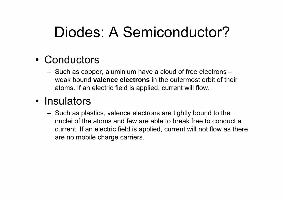
Diodes: A Semiconductor?
• Conductors– Such as copper, aluminium have a cloud of free electrons –
weak bound valence electrons in the outermost orbit of their atoms. If an electric field is applied, current will flow.
• Insulators– Such as plastics, valence electrons are tightly bound to the
nuclei of the atoms and few are able to break free to conduct a current. If an electric field is applied, current will not flow as there are no mobile charge carriers.
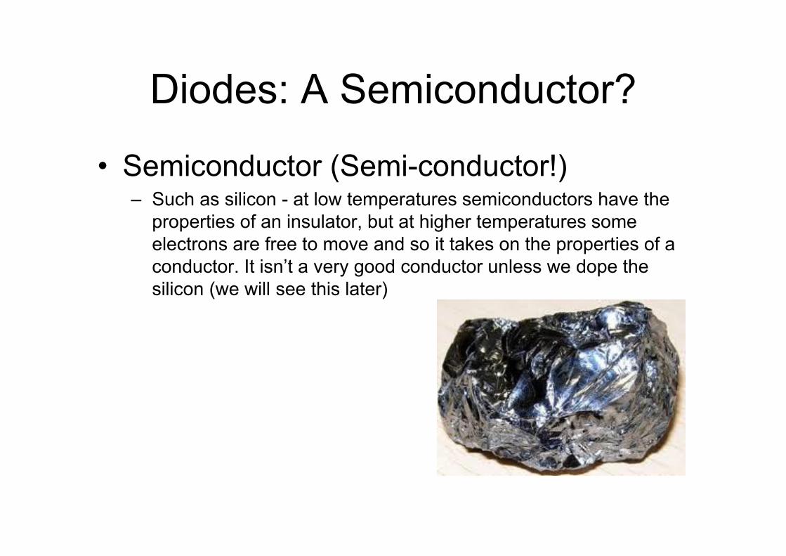
Diodes: A Semiconductor?
• Semiconductor (Semi-conductor!)– Such as silicon - at low temperatures semiconductors have the
properties of an insulator, but at higher temperatures some electrons are free to move and so it takes on the properties of a conductor. It isn’t a very good conductor unless we dope the silicon (we will see this later)
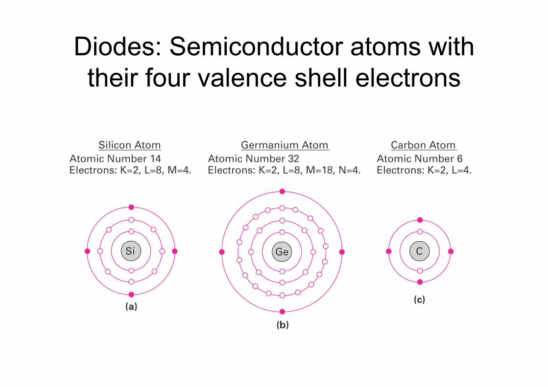
Diodes: Semiconductor atoms with their four valence shell electrons
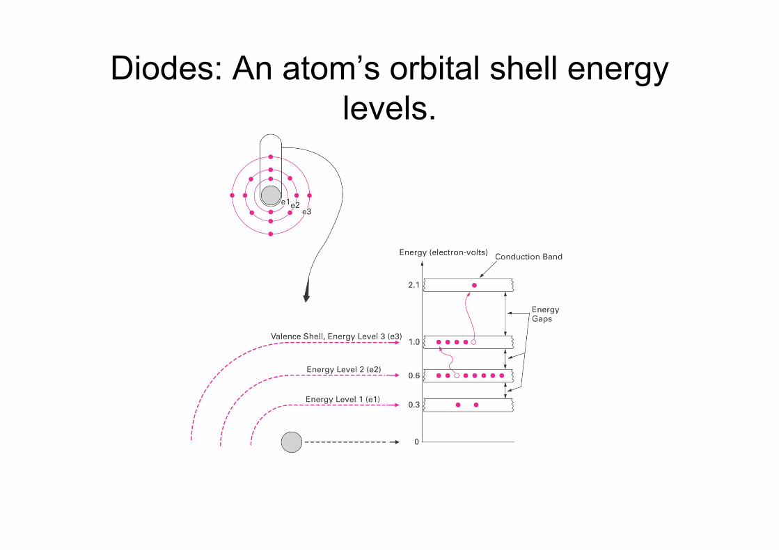
Diodes: An atom’s orbital shell energy levels.

Diodes: Covalent bonding
• Pure Silicon– Silicon is a tetravalent (4 valence electrons)
material. Outermost electron shell can accommodate 8 electrons and the atom is stable when it is in this form.
• At low Temperatures:– Tight bonding means no electrons free to
conduct current.
• At higher Temperatures:– Thermal vibration of the crystal lattice results
in some of the bonds being broken, generating free electrons and leaving behind holes.

Diodes: Temperature effects on semiconductor materials
At room temperature the number of charge carriers present in pure silicon is small and it is a poor conductor – we call this intrinsic conduction.
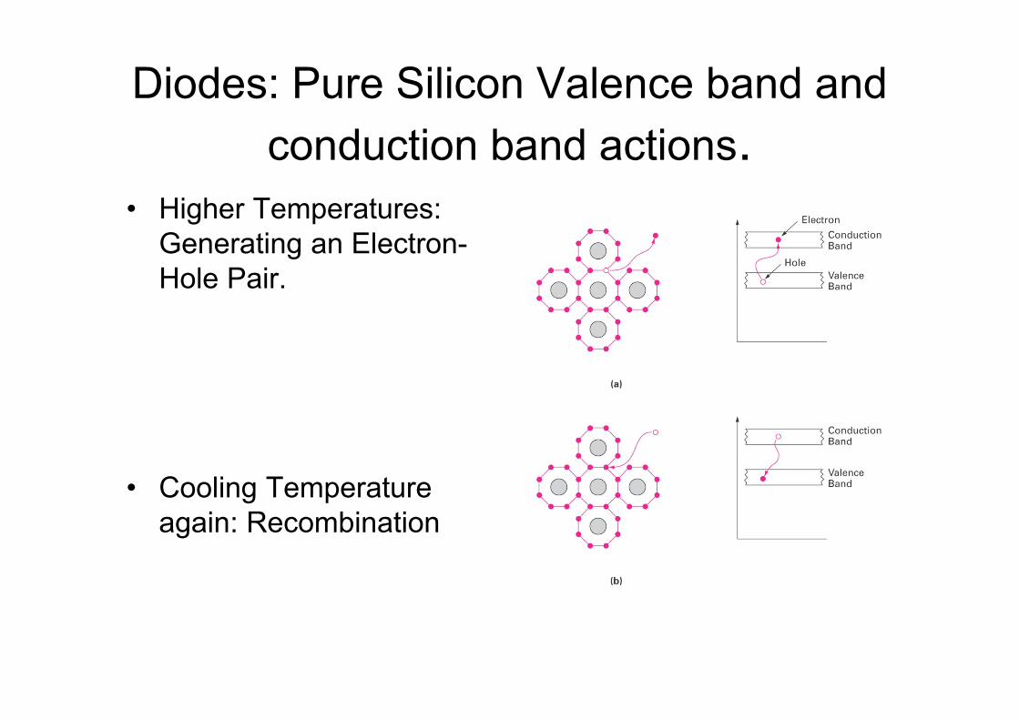
Diodes: Pure Silicon Valence band and conduction band actions.
• Higher Temperatures: Generating an Electron-Hole Pair.
• Cooling Temperature again: Recombination

Diodes: Packaging & Schematic
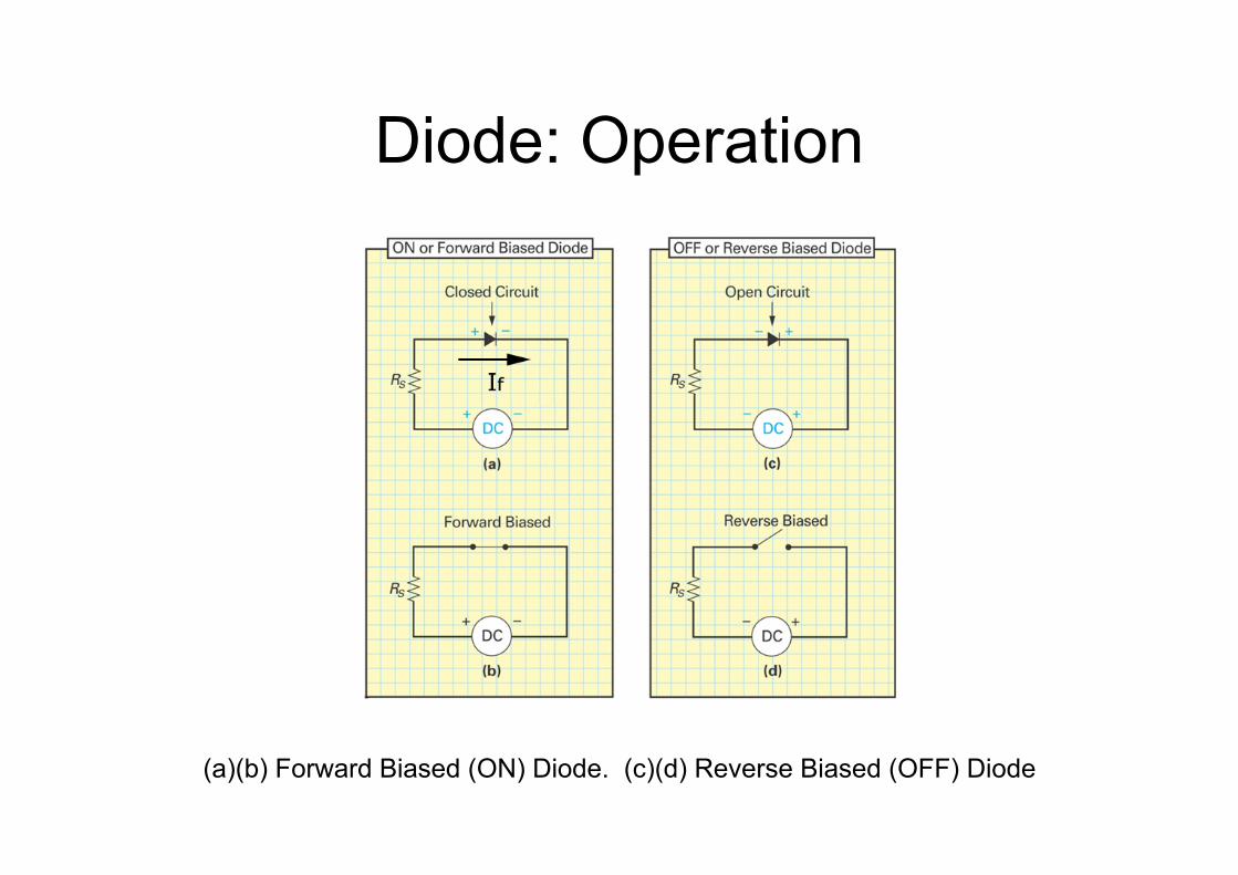
Diode: Operation
(a)(b) Forward Biased (ON) Diode. (c)(d) Reverse Biased (OFF) Diode

Diodes: Doping• Adding small amounts of impurities to silicon
– Can hugely affect its properties – especially if it can fit within the crystal lattice but has a different number of valence electrons. For example: Phosphorus
– Its fifth valence electron is very weakly bound– Has an excess of free electrons
– Called n-type semiconductors as they have free negative charge carriers
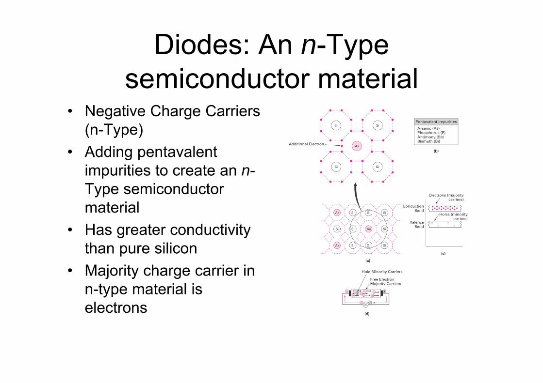
Diodes: An n-Type semiconductor material
• Negative Charge Carriers (n-Type)
• Adding pentavalent impurities to create an n-Type semiconductor material
• Has greater conductivity than pure silicon
• Majority charge carrier in n-type material is electrons
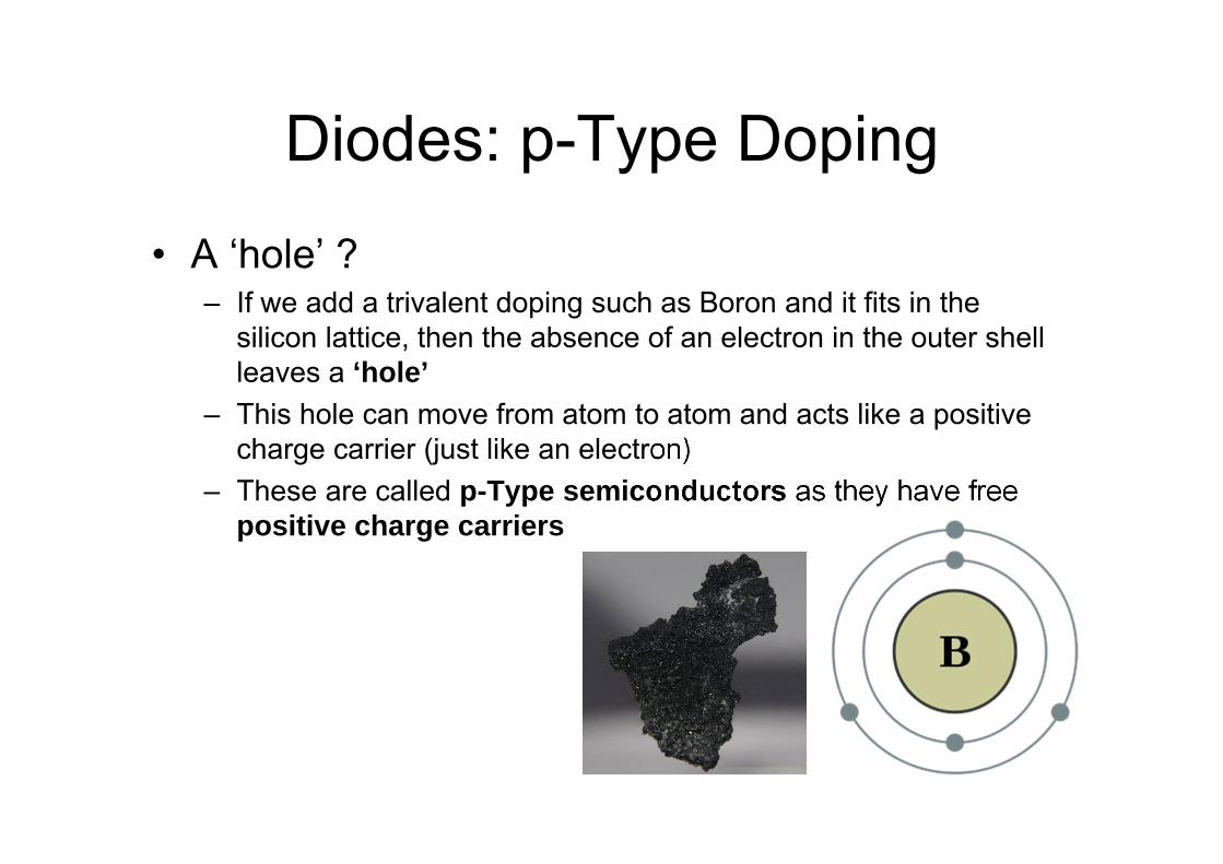
Diodes: p-Type Doping
• A ‘hole’ ?– If we add a trivalent doping such as Boron and it fits in the
silicon lattice, then the absence of an electron in the outer shell leaves a ‘hole’
– This hole can move from atom to atom and acts like a positive charge carrier (just like an electron)
– These are called p-Type semiconductors as they have free positive charge carriers
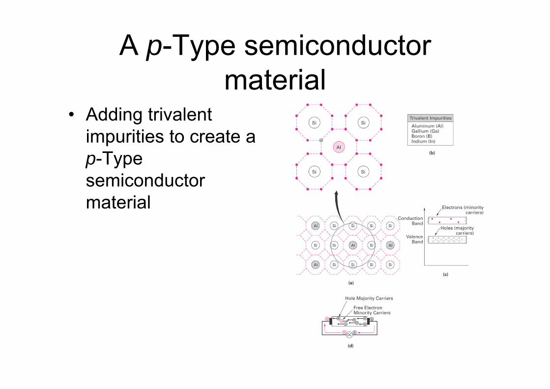
A p-Type semiconductor material
• Adding trivalent impurities to create a p-Type semiconductor material

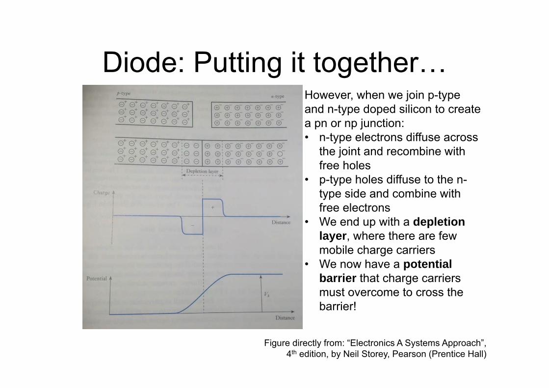
Diode: Putting it together…
Figure directly from: “Electronics A Systems Approach”, 4th edition, by Neil Storey, Pearson (Prentice Hall)
Doped silicon is also electrically neutral (like non-doped silicon) – each mobile charge carrier is matched by an equal number of bound charge carriers of the opposite polarity. The dominant charge carriers (electrons in n-type, holes in p-type) are called majority charge carriers.
Diode: Putting it together…
Figure directly from: “Electronics A Systems Approach”, 4th edition, by Neil Storey, Pearson (Prentice Hall)
However, when we join p-type and n-type doped silicon to create a pn or np junction:• n-type electrons diffuse across
the joint and recombine with free holes
• p-type holes diffuse to the n-type side and combine with free electrons
• We end up with a depletion layer, where there are few mobile charge carriers
• We now have a potential barrier that charge carriers must overcome to cross the barrier!

Diode: With No Applied Voltage…
Figure directly from: “Electronics A Systems Approach”, 4th edition, by Neil Storey, Pearson (Prentice Hall)
• In Isolation (no applied voltage), some majority charge carriers cross the depletion layer, creating a small diffusion current (moving from areas of high concentration to areas of low concentration without an electric field); however there is exactly equivalent movement of minority charge carriers in the opposite direction (a drift current). The drift current cancels out the diffusion current.

Diode: Forward Bias…
Figure directly from: “Electronics A Systems Approach”, 4th edition, by Neil Storey, Pearson (Prentice Hall)
• In Forward Bias - the p-type side is made positive with respect to the n-type side and the depletion layer shrinks. The height of the potential barrier decreases and majority carriers can now cross the barrier.
• Diffusion current > Drift current and there is a net current flow.
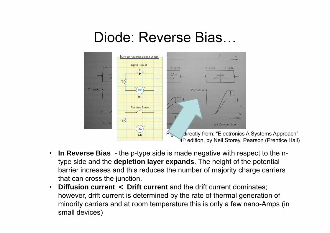
Diode: Reverse Bias…
Figure directly from: “Electronics A Systems Approach”, 4th edition, by Neil Storey, Pearson (Prentice Hall)
• In Reverse Bias - the p-type side is made negative with respect to the n-type side and the depletion layer expands. The height of the potential barrier increases and this reduces the number of majority charge carriers that can cross the junction.
• Diffusion current < Drift current and the drift current dominates; however, drift current is determined by the rate of thermal generation of minority carriers and at room temperature this is only a few nano-Amps (in small devices)

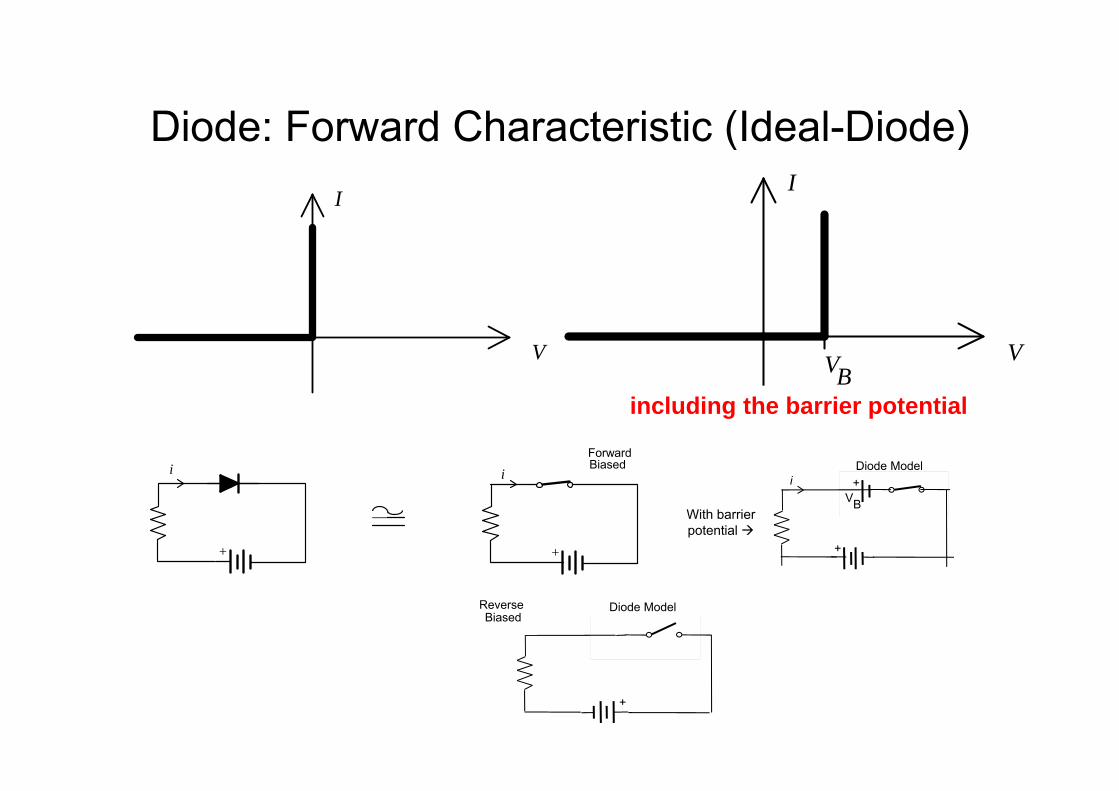
Forward Biasing a PN-JunctionPassing current through in a forward direction
• When device conducting (current flow np), threshold voltage appears as voltage dropacross junction e.g. Si junction,
voltmeter = 0.7V• N.B.
VTh for Si = 0.7VVTh for Ger = 0.3V
Fig (d)• Forward-biased PN junction acts as closed switch with small resistance Switch opens again, when applied voltage drops < VTh needed for np
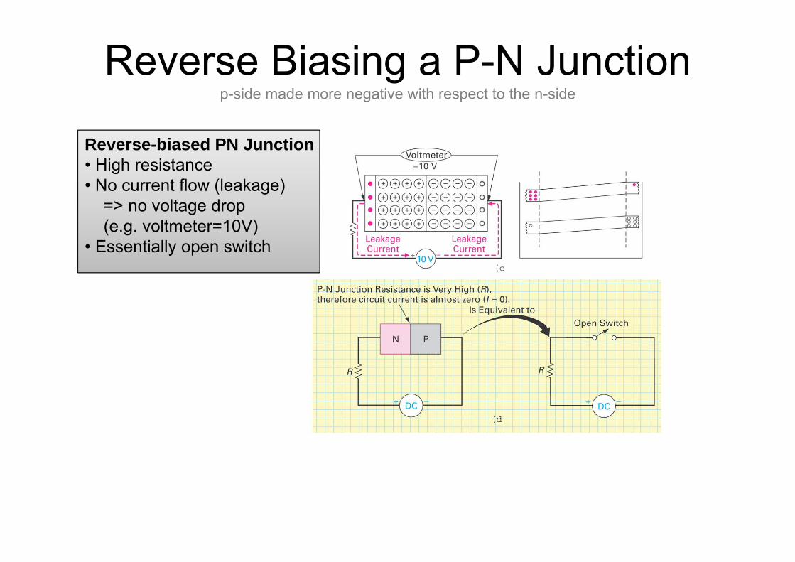
Reverse-biased PN Junction • High resistance• No current flow (leakage)
=> no voltage drop(e.g. voltmeter=10V)
• Essentially open switch
Reverse Biasing a P-N Junctionp-side made more negative with respect to the n-side

Biased pn-junctions – How biased?

Diode: Operation Summary
(a)(b) Forward Biased (ON) Diode. (c)(d) Reverse Biased (OFF) Diode

Diode: Worked Examples
• Solution of (a) I=0mA and V=6V• Solution of (b) I=(Vs-Vpn)/R
I=6.08mA (i.e. VR = 7.3V, taking Vpn=0.7V)
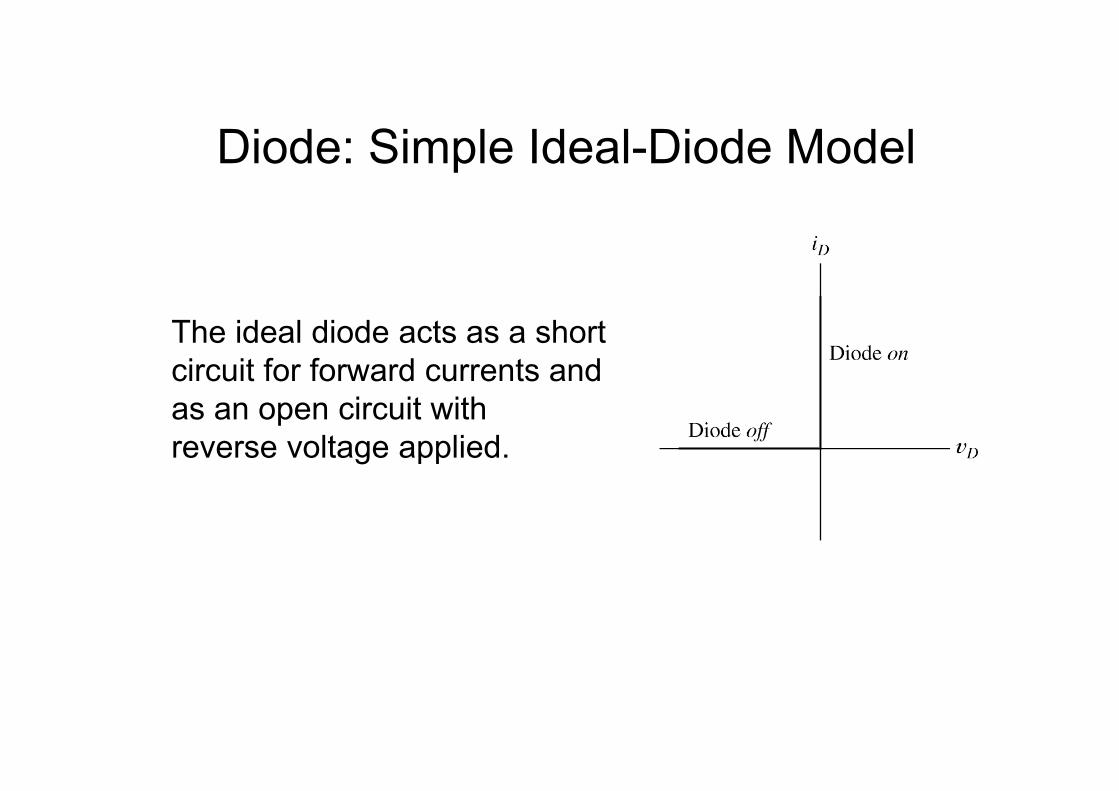
The ideal diode acts as a short circuit for forward currents and as an open circuit withreverse voltage applied.
Diode: Simple Ideal-Diode Model
V
I
BV
Diode: Forward Characteristic (Ideal-Diode)
V
I
including the barrier potential
+
i
+
i
+
i +Diode Model
Forward
VB
Biased
+
Diode ModelReverseBiased
With barrierpotential
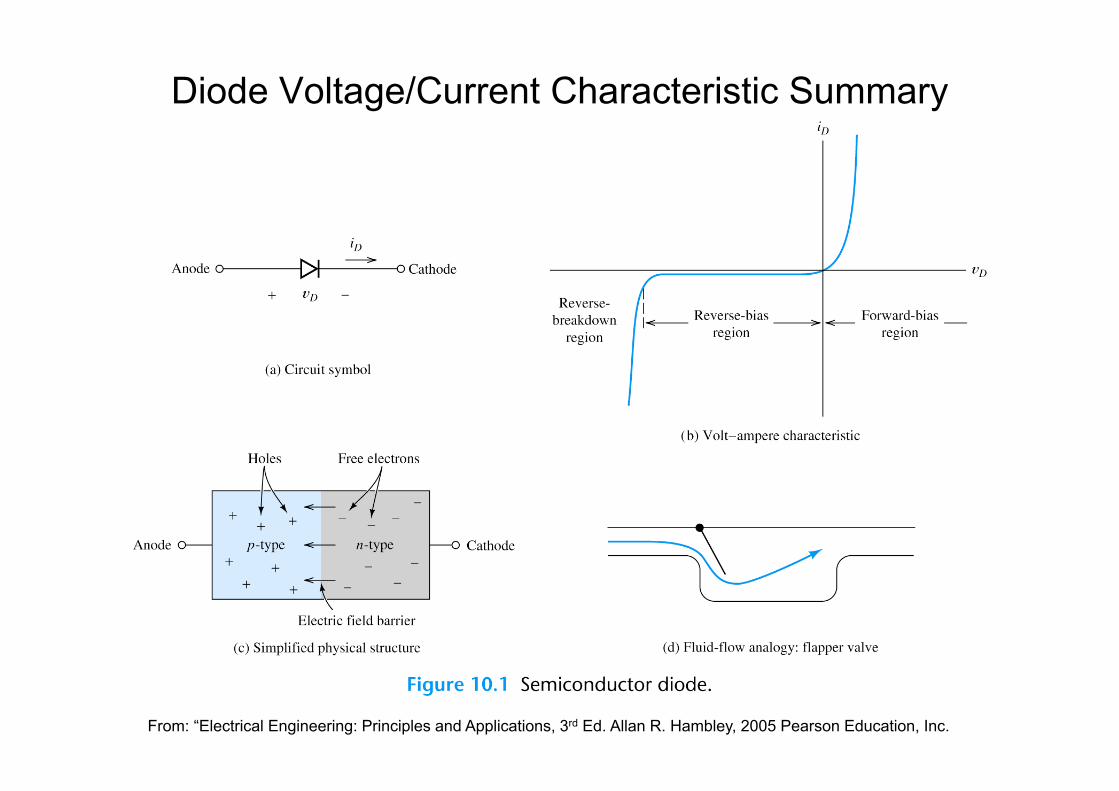
Diode Voltage/Current Characteristic Summary
From: “Electrical Engineering: Principles and Applications, 3rd Ed. Allan R. Hambley, 2005 Pearson Education, Inc.
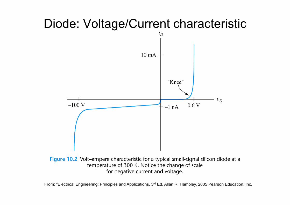
Diode: Voltage/Current characteristic
From: “Electrical Engineering: Principles and Applications, 3rd Ed. Allan R. Hambley, 2005 Pearson Education, Inc.
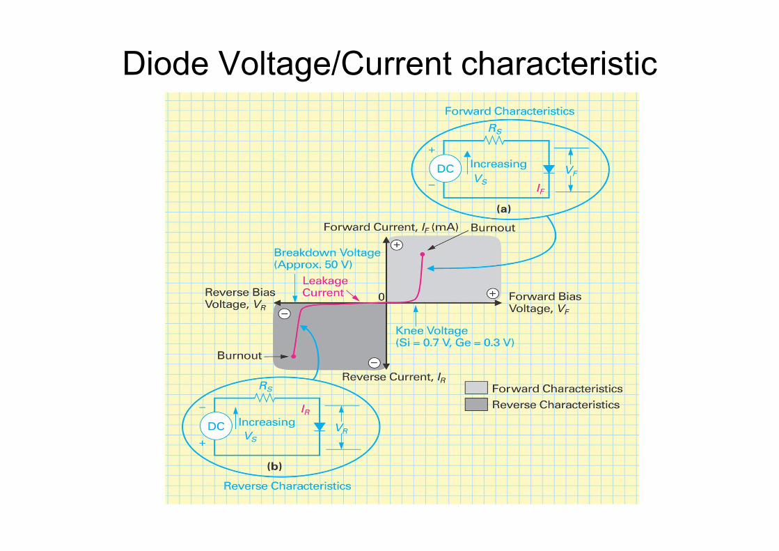
Diode Voltage/Current characteristic
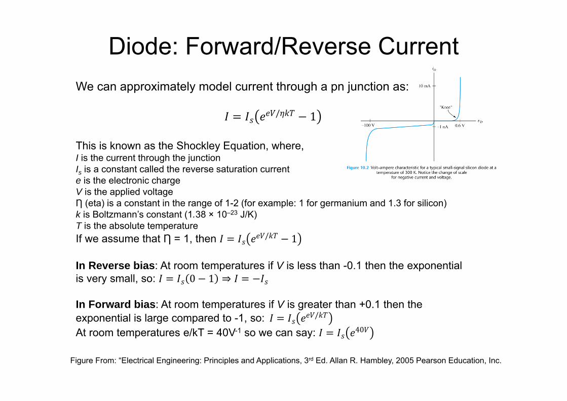
Diode: Forward/Reverse Current
Figure From: “Electrical Engineering: Principles and Applications, 3rd Ed. Allan R. Hambley, 2005 Pearson Education, Inc.
We can approximately model current through a pn junction as:= / − 1This is known as the Shockley Equation, where,I is the current through the junctionIs is a constant called the reverse saturation currente is the electronic chargeV is the applied voltageȠ (eta) is a constant in the range of 1-2 (for example: 1 for germanium and 1.3 for silicon)k is Boltzmann’s constant (1.38 × 10⁻²³ J/K)T is the absolute temperatureIf we assume that Ƞ = 1, then = / − 1In Reverse bias: At room temperatures if V is less than -0.1 then the exponential is very small, so: = 0 − 1 ⇒ = −In Forward bias: At room temperatures if V is greater than +0.1 then the exponential is large compared to -1, so: = /At room temperatures e/kT = 40V-1 so we can say: = 40
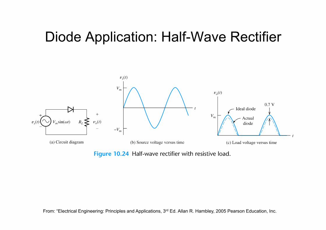
Diode Application: Half-Wave Rectifier
From: “Electrical Engineering: Principles and Applications, 3rd Ed. Allan R. Hambley, 2005 Pearson Education, Inc.

Diode Application: Half-Wave Rectifier(with smoothing)
From: “Electrical Engineering: Principles and Applications, 3rd Ed. Allan R. Hambley, 2005 Pearson Education, Inc.
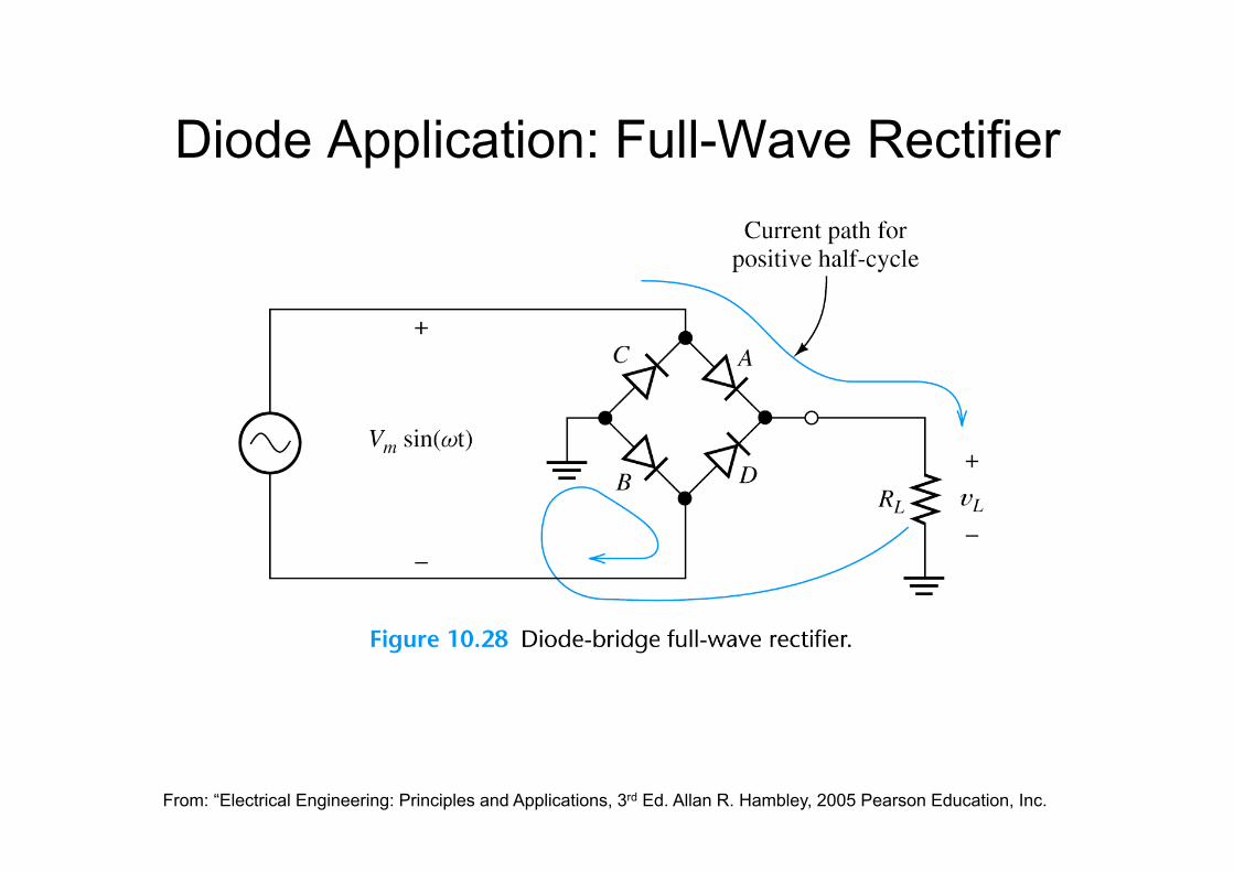
Diode Application: Full-Wave Rectifier
From: “Electrical Engineering: Principles and Applications, 3rd Ed. Allan R. Hambley, 2005 Pearson Education, Inc.

Load Line (Slide 1)
DDSS viRV += .
We know R and VSS. What are iD and vD?
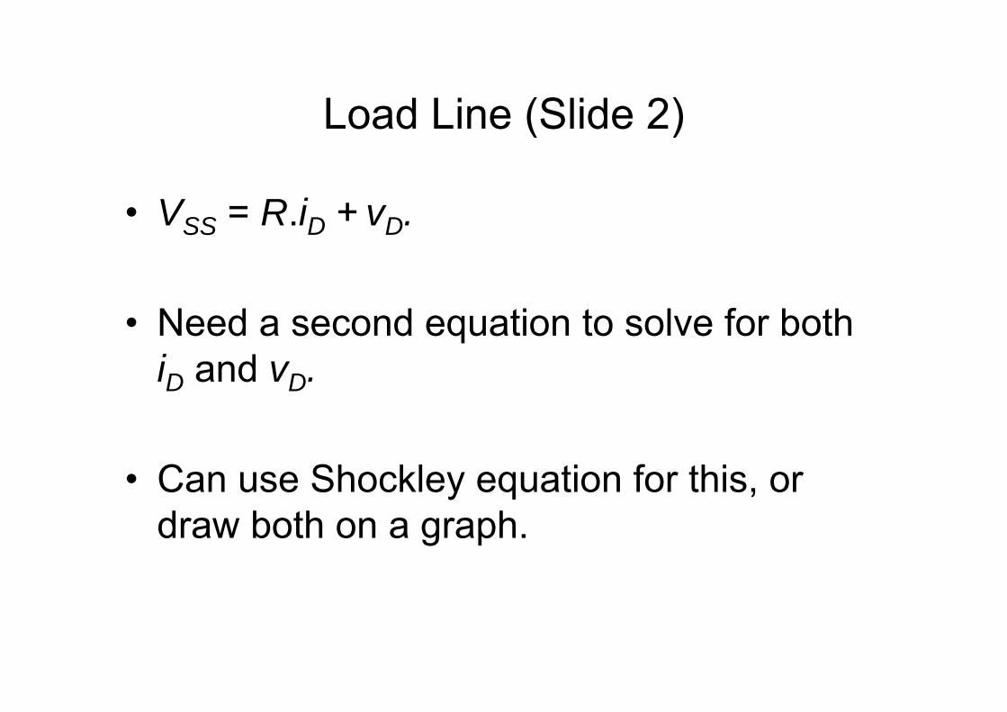
Load Line (Slide 2)
• VSS = R.iD + vD.
• Need a second equation to solve for both iD and vD.
• Can use Shockley equation for this, or draw both on a graph.

Load Line (Slide 3)
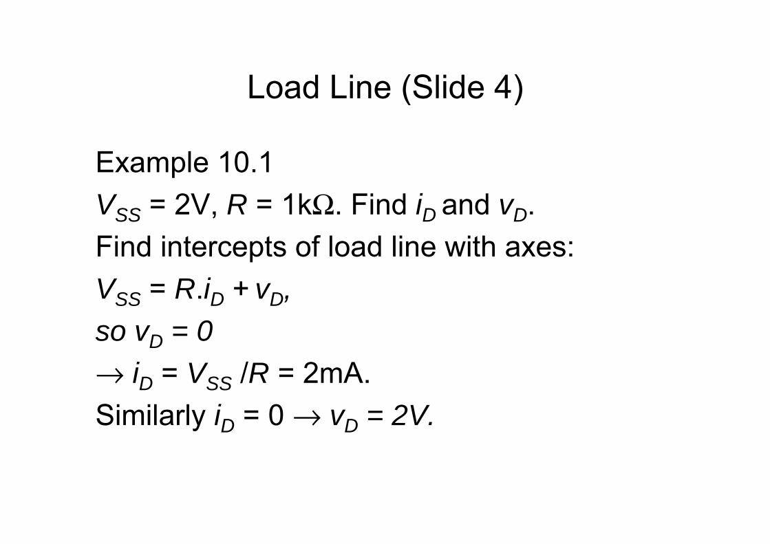
Load Line (Slide 4)
Example 10.1VSS = 2V, R = 1kΩ. Find iD and vD.Find intercepts of load line with axes:VSS = R.iD + vD, so vD = 0→ iD = VSS /R = 2mA.Similarly iD = 0 → vD = 2V.
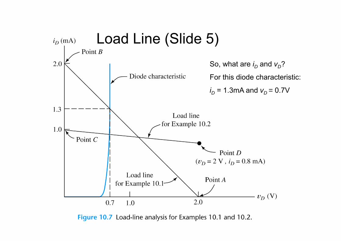
Load Line (Slide 5)So, what are iD and vD?
For this diode characteristic:
iD = 1.3mA and vD = 0.7V
Load Line (Slide 6)
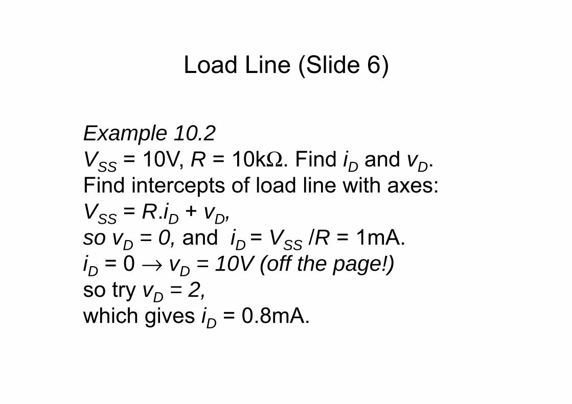
Example 10.2VSS = 10V, R = 10kΩ. Find iD and vD.Find intercepts of load line with axes:VSS = R.iD + vD, so vD = 0, and iD = VSS /R = 1mA.iD = 0 → vD = 10V (off the page!) so try vD = 2, which gives iD = 0.8mA.

Zener DiodesDiodes that are intended to operate in the breakdown region are called Zener diodes.
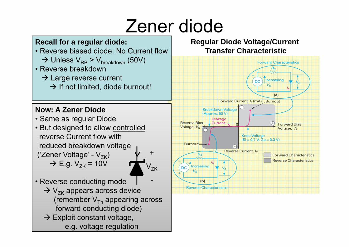
Now: A Zener Diode• Same as regular Diode• But designed to allow controlled
reverse Current flow with reduced breakdown voltage
(‘Zener Voltage’ - VZK) E.g. VZK = 10V
• Reverse conducting mode VZK appears across device
(remember VTh appearing across forward conducting diode)
Exploit constant voltage, e.g. voltage regulation
Zener diodeRegular Diode Voltage/Current
Transfer CharacteristicRecall for a regular diode:• Reverse biased diode: No Current flow Unless VRB > Vbreakdown (50V)
• Reverse breakdown Large reverse current If not limited, diode burnout!
+
VZK
-
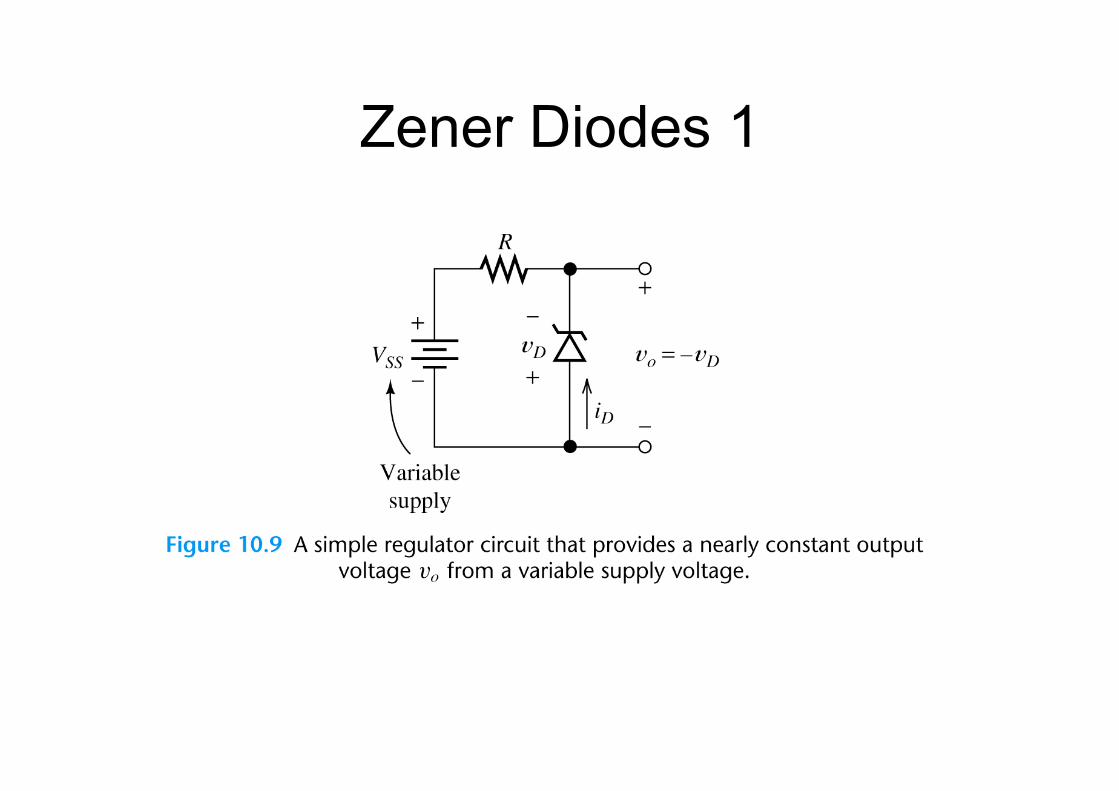
Zener Diodes 1
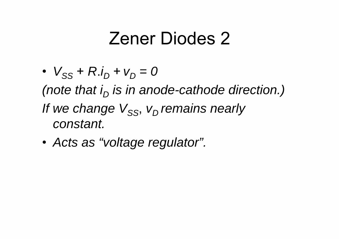
Zener Diodes 2
• VSS + R.iD + vD = 0(note that iD is in anode-cathode direction.)If we change VSS, vD remains nearly
constant.• Acts as “voltage regulator”.

Zener Diodes 3

Zener Diodes 4Example 10.3R = 1kΩ; find vD for VSS = 15V and for VSS = 20V.
Although VSS changes by 5V, vD changes by only 0.5V;
this is called regulation.