diodes and uncontrolled rectifiers dl dca201.1 power
TRANSCRIPT

Power Electronics
DIODES AND UNCONTROLLEDRECTIFIERSDL DCA201.1

DL DCA201.1
II ver b20120131
blank page

DL DCA201.1
ver b20120131 III
CONTENTS
1. THEORETICAL SECTION
1.1. INTRODUCTION Page 1
1.2 RECTIFIER DIODES Page 21.2.1 Selenium rectifier cell Page 21.2.2 Silicon diode Page 21.2.3 Main parameters of diodes Page 2
1.3 UNCONTROLLED RECTIFIERS Page 3
1.4 SINGLE-PULSE RECTIFIER E1UK Page 41.4.1 Inductive load Page 5
1.5 TWO-PULSE MIDPOINT RECTIFIER M2UK Page 6
1.6 TWO-PULSE BRIDGE RECTIFIER B2U Page 8
1.7 THREE-PULSE MIDPOINT RECTIFIER M3UK Page 10
1.8 SIX-PULSE MIDPOINT RECTIFIER M6UK Page 12
1.9 SIX-PULSE BRIDGE RECTIFIER B6U Page 14
2. INFORMATIONS
2.1 EXPERIMENT COMPONENTS Page 17
2.2 SETTING UP AND CONDUCTING EXPERIMENTS Page 17
2.3 MEASUREMENTS WITH OSCILLOSCOPE Page 182.3.1 No mains isolation Page 182.3.2 Power supply via a transformer with isolated windings Page 192.3.3 Current measurement Page 202.3.4 Current and voltage measurement Page 202.3.5 Isolation amplifier Page 21
2.4 SAFETY INFORMATION Page 21

DL DCA201.1
IV ver b20120131
Page 29
Page 33
Page 39
Page 45
Page 51
Page 57
Page 63
Page 69
Page 77
Page 85
Page 93
Page 101
EXPERIMENTS
EXPERIMENT N°2Silicon diode
EXPERIMENT N°3ASingle-pulse rectifier E1UK, ohmic load
EXPERIMENT N°3BSingle-pulse rectifier E1UK, ohmic-inductive load
EXPERIMENT N°4AThree-pulse rectifier M2UK, ohmic load
EXPERIMENT N°4BThree-pulse rectifier M2UK, ohmic-inductive load
EXPERIMENT N°5ATwo-pulse bridge rectifier B2UK, ohmic load
EXPERIMENT N°5BTwo-pulse bridge rectifier B2UK, ohmic-inductive load
EXPERIMENT N°6AThree-pulse rectifier M3UK, ohmic load
EXPERIMENT N°6BThree-pulse rectifier M3UK, ohmic-inductive load
EXPERIMENT N°7ASix-pulse rectifier M6UK, ohmic load
EXPERIMENT N°7BSix-pulse rectifier M6UK, ohmic-inductive load
EXPERIMENT N°8ASix-pulse bridge rectifier B6UK, ohmic load
EXPERIMENT N°8BSix-pulse bridge rectifier B6UK, ohmic-inductive load
Page 107
DL DCA201.1
ver b20120131 1
1. THEORETICAL SECTION
1.1 INTRODUCTION
Power electronics performs the application of electronic devices to conversion and control ofelectrical power with the greatest possible efficiency.The origins of power electronics may be associated to the introduction of the mercury arc powerrectifiers, occurred before 1940.To day power electronics has evolved thanks to solid state devices of small dimensions, highefficiency, good reliability and high mechanical strength.These last devices form the base of the most important circuits that perform the control of the powersupplied by the mains to the actuator in the automatic control systems.In short these devices are classified as follows:
uncontrolled ac/dc converters (rectifiers) controlled ac/dc converters controlled ac/ac converters dc/dc converters (choppers) dc/ac converters (inverters)

DL DCA201.1
2 ver b20120131
1.2 RECTIFIER DIODES
The most simple device used in uncontrolled ac/dc converters is the rectifier diode which has twoterminals, anode A and cathode K.The diode has an asymmetrical volt-ampere characteristic, as shown in the following Fig.1.
Fig.1 Diode symbol and volt-ampere characteristic
The diode conducts in one direction only and acts as a switch that automatically switches-on whenthe anode potential is positive in comparison to the cathode potential while automatically switchesoff when the anode-cathode potential difference is negative and smaller than the breakdownvoltage. Commonly used uncontrolled rectifiers include selenium cells and silicon diodes.
1.2.1 Selenium rectifier cell
The selenium cell has an aluminium base with several layers of metallic alloys and semiconductiveselenium with a polycrystalline structure.The cell is an asymmetrical resistance, low in the forward direction and very high in the reversedirection.The cell is currently used in rectifier circuits at low voltage and designed to withstand surgecurrents and also used in some circuits for protection against transient overvoltages.
1.2.2 Silicon diode
Silicon diode is made of monocrystalline semiconductor chip with P-N junction which permits theeasy flow of charge in one direction but restrains the flow in the opposite direction.Silicon diodes replace selenium cells in numerous applications and are used for uncontrolledrectifiers of all power ratings and as free-wheeling diodes.
1.2.3 Main parameters of diodes
U(TO) = threshold voltageUF = diode forward voltage at direct current IF
IFRM = repetitive peak forward currentIFRMS = root-mean-square of the forward current IF
IFAV = average forward current, rectified currentIFSM = surge forward current, non repetitiveURRM = repetitive peak reverse voltageURSM = surge reverse voltage, non repetitiveIR = diode reverse currentUBR = breakdown voltagetrr = reverse recovery time

DL DCA201.1
ver b20120131 3
1.3 UNCONTROLLED RECTIFIERS
Static rectifier with diodes performs the basic function of dc rectification: the output voltage of arectifier is a pulsating unipolar voltage with an average value.The common type of ac/dc converter is composed by a transformer and a diode rectifier circuit, asshown in the following Fig.2.
Fig.2 Uncontrolled ac/dc converter
In considering rectifier circuits it is important to know the relationships between the input (rmsvalues) and out (average values) parameters, which have the following specifications:
Uv = alternating line voltage (r.m.s.)Iv = alternating line current (r.m.s.)Ud = output dc voltageId = output dc current
Afterwards the main rectifier circuits and their identification alphanumeric code are illustrated.

DL DCA201.1
4 ver b20120131
1.4 SINGLE PULSE RECTIFIER E1UK
The single pulse rectifier, or half wave rectifier illustrated in Fig.3, represents the simplest form ofstatic ac/dc converter.
Fig.3 Single pulse rectifier E1UK
When an ohmic load R is applied, the diode switches the positive half of the ac voltage Uv to theload and blocks the negative half-wave. As a result, the dc voltage Ud is made up of intermittentsinusoidal half-waves: the direct current Id follows the same sinusoidal time profile as the dcvoltage and is in phase with the latter, as illustrated in the following Fig.4.
Fig.4 Voltage and current time profiles E1UK

DL DCA201.1
ver b20120131 5
The rectified voltage can be considered as a voltage which varies about the average dc componentUdAV.
All the following characteristic values apply to resistive load, neglecting losses in the rectifier.
1) Average value of direct voltage
UdAV = 0.45 Uv
2) Rms value of direct voltage
UdRMS = 0.707 Uv
3) Form factor of direct voltage
fU
UdRMS
dAV
157.
4) Rms value of direct current
IdfRMS = 1.57 IdAV
5) Ripple factor
w = 100 f 2 1 = 121%
6) Rms value of alternating part of direct voltage
UdAC = 1.21 UdAV
7) Repetitive peak reverse voltage value of the diode
URRM = 3.14 UdAV = 1.41 Uv
1.4.1 Inductive load
If we examine the theoretical load case of a purely inductive load, the diode conducts at the positivezero transition of the ac voltage Uv and the current Id increases continuously: the choke storesmagnetic energy. At the next zero transition with negative ac voltage, the direct current continues toflow at a decreasing rate until the choke has been discharged: since there are no resistive losses, thedischarge time equals the charging time and the current conduction time equals the cycle duration Tof the ac voltage.If now we consider the real case of an ohmic-inductive R-L series load, the current conduction timevaries between T/2 and T, depending on the magnitude of R and L.
DL DCA201.1
6 ver b20120131
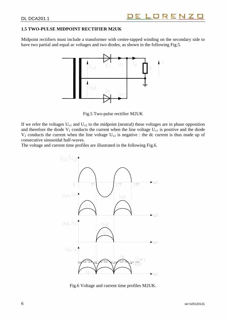
1.5 TWO-PULSE MIDPOINT RECTIFIER M2UK
Midpoint rectifiers must include a transformer with centre-tapped winding on the secondary side tohave two partial and equal ac voltages and two diodes, as shown in the following Fig.5.
Fig.5 Two-pulse rectifier M2UK
If we refer the voltages Uv1 and Uv2 to the midpoint (neutral) these voltages are in phase oppositionand therefore the diode V1 conducts the current when the line voltage Uv1 is positive and the diodeV2 conducts the current when the line voltage Uv2 is negative : the dc current is thus made up ofconsecutive sinusoidal half-waves.The voltage and current time profiles are illustrated in the following Fig.6.
Fig.6 Voltage and current time profiles M2UK.

DL DCA201.1
ver b20120131 7
All the following characteristic values apply to resistive load, neglecting losses in the rectifier.
1) Average value of direct voltage
UdAV = 0.9 Uv1 = 0.9 Uv2
2) Rms value of direct voltage
UdRMS = Uv1 = Uv2
3) Form factor of direct voltage
fU
UdRMS
dAV
111.
4) RMS value of direct current
IdRMS = 1.11 IdAV
5) Ripple factor
w = 100 f 2 1 = 48%
6) Rms value of alternating part of direct voltage
UdAC = 0.48 UdAV
7) Repetitive peak reverse voltage value of the diodes
URRM = 3.14 UdAV = 2.82 Uv1 = 2.82 Uv2

DL DCA201.1
8 ver b20120131
1.6 TWO-PULSE BRIDGE RECTIFIER B2U
The bridge circuit has two branch pairs of series diodes, parallel connected, as indicated in thefollowing Fig.7.
Fig.7 Bridge rectifier B2U
In the bridge circuit (Graetz bridge) alternatively two diodes (V2 -V3) are forward biased and two(V4 -V1)reverse biased: the current Id flows through the load R during the two half-periods ofalternate voltage Uv.The bridge circuit may be considered as two midpoint circuits connected in series, so the voltageand current profiles are those indicated in Fig.6.

DL DCA201.1
ver b20120131 9
All the following characteristic values apply to resistive load, neglecting losses in the rectifier.
1) Average value of direct voltage
UdAV = 0.9 Uv
2) Rms value of direct voltage
UdRMS = Uv
3) Form factor of direct voltage
fU
UdRMS
dAV
111.
4) Rms value of direct current
IdRMS = 1.11 IdAV
5) Ripple factor
w = 100 f 2 1 = 48 %
6) Rms value of alternating part of direct voltage
UdAC = 0.48 UdAV
7) Repetitive peak reverse voltage value of the diode
URRM = 1.57 UdAV = 1.41 Uv

DL DCA201.1
ver b20120131 39
EXPERIMENT N°3B
SINGLE-PULSE RECTIFIER E1UK, OHMIC-INDUCTIVE LOAD
Objectives: Recording voltage and current time profiles Voltage and current measurements Determination of various characteristic data
Equipments: 1 DL 2602 Silicon diode 1 DL 2626 Mains transformer 1 DL 2628 Super-fast fuses (3x6.3 A) 1 DL 2635 Universal load 1 DL 2643 Socket with shunts 1 1 DL 2109T3PV Moving-iron voltmeter (125-250-500 V) 1 DL 2109D33 True rms meter 1 Dual-channel oscilloscope (preferred storage type)
Circuit diagram

DCA 201.1
40 ver b20120131

DL DCA201.1
ver b20120131 41
Experiment procedure
Assemble the circuit according with the foregoing topographic diagram, disregarding detail (a) atfirst.
1) Voltage and current measurementsSupply the circuit and measure:1.1) the rms value Uv of the supply voltage by the voltmeter P1;1.2) the average value UdAV and the rms value UdRMS of the direct voltage by the voltmeter P2;1.3) the average value IdAV and the rms value IdRMS of the direct current by the ammeter P3.
Enter the measured value in the following table.
Uv
(V)UdAV
(V)UdRMS
(V)IdAV
(A)IdRMS
(A)46 20 33 0.57 0.87
Evaluate the various characteristic data of the rectifier
Form factor
fI
IidRMS
dAV
153.
Ripple
wi(%) = 116%

DL DCA201.1
42 ver b20120131
2) Recording on the oscilloscope
NoteSince the basic instrument set does not normally allow simultaneous measurements, themeasures may have to be carried out successively.
2.1) Recording the supply Uv and direct Ud voltages.Oscilloscope settingDC coupling; Yt mode. Trigger: AC Line.Channel 1 (voltage Uv) 50 V/div; probe x10.Channel 2 (voltage Ud): 20 V/div; probe x10.
Oscillogram.
The diode is turned on when the anode voltage is positive and connects the positive half-wavesof the supply voltage to the load.The dc voltage has the same profile as the feed voltage until the diode blocks and is made up ofboth positive and negative time-area components.

DL DCA201.1
ver b20120131 43
2.2) Recording the diode voltage Uv and the direct current Id.Oscilloscope setting.Assemble the measuring circuit according with detail (a).Channel 1 (UV voltage): 50 V/div; probe x10.Channel 2 (current Id proportional to voltage at shunt Rs =1 ): 0.5 V/div; probe x1.
Oscillogram
The negative half-wave of supply voltage is present at the diode as a reverse voltage as soon asthe diode blocks.The direct current is an intermittent, pulsating current.When the diode conducts, magnetic energy is stored in the load circuit choke. When the voltagenext crosses the zero line, the current continues to flow until the inductance has been discharged.The conduction angle is thus greater than in the case of a resistive load.For L , the time required to charge and discharge the choke is equally long, i.e. theconduction angle becomes 360° in limiting case.
2.3 Voltage and current time profiles E1UK.

DL DCA201.1
44 ver b20120131
blank page

DL DCA201.1
ver b20120131 45
EXPERIMENT N°4A
TWO-PULSE RECTIFIER M2UK, OHMIC LOAD
Objectives: Recording voltage and current time profiles Voltage and current measurements Determination of various characteristic data
Equipments: 1 DL 2603 Diode stack 1 DL 2626 Mains transformer 1 DL 2628 Super-fast fuses (3x6.3 A) 1 DL 2635 Universal load 1 DL 2643 Socket with shunts 1 1 DL 2109T3PV Moving-iron voltmeter (125-250-500 V) 2 DL 2109D33 True rms meter 1 Dual-channel oscilloscope (preferred storage type)
Circuit diagram

DCA 201.1
46 ver b20120131

DL DCA201.1
ver b20120131 47
Experiment procedure
Assemble the circuit according with the foregoing topographic diagram, disregarding details (a), (b)and (c) at first.
1) Voltage and current measurementsSupply the circuit and measure:1.1) the rms value Uv1 of the supply voltage by the voltmeter P1;1.2) the average value UdAV, the rms value UdRMS and the rms value UdAC of the alternating part
of the direct voltage by the voltmeter P4;1.3) the average value IdAV and the rms value IdRMS of the direct current by the ammeter P31.4) the average value IF1AV and the rms value IF1RMS of the diode V1 by the ammeter P2.
Enter the measured value in the following table.
Uv
(V)UdAV
(V)UdRMS
(V)UdAC
(V)IF1AV
(A)IF1RMS
(A)IdAV
(A)IdRMS
(A)46 42 47 20.2 0.6 0.92 1.19 1.3
Evaluate the various characteristic data of the rectifier specified in the following table andcompare these with the theoretical values (see § 1.5, page 7).
Theoretical MeasuredUdAV / Uv1 0.9 0.91UdRMS / Uv1 1 1.02
Form factor fu UdRMS / UdAV 1.11 1.12Ripple wu (%) 48 50Ripples UdAC / UdAV 0.48 0.48Form factor fi IdRMS / IdAV 1.11 1.09Ripple wi (%) 48 44
IF1AV / IdAV 0.5 0.504

DL DCA201.1
48 ver b20120131
2) Recording on the oscilloscope
NoteSince the basic instrument set does not normally allow simultaneous measurements, themeasures may have to be carried out successively.
2.1) Recording the supply Uv1 and direct Ud voltages.Oscilloscope settingDC coupling; Yt mode. Trigger: AC Line.Channel 1 (voltage Uv1) 50 V/div; probe x10.Channel 2 (voltage Ud): 20 V/div; probe x10.
Oscillogram.
The diodes alternatively conduct whenever the anode voltage is positive.The dc voltage is made up of successive half-waves.
DL DCA201.1
ver b20120131 49
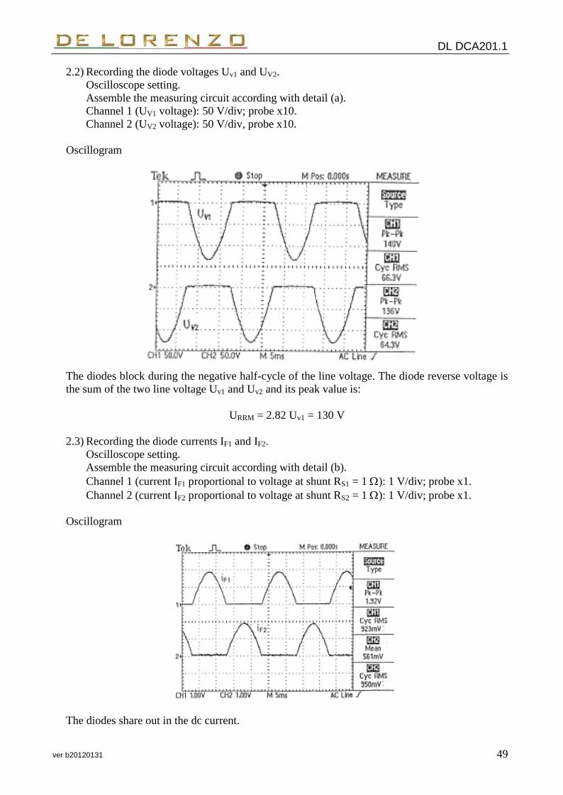
2.2) Recording the diode voltages Uv1 and UV2.Oscilloscope setting.Assemble the measuring circuit according with detail (a).Channel 1 (UV1 voltage): 50 V/div; probe x10.Channel 2 (UV2 voltage): 50 V/div, probe x10.
Oscillogram
The diodes block during the negative half-cycle of the line voltage. The diode reverse voltage isthe sum of the two line voltage Uv1 and Uv2 and its peak value is:
URRM = 2.82 Uv1 = 130 V
2.3) Recording the diode currents IF1 and IF2.Oscilloscope setting.Assemble the measuring circuit according with detail (b).Channel 1 (current IF1 proportional to voltage at shunt RS1 = 1 ): 1 V/div; probe x1.Channel 2 (current IF2 proportional to voltage at shunt RS2 = 1 ): 1 V/div; probe x1.
Oscillogram
The diodes share out in the dc current.

DL DCA201.1
50 ver b20120131
2.4) Recording the direct current Id and voltage Ud.Oscilloscope settingAssemble the measuring circuit according with detail (c).Channel 1 (current Id proportional to voltage at shunt RS3 = 1 ): 1 V/div; probe x1.Channel 2 (voltage Ud ) 20 V/div; probe x10.
Oscillogram
The load current is in phase with the dc voltage.
2.5) Voltage and current time profiles M2UK.

© 1996 - 2012 DE LORENZO SPA - Printed in Italy - All right reserved
DE LORENZO SPAV.le Romagna, 20 - 20089 Rozzano (MI) ItalyTel. ++39 02 8254551 - Fax ++39 02 8255181E-mail: [email protected] sites: www.delorenzoglobal.com - www.technical-education.it - www.delorenzoenergy.com