digital integrated circuit design ii ece 426/526...
TRANSCRIPT

Digital Integrated Circuit Design IIECE 426/526, Announcements
$Date: 2016/06/02 00:31:36 $
Professor R. Daasch
Depar tment of Electrical and Computer EngineeringPortland State UniversityPortland, OR 97207-0751([email protected])
Course Website⟨http://ece.pdx.edu/%7Eecex26⟩
[Note links are parsed by Adober Reader but may not be parsed by browser viewers]
©R.Daasch, Por tland State University 1 June 2016
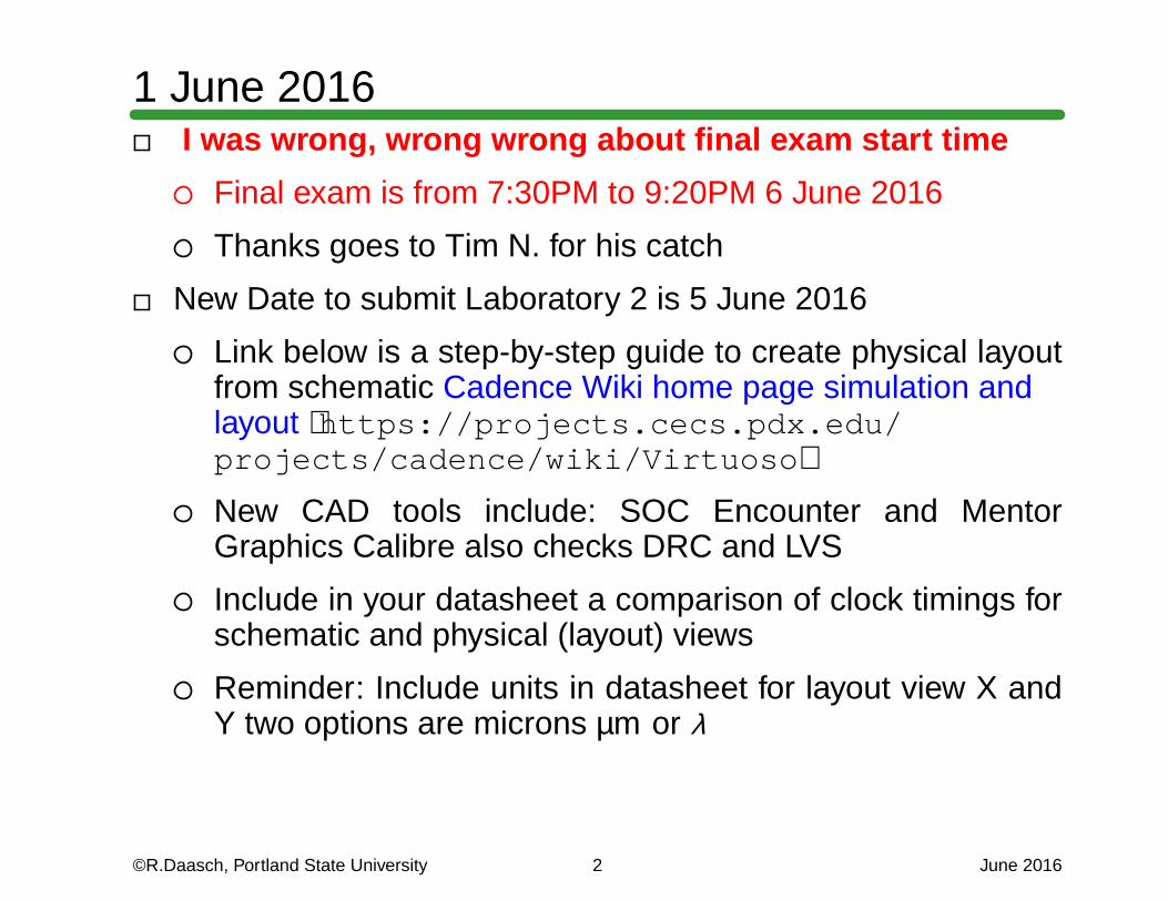
1 June 2016I was wrong, wrong wrong about final exam star t t ime
Final exam is from 7:30PM to 9:20PM 6 June 2016
Thanks goes to Tim N. for his catch
New Date to submit Laborator y 2 is 5 June 2016
Link below is a step-by-step guide to create physical layoutfrom schematic Cadence Wiki home page simulation andlayout ⟨https://projects.cecs.pdx.edu/projects/cadence/wiki/Virtuoso⟩
New CAD tools include: SOC Encounter and MentorGraphics Calibre also checks DRC and LVS
Include in your datasheet a comparison of clock timings forschematic and physical (layout) views
Reminder : Include units in datasheet for layout view X andY two options are microns µm or λ
©R.Daasch, Por tland State University 2 June 2016

1 June 2016In your design test enable can be either TE active LOW orTE active HIGH
Submit completed datasheets for adder subtractor design byemail Rohan [email protected]
Use correct subject
Subject : ECE x26 Laborator y 2 Version {1,2,3} LastName #
No late submissions will be accepted
©R.Daasch, Por tland State University 3 June 2016

23 May 2016University Closed for Memorial Day, No class Monday 30 May2016
Final Exam Announcement
Final Exam, June 6, 1930-1920 (7:30PM - 9:20PM)
Ondine 218
NOTE: Final Exam start time is one hour earlier than classstar t time
Comprehensive: Chapters 9-15
Laborator y 2 Pre-grade distributed
Some did not submit (why hur t yourself?)
Points accumulated by pre-grade will be applied to finallaborator y score
Corrections and additions will be added to final laborator yscore
©R.Daasch, Por tland State University 4 June 2016

23 May 2016New mater ial will be added to the final laborator y score
©R.Daasch, Por tland State University 5 June 2016

16 May 2016Reminder about Ver ilog module identifiers ’module identifier()’
Verilog module identifiers begin with either a lowercaseletter [a-z], an uppercase letter [A-Z], or the underscore (_)
Identifiers of more than one character can include anysequence of letters [a-zA-Z], digits [0-9], dollar signs ($),and underscore characters (_).
Correct module identifiers: AdderSubtractor, _fourBitAdder
Incorrect module identifiers: 4bitadder, $4bit
May 20th or before you may submit one new cell, of yourchoosing, for early grading.
Select and submit only one completed cell datasheet either
D Flip-flop Scan Register Design,
Overflow and Underflow Combinational Design, or
©R.Daasch, Por tland State University 6 June 2016

16 May 2016Scan and Parallel Register Design.
Email submit on May 20 one completed datasheet as a PDFto TA, Rohan Jagtap, [email protected]
Subject line
Subject : ECE x26 PreLaborator y 2 Cell_NAME LastName #
The submitted cell datasheet will be graded and wor th up to15% of the total Laborator y 2 score
You may either accept the grade for the cell or submit arevised datasheet on 29 May 2016
All ear ly grading (errors) have to be fixed to ear n additionalscore
©R.Daasch, Por tland State University 7 June 2016

9 May 2016Pre-submission of one cell of your choice for “pre-grading”
20 May 2016, submit one cell
Submit for one cell a completed datasheet as a PDF by emailto TA, Rohan Jagtap.
With subject lineSubject: ECE x26 PreLaborator y 2 Cell LastName #
©R.Daasch, Por tland State University 8 June 2016

4 May 2016Tw o options for place and route structural Ver ilog
NC-Ver ilog output with input a structural schematic ofstandard cells
Synthesized output with input a behavioral Ver ilog design
Warning: Using structural Ver ilog from synthesis introducespossible inconsistency in Spectre simulation results
From CIW -> File -> Import -> Ver ilog
©R.Daasch, Por tland State University 9 June 2016

2 May 2016Midter m graded, returned today
Each question wor th 20 points
ECE 426: 39:67
ECE 526: 55:79
See me during Office hours or by appointment aboutgrading
Low scores should set appointment to discuss improvingfor final exam
Combining Laborator y 2 and Laborator y 3 for single due dateof final design
Combined laborator y descr iption posted by 4 May 2016
Be sure to set transient option to lvl and nestlvl = 1
Completed design submitted 29 May 2016
©R.Daasch, Por tland State University 10 June 2016

2 May 2016Laborator y 2 design a register with both parallel and serialloading options, a one bit-slice and hierarchical design witha 11 bit word
Laborator y 3 combines Laborator y 2 register with Adder-subtractor
©R.Daasch, Por tland State University 11 June 2016

25 April 2016Fortunately the fix is simple for Cadence 6.15 Calculatordifference from 6.10 Calculator for the bitgen DC supply in thetestbench
The trouble is with a single character a ’/’ in the name of thecurrent signal name "/Vvdd:p"
Removing the ’/’ by clicking into the buffer or other editablewindow and delete the ’/’
NO NEED to revert to IC 6.1.0 stay with IC 6.1.5
©R.Daasch, Por tland State University 12 June 2016

25 April 2016
Red circle arrow on left note ’/’ before the ’/V’ and ’/’deleted on right in green
©R.Daasch, Por tland State University 13 June 2016

25 April 2016Laborator y 1 with power evaluated due date reset to thisFr iday 29 Apr il 2016
Reminder Exam 27 April 2016
Coverage: 9, 10, 11.1,2,10
©R.Daasch, Por tland State University 14 June 2016

20 April 2016Exam 27 April 2016
Entire period
Closed book and notes
Technology parameters, Equations (e.g. logical effor t)provided on standard cover page
Detailed coverage set 25 April 2016; Chapter 9, 10, 11
Spectre notes
Limit transient output file sizes by replacing default Optionsto lvl from allpub
• Set nestlvl =1
Bitgen buses are noted in schematics as “wide-wire”bundles
©R.Daasch, Por tland State University 15 June 2016

20 April 2016Signal Bitgen SchematicName Single Bus Bundle Bus
A1 A1 A<1:3> A1,A2,A3A<1> A<1> A<1:3>
©R.Daasch, Por tland State University 16 June 2016

18 April 2016Midter m will be 27 April 2016
Coverage 9, 10, 11
Practice Problems for each chapter are available inAssignments
Laborator y 1, clarifying FO4 load
Nor mally, Sbus is driven by ExOr (or similar gates) and C4is NAND
The definition of FO4 uses h = Cout /C in that is, like gates
Use FO4 ≡ ExOr loads for Sbus and C4
No new yet for ECE x26 video from Winter 2014, it may belost
©R.Daasch, Por tland State University 17 June 2016

13 April 2016First Call on mid-term exam Tentatively set for 27 April 2016
Midter m no earlier than 27 April
For coverage of Chapter 11 be move back to 2 May
©R.Daasch, Por tland State University 18 June 2016

11 April 2016Laborator y 1 bitgen demo
PDK 45 Standard cell redefinition that may ease clutter inschematics
Not completed yet
©R.Daasch, Por tland State University 19 June 2016

6 Apr il 2016Laborator y 1, Standard Cell Place and Route is misnamedand is causing confusion
Laborator y 1 prepares the design of the 4-bit adder-subtractorfor place and route
Place and route (and a new tool Cadence SOC Encounter) isLaborator y 2
To check if you have latest revision of the notes the date isadded to header page
©R.Daasch, Por tland State University 20 June 2016

4 Apr il 2016PDF of syllabus posted
Syllabus ⟨http://web.cecs.pdx.edu/%7Eecex26/ecex26.cgi?2#2⟩
Laborator y 1 is posted and due 25 April 2016
A standard for mat Word file is used to submit reports.Standard Cell Report ⟨http://ece.pdx.edu/%7Eecex26/doc/Standard_Cell_Report.docx⟩
Repor ts do not have to be long.
• Modeled after the essential elements of standard cellbased design documentation.
Laborator y 1 ⟨http://ece.pdx.edu/%7Eecex26/pdf/laboratory1.pdf⟩
Meet Rohan Jagtap, TA
©R.Daasch, Por tland State University 21 June 2016

4 Apr il 2016Reminder email subject line use the string ECE x26,
Adding course number string to subject reduces the delayfor a response
©R.Daasch, Por tland State University 22 June 2016

30 March 2016TA is Rohan Jagtap, [email protected],
Office hours in VLSI Lab: Tu Th 2:00-3:00PM or byappointment
See Assignments ⟨http://ece.pdx.edu/%7Eecex26/ecex26.cgi?3#3/⟩ for chapter reading order
Course Coverage of Digital Integrated Circuits II
Complete Weste and Harris, CMOS VLSI Design
Review ECE x25
• Key Chapters: Chapter 4, Chapter 7, Chapter 9
Chapter 10, Sequential
Chapter 11, Datapath
Chapter 12, Arrays
Chapter 13, Special-Purpose
©R.Daasch, Por tland State University 23 June 2016

30 March 2016Chapter 15, Test
©R.Daasch, Por tland State University 24 June 2016

28 March 2016On email subject line use the string ECE x26, adding thisstr ing to subject reduces the delay for a response
Laborator y 1 is a character ization of standard cells and logicdesign of a simple adder and subtractor
Simplified data sheet for mat PDK cell ⟨http://ece.pdx.edu/%7Eecex26/lab/PDK45_Cell_Datasheet.doc⟩ PDK circuit design⟨http://ece.pdx.edu/%7Eecex26/lab/PDK45_Design_Datasheet.doc⟩
Points to consider in the shift from logic cells to logic design
Input is different for testing a logic design than input fortesting a single logic gate
Eventually, number of rows in truth table is too large 2n , nnumber of inputs
Bitgen is a simple Spectre compatible generator for input
©R.Daasch, Por tland State University 25 June 2016
28 March 2016Place and route will commence starting with Laborator y 2
©R.Daasch, Por tland State University 26 June 2016