digital integrated circuit design i ece 425/525 chapter...
TRANSCRIPT

Digital Integrated Circuit Design IECE 425/525
Chapter 1
Professor R. Daasch
Depar tment of Electrical and Computer EngineeringPortland State UniversityPortland, OR 97207-0751([email protected])
http://ece .pdx.edu/ ~ecex25
©R.Daasch, Por tland State University 1 Apr il 2016

Chapter 1Dr ivers for bigger, better, faster integrated circuits
Computers - big iron mainframes to Palm Pilots
Data Communication - aka “The Internet”
Wireless - cell phones, wireless LAN, wireless WAN
Enter tainment
Lifestyle
©R.Daasch, Por tland State University 2 Apr il 2016

Chapter 1Logic Complexity
Complexity(gates / chip)Catch Phrase Date
Single Transistor 1958 <1Unit Logic 1960 1Multi-Function 1962 2-4Complex Function 1964 5-20Medium Scale Integration 1967 20-200Large Scale Integration 1972 200-2,000Very Large Scale Integration 1978 2,000-20,000Ultra Large Scale Integration 1989 20,000-System-on-Chip 2000 1,000,000-
©R.Daasch, Por tland State University 3 Apr il 2016

Chapter 1Logic Complexity
Size Number(µm) (x 1, 000)Catch Phrase Date
Single Transistor 1958Unit Logic 1960Multi-Function 1962Complex Function 1964 10Medium Scale Integration 1967Large Scale Integration 1972 4 5Very Large Scale Integration 1978 2 50Ultra Large Scale Integration 1989 1 500Change phrase to describe transistorItsy Bitsy 1993 0.600 1,000Teensy Weensy 1996 0.350 2,000Incredibly Small 2000 0.250 5,000Unbelievably Tiny 2003 0.130 10,000Rediculously Small 2006 0.090 20,000Damn This is Tiny 2009 0.045 40,000Smaller than tobacco smoke par ticles (STSMP)2010 0.022 80,000
©R.Daasch, Por tland State University 4 Apr il 2016

Chapter 1Tr ansistor count is for an average size die (≈ 100mm2)
Human hair has a thickness of about 100,000 nanometers(100 µm, 0.1 mm)
Year
Sal
es (
billi
ons)
1985 1990 1995 2000 2005 2010
100
200
300
• •• • • • •
••
•• •
••
•
• ••
••
• • ••
• • •
Worldwide Semiconductor Sales
Moore’s LawThe number of transistors per chip doubles every one and
©R.Daasch, Por tland State University 5 Apr il 2016
Chapter 1one-half years.
New mater ials are beginning to replace Silicon, SiO2 in thetransistor
Additional metals and other materials (e.g. carbon nanotubes)continue to be discussed
Research active in memor ies and logic
Prototypes only no products as of yet
©R.Daasch, Por tland State University 6 Apr il 2016

Chapter 1IBM Technology Summary Cu-32
Process generation 32nm Technology SOI HKMGSupply voltage (VDD) 0.9V/0.85V Wireable gates ≈ 400millionTotal levels of metal 11
Fast Trc eDRAM (SRAM alternative)Multi-banked eDRAM (bandwidth optimized)Pseudo two-por t eDRAM
eDRAM compilers
One- & two-por t SRAMsDual-por t SRAMTernar y CAMTw o- and four-por t RA latches, ROMOne-por t and dense two-por t register files
Other memory compilers
6G supporting PCI-Express Gen1 and Gen215G chip-to-chip core supporting low-power optical15G backplane core 16G Fibre Channel28G backplane core 32G Fibre ChannelPCI-Express PCI-Express Gen1, Gen2 and Gen3
HSS cores
©R.Daasch, Por tland State University 7 Apr il 2016

Chapter 1IBM Technology Summary Cu-32 (continued)
Multi-Vt, Regular Vt, mezzanine Vt, ultra-high VtClock gating (by design or through synthesis)Po wer supply, IP in voltage islands can usedifferent supply voltages)Selective voltage binningLow-power SRAMsSemi-custom
Base Pow er management
Voltage island power gating (turn off unusedareas of a chip)Dynamic voltage scaling (modify powersupply on-demand, with feedback)Full custom Dynamic frequency scaling (modify clock on-demand, with feedback)
But frequencies are stalling with scallingIEEE ⟨http://spectrum.ieee.org/computing/hardware/
why-cpu-frequency-stalled⟩Spectr um
©R.Daasch, Por tland State University 8 Apr il 2016

Chapter 1 ��������������������������������������������������������������������������������������������������������������������������������������������������������������������������������������������������������������������������������������������������������������������������������������������������������������������������������������������������������������������������������������������������������������������������������������������������������������������������������������������������������������������
SEM of a Intel 90nm transistor ; from IEEE Spectrum, October2002
Single gate transistor controls channel from one side only
©R.Daasch, Por tland State University 9 Apr il 2016

Chapter 1
from Multigate Device, Wikipedia 2013
Tr ansistor “fin” extends above the plane of Silicon wafer
Double gate transistor controls channel from both sides
©R.Daasch, Por tland State University 10 Apr il 2016

Chapter 1
from Multigate Device, Wikipedia 2013
Intel Tri-gate transistor controls channel from both sides @22nm
Note all transistors are one size
All transistors have a single common gate electrode
On right SEM five transistor (sources) drains are shortedtogether
©R.Daasch, Por tland State University 11 Apr il 2016

Chapter 1 ��������������������������������������������������������������������������������������������������������������������������������������������������������������������������������������������������������������������������������������������������������������������������������������������������������������������������������������������������������������������������������������������������������������������������������������������������������������������������������������������������������������������
Mater ials are changing from pure Silicon to complexstr uctures that strain a lattice to engineer improvements to thefundamental electronic structure; from IEEE Spectrum,October 2002
©R.Daasch, Por tland State University 12 Apr il 2016

Chapter 1The enormous flexibility comes with several costs
Technology - \ billion or more for fabr ication plants withequipment and facilities
Talent - materials, devices, hardware designers, softwaredesigners, mechanical engineering, chemical engineering,business (marketing, sales)
Complexity - hardware design, software design, testdesign, tools for fabr ication and test
©R.Daasch, Por tland State University 13 Apr il 2016
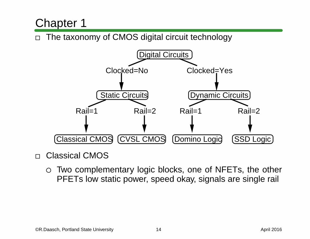
Chapter 1The taxonomy of CMOS digital circuit technology
Digital Circuits
Clocked=No Clocked=Yes
Dynamic Circuits
Rail=1 Rail=2
Static Circuits
Rail=1 Rail=2
CVSL CMOS Classical CMOS Domino Logic SSD Logic
Classical CMOS
Tw o complementar y logic blocks, one of NFETs, the otherPFETs low static power, speed okay, signals are single rail
©R.Daasch, Por tland State University 14 Apr il 2016

Chapter 1Domino Logic
Single logic block of (generally) NFETs, low static powermore average power and faster than classical CMOS, twodistinct phases controlled by a global clock
Tr ansmission Gate Logic
Doesn’t fit into taxonomy ver y well; depending on the viewlooks static or dynamic
©R.Daasch, Por tland State University 15 Apr il 2016

Chapter 1Design Hierarchy
Design is an art, a discipline, a craft and a science
• Designs should be appealing to the eye (ar t and craft)
• Design is a rigorous study (discipline and a science)
Tr aditional top-down design flow
• System specification — project concept; exter nalrequirements
• High(First)-Level Model — behavior design(VHDL/Ver ilog); system blocks specification; behaviorverification; internal requirements; begin test plan
• Logic Synthesis — structure and logic design(VHDL/Ver ilog); subsystem interface requirements; area,power, timing resource specification; logic ver ification;refine and iterate test plan
©R.Daasch, Por tland State University 16 Apr il 2016

Chapter 1• Circuit Design — technology mapping; interface design;
area, power, timing allocation; circuit ver ification andsimulation; converge test plan
• Physical Design — area, power, timing closure; physicalsimulation; test plan ver ification
• Manufactur ing — packaging, engineering prototypes,test and validation; Product production, test andvalidation;
Top-down approach reflects an organizational approach forproducts but a poor way to study CMOS design
This course will use bottom-up approach that mixes circuitand physical design
©R.Daasch, Por tland State University 17 Apr il 2016

Chapter 1Full-Adder Design Example
Sum = ABC + ABC + ABC + ABC
Sum = A+B+C
Carry = AB + AC + BC
Physical Design; Area, power, timing
Propagation Delays (50%) 1.2nsTr ansition Delays (10%-90%) 1.2nsCircuit Area < 1500µm2
DynPow er (@ VDD = 5V fmax = 20MHz ) <1mW
Circuit Design; circuit topology, CMOS technology
• CMOS technology - static (classical) CMOS
• Circuit topology - two interconnected sub-blocks for sumand carry
©R.Daasch, Por tland State University 18 Apr il 2016

Chapter 1• Merge into a single, two output, complex-gate in
“transistor schematic”
• The var ious transistor-level alter natives permit physicaldesign tradeoffs
Circuit designers (versus a VHDL programmer) have theadded flexibility realizing the complex gates
More familiar gates such as INVERTER, NAND2 and NOR2can also be used
©R.Daasch, Por tland State University 19 Apr il 2016
Chapter 1
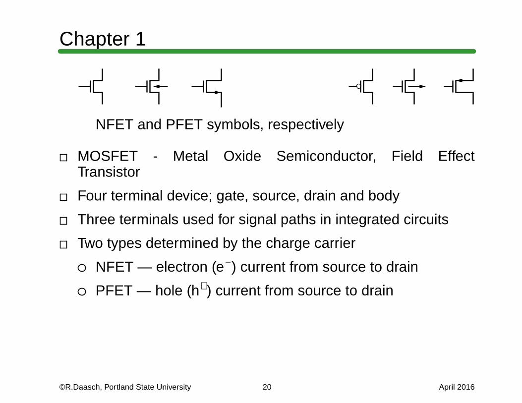
NFET and PFET symbols, respectively
MOSFET - Metal Oxide Semiconductor, Field EffectTr ansistor
Four terminal device; gate, source, drain and body
Three terminals used for signal paths in integrated circuits
Tw o types determined by the charge carrier
NFET — electron (e−) current from source to drain
PFET — hole (h+) current from source to drain
©R.Daasch, Por tland State University 20 Apr il 2016

Chapter 1
��������
��������
In Out0 11 0
Inverter
Po wer supply voltage (global)
Circuit design var iables
Independent adjustment of length (L) and width (W) ofeach transistor (local)
©R.Daasch, Por tland State University 21 Apr il 2016

Chapter 1
InA
InA
��������
��������
��������
InInB
B
InA InB Out0 0 10 1 11 0 11 1 0
NAND2
Circuit design var iables
Po wer supply voltage (global)
Adjust each transistor length and width independently(local)
Assign signals InA and InB to gate inputs independently(local)
©R.Daasch, Por tland State University 22 Apr il 2016

Chapter 1
��������
��������
��������
��������
InA
In BIn
In
A
B
InA InB Out0 0 10 1 01 0 01 1 0
NOR@
Circuit design var iables
Po wer supply voltage (global)
Independent adjustment of length and width of eachtransistor (local)
Independent assignment of InA and InB to inputs
Inter nal logic states are stored in registers and memories
Registers are assembled from latches or flip flops
Memor ies are assembled from specific memory cell designs(SRAM, DRAM, CAM...)
©R.Daasch, Por tland State University 23 Apr il 2016

Chapter 1
0
1Q
Qbar
CLKDATA
Prototype Latch
Latches clocked by one clock and clock (φ and φ ) or twoclocks (φ1 and φ2)
Mux above is simplified from traditional NAND-NAND by passtransistor logic
0
1Q
Qbar
CLKDATA
0
1
CLK
Prototype (positive-edge) Flip-Flop
©R.Daasch, Por tland State University 24 Apr il 2016

Chapter 1Latches are combined to provide simple flip-flop behavior
Physical design of the gates translates the ideal cartoons ofPFET and NFET into mask layers
Each mask layer has a minimum printing feature rangingfrom 2λ to 3λ
Top view of the design typically shows the 3D effects withstipple patterns, color or both
• Stick diagrams are a simplified top view to per mit a quickand easy estimate of the physical design complexity
Cross-section is rarely used in design and quite commonin the discussion of the fabr ication process and deviceoperating character istics
©R.Daasch, Por tland State University 25 Apr il 2016

Chapter 1Regular Design — Circuit blocks used like Lego blocks
Divide subsystem into similar circuit building blocks
Iterate in X direction, Y direction for one-dimensionalexpansion and X,Y directions for arrays
• A N-bit ripple, carr y full-adder is assembled from Ncopies of 1-bit full adder circuits
• A N-bit by W-word memory is assembled from N ⋅Wcopies of 1-bit register
At higher design hierarchy lev els entire processors may becopied
©R.Daasch, Por tland State University 26 Apr il 2016

Chapter 1Modular ity — well defined interfaces and function
Analogous software concepts are the C-function or For transubroutine
Block inputs control but are isolated from function andoutputs
Block outputs are valid inputs to other blocks
Temporal (time) and physical interfaces are equallyimpor tant
Locality — inputs and outputs are physically and temporallyclose
Inter nal details of circuit hidden from inputs and outputs
Modular and Regular circuits can be “wired” by placementalone
©R.Daasch, Por tland State University 27 Apr il 2016