digital ic design - assignment 1 18/08/14ee11b087/aman_digital-ic.pdf · digital ic design -...
TRANSCRIPT
Digital IC Design - Assignment 1 18/08/14
Aman Goel Roll No. EE11B087 Platform: SPICEOPUS (Windows)
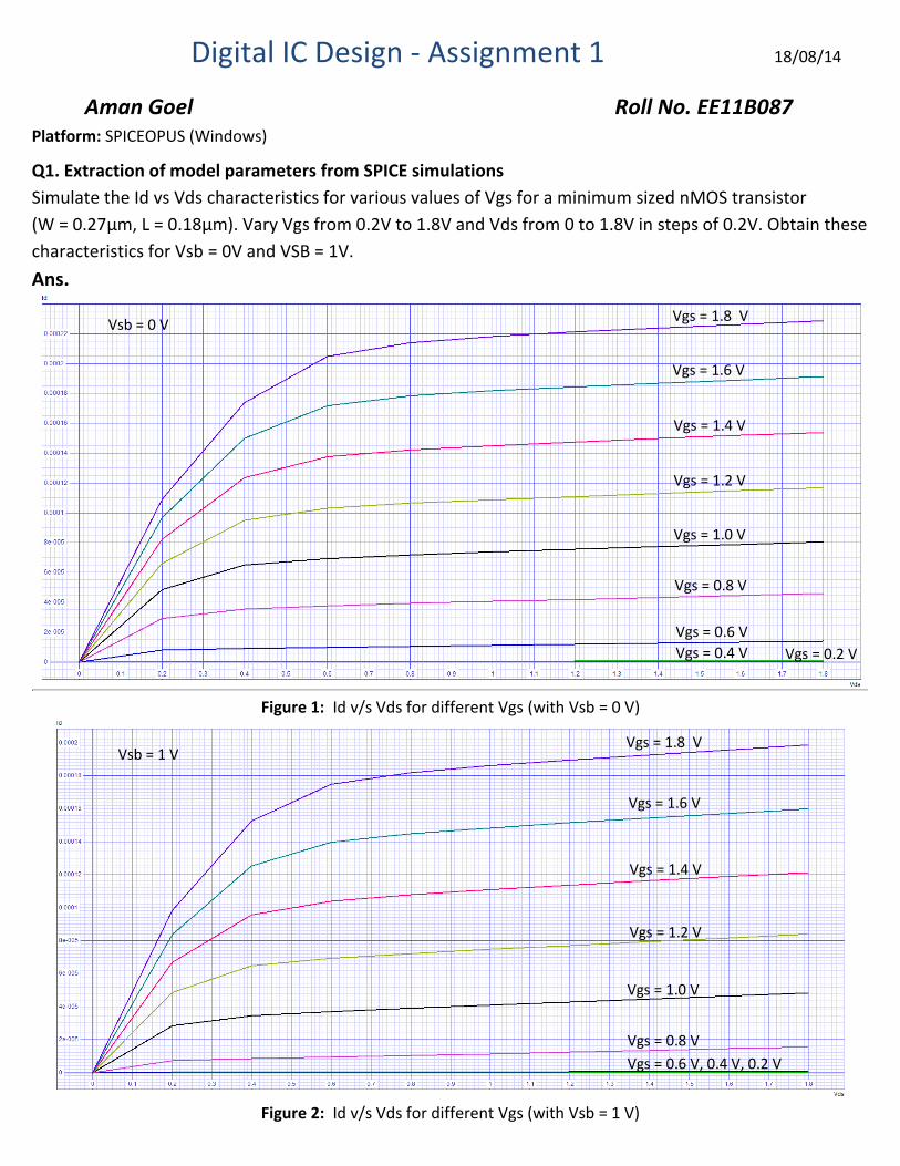
Q1. Extraction of model parameters from SPICE simulations
Simulate the Id vs Vds characteristics for various values of Vgs for a minimum sized nMOS transistor
(W = 0.27µm, L = 0.18µm). Vary Vgs from 0.2V to 1.8V and Vds from 0 to 1.8V in steps of 0.2V. Obtain these
characteristics for Vsb = 0V and VSB = 1V.
Ans.
Figure 1: Id v/s Vds for different Vgs (with Vsb = 0 V)
Figure 2: Id v/s Vds for different Vgs (with Vsb = 1 V)
Vgs = 1.8 V
Vgs = 1.6 V
Vgs = 1.4 V
Vgs = 1.2 V
Vgs = 1.0 V
Vgs = 0.8 V
Vgs = 0.6 V
Vgs = 0.4 V Vgs = 0.2 V
Vsb = 0 V
Vsb = 1 V Vgs = 1.8 V
Vgs = 1.6 V
Vgs = 1.4 V
Vgs = 1.2 V
Vgs = 1.0 V
Vgs = 0.8 V
Vgs = 0.6 V, 0.4 V, 0.2 V

(a) Using the characteristic for VGS equal to 0.6V and 0.8V, estimate VT, Kn, ƛ and ɣ.
Ans.
Figure 3: Id v/s Vds for Vgs = 0.6 V (red) and Vgs = 0.8 V (green) (with Vsb = 0 V)
Estimation of VT
Using SPICE Level 1 model, Id = 0.5*Kn*(W/L)*(Vgs – VT)2 * (1 + ƛ *Vds) (Eq - 1)
For Vds = 1.8 V,
Point 1 – Vgs = 0.8 V, Id (observed) = 4.59e-05 A
Point 2 - Vgs = 0.6 V, Id (observed) = 1.37e-05 A
Solving Point 1 & 2 in Eq – 1 gives-
VT1 = 0.359 V
For Vds = 1.6 V,
Point 3 - Vgs = 0.6 V, Id (observed) = 1.30e-05 A
Point 4 - Vgs = 0.8 V, Id (observed) = 4.45e-05 A
Solving Point 3 & 4 in Eq – 1 gives-
VT2 = 0.365 V
Therefore VT (estimated) = (VT1 + VT2)/2 = 0.362 V (approx)
Estimation of ƛ and Kn
W/L = 0.27/0.18 = 1.5
VT = 0.362 V
Using SPICE Level 1 model,
For Vgs = 0.8 V,
Point 1 - Vds = 1.2 V, Id (observed) = 4.18e-05 A
Vgs = 0.8 V
Vgs = 0.6 V
Vsb = 0 V

Point 2 - Vds = 1.8 V, Id (observed) = 4.59e-05 A
Solving Point 1 & 2 in Eq – 1 gives-
Kn1 = 2.34e-04 A.V-2
ƛ1 = 0.20 V-1
For Vgs = 0.6 V,
Point 1 - Vds = 1.2 V, Id (observed) = 1.17e-05 A
Point 2 - Vds = 1.8 V, Id (observed) = 1.37e-05 A
Solving Point 1 & 2 in Eq – 1 gives-
Kn2 = 1.81e-04 A.V-2
ƛ2 = 0.43 V-1
Therefore,
Kn (estimated) = (Kn1 + Kn2) / 2 = 2.08e-04 A.V-2 (approx)
ƛ (estimated) = (ƛ 1 + ƛ 2) / 2 = 0.315 V-1 (approx)
Estimation of ɣ
Φ = 0.6 V
ΔVT = ɣ*((2*Φ + Vsb)1/2 + (2*Φ)1/2) (Eq. - 2)
Figure 4: Id v/s Vds for Vgs = 0.6 V (red) and Vgs = 0.8 V (green) (with Vsb = 1 V)
For Vsb = 1 V and Vds = 0.8 V,
Point 1 – Vgs = 0.8 V, Id (observed) = 1.56e-05 A
Point 2 - Vgs = 0.6 V, Id (observed) = 5.17e-07 A
Solving Point 1 & 2 in Eq – 1 gives-
VT = 0.555 V
Vsb = 1 V
Vgs = 0.8 V
Vgs = 0.6 V

ΔVT = 0.555 V – 0.362 V = 0.193 V
Solving in Eq. – 2 we get,
ɣ (estimated) = 0.50 V-1 (approx)
(b) Plot the ID vs VDS characteristics using the level 1 model parameters. (Use the .MODEL command in SPICE. For example for an nMOS transistor, it is .MODEL nfet1 NMOS (LEVEL=1 KP=xx VT0=xx LAMBDA=xx GAMMA=xx PHI=0.6)) Ans.
KP=0.000208, VT0=0.362, LAMBDA=0.315, GAMMA=0.5, PHI=0.6
Figure 5: Id v/s Vds for different Vgs (with Vsb = 0 V)
(c) Tabulate the error in the current at Vds = 1.8V, for various values of Vgs.
Ans.
Vgs (V) Id (µA)- Level 53 Id (µA)- Level 1 Error in Current (µA) Error %
0.2 0.02 0.01 0.01 48.50
0.4 0.50 0.39 0.11 22.60
0.6 13.93 13.70 0.23 1.65
0.8 45.97 47.20 -1.23 -2.68
1.0 80.49 98.50 -18.01 -22.38
1.2 117.11 172.00 -54.89 -46.87
1.4 153.74 264.00 -110.26 -71.72
1.6 191.77 375.00 -183.23 -95.55
1.8 228.75 506.00 -277.25 -121.20
Vsb = 0 V Vgs = 1.8 V
Vgs = 1.6 V
Vgs = 1.4 V
Vgs = 1.2 V
Vgs = 1.0 V
Vgs = 0.8 V
Vgs = 0.6 V

(d) Assuming Ec = 1.5V/µm, Cox = 8.42 f F/µm2, vsat = 8.4 x 10⁴m/s), estimate the value of Ids at Vds = 1.8V
assuming velocity saturation and including channel length modulation. Use the value of VT obtained in part.
Also tabulate the error in this case. At what point can it be assumed that velocity saturation is significant?
Ans.
Ec = 1.5 V/µm
Cox = 8.42 f F/µm2
vsat = 8.4 x 10⁴m/s
Vds = 1.8 V
VT = 0.362 V
ƛ = 0.315 V-1
(Eq. - 3)
(
) (Eq. – 4)
Using Eq. – 3 and 4
Vgs (V) Id (µA) (Estimated) Id (µA)- Level 53 (Observed)
Error in Current (µA) Error %
0.2 0.0 0.02 -0.02 -
0.4 1.40 0.50 -0.90 180.60
0.6 33.37 13.93 -19.44 139.54
0.8 81.09 45.97 -35.12 76.39
1.0 134.15 80.49 -53.66 66.67
1.2 189.66 117.11 -72.55 61.95
1.4 246.50 153.74 -92.76 60.34
1.6 304.14 191.77 -112.37 58.60
1.8 362.30 228.75 -133.55 58.38
As Vgs increases, the error in current estimated using velocity saturation model keeps on decreasing. This
shows that velocity saturation is significant for larger values of Vgs. Equivalently; we can say that effect of
velocity saturation is more when K is high.
Observing the variation in error in current with Vgs, we can then say that velocity saturation is significant
for Vgs > 1.0 V as there is steep decrease in error in estimated current on this point.

2. Simulate the Id vs Vgs for Vds = Vdd for a minimum sized (W = 0.27mm, L = 0.18mm) nMOS transistor.
Estimate the threshold voltage by extrapolating at small values of VGS. How does it compare with the value
extracted in the previous question?
Ans.
Figure 6: Id v/s Vgs for Vds = 1.8 V (with Vsb = 0 V)
Figure 7: Id v/s Vgs for Vds = 1.8 V (zoomed view)

Estimation of VT
Point 1 – Vgs = 0.36 V, Id (observed) = 7.0086e-10 A
Point 2 - Vgs = 0.38 V, Id (observed) = 1.49e-09 A
Equation of line connecting Point 1 & 2,
Id = 3.7957e-08 Vgs – 1.2934e-08
By extrapolating we get, VT = 0.3408 V
The value obtained in this part is quite close to the one obtained in previous question.
Error in VT = 0.362 – 0.3408 = 0.0212
Error % = 6.22 %
Spice .cir file
*mosfet
.include tech180nm.txt
m1 D G S B nfet l=0.18u w=0.27u
vd supply 0 dc 1.8
vdummy supply D 0
vgate G 0 1.8
vsource S 0 0
vbulk B 0 0
*********** Analysis and Results *****************************
.control
dc vd 0 1.8 0.2 vgate 0.2 1.8 0.2
plot i(vdummy) xlabel Vds ylabel Id title ' Id Vs. Vds for NMOS transistor'
let i0=i(vdummy)[0,9]
let i1=i(vdummy)[10,19]
let i2=i(vdummy)[20,29]
let i3=i(vdummy)[30,39]
let i4=i(vdummy)[40,49]
let i5=i(vdummy)[50,59]
let i6=i(vdummy)[60,69]
let i7=i(vdummy)[70,79]
let i8=i(vdummy)[80,89]
plot i0 i1 i2 i3 i4 i5 i6 i7 i8 xlabel Vds ylabel Id title ' Id Vs. Vds for NMOS transistor'
.endc
.end
********************************************END**********************************************
Digital IC Design - Assignment 2 14/09/14
Aman Goel Roll No. EE11B087 Platform: SPICEOPUS (Windows)
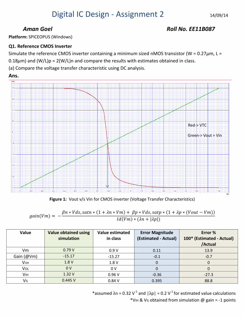
Q1. Reference CMOS Inverter
Simulate the reference CMOS inverter containing a minimum sized nMOS transistor (W = 0.27µm, L =
0.18µm) and (W/L)p = 2(W/L)n and compare the results with estimates obtained in class.
(a) Compare the voltage transfer characteristic using DC analysis.
Ans.
Figure 1: Vout v/s Vin for CMOS inverter (Voltage Transfer Characteristics)
Value Value obtained using simulation
Value estimated in class
Error Magnitude (Estimated - Actual)
Error % 100* (Estimated - Actual)
/Actual
Vm 0.79 V 0.9 V 0.11 13.9
Gain (@Vm) -15.17 -15.27 -0.1 -0.7
VOH 1.8 V 1.8 V 0 0
VOL 0 V 0 V 0 0
VIH 1.32 V 0.96 V -0.36 -27.3
VIL 0.445 V 0.84 V 0.395 88.8
*assumed λn = 0.32 V-1 and |λp| = 0.2 V-1 for estimated value calculations
*VIH & VIL obtained from simulation @ gain = -1 points
Red-> VTC
Green-> Vout = Vin

(b) Assume that the inverter drives another identical inverter. With an input rise and fall time of 10ps, find
the propagation delay using transient analysis. Use the same drain areas and perimeter used to estimate
values in class.
Ans.
Figure 2: Vout v/s time for pulse input (CMOS inverter – load = identical CMOS inverter)
Value Value obtained using simulation
Value estimated in class
Error (Magnitude) Error %
tPHL 15.2 ps 27 ps 11.8 77.6
tPLH 22.6 ps 19 ps -3.6 -15.9
tP 18.8 ps 23 ps 4.2 22.3
*delays obtained from stable input point to time observed at VDD/2
(c) If the time period of the input is 200ps and the rise and fall time is 10ps, estimate the average power
consumption of the inverter. Use a single inverter and explicitly connect the load capacitance estimated in
class. Do not use the AD, PD options.
Ans.
∫
(Eq. - 1)
Average power consumption = 75.3 µW
*Spice code attached at the end
Estimated power in class = CL x VDD2 x f x P0->1
= 3.4fF x 1.82 x (1/200ps) x 1
= 55.08 µW
Red-> Vin
Green-> Vout
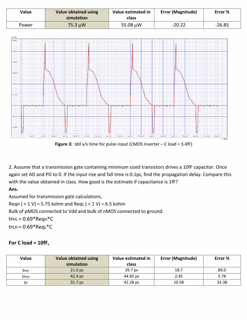
Value Value obtained using simulation
Value estimated in class
Error (Magnitude) Error %
Power 75.3 µW 55.08 µW -20.22 -26.85
Figure 3: Idd v/s time for pulse input (CMOS inverter – C load = 3.4fF)
2. Assume that a transmission gate containing minimum sized transistors drives a 10fF capacitor. Once
again set AD and PD to 0. If the input rise and fall time is 0.1ps, find the propagation delay. Compare this
with the value obtained in class. How good is the estimate if capacitance is 1fF?
Ans.
Assumed for transmission gate calculations,
ReqH ( > 1 V) = 5.75 kohm and ReqL ( < 1 V) = 6.5 kohm
Bulk of pMOS connected to Vdd and bulk of nMOS connected to ground.
tPHL = 0.69*ReqH*C
tPLH = 0.69*ReqL*C
For C load = 10fF,
Value Value obtained using simulation
Value estimated in class
Error (Magnitude) Error %
tPHL 21.0 ps 39.7 ps 18.7 89.0
tPLH 42.4 ps 44.85 ps 2.45 5.78
tP 31.7 ps 42.28 ps 10.58 33.38
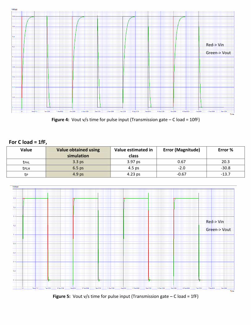
Figure 4: Vout v/s time for pulse input (Transmission gate – C load = 10fF)
For C load = 1fF,
Value Value obtained using simulation
Value estimated in class
Error (Magnitude) Error %
tPHL 3.3 ps 3.97 ps 0.67 20.3
tPLH 6.5 ps 4.5 ps -2.0 -30.8
tP 4.9 ps 4.23 ps -0.67 -13.7
Figure 5: Vout v/s time for pulse input (Transmission gate – C load = 1fF)
Green-> Vout
Red-> Vin
Green-> Vout
Red-> Vin

Spice .cir file for Q 1) c)
*cmos_inverter
.include tech180nm.txt
.subckt cmos D G Sp Sn
m1 D G Sn Sn nfet l=0.18u w=0.27u
m2 D G Sp Sp pfet l=0.18u w=0.54u
.ends
x1 out in 1 0 cmos
c1 out 0 3.4f
vd 1 0 dc=1.8
vgate in 0 PULSE 0 1.8 0p 10p 10p 90ps 200ps
*********** Transient Analysis and Results *****************************
.control
tran 10ps 900ps
let i0=-i(vd)
let i1=integrate(i0)
let power=1.8*i1[28]/200p
print power
.endc
.end
********************************************END**********************************************

Digital IC Design - Assignment 3 05/10/14
Aman Goel Roll No. EE11B087 Platform: SPICEOPUS (Windows)
Q1.
(a) Use a single stage reference inverter driving a fixed capacitance C and plot the delay as a function of C.
Choose C as integer multiples of the input gate capacitance of the reference inverter, Crin (Estimate Crin
using Cox from the model files). Use the same drain areas and perimeter used to estimate values in class.
Assume an input rise and fall time of 10ps for the simulation.
Ans.
Crin calculation
tox = 4.1E-9 (from model file)
ϵr = 3.9 (relative permittivity of SiO2)
ϵ = 8.854E-12 (permittivity of free space)
Cox = 8.4 fF/µm2
Crin = 3.W.L.Cox
Wref = 0.27 µm
Lref = 0.18 µm
Crin = 1.225 fF
Figure 1: Vout v/s Vin for CMOS inverter (Voltage Transfer Characteristics for C = Crin)
Red-> Vin
Green-> Vout

h C (h*Crin) ( fF )
tPLH ( ps )
tPHL ( ps )
tP (delay) ( ps )
0 0 16.4 13.2 14.8
1 1.225 24.1 18.6 21.4
2 2.45 31.6 23.8 27.7
3 3.675 38.8 28.9 33.8
4 4.9 46 33.9 39.9
5 6.125 53.1 38.9 46
6 7.35 60.1 43.9 52
7 8.575 67.2 48.8 58
8 9.8 74.2 53.8 64
9 11.025 81.2 58.7 69.9
10 12.25 88.2 63.7 75.9
11 13.475 95.1 68.6 81.9
12 14.7 102.1 73.3 87.7
(b) If d = Pd+ τ(C/Crin ), find the parasitic delay pd and t from the intercept and the average slope.
Ans.
From the plot obtained in (a), we can get Pd and τ values from intercept and average slope.
Pd = 14.8 ps
τ = 6.05 ps
0
10
20
30
40
50
60
70
80
90
100
0 1 2 3 4 5 6 7 8 9 10 11 12
De
lay
in p
s
h (h = C/Crin)
Delay v/s C/Crin for CMOS Inverter

(c) Do a similar simulation of a NAND2 gate. Find its logical and parasitic effort, using the data from part (b).
Ans.
Inputs of NAND2 gate -> A, B
A -> Pulse input
B -> 1
C -> Output of gate
Cin = 4/3 *Crin = 1.6333 fF
Figure 2: Vout v/s Vin for NAND2 gate (for C = Cin)
h C (h*Cin) ( fF )
tPLH ( ps )
tPHL ( ps )
tP (delay) ( ps )
0 0 33 21.7 27.4
1 1.63333 43 27.9 35.5
2 3.26666 52.7 34 43.4
3 4.89999 62.3 40 51.2
4 6.53332 71.7 46 58.9
5 8.16665 81.1 52 66.6
6 9.79998 90.5 57.9 74.2
7 11.43331 99.8 63.9 81.9
8 13.06664 109.2 69.9 89.5
9 14.69997 118.5 75.8 97.1
10 16.3333 127.8 81.6 104.7
11 17.96663 137.1 87.4 112.2
12 19.59996 146.4 93.1 119.7
Red-> Vin
Green-> Vout
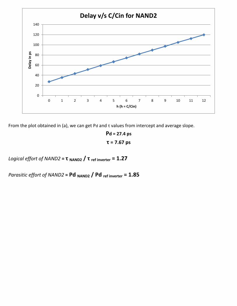
From the plot obtained in (a), we can get Pd and τ values from intercept and average slope.
Pd = 27.4 ps
τ = 7.67 ps
Logical effort of NAND2 = τ NAND2 / τ ref inverter = 1.27
Parasitic effort of NAND2 = Pd NAND2 / Pd ref inverter = 1.85
0
20
40
60
80
100
120
140
0 1 2 3 4 5 6 7 8 9 10 11 12
De
lay
in p
s
h (h = C/Cin)
Delay v/s C/Cin for NAND2

2. A load capacitance of 64Crin is driven by N inverters. Find the optimum inverter sizes for N = 2,3,4,5,
given that the first inverter is the reference inverter. Simulate each case in SPICE. How does it compare
with the delay values obtained in class?
Ans. *assumed non-integer size values allowed
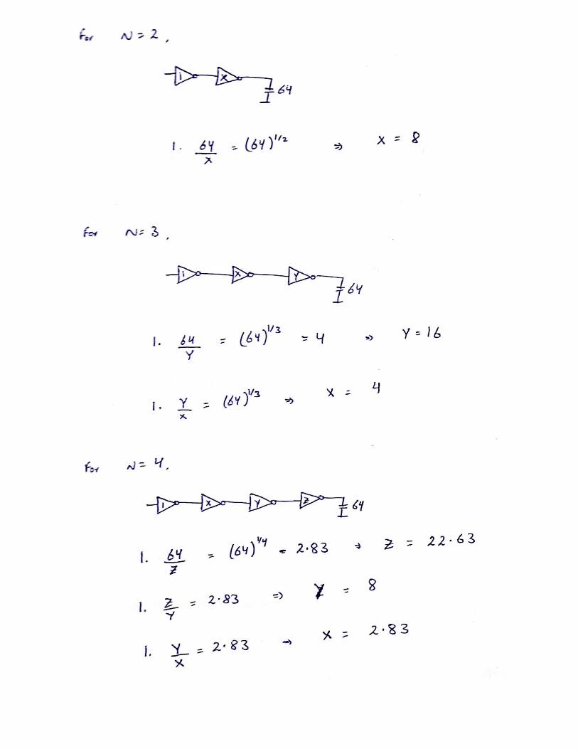

Figure 3: Vout v/s Vin for cascade of 4 CMOS inverters (for C =64Crin)
N tP1 (delay – class est.) (ps)
tP2 (delay - simulation) (ps)
Error (tP2 – tP1)
Error % (tP2 – tP1)/ tP2
2 216 208.8 -7.2 -3.5
3 180 211.6 31.6 14.9
4 183.8 233.7 49.9 21.4
5 197.8 285.1 87.3 30.6
Red-> Vin
Green-> Vout

Spice .cir file for Q 2) (N = 3)
*delay 3 inverters
.include tech180nm.txt
.subckt cmos_1 D G Sp Sn
m1 D G Sn Sn nfet l=0.18u w=0.27u ad=0.1539p as=0.1539p pd=1.35u ps=1.35u
m2 D G Sp Sp pfet l=0.18u w=0.54u ad=0.2439p as=0.2439p pd=1.44u ps=1.44u
.ends
.subckt cmos_n D G Sp Sn param: lambda = 0.09u n
m1 D G Sn Sn nfet l=0.18u w={3*n*lambda} ad={15*lambda*lambda*n} pd={(3*n*lambda)+(2*2*lambda)}
as={15*lambda*lambda*n} ps={(3*n*lambda)+(2*2*lambda)}
m2 D G Sp Sp pfet l=0.18u w={6*n*lambda} ad={30*lambda*lambda*n} pd={(6*n*lambda)+(2*2*lambda)}
as={30*lambda*lambda*n} ps={(6*n*lambda)+(2*2*lambda)}
.ends
x1 out in 1 0 cmos_1
x2 out2 out 1 0 cmos_n n=4
x3 out3 out2 1 0 cmos_n n=16
vd 1 0 1.8
c1 out3 0 c=78.4f
vgate in 0 PULSE 0 1.8 0p 10p 10p 1490ps 3000ps
*********** Transient Analysis and Results *****************************
.control
tran 1ps 8600ps
let p1 = 0
let p2 = 0
cursor p1 right V(in) 0.9 1 rising
let t1 = time[%p1]
cursor p2 right V(out3) 0.9 1 falling
let t2 = time[%p2]
let tf = t2-t1
cursor p1 right V(in) 0.9 1 falling
let t1 = time[%p1]
cursor p2 right V(out3) 0.9 1 rising
let t2 = time[%p2]
let tr = t2-t1
let d = 0.5*(tr+tf)
echo rise time = {tr}
echo fall time = {tf}
echo delay = {d}
plot v(in) v(out3) xlabel Time ylabel Voltage title '3 Inverters Delay'
.endc
.end
********************************************END**********************************************

Digital IC Design - Assignment 4 02/11/14
Aman Goel Roll No. EE11B087 Platform: SPICEOPUS (Windows), Magic (Ubuntu)
Q1. Design a four input NAND gate so that it has approximately the same rise and fall time as the reference
inverter. Use a linear delay model. Simulate the circuit using SPICE and find the propagation delay for each
of the following combinations of input slews (rise and fall time) and load capacitances.
(a) Input slew: 10ps, 50ps and 100ps
(b) Output capacitance: 5fF, 50fF and 100fF. Put your results in a tabular form (as a matrix).
Ans. 4 input NAND gate Design
(considered 4λ X 4λ contacts and separate S & D for each transistor)

Simulation in Spice Opus (input applied at A)
Figure 1: Vout v/s Vin for 4 i/p NAND gate (Vin = VA(Vin = VA, i/p slew =100ps, Cout = 100fF)
tP (delay) before layout ( ps )
Input Slew 10ps 50ps 100ps
Cout
5fF 107.57 113.47 119.94
50fF 321.67 327.15 333.63
100fF 555.05 560.49 567.08
Red-> VA
Green-> Vout

Q2. Use MAGIC and do the layout of the NAND gate as a standard cell of height 72l.
Ans.
MAGIC Layout
(Assumed input contacts from poly-gate can be taken outside 72λ height)
Figure 2: 4 input NAND gate MAGIC Layout

Figure 3: MAGIC LAYOUT (with grid)
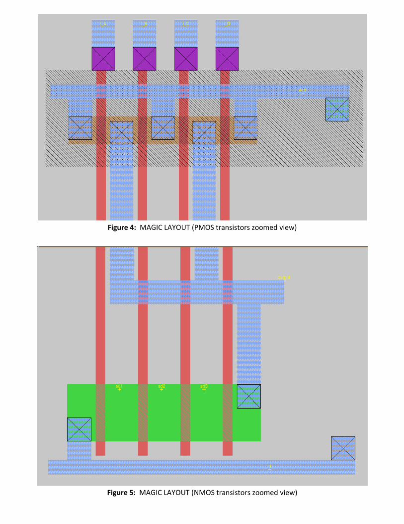
Figure 4: MAGIC LAYOUT (PMOS transistors zoomed view)
Figure 5: MAGIC LAYOUT (NMOS transistors zoomed view)
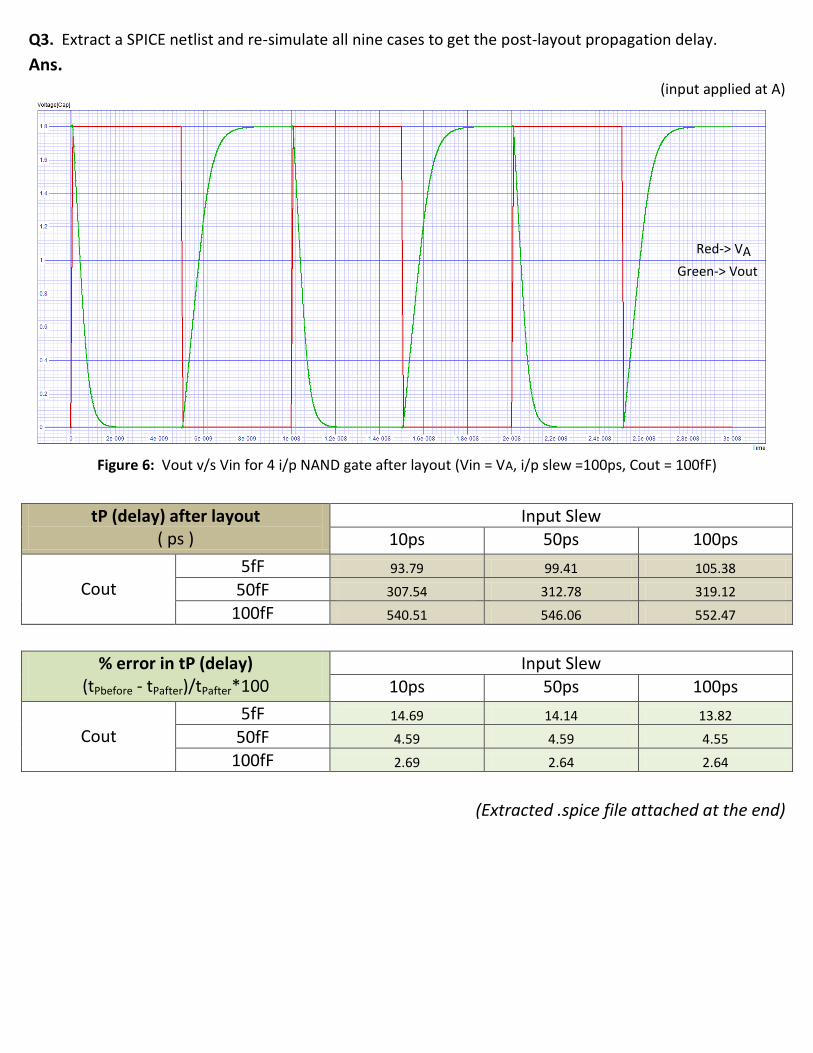
Q3. Extract a SPICE netlist and re-simulate all nine cases to get the post-layout propagation delay.
Ans.
(input applied at A)
Figure 6: Vout v/s Vin for 4 i/p NAND gate after layout (Vin = VA, i/p slew =100ps, Cout = 100fF)
tP (delay) after layout ( ps )
Input Slew 10ps 50ps 100ps
Cout
5fF 93.79 99.41 105.38
50fF 307.54 312.78 319.12
100fF 540.51 546.06 552.47
% error in tP (delay) (tPbefore - tPafter)/tPafter*100
Input Slew 10ps 50ps 100ps
Cout
5fF 14.69 14.14 13.82
50fF 4.59 4.59 4.55
100fF 2.69 2.64 2.64
(Extracted .spice file attached at the end)
Red-> VA
Green-> Vout

Spice .cir file befor layout for Q 1) (Input slew = 100ps, Cout = 100fF)
*nand_4 gate
.include tech180nm.txt
m5(output i_A Vdd Vdd) pfet l=0.18u w=0.54u ad = 0.243p pd = 1.44u as = 0.243p ps = 1.44u
m6(output i_B Vdd Vdd) pfet l=0.18u w=0.54u ad = 0.243p pd = 1.44u as = 0.243p ps = 1.44u
m7(output i_C Vdd Vdd) pfet l=0.18u w=0.54u ad = 0.243p pd = 1.44u as = 0.243p ps = 1.44u
m8(output i_D Vdd Vdd) pfet l=0.18u w=0.54u ad = 0.243p pd = 1.44u as = 0.243p ps = 1.44u
m1(sd1 i_A 0 0) nfet l=0.18u w=1.08u ad = 0.486p pd = 1.98u as = 0.486p ps = 1.98u
m2(sd2 i_B sd1 0) nfet l=0.18u w=1.08u ad = 0.486p pd = 1.98u as = 0.486p ps = 1.98u
m3(sd3 i_C sd2 0) nfet l=0.18u w=1.08u ad = 0.486p pd = 1.98u as = 0.486p ps = 1.98u
m4(output i_D sd3 0) nfet l=0.18u w=1.08u ad = 0.486p pd = 1.98u as = 0.486p ps = 1.98u
vsupply (Vdd 0) dc = 1.8
vb (i_B 0) dc = 1.8
vc (i_C 0) dc = 1.8
vd (i_D 0) dc = 1.8
va (i_A 0) pulse = (0 1.8 0p 100p 100p 4900p 10000p)
c1 (output 0) c=100f
*********** Transient Analysis and Results *****************************
.control
tran 1ps 30000ps
let ca = 0
let cb = 0
cursor ca right v(i_A) 0.9 1 falling
let a = time[%ca]
cursor cb right v(output) 0.9 1 rising
let b = time[%cb]
let tr = b-a
cursor ca right v(i_A) 0.9 1 rising
let a = time[%ca]
cursor cb right v(output) 0.9 1 falling
let b = time[%cb]
let tf = b-a
let d = 0.5*(tr+tf)
echo rise time = {tr}
echo fall time = {tf}
echo delay = {d}
plot v(i_A) v(output) xlabel Time ylabel Voltage[Cap]
.endc
.end
********************************************END**********************************************

.spice file after layout for Q 3)
* SPICE3 file created from NAND_4v2.ext - technology: sample_6m
.option scale=0.09u
M1000 output i_A Vdd Vdd pmos w=6 l=2
+ ad=84 pd=52 as=114 ps=74
M1001 Vdd i_B output Vdd pmos w=6 l=2
+ ad=0 pd=0 as=0 ps=0
M1002 output i_C Vdd Vdd pmos w=6 l=2
+ ad=0 pd=0 as=0 ps=0
M1003 Vdd i_D output Vdd pmos w=6 l=2
+ ad=0 pd=0 as=0 ps=0
M1004 sd1 i_A 0 gnd nmos w=12 l=2
+ ad=84 pd=38 as=72 ps=36
M1005 sd2 i_B sd1 gnd nmos w=12 l=2
+ ad=84 pd=38 as=0 ps=0
M1006 sd3 i_C sd2 gnd nmos w=12 l=2
+ ad=84 pd=38 as=0 ps=0
M1007 output i_D sd3 gnd nmos w=12 l=2
+ ad=72 pd=36 as=0 ps=0
********************************************END**********************************************
Spice .cir file after layout for Q 3) (Input slew = 100ps, Cout = 100fF)
*nand4 gate
.include tech180nm.txt
.include NAND_4v2.spice
vsupply (Vdd 0) dc = 1.8
vdum (gnd 0) 0
vb (i_B 0) dc = 1.8
vc (i_C 0) dc = 1.8
vd (i_D 0) dc = 1.8
va (i_A 0) pulse = (0 1.8 0p 100p 100p 4900p 10000p)
c1 (output 0) c=100f
*********** Transient Analysis and Results *****************************
.control
tran 1ps 30000ps
let ca = 0
let cb = 0

cursor ca right v(i_A) 0.9 1 falling
let a = time[%ca]
cursor cb right v(output) 0.9 1 rising
let b = time[%cb]
let tr = b-a
cursor ca right v(i_A) 0.9 1 rising
let a = time[%ca]
cursor cb right v(output) 0.9 1 falling
let b = time[%cb]
let tf = b-a
let d = 0.5*(tr+tf)
echo rise time = {tr}
echo fall time = {tf}
echo delay = {d}
plot v(i_A) v(output) xlabel Time ylabel Voltage[Cap]
.endc
.end
********************************************END**********************************************