digital fundamentals - web page for...
TRANSCRIPT
© 2009 Pearson Education, Upper Saddle River, NJ 07458. All Rights ReservedFloyd, Digital Fundamentals, 10th ed
Digital
FundamentalsTenth Edition
Floyd
Chapter 5
© 2008 Pearson Education© Modified by Yuttapong Jiraraksopakun
ENE, KMUTT 2009
© 2009 Pearson Education, Upper Saddle River, NJ 07458. All Rights ReservedFloyd, Digital Fundamentals, 10th ed
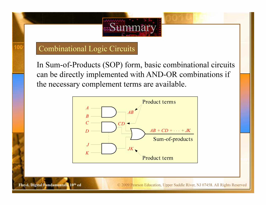
In Sum-of-Products (SOP) form, basic combinational circuits
can be directly implemented with AND-OR combinations if
the necessary complement terms are available.
Summary
Combinational Logic Circuits
JKJ
K
A
BAB
Product terms
Sum-of-products
Product term
C
D
CD
AB + CD + + JK. . .
© 2009 Pearson Education, Upper Saddle River, NJ 07458. All Rights ReservedFloyd, Digital Fundamentals, 10th ed
Summary
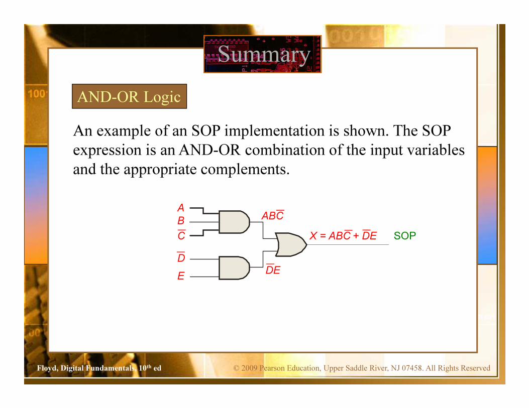
An example of an SOP implementation is shown. The SOP
expression is an AND-OR combination of the input variables
and the appropriate complements.
AND-OR Logic
SOP
DE
ABCA
B
C
E
D
X = ABC + DE
© 2009 Pearson Education, Upper Saddle River, NJ 07458. All Rights ReservedFloyd, Digital Fundamentals, 10th ed
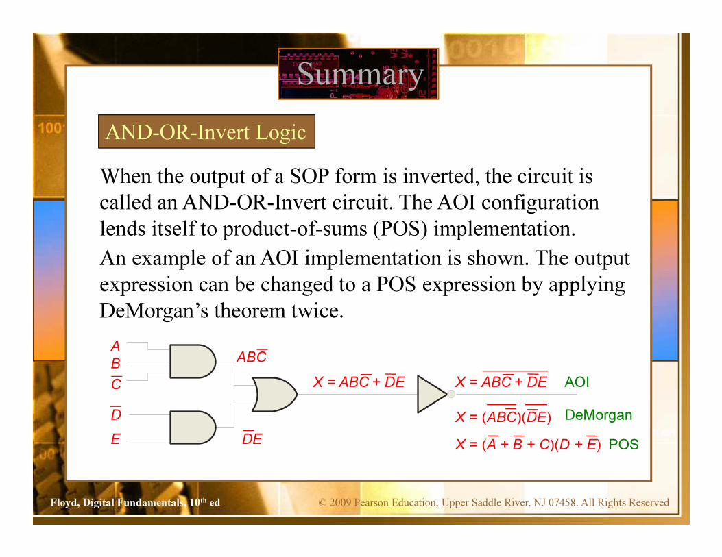
When the output of a SOP form is inverted, the circuit is
called an AND-OR-Invert circuit. The AOI configuration
lends itself to product-of-sums (POS) implementation.
Summary
An example of an AOI implementation is shown. The output
expression can be changed to a POS expression by applying
DeMorgan’s theorem twice.
AND-OR-Invert Logic
POSDE
ABCA
B
C
E
D
X = ABC + DE X = ABC + DE
X = (A + B + C)(D + E)
X = (ABC)(DE)
AOI
DeMorgan

© 2009 Pearson Education, Upper Saddle River, NJ 07458. All Rights ReservedFloyd, Digital Fundamentals, 10th ed
AO or AOI can be used
for positive- or
negative-logic control
circuits
Summary
Example Logic
© 2009 Pearson Education, Upper Saddle River, NJ 07458. All Rights ReservedFloyd, Digital Fundamentals, 10th ed
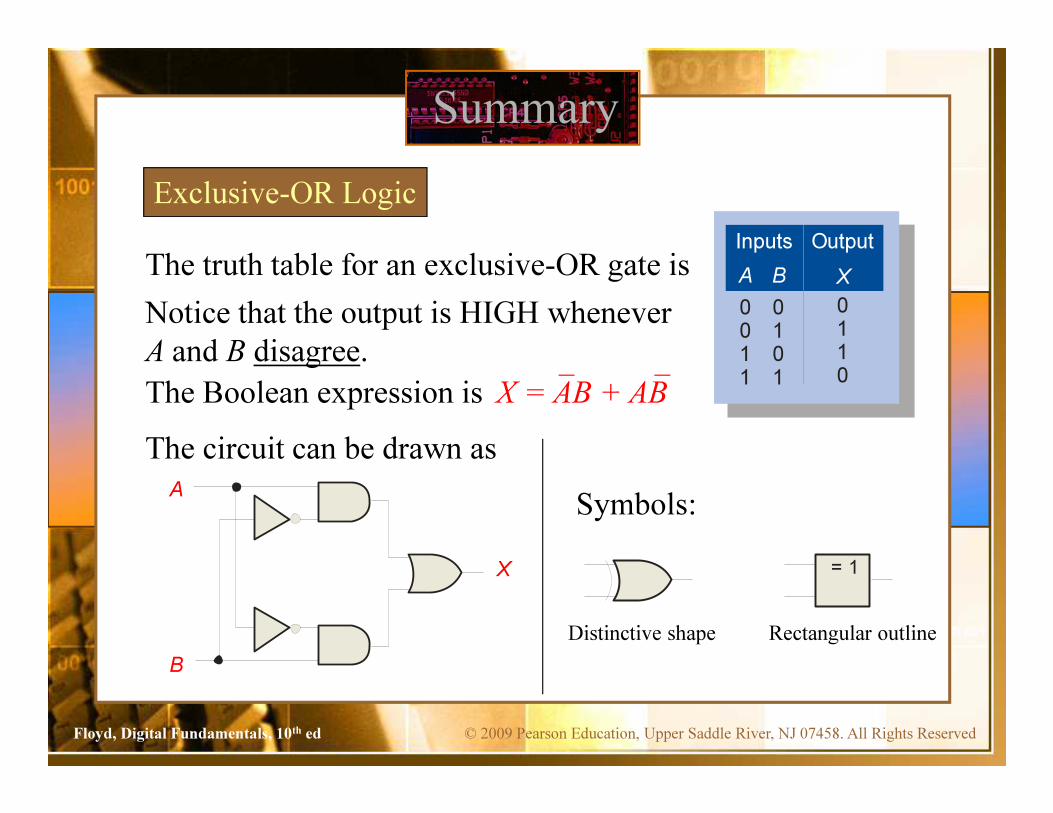
The truth table for an exclusive-OR gate is
Summary
Exclusive-OR Logic
A
B
OutputInputs
A B X
0011
0101
0110
Notice that the output is HIGH whenever
A and B disagree.
The Boolean expression is
The circuit can be drawn as
X = 1
Symbols:
Distinctive shape Rectangular outline
X = AB + AB

© 2009 Pearson Education, Upper Saddle River, NJ 07458. All Rights ReservedFloyd, Digital Fundamentals, 10th ed
Summary
Even-parity generator/checker

© 2009 Pearson Education, Upper Saddle River, NJ 07458. All Rights ReservedFloyd, Digital Fundamentals, 10th ed
The truth table for an exclusive-NOR gate is
Summary
Exclusive-NOR Logic
A
B
Notice that the output is HIGH whenever
A and B agree.
The Boolean expression is
The circuit can be drawn as
X
Symbols:
Distinctive shape Rectangular outline
OutputInputs
A B X
0011
0101
1001
= 1
X = AB + AB
© 2009 Pearson Education, Upper Saddle River, NJ 07458. All Rights ReservedFloyd, Digital Fundamentals, 10th ed
Summary
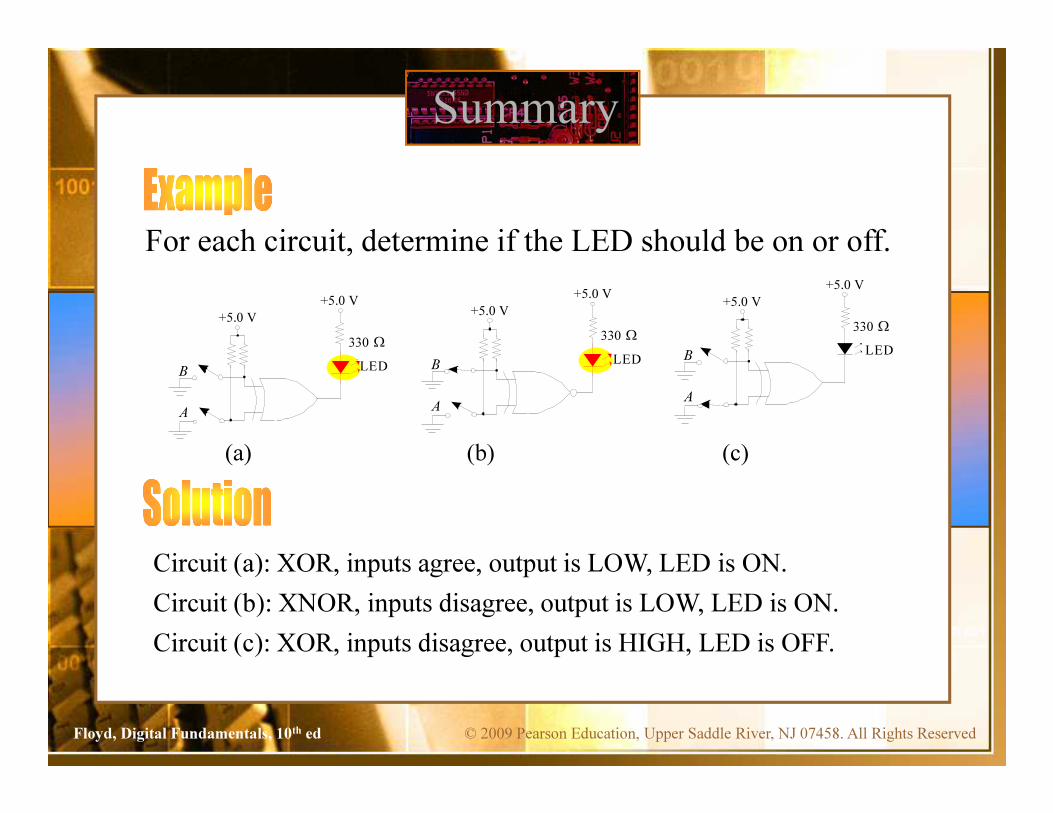
For each circuit, determine if the LED should be on or off.
+5.0 V
+5.0 V
330 Ω
LEDB
A
+5.0 V
+5.0 V
330 Ω
LEDB
A
+5.0 V
+5.0 V
330 Ω
LEDB
A
(a) (b) (c)
Circuit (a): XOR, inputs agree, output is LOW, LED is ON.
Circuit (b): XNOR, inputs disagree, output is LOW, LED is ON.
Circuit (c): XOR, inputs disagree, output is HIGH, LED is OFF.

© 2009 Pearson Education, Upper Saddle River, NJ 07458. All Rights ReservedFloyd, Digital Fundamentals, 10th ed
Implementing a SOP expression is done by first forming the
AND terms; then the terms are ORed together.
Summary
Implementing Combinational Logic
Show the circuit that will implement the Boolean expression
X = ABC + ABD + BDE. (Assume that the variables and
their complements are available.)
C
AB
E
D
B
A
B
D
Start by forming the terms using three 3-input AND gates.
Then combine the three terms using a 3-input OR gate.
X = ABC + ABD + BDE

© 2009 Pearson Education, Upper Saddle River, NJ 07458. All Rights ReservedFloyd, Digital Fundamentals, 10th ed
For basic combinational logic circuits, the Karnaugh map
can be read and the circuit drawn as a minimum SOP.
Summary
Karnaugh Map Implementation
A Karnaugh map is drawn from a truth table. Read the
minimum SOP expression and draw the circuit.
1. Group the 1’s into two overlapping
groups as indicated.
2. Read each group by eliminating any
variable that changes across a boundary.
C C
AB
AB
AB
AB
1
1 1
C C
AB
AB
AB
AB
1
1 1
B changes
across this
boundary
C changes
across this
boundary
3. The vertical group is read AC.
4. The horizontal group is read AB.
The circuit is on the next slide:

© 2009 Pearson Education, Upper Saddle River, NJ 07458. All Rights ReservedFloyd, Digital Fundamentals, 10th ed
Summary
Circuit:
C
A
A
CA + A B
continued…
X =
The result is shown as a sum of products.
B

© 2009 Pearson Education, Upper Saddle River, NJ 07458. All Rights ReservedFloyd, Digital Fundamentals, 10th ed
Summary
= ABC + ABCD + ABCD+ ABCD

© 2009 Pearson Education, Upper Saddle River, NJ 07458. All Rights ReservedFloyd, Digital Fundamentals, 10th ed
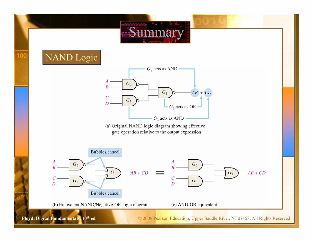
Summary
It is a simple matter to implement this form using only
NAND gates as shown in the text and following example.
© 2009 Pearson Education, Upper Saddle River, NJ 07458. All Rights ReservedFloyd, Digital Fundamentals, 10th ed
Summary
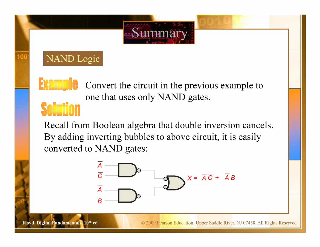
NAND Logic
Convert the circuit in the previous example to
one that uses only NAND gates.
Recall from Boolean algebra that double inversion cancels.
By adding inverting bubbles to above circuit, it is easily
converted to NAND gates:
C
A
B
A
CA + A BX =
© 2009 Pearson Education, Upper Saddle River, NJ 07458. All Rights ReservedFloyd, Digital Fundamentals, 10th ed
Summary
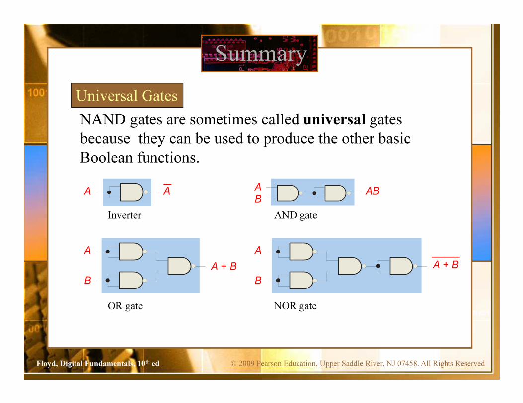
NAND gates are sometimes called universal gates
because they can be used to produce the other basic
Boolean functions.
Universal Gates
Inverter
AA
AND gate
A
BAB
A
B
A + B
OR gate
A
B
A + B
NOR gate
© 2009 Pearson Education, Upper Saddle River, NJ 07458. All Rights ReservedFloyd, Digital Fundamentals, 10th ed
Summary
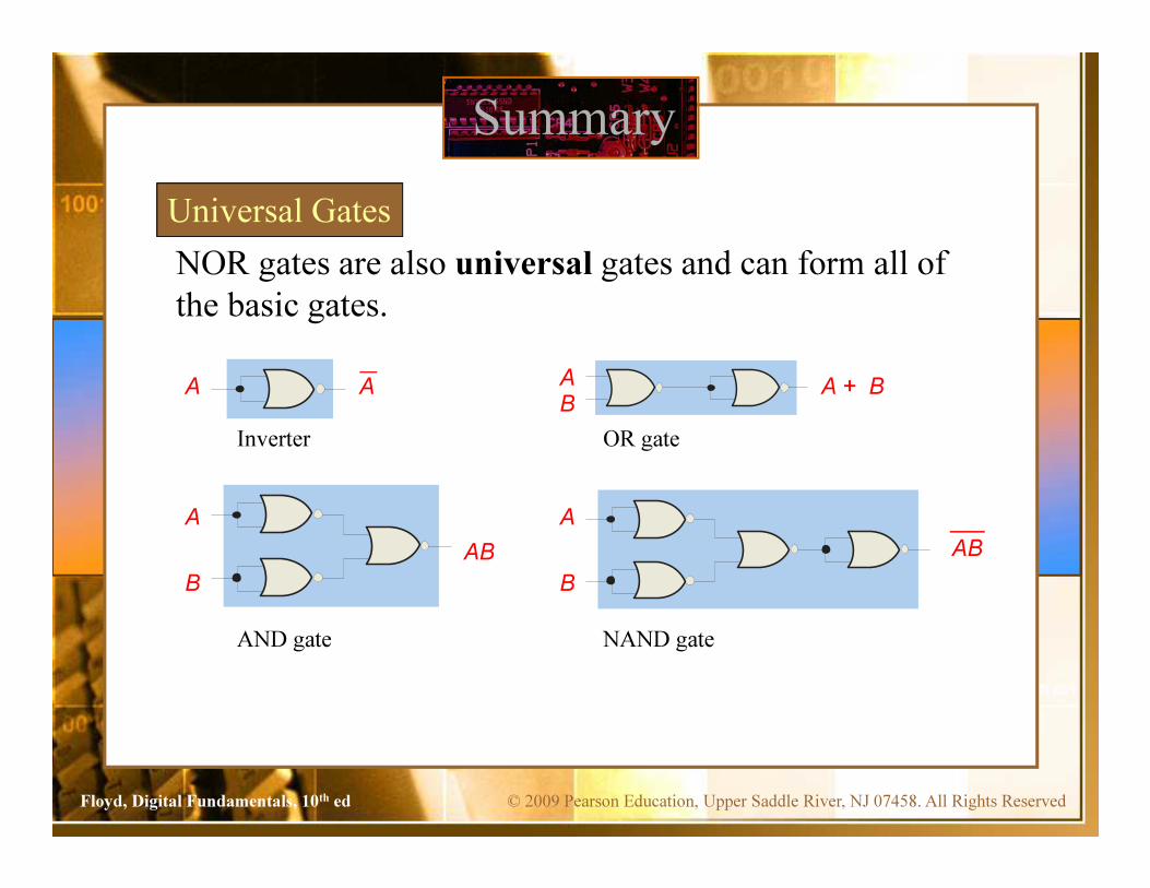
NOR gates are also universal gates and can form all of
the basic gates.
Universal Gates
Inverter
AA
OR gate
A
BA + B
A
B
AB
AND gate
A
B
AB
NAND gate
© 2009 Pearson Education, Upper Saddle River, NJ 07458. All Rights ReservedFloyd, Digital Fundamentals, 10th ed
Summary
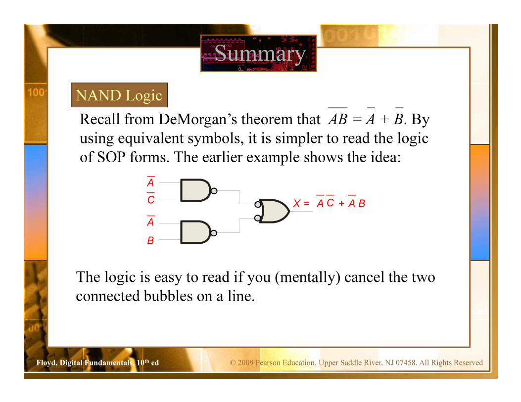
Recall from DeMorgan’s theorem that AB = A + B. By
using equivalent symbols, it is simpler to read the logic
of SOP forms. The earlier example shows the idea:
NAND Logic
C
A
B
A
CA + A BX =
The logic is easy to read if you (mentally) cancel the two
connected bubbles on a line.
© 2009 Pearson Education, Upper Saddle River, NJ 07458. All Rights ReservedFloyd, Digital Fundamentals, 10th ed
Summary
NAND Logic
© 2009 Pearson Education, Upper Saddle River, NJ 07458. All Rights ReservedFloyd, Digital Fundamentals, 10th ed
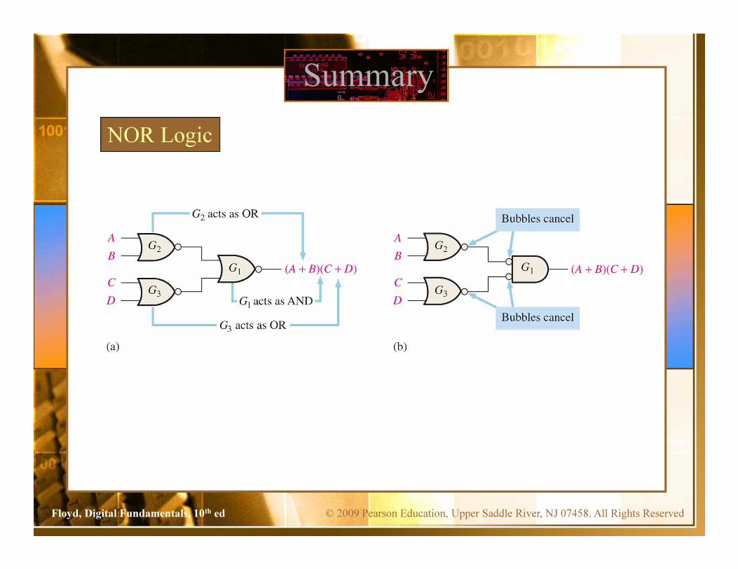
Summary
NOR Logic
B
A
C
A
X =
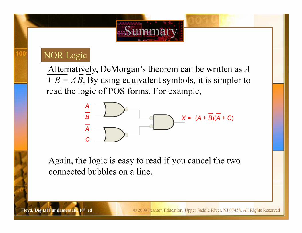
Again, the logic is easy to read if you cancel the two
connected bubbles on a line.
Alternatively, DeMorgan’s theorem can be written as A
+ B = AB. By using equivalent symbols, it is simpler to
read the logic of POS forms. For example,
(A + B)(A + C)
© 2009 Pearson Education, Upper Saddle River, NJ 07458. All Rights ReservedFloyd, Digital Fundamentals, 10th ed
Summary
NOR Logic

© 2009 Pearson Education, Upper Saddle River, NJ 07458. All Rights ReservedFloyd, Digital Fundamentals, 10th ed
Summary
Pulsed Waveforms
For combinational circuits with pulsed inputs, the output
can be predicted by developing intermediate outputs and
combining the result. For example, the circuit shown can
be analyzed at the outputs of the OR gates:
A
B
C
D
A
B
C
D
G1
G2
G3
G1
G2
G3

© 2009 Pearson Education, Upper Saddle River, NJ 07458. All Rights ReservedFloyd, Digital Fundamentals, 10th ed
Summary
Pulsed Waveforms
Alternatively, you can develop the truth table for
the circuit and enter 0’s and 1’s on the waveforms.
Then read the output from the table.
A
B
C
D
A
B
C
D
G1
G2
G3
G3
Inputs
A B C D
Output
0 0 0 00 0 0 10 0 1 00 0 1 10 1 0 00 1 0 10 1 1 00 1 1 11 0 0 01 0 0 11 0 1 01 0 1 11 1 0 01 1 0 11 1 1 01 1 1 1
0 1 0 1 0 1 0 1 0 1
0 1 1 0 0 1 1 0 0 0
0 0 0 1 1 1 1 0 0 0
0 0 0 0 0 0 0 1 1 0
0 0 0 0 1 1 1 0 1 0
X
01110111
00000111

© 2009 Pearson Education, Upper Saddle River, NJ 07458. All Rights ReservedFloyd, Digital Fundamentals, 10th ed
Homework 8
• Chapter 5 (4, 12, 21, 32, 35)