digital electronics - khulna university
TRANSCRIPT

Digital Electronics ECE 2203
Professor Dr. Md. Shamim Ahsan Electronics and Communication Engineering Discipline
Khulna University.
Lecture 3
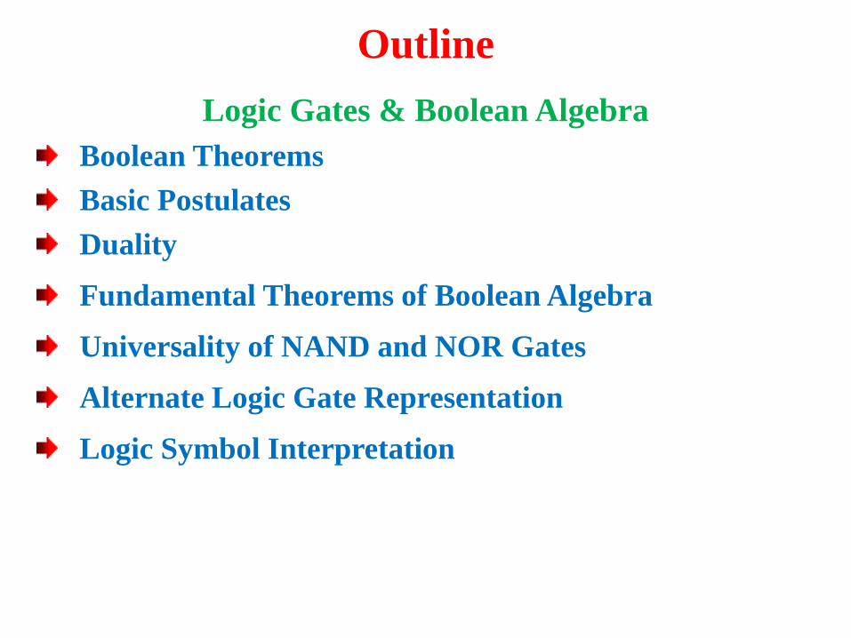
Logic Gates & Boolean Algebra
Boolean Theorems
Basic Postulates
Duality
Fundamental Theorems of Boolean Algebra
Universality of NAND and NOR Gates
Alternate Logic Gate Representation
Logic Symbol Interpretation
Outline

Logic Gates & Boolean Algebra
Boolean Theorems:
• We have seen how Boolean algebra can be used to help analyze a logic circuit
and express its operation mathematically.
• We will continue our study of Boolean algebra by investigating the various
Boolean theorems (rules) that can help us to simplify logic expressions and
logic circuits.
Basic Postulates:

Logic Gates & Boolean Algebra
Basic Postulates:

Logic Gates & Boolean Algebra
Duality:
• The principle of duality is a very important concept in Boolean algebra.
Briefly stated, the principle of duality pronounces that, if an expression is valid
in Boolean algebra, the dual of the expression is also valid.
• The expression is found by replacing all „+‟ operators with „.‟, all „.‟ operators
with „+‟, all ones with zeros, and all zeros with ones.
• The principle of duality will be used extensively in proving Boolean algebra
theorems. In fact, once we have employed the postulates and previously
proven theorems to demonstrate the validity of one expression, duality can be
used to prove the validity of the dual expressions.
Example (1): Find the dual expression ~ a + (bc) = (a + b)(a + c)
Solution:
a(b + c) = ab + ac
When obtaining a dual, we must be careful not to alter the location of
parentheses, if they are present.

Logic Gates & Boolean Algebra
Fundamental Theorems of Boolean Algebra:
Table 1. Summary of the fundamental postulates & theorems of Boolean algebra.
Expression Dual

Logic Gates & Boolean Algebra
Proof of 1(a): Proof of 1(b)
a.a = aa + 0 [P-2(a)]
= aa + aa [P-6(b)]
= a(a + a) [P-5(b)]
= a.1 [P-6(a)]
= a [P-2(b)]
Proof of 2(a): Proof of 2(b)
a.0 = 0 by duality

Logic Gates & Boolean Algebra
Example (2):
(i)
(ii)
(iii)
Proof of 4(a): Proof of 4(b)
a(a + b) = (a + 0)(a + b) [P-2(a)]
= a + 0.b [P-5(a)]
= a + 0 [P-2(b)]
= a [P-2(a)]

Logic Gates & Boolean Algebra
Example (3):
(i)
(ii)
(iii)
(iv)
Proof of 5(a): Proof of 5(b)
a(a + b) = aa + ab [P-5(b)]
= 0 + ab [P-6(b)]
= ab [P-2(a)]
Logic Gates & Boolean Algebra
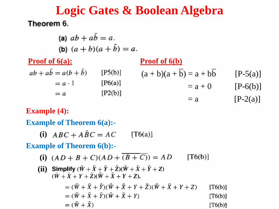
Example (4):
Example of Theorem 6(a):-
(i)
Example of Theorem 6(b):-
(i)
(ii)
Proof of 6(a): Proof of 6(b)
(a + b)(a + b) = a + bb [P-5(a)]
= a + 0 [P-6(b)]
= a [P-2(a)]

Logic Gates & Boolean Algebra
Example (5):
Example of Theorem 7(a):-
(i)
(ii)
Example of Theorem 7(b):-
(i)
(ii)
Proof of 7(a): Proof of 7(b)
(a + b)(a + b + c) = a + b(b + c) [P-5(a)]
= a + bb + bc [P-5(b)]
= a + 0 + bc [P-2(a)]
= a + bc [P-2(a)]
= (a + b)(a + c) [P-5(a)]

Logic Gates & Boolean Algebra
Proof of 8(a):

Logic Gates & Boolean Algebra
Proof of 8(a) (Continued):
Logic Gates & Boolean Algebra
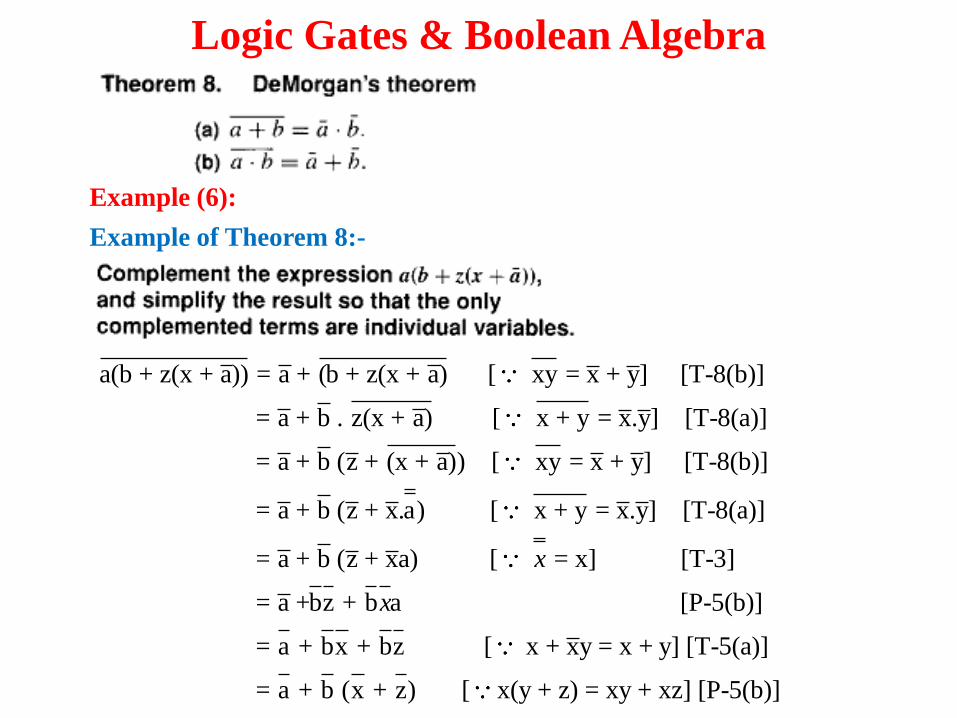
Example (6):
Example of Theorem 8:-
a(b + z(x + a)) = a + (b + z(x + a) [ xy = x + y] [T-8(b)]
= a + b . z(x + a) [ x + y = x.y] [T-8(a)]
= a + b (z + (x + a)) [ xy = x + y] [T-8(b)]
= a + b (z + x.a) [ x + y = x.y] [T-8(a)]
= a + b (z + xa) [ = x] [T-3]
x
= a +bz + b a [P-5(b)]
= a + bx + bz [ x + xy = x + y] [T-5(a)]
= a + b (x + z) [ x(y + z) =
x
xy + xz] [P-5(b)]

Example (7):
Example of Theorem 9(a):-
(i)
(ii)
Example of Theorem 9(b):-
(i)
Logic Gates & Boolean Algebra
Proof of 9(a):
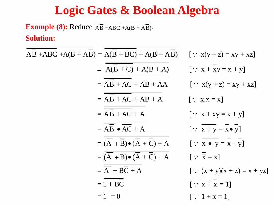
Example (8): Reduce .
Solution:
Logic Gates & Boolean Algebra
AB +ABC +A(B + AB)
AB +ABC +A(B + AB) = A(B + BC) + A(B + AB) [ x(y + z) = xy + xz]
A(B + C) + A(B + A) [ x + xy = x + y]
= A
B + AC + AB + AA [ x(y + z) = xy + xz]
= AB + AC + AB + A [ x.x = x]
= AB + AC + A [ x + xy = x + y]
= AB AC + A [ x + y = x y]
= (A B) (A + C) + A [ x y = x y
]
= (A B) (A + C) + A [ x = x]
= A + BC + A [ (x + y)(x + z) = x + yz]
= 1 + BC [ x + x = 1]
= 1 = 0 [ 1 + x = 1]
Logic Gates & Boolean Algebra
Universality of NAND and NOR Gates:
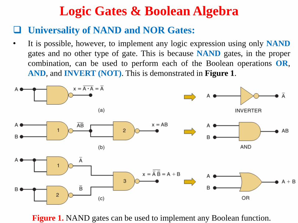
• It is possible, however, to implement any logic expression using only NAND
gates and no other type of gate. This is because NAND gates, in the proper
combination, can be used to perform each of the Boolean operations OR,
AND, and INVERT (NOT). This is demonstrated in Figure 1.
Figure 1. NAND gates can be used to implement any Boolean function.

Logic Gates & Boolean Algebra
Universality of NAND and NOR Gates:
• In a similar manner, it can be shown that NOR gates can be arranged to
implement any of the Boolean operations. This is illustrated in Figure 2.
That’s why NAND and NOR gates are called Universal Gates.
Figure 2. NOR gates can be used to implement any Boolean function.

Problem (Tocci-C 3-28):
.
Figure 3-53(b)
Solution:
• The output expression of Figure 3-53(b) is ~
• The equivalent circuit of Figure 3-53(b) using only NAND gates is shown in
Figure 3.
Logic Gates & Boolean Algebra
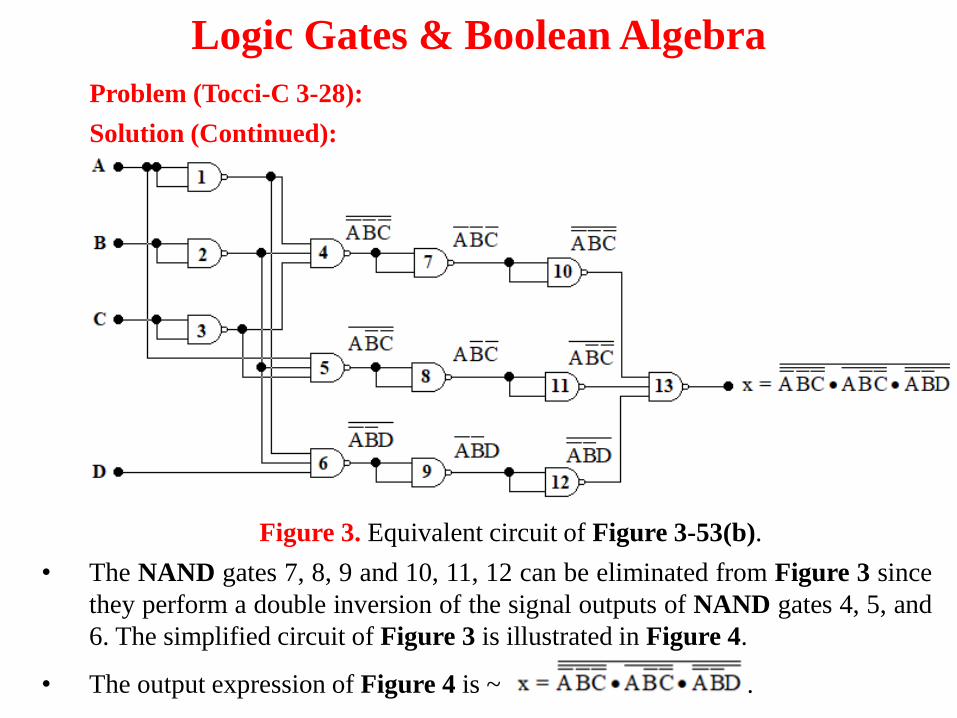
Problem (Tocci-C 3-28):
Solution (Continued):
Figure 3. Equivalent circuit of Figure 3-53(b).
• The NAND gates 7, 8, 9 and 10, 11, 12 can be eliminated from Figure 3 since
they perform a double inversion of the signal outputs of NAND gates 4, 5, and
6. The simplified circuit of Figure 3 is illustrated in Figure 4.
• The output expression of Figure 4 is ~ .
Logic Gates & Boolean Algebra
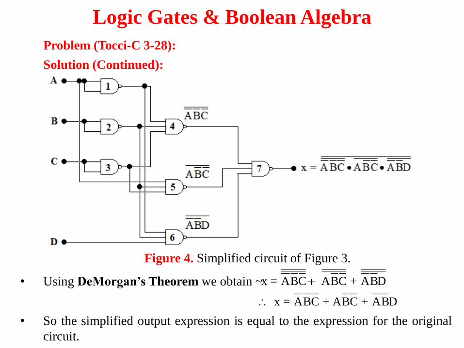
Problem (Tocci-C 3-28):
Solution (Continued):
Figure 4. Simplified circuit of Figure 3.
• Using DeMorgan‟s Theorem we obtain ~
• So the simplified output expression is equal to the expression for the original
circuit.
Logic Gates & Boolean Algebra
x = ABC ABC + ABD
x = ABC + ABC + ABD

Logic Gates & Boolean Algebra
Alternate Logic-gate Representation:
• Although you may find that some circuit diagrams still use these standard
symbols exclusively, it has become increasingly more common to find circuit
diagrams that utilize alternate logic symbols in addition to the standard
symbols shown in Figure 5.
Figure 5. Standard and alternate symbols for various logic gates. .

Logic Gates & Boolean Algebra
Logic Symbol Interpretation:
• When an input or output line on a logic circuit symbol has no bubble on ot,
that line is said to be active-HIGH. When an input or output line does have a
bubble on it, that line is said to be active-LOW.
• To illustrate, Figure 6(a) shows the standard symbol for a NAND gate. It has
an active-LOW output and active-HIGH inputs. The logic operation
represented by this symbol can therefore be interpreted as follows:
“The output goes LOW only when all of the inputs are HIGH.”
Figure 6. Interpretation of the two NAND gate symbols. .

Logic Gates & Boolean Algebra
Logic Symbol Interpretation:
• The alternate symbol for a NAND gate shown in Figure 6(b) has an active-
HIGH output and active-LOW inputs, and so its operation can be stated as
follows:
“The out goes HIGH when any input is LOW.”
• For now, let us summarize the important points concerning the logic-gate
representations.
(1) To obtain the alternate symbol for a logic gate, take the standard symbol
and change its operation symbol (OR to AND, or AND to OR), and
change the bubbles on both inputs and output (i.e. delete bubbles that are
present, and add bubbles where there are none).
(2) To interpret the logic-gate operation, first note which logic state, 0 or 1, is
the active state for the inputs and which is the active state for the output.
Then realize that the output’s active state is produced by having all of the
inputs in their active state (if an AND symbol is used) or by having any
of the inputs in its active state (if an OR symbol is used).
Self Study: Tocci-3-14

Problem (Tocci-B 3-40):
Figure 3-59
Solution:
• The active state of the output of Figure 3-59 is active-HIGH or 1. Inputs to the
Gate-3 is active LOW. So any one of the inputs to the OR gate is 0, the output
goes to 1. So, D should be 0.
• So, E should be 1. When B and C are 0, the output of the Gate-2 will be 0.
• Again when B = 1 and A = 0, then the output of the Gate-1 will be 0.
• So, X will go HIGH when E = 1, or D = 0, or B = C = 0, or when B = 1 and A
= 0.
Logic Gates & Boolean Algebra
Logic Gates & Boolean Algebra
Homework:
• Problems-Tocci-Chapter 3:- 3.1, 3.6, 3.12 to 3.21, 3.24 to 3.31,
3.38.

References
[1] “Digital Systems: Principles and Applications,” Neal S. Widmer,
Gregory L. Moss, and Ronald J. Tocci, 12th Ed., Pearson (2018).
[2] “Digital Logic and Computer Design,” M. Morris Mano, 1st Ed.,
Pearson (2016).
[3] “Digital Logic Circuit Analysis and Design,” Victor P. Nelson, H.
Troy Nagle, Bill D. Carroll, and David Irwin, 1st Ed., Pearson
(1995).